mc68hc908ld60 technical data - nxp
TRANSCRIPT

M68HC08Microcontrollers
freescale.com
MC68HC908LD60Technical Data
Rev. 1.1MC68HC908LD60/DAugust 16, 2005

MC68HC908LD60Technical Data
Freescale reserves the right to make changes without further notice to any productsherein. Freescale makes no warranty, representation or guarantee regarding thesuitability of its products for any particular purpose, nor does Freescale assume anyliability arising out of the application or use of any product or circuit, and specificallydisclaims any and all liability, including without limitation consequential or incidentaldamages. "Typical" parameters which may be provided in Freescale data sheetsand/or specifications can and do vary in different applications and actual performancemay vary over time. All operating parameters, including "Typicals" must be validatedfor each customer application by customer's technical experts. Freescale does notconvey any license under its patent rights nor the rights of others. Freescale productsare not designed, intended, or authorized for use as components in systems intendedfor surgical implant into the body, or other applications intended to support or sustainlife, or for any other application in which the failure of the Freescale product couldcreate a situation where personal injury or death may occur. Should Buyer purchase oruse Freescale products for any such unintended or unauthorized application, Buyershall indemnify and hold Freescale and its officers, employees, subsidiaries, affiliates,and distributors harmless against all claims, costs, damages, and expenses, andreasonable attorney fees arising out of, directly or indirectly, any claim of personalinjury or death associated with such unintended or unauthorized use, even if such claimalleges that Freescale was negligent regarding the design or manufacture of the part.Freescale, Inc. is an Equal Opportunity/Affirmative Action Employer.
© Freescale, Inc., 2001
MC68HC908LD60 — Rev. 1.1 Technical Data
Freescale Semiconductor Technical Data 3

Technical Data
Technical Data MC68HC908LD60 — Rev. 1.1
4 Technical Data Freescale Semiconductor
Technical Data — MC68HC908LD60
List of Sections
Section 1. General Description . . . . . . . . . . . . . . . . . . . . 31
Section 2. Memory Map . . . . . . . . . . . . . . . . . . . . . . . . . . 39
Section 3. Random-Access Memory (RAM) . . . . . . . . . . 53
Section 4. FLASH Memory . . . . . . . . . . . . . . . . . . . . . . . . 55
Section 5. Configuration Register (CONFIG) . . . . . . . . . 67
Section 6. Central Processor Unit (CPU) . . . . . . . . . . . . 69
Section 7. Oscillator (OSC) . . . . . . . . . . . . . . . . . . . . . . . 89
Section 8. Clock Generator Module (CGM). . . . . . . . . . . 93
Section 9. System Integration Module (SIM) . . . . . . . . 107
Section 10. Monitor ROM (MON) . . . . . . . . . . . . . . . . . . 131
Section 11. Timer Interface Module (TIM) . . . . . . . . . . . 143
Section 12. Pulse Width Modulator (PWM) . . . . . . . . . . 165
Section 13. Analog-to-Digital Converter (ADC) . . . . . . 171
Section 14. Multi-Master IIC Interface (MMIIC) . . . . . . . 181
Section 15. DDC12AB Interface . . . . . . . . . . . . . . . . . . . 195
Section 16. Sync Processor . . . . . . . . . . . . . . . . . . . . . . 211
Section 17. Input/Output (I/O) Ports . . . . . . . . . . . . . . . 231
Section 18. External Interrupt (IRQ) . . . . . . . . . . . . . . . 251
Section 19. Keyboard Interrupt Module (KBI). . . . . . . . 257
Section 20. Computer Operating Properly (COP) . . . . 265
Section 21. Break Module (BRK) . . . . . . . . . . . . . . . . . . 271
Section 22. Electrical Specifications. . . . . . . . . . . . . . . 279
Section 23. Mechanical Specifications . . . . . . . . . . . . . 287
Section 24. Ordering Information . . . . . . . . . . . . . . . . . 289
MC68HC908LD60 — Rev. 1.1 Technical Data
Freescale Semiconductor List of Sections 5

List of Sections
Technical Data MC68HC908LD60 — Rev. 1.1
6 List of Sections Freescale Semiconductor

Technical Data — MC68HC908LD60
Table of Contents
Section 1. General Description
1.1 Contents . . . . . . . . . . . . . . . . . . . . . . . . . . . . . . . . . . . . . . . . . .31
1.2 Introduction . . . . . . . . . . . . . . . . . . . . . . . . . . . . . . . . . . . . . . . .31
1.3 Features . . . . . . . . . . . . . . . . . . . . . . . . . . . . . . . . . . . . . . . . . .32
1.4 MCU Block Diagram . . . . . . . . . . . . . . . . . . . . . . . . . . . . . . . . .34
1.5 Pin Assignments . . . . . . . . . . . . . . . . . . . . . . . . . . . . . . . . . . . .35
1.6 Pin Functions . . . . . . . . . . . . . . . . . . . . . . . . . . . . . . . . . . . . . .36
Section 2. Memory Map
2.1 Contents . . . . . . . . . . . . . . . . . . . . . . . . . . . . . . . . . . . . . . . . . .39
2.2 Introduction . . . . . . . . . . . . . . . . . . . . . . . . . . . . . . . . . . . . . . . .39
2.3 Unimplemented Memory Locations . . . . . . . . . . . . . . . . . . . . .39
2.4 Reserved Memory Locations . . . . . . . . . . . . . . . . . . . . . . . . . .40
2.5 Input/Output (I/O) Section. . . . . . . . . . . . . . . . . . . . . . . . . . . . .40
Section 3. Random-Access Memory (RAM)
3.1 Contents . . . . . . . . . . . . . . . . . . . . . . . . . . . . . . . . . . . . . . . . . .53
3.2 Introduction . . . . . . . . . . . . . . . . . . . . . . . . . . . . . . . . . . . . . . . .53
3.3 Functional Description . . . . . . . . . . . . . . . . . . . . . . . . . . . . . . .53
Section 4. FLASH Memory
4.1 Contents . . . . . . . . . . . . . . . . . . . . . . . . . . . . . . . . . . . . . . . . . .55
4.2 Introduction . . . . . . . . . . . . . . . . . . . . . . . . . . . . . . . . . . . . . . . .55
MC68HC908LD60 — Rev. 1.1 Technical Data
Freescale Semiconductor Table of Contents 7
Table of Contents
4.3 Functional Description . . . . . . . . . . . . . . . . . . . . . . . . . . . . . . .56
4.4 FLASH Control Registers . . . . . . . . . . . . . . . . . . . . . . . . . . . . .574.4.1 13k-Byte FLASH Even Byte Write Buffer (13KEBUF) . . . . .59
4.5 FLASH Block Erase Operation . . . . . . . . . . . . . . . . . . . . . . . . .59
4.6 FLASH Mass Erase Operation . . . . . . . . . . . . . . . . . . . . . . . . .60
4.7 FLASH Program Operation. . . . . . . . . . . . . . . . . . . . . . . . . . . .61
4.8 FLASH Block Protection . . . . . . . . . . . . . . . . . . . . . . . . . . . . . .624.8.1 FLASH Block Protect Registers . . . . . . . . . . . . . . . . . . . . . .64
Section 5. Configuration Register (CONFIG)
5.1 Contents . . . . . . . . . . . . . . . . . . . . . . . . . . . . . . . . . . . . . . . . . .67
5.2 Introduction . . . . . . . . . . . . . . . . . . . . . . . . . . . . . . . . . . . . . . . .67
5.3 Functional Description . . . . . . . . . . . . . . . . . . . . . . . . . . . . . . .67
5.4 Configuration Register . . . . . . . . . . . . . . . . . . . . . . . . . . . . . . .68
Section 6. Central Processor Unit (CPU)
6.1 Contents . . . . . . . . . . . . . . . . . . . . . . . . . . . . . . . . . . . . . . . . . .69
6.2 Introduction . . . . . . . . . . . . . . . . . . . . . . . . . . . . . . . . . . . . . . . .69
6.3 Features . . . . . . . . . . . . . . . . . . . . . . . . . . . . . . . . . . . . . . . . . .70
6.4 CPU Registers . . . . . . . . . . . . . . . . . . . . . . . . . . . . . . . . . . . . .706.4.1 Accumulator . . . . . . . . . . . . . . . . . . . . . . . . . . . . . . . . . . . . .716.4.2 Index Register . . . . . . . . . . . . . . . . . . . . . . . . . . . . . . . . . . .726.4.3 Stack Pointer . . . . . . . . . . . . . . . . . . . . . . . . . . . . . . . . . . . .726.4.4 Program Counter . . . . . . . . . . . . . . . . . . . . . . . . . . . . . . . . .736.4.5 Condition Code Register . . . . . . . . . . . . . . . . . . . . . . . . . . .73
6.5 Arithmetic/Logic Unit (ALU) . . . . . . . . . . . . . . . . . . . . . . . . . . .76
6.6 Low-Power Modes . . . . . . . . . . . . . . . . . . . . . . . . . . . . . . . . . .766.6.1 Wait Mode . . . . . . . . . . . . . . . . . . . . . . . . . . . . . . . . . . . . . .766.6.2 Stop Mode . . . . . . . . . . . . . . . . . . . . . . . . . . . . . . . . . . . . . .77
6.7 CPU During Break Interrupts . . . . . . . . . . . . . . . . . . . . . . . . . .77
Technical Data MC68HC908LD60 — Rev. 1.1
8 Table of Contents Freescale Semiconductor
Table of Contents
6.8 Instruction Set Summary . . . . . . . . . . . . . . . . . . . . . . . . . . . . .77
6.9 Opcode Map . . . . . . . . . . . . . . . . . . . . . . . . . . . . . . . . . . . . . . .77
Section 7. Oscillator (OSC)
7.1 Contents . . . . . . . . . . . . . . . . . . . . . . . . . . . . . . . . . . . . . . . . . .89
7.2 Introduction . . . . . . . . . . . . . . . . . . . . . . . . . . . . . . . . . . . . . . . .89
7.3 Oscillator External Connections . . . . . . . . . . . . . . . . . . . . . . . .90
7.4 I/O Signals . . . . . . . . . . . . . . . . . . . . . . . . . . . . . . . . . . . . . . . .917.4.1 Crystal Amplifier Input Pin (OSC1). . . . . . . . . . . . . . . . . . . .917.4.2 Crystal Amplifier Output Pin (OSC2) . . . . . . . . . . . . . . . . . .917.4.3 Oscillator Enable Signal (SIMOSCEN). . . . . . . . . . . . . . . . .917.4.4 External Clock Source (OSCXCLK) . . . . . . . . . . . . . . . . . . .917.4.5 Oscillator Out (OSCOUT). . . . . . . . . . . . . . . . . . . . . . . . . . .91
7.5 Low Power Modes . . . . . . . . . . . . . . . . . . . . . . . . . . . . . . . . . .927.5.1 Wait Mode . . . . . . . . . . . . . . . . . . . . . . . . . . . . . . . . . . . . . .927.5.2 Stop Mode . . . . . . . . . . . . . . . . . . . . . . . . . . . . . . . . . . . . . .92
7.6 Oscillator During Break Mode. . . . . . . . . . . . . . . . . . . . . . . . . .92
Section 8. Clock Generator Module (CGM)
8.1 Contents . . . . . . . . . . . . . . . . . . . . . . . . . . . . . . . . . . . . . . . . . .93
8.2 Introduction . . . . . . . . . . . . . . . . . . . . . . . . . . . . . . . . . . . . . . . .94
8.3 Features . . . . . . . . . . . . . . . . . . . . . . . . . . . . . . . . . . . . . . . . . .94
8.4 Functional Description . . . . . . . . . . . . . . . . . . . . . . . . . . . . . . .948.4.1 Crystal Oscillator Circuit . . . . . . . . . . . . . . . . . . . . . . . . . . . .97
8.5 CGM I/O Signals. . . . . . . . . . . . . . . . . . . . . . . . . . . . . . . . . . . .978.5.1 External Filter Capacitor Pin (CGMXFC) . . . . . . . . . . . . . . .978.5.2 PLL Analog Power Pin (VDDA) . . . . . . . . . . . . . . . . . . . . . .978.5.3 PLL Analog Ground Pin (VSSA). . . . . . . . . . . . . . . . . . . . . .978.5.4 Crystal Output Frequency Signal (OSCXCLK). . . . . . . . . . .988.5.5 Crystal Reference Frequency Signal (OSCRCLK). . . . . . . .988.5.6 CGM Base Clock Output (DCLK1) . . . . . . . . . . . . . . . . . . . .988.5.7 CGM CPU Interrupt (CGMINT) . . . . . . . . . . . . . . . . . . . . . .98
MC68HC908LD60 — Rev. 1.1 Technical Data
Freescale Semiconductor Table of Contents 9
Table of Contents
8.6 CGM I/O Registers . . . . . . . . . . . . . . . . . . . . . . . . . . . . . . . . . .988.6.1 PLL Control Register (PCTL) . . . . . . . . . . . . . . . . . . . . . . . .998.6.2 PLL Bandwidth Control Register (PBWC) . . . . . . . . . . . . .1008.6.3 PLL Programming Register (PPG) . . . . . . . . . . . . . . . . . . .1028.6.4 H & V Sync Output Control Register (HVOCR) . . . . . . . . .104
8.7 Interrupts. . . . . . . . . . . . . . . . . . . . . . . . . . . . . . . . . . . . . . . . .105
8.8 Low-Power Modes . . . . . . . . . . . . . . . . . . . . . . . . . . . . . . . . .1058.8.1 Wait Mode . . . . . . . . . . . . . . . . . . . . . . . . . . . . . . . . . . . . .1058.8.2 Stop Mode . . . . . . . . . . . . . . . . . . . . . . . . . . . . . . . . . . . . .106
8.9 CGM During Break Interrupts . . . . . . . . . . . . . . . . . . . . . . . . .106
Section 9. System Integration Module (SIM)
9.1 Contents . . . . . . . . . . . . . . . . . . . . . . . . . . . . . . . . . . . . . . . . .107
9.2 Introduction . . . . . . . . . . . . . . . . . . . . . . . . . . . . . . . . . . . . . . .108
9.3 SIM Bus Clock Control and Generation . . . . . . . . . . . . . . . . .1119.3.1 Bus Timing . . . . . . . . . . . . . . . . . . . . . . . . . . . . . . . . . . . . .1119.3.2 Clock Start-Up from POR . . . . . . . . . . . . . . . . . . . . . . . . . .1119.3.3 Clocks in Stop Mode and Wait Mode . . . . . . . . . . . . . . . . .111
9.4 Reset and System Initialization. . . . . . . . . . . . . . . . . . . . . . . .1129.4.1 External Pin Reset . . . . . . . . . . . . . . . . . . . . . . . . . . . . . . .1129.4.2 Active Resets from Internal Sources . . . . . . . . . . . . . . . . .1139.4.2.1 Power-On Reset . . . . . . . . . . . . . . . . . . . . . . . . . . . . . .1149.4.2.2 Computer Operating Properly (COP) Reset. . . . . . . . . .1159.4.2.3 Low-Voltage Inhibit Reset . . . . . . . . . . . . . . . . . . . . . . .1159.4.2.4 Illegal Opcode Reset . . . . . . . . . . . . . . . . . . . . . . . . . . .1159.4.2.5 Illegal Address Reset . . . . . . . . . . . . . . . . . . . . . . . . . . .116
9.5 SIM Counter . . . . . . . . . . . . . . . . . . . . . . . . . . . . . . . . . . . . . .1169.5.1 SIM Counter During Power-On Reset . . . . . . . . . . . . . . . .1169.5.2 SIM Counter During Stop Mode Recovery . . . . . . . . . . . . .1169.5.3 SIM Counter and Reset States. . . . . . . . . . . . . . . . . . . . . .117
9.6 Exception Control . . . . . . . . . . . . . . . . . . . . . . . . . . . . . . . . . .1179.6.1 Interrupts . . . . . . . . . . . . . . . . . . . . . . . . . . . . . . . . . . . . . .1189.6.1.1 Hardware Interrupts . . . . . . . . . . . . . . . . . . . . . . . . . . . .120
Technical Data MC68HC908LD60 — Rev. 1.1
10 Table of Contents Freescale Semiconductor

Table of Contents
9.6.1.2 SWI Instruction. . . . . . . . . . . . . . . . . . . . . . . . . . . . . . . .1219.6.2 Interrupt Status Registers. . . . . . . . . . . . . . . . . . . . . . . . . .1219.6.2.1 Interrupt Status Register 1 . . . . . . . . . . . . . . . . . . . . . . .1239.6.2.2 Interrupt Status Register 2 . . . . . . . . . . . . . . . . . . . . . . .1239.6.3 Reset . . . . . . . . . . . . . . . . . . . . . . . . . . . . . . . . . . . . . . . . .1249.6.4 Break Interrupts . . . . . . . . . . . . . . . . . . . . . . . . . . . . . . . . .1249.6.5 Status Flag Protection in Break Mode . . . . . . . . . . . . . . . .124
9.7 Low-Power Modes . . . . . . . . . . . . . . . . . . . . . . . . . . . . . . . . .1259.7.1 Wait Mode . . . . . . . . . . . . . . . . . . . . . . . . . . . . . . . . . . . . .1259.7.2 Stop Mode . . . . . . . . . . . . . . . . . . . . . . . . . . . . . . . . . . . . .126
9.8 SIM Registers . . . . . . . . . . . . . . . . . . . . . . . . . . . . . . . . . . . . .1289.8.1 SIM Break Status Register (SBSR) . . . . . . . . . . . . . . . . . .1289.8.2 SIM Reset Status Register (SRSR) . . . . . . . . . . . . . . . . . .1299.8.3 SIM Break Flag Control Register (SBFCR) . . . . . . . . . . . .130
Section 10. Monitor ROM (MON)
10.1 Contents . . . . . . . . . . . . . . . . . . . . . . . . . . . . . . . . . . . . . . . . .131
10.2 Introduction . . . . . . . . . . . . . . . . . . . . . . . . . . . . . . . . . . . . . . .131
10.3 Features . . . . . . . . . . . . . . . . . . . . . . . . . . . . . . . . . . . . . . . . .132
10.4 Functional Description . . . . . . . . . . . . . . . . . . . . . . . . . . . . . .13210.4.1 Entering Monitor Mode . . . . . . . . . . . . . . . . . . . . . . . . . . . .13410.4.2 Data Format . . . . . . . . . . . . . . . . . . . . . . . . . . . . . . . . . . . .13610.4.3 Echoing . . . . . . . . . . . . . . . . . . . . . . . . . . . . . . . . . . . . . . .13710.4.4 Break Signal . . . . . . . . . . . . . . . . . . . . . . . . . . . . . . . . . . . .13710.4.5 Commands . . . . . . . . . . . . . . . . . . . . . . . . . . . . . . . . . . . . .13810.4.6 Baud Rate . . . . . . . . . . . . . . . . . . . . . . . . . . . . . . . . . . . . .141
Section 11. Timer Interface Module (TIM)
11.1 Contents . . . . . . . . . . . . . . . . . . . . . . . . . . . . . . . . . . . . . . . . .143
11.2 Introduction . . . . . . . . . . . . . . . . . . . . . . . . . . . . . . . . . . . . . . .144
11.3 Features . . . . . . . . . . . . . . . . . . . . . . . . . . . . . . . . . . . . . . . . .144
11.4 Pin Name Conventions . . . . . . . . . . . . . . . . . . . . . . . . . . . . . .144
MC68HC908LD60 — Rev. 1.1 Technical Data
Freescale Semiconductor Table of Contents 11

Table of Contents
11.5 Functional Description . . . . . . . . . . . . . . . . . . . . . . . . . . . . . .14511.5.1 TIM Counter Prescaler . . . . . . . . . . . . . . . . . . . . . . . . . . . .14711.5.2 Input Capture . . . . . . . . . . . . . . . . . . . . . . . . . . . . . . . . . . .14711.5.3 Output Compare. . . . . . . . . . . . . . . . . . . . . . . . . . . . . . . . .14711.5.3.1 Unbuffered Output Compare . . . . . . . . . . . . . . . . . . . . .14811.5.3.2 Buffered Output Compare . . . . . . . . . . . . . . . . . . . . . . .14911.5.4 Pulse Width Modulation (PWM) . . . . . . . . . . . . . . . . . . . . .14911.5.4.1 Unbuffered PWM Signal Generation . . . . . . . . . . . . . . .15011.5.4.2 Buffered PWM Signal Generation . . . . . . . . . . . . . . . . .15111.5.4.3 PWM Initialization . . . . . . . . . . . . . . . . . . . . . . . . . . . . .152
11.6 Interrupts. . . . . . . . . . . . . . . . . . . . . . . . . . . . . . . . . . . . . . . . .153
11.7 Low-Power Modes . . . . . . . . . . . . . . . . . . . . . . . . . . . . . . . . .15311.7.1 Wait Mode . . . . . . . . . . . . . . . . . . . . . . . . . . . . . . . . . . . . .15311.7.2 Stop Mode . . . . . . . . . . . . . . . . . . . . . . . . . . . . . . . . . . . . .154
11.8 TIM During Break Interrupts . . . . . . . . . . . . . . . . . . . . . . . . . .154
11.9 I/O Signals . . . . . . . . . . . . . . . . . . . . . . . . . . . . . . . . . . . . . . .154
11.10 I/O Registers. . . . . . . . . . . . . . . . . . . . . . . . . . . . . . . . . . . . . .15511.10.1 TIM Status and Control Register (TSC) . . . . . . . . . . . . . . .15511.10.2 TIM Counter Registers (TCNTH:TCNTL) . . . . . . . . . . . . . .15711.10.3 TIM Counter Modulo Registers (TMODH:TMODL) . . . . . .15811.10.4 TIM Channel Status and Control Registers (TSC0:TSC1) .15911.10.5 TIM Channel Registers (TCH0H/L:TCH1H/L) . . . . . . . . . .162
Section 12. Pulse Width Modulator (PWM)
12.1 Contents . . . . . . . . . . . . . . . . . . . . . . . . . . . . . . . . . . . . . . . . .165
12.2 Introduction . . . . . . . . . . . . . . . . . . . . . . . . . . . . . . . . . . . . . . .165
12.3 Functional Description . . . . . . . . . . . . . . . . . . . . . . . . . . . . . .165
12.4 PWM Registers. . . . . . . . . . . . . . . . . . . . . . . . . . . . . . . . . . . .16712.4.1 PWM Data Registers 0 to 7 (0PWM–7PWM). . . . . . . . . . .16712.4.2 PWM Control Register (PWMCR) . . . . . . . . . . . . . . . . . . .168
Technical Data MC68HC908LD60 — Rev. 1.1
12 Table of Contents Freescale Semiconductor

Table of Contents
Section 13. Analog-to-Digital Converter (ADC)
13.1 Contents . . . . . . . . . . . . . . . . . . . . . . . . . . . . . . . . . . . . . . . . .171
13.2 Introduction . . . . . . . . . . . . . . . . . . . . . . . . . . . . . . . . . . . . . . .172
13.3 Features . . . . . . . . . . . . . . . . . . . . . . . . . . . . . . . . . . . . . . . . .172
13.4 Functional Description . . . . . . . . . . . . . . . . . . . . . . . . . . . . . .17313.4.1 ADC Port I/O Pins . . . . . . . . . . . . . . . . . . . . . . . . . . . . . . .17413.4.2 Voltage Conversion . . . . . . . . . . . . . . . . . . . . . . . . . . . . . .17413.4.3 Conversion Time . . . . . . . . . . . . . . . . . . . . . . . . . . . . . . . .17413.4.4 Continuous Conversion . . . . . . . . . . . . . . . . . . . . . . . . . . .17513.4.5 Accuracy and Precision . . . . . . . . . . . . . . . . . . . . . . . . . . .175
13.5 Interrupts. . . . . . . . . . . . . . . . . . . . . . . . . . . . . . . . . . . . . . . . .175
13.6 Low-Power Modes . . . . . . . . . . . . . . . . . . . . . . . . . . . . . . . . .17513.6.1 Wait Mode . . . . . . . . . . . . . . . . . . . . . . . . . . . . . . . . . . . . .17513.6.2 Stop Mode . . . . . . . . . . . . . . . . . . . . . . . . . . . . . . . . . . . . .176
13.7 I/O Signals . . . . . . . . . . . . . . . . . . . . . . . . . . . . . . . . . . . . . . .17613.7.1 ADC Analog Power Pin (VDDA). . . . . . . . . . . . . . . . . . . . .17613.7.2 ADC Analog Ground Pin (VSSA) . . . . . . . . . . . . . . . . . . . .17613.7.3 ADC Voltage Reference High Pin (VRH) . . . . . . . . . . . . . .17613.7.4 ADC Voltage Reference Low Pin (VRL). . . . . . . . . . . . . . .17613.7.5 ADC Voltage In (ADCVIN) . . . . . . . . . . . . . . . . . . . . . . . . .176
13.8 I/O Registers. . . . . . . . . . . . . . . . . . . . . . . . . . . . . . . . . . . . . .17713.8.1 ADC Status and Control Register. . . . . . . . . . . . . . . . . . . .17713.8.2 ADC Data Register. . . . . . . . . . . . . . . . . . . . . . . . . . . . . . .17913.8.3 ADC Input Clock Register . . . . . . . . . . . . . . . . . . . . . . . . .179
Section 14. Multi-Master IIC Interface (MMIIC)
14.1 Contents . . . . . . . . . . . . . . . . . . . . . . . . . . . . . . . . . . . . . . . . .181
14.2 Introduction . . . . . . . . . . . . . . . . . . . . . . . . . . . . . . . . . . . . . . .181
14.3 Features . . . . . . . . . . . . . . . . . . . . . . . . . . . . . . . . . . . . . . . . .182
14.4 I/O Pins . . . . . . . . . . . . . . . . . . . . . . . . . . . . . . . . . . . . . . . . . .182
14.5 Multi-Master IIC Registers . . . . . . . . . . . . . . . . . . . . . . . . . . .183
MC68HC908LD60 — Rev. 1.1 Technical Data
Freescale Semiconductor Table of Contents 13
Table of Contents
14.5.1 Multi-Master IIC Address Register (MMADR) . . . . . . . . . .18414.5.2 Multi-Master IIC Control Register (MMCR) . . . . . . . . . . . .18514.5.3 Multi-Master IIC Master Control Register (MIMCR) . . . . . .18614.5.4 Multi-Master IIC Status Register (MMSR) . . . . . . . . . . . . .18814.5.5 Multi-Master IIC Data Transmit Register (MMDTR) . . . . . .19014.5.6 Multi-Master IIC Data Receive Register (MMDRR) . . . . . .191
14.6 Programming Considerations . . . . . . . . . . . . . . . . . . . . . . . . .192
Section 15. DDC12AB Interface
15.1 Contents . . . . . . . . . . . . . . . . . . . . . . . . . . . . . . . . . . . . . . . . .195
15.2 Introduction . . . . . . . . . . . . . . . . . . . . . . . . . . . . . . . . . . . . . . .195
15.3 Features . . . . . . . . . . . . . . . . . . . . . . . . . . . . . . . . . . . . . . . . .196
15.4 I/O Pins . . . . . . . . . . . . . . . . . . . . . . . . . . . . . . . . . . . . . . . . . .196
15.5 DDC Protocols . . . . . . . . . . . . . . . . . . . . . . . . . . . . . . . . . . . .198
15.6 DDC Registers . . . . . . . . . . . . . . . . . . . . . . . . . . . . . . . . . . . .19815.6.1 DDC Address Register (DADR) . . . . . . . . . . . . . . . . . . . . .19815.6.2 DDC2 Address Register (D2ADR) . . . . . . . . . . . . . . . . . . .19915.6.3 DDC Control Register (DCR) . . . . . . . . . . . . . . . . . . . . . . .20015.6.4 DDC Master Control Register (DMCR) . . . . . . . . . . . . . . .20115.6.5 DDC Status Register (DSR) . . . . . . . . . . . . . . . . . . . . . . . .20415.6.6 DDC Data Transmit Register (DDTR) . . . . . . . . . . . . . . . .20615.6.7 DDC Data Receive Register (DDRR). . . . . . . . . . . . . . . . .207
15.7 Programming Considerations . . . . . . . . . . . . . . . . . . . . . . . . .208
Section 16. Sync Processor
16.1 Contents . . . . . . . . . . . . . . . . . . . . . . . . . . . . . . . . . . . . . . . . .211
16.2 Introduction . . . . . . . . . . . . . . . . . . . . . . . . . . . . . . . . . . . . . . .212
16.3 Features . . . . . . . . . . . . . . . . . . . . . . . . . . . . . . . . . . . . . . . . .212
16.4 I/O Pins . . . . . . . . . . . . . . . . . . . . . . . . . . . . . . . . . . . . . . . . . .213
16.5 Functional Blocks . . . . . . . . . . . . . . . . . . . . . . . . . . . . . . . . . .21516.5.1 Polarity Detection . . . . . . . . . . . . . . . . . . . . . . . . . . . . . . . .216
Technical Data MC68HC908LD60 — Rev. 1.1
14 Table of Contents Freescale Semiconductor
Table of Contents
16.5.1.1 Hsync Polarity Detection . . . . . . . . . . . . . . . . . . . . . . . .21616.5.1.2 Vsync Polarity Detection . . . . . . . . . . . . . . . . . . . . . . . .21616.5.1.3 Composite Sync Polarity Detection . . . . . . . . . . . . . . . .21616.5.2 Sync Signal Counters. . . . . . . . . . . . . . . . . . . . . . . . . . . . .21716.5.3 Polarity Controlled HOUT and VOUT Outputs . . . . . . . . . .21716.5.4 Clamp Pulse Output . . . . . . . . . . . . . . . . . . . . . . . . . . . . . .21816.5.5 Low Vertical Frequency Detect . . . . . . . . . . . . . . . . . . . . .219
16.6 Sync Processor I/O Registers. . . . . . . . . . . . . . . . . . . . . . . . .21916.6.1 Sync Processor Control & Status Register (SPCSR). . . . .21916.6.2 Sync Processor Input/Output Control Register (SPIOCR) .22116.6.3 Vertical Frequency Registers (VFRs). . . . . . . . . . . . . . . . .22316.6.4 Hsync Frequency Registers (HFRs). . . . . . . . . . . . . . . . . .22516.6.5 Sync Processor Control Register 1 (SPCR1). . . . . . . . . . .22716.6.6 H & V Sync Output Control Register (HVOCR) . . . . . . . . .228
16.7 System Operation . . . . . . . . . . . . . . . . . . . . . . . . . . . . . . . . . .229
Section 17. Input/Output (I/O) Ports
17.1 Contents . . . . . . . . . . . . . . . . . . . . . . . . . . . . . . . . . . . . . . . . .231
17.2 Introduction . . . . . . . . . . . . . . . . . . . . . . . . . . . . . . . . . . . . . . .232
17.3 Port A . . . . . . . . . . . . . . . . . . . . . . . . . . . . . . . . . . . . . . . . . . .23517.3.1 Port A Data Register . . . . . . . . . . . . . . . . . . . . . . . . . . . . .23517.3.2 Data Direction Register A . . . . . . . . . . . . . . . . . . . . . . . . .23617.3.3 Port A Options . . . . . . . . . . . . . . . . . . . . . . . . . . . . . . . . . .237
17.4 Port B . . . . . . . . . . . . . . . . . . . . . . . . . . . . . . . . . . . . . . . . . . .23817.4.1 Port B Data Register . . . . . . . . . . . . . . . . . . . . . . . . . . . . .23817.4.2 Data Direction Register B . . . . . . . . . . . . . . . . . . . . . . . . .23917.4.3 Port B Options . . . . . . . . . . . . . . . . . . . . . . . . . . . . . . . . . .240
17.5 Port C . . . . . . . . . . . . . . . . . . . . . . . . . . . . . . . . . . . . . . . . . . .24117.5.1 Port C Data Register . . . . . . . . . . . . . . . . . . . . . . . . . . . . .24117.5.2 Data Direction Register C . . . . . . . . . . . . . . . . . . . . . . . . .24217.5.3 Port C Options . . . . . . . . . . . . . . . . . . . . . . . . . . . . . . . . . .243
17.6 Port D . . . . . . . . . . . . . . . . . . . . . . . . . . . . . . . . . . . . . . . . . . .24417.6.1 Port D Data Register . . . . . . . . . . . . . . . . . . . . . . . . . . . . .24417.6.2 Data Direction Register D. . . . . . . . . . . . . . . . . . . . . . . . . .245
MC68HC908LD60 — Rev. 1.1 Technical Data
Freescale Semiconductor Table of Contents 15
Table of Contents
17.6.3 Port D Options . . . . . . . . . . . . . . . . . . . . . . . . . . . . . . . . . .247
17.7 Port E . . . . . . . . . . . . . . . . . . . . . . . . . . . . . . . . . . . . . . . . . . .24917.7.1 Port E Data Register . . . . . . . . . . . . . . . . . . . . . . . . . . . . .24917.7.2 Data Direction Register E. . . . . . . . . . . . . . . . . . . . . . . . . .249
Section 18. External Interrupt (IRQ)
18.1 Contents . . . . . . . . . . . . . . . . . . . . . . . . . . . . . . . . . . . . . . . . .251
18.2 Introduction . . . . . . . . . . . . . . . . . . . . . . . . . . . . . . . . . . . . . . .251
18.3 Features . . . . . . . . . . . . . . . . . . . . . . . . . . . . . . . . . . . . . . . . .251
18.4 Functional Description . . . . . . . . . . . . . . . . . . . . . . . . . . . . . .25218.4.1 IRQ Pin. . . . . . . . . . . . . . . . . . . . . . . . . . . . . . . . . . . . . . . .254
18.5 IRQ Status and Control Register (INTSCR) . . . . . . . . . . . . . .255
18.6 IRQ Module During Break Interrupts . . . . . . . . . . . . . . . . . . .256
Section 19. Keyboard Interrupt Module (KBI)
19.1 Contents . . . . . . . . . . . . . . . . . . . . . . . . . . . . . . . . . . . . . . . . .257
19.2 Introduction . . . . . . . . . . . . . . . . . . . . . . . . . . . . . . . . . . . . . . .257
19.3 Features . . . . . . . . . . . . . . . . . . . . . . . . . . . . . . . . . . . . . . . . .258
19.4 I/O Pins . . . . . . . . . . . . . . . . . . . . . . . . . . . . . . . . . . . . . . . . . .258
19.5 Functional Description . . . . . . . . . . . . . . . . . . . . . . . . . . . . . .259
19.6 Keyboard Initialization. . . . . . . . . . . . . . . . . . . . . . . . . . . . . . .261
19.7 I/O Registers. . . . . . . . . . . . . . . . . . . . . . . . . . . . . . . . . . . . . .26119.7.1 Keyboard Status and Control Register. . . . . . . . . . . . . . . .26219.7.2 Keyboard Interrupt Enable Register . . . . . . . . . . . . . . . . . .263
19.8 Low-Power Modes . . . . . . . . . . . . . . . . . . . . . . . . . . . . . . . . .26319.8.1 Wait Mode . . . . . . . . . . . . . . . . . . . . . . . . . . . . . . . . . . . . .26319.8.2 Stop Mode . . . . . . . . . . . . . . . . . . . . . . . . . . . . . . . . . . . . .263
19.9 Keyboard Module During Break Interrupts . . . . . . . . . . . . . . .264
Technical Data MC68HC908LD60 — Rev. 1.1
16 Table of Contents Freescale Semiconductor
Table of Contents
Section 20. Computer Operating Properly (COP)
20.1 Contents . . . . . . . . . . . . . . . . . . . . . . . . . . . . . . . . . . . . . . . . .265
20.2 Introduction . . . . . . . . . . . . . . . . . . . . . . . . . . . . . . . . . . . . . . .265
20.3 Functional Description . . . . . . . . . . . . . . . . . . . . . . . . . . . . . .266
20.4 I/O Signals . . . . . . . . . . . . . . . . . . . . . . . . . . . . . . . . . . . . . . .26720.4.1 OSCXCLK . . . . . . . . . . . . . . . . . . . . . . . . . . . . . . . . . . . . .26720.4.2 STOP Instruction . . . . . . . . . . . . . . . . . . . . . . . . . . . . . . . .26720.4.3 COPCTL Write . . . . . . . . . . . . . . . . . . . . . . . . . . . . . . . . . .26720.4.4 Power-On Reset. . . . . . . . . . . . . . . . . . . . . . . . . . . . . . . . .26720.4.5 Internal Reset . . . . . . . . . . . . . . . . . . . . . . . . . . . . . . . . . . .26820.4.6 Reset Vector Fetch. . . . . . . . . . . . . . . . . . . . . . . . . . . . . . .26820.4.7 COPD (COP Disable). . . . . . . . . . . . . . . . . . . . . . . . . . . . .26820.4.8 COPRS (COP Rate Select) . . . . . . . . . . . . . . . . . . . . . . . .268
20.5 COP Control Register . . . . . . . . . . . . . . . . . . . . . . . . . . . . . . .269
20.6 Interrupts. . . . . . . . . . . . . . . . . . . . . . . . . . . . . . . . . . . . . . . . .269
20.7 Monitor Mode . . . . . . . . . . . . . . . . . . . . . . . . . . . . . . . . . . . . .269
20.8 Low-Power Modes . . . . . . . . . . . . . . . . . . . . . . . . . . . . . . . . .26920.8.1 Wait Mode . . . . . . . . . . . . . . . . . . . . . . . . . . . . . . . . . . . . .27020.8.2 Stop Mode . . . . . . . . . . . . . . . . . . . . . . . . . . . . . . . . . . . . .270
20.9 COP Module During Break Mode . . . . . . . . . . . . . . . . . . . . . .270
Section 21. Break Module (BRK)
21.1 Contents . . . . . . . . . . . . . . . . . . . . . . . . . . . . . . . . . . . . . . . . .271
21.2 Introduction . . . . . . . . . . . . . . . . . . . . . . . . . . . . . . . . . . . . . . .271
21.3 Features . . . . . . . . . . . . . . . . . . . . . . . . . . . . . . . . . . . . . . . . .272
21.4 Functional Description . . . . . . . . . . . . . . . . . . . . . . . . . . . . . .27221.4.1 Flag Protection During Break Interrupts . . . . . . . . . . . . . . .27421.4.2 CPU During Break Interrupts . . . . . . . . . . . . . . . . . . . . . . .27421.4.3 TIM During Break Interrupts . . . . . . . . . . . . . . . . . . . . . . . .27421.4.4 COP During Break Interrupts . . . . . . . . . . . . . . . . . . . . . . .274
21.5 Low-Power Modes . . . . . . . . . . . . . . . . . . . . . . . . . . . . . . . . .274
MC68HC908LD60 — Rev. 1.1 Technical Data
Freescale Semiconductor Table of Contents 17

Table of Contents
21.5.1 Wait Mode . . . . . . . . . . . . . . . . . . . . . . . . . . . . . . . . . . . . .27421.5.2 Stop Mode . . . . . . . . . . . . . . . . . . . . . . . . . . . . . . . . . . . . .275
21.6 Break Module Registers . . . . . . . . . . . . . . . . . . . . . . . . . . . . .27521.6.1 Break Status and Control Register. . . . . . . . . . . . . . . . . . .27521.6.2 Break Address Registers . . . . . . . . . . . . . . . . . . . . . . . . . .27621.6.3 SIM Break Status Register . . . . . . . . . . . . . . . . . . . . . . . . .27621.6.4 SIM Break Flag Control Register . . . . . . . . . . . . . . . . . . . .278
Section 22. Electrical Specifications
22.1 Contents . . . . . . . . . . . . . . . . . . . . . . . . . . . . . . . . . . . . . . . . .279
22.2 Introduction . . . . . . . . . . . . . . . . . . . . . . . . . . . . . . . . . . . . . . .280
22.3 Absolute Maximum Ratings . . . . . . . . . . . . . . . . . . . . . . . . . .280
22.4 Functional Operating Range. . . . . . . . . . . . . . . . . . . . . . . . . .281
22.5 Thermal Characteristics . . . . . . . . . . . . . . . . . . . . . . . . . . . . .281
22.6 DC Electrical Characteristics . . . . . . . . . . . . . . . . . . . . . . . . .282
22.7 Control Timing . . . . . . . . . . . . . . . . . . . . . . . . . . . . . . . . . . . .283
22.8 TImer Interface Module Characteristics . . . . . . . . . . . . . . . . .283
22.9 Oscillator Characteristics . . . . . . . . . . . . . . . . . . . . . . . . . . . .283
22.10 ADC Electrical Characteristics . . . . . . . . . . . . . . . . . . . . . . . .284
22.11 Sync Processor Timing. . . . . . . . . . . . . . . . . . . . . . . . . . . . . .284
22.12 DDC12AB/MMIIC Timing . . . . . . . . . . . . . . . . . . . . . . . . . . . .28522.12.1 DDC12AB/MMIIC Interface Input Signal Timing . . . . . . . .28522.12.2 DDC12AB/MMIIC Interface Output Signal Timing . . . . . . .285
22.13 FLASH Memory Characteristics . . . . . . . . . . . . . . . . . . . . . . .286
Section 23. Mechanical Specifications
23.1 Contents . . . . . . . . . . . . . . . . . . . . . . . . . . . . . . . . . . . . . . . . .287
23.2 Introduction . . . . . . . . . . . . . . . . . . . . . . . . . . . . . . . . . . . . . . .287
23.3 64-Pin Plastic Quad Flat Pack (QFP) . . . . . . . . . . . . . . . . . . .288
Technical Data MC68HC908LD60 — Rev. 1.1
18 Table of Contents Freescale Semiconductor

Table of Contents
Section 24. Ordering Information
24.1 Contents . . . . . . . . . . . . . . . . . . . . . . . . . . . . . . . . . . . . . . . . .289
24.2 Introduction . . . . . . . . . . . . . . . . . . . . . . . . . . . . . . . . . . . . . . .289
24.3 MC Order Numbers . . . . . . . . . . . . . . . . . . . . . . . . . . . . . . . .289
MC68HC908LD60 — Rev. 1.1 Technical Data
Freescale Semiconductor Table of Contents 19

Table of Contents
Technical Data MC68HC908LD60 — Rev. 1.1
20 Table of Contents Freescale Semiconductor
Technical Data — MC68HC908LD60
List of Figures
Figure Title Page
1-1 MC68HC908LD60 MCU Block Diagram. . . . . . . . . . . . . . . . . .341-2 64-Pin QFP Pin Assignment . . . . . . . . . . . . . . . . . . . . . . . . . . .35
2-1 Memory Map. . . . . . . . . . . . . . . . . . . . . . . . . . . . . . . . . . . . . . .412-2 Control, Status, and Data Registers . . . . . . . . . . . . . . . . . . . . .43
4-1 FLASH I/O Register Summary . . . . . . . . . . . . . . . . . . . . . . . . .564-2 47,616-byte FLASH Control Register (FLCR) . . . . . . . . . . . . .574-3 13k-byte FLASH Control Register (FLCR1) . . . . . . . . . . . . . . .574-4 13k-Byte FLASH Even Byte Write Buffer (13KEBUF) . . . . . . .594-5 FLASH Programming Flowchart . . . . . . . . . . . . . . . . . . . . . . . .634-6 47,616-byte FLASH Block Protect Register (FLBPR). . . . . . . .644-7 13k-byte FLASH Block Protect Register 1 (FLBPR1). . . . . . . .644-8 FLASH Block Protect Start Address . . . . . . . . . . . . . . . . . . . . .65
5-1 Configuration Register (CONFIG). . . . . . . . . . . . . . . . . . . . . . .68
6-1 CPU Registers . . . . . . . . . . . . . . . . . . . . . . . . . . . . . . . . . . . . .716-2 Accumulator (A) . . . . . . . . . . . . . . . . . . . . . . . . . . . . . . . . . . . .716-3 Index Register (H:X) . . . . . . . . . . . . . . . . . . . . . . . . . . . . . . . . .726-4 Stack Pointer (SP) . . . . . . . . . . . . . . . . . . . . . . . . . . . . . . . . . .736-5 Program Counter (PC) . . . . . . . . . . . . . . . . . . . . . . . . . . . . . . .736-6 Condition Code Register (CCR) . . . . . . . . . . . . . . . . . . . . . . . .74
7-1 Oscillator External Connections . . . . . . . . . . . . . . . . . . . . . . . .90
8-1 CGM Block Diagram. . . . . . . . . . . . . . . . . . . . . . . . . . . . . . . . .958-2 CGM I/O Register Summary. . . . . . . . . . . . . . . . . . . . . . . . . . .968-3 PLL Control Register (PCTL) . . . . . . . . . . . . . . . . . . . . . . . . . .998-4 PLL Bandwidth Control Register (PBWC) . . . . . . . . . . . . . . .101
MC68HC908LD60 — Rev. 1.1 Technical Data
Freescale Semiconductor List of Figures 21
List of Figures
Figure Title Page
8-5 PLL Programming Register (PPG) . . . . . . . . . . . . . . . . . . . . .1028-6 H&V Sync Output Control Register (HVOCR) . . . . . . . . . . . .104
9-1 SIM Block Diagram. . . . . . . . . . . . . . . . . . . . . . . . . . . . . . . . .1099-2 SIM I/O Register Summary. . . . . . . . . . . . . . . . . . . . . . . . . . .1109-3 OSC Clock Signals . . . . . . . . . . . . . . . . . . . . . . . . . . . . . . . . .1119-4 External Reset Timing . . . . . . . . . . . . . . . . . . . . . . . . . . . . . .1139-5 Internal Reset Timing . . . . . . . . . . . . . . . . . . . . . . . . . . . . . . .1139-6 Sources of Internal Reset . . . . . . . . . . . . . . . . . . . . . . . . . . . .1139-7 POR Recovery . . . . . . . . . . . . . . . . . . . . . . . . . . . . . . . . . . . .1149-8 Interrupt Entry . . . . . . . . . . . . . . . . . . . . . . . . . . . . . . . . . . . . .1189-9 Interrupt Recovery . . . . . . . . . . . . . . . . . . . . . . . . . . . . . . . . .1189-10 Interrupt Processing . . . . . . . . . . . . . . . . . . . . . . . . . . . . . . . .1199-11 Interrupt Recognition Example . . . . . . . . . . . . . . . . . . . . . . . .1209-12 Interrupt Status Register 1 (INT1). . . . . . . . . . . . . . . . . . . . . .1239-13 Interrupt Status Register 2 (INT2). . . . . . . . . . . . . . . . . . . . . .1239-14 Wait Mode Entry Timing . . . . . . . . . . . . . . . . . . . . . . . . . . . . .1259-15 Wait Recovery from Interrupt or Break . . . . . . . . . . . . . . . . . .1269-16 Wait Recovery from Internal Reset. . . . . . . . . . . . . . . . . . . . .1269-17 Stop Mode Entry Timing . . . . . . . . . . . . . . . . . . . . . . . . . . . . .1279-18 Stop Mode Recovery from Interrupt or Break . . . . . . . . . . . . .1279-19 SIM Break Status Register (SBSR) . . . . . . . . . . . . . . . . . . . .1289-20 SIM Reset Status Register (SRSR) . . . . . . . . . . . . . . . . . . . .1299-21 SIM Break Flag Control Register (SBFCR) . . . . . . . . . . . . . .130
10-1 Monitor Mode Circuit. . . . . . . . . . . . . . . . . . . . . . . . . . . . . . . .13310-2 Monitor Data Format. . . . . . . . . . . . . . . . . . . . . . . . . . . . . . . .13710-3 Sample Monitor Waveforms . . . . . . . . . . . . . . . . . . . . . . . . . .13710-4 Read Transaction . . . . . . . . . . . . . . . . . . . . . . . . . . . . . . . . . .13710-5 Break Transaction. . . . . . . . . . . . . . . . . . . . . . . . . . . . . . . . . .138
11-1 TIM Block Diagram . . . . . . . . . . . . . . . . . . . . . . . . . . . . . . . . .14511-2 PWM Period and Pulse Width . . . . . . . . . . . . . . . . . . . . . . . .15011-3 TIM Status and Control Register (TSC) . . . . . . . . . . . . . . . . .15511-4 TIM Counter Registers (TCNTH:TCNTL) . . . . . . . . . . . . . . . .15711-5 TIM Counter Modulo Registers (TMODH:TMODL). . . . . . . . .158
Technical Data MC68HC908LD60 — Rev. 1.1
22 List of Figures Freescale Semiconductor
List of Figures
Figure Title Page
11-6 TIM Channel Status and Control Registers (TSC0:TSC1) . . .15911-7 CHxMAX Latency . . . . . . . . . . . . . . . . . . . . . . . . . . . . . . . . . .16211-8 TIM Channel Registers (TCH0H/L:TCH1H/L). . . . . . . . . . . . .163
12-1 PWM I/O Register Summary . . . . . . . . . . . . . . . . . . . . . . . . .16612-2 PWM Data Registers 0 to 7 (0PWM–7PWM) . . . . . . . . . . . . .16712-3 PWM Control Register (PWMCR). . . . . . . . . . . . . . . . . . . . . .16812-4 8-Bit PWM Output Waveforms . . . . . . . . . . . . . . . . . . . . . . . .169
13-1 ADC I/O Register Summary . . . . . . . . . . . . . . . . . . . . . . . . . .17213-2 ADC Block Diagram . . . . . . . . . . . . . . . . . . . . . . . . . . . . . . . .17313-3 ADC Status and Control Register (ADSCR) . . . . . . . . . . . . . .17713-4 ADC Data Register (ADR) . . . . . . . . . . . . . . . . . . . . . . . . . . .17913-5 ADC Input Clock Register (ADICLK) . . . . . . . . . . . . . . . . . . .179
14-1 MMIIC I/O Register Summary. . . . . . . . . . . . . . . . . . . . . . . . .18314-2 Multi-Master IIC Address Register (MMADR). . . . . . . . . . . . .18414-3 Multi-Master IIC Control Register (MMCR). . . . . . . . . . . . . . .18514-4 Multi-Master IIC Master Control Register (MIMCR) . . . . . . . .18614-5 Multi-Master IIC Status Register (MMSR) . . . . . . . . . . . . . . .18814-6 Multi-Master IIC Data Transmit Register (MMDTR) . . . . . . . .19014-7 Multi-Master IIC Data Receive Register (MMDRR) . . . . . . . .19114-8 Data Transfer Sequences for Master/Slave
Transmit/Receive Modes . . . . . . . . . . . . . . . . . . . . . . . . . .193
15-1 DDC I/O Register Summary . . . . . . . . . . . . . . . . . . . . . . . . . .19715-2 DDC Address Register (DADR) . . . . . . . . . . . . . . . . . . . . . . .19815-3 DDC2 Address Register (D2ADR) . . . . . . . . . . . . . . . . . . . . .19915-4 DDC Control Register (DCR) . . . . . . . . . . . . . . . . . . . . . . . . .20015-5 DDC Master Control Register (DMCR). . . . . . . . . . . . . . . . . .20115-6 DDC Status Register (DSR) . . . . . . . . . . . . . . . . . . . . . . . . . .20415-7 DDC Data Transmit Register (DDTR). . . . . . . . . . . . . . . . . . .20615-8 DDC Data Receive Register (DDRR) . . . . . . . . . . . . . . . . . . .20715-9 Data Transfer Sequences for Master/Slave
Transmit/Receive Modes . . . . . . . . . . . . . . . . . . . . . . . . . .209
MC68HC908LD60 — Rev. 1.1 Technical Data
Freescale Semiconductor List of Figures 23

List of Figures
Figure Title Page
16-1 Sync Processor I/O Register Summary . . . . . . . . . . . . . . . . .21416-2 Sync Processor Block Diagram . . . . . . . . . . . . . . . . . . . . . . .21516-3 Clamp Pulse Output Timing . . . . . . . . . . . . . . . . . . . . . . . . . .21816-4 Sync Processor Control & Status Register (SPCSR) . . . . . . .21916-5 Sync Processor Input/Output Control Register (SPIOCR) . . .22116-6 Vertical Frequency High Register . . . . . . . . . . . . . . . . . . . . . .22316-7 Vertical Frequency Low Register . . . . . . . . . . . . . . . . . . . . . .22316-8 Hsync Frequency High Register . . . . . . . . . . . . . . . . . . . . . . .22516-9 Hsync Frequency Low Register . . . . . . . . . . . . . . . . . . . . . . .22516-10 Sync Processor Control Register 1 (SPCR1) . . . . . . . . . . . . .22716-11 H&V Sync Output Control Register (HVOCR) . . . . . . . . . . . .228
17-1 Port I/O Register Summary. . . . . . . . . . . . . . . . . . . . . . . . . . .23217-2 Port A Data Register (PTA) . . . . . . . . . . . . . . . . . . . . . . . . . .23517-3 Data Direction Register A (DDRA) . . . . . . . . . . . . . . . . . . . . .23617-4 Port A I/O Circuit. . . . . . . . . . . . . . . . . . . . . . . . . . . . . . . . . . .23617-5 Keyboard Interrupt Enable Register (KIER) . . . . . . . . . . . . . .23717-6 Port B Data Register (PTB) . . . . . . . . . . . . . . . . . . . . . . . . . .23817-7 Data Direction Register B (DDRB) . . . . . . . . . . . . . . . . . . . . .23917-8 Port B I/O Circuit. . . . . . . . . . . . . . . . . . . . . . . . . . . . . . . . . . .23917-9 PWM Control Register (PWMCR). . . . . . . . . . . . . . . . . . . . . .24017-10 Port C Data Register (PTC) . . . . . . . . . . . . . . . . . . . . . . . . . .24117-11 Data Direction Register C (DDRC) . . . . . . . . . . . . . . . . . . . . .24217-12 Port C I/O Circuit. . . . . . . . . . . . . . . . . . . . . . . . . . . . . . . . . . .24317-13 Port D Data Register (PTD) . . . . . . . . . . . . . . . . . . . . . . . . . .24417-14 Data Direction Register D (DDRD) . . . . . . . . . . . . . . . . . . . . .24517-15 Port D I/O Circuit. . . . . . . . . . . . . . . . . . . . . . . . . . . . . . . . . . .24617-16 Port D Control Register (PDCR) . . . . . . . . . . . . . . . . . . . . . . .24717-17 Port E Data Register (PTE) . . . . . . . . . . . . . . . . . . . . . . . . . .24917-18 Data Direction Register E (DDRE) . . . . . . . . . . . . . . . . . . . . .24917-19 Port E I/O Circuit. . . . . . . . . . . . . . . . . . . . . . . . . . . . . . . . . . .250
18-1 IRQ Module Block Diagram . . . . . . . . . . . . . . . . . . . . . . . . . .25318-2 IRQ I/O Register Summary. . . . . . . . . . . . . . . . . . . . . . . . . . .25318-3 IRQ Status and Control Register (INTSCR) . . . . . . . . . . . . . .255
Technical Data MC68HC908LD60 — Rev. 1.1
24 List of Figures Freescale Semiconductor
List of Figures
Figure Title Page
19-1 KBI I/O Register Summary . . . . . . . . . . . . . . . . . . . . . . . . . . .25819-2 Keyboard Interrupt Module Block Diagram. . . . . . . . . . . . . . .25919-3 Keyboard Status and Control Register (KBSCR) . . . . . . . . . .26219-4 Keyboard Interrupt Enable Register (KBIER) . . . . . . . . . . . . .263
20-1 COP Block Diagram . . . . . . . . . . . . . . . . . . . . . . . . . . . . . . . .26620-2 Configuration Register (CONFIG). . . . . . . . . . . . . . . . . . . . . .26820-3 COP Control Register (COPCTL) . . . . . . . . . . . . . . . . . . . . . .269
21-1 Break Module Block Diagram . . . . . . . . . . . . . . . . . . . . . . . . .27321-2 Break Module I/O Register Summary . . . . . . . . . . . . . . . . . . .27321-3 Break Status and Control Register (BRKSCR). . . . . . . . . . . .27521-4 Break Address Register High (BRKH) . . . . . . . . . . . . . . . . . .27621-5 Break Address Register Low (BRKL) . . . . . . . . . . . . . . . . . . .27621-6 SIM Break Status Register (SBSR) . . . . . . . . . . . . . . . . . . . .27721-7 SIM Break Flag Control Register (SBFCR) . . . . . . . . . . . . . .278
22-1 MMIIC Signal Timings. . . . . . . . . . . . . . . . . . . . . . . . . . . . . . .285
23-1 64-Pin Plastic Quad Flat Pack (QFP) . . . . . . . . . . . . . . . . . . .288
MC68HC908LD60 — Rev. 1.1 Technical Data
Freescale Semiconductor List of Figures 25

List of Figures
Technical Data MC68HC908LD60 — Rev. 1.1
26 List of Figures Freescale Semiconductor
Technical Data — MC68HC908LD60
List of Tables
Table Title Page
1-1 Pin Functions . . . . . . . . . . . . . . . . . . . . . . . . . . . . . . . . . . . . . .36
2-1 Vector Addresses . . . . . . . . . . . . . . . . . . . . . . . . . . . . . . . . . . .52
4-1 FLASH Memory Array Summary . . . . . . . . . . . . . . . . . . . . . . .56
6-1 Instruction Set Summary . . . . . . . . . . . . . . . . . . . . . . . . . . . . .786-2 Opcode Map . . . . . . . . . . . . . . . . . . . . . . . . . . . . . . . . . . . . . . .87
8-1 Free-Running HSOUT, VSOUT, DE, and DCLK Settings . . . .968-2 VCO Frequency Multiplier (N) Selection. . . . . . . . . . . . . . . . .103
9-1 Signal Name Conventions . . . . . . . . . . . . . . . . . . . . . . . . . . .1109-2 PIN Bit Set Timing . . . . . . . . . . . . . . . . . . . . . . . . . . . . . . . . .1129-3 Interrupt Sources . . . . . . . . . . . . . . . . . . . . . . . . . . . . . . . . . .1229-4 SIM Registers Summary. . . . . . . . . . . . . . . . . . . . . . . . . . . . .128
10-1 Monitor Mode Signal Requirements and Options . . . . . . . . . .13510-2 Mode Differences . . . . . . . . . . . . . . . . . . . . . . . . . . . . . . . . . .13610-3 READ (Read Memory) Command . . . . . . . . . . . . . . . . . . . . .13810-4 WRITE (Write Memory) Command. . . . . . . . . . . . . . . . . . . . .13910-5 IREAD (Indexed Read) Command . . . . . . . . . . . . . . . . . . . . .13910-6 IWRITE (Indexed Write) Command . . . . . . . . . . . . . . . . . . . .14010-7 READSP (Read Stack Pointer) Command. . . . . . . . . . . . . . .14010-8 RUN (Run User Program) Command . . . . . . . . . . . . . . . . . . .14110-9 Monitor Baud Rate Selection . . . . . . . . . . . . . . . . . . . . . . . . .141
11-1 Pin Name Conventions . . . . . . . . . . . . . . . . . . . . . . . . . . . . . .14411-2 Prescaler Selection. . . . . . . . . . . . . . . . . . . . . . . . . . . . . . . . .15711-3 Mode, Edge, and Level Selection . . . . . . . . . . . . . . . . . . . . . .161
MC68HC908LD60 — Rev. 1.1 Technical Data
Freescale Semiconductor List of Tables 27

List of Tables
Table Title Page
12-1 PWM Channels and Port I/O pins. . . . . . . . . . . . . . . . . . . . . .168
13-1 MUX Channel Select . . . . . . . . . . . . . . . . . . . . . . . . . . . . . . .17813-2 ADC Clock Divide Ratio . . . . . . . . . . . . . . . . . . . . . . . . . . . . .180
14-1 Pin Name Conventions . . . . . . . . . . . . . . . . . . . . . . . . . . . . . .18214-2 Baud Rate Select . . . . . . . . . . . . . . . . . . . . . . . . . . . . . . . . . .188
15-1 Pin Name Conventions . . . . . . . . . . . . . . . . . . . . . . . . . . . . . .19615-2 Baud Rate Select . . . . . . . . . . . . . . . . . . . . . . . . . . . . . . . . . .203
16-1 Pin Name Conventions . . . . . . . . . . . . . . . . . . . . . . . . . . . . . .21316-2 Sync Output Control . . . . . . . . . . . . . . . . . . . . . . . . . . . . . . . .21716-3 Sync Output Polarity . . . . . . . . . . . . . . . . . . . . . . . . . . . . . . . .21816-4 ATPOL, VINVO, and HINVO setting. . . . . . . . . . . . . . . . . . . .22116-5 Sample Vertical Frame Frequencies . . . . . . . . . . . . . . . . . . .22416-6 Clamp Pulse Width . . . . . . . . . . . . . . . . . . . . . . . . . . . . . . . . .22516-7 HSYNC Polarity Detection Pulse Width . . . . . . . . . . . . . . . . .22716-8 ATPOL, VINVO, and HINVO setting. . . . . . . . . . . . . . . . . . . .22816-9 Free-Running HSOUT, VSOUT, DE, and DCLK Settings . . .229
17-1 Port Control Register Bits Summary. . . . . . . . . . . . . . . . . . . .23417-2 Port A Pin Functions . . . . . . . . . . . . . . . . . . . . . . . . . . . . . . . .23717-3 Port B Pin Functions . . . . . . . . . . . . . . . . . . . . . . . . . . . . . . . .24017-4 Port C Pin Functions. . . . . . . . . . . . . . . . . . . . . . . . . . . . . . . .24317-5 Port D Pin Functions. . . . . . . . . . . . . . . . . . . . . . . . . . . . . . . .24617-6 Port E Pin Functions . . . . . . . . . . . . . . . . . . . . . . . . . . . . . . . .250
19-1 Pin Name Conventions . . . . . . . . . . . . . . . . . . . . . . . . . . . . . .258
22-1 Absolute Maximum Ratings . . . . . . . . . . . . . . . . . . . . . . . . . .28022-2 Operating Range . . . . . . . . . . . . . . . . . . . . . . . . . . . . . . . . . .28122-3 Thermal Characteristics . . . . . . . . . . . . . . . . . . . . . . . . . . . . .28122-4 DC Electrical Characteristics . . . . . . . . . . . . . . . . . . . . . . . . .28222-5 Control Timing . . . . . . . . . . . . . . . . . . . . . . . . . . . . . . . . . . . .28322-6 TIM Characteristics. . . . . . . . . . . . . . . . . . . . . . . . . . . . . . . . .283
Technical Data MC68HC908LD60 — Rev. 1.1
28 List of Tables Freescale Semiconductor

List of Tables
Table Title Page
22-7 Oscillator Characteristics . . . . . . . . . . . . . . . . . . . . . . . . . . . .28322-8 ADC Electrical Characteristics . . . . . . . . . . . . . . . . . . . . . . . .28422-9 Sync Processor Timing. . . . . . . . . . . . . . . . . . . . . . . . . . . . . .28422-10 DDC12AB/MMIIC Interface Input Signal Timing. . . . . . . . . . .28522-11 DDC12AB/MMIIC Interface Output Signal Timing . . . . . . . . .28522-12 FLASH Memory Electrical Characteristics . . . . . . . . . . . . . . .286
24-1 MC Order Numbers . . . . . . . . . . . . . . . . . . . . . . . . . . . . . . . .289
MC68HC908LD60 — Rev. 1.1 Technical Data
Freescale Semiconductor List of Tables 29

List of Tables
Technical Data MC68HC908LD60 — Rev. 1.1
30 List of Tables Freescale Semiconductor
Technical Data — MC68HC908LD60
Section 1. General Description
1.1 Contents
1.2 Introduction . . . . . . . . . . . . . . . . . . . . . . . . . . . . . . . . . . . . . . . .31
1.3 Features . . . . . . . . . . . . . . . . . . . . . . . . . . . . . . . . . . . . . . . . . .32
1.4 MCU Block Diagram . . . . . . . . . . . . . . . . . . . . . . . . . . . . . . . . .34
1.5 Pin Assignments . . . . . . . . . . . . . . . . . . . . . . . . . . . . . . . . . . . .35
1.6 Pin Functions . . . . . . . . . . . . . . . . . . . . . . . . . . . . . . . . . . . . . .36
1.2 Introduction
The MC68HC908LD60 is a member of the low-cost, high-performance M68HC08 Family of 8-bit microcontroller units (MCUs). The M68HC08 Family is based on the customer-specified integrated circuit (CSIC) design strategy. All MCUs in the family use the enhanced M68HC08 central processor unit (CPU08) and are available with a variety of modules, memory sizes and types, and package types.
With special modules such as the sync processor, analog-to-digital converter, pulse modulator module, DDC12AB interface, and multi-master IIC interface, the MC68HC908LD60 is designed specifically for use in digital monitor systems.
MC68HC908LD60 — Rev. 1.1 Technical Data
Freescale Semiconductor General Description 31
General Description
1.3 Features
Features of the MC68HC908LD60 MCU include the following:
• High-performance M68HC08 architecture
• Fully upward-compatible object code with M6805, M146805, and M68HC05 families
• Low-power design; fully static with stop and wait modes
• 3.3V operating voltage
• 6MHz internal bus frequency; with 24MHz external crystal
• 60,928 bytes of on-chip FLASH memory with security1 feature
• 1,024 bytes of on-chip random access memory (RAM)
• 39 general-purpose input/output (I/O) pins, including:
– 9 dedicated I/O pins
– 30 shared-function I/O pins
– 8-bit keyboard interrupt port
• 2-channel, 16-bit timer interface module (TIM) with selectable input capture, output compare, and PWM capability on one channel
• 6-channel, 8-bit analog-to-digital converter (ADC)
• 8-channel, 8-bit pulse width modulator (PWM)
• Sync signal processor with the following features:
– Horizontal and vertical frequency counters
– Low vertical frequency indicator (40.7Hz)
– Polarity controlled Hsync and Vsync outputs from separate sync or composite sync inputs
– Internal generated free-running Hsync, Vsync, DE, and DCLK
– CLAMP pulse output to the external pre-amp chip
1. No security feature is absolutely secure. However, Freescale’s strategy is to make reading or copying the FLASH difficult for unauthorized users.
Technical Data MC68HC908LD60 — Rev. 1.1
32 General Description Freescale Semiconductor

General DescriptionFeatures
• DDC12AB1 module with the following:
– DDC1 hardware
– Multi-master IIC2 hardware for DDC2AB; with dual address
• Additional multi-master IIC module
• In-system programming capability using DDC12AB communication, or standard serial link on PTA0 pin
• System protection features:
– Optional computer operating properly (COP) reset
– Illegal opcode detection with reset
– Illegal address detection with reset
• Master reset pin (with internal pull-up) and power-on reset
• IRQ interrupt pin with internal pull-up and schmitt-trigger input
• 64-pin quad flat pack (QFP) package
Features of the CPU08 include the following:
• Enhanced HC05 programming model
• Extensive loop control functions
• 16 addressing modes (eight more than the HC05)
• 16-bit index register and stack pointer
• Memory-to-memory data transfers
• Fast 8 × 8 multiply instruction
• Fast 16/8 divide instruction
• Binary-coded decimal (BCD) instructions
• Optimization for controller applications
• Third party C language support
1. DDC is a VESA bus standard.2. IIC is a proprietary Philips interface bus.
MC68HC908LD60 — Rev. 1.1 Technical Data
Freescale Semiconductor General Description 33
General Description
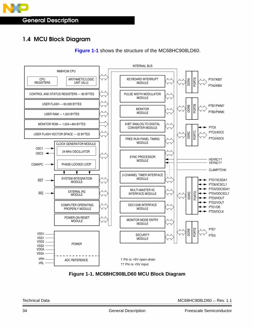
1.4 MCU Block Diagram
Figure 1-1 shows the structure of the MC68HC908LD60.
Figure 1-1. MC68HC908LD60 MCU Block Diagram
SYSTEM INTEGRATIONMODULE
ARITHMETIC/LOGICUNIT (ALU)
CPUREGISTERS
M68HC08 CPU
CONTROL AND STATUS REGISTERS — 80 BYTES
USER FLASH — 60,928 BYTES
USER RAM — 1,024 BYTES
MONITOR ROM — 1,024+464 BYTES
USER FLASH VECTOR SPACE — 32 BYTES
EXTERNAL IRQMODULE
DDRD
PORT
D
INTERNAL BUS
RST
IRQ
COMPUTER OPERATINGPROPERLY MODULE
PTD7/IICSDA†PTD6/IICSCL†PTD5/DDCSDA†PTD4/DDCSCL†PTD3/HOUTPTD2/VOUT
CLAMP/TCH0
POWER-ON RESETMODULE
POWER
VSS1VDD1
VSS2VDD2
HSYNC††VSYNC††
PORT
A
DDRA PTA7/KBI7
PTD1/DEPTD0/DCLK
† Pin is +5V open-drain†† Pin is +5V input
SECURITYMODULE
MONITOR MODE ENTRYMODULE
DDC12AB INTERFACEMODULE
2-CHANNEL TIMER INTERFACEMODULE
MULTI-MASTER IICINTERFACE MODULE
SYNC PROCESSORMODULE
FREE-RUN PANEL TIMINGMODULE
KEYBOARD INTERRUPTMODULE
PULSE WIDTH MODULATORMODULE
MONITORMODULE
8-BIT ANALOG-TO-DIGITALCONVERTER MODULE
PTA0/KBI0:
PORT
B
DDRB PTB7/PWM7
PTB0/PWM0:
PORT
C
DDRC PTC5/ADC5
PTC0/ADC0:
PTC6
CLOCK GENERATOR MODULEOSC1
OSC2
CGMXFC
24-MHz OSCILLATOR
PHASE-LOCKED LOOP
VSSAVDDA
ADC REFERENCEVRLVRH
PORT
E
DDRE PTE7
PTE0:
Technical Data MC68HC908LD60 — Rev. 1.1
34 General Description Freescale Semiconductor

General DescriptionPin Assignments
1.5 Pin Assignments
Figure 1-2. 64-Pin QFP Pin Assignment
PTE2
PTE0
PTC3
/AD
C3
PTB5/PWM5
RESERVED
RESERVED
VDD1
VSSA
OSC2
OSC1
VDDA
PTE1
PTE3
PTE4
PTE5
PTE6
PTE7
CGMXFC
PTA3/KBI3
PTA2/KBI2
PTA1/KBI1
PTA0/KBI0
VDD2
PTB7/PWM7
PTB6/PWM6
PTB4/PWM4
PTB3/PWM3
PTB2/PWM2
PTB1/PWM1
PTB0/PWM0
PTD7IICSDA
PTD6/IICSCL
PTD5/DDCSDA
PTC4
/AD
C4
VSS2
PTC5
/AD
C5
PTC6
PTA7
/KBI
7
PTA6
/KBI
6
PTA5
/KBI
5
PTA4
/KBI
4
IRQ
RST
VRH
VRL
PTC0
/AD
C0
PTC1
/AD
C1
PTC2
/AD
C2
VSYN
C
VSS1
CLAM
P/TC
H0
HSYN
C
RESE
RVED
RESE
RVED
RESE
RVED
RESE
RVED
RESE
RVED
RESE
RVED
RESE
RVED
PTD
0/DC
LK
PTD1
/DE
PTD2
/VO
UT
PTD3
/HO
UT
PTD4
/DDC
SCL
1
2
3
4
5
6
7
8
9
10
11
12
13
14
15
16
17
18 19 20 21 22 23 24 25 26 27 28 29 30 31
32
48
47
46
45
44
43
42
41
40
39
38
37
36
35
34
33
64
63 62 61 60 59 58 57 56 55 54 53 52 51 50
49
RESERVED pins should not be connected.
MC68HC908LD60 — Rev. 1.1 Technical Data
Freescale Semiconductor General Description 35

General Description
1.6 Pin Functions
Description of the pin functions are provided in Table 1-1.
Table 1-1. Pin Functions
PIN NAME PIN DESCRIPTION
VDD1, VDD2 Power supply input to the MCU.
VSS1, VSS2 Power supply ground.
VDDA Power supply input for analog circuits.
VSSA Power supply ground for analog circuits.
OSC1, OSC2
Connections to the on-chip oscillator.An external clock can be connected directly to OSC1; with OSC2 floating.See Section 7. Oscillator (OSC).
RST
External reset pin; active low; with internal pull-up and schmitt trigger input. It is driven low when any internal reset source is asserted.See Section 9. System Integration Module (SIM).
IRQ
External IRQ pin; with schmitt trigger input and internal pull-up. This pin is also used for mode entry selection.See Section 18. External Interrupt (IRQ) and Section 9. System Integration Module (SIM).
CGMXFCExternal filter capacitor connection for the CGM module.See Section 8. Clock Generator Module (CGM).
VSYNCVsync input to the sync processor. This pin is rated at +5V.See Section 16. Sync Processor.
HSYNCHsync input to the sync processor.This pin is rated at +5V.See Section 16. Sync Processor.
PTA7/KBI7–PTA0/KBI0
These are shared function, bidirectional I/O port pins. Each pin contains a pullup device to VDD when it is configured as an external keyboard interrupt pin.See Section 17. Input/Output (I/O) Ports and Section 19. Keyboard Interrupt Module (KBI).
Technical Data MC68HC908LD60 — Rev. 1.1
36 General Description Freescale Semiconductor

General DescriptionPin Functions
PTB7/PWM7–PTB0/PWM0
These are shared-function, bidirectional I/O port pins. Each pin can be configured as a standard I/O pin or a PWM output channel.See Section 17. Input/Output (I/O) Ports and Section 12. Pulse Width Modulator (PWM).
VRH High voltage reference input to ADC module.
VRL Low voltage reference input to ADC module.
PTC6This pin is a standard bidirectional I/O pin.See Section 17. Input/Output (I/O) Ports.
PTC5/ADC5–PTC0/ADC0
These are shared-function, bidirectional I/O port pins. Each pin can be configured as a standard I/O pin or an ADC input channel.See Section 17. Input/Output (I/O) Ports and Section 13. Analog-to-Digital Converter (ADC).
PTD7/IICSDA
This is a shared-function pin. It can be configured as a standard I/O pin or the data line of the multi-master IIC module. This pin is +5V open-drain when configured as output.See Section 17. Input/Output (I/O) Ports and Section 14. Multi-Master IIC Interface (MMIIC).
PTD6/IICSCL
This is a shared function pin. It can be configured as a standard I/O pin or the clock line of the multi-master IIC module. This pin is +5V open-drain when configured as output.See Section 17. Input/Output (I/O) Ports and Section 14. Multi-Master IIC Interface (MMIIC).
PTD5/DDCSDA
This is a shared function pin. It can be configured as a standard I/O pin or the data line of the DDC12AB module. This pin is +5V open-drain when configured as output.See Section 17. Input/Output (I/O) Ports and Section 15. DDC12AB Interface.
PTD4/DDCSCL
This is a shared function pin. It can be configured as a standard I/O pin or the clock line of the DDC12AB module. This pin is +5V open-drain when configured as output.See Section 17. Input/Output (I/O) Ports and Section 15. DDC12AB Interface.
Table 1-1. Pin Functions (Continued)
PIN NAME PIN DESCRIPTION
MC68HC908LD60 — Rev. 1.1 Technical Data
Freescale Semiconductor General Description 37

General Description
NOTE: Any unused inputs and I/O ports should be tied to an appropriate logic level (either VDD or VSS). Although the I/O ports of the MC68HC908LD60 do not require termination, termination is recommended to reduce the possibility of static damage.
PTD3/HOUTPTD2/VOUT
PTD1/DEPTD0/DCLK
These are shared function, bidirectional I/O port pins. These pins can be configured as standard I/O pins or free-run timing output signals.See Section 17. Input/Output (I/O) Ports and Section 16. Sync Processor.
CLAMP/TCH0
This is shared function pins. This TIM channel 0 I/O pin can be configured as the Sync processor CLAMP output pin.See Section 11. Timer Interface Module (TIM) and Section 16. Sync Processor.
PTE7–PTE0These are bidirectional I/O port pins.See Section 17. Input/Output (I/O) Ports.
Table 1-1. Pin Functions (Continued)
PIN NAME PIN DESCRIPTION
Technical Data MC68HC908LD60 — Rev. 1.1
38 General Description Freescale Semiconductor

Technical Data — MC68HC908LD60
Section 2. Memory Map
2.1 Contents
2.2 Introduction . . . . . . . . . . . . . . . . . . . . . . . . . . . . . . . . . . . . . . . .39
2.3 Unimplemented Memory Locations . . . . . . . . . . . . . . . . . . . . .39
2.4 Reserved Memory Locations . . . . . . . . . . . . . . . . . . . . . . . . . .40
2.5 Input/Output (I/O) Section. . . . . . . . . . . . . . . . . . . . . . . . . . . . .40
2.2 Introduction
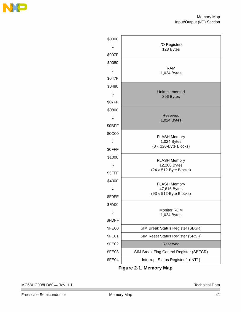
The CPU08 can address 64k-bytes of memory space. The memory map, shown in Figure 2-1, includes:
• 60,928 bytes of FLASH memory
• 1,024 bytes of random-access memory (RAM)
• 32 bytes of user-defined vectors
• 1024 + 464 bytes of monitor ROM
2.3 Unimplemented Memory Locations
Accessing an unimplemented location can cause an illegal address reset if illegal address resets are enabled. In the memory map (Figure 2-1) and in register figures in this document, unimplemented locations are shaded.
MC68HC908LD60 — Rev. 1.1 Technical Data
Freescale Semiconductor Memory Map 39

Memory Map
2.4 Reserved Memory Locations
Accessing a reserved location can have unpredictable effects on MCU operation. In the Figure 2-1 and in register figures in this document, reserved locations are marked with the word Reserved or with the letter R.
2.5 Input/Output (I/O) Section
Most of the control, status, and data registers are in the zero page area of $0000–$007F. Additional I/O registers have these addresses:
• $FE00; SIM break status register, SBSR
• $FE01; SIM reset status register, SRSR
• $FE02; Reserved
• $FE03; SIM break flag control register, SBFCR
• $FE04; Interrupt status register 1, INT1
• $FE05; Interrupt status register 2, INT2
• $FE06; Reserved
• $FE07; 47,616 bytes FLASH control register, FLCR
• $FE08; 47,616 bytes FLASH block protect register, FLBPR
• $FE09; Reserved
• $FE0A; 13k-bytes FLASH control register, FLCR1
• $FE0B; 13k-bytes FLASH block protect register, FLBPR1
• $FE0C; Break address register high, BRKH
• $FE0D; Break address register low, BRKL
• $FE0E; Break status and control register, BRKSCR
• $FE0F; Reserved
• $FFFF; COP control register, COPCTL
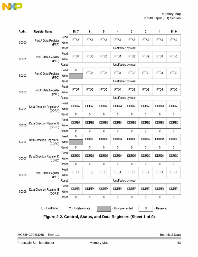
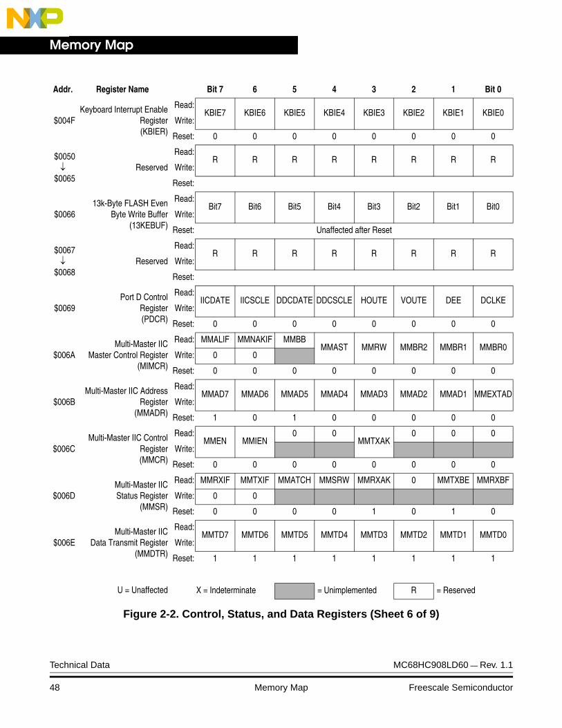
Data registers are shown in Figure 2-2. Table 2-1 is a list of vector locations.
Technical Data MC68HC908LD60 — Rev. 1.1
40 Memory Map Freescale Semiconductor
Memory MapInput/Output (I/O) Section
$0000I/O Registers
128 Bytes↓
$007F
$0080RAM
1,024 Bytes↓
$047F
$0480Unimplemented
896 Bytes↓
$07FF
$0800Reserved
1,024 Bytes↓
$0BFF
$0C00FLASH Memory
1,024 Bytes(8 × 128-Byte Blocks)
↓
$0FFF
$1000FLASH Memory
12,288 Bytes(24 × 512-Byte Blocks)
↓
$3FFF
$4000FLASH Memory
47,616 Bytes(93 × 512-Byte Blocks)
↓
$F9FF
$FA00Monitor ROM1,024 Bytes
↓
$FDFF
$FE00 SIM Break Status Register (SBSR)
$FE01 SIM Reset Status Register (SRSR)
$FE02 Reserved
$FE03 SIM Break Flag Control Register (SBFCR)
$FE04 Interrupt Status Register 1 (INT1)
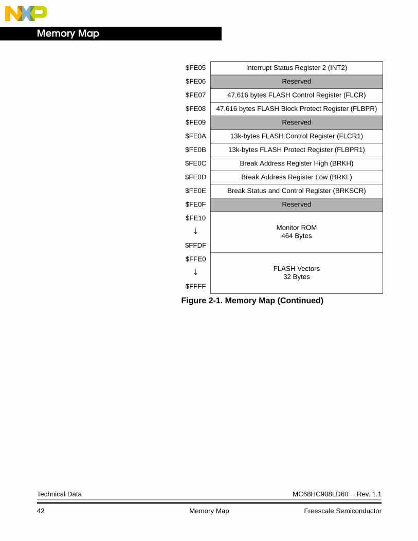
Figure 2-1. Memory Map
MC68HC908LD60 — Rev. 1.1 Technical Data
Freescale Semiconductor Memory Map 41
Memory Map
$FE05 Interrupt Status Register 2 (INT2)
$FE06 Reserved
$FE07 47,616 bytes FLASH Control Register (FLCR)
$FE08 47,616 bytes FLASH Block Protect Register (FLBPR)
$FE09 Reserved
$FE0A 13k-bytes FLASH Control Register (FLCR1)
$FE0B 13k-bytes FLASH Protect Register (FLBPR1)
$FE0C Break Address Register High (BRKH)
$FE0D Break Address Register Low (BRKL)
$FE0E Break Status and Control Register (BRKSCR)
$FE0F Reserved
$FE10Monitor ROM
464 Bytes↓
$FFDF
$FFE0FLASH Vectors
32 Bytes↓
$FFFF
Figure 2-1. Memory Map (Continued)
Technical Data MC68HC908LD60 — Rev. 1.1
42 Memory Map Freescale Semiconductor
Memory MapInput/Output (I/O) Section
Addr. Register Name Bit 7 6 5 4 3 2 1 Bit 0
$0000Port A Data Register
(PTA)
Read:PTA7 PTA6 PTA5 PTA4 PTA3 PTA2 PTA1 PTA0
Write:
Reset: Unaffected by reset
$0001Port B Data Register
(PTB)
Read:PTB7 PTB6 PTB5 PTB4 PTB3 PTB2 PTB1 PTB0
Write:
Reset: Unaffected by reset
$0002Port C Data Register
(PTC)
Read: 0PTC6 PTC5 PTC4 PTC3 PTC2 PTC1 PTC0
Write:
Reset: Unaffected by reset
$0003Port D Data Register
(PTD)
Read:PTD7 PTD6 PTD5 PTD4 PTD3 PTD2 PTD1 PTD0
Write:
Reset: Unaffected by reset
$0004Data Direction Register A
(DDRA)
Read:DDRA7 DDRA6 DDRA5 DDRA4 DDRA3 DDRA2 DDRA1 DDRA0
Write:
Reset: 0 0 0 0 0 0 0 0
$0005Data Direction Register B
(DDRB)
Read:DDRB7 DDRB6 DDRB5 DDRB4 DDRB3 DDRB2 DDRB1 DDRB0
Write:
Reset: 0 0 0 0 0 0 0 0
$0006Data Direction Register C
(DDRC)
Read: 0DDRC6 DDRC5 DDRC4 DDRC3 DDRC2 DDRC1 DDRC0
Write:
Reset: 0 0 0 0 0 0 0 0
$0007Data Direction Register D
(DDRD)
Read:DDRD7 DDRD6 DDRD5 DDRD4 DDRD3 DDRD2 DDRD1 DDRD0
Write:
Reset: 0 0 0 0 0 0 0 0
$0008Port E Data Register
(PTE)
Read:PTE7 PTE6 PTE5 PTE4 PTE3 PTE2 PTE1 PTE0
Write:
Reset: Unaffected by reset
$0009 Data Direction Register E
(DDRE)
Read:DDRE7 DDRE6 DDRE5 DDRE4 DDRE3 DDRE2 DDRE1 DDRE0
Write:
Reset: 0 0 0 0 0 0 0 0
U = Unaffected X = Indeterminate = Unimplemented R = Reserved
Figure 2-2. Control, Status, and Data Registers (Sheet 1 of 9)
MC68HC908LD60 — Rev. 1.1 Technical Data
Freescale Semiconductor Memory Map 43

Memory Map
$000ATIM Status and Control
Register(TSC)
Read: TOFTOIE TSTOP
0 0PS2 PS1 PS0
Write: 0 TRST
Reset: 0 0 1 0 0 0 0 0
$000B Unimplemented
Read:
Write:
Reset: 0 0 0 0 0 0 0 0
$000CTIM Counter Register High
(TCNTH)
Read: Bit15 Bit14 Bit13 Bit12 Bit11 Bit10 Bit9 Bit8
Write:
Reset: 0 0 0 0 0 0 0 0
$000DTIM Counter Register Low
(TCNTL)
Read: Bit7 Bit6 Bit5 Bit4 Bit3 Bit2 Bit1 Bit0
Write:
Reset: 0 0 0 0 0 0 0 0
$000ETIM Counter Modulo
Register High(TMODH)
Read:Bit15 Bit14 Bit13 Bit12 Bit11 Bit10 Bit9 Bit8
Write:
Reset: 1 1 1 1 1 1 1 1
$000FTIM Counter Modulo
Register Low(TMODL)
Read:Bit7 Bit6 Bit5 Bit4 Bit3 Bit2 Bit1 Bit0
Write:
Reset: 1 1 1 1 1 1 1 1
$0010
TIM Channel 0Status and Control
Register(TSC0)
Read: CH0FCH0IE MS0B MS0A ELS0B ELS0A TOV0 CH0MAX
Write: 0
Reset: 0 0 0 0 0 0 0 0
$0011TIM Channel 0Register High
(TCH0H)
Read:Bit15 Bit14 Bit13 Bit12 Bit11 Bit10 Bit9 Bit8
Write:
Reset: Indeterminate after reset
$0012TIM Channel 0
Register Low(TCH0L)
Read:Bit7 Bit6 Bit5 Bit4 Bit3 Bit2 Bit1 Bit0
Write:
Reset: Indeterminate after reset
$0013
TIM Channel 1Status and Control
Register(TSC1)
Read: CH1FCH1IE
0MS1A ELS1B ELS1A TOV1 CH1MAX
Write: 0
Reset: 0 0 0 0 0 0 0 0
Addr. Register Name Bit 7 6 5 4 3 2 1 Bit 0
U = Unaffected X = Indeterminate = Unimplemented R = Reserved
Figure 2-2. Control, Status, and Data Registers (Sheet 2 of 9)
Technical Data MC68HC908LD60 — Rev. 1.1
44 Memory Map Freescale Semiconductor

Memory MapInput/Output (I/O) Section
$0014TIM Channel 1Register High
(TCH1H)
Read:Bit15 Bit14 Bit13 Bit12 Bit11 Bit10 Bit9 Bit8
Write:
Reset: Indeterminate after reset
$0015TIM Channel 1
Register Low(TCH1L)
Read:Bit7 Bit6 Bit5 Bit4 Bit3 Bit2 Bit1 Bit0
Write:
Reset: Indeterminate after reset
$0016DDC Master Control
Register(DMCR)
Read:ALIF NAKIF BB MAST MRW BR2 BR1 BR0
Write:
Reset: 0 0 0 0 0 0 0 0
$0017DDC Address Register
(DADR)
Read:DAD7 DAD6 DAD5 DAD4 DAD3 DAD2 DAD1 EXTAD
Write:
Reset: 1 0 1 0 0 0 0 0
$0018DDC Control Register
(DCR)
Read:DEN DIEN
0 0TXAK SCLIEN DDC1EN
0
Write:
Reset: 0 0 0 0 0 0 0 0
$0019DDC Status Register
(DSR)
Read: RXIF TXIF MATCH SRW RXAK SCLIF TXBE RXBF
Write: 0 0 0
Reset: 0 0 0 0 1 0 1 0
$001ADDC Data Transmit
Register(DDTR)
Read:DTD7 DTD6 DTD5 DTD4 DTD3 DTD2 DTD1 DTD0
Write:
Reset: 1 1 1 1 1 1 1 1
$001B
DDC Data ReceiveRegister(DDRR)
Read: DRD7 DRD6 DRD5 DRD4 DRD3 DRD2 DRD1 DRD0
Write:
Reset: 0 0 0 0 0 0 0 0
$001CDDC2 Address Register
(D2ADR)
Read:D2AD7 D2AD6 D2AD5 D2AD4 D2AD3 D2AD2 D2AD1
0
Write:
Reset: 0 0 0 0 0 0 0 0
$001D Unimplemented
Read:
Write:
Reset:
Addr. Register Name Bit 7 6 5 4 3 2 1 Bit 0
U = Unaffected X = Indeterminate = Unimplemented R = Reserved
Figure 2-2. Control, Status, and Data Registers (Sheet 3 of 9)
MC68HC908LD60 — Rev. 1.1 Technical Data
Freescale Semiconductor Memory Map 45

Memory Map
$001EIRQ Status and Control
Register(INTSCR)
Read: 0 0 0 0 IRQF 0IMASK MODE
Write: ACK
Reset: 0 0 0 0 0 0 0 0
$001FConfiguration Register
(CONFIG)†
Read: 0 0 0 0SSREC COPRS STOP COPD
Write:
Reset: 0 0 0 0 0 0 0 0
† One-time writable register after each reset.
$0020↓
$0037Reserved
Read:R R R R R R R R
Write:
Reset:
$0038PLL Control Register
(PCTL)
Read:PLLIE
PLLFPLLON BCS
1 1 1 1
Write:
Reset: 0 0 1 0 1 1 1 1
$0039PLL Bandwidth Control
Register(PBWC)
Read:AUTO
LOCKACQ XLD
0 0 0 0
Write:
Reset: 0 0 0 0 0 0 0 0
$003APLL Programming
Register(PPG)
Read:MUL7 MUL6 MUL5 MUL4 VRS7 VRS6 VRS5 VRS4
Write:
Reset: 0 1 1 0 0 1 1 0
$003BADC Status and Control
Register(ADSCR)
Read: COCOAIEN ADCO ADCH4 ADCH3 ADCH2 ADCH1 ADCH0
Write:
Reset: 0 0 0 1 1 1 1 1
$003CADC Data Register
(ADR)
Read: AD7 AD6 AD5 AD4 AD3 AD2 AD1 AD0
Write:
Reset: Unaffected after Reset
$003DADC Input Clock Register
(ADICLK)
Read:ADIV2 ADIV1 ADIV0
0 0 0 0 0
Write:
Reset: 0 0 0 0 0 0 0 0
$003E Unimplemented
Read:
Write:
Reset:
Addr. Register Name Bit 7 6 5 4 3 2 1 Bit 0
U = Unaffected X = Indeterminate = Unimplemented R = Reserved
Figure 2-2. Control, Status, and Data Registers (Sheet 4 of 9)
Technical Data MC68HC908LD60 — Rev. 1.1
46 Memory Map Freescale Semiconductor
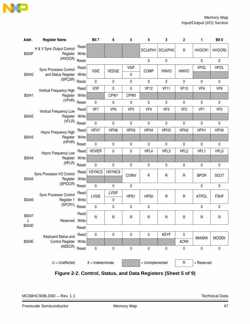
Memory MapInput/Output (I/O) Section
$003FH & V Sync Output Control
Register(HVOCR)
Read:DCLKPH1 DCLKPH0 R HVOCR1 HVOCR0
Write:
Reset: 0 0 0 0
$0040Sync Processor Control
and Status Register(SPCSR)
Read:VSIE VEDGE
VSIFCOMP VINVO HINVO
VPOL HPOL
Write: 0
Reset: 0 0 0 0 0 0 0 0
$0041Vertical Frequency High
Register(VFHR)
Read: VOF 0 0 VF12 VF11 VF10 VF9 VF8
Write: CPW1 CPW0
Reset: 0 0 0 0 0 0 0 0
$0042Vertical Frequency Low
Register(VFLR)
Read: VF7 VF6 VF5 VF4 VF3 VF2 VF1 VF0
Write:
Reset: 0 0 0 0 0 0 0 0
$0043Hsync Frequency High
Register(HFHR)
Read: HFH7 HFH6 HFH5 HFH4 HFH3 HFH2 HFH1 HFH0
Write:
Reset: 0 0 0 0 0 0 0 0
$0044Hsync Frequency Low
Register(HFLR)
Read: HOVER 0 0 HFL4 HFL3 HFL2 HFL1 HFL0
Write:
Reset: 0 0 0 0 0 0 0 0
$0045Sync Processor I/O Control
Register(SPIOCR)
Read: VSYNCS HSYNCSCOINV R R R BPOR SOUT
Write:
Reset: 0 0 0 0 0
$0046Sync Processor Control
Register 1(SPCR1)
Read:LVSIE
LVSIFHPS1 HPS0 R R ATPOL FSHF
Write: 0
Reset: 0 0 0 0 0 0
$0047↓
$004DReserved
Read:R R R R R R R R
Write:
Reset:
$004EKeyboard Status and
Control Register(KBSCR)
Read: 0 0 0 0 KEYF 0IMASKK MODEK
Write: ACKK
Reset: 0 0 0 0 0 0 0 0
Addr. Register Name Bit 7 6 5 4 3 2 1 Bit 0
U = Unaffected X = Indeterminate = Unimplemented R = Reserved
Figure 2-2. Control, Status, and Data Registers (Sheet 5 of 9)
MC68HC908LD60 — Rev. 1.1 Technical Data
Freescale Semiconductor Memory Map 47
Memory Map
$004FKeyboard Interrupt Enable
Register(KBIER)
Read:KBIE7 KBIE6 KBIE5 KBIE4 KBIE3 KBIE2 KBIE1 KBIE0
Write:
Reset: 0 0 0 0 0 0 0 0
$0050↓
$0065Reserved
Read:R R R R R R R R
Write:
Reset:
$006613k-Byte FLASH Even
Byte Write Buffer(13KEBUF)
Read:Bit7 Bit6 Bit5 Bit4 Bit3 Bit2 Bit1 Bit0
Write:
Reset: Unaffected after Reset
$0067↓
$0068Reserved
Read:R R R R R R R R
Write:
Reset:
$0069Port D Control
Register(PDCR)
Read:IICDATE IICSCLE DDCDATE DDCSCLE HOUTE VOUTE DEE DCLKE
Write:
Reset: 0 0 0 0 0 0 0 0
$006AMulti-Master IIC
Master Control Register(MIMCR)
Read: MMALIF MMNAKIF MMBBMMAST MMRW MMBR2 MMBR1 MMBR0
Write: 0 0
Reset: 0 0 0 0 0 0 0 0
$006BMulti-Master IIC Address
Register(MMADR)
Read:MMAD7 MMAD6 MMAD5 MMAD4 MMAD3 MMAD2 MMAD1 MMEXTAD
Write:
Reset: 1 0 1 0 0 0 0 0
$006CMulti-Master IIC Control
Register(MMCR)
Read:MMEN MMIEN
0 0MMTXAK
0 0 0
Write:
Reset: 0 0 0 0 0 0 0 0
$006DMulti-Master IICStatus Register
(MMSR)
Read: MMRXIF MMTXIF MMATCH MMSRW MMRXAK 0 MMTXBE MMRXBF
Write: 0 0
Reset: 0 0 0 0 1 0 1 0
$006EMulti-Master IIC
Data Transmit Register(MMDTR)
Read:MMTD7 MMTD6 MMTD5 MMTD4 MMTD3 MMTD2 MMTD1 MMTD0
Write:
Reset: 1 1 1 1 1 1 1 1
Addr. Register Name Bit 7 6 5 4 3 2 1 Bit 0
U = Unaffected X = Indeterminate = Unimplemented R = Reserved
Figure 2-2. Control, Status, and Data Registers (Sheet 6 of 9)
Technical Data MC68HC908LD60 — Rev. 1.1
48 Memory Map Freescale Semiconductor
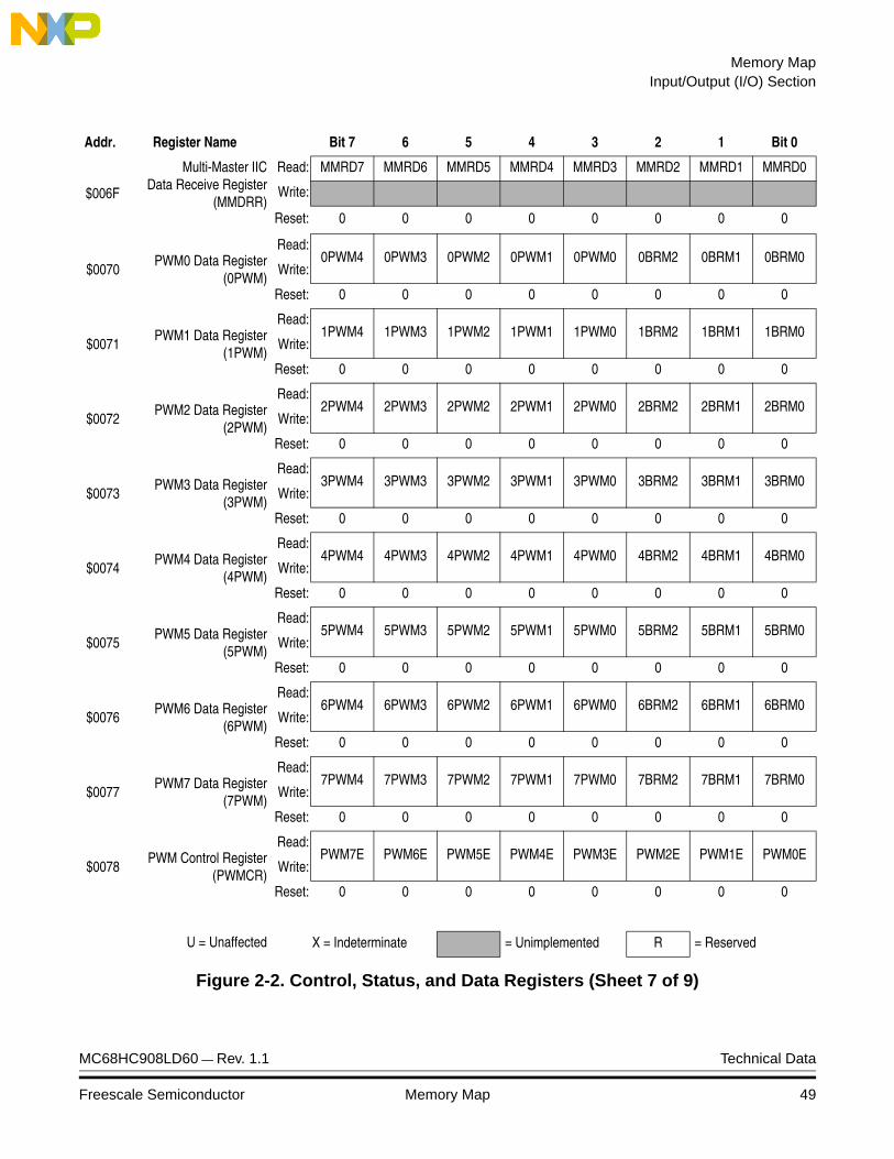
Memory MapInput/Output (I/O) Section
$006F
Multi-Master IICData Receive Register
(MMDRR)
Read: MMRD7 MMRD6 MMRD5 MMRD4 MMRD3 MMRD2 MMRD1 MMRD0
Write:
Reset: 0 0 0 0 0 0 0 0
$0070PWM0 Data Register
(0PWM)
Read:0PWM4 0PWM3 0PWM2 0PWM1 0PWM0 0BRM2 0BRM1 0BRM0
Write:
Reset: 0 0 0 0 0 0 0 0
$0071PWM1 Data Register
(1PWM)
Read:1PWM4 1PWM3 1PWM2 1PWM1 1PWM0 1BRM2 1BRM1 1BRM0
Write:
Reset: 0 0 0 0 0 0 0 0
$0072PWM2 Data Register
(2PWM)
Read:2PWM4 2PWM3 2PWM2 2PWM1 2PWM0 2BRM2 2BRM1 2BRM0
Write:
Reset: 0 0 0 0 0 0 0 0
$0073PWM3 Data Register
(3PWM)
Read:3PWM4 3PWM3 3PWM2 3PWM1 3PWM0 3BRM2 3BRM1 3BRM0
Write:
Reset: 0 0 0 0 0 0 0 0
$0074PWM4 Data Register
(4PWM)
Read:4PWM4 4PWM3 4PWM2 4PWM1 4PWM0 4BRM2 4BRM1 4BRM0
Write:
Reset: 0 0 0 0 0 0 0 0
$0075PWM5 Data Register
(5PWM)
Read:5PWM4 5PWM3 5PWM2 5PWM1 5PWM0 5BRM2 5BRM1 5BRM0
Write:
Reset: 0 0 0 0 0 0 0 0
$0076PWM6 Data Register
(6PWM)
Read:6PWM4 6PWM3 6PWM2 6PWM1 6PWM0 6BRM2 6BRM1 6BRM0
Write:
Reset: 0 0 0 0 0 0 0 0
$0077PWM7 Data Register
(7PWM)
Read:7PWM4 7PWM3 7PWM2 7PWM1 7PWM0 7BRM2 7BRM1 7BRM0
Write:
Reset: 0 0 0 0 0 0 0 0
$0078PWM Control Register
(PWMCR)
Read:PWM7E PWM6E PWM5E PWM4E PWM3E PWM2E PWM1E PWM0E
Write:
Reset: 0 0 0 0 0 0 0 0
Addr. Register Name Bit 7 6 5 4 3 2 1 Bit 0
U = Unaffected X = Indeterminate = Unimplemented R = Reserved
Figure 2-2. Control, Status, and Data Registers (Sheet 7 of 9)
MC68HC908LD60 — Rev. 1.1 Technical Data
Freescale Semiconductor Memory Map 49

Memory Map
$0079↓
$007FUnimplemented
Read:
Write:
Reset:
$FE00SIM Break Status Register
(SBSR)
Read:R R R R R R
SBSWR
Write: Note
Reset: 0
Note: Writing a logic 0 clears SBSW.
$FE01SIM Reset Status Register
(SRSR)
Read: POR PIN COP ILOP ILAD R 0 0
Write:
POR: 1 0 0 0 0 0 0
$FE02 Reserved
Read:R R R R R R R R
Write:
Reset:
$FE03SIM Break Flag Control
Register(SBFCR)
Read:BCFE R R R R R R R
Write:
Reset: 0
$FE04Interrupt Status Register 1
(INT1)
Read: IF6 IF5 IF4 IF3 IF2 IF1 0 0
Write: R R R R R R R R
Reset: 0 0 0 0 0 0 0 0
$FE05Interrupt Status Register 2
(INT2)
Read: IF14 IF13 IF12 IF11 IF10 IF9 IF8 IF7
Write: R R R R R R R R
Reset: 0 0 0 0 0 0 0 0
$FE06 Reserved
Read:R R R R R R R R
Write:
Reset:
$FE0747,616 Bytes FLASH
Control Register(FLCR)
Read: 0 0 0 0HVEN MASS ERASE PGM
Write:
Reset: 0 0 0 0 0 0 0 0
Addr. Register Name Bit 7 6 5 4 3 2 1 Bit 0
U = Unaffected X = Indeterminate = Unimplemented R = Reserved
Figure 2-2. Control, Status, and Data Registers (Sheet 8 of 9)
Technical Data MC68HC908LD60 — Rev. 1.1
50 Memory Map Freescale Semiconductor

Memory MapInput/Output (I/O) Section
$FE0847,616 Bytes FLASH
Block Protect Register(FLBPR)
Read:BPR7 BPR6 BPR5 BPR4 BPR3 BPR2 BPR1
0
Write:
Reset: 0 0 0 0 0 0 0 0
$FE09 Reserved
Read:R R R R R R R R
Write:
Reset:
$FE0A13k-Bytes FLASH
Control Register(FLCR1)
Read: 0 0 0 0HVEN1 MASS1 ERASE1 PGM1
Write:
Reset: 0 0 0 0 0 0 0 0
$FE0B13k-Bytes FLASH
Block Protect Register(FLBPR1)
Read:BPR17 BPR16 BPR15 BPR14 BPR13 BPR12 BPR11
0
Write:
Reset: 0 0 0 0 0 0 0 0
$FE0CBreak Address High
Register (BRKH)
Read:Bit 15 14 13 12 11 10 9 Bit 8
Write:
Reset: 0 0 0 0 0 0 0 0
$FE0DBreak Address Low
Register (BRKL)
Read:Bit 7 6 5 4 3 2 1 Bit 0
Write:
Reset: 0 0 0 0 0 0 0 0
$FE0EBreak Status and Control
Register(BRKSCR)
Read:BRKE BRKA
0 0 0 0 0 0
Write:
Reset: 0 0 0 0 0 0 0 0
$FFFFCOP Control Register
(COPCTL)
Read: Low byte of reset vector
Write: Writing clears COP counter (any value)
Reset: Unaffected by reset
Addr. Register Name Bit 7 6 5 4 3 2 1 Bit 0
U = Unaffected X = Indeterminate = Unimplemented R = Reserved
Figure 2-2. Control, Status, and Data Registers (Sheet 9 of 9)
MC68HC908LD60 — Rev. 1.1 Technical Data
Freescale Semiconductor Memory Map 51

Memory Map
.
Table 2-1. Vector Addresses
Vector Priority Vector Address Vector
LowestIF14
$FFE0 CGM PLL Interrupt Vector (High)
$FFE1 CGM PLL Interrupt Vector (Low)
IF13$FFE2 Keyboard Interrupt Vector (High)
$FFE3 Keyboard Interrupt Vector (Low)
IF12$FFE4 ADC Interrupt Vector (High)
$FFE5 ADC Interrupt Vector (Low)
IF11$FFE6 Reserved
$FFE7 Reserved
IF10$FFE8 MMIIC Vector (High)
$FFE9 MMIIC Vector (Low)
IF9$FFEA Sync Processor Vector (High)
$FFEB Sync Processor Vector (Low)
IF8$FFEC TIM Overflow Vector (High)
$FFED TIM Overflow Vector (Low)
IF7$FFEE TIM Channel 1 Vector (High)
$FFEF TIM Channel 1 Vector (Low)
IF6$FFF0 TIM Channel 0 Vector (High)
$FFF1 TIM Channel 0 Vector (Low)
IF5$FFF2 DDC12AB Vector (High)
$FFF3 DDC12AB Vector (Low)
IF4$FFF4 Reserved
$FFF5 Reserved
IF3$FFF6 Reserved
$FFF7 Reserved
IF2$FFF8 Reserved
$FFF9 Reserved
IF1$FFFA IRQ Vector (High)
$FFFB IRQ Vector (Low)
—$FFFC SWI Vector (High)
$FFFD SWI Vector (Low)
—$FFFE Reset Vector (High)
Highest $FFFF Reset Vector (Low)
Technical Data MC68HC908LD60 — Rev. 1.1
52 Memory Map Freescale Semiconductor
Technical Data — MC68HC908LD60
Section 3. Random-Access Memory (RAM)
3.1 Contents
3.2 Introduction . . . . . . . . . . . . . . . . . . . . . . . . . . . . . . . . . . . . . . . .53
3.3 Functional Description . . . . . . . . . . . . . . . . . . . . . . . . . . . . . . .53
3.2 Introduction
This section describes the 1,024 bytes of RAM (random-access memory).
3.3 Functional Description
Addresses $0080 through $047F are RAM locations. The location of the stack RAM is programmable. The 16-bit stack pointer allows the stack to be anywhere in the 64-Kbyte memory space.
NOTE: For correct operation, the stack pointer must point only to RAM locations.
Within page zero are 128 bytes of RAM. Because the location of the stack RAM is programmable, all page zero RAM locations can be used for I/O control and user data or code. When the stack pointer is moved from its reset location at $00FF out of page zero, direct addressing mode instructions can efficiently access all page zero RAM locations. Page zero RAM, therefore, provides ideal locations for frequently accessed global variables.
Before processing an interrupt, the CPU uses five bytes of the stack to save the contents of the CPU registers.
NOTE: For M6805 compatibility, the H register is not stacked.
MC68HC908LD60 — Rev. 1.1 Technical Data
Freescale Semiconductor Random-Access Memory (RAM) 53
Random-Access Memory (RAM)
During a subroutine call, the CPU uses two bytes of the stack to store the return address. The stack pointer decrements during pushes and increments during pulls.
NOTE: Be careful when using nested subroutines. The CPU may overwrite data in the RAM during a subroutine or during the interrupt stacking operation.
Technical Data MC68HC908LD60 — Rev. 1.1
54 Random-Access Memory (RAM) Freescale Semiconductor
Technical Data — MC68HC908LD60
Section 4. FLASH Memory
4.1 Contents
4.2 Introduction . . . . . . . . . . . . . . . . . . . . . . . . . . . . . . . . . . . . . . . .55
4.3 Functional Description . . . . . . . . . . . . . . . . . . . . . . . . . . . . . . .56
4.4 FLASH Control Registers . . . . . . . . . . . . . . . . . . . . . . . . . . . . .574.4.1 13k-Byte FLASH Even Byte Write Buffer (13KEBUF) . . . . .59
4.5 FLASH Block Erase Operation . . . . . . . . . . . . . . . . . . . . . . . . .59
4.6 FLASH Mass Erase Operation . . . . . . . . . . . . . . . . . . . . . . . . .60
4.7 FLASH Program Operation. . . . . . . . . . . . . . . . . . . . . . . . . . . .61
4.8 FLASH Block Protection . . . . . . . . . . . . . . . . . . . . . . . . . . . . . .624.8.1 FLASH Block Protect Registers . . . . . . . . . . . . . . . . . . . . . .64
4.2 Introduction
This section describes the operation of the embedded FLASH memory. This memory can be read, programmed, and erased from a single external supply. The program and erase operations are enabled through the use of an internal charge pump.
MC68HC908LD60 — Rev. 1.1 Technical Data
Freescale Semiconductor FLASH Memory 55
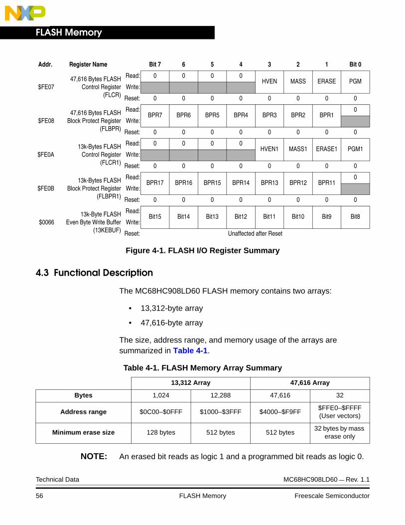
FLASH Memory
4.3 Functional Description
The MC68HC908LD60 FLASH memory contains two arrays:
• 13,312-byte array
• 47,616-byte array
The size, address range, and memory usage of the arrays are summarized in Table 4-1.
NOTE: An erased bit reads as logic 1 and a programmed bit reads as logic 0.
Addr. Register Name Bit 7 6 5 4 3 2 1 Bit 0
$FE0747,616 Bytes FLASH
Control Register(FLCR)
Read: 0 0 0 0HVEN MASS ERASE PGM
Write:
Reset: 0 0 0 0 0 0 0 0
$FE0847,616 Bytes FLASH
Block Protect Register(FLBPR)
Read:BPR7 BPR6 BPR5 BPR4 BPR3 BPR2 BPR1
0
Write:
Reset: 0 0 0 0 0 0 0 0
$FE0A13k-Bytes FLASH
Control Register(FLCR1)
Read: 0 0 0 0HVEN1 MASS1 ERASE1 PGM1
Write:
Reset: 0 0 0 0 0 0 0 0
$FE0B13k-Bytes FLASH
Block Protect Register(FLBPR1)
Read:BPR17 BPR16 BPR15 BPR14 BPR13 BPR12 BPR11
0
Write:
Reset: 0 0 0 0 0 0 0 0
$006613k-Byte FLASH
Even Byte Write Buffer(13KEBUF)
Read:Bit15 Bit14 Bit13 Bit12 Bit11 Bit10 Bit9 Bit8
Write:
Reset: Unaffected after Reset
Figure 4-1. FLASH I/O Register Summary
Table 4-1. FLASH Memory Array Summary
13,312 Array 47,616 Array
Bytes 1,024 12,288 47,616 32
Address range $0C00–$0FFF $1000–$3FFF $4000–$F9FF$FFE0–$FFFF(User vectors)
Minimum erase size 128 bytes 512 bytes 512 bytes32 bytes by mass
erase only
Technical Data MC68HC908LD60 — Rev. 1.1
56 FLASH Memory Freescale Semiconductor
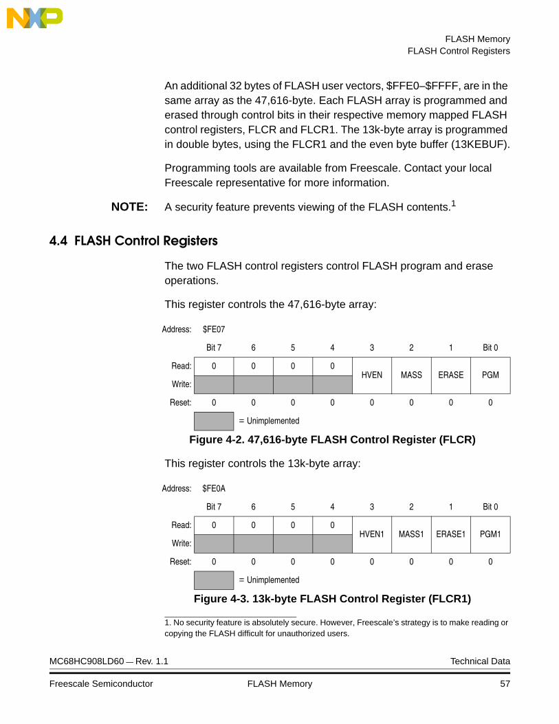
FLASH MemoryFLASH Control Registers
An additional 32 bytes of FLASH user vectors, $FFE0–$FFFF, are in the same array as the 47,616-byte. Each FLASH array is programmed and erased through control bits in their respective memory mapped FLASH control registers, FLCR and FLCR1. The 13k-byte array is programmed in double bytes, using the FLCR1 and the even byte buffer (13KEBUF).
Programming tools are available from Freescale. Contact your local Freescale representative for more information.
NOTE: A security feature prevents viewing of the FLASH contents.1
4.4 FLASH Control Registers
The two FLASH control registers control FLASH program and erase operations.
This register controls the 47,616-byte array:
This register controls the 13k-byte array:
1. No security feature is absolutely secure. However, Freescale’s strategy is to make reading or copying the FLASH difficult for unauthorized users.
Address: $FE07
Bit 7 6 5 4 3 2 1 Bit 0
Read: 0 0 0 0HVEN MASS ERASE PGM
Write:
Reset: 0 0 0 0 0 0 0 0
= Unimplemented
Figure 4-2. 47,616-byte FLASH Control Register (FLCR)
Address: $FE0A
Bit 7 6 5 4 3 2 1 Bit 0
Read: 0 0 0 0HVEN1 MASS1 ERASE1 PGM1
Write:
Reset: 0 0 0 0 0 0 0 0
= Unimplemented
Figure 4-3. 13k-byte FLASH Control Register (FLCR1)
MC68HC908LD60 — Rev. 1.1 Technical Data
Freescale Semiconductor FLASH Memory 57
FLASH Memory
The bit definitions for FLCR are the same for FLCR1 for the other array.
HVEN — High-Voltage Enable Bit
This read/write bit enables the charge pump to drive high voltages for program and erase operations in the array. HVEN can only be set if either PGM = 1 or ERASE = 1 and the proper sequence for program or erase is followed.
1 = High voltage enabled to array and charge pump on0 = High voltage disabled to array and charge pump off
MASS — Mass Erase Control Bit
This read/write bit configures the memory for mass erase operation or block erase operation when the ERASE bit is set.
1 = Mass Erase operation selected0 = Mass Erase operation not selected
ERASE — Erase Control Bit
This read/write bit configures the memory for erase operation. ERASE is interlocked with the PGM bit such that both bits cannot be equal to 1 or set to 1 at the same time.
1 = Erase operation selected0 = Erase operation not selected
PGM — Program Control Bit
This read/write bit configures the memory for program operation. PGM is interlocked with the ERASE bit such that both bits cannot be equal to 1 or set to 1 at the same time.
1 = Program operation selected0 = Program operation not selected
NOTE: The 13k-byte FLASH array is programmed in double bytes. The FLASH control register 1 (FLCR1) is used in conjunction with the 13k-byte FLASH even byte write buffer register (13KEBUF) for programming operations. See 4.4.1 13k-Byte FLASH Even Byte Write Buffer (13KEBUF) and 4.7 FLASH Program Operation.
Technical Data MC68HC908LD60 — Rev. 1.1
58 FLASH Memory Freescale Semiconductor

FLASH MemoryFLASH Block Erase Operation
4.4.1 13k-Byte FLASH Even Byte Write Buffer (13KEBUF)
Bit[7:0] — 13k-Byte FLASH Even Write Byte Buffer
Data is written to this buffer to be programmed to an even location of the 13k-byte array. The byte gets programmed to the FLASH memory when the odd location is programmed. Even locations are $0C00, $0CDE, $1000, etc; the corresponding odd locations are $0C01, $0CDF, $1001, etc. The 13k-byte array are locations from $0C00 to $3FFF. Reset has no effect on these bits.
4.5 FLASH Block Erase Operation
The minimum erase size for the FLASH memory is one block, and is carried out by the block erase operation. For memory $0C00–$0FFF, a block consists of 128 consecutive bytes starting from addresses $xx00 or $xx80. For memory $1000–$3FFF and $4000–$F9FF, a block consists of 512 consecutive bytes starting from addresses $x000, $x200, $x400, $x600, $x800, $xA00, $xC00, or $xE00.
NOTE: The 32-byte user vectors, $FFE0–$FFFF, cannot be erased by the block erase operation because of security reasons. Mass erase is required to erase this block.
Use the following procedure to erase a block of FLASH memory:
1. Set the ERASE bit, and clear the MASS bit in the FLASH control register.
2. Write any data to any FLASH address within the block address range desired.
3. Wait for a time, tnvs (min. 5µs)
Address: $0066
Bit 7 6 5 4 3 2 1 0
Read:Bit7 Bit6 Bit5 Bit4 Bit3 Bit2 Bit1 Bit0
Write:
Reset: Unaffected by reset
Figure 4-4. 13k-Byte FLASH Even Byte Write Buffer (13KEBUF)
MC68HC908LD60 — Rev. 1.1 Technical Data
Freescale Semiconductor FLASH Memory 59

FLASH Memory
4. Set the HVEN bit.
5. Wait for a time, tErase (min. 10ms)
6. Clear the ERASE bit.
7. Wait for a time, tnvh (min. 5µs)
8. Clear the HVEN bit.
9. After a time, trcv (min. 1µs), the memory can be accessed again in read mode.
NOTE: Programming and erasing of FLASH locations cannot be performed by code being executed from the same FLASH array that is being programmed or erased. While these operations must be performed in the order as shown, but other unrelated operations may occur between the steps.
4.6 FLASH Mass Erase Operation
A mass erase operation erases an entire array of FLASH memory. The MC68HC908LD60 contains two FLASH memory arrays, therefore, two mass erase operations are required to erase all FLASH memory in the device. Mass erasing the 13k-byte array, erases all FLASH memory from $0800 to $3FFF. Mass erasing the 47,616-byte array, erases all FLASH memory from $4000 to $FFFF.
Use the following procedure to erase an entire FLASH memory array:
1. Set both the ERASE bit, and the MASS bit in the FLASH control register.
2. Write any data to any FLASH address within the FLASH memory address range.
3. Wait for a time, tnvs (5µs).
4. Set the HVEN bit.
5. Wait for a time, tERASE (10ms).
6. Clear the ERASE bit.
7. Wait for a time, tnvhl (100µs).
Technical Data MC68HC908LD60 — Rev. 1.1
60 FLASH Memory Freescale Semiconductor

FLASH MemoryFLASH Program Operation
8. Clear the HVEN bit.
9. After time, trcv (1µs), the memory can be accessed again in read mode.
NOTE: Programming and erasing of FLASH locations cannot be performed by code being executed from the same FLASH array that is being programmed or erased. While these operations must be performed in the order as shown, but other unrelated operations may occur between the steps.
4.7 FLASH Program Operation
Programming of the FLASH memory is done on a row basis. A row consists of 64 consecutive bytes starting from addresses $XX00, $XX40, $XX80, and $XXC0. Use this step-by-step procedure to program a row of FLASH memory (Figure 4-5 is a flowchart representation):
NOTE: In order to avoid program disturbs, the row must be erased before any byte on that row is programmed.
1. Set the PGM bit. This configures the memory for program operation and enables the latching of address and data for programming.
2. Write any data to any FLASH address within the row address range desired.
3. Wait for a time, tnvs (min. 5µs).
4. Set the HVEN bit.
5. Wait for a time, tpgs (min. 10µs).
6. For 47,616-byte array: Write data to the FLASH address to beprogrammed.
For 13k-byte array: Write even location data to 13KEBUF thenwrite odd location data to the odd FLASHaddress to be programmed.
7. Wait for time, tPROG (min. 20µs).
8. Repeat step 6 and 7 until all the bytes within the row are programmed.
MC68HC908LD60 — Rev. 1.1 Technical Data
Freescale Semiconductor FLASH Memory 61

FLASH Memory
9. Clear the PGM bit.
10. Wait for time, tnvh (min. 5µs).
11. Clear the HVEN bit.
12. After time, trcv (min 1µs), the memory can be accessed in read mode again.
This program sequence is repeated throughout the memory until all data is programmed.
NOTE: Programming and erasing of FLASH locations cannot be performed by code being executed from the same FLASH array that is being programmed or erased. While these operations must be performed in the order shown, other unrelated operations may occur between the steps. Do not exceed tPROG maximum. See 22.13 FLASH Memory Characteristics.
4.8 FLASH Block Protection
Due to the ability of the on-board charge pump to erase and program the FLASH memory in the target application, provision is made for protecting blocks of memory from unintentional erase or program operations due to system malfunction. This protection is done by use of a FLASH Block Protect Register for each array (FLBPR and FLBPR1). The block protect register determines the range of the FLASH memory which is to be protected. The range of the protected area starts from a location defined by block protect register and ends at the bottom of the FLASH memory array ($FFFF and $3FFF). When the memory is protected, the HVEN bit cannot be set in either ERASE or PROGRAM operations.
Technical Data MC68HC908LD60 — Rev. 1.1
62 FLASH Memory Freescale Semiconductor

FLASH MemoryFLASH Block Protection
Figure 4-5. FLASH Programming Flowchart
Set HVEN bit
Write any data to any FLASH addresswithin the row address range desired
Wait for a time, tnvs
Set PGM bit
Wait for a time, tpgs
Write data to the FLASH addressto be programmed
Wait for a time, tprog
Clear PGM bit
Wait for a time, tnvh
Clear HVEN bit
Wait for a time, trcv
Completedprogramming
this row?
Y
N
End of Programming
The time between each FLASH address change (step 6 to step 6), or
must not exceed the maximum programmingtime, tPROG max.
the time between the last FLASH address programmedto clearing PGM bit (step 6 to step 9)
NOTE:
1
2
3
4
5
6
7
9
10
11
12
Algorithm for programminga row (64 bytes) of FLASH memory
This row program algorithm assumes the row/sto be programmed are initially erased.
Write even location byte to 13k-byteFLASH Even Byte Write Buffer at $0066.
Write odd location byte to the oddFLASH adress to be programmed.
For 47,616 bytes array
For 13k-bytes array
MC68HC908LD60 — Rev. 1.1 Technical Data
Freescale Semiconductor FLASH Memory 63
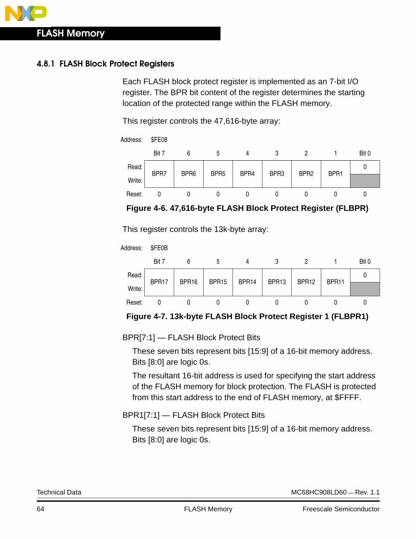
FLASH Memory
4.8.1 FLASH Block Protect Registers
Each FLASH block protect register is implemented as an 7-bit I/O register. The BPR bit content of the register determines the starting location of the protected range within the FLASH memory.
This register controls the 47,616-byte array:
This register controls the 13k-byte array:
BPR[7:1] — FLASH Block Protect Bits
These seven bits represent bits [15:9] of a 16-bit memory address.Bits [8:0] are logic 0s.
The resultant 16-bit address is used for specifying the start address of the FLASH memory for block protection. The FLASH is protected from this start address to the end of FLASH memory, at $FFFF.
BPR1[7:1] — FLASH Block Protect Bits
These seven bits represent bits [15:9] of a 16-bit memory address.Bits [8:0] are logic 0s.
Address: $FE08
Bit 7 6 5 4 3 2 1 Bit 0
Read:BPR7 BPR6 BPR5 BPR4 BPR3 BPR2 BPR1
0
Write:
Reset: 0 0 0 0 0 0 0 0
Figure 4-6. 47,616-byte FLASH Block Protect Register (FLBPR)
Address: $FE0B
Bit 7 6 5 4 3 2 1 Bit 0
Read:BPR17 BPR16 BPR15 BPR14 BPR13 BPR12 BPR11
0
Write:
Reset: 0 0 0 0 0 0 0 0
Figure 4-7. 13k-byte FLASH Block Protect Register 1 (FLBPR1)
Technical Data MC68HC908LD60 — Rev. 1.1
64 FLASH Memory Freescale Semiconductor

FLASH MemoryFLASH Block Protection
The resultant 16-bit address is used for specifying the start address of the FLASH memory for block protection. The FLASH is protected from this start address to the end of FLASH memory, at $3FFF.
Examples of block protection for 47,616-byte FLASH memory array:
Examples of block protection for 13k-byte FLASH memory array:
16-bit memory address
Start address of FLASH block protect 0 0 0 0 0 0 0 0 0
BPR[7:1] 0
Figure 4-8. FLASH Block Protect Start Address
BPR[7:0] FLASH Memory Protected Range
$40 The entire 47,616 bytes of FLASH memory is protected.
$42 (0100 0010) $4200 (0100 0010 0000 0000) to $FFFF
$44 (0100 0100) $4400 (0100 0100 0000 0000) to $FFFF
and so on...
$F8 (1111 1000) $F800 (1111 1000 0000 0000) to $FFFF
$FA $FFE0 to $FFFF (FLASH Vectors)
$FC $FFE0 to $FFFF (FLASH Vectors)
$FE $FFE0 to $FFFF (FLASH Vectors)
$00–3E The entire 47,616 bytes FLASH memory is not protected.
BPR1[7:0] FLASH Memory Protected Range
$0C The entire 13k-byte FLASH memory is protected.
$0E (0000 1110) $0E00 (0000 1110 0000 0000) to $3FFF
$10 (0001 0000) $1000 (0001 0000 0000 0000) to $3FFF
and so on...
$38 (0011 1000) $3800 (0011 1000 0000 0000) to $3FFF
$3A (0011 1010) $3A00 (0011 1010 0000 0000) to $3FFF
$3C (0011 1100) $3C00 (0011 1100 0000 0000) to $3FFF
$3E (0011 1110) $3E00 (0011 1110 0000 0000) to $3FFF
$00–$0B or $40–$FE The entire 13k-byte FLASH memory is not protected.
MC68HC908LD60 — Rev. 1.1 Technical Data
Freescale Semiconductor FLASH Memory 65

FLASH Memory
Technical Data MC68HC908LD60 — Rev. 1.1
66 FLASH Memory Freescale Semiconductor
Technical Data — MC68HC908LD60
Section 5. Configuration Register (CONFIG)
5.1 Contents
5.2 Introduction . . . . . . . . . . . . . . . . . . . . . . . . . . . . . . . . . . . . . . . .67
5.3 Functional Description . . . . . . . . . . . . . . . . . . . . . . . . . . . . . . .67
5.4 Configuration Register . . . . . . . . . . . . . . . . . . . . . . . . . . . . . . .68
5.2 Introduction
This section describes the configuration register, CONFIG. The configuration register enables or disables these options:
• Stop mode recovery time (32 OSCXCLK cycles or 4096 OSCXCLK cycles)
• COP timeout period (218 – 24 or 213 – 24 OSCXCLK cycles)
• STOP instruction
• Computer operating properly module (COP)
5.3 Functional Description
The configuration register is used in the initialization of various options. The configuration register can be written once after each reset. All of the configuration register bits are cleared during reset. Since the various options affect the operation of the MCU, it is recommended that this register be written immediately after reset. The configuration register is located at $001F. The configuration register may be read at anytime.
MC68HC908LD60 — Rev. 1.1 Technical Data
Freescale Semiconductor Configuration Register (CONFIG) 67
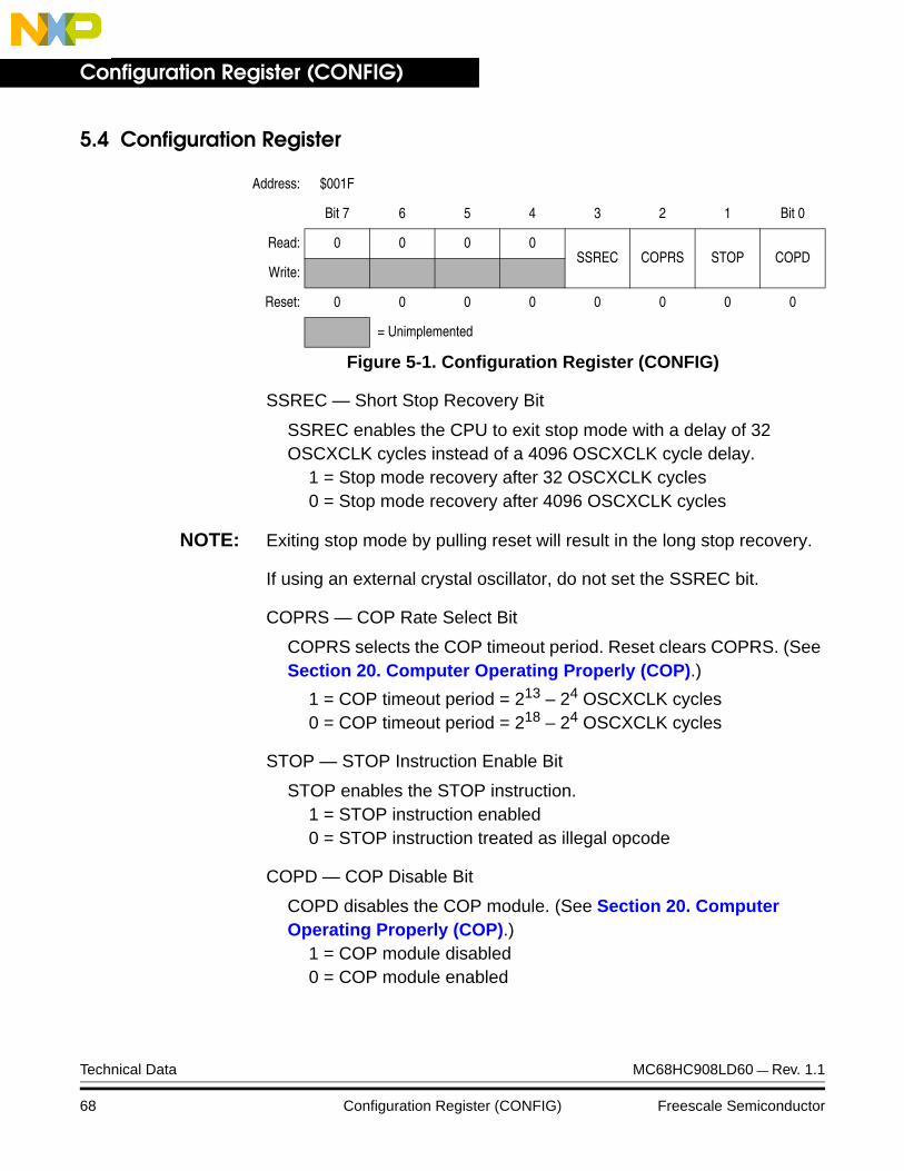
Configuration Register (CONFIG)
5.4 Configuration Register
SSREC — Short Stop Recovery Bit
SSREC enables the CPU to exit stop mode with a delay of 32 OSCXCLK cycles instead of a 4096 OSCXCLK cycle delay.
1 = Stop mode recovery after 32 OSCXCLK cycles0 = Stop mode recovery after 4096 OSCXCLK cycles
NOTE: Exiting stop mode by pulling reset will result in the long stop recovery.
If using an external crystal oscillator, do not set the SSREC bit.
COPRS — COP Rate Select Bit
COPRS selects the COP timeout period. Reset clears COPRS. (See Section 20. Computer Operating Properly (COP).)
1 = COP timeout period = 213 – 24 OSCXCLK cycles0 = COP timeout period = 218 – 24 OSCXCLK cycles
STOP — STOP Instruction Enable Bit
STOP enables the STOP instruction.1 = STOP instruction enabled0 = STOP instruction treated as illegal opcode
COPD — COP Disable Bit
COPD disables the COP module. (See Section 20. Computer Operating Properly (COP).)
1 = COP module disabled0 = COP module enabled
Address: $001F
Bit 7 6 5 4 3 2 1 Bit 0
Read: 0 0 0 0SSREC COPRS STOP COPD
Write:
Reset: 0 0 0 0 0 0 0 0
= Unimplemented
Figure 5-1. Configuration Register (CONFIG)
Technical Data MC68HC908LD60 — Rev. 1.1
68 Configuration Register (CONFIG) Freescale Semiconductor
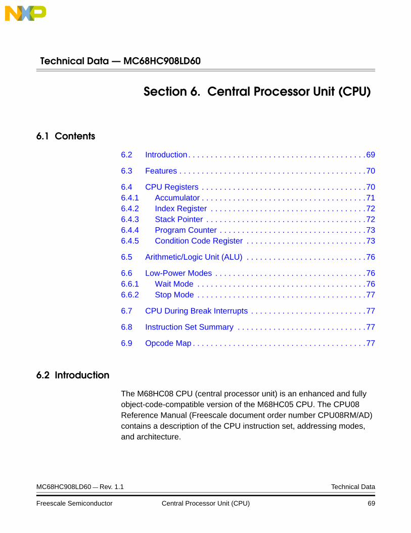
Technical Data — MC68HC908LD60
Section 6. Central Processor Unit (CPU)
6.1 Contents
6.2 Introduction . . . . . . . . . . . . . . . . . . . . . . . . . . . . . . . . . . . . . . . .69
6.3 Features . . . . . . . . . . . . . . . . . . . . . . . . . . . . . . . . . . . . . . . . . .70
6.4 CPU Registers . . . . . . . . . . . . . . . . . . . . . . . . . . . . . . . . . . . . .706.4.1 Accumulator . . . . . . . . . . . . . . . . . . . . . . . . . . . . . . . . . . . . .716.4.2 Index Register . . . . . . . . . . . . . . . . . . . . . . . . . . . . . . . . . . .726.4.3 Stack Pointer . . . . . . . . . . . . . . . . . . . . . . . . . . . . . . . . . . . .726.4.4 Program Counter . . . . . . . . . . . . . . . . . . . . . . . . . . . . . . . . .736.4.5 Condition Code Register . . . . . . . . . . . . . . . . . . . . . . . . . . .73
6.5 Arithmetic/Logic Unit (ALU) . . . . . . . . . . . . . . . . . . . . . . . . . . .76
6.6 Low-Power Modes . . . . . . . . . . . . . . . . . . . . . . . . . . . . . . . . . .766.6.1 Wait Mode . . . . . . . . . . . . . . . . . . . . . . . . . . . . . . . . . . . . . .766.6.2 Stop Mode . . . . . . . . . . . . . . . . . . . . . . . . . . . . . . . . . . . . . .77
6.7 CPU During Break Interrupts . . . . . . . . . . . . . . . . . . . . . . . . . .77
6.8 Instruction Set Summary . . . . . . . . . . . . . . . . . . . . . . . . . . . . .77
6.9 Opcode Map . . . . . . . . . . . . . . . . . . . . . . . . . . . . . . . . . . . . . . .77
6.2 Introduction
The M68HC08 CPU (central processor unit) is an enhanced and fully object-code-compatible version of the M68HC05 CPU. The CPU08 Reference Manual (Freescale document order number CPU08RM/AD) contains a description of the CPU instruction set, addressing modes, and architecture.
MC68HC908LD60 — Rev. 1.1 Technical Data
Freescale Semiconductor Central Processor Unit (CPU) 69

Central Processor Unit (CPU)
6.3 Features
• Object code fully upward-compatible with M68HC05 Family
• 16-bit stack pointer with stack manipulation instructions
• 16-bit index register with x-register manipulation instructions
• 6-MHz CPU internal bus frequency
• 64K-byte program/data memory space
• 16 addressing modes
• Memory-to-memory data moves without using accumulator
• Fast 8-bit by 8-bit multiply and 16-bit by 8-bit divide instructions
• Enhanced binary-coded decimal (BCD) data handling
• Modular architecture with expandable internal bus definition for extension of addressing range beyond 64K-bytes
• Low-power stop and wait modes
6.4 CPU Registers
Figure 6-1 shows the five CPU registers. CPU registers are not part of the memory map.
Technical Data MC68HC908LD60 — Rev. 1.1
70 Central Processor Unit (CPU) Freescale Semiconductor
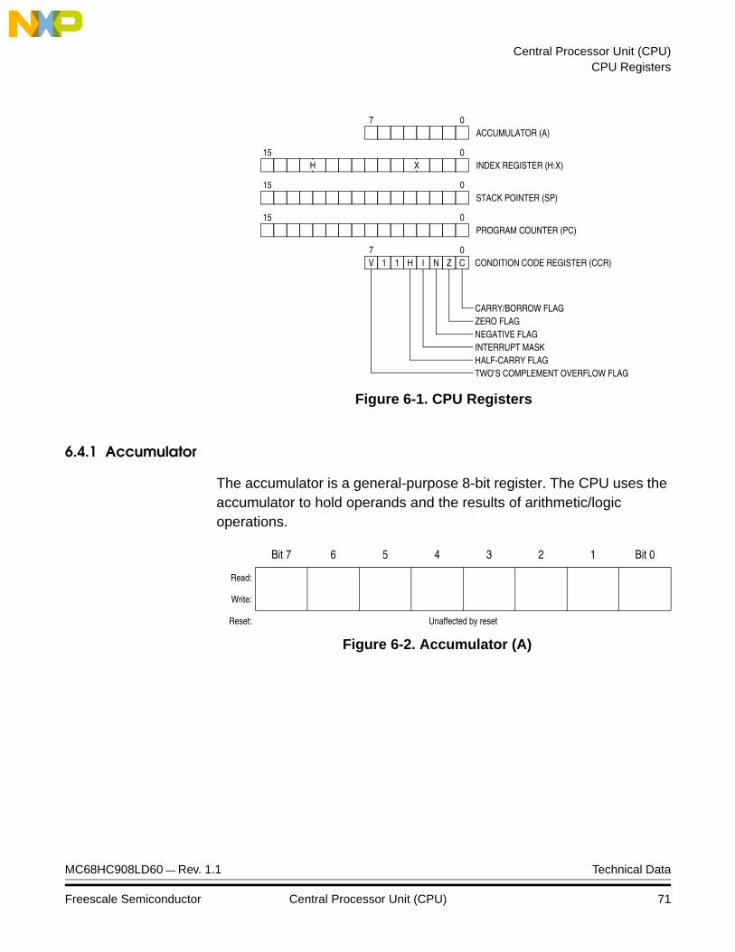
Central Processor Unit (CPU)CPU Registers
Figure 6-1. CPU Registers
6.4.1 Accumulator
The accumulator is a general-purpose 8-bit register. The CPU uses the accumulator to hold operands and the results of arithmetic/logic operations.
ACCUMULATOR (A)
INDEX REGISTER (H:X)
STACK POINTER (SP)
PROGRAM COUNTER (PC)
CONDITION CODE REGISTER (CCR)
CARRY/BORROW FLAGZERO FLAGNEGATIVE FLAGINTERRUPT MASKHALF-CARRY FLAGTWO’S COMPLEMENT OVERFLOW FLAG
V 1 1 H I N Z C
H X
0
0
0
0
7
15
15
15
7 0
Bit 7 6 5 4 3 2 1 Bit 0
Read:
Write:
Reset: Unaffected by reset
Figure 6-2. Accumulator (A)
MC68HC908LD60 — Rev. 1.1 Technical Data
Freescale Semiconductor Central Processor Unit (CPU) 71
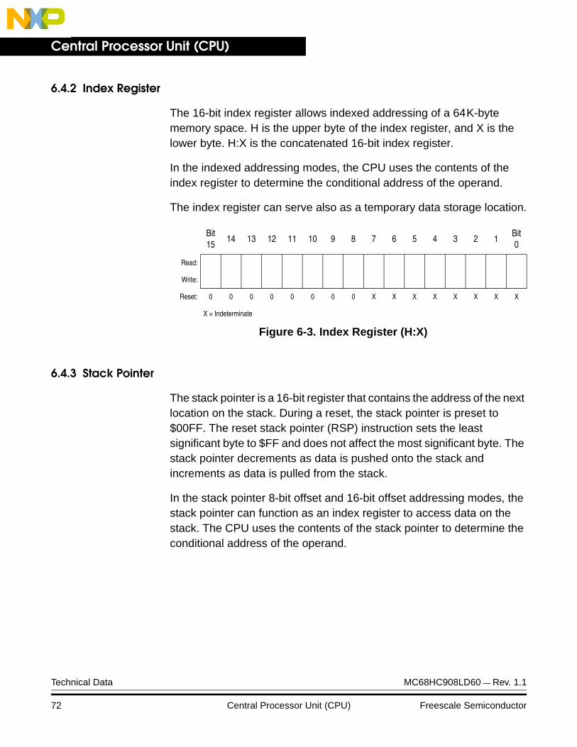
Central Processor Unit (CPU)
6.4.2 Index Register
The 16-bit index register allows indexed addressing of a 64K-byte memory space. H is the upper byte of the index register, and X is the lower byte. H:X is the concatenated 16-bit index register.
In the indexed addressing modes, the CPU uses the contents of the index register to determine the conditional address of the operand.
The index register can serve also as a temporary data storage location.
6.4.3 Stack Pointer
The stack pointer is a 16-bit register that contains the address of the next location on the stack. During a reset, the stack pointer is preset to $00FF. The reset stack pointer (RSP) instruction sets the least significant byte to $FF and does not affect the most significant byte. The stack pointer decrements as data is pushed onto the stack and increments as data is pulled from the stack.
In the stack pointer 8-bit offset and 16-bit offset addressing modes, the stack pointer can function as an index register to access data on the stack. The CPU uses the contents of the stack pointer to determine the conditional address of the operand.
Bit 15
14 13 12 11 10 9 8 7 6 5 4 3 2 1Bit 0
Read:
Write:
Reset: 0 0 0 0 0 0 0 0 X X X X X X X X
X = Indeterminate
Figure 6-3. Index Register (H:X)
Technical Data MC68HC908LD60 — Rev. 1.1
72 Central Processor Unit (CPU) Freescale Semiconductor
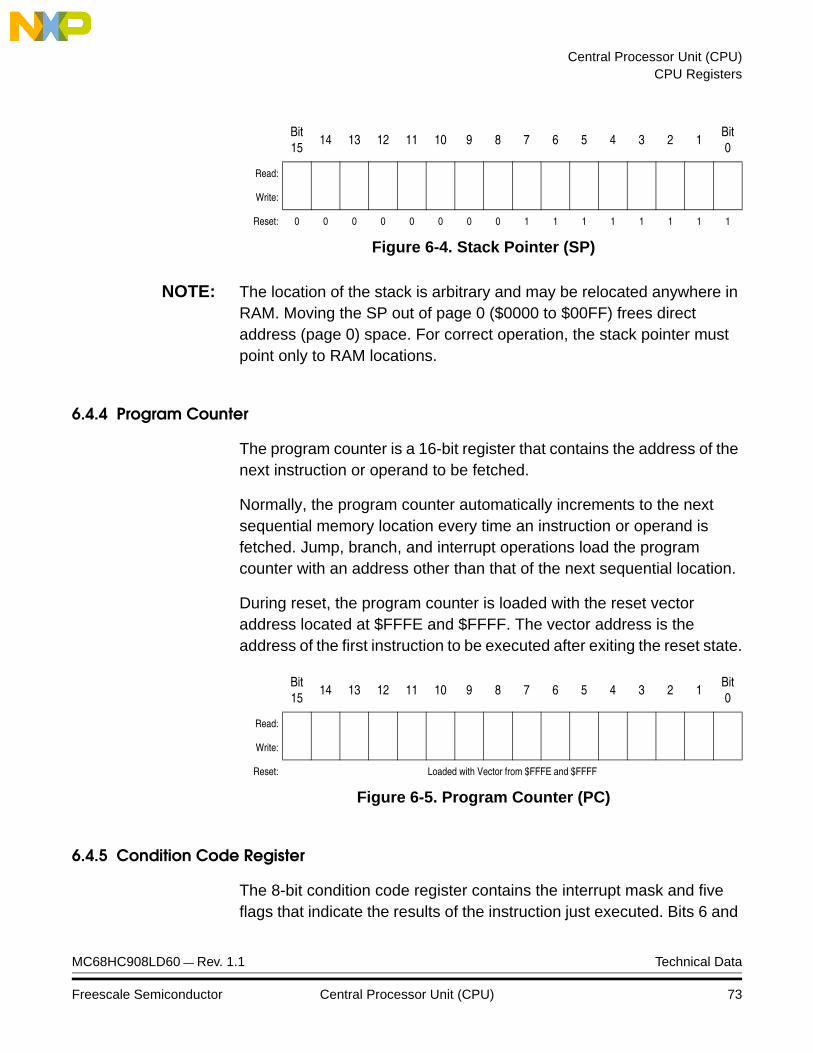
Central Processor Unit (CPU)CPU Registers
NOTE: The location of the stack is arbitrary and may be relocated anywhere in RAM. Moving the SP out of page 0 ($0000 to $00FF) frees direct address (page 0) space. For correct operation, the stack pointer must point only to RAM locations.
6.4.4 Program Counter
The program counter is a 16-bit register that contains the address of the next instruction or operand to be fetched.
Normally, the program counter automatically increments to the next sequential memory location every time an instruction or operand is fetched. Jump, branch, and interrupt operations load the program counter with an address other than that of the next sequential location.
During reset, the program counter is loaded with the reset vector address located at $FFFE and $FFFF. The vector address is the address of the first instruction to be executed after exiting the reset state.
6.4.5 Condition Code Register
The 8-bit condition code register contains the interrupt mask and five flags that indicate the results of the instruction just executed. Bits 6 and
Bit 15
14 13 12 11 10 9 8 7 6 5 4 3 2 1Bit 0
Read:
Write:
Reset: 0 0 0 0 0 0 0 0 1 1 1 1 1 1 1 1
Figure 6-4. Stack Pointer (SP)
Bit15
14 13 12 11 10 9 8 7 6 5 4 3 2 1Bit 0
Read:
Write:
Reset: Loaded with Vector from $FFFE and $FFFF
Figure 6-5. Program Counter (PC)
MC68HC908LD60 — Rev. 1.1 Technical Data
Freescale Semiconductor Central Processor Unit (CPU) 73

Central Processor Unit (CPU)
5 are set permanently to logic 1. The following paragraphs describe the functions of the condition code register.
V — Overflow Flag
The CPU sets the overflow flag when a two's complement overflow occurs. The signed branch instructions BGT, BGE, BLE, and BLT use the overflow flag.
1 = Overflow0 = No overflow
H — Half-Carry Flag
The CPU sets the half-carry flag when a carry occurs between accumulator bits 3 and 4 during an add-without-carry (ADD) or add-with-carry (ADC) operation. The half-carry flag is required for binary-coded decimal (BCD) arithmetic operations. The DAA instruction uses the states of the H and C flags to determine the appropriate correction factor.
1 = Carry between bits 3 and 40 = No carry between bits 3 and 4
Bit 7 6 5 4 3 2 1 Bit 0
Read:V 1 1 H I N Z C
Write:
Reset: X 1 1 X 1 X X X
X = Indeterminate
Figure 6-6. Condition Code Register (CCR)
Technical Data MC68HC908LD60 — Rev. 1.1
74 Central Processor Unit (CPU) Freescale Semiconductor

Central Processor Unit (CPU)CPU Registers
I — Interrupt Mask
When the interrupt mask is set, all maskable CPU interrupts are disabled. CPU interrupts are enabled when the interrupt mask is cleared. When a CPU interrupt occurs, the interrupt mask is set automatically after the CPU registers are saved on the stack, but before the interrupt vector is fetched.
1 = Interrupts disabled0 = Interrupts enabled
NOTE: To maintain M6805 Family compatibility, the upper byte of the index register (H) is not stacked automatically. If the interrupt service routine modifies H, then the user must stack and unstack H using the PSHH and PULH instructions.
After the I bit is cleared, the highest-priority interrupt request is serviced first.
A return-from-interrupt (RTI) instruction pulls the CPU registers from the stack and restores the interrupt mask from the stack. After any reset, the interrupt mask is set and can be cleared only by the clear interrupt mask software instruction (CLI).
N — Negative flag
The CPU sets the negative flag when an arithmetic operation, logic operation, or data manipulation produces a negative result, setting bit 7 of the result.
1 = Negative result0 = Non-negative result
Z — Zero flag
The CPU sets the zero flag when an arithmetic operation, logic operation, or data manipulation produces a result of $00.
1 = Zero result0 = Non-zero result
MC68HC908LD60 — Rev. 1.1 Technical Data
Freescale Semiconductor Central Processor Unit (CPU) 75
Central Processor Unit (CPU)
C — Carry/Borrow Flag
The CPU sets the carry/borrow flag when an addition operation produces a carry out of bit 7 of the accumulator or when a subtraction operation requires a borrow. Some instructions — such as bit test and branch, shift, and rotate — also clear or set the carry/borrow flag.
1 = Carry out of bit 70 = No carry out of bit 7
6.5 Arithmetic/Logic Unit (ALU)
The ALU performs the arithmetic and logic operations defined by the instruction set.
Refer to the CPU08 Reference Manual (Freescale document order number CPU08RM/AD) for a description of the instructions and addressing modes and more detail about the architecture of the CPU.
6.6 Low-Power Modes
The WAIT and STOP instructions put the MCU in low power-consumption standby modes.
6.6.1 Wait Mode
The WAIT instruction:
• Clears the interrupt mask (I bit) in the condition code register, enabling interrupts. After exit from wait mode by interrupt, the I bit remains clear. After exit by reset, the I bit is set.
• Disables the CPU clock
Technical Data MC68HC908LD60 — Rev. 1.1
76 Central Processor Unit (CPU) Freescale Semiconductor
Central Processor Unit (CPU)CPU During Break Interrupts
6.6.2 Stop Mode
The STOP instruction:
• Clears the interrupt mask (I bit) in the condition code register, enabling external interrupts. After exit from stop mode by external interrupt, the I bit remains clear. After exit by reset, the I bit is set.
• Disables the CPU clock
After exiting stop mode, the CPU clock begins running after the oscillator stabilization delay.
6.7 CPU During Break Interrupts
If a break module is present on the MCU, the CPU starts a break interrupt by:
• Loading the instruction register with the SWI instruction
• Loading the program counter with $FFFC:$FFFD or with $FEFC:$FEFD in monitor mode
The break interrupt begins after completion of the CPU instruction in progress. If the break address register match occurs on the last cycle of a CPU instruction, the break interrupt begins immediately.
A return-from-interrupt instruction (RTI) in the break routine ends the break interrupt and returns the MCU to normal operation if the break interrupt has been deasserted.
6.8 Instruction Set Summary
6.9 Opcode Map
See Table 6-2.
MC68HC908LD60 — Rev. 1.1 Technical Data
Freescale Semiconductor Central Processor Unit (CPU) 77

Central Processor Unit (CPU)
Table 6-1. Instruction Set Summary
SourceForm Operation Description
Effect onCCR
Ad
dre
ssM
od
e
Op
cod
e
Op
eran
d
Cyc
les
V H I N Z C
ADC #oprADC oprADC oprADC opr,XADC opr,XADC ,XADC opr,SPADC opr,SP
Add with Carry A ← (A) + (M) + (C) –
IMMDIREXTIX2IX1IXSP1SP2
A9B9C9D9E9F9
9EE99ED9
iiddhh llee ffff
ffee ff
23443245
ADD #oprADD oprADD oprADD opr,XADD opr,XADD ,XADD opr,SPADD opr,SP
Add without Carry A ← (A) + (M) –
IMMDIREXTIX2IX1IXSP1SP2
ABBBCBDBEBFB
9EEB9EDB
iiddhh llee ffff
ffee ff
23443245
AIS #opr Add Immediate Value (Signed) to SP SP ← (SP) + (16 « M) – – – – – – IMM A7 ii 2
AIX #opr Add Immediate Value (Signed) to H:X H:X ← (H:X) + (16 « M) – – – – – – IMM AF ii 2
AND #oprAND oprAND oprAND opr,XAND opr,XAND ,XAND opr,SPAND opr,SP
Logical AND A ← (A) & (M) 0 – – –
IMMDIREXTIX2IX1IXSP1SP2
A4B4C4D4E4F4
9EE49ED4
iiddhh llee ffff
ffee ff
23443245
ASL oprASLAASLXASL opr,XASL ,XASL opr,SP
Arithmetic Shift Left(Same as LSL)
– –
DIRINHINHIX1IXSP1
3848586878
9E68
dd
ff
ff
411435
ASR oprASRAASRXASR opr,XASR opr,XASR opr,SP
Arithmetic Shift Right – –
DIRINHINHIX1IXSP1
3747576777
9E67
dd
ff
ff
411435
BCC rel Branch if Carry Bit Clear PC ← (PC) + 2 + rel ? (C) = 0 – – – – – – REL 24 rr 3
BCLR n, opr Clear Bit n in M Mn ← 0 – – – – – –
DIR (b0)DIR (b1)DIR (b2)DIR (b3)DIR (b4)DIR (b5)DIR (b6)DIR (b7)
11131517191B1D1F
dd dd dd dd dd dd dd dd
44444444
C
b0b7
0
b0b7
C
Technical Data MC68HC908LD60 — Rev. 1.1
78 Central Processor Unit (CPU) Freescale Semiconductor

Central Processor Unit (CPU)Opcode Map
BCS rel Branch if Carry Bit Set (Same as BLO) PC ← (PC) + 2 + rel ? (C) = 1 – – – – – – REL 25 rr 3
BEQ rel Branch if Equal PC ← (PC) + 2 + rel ? (Z) = 1 – – – – – – REL 27 rr 3
BGE oprBranch if Greater Than or Equal To (Signed Operands)
PC ← (PC) + 2 + rel ? (N ⊕ V) = 0 – – – – – – REL 90 rr 3
BGT oprBranch if Greater Than (Signed Operands)
PC ← (PC) + 2 + rel ? (Z) | (N ⊕ V) = 0
– – – – – – REL 92 rr 3
BHCC rel Branch if Half Carry Bit Clear PC ← (PC) + 2 + rel ? (H) = 0 – – – – – – REL 28 rr 3
BHCS rel Branch if Half Carry Bit Set PC ← (PC) + 2 + rel ? (H) = 1 – – – – – – REL 29 rr 3
BHI rel Branch if Higher PC ← (PC) + 2 + rel ? (C) | (Z) = 0 – – – – – – REL 22 rr 3
BHS relBranch if Higher or Same(Same as BCC)
PC ← (PC) + 2 + rel ? (C) = 0 – – – – – – REL 24 rr 3
BIH rel Branch if IRQ Pin High PC ← (PC) + 2 + rel ? IRQ = 1 – – – – – – REL 2F rr 3
BIL rel Branch if IRQ Pin Low PC ← (PC) + 2 + rel ? IRQ = 0 – – – – – – REL 2E rr 3
BIT #oprBIT oprBIT oprBIT opr,XBIT opr,XBIT ,XBIT opr,SPBIT opr,SP
Bit Test (A) & (M) 0 – – –
IMMDIREXTIX2IX1IXSP1SP2
A5B5C5D5E5F5
9EE59ED5
iiddhh llee ffff
ffee ff
23443245
BLE oprBranch if Less Than or Equal To (Signed Operands)
PC ← (PC) + 2 + rel ? (Z) | (N ⊕ V) = 1
– – – – – – REL 93 rr 3
BLO rel Branch if Lower (Same as BCS) PC ← (PC) + 2 + rel ? (C) = 1 – – – – – – REL 25 rr 3
BLS rel Branch if Lower or Same PC ← (PC) + 2 + rel ? (C) | (Z) = 1 – – – – – – REL 23 rr 3
BLT opr Branch if Less Than (Signed Operands) PC ← (PC) + 2 + rel ? (N ⊕ V) =1 – – – – – – REL 91 rr 3
BMC rel Branch if Interrupt Mask Clear PC ← (PC) + 2 + rel ? (I) = 0 – – – – – – REL 2C rr 3
BMI rel Branch if Minus PC ← (PC) + 2 + rel ? (N) = 1 – – – – – – REL 2B rr 3
BMS rel Branch if Interrupt Mask Set PC ← (PC) + 2 + rel ? (I) = 1 – – – – – – REL 2D rr 3
BNE rel Branch if Not Equal PC ← (PC) + 2 + rel ? (Z) = 0 – – – – – – REL 26 rr 3
BPL rel Branch if Plus PC ← (PC) + 2 + rel ? (N) = 0 – – – – – – REL 2A rr 3
BRA rel Branch Always PC ← (PC) + 2 + rel – – – – – – REL 20 rr 3
Table 6-1. Instruction Set Summary (Continued)
SourceForm Operation Description
Effect onCCR
Ad
dre
ssM
od
e
Op
cod
e
Op
eran
d
Cyc
les
V H I N Z C
MC68HC908LD60 — Rev. 1.1 Technical Data
Freescale Semiconductor Central Processor Unit (CPU) 79
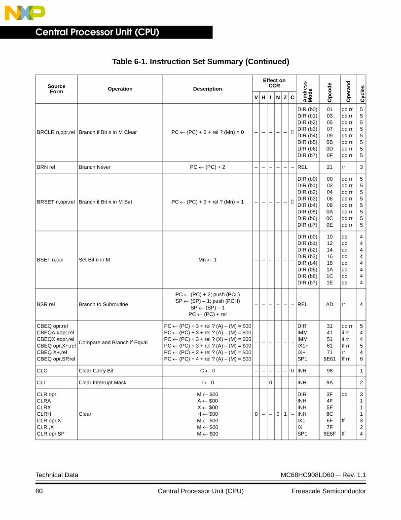
Central Processor Unit (CPU)
BRCLR n,opr,rel Branch if Bit n in M Clear PC ← (PC) + 3 + rel ? (Mn) = 0 – – – – –
DIR (b0)DIR (b1)DIR (b2)DIR (b3)DIR (b4)DIR (b5)DIR (b6)DIR (b7)
01030507090B0D0F
dd rrdd rrdd rrdd rrdd rrdd rrdd rrdd rr
55555555
BRN rel Branch Never PC ← (PC) + 2 – – – – – – REL 21 rr 3
BRSET n,opr,rel Branch if Bit n in M Set PC ← (PC) + 3 + rel ? (Mn) = 1 – – – – –
DIR (b0)DIR (b1)DIR (b2)DIR (b3)DIR (b4)DIR (b5)DIR (b6)DIR (b7)
00020406080A0C0E
dd rrdd rrdd rrdd rrdd rrdd rrdd rrdd rr
55555555
BSET n,opr Set Bit n in M Mn ← 1 – – – – – –
DIR (b0)DIR (b1)DIR (b2)DIR (b3)DIR (b4)DIR (b5)DIR (b6)DIR (b7)
10121416181A1C1E
dddddddddddddddd
44444444
BSR rel Branch to Subroutine
PC ← (PC) + 2; push (PCL)SP ← (SP) – 1; push (PCH)
SP ← (SP) – 1PC ← (PC) + rel
– – – – – – REL AD rr 4
CBEQ opr,relCBEQA #opr,relCBEQX #opr,relCBEQ opr,X+,relCBEQ X+,relCBEQ opr,SP,rel
Compare and Branch if Equal
PC ← (PC) + 3 + rel ? (A) – (M) = $00PC ← (PC) + 3 + rel ? (A) – (M) = $00PC ← (PC) + 3 + rel ? (X) – (M) = $00PC ← (PC) + 3 + rel ? (A) – (M) = $00PC ← (PC) + 2 + rel ? (A) – (M) = $00PC ← (PC) + 4 + rel ? (A) – (M) = $00
– – – – – –
DIRIMMIMMIX1+IX+SP1
3141516171
9E61
dd rrii rrii rrff rrrrff rr
544546
CLC Clear Carry Bit C ← 0 – – – – – 0 INH 98 1
CLI Clear Interrupt Mask I ← 0 – – 0 – – – INH 9A 2
CLR oprCLRACLRXCLRHCLR opr,XCLR ,XCLR opr,SP
Clear
M ← $00A ← $00X ← $00H ← $00M ← $00M ← $00M ← $00
0 – – 0 1 –
DIRINHINHINHIX1IXSP1
3F4F5F8C6F7F
9E6F
dd
ff
ff
3111324
Table 6-1. Instruction Set Summary (Continued)
SourceForm Operation Description
Effect onCCR
Ad
dre
ssM
od
e
Op
cod
e
Op
eran
d
Cyc
les
V H I N Z C
Technical Data MC68HC908LD60 — Rev. 1.1
80 Central Processor Unit (CPU) Freescale Semiconductor
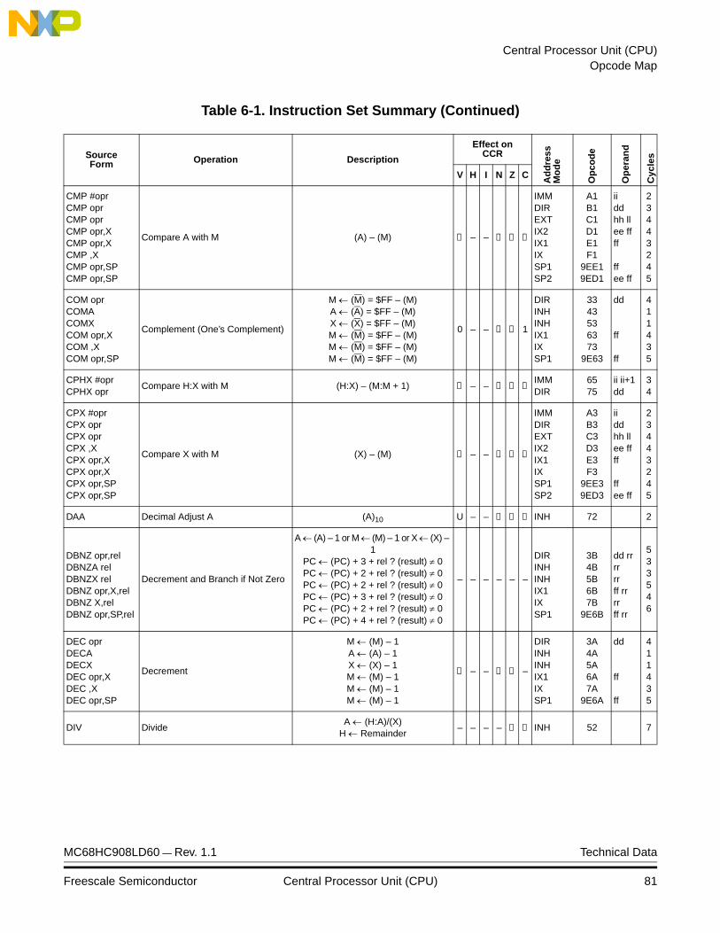
Central Processor Unit (CPU)Opcode Map
CMP #oprCMP oprCMP oprCMP opr,XCMP opr,XCMP ,XCMP opr,SPCMP opr,SP
Compare A with M (A) – (M) – –
IMMDIREXTIX2IX1IXSP1SP2
A1B1C1D1E1F1
9EE19ED1
iiddhh llee ffff
ffee ff
23443245
COM oprCOMACOMXCOM opr,XCOM ,XCOM opr,SP
Complement (One’s Complement)
M ← (M) = $FF – (M)A ← (A) = $FF – (M)X ← (X) = $FF – (M)M ← (M) = $FF – (M)M ← (M) = $FF – (M)M ← (M) = $FF – (M)
0 – – 1
DIRINHINHIX1IXSP1
3343536373
9E63
dd
ff
ff
411435
CPHX #oprCPHX opr
Compare H:X with M (H:X) – (M:M + 1) – – IMMDIR
6575
ii ii+1dd
34
CPX #oprCPX oprCPX oprCPX ,XCPX opr,XCPX opr,XCPX opr,SPCPX opr,SP
Compare X with M (X) – (M) – –
IMMDIREXTIX2IX1IXSP1SP2
A3B3C3D3E3F3
9EE39ED3
iiddhh llee ffff
ffee ff
23443245
DAA Decimal Adjust A (A)10 U – – INH 72 2
DBNZ opr,relDBNZA relDBNZX relDBNZ opr,X,relDBNZ X,relDBNZ opr,SP,rel
Decrement and Branch if Not Zero
A ← (A) – 1 or M ← (M) – 1 or X ← (X) – 1
PC ← (PC) + 3 + rel ? (result) ≠ 0PC ← (PC) + 2 + rel ? (result) ≠ 0PC ← (PC) + 2 + rel ? (result) ≠ 0PC ← (PC) + 3 + rel ? (result) ≠ 0PC ← (PC) + 2 + rel ? (result) ≠ 0PC ← (PC) + 4 + rel ? (result) ≠ 0
– – – – – –
DIRINHINHIX1IXSP1
3B4B5B6B7B
9E6B
dd rrrrrrff rrrrff rr
533546
DEC oprDECADECXDEC opr,XDEC ,XDEC opr,SP
Decrement
M ← (M) – 1A ← (A) – 1X ← (X) – 1M ← (M) – 1M ← (M) – 1M ← (M) – 1
– – –
DIRINHINHIX1IXSP1
3A4A5A6A7A
9E6A
dd
ff
ff
411435
DIV DivideA ← (H:A)/(X)
H ← Remainder– – – – INH 52 7
Table 6-1. Instruction Set Summary (Continued)
SourceForm Operation Description
Effect onCCR
Ad
dre
ssM
od
e
Op
cod
e
Op
eran
d
Cyc
les
V H I N Z C
MC68HC908LD60 — Rev. 1.1 Technical Data
Freescale Semiconductor Central Processor Unit (CPU) 81

Central Processor Unit (CPU)
EOR #oprEOR oprEOR oprEOR opr,XEOR opr,XEOR ,XEOR opr,SPEOR opr,SP
Exclusive OR M with A A ← (A ⊕ M) 0 – – –
IMMDIREXTIX2IX1IXSP1SP2
A8B8C8D8E8F8
9EE89ED8
iiddhh llee ffff
ffee ff
23443245
INC oprINCAINCXINC opr,XINC ,XINC opr,SP
Increment
M ← (M) + 1A ← (A) + 1X ← (X) + 1M ← (M) + 1M ← (M) + 1M ← (M) + 1
– – –
DIRINHINHIX1IXSP1
3C4C5C6C7C
9E6C
dd
ff
ff
411435
JMP oprJMP oprJMP opr,XJMP opr,XJMP ,X
Jump PC ← Jump Address – – – – – –
DIREXTIX2IX1IX
BCCCDCECFC
ddhh llee ffff
23432
JSR oprJSR oprJSR opr,XJSR opr,XJSR ,X
Jump to Subroutine
PC ← (PC) + n (n = 1, 2, or 3)Push (PCL); SP ← (SP) – 1Push (PCH); SP ← (SP) – 1PC ← Unconditional Address
– – – – – –
DIREXTIX2IX1IX
BDCDDDEDFD
ddhh llee ffff
45654
LDA #oprLDA oprLDA oprLDA opr,XLDA opr,XLDA ,XLDA opr,SPLDA opr,SP
Load A from M A ← (M) 0 – – –
IMMDIREXTIX2IX1IXSP1SP2
A6B6C6D6E6F6
9EE69ED6
iiddhh llee ffff
ffee ff
23443245
LDHX #oprLDHX opr
Load H:X from M H:X ← (M:M + 1) 0 – – –IMMDIR
4555
ii jjdd
34
LDX #oprLDX oprLDX oprLDX opr,XLDX opr,XLDX ,XLDX opr,SPLDX opr,SP
Load X from M X ← (M) 0 – – –
IMMDIREXTIX2IX1IXSP1SP2
AEBECEDEEEFE
9EEE9EDE
iiddhh llee ffff
ffee ff
23443245
LSL oprLSLALSLXLSL opr,XLSL ,XLSL opr,SP
Logical Shift Left(Same as ASL)
– –
DIRINHINHIX1IXSP1
3848586878
9E68
dd
ff
ff
411435
Table 6-1. Instruction Set Summary (Continued)
SourceForm Operation Description
Effect onCCR
Ad
dre
ssM
od
e
Op
cod
e
Op
eran
d
Cyc
les
V H I N Z C
C
b0b7
0
Technical Data MC68HC908LD60 — Rev. 1.1
82 Central Processor Unit (CPU) Freescale Semiconductor
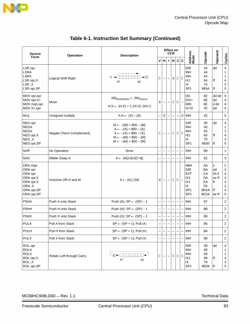
Central Processor Unit (CPU)Opcode Map
LSR oprLSRALSRXLSR opr,XLSR ,XLSR opr,SP
Logical Shift Right – – 0
DIRINHINHIX1IXSP1
3444546474
9E64
dd
ff
ff
411435
MOV opr,oprMOV opr,X+MOV #opr,oprMOV X+,opr
Move(M)Destination ← (M)Source
H:X ← (H:X) + 1 (IX+D, DIX+)0 – – –
DDDIX+IMDIX+D
4E5E6E7E
dd ddddii dddd
5444
MUL Unsigned multiply X:A ← (X) × (A) – 0 – – – 0 INH 42 5
NEG oprNEGANEGXNEG opr,XNEG ,XNEG opr,SP
Negate (Two’s Complement)
M ← –(M) = $00 – (M)A ← –(A) = $00 – (A)X ← –(X) = $00 – (X)M ← –(M) = $00 – (M)M ← –(M) = $00 – (M)
– –
DIRINHINHIX1IXSP1
3040506070
9E60
dd
ff
ff
411435
NOP No Operation None – – – – – – INH 9D 1
NSA Nibble Swap A A ← (A[3:0]:A[7:4]) – – – – – – INH 62 3
ORA #oprORA oprORA oprORA opr,XORA opr,XORA ,XORA opr,SPORA opr,SP
Inclusive OR A and M A ← (A) | (M) 0 – – –
IMMDIREXTIX2IX1IXSP1SP2
AABACADAEAFA
9EEA9EDA
iiddhh llee ffff
ffee ff
23443245
PSHA Push A onto Stack Push (A); SP ← (SP) – 1 – – – – – – INH 87 2
PSHH Push H onto Stack Push (H); SP ← (SP) – 1 – – – – – – INH 8B 2
PSHX Push X onto Stack Push (X); SP ← (SP) – 1 – – – – – – INH 89 2
PULA Pull A from Stack SP ← (SP + 1); Pull (A) – – – – – – INH 86 2
PULH Pull H from Stack SP ← (SP + 1); Pull (H) – – – – – – INH 8A 2
PULX Pull X from Stack SP ← (SP + 1); Pull (X) – – – – – – INH 88 2
ROL oprROLAROLXROL opr,XROL ,XROL opr,SP
Rotate Left through Carry – –
DIRINHINHIX1IXSP1
3949596979
9E69
dd
ff
ff
411435
Table 6-1. Instruction Set Summary (Continued)
SourceForm Operation Description
Effect onCCR
Ad
dre
ssM
od
e
Op
cod
e
Op
eran
d
Cyc
les
V H I N Z C
b0b7
C0
C
b0b7
MC68HC908LD60 — Rev. 1.1 Technical Data
Freescale Semiconductor Central Processor Unit (CPU) 83
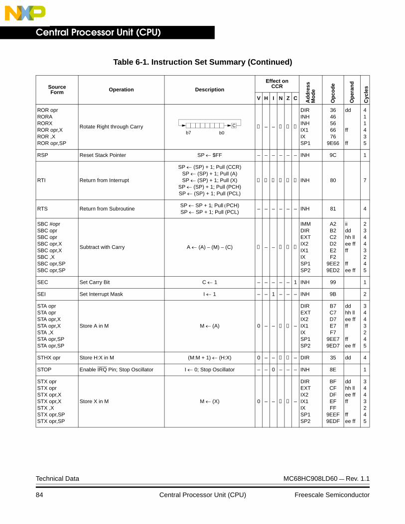
Central Processor Unit (CPU)
ROR oprRORARORXROR opr,XROR ,XROR opr,SP
Rotate Right through Carry – –
DIRINHINHIX1IXSP1
3646566676
9E66
dd
ff
ff
411435
RSP Reset Stack Pointer SP ← $FF – – – – – – INH 9C 1
RTI Return from Interrupt
SP ← (SP) + 1; Pull (CCR)SP ← (SP) + 1; Pull (A)SP ← (SP) + 1; Pull (X)
SP ← (SP) + 1; Pull (PCH)SP ← (SP) + 1; Pull (PCL)
INH 80 7
RTS Return from SubroutineSP ← SP + 1; Pull (PCH)SP ← SP + 1; Pull (PCL)
– – – – – – INH 81 4
SBC #oprSBC oprSBC oprSBC opr,XSBC opr,XSBC ,XSBC opr,SPSBC opr,SP
Subtract with Carry A ← (A) – (M) – (C) – –
IMMDIREXTIX2IX1IXSP1SP2
A2B2C2D2E2F2
9EE29ED2
iiddhh llee ffff
ffee ff
23443245
SEC Set Carry Bit C ← 1 – – – – – 1 INH 99 1
SEI Set Interrupt Mask I ← 1 – – 1 – – – INH 9B 2
STA oprSTA oprSTA opr,XSTA opr,XSTA ,XSTA opr,SPSTA opr,SP
Store A in M M ← (A) 0 – – –
DIREXTIX2IX1IXSP1SP2
B7C7D7E7F7
9EE79ED7
ddhh llee ffff
ffee ff
3443245
STHX opr Store H:X in M (M:M + 1) ← (H:X) 0 – – – DIR 35 dd 4
STOP Enable IRQ Pin; Stop Oscillator I ← 0; Stop Oscillator – – 0 – – – INH 8E 1
STX oprSTX oprSTX opr,XSTX opr,XSTX ,XSTX opr,SPSTX opr,SP
Store X in M M ← (X) 0 – – –
DIREXTIX2IX1IXSP1SP2
BFCFDFEFFF
9EEF9EDF
ddhh llee ffff
ffee ff
3443245
Table 6-1. Instruction Set Summary (Continued)
SourceForm Operation Description
Effect onCCR
Ad
dre
ssM
od
e
Op
cod
e
Op
eran
d
Cyc
les
V H I N Z C
b0b7
C
Technical Data MC68HC908LD60 — Rev. 1.1
84 Central Processor Unit (CPU) Freescale Semiconductor
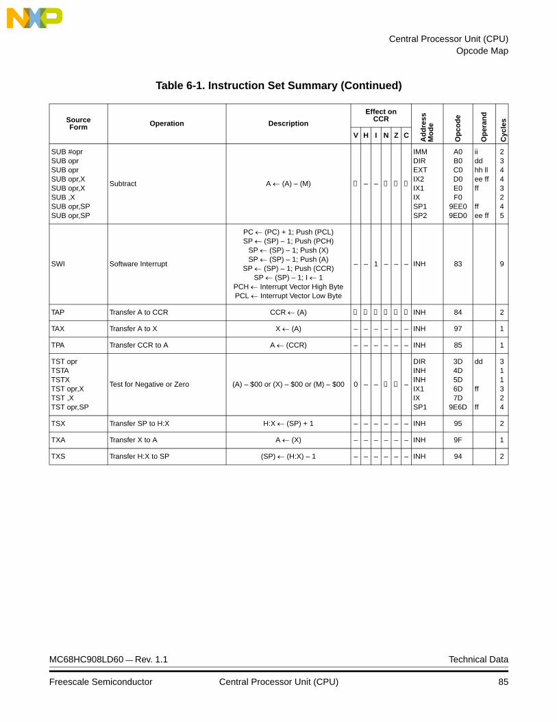
Central Processor Unit (CPU)Opcode Map
SUB #oprSUB oprSUB oprSUB opr,XSUB opr,XSUB ,XSUB opr,SPSUB opr,SP
Subtract A ← (A) – (M) – –
IMMDIREXTIX2IX1IXSP1SP2
A0B0C0D0E0F0
9EE09ED0
iiddhh llee ffff
ffee ff
23443245
SWI Software Interrupt
PC ← (PC) + 1; Push (PCL)SP ← (SP) – 1; Push (PCH)
SP ← (SP) – 1; Push (X)SP ← (SP) – 1; Push (A)
SP ← (SP) – 1; Push (CCR)SP ← (SP) – 1; I ← 1
PCH ← Interrupt Vector High BytePCL ← Interrupt Vector Low Byte
– – 1 – – – INH 83 9
TAP Transfer A to CCR CCR ← (A) INH 84 2
TAX Transfer A to X X ← (A) – – – – – – INH 97 1
TPA Transfer CCR to A A ← (CCR) – – – – – – INH 85 1
TST oprTSTATSTXTST opr,XTST ,XTST opr,SP
Test for Negative or Zero (A) – $00 or (X) – $00 or (M) – $00 0 – – –
DIRINHINHIX1IXSP1
3D4D5D6D7D
9E6D
dd
ff
ff
311324
TSX Transfer SP to H:X H:X ← (SP) + 1 – – – – – – INH 95 2
TXA Transfer X to A A ← (X) – – – – – – INH 9F 1
TXS Transfer H:X to SP (SP) ← (H:X) – 1 – – – – – – INH 94 2
Table 6-1. Instruction Set Summary (Continued)
SourceForm Operation Description
Effect onCCR
Ad
dre
ssM
od
e
Op
cod
e
Op
eran
d
Cyc
les
V H I N Z C
MC68HC908LD60 — Rev. 1.1 Technical Data
Freescale Semiconductor Central Processor Unit (CPU) 85
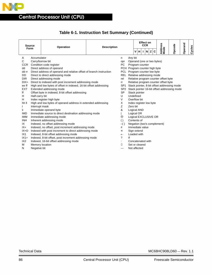
Central Processor Unit (CPU)
A Accumulator n Any bitC Carry/borrow bit opr Operand (one or two bytes)CCR Condition code register PC Program counterdd Direct address of operand PCH Program counter high bytedd rr Direct address of operand and relative offset of branch instruction PCL Program counter low byteDD Direct to direct addressing mode REL Relative addressing modeDIR Direct addressing mode rel Relative program counter offset byteDIX+ Direct to indexed with post increment addressing mode rr Relative program counter offset byteee ff High and low bytes of offset in indexed, 16-bit offset addressing SP1 Stack pointer, 8-bit offset addressing modeEXT Extended addressing mode SP2 Stack pointer 16-bit offset addressing modeff Offset byte in indexed, 8-bit offset addressing SP Stack pointerH Half-carry bit U UndefinedH Index register high byte V Overflow bithh ll High and low bytes of operand address in extended addressing X Index register low byteI Interrupt mask Z Zero bitii Immediate operand byte & Logical ANDIMD Immediate source to direct destination addressing mode | Logical ORIMM Immediate addressing mode ⊕ Logical EXCLUSIVE ORINH Inherent addressing mode ( ) Contents ofIX Indexed, no offset addressing mode –( ) Negation (two’s complement)IX+ Indexed, no offset, post increment addressing mode # Immediate valueIX+D Indexed with post increment to direct addressing mode « Sign extendIX1 Indexed, 8-bit offset addressing mode ← Loaded withIX1+ Indexed, 8-bit offset, post increment addressing mode ? IfIX2 Indexed, 16-bit offset addressing mode : Concatenated withM Memory location Set or clearedN Negative bit — Not affected
Table 6-1. Instruction Set Summary (Continued)
SourceForm Operation Description
Effect onCCR
Ad
dre
ssM
od
e
Op
cod
e
Op
eran
d
Cyc
les
V H I N Z C
Technical Data MC68HC908LD60 — Rev. 1.1
86 Central Processor Unit (CPU) Freescale Semiconductor
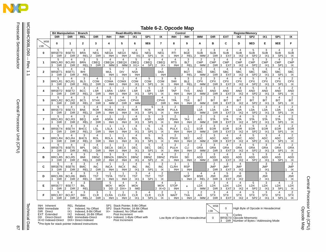
MC
68H
Freescale S
emiconductor
Central P
rocessor Unit (C
PU
)87
Central P
rocessor Unit (C
PU
)O
pcode Map
Table 6-2. Opcode MapRegister/Memory
IX2 SP2 IX1 SP1 IX
D 9ED E 9EE F
4SUB
IX2
5SUB
4 SP2
3SUB
2 IX1
4SUB
3 SP1
2SUB
1 IX4
CMPIX2
5CMP
4 SP2
3CMP
2 IX1
4CMP
3 SP1
2CMP
1 IX4
SBCIX2
5SBC
4 SP2
3SBC
2 IX1
4SBC
3 SP1
2SBC
1 IX4
CPXIX2
5CPX
4 SP2
3CPX
2 IX1
4CPX
3 SP1
2CPX
1 IX4
ANDIX2
5AND
4 SP2
3AND
2 IX1
4AND
3 SP1
2AND
1 IX4
BITIX2
5BIT
4 SP2
3BIT
2 IX1
4BIT
3 SP1
2BIT
1 IX4
LDAIX2
5LDA
4 SP2
3LDA
2 IX1
4LDA
3 SP1
2LDA
1 IX4
STAIX2
5STA
4 SP2
3STA
2 IX1
4STA
3 SP1
2STA
1 IX4
EORIX2
5EOR
4 SP2
3EOR
2 IX1
4EOR
3 SP1
2EOR
1 IX4
ADCIX2
5ADC
4 SP2
3ADC
2 IX1
4ADC
3 SP1
2ADC
1 IX4
ORAIX2
5ORA
4 SP2
3ORA
2 IX1
4ORA
3 SP1
2ORA
1 IX4
ADDIX2
5ADD
4 SP2
3ADD
2 IX1
4ADD
3 SP1
2ADD
1 IX4
JMPIX2
3JMP
2 IX1
2JMP
1 IX6
JSRIX2
5JSR
2 IX1
4JSR
1 IX4
LDXIX2
5LDX
4 SP2
3LDX
2 IX1
4LDX
3 SP1
2LDX
1 IX4
STXIX2
5STX
4 SP2
3STX
2 IX1
4STX
3 SP1
2STX
1 IX
igh Byte of Opcode in Hexadecimal
yclespcode Mnemonicumber of Bytes / Addressing Mode
C908LD
60 —
Rev. 1.1
Technical Data
Bit Manipulation Branch Read-Modify-Write ControlDIR DIR REL DIR INH INH IX1 SP1 IX INH INH IMM DIR EXT
0 1 2 3 4 5 6 9E6 7 8 9 A B C
05
BRSET03 DIR
4BSET0
2 DIR
3BRA
2 REL
4NEG
2 DIR
1NEGA
1 INH
1NEGX
1 INH
4NEG
2 IX1
5NEG
3 SP1
3NEG
1 IX
7RTI
1 INH
3BGE
2 REL
2SUB
2 IMM
3SUB
2 DIR
4SUB
3 EXT 3
15
BRCLR03 DIR
4BCLR0
2 DIR
3BRN
2 REL
5CBEQ
3 DIR
4CBEQA3 IMM
4CBEQX3 IMM
5CBEQ
3 IX1+
6CBEQ
4 SP1
4CBEQ
2 IX+
4RTS
1 INH
3BLT
2 REL
2CMP
2 IMM
3CMP
2 DIR
4CMP
3 EXT 3
25
BRSET13 DIR
4BSET1
2 DIR
3BHI
2 REL
5MUL
1 INH
7DIV
1 INH
3NSA
1 INH
2DAA
1 INH
3BGT
2 REL
2SBC
2 IMM
3SBC
2 DIR
4SBC
3 EXT 3
35
BRCLR13 DIR
4BCLR1
2 DIR
3BLS
2 REL
4COM
2 DIR
1COMA
1 INH
1COMX
1 INH
4COM
2 IX1
5COM
3 SP1
3COM
1 IX
9SWI
1 INH
3BLE
2 REL
2CPX
2 IMM
3CPX
2 DIR
4CPX
3 EXT 3
45
BRSET23 DIR
4BSET2
2 DIR
3BCC
2 REL
4LSR
2 DIR
1LSRA
1 INH
1LSRX
1 INH
4LSR
2 IX1
5LSR
3 SP1
3LSR
1 IX
2TAP
1 INH
2TXS
1 INH
2AND
2 IMM
3AND
2 DIR
4AND
3 EXT 3
55
BRCLR23 DIR
4BCLR2
2 DIR
3BCS
2 REL
4STHX
2 DIR
3LDHX
3 IMM
4LDHX
2 DIR
3CPHX
3 IMM
4CPHX
2 DIR
1TPA
1 INH
2TSX
1 INH
2BIT
2 IMM
3BIT
2 DIR
4BIT
3 EXT 3
65
BRSET33 DIR
4BSET3
2 DIR
3BNE
2 REL
4ROR
2 DIR
1RORA
1 INH
1RORX
1 INH
4ROR
2 IX1
5ROR
3 SP1
3ROR
1 IX
2PULA
1 INH
2LDA
2 IMM
3LDA
2 DIR
4LDA
3 EXT 3
75
BRCLR33 DIR
4BCLR3
2 DIR
3BEQ
2 REL
4ASR
2 DIR
1ASRA
1 INH
1ASRX
1 INH
4ASR
2 IX1
5ASR
3 SP1
3ASR
1 IX
2PSHA
1 INH
1TAX
1 INH
2AIS
2 IMM
3STA
2 DIR
4STA
3 EXT 3
85
BRSET43 DIR
4BSET4
2 DIR
3BHCC
2 REL
4LSL
2 DIR
1LSLA
1 INH
1LSLX
1 INH
4LSL
2 IX1
5LSL
3 SP1
3LSL
1 IX
2PULX
1 INH
1CLC
1 INH
2EOR
2 IMM
3EOR
2 DIR
4EOR
3 EXT 3
95
BRCLR43 DIR
4BCLR4
2 DIR
3BHCS
2 REL
4ROL
2 DIR
1ROLA
1 INH
1ROLX
1 INH
4ROL
2 IX1
5ROL
3 SP1
3ROL
1 IX
2PSHX
1 INH
1SEC
1 INH
2ADC
2 IMM
3ADC
2 DIR
4ADC
3 EXT 3
A5
BRSET53 DIR
4BSET5
2 DIR
3BPL
2 REL
4DEC
2 DIR
1DECA
1 INH
1DECX
1 INH
4DEC
2 IX1
5DEC
3 SP1
3DEC
1 IX
2PULH
1 INH
2CLI
1 INH
2ORA
2 IMM
3ORA
2 DIR
4ORA
3 EXT 3
B5
BRCLR53 DIR
4BCLR5
2 DIR
3BMI
2 REL
5DBNZ
3 DIR
3DBNZA2 INH
3DBNZX2 INH
5DBNZ
3 IX1
6DBNZ
4 SP1
4DBNZ
2 IX
2PSHH
1 INH
2SEI
1 INH
2ADD
2 IMM
3ADD
2 DIR
4ADD
3 EXT 3
C5
BRSET63 DIR
4BSET6
2 DIR
3BMC
2 REL
4INC
2 DIR
1INCA
1 INH
1INCX
1 INH
4INC
2 IX1
5INC
3 SP1
3INC
1 IX
1CLRH
1 INH
1RSP
1 INH
2JMP
2 DIR
3JMP
3 EXT 3
D5
BRCLR63 DIR
4BCLR6
2 DIR
3BMS
2 REL
3TST
2 DIR
1TSTA
1 INH
1TSTX
1 INH
3TST
2 IX1
4TST
3 SP1
2TST
1 IX
1NOP
1 INH
4BSR
2 REL
4JSR
2 DIR
5JSR
3 EXT 3
E5
BRSET73 DIR
4BSET7
2 DIR
3BIL
2 REL
5MOV
3 DD
4MOV
2 DIX+
4MOV
3 IMD
4MOV
2 IX+D
1STOP
1 INH *2
LDX2 IMM
3LDX
2 DIR
4LDX
3 EXT 3
F5
BRCLR73 DIR
4BCLR7
2 DIR
3BIH
2 REL
3CLR
2 DIR
1CLRA
1 INH
1CLRX
1 INH
3CLR
2 IX1
4CLR
3 SP1
2CLR
1 IX
1WAIT
1 INH
1TXA
1 INH
2AIX
2 IMM
3STX
2 DIR
4STX
3 EXT 3
INH Inherent REL Relative SP1 Stack Pointer, 8-Bit OffsetIMM Immediate IX Indexed, No Offset SP2 Stack Pointer, 16-Bit OffsetDIR Direct IX1 Indexed, 8-Bit Offset IX+ Indexed, No Offset with EXT Extended IX2 Indexed, 16-Bit Offset Post IncrementDD Direct-Direct IMD Immediate-Direct IX1+ Indexed, 1-Byte Offset with IX+D Indexed-Direct DIX+ Direct-Indexed Post Increment*Pre-byte for stack pointer indexed instructions
0 H
Low Byte of Opcode in Hexadecimal 05
BRSET03 DIR
CON
MSB
LSB
MSB
LSB
Central Processor Unit (CPU)
Technical Data MC68HC908LD60 — Rev. 1.1
88 Central Processor Unit (CPU) Freescale Semiconductor

Technical Data — MC68HC908LD60
Section 7. Oscillator (OSC)
7.1 Contents
7.2 Introduction . . . . . . . . . . . . . . . . . . . . . . . . . . . . . . . . . . . . . . . .89
7.3 Oscillator External Connections . . . . . . . . . . . . . . . . . . . . . . . .90
7.4 I/O Signals . . . . . . . . . . . . . . . . . . . . . . . . . . . . . . . . . . . . . . . .917.4.1 Crystal Amplifier Input Pin (OSC1). . . . . . . . . . . . . . . . . . . .917.4.2 Crystal Amplifier Output Pin (OSC2) . . . . . . . . . . . . . . . . . .917.4.3 Oscillator Enable Signal (SIMOSCEN). . . . . . . . . . . . . . . . .917.4.4 External Clock Source (OSCXCLK) . . . . . . . . . . . . . . . . . . .917.4.5 Oscillator Out (OSCOUT). . . . . . . . . . . . . . . . . . . . . . . . . . .91
7.5 Low Power Modes . . . . . . . . . . . . . . . . . . . . . . . . . . . . . . . . . .927.5.1 Wait Mode . . . . . . . . . . . . . . . . . . . . . . . . . . . . . . . . . . . . . .927.5.2 Stop Mode . . . . . . . . . . . . . . . . . . . . . . . . . . . . . . . . . . . . . .92
7.6 Oscillator During Break Mode. . . . . . . . . . . . . . . . . . . . . . . . . .92
7.2 Introduction
The oscillator circuit is designed for use with crystals or ceramic resonators. The oscillator circuit generates the crystal clock signal, OSCXCLK, at the frequency of the crystal. This signal is divided by two before being passed on to the SIM for bus clock generation. Figure 7-1 shows the structure of the oscillator. The oscillator requires various external components.
The MC68HC908LD60 operates from a nominal 24MHz crystal or external clock, providing an 8MHz internal bus clock. The 24MHz clock is required for various modules, such as the CGM.
MC68HC908LD60 — Rev. 1.1 Technical Data
Freescale Semiconductor Oscillator (OSC) 89
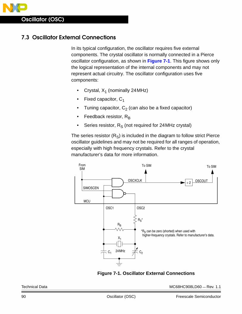
Oscillator (OSC)
7.3 Oscillator External Connections
In its typical configuration, the oscillator requires five external components. The crystal oscillator is normally connected in a Pierce oscillator configuration, as shown in Figure 7-1. This figure shows only the logical representation of the internal components and may not represent actual circuitry. The oscillator configuration uses five components:
• Crystal, X1 (nominally 24MHz)
• Fixed capacitor, C1
• Tuning capacitor, C2 (can also be a fixed capacitor)
• Feedback resistor, RB
• Series resistor, RS (not required for 24MHz crystal)
The series resistor (RS) is included in the diagram to follow strict Pierce oscillator guidelines and may not be required for all ranges of operation, especially with high frequency crystals. Refer to the crystal manufacturer’s data for more information.
Figure 7-1. Oscillator External Connections
C1 C2
SIMOSCEN
OSCXCLK
RB
X1
RS*
*RS can be zero (shorted) when used with
MCU
FromSIM
÷ 2 OSCOUT
To SIMTo SIM
OSC1 OSC2
higher-frequency crystals. Refer to manufacturer’s data.
24MHz
Technical Data MC68HC908LD60 — Rev. 1.1
90 Oscillator (OSC) Freescale Semiconductor
Oscillator (OSC)I/O Signals
7.4 I/O Signals
The following paragraphs describe the oscillator I/O signals.
7.4.1 Crystal Amplifier Input Pin (OSC1)
The OSC1 pin is an input to the crystal oscillator amplifier.
An externally generated clock also can feed the OSC1 pin of the crystal oscillator circuit. Connect the external clock to the OSC1 pin and let the OSC2 pin float.
7.4.2 Crystal Amplifier Output Pin (OSC2)
The OSC2 pin is the output of the crystal oscillator inverting amplifier.
7.4.3 Oscillator Enable Signal (SIMOSCEN)
The SIMOSCEN signal comes from the SIM and enables the oscillator.
7.4.4 External Clock Source (OSCXCLK)
OSCXCLK is the crystal oscillator output signal. It runs at the full speed of the crystal (fXCLK) and comes directly from the crystal oscillator circuit. Figure 7-1 shows only the logical relation of OSCXCLK to OSC1 and OSC2 and may not represent the actual circuitry. The duty cycle of OSCXCLK is unknown and may depend on the crystal and other external factors. Also, the frequency and amplitude of OSCXCLK can be unstable at start-up.
7.4.5 Oscillator Out (OSCOUT)
The clock driven to the SIM is the crystal frequency divided by two. This signal is driven to the SIM for generation of the bus clocks used by the CPU and other modules on the MCU. OSCOUT will be divided again in the SIM and results in the internal bus frequency being one fourth of the OSCXCLK frequency.
MC68HC908LD60 — Rev. 1.1 Technical Data
Freescale Semiconductor Oscillator (OSC) 91
Oscillator (OSC)
7.5 Low Power Modes
The WAIT and STOP instructions put the MCU in low-power-consumption standby modes.
7.5.1 Wait Mode
The WAIT instruction has no effect on the oscillator logic. OSCXCLK continues to drive to the SIM module.
7.5.2 Stop Mode
The STOP instruction disables the OSCXCLK output.
7.6 Oscillator During Break Mode
The oscillator continues drive OSCXCLK when the chip enters the break state.
Technical Data MC68HC908LD60 — Rev. 1.1
92 Oscillator (OSC) Freescale Semiconductor

Technical Data — MC68HC908LD60
Section 8. Clock Generator Module (CGM)
8.1 Contents
8.2 Introduction . . . . . . . . . . . . . . . . . . . . . . . . . . . . . . . . . . . . . . . .94
8.3 Features . . . . . . . . . . . . . . . . . . . . . . . . . . . . . . . . . . . . . . . . . .94
8.4 Functional Description . . . . . . . . . . . . . . . . . . . . . . . . . . . . . . .948.4.1 Crystal Oscillator Circuit . . . . . . . . . . . . . . . . . . . . . . . . . . . .97
8.5 CGM I/O Signals. . . . . . . . . . . . . . . . . . . . . . . . . . . . . . . . . . . .978.5.1 External Filter Capacitor Pin (CGMXFC) . . . . . . . . . . . . . . .978.5.2 PLL Analog Power Pin (VDDA) . . . . . . . . . . . . . . . . . . . . . .978.5.3 PLL Analog Ground Pin (VSSA). . . . . . . . . . . . . . . . . . . . . .978.5.4 Crystal Output Frequency Signal (OSCXCLK). . . . . . . . . . .988.5.5 Crystal Reference Frequency Signal (OSCRCLK). . . . . . . .988.5.6 CGM Base Clock Output (DCLK1) . . . . . . . . . . . . . . . . . . . .988.5.7 CGM CPU Interrupt (CGMINT) . . . . . . . . . . . . . . . . . . . . . .98
8.6 CGM I/O Registers . . . . . . . . . . . . . . . . . . . . . . . . . . . . . . . . . .988.6.1 PLL Control Register (PCTL) . . . . . . . . . . . . . . . . . . . . . . . .998.6.2 PLL Bandwidth Control Register (PBWC) . . . . . . . . . . . . .1008.6.3 PLL Programming Register (PPG) . . . . . . . . . . . . . . . . . . .1028.6.4 H & V Sync Output Control Register (HVOCR) . . . . . . . . .104
8.7 Interrupts. . . . . . . . . . . . . . . . . . . . . . . . . . . . . . . . . . . . . . . . .105
8.8 Low-Power Modes . . . . . . . . . . . . . . . . . . . . . . . . . . . . . . . . .1058.8.1 Wait Mode . . . . . . . . . . . . . . . . . . . . . . . . . . . . . . . . . . . . .1058.8.2 Stop Mode . . . . . . . . . . . . . . . . . . . . . . . . . . . . . . . . . . . . .106
8.9 CGM During Break Interrupts . . . . . . . . . . . . . . . . . . . . . . . . .106
MC68HC908LD60 — Rev. 1.1 Technical Data
Freescale Semiconductor Clock Generator Module (CGM) 93

Clock Generator Module (CGM)
8.2 Introduction
This section describes the clock generator module (CGM). Using the crystal reference clock from the oscillator module, the CGM generates the display base clock, DCLK1, for the sync processor module. The CGM is able to generate a frequency up to 108MHz from a 24MHz reference clock.
8.3 Features
Features of the CGM include the following:
• Phase-locked loop with output frequency in integer multiples of the crystal reference
• Programmable hardware voltage-controlled oscillator (VCO) for low-jitter operation
• Automatic bandwidth control mode for low-jitter operation
• Automatic frequency lock detector
• CPU interrupt on entry or exit from locked condition
8.4 Functional Description
The CGM consists of three major sub-modules:
• Crystal oscillator circuit which generates the buffered constant crystal frequency clock, OSCRCLK. (See Section 7. Oscillator (OSC).)
• Phase-locked loop (PLL) which generates the programmable VCO frequency clock CGMVCLK.
• Base clock selector circuit; this software-controlled circuit selects either OSCXCLK divided by two or the VCO clock CGMVCLK divided by two, as the base clock DCLK1. The sync processor derives other display clocks from DCLK1.
Technical Data MC68HC908LD60 — Rev. 1.1
94 Clock Generator Module (CGM) Freescale Semiconductor
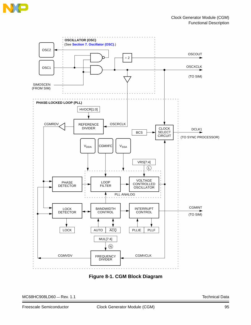
Clock Generator Module (CGM)Functional Description
Figure 8-1. CGM Block Diagram
BCS
PHASEDETECTOR
LOOPFILTER
FREQUENCYDIVIDER
VOLTAGECONTROLLEDOSCILLATOR
LOCKDETECTOR
CLOCK
OSCXCLK
CGMVDV
SIMOSCEN
OSCILLATOR (OSC)
INTERRUPTCONTROL
CGMINT
CGMRDV
PLL ANALOG
OSCRCLK
OSC2
OSC1
SELECTCIRCUIT
VDDA CGMXFC VSSA
LOCK AUTO ACQ PLLIE PLLF
MUL[7:4]
REFERENCEDIVIDER
VRS[7:4]
(TO SIM)
(TO SIM)
HVOCR[1:0]
(FROM SIM)
CGMVCLK
PHASE-LOCKED LOOP (PLL)
DCLK1
BANDWIDTHCONTROL
(TO SYNC PROCESSOR)
(See Section 7. Oscillator (OSC).)
OSCOUT÷ 2
N
L
MC68HC908LD60 — Rev. 1.1 Technical Data
Freescale Semiconductor Clock Generator Module (CGM) 95
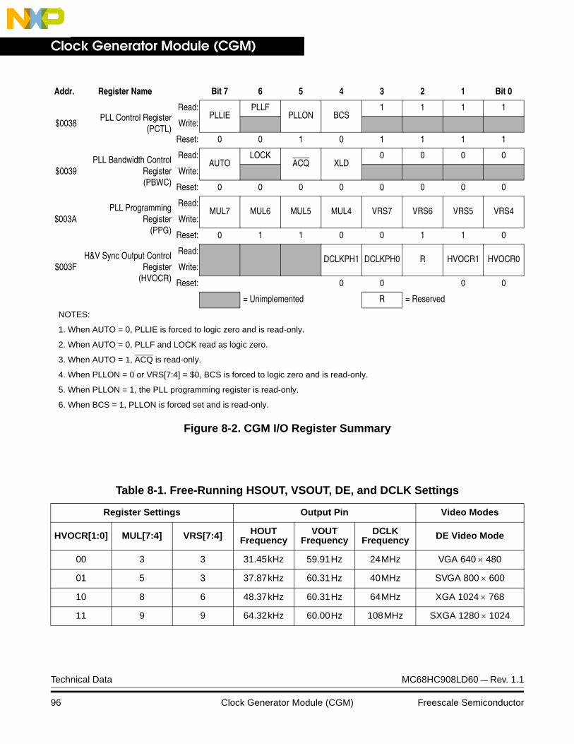
Clock Generator Module (CGM)
Addr. Register Name Bit 7 6 5 4 3 2 1 Bit 0
$0038PLL Control Register
(PCTL)
Read:PLLIE
PLLFPLLON BCS
1 1 1 1
Write:
Reset: 0 0 1 0 1 1 1 1
$0039PLL Bandwidth Control
Register(PBWC)
Read:AUTO
LOCKACQ XLD
0 0 0 0
Write:
Reset: 0 0 0 0 0 0 0 0
$003APLL Programming
Register(PPG)
Read:MUL7 MUL6 MUL5 MUL4 VRS7 VRS6 VRS5 VRS4
Write:
Reset: 0 1 1 0 0 1 1 0
$003FH&V Sync Output Control
Register(HVOCR)
Read:DCLKPH1 DCLKPH0 R HVOCR1 HVOCR0
Write:
Reset: 0 0 0 0
= Unimplemented R = Reserved
NOTES:
1. When AUTO = 0, PLLIE is forced to logic zero and is read-only.
2. When AUTO = 0, PLLF and LOCK read as logic zero.
3. When AUTO = 1, ACQ is read-only.
4. When PLLON = 0 or VRS[7:4] = $0, BCS is forced to logic zero and is read-only.
5. When PLLON = 1, the PLL programming register is read-only.
6. When BCS = 1, PLLON is forced set and is read-only.
Figure 8-2. CGM I/O Register Summary
Table 8-1. Free-Running HSOUT, VSOUT, DE, and DCLK Settings
Register Settings Output Pin Video Modes
HVOCR[1:0] MUL[7:4] VRS[7:4] HOUTFrequency
VOUTFrequency
DCLKFrequency DE Video Mode
00 3 3 31.45kHz 59.91Hz 24MHz VGA 640 × 480
01 5 3 37.87kHz 60.31Hz 40MHz SVGA 800 × 600
10 8 6 48.37kHz 60.31Hz 64MHz XGA 1024 × 768
11 9 9 64.32kHz 60.00Hz 108MHz SXGA 1280 × 1024
Technical Data MC68HC908LD60 — Rev. 1.1
96 Clock Generator Module (CGM) Freescale Semiconductor
Clock Generator Module (CGM)CGM I/O Signals
8.4.1 Crystal Oscillator Circuit
The crystal oscillator circuit consists of an inverting amplifier and an external crystal. The OSC1 pin is the input to the amplifier and the OSC2 pin is the output. The SIMOSCEN signal from the system integration module (SIM) enables the crystal oscillator circuit.
The OSCXCLK signal is the output of the crystal oscillator circuit and runs at a rate equal to the crystal frequency. OSCXCLK is then buffered to produce OSCRCLK, the PLL reference clock. (See Section 7. Oscillator (OSC).)
8.5 CGM I/O Signals
The following paragraphs describe the CGM I/O signals.
8.5.1 External Filter Capacitor Pin (CGMXFC)
The CGMXFC pin is required by the loop filter to filter out phase corrections. A small external capacitor (CF) is connected to this pin.
NOTE: To prevent noise problems, CF should be placed as close to the CGMXFC pin as possible, with minimum routing distances and no routing of other signals across the CF connection.
8.5.2 PLL Analog Power Pin (VDDA)
VDDA is the power pin used by the analog portions of the PLL. The pin should be connected to the same voltage potential as the VDD pin.
8.5.3 PLL Analog Ground Pin (VSSA)
VSSA is the ground pin used by the analog portions of the PLL. The pin should be connected to the same voltage potential as the VSS pin.
NOTE: Route VDDA and VSSA carefully for maximum noise immunity and place bypass capacitors as close as possible to the package.
MC68HC908LD60 — Rev. 1.1 Technical Data
Freescale Semiconductor Clock Generator Module (CGM) 97
Clock Generator Module (CGM)
8.5.4 Crystal Output Frequency Signal (OSCXCLK)
OSCXCLK is the crystal oscillator output signal. It runs at the full speed of the crystal (fXCLK) and is generated directly from the crystal oscillator circuit. The duty cycle of OSCXCLK is unknown and may depend on the crystal and other external factors. Also, the frequency and amplitude of OSCXCLK can be unstable at start-up.
8.5.5 Crystal Reference Frequency Signal (OSCRCLK)
OSCRCLK is the buffered version of OSCXCLK. It runs at the full speed of the crystal (fXCLK) and provides the reference for the PLL circuit.
8.5.6 CGM Base Clock Output (DCLK1)
DCLK1 is the clock output of the CGM. This signal goes to the sync processor, which generates the display clocks. DCLK1 is software programmable to be either the oscillator output (OSCXCLK) or the VCO clock (CGMVCLK).
8.5.7 CGM CPU Interrupt (CGMINT)
CGMINT is the interrupt signal generated by the PLL lock detector.
8.6 CGM I/O Registers
The following registers control and monitor operation of the CGM:
• PLL control register (PCTL)
• PLL bandwidth control register (PBWC)
• PLL programming register (PPG)
• H & V sync output control register (HVOCR)
Technical Data MC68HC908LD60 — Rev. 1.1
98 Clock Generator Module (CGM) Freescale Semiconductor
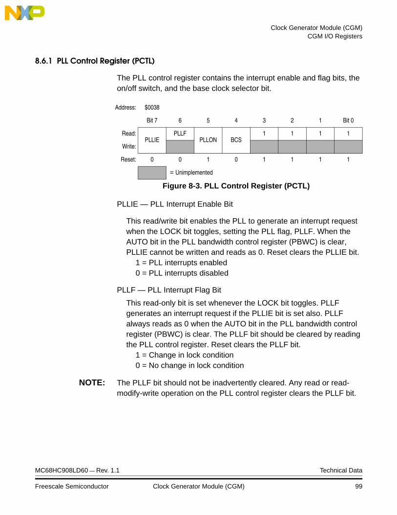
Clock Generator Module (CGM)CGM I/O Registers
8.6.1 PLL Control Register (PCTL)
The PLL control register contains the interrupt enable and flag bits, the on/off switch, and the base clock selector bit.
PLLIE — PLL Interrupt Enable Bit
This read/write bit enables the PLL to generate an interrupt request when the LOCK bit toggles, setting the PLL flag, PLLF. When the AUTO bit in the PLL bandwidth control register (PBWC) is clear, PLLIE cannot be written and reads as 0. Reset clears the PLLIE bit.
1 = PLL interrupts enabled0 = PLL interrupts disabled
PLLF — PLL Interrupt Flag Bit
This read-only bit is set whenever the LOCK bit toggles. PLLF generates an interrupt request if the PLLIE bit is set also. PLLF always reads as 0 when the AUTO bit in the PLL bandwidth control register (PBWC) is clear. The PLLF bit should be cleared by reading the PLL control register. Reset clears the PLLF bit.
1 = Change in lock condition0 = No change in lock condition
NOTE: The PLLF bit should not be inadvertently cleared. Any read or read-modify-write operation on the PLL control register clears the PLLF bit.
Address: $0038
Bit 7 6 5 4 3 2 1 Bit 0
Read:PLLIE
PLLFPLLON BCS
1 1 1 1
Write:
Reset: 0 0 1 0 1 1 1 1
= Unimplemented
Figure 8-3. PLL Control Register (PCTL)
MC68HC908LD60 — Rev. 1.1 Technical Data
Freescale Semiconductor Clock Generator Module (CGM) 99
Clock Generator Module (CGM)
PLLON — PLL On Bit
This read/write bit activates the PLL and enables the VCO clock, CGMVCLK. PLLON cannot be cleared if the VCO clock is driving the base clock, DCLK1 (BCS = 1). Reset sets this bit so that the loop can stabilize as the MCU is powering up.
1 = PLL on0 = PLL off
BCS — Base Clock Select Bit
This read/write bit selects either the crystal oscillator output, OSCXCLK, or the VCO clock, CGMVCLK, as the source of the CGM output, DCLK1. BCS cannot be set while the PLLON bit is clear. After toggling BCS, it may take up to three OSCXCLK and three CGMVCLK cycles to complete the transition from one source clock to the other. During the transition, DCLK1 is held in stasis. Reset and the STOP instruction clear the BCS bit.
1 = DCLK1 driven by CGMVCLK0 = DCLK1 driven by OSCXCLK
NOTE: PLLON and BCS have built-in protection that prevents the base clock selector circuit from selecting the VCO clock as the source of the base clock if the PLL is off. Therefore, PLLON cannot be cleared when BCS is set, and BCS cannot be set when PLLON is clear. If the PLL is off (PLLON = 0), selecting CGMVCLK requires two writes to the PLL control register.
8.6.2 PLL Bandwidth Control Register (PBWC)
The PLL bandwidth control register does the following:
• Selects automatic or manual (software-controlled) bandwidth control mode
• Indicates when the PLL is locked
• In automatic bandwidth control mode, indicates when the PLL is in acquisition or tracking mode
• In manual operation, forces the PLL into acquisition or tracking mode
Technical Data MC68HC908LD60 — Rev. 1.1
100 Clock Generator Module (CGM) Freescale Semiconductor

Clock Generator Module (CGM)CGM I/O Registers
AUTO — Automatic Bandwidth Control Bit
This read/write bit selects automatic or manual bandwidth control. When initializing the PLL for manual operation (AUTO = 0), the ACQ bit should be cleared before turning the PLL on. Reset clears the AUTO bit.
1 = Automatic bandwidth control0 = Manual bandwidth control
LOCK — Lock Indicator Bit
When the AUTO bit is set, LOCK is a read-only bit that becomes set when the VCO clock CGMVCLK, is locked (running at the programmed frequency). When the AUTO bit is clear, LOCK reads as 0 and has no meaning. Reset clears the LOCK bit.
1 = VCO frequency correct or locked0 = VCO frequency incorrect or unlocked
ACQ — Acquisition Mode Bit
When the AUTO bit is set, ACQ is a read-only bit that indicates whether the PLL is in acquisition mode or tracking mode. When the AUTO bit is clear, ACQ is a read/write bit that controls whether the PLL is in acquisition or tracking mode.
In automatic bandwidth control mode (AUTO = 1), the last-written value from manual operation is stored in a temporary location and is recovered when manual operation resumes. Reset clears this bit, enabling acquisition mode.
1 = Tracking mode0 = Acquisition mode
Address: $0039
Bit 7 6 5 4 3 2 1 Bit 0
Read:AUTO
LOCKACQ XLD
0 0 0 0
Write:
Reset: 0 0 0 0 0 0 0 0
= Unimplemented
Figure 8-4. PLL Bandwidth Control Register (PBWC)
MC68HC908LD60 — Rev. 1.1 Technical Data
Freescale Semiconductor Clock Generator Module (CGM) 101

Clock Generator Module (CGM)
XLD — Crystal Loss Detect Bit
When the VCO output, CGMVCLK, is driving DCLK1, this read/write bit indicates whether the crystal reference frequency is active or not. To check the status of the crystal reference, the following procedure should be followed:1. Write a 1 to XLD.2. Wait 4 × N cycles. (N is the VCO frequency multiplier, MUL[7:4].)3. Read XLD.
1 = Crystal reference is not active0 = Crystal reference is active
The crystal loss detect function works only when the BCS bit is set, selecting CGMVCLK to drive DCLK1. When BCS is clear, XLD always reads as 0.
Bits [3:0] — Reserved for test
These bits enable test functions not available in user mode. To ensure software portability from development systems to user applications, software should write zeros to Bits [3:0] whenever writing to PBWC.
8.6.3 PLL Programming Register (PPG)
The PLL programming register contains the programming information for the modulo feedback divider and the programming information for the hardware configuration of the VCO.
Address: $003A
Bit 7 6 5 4 3 2 1 Bit 0
Read:MUL7 MUL6 MUL5 MUL4 VRS7 VRS6 VRS5 VRS4
Write:
Reset: 0 1 1 0 0 1 1 0
Figure 8-5. PLL Programming Register (PPG)
Technical Data MC68HC908LD60 — Rev. 1.1
102 Clock Generator Module (CGM) Freescale Semiconductor
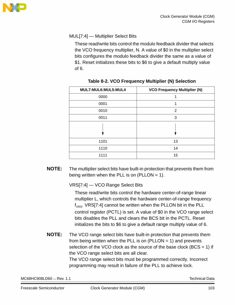
Clock Generator Module (CGM)CGM I/O Registers
MUL[7:4] — Multiplier Select Bits
These read/write bits control the modulo feedback divider that selects the VCO frequency multiplier, N. A value of $0 in the multiplier select bits configures the modulo feedback divider the same as a value of $1. Reset initializes these bits to $6 to give a default multiply value of 6.
NOTE: The multiplier select bits have built-in protection that prevents them from being written when the PLL is on (PLLON = 1).
VRS[7:4] — VCO Range Select Bits
These read/write bits control the hardware center-of-range linear multiplier L, which controls the hardware center-of-range frequency fVRS. VRS[7:4] cannot be written when the PLLON bit in the PLL
control register (PCTL) is set. A value of $0 in the VCO range select bits disables the PLL and clears the BCS bit in the PCTL. Reset initializes the bits to $6 to give a default range multiply value of 6.
NOTE: The VCO range select bits have built-in protection that prevents them from being written when the PLL is on (PLLON = 1) and prevents selection of the VCO clock as the source of the base clock (BCS = 1) if the VCO range select bits are all clear.The VCO range select bits must be programmed correctly. Incorrect programming may result in failure of the PLL to achieve lock.
Table 8-2. VCO Frequency Multiplier (N) Selection
MUL7:MUL6:MUL5:MUL4 VCO Frequency Multiplier (N)
0000 1
0001 1
0010 2
0011 3
1101 13
1110 14
1111 15
MC68HC908LD60 — Rev. 1.1 Technical Data
Freescale Semiconductor Clock Generator Module (CGM) 103

Clock Generator Module (CGM)
8.6.4 H & V Sync Output Control Register (HVOCR)
The H&V sync output control register controls the PLL reference input prescaler and the final free-running waveforms for the sync processor output signals on HOUT, VOUT, DCLK, and DE pins.(See Section 16. Sync Processor.)
DCLKPH[1:0] — DCLK Output Phase Adjustment
These two bits are programmed to adjust the DCLK output phase. Each increment adds approximately 2 to 3ns delay to the DCLK output.
HVOCR[1:0] — Free Running Video Mode Select Bits
These two bits together with MUL[7:4] and VRS[7:4] in the PLL programming register determine the frequencies of the internal generated free-running signals for output to HOUT, VOUT, DE, and DCLK pins, when the SOUT bit is set in the sync processor I/O control register. These two bits determine the prescaler of PLL reference clock in the CGM module. When HVOCR[1:0]=11, the prescaler is 2; for other values, the prescaler is 3. Reset clears these bits, setting a default horizontal frequency of 31.25kHz and a vertical frequency of 60Hz, a video mode of 640×480.
Address: $003F
Bit 7 6 5 4 3 2 1 Bit 0
Read:DCLKPH1 DCLKPH0 R HVOCR1 HVOCR0
Write:
Reset: 0 0 0 0
= Unimplemented R = Reserved
Figure 8-6. H&V Sync Output Control Register (HVOCR)
Register Settings Pin Outputs Video Modes
HVOCR[1:0] MUL[7:4] VRS[7:4] HOUTFrequency
VOUTFrequency
DCLKFrequency DE Video Mode
00 3 3 31.45kHz 59.91Hz 24MHz VGA 640 × 480
01 5 3 37.87kHz 60.31Hz 40MHz SVGA 800 × 600
10 8 6 48.37kHz 60.31Hz 64MHz XGA 1024 × 768
11 9 9 64.32kHz 60.00Hz 108MHz SXGA 1280 × 1024
Technical Data MC68HC908LD60 — Rev. 1.1
104 Clock Generator Module (CGM) Freescale Semiconductor

Clock Generator Module (CGM)Interrupts
8.7 Interrupts
When the AUTO bit is set in the PLL bandwidth control register (PBWC), the PLL can generate a CPU interrupt request every time the LOCK bit changes state. The PLLIE bit in the PLL control register (PCTL) enables CPU interrupts from the PLL. PLLF, the interrupt flag in the PCTL, becomes set whether interrupts are enabled or not. When the AUTO bit is clear, CPU interrupts from the PLL are disabled and PLLF reads as 0.
Software should read the LOCK bit after a PLL interrupt request to see if the request was due to an entry into lock or an exit from lock. When the PLL enters lock, the VCO clock CGMVCLK, can be selected as the DCLK1 source by setting BCS in the PCTL. When the PLL exits lock, the VCO clock frequency is corrupt, and appropriate precautions should be taken. If the application is not frequency-sensitive, interrupts should be disabled to prevent PLL interrupt service routines from impeding software performance or from exceeding stack limitations.
Software can select CGMVCLK as the DCLK1 source even if the PLL is not locked (LOCK = 0). Therefore, software should make sure the PLL is locked before setting the BCS bit.
8.8 Low-Power Modes
The WAIT and STOP instructions put the MCU in low-power-consumption standby modes.
8.8.1 Wait Mode
The WAIT instruction does not affect the CGM. Before entering WAIT mode, software can disengage and turn off the PLL by clearing the BCS and PLLON bits in the PLL control register (PCTL). Less power-sensitive applications can disengage the PLL without turning it off. Applications that require the PLL to wake the MCU from WAIT mode also can deselect the PLL output without turning off the PLL.
MC68HC908LD60 — Rev. 1.1 Technical Data
Freescale Semiconductor Clock Generator Module (CGM) 105

Clock Generator Module (CGM)
8.8.2 Stop Mode
When the STOP instruction executes, the SIM drives the SIMOSCEN signal low, disabling the CGM and holding low all CGM outputs (OSCXCLK, DCLK1, and CGMINT).
If the STOP instruction is executed with the VCO clock, CGMVCLK, driving DCLK1, the PLL automatically clears the BCS bit in the PLL control register (PCTL), thereby selecting the crystal clock, OSCXCLK, as the source of DCLK1. When the MCU recovers from STOP, the crystal clock drives DCLK1 and BCS remains clear.
8.9 CGM During Break Interrupts
The system integration module (SIM) controls whether status bits in other modules can be cleared during the break state. The BCFE bit in the SIM break flag control register (SBFCR) enables software to clear status bits during the break state. See Section 9. System Integration Module (SIM).
To allow software to clear status bits during a break interrupt, a 1 should be written to the BCFE bit. If a status bit is cleared during the break state, it remains cleared when the MCU exits the break state.
To protect the PLLF bit during the break state, write a 0 to the BCFE bit. With BCFE at 0 (its default state), software can read and write the PLL control register during the break state without affecting the PLLF bit.
Technical Data MC68HC908LD60 — Rev. 1.1
106 Clock Generator Module (CGM) Freescale Semiconductor
Technical Data — MC68HC908LD60
Section 9. System Integration Module (SIM)
9.1 Contents
9.2 Introduction . . . . . . . . . . . . . . . . . . . . . . . . . . . . . . . . . . . . . . .108
9.3 SIM Bus Clock Control and Generation . . . . . . . . . . . . . . . . .1119.3.1 Bus Timing . . . . . . . . . . . . . . . . . . . . . . . . . . . . . . . . . . . . .1119.3.2 Clock Start-Up from POR . . . . . . . . . . . . . . . . . . . . . . . . . .1119.3.3 Clocks in Stop Mode and Wait Mode . . . . . . . . . . . . . . . . .111
9.4 Reset and System Initialization. . . . . . . . . . . . . . . . . . . . . . . .1129.4.1 External Pin Reset . . . . . . . . . . . . . . . . . . . . . . . . . . . . . . .1129.4.2 Active Resets from Internal Sources . . . . . . . . . . . . . . . . .1139.4.2.1 Power-On Reset . . . . . . . . . . . . . . . . . . . . . . . . . . . . . .1149.4.2.2 Computer Operating Properly (COP) Reset. . . . . . . . . .1159.4.2.3 Low-Voltage Inhibit Reset . . . . . . . . . . . . . . . . . . . . . . .1159.4.2.4 Illegal Opcode Reset . . . . . . . . . . . . . . . . . . . . . . . . . . .1159.4.2.5 Illegal Address Reset . . . . . . . . . . . . . . . . . . . . . . . . . . .116
9.5 SIM Counter . . . . . . . . . . . . . . . . . . . . . . . . . . . . . . . . . . . . . .1169.5.1 SIM Counter During Power-On Reset . . . . . . . . . . . . . . . .1169.5.2 SIM Counter During Stop Mode Recovery . . . . . . . . . . . . .1169.5.3 SIM Counter and Reset States. . . . . . . . . . . . . . . . . . . . . .117
9.6 Exception Control . . . . . . . . . . . . . . . . . . . . . . . . . . . . . . . . . .1179.6.1 Interrupts . . . . . . . . . . . . . . . . . . . . . . . . . . . . . . . . . . . . . .1189.6.1.1 Hardware Interrupts . . . . . . . . . . . . . . . . . . . . . . . . . . . .1209.6.1.2 SWI Instruction. . . . . . . . . . . . . . . . . . . . . . . . . . . . . . . .1219.6.2 Interrupt Status Registers. . . . . . . . . . . . . . . . . . . . . . . . . .1219.6.2.1 Interrupt Status Register 1 . . . . . . . . . . . . . . . . . . . . . . .1239.6.2.2 Interrupt Status Register 2 . . . . . . . . . . . . . . . . . . . . . . .1239.6.3 Reset . . . . . . . . . . . . . . . . . . . . . . . . . . . . . . . . . . . . . . . . .1249.6.4 Break Interrupts . . . . . . . . . . . . . . . . . . . . . . . . . . . . . . . . .1249.6.5 Status Flag Protection in Break Mode . . . . . . . . . . . . . . . .124
MC68HC908LD60 — Rev. 1.1 Technical Data
Freescale Semiconductor System Integration Module (SIM) 107

System Integration Module (SIM)
9.7 Low-Power Modes . . . . . . . . . . . . . . . . . . . . . . . . . . . . . . . . .1259.7.1 Wait Mode . . . . . . . . . . . . . . . . . . . . . . . . . . . . . . . . . . . . .1259.7.2 Stop Mode . . . . . . . . . . . . . . . . . . . . . . . . . . . . . . . . . . . . .126
9.8 SIM Registers . . . . . . . . . . . . . . . . . . . . . . . . . . . . . . . . . . . . .1289.8.1 SIM Break Status Register (SBSR) . . . . . . . . . . . . . . . . . .1289.8.2 SIM Reset Status Register (SRSR) . . . . . . . . . . . . . . . . . .1299.8.3 SIM Break Flag Control Register (SBFCR) . . . . . . . . . . . .130
9.2 Introduction
This section describes the system integration module, which supports up to 16 external and/or internal interrupts. Together with the CPU, the SIM controls all MCU activities. A block diagram of the SIM is shown in Figure 9-1. Figure 9-2 shows a summary of the SIM I/O registers. The SIM is a system state controller that coordinates CPU and exception timing. The SIM is responsible for:
• Bus clock generation and control for CPU and peripherals:
– Stop/wait/reset/break entry and recovery
– Internal clock control
• Master reset control, including power-on reset (POR) and COP timeout
• Interrupt control:
– Acknowledge timing
– Arbitration control timing
– Vector address generation
• CPU enable/disable timing
• Modular architecture expandable to 128 interrupt sources
Technical Data MC68HC908LD60 — Rev. 1.1
108 System Integration Module (SIM) Freescale Semiconductor
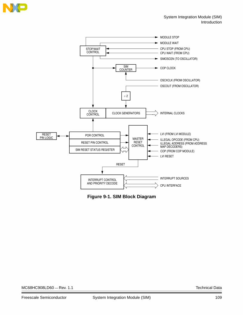
System Integration Module (SIM)Introduction
Figure 9-1. SIM Block Diagram
STOP/WAIT
CLOCKCONTROL CLOCK GENERATORS
POR CONTROL
RESET PIN CONTROL
SIM RESET STATUS REGISTER
INTERRUPT CONTROLAND PRIORITY DECODE
MODULE STOP
MODULE WAIT
CPU STOP (FROM CPU)CPU WAIT (FROM CPU)
SIMOSCEN (TO OSCILLATOR)
OSCOUT (FROM OSCILLATOR)
INTERNAL CLOCKS
MASTERRESET
CONTROL
RESETPIN LOGIC
LVI (FROM LVI MODULE)
ILLEGAL OPCODE (FROM CPU)ILLEGAL ADDRESS (FROM ADDRESSMAP DECODERS)COP (FROM COP MODULE)
INTERRUPT SOURCES
CPU INTERFACE
RESET
CONTROL
SIMCOUNTER COP CLOCK
OSCXCLK (FROM OSCILLATOR)
÷ 2
LVI RESET
MC68HC908LD60 — Rev. 1.1 Technical Data
Freescale Semiconductor System Integration Module (SIM) 109
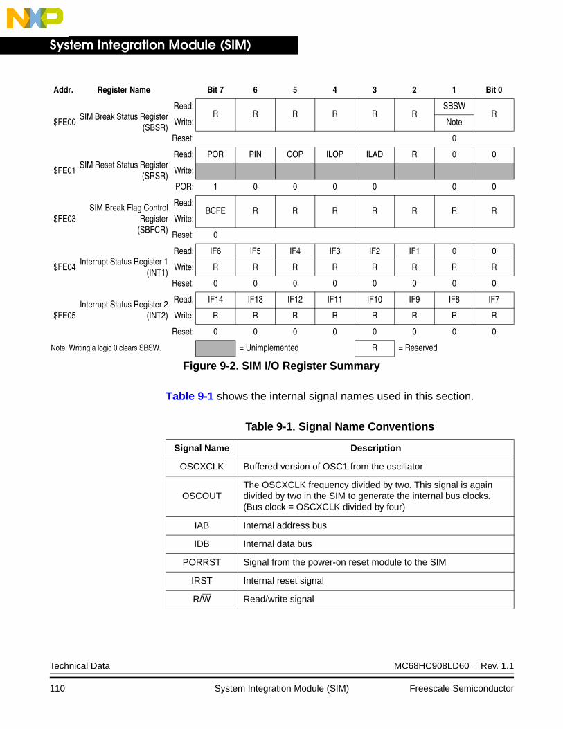
System Integration Module (SIM)
Table 9-1 shows the internal signal names used in this section.
Addr. Register Name Bit 7 6 5 4 3 2 1 Bit 0
$FE00SIM Break Status Register
(SBSR)
Read:R R R R R R
SBSWR
Write: Note
Reset: 0
$FE01SIM Reset Status Register
(SRSR)
Read: POR PIN COP ILOP ILAD R 0 0
Write:
POR: 1 0 0 0 0 0 0
$FE03SIM Break Flag Control
Register(SBFCR)
Read:BCFE R R R R R R R
Write:
Reset: 0
$FE04Interrupt Status Register 1
(INT1)
Read: IF6 IF5 IF4 IF3 IF2 IF1 0 0
Write: R R R R R R R R
Reset: 0 0 0 0 0 0 0 0
$FE05Interrupt Status Register 2
(INT2)
Read: IF14 IF13 IF12 IF11 IF10 IF9 IF8 IF7
Write: R R R R R R R R
Reset: 0 0 0 0 0 0 0 0
Note: Writing a logic 0 clears SBSW. = Unimplemented R = Reserved
Figure 9-2. SIM I/O Register Summary
Table 9-1. Signal Name Conventions
Signal Name Description
OSCXCLK Buffered version of OSC1 from the oscillator
OSCOUTThe OSCXCLK frequency divided by two. This signal is again divided by two in the SIM to generate the internal bus clocks.(Bus clock = OSCXCLK divided by four)
IAB Internal address bus
IDB Internal data bus
PORRST Signal from the power-on reset module to the SIM
IRST Internal reset signal
R/W Read/write signal
Technical Data MC68HC908LD60 — Rev. 1.1
110 System Integration Module (SIM) Freescale Semiconductor
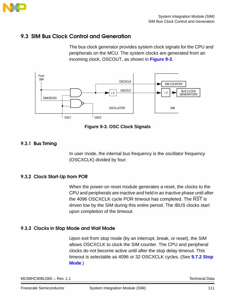
System Integration Module (SIM)SIM Bus Clock Control and Generation
9.3 SIM Bus Clock Control and Generation
The bus clock generator provides system clock signals for the CPU and peripherals on the MCU. The system clocks are generated from an incoming clock, OSCOUT, as shown in Figure 9-3.
Figure 9-3. OSC Clock Signals
9.3.1 Bus Timing
In user mode, the internal bus frequency is the oscillator frequency (OSCXCLK) divided by four.
9.3.2 Clock Start-Up from POR
When the power-on reset module generates a reset, the clocks to the CPU and peripherals are inactive and held in an inactive phase until after the 4096 OSCXCLK cycle POR timeout has completed. The RST is driven low by the SIM during this entire period. The IBUS clocks start upon completion of the timeout.
9.3.3 Clocks in Stop Mode and Wait Mode
Upon exit from stop mode (by an interrupt, break, or reset), the SIM allows OSCXCLK to clock the SIM counter. The CPU and peripheral clocks do not become active until after the stop delay timeout. This timeout is selectable as 4096 or 32 OSCXCLK cycles. (See 9.7.2 Stop Mode.)
SIMOSCEN
OSCXCLK
FromSIM
÷ 2OSCOUT
OSC1 OSC2
÷ 2 BUS CLOCKGENERATORS
SIM
SIM COUNTER
OSCILLATOR
MC68HC908LD60 — Rev. 1.1 Technical Data
Freescale Semiconductor System Integration Module (SIM) 111

System Integration Module (SIM)
In wait mode, the CPU clocks are inactive. The SIM also produces two sets of clocks for other modules. Refer to the wait mode subsection of each module to see if the module is active or inactive in wait mode. Some modules can be programmed to be active in wait mode.
9.4 Reset and System Initialization
The MCU has the following reset sources:
• Power-on reset module (POR)
• External reset pin (RST)
• Computer operating properly module (COP)
• Low-voltage inhibit (LVI)
• Illegal opcode
• Illegal address
All of these resets produce the vector $FFFE–FFFF ($FEFE–FEFF in monitor mode) and assert the internal reset signal (IRST). IRST causes all registers to be returned to their default values and all modules to be returned to their reset states.
An internal reset clears the SIM counter (see 9.5 SIM Counter), but an external reset does not. Each of the resets sets a corresponding bit in the SIM reset status register (SRSR) (see 9.8 SIM Registers).
9.4.1 External Pin Reset
Pulling the asynchronous RST pin low halts all processing. The PIN bit of the SIM reset status register (SRSR) is set as long as RST is held low for a minimum of 67 OSCXCLK cycles, assuming that the POR was not the source of the reset (see Table 9-2. PIN Bit Set Timing). Figure 9-4 shows the relative timing.
Table 9-2. PIN Bit Set Timing
Reset Type Number of Cycles Required to Set PIN
POR 4163 (4096 + 64 + 3)
All others 67 (64 + 3)
Technical Data MC68HC908LD60 — Rev. 1.1
112 System Integration Module (SIM) Freescale Semiconductor
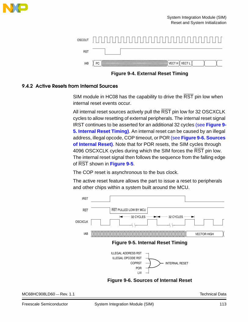
System Integration Module (SIM)Reset and System Initialization
Figure 9-4. External Reset Timing
9.4.2 Active Resets from Internal Sources
SIM module in HC08 has the capability to drive the RST pin low when internal reset events occur.
All internal reset sources actively pull the RST pin low for 32 OSCXCLK cycles to allow resetting of external peripherals. The internal reset signal IRST continues to be asserted for an additional 32 cycles (see Figure 9-5. Internal Reset Timing). An internal reset can be caused by an illegal address, illegal opcode, COP timeout, or POR (see Figure 9-6. Sources of Internal Reset). Note that for POR resets, the SIM cycles through 4096 OSCXCLK cycles during which the SIM forces the RST pin low. The internal reset signal then follows the sequence from the falling edge of RST shown in Figure 9-5.
The COP reset is asynchronous to the bus clock.
The active reset feature allows the part to issue a reset to peripherals and other chips within a system built around the MCU.
Figure 9-5. Internal Reset Timing
Figure 9-6. Sources of Internal Reset
RST
IAB PC VECT H VECT L
OSCOUT
IRST
RST RST PULLED LOW BY MCU
IAB
32 CYCLES 32 CYCLES
VECTOR HIGH
OSCXCLK
ILLEGAL ADDRESS RST
ILLEGAL OPCODE RST
COPRST
POR
INTERNAL RESET
LVI
MC68HC908LD60 — Rev. 1.1 Technical Data
Freescale Semiconductor System Integration Module (SIM) 113
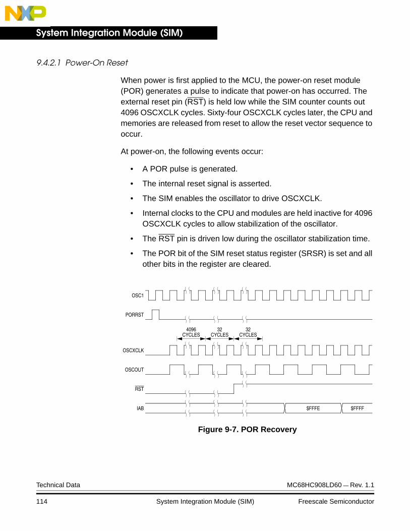
System Integration Module (SIM)
9.4.2.1 Power-On Reset
When power is first applied to the MCU, the power-on reset module (POR) generates a pulse to indicate that power-on has occurred. The external reset pin (RST) is held low while the SIM counter counts out 4096 OSCXCLK cycles. Sixty-four OSCXCLK cycles later, the CPU and memories are released from reset to allow the reset vector sequence to occur.
At power-on, the following events occur:
• A POR pulse is generated.
• The internal reset signal is asserted.
• The SIM enables the oscillator to drive OSCXCLK.
• Internal clocks to the CPU and modules are held inactive for 4096 OSCXCLK cycles to allow stabilization of the oscillator.
• The RST pin is driven low during the oscillator stabilization time.
• The POR bit of the SIM reset status register (SRSR) is set and all other bits in the register are cleared.
Figure 9-7. POR Recovery
PORRST
OSC1
OSCXCLK
OSCOUT
RST
IAB
4096CYCLES
32CYCLES
32CYCLES
$FFFE $FFFF
Technical Data MC68HC908LD60 — Rev. 1.1
114 System Integration Module (SIM) Freescale Semiconductor
System Integration Module (SIM)Reset and System Initialization
9.4.2.2 Computer Operating Properly (COP) Reset
An input to the SIM is reserved for the COP reset signal. The overflow of the COP counter causes an internal reset and sets the COP bit in the SIM reset status register (SRSR). The SIM actively pulls down the RST pin for all internal reset sources.
To prevent a COP module timeout, write any value to location $FFFF. Writing to location $FFFF clears the COP counter and bits 12 through 5 of the SIM counter. The SIM counter output, which occurs at least every 212 – 24 OSCXCLK cycles, drives the COP counter. The COP should be serviced as soon as possible out of reset to guarantee the maximum amount of time before the first timeout.
The COP module is disabled if the RST pin or the IRQ is held at VTST while the MCU is in monitor mode. The COP module can be disabled only through combinational logic conditioned with the high voltage signal on the RST pin or the IRQ pin. This prevents the COP from becoming disabled as a result of external noise. During a break state, VTST on the RST pin disables the COP module.
9.4.2.3 Low-Voltage Inhibit Reset
The low-voltage inhibit circuit performs an internal reset when the VDD voltage falls to the LVI trip voltage VTRIPF. The external reset pin (RST) is held low while the SIM counter counts out 4096 OSCXCLK cycles. Sixty-four OSCXCLK cycles later, the CPU and memories are released from reset to allow the reset vector sequence to occur.
9.4.2.4 Illegal Opcode Reset
The SIM decodes signals from the CPU to detect illegal instructions. An illegal instruction sets the ILOP bit in the SIM reset status register (SRSR) and causes a reset.
If the stop enable bit, STOP, in the configure register (CONFIG) is logic zero, the SIM treats the STOP instruction as an illegal opcode and causes an illegal opcode reset. The SIM actively pulls down the RST pin for all internal reset sources.
MC68HC908LD60 — Rev. 1.1 Technical Data
Freescale Semiconductor System Integration Module (SIM) 115

System Integration Module (SIM)
9.4.2.5 Illegal Address Reset
An opcode fetch from an unmapped address generates an illegal address reset. The SIM verifies that the CPU is fetching an opcode prior to asserting the ILAD bit in the SIM reset status register (SRSR) and resetting the MCU. A data fetch from an unmapped address does not generate a reset. The SIM actively pulls down the RST pin for all internal reset sources.
9.5 SIM Counter
The SIM counter is used by the power-on reset module (POR) and in stop mode recovery to allow the oscillator time to stabilize before enabling the internal bus (IBUS) clocks. The SIM counter also serves as a prescaler for the computer operating properly module (COP). The SIM counter overflow supplies the clock for the COP module. The SIM counter is 12 bits long and is clocked by the falling edge of OSCXCLK.
9.5.1 SIM Counter During Power-On Reset
The power-on reset module (POR) detects power applied to the MCU. At power-on, the POR circuit asserts the signal PORRST. Once the SIM is initialized, it enables the oscillator to drive the bus clock state machine.
9.5.2 SIM Counter During Stop Mode Recovery
The SIM counter also is used for stop mode recovery. The STOP instruction clears the SIM counter. After an interrupt, break, or reset, the SIM senses the state of the short stop recovery bit, SSREC, in the configure register (CONFIG). If the SSREC bit is a logic one, then the stop recovery is reduced from the normal delay of 4096 OSCXCLK cycles down to 32 OSCXCLK cycles. This is ideal for applications using canned oscillators that do not require long start-up times from stop mode. External crystal applications should use the full stop recovery time, that is, with SSREC cleared.
Technical Data MC68HC908LD60 — Rev. 1.1
116 System Integration Module (SIM) Freescale Semiconductor
System Integration Module (SIM)Exception Control
9.5.3 SIM Counter and Reset States
External reset has no effect on the SIM counter (see 9.7.2 Stop Mode). The SIM counter is free-running after all reset states (see 9.4.2 Active Resets from Internal Sources for counter control and internal reset recovery sequences).
9.6 Exception Control
Normally, sequential program execution can be changed in three different ways:
• Interrupts
– Maskable hardware CPU interrupts
– Non-maskable software interrupt instruction (SWI)
• Reset
• Break interrupts
MC68HC908LD60 — Rev. 1.1 Technical Data
Freescale Semiconductor System Integration Module (SIM) 117

System Integration Module (SIM)
9.6.1 Interrupts
An interrupt temporarily changes the sequence of program execution to respond to a particular event. Figure 9-10 flow charts the handling of system interrupts.
Interrupts are latched, and arbitration is performed in the SIM at the start of interrupt processing. The arbitration result is a constant that the CPU uses to determine which vector to fetch. Once an interrupt is latched by the SIM, no other interrupt can take precedence, regardless of priority, until the latched interrupt is serviced (or the I bit is cleared).
At the beginning of an interrupt, the CPU saves the CPU register contents on the stack and sets the interrupt mask (I bit) to prevent additional interrupts. At the end of an interrupt, the RTI instruction recovers the CPU register contents from the stack so that normal processing can resume. Figure 9-8 shows interrupt entry timing. Figure 9-9 shows interrupt recovery timing.
Figure 9-8. Interrupt Entry
Figure 9-9. Interrupt Recovery
MODULE
IDB
R/W
INTERRUPT
DUMMY SP SP – 1 SP – 2 SP – 3 SP – 4 VECT H VECT L START ADDRIAB
DUMMY PC – 1[7:0] PC – 1[15:8] X A CCR V DATA H V DATA L OPCODE
I BIT
MODULE
IDB
R/W
INTERRUPT
SP – 4 SP – 3 SP – 2 SP – 1 SP PC PC + 1IAB
CCR A X PC – 1[7:0] PC – 1[15:8] OPCODE OPERAND
I BIT
Technical Data MC68HC908LD60 — Rev. 1.1
118 System Integration Module (SIM) Freescale Semiconductor
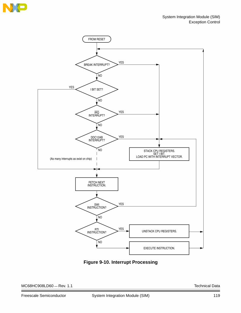
System Integration Module (SIM)Exception Control
Figure 9-10. Interrupt Processing
NO
NO
NO
YES
NO
NO
YES
NO
YES
YES
(As many interrupts as exist on chip)
I BIT SET?
FROM RESET
BREAK INTERRUPT?
I BIT SET?
IRQINTERRUPT?
DDC12ABINTERRUPT?
SWIINSTRUCTION?
RTIINSTRUCTION?
FETCH NEXTINSTRUCTION.
UNSTACK CPU REGISTERS.
STACK CPU REGISTERS.SET I BIT.
LOAD PC WITH INTERRUPT VECTOR.
EXECUTE INSTRUCTION.
YES
YES
MC68HC908LD60 — Rev. 1.1 Technical Data
Freescale Semiconductor System Integration Module (SIM) 119
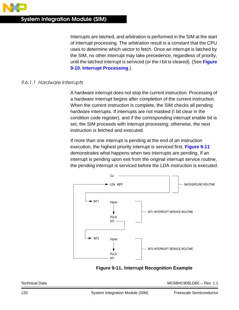
System Integration Module (SIM)
Interrupts are latched, and arbitration is performed in the SIM at the start of interrupt processing. The arbitration result is a constant that the CPU uses to determine which vector to fetch. Once an interrupt is latched by the SIM, no other interrupt may take precedence, regardless of priority, until the latched interrupt is serviced (or the I bit is cleared). (See Figure 9-10. Interrupt Processing.)
9.6.1.1 Hardware Interrupts
A hardware interrupt does not stop the current instruction. Processing of a hardware interrupt begins after completion of the current instruction. When the current instruction is complete, the SIM checks all pending hardware interrupts. If interrupts are not masked (I bit clear in the condition code register), and if the corresponding interrupt enable bit is set, the SIM proceeds with interrupt processing; otherwise, the next instruction is fetched and executed.
If more than one interrupt is pending at the end of an instruction execution, the highest priority interrupt is serviced first. Figure 9-11 demonstrates what happens when two interrupts are pending. If an interrupt is pending upon exit from the original interrupt service routine, the pending interrupt is serviced before the LDA instruction is executed.
Figure 9-11. Interrupt Recognition Example
CLI
LDA
INT1
PULHRTI
INT2
BACKGROUND ROUTINE#$FF
PSHH
INT1 INTERRUPT SERVICE ROUTINE
PULHRTI
PSHH
INT2 INTERRUPT SERVICE ROUTINE
Technical Data MC68HC908LD60 — Rev. 1.1
120 System Integration Module (SIM) Freescale Semiconductor

System Integration Module (SIM)Exception Control
The LDA opcode is pre-fetched by both the INT1 and INT2 RTI instructions. However, in the case of the INT1 RTI pre-fetch, this is a redundant operation.
NOTE: To maintain compatibility with the M6805 Family, the H register is not pushed on the stack during interrupt entry. If the interrupt service routine modifies the H register or uses the indexed addressing mode, software should save the H register and then restore it prior to exiting the routine.
9.6.1.2 SWI Instruction
The SWI instruction is a non-maskable instruction that causes an interrupt regardless of the state of the interrupt mask (I bit) in the condition code register.
NOTE: A software interrupt pushes PC onto the stack. A software interrupt does not push PC – 1, as a hardware interrupt does.
9.6.2 Interrupt Status Registers
The flags in the interrupt status registers identify maskable interrupt sources. Table 9-3 summarizes the interrupt sources and the interrupt status register flags that they set. The interrupt status registers can be useful for debugging.
MC68HC908LD60 — Rev. 1.1 Technical Data
Freescale Semiconductor System Integration Module (SIM) 121

System Integration Module (SIM)
Table 9-3. Interrupt Sources
Source Flag Mask(1) INT Register Flag Priority(2) Vector
Address
Reset None None None 0 $FFFE–$FFFF
SWI Instruction None None None 0 $FFFC–$FFFD
IRQ pin IRQF IMASK IF1 1 $FFFA–$FFFB
Reserved — — IF2 2 $FFF8–$FFF9
Reserved — — IF3 3 $FFF6–$FFF7
Reserved — — IF4 3 $FFF4–$FFF5
DDC12AB
ALIF
DIENIF5 5 $FFF2–$FFF3
NAKIF
RXIF
TXIF
SCLIF SCLIEN
TIM channel 0 CH0F CH0IE IF6 6 $FFF0–$FFF1
TIM channel 1 CH1F CH1IE IF7 7 $FFEE–$FFEF
TIM overflow TOF TOIE IF8 8 $FFEC–$FFED
Sync processorVSIF VSIE
IF9 9 $FFEA–$FFEBLVSIF LVSIE
Multi-master IIC
MMALIF
MMIEN IF10 10 $FFE8–FFE9MMNAKIF
MMRXIF
MMTXIF
Reserved — — IF11 11 $FFE6–$FFE7
ADC conversion complete COCO AIEN IF12 12 $FFE4–$FFE5
Keyboard Interrupt KEYF KBIE7–KBIE0 IF13 13 $FFE2–$FFE3
CGM PLL PLLF PLLIE IF14 14 $FFE0–$FFE1
Notes:1. The I bit in the condition code register is a global mask for all interrupt sources except the SWI instruction.2. Highest priority = 0.
Technical Data MC68HC908LD60 — Rev. 1.1
122 System Integration Module (SIM) Freescale Semiconductor
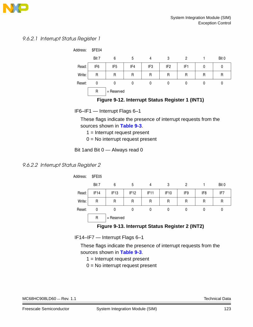
System Integration Module (SIM)Exception Control
9.6.2.1 Interrupt Status Register 1
IF6–IF1 — Interrupt Flags 6–1
These flags indicate the presence of interrupt requests from the sources shown in Table 9-3.
1 = Interrupt request present0 = No interrupt request present
Bit 1and Bit 0 — Always read 0
9.6.2.2 Interrupt Status Register 2
IF14–IF7 — Interrupt Flags 6–1
These flags indicate the presence of interrupt requests from the sources shown in Table 9-3.
1 = Interrupt request present0 = No interrupt request present
Address: $FE04
Bit 7 6 5 4 3 2 1 Bit 0
Read: IF6 IF5 IF4 IF3 IF2 IF1 0 0
Write: R R R R R R R R
Reset: 0 0 0 0 0 0 0 0
R = Reserved
Figure 9-12. Interrupt Status Register 1 (INT1)
Address: $FE05
Bit 7 6 5 4 3 2 1 Bit 0
Read: IF14 IF13 IF12 IF11 IF10 IF9 IF8 IF7
Write: R R R R R R R R
Reset: 0 0 0 0 0 0 0 0
R = Reserved
Figure 9-13. Interrupt Status Register 2 (INT2)
MC68HC908LD60 — Rev. 1.1 Technical Data
Freescale Semiconductor System Integration Module (SIM) 123
System Integration Module (SIM)
9.6.3 Reset
All reset sources always have equal and highest priority and cannot be arbitrated.
9.6.4 Break Interrupts
The break module can stop normal program flow at a software-programmable break point by asserting its break interrupt output (see Section 21. Break Module (BRK)). The SIM puts the CPU into the break state by forcing it to the SWI vector location. Refer to the break interrupt subsection of each module to see how each module is affected by the break state.
9.6.5 Status Flag Protection in Break Mode
The SIM controls whether status flags contained in other modules can be cleared during break mode. The user can select whether flags are protected from being cleared by properly initializing the break clear flag enable bit (BCFE) in the SIM break flag control register (SBFCR).
Protecting flags in break mode ensures that set flags will not be cleared while in break mode. This protection allows registers to be freely read and written during break mode without losing status flag information.
Setting the BCFE bit enables the clearing mechanisms. Once cleared in break mode, a flag remains cleared even when break mode is exited. Status flags with a two-step clearing mechanism — for example, a read of one register followed by the read or write of another — are protected, even when the first step is accomplished prior to entering break mode. Upon leaving break mode, execution of the second step will clear the flag as normal.
Technical Data MC68HC908LD60 — Rev. 1.1
124 System Integration Module (SIM) Freescale Semiconductor

System Integration Module (SIM)Low-Power Modes
9.7 Low-Power Modes
Executing the WAIT or STOP instruction puts the MCU in a low-power-consumption mode for standby situations. The SIM holds the CPU in a non-clocked state. The operation of each of these modes is described below. Both STOP and WAIT clear the interrupt mask (I) in the condition code register, allowing interrupts to occur.
9.7.1 Wait Mode
In wait mode, the CPU clocks are inactive while the peripheral clocks continue to run. Figure 9-14 shows the timing for wait mode entry.
A module that is active during wait mode can wake up the CPU with an interrupt if the interrupt is enabled. Stacking for the interrupt begins one cycle after the WAIT instruction during which the interrupt occurred. In wait mode, the CPU clocks are inactive. Refer to the wait mode subsection of each module to see if the module is active or inactive in wait mode. Some modules can be programmed to be active in wait mode.
Wait mode can also be exited by a reset or break. A break interrupt during wait mode sets the SIM break stop/wait bit, SBSW, in the SIM break status register (SBSR). If the COP disable bit, COPD, in configuration register (CONFIG) is logic zero, then the computer operating properly module (COP) is enabled and remains active in wait mode.
Figure 9-14. Wait Mode Entry Timing
Figure 9-15 and Figure 9-16 show the timing for WAIT recovery.
WAIT ADDR + 1 SAME SAMEIAB
IDB PREVIOUS DATA NEXT OPCODE SAME
WAIT ADDR
SAME
R/W
NOTE: Previous data can be operand data or the WAIT opcode, depending on the last instruction.
MC68HC908LD60 — Rev. 1.1 Technical Data
Freescale Semiconductor System Integration Module (SIM) 125

System Integration Module (SIM)
Figure 9-15. Wait Recovery from Interrupt or Break
Figure 9-16. Wait Recovery from Internal Reset
9.7.2 Stop Mode
In stop mode, the SIM counter is reset and the system clocks are disabled. An interrupt request from a module can cause an exit from stop mode. Stacking for interrupts begins after the selected stop recovery time has elapsed. Reset or break also causes an exit from stop mode.
The SIM disables the oscillator signals (OSCOUT and OSCXCLK) in stop mode, stopping the CPU and peripherals. Stop recovery time is selectable using the SSREC bit in configuration register (CONFIG). If SSREC is set, stop recovery is reduced from the normal delay of 4096 OSCXCLK cycles down to 32. This is ideal for applications using canned oscillators that do not require long start-up times from stop mode.
NOTE: External crystal applications should use the full stop recovery time by clearing the SSREC bit.
$6E0C$6E0B $00FF $00FE $00FD $00FC
$A6 $A6 $01 $0B $6E$A6
IAB
IDB
EXITSTOPWAIT
NOTE: EXITSTOPWAIT = RST pin OR CPU interrupt OR break interrupt
IAB
IDB
RST
$A6 $A6
$6E0B RST VCT H RST VCT L
$A6
OSCXCLK
32Cycles
32Cycles
Technical Data MC68HC908LD60 — Rev. 1.1
126 System Integration Module (SIM) Freescale Semiconductor
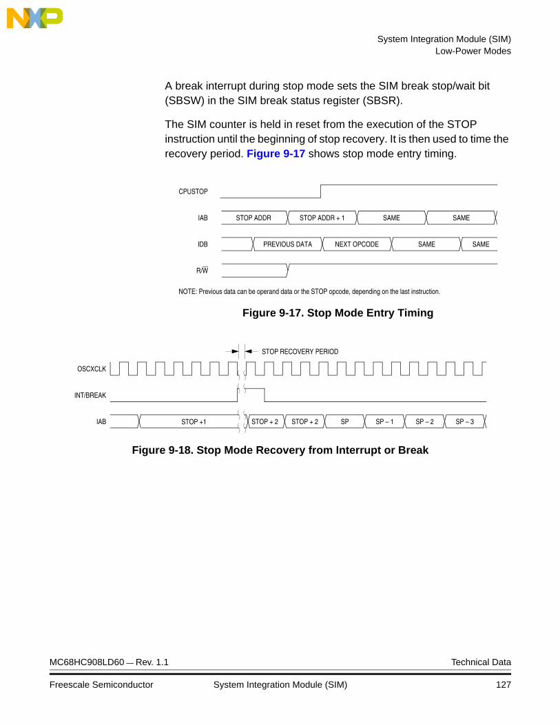
System Integration Module (SIM)Low-Power Modes
A break interrupt during stop mode sets the SIM break stop/wait bit (SBSW) in the SIM break status register (SBSR).
The SIM counter is held in reset from the execution of the STOP instruction until the beginning of stop recovery. It is then used to time the recovery period. Figure 9-17 shows stop mode entry timing.
Figure 9-17. Stop Mode Entry Timing
Figure 9-18. Stop Mode Recovery from Interrupt or Break
STOP ADDR + 1 SAME SAMEIAB
IDB PREVIOUS DATA NEXT OPCODE SAME
STOP ADDR
SAME
R/W
CPUSTOP
NOTE: Previous data can be operand data or the STOP opcode, depending on the last instruction.
OSCXCLK
INT/BREAK
IAB STOP + 2 STOP + 2 SP SP – 1 SP – 2 SP – 3STOP +1
STOP RECOVERY PERIOD
MC68HC908LD60 — Rev. 1.1 Technical Data
Freescale Semiconductor System Integration Module (SIM) 127
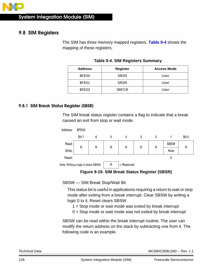
System Integration Module (SIM)
9.8 SIM Registers
The SIM has three memory mapped registers. Table 9-4 shows the mapping of these registers.
9.8.1 SIM Break Status Register (SBSR)
The SIM break status register contains a flag to indicate that a break caused an exit from stop or wait mode.
SBSW — SIM Break Stop/Wait Bit
This status bit is useful in applications requiring a return to wait or stop mode after exiting from a break interrupt. Clear SBSW by writing a logic 0 to it. Reset clears SBSW.
1 = Stop mode or wait mode was exited by break interrupt0 = Stop mode or wait mode was not exited by break interrupt
SBSW can be read within the break interrupt routine. The user can modify the return address on the stack by subtracting one from it. The following code is an example.
Table 9-4. SIM Registers Summary
Address Register Access Mode
$FE00 SBSR User
$FE01 SRSR User
$FE03 SBFCR User
Address: $FE00
Bit 7 6 5 4 3 2 1 Bit 0
Read:R R R R R R
SBSWR
Write: Note
Reset: 0
Note: Writing a logic 0 clears SBSW. R = Reserved
Figure 9-19. SIM Break Status Register (SBSR)
Technical Data MC68HC908LD60 — Rev. 1.1
128 System Integration Module (SIM) Freescale Semiconductor

System Integration Module (SIM)SIM Registers
9.8.2 SIM Reset Status Register (SRSR)
This register contains six flags that show the source of the last reset. Clear the SIM reset status register by reading it. A power-on reset sets the POR bit and clears all other bits in the register.
POR — Power-On Reset Bit1 = Last reset caused by POR circuit0 = Read of SRSR
PIN — External Reset Bit1 = Last reset caused by external reset pin (RST)0 = POR or read of SRSR
;;;
This code works if the H register has been pushed onto the stack in the break service routine software. This code should be executed at the end of the break service routine software.
HIBYTE EQU 5
LOBYTE EQU 6
; If not SBSW, do RTI
BRCLR SBSW,SBSR, RETURN ;;See if wait mode or stop mode was exited by break.
TST LOBYTE,SP ;If RETURNLO is not zero,
BNE DOLO ;then just decrement low byte.
DEC HIBYTE,SP ;Else deal with high byte, too.
DOLO DEC LOBYTE,SP ;Point to WAIT/STOP opcode.
RETURN PULHRTI
;Restore H register.
Address: $FE01
Bit 7 6 5 4 3 2 1 Bit 0
Read: POR PIN COP ILOP ILAD R 0 0
Write:
POR: 1 0 0 0 0 0 0
= Unimplemented R = Reserved
Figure 9-20. SIM Reset Status Register (SRSR)
MC68HC908LD60 — Rev. 1.1 Technical Data
Freescale Semiconductor System Integration Module (SIM) 129
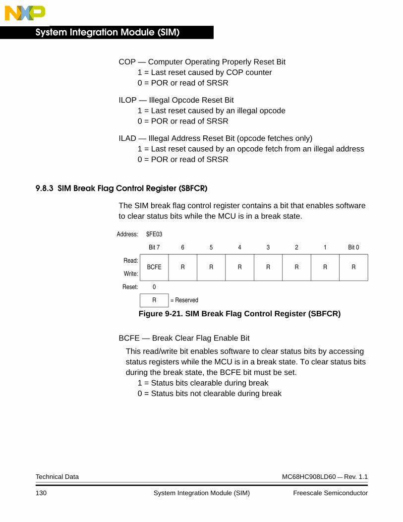
System Integration Module (SIM)
COP — Computer Operating Properly Reset Bit1 = Last reset caused by COP counter0 = POR or read of SRSR
ILOP — Illegal Opcode Reset Bit1 = Last reset caused by an illegal opcode0 = POR or read of SRSR
ILAD — Illegal Address Reset Bit (opcode fetches only)1 = Last reset caused by an opcode fetch from an illegal address0 = POR or read of SRSR
9.8.3 SIM Break Flag Control Register (SBFCR)
The SIM break flag control register contains a bit that enables software to clear status bits while the MCU is in a break state.
BCFE — Break Clear Flag Enable Bit
This read/write bit enables software to clear status bits by accessing status registers while the MCU is in a break state. To clear status bits during the break state, the BCFE bit must be set.
1 = Status bits clearable during break0 = Status bits not clearable during break
Address: $FE03
Bit 7 6 5 4 3 2 1 Bit 0
Read:BCFE R R R R R R R
Write:
Reset: 0
R = Reserved
Figure 9-21. SIM Break Flag Control Register (SBFCR)
Technical Data MC68HC908LD60 — Rev. 1.1
130 System Integration Module (SIM) Freescale Semiconductor

Technical Data — MC68HC908LD60
Section 10. Monitor ROM (MON)
10.1 Contents
10.2 Introduction . . . . . . . . . . . . . . . . . . . . . . . . . . . . . . . . . . . . . . .131
10.3 Features . . . . . . . . . . . . . . . . . . . . . . . . . . . . . . . . . . . . . . . . .132
10.4 Functional Description . . . . . . . . . . . . . . . . . . . . . . . . . . . . . .13210.4.1 Entering Monitor Mode . . . . . . . . . . . . . . . . . . . . . . . . . . . .13410.4.2 Data Format . . . . . . . . . . . . . . . . . . . . . . . . . . . . . . . . . . . .13610.4.3 Echoing . . . . . . . . . . . . . . . . . . . . . . . . . . . . . . . . . . . . . . .13710.4.4 Break Signal . . . . . . . . . . . . . . . . . . . . . . . . . . . . . . . . . . . .13710.4.5 Commands . . . . . . . . . . . . . . . . . . . . . . . . . . . . . . . . . . . . .13810.4.6 Baud Rate . . . . . . . . . . . . . . . . . . . . . . . . . . . . . . . . . . . . .141
10.2 Introduction
This section describes the monitor ROM (MON) and the monitor mode entry methods. The monitor ROM allows complete testing of the MCU through a single-wire interface with a host computer. Monitor mode entry can be achieved without use of the higher test voltage, VTST, as long as vector addresses $FFFE and $FFFF are blank, thus reducing the hardware requirements for in-circuit programming.
MC68HC908LD60 — Rev. 1.1 Technical Data
Freescale Semiconductor Monitor ROM (MON) 131

Monitor ROM (MON)
10.3 Features
Features of the monitor ROM include:
• Normal user-mode pin functionality
• One pin dedicated to serial communication between monitor ROM and host computer
• Standard mark/space non-return-to-zero (NRZ) communication with host computer
• Execution of code in RAM or FLASH
• FLASH memory security feature1
• FLASH memory programming interface
• 1024 bytes monitor ROM code size ($FA00 to $FDFF)
• Monitor mode entry without high voltage, VTST, if reset vector is blank ($FFFE and $FFFF contain $FF)
• Standard monitor mode entry if high voltage, VTST, is applied to IRQ
10.4 Functional Description
The monitor ROM receives and executes commands from a host computer. Figure 10-1 shows a sample circuit used to enter monitor mode and communicate with a host computer via a standard RS-232 interface.
Simple monitor commands can access any memory address. In monitor mode, the MCU can execute code downloaded into RAM by a host computer while most MCU pins retain normal operating mode functions. All communication between the host computer and the MCU is through the PTA0 pin. A level-shifting and multiplexing interface is required between PTA0 and the host computer. PTA0 is used in a wired-OR configuration and requires a pull-up resistor.
1. No security feature is absolutely secure. However, Freescale’s strategy is to make reading or copying the FLASH difficult for unauthorized users.
Technical Data MC68HC908LD60 — Rev. 1.1
132 Monitor ROM (MON) Freescale Semiconductor

Monitor ROM (MON)Functional Description
Figure 10-1. Monitor Mode Circuit
+
+
+
+
10 MΩX1
VDD
MC145407
MC74LCX125
68HC908LD60
RST
IRQ
OSC1
OSC2
VSS1
VDD1
PTA0
VDD
10 kΩ
0.1 µF
6
5
2
4
3
1
DB-252
3
7
20
18
17
19
16
15
VDD
VDD
VDD
20 pF
20 pF
10 µF
10 µF10 µF
10 µF
1
2
4
7
14
3
0.1 µF
9.8304 MHz
10 kΩ
PTC3VDD
10 kΩ
B
A
(See NOTES)
56
PTC0PTC1
VDD
10 kΩ
VSS2
VDD2
VSSA
VDDA0.1 µF
VDD
(PIN 6)
(PIN 7)
PTD4
PTD5
PTA7
VTST
10 Ω
D
C
(See NOTES)
SW2
SW1
NOTES:1. SW2: Position C — For monitor mode entry when IRQ = VTST:
SW1: Position A — Bus clock = OSCXCLK ÷ 4SW1: Position B — Bus clock = OSCXCLK ÷ 2
2. SW2: Position D — For monitor mode entry when reset vector is blank ($FFFE and $FFFF = $FF):Bus clock = OSCXCLK ÷ 4; PTC0, PTC1, and PTC3 voltages are not required.
3. See Table 22-4 for IRQ voltage level requirements.
MC68HC908LD60 — Rev. 1.1 Technical Data
Freescale Semiconductor Monitor ROM (MON) 133
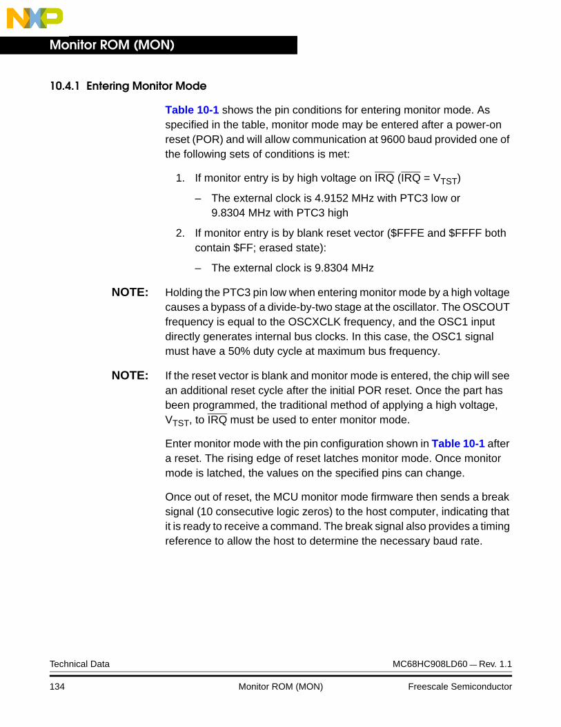
Monitor ROM (MON)
10.4.1 Entering Monitor Mode
Table 10-1 shows the pin conditions for entering monitor mode. As specified in the table, monitor mode may be entered after a power-on reset (POR) and will allow communication at 9600 baud provided one of the following sets of conditions is met:
1. If monitor entry is by high voltage on IRQ (IRQ = VTST)
– The external clock is 4.9152 MHz with PTC3 low or 9.8304 MHz with PTC3 high
2. If monitor entry is by blank reset vector ($FFFE and $FFFF both contain $FF; erased state):
– The external clock is 9.8304 MHz
NOTE: Holding the PTC3 pin low when entering monitor mode by a high voltage causes a bypass of a divide-by-two stage at the oscillator. The OSCOUT frequency is equal to the OSCXCLK frequency, and the OSC1 input directly generates internal bus clocks. In this case, the OSC1 signal must have a 50% duty cycle at maximum bus frequency.
NOTE: If the reset vector is blank and monitor mode is entered, the chip will see an additional reset cycle after the initial POR reset. Once the part has been programmed, the traditional method of applying a high voltage, VTST, to IRQ must be used to enter monitor mode.
Enter monitor mode with the pin configuration shown in Table 10-1 after a reset. The rising edge of reset latches monitor mode. Once monitor mode is latched, the values on the specified pins can change.
Once out of reset, the MCU monitor mode firmware then sends a break signal (10 consecutive logic zeros) to the host computer, indicating that it is ready to receive a command. The break signal also provides a timing reference to allow the host to determine the necessary baud rate.
Technical Data MC68HC908LD60 — Rev. 1.1
134 Monitor ROM (MON) Freescale Semiconductor
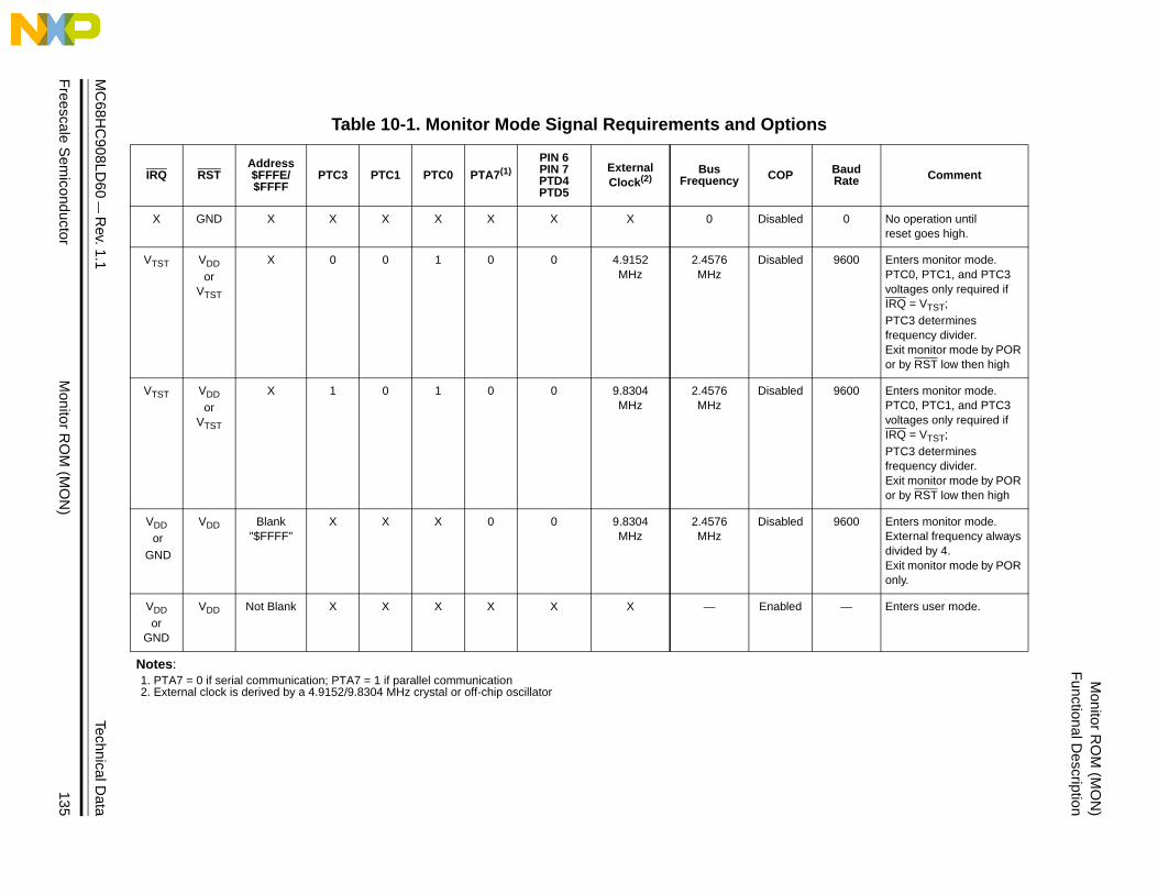
MC
68H
Freescale S
emiconductor
Monitor R
OM
(MO
N)
135
Monitor R
OM
(MO
N)
Functional D
escription
BaudRate Comment
0 No operation untilreset goes high.
9600 Enters monitor mode.PTC0, PTC1, and PTC3 voltages only required if IRQ = VTST; PTC3 determines frequency divider.Exit monitor mode by POR or by RST low then high
9600 Enters monitor mode.PTC0, PTC1, and PTC3 voltages only required if IRQ = VTST; PTC3 determines frequency divider.Exit monitor mode by POR or by RST low then high
9600 Enters monitor mode.External frequency always divided by 4.Exit monitor mode by POR only.
— Enters user mode.
C908LD
60 —
Rev. 1.1
Technical Data
Table 10-1. Monitor Mode Signal Requirements and Options
IRQ RSTAddress$FFFE/$FFFF
PTC3 PTC1 PTC0 PTA7(1)PIN 6PIN 7PTD4PTD5
ExternalClock(2)
BusFrequency COP
X GND X X X X X X X 0 Disabled
VTST VDD
orVTST
X 0 0 1 0 0 4.9152MHz
2.4576MHz
Disabled
VTST VDD
orVTST
X 1 0 1 0 0 9.8304MHz
2.4576MHz
Disabled
VDD
or GND
VDD Blank"$FFFF"
X X X 0 0 9.8304MHz
2.4576MHz
Disabled
VDD
orGND
VDD Not Blank X X X X X X — Enabled
Notes:1. PTA7 = 0 if serial communication; PTA7 = 1 if parallel communication2. External clock is derived by a 4.9152/9.8304 MHz crystal or off-chip oscillator
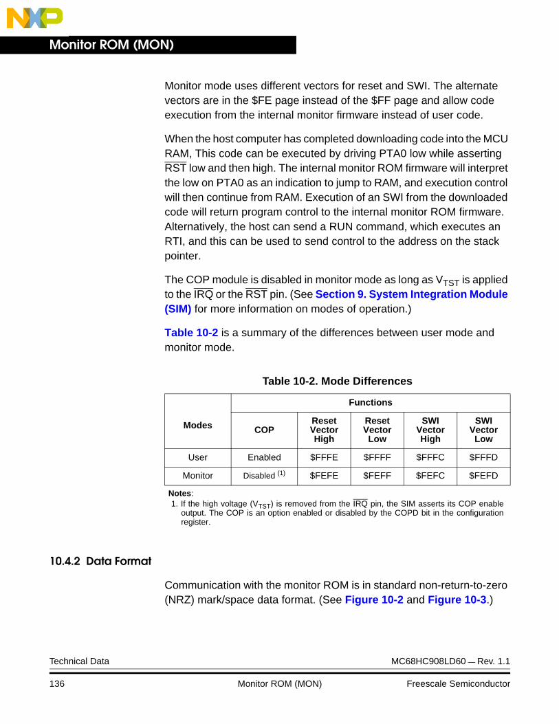
Monitor ROM (MON)
Monitor mode uses different vectors for reset and SWI. The alternate vectors are in the $FE page instead of the $FF page and allow code execution from the internal monitor firmware instead of user code.
When the host computer has completed downloading code into the MCU RAM, This code can be executed by driving PTA0 low while asserting RST low and then high. The internal monitor ROM firmware will interpret the low on PTA0 as an indication to jump to RAM, and execution control will then continue from RAM. Execution of an SWI from the downloaded code will return program control to the internal monitor ROM firmware. Alternatively, the host can send a RUN command, which executes an RTI, and this can be used to send control to the address on the stack pointer.
The COP module is disabled in monitor mode as long as VTST is applied to the IRQ or the RST pin. (See Section 9. System Integration Module (SIM) for more information on modes of operation.)
Table 10-2 is a summary of the differences between user mode and monitor mode.
10.4.2 Data Format
Communication with the monitor ROM is in standard non-return-to-zero (NRZ) mark/space data format. (See Figure 10-2 and Figure 10-3.)
Table 10-2. Mode Differences
Modes
Functions
COPResetVectorHigh
ResetVectorLow
SWIVectorHigh
SWIVector
Low
User Enabled $FFFE $FFFF $FFFC $FFFD
Monitor Disabled (1)
Notes:1. If the high voltage (VTST) is removed from the IRQ pin, the SIM asserts its COP enable
output. The COP is an option enabled or disabled by the COPD bit in the configurationregister.
$FEFE $FEFF $FEFC $FEFD
Technical Data MC68HC908LD60 — Rev. 1.1
136 Monitor ROM (MON) Freescale Semiconductor
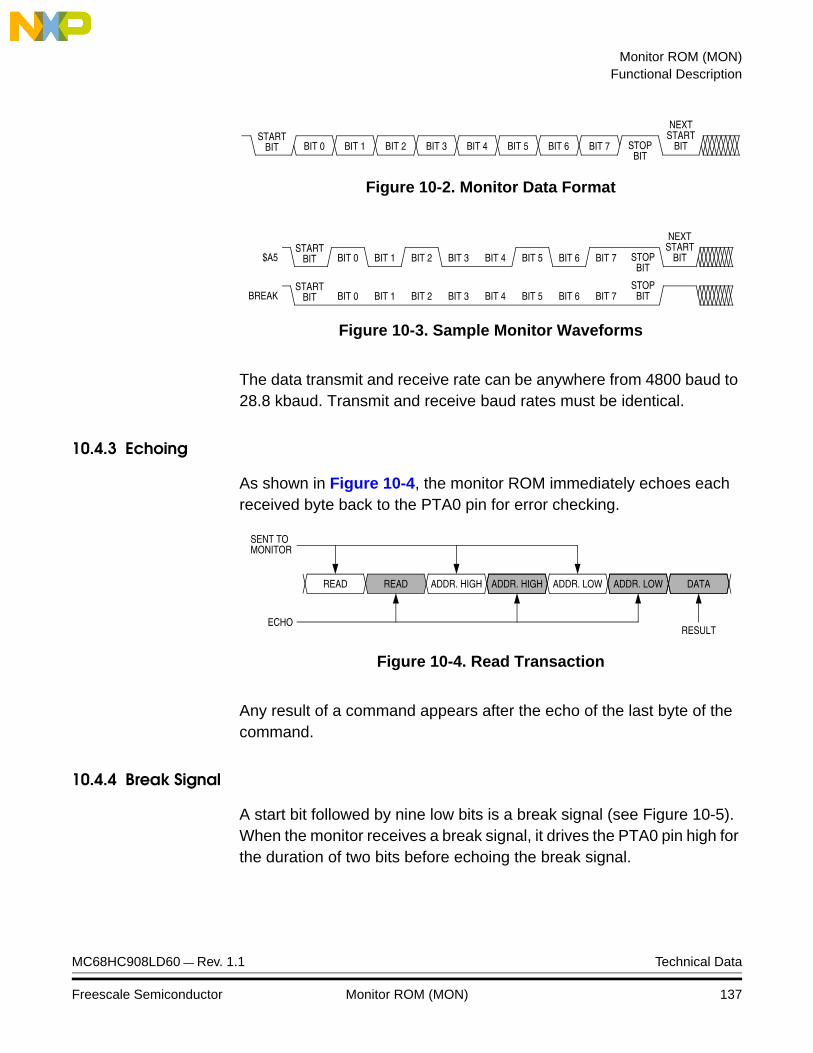
Monitor ROM (MON)Functional Description
Figure 10-2. Monitor Data Format
Figure 10-3. Sample Monitor Waveforms
The data transmit and receive rate can be anywhere from 4800 baud to 28.8 kbaud. Transmit and receive baud rates must be identical.
10.4.3 Echoing
As shown in Figure 10-4, the monitor ROM immediately echoes each received byte back to the PTA0 pin for error checking.
Figure 10-4. Read Transaction
Any result of a command appears after the echo of the last byte of the command.
10.4.4 Break Signal
A start bit followed by nine low bits is a break signal (see Figure 10-5). When the monitor receives a break signal, it drives the PTA0 pin high for the duration of two bits before echoing the break signal.
BIT 5START
BIT BIT 0 BIT 1
NEXT
STOPBIT
STARTBITBIT 2 BIT 3 BIT 4 BIT 6 BIT 7
BIT 5START
BIT BIT 0 BIT 1
NEXT
STOPBIT
STARTBITBIT 2 BIT 3 BIT 4 BIT 6 BIT 7
STARTBIT BIT 0 BIT 1
STOPBITBIT 2
$A5
BREAK BIT 3 BIT 4 BIT 5 BIT 6 BIT 7
ADDR. HIGHREADREAD ADDR. HIGH ADDR. LOW ADDR. LOW DATA
ECHO
SENT TOMONITOR
RESULT
MC68HC908LD60 — Rev. 1.1 Technical Data
Freescale Semiconductor Monitor ROM (MON) 137

Monitor ROM (MON)
Figure 10-5. Break Transaction
10.4.5 Commands
The monitor ROM uses the following commands:
• READ (read memory)
• WRITE (write memory)
• IREAD (indexed read)
• IWRITE (indexed write)
• READSP (read stack pointer)
• RUN (run user program)
0 1 2 3 4 5 6 7 0 1 2 3 4 5 6 7
MISSING STOP BITTWO-STOP-BIT DELAY BEFORE ZERO ECHO
Table 10-3. READ (Read Memory) Command
Description Read byte from memory
Operand Specifies 2-byte address in high byte:low byte order
DataReturned Returns contents of specified address
Opcode $4A
Command Sequence
READREAD
ECHO
SENT TOMONITOR
ADDRESSHIGH
ADDRESSHIGH
ADDRESSLOW DATA
RETURN
ADDRESSLOW
Technical Data MC68HC908LD60 — Rev. 1.1
138 Monitor ROM (MON) Freescale Semiconductor
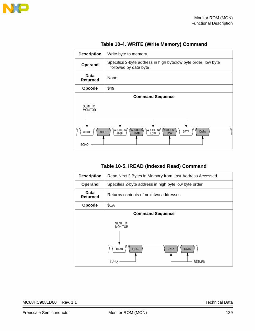
Monitor ROM (MON)Functional Description
Table 10-4. WRITE (Write Memory) Command
Description Write byte to memory
OperandSpecifics 2-byte address in high byte:low byte order; low byte
followed by data byte
DataReturned None
Opcode $49
Command Sequence
Table 10-5. IREAD (Indexed Read) Command
Description Read Next 2 Bytes in Memory from Last Address Accessed
Operand Specifies 2-byte address in high byte:low byte order
DataReturned Returns contents of next two addresses
Opcode $1A
Command Sequence
WRITEWRITE
ECHO
SEMT TOMONITOR
ADDRESSHIGH
ADDRESSHIGH
ADDRESSLOW
ADDRESSLOW
DATA DATA
IREADIREAD
ECHO
SENT TOMONITOR
DATA
RETURN
DATA
MC68HC908LD60 — Rev. 1.1 Technical Data
Freescale Semiconductor Monitor ROM (MON) 139

Monitor ROM (MON)
A sequence of IREAD or IWRITE commands can sequentially access a block of memory over the full 64k-byte memory map.
Table 10-6. IWRITE (Indexed Write) Command
Description Write to last address accessed + 1
Operand Specifies single data byte
DataReturned None
Opcode $19
Command Sequence
Table 10-7. READSP (Read Stack Pointer) Command
Description Reads stack pointer
Operand None
DataReturned Returns stack pointer in high byte:low byte order
Opcode $0C
Command Sequence
IWRITEIWRITE
ECHO
SENT TOMONITOR
DATA DATA
READSPREADSP
ECHO
SENT TOMONITOR
SP
RETURN
SPHIGH LOW
Technical Data MC68HC908LD60 — Rev. 1.1
140 Monitor ROM (MON) Freescale Semiconductor
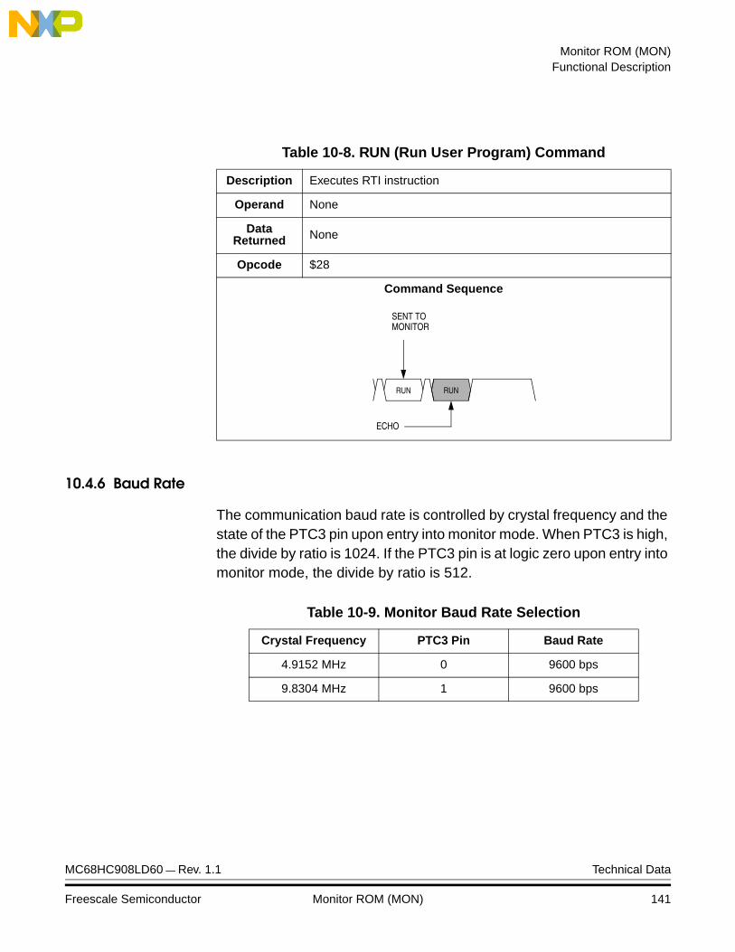
Monitor ROM (MON)Functional Description
10.4.6 Baud Rate
The communication baud rate is controlled by crystal frequency and the state of the PTC3 pin upon entry into monitor mode. When PTC3 is high, the divide by ratio is 1024. If the PTC3 pin is at logic zero upon entry into monitor mode, the divide by ratio is 512.
Table 10-8. RUN (Run User Program) Command
Description Executes RTI instruction
Operand None
DataReturned None
Opcode $28
Command Sequence
RUNRUN
ECHO
SENT TOMONITOR
Table 10-9. Monitor Baud Rate Selection
Crystal Frequency PTC3 Pin Baud Rate
4.9152 MHz 0 9600 bps
9.8304 MHz 1 9600 bps
MC68HC908LD60 — Rev. 1.1 Technical Data
Freescale Semiconductor Monitor ROM (MON) 141

Monitor ROM (MON)
Technical Data MC68HC908LD60 — Rev. 1.1
142 Monitor ROM (MON) Freescale Semiconductor
Technical Data — MC68HC908LD60
Section 11. Timer Interface Module (TIM)
11.1 Contents
11.2 Introduction . . . . . . . . . . . . . . . . . . . . . . . . . . . . . . . . . . . . . . .144
11.3 Features . . . . . . . . . . . . . . . . . . . . . . . . . . . . . . . . . . . . . . . . .144
11.4 Pin Name Conventions . . . . . . . . . . . . . . . . . . . . . . . . . . . . . .144
11.5 Functional Description . . . . . . . . . . . . . . . . . . . . . . . . . . . . . .14511.5.1 TIM Counter Prescaler . . . . . . . . . . . . . . . . . . . . . . . . . . . .14711.5.2 Input Capture . . . . . . . . . . . . . . . . . . . . . . . . . . . . . . . . . . .14711.5.3 Output Compare. . . . . . . . . . . . . . . . . . . . . . . . . . . . . . . . .14711.5.3.1 Unbuffered Output Compare . . . . . . . . . . . . . . . . . . . . .14811.5.3.2 Buffered Output Compare . . . . . . . . . . . . . . . . . . . . . . .14911.5.4 Pulse Width Modulation (PWM) . . . . . . . . . . . . . . . . . . . . .14911.5.4.1 Unbuffered PWM Signal Generation . . . . . . . . . . . . . . .15011.5.4.2 Buffered PWM Signal Generation . . . . . . . . . . . . . . . . .15111.5.4.3 PWM Initialization . . . . . . . . . . . . . . . . . . . . . . . . . . . . .152
11.6 Interrupts. . . . . . . . . . . . . . . . . . . . . . . . . . . . . . . . . . . . . . . . .153
11.7 Low-Power Modes . . . . . . . . . . . . . . . . . . . . . . . . . . . . . . . . .15311.7.1 Wait Mode . . . . . . . . . . . . . . . . . . . . . . . . . . . . . . . . . . . . .15311.7.2 Stop Mode . . . . . . . . . . . . . . . . . . . . . . . . . . . . . . . . . . . . .154
11.8 TIM During Break Interrupts . . . . . . . . . . . . . . . . . . . . . . . . . .154
11.9 I/O Signals . . . . . . . . . . . . . . . . . . . . . . . . . . . . . . . . . . . . . . .154
11.10 I/O Registers. . . . . . . . . . . . . . . . . . . . . . . . . . . . . . . . . . . . . .15511.10.1 TIM Status and Control Register (TSC) . . . . . . . . . . . . . . .15511.10.2 TIM Counter Registers (TCNTH:TCNTL) . . . . . . . . . . . . . .15711.10.3 TIM Counter Modulo Registers (TMODH:TMODL) . . . . . .15811.10.4 TIM Channel Status and Control Registers (TSC0:TSC1) .15911.10.5 TIM Channel Registers (TCH0H/L:TCH1H/L) . . . . . . . . . .162
MC68HC908LD60 — Rev. 1.1 Technical Data
Freescale Semiconductor Timer Interface Module (TIM) 143

Timer Interface Module (TIM)
11.2 Introduction
This section describes the timer interface module (TIM2, Version B). The TIM is a two-channel timer that provides a timing reference with input capture, output compare, and pulse-width-modulation functions. Figure 11-1 is a block diagram of the TIM.
11.3 Features
Features of the TIM include the following:
• Two input capture/output compare channels
– Rising-edge, falling-edge, or any-edge input capture trigger
– Set, clear, or toggle output compare action
• Buffered and unbuffered pulse width modulation (PWM) signal generation
• Programmable TIM clock input
– Seven-frequency internal bus clock prescaler selection
• Free-running or modulo up-count operation
• Toggle any channel pin on overflow
• TIM counter stop and reset bits
• Modular architecture expandable to eight channels
NOTE: TCH1 (timer channel 1) is not bonded to an external pin on this MCU. Therefore, any references to the timer TCH1 pin in the following text should be interpreted as not available — but the internal status and control registers are still available.
11.4 Pin Name Conventions
The TIM shares the TCH0 pin with the sync processor CLAMP output.
Table 11-1. Pin Name Conventions
TIM Generic Pin Name: TCH0
Full TIM Pin Name: CLAMP/TCH0
Pin Selected for TCH0 By: ELS0B:ELS0A
Technical Data MC68HC908LD60 — Rev. 1.1
144 Timer Interface Module (TIM) Freescale Semiconductor

Timer Interface Module (TIM)Functional Description
11.5 Functional Description
Figure 11-1 shows the structure of the TIM. The central component of the TIM is the 16-bit TIM counter that can operate as a free-running counter or a modulo up-counter. The TIM counter provides the timing reference for the input capture and output compare functions. The TIM counter modulo registers, TMODH:TMODL, control the modulo value of the TIM counter. Software can read the TIM counter value at any time without affecting the counting sequence.
The two TIM channels are programmable independently as input capture or output compare channels.
Figure 11-1. TIM Block Diagram
PRESCALER
PRESCALER SELECT
16-BIT COMPARATOR
PS2 PS1 PS0
16-BIT COMPARATOR
16-BIT LATCH
TCH0H:TCH0L
MS0A
ELS0B ELS0A
TOF
TOIE
16-BIT COMPARATOR
16-BIT LATCH
TCH1H:TCH1L
CHANNEL 0
CHANNEL 1
TMODH:TMODL
TRST
TSTOP
TOV0
CH0IE
CH0F
ELS1B ELS1ATOV1
CH1IE
CH1MAX
CH1F
CH0MAX
MS0B
16-BIT COUNTER
INTE
RNAL
BUS
MS1A
INTERNALBUS CLOCK
TCH1
TCH0
INTERRUPTLOGIC
PORTLOGIC
INTERRUPTLOGIC
INTERRUPTLOGIC
PORTLOGIC
(Not available)
MC68HC908LD60 — Rev. 1.1 Technical Data
Freescale Semiconductor Timer Interface Module (TIM) 145

Timer Interface Module (TIM)
Addr. Register Name Bit 7 6 5 4 3 2 1 Bit 0
$000ATIM Status and Control
Register(TSC)
Read: TOFTOIE TSTOP
0 0PS2 PS1 PS0
Write: 0 TRST
Reset: 0 0 1 0 0 0 0 0
$000CTIM Counter Register High
(TCNTH)
Read: Bit15 Bit14 Bit13 Bit12 Bit11 Bit10 Bit9 Bit8
Write:
Reset: 0 0 0 0 0 0 0 0
$000DTIM Counter Register Low
(TCNTL)
Read: Bit7 Bit6 Bit5 Bit4 Bit3 Bit2 Bit1 Bit0
Write:
Reset: 0 0 0 0 0 0 0 0
$000ETIM Counter Modulo
Register High(TMODH)
Read:Bit15 Bit14 Bit13 Bit12 Bit11 Bit10 Bit9 Bit8
Write:
Reset: 1 1 1 1 1 1 1 1
$000FTIM Counter Modulo
Register Low(TMODL)
Read:Bit7 Bit6 Bit5 Bit4 Bit3 Bit2 Bit1 Bit0
Write:
Reset: 1 1 1 1 1 1 1 1
$0010
TIM Channel 0Status and Control
Register(TSC0)
Read: CH0FCH0IE MS0B MS0A ELS0B ELS0A TOV0 CH0MAX
Write: 0
Reset: 0 0 0 0 0 0 0 0
$0011TIM Channel 0Register High
(TCH0H)
Read:Bit15 Bit14 Bit13 Bit12 Bit11 Bit10 Bit9 Bit8
Write:
Reset: Indeterminate after reset
$0012TIM Channel 0
Register Low(TCH0L)
Read:Bit7 Bit6 Bit5 Bit4 Bit3 Bit2 Bit1 Bit0
Write:
Reset: Indeterminate after reset
$0013
TIM Channel 1Status and Control
Register(TSC1)
Read: CH1FCH1IE
0MS1A ELS1B ELS1A TOV1 CH1MAX
Write: 0
Reset: 0 0 0 0 0 0 0 0
Technical Data MC68HC908LD60 — Rev. 1.1
146 Timer Interface Module (TIM) Freescale Semiconductor

Timer Interface Module (TIM)Functional Description
11.5.1 TIM Counter Prescaler
The TIM clock source can be one of the seven prescaler outputs. The prescaler generates seven clock rates from the internal bus clock. The prescaler select bits, PS[2:0], in the TIM status and control register (TSC) select the TIM clock source.
11.5.2 Input Capture
With the input capture function, the TIM can capture the time at which an external event occurs. When an active edge occurs on the pin of an input capture channel, the TIM latches the contents of the TIM counter into the TIM channel registers, TCHxH:TCHxL. The polarity of the active edge is programmable. Input captures can generate TIM CPU interrupt requests.
11.5.3 Output Compare
With the output compare function, the TIM can generate a periodic pulse with a programmable polarity, duration, and frequency. When the counter reaches the value in the registers of an output compare channel, the TIM can set, clear, or toggle the channel pin. Output compares can generate TIM CPU interrupt requests.
$0014TIM Channel 1Register High
(TCH1H)
Read:Bit15 Bit14 Bit13 Bit12 Bit11 Bit10 Bit9 Bit8
Write:
Reset: Indeterminate after reset
$0015TIM Channel 1
Register Low(TCH1L)
Read:Bit7 Bit6 Bit5 Bit4 Bit3 Bit2 Bit1 Bit0
Write:
Reset: Indeterminate after reset
= Unimplemented
Addr. Register Name Bit 7 6 5 4 3 2 1 Bit 0
MC68HC908LD60 — Rev. 1.1 Technical Data
Freescale Semiconductor Timer Interface Module (TIM) 147
Timer Interface Module (TIM)
11.5.3.1 Unbuffered Output Compare
Any output compare channel can generate unbuffered output compare pulses as described in 11.5.3 Output Compare. The pulses are unbuffered because changing the output compare value requires writing the new value over the old value currently in the TIM channel registers.
An unsynchronized write to the TIM channel registers to change an output compare value could cause incorrect operation for up to two counter overflow periods. For example, writing a new value before the counter reaches the old value but after the counter reaches the new value prevents any compare during that counter overflow period. Also, using a TIM overflow interrupt routine to write a new, smaller output compare value may cause the compare to be missed. The TIM may pass the new value before it is written.
Use the following methods to synchronize unbuffered changes in the output compare value on channel x:
• When changing to a smaller value, enable channel x output compare interrupts and write the new value in the output compare interrupt routine. The output compare interrupt occurs at the end of the current output compare pulse. The interrupt routine has until the end of the counter overflow period to write the new value.
• When changing to a larger output compare value, enable channel x TIM overflow interrupts and write the new value in the TIM overflow interrupt routine. The TIM overflow interrupt occurs at the end of the current counter overflow period. Writing a larger value in an output compare interrupt routine (at the end of the current pulse) could cause two output compares to occur in the same counter overflow period.
Technical Data MC68HC908LD60 — Rev. 1.1
148 Timer Interface Module (TIM) Freescale Semiconductor
Timer Interface Module (TIM)Functional Description
11.5.3.2 Buffered Output Compare
Channels 0 and 1 can be linked to form a buffered output compare channel whose output appears on the TCH0 pin. The TIM channel registers of the linked pair alternately control the output.
Setting the MS0B bit in TIM channel 0 status and control register (TSC0) links channel 0 and channel 1. The output compare value in the TIM channel 0 registers initially controls the output on the TCH0 pin. Writing to the TIM channel 1 registers enables the TIM channel 1 registers to synchronously control the output after the TIM overflows. At each subsequent overflow, the TIM channel registers (0 or 1) that control the output are the ones written to last. TSC0 controls and monitors the buffered output compare function, and TIM channel 1 status and control register (TSC1) is unused.
NOTE: In buffered output compare operation, do not write new output compare values to the currently active channel registers. Writing to the active channel registers is the same as generating unbuffered output compares.
11.5.4 Pulse Width Modulation (PWM)
By using the toggle-on-overflow feature with an output compare channel, the TIM can generate a PWM signal. The value in the TIM counter modulo registers determines the period of the PWM signal. The channel pin toggles when the counter reaches the value in the TIM counter modulo registers. The time between overflows is the period of the PWM signal.
As Figure 11-2 shows, the output compare value in the TIM channel registers determines the pulse width of the PWM signal. The time between overflow and output compare is the pulse width. Program the TIM to clear the channel pin on output compare if the state of the PWM pulse is logic one. Program the TIM to set the pin if the state of the PWM pulse is logic zero.
MC68HC908LD60 — Rev. 1.1 Technical Data
Freescale Semiconductor Timer Interface Module (TIM) 149
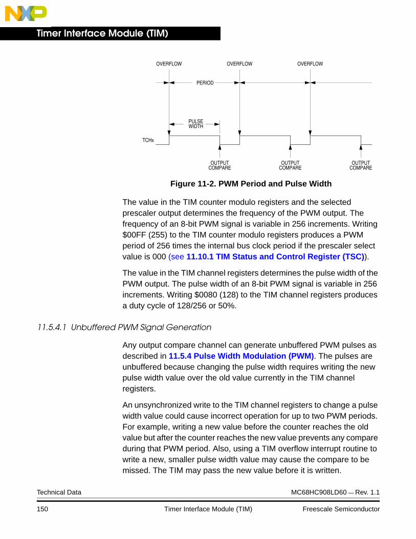
Timer Interface Module (TIM)
Figure 11-2. PWM Period and Pulse Width
The value in the TIM counter modulo registers and the selected prescaler output determines the frequency of the PWM output. The frequency of an 8-bit PWM signal is variable in 256 increments. Writing $00FF (255) to the TIM counter modulo registers produces a PWM period of 256 times the internal bus clock period if the prescaler select value is 000 (see 11.10.1 TIM Status and Control Register (TSC)).
The value in the TIM channel registers determines the pulse width of the PWM output. The pulse width of an 8-bit PWM signal is variable in 256 increments. Writing $0080 (128) to the TIM channel registers produces a duty cycle of 128/256 or 50%.
11.5.4.1 Unbuffered PWM Signal Generation
Any output compare channel can generate unbuffered PWM pulses as described in 11.5.4 Pulse Width Modulation (PWM). The pulses are unbuffered because changing the pulse width requires writing the new pulse width value over the old value currently in the TIM channel registers.
An unsynchronized write to the TIM channel registers to change a pulse width value could cause incorrect operation for up to two PWM periods. For example, writing a new value before the counter reaches the old value but after the counter reaches the new value prevents any compare during that PWM period. Also, using a TIM overflow interrupt routine to write a new, smaller pulse width value may cause the compare to be missed. The TIM may pass the new value before it is written.
TCHx
PERIOD
PULSEWIDTH
OVERFLOW OVERFLOW OVERFLOW
OUTPUTCOMPARE
OUTPUTCOMPARE
OUTPUTCOMPARE
Technical Data MC68HC908LD60 — Rev. 1.1
150 Timer Interface Module (TIM) Freescale Semiconductor
Timer Interface Module (TIM)Functional Description
Use the following methods to synchronize unbuffered changes in the PWM pulse width on channel x:
• When changing to a shorter pulse width, enable channel x output compare interrupts and write the new value in the output compare interrupt routine. The output compare interrupt occurs at the end of the current pulse. The interrupt routine has until the end of the PWM period to write the new value.
• When changing to a longer pulse width, enable channel x TIM overflow interrupts and write the new value in the TIM overflow interrupt routine. The TIM overflow interrupt occurs at the end of the current PWM period. Writing a larger value in an output compare interrupt routine (at the end of the current pulse) could cause two output compares to occur in the same PWM period.
NOTE: In PWM signal generation, do not program the PWM channel to toggle on output compare. Toggling on output compare prevents reliable 0% duty cycle generation and removes the ability of the channel to self-correct in the event of software error or noise. Toggling on output compare also can cause incorrect PWM signal generation when changing the PWM pulse width to a new, much larger value.
11.5.4.2 Buffered PWM Signal Generation
Channels 0 and 1 can be linked to form a buffered PWM channel whose output appears on the TCH0 pin. The TIM channel registers of the linked pair alternately control the pulse width of the output.
Setting the MS0B bit in TIM channel 0 status and control register (TSC0) links channel 0 and channel 1. The TIM channel 0 registers initially control the pulse width on the TCH0 pin. Writing to the TIM channel 1 registers enables the TIM channel 1 registers to synchronously control the pulse width at the beginning of the next PWM period. At each subsequent overflow, the TIM channel registers (0 or 1) that control the pulse width are the ones written to last. TSC0 controls and monitors the buffered PWM function, and TIM channel 1 status and control register (TSC1) is unused. While the MS0B bit is set, the channel 1 pin, TCH1, is available as a general-purpose I/O pin.
MC68HC908LD60 — Rev. 1.1 Technical Data
Freescale Semiconductor Timer Interface Module (TIM) 151

Timer Interface Module (TIM)
NOTE: In buffered PWM signal generation, do not write new pulse width values to the currently active channel registers. Writing to the active channel registers is the same as generating unbuffered PWM signals.
11.5.4.3 PWM Initialization
To ensure correct operation when generating unbuffered or buffered PWM signals, use the following initialization procedure:
1. In the TIM status and control register (TSC):
a. Stop the TIM counter by setting the TIM stop bit, TSTOP.
b. Reset the TIM counter by setting the TIM reset bit, TRST.
2. In the TIM counter modulo registers (TMODH:TMODL), write the value for the required PWM period.
3. In the TIM channel x registers (TCHxH:TCHxL), write the value for the required pulse width.
4. In TIM channel x status and control register (TSCx):
a. Write 0:1 (for unbuffered output compare or PWM signals) or 1:0 (for buffered output compare or PWM signals) to the mode select bits, MSxB:MSxA. (See Table 11-3.)
b. Write 1 to the toggle-on-overflow bit, TOVx.
c. Write 1:0 (to clear output on compare) or 1:1 (to set output on compare) to the edge/level select bits, ELSxB:ELSxA. The output action on compare must force the output to the complement of the pulse width level. (See Table 11-3.)
NOTE: In PWM signal generation, do not program the PWM channel to toggle on output compare. Toggling on output compare prevents reliable 0% duty cycle generation and removes the ability of the channel to self-correct in the event of software error or noise. Toggling on output compare can also cause incorrect PWM signal generation when changing the PWM pulse width to a new, much larger value.
5. In the TIM status control register (TSC), clear the TIM stop bit, TSTOP.
Technical Data MC68HC908LD60 — Rev. 1.1
152 Timer Interface Module (TIM) Freescale Semiconductor
Timer Interface Module (TIM)Interrupts
Setting MS0B links channels 0 and 1 and configures them for buffered PWM operation. The TIM channel 0 registers (TCH0H:TCH0L) initially control the buffered PWM output. TIM status control register 0 (TSCR0) controls and monitors the PWM signal from the linked channels. MS0B takes priority over MS0A.
Clearing the toggle-on-overflow bit, TOVx, inhibits output toggles on TIM overflows. Subsequent output compares try to force the output to a state it is already in and have no effect. The result is a 0% duty cycle output.
Setting the channel x maximum duty cycle bit (CHxMAX) and clearing the TOVx bit generates a 100% duty cycle output. See 11.10.4 TIM Channel Status and Control Registers (TSC0:TSC1).
11.6 Interrupts
The following TIM sources can generate interrupt requests:
• TIM overflow flag (TOF) — The TOF bit is set when the TIM counter value rolls over to $0000 after matching the value in the TIM counter modulo registers. The TIM overflow interrupt enable bit, TOIE, enables TIM overflow CPU interrupt requests. TOF and TOIE are in the TIM status and control register.
• TIM channel flags (CH1F:CH0F) — The CHxF bit is set when an input capture or output compare occurs on channel x. Channel x TIM CPU interrupt requests are controlled by the channel x interrupt enable bit, CHxIE. Channel x TIM CPU interrupt requests are enabled when CHxIE=1. CHxF and CHxIE are in the TIM channel x status and control register.
11.7 Low-Power Modes
The WAIT and STOP instructions puts the MCU in low-power-consumption standby modes.
11.7.1 Wait Mode
The TIM remains active after the execution of a WAIT instruction. In wait mode the TIMA registers are not accessible by the CPU. Any enabled CPU interrupt request from the TIM can bring the MCU out of wait mode.
MC68HC908LD60 — Rev. 1.1 Technical Data
Freescale Semiconductor Timer Interface Module (TIM) 153
Timer Interface Module (TIM)
If TIM functions are not required during wait mode, reduce power consumption by stopping the TIM before executing the WAIT instruction.
11.7.2 Stop Mode
The TIM is inactive after the execution of a STOP instruction. The STOP instruction does not affect register conditions or the state of the TIM counter. TIM operation resumes when the MCU exit stop mode after an external interrupt.
11.8 TIM During Break Interrupts
A break interrupt stops the TIM counter.
The system integration module (SIM) controls whether status bits in other modules can be cleared during the break state. The BCFE bit in the break flag control register (BFCR) enables software to clear status bits during the break state. (See 21.6.4 SIM Break Flag Control Register.)
To allow software to clear status bits during a break interrupt, write a logic one to the BCFE bit. If a status bit is cleared during the break state, it remains cleared when the MCU exits the break state.
To protect status bits during the break state, write a logic zero to the BCFE bit. With BCFE at logic zero (its default state), software can read and write I/O registers during the break state without affecting status bits. Some status bits have a two-step read/write clearing procedure. If software does the first step on such a bit before the break, the bit cannot change during the break state as long as BCFE is at logic zero. After the break, doing the second step clears the status bit.
11.9 I/O Signals
The TIM channel I/O pin is CLAMP/TCH0. The pin is shared with sync processor CLAMP output signal.
TCH0 pin is programmable independently as an input capture pin or an output compare pin. It also can be configured as a buffered output compare or buffered PWM pin.
Technical Data MC68HC908LD60 — Rev. 1.1
154 Timer Interface Module (TIM) Freescale Semiconductor

Timer Interface Module (TIM)I/O Registers
11.10 I/O Registers
The following I/O registers control and monitor operation of the TIM:
• TIM status and control register (TSC)
• TIM counter registers (TCNTH:TCNTL)
• TIM counter modulo registers (TMODH:TMODL)
• TIM channel status and control registers (TSC0 and TSC1)
• TIM channel registers (TCH0H:TCH0L and TCH1H:TCH1L)
11.10.1 TIM Status and Control Register (TSC)
The TIM status and control register does the following:
• Enables TIM overflow interrupts
• Flags TIM overflows
• Stops the TIM counter
• Resets the TIM counter
• Prescales the TIM counter clock
TOF — TIM Overflow Flag Bit
This read/write flag is set when the TIM counter resets to $0000 after reaching the modulo value programmed in the TIM counter modulo registers. Clear TOF by reading the TIM status and control register when TOF is set and then writing a logic zero to TOF. If another TIM
Address: $000A
Bit 7 6 5 4 3 2 1 Bit 0
Read: TOFTOIE TSTOP
0 0PS2 PS1 PS0
Write: 0 TRST
Reset: 0 0 1 0 0 0 0 0
= Unimplemented
Figure 11-3. TIM Status and Control Register (TSC)
MC68HC908LD60 — Rev. 1.1 Technical Data
Freescale Semiconductor Timer Interface Module (TIM) 155

Timer Interface Module (TIM)
overflow occurs before the clearing sequence is complete, then writing logic zero to TOF has no effect. Therefore, a TOF interrupt request cannot be lost due to inadvertent clearing of TOF. Reset clears the TOF bit. Writing a logic one to TOF has no effect.
1 = TIM counter has reached modulo value0 = TIM counter has not reached modulo value
TOIE — TIM Overflow Interrupt Enable Bit
This read/write bit enables TIM overflow interrupts when the TOF bit becomes set. Reset clears the TOIE bit.
1 = TIM overflow interrupts enabled0 = TIM overflow interrupts disabled
TSTOP — TIM Stop Bit
This read/write bit stops the TIM counter. Counting resumes when TSTOP is cleared. Reset sets the TSTOP bit, stopping the TIM counter until software clears the TSTOP bit.
1 = TIM counter stopped0 = TIM counter active
NOTE: Do not set the TSTOP bit before entering wait mode if the TIM is required to exit wait mode.
TRST — TIM Reset Bit
Setting this write-only bit resets the TIM counter and the TIM prescaler. Setting TRST has no effect on any other registers. Counting resumes from $0000. TRST is cleared automatically after the TIM counter is reset and always reads as logic zero. Reset clears the TRST bit.
1 = Prescaler and TIM counter cleared0 = No effect
NOTE: Setting the TSTOP and TRST bits simultaneously stops the TIM counter at a value of $0000.
PS[2:0] — Prescaler Select Bits
These read/write bits select either the TCLK pin or one of the seven prescaler outputs as the input to the TIM counter as Table 11-2 shows. Reset clears the PS[2:0] bits.
Technical Data MC68HC908LD60 — Rev. 1.1
156 Timer Interface Module (TIM) Freescale Semiconductor

Timer Interface Module (TIM)I/O Registers
11.10.2 TIM Counter Registers (TCNTH:TCNTL)
The two read-only TIM counter registers contain the high and low bytes of the value in the TIM counter. Reading the high byte (TCNTH) latches the contents of the low byte (TCNTL) into a buffer. Subsequent reads of TCNTH do not affect the latched TCNTL value until TCNTL is read. Reset clears the TIM counter registers. Setting the TIM reset bit (TRST) also clears the TIM counter registers.
Table 11-2. Prescaler Selection
PS2 PS1 PS0 TIM Clock Source
0 0 0 Internal Bus Clock ÷ 1
0 0 1 Internal Bus Clock ÷ 2
0 1 0 Internal Bus Clock ÷ 4
0 1 1 Internal Bus Clock ÷ 8
1 0 0 Internal Bus Clock ÷ 16
1 0 1 Internal Bus Clock ÷ 32
1 1 0 Internal Bus Clock ÷ 64
1 1 1 Not available
Address: $000C TCNTH
Bit 7 6 5 4 3 2 1 Bit 0
Read: Bit15 Bit14 Bit13 Bit12 Bit11 Bit10 Bit9 Bit8
Write:
Reset: 0 0 0 0 0 0 0 0
Address: $000D TCNTL
Bit 7 6 5 4 3 2 1 Bit 0
Read: Bit7 Bit6 Bit5 Bit4 Bit3 Bit2 Bit1 Bit0
Write:
Reset: 0 0 0 0 0 0 0 0
= Unimplemented
Figure 11-4. TIM Counter Registers (TCNTH:TCNTL)
MC68HC908LD60 — Rev. 1.1 Technical Data
Freescale Semiconductor Timer Interface Module (TIM) 157
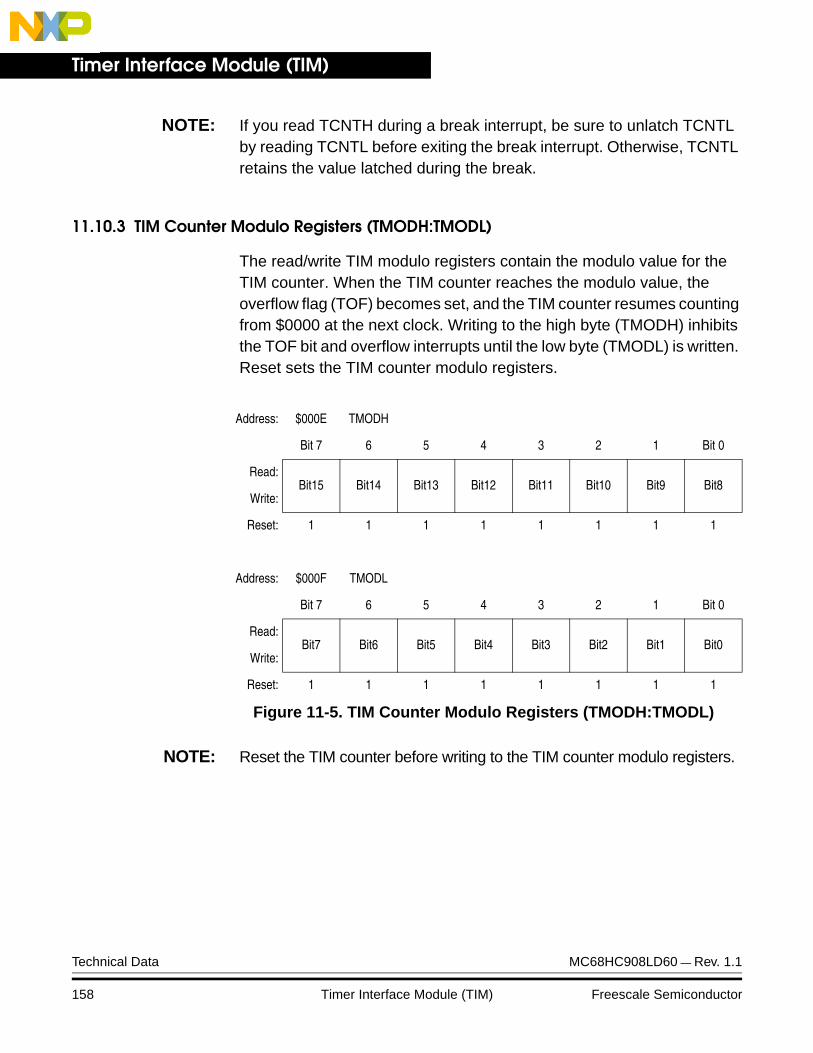
Timer Interface Module (TIM)
NOTE: If you read TCNTH during a break interrupt, be sure to unlatch TCNTL by reading TCNTL before exiting the break interrupt. Otherwise, TCNTL retains the value latched during the break.
11.10.3 TIM Counter Modulo Registers (TMODH:TMODL)
The read/write TIM modulo registers contain the modulo value for the TIM counter. When the TIM counter reaches the modulo value, the overflow flag (TOF) becomes set, and the TIM counter resumes counting from $0000 at the next clock. Writing to the high byte (TMODH) inhibits the TOF bit and overflow interrupts until the low byte (TMODL) is written. Reset sets the TIM counter modulo registers.
NOTE: Reset the TIM counter before writing to the TIM counter modulo registers.
Address: $000E TMODH
Bit 7 6 5 4 3 2 1 Bit 0
Read:Bit15 Bit14 Bit13 Bit12 Bit11 Bit10 Bit9 Bit8
Write:
Reset: 1 1 1 1 1 1 1 1
Address: $000F TMODL
Bit 7 6 5 4 3 2 1 Bit 0
Read:Bit7 Bit6 Bit5 Bit4 Bit3 Bit2 Bit1 Bit0
Write:
Reset: 1 1 1 1 1 1 1 1
Figure 11-5. TIM Counter Modulo Registers (TMODH:TMODL)
Technical Data MC68HC908LD60 — Rev. 1.1
158 Timer Interface Module (TIM) Freescale Semiconductor
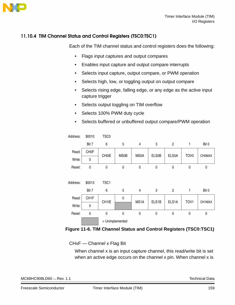
Timer Interface Module (TIM)I/O Registers
11.10.4 TIM Channel Status and Control Registers (TSC0:TSC1)
Each of the TIM channel status and control registers does the following:
• Flags input captures and output compares
• Enables input capture and output compare interrupts
• Selects input capture, output compare, or PWM operation
• Selects high, low, or toggling output on output compare
• Selects rising edge, falling edge, or any edge as the active input capture trigger
• Selects output toggling on TIM overflow
• Selects 100% PWM duty cycle
• Selects buffered or unbuffered output compare/PWM operation
CHxF — Channel x Flag Bit
When channel x is an input capture channel, this read/write bit is set when an active edge occurs on the channel x pin. When channel x is
Address: $0010 TSC0
Bit 7 6 5 4 3 2 1 Bit 0
Read: CH0FCH0IE MS0B MS0A ELS0B ELS0A TOV0 CH0MAX
Write: 0
Reset: 0 0 0 0 0 0 0 0
Address: $0013 TSC1
Bit 7 6 5 4 3 2 1 Bit 0
Read: CH1FCH1IE
0MS1A ELS1B ELS1A TOV1 CH1MAX
Write: 0
Reset: 0 0 0 0 0 0 0 0
= Unimplemented
Figure 11-6. TIM Channel Status and Control Registers (TSC0:TSC1)
MC68HC908LD60 — Rev. 1.1 Technical Data
Freescale Semiconductor Timer Interface Module (TIM) 159

Timer Interface Module (TIM)
an output compare channel, CHxF is set when the value in the TIM counter registers matches the value in the TIM channel x registers.
When TIM CPU interrupt requests are enabled (CHxIE=1), clear CHxF by reading the TIM channel x status and control register with CHxF set and then writing a logic zero to CHxF. If another interrupt request occurs before the clearing sequence is complete, then writing logic zero to CHxF has no effect. Therefore, an interrupt request cannot be lost due to inadvertent clearing of CHxF.
Reset clears the CHxF bit. Writing a logic one to CHxF has no effect.1 = Input capture or output compare on channel x0 = No input capture or output compare on channel x
CHxIE — Channel x Interrupt Enable Bit
This read/write bit enables TIM CPU interrupt service requests on channel x. Reset clears the CHxIE bit.
1 = Channel x CPU interrupt requests enabled0 = Channel x CPU interrupt requests disabled
MSxB — Mode Select Bit B
This read/write bit selects buffered output compare/PWM operation. MSxB exists only in the TIM channel 0 status and control register.
Setting MS0B disables the channel 1 status and control register and reverts TCH1 to general-purpose I/O.
Reset clears the MSxB bit.1 = Buffered output compare/PWM operation enabled0 = Buffered output compare/PWM operation disabled
MSxA — Mode Select Bit A
When ELSxB:A ≠ 00, this read/write bit selects either input capture operation or unbuffered output compare/PWM operation. See Table 11-3.
1 = Unbuffered output compare/PWM operation0 = Input capture operation
When ELSxB:A = 00, this read/write bit selects the initial output level of the TCHx pin. (See Table 11-3.) Reset clears the MSxA bit.
1 = Initial output level low0 = Initial output level high
Technical Data MC68HC908LD60 — Rev. 1.1
160 Timer Interface Module (TIM) Freescale Semiconductor

Timer Interface Module (TIM)I/O Registers
NOTE: Before changing a channel function by writing to the MSxB or MSxA bit, set the TSTOP and TRST bits in the TIM status and control register (TSC).
ELSxB and ELSxA — Edge/Level Select Bits
When channel x is an input capture channel, these read/write bits control the active edge-sensing logic on channel x.
When channel x is an output compare channel, ELSxB and ELSxA control the channel x output behavior when an output compare occurs.
When ELS0B and ELS0A are both clear, channel 0 is not connected to the CLAMP/TCH0 pin. The pin is available as the CLAMP output of the sync processor.
Table 11-3 shows how ELSxB and ELSxA work. Reset clears the ELSxB and ELSxA bits.
NOTE: Before enabling a TIM channel register for input capture operation, make sure that the TCHx pin is stable for at least two bus clocks.
Table 11-3. Mode, Edge, and Level Selection
MSxB MSxA ELSxB ELSxA Mode Configuration
X 0 0 0Output Preset
Pin is CLAMP of sync processor(1);Initial Output Level High
Notes:1. For CLAMP/TCH0 pin only.
X 1 0 0Pin is CLAMP of sync processor(1);Initial Output Level Low
0 0 0 1Input
Capture
Capture on Rising Edge Only
0 0 1 0 Capture on Falling Edge Only
0 0 1 1 Capture on Rising or Falling Edge
0 1 0 1Output
Compare or PWM
Toggle Output on Compare
0 1 1 0 Clear Output on Compare
0 1 1 1 Set Output on Compare
1 X 0 1 Buffered Output
Compare or Buffered PWM
Toggle Output on Compare
1 X 1 0 Clear Output on Compare
1 X 1 1 Set Output on Compare
MC68HC908LD60 — Rev. 1.1 Technical Data
Freescale Semiconductor Timer Interface Module (TIM) 161
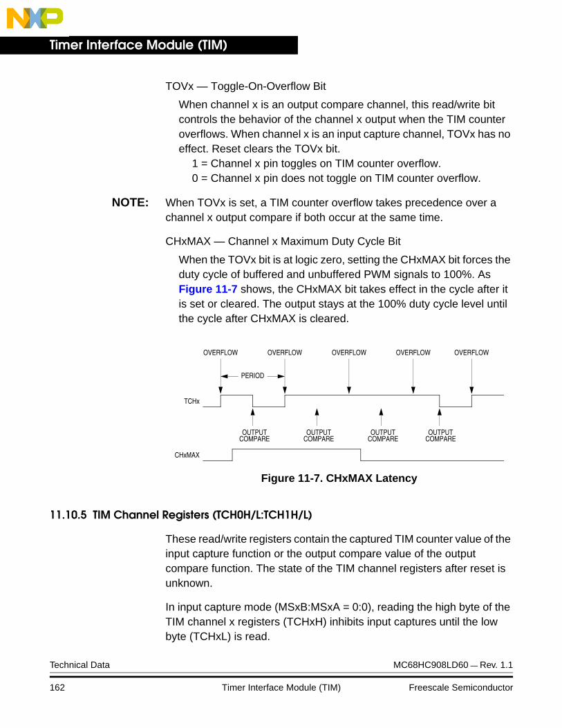
Timer Interface Module (TIM)
TOVx — Toggle-On-Overflow Bit
When channel x is an output compare channel, this read/write bit controls the behavior of the channel x output when the TIM counter overflows. When channel x is an input capture channel, TOVx has no effect. Reset clears the TOVx bit.
1 = Channel x pin toggles on TIM counter overflow.0 = Channel x pin does not toggle on TIM counter overflow.
NOTE: When TOVx is set, a TIM counter overflow takes precedence over a channel x output compare if both occur at the same time.
CHxMAX — Channel x Maximum Duty Cycle Bit
When the TOVx bit is at logic zero, setting the CHxMAX bit forces the duty cycle of buffered and unbuffered PWM signals to 100%. As Figure 11-7 shows, the CHxMAX bit takes effect in the cycle after it is set or cleared. The output stays at the 100% duty cycle level until the cycle after CHxMAX is cleared.
Figure 11-7. CHxMAX Latency
11.10.5 TIM Channel Registers (TCH0H/L:TCH1H/L)
These read/write registers contain the captured TIM counter value of the input capture function or the output compare value of the output compare function. The state of the TIM channel registers after reset is unknown.
In input capture mode (MSxB:MSxA = 0:0), reading the high byte of the TIM channel x registers (TCHxH) inhibits input captures until the low byte (TCHxL) is read.
OUTPUT
OVERFLOW
TCHx
PERIOD
CHxMAX
OVERFLOW OVERFLOW OVERFLOW OVERFLOW
COMPAREOUTPUT
COMPAREOUTPUT
COMPAREOUTPUT
COMPARE
Technical Data MC68HC908LD60 — Rev. 1.1
162 Timer Interface Module (TIM) Freescale Semiconductor
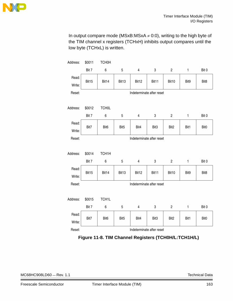
Timer Interface Module (TIM)I/O Registers
In output compare mode (MSxB:MSxA ≠ 0:0), writing to the high byte of the TIM channel x registers (TCHxH) inhibits output compares until the low byte (TCHxL) is written.
Address: $0011 TCH0H
Bit 7 6 5 4 3 2 1 Bit 0
Read:Bit15 Bit14 Bit13 Bit12 Bit11 Bit10 Bit9 Bit8
Write:
Reset: Indeterminate after reset
Address: $0012 TCH0L
Bit 7 6 5 4 3 2 1 Bit 0
Read:Bit7 Bit6 Bit5 Bit4 Bit3 Bit2 Bit1 Bit0
Write:
Reset: Indeterminate after reset
Address: $0014 TCH1H
Bit 7 6 5 4 3 2 1 Bit 0
Read:Bit15 Bit14 Bit13 Bit12 Bit11 Bit10 Bit9 Bit8
Write:
Reset: Indeterminate after reset
Address: $0015 TCH1L
Bit 7 6 5 4 3 2 1 Bit 0
Read:Bit7 Bit6 Bit5 Bit4 Bit3 Bit2 Bit1 Bit0
Write:
Reset: Indeterminate after reset
Figure 11-8. TIM Channel Registers (TCH0H/L:TCH1H/L)
MC68HC908LD60 — Rev. 1.1 Technical Data
Freescale Semiconductor Timer Interface Module (TIM) 163

Timer Interface Module (TIM)
Technical Data MC68HC908LD60 — Rev. 1.1
164 Timer Interface Module (TIM) Freescale Semiconductor

Technical Data — MC68HC908LD60
Section 12. Pulse Width Modulator (PWM)
12.1 Contents
12.2 Introduction . . . . . . . . . . . . . . . . . . . . . . . . . . . . . . . . . . . . . . .165
12.3 Functional Description . . . . . . . . . . . . . . . . . . . . . . . . . . . . . .165
12.4 PWM Registers. . . . . . . . . . . . . . . . . . . . . . . . . . . . . . . . . . . .16712.4.1 PWM Data Registers 0 to 7 (0PWM–7PWM). . . . . . . . . . .16712.4.2 PWM Control Register (PWMCR) . . . . . . . . . . . . . . . . . . .168
12.2 Introduction
Eight 8-bit PWM channels are available on the MC68HC908LD60. Channels 0 to 7 are shared with port-B I/O pins under the control of the PWM control register.
12.3 Functional Description
Each 8-Bit PWM channel is composed of an 8-bit register which contains a 5-bit PWM in MSB portion and a 3-bit binary rate multiplier (BRM) in LSB portion. There are eight PWM data registers, controlling each PWM channel. The value programmed in the 5-bit PWM portion will determine the pulse length of the output. The clock to the 5-bit PWM portion is the system bus clock, the repetition rate of the output is hence 187.5kHz at 6MHz clock.
The 3-bit BRM will generate a number of narrow pulses which are equally distributed among an 8-PWM-cycle frame. The number of pulses generated is equal to the number programmed in the 3-bit BRM portion. Example of the waveforms are shown in Figure 12-4.
MC68HC908LD60 — Rev. 1.1 Technical Data
Freescale Semiconductor Pulse Width Modulator (PWM) 165
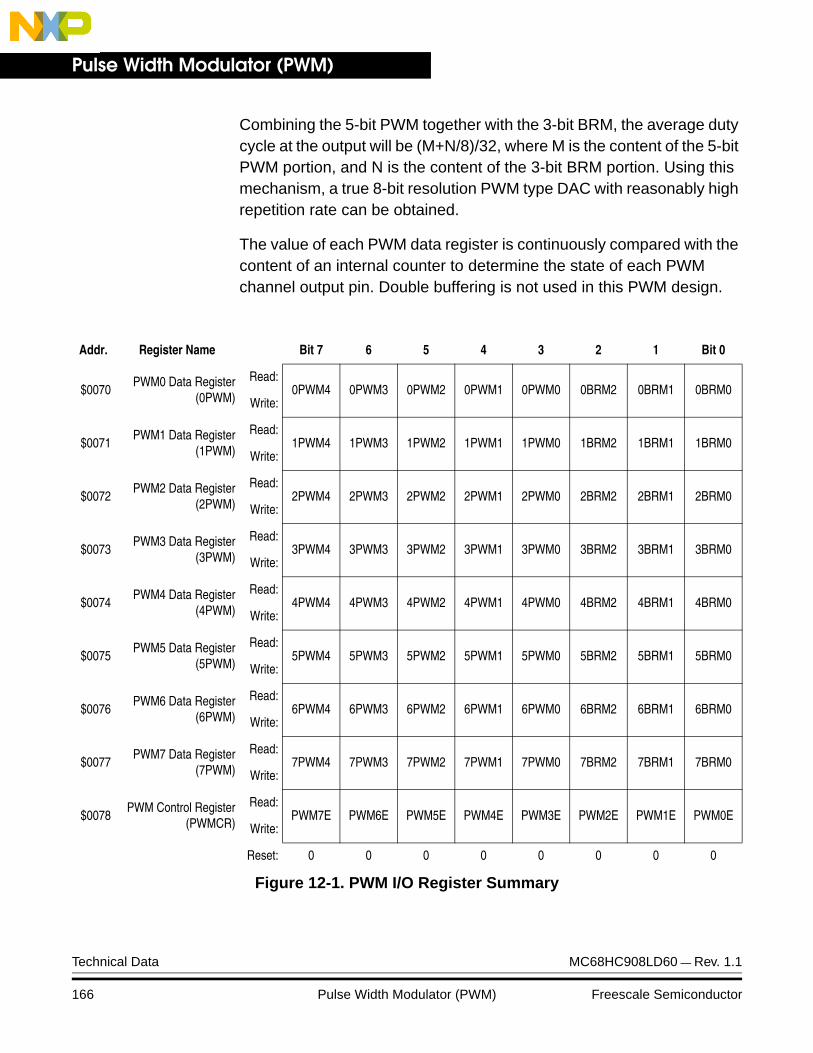
Pulse Width Modulator (PWM)
Combining the 5-bit PWM together with the 3-bit BRM, the average duty cycle at the output will be (M+N/8)/32, where M is the content of the 5-bit PWM portion, and N is the content of the 3-bit BRM portion. Using this mechanism, a true 8-bit resolution PWM type DAC with reasonably high repetition rate can be obtained.
The value of each PWM data register is continuously compared with the content of an internal counter to determine the state of each PWM channel output pin. Double buffering is not used in this PWM design.
Addr. Register Name Bit 7 6 5 4 3 2 1 Bit 0
$0070PWM0 Data Register
(0PWM)
Read:0PWM4 0PWM3 0PWM2 0PWM1 0PWM0 0BRM2 0BRM1 0BRM0
Write:
$0071PWM1 Data Register
(1PWM)
Read:1PWM4 1PWM3 1PWM2 1PWM1 1PWM0 1BRM2 1BRM1 1BRM0
Write:
$0072PWM2 Data Register
(2PWM)
Read:2PWM4 2PWM3 2PWM2 2PWM1 2PWM0 2BRM2 2BRM1 2BRM0
Write:
$0073PWM3 Data Register
(3PWM)
Read:3PWM4 3PWM3 3PWM2 3PWM1 3PWM0 3BRM2 3BRM1 3BRM0
Write:
$0074PWM4 Data Register
(4PWM)
Read:4PWM4 4PWM3 4PWM2 4PWM1 4PWM0 4BRM2 4BRM1 4BRM0
Write:
$0075PWM5 Data Register
(5PWM)
Read:5PWM4 5PWM3 5PWM2 5PWM1 5PWM0 5BRM2 5BRM1 5BRM0
Write:
$0076PWM6 Data Register
(6PWM)
Read:6PWM4 6PWM3 6PWM2 6PWM1 6PWM0 6BRM2 6BRM1 6BRM0
Write:
$0077PWM7 Data Register
(7PWM)
Read:7PWM4 7PWM3 7PWM2 7PWM1 7PWM0 7BRM2 7BRM1 7BRM0
Write:
$0078PWM Control Register
(PWMCR)
Read:PWM7E PWM6E PWM5E PWM4E PWM3E PWM2E PWM1E PWM0E
Write:
Reset: 0 0 0 0 0 0 0 0
Figure 12-1. PWM I/O Register Summary
Technical Data MC68HC908LD60 — Rev. 1.1
166 Pulse Width Modulator (PWM) Freescale Semiconductor

Pulse Width Modulator (PWM)PWM Registers
12.4 PWM Registers
The PWM module uses of nine registers for data and control functions.
• PWM data registers ($0070–$0077)
• PWM control register ($0078)
12.4.1 PWM Data Registers 0 to 7 (0PWM–7PWM)
The output waveform of the eight PWM channels are each configured by an 8-bit register, which contains a 5-bit PWM in MSB portion and a 3-bit binary rate multiplier (BRM) in LSB portion
xPWM4–xPWM0 — PWM Bits
The value programmed in the 5-bit PWM portion will determine the pulse length of the output. The clock to the 5-bit PWM portion is the system bus clock, the repetition rate of the output is hence fOP ÷ 32.
Examples of PWM output waveforms are shown in Figure 12-4.
xBRM2–xBRM0 — Binary Rate Multiplier Bits
The 3-bit BRM will generate a number of narrow pulses which are equally distributed among an 8-PWM-cycle frame. The number of pulses generated is equal to the number programmed in the 3-bit BRM portion. Examples of PWM output waveforms are shown in Figure 12-4.
Address: $0070–$0077
Bit 7 6 5 4 3 2 1 Bit 0
Read:xPWM4 xPWM3 xPWM2 xPWM1 xPWM0 xBRM2 xBRM1 xBRM0
Write:
Reset: 0 0 0 0 0 0 0 0
Figure 12-2. PWM Data Registers 0 to 7 (0PWM–7PWM)
MC68HC908LD60 — Rev. 1.1 Technical Data
Freescale Semiconductor Pulse Width Modulator (PWM) 167
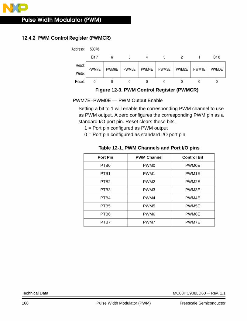
Pulse Width Modulator (PWM)
12.4.2 PWM Control Register (PWMCR)
PWM7E–PWM0E — PWM Output Enable
Setting a bit to 1 will enable the corresponding PWM channel to use as PWM output. A zero configures the corresponding PWM pin as a standard I/O port pin. Reset clears these bits.
1 = Port pin configured as PWM output0 = Port pin configured as standard I/O port pin.
Address: $0078
Bit 7 6 5 4 3 2 1 Bit 0
Read:PWM7E PWM6E PWM5E PWM4E PWM3E PWM2E PWM1E PWM0E
Write:
Reset: 0 0 0 0 0 0 0 0
Figure 12-3. PWM Control Register (PWMCR)
Table 12-1. PWM Channels and Port I/O pins
Port Pin PWM Channel Control Bit
PTB0 PWM0 PWM0E
PTB1 PWM1 PWM1E
PTB2 PWM2 PWM2E
PTB3 PWM3 PWM3E
PTB4 PWM4 PWM4E
PTB5 PWM5 PWM5E
PTB6 PWM6 PWM6E
PTB7 PWM7 PWM7E
Technical Data MC68HC908LD60 — Rev. 1.1
168 Pulse Width Modulator (PWM) Freescale Semiconductor

Pulse Width Modulator (PWM)PWM Registers
Figure 12-4. 8-Bit PWM Output Waveforms
M=$00
1 PWM cycle = 32T
M=$01
M=$0F
M=$1F
T=1 CPU clock period (0.167ms if CPU clock=6MHz)
Pulse inserted at end of PWM cycle
NPWM cycles where pulses are
inserted in a 8-cycle frameNumber of inserted pulses in
a 8-cycle framexx1 4 1x1x 2, 6 2
1xx 1, 3, 5, 7 4
31T
16T 16T
31T
T
M = value set in 5-bit PWM (bit3-bit7)N = value set in 3-bit BRM (bit0-bit2)
Tdepends on setting of N.
MC68HC908LD60 — Rev. 1.1 Technical Data
Freescale Semiconductor Pulse Width Modulator (PWM) 169

Pulse Width Modulator (PWM)
Technical Data MC68HC908LD60 — Rev. 1.1
170 Pulse Width Modulator (PWM) Freescale Semiconductor
Technical Data — MC68HC908LD60
Section 13. Analog-to-Digital Converter (ADC)
13.1 Contents
13.2 Introduction . . . . . . . . . . . . . . . . . . . . . . . . . . . . . . . . . . . . . . .172
13.3 Features . . . . . . . . . . . . . . . . . . . . . . . . . . . . . . . . . . . . . . . . .172
13.4 Functional Description . . . . . . . . . . . . . . . . . . . . . . . . . . . . . .17313.4.1 ADC Port I/O Pins . . . . . . . . . . . . . . . . . . . . . . . . . . . . . . .17413.4.2 Voltage Conversion . . . . . . . . . . . . . . . . . . . . . . . . . . . . . .17413.4.3 Conversion Time . . . . . . . . . . . . . . . . . . . . . . . . . . . . . . . .17413.4.4 Continuous Conversion . . . . . . . . . . . . . . . . . . . . . . . . . . .17513.4.5 Accuracy and Precision . . . . . . . . . . . . . . . . . . . . . . . . . . .175
13.5 Interrupts. . . . . . . . . . . . . . . . . . . . . . . . . . . . . . . . . . . . . . . . .175
13.6 Low-Power Modes . . . . . . . . . . . . . . . . . . . . . . . . . . . . . . . . .17513.6.1 Wait Mode . . . . . . . . . . . . . . . . . . . . . . . . . . . . . . . . . . . . .17513.6.2 Stop Mode . . . . . . . . . . . . . . . . . . . . . . . . . . . . . . . . . . . . .176
13.7 I/O Signals . . . . . . . . . . . . . . . . . . . . . . . . . . . . . . . . . . . . . . .17613.7.1 ADC Analog Power Pin (VDDA). . . . . . . . . . . . . . . . . . . . .17613.7.2 ADC Analog Ground Pin (VSSA) . . . . . . . . . . . . . . . . . . . .17613.7.3 ADC Voltage Reference High Pin (VRH) . . . . . . . . . . . . . .17613.7.4 ADC Voltage Reference Low Pin (VRL). . . . . . . . . . . . . . .17613.7.5 ADC Voltage In (ADCVIN) . . . . . . . . . . . . . . . . . . . . . . . . .176
13.8 I/O Registers. . . . . . . . . . . . . . . . . . . . . . . . . . . . . . . . . . . . . .17713.8.1 ADC Status and Control Register. . . . . . . . . . . . . . . . . . . .17713.8.2 ADC Data Register. . . . . . . . . . . . . . . . . . . . . . . . . . . . . . .17913.8.3 ADC Input Clock Register . . . . . . . . . . . . . . . . . . . . . . . . .179
MC68HC908LD60 — Rev. 1.1 Technical Data
Freescale Semiconductor Analog-to-Digital Converter (ADC) 171
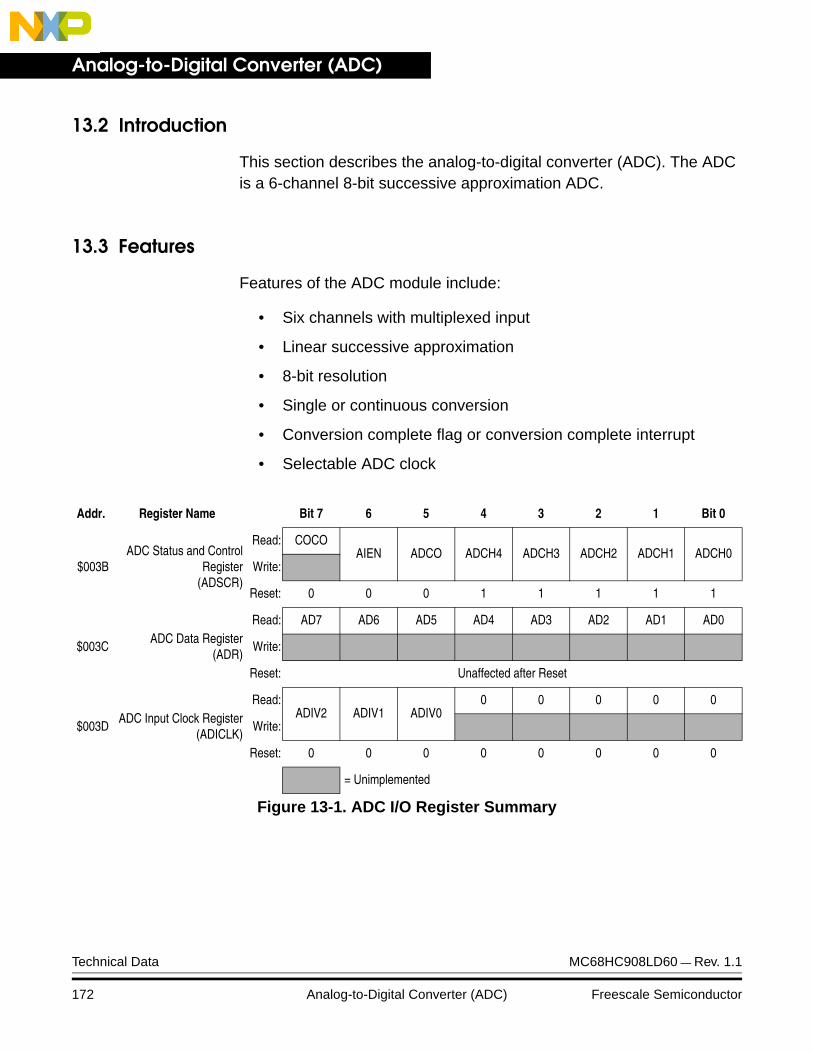
Analog-to-Digital Converter (ADC)
13.2 Introduction
This section describes the analog-to-digital converter (ADC). The ADC is a 6-channel 8-bit successive approximation ADC.
13.3 Features
Features of the ADC module include:
• Six channels with multiplexed input
• Linear successive approximation
• 8-bit resolution
• Single or continuous conversion
• Conversion complete flag or conversion complete interrupt
• Selectable ADC clock
Addr. Register Name Bit 7 6 5 4 3 2 1 Bit 0
$003BADC Status and Control
Register(ADSCR)
Read: COCOAIEN ADCO ADCH4 ADCH3 ADCH2 ADCH1 ADCH0
Write:
Reset: 0 0 0 1 1 1 1 1
$003CADC Data Register
(ADR)
Read: AD7 AD6 AD5 AD4 AD3 AD2 AD1 AD0
Write:
Reset: Unaffected after Reset
$003DADC Input Clock Register
(ADICLK)
Read:ADIV2 ADIV1 ADIV0
0 0 0 0 0
Write:
Reset: 0 0 0 0 0 0 0 0
= Unimplemented
Figure 13-1. ADC I/O Register Summary
Technical Data MC68HC908LD60 — Rev. 1.1
172 Analog-to-Digital Converter (ADC) Freescale Semiconductor

Analog-to-Digital Converter (ADC)Functional Description
13.4 Functional Description
Six ADC channels are available for sampling external sources at pins PTC5–PTC0. An analog multiplexer allows the single ADC converter to select one of the six ADC channels as ADC voltage input (ADCVIN). ADCVIN is converted by the successive approximation register-based counters. The ADC resolution is eight bits. When the conversion is completed, ADC puts the result in the ADC data register and sets a flag or generates an interrupt. Figure 13-2 shows a block diagram of the ADC.
Figure 13-2. ADC Block Diagram
INTERNALDATA BUS
INTERRUPTLOGIC
CHANNELSELECTADC
CLOCKGENERATOR
CONVERSIONCOMPLETE
ADC VOLTAGE INADCVIN
ADC CLOCK
BUS CLOCK
ADCH[4:0]
ADC DATA REGISTER
ADIV[2:0] ADICLK
AIEN COCO
DISABLE
DISABLE
ADC CHANNEL x
READ DDRC
WRITE DDRC
RESET
WRITE PTC
READ PTC
PTCx/ADCx
DDRCx
PTCx
(1 OF 6 CHANNELS)
MC68HC908LD60 — Rev. 1.1 Technical Data
Freescale Semiconductor Analog-to-Digital Converter (ADC) 173
Analog-to-Digital Converter (ADC)
13.4.1 ADC Port I/O Pins
PTC5/ADC5–PTC0/ADC0 are general-purpose I/O pins that are shared with the ADC channels. The channel select bits, ADCH[4:0], in the ADC status and control register define which ADC channel/port pin will be used as the input signal. The ADC overrides the port I/O logic by forcing that pin as input to the ADC. The remaining ADC channels/port pins are controlled by the port I/O logic and can be used as general-purpose I/O. Writes to the port register or DDR will not have any affect on the port pin that is selected by the ADC. Read of a port pin which is in use by the ADC will return a logic 0 if the corresponding DDR bit is at logic 0. If the DDR bit is at logic 1, the value in the port data latch is read.
13.4.2 Voltage Conversion
When the input voltage to the ADC equals to VRH, the ADC converts the signal to $FF (full scale). If the input voltage equals to VRL, the ADC converts it to $00. Input voltages between VRH and VRL is a straight-line linear conversion. All other input voltages will result in $FF if greater than VRH and $00 if less than VRL.
NOTE: Input voltage should not exceed the analog supply voltages.
13.4.3 Conversion Time
Sixteen ADC internal clocks are required to perform one conversion. The ADC starts a conversion on the first rising edge of the ADC internal clock immediately following a write to the ADSCR. If the ADC internal clock is selected to run at 1MHz, then one conversion will take 16µs to complete. With a 1MHz ADC internal clock the maximum sample rate is 62.5kHz.
16 to17 ADC cyclesConversion time =
ADC frequency
Number of bus cycles = conversion time × bus frequency
Technical Data MC68HC908LD60 — Rev. 1.1
174 Analog-to-Digital Converter (ADC) Freescale Semiconductor
Analog-to-Digital Converter (ADC)Interrupts
13.4.4 Continuous Conversion
In the continuous conversion mode, the ADC continuously converts the selected channel filling the ADC data register with new data after each conversion. Data from the previous conversion will be overwritten whether that data has been read or not. Conversions will continue until the ADCO bit is cleared. The conversion complete bit, COCO, in the ADC status and control register is set after each conversion and can be cleared by writing to the ADC status and control register or reading of the ADC data register.
13.4.5 Accuracy and Precision
The conversion process is monotonic and has no missing codes.
13.5 Interrupts
When the AIEN bit is set, the ADC module is capable of generating a CPU interrupt after each ADC conversion. A CPU interrupt is generated if the COCO bit is at logic 0. The COCO bit is not used as a conversion complete flag when interrupts are enabled. The interrupt vector is defined in Table 2-1 . Vector Addresses.
13.6 Low-Power Modes
The WAIT and STOP instruction can put the MCU in low-power consumption standby modes.
13.6.1 Wait Mode
The ADC continues normal operation during wait mode. Any enabled CPU interrupt request from the ADC can bring the MCU out of wait mode. If the ADC is not required to bring the MCU out of wait mode, power down the ADC by setting the ADCH[4:0] bits in the ADC status and control register to logic 1’s before executing the WAIT instruction.
MC68HC908LD60 — Rev. 1.1 Technical Data
Freescale Semiconductor Analog-to-Digital Converter (ADC) 175

Analog-to-Digital Converter (ADC)
13.6.2 Stop Mode
The ADC module is inactive after the execution of a STOP instruction. Any pending conversion is aborted. ADC conversions resume when the MCU exits stop mode. Allow one conversion cycle to stabilize the analog circuitry before attempting a new ADC conversion after exiting stop mode.
13.7 I/O Signals
The ADC module has six channels that are shared with port C I/O pins, PTC5/ADC5–PTC0/ADC0.
13.7.1 ADC Analog Power Pin (VDDA)
The ADC analog portion uses VDDA as its power pin. Connect the VDDA pin to the same voltage potential as VDD. External filtering may be necessary to ensure clean VDDA for good results.
NOTE: Route VDDA carefully for maximum noise immunity and place bypass capacitors as close as possible to the package.
13.7.2 ADC Analog Ground Pin (VSSA)
The ADC analog portion uses VSSA as its ground pin. Connect the VSSA pin to the same voltage potential as VSS.
13.7.3 ADC Voltage Reference High Pin (VRH)
VRH is the high voltage reference for the ADC.
13.7.4 ADC Voltage Reference Low Pin (VRL)
VRL is the low voltage reference for the ADC.
13.7.5 ADC Voltage In (ADCVIN)
ADCVIN is the input voltage signal from one of the six ADC channels to the ADC module.
Technical Data MC68HC908LD60 — Rev. 1.1
176 Analog-to-Digital Converter (ADC) Freescale Semiconductor
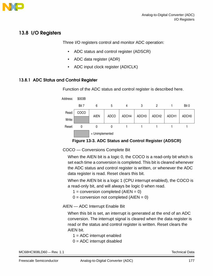
Analog-to-Digital Converter (ADC)I/O Registers
13.8 I/O Registers
Three I/O registers control and monitor ADC operation:
• ADC status and control register (ADSCR)
• ADC data register (ADR)
• ADC input clock register (ADICLK)
13.8.1 ADC Status and Control Register
Function of the ADC status and control register is described here.
COCO — Conversions Complete Bit
When the AIEN bit is a logic 0, the COCO is a read-only bit which is set each time a conversion is completed. This bit is cleared whenever the ADC status and control register is written, or whenever the ADC data register is read. Reset clears this bit.
When the AIEN bit is a logic 1 (CPU interrupt enabled), the COCO is a read-only bit, and will always be logic 0 when read.
1 = conversion completed (AIEN = 0) 0 = conversion not completed (AIEN = 0)
AIEN — ADC Interrupt Enable Bit
When this bit is set, an interrupt is generated at the end of an ADC conversion. The interrupt signal is cleared when the data register is read or the status and control register is written. Reset clears the AIEN bit.
1 = ADC interrupt enabled0 = ADC interrupt disabled
Address: $003B
Bit 7 6 5 4 3 2 1 Bit 0
Read: COCOAIEN ADCO ADCH4 ADCH3 ADCH2 ADCH1 ADCH0
Write:
Reset: 0 0 0 1 1 1 1 1
= Unimplemented
Figure 13-3. ADC Status and Control Register (ADSCR)
MC68HC908LD60 — Rev. 1.1 Technical Data
Freescale Semiconductor Analog-to-Digital Converter (ADC) 177

Analog-to-Digital Converter (ADC)
ADCO — ADC Continuous Conversion Bit
When set, the ADC will convert samples continuously and update the ADR register at the end of each conversion. Only one conversion is allowed when this bit is cleared. Reset clears the ADCO bit.
1 = Continuous ADC conversion0 = One ADC conversion
ADCH[4:0] — ADC Channel Select Bits
ADCH[4:0] form a 5-bit field which is used to select one of the ADC channels or reference voltages. The five channel select bits are detailed in the Table 13-1.
NOTE: Care should be taken when using a port pin as both an analog and a digital input simultaneously to prevent switching noise from corrupting the analog signal.
NOTE: Recovery from the disabled state requires one conversion cycle to stabilize.
Table 13-1. MUX Channel Select
ADCH4 ADCH3 ADCH2 ADCH1 ADCH0 ADC Channel Input Select
0 0 0 0 0 ADC0 PTC0/ADC0
0 0 0 0 1 ADC1 PTC1/ADC1
0 0 0 1 0 ADC2 PTC2/ADC2
0 0 0 1 1 ADC3 PTC3/ADC3
0 0 1 0 0 ADC4 PTC4/ADC4
0 0 1 0 1 ADC5 PTC5/ADC5
0 0 1 1 0
Unused(1)↓ ↓ ↓ ↓ ↓ —
1 1 0 1 0
1 1 0 1 1 — Reserved
1 1 1 0 0 — Unused
1 1 1 0 1 VRH
1 1 1 1 0 VRL
1 1 1 1 1 ADC power off
Notes:1. If any unused channels are selected, the resulting ADC conversion will be unknown.
Technical Data MC68HC908LD60 — Rev. 1.1
178 Analog-to-Digital Converter (ADC) Freescale Semiconductor
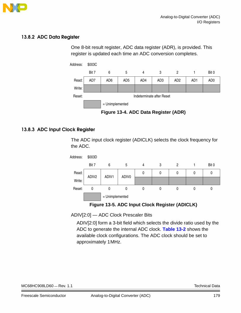
Analog-to-Digital Converter (ADC)I/O Registers
13.8.2 ADC Data Register
One 8-bit result register, ADC data register (ADR), is provided. This register is updated each time an ADC conversion completes.
13.8.3 ADC Input Clock Register
The ADC input clock register (ADICLK) selects the clock frequency for the ADC.
ADIV[2:0] — ADC Clock Prescaler Bits
ADIV[2:0] form a 3-bit field which selects the divide ratio used by the ADC to generate the internal ADC clock. Table 13-2 shows the available clock configurations. The ADC clock should be set to approximately 1MHz.
Address: $003C
Bit 7 6 5 4 3 2 1 Bit 0
Read: AD7 AD6 AD5 AD4 AD3 AD2 AD1 AD0
Write:
Reset: Indeterminate after Reset
= Unimplemented
Figure 13-4. ADC Data Register (ADR)
Address: $003D
Bit 7 6 5 4 3 2 1 Bit 0
Read:ADIV2 ADIV1 ADIV0
0 0 0 0 0
Write:
Reset: 0 0 0 0 0 0 0 0
= Unimplemented
Figure 13-5. ADC Input Clock Register (ADICLK)
MC68HC908LD60 — Rev. 1.1 Technical Data
Freescale Semiconductor Analog-to-Digital Converter (ADC) 179
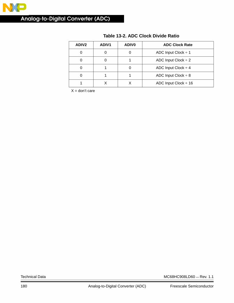
Analog-to-Digital Converter (ADC)
Table 13-2. ADC Clock Divide Ratio
ADIV2 ADIV1 ADIV0 ADC Clock Rate
0 0 0 ADC Input Clock ÷ 1
0 0 1 ADC Input Clock ÷ 2
0 1 0 ADC Input Clock ÷ 4
0 1 1 ADC Input Clock ÷ 8
1 X X ADC Input Clock ÷ 16
X = don’t care
Technical Data MC68HC908LD60 — Rev. 1.1
180 Analog-to-Digital Converter (ADC) Freescale Semiconductor

Technical Data — MC68HC908LD60
Section 14. Multi-Master IIC Interface (MMIIC)
14.1 Contents
14.2 Introduction . . . . . . . . . . . . . . . . . . . . . . . . . . . . . . . . . . . . . . .181
14.3 Features . . . . . . . . . . . . . . . . . . . . . . . . . . . . . . . . . . . . . . . . .182
14.4 I/O Pins . . . . . . . . . . . . . . . . . . . . . . . . . . . . . . . . . . . . . . . . . .182
14.5 Multi-Master IIC Registers . . . . . . . . . . . . . . . . . . . . . . . . . . .18314.5.1 Multi-Master IIC Address Register (MMADR) . . . . . . . . . .18414.5.2 Multi-Master IIC Control Register (MMCR) . . . . . . . . . . . .18514.5.3 Multi-Master IIC Master Control Register (MIMCR) . . . . . .18614.5.4 Multi-Master IIC Status Register (MMSR) . . . . . . . . . . . . .18814.5.5 Multi-Master IIC Data Transmit Register (MMDTR) . . . . . .19014.5.6 Multi-Master IIC Data Receive Register (MMDRR) . . . . . .191
14.6 Programming Considerations . . . . . . . . . . . . . . . . . . . . . . . . .192
14.2 Introduction
This Multi-master IIC (MMIIC) Interface is designed for internal serial communication between the MCU and other IIC devices. A hardware circuit generates "start" and "stop" signal, while byte by byte data transfer is interrupt driven by the software algorithm. Therefore, it can greatly help the software in dealing with other devices to have higher system efficiency in a typical digital monitor system.
This module not only can be applied in internal communications, but can also be used as a typical command reception serial bus for factory setup and alignment purposes. It also provides the flexibility of hooking additional devices to an existing system for future expansion without adding extra hardware.
MC68HC908LD60 — Rev. 1.1 Technical Data
Freescale Semiconductor Multi-Master IIC Interface (MMIIC) 181
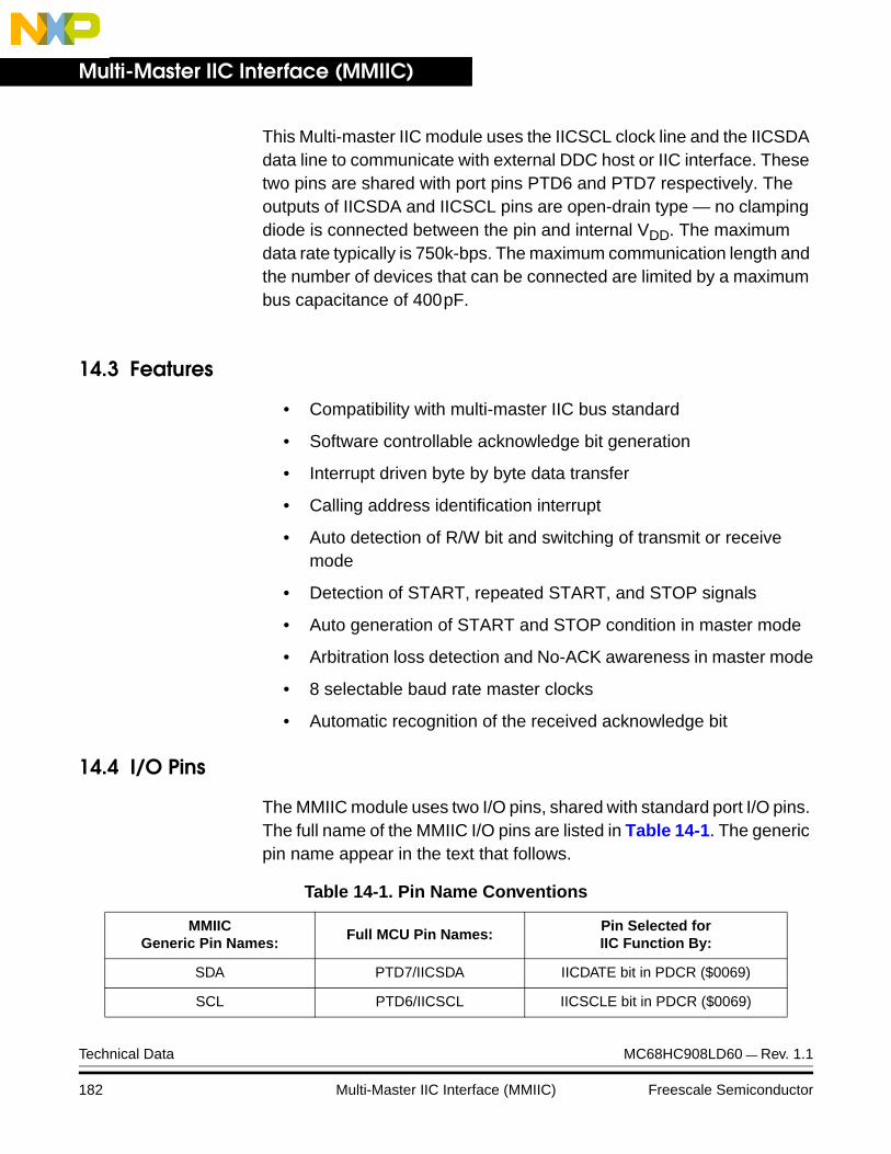
Multi-Master IIC Interface (MMIIC)
This Multi-master IIC module uses the IICSCL clock line and the IICSDA data line to communicate with external DDC host or IIC interface. These two pins are shared with port pins PTD6 and PTD7 respectively. The outputs of IICSDA and IICSCL pins are open-drain type — no clamping diode is connected between the pin and internal VDD. The maximum data rate typically is 750k-bps. The maximum communication length and the number of devices that can be connected are limited by a maximum bus capacitance of 400pF.
14.3 Features
• Compatibility with multi-master IIC bus standard
• Software controllable acknowledge bit generation
• Interrupt driven byte by byte data transfer
• Calling address identification interrupt
• Auto detection of R/W bit and switching of transmit or receive mode
• Detection of START, repeated START, and STOP signals
• Auto generation of START and STOP condition in master mode
• Arbitration loss detection and No-ACK awareness in master mode
• 8 selectable baud rate master clocks
• Automatic recognition of the received acknowledge bit
14.4 I/O Pins
The MMIIC module uses two I/O pins, shared with standard port I/O pins. The full name of the MMIIC I/O pins are listed in Table 14-1. The generic pin name appear in the text that follows.
Table 14-1. Pin Name Conventions
MMIICGeneric Pin Names:
Full MCU Pin Names:Pin Selected forIIC Function By:
SDA PTD7/IICSDA IICDATE bit in PDCR ($0069)
SCL PTD6/IICSCL IICSCLE bit in PDCR ($0069)
Technical Data MC68HC908LD60 — Rev. 1.1
182 Multi-Master IIC Interface (MMIIC) Freescale Semiconductor

Multi-Master IIC Interface (MMIIC)Multi-Master IIC Registers
14.5 Multi-Master IIC Registers
Six registers are associated with the Multi-master IIC module, they are outlined in the following sections.
Addr. Register Name Bit 7 6 5 4 3 2 1 Bit 0
$006AMulti-Master IIC
Master Control Register(MIMCR)
Read: MMALIF MMNAKIF MMBBMMAST MMRW MMBR2 MMBR1 MMBR0
Write: 0 0
Reset: 0 0 0 0 0 0 0 0
$006BMulti-Master IIC Address
Register(MMADR)
Read:MMAD7 MMAD6 MMAD5 MMAD4 MMAD3 MMAD2 MMAD1 MMEXTAD
Write:
Reset: 1 0 1 0 0 0 0 0
$006CMulti-Master IIC Control
Register(MMCR)
Read:MMEN MMIEN
0 0MMTXAK
0 0 0
Write:
Reset: 0 0 0 0 0 0 0 0
$006DMulti-Master IICStatus Register
(MMSR)
Read: MMRXIF MMTXIF MMATCH MMSRW MMRXAK 0 MMTXBE MMRXBF
Write: 0 0
Reset: 0 0 0 0 1 0 1 0
$006EMulti-Master IIC
Data Transmit Register(MMDTR)
Read:MMTD7 MMTD6 MMTD5 MMTD4 MMTD3 MMTD2 MMTD1 MMTD0
Write:
Reset: 1 1 1 1 1 1 1 1
$006F
Multi-Master IICData Receive Register
(MMDRR)
Read: MMRD7 MMRD6 MMRD5 MMRD4 MMRD3 MMRD2 MMRD1 MMRD0
Write:
Reset: 0 0 0 0 0 0 0 0
= Unimplemented
Figure 14-1. MMIIC I/O Register Summary
MC68HC908LD60 — Rev. 1.1 Technical Data
Freescale Semiconductor Multi-Master IIC Interface (MMIIC) 183
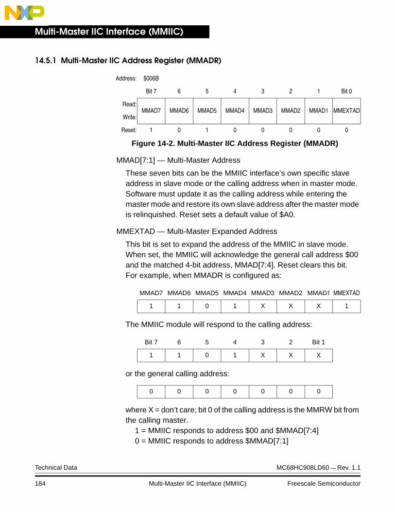
Multi-Master IIC Interface (MMIIC)
14.5.1 Multi-Master IIC Address Register (MMADR)
MMAD[7:1] — Multi-Master Address
These seven bits can be the MMIIC interface’s own specific slave address in slave mode or the calling address when in master mode. Software must update it as the calling address while entering the master mode and restore its own slave address after the master mode is relinquished. Reset sets a default value of $A0.
MMEXTAD — Multi-Master Expanded Address
This bit is set to expand the address of the MMIIC in slave mode. When set, the MMIIC will acknowledge the general call address $00 and the matched 4-bit address, MMAD[7:4]. Reset clears this bit.For example, when MMADR is configured as:
The MMIIC module will respond to the calling address:
or the general calling address:
where X = don’t care; bit 0 of the calling address is the MMRW bit from the calling master.
1 = MMIIC responds to address $00 and $MMAD[7:4] 0 = MMIIC responds to address $MMAD[7:1]
Address: $006B
Bit 7 6 5 4 3 2 1 Bit 0
Read:MMAD7 MMAD6 MMAD5 MMAD4 MMAD3 MMAD2 MMAD1 MMEXTAD
Write:
Reset: 1 0 1 0 0 0 0 0
Figure 14-2. Multi-Master IIC Address Register (MMADR)
MMAD7 MMAD6 MMAD5 MMAD4 MMAD3 MMAD2 MMAD1 MMEXTAD
1 1 0 1 X X X 1
Bit 7 6 5 4 3 2 Bit 1
1 1 0 1 X X X
0 0 0 0 0 0 0
Technical Data MC68HC908LD60 — Rev. 1.1
184 Multi-Master IIC Interface (MMIIC) Freescale Semiconductor
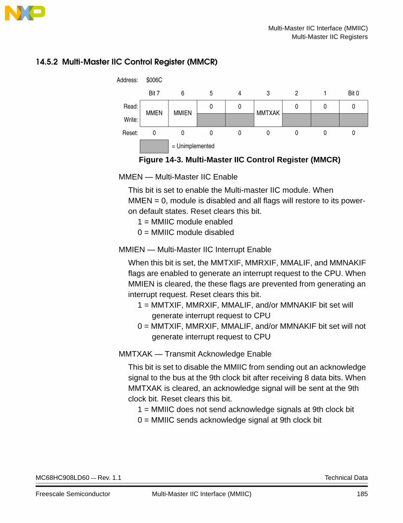
Multi-Master IIC Interface (MMIIC)Multi-Master IIC Registers
14.5.2 Multi-Master IIC Control Register (MMCR)
MMEN — Multi-Master IIC Enable
This bit is set to enable the Multi-master IIC module. When MMEN = 0, module is disabled and all flags will restore to its power-on default states. Reset clears this bit.
1 = MMIIC module enabled0 = MMIIC module disabled
MMIEN — Multi-Master IIC Interrupt Enable
When this bit is set, the MMTXIF, MMRXIF, MMALIF, and MMNAKIF flags are enabled to generate an interrupt request to the CPU. When MMIEN is cleared, the these flags are prevented from generating an interrupt request. Reset clears this bit.
1 = MMTXIF, MMRXIF, MMALIF, and/or MMNAKIF bit set will generate interrupt request to CPU
0 = MMTXIF, MMRXIF, MMALIF, and/or MMNAKIF bit set will not generate interrupt request to CPU
MMTXAK — Transmit Acknowledge Enable
This bit is set to disable the MMIIC from sending out an acknowledge signal to the bus at the 9th clock bit after receiving 8 data bits. When MMTXAK is cleared, an acknowledge signal will be sent at the 9th clock bit. Reset clears this bit.
1 = MMIIC does not send acknowledge signals at 9th clock bit0 = MMIIC sends acknowledge signal at 9th clock bit
Address: $006C
Bit 7 6 5 4 3 2 1 Bit 0
Read:MMEN MMIEN
0 0MMTXAK
0 0 0
Write:
Reset: 0 0 0 0 0 0 0 0
= Unimplemented
Figure 14-3. Multi-Master IIC Control Register (MMCR)
MC68HC908LD60 — Rev. 1.1 Technical Data
Freescale Semiconductor Multi-Master IIC Interface (MMIIC) 185
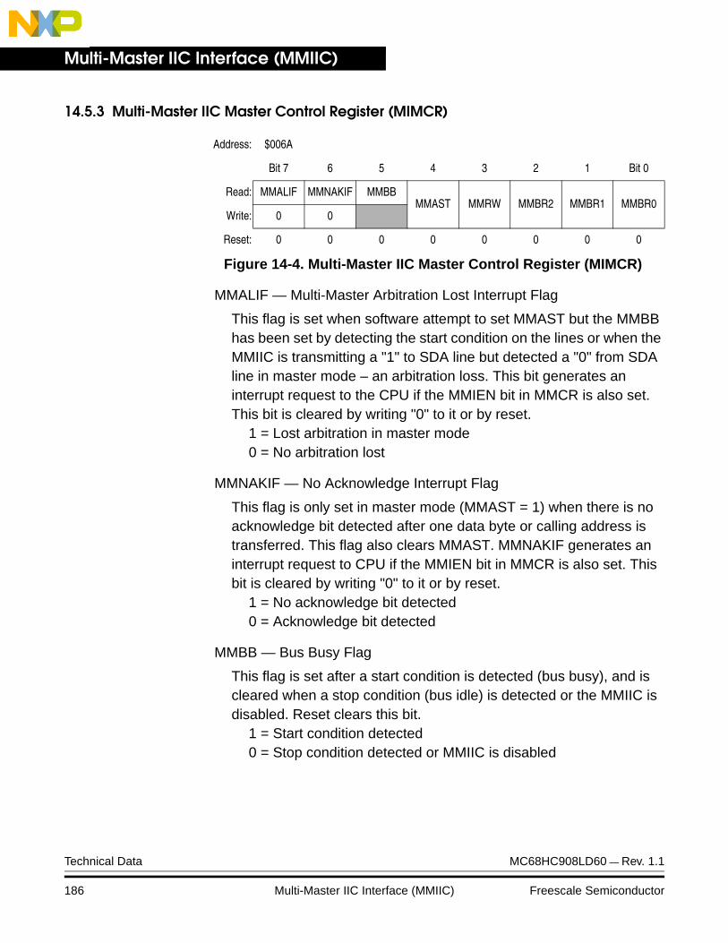
Multi-Master IIC Interface (MMIIC)
14.5.3 Multi-Master IIC Master Control Register (MIMCR)
MMALIF — Multi-Master Arbitration Lost Interrupt Flag
This flag is set when software attempt to set MMAST but the MMBB has been set by detecting the start condition on the lines or when the MMIIC is transmitting a "1" to SDA line but detected a "0" from SDA line in master mode – an arbitration loss. This bit generates an interrupt request to the CPU if the MMIEN bit in MMCR is also set. This bit is cleared by writing "0" to it or by reset.
1 = Lost arbitration in master mode0 = No arbitration lost
MMNAKIF — No Acknowledge Interrupt Flag
This flag is only set in master mode (MMAST = 1) when there is no acknowledge bit detected after one data byte or calling address is transferred. This flag also clears MMAST. MMNAKIF generates an interrupt request to CPU if the MMIEN bit in MMCR is also set. This bit is cleared by writing "0" to it or by reset.
1 = No acknowledge bit detected0 = Acknowledge bit detected
MMBB — Bus Busy Flag
This flag is set after a start condition is detected (bus busy), and is cleared when a stop condition (bus idle) is detected or the MMIIC is disabled. Reset clears this bit.
1 = Start condition detected0 = Stop condition detected or MMIIC is disabled
Address: $006A
Bit 7 6 5 4 3 2 1 Bit 0
Read: MMALIF MMNAKIF MMBBMMAST MMRW MMBR2 MMBR1 MMBR0
Write: 0 0
Reset: 0 0 0 0 0 0 0 0
Figure 14-4. Multi-Master IIC Master Control Register (MIMCR)
Technical Data MC68HC908LD60 — Rev. 1.1
186 Multi-Master IIC Interface (MMIIC) Freescale Semiconductor

Multi-Master IIC Interface (MMIIC)Multi-Master IIC Registers
MMAST — Master Control Bit
This bit is set to initiate a master mode transfer. In master mode, the module generates a start condition to the SDA and SCL lines, followed by sending the calling address stored in MMADR.When the MMAST bit is cleared by MMNAKIF set (no acknowledge) or by software, the module generates the stop condition to the lines after the current byte is transmitted.If an arbitration loss occurs (MMALIF = 1), the module reverts to slave mode by clearing MMAST, and releasing SDA and SCL lines immediately.This bit is cleared by writing "0" to it or by reset.
1 = Master mode operation0 = Slave mode operation
MMRW — Master Read/Write
This bit will be transmitted out as bit 0 of the calling address when the module sets the MMAST bit to enter master mode. The MMRW bit determines the transfer direction of the data bytes that follows. When it is "1", the module is in master receive mode. When it is "0", the module is in master transmit mode. Reset clears this bit.
1 = Master mode receive0 = Master mode transmit
MMBR2–MMBR0 — Baud Rate Select
These three bits select one of eight clock rates as the master clock when the module is in master mode.Since this master clock is derived the CPU bus clock, the user program should not execute the WAIT instruction when the MMIIC module in master mode. This will cause the SDA and SCL lines to hang, as the WAIT instruction places the MCU in wait mode, with CPU clock is halted. These bits are cleared upon reset. (See Table 14-2 . Baud Rate Select.)
MC68HC908LD60 — Rev. 1.1 Technical Data
Freescale Semiconductor Multi-Master IIC Interface (MMIIC) 187
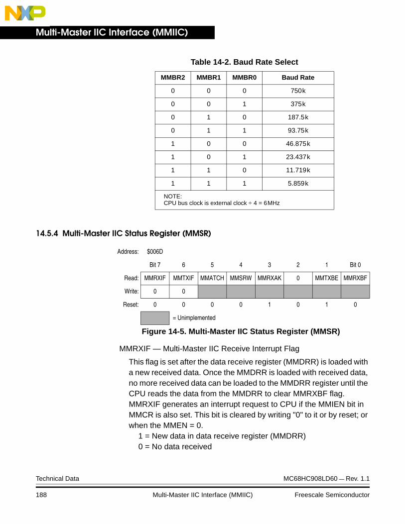
Multi-Master IIC Interface (MMIIC)
14.5.4 Multi-Master IIC Status Register (MMSR)
MMRXIF — Multi-Master IIC Receive Interrupt Flag
This flag is set after the data receive register (MMDRR) is loaded with a new received data. Once the MMDRR is loaded with received data, no more received data can be loaded to the MMDRR register until the CPU reads the data from the MMDRR to clear MMRXBF flag. MMRXIF generates an interrupt request to CPU if the MMIEN bit in MMCR is also set. This bit is cleared by writing "0" to it or by reset; or when the MMEN = 0.
1 = New data in data receive register (MMDRR)0 = No data received
Table 14-2. Baud Rate Select
MMBR2 MMBR1 MMBR0 Baud Rate
0 0 0 750k
0 0 1 375k
0 1 0 187.5k
0 1 1 93.75k
1 0 0 46.875k
1 0 1 23.437k
1 1 0 11.719k
1 1 1 5.859k
NOTE:CPU bus clock is external clock ÷ 4 = 6MHz
Address: $006D
Bit 7 6 5 4 3 2 1 Bit 0
Read: MMRXIF MMTXIF MMATCH MMSRW MMRXAK 0 MMTXBE MMRXBF
Write: 0 0
Reset: 0 0 0 0 1 0 1 0
= Unimplemented
Figure 14-5. Multi-Master IIC Status Register (MMSR)
Technical Data MC68HC908LD60 — Rev. 1.1
188 Multi-Master IIC Interface (MMIIC) Freescale Semiconductor
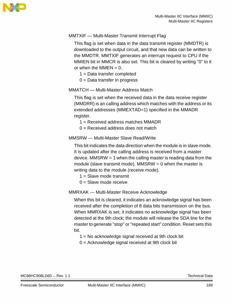
Multi-Master IIC Interface (MMIIC)Multi-Master IIC Registers
MMTXIF — Multi-Master Transmit Interrupt Flag
This flag is set when data in the data transmit register (MMDTR) is downloaded to the output circuit, and that new data can be written to the MMDTR. MMTXIF generates an interrupt request to CPU if the MMIEN bit in MMCR is also set. This bit is cleared by writing "0" to it or when the MMEN = 0.
1 = Data transfer completed0 = Data transfer in progress
MMATCH — Multi-Master Address Match
This flag is set when the received data in the data receive register (MMDRR) is an calling address which matches with the address or its extended addresses (MMEXTAD=1) specified in the MMADR register.
1 = Received address matches MMADR0 = Received address does not match
MMSRW — Multi-Master Slave Read/Write
This bit indicates the data direction when the module is in slave mode. It is updated after the calling address is received from a master device. MMSRW = 1 when the calling master is reading data from the module (slave transmit mode). MMSRW = 0 when the master is writing data to the module (receive mode).
1 = Slave mode transmit0 = Slave mode receive
MMRXAK — Multi-Master Receive Acknowledge
When this bit is cleared, it indicates an acknowledge signal has been received after the completion of 8 data bits transmission on the bus. When MMRXAK is set, it indicates no acknowledge signal has been detected at the 9th clock; the module will release the SDA line for the master to generate "stop" or "repeated start" condition. Reset sets this bit.
1 = No acknowledge signal received at 9th clock bit0 = Acknowledge signal received at 9th clock bit
MC68HC908LD60 — Rev. 1.1 Technical Data
Freescale Semiconductor Multi-Master IIC Interface (MMIIC) 189

Multi-Master IIC Interface (MMIIC)
MMTXBE — Multi-Master Transmit Buffer Empty
This flag indicates the status of the data transmit register (MMDTR). When the CPU writes the data to the MMDTR, the MMTXBE flag will be cleared. MMTXBE is set when MMDTR is emptied by a transfer of its data to the output circuit. Reset sets this bit.
1 = Data transmit register empty0 = Data transmit register full
MMRXBF — Multi-Master Receive Buffer Full
This flag indicates the status of the data receive register (MMDRR). When the CPU reads the data from the MMDRR, the MMRXBF flag will be cleared. MMRXBF is set when MMDRR is full by a transfer of data from the input circuit to the MMDRR. Reset clears this bit.
1 = Data receive register full0 = Data receive register empty
14.5.5 Multi-Master IIC Data Transmit Register (MMDTR)
When the MMIIC module is enabled, MMEN = 1, data written into this register depends on whether module is in master or slave mode.
In slave mode, the data in MMDTR will be transferred to the output circuit when:
• the module detects a matched calling address (MMATCH = 1), with the calling master requesting data (MMSRW = 1); or
• the previous data in the output circuit has be transmitted and the receiving master returns an acknowledge bit, indicated by a received acknowledge bit (MMRXAK = 0).
Address: $006E
Bit 7 6 5 4 3 2 1 Bit 0
Read:MMTD7 MMTD6 MMTD5 MMTD4 MMTD3 MMTD2 MMTD1 MMTD0
Write:
Reset: 1 1 1 1 1 1 1 1
Figure 14-6. Multi-Master IIC Data Transmit Register (MMDTR)
Technical Data MC68HC908LD60 — Rev. 1.1
190 Multi-Master IIC Interface (MMIIC) Freescale Semiconductor
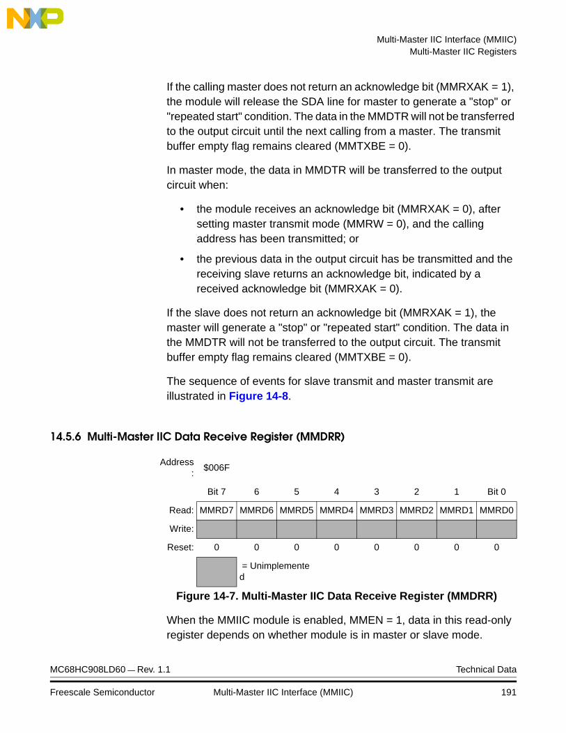
Multi-Master IIC Interface (MMIIC)Multi-Master IIC Registers
If the calling master does not return an acknowledge bit (MMRXAK = 1), the module will release the SDA line for master to generate a "stop" or "repeated start" condition. The data in the MMDTR will not be transferred to the output circuit until the next calling from a master. The transmit buffer empty flag remains cleared (MMTXBE = 0).
In master mode, the data in MMDTR will be transferred to the output circuit when:
• the module receives an acknowledge bit (MMRXAK = 0), aftersetting master transmit mode (MMRW = 0), and the calling address has been transmitted; or
• the previous data in the output circuit has be transmitted and the receiving slave returns an acknowledge bit, indicated by a received acknowledge bit (MMRXAK = 0).
If the slave does not return an acknowledge bit (MMRXAK = 1), the master will generate a "stop" or "repeated start" condition. The data in the MMDTR will not be transferred to the output circuit. The transmit buffer empty flag remains cleared (MMTXBE = 0).
The sequence of events for slave transmit and master transmit are illustrated in Figure 14-8.
14.5.6 Multi-Master IIC Data Receive Register (MMDRR)
When the MMIIC module is enabled, MMEN = 1, data in this read-only register depends on whether module is in master or slave mode.
Address:
$006F
Bit 7 6 5 4 3 2 1 Bit 0
Read: MMRD7 MMRD6 MMRD5 MMRD4 MMRD3 MMRD2 MMRD1 MMRD0
Write:
Reset: 0 0 0 0 0 0 0 0
= Unimplemented
Figure 14-7. Multi-Master IIC Data Receive Register (MMDRR)
MC68HC908LD60 — Rev. 1.1 Technical Data
Freescale Semiconductor Multi-Master IIC Interface (MMIIC) 191

Multi-Master IIC Interface (MMIIC)
In slave mode, the data in MMDRR is:
• the calling address from the master when the address match flag is set (MMATCH = 1); or
• the last data received when MMATCH = 0.
In master mode, the data in the MMDRR is:
• the last data received.
When the MMDRR is read by the CPU, the receive buffer full flag is cleared (MMRXBF = 0), and the next received data is loaded to the MMDRR. Each time when new data is loaded to the MMDRR, the MMRXIF interrupt flag is set, indicating that new data is available in MMDRR.
The sequence of events for slave receive and master receive are illustrated in Figure 14-8.
14.6 Programming Considerations
When the MMIIC module detects an arbitration loss in master mode, it will release both SDA and SCL lines immediately. But if there are no further STOP conditions detected, the module will hang up. Therefore, it is recommended to have time-out software to recover from such ill condition. The software can start the time-out counter by looking at the MMBB (Bus Busy) flag in the MIMCR and reset the counter on the completion of one byte transmission. If a time-out occur, software can clear the MMEN bit (disable MMIIC module) to release the bus, and hence clearing the MMBB flag. This is the only way to clear the MMBB flag by software if the module hangs up due to a no STOP condition received. The MMIIC can resume operation again by setting the MMEN bit.
Technical Data MC68HC908LD60 — Rev. 1.1
192 Multi-Master IIC Interface (MMIIC) Freescale Semiconductor
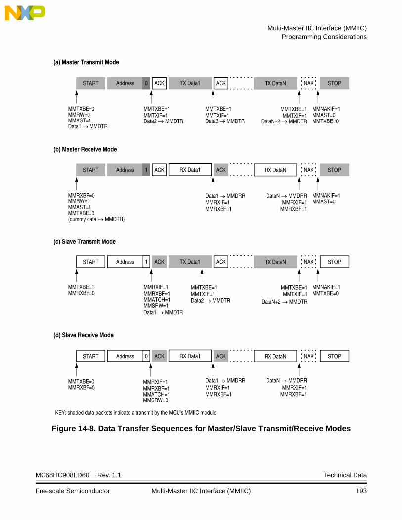
Multi-Master IIC Interface (MMIIC)Programming Considerations
Figure 14-8. Data Transfer Sequences for Master/Slave Transmit/Receive Modes
START Address ACK TX Data1
MMTXBE=0MMRW=0MMAST=1
MMTXIF=1MMTXBE=1 MMNAKIF=1
MMAST=0MMTXBE=1
(a) Master Transmit Mode
(b) Master Receive Mode
(c) Slave Transmit Mode
MMTXIF=1MMTXBE=0
ACK TX DataN NAK STOP
MMTXIF=1MMTXBE=1
START Address ACK RX Data1
MMRXBF=0
MMAST=1MMTXBE=0
MMRXBF=1MMRXIF=1
MMNAKIF=1MMAST=0MMRXIF=1
MMRXBF=1
ACK RX DataN NAK STOP
1START Address ACK TX Data1
MMTXBE=1MMRXBF=0
MMNAKIF=1MMTXBE=0
MMTXBE=1
(d) Slave Receive Mode
MMTXIF=1
ACK TX DataN NAK STOP
MMRXBF=1MMRXIF=1
MMATCH=1MMSRW=1
MMTXIF=1MMTXBE=1
0START Address ACK RX Data1
MMRXBF=1MMRXIF=1 MMRXIF=1
MMRXBF=1
ACK RX DataN NAK STOP
MMTXBE=0MMRXBF=0 MMRXBF=1
MMRXIF=1
MMATCH=1MMSRW=0
Data1 → MMDRR DataN → MMDRR
Data1 → MMDTR
Data2 → MMDTR DataN+2 → MMDTR
Data1 → MMDTRData2 → MMDTR Data3 → MMDTR DataN+2 → MMDTR
(dummy data → MMDTR)
MMRW=1Data1 → MMDRR DataN → MMDRR
0
1
KEY: shaded data packets indicate a transmit by the MCU’s MMIIC module
MC68HC908LD60 — Rev. 1.1 Technical Data
Freescale Semiconductor Multi-Master IIC Interface (MMIIC) 193

Multi-Master IIC Interface (MMIIC)
Technical Data MC68HC908LD60 — Rev. 1.1
194 Multi-Master IIC Interface (MMIIC) Freescale Semiconductor

Technical Data — MC68HC908LD60
Section 15. DDC12AB Interface
15.1 Contents
15.2 Introduction . . . . . . . . . . . . . . . . . . . . . . . . . . . . . . . . . . . . . . .195
15.3 Features . . . . . . . . . . . . . . . . . . . . . . . . . . . . . . . . . . . . . . . . .196
15.4 I/O Pins . . . . . . . . . . . . . . . . . . . . . . . . . . . . . . . . . . . . . . . . . .196
15.5 DDC Protocols . . . . . . . . . . . . . . . . . . . . . . . . . . . . . . . . . . . .198
15.6 DDC Registers . . . . . . . . . . . . . . . . . . . . . . . . . . . . . . . . . . . .19815.6.1 DDC Address Register (DADR) . . . . . . . . . . . . . . . . . . . . .19815.6.2 DDC2 Address Register (D2ADR) . . . . . . . . . . . . . . . . . . .19915.6.3 DDC Control Register (DCR) . . . . . . . . . . . . . . . . . . . . . . .20015.6.4 DDC Master Control Register (DMCR) . . . . . . . . . . . . . . .20115.6.5 DDC Status Register (DSR) . . . . . . . . . . . . . . . . . . . . . . . .20415.6.6 DDC Data Transmit Register (DDTR) . . . . . . . . . . . . . . . .20615.6.7 DDC Data Receive Register (DDRR). . . . . . . . . . . . . . . . .207
15.7 Programming Considerations . . . . . . . . . . . . . . . . . . . . . . . . .208
15.2 Introduction
This DDC12AB Interface module is used by the digital monitor to show its identification information to the video controller. It contains DDC1 hardware and a two-wire, bidirectional serial bus which is fully compatible with multi-master IIC bus protocol to support DDC2AB interface.
This module not only can be applied in internal communications, but can also be used as a typical command reception serial bus for factory setup and alignment purposes. It also provides the flexibility of hooking additional devices to an existing system for future expansion without adding extra hardware.
MC68HC908LD60 — Rev. 1.1 Technical Data
Freescale Semiconductor DDC12AB Interface 195
DDC12AB Interface
This DDC12AB module uses the DDCSCL clock line and the DDCSDA data line to communicate with external DDC host or IIC interface. These two pins are shared with port pins PTD4 and PTD5 respectively. The outputs of DDCSDA and DDCSCL pins are open-drain type — no clamping diode is connected between the pin and internal VDD. The maximum data rate typically is 100k-bps. The maximum communication length and the number of devices that can be connected are limited by a maximum bus capacitance of 400pF.
15.3 Features
• DDC1 hardware
• Compatibility with multi-master IIC bus standard
• Software controllable acknowledge bit generation
• Interrupt driven byte by byte data transfer
• Calling address identification interrupt
• Auto detection of R/W bit and switching of transmit or receive mode
• Detection of START, repeated START, and STOP signals
• Auto generation of START and STOP condition in master mode
• Arbitration loss detection and No-ACK awareness in master mode
• 8 selectable baud rate master clocks
• Automatic recognition of the received acknowledge bit
15.4 I/O Pins
The DDC12AB module uses two I/O pins, shared with standard port I/O pins. The full name of the DDC12AB I/O pins are listed in Table 15-1. The generic pin name appear in the text that follows.
Table 15-1. Pin Name Conventions
DDC12ABGeneric Pin Names:
Full MCU Pin Names:Pin Selected for
DDC Function By:
SDA PTD5/DDCSDA DDCDATE bit in PDCR ($0069)
SCL PTD4/DDCSCL DDCSCLE bit in PDCR ($0069)
Technical Data MC68HC908LD60 — Rev. 1.1
196 DDC12AB Interface Freescale Semiconductor

DDC12AB InterfaceI/O Pins
Addr. Register Name Bit 7 6 5 4 3 2 1 Bit 0
$0016DDC Master Control
Register(DMCR)
Read: ALIF NAKIF BBMAST MRW BR2 BR1 BR0
Write: 0 0
Reset: 0 0 0 0 0 0 0 0
$0017DDC Address Register
(DADR)
Read:DAD7 DAD6 DAD5 DAD4 DAD3 DAD2 DAD1 EXTAD
Write:
Reset: 1 0 1 0 0 0 0 0
$0018DDC Control Register
(DCR)
Read:DEN DIEN
0 0TXAK SCLIEN DDC1EN
0
Write:
Reset: 0 0 0 0 0 0 0 0
$0019DDC Status Register
(DSR)
Read: RXIF TXIF MATCH SRW RXAK SCLIF TXBE RXBF
Write: 0 0 0
Reset: 0 0 0 0 1 0 1 0
$001ADDC
Data Transmit Register(DDTR)
Read:DTD7 DTD6 DTD5 DTD4 DTD3 DTD2 DTD1 DTD0
Write:
Reset: 1 1 1 1 1 1 1 1
$001B
DDCData Receive Register
(DDRR)
Read: DRD7 DRD6 DRD5 DRD4 DRD3 DRD2 DRD1 DRD0
Write:
Reset: 0 0 0 0 0 0 0 0
$001CDDC2 Address Register
(D2ADR)
Read:D2AD7 D2AD6 D2AD5 D2AD4 D2AD3 D2AD2 D2AD1
0
Write:
Reset: 0 0 0 0 0 0 0 0
= Unimplemented
Figure 15-1. DDC I/O Register Summary
MC68HC908LD60 — Rev. 1.1 Technical Data
Freescale Semiconductor DDC12AB Interface 197
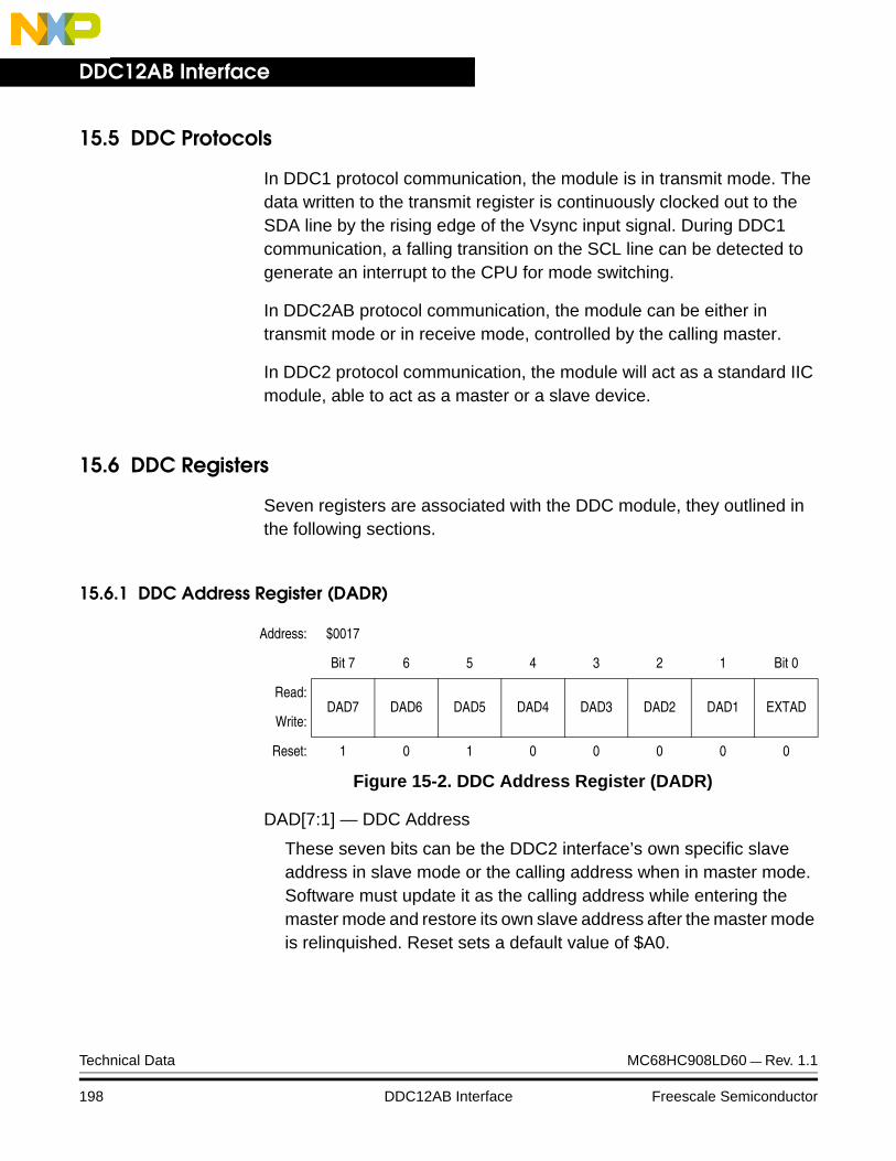
DDC12AB Interface
15.5 DDC Protocols
In DDC1 protocol communication, the module is in transmit mode. The data written to the transmit register is continuously clocked out to the SDA line by the rising edge of the Vsync input signal. During DDC1 communication, a falling transition on the SCL line can be detected to generate an interrupt to the CPU for mode switching.
In DDC2AB protocol communication, the module can be either in transmit mode or in receive mode, controlled by the calling master.
In DDC2 protocol communication, the module will act as a standard IIC module, able to act as a master or a slave device.
15.6 DDC Registers
Seven registers are associated with the DDC module, they outlined in the following sections.
15.6.1 DDC Address Register (DADR)
DAD[7:1] — DDC Address
These seven bits can be the DDC2 interface’s own specific slave address in slave mode or the calling address when in master mode. Software must update it as the calling address while entering the master mode and restore its own slave address after the master mode is relinquished. Reset sets a default value of $A0.
Address: $0017
Bit 7 6 5 4 3 2 1 Bit 0
Read:DAD7 DAD6 DAD5 DAD4 DAD3 DAD2 DAD1 EXTAD
Write:
Reset: 1 0 1 0 0 0 0 0
Figure 15-2. DDC Address Register (DADR)
Technical Data MC68HC908LD60 — Rev. 1.1
198 DDC12AB Interface Freescale Semiconductor
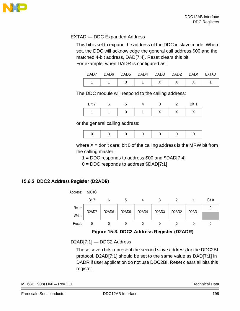
DDC12AB InterfaceDDC Registers
EXTAD — DDC Expanded Address
This bit is set to expand the address of the DDC in slave mode. When set, the DDC will acknowledge the general call address $00 and the matched 4-bit address, DAD[7:4]. Reset clears this bit.For example, when DADR is configured as:
The DDC module will respond to the calling address:
or the general calling address:
where X = don’t care; bit 0 of the calling address is the MRW bit from the calling master.
1 = DDC responds to address $00 and $DAD[7:4] 0 = DDC responds to address $DAD[7:1]
15.6.2 DDC2 Address Register (D2ADR)
D2AD[7:1] — DDC2 Address
These seven bits represent the second slave address for the DDC2BI protocol. D2AD[7:1] should be set to the same value as DAD[7:1] in DADR if user application do not use DDC2BI. Reset clears all bits this register.
DAD7 DAD6 DAD5 DAD4 DAD3 DAD2 DAD1 EXTAD
1 1 0 1 X X X 1
Bit 7 6 5 4 3 2 Bit 1
1 1 0 1 X X X
0 0 0 0 0 0 0
Address: $001C
Bit 7 6 5 4 3 2 1 Bit 0
Read:D2AD7 D2AD6 D2AD5 D2AD4 D2AD3 D2AD2 D2AD1
0
Write:
Reset: 0 0 0 0 0 0 0 0
Figure 15-3. DDC2 Address Register (D2ADR)
MC68HC908LD60 — Rev. 1.1 Technical Data
Freescale Semiconductor DDC12AB Interface 199

DDC12AB Interface
15.6.3 DDC Control Register (DCR)
DEN — DDC Enable
This bit is set to enable the DDC module. When DEN = 0, module is disabled and all flags will restore to its power-on default states. Reset clears this bit.
1 = DDC module enabled0 = DDC module disabled
DIEN — DDC Interrupt Enable
When this bit is set, the TXIF, RXIF, ALIF, and NAKIF flags are enabled to generate an interrupt request to the CPU. When DIEN is cleared, the these flags are prevented from generating an interrupt request. Reset clears this bit.
1 = TXIF, RXIF, ALIF, and/or NAKIF bit set will generate interrupt request to CPU
0 = TXIF, RXIF, ALIF, and/or NAKIF bit set will not generate interrupt request to CPU
TXAK — Transmit Acknowledge Enable
This bit is set to disable the DDC from sending out an acknowledge signal to the bus at the 9th clock bit after receiving 8 data bits. When TXAK is cleared, an acknowledge signal will be sent at the 9th clock bit. Reset clears this bit.
1 = DDC does not send acknowledge signals at 9th clock bit0 = DDC sends acknowledge signal at 9th clock bit
Address: $0018
Bit 7 6 5 4 3 2 1 Bit 0
Read:DEN DIEN
0 0TXAK SCLIEN DDC1EN
0
Write:
Reset: 0 0 0 0 0 0 0 0
= Unimplemented
Figure 15-4. DDC Control Register (DCR)
Technical Data MC68HC908LD60 — Rev. 1.1
200 DDC12AB Interface Freescale Semiconductor
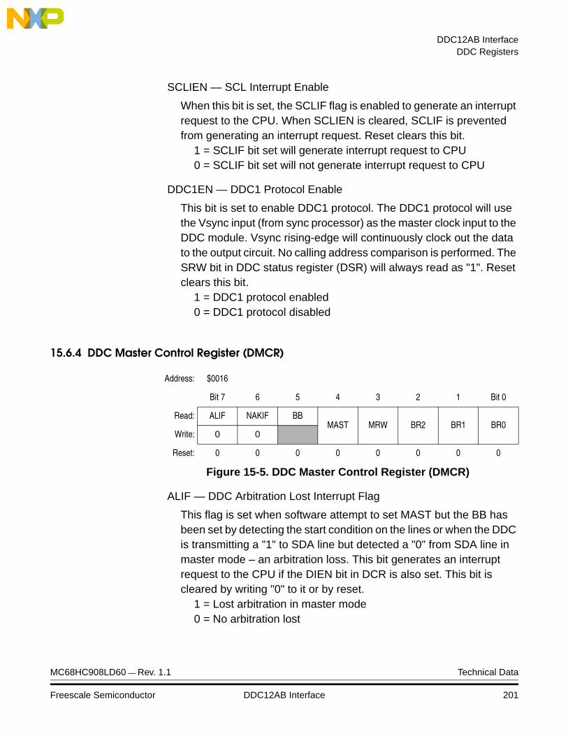
DDC12AB InterfaceDDC Registers
SCLIEN — SCL Interrupt Enable
When this bit is set, the SCLIF flag is enabled to generate an interrupt request to the CPU. When SCLIEN is cleared, SCLIF is prevented from generating an interrupt request. Reset clears this bit.
1 = SCLIF bit set will generate interrupt request to CPU0 = SCLIF bit set will not generate interrupt request to CPU
DDC1EN — DDC1 Protocol Enable
This bit is set to enable DDC1 protocol. The DDC1 protocol will use the Vsync input (from sync processor) as the master clock input to the DDC module. Vsync rising-edge will continuously clock out the data to the output circuit. No calling address comparison is performed. The SRW bit in DDC status register (DSR) will always read as "1". Reset clears this bit.
1 = DDC1 protocol enabled0 = DDC1 protocol disabled
15.6.4 DDC Master Control Register (DMCR)
ALIF — DDC Arbitration Lost Interrupt Flag
This flag is set when software attempt to set MAST but the BB has been set by detecting the start condition on the lines or when the DDC is transmitting a "1" to SDA line but detected a "0" from SDA line in master mode – an arbitration loss. This bit generates an interrupt request to the CPU if the DIEN bit in DCR is also set. This bit is cleared by writing "0" to it or by reset.
1 = Lost arbitration in master mode0 = No arbitration lost
Address: $0016
Bit 7 6 5 4 3 2 1 Bit 0
Read: ALIF NAKIF BBMAST MRW BR2 BR1 BR0
Write: 0 0
Reset: 0 0 0 0 0 0 0 0
Figure 15-5. DDC Master Control Register (DMCR)
MC68HC908LD60 — Rev. 1.1 Technical Data
Freescale Semiconductor DDC12AB Interface 201
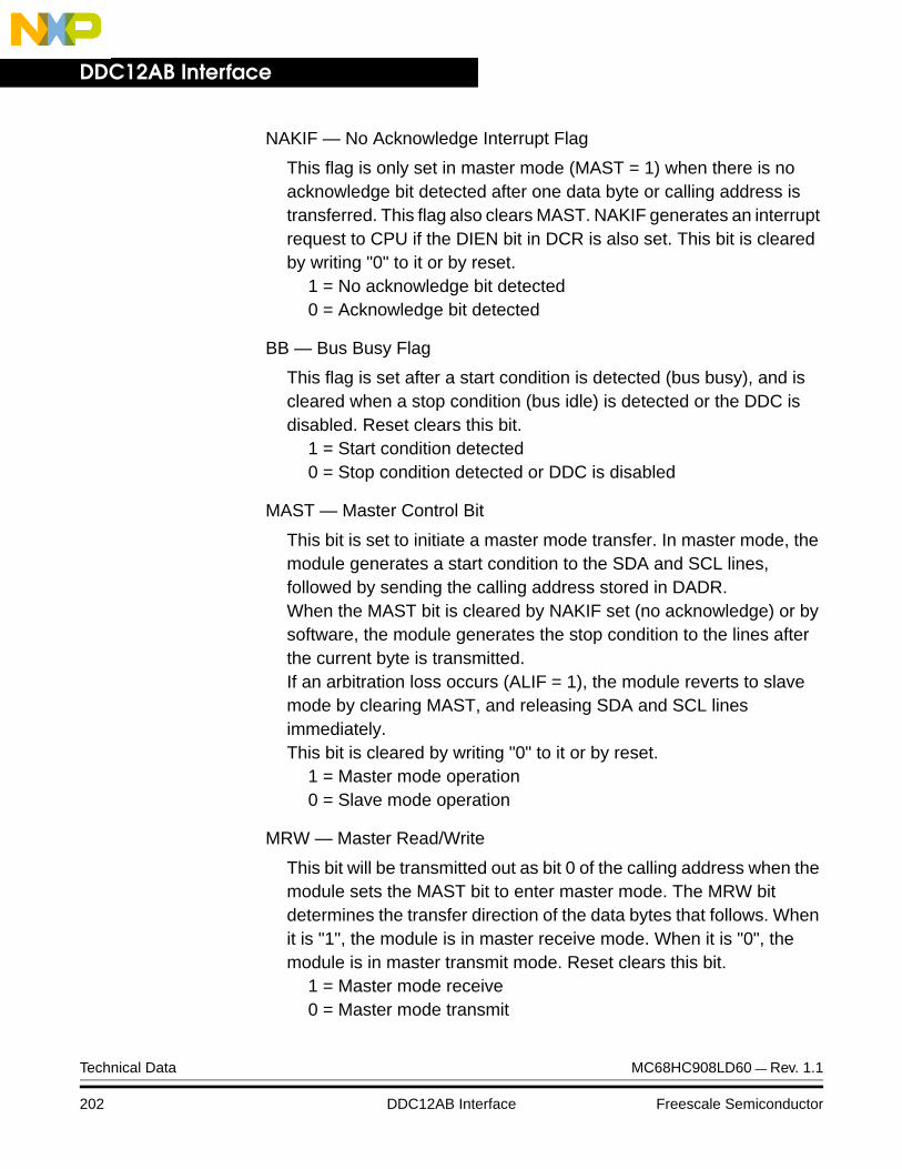
DDC12AB Interface
NAKIF — No Acknowledge Interrupt Flag
This flag is only set in master mode (MAST = 1) when there is no acknowledge bit detected after one data byte or calling address is transferred. This flag also clears MAST. NAKIF generates an interrupt request to CPU if the DIEN bit in DCR is also set. This bit is cleared by writing "0" to it or by reset.
1 = No acknowledge bit detected0 = Acknowledge bit detected
BB — Bus Busy Flag
This flag is set after a start condition is detected (bus busy), and is cleared when a stop condition (bus idle) is detected or the DDC is disabled. Reset clears this bit.
1 = Start condition detected0 = Stop condition detected or DDC is disabled
MAST — Master Control Bit
This bit is set to initiate a master mode transfer. In master mode, the module generates a start condition to the SDA and SCL lines, followed by sending the calling address stored in DADR.When the MAST bit is cleared by NAKIF set (no acknowledge) or by software, the module generates the stop condition to the lines after the current byte is transmitted.If an arbitration loss occurs (ALIF = 1), the module reverts to slave mode by clearing MAST, and releasing SDA and SCL lines immediately.This bit is cleared by writing "0" to it or by reset.
1 = Master mode operation0 = Slave mode operation
MRW — Master Read/Write
This bit will be transmitted out as bit 0 of the calling address when the module sets the MAST bit to enter master mode. The MRW bit determines the transfer direction of the data bytes that follows. When it is "1", the module is in master receive mode. When it is "0", the module is in master transmit mode. Reset clears this bit.
1 = Master mode receive0 = Master mode transmit
Technical Data MC68HC908LD60 — Rev. 1.1
202 DDC12AB Interface Freescale Semiconductor

DDC12AB InterfaceDDC Registers
BR2–BR0 — Baud Rate Select
These three bits select one of eight clock rates as the master clock when the module is in master mode.Since this master clock is derived the CPU bus clock, the user program should not execute the WAIT instruction when the DDC module in master mode. This will cause the SDA and SCL lines to hang, as the WAIT instruction places the MCU in WAIT mode, with CPU clock is halted. These bits are cleared upon reset. (See Table 15-2 . Baud Rate Select.)
Table 15-2. Baud Rate Select
BR2 BR1 BR0 Baud Rate
0 0 0 100k
0 0 1 50k
0 1 0 25k
0 1 1 12.5k
1 0 0 6.25k
1 0 1 3.125k
1 1 0 1.56k
1 1 1 0.78k
NOTE:CPU bus clock is external clock ÷ 4 = 6MHz
MC68HC908LD60 — Rev. 1.1 Technical Data
Freescale Semiconductor DDC12AB Interface 203
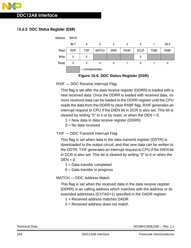
DDC12AB Interface
15.6.5 DDC Status Register (DSR)
RXIF — DDC Receive Interrupt Flag
This flag is set after the data receive register (DDRR) is loaded with a new received data. Once the DDRR is loaded with received data, no more received data can be loaded to the DDRR register until the CPU reads the data from the DDRR to clear RXBF flag. RXIF generates an interrupt request to CPU if the DIEN bit in DCR is also set. This bit is cleared by writing "0" to it or by reset; or when the DEN = 0.
1 = New data in data receive register (DDRR)0 = No data received
TXIF — DDC Transmit Interrupt Flag
This flag is set when data in the data transmit register (DDTR) is downloaded to the output circuit, and that new data can be written to the DDTR. TXIF generates an interrupt request to CPU if the DIEN bit in DCR is also set. This bit is cleared by writing "0" to it or when the DEN = 0.
1 = Data transfer completed0 = Data transfer in progress
MATCH — DDC Address Match
This flag is set when the received data in the data receive register (DDRR) is an calling address which matches with the address or its extended addresses (EXTAD=1) specified in the DADR register.
1 = Received address matches DADR0 = Received address does not match
Address: $0019
Bit 7 6 5 4 3 2 1 Bit 0
Read: RXIF TXIF MATCH SRW RXAK SCLIF TXBE RXBF
Write: 0 0 0
Reset: 0 0 0 0 1 0 1 0
= Unimplemented
Figure 15-6. DDC Status Register (DSR)
Technical Data MC68HC908LD60 — Rev. 1.1
204 DDC12AB Interface Freescale Semiconductor

DDC12AB InterfaceDDC Registers
SRW — DDC Slave Read/Write
This bit indicates the data direction when the module is in slave mode. It is updated after the calling address is received from a master device. SRW = 1 when the calling master is reading data from the module (slave transmit mode). SRW = 0 when the master is writing data to the module (receive mode).
1 = Slave mode transmit0 = Slave mode receive
RXAK — DDC Receive Acknowledge
When this bit is cleared, it indicates an acknowledge signal has been received after the completion of 8 data bits transmission on the bus. When RXAK is set, it indicates no acknowledge signal has been detected at the 9th clock; the module will release the SDA line for the master to generate "stop" or "repeated start" condition. Reset sets this bit.
1 = No acknowledge signal received at 9th clock bit0 = Acknowledge signal received at 9th clock bit
SCLIF — SCL Interrupt Flag
This flag is set when a falling edge is detected on the SCL line, only if DDC1EN bit is set. SCLIF generates an interrupt request to CPU if the SCLIEN bit in DCR is also set. SCLIF is cleared by writing "0" to it or when the DCC1EN = 0, or DEN = 0. Reset clears this bit.
1 = Falling edge detected on SCL line0 = No falling edge detected on SCL line
TXBE — DDC Transmit Buffer Empty
This flag indicates the status of the data transmit register (DDTR). When the CPU writes the data to the DDTR, the TXBE flag will be cleared. TXBE is set when DDTR is emptied by a transfer of its data to the output circuit. Reset sets this bit.
1 = Data transmit register empty0 = Data transmit register full
MC68HC908LD60 — Rev. 1.1 Technical Data
Freescale Semiconductor DDC12AB Interface 205
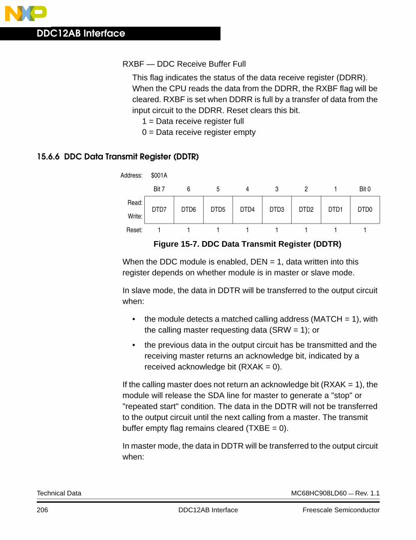
DDC12AB Interface
RXBF — DDC Receive Buffer Full
This flag indicates the status of the data receive register (DDRR). When the CPU reads the data from the DDRR, the RXBF flag will be cleared. RXBF is set when DDRR is full by a transfer of data from the input circuit to the DDRR. Reset clears this bit.
1 = Data receive register full0 = Data receive register empty
15.6.6 DDC Data Transmit Register (DDTR)
When the DDC module is enabled, DEN = 1, data written into this register depends on whether module is in master or slave mode.
In slave mode, the data in DDTR will be transferred to the output circuit when:
• the module detects a matched calling address (MATCH = 1), with the calling master requesting data (SRW = 1); or
• the previous data in the output circuit has be transmitted and the receiving master returns an acknowledge bit, indicated by a received acknowledge bit (RXAK = 0).
If the calling master does not return an acknowledge bit (RXAK = 1), the module will release the SDA line for master to generate a "stop" or "repeated start" condition. The data in the DDTR will not be transferred to the output circuit until the next calling from a master. The transmit buffer empty flag remains cleared (TXBE = 0).
In master mode, the data in DDTR will be transferred to the output circuit when:
Address: $001A
Bit 7 6 5 4 3 2 1 Bit 0
Read:DTD7 DTD6 DTD5 DTD4 DTD3 DTD2 DTD1 DTD0
Write:
Reset: 1 1 1 1 1 1 1 1
Figure 15-7. DDC Data Transmit Register (DDTR)
Technical Data MC68HC908LD60 — Rev. 1.1
206 DDC12AB Interface Freescale Semiconductor
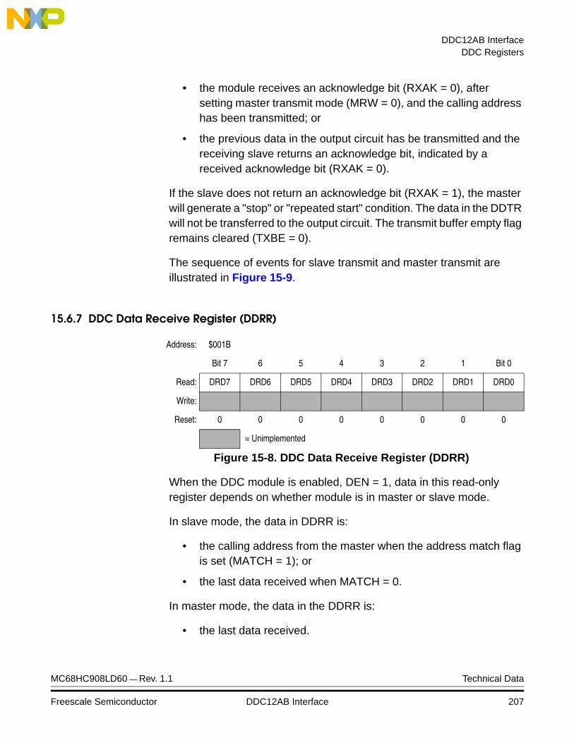
DDC12AB InterfaceDDC Registers
• the module receives an acknowledge bit (RXAK = 0), aftersetting master transmit mode (MRW = 0), and the calling address has been transmitted; or
• the previous data in the output circuit has be transmitted and the receiving slave returns an acknowledge bit, indicated by a received acknowledge bit (RXAK = 0).
If the slave does not return an acknowledge bit (RXAK = 1), the master will generate a "stop" or "repeated start" condition. The data in the DDTR will not be transferred to the output circuit. The transmit buffer empty flag remains cleared (TXBE = 0).
The sequence of events for slave transmit and master transmit are illustrated in Figure 15-9.
15.6.7 DDC Data Receive Register (DDRR)
When the DDC module is enabled, DEN = 1, data in this read-only register depends on whether module is in master or slave mode.
In slave mode, the data in DDRR is:
• the calling address from the master when the address match flag is set (MATCH = 1); or
• the last data received when MATCH = 0.
In master mode, the data in the DDRR is:
• the last data received.
Address: $001B
Bit 7 6 5 4 3 2 1 Bit 0
Read: DRD7 DRD6 DRD5 DRD4 DRD3 DRD2 DRD1 DRD0
Write:
Reset: 0 0 0 0 0 0 0 0
= Unimplemented
Figure 15-8. DDC Data Receive Register (DDRR)
MC68HC908LD60 — Rev. 1.1 Technical Data
Freescale Semiconductor DDC12AB Interface 207
DDC12AB Interface
When the DDRR is read by the CPU, the receive buffer full flag is cleared (RXBF = 0), and the next received data is loaded to the DDRR. Each time when new data is loaded to the DDRR, the RXIF interrupt flag is set, indicating that new data is available in DDRR.
The sequence of events for slave receive and master receive are illustrated in Figure 15-9.
15.7 Programming Considerations
When the DDC module detects an arbitration loss in master mode, it will release both SDA and SCL lines immediately. But if there are no further STOP conditions detected, the module will hang up. Therefore, it is recommended to have time-out software to recover from such ill condition. The software can start the time-out counter by looking at the BB (Bus Busy) flag in the DMCR and reset the counter on the completion of one byte transmission. If a time-out occur, software can clear the DEN bit (disable DDC module) to release the bus, and hence clearing the BB flag. This is the only way to clear the BB flag by software if the module hangs up due to a no STOP condition received. The DDC can resume operation again by setting the DEN bit.
Technical Data MC68HC908LD60 — Rev. 1.1
208 DDC12AB Interface Freescale Semiconductor

DDC12AB InterfaceProgramming Considerations
Figure 15-9. Data Transfer Sequences for Master/Slave Transmit/Receive Modes
START Address ACK TX Data1
TXBE=0MRW=0MAST=1
TXIF=1TXBE=1 NAKIF=1
MAST=0TXBE=1
(a) Master Transmit Mode
(b) Master Receive Mode
(c) Slave Transmit Mode
TXIF=1TXBE=0
ACK TX DataN NAK STOP
TXIF=1TXBE=1
START Address ACK RX Data1
RXBF=0
MAST=1TXBE=0
RXBF=1RXIF=1
NAKIF=1MAST=0RXIF=1
RXBF=1
ACK RX DataN NAK STOP
1START Address ACK TX Data1
TXBE=1RXBF=0
NAKIF=1TXBE=0
TXBE=1
(d) Slave Receive Mode
TXIF=1
ACK TX DataN NAK STOP
RXBF=1RXIF=1
MATCH=1SRW=1
TXIF=1TXBE=1
0START Address ACK RX Data1
RXBF=1RXIF=1 RXIF=1
RXBF=1
ACK RX DataN NAK STOP
TXBE=0RXBF=0 RXBF=1
RXIF=1
MATCH=1SRW=0
Data1 → DDRR DataN → DDRR
Data1 → DDTR
Data2 → DDTR DataN+2 → DDTR
Data1 → DDTRData2 → DDTR Data3 → DDTR DataN+2 → DDTR
(dummy data → DDTR)
MRW=1Data1 → DDRR DataN → DDRR
0
1
KEY: shaded data packets indicate a transmit by the MCU’s DDC module
MC68HC908LD60 — Rev. 1.1 Technical Data
Freescale Semiconductor DDC12AB Interface 209

DDC12AB Interface
Technical Data MC68HC908LD60 — Rev. 1.1
210 DDC12AB Interface Freescale Semiconductor
Technical Data — MC68HC908LD60
Section 16. Sync Processor
16.1 Contents
16.2 Introduction . . . . . . . . . . . . . . . . . . . . . . . . . . . . . . . . . . . . . . .212
16.3 Features . . . . . . . . . . . . . . . . . . . . . . . . . . . . . . . . . . . . . . . . .212
16.4 I/O Pins . . . . . . . . . . . . . . . . . . . . . . . . . . . . . . . . . . . . . . . . . .213
16.5 Functional Blocks . . . . . . . . . . . . . . . . . . . . . . . . . . . . . . . . . .21516.5.1 Polarity Detection . . . . . . . . . . . . . . . . . . . . . . . . . . . . . . . .21616.5.1.1 Hsync Polarity Detection . . . . . . . . . . . . . . . . . . . . . . . .21616.5.1.2 Vsync Polarity Detection . . . . . . . . . . . . . . . . . . . . . . . .21616.5.1.3 Composite Sync Polarity Detection . . . . . . . . . . . . . . . .21616.5.2 Sync Signal Counters. . . . . . . . . . . . . . . . . . . . . . . . . . . . .21716.5.3 Polarity Controlled HOUT and VOUT Outputs . . . . . . . . . .21716.5.4 Clamp Pulse Output . . . . . . . . . . . . . . . . . . . . . . . . . . . . . .21816.5.5 Low Vertical Frequency Detect . . . . . . . . . . . . . . . . . . . . .219
16.6 Sync Processor I/O Registers. . . . . . . . . . . . . . . . . . . . . . . . .21916.6.1 Sync Processor Control & Status Register (SPCSR). . . . .21916.6.2 Sync Processor Input/Output Control Register (SPIOCR) .22116.6.3 Vertical Frequency Registers (VFRs). . . . . . . . . . . . . . . . .22316.6.4 Hsync Frequency Registers (HFRs). . . . . . . . . . . . . . . . . .22516.6.5 Sync Processor Control Register 1 (SPCR1). . . . . . . . . . .22716.6.6 H & V Sync Output Control Register (HVOCR) . . . . . . . . .228
16.7 System Operation . . . . . . . . . . . . . . . . . . . . . . . . . . . . . . . . . .229
MC68HC908LD60 — Rev. 1.1 Technical Data
Freescale Semiconductor Sync Processor 211
Sync Processor
16.2 Introduction
The Sync Processor is designed to detect and process sync signals inside a digital monitor system — from separated Hsync and Vsync inputs. After detection and the necessary polarity correction and/or sync separation, the corrected sync signals are sent out. The MCU can also send commands to other monitor circuitry, such as for the geometry correction and OSD, using the DDC12AB and/or the IIC communication channels.
The block diagram of the Sync Processor is shown in Figure 16-2.
NOTE: All quoted timings in this section assume an internal bus frequency of 6MHz.
16.3 Features
Features of the Sync Processor include the following:
• Polarity detector
• Horizontal frequency counter
• Vertical frequency counter
• Low vertical frequency indicator (40.7Hz)
• Polarity controlled HOUT and VOUT outputs:
– From separate Hsync and Vsync
– From composite sync on HSYNC input pin
– From internal selectable free running Hsync and Vsync pulses
• Free-running Hsync, Vsync, DE, and DCLK of 4 video modes
• CLAMP pulse output to the external pre-amp chip
• Internal schmitt trigger on HSYNC, and VSYNC input pins to improve noise immunity
Technical Data MC68HC908LD60 — Rev. 1.1
212 Sync Processor Freescale Semiconductor
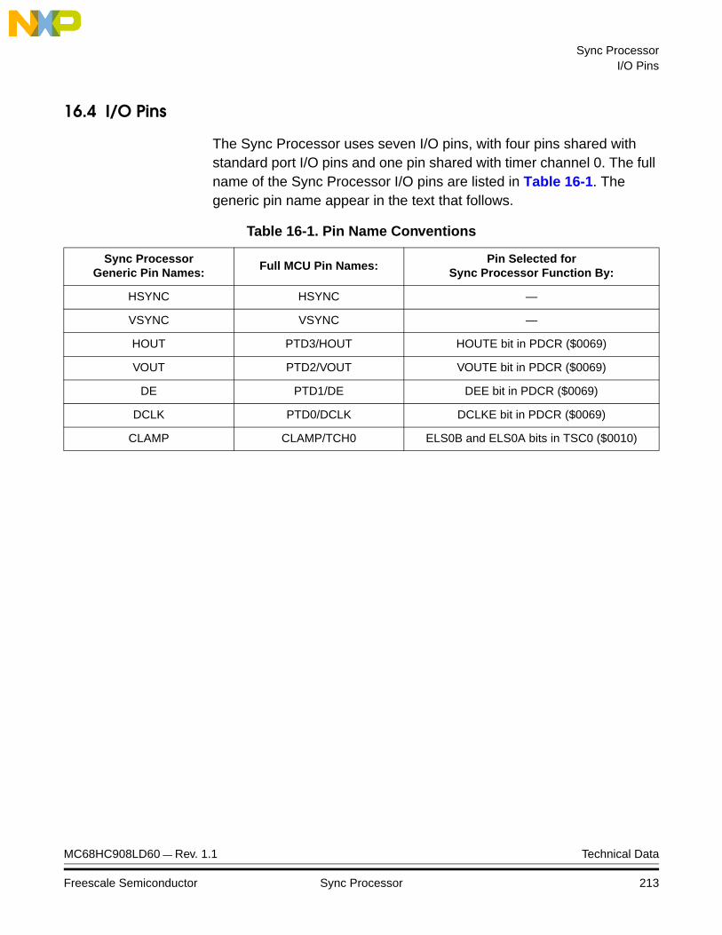
Sync ProcessorI/O Pins
16.4 I/O Pins
The Sync Processor uses seven I/O pins, with four pins shared with standard port I/O pins and one pin shared with timer channel 0. The full name of the Sync Processor I/O pins are listed in Table 16-1. The generic pin name appear in the text that follows.
Table 16-1. Pin Name Conventions
Sync ProcessorGeneric Pin Names:
Full MCU Pin Names:Pin Selected for
Sync Processor Function By:
HSYNC HSYNC —
VSYNC VSYNC —
HOUT PTD3/HOUT HOUTE bit in PDCR ($0069)
VOUT PTD2/VOUT VOUTE bit in PDCR ($0069)
DE PTD1/DE DEE bit in PDCR ($0069)
DCLK PTD0/DCLK DCLKE bit in PDCR ($0069)
CLAMP CLAMP/TCH0 ELS0B and ELS0A bits in TSC0 ($0010)
MC68HC908LD60 — Rev. 1.1 Technical Data
Freescale Semiconductor Sync Processor 213

Sync Processor
Addr. Register Name Bit 7 6 5 4 3 2 1 Bit 0
$0040Sync Processor Control
and Status Register(SPCSR)
Read:VSIE VEDGE
VSIFCOMP VINVO HINVO
VPOL HPOL
Write: 0
Reset: 0 0 0 0 0 0 0 0
$0041Vertical Frequency High
Register(VFHR)
Read: VOF 0 0 VF12 VF11 VF10 VF9 VF8
Write: CPW1 CPW0
Reset: 0 0 0 0 0 0 0 0
$0042Vertical Frequency Low
Register(VFLR)
Read: VF7 VF6 VF5 VF4 VF3 VF2 VF1 VF0
Write:
Reset: 0 0 0 0 0 0 0 0
$0043Hsync Frequency High
Register(HFHR)
Read: HFH7 HFH6 HFH5 HFH4 HFH3 HFH2 HFH1 HFH0
Write:
Reset: 0 0 0 0 0 0 0 0
$0044Hsync Frequency Low
Register(HFLR)
Read: HOVER 0 0 HFL4 HFL3 HFL2 HFL1 HFL0
Write:
Reset: 0 0 0 0 0 0 0 0
$0045Sync Processor I/O Control
Register (SPIOCR)
Read: VSYNCS HSYNCSCOINV R R R BPOR SOUT
Write:
Reset: 0 0 0 0 0
$0046Sync Processor Control
Register 1(SPCR1)
Read:LVSIE
LVSIFHPS1 HPS0 R R ATPOL FSHF
Write: 0
Reset: 0 0 0 0 0 0
$003FH&V Sync Output Control
Register(HVOCR)
Read:DCLKPH1 DCLKPH0 R HVOCR1 HVOCR0
Write:
Reset: 0 0 0 0
= Unimplemented R = Reserved
Figure 16-1. Sync Processor I/O Register Summary
Technical Data MC68HC908LD60 — Rev. 1.1
214 Sync Processor Freescale Semiconductor
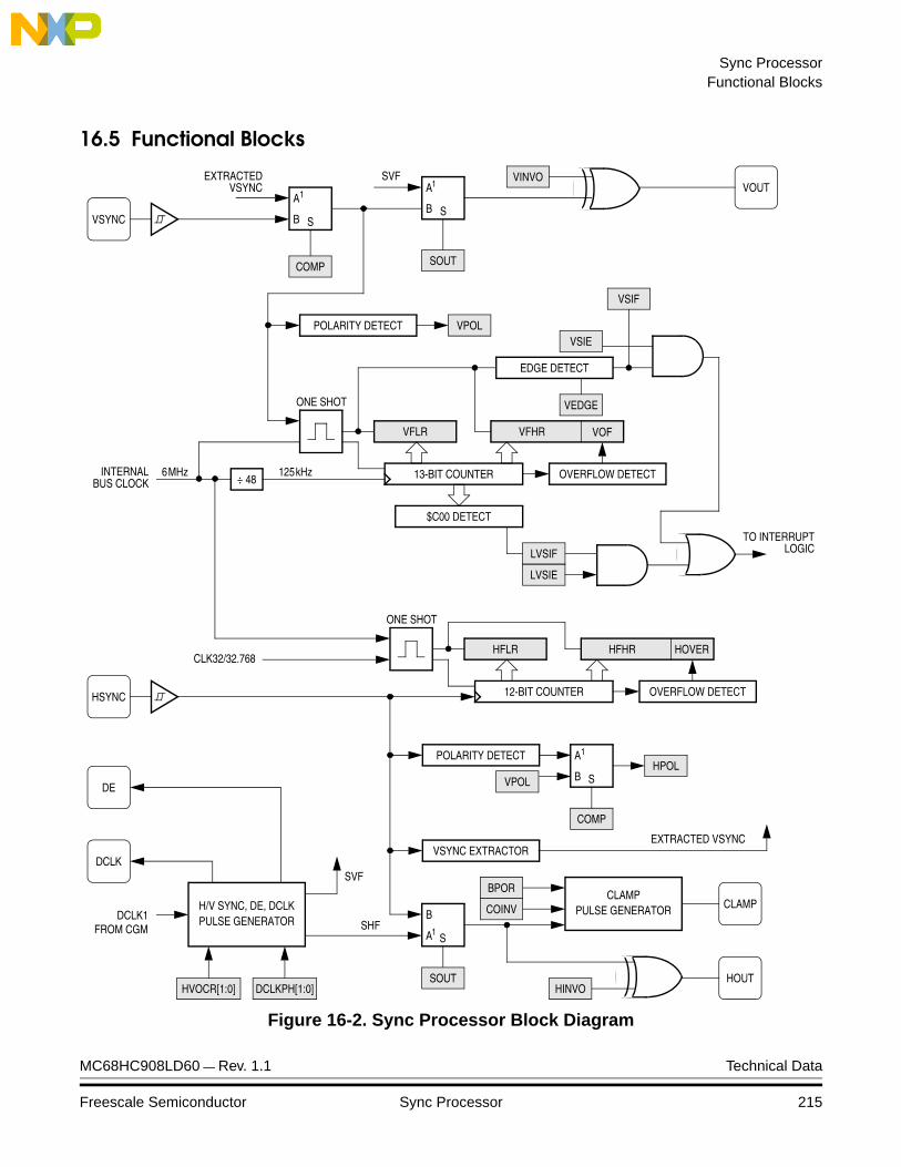
Sync ProcessorFunctional Blocks
16.5 Functional Blocks
Figure 16-2. Sync Processor Block Diagram
13-BIT COUNTER÷ 48
A1
B S
EXTRACTED
VSYNC
A1
B S
SVF
COMP SOUT
VINVOVOUT
POLARITY DETECT
EDGE DETECT
VPOL
ONE SHOT VEDGE
INTERNALBUS CLOCK
OVERFLOW DETECT
VOF
LVSIE
TO INTERRUPTLOGIC
12-BIT COUNTER
ONE SHOT
OVERFLOW DETECT
CLK32/32.768
HSYNC
DCLK
A1
B S
POLARITY DETECTHPOL
COMP
VSYNC EXTRACTOREXTRACTED VSYNC
B
A1S
H/V SYNC, DE, DCLKDCLK1 PULSE GENERATOR
SVF
SHF
CLAMPPULSE GENERATOR CLAMP
HOUT
VFLR VFHR
HFLR HFHR
BPOR
COINV
SOUT
HOVER
VPOL
VSIE
VSIF
$C00 DETECT
LVSIF
HINVOHVOCR[1:0]
VSYNC
125kHz6MHz
DE
FROM CGM
DCLKPH[1:0]
MC68HC908LD60 — Rev. 1.1 Technical Data
Freescale Semiconductor Sync Processor 215
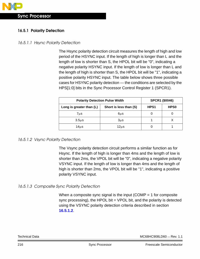
Sync Processor
16.5.1 Polarity Detection
16.5.1.1 Hsync Polarity Detection
The Hsync polarity detection circuit measures the length of high and low period of the HSYNC input. If the length of high is longer than L and the length of low is shorter than S, the HPOL bit will be "0", indicating a negative polarity HSYNC input. If the length of low is longer than L and the length of high is shorter than S, the HPOL bit will be "1", indicating a positive polarity HSYNC input. The table below shows three possible cases for HSYNC polarity detection — the conditions are selected by the HPS[1:0] bits in the Sync Processor Control Register 1 (SPCR1).
16.5.1.2 Vsync Polarity Detection
The Vsync polarity detection circuit performs a similar function as for Hsync. If the length of high is longer than 4ms and the length of low is shorter than 2ms, the VPOL bit will be "0", indicating a negative polarity VSYNC input. If the length of low is longer than 4ms and the length of high is shorter than 2ms, the VPOL bit will be "1", indicating a positive polarity VSYNC input.
16.5.1.3 Composite Sync Polarity Detection
When a composite sync signal is the input (COMP = 1 for composite sync processing), the HPOL bit = VPOL bit, and the polarity is detected using the VSYNC polarity detection criteria described in section 16.5.1.2.
Polarity Detection Pulse Width SPCR1 ($0046)
Long is greater than (L) Short is less than (S) HPS1 HPS0
7µs 6µs 0 0
3.5µs 3µs 1 X
14µs 12µs 0 1
Technical Data MC68HC908LD60 — Rev. 1.1
216 Sync Processor Freescale Semiconductor
Sync ProcessorFunctional Blocks
16.5.2 Sync Signal Counters
There are two counters: a 13-bit horizontal frequency counter to count the number of horizontal sync pulses within a 32ms or 8ms period; and a 13-bit vertical frequency counter to count the number of system clock cycles between two vertical sync pulses. These two data can be read by the CPU to check the signal frequencies and to determine the video mode.
The 13-bit vertical frequency register encompasses vertical frequency range from approximately 15Hz to 128kHz. Due to the asynchronous timing between the incoming VSYNC signal and internal system clock, there will be ±1 count error on reading the Vertical Frequency Registers (VFRs) for the same vertical frequency.
The horizontal counter counts the pulses on HSYNC pin input, and is uploaded to the Hsync Frequency Registers (HFRs) every 32.768ms or 8.192ms.
16.5.3 Polarity Controlled HOUT and VOUT Outputs
The processed sync signals are output on HOUT and VOUT when the corresponding bits in Configuration Register 0 ($0069) are set. The signal to these output pins depend on SOUT and COMP bits (see Table 16-2), with polarity controlled by ATPOL, HINVO, and VINVO bits as shown in Table 16-3.
Table 16-2. Sync Output Control
SOUT COMP Sync Outputs:VOUT and HOUT
1 X Free-running video mode output
0 0Sync outputs follow sync inputs VSYNC and HSYNC respectively, with polarity correction shown in Table 16-3.
0 1HOUT follows the composite sync input and VOUT is the extracted Vsync (3 to 14µs delay to composite input), with polarity correction shown in Table 16-3.
MC68HC908LD60 — Rev. 1.1 Technical Data
Freescale Semiconductor Sync Processor 217

Sync Processor
When the SOUT bit is set, the HOUT output is a free-running pulse. Both HOUT and VOUT outputs are negative polarity, with frequencies selected by the H & V Sync Output Control Register (HVOCR).
16.5.4 Clamp Pulse Output
When the ELS0B and ELS0A bits in the TSC0 register are logic 0 (see Table 11-3), a clamp signal is output on the CLAMP pin. This clamp pulse is triggered either on the leading edge or the trailing edge of HSYNC, controlled by BPOR bit, with the polarity controlled by the COINV bit. See Figure 16-3 . Clamp Pulse Output Timing.
Figure 16-3. Clamp Pulse Output Timing
Table 16-3. Sync Output Polarity
ATPOL SOUTVINVO
orHINVO
Sync Outputs:VOUT/HOUT
X 1 X Free-running video mode output
0 0 0 Same polarity as sync input
0 0 1 Inverted polarity of sync input
1 0 0 Negative polarity sync output
1 0 1 Positive polarity sync output
Pulse width = 0.33~2.1µs
Pulse width = 0.33~2.1µs
Pulse width = 0.33~2.1µs
Pulse width = 0.33~2.1µs
HSYNC(HPOL = 1)
CLAMP(BPOR = 0)
CLAMP(BPOR = 1)
HSYNC(HPOL = 0)
CLAMP(BPOR = 0)
CLAMP(BPOR = 1)
Technical Data MC68HC908LD60 — Rev. 1.1
218 Sync Processor Freescale Semiconductor

Sync ProcessorSync Processor I/O Registers
16.5.5 Low Vertical Frequency Detect
Logic monitors the value of the Vsync Frequency Register (VFR), and sets the low vertical frequency flag (LVSIF) when the value of VFR is higher than $C00 (frequency below 40.7Hz). LVSIF bit can generate an interrupt request to the CPU when the LVSIE bit is set and I-bit in the Condition Code Register is "0". The LVSIF bit can help the system to detect video off mode fast.
16.6 Sync Processor I/O Registers
Eight registers are associated with the Sync Processor, they outlined in the following sections.
16.6.1 Sync Processor Control & Status Register (SPCSR)
VSIE — VSync Interrupt Enable
When this bit is set, the VSIF flag is enabled to generate an interrupt request to the CPU. When VSIE is cleared, the VSIF flag is prevented from generating an interrupt request to the CPU. Reset clears this bit.
1 = VSIF bit set will generate interrupt request to CPU0 = VSIF bit set does not generate interrupt request to CPU
Address: $0040
Bit 7 6 5 4 3 2 1 Bit 0
Read:VSIE VEDGE
VSIFCOMP VINVO HINVO
VPOL HPOL
Write: 0
Reset: 0 0 0 0 0 0 0 0
= Unimplemented
Figure 16-4. Sync Processor Control & Status Register (SPCSR)
MC68HC908LD60 — Rev. 1.1 Technical Data
Freescale Semiconductor Sync Processor 219

Sync Processor
VEDGE — VSync Interrupt Edge Select
This bit specifies the triggering edge of Vsync interrupt. When it is "0", the rising edge of internal Vsync signal which is either from the VSYNC pin or extracted from the composite input signal will set VSIF flag. When it is "1", the falling edge of internal Vsync signal will set VSIF flag. Reset clears this bit.
1 = VSIF bit will be set by rising edge of Vsync0 = VSIF bit will be set by falling edge of Vsync
VSIF — VSync Interrupt Flag
This flag is only set by the specified edge of the internal Vsync signal, which is either from the VSYNC input pin or extracted from the composite sync input signal. The triggering edge is specified by the VEDGE bit. VSIF generates an interrupt request to the CPU if the VSIE bit is also set. This bit is cleared by writing a "0" to it or by a reset.
1 = A valid edge is detected on the Vsync0 = No valid Vsync is detected
COMP — Composite Sync Input Enable
This bit is set to enable the separator circuit which extracts the Vsync pulse from the composite sync input on HSYNC or SOG pin (select by SOGSEL bit). The extracted Vsync signal is used as it were from the VSYNC input. Reset clears this bit.
1 = Composite Sync Input Enabled0 = Composite Sync Input Disabled
VINVO — VOUT Signal Polarity
This bit, together with the ATPOL bit in SPCR1 controls the output polarity of the VOUT signal (see Table 16-4).
HINVO — HOUT Signal Polarity
This bit, together with the ATPOL bit in SPCR1 controls the output polarity of the HOUT signal (see Table 16-4).
Technical Data MC68HC908LD60 — Rev. 1.1
220 Sync Processor Freescale Semiconductor

Sync ProcessorSync Processor I/O Registers
VPOL — Vsync Input Polarity
This bit indicates the polarity of the VSYNC input, or the extracted Vsync from a composite sync input (COMP=1). Reset clears this bit.
1 = Vsync is positive polarity0 = Vsync is negative polarity
HPOL — Hsync Input Polarity
This bit indicates the polarity of the HSYNC input. This bit equals the VPOL bit when the COMP bit is set. Reset clears this bit.
1 = Hsync is positive polarity0 = Hsync is negative polarity
16.6.2 Sync Processor Input/Output Control Register (SPIOCR)
VSYNCS — VSYNC Input State
This read-only bit reflects the logical state of the VSYNC input.
HSYNCS — HSYNC Input State
This read-only bit reflects the logical state of the HSYNC input.
Table 16-4. ATPOL, VINVO, and HINVO setting
ATPOL VINVO / HINVO Sync Outputs:VOUT/HOUT
0 0 Same polarity as sync input
0 1 Inverted polarity of sync input
1 0 Negative polarity sync output
1 1 Positive polarity sync output
Address: $0045
Bit 7 6 5 4 3 2 1 Bit 0
Read: VSYNCS HSYNCSCOINV R R R BPOR SOUT
Write:
Reset: 0 0 0 0 0
= Unimplemented R = Reserved
Figure 16-5. Sync Processor Input/Output Control Register (SPIOCR)
MC68HC908LD60 — Rev. 1.1 Technical Data
Freescale Semiconductor Sync Processor 221

Sync Processor
COINV — Clamp Output Invert
This bit is set to invert the clamp pulse output to negative. Reset clears this bit.
1 = Clamp output is set for negative pulses0 = Clamp output is set for positive pulses
BPOR — Back Porch
This bit defines the triggering edge of the clamp pulse output relative to the HSYNC input. Reset clears this bit.
1 = Clamp pulse is generated on the trailing edge of HSYNC0 = Clamp pulse is generated on the leading edge of HSYNC
SOUT — Sync Output Enable
This bit will select the output signals for the VOUT and HOUT pins and generate the DE and DCLK signals to the pins. Reset clears this bit.
1 = VOUT, HOUT, DE, and DCLK outputs are internally generated free-running timing pulses with frequencies determined by HVCOR[1:0] bits in HVCOR and CGM values.
0 = VOUT and HOUT outputs are processed VSYNC and HSYNC inputs respectively and DE and DCLK are hold as logic low.
Technical Data MC68HC908LD60 — Rev. 1.1
222 Sync Processor Freescale Semiconductor

Sync ProcessorSync Processor I/O Registers
16.6.3 Vertical Frequency Registers (VFRs)
This register pair contains the 13-bit vertical frequency count value, an overflow bit, and the clamp pulse width selection bits.
VF[12:0] — Vertical Frame Frequency
This read-only 13-bit contains information of the vertical frame frequency. An internal 13-bit counter counts the number of 8µs periods between two Vsync pulses. The most significant 5 bits of the counted value is transferred to the high byte register, and the least significant 8 bits is transferred to an intermediate buffer. When the high byte register is read, the 8-bit counted value stored in the intermediate buffer will be uploaded to the low byte register. Therefore, user program must read the high byte register first, then low byte register in order to get the complete counted value of one vertical frame. If the counter overflows, the overflow flag, VOF, will be set, indicating the counter value stored in the VFRs is meaningless. The data corresponds to the period of one vertical frame. This register can be read to determine if the frame frequency is valid, and to determine the video mode.
Address: $0041
Bit 7 6 5 4 3 2 1 Bit 0
Read: VOF 0 0 VF12 VF11 VF10 VF9 VF8
Write: CPW1 CPW0
Reset: 0 0 0 0 0 0 0 0
Figure 16-6. Vertical Frequency High Register
Address: $0042
Bit 7 6 5 4 3 2 1 Bit 0
Read: VF7 VF6 VF5 VF4 VF3 VF2 VF1 VF0
Write:
Reset: 0 0 0 0 0 0 0 0
= Unimplemented
Figure 16-7. Vertical Frequency Low Register
MC68HC908LD60 — Rev. 1.1 Technical Data
Freescale Semiconductor Sync Processor 223

Sync Processor
The frame frequency is calculated by:
Table 16-5 shows examples for the Vertical Frequency Register, all VFR numbers are in hexadecimal.
VOF — Vertical Frequency Counter Overflow
This read-only bit is set when an overflow has occurred on the 13-bit vertical frequency counter. Reset clears this bit, and will be updated every vertical frame.An overflow occurs when the period of Vsync frame exceeds 64.768ms (a vertical frame frequency lower than 15.258Hz).
1 = A vertical frequency counter overflow has occurred0 = No vertical frequency counter overflow has occurred
Table 16-5. Sample Vertical Frame Frequencies
VFR Max Freq. Min Freq. VFR Max Freq. Min Freq.
$02A0 186.20 Hz 185.70 Hz $0780 65.10 Hz 65.00 Hz
$03C0 130.34 Hz 130.07 Hz $0823 60.04 Hz 59.98 Hz
$03C1 130.21 Hz 129.94 Hz $0824 60.01 Hz 59.95 Hz
$03C2 130.07 Hz 129.80 Hz $0825 59.98 Hz 59.92 Hz
$04E2 100.08 Hz 99.92 Hz $09C4 50.02 Hz 49.98 Hz
$04E3 100.00 Hz 99.84 Hz $09C5 50.00 Hz 49.96 Hz
$04E4 99.92 Hz 99.76 Hz $09C6 49.98 Hz 49.94 Hz
$06F9 70.07 Hz 69.99 Hz $1FFD 15.266 Hz 15.262 Hz
$06FA 70.03 Hz 69.95 Hz $1FFE 15.264 Hz 15.260 Hz
$06FB 69.99 Hz 69.91 Hz $1FFF 15.262 Hz 15.258 Hz
Vertical Frame Frequency 1VFR 1± 48 tCYC××---------------------------------------------------=
1VFR 1± 8µ× s--------------------------------------=
for internal bus clock of 6MHz
Technical Data MC68HC908LD60 — Rev. 1.1
224 Sync Processor Freescale Semiconductor
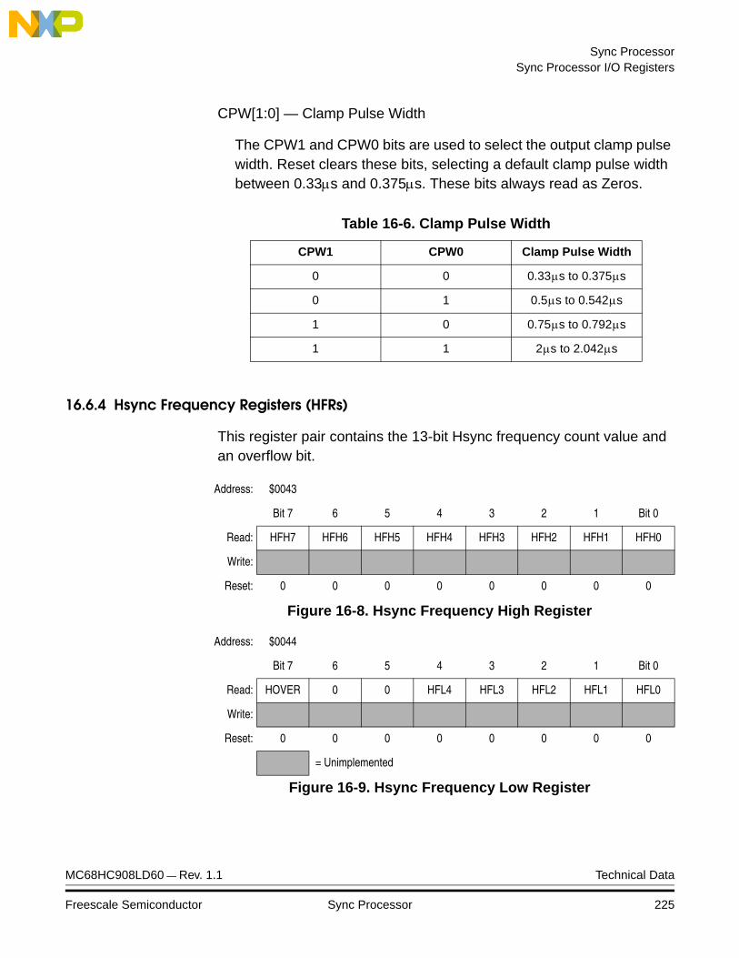
Sync ProcessorSync Processor I/O Registers
CPW[1:0] — Clamp Pulse Width
The CPW1 and CPW0 bits are used to select the output clamp pulse width. Reset clears these bits, selecting a default clamp pulse width between 0.33µs and 0.375µs. These bits always read as Zeros.
16.6.4 Hsync Frequency Registers (HFRs)
This register pair contains the 13-bit Hsync frequency count value and an overflow bit.
Table 16-6. Clamp Pulse Width
CPW1 CPW0 Clamp Pulse Width
0 0 0.33µs to 0.375µs
0 1 0.5µs to 0.542µs
1 0 0.75µs to 0.792µs
1 1 2µs to 2.042µs
Address: $0043
Bit 7 6 5 4 3 2 1 Bit 0
Read: HFH7 HFH6 HFH5 HFH4 HFH3 HFH2 HFH1 HFH0
Write:
Reset: 0 0 0 0 0 0 0 0
Figure 16-8. Hsync Frequency High Register
Address: $0044
Bit 7 6 5 4 3 2 1 Bit 0
Read: HOVER 0 0 HFL4 HFL3 HFL2 HFL1 HFL0
Write:
Reset: 0 0 0 0 0 0 0 0
= Unimplemented
Figure 16-9. Hsync Frequency Low Register
MC68HC908LD60 — Rev. 1.1 Technical Data
Freescale Semiconductor Sync Processor 225

Sync Processor
HFH[7:0], HFL[4:0] — Horizontal Line Frequency
This read-only 13-bit contains the number of horizontal lines in a 32ms window. An internal 13-bit counter counts the Hsync pulses within a 32ms window in every 32.768ms period. If the FSHF bit in SPCR1 is set, only the most 11-bits (HFH[7:0] & HFL[4:2]) will be updated by the counter. Thus, providing a Hsync pulse count in a 8ms window in every 8.192ms.The most significant 8 bits of counted value is transferred to the high byte register, and the least significant 5 bits is transferred to an intermediate buffer. When the high byte register is read, the 5-bit counted value stored in the intermediate buffer will be uploaded to the low byte register. Therefore, user the program must read the high byte register first then low byte register in order to get the complete counted value of Hsync pulses. If the counter overflows, the overflow flag, HOVER, will be set, indicating the number of Hsync pulses in
32ms are more than 8191 (213–1), i.e. a Hsync frequency greater than 256kHz.For the 32ms window, the HFHR and HFLR are such that the frequency step unit in the 5-bit of HFLR is 0.03125kHz, and the step unit in the 8-bit HFHR is 1kHz. Therefore, the Hsync frequency can be easily calculated by:
HOVER — Hsync Frequency Counter Overflow
This read-only bit is set when an overflow has occurred on the 13-bit Hsync frequency counter. Reset clears this bit, and will be updated every count period.An overflow occurs when the number Hsync pulses exceed 8191, a Hsync frequency greater than 256kHz.
1 = A Hsync frequency counter overflow has occurred0 = No Hsync frequency counter overflow has occurred
Hsync Frequency = [HFH + (HFL × 0.03125)] kHz
where: HFH is the value of HFH[7:0]
HFL is the value of HFL[4:0]
Technical Data MC68HC908LD60 — Rev. 1.1
226 Sync Processor Freescale Semiconductor
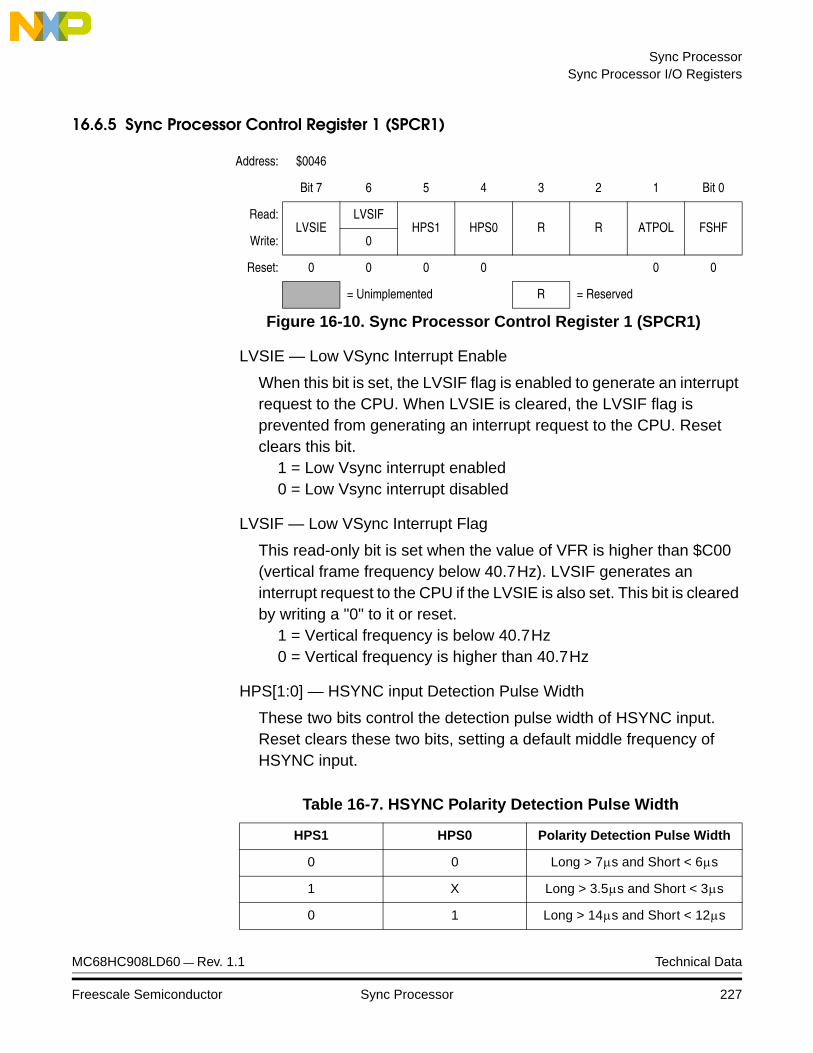
Sync ProcessorSync Processor I/O Registers
16.6.5 Sync Processor Control Register 1 (SPCR1)
LVSIE — Low VSync Interrupt Enable
When this bit is set, the LVSIF flag is enabled to generate an interrupt request to the CPU. When LVSIE is cleared, the LVSIF flag is prevented from generating an interrupt request to the CPU. Reset clears this bit.
1 = Low Vsync interrupt enabled0 = Low Vsync interrupt disabled
LVSIF — Low VSync Interrupt Flag
This read-only bit is set when the value of VFR is higher than $C00 (vertical frame frequency below 40.7Hz). LVSIF generates an interrupt request to the CPU if the LVSIE is also set. This bit is cleared by writing a "0" to it or reset.
1 = Vertical frequency is below 40.7Hz0 = Vertical frequency is higher than 40.7Hz
HPS[1:0] — HSYNC input Detection Pulse Width
These two bits control the detection pulse width of HSYNC input. Reset clears these two bits, setting a default middle frequency of HSYNC input.
Address: $0046
Bit 7 6 5 4 3 2 1 Bit 0
Read:LVSIE
LVSIFHPS1 HPS0 R R ATPOL FSHF
Write: 0
Reset: 0 0 0 0 0 0
= Unimplemented R = Reserved
Figure 16-10. Sync Processor Control Register 1 (SPCR1)
Table 16-7. HSYNC Polarity Detection Pulse Width
HPS1 HPS0 Polarity Detection Pulse Width
0 0 Long > 7µs and Short < 6µs
1 X Long > 3.5µs and Short < 3µs
0 1 Long > 14µs and Short < 12µs
MC68HC908LD60 — Rev. 1.1 Technical Data
Freescale Semiconductor Sync Processor 227
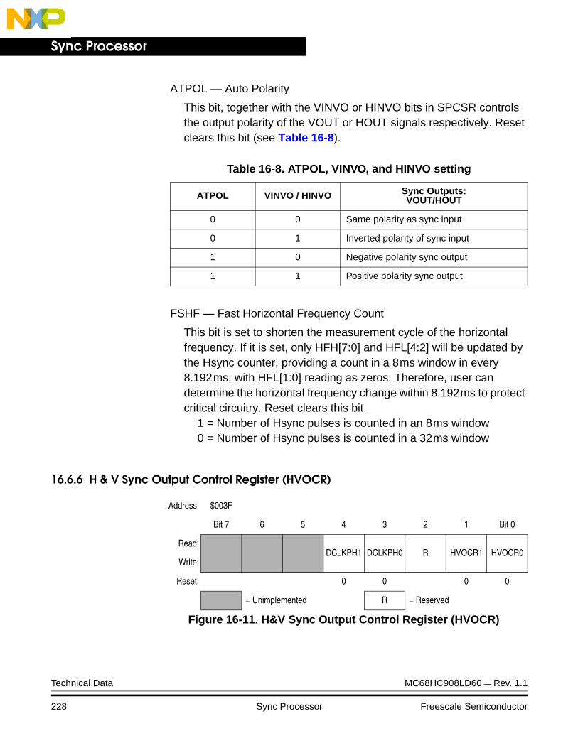
Sync Processor
ATPOL — Auto Polarity
This bit, together with the VINVO or HINVO bits in SPCSR controls the output polarity of the VOUT or HOUT signals respectively. Reset clears this bit (see Table 16-8).
FSHF — Fast Horizontal Frequency Count
This bit is set to shorten the measurement cycle of the horizontal frequency. If it is set, only HFH[7:0] and HFL[4:2] will be updated by the Hsync counter, providing a count in a 8ms window in every 8.192ms, with HFL[1:0] reading as zeros. Therefore, user can determine the horizontal frequency change within 8.192ms to protect critical circuitry. Reset clears this bit.
1 = Number of Hsync pulses is counted in an 8ms window0 = Number of Hsync pulses is counted in a 32ms window
16.6.6 H & V Sync Output Control Register (HVOCR)
Table 16-8. ATPOL, VINVO, and HINVO setting
ATPOL VINVO / HINVO Sync Outputs:VOUT/HOUT
0 0 Same polarity as sync input
0 1 Inverted polarity of sync input
1 0 Negative polarity sync output
1 1 Positive polarity sync output
Address: $003F
Bit 7 6 5 4 3 2 1 Bit 0
Read:DCLKPH1 DCLKPH0 R HVOCR1 HVOCR0
Write:
Reset: 0 0 0 0
= Unimplemented R = Reserved
Figure 16-11. H&V Sync Output Control Register (HVOCR)
Technical Data MC68HC908LD60 — Rev. 1.1
228 Sync Processor Freescale Semiconductor
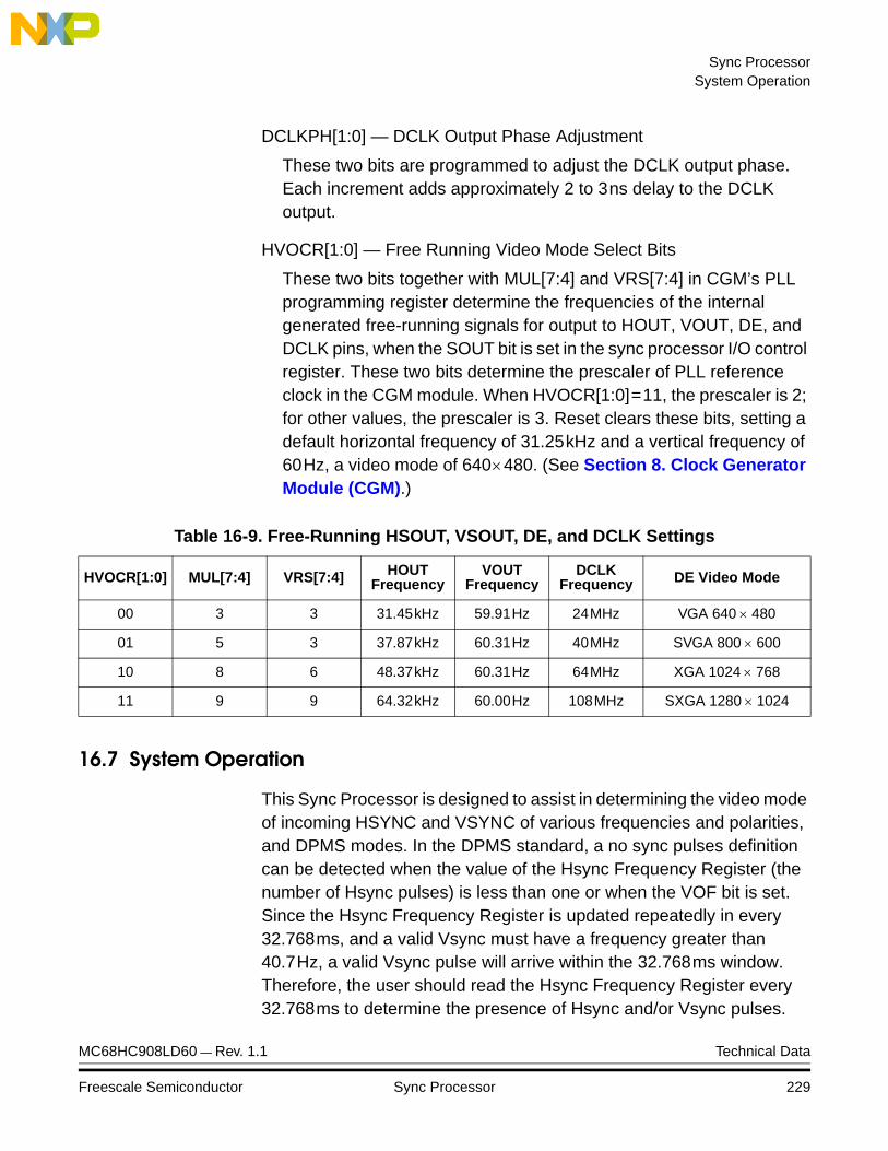
Sync ProcessorSystem Operation
DCLKPH[1:0] — DCLK Output Phase Adjustment
These two bits are programmed to adjust the DCLK output phase. Each increment adds approximately 2 to 3ns delay to the DCLK output.
HVOCR[1:0] — Free Running Video Mode Select Bits
These two bits together with MUL[7:4] and VRS[7:4] in CGM’s PLL programming register determine the frequencies of the internal generated free-running signals for output to HOUT, VOUT, DE, and DCLK pins, when the SOUT bit is set in the sync processor I/O control register. These two bits determine the prescaler of PLL reference clock in the CGM module. When HVOCR[1:0]=11, the prescaler is 2; for other values, the prescaler is 3. Reset clears these bits, setting a default horizontal frequency of 31.25kHz and a vertical frequency of 60Hz, a video mode of 640×480. (See Section 8. Clock Generator Module (CGM).)
16.7 System Operation
This Sync Processor is designed to assist in determining the video mode of incoming HSYNC and VSYNC of various frequencies and polarities, and DPMS modes. In the DPMS standard, a no sync pulses definition can be detected when the value of the Hsync Frequency Register (the number of Hsync pulses) is less than one or when the VOF bit is set. Since the Hsync Frequency Register is updated repeatedly in every 32.768ms, and a valid Vsync must have a frequency greater than 40.7Hz, a valid Vsync pulse will arrive within the 32.768ms window. Therefore, the user should read the Hsync Frequency Register every 32.768ms to determine the presence of Hsync and/or Vsync pulses.
Table 16-9. Free-Running HSOUT, VSOUT, DE, and DCLK Settings
HVOCR[1:0] MUL[7:4] VRS[7:4] HOUTFrequency
VOUTFrequency
DCLKFrequency DE Video Mode
00 3 3 31.45kHz 59.91Hz 24MHz VGA 640 × 480
01 5 3 37.87kHz 60.31Hz 40MHz SVGA 800 × 600
10 8 6 48.37kHz 60.31Hz 64MHz XGA 1024 × 768
11 9 9 64.32kHz 60.00Hz 108MHz SXGA 1280 × 1024
MC68HC908LD60 — Rev. 1.1 Technical Data
Freescale Semiconductor Sync Processor 229

Sync Processor
Technical Data MC68HC908LD60 — Rev. 1.1
230 Sync Processor Freescale Semiconductor

Technical Data — MC68HC908LD60
Section 17. Input/Output (I/O) Ports
17.1 Contents
17.2 Introduction . . . . . . . . . . . . . . . . . . . . . . . . . . . . . . . . . . . . . . .232
17.3 Port A . . . . . . . . . . . . . . . . . . . . . . . . . . . . . . . . . . . . . . . . . . .23517.3.1 Port A Data Register . . . . . . . . . . . . . . . . . . . . . . . . . . . . .23517.3.2 Data Direction Register A . . . . . . . . . . . . . . . . . . . . . . . . .23617.3.3 Port A Options . . . . . . . . . . . . . . . . . . . . . . . . . . . . . . . . . .237
17.4 Port B . . . . . . . . . . . . . . . . . . . . . . . . . . . . . . . . . . . . . . . . . . .23817.4.1 Port B Data Register . . . . . . . . . . . . . . . . . . . . . . . . . . . . .23817.4.2 Data Direction Register B . . . . . . . . . . . . . . . . . . . . . . . . .23917.4.3 Port B Options . . . . . . . . . . . . . . . . . . . . . . . . . . . . . . . . . .240
17.5 Port C . . . . . . . . . . . . . . . . . . . . . . . . . . . . . . . . . . . . . . . . . . .24117.5.1 Port C Data Register . . . . . . . . . . . . . . . . . . . . . . . . . . . . .24117.5.2 Data Direction Register C . . . . . . . . . . . . . . . . . . . . . . . . .24217.5.3 Port C Options . . . . . . . . . . . . . . . . . . . . . . . . . . . . . . . . . .243
17.6 Port D . . . . . . . . . . . . . . . . . . . . . . . . . . . . . . . . . . . . . . . . . . .24417.6.1 Port D Data Register . . . . . . . . . . . . . . . . . . . . . . . . . . . . .24417.6.2 Data Direction Register D. . . . . . . . . . . . . . . . . . . . . . . . . .24517.6.3 Port D Options . . . . . . . . . . . . . . . . . . . . . . . . . . . . . . . . . .247
17.7 Port E . . . . . . . . . . . . . . . . . . . . . . . . . . . . . . . . . . . . . . . . . . .24917.7.1 Port E Data Register . . . . . . . . . . . . . . . . . . . . . . . . . . . . .24917.7.2 Data Direction Register E. . . . . . . . . . . . . . . . . . . . . . . . . .249
MC68HC908LD60 — Rev. 1.1 Technical Data
Freescale Semiconductor Input/Output (I/O) Ports 231

Input/Output (I/O) Ports
17.2 Introduction
Thirty-nine (39) bidirectional input-output (I/O) pins form five parallel ports. All I/O pins are programmable as inputs or outputs.
NOTE: Connect any unused I/O pins to an appropriate logic level, either VDD or VSS. Although the I/O ports do not require termination for proper operation, termination reduces excess current consumption and the possibility of electrostatic damage.
Addr. Register Name Bit 7 6 5 4 3 2 1 Bit 0
$0000Port A Data Register
(PTA)
Read:PTA7 PTA6 PTA5 PTA4 PTA3 PTA2 PTA1 PTA0
Write:
Reset: Unaffected by reset
$0001Port B Data Register
(PTB)
Read:PTB7 PTB6 PTB5 PTB4 PTB3 PTB2 PTB1 PTB0
Write:
Reset: Unaffected by reset
$0002Port C Data Register
(PTC)
Read: 0PTC6 PTC5 PTC4 PTC3 PTC2 PTC1 PTC0
Write:
Reset: Unaffected by reset
$0003Port D Data Register
(PTD)
Read:PTD7 PTD6 PTD5 PTD4 PTD3 PTD2 PTD1 PTD0
Write:
Reset: Unaffected by reset
$0004Data Direction Register A
(DDRA)
Read:DDRA7 DDRA6 DDRA5 DDRA4 DDRA3 DDRA2 DDRA1 DDRA0
Write:
Reset: 0 0 0 0 0 0 0 0
$0005Data Direction Register B
(DDRB)
Read:DDRB7 DDRB6 DDRB5 DDRB4 DDRB3 DDRB2 DDRB1 DDRB0
Write:
Reset: 0 0 0 0 0 0 0 0
= Unimplemented
Figure 17-1. Port I/O Register Summary
Technical Data MC68HC908LD60 — Rev. 1.1
232 Input/Output (I/O) Ports Freescale Semiconductor
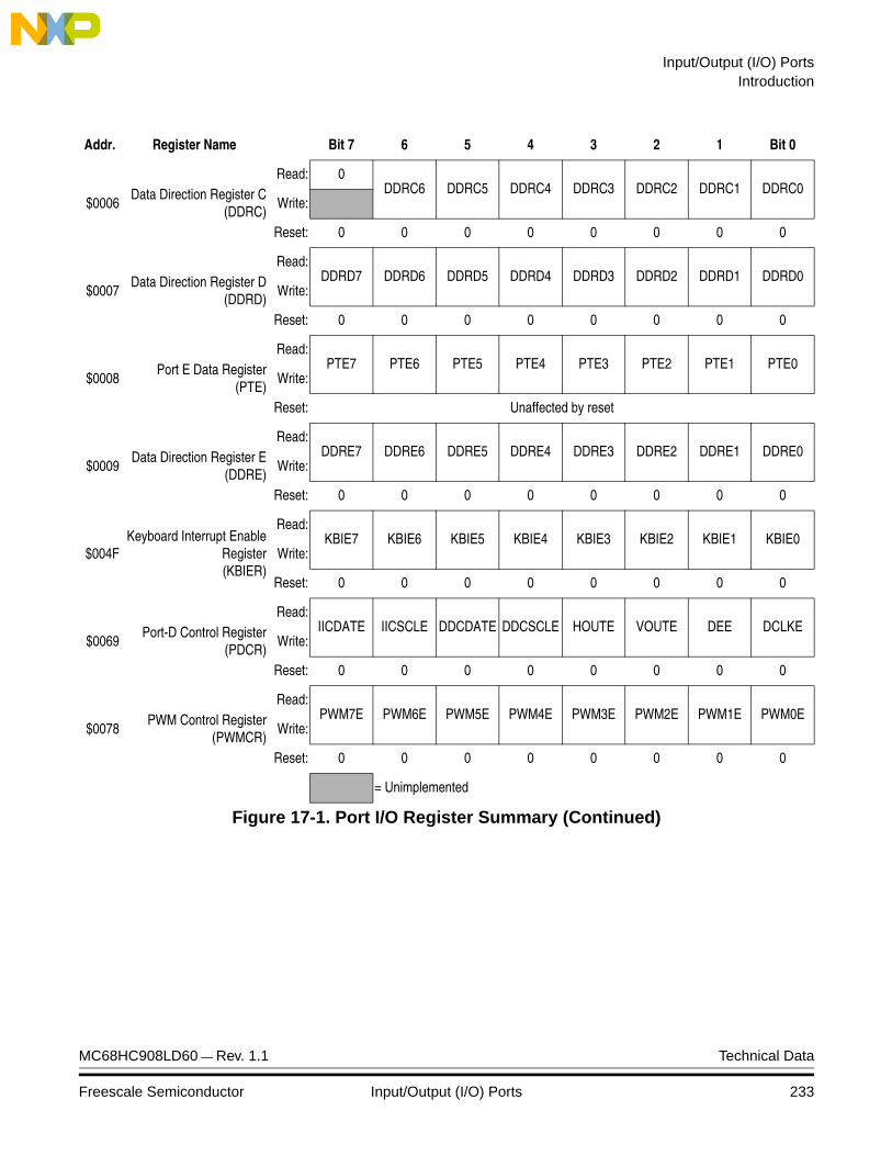
Input/Output (I/O) PortsIntroduction
$0006Data Direction Register C
(DDRC)
Read: 0DDRC6 DDRC5 DDRC4 DDRC3 DDRC2 DDRC1 DDRC0
Write:
Reset: 0 0 0 0 0 0 0 0
$0007Data Direction Register D
(DDRD)
Read:DDRD7 DDRD6 DDRD5 DDRD4 DDRD3 DDRD2 DDRD1 DDRD0
Write:
Reset: 0 0 0 0 0 0 0 0
$0008Port E Data Register
(PTE)
Read:PTE7 PTE6 PTE5 PTE4 PTE3 PTE2 PTE1 PTE0
Write:
Reset: Unaffected by reset
$0009 Data Direction Register E
(DDRE)
Read:DDRE7 DDRE6 DDRE5 DDRE4 DDRE3 DDRE2 DDRE1 DDRE0
Write:
Reset: 0 0 0 0 0 0 0 0
$004FKeyboard Interrupt Enable
Register(KBIER)
Read:KBIE7 KBIE6 KBIE5 KBIE4 KBIE3 KBIE2 KBIE1 KBIE0
Write:
Reset: 0 0 0 0 0 0 0 0
$0069Port-D Control Register
(PDCR)
Read:IICDATE IICSCLE DDCDATE DDCSCLE HOUTE VOUTE DEE DCLKE
Write:
Reset: 0 0 0 0 0 0 0 0
$0078PWM Control Register
(PWMCR)
Read:PWM7E PWM6E PWM5E PWM4E PWM3E PWM2E PWM1E PWM0E
Write:
Reset: 0 0 0 0 0 0 0 0
Addr. Register Name Bit 7 6 5 4 3 2 1 Bit 0
= Unimplemented
Figure 17-1. Port I/O Register Summary (Continued)
MC68HC908LD60 — Rev. 1.1 Technical Data
Freescale Semiconductor Input/Output (I/O) Ports 233

Input/Output (I/O) Ports
Table 17-1. Port Control Register Bits Summary
Port Bit DDRModule Control
PinModule Register Control Bit
A
0 DDRA0
KBIKBIER$004F
KBIE0 PTA0/KBI0
1 DDRA1 KBIE1 PTA1/KBI1
2 DDRA2 KBIE2 PTA2/KBI2
3 DDRA3 KBIE3 PTA3/KBI3
4 DDRA4 KBIE4 PTA4/KBI4
5 DDRA5 KBIE5 PTA5/KBI5
6 DDRA6 KBIE6 PTA6/KBI6
7 DDRA7 KBIE7 PTA7/KBI7
B
0 DDRB0
PWMPWMCR$0078
PWM0E PTB0/PWM0
1 DDRB1 PWM1E PTB1/PWM1
2 DDRB2 PWM2E PTB2/PWM2
3 DDRB3 PWM3E PTB3/PWM3
4 DDRB4 PWM4E PTB4/PWM4
5 DDRB5 PWM5E PTB5/PWM5
6 DDRB6 PWM6E PTB6/PWM6
7 DDRB7 PWM7E PTB7/PWM7
C
0 DDRC0
ADCADSCR$003B
ADCH[4:0]
PTC0/ADC0
1 DDRC1 PTC1/ADC1
2 DDRC2 PTC2/ADC2
3 DDRC3 PTC3/ADC3
4 DDRC4 PTC4/ADC4
5 DDRC5 PTC5/ADC5
6 DDRC6 — — — PTC6
D
0 DDRD0
SYNC
PDCR$0069
DCLKE PTD0/DCLK
1 DDRD1 DEE PTD1/DE
2 DDRD2 VOUTE PTD2/VOUT
3 DDRD3 HOUTE PTD3/HOUT
4 DDRD4DDC12AB
DDCSCLE PTD4/DDCSCL
5 DDRD5 DDCDATE PTD5/DDCSDA
6 DDRD6MMIIC
IICSCLE PTD6/IICSCL
7 DDRD7 IICDATE PTD7/IICSDA
E
0 DDRE0
— — —
PTE0
1 DDRE1 PTE1
2 DDRE2 PTE2
3 DDRE3 PTE3
4 DDRE4 PTE4
5 DDRE5 PTE5
6 DDRE6 PTE6
7 DDRE7 PTE7
Technical Data MC68HC908LD60 — Rev. 1.1
234 Input/Output (I/O) Ports Freescale Semiconductor
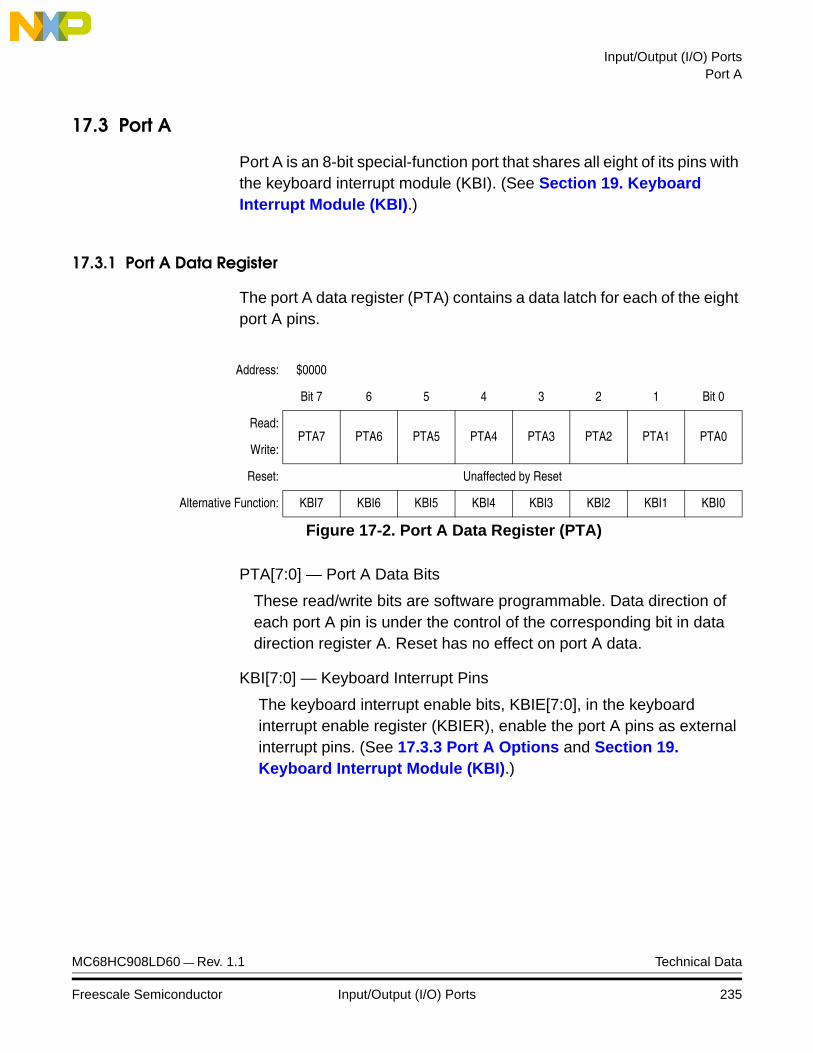
Input/Output (I/O) PortsPort A
17.3 Port A
Port A is an 8-bit special-function port that shares all eight of its pins with the keyboard interrupt module (KBI). (See Section 19. Keyboard Interrupt Module (KBI).)
17.3.1 Port A Data Register
The port A data register (PTA) contains a data latch for each of the eight port A pins.
PTA[7:0] — Port A Data Bits
These read/write bits are software programmable. Data direction of each port A pin is under the control of the corresponding bit in data direction register A. Reset has no effect on port A data.
KBI[7:0] — Keyboard Interrupt Pins
The keyboard interrupt enable bits, KBIE[7:0], in the keyboard interrupt enable register (KBIER), enable the port A pins as external interrupt pins. (See 17.3.3 Port A Options and Section 19. Keyboard Interrupt Module (KBI).)
Address: $0000
Bit 7 6 5 4 3 2 1 Bit 0
Read:PTA7 PTA6 PTA5 PTA4 PTA3 PTA2 PTA1 PTA0
Write:
Reset: Unaffected by Reset
Alternative Function: KBI7 KBI6 KBI5 KBI4 KBI3 KBI2 KBI1 KBI0
Figure 17-2. Port A Data Register (PTA)
MC68HC908LD60 — Rev. 1.1 Technical Data
Freescale Semiconductor Input/Output (I/O) Ports 235

Input/Output (I/O) Ports
17.3.2 Data Direction Register A
Data direction register A (DDRA) determines whether each port A pin is an input or an output. Writing a logic 1 to a DDRA bit enables the output buffer for the corresponding port A pin; a logic 0 disables the output buffer.
DDRA[7:0] — Data Direction Register A Bits
These read/write bits control port A data direction. Reset clears DDRA[7:0], configuring all port A pins as inputs.
1 = Corresponding port A pin configured as output0 = Corresponding port A pin configured as input
NOTE: Avoid glitches on port A pins by writing to the port A data register before changing data direction register A bits from 0 to 1.
Figure 17-4 shows the port A I/O logic.
Figure 17-4. Port A I/O Circuit
Address: $0004
Bit 7 6 5 4 3 2 1 Bit 0
Read:DDRA7 DDRA6 DDRA5 DDRA4 DDRA3 DDRA2 DDRA1 DDRA0
Write:
Reset: 0 0 0 0 0 0 0 0
Figure 17-3. Data Direction Register A (DDRA)
READ DDRA ($0004)
WRITE DDRA ($0004)
RESET
WRITE PTA ($0000)
READ PTA ($0000)
PTAx
DDRAx
PTAx
INTE
RNAL
DAT
A BU
S
Technical Data MC68HC908LD60 — Rev. 1.1
236 Input/Output (I/O) Ports Freescale Semiconductor

Input/Output (I/O) PortsPort A
When bit DDRAx is a logic 1, reading address $0000 reads the PTAx data latch. When bit DDRAx is a logic 0, reading address $0000 reads the voltage level on the pin. The data latch can always be written, regardless of the state of its data direction bit. Table 17-2 summarizes the operation of the port A pins.
17.3.3 Port A Options
The keyboard interrupt enable register (KBIER) selects the port A pins for keyboard interrupt function or as standard I/O function. (See Section 19. Keyboard Interrupt Module (KBI).)
KBIE[7:0] — Keyboard Interrupt Enable Bits
Setting a KBIEx bit to logic 1 configures the PTAx/KBIx pin for keyboard interrupt function. Reset clears the KBIEx bits.
1 = PTAx/KBIx pin configured as KBIx interrupt pin0 = PTAx/KBIx pin configured as PTAx standard I/O pin
Table 17-2. Port A Pin Functions
DDRABit PTA Bit I/O Pin Mode
Accesses to DDRA Accesses to PTA
Read/Write Read Write
0 X(1)
Notes:1. X = don’t care.
Input, Hi-Z(2)
2. Hi-Z = high impedance.
DDRA[7:0] Pin PTA[7:0](3)
3. Writing affects data register, but does not affect input.
1 X Output DDRA[7:0] PTA[7:0] PTA[7:0]
Address: $004F
Bit 7 6 5 4 3 2 1 Bit 0
Read:KBIE7 KBIE6 KBIE5 KBIE4 KBIE3 KBIE2 KBIE1 KBIE0
Write:
Reset: 0 0 0 0 0 0 0 0
Figure 17-5. Keyboard Interrupt Enable Register (KIER)
MC68HC908LD60 — Rev. 1.1 Technical Data
Freescale Semiconductor Input/Output (I/O) Ports 237
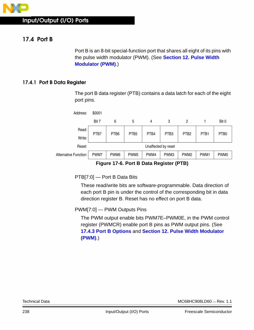
Input/Output (I/O) Ports
17.4 Port B
Port B is an 8-bit special-function port that shares all eight of its pins with the pulse width modulator (PWM). (See Section 12. Pulse Width Modulator (PWM).)
17.4.1 Port B Data Register
The port B data register (PTB) contains a data latch for each of the eight port pins.
PTB[7:0] — Port B Data Bits
These read/write bits are software-programmable. Data direction of each port B pin is under the control of the corresponding bit in data direction register B. Reset has no effect on port B data.
PWM[7:0] — PWM Outputs Pins
The PWM output enable bits PWM7E–PWM0E, in the PWM control register (PWMCR) enable port B pins as PWM output pins. (See 17.4.3 Port B Options and Section 12. Pulse Width Modulator (PWM).)
Address: $0001
Bit 7 6 5 4 3 2 1 Bit 0
Read:PTB7 PTB6 PTB5 PTB4 PTB3 PTB2 PTB1 PTB0
Write:
Reset: Unaffected by reset
Alternative Function: PWM7 PWM6 PWM5 PWM4 PWM3 PWM2 PWM1 PWM0
Figure 17-6. Port B Data Register (PTB)
Technical Data MC68HC908LD60 — Rev. 1.1
238 Input/Output (I/O) Ports Freescale Semiconductor
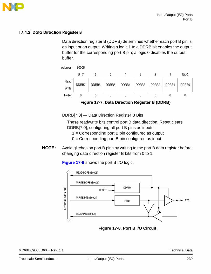
Input/Output (I/O) PortsPort B
17.4.2 Data Direction Register B
Data direction register B (DDRB) determines whether each port B pin is an input or an output. Writing a logic 1 to a DDRB bit enables the output buffer for the corresponding port B pin; a logic 0 disables the output buffer.
DDRB[7:0] — Data Direction Register B Bits
These read/write bits control port B data direction. Reset clears DDRB[7:0], configuring all port B pins as inputs.
1 = Corresponding port B pin configured as output0 = Corresponding port B pin configured as input
NOTE: Avoid glitches on port B pins by writing to the port B data register before changing data direction register B bits from 0 to 1.
Figure 17-8 shows the port B I/O logic.
Figure 17-8. Port B I/O Circuit
Address: $0005
Bit 7 6 5 4 3 2 1 Bit 0
Read:DDRB7 DDRB6 DDRB5 DDRB4 DDRB3 DDRB2 DDRB1 DDRB0
Write:
Reset: 0 0 0 0 0 0 0 0
Figure 17-7. Data Direction Register B (DDRB)
READ DDRB ($0005)
WRITE DDRB ($0005)
RESET
WRITE PTB ($0001)
READ PTB ($0001)
PTBx
DDRBx
PTBx
INTE
RNAL
DAT
A BU
S
MC68HC908LD60 — Rev. 1.1 Technical Data
Freescale Semiconductor Input/Output (I/O) Ports 239

Input/Output (I/O) Ports
When bit DDRBx is a logic 1, reading address $0001 reads the PTBx data latch. When bit DDRBx is a logic 0, reading address $0001 reads the voltage level on the pin. The data latch can always be written, regardless of the state of its data direction bit. Table 17-3 summarizes the operation of the port B pins.
17.4.3 Port B Options
The PWM control register (PWMCR) selects the port B pins for PWM function or as standard I/O function. (See Section 12. Pulse Width Modulator (PWM).)
PWM7E–PWM0E — PWM Output Enable Bits
Setting a PWMxE bit to logic 1 configures the PTBx/PWMx pin for PWM output function. Reset clears the PWMxE bits.
1 = PTBAx/PWMx pin configured as PWMx interrupt pin0 = PTBAx/PWMx pin configured as PTBx standard I/O pin
Table 17-3. Port B Pin Functions
DDRBBit PTB Bit I/O Pin Mode
Accesses to DDRB Accesses to PTB
Read/Write Read Write
0 X(1)
Notes:1. X = don’t care.
Input, Hi-Z(2)
2. Hi-Z = high impedance.
DDRB[6:0] Pin PTB[6:0](3)
3. Writing affects data register, but does not affect input.
1 X Output DDRB[6:0] PTB[6:0] PTB[6:0]
Address: $0078
Bit 7 6 5 4 3 2 1 Bit 0
Read:PWM7E PWM6E PWM5E PWM4E PWM3E PWM2E PWM1E PWM0E
Write:
Reset: 0 0 0 0 0 0 0 0
Figure 17-9. PWM Control Register (PWMCR)
Technical Data MC68HC908LD60 — Rev. 1.1
240 Input/Output (I/O) Ports Freescale Semiconductor

Input/Output (I/O) PortsPort C
17.5 Port C
Port C is an 7-bit special-function port that shares six of its pins with the analog-to-digital converter (ADC) module. (See Section 13. Analog-to-Digital Converter (ADC).)
17.5.1 Port C Data Register
The port C data register (PTC) contains a data latch for each of the seven port C pins.
PTC[6:0] — Port C Data Bits
These read/write bits are software-programmable. Data direction of each port C pin is under the control of the corresponding bit in data direction register C. Reset has no effect on port C data.
ADC[5:0] — Analog-to-Digital Input Pins
ADC[5:0] are pins used for the input channels to the analog-to-digital converter module. The channel select bits, ADCH[4:0], in the ADC Status and Control Register define which port C pin will be used as an ADC input and overrides any control from the port I/O logic. (See 17.5.3 Port C Options and Section 13. Analog-to-Digital Converter (ADC).)
Address: $0002
Bit 7 6 5 4 3 2 1 Bit 0
Read: 0PTC6 PTC5 PTC4 PTC3 PTC2 PTC1 PTC0
Write:
Reset: Unaffected by reset
Alternative Function: ADC5 ADC4 ADC3 ADC2 ADC1 ADC0
= Unimplemented
Figure 17-10. Port C Data Register (PTC)
MC68HC908LD60 — Rev. 1.1 Technical Data
Freescale Semiconductor Input/Output (I/O) Ports 241
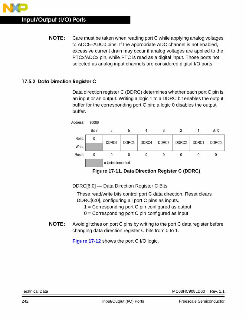
Input/Output (I/O) Ports
NOTE: Care must be taken when reading port C while applying analog voltages to ADC5–ADC0 pins. If the appropriate ADC channel is not enabled, excessive current drain may occur if analog voltages are applied to the PTCx/ADCx pin, while PTC is read as a digital input. Those ports not selected as analog input channels are considered digital I/O ports.
17.5.2 Data Direction Register C
Data direction register C (DDRC) determines whether each port C pin is an input or an output. Writing a logic 1 to a DDRC bit enables the output buffer for the corresponding port C pin; a logic 0 disables the output buffer.
DDRC[6:0] — Data Direction Register C Bits
These read/write bits control port C data direction. Reset clears DDRC[6:0], configuring all port C pins as inputs.
1 = Corresponding port C pin configured as output0 = Corresponding port C pin configured as input
NOTE: Avoid glitches on port C pins by writing to the port C data register before changing data direction register C bits from 0 to 1.
Figure 17-12 shows the port C I/O logic.
Address: $0006
Bit 7 6 5 4 3 2 1 Bit 0
Read: 0DDRC6 DDRC5 DDRC4 DDRC3 DDRC2 DDRC1 DDRC0
Write:
Reset: 0 0 0 0 0 0 0 0
= Unimplemented
Figure 17-11. Data Direction Register C (DDRC)
Technical Data MC68HC908LD60 — Rev. 1.1
242 Input/Output (I/O) Ports Freescale Semiconductor
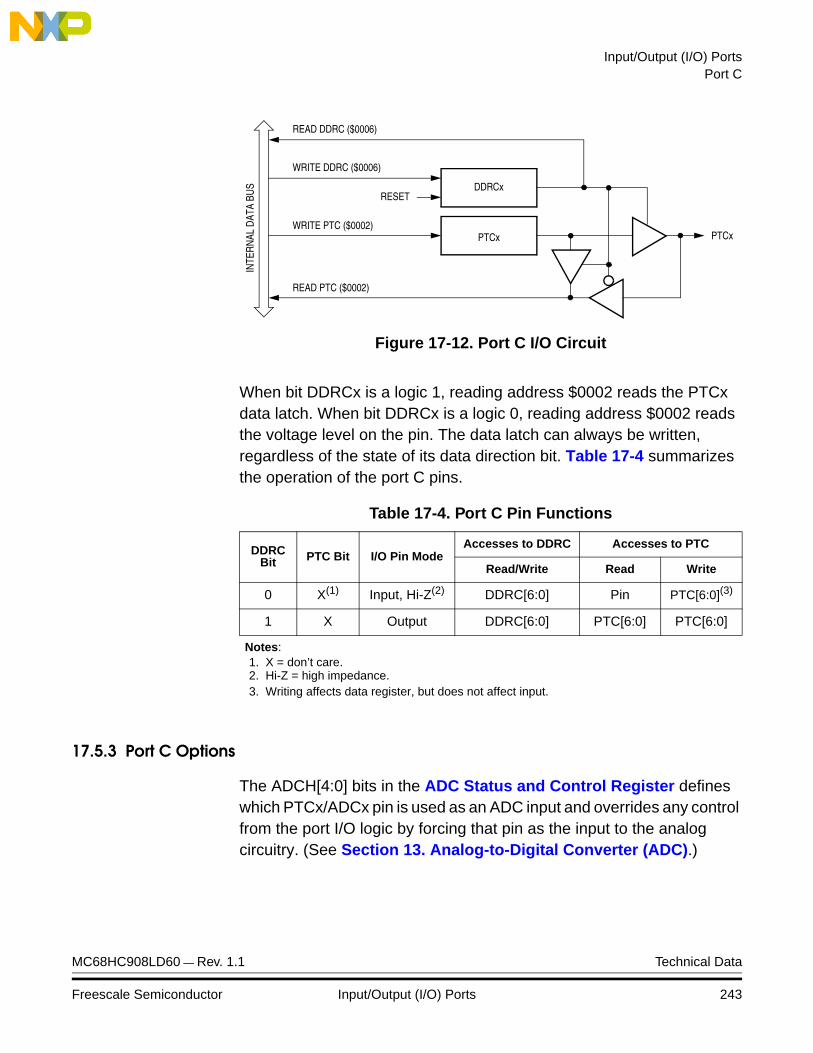
Input/Output (I/O) PortsPort C
Figure 17-12. Port C I/O Circuit
When bit DDRCx is a logic 1, reading address $0002 reads the PTCx data latch. When bit DDRCx is a logic 0, reading address $0002 reads the voltage level on the pin. The data latch can always be written, regardless of the state of its data direction bit. Table 17-4 summarizes the operation of the port C pins.
17.5.3 Port C Options
The ADCH[4:0] bits in the ADC Status and Control Register defines which PTCx/ADCx pin is used as an ADC input and overrides any control from the port I/O logic by forcing that pin as the input to the analog circuitry. (See Section 13. Analog-to-Digital Converter (ADC).)
Table 17-4. Port C Pin Functions
DDRCBit PTC Bit I/O Pin Mode
Accesses to DDRC Accesses to PTC
Read/Write Read Write
0 X(1)
Notes:1. X = don’t care.
Input, Hi-Z(2)
2. Hi-Z = high impedance.
DDRC[6:0] Pin PTC[6:0](3)
3. Writing affects data register, but does not affect input.
1 X Output DDRC[6:0] PTC[6:0] PTC[6:0]
READ DDRC ($0006)
WRITE DDRC ($0006)
RESET
WRITE PTC ($0002)
READ PTC ($0002)
PTCx
DDRCx
PTCxIN
TERN
AL D
ATA
BUS
MC68HC908LD60 — Rev. 1.1 Technical Data
Freescale Semiconductor Input/Output (I/O) Ports 243

Input/Output (I/O) Ports
17.6 Port D
Port D is an 8-bit special-function port that shares two of its pins with the multi-master IIC (MMIIC) module, two of its pins with the DDC12AB module, and four of its pins with the sync processor.
17.6.1 Port D Data Register
The port D data register (PTD) contains a data latch for each of the eight port D pins.
PTD[7:0] — Port D Data Bits
These read/write bits are software-programmable. Data direction of each port D pin is under the control of the corresponding bit in data direction register D. Reset has no effect on port D data.
IICSDA, IICSCL — Multi-master IIC Data and Clock pins
The PTD7/IICSDA and PTD6/IICSCL pins are multi-master IIC data and clock pins. When the IICDATE and IICSCLE bits in the port D control register (PDCR) are clear, the PTD7/IICSDA and PTD6/IICSCL pins are available for general-purpose I/O. (See 17.6.3 Port D Options.)
DDCSCL, DDCSDA — DDC12AB Data and Clock pins
The PTD4/DDCSCL and PTD5/DDCSDA pins are DDC12AB clock and data pins respectively. When the DDCSCLE and DDCDATE bits in the port D control register (PDCR) are clear, the PTD4/DDCSCL and PTD5/DDCSDA pins are available for general-purpose I/O. (See 17.6.3 Port D Options.)
Address: $0003
Bit 7 6 5 4 3 2 1 Bit 0
Read:PTD7 PTD6 PTD5 PTD4 PTD3 PTD2 PTD1 PTD0
Write:
Reset: Unaffected by reset
Alternative Function: IICSDA IICSCL DDCSDA DDCSCL HOUT VOUT DE DCLK
Figure 17-13. Port D Data Register (PTD)
Technical Data MC68HC908LD60 — Rev. 1.1
244 Input/Output (I/O) Ports Freescale Semiconductor

Input/Output (I/O) PortsPort D
HOUT— Sync Processor HOUT Pulse Output Pin
The PTD3/HOUT pin is the sync processor HOUT pulse output pin. When the HOUTE bit in the port D control register (PDCR) is clear, the PTD3/HOUT pin is available for general-purpose I/O. (See 17.6.3 Port D Options.)
VOUT — Sync Processor VOUT Pulse Output Pin
The PTD2/VOUT pin is the sync processor VOUT pulse output pin. When the VOUTE bit in the port D control register (PDCR) is clear, the PTD2/VOUT pin is available for general-purpose I/O. (See 17.6.3 Port D Options.)
DE — Sync Processor DE Pulse Output Pin
The PTD1/DE pin is the sync processor DE pulse output pin. When the DEE bit in the port D control register (PDCR) is clear, the PTD1/DE pin is available for general-purpose I/O. (See 17.6.3 Port D Options.)
DCLK — Sync Processor DCLK Pulse Output Pin
The PTD0/DCLK pin is the sync processor DCLK pulse output pin. When the DCLKE bit in the port D control register (PDCR) is clear, the PTD0/DCLK pin is available for general-purpose I/O. (See 17.6.3 Port D Options.)
17.6.2 Data Direction Register D
Data direction register D (DDRD) determines whether each port D pin is an input or an output. Writing a logic 1 to a DDRD bit enables the output buffer for the corresponding port D pin; a logic 0 disables the output buffer.
Address: $0007
Bit 7 6 5 4 3 2 1 Bit 0
Read:DDRD7 DDRD6 DDRD5 DDRD4 DDRD3 DDRD2 DDRD1 DDRD0
Write:
Reset: 0 0 0 0 0 0 0 0
Figure 17-14. Data Direction Register D (DDRD)
MC68HC908LD60 — Rev. 1.1 Technical Data
Freescale Semiconductor Input/Output (I/O) Ports 245

Input/Output (I/O) Ports
DDRD[7:0] — Data Direction Register D Bits
These read/write bits control port D data direction. Reset clears DDRD[7:0], configuring all port D pins as inputs.
1 = Corresponding port D pin configured as output0 = Corresponding port D pin configured as input
NOTE: Avoid glitches on port D pins by writing to the port D data register before changing data direction register D bits from 0 to 1.
Figure 17-15 shows the port D I/O logic.
Figure 17-15. Port D I/O Circuit
When bit DDRDx is a logic 1, reading address $0003 reads the PTDx data latch. When bit DDRDx is a logic 0, reading address $0003 reads the voltage level on the pin. The data latch can always be written, regardless of the state of its data direction bit. Table 17-5 summarizes the operation of the port D pins.
Table 17-5. Port D Pin Functions
DDRDBit PTD Bit I/O Pin
Mode
Accesses to DDRD Accesses to PTD
Read/Write Read Write
0 X(1)
Notes:1. X = don’t care.
Input, Hi-Z(2)
2. Hi-Z = high impedance.
DDRD[7:0] Pin PTD[7:0](3)
3. Writing affects data register, but does not affect the input.
1 X Output DDRD[7:0] PTD[7:0] PTD[7:0]
READ DDRD ($0007)
WRITE DDRD ($0007)
RESET
WRITE PTD ($0003)
READ PTD ($0003)
PTDx
DDRDx
PTDx
INTE
RNAL
DAT
A BU
S
Technical Data MC68HC908LD60 — Rev. 1.1
246 Input/Output (I/O) Ports Freescale Semiconductor

Input/Output (I/O) PortsPort D
17.6.3 Port D Options
The port D control register (PDCR) selects the port D pins for module function or as standard I/O function.
IICDATE — MMIIC Data Pin Enable
This bit is set to configure the PTD7/IICSDA pin for IICSDA function. Reset clears this bit.
1 = PTD7/IICSDA pin configured as IICSDA pin0 = PTD7/IICSDA pin configured as standard I/O pin
IICSCLE — MMIIC Clock Pin Enable
This bit is set to configure the PTD6/IICSCL pin for IICSCL function. Reset clears this bit.
1 = PTD6/IICSCL pin configured as IICSCL pin0 = PTD6/IICSCL pin configured as standard I/O pin
DDCDATE — DDC Data Pin Enable
This bit is set to configure the PTD5/DDCSDA pin for DDCSDA function. Reset clears this bit.
1 = PTD5/DDCSDA pin configured as DDCSDA pin0 = PTD5/DDCSDA pin configured as standard I/O port
DDCSCLE — DDC Clock Pin Enable
This bit is set to configure the PTD4/DDCSCL pin for DDCSCL function. Reset clears this bit.
1 = PTD4/DDCSCL pin configured as DDCSCL pin0 = PTD4/DDCSCL pin configured as standard I/O port
Address: $0069
Bit 7 6 5 4 3 2 1 Bit 0
Read:IICDATE IICSCLE DDCDATE DDCSCLE HOUTE VOUTE DEE DCLKE
Write:
Reset: 0 0 0 0 0 0 0 0
Figure 17-16. Port D Control Register (PDCR)
MC68HC908LD60 — Rev. 1.1 Technical Data
Freescale Semiconductor Input/Output (I/O) Ports 247
Input/Output (I/O) Ports
HOUTE — HOUT Pin Enable
This bit is set to configure the PTD3/HOUT pin for sync processor HOUT output. Reset clears this bit.
1 = PTD3/HOUT pin configured as HOUT pin0 = PTD3/HOUT pin configured as standard I/O pin
VOUTE — VOUT Pin Enable
This bit is set to configure the PTD2/VOUT pin for sync processor VOUT output. Reset clears this bit.
1 = PTD2/VOUT pin configured as VOUT pin0 = PTD2/VOUT pin configured as standard I/O pin
DEE — DE Pin Enable
This bit is set to configure the PTD1/DE pin for sync processor DE output. Reset clears this bit.
1 = PTD1/DE pin configured as DE pin0 = PTD1/DE pin configured as standard I/O pin
DCLKE — DCLK Pin Enable
This bit is set to configure the PTD0/DCLK pin for sync processor DCLK output. Reset clears this bit.
1 = PTD0/DCLK pin configured as DCLK pin0 = PTD0/DCLK pin configured as standard I/O pin
Technical Data MC68HC908LD60 — Rev. 1.1
248 Input/Output (I/O) Ports Freescale Semiconductor
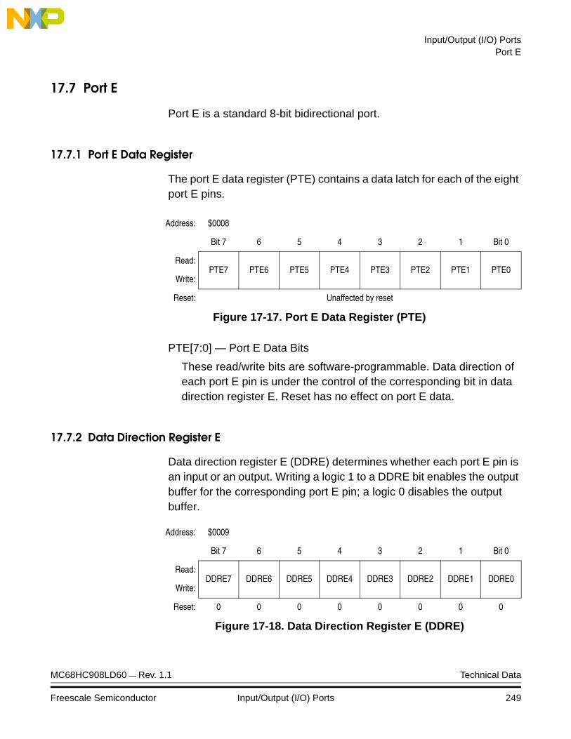
Input/Output (I/O) PortsPort E
17.7 Port E
Port E is a standard 8-bit bidirectional port.
17.7.1 Port E Data Register
The port E data register (PTE) contains a data latch for each of the eight port E pins.
PTE[7:0] — Port E Data Bits
These read/write bits are software-programmable. Data direction of each port E pin is under the control of the corresponding bit in data direction register E. Reset has no effect on port E data.
17.7.2 Data Direction Register E
Data direction register E (DDRE) determines whether each port E pin is an input or an output. Writing a logic 1 to a DDRE bit enables the output buffer for the corresponding port E pin; a logic 0 disables the output buffer.
Address: $0008
Bit 7 6 5 4 3 2 1 Bit 0
Read:PTE7 PTE6 PTE5 PTE4 PTE3 PTE2 PTE1 PTE0
Write:
Reset: Unaffected by reset
Figure 17-17. Port E Data Register (PTE)
Address: $0009
Bit 7 6 5 4 3 2 1 Bit 0
Read:DDRE7 DDRE6 DDRE5 DDRE4 DDRE3 DDRE2 DDRE1 DDRE0
Write:
Reset: 0 0 0 0 0 0 0 0
Figure 17-18. Data Direction Register E (DDRE)
MC68HC908LD60 — Rev. 1.1 Technical Data
Freescale Semiconductor Input/Output (I/O) Ports 249
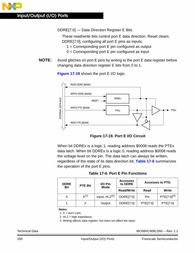
Input/Output (I/O) Ports
DDRE[7:0] — Data Direction Register E Bits
These read/write bits control port E data direction. Reset clears DDRE[7:0], configuring all port E pins as inputs.
1 = Corresponding port E pin configured as output0 = Corresponding port E pin configured as input
NOTE: Avoid glitches on port E pins by writing to the port E data register before changing data direction register E bits from 0 to 1.
Figure 17-19 shows the port E I/O logic.
Figure 17-19. Port E I/O Circuit
When bit DDREx is a logic 1, reading address $0008 reads the PTEx data latch. When bit DDREx is a logic 0, reading address $0008 reads the voltage level on the pin. The data latch can always be written, regardless of the state of its data direction bit. Table 17-6 summarizes the operation of the port E pins.
Table 17-6. Port E Pin Functions
DDREBit PTE Bit I/O Pin
Mode
Accesses to DDRE Accesses to PTD
Read/Write Read Write
0 X(1)
Notes:1. X = don’t care.
Input, Hi-Z(2)
2. Hi-Z = high impedance.
DDRE[7:0] Pin PTE[7:0](3)
3. Writing affects data register, but does not affect the input.
1 X Output DDRE[7:0] PTE[7:0] PTE[7:0]
READ DDRE ($0009)
WRITE DDRE ($0009)
RESET
WRITE PTE ($0008)
READ PTE ($0008)
PTEx
DDREx
PTEx
INTE
RNAL
DAT
A BU
S
Technical Data MC68HC908LD60 — Rev. 1.1
250 Input/Output (I/O) Ports Freescale Semiconductor

Technical Data — MC68HC908LD60
Section 18. External Interrupt (IRQ)
18.1 Contents
18.2 Introduction . . . . . . . . . . . . . . . . . . . . . . . . . . . . . . . . . . . . . . .251
18.3 Features . . . . . . . . . . . . . . . . . . . . . . . . . . . . . . . . . . . . . . . . .251
18.4 Functional Description . . . . . . . . . . . . . . . . . . . . . . . . . . . . . .25218.4.1 IRQ Pin. . . . . . . . . . . . . . . . . . . . . . . . . . . . . . . . . . . . . . . .254
18.5 IRQ Status and Control Register (INTSCR) . . . . . . . . . . . . . .255
18.6 IRQ Module During Break Interrupts . . . . . . . . . . . . . . . . . . .256
18.2 Introduction
The IRQ (external interrupt) module provides a maskable interrupt input.
18.3 Features
Features of the IRQ module include the following:
• A dedicated external interrupt pin, IRQ
• IRQ interrupt control bits
• Hysteresis buffer
• Programmable edge-only or edge and level interrupt sensitivity
• Automatic interrupt acknowledge
• Internal pullup resistor
MC68HC908LD60 — Rev. 1.1 Technical Data
Freescale Semiconductor External Interrupt (IRQ) 251
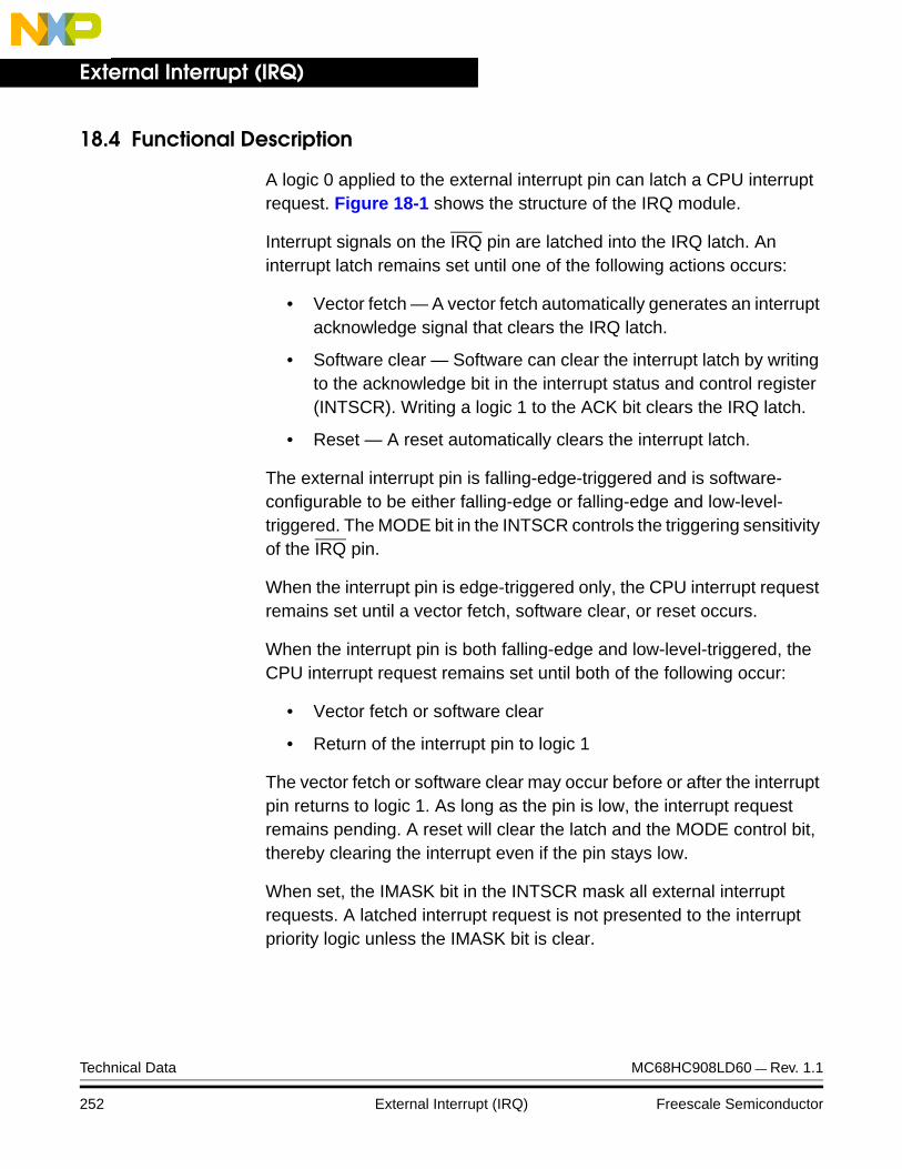
External Interrupt (IRQ)
18.4 Functional Description
A logic 0 applied to the external interrupt pin can latch a CPU interrupt request. Figure 18-1 shows the structure of the IRQ module.
Interrupt signals on the IRQ pin are latched into the IRQ latch. An interrupt latch remains set until one of the following actions occurs:
• Vector fetch — A vector fetch automatically generates an interrupt acknowledge signal that clears the IRQ latch.
• Software clear — Software can clear the interrupt latch by writing to the acknowledge bit in the interrupt status and control register (INTSCR). Writing a logic 1 to the ACK bit clears the IRQ latch.
• Reset — A reset automatically clears the interrupt latch.
The external interrupt pin is falling-edge-triggered and is software-configurable to be either falling-edge or falling-edge and low-level-triggered. The MODE bit in the INTSCR controls the triggering sensitivity of the IRQ pin.
When the interrupt pin is edge-triggered only, the CPU interrupt request remains set until a vector fetch, software clear, or reset occurs.
When the interrupt pin is both falling-edge and low-level-triggered, the CPU interrupt request remains set until both of the following occur:
• Vector fetch or software clear
• Return of the interrupt pin to logic 1
The vector fetch or software clear may occur before or after the interrupt pin returns to logic 1. As long as the pin is low, the interrupt request remains pending. A reset will clear the latch and the MODE control bit, thereby clearing the interrupt even if the pin stays low.
When set, the IMASK bit in the INTSCR mask all external interrupt requests. A latched interrupt request is not presented to the interrupt priority logic unless the IMASK bit is clear.
Technical Data MC68HC908LD60 — Rev. 1.1
252 External Interrupt (IRQ) Freescale Semiconductor
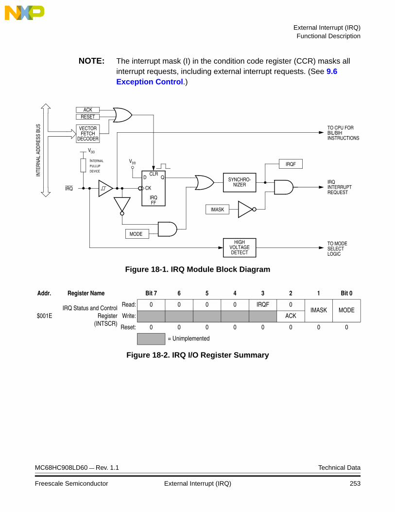
External Interrupt (IRQ)Functional Description
NOTE: The interrupt mask (I) in the condition code register (CCR) masks all interrupt requests, including external interrupt requests. (See 9.6 Exception Control.)
Figure 18-1. IRQ Module Block Diagram
Addr. Register Name Bit 7 6 5 4 3 2 1 Bit 0
$001EIRQ Status and Control
Register(INTSCR)
Read: 0 0 0 0 IRQF 0IMASK MODE
Write: ACK
Reset: 0 0 0 0 0 0 0 0
= Unimplemented
Figure 18-2. IRQ I/O Register Summary
ACK
IMASK
D Q
CK
CLR
IRQ
HIGH
INTERRUPT
TO MODESELECTLOGIC
IRQFF
REQUEST
VDD
MODE
VOLTAGEDETECT
SYNCHRO-NIZER
IRQF
TO CPU FORBIL/BIHINSTRUCTIONS
VECTORFETCH
DECODER
INTE
RNAL
ADD
RESS
BUS
RESET
VDD
INTERNAL
PULLUP
DEVICE
IRQ
MC68HC908LD60 — Rev. 1.1 Technical Data
Freescale Semiconductor External Interrupt (IRQ) 253

External Interrupt (IRQ)
18.4.1 IRQ Pin
A logic 0 on the IRQ pin can latch an interrupt request into the IRQ latch. A vector fetch, software clear, or reset clears the IRQ latch.
If the MODE bit is set, the IRQ pin is both falling-edge-sensitive and low-level-sensitive. With MODE set, both of the following actions must occur to clear IRQ:
• Vector fetch or software clear — A vector fetch generates an interrupt acknowledge signal to clear the latch. Software may generate the interrupt acknowledge signal by writing a logic 1 to the ACK bit in the interrupt status and control register (INTSCR). The ACK bit is useful in applications that poll the IRQ pin and require software to clear the IRQ latch. Writing to the ACK bit prior to leaving an interrupt service routine can also prevent spurious interrupts due to noise. Setting ACK does not affect subsequent transitions on the IRQ pin. A falling edge that occurs after writing to the ACK bit latches another interrupt request. If the IRQ mask bit, IMASK, is clear, the CPU loads the program counter with the vector address at locations $FFFA and $FFFB.
• Return of the IRQ pin to logic 1 — As long as the IRQ pin is at logic 0, IRQ remains active.
The vector fetch or software clear and the return of the IRQ pin to logic 1 may occur in any order. The interrupt request remains pending as long as the IRQ pin is at logic 0. A reset will clear the latch and the MODE control bit, thereby clearing the interrupt even if the pin stays low.
If the MODE bit is clear, the IRQ pin is falling-edge-sensitive only. With MODE clear, a vector fetch or software clear immediately clears the IRQ latch.
The IRQF bit in the INTSCR register can be used to check for pending interrupts. The IRQF bit is not affected by the IMASK bit, which makes it useful in applications where polling is preferred.
Use the BIH or BIL instruction to read the logic level on the IRQ pin.
NOTE: When using the level-sensitive interrupt trigger, avoid false interrupts by masking interrupt requests in the interrupt routine.
Technical Data MC68HC908LD60 — Rev. 1.1
254 External Interrupt (IRQ) Freescale Semiconductor

External Interrupt (IRQ)IRQ Status and Control Register (INTSCR)
18.5 IRQ Status and Control Register (INTSCR)
The IRQ status and control register (INTSCR) controls and monitors operation of the IRQ module. The INTSCR has the following functions:
• Shows the state of the IRQ flag
• Clears the IRQ latch
• Masks IRQ interrupt request
• Controls triggering sensitivity of the IRQ interrupt pin
IRQF — IRQ Flag
This read-only status bit is high when the IRQ interrupt is pending.1 = IRQ interrupt pending0 = IRQ interrupt not pending
ACK — IRQ Interrupt Request Acknowledge Bit
Writing a logic 1 to this write-only bit clears the IRQ latch. ACK always reads as logic 0. Reset clears ACK.
IMASK — IRQ Interrupt Mask Bit
Writing a logic 1 to this read/write bit disables IRQ interrupt requests. Reset clears IMASK.
1 = IRQ interrupt requests disabled0 = IRQ interrupt requests enabled
MODE — IRQ Edge/Level Select Bit
This read/write bit controls the triggering sensitivity of the IRQ pin. Reset clears MODE.
1 = IRQ interrupt requests on falling edges and low levels0 = IRQ interrupt requests on falling edges only
Address: $001E
Bit 7 6 5 4 3 2 1 Bit 0
Read: 0 0 0 0 IRQF 0IMASK MODE
Write: ACK
Reset: 0 0 0 0 0 0 0 0
= Unimplemented
Figure 18-3. IRQ Status and Control Register (INTSCR)
MC68HC908LD60 — Rev. 1.1 Technical Data
Freescale Semiconductor External Interrupt (IRQ) 255

External Interrupt (IRQ)
18.6 IRQ Module During Break Interrupts
The system integration module (SIM) controls whether the IRQ latch can be cleared during the break state. The BCFE bit in the break flag control register (BFCR) enables software to clear the latches during the break state. (See Section 9. System Integration Module (SIM).)
To allow software to clear the IRQ latch during a break interrupt, write a logic 1 to the BCFE bit. If a latch is cleared during the break state, it remains cleared when the MCU exits the break state.
To protect the latches during the break state, write a logic 0 to the BCFE bit. With BCFE at logic 0 (its default state), writing to the ACK bit in the IRQ status and control register during the break state has no effect on the IRQ latch.
Technical Data MC68HC908LD60 — Rev. 1.1
256 External Interrupt (IRQ) Freescale Semiconductor

Technical Data — MC68HC908LD60
Section 19. Keyboard Interrupt Module (KBI)
19.1 Contents
19.2 Introduction . . . . . . . . . . . . . . . . . . . . . . . . . . . . . . . . . . . . . . .257
19.3 Features . . . . . . . . . . . . . . . . . . . . . . . . . . . . . . . . . . . . . . . . .258
19.4 I/O Pins . . . . . . . . . . . . . . . . . . . . . . . . . . . . . . . . . . . . . . . . . .258
19.5 Functional Description . . . . . . . . . . . . . . . . . . . . . . . . . . . . . .259
19.6 Keyboard Initialization. . . . . . . . . . . . . . . . . . . . . . . . . . . . . . .261
19.7 I/O Registers. . . . . . . . . . . . . . . . . . . . . . . . . . . . . . . . . . . . . .26119.7.1 Keyboard Status and Control Register. . . . . . . . . . . . . . . .26219.7.2 Keyboard Interrupt Enable Register . . . . . . . . . . . . . . . . . .263
19.8 Low-Power Modes . . . . . . . . . . . . . . . . . . . . . . . . . . . . . . . . .26319.8.1 Wait Mode . . . . . . . . . . . . . . . . . . . . . . . . . . . . . . . . . . . . .26319.8.2 Stop Mode . . . . . . . . . . . . . . . . . . . . . . . . . . . . . . . . . . . . .263
19.9 Keyboard Module During Break Interrupts . . . . . . . . . . . . . . .264
19.2 Introduction
The keyboard interrupt module (KBI) provides eight independently maskable external interrupts which are accessible via PTA0–PTA7. When a port pin is enabled for keyboard interrupt function, an internal pullup device is also enabled on the pin.
MC68HC908LD60 — Rev. 1.1 Technical Data
Freescale Semiconductor Keyboard Interrupt Module (KBI) 257

Keyboard Interrupt Module (KBI)
19.3 Features
Features of the keyboard interrupt module (KBI) include:
• Eight keyboard interrupt pins with pullup devices
• Separate keyboard interrupt enable bits and one keyboard interrupt mask
• Programmable edge-only or edge- and level- interrupt sensitivity
• Exit from low-lower modes
19.4 I/O Pins
The eight keyboard interrupt pins are shared with standard port I/O pins. The full name of the KBI pins are listed in Table 19-1. The generic pin name appear in the text that follows.
Addr. Register Name Bit 7 6 5 4 3 2 1 Bit 0
$004EKeyboard Status and
Control Register(KBSCR)
Read: 0 0 0 0 KEYF 0IMASKK MODEK
Write: ACKK
Reset: 0 0 0 0 0 0 0 0
$004FKeyboard Interrupt Enable
Register(KBIER)
Read:KBIE7 KBIE6 KBIE5 KBIE4 KBIE3 KBIE2 KBIE1 KBIE0
Write:
Reset: 0 0 0 0 0 0 0 0
= Unimplemented
Figure 19-1. KBI I/O Register Summary
Table 19-1. Pin Name Conventions
KBIGeneric Pin Name
Full MCU Pin NamePin Selected for KBI Function by
KBIEx Bit in KBIER
KBI0–KBI7 PTA0/KBI0–PTA7/KBI7 KBIE0–KBIE7
Technical Data MC68HC908LD60 — Rev. 1.1
258 Keyboard Interrupt Module (KBI) Freescale Semiconductor
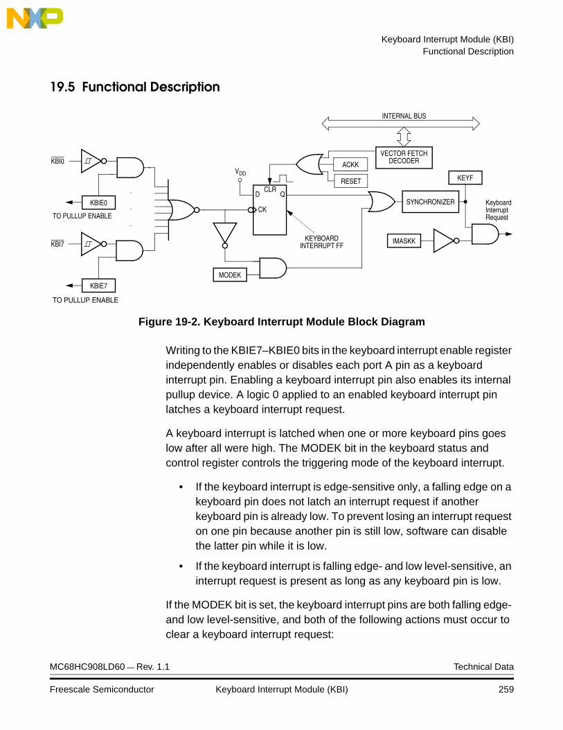
Keyboard Interrupt Module (KBI)Functional Description
19.5 Functional Description
Figure 19-2. Keyboard Interrupt Module Block Diagram
Writing to the KBIE7–KBIE0 bits in the keyboard interrupt enable register independently enables or disables each port A pin as a keyboard interrupt pin. Enabling a keyboard interrupt pin also enables its internal pullup device. A logic 0 applied to an enabled keyboard interrupt pin latches a keyboard interrupt request.
A keyboard interrupt is latched when one or more keyboard pins goes low after all were high. The MODEK bit in the keyboard status and control register controls the triggering mode of the keyboard interrupt.
• If the keyboard interrupt is edge-sensitive only, a falling edge on a keyboard pin does not latch an interrupt request if another keyboard pin is already low. To prevent losing an interrupt request on one pin because another pin is still low, software can disable the latter pin while it is low.
• If the keyboard interrupt is falling edge- and low level-sensitive, an interrupt request is present as long as any keyboard pin is low.
If the MODEK bit is set, the keyboard interrupt pins are both falling edge- and low level-sensitive, and both of the following actions must occur to clear a keyboard interrupt request:
KBIE0
KBIE7
.
.
.
D Q
CK
CLR
VDD
MODEK
IMASKKKEYBOARDINTERRUPT FF
VECTOR FETCHDECODERACKK
INTERNAL BUS
RESET
KBI7
KBI0
SYNCHRONIZER
KEYF
KeyboardInterruptRequest
TO PULLUP ENABLE
TO PULLUP ENABLE
MC68HC908LD60 — Rev. 1.1 Technical Data
Freescale Semiconductor Keyboard Interrupt Module (KBI) 259

Keyboard Interrupt Module (KBI)
• Vector fetch or software clear — A vector fetch generates an interrupt acknowledge signal to clear the interrupt request. Software may generate the interrupt acknowledge signal by writing a logic 1 to the ACKK bit in the keyboard status and control register (KBSCR). The ACKK bit is useful in applications that poll the keyboard interrupt pins and require software to clear the keyboard interrupt request. Writing to the ACKK bit prior to leaving an interrupt service routine also can prevent spurious interrupts due to noise. Setting ACKK does not affect subsequent transitions on the keyboard interrupt pins. A falling edge that occurs after writing to the ACKK bit latches another interrupt request. If the keyboard interrupt mask bit, IMASKK, is clear, the CPU loads the program counter with the vector address at locations $FFE2 and $FFE3.
• Return of all enabled keyboard interrupt pins to logic 1 — As long as any enabled keyboard interrupt pin is at logic 0, the keyboard interrupt remains set.
The vector fetch or software clear and the return of all enabled keyboard interrupt pins to logic 1 may occur in any order.
If the MODEK bit is clear, the keyboard interrupt pin is falling-edge-sensitive only. With MODEK clear, a vector fetch or software clear immediately clears the keyboard interrupt request.
Reset clears the keyboard interrupt request and the MODEK bit, clearing the interrupt request even if a keyboard interrupt pin stays at logic 0.
The keyboard flag bit (KEYF) in the keyboard status and control register can be used to see if a pending interrupt exists. The KEYF bit is not affected by the keyboard interrupt mask bit (IMASKK) which makes it useful in applications where polling is preferred.
To determine the logic level on a keyboard interrupt pin, use the data direction register to configure the pin as an input and read the data register.
NOTE: Setting a keyboard interrupt enable bit (KBIEx) forces the corresponding keyboard interrupt pin to be an input, overriding the data direction register. However, the data direction register bit must be a logic 0 for software to read the pin.
Technical Data MC68HC908LD60 — Rev. 1.1
260 Keyboard Interrupt Module (KBI) Freescale Semiconductor
Keyboard Interrupt Module (KBI)Keyboard Initialization
19.6 Keyboard Initialization
When a keyboard interrupt pin is enabled, it takes time for the pullup device to reach a logic 1. Therefore, a false interrupt can occur as soon as the pin is enabled.
To prevent a false interrupt on keyboard initialization:
1. Mask keyboard interrupts by setting the IMASKK bit in the keyboard status and control register.
2. Enable the KBI pins by setting the appropriate KBIEx bits in the keyboard interrupt enable register.
3. Write to the ACKK bit in the keyboard status and control register to clear any false interrupts.
4. Clear the IMASKK bit.
An interrupt signal on an edge-triggered pin can be acknowledged immediately after enabling the pin. An interrupt signal on an edge- and level-triggered interrupt pin must be acknowledged after a delay that depends on the external load.
Another way to avoid a false interrupt:
1. Configure the keyboard pins as outputs by setting the appropriate DDRA bits in data direction register A.
2. Write logic 1s to the appropriate port A data register bits.
3. Enable the KBI pins by setting the appropriate KBIEx bits in the keyboard interrupt enable register.
19.7 I/O Registers
These registers control and monitor operation of the keyboard module:
• Keyboard status and control register (KBSCR)
• Keyboard interrupt enable register (KBIER)
MC68HC908LD60 — Rev. 1.1 Technical Data
Freescale Semiconductor Keyboard Interrupt Module (KBI) 261
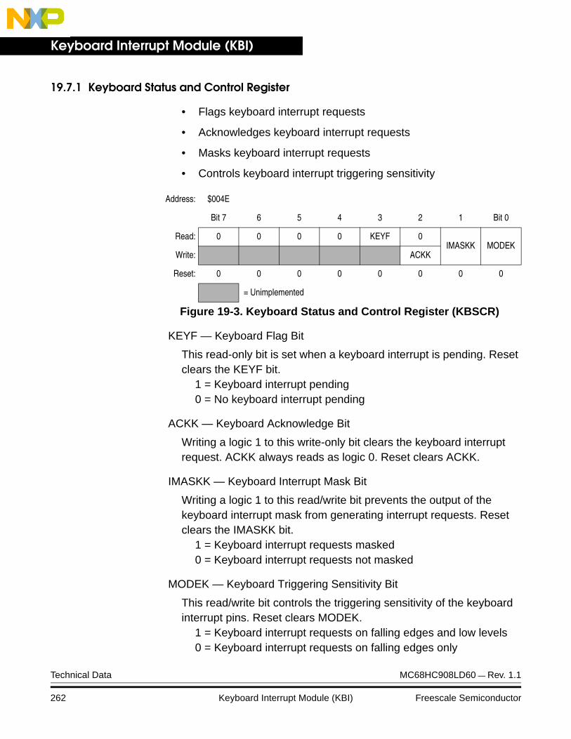
Keyboard Interrupt Module (KBI)
19.7.1 Keyboard Status and Control Register
• Flags keyboard interrupt requests
• Acknowledges keyboard interrupt requests
• Masks keyboard interrupt requests
• Controls keyboard interrupt triggering sensitivity
KEYF — Keyboard Flag Bit
This read-only bit is set when a keyboard interrupt is pending. Reset clears the KEYF bit.
1 = Keyboard interrupt pending0 = No keyboard interrupt pending
ACKK — Keyboard Acknowledge Bit
Writing a logic 1 to this write-only bit clears the keyboard interrupt request. ACKK always reads as logic 0. Reset clears ACKK.
IMASKK — Keyboard Interrupt Mask Bit
Writing a logic 1 to this read/write bit prevents the output of the keyboard interrupt mask from generating interrupt requests. Reset clears the IMASKK bit.
1 = Keyboard interrupt requests masked0 = Keyboard interrupt requests not masked
MODEK — Keyboard Triggering Sensitivity Bit
This read/write bit controls the triggering sensitivity of the keyboard interrupt pins. Reset clears MODEK.
1 = Keyboard interrupt requests on falling edges and low levels0 = Keyboard interrupt requests on falling edges only
Address: $004E
Bit 7 6 5 4 3 2 1 Bit 0
Read: 0 0 0 0 KEYF 0IMASKK MODEK
Write: ACKK
Reset: 0 0 0 0 0 0 0 0
= Unimplemented
Figure 19-3. Keyboard Status and Control Register (KBSCR)
Technical Data MC68HC908LD60 — Rev. 1.1
262 Keyboard Interrupt Module (KBI) Freescale Semiconductor
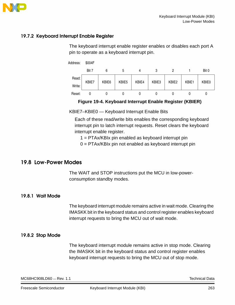
Keyboard Interrupt Module (KBI)Low-Power Modes
19.7.2 Keyboard Interrupt Enable Register
The keyboard interrupt enable register enables or disables each port A pin to operate as a keyboard interrupt pin.
KBIE7–KBIE0 — Keyboard Interrupt Enable Bits
Each of these read/write bits enables the corresponding keyboard interrupt pin to latch interrupt requests. Reset clears the keyboard interrupt enable register.
1 = PTAx/KBIx pin enabled as keyboard interrupt pin0 = PTAx/KBIx pin not enabled as keyboard interrupt pin
19.8 Low-Power Modes
The WAIT and STOP instructions put the MCU in low-power-consumption standby modes.
19.8.1 Wait Mode
The keyboard interrupt module remains active in wait mode. Clearing the IMASKK bit in the keyboard status and control register enables keyboard interrupt requests to bring the MCU out of wait mode.
19.8.2 Stop Mode
The keyboard interrupt module remains active in stop mode. Clearing the IMASKK bit in the keyboard status and control register enables keyboard interrupt requests to bring the MCU out of stop mode.
Address: $004F
Bit 7 6 5 4 3 2 1 Bit 0
Read:KBIE7 KBIE6 KBIE5 KBIE4 KBIE3 KBIE2 KBIE1 KBIE0
Write:
Reset: 0 0 0 0 0 0 0 0
Figure 19-4. Keyboard Interrupt Enable Register (KBIER)
MC68HC908LD60 — Rev. 1.1 Technical Data
Freescale Semiconductor Keyboard Interrupt Module (KBI) 263
Keyboard Interrupt Module (KBI)
19.9 Keyboard Module During Break Interrupts
The system integration module (SIM) controls whether the keyboard interrupt latch can be cleared during the break state. The BCFE bit in the break flag control register (BFCR) enables software to clear status bits during the break state.
To allow software to clear the keyboard interrupt latch during a break interrupt, write a logic 1 to the BCFE bit. If a latch is cleared during the break state, it remains cleared when the MCU exits the break state.
To protect the latch during the break state, write a logic 0 to the BCFE bit. With BCFE at logic 0 (its default state), writing to the keyboard acknowledge bit (ACKK) in the keyboard status and control register during the break state has no effect. (See 19.7.1 Keyboard Status and Control Register.)
Technical Data MC68HC908LD60 — Rev. 1.1
264 Keyboard Interrupt Module (KBI) Freescale Semiconductor

Technical Data — MC68HC908LD60
Section 20. Computer Operating Properly (COP)
20.1 Contents
20.2 Introduction . . . . . . . . . . . . . . . . . . . . . . . . . . . . . . . . . . . . . . .265
20.3 Functional Description . . . . . . . . . . . . . . . . . . . . . . . . . . . . . .266
20.4 I/O Signals . . . . . . . . . . . . . . . . . . . . . . . . . . . . . . . . . . . . . . .26720.4.1 OSCXCLK . . . . . . . . . . . . . . . . . . . . . . . . . . . . . . . . . . . . .26720.4.2 STOP Instruction . . . . . . . . . . . . . . . . . . . . . . . . . . . . . . . .26720.4.3 COPCTL Write . . . . . . . . . . . . . . . . . . . . . . . . . . . . . . . . . .26720.4.4 Power-On Reset. . . . . . . . . . . . . . . . . . . . . . . . . . . . . . . . .26720.4.5 Internal Reset . . . . . . . . . . . . . . . . . . . . . . . . . . . . . . . . . . .26820.4.6 Reset Vector Fetch. . . . . . . . . . . . . . . . . . . . . . . . . . . . . . .26820.4.7 COPD (COP Disable). . . . . . . . . . . . . . . . . . . . . . . . . . . . .26820.4.8 COPRS (COP Rate Select) . . . . . . . . . . . . . . . . . . . . . . . .268
20.5 COP Control Register . . . . . . . . . . . . . . . . . . . . . . . . . . . . . . .269
20.6 Interrupts. . . . . . . . . . . . . . . . . . . . . . . . . . . . . . . . . . . . . . . . .269
20.7 Monitor Mode . . . . . . . . . . . . . . . . . . . . . . . . . . . . . . . . . . . . .269
20.8 Low-Power Modes . . . . . . . . . . . . . . . . . . . . . . . . . . . . . . . . .26920.8.1 Wait Mode . . . . . . . . . . . . . . . . . . . . . . . . . . . . . . . . . . . . .27020.8.2 Stop Mode . . . . . . . . . . . . . . . . . . . . . . . . . . . . . . . . . . . . .270
20.9 COP Module During Break Mode . . . . . . . . . . . . . . . . . . . . . .270
20.2 Introduction
The computer operating properly (COP) module contains a free-running counter that generates a reset if allowed to overflow. The COP module helps software recover from runaway code. Prevent a COP reset by clearing the COP counter periodically. The COP module can be disabled through the COPD bit in the CONFIG register.
MC68HC908LD60 — Rev. 1.1 Technical Data
Freescale Semiconductor Computer Operating Properly (COP) 265
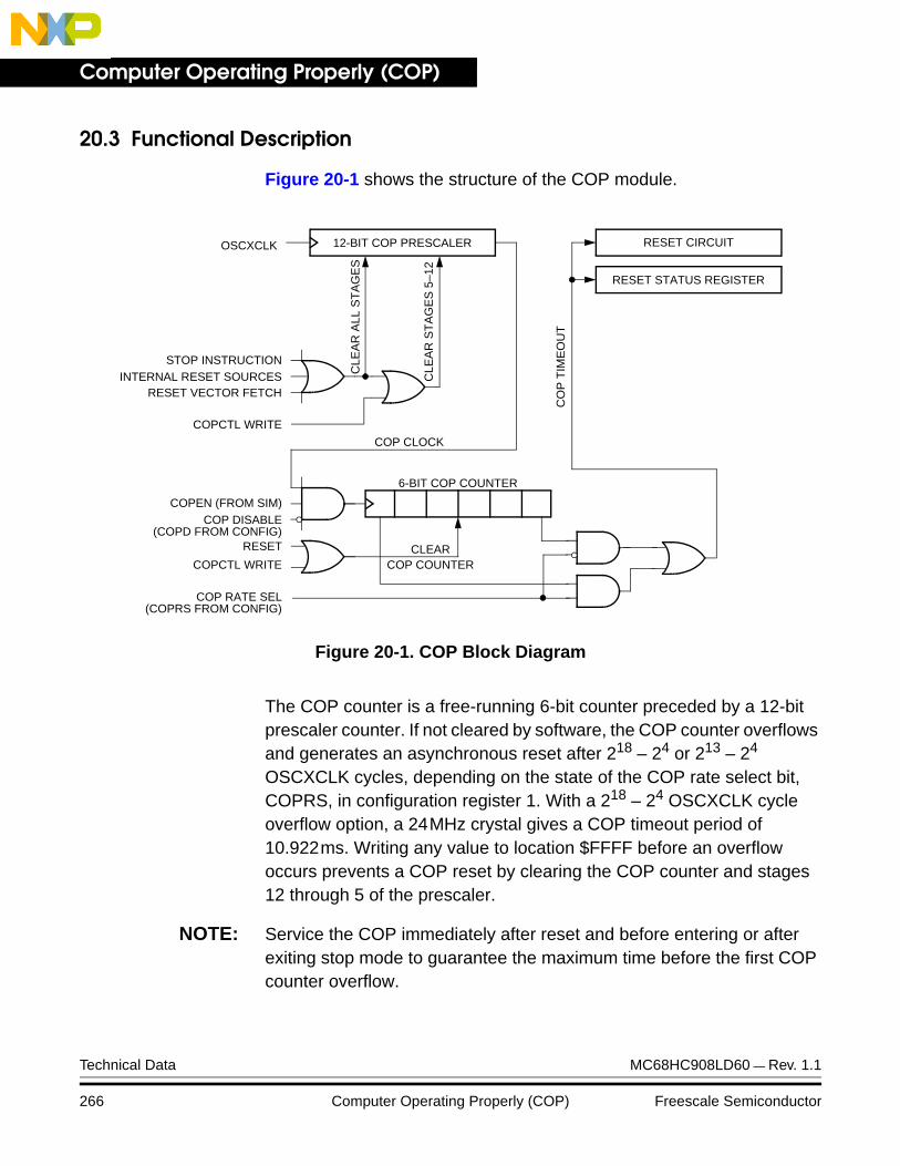
Computer Operating Properly (COP)
20.3 Functional Description
Figure 20-1 shows the structure of the COP module.
Figure 20-1. COP Block Diagram
The COP counter is a free-running 6-bit counter preceded by a 12-bit prescaler counter. If not cleared by software, the COP counter overflows and generates an asynchronous reset after 218 – 24 or 213 – 24
OSCXCLK cycles, depending on the state of the COP rate select bit, COPRS, in configuration register 1. With a 218 – 24 OSCXCLK cycle overflow option, a 24MHz crystal gives a COP timeout period of 10.922ms. Writing any value to location $FFFF before an overflow occurs prevents a COP reset by clearing the COP counter and stages 12 through 5 of the prescaler.
NOTE: Service the COP immediately after reset and before entering or after exiting stop mode to guarantee the maximum time before the first COP counter overflow.
COPCTL WRITE
OSCXCLK
RESET VECTOR FETCH
RESET CIRCUIT
RESET STATUS REGISTER
INTERNAL RESET SOURCES
12-BIT COP PRESCALER
CLE
AR
ALL
ST
AG
ES
6-BIT COP COUNTER
COP DISABLE
RESET
COPCTL WRITECLEAR
COPEN (FROM SIM)
COP COUNTER
COP CLOCK
CO
P T
IME
OU
T
STOP INSTRUCTION
(COPD FROM CONFIG)
COP RATE SEL (COPRS FROM CONFIG)
CLE
AR
ST
AG
ES
5–1
2
Technical Data MC68HC908LD60 — Rev. 1.1
266 Computer Operating Properly (COP) Freescale Semiconductor
Computer Operating Properly (COP)I/O Signals
A COP reset pulls the RST pin low for 32 OSCXCLK cycles and sets the COP bit in the SIM reset status register (SRSR).
In monitor mode, the COP is disabled if the RST pin or the IRQ is held at VTST. During the break state, VTST on the RST pin disables the COP.
NOTE: Place COP clearing instructions in the main program and not in an interrupt subroutine. Such an interrupt subroutine could keep the COP from generating a reset even while the main program is not working properly.
20.4 I/O Signals
The following paragraphs describe the signals shown in Figure 20-1.
20.4.1 OSCXCLK
OSCXCLK is the crystal oscillator output signal. OSCXCLK frequency is equal to the crystal frequency.
20.4.2 STOP Instruction
The STOP instruction clears the COP prescaler.
20.4.3 COPCTL Write
Writing any value to the COP control register (COPCTL) (see 20.5 COP Control Register) clears the COP counter and clears bits 12 through 5 of the prescaler. Reading the COP control register returns the low byte of the reset vector.
20.4.4 Power-On Reset
The power-on reset (POR) circuit clears the COP prescaler 4096 OSCXCLK cycles after power-up.
MC68HC908LD60 — Rev. 1.1 Technical Data
Freescale Semiconductor Computer Operating Properly (COP) 267

Computer Operating Properly (COP)
20.4.5 Internal Reset
An internal reset clears the COP prescaler and the COP counter.
20.4.6 Reset Vector Fetch
A reset vector fetch occurs when the vector address appears on the data bus. A reset vector fetch clears the COP prescaler.
20.4.7 COPD (COP Disable)
The COPD signal reflects the state of the COP disable bit (COPD) in the CONFIG register. (See Figure 20-2.)
20.4.8 COPRS (COP Rate Select)
The COPRS signal reflects the state of the COP rate select bit (COPRS) in the CONFIG register. (See Figure 20-2.)
COPRS — COP Rate Select Bit
COPRS selects the COP timeout period. Reset clears COPRS.
1 = COP timeout period is 213 – 24 OSCXCLK cycles0 = COP timeout period is 218 – 24 OSCXCLK cycles
COPD — COP Disable Bit
COPD disables the COP module.1 = COP module disabled0 = COP module enabled
Address: $001F
Bit 7 6 5 4 3 2 1 Bit 0
Read: 0 0 0 0SSREC COPRS STOP COPD
Write:
Reset: 0 0 0 0 0 0 0 0
= Unimplemented
Figure 20-2. Configuration Register (CONFIG)
Technical Data MC68HC908LD60 — Rev. 1.1
268 Computer Operating Properly (COP) Freescale Semiconductor
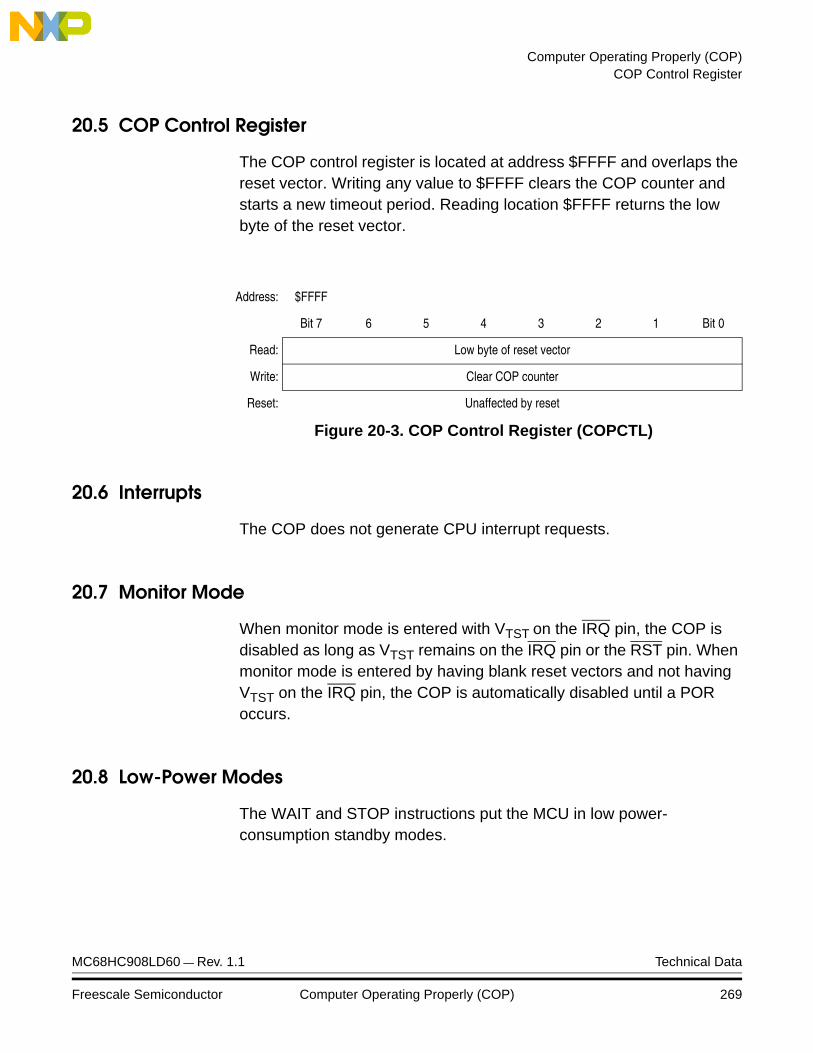
Computer Operating Properly (COP)COP Control Register
20.5 COP Control Register
The COP control register is located at address $FFFF and overlaps the reset vector. Writing any value to $FFFF clears the COP counter and starts a new timeout period. Reading location $FFFF returns the low byte of the reset vector.
20.6 Interrupts
The COP does not generate CPU interrupt requests.
20.7 Monitor Mode
When monitor mode is entered with VTST on the IRQ pin, the COP is disabled as long as VTST remains on the IRQ pin or the RST pin. When monitor mode is entered by having blank reset vectors and not having VTST on the IRQ pin, the COP is automatically disabled until a POR occurs.
20.8 Low-Power Modes
The WAIT and STOP instructions put the MCU in low power-consumption standby modes.
Address: $FFFF
Bit 7 6 5 4 3 2 1 Bit 0
Read: Low byte of reset vector
Write: Clear COP counter
Reset: Unaffected by reset
Figure 20-3. COP Control Register (COPCTL)
MC68HC908LD60 — Rev. 1.1 Technical Data
Freescale Semiconductor Computer Operating Properly (COP) 269
Computer Operating Properly (COP)
20.8.1 Wait Mode
The COP remains active during wait mode. To prevent a COP reset during wait mode, periodically clear the COP counter in a CPU interrupt routine.
20.8.2 Stop Mode
Stop mode turns off the OSCXCLK input to the COP and clears the COP prescaler. Service the COP immediately before entering or after exiting stop mode to ensure a full COP timeout period after entering or exiting stop mode.
To prevent inadvertently turning off the COP with a STOP instruction, a configuration option is available that disables the STOP instruction. When the STOP bit in the configuration register has the STOP instruction is disabled, execution of a STOP instruction results in an illegal opcode reset.
20.9 COP Module During Break Mode
The COP is disabled during a break interrupt when VTST is present on the RST pin.
Technical Data MC68HC908LD60 — Rev. 1.1
270 Computer Operating Properly (COP) Freescale Semiconductor
Technical Data — MC68HC908LD60
Section 21. Break Module (BRK)
21.1 Contents
21.2 Introduction . . . . . . . . . . . . . . . . . . . . . . . . . . . . . . . . . . . . . . .271
21.3 Features . . . . . . . . . . . . . . . . . . . . . . . . . . . . . . . . . . . . . . . . .272
21.4 Functional Description . . . . . . . . . . . . . . . . . . . . . . . . . . . . . .27221.4.1 Flag Protection During Break Interrupts . . . . . . . . . . . . . . .27421.4.2 CPU During Break Interrupts . . . . . . . . . . . . . . . . . . . . . . .27421.4.3 TIM During Break Interrupts . . . . . . . . . . . . . . . . . . . . . . . .27421.4.4 COP During Break Interrupts . . . . . . . . . . . . . . . . . . . . . . .274
21.5 Low-Power Modes . . . . . . . . . . . . . . . . . . . . . . . . . . . . . . . . .27421.5.1 Wait Mode . . . . . . . . . . . . . . . . . . . . . . . . . . . . . . . . . . . . .27421.5.2 Stop Mode . . . . . . . . . . . . . . . . . . . . . . . . . . . . . . . . . . . . .275
21.6 Break Module Registers . . . . . . . . . . . . . . . . . . . . . . . . . . . . .27521.6.1 Break Status and Control Register. . . . . . . . . . . . . . . . . . .27521.6.2 Break Address Registers . . . . . . . . . . . . . . . . . . . . . . . . . .27621.6.3 SIM Break Status Register . . . . . . . . . . . . . . . . . . . . . . . . .27621.6.4 SIM Break Flag Control Register . . . . . . . . . . . . . . . . . . . .278
21.2 Introduction
This section describes the break module. The break module can generate a break interrupt that stops normal program flow at a defined address to enter a background program.
MC68HC908LD60 — Rev. 1.1 Technical Data
Freescale Semiconductor Break Module (BRK) 271
Break Module (BRK)
21.3 Features
Features of the break module include:
• Accessible input/output (I/O) registers during the break interrupt
• CPU-generated break interrupts
• Software-generated break interrupts
• COP disabling during break interrupts
21.4 Functional Description
When the internal address bus matches the value written in the break address registers, the break module issues a breakpoint signal to the CPU. The CPU then loads the instruction register with a software interrupt instruction (SWI) after completion of the current CPU instruction. The program counter vectors to $FFFC and $FFFD ($FEFC and $FEFD in monitor mode).
The following events can cause a break interrupt to occur:
• A CPU-generated address (the address in the program counter) matches the contents of the break address registers.
• Software writes a logic 1 to the BRKA bit in the break status and control register.
When a CPU-generated address matches the contents of the break address registers, the break interrupt begins after the CPU completes its current instruction. A return-from-interrupt instruction (RTI) in the break routine ends the break interrupt and returns the MCU to normal operation. Figure 21-1 shows the structure of the break module.
Technical Data MC68HC908LD60 — Rev. 1.1
272 Break Module (BRK) Freescale Semiconductor

Break Module (BRK)Functional Description
Figure 21-1. Break Module Block Diagram
IAB15–IAB8
IAB7–IAB0
8-BIT COMPARATOR
8-BIT COMPARATOR
CONTROL
BREAK ADDRESS REGISTER LOW
BREAK ADDRESS REGISTER HIGH
IAB15–IAB0BREAK
Addr. Register Name Bit 7 6 5 4 3 2 1 Bit 0
$FE00SIM Break Status Register
(SBSR)
Read:R R R R R R
SBSWR
Write: Note
Reset: 0
$FE03SIM Break Flag Control
Register (SBFCR)
Read:BCFE R R R R R R R
Write:
Reset: 0
$FE0CBreak Address Register
High (BRKH)
Read:Bit 15 14 13 12 11 10 9 Bit 8
Write:
Reset: 0 0 0 0 0 0 0 0
$FE0DBreak Address Register
Low (BRKL)
Read:Bit 7 6 5 4 3 2 1 Bit 0
Write:
Reset: 0 0 0 0 0 0 0 0
$FE0EBreak Status and Control
Register (BRKSCR)
Read:BRKE BRKA
0 0 0 0 0 0
Write:
Reset: 0 0 0 0 0 0 0 0
Note: Writing a logic 0 clears SBSW. = Unimplemented R = Reserved
Figure 21-2. Break Module I/O Register Summary
MC68HC908LD60 — Rev. 1.1 Technical Data
Freescale Semiconductor Break Module (BRK) 273
Break Module (BRK)
21.4.1 Flag Protection During Break Interrupts
The BCFE bit in the SIM break flag control register (SBFCR) enables software to clear status bits during the break state.
21.4.2 CPU During Break Interrupts
The CPU starts a break interrupt by:
• Loading the instruction register with the SWI instruction
• Loading the program counter with $FFFC and $FFFD($FEFC and $FEFD in monitor mode)
The break interrupt begins after completion of the CPU instruction in progress. If the break address register match occurs on the last cycle of a CPU instruction, the break interrupt begins immediately.
21.4.3 TIM During Break Interrupts
A break interrupt stops the timer counters.
21.4.4 COP During Break Interrupts
The COP is disabled during a break interrupt when VTST is present on the RST pin.
21.5 Low-Power Modes
The WAIT and STOP instructions put the MCU in low power-consumption standby modes.
21.5.1 Wait Mode
If enabled, the break module is active in wait mode. In the break routine, the user can subtract one from the return address on the stack if SBSW is set (see Section 9. System Integration Module (SIM)). Clear the SBSW bit by writing logic 0 to it.
Technical Data MC68HC908LD60 — Rev. 1.1
274 Break Module (BRK) Freescale Semiconductor
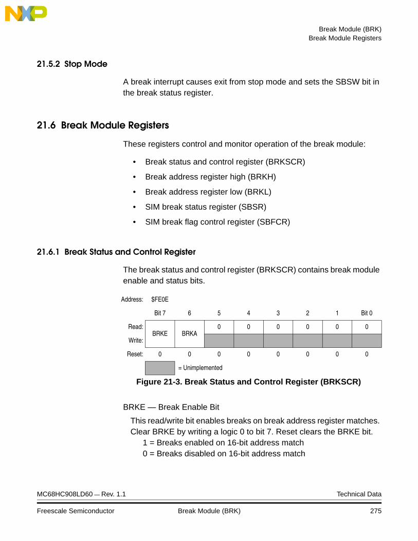
Break Module (BRK)Break Module Registers
21.5.2 Stop Mode
A break interrupt causes exit from stop mode and sets the SBSW bit in the break status register.
21.6 Break Module Registers
These registers control and monitor operation of the break module:
• Break status and control register (BRKSCR)
• Break address register high (BRKH)
• Break address register low (BRKL)
• SIM break status register (SBSR)
• SIM break flag control register (SBFCR)
21.6.1 Break Status and Control Register
The break status and control register (BRKSCR) contains break module enable and status bits.
BRKE — Break Enable Bit
This read/write bit enables breaks on break address register matches. Clear BRKE by writing a logic 0 to bit 7. Reset clears the BRKE bit.
1 = Breaks enabled on 16-bit address match0 = Breaks disabled on 16-bit address match
Address: $FE0E
Bit 7 6 5 4 3 2 1 Bit 0
Read:BRKE BRKA
0 0 0 0 0 0
Write:
Reset: 0 0 0 0 0 0 0 0
= Unimplemented
Figure 21-3. Break Status and Control Register (BRKSCR)
MC68HC908LD60 — Rev. 1.1 Technical Data
Freescale Semiconductor Break Module (BRK) 275
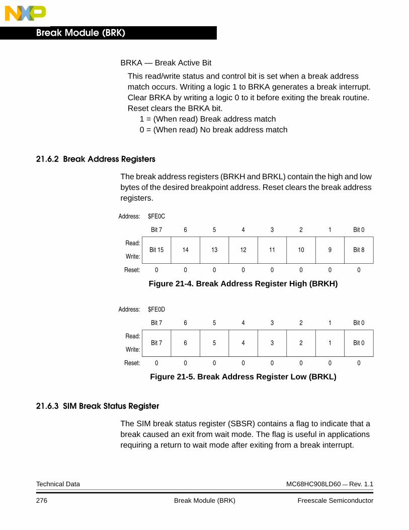
Break Module (BRK)
BRKA — Break Active Bit
This read/write status and control bit is set when a break address match occurs. Writing a logic 1 to BRKA generates a break interrupt. Clear BRKA by writing a logic 0 to it before exiting the break routine. Reset clears the BRKA bit.
1 = (When read) Break address match0 = (When read) No break address match
21.6.2 Break Address Registers
The break address registers (BRKH and BRKL) contain the high and low bytes of the desired breakpoint address. Reset clears the break address registers.
21.6.3 SIM Break Status Register
The SIM break status register (SBSR) contains a flag to indicate that a break caused an exit from wait mode. The flag is useful in applications requiring a return to wait mode after exiting from a break interrupt.
Address: $FE0C
Bit 7 6 5 4 3 2 1 Bit 0
Read:Bit 15 14 13 12 11 10 9 Bit 8
Write:
Reset: 0 0 0 0 0 0 0 0
Figure 21-4. Break Address Register High (BRKH)
Address: $FE0D
Bit 7 6 5 4 3 2 1 Bit 0
Read:Bit 7 6 5 4 3 2 1 Bit 0
Write:
Reset: 0 0 0 0 0 0 0 0
Figure 21-5. Break Address Register Low (BRKL)
Technical Data MC68HC908LD60 — Rev. 1.1
276 Break Module (BRK) Freescale Semiconductor
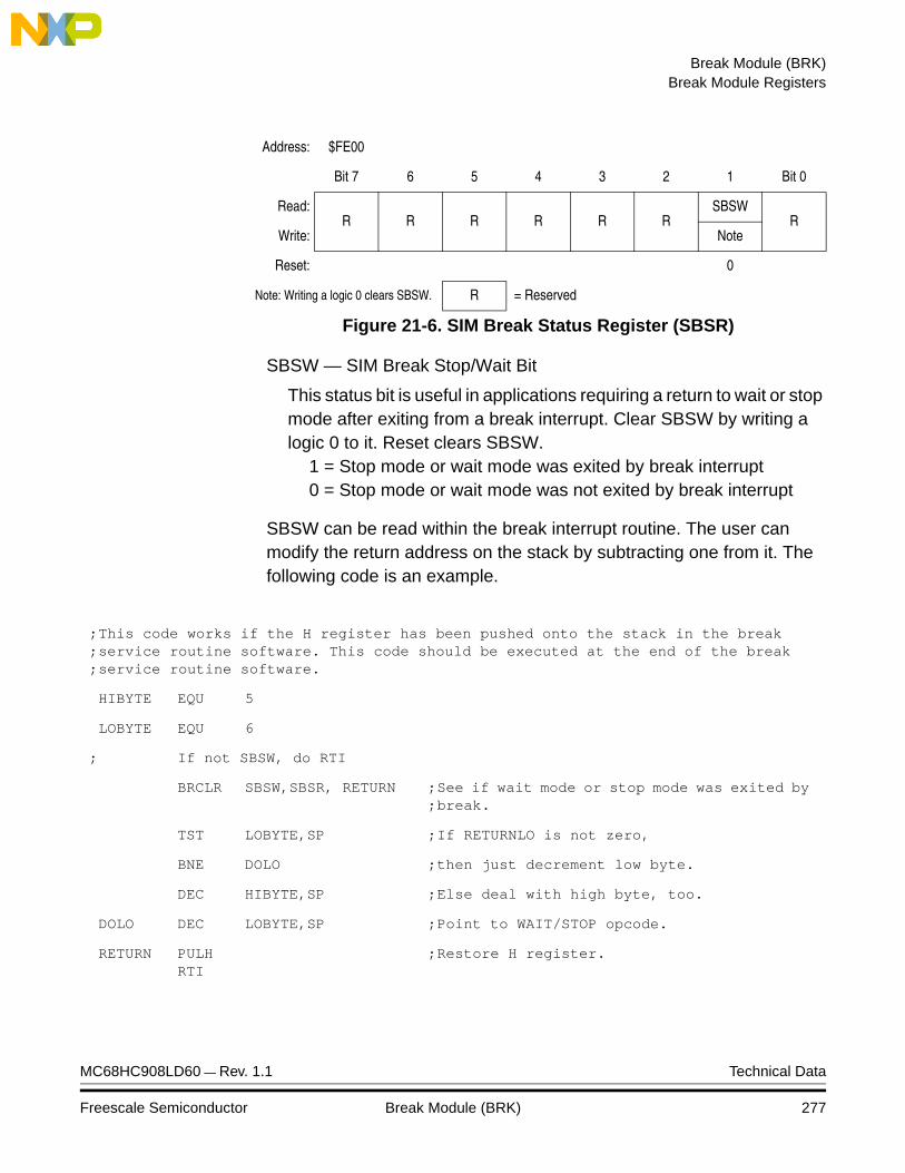
Break Module (BRK)Break Module Registers
SBSW — SIM Break Stop/Wait Bit
This status bit is useful in applications requiring a return to wait or stop mode after exiting from a break interrupt. Clear SBSW by writing a logic 0 to it. Reset clears SBSW.
1 = Stop mode or wait mode was exited by break interrupt0 = Stop mode or wait mode was not exited by break interrupt
SBSW can be read within the break interrupt routine. The user can modify the return address on the stack by subtracting one from it. The following code is an example.
Address: $FE00
Bit 7 6 5 4 3 2 1 Bit 0
Read:R R R R R R
SBSWR
Write: Note
Reset: 0
Note: Writing a logic 0 clears SBSW. R = Reserved
Figure 21-6. SIM Break Status Register (SBSR)
;;;
This code works if the H register has been pushed onto the stack in the break service routine software. This code should be executed at the end of the break service routine software.
HIBYTE EQU 5
LOBYTE EQU 6
; If not SBSW, do RTI
BRCLR SBSW,SBSR, RETURN ;;See if wait mode or stop mode was exited by break.
TST LOBYTE,SP ;If RETURNLO is not zero,
BNE DOLO ;then just decrement low byte.
DEC HIBYTE,SP ;Else deal with high byte, too.
DOLO DEC LOBYTE,SP ;Point to WAIT/STOP opcode.
RETURN PULHRTI
;Restore H register.
MC68HC908LD60 — Rev. 1.1 Technical Data
Freescale Semiconductor Break Module (BRK) 277

Break Module (BRK)
21.6.4 SIM Break Flag Control Register
The SIM break flag control register (SBFCR) contains a bit that enables software to clear status bits while the MCU is in a break state.
BCFE — Break Clear Flag Enable Bit
This read/write bit enables software to clear status bits by accessing status registers while the MCU is in a break state. To clear status bits during the break state, the BCFE bit must be set.
1 = Status bits clearable during break0 = Status bits not clearable during break
Address: $FE03
Bit 7 6 5 4 3 2 1 Bit 0
Read:BCFE R R R R R R R
Write:
Reset: 0
R = Reserved
Figure 21-7. SIM Break Flag Control Register (SBFCR)
Technical Data MC68HC908LD60 — Rev. 1.1
278 Break Module (BRK) Freescale Semiconductor
Technical Data — MC68HC908LD60
Section 22. Electrical Specifications
22.1 Contents
22.2 Introduction . . . . . . . . . . . . . . . . . . . . . . . . . . . . . . . . . . . . . . .280
22.3 Absolute Maximum Ratings . . . . . . . . . . . . . . . . . . . . . . . . . .280
22.4 Functional Operating Range. . . . . . . . . . . . . . . . . . . . . . . . . .281
22.5 Thermal Characteristics . . . . . . . . . . . . . . . . . . . . . . . . . . . . .281
22.6 DC Electrical Characteristics . . . . . . . . . . . . . . . . . . . . . . . . .282
22.7 Control Timing . . . . . . . . . . . . . . . . . . . . . . . . . . . . . . . . . . . .283
22.8 TImer Interface Module Characteristics . . . . . . . . . . . . . . . . .283
22.9 Oscillator Characteristics . . . . . . . . . . . . . . . . . . . . . . . . . . . .283
22.10 ADC Electrical Characteristics . . . . . . . . . . . . . . . . . . . . . . . .284
22.11 Sync Processor Timing. . . . . . . . . . . . . . . . . . . . . . . . . . . . . .284
22.12 DDC12AB/MMIIC Timing . . . . . . . . . . . . . . . . . . . . . . . . . . . .28522.12.1 DDC12AB/MMIIC Interface Input Signal Timing . . . . . . . .28522.12.2 DDC12AB/MMIIC Interface Output Signal Timing . . . . . . .285
22.13 FLASH Memory Characteristics . . . . . . . . . . . . . . . . . . . . . . .286
MC68HC908LD60 — Rev. 1.1 Technical Data
Freescale Semiconductor Electrical Specifications 279
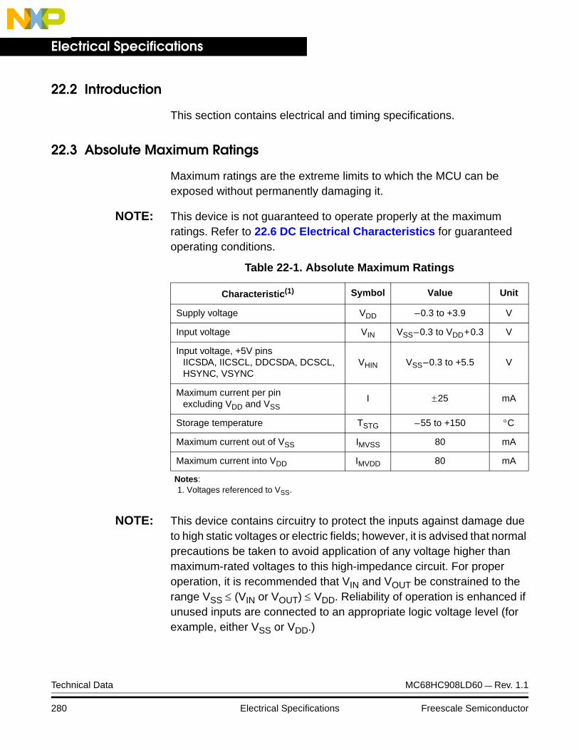
Electrical Specifications
22.2 Introduction
This section contains electrical and timing specifications.
22.3 Absolute Maximum Ratings
Maximum ratings are the extreme limits to which the MCU can be exposed without permanently damaging it.
NOTE: This device is not guaranteed to operate properly at the maximum ratings. Refer to 22.6 DC Electrical Characteristics for guaranteed operating conditions.
NOTE: This device contains circuitry to protect the inputs against damage due to high static voltages or electric fields; however, it is advised that normal precautions be taken to avoid application of any voltage higher than maximum-rated voltages to this high-impedance circuit. For proper operation, it is recommended that VIN and VOUT be constrained to the range VSS ≤ (VIN or VOUT) ≤ VDD. Reliability of operation is enhanced if unused inputs are connected to an appropriate logic voltage level (for example, either VSS or VDD.)
Table 22-1. Absolute Maximum Ratings
Characteristic(1)
Notes:1. Voltages referenced to VSS.
Symbol Value Unit
Supply voltage VDD –0.3 to +3.9 V
Input voltage VIN VSS–0.3 to VDD+0.3 V
Input voltage, +5V pinsIICSDA, IICSCL, DDCSDA, DCSCL, HSYNC, VSYNC
VHIN VSS–0.3 to +5.5 V
Maximum current per pinexcluding VDD and VSS
I ±25 mA
Storage temperature TSTG –55 to +150 °C
Maximum current out of VSS IMVSS 80 mA
Maximum current into VDD IMVDD 80 mA
Technical Data MC68HC908LD60 — Rev. 1.1
280 Electrical Specifications Freescale Semiconductor

Electrical SpecificationsFunctional Operating Range
22.4 Functional Operating Range
22.5 Thermal Characteristics
Table 22-2. Operating Range
Characteristic Symbol Value Unit
Operating temperature range TA 0 to +85 °C
Operating voltage range VDD 3.0 to 3.6 V
Table 22-3. Thermal Characteristics
Characteristic Symbol Value Unit
Thermal resistanceQFP (64 pins)
θJA 70°C/W
I/O pin power dissipation PI/O User determined W
Power dissipation(1)
Notes:1. Power dissipation is a function of temperature.
PDPD = (IDD x VDD) + PI/O =
K/(TJ + 273 °C)W
Constant(2)
2. K is a constant unique to the device. K can be determined for a known TA and measuredPD. With this value of K, PD and TJ can be determined for any value of TA.
KPD × (TA + 273 °C)
+ PD2
× θJAW/°C
Average junction temperature TJ TA + (PD × θJA) °C
Maximum junction temperature TJM 100 °C
MC68HC908LD60 — Rev. 1.1 Technical Data
Freescale Semiconductor Electrical Specifications 281
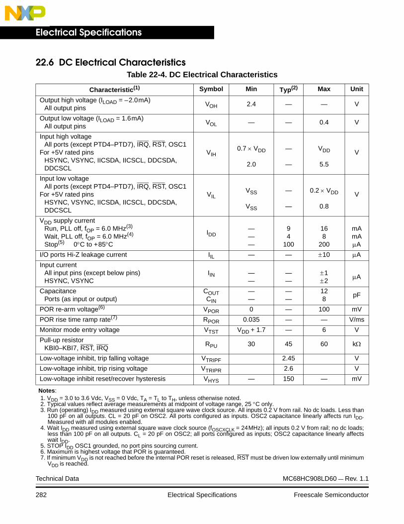
Electrical Specifications
22.6 DC Electrical CharacteristicsTable 22-4. DC Electrical Characteristics
Characteristic(1)
Notes:1. VDD = 3.0 to 3.6 Vdc, VSS = 0 Vdc, TA = TL to TH, unless otherwise noted.
Symbol Min Typ(2)
2. Typical values reflect average measurements at midpoint of voltage range, 25 °C only.
Max Unit
Output high voltage (ILOAD = –2.0mA)All output pins
VOH 2.4 — — V
Output low voltage (ILOAD = 1.6mA)All output pins
VOL — — 0.4 V
Input high voltageAll ports (except PTD4–PTD7), IRQ, RST, OSC1
For +5V rated pinsHSYNC, VSYNC, IICSDA, IICSCL, DDCSDA, DDCSCL
VIH0.7 × VDD
2.0
—
—
VDD
5.5
V
Input low voltageAll ports (except PTD4–PTD7), IRQ, RST, OSC1
For +5V rated pinsHSYNC, VSYNC, IICSDA, IICSCL, DDCSDA, DDCSCL
VILVSS
VSS
—
—
0.2 × VDD
0.8
V
VDD supply current Run, PLL off, fOP = 6.0 MHz(3)
Wait, PLL off, fOP = 6.0 MHz(4)
Stop(5) 0°C to +85°C
3. Run (operating) IDD measured using external square wave clock source. All inputs 0.2 V from rail. No dc loads. Less than100 pF on all outputs. CL = 20 pF on OSC2. All ports configured as inputs. OSC2 capacitance linearly affects run IDD.Measured with all modules enabled.
4. Wait IDD measured using external square wave clock source (fOSCXCLK = 24MHz); all inputs 0.2 V from rail; no dc loads;less than 100 pF on all outputs. CL = 20 pF on OSC2; all ports configured as inputs; OSC2 capacitance linearly affectswait IDD.
5. STOP IDD OSC1 grounded, no port pins sourcing current.
IDD———
94
100
168
200
mAmAµA
I/O ports Hi-Z leakage current IIL — — ±10 µA
Input currentAll input pins (except below pins)HSYNC, VSYNC
IIN ——
——
±1±2
µA
CapacitancePorts (as input or output)
COUTCIN
——
——
128
pF
POR re-arm voltage(6)
6. Maximum is highest voltage that POR is guaranteed.
VPOR 0 — 100 mV
POR rise time ramp rate(7)
7. If minimum VDD is not reached before the internal POR reset is released, RST must be driven low externally until minimumVDD is reached.
RPOR 0.035 — — V/ms
Monitor mode entry voltage VTST VDD + 1.7 — 6 V
Pull-up resistorKBI0–KBI7, RST, IRQ
RPU 30 45 60 kΩ
Low-voltage inhibit, trip falling voltage VTRIPF 2.45 V
Low-voltage inhibit, trip rising voltage VTRIPR 2.6 V
Low-voltage inhibit reset/recover hysteresis VHYS — 150 — mV
Technical Data MC68HC908LD60 — Rev. 1.1
282 Electrical Specifications Freescale Semiconductor
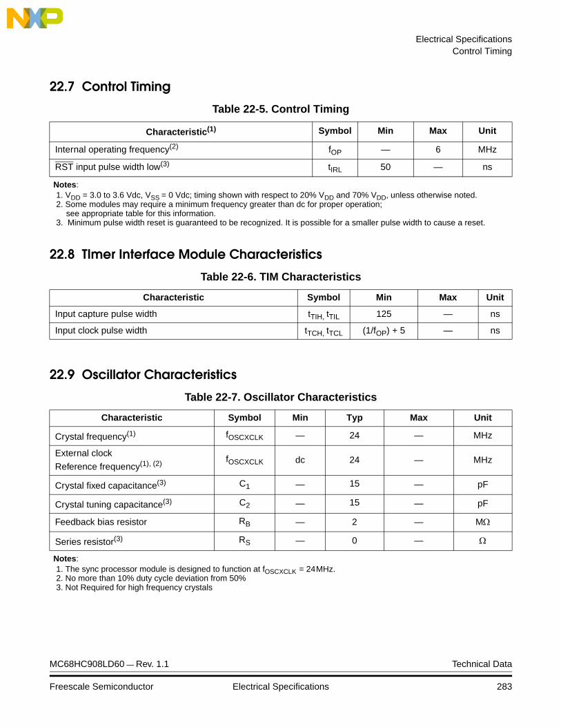
Electrical SpecificationsControl Timing
22.7 Control Timing
22.8 TImer Interface Module Characteristics
22.9 Oscillator Characteristics
Table 22-5. Control Timing
Characteristic(1)
Notes:1. VDD = 3.0 to 3.6 Vdc, VSS = 0 Vdc; timing shown with respect to 20% VDD and 70% VDD, unless otherwise noted.
Symbol Min Max Unit
Internal operating frequency(2)
2. Some modules may require a minimum frequency greater than dc for proper operation; see appropriate table for this information.
fOP — 6 MHz
RST input pulse width low(3)
3. Minimum pulse width reset is guaranteed to be recognized. It is possible for a smaller pulse width to cause a reset.
tIRL 50 — ns
Table 22-6. TIM Characteristics
Characteristic Symbol Min Max Unit
Input capture pulse width tTIH, tTIL 125 — ns
Input clock pulse width tTCH, tTCL (1/fOP) + 5 — ns
Table 22-7. Oscillator Characteristics
Characteristic Symbol Min Typ Max Unit
Crystal frequency(1)
Notes:1. The sync processor module is designed to function at fOSCXCLK = 24MHz.
fOSCXCLK — 24 — MHz
External clock
Reference frequency(1), (2)
2. No more than 10% duty cycle deviation from 50%
fOSCXCLK dc 24 — MHz
Crystal fixed capacitance(3) C1 — 15 — pF
Crystal tuning capacitance(3) C2 — 15 — pF
Feedback bias resistor RB — 2 — MΩ
Series resistor(3)
3. Not Required for high frequency crystals
RS — 0 — Ω
MC68HC908LD60 — Rev. 1.1 Technical Data
Freescale Semiconductor Electrical Specifications 283
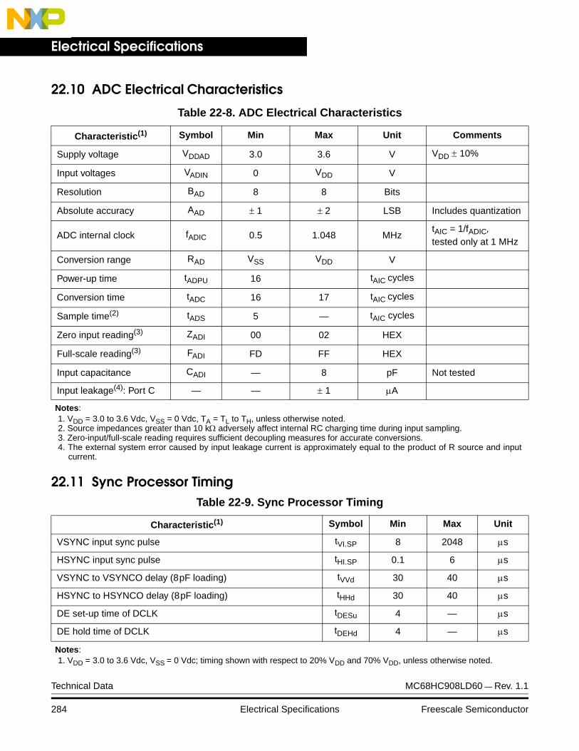
Electrical Specifications
22.10 ADC Electrical Characteristics
22.11 Sync Processor Timing
Table 22-8. ADC Electrical Characteristics
Characteristic(1)
Notes:1. VDD = 3.0 to 3.6 Vdc, VSS = 0 Vdc, TA = TL to TH, unless otherwise noted.
Symbol Min Max Unit Comments
Supply voltage VDDAD 3.0 3.6 V VDD ± 10%
Input voltages VADIN 0 VDD V
Resolution BAD 8 8 Bits
Absolute accuracy AAD ± 1 ± 2 LSB Includes quantization
ADC internal clock fADIC 0.5 1.048 MHztAIC = 1/fADIC, tested only at 1 MHz
Conversion range RAD VSS VDD V
Power-up time tADPU 16 tAIC cycles
Conversion time tADC 16 17 tAIC cycles
Sample time(2)
2. Source impedances greater than 10 kΩ adversely affect internal RC charging time during input sampling.
tADS 5 — tAIC cycles
Zero input reading(3)
3. Zero-input/full-scale reading requires sufficient decoupling measures for accurate conversions.
ZADI 00 02 HEX
Full-scale reading(3) FADI FD FF HEX
Input capacitance CADI — 8 pF Not tested
Input leakage(4): Port C
4. The external system error caused by input leakage current is approximately equal to the product of R source and inputcurrent.
— — ± 1 µA
Table 22-9. Sync Processor Timing
Characteristic(1)
Notes:1. VDD = 3.0 to 3.6 Vdc, VSS = 0 Vdc; timing shown with respect to 20% VDD and 70% VDD, unless otherwise noted.
Symbol Min Max Unit
VSYNC input sync pulse tVI.SP 8 2048 µs
HSYNC input sync pulse tHI.SP 0.1 6 µs
VSYNC to VSYNCO delay (8pF loading) tVVd 30 40 µs
HSYNC to HSYNCO delay (8pF loading) tHHd 30 40 µs
DE set-up time of DCLK tDESu 4 — µs
DE hold time of DCLK tDEHd 4 — µs
Technical Data MC68HC908LD60 — Rev. 1.1
284 Electrical Specifications Freescale Semiconductor

Electrical SpecificationsDDC12AB/MMIIC Timing
22.12 DDC12AB/MMIIC Timing
Figure 22-1. MMIIC Signal Timings
22.12.1 DDC12AB/MMIIC Interface Input Signal Timing
22.12.2 DDC12AB/MMIIC Interface Output Signal Timing
Table 22-10. DDC12AB/MMIIC Interface Input Signal Timing
Characteristic(1)
Notes:1. VDD = 3.0 to 3.6 Vdc, VSS = 0 Vdc; timing shown with respect to 20% VDD and 70% VDD, unless otherwise noted.
Symbol Min Max Unit
START condition hold time tHD.STA 2 — tCYC
Clock low period tLOW 4 — tCYC
Clock high period tHIGH 4 — tCYC
Data set-up time tSU.DAT 250 — ns
Data hold time tHD.DAT 0 — ns
START condition set-up time(for repeated START condition only)
tSU.STA 2 — tCYC
STOP condition set-up time tSU.STO 2 — tCYC
Table 22-11. DDC12AB/MMIIC Interface Output Signal Timing
Characteristic(1)
Notes:1. VDD = 3.0 to 3.6 Vdc, VSS = 0 Vdc; timing shown with respect to 20% VDD and 70% VDD, unless otherwise noted.
Symbol Min Max Unit
SDA/SCL rise time(2)
2. With 200pF loading on the SDA/SCL pins.
tR — 1 µs
SDA/SCL fall time tF — 300 ns
Data set-up time tSU.DAT tLOW — ns
Data hold time tHD.DAT 0 — ns
SDA
SCL
tHD.STA tLOW tHIGH tSU.DAT tHD.DAT tSU.STA tSU.STO
MC68HC908LD60 — Rev. 1.1 Technical Data
Freescale Semiconductor Electrical Specifications 285
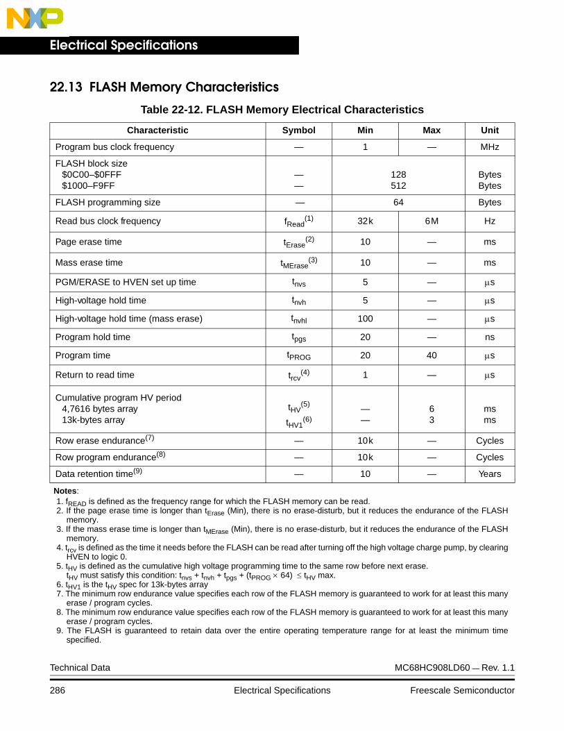
Electrical Specifications
22.13 FLASH Memory Characteristics
Table 22-12. FLASH Memory Electrical Characteristics
Characteristic Symbol Min Max Unit
Program bus clock frequency — 1 — MHz
FLASH block size$0C00–$0FFF$1000–F9FF
——
128512
BytesBytes
FLASH programming size — 64 Bytes
Read bus clock frequency fRead(1)
Notes:1. fREAD is defined as the frequency range for which the FLASH memory can be read.
32k 6M Hz
Page erase time tErase(2)
2. If the page erase time is longer than tErase (Min), there is no erase-disturb, but it reduces the endurance of the FLASHmemory.
10 — ms
Mass erase time tMErase(3)
3. If the mass erase time is longer than tMErase (Min), there is no erase-disturb, but it reduces the endurance of the FLASHmemory.
10 — ms
PGM/ERASE to HVEN set up time tnvs 5 — µs
High-voltage hold time tnvh 5 — µs
High-voltage hold time (mass erase) tnvhl 100 — µs
Program hold time tpgs 20 — ns
Program time tPROG 20 40 µs
Return to read time trcv(4)
4. trcv is defined as the time it needs before the FLASH can be read after turning off the high voltage charge pump, by clearingHVEN to logic 0.
1 — µs
Cumulative program HV period4,7616 bytes array13k-bytes array
tHV(5)
tHV1(6)
5. tHV is defined as the cumulative high voltage programming time to the same row before next erase.tHV must satisfy this condition: tnvs + tnvh + tpgs + (tPROG × 64) ≤ tHV max.
6. tHV1 is the tHV spec for 13k-bytes array
——
63
msms
Row erase endurance(7)
7. The minimum row endurance value specifies each row of the FLASH memory is guaranteed to work for at least this manyerase / program cycles.
— 10k — Cycles
Row program endurance(8)
8. The minimum row endurance value specifies each row of the FLASH memory is guaranteed to work for at least this manyerase / program cycles.
— 10k — Cycles
Data retention time(9)
9. The FLASH is guaranteed to retain data over the entire operating temperature range for at least the minimum timespecified.
— 10 — Years
Technical Data MC68HC908LD60 — Rev. 1.1
286 Electrical Specifications Freescale Semiconductor
Technical Data — MC68HC908LD60
Section 23. Mechanical Specifications
23.1 Contents
23.2 Introduction . . . . . . . . . . . . . . . . . . . . . . . . . . . . . . . . . . . . . . .287
23.3 64-Pin Plastic Quad Flat Pack (QFP) . . . . . . . . . . . . . . . . . . .288
23.2 Introduction
This section gives the dimensions for:
• 64-pin plastic quad flat pack (case 840B-01)
Figure 23-1 shows the latest package drawing at the time of this publication. To make sure that you have the latest package specifications, please visit the Freescale website at http://freescale.com. Follow the World Wide Web on-line instructions to retrieve the current mechanical specifications.
MC68HC908LD60 — Rev. 1.1 Technical Data
Freescale Semiconductor Mechanical Specifications 287
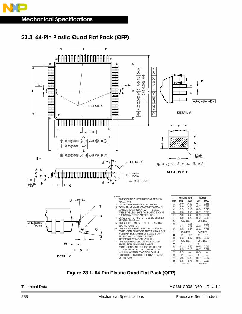
Mechanical Specifications
23.3 64-Pin Plastic Quad Flat Pack (QFP)
Figure 23-1. 64-Pin Plastic Quad Flat Pack (QFP)
L
L
–A– –B–
DETAIL A
–D–
B
A
S
V
DETAIL A
PB
B
D
–A–, –B–, –D–
C
–C–
E
HG
M
M DETAILC
SEATINGPLANE
DATUMPLANE
1 16
–H–
0.01 (0.004)
R
DETAIL C
DATUMPLANE
–H–
T
U
Q
K
W
X
SA–BM0.20 (0.008) D SH
SA–BM0.20 (0.008) D SC
0.05 (0.002) A–B
SA–
BM
0.20
(0.0
08)
DS
C
0.05
(0.0
02)
A–B
SA–
BM
0.20
(0.0
08)
DS
H
48 33
SA–BM0.02 (0.008) D SC
N
F
J
BASEMETAL
3249
1764
DIM MIN MAX MIN MAXINCHESMILLIMETERS
A 13.90 14.10 0.547 0.555B 13.90 14.10 0.547 0.555C 2.15 2.45 0.085 0.096D 0.30 0.45 0.012 0.018E 2.00 2.40 0.079 0.094F 0.30 0.40 0.012 0.016G 0.80 BSC 0.031 BSCH — 0.25 — 0.010J 0.13 0.23 0.005 0.009K 0.65 0.95 0.026 0.037L 12.00 REF 0.472 REFM 5° 10° 5° 10° N 0.13 0.17 0.005 0.007P 0.40 BSC 0.016 BSCQ 0° 7° 0° 7° R 0.13 0.30 0.005 0.012S 16.95 17.45 0.667 0.687T 0.13 — 0.005 —U 0° — 0° —V 16.95 17.45 0.667 0.687W 0.35 0.45 0.014 0.018X 1.6 REF 0.063 REF
NOTES:1. DIMENSIONING AND TOLERANCING PER ANSI
Y14.5M, 1982.2. CONTROLLING DIMENSION: MILLIMETER.3. DATUM PLANE –H– IS LOCATED AT BOTTOM OF
LEAD AND IS COINCIDENT WITH THE LEADWHERE THE LEAD EXITS THE PLASTIC BODY ATTHE BOTTOM OF THE PARTING LINE.
4. DATUMS –A–, –B– AND –D– TO BE DETERMINEDAT DATUM PLANE –H–.
5. DIMENSIONS S AND V TO BE DETERMINED ATSEATING PLANE –C–.
6. DIMENSIONS A AND B DO NOT INCLUDE MOLDPROTRUSION. ALLOWABLE PROTRUSION IS 0.25(0.010) PER SIDE. DIMENSIONS A AND B DOINCLUDE MOLD MISMATCH AND AREDETERMINED AT DATUM PLANE –H–.
7. DIMENSION D DOES NOT INCLUDE DAMBARPROTRUSION. ALLOWABLE DAMBARPROTRUSION SHALL BE 0.08 (0.003) PER SIDE.TOTAL IN EXCESS OF THE D DIMENSION ATMAXIMUM MATERIAL CONDITION. DAMBARCANNOT BE LOCATED ON THE LOWER RADIUSOR THE FOOT.
SECTION B–B
Technical Data MC68HC908LD60 — Rev. 1.1
288 Mechanical Specifications Freescale Semiconductor

Technical Data — MC68HC908LD60
Section 24. Ordering Information
24.1 Contents
24.2 Introduction . . . . . . . . . . . . . . . . . . . . . . . . . . . . . . . . . . . . . . .289
24.3 MC Order Numbers . . . . . . . . . . . . . . . . . . . . . . . . . . . . . . . .289
24.2 Introduction
This section contains ordering numbers for the MC68HC908LD60.
24.3 MC Order Numbers
Table 24-1. MC Order Numbers
MC Order Number(1)
Notes:1. I = Operating temperature range: 0 °C to +85 °C
FU = Quad Flat Pack
Package OperatingTemperature Range
MC68HC908LD60IFU 64-Pin QFP 0 °C to +85 °C
MC68HC908LD60 — Rev. 1.1 Technical Data
Freescale Semiconductor Ordering Information 289
Ordering Information
Technical Data MC68HC908LD60 — Rev. 1.1
290 Ordering Information Freescale Semiconductor

How to Reach Us:
Home Page:www.freescale.com
E-mail:[email protected]
USA/Europe or Locations Not Listed:Freescale SemiconductorTechnical Information Center, CH3701300 N. Alma School RoadChandler, Arizona 85224+1-800-521-6274 or [email protected]
Europe, Middle East, and Africa:Freescale Halbleiter Deutschland GmbHTechnical Information CenterSchatzbogen 781829 Muenchen, Germany+44 1296 380 456 (English)+46 8 52200080 (English)+49 89 92103 559 (German)+33 1 69 35 48 48 (French)[email protected]
Japan:Freescale Semiconductor Japan Ltd.HeadquartersARCO Tower 15F1-8-1, Shimo-Meguro, Meguro-ku,Tokyo 153-0064Japan0120 191014 or +81 3 5437 [email protected]
Asia/Pacific:Freescale Semiconductor Hong Kong Ltd.Technical Information Center2 Dai King StreetTai Po Industrial EstateTai Po, N.T., Hong Kong+800 2666 [email protected]
For Literature Requests Only:Freescale Semiconductor Literature Distribution CenterP.O. Box 5405Denver, Colorado 802171-800-441-2447 or 303-675-2140Fax: [email protected]
Information in this document is provided solely to enable system and software implementers to use Freescale Semiconductor products. There are no express or implied copyright licenses granted hereunder to design or fabricate any integrated circuits or integrated circuits based on the information in this document.
Freescale Semiconductor reserves the right to make changes without further notice to any products herein. Freescale Semiconductor makes no warranty, representation or guarantee regarding the suitability of its products for any particular purpose, nor does Freescale Semiconductor assume any liability arising out of the application or use of any product or circuit, and specifically disclaims any and all liability, including without limitation consequential or incidental damages. “Typical” parameters that may be provided in Freescale Semiconductor data sheets and/or specifications can and do vary in different applications and actual performance may vary over time. All operating parameters, including “Typicals”, must be validated for each customer application by customer’s technical experts. Freescale Semiconductor does not convey any license under its patent rights nor the rights of others. Freescale Semiconductor products are not designed, intended, or authorized for use as components in systems intended for surgical implant into the body, or other applications intended to support or sustain life, or for any other application in which the failure of the Freescale Semiconductor product could create a situation where personal injury or death may occur. Should Buyer purchase or use Freescale Semiconductor products for any such unintended or unauthorized application, Buyer shall indemnify and hold Freescale Semiconductor and its officers, employees, subsidiaries, affiliates, and distributors harmless against all claims, costs, damages, and expenses, and reasonable attorney fees arising out of, directly or indirectly, any claim of personal injury or death associated with such unintended or unauthorized use, even if such claim alleges that Freescale Semiconductor was negligent regarding the design or manufacture of the part.
Freescale™ and the Freescale logo are trademarks of Freescale Semiconductor, Inc.All other product or service names are the property of their respective owners. The ARM POWERED logo is a registered trademark of ARM Limited. ARM7TDMI-S is a trademark of ARM Limited. Java and all other Java-based marks are trademarks or registered trademarks of Sun Microsystems, Inc. in the U.S. and other countries. The Bluetooth trademarks are owned by their proprietor and used by Freescale Semiconductor, Inc. under license.
© Freescale Semiconductor, Inc. 2005. All rights reserved.
Rev. 1.1MC68HC908LD60/DAugust 16, 2005