pr533 - nxp
TRANSCRIPT

1. General description
The PR5331C3HN is a highly integrated transceiver module for contactless reader/writer communication at 13.56 MHz.
A dedicated ROM code is implemented to handle different RF protocols by an integrated microcontroller. The system host controller communicates with the PR5331C3HN by using the USB or the HSU link.
The protocol between the host controller and the PR5331C3HN, on top of this physical link is the CCID protocol.
1.1 RF protocols
PR5331C3HN supports the PCD mode for FeliCa (212 kbps and 424 kbps), ISO/IEC14443 Type A and B (from 106 kbps to 848 kbps), MIFARE (106 kbps), B' cards (106 kbps), picoPass tag (106 kbps) and Innovision Jewel cards (106 kbps)
The Initiator passive mode (from 106 kbps to 424 kbps) can be supported through the PC/SC transparent mode.
1.2 Interfaces
The PR5331C3HN supports a USB 2.0 full speed interface (bus powered or host powered mode).
Alternatively to the USB interface, a High Speed UART (from 9600b up to 1.2 Mb) can be used to connect the PR533 to a host.
The R5331C3HN has also a master I2C-bus interface that allows to connect one of the following peripherals:
• An external EEPROM: in this case the PR5331C3HN is configured as master and is able to communicate with external EEPROM (address A0h) which can store configuration data like PID, UID and RF parameters. When a USB host interface is used, these parameters are retrieved from the EEPROM at startup of the device
• A TDA8029 contact smart card reader
1.3 Standards compliancy
PR5331C3HN offers commands in order for applications to be compliant with “EMV Contactless Communication Protocol Specification V2.0.1”.
PR5331C3HN supports RF protocols ISO/IEC 14443A and B such as compliancy with Smart eID standard can be achieved at application level.
PR533USB NFC integrated reader solutionRev. 3.6 — 29 November 2017208936
Product data sheetCOMPANY PUBLIC
NXP Semiconductors PR533USB NFC integrated reader solution
Support of USB 2.0 full speed, interoperable with USB 3.0 hubs
The PR533C3HN in PCD mode is compliant with EMV contactless specification V2.0.1.
1.4 Supported operating systems
• Microsoft Windows 2000
• Microsoft Windows XP (32 and 64 bits)
• Microsoft Windows 2003 Server (32 and 64 bits)
• Microsoft Windows 2008 Server (32 and 64 bits)
• Microsoft Windows Vista (32 and 64 bits)
• Microsoft Windows 7 (32 and 64 bits)
The PR533 is supported by the following OS through the PCSC-Lite driver:
• GNU/Linux using libusb 1.0.x and later
• Mac OS Leopard (1.5.6 and newer)
• Mac OS Snow Leopard (1.6.X)
• Solaris
• FreeBSD
2. Features and benefits
USB 2.0 full speed host interface and CCID protocol support
Integrated microcontroller implements high-level RF protocols
Buffered output drivers to connect an antenna with minimum number of external components
Integrated RF level detector
Integrated data mode detector
Supports ISO/IEC 14443A Reader/Writer mode up to 848 kbit/s
Supports ISO/IEC 14443B Reader/Writer mode up to 848 kbit/s
Supports contactless communication according to the FeliCa protocol at 212 kbit/s and 424 kbit/s
Supports MIFARE encryption
Typical operating distance in Read/Write mode for communication to ISO/IEC 14443A/MIFARE, ISO/IEC 14443B or FeliCa cards up to 50 mm depending on antenna size and tuning
I2C-bus master interface allows to connect an external I2C EEPROM for configuration data storage or to control a TDA8029 contact smart card reader
Low-power modes
Hard power-down mode
Soft power-down mode
Only one external oscillator required (27.12 MHz Crystal oscillator)
Power modes
USB bus power mode
2.5 V to 3.6 V power supply operating range in non-USB bus power mode
PR533 All information provided in this document is subject to legal disclaimers. © NXP Semiconductors N.V. 2017. All rights reserved.
Product data sheetCOMPANY PUBLIC
Rev. 3.6 — 29 November 2017208936 2 of 216

NXP Semiconductors PR533USB NFC integrated reader solution
Dedicated I/O ports for external device control
3. Quick reference data
[1] VDDD, VDDA and VDD(TVDD) must always be at the same supply voltage.
4. Ordering information
Table 1. Quick reference data
Symbol Parameter Conditions Min Typ Max Unit
VBUS bus supply voltage 4.02 5 5.25 V
(non-USB mode); VBUS = VDDD; VSSD = 0 V
2.5 3.3 3.6 V
VDDA analog supply voltage VDDA = VDDD = VDD(TVDD) = VDD(PVDD); VSSA = VSSD = VSS(PVSS) = VSS(TVSS) = 0 V
[1] 2.5 3.3 3.6 V
VDDD digital supply voltage [1] 2.5 3.3 3.6 V
VDD(TVDD) TVDD supply voltage [1] 2.5 3.3 3.6 V
VDD(PVDD) PVDD supply voltage 1.6 - 3.6 V
VDD(SVDD) SVDD supply voltage VSSA = VSSD = VSS(PVSS) = VSS(TVSS) = 0 V; reserved for future use
VDDD 0.1 - VDDD V
IBUS bus supply current maximum load current (USB mode); measured on VBUS
150 mA
maximum inrush current limitation; at power-up (curlimoff = 0)
100 mA
Ipd power-down current VDDA = VDDD = VDD(TVDD) = VDD(PVDD) = 3 V; not powered from USB
hard power-down; RF level detector off
10 A
soft power-down; RF level detector on
30 A
ICCSL suspended low-power device supply current
RF level detector on, (without resistor on DP/DM)
- - 250 A
IDDD digital supply current RF level detector on, VDD(SVDD) switch off
[1] - 15 - mA
IDD(SVDD) SVDD supply current VDDS = 3 V - - 30 mA
IDDA analog supply current RF level detector on - 6 - mA
IDD(TVDD) TVDD supply current during RF transmission; VDD(TVDD) = 3 V
- 60 100 mA
Ptot total power dissipation Tamb = 30 to +85 C - - 0.55 W
Tamb ambient temperature 30 - +85 C
Table 2. Ordering information
Type number Package
Name Description Version
PR5331C3HN/C360[1][2][3] HVQFN40 plastic thermal enhanced very thin quad flat package; no leads; 40 terminals; body 6 6 0.85 mm
SOT618-1
PR5331C3HN/C370[1][2][3]
PR533 All information provided in this document is subject to legal disclaimers. © NXP Semiconductors N.V. 2017. All rights reserved.
Product data sheetCOMPANY PUBLIC
Rev. 3.6 — 29 November 2017208936 3 of 216

NXP Semiconductors PR533USB NFC integrated reader solution
[1] 60 or 70 refers to the ROM code version described in the User Manual. For differences of romcode versions refer to the release note of the product.
[2] Refer to Section 17.4 “Licenses”.
[3] MSL 2 (Moisture Sensitivity Level).
5. Block diagram
The following block diagram describes hardware blocks controlled by PR5331C3HN firmware or which can be accessible for data transaction by a host baseband.
Fig 1. Block diagram
aaa-000043
SUPPLYSUPERVISOR
27 MHz OSCAND
FRAC NPLL
SVDDSWITCH
NFCANALOG
FRONT ENDAND
CLUART
80C51 CPU
44 k ROM1.2 k BYTES RAM
USBDEVICE
I2CMASTER
MATX
RSTPD_N
PVDD
SVDD
VBUS
P30 P31 P32_INT0
GPIOs
P33_INT0 P35
RSTOUT_N DVDD P70_IRQ AVSS
DVSS
OSCIN
OSCOUT
I0
I1
SDA
P50_SCL
DELATT
48 MHz
SIGIN
SIGOUT
P34
TVDD
AVDD
RX
VMID
TX1
TVSS
TX2
REGULATOR3.3 V
PCR
PR533 All information provided in this document is subject to legal disclaimers. © NXP Semiconductors N.V. 2017. All rights reserved.
Product data sheetCOMPANY PUBLIC
Rev. 3.6 — 29 November 2017208936 4 of 216

NXP Semiconductors PR533USB NFC integrated reader solution
6. Pinning information
6.1 Pinning
6.2 Pin description
Fig 2. Pin configuration for HVQFN 40 (SOT618-1)
aaa-000044
PR533
P70_IRQ
VMID
RX
RSTOUT_N
AVDD DVSS
TVSS2 DM
TX2 DP
TVDD PVDD
TX1 DELATT
TVSS1 P30
LOADMOD P31
DVSS P32_INT0
AV
SS
AU
X1
AU
X2
DV
SS
OS
CIN
OS
CO
UT I0 I1
TES
TEN
P35
VB
US
DV
DD
RS
TPD
_N
SV
DD
SIG
IN
SIG
OU
T
P34
SD
A
P50
_SC
L
P33
_IN
T1
10 21
9 22
8 23
7 24
6 25
5 26
4 27
3 28
2 29
1 30
11 12 13 14 15 16 17 18 19 20
40 39 38 37 36 35 34 33 32 31
terminal 1index area
Transparent top view
Table 3. PR533 pin description
Symbol Pin Type Pad ref voltage
Description
DVSS 1 G digital ground
LOADMOD 2 O DVDD load modulation output provides digital signal for FeliCa and MIFARE card operating mode
TVSS1 3 G transmitter ground: supplies the output stage of TX1
TX1 4 O TVDD transmitter 1: transmits modulated 13.56 MHz energy carrier
TVDD 5 P transmitter power supply: supplies the output stage of TX1 and TX2
TX2 6 O TVDD transmitter 2: delivers the modulated 13.56 MHz energy carrier
TVSS2 7 G transmitter ground: supplies the output stage of TX2
AVDD 8 P analog power supply
VMID 9 P AVDD internal reference voltage: This pin delivers the internal reference voltage.
RX 10 I AVDD receiver input: Input pin for the reception signal, which is the load modulated 13.56 MHz energy carrier from the antenna circuit
AVSS 11 G analog ground
AUX1 12 O DVDD auxiliary output 1: This pin delivers analog and digital test signals
AUX2 13 O DVDD auxiliary output 2: This pin delivers analog and digital test signals
DVSS 14 G digital ground
PR533 All information provided in this document is subject to legal disclaimers. © NXP Semiconductors N.V. 2017. All rights reserved.
Product data sheetCOMPANY PUBLIC
Rev. 3.6 — 29 November 2017208936 5 of 216
NXP Semiconductors PR533USB NFC integrated reader solution
OSCIN 15 I AVDD crystal oscillator input: input to the inverting amplifier of the oscillator. This pin is also the input for an externally generated clock (fclk = 27.12 MHz).
OSCOUT 16 O AVDD crystal oscillator output: output of the inverting amplifier of the oscillator.
I0 17 I DVDD interface mode lines: selects the used host interface; in test mode I0 is used as test signals.I1 18 I DVDD
TESTEN 19 I DVDD test enable pin:
when set to 1 enable the test mode.
when set to 0 reset the TCB and disable the access to the test mode.
P35 20 I/O DVDD general purpose I/O signal
P70_IRQ 21 I/O PVDD interrupt request: output to signal an interrupt event to the host (Port 7 bit 0)
RSTOUT_N 22 O PVDD output reset signal; when LOW it indicates that the circuit is in reset state.
DVSS 23 G digital ground
DM 24 I/O PVDD USB D data line in USB mode or TX in HSU mode; in test mode this signal is used as input and output test signal
DP 25 I/O PVDD USB D+ data line in USB mode or RX in HSU mode; in test mode this signal is used as input and output test signal.
PVDD 26 P I/O pad power supply
DELATT 27 O PVDD optional output for an external 1.5 k resistor connection on D+.
P30 28 I/O PVDD general purpose I/O signal. Can be configured to act either as RX line of the second serial interface UART or general purpose I/O.
In test mode this signal is used as input and output test signal.
P31 29 I/O PVDD general purpose I/O signal. Can be configured to act either as TX line of the second serial interface UART or general purpose I/O.
In test mode this signal is used as input and output test signal.
P32_INT0 30 I/O PVDD general purpose I/O signal. Can also be used as an interrupt sourceIn test mode this signal is used as input and output test signal.
P33_INT1 31 I/O PVDD general purpose I/O signal. Can be used to generate an HZ state on the output of the selected interface for the Host communication and to enter into power-down mode without resetting the internal state of PR533.
In test mode this signal is used as input and output test signal.
P50_SCL 32 I/O DVDD I2C-bus clock line - open-drain in output mode
SDA 33 I/O DVDD I2C-bus data line - open-drain in output mode
P34 34 I/O SVDD general purpose I/O signal or clock signal for the SAM
SIGOUT 35 O SVDD contactless communication interface output: delivers a serial data stream according to NFCIP-1 and output signal for the SAM.
In test mode this signal is used as test signal output.
SIGIN 36 I SVDD contactless communication interface input: accepts a digital, serial data stream according to NFCIP-1 and input signal from the SAM.
In test mode this signal is used as test signal input.
SVDD 37 P output power for SAM power supply. Switched on by Firmware with an overload detection. Used as a reference voltage for SAM communication.
Table 3. PR533 pin description …continued
Symbol Pin Type Pad ref voltage
Description
PR533 All information provided in this document is subject to legal disclaimers. © NXP Semiconductors N.V. 2017. All rights reserved.
Product data sheetCOMPANY PUBLIC
Rev. 3.6 — 29 November 2017208936 6 of 216
NXP Semiconductors PR533USB NFC integrated reader solution
[1] Pin types: I= Input, O = Output, I/O = Input/Output, P = Power and G = Ground.
7. Functional description
7.1 80C51
The PR533 is controlled via an embedded 80C51 microcontroller core (for more details http://www.standardics.nxp.com/support/documents/microcontrollers/?scope=80C51). Its principle features are listed below:
• 6-clock cycle CPU. One machine cycle comprises 6 clock cycles or states (S1 to S6). An instruction needs at least one machine cycle.
• ROM interface
• RAM interface to embedded IDATA and XRAM memories (see Figure 4 on page 9)
• Peripheral interface (PIF)
• Power control module to manage the CPU power consumption
• Clock module to control CPU clock during Shutdown and Wake-up modes
• Port module interface to configure I/O pads
• Interrupt controller
• Three timers
• Debug UART
The block diagram describes the main blocks described in this 80C51 section.
RSTPD_N 38 I PVDD reset and power-down: When LOW, internal current sources are switched off, the oscillator is inhibited, and the input pads are disconnected from the outside world.
With a negative edge on this pin the internal reset phase starts.
DVDD 39 P digital power supply
VBUS 40 P USB power supply.
Table 3. PR533 pin description …continued
Symbol Pin Type Pad ref voltage
Description
PR533 All information provided in this document is subject to legal disclaimers. © NXP Semiconductors N.V. 2017. All rights reserved.
Product data sheetCOMPANY PUBLIC
Rev. 3.6 — 29 November 2017208936 7 of 216
NXP Semiconductors PR533USB NFC integrated reader solution
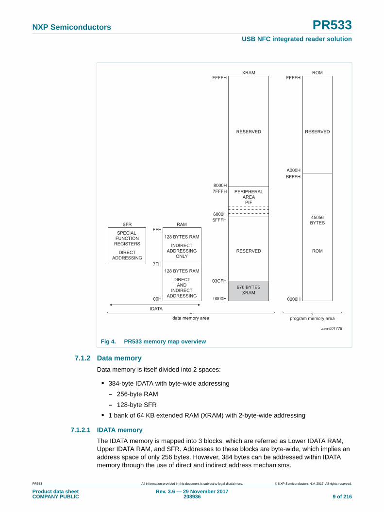
7.1.1 PR533 memory map
The memory map of PR533 is composed of 2 main memory spaces: data memory and program memory. The following figure illustrates the structure.
Fig 3. PR533 80C51 block description
PR533
HOSTINTERFACES
80C51
RAM
POWERDISTRIBUTION
POWER CLOCKRESET CONTROLLER
(PCR)
CONTACTLESSINTERFACE UNIT
(CIU)
CPU
TIMER0/1
TIMER2
DEBUGUART
PIF
SFR
ROM
aaa-001777
PR533 All information provided in this document is subject to legal disclaimers. © NXP Semiconductors N.V. 2017. All rights reserved.
Product data sheetCOMPANY PUBLIC
Rev. 3.6 — 29 November 2017208936 8 of 216
NXP Semiconductors PR533USB NFC integrated reader solution
7.1.2 Data memory
Data memory is itself divided into 2 spaces:
• 384-byte IDATA with byte-wide addressing
– 256-byte RAM
– 128-byte SFR
• 1 bank of 64 KB extended RAM (XRAM) with 2-byte-wide addressing
7.1.2.1 IDATA memory
The IDATA memory is mapped into 3 blocks, which are referred as Lower IDATA RAM, Upper IDATA RAM, and SFR. Addresses to these blocks are byte-wide, which implies an address space of only 256 bytes. However, 384 bytes can be addressed within IDATA memory through the use of direct and indirect address mechanisms.
Fig 4. PR533 memory map overview
SPECIAL FUNCTION
REGISTERS
DIRECTADDRESSING
FFHSFR
128 BYTES RAM
INDIRECTADDRESSING
ONLY
128 BYTES RAM
DIRECTAND
INDIRECTADDRESSING
00H
7FH
RAM5FFFH
0000H
FFFFHXRAM
7FFFH
A000H
data memory area program memory area
IDATA
ROM
ROM
PERIPHERALAREA
PIF
976 BYTESXRAM
45056BYTES
FFFFH
0000H
03CFH
6000H
8000H
BFFFH
aaa-001778
RESERVED
RESERVED
RESERVED
PR533 All information provided in this document is subject to legal disclaimers. © NXP Semiconductors N.V. 2017. All rights reserved.
Product data sheetCOMPANY PUBLIC
Rev. 3.6 — 29 November 2017208936 9 of 216
NXP Semiconductors PR533USB NFC integrated reader solution
• Direct addressing: the operand is specified by an 8-bit address field in the instruction.
• Indirect addressing: the instruction specifies a register where the address of the operand is stored.
For the range 80h to FFh, direct addressing will access the SFR space; indirect addressing accesses Upper IDATA RAM. For the range 00h to 7Fh, Lower IDATA RAM is accessed, regardless of addressing mode. This behavior is summarized in the table below:
The SFRs and their addresses are described in the Table 5:
Table 4. IDATA memory addressing
Address Addressing mode
Direct Indirect
00h to 7Fh Lower IDATA RAM Lower IDATA RAM
80h to FFh SFRs Upper IDATA RAM
PR533 All information provided in this document is subject to legal disclaimers. © NXP Semiconductors N.V. 2017. All rights reserved.
Product data sheetCOMPANY PUBLIC
Rev. 3.6 — 29 November 2017208936 10 of 216

xxxxxxxxxxxxxxxxxxxxx xxxxxxxxxxxxxxxxxxxxxxxxxx xxxxxxx x x x xxxxxxxxxxxxxxxxxxxxxxxxxxxxxx xxxxxxxxxxxxxxxxxxx xx xx xxxxx xxxxxxxxxxxxxxxxxxxxxxxxxxx xxxxxxxxxxxxxxxxxxx xxxxxx xxxxxxxxxxxxxxxxxxxxxxxxxxxxxxxxxxx xxxxxxxxxxxx x x xxxxxxxxxxxxxxxxxxxxx xxxxxxxxxxxxxxxxxxxxxxxxxxxxxx xxxxx xxxxxxxxxxxxxxxxxxxxxxxxxxxxxxxxxxxxxxxxxxxxxxxxxx xxxxxxxx xxxxxxxxxxxxxxxxxxxxxxxxx xxxxxxxxxxxxxxxxxxxx xxx
PR
533
Pro
du
ct data sh
eetC
OM
PA
NY
PU
BL
ICR
ev. 3.6 —
29 N
ove
mb
er 2
017208936
11 of 216
NX
P S
emico
nd
ucto
rsP
R533
US
B N
FC
integ
rated read
er solu
tion
Table 5. SFR map of NFC controller
Address Bit- Byte-addressable Address
FFh
P7 F7h
raming CIU_Coll EFh
E7h
CIU_Status1 DFh
rror D7h
CFh
C7h
BFh
B7h
CNT AFh
A7h
F FIT 9Fh
97h
8Fh
PCON 87h
All inform
ation provided
in this docum
ent is subject to leg
al disclaim
ers.©
NX
P S
em
iconductors N
.V. 2017. A
ll rights rese
rved.
addressable
F8h IP1 XRAMP P3CFGA P3CFGB
F0h B P7CFGA P7CFGB
E8h IE1 CIU_Status2 CIU_FIFOData CIU_FIFOLevel CIU_WaterLevel CIU_Control CIU_BitF
E0h ACC
D8h I2CC0N I2CSTA I2CDAT I2CADR
D0h PSW CIU_Command CIU_CommIEn CIU_DivIEn CIU_CommIrq CIU_DivIrq CIU_E
C8h T2CON T2MOD RCAP2L RCAP2H T2L T2H
C0h
B8h IP0
B0h P3
A8h IE0 HSU_STA HSU_CTR HSU_PRE HSU_
A0h FITEN FDATA FSIZE
98h S0CON SBUF RWL TWL FIFOFS FIFOFF SF
90h
88h T01CON T01MOD T0L T1L T0H T1H
80h SP DPL DPH

NXP Semiconductors PR533USB NFC integrated reader solution
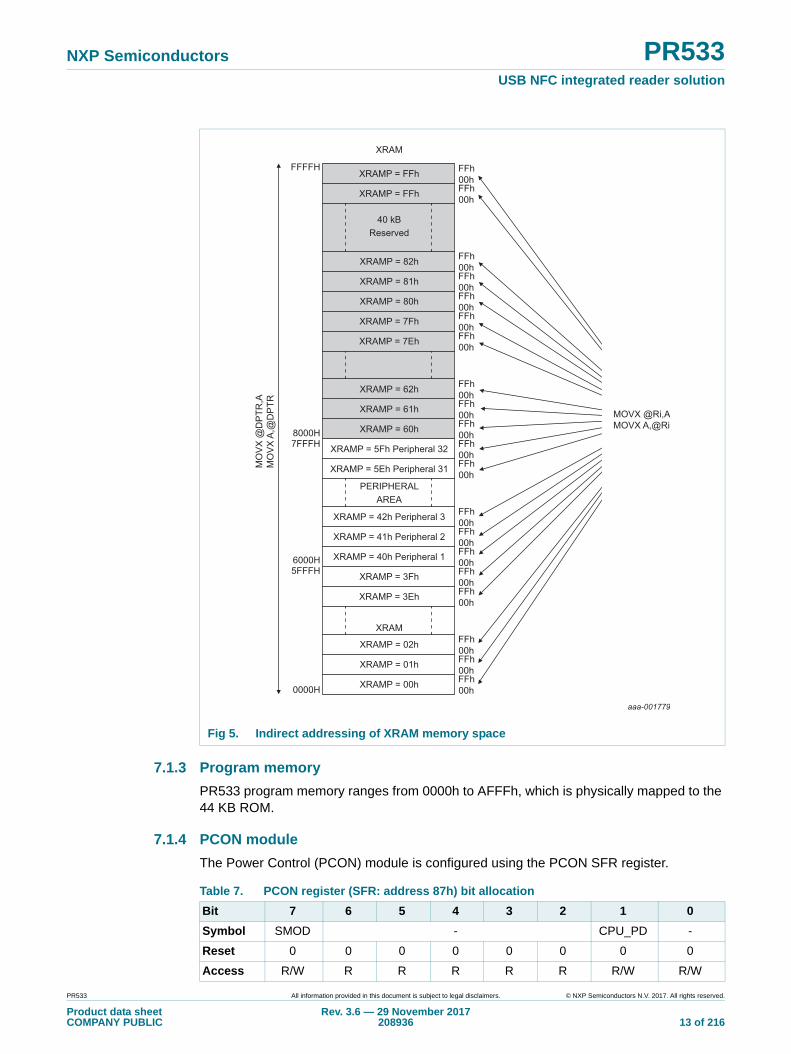
7.1.2.2 XRAM memory
The XRAM memory is divided into 2 memory spaces:
• 0000h to 5FFFh: reserved for addressing embedded RAM. For the PR533, only accesses between 0000h and 03C7h are valid.
• 6000h to 7FFFh: reserved for addressing embedded peripherals. This space is divided into 32 regions of 256 bytes each. Addressing can be performed using R0 or R1 and the XRAMP SFR.
The Table 6 depicts the mapping of internal peripherals into XRAM.
XRAM is accessed via the dedicated MOVX instructions. There are two access modes:
• 16-bit data pointer (DPTR): the full XRAM address space can be accessed.
• paging mechanism: the upper address byte is stored in the SFR register XRAMP; the lower byte is stored in either R1 or R0.
The Figure 5 illustrates both mechanisms.
Table 6. Peripheral mapping into XRAM memory space
Base Address
End Address
Description
6000h 60FFh Reserved.
6100h 61FFh IOs and miscellaneous registers configurationRefer to Section 7.2 “General purpose IOs configurations” on page 34
6200h 62FFh Power Clock and Reset controller Refer to Section 7.5.10 “PCR extension registers” on page 96
6300h 633Fh Contactless Unit InterfaceRefer to Section 8.6 “Contactless Interface Unit (CIU)” on page 110
6340h FFFFh Reserved
PR533 All information provided in this document is subject to legal disclaimers. © NXP Semiconductors N.V. 2017. All rights reserved.
Product data sheetCOMPANY PUBLIC
Rev. 3.6 — 29 November 2017208936 12 of 216
NXP Semiconductors PR533USB NFC integrated reader solution
7.1.3 Program memory
PR533 program memory ranges from 0000h to AFFFh, which is physically mapped to the 44 KB ROM.
7.1.4 PCON module
The Power Control (PCON) module is configured using the PCON SFR register.
Fig 5. Indirect addressing of XRAM memory space
XRAM
XRAMP = 80h
XRAMP = 81h
XRAMP = 82h
XRAMP = FFh
6000H
7FFFH
0000H
5FFFH
8000H
FFFFH
XRAM
PERIPHERALAREA
40 kBReserved
XRAMP = 00h
XRAMP = 01h
00h
XRAMP = 02h
XRAMP = 3Fh
XRAMP = 3Eh
FFh00hFFh00hFFh
00hFFh
00hFFh
XRAMP = 40h Peripheral 1
XRAMP = 41h Peripheral 2
00h
XRAMP = 42h Peripheral 3
XRAMP = 5Fh Peripheral 32
XRAMP = 5Eh Peripheral 31
FFh00hFFh00hFFh
00hFFh
00hFFh
XRAMP = 60h
XRAMP = 61h
00h
XRAMP = 62h
XRAMP = 7Fh
XRAMP = 7Eh
FFh00hFFh00hFFh
00hFFh
00hFFh
00hFFh00hFFh00hFFh
00hFFh
00hFFh
XRAMP = FFh
MO
VX
@D
PTR
,AM
OV
X A
,@D
PTR
MOVX @Ri,AMOVX A,@Ri
aaa-001779
Table 7. PCON register (SFR: address 87h) bit allocation
Bit 7 6 5 4 3 2 1 0
Symbol SMOD - CPU_PD -
Reset 0 0 0 0 0 0 0 0
Access R/W R R R R R R/W R/W
PR533 All information provided in this document is subject to legal disclaimers. © NXP Semiconductors N.V. 2017. All rights reserved.
Product data sheetCOMPANY PUBLIC
Rev. 3.6 — 29 November 2017208936 13 of 216
NXP Semiconductors PR533USB NFC integrated reader solution
7.1.5 Interrupt Controller
The interrupt controller has the following features:
• 1interrupt source
• Interrupt enable registers IE0 and IE1
• Interrupt priority registers IP0 and IP1
• Wake-up from Power-down state
7.1.5.1 Interrupt vectors
The mapping between interrupt sources and interrupt vectors is shown in Table 9.
7.1.5.2 Interrupt enable: IE0 and IE1 registers
Each interrupt source can be individually enabled or disabled by setting a bit in IE0 or IE1. In register IE0, a global interrupt enable bit can be set to logic level 0 to disable all interrupts at once.
The 2 following tables describe IE0.
Table 8. Description of PCON bits
Bit Symbol Description
7 SMOD Serial MODe: When set to logic level 1, the baud rate of the Debug UART is doubled
6 to 2 - Reserved.
1 CPU_PD Power-down: When set to logic level 1, the microcontroller goes in Power-down mode
0 Reserved This bit should only ever contain logic level 0.
Table 9. Interrupt vector
Interrupt number
Interrupt vector
Interrupt sources Incremental priority level(conflict resolution level)
0 0003h External P32_INT0 Highest
1 000Bh Timer0 interrupt
2 0013h External P33_INT1
3 001Bh Timer1 interrupt
4 0023h Debug UART interrupt
5 002Bh Timer2 interrupt
6 0033h NFC-WI interrupt
7 003Bh Reserved
8 0043h Reserved
9 004Bh CIU interrupt 1
10 0053h CIU interrupt 0
11 005Bh I2C interrupt
12 0063h FIFO or HSU interrupts
13 006Bh USB interrupt
14 0073h General Purpose IRQ Lowest
PR533 All information provided in this document is subject to legal disclaimers. © NXP Semiconductors N.V. 2017. All rights reserved.
Product data sheetCOMPANY PUBLIC
Rev. 3.6 — 29 November 2017208936 14 of 216
NXP Semiconductors PR533USB NFC integrated reader solution
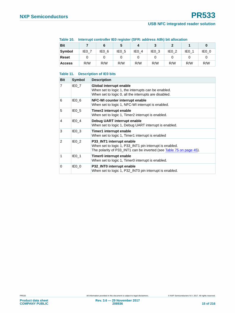
Table 10. Interrupt controller IE0 register (SFR: address A8h) bit allocation
Bit 7 6 5 4 3 2 1 0
Symbol IE0_7 IE0_6 IE0_5 IE0_4 IE0_3 IE0_2 IE0_1 IE0_0
Reset 0 0 0 0 0 0 0 0
Access R/W R/W R/W R/W R/W R/W R/W R/W
Table 11. Description of IE0 bits
Bit Symbol Description
7 IE0_7 Global interrupt enableWhen set to logic 1, the interrupts can be enabled.When set to logic 0, all the interrupts are disabled.
6 IE0_6 NFC-WI counter interrupt enableWhen set to logic 1, NFC-WI interrupt is enabled.
5 IE0_5 Timer2 interrupt enableWhen set to logic 1, Timer2 interrupt is enabled.
4 IE0_4 Debug UART interrupt enable When set to logic 1, Debug UART interrupt is enabled.
3 IE0_3 Timer1 interrupt enable When set to logic 1, Timer1 interrupt is enabled
2 IE0_2 P33_INT1 interrupt enableWhen set to logic 1, P33_INT1 pin interrupt is enabled.The polarity of P33_INT1 can be inverted (see Table 75 on page 45).
1 IE0_1 Timer0 interrupt enableWhen set to logic 1, Timer0 interrupt is enabled.
0 IE0_0 P32_INT0 interrupt enable When set to logic 1, P32_INT0 pin interrupt is enabled.
PR533 All information provided in this document is subject to legal disclaimers. © NXP Semiconductors N.V. 2017. All rights reserved.
Product data sheetCOMPANY PUBLIC
Rev. 3.6 — 29 November 2017208936 15 of 216
NXP Semiconductors PR533USB NFC integrated reader solution
The 2 following tables describe IE1.
7.1.5.3 Interrupt prioritization: IP0 and IP1 registers
Each interrupt source can be individually programmed to be one of two priority levels by setting or clearing a bit in the interrupt priority registers IP0 and IP1. If two interrupt requests of different priority levels are received simultaneously, the request with the high priority is serviced first. On the other hand, if the interrupts are of the same priority, precedence is resolved by comparing their respective conflict resolution levels (see Table 9 on page 14 for details). The processing of a low priority interrupt can be interrupted by one with a high priority.
A RETI (Return From Interrupt) instruction jumps to the address immediately succeeding the point at which the interrupt was serviced. The instruction found at the return address will be executed, prior to servicing any pending interrupts.
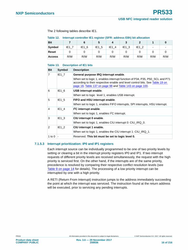
Table 12. Interrupt controller IE1 register (SFR: address E8h) bit allocation
Bit 7 6 5 4 3 2 1 0
Symbol IE1_7 IE1_6 IE1_5 IE1_4 IE1_3 IE1_2 - -
Reset 0 0 0 0 0 0 0 0
Access R/W R/W R/W R/W R/W R/W R/W R/W
Table 13. Description of IE1 bits
Bit Symbol Description
7 IE1_7 General purpose IRQ interrupt enable.
When set to logic 1, enables interrupt function of P34, P35, P50_SCL and P71 according to their respective enable and level control bits. See Table 19 on page 18, Table 137 on page 98 and Table 143 on page 100.
6 IE1_6 USB interrupt enable.
When set to logic level 1, enables USB interrupt.
5 IE1_5 FIFO and HSU interrupt enable.
When set to logic 1, enables FIFO interrupts, SPI interrupts, HSU interrupt.
4 IE1_4 I2C interrupt enable.
When set to logic 1, enables I2C interrupt.
3 IE1_3 CIU interrupt 0 enable.
When set to logic 1, enables CIU interrupt 0: CIU_IRQ_0.
2 IE1_2 CIU interrupt 1 enable.
When set to logic 1, enables the CIU interrupt 1: CIU_IRQ_1.
1 to 0 - Reserved. This bit must be set to logic level 0.
PR533 All information provided in this document is subject to legal disclaimers. © NXP Semiconductors N.V. 2017. All rights reserved.
Product data sheetCOMPANY PUBLIC
Rev. 3.6 — 29 November 2017208936 16 of 216
NXP Semiconductors PR533USB NFC integrated reader solution
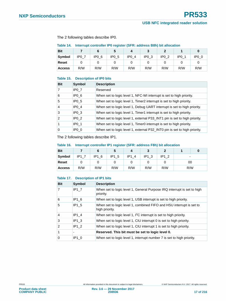
The 2 following tables describe IP0.
The 2 following tables describe IP1.
Table 14. Interrupt controller IP0 register (SFR: address B8h) bit allocation
Bit 7 6 5 4 3 2 1 0
Symbol IP0_7 IP0_6 IP0_5 IP0_4 IP0_3 IP0_2 IP0_1 IP0_0
Reset 0 0 0 0 0 0 0 0
Access R/W R/W R/W R/W R/W R/W R/W R/W
Table 15. Description of IP0 bits
Bit Symbol Description
7 IP0_7 Reserved
6 IP0_6 When set to logic level 1, NFC-WI interrupt is set to high priority.
5 IP0_5 When set to logic level 1, Timer2 interrupt is set to high priority.
4 IP0_4 When set to logic level 1, Debug UART interrupt is set to high priority.
3 IP0_3 When set to logic level 1, Timer1 interrupt is set to high priority.
2 IP0_2 When set to logic level 1, external P33_INT1 pin is set to high priority.
1 IP0_1 When set to logic level 1, Timer0 interrupt is set to high priority.
0 IP0_0 When set to logic level 1, external P32_INT0 pin is set to high priority.
Table 16. Interrupt controller IP1 register (SFR: address F8h) bit allocation
Bit 7 6 5 4 3 2 1 0
Symbol IP1_7 IP1_6 IP1_5 IP1_4 IP1_3 IP1_2 -
Reset 0 0 0 0 0 0 00
Access R/W R/W R/W R/W R/W R/W R/W
Table 17. Description of IP1 bits
Bit Symbol Description
7 IP1_7 When set to logic level 1, General Purpose IRQ interrupt is set to high priority.
6 IP1_6 When set to logic level 1, USB interrupt is set to high priority.
5 IP1_5 When set to logic level 1, combined FIFO and HSU interrupt is set to high priority.
4 IP1_4 When set to logic level 1, I2C interrupt is set to high priority.
3 IP1_3 When set to logic level 1, CIU interrupt 0 is set to high priority.
2 IP1_2 When set to logic level 1, CIU interrupt 1 is set to high priority.
1 - Reserved. This bit must be set to logic level 0.
0 IP1_0 When set to logic level 1, interrupt number 7 is set to high priority.
PR533 All information provided in this document is subject to legal disclaimers. © NXP Semiconductors N.V. 2017. All rights reserved.
Product data sheetCOMPANY PUBLIC
Rev. 3.6 — 29 November 2017208936 17 of 216
NXP Semiconductors PR533USB NFC integrated reader solution
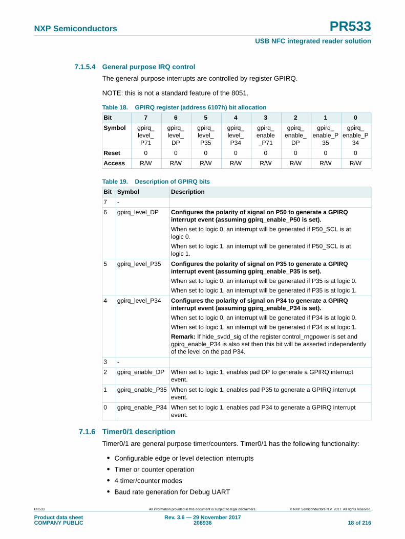
7.1.5.4 General purpose IRQ control
The general purpose interrupts are controlled by register GPIRQ.
NOTE: this is not a standard feature of the 8051.
7.1.6 Timer0/1 description
Timer0/1 are general purpose timer/counters. Timer0/1 has the following functionality:
• Configurable edge or level detection interrupts
• Timer or counter operation
• 4 timer/counter modes
• Baud rate generation for Debug UART
Table 18. GPIRQ register (address 6107h) bit allocation
Bit 7 6 5 4 3 2 1 0
Symbol gpirq_level_P71
gpirq_level_
DP
gpirq_level_P35
gpirq_level_P34
gpirq_enable _P71
gpirq_enable_
DP
gpirq_enable_P
35
gpirq_enable_P
34
Reset 0 0 0 0 0 0 0 0
Access R/W R/W R/W R/W R/W R/W R/W R/W
Table 19. Description of GPIRQ bits
Bit Symbol Description
7 -
6 gpirq_level_DP Configures the polarity of signal on P50 to generate a GPIRQ interrupt event (assuming gpirq_enable_P50 is set).
When set to logic 0, an interrupt will be generated if P50_SCL is at logic 0.
When set to logic 1, an interrupt will be generated if P50_SCL is at logic 1.
5 gpirq_level_P35 Configures the polarity of signal on P35 to generate a GPIRQ interrupt event (assuming gpirq_enable_P35 is set).
When set to logic 0, an interrupt will be generated if P35 is at logic 0.
When set to logic 1, an interrupt will be generated if P35 is at logic 1.
4 gpirq_level_P34 Configures the polarity of signal on P34 to generate a GPIRQ interrupt event (assuming gpirq_enable_P34 is set).
When set to logic 0, an interrupt will be generated if P34 is at logic 0.
When set to logic 1, an interrupt will be generated if P34 is at logic 1.
Remark: If hide_svdd_sig of the register control_rngpower is set and gpirq_enable_P34 is also set then this bit will be asserted independently of the level on the pad P34.
3 -
2 gpirq_enable_DP When set to logic 1, enables pad DP to generate a GPIRQ interrupt event.
1 gpirq_enable_P35 When set to logic 1, enables pad P35 to generate a GPIRQ interrupt event.
0 gpirq_enable_P34 When set to logic 1, enables pad P34 to generate a GPIRQ interrupt event.
PR533 All information provided in this document is subject to legal disclaimers. © NXP Semiconductors N.V. 2017. All rights reserved.
Product data sheetCOMPANY PUBLIC
Rev. 3.6 — 29 November 2017208936 18 of 216
NXP Semiconductors PR533USB NFC integrated reader solution
Timer0/1 comprises two 16-bit timer/counters: Timer0 and Timer1. Both can be configured as either a timer or an event counter.
Each of the timers can operate in one of four modes:
• Mode 0: 13-bit timer/counter
• Mode 1: 16-bit timer/counter
• Mode 2: 8-bit timer/counter with programmable preload value
• Mode 3: two individual 8-bit timer/counters (Timer0 only)
In the ‘timer’ function, the timer/counter is incremented every machine cycle. The count rate is 1/6 of the CPU clock frequency (CPU_CLK).
In the ‘counter’ function, the timer/counter is incremented in response to a 1-to-0 transition on the input pins P34 / SIC_CLK (Timer0) or P35 (Timer1). In this mode, the external input is sampled during state S5 of every machine cycle. If the associated pin is at logic level 1 for a machine cycle, followed by logic level 0 on the next machine cycle, the count is incremented. The new count value appears in the timer/counter in state S3 of the machine cycle following the one in which the transition was detected. The maximum count rate is 1/12 of the CPU_CLK frequency. There are no restrictions on the duty cycle of the external input signal but to ensure that a given level is sampled at least once before it changes, it should be held for at least one full machine cycle.
The overflow output ‘t1_ovf’ of Timer1 can be used as a baud rate generator for the Debug UART. The Timer1 interrupt should be disabled in this case. For most applications which drive the Debug UART, Timer1 is configured for ‘timer’ operation and in auto-reload mode.
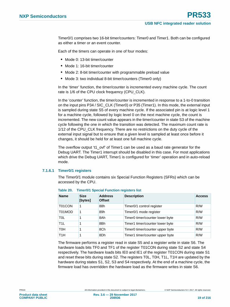
7.1.6.1 Timer0/1 registers
The Timer0/1 module contains six Special Function Registers (SFRs) which can be accessed by the CPU.
The firmware performs a register read in state S5 and a register write in state S6. The hardware loads bits TF0 and TF1 of the register T01CON during state S2 and state S4 respectively. The hardware loads bits IE0 and IE1 of the register T01CON during state S1 and reset these bits during state S2. The registers T0L, T0H, T1L, T1H are updated by the hardware during states S1, S2, S3 and S4 respectively. At the end of a machine cycle, the firmware load has overridden the hardware load as the firmware writes in state S6.
Table 20. Timer0/1 Special Function registers list
Name Size[bytes]
AddressOffset
Description Access
T01CON 1 88h Timer0/1 control register R/W
T01MOD 1 89h Timer0/1 mode register R/W
T0L 1 8Ah Timer0 timer/counter lower byte R/W
T1L 1 8Bh Timer1 timer/counter lower byte R/W
T0H 1 8Ch Timer0 timer/counter upper byte R/W
T1H 1 8Dh Timer1 timer/counter upper byte R/W
PR533 All information provided in this document is subject to legal disclaimers. © NXP Semiconductors N.V. 2017. All rights reserved.
Product data sheetCOMPANY PUBLIC
Rev. 3.6 — 29 November 2017208936 19 of 216
NXP Semiconductors PR533USB NFC integrated reader solution
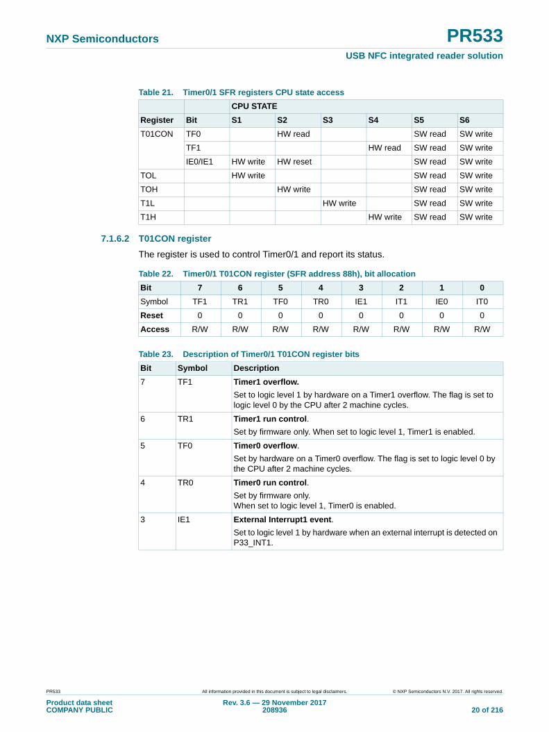
7.1.6.2 T01CON register
The register is used to control Timer0/1 and report its status.
Table 21. Timer0/1 SFR registers CPU state access
CPU STATE
Register Bit S1 S2 S3 S4 S5 S6
T01CON TF0 HW read SW read SW write
TF1 HW read SW read SW write
IE0/IE1 HW write HW reset SW read SW write
TOL HW write SW read SW write
TOH HW write SW read SW write
T1L HW write SW read SW write
T1H HW write SW read SW write
Table 22. Timer0/1 T01CON register (SFR address 88h), bit allocation
Bit 7 6 5 4 3 2 1 0
Symbol TF1 TR1 TF0 TR0 IE1 IT1 IE0 IT0
Reset 0 0 0 0 0 0 0 0
Access R/W R/W R/W R/W R/W R/W R/W R/W
Table 23. Description of Timer0/1 T01CON register bits
Bit Symbol Description
7 TF1 Timer1 overflow.
Set to logic level 1 by hardware on a Timer1 overflow. The flag is set to logic level 0 by the CPU after 2 machine cycles.
6 TR1 Timer1 run control.
Set by firmware only. When set to logic level 1, Timer1 is enabled.
5 TF0 Timer0 overflow.
Set by hardware on a Timer0 overflow. The flag is set to logic level 0 by the CPU after 2 machine cycles.
4 TR0 Timer0 run control.
Set by firmware only.When set to logic level 1, Timer0 is enabled.
3 IE1 External Interrupt1 event.
Set to logic level 1 by hardware when an external interrupt is detected on P33_INT1.
PR533 All information provided in this document is subject to legal disclaimers. © NXP Semiconductors N.V. 2017. All rights reserved.
Product data sheetCOMPANY PUBLIC
Rev. 3.6 — 29 November 2017208936 20 of 216
NXP Semiconductors PR533USB NFC integrated reader solution
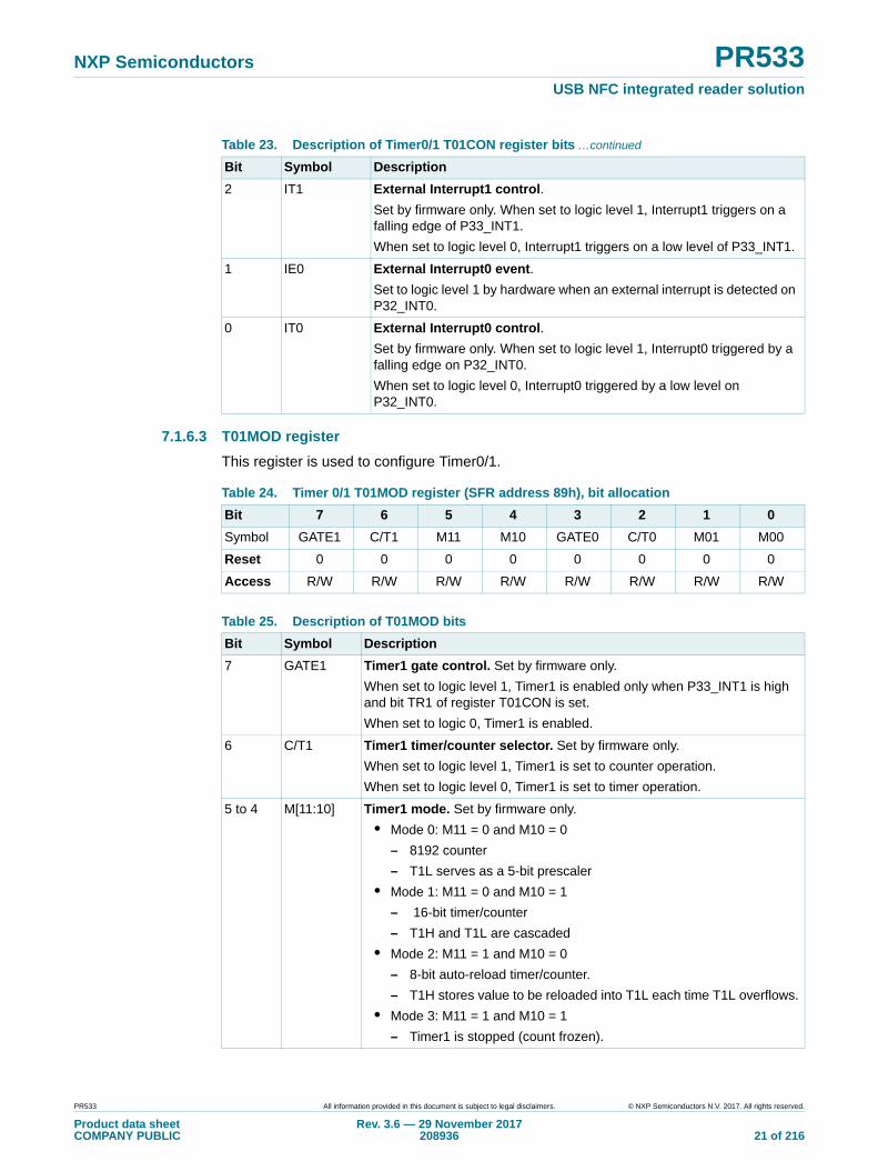
7.1.6.3 T01MOD register
This register is used to configure Timer0/1.
2 IT1 External Interrupt1 control.
Set by firmware only. When set to logic level 1, Interrupt1 triggers on a falling edge of P33_INT1.
When set to logic level 0, Interrupt1 triggers on a low level of P33_INT1.
1 IE0 External Interrupt0 event.
Set to logic level 1 by hardware when an external interrupt is detected on P32_INT0.
0 IT0 External Interrupt0 control.
Set by firmware only. When set to logic level 1, Interrupt0 triggered by a falling edge on P32_INT0.
When set to logic level 0, Interrupt0 triggered by a low level on P32_INT0.
Table 23. Description of Timer0/1 T01CON register bits …continued
Bit Symbol Description
Table 24. Timer 0/1 T01MOD register (SFR address 89h), bit allocation
Bit 7 6 5 4 3 2 1 0
Symbol GATE1 C/T1 M11 M10 GATE0 C/T0 M01 M00
Reset 0 0 0 0 0 0 0 0
Access R/W R/W R/W R/W R/W R/W R/W R/W
Table 25. Description of T01MOD bits
Bit Symbol Description
7 GATE1 Timer1 gate control. Set by firmware only.
When set to logic level 1, Timer1 is enabled only when P33_INT1 is high and bit TR1 of register T01CON is set.
When set to logic 0, Timer1 is enabled.
6 C/T1 Timer1 timer/counter selector. Set by firmware only.
When set to logic level 1, Timer1 is set to counter operation.
When set to logic level 0, Timer1 is set to timer operation.
5 to 4 M[11:10] Timer1 mode. Set by firmware only.
• Mode 0: M11 = 0 and M10 = 0
– 8192 counter
– T1L serves as a 5-bit prescaler
• Mode 1: M11 = 0 and M10 = 1
– 16-bit timer/counter
– T1H and T1L are cascaded
• Mode 2: M11 = 1 and M10 = 0
– 8-bit auto-reload timer/counter.
– T1H stores value to be reloaded into T1L each time T1L overflows.
• Mode 3: M11 = 1 and M10 = 1
– Timer1 is stopped (count frozen).
PR533 All information provided in this document is subject to legal disclaimers. © NXP Semiconductors N.V. 2017. All rights reserved.
Product data sheetCOMPANY PUBLIC
Rev. 3.6 — 29 November 2017208936 21 of 216

NXP Semiconductors PR533USB NFC integrated reader solution
7.1.6.4 T0L and T0H registers
These are the actual timer/counter bytes for Timer0: T0L is the lower byte; T0H is the upper byte.
3 GATE0 Timer0 gate control. Set by firmware only.
When set to logic level 1, Timer0 is enabled only when P32_INT0 is high and bit TR0 of register T01CON is set.
When set to logic level 0, Timer0 is enabled.
2 C/T0 Timer0 timer/counter selector. Set by firmware only.
When set to logic level 1, Timer0 is set to counter operation.
When set to logic level 0, Timer0 is set to timer operation.
1 to 0 M[01:00] Timer0 mode. Set by firmware only.
• Mode 0: M01 = 0 and M00 = 0
– 8192 timer
– T0L acts as a 5-bit prescaler.
• Mode 1: M01 = 0 and M00 = 1
– 16-bit timer/counter
– T0H and T0L are cascaded.
• Mode 2: M01 = 1 and M00 = 0
– 8-bit auto-reload timer/counter
– T0H stores value to be reloaded into T0L each time T0L overflows.
• Mode 3: M01 = 1 and M00 = 1
– Timer0 split into two 8-bit timer/counters T0H and T0L
– T0H is controlled by the control bit of Timer1: bit TR1 of register T01CON
– T0L is controlled by standard Timer0 control: “{P32_INT0 OR (NOT GATE0)} AND bit TR0”.
Table 25. Description of T01MOD bits …continued
Bit Symbol Description
Table 26. Timer0/1 T0L register (SFR address 8Ah), bit allocation
Bit 7 6 5 4 3 2 1 0
Symbol T0L.7 T0L.6 T0L.5 T0L.4 T0L.3 T0L.2 T0L.1 T0L.0
Reset 0 0 0 0 0 0 0 0
Access R/W R/W R/W R/W R/W R/W R/W R/W
Table 27. Description of T0L bits
Bit Symbol Description
7:0 T0L.7 to T0L.0 Timer0 timer/counter lower byte
Table 28. Timer0/1 T0H register (SFR address 8Ch), bit allocation
Bit 7 6 5 4 3 2 1 0
Symbol T0H.7 T0H.6 T0H.5 T0H.4 T0H.3 T0H.2 T0H.1 T0H.0
Reset 0 0 0 0 0 0 0 0
Access R/W R/W R/W R/W R/W R/W R/W R/W
PR533 All information provided in this document is subject to legal disclaimers. © NXP Semiconductors N.V. 2017. All rights reserved.
Product data sheetCOMPANY PUBLIC
Rev. 3.6 — 29 November 2017208936 22 of 216

NXP Semiconductors PR533USB NFC integrated reader solution
7.1.6.5 T1L and T1H registers
These are the actual timer/counter bytes for Timer1. T1L is the lower byte, T1H is the upper byte.
7.1.6.6 Incrementer
The two 16-bit timer/counters are built around an 8-bit incrementer. The Timer0/1 are incremented in the CPU states S1 to S4; the overflow flags are set in CPU states S2 and S4.
• CPU state S1: TOL is incremented if Timer0 is set to:
– timer operation
– counter operation and when a 1-to-0 transition is detected on P34 / SIC_CLK input.
• CPU state S2: TOH is incremented if:
– T0L overflows. The overflow flag TF0 in register T01CON is updated.
• CPU state S3: T1L is incremented if Timer1 is set to:
– timer operation or
– counter operation and when a 1-to-0 transition is detected on P35 input.
• CPU state S4: T1H is incremented if:
– T1L overflows. The overflow flag TF1 in register T01CON is updated.
Table 29. Description of T0H bits
Bit Symbol Description
7 to 0 T0H.7 to T0H.0 Timer0 timer/counter upper byte
Table 30. Timer0/1 T1L register (SFR address 8Bh), bit allocation
Bit 7 6 5 4 3 2 1 0
Symbol T1L.7 T1L.6 T1L.5 T1L.4 T1L.3 T1L.2 T1L.1 T1L.0
Reset 0 0 0 0 0 0 0 0
Access R/W R/W R/W R/W R/W R/W R/W R/W
Table 31. Description of T1L bits
Bit Symbol Description
7 to 0 T1L.7 to T1L.0 Timer1 timer/counter lower byte
Table 32. Timer0/1 T1H register (SFR address 8Dh), bit allocation
Bit 7 6 5 4 3 2 1 0
Symbol T1H.7 T1H.6 T1H.5 T1H.4 T1H.3 T1H.2 T1H.1 T1H.0
Reset 0 0 0 0 0 0 0 0
Access R/W R/W R/W R/W R/W R/W R/W R/W
Table 33. Description of T1H bits
Bit Symbol Description
7 to 0 T1H.7 to T1H.0 Timer1 timer/counter upper byte
PR533 All information provided in this document is subject to legal disclaimers. © NXP Semiconductors N.V. 2017. All rights reserved.
Product data sheetCOMPANY PUBLIC
Rev. 3.6 — 29 November 2017208936 23 of 216
NXP Semiconductors PR533USB NFC integrated reader solution
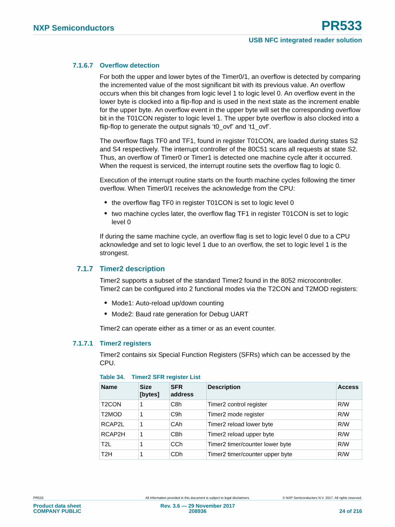
7.1.6.7 Overflow detection
For both the upper and lower bytes of the Timer0/1, an overflow is detected by comparing the incremented value of the most significant bit with its previous value. An overflow occurs when this bit changes from logic level 1 to logic level 0. An overflow event in the lower byte is clocked into a flip-flop and is used in the next state as the increment enable for the upper byte. An overflow event in the upper byte will set the corresponding overflow bit in the T01CON register to logic level 1. The upper byte overflow is also clocked into a flip-flop to generate the output signals ‘t0_ovf’ and ‘t1_ovf’.
The overflow flags TF0 and TF1, found in register T01CON, are loaded during states S2 and S4 respectively. The interrupt controller of the 80C51 scans all requests at state S2. Thus, an overflow of Timer0 or Timer1 is detected one machine cycle after it occurred. When the request is serviced, the interrupt routine sets the overflow flag to logic 0.
Execution of the interrupt routine starts on the fourth machine cycles following the timer overflow. When Timer0/1 receives the acknowledge from the CPU:
• the overflow flag TF0 in register T01CON is set to logic level 0
• two machine cycles later, the overflow flag TF1 in register T01CON is set to logic level 0
If during the same machine cycle, an overflow flag is set to logic level 0 due to a CPU acknowledge and set to logic level 1 due to an overflow, the set to logic level 1 is the strongest.
7.1.7 Timer2 description
Timer2 supports a subset of the standard Timer2 found in the 8052 microcontroller. Timer2 can be configured into 2 functional modes via the T2CON and T2MOD registers:
• Mode1: Auto-reload up/down counting
• Mode2: Baud rate generation for Debug UART
Timer2 can operate either as a timer or as an event counter.
7.1.7.1 Timer2 registers
Timer2 contains six Special Function Registers (SFRs) which can be accessed by the CPU.
Table 34. Timer2 SFR register List
Name Size[bytes]
SFRaddress
Description Access
T2CON 1 C8h Timer2 control register R/W
T2MOD 1 C9h Timer2 mode register R/W
RCAP2L 1 CAh Timer2 reload lower byte R/W
RCAP2H 1 CBh Timer2 reload upper byte R/W
T2L 1 CCh Timer2 timer/counter lower byte R/W
T2H 1 CDh Timer2 timer/counter upper byte R/W
PR533 All information provided in this document is subject to legal disclaimers. © NXP Semiconductors N.V. 2017. All rights reserved.
Product data sheetCOMPANY PUBLIC
Rev. 3.6 — 29 November 2017208936 24 of 216
NXP Semiconductors PR533USB NFC integrated reader solution
Timer2 registers can be written to by either hardware or firmware. If both the hardware and firmware attempt to update the registers T2H, T2L, RCAP2H or RCAP2L during the same machine cycle, the firmware write takes precedence. A firmware write occurs in state S6 of the machine cycle.
Each increment or decrement of Timer2 occurs in state S1 except when in baud rate generation mode and configured as a counter. In this mode, Timer2 increments on each clock cycle. When configured as a timer, Timer2 is incremented every machine cycle. Since a machine cycle consists of 6 clock periods, the count rate is 1/6 of the CPU clock frequency.
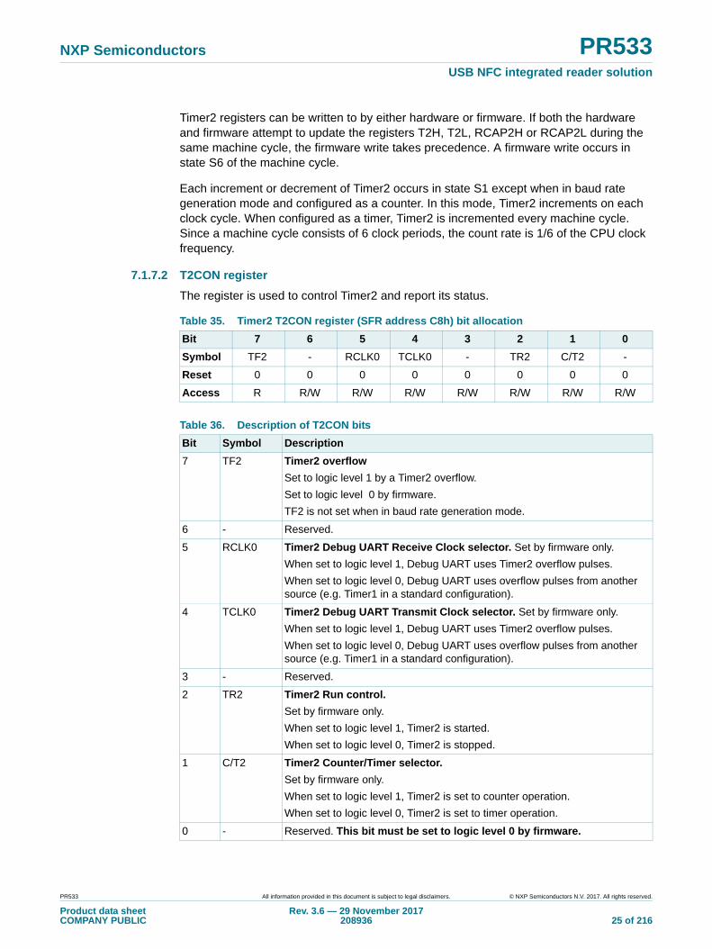
7.1.7.2 T2CON register
The register is used to control Timer2 and report its status.
Table 35. Timer2 T2CON register (SFR address C8h) bit allocation
Bit 7 6 5 4 3 2 1 0
Symbol TF2 - RCLK0 TCLK0 - TR2 C/T2 -
Reset 0 0 0 0 0 0 0 0
Access R R/W R/W R/W R/W R/W R/W R/W
Table 36. Description of T2CON bits
Bit Symbol Description
7 TF2 Timer2 overflow
Set to logic level 1 by a Timer2 overflow.
Set to logic level 0 by firmware.
TF2 is not set when in baud rate generation mode.
6 - Reserved.
5 RCLK0 Timer2 Debug UART Receive Clock selector. Set by firmware only.
When set to logic level 1, Debug UART uses Timer2 overflow pulses.
When set to logic level 0, Debug UART uses overflow pulses from another source (e.g. Timer1 in a standard configuration).
4 TCLK0 Timer2 Debug UART Transmit Clock selector. Set by firmware only.
When set to logic level 1, Debug UART uses Timer2 overflow pulses.
When set to logic level 0, Debug UART uses overflow pulses from another source (e.g. Timer1 in a standard configuration).
3 - Reserved.
2 TR2 Timer2 Run control.
Set by firmware only.
When set to logic level 1, Timer2 is started.
When set to logic level 0, Timer2 is stopped.
1 C/T2 Timer2 Counter/Timer selector.
Set by firmware only.
When set to logic level 1, Timer2 is set to counter operation.
When set to logic level 0, Timer2 is set to timer operation.
0 - Reserved. This bit must be set to logic level 0 by firmware.
PR533 All information provided in this document is subject to legal disclaimers. © NXP Semiconductors N.V. 2017. All rights reserved.
Product data sheetCOMPANY PUBLIC
Rev. 3.6 — 29 November 2017208936 25 of 216

NXP Semiconductors PR533USB NFC integrated reader solution
7.1.7.3 T2MOD register
This Special Function Register is used to configure Timer2.
7.1.7.4 T2L, T2H registers
These are the actual timer/counter bytes. T2L is the lower byte, T2H the upper byte.
On the fly reading can give a wrong value since T2H can be changed after T2L is read and before T2H is read. This situation is indicated by flag T2RD in T2MOD.
These two 8-bit registers are always combined to operate as one 16-bit timer/counter.
Table 37. Timer2 T2MOD register (SFR address C9h) bit allocation
Bit 7 6 5 4 3 2 1 0
Symbol - - - - - T2RD - DCEN
Reset 0 0 0 0 0 0 0 0
Access R R R R R R R/W R/W
Table 38. Description of TMOD bits
Bit Symbol Description
7 to 3 - Reserved.
2 T2RD Timer2 ReaD flag.
Set by hardware and firmware.
This bit is set to logic level 1 by hardware, if T2H is incremented between reading T2L and reading T2H. This bit is set to logic level 0, on the trailing edge of next T2L read.
This bit is used to indicate that the16-bit Timer2 register is not read properly since the T2H part was incremented by hardware before it was read.
1 - Reserved
0 DCEN Timer2 Down Count ENable.
Set by firmware only.
When this bit is set, Timer2 can be configured (in auto_reload mode) as an up-counter.
When this bit is reset, Timer2 can be configured (in auto-reload mode) as a down-counter.
Table 39. Timer2 T2L register (SFR address CCh) bit allocation
Bit 7 6 5 4 3 2 1 0
Symbol T2L.7 T2L.6 T2L.5 T2L.4 T2L.3 T2L.2 T2L.1 T2L.0
Reset 0 0 0 0 0 0 0 0
Access R/W R/W R/W R/W R/W R/W R/W R/W
Table 40. Description of T2L bits
Bit Symbol Description
7 to 0 T2L.7 to T2L.0 Timer2 timer/counter lower byte
PR533 All information provided in this document is subject to legal disclaimers. © NXP Semiconductors N.V. 2017. All rights reserved.
Product data sheetCOMPANY PUBLIC
Rev. 3.6 — 29 November 2017208936 26 of 216

NXP Semiconductors PR533USB NFC integrated reader solution
7.1.7.5 RCAP2L, RCAP2H registers
These are the reload bytes. In the reload mode the T2H/T2L counters are loaded with the values found in the RCAP2H/RCAP2L registers respectively.
7.1.8 Debug UART
The Debug UART is implemented to assist debug using UART_RX and UART_TX pins.
7.1.8.1 Feature list
The Debug UART has the following characteristics:
• Full duplex serial port
• Receive buffer to allow reception of a second byte while the first byte is being read out by the CPU
• Four modes of operation which support 8-bit and 9-bit data transfer at various baud rates
• Supports multi-processor communication
Table 41. Timer2 T2H register (SFR address CDh) bit allocation
Bit 7 6 5 4 3 2 1 0
Symbol T2H.7 T2H.6 T2H.5 T2H.4 T2H.3 T2H.2 T2H.1 T2H.0
Reset 0 0 0 0 0 0 0 0
Access R/W R/W R/W R/W R/W R/W R/W R/W
Table 42. Description of T2H bits
Bit Symbol Description
7 to 0 T2H.7 to T2H.0 Timer2 timer/counter upper byte
Table 43. Timer2 RCAP2L register (SFR address CAh) bit allocation
Bit 7 6 5 4 3 2 1 0
Symbol R2L.7 R2L.6 R2L.5 R2L.4 R2L.3 R2L.2 R2L.1 R2L.0
Reset 0 0 0 0 0 0 0 0
Access R/W R/W R/W R/W R/W R/W R/W R/W
Table 44. Description of RCAP2L bits
Bit Symbol Description
7 to 0 R2L.7 to R2L.0 Timer2 lower reload byte
Table 45. Timer2 RCAP2H register (SFR address CBh) bit allocation
Bit 7 6 5 4 3 2 1 0
Symbol R2H.7 R2H.6 R2H.5 R2H.4 R2H.3 R2H.2 R2H.1 R2H.0
Reset 0 0 0 0 0 0 0 0
Access R/W R/W R/W R/W R/W R/W R/W R/W
Table 46. Description of RCAP2H bits
Bit Symbol Description
7 to 0 R2H.7 to R2H.0 Timer2 upper reload byte
PR533 All information provided in this document is subject to legal disclaimers. © NXP Semiconductors N.V. 2017. All rights reserved.
Product data sheetCOMPANY PUBLIC
Rev. 3.6 — 29 November 2017208936 27 of 216
NXP Semiconductors PR533USB NFC integrated reader solution
• Baud rate can be controlled through Timer1 or Timer2 baud rate generator
7.1.8.2 Debug UART functional description
The serial port has a receive buffer: a second byte can be stored while the previous one is read out of the buffer by the CPU. However, if the first byte has still not been read by the time reception of the second byte is complete, one of the bytes will be lost.
The receive and transmit data registers of the serial port are both accessed by firmware via the Special Function Register S0BUF. Writing to S0BUF loads the transmit register; reading from S0BUF accesses a physically separate receive register.
The serial port can operate in 4 modes. These modes are selected by programming bits SM0 and SM1 in S0CON:
• Mode 0:
– Serial data are received and transmitted through UART_RX. UART_TX outputs the shift clock. 8 bits are transmitted/received (LSB first)
Baud rate: fixed at 1/6 of the frequency of the CPU clock
• Mode 1:
– 10 bits are transmitted through UART_TX or received through UART_RX: a start bit (0), 8 data bits (LSB first), and a stop bit (1)
– Receive: The received stop bit is stored into bit RB8 of register S0CON
– Baud rate: variable (depends on overflow of Timer1 or Timer2)
• Mode 2:
– 11 bits are transmitted through UART_TX or received through UART_RX: start bit (0), 8 data bits (LSB first), a 9th data bit, and a stop bit (1)
– Transmit: the 9th data bit is taken from bit TB8 of S0CON. For example, the parity bit could be loaded into TB8.
– Receive: the 9th data bit is stored into RB8 of S0CON, while the stop bit is ignored
– Baud rate: programmable to either 1/16 or 1/32 the frequency of the CPU clock
PR533 All information provided in this document is subject to legal disclaimers. © NXP Semiconductors N.V. 2017. All rights reserved.
Product data sheetCOMPANY PUBLIC
Rev. 3.6 — 29 November 2017208936 28 of 216
NXP Semiconductors PR533USB NFC integrated reader solution
• Mode 3:
– 11 bits are transmitted through UART_TX or received through UART_RX: a start bit (0), 8 data bits (LSB first), a 9th data bit, and a stop bit (1). In fact, mode 3 is the same as mode 2 in all aspects except the baud rate
– Transmit: as mode 2, the 9th data bit is taken from TB8 of S0CON
– Receive: as mode 2, the 9th data bit is stored into RB8 of S0CON
– Baud rate: depends on overflows of Timer1 or Timer2
The Debug UART initiates transmission and/or reception as follows.
• Transmission is initiated, in modes 0, 1, 2, 3, by any instruction that uses S0BUF as destination
• Reception is initiated, in mode 0, if RI and REN in S0CON are set to logic 0 and 1 respectively
• Reception is initiated in modes 1, 2, 3 by the incoming start bit if REN in S0CON is set to a logic 1
The Debug UART contains 2 SFRs:
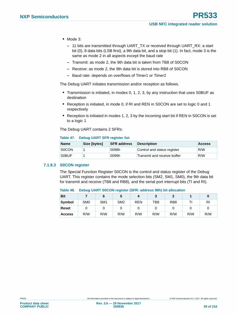
7.1.8.3 S0CON register
The Special Function Register S0CON is the control and status register of the Debug UART. This register contains the mode selection bits (SM2, SM1, SM0), the 9th data bit for transmit and receive (TB8 and RB8), and the serial port interrupt bits (TI and RI).
Table 47. Debug UART SFR register list
Name Size [bytes] SFR address Description Access
S0CON 1 0098h Control and status register R/W
S0BUF 1 0099h Transmit and receive buffer R/W
Table 48. Debug UART S0CON register (SFR: address 98h) bit allocation
Bit 7 6 5 4 3 2 1 0
Symbol SM0 SM1 SM2 REN TB8 RB8 TI RI
Reset 0 0 0 0 0 0 0 0
Access R/W R/W R/W R/W R/W R/W R/W R/W
PR533 All information provided in this document is subject to legal disclaimers. © NXP Semiconductors N.V. 2017. All rights reserved.
Product data sheetCOMPANY PUBLIC
Rev. 3.6 — 29 November 2017208936 29 of 216

NXP Semiconductors PR533USB NFC integrated reader solution
[1] If SM2 is set to logic 1, loading RB8 can be blocked, see bit description of SM2 above.
Table 49. Description of S0CON bits
Bit Symbol Description
7 to 6 SM (0:1) Mode selection bit 0 and 1.
Set by firmware only. The Debug UART has 4 modes (Table 50 “Debug UART modes” on page 31).
5 SM2 Multi-processor communication enable.
Enables the multi-processor communication feature. Set by firmware only.
In mode 2 and 3:
if SM2 is set to logic level 1, then RI will not be activated and RB8 and S0BUF will not be loaded if the 9th data bit received is a logic 0
if SM2 is set to logic level 0, it has no influence on the activation of RI and RB8
In mode 1:
if SM2 is set to logic level 1, then RI will not be activated and RB8 and S0BUF will not be loaded if no valid stop bit was received
if SM2 is set to logic level 0, it has no influence on the activation of RI and RB8
In mode 0, SM2 has no influence
4 REN Serial reception enable.
Set by firmware only.
When set to logic level 1, enables reception.
3 TB8 Transmit data bit.
Set by firmware only.
In modes 2 and 3, the value of TB8 is transmitted as the 9th data bit
In modes 0 and 1, the TB8 bit is not used
2 RB8 Receive data bit.
Set by hardware and by firmware.[1]
When set to logic level 1:
In modes 2 or 3, the hardware stores the 9th data bit that was received in RB8
In mode 1, the hardware stores the stop bit that was received in RB8
In mode 0, the hardware does not change RB8.
1 TI Transmit interrupt flag.
TI must be set to logic level 0 by firmware.
In modes 2 or 3, when transmitting, the hardware sets to logic level 1 the transmit interrupt flag TI at the end of the 9th bit time
In modes 0 or 1, when transmitting, the hardware sets to logic level 1 the transmit interrupt flag TI at the end of the 8th bit time.
0 RI Receive interrupt flag.
RI must be set to logic level 0 by firmware.
In modes 2 or 3, when receiving, the hardware sets to logic level 1 the receive interrupt flag 1 clock period after sampling the 9th data bit (if SM2=1 setting RI can be blocked, see bit description of SM2 above)
In mode 1, when receiving, the hardware sets to logic level 1 the receive interrupt flag 1 clock period after sampling the stop bit [2]
In mode 0, when receiving, the hardware sets to logic level 1 RI at the end of the CPU state 1 of the 9th machine cycle after the machine cycle where the data reception started by a write to S0CON.
PR533 All information provided in this document is subject to legal disclaimers. © NXP Semiconductors N.V. 2017. All rights reserved.
Product data sheetCOMPANY PUBLIC
Rev. 3.6 — 29 November 2017208936 30 of 216

NXP Semiconductors PR533USB NFC integrated reader solution
[2] If SM2 is set to logic 1, setting RI can be blocked, see bit description of SM2 above.
Remark: The S0CON register supports a locking mechanism to prevent firmware read-modify-write instructions to overwrite the contents while hardware is modifying the contents of the register.
7.1.8.4 S0BUF register
This register is implemented twice. Writing to S0BUF writes to the transmit buffer. Reading from S0BUF reads from the receive buffer. Only hardware can read from the transmit buffer and write to the receive buffer.
7.1.8.5 Mode 0 baud rate
In mode 0, the baud rate is derived from the CPU states signals and thus:
(1)
The next table lists the baud rates in Debug UART mode 0.
7.1.8.6 Mode 2 baud rate
In mode 2, the baud rate depends on the value of bit SMOD from the SFR register PCON.
Table 50. Debug UART modes
Mode SM0 SM1 Description Baud rate
0 0 0 Shift register fclk/6
1 0 1 8 bits Debug UART Variable
2 1 0 9 bits Debug UART fclk/64 or fclk/32
3 1 1 9 bits Debug UART Variable
Table 51. Debug UART S0BUF Register (SFR: address 99h) bit allocation
Bit 7 6 5 4 3 2 1 0
Symbol S0BUF[7:0]
Reset 0 0 0 0 0 0 0 0
Access R/W R/W R/W R/W R/W R/W R/W R/W
Table 52. Description of S0BUF bits
Bit Symbol Description
7 to 0 S0BUF[7:0] Writing to S0BUF writes to the transmit buffer.
Reading from S0BUF reads from the receive buffer.
Table 53. Baud rates in mode 0
Conditions Min Typ Max Unit
fCLK 6.78 13.56 27.12 MHz
Baud rate 1.13 2.26 4.52 Mb/s
clk6
-------
PR533 All information provided in this document is subject to legal disclaimers. © NXP Semiconductors N.V. 2017. All rights reserved.
Product data sheetCOMPANY PUBLIC
Rev. 3.6 — 29 November 2017208936 31 of 216
NXP Semiconductors PR533USB NFC integrated reader solution
(2)
The next table lists the baud rates in Debug UART mode 2.
7.1.8.7 Mode 1 and mode 3 baud rate
In mode 1 and in mode 3, the baud rate is determined by the rate of timer1 and timer2 overflow bits: ‘t1_ovf’ and ‘t2_ovf’. The register bit TCLK0 from the register T2CON selects if ‘t1_ovf’ or ‘t2_ovf’ should be used as a source when transmitting. The register bit RCLK0 from the register T2CON selects if ‘t1_ovf’ or ‘t2_ovf’ should be used as a source when receiving. The timers interrupt should be disabled when used to define the Debug UART baud rates.
The data rate is also dependant on the value of the bit SMOD from the SFR register PCON.
If over1rate is the equivalent ‘t1_ovf’ frequency and over2rate is the equivalent ‘t2_ovf’ frequency then:
Baud rate in mode 1 and mode 3 when related to timer1 overflow
(3)
See also Section 7.1.8.8 “Baud rates using Timer1 (Debug UART mode 1 and 3)”
Baud rate in mode 1 and mode 3 when related to timer2 overflow
(4)
See also Section 7.1.8.9 “Baud rates using Timer2 (Debug UART mode 1 and 3)”
The next table shows the trigger select:
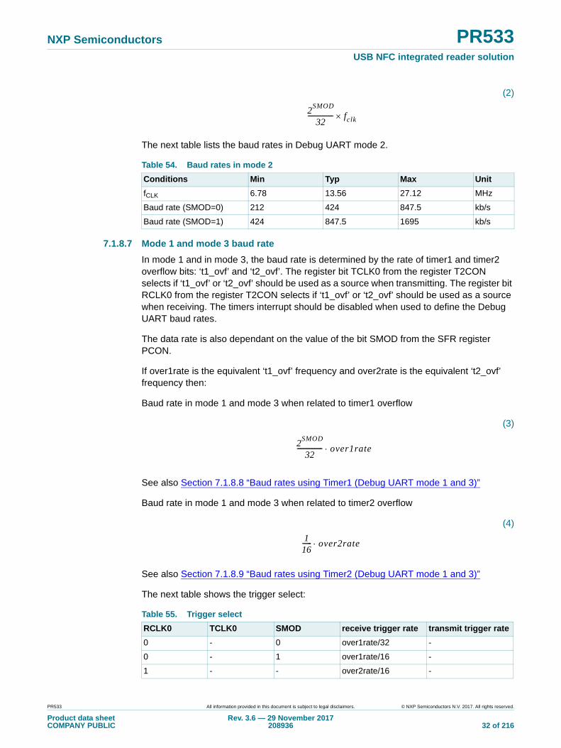
Table 54. Baud rates in mode 2
Conditions Min Typ Max Unit
fCLK 6.78 13.56 27.12 MHz
Baud rate (SMOD=0) 212 424 847.5 kb/s
Baud rate (SMOD=1) 424 847.5 1695 kb/s
2SMOD
32---------------- fclk
Table 55. Trigger select
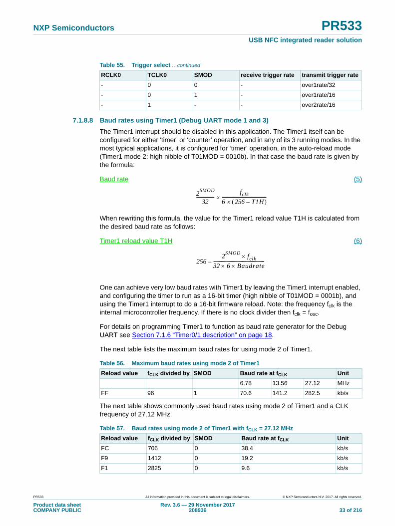
RCLK0 TCLK0 SMOD receive trigger rate transmit trigger rate
0 - 0 over1rate/32 -
0 - 1 over1rate/16 -
1 - - over2rate/16 -
2SMOD
32---------------- over1rate
116------ over2rate
PR533 All information provided in this document is subject to legal disclaimers. © NXP Semiconductors N.V. 2017. All rights reserved.
Product data sheetCOMPANY PUBLIC
Rev. 3.6 — 29 November 2017208936 32 of 216
NXP Semiconductors PR533USB NFC integrated reader solution
7.1.8.8 Baud rates using Timer1 (Debug UART mode 1 and 3)
The Timer1 interrupt should be disabled in this application. The Timer1 itself can be configured for either ‘timer’ or ‘counter’ operation, and in any of its 3 running modes. In the most typical applications, it is configured for ‘timer’ operation, in the auto-reload mode (Timer1 mode 2: high nibble of T01MOD = 0010b). In that case the baud rate is given by the formula:
Baud rate (5)
When rewriting this formula, the value for the Timer1 reload value T1H is calculated from the desired baud rate as follows:
Timer1 reload value T1H (6)
One can achieve very low baud rates with Timer1 by leaving the Timer1 interrupt enabled, and configuring the timer to run as a 16-bit timer (high nibble of T01MOD = 0001b), and using the Timer1 interrupt to do a 16-bit firmware reload. Note: the frequency fclk is the internal microcontroller frequency. If there is no clock divider then fclk = fosc.
For details on programming Timer1 to function as baud rate generator for the Debug UART see Section 7.1.6 “Timer0/1 description” on page 18.
The next table lists the maximum baud rates for using mode 2 of Timer1.
The next table shows commonly used baud rates using mode 2 of Timer1 and a CLK frequency of 27.12 MHz.
- 0 0 - over1rate/32
- 0 1 - over1rate/16
- 1 - - over2rate/16
Table 55. Trigger select …continued
RCLK0 TCLK0 SMOD receive trigger rate transmit trigger rate
Table 56. Maximum baud rates using mode 2 of Timer1
Reload value fCLK divided by SMOD Baud rate at fCLK Unit
6.78 13.56 27.12 MHz
FF 96 1 70.6 141.2 282.5 kb/s
Table 57. Baud rates using mode 2 of Timer1 with fCLK = 27.12 MHz
Reload value fCLK divided by SMOD Baud rate at fCLK Unit
FC 706 0 38.4 kb/s
F9 1412 0 19.2 kb/s
F1 2825 0 9.6 kb/s
2SMOD
32----------------
fclk
6 256 T1H– ----------------------------------------
2562
SMODfclk
32 6 Baudrate----------------------------------------------–
PR533 All information provided in this document is subject to legal disclaimers. © NXP Semiconductors N.V. 2017. All rights reserved.
Product data sheetCOMPANY PUBLIC
Rev. 3.6 — 29 November 2017208936 33 of 216

NXP Semiconductors PR533USB NFC integrated reader solution
7.1.8.9 Baud rates using Timer2 (Debug UART mode 1 and 3)
Timer2 has a programming mode to function as baud rate generator for the Debug UART. In this mode the baud rate is given by formula:
Baud rate using Timer2 (7)
When rewriting this formula, the value for the Timer2 reload values T2RCH/L is calculated from the desired baud rate as follows:
Reload value T2RCH/L (8)
For details on programming Timer2 to function as baud rate generator for the Debug UART (see Section 8.1.7 “Timer2 description” on page 31).
Note: the frequency fclk is the internal microcontroller frequency. If there is no clock divider then fclk = fosc.
The next table lists the maximum baud rates when using Timer2.
7.2 General purpose IOs configurations
This chapter describes the different configurations for the IO pads:
P70_IRQ
P35
P34, alternate function SIC_CLK
P33_INT1
P32_INT0
P31, alternate function UART_TX
P30, alternate function UART_RX
Note that in Hard Power Down mode, these ports are disconnected from their supply rail.
For a given port x, there are three configuration registers:
E3 5650 0 4.8 kb/s
C5 11300 0 2.4 kb/s
8A 22600 0 1.2 kb/s
Table 57. Baud rates using mode 2 of Timer1 with fCLK = 27.12 MHz …continued
Reload value fCLK divided by SMOD Baud rate at fCLK Unit
Table 58. Maximum baud rates using Timer2
Reload value T2RCH/L fCLK divided by Baud rate Unit
6.78 13.56 27.12 MHz
FFFF 16 424 847.5 1695 kb/s
fclk
16 65536 T2RCH T2RCL( , )– ----------------------------------------------------------------------------------
65536fclk
16 Baudrate-------------------------------------–
PR533 All information provided in this document is subject to legal disclaimers. © NXP Semiconductors N.V. 2017. All rights reserved.
Product data sheetCOMPANY PUBLIC
Rev. 3.6 — 29 November 2017208936 34 of 216
NXP Semiconductors PR533USB NFC integrated reader solution
PxCFGA[n]
PxCFGB[n]
Px[n]
where x is 3 or 7 and n is the bit index.
At maximum 4 different controllable modes can be supported. These modes are defined with the following bits:
• PxCFGA[n]=0 and PxCFGB[n]=0: Open drain
• PxCFGA[n]=1 and PxCFGB[n]=0: Quasi Bidirectional (Reset mode)
• PxCFGA[n]=0 and PxCFGB[n]=1: input (High Impedance)
• PxCFGA[n]=1 and PxCFGB[n]=1: Push/pull output
Px[n] is used to write or read the port value.
Here is the list of the registers used for these GPIO configuration
Table 59. Timer0/1 Special Function registers List
Name Size[bytes]
SFR address Description Access
P3CFGA 1 FCh Port 3 configuration R/W
P3CFGB 1 FDh Port 3 configuration R/W
P3 1 B0h Port 3 value R/W
P7CFGA 1 F4h Port 7configuration R/W
P7CFGB 1 F5h Port 7 configuration R/W
P7 1 F7h Port 7 value R/W
PR533 All information provided in this document is subject to legal disclaimers. © NXP Semiconductors N.V. 2017. All rights reserved.
Product data sheetCOMPANY PUBLIC
Rev. 3.6 — 29 November 2017208936 35 of 216
NXP Semiconductors PR533USB NFC integrated reader solution
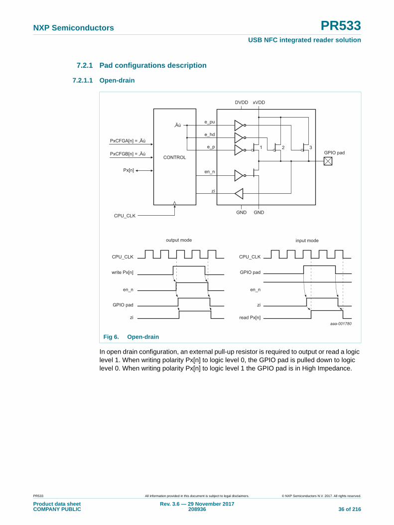
7.2.1 Pad configurations description
7.2.1.1 Open-drain
In open drain configuration, an external pull-up resistor is required to output or read a logic level 1. When writing polarity Px[n] to logic level 0, the GPIO pad is pulled down to logic level 0. When writing polarity Px[n] to logic level 1 the GPIO pad is in High Impedance.
Fig 6. Open-drain
CPU_CLK
en_n
zi
output mode input mode
write Px[n]
en_n
ziGPIO pad
read Px[n]
GPIO pad
CPU_CLK
1 2
Px[n]
zi
e_hd
e_pu
e_p
en_n
DVDD
GND GND
xVDD
3
CONTROL
“
GPIO pad
CPU_CLK
PxCFGA[n] = “
PxCFGB[n] = “
aaa-001780
PR533 All information provided in this document is subject to legal disclaimers. © NXP Semiconductors N.V. 2017. All rights reserved.
Product data sheetCOMPANY PUBLIC
Rev. 3.6 — 29 November 2017208936 36 of 216
NXP Semiconductors PR533USB NFC integrated reader solution
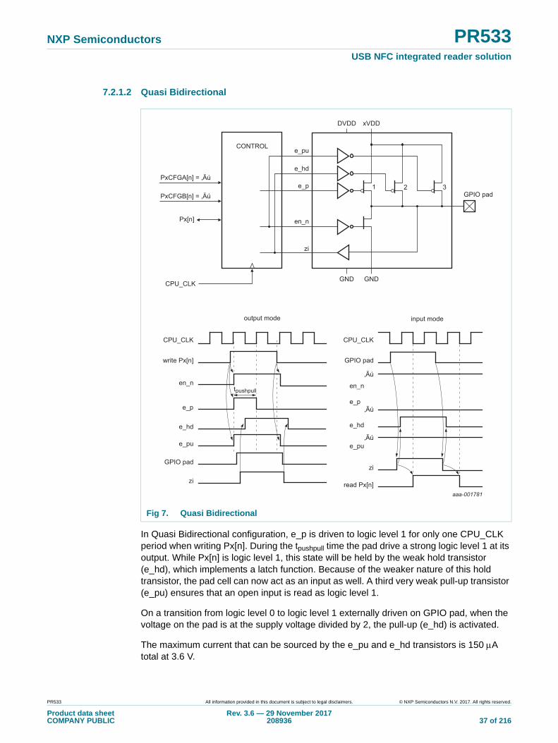
7.2.1.2 Quasi Bidirectional
In Quasi Bidirectional configuration, e_p is driven to logic level 1 for only one CPU_CLK period when writing Px[n]. During the tpushpull time the pad drive a strong logic level 1 at its output. While Px[n] is logic level 1, this state will be held by the weak hold transistor (e_hd), which implements a latch function. Because of the weaker nature of this hold transistor, the pad cell can now act as an input as well. A third very weak pull-up transistor (e_pu) ensures that an open input is read as logic level 1.
On a transition from logic level 0 to logic level 1 externally driven on GPIO pad, when the voltage on the pad is at the supply voltage divided by 2, the pull-up (e_hd) is activated.
The maximum current that can be sourced by the e_pu and e_hd transistors is 150 A total at 3.6 V.
Fig 7. Quasi Bidirectional
output mode input mode
1 2
Px[n]
zi
e_hd
e_pu
e_p
en_n
DVDD
GND GND
xVDD
3
CONTROL
GPIO pad
CPU_CLK
PxCFGA[n] = “
PxCFGB[n] = “
aaa-001781
en_n
zi
read Px[n]
GPIO pad
CPU_CLK
e_p
e_hd
e_pu
“
“
“
CPU_CLK
en_n
e_hd
write Px[n]
e_p
GPIO pad
e_pu
zi
tpushpull
PR533 All information provided in this document is subject to legal disclaimers. © NXP Semiconductors N.V. 2017. All rights reserved.
Product data sheetCOMPANY PUBLIC
Rev. 3.6 — 29 November 2017208936 37 of 216
NXP Semiconductors PR533USB NFC integrated reader solution
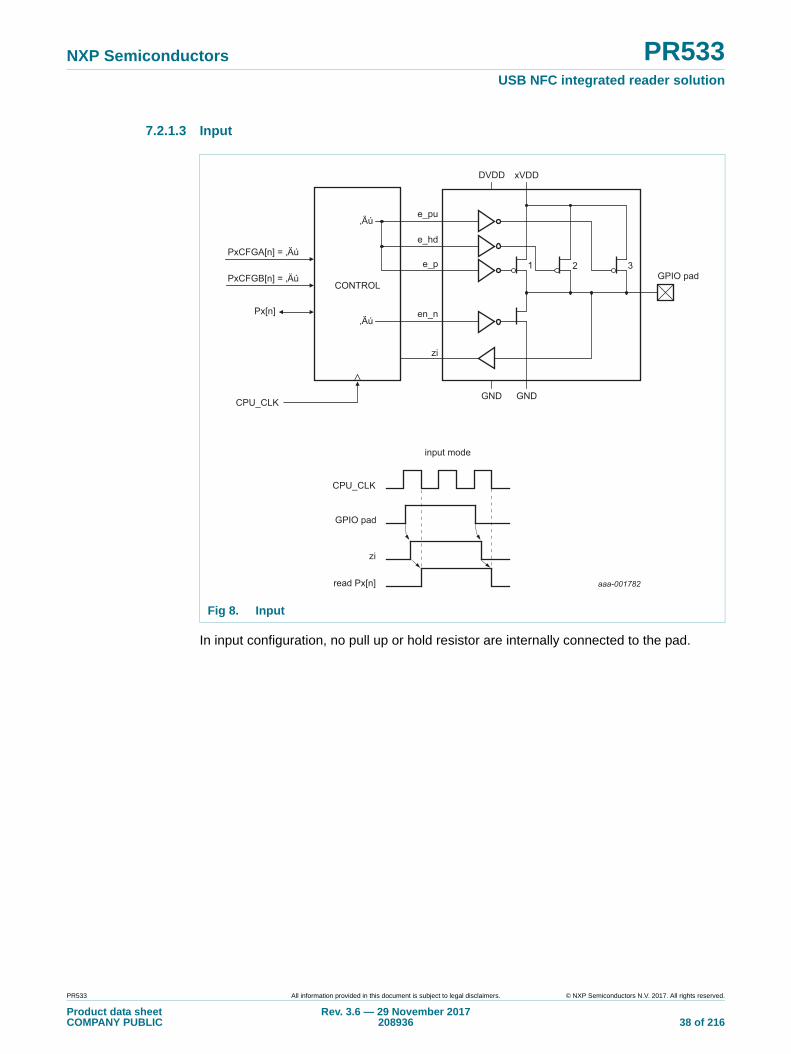
7.2.1.3 Input
In input configuration, no pull up or hold resistor are internally connected to the pad.
Fig 8. Input
input mode
Px[n]
zi
e_hd
e_pu
e_p
en_n
DVDD
GND GND
xVDD
CONTROL
“
“
GPIO pad
CPU_CLK
PxCFGA[n] = “
PxCFGB[n] = “
aaa-001782
zi
read Px[n]
GPIO pad
CPU_CLK
1 2 3
PR533 All information provided in this document is subject to legal disclaimers. © NXP Semiconductors N.V. 2017. All rights reserved.
Product data sheetCOMPANY PUBLIC
Rev. 3.6 — 29 November 2017208936 38 of 216
NXP Semiconductors PR533USB NFC integrated reader solution
7.2.1.4 Push-pull output
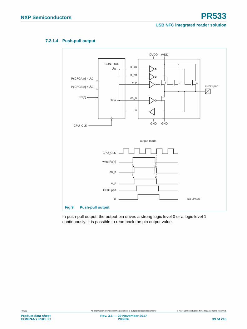
In push-pull output, the output pin drives a strong logic level 0 or a logic level 1 continuously. It is possible to read back the pin output value.
Fig 9. Push-pull output
output mode
Px[n]
zi
e_hd
e_pu
e_p
en_n
DVDD
GND GND
xVDD
CONTROL
“
Data
GPIO pad
CPU_CLK
PxCFGA[n] = “
PxCFGB[n] = “
aaa-001783
CPU_CLK
en_n
write Px[n]
e_p
GPIO pad
zi
1 2 3
PR533 All information provided in this document is subject to legal disclaimers. © NXP Semiconductors N.V. 2017. All rights reserved.
Product data sheetCOMPANY PUBLIC
Rev. 3.6 — 29 November 2017208936 39 of 216

NXP Semiconductors PR533USB NFC integrated reader solution
7.2.2 GPIO registers description
7.2.2.1 P7CFGA register
7.2.2.2 P7CFGB register
7.2.2.3 P7 register
Table 60. P7CFGA register (SFR: address F4h) bit allocation
Bit 7 6 5 4 3 2 1 0
Symbol - - - - - - - P7CFGA[0]
Reset 1 1 1 1 1 1 1 1
Access R R R R R R R R/W
Table 61. Description of P7CFGA bits
Bit Symbol Description
7 to 1 - reserved.
0 P7CFGA[0] with the P7CFGB[0], it configures the functional mode of P70_IRQ pin.
Table 62. P7CFGB register (SFR: address F5h) bit allocation
Bit 7 6 5 4 3 2 1 0
Symbol - - - - - - - P7CFGB[0]
Reset 0 0 0 0 0 0 0 0
Access R R R R R R R R/W
Table 63. Description of P7CFGB bits
Bit Symbol Description
7 to 1 - Reserved.
0 P7CFGB[0] with the P7CFGA[0], it configures the functional mode of P70_IRQ pin.
Table 64. P7 register (SFR: address F7h) bit allocation
Bit 7 6 5 4 3 2 1 0
Symbol - - - - - - - P7[0]
Reset 1 1 1 1 1 1 1 1
Access R R R R R R R R/W
Table 65. Description of P7 bits
Bit Symbol Description
7 to 1 - Reserved.
0 P7[0] Writing to P7[0] writes the corresponding value to the P70_IRQ pin according to the configuration mode defined by P7CFGA[0] and P7CFGB[0].
Reading from P7[0] reads the state of P70_IRQ pin.
PR533 All information provided in this document is subject to legal disclaimers. © NXP Semiconductors N.V. 2017. All rights reserved.
Product data sheetCOMPANY PUBLIC
Rev. 3.6 — 29 November 2017208936 40 of 216
NXP Semiconductors PR533USB NFC integrated reader solution
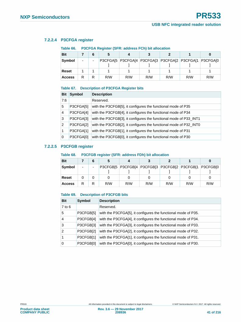
7.2.2.4 P3CFGA register
7.2.2.5 P3CFGB register
Table 66. P3CFGA Register (SFR: address FCh) bit allocation
Bit 7 6 5 4 3 2 1 0
Symbol - - P3CFGA[5]
P3CFGA[4]
P3CFGA[3]
P3CFGA[2]
P3CFGA[1]
P3CFGA[0]
Reset 1 1 1 1 1 1 1 1
Access R R R/W R/W R/W R/W R/W R/W
Table 67. Description of P3CFGA Register bits
Bit Symbol Description
7:6 Reserved.
5 P3CFGA[5] with the P3CFGB[5], it configures the functional mode of P35
4 P3CFGA[4] with the P3CFGB[4], it configures the functional mode of P34
3 P3CFGA[3] with the P3CFGB[3], it configures the functional mode of P33_INT1
2 P3CFGA[2] with the P3CFGB[2], it configures the functional mode of P32_INT0
1 P3CFGA[1] with the P3CFGB[1], it configures the functional mode of P31
0 P3CFGA[0] with the P3CFGB[0], it configures the functional mode of P30
Table 68. P3CFGB register (SFR: address FDh) bit allocation
Bit 7 6 5 4 3 2 1 0
Symbol - - P3CFGB[5]
P3CFGB[4]
P3CFGB[3]
P3CFGB[2]
P3CFGB[1]
P3CFGB[0]
Reset 0 0 0 0 0 0 0 0
Access R R R/W R/W R/W R/W R/W R/W
Table 69. Description of P3CFGB bits
Bit Symbol Description
7 to 6 Reserved.
5 P3CFGB[5] with the P3CFGA[5], it configures the functional mode of P35.
4 P3CFGB[4] with the P3CFGA[4], it configures the functional mode of P34.
3 P3CFGB[3] with the P3CFGA[3], it configures the functional mode of P33.
2 P3CFGB[2] with the P3CFGA[2], it configures the functional mode of P32.
1 P3CFGB[1] with the P3CFGA[1], it configures the functional mode of P31.
0 P3CFGB[0] with the P3CFGA[0], it configures the functional mode of P30.
PR533 All information provided in this document is subject to legal disclaimers. © NXP Semiconductors N.V. 2017. All rights reserved.
Product data sheetCOMPANY PUBLIC
Rev. 3.6 — 29 November 2017208936 41 of 216

NXP Semiconductors PR533USB NFC integrated reader solution
7.2.2.6 P3 register
Table 70. P3 register (SFR: address B0h) bit allocation
Bit 7 6 5 4 3 2 1 0
Symbol - - P3[5] P3[4] P3[3] P3[2] P3[1] P3[0]
Reset 1 1 1 1 1 1 1 1
Access R R R/W R/W R/W R/W R/W R/W
Table 71. Description of P3 bits
Bit Symbol Description
7 to 6 - Reserved.
5 P3[5] Writing to P3[5] writes the corresponding value to P35 pin according to the configuration mode defined by P3CFGA[5] and P3CFGB[5].
Reading from P3[5] reads the state of P35 pin.
4 P3[4] When P34 alternate function SIC_CLK is not used, writing to P3[4] writes the corresponding value to P34 pin according to the configuration mode defined by P3CFGA[4] and P3CFGB[4].
Reading from P3[4] reads the state of P34 pin.
3 P3[3] Writing to P3[3] writes the corresponding value to P33_INT1 pin according to the configuration mode defined by P3CFGA[3] and P3CFGB[3].
Reading from P3[3] reads the state of P33_INT1 pin.
2 P3[2] Writing to P3[2] writes the corresponding value to P32_INT0 pin according to the configuration mode defined by P3CFGA[2] and P3CFGB[2].
Reading from P3[2] reads the state of P32_INT0 pin.
1 P3[1] When the P31 pin alternate function UART_TX is not used, writing to P3[1] writes the corresponding value to P31 pin according to the configuration mode defined by P3CFGA[1] and P3CFGB[1].
Reading from P3[1] reads the state of P31 pin.
0 P3[0] When the P30 pin alternate function UART_RX is not used, writing to P3[0] writes the corresponding value to P30 pin according to the configuration mode defined by P3CFGA[0] and P3CFGB[0].
Reading from P3[0] reads the state of P30 pin.
PR533 All information provided in this document is subject to legal disclaimers. © NXP Semiconductors N.V. 2017. All rights reserved.
Product data sheetCOMPANY PUBLIC
Rev. 3.6 — 29 November 2017208936 42 of 216

NXP Semiconductors PR533USB NFC integrated reader solution
7.2.2.7 P5 register
Remark: P5 supports only open drain mode
7.3 Host interfaces
PR533 must be able to support different kind of interfaces to communicate with the HOST. All the interfaces that have to be supported are exclusive.
• USB interface
• High Speed UART (HSU): supporting specific high baud rates
Table 72. P5 register (SFR: address D7h) bit allocation
Bit 7 6 5 4 3 2 1 0
Symbol - - - - - P5[2] P5[1] P5[0]
Reset 1 1 1 1 1 1 1 1
Access R R R R R R R/W R/W
Table 73. Description of P5 bits
Bit Symbol Description
7 to 3 - Reserved.
2 P5[2] Bit 2 of P5 register is attached to USB signal “MP_ready” that indicates USb block is ready for a new transaction like write command, write data or read data.
This bit is polled by embeded firmware that manage USB transactions.
1 P5[1] Writing to P5[1] writes the corresponding value to SDA I2C pin according to the open drain configuration mode.
Reading from P5[1] reads the state of SDA I2C pin.
0 P5[0] Writing to P5[0] writes the corresponding value to SCL of the I2C pin according to the open drain configuration mode.
Reading from P5[0] reads the state of NSS I2C pin.
PR533 All information provided in this document is subject to legal disclaimers. © NXP Semiconductors N.V. 2017. All rights reserved.
Product data sheetCOMPANY PUBLIC
Rev. 3.6 — 29 November 2017208936 43 of 216

NXP Semiconductors PR533USB NFC integrated reader solution
7.3.1 MATX description
After every Power-On or Hard Reset (RSTPD_N at low level), the PR533 also resets its interfaces and checks the current HOST interface type.
The PR533 identifies the selected HOST interface with the logic levels on the control pins I0 and I1 after the Reset Phase. This is done by a combination of fixed pin connections
The Power for the MATX is delivered from PVDD.The firmware must copy the value of the pads I0 and I1 to respectively selif[0] and selif[1].
7.3.1.1 MATX register
The Config I0_I1 register is used to select the host interface. It manages also the polarity of P33_INT1.
Fig 10. Host interface block diagram
PN533
CPU
HOST INTERFACES
I2C
SPI
HSU
RAMFIFOMANAGER
MIF HOST
selif(1:0)
aaa-001784
Table 74. HOST interface selection
PR533 Host Interface selected
Pin number Config_I0_I1 register
HSU“3.3 V external source”
HSU“3.3 V external source”
USB“3.3 V external source”
USB“5 V source”
18 selif[1] 0 1 0 1
17 selif[0] 0 0 1 1
25 DP RX RX DP DP
24 DM TX TX DM DM
PR533 All information provided in this document is subject to legal disclaimers. © NXP Semiconductors N.V. 2017. All rights reserved.
Product data sheetCOMPANY PUBLIC
Rev. 3.6 — 29 November 2017208936 44 of 216

NXP Semiconductors PR533USB NFC integrated reader solution
7.3.1.2 Pads NSS/P50_SCL/HSU_RX and MOSI/SDA / HSU_TX
The I2C SDA and SCL IO ports are configured in open drain mode. A pull-up resistor is required for both pins to output or read a logic ‘1’.In HSU mode, HSU_RX is in input mode and HSU_TX is in push-pull mode.
7.3.2 I2C interface
It is recommended to refer the I2C standard for more information.
The I2C interface implements a Master I2C bus interface with integrated shift register, shift timing generation. I2C Standard mode (100 kHz SCLK) and Fast mode (400 kHz SCLK) are supported.
General Call +W is supported, not hardware General Call (GC +R).
The mains characteristics of the I2C module are:
• Support Master I2C bus
• Standard and Fast mode supported
The I2C module is control through 5 registers:
Table 75. Config I0_I1 register (address 6103h) bit allocation
Bit 7 6 5 4 3 2 1 0
Symbol int1_pol - pad_I1 - pad_I0 enselif Selif[1:0]
Reset 0 0 X 0 X 0 0 0
Access R/W R R/W R R/W R/W R/W R/W
Table 76. Description of Config I0_I1 bits
Bit Symbol Description
7 int1_pol When set to logic 1, the value of the P33_INT1 pin is inverted.
6 - Reserved.
5 pad_I1 When read this bit gives the state of the I1 pin.
4 - Reserved.
3 pad_I0 When read this bit gives the state of the I0 pin.
2 enselif When set to logic 1, this bit indicates that the selif bits are valid and that the selected interface on the MIF can drive the pins.The firmware must copy the value of the pads I0 and I1 to respectively selif[0] and selif[1]
When set to logic 0, the MIF cannot drive the IO lines.
1 to 0 Selif[1:0] These bits are used by the firmware to select the host interface communication link, see Table 74 on page 44.
Table 77. I2C register list
Name Size[bytes]
Address Description Access
I2CCON 1 D8h (SFR) Control register R/W
I2CSTA 1 D9h (SFR) Status register R/W
I2CDAT 1 DAh (SFR) Data register R/W
I2CADR 1 DBh (SFR) Slave Address register R/W
PR533 All information provided in this document is subject to legal disclaimers. © NXP Semiconductors N.V. 2017. All rights reserved.
Product data sheetCOMPANY PUBLIC
Rev. 3.6 — 29 November 2017208936 45 of 216

NXP Semiconductors PR533USB NFC integrated reader solution
7.3.2.1 I2C functional description
The I2C interface may operate in any of the following two modes:
• Master Transmitter
• Master Receiver
Two types of data transfers are possible on the I2C bus:
• Data transfer from a Master transmitter to a Slave receiver. The first byte transmitted by the Master is the Slave address. Next follows a number of data bytes. The Slave returns an acknowledge bit after each received byte.
• Data transfer from a Slave transmitter to a Master receiver. The first byte (the Slave address) is transmitted by the Master. The Slave then returns an acknowledge bit. Next follows the data bytes transmitted by the Slave to the Master. The Master returns an acknowledge bit after each received byte except the last byte. At the end of the last received byte, a “not acknowledge” is returned.
In a given application, the I2C interface may operate as a Master or as a Slave.
In the Slave mode, the I2C interface hardware looks for its own Slave address and the general call address. If one of these addresses is detected, an interrupt is requested. When the PR533 microcontroller wishes to become the bus Master, the hardware waits until the bus is free before the Master mode is entered so that a possible Slave action is not interrupted. If bus arbitration is lost in the Master mode, the I2C interface switches to the Slave mode immediately and can detect its own Slave address in the same serial transfer.
7.3.2.2 Master transmitter mode
As a Master, the I2C logic will generate all of the serial clock pulses and the START and STOP conditions. A transfer is ended with a STOP condition or with a repeated START condition. Since a repeated START condition is also the beginning of the next serial transfer, the I2C bus will not be released.
I2C data are output through SDA while P50_SCL outputs the serial clock. The first byte transmitted contains the Slave address of the receiving device (7-bit SLA) and the data direction bit. In this case the data direction bit (R/W) will be a logic ‘0’ (W). I2C data are transmitted 8 bits at a time. After each byte is transmitted, an acknowledge bit is received. START and STOP conditions are output to indicate the beginning and the end of a serial transfer.
In the Master transmitter mode, a number of data bytes can be transmitted to the Slave receiver. Before the Master transmitter mode can be entered, I2CCON must be initialized with the ENS1 bit set to logic level 1 and the STA, STO and SI bits set to logic level 0. ENS1 must be set to logic level 1 to enable the I2C interface. If the AA bit is set to logic level 0, the I2C interface will not acknowledge its own Slave address or the general call address if they are present on the bus. This will prevent the I2C interface from entering a Slave mode.
The Master transmitter mode may now be entered by setting the STA bit. The I2C interface logic will then test the I2C bus and generate a start condition as soon as the bus becomes free. When a START condition is transmitted, the serial interrupt flag (SI) is set to logic level 1, and the status code in the status register (I2CSTA) will be 08h. This status
PR533 All information provided in this document is subject to legal disclaimers. © NXP Semiconductors N.V. 2017. All rights reserved.
Product data sheetCOMPANY PUBLIC
Rev. 3.6 — 29 November 2017208936 46 of 216
NXP Semiconductors PR533USB NFC integrated reader solution
code must be used to vector to an interrupt service routine that loads I2CDAT with the Slave address and the data direction bit (SLA+W). The SI bit in I2CCON must then be set to logic level 0 before the serial transfer can continue.
When the Slave address and the direction bit have been transmitted and an acknowledgment bit has been received, the serial interrupt flag (SI) is set to logic level 1 again, and a number of status codes in I2CSTA are possible. The appropriate action to be taken for any of the status codes is detailed in Table 82 on page 52. After a repeated start condition (state 10h), the I2C interface may switch to the Master receiver mode by loading I2CDAT with SLA+R.
7.3.2.3 Master receiver mode
As a Master, the I2C logic will generate all of the serial clock pulses and the START and STOP conditions. A transfer is ended with a STOP condition or with a repeated START condition. Since a repeated START condition is also the beginning of the next serial transfer, the I2C bus will not be released.
The first byte transmitted contains the Slave address of the transmitting device (7-bit SLA) and the data direction bit. In this case the data direction bit (R/W) will be logic level 1 (R). I2C data are received via SDA while P50_SCL outputs the serial clock. I2C data are received 8 bits at a time. After each byte is received, an acknowledge bit is transmitted. START and STOP conditions are output to indicate the beginning and end of a serial transfer.
In the Master receiver mode, a number of data bytes are received from a Slave transmitter. The transfer is initialized as in the Master transmitter mode. When the START condition has been transmitted, the interrupt service routine must load I2CDAT with the 7-bit Slave address and the data direction bit (SLA+R). The SI bit in I2CCON must then be set to logic 0 before the serial transfer can continue.
When the Slave address and the data direction bit have been transmitted and an acknowledgment bit has been received, the serial interrupt flag (SI) is set to logic level 1 again, and a number of status codes are possible in I2CSTA. The appropriate action to be taken for each of the status codes is detailed in Table 83 on page 53. After a repeated start condition (state 10h), the I2C interface may switch to the Master transmitter mode by loading I2CDAT with SLA+W.
7.3.2.4 I2CCON register
The CPU can read from and write to this 8-bit SFR. Two bits are affected by the Serial IO (the I2C interface) hardware: the SI bit is set to logic level 1 when a serial interrupt is requested, and the STO bit is set to logic level 0 when a STOP condition is present on the I2C bus. The STO bit is also set to logic level 0 when ENS1 = ‘0’.
Table 78. I2CCON register (SFR: address D8h) bit allocation
Bit 7 6 5 4 3 2 1 0
Symbol CR[2] ENS1 STA STO SI AA CR[1:0]
Reset 0 0 0 0 0 0 0 0
Access R/W R/W R/W R/W R/W R/W R/W R/W
PR533 All information provided in this document is subject to legal disclaimers. © NXP Semiconductors N.V. 2017. All rights reserved.
Product data sheetCOMPANY PUBLIC
Rev. 3.6 — 29 November 2017208936 47 of 216
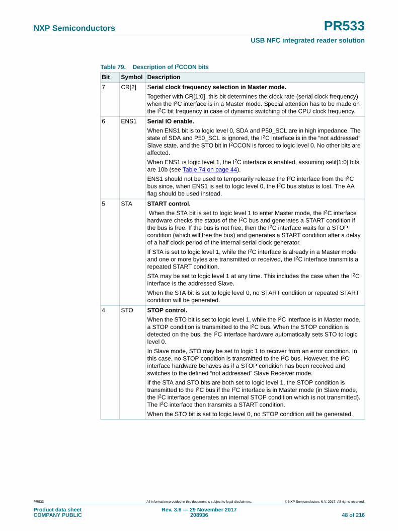
NXP Semiconductors PR533USB NFC integrated reader solution
Table 79. Description of I2CCON bits
Bit Symbol Description
7 CR[2] Serial clock frequency selection in Master mode.
Together with CR[1:0], this bit determines the clock rate (serial clock frequency) when the I2C interface is in a Master mode. Special attention has to be made on the I2C bit frequency in case of dynamic switching of the CPU clock frequency.
6 ENS1 Serial IO enable.
When ENS1 bit is to logic level 0, SDA and P50_SCL are in high impedance. The state of SDA and P50_SCL is ignored, the I2C interface is in the “not addressed” Slave state, and the STO bit in I2CCON is forced to logic level 0. No other bits are affected.
When ENS1 is logic level 1, the I2C interface is enabled, assuming selif[1:0] bits are 10b (see Table 74 on page 44).
ENS1 should not be used to temporarily release the I2C interface from the I2C bus since, when ENS1 is set to logic level 0, the I2C bus status is lost. The AA flag should be used instead.
5 STA START control.
When the STA bit is set to logic level 1 to enter Master mode, the I2C interface hardware checks the status of the I2C bus and generates a START condition if the bus is free. If the bus is not free, then the I2C interface waits for a STOP condition (which will free the bus) and generates a START condition after a delay of a half clock period of the internal serial clock generator.
If STA is set to logic level 1, while the I2C interface is already in a Master mode and one or more bytes are transmitted or received, the I2C interface transmits a repeated START condition.
STA may be set to logic level 1 at any time. This includes the case when the I2C interface is the addressed Slave.
When the STA bit is set to logic level 0, no START condition or repeated START condition will be generated.
4 STO STOP control.
When the STO bit is set to logic level 1, while the I2C interface is in Master mode, a STOP condition is transmitted to the I2C bus. When the STOP condition is detected on the bus, the I2C interface hardware automatically sets STO to logic level 0.
In Slave mode, STO may be set to logic 1 to recover from an error condition. In this case, no STOP condition is transmitted to the I2C bus. However, the I2C interface hardware behaves as if a STOP condition has been received and switches to the defined “not addressed” Slave Receiver mode.
If the STA and STO bits are both set to logic level 1, the STOP condition is transmitted to the I2C bus if the I2C interface is in Master mode (in Slave mode, the I2C interface generates an internal STOP condition which is not transmitted). The I2C interface then transmits a START condition.
When the STO bit is set to logic level 0, no STOP condition will be generated.
PR533 All information provided in this document is subject to legal disclaimers. © NXP Semiconductors N.V. 2017. All rights reserved.
Product data sheetCOMPANY PUBLIC
Rev. 3.6 — 29 November 2017208936 48 of 216

NXP Semiconductors PR533USB NFC integrated reader solution
3 SI Serial interrupt flag.
When SI is set to logic level 1, then if the serial interrupt from the I2C interface port is enabled, the CPU will receive an interrupt. SI is set by hardware when any one of 25 of the possible 26 states of the I2C interface are entered. The only state that does not cause SI to be set to logic level 1 is state F8h, which indicates that no relevant state information is available. While SI is set by hardware to logic level 1, P50_SCL is held in logic 0 when the SCL line is logic level 0, and P50_SCL is held in high impedance when the SCL line is logic level 1.
SI must be set to logic level 0 by firmware.When the SI flag is set to logic level 0, no serial interrupt is requested, and there is no stretching of the SCL line via P50_SCL.
The bit IE1_4 of register IE1 (see Table 13 on page 16) has also to be set to logic level 1 to enable the corresponding I2C interrupt to the CPU.
2 AA Assert Acknowledge flag.
If AA is set to logic level 1, an acknowledge (low level to SDA) will be returned during the acknowledge clock pulse on the P50_SCL line when:
• The “own Slave address” has been received.
• The general call address has been received while the general call bit (GC) in I2CADR is set.
• A data byte has been received while the I2C interface is in Master Receiver mode.
• A data byte has been received while the I2C interface is in the addressed Slave Receiver mode.
When the I2C interface is in the addressed Slave Transmitter mode, state C8h will be entered after the last serial bit is transmitted. When SI is set to logic level 0, the I2C interface leaves state C8h, enters the Not-addressed Slave Receiver mode, and the SDA line remains at logic 1. In state C8h, AA can be set to logic level 1 again for future address recognition.
When the I2C interface is in the Not-addressed Slave mode, its own Slave address and the general call address are ignored. Consequently, no acknowledge is returned, and a serial interrupt is not requested. Thus, the I2C interface can be temporarily released from the I2C bus while the bus status is monitored. While the I2C interface is released from the bus, START and STOP conditions are detected, and I2C data are shifted in. Address recognition can be resumed at any time by setting AA to logic level 1.
If AA is set to logic level 1 when the I2C own Slave address or the general call address has been partly received, the address will be recognized at the end of the byte transmission.
Table 79. Description of I2CCON bits …continued
Bit Symbol Description
PR533 All information provided in this document is subject to legal disclaimers. © NXP Semiconductors N.V. 2017. All rights reserved.
Product data sheetCOMPANY PUBLIC
Rev. 3.6 — 29 November 2017208936 49 of 216
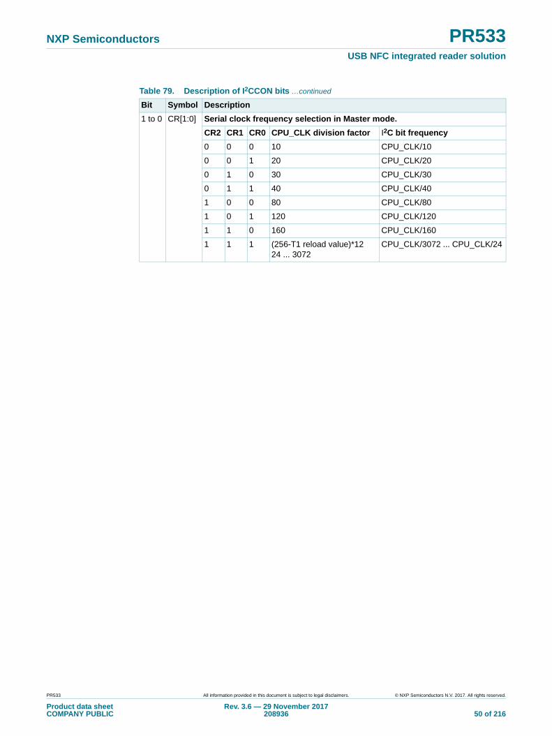
NXP Semiconductors PR533USB NFC integrated reader solution
1 to 0 CR[1:0] Serial clock frequency selection in Master mode.
CR2 CR1 CR0 CPU_CLK division factor I2C bit frequency
0 0 0 10 CPU_CLK/10
0 0 1 20 CPU_CLK/20
0 1 0 30 CPU_CLK/30
0 1 1 40 CPU_CLK/40
1 0 0 80 CPU_CLK/80
1 0 1 120 CPU_CLK/120
1 1 0 160 CPU_CLK/160
1 1 1 (256-T1 reload value)*1224 ... 3072
CPU_CLK/3072 ... CPU_CLK/24
Table 79. Description of I2CCON bits …continued
Bit Symbol Description
PR533 All information provided in this document is subject to legal disclaimers. © NXP Semiconductors N.V. 2017. All rights reserved.
Product data sheetCOMPANY PUBLIC
Rev. 3.6 — 29 November 2017208936 50 of 216
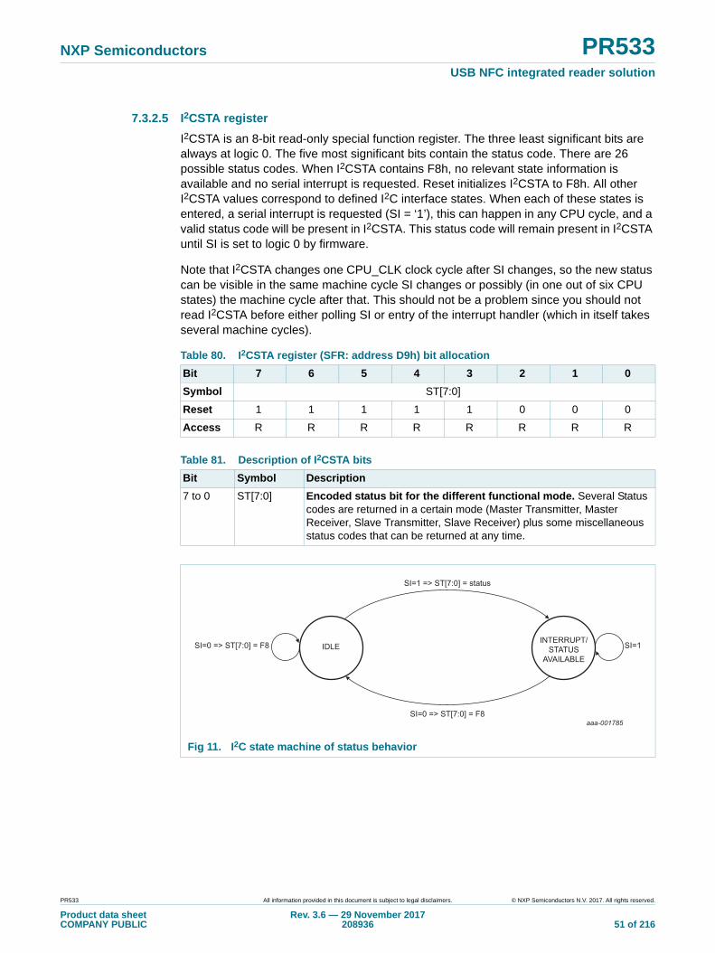
NXP Semiconductors PR533USB NFC integrated reader solution
7.3.2.5 I2CSTA register
I2CSTA is an 8-bit read-only special function register. The three least significant bits are always at logic 0. The five most significant bits contain the status code. There are 26 possible status codes. When I2CSTA contains F8h, no relevant state information is available and no serial interrupt is requested. Reset initializes I2CSTA to F8h. All other I2CSTA values correspond to defined I2C interface states. When each of these states is entered, a serial interrupt is requested (SI = ‘1’), this can happen in any CPU cycle, and a valid status code will be present in I2CSTA. This status code will remain present in I2CSTA until SI is set to logic 0 by firmware.
Note that I2CSTA changes one CPU_CLK clock cycle after SI changes, so the new status can be visible in the same machine cycle SI changes or possibly (in one out of six CPU states) the machine cycle after that. This should not be a problem since you should not read I2CSTA before either polling SI or entry of the interrupt handler (which in itself takes several machine cycles).
Table 80. I2CSTA register (SFR: address D9h) bit allocation
Bit 7 6 5 4 3 2 1 0
Symbol ST[7:0]
Reset 1 1 1 1 1 0 0 0
Access R R R R R R R R
Table 81. Description of I2CSTA bits
Bit Symbol Description
7 to 0 ST[7:0] Encoded status bit for the different functional mode. Several Status codes are returned in a certain mode (Master Transmitter, Master Receiver, Slave Transmitter, Slave Receiver) plus some miscellaneous status codes that can be returned at any time.
Fig 11. I2C state machine of status behavior
aaa-001785
IDLE
SI=1 => ST[7:0] = status
SI=0 => ST[7:0] = F8
INTERRUPT/STATUS
AVAILABLE
SI=1SI=0 => ST[7:0] = F8
PR533 All information provided in this document is subject to legal disclaimers. © NXP Semiconductors N.V. 2017. All rights reserved.
Product data sheetCOMPANY PUBLIC
Rev. 3.6 — 29 November 2017208936 51 of 216

xxxxxxxxxxxxxxxxxxxxx xxxxxxxxxxxxxxxxxxxxxxxxxx xxxxxxx x x x xxxxxxxxxxxxxxxxxxxxxxxxxxxxxx xxxxxxxxxxxxxxxxxxx xx xx xxxxx xxxxxxxxxxxxxxxxxxxxxxxxxxx xxxxxxxxxxxxxxxxxxx xxxxxx xxxxxxxxxxxxxxxxxxxxxxxxxxxxxxxxxxx xxxxxxxxxxxx x x xxxxxxxxxxxxxxxxxxxxx xxxxxxxxxxxxxxxxxxxxxxxxxxxxxx xxxxx xxxxxxxxxxxxxxxxxxxxxxxxxxxxxxxxxxxxxxxxxxxxxxxxxx xxxxxxxx xxxxxxxxxxxxxxxxxxxxxxxxx xxxxxxxxxxxxxxxxxxxx xxx
PR
533
Pro
du
ct data sh
eetC
OM
PA
NY
PU
BL
ICR
ev. 3.6 —
29 N
ove
mb
er 2
017208936
52 of 216
NX
P S
emico
nd
ucto
rsP
R533
US
B N
FC
integ
rated read
er solu
tion
Table 82. I2C Master Transmitter Mode status code
Status Status of the I2C Bus Application firmware Response Next Action Taken By the I2C interface Hardware
received
T/(TRX or REC) mode
ill be received
ondition will be transmitted
ondition will be transmitted
ill be received
ondition will be transmitted
All inform
ation provided
in this docum
ent is subject to leg
al disclaim
ers.©
NX
P S
em
iconductors N
.V. 2017. A
ll rights rese
rved.
Code ST[7:0]
and of theI2C interface Hardware
To/from I2CDAT TO I2CCON
STA STO SI AA
08h A START condition has been transmitted
Load SLA+W X 0 0 X SLA+W will be transmitted ACK will be
10h A repeated START condition has been transmitted
Load SLA+W X 0 0 X As above
Load SLA+R X 0 0 X SLA+W will be transmitted;the I2C interface will be switched to MS
18h SLA+W has been transmitted; ACK has been received
Load data byte 0 0 0 X Data byte will be transmitted; ACK bit w
No I2CDAT action 1 0 0 X Repeated START will be transmitted
No I2CDAT action 0 1 0 X STOP condition will be transmittedSTO flag will be set to logic level 0
No I2CDAT action 1 1 0 X STOP condition followed by a START cSTO flag will be set to logic level 0
20h SLA+W has been transmitted; NOT ACK has been received
Load data byte 0 0 0 X Data byte will be transmittedACK bit will be received
No I2CDAT action 1 0 0 X Repeated START will be transmitted
No I2CDAT action 0 1 0 X STOP condition will be transmittedSTO flag will be set to logic level 0
No I2CDAT action 1 1 0 X STOP condition followed by a START cSTO flag will be set to logic level 0
28h Write data byte in I2CDAT has been transmitted; ACK has been received
Load data byte 0 0 0 X Data byte will be transmitted; ACK bit w
No I2CDAT action 1 0 0 X Repeated START will be transmitted
No I2CDAT action 0 1 0 X STOP condition will be transmittedSTO flag will be set to logic level 0
No I2CDAT action 1 1 0 X STOP condition followed by a START cSTO flag will be set to logic level 0
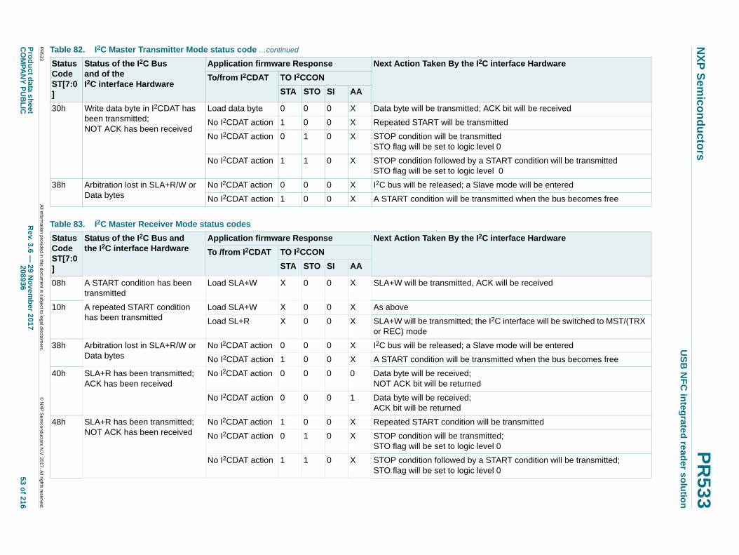
xxxxxxxxxxxxxxxxxxxxx xxxxxxxxxxxxxxxxxxxxxxxxxx xxxxxxx x x x xxxxxxxxxxxxxxxxxxxxxxxxxxxxxx xxxxxxxxxxxxxxxxxxx xx xx xxxxx xxxxxxxxxxxxxxxxxxxxxxxxxxx xxxxxxxxxxxxxxxxxxx xxxxxx xxxxxxxxxxxxxxxxxxxxxxxxxxxxxxxxxxx xxxxxxxxxxxx x x xxxxxxxxxxxxxxxxxxxxx xxxxxxxxxxxxxxxxxxxxxxxxxxxxxx xxxxx xxxxxxxxxxxxxxxxxxxxxxxxxxxxxxxxxxxxxxxxxxxxxxxxxx xxxxxxxx xxxxxxxxxxxxxxxxxxxxxxxxx xxxxxxxxxxxxxxxxxxxx xxx
PR
533
Pro
du
ct data sh
eetC
OM
PA
NY
PU
BL
ICR
ev. 3.6 —
29 N
ove
mb
er 2
017208936
53 of 216
NX
P S
emico
nd
ucto
rsP
R533
US
B N
FC
integ
rated read
er solu
tion
ill be received
ondition will be transmitted
will be entered
hen the bus becomes free
Table 82. I2C Master Transmitter Mode status code …continued
Status Code
Status of the I2C Bus and of the
Application firmware Response Next Action Taken By the I2C interface Hardware2 2
e Hardware
received
face will be switched to MST/(TRX
will be entered
hen the bus becomes free
smitted
ondition will be transmitted;
All inform
ation provided
in this docum
ent is subject to leg
al disclaim
ers.©
NX
P S
em
iconductors N
.V. 2017. A
ll rights rese
rved.
30h Write data byte in I2CDAT has been transmitted; NOT ACK has been received
Load data byte 0 0 0 X Data byte will be transmitted; ACK bit w
No I2CDAT action 1 0 0 X Repeated START will be transmitted
No I2CDAT action 0 1 0 X STOP condition will be transmittedSTO flag will be set to logic level 0
No I2CDAT action 1 1 0 X STOP condition followed by a START cSTO flag will be set to logic level 0
38h Arbitration lost in SLA+R/W or Data bytes
No I2CDAT action 0 0 0 X I2C bus will be released; a Slave mode
No I2CDAT action 1 0 0 X A START condition will be transmitted w
ST[7:0]
I2C interface HardwareTo/from I CDAT TO I CCON
STA STO SI AA
Table 83. I2C Master Receiver Mode status codes
Status Code ST[7:0]
Status of the I2C Bus and the I2C interface Hardware
Application firmware Response Next Action Taken By the I2C interfac
To /from I2CDAT TO I2CCON
STA STO SI AA
08h A START condition has been transmitted
Load SLA+W X 0 0 X SLA+W will be transmitted, ACK will be
10h A repeated START condition has been transmitted
Load SLA+W X 0 0 X As above
Load SL+R X 0 0 X SLA+W will be transmitted; the I2C interor REC) mode
38h Arbitration lost in SLA+R/W or Data bytes
No I2CDAT action 0 0 0 X I2C bus will be released; a Slave mode
No I2CDAT action 1 0 0 X A START condition will be transmitted w
40h SLA+R has been transmitted; ACK has been received
No I2CDAT action 0 0 0 0 Data byte will be received;NOT ACK bit will be returned
No I2CDAT action 0 0 0 1 Data byte will be received;ACK bit will be returned
48h SLA+R has been transmitted; NOT ACK has been received
No I2CDAT action 1 0 0 X Repeated START condition will be tran
No I2CDAT action 0 1 0 X STOP condition will be transmitted;STO flag will be set to logic level 0
No I2CDAT action 1 1 0 X STOP condition followed by a START cSTO flag will be set to logic level 0
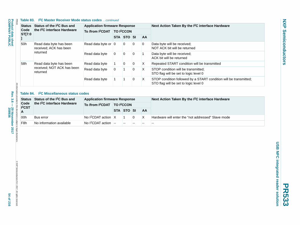
xxxxxxxxxxxxxxxxxxxxx xxxxxxxxxxxxxxxxxxxxxxxxxx xxxxxxx x x x xxxxxxxxxxxxxxxxxxxxxxxxxxxxxx xxxxxxxxxxxxxxxxxxx xx xx xxxxx xxxxxxxxxxxxxxxxxxxxxxxxxxx xxxxxxxxxxxxxxxxxxx xxxxxx xxxxxxxxxxxxxxxxxxxxxxxxxxxxxxxxxxx xxxxxxxxxxxx x x xxxxxxxxxxxxxxxxxxxxx xxxxxxxxxxxxxxxxxxxxxxxxxxxxxx xxxxx xxxxxxxxxxxxxxxxxxxxxxxxxxxxxxxxxxxxxxxxxxxxxxxxxx xxxxxxxx xxxxxxxxxxxxxxxxxxxxxxxxx xxxxxxxxxxxxxxxxxxxx xxx
PR
533
Pro
du
ct data sh
eetC
OM
PA
NY
PU
BL
ICR
ev. 3.6 —
29 N
ove
mb
er 2
017208936
54 of 216
NX
P S
emico
nd
ucto
rsP
R533
US
B N
FC
integ
rated read
er solu
tion
smitted
ondition will be transmitted;
Table 83. I2C Master Receiver Mode status codes …continued
Status Code
Status of the I2C Bus and the I2C interface Hardware
Application firmware Response Next Action Taken By the I2C interface Hardware2 2
e Hardware
” Slave mode
All inform
ation provided
in this docum
ent is subject to leg
al disclaim
ers.©
NX
P S
em
iconductors N
.V. 2017. A
ll rights rese
rved.
50h Read data byte has been received; ACK has been returned
Read data byte or 0 0 0 0 Data byte will be received;NOT ACK bit will be returned
Read data byte 0 0 0 1 Data byte will be received;ACK bit will be returned
58h Read data byte has been received; NOT ACK has been returned
Read data byte 1 0 0 X Repeated START condition will be tran
Read data byte 0 1 0 X STOP condition will be transmitted;STO flag will be set to logic level 0
Read data byte 1 1 0 X STOP condition followed by a START cSTO flag will be set to logic level 0
ST[7:0]
To /from I CDAT TO I CCON
STA STO SI AA
Table 84. I2C Miscellaneous status codes
Status Code I2CSTA
Status of the I2C Bus and the I2C interface Hardware
Application firmware Response Next Action Taken By the I2C interfac
To /from I2CDAT TO I2CCON
STA STO SI AA
00h Bus error No I2CDAT action X 1 0 X Hardware will enter the “not addressed
F8h No information available No I2CDAT action -- -- -- -- --
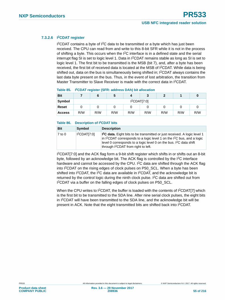
NXP Semiconductors PR533USB NFC integrated reader solution
7.3.2.6 I2CDAT register
I2CDAT contains a byte of I2C data to be transmitted or a byte which has just been received. The CPU can read from and write to this 8-bit SFR while it is not in the process of shifting a byte. This occurs when the I2C interface is in a defined state and the serial interrupt flag SI is set to logic level 1. Data in I2CDAT remains stable as long as SI is set to logic level 1. The first bit to be transmitted is the MSB (bit 7), and, after a byte has been received, the first bit of received data is located at the MSB of I2CDAT. While data is being shifted out, data on the bus is simultaneously being shifted in; I2CDAT always contains the last data byte present on the bus. Thus, in the event of lost arbitration, the transition from Master Transmitter to Slave Receiver is made with the correct data in I2CDAT.
I2CDAT[7:0] and the ACK flag form a 9-bit shift register which shifts in or shifts out an 8-bit byte, followed by an acknowledge bit. The ACK flag is controlled by the I2C interface hardware and cannot be accessed by the CPU. I2C data are shifted through the ACK flag into I2CDAT on the rising edges of clock pulses on P50_SCL. When a byte has been shifted into I2CDAT, the I2C data are available in I2CDAT, and the acknowledge bit is returned by the control logic during the ninth clock pulse. I2C data are shifted out from I2CDAT via a buffer on the falling edges of clock pulses on P50_SCL.
When the CPU writes to I2CDAT, the buffer is loaded with the contents of I2CDAT[7] which is the first bit to be transmitted to the SDA line. After nine serial clock pulses, the eight bits in I2CDAT will have been transmitted to the SDA line, and the acknowledge bit will be present in ACK. Note that the eight transmitted bits are shifted back into I2CDAT.
Table 85. I2CDAT register (SFR: address DAh) bit allocation
Bit 7 6 5 4 3 2 1 0
Symbol I2CDAT[7:0]
Reset 0 0 0 0 0 0 0 0
Access R/W R/W R/W R/W R/W R/W R/W R/W
Table 86. Description of I2CDAT bits
Bit Symbol Description
7 to 0 I2CDAT[7:0] I2C data. Eight bits to be transmitted or just received. A logic level 1 in I2CDAT corresponds to a logic level 1 on the I2C bus, and a logic level 0 corresponds to a logic level 0 on the bus. I2C data shift through I2CDAT from right to left.
PR533 All information provided in this document is subject to legal disclaimers. © NXP Semiconductors N.V. 2017. All rights reserved.
Product data sheetCOMPANY PUBLIC
Rev. 3.6 — 29 November 2017208936 55 of 216
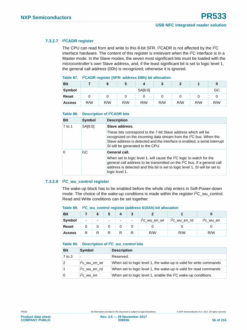
NXP Semiconductors PR533USB NFC integrated reader solution
7.3.2.7 I2CADR register
The CPU can read from and write to this 8-bit SFR. I2CADR is not affected by the I2C interface hardware. The content of this register is irrelevant when the I2C interface is in a Master mode. In the Slave modes, the seven most significant bits must be loaded with the microcontroller’s own Slave address, and, if the least significant bit is set to logic level 1, the general call address (00h) is recognized; otherwise it is ignored.
7.3.2.8 I2C_wu_control register
The wake-up block has to be enabled before the whole chip enters in Soft-Power-down mode. The choice of the wake-up conditions is made within the register I2C_wu_control. Read and Write conditions can be set together.
Table 87. I2CADR register (SFR: address DBh) bit allocation
Bit 7 6 5 4 3 2 1 0
Symbol SA[6:0] GC
Reset 0 0 0 0 0 0 0 0
Access R/W R/W R/W R/W R/W R/W R/W R/W
Table 88. Description of I2CADR bits
Bit Symbol Description
7 to 1 SA[6:0] Slave address.
These bits correspond to the 7-bit Slave address which will be recognized on the incoming data stream from the I2C bus. When the Slave address is detected and the interface is enabled, a serial interrupt SI will be generated to the CPU.
0 GC General call.
When set to logic level 1, will cause the I2C logic to watch for the general call address to be transmitted on the I2C bus. If a general call address is detected and this bit is set to logic level 1, SI will be set to logic level 1.
Table 89. I2C_wu_control register (address 610Ah) bit allocation
Bit 7 6 5 4 3 2 1 0
Symbol - - - - - i2c_wu_en_wr i2c_wu_en_rd i2c_wu_en
Reset 0 0 0 0 0 0 0 0
Access R R R R R R/W R/W R/W
Table 90. Description of I2C_wu_control bits
Bit Symbol Description
7 to 3 - Reserved.
2 i2c_wu_en_wr When set to logic level 1, the wake-up is valid for write commands
1 i2c_wu_en_rd When set to logic level 1, the wake-up is valid for read commands
0 i2c_wu_en When set to logic level 1, enable the I2C wake-up conditions
PR533 All information provided in this document is subject to legal disclaimers. © NXP Semiconductors N.V. 2017. All rights reserved.
Product data sheetCOMPANY PUBLIC
Rev. 3.6 — 29 November 2017208936 56 of 216

NXP Semiconductors PR533USB NFC integrated reader solution
7.3.3 FIFO manager
This block is designed to manage a RAM as a FIFO in order to optimize the data exchange between the CPU and the HOST.
7.3.3.1 FIFO manager functional description
The RAM used for the FIFO is shared between the SPI and HSU interfaces. Indeed, these interfaces cannot be used simultaneously. The selection of the interface used is done by firmware. The FIFO manager block is the common part between the USBB and the HSU interfaces. It consists of a Data register, a Status register and also some registers to define the characteristics of the FIFO. These registers are addressed by the CPU as SFRs.
The RAM used as a FIFO is divided into two part: a receive part and a transmit part.
This block also manages the possible conflicts existing around the FIFO between the CPU and the interfaces. Indeed, a request coming from the interface (TR_req or RCV_req) can be simultaneous with a request to access to the data register coming from the CPU.
9 SFR registers are needed to manage the FIFO manager.
Fig 12. FIFO manager block diagram
sfr_rd
sfr_wr
sfr_sel
DATA
irq
CPU
A controlD Q
HIGHSPEEDUART
USB
HSU_TR_Req
HSU_TR_Ack
HSU_RCV_Req
HSU_RCV_Ack
HSU_DATA
USB_control
USB_DATA
FIFOMANAGER
aaa-001786
PR533 All information provided in this document is subject to legal disclaimers. © NXP Semiconductors N.V. 2017. All rights reserved.
Product data sheetCOMPANY PUBLIC
Rev. 3.6 — 29 November 2017208936 57 of 216

NXP Semiconductors PR533USB NFC integrated reader solution
7.3.3.2 RWL register
This register defines the warning level of the Receive FIFO for the CPU. It implies a FIFO buffer overflow.
7.3.3.3 TWL register
This register defines the warning level of the Transmit FIFO for the CPU. It implies a FIFO buffer underflow.
Table 91. Fifo manager SFR register list
Name Size [bytes]
SFR Address
Description Access
RWL 1 9Ah FIFO Receive Waterlevel: Controls the threshold of the FIFO in reception
R/W
TWL 1 9Bh FIFO Transmit Waterlevel: Controls the threshold of the FIFO in transmission
R/W
FIFOFS 1 9Ch FIFO Transmit FreeSpace: Status of the number of characters which can still be loaded in the FIFO
R/W
FIFOFF 1 9Dh FIFO Receive Fullness: Status of the number of received characters in the FIFO
R/W
SFF 1 9Eh Global Status/Error messages R
FIT 1 9Fh Interrupt Source R/W
FITEN 1 A1h Interrupt Enable and Reset FIFO R
FDATA 1 A2h Data reception/transmission buffer R/W
FSIZE 1 A3h Control the size of the FIFO in Reception R/W
Table 92. RWL register (SFR: address 9Ah) bit allocation
Bit 7 6 5 4 3 2 1 0
Symbol RWaterlevel[7:0]
Reset 0 0 0 0 0 0 0 0
Access R/W R/W R/W R/W R/W R/W R/W R/W
Table 93. Description of RWL bits
Bit Symbol Description
7 to 0 RWaterlevel[7:0] Overflow threshold of the Receive FIFO to set a warning
Table 94. TWL register (SFR: address 9Bh) bit allocation
Bit 7 6 5 4 3 2 1 0
Symbol TWaterlevel[7:0]
Reset 0 0 0 0 0 0 0 0
Access R/W R/W R/W R/W R/W R/W R/W R/W
Table 95. Description of TWL bits
Bit Symbol Description
7 to 0 TWaterlevel[7:0] Underflow threshold of the Transmit FIFO to set a warning
PR533 All information provided in this document is subject to legal disclaimers. © NXP Semiconductors N.V. 2017. All rights reserved.
Product data sheetCOMPANY PUBLIC
Rev. 3.6 — 29 November 2017208936 58 of 216

NXP Semiconductors PR533USB NFC integrated reader solution
7.3.3.4 FIFOFS register
This register indicates the number of bytes that the CPU can still load into the FIFO until the Transmit FIFO is full.
7.3.3.5 FIFOFF register
This register indicates the number of bytes already received and loaded into the Receive FIFO.
7.3.3.6 SFF register
The register bits are used to allow the CPU to monitor the status of the FIFO. The primary purpose is to detect completion of data transfers.
Table 96. FIFOFS register (SFR: address 9Ch) bit allocation
Bit 7 6 5 4 3 2 1 0
Symbol TransmitFreespace[7:0]
Reset 0 0 0 0 0 0 0 0
Access R/W R/W R/W R/W R/W R/W R/W R/W
Table 97. Description of FIFOFS register bits
Bit Symbol Description
7 to 0 TransmitFreespace[7:0] Freespace into the FIFO
Table 98. FIFOFF register (SFR: address 9Dh) bit allocation
Bit 7 6 5 4 3 2 1 0
Symbol ReceiveFullness[7:0]
Reset 0 0 0 0 0 0 0 0
Access R/W R/W R/W R/W R/W R/W R/W R/W
Table 99. Description of FIFOFF bits
Bit Symbol Description
7 to 0 ReceiveFullness[7:0] Number of bytes received in the FIFO
Table 100. SFF register (SFR: address 9Eh) bit allocation
Bit 7 6 5 4 3 2 1 0
Symbol FIFO_EN - TWLL TFF TFE RWLH RFF RFE
Reset 0 0 1 0 1 0 0 1
Access R/W R R R R R R R
Table 101. Description of SFF bits
Bit Symbol Description
7 FIFO_EN Fifo Enable:
Set to logic 1 this bit enables the FIFO manager clock (CPU_CLK).
Set to logic 0 the clock remains low.
6 - Reserved.
5 TWLL Transmit WaterlLevelLow:
This bit is set to logic 1 when the number of bytes stored into the Transmit FIFO is equal or smaller than the threshold TWaterlevel.
PR533 All information provided in this document is subject to legal disclaimers. © NXP Semiconductors N.V. 2017. All rights reserved.
Product data sheetCOMPANY PUBLIC
Rev. 3.6 — 29 November 2017208936 59 of 216
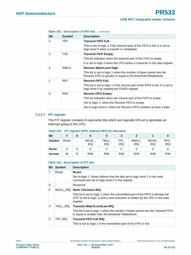
NXP Semiconductors PR533USB NFC integrated reader solution
7.3.3.7 FIT register
The FIT register contains 6 read-write bits which are logically OR-ed to generate an interrupt going to the CPU.
4 TFF Transmit FIFO Full:
This is set to logic 1 if the transmit part of the FIFO is full. It is set to logic level 0 when a transfer is completed.
3 TFE Transmit FIFO Empty:
This bit indicates when the transmit part of the FIFO is empty.
It is set to logic 0 when the CPU writes a character in the data register.
2 RWLH Receive WaterLevel High:
This bit is set to logic 1 when the number of bytes stored into the Receive FIFO is greater or equal to the threshold RWaterlevel.
1 RFF Receive FIFO Full:
This bit is set to logic 1 if the receive part of the FIFO is full. It is set to logic level 0 by reading the FDATA register.
0 RFE Receive FIFO Empty:
This bit indicates when the receive part of the FIFO is empty.
Set to logic 1, when the Receive FIFO is empty.
Set to logic level 0, when the Receive FIFO contains at least 1 byte.
Table 101. Description of SFF bits …continued
Bit Symbol Description
Table 102. FIT register (SFR: address 9Fh) bit allocation
Bit 7 6 5 4 3 2 1 0
Symbol Reset - WCOL_IRQ
TWLL_IRQ
TFF_IRQ
RWLH_IRQ
ROVR_IRQ
RFF_IRQ
Reset 0 0 0 0 0 0 0 0
Access W R R/W R/W R/W R/W R/W R/W
Table 103. Description of FIT bits
Bit Symbol Description
7 Reset Reset:
Set to logic 1, Reset defines that the bits set to logic level 1 in the write command are set to logic level 0 in the register.
6 - Reserved
5 WCOL_IRQ Write COLlision IRQ:
This bit is set to logic 1 when the transmitted part of the FIFO is already full (TFF is set to logic 1) and a new character is written by the CPU in the data register.
4 TWLL_IRQ Transmit WaterlLevelLow IRQ:
This bit is set to logic 1 when the number of bytes stored into the Transmit FIFO is equal or smaller than the threshold TWaterlevel.
3 TFF_IRQ Transmit FIFO Full IRQ:
This is set to logic 1 if the transmitted part of the FIFO is full.
PR533 All information provided in this document is subject to legal disclaimers. © NXP Semiconductors N.V. 2017. All rights reserved.
Product data sheetCOMPANY PUBLIC
Rev. 3.6 — 29 November 2017208936 60 of 216
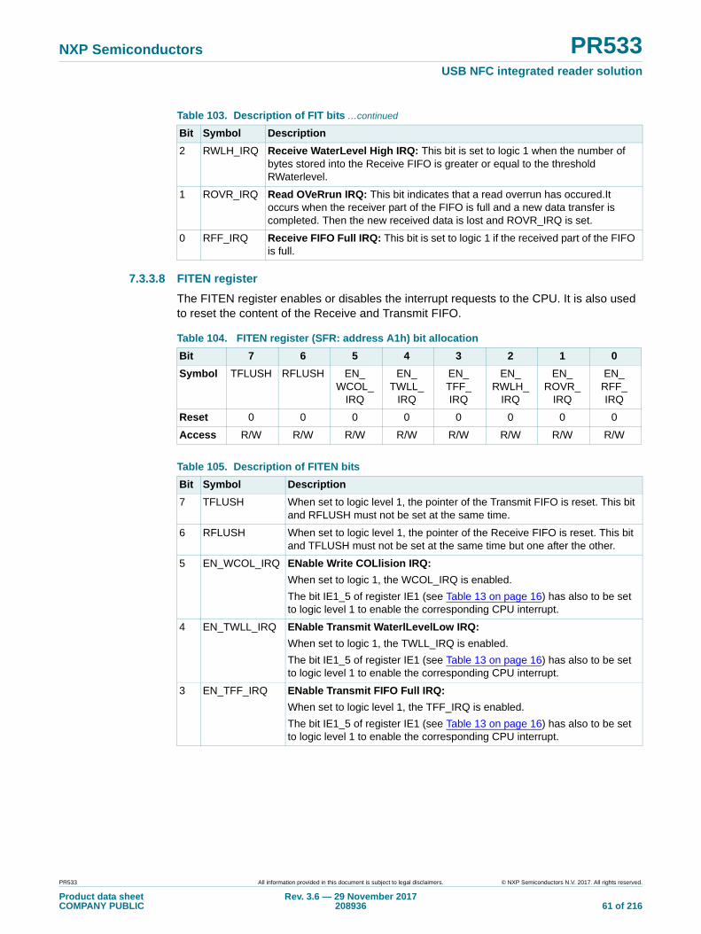
NXP Semiconductors PR533USB NFC integrated reader solution
7.3.3.8 FITEN register
The FITEN register enables or disables the interrupt requests to the CPU. It is also used to reset the content of the Receive and Transmit FIFO.
2 RWLH_IRQ Receive WaterLevel High IRQ: This bit is set to logic 1 when the number of bytes stored into the Receive FIFO is greater or equal to the threshold RWaterlevel.
1 ROVR_IRQ Read OVeRrun IRQ: This bit indicates that a read overrun has occured.It occurs when the receiver part of the FIFO is full and a new data transfer is completed. Then the new received data is lost and ROVR_IRQ is set.
0 RFF_IRQ Receive FIFO Full IRQ: This bit is set to logic 1 if the received part of the FIFO is full.
Table 103. Description of FIT bits …continued
Bit Symbol Description
Table 104. FITEN register (SFR: address A1h) bit allocation
Bit 7 6 5 4 3 2 1 0
Symbol TFLUSH RFLUSH EN_WCOL_
IRQ
EN_TWLL_
IRQ
EN_TFF_ IRQ
EN_RWLH_
IRQ
EN_ROVR_
IRQ
EN_RFF_ IRQ
Reset 0 0 0 0 0 0 0 0
Access R/W R/W R/W R/W R/W R/W R/W R/W
Table 105. Description of FITEN bits
Bit Symbol Description
7 TFLUSH When set to logic level 1, the pointer of the Transmit FIFO is reset. This bit and RFLUSH must not be set at the same time.
6 RFLUSH When set to logic level 1, the pointer of the Receive FIFO is reset. This bit and TFLUSH must not be set at the same time but one after the other.
5 EN_WCOL_IRQ ENable Write COLlision IRQ:
When set to logic 1, the WCOL_IRQ is enabled.
The bit IE1_5 of register IE1 (see Table 13 on page 16) has also to be set to logic level 1 to enable the corresponding CPU interrupt.
4 EN_TWLL_IRQ ENable Transmit WaterlLevelLow IRQ:
When set to logic 1, the TWLL_IRQ is enabled.
The bit IE1_5 of register IE1 (see Table 13 on page 16) has also to be set to logic level 1 to enable the corresponding CPU interrupt.
3 EN_TFF_IRQ ENable Transmit FIFO Full IRQ:
When set to logic level 1, the TFF_IRQ is enabled.
The bit IE1_5 of register IE1 (see Table 13 on page 16) has also to be set to logic level 1 to enable the corresponding CPU interrupt.
PR533 All information provided in this document is subject to legal disclaimers. © NXP Semiconductors N.V. 2017. All rights reserved.
Product data sheetCOMPANY PUBLIC
Rev. 3.6 — 29 November 2017208936 61 of 216

NXP Semiconductors PR533USB NFC integrated reader solution
7.3.3.9 FDATA register
The FDATA register is used to provide the transmitted and received data bytes. Each data written in the data register is pushed into the Transmit FIFO. Each data read from the data register is popped from the Receive FIFO.
7.3.3.10 FSIZE register
This register defines the size of the Receive FIFO. The maximum size is 182 bytes. The free space not used by the Receive FIFO in the RAM will be allocated to Transmit FIFO.
2 EN_RWLH_IRQ ENable Receive WaterLevel High IRQ:
When set to logic 1, the RWLH_IRQ is enabled.
The bit IE1_5 of register IE1 (see Table 13 on page 16) has also to be set to logic level 1 to enable the corresponding CPU interrupt.
1 EN_ROVR_IRQ ENable Read OVeRrun IRQ:
When set to logic 1, the ROVR_IRQ is enabled.
The bit IE1_5 of register IE1 (see Table 13 on page 16) has also to be set to logic level 1 to enable the corresponding CPU interrupt.
0 EN_RFF_IRQ ENable Receive FIFO Full IRQ:
When set to logic 1, the RFF_IRQ is enabled.
The bit IE1_5 of register IE1 (see Table 13 on page 16) has also to be set to logic level 1 to enable the corresponding CPU interrupt.
Table 105. Description of FITEN bits …continued
Bit Symbol Description
Table 106. FDATA register (SFR: address A2h) bit allocation
Bit 7 6 5 4 3 2 1 0
Symbol FDATA[7:0]
Reset 0 0 0 0 0 0 0 0
Access R/W R/W R/W R/W R/W R/W R/W R/W
Table 107. Description of FDATA bits
Bit Symbol Description
7 to 0 FDATA[7:0] Writing to FDATA writes to the transmit buffer.
Reading from FDATA reads from the receive buffer.
Table 108. FSIZE register (SFR: address A3h) bit allocation
Bit 7 6 5 4 3 2 1 0
Symbol ReceiveSize[7:0]
Reset 0 0 0 0 0 0 0 0
Access R/W R/W R/W R/W R/W R/W R/W R/W
Table 109. Description of FSIZE bits
Bit Symbol Description
7 to 0 ReceiveSize[7:0] Size of the Receive FIFO
PR533 All information provided in this document is subject to legal disclaimers. © NXP Semiconductors N.V. 2017. All rights reserved.
Product data sheetCOMPANY PUBLIC
Rev. 3.6 — 29 November 2017208936 62 of 216

NXP Semiconductors PR533USB NFC integrated reader solution
7.3.4 High Speed UART (HSU)
The High Speed UART (HSU) provides a high speed link to the host (up to 1.288 Mbit/s).
The HSU is a full duplex serial port. The serial port has a Receive-buffer: with the FIFO manager, the reception of several bytes can be performed without strong CPU real time constraints. However, if the Receive FIFO still has not been read by the CPU, and the number of receive bytes is greater than the Receive FIFO size then the new incoming bytes will be lost.
The HSU receive and transmit data registers are both accessed by firmware in the FIFO manager FDATA register. Writing to FDATA loads the transmit register, reading from FDATA accesses the separate receive register.
The characteristics of the UART are the following:
• Full duplex serial port
• Receive buffer to allow reception of byte while the previous bytes are stored into the FIFO manager
• 8-bit data transfers
• Programmable baud rate generator using prescaler for transmission and reception
• Based on 27.12 MHz clock frequency
• Dedicated protocol preamble filter
• Wake-up generator
PR533 All information provided in this document is subject to legal disclaimers. © NXP Semiconductors N.V. 2017. All rights reserved.
Product data sheetCOMPANY PUBLIC
Rev. 3.6 — 29 November 2017208936 63 of 216
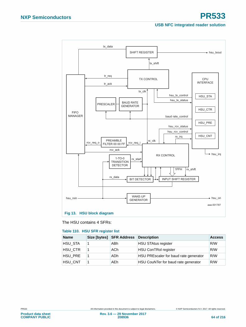
NXP Semiconductors PR533USB NFC integrated reader solution
The HSU contains 4 SFRs:
Fig 13. HSU block diagram
Table 110. HSU SFR register list
Name Size [bytes] SFR Address Description Access
HSU_STA 1 ABh HSU STAtus register R/W
HSU_CTR 1 ACh HSU ConTRol register R/W
HSU_PRE 1 ADh HSU PREscaler for baud rate generator R/W
HSU_CNT 1 AEh HSU CouNTer for baud rate generator R/W
RX CONTROL
rx_shift
rx_start
rx_irqrx_clk
INPUT SHIFT REGISTER
1FFH
BIT DETECTOR
1-TO-0TRANSITIONDETECTOR
TX CONTROL
SHIFT REGISTER hsu_txout
tx_shift
tx_clk
FIFO MANAGER
tr_ack
tr_req
tx_data
PRESCALER BAUD RATEGENERATOR
rcv_ack
rcv_req_i
CPUINTERFACE
hsu_tx_control
hsu_tx_status
hsu_rcv_control
hsu_rcv_status
baud rate_control
HSU_STA
HSU_CTR
HSU_PRE
HSU_CNT
rx_data
PREAMBLEFILTER 00 00 FFrcv_req_o
WAKE-UPGENERATORhsu_rxin hsu_on
aaa-001787
hsu_irq
PR533 All information provided in this document is subject to legal disclaimers. © NXP Semiconductors N.V. 2017. All rights reserved.
Product data sheetCOMPANY PUBLIC
Rev. 3.6 — 29 November 2017208936 64 of 216

NXP Semiconductors PR533USB NFC integrated reader solution
7.3.4.1 Mode of operation
The HSU supports only one operational mode, which has the following characteristics:
• Start bit:
– Start bit is detected when a logic level 0 is asserted on the HSU_RX line.
• 8 data bits:
– The data bits are sent or received LSB first.
• Stop bit:
– During reception, the Stop bit(s) is detected when all the data bits are received and when Stop bit(s) is sampled to logic level 1. The number of Stop bits is programmable. It can be 1 or 2.
– During Transmission, after the complete data bit transmission, a variable number of Stop bit(s) is transmitted. This number is programmable from 1 to 4.
7.3.4.2 HSU Baud rate generator
To reach the high speed transfer rate, the HSU has it own baud rate generator. The baud rate generator comprises a prescaler and a counter. The prescaler is located before the counter. The purpose of the prescaler is to divide the frequency of the count signal to enlarge the range of the counter (at the cost of a lower resolution). The division factor of the prescaler is equal to 2 to the power HSU_PRE[8:0] (Table 113 on page 67), resulting in division factors ranging from 1 (20) to 256 (28). The combination of these 2 blocks defines the bit duration and the bit sampling.
7.3.4.3 HSU preamble filter
Received characters are sent to the FIFO manager after three consecutives characters have been received: 00 00 FF. When the frame is finished, and before a new frame arrives, firmware shall write a logic level 1 in the start_frame bit of the HSU_CTR register to reactivate the preamble filter. If firmware does not write a logic level 1 then all characters of the frame are sent to the FIFO manager (including the preamble).
7.3.4.4 HSU wake-up generator
The wake-up generator is a 3-bit counter which counts on every rising edge of the HSU_RX pin. When the counter reaches 5, the hsu_on signal is set to logic level 1 in order to wake up the PR533. This block is useful in Soft-Power-down mode. The firmware shall reset this counter just before going in Soft-Power-down by writing a logic level 1 in the hsu_wu_en bit into the HSU_CTR register.
PR533 All information provided in this document is subject to legal disclaimers. © NXP Semiconductors N.V. 2017. All rights reserved.
Product data sheetCOMPANY PUBLIC
Rev. 3.6 — 29 November 2017208936 65 of 216
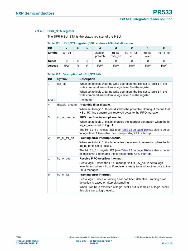
NXP Semiconductors PR533USB NFC integrated reader solution
7.3.4.5 HSU_STA register
The SFR HSU_STA is the status register of the HSU.
Table 111. HSU_STA register (SFR: address ABh) bit allocation
Bit 7 6 5 4 3 2 1 0
Symbol set_bit - - disable_preamb
irq_rx_over_en
irq_rx_fer_ en
irq_rx_over
irq_rx_fer
Reset 0 0 0 0 0 0 0 0
Access R/W R R R/W R/W R/W R/W R/W
Table 112. Description of HSU_STA bits
Bit Symbol Description
7 set_bit When set to logic 0 during write operation, the bits set to logic 1 in the write command are written to logic level 0 in the register.
When set to logic 1 during write operation, the bits set to logic 1 in the write command are written to logic level 1 in the register.
6 to 5 - Reserved
4 disable_preamb Preamble filter disable.
When set to logic 1, this bit disables the preamble filtering, it means that HSU_RX line transmit any received bytes to the FIFO manager.
3 irq_rx_over_en FIFO overflow interrupt enable.
When set to logic 1, this bit enables the interrupt generation when the bit irq_rx_over is set to logic 1.
The bit IE1_5 of register IE1 (see Table 13 on page 16) has also to be set to logic level 1 to enable the corresponding CPU interrupt.
2 irq_rx_fer_en Framing error interrupt enable.
When set to logic 1, this bit enables the interrupt generation when the bit irq_rx_fer is set to logic 1.
The bit IE1_5 of register IE1 (see Table 13 on page 16) has also to be set to logic level 1 to enable the corresponding CPU interrupt.
1 irq_rx_over Receive FIFO overflow interrupt.
Set to logic 1 when the FIFO manager is full (rcv_ack is set to logic level 0) and when HSU shift register is ready to send another byte to the FIFO manager.
0 irq_rx_fer Framing error interrupt.
Set to logic 1 when a framing error has been detected. Framing error detection is based on Stop bit sampling.
When Stop bit is expected at logic level 1 but is sampled at logic level 0, this bit is set to logic level 1.
PR533 All information provided in this document is subject to legal disclaimers. © NXP Semiconductors N.V. 2017. All rights reserved.
Product data sheetCOMPANY PUBLIC
Rev. 3.6 — 29 November 2017208936 66 of 216

NXP Semiconductors PR533USB NFC integrated reader solution
7.3.4.6 HSU_CTR register
This register controls the configuration of the HSU.
Table 113. HSU_CTR register (SFR: address ACh) bit allocation
Bit 7 6 5 4 3 2 1 0
Symbol hsu_wu_en
start_frame tx_stopbit[1:0] rx_stopbit tx_en rx_en soft_reset_n
Reset 0 0 0 0 0 0 0 1
Access R/W R/W R/W R/W R/W R/W R/W R/W
Table 114. Description of HSU_CTR bits
Bit Symbol Description
7 hsu_wu_en HSU wake-up enable.
When set to logic 1 this bit reactivates the NSS / SCL / HSU_RX rising-edge counter. When the counter is 5 then a signal hsu_on is activated. This signal is one of the possible wake-up events from Soft-Power-down mode in the PCR block.
The firmware shall set this bit to logic level 1 just before requesting a Soft-Power-down mode.
The bit IE1_5 of register IE1 (see Table 13 on page 16) has also to be set to logic level 1 to enable the corresponding CPU interrupt.
6 start_frame Enables the preamble filter for next frame.
When set to logic 1 this bit indicates that a new frame is coming. This reactivates the preamble filter (when enabled), meaning that the first “00 00 FF” characters will not be sent to the FIFO manager.
5:4 tx_stopbit[1:0] Defines the number of stop bit during transmission.
These 2 bits define the number of Stop bit(s) inserted at the end of the transmitted frame.
The number of Stop bit(s) transmitted is equal to tx_stopbit +1.
3 rx_stopbit Defines the number of stop bit during reception.
This bit defines the number of Stop bit(s) inserted at the end of the received frame.
The number of Stop bit(s) expected in reception is equal to rx_stopbit +1.
2 tx_en Enables the transmission of HSU.
When set to logic 1 this bit enables the transmission of characters.
When set to logic 0, the transmission is disabled only after the completion of the current transmission.
1 rx_en Enables the reception of the HSU.
When set to logic 1 this bit enables the reception of characters.
When set to logic 0, the reception is disabled only after the completion of the current reception.
0 soft_reset_n HSU Reset.
When set to logic 0, this bit disables the clock of the HSU_RX control, HSU_TX control and baud rate generator modules.
PR533 All information provided in this document is subject to legal disclaimers. © NXP Semiconductors N.V. 2017. All rights reserved.
Product data sheetCOMPANY PUBLIC
Rev. 3.6 — 29 November 2017208936 67 of 216

NXP Semiconductors PR533USB NFC integrated reader solution
7.3.4.7 HSU_PRE register
This register is used to configure the baud rate generator prescaler.The prescaler enlarges the range of the counter (at the cost of a lower resolution). The division factor of the prescaler ranges from 1 (20) to 256 (28).
7.3.4.8 HSU_CNT register
This register is used to configure the baud rate generator counter.
Here is a table of recommendation for some data rates:
Table 115. HSU_PRE register (SFR: address ADh) bit allocation
Bit 7 6 5 4 3 2 1 0
Symbol hsu_prescaler[7:0]
Reset 0 0 0 1 1 0 0 0
Access R/W R/W R/W R/W R/W R/W R/W R/W
Table 116. Description of HSU_PRE bits
Bit Symbol Description
7 to 0 hsu_prescaler[7:0] With HSU_CNT, defines the HSU baud rate.
Baud rate = fclk / ((hsu_prescaler +1) * hsu_counter)
Table 117. HSU_CNT register (SFR: address AEh) bit allocation
Bit 7 6 5 4 3 2 1 0
Symbol hsu_counter[7:0]
Reset 0 1 1 1 0 0 0 0
Access R/W R/W R/W R/W R/W R/W R/W R/W
Table 118. Description of HSU_CNT bits
Bit Symbol Description
7 to 0 hsu_counter[7:0] With HSU_PRE, defines the HSU baud rate.
Baud rate = fclk / ((hsu_prescaler +1) * hsu_counter)
Table 119. Recommendation for HSU data rates
Targeted data rate
HSU_CNT value
HSU_PRE value
Real HSU freq
Min recommended Host HSU freq
Max recommended Host HSU freq
9 600 0x71 0x18 9 516 9 408 9 792
19 200 0x9D 0x08 19 072 18 816 19 584
38 400 0x65 0x06 37 893 37 632 39 168
57 600 0x9D 0x02 57 215 56 448 58 752
115 200 0xEB 0x00 114 915 112 896 117 504
230 400 0x76 0x00 227 899 225 792 235 008
460 800 0x3B 0x00 452 000 451 584 470 016
921 600 0x1D 0x00 904 000 903 168 940 032
1 288 000 0x15 0x00 1 291 429 1 262 240 1 313 760
PR533 All information provided in this document is subject to legal disclaimers. © NXP Semiconductors N.V. 2017. All rights reserved.
Product data sheetCOMPANY PUBLIC
Rev. 3.6 — 29 November 2017208936 68 of 216

NXP Semiconductors PR533USB NFC integrated reader solution
7.3.5 USB
The USB module is an USB2.0 compliant device with embedded function.Special power management features such as a clock divider and clock switch are also implemented in the device.
7.3.5.1 Features list
The USB module is a USB device only supporting full speed communication schem. All embedded functions are passed to the micro controller.
The USB module includes the following features:
• SoftConnect supported
• Command GetFrameNumber supported
• Interrupt signaling to mController
• Control EP0 endpoint of 8 bytes
• 3 interrupt endpoints of 8 bytes
• 2 bidirectional bulk endpoints of 64 bytes
• resume by host
• remote wake-up
The endpoints setup is described in the following table.
7.3.5.2 USB interrupt
The interrupt line of the USB module is asserted to indicates to the microcontroller that there was a transaction on one of the endpoints, or that there is new status information available.
7.3.5.3 Resume by host
Resume by host in supsend state
After 3 ms of no USB activity on the bus, the device goes in suspend. About 2 ms later the device will indicate that it no longer needs the clock (Clk_Enable_N becomes inactive).The host can then send a resume to the device. The device needs to wake up and will require the main clock (USB_Clk_Enable_N becomes active). The main clock starts running after complete PCR wake-up sequence. PLL_LOCK indicates that the main clock is running stable(a PLL can need several ms to start running at the specified frequency). The device then knows that the clock is present and can go out of suspend.
Table 120. Endpoints Setup
Logical Endpoints OUT Type IN Type OUT Map IN Map OUT size IN size Note
Deivce function description
0 Control Control 0.0 0.1 8 8
1 - Int - 0.2 8
2 - Int - 0.3 8
3 - Int - 0.4 8
4 Bulk Bulk 0.5 0.6 64 64
PR533 All information provided in this document is subject to legal disclaimers. © NXP Semiconductors N.V. 2017. All rights reserved.
Product data sheetCOMPANY PUBLIC
Rev. 3.6 — 29 November 2017208936 69 of 216
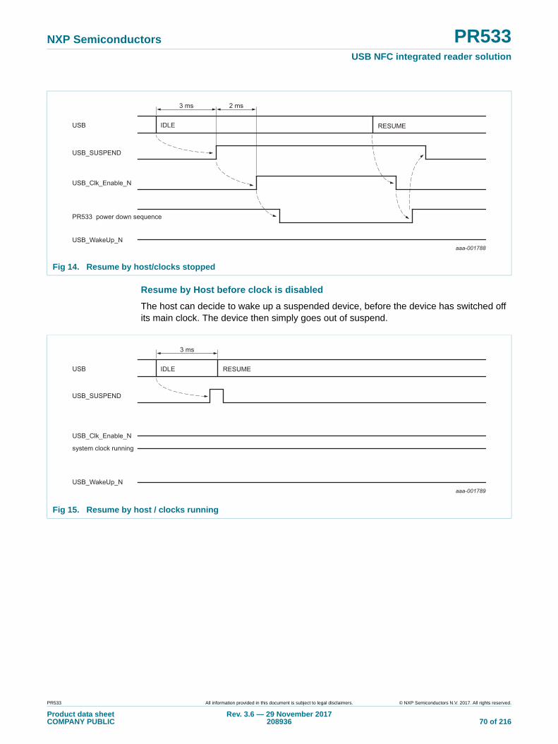
NXP Semiconductors PR533USB NFC integrated reader solution
Resume by Host before clock is disabled
The host can decide to wake up a suspended device, before the device has switched off its main clock. The device then simply goes out of suspend.
Fig 14. Resume by host/clocks stopped
USB_SUSPEND
USB_Clk_Enable_N
USB_WakeUp_N
USB IDLE RESUME
PR533 power down sequence
3 ms
aaa-001788
2 ms
Fig 15. Resume by host / clocks running
IDLE
3 ms
USB_SUSPEND
USB_Clk_Enable_N
USB_WakeUp_N
USB
system clock running
RESUME
aaa-001789
PR533 All information provided in this document is subject to legal disclaimers. © NXP Semiconductors N.V. 2017. All rights reserved.
Product data sheetCOMPANY PUBLIC
Rev. 3.6 — 29 November 2017208936 70 of 216

NXP Semiconductors PR533USB NFC integrated reader solution
7.3.5.4 Remote wake-up
The remote wake-up implemented in the PR533 platform is partly controlled by the micro controller as depicted below:
When a remote wake-up is requested on an external interrupt (P32_INT0, P33_INT1) or a RF detector event, the Power Clock and Reset controller (PCR):
• enables the 27.12 MHZ oscillator,
• generates an interrupt to resume the CPU from Power-down mode,
• then the cpu enable the 4 MHZ oscillator, the PLL and the 48 MHZ clock.
The CPU sends a command to the USB module to perform a USB remote wake-up, then the USB module exits from suspend mode and sends a resume on its upstream port.
Resume by Remote Wake-up before clock is disabled: Resume by Remote Wake-up before clock is disabled
If USB_WakeUp_N is made active before the main clock is switched off (USB_Clk_Enable_N becomes inactive), the device waits until it has been suspended for 2 ms, then wakes up and sends a resume on its upstream port.
Fig 16. RemoteWakeUp by uC
UpstreamRESUME
device receives wake up command from μC
USB_SUSPEND
USB_Clk_Enable_N
USB_WakeUp_N
USB IDLE
PCR power down sequence
3 ms
aaa-001790
2 ms
PR533 All information provided in this document is subject to legal disclaimers. © NXP Semiconductors N.V. 2017. All rights reserved.
Product data sheetCOMPANY PUBLIC
Rev. 3.6 — 29 November 2017208936 71 of 216

NXP Semiconductors PR533USB NFC integrated reader solution
7.3.5.5 Softconnect
The following figure shows how the embedded firmware Controlled Connect can be implemented.
When USB_SoftConnect_N is active, one of the data lines (D+) must be pulled high. This is done by using internal switch.
The internal pull up resistor or an external resistor (connected to delatt) can be used to perform the soft connection. The selection of the pullup resistor to use is made through the usb configuration register. refer to Table 121 on page 72.
Fig 17. SoftConnect connection
D+D-
upstream hubor host
VbusATX
gnd gnd
PR533 PVDD
delatt
VbusDVDD
VSS
USB_UseIntUpRes
softonnect
USB CORE
aaa-001791
Table 121. USB configuration register (6000h)
Bit Name Description Reset R/W
7 to 6 - Reserved xx R/W
5 USB_UseIntUpRes It controls switch for internal Upstream resistor.When set to logic level 1, external pull up resistor is used. When set to logic level 0, internal pull up resistor is used.
0 R/W
4 to 0 - Reserved xxxxx R/W
PR533 All information provided in this document is subject to legal disclaimers. © NXP Semiconductors N.V. 2017. All rights reserved.
Product data sheetCOMPANY PUBLIC
Rev. 3.6 — 29 November 2017208936 72 of 216
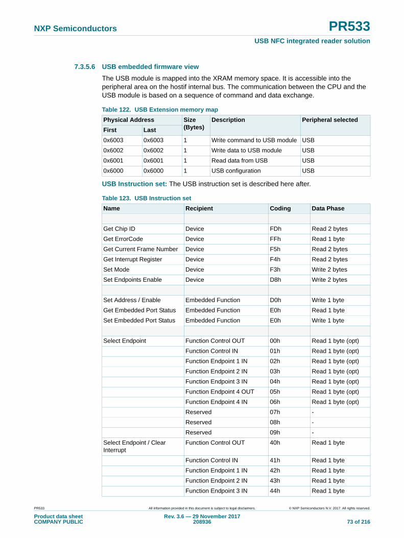
NXP Semiconductors PR533USB NFC integrated reader solution
7.3.5.6 USB embedded firmware view
The USB module is mapped into the XRAM memory space. It is accessible into the peripheral area on the hostif internal bus. The communication between the CPU and the USB module is based on a sequence of command and data exchange.
USB Instruction set: The USB instruction set is described here after.
Table 122. USB Extension memory map
Physical Address Size(Bytes)
Description Peripheral selected
First Last
0x6003 0x6003 1 Write command to USB module USB
0x6002 0x6002 1 Write data to USB module USB
0x6001 0x6001 1 Read data from USB USB
0x6000 0x6000 1 USB configuration USB
Table 123. USB Instruction set
Name Recipient Coding Data Phase
Get Chip ID Device FDh Read 2 bytes
Get ErrorCode Device FFh Read 1 byte
Get Current Frame Number Device F5h Read 2 bytes
Get Interrupt Register Device F4h Read 2 bytes
Set Mode Device F3h Write 2 bytes
Set Endpoints Enable Device D8h Write 2 bytes
Set Address / Enable Embedded Function D0h Write 1 byte
Get Embedded Port Status Embedded Function E0h Read 1 byte
Set Embedded Port Status Embedded Function E0h Write 1 byte
Select Endpoint Function Control OUT 00h Read 1 byte (opt)
Function Control IN 01h Read 1 byte (opt)
Function Endpoint 1 IN 02h Read 1 byte (opt)
Function Endpoint 2 IN 03h Read 1 byte (opt)
Function Endpoint 3 IN 04h Read 1 byte (opt)
Function Endpoint 4 OUT 05h Read 1 byte (opt)
Function Endpoint 4 IN 06h Read 1 byte (opt)
Reserved 07h -
Reserved 08h -
Reserved 09h -
Select Endpoint / Clear Interrupt
Function Control OUT 40h Read 1 byte
Function Control IN 41h Read 1 byte
Function Endpoint 1 IN 42h Read 1 byte
Function Endpoint 2 IN 43h Read 1 byte
Function Endpoint 3 IN 44h Read 1 byte
PR533 All information provided in this document is subject to legal disclaimers. © NXP Semiconductors N.V. 2017. All rights reserved.
Product data sheetCOMPANY PUBLIC
Rev. 3.6 — 29 November 2017208936 73 of 216
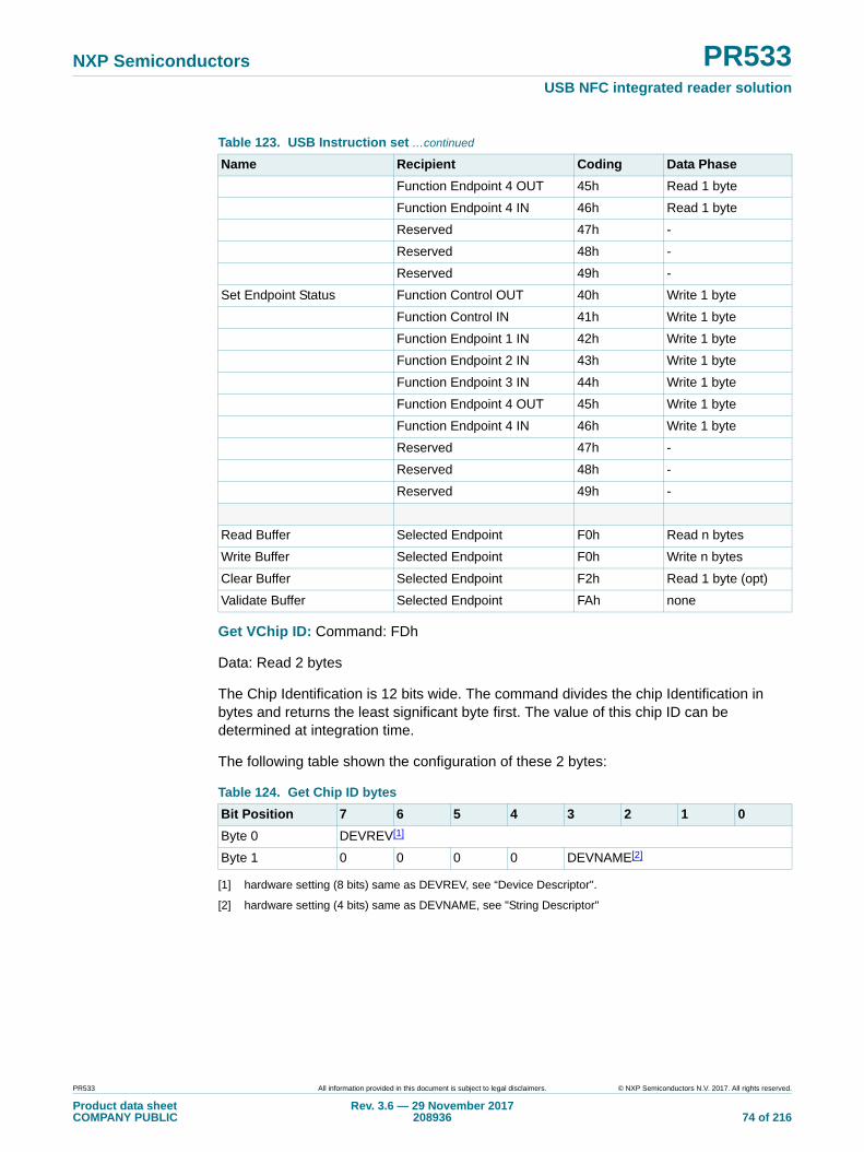
NXP Semiconductors PR533USB NFC integrated reader solution
Get VChip ID: Command: FDh
Data: Read 2 bytes
The Chip Identification is 12 bits wide. The command divides the chip Identification in bytes and returns the least significant byte first. The value of this chip ID can be determined at integration time.
The following table shown the configuration of these 2 bytes:
[1] hardware setting (8 bits) same as DEVREV, see “Device Descriptor".
[2] hardware setting (4 bits) same as DEVNAME, see "String Descriptor"
Function Endpoint 4 OUT 45h Read 1 byte
Function Endpoint 4 IN 46h Read 1 byte
Reserved 47h -
Reserved 48h -
Reserved 49h -
Set Endpoint Status Function Control OUT 40h Write 1 byte
Function Control IN 41h Write 1 byte
Function Endpoint 1 IN 42h Write 1 byte
Function Endpoint 2 IN 43h Write 1 byte
Function Endpoint 3 IN 44h Write 1 byte
Function Endpoint 4 OUT 45h Write 1 byte
Function Endpoint 4 IN 46h Write 1 byte
Reserved 47h -
Reserved 48h -
Reserved 49h -
Read Buffer Selected Endpoint F0h Read n bytes
Write Buffer Selected Endpoint F0h Write n bytes
Clear Buffer Selected Endpoint F2h Read 1 byte (opt)
Validate Buffer Selected Endpoint FAh none
Table 124. Get Chip ID bytes
Bit Position 7 6 5 4 3 2 1 0
Byte 0 DEVREV[1]
Byte 1 0 0 0 0 DEVNAME[2]
Table 123. USB Instruction set …continued
Name Recipient Coding Data Phase
PR533 All information provided in this document is subject to legal disclaimers. © NXP Semiconductors N.V. 2017. All rights reserved.
Product data sheetCOMPANY PUBLIC
Rev. 3.6 — 29 November 2017208936 74 of 216
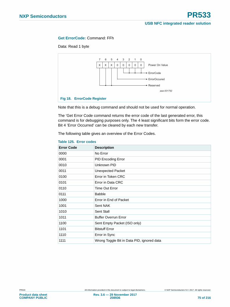
NXP Semiconductors PR533USB NFC integrated reader solution
Get ErrorCode: Command: FFh
Data: Read 1 byte
Note that this is a debug command and should not be used for normal operation.
The ’Get Error Code command returns the error code of the last generated error, this command is for debugging purposes only. The 4 least significant bits form the error code. Bit 4 ’Error Occurred’ can be cleared by each new transfer.
The following table gives an overview of the Error Codes.
Fig 18. ErrorCode Register
Table 125. Error codes
Error Code Description
0000 No Error
0001 PID Encoding Error
0010 Unknown PID
0011 Unexpected Packet
0100 Error in Token CRC
0101 Error in Data CRC
0110 Time Out Error
0111 Babble
1000 Error in End of Packet
1001 Sent NAK
1010 Sent Stall
1011 Buffer Overrun Error
1100 Sent Empty Packet (ISO only)
1101 Bitstuff Error
1110 Error in Sync
1111 Wrong Toggle Bit in Data PID, ignored data
X X X 0 0 0 0 0 Power On Value
ErrorCode
ErrorOccured
Reserved
7 6 5 4 3 2 1 0
aaa-001792
PR533 All information provided in this document is subject to legal disclaimers. © NXP Semiconductors N.V. 2017. All rights reserved.
Product data sheetCOMPANY PUBLIC
Rev. 3.6 — 29 November 2017208936 75 of 216

NXP Semiconductors PR533USB NFC integrated reader solution
Get Current Frame Number: Command: F5h
Data: Read 1 or 2 byte(s)
Data: Write 2 bytes
Get interrupt register: Command: F4h
Data: Read 2 bytes
This command indicates the origin of an interrupt. The endpoint interrupt bits (bits 0 to 9) are cleared by selecting the endpoint. The device status register change bit is reset by reading the device status change register. The Port Status Change Register change bit is reset by reading the port Status Change Register.
Set Mode:
Command:F3h
Data: Write 2 bytes
0.0.1Set Mode
Fig 19. Interrupt Register byte 1
Fig 20. Interrupt Register byte 2
Reserved
aaa-001793
0 0 0 0 0
7 6 5 4 3 2 1 0
0 0 0 Power On Value
EmbFuncCtrlOutEnpd
EmbFuncCtrlInEnpd
EmbFuncEnpd1In
EmbFuncEnpd2In
EmbFuncEnpd3In
EmbFuncEnpd4Out
EmbFuncEnpd4In
Reserved
aaa-001794
X 0 0 0 0
7 6 5 4 3 2 1 0
X X X Power On Value
Reserved
Reserved
Port 3 Status Register Change
Device Status Register Change
PR533 All information provided in this document is subject to legal disclaimers. © NXP Semiconductors N.V. 2017. All rights reserved.
Product data sheetCOMPANY PUBLIC
Rev. 3.6 — 29 November 2017208936 76 of 216

NXP Semiconductors PR533USB NFC integrated reader solution
Command:F3h
Data: Write 2 bytes
Configuration byte:
• InterruptOnNAK:A ’1’ indicates that "NAKing" is reported and will generate interrupt. A ’0’ indicates that only successful transactions are reported.
• AlwaysPLLClock:A ’1’indicates that the internal clocks and PLL are always running even during suspend state. A ’0’ indicates that the internal clock, crystal oscillator and PLL are stopped whenever not needed. To meet the strict suspend current requirement, this bit needs to be set to ’0’.
Clock division
• ClkDivFactor:The value indicates clock division factor for CLOCKOUT. The output frequency is 48 MHz/(N+1) where N is the Clock Division Factor. The reset value is 3. This will produce the output frequency of 12 MHz which can then be programmed up (or down) by the user. This design ensures no glitching during frequency change. The programmed value will not be changed by a bus reset.
Fig 21. Configuration byte
Fig 22. Clock division
Reserved
aaa-001795
0 0 0 X 1
7 6 5 4 3 2 1 0
X 0 0 Power On Value
InterruptOnNAK
Reserved
Reserved
AlwaysPLLClock
Reserved
Reserved
Reserved
X X 0 0 0 0 1 1 Power On Value
ClkDivFactor
Reserved. Write 0
7 6 5 4 3 2 1 0
aaa-001796
PR533 All information provided in this document is subject to legal disclaimers. © NXP Semiconductors N.V. 2017. All rights reserved.
Product data sheetCOMPANY PUBLIC
Rev. 3.6 — 29 November 2017208936 77 of 216
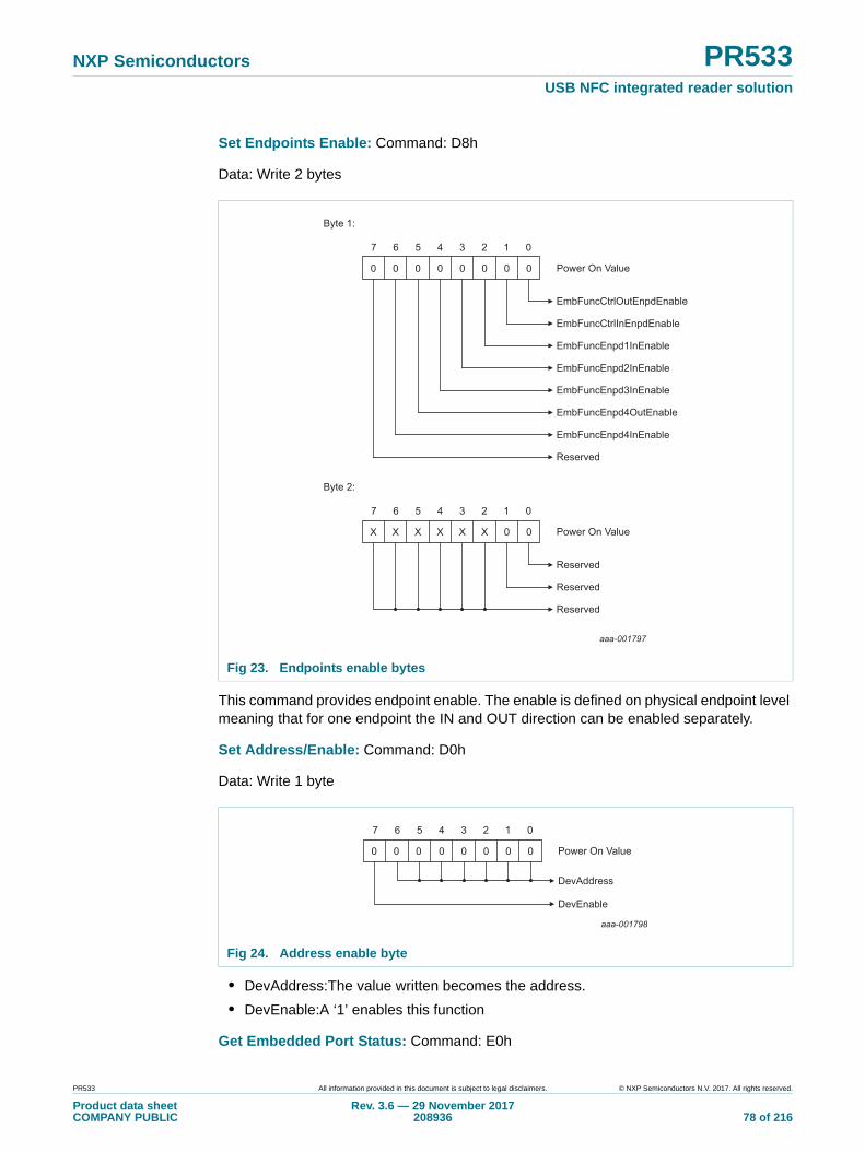
NXP Semiconductors PR533USB NFC integrated reader solution
Set Endpoints Enable: Command: D8h
Data: Write 2 bytes
This command provides endpoint enable. The enable is defined on physical endpoint level meaning that for one endpoint the IN and OUT direction can be enabled separately.
Set Address/Enable: Command: D0h
Data: Write 1 byte
• DevAddress:The value written becomes the address.
• DevEnable:A ‘1’ enables this function
Get Embedded Port Status: Command: E0h
Fig 23. Endpoints enable bytes
Fig 24. Address enable byte
aaa-001797
0 0 0 0 0
7 6 5 4 3 2 1 0
0 0 0 Power On Value
Byte 1:
X X X 0 0
7 6 5 4 3 2 1 0
X X X Power On Value
Reserved
Reserved
Reserved
Byte 2:
EmbFuncCtrlOutEnpdEnable
EmbFuncCtrlInEnpdEnable
EmbFuncEnpd1InEnable
EmbFuncEnpd2InEnable
EmbFuncEnpd3InEnable
EmbFuncEnpd4OutEnable
EmbFuncEnpd4InEnable
Reserved
0 0 0 0 0 0 0 0 Power On Value
DevAddress
DevEnable
7 6 5 4 3 2 1 0
aaa-001798
PR533 All information provided in this document is subject to legal disclaimers. © NXP Semiconductors N.V. 2017. All rights reserved.
Product data sheetCOMPANY PUBLIC
Rev. 3.6 — 29 November 2017208936 78 of 216
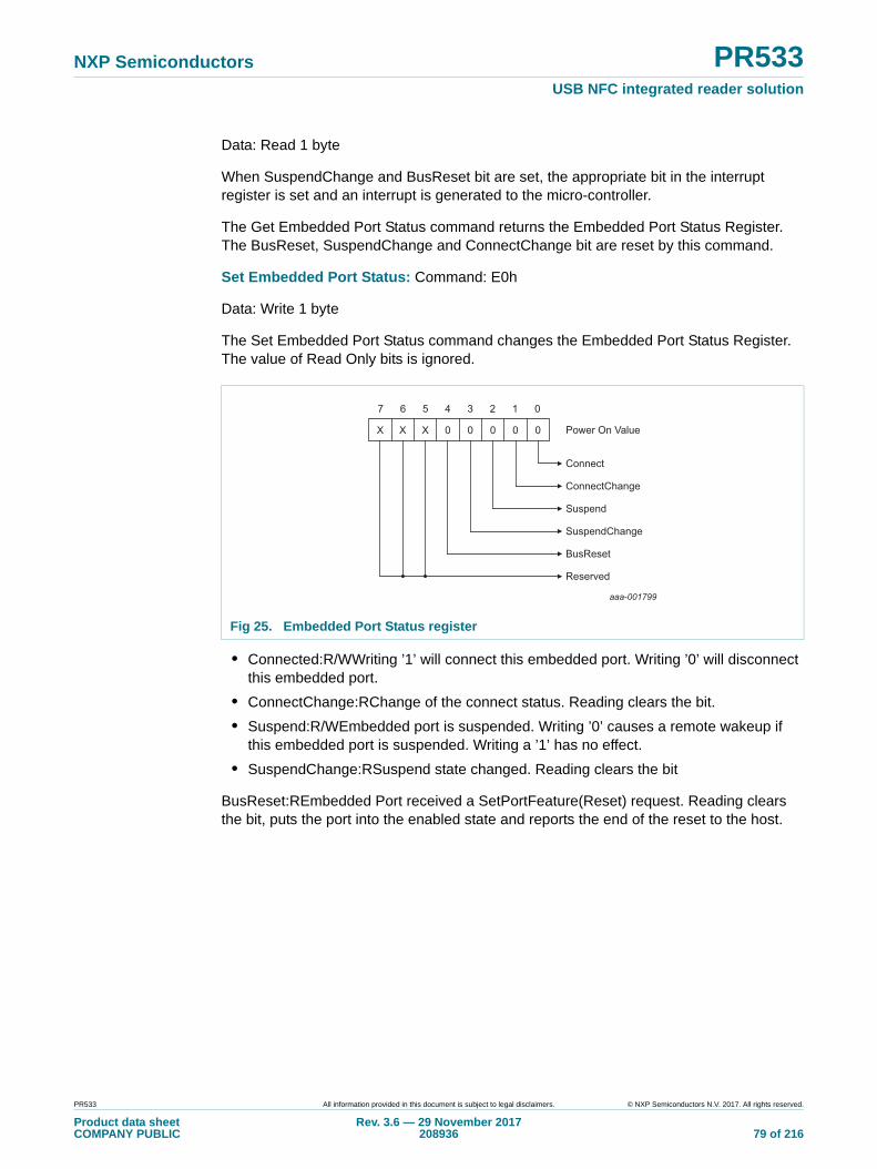
NXP Semiconductors PR533USB NFC integrated reader solution
Data: Read 1 byte
When SuspendChange and BusReset bit are set, the appropriate bit in the interrupt register is set and an interrupt is generated to the micro-controller.
The Get Embedded Port Status command returns the Embedded Port Status Register. The BusReset, SuspendChange and ConnectChange bit are reset by this command.
Set Embedded Port Status: Command: E0h
Data: Write 1 byte
The Set Embedded Port Status command changes the Embedded Port Status Register. The value of Read Only bits is ignored.
• Connected:R/WWriting ’1’ will connect this embedded port. Writing ’0’ will disconnect this embedded port.
• ConnectChange:RChange of the connect status. Reading clears the bit.
• Suspend:R/WEmbedded port is suspended. Writing ’0’ causes a remote wakeup if this embedded port is suspended. Writing a ’1’ has no effect.
• SuspendChange:RSuspend state changed. Reading clears the bit
BusReset:REmbedded Port received a SetPortFeature(Reset) request. Reading clears the bit, puts the port into the enabled state and reports the end of the reset to the host.
Fig 25. Embedded Port Status register
Reserved
aaa-001799
0 0 0 0 0
7 6 5 4 3 2 1 0
X X X Power On Value
Connect
ConnectChange
Suspend
SuspendChange
BusReset
PR533 All information provided in this document is subject to legal disclaimers. © NXP Semiconductors N.V. 2017. All rights reserved.
Product data sheetCOMPANY PUBLIC
Rev. 3.6 — 29 November 2017208936 79 of 216
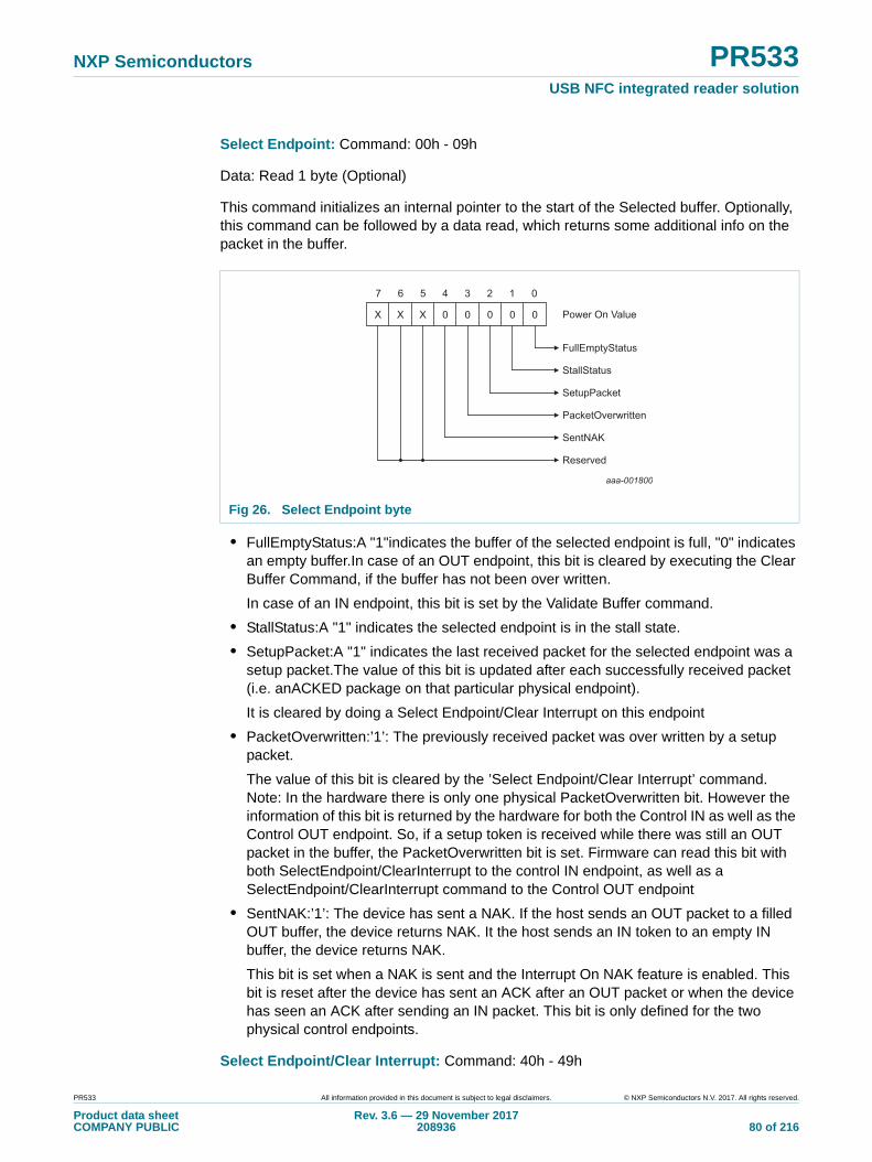
NXP Semiconductors PR533USB NFC integrated reader solution
Select Endpoint: Command: 00h - 09h
Data: Read 1 byte (Optional)
This command initializes an internal pointer to the start of the Selected buffer. Optionally, this command can be followed by a data read, which returns some additional info on the packet in the buffer.
• FullEmptyStatus:A "1"indicates the buffer of the selected endpoint is full, "0" indicates an empty buffer.In case of an OUT endpoint, this bit is cleared by executing the Clear Buffer Command, if the buffer has not been over written.
In case of an IN endpoint, this bit is set by the Validate Buffer command.
• StallStatus:A "1" indicates the selected endpoint is in the stall state.
• SetupPacket:A "1" indicates the last received packet for the selected endpoint was a setup packet.The value of this bit is updated after each successfully received packet (i.e. anACKED package on that particular physical endpoint).
It is cleared by doing a Select Endpoint/Clear Interrupt on this endpoint
• PacketOverwritten:’1’: The previously received packet was over written by a setup packet.
The value of this bit is cleared by the ’Select Endpoint/Clear Interrupt’ command.Note: In the hardware there is only one physical PacketOverwritten bit. However the information of this bit is returned by the hardware for both the Control IN as well as the Control OUT endpoint. So, if a setup token is received while there was still an OUT packet in the buffer, the PacketOverwritten bit is set. Firmware can read this bit with both SelectEndpoint/ClearInterrupt to the control IN endpoint, as well as a SelectEndpoint/ClearInterrupt command to the Control OUT endpoint
• SentNAK:’1’: The device has sent a NAK. If the host sends an OUT packet to a filled OUT buffer, the device returns NAK. It the host sends an IN token to an empty IN buffer, the device returns NAK.
This bit is set when a NAK is sent and the Interrupt On NAK feature is enabled. This bit is reset after the device has sent an ACK after an OUT packet or when the device has seen an ACK after sending an IN packet. This bit is only defined for the two physical control endpoints.
Select Endpoint/Clear Interrupt: Command: 40h - 49h
Fig 26. Select Endpoint byte
aaa-001800
0 0 0 0 0
7 6 5 4 3 2 1 0
X X X Power On Value
FullEmptyStatus
StallStatus
SetupPacket
PacketOverwritten
SentNAK
Reserved
PR533 All information provided in this document is subject to legal disclaimers. © NXP Semiconductors N.V. 2017. All rights reserved.
Product data sheetCOMPANY PUBLIC
Rev. 3.6 — 29 November 2017208936 80 of 216

NXP Semiconductors PR533USB NFC integrated reader solution
Data: Read 1 byte
Commands 40h to 49h are identical to their Select Endpoint equivalent, with the following differences:
• The command clears the associated interrupt
• The command clear the Setup and Overwritten bits in case of a control out endpoint
• The read of one byte is mandatoryNote: The hardware will clear the control IN buffer when firmware reads the 2nd byte in the control OUT buffer and there is a setup packet in the buffer.
• Clears the coresponding interrupt only at indicated end point.
Set Endpoint Status: Command: 40h - 49h
Data: Write 1 byte
• Stalled:A "1" indicates the endpoint is stalled.
• Disable:A "1" indicates the endpoint is disabled. After a bus-reset each endpoint is enabled, ie., this bit is set to ’0’.
• RateFeedbackMode:’0’: Interrupt endpoint in ’toggle mode’
’1’: Interrupt endpoint in ’rate feedback mode’
• Conditional Stall:’1’: Stall both endpoint zero endpoints, unless the ’Setup Packet’ bit is set. It is only defined for control OUT endpoints
Read Buffer: Command: F0h
Data: Read up to n+2 bytes
’n’ is equal to the number of data bytes in the selected buffer.
This command is followed by a number of data reads, which return the contents of the selected endpoint data buffer. After each read, the internal buffer pointer is incremented by 1.
The buffer pointer is not reset to the beginning of the buffer by this command. This means that reading or writing a buffer can be interrupted by any other command (except for Select Endpoint).
The data in the buffer are organized as follow:
Fig 27. Endpoint Status byte
X X X X 0
7 6 5 4 3 2 1 0
0 0 0 Power On Value
Stalled
Reserved
Disable
RateFeedbackMode
Conditional Stall
aaa-001801
PR533 All information provided in this document is subject to legal disclaimers. © NXP Semiconductors N.V. 2017. All rights reserved.
Product data sheetCOMPANY PUBLIC
Rev. 3.6 — 29 November 2017208936 81 of 216

NXP Semiconductors PR533USB NFC integrated reader solution
Write Buffer: Command: F0h
Data: Write up to n+2 bytes
’n’ is equal to the number of data bytes in the selected buffer.
This command is followed by a number of data writes, which load the data buffer of the selected endpoint. After each write, the internal pointer is incremented by 1. The buffer pointer is not reset to the beginning of the buffer by the Write Buffer command. This means that writing a buffer can be interrupted by any other command (except for Select Endpoint).
The data in the buffer are organized as follow:
Clear Buffer: Command: F2h
Data: Read 1 byte (Optional)
When a packet is received completely, an internal endpoint buffer full flag is set. All subsequent packets will be refused by returning a NAK. When the microcontroller has read the data, it should free the buffer by the Clear Buffer command. When the buffer is cleared new packets will be accepted.
When bit ’0’ of the optional data byte is ’1’, the previously received packet was over written by a Setup Packet. A buffer cannot be cleared when its Packet Overwritten bit is set.
Validate Buffer: Command: FAh
Table 126. Read buffer bytes
Bit Position 7 6 5 4 3 2 1 0
Byte 0 0/1 0/1 - - - - - -
Byte 1 - Number of Data bytes in buffer
Byte 2 Data byte 0
...
Byte n+1 Data Byte n -1
Table 127. Write buffer bytes
Bit Position 7 6 5 4 3 2 1 0
Byte 0 0/1 0/1 - - - - - -
Byte 1 - Number of Data bytes in buffer
Byte 2 Data byte 0
...
Byte n+1 Data Byte n -1
Fig 28. Clear buffer byte
X X X X X X X 0 Power On Value
PacketOverwritten
Reserved
7 6 5 4 3 2 1 0
aaa-001802
PR533 All information provided in this document is subject to legal disclaimers. © NXP Semiconductors N.V. 2017. All rights reserved.
Product data sheetCOMPANY PUBLIC
Rev. 3.6 — 29 November 2017208936 82 of 216
NXP Semiconductors PR533USB NFC integrated reader solution
Data: None
When the microprocessor has written data into an IN buffer, it should set the buffer full flag by the Validate Buffer command.
This indicates that the data in the buffer is valid and can be sent to the host when the next IN token is received. A control IN buffer cannot be validated when the Packet Overwritten bit of its corresponding OUT buffer is set.
7.4 Power management
This chapter defines the power distribution scheme according to the different system configuration. The PR533 can be supplied by the USB connector on VBUS or directly on the VBUS, AVDD, DVDD, PVDD and TVDD. Regarding the system configuration, the power distribution shall be different. This may require the activation or desactivation of the 3.3 V regulator controlled via the I1 pin. Inappropiriate setting of this pin may lead to power conflict and/or unexpected behavior.
7.4.1 5 V external power source
In this mode the power distinction is performed from the USB bus. The unique “5 V external power source” from the USB bus is connected to the USB pin. In this mode, VBUS shall be between 4.02 V and 5.5 V according to USB standardization.The power delivered to the different peripherals is controlled by the PR533 chip directly. Pin I1 must be connected to DVDD in order to activate the internal regulator.
PR533 All information provided in this document is subject to legal disclaimers. © NXP Semiconductors N.V. 2017. All rights reserved.
Product data sheetCOMPANY PUBLIC
Rev. 3.6 — 29 November 2017208936 83 of 216
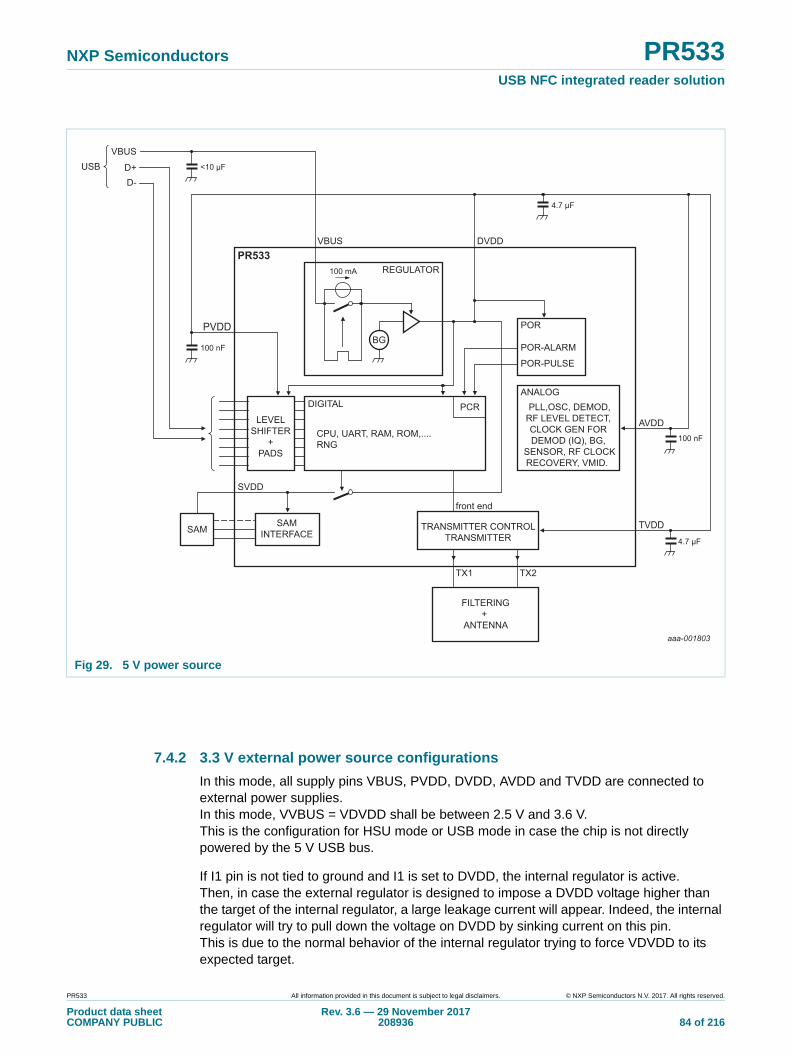
NXP Semiconductors PR533USB NFC integrated reader solution
7.4.2 3.3 V external power source configurations
In this mode, all supply pins VBUS, PVDD, DVDD, AVDD and TVDD are connected to external power supplies.In this mode, VVBUS = VDVDD shall be between 2.5 V and 3.6 V.This is the configuration for HSU mode or USB mode in case the chip is not directlypowered by the 5 V USB bus.
If I1 pin is not tied to ground and I1 is set to DVDD, the internal regulator is active. Then, in case the external regulator is designed to impose a DVDD voltage higher than the target of the internal regulator, a large leakage current will appear. Indeed, the internal regulator will try to pull down the voltage on DVDD by sinking current on this pin.This is due to the normal behavior of the internal regulator trying to force VDVDD to its expected target.
Fig 29. 5 V power source
100 mA
DVDD
AVDD
ANALOG
PR533VBUS
REGULATOR
PLL,OSC, DEMOD,RF LEVEL DETECT, CLOCK GEN FOR DEMOD (IQ), BG,
SENSOR, RF CLOCKRECOVERY, VMID.
PVDDBG
LEVELSHIFTER
+PADS
DIGITAL
CPU, UART, RAM, ROM,....RNG
PCR
TVDD
front end
TX1 TX2
TRANSMITTER CONTROLTRANSMITTER
SAM
SVDD
SAMINTERFACE
4.7 μF
FILTERING+
ANTENNA
D+D-
VBUSUSB <10 μF
100 nF
100 nF
4.7 μF
POR
POR-ALARM
POR-PULSE
aaa-001803
PR533 All information provided in this document is subject to legal disclaimers. © NXP Semiconductors N.V. 2017. All rights reserved.
Product data sheetCOMPANY PUBLIC
Rev. 3.6 — 29 November 2017208936 84 of 216

NXP Semiconductors PR533USB NFC integrated reader solution
7.4.3 HOST powered (single source)
In that case, the power distribution is performed from a single power supply source. The Figure 30 “HOST powered from single source” depicts the system approach for the power distribution.
Fig 30. HOST powered from single source
100 mA
DVDD
AVDD
ANALOG
PR533VBUS
REGULATOR
PLL,OSC, DEMOD,RF LEVEL DETECT, CLOCK GEN FOR DEMOD (IQ), BG,
SENSOR, RF CLOCKRECOVERY, VMID.
PVDDBG
LEVELSHIFTER
+PADS
HOST
DIGITAL
CPU, UART, RAM, ROM,....RNG
PCR
TVDD
front end
TX1 TX2
TRANSMITTER CONTROLTRANSMITTER
SAM
SVDD
SAMINTERFACE
FILTERING+
ANTENNA
100 nF
100 nF
100 nF 10 μF
POR
POR-ALARM
POR-PULSE
aaa-001804
VDD (2.5 V => 3.6 V)
VDD
PR533 All information provided in this document is subject to legal disclaimers. © NXP Semiconductors N.V. 2017. All rights reserved.
Product data sheetCOMPANY PUBLIC
Rev. 3.6 — 29 November 2017208936 85 of 216

NXP Semiconductors PR533USB NFC integrated reader solution
7.4.4 HOST powered (double source)
The power distribution is performed from the second source from the Host. The Figure 31 “HOST powered from double source” depicts the system approach for the power distribution.
This supply distribution requires to set I0 pin to DVDD and I1 pin to Ground.
This configuration has as effect to disable the internal regulator.
Fig 31. HOST powered from double source
100 mA
DVDD
AVDD
ANALOG
PR533VBUS
REGULATOR
PLL,OSC, DEMOD,RF LEVEL DETECT, CLOCK GEN FOR DEMOD (IQ), BG,
SENSOR, RF CLOCKRECOVERY, VMID.
PVDDBG
LEVELSHIFTER
+PADS
HOST
DIGITAL
CPU, UART, RAM, ROM,....RNG
PCR
TVDD
front end
TX1 TX2
TRANSMITTER CONTROLTRANSMITTER
SAM
SVDD
SAMINTERFACE
FILTERING+
ANTENNA
100 nF
100 nF
100 nF
100 nF 10 μF
POR
POR-ALARM
POR-PULSE
aaa-001805
VDDHOST (1.6 V => 3.6 V)
VDD
VDDPR533 (2.5 V => 3.6 V)
PR533 All information provided in this document is subject to legal disclaimers. © NXP Semiconductors N.V. 2017. All rights reserved.
Product data sheetCOMPANY PUBLIC
Rev. 3.6 — 29 November 2017208936 86 of 216
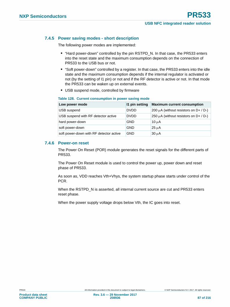
NXP Semiconductors PR533USB NFC integrated reader solution
7.4.5 Power saving modes - short description
The following power modes are implemented:
• “Hard power-down” controlled by the pin RSTPD_N. In that case, the PR533 enters into the reset state and the maximum consumption depends on the connection of PR533 to the USB bus or not.
• “Soft power-down” controlled by a register. In that case, the PR533 enters into the idle state and the maximum consumption depends if the internal regulator is activated or not (by the setting of I1 pin) or not and if the RF detector is active or not. In that mode the PR533 can be waken up on external events.
• USB suspend mode, controlled by firmware
7.4.6 Power-on reset
The Power On Reset (POR) module generates the reset signals for the different parts of PR533.
The Power On Reset module is used to control the power up, power down and reset phase of PR533.
As soon as, VDD reaches Vth+Vhys, the system startup phase starts under control of the PCR.
When the RSTPD_N is asserted, all internal current source are cut and PR533 enters reset phase.
When the power supply voltage drops below Vth, the IC goes into reset.
Table 128. Current consumption in power saving mode
Low power mode I1 pin setting Maximum current consumption
USB suspend DVDD 200 A (without resistors on D+ / D-)
USB suspend with RF detector active DVDD 250 A (without resistors on D+ / D-)
hard power-down GND 10 A
soft power-down GND 25 A
soft power-down with RF detector active GND 30 A
PR533 All information provided in this document is subject to legal disclaimers. © NXP Semiconductors N.V. 2017. All rights reserved.
Product data sheetCOMPANY PUBLIC
Rev. 3.6 — 29 November 2017208936 87 of 216
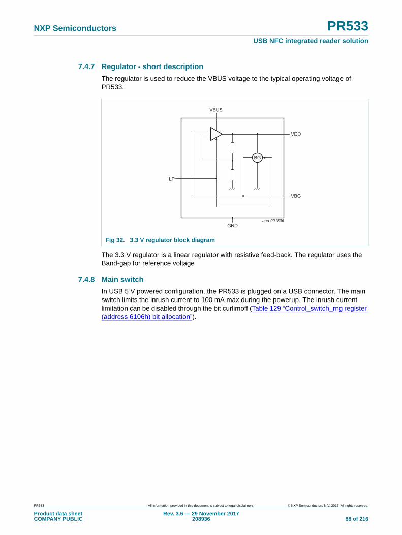
NXP Semiconductors PR533USB NFC integrated reader solution
7.4.7 Regulator - short description
The regulator is used to reduce the VBUS voltage to the typical operating voltage of PR533.
The 3.3 V regulator is a linear regulator with resistive feed-back. The regulator uses the Band-gap for reference voltage
7.4.8 Main switch
In USB 5 V powered configuration, the PR533 is plugged on a USB connector. The main switch limits the inrush current to 100 mA max during the powerup. The inrush current limitation can be disabled through the bit curlimoff (Table 129 “Control_switch_rng register (address 6106h) bit allocation”).
Fig 32. 3.3 V regulator block diagram
aaa-001806
VBUS
VDD
VBG
GND
LP
BG
PR533 All information provided in this document is subject to legal disclaimers. © NXP Semiconductors N.V. 2017. All rights reserved.
Product data sheetCOMPANY PUBLIC
Rev. 3.6 — 29 November 2017208936 88 of 216
NXP Semiconductors PR533USB NFC integrated reader solution
7.4.9 SVDD switch
The SVDD switch is used to control power to the secure IC. The switch is controlled by register Control_switch_rng (address 6106h). The switch is enabled with bit sic_switch_en. When disabled, the SVDD pin is tied to ground. A current limiter is incorporated into the switch. Current consumption exceeding 40 mA triggers the limiter and the status bit sic_switch_overload is set.Register Control_switch_rng also controls the random generator within the Contactless Interface Unit (CIU) and the regulator current limitation.
Table 129. Control_switch_rng register (address 6106h) bit allocation
Bit 7 6 5 4 3 2 1 0
Symbol - hide_svdd_sig
sic_switch_overload
sic_switch_en
curlimoff cpu_need_ rng
random_ dataready
-
Reset 0 1 0 0 0 0 0 1
Access R R/W R R/W R/W R/W R/W R
Table 130. Description of Control_switch_rng bits
Bit Symbol Description
7 - Reserved.
6 hide_svdd_sig Configures internal state of input signals SIGIN and P34 when idle. This bit can be used to avoid spikes on SIGIN and P34 when the SVDD switch is enabled or disabled.
When set to logic 0, internal state of SIGIN and P34 are driven by pads SIGIN and P34 respectively.
When set to logic 1, internal state of SIGIN is set to logic level 0 and internal state of P34 is set to logic 1.
5 sic_switch_overload Indicates state of SVDD switch current limiter.
When set to logic 0, indicates that current consumption through SVDD switch does not exceed limit (40 mA).
When set to logic 1, the SVDD switch current limiter is activated.
4 sic_switch_en Enables or disables power to SVDD switch.
When set to logic 0, SVDD switch is disabled and SVDD output is tied to the ground.
When set to logic 1, the SVDD switch is enabled and the SVDD output delivers power to secure IC and internal pads (SIGIN, SIGOUT and P34).
3 curlimoff Configure the regulator to deliver more current than 100 mA.
When set to 0, the 100 mA current limitations is activated.
When set to 1, the 100 mA current limitations is desactivated.
When configured in host powered mode, the state of this bit is not considered.
PR533 All information provided in this document is subject to legal disclaimers. © NXP Semiconductors N.V. 2017. All rights reserved.
Product data sheetCOMPANY PUBLIC
Rev. 3.6 — 29 November 2017208936 89 of 216
NXP Semiconductors PR533USB NFC integrated reader solution
7.5 Power clock and reset controller
The PCR controller is the controller for the clock generation, power management and reset architecture for the PR533.
7.5.1 PCR in the system
This block diagram Figure 33 “PR533 Power Management block diagram” shows the relationship between the PCR, other embedded blocks and external signals.
2 cpu_need_rng Forces random number generator into running mode.
When set to logic 0, random number generator is under control of Contactless Interface Unit.
When set to logic 1, random number generator is forced to run.
1 random_dataready Indicates availability of random number.
When set to logic 1, a new random number is available.
Automatically set to logic 0 when register data_rng (address 6105h) is read.
0 - Reserved.
Table 130. Description of Control_switch_rng bits …continued
Bit Symbol Description
Table 131. PR533 clock source characteristics
Clock name Frequency MHz Tolerance Clock source Comments
OSC_CLK27 27.12 14 kHz OSC 27.12 Output of OSC 27
PLL_CLK96 96 0.25 % USB PLL Output of USB PLL
USB_CLK 48 0.25 % USB PLL
CPU_CLK 27.12/13.56/6.78 OSC 27 Default is 6.78 MHz
HSU_CLK 27.12 OSC 27
PR533 All information provided in this document is subject to legal disclaimers. © NXP Semiconductors N.V. 2017. All rights reserved.
Product data sheetCOMPANY PUBLIC
Rev. 3.6 — 29 November 2017208936 90 of 216
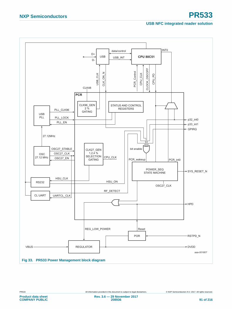
NXP Semiconductors PR533USB NFC integrated reader solution
Fig 33. PR533 Power Management block diagram
PLL_LOCK
REGULATOR
POR
D+USB
D-CPU 80C51USB_INT
PLL_EN
OSC27_EN
27.12MHz
PLL_CLK96
VBUS DVDD
REG_LOW_POWER
data/control
CLO
CK
_OS
CO
FF
PC
R_C
ontro
l
CLK27_GEN1,2,4 %
SELECTIONGATING
POWER_SEQSTATE MACHINE
PCR
Reset
CP
U_P
D
STATUS AND CONTROLREGISTERS
INT0
CPU_CLK
CP
U_C
LK
CLK
_ON
_N
US
B_C
LK
RSTPD_N
p32_int0
p33_int1
PCR_wakeup PCR_int0
OSC27.12 MHz
OSC27_CLK
OSC27_STABLE
RS232
CL UART
CLK96_GEN2 %
GATING
HSU_ON
RF_DETECT
OSC27_CLK
HSU_CLK
CLK48
UARTCL_CLK
bit enable
HPD
GPIRQ
SYS_RESET_N
USBPLL
aaa-001807
PR533 All information provided in this document is subject to legal disclaimers. © NXP Semiconductors N.V. 2017. All rights reserved.
Product data sheetCOMPANY PUBLIC
Rev. 3.6 — 29 November 2017208936 91 of 216
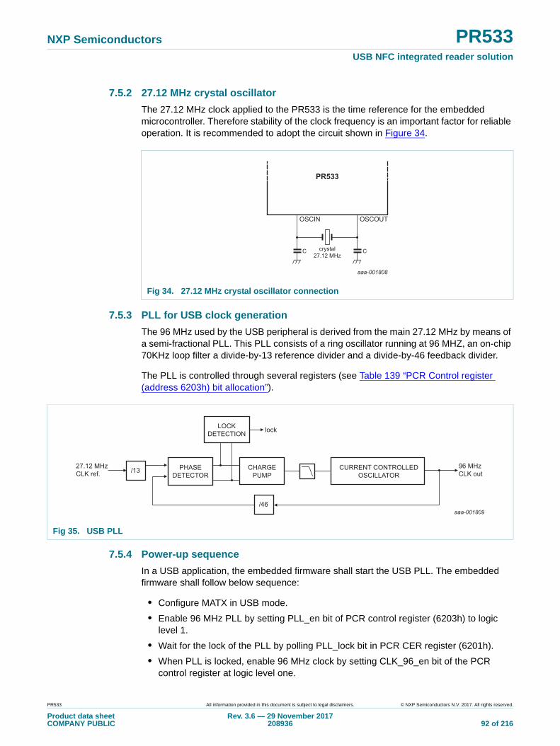
NXP Semiconductors PR533USB NFC integrated reader solution
7.5.2 27.12 MHz crystal oscillator
The 27.12 MHz clock applied to the PR533 is the time reference for the embedded microcontroller. Therefore stability of the clock frequency is an important factor for reliable operation. It is recommended to adopt the circuit shown in Figure 34.
7.5.3 PLL for USB clock generation
The 96 MHz used by the USB peripheral is derived from the main 27.12 MHz by means of a semi-fractional PLL. This PLL consists of a ring oscillator running at 96 MHZ, an on-chip 70KHz loop filter a divide-by-13 reference divider and a divide-by-46 feedback divider.
The PLL is controlled through several registers (see Table 139 “PCR Control register (address 6203h) bit allocation”).
7.5.4 Power-up sequence
In a USB application, the embedded firmware shall start the USB PLL. The embedded firmware shall follow below sequence:
• Configure MATX in USB mode.
• Enable 96 MHz PLL by setting PLL_en bit of PCR control register (6203h) to logic level 1.
• Wait for the lock of the PLL by polling PLL_lock bit in PCR CER register (6201h).
• When PLL is locked, enable 96 MHz clock by setting CLK_96_en bit of the PCR control register at logic level one.
Fig 34. 27.12 MHz crystal oscillator connection
C Ccrystal27.12 MHz
OSCIN OSCOUT
PR533
aaa-001808
Fig 35. USB PLL
27.12 MHzCLK ref. /13
/46
PHASEDETECTOR
CHARGEPUMP
LOCKDETECTION
CURRENT CONTROLLEDOSCILLATOR
96 MHzCLK out
lock
aaa-001809
PR533 All information provided in this document is subject to legal disclaimers. © NXP Semiconductors N.V. 2017. All rights reserved.
Product data sheetCOMPANY PUBLIC
Rev. 3.6 — 29 November 2017208936 92 of 216

NXP Semiconductors PR533USB NFC integrated reader solution
• Enable 48 MHz USB clock that is derived from 96 MHz clock by setting USB_enable bit of PCR CER register (6201h) at logic level one.
• Set reset_USB_n bit of PCR control register (6203h) at logic level one.
7.5.5 Power saving modes
The following power saving modes are implemented:
• Hard-Power-down mode (HPD): controlled by the pin RSTPD_N. The PR533 goes into reset and power consumption is at a minimum, see Section 7.5.6 “Reset modes”.
• Soft-Power-down mode (SPD): controlled by firmware In HSU application. See Section 7.5.7 “Soft-Power-down mode (SPD)” to optimize the power consumption in this mode.
• Suspend mode: In a USB application, the suspend mode is controlled by firmware.
7.5.6 Reset modes
The possible reset mechanisms are listed below:
• Supply rail variation
When DVDD falls below Vth, the POR (Power-On-Reset) asserts an internal reset signal. The Power Sequencer disables all clocks. When DVDD rises above Vth+Vhys, the POR deasserts the internal reset signal and the Power Sequencer starts the power-up sequence. Once the PR533 is out of reset, the RSTOUT_N pin is driven high.
• Glitch on DVDD
When DVDD falls below Vth for more than 1 s, the POR asserts an internal reset signal. The power sequencer starts the Power-down sequence. The PR533 goes into reset and the RSTOUT_N signal is driven low.
• Hard Power-down mode (HPD)
When RSTPD_N is set to logic level 0, the PR533 goes into Hard Power Down (HDP) mode. The PR533 goes into reset and the RSTOUT_N signal is driven low. The power consumption is at the minimum. DVDD is tied to ground and ports are disconnected from their supply rails. The PR533 goes into reset .
7.5.7 Soft-Power-down mode (SPD)
In order to initiate the Soft-Power-down mode with minimal power consumption, the firmware should:
• Configure I/Os to minimize power consumption
• Shut down unused functions
– Contactless Interface Unit with bit Power-down of SFR register D1h, see Table 175 on page 138.
– Disable the SVDD switch, see Table 130 on page 89
– Power down the RF level detector if RF wake-up is not enabled, see Table 283 on page 176.
• Enable relevant wake-up sources
• Disable unwanted interrupts
PR533 All information provided in this document is subject to legal disclaimers. © NXP Semiconductors N.V. 2017. All rights reserved.
Product data sheetCOMPANY PUBLIC
Rev. 3.6 — 29 November 2017208936 93 of 216

NXP Semiconductors PR533USB NFC integrated reader solution
• Set to logic level one the CPU_PD bit in PCON register, see Table 7 on page 13
7.5.8 Suspend mode
After 3 ms of no USB activity on the bus, the device goes in suspend. About 2 ms later the device will indicate that it no longer needs the clock by setting to logic level one suspended bit (refer to bit “suspended” of “get device status” USB register at FEh address).
In order to initiate the Suspend mode with minimal power consumption, the firmware should:
• Poll the clock_on bit in the CER register at 6201h address
• Configure I/Os to minimize power consumption
• Shut down unused functions
– Contactless Interface Unit with bit Power-down of SFR register D1h, see Table 175 on page 138.
– Disable the SVDD switch, see Table 130 on page 89
– Power down the RF level detector if RF wake-up is not enabled, see Table 283 on page 176.
• Enable relevant wake-up sources; USB wake-up source is mandatory
• Disable unwanted interrupts
• Disable CLK_96 MHz Clock, by setting to logic level zero CLK_96_en bit of the PCR control register at 6203h address
• Disable USB PLL by setting to logic level zero PLL_en bit in PCR control register
• Set logic level one the CPU_PD bit in PCON register, see Table 7 on page 13
7.5.9 Remote wake-up
The PR533 can be woken up from a Soft-Power-down mode or Suspend mode when an event occurs on one of the wake-up sources, which has been enabled. There are seven wake-up sources:
• P32_INT0
• P33_INT1
• RF field detected
• HSU wake-up (valid when in Soft-Power-down mode)
• USB wake-up (valid when in Suspend mode)
• NFC_WI counters
• GPIRQ: P34, P35, DP
When one of these signals is asserted, if its corresponding enable bit is set (see Table 144 on page 101), the Power Sequencer starts the wake-up sequence. The wake-up event can only be serviced if the Power Sequencer is in the Stopped state, which means the PR533 is fully entered in Soft-Power-down mode.
PR533 All information provided in this document is subject to legal disclaimers. © NXP Semiconductors N.V. 2017. All rights reserved.
Product data sheetCOMPANY PUBLIC
Rev. 3.6 — 29 November 2017208936 94 of 216

NXP Semiconductors PR533USB NFC integrated reader solution
Figure 36 illustrates the wake-up mechanism, using an event on P33_INT1 as an example. CPU_CLK is active T1 after the falling edge of P33_INT1 and the PR533 is ready. T1 depends on the choice of crystal oscillator and its layout. For devices such as TAS-3225A, TAS-7 or KSS2F, T1 is a maximum of 2 ms. Exit from the Power-down mode is signaled by CPU_PD going low one clock cycle later.
When woken up, two cases are to be considered: non-USB application and USB application
• In a non-USB application, system is ready to operate
• In a USB application, the embedded firmware shall start the USB PLL. It shall then poll the PLL_lock signal to enable the 96 MHz clocks. When the 96 MHz clock is enabled, the 48 MHz clock is available.
Fig 36. Remote wake-up from Power-down with P33 as wake-up source
aaa-001810
T1CPU_CLK
P33_INT1(if active low)
OSC27_CLK
CPU_PD
PR533 All information provided in this document is subject to legal disclaimers. © NXP Semiconductors N.V. 2017. All rights reserved.
Product data sheetCOMPANY PUBLIC
Rev. 3.6 — 29 November 2017208936 95 of 216
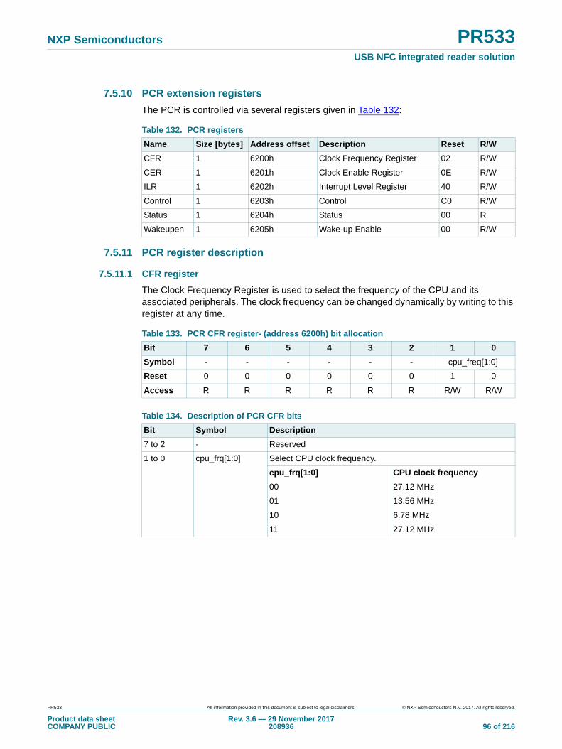
NXP Semiconductors PR533USB NFC integrated reader solution
7.5.10 PCR extension registers
The PCR is controlled via several registers given in Table 132:
7.5.11 PCR register description
7.5.11.1 CFR register
The Clock Frequency Register is used to select the frequency of the CPU and its associated peripherals. The clock frequency can be changed dynamically by writing to this register at any time.
Table 132. PCR registers
Name Size [bytes] Address offset Description Reset R/W
CFR 1 6200h Clock Frequency Register 02 R/W
CER 1 6201h Clock Enable Register 0E R/W
ILR 1 6202h Interrupt Level Register 40 R/W
Control 1 6203h Control C0 R/W
Status 1 6204h Status 00 R
Wakeupen 1 6205h Wake-up Enable 00 R/W
Table 133. PCR CFR register- (address 6200h) bit allocation
Bit 7 6 5 4 3 2 1 0
Symbol - - - - - - cpu_freq[1:0]
Reset 0 0 0 0 0 0 1 0
Access R R R R R R R/W R/W
Table 134. Description of PCR CFR bits
Bit Symbol Description
7 to 2 - Reserved
1 to 0 cpu_frq[1:0] Select CPU clock frequency.
cpu_frq[1:0] CPU clock frequency
00 27.12 MHz
01 13.56 MHz
10 6.78 MHz
11 27.12 MHz
PR533 All information provided in this document is subject to legal disclaimers. © NXP Semiconductors N.V. 2017. All rights reserved.
Product data sheetCOMPANY PUBLIC
Rev. 3.6 — 29 November 2017208936 96 of 216

NXP Semiconductors PR533USB NFC integrated reader solution
7.5.11.2 CER register
The Clock Enable Register is used to enable or disable the clock of the USB and HSU interfaces (frequency is fixed at 27.12 MHz). The clock can be switched on or off at any time.
This register also contains the PLL_lock signal that the embedded firmware should poll.
Table 135. PCR CER register (address 6201h) bit allocation
Bit 7 6 5 4 3 2 1 0
Symbol - - clock_on PLL_lock hsu_enable - - usb_enable
Reset 0 0 1 0 1 1 1 0
Access R R R R R/W R R R/W
Table 136. Description of PCR CER bits
Bit Symbol Description
7 to 6 - Reserved.
5 clock_on USB clock_on signal to poll before entering PR533 into power down.
4 PLL_lock PLL_lock signal.
3 hsu_enable Enable HSU clock. When 1, HSU is enabled. When 0, HSU is disabled.
2 to 1 - Reserved.
0 usb_enable Enable USB clock.
PR533 All information provided in this document is subject to legal disclaimers. © NXP Semiconductors N.V. 2017. All rights reserved.
Product data sheetCOMPANY PUBLIC
Rev. 3.6 — 29 November 2017208936 97 of 216
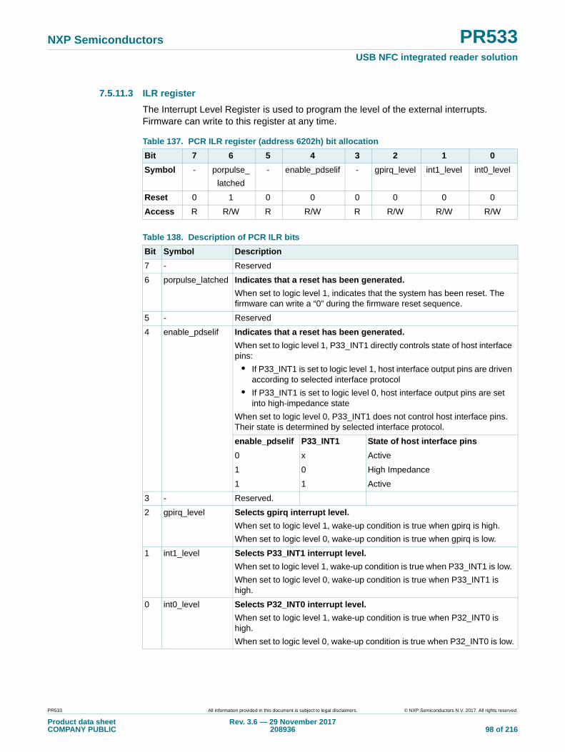
NXP Semiconductors PR533USB NFC integrated reader solution
7.5.11.3 ILR register
The Interrupt Level Register is used to program the level of the external interrupts. Firmware can write to this register at any time.
Table 137. PCR ILR register (address 6202h) bit allocation
Bit 7 6 5 4 3 2 1 0
Symbol - porpulse_
latched
- enable_pdselif - gpirq_level int1_level int0_level
Reset 0 1 0 0 0 0 0 0
Access R R/W R R/W R R/W R/W R/W
Table 138. Description of PCR ILR bits
Bit Symbol Description
7 - Reserved
6 porpulse_latched Indicates that a reset has been generated.
When set to logic level 1, indicates that the system has been reset. The firmware can write a “0” during the firmware reset sequence.
5 - Reserved
4 enable_pdselif Indicates that a reset has been generated.
When set to logic level 1, P33_INT1 directly controls state of host interface pins:
• If P33_INT1 is set to logic level 1, host interface output pins are driven according to selected interface protocol
• If P33_INT1 is set to logic level 0, host interface output pins are set into high-impedance state
When set to logic level 0, P33_INT1 does not control host interface pins. Their state is determined by selected interface protocol.
enable_pdselif P33_INT1 State of host interface pins
0 x Active
1 0 High Impedance
1 1 Active
3 - Reserved.
2 gpirq_level Selects gpirq interrupt level.
When set to logic level 1, wake-up condition is true when gpirq is high.
When set to logic level 0, wake-up condition is true when gpirq is low.
1 int1_level Selects P33_INT1 interrupt level.
When set to logic level 1, wake-up condition is true when P33_INT1 is low.
When set to logic level 0, wake-up condition is true when P33_INT1 is high.
0 int0_level Selects P32_INT0 interrupt level.
When set to logic level 1, wake-up condition is true when P32_INT0 is high.
When set to logic level 0, wake-up condition is true when P32_INT0 is low.
PR533 All information provided in this document is subject to legal disclaimers. © NXP Semiconductors N.V. 2017. All rights reserved.
Product data sheetCOMPANY PUBLIC
Rev. 3.6 — 29 November 2017208936 98 of 216
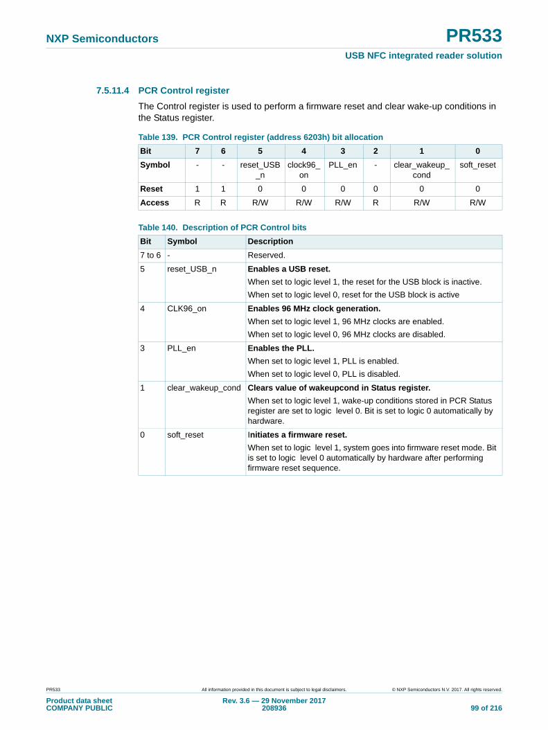
NXP Semiconductors PR533USB NFC integrated reader solution
7.5.11.4 PCR Control register
The Control register is used to perform a firmware reset and clear wake-up conditions in the Status register.
Table 139. PCR Control register (address 6203h) bit allocation
Bit 7 6 5 4 3 2 1 0
Symbol - - reset_USB_n
clock96_on
PLL_en - clear_wakeup_cond
soft_reset
Reset 1 1 0 0 0 0 0 0
Access R R R/W R/W R/W R R/W R/W
Table 140. Description of PCR Control bits
Bit Symbol Description
7 to 6 - Reserved.
5 reset_USB_n Enables a USB reset.
When set to logic level 1, the reset for the USB block is inactive.
When set to logic level 0, reset for the USB block is active
4 CLK96_on Enables 96 MHz clock generation.
When set to logic level 1, 96 MHz clocks are enabled.
When set to logic level 0, 96 MHz clocks are disabled.
3 PLL_en Enables the PLL.
When set to logic level 1, PLL is enabled.
When set to logic level 0, PLL is disabled.
1 clear_wakeup_cond Clears value of wakeupcond in Status register.
When set to logic level 1, wake-up conditions stored in PCR Status register are set to logic level 0. Bit is set to logic 0 automatically by hardware.
0 soft_reset Initiates a firmware reset.
When set to logic level 1, system goes into firmware reset mode. Bit is set to logic level 0 automatically by hardware after performing firmware reset sequence.
PR533 All information provided in this document is subject to legal disclaimers. © NXP Semiconductors N.V. 2017. All rights reserved.
Product data sheetCOMPANY PUBLIC
Rev. 3.6 — 29 November 2017208936 99 of 216
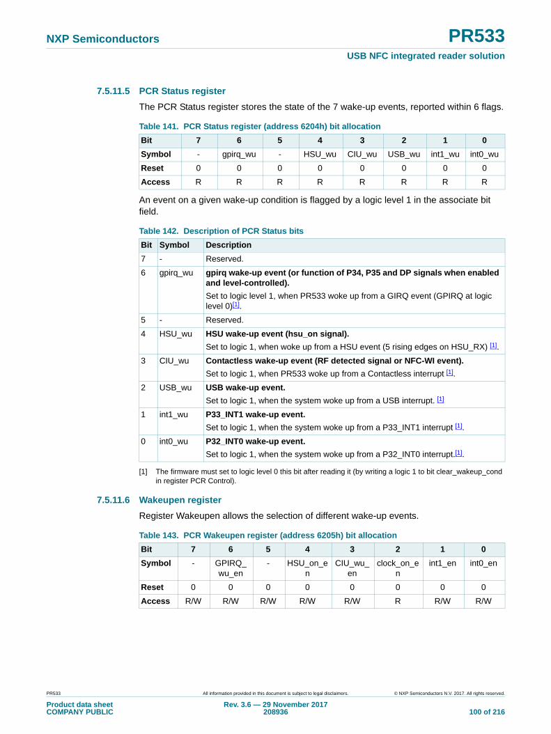
NXP Semiconductors PR533USB NFC integrated reader solution
7.5.11.5 PCR Status register
The PCR Status register stores the state of the 7 wake-up events, reported within 6 flags.
An event on a given wake-up condition is flagged by a logic level 1 in the associate bit field.
[1] The firmware must set to logic level 0 this bit after reading it (by writing a logic 1 to bit clear_wakeup_cond in register PCR Control).
7.5.11.6 Wakeupen register
Register Wakeupen allows the selection of different wake-up events.
Table 141. PCR Status register (address 6204h) bit allocation
Bit 7 6 5 4 3 2 1 0
Symbol - gpirq_wu - HSU_wu CIU_wu USB_wu int1_wu int0_wu
Reset 0 0 0 0 0 0 0 0
Access R R R R R R R R
Table 142. Description of PCR Status bits
Bit Symbol Description
7 - Reserved.
6 gpirq_wu gpirq wake-up event (or function of P34, P35 and DP signals when enabled and level-controlled).
Set to logic level 1, when PR533 woke up from a GIRQ event (GPIRQ at logic level 0)[1].
5 - Reserved.
4 HSU_wu HSU wake-up event (hsu_on signal).
Set to logic 1, when woke up from a HSU event (5 rising edges on HSU_RX) [1].
3 CIU_wu Contactless wake-up event (RF detected signal or NFC-WI event).
Set to logic 1, when PR533 woke up from a Contactless interrupt [1].
2 USB_wu USB wake-up event.
Set to logic 1, when the system woke up from a USB interrupt. [1]
1 int1_wu P33_INT1 wake-up event.
Set to logic 1, when the system woke up from a P33_INT1 interrupt [1].
0 int0_wu P32_INT0 wake-up event.
Set to logic 1, when the system woke up from a P32_INT0 interrupt.[1].
Table 143. PCR Wakeupen register (address 6205h) bit allocation
Bit 7 6 5 4 3 2 1 0
Symbol - GPIRQ_wu_en
- HSU_on_en
CIU_wu_en
clock_on_en
int1_en int0_en
Reset 0 0 0 0 0 0 0 0
Access R/W R/W R/W R/W R/W R R/W R/W
PR533 All information provided in this document is subject to legal disclaimers. © NXP Semiconductors N.V. 2017. All rights reserved.
Product data sheetCOMPANY PUBLIC
Rev. 3.6 — 29 November 2017208936 100 of 216

NXP Semiconductors PR533USB NFC integrated reader solution
7.6 Contactless Interface Unit (CIU)
The PR533 CIU is a modem for contactless communication at 13.56 MHz. The implemented firmware supports 4 different operating modes
• PCD mode for ISO/IEC 14443A/MIFARE
• PCD mode for FeliCa
• PCD mode for ISO/IEC 14443B,
• PCD mode for B’
Together with the firmware, the CIU implements a demodulator and decoder for signals from ISO/IEC 14443A/MIFARE compatible cards. The CIU handles the complete ISO/IEC 14443A framing and error detection (Parity & CRC).
The CIU supports contactless communication using MIFARE Higher transfer speeds up to 424 kbit/s in both directions.
The CIU can demodulate and decode FeliCa coded signals. The CIU digital part handles the FeliCa framing and error detection. The CIU supports contactless communication using FeliCa Higher transfer speeds up to 424 kbit/s in both directions.
The CIU supports layers 2 and 3 of the ISO/IEC 1444 B Reader/Writer communication scheme, except anticollision which is implemented in firmware and requires support from upper layers as well.
The CIU transceiver can be connected to an external antenna for Reader/Writer mode, without any additional active component.
Table 144. Description of PCR Wakeupen bits
Bit Symbol Description
7 - Reserved.
6 GPIRQ_wu_en General Purpose IRQ wake-up source enable.
When set to logic 1, a GPIRQ event can wake up PR533.
5 - Reserved.
4 HSU_on_en HSU wake-up source enable.
When set to logic 1, an HSU event can wake up PR533.
3 CIU_wu_en Contactless Interface Unit wake-up source enable.
When set to logic 1, a CIU event (RF detected or NFC-WI event) can wake up PR533.
2 clock_on_en USB wake-up source enable.
1 int1_en P33_INT1 wake-up source enable.
When set to logic 1, a P33_INT1 event can wake up PR533.
0 int0_en P32_INT0 wake-up source enable.
When set to logic 1, a P32_INT0 event can wake up PR533.
PR533 All information provided in this document is subject to legal disclaimers. © NXP Semiconductors N.V. 2017. All rights reserved.
Product data sheetCOMPANY PUBLIC
Rev. 3.6 — 29 November 2017208936 101 of 216

NXP Semiconductors PR533USB NFC integrated reader solution
7.6.1 Feature list
• Frequently accessed registers placed in SFR space
• Highly integrated analog circuitry to demodulate and decode received data
• Buffered transmitter drivers to minimize external components to connect an antenna.
• Integrated RF level detector
• Integrated data mode detector
• Typical operating distance of 50 mm in ISO/IEC 14443A/MIFARE or FeliCa in Reader/Writer mode depending on the antenna size, tuning and power supply
• Supports MIFARE 1 KB or MIFARE 4 KB emulation encryption in Reader/Writer mode
• Supports MIFARE higher data rate at 212 kbit/s and 424 kbit/s
• Supports contactless communication according to the FeliCa scheme at 212 kbit/s and 424 kbit/s
• 64 bytes send and receive FIFO-buffer
• Programmable timer
• CRC Co-processor
• Internal self test
• 2 interrupt sources
• Adjustable parameters to optimize the transceiver performance according to the antenna characteristics
7.6.2 Simplified block diagram
The Analog Interface handles the modulation and demodulation of the analog signals according Reader/Writer mode communication scheme.
Fig 37. Simplify Contactless Interface Unit (CIU) block diagram
80C51
FIFOSERIALDATA
SWITCH CL UART
DATAMODE
DETECTOR
RFLEVEL
DETECTOR
ANALOGINTERFACE
antenna
PR533
CONTACTLESS INTERFACE UNIT
aaa-001811
PR533 All information provided in this document is subject to legal disclaimers. © NXP Semiconductors N.V. 2017. All rights reserved.
Product data sheetCOMPANY PUBLIC
Rev. 3.6 — 29 November 2017208936 102 of 216
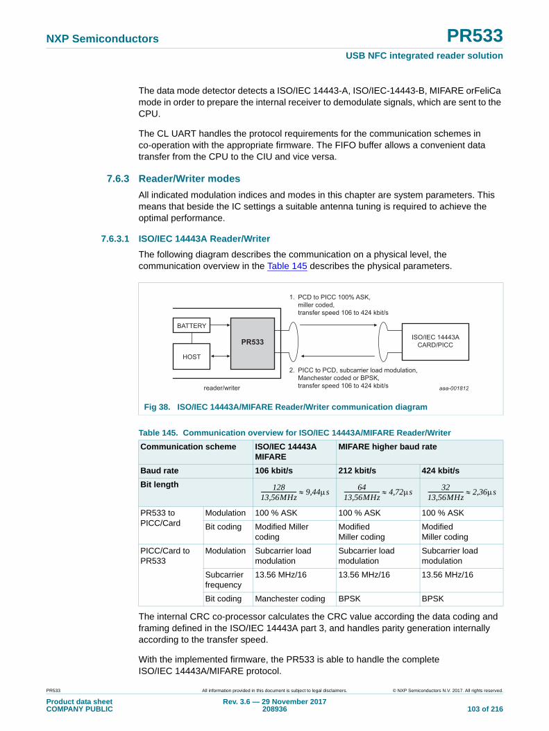
NXP Semiconductors PR533USB NFC integrated reader solution
The data mode detector detects a ISO/IEC 14443-A, ISO/IEC-14443-B, MIFARE orFeliCa mode in order to prepare the internal receiver to demodulate signals, which are sent to the CPU.
The CL UART handles the protocol requirements for the communication schemes in co-operation with the appropriate firmware. The FIFO buffer allows a convenient data transfer from the CPU to the CIU and vice versa.
7.6.3 Reader/Writer modes
All indicated modulation indices and modes in this chapter are system parameters. This means that beside the IC settings a suitable antenna tuning is required to achieve the optimal performance.
7.6.3.1 ISO/IEC 14443A Reader/Writer
The following diagram describes the communication on a physical level, the communication overview in the Table 145 describes the physical parameters.
The internal CRC co-processor calculates the CRC value according the data coding and framing defined in the ISO/IEC 14443A part 3, and handles parity generation internally according to the transfer speed.
With the implemented firmware, the PR533 is able to handle the complete ISO/IEC 14443A/MIFARE protocol.
Fig 38. ISO/IEC 14443A/MIFARE Reader/Writer communication diagram
Table 145. Communication overview for ISO/IEC 14443A/MIFARE Reader/Writer
Communication scheme ISO/IEC 14443AMIFARE
MIFARE higher baud rate
Baud rate 106 kbit/s 212 kbit/s 424 kbit/s
Bit length
PR533 to PICC/Card
Modulation 100 % ASK 100 % ASK 100 % ASK
Bit coding Modified Miller coding
Modified Miller coding
Modified Miller coding
PICC/Card to PR533
Modulation Subcarrier load modulation
Subcarrier load modulation
Subcarrier load modulation
Subcarrier frequency
13.56 MHz/16 13.56 MHz/16 13.56 MHz/16
Bit coding Manchester coding BPSK BPSK
aaa-001812
PCD to PICC 100% ASK,miller coded, transfer speed 106 to 424 kbit/s
PICC to PCD, subcarrier load modulation,Manchester coded or BPSK,transfer speed 106 to 424 kbit/sreader/writer
PR533
HOST
BATTERY
ISO/IEC 14443ACARD/PICC
1.
2.
12813,56MHz-------------------------- 9,44s 64
13,56MHz-------------------------- 4,72s 32
13,56MHz-------------------------- 2,36s
PR533 All information provided in this document is subject to legal disclaimers. © NXP Semiconductors N.V. 2017. All rights reserved.
Product data sheetCOMPANY PUBLIC
Rev. 3.6 — 29 November 2017208936 103 of 216

NXP Semiconductors PR533USB NFC integrated reader solution
7.6.3.2 FeliCa Reader/Writer
The following diagram describes the communication at the physical level. Table 146 describes the physical parameters.
With appropriate firmware, the PR533 can handle the FeliCa protocol.
The FeliCa Framing and coding must comply with the following table:
Fig 39. Data coding and framing according to ISO/IEC 14443A
8 bit data8 bit data8 bit data
start
oddpar
oddpar
oddparstart bit is “1”
current ISO 14443-A framing at 106 kbit/s
8 bit data8 bit data8 bit data
start
evenpar
oddpar
oddparstart bit is “0”
MIFARE higher baudrate framing fot 212, 424 kbit/s
even parity at theend of the frame!
burst of 32 subcarrier
clocksaaa-001813
Fig 40. FeliCa Reader/Writer communication diagram
Table 146. Communication overview for FeliCa Reader/Writer
Communication scheme FeliCa FeliCa higher baud rate
Baud rate 212 kbit/s 424 kbit/s
Bit length
PR533 to PICC/Card
Modulation 8 - 30 % ASK 8 - 30 % ASK
Bit coding Manchester coding Manchester coding
PICC/Card to PR533
Modulation >12 % ASK >12 % ASK
Bit coding Manchester coding Manchester coding
aaa-001814reader/writer
PR533
HOST
BATTERY
FELICACARD
reader/rriter to card 8 - 30 % ASK,Manchester coded,baud rate 212 to 424 kbit/s
card to reader/writer, > 12 % ASK load modulation,Manchester coded,baud rate 212 to 424 kbit/s
1.
2.
6413,56MHz-------------------------- 4,72s 32
13,56MHz-------------------------- 2,36s
PR533 All information provided in this document is subject to legal disclaimers. © NXP Semiconductors N.V. 2017. All rights reserved.
Product data sheetCOMPANY PUBLIC
Rev. 3.6 — 29 November 2017208936 104 of 216

NXP Semiconductors PR533USB NFC integrated reader solution
To enable the FeliCa communication a 6-byte preamble (00h, 00h, 00h, 00h, 00h, 00h) and 2-byte SYNC bytes (B2h, 4Dh) are sent to synchronize the receiver.
The following LEN byte indicates the length of the sent data bytes plus the LEN byte itself. The CRC calculation is done according to the FeliCa definitions with the MSB first.
To transmit data on the RF interface, the 80C51 has to send the LEN and data bytes to the CIU. The Preamble and SYNC bytes are generated by the CIU automatically and must not be written to the FIFO. The CIU performs internally the CRC calculation and adds the result to the frame.
The starting value for the CRC Polynomial is 2 null bytes: (00h), (00h)
Example of frame:
7.6.3.3 ISO/IEC 14443B Reader/Writer
The CIU supports layers 2 and 3 of the ISO/IEC 14443B Reader/Writer communication scheme, except anticollision which must be implemented in firmware as well as upper layers.
The following diagram describes the communication at the physical level. Table 149 describes the physical parameters.
With appropriate firmware, the PR533 can handle the ISO/IEC 14443B protocol.
Table 147. FeliCa Framing and Coding
Preamble SYNC LEN n-Data CRC
00h 00h 00h 00h 00h 00h B2h 4Dh
Table 148. FeliCa framing and coding
Preamble SYNC LEN 2 Data Bytes CRC
00 00 00 00 00 00 B2 4D 03 AB CD 90 35
Fig 41. ISO/IEC 14443B Reader/Writer communication diagram
aaa-001815reader/writer
PR533
HOST
BATTERY
ISO/IEC 14443BCARD/PICC
PCD to PICC, 8 - 14 % ASK,NRZ-L coded,transfer speed 106 to 424 kbit/s
PICC to PCD, subcarrier load modulation,BPSK,transfer speed 106 to 424 kbit/s
1.
2.
PR533 All information provided in this document is subject to legal disclaimers. © NXP Semiconductors N.V. 2017. All rights reserved.
Product data sheetCOMPANY PUBLIC
Rev. 3.6 — 29 November 2017208936 105 of 216

NXP Semiconductors PR533USB NFC integrated reader solution
7.6.4 Overall CIU block diagram
The PR533 supports different contactless communication modes. The firmware together with CIU supports the internal 80C51 for the Reader/Writer Operating mode up to 424 kbit/s. The CIU generates bit- and byte-oriented framing and handles error detection according to theis contactless protocol.
Remark: The size and tuning of the antenna have an important impact on the achievable operating distance.
Table 149. Communication overview for ISO/IEC 14443B Reader/Writer
Communication scheme ISO/IEC 14443B Type B higher baud rate
Baud rate 106 kbit/s 212 kbit/s 424 kbit/s
Bit length
PR533 to PICC/Card
Modulation 8 % - 14 % ASK 8 % - 14 % ASK 8 % - 14 % ASK
Bit coding NRZ-L NRZ-L NRZ-L
PICC/Card to PR533
Modulation Subcarrier load modulation
Subcarrier load modulation
Subcarrier load modulation
Subcarrier frequency
13.56 MHz/16 13.56 MHz/16 13.56 MHz/16
Bit coding BPSK BPSK BPSK
12813,56MHz-------------------------- 9,44s 64
13,56MHz-------------------------- 4,72s 32
13,56MHz-------------------------- 2,36s
PR533 All information provided in this document is subject to legal disclaimers. © NXP Semiconductors N.V. 2017. All rights reserved.
Product data sheetCOMPANY PUBLIC
Rev. 3.6 — 29 November 2017208936 106 of 216
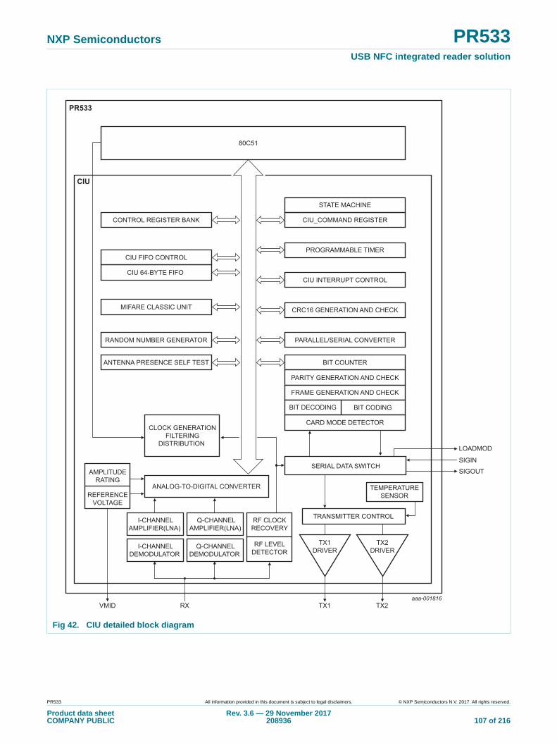
NXP Semiconductors PR533USB NFC integrated reader solution
Fig 42. CIU detailed block diagram
PR533
VMID RX TX1 TX2
SIGOUT
SIGIN
LOADMOD
PARALLEL/SERIAL CONVERTER
BIT COUNTER
PARITY GENERATION AND CHECK
FRAME GENERATION AND CHECK
CARD MODE DETECTOR
BIT DECODING BIT CODING
CRC16 GENERATION AND CHECK
CIU INTERRUPT CONTROL
PROGRAMMABLE TIMER
CIU_COMMAND REGISTER
CIU FIFO CONTROL
CIU 64-BYTE FIFO
MIFARE CLASSIC UNIT
RANDOM NUMBER GENERATOR
SERIAL DATA SWITCH
CLOCK GENERATIONFILTERING
DISTRIBUTION
TRANSMITTER CONTROL
TEMPERATURESENSOR
TX1DRIVER
TX2DRIVER
ANALOG-TO-DIGITAL CONVERTER
I-CHANNELAMPLIFIER(LNA)
I-CHANNELDEMODULATOR
Q-CHANNELAMPLIFIER(LNA)
Q-CHANNELDEMODULATOR
RF CLOCKRECOVERY
RF LEVELDETECTOR
80C51
CONTROL REGISTER BANK
REFERENCEVOLTAGE
AMPLITUDERATING
CIU
STATE MACHINE
ANTENNA PRESENCE SELF TEST
aaa-001816
PR533 All information provided in this document is subject to legal disclaimers. © NXP Semiconductors N.V. 2017. All rights reserved.
Product data sheetCOMPANY PUBLIC
Rev. 3.6 — 29 November 2017208936 107 of 216
NXP Semiconductors PR533USB NFC integrated reader solution
7.6.5 Transmitter control
The signals delivered by the transmitter are on pins TX1 and pin TX2. The supply and grounds of the transmitter drivers are TVDD, TVSS1 and TVSS2.
The signals delivered are the 13.56 MHz energy carrier modulated by an envelope signal. It can be used to drive an antenna directly, using a few passive components for matching and filtering, see Section 12 “Application information” on page 206. The signals on TX1 and TX2 can be configured by the register CIU_TxControl.
The modulation index can be set by adjusting the impedance of the drivers. The impedance of the p-driver can be configured by the registers CIU_CWGsP and CIU_ModGsP. The impedance of the n-driver can be configured by the registers CIU_GsNOn and CIU_GsNOFF. Furthermore, the modulation index depends on the antenna design and tuning.
Remark: It is recommended to use a modulation index in the range of 8 % for the FeliCa and NFCIP-1 communication scheme at 212 kbit/s and 424 kbit/s.
The registers CIU_TxMode and CIU_TxAuto control the data rate and framing during the transmission and the setting of the antenna driver to support the different requirements at the different modes and transfer speeds.
In the following tables, these abbreviations are used:
• RF: 13.56 MHz clock derived from 27.12 MHz quartz divided by 2
• RF_n: inverted 13.56 MHz clock
• GsPMos: Conductance of the transmitter PMOS
• GsNMos: Conductance of the transmitter NMOS
• CWGsP: PMOS conductance value for Continuous Wave (see Table 245 on page 165)
• ModGsP: refers to ModGsP[5:0], PMOS conductance value for Modulation (see Table 246 on page 166)
• On: refers to CWGsP[5:0], NMOS conductance value for Continuous Wave (see Table 243 on page 165)
• ModGsNOn: NMOS conductance value for Modulation when generating RF field (see Table 243 on page 165)
• CWGsNOff: NMOS conductance value for Continuous Wave when no RF is generated by the PR533 itself (see Table 235 on page 162)
• ModGsNOff: NMOS conductance value for modulation when load Modulation (see Table 235 on page 162)
Remark: If only 1 driver is switched on, the values for ModGsNOn and CWGsNOn are used for both drivers.
PR533 All information provided in this document is subject to legal disclaimers. © NXP Semiconductors N.V. 2017. All rights reserved.
Product data sheetCOMPANY PUBLIC
Rev. 3.6 — 29 November 2017208936 108 of 216

xxxxxxxxxxxxxxxxxxxxx xxxxxxxxxxxxxxxxxxxxxxxxxx xxxxxxx x x x xxxxxxxxxxxxxxxxxxxxxxxxxxxxxx xxxxxxxxxxxxxxxxxxx xx xx xxxxx xxxxxxxxxxxxxxxxxxxxxxxxxxx xxxxxxxxxxxxxxxxxxx xxxxxx xxxxxxxxxxxxxxxxxxxxxxxxxxxxxxxxxxx xxxxxxxxxxxx x x xxxxxxxxxxxxxxxxxxxxx xxxxxxxxxxxxxxxxxxxxxxxxxxxxxx xxxxx xxxxxxxxxxxxxxxxxxxxxxxxxxxxxxxxxxxxxxxxxxxxxxxxxx xxxxxxxx xxxxxxxxxxxxxxxxxxxxxxxxx xxxxxxxxxxxxxxxxxxxx xxx
PR
533
Pro
du
ct data sh
eetC
OM
PA
NY
PU
BL
ICR
ev. 3.6 —
29 N
ove
mb
er 2
017208936
109 of 216
NX
P S
emico
nd
ucto
rsP
R533
US
B N
FC
integ
rated read
er solu
tion
Table 150. Settings for TX1
TX1RFEn
Force100ASK
InvTx1RFON
InvTx1RFOFF
Envelope TX1 GsPMos GsNMos Remarks
X1 is set to logic 0 or 1 depending s no effect. Envelope modulates
hase of TX1 is depending on fect; when Envelope is set to
X2 is forced to 0 or 1 depending on SK100 has no effect. The signal
ctance value
ductance values are always
All inform
ation provided
in this docum
ent is subject to leg
al disclaim
ers.©
NX
P S
em
iconductors N
.V. 2017. A
ll rights rese
rved.
0 X X 0 0 0 ModGsNOff If TX1RFEN is set to logic level 0, the pin Ton InvTx1RFOFF. The bit Force 100ASK hathe transconductance value.
1 0 CWGsNOff
1 0 1 ModGsP
1 1 CWGsP
1 0 0 X 0 RF ModGsP ModGsNON If TX1RFEN is set to logic level 1, the RF pInvTx1RFON. The bit Force100ASK has eflogic level 0, TX1 is pulled to ground.
1 RF CWGsP CWGsNON
0 1 X 0 RF_n ModGsP ModGsNON
1 RF_n CWGsP CWGsNON
1 0 X 0 0 ModGsNON
1 RF CWGsP CWGsNON
1 1 X 0 0 ModGsNON
1 RF_n CWGsP CWGsNON
Table 151. Settings for TX2
TX2RFEn
Force100ASK
TX2CW InVTx2RFON
InvTx2RFOFF
Envelope TX2 GsPMos GsNMos Remarks
0 X 0 X 0 0 0 ModGsNOff If Tx2RFEn is set to logic 0, the pin Tthe InvTx2RFOFF bit. The bit ForceAEnvelope modulates the transcondu
1 0 CWGsNOff
1 0 1 ModGsP
1 1 CWGsP
1 X 0 0 0 CWGsNOff When Tx2CW bit is set, the transconCWGsP or CWGsNOff1 0 CWGsNOff
1 0 1 CWGsP
1 1 CWGsP
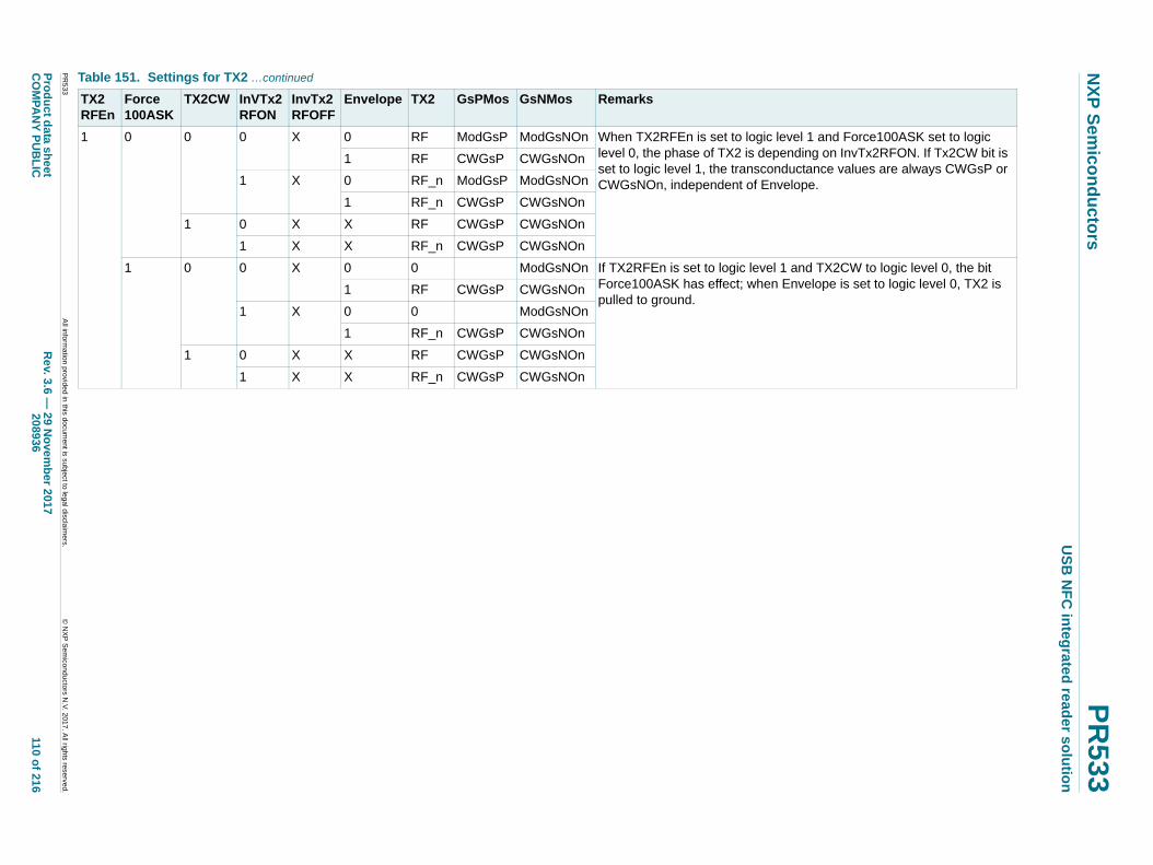
xxxxxxxxxxxxxxxxxxxxx xxxxxxxxxxxxxxxxxxxxxxxxxx xxxxxxx x x x xxxxxxxxxxxxxxxxxxxxxxxxxxxxxx xxxxxxxxxxxxxxxxxxx xx xx xxxxx xxxxxxxxxxxxxxxxxxxxxxxxxxx xxxxxxxxxxxxxxxxxxx xxxxxx xxxxxxxxxxxxxxxxxxxxxxxxxxxxxxxxxxx xxxxxxxxxxxx x x xxxxxxxxxxxxxxxxxxxxx xxxxxxxxxxxxxxxxxxxxxxxxxxxxxx xxxxx xxxxxxxxxxxxxxxxxxxxxxxxxxxxxxxxxxxxxxxxxxxxxxxxxx xxxxxxxx xxxxxxxxxxxxxxxxxxxxxxxxx xxxxxxxxxxxxxxxxxxxx xxx
PR
533
Pro
du
ct data sh
eetC
OM
PA
NY
PU
BL
ICR
ev. 3.6 —
29 N
ove
mb
er 2
017208936
110 of 216
NX
P S
emico
nd
ucto
rsP
R533
US
B N
FC
integ
rated read
er solu
tion
1 and Force100ASK set to logic g on InvTx2RFON. If Tx2CW bit is nce values are always CWGsP or
e.
TX2CW to logic level 0, the bit lope is set to logic level 0, TX2 is
Table 151. Settings for TX2 …continued
TX2RFEn
Force100ASK
TX2CW InVTx2RFON
InvTx2RFOFF
Envelope TX2 GsPMos GsNMos Remarks
All inform
ation provided
in this docum
ent is subject to leg
al disclaim
ers.©
NX
P S
em
iconductors N
.V. 2017. A
ll rights rese
rved.
1 0 0 0 X 0 RF ModGsP ModGsNOn When TX2RFEn is set to logic level level 0, the phase of TX2 is dependinset to logic level 1, the transconductaCWGsNOn, independent of Envelop
1 RF CWGsP CWGsNOn
1 X 0 RF_n ModGsP ModGsNOn
1 RF_n CWGsP CWGsNOn
1 0 X X RF CWGsP CWGsNOn
1 X X RF_n CWGsP CWGsNOn
1 0 0 X 0 0 ModGsNOn If TX2RFEn is set to logic level 1 andForce100ASK has effect; when Envepulled to ground.
1 RF CWGsP CWGsNOn
1 X 0 0 ModGsNOn
1 RF_n CWGsP CWGsNOn
1 0 X X RF CWGsP CWGsNOn
1 X X RF_n CWGsP CWGsNOn
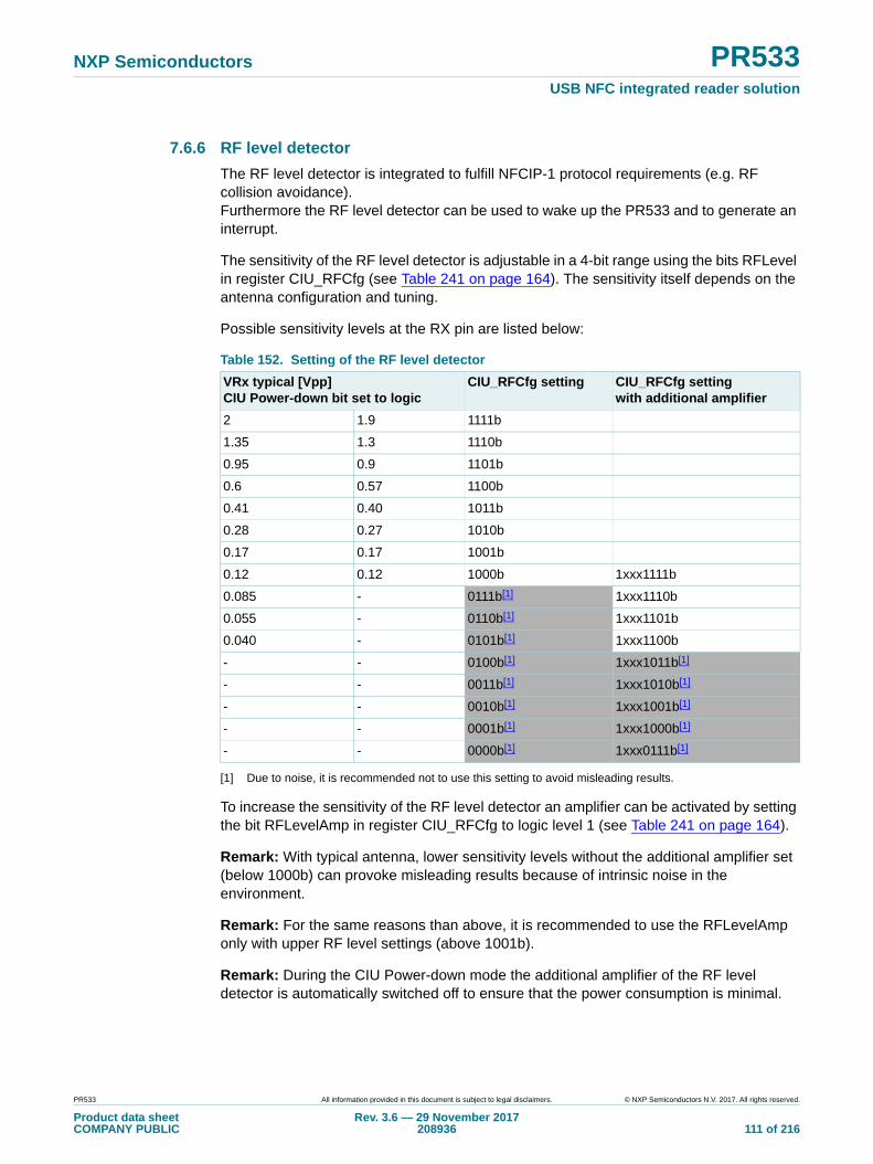
NXP Semiconductors PR533USB NFC integrated reader solution
7.6.6 RF level detector
The RF level detector is integrated to fulfill NFCIP-1 protocol requirements (e.g. RF collision avoidance).Furthermore the RF level detector can be used to wake up the PR533 and to generate an interrupt.
The sensitivity of the RF level detector is adjustable in a 4-bit range using the bits RFLevel in register CIU_RFCfg (see Table 241 on page 164). The sensitivity itself depends on the antenna configuration and tuning.
Possible sensitivity levels at the RX pin are listed below:
[1] Due to noise, it is recommended not to use this setting to avoid misleading results.
To increase the sensitivity of the RF level detector an amplifier can be activated by setting the bit RFLevelAmp in register CIU_RFCfg to logic level 1 (see Table 241 on page 164).
Remark: With typical antenna, lower sensitivity levels without the additional amplifier set (below 1000b) can provoke misleading results because of intrinsic noise in the environment.
Remark: For the same reasons than above, it is recommended to use the RFLevelAmp only with upper RF level settings (above 1001b).
Remark: During the CIU Power-down mode the additional amplifier of the RF level detector is automatically switched off to ensure that the power consumption is minimal.
Table 152. Setting of the RF level detector
VRx typical [Vpp]CIU Power-down bit set to logic
CIU_RFCfg setting CIU_RFCfg settingwith additional amplifier
2 1.9 1111b
1.35 1.3 1110b
0.95 0.9 1101b
0.6 0.57 1100b
0.41 0.40 1011b
0.28 0.27 1010b
0.17 0.17 1001b
0.12 0.12 1000b 1xxx1111b
0.085 - 0111b[1] 1xxx1110b
0.055 - 0110b[1] 1xxx1101b
0.040 - 0101b[1] 1xxx1100b
- - 0100b[1] 1xxx1011b[1]
- - 0011b[1] 1xxx1010b[1]
- - 0010b[1] 1xxx1001b[1]
- - 0001b[1] 1xxx1000b[1]
- - 0000b[1] 1xxx0111b[1]
PR533 All information provided in this document is subject to legal disclaimers. © NXP Semiconductors N.V. 2017. All rights reserved.
Product data sheetCOMPANY PUBLIC
Rev. 3.6 — 29 November 2017208936 111 of 216

NXP Semiconductors PR533USB NFC integrated reader solution
7.6.7 Antenna presence self test
The goal of the Antenna Presence Self Test is to facilitate at assembly phase the detection of the absence of the antenna and/or antenna matching components. Such a detection is done by mean of measuring the current consumption.
7.6.7.1 Principle
The principle is explained with typical antenna tuning and matching components.
The testing operation can be managed via a dedicated register Table 154 on page 113 and requires the transmitter to be activated. When activated by asserting bit 0, the detector will monitor the current consumption through the internal low dropout voltage regulator. Any violation to the current limits will be reported via bits 7 and 6 of the register.
Several levels of detection can be programmed through the register to offer a large panel of compatibility to different type of antennas. The high current threshold can be programmed from 40 mA to 150 mA with 15 mA steps (total current consumption of the IC). The low current threshold can be programmed from 5 mA to 35 mA with a 10 mA step (total current consumption of the IC).
There is no dedicated pin for the output of the detector. The result of the detection is to be read out from the antenna test register.
• Cases 1 and 2: If the antenna and/or the tuning network are not connected, the TVDD current is higher than the nominal one. The antenna detector detects this higher consumption and the andet_up bit in andet_control register is set to high
• Case 3: If the EMC filter is not correctly connected, the current within TVDD is lower than the nominal one. The antenna detector detects this lower consumption and the andet_bot bit in andet_control register is set to high.
To have this functionality working properly it is needed to have the transmitter generating some RF in the antenna.
Fig 43. Disconnection localization for the antenna detection
RX
VMID
TX1PR533
aaa-001817
R2R1
Cvmid
C0
C0
CRX
C1 RQL0
TVSS1TVSS2
TX2C1 RQL0
C2
C2
ANTENNA
(3) (2) (1)
PR533 All information provided in this document is subject to legal disclaimers. © NXP Semiconductors N.V. 2017. All rights reserved.
Product data sheetCOMPANY PUBLIC
Rev. 3.6 — 29 November 2017208936 112 of 216

NXP Semiconductors PR533USB NFC integrated reader solution
7.6.7.2 Antenna presence detector register
Table 153. andet_control register (address 610Ch) bit allocation
Bit 7 6 5 4 3 2 1 0
Symbol andet_bot andet_up andet_ithl[1:0] andet_ithh[2:0] andet_en
Reset 0 0 0 0 0 0 0 0
Access R R R/W R/W R/W R/W R/W R/W
Table 154. Description of andet_control bits
Bit Symbol Description
7 andet_bot A too low power consumption has been detected
6 andet_up A too high power consumption has been detected
5 to 4 andet_ithl[1:0 Set the low current consumption threshold to be detected
Define the overcurrent threshold
00: 6 mA
01: 18 mA
10: 29 mA
11: 40 mA
3 to 1 andet_ithh[2:0] Set the high current consumption threshold to be detected
000: 38 mA
001: 50 mA
010: 64 mA
011: 76 mA
100: 89 mA
101: 102 mA
110: 115 mA
111: 127 mA
0 andet_en Enable the detection of the antenna presence detector functionality.
PR533 All information provided in this document is subject to legal disclaimers. © NXP Semiconductors N.V. 2017. All rights reserved.
Product data sheetCOMPANY PUBLIC
Rev. 3.6 — 29 November 2017208936 113 of 216
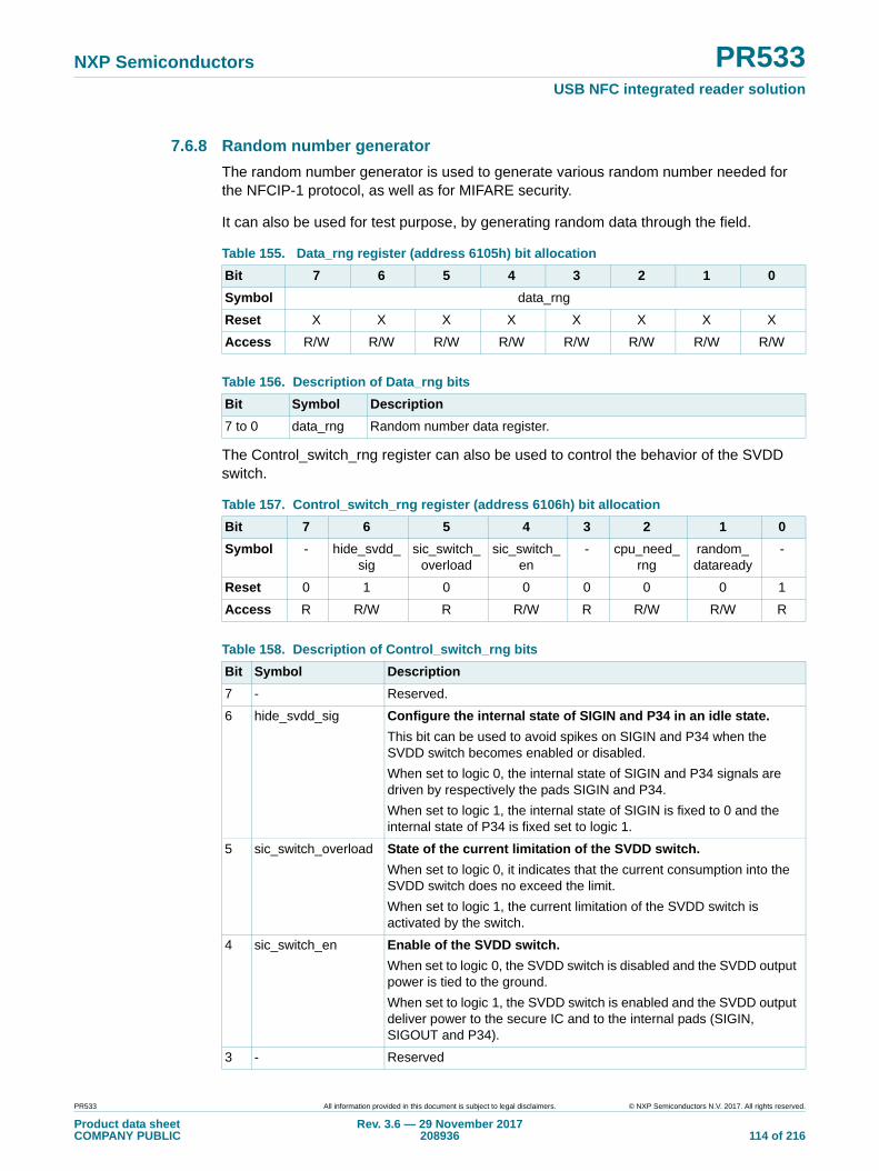
NXP Semiconductors PR533USB NFC integrated reader solution
7.6.8 Random number generator
The random number generator is used to generate various random number needed for the NFCIP-1 protocol, as well as for MIFARE security.
It can also be used for test purpose, by generating random data through the field.
The Control_switch_rng register can also be used to control the behavior of the SVDD switch.
Table 155. Data_rng register (address 6105h) bit allocation
Bit 7 6 5 4 3 2 1 0
Symbol data_rng
Reset X X X X X X X X
Access R/W R/W R/W R/W R/W R/W R/W R/W
Table 156. Description of Data_rng bits
Bit Symbol Description
7 to 0 data_rng Random number data register.
Table 157. Control_switch_rng register (address 6106h) bit allocation
Bit 7 6 5 4 3 2 1 0
Symbol - hide_svdd_sig
sic_switch_overload
sic_switch_en
- cpu_need_ rng
random_ dataready
-
Reset 0 1 0 0 0 0 0 1
Access R R/W R R/W R R/W R/W R
Table 158. Description of Control_switch_rng bits
Bit Symbol Description
7 - Reserved.
6 hide_svdd_sig Configure the internal state of SIGIN and P34 in an idle state.
This bit can be used to avoid spikes on SIGIN and P34 when the SVDD switch becomes enabled or disabled.
When set to logic 0, the internal state of SIGIN and P34 signals are driven by respectively the pads SIGIN and P34.
When set to logic 1, the internal state of SIGIN is fixed to 0 and the internal state of P34 is fixed set to logic 1.
5 sic_switch_overload State of the current limitation of the SVDD switch.
When set to logic 0, it indicates that the current consumption into the SVDD switch does no exceed the limit.
When set to logic 1, the current limitation of the SVDD switch is activated by the switch.
4 sic_switch_en Enable of the SVDD switch.
When set to logic 0, the SVDD switch is disabled and the SVDD output power is tied to the ground.
When set to logic 1, the SVDD switch is enabled and the SVDD output deliver power to the secure IC and to the internal pads (SIGIN, SIGOUT and P34).
3 - Reserved
PR533 All information provided in this document is subject to legal disclaimers. © NXP Semiconductors N.V. 2017. All rights reserved.
Product data sheetCOMPANY PUBLIC
Rev. 3.6 — 29 November 2017208936 114 of 216
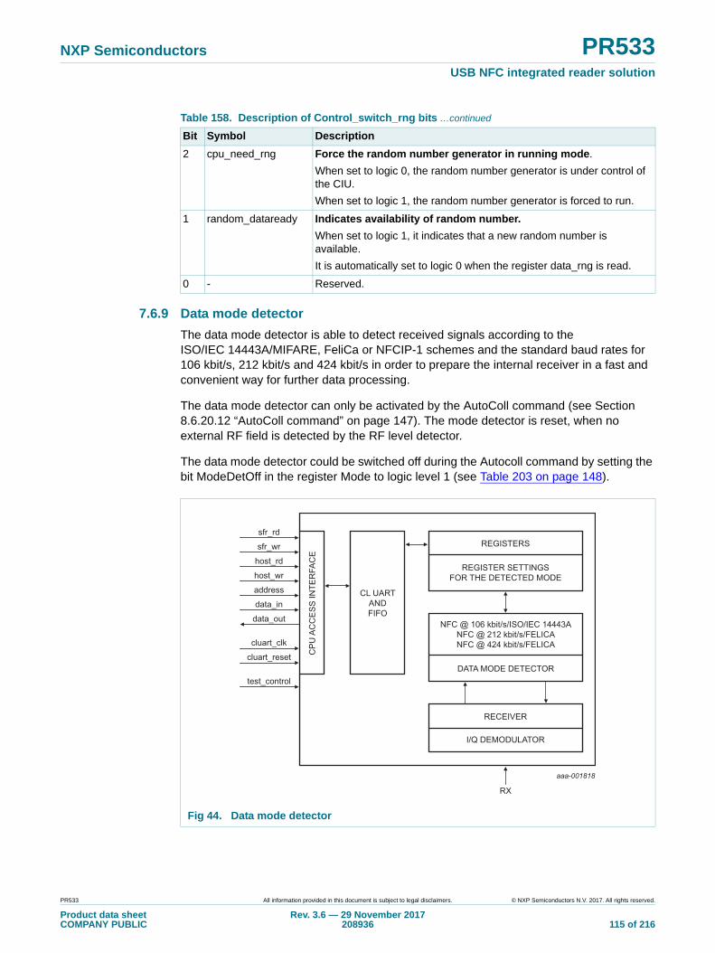
NXP Semiconductors PR533USB NFC integrated reader solution
7.6.9 Data mode detector
The data mode detector is able to detect received signals according to the ISO/IEC 14443A/MIFARE, FeliCa or NFCIP-1 schemes and the standard baud rates for 106 kbit/s, 212 kbit/s and 424 kbit/s in order to prepare the internal receiver in a fast and convenient way for further data processing.
The data mode detector can only be activated by the AutoColl command (see Section 8.6.20.12 “AutoColl command” on page 147). The mode detector is reset, when no external RF field is detected by the RF level detector.
The data mode detector could be switched off during the Autocoll command by setting the bit ModeDetOff in the register Mode to logic level 1 (see Table 203 on page 148).
2 cpu_need_rng Force the random number generator in running mode.
When set to logic 0, the random number generator is under control of the CIU.
When set to logic 1, the random number generator is forced to run.
1 random_dataready Indicates availability of random number.
When set to logic 1, it indicates that a new random number is available.
It is automatically set to logic 0 when the register data_rng is read.
0 - Reserved.
Table 158. Description of Control_switch_rng bits …continued
Bit Symbol Description
Fig 44. Data mode detector
RECEIVER
REGISTER SETTINGSFOR THE DETECTED MODE
NFC @ 106 kbit/s/ISO/IEC 14443ANFC @ 212 kbit/s/FELICANFC @ 424 kbit/s/FELICA
DATA MODE DETECTOR
I/Q DEMODULATOR
CL UARTANDFIFO
CP
U A
CC
ES
S IN
TER
FAC
E
sfr_rd
sfr_wr
host_rd
host_wr
address
data_in
data_out
cluart_clk
cluart_reset
test_control
RX
REGISTERS
aaa-001818
PR533 All information provided in this document is subject to legal disclaimers. © NXP Semiconductors N.V. 2017. All rights reserved.
Product data sheetCOMPANY PUBLIC
Rev. 3.6 — 29 November 2017208936 115 of 216
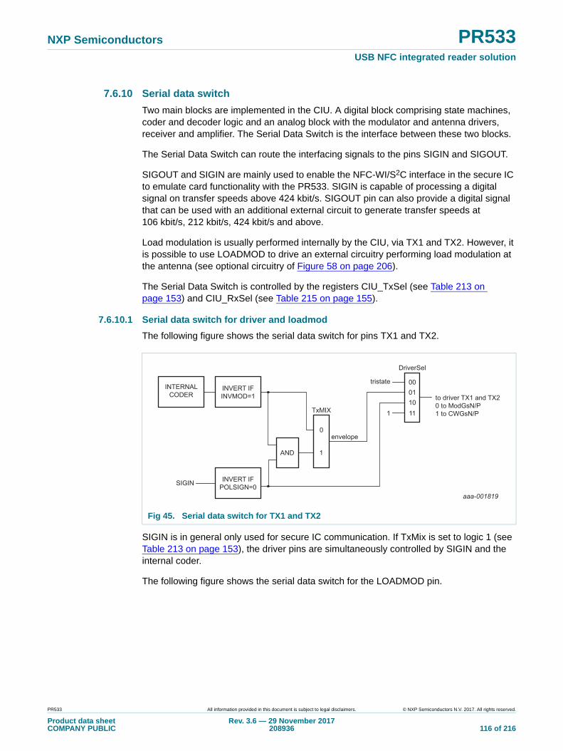
NXP Semiconductors PR533USB NFC integrated reader solution
7.6.10 Serial data switch
Two main blocks are implemented in the CIU. A digital block comprising state machines, coder and decoder logic and an analog block with the modulator and antenna drivers, receiver and amplifier. The Serial Data Switch is the interface between these two blocks.
The Serial Data Switch can route the interfacing signals to the pins SIGIN and SIGOUT.
SIGOUT and SIGIN are mainly used to enable the NFC-WI/S2C interface in the secure IC to emulate card functionality with the PR533. SIGIN is capable of processing a digital signal on transfer speeds above 424 kbit/s. SIGOUT pin can also provide a digital signal that can be used with an additional external circuit to generate transfer speeds at 106 kbit/s, 212 kbit/s, 424 kbit/s and above.
Load modulation is usually performed internally by the CIU, via TX1 and TX2. However, it is possible to use LOADMOD to drive an external circuitry performing load modulation at the antenna (see optional circuitry of Figure 58 on page 206).
The Serial Data Switch is controlled by the registers CIU_TxSel (see Table 213 on page 153) and CIU_RxSel (see Table 215 on page 155).
7.6.10.1 Serial data switch for driver and loadmod
The following figure shows the serial data switch for pins TX1 and TX2.
SIGIN is in general only used for secure IC communication. If TxMix is set to logic 1 (see Table 213 on page 153), the driver pins are simultaneously controlled by SIGIN and the internal coder.
The following figure shows the serial data switch for the LOADMOD pin.
Fig 45. Serial data switch for TX1 and TX2
INTERNALCODER
INVERT IFINVMOD=1
INVERT IFPOLSIGN=0
AND
0
1
00011011
DriverSel
TxMIX
envelope
to driver TX1 and TX20 to ModGsN/P1 to CWGsN/P
tristate
1
SIGIN
aaa-001819
PR533 All information provided in this document is subject to legal disclaimers. © NXP Semiconductors N.V. 2017. All rights reserved.
Product data sheetCOMPANY PUBLIC
Rev. 3.6 — 29 November 2017208936 116 of 216
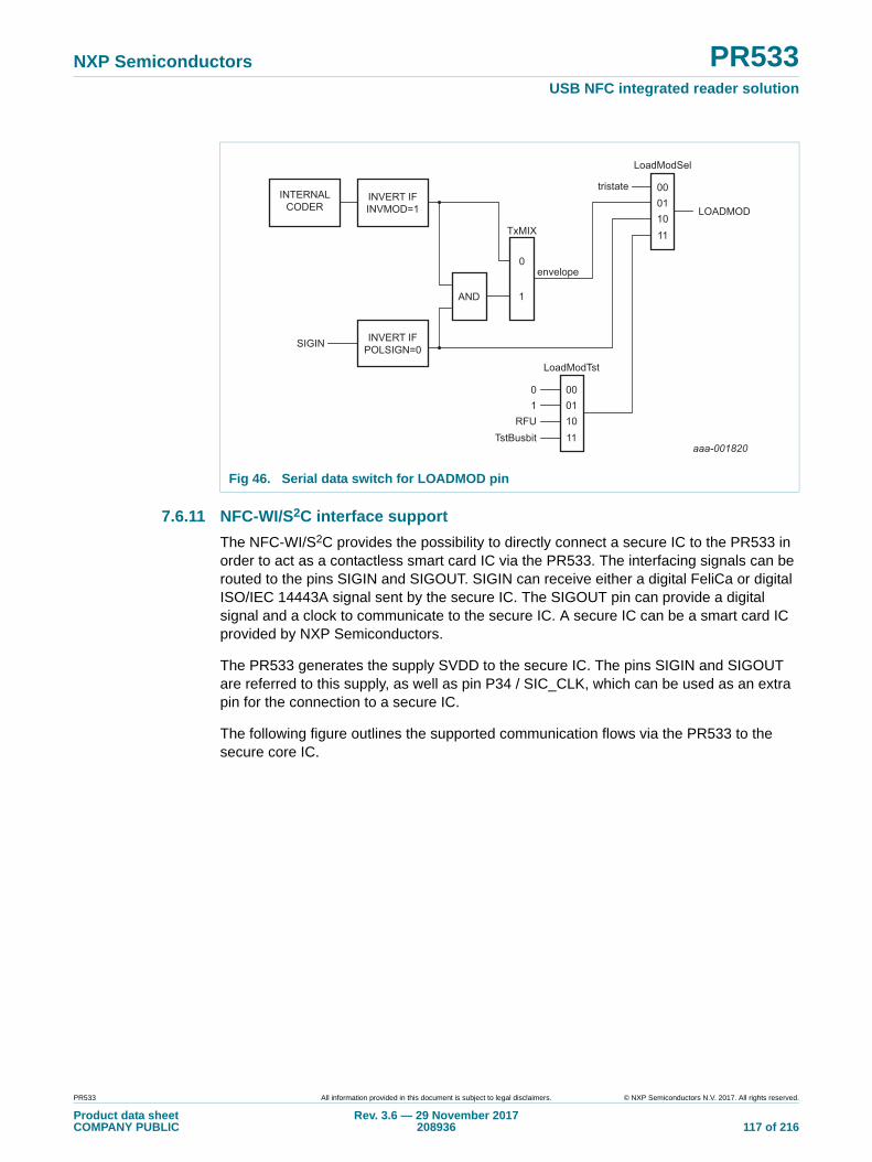
NXP Semiconductors PR533USB NFC integrated reader solution
7.6.11 NFC-WI/S2C interface support
The NFC-WI/S2C provides the possibility to directly connect a secure IC to the PR533 in order to act as a contactless smart card IC via the PR533. The interfacing signals can be routed to the pins SIGIN and SIGOUT. SIGIN can receive either a digital FeliCa or digital ISO/IEC 14443A signal sent by the secure IC. The SIGOUT pin can provide a digital signal and a clock to communicate to the secure IC. A secure IC can be a smart card IC provided by NXP Semiconductors.
The PR533 generates the supply SVDD to the secure IC. The pins SIGIN and SIGOUT are referred to this supply, as well as pin P34 / SIC_CLK, which can be used as an extra pin for the connection to a secure IC.
The following figure outlines the supported communication flows via the PR533 to the secure core IC.
Fig 46. Serial data switch for LOADMOD pin
INTERNALCODER
INVERT IFINVMOD=1
INVERT IFPOLSIGN=0
AND
0
1
00011011
LoadModSel
TxMIX
envelope
LOADMOD
tristate
SIGIN
00011011
01
RFUTstBusbit
LoadModTst
aaa-001820
PR533 All information provided in this document is subject to legal disclaimers. © NXP Semiconductors N.V. 2017. All rights reserved.
Product data sheetCOMPANY PUBLIC
Rev. 3.6 — 29 November 2017208936 117 of 216
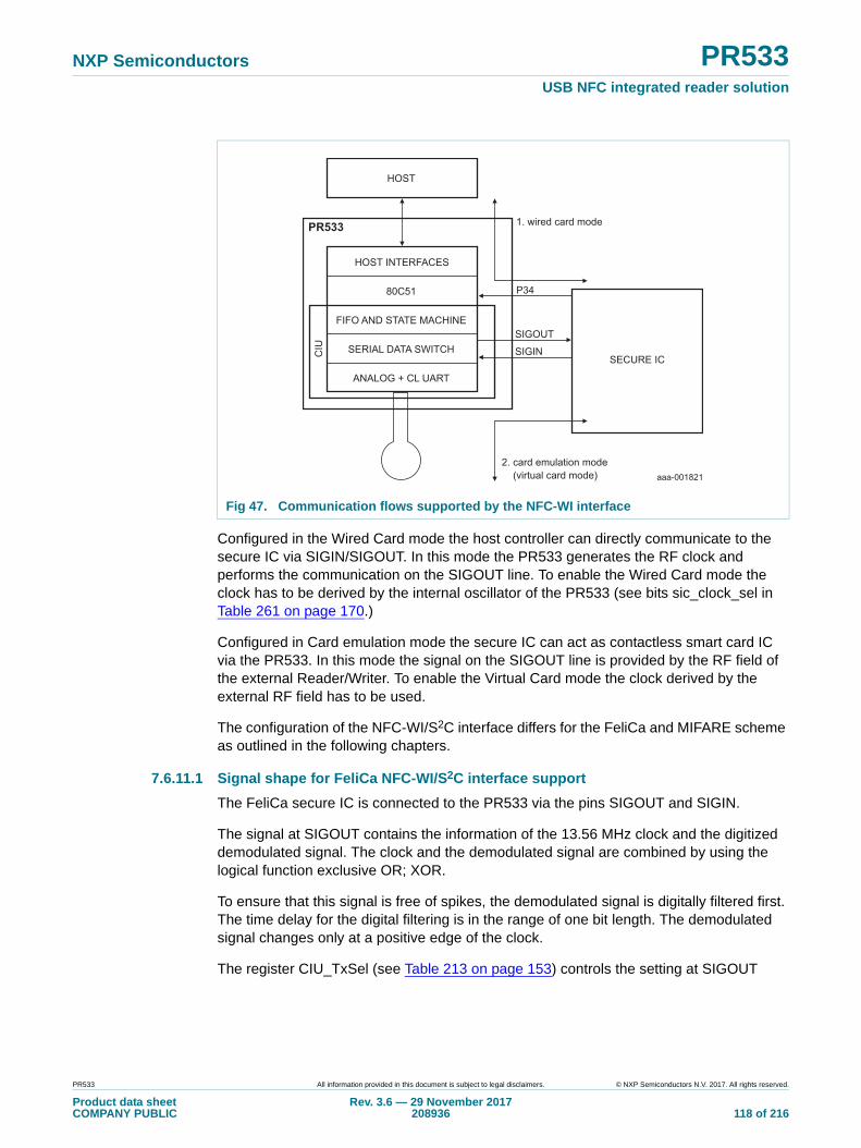
NXP Semiconductors PR533USB NFC integrated reader solution
Configured in the Wired Card mode the host controller can directly communicate to the secure IC via SIGIN/SIGOUT. In this mode the PR533 generates the RF clock and performs the communication on the SIGOUT line. To enable the Wired Card mode the clock has to be derived by the internal oscillator of the PR533 (see bits sic_clock_sel in Table 261 on page 170.)
Configured in Card emulation mode the secure IC can act as contactless smart card IC via the PR533. In this mode the signal on the SIGOUT line is provided by the RF field of the external Reader/Writer. To enable the Virtual Card mode the clock derived by the external RF field has to be used.
The configuration of the NFC-WI/S2C interface differs for the FeliCa and MIFARE scheme as outlined in the following chapters.
7.6.11.1 Signal shape for FeliCa NFC-WI/S2C interface support
The FeliCa secure IC is connected to the PR533 via the pins SIGOUT and SIGIN.
The signal at SIGOUT contains the information of the 13.56 MHz clock and the digitized demodulated signal. The clock and the demodulated signal are combined by using the logical function exclusive OR; XOR.
To ensure that this signal is free of spikes, the demodulated signal is digitally filtered first. The time delay for the digital filtering is in the range of one bit length. The demodulated signal changes only at a positive edge of the clock.
The register CIU_TxSel (see Table 213 on page 153) controls the setting at SIGOUT
Fig 47. Communication flows supported by the NFC-WI interface
80C51
HOST
HOST INTERFACES
FIFO AND STATE MACHINE
SERIAL DATA SWITCHSECURE IC
P34
SIGOUT
SIGIN
1. wired card mode
2. card emulation mode
PR533
ANALOG + CL UART
CIU
(virtual card mode) aaa-001821
PR533 All information provided in this document is subject to legal disclaimers. © NXP Semiconductors N.V. 2017. All rights reserved.
Product data sheetCOMPANY PUBLIC
Rev. 3.6 — 29 November 2017208936 118 of 216

NXP Semiconductors PR533USB NFC integrated reader solution
The response from the FeliCa secure IC is transferred from SIGIN directly to the antenna driver. The modulation is done according to the register setting of the antenna drivers.
The clock is switched to P34 / SIC_CLK (see sic_clk_p34_en bit in Table 173 on page 138).
Remark: The signal on antenna is shown in principle only. This signal is sinusoidal. The clock for SIGIN is the same as the clock for SIGOUT.
7.6.11.2 Signal shape for ISO/IEC14443A and MIFARE NFC-WI/S2C support
The secure IC, e.g. the SmartMX is connected to the PR533 via the pins SIGOUT, SIGIN and P34 / SIC_CLK.
The signal at SIGOUT is a digital 13.56 MHz Miller coded signal between PVSS and SVDD. It is either derived from the external 13.56 MHz carrier signal when in Virtual Card Mode or internally generated when in Wired Card mode.
The register CIU_TxSel controls the setting at SIGOUT.
Note: The clock settings for the Wired Card mode and the Virtual Card mode differ. Refer to the description of the bit SicClockSel in register CIU_TestSel1.
Fig 48. Signal shape for SIGOUT in FeliCa secure IC mode
Fig 49. Signal shape for SIGIN in FeliCa secure IC mode
aaa-001822
clockdemodulated
signalsignal onSIGOUT
aaa-001823
clock
signal onSIGIN
signal onantenna
PR533 All information provided in this document is subject to legal disclaimers. © NXP Semiconductors N.V. 2017. All rights reserved.
Product data sheetCOMPANY PUBLIC
Rev. 3.6 — 29 November 2017208936 119 of 216

NXP Semiconductors PR533USB NFC integrated reader solution
The signal at SIGIN is a digital Manchester coded signal compliant with ISO/IEC 14443A with a subcarrier frequency of 847.5 kHz generated by the secure IC.
7.6.11.3 NFC-WI/S2C initiator mode
The PR533 includes 2 counters of 127 and 31, with digital filtering, to enable activation from the secure IC (ACT_REQ_Si), or the command to go from data to command mode (ESC_REQ).
Fig 50. Signal shape for SIGOUT in NFC-WI mode
Fig 51. Signal shape for SIGIN in NFC-WI mode
aaa-001824
1
0
bitvalue RF
signal onantenna
signal onSIGOUT
0 1 0 0 1
aaa-001825
0
1
0
0 01 1bit
value
signal onantenna
signal onSIGIN
Table 159. NFC_WI_control register (address 610Eh) bit allocation
Bit 7 6 5 4 3 2 1 0
Symbol - - - - nfc_wi_status - nfc_wi_en_act_req_im
nfc_wi_en_clk
Reset 0 0 0 0 0 0 0 0
Access R R R R R R/W R/W R/W
PR533 All information provided in this document is subject to legal disclaimers. © NXP Semiconductors N.V. 2017. All rights reserved.
Product data sheetCOMPANY PUBLIC
Rev. 3.6 — 29 November 2017208936 120 of 216
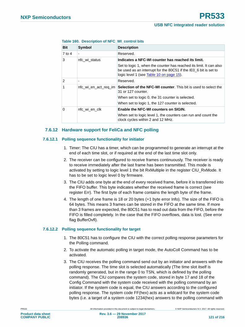
NXP Semiconductors PR533USB NFC integrated reader solution
7.6.12 Hardware support for FeliCa and NFC polling
7.6.12.1 Polling sequence functionality for initiator
1. Timer: The CIU has a timer, which can be programmed to generate an interrupt at the end of each time slot, or if required at the end of the last time slot only.
2. The receiver can be configured to receive frames continuously. The receiver is ready to receive immediately after the last frame has been transmitted. This mode is activated by setting to logic level 1 the bit RxMultiple in the register CIU_RxMode. It has to be set to logic level 0 by firmware.
3. The CIU adds one byte at the end of every received frame, before it is transferred into the FIFO buffer. This byte indicates whether the received frame is correct (see register Err). The first byte of each frame contains the length byte of the frame.
4. The length of one frame is 18 or 20 bytes (+1 byte error Info). The size of the FIFO is 64 bytes. This means 3 frames can be stored in the FIFO at the same time. If more than 3 frames are expected, the 80C51 has to read out data from the FIFO, before the FIFO is filled completely. In the case that the FIFO overflows, data is lost. (See error flag BufferOvfl).
7.6.12.2 Polling sequence functionality for target
1. The 80C51 has to configure the CIU with the correct polling response parameters for the Polling command.
2. To activate the automatic polling in target mode, the AutoColl Command has to be activated.
3. The CIU receives the polling command send out by an initiator and answers with the polling response. The time slot is selected automatically (The time slot itself is randomly generated, but in the range 0 to TSN, which is defined by the polling command). The CIU compares the system code, stored in byte 17 and 18 of the Config Command with the system code received with the polling command by an initiator. If the system code is equal, the CIU answers according to the configured polling response. The system code FF(hex) acts as a wildcard for the system code bytes (i.e. a target of a system code 1234(hex) answers to the polling command with
Table 160. Description of NFC_WI_control bits
Bit Symbol Description
7 to 4 - Reserved.
3 nfc_wi_status Indicates a NFC-WI counter has reached its limit.
Set to logic 1, when the counter has reached its limit. It can also be used as an interrupt for the 80C51 if the IE0_6 bit is set to logic level 1 (see Table 10 on page 15).
2 - Reserved.
1 nfc_wi_en_act_req_im Selection of the NFC-WI counter. This bit is used to select the 31 or 127 counter.
When set to logic 0, the 31 counter is selected.
When set to logic 1, the 127 counter is selected.
0 nfc_wi_en_clk Enable the NFC-WI counters on SIGIN.
When set to logic level 1, the counters can run and count the clock cycles within 2 and 12 MHz.
PR533 All information provided in this document is subject to legal disclaimers. © NXP Semiconductors N.V. 2017. All rights reserved.
Product data sheetCOMPANY PUBLIC
Rev. 3.6 — 29 November 2017208936 121 of 216
NXP Semiconductors PR533USB NFC integrated reader solution
one of the following system codes 1234(hex), 12FF(hex), FF34 (hex) or FFFF(hex)). If the system code does not match no answer is sent back by the PR533. If a valid command, which is not a Polling command, is received by the CIU, no answer is sent back and the command AutoColl is stopped. The received frame is stored in the FIFO.
7.6.12.3 Additional hardware support for FeliCa and NFC
Additionally to the polling sequence support for the FeliCa mode, the PR533 supports the check of the LEN-byte.
The received LEN-byte is checked by the registers CIU_FelNFC1 and CIU_FelNFC2:
DataLenMin in register CIU_FelNFC1 defines the minimum length of the accepted frame length. This register is 6 bits long. Each value represents a length of 4.
DataLenMax in register CIU_FelNFC2 defines the maximum length of the accepted frame. This register is 6 bits long. Each value represents a length of 4. If set to logic 0 this limit is switched off. If the length is not in the supposed area, the packed is not transferred to the FIFO and receiving is kept active.
Example 1:
• DataLenMin = 4
– The length shall be greater or equal 16.
• DataLenMax = 5
– The length shall be smaller than 20. Valid area: 16, 17, 18, 19
Example 2:
• DataLenMin = 9
– The length shall be greater or equal 36.
• DataLenMax = 0
– The length shall be smaller than 256. Valid area: 36 to 255
7.6.13 CRC co-processor
The CRC preset value of the CRC co-processor can be configured to 0000h, 6363h, A671h or FFFFh depending of the bits CRCPreset in the register Mode.This is only valid when using CalcCRC command (see Section 8.6.20.7 “CalcCRC command” on page 145)
During a communication, the preset value of the CRC coprocessor is set according to the bits CIU_RxMode and CIU_TxMode.
The CRC polynomial for the 16-bit CRC is fixed to x16 + x12 + x5 + 1.
The CRC co-processor is configurable to handle the different MSB and LSB requirements for the different protocols.The bit MSBFirst in the register CIU_Mode indicates that the data will be loaded with MSB first
The registers CRCResult-Hi and CRCResult-Lo indicate the result of the CRC calculation.
PR533 All information provided in this document is subject to legal disclaimers. © NXP Semiconductors N.V. 2017. All rights reserved.
Product data sheetCOMPANY PUBLIC
Rev. 3.6 — 29 November 2017208936 122 of 216

NXP Semiconductors PR533USB NFC integrated reader solution
7.6.14 FIFO buffer
An 64*8 bits FIFO buffer is implemented in the CIU. It buffers the input and output data stream between the 80C51 and the internal state machine of the CIU. Thus, it is possible to handle data streams with lengths of up to 64 bytes without taking timing constraints into account.
7.6.14.1 Accessing the FIFO buffer
The FIFO-buffer input and output data bus is connected to the register CIU_FIFOData. Writing to this register stores one byte in the FIFO-buffer and increments the internal FIFO-buffer write-pointer. Reading from this register shows the FIFO-buffer contents stored at the FIFO-buffer read-pointer and decrements the FIFO-buffer read-pointer. The distance between the write- and read-pointer can be obtained by reading the register CIU_FIFOLevel.
When the 80C51 starts a command, the CIU may, while the command is in progress, access the FIFO-buffer according to that command. Physically only one FIFO-buffer is implemented, which can be used in input- and output direction. Therefore the 80C51 has to take care, not to access the FIFO-buffer in an unintended way.
7.6.14.2 Controlling the FIFO buffer
Besides writing to and reading from the FIFO-buffer, the FIFO-buffer pointers might be reset by setting the bit FlushBuffer in the register CIU_FIFOLevel. Consequently, the FIFOLevel[6:0] bits are set to logic level 0, the bit BufferOvfl in the register CIU_Error is set to logic level 0, the actually stored bytes are not accessible anymore and the FIFO-buffer can be filled with another 64 bytes again.
7.6.14.3 Status information about the FIFO buffer
The 80C51may obtain the following data about the FIFO-buffers status:
• Number of bytes already stored in the FIFO-buffer: FIFOLevel[6:0] in register CIU_FIFOLevel
• Warning, that the FIFO-buffer is quite full: HiAlert in register CIU_Status1
• Warning, that the FIFO-buffer is quite empty: LoAlert in register CIU_Status1
• Indication, that bytes were written to the FIFO-buffer although it was already full: BufferOvfl in register CIU_Error.
BufferOvfl can be set to logic level 0 only by setting to logic level 1 bit FlushBuffer in the register CIU_FIFOLevel.
The CIU can generate an interrupt signal
• If LoAlertIEn in register CIU_CommIEn is set to logic 1, it will set to logic level 1 CIU_IRQ_0 in the register CIU_Status1, when LoAlert in the same register changes to logic level 1.
• If HiAlertIEN in register CIU_CommIEn is set to logic 1, it will set to logic level 1 CIU_IRQ_0 in the register CIU_Status1, when HiAlert in the same register changes to logic level 1.
PR533 All information provided in this document is subject to legal disclaimers. © NXP Semiconductors N.V. 2017. All rights reserved.
Product data sheetCOMPANY PUBLIC
Rev. 3.6 — 29 November 2017208936 123 of 216
NXP Semiconductors PR533USB NFC integrated reader solution
The flag HiAlert is set to logic 1 if only WaterLevel[5:0] bits (as set in register CIU_WaterLevel) or less can be stored in the FIFO-buffer. It is generated by the following equation:
The flag LoAlert is set to logic 1 if WaterLevel[5:0] bits (as set in register CIU_WaterLevel) or less are actually stored in the FIFO-buffer. It is generated by the following equation:
7.6.15 CIU_timer
A timer unit is implemented in the CIU: CIU_timer. The 80C51 use CIU_timer to manage timing relevant tasks for contactless communication. CIU_timer may be used in one of the following configurations:
• Timeout-Counter
• Watch-Dog Counter
• Stop Watch
• Programmable One-Shot
• Periodical Trigger
CIU_timer can be used to measure the time interval between two events or to indicate that a specific event occurred after a specific time. CIU_timer can be triggered by events which will be explained in the following, but it does not itself influence any internal event (e.g. A timeout during data reception does not influence the reception process automatically). Furthermore, several timer related bits are set and these bits can be used to generate an interrupt.
CIU_timer has a input clock of 6.78 MHz (derived from the 27.12 MHz quartz). CIU_timer consists of 2 stages: 1 prescaler and 1 counter.
The prescaler is a 12 bits counter. The reload value for the prescaler can be defined between 0 and 4095 in register CIU_TMode and CIU_TPrescaler. This decimal value is called TPrescaler.
The reload value TReloadVal for the counter is defined with 16 bits in a range from 0 to 65535 in the registers CIU_TReloadVal_Lo and CIU_TReloadVal_Hi.
The current value of CIU_timer is indicated by the registers CIU_TCounterVal_lo and CIU_TCounterVal_hi.
If the counter reaches 0 an interrupt will be generated automatically indicated by setting the TimerIRq flag in the register CommonIRq. If enabled, it will set to logic level 1 CIU_IRQ_1 in the register CIU_Status1. TimerIRq flag can be set to logic level 1 or to logic level 0 by the 80C51. Depending on the configuration, CIU_timer will stop at 0 or restart with the value of the registers CIU_TReloadVal_Lo and CIU_TReloadVal_Hi.
Status of CIU_timer is indicated by the bit TRunning in the register CIU_Status1.
CIU_timer can be manually started by TStartNow in register Control or manually stopped by TStopNow in register Control.
HiAlert 64 FIFOLenght– WaterLevel=
LoAlert FIFOLenght WaterLevel=
PR533 All information provided in this document is subject to legal disclaimers. © NXP Semiconductors N.V. 2017. All rights reserved.
Product data sheetCOMPANY PUBLIC
Rev. 3.6 — 29 November 2017208936 124 of 216

NXP Semiconductors PR533USB NFC integrated reader solution
Furthermore CIU_timer can be activated automatically by setting the bit TAuto in the register CIU_TMode to fulfill dedicated protocol requirements automatically.
The time delay of a timer stage is the reload value +1.
Maximum time:
TPrescaler = 4095, TReloadVal = 65535 => 4096 * 65536/6.78 MHz = 39.59 s
Example:
To indicate 100 ms it is required to count 678 clock cycles. This means the value for TPrescaler has to be set to TPrescaler = 677.The timer has now an input clock of 100 us. The timer can count up to 65535 time slots of 100 ms.
7.6.16 Interrupt request system
The CIU indicates certain events by setting interrupt bits in the register CIU_Status1 and, in addition it will set to logic level 1 CIU_interrupt1 or CIU_IRQ_0. If this interrupt is enabled (see Table 12 on page 16) the 80C51 will be interrupted. This allows the implementation of efficient interrupt-driven firmware.
7.6.16.1 Interrupt sources
The following table shows the integrated interrupt flags, the corresponding source and the condition for its activation.
The interrupt flag TimerIRq in the register CIU_CommIrq indicates an interrupt set by the timer unit. The setting is done when the timer decrements from logic level 1 down to logic level 0.
The TxIRq bit in the register CIU_CommIrq indicates that the transmitter has finished. If the state changes from sending data to transmitting the end of frame pattern, the transmitter unit sets automatically the interrupt bit to logic level 1.
The CRC coprocessor sets the flag CRCIRq in the register CIU_DivIrq after having processed all data from the FIFO buffer. This is indicated by the flag CRCReady set to logic level 1.
The RxIRq flag in the register CIU_CommIrq indicates an interrupt when the end of the received data is detected.
The flag IdleIRq in the register CIU_CommIrq is set to level 1 if a command finishes and the content of the CIU_Command register changes to idle.
The flag HiAlertIRq in the register CIU_CommIrq is set to level 1 if the HiAlert bit is set to logic 1, that means the Contactless FIFO buffer has reached the level indicated by the bits WaterLevel[5:0].
The flag LoAlertIRq in the register CIU_CommIrq is set to logic level 1 if the LoAlert bit is set to logic level 1, that means the Contactless FIFO buffer has reached the level indicated by the bits WaterLevel[5:0].
The flag RFOnIRq in the register CIU_DivIrq is set to logic level 1, when the RF level detector detects an external RF field.
PR533 All information provided in this document is subject to legal disclaimers. © NXP Semiconductors N.V. 2017. All rights reserved.
Product data sheetCOMPANY PUBLIC
Rev. 3.6 — 29 November 2017208936 125 of 216
NXP Semiconductors PR533USB NFC integrated reader solution
The flag RFOffIRq in the register CIU_DivIrq is set to logic level 1, when a present external RF field is switched off.
The flag ErrIRq in the register CIU_CommIrq indicates an error detected by the CIU during sending or receiving. This is indicated by any bit set to logic 1 in register CIU_Error.
The flag ModeIRq in the register CIU_DivIrq indicates that the data mode detector has detected the current mode.
These flags are summarized with 2 interrupt bits within the register CIU_Status1:
• the high priority interrupt sources are summarized with CIU_IRQ_0.
• the low priority interrupt sources are summarized with CIU_IRQ_1.
See the register Table 186 on page 143.
7.6.17 CIU Power Reduction Modes
7.6.17.1 Hard-Power-down
A Hard-Power-down is enabled when RSTPD_N is low. None of the CIU blocks are running, even the RF level detector.
7.6.17.2 CIU Power-down
The CIU Power-down mode is entered immediately by setting the Power-down bit in the register CIU_Command. All CIU blocks are switched off, except the 27.12 MHz oscillator and the RF level detector.
All registers and the FIFO will keep the content during CIU Power-down.
If the bit AutoWakeUp in the register CIU_TxAuto is set and an external RF field is detected, the CIU Power-down mode is left automatically.
Table 161. High priority interrupt sources (CIU_IRQ_0)
Interrupt Flag Interrupt source Set automatically, WHEN
TxIRq Transmitter a transmitted data stream ends
RxIRq Receiver a received data stream ends
HiAlertIRq FIFO-buffer the FIFO-buffer is getting full
LoAlertIRq FIFO-buffer the FIFO-buffer is getting empty
Table 162. Low priority interrupt sources (CIU_IRQ_1)
Interrupt Flag Interrupt source Set automatically, WHEN
TimerIRq Timer Unit the timer counts from 1 to 0
CRCIRq CRC-Coprocessor all data from the FIFO buffer have been processed
IdleIRq CIU_Command Register
a command execution finishes
RFOnIRq RF Level Detector an external RF field is detected
RFOffIRq RF Level Detector a present external RF field is switched off
ErrIRq CIU an error is detected
ModeIRq data mode detector the mode has been detected
PR533 All information provided in this document is subject to legal disclaimers. © NXP Semiconductors N.V. 2017. All rights reserved.
Product data sheetCOMPANY PUBLIC
Rev. 3.6 — 29 November 2017208936 126 of 216
NXP Semiconductors PR533USB NFC integrated reader solution
After setting bit Power-down to logic level 0 in the register CIU_Command, it needs 1024 clocks cycle until the CIU Power-down mode is left indicated by the Power-down bit itself. Setting it to logic 0 does not immediately set it to logic level 0. It is automatically set to logic level 0 by the CIU when the CIU Power-down mode is left.
When in CIU Power-down mode and DriverSel[1:0] is no set to 00b (see Table 213 on page 153), to ensure a minimum impedance at the transmitter outputs, the CWGsNOn[3], CWGsNOff[3], ModGsNOn[3], ModGsNOff[3], CWGsP[5], ModGsP[5] bits are set to logic level 1, but it is not readable in the registers.
7.6.17.3 Transmitter Power-down
The Transmitter Power-down mode switches off the internal antenna drivers to turn off the RF field by setting the bits Tx1RFEn and Tx2RFEn in the register CIU_TxControl to logic level 0. The receiver is still switched on, meaning the CIU can be accessed by a second NFC device as a NFCIP-1 target.
Note: In case the bit InitialRFOn has been set to logic 1, when the drivers were already switched on, it is needed either to set InitialRFOn to logic level 0, before setting the bits Tx1RFEn and Tx2RFEn in the register CIU_TxControl to logic 0, or to set also the bits Tx1RFAutoEn and Tx2RFAutoEn in the register CIU_TxAuto to logic level 0.
7.6.18 CIU command set
7.6.18.1 General description
The CIU behaviour is determined by an internal state machine capable to perform a certain set of commands. Writing the according command code to the CIU_Command register starts the commands.
Arguments and/or data necessary to process a command are mainly exchanged via the FIFO buffer.
7.6.18.2 General behaviour
• Each command, that needs a data stream (or data byte stream) as input will immediately process the data it finds in the FIFO buffer. An exception to this rule is the Transceive command. Using this command the transmission is started with the StartSend bit in CIU_BitFraming register.
• Each command that needs a certain number of arguments will start processing only when it has received the correct number of arguments via the FIFO buffer.
• The FIFO buffer is not cleared automatically at command start. Therefore, it is also possible to write the command arguments and/or the data bytes into the FIFO buffer and start the command afterwards.
• Each command may be interrupted by the 80C51 by writing a new command code into the CIU_Command register e.g.: the Idle command.
PR533 All information provided in this document is subject to legal disclaimers. © NXP Semiconductors N.V. 2017. All rights reserved.
Product data sheetCOMPANY PUBLIC
Rev. 3.6 — 29 November 2017208936 127 of 216

NXP Semiconductors PR533USB NFC integrated reader solution
7.6.18.3 Commands overview
7.6.18.4 Idle command
The CIU is in idle mode. This command is also used to terminate the actual command.
7.6.18.5 Config command
To configure the automatic MIFARE Anticollision, FeliCa Polling and NFCID3, the data used for these transactions have to be stored internally. All the following data have to be written to the FIFO in this order:
• SENS_RES (2 bytes): in order byte0, byte1
• NFCID1 (3 bytes): in order byte0, byte1, byte 2; the first NFCID1 byte if fixed to 08h and the check byte is calculated automatically
• SEL_RES (1 byte)
• Polling response (2 bytes (shall be 01h, FEh)+ 6 bytes NFCID2 + 8 bytes Pad + 2 bytes system code)
• NFCID3 (1 byte)
In total 25 bytes which are transferred into an internal buffer with the Config command.
The complete NFCID3 is 10 bytes long and consist of the 3 NFCID1 bytes, the 6 NFCID2 bytes and the NFCID3 byte listed above.
Table 163. Command overview
Command Command code Action
Idle 0000 No action; cancels current command execution.
Config 0001 Configures the CIU for FeliCa, MIFARE and NFCIP-1 communication.
Generate RandomID 0010 Generates 10-byte random ID number
CalcCRC 0011 Activates the CRC co-processor or perform self-test.
Transmit 0100 Transmits data from the FIFO buffer.
NoCmdChange 0111 No command change. This command can be used to modify different bits in the CIU_Command register without touching the command. e.g. Power-down bit.
Receive 1000 Activates the receiver circuitry.
SelfTest 1001 Activates the self-test. Not described in this chapter.
Transceive 1100 If bit Initiator in the register CIU_Control is set to logic 1:
Transmits data from FIFO buffer to the antenna and activates automatically the receiver after transmission is finished.
If bit Initiator in the register CIU_Control is set to logic 0:
Receives data from antenna and activates automatically the transmitter after reception.
AutoColl 1101 Handles FeliCa polling (Card operating mode only) and MIFARE anticollision (Card operating mode only)
MFAuthent 1110 Performs the MIFARE 1 KB or MIFARE 4 KB emulation authentication in MIFARE Reader/Writer mode only.
Soft Reset 1111 Resets the CIU.
PR533 All information provided in this document is subject to legal disclaimers. © NXP Semiconductors N.V. 2017. All rights reserved.
Product data sheetCOMPANY PUBLIC
Rev. 3.6 — 29 November 2017208936 128 of 216

NXP Semiconductors PR533USB NFC integrated reader solution
To read out this configuration (after it has been loaded), the command Config with an empty FIFO buffer has to be started. In this case the 25 bytes are transferred from the internal buffer to the FIFO.
The CIU has to be configured after each power up, before using the automatic Anticollision/Polling function (AutoColl command). During a Hard-Power-down (RSTPD_N set to logic level 0) this configuration remains unchanged.
This command terminates automatically when finished and the active command is Idle.
7.6.18.6 Generate RandomID command
This command generates a 10-byte random number stored in the internal 25 bytes buffer and overwrites the 10 NFCID3 bytes. This random number might be used for fast generation of all necessary ID bytes for the automatic Anticollision / Polling function.
Note: To configure the CIU, Config command has to be used first.
This command terminates automatically when finished and the active command is Idle.
7.6.18.7 CalcCRC command
The content of the FIFO is transferred to the CRC co-processor and a CRC calculation is started. The result is stored in the CRCResult register. The CRC calculation is not limited to a dedicated number of bytes. The calculation is not stopped when the FIFO gets empty during the data stream. The next byte written to the FIFO is added to the calculation.
The preset value of the CRC is defined by the CRCPreset bits of the register CIU_Mode, and the chosen value is loaded to the CRC co-processor when the command is started.
This command has to be terminated by firmware by writing any command to the CIU_Command register e.g. the Idle command.
If SelfTest in register CIU_AutoTest is set to logic 1, the CRC co-processor is in Self Test mode and performs a digital self-test. The result of the self-test is written in the FIFO.
7.6.18.8 Transmit command
The content of the FIFO is transmitted immediately after starting the command. Before transmitting FIFO content, all relevant register settings have to be set to transmit data in the selected mode.
This command terminates automatically when the FIFO gets empty and the active command is Idle. It can be terminated by any other command written to the CIU_Command register.
7.6.18.9 NoCmdChange command
This command does not influence any ongoing command in the CIU_Command register. It can be used to manipulate any bit except the command bits in the CIU_Command register, e.g. the bits RcvOff or Power-down.
7.6.18.10 Receive command
The CIU activates the receiver path and waits for any data stream to be received. The correct settings for the expected mode have to be set before starting this command.
PR533 All information provided in this document is subject to legal disclaimers. © NXP Semiconductors N.V. 2017. All rights reserved.
Product data sheetCOMPANY PUBLIC
Rev. 3.6 — 29 November 2017208936 129 of 216
NXP Semiconductors PR533USB NFC integrated reader solution
This command terminates automatically when the receive data stream ends and the active command is Idle. This is indicated either by the end of frame pattern or by the length byte depending on the selected framing and speed.
Note: If the bit RxMultiple in the register CIU_RxMode is set to logic 1, the Receive command does not terminate automatically. It has to be terminated by setting any other command in the CIU_Command register.
7.6.18.11 Transceive command
This circular command repeats transmitting data from the FIFO and receiving data from the RF field continuously. If the bit Initiator in the register CIU_Control is set to logic 1, it indicates that the first action is transmitting and after having finished transmission the receiver is activated to receive data. If the bit Initiator in the CIU_Control register is set to logic 0, the first action is receiving and after having received a data stream, the transmitter is activated to transmit data. In the second configuration the PR533 first acts as a receiver and if a data stream is received it switches to the Transmit mode.
Each transmission process has to be started with setting bit StartSend in the register CIU_BitFraming. This command has to be cleared by firmware by writing any command to the CIU_Command register e.g. the command idle.
Note: If the bit RxMultiple in register CIU_RxMode is set, this command will never leave the receiving state, because the receiving will not be cancelled automatically.
7.6.18.12 AutoColl command
This command automatically handles the MIFARE activation and the FeliCa polling in the Card Operation mode. The bit Initiator in the CIU_Control register has to be set to logic level 0 for correct operation. During this command, Mode Detector is active if not deactivated by setting the bit ModeDetOff in the CIU_Mode register. After Mode Detector detects a mode, the mode-dependent registers are set according to the received data. In case of no external RF field this command resets the internal state machine and returns to the initial state but it will not be terminated.
When the Autocoll command terminates the Transceive command gets active.
During Autocoll command:
• The CIU interrupt bits, except RfOnIRq, RfOffIRq and SIGINActIRq (see Table 183 on page 141), are not supported. Only the last received frame will serve the CIU interrupts.
• During ISO/IEC 14443A activation, TxCRCEn and RxCRCEn bits are defined by the AutoColl command. The changes cannot be observed at the CIU_TxMode and CIU_RxMode registers. When the Transceive command is active, the value of the bits is relevant.
Table 164. Transceive command scenario
Communication step Initiator =1 Initiator=0
1 Send Receive
2 Receive Send
3 Send Receive
4 Receive Send
PR533 All information provided in this document is subject to legal disclaimers. © NXP Semiconductors N.V. 2017. All rights reserved.
Product data sheetCOMPANY PUBLIC
Rev. 3.6 — 29 November 2017208936 130 of 216
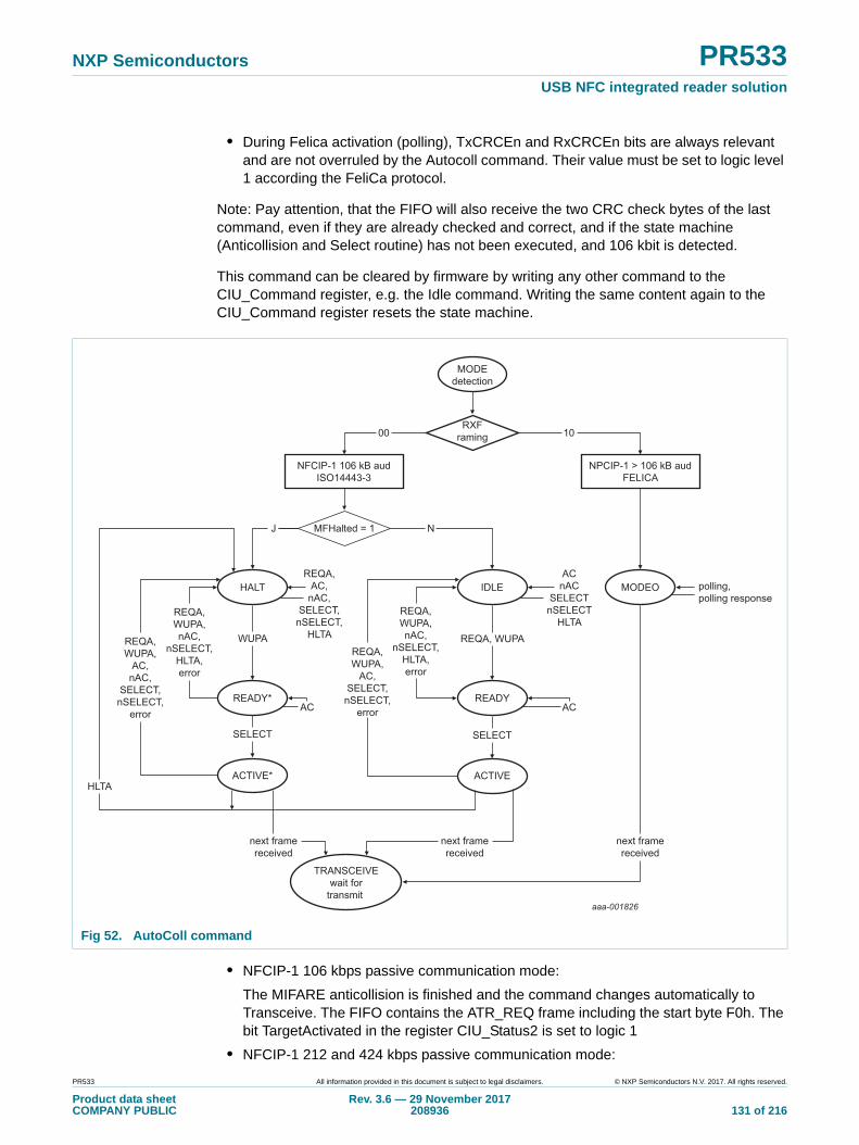
NXP Semiconductors PR533USB NFC integrated reader solution
• During Felica activation (polling), TxCRCEn and RxCRCEn bits are always relevant and are not overruled by the Autocoll command. Their value must be set to logic level 1 according the FeliCa protocol.
Note: Pay attention, that the FIFO will also receive the two CRC check bytes of the last command, even if they are already checked and correct, and if the state machine (Anticollision and Select routine) has not been executed, and 106 kbit is detected.
This command can be cleared by firmware by writing any other command to the CIU_Command register, e.g. the Idle command. Writing the same content again to the CIU_Command register resets the state machine.
• NFCIP-1 106 kbps passive communication mode:
The MIFARE anticollision is finished and the command changes automatically to Transceive. The FIFO contains the ATR_REQ frame including the start byte F0h. The bit TargetActivated in the register CIU_Status2 is set to logic 1
• NFCIP-1 212 and 424 kbps passive communication mode:
Fig 52. AutoColl command
NFCIP-1 106 kB audISO14443-3
NPCIP-1 > 106 kB audFELICA
IDLE MODEO
MODEdetection
RXFraming
MFHalted = 1
HALTAC
nACSELECT
nSELECTHLTA
AC
polling,polling response
next framereceived
next framereceived
REQA, WUPA
READY
ACTIVE
WUPA
SELECT SELECT
READY*
ACTIVE*
TRANSCEIVEwait for
transmit
next framereceived
NJ
HLTA
REQA,WUPA,
AC,nAC,
SELECT,nSELECT,
error
REQA,AC,
nAC,SELECT,
nSELECT,HLTA
REQA,WUPA,nAC,
nSELECT,HLTA,error
REQA,WUPA,nAC,
nSELECT,HLTA,error
REQA,WUPA,
AC,SELECT,
nSELECT,error
00 10
AC
aaa-001826
PR533 All information provided in this document is subject to legal disclaimers. © NXP Semiconductors N.V. 2017. All rights reserved.
Product data sheetCOMPANY PUBLIC
Rev. 3.6 — 29 November 2017208936 131 of 216
NXP Semiconductors PR533USB NFC integrated reader solution
The FeliCa polling command is finished and the command has automatically changed to Transceive. The FIFO contains the ATR_REQ frame. The bit TargetActivated in the register CIU_Status2 is set to logic 1.
• NFCIP-1 106, 212 and 424 kbps active communication mode:
This command is changing automatically to Transceive. The FIFO contains the ATR_REQ frame. The bit TargetActivated in the register CIU_Status2 is set to logic 0. For 106 kbps only, the first byte in the FIFO indicates the start byte F0h and the CRC is added into the FIFO.
• ISO/IEC 14443A/MIFARE (Card Operating mode):
The MIFARE anticollision is finished and the command has automatically changed to Transceive. The FIFO contains the first command after the Select. The bit TargetActivated in the register CIU_Status2 is set to logic 1.
• FeliCa (Card Operating mode):
The FeliCa polling command is finished and the command has automatically changed to Transceive. The FIFO contains the command after the Polling in the FeliCa protocol. The bit TargetActivated in the register CIU_Status2 is set to logic 1.
7.6.18.13 MFAuthent command
This command handles the MIFARE authentication in Reader/Writer mode to enable a secure communication to any MIFARE 1 KB and MIFARE 4 KB emulation card. The following data shall be written to the FIFO before the command can be activated:
• Authentication command code (60h for key A, 61h for key B)
• Block address
• Sector key byte 0
• Sector key byte 1
• Sector key byte 2
• Sector key byte 3
• Sector key byte 4
• Sector key byte 5
• Card serial number byte 0
• Card serial number byte 1
• Card serial number byte 2
• Card serial number byte 3
In total 12 bytes shall be written to the FIFO.
Note: When the MFAuthent command is active, any FIFO access is blocked. Anyhow if there is an access to the FIFO, the bit WrErr in the register CIU_Error is set to logic level 1.
This command terminates automatically when the MIFARE 1 KB or MIFARE 4 KB emulation card is authenticated. The bit MFCrypto1On in the register CIU_Status2 is set to logic level 1.
PR533 All information provided in this document is subject to legal disclaimers. © NXP Semiconductors N.V. 2017. All rights reserved.
Product data sheetCOMPANY PUBLIC
Rev. 3.6 — 29 November 2017208936 132 of 216
NXP Semiconductors PR533USB NFC integrated reader solution
This command does not terminate automatically when the card does not answer, therefore CIU timer should be initialized to automatic mode. In this case, beside the bit IdleIRq, the bit TimerIRq can be used as termination criteria. During authentication processing, the bits RxIRq and TxIRq of CIU_CommIrq register are blocked.
The Crypto1On bit is only valid after termination of the MFAuthent command (either after processing the authentication or after writing the Idle command in the register CIU_Command).
In case there is an error during the MIFARE authentication, the ProtocolErr bit in the CIU_Error register is set to logic 1 and the Crypto1On bit in CIU_Status2 register is set to logic 0.
7.6.18.14 SoftReset command
This command performs a reset of the CIU. The configuration data of the internal buffer remains unchanged. All registers are set to the reset values.
When SoftReset is finished, the active command switches to Idle.
7.6.19 CIU tests signals
7.6.19.1 CIU self-test
The CIU has the capability to perform a self-test. To start the self-test the following procedure has to be performed:
1. Perform a SoftReset.
2. Clear the internal buffer by writing 25 bytes of 00h and perform the Config command.
3. Enable the self-test by writing the value 09h to the register CIU_AutoTest.
4. Write 00h to the FIFO.
5. Start the self-test with the CalcCRC command.
6. The self-test will be performed.
7. When the self-test is finished, the FIFO is contains the following bytes:
– Correct answer for VersionReg equal to 80h:
0x00, 0xaa, 0xe3, 0x29, 0x0c, 0x10, 0x29, 0x6b
0x76, 0x8d, 0xaf, 0x4b, 0xa2, 0xda, 0x76, 0x99
0xc7, 0x5e, 0x24, 0x69, 0xd2, 0xba, 0xfa, 0xbc
0x3e, 0xda, 0x96, 0xb5, 0xf5, 0x94, 0xb0, 0x3a
0x4e, 0xc3, 0x9d, 0x94, 0x76, 0x4c, 0xea, 0x5e
0x38, 0x10, 0x8f, 0x2d, 0x21, 0x4b, 0x52, 0xbf
0xfb, 0xf4, 0x19, 0x94, 0x82, 0x5a, 0x72, 0x9d
0xba, 0x0d, 0x1f, 0x17, 0x56, 0x22, 0xb9, 0x08
PR533 All information provided in this document is subject to legal disclaimers. © NXP Semiconductors N.V. 2017. All rights reserved.
Product data sheetCOMPANY PUBLIC
Rev. 3.6 — 29 November 2017208936 133 of 216
NXP Semiconductors PR533USB NFC integrated reader solution
7.6.19.2 CIU test bus
The test bus is implemented for production test purposes. The following configuration can be used to improve the design of a system using the PR533. The test bus allows to route internal signals to output pins.
The Observe_testbus register is used to enable this functionality.
The test bus signals are selected by accessing TestBusSel in register CIU_TestSel2.
Table 165. Observe_testbus register (address 6104h) bit allocation
Bit 7 6 5 4 3 2 1 0
Symbol - - - - - - - observe_ciu
Reset 0 0 0 0 0 0 0 0
Access R R R R R R R R/W
Table 166. Description of Observe_testbus bits
Bit Symbol Description
7 to 1 - Reserved.
0 observe_ciu Configure the pads P3x (P30 to P35), RSTOUT_N and P70_IRQ to observe internal CIU data bus.
When set to logic 1, the pads are configured in output mode and show the internal data bus D0 to D6 of the CIU. P70_IRQ is the 13.56 MHz digital clock of CIU (generated from field or crystal).
Table 167. TstBusBitSel set to 07h
Test bus bit Test signal Comments
D6 sdata shows the actual received data value.
D5 scoll shows if in the actual bit a collision has been detected (106 kbit/s only)
D4 svalid shows if sdata and scoll are valid
D3 sover shows that the receiver has detected a stop bit (ISO/IEC 14443A/MIFARE mode only)
D2 RCV_reset shows if the receiver is reset
D1 RFon filtered shows the value of the internal RF level detector
D0 Envelope shows the output of the internal coder
Table 168. TstBusBitSel set to 0Dh
Test bus bit Test signal Comments
D6 clkstable shows if the oscillator delivers a stable signal
D5 clk27/8 shows the output signal of the oscillator divided by 8
D4 clk27rf/8 shows the clk27rf signal divided by 8
D3 clk13/4 shows the clk13rf divided by 4
D2 clk27 shows the output signal of the oscillator
D1 clk27rf shows the RF clock multiplied by 2
D0 clk13rf shows the RF clock of 13.56 MHz
PR533 All information provided in this document is subject to legal disclaimers. © NXP Semiconductors N.V. 2017. All rights reserved.
Product data sheetCOMPANY PUBLIC
Rev. 3.6 — 29 November 2017208936 134 of 216
NXP Semiconductors PR533USB NFC integrated reader solution
7.6.19.3 Test signals at pin AUX
Each signal can be switched to pin AUX1 or AUX2 by setting SelAux1 or SelAux2 in the register CIU_AnalogTest. See Table 275 on page 173
7.6.19.4 PRBS
Enables the Pseudo Random Bit Stream of 9-bit or 15-bit length sequence, PRBS9 or PRBS15, according to ITU-TO150. To start the transmission of the defined data stream, Transmit command has to be activated. The preamble/Sync byte/start bit/parity bit are generated automatically depending on the selected mode.
Note: All relevant registers to transmit data have to be configured before entering PRBS mode according ITU-TO150.
7.6.20 CIU memory map
The registers of the CIU are either map into the SFR or into the XRAM memory space.
Table 169. Contactless Interface Unit SFR memory map
ADDR Bytesize
Register name Description
D1h 1 CIU_Command Starts and stops the command execution
D2h 1 CIU_CommlEn Control bits to enable and disable the passing of interrupt requests
D3h 1 CIU_DivlEn Control bits to enable and disable the passing of interrupt requests
D4h 1 CIU_CommIrq Contains common Interrupt Request flags
D5h 1 CIU_DivIrq Contains diverse Interrupt Request flags
D6h 1 CIU_Error Error flags showing the error status of the last command executed
DFh 1 CIU_Status1 Contains status flags of the CRC, Interrupt Request System and FIFO buffer
E9h 1 CIU_Status2 Contain status flags of the Receiver, Transmitter and Data Mode Detector
EAh 1 CIU_FIFOData in- and output of 64 bytes FIFO buffer
EBh 1 CIU_FIFOLevel Indicates the number of bytes stored in the FIFO
ECh 1 CIU_WaterLevel Defines the thresholds for FIFO under- and overflow warning
EDh 1 CIU_Control Contains miscellaneous Control bits
EEh 1 CIU_BitFraming Adjustments for bit oriented frames
EFh 1 CIU_Coll Bit position of the first bit collision detected on the RF-interface
Table 170. Contactless Interface Unit extension memory map
ADDR Bytesize
Register name Description
6301h 1 CIU_Mode Defines general modes for transmitting and receiving
6302h 1 CIU_TxMode Defines the transmission data rate and framing during transmission
6303h 1 CIU_RxMode Defines the transmission data rate and framing during receiving
PR533 All information provided in this document is subject to legal disclaimers. © NXP Semiconductors N.V. 2017. All rights reserved.
Product data sheetCOMPANY PUBLIC
Rev. 3.6 — 29 November 2017208936 135 of 216

NXP Semiconductors PR533USB NFC integrated reader solution
6304h 1 CIU_TxControl Controls the logical behavior of the antenna driver pins TX1 and TX2
6305h 1 CIU_TxAuto Controls the settings of the antenna driver
6306h 1 CIU_TxSel Selects the internal sources for the antenna driver
1 CIU_RxSel Selects internal receiver settings
6308h 1 CIU_RxThreshold Selects thresholds for the bit decoder
6309h 1 CIU_Demod Defines demodulator settings
630Ah 1 CIU_FelNFC1 Defines the length of the valid range for the received frame
630Bh 1 CIU_FelNFC2 Defines the length of the valid range for the received frame
630Ch 1 CIU_MifNFC Controls the communication in ISO/IEC 14443/MIFARE and NFC target mode at 106 kbit/s
630Dh 1 CIU_ManualRCV Allows manual fine-tuning of the internal receiver
630Eh 1 CIU_TypeB Configure the ISO/IEC 14443 type B
630Fh 1 - Reserved
6310h 1 - Reserved
6311h 1 CIU_CRCResultMSB Shows the actual MSB values of the CRC calculation
6312h 1 CIU_CRCResultLSB Shows the actual LSB values of the CRC calculation
6313h 1 CIU_GsNOFF Selects the conductance of the antenna driver pins TX1 and TX2 for load modulation when own RF field is switched OFF
6314h 1 CIU_ModWidth Controls the setting of the width of the Miller pause
6315h 1 CIU_TxBitPhase Bit synchronization at 106 kbit/s
6316h 1 CIU_RFCfg Configures the receiver gain and RF level
6317h 1 CIU_GsNOn Selects the conductance of the antenna driver pins TX1 and TX2 for modulation, when own RF field is switched ON
6318h 1 CIU_CWGsP Selects the conductance of the antenna driver pins TX1 and TX2 when not in modulation phase
6319h 1 CIU_ModGsP Selects the conductance of the antenna driver pins TX1 and TX2 when in modulation phase
631Ah 1 CIU_TModeCIU_TPrescaler
Defines settings for the internal timer
631Bh 1
631Ch 1 CIU_TReloadVal_hi Describes the 16-bit long timer reload value (Higher 8 bits)
631Dh 1 CIU_TReloadVal_lo Describes the 16-bit long timer reload value (Lower 8 bits)
631Eh 1 CIU_TCounterVal_hi Describes the 16-bit long timer actual value (Higher 8 bits)
631Fh 1 CIU_TCounterVal_lo Describes the 16-bit long timer actual value (Lower 8 bits)
6320h 1 - Reserved
6321h 1 CIU_TestSel1 General test signals configuration
6322h 1 CIU_TestSel2 General test signals configuration and PRBS control
6323h 1 CIU_TestPinEn Enables test signals output on pins.
6324h 1 CIU_TestPinValue Defines the values for the 8-bit parallel bus when it is used as I/O bus
6325h 1 CIU_TestBus Shows the status of the internal test bus
6326h 1 CIU_AutoTest Controls the digital self-test
Table 170. Contactless Interface Unit extension memory map …continued
ADDR Bytesize
Register name Description
PR533 All information provided in this document is subject to legal disclaimers. © NXP Semiconductors N.V. 2017. All rights reserved.
Product data sheetCOMPANY PUBLIC
Rev. 3.6 — 29 November 2017208936 136 of 216

NXP Semiconductors PR533USB NFC integrated reader solution
7.6.21 CIU register description
7.6.21.1 CIU register bit behaviour
Depending of the functionality of a register, the access condition to the bits can vary. The following table describes the access conditions:
7.6.21.2 CIU_SIC_CLK_en register (6330h)
Enables the use of P34 / SIC_CLK as secure IC clock.
6327h 1 CIU_Version Shows the CIU version
6328h 1 CIU_AnalogTest Controls the pins AUX1 and AUX2
6329h 1 CIU_TestDAC1 Defines the test value for the TestDAC1
632Ah 1 CIU_TestDAC2 Defines the test value for the TestDAC2
632Bh 1 CIU_TestADC Show the actual value of ADC I and Q
632Ch 1 - Reserved for tests
632Dh 1 - Reserved for tests
632Eh 1 - Reserved for tests
632Fh 1 CIU_RFlevelDet Power down of the RF level detector
6330h 1 CIU_SIC_CLK_en Enables the use of secure IC clock on P34 / SIC_CLK.
Table 170. Contactless Interface Unit extension memory map …continued
ADDR Bytesize
Register name Description
Table 171. Behavior of register bits
Abbreviation Behavior Description
R/W Read and Write
These bits can be written and read by the 80C51. Since they are used only for control means, there content is not influenced by internal state machines, e.g. CIU_CommIEn may be written and read by the CPU. It will also be read by internal state machines, but never changed by them.
DY DYnamic These bits can be written and read by the 80C51. Nevertheless, they may also be written automatically by CIU internal state machines, e.g. the commands in the CIU_Command register change their values automatically after their execution.
R Read only These registers hold flags, which value is determined by CIU internal states only, e.g. the CRCReady register can not be written from external but shows CIU internal states.
W Write only These registers are used for control means only. They may be written by the 80C51 but can not be read. Reading these registers returns always logic level 0.
Reserved These registers are not implemented or reserved for NXP testing use.
Table 172. CIU_SIC_CLK_en register (address 6330h) bit allocation
Bit 7 6 5 4 3 2 1 0
Symbol sic_clk_p34_en - - - Errorbusbitenable Errorbusbitsel[2:0]
Reset 0 0 0 0 0 0 0 0
Access R/W R R R R/W R/W R/W R/W
PR533 All information provided in this document is subject to legal disclaimers. © NXP Semiconductors N.V. 2017. All rights reserved.
Product data sheetCOMPANY PUBLIC
Rev. 3.6 — 29 November 2017208936 137 of 216
NXP Semiconductors PR533USB NFC integrated reader solution
7.6.21.3 CIU_Command register (D1h or 6331h)
Starts and stops the command execution.
Table 173. Description of CIU_SIC_CLK_en bits
Bit Symbol Description
7 sic_clk_p34_en Set to logic 1, this bit configures P34 / SIC_CLK to be used as secure IC clock: SIC_CLK.
Set to logic 0, P34 / SIC_CLK is in normal mode: P34.
6 to 4 - Reserved
3 Errorbusbitenable Set to logic 1, enable the error source selected by Errorbusbitsel on AUX pads according to SelAux1 and SelAux2 bits (code 1010b).
2 to 0 Errorbusbitsel[2:0] Define the error source on ErrorBusBit:
ValueDescription
000 selects ProtocollErr on test bus
001selects ParityErr on test bus
010selects CRCErr on test bus
011selects CollErr on test bus
100 selects BufferOvfl on test bus
101 selects RFErr on test bus
110 selects TempErr on test bus
111 selects WrErr on test bus
Table 174. CIU_Command register (address D1h or 6331h) bit allocation
Bit 7 6 5 4 3 2 1 0
Symbol - - RcvOff Power-down Command
Reset 0 0 1 0 0 0 0 0
Access R R R/W DY DY DY DY DY
Table 175. Description of CIU_Command bits
Bit Symbol Description
7 to 6 - Reserved
5 RcvOff Set to logic 1, the analog part of the receiver is switched off.
4 Power-down Set to logic 1, the CIU Power-down mode is entered. This means, internal current consuming blocks of the contactless analog module are switched off, except for the RF level detector.
Set to logic 0, the PR533 starts the wake-up procedure. During this procedure this bit still shows a logic level 1. A logic level 0 indicates that the PR533 is ready for operations; see Section 8.6.19.2 “CIU Power-down” on page 142.
Note: The Power-down bit can not be set, when the SoftReset command has been activated.
3 to 0 Command Activates a command according the Command Code.
Reading this register shows, which command is actually executed. See Section 8.6.20 “CIU command set” on page 143
PR533 All information provided in this document is subject to legal disclaimers. © NXP Semiconductors N.V. 2017. All rights reserved.
Product data sheetCOMPANY PUBLIC
Rev. 3.6 — 29 November 2017208936 138 of 216
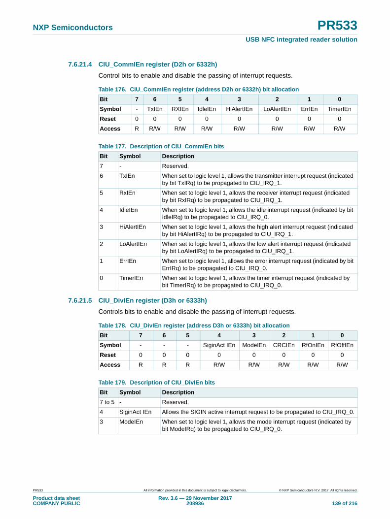
NXP Semiconductors PR533USB NFC integrated reader solution
7.6.21.4 CIU_CommIEn register (D2h or 6332h)
Control bits to enable and disable the passing of interrupt requests.
7.6.21.5 CIU_DivIEn register (D3h or 6333h)
Controls bits to enable and disable the passing of interrupt requests.
Table 176. CIU_CommIEn register (address D2h or 6332h) bit allocation
Bit 7 6 5 4 3 2 1 0
Symbol - TxIEn RXIEn IdleIEn HiAlertIEn LoAlertIEn ErrIEn TimerIEn
Reset 0 0 0 0 0 0 0 0
Access R R/W R/W R/W R/W R/W R/W R/W
Table 177. Description of CIU_CommIEn bits
Bit Symbol Description
7 - Reserved.
6 TxIEn When set to logic level 1, allows the transmitter interrupt request (indicated by bit TxIRq) to be propagated to CIU_IRQ_1.
5 RxIEn When set to logic level 1, allows the receiver interrupt request (indicated by bit RxIRq) to be propagated to CIU_IRQ_1.
4 IdleIEn When set to logic level 1, allows the idle interrupt request (indicated by bit IdleIRq) to be propagated to CIU_IRQ_0.
3 HiAlertIEn When set to logic level 1, allows the high alert interrupt request (indicated by bit HiAlertIRq) to be propagated to CIU_IRQ_1.
2 LoAlertIEn When set to logic level 1, allows the low alert interrupt request (indicated by bit LoAlertIRq) to be propagated to CIU_IRQ_1.
1 ErrIEn When set to logic level 1, allows the error interrupt request (indicated by bit ErrIRq) to be propagated to CIU_IRQ_0.
0 TimerIEn When set to logic level 1, allows the timer interrupt request (indicated by bit TimerIRq) to be propagated to CIU_IRQ_0.
Table 178. CIU_DivIEn register (address D3h or 6333h) bit allocation
Bit 7 6 5 4 3 2 1 0
Symbol - - - SiginAct IEn ModeIEn CRCIEn RfOnIEn RfOffIEn
Reset 0 0 0 0 0 0 0 0
Access R R R R/W R/W R/W R/W R/W
Table 179. Description of CIU_DivIEn bits
Bit Symbol Description
7 to 5 - Reserved.
4 SiginAct IEn Allows the SIGIN active interrupt request to be propagated to CIU_IRQ_0.
3 ModeIEn When set to logic level 1, allows the mode interrupt request (indicated by bit ModeIRq) to be propagated to CIU_IRQ_0.
PR533 All information provided in this document is subject to legal disclaimers. © NXP Semiconductors N.V. 2017. All rights reserved.
Product data sheetCOMPANY PUBLIC
Rev. 3.6 — 29 November 2017208936 139 of 216
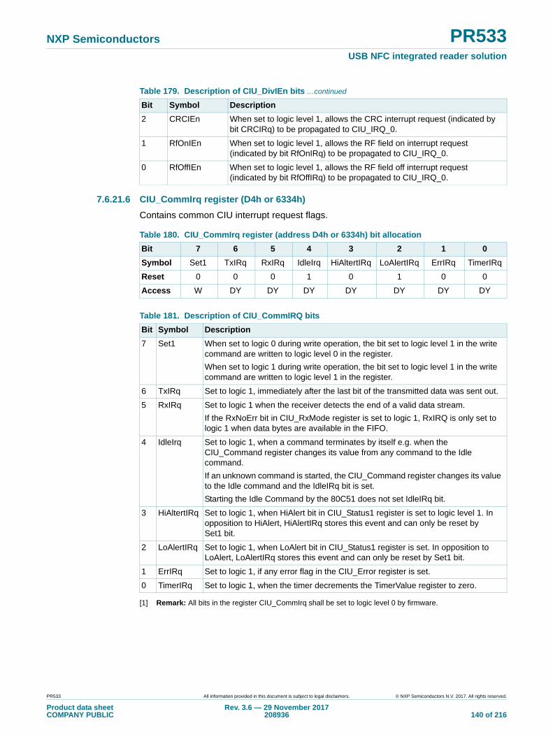
NXP Semiconductors PR533USB NFC integrated reader solution
7.6.21.6 CIU_CommIrq register (D4h or 6334h)
Contains common CIU interrupt request flags.
[1] Remark: All bits in the register CIU_CommIrq shall be set to logic level 0 by firmware.
2 CRCIEn When set to logic level 1, allows the CRC interrupt request (indicated by bit CRCIRq) to be propagated to CIU_IRQ_0.
1 RfOnIEn When set to logic level 1, allows the RF field on interrupt request (indicated by bit RfOnIRq) to be propagated to CIU_IRQ_0.
0 RfOffIEn When set to logic level 1, allows the RF field off interrupt request (indicated by bit RfOffIRq) to be propagated to CIU_IRQ_0.
Table 179. Description of CIU_DivIEn bits …continued
Bit Symbol Description
Table 180. CIU_CommIrq register (address D4h or 6334h) bit allocation
Bit 7 6 5 4 3 2 1 0
Symbol Set1 TxIRq RxIRq IdleIrq HiAltertIRq LoAlertIRq ErrIRq TimerIRq
Reset 0 0 0 1 0 1 0 0
Access W DY DY DY DY DY DY DY
Table 181. Description of CIU_CommIRQ bits
Bit Symbol Description
7 Set1 When set to logic 0 during write operation, the bit set to logic level 1 in the write command are written to logic level 0 in the register.
When set to logic 1 during write operation, the bit set to logic level 1 in the write command are written to logic level 1 in the register.
6 TxIRq Set to logic 1, immediately after the last bit of the transmitted data was sent out.
5 RxIRq Set to logic 1 when the receiver detects the end of a valid data stream.
If the RxNoErr bit in CIU_RxMode register is set to logic 1, RxIRQ is only set to logic 1 when data bytes are available in the FIFO.
4 IdleIrq Set to logic 1, when a command terminates by itself e.g. when the CIU_Command register changes its value from any command to the Idle command.
If an unknown command is started, the CIU_Command register changes its value to the Idle command and the IdleIRq bit is set.
Starting the Idle Command by the 80C51 does not set IdleIRq bit.
3 HiAltertIRq Set to logic 1, when HiAlert bit in CIU_Status1 register is set to logic level 1. In opposition to HiAlert, HiAlertIRq stores this event and can only be reset by Set1 bit.
2 LoAlertIRq Set to logic 1, when LoAlert bit in CIU_Status1 register is set. In opposition to LoAlert, LoAlertIRq stores this event and can only be reset by Set1 bit.
1 ErrIRq Set to logic 1, if any error flag in the CIU_Error register is set.
0 TimerIRq Set to logic 1, when the timer decrements the TimerValue register to zero.
PR533 All information provided in this document is subject to legal disclaimers. © NXP Semiconductors N.V. 2017. All rights reserved.
Product data sheetCOMPANY PUBLIC
Rev. 3.6 — 29 November 2017208936 140 of 216

NXP Semiconductors PR533USB NFC integrated reader solution
7.6.21.7 CIU_DivIrq register (D5h or 6335h)
Contains miscellaneous interrupt request flags.
Table 182. CIU_DivIrq register (address D5h or 6335h) bit allocation
Bit 7 6 5 4 3 2 1 0
Symbol Set2 - - SiginActIrq ModeIRq CRCIRq RfOnIRq RfOffIRq
Reset 0 0 0 X 0 0 X X
Access W R R DY DY DY DY DY
Table 183. Description of CIU_DivIrq bits
Bit Symbol Description
7 Set2 When set to logic 0 during write operation, the bit set to logic level 1 in the write command are written to logic level 0 in the register.
When set to logic 1 during write operation, the bit set to logic level 1 in the write command are written to logic level 1 in the register.
6 to 5 - Reserved.
4 SiginActIrq Set to logic level 1, when SIGIN is active. See Section 8.6.13 “NFC-WI/S2C interface support” on page 133. This interrupt is set when either a rising or falling edge is detected on SIGIN.
3 ModeIRq Set to logic 1, when the mode has been detected by the Data Mode Detector.
Note: The Data Mode Detector can only be activated by the AutoColl command and is terminated automatically having the detected the communication mode.
Note: The Data Mode Detector is automatically restarted after each RF reset.
2 CRCIRq Set to logic 1, when the CRC command is active and all data are processed.
1 RfOnIRq Set to logic 1, when an external RF field is detected.
0 RfOffIRq Set to logic 1, when an present external RF field is switched off.
PR533 All information provided in this document is subject to legal disclaimers. © NXP Semiconductors N.V. 2017. All rights reserved.
Product data sheetCOMPANY PUBLIC
Rev. 3.6 — 29 November 2017208936 141 of 216

NXP Semiconductors PR533USB NFC integrated reader solution
7.6.21.8 CIU_Error register (D6h or 6336h)
Error flags showing the error status of the last command executed.
[1] Command execution will clear all error flags except for bit TempErr. A setting by firmware is impossible.
Table 184. CIU_Error register (address D6h or 6336h) bit allocation
Bit 7 6 5 4 3 2 1 0
Symbol WrErr TempErr RFErr BufferOvfl CollErr CRCErr ParityErr ProtocollErr
Reset 0 0 0 0 0 0 0 0
Access R R R R R R R R
Table 185. Description of CIU_Error bits
Bit Symbol Description
7 WrErr Set to logic 1, when data is written into the FIFO by the 80C51 during the AutoColl command or MFAuthent command or if data is written into the FIFO by the 80C51 during the time between sending the last bit on the RF interface and receiving the last bit on the RF interface.
6 TempErr[1] Set to logic 1, if the internal temperature sensor detects overheating. In this case the antenna drivers are switched off automatically.
5 RFErr Set to logic 1, if in active communication mode the counterpart does not switch on the RF field in time as defined in NFCIP-1 standard.
Note: RFErr is only used in active communication mode. The bit RxFraming or the bit TxFraming has to be set to 01h to enable this functionality.
4 BufferOvfl Set to logic 1, if the 80C51 or if the internal state machine (e.g. receiver) tries to write data into the FIFO buffer although the FIFO buffer is already full.
3 CollErr Set to logic 1, if a bit-collision is detected. It is set to logic level 0 automatically at receiver start phase. This flag is only valid during the bitwise anticollision at 106 kbit/s. During communication schemes at 212 and 424 kbit/s this flag is always set to logic level 0.
2 CRCErr Set to logic 1, if RxCRCEn in CIU_RxMode register is set to logic level 1 and the CRC calculation fails. It is set to logic level 0 automatically at receiver start-up phase.
1 ParityErr Set to logic 1, if the parity check has failed. It is set to logic level 0 automatically at receiver start-up phase. Only valid for ISO/IEC 14443A/MIFARE or NFCIP-1 communication at 106 kbit/s.
0 ProtocollErr Set to logic 1, if one out of the following cases occurs:
• In ISO/IEC 14443A if :
- the start bit is not correct
- in card mode if a received MiFare gap is too long.
In ISO/IEC 14443B if If a required EOF is missing
• During the AutoColl command, ProtocolErr is set to logic 1, if the Initiator bit in CIU_Control register is set to logic 1.
• During the MFAuthent Command, ProtocolErr is set to logic 1, if the number of bytes received in one data stream is incorrect.
• Set to logic 1, if the Miller Decoder detects 2 pauses below the minimum time according to the ISO/IEC 14443A definitions.
PR533 All information provided in this document is subject to legal disclaimers. © NXP Semiconductors N.V. 2017. All rights reserved.
Product data sheetCOMPANY PUBLIC
Rev. 3.6 — 29 November 2017208936 142 of 216

NXP Semiconductors PR533USB NFC integrated reader solution
7.6.21.9 CIU_Status1 register (DFh or 6337h)
Contains status flags of the CRC, Interrupt Request System and FIFO buffer.
Table 186. CIU_Status1 register (address DFh or 6337h) bit allocation
Bit 7 6 5 4 3 2 1 0
Symbol CIU_IRQ_1 CRCOk CRCReady CIU_IRQ_0 TRunning RFOn HiAlert LoAlert
Reset 0 0 1 0 0 X 0 1
Access R R R R R R R R
Table 187. Description of CIU_Status1 bits
Bit Symbol Description
7 CIU_IRQ_1 This bit shows, if any CIU_IRQ_1 source requests attention (with respect to the setting of the interrupt enable flags, see CIU_CommIEn and CIU_DivIEn registers).
6 CRCOk Set to logic 1, the CRC result is zero. For data transmission and reception the bit CRCOk is undefined (use CRCErr in CIU_Error register). CRCok indicates the status of the CRC coprocessor, during calculation the value changes to logic level 0, when the calculation is done correctly, the value changes to logic level 1.
5 CRCReady Set to logic 1, when the CRC calculation has finished. This bit is only valid for the CRC co-processor calculation using the CalcCRC command.
4 CIU_IRQ_0 This bit shows, if any CIU_IRQ_0 source requests attention (with respect to the setting of the interrupt enable flags, see CIU_CommIEn and CIU_DivIEn registers).
3 TRunning Set to logic 1, the CIU_timer is running, e.g. the CIU_timer will decrement the CIU_TCounterVal_lo with the next timer clock.
Note: In the gated mode TRunning is set to logic 1, when the CIU_timer is enabled by the register bits. This bit is not influenced by the gated signal.
2 RFOn Set to logic 1, if an external RF field is detected. This bit does not store the state of the RF field.
1 HiAlert Set to logic 1, when the number of bytes stored in the FIFO buffer fulfils the following equation:
Example:
0 LoAlert Set to logic 1, when the number of bytes stored in the FIFO buffer fulfills the following equation:
Example:
HiAlert 64 FIFOLength– WaterLevel=
FIFOLenght 60 WaterLevel 4= = HiAlert 1=
FIFOLenght 59 WaterLevel 4= = HiAlert 0=
LoAlert FIFOLength WaterLevel=
FIFOLenght 4 WaterLevel 4= = LoAlert 1=
FIFOLenght 5 WaterLevel 4= = LoAlert 0=
PR533 All information provided in this document is subject to legal disclaimers. © NXP Semiconductors N.V. 2017. All rights reserved.
Product data sheetCOMPANY PUBLIC
Rev. 3.6 — 29 November 2017208936 143 of 216
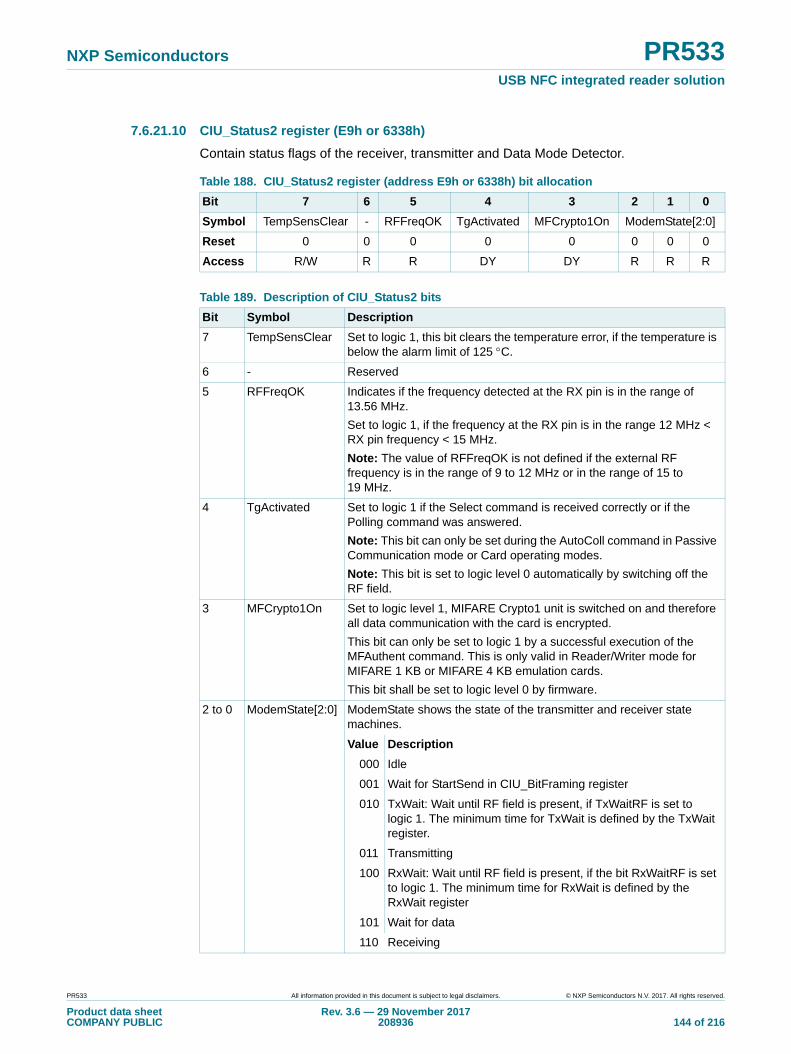
NXP Semiconductors PR533USB NFC integrated reader solution
7.6.21.10 CIU_Status2 register (E9h or 6338h)
Contain status flags of the receiver, transmitter and Data Mode Detector.
Table 188. CIU_Status2 register (address E9h or 6338h) bit allocation
Bit 7 6 5 4 3 2 1 0
Symbol TempSensClear - RFFreqOK TgActivated MFCrypto1On ModemState[2:0]
Reset 0 0 0 0 0 0 0 0
Access R/W R R DY DY R R R
Table 189. Description of CIU_Status2 bits
Bit Symbol Description
7 TempSensClear Set to logic 1, this bit clears the temperature error, if the temperature is below the alarm limit of 125 C.
6 - Reserved
5 RFFreqOK Indicates if the frequency detected at the RX pin is in the range of 13.56 MHz.
Set to logic 1, if the frequency at the RX pin is in the range 12 MHz < RX pin frequency < 15 MHz.
Note: The value of RFFreqOK is not defined if the external RF frequency is in the range of 9 to 12 MHz or in the range of 15 to 19 MHz.
4 TgActivated Set to logic 1 if the Select command is received correctly or if the Polling command was answered.
Note: This bit can only be set during the AutoColl command in Passive Communication mode or Card operating modes.
Note: This bit is set to logic level 0 automatically by switching off the RF field.
3 MFCrypto1On Set to logic level 1, MIFARE Crypto1 unit is switched on and therefore all data communication with the card is encrypted.
This bit can only be set to logic 1 by a successful execution of the MFAuthent command. This is only valid in Reader/Writer mode for MIFARE 1 KB or MIFARE 4 KB emulation cards.
This bit shall be set to logic level 0 by firmware.
2 to 0 ModemState[2:0] ModemState shows the state of the transmitter and receiver state machines.
Value Description
000 Idle
001 Wait for StartSend in CIU_BitFraming register
010 TxWait: Wait until RF field is present, if TxWaitRF is set to logic 1. The minimum time for TxWait is defined by the TxWait register.
011 Transmitting
100 RxWait: Wait until RF field is present, if the bit RxWaitRF is set to logic 1. The minimum time for RxWait is defined by the RxWait register
101 Wait for data
110 Receiving
PR533 All information provided in this document is subject to legal disclaimers. © NXP Semiconductors N.V. 2017. All rights reserved.
Product data sheetCOMPANY PUBLIC
Rev. 3.6 — 29 November 2017208936 144 of 216
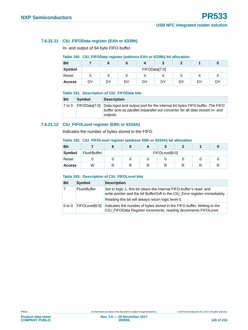
NXP Semiconductors PR533USB NFC integrated reader solution
7.6.21.11 CIU_FIFOData register (EAh or 6339h)
In- and output of 64 byte FIFO buffer.
7.6.21.12 CIU_FIFOLevel register (EBh or 633Ah)
Indicates the number of bytes stored in the FIFO.
Table 190. CIU_FIFOData register (address EAh or 6339h) bit allocation
Bit 7 6 5 4 3 2 1 0
Symbol FIFOData[7:0]
Reset X X X X X X X X
Access DY DY DY DY DY DY DY DY
Table 191. Description of CIU_FIFOData bits
Bit Symbol Description
7 to 0 FIFOData[7:0] Data input and output port for the internal 64 bytes FIFO buffer. The FIFO buffer acts as parallel in/parallel out converter for all data stream in- and outputs
Table 192. CIU_FIFOLevel register (address EBh or 633Ah) bit allocation
Bit 7 6 5 4 3 2 1 0
Symbol FlushBuffer FIFOLevel[6:0]
Reset 0 0 0 0 0 0 0 0
Access W R R R R R R R
Table 193. Description of CIU_FIFOLevel bits
Bit Symbol Description
7 FlushBuffer Set to logic 1, this bit clears the internal FIFO-buffer’s read- and write-pointer and the bit BufferOvfl in the CIU_Error register immediately.
Reading this bit will always return logic level 0.
6 to 0 FIFOLevel[6:0] Indicates the number of bytes stored in the FIFO buffer. Writing to the CIU_FIFOData Register increments, reading decrements FIFOLevel.
PR533 All information provided in this document is subject to legal disclaimers. © NXP Semiconductors N.V. 2017. All rights reserved.
Product data sheetCOMPANY PUBLIC
Rev. 3.6 — 29 November 2017208936 145 of 216
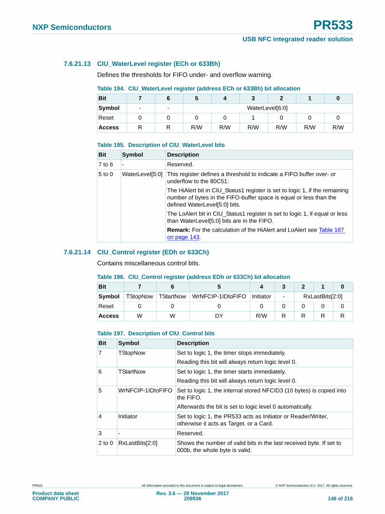
NXP Semiconductors PR533USB NFC integrated reader solution
7.6.21.13 CIU_WaterLevel register (ECh or 633Bh)
Defines the thresholds for FIFO under- and overflow warning.
7.6.21.14 CIU_Control register (EDh or 633Ch)
Contains miscellaneous control bits.
Table 194. CIU_WaterLevel register (address ECh or 633Bh) bit allocation
Bit 7 6 5 4 3 2 1 0
Symbol - - WaterLevel[6:0]
Reset 0 0 0 0 1 0 0 0
Access R R R/W R/W R/W R/W R/W R/W
Table 195. Description of CIU_WaterLevel bits
Bit Symbol Description
7 to 6 - Reserved.
5 to 0 WaterLevel[5:0] This register defines a threshold to indicate a FIFO buffer over- or underflow to the 80C51:
The HiAlert bit in CIU_Status1 register is set to logic 1, if the remaining number of bytes in the FIFO-buffer space is equal or less than the defined WaterLevel[5:0] bits.
The LoAlert bit in CIU_Status1 register is set to logic 1, if equal or less than WaterLevel[5:0] bits are in the FIFO.
Remark: For the calculation of the HiAlert and LoAlert see Table 187 on page 143.
Table 196. CIU_Control register (address EDh or 633Ch) bit allocation
Bit 7 6 5 4 3 2 1 0
Symbol TStopNow TStartNow WrNFCIP-1IDtoFIFO Initiator - RxLastBits[2:0]
Reset 0 0 0 0 0 0 0 0
Access W W DY R/W R R R R
Table 197. Description of CIU_Control bits
Bit Symbol Description
7 TStopNow Set to logic 1, the timer stops immediately.
Reading this bit will always return logic level 0.
6 TStartNow Set to logic 1, the timer starts immediately.
Reading this bit will always return logic level 0.
5 WrNFCIP-1IDtoFIFO Set to logic 1, the internal stored NFCID3 (10 bytes) is copied into the FIFO.
Afterwards the bit is set to logic level 0 automatically.
4 Initiator Set to logic 1, the PR533 acts as Initiator or Reader/Writer, otherwise it acts as Target. or a Card.
3 - Reserved.
2 to 0 RxLastBits[2:0] Shows the number of valid bits in the last received byte. If set to 000b, the whole byte is valid.
PR533 All information provided in this document is subject to legal disclaimers. © NXP Semiconductors N.V. 2017. All rights reserved.
Product data sheetCOMPANY PUBLIC
Rev. 3.6 — 29 November 2017208936 146 of 216
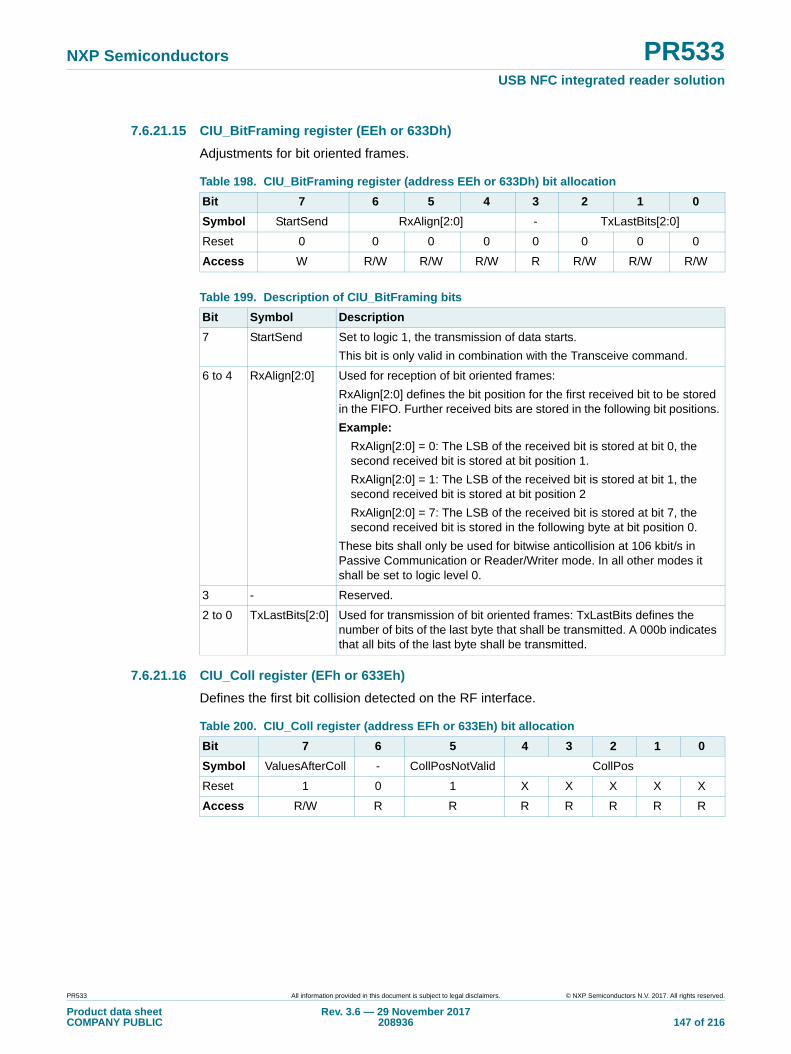
NXP Semiconductors PR533USB NFC integrated reader solution
7.6.21.15 CIU_BitFraming register (EEh or 633Dh)
Adjustments for bit oriented frames.
7.6.21.16 CIU_Coll register (EFh or 633Eh)
Defines the first bit collision detected on the RF interface.
Table 198. CIU_BitFraming register (address EEh or 633Dh) bit allocation
Bit 7 6 5 4 3 2 1 0
Symbol StartSend RxAlign[2:0] - TxLastBits[2:0]
Reset 0 0 0 0 0 0 0 0
Access W R/W R/W R/W R R/W R/W R/W
Table 199. Description of CIU_BitFraming bits
Bit Symbol Description
7 StartSend Set to logic 1, the transmission of data starts.
This bit is only valid in combination with the Transceive command.
6 to 4 RxAlign[2:0] Used for reception of bit oriented frames:
RxAlign[2:0] defines the bit position for the first received bit to be stored in the FIFO. Further received bits are stored in the following bit positions.
Example:
RxAlign[2:0] = 0: The LSB of the received bit is stored at bit 0, the second received bit is stored at bit position 1.
RxAlign[2:0] = 1: The LSB of the received bit is stored at bit 1, the second received bit is stored at bit position 2
RxAlign[2:0] = 7: The LSB of the received bit is stored at bit 7, the second received bit is stored in the following byte at bit position 0.
These bits shall only be used for bitwise anticollision at 106 kbit/s in Passive Communication or Reader/Writer mode. In all other modes it shall be set to logic level 0.
3 - Reserved.
2 to 0 TxLastBits[2:0] Used for transmission of bit oriented frames: TxLastBits defines the number of bits of the last byte that shall be transmitted. A 000b indicates that all bits of the last byte shall be transmitted.
Table 200. CIU_Coll register (address EFh or 633Eh) bit allocation
Bit 7 6 5 4 3 2 1 0
Symbol ValuesAfterColl - CollPosNotValid CollPos
Reset 1 0 1 X X X X X
Access R/W R R R R R R R
PR533 All information provided in this document is subject to legal disclaimers. © NXP Semiconductors N.V. 2017. All rights reserved.
Product data sheetCOMPANY PUBLIC
Rev. 3.6 — 29 November 2017208936 147 of 216
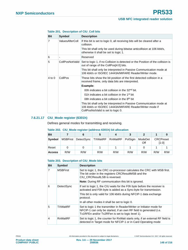
NXP Semiconductors PR533USB NFC integrated reader solution
7.6.21.17 CIU_Mode register (6301h)
Defines general modes for transmitting and receiving.
Table 201. Description of CIU_Coll bits
Bit Symbol Description
7 ValuesAfterColl If this bit is set to logic 0, all receiving bits will be cleared after a collision.
This bit shall only be used during bitwise anticollision at 106 kbit/s, otherwise it shall be set to logic 1.
6 - Reserved
5 CollPosNotValid Set to logic 1, if no Collision is detected or the Position of the collision is out of range of the CollPos[4:0] bits.
This bit shall only be interpreted in Passive Communication mode at 106 kbit/s or ISO/IEC 14443A/MIFARE Reader/Writer mode.
4 to 0 CollPos These bits show the bit position of the first detected collision in a received frame, only data bits are interpreted.
Example:
00h indicates a bit collision in the 32nd bit.
01h indicates a bit collision in the 1st bit
08h indicates a bit collision in the 8th bit
This bit shall only be interpreted in Passive Communication mode at 106 kbit/s or ISO/IEC 14443A/MIFARE Reader/Writer mode if CollPosNotValid is set to logic 0.
Table 202. CIU_Mode register (address 6301h) bit allocation
Bit 7 6 5 4 3 2 1 0
Symbol MSBFirst DetectSync TXWaitRF RxWaitRF PolSigin ModeDetOff
CRCPreset[1:0]
Reset 0 0 1 1 1 0 1 1
Access R/W R/W R/W R/W R/W R/W R/W R/W
Table 203. Description of CIU_Mode bits
Bit Symbol Description
7 MSBFirst Set to logic 1, the CRC co-processor calculates the CRC with MSB first. The bit order in the registers CRCResultMSB and the CIU_CRCResultLSB is reversed.
Note: During RF communication this bit is ignored.
6 DetectSync If set to logic 1, the CIU waits for the F0h byte before the receiver is activated and F0h byte is added as a Sync-byte for transmission.
This bit is only valid for 106 kbit/s during NFCIP-1 data exchange protocol.
In all other modes it shall be set to logic 0.
5 TXWaitRF Set to logic 1 the transmitter in Reader/Writer or Initiator mode for NFCIP-1 can only be started, if an own RF field is generated (i.e. Tx1RFEn and/or Tx2RFen is set to logic level 1).
4 RxWaitRF Set to logic 1, the counter for RxWait starts only, if an external RF field is detected in Target mode for NFCIP-1 or in Card Operating mode
PR533 All information provided in this document is subject to legal disclaimers. © NXP Semiconductors N.V. 2017. All rights reserved.
Product data sheetCOMPANY PUBLIC
Rev. 3.6 — 29 November 2017208936 148 of 216
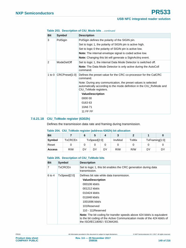
NXP Semiconductors PR533USB NFC integrated reader solution
7.6.21.18 CIU_TxMode register (6302h)
Defines the transmission data rate and framing during transmission.
3 PolSigin PolSigin defines the polarity of the SIGIN pin.
Set to logic 1, the polarity of SIGIN pin is active high.
Set to logic 0 the polarity of SIGIN pin is active low.
Note: The internal envelope signal is coded active low.
Note: Changing this bit will generate a SiginActIrq event.
2 ModeDetOff Set to logic 1, the internal Data Mode Detector is switched off.
Note: The Data Mode Detector is only active during the AutoColl command.
1 to 0 CRCPreset[1:0] Defines the preset value for the CRC co-processor for the CalCRC command.
Note: During any communication, the preset values is selected automatically according to the mode definition in the CIU_RxMode and CIU_TxMode registers.
ValueDescription
0000 00
0163 63
10A6 71
11 FF FF
Table 203. Description of CIU_Mode bits …continued
Bit Symbol Description
Table 204. CIU_TxMode register (address 6302h) bit allocation
Bit 7 6 5 4 3 2 1 0
Symbol TxCRCEn TxSpeed[2:0] InvMod TxMix TxFraming[1:0]
Reset 0 0 0 0 0 0 0 0
Access R/W DY DY DY R/W R/W DY DY
Table 205. Description of CIU_TxMode bits
Bit Symbol Description
7 TxCRCEn Set to logic 1, this bit enables the CRC generation during data transmission.
6 to 4 TxSpeed[2:0] Defines bit rate while data transmission.
ValueDescription
000106 kbit/s
001212 kbit/s
010424 kbit/s
011848 kbit/s
1001696 kbit/s
101Reserved
110 - 111Reserved
Note: The bit coding for transfer speeds above 424 kbit/s is equivalent to the bit coding of the Active Communication mode of the 424 kbit/s of the ISO/IEC18092 / ECMA340.
PR533 All information provided in this document is subject to legal disclaimers. © NXP Semiconductors N.V. 2017. All rights reserved.
Product data sheetCOMPANY PUBLIC
Rev. 3.6 — 29 November 2017208936 149 of 216
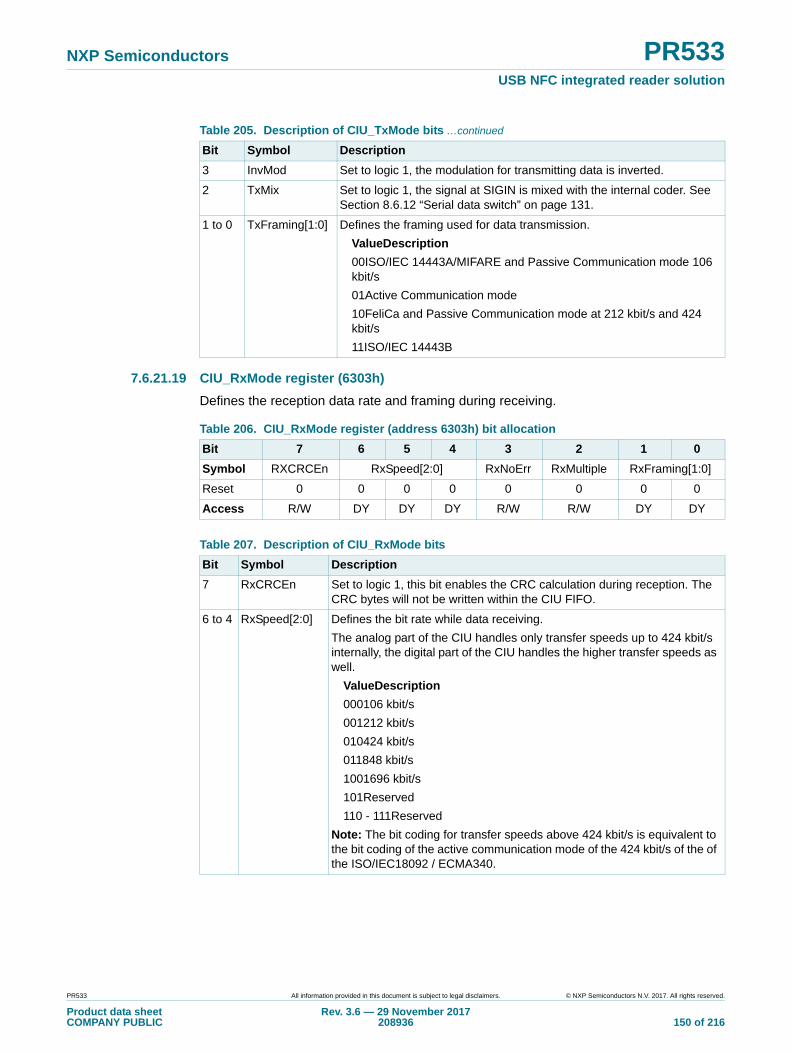
NXP Semiconductors PR533USB NFC integrated reader solution
7.6.21.19 CIU_RxMode register (6303h)
Defines the reception data rate and framing during receiving.
3 InvMod Set to logic 1, the modulation for transmitting data is inverted.
2 TxMix Set to logic 1, the signal at SIGIN is mixed with the internal coder. See Section 8.6.12 “Serial data switch” on page 131.
1 to 0 TxFraming[1:0] Defines the framing used for data transmission.
ValueDescription
00ISO/IEC 14443A/MIFARE and Passive Communication mode 106 kbit/s
01Active Communication mode
10FeliCa and Passive Communication mode at 212 kbit/s and 424 kbit/s
11ISO/IEC 14443B
Table 205. Description of CIU_TxMode bits …continued
Bit Symbol Description
Table 206. CIU_RxMode register (address 6303h) bit allocation
Bit 7 6 5 4 3 2 1 0
Symbol RXCRCEn RxSpeed[2:0] RxNoErr RxMultiple RxFraming[1:0]
Reset 0 0 0 0 0 0 0 0
Access R/W DY DY DY R/W R/W DY DY
Table 207. Description of CIU_RxMode bits
Bit Symbol Description
7 RxCRCEn Set to logic 1, this bit enables the CRC calculation during reception. The CRC bytes will not be written within the CIU FIFO.
6 to 4 RxSpeed[2:0] Defines the bit rate while data receiving.
The analog part of the CIU handles only transfer speeds up to 424 kbit/s internally, the digital part of the CIU handles the higher transfer speeds as well.
ValueDescription
000106 kbit/s
001212 kbit/s
010424 kbit/s
011848 kbit/s
1001696 kbit/s
101Reserved
110 - 111Reserved
Note: The bit coding for transfer speeds above 424 kbit/s is equivalent to the bit coding of the active communication mode of the 424 kbit/s of the of the ISO/IEC18092 / ECMA340.
PR533 All information provided in this document is subject to legal disclaimers. © NXP Semiconductors N.V. 2017. All rights reserved.
Product data sheetCOMPANY PUBLIC
Rev. 3.6 — 29 November 2017208936 150 of 216
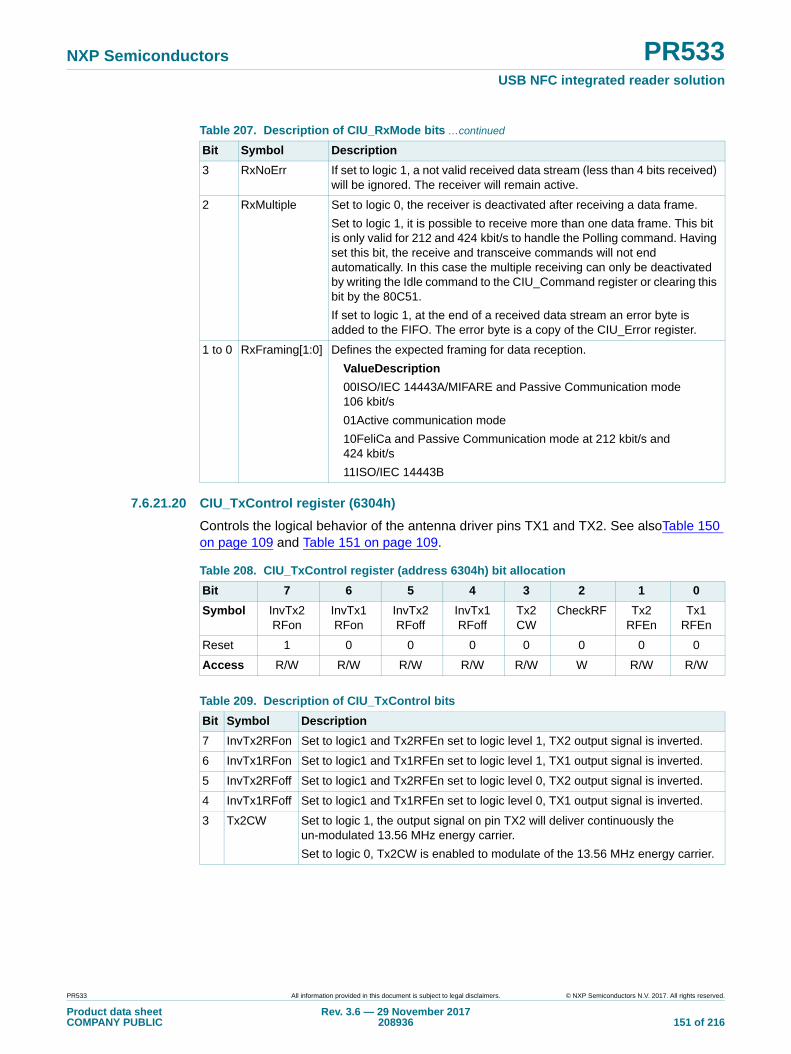
NXP Semiconductors PR533USB NFC integrated reader solution
7.6.21.20 CIU_TxControl register (6304h)
Controls the logical behavior of the antenna driver pins TX1 and TX2. See alsoTable 150 on page 109 and Table 151 on page 109.
3 RxNoErr If set to logic 1, a not valid received data stream (less than 4 bits received) will be ignored. The receiver will remain active.
2 RxMultiple Set to logic 0, the receiver is deactivated after receiving a data frame.
Set to logic 1, it is possible to receive more than one data frame. This bit is only valid for 212 and 424 kbit/s to handle the Polling command. Having set this bit, the receive and transceive commands will not end automatically. In this case the multiple receiving can only be deactivated by writing the Idle command to the CIU_Command register or clearing this bit by the 80C51.
If set to logic 1, at the end of a received data stream an error byte is added to the FIFO. The error byte is a copy of the CIU_Error register.
1 to 0 RxFraming[1:0] Defines the expected framing for data reception.
ValueDescription
00ISO/IEC 14443A/MIFARE and Passive Communication mode 106 kbit/s
01Active communication mode
10FeliCa and Passive Communication mode at 212 kbit/s and 424 kbit/s
11ISO/IEC 14443B
Table 207. Description of CIU_RxMode bits …continued
Bit Symbol Description
Table 208. CIU_TxControl register (address 6304h) bit allocation
Bit 7 6 5 4 3 2 1 0
Symbol InvTx2RFon
InvTx1RFon
InvTx2RFoff
InvTx1RFoff
Tx2CW
CheckRF Tx2RFEn
Tx1RFEn
Reset 1 0 0 0 0 0 0 0
Access R/W R/W R/W R/W R/W W R/W R/W
Table 209. Description of CIU_TxControl bits
Bit Symbol Description
7 InvTx2RFon Set to logic1 and Tx2RFEn set to logic level 1, TX2 output signal is inverted.
6 InvTx1RFon Set to logic1 and Tx1RFEn set to logic level 1, TX1 output signal is inverted.
5 InvTx2RFoff Set to logic1 and Tx2RFEn set to logic level 0, TX2 output signal is inverted.
4 InvTx1RFoff Set to logic1 and Tx1RFEn set to logic level 0, TX1 output signal is inverted.
3 Tx2CW Set to logic 1, the output signal on pin TX2 will deliver continuously the un-modulated 13.56 MHz energy carrier.
Set to logic 0, Tx2CW is enabled to modulate of the 13.56 MHz energy carrier.
PR533 All information provided in this document is subject to legal disclaimers. © NXP Semiconductors N.V. 2017. All rights reserved.
Product data sheetCOMPANY PUBLIC
Rev. 3.6 — 29 November 2017208936 151 of 216

NXP Semiconductors PR533USB NFC integrated reader solution
7.6.21.21 CIU_TxAuto register (6305h)
Controls the setting of the antenna driver.
2 CheckRF Set to logic 1, Tx2RFEn and Tx1RFEn can not be set if an external RF field is detected.
Only valid when using in combination with Tx2RFAutoEn and TX1RFAutoEn bits in CIU_TxAuto register.
1 Tx2RFEn Set to logic 1, the output signal on pin TX2 will deliver the 13.56 MHz energy carrier modulated by the transmission data.
0 Tx1RFEn Set to logic 1, the output signal on pin TX1 will deliver the 13.56 MHz energy carrier modulated by the transmission data.
Table 209. Description of CIU_TxControl bits …continued
Bit Symbol Description
Table 210. CIU_TxAuto register (address 6305h) bit allocation
Bit 7 6 5 4 3 2 1 0
Symbol AutoRFOFF
Force100ASK
AutoWakeUp - CAOn InitialRFOn Tx2RFAutoEn
Tx1RFAutoEn
Reset 0 0 0 0 0 0 0 0
Access R/W R/W R/W R R/W W R/W R/W
Table 211. Description of CIU_TxAuto bits
Bit Symbol Description
7 AutoRFOff Set to logic 1, own RF field is switched off after the last data bit has been transmitted as defined in the NFCIP-1 standard.
6 Force100ASK Set to logic 1, Force100ASK forces a 100% ASK modulation independent of the setting in CIU_ModGsP register.
5 AutoWakeUp Set to logic 1, the PR533 in CIU Power-down mode can be woken up by the RF level detector.
4 Reserved
3 CAOn Set to logic 1, the collision avoidance is activated and internally the value n is set in accordance to the ISO/IEC 18092 / ECMA340 NFCIP-1 standards.
2 InitialRFOn Set to logic 1, the initial RF collision avoidance is performed and the bit InitialRFOn is set to logic level 0 automatically, if the RF is switched ON.
Note: The driver(s) which should be switched on, have to enabled by Tx2RFAutoEn and/or Tx1RFAutoEn bits.
Note: If the own RF field is already ON when the bit InitialRFOn is set, it is not set to logic level 0.
1 Tx2RFAutoEn Set to logic 1, RF is switched on at TX2 (i.e. Tx2RFEn is set to logic level 1) after the external RF field is switched off according to the time TADT. If the InitialRFOn and Tx2RFAutoEn bits are set to logic 1, RF is switched on at TX2 if no external RF field is detected during the time TIDT.
Note: The times TADT and TIDT are in accordance to the ISO/IEC 18092/ ECMA340 NFCIP-1 standards.
0 Tx1RFAutoEn Set to logic 1, RF is switched on at TX1(i.e. Tx1RFEn is set to logic level 1) after the external RF field is switched off according to the time TADT. If the InitialRFOn and Tx1RFAutoEn bits are set to logic 1, RF is switched on at TX1 if no external RF field is detected during the time TIDT.
Note: The times TADT and TIDT are in accordance to the ISO/IEC 18092/ ECMA340 NFCIP-1 standards.
PR533 All information provided in this document is subject to legal disclaimers. © NXP Semiconductors N.V. 2017. All rights reserved.
Product data sheetCOMPANY PUBLIC
Rev. 3.6 — 29 November 2017208936 152 of 216
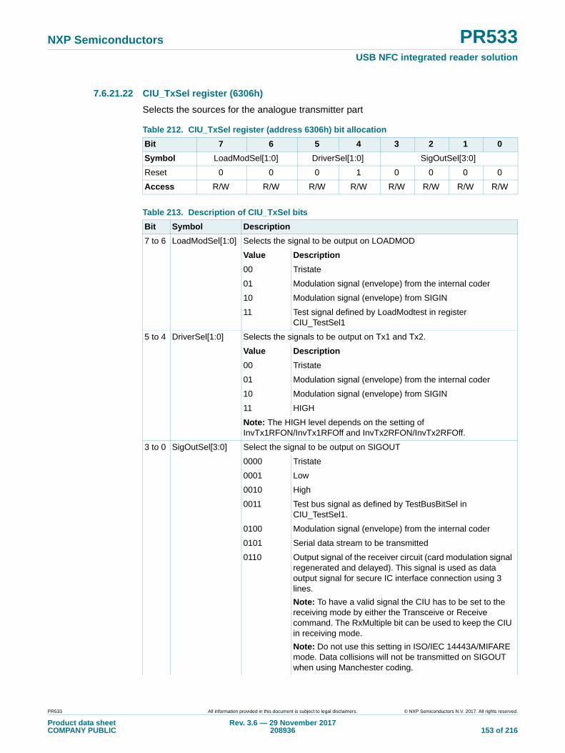
NXP Semiconductors PR533USB NFC integrated reader solution
7.6.21.22 CIU_TxSel register (6306h)
Selects the sources for the analogue transmitter part
Table 212. CIU_TxSel register (address 6306h) bit allocation
Bit 7 6 5 4 3 2 1 0
Symbol LoadModSel[1:0] DriverSel[1:0] SigOutSel[3:0]
Reset 0 0 0 1 0 0 0 0
Access R/W R/W R/W R/W R/W R/W R/W R/W
Table 213. Description of CIU_TxSel bits
Bit Symbol Description
7 to 6 LoadModSel[1:0] Selects the signal to be output on LOADMOD
Value Description
00 Tristate
01 Modulation signal (envelope) from the internal coder
10 Modulation signal (envelope) from SIGIN
11 Test signal defined by LoadModtest in register CIU_TestSel1
5 to 4 DriverSel[1:0] Selects the signals to be output on Tx1 and Tx2.
Value Description
00 Tristate
01 Modulation signal (envelope) from the internal coder
10 Modulation signal (envelope) from SIGIN
11 HIGH
Note: The HIGH level depends on the setting of InvTx1RFON/InvTx1RFOff and InvTx2RFON/InvTx2RFOff.
3 to 0 SigOutSel[3:0] Select the signal to be output on SIGOUT
0000 Tristate
0001 Low
0010 High
0011 Test bus signal as defined by TestBusBitSel in CIU_TestSel1.
0100 Modulation signal (envelope) from the internal coder
0101 Serial data stream to be transmitted
0110 Output signal of the receiver circuit (card modulation signal regenerated and delayed). This signal is used as data output signal for secure IC interface connection using 3 lines.
Note: To have a valid signal the CIU has to be set to the receiving mode by either the Transceive or Receive command. The RxMultiple bit can be used to keep the CIU in receiving mode.
Note: Do not use this setting in ISO/IEC 14443A/MIFARE mode. Data collisions will not be transmitted on SIGOUT when using Manchester coding.
PR533 All information provided in this document is subject to legal disclaimers. © NXP Semiconductors N.V. 2017. All rights reserved.
Product data sheetCOMPANY PUBLIC
Rev. 3.6 — 29 November 2017208936 153 of 216
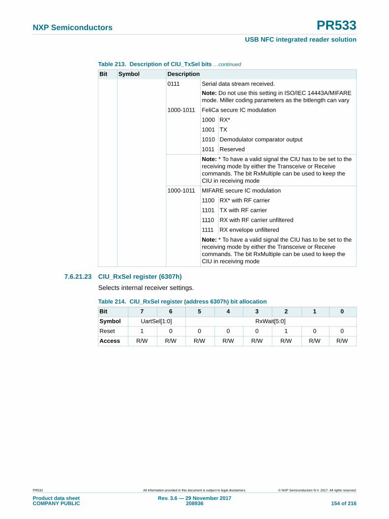
NXP Semiconductors PR533USB NFC integrated reader solution
7.6.21.23 CIU_RxSel register (6307h)
Selects internal receiver settings.
0111 Serial data stream received.
Note: Do not use this setting in ISO/IEC 14443A/MIFARE mode. Miller coding parameters as the bitlength can vary
1000-1011 FeliCa secure IC modulation
1000 RX*
1001 TX
1010 Demodulator comparator output
1011 Reserved
Note: * To have a valid signal the CIU has to be set to the receiving mode by either the Transceive or Receive commands. The bit RxMultiple can be used to keep the CIU in receiving mode
1000-1011 MIFARE secure IC modulation
1100 RX* with RF carrier
1101 TX with RF carrier
1110 RX with RF carrier unfiltered
1111 RX envelope unfiltered
Note: * To have a valid signal the CIU has to be set to the receiving mode by either the Transceive or Receive commands. The bit RxMultiple can be used to keep the CIU in receiving mode
Table 213. Description of CIU_TxSel bits …continued
Bit Symbol Description
Table 214. CIU_RxSel register (address 6307h) bit allocation
Bit 7 6 5 4 3 2 1 0
Symbol UartSel[1:0] RxWait[5:0]
Reset 1 0 0 0 0 1 0 0
Access R/W R/W R/W R/W R/W R/W R/W R/W
PR533 All information provided in this document is subject to legal disclaimers. © NXP Semiconductors N.V. 2017. All rights reserved.
Product data sheetCOMPANY PUBLIC
Rev. 3.6 — 29 November 2017208936 154 of 216

NXP Semiconductors PR533USB NFC integrated reader solution
7.6.21.24 CIU_RxThreshold register (6308h)
Selects thresholds for the bit decoder.
7.6.21.25 CIU_Demod register (6309h)
Defines demodulator settings.
Table 215. Description of CIU_RxSel bits
Bit Symbol Description
7 to 6 UartSel[1:0] Selects the input of the digital part (CL UART) of the CIU
Value Description
00 Constant Low
01 Envelope signal at SIGIN
10 Modulation signal from the internal analog part
11 Modulation signal from SIGIN pin. Only valid for transfer speeds above 424 kbit/s
5 to 0 RxWait[5:0] After data transmission, the activation of the receiver is delayed for RxWait bit-clocks. During this ‘frame guard time’ any signal at pin Rx is ignored.
This parameter is ignored by the Receive command. All other commands (e.g. Transceive, Autocoll, MFAuthent) use this parameter. Depending on the mode of the CIU, the counter starts differently. In Passive Communication mode the counters starts with the last modulation of the transmitted data stream. In Active Communication mode the counter starts immediately after the external RF field is switched on.
Table 216. CIU_RxThreshold register (address 6308h) bit allocation
Bit 7 6 5 4 3 2 1 0
Symbol MinLevel[3:0] - Collevel[2:0]
Reset 1 0 0 0 0 1 0 0
Access R/W R/W R/W R/W R R/W R/W R/W
Table 217. Description of CIU_RxThreshold bits
Bit Symbol Description
7 to 4 MinLevel[3:0] Defines the minimum signal strength at the decoder input that shall be accepted. If the signal strength is below this level, it is not evaluated.
3 - Reserved
2 to 0 Collevel[2:0] Defines the minimum signal strength at the decoder input that has to be reached by the weaker half-bit of the Manchester-coded signal to generate a bit-collision relatively to the amplitude of the stronger half-bit.
Table 218. CIU_Demod register (address 6309h) bit allocation
Bit 7 6 5 4 3 2 1 0
Symbol AddIQ[1:0] FixIQ - TauRcv[1:0] TauSync[1:0]
Reset 0 1 0 0 1 1 0 1
Access R/W R/W R/W R R/W R/W R/W R/W
PR533 All information provided in this document is subject to legal disclaimers. © NXP Semiconductors N.V. 2017. All rights reserved.
Product data sheetCOMPANY PUBLIC
Rev. 3.6 — 29 November 2017208936 155 of 216

NXP Semiconductors PR533USB NFC integrated reader solution
7.6.21.26 CIU_FelNFC1 register (630Ah)
Defines the length of the FeliCa Sync bytes and the minimum length of the received frame.
7.6.21.27 CIU_FelNFC2 register (630Bh)
Defines the maximum length of the received frame.
Table 219. Description of CIU_Demod bits
Bit Symbol Description
7 to 6 AddIQ[1:0] Defines the use of I and Q channel during reception.
Note: FixIQ has to be set to logic 0 to enable the following settings.
ValueDescription
00Select the stronger channel
01Select the stronger and freeze the selected during communication
10Combines the I and Q channel
11RFU
5 FixIQ If set to logic 1 and AddIQ[0] is set to logic level 0, the reception is fixed to I channel.
If set to logic 1 and AddIQ[0] is set to logic level 1, the reception is fixed to Q channel.
4 - Reserved
3 to 2 TauRcv[1:0] Changes time-constant of internal PLL during data receiving.
Note: If set to 00h, the PLL is frozen during data receiving.
1 to 0 TauSync[1:0] Changes time-constant of internal PLL during burst (out of data reception)
Table 220. CIU_FelNFC1 register (address 630Ah) bit allocation
Bit 7 6 5 4 3 2 1 0
Symbol FelSyncLen[1:0] DataLenMin[5:0]
Reset 0 0 0 0 0 0 0 0
Access R/W R/W R/W R/W R/W R/W R/W R/W
Table 221. Description of CIU_FelNFC1 bits
Bit Symbol Description
7 to 6 FelSyncLen[1:0]] Defines the length of the Sync bytes.
ValueDescription
00B2 4D
0100 B2 4D
1000 00 B2 4D
1100 00 00 B2 4D
5 to 0 DataLenMin[5:0] These bits define the minimum length of the accepted frame length.
This parameter is ignored at 106 kbit/s if the DetectSync bit in CIU_Mode register is set to logic 0. If a received frame is shorter as the defined DataLenMin value, the frame will be ignored.
DataLenMin 4 DataPacketLenght
PR533 All information provided in this document is subject to legal disclaimers. © NXP Semiconductors N.V. 2017. All rights reserved.
Product data sheetCOMPANY PUBLIC
Rev. 3.6 — 29 November 2017208936 156 of 216
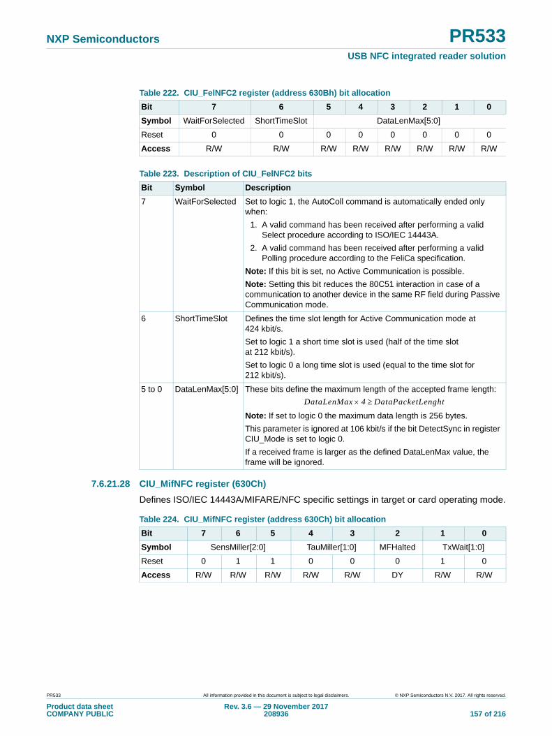
NXP Semiconductors PR533USB NFC integrated reader solution
7.6.21.28 CIU_MifNFC register (630Ch)
Defines ISO/IEC 14443A/MIFARE/NFC specific settings in target or card operating mode.
Table 222. CIU_FelNFC2 register (address 630Bh) bit allocation
Bit 7 6 5 4 3 2 1 0
Symbol WaitForSelected ShortTimeSlot DataLenMax[5:0]
Reset 0 0 0 0 0 0 0 0
Access R/W R/W R/W R/W R/W R/W R/W R/W
Table 223. Description of CIU_FelNFC2 bits
Bit Symbol Description
7 WaitForSelected Set to logic 1, the AutoColl command is automatically ended only when:
1. A valid command has been received after performing a valid Select procedure according to ISO/IEC 14443A.
2. A valid command has been received after performing a valid Polling procedure according to the FeliCa specification.
Note: If this bit is set, no Active Communication is possible.
Note: Setting this bit reduces the 80C51 interaction in case of a communication to another device in the same RF field during Passive Communication mode.
6 ShortTimeSlot Defines the time slot length for Active Communication mode at 424 kbit/s.
Set to logic 1 a short time slot is used (half of the time slot at 212 kbit/s).
Set to logic 0 a long time slot is used (equal to the time slot for 212 kbit/s).
5 to 0 DataLenMax[5:0] These bits define the maximum length of the accepted frame length:
Note: If set to logic 0 the maximum data length is 256 bytes.
This parameter is ignored at 106 kbit/s if the bit DetectSync in register CIU_Mode is set to logic 0.
If a received frame is larger as the defined DataLenMax value, the frame will be ignored.
DataLenMax 4 DataPacketLenght
Table 224. CIU_MifNFC register (address 630Ch) bit allocation
Bit 7 6 5 4 3 2 1 0
Symbol SensMiller[2:0] TauMiller[1:0] MFHalted TxWait[1:0]
Reset 0 1 1 0 0 0 1 0
Access R/W R/W R/W R/W R/W DY R/W R/W
PR533 All information provided in this document is subject to legal disclaimers. © NXP Semiconductors N.V. 2017. All rights reserved.
Product data sheetCOMPANY PUBLIC
Rev. 3.6 — 29 November 2017208936 157 of 216

NXP Semiconductors PR533USB NFC integrated reader solution
7.6.21.29 CIU_ManualRCV register (630Dh)
Allows manual fine-tuning of the internal receiver.
IMPORTANT NOTE: For standard application it is not recommended to change this register settings.
Table 225. Description of CIU_MifNFC bits
Bit Symbol Description
7 to 5 SensMiller[2:0] This bit defines the sensitivity of the Miller decoder.
4 to 3 TauMiller[1:0] This bit defines the time constant of the Miller decoder.
2 MFHalted Set to logic 1, this bit indicates that the CIU is set to HALT mode in Card Operating mode at 106 kbit/s. This bit is either set by the 80C51 or by the internal state machine and indicates that only the code 52h is accepted as a Request command.
This bit is automatically set to logic level 0 by RF reset.
1 to 0 TxWait[1:0] These bits define the minimum response time between receive and transmit in number of data bits + 7 data bits.
The shortest possible minimum response time is 7 data bits. (TxWait=0). The minimum response time can be increased by the number of bits defined in TxWait. The longest minimum response time is 10 data bits (TxWait = 3).
If a transmission of a frame is started before the minimum response time is over, the PR533 waits before transmitting the data until the minimum response time is over.
If a transmission of a frame is started after the minimum response time is over, the frame is started immediately if the data bit synchronization is correct. (adjustable with TxBitPhase)
Table 226. CIU_ManualRCV register (address 630Dh) bit allocation
Bit 7 6 5 4 3 2 1 0
Symbol - FastFiltMF_SO
DelayMF_SO
ParityDisable LargeBWPLL ManualHPCF HPCF[1:0]
Reset 0 0 0 0 0 0 0 0
Access R R/W R/W R/W R/W R/W R/W R/W
PR533 All information provided in this document is subject to legal disclaimers. © NXP Semiconductors N.V. 2017. All rights reserved.
Product data sheetCOMPANY PUBLIC
Rev. 3.6 — 29 November 2017208936 158 of 216
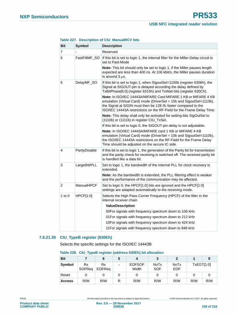
NXP Semiconductors PR533USB NFC integrated reader solution
7.6.21.30 CIU_TypeB register (630Eh)
Selects the specific settings for the ISO/IEC 14443B
Table 227. Description of CIU_ManualRCV bits
Bit Symbol Description
7 - Reserved
6 FastFiltMF_SO If this bit is set to logic 1, the internal filter for the Miller-Delay circuit is set to Fast-Mode
Note: This bit should only be set to logic 1, if the Miller pauses length expected are less than 400 ns. At 106 kbit/s, the Miller pauses duration is around 3 s.
5 DelayMF_SO If this bit is set to logic 1, when SigoutSel=1100b (register 6306h), the Signal at SIGOUT-pin is delayed according the delay defined by TxBitPhase[6:0] (register 6315h) and TxWait bits (register 630Ch).
Note: In ISO/IEC 14443A/MIFARE Card MIFARE 1 KB or MIFARE 4 KB emulation (Virtual Card) mode (DriverSel = 10b and SigoutSel=1110b), the Signal at SIGIN must then be 128 /fc faster compared to the ISO/IEC 14443A restrictions on the RF-Field for the Frame Delay Time.
Note: This delay shall only be activated for setting bits SigOutSel to (1110b) or (1111b) in register CIU_TxSel.
If this bit is set to logic 0, the SIGOUT-pin delay is not adjustable.
Note: In ISO/IEC 14443A/MIFARE card 1 KB or MIFARE 4 KB emulation (Virtual Card) mode (DriverSel = 10b and SigoutSel=1110b), the ISO/IEC 14443A restrictions on the RF-Field for the Frame Delay Time should be adjusted on the secure IC side
4 ParityDisable If this bit is set to logic 1, the generation of the Parity bit for transmission and the parity check for receiving is switched off. The received parity bit is handled like a data bit.
3 LargeBWPLL Set to logic 1, the bandwidth of the internal PLL for clock recovery is extended.
Note: As the bandwidth is extended, the PLL filtering effect is weaker and the performance of the communication may be affected.
2 ManualHPCF Set to logic 0, the HPCF[1:0] bits are ignored and the HPCF[1:0] settings are adapted automatically to the receiving mode.
1 to 0 HPCF[1:0] Selects the High Pass Corner Frequency (HPCF) of the filter in the internal receiver chain
ValueDescription
00For signals with frequency spectrum down to 106 kHz
01For signals with frequency spectrum down to 212 kHz
10For signals with frequency spectrum down to 424 kHz
11For signals with frequency spectrum down to 848 kHz
Table 228. CIU_TypeB register (address 630Eh) bit allocation
Bit 7 6 5 4 3 2 1 0
Symbol RxSOFReq
RxEOFReq
- EOFSOFWidth
NoTxSOF
NoTxEOF
TxEGT[1:0]
Reset 0 0 0 0 0 0 0 0
Access R/W R/W R R/W R/W R/W R/W R/W
PR533 All information provided in this document is subject to legal disclaimers. © NXP Semiconductors N.V. 2017. All rights reserved.
Product data sheetCOMPANY PUBLIC
Rev. 3.6 — 29 November 2017208936 159 of 216

NXP Semiconductors PR533USB NFC integrated reader solution
7.6.21.31 CIU_CRCResultMSB register (6311h)
Shows the actual MSB values of the CRC calculation.
Note: The CRC is split into two 8-bit registers. See also the CIU_CRCResultLSB register.
Note: Setting the bit MSBFirst in CIU_Mode register reverses the bit order, the byte order is not changed
7.6.21.32 CIU_CRCResultLSB register (6312h)
Shows the actual LSB values of the CRC calculation.
Table 229. Description of CIU_TypeB bits
Bit Symbol Description
7 RxSOFReq If this bit is set to logic 1, the SOF is required. A datastream starting without SOF is ignored.
If this bit is set to logic level 0, a datastream with and without SOF is accepted. The SOF will be removed and not written into the FIFO.
6 RxEOFReq If this bit is set to logic 1, the EOF is required. A datastream ending without EOF will generate a protocol error: ProtocollErr in the CIU_Error register will be set to logic level 1.
If this bit is set to logic level 0, a datastream with and without EOF is accepted. The EOF will be removed and not written into the FIFO.
5 - Reserved.
4 EOFSOFWidth If this bit is set to logic 1, the SOF and EOF will have the maximum length defined in the ISO/IEC 14443B.
If this bit is set to logic level 0, the SOF and EOF will have the minimum length defined in the ISO/IEC 14443B.
3 NoTxSOF If this bit is set to logic 1, the generation of the SOF is suppressed.
2 NoTxEOF If this bit is set to logic 1, the generation of the EOF is suppressed.
1 to 0 TxEGT[1:0] These bits define the length of the EGT, as defined in the ISO/IEC 14443B
ValueDescription
000 bit
011 bit
102 bits
113 bits
Table 230. CIU_CRCResultMSB register (address 6311h) bit allocation
Bit 7 6 5 4 3 2 1 0
Symbol CRCResultMSB[7:0]
Reset 1 1 1 1 1 1 1 1
Access R R R R R R R R
Table 231. Description of CIU_CRCResultMSB bits
Bit Symbol Description
7 to 0 CRCResultMSB[7:0] This register shows the actual value of the most significant byte of the CRC calculation. It is valid only if CRCReady bit in CIU_Status1 register is set to logic 1.
PR533 All information provided in this document is subject to legal disclaimers. © NXP Semiconductors N.V. 2017. All rights reserved.
Product data sheetCOMPANY PUBLIC
Rev. 3.6 — 29 November 2017208936 160 of 216
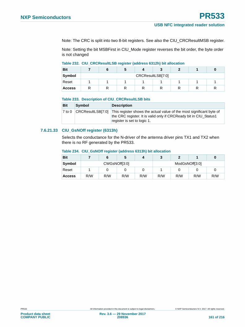
NXP Semiconductors PR533USB NFC integrated reader solution
Note: The CRC is split into two 8-bit registers. See also the CIU_CRCResultMSB register.
Note: Setting the bit MSBFirst in CIU_Mode register reverses the bit order, the byte order is not changed
7.6.21.33 CIU_GsNOff register (6313h)
Selects the conductance for the N-driver of the antenna driver pins TX1 and TX2 when there is no RF generated by the PR533.
Table 232. CIU_CRCResultLSB register (address 6312h) bit allocation
Bit 7 6 5 4 3 2 1 0
Symbol CRCResultLSB[7:0]
Reset 1 1 1 1 1 1 1 1
Access R R R R R R R R
Table 233. Description of CIU_CRCResultLSB bits
Bit Symbol Description
7 to 0 CRCResultLSB[7:0] This register shows the actual value of the most significant byte of the CRC register. It is valid only if CRCReady bit in CIU_Status1 register is set to logic 1.
Table 234. CIU_GsNOff register (address 6313h) bit allocation
Bit 7 6 5 4 3 2 1 0
Symbol CWGsNOff[3:0] ModGsNOff[3:0]
Reset 1 0 0 0 1 0 0 0
Access R/W R/W R/W R/W R/W R/W R/W R/W
PR533 All information provided in this document is subject to legal disclaimers. © NXP Semiconductors N.V. 2017. All rights reserved.
Product data sheetCOMPANY PUBLIC
Rev. 3.6 — 29 November 2017208936 161 of 216
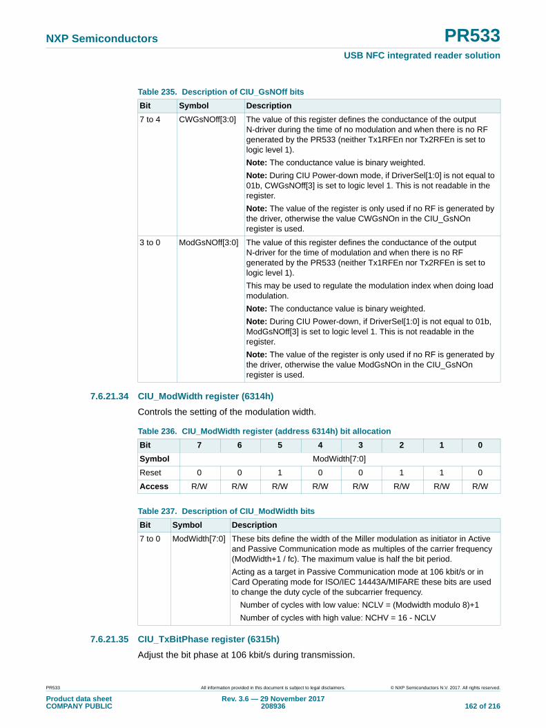
NXP Semiconductors PR533USB NFC integrated reader solution
7.6.21.34 CIU_ModWidth register (6314h)
Controls the setting of the modulation width.
7.6.21.35 CIU_TxBitPhase register (6315h)
Adjust the bit phase at 106 kbit/s during transmission.
Table 235. Description of CIU_GsNOff bits
Bit Symbol Description
7 to 4 CWGsNOff[3:0] The value of this register defines the conductance of the output N-driver during the time of no modulation and when there is no RF generated by the PR533 (neither Tx1RFEn nor Tx2RFEn is set to logic level 1).
Note: The conductance value is binary weighted.
Note: During CIU Power-down mode, if DriverSel[1:0] is not equal to 01b, CWGsNOff[3] is set to logic level 1. This is not readable in the register.
Note: The value of the register is only used if no RF is generated by the driver, otherwise the value CWGsNOn in the CIU_GsNOn register is used.
3 to 0 ModGsNOff[3:0] The value of this register defines the conductance of the output N-driver for the time of modulation and when there is no RF generated by the PR533 (neither Tx1RFEn nor Tx2RFEn is set to logic level 1).
This may be used to regulate the modulation index when doing load modulation.
Note: The conductance value is binary weighted.
Note: During CIU Power-down, if DriverSel[1:0] is not equal to 01b, ModGsNOff[3] is set to logic level 1. This is not readable in the register.
Note: The value of the register is only used if no RF is generated by the driver, otherwise the value ModGsNOn in the CIU_GsNOn register is used.
Table 236. CIU_ModWidth register (address 6314h) bit allocation
Bit 7 6 5 4 3 2 1 0
Symbol ModWidth[7:0]
Reset 0 0 1 0 0 1 1 0
Access R/W R/W R/W R/W R/W R/W R/W R/W
Table 237. Description of CIU_ModWidth bits
Bit Symbol Description
7 to 0 ModWidth[7:0] These bits define the width of the Miller modulation as initiator in Active and Passive Communication mode as multiples of the carrier frequency (ModWidth+1 / fc). The maximum value is half the bit period.
Acting as a target in Passive Communication mode at 106 kbit/s or in Card Operating mode for ISO/IEC 14443A/MIFARE these bits are used to change the duty cycle of the subcarrier frequency.
Number of cycles with low value: NCLV = (Modwidth modulo 8)+1
Number of cycles with high value: NCHV = 16 - NCLV
PR533 All information provided in this document is subject to legal disclaimers. © NXP Semiconductors N.V. 2017. All rights reserved.
Product data sheetCOMPANY PUBLIC
Rev. 3.6 — 29 November 2017208936 162 of 216
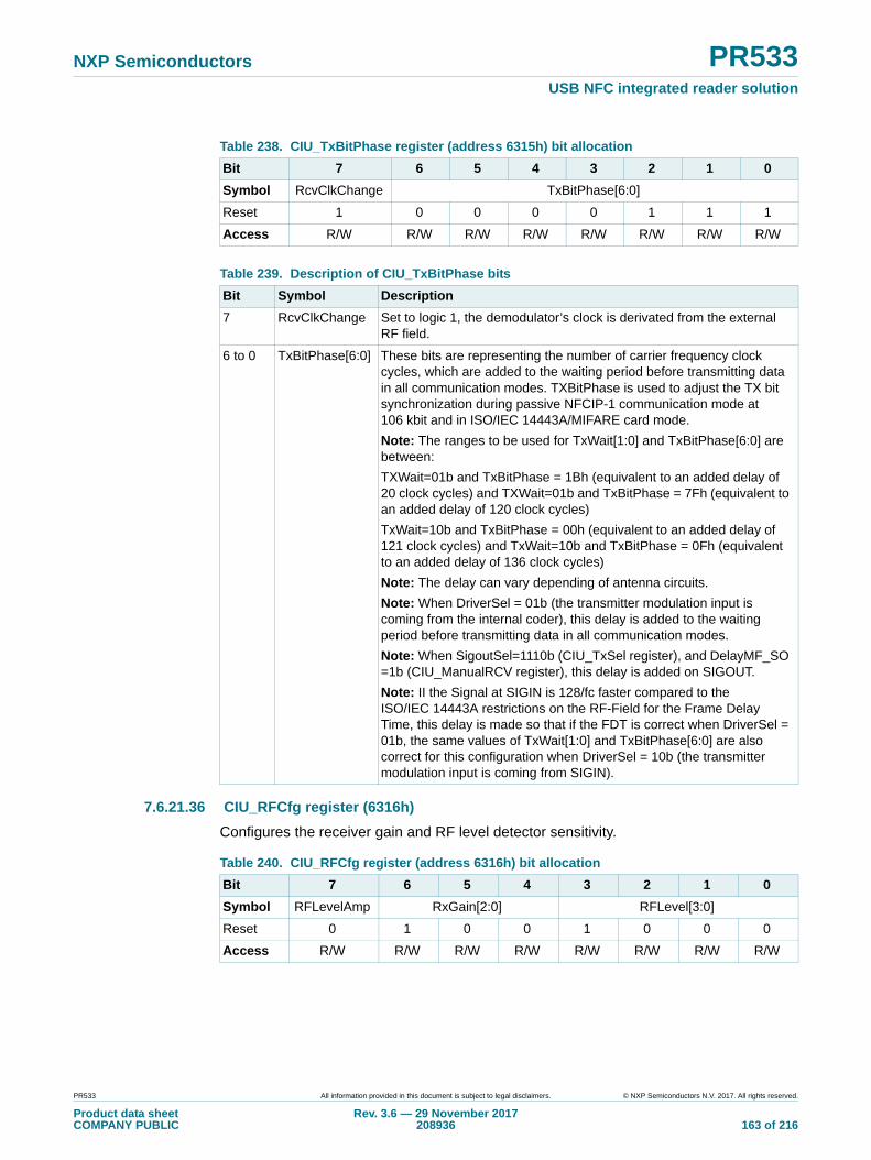
NXP Semiconductors PR533USB NFC integrated reader solution
7.6.21.36 CIU_RFCfg register (6316h)
Configures the receiver gain and RF level detector sensitivity.
Table 238. CIU_TxBitPhase register (address 6315h) bit allocation
Bit 7 6 5 4 3 2 1 0
Symbol RcvClkChange TxBitPhase[6:0]
Reset 1 0 0 0 0 1 1 1
Access R/W R/W R/W R/W R/W R/W R/W R/W
Table 239. Description of CIU_TxBitPhase bits
Bit Symbol Description
7 RcvClkChange Set to logic 1, the demodulator’s clock is derivated from the external RF field.
6 to 0 TxBitPhase[6:0] These bits are representing the number of carrier frequency clock cycles, which are added to the waiting period before transmitting data in all communication modes. TXBitPhase is used to adjust the TX bit synchronization during passive NFCIP-1 communication mode at 106 kbit and in ISO/IEC 14443A/MIFARE card mode.
Note: The ranges to be used for TxWait[1:0] and TxBitPhase[6:0] are between:
TXWait=01b and TxBitPhase = 1Bh (equivalent to an added delay of 20 clock cycles) and TXWait=01b and TxBitPhase = 7Fh (equivalent to an added delay of 120 clock cycles)
TxWait=10b and TxBitPhase = 00h (equivalent to an added delay of 121 clock cycles) and TxWait=10b and TxBitPhase = 0Fh (equivalent to an added delay of 136 clock cycles)
Note: The delay can vary depending of antenna circuits.
Note: When DriverSel = 01b (the transmitter modulation input is coming from the internal coder), this delay is added to the waiting period before transmitting data in all communication modes.
Note: When SigoutSel=1110b (CIU_TxSel register), and DelayMF_SO =1b (CIU_ManualRCV register), this delay is added on SIGOUT.
Note: II the Signal at SIGIN is 128/fc faster compared to the ISO/IEC 14443A restrictions on the RF-Field for the Frame Delay Time, this delay is made so that if the FDT is correct when DriverSel = 01b, the same values of TxWait[1:0] and TxBitPhase[6:0] are also correct for this configuration when DriverSel = 10b (the transmitter modulation input is coming from SIGIN).
Table 240. CIU_RFCfg register (address 6316h) bit allocation
Bit 7 6 5 4 3 2 1 0
Symbol RFLevelAmp RxGain[2:0] RFLevel[3:0]
Reset 0 1 0 0 1 0 0 0
Access R/W R/W R/W R/W R/W R/W R/W R/W
PR533 All information provided in this document is subject to legal disclaimers. © NXP Semiconductors N.V. 2017. All rights reserved.
Product data sheetCOMPANY PUBLIC
Rev. 3.6 — 29 November 2017208936 163 of 216
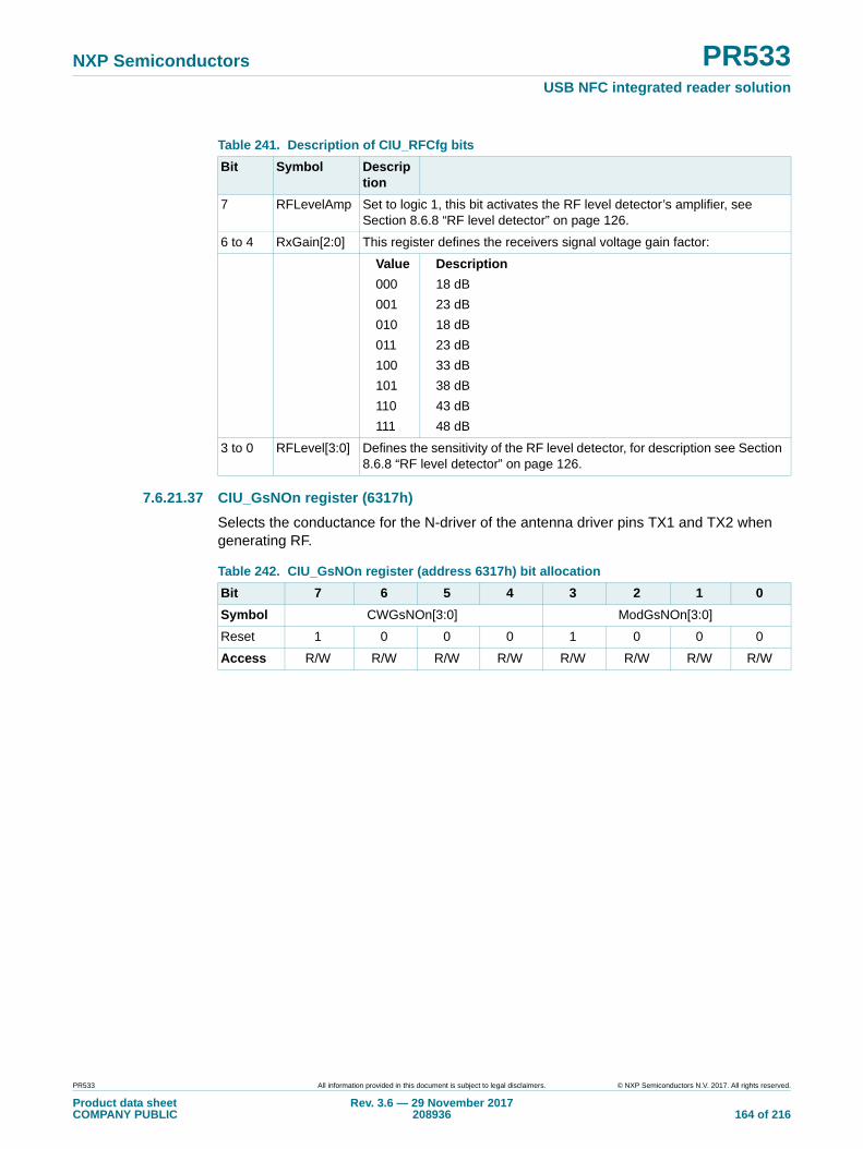
NXP Semiconductors PR533USB NFC integrated reader solution
7.6.21.37 CIU_GsNOn register (6317h)
Selects the conductance for the N-driver of the antenna driver pins TX1 and TX2 when generating RF.
Table 241. Description of CIU_RFCfg bits
Bit Symbol Description
7 RFLevelAmp Set to logic 1, this bit activates the RF level detector’s amplifier, see Section 8.6.8 “RF level detector” on page 126.
6 to 4 RxGain[2:0] This register defines the receivers signal voltage gain factor:
Value
000
001
010
011
100
101
110
111
Description
18 dB
23 dB
18 dB
23 dB
33 dB
38 dB
43 dB
48 dB
3 to 0 RFLevel[3:0] Defines the sensitivity of the RF level detector, for description see Section 8.6.8 “RF level detector” on page 126.
Table 242. CIU_GsNOn register (address 6317h) bit allocation
Bit 7 6 5 4 3 2 1 0
Symbol CWGsNOn[3:0] ModGsNOn[3:0]
Reset 1 0 0 0 1 0 0 0
Access R/W R/W R/W R/W R/W R/W R/W R/W
PR533 All information provided in this document is subject to legal disclaimers. © NXP Semiconductors N.V. 2017. All rights reserved.
Product data sheetCOMPANY PUBLIC
Rev. 3.6 — 29 November 2017208936 164 of 216

NXP Semiconductors PR533USB NFC integrated reader solution
7.6.21.38 CIU_CWGsP register (6318h)
Defines the conductance of the P-driver.
7.6.21.39 CIU_ModGsP register (6319h)
Defines the driver P-output conductance for the time of modulation.
Table 243. Description of CIU_GsNOn bits
Bit Symbol Description
7 to 4 CWGsNOn[3:0] The value of this register defines the conductance of the output N-driver. during times of no modulation and when the PR533 generates the RF field.
This may be used to regulate the output power and subsequently current consumption and operating distance.
Note: The conductance value is binary weighted.
Note: During CIU Power-down mode, if DriverSel[1:0] is not equal to 01b, CWGsNOn[3] is set to logic level 1. This is not readable in the register.
Note: The value of the register is only used if RF is generated by the driver (either Tx1RFEn or Tx2RFEn is set to logic level 1), otherwise the value CWGsNOFF in the register CIU_GsNOff is used.
3 to 0 ModGsNOn[3:0] The value of this register defines the conductance of the output N-driver for the time of modulation and when the PR533 generates the RF field.
This may be used to regulate the modulation index.
Note: The conductance value is binary weighted.
Note: During CIU Power-down mode, if DriverSel[1:0] is not equal to 01b, ModGsNOn[3] is set to logic level 1. This is not readable in the register.
Note: The value of the register is only used if RF is generated by the driver (either Tx1RFEn or Tx2RFEn is set to logic level 1), otherwise the value ModGsNOff in the register CIU_GsNOFF is used.
Table 244. CIU_CWGsP register (address 6318h) bit allocation
Bit 7 6 5 4 3 2 1 0
Symbol - - CWGsP[5:0]
Reset 0 0 1 0 0 0 0 0
Access R R R/W R/W R/W R/W R/W R/W
Table 245. Description of CIU_CWGsP bits
Bit Symbol Description
7 to 6 - Reserved.
5 to 0 CWGsP[5:0] The value of this register defines the conductance of the output P-driver, during times of no modulation.
This may be used to regulate the output power and subsequently current consumption and operating distance.
Note: The conductance value is binary weighted.
Note: During CIU Power-down mode, if DriverSel[1:0] is not equal to 01b, CWGsP[5] is set to logic level 1. This is not readable in the register.
PR533 All information provided in this document is subject to legal disclaimers. © NXP Semiconductors N.V. 2017. All rights reserved.
Product data sheetCOMPANY PUBLIC
Rev. 3.6 — 29 November 2017208936 165 of 216

NXP Semiconductors PR533USB NFC integrated reader solution
7.6.21.40 CIU_TMode register (631Ah)
Defines settings for the internal timer.
Table 246. CIU_ModGsP register (address 6319h) bit allocation
Bit 7 6 5 4 3 2 1 0
Symbol - - ModGsP[5:0]
Reset 0 0 1 0 0 0 0 0
Access R R R/W R/W R/W R/W R/W R/W
Table 247. Description of CIU_ModGsP bits
Bit Symbol Description
7 to 6 - Reserved.
5 to 0 ModGsP[5:0] The value of this register defines the conductance of the output P-driver for the time of modulation.
This may be used to regulate the modulation index.
Note: The conductance value is binary weighted.
Note: During CIU Power-down mode, if DriverSel[1:0] is not equal to 01b, ModGsP[5] is set to logic level 1. This is not readable in the register.
Note: If Force100ASK in CIU_TxAuto register is set to logic level 1, the ModGsP[5:0] setting has no effect.
Table 248. CIU_TMode register (address 631Ah) bit allocation
Bit 7 6 5 4 3 2 1 0
Symbol TAuto TGated[1:0] TAutoRestart TPrescaler_Hi[3:0]
Reset 0 0 0 0 0 0 0 0
Access R/W R/W R/W R/W R/W R/W R/W R/W
PR533 All information provided in this document is subject to legal disclaimers. © NXP Semiconductors N.V. 2017. All rights reserved.
Product data sheetCOMPANY PUBLIC
Rev. 3.6 — 29 November 2017208936 166 of 216

NXP Semiconductors PR533USB NFC integrated reader solution
7.6.21.41 CIU_TPrescaler register (631Bh)
Define the LSB of the Timer-Prescaler.
Table 249. Description of CIU_TMode bits
Bit Symbol Description
7 TAuto Set to logic 1, the timer starts automatically at the end of the transmission in all communication modes at all speed, or when InitialRFOn (in CIU_TxAuto) is set to logic 1 and the external RF field is switched on. The timer stops immediately after receiving the first data bit if RxMultiple in the CIU_RxMode register is set to logic level 0.
If RxMultiple is set to logic 1, the timer never stops. In this case the timer can be stopped by setting the bit TStopNow in register CIU_Control to 1.
Set to logic 0 indicates, that the timer is not influenced by the protocol.
6 to 5 TGated[1:0] The internal timer is running in gated mode.
Note: In the gated mode, the bit TRunning is logic level 1 when the timer is enabled by the register bits. This bit does not influence the gating signal
ValueDescription
00No gated mode
01Gated by SIGIN
10Gated by AUX1
11Reserved
4 TAutoRestart Set to logic 1 the timer automatically restart its count-down from TReloadValue defined within when reaches zero.
Set to logic 0 the timer decrements to zero and the bit TimerIRq is set to logic 1.
3 to 0 TPrescaler_Hi[3:0] Defines higher 4 bits for the TPrescaler.
The following formula is used to calculate fTimer:
For detailed description see Section 8.6.17 “CIU_timer” on page 140.
Note: TPreScaler is defined with TPreScaler_Hi[3:0] in this register and TPreScaler_LO[7:0] in CIU_TPrescaler.
fTimer 6,78MHz TPreScaler=
Table 250. CIU_TPrescaler register (address 631Bh) bit allocation
Bit 7 6 5 4 3 2 1 0
Symbol TPrescaler_LO[7:0]
Reset 0 0 0 0 0 0 0 0
Access R/W R/W R/W R/W R/W R/W R/W R/W
PR533 All information provided in this document is subject to legal disclaimers. © NXP Semiconductors N.V. 2017. All rights reserved.
Product data sheetCOMPANY PUBLIC
Rev. 3.6 — 29 November 2017208936 167 of 216

NXP Semiconductors PR533USB NFC integrated reader solution
7.6.21.42 CIU_TReload_hi register (631Ch)
Defines the MSB of the 16-bit long timer reload value.
7.6.21.43 CIU_TReloadVal_lo register (631Dh)
Defines the LSB of the 16 bit long timer reload value.
7.6.21.44 CIU_TCounterVal_hi register (631Eh)
Defines the MSB byte of the current value of the timer.
Table 251. Description of CIU_TPrescaler bits
Bit Symbol Description
7 to 0 TPrescaler_LO[7:0] Defines lower 8 bits for TPrescaler.
The following formula is used to calculate fTimer
For detailed description see Section 8.6.17 “CIU_timer” on page 140.
Note: The TPreScaler time is defined with TPreScaler_Hi[3:0] in CIU_TMode and TPreScaler_LO[7:0] in this register.
fTimer 6,78MHz TPreScaler=
Table 252. CIU_TReloadVal_hi register (address 631Ch) bit allocation
Bit 7 6 5 4 3 2 1 0
Symbol TReloadVal_Hi[7:0]
Reset 0 0 0 0 0 0 0 0
Access R/W R/W R/W R/W R/W R/W R/W R/W
Table 253. Description of CIU_TReloadVal_hi bits
Bit Symbol Description
7 to 0 TReloadVal_Hi[7:0] Defines the higher 8 bits for the TReloadValue.
With a start event the timer loads with the TReloadValue. Changing this register affects the timer only with the next start event.
Note: The reload value is defined with TReloadVal_Hi[7:0] in this register and TReloadVal_Lo[7:0] in CIU_TReloadVal_lo
Table 254. CIU_TReload_lo register (address 631Dh) bit allocation
Bit 7 6 5 4 3 2 1 0
Symbol TReloadVal_Lo[7:0]
Reset 0 0 0 0 0 0 0 0
Access R/W R/W R/W R/W R/W R/W R/W R/W
Table 255. Description of CIU_TReload_lo bits
Bit Symbol Description
7 to 0 TReloadVal_Lo[7:0] Defines the lower 8 bits for the TReloadValue.
With a start event the timer loads with the TReloadValue. Changing this register affects the timer only with the next start event.
Note: The reload value is defined with TReloadVal_Lo[7:0] in this register and TReloadVal_Hi[7:0] in CIU_TReload_Hi.
PR533 All information provided in this document is subject to legal disclaimers. © NXP Semiconductors N.V. 2017. All rights reserved.
Product data sheetCOMPANY PUBLIC
Rev. 3.6 — 29 November 2017208936 168 of 216
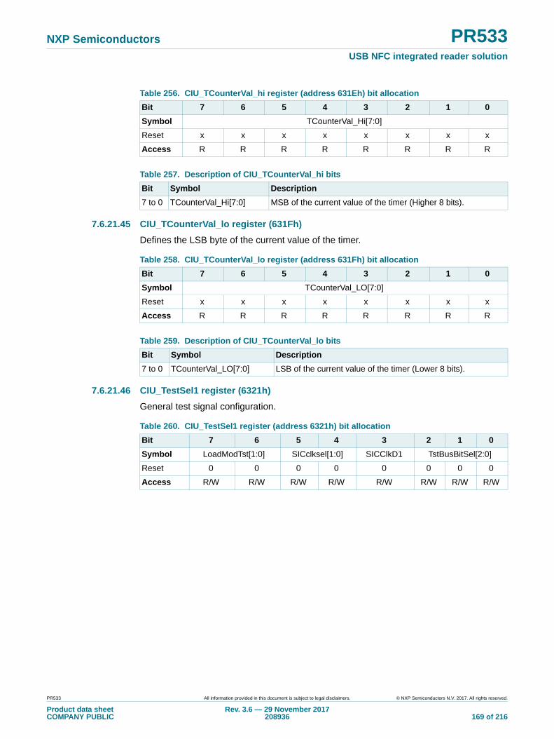
NXP Semiconductors PR533USB NFC integrated reader solution
7.6.21.45 CIU_TCounterVal_lo register (631Fh)
Defines the LSB byte of the current value of the timer.
7.6.21.46 CIU_TestSel1 register (6321h)
General test signal configuration.
Table 256. CIU_TCounterVal_hi register (address 631Eh) bit allocation
Bit 7 6 5 4 3 2 1 0
Symbol TCounterVal_Hi[7:0]
Reset x x x x x x x x
Access R R R R R R R R
Table 257. Description of CIU_TCounterVal_hi bits
Bit Symbol Description
7 to 0 TCounterVal_Hi[7:0] MSB of the current value of the timer (Higher 8 bits).
Table 258. CIU_TCounterVal_lo register (address 631Fh) bit allocation
Bit 7 6 5 4 3 2 1 0
Symbol TCounterVal_LO[7:0]
Reset x x x x x x x x
Access R R R R R R R R
Table 259. Description of CIU_TCounterVal_lo bits
Bit Symbol Description
7 to 0 TCounterVal_LO[7:0] LSB of the current value of the timer (Lower 8 bits).
Table 260. CIU_TestSel1 register (address 6321h) bit allocation
Bit 7 6 5 4 3 2 1 0
Symbol LoadModTst[1:0] SICclksel[1:0] SICClkD1 TstBusBitSel[2:0]
Reset 0 0 0 0 0 0 0 0
Access R/W R/W R/W R/W R/W R/W R/W R/W
PR533 All information provided in this document is subject to legal disclaimers. © NXP Semiconductors N.V. 2017. All rights reserved.
Product data sheetCOMPANY PUBLIC
Rev. 3.6 — 29 November 2017208936 169 of 216

NXP Semiconductors PR533USB NFC integrated reader solution
7.6.21.47 CIU_TestSel2 register (6322h)
General test signal configuration and PRBS control.
Table 261. Description of CIU_TestSel1 bits
Bit Symbol Description
7 to 6 LoadModTst[1:0] Defines the test signal for the LOADMOD pin
Note: The bits LoadModSel in register CIU_TxSel has to be set to logic 1 to enable LoadModTst:
ValueDescription
00Low
01High
10RFU
11TstBusBit as defined by the TestBusBitSel bit of this register
5 to 4 SICclksel[1:0] Defines the source for the 13.56 MHz secure IC clock
ValueDescription
00GND - secure IC clock is switched off
01Clock derivated by the internal oscillator
10Internal CIU clock
11Clock derivated from the RF Field
3 SICClkD1 Set to logic 1, the secure IC clock is delivered to P31 / UART_TX if the observe_ciu bit is set to logic 1.
2 to 0 TstBusBitSel(2:0] Select the TstBusBit from the test bus.
Table 262. CIU_TestSel2 register (address 6322h) bit allocation
Bit 7 6 5 4 3 2 1 0
Symbol TstBusFlip PRBS9 PRBS15 TstBusSel[4:0]
Reset 0 0 0 0 0 0 0 0
Access R/W R/W R/W R/W R/W R/W R/W R/W
Table 263. Description of CIU_TestSel2 bits
Bit Symbol Description
7 TstBusFlip If set to logic 1, the internal test bus(D6-D0) is mapped to the external test bus pins by the following order: D4,D3, D2,D6,D5, D0, D1. See Section 8.6.21.2 “CIU test bus” on page 151.
6 PRBS9 Starts and enables the PRBS9 sequence according ITU-TO150.
Note: All relevant register to transmit data have to be configured before entering PRBS9 mode.
Note: The data transmission of the defined sequence is started by the Transmit command.
5 PRBS15 Starts and enables the PRBS15 sequence according ITU-TO150.
Note: All relevant register to transmit data have to be configured before entering PRBS15 mode.
Note: The data transmission of the defined sequence is started by the Transmit command.
4 to 0 TstBusSel[4:0] Selects the test bus source. See Section 8.6.21.2 “CIU test bus” on page 151.
PR533 All information provided in this document is subject to legal disclaimers. © NXP Semiconductors N.V. 2017. All rights reserved.
Product data sheetCOMPANY PUBLIC
Rev. 3.6 — 29 November 2017208936 170 of 216
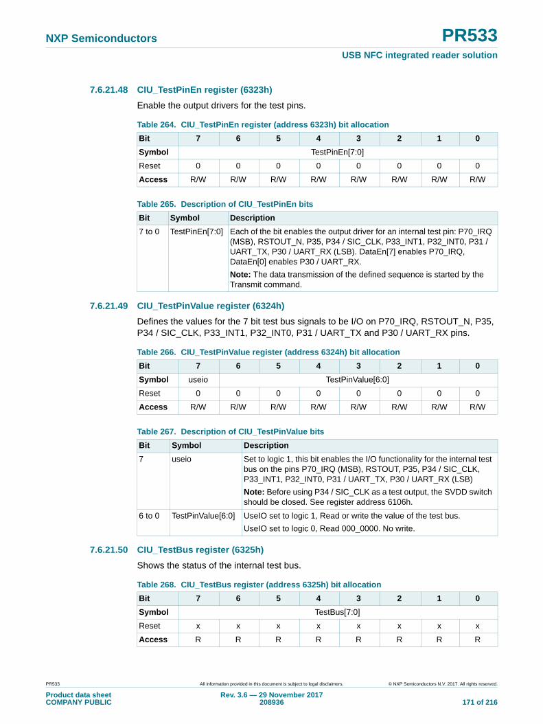
NXP Semiconductors PR533USB NFC integrated reader solution
7.6.21.48 CIU_TestPinEn register (6323h)
Enable the output drivers for the test pins.
7.6.21.49 CIU_TestPinValue register (6324h)
Defines the values for the 7 bit test bus signals to be I/O on P70_IRQ, RSTOUT_N, P35, P34 / SIC_CLK, P33_INT1, P32_INT0, P31 / UART_TX and P30 / UART_RX pins.
7.6.21.50 CIU_TestBus register (6325h)
Shows the status of the internal test bus.
Table 264. CIU_TestPinEn register (address 6323h) bit allocation
Bit 7 6 5 4 3 2 1 0
Symbol TestPinEn[7:0]
Reset 0 0 0 0 0 0 0 0
Access R/W R/W R/W R/W R/W R/W R/W R/W
Table 265. Description of CIU_TestPinEn bits
Bit Symbol Description
7 to 0 TestPinEn[7:0] Each of the bit enables the output driver for an internal test pin: P70_IRQ (MSB), RSTOUT_N, P35, P34 / SIC_CLK, P33_INT1, P32_INT0, P31 / UART_TX, P30 / UART_RX (LSB). DataEn[7] enables P70_IRQ, DataEn[0] enables P30 / UART_RX.
Note: The data transmission of the defined sequence is started by the Transmit command.
Table 266. CIU_TestPinValue register (address 6324h) bit allocation
Bit 7 6 5 4 3 2 1 0
Symbol useio TestPinValue[6:0]
Reset 0 0 0 0 0 0 0 0
Access R/W R/W R/W R/W R/W R/W R/W R/W
Table 267. Description of CIU_TestPinValue bits
Bit Symbol Description
7 useio Set to logic 1, this bit enables the I/O functionality for the internal test bus on the pins P70_IRQ (MSB), RSTOUT, P35, P34 / SIC_CLK, P33_INT1, P32_INT0, P31 / UART_TX, P30 / UART_RX (LSB)
Note: Before using P34 / SIC_CLK as a test output, the SVDD switch should be closed. See register address 6106h.
6 to 0 TestPinValue[6:0] UseIO set to logic 1, Read or write the value of the test bus.
UseIO set to logic 0, Read 000_0000. No write.
Table 268. CIU_TestBus register (address 6325h) bit allocation
Bit 7 6 5 4 3 2 1 0
Symbol TestBus[7:0]
Reset x x x x x x x x
Access R R R R R R R R
PR533 All information provided in this document is subject to legal disclaimers. © NXP Semiconductors N.V. 2017. All rights reserved.
Product data sheetCOMPANY PUBLIC
Rev. 3.6 — 29 November 2017208936 171 of 216
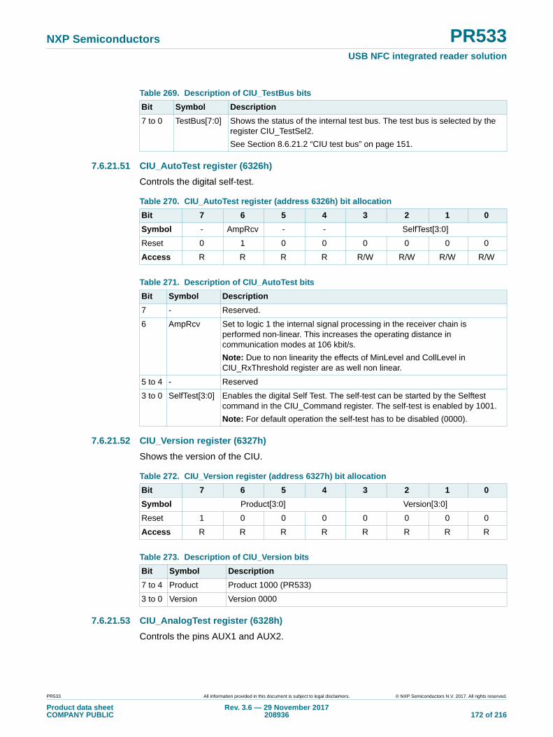
NXP Semiconductors PR533USB NFC integrated reader solution
7.6.21.51 CIU_AutoTest register (6326h)
Controls the digital self-test.
7.6.21.52 CIU_Version register (6327h)
Shows the version of the CIU.
7.6.21.53 CIU_AnalogTest register (6328h)
Controls the pins AUX1 and AUX2.
Table 269. Description of CIU_TestBus bits
Bit Symbol Description
7 to 0 TestBus[7:0] Shows the status of the internal test bus. The test bus is selected by the register CIU_TestSel2.
See Section 8.6.21.2 “CIU test bus” on page 151.
Table 270. CIU_AutoTest register (address 6326h) bit allocation
Bit 7 6 5 4 3 2 1 0
Symbol - AmpRcv - - SelfTest[3:0]
Reset 0 1 0 0 0 0 0 0
Access R R R R R/W R/W R/W R/W
Table 271. Description of CIU_AutoTest bits
Bit Symbol Description
7 - Reserved.
6 AmpRcv Set to logic 1 the internal signal processing in the receiver chain is performed non-linear. This increases the operating distance in communication modes at 106 kbit/s.
Note: Due to non linearity the effects of MinLevel and CollLevel in CIU_RxThreshold register are as well non linear.
5 to 4 - Reserved
3 to 0 SelfTest[3:0] Enables the digital Self Test. The self-test can be started by the Selftest command in the CIU_Command register. The self-test is enabled by 1001.
Note: For default operation the self-test has to be disabled (0000).
Table 272. CIU_Version register (address 6327h) bit allocation
Bit 7 6 5 4 3 2 1 0
Symbol Product[3:0] Version[3:0]
Reset 1 0 0 0 0 0 0 0
Access R R R R R R R R
Table 273. Description of CIU_Version bits
Bit Symbol Description
7 to 4 Product Product 1000 (PR533)
3 to 0 Version Version 0000
PR533 All information provided in this document is subject to legal disclaimers. © NXP Semiconductors N.V. 2017. All rights reserved.
Product data sheetCOMPANY PUBLIC
Rev. 3.6 — 29 November 2017208936 172 of 216

NXP Semiconductors PR533USB NFC integrated reader solution
Table 274. CIU_AnalogTest register (address 6328h) bit allocation
Bit 7 6 5 4 3 2 1 0
Symbol AnalogSelAux1[3:0] AnalogSelAux2[3:0]
Reset 0 0 0 0 0 0 0 0
Access R/W R/W R/W R/W R/W R/W R/W R/W
Table 275. Description of CIU_AnalogTest bits
Bit Symbol Description
7 to 4 AnalogSelAux1[3:0] Controls the AUX1 pin. Note: All test signals are described in Section 8.6.21.3 “Test signals at pin AUX” on page 152.
0000 Tristate
0001 DAC output: register CIU_TestDAC1[1]
0010 DAC output: test signal corr1[1]
0011 DAC output: test signal corr2[1]
0100 DAC output: test signal MinLevel[1]
0101 DAC output: ADC_I[1]
0110 DAC output: ADC_Q[1]
0111 DAC output: ADC_I combined with ADC_Q[1]
1000 Test signal for production test
1001 secure IC clock
1010 ErrorBusBit as described in Table 173 on page 138
1011 Low
1100 TxActive
At 106 kbit/s: High during Start bit, Data bits, Parity and CRCAt 212 kbit/s and 424 kbit/s: High during Preamble, Sync, Data bits and CRC
1101 RxActive
At 106 kbit/s: High during Data bits, Parity and CRCAt 212 kbit/s and 424 kbit/s: High during Data bits and CRC
1110 Subcarrier detected
At 106 kbit/s: not applicableAt 212 kbit/s and 424 kbit/s: High during last part of preamble, Sync, Data bits and CRC.
1111 Test bus bit as defined by the TstBusBitSel in Table 261 on page 170
PR533 All information provided in this document is subject to legal disclaimers. © NXP Semiconductors N.V. 2017. All rights reserved.
Product data sheetCOMPANY PUBLIC
Rev. 3.6 — 29 November 2017208936 173 of 216

NXP Semiconductors PR533USB NFC integrated reader solution
[1] Current output. The use of 1 k pull down resistor on AUX1 is recommended.
[2] Current output. The use of 1 k pull down resistor on AUX2 is recommended.
7.6.21.54 CIU_TestDAC1 register (6329h)
Defines the test value for TestDAC1.
3 to 0 AnalogSelAux2[3:0] Controls the AUX2 pin. Note: All test signals are described in Section 8.6.21.3 “Test signals at pin AUX” on page 152.
0000 Tristate
0001 DAC output: register CIU_TestDAC2[2]
0010 DAC output: test signal corr1[2]
0011 DAC output: test signal corr2[2]
0100 DAC output: test signal MinLevel[2]
0101 DAC output: ADC_I[2]
0110 DAC output: ADC_Q[2]
0111 DAC output: ADC_I combined with ADC_Q[2]
1000 Test signal for production test
1001 secure IC clock
1010 ErrorBusBit as described in Table 173 on page 138
1011 Low
1100 TxActive
At 106 kbit/s: High during Start bit, Data bits, Parity and CRCAt 212 kbit/s and 424 kbit/s: High during Preamble, Sync, Data bits and CRC
1101 RxActive
At 106 kbit/s: High during Data bits, Parity and CRCAt 212 kbit/s and 424 kbit/s: High during Data bits and CRC
1110 Subcarrier detected
At 106 kbit/s: not applicableAt 212 kbit/s and 424 kbit/s: High during last part of preamble, Sync, Data bits and CRC.
1111 Test bus bit as defined by the TstBusBitSel in Table 260 on page 169
Table 275. Description of CIU_AnalogTest bits …continued
Bit Symbol Description
Table 276. CIU_TestDAC1 register (address 6329h) bit allocation
Bit 7 6 5 4 3 2 1 0
Symbol - - TestDAC1[5:0]
Reset 0 0 X X X X X X
Access R R R/W R/W R/W R/W R/W R/W
PR533 All information provided in this document is subject to legal disclaimers. © NXP Semiconductors N.V. 2017. All rights reserved.
Product data sheetCOMPANY PUBLIC
Rev. 3.6 — 29 November 2017208936 174 of 216

NXP Semiconductors PR533USB NFC integrated reader solution
7.6.21.55 CIU_TestDAC2 register (632Ah)
Defines the test value for TestDAC2.
7.6.21.56 CIU_TestADC register (632Bh)
Shows the actual value of ADC I and Q channel.
7.6.21.57 CIU_RFlevelDet register (632Fh)
Power down of the RF level detector.
Table 277. Description of CIU_TestDAC1 bits
Bit Symbol Description
7 to 6 - Reserved.
5 to 0 TestDAC1[5:0] Defines the test value for TestDAC1. The output of the DAC1 can be switched to AUX1 by setting AnalogSelAux1 to 0001 in the CIU_AnalogTest register.
Table 278. CIU_TestDAC2 register (address 632Ah) bit allocation
Bit 7 6 5 4 3 2 1 0
Symbol - - TestDAC2[6:0]
Reset 0 0 X X X X X X
Access R R R/W R/W R/W R/W R/W R/W
Table 279. Description of CIU_TestDAC2 bits
Bit Symbol Description
7 to 6 - Reserved.
5 to 0 TestDAC2[6:0] Defines the test value for TestDAC2. The output of the DAC2 can be switched to AUX2 by setting AnalogSelAux2 to 0001 in the CIU_AnalogTest register.
Table 280. CIU_TestADC register (address 632Bh) bit allocation
Bit 7 6 5 4 3 2 1 0
Symbol ADC_I[3:0] ADC_Q[3:0]
Reset X X X X X X X X
Access R R R R R R R R
Table 281. Description of CIU_TestADC bits
Bit Symbol Description
7 to 4 ADC_I[3:0] Shows the actual value of ADC I channel.
3 to 0 ADC_Q[3:0] Shows the actual value of ADC Q channel.
Table 282. CIU_RFlevelDet register (address 632Fh) bit allocation
Bit 7 6 5 4 3 2 1 0
Symbol - - - pd_rflvldet - - - -
Reset 0 0 0 0 0 0 0 0
Access R/W R/W R/W R/W R/W R/W R/W R/W
PR533 All information provided in this document is subject to legal disclaimers. © NXP Semiconductors N.V. 2017. All rights reserved.
Product data sheetCOMPANY PUBLIC
Rev. 3.6 — 29 November 2017208936 175 of 216

NXP Semiconductors PR533USB NFC integrated reader solution
Table 283. Description of CIU_RFlevelDet bits
Bit Symbol Description
7 to 5 - Reserved. These bits must be set to logic level 0.
4 pd_rfleveldet Power down of the RF level detector.
When set to logic 1, the RF level detector is in power down mode.
3 to 0 - Reserved. These bits must be set to logic level 0.
PR533 All information provided in this document is subject to legal disclaimers. © NXP Semiconductors N.V. 2017. All rights reserved.
Product data sheetCOMPANY PUBLIC
Rev. 3.6 — 29 November 2017208936 176 of 216
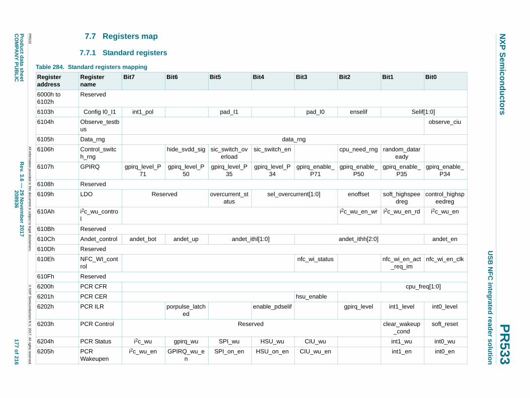
xxxxxxxxxxxxxxxxxxxxx xxxxxxxxxxxxxxxxxxxxxxxxxx xxxxxxx x x x xxxxxxxxxxxxxxxxxxxxxxxxxxxxxx xxxxxxxxxxxxxxxxxxx xx xx xxxxx xxxxxxxxxxxxxxxxxxxxxxxxxxx xxxxxxxxxxxxxxxxxxx xxxxxx xxxxxxxxxxxxxxxxxxxxxxxxxxxxxxxxxxx xxxxxxxxxxxx x x xxxxxxxxxxxxxxxxxxxxx xxxxxxxxxxxxxxxxxxxxxxxxxxxxxx xxxxx xxxxxxxxxxxxxxxxxxxxxxxxxxxxxxxxxxxxxxxxxxxxxxxxxx xxxxxxxx xxxxxxxxxxxxxxxxxxxxxxxxx xxxxxxxxxxxxxxxxxxxx xxx
PR
533
Pro
du
ct data sh
eetC
OM
PA
NY
PU
BL
ICR
ev. 3.6 —
29 N
ove
mb
er 2
017208936
177 of 216
NX
P S
emico
nd
ucto
rsP
R533
US
B N
FC
integ
rated read
er solu
tion
7.7 Registers map
7.7.1 Standard registers
Bit1 Bit0
Selif[1:0]
observe_ciu
ng random_dataready
e_ gpirq_enable_P35
gpirq_enable_P34
soft_highspeedreg
control_highspeedreg
wr i2c_wu_en_rd i2c_wu_en
:0] andet_en
nfc_wi_en_act_req_im
nfc_wi_en_clk
cpu_freq[1:0]
l int1_level int0_level
clear_wakeup_cond
soft_reset
int1_wu int0_wu
int1_en int0_en
All inform
ation provided
in this docum
ent is subject to leg
al disclaim
ers.©
NX
P S
em
iconductors N
.V. 2017. A
ll rights rese
rved.
Table 284. Standard registers mapping
Registeraddress
Register name
Bit7 Bit6 Bit5 Bit4 Bit3 Bit2
6000h to 6102h
Reserved
6103h Config I0_I1 int1_pol pad_I1 pad_I0 enselif
6104h Observe_testbus
6105h Data_rng data_rng
6106h Control_switch_rng
hide_svdd_sig sic_switch_overload
sic_switch_en cpu_need_r
6107h GPIRQ gpirq_level_P71
gpirq_level_P50
gpirq_level_P35
gpirq_level_P34
gpirq_enable_P71
gpirq_enablP50
6108h Reserved
6109h LDO Reserved overcurrent_status
sel_overcurrent[1:0] enoffset
610Ah i2c_wu_control
i2c_wu_en_
610Bh Reserved
610Ch Andet_control andet_bot andet_up andet_ithl[1:0] andet_ithh[2
610Dh Reserved
610Eh NFC_WI_control
nfc_wi_status
610Fh Reserved
6200h PCR CFR
6201h PCR CER hsu_enable
6202h PCR ILR porpulse_latched
enable_pdselif gpirq_leve
6203h PCR Control Reserved
6204h PCR Status i2c_wu gpirq_wu SPI_wu HSU_wu CIU_wu
6205h PCR Wakeupen
i2c_wu_en GPIRQ_wu_en
SPI_on_en HSU_on_en CIU_wu_en

xxxxxxxxxxxxxxxxxxxxx xxxxxxxxxxxxxxxxxxxxxxxxxx xxxxxxx x x x xxxxxxxxxxxxxxxxxxxxxxxxxxxxxx xxxxxxxxxxxxxxxxxxx xx xx xxxxx xxxxxxxxxxxxxxxxxxxxxxxxxxx xxxxxxxxxxxxxxxxxxx xxxxxx xxxxxxxxxxxxxxxxxxxxxxxxxxxxxxxxxxx xxxxxxxxxxxx x x xxxxxxxxxxxxxxxxxxxxx xxxxxxxxxxxxxxxxxxxxxxxxxxxxxx xxxxx xxxxxxxxxxxxxxxxxxxxxxxxxxxxxxxxxxxxxxxxxxxxxxxxxx xxxxxxxx xxxxxxxxxxxxxxxxxxxxxxxxx xxxxxxxxxxxxxxxxxxxx xxx
PR
533
Pro
du
ct data sh
eetC
OM
PA
NY
PU
BL
ICR
ev. 3.6 —
29 N
ove
mb
er 2
017208936
178 of 216
NX
P S
emico
nd
ucto
rsP
R533
US
B N
FC
integ
rated read
er solu
tion
ff CRCPreset[1:0]
TxFraming[1:0]
RxFraming[1:0]
Tx2RFEn Tx1RFEn
Tx2RFAutoEn Tx1RFAutoEn
utSel[3:0]
Collevel[2:0]
TauSync[1:0]
TxWait[1:0]
F HPCF[1:0]
TxEGT[1:0]
sNOff[3:0]
Level[3:0]
Table 284. Standard registers mapping …continued
Registeraddress
Register name
Bit7 Bit6 Bit5 Bit4 Bit3 Bit2 Bit1 Bit0
All inform
ation provided
in this docum
ent is subject to leg
al disclaim
ers.©
NX
P S
em
iconductors N
.V. 2017. A
ll rights rese
rved.
6206h to 6300h
Reserved
6301h CIU_Mode MSBFirst DetectSync TXWaitRF RxWaitRF PolSigin ModeDetO
6302h CIU_TxMode TxCRCEn TxSpeed[2:0] InvMod TxMix
6303h CIU_RxMode RXCRCEn RxSpeed[2:0] RxNoErr RxMultiple
6304h CIU_TxControl
InvTx2RFon InvTx1RFon InvTx2RFoff InvTx1RFoff Tx2CW CheckRF
6305h CIU_TxAuto AutoRFOFF Force100ASK AutoWakeUp CAOn InitialRFOn
6306h CIU_TxSel LoadModSel[1:0] DriverSel[1:0] SigO
6307h CIU_RxSel UartSel[1:0] RxWait[5:0]
6308h CIU_RxThreshold
MinLevel[3:0]
6309h CIU_Demod AddIQ[1:0] FixIQ TauRcv[1:0]
630Ah CIU_FelNFC1 FelSyncLen[1:0] DataLenMin[5:0]
630Bh CIU_FelNFC2 WaitForSelected
ShortTimeSlot DataLenMax[5:0]
630Ch CIU_MifNFC SensMiller[2:0] TauMiller[1:0] MFHalted
630Dh CIU_ManualRCV
FastFiltMF_SO
DelayMF_SO ParityDisable LargeBWPLL ManualHPC
630Eh CIU_TypeB RxSOFReq RxEOFReq Reserved EOFSOFWidth
NoTxSOF NoTxEOF
630Fh to 6310h
Reserved
6311h CIU_CRCResultMSB
CRCResultMSB[7:0]
6312h CIU_CRCResultLSB
CRCResultLSB[7:0]
6313h CIU_GsNOff CWGsNOff[3:0] ModG
6314h CIU_ModWidth
ModWidth[7:0]
6315h CIU_TxBitPhase
RcvClkChange
TxBitPhase[6:0]
6316h CIU_RFCfg RFLevelAmp RxGain[2:0] RF

xxxxxxxxxxxxxxxxxxxxx xxxxxxxxxxxxxxxxxxxxxxxxxx xxxxxxx x x x xxxxxxxxxxxxxxxxxxxxxxxxxxxxxx xxxxxxxxxxxxxxxxxxx xx xx xxxxx xxxxxxxxxxxxxxxxxxxxxxxxxxx xxxxxxxxxxxxxxxxxxx xxxxxx xxxxxxxxxxxxxxxxxxxxxxxxxxxxxxxxxxx xxxxxxxxxxxx x x xxxxxxxxxxxxxxxxxxxxx xxxxxxxxxxxxxxxxxxxxxxxxxxxxxx xxxxx xxxxxxxxxxxxxxxxxxxxxxxxxxxxxxxxxxxxxxxxxxxxxxxxxx xxxxxxxx xxxxxxxxxxxxxxxxxxxxxxxxx xxxxxxxxxxxxxxxxxxxx xxx
PR
533
Pro
du
ct data sh
eetC
OM
PA
NY
PU
BL
ICR
ev. 3.6 —
29 N
ove
mb
er 2
017208936
179 of 216
NX
P S
emico
nd
ucto
rsP
R533
US
B N
FC
integ
rated read
er solu
tion
sNOn[3:0]
caler_Hi[3:0]
TstBusBitSel[2:0]
:0]
lfTest[3:0]
ersion
SelAux2[3:0]
]
Table 284. Standard registers mapping …continued
Registeraddress
Register name
Bit7 Bit6 Bit5 Bit4 Bit3 Bit2 Bit1 Bit0
All inform
ation provided
in this docum
ent is subject to leg
al disclaim
ers.©
NX
P S
em
iconductors N
.V. 2017. A
ll rights rese
rved.
6317h CIU_GsNOn CWGsNOn[3:0] ModG
6318h CIU_CWGsP Reserved CWGsP[5:0]
6319h CIU_ModGsP Reserved ModGsP[5:0]
631Ah CIU_TMode TAuto TGated[1:0] TAutoRestart TPres
631Bh CIU_TPrescaler
TPrescaler_LO[7:0]
631Ch CIU_TReloadVal_Hi
TReloadVal_Hi[7:0]
631Dh CIU_TReloadVal_Lo
TReloadVal_Lo[7:0]
631Eh CIU_TCounterVal_hi
TCounterVal_Hi[7:0]
631Fh CIU_TCounterVal_lo
TCounterVal_LO[7:0]
6320h Reserved
6321h CIU_TestSel1 LoadModTst[1:0] SICclksel[1:0] SICClkD1
6322h CIU_TestSel2 TstBusFlip PRBS9 PRBS15 TstBusSel[4
6323h CIU_TestPinEn
TestPinEn[7:0]
6324h CIU_TestPinValue
useio TestPinValue[6:0]
6325h CIU_TestBus TestBus[7:0]
6326h CIU_AutoTest Reserved AmpRcv Reserved Se
6327h CIU_Version Product V
6328h CIU_AnalogTest
AnalogSelAux1[3:0] Analog
6329h CIU_TestDAC1
Reserved TestDAC1[5:0]
632Ah CIU_TestDAC2
Reserved TestDAC2[5:0]
632Bh CIU_TestADC ADC_I[3:0] ADC_Q[3:0
632Ch to 632Eh
Reserved
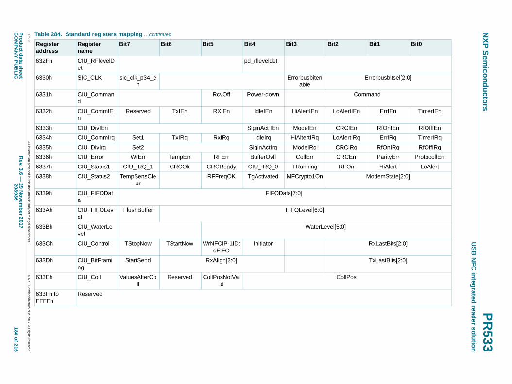
xxxxxxxxxxxxxxxxxxxxx xxxxxxxxxxxxxxxxxxxxxxxxxx xxxxxxx x x x xxxxxxxxxxxxxxxxxxxxxxxxxxxxxx xxxxxxxxxxxxxxxxxxx xx xx xxxxx xxxxxxxxxxxxxxxxxxxxxxxxxxx xxxxxxxxxxxxxxxxxxx xxxxxx xxxxxxxxxxxxxxxxxxxxxxxxxxxxxxxxxxx xxxxxxxxxxxx x x xxxxxxxxxxxxxxxxxxxxx xxxxxxxxxxxxxxxxxxxxxxxxxxxxxx xxxxx xxxxxxxxxxxxxxxxxxxxxxxxxxxxxxxxxxxxxxxxxxxxxxxxxx xxxxxxxx xxxxxxxxxxxxxxxxxxxxxxxxx xxxxxxxxxxxxxxxxxxxx xxx
PR
533
Pro
du
ct data sh
eetC
OM
PA
NY
PU
BL
ICR
ev. 3.6 —
29 N
ove
mb
er 2
017208936
180 of 216
NX
P S
emico
nd
ucto
rsP
R533
US
B N
FC
integ
rated read
er solu
tion
Errorbusbitsel[2:0]
ommand
ErrIEn TimerIEn
RfOnIEn RfOffIEn
ErrIRq TimerIRq
RfOnIRq RfOffIRq
ParityErr ProtocollErr
HiAlert LoAlert
ModemState[2:0]
RxLastBits[2:0]
TxLastBits[2:0]
Table 284. Standard registers mapping …continued
Registeraddress
Register name
Bit7 Bit6 Bit5 Bit4 Bit3 Bit2 Bit1 Bit0
All inform
ation provided
in this docum
ent is subject to leg
al disclaim
ers.©
NX
P S
em
iconductors N
.V. 2017. A
ll rights rese
rved.
632Fh CIU_RFlevelDet
pd_rfleveldet
6330h SIC_CLK sic_clk_p34_en
Errorbusbitenable
6331h CIU_Command
RcvOff Power-down C
6332h CIU_CommIEn
Reserved TxIEn RXIEn IdleIEn HiAlertIEn LoAlertIEn
6333h CIU_DivIEn SiginAct IEn ModeIEn CRCIEn
6334h CIU_CommIrq Set1 TxIRq RxIRq IdleIrq HiAltertIRq LoAlertIRq
6335h CIU_DivIrq Set2 SiginActIrq ModeIRq CRCIRq
6336h CIU_Error WrErr TempErr RFErr BufferOvfl CollErr CRCErr
6337h CIU_Status1 CIU_IRQ_1 CRCOk CRCReady CIU_IRQ_0 TRunning RFOn
6338h CIU_Status2 TempSensClear
RFFreqOK TgActivated MFCrypto1On
6339h CIU_FIFOData
FIFOData[7:0]
633Ah CIU_FIFOLevel
FlushBuffer FIFOLevel[6:0]
633Bh CIU_WaterLevel
WaterLevel[5:0]
633Ch CIU_Control TStopNow TStartNow WrNFCIP-1IDtoFIFO
Initiator
633Dh CIU_BitFraming
StartSend RxAlign[2:0]
633Eh CIU_Coll ValuesAfterColl
Reserved CollPosNotValid
CollPos
633Fh to FFFFh
Reserved

xxxxxxxxxxxxxxxxxxxxx xxxxxxxxxxxxxxxxxxxxxxxxxx xxxxxxx x x x xxxxxxxxxxxxxxxxxxxxxxxxxxxxxx xxxxxxxxxxxxxxxxxxx xx xx xxxxx xxxxxxxxxxxxxxxxxxxxxxxxxxx xxxxxxxxxxxxxxxxxxx xxxxxx xxxxxxxxxxxxxxxxxxxxxxxxxxxxxxxxxxx xxxxxxxxxxxx x x xxxxxxxxxxxxxxxxxxxxx xxxxxxxxxxxxxxxxxxxxxxxxxxxxxx xxxxx xxxxxxxxxxxxxxxxxxxxxxxxxxxxxxxxxxxxxxxxxxxxxxxxxx xxxxxxxx xxxxxxxxxxxxxxxxxxxxxxxxx xxxxxxxxxxxxxxxxxxxx xxx
PR
533
Pro
du
ct data sh
eetC
OM
PA
NY
PU
BL
ICR
ev. 3.6 —
29 N
ove
mb
er 2
017208936
181 of 216
NX
P S
emico
nd
ucto
rsP
R533
US
B N
FC
integ
rated read
er solu
tion
7.7.2 SFR registers
Table 285. SFR registers mapping
Bit1 Bit0
CPU_PD Reserved
IE0 IT0
M01 M00
T0L.1 T0L.0
T1L.1 T1L.0
T0H.1 T0H.0
T1H.1 T1H.0
TI RI
RFF RFE
ROVR_IRQ RFF_IRQ
IR EN_ROVR_IRQ
EN_RFF_ IRQ
All inform
ation provided
in this docum
ent is subject to leg
al disclaim
ers.©
NX
P S
em
iconductors N
.V. 2017. A
ll rights rese
rved.
SFRaddress
Register name
Bit7 Bit6 Bit5 Bit4 Bit3 Bit2
80h Reserved
81h[1] SP Stack Pointer
SP[7:0]
82h[1] DPL Data Pointer Low
DPL[7:0]
83h[1] DPH Data Pointer High
DPLH7:0]
84h to 86h Reserved
87h PCON SMOD Reserved
88h T01CON TF1 TR1 TF0 TR0 IE1 IT1
89h T01MOD GATE1 C/T1 M11 M10 GATE0 C/T0
8Ah T0L T0L.7 T0L.6 T0L.5 T0L.4 T0L.3 T0L.2
8Bh T1L T1L.7 T1L.6 T1L.5 T1L.4 T1L.3 T1L.2
8Ch T0H T0H.7 T0H.6 T0H.5 T0H.4 T0H.3 T0H.2
8Dh T1H T1H.7 T1H.6 T1H.5 T1H.4 T1H.3 T1H.2
8Eh to 97h Reserved
98h S0CON SM0 SM1 SM2 REN TB8 RB8
99h S0BUF S0BUF[7:0]
9Ah RWL RWaterlevel[7:0]
9Bh TWL TWaterlevel[7:0]
9Ch FIFOFS TransmitFreespace[7:0]
9Dh FIFOFF ReceiveFullness[7:0]
9Eh SFF FIFO_EN Reserved TWLL TFF TFE RWLH
9Fh FIT Reset Reserved WCOL_IRQ TWLL_IRQ TFF_IRQ RWLH_IRQ
A0h Reserved
A1h FITEN TFLUSH RFLUSH EN_WCOL_IRQ
EN_TWLL_IRQ
EN_TFF_ IRQ EN_RWLH_Q
A2h FDATA FDATA[7:0]
A3h FSIZE ReceiveSize[7:0]
A4h to A7h Reserved

xxxxxxxxxxxxxxxxxxxxx xxxxxxxxxxxxxxxxxxxxxxxxxx xxxxxxx x x x xxxxxxxxxxxxxxxxxxxxxxxxxxxxxx xxxxxxxxxxxxxxxxxxx xx xx xxxxx xxxxxxxxxxxxxxxxxxxxxxxxxxx xxxxxxxxxxxxxxxxxxx xxxxxx xxxxxxxxxxxxxxxxxxxxxxxxxxxxxxxxxxx xxxxxxxxxxxx x x xxxxxxxxxxxxxxxxxxxxx xxxxxxxxxxxxxxxxxxxxxxxxxxxxxx xxxxx xxxxxxxxxxxxxxxxxxxxxxxxxxxxxxxxxxxxxxxxxxxxxxxxxx xxxxxxxx xxxxxxxxxxxxxxxxxxxxxxxxx xxxxxxxxxxxxxxxxxxxx xxx
PR
533
Pro
du
ct data sh
eetC
OM
PA
NY
PU
BL
ICR
ev. 3.6 —
29 N
ove
mb
er 2
017208936
182 of 216
NX
P S
emico
nd
ucto
rsP
R533
US
B N
FC
integ
rated read
er solu
tion
IE0_1 IE0_0
IE1 IE0
Reserved READY
n irq_rx_over irq_rx_fer
rx_en soft_reset_n
P3[1] P3[0]
IP0_1 IP0_0
C/T2 CP/RL2
DCEN
R2L.1 R2L.0
R2H.1 R2H.0
T2L.1 T2L.0
T2H.1 T2H.0
ommand
ErrIEn TimerIEn
RfOnIEn RfOffIEn
ErrIRq TimerIRq
RfOnIRq RfOffIRq
ParityErr ProtocollErr
Table 285. SFR registers mapping …continued
SFRaddress
Register name
Bit7 Bit6 Bit5 Bit4 Bit3 Bit2 Bit1 Bit0
All inform
ation provided
in this docum
ent is subject to leg
al disclaim
ers.©
NX
P S
em
iconductors N
.V. 2017. A
ll rights rese
rved.
A8h IE0 IE0_7 IE0_6 IE0_5 IE0_4 IE0_3 IE0_2
A9h SPIcontrol Reserved Enable Reserved CPHA CPOL
AAh SPIstatus Reserved TR_FE RCV_OVR
ABh HSU_STA set_bit Reserved disable_preamb
irq_rx_over_en
irq_rx_fer_e
ACh HSU_CTR hsu_wu_en start_frame tx_stopbit[1:0] rx_stopbit tx_en
ADh HSU_PRE hsu_prescaler[7:0]
AEh HSU_CNT hsu_counter[7:0]
AFh Reserved
B0h P3 Reserved P3[5] P3[4] P3[3] P3[2]
B1h to B7h Reserved
B8h IP0 IP0_7 IP0_6 IP0_5 IP0_4 IP0_3 IP0_2
B9h to C7h Reserved
C8h T2CON TF2 Reserved RCLK0 TCLK0 Reserved TR2
C9h T2MOD Reserved T2RD
CAh RCAP2L R2L.7 R2L.6 R2L.5 R2L.4 R2L.3 R2L.2
CBh RCAP2H R2H.7 R2H.6 R2H.5 R2H.4 R2H.3 R2H.2
CCh T2L T2L.7 T2L.6 T2L.5 T2L.4 T2L.3 T2L.2
CDh T2H T2H.7 T2H.6 T2H.5 T2H.4 T2H.3 T2H.2
CEh to CFh Reserved
D0h[1] PSW Program Status Word
PSW[7:0]
D1h CIU_Command
Reserved RcvOff Power-down C
D2h CIU_CommIEn
TxIEn RXIEn IdleIEn HiAlertIEn LoAlertIEn
D3h CIU_DivIEn Reserved SiginAct IEn ModeIEn CRCIEn
D4h CIU_CommIrq Set1 TxIRq RxIRq IdleIrq HiAltertIRq LoAlertIRq
D5h CIU_DivIrq Set2 Reserved SiginActIrq ModeIRq CRCIRq
D6h CIU_Error WrErr TempErr RFErr BufferOvfl CollErr CRCErr
D7h Reserved
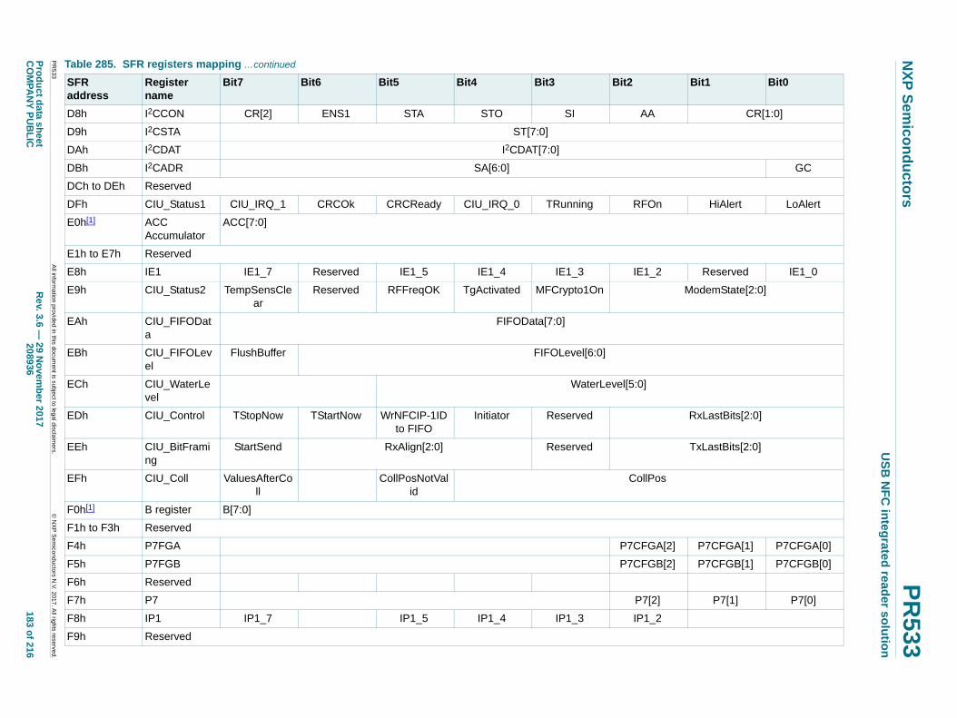
xxxxxxxxxxxxxxxxxxxxx xxxxxxxxxxxxxxxxxxxxxxxxxx xxxxxxx x x x xxxxxxxxxxxxxxxxxxxxxxxxxxxxxx xxxxxxxxxxxxxxxxxxx xx xx xxxxx xxxxxxxxxxxxxxxxxxxxxxxxxxx xxxxxxxxxxxxxxxxxxx xxxxxx xxxxxxxxxxxxxxxxxxxxxxxxxxxxxxxxxxx xxxxxxxxxxxx x x xxxxxxxxxxxxxxxxxxxxx xxxxxxxxxxxxxxxxxxxxxxxxxxxxxx xxxxx xxxxxxxxxxxxxxxxxxxxxxxxxxxxxxxxxxxxxxxxxxxxxxxxxx xxxxxxxx xxxxxxxxxxxxxxxxxxxxxxxxx xxxxxxxxxxxxxxxxxxxx xxx
PR
533
Pro
du
ct data sh
eetC
OM
PA
NY
PU
BL
ICR
ev. 3.6 —
29 N
ove
mb
er 2
017208936
183 of 216
NX
P S
emico
nd
ucto
rsP
R533
US
B N
FC
integ
rated read
er solu
tion
CR[1:0]
GC
HiAlert LoAlert
Reserved IE1_0
ModemState[2:0]
RxLastBits[2:0]
TxLastBits[2:0]
] P7CFGA[1] P7CFGA[0]
] P7CFGB[1] P7CFGB[0]
P7[1] P7[0]
Table 285. SFR registers mapping …continued
SFRaddress
Register name
Bit7 Bit6 Bit5 Bit4 Bit3 Bit2 Bit1 Bit0
All inform
ation provided
in this docum
ent is subject to leg
al disclaim
ers.©
NX
P S
em
iconductors N
.V. 2017. A
ll rights rese
rved.
D8h I2CCON CR[2] ENS1 STA STO SI AA
D9h I2CSTA ST[7:0]
DAh I2CDAT I2CDAT[7:0]
DBh I2CADR SA[6:0]
DCh to DEh Reserved
DFh CIU_Status1 CIU_IRQ_1 CRCOk CRCReady CIU_IRQ_0 TRunning RFOn
E0h[1] ACC Accumulator
ACC[7:0]
E1h to E7h Reserved
E8h IE1 IE1_7 Reserved IE1_5 IE1_4 IE1_3 IE1_2
E9h CIU_Status2 TempSensClear
Reserved RFFreqOK TgActivated MFCrypto1On
EAh CIU_FIFOData
FIFOData[7:0]
EBh CIU_FIFOLevel
FlushBuffer FIFOLevel[6:0]
ECh CIU_WaterLevel
WaterLevel[5:0]
EDh CIU_Control TStopNow TStartNow WrNFCIP-1ID to FIFO
Initiator Reserved
EEh CIU_BitFraming
StartSend RxAlign[2:0] Reserved
EFh CIU_Coll ValuesAfterColl
CollPosNotValid
CollPos
F0h[1] B register B[7:0]
F1h to F3h Reserved
F4h P7FGA P7CFGA[2
F5h P7FGB P7CFGB[2
F6h Reserved
F7h P7 P7[2]
F8h IP1 IP1_7 IP1_5 IP1_4 IP1_3 IP1_2
F9h Reserved
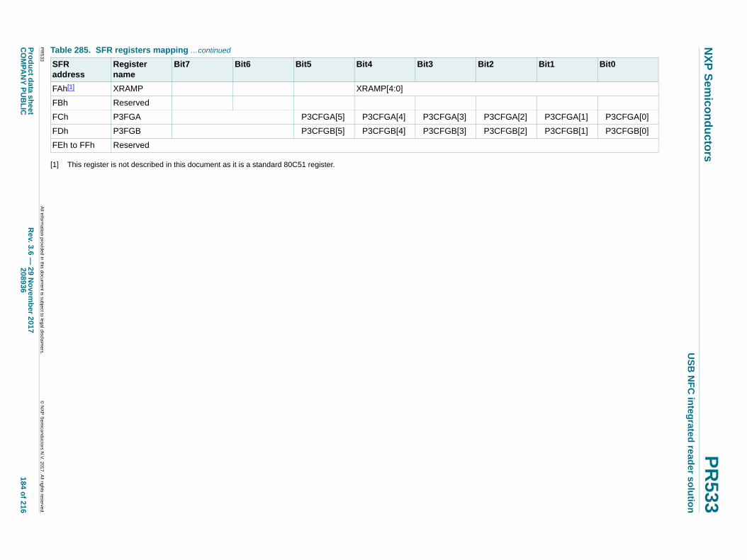
xxxxxxxxxxxxxxxxxxxxx xxxxxxxxxxxxxxxxxxxxxxxxxx xxxxxxx x x x xxxxxxxxxxxxxxxxxxxxxxxxxxxxxx xxxxxxxxxxxxxxxxxxx xx xx xxxxx xxxxxxxxxxxxxxxxxxxxxxxxxxx xxxxxxxxxxxxxxxxxxx xxxxxx xxxxxxxxxxxxxxxxxxxxxxxxxxxxxxxxxxx xxxxxxxxxxxx x x xxxxxxxxxxxxxxxxxxxxx xxxxxxxxxxxxxxxxxxxxxxxxxxxxxx xxxxx xxxxxxxxxxxxxxxxxxxxxxxxxxxxxxxxxxxxxxxxxxxxxxxxxx xxxxxxxx xxxxxxxxxxxxxxxxxxxxxxxxx xxxxxxxxxxxxxxxxxxxx xxx
PR
533
Pro
du
ct data sh
eetC
OM
PA
NY
PU
BL
ICR
ev. 3.6 —
29 N
ove
mb
er 2
017208936
184 of 216
NX
P S
emico
nd
ucto
rsP
R533
US
B N
FC
integ
rated read
er solu
tion
] P3CFGA[1] P3CFGA[0]
] P3CFGB[1] P3CFGB[0]
Table 285. SFR registers mapping …continued
SFRaddress
Register name
Bit7 Bit6 Bit5 Bit4 Bit3 Bit2 Bit1 Bit0
All inform
ation provided
in this docum
ent is subject to leg
al disclaim
ers.©
NX
P S
em
iconductors N
.V. 2017. A
ll rights rese
rved.
[1] This register is not described in this document as it is a standard 80C51 register.
FAh[1] XRAMP XRAMP[4:0]
FBh Reserved
FCh P3FGA P3CFGA[5] P3CFGA[4] P3CFGA[3] P3CFGA[2
FDh P3FGB P3CFGB[5] P3CFGB[4] P3CFGB[3] P3CFGB[2
FEh to FFh Reserved
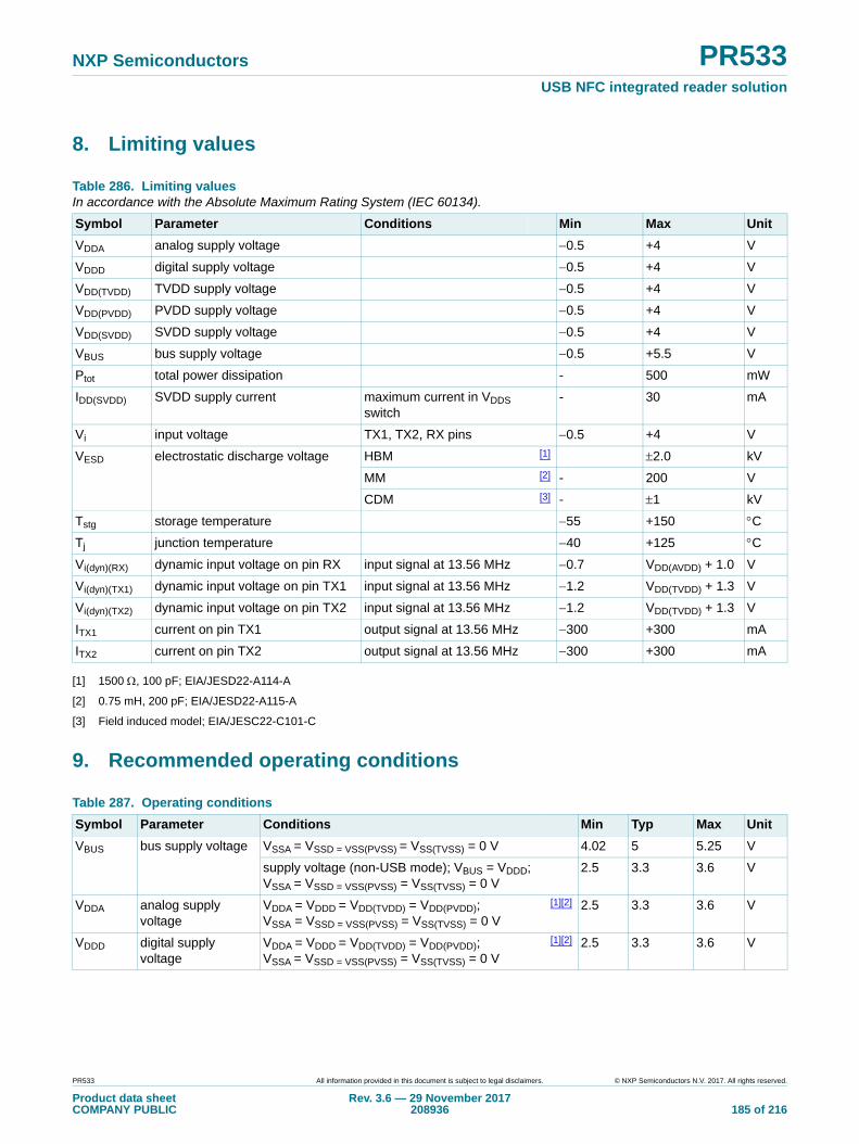
NXP Semiconductors PR533USB NFC integrated reader solution
8. Limiting values
[1] 1500 , 100 pF; EIA/JESD22-A114-A
[2] 0.75 mH, 200 pF; EIA/JESD22-A115-A
[3] Field induced model; EIA/JESC22-C101-C
9. Recommended operating conditions
Table 286. Limiting valuesIn accordance with the Absolute Maximum Rating System (IEC 60134).
Symbol Parameter Conditions Min Max Unit
VDDA analog supply voltage 0.5 +4 V
VDDD digital supply voltage 0.5 +4 V
VDD(TVDD) TVDD supply voltage 0.5 +4 V
VDD(PVDD) PVDD supply voltage 0.5 +4 V
VDD(SVDD) SVDD supply voltage 0.5 +4 V
VBUS bus supply voltage 0.5 +5.5 V
Ptot total power dissipation - 500 mW
IDD(SVDD) SVDD supply current maximum current in VDDS switch
- 30 mA
Vi input voltage TX1, TX2, RX pins 0.5 +4 V
VESD electrostatic discharge voltage HBM [1] 2.0 kV
MM [2] - 200 V
CDM [3] - 1 kV
Tstg storage temperature 55 +150 C
Tj junction temperature 40 +125 C
Vi(dyn)(RX) dynamic input voltage on pin RX input signal at 13.56 MHz 0.7 VDD(AVDD) + 1.0 V
Vi(dyn)(TX1) dynamic input voltage on pin TX1 input signal at 13.56 MHz 1.2 VDD(TVDD) + 1.3 V
Vi(dyn)(TX2) dynamic input voltage on pin TX2 input signal at 13.56 MHz 1.2 VDD(TVDD) + 1.3 V
ITX1 current on pin TX1 output signal at 13.56 MHz 300 +300 mA
ITX2 current on pin TX2 output signal at 13.56 MHz 300 +300 mA
Table 287. Operating conditions
Symbol Parameter Conditions Min Typ Max Unit
VBUS bus supply voltage VSSA = VSSD = VSS(PVSS) = VSS(TVSS) = 0 V 4.02 5 5.25 V
supply voltage (non-USB mode); VBUS = VDDD; VSSA = VSSD = VSS(PVSS) = VSS(TVSS) = 0 V
2.5 3.3 3.6 V
VDDA analog supply voltage
VDDA = VDDD = VDD(TVDD) = VDD(PVDD); VSSA = VSSD = VSS(PVSS) = VSS(TVSS) = 0 V
[1][2] 2.5 3.3 3.6 V
VDDD digital supply voltage
VDDA = VDDD = VDD(TVDD) = VDD(PVDD); VSSA = VSSD = VSS(PVSS) = VSS(TVSS) = 0 V
[1][2] 2.5 3.3 3.6 V
PR533 All information provided in this document is subject to legal disclaimers. © NXP Semiconductors N.V. 2017. All rights reserved.
Product data sheetCOMPANY PUBLIC
Rev. 3.6 — 29 November 2017208936 185 of 216

NXP Semiconductors PR533USB NFC integrated reader solution
[1] VSSA, VDDD and VDD(TVDD) shall always be on the same voltage level.
[2] Supply voltages below 3 V reduces the performance (e.g. the achievable operating distance).
10. Thermal characteristics
11. Characteristics
Unless otherwise specified, the limits are given for the full operating conditions. The typical value is given for 25 C, VDDD = 3.4 V and VDD(PVDD) = 3 V in non-USB bus power mode, VBUS = 5 V in USB power mode.
Timings are only given from characterization results.
11.1 Power management characteristics
11.1.1 Current consumption characteristics
Typical value using a complementary driver configuration and an antenna matched to 40 between TX1 and TX2 at 13.56 MHz.
VDD(TVDD) TVDD supply voltage
VDDA = VDDD = VDD(TVDD) = VDD(PVDD); VSSA = VSSD = VSS(PVSS) = VSS(TVSS) = 0 V
[1][2] 2.5 3.3 3.6 V
VDD(PVDD) PVDD supply voltage
supply pad for host interface; VDDA = VDDD = VDD(TVDD) = VDD(PVDD); VSSA = VSSD = VSS(PVSS) = VSS(TVSS) = 0 V
[2] 1.6 1.8 to 3.3 3.6 V
Tamb ambient temperature
30 +25 +85 C
Table 287. Operating conditions …continued
Symbol Parameter Conditions Min Typ Max Unit
Table 288. Thermal characteristics
Symbol Parameter Conditions Min Typ Max Unit
Rth(j-a) thermal resistance from junction to ambient
in free air with exposed pad soldered on a 4 layer Jedec PCB-0.5
- 37 41.1 K/W
Table 289. Current consumption characteristics
Symbol Parameter Conditions Min Typ Max Unit
Ipd power-down current VDDA = VDDD = VDD(TVDD) = VDD(PVDD) = 3 V; not powered from USB
hard power-down current; not powered from USB; RF level detector off
[1] - 1.3 10 A
soft power-down current; not powered from USB; RF level detector on
[1] - 9 30 A
ICCSL suspended low-power device supply current
VBUS = 5 V; VDDA = VDDD = VDD(TVDD) = VDD(PVDD) = 3 V; VDDS = 0 V; RF level detector on (without resistor on pin DP (D+))
[1] - 120 250 A
IDDD digital supply current VDDA = VDDD = VDD(TVDD) = VDD(PVDD) = 3 V; RF level detector on
- 12 - mA
PR533 All information provided in this document is subject to legal disclaimers. © NXP Semiconductors N.V. 2017. All rights reserved.
Product data sheetCOMPANY PUBLIC
Rev. 3.6 — 29 November 2017208936 186 of 216
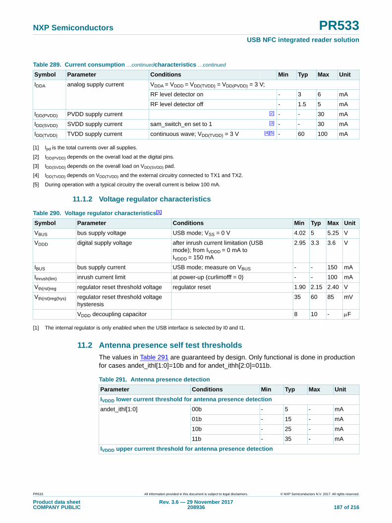
NXP Semiconductors PR533USB NFC integrated reader solution
[1] Ipd is the total currents over all supplies.
[2] IDD(PVDD) depends on the overall load at the digital pins.
[3] IDD(SVDD) depends on the overall load on VDD(SVDD) pad.
[4] IDD(TVDD) depends on VDD(TVDD) and the external circuitry connected to TX1 and TX2.
[5] During operation with a typical circuitry the overall current is below 100 mA.
11.1.2 Voltage regulator characteristics
[1] The internal regulator is only enabled when the USB interface is selected by I0 and I1.
11.2 Antenna presence self test thresholds
The values in Table 291 are guaranteed by design. Only functional is done in production for cases andet_ithl[1:0]=10b and for andet_ithh[2:0]=011b.
IDDA analog supply current VDDA = VDDD = VDD(TVDD) = VDD(PVDD) = 3 V;
RF level detector on - 3 6 mA
RF level detector off - 1.5 5 mA
IDD(PVDD) PVDD supply current [2] - - 30 mA
IDD(SVDD) SVDD supply current sam_switch_en set to 1 [3] - - 30 mA
IDD(TVDD) TVDD supply current continuous wave; VDD(TVDD) = 3 V [4][5] - 60 100 mA
Table 289. Current consumption …continuedcharacteristics …continued
Symbol Parameter Conditions Min Typ Max Unit
Table 290. Voltage regulator characteristics[1]
Symbol Parameter Conditions Min Typ Max Unit
VBUS bus supply voltage USB mode; VSS = 0 V 4.02 5 5.25 V
VDDD digital supply voltage after inrush current limitation (USB mode); from IVDDD = 0 mA to IVDDD = 150 mA
2.95 3.3 3.6 V
IBUS bus supply current USB mode; measure on VBUS - - 150 mA
Iinrush(lim) inrush current limit at power-up (curlimofff = 0) - - 100 mA
Vth(rst)reg regulator reset threshold voltage regulator reset 1.90 2.15 2.40 V
Vth(rst)reg(hys) regulator reset threshold voltage hysteresis
35 60 85 mV
VDDD decoupling capacitor 8 10 - F
Table 291. Antenna presence detection
Parameter Conditions Min Typ Max Unit
IVDDD lower current threshold for antenna presence detection
andet_ithl[1:0] 00b - 5 - mA
01b - 15 - mA
10b - 25 - mA
11b - 35 - mA
IVDDD upper current threshold for antenna presence detection
PR533 All information provided in this document is subject to legal disclaimers. © NXP Semiconductors N.V. 2017. All rights reserved.
Product data sheetCOMPANY PUBLIC
Rev. 3.6 — 29 November 2017208936 187 of 216
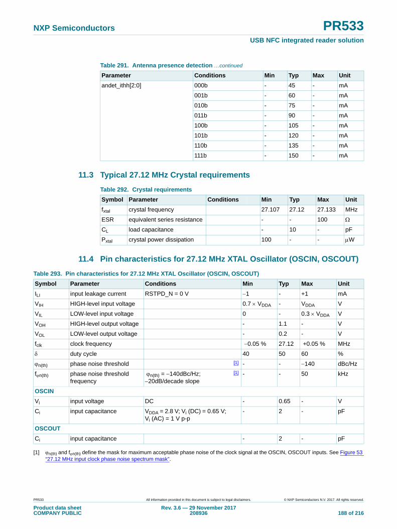
NXP Semiconductors PR533USB NFC integrated reader solution
11.3 Typical 27.12 MHz Crystal requirements
11.4 Pin characteristics for 27.12 MHz XTAL Oscillator (OSCIN, OSCOUT)
[1] n(th) and fn(th) define the mask for maximum acceptable phase noise of the clock signal at the OSCIN, OSCOUT inputs. See Figure 53 “27.12 MHz input clock phase noise spectrum mask”.
andet_ithh[2:0] 000b - 45 - mA
001b - 60 - mA
010b - 75 - mA
011b - 90 - mA
100b - 105 - mA
101b - 120 - mA
110b - 135 - mA
111b - 150 - mA
Table 291. Antenna presence detection …continued
Parameter Conditions Min Typ Max Unit
Table 292. Crystal requirements
Symbol Parameter Conditions Min Typ Max Unit
fxtal crystal frequency 27.107 27.12 27.133 MHz
ESR equivalent series resistance - - 100
CL load capacitance - 10 - pF
Pxtal crystal power dissipation 100 - - W
Table 293. Pin characteristics for 27.12 MHz XTAL Oscillator (OSCIN, OSCOUT)
Symbol Parameter Conditions Min Typ Max Unit
ILI input leakage current RSTPD_N = 0 V 1 - +1 mA
VIH HIGH-level input voltage 0.7 VDDA - VDDA V
VIL LOW-level input voltage 0 - 0.3 VDDA V
VOH HIGH-level output voltage - 1.1 - V
VOL LOW-level output voltage - 0.2 - V
fclk clock frequency 0.05 % 27.12 +0.05 % MHz
duty cycle 40 50 60 %
n(th) phase noise threshold [1] - - 140 dBc/Hz
fn(th) phase noise threshold frequency
n(th) = 140dBc/Hz; 20dB/decade slope
[1] - - 50 kHz
OSCIN
Vi input voltage DC - 0.65 - V
Ci input capacitance VDDA = 2.8 V; Vi (DC) = 0.65 V; Vi (AC) = 1 V p-p
- 2 - pF
OSCOUT
Ci input capacitance - 2 - pF
PR533 All information provided in this document is subject to legal disclaimers. © NXP Semiconductors N.V. 2017. All rights reserved.
Product data sheetCOMPANY PUBLIC
Rev. 3.6 — 29 November 2017208936 188 of 216
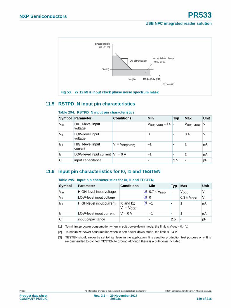
NXP Semiconductors PR533USB NFC integrated reader solution
11.5 RSTPD_N input pin characteristics
11.6 Input pin characteristics for I0, I1 and TESTEN
[1] To minimize power consumption when in soft power-down mode, the limit is VDDD 0.4 V.
[2] To minimize power consumption when in soft power-down mode, the limit is 0.4 V.
[3] TESTEN should never be set to high level in the application. It is used for production test purpose only. It is recommended to connect TESTEN to ground although there is a pull-down included.
Fig 53. 27.12 MHz input clock phase noise spectrum mask
φn(th)
phase noise(dBc/Hz)
-20 dB/decadeacceptable phase noise area
001aao393
fφn(th) frequency (Hz)
Table 294. RSTPD_N input pin characteristics
Symbol Parameter Conditions Min Typ Max Unit
VIH HIGH-level input voltage
VDD(PVDD) 0.4 - VDD(PVDD) V
VIL LOW-level input voltage
0 - 0.4 V
IIH HIGH-level input current
VI = VDD(PVDD) 1 - 1 A
IIL LOW-level input current VI = 0 V 1 - 1 A
Ci input capacitance - 2.5 - pF
Table 295. Input pin characteristics for I0, I1 and TESTEN
Symbol Parameter Conditions Min Typ Max Unit
VIH HIGH-level input voltage [1] 0.7 VDDD - VDDD V
VIL LOW-level input voltage [2] 0 0.3 VDDD V
IIH HIGH-level input current I0 and I1; VI = VDDD
[3] 1 - 1 A
IIL LOW-level input current VI = 0 V 1 - 1 A
Ci input capacitance - 2.5 - pF
PR533 All information provided in this document is subject to legal disclaimers. © NXP Semiconductors N.V. 2017. All rights reserved.
Product data sheetCOMPANY PUBLIC
Rev. 3.6 — 29 November 2017208936 189 of 216

NXP Semiconductors PR533USB NFC integrated reader solution
11.7 RSTOUT_N output pin characteristics
[1] Data at VDD(PVDD) = 1.8V are only given from characterization results.
[2] IOH and IOL give the output drive capability from which the rise and fall times may be calculated as a function of the load capacitance.
Table 296. RSTOUT_N output pin characteristics
Symbol Parameter Conditions Min Typ Max Unit
VOH HIGH-level output voltage
VDD(PVDD) = 3 V; IOH = 4 mA 0.7 VDD(PVDD) - VDD(PVDD) V
VDD(PVDD) = 1.8 V; IOH = 2 mA [1] 0.7 VDD(PVDD) - VDD(PVDD) V
VOL LOW-level output voltage
VDD(PVDD) = 3 V; IOL = 4 mA 0 - 0.3 VDD(PVDD) V
VDD(PVDD) = 1.8 V; IOL = 2 mA [1] 0 - 0.3 VDD(PVDD) V
IOH HIGH-level output current
VDD(PVDD) = 3 V; VOH = 0.8 VDD(PVDD)
[2] 4 - - mA
VDD(PVDD) = 1.8 V; VOH = 0.7 VDD(PVDD)
2 - - mA
IOL LOW-level output current
VDD(PVDD) = 3 V; VOL = 0.2 VDD(PVDD)
[2] 4 - - mA
VDD(PVDD) = 1.8 V; VOL = 0.3 VDD(PVDD)
2 - - mA
CL load capacitance - 30 pF
tr rise time VDD(PVDD) = 3 V; VOH = 0.8 VDD(PVDD); CL = 30 pF
- - 13.5 ns
VDDP = 1.8 V; VOH = 0.7 VDD(PVDD); CL = 30 pF
- - 10.8 ns
tf fall time VDD(PVDD) = 3 V; VOL = 0.2 VDD(PVDD); CL = 30 pF
- - 13.5 ns
VDD(PVDD) = 1.8 V; VOL = 0.3 VDD(PVDD); CL = 30 pF
- - 10.8 ns
PR533 All information provided in this document is subject to legal disclaimers. © NXP Semiconductors N.V. 2017. All rights reserved.
Product data sheetCOMPANY PUBLIC
Rev. 3.6 — 29 November 2017208936 190 of 216
NXP Semiconductors PR533USB NFC integrated reader solution
11.8 Input/output characteristics for pin P70_IRQ
[1] To minimize power consumption when in soft power-down mode, the limit is VDD(PVDD) 0.4 V.
[2] To minimize power consumption when in soft power-down mode, the limit is 0.4 V.
[3] Data at VDD(PVDD) = 1.8 V are only given from characterization results.
[4] The IOH and IOL give the output driving capability and allow to calculate directly the rise and fall time as function of the load capacitance.
Table 297. Input/output pin characteristics for pin P70_IRQ
Symbol Parameter Conditions Min Typ Max Unit
VIH HIGH-level input voltage
[1] 0.7 VDD(PVDD) - VDD(PVDD) V
VIL LOW-level input voltage [2] 0 - 0.3 VDD(PVDD) V
VOH HIGH-level output voltage
push-pull mode; VDD(PVDD) = 3 V; IOH = 4 mA
0.7 VDD(PVDD) - VDD(PVDD) V
push-pull mode; VDD(PVDD) = 1.8 V; IOH = -2 mA
[3] 0.7 VDD(PVDD) - VDD(PVDD) V
VOL LOW-level output voltage
push-pull mode; VDD(PVDD) = 3 V; IOL = 4 mA
0 - 0.3 VDD(PVDD) V
push-pull mode; VDD(PVDD) = 1.8 V; IOL = 2 mA
[3] 0 - 0.3 VDD(PVDD) V
IIH HIGH-level input current input mode; VI = VDDD 1 - 1 A
IIL LOW-level input current input mode; VI = 0 V 1 - 1 A
IOH HIGH-level output current
VDD(PVDD) = 3 V; VOH = 0.8 VDD(PVDD)
[5] 4 - - mA
IOL LOW-level output current
VDD(PVDD) = 3 V; VOL = 0.2 VDD(PVDD)
[5] 4 - - mA
ILI input leakage current RSTPD_N = 0.4 V 1 - 1 A
Ci input capacitance - 2.5 pF
CL load capacitance - - 30 pF
tr rise time VDD(PVDD) = 3 V; VOH = 0.8 VDD(PVDD); CL = 30 pF
- - 13.5 ns
VDD(PVDD) = 1.8 V; VOH = 0.7 VDD(PVDD); CL = 30 pF
- - 10.8 ns
tf fall time VDD(PVDD) = 3 V; VOL = 0.2 VDD(PVDD); CL= 30 pF
- - 13.5 ns
VDD(PVDD) = 1.8 V; VOL = 0.3 VDD(PVDD); CL = 30 pF
- - 10.8 ns
PR533 All information provided in this document is subject to legal disclaimers. © NXP Semiconductors N.V. 2017. All rights reserved.
Product data sheetCOMPANY PUBLIC
Rev. 3.6 — 29 November 2017208936 191 of 216
NXP Semiconductors PR533USB NFC integrated reader solution
11.9 Input/output pin characteristics for P30 / UART_RX, P31 / UART_TX, P32_INT0, P33_INT1
[1] To minimize power consumption when in soft power-down mode, the limit is VDD(PVDD) 0.4 V.
[2] To minimize power consumption when in soft power-down mode, the limit is 0.4 V
[3] Data at VDD(PVDD) = 1.8 V are only given from characterization results.
[4] The IOH and IOL give the output driving capability and allow to calculate directly the rise and fall time as function of the load capacitance.
Table 298. Input/output pin characteristics for P30 / UART_RX, P31 / UART_TX, P32_INT0, P33_INT1
Symbol Parameter Conditions Min Typ Max Unit
VIH HIGH-level input voltage [1] 0.7 VDD(PVDD) - VDD(PVDD) V
VIL LOW-level input voltage [2] 0 - 0.3 VDD(PVDD) V
VOH HIGH-level output voltage
push-pull mode; VDD(PVDD) = 3 V; IOH = 4 mA
VDD(PVDD) 0.4 - VDD(PVDD) V
VDD(PVDD) = 1.8 V; IOH = 2 mA
[3] VDD(PVDD) 0.4 - VDD(PVDD) V
VOL LOW-level output voltage
push-pull mode; VDD(PVDD) = 3 V; IOL = 4 mA
0 - 0.4 V
VDD(PVDD) = 1.8 V; IOL = 2 mA
[3] 0 - 0.4 V
IIH HIGH-level input current input mode; VI = VDD(PVDD)
-1 - 1 A
IIL LOW-level input current input mode; VI = 0 V -1 - 1 A
IOH HIGH-level output current
VDD(PVDD) = 3 V; VOH = 0.8 VDD(PVDD)
[4] -4 - - mA
IOL LOW-level output current VDD(PVDD) = 3 V; VOL = 0.2 VDD(PVDD)
[4] 4 - - mA
ILI input leakage current RSTPD_N = 0.4 V -1 - 1 A
Ci input capacitance - 2.5 - pF
CL load capacitance - - 30 pF
tr rise time VDD(PVDD) = 3 V; VOH = 0.8 VDD(PVDD); CL = 30 pF
- - 13.5 ns
VDD(PVDD) = 1.8 V; VOH = 0.7 VDD(PVDD); CL = 30 pF
- - 10.8 ns
tf fall time VDD(PVDD) = 3 V; VOL = 0.2 VDD(PVDD); CL= 30 pF
- - 13.5 ns
VDD(PVDD) = 1.8 V; VOL = 0.3 VDD(PVDD); CL = 30 pF
- - 10.8 ns
PR533 All information provided in this document is subject to legal disclaimers. © NXP Semiconductors N.V. 2017. All rights reserved.
Product data sheetCOMPANY PUBLIC
Rev. 3.6 — 29 November 2017208936 192 of 216
NXP Semiconductors PR533USB NFC integrated reader solution
11.10 Input/output pin characteristics for P35
[1] To minimize power consumption when in soft power-down mode, the limit is VDDD 0.4 V.
[2] To minimize power consumption when in soft power-down mode, the limit is 0.4 V.
[3] The IOH and IOL give the output driving capability and allow to calculate directly the rise and fall time as function of the load capacitance.
Table 299. Input/output pin characteristics for P35
Symbol Parameter Conditions Min Typ Max Unit
VIH HIGH-level input voltage [1] 0.7 VDDD - VDDD V
VIL LOW-level input voltage [2] 0 - 0.3 VDDD V
VOH HIGH-level output voltage
VDDD = 3 V; IOH = 4 mA VDDD 0.4 - VDDD V
VOL LOW-level output voltage VDDD = 3 V; IOL = 4 mA 0 - 0.4 V
IIH HIGH-level input current VI = VDDD -1 - 1 A
IIL LOW-level input current VI = 0 V -1 - 1 A
IOH HIGH-level output current VDDD = 3 V; VOH = 0.8 VDD(PVDD)
[3] -4 - - mA
IOL LOW-level output current VDDD = 3 V; VOL = 0.2 VDD(PVDD)
[3] 4 - - mA
ILI input leakage current RSTPD_N = 0.4 V -1 - 1 A
Ci input capacitance - 2.5 - pF
CL load capacitance - - 30 pF
tr rise time VDDD = 3 V; VOH = 0.8 VDDD; CL = 30 pF
- - 13.5 ns
VDDD = 1.8 V; VOH = 0.7 VDDD; CL = 30 pF
- - 10.8 ns
tf fall time VDDD = 3 V; VOL = 0.2 VDDD; CL= 30 pF
- - 13.5 ns
VDDD = 1.8 V; VOL = 0.3 VDDD; CL = 30 pF
- - 10.8 ns
PR533 All information provided in this document is subject to legal disclaimers. © NXP Semiconductors N.V. 2017. All rights reserved.
Product data sheetCOMPANY PUBLIC
Rev. 3.6 — 29 November 2017208936 193 of 216

NXP Semiconductors PR533USB NFC integrated reader solution
11.11 Input/output pin characteristics for DP and DM
[1] The value does not guarantee the power-down consumptions. To reach the specified power-down consumptions, the limit is 0.4 V.
[2] The IOH and IOL give the output driving capability and allow to calculate directly the rise and fall time as function of the load capacitance.
Table 300. Input/output pin characteristics for DP and DM for USB interface
Symbol Parameter Conditions Min Typ Max Unit
VIH HIGH-level input voltage VDD(PVDD) = 3.3 V 2 - 3.6 V
VIL LOW-level input voltage [1] 0 - 0.8 V
VOH HIGH-level output voltage VDD(PVDD) = 3.3 V; RPD = 1.5 to VSS
2.8 - VDD(PVDD) V
VOL LOW-level output voltage VDD(PVDD) = 3.3 V; RPD = 1.5 to VDD(PVDD)
0 - 0.3 V
IOH HIGH-level output current VDD(PVDD) = 3.3 V; VOH = 0.8 VDD(PVDD)
[2] -4 - - mA
VDD(PVDD) = 1.8 V; VOH = 0.7 VDD(PVDD)
-2 - - mA
IOL LOW-level output current VDD(PVDD) = 3.3 V; VOL = 0.2 VDD(PVDD)
[2] 4 - - mA
VDD(PVDD) = 1.8 V; VOL = 0.3 VDD(PVDD)
2 - - mA
IIH HIGH-level input current VI = VDD(PVDD) - - 1 A
IIL LOW-level input current VI = 0 V - - 1 A
ILI input leakage current RSTPD_N = 0 V -1 - +1 A
Ci input capacitance - 2.5 3.5 pF
ZINP input impedance exclusive of pull-up/pull-down (for low-/full speed)
300 - - k
ZDRV driver output impedance for driver which is not high-speed capable
28 - 44
tFDRATE full-speed data rate for devices which are not high-speed capable
11.97 - 12.03 Mb/s
tDJ1 source jitter total (including frequency tolerance) to next transition
-3.5 - +3.5 ns
tDJ2 source jitter total (including frequency tolerance) for paired transitions
-4 - +4 ns
tFDEOP source jitter for differential transition to SE0 transition
-2 - +5 ns
tJR1 receiver jitter to next transition -18.5 - +18.5 ns
tJR2 receiver jitter for paired transitions -9 - +9 ns
tFEOPT source SE0 interval of EOP 160 - 175 ns
tFEOPR receiver SE0 interval of EOP 82 - - ns
tFST width of SE0 interval during differential transition
- - 14 ns
PR533 All information provided in this document is subject to legal disclaimers. © NXP Semiconductors N.V. 2017. All rights reserved.
Product data sheetCOMPANY PUBLIC
Rev. 3.6 — 29 November 2017208936 194 of 216

NXP Semiconductors PR533USB NFC integrated reader solution
Table 301. USB DP/DM differential receiver input levels
Symbol Parameter Conditions Min Typ Max Unit
VDI differential input sensitivity voltage
- 0.2 - - V
VCM differential common mode voltage range
- 0.8 - 2.5 V
Table 302. USB DP/DM driver characteristics
Symbol Parameter Conditions Min Typ Max Unit
tr rise time CL = 50 pF; 10 % to 90 % of (VOH - VOL)
4 - 20 ns
tf fall time CL = 50 pF; 10 % to 90 % of (VOH - VOL)
4 - 20 ns
tFRFM differential rise and fall time matching
(tFR/tFF); excluding the first transition from Idle state
90 - 111.1 %
VCRS output signal crossover voltage
excluding the first transition from Idle state
1.3 - 2.0 V
Fig 54. Transmit waveform at DP/DM
001aan914
level 1
level 2
-400 mV differential
+400 mV differential
0 V differential
unit interval 100 %0 %
point 5 point 6
point 3 point 4
point 1 point 2
PR533 All information provided in this document is subject to legal disclaimers. © NXP Semiconductors N.V. 2017. All rights reserved.
Product data sheetCOMPANY PUBLIC
Rev. 3.6 — 29 November 2017208936 195 of 216
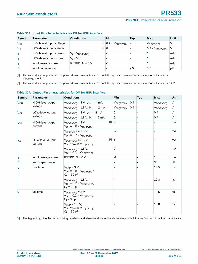
NXP Semiconductors PR533USB NFC integrated reader solution
[1] The value does not guarantee the power-down consumptions. To reach the specified power-down consumptions, the limit is VDD(PVDD) 0.4 V.
[2] The value does not guarantee the power-down consumptions. To reach the specified power-down consumptions, the limit is 0.4 V.
[1] The IOH and IOL give the output driving capability and allow to calculate directly the rise and fall time as function of the load capacitance
Table 303. Input Pin characteristics for DP for HSU interface
Symbol Parameter Conditions Min Typ Max Unit
VIH HIGH-level input voltage [1] 0.7 VDD(PVDD) - VDD(PVDD) V
VIL LOW-level input voltage [2] 0 - 0.3 VDD(PVDD) V
IIH HIGH-level input current Vi = VDD(PVDD) - - 1 mA
IIL LOW-level input current Vi = 0 V - - 1 mA
ILI input leakage current RSTPD_N = 0 V -1 1 mA
Ci input capacitance - 2.5 3.5 pF
Table 304. Output Pin characteristics for DM for HSU interface
Symbol Parameter Conditions Min Typ Max Unit
VOH HIGH-level output voltage
VDD(PVDD) = 3 V; IOH = 4 mA VDD(PVDD) 0.4 - VDD(PVDD) V
VDD(PVDD) = 1.8 V; IOH = 2 mA VDD(PVDD) 0.4 - VDD(PVDD) V
VOL LOW-level output voltage
VDD(PVDD) = 3 V; IOL = 4 mA 0 - 0.4 V
VDD(PVDD) = 1.8 V; IOL = 2 mA 0 - 0.4 V
IOH HIGH-level output current
VDD(PVDD) = 3 V; VOH = 0.8 VDD(PVDD)
[1] -4 - - mA
VDD(PVDD) = 1.8 V; VOH = 0.7 VDD(PVDD)
-2 - - mA
IOL LOW-level output current
VDD(PVDD) = 3.3 V; VOL = 0.2 VDD(PVDD)
[1] 4 - - mA
VDD(PVDD) = 1.8 V; VOL = 0.3 VDD(PVDD)
2 - - mA
ILI input leakage current RSTPD_N = 0 V -1 - 1 mA
CL load capacitance - - 30 pF
tr rise time VDDP = 3 V; VOH = 0.8 VDD(PVDD); CL = 30 pF
- - 13.5 ns
VDD(PVDD) = 1.8 V; VOH = 0.7 VDD(PVDD); CL = 30 pF
- - 10.8 ns
tf fall time VDD(PVDD) = 3 V; VOL = 0.2 VDD(PVDD); CL= 30 pF
- - 13.5 ns
VDDP = 1.8 V; VOL = 0.3 VDD(PVDD); CL = 30 pF
- - 10.8 ns
PR533 All information provided in this document is subject to legal disclaimers. © NXP Semiconductors N.V. 2017. All rights reserved.
Product data sheetCOMPANY PUBLIC
Rev. 3.6 — 29 November 2017208936 196 of 216
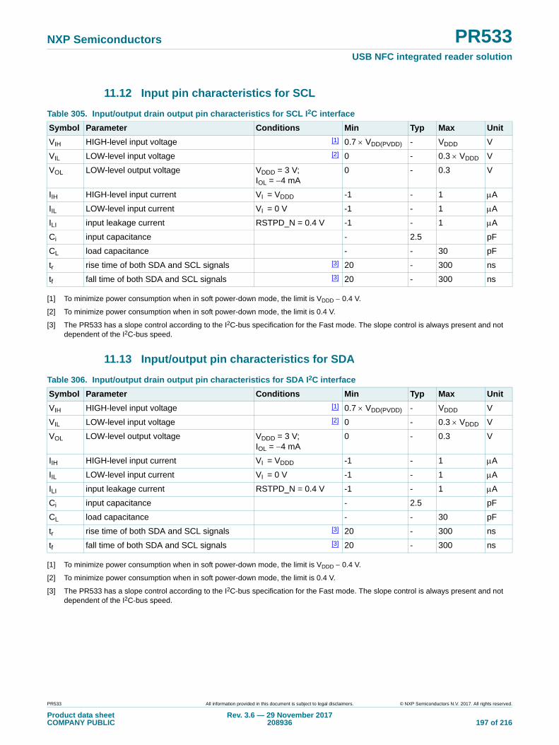
NXP Semiconductors PR533USB NFC integrated reader solution
11.12 Input pin characteristics for SCL
[1] To minimize power consumption when in soft power-down mode, the limit is VDDD 0.4 V.
[2] To minimize power consumption when in soft power-down mode, the limit is 0.4 V.
[3] The PR533 has a slope control according to the I2C-bus specification for the Fast mode. The slope control is always present and not dependent of the I2C-bus speed.
11.13 Input/output pin characteristics for SDA
[1] To minimize power consumption when in soft power-down mode, the limit is VDDD 0.4 V.
[2] To minimize power consumption when in soft power-down mode, the limit is 0.4 V.
[3] The PR533 has a slope control according to the I2C-bus specification for the Fast mode. The slope control is always present and not dependent of the I2C-bus speed.
Table 305. Input/output drain output pin characteristics for SCL I2C interface
Symbol Parameter Conditions Min Typ Max Unit
VIH HIGH-level input voltage [1] 0.7 VDD(PVDD) - VDDD V
VIL LOW-level input voltage [2] 0 - 0.3 VDDD V
VOL LOW-level output voltage VDDD = 3 V; IOL = 4 mA
0 - 0.3 V
IIH HIGH-level input current VI = VDDD -1 - 1 A
IIL LOW-level input current VI = 0 V -1 - 1 A
ILI input leakage current RSTPD_N = 0.4 V -1 - 1 A
Ci input capacitance - 2.5 pF
CL load capacitance - - 30 pF
tr rise time of both SDA and SCL signals [3] 20 - 300 ns
tf fall time of both SDA and SCL signals [3] 20 - 300 ns
Table 306. Input/output drain output pin characteristics for SDA I2C interface
Symbol Parameter Conditions Min Typ Max Unit
VIH HIGH-level input voltage [1] 0.7 VDD(PVDD) - VDDD V
VIL LOW-level input voltage [2] 0 - 0.3 VDDD V
VOL LOW-level output voltage VDDD = 3 V; IOL = 4 mA
0 - 0.3 V
IIH HIGH-level input current VI = VDDD -1 - 1 A
IIL LOW-level input current VI = 0 V -1 - 1 A
ILI input leakage current RSTPD_N = 0.4 V -1 - 1 A
Ci input capacitance - 2.5 pF
CL load capacitance - - 30 pF
tr rise time of both SDA and SCL signals [3] 20 - 300 ns
tf fall time of both SDA and SCL signals [3] 20 - 300 ns
PR533 All information provided in this document is subject to legal disclaimers. © NXP Semiconductors N.V. 2017. All rights reserved.
Product data sheetCOMPANY PUBLIC
Rev. 3.6 — 29 November 2017208936 197 of 216

NXP Semiconductors PR533USB NFC integrated reader solution
11.14 Output pin characteristics for DELATT
[1] To minimize power consumption when in soft power-down mode, the limit is VDD(PVDD) 0.4 V.
11.15 Input pin characteristics for SIGIN
[1] To minimize power consumption when in soft power-down mode, the limit is VDD(SVDD) 0.4 V.
[2] To minimize power consumption when in soft power-down mode, the limit is 0.4 V.
11.16 Output pin characteristics for SIGOUT
Table 307. Output pin characteristics for DELATT
Symbol Parameter Conditions Min Typ Max Unit
VOH HIGH-level output voltage [1] 0.7 VDD(SVDD) - VDD(SVDD) V
VIL LOW-level input voltage 0 - 0.3 VDD(PVDD) V
IIH HIGH-level input current input mode; VI = VDD(SVDD) -1 - 1 A
IIL LOW-level input current input mode; VI = 0 V -1 - 1 A
ILI input leakage current RSTPD_N = 0.4 V -1 - 1 A
Ci input capacitance - 2.5 - pF
Table 308. Input/output pin characteristics for SIGIN
Symbol Parameter Conditions Min Typ Max Unit
VIH HIGH-level input voltage [1] 0.7 VDD(SVDD) - VDD(SVDD) V
VIL LOW-level input voltage [2] 0 - 0.3 VDD(SVDD) V
IIH HIGH-level input current VI = VDD(SVDD) -1 - +1 A
IIL LOW-level input current VI = 0 V -1 - +1 A
ILI input leakage current RSTPD_N = 0.4 V -1 - +1 A
Ci input capacitance - 2.5 - pF
Table 309. Output pin characteristics for SIGOUT
Symbol Parameter Conditions Min Typ Max Unit
VOH HIGH-level output voltage VDDD 0.1 < VDD(SVDD) < VDDD
IOH = 4 mAVDD(SVDD) 0.4 - VDD(SVDD) V
VOL LOW-level output voltage VDDD 0.1 < VDD(SVDD) < VDDD IOL = +4 mA
0 - 0.4 V
IOH HIGH-level output current VDDD 0.1 < VDD(SVDD) < VDDD IOH = 4 mA
-0.4 - - mA
IOL LOW-level output current VDDD 0.1 < VDD(SVDD) < VDDD IOL = +4 mA
4 - - mA
ILI input leakage current RSTPD_N = 0.4 V -1 - +1 A
Ci input capacitance - 2.5 pF
CL load capacitance - - 30 pF
tr rise time VDD(SVDD) = 3 V; VOH = 0.8 VDD(SVDD); Cout = 30 pF
- - 9 ns
tf fall time VDD(SVDD) = 3 V; VOL = 0.2 VDD(SVDD); Cout = 30 pF
- - 9 ns
PR533 All information provided in this document is subject to legal disclaimers. © NXP Semiconductors N.V. 2017. All rights reserved.
Product data sheetCOMPANY PUBLIC
Rev. 3.6 — 29 November 2017208936 198 of 216
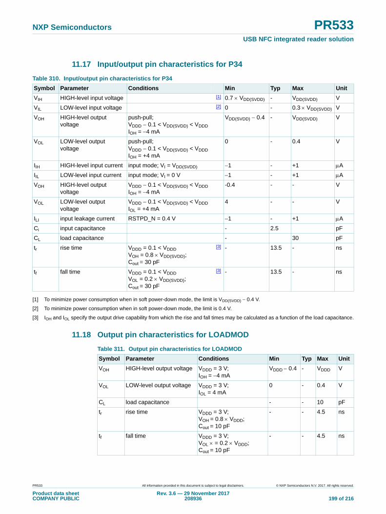
NXP Semiconductors PR533USB NFC integrated reader solution
11.17 Input/output pin characteristics for P34
[1] To minimize power consumption when in soft power-down mode, the limit is VDD(SVDD) 0.4 V.
[2] To minimize power consumption when in soft power-down mode, the limit is 0.4 V.
[3] IOH and IOL specify the output drive capability from which the rise and fall times may be calculated as a function of the load capacitance.
11.18 Output pin characteristics for LOADMOD
Table 310. Input/output pin characteristics for P34
Symbol Parameter Conditions Min Typ Max Unit
VIH HIGH-level input voltage [1] 0.7 VDD(SVDD) - VDD(SVDD) V
VIL LOW-level input voltage [2] 0 - 0.3 VDD(SVDD) V
VOH HIGH-level output voltage
push-pull; VDDD 0.1 < VDD(SVDD) < VDDD IOH = 4 mA
VDD(SVDD) 0.4 - VDD(SVDD) V
VOL LOW-level output voltage
push-pull; VDDD 0.1 < VDD(SVDD) < VDDD IOH = +4 mA
0 - 0.4 V
IIH HIGH-level input current input mode; VI = VDD(SVDD) 1 - +1 A
IIL LOW-level input current input mode; VI = 0 V 1 - +1 A
VOH HIGH-level output voltage
VDDD 0.1 < VDD(SVDD) < VDDD IOH = 4 mA
-0.4 - - V
VOL LOW-level output voltage
VDDD 0.1 < VDD(SVDD) < VDDD IOL = +4 mA
4 - - V
ILI input leakage current RSTPD_N = 0.4 V 1 - +1 A
Ci input capacitance - 2.5 pF
CL load capacitance - 30 pF
tr rise time VDDD = 0.1 < VDDD VOH = 0.8 VDD(SVDD); Cout = 30 pF
[3] - 13.5 - ns
tf fall time VDDD = 0.1 < VDDD VOL = 0.2 VDD(SVDD); Cout = 30 pF
[3] - 13.5 - ns
Table 311. Output pin characteristics for LOADMOD
Symbol Parameter Conditions Min Typ Max Unit
VOH HIGH-level output voltage VDDD = 3 V; IOH = 4 mA
VDDD 0.4 - VDDD V
VOL LOW-level output voltage VDDD = 3 V; IOL = 4 mA
0 - 0.4 V
CL load capacitance - - 10 pF
tr rise time VDDD = 3 V; VOH = 0.8 VDDD; Cout = 10 pF
- - 4.5 ns
tf fall time VDDD = 3 V; VOL = 0.2 VDDD; Cout = 10 pF
- - 4.5 ns
PR533 All information provided in this document is subject to legal disclaimers. © NXP Semiconductors N.V. 2017. All rights reserved.
Product data sheetCOMPANY PUBLIC
Rev. 3.6 — 29 November 2017208936 199 of 216

NXP Semiconductors PR533USB NFC integrated reader solution
11.19 Input pin characteristics for RX
Fig 55. RX input parameters
Table 312. Input pin characteristics for RX
Symbol Parameter Conditions Min Typ Max Unit
Vi input voltage dynamic; signal frequency at 13.56 MHz
0.7 VDDA +1 V
Ci input capacitance 6 10 14 pF
Rs series resistance RX input; VDDA = 3 V; receiver active; VRX(p-p) = 1 V; 1.5 V DC offset
315 350 385
Minimum dynamic input voltage
VMID
AVDD +1 VVin, RX
0 V
VRX, IV, mil
mRXmil =VRX, IV, mil - Vmod
VRX, IV, mil + Vmod
Vmod
13.56 MHzcarrier
Miller coded signals
aaa-002342
VMID
AVDD +1 VVin, RX
0 V
VRX, IV, Man Vmod
VRXMod, Man
13.56 MHzcarrier
Manchester coded signals
PR533 All information provided in this document is subject to legal disclaimers. © NXP Semiconductors N.V. 2017. All rights reserved.
Product data sheetCOMPANY PUBLIC
Rev. 3.6 — 29 November 2017208936 200 of 216

NXP Semiconductors PR533USB NFC integrated reader solution
[1] The minimum modulation voltage is valid for all modulation schemes except Miller coded signals.
11.20 Output pin characteristics for AUX1/AUX2
VRX(p-p) peak-to-peak receiver voltage
Miller coded; 106 kbit/s
- 150 500 mV
Manchester coded; 212 kbit/s and 424 kbit/s
- 100 200 mV
Maximum dynamic input voltage
VRX(p-p) peak-to-peak receiver voltage
Miller coded; 106 kbit/s
VDDA - - V
Manchester coded; 212 and 424 kbit/s
VDDA - - V
Minimum modulation voltage
Vmod modulation voltage RxGain = 6 and 7 [1] - - 6 mV
RxGain = 4 and 5 [1] - - 18 mV
RxGain = 0 to 3 [1] - - 120 mV
Minimum modulation index
m modulation index Miller coded; 106 kbit/s VRX(p-p)= 1.5 V; SensMiller = 3
- 33 - %
Table 312. Input pin characteristics for RX …continued
Symbol Parameter Conditions Min Typ Max Unit
Table 313. Output pin characteristics for AUX1/AUX2
Symbol Parameter Conditions Min Typ Max Unit
VOH HIGH-level output voltage VDDD = 3 V; IOH = 4 mA
VDDD 0.4 - VDDD V
VOL LOW-level output voltage VDDD = 3 V; IOL = 4 mA
VSSD - VSSD +0.4 V
IOH HIGH-level output current VDDD= 3 V; VOH = VDDD 0.3
-4 - - mA
IOL LOW-level output current VDDD= 3 V; VOL = VDDD -0.3
4 - - mA
ILI input leakage current RSTPD_N = 0 V -1 - +1 A
Ci input capacitance - 2.5 - pF
CL load capacitance - - 15 pF
PR533 All information provided in this document is subject to legal disclaimers. © NXP Semiconductors N.V. 2017. All rights reserved.
Product data sheetCOMPANY PUBLIC
Rev. 3.6 — 29 November 2017208936 201 of 216

NXP Semiconductors PR533USB NFC integrated reader solution
11.21 Output pin characteristics for TX1/TX2
Table 314. Output pin characteristics for TX1/TX2
Symbol Parameter Conditions Min Typ Max Unit
VOH HIGH-level output voltage VDD(TVDD) = 3 V; IO = 32 mA; CWGsN = Fh
- - 150 mV
VDD(TVDD) = 3 V; IO = 80 mA; CWGsN = Fh
- - 400 mV
VOL LOW-level output voltage VDD(TVDD) = 2.5 V; IO = 32 mA; CWGsN = Fh
- - 240 mV
VDD(TVDD) = 2.5 V; IO = 80 mA; CWGsN = Fh
- - 640 mV
Table 315. Output resistance for TX1/TX2
Symbol Parameter Conditions1 CWGsP Min Typ Max Unit
ROH HIGH-level output resistance
VDD(TVDD) = 3 V; VO = VDD(TVDD) 100 mV
01h 133 180 251 W
02h 67 90 125 W
04h 34 46 62 W
08h 17 23 31 W
10h 8.5 12 15.5 W
20h 4.7 6 7.8 W
3Fh 2.3 3 4.4 W
ROL LOW-level output resistance
10h 34 46 62 W
20h 17 23 31 W
40h 8.5 12 15.5 W
80h 4.7 6 7.8 W
F0h 2.3 3 4.4 W
PR533 All information provided in this document is subject to legal disclaimers. © NXP Semiconductors N.V. 2017. All rights reserved.
Product data sheetCOMPANY PUBLIC
Rev. 3.6 — 29 November 2017208936 202 of 216
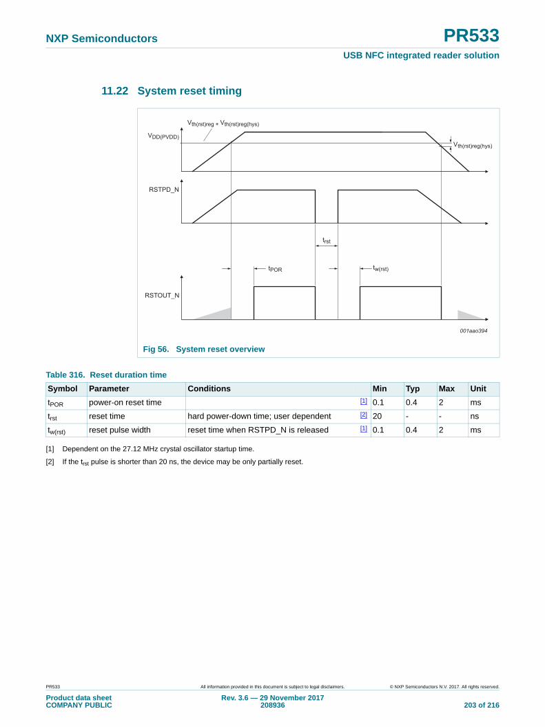
NXP Semiconductors PR533USB NFC integrated reader solution
11.22 System reset timing
[1] Dependent on the 27.12 MHz crystal oscillator startup time.
[2] If the trst pulse is shorter than 20 ns, the device may be only partially reset.
Fig 56. System reset overview
tw(rst)
trst
Vth(rst)reg + Vth(rst)reg(hys)
Vth(rst)reg(hys)
VDD(PVDD)
RSTPD_N
RSTOUT_N
tPOR
001aao394
Table 316. Reset duration time
Symbol Parameter Conditions Min Typ Max Unit
tPOR power-on reset time [1] 0.1 0.4 2 ms
trst reset time hard power-down time; user dependent [2] 20 - - ns
tw(rst) reset pulse width reset time when RSTPD_N is released [1] 0.1 0.4 2 ms
PR533 All information provided in this document is subject to legal disclaimers. © NXP Semiconductors N.V. 2017. All rights reserved.
Product data sheetCOMPANY PUBLIC
Rev. 3.6 — 29 November 2017208936 203 of 216
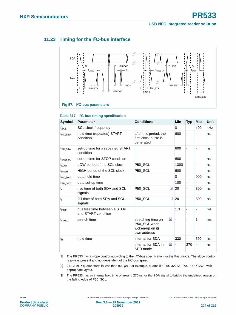
NXP Semiconductors PR533USB NFC integrated reader solution
11.23 Timing for the I2C-bus interface
[1] The PR533 has a slope control according to the I2C-bus specification for the Fast mode. The slope control is always present and not dependent of the I2C-bus speed.
[2] 27.12 MHz quartz starts in less than 800 s. For example, quartz like TAS-3225A, TAS-7 or KSS2F with appropriate layout.
[3] The PR533 has an internal hold time of around 270 ns for the SDA signal to bridge the undefined region of the falling edge of P50_SCL.
Fig 57. I2C-bus parameters
Table 317. I2C-bus timing specification
Symbol Parameter Conditions Min Typ Max Unit
fSCL SCL clock frequency 0 - 400 kHz
tHD;STA hold time (repeated) START condition
after this period, the first clock pulse is generated
600 - - ns
tSU;STA set-up time for a repeated START condition
600 - - ns
tSU;STO set-up time for STOP condition 600 - - ns
tLOW LOW period of the SCL clock P50_SCL 1300 - - ns
tHIGH HIGH period of the SCL clock P50_SCL 600 - - ns
tHD;DAT data hold time 0 - 900 ns
tSU;DAT data set-up time 100 - - ns
tr rise time of both SDA and SCL signals
P50_SCL [1] 20 - 300 ns
tf fall time of both SDA and SCL signals
P50_SCL [1] 20 - 300 ns
tBUF bus free time between a STOP and START condition
1.3 - - ms
tstretch stretch time stretching time on P50_SCL when woken-up on its own address
[2] - - 1 ms
th hold time internal for SDA 330 - 590 ns
internal for SDA in SPD mode
[3] - 270 - ns
001aaj635
SDA
tf
SCL
tLOW tf
tSP tr
tHD;STAtHD;DAT
tHD;STA
tr tHIGH
tSU;DAT
S Sr P S
tSU;STA
tSU;STO
tBUF
PR533 All information provided in this document is subject to legal disclaimers. © NXP Semiconductors N.V. 2017. All rights reserved.
Product data sheetCOMPANY PUBLIC
Rev. 3.6 — 29 November 2017208936 204 of 216
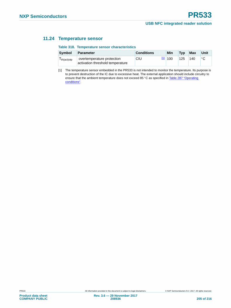
NXP Semiconductors PR533USB NFC integrated reader solution
11.24 Temperature sensor
[1] The temperature sensor embedded in the PR533 is not intended to monitor the temperature. Its purpose is to prevent destruction of the IC due to excessive heat. The external application should include circuitry to ensure that the ambient temperature does not exceed 85 C as specified in Table 287 “Operating conditions”.
Table 318. Temperature sensor characteristics
Symbol Parameter Conditions Min Typ Max Unit
Tth(act)otp overtemperature protection activation threshold temperature
CIU [1] 100 125 140 C
PR533 All information provided in this document is subject to legal disclaimers. © NXP Semiconductors N.V. 2017. All rights reserved.
Product data sheetCOMPANY PUBLIC
Rev. 3.6 — 29 November 2017208936 205 of 216
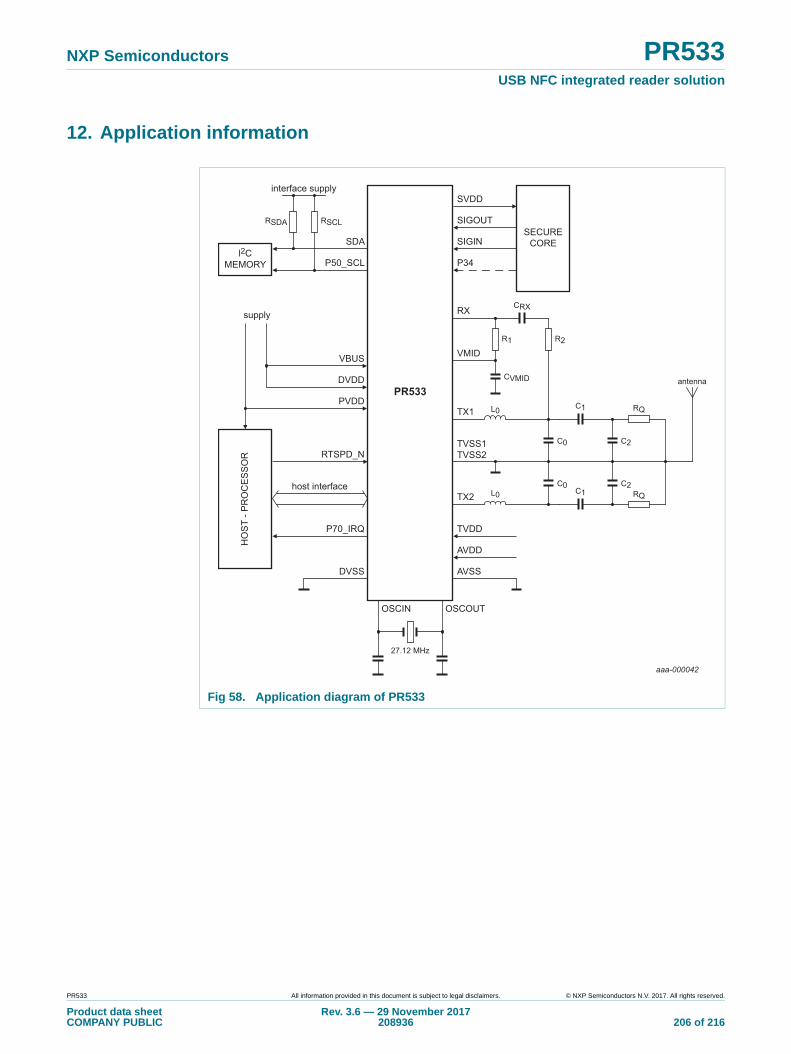
NXP Semiconductors PR533USB NFC integrated reader solution
12. Application information
Fig 58. Application diagram of PR533
aaa-000042
RSCL
R1
L0
L0
C1
C1
C0 C2
C0 C2
RQ
RQ
R2
CRX
antennaCVMID
interface supply
supply
RSDA
l2CMEMORY
SECURECORESDA
SVDD
SIGOUT
SIGIN
TVDDP70_IRQ
RTSPD_N
PVDD
DVDD
VBUS
HO
ST
- PR
OC
ES
SO
R
host interface
AVDD
OSCIN OSCOUT
AVSSDVSS
27.12 MHz
P34
RX
VMID
PR533
TX1
TVSS1TVSS2
TX2
P50_SCL
PR533 All information provided in this document is subject to legal disclaimers. © NXP Semiconductors N.V. 2017. All rights reserved.
Product data sheetCOMPANY PUBLIC
Rev. 3.6 — 29 November 2017208936 206 of 216
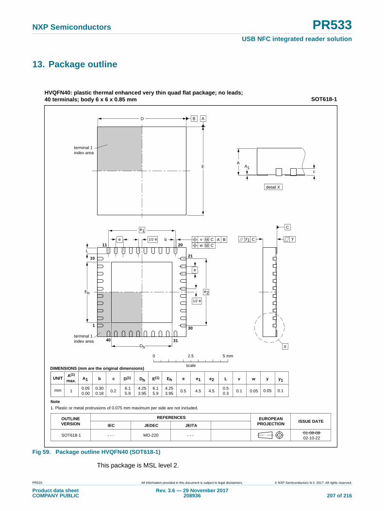
NXP Semiconductors PR533USB NFC integrated reader solution
13. Package outline
This package is MSL level 2.
Fig 59. Package outline HVQFN40 (SOT618-1)
terminal 1index area
0.51
A1 EhbUNIT ye
0.2
c
REFERENCESOUTLINEVERSION
EUROPEANPROJECTION ISSUE DATE
IEC JEDEC JEITA
mm 6.15.9
Dh
4.253.95
y1
6.15.9
4.253.95
e1
4.5
e2
4.50.300.18
0.050.00
0.05 0.1
DIMENSIONS (mm are the original dimensions)
SOT618-1 MO-220- - - - - -
0.50.3
L
0.1
v
0.05
w
0 2.5 5 mm
scale
SOT618-1HVQFN40: plastic thermal enhanced very thin quad flat package; no leads;40 terminals; body 6 x 6 x 0.85 mm
A(1)
max.
AA1
c
detail X
yy1 Ce
L
Eh
Dh
e
e1
b11 20
40 31
30
2110
1
X
D
E
C
B A
e2
01-08-0802-10-22
terminal 1index area
1/2 e
1/2 e
ACC
Bv M
w M
Note
1. Plastic or metal protrusions of 0.075 mm maximum per side are not included.
D(1) E(1)
PR533 All information provided in this document is subject to legal disclaimers. © NXP Semiconductors N.V. 2017. All rights reserved.
Product data sheetCOMPANY PUBLIC
Rev. 3.6 — 29 November 2017208936 207 of 216

NXP Semiconductors PR533USB NFC integrated reader solution
14. Abbreviations
15. Glossary
Initiator — Generates RF field at 13.56 MHz and starts the NFCIP-1 communication.
Load modulation Index — The load modulation index is defined as the card’s voltage ratio (Vmax - Vmin) / (Vmax + Vmin) measured at the card’s coil.
Modulation Index — The modulation index is defined as the voltage ratio (Vmax - Vmin) / (Vmax + Vmin).
Target — Responds to initiator command either using load modulation scheme (RF field generated by Initiator) or using modulation of self-generated RF field (no RF field generated by initiator during target answer).
Table 319. Abbreviations
Acronym Description
ASK Amplitude Shift Keying
CDM Charge Device body Model
CIU Contactless Interface Unit
CRC Cyclic Redundancy Check
EEPROM Electrically Erasable Programmable Read-Only Memory
HPD Hard Power Down (see Section 7.5.6 on page 93)
HBM Human Body Model
HPD Hard Power Down
HZ High Impedance
MM Machine Model
MSL Moisture Sensitivity Level
NFC Near Field Communication
PCD Proximity Coupling Device. Definition for a Card Reader/ Writer according to the ISO/IEC 14443 Specification
PCR Power Clock Reset controller
PICC Proximity Cards. Definition for a contactless Smart Card according to the ISO/IEC 14443 specification
SAM Secure Access Module
SIC Secure Integrated Circuit (can be a Smart Card IC, a Secure Access Module (SAM),...)
SPI Serial Parallel Interface
SPD Soft Power Down mode (see Section 7.5.7 on page 93)
PR533 All information provided in this document is subject to legal disclaimers. © NXP Semiconductors N.V. 2017. All rights reserved.
Product data sheetCOMPANY PUBLIC
Rev. 3.6 — 29 November 2017208936 208 of 216
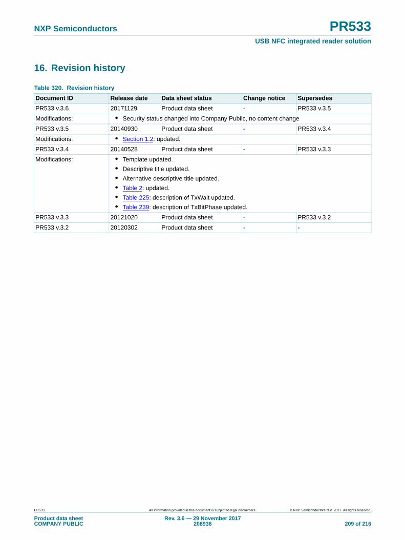
NXP Semiconductors PR533USB NFC integrated reader solution
16. Revision history
Table 320. Revision history
Document ID Release date Data sheet status Change notice Supersedes
PR533 v.3.6 20171129 Product data sheet - PR533 v.3.5
Modifications: • Security status changed into Company Pubilc, no content change
PR533 v.3.5 20140930 Product data sheet - PR533 v.3.4
Modifications: • Section 1.2: updated.
PR533 v.3.4 20140528 Product data sheet - PR533 v.3.3
Modifications: • Template updated.
• Descriptive title updated.
• Alternative descriptive title updated.
• Table 2: updated.
• Table 225: description of TxWait updated.
• Table 239: description of TxBitPhase updated.
PR533 v.3.3 20121020 Product data sheet - PR533 v.3.2
PR533 v.3.2 20120302 Product data sheet - -
PR533 All information provided in this document is subject to legal disclaimers. © NXP Semiconductors N.V. 2017. All rights reserved.
Product data sheetCOMPANY PUBLIC
Rev. 3.6 — 29 November 2017208936 209 of 216

NXP Semiconductors PR533USB NFC integrated reader solution
17. Legal information
17.1 Data sheet status
[1] Please consult the most recently issued document before initiating or completing a design.
[2] The term ‘short data sheet’ is explained in section “Definitions”.
[3] The product status of device(s) described in this document may have changed since this document was published and may differ in case of multiple devices. The latest product status information is available on the Internet at URL http://www.nxp.com.
17.2 Definitions
Draft — The document is a draft version only. The content is still under internal review and subject to formal approval, which may result in modifications or additions. NXP Semiconductors does not give any representations or warranties as to the accuracy or completeness of information included herein and shall have no liability for the consequences of use of such information.
Short data sheet — A short data sheet is an extract from a full data sheet with the same product type number(s) and title. A short data sheet is intended for quick reference only and should not be relied upon to contain detailed and full information. For detailed and full information see the relevant full data sheet, which is available on request via the local NXP Semiconductors sales office. In case of any inconsistency or conflict with the short data sheet, the full data sheet shall prevail.
Product specification — The information and data provided in a Product data sheet shall define the specification of the product as agreed between NXP Semiconductors and its customer, unless NXP Semiconductors and customer have explicitly agreed otherwise in writing. In no event however, shall an agreement be valid in which the NXP Semiconductors product is deemed to offer functions and qualities beyond those described in the Product data sheet.
17.3 Disclaimers
Limited warranty and liability — Information in this document is believed to be accurate and reliable. However, NXP Semiconductors does not give any representations or warranties, expressed or implied, as to the accuracy or completeness of such information and shall have no liability for the consequences of use of such information. NXP Semiconductors takes no responsibility for the content in this document if provided by an information source outside of NXP Semiconductors.
In no event shall NXP Semiconductors be liable for any indirect, incidental, punitive, special or consequential damages (including - without limitation - lost profits, lost savings, business interruption, costs related to the removal or replacement of any products or rework charges) whether or not such damages are based on tort (including negligence), warranty, breach of contract or any other legal theory.
Notwithstanding any damages that customer might incur for any reason whatsoever, NXP Semiconductors’ aggregate and cumulative liability towards customer for the products described herein shall be limited in accordance with the Terms and conditions of commercial sale of NXP Semiconductors.
Right to make changes — NXP Semiconductors reserves the right to make changes to information published in this document, including without limitation specifications and product descriptions, at any time and without notice. This document supersedes and replaces all information supplied prior to the publication hereof.
Suitability for use — NXP Semiconductors products are not designed, authorized or warranted to be suitable for use in life support, life-critical or safety-critical systems or equipment, nor in applications where failure or malfunction of an NXP Semiconductors product can reasonably be expected to result in personal injury, death or severe property or environmental damage. NXP Semiconductors and its suppliers accept no liability for inclusion and/or use of NXP Semiconductors products in such equipment or applications and therefore such inclusion and/or use is at the customer’s own risk.
Applications — Applications that are described herein for any of these products are for illustrative purposes only. NXP Semiconductors makes no representation or warranty that such applications will be suitable for the specified use without further testing or modification.
Customers are responsible for the design and operation of their applications and products using NXP Semiconductors products, and NXP Semiconductors accepts no liability for any assistance with applications or customer product design. It is customer’s sole responsibility to determine whether the NXP Semiconductors product is suitable and fit for the customer’s applications and products planned, as well as for the planned application and use of customer’s third party customer(s). Customers should provide appropriate design and operating safeguards to minimize the risks associated with their applications and products.
NXP Semiconductors does not accept any liability related to any default, damage, costs or problem which is based on any weakness or default in the customer’s applications or products, or the application or use by customer’s third party customer(s). Customer is responsible for doing all necessary testing for the customer’s applications and products using NXP Semiconductors products in order to avoid a default of the applications and the products or of the application or use by customer’s third party customer(s). NXP does not accept any liability in this respect.
Limiting values — Stress above one or more limiting values (as defined in the Absolute Maximum Ratings System of IEC 60134) will cause permanent damage to the device. Limiting values are stress ratings only and (proper) operation of the device at these or any other conditions above those given in the Recommended operating conditions section (if present) or the Characteristics sections of this document is not warranted. Constant or repeated exposure to limiting values will permanently and irreversibly affect the quality and reliability of the device.
Terms and conditions of commercial sale — NXP Semiconductors products are sold subject to the general terms and conditions of commercial sale, as published at http://www.nxp.com/profile/terms, unless otherwise agreed in a valid written individual agreement. In case an individual agreement is concluded only the terms and conditions of the respective agreement shall apply. NXP Semiconductors hereby expressly objects to applying the customer’s general terms and conditions with regard to the purchase of NXP Semiconductors products by customer.
No offer to sell or license — Nothing in this document may be interpreted or construed as an offer to sell products that is open for acceptance or the grant, conveyance or implication of any license under any copyrights, patents or other industrial or intellectual property rights.
Document status[1][2] Product status[3] Definition
Objective [short] data sheet Development This document contains data from the objective specification for product development.
Preliminary [short] data sheet Qualification This document contains data from the preliminary specification.
Product [short] data sheet Production This document contains the product specification.
PR533 All information provided in this document is subject to legal disclaimers. © NXP Semiconductors N.V. 2017. All rights reserved.
Product data sheetCOMPANY PUBLIC
Rev. 3.6 — 29 November 2017208936 210 of 216

NXP Semiconductors PR533USB NFC integrated reader solution
Export control — This document as well as the item(s) described herein may be subject to export control regulations. Export might require a prior authorization from competent authorities.
Quick reference data — The Quick reference data is an extract of the product data given in the Limiting values and Characteristics sections of this document, and as such is not complete, exhaustive or legally binding.
Non-automotive qualified products — Unless this data sheet expressly states that this specific NXP Semiconductors product is automotive qualified, the product is not suitable for automotive use. It is neither qualified nor tested in accordance with automotive testing or application requirements. NXP Semiconductors accepts no liability for inclusion and/or use of non-automotive qualified products in automotive equipment or applications.
In the event that customer uses the product for design-in and use in automotive applications to automotive specifications and standards, customer (a) shall use the product without NXP Semiconductors’ warranty of the product for such automotive applications, use and specifications, and (b) whenever customer uses the product for automotive applications beyond NXP Semiconductors’ specifications such use shall be solely at customer’s own risk, and (c) customer fully indemnifies NXP Semiconductors for any liability, damages or failed product claims resulting from customer design and use of the product for automotive applications beyond NXP Semiconductors’ standard warranty and NXP Semiconductors’ product specifications.
Translations — A non-English (translated) version of a document is for reference only. The English version shall prevail in case of any discrepancy between the translated and English versions.
17.4 Licenses
17.5 TrademarksNotice: All referenced brands, product names, service names and trademarks are the property of their respective owners.
MIFARE — is a trademark of NXP B.V.
I2C-bus — logo is a trademark of NXP B.V.
18. Contact information
For more information, please visit: http://www.nxp.com
For sales office addresses, please send an email to: [email protected]
Purchase of NXP ICs with ISO/IEC 14443 type B functionality
This NXP Semiconductors IC is ISO/IEC 14443 Type B software enabled and is licensed under Innovatron’s Contactless Card patents license for ISO/IEC 14443 B.
The license includes the right to use the IC in systems and/or end-user equipment.
RATP/Innovatron Technology
Purchase of NXP ICs with NFC technology
Purchase of an NXP Semiconductors IC that complies with one of the Near Field Communication (NFC) standards ISO/IEC 18092 and ISO/IEC 21481 does not convey an implied license under any patent right infringed by implementation of any of those standards. Purchase of NXP Semiconductors IC does not include a license to any NXP patent (or other IP right) covering combinations of those products with other products, whether hardware or software.
PR533 All information provided in this document is subject to legal disclaimers. © NXP Semiconductors N.V. 2017. All rights reserved.
Product data sheetCOMPANY PUBLIC
Rev. 3.6 — 29 November 2017208936 211 of 216

NXP Semiconductors PR533USB NFC integrated reader solution
Notes
PR533 All information provided in this document is subject to legal disclaimers. © NXP Semiconductors N.V. 2017. All rights reserved.
Product data sheetCOMPANY PUBLIC
Rev. 3.6 — 29 November 2017208936 212 of 216
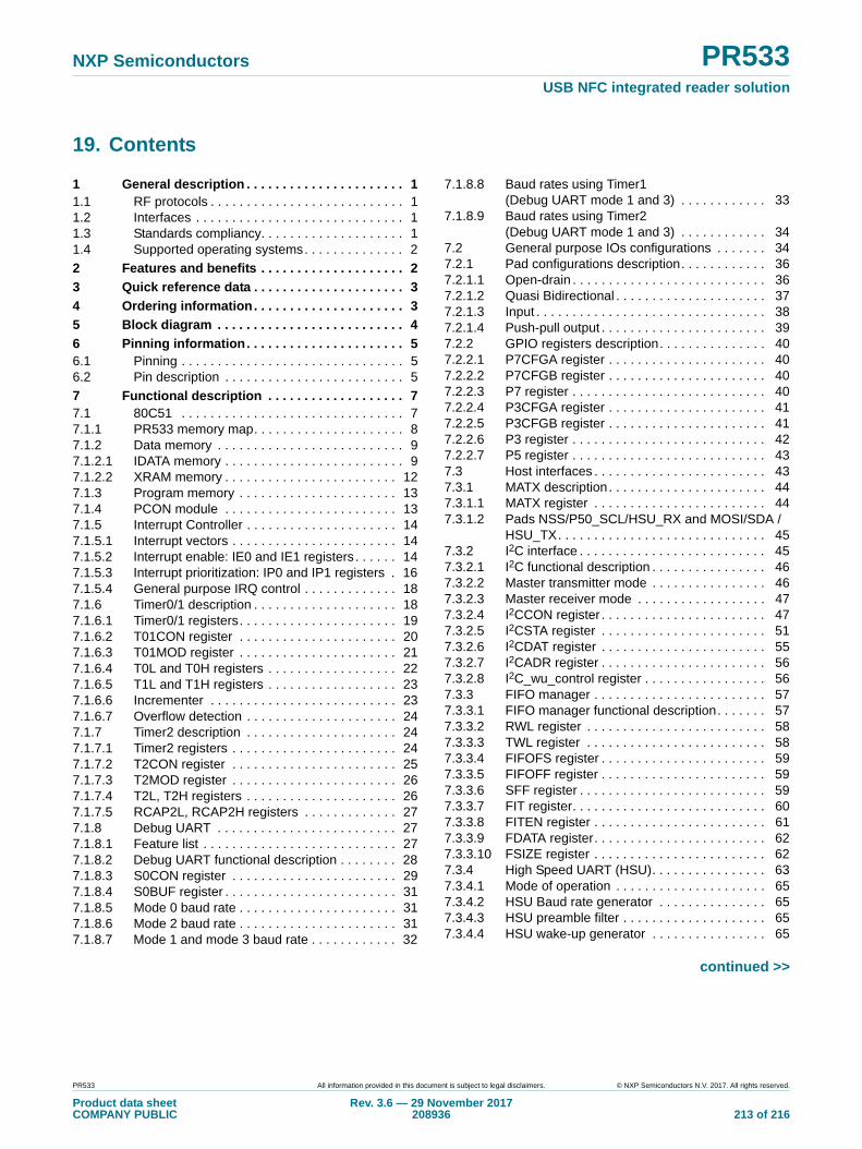
NXP Semiconductors PR533USB NFC integrated reader solution
19. Contents
1 General description . . . . . . . . . . . . . . . . . . . . . . 11.1 RF protocols . . . . . . . . . . . . . . . . . . . . . . . . . . . 11.2 Interfaces . . . . . . . . . . . . . . . . . . . . . . . . . . . . . 11.3 Standards compliancy. . . . . . . . . . . . . . . . . . . . 11.4 Supported operating systems. . . . . . . . . . . . . . 2
2 Features and benefits . . . . . . . . . . . . . . . . . . . . 2
3 Quick reference data . . . . . . . . . . . . . . . . . . . . . 3
4 Ordering information. . . . . . . . . . . . . . . . . . . . . 3
5 Block diagram . . . . . . . . . . . . . . . . . . . . . . . . . . 4
6 Pinning information. . . . . . . . . . . . . . . . . . . . . . 56.1 Pinning . . . . . . . . . . . . . . . . . . . . . . . . . . . . . . . 56.2 Pin description . . . . . . . . . . . . . . . . . . . . . . . . . 5
7 Functional description . . . . . . . . . . . . . . . . . . . 77.1 80C51 . . . . . . . . . . . . . . . . . . . . . . . . . . . . . . . 77.1.1 PR533 memory map. . . . . . . . . . . . . . . . . . . . . 87.1.2 Data memory . . . . . . . . . . . . . . . . . . . . . . . . . . 97.1.2.1 IDATA memory . . . . . . . . . . . . . . . . . . . . . . . . . 97.1.2.2 XRAM memory . . . . . . . . . . . . . . . . . . . . . . . . 127.1.3 Program memory . . . . . . . . . . . . . . . . . . . . . . 137.1.4 PCON module . . . . . . . . . . . . . . . . . . . . . . . . 137.1.5 Interrupt Controller . . . . . . . . . . . . . . . . . . . . . 147.1.5.1 Interrupt vectors . . . . . . . . . . . . . . . . . . . . . . . 147.1.5.2 Interrupt enable: IE0 and IE1 registers. . . . . . 147.1.5.3 Interrupt prioritization: IP0 and IP1 registers . 167.1.5.4 General purpose IRQ control . . . . . . . . . . . . . 187.1.6 Timer0/1 description . . . . . . . . . . . . . . . . . . . . 187.1.6.1 Timer0/1 registers. . . . . . . . . . . . . . . . . . . . . . 197.1.6.2 T01CON register . . . . . . . . . . . . . . . . . . . . . . 207.1.6.3 T01MOD register . . . . . . . . . . . . . . . . . . . . . . 217.1.6.4 T0L and T0H registers . . . . . . . . . . . . . . . . . . 227.1.6.5 T1L and T1H registers . . . . . . . . . . . . . . . . . . 237.1.6.6 Incrementer . . . . . . . . . . . . . . . . . . . . . . . . . . 237.1.6.7 Overflow detection . . . . . . . . . . . . . . . . . . . . . 247.1.7 Timer2 description . . . . . . . . . . . . . . . . . . . . . 247.1.7.1 Timer2 registers . . . . . . . . . . . . . . . . . . . . . . . 247.1.7.2 T2CON register . . . . . . . . . . . . . . . . . . . . . . . 257.1.7.3 T2MOD register . . . . . . . . . . . . . . . . . . . . . . . 267.1.7.4 T2L, T2H registers . . . . . . . . . . . . . . . . . . . . . 267.1.7.5 RCAP2L, RCAP2H registers . . . . . . . . . . . . . 277.1.8 Debug UART . . . . . . . . . . . . . . . . . . . . . . . . . 277.1.8.1 Feature list . . . . . . . . . . . . . . . . . . . . . . . . . . . 277.1.8.2 Debug UART functional description . . . . . . . . 287.1.8.3 S0CON register . . . . . . . . . . . . . . . . . . . . . . . 297.1.8.4 S0BUF register . . . . . . . . . . . . . . . . . . . . . . . . 317.1.8.5 Mode 0 baud rate . . . . . . . . . . . . . . . . . . . . . . 317.1.8.6 Mode 2 baud rate . . . . . . . . . . . . . . . . . . . . . . 317.1.8.7 Mode 1 and mode 3 baud rate . . . . . . . . . . . . 32
7.1.8.8 Baud rates using Timer1 (Debug UART mode 1 and 3) . . . . . . . . . . . . 33
7.1.8.9 Baud rates using Timer2 (Debug UART mode 1 and 3) . . . . . . . . . . . . 34
7.2 General purpose IOs configurations . . . . . . . 347.2.1 Pad configurations description. . . . . . . . . . . . 367.2.1.1 Open-drain . . . . . . . . . . . . . . . . . . . . . . . . . . . 367.2.1.2 Quasi Bidirectional . . . . . . . . . . . . . . . . . . . . . 377.2.1.3 Input . . . . . . . . . . . . . . . . . . . . . . . . . . . . . . . . 387.2.1.4 Push-pull output . . . . . . . . . . . . . . . . . . . . . . . 397.2.2 GPIO registers description. . . . . . . . . . . . . . . 407.2.2.1 P7CFGA register . . . . . . . . . . . . . . . . . . . . . . 407.2.2.2 P7CFGB register . . . . . . . . . . . . . . . . . . . . . . 407.2.2.3 P7 register . . . . . . . . . . . . . . . . . . . . . . . . . . . 407.2.2.4 P3CFGA register . . . . . . . . . . . . . . . . . . . . . . 417.2.2.5 P3CFGB register . . . . . . . . . . . . . . . . . . . . . . 417.2.2.6 P3 register . . . . . . . . . . . . . . . . . . . . . . . . . . . 427.2.2.7 P5 register . . . . . . . . . . . . . . . . . . . . . . . . . . . 437.3 Host interfaces . . . . . . . . . . . . . . . . . . . . . . . . 437.3.1 MATX description. . . . . . . . . . . . . . . . . . . . . . 447.3.1.1 MATX register . . . . . . . . . . . . . . . . . . . . . . . . 447.3.1.2 Pads NSS/P50_SCL/HSU_RX and MOSI/SDA /
HSU_TX. . . . . . . . . . . . . . . . . . . . . . . . . . . . . 457.3.2 I2C interface . . . . . . . . . . . . . . . . . . . . . . . . . . 457.3.2.1 I2C functional description . . . . . . . . . . . . . . . . 467.3.2.2 Master transmitter mode . . . . . . . . . . . . . . . . 467.3.2.3 Master receiver mode . . . . . . . . . . . . . . . . . . 477.3.2.4 I2CCON register . . . . . . . . . . . . . . . . . . . . . . . 477.3.2.5 I2CSTA register . . . . . . . . . . . . . . . . . . . . . . . 517.3.2.6 I2CDAT register . . . . . . . . . . . . . . . . . . . . . . . 557.3.2.7 I2CADR register . . . . . . . . . . . . . . . . . . . . . . . 567.3.2.8 I2C_wu_control register . . . . . . . . . . . . . . . . . 567.3.3 FIFO manager . . . . . . . . . . . . . . . . . . . . . . . . 577.3.3.1 FIFO manager functional description. . . . . . . 577.3.3.2 RWL register . . . . . . . . . . . . . . . . . . . . . . . . . 587.3.3.3 TWL register . . . . . . . . . . . . . . . . . . . . . . . . . 587.3.3.4 FIFOFS register . . . . . . . . . . . . . . . . . . . . . . . 597.3.3.5 FIFOFF register . . . . . . . . . . . . . . . . . . . . . . . 597.3.3.6 SFF register . . . . . . . . . . . . . . . . . . . . . . . . . . 597.3.3.7 FIT register. . . . . . . . . . . . . . . . . . . . . . . . . . . 607.3.3.8 FITEN register . . . . . . . . . . . . . . . . . . . . . . . . 617.3.3.9 FDATA register. . . . . . . . . . . . . . . . . . . . . . . . 627.3.3.10 FSIZE register . . . . . . . . . . . . . . . . . . . . . . . . 627.3.4 High Speed UART (HSU). . . . . . . . . . . . . . . . 637.3.4.1 Mode of operation . . . . . . . . . . . . . . . . . . . . . 657.3.4.2 HSU Baud rate generator . . . . . . . . . . . . . . . 657.3.4.3 HSU preamble filter . . . . . . . . . . . . . . . . . . . . 657.3.4.4 HSU wake-up generator . . . . . . . . . . . . . . . . 65
PR533 All information provided in this document is subject to legal disclaimers. © NXP Semiconductors N.V. 2017. All rights reserved.
Product data sheetCOMPANY PUBLIC
Rev. 3.6 — 29 November 2017208936 213 of 216
continued >>

NXP Semiconductors PR533USB NFC integrated reader solution
7.3.4.5 HSU_STA register . . . . . . . . . . . . . . . . . . . . . 667.3.4.6 HSU_CTR register . . . . . . . . . . . . . . . . . . . . . 677.3.4.7 HSU_PRE register . . . . . . . . . . . . . . . . . . . . . 687.3.4.8 HSU_CNT register . . . . . . . . . . . . . . . . . . . . . 687.3.5 USB . . . . . . . . . . . . . . . . . . . . . . . . . . . . . . . . 697.3.5.1 Features list . . . . . . . . . . . . . . . . . . . . . . . . . . 697.3.5.2 USB interrupt . . . . . . . . . . . . . . . . . . . . . . . . . 697.3.5.3 Resume by host . . . . . . . . . . . . . . . . . . . . . . . 69
Resume by host in supsend state . . . . . . . . . .69Resume by Host before clock is disabled. . . . .70
7.3.5.4 Remote wake-up . . . . . . . . . . . . . . . . . . . . . . 717.3.5.5 Softconnect. . . . . . . . . . . . . . . . . . . . . . . . . . . 727.3.5.6 USB embedded firmware view . . . . . . . . . . . . 737.4 Power management . . . . . . . . . . . . . . . . . . . . 837.4.1 5 V external power source . . . . . . . . . . . . . . . 837.4.2 3.3 V external power source configurations . . 847.4.3 HOST powered (single source) . . . . . . . . . . . 857.4.4 HOST powered (double source) . . . . . . . . . . . 867.4.5 Power saving modes - short description. . . . . 877.4.6 Power-on reset . . . . . . . . . . . . . . . . . . . . . . . . 877.4.7 Regulator - short description . . . . . . . . . . . . . 887.4.8 Main switch. . . . . . . . . . . . . . . . . . . . . . . . . . . 887.4.9 SVDD switch. . . . . . . . . . . . . . . . . . . . . . . . . . 897.5 Power clock and reset controller. . . . . . . . . . . 907.5.1 PCR in the system . . . . . . . . . . . . . . . . . . . . . 907.5.2 27.12 MHz crystal oscillator . . . . . . . . . . . . . . 927.5.3 PLL for USB clock generation . . . . . . . . . . . . 927.5.4 Power-up sequence . . . . . . . . . . . . . . . . . . . . 927.5.5 Power saving modes . . . . . . . . . . . . . . . . . . . 937.5.6 Reset modes . . . . . . . . . . . . . . . . . . . . . . . . . 937.5.7 Soft-Power-down mode (SPD) . . . . . . . . . . . . 937.5.8 Suspend mode . . . . . . . . . . . . . . . . . . . . . . . . 947.5.9 Remote wake-up . . . . . . . . . . . . . . . . . . . . . . 947.5.10 PCR extension registers . . . . . . . . . . . . . . . . 967.5.11 PCR register description. . . . . . . . . . . . . . . . . 967.5.11.1 CFR register . . . . . . . . . . . . . . . . . . . . . . . . . . 967.5.11.2 CER register . . . . . . . . . . . . . . . . . . . . . . . . . . 977.5.11.3 ILR register . . . . . . . . . . . . . . . . . . . . . . . . . . . 987.5.11.4 PCR Control register . . . . . . . . . . . . . . . . . . . 997.5.11.5 PCR Status register . . . . . . . . . . . . . . . . . . . 1007.5.11.6 Wakeupen register . . . . . . . . . . . . . . . . . . . . 1007.6 Contactless Interface Unit (CIU) . . . . . . . . . . 1017.6.1 Feature list . . . . . . . . . . . . . . . . . . . . . . . . . . 1027.6.2 Simplified block diagram. . . . . . . . . . . . . . . . 1027.6.3 Reader/Writer modes . . . . . . . . . . . . . . . . . . 1037.6.3.1 ISO/IEC 14443A Reader/Writer . . . . . . . . . . 1037.6.3.2 FeliCa Reader/Writer . . . . . . . . . . . . . . . . . . 1047.6.3.3 ISO/IEC 14443B Reader/Writer . . . . . . . . . . 1057.6.4 Overall CIU block diagram . . . . . . . . . . . . . . 1067.6.5 Transmitter control . . . . . . . . . . . . . . . . . . . . 1087.6.6 RF level detector . . . . . . . . . . . . . . . . . . . . . 111
7.6.7 Antenna presence self test . . . . . . . . . . . . . . 1127.6.7.1 Principle . . . . . . . . . . . . . . . . . . . . . . . . . . . . . 1127.6.7.2 Antenna presence detector register. . . . . . . . 1137.6.8 Random number generator . . . . . . . . . . . . . . 1147.6.9 Data mode detector . . . . . . . . . . . . . . . . . . . . 1157.6.10 Serial data switch. . . . . . . . . . . . . . . . . . . . . . 1167.6.10.1 Serial data switch for driver and loadmod . . . 1167.6.11 NFC-WI/S2C interface support. . . . . . . . . . . . 1177.6.11.1 Signal shape for FeliCa NFC-WI/S2C interface
support . . . . . . . . . . . . . . . . . . . . . . . . . . . . . . 1187.6.11.2 Signal shape for ISO/IEC14443A and MIFARE
NFC-WI/S2C support . . . . . . . . . . . . . . . . . . . 1197.6.11.3 NFC-WI/S2C initiator mode . . . . . . . . . . . . . 1207.6.12 Hardware support for FeliCa and NFC
polling. . . . . . . . . . . . . . . . . . . . . . . . . . . . . . 1217.6.12.1 Polling sequence functionality for initiator . . 1217.6.12.2 Polling sequence functionality for target . . . 1217.6.12.3 Additional hardware support for FeliCa
and NFC. . . . . . . . . . . . . . . . . . . . . . . . . . . . 1227.6.13 CRC co-processor . . . . . . . . . . . . . . . . . . . . 1227.6.14 FIFO buffer. . . . . . . . . . . . . . . . . . . . . . . . . . 1237.6.14.1 Accessing the FIFO buffer . . . . . . . . . . . . . . 1237.6.14.2 Controlling the FIFO buffer . . . . . . . . . . . . . 1237.6.14.3 Status information about the FIFO buffer . . . 1237.6.15 CIU_timer . . . . . . . . . . . . . . . . . . . . . . . . . . 1247.6.16 Interrupt request system . . . . . . . . . . . . . . . 1257.6.16.1 Interrupt sources . . . . . . . . . . . . . . . . . . . . . 1257.6.17 CIU Power Reduction Modes. . . . . . . . . . . . 1267.6.17.1 Hard-Power-down . . . . . . . . . . . . . . . . . . . . 1267.6.17.2 CIU Power-down . . . . . . . . . . . . . . . . . . . . . 1267.6.17.3 Transmitter Power-down . . . . . . . . . . . . . . . 1277.6.18 CIU command set . . . . . . . . . . . . . . . . . . . . 1277.6.18.1 General description . . . . . . . . . . . . . . . . . . . 1277.6.18.2 General behaviour . . . . . . . . . . . . . . . . . . . . 1277.6.18.3 Commands overview . . . . . . . . . . . . . . . . . . 1287.6.18.4 Idle command . . . . . . . . . . . . . . . . . . . . . . . 1287.6.18.5 Config command . . . . . . . . . . . . . . . . . . . . . 1287.6.18.6 Generate RandomID command . . . . . . . . . . 1297.6.18.7 CalcCRC command . . . . . . . . . . . . . . . . . . . 1297.6.18.8 Transmit command . . . . . . . . . . . . . . . . . . . 1297.6.18.9 NoCmdChange command . . . . . . . . . . . . . . 1297.6.18.10 Receive command . . . . . . . . . . . . . . . . . . . . 1297.6.18.11 Transceive command. . . . . . . . . . . . . . . . . . 1307.6.18.12 AutoColl command. . . . . . . . . . . . . . . . . . . . 1307.6.18.13 MFAuthent command. . . . . . . . . . . . . . . . . . 1327.6.18.14 SoftReset command . . . . . . . . . . . . . . . . . . 1337.6.19 CIU tests signals . . . . . . . . . . . . . . . . . . . . . 1337.6.19.1 CIU self-test . . . . . . . . . . . . . . . . . . . . . . . . . 1337.6.19.2 CIU test bus . . . . . . . . . . . . . . . . . . . . . . . . . 1347.6.19.3 Test signals at pin AUX . . . . . . . . . . . . . . . . 1357.6.19.4 PRBS . . . . . . . . . . . . . . . . . . . . . . . . . . . . . . 135
PR533 All information provided in this document is subject to legal disclaimers. © NXP Semiconductors N.V. 2017. All rights reserved.
Product data sheetCOMPANY PUBLIC
Rev. 3.6 — 29 November 2017208936 214 of 216
continued >>

NXP Semiconductors PR533USB NFC integrated reader solution
7.6.20 CIU memory map . . . . . . . . . . . . . . . . . . . . . 1357.6.21 CIU register description . . . . . . . . . . . . . . . . 1377.6.21.1 CIU register bit behaviour . . . . . . . . . . . . . . . 1377.6.21.2 CIU_SIC_CLK_en register (6330h) . . . . . . . 1377.6.21.3 CIU_Command register (D1h or 6331h). . . . 1387.6.21.4 CIU_CommIEn register (D2h or 6332h) . . . . 1397.6.21.5 CIU_DivIEn register (D3h or 6333h). . . . . . . 1397.6.21.6 CIU_CommIrq register (D4h or 6334h). . . . . 1407.6.21.7 CIU_DivIrq register (D5h or 6335h) . . . . . . . 1417.6.21.8 CIU_Error register (D6h or 6336h) . . . . . . . . 1427.6.21.9 CIU_Status1 register (DFh or 6337h) . . . . . . 1437.6.21.10 CIU_Status2 register (E9h or 6338h) . . . . . . 1447.6.21.11 CIU_FIFOData register (EAh or 6339h) . . . . 1457.6.21.12 CIU_FIFOLevel register (EBh or 633Ah) . . . 1457.6.21.13 CIU_WaterLevel register (ECh or 633Bh) . . 1467.6.21.14 CIU_Control register (EDh or 633Ch). . . . . . 1467.6.21.15 CIU_BitFraming register (EEh or 633Dh) . . . 1477.6.21.16 CIU_Coll register (EFh or 633Eh). . . . . . . . . 1477.6.21.17 CIU_Mode register (6301h) . . . . . . . . . . . . . 1487.6.21.18 CIU_TxMode register (6302h) . . . . . . . . . . . 1497.6.21.19 CIU_RxMode register (6303h) . . . . . . . . . . . 1507.6.21.20 CIU_TxControl register (6304h) . . . . . . . . . . 1517.6.21.21 CIU_TxAuto register (6305h) . . . . . . . . . . . . 1527.6.21.22 CIU_TxSel register (6306h) . . . . . . . . . . . . . 1537.6.21.23 CIU_RxSel register (6307h) . . . . . . . . . . . . . 1547.6.21.24 CIU_RxThreshold register (6308h). . . . . . . . 1557.6.21.25 CIU_Demod register (6309h) . . . . . . . . . . . . 1557.6.21.26 CIU_FelNFC1 register (630Ah) . . . . . . . . . . 1567.6.21.27 CIU_FelNFC2 register (630Bh) . . . . . . . . . . 1567.6.21.28 CIU_MifNFC register (630Ch) . . . . . . . . . . . 1577.6.21.29 CIU_ManualRCV register (630Dh) . . . . . . . . 1587.6.21.30 CIU_TypeB register (630Eh) . . . . . . . . . . . . 1597.6.21.31 CIU_CRCResultMSB register (6311h) . . . . . 1607.6.21.32 CIU_CRCResultLSB register (6312h) . . . . . 1607.6.21.33 CIU_GsNOff register (6313h) . . . . . . . . . . . . 1617.6.21.34 CIU_ModWidth register (6314h) . . . . . . . . . . 1627.6.21.35 CIU_TxBitPhase register (6315h). . . . . . . . . 1627.6.21.36 CIU_RFCfg register (6316h) . . . . . . . . . . . . 1637.6.21.37 CIU_GsNOn register (6317h) . . . . . . . . . . . . 1647.6.21.38 CIU_CWGsP register (6318h) . . . . . . . . . . . 1657.6.21.39 CIU_ModGsP register (6319h) . . . . . . . . . . . 1657.6.21.40 CIU_TMode register (631Ah) . . . . . . . . . . . . 1667.6.21.41 CIU_TPrescaler register (631Bh) . . . . . . . . . 1677.6.21.42 CIU_TReload_hi register (631Ch) . . . . . . . . 1687.6.21.43 CIU_TReloadVal_lo register (631Dh) . . . . . . 1687.6.21.44 CIU_TCounterVal_hi register (631Eh) . . . . . 1687.6.21.45 CIU_TCounterVal_lo register (631Fh) . . . . . 1697.6.21.46 CIU_TestSel1 register (6321h) . . . . . . . . . . . 1697.6.21.47 CIU_TestSel2 register (6322h) . . . . . . . . . . . 1707.6.21.48 CIU_TestPinEn register (6323h). . . . . . . . . . 1717.6.21.49 CIU_TestPinValue register (6324h) . . . . . . . 171
7.6.21.50 CIU_TestBus register (6325h) . . . . . . . . . . . 1717.6.21.51 CIU_AutoTest register (6326h) . . . . . . . . . . 1727.6.21.52 CIU_Version register (6327h) . . . . . . . . . . . 1727.6.21.53 CIU_AnalogTest register (6328h). . . . . . . . . 1727.6.21.54 CIU_TestDAC1 register (6329h) . . . . . . . . . 1747.6.21.55 CIU_TestDAC2 register (632Ah) . . . . . . . . . 1757.6.21.56 CIU_TestADC register (632Bh) . . . . . . . . . . 1757.6.21.57 CIU_RFlevelDet register (632Fh) . . . . . . . . 1757.7 Registers map . . . . . . . . . . . . . . . . . . . . . . . 1777.7.1 Standard registers . . . . . . . . . . . . . . . . . . . . 1777.7.2 SFR registers . . . . . . . . . . . . . . . . . . . . . . . . 181
8 Limiting values . . . . . . . . . . . . . . . . . . . . . . . 185
9 Recommended operating conditions . . . . . 185
10 Thermal characteristics . . . . . . . . . . . . . . . . 186
11 Characteristics . . . . . . . . . . . . . . . . . . . . . . . 18611.1 Power management characteristics. . . . . . . 18611.1.1 Current consumption characteristics . . . . . . 18611.1.2 Voltage regulator characteristics . . . . . . . . . 18711.2 Antenna presence self test thresholds. . . . . 18711.3 Typical 27.12 MHz Crystal requirements . . . 18811.4 Pin characteristics for 27.12 MHz XTAL
Oscillator (OSCIN, OSCOUT) . . . . . . . . . . . 18811.5 RSTPD_N input pin characteristics . . . . . . . 18911.6 Input pin characteristics for I0, I1
and TESTEN . . . . . . . . . . . . . . . . . . . . . . . . 18911.7 RSTOUT_N output pin characteristics . . . . . 19011.8 Input/output characteristics for pin P70_IRQ 19111.9 Input/output pin characteristics for P30 /
UART_RX, P31 / UART_TX, P32_INT0, P33_INT1. . . . . . . . . . . . . . . . . . . . . . . . . . . 192
11.10 Input/output pin characteristics for P35 . . . . 19311.11 Input/output pin characteristics for DP
and DM . . . . . . . . . . . . . . . . . . . . . . . . . . . . 19411.12 Input pin characteristics for SCL . . . . . . . . . 19711.13 Input/output pin characteristics for SDA. . . . 19711.14 Output pin characteristics for DELATT. . . . . 19811.15 Input pin characteristics for SIGIN . . . . . . . . 19811.16 Output pin characteristics for SIGOUT . . . . 19811.17 Input/output pin characteristics for P34 . . . . 19911.18 Output pin characteristics for LOADMOD . . 19911.19 Input pin characteristics for RX . . . . . . . . . . 20011.20 Output pin characteristics for AUX1/AUX2 . 20111.21 Output pin characteristics for TX1/TX2 . . . . 20211.22 System reset timing . . . . . . . . . . . . . . . . . . . 20311.23 Timing for the I2C-bus interface . . . . . . . . . . 20411.24 Temperature sensor . . . . . . . . . . . . . . . . . . . 205
12 Application information . . . . . . . . . . . . . . . . 206
13 Package outline. . . . . . . . . . . . . . . . . . . . . . . 207
14 Abbreviations . . . . . . . . . . . . . . . . . . . . . . . . 208
PR533 All information provided in this document is subject to legal disclaimers. © NXP Semiconductors N.V. 2017. All rights reserved.
Product data sheetCOMPANY PUBLIC
Rev. 3.6 — 29 November 2017208936 215 of 216
continued >>
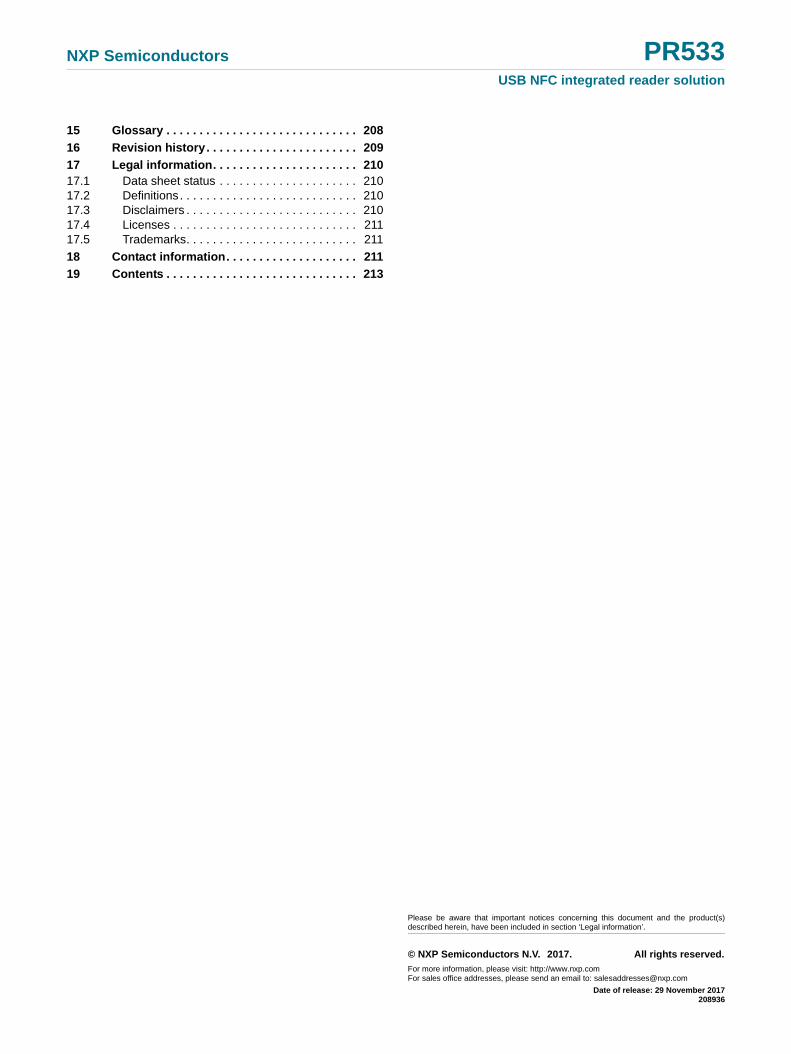
NXP Semiconductors PR533USB NFC integrated reader solution
15 Glossary . . . . . . . . . . . . . . . . . . . . . . . . . . . . . 208
16 Revision history. . . . . . . . . . . . . . . . . . . . . . . 209
17 Legal information. . . . . . . . . . . . . . . . . . . . . . 21017.1 Data sheet status . . . . . . . . . . . . . . . . . . . . . 21017.2 Definitions. . . . . . . . . . . . . . . . . . . . . . . . . . . 21017.3 Disclaimers . . . . . . . . . . . . . . . . . . . . . . . . . . 21017.4 Licenses . . . . . . . . . . . . . . . . . . . . . . . . . . . . 21117.5 Trademarks. . . . . . . . . . . . . . . . . . . . . . . . . . 211
18 Contact information. . . . . . . . . . . . . . . . . . . . 211
19 Contents . . . . . . . . . . . . . . . . . . . . . . . . . . . . . 213
© NXP Semiconductors N.V. 2017. All rights reserved.
For more information, please visit: http://www.nxp.comFor sales office addresses, please send an email to: [email protected]
Date of release: 29 November 2017208936
Please be aware that important notices concerning this document and the product(s)described herein, have been included in section ‘Legal information’.