alpha-prototype system for zone-plate-array lithography
TRANSCRIPT
Alpha-prototype system for zone-plate-array lithographyRajesh Menon,a) Amil Patel, Euclid E. Moon, and Henry I. SmithDepartment of Electrical Engineering and Computer Science, and Research Laboratory of Electronics,Massachusetts Institute of Technology, Cambridge, Massachusetts 02139
(Received 3 June 2004; accepted 13 September 2004; published 10 December 2004)
In this article, we present lithography results from a continuous-scan zone-plate-array lithography(ZPAL) system using the grating light valve(GLV) as the multiplexing element. ZPAL is anoptical-maskless-lithography technique, in which an array of diffractive lenses(e.g., zone plates)focuses incident light into an array of spots on a photoresist-coated substrate. The intensity of thelight incident on each lens is controlled by the GLV. By scanning the wafer and appropriatelymodulating the incident light, patterns are written in a “dot-matrix” fashion. We have incorporatedthe elements of ZPAL into an alpha-prototype system. We describe this system and characterize its
lithographic performance.© 2004 American Vacuum Society.[DOI: 10.1116/1.1813464]anuin-
e,proxch-
nmasieaventt an
phice-andh-
oflow
-of
sedity isubtternon.hesvan
htlycoge.
erThe
then for
thente-
de-rfor-
ightlator,atial-in-usedesist.simul-eter-
s a
f 24
byd
r istg,ble.g a
huseMAore;
I. INTRODUCTION
Since about 1980, optical-projection lithography(OPL)has been the lithographic technique of choice for the mfacture of integrated electronics. Wavelength scaling,creases in numerical aperture(NA), increases in field sizuse of resolution-enhancement techniques and opticalimity correction(OPC) have combined to enable OPL tenology to push minimum feature sizes into the sub-100domain. Water immersion is now widely seen as an epath to smaller features than shrinking of the source wlength from 193 nm to 157 nm.1 Resolution-enhancemetechniques and OPC have significantly increased the coscomplexity of photomasks as well as the entire lithograprocess.2–4 The problem is particularly acute for circuit dsigners, who have to rely on complex simulation toolsvery limited prototyping capabilities. Low-cost higresolution maskless lithography would mitigate somethese problems, and enable rapid prototyping as well asvolume manufacturing.
Zone-plate-array lithography(ZPAL) is an opticalmaskless-lithography technique, in which an arrayhigh-NA diffractive lenses creates an array of tightly focuspots on a photoresist-coated substrate. The light intenseach spot is controlled by a spatial-light modulator. Thestrate is scanned by a high-precision stage, enabling paof arbitrary geometry to be printed in a “dot-matrix” fashi
Although a variety of maskless lithography approachave been proposed, ZPAL has a number of unique adtages. In ZPAL, the pattern is written by scanning tigfocused spots. Since the zone plates focus on axis, theytribute no aberrations or distortions to the printed imaProximity-effect correction in ZPAL is significantly simplthan in OPL due to the incoherent addition of spots.
a)Author to whom correspondence should be addressed at MassacInstitute of Technology, 60 Vassar St., Bldg. 36-225, Cambridge,02139, also affiliated with Nanyang Technological University, Singap
electronic mail: [email protected]3032 J. Vac. Sci. Technol. B 22 (6), Nov/Dec 2004 0734-211X/2004
-
-
r-
d
-
n-s
-
n-
simplicity and extendibility of the ZPAL architecture, andabsence of photomasks make it a very attractive optiolow-cost high-resolution lithography.
In the past, we have demonstrated the feasibility ofelements of ZPAL.5–9 These elements have now been igrated into an alpha-prototype system. In this article, wescribe this system and characterize its lithographic pemance.
II. ALPHA-PROTOTYPE SYSTEM
The ZPAL architecture consists of four components: Lsource, array of Fresnel zone plates, spatial-light moduand scanning stage. The light source illuminates the splight modulator, which divides the light into an array ofdependently modulated beamlets. Each beamlet is focby one zone plate onto a substrate coated with photorThe substrate is raster scanned while the beamlets aretaneously modulated. The modulation during the scan dmines the pattern written by any given zone plate.
A. Light source
The light source in the alpha-prototype system i25 mW continuous wave GaN diode lasersl=400 nmd.
B. Zone-plate array
The alpha-prototype system contains a linear array ophase zone plates, placed at a pitch of 90mm. The zoneplates were fabricated on a fused-silica substratescanning-electron-beam lithography.10 They were designewith a NA of 0.7 and a focal length of 40mm.
C. Spatial-light modulator
The alpha-prototype system’s spatial-light modulatothe grating light valve(GLV), available from Silicon LighMachines.11 Each pixel in the GLV is a diffraction gratinwhich consists of six ribbons, three of which are moveaThe moveable ribbons can be pulled down by applyin
tts
voltage to a bottom electrode. This controls the diffraction
3032/22 (6)/3032/6/$19.00 ©2004 American Vacuum Society
d to
theh it
late,
-
e. Actiod at-plami-fromone
e 0ight
is
alstomcal
sfer, inns-are
adedra-
ntsedceabe
mer534ta ford forof an.
ntinger 75
spinkedI-88a hotde-ed
m.s
ofarehtism-
h-e
chtoin
nsu-opeones
3033 Menon et al. : Alpha-prototype system for ZPAL 3033
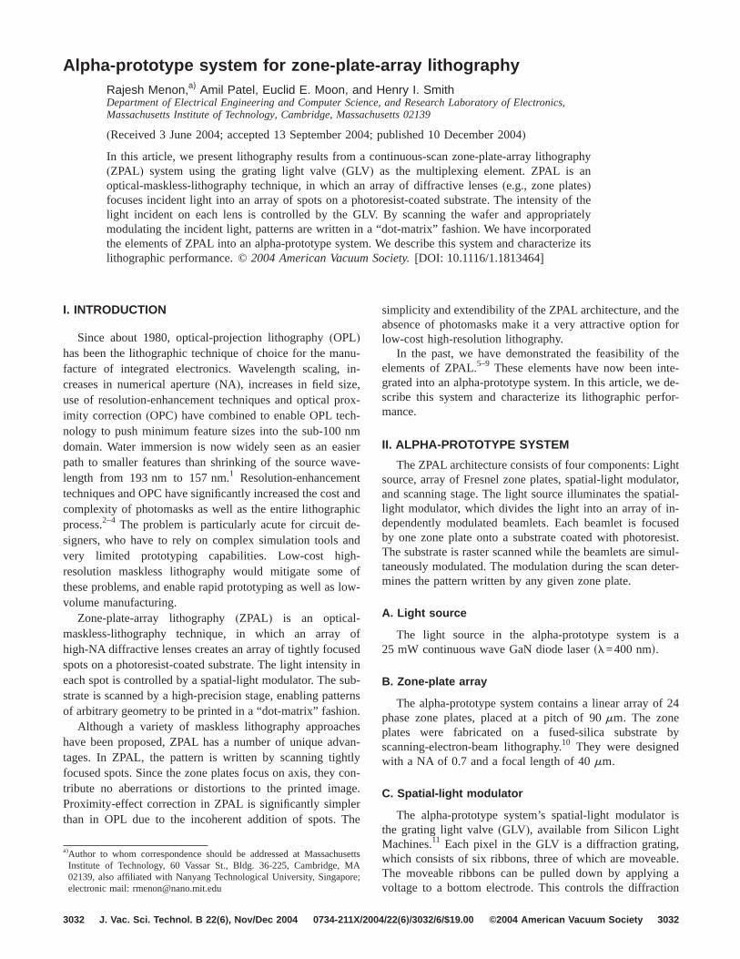
efficiency of the grating formed by the ribbons.12 In thealpha-prototype system, the +1 diffraction order is useilluminate the zone plates.
A variable magnification telescope was built to mappixels on the GLV to the zone plates in the array. Althougis possible to use one GLV pixel to illuminate one zone pin order to simplify the optics of the telescope(by keepingmagnification close to 1), we used four GLV pixels to illuminate one zone plate. The telescope consists of a 4f opticalsystem, as shown in Fig. 1(b). The Fourier transform of thGLV is formed at the back-focal plane of the first lensband-pass filter located at this plane selects the +1 diffraorder. The Fourier transform of the filtered field is formethe back-focal plane of the second lens, where the zonearray is located. This results in individual beamlets illunating the zone plates. When the pixel is actuated, lightthe +1 diffraction order reaches the corresponding zplate. When the pixel is not actuated, all light is in thorder, which is blocked within the telescope and no lreaches the corresponding zone plate.
D. Stage
The scanning stage in the alpha-prototype systemPolytec PI P-770 piezo-controlled stage with a 200mmrange in bothX and Y. The stage is controlled by NationInstruments hardware for continuous raster scan. Cuelectronics were built, which allow the stage to place fo
spots within 10 nm of their intendedsx,yd position.JVST B - Microelectronics and Nanometer Structures
n
te
a
We also built custom hardware and software that tranthe pattern data from a file on the computer to the GLVconjunction with the position of the stage. Software tralates the pattern into a sequence of GLV frames, whichstored on a hard disk. Prior to exposure, the pattern is lofrom the disk to the main memory. During real-time opetion, the data for a single scan(up to 2000 frames) is trans-ferred from the main memory to two National InstrumeNI-6534 digital input/output boards(each board is equippwith a 32 MB cache) via the peripheral component interfa(PCI) bus. As the stage scans along theX axis, it sendstrigger to the GLV indicating that the next frame shouldloaded. The trigger is received by a NI-6602 counter/tiboard, which transfers a single frame from the NI-6boards to the GLV. Once the scan is completed, the dathe next scan is loaded during the dead time requirestage turnaround. The data delivery system is capableaverage data transfer rate of over 128 Mbits per second
III. LITHOGRAPHIC CHARACTERIZATION
The alpha-prototype system was characterized by privarious test patterns. These patterns were printed on eithor 100 mm diameter silicon wafers. Each wafer wascoated at 6000 rpm with 200 nm of BarLi ARC and baon a hot plate at 175°C for 90 s. Then, 200 nm of PFphotoresist was spin coated at 3800 rpm and baked onplate at 90°C for 90 s. After lithography, the wafer wasveloped in CD-26 for 45 s, followed by rinse in de-ioniz
FIG. 1. ZPAL alpha-prototype syste(a) An array of high-NA zone platefocus incident light into an arrayspots on the substrate. The spotsturned ON and OFF by a spatial-ligmodulator, while the substratescanned. Patterns of arbitrary geoetry are written in a dot-matrix fasion. The spatial-light modulator is thGLV. (b) A telescope is used to matpixels on the spatial-light modulatorthe zone plates. A band-pass filterthe back-focal plane of the first leselects the +1 diffraction order to illminate the zone plates. The telescalso matches the pitch of the pixelsthe GLV to the pitch of the zone platin the array.
(DI) water. The wafer was blown dry with dry nitrogen, and
s tospu
tern-
fontial
re-Figtha
ithallel-
tical
-pat-oneNA
ing-sings
d
pey ofL at
3034 Menon et al. : Alpha-prototype system for ZPAL 3034
then examined in an optical microscope. If the wafer wabe examined in a scanning-electron microscope, it waster coated with Au/Pd.
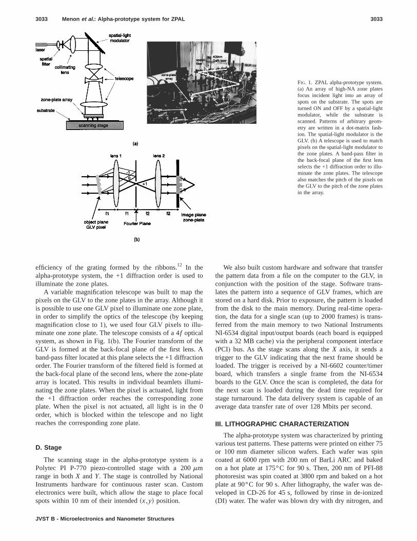
Figure 2 shows scanning-electron micrographs of patexposed atl=400 nm representing:[Fig. 2(a)] a photonicband-gap device,[Fig. 2(b)] a portion of a mask layout,[Fig.2(c)] a ring resonator optical filter, and[Fig. 2(d)] an array oelliptical rings for magnetic studies. These patterns demstrate the versatility of the ZPAL technology and its potenfor prototyping of novel designs.
A. Parallel patterning
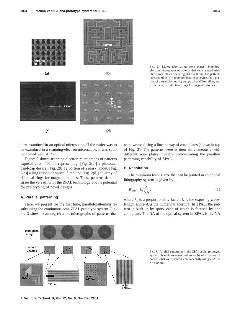
Here, we present for the first time, parallel-patterningsults using the continuous-scan ZPAL prototype system.ure 3 shows scanning-electron micrographs of patterns
J. Vac. Sci. Technol. B, Vol. 22, No. 6, Nov/Dec 2004
t-
s
-
-t
were written using a linear array of zone plates(shown in topof Fig. 3). The patterns were written simultaneously wdifferent zone plates, thereby demonstrating the parpatterning capability of ZPAL.
B. Resolution
The minimum feature size that can be printed in an oplithography system is given by
Wmin = k1l
NA, s1d
wherek1 is a proportionality factor,l is the exposing wavelength, and NA is the numerical aperture. In ZPAL, thetern is built up by spots, each of which is focused byzone plate. The NA of the optical system in ZPAL is the
FIG. 2. Lithography using zone plates. Scannelectron micrographs of patterns that were printed uphase zone plates operating atl=400 nm. The patterncorrespond to(a) a photonic-band-gap device,(b) a por-tion of a mask layout,(c) an optical add/drop filter, an(d) an array of elliptical rings for magnetic studies.
FIG. 3. Parallel patterning in the ZPAL alpha-prototysystem. Scanning-electron micrographs of a varietpatterns that were printed simultaneously using ZPAl=400 nm.
ay btheFig.s anceto a
NAedrrayeraexoutcusten-re-
sub-ry to
d uponeTheroteing
larthe
hingcy ofweund-
em.lineses ofm.
ly.
ys-
eldsinty oft 13asemean
3035 Menon et al. : Alpha-prototype system for ZPAL 3035
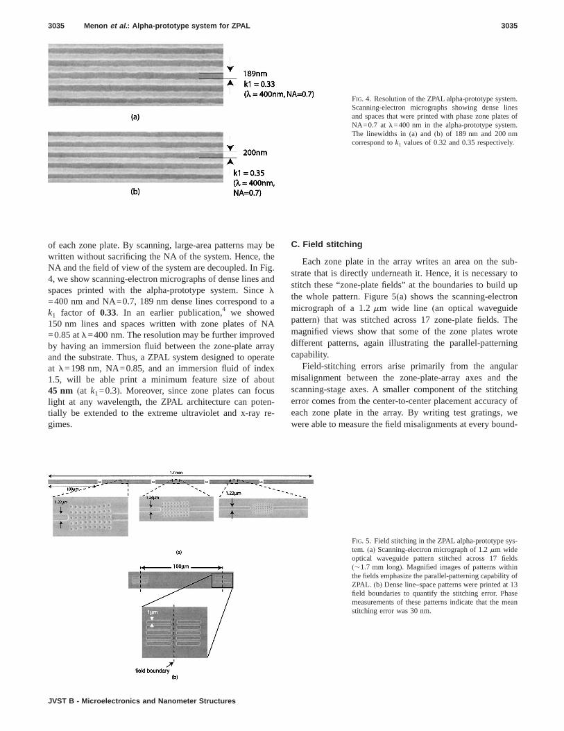
of each zone plate. By scanning, large-area patterns mwritten without sacrificing the NA of the system. Hence,NA and the field of view of the system are decoupled. In4, we show scanning-electron micrographs of dense linespaces printed with the alpha-prototype system. Sinl=400 nm and NA=0.7, 189 nm dense lines correspondk1 factor of 0.33. In an earlier publication,4 we showed150 nm lines and spaces written with zone plates of=0.85 atl=400 nm. The resolution may be further improvby having an immersion fluid between the zone-plate aand the substrate. Thus, a ZPAL system designed to opat l=198 nm, NA=0.85, and an immersion fluid of ind1.5, will be able print a minimum feature size of ab45 nm (at k1=0.3). Moreover, since zone plates can folight at any wavelength, the ZPAL architecture can potially be extended to the extreme ultraviolet and x-raygimes.
JVST B - Microelectronics and Nanometer Structures
e
d
te
C. Field stitching
Each zone plate in the array writes an area on thestrate that is directly underneath it. Hence, it is necessastitch these “zone-plate fields” at the boundaries to builthe whole pattern. Figure 5(a) shows the scanning-electrmicrograph of a 1.2mm wide line (an optical waveguidpattern) that was stitched across 17 zone-plate fields.magnified views show that some of the zone plates wdifferent patterns, again illustrating the parallel-patterncapability.
Field-stitching errors arise primarily from the angumisalignment between the zone-plate-array axes andscanning-stage axes. A smaller component of the stitcerror comes from the center-to-center placement accuraeach zone plate in the array. By writing test gratings,were able to measure the field misalignments at every bo
FIG. 4. Resolution of the ZPAL alpha-prototype systScanning-electron micrographs showing denseand spaces that were printed with phase zone platNA=0.7 at l=400 nm in the alpha-prototype systeThe linewidths in(a) and (b) of 189 nm and 200 nmcorrespond tok1 values of 0.32 and 0.35 respective
FIG. 5. Field stitching in the ZPAL alpha-prototype stem. (a) Scanning-electron micrograph of 1.2mm wideoptical waveguide pattern stitched across 17 fi(,1.7 mm long). Magnified images of patterns withthe fields emphasize the parallel-patterning capabiliZPAL. (b) Dense line–space patterns were printed afield boundaries to quantify the stitching error. Phmeasurements of these patterns indicate that thestitching error was 30 nm.
pen-cror tothees octuaoursin
to re
ageste
be-er-ms
es f
y of
eams. Thethog-e,pable
destare.
m-hesen thepable
iodslatedrive
le-tem.
m.ver-singal-arkst the
phyofan
gra-
3036 Menon et al. : Alpha-prototype system for ZPAL 3036
ary. Using this information as a lookup table, we precomsate the patterns such that the actual stitching errors aall field boundaries are significantly reduced. In ordequantify the stitching error, we printed gratings close tofield boundaries as shown in Fig. 5(b). The spatial phasdifference between the gratings printed on the two sideeach field boundary is a very sensitive measure of the astitching error. We gained some preliminary statistics onsystem by measuring the error at 13 field boundaries. Uthe pattern precompensation technique, we were ableduce the mean stitching error to less than30 nm with a s of16 nm. This can be further reduced if we utilize a stequipped with a laser-interferometer-based feedback sywith its higher positional accuracy.
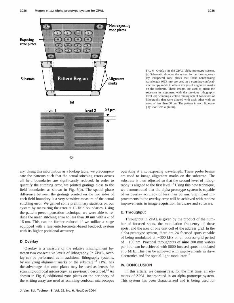
D. Overlay
Overlay is a measure of the relative misalignmenttween two consecutive levels of lithography. In ZPAL, ovlay can be performed, as in traditional lithography systeby analyzing alignment marks on the substrate.13 ZPAL hasthe advantage that zone plates may be used as lensscanning-confocal microscopy, as previously described.14 Asshown in Fig. 6, additional zone plates on the peripher
the writing array are used as scanning-confocal microscopeJ. Vac. Sci. Technol. B, Vol. 22, No. 6, Nov/Dec 2004
ss
fl
g-
m
,
or
operating at a nonexposing wavelength. These probe bare used to image alignment marks on the substratesubstrate is then adjusted so that the second level of liraphy is aligned to the first level.15 Using this new techniquwe demonstrated that the alpha-prototype system is caof an overlay accuracy of less than50 nm. Significant im-provements to the overlay error will be achieved with moimprovements in image acquisition hardware and softw
E. Throughput
Throughput in ZPAL is given by the product of the nuber of focused spots, the modulation frequency of tspots, and the area of one unit cell of the address grid. Ialpha-prototype system, there are 24 focused spots caof being modulated at,300 kHz on an address-grid perof ,100 nm. Practical throughputs ofnine 200 mm waferper hour can be achieved with 5000 focused spots moduat 5 MHz. This can be achieved with improvements in delectronics and the spatial-light modulator.16
IV. CONCLUSION
In this article, we demonstrate, for the first time, all ements of ZPAL incorporated in an alpha-prototype sys
FIG. 6. Overlay in the ZPAL alpha-prototype syste(a) Schematic showing the system for performing olay. Peripheral zone plates that focus nonexpowavelengths633 nmd are used in a scanning-confocmicroscopy mode to obtain images of alignment mon the susbtrate. These images are used to oriensubstrate in alignment with the previous lithogralevel. (b) Scanning-electron micrograph of two levelslithography that were aligned with each other witherror of less than 50 nm. The pattern in each lithophy level was a grating.
sThis system has been characterized and is being used for

l totion
sorandThise-
.
H.
Sci.
PIE
h, S.
nol.
ci.
3037 Menon et al. : Alpha-prototype system for ZPAL 3037
device fabrication. We believe that ZPAL has the potentiabe the most efficient and cost-effective next-generamaskless-lithography technology.
ACKNOWLEDGMENTS
The authors would like to thank Dr. Dario Gil, ProfesGeorge Barbastathis, Dr. David Carter, Jim Daley,Jimmy Carter for helpful discussion and suggestions.work was supported in part by DARPA and the Army Rsearch Office under Grant No. DAAD19-01-1-0330.
1M. Switkes and M. Rothschild, Proc. SPIE4691, 459 (2002).2L. Van den Hove and K. Ronse, Microelectron. Eng.27, 357 (1995).3Resolution Enhancement Techniques in Optical Lithography, edited by FM. Schellenberg(SPIE, Bellingham, WA, 2004), M5178.
4M. E. Mason, Microlithogr. World12, 8 (2003).5H. I. Smith, J. Vac. Sci. Technol. B14, 4318(1996).
JVST B - Microelectronics and Nanometer Structures
6D. Gil, R. Menon, and H. I. Smith, J. Vac. Sci. Technol. B21, 2810(2003).
7D. J. D. Carter, D. Gil, R. Menon, M. K. Mondol, E. H. Anderson, andI. Smith, J. Vac. Sci. Technol. B17, 3449(1999).
8D. Gil, R. Menon, X. Tang, H. I. Smith, and D. J. D. Carter, J. Vac.Technol. B 20, 2597(2002).
9R. Menon, D. Gil, D. J. D. Carter, A. Patel, and H. I. Smith, Proc. S4984, 10 (2003).
10D. Gil, R. Menon, and H. I. Smith, J. Vac. Sci. Technol. B21, 2956(2003).
11D. T. Amm and R. W. Corrigan, Proc. SPIE3634, 71 (1999).12D. M. Bloom, Proc. SPIE3013, 165 (1997).13T. Mono, U. P. Schroder, D. Nees, K. Palitzsch, W. Kostler, J. Bruc
Kramp, M. Veldkamp, and R. Schuster, Proc. SPIE5038, 121 (2003).14D. Gil, R. Menon, D. J. D. Carter, and H. I. Smith, J. Vac. Sci. Tech
B 18, 2881(2000).15R. Menon, E. E. Moon, Mark K. Mondol, and H. I. Smith, J. Vac. S
Technol. B , these proceedings.16A. Payne, W. DeGroot, R. Monteverde, and D. Amm, Proc. SPIE5348,
76 (2004).