adaptive supply voltage management for low power logic circuitry operating at subthreshold
TRANSCRIPT
International Journal of VLSI design & Communication Systems (VLSICS) Vol.6, No.2, April 2015
DOI : 10.5121/vlsic.2015.6201 1
ADAPTIVE SUPPLY VOLTAGE MANAGEMENT FOR
LOW POWER LOGIC CIRCUITRY OPERATING AT
SUBTHRESHOLD
Rehan Ahmed1
1Department of Electrical and Computer Engineering, Oklahoma State University,
Stillwater,OK, USA
ABSTRACT
With the rise in demand of portable hand held devices and with the rise in application of wireless sensor
networks and RFID reduction of total power consumption has become a necessity. To save power we
operate the logic circuitry of our devices at sub-threshold. In sub-threshold the drain current is
exponentially dependent on the threshold voltage hence the threshold variation causes profound variation
of ION and IOFF the ratio of which affect the speed of a circuit drastically. So to mitigate this problem we
present a adaptive power management circuit which will determine the minimum required supply voltage
to meet the timing requirement. Also to reduce the power overhead and avoid bulky coil and EMI noise
we used the switch capacitor power regulator to regulate and manage power instead of linear dropout
(LDO) and Inductor base switch mode power converter.
KEYWORDS
Adaptive; Low power; Switch Capacitor; Converter; Sub-threshold
1. INTRODUCTION
This paper discusses about the supply voltage management for logic parts which represents the
microcontroller and the digital circuitry of hand held or portable devices. Most these hand held
or portable devices used do not need to run at very high speed and are also desired to consume
low power so it would run for longer. Thus considering the above reasoning the digital or the
logic parts should be operated in subthreshold. Circuits operating in subthreshold are found to
consume less energy for active operation and dissipate less leakage power also with new process
technology subthreshold circuit designing has gain much more favour. In severely energy
constrained system like in case of passive RFID, medical implantable device, wearable sensors
or portable devices where conserving energy is the primary objective and the speed is high
enough, subthreshold circuits are ideal for this type of applications. For transistor operating in
subthreshold the gate tunnelling current, gate induce drain current, DIBL effect, reverse bias
diode leakage from the source and drain to the bulk leakage effects become negligible, hence all
these contribute to lower power[1]. In subthreshold transistor channel is not inverted and current
flow is by diffusion where the current is given by
(1)
ID represent drain current IS specific current, UT thermal voltage, n ideality factor and VTH is the
threshold voltage. Equation (1) shows ID varies exponentially with the (VGS – VTH) term. As
International Journal of VLSI design & Communication Systems (VLSICS) Vol.6, No.2, April 2015
2
CMOS technology is continuously scaled down, the effect of temperature and process variation
are becoming more prominent. Along with these in deep submicron processes the effects such
as short channel effect, reverse short channel effect [2], narrow channel effect and reverse
narrow channel effect [3] causes variation in VTH. The VTH variation causes the variation of ION
and IOFF, the ratio of which affect the speed of a circuit. As the drain current ID varies
exponentially with VTH in subthreshold, the effect is more profound. Thus this problem of VTH
variation due to process, temperature and technology can be mitigated by overdesigning the
circuits which is not cost effective and also consumes excess power. Alternate methods to
compensate VTH variation are 1) adaptive body biasing [4,5,6] 2) adaptive supply voltage [7,8]
and 3) adaptive body biasing and supply voltage in tandem. In this work adaptive supply
voltage to compensate VTH variation has been applied. This concept of dynamic [9,10]supply
voltage scaling is well documented approach in power reduction where the supply voltage is
determined according to the speed the circuit needs to support. In this work discussed this
technique is being applied to compensate for the reduction in reliability due to device VTH
variability. The supply voltage is increased dynamically to mask the variation effect of VTH to a
value which ensure the systems target performance [19,20]. As a result in cases where the
threshold voltage is higher (slow slow process) the supply voltage is increased and additional
power is consumed to ensure reliability. The discussed adaptive supply voltage management
circuit is designed to supply the controller of a smart passive RFID operating at 2MHz.
2. System Description
2.1. Critical Path Monitoring Circuit
Timing of a circuit is determined based on the performance requirement, power dissipation,
technology limitation and design architecture. Hence once the cycle time is fixed and the design
begins, a number of timing paths within the integrated circuit exceeds the cycle time. These path
called the critical paths must be retimed to meet the cycle time. The critical paths are
benchmarks of system timing as such critical path monitoring (CPM) can provide real time
effects due to the VTH variation. As a result in adaptive supply voltage scaling (ASV) designing
an accurate Critical path is very important. These critical path are monitored by generation of a
feedback signal with which the supply voltage is controlled at or near its optimal value so that
the circuit operate correctly at the target speed. CPMs needs to be located in the areas where the
most severe variation is likely to occur. Inaccuracy in CPM will result in system failure [11].
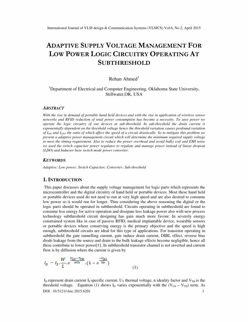
Figure 1 Schematic of CPM circuit
In developing the CPM several critical path replicas are implemented in order to better
represent the critical path behavior. All replica paths selections are ANDed so as to select the
longest delay path among the CPRs which represent the worst case of the CPM. Figure 1 shows
a CPM schematic, the circuit composed of D flipflops, critical path replicas and timing checker.
In this circuit a signal is entered which goes through all the CPRs but the output appears from
International Journal of VLSI design & Communication Systems (VLSICS) Vol.6, No.2, April 2015
3
the worst of all the CPRs as mentioned before confirming the worst delay. The output finally
reaches the timing checker which is composed of a D flipflop, and AND gate, the output of
which is applied to the reference selector controller. In the reference controller during each
cycle if the output of the timing checker is “0” the supply voltage is increased by 50mVuntil the
output is “1” In this case the reference voltage is start with 350mV and the maximum is limited
to 500mV. Single cycle of the reference selector controller circuit consists of three states or
three clock cycle. First a signal is applied through the CPRs in the second state it checks
whether the supply voltage is sufficient for the signal through the CPRs to meet the
timing and generates output S0 and S1 of a two bit counter accordingly. Finally in the
third state everything is reset and state 1 start again. While designing the CPM identical
timing delay is inserted in the cock network to compensate for the ANDs in the CPRs.
Table I gives the reference voltage selected for different S0 and S1 combination
Table 1. Reference voltage controller output
Frequency
applied S0 S1 Vref
2 MHz 1 0 450mV
1Mhz 0 1 400mV
750 KHz 0 1 400mV
500KHz 0 1 400mV
250 KHz 0 0 350mV
2.2. DC-DC Power Converter
The DC-DC power converter is a part of the power management circuit. The DC-DC converter
converts the unregulated DC input voltage to a regulated DC output voltage. This regulated
voltage can be either step-up or step-down. The DC-DC converter can be broadly divided in to
three category a) Linear regulator b) Inductor based switch mode regulator c) Capacitor based
switch mode regulator, however the working principle of all these regulators is same. The
output voltage is regulated with reference to a known reference voltage, with the help of a
closed loop feedback controller. Some of the specs that can be used to characterize a DC-DC
power converter are a) Efficiency b) Line regulation c) Load regulation and d) noise which are
explained briefly below. One of the important parameter of a DC-DC converter is efficiency
(2)
Where Pout is the output power, Pin is the total input power and Ploss is the power loss of the
converter itself. Ideally voltage conversion should take place without any loss but due to various
power loss factors, switch resistance, parasitic Cs etc. practical efficiency is lower than the ideal
value, so efficiency is a important factor especially in case like where we want to operate on
low power. For a DC-DC converter the other two important parameters to measure the
regulation performance are load regulation and line regulation
(3)
and
International Journal of VLSI design & Communication Systems (VLSICS) Vol.6, No.2, April 2015
4
(4)
Lastly switching noise characteristic of the DC-DC converter is another critical spec. As in
many low power applications like wireless sensors containing RF transmitter component or
some other devices having noise sensitive components, so if the converter has large noise
component, this noise can couple with the devices and cause problem. Hence for noise sensitive
application low noise power supply is desired.
The different type of regulator that we mentioned before and the reason for choosing the switch
capacitor based converter instead of the other two is discussed below.
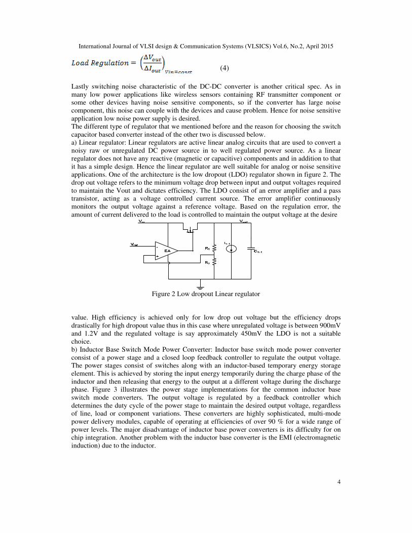
a) Linear regulator: Linear regulators are active linear analog circuits that are used to convert a
noisy raw or unregulated DC power source in to well regulated power source. As a linear
regulator does not have any reactive (magnetic or capacitive) components and in addition to that
it has a simple design. Hence the linear regulator are well suitable for analog or noise sensitive
applications. One of the architecture is the low dropout (LDO) regulator shown in figure 2. The
drop out voltage refers to the minimum voltage drop between input and output voltages required
to maintain the Vout and dictates efficiency. The LDO consist of an error amplifier and a pass
transistor, acting as a voltage controlled current source. The error amplifier continuously
monitors the output voltage against a reference voltage. Based on the regulation error, the
amount of current delivered to the load is controlled to maintain the output voltage at the desire
Figure 2 Low dropout Linear regulator
value. High efficiency is achieved only for low drop out voltage but the efficiency drops
drastically for high dropout value thus in this case where unregulated voltage is between 900mV
and 1.2V and the regulated voltage is say approximately 450mV the LDO is not a suitable
choice.
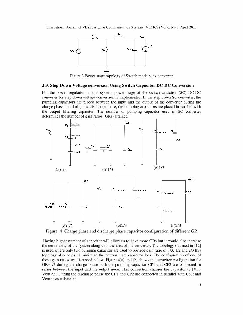
b) Inductor Base Switch Mode Power Converter: Inductor base switch mode power converter
consist of a power stage and a closed loop feedback controller to regulate the output voltage.
The power stages consist of switches along with an inductor-based temporary energy storage
element. This is achieved by storing the input energy temporarily during the charge phase of the
inductor and then releasing that energy to the output at a different voltage during the discharge
phase. Figure 3 illustrates the power stage implementations for the common inductor base
switch mode converters. The output voltage is regulated by a feedback controller which
determines the duty cycle of the power stage to maintain the desired output voltage, regardless
of line, load or component variations. These converters are highly sophisticated, multi-mode
power delivery modules, capable of operating at efficiencies of over 90 % for a wide range of
power levels. The major disadvantage of inductor base power converters is its difficulty for on
chip integration. Another problem with the inductor base converter is the EMI (electromagnetic
induction) due to the inductor.
International Journal of VLSI design & Communication Systems (VLSICS) Vol.6, No.2, April 2015
5
Figure 3 Power stage topology of Switch mode buck converter
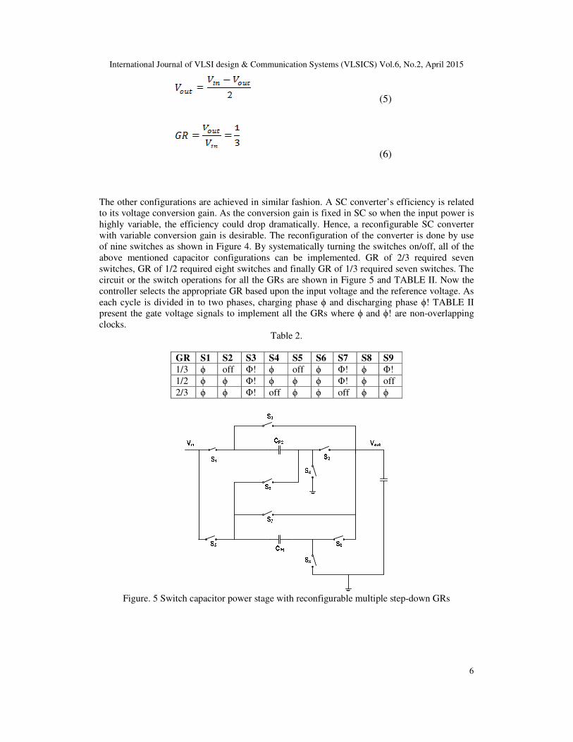
2.3. Step-Down Voltage conversion Using Switch Capacitor DC-DC Conversion
For the power regulation in this system, power stage of the switch capacitor (SC) DC-DC
converter for step-down voltage conversion is implemented. In the step-down SC converter, the
pumping capacitors are placed between the input and the output of the converter during the
charge phase and during the discharge phase, the pumping capacitors are placed in parallel with
the output filtering capacitor. The number of pumping capacitor used in SC converter
determines the number of gain ratios (GRs) attained
��� − ����
�
��� − ����
�
(a)1/3
��� − ����
�
��� − ����
�
(b)1/3
(c)1/2
(d)1/2
(e)2/3
(f)2/3
Figure. 4 Charge phase and discharge phase capacitor configuration of different GR
Having higher number of capacitor will allow us to have more GRs but it would also increase
the complexity of the system along with the area of the converter. The topology outlined in [12]
is used where only two pumping capacitor are used to provide gain ratio of 1/3, 1/2 and 2/3 this
topology also helps us minimize the bottom plate capacitor loss. The configuration of one of
these gain ratios are discussed below. Figure 4(a) and (b) shows the capacitor configuration for
GR=1/3 during the charge phase both the pumping capacitor CP1 and CP2 are connected in
series between the input and the output node. This connection charges the capacitor to (Vin-
Vout)/2 . During the discharge phase the CP1 and CP2 are connected in parallel with Cout and
Vout is calculated as
International Journal of VLSI design & Communication Systems (VLSICS) Vol.6, No.2, April 2015
6
(5)
(6)
The other configurations are achieved in similar fashion. A SC converter’s efficiency is related
to its voltage conversion gain. As the conversion gain is fixed in SC so when the input power is
highly variable, the efficiency could drop dramatically. Hence, a reconfigurable SC converter
with variable conversion gain is desirable. The reconfiguration of the converter is done by use
of nine switches as shown in Figure 4. By systematically turning the switches on/off, all of the
above mentioned capacitor configurations can be implemented. GR of 2/3 required seven
switches, GR of 1/2 required eight switches and finally GR of 1/3 required seven switches. The
circuit or the switch operations for all the GRs are shown in Figure 5 and TABLE II. Now the
controller selects the appropriate GR based upon the input voltage and the reference voltage. As
each cycle is divided in to two phases, charging phase ϕ and discharging phase ϕ! TABLE II
present the gate voltage signals to implement all the GRs where ϕ and ϕ! are non-overlapping
clocks.
Table 2.
GR S1 S2 S3 S4 S5 S6 S7 S8 S9
1/3 ϕ off Φ! ϕ off ϕ Φ! ϕ Φ!
1/2 ϕ ϕ Φ! ϕ ϕ ϕ Φ! ϕ off
2/3 ϕ ϕ Φ! off ϕ ϕ off ϕ ϕ
Figure. 5 Switch capacitor power stage with reconfigurable multiple step-down GRs
International Journal of VLSI design & Communication Systems (VLSICS) Vol.6, No.2, April 2015
7
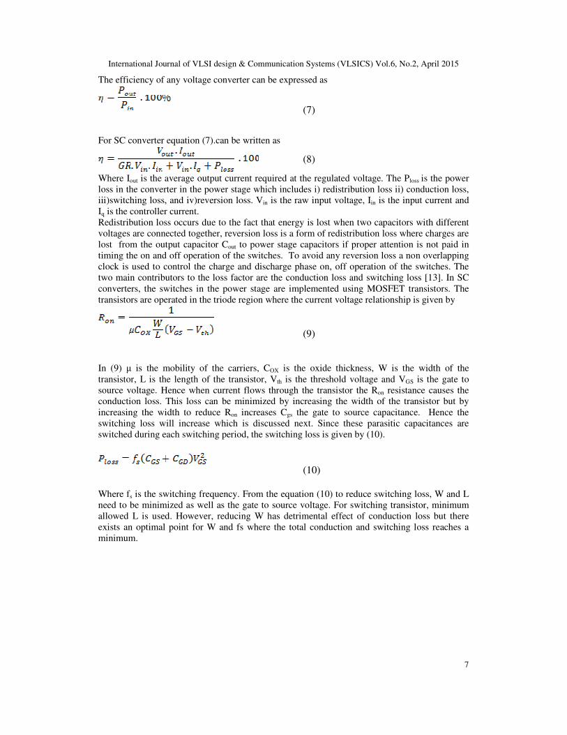
The efficiency of any voltage converter can be expressed as
(7)
For SC converter equation (7).can be written as
(8)
Where Iout is the average output current required at the regulated voltage. The Ploss is the power
loss in the converter in the power stage which includes i) redistribution loss ii) conduction loss,
iii)switching loss, and iv)reversion loss. Vin is the raw input voltage, Iin is the input current and
Iq is the controller current.
Redistribution loss occurs due to the fact that energy is lost when two capacitors with different
voltages are connected together, reversion loss is a form of redistribution loss where charges are
lost from the output capacitor Cout to power stage capacitors if proper attention is not paid in
timing the on and off operation of the switches. To avoid any reversion loss a non overlapping
clock is used to control the charge and discharge phase on, off operation of the switches. The
two main contributors to the loss factor are the conduction loss and switching loss [13]. In SC
converters, the switches in the power stage are implemented using MOSFET transistors. The
transistors are operated in the triode region where the current voltage relationship is given by
(9)
In (9) µ is the mobility of the carriers, COX is the oxide thickness, W is the width of the
transistor, L is the length of the transistor, Vth is the threshold voltage and VGS is the gate to
source voltage. Hence when current flows through the transistor the Ron resistance causes the
conduction loss. This loss can be minimized by increasing the width of the transistor but by
increasing the width to reduce Ron increases Cgs the gate to source capacitance. Hence the
switching loss will increase which is discussed next. Since these parasitic capacitances are
switched during each switching period, the switching loss is given by (10).
(10)
Where fs is the switching frequency. From the equation (10) to reduce switching loss, W and L
need to be minimized as well as the gate to source voltage. For switching transistor, minimum
allowed L is used. However, reducing W has detrimental effect of conduction loss but there
exists an optimal point for W and fs where the total conduction and switching loss reaches a
minimum.
International Journal of VLSI design & Communication Systems (VLSICS) Vol.6, No.2, April 2015
8
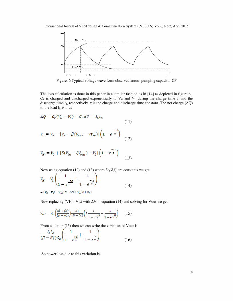
Figure. 6 Typical voltage wave form observed across pumping capacitor CP
The loss calculation is done in this paper in a similar fashion as in [14] as depicted in figure 6 .
CP is charged and discharged exponentially to VH and VL during the charge time tc and the
discharge time td, respectively. τ is the charge and discharge time constant. The net charge (∆Q)
to the load IL is thus
(11)
(12)
(13)
Now using equation (12) and (13) where β,γ,δ,ζ are constants we get
(14)
Now replacing (VH – VL) with ∆V in equation (14) and solving for Vout we get
(15)
From equation (15) then we can write the variation of Vout is
(16)
So power loss due to this variation is
International Journal of VLSI design & Communication Systems (VLSICS) Vol.6, No.2, April 2015
9
(17)
Another major power loss is due to the switching loss as discussed previously depend on the
size of the switch and the frequency thus the total power due to switching.
(18)
Where Cox is the unit oxide capacitance, σ is fabrication process related coefficient and Li, Wi
are the length and width of the ith switch. To reduce the switching power loss we have to reduce
the parasitic capacitance so we choose the Length L to be minimum, so total power loss,
(19)
The time tc and td are dependent on the turn-on resistance in the charge and discharge path
where total Ron is given by
(20)
Where M and stand for the total number of power transistor in the charge and discharge path.
From equation (19) and (20) we see that the total power loss is dependent on switching
frequency fs and Wj. Hence we need to choose Wj and fs such that we have least power loss and
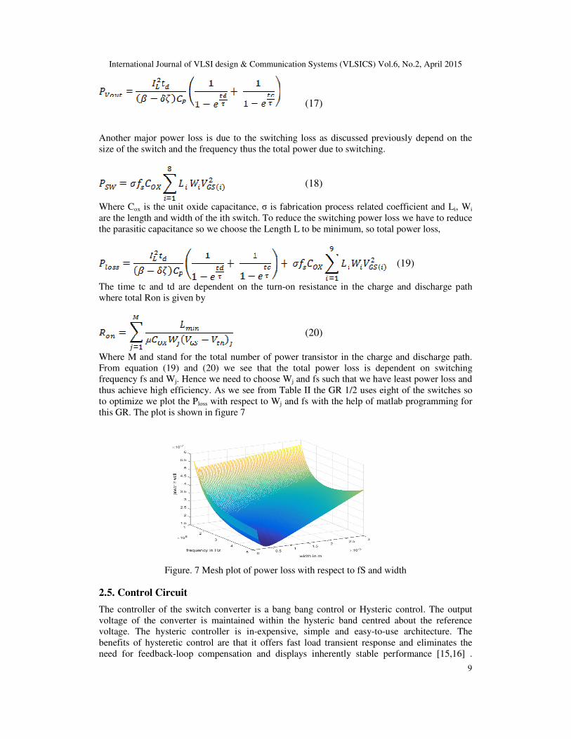
thus achieve high efficiency. As we see from Table II the GR 1/2 uses eight of the switches so
to optimize we plot the Ploss with respect to Wj and fs with the help of matlab programming for
this GR. The plot is shown in figure 7
Figure. 7 Mesh plot of power loss with respect to fS and width
2.5. Control Circuit
The controller of the switch converter is a bang bang control or Hysteric control. The output
voltage of the converter is maintained within the hysteric band centred about the reference
voltage. The hysteric controller is in-expensive, simple and easy-to-use architecture. The
benefits of hysteretic control are that it offers fast load transient response and eliminates the
need for feedback-loop compensation and displays inherently stable performance [15,16] .
International Journal of VLSI design & Communication Systems (VLSICS) Vol.6, No.2, April 2015
10
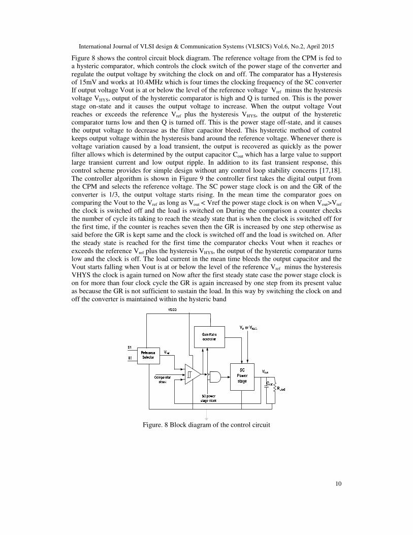
Figure 8 shows the control circuit block diagram. The reference voltage from the CPM is fed to
a hysteric comparator, which controls the clock switch of the power stage of the converter and
regulate the output voltage by switching the clock on and off. The comparator has a Hysteresis
of 15mV and works at 10.4MHz which is four times the clocking frequency of the SC converter
If output voltage Vout is at or below the level of the reference voltage Vref minus the hysteresis
voltage VHYS, output of the hysteretic comparator is high and Q is turned on. This is the power
stage on-state and it causes the output voltage to increase. When the output voltage Vout
reaches or exceeds the reference Vref plus the hysteresis VHYS, the output of the hysteretic
comparator turns low and then Q is turned off. This is the power stage off-state, and it causes
the output voltage to decrease as the filter capacitor bleed. This hysteretic method of control
keeps output voltage within the hysteresis band around the reference voltage. Whenever there is
voltage variation caused by a load transient, the output is recovered as quickly as the power
filter allows which is determined by the output capacitor Cout which has a large value to support
large transient current and low output ripple. In addition to its fast transient response, this
control scheme provides for simple design without any control loop stability concerns [17,18].
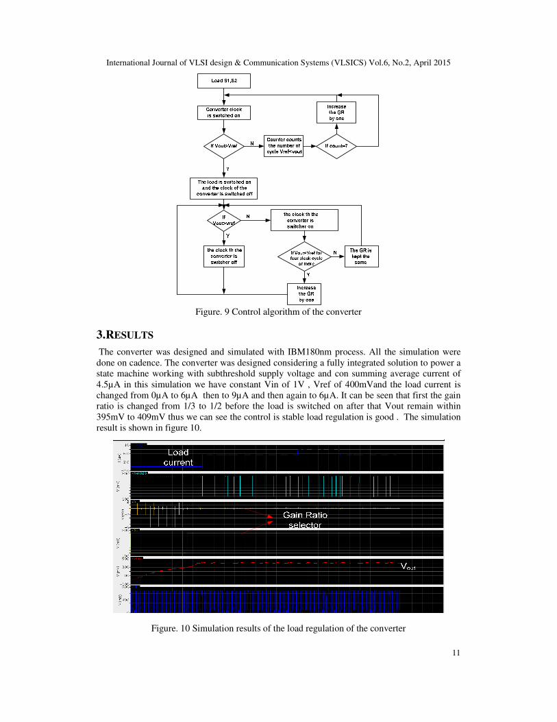
The controller algorithm is shown in Figure 9 the controller first takes the digital output from
the CPM and selects the reference voltage. The SC power stage clock is on and the GR of the
converter is 1/3, the output voltage starts rising. In the mean time the comparator goes on
comparing the Vout to the Vref as long as Vout < Vref the power stage clock is on when Vout>Vref
the clock is switched off and the load is switched on During the comparison a counter checks
the number of cycle its taking to reach the steady state that is when the clock is switched off for
the first time, if the counter is reaches seven then the GR is increased by one step otherwise as
said before the GR is kept same and the clock is switched off and the load is switched on. After
the steady state is reached for the first time the comparator checks Vout when it reaches or
exceeds the reference Vref plus the hysteresis VHYS, the output of the hysteretic comparator turns
low and the clock is off. The load current in the mean time bleeds the output capacitor and the
Vout starts falling when Vout is at or below the level of the reference Vref minus the hysteresis
VHYS the clock is again turned on Now after the first steady state case the power stage clock is
on for more than four clock cycle the GR is again increased by one step from its present value
as because the GR is not sufficient to sustain the load. In this way by switching the clock on and
off the converter is maintained within the hysteric band
Figure. 8 Block diagram of the control circuit
International Journal of VLSI design & Communication Systems (VLSICS) Vol.6, No.2, April 2015
11
Figure. 9 Control algorithm of the converter
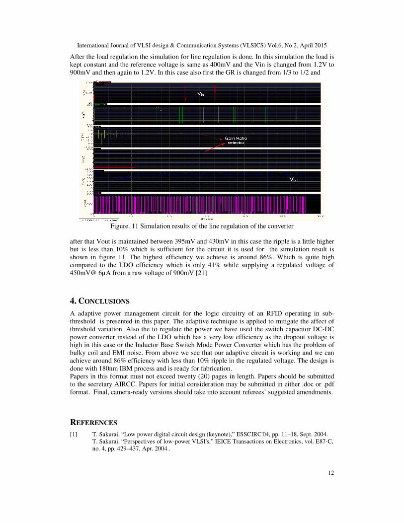
3.RESULTS
The converter was designed and simulated with IBM180nm process. All the simulation were
done on cadence. The converter was designed considering a fully integrated solution to power a
state machine working with subthreshold supply voltage and con summing average current of
4.5µA in this simulation we have constant Vin of 1V , Vref of 400mVand the load current is
changed from 0µA to 6µA then to 9µA and then again to 6µA. It can be seen that first the gain
ratio is changed from 1/3 to 1/2 before the load is switched on after that Vout remain within
395mV to 409mV thus we can see the control is stable load regulation is good . The simulation
result is shown in figure 10.
Figure. 10 Simulation results of the load regulation of the converter
International Journal of VLSI design & Communication Systems (VLSICS) Vol.6, No.2, April 2015
12
After the load regulation the simulation for line regulation is done. In this simulation the load is
kept constant and the reference voltage is same as 400mV and the Vin is changed from 1.2V to
900mV and then again to 1.2V. In this case also first the GR is changed from 1/3 to 1/2 and
Figure. 11 Simulation results of the line regulation of the converter
after that Vout is maintained between 395mV and 430mV in this case the ripple is a little higher
but is less than 10% which is sufficient for the circuit it is used for the simulation result is
shown in figure 11. The highest efficiency we achieve is around 86%. Which is quite high
compared to the LDO efficiency which is only 41% while supplying a regulated voltage of
450mV@ 6µA from a raw voltage of 900mV [21]
4. CONCLUSIONS
A adaptive power management circuit for the logic circuitry of an RFID operating in sub-
threshold is presented in this paper. The adaptive technique is applied to mitigate the affect of
threshold variation. Also the to regulate the power we have used the switch capacitor DC-DC
power converter instead of the LDO which has a very low efficiency as the dropout voltage is
high in this case or the Inductor Base Switch Mode Power Converter which has the problem of
bulky coil and EMI noise. From above we see that our adaptive circuit is working and we can
achieve around 86% efficiency with less than 10% ripple in the regulated voltage. The design is
done with 180nm IBM process and is ready for fabrication.
Papers in this format must not exceed twenty (20) pages in length. Papers should be submitted
to the secretary AIRCC. Papers for initial consideration may be submitted in either .doc or .pdf
format. Final, camera-ready versions should take into account referees’ suggested amendments.
REFERENCES
[1] T. Sakurai, “Low power digital circuit design (keynote),” ESSCIRC'04, pp. 11–18, Sept. 2004.
T. Sakurai, “Perspectives of low-power VLSI's,” IEICE Transactions on Electronics, vol. E87-C,
no. 4, pp. 429–437, Apr. 2004 .
International Journal of VLSI design & Communication Systems (VLSICS) Vol.6, No.2, April 2015
13
[2] Miura-Mattausch, M. Suetake, J. Mattausch, S. Kumashiro, and N. Shigyo, "Physical Modeling
of the Reverse-Short-Channel Effect for Circuit Simulation,"IEEE Transactions on Electron
Devices, vol. 48, no. 10, pp. 2449-2452, Oct. 2001
[3] A. One, R. Ucno, and I. Sakai, "TED Control Technology for Suppression of Reverse Narrow
Channel Effect in O.l/xm MOS Devices," in International Electron Devices Meeting (lEDM)
Digest of Technical Papers, 1997, pp. 227- 230.
[4] T. Sakurai and A. R. Newton, “Alpha-power law MOSFET model and its applications to CMOS inverter delay and other formulas,” IEEE J. Solid-State Circuits, vol. 25, no. 2, pp. 584–594, Apr. 1990
[5] T. Kobayashi and T. Sakurai, “Self-adjusting threshold-voltage scheme (SATS) for low-voltage high-speed operation,” Proc. CICC’94, pp. 271–274, May 1994
[6] Y. Yasuda, N. Kimizuka, Y. Akiyama, Y. Yamagata, Y. Goto, and K. Imai “System LSI Multi-Vth Transistors Design Methodology for Maximizing Efficiency of Body-Biasing Control to Reduce Vth Variation and Power Consumption,” IEDM Technical Digest, pp. 66–71, December 2005
[7] A. Sinha and A. Chandrakasan, “Dynamic power management in wireless sensor networks,”
IEEE Design and Test of Computers, vol. 18, no. 2, pp. 62–74, March 2001.
[8] B. Zhai et al., “A 2.6pJ/Inst subthreshold sensor processor for optimal energy efficiency,” in
Symp. VLSI Circuits Tech. Dig., pp. 192–193, June 2006.
[9] T. Kuroda, K. Suzuki, S. Mita, T. Fujita, F. Yamane, F. Sano, A. Chiba, Y. Watanabe, K.
Matsuda, T. Maeda, T. Sakurai, and T. Furuyama, “Variable supply-voltage scheme for low-
power high-speed CMOS digital design,” IEEE J. Solid-State Circuits, vol. 33, no. 3, pp. 454–
462, Mar. 1998.
[10] D.J. Frank, “Power constrained CMOS scaling limits”, IBM Journal of Research and
Development, March/May 2002, Vol. 46, No. 23, pp. 235–244
[11] Junyoung Park; Abraham, J.A., "A fast, accurate and simple critical path monitor for improving
energy-delay product in DVS systems," Low Power Electronics and Design (ISLPED) 2011
International Symposium on , vol., no., pp.391,396, 1-3 Aug. 2011
[12] Inshad Chowdhury “Efficient voltage regulator using switch capacitor DC/DC converter from
battery and energy harvesting power sources.” 2010
[13] Ling Su; Dongsheng Ma; Brokaw, A.P., "Design and Analysis of Monolithic Step-Down SC
Power Converter With Subthreshold DPWM Control for Self-Powered Wireless Sensors,"
Circuits and Systems I: Regular Papers, IEEE Transactions on , vol.57, no.1, pp.280,290, Jan.
2010
[14] Chowdhury, I.; Dongsheng Ma, "Design of Reconfigurable and Robust Integrated SC Power
Converter for Self-Powered Energy-Efficient Devices," Industrial Electronics, IEEE
Transactions on , vol.56, no.10, pp.4018,4028, Oct. 2009
[15] Keskar, N.; Rincon-Mora, G.A., "Self-stabilizing, integrated, hysteretic boost DC-DC
converter," Industrial Electronics Society, 2004. IECON 2004. 30th Annual Conference of IEEE
, vol.1, no., pp.586,591 Vol. 1, 2-6 Nov. 2004
[16] http://users.ece.gatech.edu/rincon-mora/research/hyst_ac.pdf
[17] Chung-Hsien Tso; Jiin-Chuan Wu, "A ripple control buck regulator with fixed output
frequency," Power Electronics Letters, IEEE , vol.1, no.3, pp.61,63, Sept. 2003
[18] E. I. ELEKTROTECHNIKA, "Hysteretic–controlled Voltage Regulator using Integrated Circuit
LM723 O. Ursaru, C. Aghion, M. Lucanu
[19] Jaeha Kim; Horowitz, M.A., "An efficient digital sliding controller for adaptive power-supply
regulation," Solid-State Circuits, IEEE Journal of , vol.37, no.5, pp.639,647, May 2002
[20] Gu-Yeon Wei; Horowitz, M., "A fully digital, energy-efficient, adaptive power-supply
regulator," Solid-State Circuits, IEEE Journal of , vol.34, no.4, pp.520,528, Apr 1999

International Journal of VLSI design & Communication Systems (VLSICS) Vol.6, No.2, April 2015
14
[21] Ahmed, R.; Hutchens, C.; Rennaker, R.L., "An RFID front end for smart biological sensing,"
Circuits and Systems (MWSCAS), 2012 IEEE 55th International Midwest Symposium on , vol.,
no., pp.778,781, 5-8 Aug. 2012
.