a 700 mhz switched capacitor analog waveform … 700 mhz switched capacitor analog waveform ... a...
TRANSCRIPT
SLAC-PUB-6414 December 1993
A 700 MHz Switched Capacitor Analog Waveform Sampling Circuit
Gunther M. Haller
?Qanford Linear Accelerator Center, Stanford University, Stanford, CA 94309
Bruce A. Wooley
Center for Integrated Systems, Stanford University, Stanford, CA 94305
Journal of Solid State Circuits
Work supported in part by Department of Energy contract DE-AC03-76SF00515 s -
A 700 MHz Switched Capacitor Analog Waveform Sampling Circuit*
Gunther M. Haller
Stanford Linear Accelerator Center
Bruce A. Wooley
Center for Integrated Systems
Stanford University
Stanford, Ca 94305
Correspondence Address:
Gunther M. Haller
Stanford Linear Accelerator Center
PO. Box 4349, MS 96
. Stanford, California 94309
Phone: (415) 926-4257
FAX: (415) 926-2923
I. INTRODUCTION
Many modern data acquisition systems require the recording of analog signals as a function of
time over a wide dynamic range. Most commonly, the analog information is digitized at the
required acquisition rate using an analog-to-digital converter (ADC). However, in a number of
applications analog waveforms need only be captured as snap shots; continuous digitization is not
necessary. Examples of such applications include pulse echo phenomena (RADAR, LIDAR,
ultrasonics, and non-destructive material and medical testing), pulse shape recording (high energy
physics experiments, accelerator diagnostics), and laboratory instrumentation (oscilloscopes,
- transient digitizers). In such cases an input waveform can be sampled at a high rate for a limited
period pf time, and the samples stored in an analog memory. The analog samples are then
retrieved at a lower rate and digitized with a slow ADC before a new waveform is acquired. Many
* This research was supported by the Department of Energy under Contract No. DE-ACO3-76SF00.515.
1
Hailer and Wooley: Switched Capacitor Analog Memory 2
channels may be multiplexed onto one converter when readout speed and latency are not crucial.
Advantages of using an analog memory include low overall power dissipation and cost, high den-
sity, and potentially superior dynamic range at high sampling rates.
Two main technologies are available for the realization of an integrated analog memory:
charge-coupled devices (CCD’s) and switched-capacitor circuits. Integrated circuits based on
switched-capacitor techniques are inherently capable of higher accuracy and sampling rates than
CCD devices. Furthermore, CCD’s require elaborate clocking circuitry that generally dissipates
considerable power.
Strong cost and performance incentives especially encourage the use of analog switched-
capacitor memories in high energy physics experiments [ 11. Fast analog waveform capture for
thousands of channels must be provided with a minimum of power dissipation. The design chal-
lenge is to produce a uniform and linear response in a large number of memory cells at a level of
performance comparable to the high accuracy inherent in the technology. Principal performance
issues are cell-to-cell offset and gain variations within a memory channel, which are governed by
the circuit architecture and its sensitivity to the matching properties of its constituent transistors
and capacitors [2]-[5]. In high-precision applications, the lowest achievable cell non-uniformities
may not be acceptable and therefore must be eliminated by correcting the data. In large systems, it
is essential that the number of correction constants and the computational effort be minimized.
Early analog memory circuits based on a sample-and-hold topology contain a sampling
switch, a storage capacitor, and a readout buffer in each memory cell [6]-[9]. In order to meet the
need for lower power and higher density, architectures based on switched-capacitor circuits were
introduced [lo]-[14]. In these circuits, each channel comprises a bank of capacitors that is
switched to a single operational amplifier for readout. Architectures in which the sampling tran-
sistors are placed in the signal path [6]-[13] exhibit signal-dependent charge injection in each cell.
Cell pedestals are therefore a function of the input signal and may require individual offset and
gain corrections. In addition, a serious,drawback of these implementations in high-speed applica-
tions is the dependence of the sampling transistor turn-off time on the signal level [7]. In circuits
Haller and Wooley: Switched Capacitor Analog Memory 3
based on traditional charge redistribution switched-capacitor techniques [ 141, sampling-switch
charge injection can be made independent of the signal level, but the cell gain is a linear function
of the size of the storage capacitor. Cell-to-cell gain matching of better than 0.5 % across an entire
channel is therefore difficult to achieve, and both offset and gain corrections are commonly
needed for each cell. The sampling speed of published analog memory circuits is presently limited
to less than 150 MHz.
This work presents a circuit that enables sampling rates as high as 700 MHz while sustaining
a dynamic range of more than 12 bits. In addition, cell pedestals are independent of the signal
amplitude, cell gains are insensitive to component sizes, and the sampling time is independent of
the input level. This allows a straightforward improvement in performance by means of a simple
offset subtraction. Cell-to-cell gain corrections are not needed.
A specific application for the proposed memory is high energy physics accelerators and collid-
ers, where bunches of particles are transported at close to the speed of light inside beam pipes sev-
eral miles long [15]-[17]. In order to control the operation of the particle beam with sufficient
accuracy, its transverse position must be measured at as many as a thousand locations with a pre-
cision of better than 1 pm across a range of 5 mm. The complexity and cost of such a measure- . _
ment system can be significantly reduced through use of high-speed, high dynamic range analog _
memories.
The proposed analog memory circuit is described in detail in Section II of this paper. In
Section III, the design of the on-chip write and read control circuitry is explained. Experimental
results characterizing the performance of the memory are presented in Section IV.
II. ANALOG MEMORY DESCRIPTION
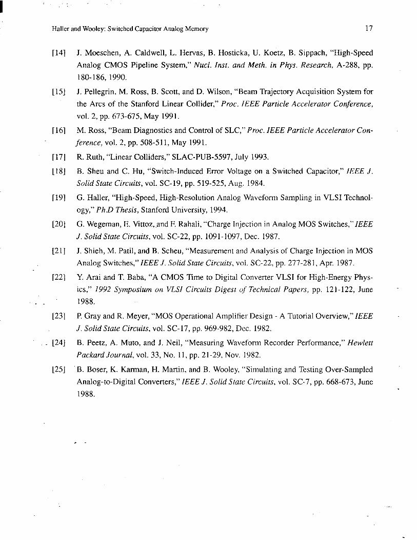
Shown in Fig. 1 is a block diagram of an analog waveform recorder with m memory channels.
The analog waveforms applied at the m inputs are sampled and stored in the main analog memory
core. The write and read addresses for the core are generated in the write and read control blocks,
Hailer and Wooley: Switched Capacitor Analog Memory 4
respectively. Since all memory channels are written and read simultaneously, the addresses are
common to all channels. In applications where the readout time permits the serial readout of the
channels, the m outputs can be read out on a single common output line by including an on-chip
analog multiplexer.
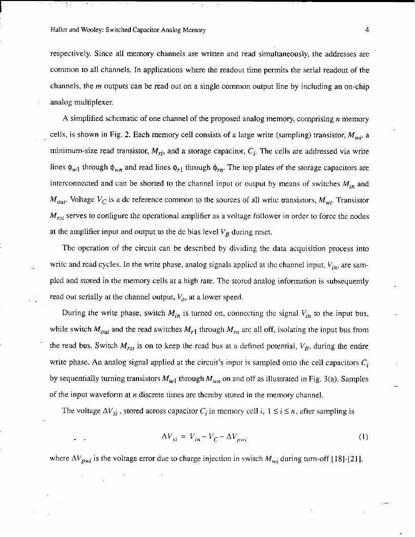
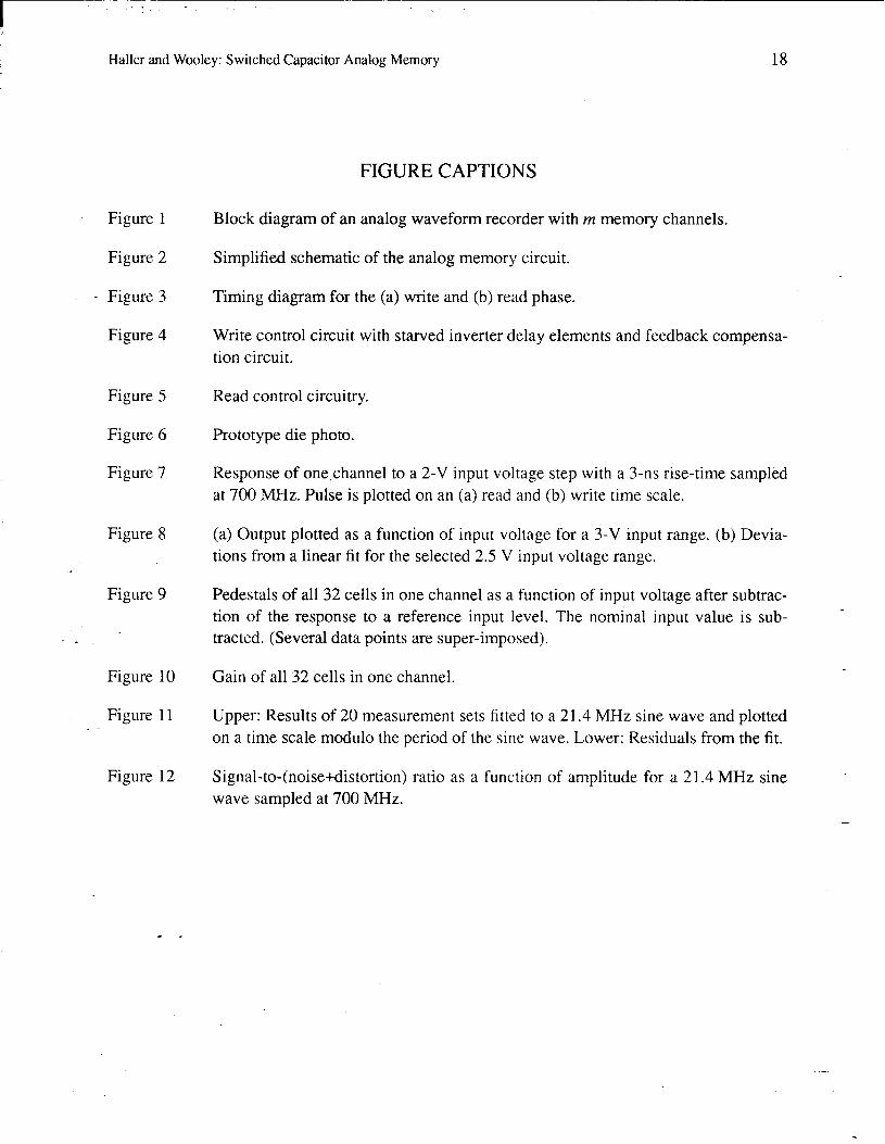
A simplified schematic of one channel of the proposed analog memory, comprising n memory
cells, is shown in Fig. 2. Each memory cell consists of a large write (sampling) transistor, M,i, a
minimum-size read transistor, Mri, and a storage capacitor, Ci. The cells are addressed via write
lines owl through o,, and read lines orI through om. The top plates of the storage capacitors are
interconnected and can be shorted to the channel input or output by means of switches Mi, and
A4 out- Voltage VC is a dc reference common to the sources of all write transistors, M,i. Transistor
Mrst serves to configure the operational amplifier as a voltage follower in order to force the nodes
at the amplifier input and output to the dc bias level VB during reset.
The operation of the circuit can be described by dividing the data acquisition process into
write and read cycles. In the write phase, analog signals applied at the channel input, Vin, are sam-
pled and stored in the memory cells at a high rate. The stored analog information is subsequently
. - re-ad out serially at the channel output, V,, at a lower speed.
During the write phase, switch Mi, is turned on, connecting the signal Vi, to the input bus,
while switch MoUt and the read switches M,l through M,,l are all off, isolating the input bus from
- - the read bus. Switch Mrst is on to keep the read bus at a defined potential, V,, during the entire.
write phase. An analog signal applied at the circuit’s input is sampled onto the cell capacitors Ci
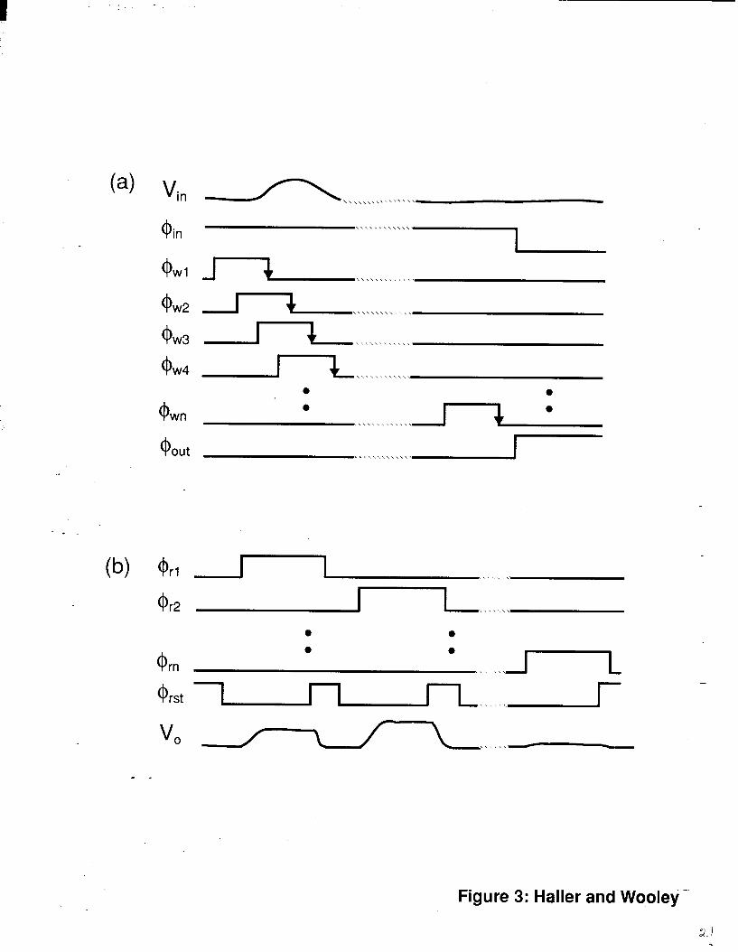
by sequentially turning transistors Mwl through M,, on and off as illustrated in Fig. 3(a). Samples
of the input waveform at n discrete times are thereby stored in the memory channel.
The voltage AV,i , stored across capacitor Ci in memory cell i, 1 5 i 5 II, after sampling is
AV,i = Vin- V,- AV~~wi (1)
where AVp,i is the voltage error due to,charge injection in switch M,i during turn-off [18]-[21].

: . ^
Haller and Wooley: Switched Capacitor Analog Memory 5
The source and drain terminals of the write transistor are at the reference voltage VC at turn-off. If
the cell capacitance Ci is much larger than the parasitic capacitances associated with the read and
write transistors, then AL’,,, can be written as [ 181
-,yy,+v,-v,) Wl 1 (2)
where C,i is the write-transistor gate overlap capacitance, Ci is the sampling capacitance, VT is
the threshold voltage, V, and V, are the low and high levels of the write-transistor gate voltage,
Co, is the oxide capacitance per unit area, W++,i and L,i are the width and length of the write tran-
sistor, U is the slew rate of the gate voltage, p = ~nCoxWwi/Lwi, and ~~ is the electron mobility in
the channel. The equation must be modified [ 191 if the associated parasitic capacitances and the
oxide capacitance are not negligible compared to Ci, but the important fact for this investigation is
that in either case AV . - pwi remains independent of the input voltage, Vi,.
After the write phase has been completed and the input waveform is stored in the analog
memory, the read cycle is initiated. During readout, the switch Mi, is turned off while Mout and
- - Mrst are turned on, forcing the input and read bus to V,. MrLYt is then turned off and the voltage
stored in the first cell is read out by turning transistor M,, on as illustrated in Fig. 3(b). After the
output has settled, the signal may be digitized with an external low-speed, low-power A/D con- -
verter. Following digitization, M,,, is again turned on and M,t is turned off, which forces the input
bus back to V, in preparation for the readout of the next cell. This cycle is repeated for all cells. It
is essential that the input bus always be forced back to V, before a new cell is read out; otherwise,
charge ‘sharing and parasitic capacitance effects will seriously degrade the performance of the
memory. By turning the cell read switches off after the reset switch is turned on, the potential
Hailer and Wooley: Switched Capacitor Analog Memory 6
across the capacitors is initialized to a defined state for the next write phase. The minimum read-
out time depends on the number of cells to be read out and the performance of the amplifier.
Once the write switch is turned off, the cell capacitor nodes connected to the cell transistors
are left in a high-impedance state for the remainder of the write phase and the entire read phase.
The charge at these nodes is thus conserved and, with the input and output bus forced to V,
between the readout of adjacent memory cells, only three parasitic capacitances influence the dc
transfer function of a memory cell. One is the capacitance CPi associated with the cell sampling
capacitor terminal that is connected to the write switch M,. CPi comprises the parasitic capaci-
tance of the sampling capacitor together with the drain-substrate capacitance of the read switch
and the drain-substrate and gate overlap capacitances of the write switch. The second parasitic
capacitance is the gate overlap capacitance of the read switch, C,i, and the third parasitic to be
considered is the capacitance, CPP, between the input bus and the read bus. CPP consists of the
capacitance between the inverting input and output of the amplifier (a fraction of the gate-drain
capacitance of the amplifier input transistor) together with capacitances associated with intercon-
nections on the chip.
- In the proposed memory the voltage across the cell capacitor, rather than the charge stored on . -
that capacitor, is sensed during readout. When memory cell i is selected for readout, the voltage at -
the output of the amplifier, Voi, can be described as a function of the input voltage, Viny in the form
- - [19]
Voi = AiVin + Vofli .
The gain factor Ai is given by
Ai = 1 1
(3)
(4)
where G is the open-loop gain of the operational amplifier. From a technical standpoint, the sam-
pling capacitance Ci can be made.large compared to CPP, which, because of careful circuit layout,
I .
Haller and Wooley: Switched Capacitor Analog Memory 7
is dominated by the input-to-output capacitance of the amplifier. The open-loop gain G of the
amplifier should exceed 60 dB for practical CMOS circuits, so that Ai is close to one.
The offset voltage, I$,,, in (3) is given by
‘pi Voffi = VB -AiV, + AiC (VB - V,) + AiVpoi + Vch .
i
(5)
Vch is an offset voltage term common to all cells in one channel and includes both the charge
injected at the turn-off of reset switch Mrst and the amplifier input offset voltage. The cell-specific
parasitic offset voltage, Vp,i, is
V 2cr-i
. = 7 uyv,> - ‘0.x wt-iLt-i
PO1 c. (VH-VB-V7.) -AVpwi 1 1
(6)
where Wri and Lri are the width and the length of the read transistor.
Because, as indicated by (4)-(6), both Ai and Vow are independent of the input voltage, Vin, it
follows that the output voltage of the analog memory channel, V,, is a linear function of Vi,.
For applications where a high input bandwidth is required, the write transistor must be made -
. - large because the cell bandwidth, B, is determined by the size of the sampling capacitor and the
resistance of the write transistor:
wwi
VOXT (V,,-V,+V,.)
B- wi
‘i
(7)
The bandwidth of a memory cell and the size of the error voltage AVp,i are therefore correlated.
In order to simplify the calibration and correction procedure, the uniformity of the sampling
- cell transfer characteristics must be considered. In the architecture presented here, memory cell
response variations across a channel are governed by switch charge injection mismatch of the
large write transistors. With the reference voltage VC set to the bias voltage V,, and W, much
larger than W,. (width of the minimum size read switch), the output voltage is approximately
-
Hailer and Wooley: Switched Capacitor Analog Memory 8
V,i = Vi, - AVpwi .
In fast turn-off conditions the variation in channel charge dominates the charge injection mis-
match [3] and can be modeled as part of the mismatch of two geometric parameters, the channel
width and length. Smaller switches yield smaller pedestal mismatches but limit the signal band-
_ width of the sampling cell. The size of the write transistor is thus a trade-off between input band-
width and pedestal mismatch for a given sampling capacitor value, which in turn is chosen on the
basis of thermal noise considerations and the need to make relevant parasitics negligible.
A single NMOS transistor is used as a write switch to avoid the need for complementary con-
trol signals, which impose a burden on high speed designs. Complementary cell switches would
reduce the overall cell pedestal sizes, but would not improve and might even worsen the cell ped-
estal uniformity across a channel. Since the pedestals can be accurately determined and then sub-
tracted from the output by either analog or digital methods, their mean value is not of great
concern. The pedestals are measured by applying a dc reference level at the channel input, record-
ing the responses of the cells, and then subtracting the results during readout. In this context it is
. - important that the charge injected by transistors M,,,, through M,, not depend on the signal level,
as is the case in [6]-[13]. Note that in the analyses presented in some of these references the error
voltages from the sampling switches are neglected, which is not a valid assumption for a high
input-bandwidth analog memory.
The influence of the size of the sampling cell capacitance on the memory cell gain can be
derived from (4), and the gain variation across a channel as a function of capacitor mismatch is
The parasitic capacitance CPP is small compared to practical values for the cell sampling capaci-
tance Ci. As a result, it is expected that the gain will be insensitive to the capacitance mismatch
and thus uniform across a memory channel.
:
Haller and Wooley: Switched Capacitor Analog Memory 9
Since the cell capacitor nodes connected to the cell transistors remain floating after the write
switch is turned off, care must be taken to ensure that no leakage occurs at those nodes, for all
possible ac and dc input signals, during the entire write and read phases. To avoid subthreshold
leakage, the maximum input voltage swing, AViny in the write phase is limited to
(10)
For the same reason, the maximum voltage swing A&i at the output of the amplifier must be less
than V, - VL during the read phase. The corresponding limit for the input voltage swing during
the write phase is then
AVoi VB-VL AVin=A-$ A, .
1 1 (11)
From (10) it is apparent that the maximum voltage swing is limited by the value of reference input
voltage, VC, which must be chosen such that the sampling switch impedances are small enough to
achieve the desired bandwidth, as given by (7). The bias level VB is set to avoid leakage during
the read phase and to ensure that V, does not exceed the amplifier output voltage range.
A common input switch, Min, could be used in the circuit of Fig. 2 because of the relatively
small number of memory cells required in each channel for the intended application. This input
switch must be large enough to achieve the desired bandwidth in the presence of the parasitic
capacitance of the input bus and the combined capacitance of the addressed memory cells.
Finally, it should be noted that in the design presented herein, the turn-off time of the sampling
switches A4wi is independent of the signal level, thus eliminating a timing error that would other-
wise be present for high-frequency input signals.
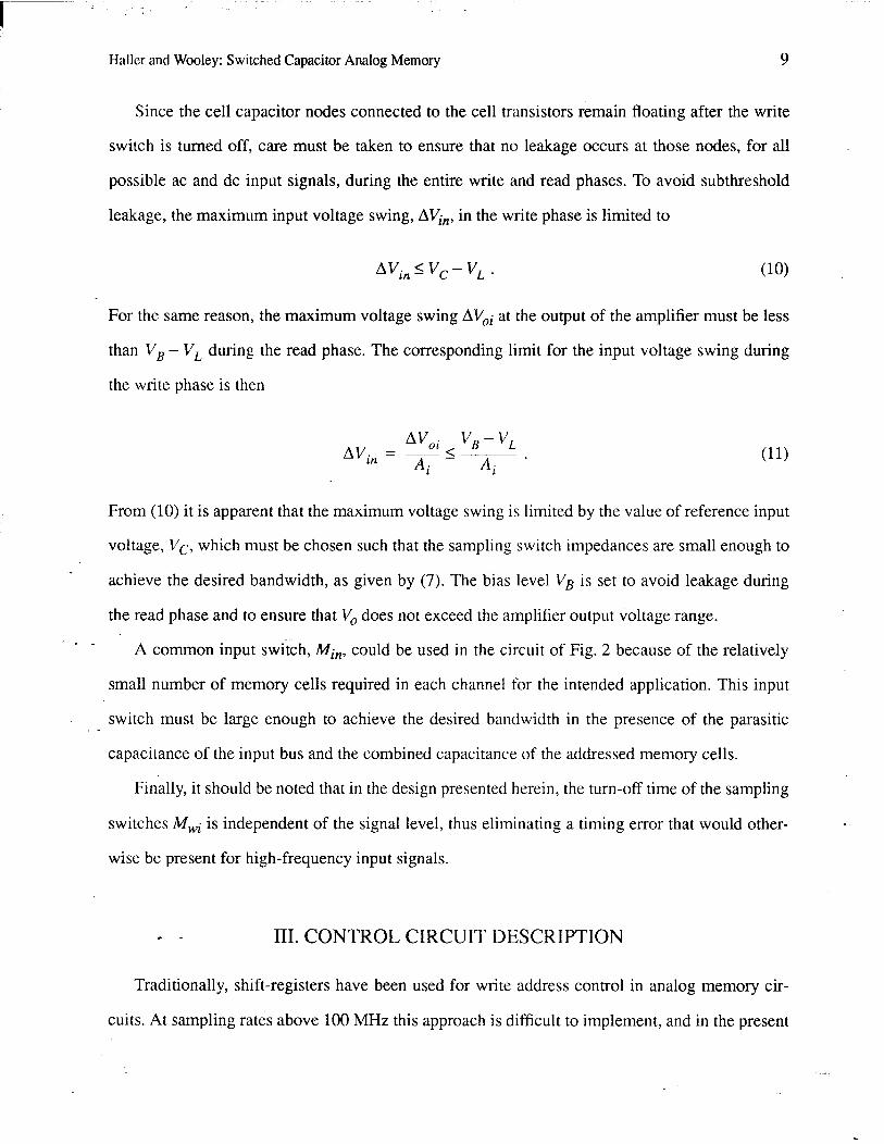
III. CONTROL CIRCUIT DESCRIPTION
Traditionally, shift-registers have been used for write address control in analog memory cir-
cuits. At sampling rates above 100 MHz this approach is difficult to implement, and in the present
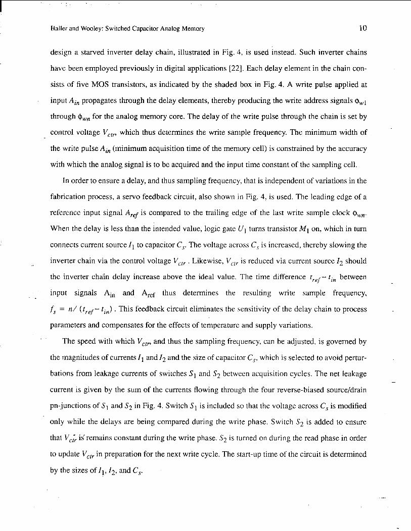
Haller and Wooley: Switched Capacitor Analog Memory 10
design a starved inverter delay chain, illustrated in Fig. 4, is used instead. Such inverter chains
have been employed previously in digital applications [22]. Each delay element in the chain con-
sists of five MOS transistors, as indicated by the shaded box in Fig. 4. A write pulse applied at
input Ain propagates through the delay elements, thereby producing the write address signals $++,I
through Qwn for the analog memory core. The delay of the write pulse through the chain is set by
control voltage Vcr,, which thus determines the write sample frequency. The minimum width of
the write pulse Ain (minimum acquisition time of the memory cell) is constrained by the accuracy
with which the analog signal is to be acquired and the input time constant of the sampling cell.
In order to ensure a delay, and thus sampling frequency, that is independent of variations in the
fabrication process, a servo feedback circuit, also shown in Fig. 4, is used. The leading edge of a
reference input signal A,.,.,., is compared to the trailing edge of the last write sample clock Qwn.
When the delay is less than the intended value, logic gate U1 turns transistor Mt on, which in turn
connects current source I, to capacitor C,. The voltage across C, is increased, thereby slowing the
inverter chain via the control voltage Vet, . Likewise, V,[, is reduced via current source Zz should
the inverter chain delay increase above the ideal value. The time difference tref- tin between
input signals Ain and A,f thus determines the resulting write sample frequency, . -
f, = n/ ( tref- tin) . This feedback circuit eliminates the sensitivity of the delay chain to process
parameters and compensates for the effects of temperature and supply variations.
The speed with which Vctr and thus the sampling frequency, can be adjusted, is governed by
the magnitudes of currents I, and 12 and the size of capacitor C,, which is selected to avoid pertur-
bations from leakage currents of switches S1 and S2 between acquisition cycles. The net leakage
current is given by the sum of the currents flowing through the four reverse-biased source/drain
pn-junctions of S1 and S2 in Fig. 4. Switch S1 is included so that the voltage across C, is modified
only while the delays are being compared during the write phase. Switch S2 is added to ensure
that V$. is remains constant during the write phase. S2 is turned on during the read phase in order
to update Vctr in preparation for the next write cycle. The start-up time of the circuit is determined
by the sizes of II,Zz, and C,.
I :
Hailer and Wooley: Switched Capacitor Analog Memory 11
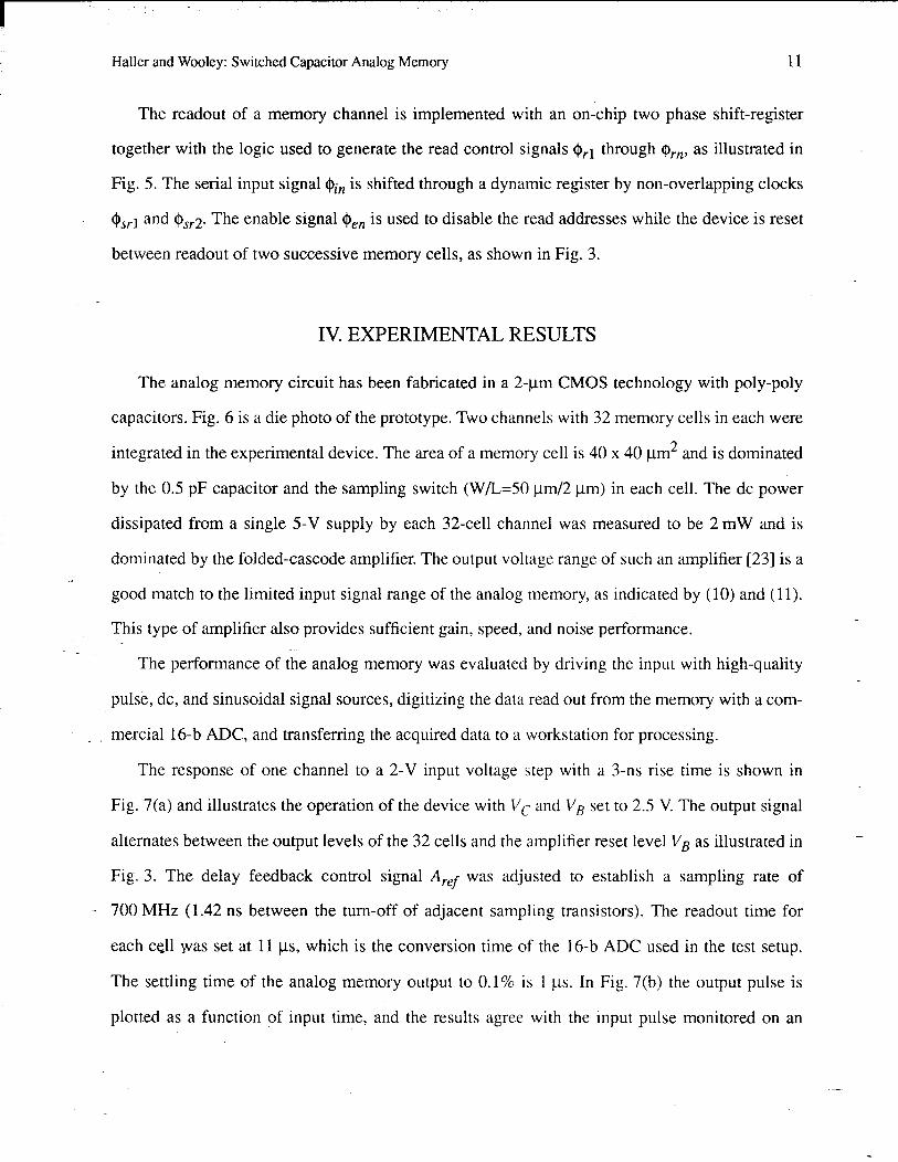
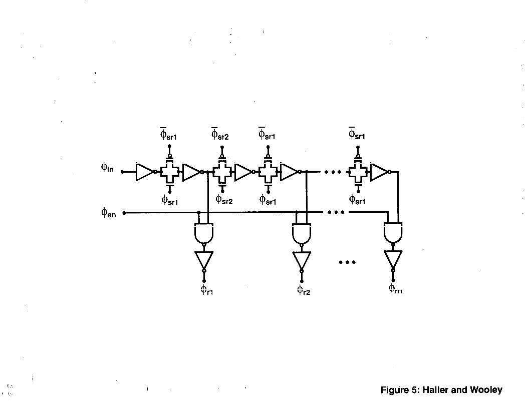
The readout of a memory channel is implemented with an on-chip two phase shift-register
together with the logic used to generate the read control signals &I through &, as illustrated in
Fig. 5. The serial input signal @iin is shifted through a dynamic register by non-overlapping clocks
0 srl and $sr2. The enable signal Qen is used to disable the read addresses while the device is reset
between readout of two successive memory cells, as shown in Fig. 3.
IV. EXPERIMENTAL RESULTS
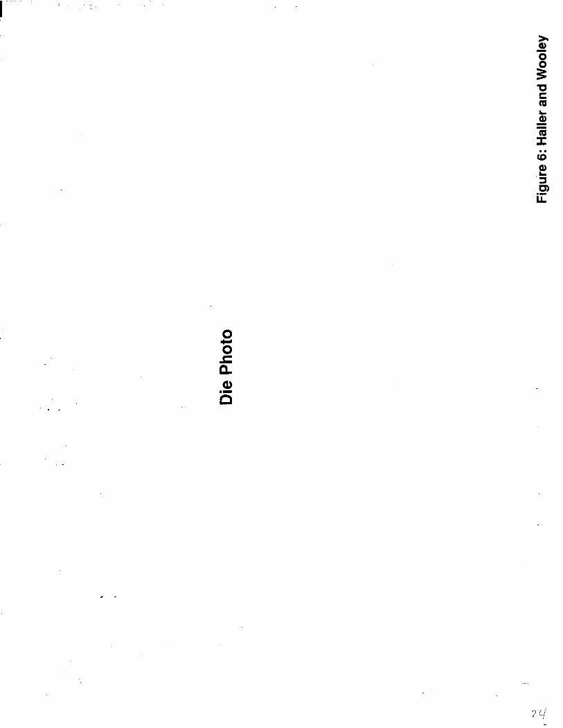
The analog memory circuit has been fabricated in a 2+m CMOS technology with poly-poly
capacitors. Fig. 6 is a die photo of the prototype. Two channels with 32 memory cells in each were
integrated in the experimental device. The area of a memory cell is 40 x 40 pm2 and is dominated
by the 0.5 pF capacitor and the sampling switch (W/L=50 pm/2 pm) in each cell. The dc power
dissipated from a single 5-V supply by each 32-cell channel was measured to be 2 mW and is
dominated by the folded-cascade amplifier. The output voltage range of such an amplifier [23] is a
good match to the limited input signal range of the analog memory, as indicated by (10) and (11).
This type of amplifier also provides sufficient gain, speed, and noise performance.
The performance of the analog memory was evaluated by driving the input with high-quality
pulse, dc, and sinusoidal signal sources, digitizing the data read out from the memory with a com-
_ - mercial 16-b ADC, and transferring the acquired data to a workstation for processing.
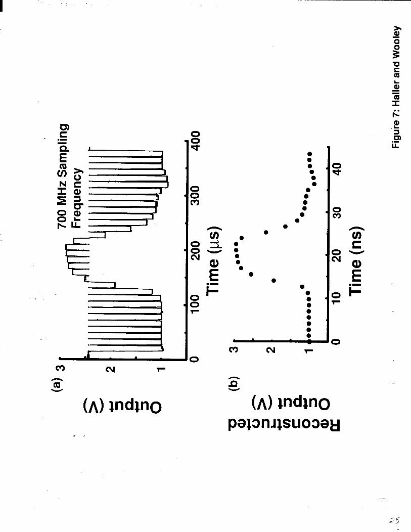
The response of one channel to a 2-V input voltage step with a 3-ns rise time is shown in
Fig. 7(a) and illustrates the operation of the device with I/c and VB set to 2.5 V. The output signal
alternates between the output levels of the 32 cells and the amplifier reset level VB as illustrated in
Fig. 3. The delay feedback control signal Aref was adjusted to establish a sampling rate of
- 700 MHz (1.42 ns between the turn-off of adjacent sampling transistors). The readout time for
each cell was set at 11 ps, which is the conversion time of the 16-b ADC used in the test setup.
The settling time of the analog memory output to 0.1% is 1 ps. In Fig. 7(b) the output pulse is
plotted as a function of input time, and the results agree with the input pulse monitored on an
I .
Haller and Wooley: Switched Capacitor Analog Memory 12
oscilloscope with respect to rise and fall time, pulse width, and the signal undershoot. The input
time constant of the memory, defined as the product of the on-resistance of the write transistor and
the capacitance Ci, was designed to be less than 0.5 ns for Vc = 2.5 V.
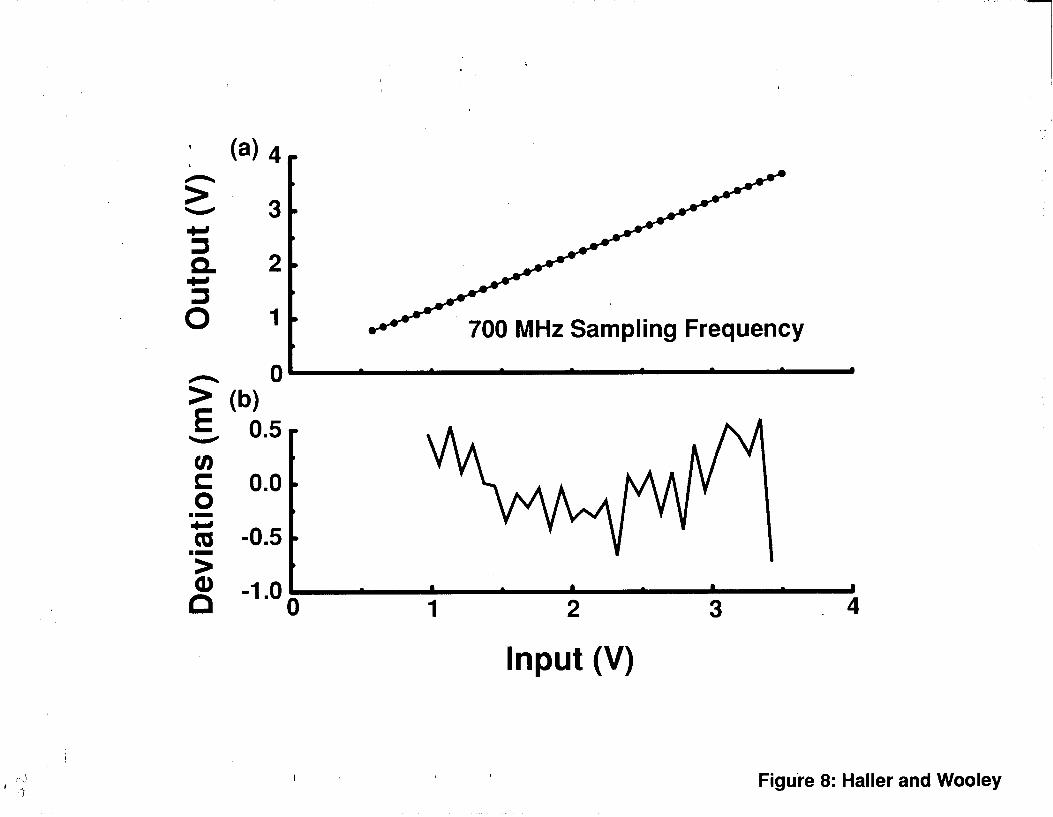
The nonlinearity of the experimental circuit was measured by applying 38 equally spaced
input voltages and fitting the output levels to a straight line using the least-squares method.
Fig. 8(a) shows the output of a typical cell plotted as a function of input voltage over a range of
3 V, and in Fig. 8(b) the deviations are shown for the chosen input voltage range of 2.5 V. The
maximum deviation is 0.7 mV, or 0.03 % of full scale.
The dynamic range is commonly defined as the maximum recordable signal divided by the
baseline noise, which determines the smallest detectable signal. The noise voltage for the analog
memory can be expressed as
v2 = !g + “+cc, 2”;q
1 ( 1 1 (12)
where C, is the capacitance at the inverting input node of the amplifier during readout, and ve4 is
the input-referred noise voltage of the amplifier. The baseline noise of the analog memory was . -
determined by recording the device response to repeated measurements with a constant input and
calculating the mean square error. An RMS of 0.3 mV was obtained from sets of 100 repeated
_ - measurements, independent of the input signal level. The dynamic range of the device is therefore
better than 8,000/l, or 13 bits.
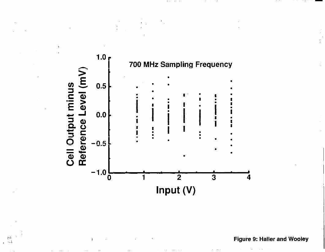
The cell-to-cell pedestal variations result in a RMS deviation of 1.8 mV across a channel. This
is expected for the selected switch and capacitor sizes and the fabrication process used. In order to
investigate whether the cell pedestals depend on the input signal, the responses to various dc input
levels were recorded, and the response to one dc reference level was subtracted from these mea-
surements; The differences for all 32 cells are plotted in Fig. 9 as a function of the input voltage.
In order to plot the data on the same scale, the nominal input level has been subtracted. Each data
point represents the mean value from five measurements so that variations in the result due to
Haller and Wooley: Switched Capacitor Analog Memory 13
baseline noise can be neglected. The RMS cell response variation after cell pedestal subtraction
across the entire input signal range is only 0.3 mV, demonstrating that the sampling switch charge
injection is independent of the dc input signal level and can be reduced to the level of the thermal
noise by a simple subtraction.
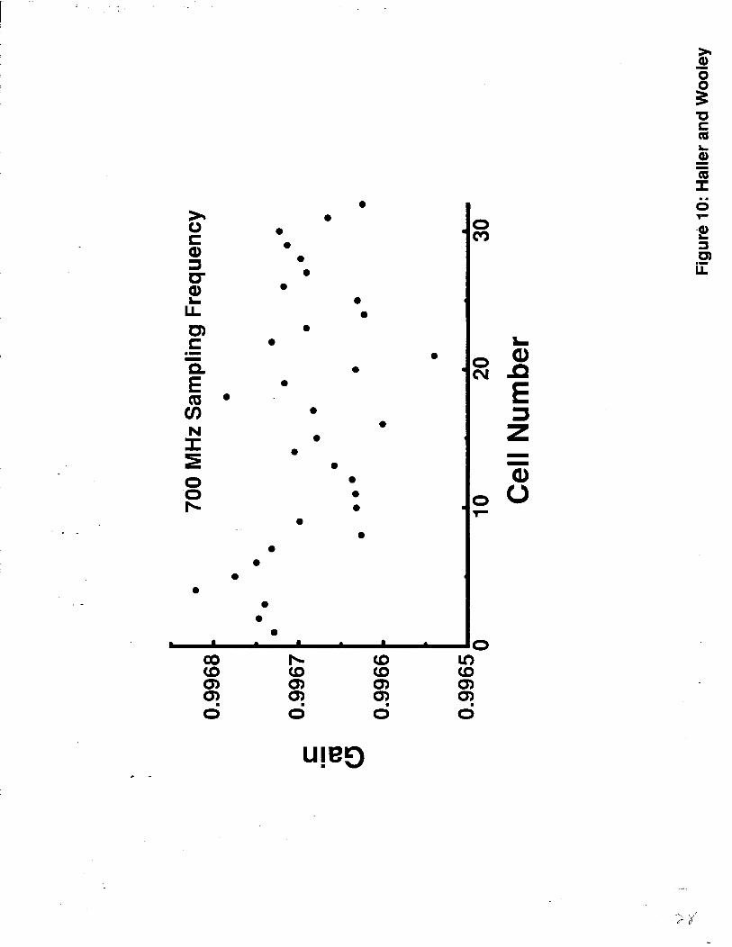
The average gain, AVJAVin, of a memory channel at low frequencies was measured to be
0.9967, with an RMS gain variation across the channel of 0.0001, as indicated by Fig. 10. Calibra-
tion of the channel therefore requires only a simple cell pedestal subtraction in order to achieve a
precision of better than 12 bits for dc signals. The measured absolute gain agrees well with esti-
mates based on (4).
The ac performance of the circuit has been quantitatively evaluated by applying free running
sine waves of various amplitudes and frequencies at the analog input. Since the phase of the input
signal was not synchronized to the sampling process, the results also provide a measure of the ac
uniformity of the cells across a channel. The pedestal subtracted responses for 20 separate sets of
measurements were fitted to a common frequency, offset, and amplitude of the signal and a free
phase for each set of measurements [24], [25]. The signal-to-(noise+distortion) ratio (SNDR) was
then calculated based on the residuals from an ideal ht. Errors can be attributed to a variety of
sources, including errors in sampling time and amplitude, variations in the ac response of different
cells, nonlinearities, and thermal noise.
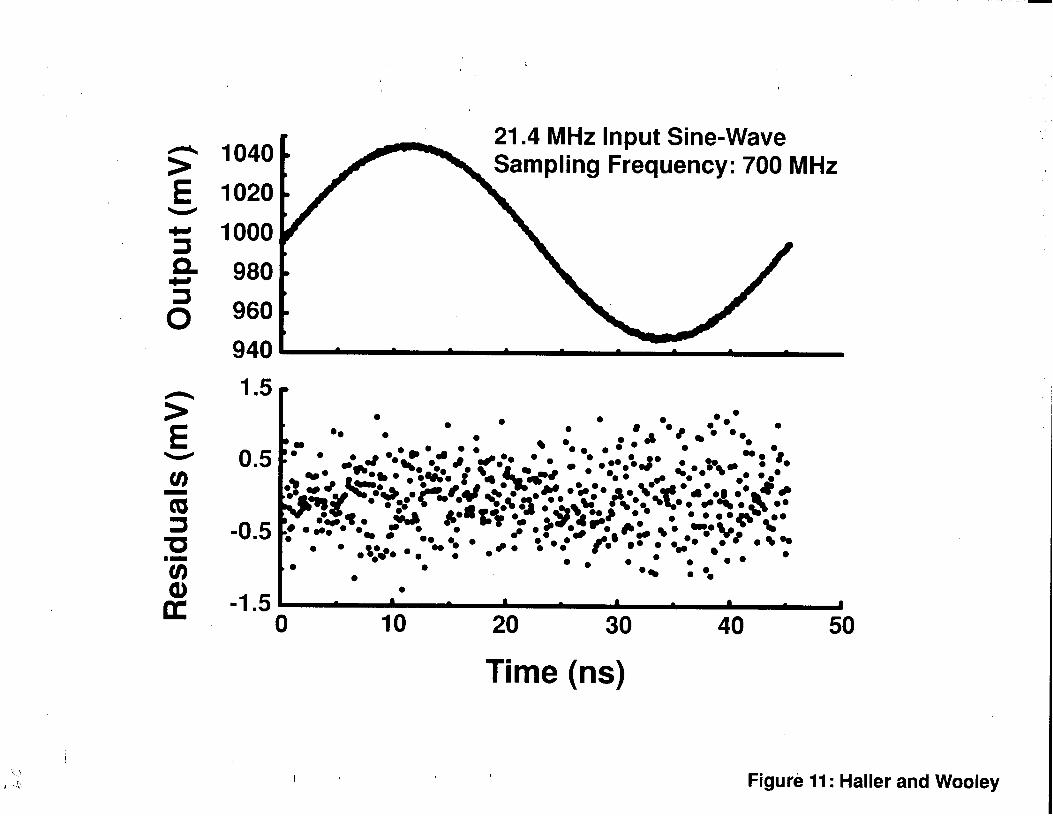
Fig. 11 shows a 21.4 MHz sine wave fitted to the data and plotted modulo the phase along
with the residuals. The fit yields RMS residuals of 0.4 mV. The amplitude and residuals remain
stable for various dc input voltage levels, demonstrating the good small-signal ac linearity across
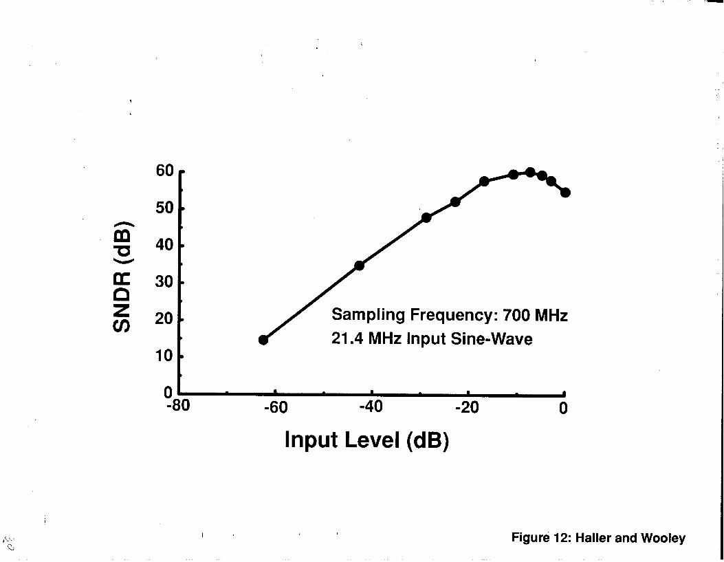
the signal range. Shown in Fig. 12 is a plot of the SNDR as a function of the input amplitude, as
measured for a 21.4 MHz input frequency. An input level of 0 dB represents a full-scale peak-to-
peak amplitude of 2.5 V. The device achieves a peak SNDR of 60 dB and a dynamic range of
74 dB for a 21.4 MHz input,
The performance of the analog memory degrades at large signal amplitudes principally
because of harmonic distortion and timing errors. Errors in sampling time can be attributed prima-
I I .
Haller and Wooley: Switched Capacitor Analog Memory 14
rily to two sections of the circuit, the delay chain and the feedback control. The total delay of the
inverter chain is regulated by the feedback control circuit. The peak-to-peak timing jitter mea-
sured at the end of the 32 stage delay chain is less than 1 ns, which translates into 31 ps per sam-
pling interval or delay element. This jitter corresponds to a sampling frequency error of 2 % at the
700 MHz rate and will decrease linearly with an increase in the number of delay elements. Addi-
tional error is introduced by cell-to-cell sampling time, or delay, variations. These variations have
been estimated by fitting the sine wave with the individual delays of the elements as a parameter
(with the same element delays for each of the 20 measurements sets). The best fit yielded an RMS
value of 25 ps for the element delay variations across a channel. This timing error is due to delay
element mismatch and is independent of the input signal level. This error can be corrected for if
required. The approximate start-up time of the delay chain was measured to be less than ten cycles
at a trigger rate of 120 Hz. For the intended application start-up effects are of no concern since the
circuit is exercised long before input waveforms need to be acquired.
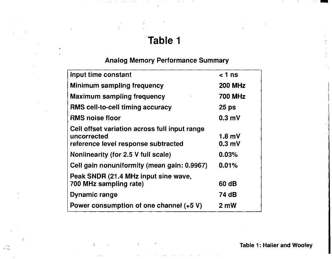
The performance of the analog memory is summarized in Table 1.
V. CONCLUSION
In analog waveform sampling applications switched-capacitor memories can provide superior
_ . performance with respect to cost, space, dynamic range, sampling rate, and power dissipation
when compared to flash A/D converters and CCD devices. Present analog memory circuits are
generally limited to sampling frequencies of 150 MHz. This paper has described a memory archi-
tecture that enables sampling rates from 200 MHz to 700 MHz by utilizing starved inverter delay
elements with on-chip delay feedback compensation. In the proposed circuit, memory cell pedes-
- tals are independent of the input signal amplitude and can be eliminated by analog or digital sub-
traction. This is an especially important attribute in applications where digitization and
subtraction are to be included on the same chip as the memory.
: .
Hallcr and Wooley: Switched Capacitor Analog Memory 15
Analysis and measurements indicate that the gain variation from cell to cell is insensitive to
the size of the capacitors, since the voltage across the capacitor, rather than the charge stored on it,
is sensed during readout. The sampling time is independent of the input signal level, which is
especially important for the acquisition of high-frequency input signals. For applications where
sampling frequencies of less than 100 MHz are sufficient, the high-speed inverter delay chain can
be replaced by traditional shift registers.
A 2 (channel) x 32 (cell) experimental device was fabricated in a 2-ym CMOS technology
with poly-poly capacitors. The measured nonlinearity is 0.03 % for a 2.5 V input range and the
cell-to-cell gain matching is 0.01 % RMS. The dynamic range of the device exceeds 12 bits and
the peak signal-to-(noise+distortion) ratio for a full-scale 21.4 MHz sine-wave sampled at
700 MHz is 60 dB. The device has been optimized for high energy physics applications where, in
general, different classes of signals covering a wide dynamic range must be processed in a chan-
nel, but where each class of signals has a limited inherent accuracy. For each class of signals it is
thus sufficient to have a peak SNDR that is lower than the dynamic range of the channel. The
power dissipation for one channel operated from a single +5 V supply is 2 mW.
. The proposed analog memory is a viable alternative to real-time analog-to-digital converters . _
in applications where continuous acquisition is not required. The power dissipation of the device
is orders of magnitude below that typical of commercial monolithic converters, which are pres-
- - ently limited to a dynamic range of 8 bits for rates exceeding 100 MHz.
ACKNOWLEDGEMENT
The authors wish to thank Dr. Dietrich Freytag for numerous helpful discussions. They are
- also grateful for the support provided by Prof. Martin Breidenbach and Prof. David Leith of the
research department at SLAC.
I : .
Haller and Wooley: Switched Capacitor Analog Memory 16
REFERENCES
[l 1
VI
- [31
r41
[51
C61
r71
RI
r91
[lOI
[Ill
[W
[I31
R. Larsen, “Overview of the Data Acquisition Electronics System Design for the SLAC
Linear Collider Detector (SLD),” ZEEE Trans. Nucl. Sci., NS-33, No. 1, pp. 65-72, Feb.
1986.
M. Pelgrom, A. Duinmaijer, and A. Welbers, “Matching Properties of MOS Transistors,”
IEEE J. Solid State Circuits, vol. SC-24, pp. 1433-1439, Oct. 1989.
K. Lakshmikumar, R. Hadaway, and M. Copeland, “Characterization and Modeling of
Mismatch in MOS Transistors for Precision Analog Design,” IEEE J. Solid State Circuits,
vol. SC-21, pp. 1057-1066, Dec. 1986.
J. McCreary, “Matching Properties, and Voltage and Temperature Dependence of MOS
Capacitors,” IEEE J. Solid State Circuits, vol. SC- 16, pp. 608-616, Dec. 198 1.
K. Nagaraj, “Switched-Capacitor Delay Circuit that is Insensitive to Capacitor Mismatch
and Stray Capacitance.” Electron. Letters, vol. 20, pp. 663-664, Aug. 1984.
J. Walker, S. Chae, S. Shapiro, and R. Larsen, “Microstore-The Stanford Analog Memory
Unit,” IEEE Trans. Nucl. Sci., NS-32, No. 1, pp. 616-621, Feb. 1985.
D. Freytag and J. Walker, “Performance Report for Stanford/SLAG Microstore Analog
Memory Unit,” ZEEE Trans. Nucl. Sci., NS-32, No. 1, pp. 622-625, Feb. 1985.
G. Haller, D. Freytag, J. Walker, and S. Chae, “Performance Report for Stanford/SLAG
Multi-Channel Sample and Hold Device,” IEEE Trans. Nucl. Sci., NS-33, No. 1, pp. 221-
225, Feb. 1986.
E. Franchi, M. Tartagni, R. Guerrieri, and G. Baccaranie, “Random Access Analog Mem-
ory for Early Vision,” IEEE J. Solid State Circuits, vol. 27, pp. 1105-l 109, July 1992.
K. Matsui, T. Matsuura, S. Fukasawa, Y. Izawa, Y. Toba, N. Miyake, and K. Nagasawa,
“CMOS Video Filters Using Switched Capacitor 14-MHz Circuits,” IEEE J. Solid State
Circuits, vol. SC-20, pp. 1096-1101, Dec. 1985.
S. Kleinfelder, “A 4096 Cell Switched Capacitor Analog Waveform Storage Integrated
Circuit,” IEEE Trans. Nucl. Sci., NS-37, pp. 1230- 1236, June 1990.
D. Munday, et. al., “A 66 MHz, 32-channel Analog Memory Circuit with Data Selection
for Fast Silicon Detectors,” Nucl. Inst. and Meth. in Phys. Research, A-326, pp. 100-111,
-1993.
R. Horisberger and D. Pitzl, “A Novel Readout Chip for Silicon Strip Readout Detectors
with Analog Pipeline and Digitally Controlled Analog Signal Processing,” Nucl. Inst. and
Meth. in.Phys. Research, A-326, pp. 92-99, 1993.
I .
Haller and Wooley: Switched Capacitor Analog Memory 17
[15
lY161
[I71
[I81
[I91
PO1
[21
[22 1
. -
~23 1
- - [241
v51
J. Moeschen, A. Caldwell, L. Hervas, B. Hosticka, U. Koetz, B. Sippach, “High-Speed
Analog CMOS Pipeline System,” Nucl. Inst. and Meth. in Phys. Research, A-288, pp.
180-186,199O.
J. Pellegrin, M. Ross, B. Scott, and D. Wilson, “Beam Trajectory Acquisition System for
the Arcs of the Stanford Linear Collider,” Proc. IEEE Particle Accelerator Conference,
vol. 2, pp. 673-675, May 1991.
M. Ross, “Beam Diagnostics and Control of SLC,” Proc. IEEE Particle Accelerator Con-
ference, vol. 2, pp. 508-5 11, May 199 1.
R. Ruth, “Linear Colliders,” SLAC-PUB-5597, July 1993.
B. Sheu and C. Hu, “Switch-Induced Error Voltage on a Switched Capacitor,” IEEE J.
Solid State Circuits, vol. SC-19, pp. 519-525, Aug. 1984.
G. Haller, “High-Speed, High-Resolution Analog Waveform Sampling in VLSI Technol-
ogy,” Ph.D Thesis, Stanford University, 1994.
G. Wegeman, E. Vittoz,.and F. Rahali, “Charge Injection in Analog MOS Switches,” IEEE
J. Solid State Circuits, vol. SC-22, pp. 1091-1097, Dec. 1987.
J. Shieh, M. Patil, and B. Scheu, “Measurement and Analysis of Charge Injection in MOS
Analog Switches,” IEEE J. Solid State Circuits, vol. SC-22, pp. 277-281, Apr. 1987.
Y. Arai and T. Baba, “A CMOS Time to Digital Converter VLSI for High-Energy Phys-
ics,” 1992 Symposium on VLSI Circuits Digest qf Technical Papers, pp. 121-122, June
1988.
P. Gray and R. Meyer, “MOS Operational Amplifier Design - A Tutorial Overview,” ZEEE
J. Solid State Circuits, vol. SC-17, pp. 969-982, Dec. 1982.
B. Peetz, A. Muto, and J. Neil, “Measuring Waveform Recorder Performance,” Hewlett
Packard Journal, vol. 33, No. 11, pp. 21-29, Nov. 1982.
B. Boser, K. Karman, H. Martin, and B. Wooley, “Simulating and Testing Over-Sampled
Analog-to-Digital Converters,” IEEE J. Solid State Circuits, vol. SC-7, pp. 668-673, June
1988.
I .
Haller and Wooley: Switched Capacitor Analog Memory 18
FIGURE CAPTIONS
Figure 1
Figure 2
- Figure 3
Figure 4
Figure 5
Figure 6
Figure 7
Figure 8
Figure 9
. -
Figure 10
Figure 11
Figure 12
Block diagram of an analog waveform recorder with m memory channels.
Simplified schematic of the analog memory circuit.
Timing diagram for the (a) write and (b) read phase.
Write control circuit with starved inverter delay elements and feedback compensa-
tion circuit.
Read control circuitry.
Prototype die photo.
Response of one.channel to a 2-V input voltage step with a 3-ns rise-time sampled
at 700 MHz. Pulse is plotted on an (a) read and (b) write time scale.
(a) Output plotted as a function of input voltage for a 3-V input range. (b) Devia-
tions from a linear fit for the selected 2.5 V input voltage range.
Pedestals of all 32 cells in one channel as a function of input voltage after subtrac-
tion of the response to a reference input level. The nominal input value is sub-
tracted. (Several data points are super-imposed).
Gain of all 32 cells in one channel.
Upper: Results of 20 measurement sets fitted to a 21.4 MHz sine wave and plotted
on a time scale modulo the period of the sine wave. Lower: Residuals from the fit.
Signal-to-(noise+distortion) ratio as a function of amplitude for a 21.4 MHz sine
wave sampled at 700 MHz. -
Input m
l
l
Input 1
Input 0
Write Control
I
I Write Address
b Channel m + Output m .
b Channel 1 + output 1
+ output 0
I Analog Memory Core
T Read Address
Read Control
--. --!&
I Figtire 1: Hailer and Wooley
Read Control
@in 9 rl 0 r2 r ( lb3 0.0
INPUT BUS
Vc.
Mr.3 READ Mm BUS
M wl M d
w2 M w3 M wn
rst
1 0.0 4) rst
(4 wl 4) w2 (hl/3°00 own
I 1 .
0 rn
Write Control
,
iu I
I 0 Figu’re 2: Hailer and Wooley
..--.. -.~ -
. .
0 wl
0 w2
0 w3
@ w4
Figure 3: Hailer and Wooley--
:
0 0 0 0 0 0
. . 0 a 0 0 a
pt+-t i 2 dl
& c .-
a
0 srl 0 sr2 0 srl
4) rl
0 00
0.0
T 0 srl
I
9 rn
Figure 5: Hailer and Wooley
.-
.
8 I-
: 0 l 0 0
0 0
: 0 0
0
I ()4 a
A >
I 31
‘5 Q 2
5 0 1 700 MHz Sampling Frequency
j- (b) g 0.5r
Q) -1 .o; a a . 4 0
1 2 3 4
Input (V)
Figu’re 8: Hailer and Wooley
700 MHz Sampling Frequency
l
.
i
.
0 .
. 1’ .
l . t
i i i i t . I I . . . . .
.
.
.
0
t .
. t
.
f
t
i t I ; t
.
. .
. .
.
1 1 2 3 4
Input (V)
Figure 9: Haller and Wooley
: .
.
0
0
0 0
0
0 0
a
0
1040
1020
1000
980
960
940
21.4 MHz Input Sine-Wave Sampling Frequency: 700 M
I . . , . ,
Hz
Figure 11: Haller and Wooley
60
50
m w 40
a’ 30 n z cn 20 Sampling Frequency: 700 MHz
21.4 MHz Input Sine-Wave
. . a t
-- -
-60 -40 -20
Input Level (dB)
0
Figure 12: Haller and Wooley
‘Table 1
Analog Memory Performance Summary
Input time constant <l ns
Minimum sampling frequency 200 MHz
Maximum sampling frequency . 700 MHz
RMS cell-to-cell timing accuracy 25 ps
RMS noise floor 0.3 mV
Cell offset variation across full input range uncorrected 1.8 mV reference level response subtracted 0.3 mV
Nonlinearity (for 2.5 V full scale) 0.03%
Cell gain nonuniformity (mean gain: 0.9967) 0.01%
Peak SNDR (21.4 MHz input sine wave, 700 MHz sampling rate) 60 dB
Dynamic range 74 dB
Power consumption of one channel (+5 V) 2mW
Table 1: Haller and Wooley
.