soft switching of switched-capacitor converters - bgupemic/publications/alumni/eli hamo soft sw of...
TRANSCRIPT

BEN-GURION UNIVERSITY OF THE NEGEV
FACULTY OF ENGINEERING SCIENCES
DEPARTMENT OF ELECTRICAL ENGINEERING
Soft Switching of
Switched-Capacitor Converters
THESIS SUBMITTED IN PARTIAL FULFILLMENT OF THE REQUIREMENTS
FOR THE M.Sc. DEGREE
By: Eli Hamo
Supervised by:
Dr. Mor Mordechai Peretz
January 2015


BEN-GURION UNIVERSITY OF THE NEGEV
FACULTY OF ENGINEERING SCIENCES
DEPARTMENT OF ELECTRICAL ENGINEERING
Soft Switching of
Switched-Capacitor Converters
THESIS SUBMITTED IN PARTIAL FULFILLMENT OF THE REQUIREMENTS
FOR THE M.Sc. DEGREE
By: Eli Hamo
Supervised by:
Dr. Mor Mordechai Peretz
Author: Eli Hamo ……………… Date: 05/01/15
Supervisor: Dr. Mor Mordechai Peretz ……………… Date: 05/01/15
Chairman of graduate studies committee
Name: Dr. Ilan Shalish ……….……… Date: 05/01/15


Dedicated to my beloved mother
Shoulamit
With love and gratitude


vii
Abstract
Switched-capacitor dc-dc power converters are a subset of dc-dc power converters that use a
network of switches and capacitors to efficiently convert one voltage to another. Unlike traditional
inductor-based dc-dc converters, switched capacitor converters (SCCs) do not rely on magnetic energy
storage. This fact makes SCC ideal for integrated implementations. However, SCCs have traditionally
been used in low power and low conversion ratio applications due to the inherent energy losses
resulting from the capacitor charging and discharging processes, conduction, and switching losses.
The primary aim of this thesis is to improve the behavior and performance of SCC applications in
the higher power range. The methods and the applications presented in this study are focused on high
efficiency including many target voltages and soft switching. Typically, these challenges prohibit the
operation of capacitor-based converters in the medium and high power ranges. This study introduces a
simple and efficient isolated gate driver circuitry and active control system for applying the soft
switching method. This work provides a streamlined procedure to design reliable and practical
multiphase SCCs with respect to the desired efficiency and conversion ratios. The research includes a
full behavioral description, analysis theorem, application examples, and experimental results. Those
parts of the research have been published in the proceedings of the IEEE Energy Conversion Congress
and Exposition (ECCE) 2013 [1], and within a larger study in the IEEE Transactions on Power
Electronics [2]. Relevant sections have also already been published [3].
Another objective of this thesis is to develop a modeling methodology to describe and explore the
loss mechanism of a resonant SCC operating in a self-commutation zero current switching (ZCS)
mode. This passive, soft switching approach simplifies the control effort and eliminates additional
circuitry involved in active soft-switching controls. The model presented in this study assists in the
simplification and optimization of SCC systems and their controls to achieve high efficiency up to the
higher power range. The modeling methodology provides a streamlined procedure to design a reliable
and low-cost soft-switched SCC. The theoretical predictions of the model were compared with
simulations and laboratory experiments in various SCC topologies and operation modes. This part of
the research has been published in the proceedings of the IEEE Applied Power Electronics Conference
(APEC) 2014 [4] and within a larger study in the IEEE Transactions on Power Electronics [5].
This research can directly contribute to the research and development of converters, regulators, and
integrated power supplies that are based on switched-capacitor technology in a wide range of power
applications.
Keywords: Average static model, binary codes, conduction losses, dc-dc power converters, free-
wheeling diode, modeling, resonant converter, self-commutation, soft switching, switched capacitor
converter, switched-mode power supply, switching losses, zero current switching.

viii
Acknowledgements
I would like to thank my supervisor Dr. Mor Peretz for his invaluable guidance and support for the
duration of my research. Through an invaluable and rare combination of professional expertise,
managerial guidance, and amiable friendship, Mor has impelled me to excellence, all the while
providing me with the opportunities for enjoyment and for the self-fulfillment of achieving my goals.
I give special thanks to my supervisor Professor Shmuel (Sam) Ben-Yaakov, for all I have learned
from him, for support and for his constant demand for high-quality science advances. Thanks for the
open mind, boundless enthusiasm, and sense of humor and for his willingness to support and to help.
Special thanks must be recorded to the co-authors of the articles, Dr. Michael Evzelman, and Mr.
Alon Cervera, for their collaboration, research work, and ideas. They are always happy to help
everyone, at anytime, anywhere.
I must not forget all undergraduate and graduate students here at our research laboratory whose
support and friendship meant so much: Mr. Alon Blumenfeld, Mr. Shai Dagan, Ms. Yara Halihal, Dr.
Natan Krihely, Mr. Zeev Rubinshtein, Mr. Ofer Ezra, Mr. Or Kirshenboim, and anyone that I forgot to
mention by name.
Of the technical staff, I would like to thank Neli Grinberg, Azrikam Yehieli, and Udovikin Larisa
who are responsible for the excellent working and social conditions of the laboratory.
I give thanks to my parents for their love and support throughout my whole life, and for their
steering me towards a higher education and the achievement of excellence in whatever I undertake
without treading on others or using any insincere techniques. It would be hard to imagine better
individuals to guide me through life, show me an example of how to live and behave, and provide for
all my spiritual and material needs, never expecting anything in return but my love.

ix
Table of Contents
List of Tables ........................................................................................................................................... xi
List of Figures ......................................................................................................................................... xii
Acronyms and Abbreviations................................................................................................................ xvii
Inline References Legend ...................................................................................................................... xvii
Chapter 1 - Introduction ........................................................................................................................ 1
1.1 Power supplies ........................................................................................................................... 1
1.1.1 Linear regulators ............................................................................................................ 1
1.1.2 Switched mode converters ............................................................................................. 2
1.2 Switched capacitor dc-dc converters.......................................................................................... 4
1.3 Generic conduction losses model and efficiency of SCC .......................................................... 6
1.3.1 Equivalent resistance calculation: Hard switching case ................................................ 6
1.3.2 Equivalent resistance calculation: Soft switching case .................................................. 8
1.3.3 Diode losses ................................................................................................................... 8
1.4 Binary and Fibonacci SCC ......................................................................................................... 9
1.4.1 Binary and Fibonacci codes ......................................................................................... 10
1.4.2 Translating the codes into SCC topologies .................................................................. 11
1.5 Resonant converters and soft switching ................................................................................... 13
1.5.1 High power resonant SCC............................................................................................ 14
1.6 Current sensing ........................................................................................................................ 16
1.6.1 Current sensors ............................................................................................................. 16
1.6.2 Zero current detection .................................................................................................. 18
1.7 Research objectives and significance ....................................................................................... 20
1.8 Thesis Overview ...................................................................................................................... 22
Chapter 2 - Multiple Conversion Ratio Resonant Switched-Capacitor Converter
with Active Zero Current Detection .............................................................................. 23
2.1 Introduction .............................................................................................................................. 23
2.2 Principle operation of the resonant binary/Fibonacci SCC ...................................................... 24
2.3 Practical implementation.......................................................................................................... 26
2.3.1 Current sensing and zero crossing detection ................................................................ 27
2.3.2 Reference voltage ......................................................................................................... 28
2.3.3 Stabilizing the flying capacitors voltage on startup ..................................................... 29
2.3.4 Switches and isolated gate drivers ............................................................................... 30
2.4 Conclusions .............................................................................................................................. 33
x
Chapter 3 - Design of the Multiphase Resonant Switched-Capacitor Converters ......................... 34
3.1 Introduction .............................................................................................................................. 34
3.2 Equivalent resistance – considerations for components selection ........................................... 34
3.3 Analysis and numerical plots ................................................................................................... 37
3.4 Experimental results of the resonant binary/Fibonacci SCC ................................................... 43
3.4.1 Resonant binary SCC with pre-calibration of the switching timing ............................ 43
3.4.2 Resonant binary SCC with active zero current detection ............................................ 45
3.5 Discussion and conclusions ..................................................................................................... 50
Chapter 4 - Modeling and Analysis of Resonant Switched-Capacitor Converters
with Free-Wheeling ZCS ................................................................................................. 52
4.1 Introduction .............................................................................................................................. 52
4.2 Basic terminology and definitions ........................................................................................... 52
4.3 Modeling approach .................................................................................................................. 54
4.4 Extraction of equivalent resistances and equivalent average voltage drop .............................. 56
4.4.1 Equivalent resistance calculation ................................................................................. 56
4.4.2 Equivalent average diode voltage source calculation .................................................. 58
4.4.3 Equivalent resistance calculation at low Q .................................................................. 59
4.5 Simulation & Experimental (Model Validation) ..................................................................... 63
4.5.1 Unity converter ............................................................................................................ 63
4.5.2 Voltage doubler SCC ................................................................................................... 65
4.5.3 Multiphase Fibonacci resonant SCC ............................................................................ 67
4.5.4 Model validation for low Q .......................................................................................... 69
4.6 Discussion and conclusions ..................................................................................................... 70
Chapter 5 - Contribution of Thesis and Suggestions for Future Research ..................................... 71
5.1 Contribution of thesis ............................................................................................................... 71
5.2 Suggestions for future research ................................................................................................ 71
References .............................................................................................................................................. 73
Appendix ................................................................................................................................................ 76
Appendix I - Further analysis of the resonant binary/Fibonacci SCC ........................................... 76
Appendix II - Analysis of the Fibonacci SCC ............................................................................... 78

xi
List of Tables
Table 1.1 The Codes for n=1÷3 ........................................................................................................... 11
Table 2.1 Solutions of the Average Capacitor Currents for Various Ratios ........................................ 26
Table 3.1 Solutions of the Average Capacitors Currents for All Ratios and Total Capacitance
per Phase .............................................................................................................................. 37
Table 3.2 Normalized Form of the Equivalent Resistors of the EXB Codes ....................................... 38
Table 3.3 Normalized Form of the Equivalent Resistors of the SFN Codes ....................................... 39
Table 3.4 Normalized Form of the Equivalent Resistors of the SGF Codes ....................................... 40
Table 3.5 Converter Parameters ........................................................................................................... 47
Table 3.6 Measurements with Active ZCS for Constant ..................................................................... 47
Table A.1 The Switches State According to the EXB Codes ............................................................... 76
xii
List of Figures
Fig. 1.1. A basic linear regulator: (a) equivalent regulator circuit (b) a simple practical
implementation. ...................................................................................................................... 2
Fig. 1.2. Basic dc-dc switching converter: (a) switching equivalent circuit (b) Output voltage. ......... 2
Fig. 3.1. (a) Buck dc-dc converter. (b) Typical waveforms voltages and currents with time in an
ideal buck converter operating in continuous mode. ............................................................. 3
Fig. 3.1. Dickson topology for basic voltage multiplier (charge pump). For example of double
gain topology - when the CLK is at low level, D1 conduct and C1 is charging from Vin
and C2 discharge to the load. CLK at high level - D2 conducted and C2 is charge from
C1. ........................................................................................................................................... 5
Fig. 3.1. Structure of modern SCC topologies. .................................................................................... 5
Fig. 3.1. SCC generic equivalent circuit. .............................................................................................. 6
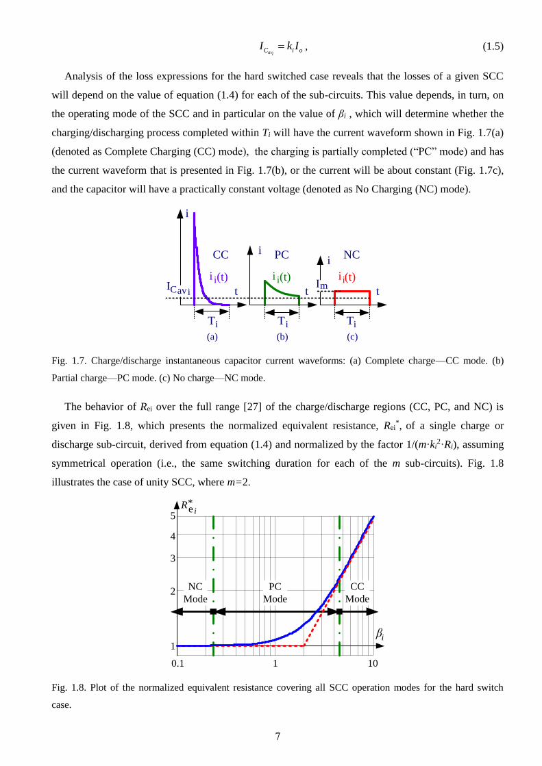
Fig. 1.7. Charge/discharge instantaneous capacitor current waveforms: (a) Complete charge—
CC mode. (b) Partial charge—PC mode. (c) No charge—NC mode. .................................... 7
Fig. 1.8. Plot of the normalized equivalent resistance covering all SCC operation modes for the
hard switch case. .................................................................................................................... 7
Fig. 1.9. The binary/Fibonacci converter with three flying capacitors (n=3): (a) step down
topology, (b) typical efficiency graph showing multiple peaks for 19 conversion ratios. ..... 9
Fig. 1.10. SCC topologies configured from the EXB codes of M=5/8. ............................................... 12
Fig. 1.11. Currents and voltages waveforms of the switching modes. (a) Hard switching with and
without snubers. (b) Resonant switching. Vs is the voltage across the switch and Is is the
current through the switch. ................................................................................................... 14
Fig. 1.12 Typical switching loci for a hard-switched converter without switching-aid-networks,
with snubbers and for a soft-switched converter operation, (VT is the voltage across the
switch and IT is the current through it). ................................................................................ 14
Fig. 1.13. High power resonant SCC topology with interleaved, Vo=Vin/5. ........................................ 15
Fig. 1.14. Waveforms of the high power resonant SCC: (a) capacitors and load currents
(b) capacitors and output voltages. Simulations set-up at: Vin=250V, Pout=12.5 kW,
L1=8.2 µH, L2=2.2 µH, all flying capacitors Cj=300 µF, and fs=1.67 kHz. ........................ 15
Fig. 1.15. Conventional DCR current sensing method in a buck converter. In this method, when
RC∙C1=L/DCR from the transfer function, VC1/IL, then VC1=DCR∙IL. .................................. 17
Fig. 1.16. A typical structure of SENSEFET and sample circuit to increase the accuracy. ................. 17
Fig. 1.17. (a) Typical basic ZCD system configuration (b) Resonant pulses and the reference
value. .................................................................................................................................... 19

xiii
Fig. 2.1. Resonant SCC scheme showing the current sensors and analog comparator for zero
cross detection. ..................................................................................................................... 24
Fig. 2.2. Resonant SCC sub-circuits configured from the EXB codes of M=5/8. ............................. 25
Fig. 2.3. Resonant binary SCC (a) Capacitors and output stage current waveforms.
(b) Capacitors and output voltages waveforms. PSIM Simulations set-up at: M=5/8,
Vin=100V, Pout=100W, Ls=200nH, all flying capacitors Cj=9.4µF, and fs=90kHz. S5 is
the normalized switch gate-source control voltages, I_C1, 2, 3 are the currents through
the flying capacitors C1,C2 and C3. I_Ls is the inductor current at the output stage, and
Iout is the load current. V_C1, 2, 3 are the capacitor voltages across the flying
capacitors and AVG(V_C1, 2, 3) are the average voltages. ................................................ 26
Fig. 2.4. Worst-case conditions of state current variation and the mismatch of the switching
instance due to fixed reference settings. .............................................................................. 29
Fig. 2.5. Conceptual operation of the soft start sequences for M=3/8 (resonant current): (a) high-
frequency switching; (b) estimated resonant values; (c) active ZCS method. ..................... 30
Fig. 2.6. Isolated Gate Driver and four-quadrant switch using N – channel power MOSFETs......... 32
Fig. 2.7. Operation modes: (a) on state - CGS charging (b) off state - CGS Discharging. ................ 32
Fig. 2.8. Experimental waveforms of the isolated gate driver: (a) C3 voltage (5 V/div). (b) C2
voltage (2 V/div). (c) D2 voltage (5 V/div). (d) output voltage, VGate (5 V/div).
Horizontal scale (10 µs/div). ................................................................................................ 32
Fig. 3.1. Worst-case plot of the normalized equivalent resistance as a function of Qj_low, for
conversion the ratios: (a) M=1/8, 3/8, and (b) M=5/8, 7/8 for dfj in the range of 0.15-
0.35 (0.05 step each iteration in dfj). The curves were extracted numerically using
MATLAB. ............................................................................................................................ 36
Fig. 3.2. Worst-case plot of the normalized equivalent resistance as a function of Qj_low, for
conversion the ratios: (a) M=2/8, 6/8 (b) M=3/8, 4/8 (c) M=2/5, 3/5 (d) M=1/3, 2/3 (e)
M=1/5 (f) M=4/5 (g) M=1/2 (h) M=1/7- 6/7 for dfj in the range of 0.15-0.35. .................. 41
Fig. 3.2. (Continued). ......................................................................................................................... 42
Fig. 3.3. Iout and VDS (S6) at Vin=100V, Pout=136W, M=5/8. .............................................................. 44
Fig. 3.4. Iout and VDS (S6) at Vin=80V, Pout=100W, M=5/8. ................................................................ 44
Fig. 3.5. Iout and VDS (S6) at Vin=60V, Pout=69.89W, M=3/8. ............................................................. 44
Fig. 3.6. Efficiency of step-down, resonant binary SCC, M=5/8. ...................................................... 44
Fig. 3.7. Prototype of the resonant binary SCC. ................................................................................. 47
xiv
Fig. 3.8. Experimental result of the binary converter operating in active ZCS mode for various
conversion ratios. (a) M=1/8, Vin=80 V, Pout=31.3 W, η=0.85; Traces top to bottom:
inductor current ILs (0.8 A/div), rectified sensed voltage resulting from Ic3,VIc3 (10
V/div), rectified sense voltage resulting from Ic2, VIc2 (10 V/div), comparator output,
Vcmp (5 V/div). Horizontal scale (5 µs/div). (b) M=3/8, Vin=100 V, Pout=76.5 W,
η=0.92; Traces top to bottom: ILs (0.8 A/div); VIc3 (10 V/div); Vcmp (5 V/div); interrupt
status Vint (5 V/div). Horizontal scale (10 µs/div). (c) M=5/8, Vin=80V, Pout=73W,
η=0.95. Traces and horizontal scale: as in (b). (d) M=7/8, Vin=80 V, Pout=131.7 W,
η=0.99. Traces top to bottom: ILs (0.4 A/div), VIc3 (5 V/div); Vcmp (5 V/div); Vint (5
V/div). Horizontal scale (5 µs/div). ..................................................................................... 48
Fig. 3.9. (a) Slope difference between the highest and the lowest current pulses at fixed output
power - 31.3 W, Io=3.6 A. (b) and (c) Slope differences between pulses at wide output
power range, Po=5 W, Io=1.7 A and Po=31.3 W, Io=3.6 A, respectively............................. 48
Fig. 3.10. Measured efficiency, M=1/8-7/8, constant Ro, Vin=30-80 V. .............................................. 49
Fig. 3.11. Measured efficiency, M=1/8-7/8, constant Vin=80 V. ......................................................... 49
Fig. 3.12. Experimental results of the inductor current for the soft-start method for M=3/8: (a)
High switching frequency; (b) estimated resonant values; (c) active ZCS method. ............ 49
Fig. 4.1. Typical resonant current waveforms during a: Charge phase ‒ DCP operation,
Discharge phase – SCP operation. ....................................................................................... 53
Fig. 4.2. Unity gain SCC with free-wheeling ZCS of the charge state. ............................................. 53
Fig. 4.3. Operation states of unity gain SCC (Fig. 4.2): (a) Charging sub-state ij = 1a, (b)
Charging sub-state ij = 1b, (c) Discharging state i = 2. ....................................................... 54
Fig. 4.4. The basic and generic instantaneous RLC sub-circuit. ......................................................... 54
Fig. 4.5. DCP switching phase current waveform. ............................................................................. 55
Fig. 4.6. SCC generic average equivalent circuit that shows the contribution of the partial sub-
circuits equivalent resistances Rei to the total equivalent circuit resistance Re. For the
unity gain SCC example of Fig. 4.2, Re1a is the loss contribution of charge sub-state 1a,
Re1b and Vd1b are the resistive and diode loss contribution of the free-wheeling sub-
state, respectively, Re2 is the loss contribution of discharging phase. .................................. 56
Fig. 4.7. Variation of Re as a function of φ1 for different ratios of loop resistances between R1a
and R1b. In the example above R1a = R2 = 10 mΩ. ............................................................... 57
Fig. 4.8. Distribution of the charge through paths ia and ib as a function of the commutation
angle φi. ................................................................................................................................ 58
Fig. 4.9. Output voltage of a unity gain SCC as a function of the commutation angle, φ. Model
calculation–solid trace, simulation–asterisk marks. Vin=10 V, VF=1.7 V, RDS(on)=100
mΩ, Ro=5 Ω, Q ≈ 30, f0 ≈ 5 kHz. ......................................................................................... 59

xv
Fig. 4.10. Illustration waveform of a resonant current for several values of the quality factors
(0.55÷7), where L=50 µH, C=100 µF and 0.1 Ω<R<1.4 Ω. ................................................ 60
Fig. 4.11. Illustration of DCP switching phase current waveform at low Q. ....................................... 61
Fig. 4.12. Distribution of the charge through paths ia and ib as a function of the commutation
angle φi for an extensive range of the quality factor (0.58>Q>10), where L=1 µH,
C=100 µF and 0.01 Ω<Rloop<0.18 Ω, (Rloop1a=Rloop1b). ........................................................ 61
Fig. 4.13. Unity gain SCC switching circuit, with charge phase operated in a DCP mode.
(Switch S1b blocks undesired conduction paths). ................................................................. 63
Fig. 4.14. Voltage doubler converter topology with free-wheeling diodes D1, D2. Charge phase:
S1a, S1b – ON, discharge phase: S2a, S2b ‒ ON. ..................................................................... 63
Fig. 4.15. Experimental waveforms obtained from a unity gain resonant SCC operating in DCP
mode with φi ≈ 126º. Upper traces–charge sub-states currents, Bottom trace–discharge
current. Scale: vertical–2 A/div, horizontal‒2 μs/div. ......................................................... 64
Fig. 4.16. Average currents at paths 1a and 1b. Model calculation–solid trace, simulation–dashed
line, and experimental results–(I1a) asterisk marks and (I1b) circle marks. .......................... 64
Fig. 4.17. Equivalent average diode voltage drop, Vd, as a function of the commutation phase, φ.
Model calculation–solid trace, simulation–dashed line, and experimental results–
asterisk marks ........................................................................................ . ............................. 64
Fig. 4.18. Output voltage as a function of the commutation phase, φ. Model calculation–solid
trace, simulation–dashed line, and experimental results–asterisk marks. ............................ 65
Fig. 4.19. Experimental waveforms obtained from a double gain resonant SCC operating in DCP
mode with φ1≈96ᵒ, φ2≈139ᵒ, Vin=10 V, Rloop1a,2a=370 mΩ, Rloop1b,2b=100 mΩ, VF1,2=1.7
V, Pout=10.6 W, Upper traces–charge sub-states currents, bottom trace–discharge sub-
states currents. Scale: vertical–2 A/div, horizontal–5 μs/div ................ . ............................. 66
Fig. 4.20. Experimental waveforms obtained from a double gain resonant SCC operating in DCP
mode with φ1=φ2≈139ᵒ, Vin=10 V, Rloop1a,2a=370 mΩ, Rloop1b,2b=100 mΩ, VF1,2=1.7 V,
Pout=11.13 W. Upper traces–charge sub-states currents, bottom trace–discharge sub-
states currents. Scale: vertical–2 A/div, horizontal–5 μs/div ................ . ............................. 66
Fig. 4.21. Experimental waveforms obtained from a double gain resonant SCC operating in DCP
mode with φ1≈148ᵒ, φ2≈139ᵒ, Vin=10 V, Rloop1a,2a=370 mΩ, Rloop1b,2b=100 mΩ, VF1,2=1.7
V, Pout=11.3 W. Upper traces–charge sub-states currents, bottom trace–discharge sub-
states currents. Scale: vertical–2 A/div, horizontal–5 μs/div ................ . ............................. 66

xvi
Fig. 4.22. SCC generic average equivalent circuit that shows the contribution of the partial sub-
circuits equivalent resistances Rei to the total equivalent circuit resistance Re. (For the
doubler SCC example of Fig. 4.14, Re1a is the loss contribution of charge sub-state 1a,
Re1b and Vd1b are the resistive and diode loss contribution of the free-wheeling sub-
state, respectively. Re2a is the loss contribution of the discharge sub-state 2a, Re2b and
Vd2b are resistive and diode loss contribution of the free-wheeling discharge sub-state,
respectively) .......................................................................................... . ............................. 66
Fig. 4.23. Multiphase Fibonacci resonant SCC topology with free-wheeling diodes D1-4. Phase1:
S1, S3–ON, Phase 2: S2, S4, S6–ON, Phase 3: S2, S5, S7, S9–ON, Phase 4: S2, S5, S8,
S10 –ON ................................................................................................. . ............................. 67
Fig. 4.24. Simulation waveforms obtained from a resonant Fibonacci SCC operating in DCP
mode with φi ≈ 144º ............................................................................... . ............................. 67
Fig. 4.25. Output voltage of the DCP operation mode of a resonant Fibonacci SCC as a function
of the commutation angle, φ. Model calculation–solid trace, simulation–asterisk marks. .. 68
Fig. 4.26. Contribution of conduction losses of the resonant Fibonacci SCC operated in DCP
mode. (a) Equivalent resistant, Re, as a function of the commutation angle, φ (b)
Equivalent average diode voltage drop, Vd, as a function of the commutation angle, φ. ..... 68
Fig. 4.27. Average currents at paths 1a and 1b at low Q as function of φ. Model calculation–(I1b)
solid trace and (I1a) dashed line, simulation results–(I1a) asterisk marks and (I1b) circle
marks ..................................................................................................... . ............................. 69
Fig. A.1. Resonant binary/Fibonacci switched capacitor step-down converter, example for n=3. .... 76
Fig. A.2. Resonant binary/Fibonacci switched capacitor step-up converter, example for n=3. ......... 76
Fig. A.3. Resonant SCC sub-circuits configured from the Fibonacci sequence M=8. ....................... 78

xvii
Acronyms and Abbreviations
AC - Alternating Current
BSD - Binary Signed-Digit
CC - Complete Charge
CCM - Continuous Conduction Mode
DC - Direct Current
DCM - Discontinuous Conduction Mode
DCP - Divided Conduction Path
DCR - Direct-Current Resistance
EMI - Electromagnetic Interference
ESR - Equivalent Series Resistance
EXB - Extended Binary
IC - Integrated Circuit
KCL - Kirchhoff’s Current Law
KVL - Kirchhoff’s Voltage Law
LDO - Low Dropout
MOSFET - Metal-Oxide-Semiconductor Field-Effect Transistor
NC - No Charge
PC - Partial Charge
PCB - Printed Circuit Board
PV - Photo Voltaic
PWM - Pulse Width Modulation
RMS - Root Mean Square
RSCC - Resonant Switched Capacitor Converter
SC - Switched Capacitor
SCC - Switched Capacitor Converter
SCP - Single Conduction Path
SFN - Signed Fibonacci Number
SGF - Signed Generalized Fibonacci
SIC - Switched Inductor Converter
SMPS - Switched Mode Power Supplies
ZCD - Zero Current Detection
ZCS - Zero Current Switching
ZVS - Zero Voltage Switching
Inline References Legend
X.XX - Section/Chapter number
(X.XX) - Equation
[XX] - Reference
Fig. X.XX - Figure

1
Chapter 1 - Introduction
1.1 Power supplies
Power supplies are an essential part of practically all-modern technological systems, ranging from
appliances to mobile phones, renewable energy sources and just about any grid-connected system.
Power supplies are used to convert the electrical energy provided by an electrical source to another
form needed for proper operation of the system. Power supplies can be divided into two basic groups–
linear regulators and switched mode converters.
1.1.1 Linear regulators
Linear regulators [6]-[11] have been widely used for decades in power supply systems, providing
supplies for low-power applications.
This kind of voltage regulator provides a low cost solution for voltage stabilization. Linear
regulators are easy in design and implementation and have good precision of the output voltage value
(in the steady- state). They are built around an active element (such as a transistor), which is normally
connected between the electrical source and the load and operated in its linear region. In this way the
active element acts as a variable resistor and together with the load forms as a voltage divider.
An example of converting a dc voltage to a lower dc voltage level is the simple circuit shown in
Fig. 1.1. The output voltage is Vout = Io Ro, where the load current is controlled by the transistor
represented by a variable resistor (see Fig. 1.1a). By adjusting the transistor base current, the output
voltage may be controlled over a range of zero to Vin. The base current can be adjusted by control
circuitry to compensate for variations in the supply voltage or the load, thus regulating the output. As
can be seen from Fig. 1.1a, the only current in the series element is the load current. Neglecting the
power required for the circuit to control the series element, the efficiency of any regulator carrying out
the process of power conversion, is defined as:
out o
in in
P V
P V , (1.1)
where Po is the output power, Pin is the input power, and the dissipated power is defined as Pin -Pout.
As can be observed, the efficiency depends on the ratio of load-to source voltage and not on the
load current. This series–pass transistor drives all the current demanded by the load. Thus, this
component has to be dimensioned to dissipate an important quantity of energy, increasing the price,
volume, and weight in the supply system. For large differences between the input and the output
voltages the efficiency of linear regulators is fairly low, and hence its use is normally restricted to low
drop out (LDO) applications, where this difference is small. While this may be a simple method of
converting a dc supply voltage to a lower dc voltage level and regulating the output, the low efficiency
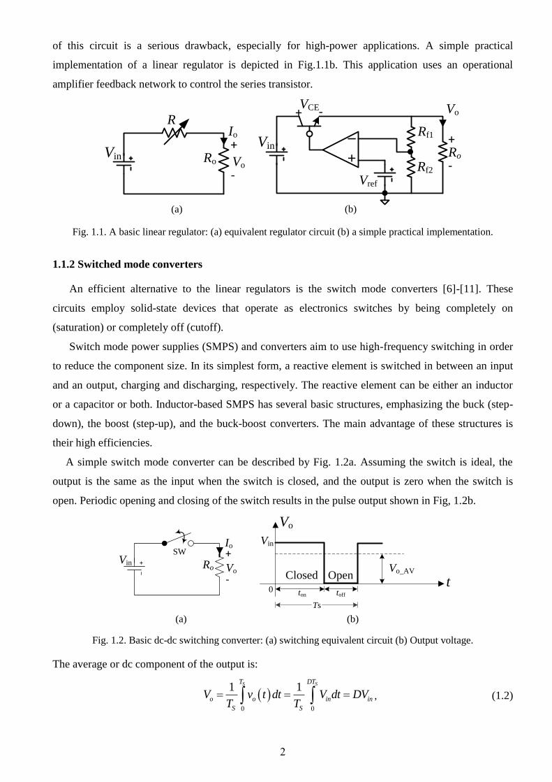
2
of this circuit is a serious drawback, especially for high-power applications. A simple practical
implementation of a linear regulator is depicted in Fig.1.1b. This application uses an operational
amplifier feedback network to control the series transistor.
Vo
Vin+
-
R
Ro
Io
(a) (b)
Vo
+
-
+ -VCE
Ro+
_ Rf1
Rf2
Vin
Vref
Fig. 1.1. A basic linear regulator: (a) equivalent regulator circuit (b) a simple practical implementation.
1.1.2 Switched mode converters
An efficient alternative to the linear regulators is the switch mode converters [6]-[11]. These
circuits employ solid-state devices that operate as electronics switches by being completely on
(saturation) or completely off (cutoff).
Switch mode power supplies (SMPS) and converters aim to use high-frequency switching in order
to reduce the component size. In its simplest form, a reactive element is switched in between an input
and an output, charging and discharging, respectively. The reactive element can be either an inductor
or a capacitor or both. Inductor-based SMPS has several basic structures, emphasizing the buck (step-
down), the boost (step-up), and the buck-boost converters. The main advantage of these structures is
their high efficiencies.
A simple switch mode converter can be described by Fig. 1.2a. Assuming the switch is ideal, the
output is the same as the input when the switch is closed, and the output is zero when the switch is
open. Periodic opening and closing of the switch results in the pulse output shown in Fig, 1.2b.
Vo
Vin+
-
Ro
IoSW
(a) (b)
Vo
Vin
t0
Ts
Closed OpenVo_AV
ton toff
Fig. 1.2. Basic dc-dc switching converter: (a) switching equivalent circuit (b) Output voltage.
The average or dc component of the output is:
0 0
1 1S ST DT
o o in in
S S
V v t dt V dt DVT T
, (1.2)
3
where D=ton/TS, ton is the time the switch is on, and TS is the switching period. The dc component of
the output is controlled by adjusting the duty ratio, D, and will be less than or equal to the input for this
circuit.
Losses will occur in a real switch because the voltage drop across it will not be zero when it is on,
and the switch must pass through the linear region when making a transition from one state to another.
Furthermore, the design and implementation of this sort of converter is a more complex process than in
linear regulators. This is important especially in the control loops when both line and load regulations
are desired. Another drawback is that the intrinsic switched nature of the converter produces ripples in
the output voltage, as well as an increment of the electromagnetic interference (EMI) due to high
frequency switching.
Controlling the dc component of a pulse output of the type in Fig. 1.2b may be sufficient for some
applications, but often the objective is to produce an output that is purely dc. One way of obtaining a
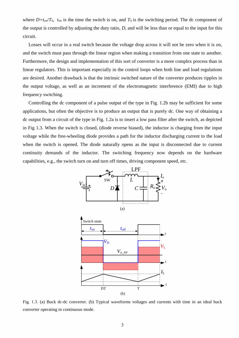
dc output from a circuit of the type in Fig. 1.2a is to insert a low pass filter after the switch, as depicted
in Fig 1.3. When the switch is closed, (diode reverse biased), the inductor is charging from the input
voltage while the free-wheeling diode provides a path for the inductor discharging current to the load
when the switch is opened. The diode naturally opens as the input is disconnected due to current
continuity demands of the inductor. The switching frequency now depends on the hardware
capabilities, e.g., the switch turn on and turn off times, driving component speed, etc.
Vo
Vin+
-
Ro
IoSW L
CD
LPF
(a)
DT T
VL
IL
t
t
t
VD
Vo_AV
ton toff
Switch state
(b)
Fig. 3.1. (a) Buck dc-dc converter. (b) Typical waveforms voltages and currents with time in an ideal buck
converter operating in continuous mode.
4
1.2 Switched capacitor dc-dc converters
Since the 1970s, switched-capacitor dc-dc converters [12] have been investigated due to their small
size, lightweight, and good integration features for a power supply on chip (Fig. 1.4). As opposed to
conventional switch mode dc-dc converters that include bulky inductors to process and store energy,
switched capacitor converters (SCCs) require only capacitors and MOSFET switches (in basic form).
The use of a small ceramic capacitor makes them very compact and suitable for high temperature
environments. Conventional switched-capacitor dc-dc converters mainly concentrate on the low-power
conversion area for portable electronic equipment applications [13]. Switched-capacitor converters are
useful for applications that require small currents, usually less than 100 mA. Applications include use
in RS-232 data signals that require both positive and negative voltages for logic levels; in flash
memory circuits, where large voltages are needed to erase stored information; and in drivers for LEDs
and LCD displays [14]-[19].
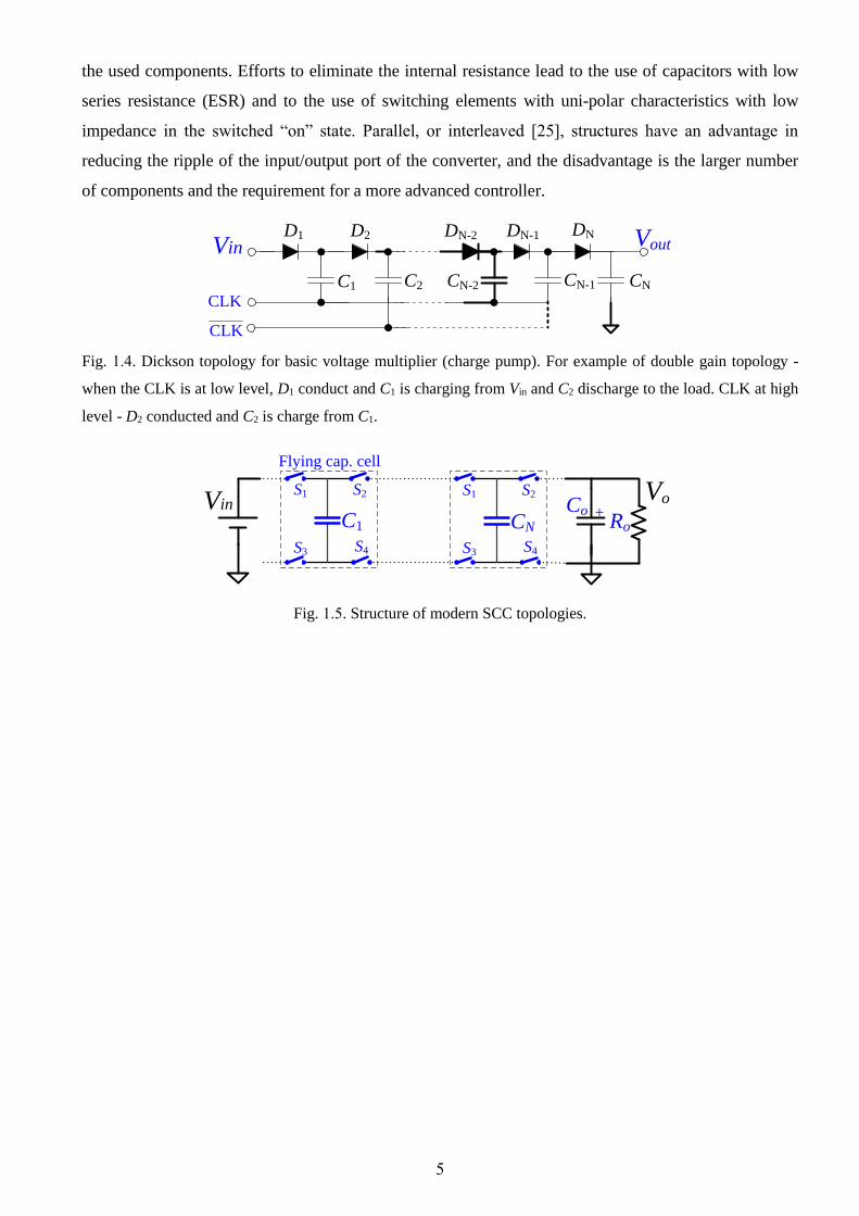
A SCC can be unidirectional or bidirectional and can have any number of inputs, outputs, or both
[14]. The basic SCC cell is shown in Fig. 1.5. It has a flying (switched) capacitor and a network of
switches that connect the capacitor to the ports of the SCC and/or other capacitors. The name ‘flying’
reflects the nature of the capacitor, which is connected to different ports during the SCC operation.
Subsequently, its common mode to ground voltage can change during the operation.
A full SCC system can be built around a single SCC cell, or can contain a large number of cells (Fig.
1.5) where they are interconnected depending on the purpose of the converter: step-up, step-down,
inverting, etc. Moreover the converter can be based on a number of sub-converters connected in series
or in parallel, or a combination of the two [15]. For example, a unit gain converter can be applied with
one cell, (includes C, S1, and S2), that connect the flying capacitor to the input stage (for charging) and
to the load (for discharging). Double gain can be obtained with one cell, (C, S1-S4), where the flying
capacitor is in series with the input voltage during its discharge cycle.
Some more advanced converters have sophisticated switch networks, which allow more than a single
conversion ratio with the same SCC stage. Many variations [15]-[21] of the switched capacitor are able
to provide multiple output levels by manipulating multiple flying capacitors, alternating between
parallel, series, or mixed parallel-series connections. An example of a multiple conversion system is an
SCC with binary and Fibonacci resolution, built around three basic SCC cells [22]-[24]. These
bidirectional SCC formed 19 discrete fractional options to voltage conversion in step-up or step-down
mode.
In order to increase the efficiency, reduce the switching losses, voltage spikes, and EMI, several zero
current switching (ZCS) topologies have been proposed. These are realized by inserting small inductors
in series with the capacitors for resonant operation [16]-[21]. An important feature of the converter is its
internal resistance of each phase, Ri. This represents the sum of all losses due to parasitic properties of
5
the used components. Efforts to eliminate the internal resistance lead to the use of capacitors with low
series resistance (ESR) and to the use of switching elements with uni-polar characteristics with low
impedance in the switched “on” state. Parallel, or interleaved [25], structures have an advantage in
reducing the ripple of the input/output port of the converter, and the disadvantage is the larger number
of components and the requirement for a more advanced controller.
C1
Vin
C2 CN-1
Vout
CLK
CLK
D1 D2 DN-1 DN
CN
DN-2
CN-2
Fig. 3.1. Dickson topology for basic voltage multiplier (charge pump). For example of double gain topology -
when the CLK is at low level, D1 conduct and C1 is charging from Vin and C2 discharge to the load. CLK at high
level - D2 conducted and C2 is charge from C1.
C1
CoRo
Vo+
Vin
Flying cap. cell
S1
S4
S2
S3
CN
S1
S4
S2
S3
Fig. 3.1. Structure of modern SCC topologies.
6
1.3 Generic conduction losses model and efficiency of SCC
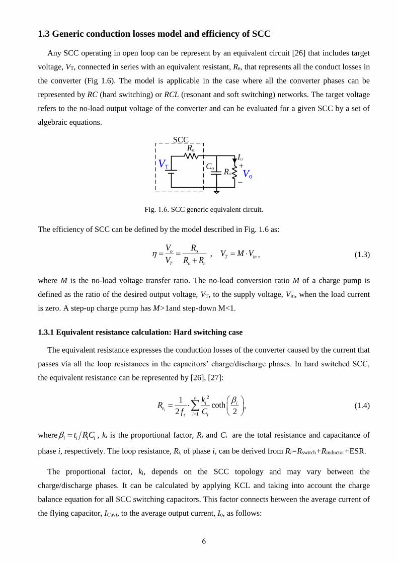
Any SCC operating in open loop can be represent by an equivalent circuit [26] that includes target
voltage, VT, connected in series with an equivalent resistant, Re, that represents all the conduct losses in
the converter (Fig 1.6). The model is applicable in the case where all the converter phases can be
represented by RC (hard switching) or RCL (resonant and soft switching) networks. The target voltage
refers to the no-load output voltage of the converter and can be evaluated for a given SCC by a set of
algebraic equations.
CO
Re
RO Vo
VT
SCC
IO
+
_
Fig. 3.1. SCC generic equivalent circuit.
The efficiency of SCC can be defined by the model described in Fig. 1.6 as:
, o oT in
T o e
V RV M V
V R R
, (1.3)
where M is the no-load voltage transfer ratio. The no-load conversion ratio M of a charge pump is
defined as the ratio of the desired output voltage, VT, to the supply voltage, Vin, when the load current
is zero. A step-up charge pump has M>1and step-down M<1.
1.3.1 Equivalent resistance calculation: Hard switching case
The equivalent resistance expresses the conduction losses of the converter caused by the current that
passes via all the loop resistances in the capacitors’ charge/discharge phases. In hard switched SCC,
the equivalent resistance can be represented by [26], [27]:
2
1
1coth
2 2i
ni i
e
is i
kR
f C
, (1.4)
where i i i it RC , ki is the proportional factor, Ri and Ci are the total resistance and capacitance of
phase i, respectively. The loop resistance, Ri, of phase i, can be derived from Ri=Rswitch+Rinductor+ESR.
The proportional factor, ki, depends on the SCC topology and may vary between the
charge/discharge phases. It can be calculated by applying KCL and taking into account the charge
balance equation for all SCC switching capacitors. This factor connects between the average current of
the flying capacitor, ICavi, to the average output current, Io, as follows:
7
avi
C i oI k I , (1.5)
Analysis of the loss expressions for the hard switched case reveals that the losses of a given SCC
will depend on the value of equation (1.4) for each of the sub-circuits. This value depends, in turn, on
the operating mode of the SCC and in particular on the value of βi , which will determine whether the
charging/discharging process completed within Ti will have the current waveform shown in Fig. 1.7(a)
(denoted as Complete Charging (CC) mode), the charging is partially completed (“PC” mode) and has
the current waveform that is presented in Fig. 1.7(b), or the current will be about constant (Fig. 1.7c),
and the capacitor will have a practically constant voltage (denoted as No Charging (NC) mode).
tt
ii
i
t
Ti Ti Ti
(b)(a) (c)
i i(t) i i(t) ii(t)
PCCC NC
ImICavi
Fig. 1.7. Charge/discharge instantaneous capacitor current waveforms: (a) Complete charge—CC mode. (b)
Partial charge—PC mode. (c) No charge—NC mode.
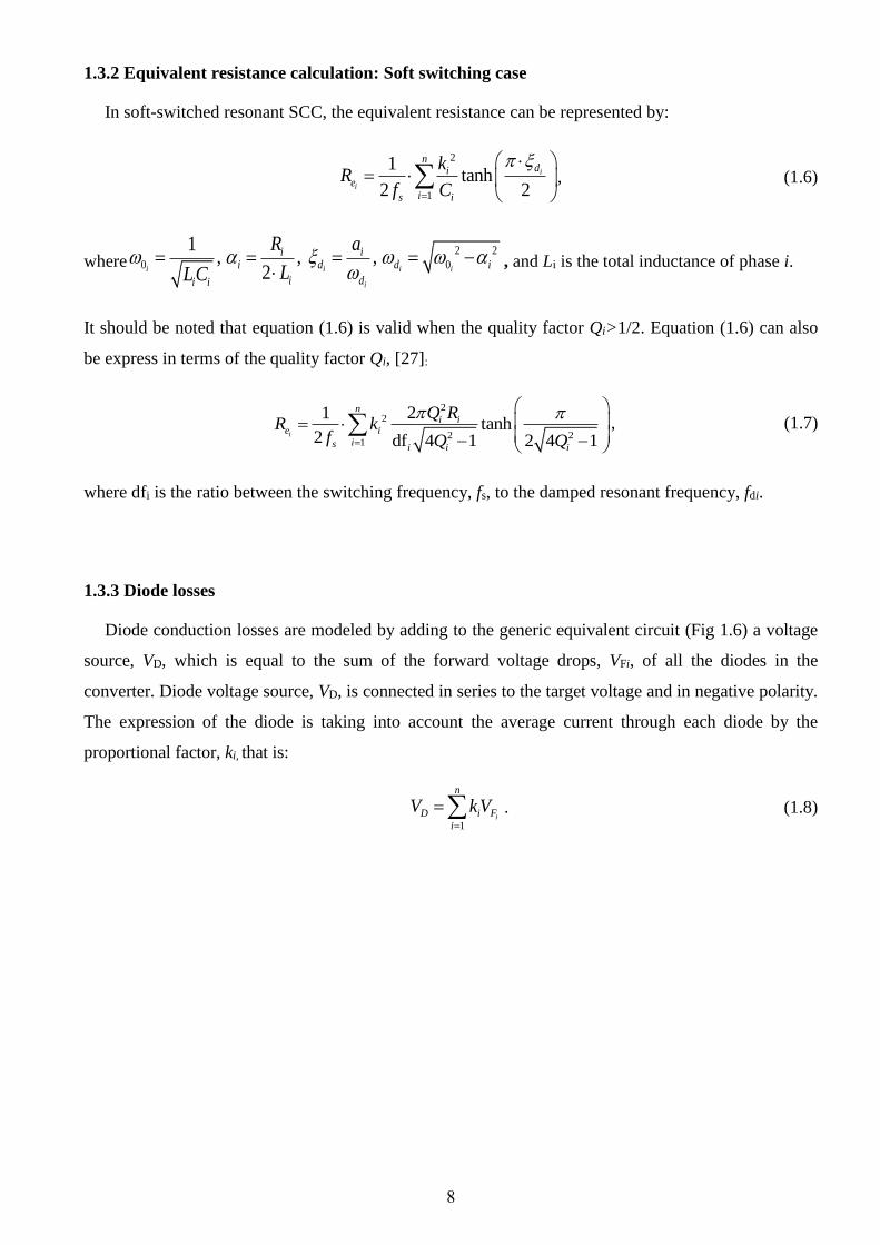
The behavior of Rei over the full range [27] of the charge/discharge regions (CC, PC, and NC) is
given in Fig. 1.8, which presents the normalized equivalent resistance, Rei*, of a single charge or
discharge sub-circuit, derived from equation (1.4) and normalized by the factor 1/(m·ki2·Ri), assuming
symmetrical operation (i.e., the same switching duration for each of the m sub-circuits). Fig. 1.8
illustrates the case of unity SCC, where m=2.
0.1 1 10
1
2
3
4
5
*eR
βi
i
PC
Mode
CC
Mode
NC
Mode
Fig. 1.8. Plot of the normalized equivalent resistance covering all SCC operation modes for the hard switch
case.
8
1.3.2 Equivalent resistance calculation: Soft switching case
In soft-switched resonant SCC, the equivalent resistance can be represented by:
2
1
1tanh
2 2i
i
ndi
e
is i
kR
f C
, (1.6)
where2 2
0 0
1, , ,
2i i i i
i
i ii d d i
i di i
R a
LLC
, and Li is the total inductance of phase i.
It should be noted that equation (1.6) is valid when the quality factor Qi>1/2. Equation (1.6) can also
be express in terms of the quality factor Qi, [27]:
22
2 21
21tanh
2 df 4 1 2 4 1i
ni i
e i
is i i i
Q RR k
f Q Q
, (1.7)
where dfi is the ratio between the switching frequency, fs, to the damped resonant frequency, fdi.
1.3.3 Diode losses
Diode conduction losses are modeled by adding to the generic equivalent circuit (Fig 1.6) a voltage
source, VD, which is equal to the sum of the forward voltage drops, VFi, of all the diodes in the
converter. Diode voltage source, VD, is connected in series to the target voltage and in negative polarity.
The expression of the diode is taking into account the average current through each diode by the
proportional factor, ki, that is:
1i
n
D i F
i
V kV
. (1.8)
9
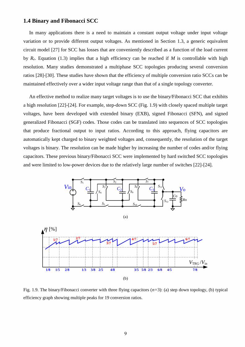
1.4 Binary and Fibonacci SCC
In many applications there is a need to maintain a constant output voltage under input voltage
variation or to provide different output voltages. As mentioned in Section 1.3, a generic equivalent
circuit model [27] for SCC has losses that are conveniently described as a function of the load current
by Re. Equation (1.3) implies that a high efficiency can be reached if M is controllable with high
resolution. Many studies demonstrated a multiphase SCC topologies producing several conversion
ratios [28]-[30]. These studies have shown that the efficiency of multiple conversion ratio SCCs can be
maintained effectively over a wider input voltage range than that of a single topology converter.
An effective method to realize many target voltages is to use the binary/Fibonacci SCC that exhibits
a high resolution [22]-[24]. For example, step-down SCC (Fig. 1.9) with closely spaced multiple target
voltages, have been developed with extended binary (EXB), signed Fibonacci (SFN), and signed
generalized Fibonacci (SGF) codes. Those codes can be translated into sequences of SCC topologies
that produce fractional output to input ratios. According to this approach, flying capacitors are
automatically kept charged to binary weighted voltages and, consequently, the resolution of the target
voltages is binary. The resolution can be made higher by increasing the number of codes and/or flying
capacitors. These previous binary/Fibonacci SCC were implemented by hard switched SCC topologies
and were limited to low-power devices due to the relatively large number of switches [22]-[24].
S1
S6
S4
S3
S9
S8
S2 S7
S12
S11
S5 S10
C1 C2 C3
CoRo
VoVin
(a)
η [%]
7/8
6/7
4/56/8
5/7
2/33/5
4/7
4/8 5/83/81/3
2/7
2/81/51/8 2/5
3/71/7
VTRG /Vin
(b)
Fig. 1.9. The binary/Fibonacci converter with three flying capacitors (n=3): (a) step down topology, (b) typical
efficiency graph showing multiple peaks for 19 conversion ratios.

10
1.4.1 Binary and Fibonacci codes
The structures of the binary SCC depicted in Fig. 1.9a are based on algebraic expressions [22]-[24]
that are described by the following definitions and observations. Any number of M in the range (0, 1)
can be represented in the form:
0
1
2n
j
j
j
M A A
, (1.9)
where A0 can be either 0 or 1, Aj takes on any of three values -1, 0, 1, and n sets the resolution. For
example, the code 1 0 -1 -1 implies:
1 2 31 0 2 1 2 1 2 5/ 8M . (1.10)
Expression (1.9) defines the EXB representation that is a modified version of the binary signed-digit
(BSD) representation [31]-[33]. Unlike the conventional binary case, a number of different EXB codes
can represent a single M value. The different codes can be generated by spawning rules [22].
The following example demonstrates how four alternative EXB codes are spawned from the binary
code of M= 5/8. For example, the conventional binary code of 5/8 is 0 1 0 1. In the left sequence of
equation (1.11) the “1” of A3 (the LSB) is replaced by “-1” and the “1” carry is added to A2. The
resulting code is 0 1 1 -1. The conventional code is transformed to other equivalent codes and so on.
A0 A1 A2 A3
20 2-1 2-2 2-3
0 1 0 1
0 0 0 1
0 1 1 0
0 0 0 -1
0 1 1 -1
A0 A1 A2 A3
20 2-1 2-2 2-3
0 1 0 1
0 0 1 0
0 1 1 1
0 0 -1 0
0 1 0 1
A0 A1 A2 A3
20 2-1 2-2 2-3
0 1 0 1
0 1 0 0
1 0 0 1
0 -1 0 0
1 -1 0 1
A0 A1 A2 A3
20 2-1 2-2 2-3
0 1 1 -1
0 1 0 0
1 0 1 -1
0 -1 0 0
1 -1 1 -1
+
+
+
+
+
+
+
+
A0 A1 A2 A3
20 2-1 2-2 2-3
1 -1 1 -1
0 0 1 0
1 0 0 -1
0 0 -1 0
1 0 -1 -1
+
+
The conventional and alternatives EXB codes, thus generated and representing the same fraction of
M=5/8 are summarized as follows:
-1 -2 -3
-1 -2 -3
-1 -2 -3
-1 -2 -3
-1 -2 -
1 0 -1 -1 1 + 0·2 -1·2 - 1·2 = 5/8
1 -1 1 -1 1 - 1·2 + 1·2 -1·2 = 5/8
0 1 1 -1 0 + 1·2 + 1·2 -1·2 = 5/8
1 -1 0 1 1 - 1·2 + 0·2 +1·2 = 5/8
0 1 0 1 0 +1·2 + 0·2 +1·2
3 5 8
. (1.12)
All other codes (SFN, SGF) extract with the same method but with different math rules. The EXB,
SFN, and SGF codes for all 19 fractions, n=1÷3, are summarized in Table 1.1.
(1.11)
11
Table 1.1 - The Codes for n=1÷3
1.4.2 Translating the codes into SCC topologies
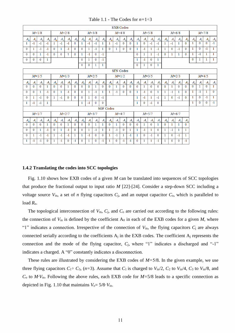
Fig. 1.10 shows how EXB codes of a given M can be translated into sequences of SCC topologies
that produce the fractional output to input ratio M [22]-[24]. Consider a step-down SCC including a
voltage source Vin, a set of n flying capacitors Cj, and an output capacitor Co, which is paralleled to
load Ro.
The topological interconnection of Vin, Cj, and Co are carried out according to the following rules:
the connection of Vin is defined by the coefficient A0 in each of the EXB codes for a given M, where
“1” indicates a connection. Irrespective of the connection of Vin, the flying capacitors Cj are always
connected serially according to the coefficients Aj in the EXB codes. The coefficient Aj represents the
connection and the mode of the flying capacitor, Cj, where “1” indicates a discharged and “-1”
indicates a charged. A “0” constantly indicates a disconnection.
These rules are illustrated by considering the EXB codes of M=1/8. In the given example, we use
three flying capacitors C1÷ C3, (n=3). Assume that C1 is charged to Vin/2, C2 to Vin/4, C3 to Vin/8, and
Co to M·Vin. Following the above rules, each EXB code for M=5/8 leads to a specific connection as
depicted in Fig. 1.10 that maintains Vo= 5/8·Vin.
12
C2 C3
Co Ro
Vo
Vin
C1
C2 C3
Co Ro
Vo
+ +
+
+ +
++
C1 C3
Co Ro
Vo+ +
+Vin
C3
Co Ro
Vo+
++
C1
1 0 -1 -1 1 -1 1 -1
0 1 1 -1 1 -1 0 1 0 1 0 1
C1 C2 C3
Co Ro
Vo
Vin
+ + +
+
Fig. 1.10. SCC topologies configured from the EXB codes of M=5/8.
Since each of the five configurations of Fig. 1.10 is a one-to-one translation of the EXB code
corresponding to 5/8, and assuming that the capacitors are charged to the binary fractions of the input
voltage, the output will be kept at 5/8·Vin, if the system cycles in perpetuity through these
configurations. The KVL equations for the SCC of Fig. 1.10 are:
2 3
1 2 3
1 2 3
1 3
1 3
0
0
0
0 0
in C C Co
in C C C Co
C C C Co
in C C Co
C C Co
V V V V
V V V V V
V V V V
V V V V
V V V
, (1.13)
The system in (1.13) comprises five equations, while the number of unknowns is equal to four. It can
be solved by eliminating one of the equations, hence:
1 2
3
1 2 , 1 4 ,
1 8 , 5 8 .
C in C in
C in Co in
V V V V
V V V V
(1.14)
Since the solutions in (1.14) are unique [22], [34], the capacitors' voltages are self-adjusting, so that
there is no need for any control system to assure that the capacitors reach the nominal value and hence
the output will always self-stabilize to the expected voltage. Considering the fact that the set of
equations (1.13) is solvable, it should also be solvable if Vin and VCo are switched as shown in (1.15).
This means switching the input and output functions and converting the step-down SCC to a step-up
SCC. The KVL equations for the SCC at step-up configuration are:
2 3
1 2 3
1 2 3
1 3
1 3
0
0
0
0 0
Co C C in
Co C C C in
Co C C C
Co C C in
Co C C
V V V V
V V V V V
V V V V
V V V V
V V V
, (1.15)

13
The solutions of equations (1.15) are:
)6(1.1 1 2
3
4 3 , 2 3 ,
1 3 , 8 5 .
C in C in
C in Co in
V V V V
V V V V
The fraction voltages value mentioned at the solutions of equation (1.13) and equation (1.15)
remain constant for all EXB codes (x/8 fractions). For the SFN codes, the flying capacitors will
stabilize on the average voltages: VC1=1/5Vin, VC2=2/5Vin, and VC3=1/5Vin at step-down configuration,
and for step-up at the average voltages VC1=Vin, VC2=2/3Vin, and VC3=1/3Vin. For the SGF codes (x/7
fractions), the flying capacitors will stabilize on the average voltages: VC1=4/7Vin, VC2=2/7Vin, and
VC3=1/7Vin at step-down configuration and for step-up at the average voltages VC1=7/4Vin, VC2=7/2Vin,
and VC3=7Vin.
1.5 Resonant converters and soft switching
Imperfect switching is one of the major contributors to power loss in converters [6]-[10]. Switching
devices absorb power when they turn on or off, if they go through a transition when both voltage and
current are nonzero (Fig. 1.11a). Another significant drawback of the switch mode operation is the
EMI produced due to large di/dt and dv/dt caused by a switch mode operation. These shortcoming of
switch mode converters are exacerbated if the switching frequency is increased in order to reduce the
converter size and weight and hence, to increase the power density. Therefore, to realize high
switching frequencies in converters, the aforementioned shortcomings are minimized if each switch in
a converter changes its status (from on to off or vice versa) when the voltage across it and/or the
current through it is zero at the switching instant.
In certain switch mode converter topologies, An LC resonant can be utilized primarily to shape the
switch voltage and current in order to provide zero voltage and/or ZCS. In the resonant switching
circuits, switching takes place when the voltage and/or current are zero, thus avoiding simultaneous
transition of voltage and current and thereby eliminating switching losses, as illustrated in Fig. 1.11b.
A circuit employing this technique is known as a resonant converter (or a quasi-resonant converter, if
only part of the resonant sinusoid is utilized) and this type of switching is called “soft” switching. A
zero current switching circuit shapes the current waveform, while a zero voltage switching (ZVS)
circuit shapes the voltage waveform.
Another method for decreasing the switching losses via reducing the overlap between the current
and voltage is by adding a network in series with the switches [6]-[9]. By adding switching-aid-
networks (called “snubers”), the slop of the voltage and current can be reduced and thereby decrease
the overlap between voltage and current by reducing dv/dt and di/dt (Fig. 1.11a).

14
t
Vs Vs
Is
t
Vs VsIs
(a) (b)
Losses
di/dt
dv/dt
Losses
Fig. 1.11. Currents and voltages waveforms of the switching modes. (a) Hard switching with and without
snubers. (b) Resonant switching. Vs is the voltage across the switch and Is is the current through the switch.
The switching trajectory in the voltage-cunrrent plane of a device is illustrated in Fig. 1.12 comparing
the paths for that of a hard-switched operation, hard-switched with adding snubbers, and a soft-
switched converter operation. It is indicative of the stresses and losses.
Fig. 1.12 Typical switching loci for a hard-switched converter without switching-aid-networks, with snubbers
and for a soft-switched converter operation, (VT is the voltage across the switch and IT is the current through it).
One of the main challenges in ZCS method is to maintain the transitions of the switches at the zero
points despite the drift of the resonant tank (RCL components) and the delay in the system, i.e., the
time duration from zero current detection (ZCD) to when the switching occurs. Moreover, zero
crossing point detection systems can be very complicated and have low cost effectiveness.
1.5.1 High power resonant SCC
A type of high-power SCC, characterized by resonant switching transitions, was introduced in [25].
This drastically reduces switching losses and introduces the possibility of employing thyristors instead
of turn-off power semiconductors. At the same time, a larger amount of energy can be transferred per
switching cycle and the application of the SCC was extended into the megawatt power range .Resonant
switching is achieved by placing an inductor between capacitors that are connected in parallel (see Fig.
1.13). This inductor has a much smaller inductance than that of a comparable buck converter and can
be realized with an air core, thereby not adding significant weight or losses. Moreover, instead of
discharging all pump capacitors simultaneously, the capacitors are discharged in interleaved manner
(see Fig. 1.14). This reduces the current stress on the discharging switches and the output capacitor.
15
Also, the output voltage ripple is significantly reduced. For operation with higher switching frequency
the thyristors were replaced by integrated gate-commutated thyristors (IGCTs), which make it possible
to avoid a turn-off time in reverse-blocking mode
The majority of the losses of this converter occur in the semiconductors due to the forward voltage
drop. Due to the relatively large number of semiconductors in the resonant SCC topology, the
efficiency is not very high at low voltages. Other drawbacks of the topology are the low frequency and
relative large number of capacitors and switches per voltage ratio. For high frequency operation,
implementation with insulated-gate bipolar transistor (IGBT) will require a complex control system to
assure the ZCS because of the component drift in the system.
Co
Ro
Vo
VinC1 C2 C3 C4
V1V2 V3 V4 V5
L1
L2
D1a
D1b
D2a
D2b
D3a
D3b
D4a
D4b
Fig. 1.13. High power resonant SCC topology with interleaved, Vo=Vin/5.
(a)
(b)
0
200
400
ICharge IDischarge
Iout
0.944 0.9445 0.945 0.9455
Time (s)
0
20
40
60
80Vc1 Vc2 Vc3 Vc4
Vout
U [V]
I [A]
Fig. 1.14. Waveforms of the high power resonant SCC: (a) capacitors and load currents (b) capacitors and
output voltages. Simulations set-up at: Vin=250V, Pout=12.5 kW, L1=8.2 µH, L2=2.2 µH, all flying capacitors
Cj=300 µF, and fs=1.67 kHz.
16
1.6 Current sensing
There are many current sensing techniques in dc-dc converters. Every method has its advantages
and disadvantages regarding the impact on power losses, number of components, etc. Almost all dc-dc
converters and linear regulators sense the inductor current for over-current protection and current-
mode control for loop control [7]. Since instantaneous changes in the input voltage are immediately
reflected in the inductor current, current-mode control provides excellent line transient response.
Another common application for current sensing in dc-dc converters where is the sensed current used
to determine when to switch between continuous-conduction mode (CCM) and discontinuous-
conduction mode (DCM), which results in an overall increase in the efficiency of the converter.
Additional common use for current sensors is ZCD for switching transition at zero points to reduce the
switching losses as detailed in Section 1.5.
1.6.1 Current sensors
The basic parameters of any current sensor are linearity, bandwidth, offset (for dc sensors) and
sensitivity, and also stability of offset and sensitivity to temperature and time. Current sensors that
contain ferromagnetic material also suffer from hysteresis. It is furthermore important for contactless
sensors to be insensitive to the actual position of the measured conductor and in addition resistant to
external currents and magnetic fields. Some of the typical current sensors will be overviewed [35].
One of the most simple and common techniques is the series sense resistor method (sometimes
called current shunt resistor). It simply inserts a sense resistor in a series with the inductor. If the value
of the resistor is known, the current flowing through the inductor is determined by sensing the voltage
across it. This method obviously incurs a power loss; however, current-sensing resistors are a robust
and cheap solution for many applications. The power loss in the resistor can be minimized by
amplifying the voltage by op-amp.
Power MOSFETs act as resistors when they are “on” state and they are biased in the Ohmic region.
Consequently, the switch current is determined by sensing the voltage across the drain-source of the
MOSFET, provided that the RDS of the MOSFET is known. The main drawback of this technique is
low accuracy. The RDS of the MOSFET is inherently nonlinear and usually has significant variation
caused by temperature, the MOSFET capacitance, and the threshold voltage. In spite of low accuracy,
this method is very common in commercially because of its high power efficiency.
Direct-current resistance (DCR) is one low loss and cost method for measuring current; it consists
of a series RC network in parallel with the inductor. The correct RC time constant will produce a
measurable capacitor voltage that matches the inductor current. However, DCR could run into issues at
fast switching frequencies where parasitics arise or when the inductor coil heats up, which increases
resistance. Both situations disarrange the tuned circuit network making the measurement less accurate.
Figure 1.15 demonstrates the method in a buck converter.
17
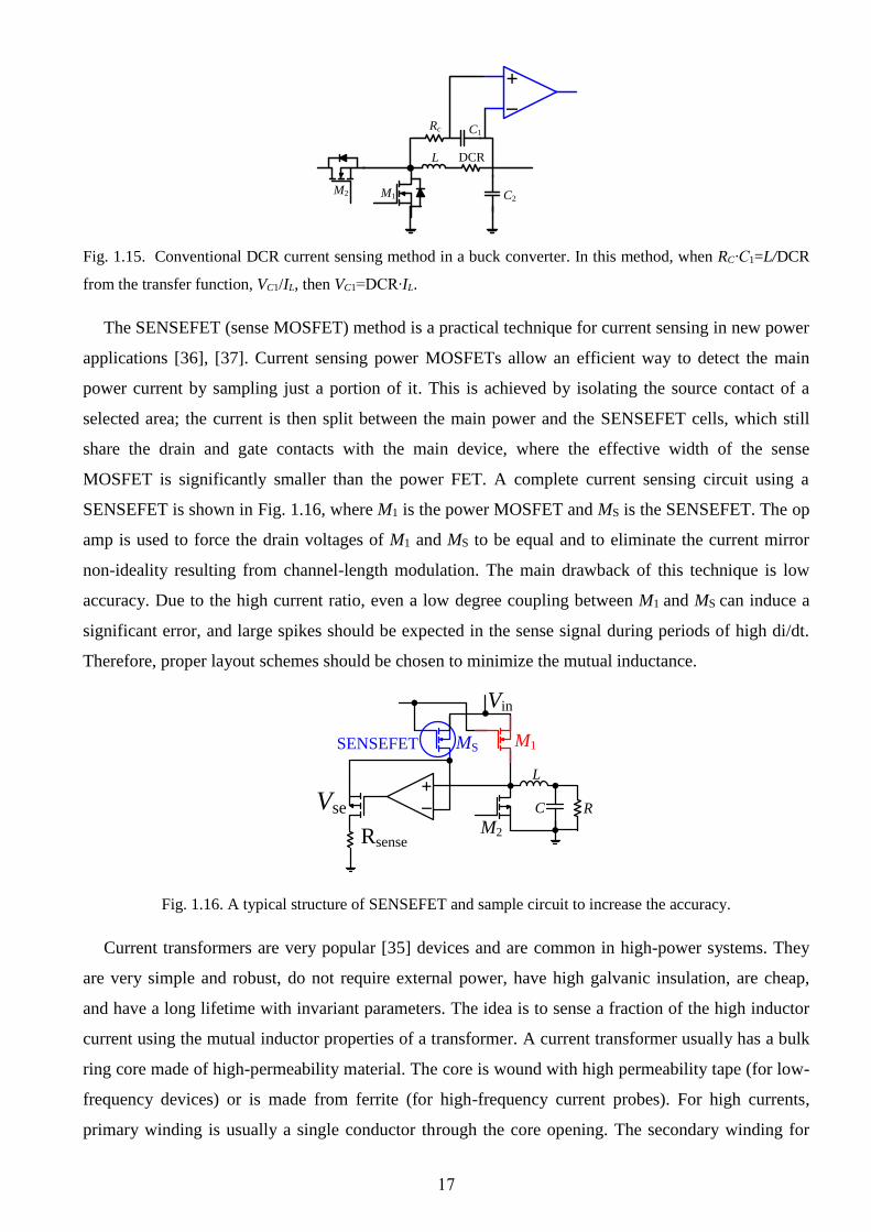
C1
L
Rc
+
_
DCR
M1M2 C2
Fig. 1.15. Conventional DCR current sensing method in a buck converter. In this method, when RC∙C1=L/DCR
from the transfer function, VC1/IL, then VC1=DCR∙IL.
The SENSEFET (sense MOSFET) method is a practical technique for current sensing in new power
applications [36], [37]. Current sensing power MOSFETs allow an efficient way to detect the main
power current by sampling just a portion of it. This is achieved by isolating the source contact of a
selected area; the current is then split between the main power and the SENSEFET cells, which still
share the drain and gate contacts with the main device, where the effective width of the sense
MOSFET is significantly smaller than the power FET. A complete current sensing circuit using a
SENSEFET is shown in Fig. 1.16, where M1 is the power MOSFET and MS is the SENSEFET. The op
amp is used to force the drain voltages of M1 and MS to be equal and to eliminate the current mirror
non-ideality resulting from channel-length modulation. The main drawback of this technique is low
accuracy. Due to the high current ratio, even a low degree coupling between M1 and MS can induce a
significant error, and large spikes should be expected in the sense signal during periods of high di/dt.
Therefore, proper layout schemes should be chosen to minimize the mutual inductance.
SENSEFET
Vin
M1MS
C
L
R
+_
M2Rsense
Vse
Fig. 1.16. A typical structure of SENSEFET and sample circuit to increase the accuracy.
Current transformers are very popular [35] devices and are common in high-power systems. They
are very simple and robust, do not require external power, have high galvanic insulation, are cheap,
and have a long lifetime with invariant parameters. The idea is to sense a fraction of the high inductor
current using the mutual inductor properties of a transformer. A current transformer usually has a bulk
ring core made of high-permeability material. The core is wound with high permeability tape (for low-
frequency devices) or is made from ferrite (for high-frequency current probes). For high currents,
primary winding is usually a single conductor through the core opening. The secondary winding for
18
most applications is connected to a small ‘burden’ resistor or impedance. In some devices, the
secondary current is measured by an active current-to-voltage converter in such a way that the burden
is virtually zero. The major drawbacks are increased size and non-integrablity. The transformer also
cannot transfer the dc portion of current, which renders this method inappropriate for over current
protection.
Rogowski coil [35] for measuring current is an air coil wound around the measured current
conductor. Stationary Rogowski coils are used to measure ac or transient currents or changes in dc
currents. The basic operating principle is given by the mutual inductance M between the primary
(single turn) and the secondary (many turns). The output voltage is proportional to the derivative of the
current, u=M (dI/dt). In order to obtain the ac current waveform, a Rogowski coil is used together with
an integrator. The Rogowski coil contains no ferromagnetic material, and thus it has excellent linearity
and an extremely large dynamic range. Printed circuit board (PCB) technology was used [35] to
produce Rogowski coils with a more precise geometry and improved temperature stability.
Further detail for passive and active current sensors can be found in [35].
1.6.2 Zero current detection
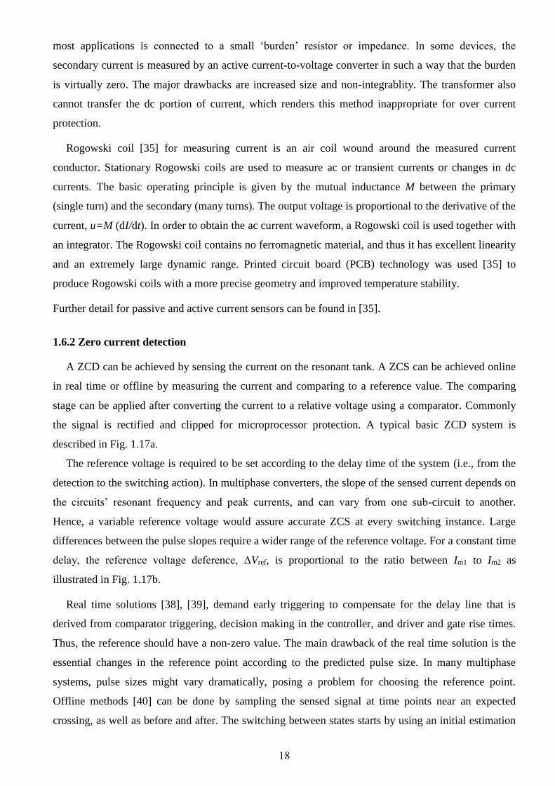
A ZCD can be achieved by sensing the current on the resonant tank. A ZCS can be achieved online
in real time or offline by measuring the current and comparing to a reference value. The comparing
stage can be applied after converting the current to a relative voltage using a comparator. Commonly
the signal is rectified and clipped for microprocessor protection. A typical basic ZCD system is
described in Fig. 1.17a.
The reference voltage is required to be set according to the delay time of the system (i.e., from the
detection to the switching action). In multiphase converters, the slope of the sensed current depends on
the circuits’ resonant frequency and peak currents, and can vary from one sub-circuit to another.
Hence, a variable reference voltage would assure accurate ZCS at every switching instance. Large
differences between the pulse slopes require a wider range of the reference voltage. For a constant time
delay, the reference voltage deference, ΔVref, is proportional to the ratio between Im1 to Im2 as
illustrated in Fig. 1.17b.
Real time solutions [38], [39], demand early triggering to compensate for the delay line that is
derived from comparator triggering, decision making in the controller, and driver and gate rise times.
Thus, the reference should have a non-zero value. The main drawback of the real time solution is the
essential changes in the reference point according to the predicted pulse size. In many multiphase
systems, pulse sizes might vary dramatically, posing a problem for choosing the reference point.
Offline methods [40] can be done by sampling the sensed signal at time points near an expected
crossing, as well as before and after. The switching between states starts by using an initial estimation
19
based on the known resonance frequency of the designed tank. An estimation and fix can be made as
to whether there is a need to increase or decrease the 'on' time of a state and by how much. The
downside of the offline calibration solution is the relatively high EMI and switching losses since the
converter continues to operate while calibration is being done. Moreover, the demand resources may
not always be available for high sampling points. Effective sampling requires many points in the tight
time interval around the zero crossing area. Ideally, in both methods, infinite bandwidth is necessary to
predict the pulse size without prior knowledge.
Ref Value
Im1
Im2
td1
td2
t0/2
t
i(t)
+
Vref
Comparator
Power Stage
Digital
Control
_
Current
sensor
A/D
Gate
Driver
(b)(a)
Vsense
Fig. 1.17. (a) Typical basic ZCD system configuration (b) Resonant pulses and the reference value.
20
1.7 Research objectives and significance
The objectives of this thesis are aimed at tackling the fundamental switched capacitor converter
issues in several interrelated, major directions.
One of the main objectives of this research is to improve the behavior and performance of SCC
applications in the higher power range. The study aims to provide an insight into the practical
limitations of multiphase SCC and to provide a soft switching method and a set of design
considerations for the selection of the power stage components, for multiple sub-circuit converters.
This was achieved by examination of a complex multiphase SCC topology that produces many
target voltages and that use soft switching techniques. This work examined the behavior and
performance of a resonant binary/Fibonacci converter with single air core inductor and stray
inductances for the medium power range.
The study introduces an active ZCS method for resonant SCC and demonstrates it on a resonant
binary/Fibonacci SCC. In order to develop an effective active control system, this study includes a
real-time ZCS method, suitable isolated gate driver circuitry that features a wide switching frequency,
and a duty cycle range and appropriate passive current detector. The zero detection method was
capable of compensating for all the processing delays.
A set of design considerations for the selection of the power stage components for multiple sub-
circuit converters has been delineated, and is followed by an implementation example of a multiphase
SCC configuration. The design method of multilevel SCCs has been carried out with respect to
conduction losses and efficiency and verified on a resonant binary SCC.
The resultant converter has a wide range of conversion ratios with high efficiencies that can be
applied to other multi-phase SCC topologies that involve a number of sub-circuits and wide operation
ranges at higher power levels.
Further objectives of this study are to introduce efficiently passive soft switching techniques that
can simplify the control effort and eliminate additional circuitry involved in active soft-switching
controls. A simple and efficient self-commutation concept has been presented and was examined. It
consists of a transistor that conducts for the majority of the resonant cycle and a parallel diode that acts
as a free-wheeling element, such that turn off occurs at zero current.
This study introduces a unified modeling methodology to describe and explore the loss mechanism
of resonant SCCs operating in this ZCS mode. The modeling presented in this study consists on the
generic equivalent model and extends it for the case where certain phases in the converter include
several paths. The theoretical predictions of the model were compared with cycle-by-cycle simulations
and laboratory experiments in various operation modes on unity, double gain, and multiphase
Fibonacci resonant SCCs with free-wheeling ZCS.

21
The model allows the use of the method that exhibits both advantages of inherent ZCS and
overcomes the deficiencies of many previous methods, such as high conduction losses and complex
control hardware.
These are certainly expanding our understanding of the SCC systems and conceivably have
practical uses by designers and users of switch mode converters in general and SCC technology in
particular. The results provide not only more natural and straightforward analysis methods, but also
highlight the operation conditions that will lead to better design and potentially improved performance
of SCC systems up to the higher power ranges.

22
1.8 Thesis Overview
The research addresses fundamental issues of SCC towards high power density, soft switching,
modeling, and analysis. The thesis can be divided into two general areas: Chapters 2 and 3 address
issues of SCC applications in the medium and high power ranges. Chapter 4 addresses a modeling and
analysis of a resonant SCC with a free-wheeling diode. The technical content of this thesis has been
presented in a number of journal and conference articles. Chapters 2 and 3 are based on [1]-[3].
Chapter 4 is based on [5] and earlier results were given in [4].
Chapter 2 proposes a high efficiency resonant multiphase SCC methodology covering several
practical issues, including the active zero detection method, current sensing, the zero crossing
detection technique, soft start, and isolated gate driver with an appropriate step-by-step design
guideline. The active ZCD method is analyzed and demonstrated on a resonant multiphase binary SCC
that prohibits high resolution of the target voltages. The converter is simulated and the principals of
operation are described.
Chapter 3 focused on the multiphase SCC design guidelines for optimal performance in terms of the
desired efficiency. A full analysis and numeric plots of the resonant binary SCC are given. Following
the design methodology, two types of experiments were demonstrated on the resonant binary SCC,
including the active ZCD method introduced in Chapter 2. Furthermore, the binary converter and the
isolated gate driver were constructed with simple means, based on the guideline detailed in Chapter 2
and 3.
Chapter 4 offers a modeling and methodology to describe and explore the loss mechanism of a
resonant switched capacitor converter operating in a self-commutation ZCS mode. Throughout the
study, the modeling concept will be explained on a unity gain resonant SCC, which highlights the
mechanism of divided conduction path operation. The general case of divided conduction path (DCP)
applies a free-wheeling mode realized by diode conduction. The model is constructed by considering a
series connection of the equivalent resistances and the voltage source between the target voltage and
the output port. More general extensions for the model were made and present a closed form to DCP
mode for the entire range of the quality factor. The modeling approach is well detailed and
demonstrates on several topologies and operation modes, including unity, double gain, and resonant
Fibonacci SCC. A very good agreement was found between the values predicted by the model, the
simulation, and the experimental results.
Contribution of the thesis and suggestions for future research are discussed in Chapter 5, which
summarizes the work.
23
Chapter 2 - Multiple Conversion Ratio Resonant Switched-Capacitor
Converter with Active Zero Current Detection
2.1 Introduction
Switched capacitor converters (SCC) are becoming an attractive alternative in many applications
ranging from low to high power. These include voltage regulators for mobile electronic systems,
voltage equalizers for batteries and capacitors, for photovoltaic (PV) modules and for automotive
applications [13]-[21].
The efficiency of an SCC linearly depends on the proportionality between the output voltage and the
target voltage Vo/VTarget [22]-[24], [29], where VTarget=MVin and M is the no-load voltage transfer ratio.
High efficiency can be reached if M is widely controllable with high resolution. The generic equivalent
circuit model for SCC [26], [27] describes the losses by an equivalent resistance connected at the output
of the SCC- ReqT, i.e., η=Vo/VTarget = Ro/(Ro+ReqT).
An effective way to realize many target voltages is the binary/Fibonacci SCC that exhibits a widely
controllable conversion ratio [24]. The benefits of a resonant operation with this converter have been
demonstrated in [3].
Soft switching in resonant converters can be obtained by switching the transistors at zero current.
Given that the resonant frequency depends on the tank's physical parameters, C, L, and R, the switching
times can be either calibrated in advance to match the resonant frequency, or a control circuit can be
implemented to identify zero crossing. For the case of conventional resonant converters, ZCS operation
and its implementation have been widely demonstrated [41]-[45]. For the case of resonant SCC
however, few topologies have been proposed e.g., [16]-[21]. A methodological approach to obtain ZCS
for the entire dynamic range of the SCC has not been reported hitherto.
The main problem of pre-calibrating resonant SCCs for ZCS is that the physical parameters of the
system are prone to drifts throughout the operation range. This is particularly crucial in resonant SCC
circuits since the inductance is often implemented by the stray inductance of the circuit, which may
vary by design and from one sub-circuit to another while the capacitance values drift as a function of
bias voltages and temperature. Hence, an active zero current cross detection circuitry is required to
compensate for all inaccuracies and uncertainties of the parameters and to assure ZCS operation.
Another challenge for sensing the current in resonant SCC is the dc component of the resonant
current. In this case, the signal is not centered around zero and requires additional processing for zero
detection. This can be done using rather costly active sensors or by resistive elements alongside with
very high gain bandwidth op-amps [46]-[49].
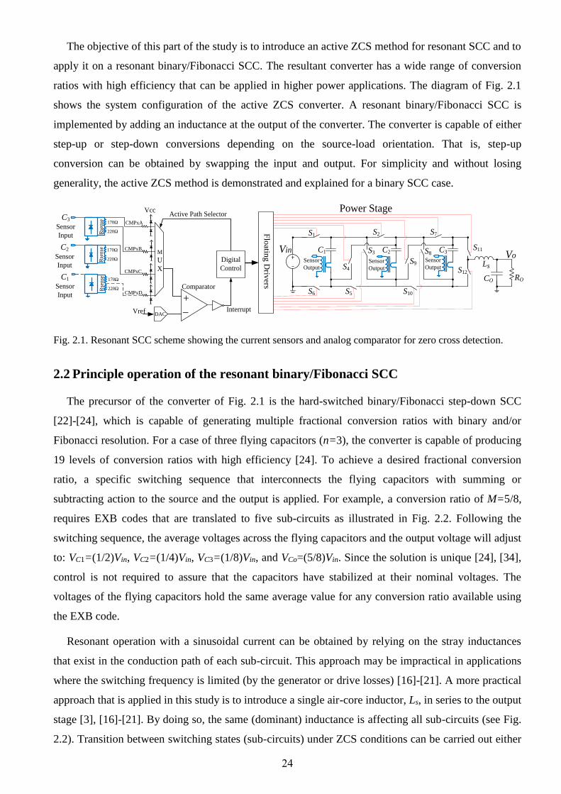
24
The objective of this part of the study is to introduce an active ZCS method for resonant SCC and to
apply it on a resonant binary/Fibonacci SCC. The resultant converter has a wide range of conversion
ratios with high efficiency that can be applied in higher power applications. The diagram of Fig. 2.1
shows the system configuration of the active ZCS converter. A resonant binary/Fibonacci SCC is
implemented by adding an inductance at the output of the converter. The converter is capable of either
step-up or step-down conversions depending on the source-load orientation. That is, step-up
conversion can be obtained by swapping the input and output. For simplicity and without losing
generality, the active ZCS method is demonstrated and explained for a binary SCC case.
+_
M
U
X
DACVref Interrupt
CMPxA
CMPxB
CMPxC
CMPxDComparator220Ω
S1
S6
S4
S3
S9
S8
S2 S7
S12
S11
S5 S10
C1 C2 C3
CO
Ls
RO
Vo
C3
Sensor
Input
C2
Sensor
Input
C1
Sensor
Input
Sensor
OutputSensor
Output
Sensor
Output
Flo
atin
g D
rivers
Active Path Selector
Digital
Control
170Ω
Vin
220Ω
170Ω
220Ω
170Ω
Vcc Power Stage
Rse
nse
Rse
nse
Rse
nse
Fig. 2.1. Resonant SCC scheme showing the current sensors and analog comparator for zero cross detection.
2.2 Principle operation of the resonant binary/Fibonacci SCC
The precursor of the converter of Fig. 2.1 is the hard-switched binary/Fibonacci step-down SCC
[22]-[24], which is capable of generating multiple fractional conversion ratios with binary and/or
Fibonacci resolution. For a case of three flying capacitors (n=3), the converter is capable of producing
19 levels of conversion ratios with high efficiency [24]. To achieve a desired fractional conversion
ratio, a specific switching sequence that interconnects the flying capacitors with summing or
subtracting action to the source and the output is applied. For example, a conversion ratio of M=5/8,
requires EXB codes that are translated to five sub-circuits as illustrated in Fig. 2.2. Following the
switching sequence, the average voltages across the flying capacitors and the output voltage will adjust
to: VC1=(1/2)Vin, VC2=(1/4)Vin, VC3=(1/8)Vin, and VCo=(5/8)Vin. Since the solution is unique [24], [34],
control is not required to assure that the capacitors have stabilized at their nominal voltages. The
voltages of the flying capacitors hold the same average value for any conversion ratio available using
the EXB code.
Resonant operation with a sinusoidal current can be obtained by relying on the stray inductances
that exist in the conduction path of each sub-circuit. This approach may be impractical in applications
where the switching frequency is limited (by the generator or drive losses) [16]-[21]. A more practical
approach that is applied in this study is to introduce a single air-core inductor, Ls, in series to the output
stage [3], [16]-[21]. By doing so, the same (dominant) inductance is affecting all sub-circuits (see Fig.
2.2). Transition between switching states (sub-circuits) under ZCS conditions can be carried out either
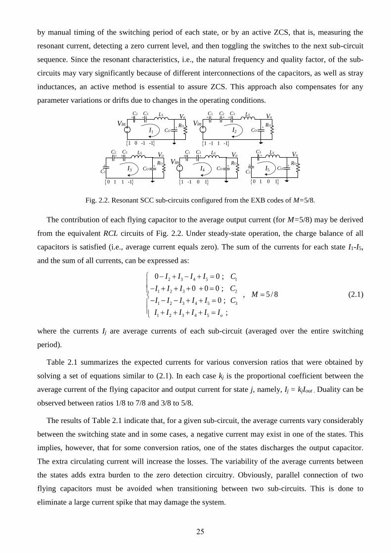
25
by manual timing of the switching period of each state, or by an active ZCS, that is, measuring the
resonant current, detecting a zero current level, and then toggling the switches to the next sub-circuit
sequence. Since the resonant characteristics, i.e., the natural frequency and quality factor, of the sub-
circuits may vary significantly because of different interconnections of the capacitors, as well as stray
inductances, an active method is essential to assure ZCS. This approach also compensates for any
parameter variations or drifts due to changes in the operating conditions.
C2 C3
CO
LS
RO
Vo
Vin
C1
C2 C3
CO
LS
RO
Vo
+ +
+
+ +
++
C1 C3
CO
LS
RO
Vo+ +
+Vin
C3
CO
LS
RO
Vo+
++
C1
1 0 -1 -1 1 -1 1 -1
0 1 1 -1 1 -1 0 1 0 1 0 1
C1 C2 C3
CO
LS
RO
Vo
Vin
+ + +
+I1 I2
I3 I4 I5
Fig. 2.2. Resonant SCC sub-circuits configured from the EXB codes of M=5/8.
The contribution of each flying capacitor to the average output current (for M=5/8) may be derived
from the equivalent RCL circuits of Fig. 2.2. Under steady-state operation, the charge balance of all
capacitors is satisfied (i.e., average current equals zero). The sum of the currents for each state I1-I5,
and the sum of all currents, can be expressed as:
2 3 4 5 1
1 2 3 2
1 2 3 4 5 3
1 2 3 4 5
0 0 ;
0 0 0 ; , 5 / 8
0 ;
; o
I I I I C
I I I CM
I I I I I C
I I I I I I
(2.1)
where the currents Ij are average currents of each sub-circuit (averaged over the entire switching
period).
Table 2.1 summarizes the expected currents for various conversion ratios that were obtained by
solving a set of equations similar to (2.3). In each case kj is the proportional coefficient between the
average current of the flying capacitor and output current for state j, namely, Ij = kjIout . Duality can be
observed between ratios 1/8 to 7/8 and 3/8 to 5/8.
The results of Table 2.1 indicate that, for a given sub-circuit, the average currents vary considerably
between the switching state and in some cases, a negative current may exist in one of the states. This
implies, however, that for some conversion ratios, one of the states discharges the output capacitor.
The extra circulating current will increase the losses. The variability of the average currents between
the states adds extra burden to the zero detection circuitry. Obviously, parallel connection of two
flying capacitors must be avoided when transitioning between two sub-circuits. This is done to
eliminate a large current spike that may damage the system.
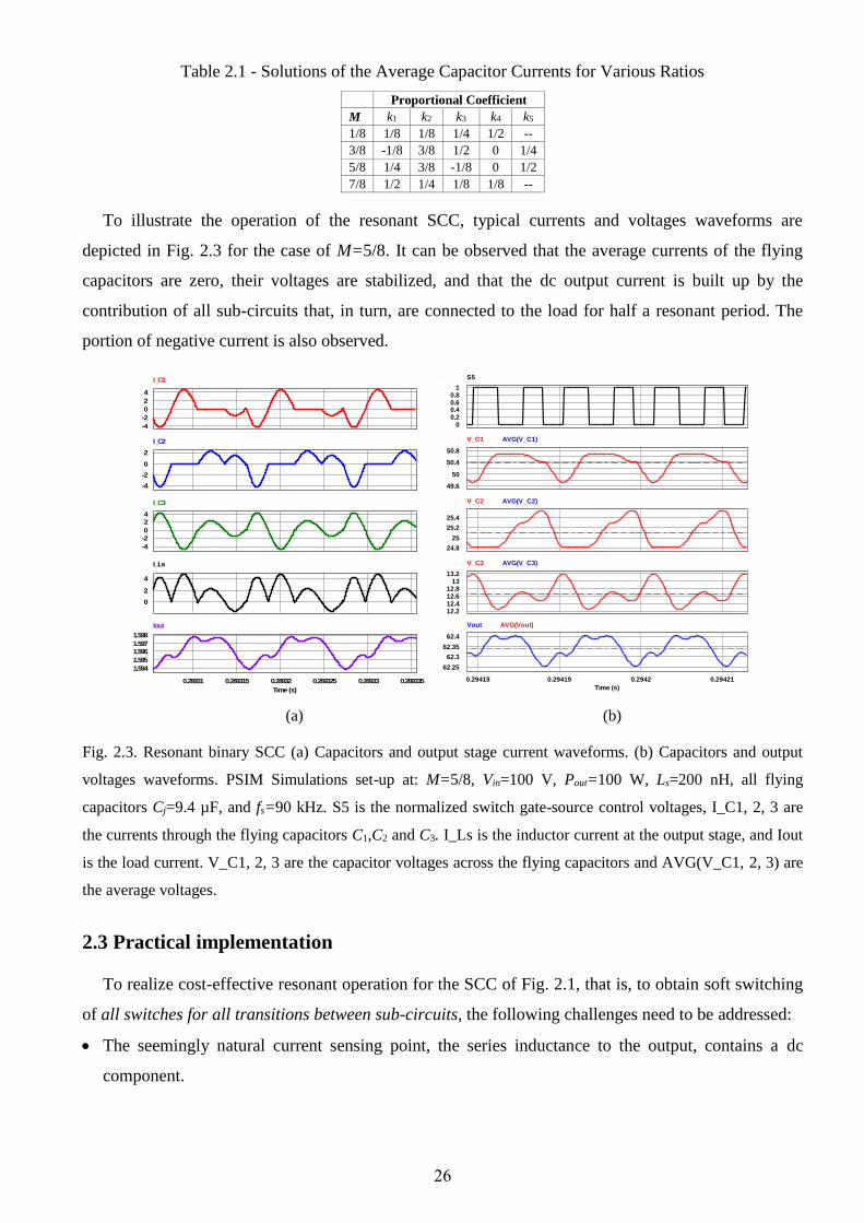
26
Table 2.1 - Solutions of the Average Capacitor Currents for Various Ratios
Proportional Coefficient
M k1 k2 k3 k4 k5
1/8 1/8 1/8 1/4 1/2 --
3/8 -1/8 3/8 1/2 0 1/4
5/8 1/4 3/8 -1/8 0 1/2
7/8 1/2 1/4 1/8 1/8 --
To illustrate the operation of the resonant SCC, typical currents and voltages waveforms are
depicted in Fig. 2.3 for the case of M=5/8. It can be observed that the average currents of the flying
capacitors are zero, their voltages are stabilized, and that the dc output current is built up by the
contribution of all sub-circuits that, in turn, are connected to the load for half a resonant period. The
portion of negative current is also observed.
(a) (b)
Fig. 2.3. Resonant binary SCC (a) Capacitors and output stage current waveforms. (b) Capacitors and output
voltages waveforms. PSIM Simulations set-up at: M=5/8, Vin=100 V, Pout=100 W, Ls=200 nH, all flying
capacitors Cj=9.4 µF, and fs=90 kHz. S5 is the normalized switch gate-source control voltages, I_C1, 2, 3 are
the currents through the flying capacitors C1,C2 and C3. I_Ls is the inductor current at the output stage, and Iout
is the load current. V_C1, 2, 3 are the capacitor voltages across the flying capacitors and AVG(V_C1, 2, 3) are
the average voltages.
2.3 Practical implementation
To realize cost-effective resonant operation for the SCC of Fig. 2.1, that is, to obtain soft switching
of all switches for all transitions between sub-circuits, the following challenges need to be addressed:
The seemingly natural current sensing point, the series inductance to the output, contains a dc
component.
0
-2
-4
2
4
I_C1
0
-2
-4
2
I_C2
0
-2
-4
2
4
I_C3
0
2
4
I_Ls
0.28931 0.289315 0.28932 0.289325 0.28933 0.289335
Time (s)
1.594
1.595
1.596
1.597
1.598
Iout
00.20.40.60.8
1
S5
49.6
50
50.4
50.8
V_C1 AVG(V_C1)
24.8
25
25.2
25.4
V_C2 AVG(V_C2)
12.212.412.612.8
1313.2
V_C3 AVG(V_C3)
0.29418 0.29419 0.2942 0.29421
Time (s)
62.25
62.3
62.35
62.4
Vout AVG(Vout)

27
The resonant characteristics (natural frequency and quality factor) are considerably different from
one sub-circuit to another. This is due to different interconnections of the flying capacitors
according to the EXB code (e.g., Fig. 2.2).
Uncertainties and variations of the parameters (inductance and capacitance) may be very large.
Especially for different operating conditions (conversion ratio and power levels).
The average and the peak current are not constant for each sub-circuit and for a given state at
different power ratings.
Zero current detection at the crossing point is impractical due to a poor signal-to-noise (SNR) ratio
and the time delay from detection to commutation of the switches. Selection of the reference
depends on the above arguments.
Gate drive circuitry to assure the operation of a large number of floating switches.
Considerations for components selection based on the expected losses of the system (further
discussed in Chapter 3).
To overcome these challenges, a ZCD and control circuitry was developed in this study and is
schematically described in Fig. 2.1. It includes a current sensor for each of the flying capacitors, a
comparator module, microcontroller, and decoders. The transition between switching states of the EXB
code is governed by comparing the resonant currents to specified references. These are discussed in this
section, which also addresses issues of limiting the inrush current, stabilizing the capacitors’ voltages
after startup, and the realization of simple and efficient floating gate drivers of the power switches.
2.3.1 Current sensing and zero crossing detection
To eliminate the need for a rather costly, active current sensing circuitry that accommodates dc
current, passive magnetic current transformers are placed on all three flying capacitors.
Since the aim of the current sensing is the detection of the zero crossing point rather than
regulation, the dc component of the current is not of interest. The reason for the apparent redundancy
in the current measurements is that there is no single capacitor that participates in all the states for all
voltage ratio configurations. In the example shown in Fig. 2.2 of 5/8, C3 participates in all the states,
but for other ratios, such as 2/8, it is omitted. By having three sensors, current can be read from any
active capacitor.
A conventional passive magnetic sensor has been utilized for zero detection. This exemplary
practice may seem against the original concept for using SCC technology to avoid magnetic
components. Fortunately, since current sensing is aimed purely for detection of the current zero
crossing point, only the shape of the current signal in the vicinity of zero is of interest. This implies
that weakly coupled, i.e., coreless, sensors may be employed [50].
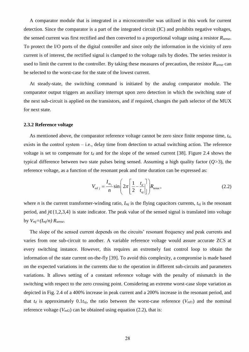
28
A comparator module that is integrated in a microcontroller was utilized in this work for current
detection. Since the comparator is a part of the integrated circuit (IC) and prohibits negative voltages,
the sensed current was first rectified and then converted to a proportional voltage using a resistor Rsense.
To protect the I/O ports of the digital controller and since only the information in the vicinity of zero
current is of interest, the rectified signal is clamped to the voltage rails by diodes. The series resistor is
used to limit the current to the controller. By taking these measures of precaution, the resistor Rsense can
be selected to the worst-case for the state of the lowest current.
At steady-state, the switching command is initiated by the analog comparator module. The
comparator output triggers an auxiliary interrupt upon zero detection in which the switching state of
the next sub-circuit is applied on the transistors, and if required, changes the path selector of the MUX
for next state.
2.3.2 Reference voltage
As mentioned above, the comparator reference voltage cannot be zero since finite response time, td,
exists in the control system ‒ i.e., delay time from detection to actual switching action. The reference
voltage is set to compensate for td and for the slope of the sensed current [38]. Figure 2.4 shows the
typical difference between two state pulses being sensed. Assuming a high quality factor (Q>3), the
reference voltage, as a function of the resonant peak and time duration can be expressed as:
m
ref sense
1sin 2
2
j dj
oj
I tV R
n t
, (2.2)
where n is the current transformer-winding ratio, Imj is the flying capacitors currents, toj is the resonant
period, and j∈1,2,3,4 is state indicator. The peak value of the sensed signal is translated into voltage
by Vmj=(Imj/n) Rsense.
The slope of the sensed current depends on the circuits’ resonant frequency and peak currents and
varies from one sub-circuit to another. A variable reference voltage would assure accurate ZCS at
every switching instance. However, this requires an extremely fast control loop to obtain the
information of the state current on-the-fly [39]. To avoid this complexity, a compromise is made based
on the expected variations in the currents due to the operation in different sub-circuits and parameters
variations. It allows setting of a constant reference voltage with the penalty of mismatch in the
switching with respect to the zero crossing point. Considering an extreme worst-case slope variation as
depicted in Fig. 2.4 of a 400% increase in peak current and a 200% increase in the resonant period, and
that td is approximately 0.1toj, the ratio between the worst-case reference (Vref1) and the nominal
reference voltage (Vref2) can be obtained using equation (2.2), that is:

29
1
1
m 1sense
1ref1
ref 2 m 1sense
1
4 0.11sin 2
2 2
0.11sin
2.1
22
o
o
o
o
I tR
n tV
V I tR
n t
, (2.3)
which translates into an absolute maximum mismatch in the switching time of 0.1toj. Provided that the
operation of each sub-circuit is in the range of microseconds, the result of equation (2.3) implies a
small deviation from the true zero crossing point, allowing the use of a fixed reference voltage.
Ref Value
Vm1
Vm2
td td
Mismatch
Comparator State
to1/2to2/2
Fig. 2.4. Worst-case conditions of state current variation and the mismatch of the switching instance due to fixed
reference settings.
In this work, the reference voltage and the sensing gain are selected such that the true ZCS is
obtained at higher power levels (higher states’ currents), and the small mismatches in the ZCS will be
at lower power levels. To allow operation in a wide range of power levels and input voltage variations
and still work in the vicinity of ZCS, a coarse tuner to switch between operation ranges is realized. The
scaling of the sensing gain is implemented by voltage dividers branching out to the MUX (Fig. 2.1).
Another consideration when setting a low reference value is the need to avoid the ground noise
caused by imperfect switching at nonzero, common-mode, etc. that may result in erroneous triggering
of the comparator. This is overcome by a blanking period of the comparator after the switching action,
as done in many commercial current sensing oriented applications.
2.3.3 Stabilizing the flying capacitors voltage on startup
The design of the active ZCS method and circuitry assumes that the voltages of all capacitors have
stabilized to their nominal values (binary fractions). Applying the above zero detection method
(demonstrated in detail in the next section), assures that at steady-state ZCS is realized for all
conversion ratios and over a wide operation range of input voltage and power levels. In a practical turn-
on situation, the capacitors’ voltages are zero. This results in high inrush currents if the converter is
allowed to operate in the vicinity of the steady-state resonant frequency. Moreover, relying on the
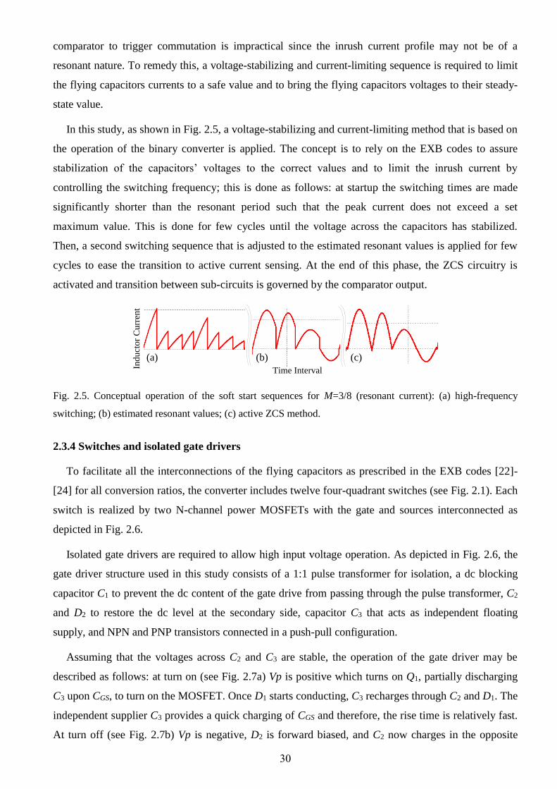
30
comparator to trigger commutation is impractical since the inrush current profile may not be of a
resonant nature. To remedy this, a voltage-stabilizing and current-limiting sequence is required to limit
the flying capacitors currents to a safe value and to bring the flying capacitors voltages to their steady-
state value.
In this study, as shown in Fig. 2.5, a voltage-stabilizing and current-limiting method that is based on
the operation of the binary converter is applied. The concept is to rely on the EXB codes to assure
stabilization of the capacitors’ voltages to the correct values and to limit the inrush current by
controlling the switching frequency; this is done as follows: at startup the switching times are made
significantly shorter than the resonant period such that the peak current does not exceed a set
maximum value. This is done for few cycles until the voltage across the capacitors has stabilized.
Then, a second switching sequence that is adjusted to the estimated resonant values is applied for few
cycles to ease the transition to active current sensing. At the end of this phase, the ZCS circuitry is
activated and transition between sub-circuits is governed by the comparator output.
Time Interval
Induct
or
Curr
ent
(a) (b) (c)
Fig. 2.5. Conceptual operation of the soft start sequences for M=3/8 (resonant current): (a) high-frequency
switching; (b) estimated resonant values; (c) active ZCS method.
2.3.4 Switches and isolated gate drivers
To facilitate all the interconnections of the flying capacitors as prescribed in the EXB codes [22]-
[24] for all conversion ratios, the converter includes twelve four-quadrant switches (see Fig. 2.1). Each
switch is realized by two N-channel power MOSFETs with the gate and sources interconnected as
depicted in Fig. 2.6.
Isolated gate drivers are required to allow high input voltage operation. As depicted in Fig. 2.6, the
gate driver structure used in this study consists of a 1:1 pulse transformer for isolation, a dc blocking
capacitor C1 to prevent the dc content of the gate drive from passing through the pulse transformer, C2
and D2 to restore the dc level at the secondary side, capacitor C3 that acts as independent floating
supply, and NPN and PNP transistors connected in a push-pull configuration.
Assuming that the voltages across C2 and C3 are stable, the operation of the gate driver may be
described as follows: at turn on (see Fig. 2.7a) Vp is positive which turns on Q1, partially discharging
C3 upon CGS, to turn on the MOSFET. Once D1 starts conducting, C3 recharges through C2 and D1. The
independent supplier C3 provides a quick charging of CGS and therefore, the rise time is relatively fast.
At turn off (see Fig. 2.7b) Vp is negative, D2 is forward biased, and C2 now charges in the opposite

31
direction through D2. In addition, CGS discharges through Q2 that is saturated, turning off the
MOSFET. R2 damps potential overshoots that may occur due to stray inductances.
For construction and component selection of the isolated gate driver of Fig. 2.6, the following
procedure is suggested:
Given a power transistor with specified gate charge requirements (Qgate) and provided the turn
on/off transition time tr, the required peak current of the low-side driver can be estimated as:
gate
pk
r
QI
t , (2.4)
The effective magnetic area, Ae, for the isolation transformer is calculated based on the
maximum flux density that is allowed, Bmax, resulting from the maximum on time ton, that is
defined by the resonant period of the system. To comply with the specification sheets of
commercial compact pulse transformers, the voltage-time product has been defined as the
target parameter as:
maxe GS onnA B V t , (2.5)
where VGS is the applied gate voltage and n is the number of turns at the secondary winding.
Resistors R1 and R2 (optional) are selected to damp oscillations and avoid high peak currents
that may appear due to the stray inductances and the total gate capacitance. These are typically
applied using manual trim.
The dc blocking and restoring capacitors C1 and C2 are selected to sustain the average drive
voltage per switching cycle.
Capacitance C3 is required to be sufficiently high to allow charging of CGS while sustaining the
required gate voltage, that is:
av
s
IC
V f
, (2.6)
where Iav is the average capacitor current, and ΔV is the voltage ripple of the capacitor.
Transistors Q1 and Q2 are selected to sustain the gate peak current with the repetitive rate of
switching frequency.
The components values (see Table 3.1) used in the experimental prototype are: C1=C2=C3=1 µF,
R1=3.3 Ω, R2=33 Ω. The operation of the experimental floating drivers has been verified at switching
frequency in the range of 30-350 kHz, wide duty cycle range of 0.1-0.9, and rise and fall times of
approximately 200 ns. Figure 2.8 demonstrated the driver output signal, VGate, voltages of capacitors
C2, C3, and the voltage across diode D2.

32
G
Dr.2
Dr.1
M1
M2
D1
D2
C2C1
C3
R2R1
Gate Drive In
Q1
Q2
T1
1:1 Pulse Trans.
Vp Vs
S
Drive Isolation Switch
Fig. 2.6. Isolated Gate Driver and four-quadrant switch using N – channel power MOSFETs.
D1
D2
C2C1
C3
R2R1VDRV
Q1
Q2
1uF1uF
1uF
+
_
CGS
+
+
D1
D2
C2C1
C3
R2R1VDRV
Q1
Q2
1uF1uF
1uF
_
+
CGS++
_
+_
(a)
(b)
VsVp
+
_
Vp Vs
+
_
Fig. 2.7. Operation modes: (a) on state - CGS charging (b) off state - CGS Discharging.
VGate
VD2
VC2
VC3
(a)
(b)
(c)
(d)
Fig. 2.8. Experimental waveforms of the isolated gate driver: (a) C3 voltage (5 V/div). (b) C2 voltage (2 V/div).
(c) D2 voltage (5 V/div). (d) output voltage, VGate (5 V/div). Horizontal scale (10 µs/div).

33
2.4 Conclusions
A resonant binary and Fibonacci step-up/down converter was introduced. The soft switching method
is based on inserting one air core inductor or the use of parasitic inductance and with an active zero
detection method. The major challenge in the design of a resonant binary SCC is the significant
variation in switching times that is required for soft-switching operation. This variation is present when
switching between one sub-circuit to another that may involve a different number of capacitors in a
series, which therefore, changes the resonant period. Another source for different resonant periods is
that the capacitance and inductance values are strongly dependent on the operating conditions. This
means that the time period of a given sub-circuit is not constant for variations in the power level or the
input voltage, and this rules out any non-instantaneous ZCS or pre-calibrated resonant operation. The
method can be implemented with most of the switch capacitor topologies for reducing conduction
losses and EMI noises. Furthermore, the converter reduces the power losses by increasing the number
of target voltages. The proposed converter is a viable approach for medium and high step-up/down
power systems, despite of the large number of switches.
34
Chapter 3 - Design of the Multiphase Resonant Switched-Capacitor
Converters
3.1 Introduction
The objective of this part of the study is to set the design guideline considerations and rules for the
selection of the power stage components, for multiple sub-circuit converters. The proposal
methodology is based on the generic equivalent model of the soft switching case [27]. The design
method of multilevel SCCs with respect to conduction losses and efficiency was demonstrated on the
resonant binary SCC. This topology was analyzed and two types of experiments were constructed to
examine the design methodologies.
3.2 Equivalent resistance – considerations for components selection
The primary contributor of losses for the ZCS resonant binary/Fibonacci SCC under study is the
conduction losses in each sub-circuit. When combined together, the total equivalent resistance is a good
tool to predict the system efficiency based on the system parameters. Examination of the losses based
on the generic equivalent modeling approach of [26], [27] adds practical insight to determine the size of
the power transistors (on resistance) and the required characteristic impedance (capacitance-inductance
ratio). There, the equivalent resistance is represented as a function of the resonant characteristics of the
system. In this study, the methodology presented in [26], [27] for a simplistic case of a unity converter
has been adapted to estimate the equivalent resistance of the resonant binary/Fibonacci SCC that
includes multiple sub-circuits per operation cycle.
Given that each stage for all EXB/SFN/SGF codes consists of four dual switches in the conduction
path, without loss of generality, the total parasitic loop resistance for every sub-circuit (Rloop j), is
approximated to 8RDS(on) (neglecting the ESR and other stray resistances). The total equivalent
resistance ReqT in its generic form can be expressed as a function of the sub-circuits’ quality factors Qj
[27] by summation of the equivalent resistances in all sub circuits, that is:
2
2
2 21
2tanh
df 4 1 2 4 1
nj loop j
eqT j
jj j j
Q RR k
Q Q
, (3.1)
where dfj = fs / fd , is the ratio between the switching frequency, fs, to the damped resonant frequency,
fd, for each sub-circuit, and j is the sub-circuit index.
Since the case under study involves multiple sub-circuits with different numbers of serially
connected capacitors, which results in different values of Qj (as can be observed from the sub-circuits
of Fig. 2.2), a direct calculation of expression (3.1) based on the system specific values has several
degrees of freedom and is therefore quite complex. To achieve a more convenient representation of
35
expression (3.1), the following manipulations are applied: 1) ReqT is normalized to Rloopj (which is
assumed to be identical for all sub-circuits); 2) Qj is represented as a function of the lowest possible
quality factor of all sub-circuits (defined as Qj_low). The value of Qj_low is obtained from the sub-circuit
with the smallest number of serially connected capacitors; 3) dfj is represented by the df of the sub-
circuit from which Qj_low is obtained (defined as dfj_low). These mathematical relationships significantly
reduce the complexity of expression (3.1) to two degrees of freedom (Qj_low and dfj_low) and can be
used to represent the worst-case design conditions from which the maximum losses can be estimated,
per conversion ratio.
To exemplify the normalization procedure and plot the resultant ReqT, consider the case of M=5/8 in
which Ct1=Ct4=C/2, Ct2=Ct3=C/3, and Ltj=Ls. This leads to Qj_low = Q1, 𝑄2 = √3 2⁄ ∙ 𝑄1, dfj_low = df1,
df2 = √2/3 ∙ df1, and the expression (3.1) can be rewritten in the normalized form as:
2 22 21 1
1 22 2 2 2
1 1 1 1 1 1
2 22 21 13 4
2 2 2 2
1 1 1 1 1 1
2 3tanh tanh
df 4 1 2 4 1 2 3 df 6 1 2 6 1
3 2 + tanh tanh
2 3 df 6 1 2 6 1 df 4 1 2 4 1
eqT
loop j
R Q Qk k
R Q Q Q Q
Q Qk k
Q Q Q Q
. (3.2)
Following the same procedure, the worst-case total equivalent resistances for several conversion
ratios (M=1/8, 3/8, 5/8, and 7/8) have been obtained and were numerically plotted as a function of
Qj_low for several values of dfj_low and are shown in Fig. 3.1. It can be observed that the normalized ReqT
asymptotically reaches a constant value for Qj_low values higher than 3. This implies that the lowest
possible losses can be obtained, even with fairly small inductances, thus allowing the use of stray
inductance or a coreless element. It can also be observed that a quality factor lower than unity
increases ReqT. This can be explained by the fact that when Q<1, the operation is no longer resonant
and the rms value of the circulating current significantly increases. Another observation from Fig. 3.1
is that a higher value of dfj (less damped circuit) is preferable in order to obtain lower conduction
losses.
Based on the above-mentioned observations and mathematical extraction, the following design
procedure is proposed and demonstrated on a case of three flying capacitors:
For the highest expected conversion ratio (smallest fraction), a worst-case Qj_low and dfj_low is
selected for the sub-circuit with the smallest number of serially connected capacitors.
From Fig. 3.1, ReqT is extracted. Alternatively, equation (3.1) and the above-mentioned order
reduction procedure can be used.
Given a desired target efficiency, the upper boundary for RDS(on) is extracted according to the
efficiency expression, that is :
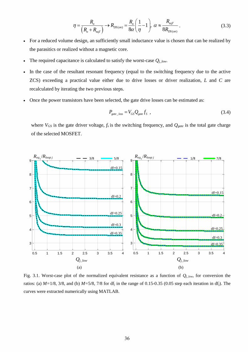
36
( )
( )
11 ,
8 8
eqTo oDS on
DS ono eqT
RR RR
RR R
. (3.3)
For a reduced volume design, an sufficiently small inductance value is chosen that can be realized by
the parasitics or realized without a magnetic core.
The required capacitance is calculated to satisfy the worst-case Qj_low.
In the case of the resultant resonant frequency (equal to the switching frequency due to the active
ZCS) exceeding a practical value either due to drive losses or driver realization, L and C are
recalculated by iterating the two previous steps.
Once the power transistors have been selected, the gate drive losses can be estimated as:
_gate loss GS gate SP V Q f , (3.4)
where VGS is the gate driver voltage, fs is the switching frequency, and Qgate is the total gate charge
of the selected MOSFET.
0.5 1 1.5 2 2.5 3 3.5 4
3
4
5
6
7
8
97/81/85/83/8
0.5 1 1.5 2 2.5 3 3.5 4
3
4
5
6
7
8
9
df=0.15
df=0.2
df=0.35
df=0.3
df=0.25
Qj_low Qj_low
(a) (b)
df=0.15
df=0.25
df=0.35
df=0.2
df=0.3
ReqT/Rloop jReq
T/Rloop j
Fig. 3.1. Worst-case plot of the normalized equivalent resistance as a function of Qj_low, for conversion the
ratios: (a) M=1/8, 3/8, and (b) M=5/8, 7/8 for dfj in the range of 0.15-0.35 (0.05 step each iteration in dfj). The
curves were extracted numerically using MATLAB.

37
3.3 Analysis and numerical plots
This section provides more details for all conversion ratios and sub-states of the resonant binary
SCC. Solutions of the average currents of the capacitors and the total capacitance per state are
summarized in Table 3.1.
Table 3.1 - Solutions of the Average Capacitors Currents for All Ratios
and Total Capacitance per Phase
Tables 3.2-3.4 summarize the normalized forms of the equivalent resistors of all conversion ratios.
The dominant part of any equivalent resistor contains the worst-case Qj_low and dfj_low and furthermore
this part is multiple with the highest value of the proportional factor, kj. The highest kj factor is related
to the lowest Qj since this phase includes the highest equivalent capacitance value (sub-circuit with the
smallest number of serially connected capacitors where Rloop and Ls are constant).
CTotal
M St1 St2 St3 St4 St5
EXB
Codes
1/8 C/3 C/3 C/2 C --
2/8 C/2 C/2 C -- --
3/8 C/3 C/3 C/2 0 C/2
4/8 C C -- -- --
5/8 C/2 C/3 C/3 0 C/2
6/8 C/2 C C/2 -- --
7/8 C C/2 C/3 C/3 --
SFN
Codes
1/5 C C/2 C/2 C/3 --
1/3 C C/2 C -- --
2/5 C C/3 C/2 C --
1/2 C C -- -- --
3/5 C C/2 C/3 C --
2/3 C C/2 C -- --
4/5 C/2 C/2 C/2 C --
SGF
Codes
1/7 C C/2 C/3 C/2 --
2/7 C C/2 C/3 C/2 --
3/7 C2 C/3 C C/2 --
4/7 C C/2 C/3 C/2 --
5/7 C/2 C/2 C C/3 --
6/7 C/2 C/3 C/2 C --
Proportional Coefficient
M k1 k2 k3 k4 k5
EXB
Codes
1/8 1/8 1/8 1/4 1/2 --
2/8 1/4 1/4 1/2 -- --
3/8 -1/8 3/8 1/2 0 1/4
4/8 1/2 1/2 -- -- --
5/8 1/4 3/8 -1/8 0 1/2
6/8 1/4 1/2 1/4 -- --
7/8 1/2 1/4 1/8 1/8 --
SFN
Codes
1/5 1/5 2/5 1/5 1/5 --
1/3 1/3 1/3 1/3 -- --
2/5 1/5 1/5 1/5 2/5 --
1/2 1/2 1/2 -- -- --
3/5 2/5 1/5 1/5 1/5 --
2/3 1/3 1/3 1/3 -- --
4/5 1/5 1/5 1/5 2/5 --
SGF
Codes
1/7 3/7 2/7 1/7 1/7 --
2/7 3/7 2/7 1/7 1/7 --
3/7 1/7 1/7 3/7 2/7 --
4/7 3/7 2/7 1/7 1/7 --
5/7 1/7 2/7 3/7 1/7 --
6/7 1/7 1/7 2/7 3/7 --
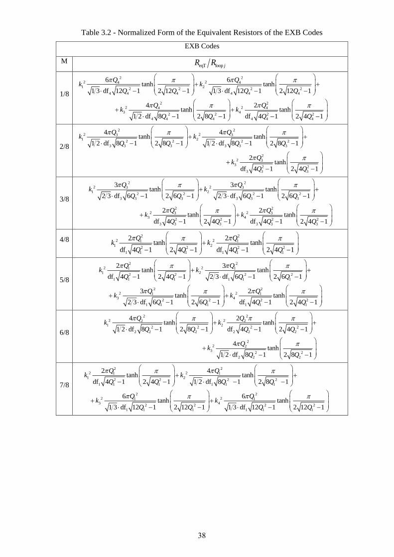
38
Table 3.2 - Normalized Form of the Equivalent Resistors of the EXB Codes
EXB Codes
eqT loop jR R M
2 22 24 4
1 22 2 2 2
4 4 4 4 4 4
2 22 24 4
3 42 2 2 2
4 4 4 4 4 4
6 6tanh tanh
1 3 df 12 1 2 12 1 1 3 df 12 1 2 12 1
4 2 tanh tanh
1 2 df 8 1 2 8 1 df 4 1 2 4 1
Q Qk k
Q Q Q Q
Q Qk k
Q Q Q Q
1/8
2 22 23 3
1 22 2 2 2
3 3 3 3 3 3
22 3
32 2
3 3 3
4 4tanh tanh
1 2 df 8 1 2 8 1 1 2 df 8 1 2 8 1
2 tanh
df 4 1 2 4 1
Q Qk k
Q Q Q Q
Qk
Q Q
2/8
2 22 23 3
1 22 2 2 2
3 3 3 3 3 3
2 22 23 3
3 42 2 2 2
3 3 3 3 3 3
3 3tanh tanh
2 3 df 6 1 2 6 1 2 3 df 6 1 2 6 1
2 2 tanh tanh
df 4 1 2 4 1 df 4 1 2 4 1
Q Qk k
Q Q Q Q
Q Qk k
Q Q Q Q
3/8
2 22 21 1
1 22 2 2 2
1 1 1 1 1 1
2 2tanh tanh
df 4 1 2 4 1 df 4 1 2 4 1
Q Qk k
Q Q Q Q
4/8
2 22 21 1
1 22 2 2 2
1 1 1 1 1 1
2 22 21 1
3 42 2 2 2
1 1 1 1 1 1
2 3tanh tanh
df 4 1 2 4 1 2 3 df 6 1 2 6 1
3 2 tanh tanh
2 3 df 6 1 2 6 1 df 4 1 2 4 1
Q Qk k
Q Q Q Q
Q Qk k
Q Q Q Q
5/8
2 22 22 2
1 22 2 2 2
2 2 2 2 2 2
22 2
32 2
2 2 2
4 2tanh tanh
1 2 df 8 1 2 8 1 df 4 1 2 4 1
4 tanh
1 2 df 8 1 2 8 1
Q Qk k
Q Q Q Q
Qk
Q Q
6/8
2 22 21 1
1 22 2 2 2
1 1 1 1 1 1
2 22 21 1
3 42 2 2 2
1 1 1 1 1 1
2 4tanh tanh
df 4 1 2 4 1 1 2 df 8 1 2 8 1
6 6 tanh tanh
1 3 df 12 1 2 12 1 1 3 df 12 1 2 12 1
Q Qk k
Q Q Q Q
Q Qk k
Q Q Q Q
7/8

39
Table 3.3 - Normalized Form of the Equivalent Resistors of the SFN Codes
SFN Codes
eqT loop jR R M
2 22 21 1
1 22 2 2 2
1 1 1 1 1 1
2 22 21 1
3 42 2 2 2
1 1 1 1 1 1
2 4tanh tanh
df 4 1 2 4 1 1 2 df 8 1 2 8 1
4 6 tanh tanh
1 2 df 8 1 2 8 1 1 3 df 12 1 2 12 1
Q Qk k
Q Q Q Q
Q Qk k
Q Q Q Q
1/5
2 22 21 1
1 22 2 2 2
1 1 1 1 1 1
22 1
32 2
1 1 1
2 4tanh tanh
df 4 1 2 4 1 1 2 df 8 1 2 8 1
2 tanh
df 4 1 2 4 1
Q Qk k
Q Q Q Q
Qk
Q Q
1/3
2 22 21 1
1 22 2 2 2
1 1 1 1 1 1
2 22 21 1
3 42 2 2 2
1 1 1 1 1 1
2 6tanh tanh
df 4 1 2 4 1 1 3 df 12 1 2 12 1
4 2 tanh tanh
1 2 df 8 1 2 8 1 df 4 1 2 4 1
Q Qk k
Q Q Q Q
Q Qk k
Q Q Q Q
2/5
2
2 2 11 2
2 2
1 1 1
2tanh
df 4 1 2 4 1
Qk k
Q Q
1/2
2 22 21 1
1 22 2 2 2
1 1 1 1 1 1
2 22 21 1
3 42 2 2 2
1 1 1 1 1 1
2 4tanh tanh
df 4 1 2 4 1 1 2 df 8 1 2 8 1
6 2 tanh tanh
1 3 df 12 1 2 12 1 df 4 1 2 4 1
Q Qk k
Q Q Q Q
Q Qk k
Q Q Q Q
3/5
2 22 21 1
1 22 2 2 2
1 1 1 1 1 1
22 1
32 2
1 1 1
2 4tanh tanh
df 4 1 2 4 1 1 2 df 8 1 2 8 1
2 tanh
df 4 1 2 4 1
Q Qk k
Q Q Q Q
Qk
Q Q
2/3
2 22 24 4
1 22 2 2 2
4 4 4 4 4 4
2 22 24 4
3 42 2 2 2
4 4 4 4 4 4
4 4tanh tanh
1 2 df 8 1 2 8 1 1 2 df 8 1 2 8 1
4 2 tanh tanh
1 2 df 8 1 2 8 1 df 4 1 2 4 1
Q Qk k
Q Q Q Q
Q Qk k
Q Q Q Q
4/5

40
Table 3.4 - Normalized Form of the Equivalent Resistors of the SGF Codes
SGF Codes
eqT loop jR R M
2 22 21 1
1 22 2 2 2
1 1 1 1 1 1
2 22 21 1
3 42 2 2 2
1 1 1 1 1 1
2 4tanh tanh
df 4 1 2 4 1 1 2 df 8 1 2 8 1
6 4tanh tanh
1 3 df 12 1 2 12 1 1 2 df 8 1 2 8 1
Q Qk k
Q Q Q Q
Q Qk k
Q Q Q Q
1/7
2 22 21 1
1 22 2 2 2
1 1 1 1 1 1
2 22 21 1
3 42 2 2 2
1 1 1 1 1 1
2 4tanh tanh
df 4 1 2 4 1 1 2 df 8 1 2 8 1
6 4tanh tanh
1 3 df 12 1 2 12 1 1 2 df 8 1 2 8 1
Q Qk k
Q Q Q Q
Q Qk k
Q Q Q Q
2/7
2 22 23 3
1 22 2 2 2
3 3 3 3 3 3
2 22 23 3
3 42 2 2 2
3 3 3 3 3 3
4 6tanh tanh
1 2 df 8 1 2 8 1 1 3 df 12 1 2 12 1
2 4 tanh tanh
df 4 1 2 4 1 1 2 df 8 1 2 8 1
Q Qk k
Q Q Q Q
Q Qk k
Q Q Q Q
3/7
2 22 21 1
1 22 2 2 2
1 1 1 1 1 1
2 22 21 1
3 42 2 2 2
1 1 1 1 1 1
2 4tanh tanh
df 4 1 2 4 1 1 2 df 8 1 2 8 1
6 4tanh tanh
1 3 df 12 1 2 12 1 1 2 df 8 1 2 8 1
Q Qk k
Q Q Q Q
Q Qk k
Q Q Q Q
4/7
2 22 23 3
1 22 2 2 2
3 3 3 3 3 3
2 22 23 3
3 42 2 2 2
3 3 3 3 3 3
4 4tanh tanh
1 2 df 8 1 2 8 1 1 2 df 8 1 2 8 1
2 6 tanh tanh
df 4 1 2 4 1 1 3 df 12 1 2 12 1
Q Qk k
Q Q Q Q
Q Qk k
Q Q Q Q
5/7
2 22 24 4
1 22 2 2 2
4 4 4 4 4 4
2 22 24 4
3 42 2 2 2
4 4 4 4 4 4
4 6tanh tanh
1 2 df 8 1 2 8 1 1 3 df 12 1 2 12 1
4 2 tanh tanh
1 2 df 8 1 2 8 1 df 4 1 2 4 1
Q Qk k
Q Q Q Q
Q Qk k
Q Q Q Q
6/7
Figures 3.2a‒h show the worst-case plot of the normalized equivalent resistance as a function of
Qj_low and dfj covering the entire conversion ratios. Figures 3.2a and b demonstrate EXB codes (x/8
fractions), Figures 3.2c–g demonstrate SFN codes, and Figure 3.2h demonstrates SGF codes (x/7
fractions). The curves were extracted numerically using MATLAB. Duality can be observed between
ratios 2/8 to 6/8, 2/5 to 3/5, 1/3 to 2/3, and between each of the x/7 fractions. Duality can be also
observed between the ratios 1/2 and 4/8, although these are extracted from different types of codes.
Similarity can be observed between ratios 3/8 to 4/8 and 3/5 to 4/5.
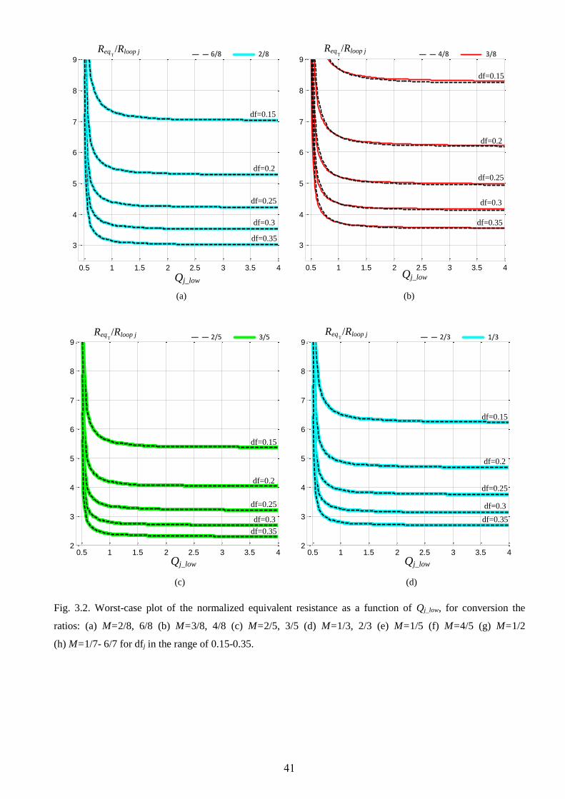
41
0.5 1 1.5 2 2.5 3 3.5 4
3
4
5
6
7
8
92/86/8
Qj_low
ReqT/Rloop j
df=0.2
df=0.35
df=0.3
df=0.25
df=0.15
0.5 1 1.5 2 2.5 3 3.5 4
3
4
5
6
7
8
93/84/8
Qj_low
df=0.2
df=0.35
df=0.3
df=0.25
df=0.15
ReqT/Rloop j
(a) (b)
0.5 1 1.5 2 2.5 3 3.5 42
3
4
5
6
7
8
93/52/5
0.5 1 1.5 2 2.5 3 3.5 42
3
4
5
6
7
8
91/32/3
Qj_lowQj_low
ReqT/Rloop jReq
T/Rloop j
df=0.2
df=0.35
df=0.3
df=0.25
df=0.15
df=0.2
df=0.35
df=0.3
df=0.25
df=0.15
(c) (d)
Fig. 3.2. Worst-case plot of the normalized equivalent resistance as a function of Qj_low, for conversion the
ratios: (a) M=2/8, 6/8 (b) M=3/8, 4/8 (c) M=2/5, 3/5 (d) M=1/3, 2/3 (e) M=1/5 (f) M=4/5 (g) M=1/2
(h) M=1/7- 6/7 for dfj in the range of 0.15-0.35.
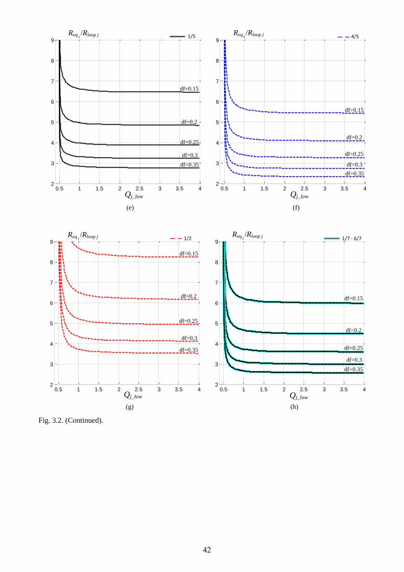
42
0.5 1 1.5 2 2.5 3 3.5 42
3
4
5
6
7
8
91/5
0.5 1 1.5 2 2.5 3 3.5 42
3
4
5
6
7
8
94/5
df=0.2
df=0.35
df=0.3
df=0.25
df=0.15
df=0.2
df=0.35
df=0.3
df=0.25
df=0.15
ReqT/Rloop jReq
T/Rloop j
Qj_lowQj_low
(e) (f)
0.5 1 1.5 2 2.5 3 3.5 42
3
4
5
6
7
8
91/7 - 6/7
Qj_low
ReqT/Rloop j
0.5 1 1.5 2 2.5 3 3.5 42
3
4
5
6
7
8
91/2
df=0.2
df=0.35
df=0.3
df=0.25
df=0.15
ReqT/Rloop j
Qj_low
df=0.2
df=0.35
df=0.3
df=0.25
df=0.15
(g) (h)
Fig. 3.2. (Continued).

43
3.4 Experimental results of the resonant binary/Fibonacci SCC
To validate the proposed design methodology, two experiments were tested at the medium power
range. The first experiment, demonstrated the binary SCC using the stray inductance and with pre-
calibration of the switching timing. The second experiment demonstrated the converter with the active
ZCD system. The design of the active zero detection system and component selection of the power
stage were done according to the guidelines and practical implementation described in Chapters 2 and
3, respectively.
3.4.1 Resonant binary SCC with pre-calibration of the switching timing
The 100 W resonant binary SCC Prototype was realized using the stray inductance in the circuit
alone without adding an additional inductor. The switching frequency was adjusted correspondingly to
the equivalent RCL circuit in every stage [3].
The test parameters of the prototype were Vin=100 V and fS≈53 kHz. The resonant capacitors are two
4.7 µF, 100 V MLCC capacitors C5750X7R2A475K (TDK) connected in parallel. Output capacitors
were ten 4.7 µF, 100 V capacitors connected in parallel with nominal Ro=39 Ω. The bidirectional
switching devices are two 100 V power MOSFETs with ‘on’ resistance around 45 mΩ each.
Microcontroller DsPic33J12GP202 was used for timing the frequency and the duty cycles, respectively.
The calculated stray inductance were approximately Lt1=680 nH, Lt2=358 nH, Lt3=866 nH,
Lt4=484 nH. Taking into account the capacitance change due to the change of the average voltages and
that the total parasitic loop resistance in every state is about 360 mΩ, the quality factors were calculated
to be Q1=1.08, Q2=1.12, Q3=1.68, and Q4=1.05. Furthermore, the frequency ratio df1=0.58, df2=0.32,
df3=0.48 and df4=0.42.
Figures 3.3 through 3.5 show the experimental waveforms of the resonant binary SCC prototype
with the components mentioned above. Figures 3.3 and 3.4 show the current at the output stage for
Vin=80 V and Vin=100 V at M=5/8, respectively, and Figure 3.5 shows for Vin=60 V at M=3/8.
Figure 3.6 shows the efficiency of various input voltages and loads. It is clear from the generic
equivalent circuit model described in Fig. 1.6 that for higher target voltages, the rms current values will
be smaller for a constant Po and the power loss on ReqT will decrease. The calculated values of ReqT
according to equation (1.3) for the 5/8 case were 1.2 Ω while the experimentally evaluated values were
about 1.3 Ω.
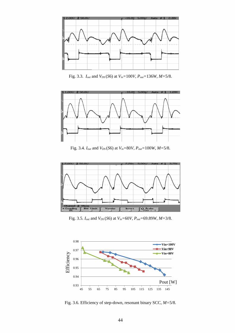
44
Fig. 3.3. Iout and VDS (S6) at Vin=100V, Pout=136W, M=5/8.
Fig. 3.4. Iout and VDS (S6) at Vin=80V, Pout=100W, M=5/8.
Fig. 3.5. Iout and VDS (S6) at Vin=60V, Pout=69.89W, M=3/8.
Fig. 3.6. Efficiency of step-down, resonant binary SCC, M=5/8.
0.93
0.94
0.95
0.96
0.97
0.98
45 55 65 75 85 95 105 115 125 135 145
Eff
icie
ncy
Pout [W]
Vin=100V
Vin=90V
Vin=80V
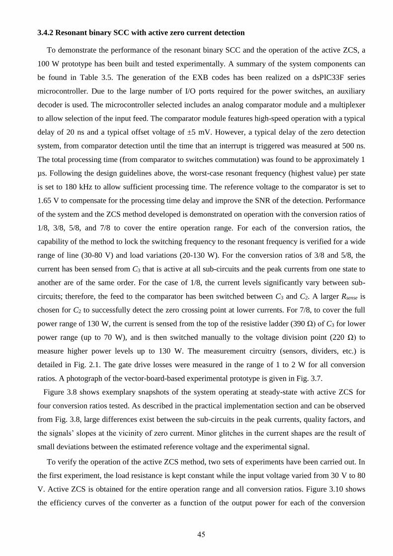
45
3.4.2 Resonant binary SCC with active zero current detection
To demonstrate the performance of the resonant binary SCC and the operation of the active ZCS, a
100 W prototype has been built and tested experimentally. A summary of the system components can
be found in Table 3.5. The generation of the EXB codes has been realized on a dsPIC33F series
microcontroller. Due to the large number of I/O ports required for the power switches, an auxiliary
decoder is used. The microcontroller selected includes an analog comparator module and a multiplexer
to allow selection of the input feed. The comparator module features high-speed operation with a typical
delay of 20 ns and a typical offset voltage of ±5 mV. However, a typical delay of the zero detection
system, from comparator detection until the time that an interrupt is triggered was measured at 500 ns.
The total processing time (from comparator to switches commutation) was found to be approximately 1
µs. Following the design guidelines above, the worst-case resonant frequency (highest value) per state
is set to 180 kHz to allow sufficient processing time. The reference voltage to the comparator is set to
1.65 V to compensate for the processing time delay and improve the SNR of the detection. Performance
of the system and the ZCS method developed is demonstrated on operation with the conversion ratios of
1/8, 3/8, 5/8, and 7/8 to cover the entire operation range. For each of the conversion ratios, the
capability of the method to lock the switching frequency to the resonant frequency is verified for a wide
range of line (30-80 V) and load variations (20-130 W). For the conversion ratios of 3/8 and 5/8, the
current has been sensed from C3 that is active at all sub-circuits and the peak currents from one state to
another are of the same order. For the case of 1/8, the current levels significantly vary between sub-
circuits; therefore, the feed to the comparator has been switched between C3 and C2. A larger Rsense is
chosen for C2 to successfully detect the zero crossing point at lower currents. For 7/8, to cover the full
power range of 130 W, the current is sensed from the top of the resistive ladder (390 Ω) of C3 for lower
power range (up to 70 W), and is then switched manually to the voltage division point (220 Ω) to
measure higher power levels up to 130 W. The measurement circuitry (sensors, dividers, etc.) is
detailed in Fig. 2.1. The gate drive losses were measured in the range of 1 to 2 W for all conversion
ratios. A photograph of the vector-board-based experimental prototype is given in Fig. 3.7.
Figure 3.8 shows exemplary snapshots of the system operating at steady-state with active ZCS for
four conversion ratios tested. As described in the practical implementation section and can be observed
from Fig. 3.8, large differences exist between the sub-circuits in the peak currents, quality factors, and
the signals’ slopes at the vicinity of zero current. Minor glitches in the current shapes are the result of
small deviations between the estimated reference voltage and the experimental signal.
To verify the operation of the active ZCS method, two sets of experiments have been carried out. In
the first experiment, the load resistance is kept constant while the input voltage varied from 30 V to 80
V. Active ZCS is obtained for the entire operation range and all conversion ratios. Figure 3.10 shows
the efficiency curves of the converter as a function of the output power for each of the conversion
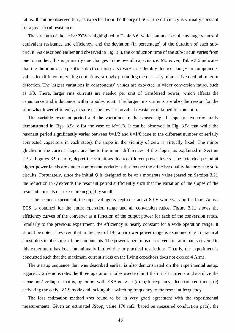
46
ratios. It can be observed that, as expected from the theory of SCC, the efficiency is virtually constant
for a given load resistance.
The strength of the active ZCS is highlighted in Table 3.6, which summarizes the average values of
equivalent resistance and efficiency, and the deviation (in percentage) of the duration of each sub-
circuit. As described earlier and observed in Fig. 3.8, the conduction time of the sub-circuit varies from
one to another; this is primarily due changes in the overall capacitance. Moreover, Table 3.6 indicates
that the duration of a specific sub-circuit may also vary considerably due to changes in components'
values for different operating conditions, strongly promoting the necessity of an active method for zero
detection. The largest variations in components’ values are expected in wider conversion ratios, such
as 1/8. There, larger rms currents are needed per unit of transferred power, which affects the
capacitance and inductance within a sub-circuit. The larger rms currents are also the reason for the
somewhat lower efficiency, in spite of the lower equivalent resistance obtained for this ratio.
The variable resonant period and the variations in the sensed signal slope are experimentally
demonstrated in Figs. 3.9a–c for the case of M=1/8. It can be observed in Fig. 3.9a that while the
resonant period significantly varies between k=1/2 and k=1/8 (due to the different number of serially
connected capacitors in each state), the slope in the vicinity of zero is virtually fixed. The minor
glitches in the current shapes are due to the minor differences of the slopes, as explained in Section
2.3.2. Figures 3.9b and c, depict the variations due to different power levels. The extended period at
higher power levels are due to component variations that reduce the effective quality factor of the sub-
circuits. Fortunately, since the initial Q is designed to be of a moderate value (based on Section 3.2),
the reduction in Q extends the resonant period sufficiently such that the variation of the slopes of the
resonant currents near zero are negligibly small.
In the second experiment, the input voltage is kept constant at 80 V while varying the load. Active
ZCS is obtained for the entire operation range and all conversion ratios. Figure 3.11 shows the
efficiency curves of the converter as a function of the output power for each of the conversion ratios.
Similarly to the previous experiment, the efficiency is nearly constant for a wide operation range. It
should be noted, however, that in the case of 1/8, a narrower power range is examined due to practical
constraints on the stress of the components. The power range for each conversion ratio that is covered in
this experiment has been intentionally limited due to practical restrictions. That is, the experiment is
conducted such that the maximum current stress on the flying capacitors does not exceed 4 Arms.
The startup sequence that was described earlier is also demonstrated on the experimental setup.
Figure 3.12 demonstrates the three operation modes used to limit the inrush currents and stabilize the
capacitors’ voltages, that is, operation with EXB code at: (a) high frequency; (b) estimated times; (c)
activating the active ZCS mode and locking the switching frequency to the resonant frequency.
The loss estimation method was found to be in very good agreement with the experimental
measurements. Given an estimated Rloopj value 170 mΩ (based on measured conduction path), the

47
calculated ReqT , according to equation (3.1) were 0.94 Ω (df ≈ 0.23, ReqT/Rloop ≈ 5.5) and 0.46 Ω (df ≈
0.35, ReqT/Rloop ≈ 2.7) for 3/8 and 1/8, while the measured ReqT were 1 Ω and 0.37 Ω, respectively. It
should be note that the discrepancies are due to the asymmetrical layout of the sub-circuits.
Table 3.5 - Converter Parameters
Component Power Stage
Part No. Value
Input capacitor C5750X7R2A475K 6 x 4.7µF/100V
Output capacitor C5750X7R2A475K 10 x4.7µF/100V
Flying capacitor C5750X7R2A475K 3 x 4.7µF/100V
MOSFETs (RDSon) IPA030N10N3 2 x 3mΩ
Air Inductor Air core 2.1µH
Microcontroller dsPIC33FJ16GS502
Current
Transformer
FXC -TN16/9.3/6.3
(Ferrite toroid) 1:100
Digital Section
Microcontroller dsPIC33FJ16GS502 16bit, 40MIPS
Decoder MC745HC139A
Floating Driver
Driver MIC4427
Pulse Transformer GT03-111-110-A 1:1
Transistor (Q1) JE181
Transistor (Q2) JE170
Diodes (D1, D2) 1N914
Table 3.6 - Measurements with Active ZCS for Constant
4 stΔ[%]
3stΔ[%]
2stΔ[%]
1 stΔ[%]
outIΔ[A]
inVΔ[V] AVη eqTR
[Ω]
Rout
[Ω] M
13.8 23.2 25 28.6 2.37 56.8 0.847 0.37 2.5 1/8
21.5 2.4 2.5 25 1.27 58.6 0.925 1.05 16 3/8
1.4 10 30 1.4 0.74 36.5 0.958 1.01 29.3 5/8
14.3 3.2 25 7.7 0.57 24.1 0.979 0.42 36.5 7/8
Δx – Indicates the amount of variation in a measured variable x value throughout the experiment.
Digital
Controller
Isolated
Gate Drivers
Power Stage
Current
transformers
Power Stage – Bottom side
Flying
capacitors
Fig. 3.7. Prototype of the resonant binary SCC.

48
I_Ls
VI_C3
Vint
VI_C3
I_Ls
VI_C3
Vcmp
VI_C2 St1 St2 St3 St4
(a) (b)
(c) (d)
Vcmp
I_LsI_Ls
Vcmp
Vcmp
Vint Vint
VI_C3
Fig. 3.8. Experimental result of the binary converter operating in active ZCS mode for various conversion ratios.
(a) M=1/8, Vin=80 V, Pout=31.3 W, η=0.85; Traces top to bottom: inductor current ILs (0.8 A/div), rectified
sensed voltage resulting from Ic3,VIc3 (10 V/div), rectified sense voltage resulting from Ic2, VIc2 (10 V/div),
comparator output, Vcmp (5 V/div). Horizontal scale (5 µs/div). (b) M=3/8, Vin=100 V, Pout=76.5 W, η=0.92;
Traces top to bottom: ILs (0.8 A/div); VIc3 (10 V/div); Vcmp (5 V/div); interrupt status Vint (5 V/div). Horizontal
scale (10 µs/div). (c) M=5/8, Vin=80V, Pout=73W, η=0.95. Traces and horizontal scale: as in (b). (d) M=7/8,
Vin=80 V, Pout=131.7 W, η=0.99. Traces top to bottom: ILs (0.4 A/div), VIc3 (5 V/div); Vcmp (5 V/div); Vint (5
V/div). Horizontal scale (5 µs/div).
k4=1/2k3=1/4k2=1/8k1=1/8
(b)
(c)
I_Ls
k1=1/8
k4=1/2
(a)
I_Ls
Fig. 3.9. (a) Slope difference between the highest and the lowest current pulses at fixed output power - 31.3 W,
Io=3.6 A. (b) and (c) Slope differences between pulses at wide output power range, Po=5 W, Io=1.7 A and
Po=31.3 W, Io=3.6 A, respectively.
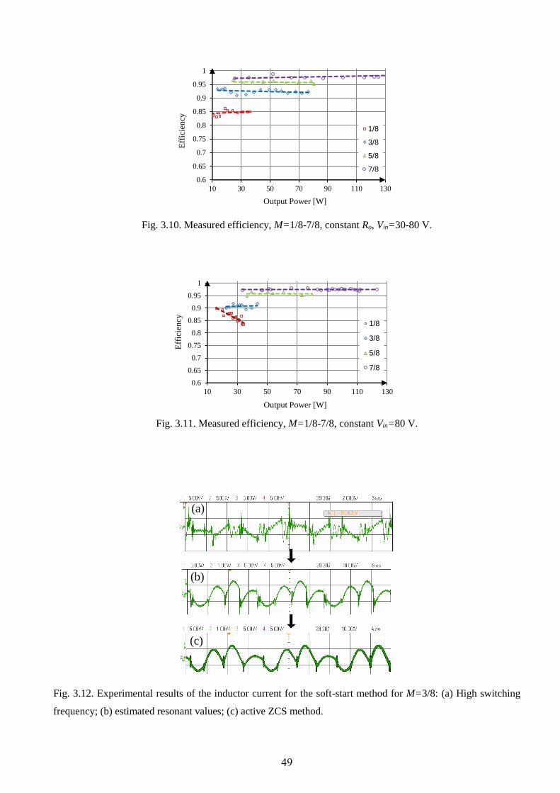
49
Fig. 3.10. Measured efficiency, M=1/8-7/8, constant Ro, Vin=30-80 V.
Fig. 3.11. Measured efficiency, M=1/8-7/8, constant Vin=80 V.
(a)
(b)
(c)
Fig. 3.12. Experimental results of the inductor current for the soft-start method for M=3/8: (a) High switching
frequency; (b) estimated resonant values; (c) active ZCS method.
0.6
0.65
0.7
0.75
0.8
0.85
0.9
0.95
1
10 30 50 70 90 110 130E
ffic
ien
cy
Output Power [W]
1/8
3/8
5/8
7/8
0.6
0.65
0.7
0.75
0.8
0.85
0.9
0.95
1
10 30 50 70 90 110 130
Eff
icie
ncy
Output Power [W]
1/8
3/8
5/8
7/8

50
3.5 Discussion and conclusions
An active ZCS method that allows resonant operation of binary and Fibonacci step-up/down SCC
was developed and tested experimentally. For high-frequency resonant operation, the stray inductances
of the circuit can be used. To lower the frequency of operation, a single air-core inductor in series to
the output stage was added. Consequently, the workload requirements from the digital processor are
eased, and a realization with a simple, low-cost controller is feasible.
The active zero current cross detection was found to accurately adjust the switching times for four
different RCL sub-circuits dictated by the EXB/SFN/SGF codes. The current sensing mechanism was
implemented using three current transformers strategically mounted after the capacitors to avoid
measurement of the output current that includes a dc component.
The experimental validation confirmed that conjecture and highlighted the advantages of an active
method. It revealed that the changes in the resonant period within a sub-circuit are significant and may
vary up to 30% for the operation range tested. It has also been established that although the resonant
periods vary considerably, the slope of the sensed current in the vicinity of the zero crossing point is
less prone to variations. Therefore, for the case of the binary SCC, the method can be further
simplified by fixed reference voltage settings. This eliminates the need for an additional fast
compensation loop to vary the reference voltage.
The experimental results also support the need for a dynamic wide-range reference voltage in order
to compensate for processing delays and different current levels of each sub-circuit. Since a reasonable
SNR is required, the reference to the comparator was kept constant (well above zero) and the reference
was changed by the effective sensing gain. This was done by resistor dividers of the sensed signal and
may be useful for implementation in other resonant switch capacitor topologies.
Study on the efficiency was carried out. It was found that although the calculated [26] equivalent
resistance is the lowest at the ratio of 1/8, that ratio provides the poorest efficiency. Moreover, the
efficiency increases for smaller conversion ratios (larger fractions). This behavior is intuitively
explained by the fact that higher ratios (such as 1/8, 3/8) have higher rms current for a given
transferred power and hence the power losses will be higher. This can be illustrated by rewriting the
well-known RSCC efficiency expression as a function of the output current, i.e., η=Vo/Vin =
(Vo/Io)/(Vo/Io+ReqT). This implies that for a given power level, the load resistance of larger ratios
(smaller fractions), such as 1/8, is significantly smaller; the efficiency is expected to drop per unit of
transferred power. Another observation on the efficiency and the expected equivalent resistance is
made by the current waveforms and from the solution for the average currents for each sub-circuit. It
shows that for some conversion ratios, there might be a sub-circuit in which the current is negative.
This phenomenon can be explained from a charge-balance perspective and is given in Section 2.2.
However, from an efficiency and ReqT point of view, that means that for this particular sub-circuit,

51
current flows from the output into the system, which may affect the estimations of ReqT and the
expected efficiency. A detailed analysis of this topic is beyond the scope of this study.
The method presented in this study has been verified to successfully operate resonant binary SCC
and to accommodate a wide and dynamic operation range, and therefore can be applied to other multi-
phase SCC topologies that involve a number of sub-circuits and a wide operation range.
52
Chapter 4 - Modeling and Analysis of Resonant Switched-Capacitor
Converters with Free-Wheeling ZCS
4.1 Introduction
In resonant switched capacitor converters (RSCC), zero current switching (ZCS) is mandatory to
achieve high power conversion efficiency and reliability. A ZCS can be achieved by employing an
active monitoring and control of the resonant current [2], [39]. This requires a complex control scheme
and circuitry. Alternatively, ZCS can be obtained by unidirectional switches, e.g., inserting a diode in
series to the active switch. In this case, ZCS is assured by simple means at the cost of increased
conduction losses. To overcome the deficiencies of these methods, a simple and efficient self-
commutation concept as illustrated in Fig. 4.1 has been presented in [41], [51], and [52]. It consists of
a transistor that conducts for the majority of the resonant cycle, and a parallel diode that acts as a free-
wheeling element such that turn off occurs at zero current. This method exhibits both advantages of
inherent ZCS and overcomes the deficiencies of previous methods, such as high conduction losses and
complex control hardware. However, due to a divided conduction path (DCP) of the resonant current
(Fig. 4.1), the conventional equivalent resistance method for loss evaluation [26], [27], [53], [54],
cannot be applied directly in this case.
The objective of this part of study is to describe and explore the loss mechanism of resonant SCC
operating in a self-commutation ZCS mode. The new modeling methodology extends the modeling
concept employed in [26], [27], and [53]-[63] to take into account the DCP of a single
charge/discharge state.
The deliverables of this modeling approach are on both theoretical and practical realms; it provides
a streamlined procedure to design a reliable and low-cost soft-switched SCC, as well as an insight into
the dominant contributors of losses in DCP operation mode.
The rest of this part of the work is organized as follows: Section 4.2 details the terminology and
basic definitions to the approach of this study; the modeling methodology is delineated in Section 4.3;
Section 4.4 derives the loss contributors; Section 4.5 provides a rigorous validation of the modeling
concept; and finally, the chapter is concluded in Section 4.6.
4.2 Basic terminology and definitions
Throughout the study, the modeling concept will be explained on a unity gain resonant SCC (Fig.
4.2). Even though the exemplary circuit is not the best candidate to showcase the strength of ZCS, it
highlights the mechanism of the DCP operation and was therefore selected.
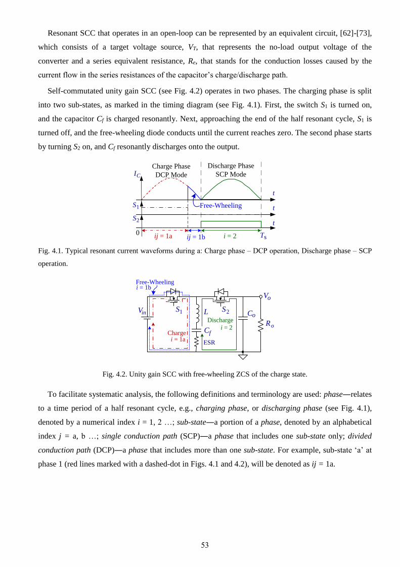
53
Resonant SCC that operates in an open-loop can be represented by an equivalent circuit, [62]-[73],
which consists of a target voltage source, VT, that represents the no-load output voltage of the
converter and a series equivalent resistance, Re, that stands for the conduction losses caused by the
current flow in the series resistances of the capacitor’s charge/discharge path.
Self-commutated unity gain SCC (see Fig. 4.2) operates in two phases. The charging phase is split
into two sub-states, as marked in the timing diagram (see Fig. 4.1). First, the switch S1 is turned on,
and the capacitor Cf is charged resonantly. Next, approaching the end of the half resonant cycle, S1 is
turned off, and the free-wheeling diode conducts until the current reaches zero. The second phase starts
by turning S2 on, and Cf resonantly discharges onto the output.
t
IC
t
t
0
S1
S2
Charge Phase
DCP Mode
Discharge Phase
SCP Mode
ij = 1a ij = 1b i = 2
Free-Wheeling
Ts
Fig. 4.1. Typical resonant current waveforms during a: Charge phase ‒ DCP operation, Discharge phase – SCP
operation.
Co
ESR
S2
Ro
Vin
Cf
Vo
Charge
Discharge
i = 2
i = 1a
L
Free-Wheeling
S1
i = 1b
Fig. 4.2. Unity gain SCC with free-wheeling ZCS of the charge state.
To facilitate systematic analysis, the following definitions and terminology are used: phase―relates
to a time period of a half resonant cycle, e.g., charging phase, or discharging phase (see Fig. 4.1),
denoted by a numerical index i = 1, 2 …; sub-state―a portion of a phase, denoted by an alphabetical
index j = a, b …; single conduction path (SCP)―a phase that includes one sub-state only; divided
conduction path (DCP)―a phase that includes more than one sub-state. For example, sub-state ‘a’ at
phase 1 (red lines marked with a dashed-dot in Figs. 4.1 and 4.2), will be denoted as ij = 1a.

54
4.3 Modeling approach
The generic approach to extract the equivalent model of resonant SCC operating in the particular
case of SCP has been presented in [26], [27], [53] and [54]. Generalization of the model to include
DCP operation requires the following steps: first, based on the switching sequence applied to the SCC,
each phase is described by one or more sub-states according to the operation mode (SCP or DCP).
Given the example on hand, the operation of SCC in Fig. 4.2 is represented by three sub-circuits, that
is, a charging sub-state by the transistor conduction (see Fig. 4.3a), a charging sub-state by the free-
wheeling diode (see Fig. 4.3b), and a discharge phase (see Fig. 4.3c).
Co
ESR
Ro
Vin
(a)
Cf
Vo
LS1 Co
ESR
Ro
Vin
Cf
Vo
LS1
Co
ESR
S2
RoCf
Vo
L
(b) (c)
Fig. 4.3. Operation states of unity gain SCC (Fig. 4.2): (a) Charging sub-state ij = 1a, (b) Charging sub-state ij =
1b, (c) Discharging state i = 2.
Second, each of the sub-circuits is simplified to a lumped RLC circuit as shown in Fig. 4.4. This
circuit is used to describe the operation of each sub-circuit in its relevant conduction time, where Vi is
the initial voltage difference between the charging/discharging source and the resonant tank voltage,
Rij is the total loop resistance (switch resistance RSi, inductor resistance RLi, and capacitor ESR), Ci and
Li are the total capacitance and inductance of the loop, respectively.
Si RijCi
ΔVi
i(t)Li
Fig. 4.4. The basic and generic instantaneous RLC sub-circuit.
The next step applies the calculation of the power loss, Pij, due to the series resistances Rij of each
sub-state, and expressing it as a function of the average capacitor current Iavi. The average capacitor
current of each phase is linearly proportional to the average output current [27], [68], [69]. By doing
so, the power dissipated in each phase is referenced to the output current, using the proportionality
factor ki. The equivalent resistances of each sub-state, Reij, are then extracted from the dissipated
power, Pij. It should be noted that by addressing the model calculation from the average current
domain, the calculation of Vi which primarily depends on the capacitors value and the operating
frequency, is eliminated [26], [27], [53].
The general case of DCP applies a free-wheeling mode realized by diode conduction. Since the
dominant loss contributor of the diode is the average current, an additional proportionality factor is
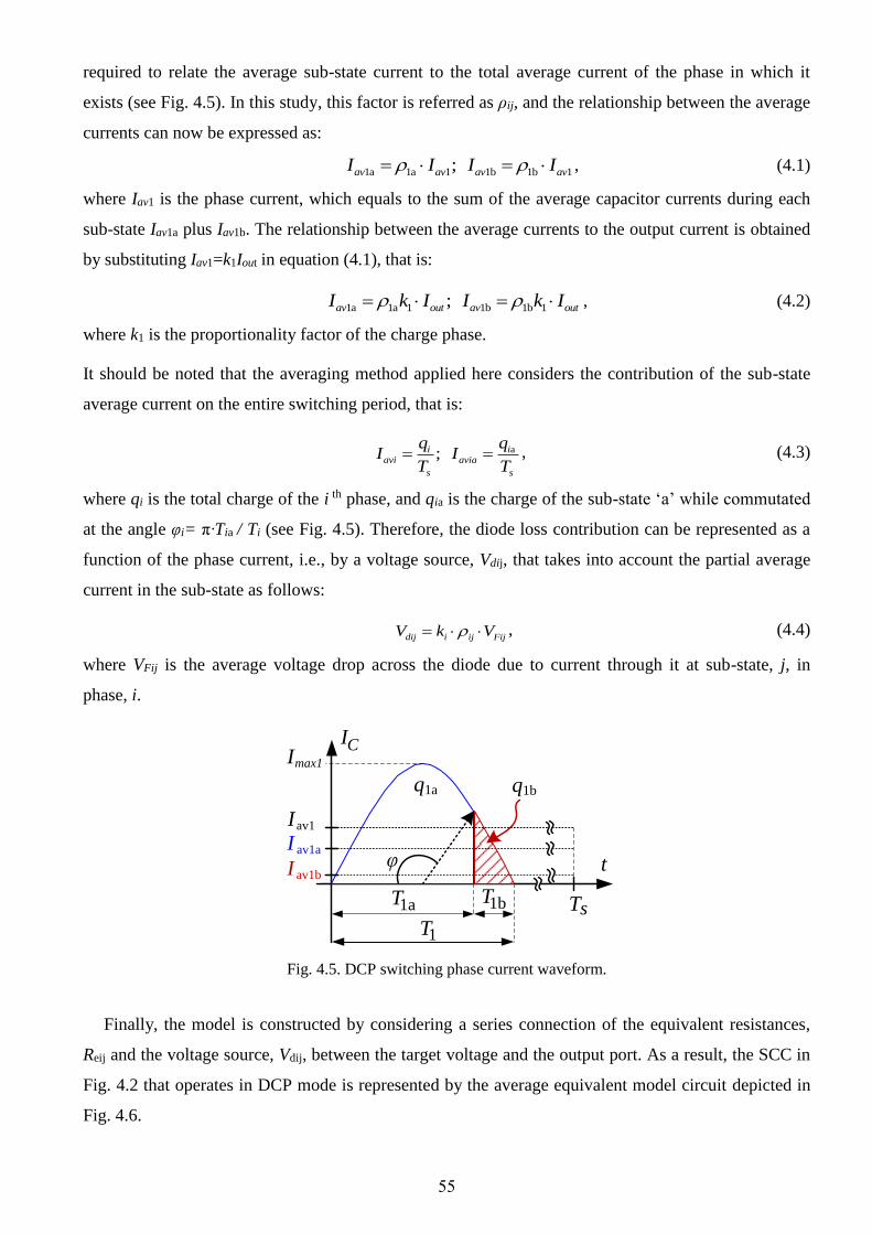
55
required to relate the average sub-state current to the total average current of the phase in which it
exists (see Fig. 4.5). In this study, this factor is referred as ρij, and the relationship between the average
currents can now be expressed as:
1a 1a 1 1b 1b 1; av av av avI I I I , (4.1)
where Iav1 is the phase current, which equals to the sum of the average capacitor currents during each
sub-state Iav1a plus Iav1b. The relationship between the average currents to the output current is obtained
by substituting Iav1=k1Iout in equation (4.1), that is:
1a 1a 1 1b 1b 1; av out av outI k I I k I , (4.2)
where k1 is the proportionality factor of the charge phase.
It should be noted that the averaging method applied here considers the contribution of the sub-state
average current on the entire switching period, that is:
a; i iavi avia
s s
q qI I
T T , (4.3)
where qi is the total charge of the i th phase, and qia is the charge of the sub-state ‘a’ while commutated
at the angle φi= π∙Tia / Ti (see Fig. 4.5). Therefore, the diode loss contribution can be represented as a
function of the phase current, i.e., by a voltage source, Vdij, that takes into account the partial average
current in the sub-state as follows:
dij i ij FijV k V , (4.4)
where VFij is the average voltage drop across the diode due to current through it at sub-state, j, in
phase, i.
t
q1a q1b
T1a T1b
T1
sT
φ
Imax1
I av1a
I av1b
Iav1
I C
Fig. 4.5. DCP switching phase current waveform.
Finally, the model is constructed by considering a series connection of the equivalent resistances,
Reij and the voltage source, Vdij, between the target voltage and the output port. As a result, the SCC in
Fig. 4.2 that operates in DCP mode is represented by the average equivalent model circuit depicted in
Fig. 4.6.

56
Io
VTCo Ro
VoRe1a Re2
ReRe1b
Charge Phase
DCP Mode
Vd1b
SCC
Discharge Phase
SCP Mode
Fig. 4.6. SCC generic average equivalent circuit that shows the contribution of the partial sub-circuits equivalent
resistances Rei to the total equivalent circuit resistance Re. For the unity gain SCC example of Fig. 4.2, Re1a is the
loss contribution of charge sub-state 1a, Re1b and Vd1b are the resistive and diode loss contribution of the free-
wheeling sub-state, respectively, Re2 is the loss contribution of discharging phase.
4.4 Extraction of equivalent resistances and equivalent average voltage drop
Following the modeling methodology described earlier, the equivalent resistance value is extracted
in this section. It is assumed that each RLC sub-state (Fig. 4.4) operates under ZCS conditions, and the
quality factor, Qij, is sufficiently high (Qij>5).
The peak currents, Ipkij of the sub-states are considered equal to the charge phase peak current Ipki.
For the case of the circuit in Fig. 4.2, this applies the following:
a bpki pki pkiI I I , (4.5)
where Ipki , Ipkia, and Ipkib, are the potential peak currents that are or could be developed given the
conditions of the switching phase i, or the sub-state j, ia and ib, respectively.
4.4.1 Equivalent resistance calculation
The energy, Eia, dissipated in the sub-circuit due to the loop resistance, Ria (Fig. 4.4) and the current
during the time interval Tia (Fig. 4.5) is derived by integrating the instantaneous power p(t) = iC 2(t)∙Ria
(iC(t) is the capacitor current) over the sub-state time interval, Tia:
0 a
2 22
a a 0 a a
0 a0
cos sinsin
2
i i
i i i
i i pki i i pki
i
E R I t dt R I
,
(4.6)
where ω0ia = 2f0ia is the natural resonance frequency of the phase i, sub-state ‘a’. The relationship
between the peak current and the average current of phase, i, can be expressed as:
(2 / ) (2 df )pki avi iI I , (4.7)
where dfi = fs / f0i is the ratio between the switching frequency and the natural frequency of the resonant
network [27].
Substituting expressions (4.2) and (4.7) into expression (4.6), and after some manipulations, the
power loss of the sub-state can be expressed as a function of the average output current, Io by:
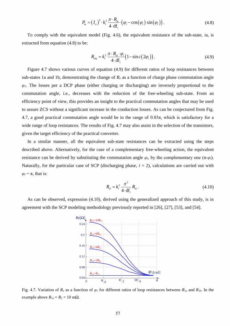
57
2 2 a
a cos sin4 df
ii o i i i i
i
RP I k
. (4.8)
To comply with the equivalent model (Fig. 4.6), the equivalent resistance of the sub-state, ia, is
extracted from equation (4.8) to be:
2 aa 1 sin 2
4 dfi i
ei i i
i
RR k c
. (4.9)
Figure 4.7 shows various curves of equation (4.9) for different ratios of loop resistances between
sub-states 1a and 1b, demonstrating the change of Re as a function of charge phase commutation angle
φ1. The losses per a DCP phase (either charging or discharging) are inversely proportional to the
commutation angle, i.e., decreases with the reduction of the free-wheeling sub-state. From an
efficiency point of view, this provides an insight to the practical commutation angles that may be used
to assure ZCS without a significant increase in the conduction losses. As can be conjectured from Fig.
4.7, a good practical commutation angle would be in the range of 0.85π, which is satisfactory for a
wide range of loop resistances. The results of Fig. 4.7 may also assist in the selection of the transistors,
given the target efficiency of the practical converter.
In a similar manner, all the equivalent sub-state resistances can be extracted using the steps
described above. Alternatively, for the case of a complementary free-wheeling action, the equivalent
resistance can be derived by substituting the commutation angle φi, by the complementary one (π-φi).
Naturally, for the particular case of SCP (discharging phase, i = 2), calculations are carried out with
φi = π, that is:
22
a4 df
ei i i
i
R k R
. (4.10)
As can be observed, expression (4.10), derived using the generalized approach of this study, is in
agreement with the SCP modeling methodology previously reported in [26], [27], [53], and [54].
0.04
0.08
0.12
0.16
0.2
0.24
0 2π
4π π43π
φ1[rad]
Re[Ω]
R1b=R1a
R1b=2R1a
R1b=10R1a
R1b=6R1a
R1b=4R1a
Fig. 4.7. Variation of Re as a function of φ1 for different ratios of loop resistances between R1a and R1b. In the
example above R1a = R2 = 10 mΩ.
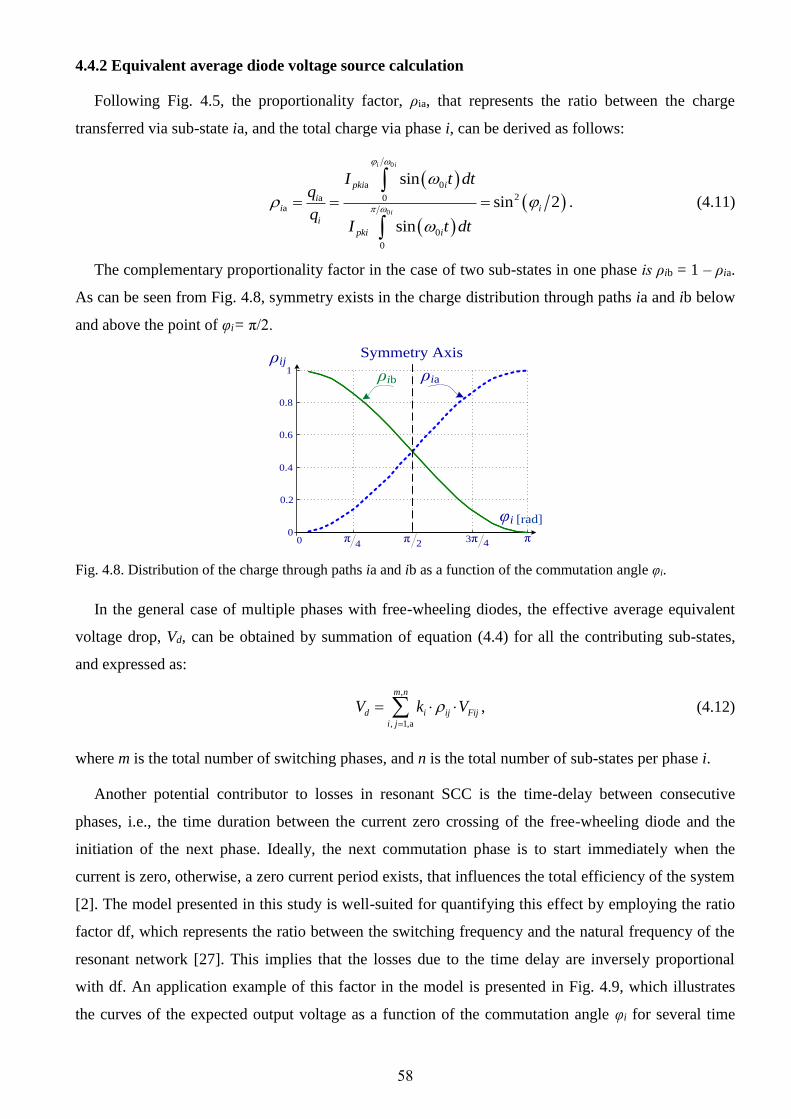
58
4.4.2 Equivalent average diode voltage source calculation
Following Fig. 4.5, the proportionality factor, ρia, that represents the ratio between the charge
transferred via sub-state ia, and the total charge via phase i, can be derived as follows:
0
0
a 0
2a 0a
0
0
sin
sin 2
sin
i i
i
pki i
ii i
i
pki i
I t dtq
qI t dt
. (4.11)
The complementary proportionality factor in the case of two sub-states in one phase is ρib = 1 – ρia.
As can be seen from Fig. 4.8, symmetry exists in the charge distribution through paths ia and ib below
and above the point of φi= π/2.
0
0.2
0.4
0.6
0.8
1
0 2π
4π π
43π
ρij
φi [rad]
ρib ρia
Symmetry Axis
Fig. 4.8. Distribution of the charge through paths ia and ib as a function of the commutation angle φi.
In the general case of multiple phases with free-wheeling diodes, the effective average equivalent
voltage drop, Vd, can be obtained by summation of equation (4.4) for all the contributing sub-states,
and expressed as:
,
, 1,a
m n
d i ij Fij
i j
V k V
, (4.12)
where m is the total number of switching phases, and n is the total number of sub-states per phase i.
Another potential contributor to losses in resonant SCC is the time-delay between consecutive
phases, i.e., the time duration between the current zero crossing of the free-wheeling diode and the
initiation of the next phase. Ideally, the next commutation phase is to start immediately when the
current is zero, otherwise, a zero current period exists, that influences the total efficiency of the system
[2]. The model presented in this study is well-suited for quantifying this effect by employing the ratio
factor df, which represents the ratio between the switching frequency and the natural frequency of the
resonant network [27]. This implies that the losses due to the time delay are inversely proportional
with df. An application example of this factor in the model is presented in Fig. 4.9, which illustrates
the curves of the expected output voltage as a function of the commutation angle φi for several time
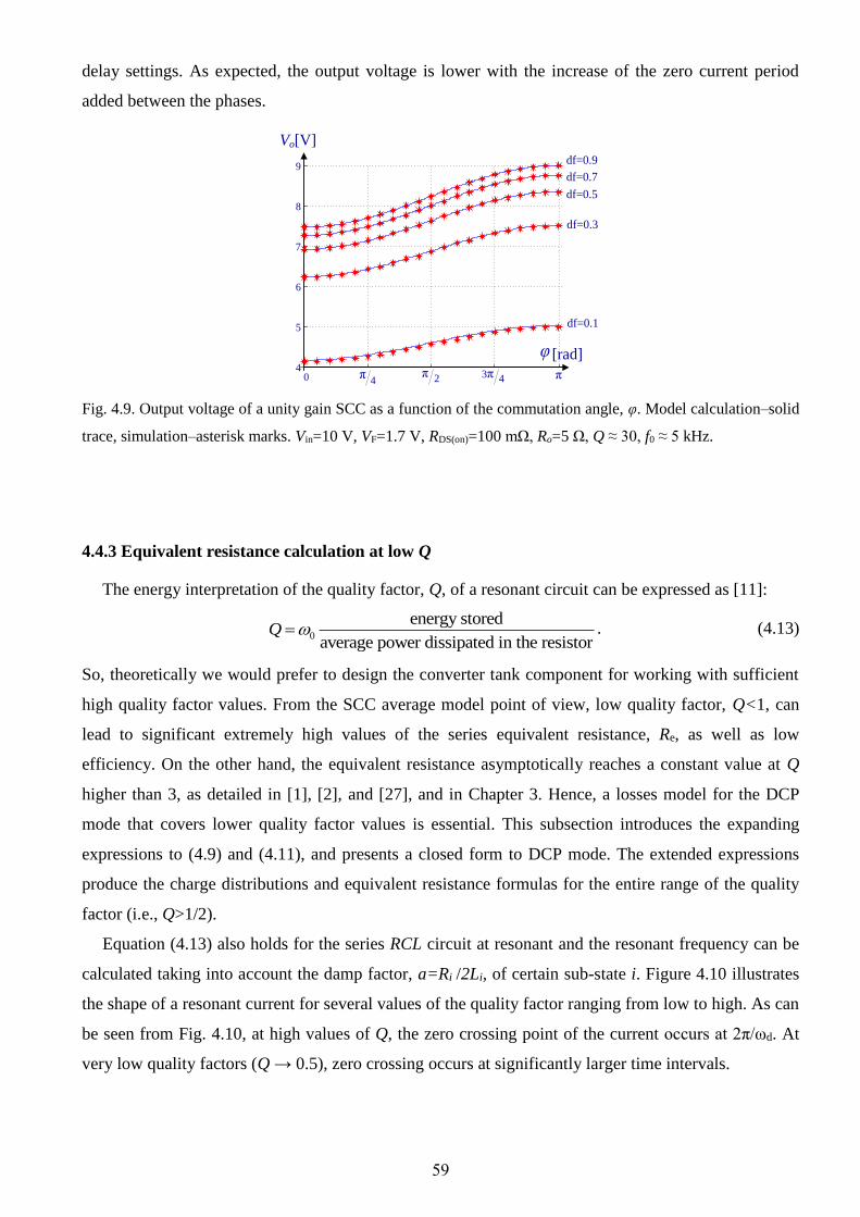
59
delay settings. As expected, the output voltage is lower with the increase of the zero current period
added between the phases.
4
5
6
7
8
9
[rad]φ
Vo[V]
0 2π
4π π43π
df=0.1
df=0.3
df=0.5
df=0.7
df=0.9
Fig. 4.9. Output voltage of a unity gain SCC as a function of the commutation angle, φ. Model calculation–solid
trace, simulation–asterisk marks. Vin=10 V, VF=1.7 V, RDS(on)=100 mΩ, Ro=5 Ω, Q ≈ 30, f0 ≈ 5 kHz.
4.4.3 Equivalent resistance calculation at low Q
The energy interpretation of the quality factor, Q, of a resonant circuit can be expressed as [11]:
0
energy stored
average power dissipated in the resistorQ . (4.13)
So, theoretically we would prefer to design the converter tank component for working with sufficient
high quality factor values. From the SCC average model point of view, low quality factor, Q<1, can
lead to significant extremely high values of the series equivalent resistance, Re, as well as low
efficiency. On the other hand, the equivalent resistance asymptotically reaches a constant value at Q
higher than 3, as detailed in [1], [2], and [27], and in Chapter 3. Hence, a losses model for the DCP
mode that covers lower quality factor values is essential. This subsection introduces the expanding
expressions to (4.9) and (4.11), and presents a closed form to DCP mode. The extended expressions
produce the charge distributions and equivalent resistance formulas for the entire range of the quality
factor (i.e., Q>1/2).
Equation (4.13) also holds for the series RCL circuit at resonant and the resonant frequency can be
calculated taking into account the damp factor, a=Ri /2Li, of certain sub-state i. Figure 4.10 illustrates
the shape of a resonant current for several values of the quality factor ranging from low to high. As can
be seen from Fig. 4.10, at high values of Q, the zero crossing point of the current occurs at 2π/ωd. At
very low quality factors (Q → 0.5), zero crossing occurs at significantly larger time intervals.
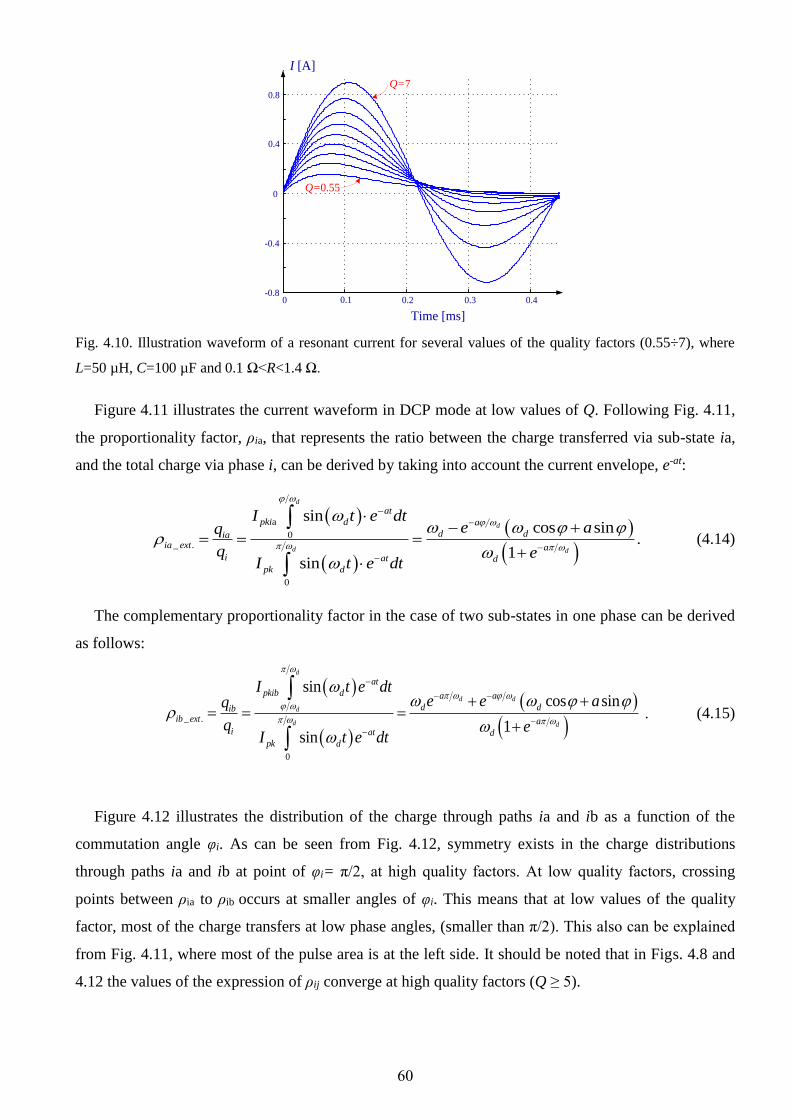
60
0 0.1 0.2 0.3 0.4-0.8
-0.4
0
0.4
0.8
Q=7
Q=0.55
Time [ms]
I [A]
Fig. 4.10. Illustration waveform of a resonant current for several values of the quality factors (0.55÷7), where
L=50 µH, C=100 µF and 0.1 Ω<R<1.4 Ω.
Figure 4.11 illustrates the current waveform in DCP mode at low values of Q. Following Fig. 4.11,
the proportionality factor, ρia, that represents the ratio between the charge transferred via sub-state ia,
and the total charge via phase i, can be derived by taking into account the current envelope, e-at:
_ .
a
0
0
sincos sin
1sin
d
d
d
d
at
d
d diaia ext a
i at d
pki a
dpk
t e dtIe aq
q et e dtI
. (4.14)
The complementary proportionality factor in the case of two sub-states in one phase can be derived
as follows:
_ .
0
sincos sin
1sin
d
d d
d
d d
at
d a
d dibib ext a
i at
pkib a
pkd
d
t e dte e aq
q
I
et e dI t
. (4.15)
Figure 4.12 illustrates the distribution of the charge through paths ia and ib as a function of the
commutation angle φi. As can be seen from Fig. 4.12, symmetry exists in the charge distributions
through paths ia and ib at point of φi= π/2, at high quality factors. At low quality factors, crossing
points between ρia to ρib occurs at smaller angles of φi. This means that at low values of the quality
factor, most of the charge transfers at low phase angles, (smaller than π/2). This also can be explained
from Fig. 4.11, where most of the pulse area is at the left side. It should be noted that in Figs. 4.8 and
4.12 the values of the expression of ρij converge at high quality factors (Q ≥ 5).
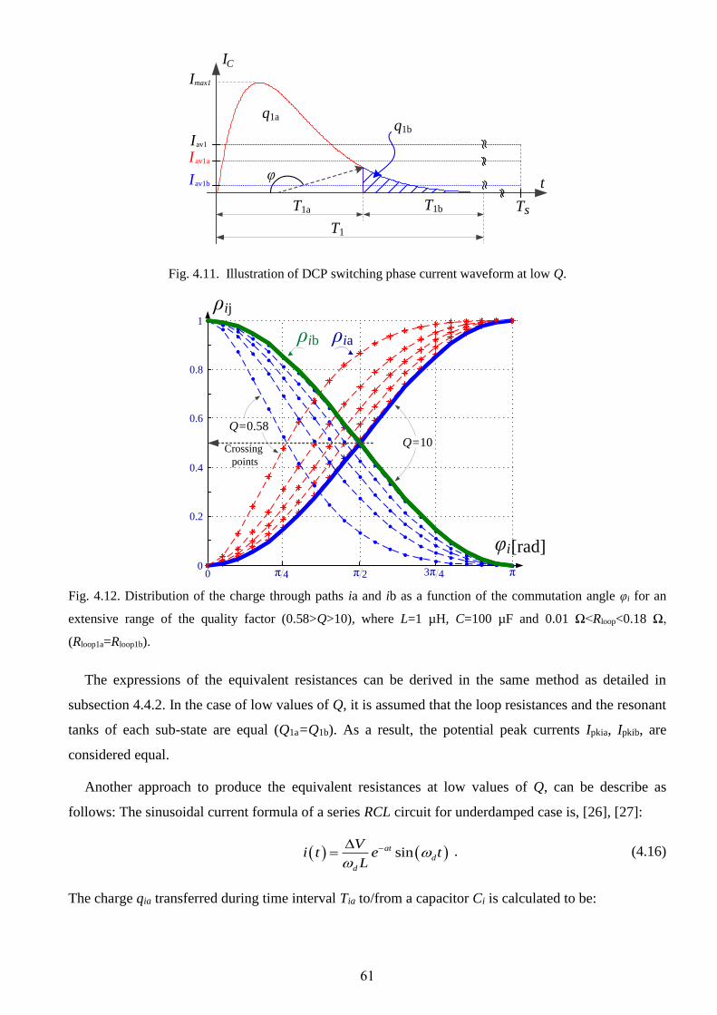
61
t
T1a T1b
T1
I C
q1b
q1a
φ
Imax1
I av1a
Iav1b
Iav1
Ts
Fig. 4.11. Illustration of DCP switching phase current waveform at low Q.
0
0.2
0.4
0.6
0.8
1
Crossing
points
φi
Q=10
ρib ρia
Q=0.58
[rad]
ρij
0 2π4π π43π
Fig. 4.12. Distribution of the charge through paths ia and ib as a function of the commutation angle φi for an
extensive range of the quality factor (0.58>Q>10), where L=1 µH, C=100 µF and 0.01 Ω<Rloop<0.18 Ω,
(Rloop1a=Rloop1b).
The expressions of the equivalent resistances can be derived in the same method as detailed in
subsection 4.4.2. In the case of low values of Q, it is assumed that the loop resistances and the resonant
tanks of each sub-state are equal (Q1a=Q1b). As a result, the potential peak currents Ipkia, Ipkib, are
considered equal.
Another approach to produce the equivalent resistances at low values of Q, can be describe as
follows: The sinusoidal current formula of a series RCL circuit for underdamped case is, [26], [27]:
sinat
d
d
Vi t e t
L
. (4.16)
The charge qia transferred during time interval Tia to/from a capacitor Ci is calculated to be:

62
2
0 0
sin cos sind d
daat
ia d d d
d d o
V Vq i dt e t dt e a
L L
. (4.17)
Hence from equation (4.17), we obtain:
( )
cos sind
d av ia
a
s d d
IV
f C e a
, (4.18)
where the average capacitor current, I(av)ia, is obtain from:
( )ia av ia sq I f . (4.19)
The energy loss, Eia, dissipated in the sub-state ‘a’ at DCP mode calculated to be:
2
2
a
0 0
2 22 2 2 2
2 2 2
2 22 2 22
sin
1 cos 2 sin 2
4
1 cos 2 sin 2
2
d d
d d
d d
at
i d
d
a a
d d
d o
a a
d d
d
VE i Rdt e t R dt
L
V Re a e a a
aL
e a e a aV C
2
.
(4.20)
Substituting (4.18) into (4.20) yields:
2 22 2 2
2
( ) 22
1 cos 2 sin 2
2 cos sin
d d
d
a a
d d
ia av iaa
s d d
e a e a aE I
f C e a
. (4.21)
The power loss, Pia, dissipated in the sub-state ‘a’ can be calculated from the energy loss by
multiplying it by fs. Once the power loss, Pia, is obtained, it can be directly used to express the
equivalent resistance, Reia, taking into account the relative proportionality factor (i.e., Iavi=ki ∙ ρia ∙Iout).
Hence, the equivalent resistance of the sub-state ia, can be express as:
2
2
2 2 2 2
_
1 cos 2 i
2 1
s n 2i d
d
i da a
d i d ii
eia ea
x
d
t
d
e e a a akR
ef C
. (4.22)
Similarly, the equivalent resistance of the sub-state ‘b’, can be derived by solving the charge and
energy loss integrals, (qib, Eib), in the interval of φ/ωd to π/ωd. So, the equivalent resistance of the sub-
state ib, can be expressed as:
2 22 2 2 22
_ 2
cos 2 sin 2
2 1
i d
d
da a
d i d i die b ex
dd
i ta
e a a akR
C e
e
f
. (4.23)
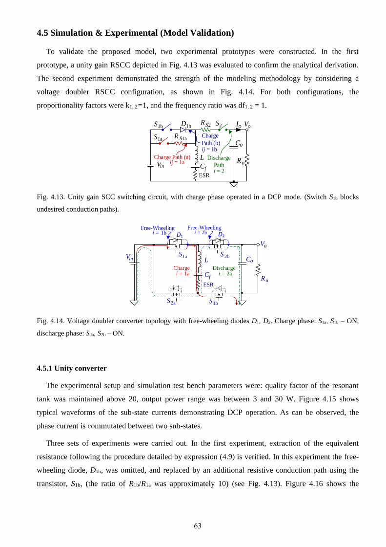
63
4.5 Simulation & Experimental (Model Validation)
To validate the proposed model, two experimental prototypes were constructed. In the first
prototype, a unity gain RSCC depicted in Fig. 4.13 was evaluated to confirm the analytical derivation.
The second experiment demonstrated the strength of the modeling methodology by considering a
voltage doubler RSCC configuration, as shown in Fig. 4.14. For both configurations, the
proportionality factors were k1, 2=1, and the frequency ratio was df1, 2 = 1.
Co
ESR
S1a
S2
RoVin
RS2 Io
Cf
Vo
Charge Path (a) Discharge
Pathi = 2
ij = 1aL
S1b
R S1aCharge
Path (b)ij = 1b
D1b
Fig. 4.13. Unity gain SCC switching circuit, with charge phase operated in a DCP mode. (Switch S1b blocks
undesired conduction paths).
Chargei = 1a
Dischargei = 2a
Co
ESR
S2b
Ro
Vin
Cf
Vo
LS1a
S1bS2a
D1 D2
Free-Wheelingi = 1b
Free-Wheelingi = 2b
Fig. 4.14. Voltage doubler converter topology with free-wheeling diodes D1, D2. Charge phase: S1a, S1b – ON,
discharge phase: S2a, S2b ‒ ON.
4.5.1 Unity converter
The experimental setup and simulation test bench parameters were: quality factor of the resonant
tank was maintained above 20, output power range was between 3 and 30 W. Figure 4.15 shows
typical waveforms of the sub-state currents demonstrating DCP operation. As can be observed, the
phase current is commutated between two sub-states.
Three sets of experiments were carried out. In the first experiment, extraction of the equivalent
resistance following the procedure detailed by expression (4.9) is verified. In this experiment the free-
wheeling diode, D1b, was omitted, and replaced by an additional resistive conduction path using the
transistor, S1b, (the ratio of R1b/R1a was approximately 10) (see Fig. 4.13). Figure 4.16 shows the
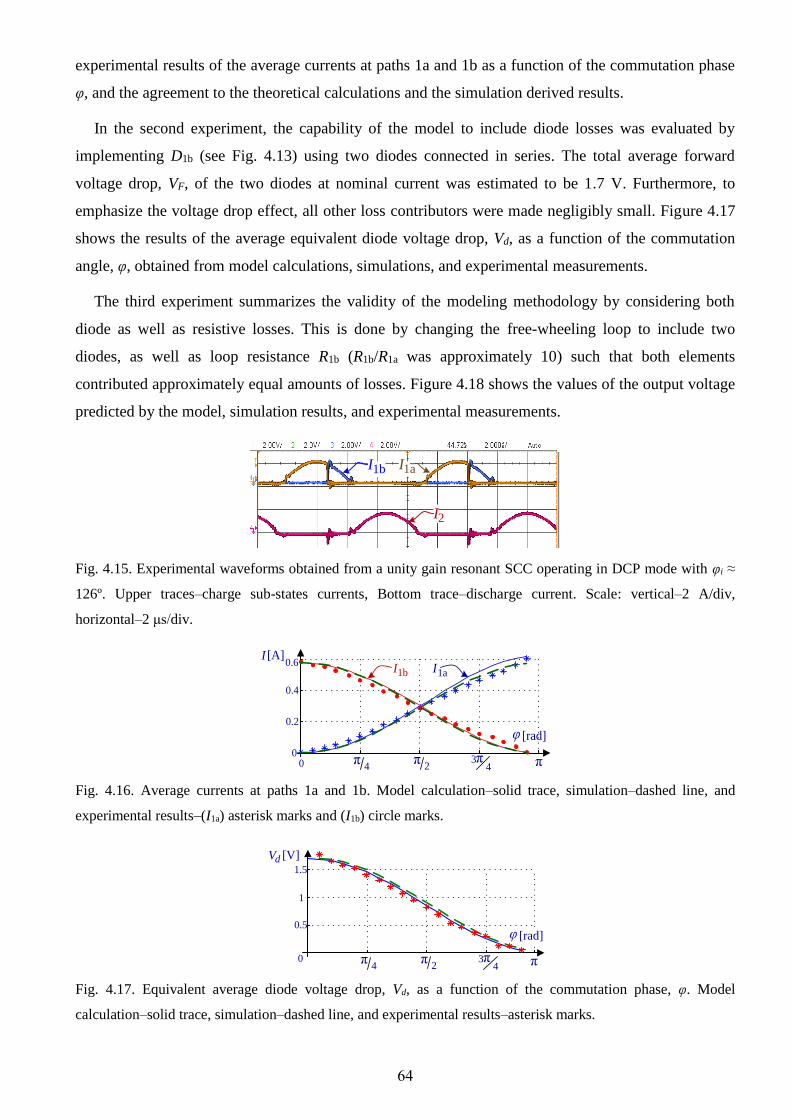
64
experimental results of the average currents at paths 1a and 1b as a function of the commutation phase
φ, and the agreement to the theoretical calculations and the simulation derived results.
In the second experiment, the capability of the model to include diode losses was evaluated by
implementing D1b (see Fig. 4.13) using two diodes connected in series. The total average forward
voltage drop, VF, of the two diodes at nominal current was estimated to be 1.7 V. Furthermore, to
emphasize the voltage drop effect, all other loss contributors were made negligibly small. Figure 4.17
shows the results of the average equivalent diode voltage drop, Vd, as a function of the commutation
angle, φ, obtained from model calculations, simulations, and experimental measurements.
The third experiment summarizes the validity of the modeling methodology by considering both
diode as well as resistive losses. This is done by changing the free-wheeling loop to include two
diodes, as well as loop resistance R1b (R1b/R1a was approximately 10) such that both elements
contributed approximately equal amounts of losses. Figure 4.18 shows the values of the output voltage
predicted by the model, simulation results, and experimental measurements.
1bI 1aI
2I
Fig. 4.15. Experimental waveforms obtained from a unity gain resonant SCC operating in DCP mode with φi ≈
126º. Upper traces–charge sub-states currents, Bottom trace–discharge current. Scale: vertical–2 A/div,
horizontal‒2 μs/div.
0
0.2
0.4
0.6
2
π4
π π4π3
φ [rad]
0
I1b I1a
I [A]
Fig. 4.16. Average currents at paths 1a and 1b. Model calculation–solid trace, simulation–dashed line, and
experimental results–(I1a) asterisk marks and (I1b) circle marks.
0
0.5
1
1.5
2π
4π π4
π3
φ [rad]
Vd [V]
Fig. 4.17. Equivalent average diode voltage drop, Vd, as a function of the commutation phase, φ. Model
calculation–solid trace, simulation–dashed line, and experimental results–asterisk marks.
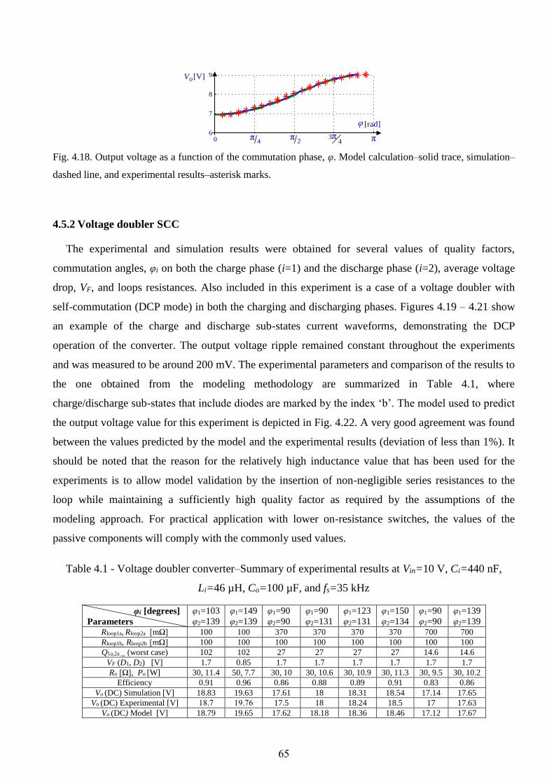
65
0
7
8
9
2
π4
π π4π3
φ [rad]6
Vo[V]
Fig. 4.18. Output voltage as a function of the commutation phase, φ. Model calculation–solid trace, simulation–
dashed line, and experimental results–asterisk marks.
4.5.2 Voltage doubler SCC
The experimental and simulation results were obtained for several values of quality factors,
commutation angles, φi on both the charge phase (i=1) and the discharge phase (i=2), average voltage
drop, VF, and loops resistances. Also included in this experiment is a case of a voltage doubler with
self-commutation (DCP mode) in both the charging and discharging phases. Figures 4.19 – 4.21 show
an example of the charge and discharge sub-states current waveforms, demonstrating the DCP
operation of the converter. The output voltage ripple remained constant throughout the experiments
and was measured to be around 200 mV. The experimental parameters and comparison of the results to
the one obtained from the modeling methodology are summarized in Table 4.1, where
charge/discharge sub-states that include diodes are marked by the index ‘b’. The model used to predict
the output voltage value for this experiment is depicted in Fig. 4.22. A very good agreement was found
between the values predicted by the model and the experimental results (deviation of less than 1%). It
should be noted that the reason for the relatively high inductance value that has been used for the
experiments is to allow model validation by the insertion of non-negligible series resistances to the
loop while maintaining a sufficiently high quality factor as required by the assumptions of the
modeling approach. For practical application with lower on-resistance switches, the values of the
passive components will comply with the commonly used values.
Table 4.1 - Voltage doubler converter–Summary of experimental results at Vin=10 V, Ci=440 nF,
Li=46 µH, Co=100 µF, and fs=35 kHz
φi [degrees] Parameters
φ1=103
φ2=139 φ1=149
φ2=139 φ1=90
φ2=90 φ1=90
φ2=131 φ1=123
φ2=131 φ1=150
φ2=134 φ1=90
φ2=90 φ1=139
φ2=139 Rloop1a, Rloop2a [mΩ] 100 100 370 370 370 370 700 700
Rloop1b, Rloop2b [mΩ] 100 100 100 100 100 100 100 100
Q1a,2a _ (worst case) 102 102 27 27 27 27 14.6 14.6
VF (D1, D2) [V] 1.7 0.85 1.7 1.7 1.7 1.7 1.7 1.7
Ro [Ω], Po [W] 30, 11.4 50, 7.7 30, 10 30, 10.6 30, 10.9 30, 11.3 30, 9.5 30, 10.2
Efficiency 0.91 0.96 0.86 0.88 0.89 0.91 0.83 0.86
Vo (DC) Simulation [V] 18.83 19.63 17.61 18 18.31 18.54 17.14 17.65
Vo (DC) Experimental [V] 3..7 37.71 17.5 18 18.24 18.5 17 17.63
Vo (DC) Model [V] 18.79 19.65 17.62 18.18 18.36 18.46 17.12 17.67

66
I_S1aID1
I_S2b ID2
Fig. 4.19. Experimental waveforms obtained from a double gain resonant SCC operating in DCP mode with
φ1≈96ᵒ, φ2≈139ᵒ, Vin=10 V, Rloop1a,2a=370 mΩ, Rloop1b,2b=100 mΩ, VF1,2=1.7 V, Pout=10.6 W, Upper traces–charge
sub-states currents, bottom trace–discharge sub-states currents. Scale: vertical–2 A/div, horizontal–5 μs/div.
I_S1aID1
I_S2b ID2
Fig. 4.20. Experimental waveforms obtained from a double gain resonant SCC operating in DCP mode with
φ1=φ2≈139ᵒ, Vin=10 V, Rloop1a,2a=370 mΩ, Rloop1b,2b=100 mΩ, VF1,2=1.7 V, Pout=11.13 W. Upper traces–charge
sub-states currents, bottom trace–discharge sub-states currents. Scale: vertical–2 A/div, horizontal–5 μs/div.
I_S1aID1
I_S2b ID2
Fig. 4.21. Experimental waveforms obtained from a double gain resonant SCC operating in DCP mode with
φ1≈148ᵒ, φ2≈139ᵒ, Vin=10 V, Rloop1a,2a=370 mΩ, Rloop1b,2b=100 mΩ, VF1,2=1.7 V, Pout=11.3 W. Upper traces–
charge sub-states currents, bottom trace–discharge sub-states currents. Scale: vertical–2 A/div, horizontal–
5 μs/div.
Io
VTCo Ro
VoRe1a Re2a
ReRe1b
Charge Phase
DCP Mode
Vd1b
SCC
Discharge Phase
DCP Mode
Re2b Vd2b
Fig. 4.22. SCC generic average equivalent circuit that shows the contribution of the partial sub-circuits
equivalent resistances Rei to the total equivalent circuit resistance Re. (For the doubler SCC example of Fig. 4.14,
Re1a is the loss contribution of charge sub-state 1a, Re1b and Vd1b are the resistive and diode loss contribution of
the free-wheeling sub-state, respectively. Re2a is the loss contribution of the discharge sub-state 2a, Re2b and Vd2b
are resistive and diode loss contribution of the free-wheeling discharge sub-state, respectively).
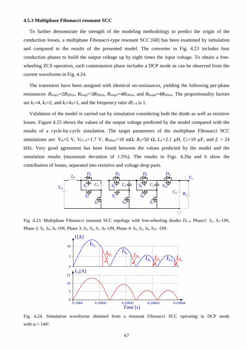
67
4.5.3 Multiphase Fibonacci resonant SCC
To further demonstrate the strength of the modeling methodology to predict the origin of the
conduction losses, a multiphase Fibonacci-type resonant SCC [68] has been examined by simulation
and compared to the results of the presented model. The converter in Fig. 4.23 includes four
conduction phases to build the output voltage up by eight times the input voltage. To obtain a free-
wheeling ZCS operation, each commutation phase includes a DCP mode as can be observed from the
current waveforms in Fig. 4.24.
The transistors have been assigned with identical on-resistances, yielding the following per-phase
resistances: Rloop1=2RDSon, Rloop2=3RDSon, Rloop3=4RDSon, and Rloop4=4RDSon. The proportionality factors
are k1=4, k2=2, and k3=k4=1, and the frequency ratio df1-4 is 1.
Validation of the model is carried out by simulation considering both the diode as well as resistive
losses. Figure 4.25 shows the values of the output voltage predicted by the model compared with the
results of a cycle-by-cycle simulation. The target parameters of the multiphase Fibonacci SCC
simulations are: Vin=5 V, VF1-4=1.7 V, RDSon=10 mΩ, Ro=50 Ω, LS=2.1 µH, Ci=10 µF, and fs ≈ 24
kHz. Very good agreement has been found between the values predicted by the model and the
simulation results (maximum deviation of 1.5%). The results in Figs. 4.26a and b show the
contribution of losses, separated into resistive and voltage drop parts.
C1 C2 C3
Co Ro
S1
S3
S2 S5
S4
S6
S8
S7
S9 S10
Vo
Vin
LSD1 D2 D3 D4
Fig. 4.23. Multiphase Fibonacci resonant SCC topology with free-wheeling diodes D1-4. Phase1: S1, S3–ON,
Phase 2: S2, S4, S6–ON, Phase 3: S2, S5, S7, S9–ON, Phase 4: S2, S5, S8, S10 –ON.
0
5
10
ID ID ID IS
IS
IS
0.1084 0.10841 0.10842 0.10843
Time [s]
0
5
10
15ILs[A]
I [A]
0.10844
3
16
29 3 10 4
IDIS
Fig. 4.24. Simulation waveforms obtained from a resonant Fibonacci SCC operating in DCP mode
with φi ≈ 144º.
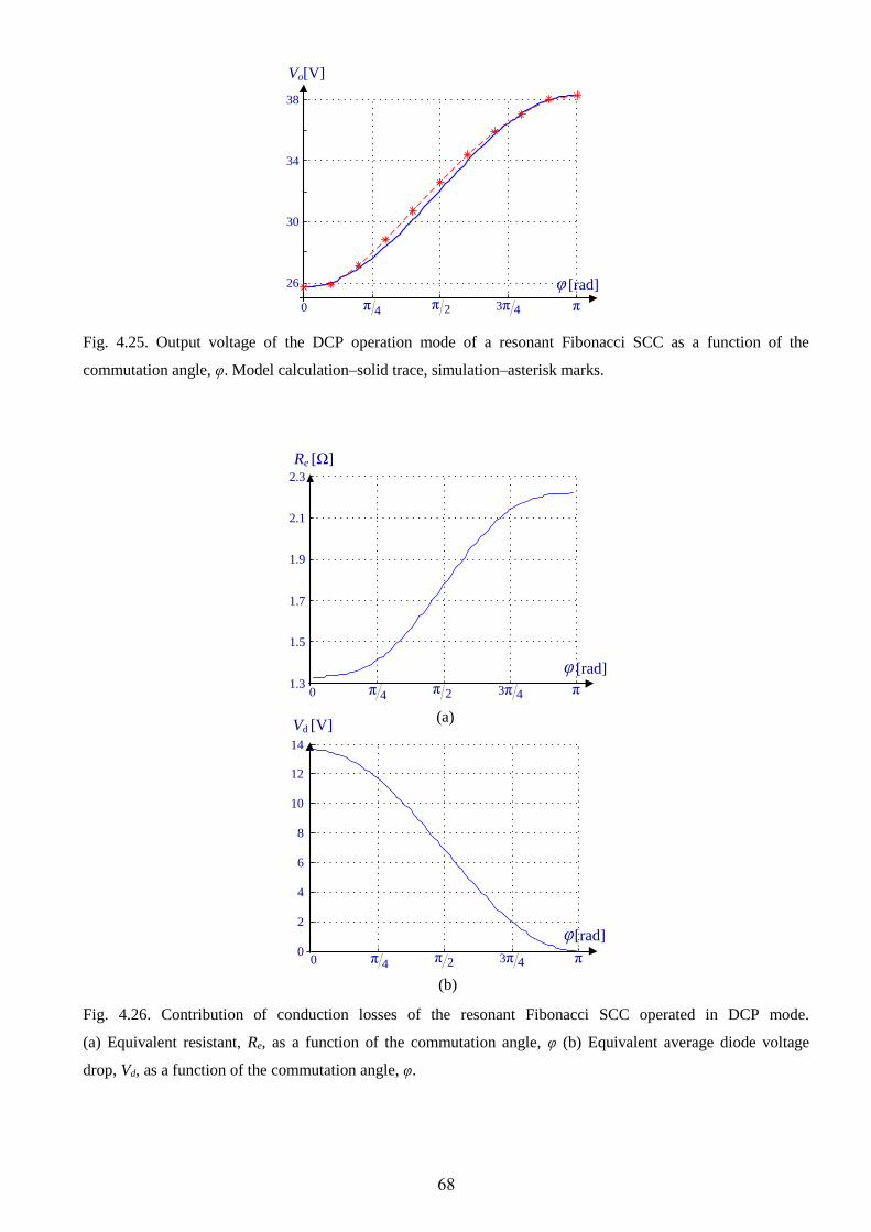
68
26
30
34
38
Vo[V]
0 2π4π π43π
[rad]φ
Fig. 4.25. Output voltage of the DCP operation mode of a resonant Fibonacci SCC as a function of the
commutation angle, φ. Model calculation–solid trace, simulation–asterisk marks.
1.3
1.5
1.7
1.9
2.1
2.3
0
2
4
6
8
10
12
14
0 2π4π π43π
0 2π4π π43π
Vd [V]
[rad]φ
[rad]φ
Re [Ω]
(a)
(b)
Fig. 4.26. Contribution of conduction losses of the resonant Fibonacci SCC operated in DCP mode.
(a) Equivalent resistant, Re, as a function of the commutation angle, φ (b) Equivalent average diode voltage
drop, Vd, as a function of the commutation angle, φ.

69
4.5.4 Model validation for low Q
To validate the formulas of the extended equivalent resistances, R1a_ext and R1b_ext, unit gain (Fig.
4.13) with charge phase operated in a DCP mode was simulated and compared to the results of the
presented model. Simulations were set-up at: Vin=10 V, Ci=100 µF, Li=1 µH, Q1a=Q1b=0.55, Q2=1,
(Rloop1a= Rloop1b=0.18 Ω, Rloop2=100 mΩ), Ro=5 Ω, and fs=9.23 kHz. The proportionality factors were
k1,2=1, and the frequency ratio was df1,2 =1. Figure 4.27 shows the simulation results of the average
currents at paths 1a and 1b as a function of the commutation phase φ, and the agreement to the
theoretical calculations. Very good agreement was found between the values predict by model and
simulation results.
0
0.2
0.4
0.6
0.8
1
1.2
1.4
1.6
1.8
φ[rad]
I [A]
I1b I1a
0 2π4π π43π
Fig. 4.27. Average currents at paths 1a and 1b at low Q as function of φ. Model calculation–(I1b) solid trace and
(I1a) dashed line, simulation results–(I1a) asterisk marks and (I1b) circle marks.
70
4.6 Discussion and conclusions
This thesis presented a modeling approach of resonant SCC that is applicable to both the
conventional resonant operation as well as to converters that operate in a more general case of a
divided conduction path ZCS. The modeling concept applies representation of the resistive losses by
partial equivalent resistance and losses originated from P-N junction devices, all with respect to the
output current of the converter. Although rigorously demonstrated on a relatively simple case of two
conduction paths, the modeling methodology is well-qualified to extract the behavior of a resonant
SCC with any number of split current loops, such as a resonant Fibonacci converter, exemplified in
Section 4.5.3. The resultant model is limited, however, within the assumptions specified, to resonant
networks with relatively high quality factors, i.e., sinusoidal resonant current.
The experimental study confirmed the validity of the modeling method to distinguish between
losses types (resistive and voltage drop) with excellent agreement between the analytical derivations,
simulations, and experimental results. It was found that while the partial equivalent resistances are
extracted as a function of the rms currents and the related commutation phase, the equivalent average
diode voltage source depends primarily on the ratio between the sub-states charges (proportionality
factor, ).
The overall efficiency in circuits operated in a DCP mode is highly dependent on the loss amount in
each of the conduction paths. It is assumed throughout this work that switches with a resistive
behavior, i.e., MOSFETs have lower conduction losses than devices based on a P-N junction, which is
the case in modern power components for low and intermediate voltage conversion applications.
Hence, there exists a tradeoff between the target efficiency and the component tolerances. Wider
component variance from their nominal values results in higher uncertainty of the zero crossing point
and longer duration of diode conduction path, which translates into higher losses. It should also be
noted that from an efficiency point of view, the lossy diode-based conduction path is to be activated in
the vicinity of zero current, so it’s contribution to the losses is minimized.
A self-commutation approach may not be compatible with all converter configurations, for
example, converters where the voltage difference between input and output is higher than the forward
voltage drop of the free-wheeling diode. Under these conditions undesirable current paths may appear.
It should be noted that the presented modeling methodology focuses on the dominant part of the
contributing losses in resonant SCC and omits the discussion on other issues such as EMI effects, gate
drive losses, etc.
The DCP operation mode can significantly simplify the control effort and eliminate the additional
circuitry that is required to achieve ZCS in resonant converters and in particular for resonant SCC that
require active ZCD to improve the power conversion efficiency.

71
Chapter 5 - Contribution of Thesis and Suggestions for Future Research
5.1 Contribution of thesis
The key contributions of this work are summarized as follows:
Generalized method of active ZCD for multiphase resonant SCCs. This research presents an
active method for ZCS for resonant SCC with a wide dynamic range. The method is demonstrated on a
resonant binary and Fibonacci SCC that feature a wide range of conversion ratios. This approach
reduces the power losses by reducing the switching losses together with increasing the number of
target voltages. Due to the resultant high efficiency of the converter operating under soft-switching
conditions, it is applicable for higher power levels up to the medium power range. A zero detection
method was developed that was capable of compensating for both the processing delays (from
detection to switching action) and for the large variations of the resonant characteristics (due to
transition between sub-circuits), and for any other component variations.
A Unique isolated gate driver with an extremely wide range of duty cycle and frequency was
developed. This work discusses the construction and component selection of the floating driver. The
isolated driver can be suitable with many other applications.
Design guideline of multiphase resonant SCC. For proper construction of a high power
multiphase SCC application with desired target efficiency, a set of design considerations for the
selection of the power stage components, for a multiple sub-circuits converter has been delineated. The
design method of multilevel SCCs with respect to conduction losses and efficiency was demonstrated
and verified to successfully operate resonant binary SCC and to accommodate a wide and dynamic
operation range and can be applied to other complex multi-phase SCC topologies that involve a
number of sub-circuits and wide operation ranges at high power levels.
Unified modeling methodology of self-commutation ZCS. This study introduces a unified
modeling methodology to describe and explore the loss mechanism of resonant SCC operating in a
self-commutation ZCS mode. The new modeling concept is compatible to describe the losses resulting
from resistive elements as well as P-N junction devices. The model can help in the simplification and
optimization of SCC systems and their control to achieve high efficiency up to the high power range.
5.2 Suggestions for future research
Some suggestions for future lines of investigation that can be developed as a result of this thesis are
outlined below:

72
Examination of the SCC design method with additional topologies. The multiphase SCC design
method developed can be adapted for traditional inductor-based dc-dc converters and can be examined
with more practical SCC topology ranging from low to high power.
Equivalent average diode voltage drop for low Q. The study that was carried out on the loss
mechanism of resonant SCCs operating in a self-commutation ZCS mode can be expended to a closed-
form solution. The model can be expanded to include the loss resulting from P-N junction devices at
low quality factors.
Equivalent resistance model for higher-order networks. The equivalent resistance model is valid
for cases where the sub-circuits of the converter can be described or approximated by a first and
second order (RC and RCL, respectively) networks. The method that was used to describe the loss in a
self-commutation ZCS mode can be used to explore the modeling for the cases where there are several
RC times constants and for higher order networks.
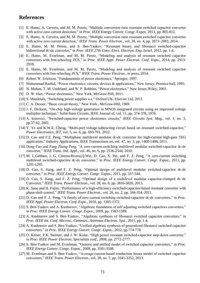
73
References
[1] E. Hamo, A. Cervera, and M. M. Peretz, “Multiple conversion ratio resonant swtiched capacitor converter
with active zero current detection,” in Proc. IEEE Energy Conver. Congr. Expos. 2013, pp. 805-812.
[2] E. Hamo, A. Cervera, and M. M. Peretz, “Multiple conversion ratio resonant swtiched capacitor converter
with active zero current detection,” IEEE Trans. Power Electron., vol. 30, no. 4, pp. 2073–2083, 2014.
[3] E. Hamo, M. M. Peretz, and S. Ben-Yaakov, “Resonant binary and fibonacci switched-capacitor
bidirectional dc-dc converter,” in Proc. IEEE 27th Conv. Elect. Electron. Eng. Israel, 2012, pp. 1-4.
[4] E. Hamo, M. Evzelman, and M. M. Peretz, “Modeling and analysis of resonant switched capacitor
converters with free-wheeling ZCS,” in Proc. IEEE Appl. Power Electron. Conf. Expo., 2014, pp. 2913-
2918.
[5] E. Hamo, M. Evzelman, and M. M. Peretz, “Modeling and analysis of resonant switched capacitor
converters with free-wheeling ZCS,” IEEE Trans. Power Electron., in press, 2014.
[6] Robert W. Erickson, “Fundamentals of power electronics,” Springer, 1997.
[7] Muhammad Rashid, “Power electronics: circuits, devices & applications,” New Jersey, Prentice-hall, 1993.
[8] N. Mohan, T. M. Undeland, and W. P. Robbins, “Power electronics,” New Jersey,Wiley, 2003.
[9] D. W. Hart, “Power electronics,” New York, McGraw-Hill, 2011.
[10] S. Maniktala, “Switching power supplies a-z,” Oxford UK, Elsevier Ltd, 2012.
[11] C. A. Desoer, “Basic circuit theory,” New York , McGraw-Hill, 1969.
[12] J. F. Dickson, “On-chip high-voltage generation in MNOS integrated circuits using an improved voltage
multiplier technique,” Solid-State Circuits, IEEE Journal of, vol. 11, pp. 374-378, 1976.
[13] A. Ioinovici, “Switched-capacitor power electronics circuits,” IEEE Circuits Syst. Mag., vol. 1, no. 3,
pp.37-42, 2001.
[14] Y. Ye and K.W.E. Cheng, “Multi-port voltage-subtracting circuit based on resonant switched-capacitor,”
Power Electronics, IET, vol. 5, no. 6, pp. 693-701, 2012.
[15] D. Cao and F.Z. Peng, “Multiphase multilevel modular dc-dc converter for high-current high-gain TEG
application,” Industry Applications, IEEE Transactions on, vol. 47, no. 3, pp. 1400-1408, 2011.
[16] Dong Cao and Fang Zheng Peng, “A zero-current-switching multilevel modular switched-capacitor dc-dc
converter,” IEEE Trans. Ind. Appl., vol. 46, no. 6, pp. 2536-2544, 2010.
[17] M. L.Gebben, J. G. Cintron-Rivera,Q.Wei, D. Cao, X. Pei, and F. Z. Peng, “A zero-current switching
multilevel switched-capacitor dc-dc converter,” in Proc. IEEE Energy Conver. Congr. Expos., 2011, pp.
1291-1295.
[18] D. Cao, S. Jiang, and F. Z. Peng, “Optimal design of multilevel modular switched-capacitor dc-dc
converter,” in Proc. IEEE Energy Conver. Congr. Expos., 2011, pp. 537-544.
[19] D. Cao, S. Jiang, and F. Z. Peng, “Optimal design of a multilevel modular capacitor-clamped dc–dc
Converter,” IEEE Trans. Power Electron., vol. 28, no. 8, pp. 3816-3826, 2013.
[20] K. Sano and H. Fujita, “Performance of a high-efficiency switched-capacitor-based resonant converter with
phase-shift control,” IEEE Trans. Power Electron., vol. 26, no. 2, pp. 344-354, 2011.
[21] D. Cao and F. Z. Peng, “A family of zero current switching switched-capacitor dc-dc converters,” in Proc.
IEEE Appl. Power Electron. Conf. Expo., 2010, pp. 1365-1372.
[22] S. Ben-Yaakov and A. Kushnerov, “Algebraic foundation of self adjusting switched capacitors converters,”
in Proc. IEEE Energy Conver. Congr. Expos., 2009, pp. 1582-1589.
[23] A. Kushnerov and S. Ben-Yaakov, “Algebraic synthesis of fibonacci switched capacitor converters,” in
Proc. IEEE Int. Conf. Microw., Commun., Antennas Electron. Syst., 2011, pp. 1-4.
[24] A. Kushnerov and S. Ben-Yaakov, “Unified algebraic synthesis of generalized fibonacci switched capacitor
converters,” in Proc. IEEE Energy Conver. Congr. Expos., 2012, pp.774-778.
[25] O. Keiser, P.K. Steimer, and J. W. Kolar, “High power resonant switched-capacitor step-down converter,”
in Proc. IEEE Power Electron. Specialists conf., 2008, pp. 2772-2777.
[26] S. Ben-Yaakov and M. Evzelman, “Generic and unified model of switched capacitor converters,” in Proc.
IEEE Energy Conver. Congr. Expos., 2009, pp. 3501-3508.
[27] M. Evzelman and S. Ben-Yaakov, “Average-current-based conduction losses model of switched capacitor
converters,” IEEE Trans. Power Electron., vol. 28, no. 7, pp. 3341-3352, 2013.
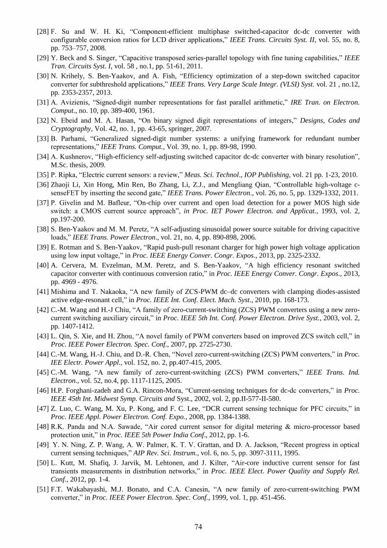
74
[28] F. Su and W. H. Ki, “Component-efficient multiphase switched-capacitor dc-dc converter with
configurable conversion ratios for LCD driver applications,” IEEE Trans. Circuits Syst. II, vol. 55, no. 8,
pp. 753–757, 2008.
[29] Y. Beck and S. Singer, “Capacitive transposed series-parallel topology with fine tuning capabilities,” IEEE
Tran. Circuits Syst. I, vol. 58 , no.1, pp. 51-61, 2011.
[30] N. Krihely, S. Ben-Yaakov, and A. Fish, “Efficiency optimization of a step-down switched capacitor
converter for subthreshold applications,” IEEE Trans. Very Large Scale Integr. (VLSI) Syst. vol. 21 , no.12,
pp. 2353-2357, 2013.
[31] A. Avizienis, “Signed-digit number representations for fast parallel arithmetic,” IRE Tran. on Electron.
Comput., no. 10, pp. 389-400, 1961.
[32] N. Ebeid and M. A. Hasan, “On binary signed digit representations of integers,” Designs, Codes and
Cryptography, Vol. 42, no. 1, pp. 43-65, springer, 2007.
[33] B. Parhami, “Generalized signed-digit number systems: a unifying framework for redundant number
representations,” IEEE Trans. Comput., Vol. 39, no. 1, pp. 89-98, 1990.
[34] A. Kushnerov, “High-efficiency self-adjusting switched capacitor dc-dc converter with binary resolution”,
M.Sc. thesis, 2009.
[35] P. Ripka, “Electric current sensors: a review,” Meas. Sci. Technol., IOP Publishing, vol. 21 pp. 1-23, 2010.
[36] Zhaoji Li, Xin Hong, Min Ren, Bo Zhang, Li, Z.J., and Mengliang Qian, “Controllable high-voltage c-
senseFET by inserting the second gate,” IEEE Trans. Power Electron., vol. 26, no. 5, pp. 1329-1332, 2011.
[37] P. Givelin and M. Bafleur, “On-chip over current and open load detection for a power MOS high side
switch: a CMOS current source approach”, in Proc. IET Power Electron. and Applicat., 1993, vol. 2,
pp.197-200.
[38] S. Ben-Yaakov and M. M. Peretz, “A self-adjusting sinusoidal power source suitable for driving capacitive
loads,” IEEE Trans. Power Electron., vol. 21, no. 4, pp. 890-898, 2006.
[39] E. Rotman and S. Ben-Yaakov, “Rapid push-pull resonant charger for high power high voltage application
using low input voltage,” in Proc. IEEE Energy Conver. Congr. Expos., 2013, pp. 2325-2332.
[40] A. Cervera, M. Evzelman, M.M. Peretz, and S. Ben-Yaakov, “A high efficiency resonant switched
capacitor converter with continuous conversion ratio,” in Proc. IEEE Energy Conver. Congr. Expos., 2013,
pp. 4969 - 4976.
[41] Mishima and T. Nakaoka, “A new family of ZCS-PWM dc–dc converters with clamping diodes-assisted
active edge-resonant cell,” in Proc. IEEE Int. Conf. Elect. Mach. Syst., 2010, pp. 168-173.
[42] C.-M. Wang and H.-J Chiu, “A family of zero-current-switching (ZCS) PWM converters using a new zero-
current switching auxiliary circuit,” in Proc. IEEE 5th Int. Conf. Power Electron. Drive Syst., 2003, vol. 2,
pp. 1407-1412.
[43] L. Qin, S. Xie, and H. Zhou, “A novel family of PWM converters based on improved ZCS switch cell,” in
Proc. IEEE Power Electron. Spec. Conf., 2007, pp. 2725-2730.
[44] C.-M. Wang, H.-J. Chiu, and D.-R. Chen, “Novel zero-current-switching (ZCS) PWM converters,” in Proc.
IEE Electr. Power Appl., vol. 152, no. 2, pp.407-415, 2005.
[45] C.-M. Wang, “A new family of zero-current-switching (ZCS) PWM converters,” IEEE Trans. Ind.
Electron., vol. 52, no.4, pp. 1117-1125, 2005.
[46] H.P. Forghani-zadeh and G.A. Rincon-Mora, “Current-sensing techniques for dc-dc converters,” in Proc.
IEEE 45th Int. Midwest Symp. Circuits and Syst., 2002, vol. 2, pp.II-577-II-580.
[47] Z. Luo, C. Wang, M. Xu, P. Kong, and F. C. Lee, “DCR current sensing technique for PFC circuits,” in
Proc. IEEE Appl. Power Electron. Conf. Expo., 2008, pp. 1384-1388.
[48] R.K. Panda and N.A. Sawade, “Air cored current sensor for digital metering & micro-processor based
protection unit,” in Proc. IEEE 5th Power India Conf., 2012, pp. 1-6.
[49] Y. N. Ning, Z. P. Wang, A. W. Palmer, K. T. V. Grattan, and D. A. Jackson, “Recent progress in optical
current sensing techniques,” AIP Rev. Sci. Instrum., vol. 6, no. 5, pp. 3097-3111, 1995.
[50] L. Kutt, M. Shafiq, J. Jarvik, M. Lehtonen, and J. Kilter, “Air-core inductive current sensor for fast
transients measurements in distribution networks,” in Proc. IEEE Elect. Power Quality and Supply Rel.
Conf., 2012, pp. 1-4.
[51] F.T. Wakabayashi, M.J. Bonato, and C.A. Canesin, “A new family of zero-current-switching PWM
converter,” in Proc. IEEE Power Electron. Spec. Conf., 1999, vol. 1, pp. 451-456.
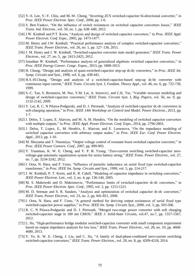
75
[52] Y.-S. Lee, Y.-Y. Chiu, and M.-W. Cheng, “Inverting ZCS switched-capacitor bi-directional converter,” in
Proc. IEEE Power Electron. Spec. Conf., 2006, pp. 1-6.
[53] S. Ben-Yaakov, “On the influence of switch resistances on switched capacitor converters losses,” IEEE
Trans. Ind. Electron., vol. 59, no. 1, pp. 638–640, 2012.
[54] J.W. Kimball and P.T. Krein, “Analysis and design of switched capacitor converters,” in Proc. IEEE Appl.
Power Electron. Conf. Expo., 2005, pp. 1473-1477.
[55] M. Henry and J.W. Kimball, “Practical performance analysis of complex switched-capacitor converters,”
IEEE Trans. Power Electron., vol. 26, no. 1, pp. 127–136, 2011.
[56] J. M. Henry and J. W. Kimball, “Switched-capacitor converter state model generator,” IEEE Trans. Power
Electron., vol. 27, no. 5, pp. 2415-2425, 2012.
[57] Jonathan W. Kimball, “Performance analysis of generalized algebraic switched capacitor converters,” in
Proc. IEEE Energy Conver. Congr. Expos., 2013, pp. 1808-1813.
[58] H. Chung, “Design and analysis of quasi-switched-capacitor step-up dc/dc converters,” in Proc. IEEE Int.
Symp. Circuits and Syst., 1998, vol. 6, pp. 438-441.
[59] H.S.-H.Chung, “Design and analysis of a switched-capacitor-based step-up dc/dc converter with
continuous input current,” IEEE Trans .Circuits Syst. I, Fundam. Theory Appl., vol. 46, no. 6, pp. 722-730,
1999.
[60] S.-C. Tan, S. Bronstein, M. Nur, Y.M. Lai, A. Ioinovici, and C.K. Tse, “Variable structure modeling and
design of switched-capacitor converters,” IEEE Trans. Circuits Syst. I, Reg. Papers, vol. 56, no. 9, pp.
2132-2142, 2009.
[61] Y. Lei, R. C. N Pilawa-Podgurski, and D. J. Perreault, “Analysis of switched-capacitor dc-dc converters in
soft-charging operation,” in Proc. IEEE 14th Workshop on Control and Model. Power Electron., 2013, pp.
1-7.
[62] J. Delos, T. Lopez, E. Alarcon, and M. A. M. Hendrix, “On the modeling of switched capacitor converters
with multiple outputs,” in Proc. IEEE Appl. Power Electron. Conf. Expo., 2014, pp. 2796-2803.
[63] J. Delos, T. Lopez, E., M. Hendrix, E. Alarcon, and E. Lomonova, “On the impedance modeling of
switched capacitor converters with arbitrary output nodes,” in Proc. IEEE Eur. Conf. Power Electron.
Appl., 2013, pp. 1-10.
[64] M. Shoyama and T. Ninomiya, “Output voltage control of resonant boost switched capacitor converter,” in
Proc. IEEE Power Convers. Conf., 2007, pp. 899-903.
[65] Y. Yuanmao, K. W. E. Cheng, and Y. P. B. Yeung, “Zero-current switching switched-capacitor zero-
voltage-gap automatic equalization system for series battery string,” IEEE Trans. Power Electron., vol. 27,
no. 7, pp. 3234-3242, 2012.
[66] I. Oota, N. Hara, and F. Ueno, “Influence of parasitic inductance on serial fixed type switched-capacitor
transformer,” in Proc. IEEE Int. Symp. Circuits and Syst., 1999, vol. 5, pp. 214-217.
[67] J. W. Kimball, P. T. Krein, and K. R. Cahill, “Modeling of capacitor impedance in switching converters,”
IEEE Power Electron. Lett., vol. 3, no. 4, pp. 136-140, 2005.
[68] M. S. Makowski and D. Maksimovic, “Performance limits of switched-capacitor dc-dc converters,” in
Proc. IEEE Power Electron. Spec. Conf., 1995, vol. 2, pp. 1215-1221.
[69] M. D. Seeman and S. R. Sanders, “Analysis and optimization of switched capacitor dc-dc converters,”
IEEE Trans. Power Electron., vol. 23, no. 2, pp. 841-851, 2008.
[70] I. Oota, N. Hara, and F. Ueno, “A general method for deriving output resistances of serial fixed type
switched-capacitor power supplies,” in Proc. IEEE Int. Symp. Circuits Syst., 2000, vol. 3, pp. 503-506.
[71] R. C. N Pilawa-Podgurski and D. J. Perreault, “Merged two-stage power converter with soft charging
switched-capacitor stage in 180 nm CMOS,” IEEE J. Solid-State Circuits, vol.47, no.7, pp. 1557-1567,
2012.
[72] L. He, “High-performance bridge modular switched-capacitor converter with small component requirement
based on output impedance analysis for low loss,” IEEE Trans. Power Electron., vol. 28, no. 10, pp. 4668-
4680, 2013.
[73] Y. Ye, K. W. E. Cheng, J. Liu, and C. Xu, “A family of dual-phase-combined zero-current switching
switched-capacitor converters,” IEEE Trans. Power Electron., vol. 29, no. 8, pp. 4209-4218, 2014.
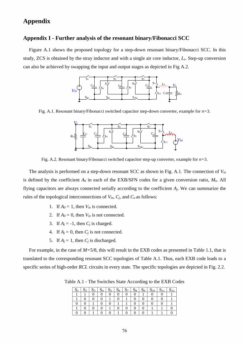
76
Appendix
Appendix I - Further analysis of the resonant binary/Fibonacci SCC
Figure A.1 shows the proposed topology for a step-down resonant binary/Fibonacci SCC. In this
study, ZCS is obtained by the stray inductor and with a single air core inductor, Ls. Step-up conversion
can also be achieved by swapping the input and output stages as depicted in Fig A.2.
S1
S6
S4
S3
S9
S8
S2 S7
S12
S11
S5 S10
C1 C2 C3
CO
LS
RO
Vo
Vin
Fig. A.1. Resonant binary/Fibonacci switched capacitor step-down converter, example for n=3.
S1
S6
S4
S3
S9
S8
S2 S7
S12
S11
S5 S10
C1 C2 C3
Vin
CO
RO
Vo
LS
Fig. A.2. Resonant binary/Fibonacci switched capacitor step-up converter, example for n=3.
The analysis is performed on a step-down resonant SCC as shown in Fig. A.1. The connection of Vin
is defined by the coefficient A0 in each of the EXB/SFN codes for a given conversion ratio, Mn. All
flying capacitors are always connected serially according to the coefficient Aj. We can summarize the
rules of the topological interconnections of Vin, Cj, and Co as follows:
1. If A0 = 1, then Vin is connected.
2. If A0 = 0, then Vin is not connected.
3. If Aj = -1, then Cj is charged.
4. If Aj = 0, then Cj is not connected.
5. If Aj = 1, then Cj is discharged.
For example, in the case of M=5/8, this will result in the EXB codes as presented in Table 1.1, that is
translated to the corresponding resonant SCC topologies of Table A.1. Thus, each EXB code leads to a
specific series of high-order RCL circuits in every state. The specific topologies are depicted in Fig. 2.2.
Table A.1 - The Switches State According to the EXB Codes
S1 S2 S3 S4 S5 S6 S7 S8 S9 S10 S11 S12
1 1 0 0 0 0 0 0 1 0 0 1 1 0 0 0 1 0 1 0 0 0 0 1
0 0 1 0 0 1 1 0 0 0 0 1
1 0 0 0 1 0 0 0 0 1 1 0 0 0 1 0 0 1 0 0 0 1 1 0
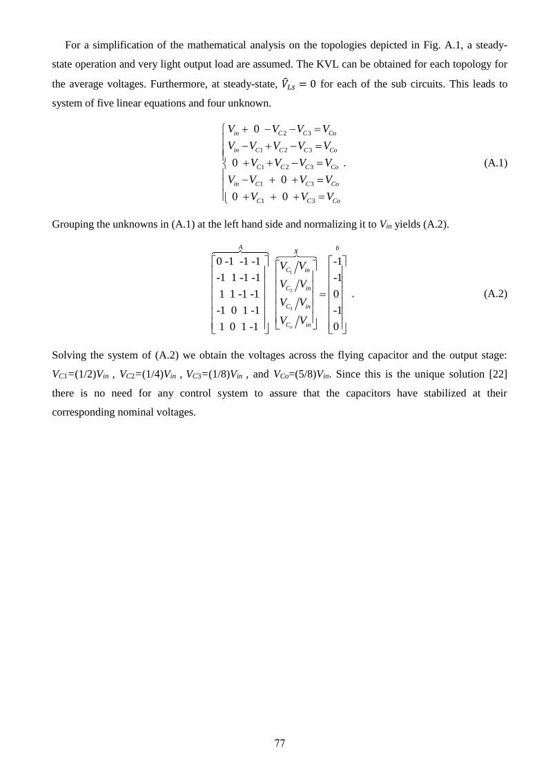
77
For a simplification of the mathematical analysis on the topologies depicted in Fig. A.1, a steady-
state operation and very light output load are assumed. The KVL can be obtained for each topology for
the average voltages. Furthermore, at steady-state, 𝐿𝑠 = 0 for each of the sub circuits. This leads to
system of five linear equations and four unknown.
2 3
1 2 3
1 2 3
1 3
1 3
0
0
0
0 0
in C C Co
in C C C Co
C C C Co
in C C Co
C C Co
V V V V
V V V V V
V V V V
V V V V
V V V
. (A.1)
Grouping the unknowns in (A.1) at the left hand side and normalizing it to Vin yields (A.2).
1
2
3
0 -1 -1 -1 -1
-1 1 -1 -1 -1
1 1 -1 -1 0
-1 0 1 -1 -1
1 0 1 -1 0o
A bX
C in
C in
C in
C in
V V
V V
V V
V V
. (A.2)
Solving the system of (A.2) we obtain the voltages across the flying capacitor and the output stage:
VC1=(1/2)Vin , VC2=(1/4)Vin , VC3=(1/8)Vin , and VCo=(5/8)Vin. Since this is the unique solution [22]
there is no need for any control system to assure that the capacitors have stabilized at their
corresponding nominal voltages.

78
Appendix II - Analysis of the Fibonacci SCC
Figure 4.23 shows a resonant multiphase converter with the ideal step-up conversion ratio M=8.
The flying capacitors’ voltages follow the Fibonacci sequence [68]. Following the switching sequence,
the average voltages across the flying capacitors and the output voltage will adjust to: VC1=Vin,
VC2=2Vin, VC3=4Vin, and VC4=8Vin.
The contribution of each flying capacitor to the average output current may be derived from the
equivalent RCL circuits of Fig. A.3. Under steady-state operation, charge balance of all capacitors is
satisfied (i.e., average current equals zero). The sum of the currents for each state I1-I4, and the sum of
all currents, can be expressed as:
1 2 3 4 1
2 3 4 2
3 4 3
4
0 :
0 0 :
0 0 0 :
0 0 0 o
I I I I C
I I I C
I I C
I I
, (A.3)
where the currents Ij are the average currents of each sub-circuit (averaged over the entire switching
period).
The solution of the system obtains the proportional coefficient between the average current of the
flying capacitor and output current for state j, so, k1=4, k2=2, and k3=k4=1.
C1 C2LS
Vin
+ +
C1 C2 C3LS
Vin
+ + +
C1 C2 C3
Co
LS
RO
Vo
Vin
+ + +
+
C1LS
Vin
+
Co RO
Vo
+
Co RO
Vo
+
Co RO
Vo
+
State1
State2
State3
State4
Fig. A.3. Resonant SCC sub-circuits configured from the Fibonacci sequence M=8.


תקציר
המורכבים מקבלים ורשת מתגים שבאמצעותם ממותגים כוח ספקי הינם תת קבוצה ממשפחתממירי קבלים ממותגים
ממירים מתחים ביעילות. בניגוד לממירים מסורתיים, מבוססי סליל, ממירים מבוססי קבל ממתמתג אינם נשענים על
רכיבים מגנטיים לאגירת האנרגיה. עובדה זו הופכת את משפחת ממירים זו כאידיאלית למימוש במעגלים משולבים. יחד
עם זאת ובאופן מסורתי, ממירי קבלים מיושמים בהספקים וביחסי המרה נמוכים הודות להפסדי אנרגיה פנימיים הנובעים
בעיקר מתהליך טעינה ופריקה של הקבלים, הפסדי הולכה והפסדי מיתוג.
המבוססים על ממירי קבלים םיישומיהמטרה העיקרית של התזה הינה לשפר את ההתנהגות והביצועים של מגוון
ממותגים בתחום ההספקים הגבוהים. האפליקציות והמתודות המוצגות בעבודה זו מתמקדות בנצילות גבוהה וכוללות מגוון
נרחב של מתחי מטרה ומיתוג רך. באופן טיפוסי אתגרים אלו מגבילים את המימוש של ממירי קבלים ממותגים בתחום
. עבודת מחקר זו מציגה דריבר צף, פשוט ויעיל, ומערכת בקרה אקטיבית למימוש מטודת ההספקים הבינוניים והגבוהים
ישומים, עבודה זו מציגה הליך יעיל לתכנון אמין ומעשי של ממירי קבלים ממותגים, מולטי פאזיים, יהמיתוג הרך. בנוסף ל
רט, אנליזה וניתוח תיאורטי, דוגמא בהיבט של נצילות ויחסי המרה רצויים. המחקר כולל תיאור התנהגותי מלא ומפו
IEEE Energy Conversion Congress and -יישומית ותוצאות ניסיוניות. חלקים אלו במחקר פורסמו בכנס
Exposition (ECCE) 2013[ ,3ובתוספת ,] עבודה נרחבת פורסם בעיתון-IEEE Transactions on Power
Electronics [2] [. 1דם לכן ]פורסמו קו מסוימים. חלקים
מטרה נוספת של התזה הינה לפתח מודל ומתודולוגיה לתיאור וניתוח של מכניזם ההפסדים בממירי קבלים ממותגים
תהודתיים, הפועלים בשיטת מיתוג בזרם אפס ובטכניקת קומוטציה עצמית. גישה פאסיבית זו מפשטת את אמצעי הבקרה
המודל ערכות בקרה אקטיביות שיועדו לשמירה ומימוש של מיתוג רך. ומייתרת את הצורך במעגלים ורכיבים נוספים למ
של ממירי קבלים ממותגים ומערכות הבקרה הנלוות להשגת נצילות הואופטימיזציהמוצג בעבודת מחקר זו מסייע לפישוט
טני של ממירי גבוהה בתחום הספקים נרחב יותר. כמו כן, מתודולוגיית המודל מציעה הליך יעיל ואמין לתכנון זול ופש
קבלים ממותגים במיתוג רך. בעבודה זו נערכה השוואה בין תוצאות החיזוי והניתוח התאורטי באמצעות המודל לבין
סימולציות ותוצאות מעבדה ניסיוניות במגוון טופולוגיות ומודי פעולה של ממירי קבלים ממותגים. חלק זה במחקר פורסם
[, ובתוספת עבודה נרחבת פורסם 1, ]IEEE Applied Power Electronics Conference (APEC) 2014 -בכנס
IEEE Transactions on Power Electronics[ ,1 .] -בעיתון
תרומת מחקר זה, יכולה להשפיע ישירות על חוקרים ומפתחים של ממירים, רגולטורים, וספקי כח במעגלים משולבים
. םיישומיהמבוססים על טכנולוגיית קבלים מתמתגים בתחום נרחב של
ל, מיתוג זרם אפס, ממירי הספק זרם ישר לזרם הפסדי הולכה, הפסדי מיתוג, מודל סטטי ממוצע, מידו – מילות מפתח
קומוטציה עצמית, ישר, ממירי קבלים ממותגים, ממירי קבלים ממותגים, מיתוג רך, ממירים תהודתיים, ספקי כח ממותגים,
קודים בינאריים.


גוריון בנגב-אוניברסיטת בן
הפקולטה למדעי ההנדסה ומחשביםהמחלקה להנדסת חשמל
בממירי קבלים ממותגים מיתוג רך
חיבור זה מהווה חלק מהדרישות לקבלת תואר מגיסטר בהנדסה
אלי חמו: מאת
:בהנחיית
דוקטור מור מרדכי פרץ
05/01/15 :תאריך .......................... אלי חמו : המחבר
05/01/15: תאריך ........................ .מור מרדכי פרץ ' דר: מנחה
05/01/15 :תאריך .......................... ר ועדת תואר שני"אישור יו


בנגבגוריון -אוניברסיטת בן
הפקולטה למדעי ההנדסה המחלקה להנדסת חשמל ומחשבים
בממירי קבלים ממותגים מיתוג רך
חיבור זה מהווה חלק מהדרישות לקבלת תואר מגיסטר בהנדסה
אלי חמו: מאת
:בהנחיית
דוקטור מור מרדכי פרץ
2031 ינואר "ה עהתש טבת