lecture 3 switched-capacitor circuits
TRANSCRIPT
ECE13712
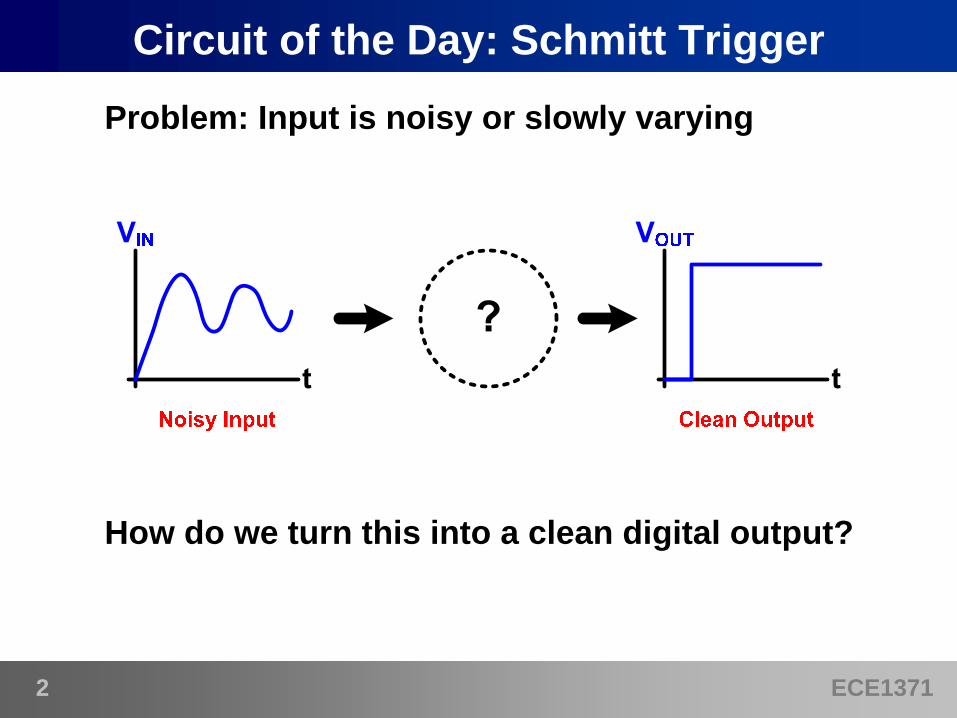
Circuit of the Day: Schmitt TriggerProblem: Input is noisy or slowly varying
How do we turn this into a clean digital output?
ECE13713
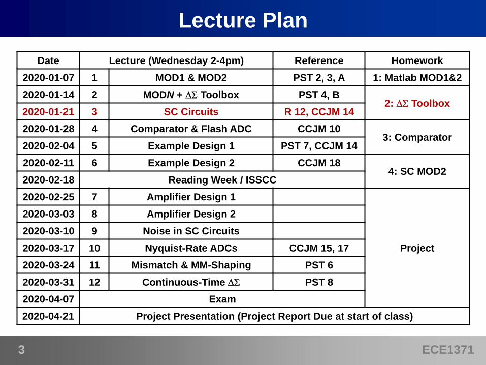
Lecture PlanDate Lecture (Wednesday 2-4pm) Reference Homework
2020-01-07 1 MOD1 & MOD2 PST 2, 3, A 1: Matlab MOD1&22020-01-14 2 MODN + Toolbox PST 4, B
2: Toolbox2020-01-21 3 SC Circuits R 12, CCJM 142020-01-28 4 Comparator & Flash ADC CCJM 10
3: Comparator2020-02-04 5 Example Design 1 PST 7, CCJM 142020-02-11 6 Example Design 2 CCJM 18
4: SC MOD22020-02-18 Reading Week / ISSCC2020-02-25 7 Amplifier Design 1
Project
2020-03-03 8 Amplifier Design 22020-03-10 9 Noise in SC Circuits2020-03-17 10 Nyquist-Rate ADCs CCJM 15, 172020-03-24 11 Mismatch & MM-Shaping PST 62020-03-31 12 Continuous-Time PST 82020-04-07 Exam2020-04-21 Project Presentation (Project Report Due at start of class)
ECE13714
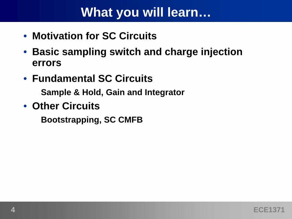
What you will learn…• Motivation for SC Circuits• Basic sampling switch and charge injection
errors• Fundamental SC Circuits
Sample & Hold, Gain and Integrator• Other Circuits
Bootstrapping, SC CMFB
ECE13715
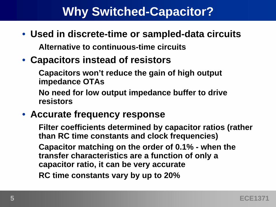
Why Switched-Capacitor?• Used in discrete-time or sampled-data circuits
Alternative to continuous-time circuits• Capacitors instead of resistors
Capacitors won’t reduce the gain of high output impedance OTAsNo need for low output impedance buffer to drive resistors
• Accurate frequency responseFilter coefficients determined by capacitor ratios (rather than RC time constants and clock frequencies)Capacitor matching on the order of 0.1% - when the transfer characteristics are a function of only a capacitor ratio, it can be very accurateRC time constants vary by up to 20%
ECE13716
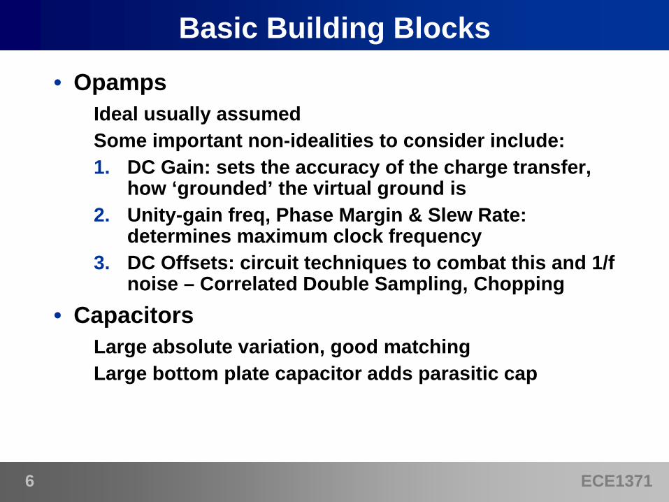
Basic Building Blocks• Opamps
Ideal usually assumedSome important non-idealities to consider include:1. DC Gain: sets the accuracy of the charge transfer,
how ‘grounded’ the virtual ground is2. Unity-gain freq, Phase Margin & Slew Rate:
determines maximum clock frequency3. DC Offsets: circuit techniques to combat this and 1/f
noise – Correlated Double Sampling, Chopping• Capacitors
Large absolute variation, good matchingLarge bottom plate capacitor adds parasitic cap
ECE13717
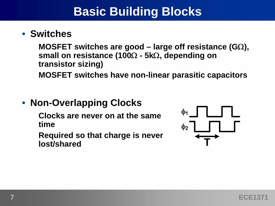
Basic Building Blocks• Switches
MOSFET switches are good – large off resistance (G), small on resistance (100 - 5k, depending on transistor sizing)MOSFET switches have non-linear parasitic capacitors
• Non-Overlapping ClocksClocks are never on at the same timeRequired so that charge is never lost/shared
ECE13718
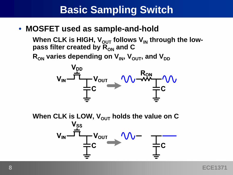
Basic Sampling Switch• MOSFET used as sample-and-hold
When CLK is HIGH, VOUT follows VIN through the low-pass filter created by RON and CRON varies depending on VIN, VOUT, and VDD
When CLK is LOW, VOUT holds the value on C
ECE13719
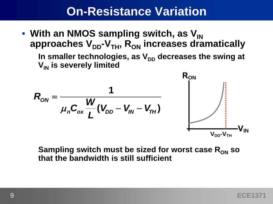
On-Resistance Variation• With an NMOS sampling switch, as VIN
approaches VDD-VTH, RON increases dramaticallyIn smaller technologies, as VDD decreases the swing at VIN is severely limited
Sampling switch must be sized for worst case RON so that the bandwidth is still sufficient
1
( )ON
n ox DD IN TH
R WC V V VL
IN
ON
VDD-VTH
ECE137110
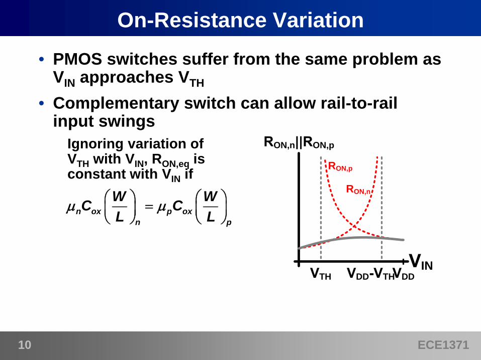
On-Resistance Variation• PMOS switches suffer from the same problem as
VIN approaches VTH
• Complementary switch can allow rail-to-rail input swings
Ignoring variation of VTH with VIN, RON,eq is constant with VIN if
n ox p oxn p
W WC CL L
IN
ON,n ON,p
TH DDDD TH
RON,p
RON,n
ECE137111
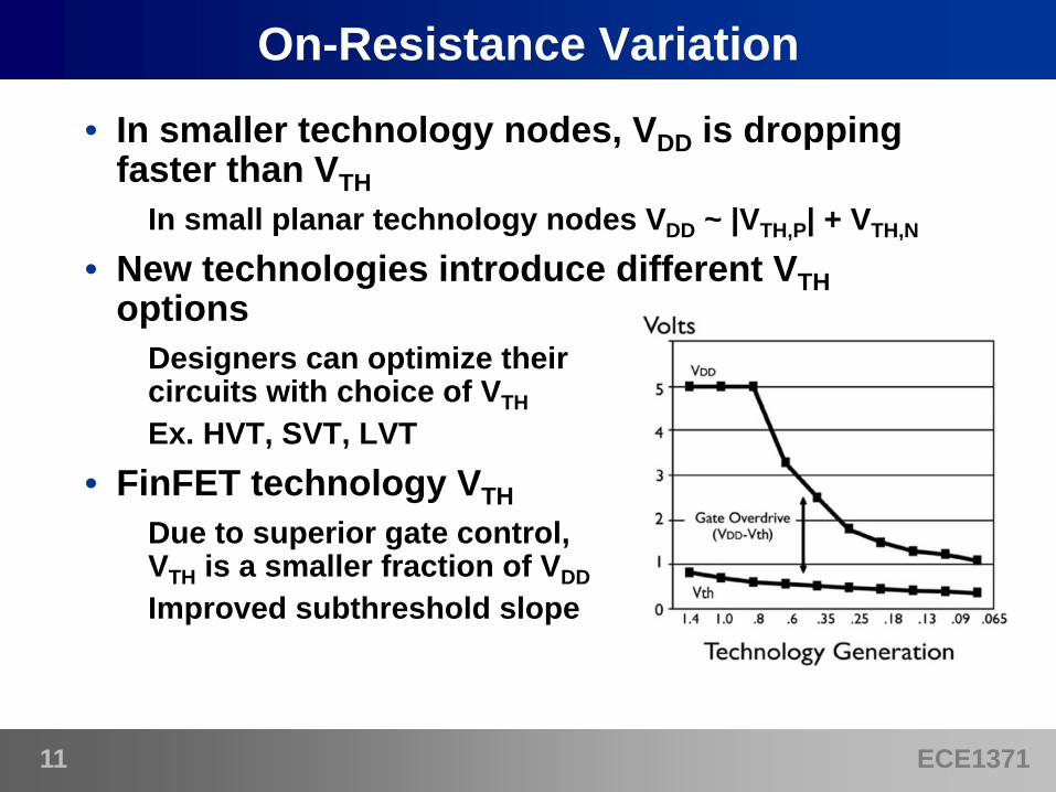
On-Resistance Variation• In smaller technology nodes, VDD is dropping
faster than VTHIn small planar technology nodes VDD ~ |VTH,P| + VTH,N
• New technologies introduce different VTHoptions
Designers can optimize their circuits with choice of VTHEx. HVT, SVT, LVT
• FinFET technology VTHDue to superior gate control, VTH is a smaller fraction of VDDImproved subthreshold slope
ECE137112
Settling Accuracy• Two situations to consider
1. Discrete-time signalWhen analyzing a signal within a switched-capacitor circuit (for example, at the output of the first OTA)
2. Continuous-time signalWhen analyzing a signal that is sampled at the input
ECE137113
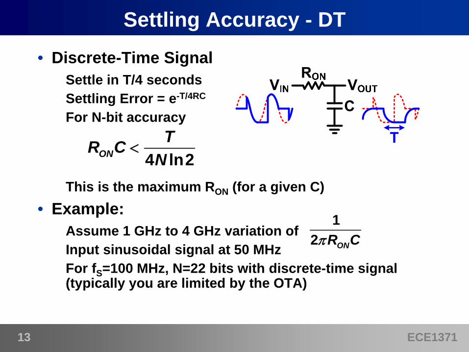
Settling Accuracy - DT• Discrete-Time Signal
Settle in T/4 secondsSettling Error = e-T/4RC
For N-bit accuracy
This is the maximum RON (for a given C)• Example:
Assume 1 GHz to 4 GHz variation of Input sinusoidal signal at 50 MHzFor fS=100 MHz, N=22 bits with discrete-time signal (typically you are limited by the OTA)
4 ln2ONTR C
N
12 ONR C
ECE137114
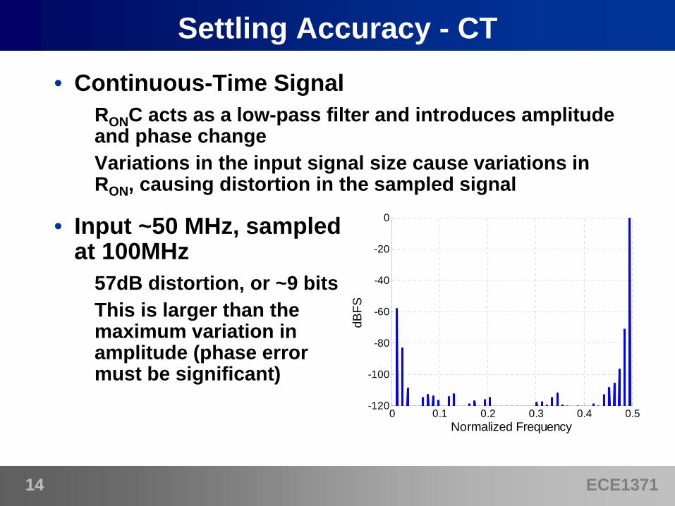
Settling Accuracy - CT• Continuous-Time Signal
RONC acts as a low-pass filter and introduces amplitude and phase changeVariations in the input signal size cause variations in RON, causing distortion in the sampled signal
0 0.1 0.2 0.3 0.4 0.5-120
-100
-80
-60
-40
-20
0
Normalized Frequency
dBFS
• Input ~50 MHz, sampled at 100MHz
57dB distortion, or ~9 bitsThis is larger than the maximum variation in amplitude (phase error must be significant)

ECE137115
Amplitude Error• Variation in RC filter magnitude
RON varies depending on input voltage, causes amplitude through RC filter to be signal dependentAt 50 MHz (with same RONC variation as DT case), maximum variation in amplitude is 0.1%
ECE137116
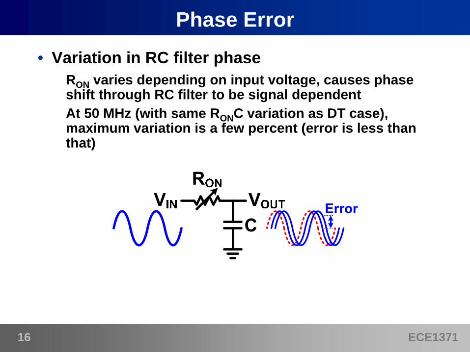
Phase Error• Variation in RC filter phase
RON varies depending on input voltage, causes phase shift through RC filter to be signal dependentAt 50 MHz (with same RONC variation as DT case), maximum variation is a few percent (error is less than that)
ECE137117
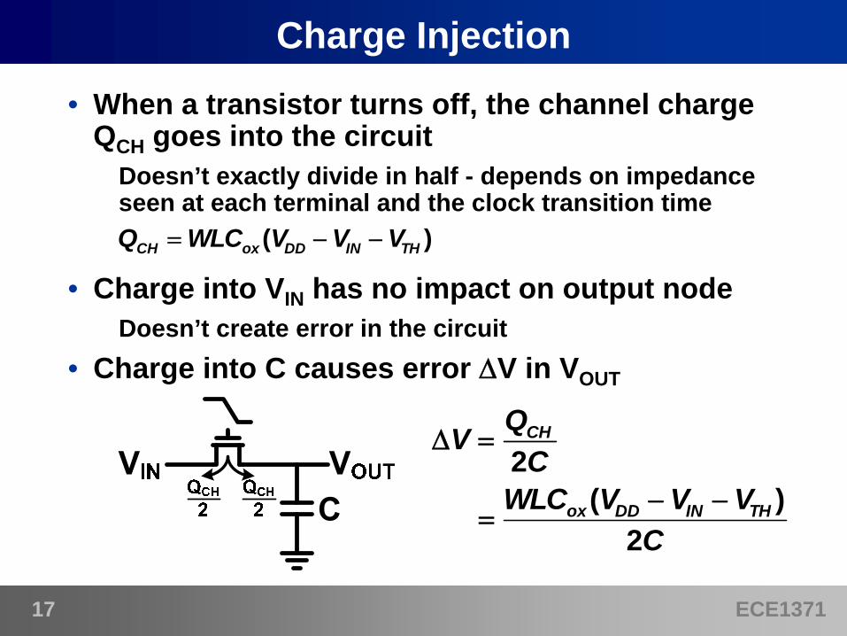
Charge Injection• When a transistor turns off, the channel charge
QCH goes into the circuitDoesn’t exactly divide in half - depends on impedance seen at each terminal and the clock transition time
• Charge into VIN has no impact on output nodeDoesn’t create error in the circuit
• Charge into C causes error V in VOUT
( )2
ox DD IN THWLC V V VC
( )CH ox DD IN THQ WLC V V V
2CHQVC
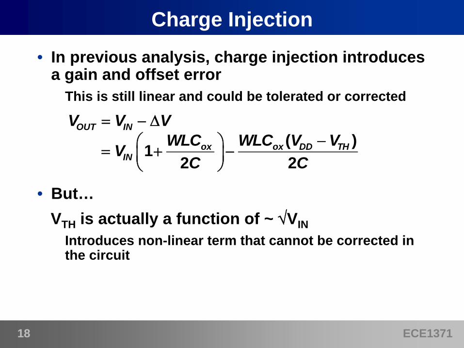
ECE137118
Charge Injection• In previous analysis, charge injection introduces
a gain and offset errorThis is still linear and could be tolerated or corrected
• But…VTH is actually a function of ~ VIN
Introduces non-linear term that cannot be corrected in the circuit
OUT INV V V ( )1
2 2ox ox DD TH
INWLC WLC V VV
C C
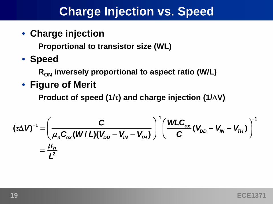
ECE137119
Charge Injection vs. Speed• Charge injection
Proportional to transistor size (WL)• Speed
RON inversely proportional to aspect ratio (W/L)• Figure of Merit
Product of speed (1/) and charge injection (1/V)
1 11( ) ( )
( / )( )ox
DD IN THn ox DD IN TH
WLCCV V V VC W L V V V C
2n
L
ECE137120
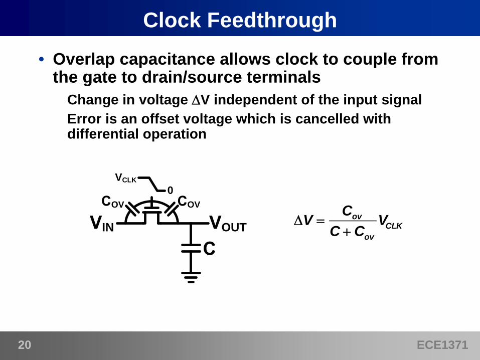
Clock Feedthrough• Overlap capacitance allows clock to couple from
the gate to drain/source terminalsChange in voltage V independent of the input signalError is an offset voltage which is cancelled with differential operation
ovCLK
ov
CV VC C
IN OUT
OVOV
VCLK0
ECE137121
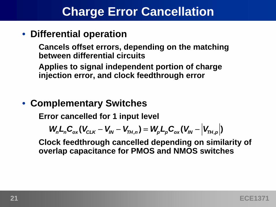
Charge Error Cancellation• Differential operation
Cancels offset errors, depending on the matching between differential circuitsApplies to signal independent portion of charge injection error, and clock feedthrough error
• Complementary SwitchesError cancelled for 1 input level
Clock feedthrough cancelled depending on similarity of overlap capacitance for PMOS and NMOS switches
, ,( ) ( )n n ox CLK IN TH n p p ox IN TH pW L C V V V W L C V V
ECE137122
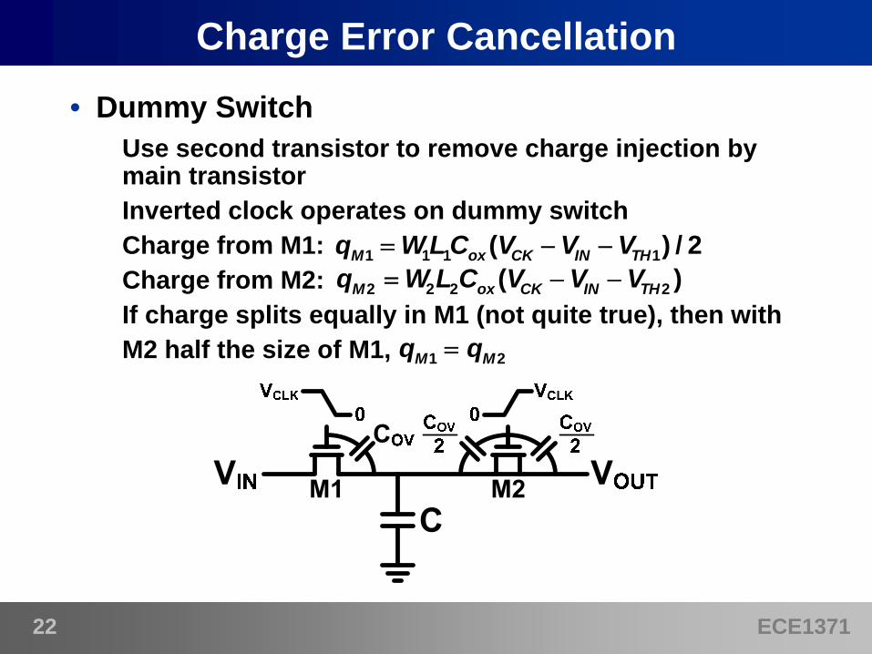
Charge Error Cancellation• Dummy Switch
Use second transistor to remove charge injection by main transistorInverted clock operates on dummy switchCharge from M1:Charge from M2: If charge splits equally in M1 (not quite true), then with M2 half the size of M1,
2 2 2 2( )M ox CK IN THq W L C V V V 1 1 1 1( ) / 2M ox CK IN THq W L C V V V
1 2M Mq q

ECE137123
Sample and Hold Amplifier• Input dependent charge from S1 onto C
When S1 turns off, charge q adds to CVOUT is then equal to VIN+q/C where q has a non-linear dependence on VIN
We can improve on this by making VOUTindependent of input-dependent charge…

ECE137124
S/H Amplifier• Two phases
Phase 1: S1 and S2 closed, VIN sampled on CPhase 2: S3 closed, C is tied to VOUT
• Phase 1Charge on C is CVINS2 opens, injecting signal independent charge at node XThen S1 opens, injecting signal dependent charge q onto C + Cp

ECE137125
S/H Amplifier• Phase 2
S3 closes, node X is a virtual groundCharge on Cp is zero, charge on C is still CVINS3 injects charge on X that must be discharged due to virtual ground node – it does not disturb charge on C VOUT = VIN
S1 / S3 are non-overlapping, S2 slightly ahead of S1
ECE137126
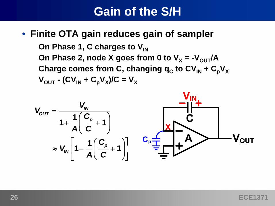
Gain of the S/H• Finite OTA gain reduces gain of sampler
On Phase 1, C charges to VINOn Phase 2, node X goes from 0 to VX = -VOUT/ACharge comes from C, changing qC to CVIN + CpVXVOUT - (CVIN + CpVX)/C = VX
11 1
INOUT
p
VVC
A C
11 1pIN
CV
A C

ECE137127
Speed of the S/H• In sampling mode (Phase 1)
At node X, RX ~ 1/GM , 1 ~ (Ron1+1/GM)C• In amplification mode (Phase 2)
Replace charge on C by voltage source VIN(like switching in voltage source at start of Phase 2)After analysis, 2 = (CLCp+CpC+CCL)/GMCReduces to 2 ~ CL/GM if Cp is small
ECE137128
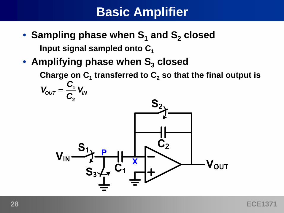
Basic Amplifier• Sampling phase when S1 and S2 closed
Input signal sampled onto C1
• Amplifying phase when S3 closedCharge on C1 transferred to C2 so that the final output is
1
2OUT IN
CV VC

ECE137129
Basic Amplifier• S2 must open before S1 for the charge injection
to be signal independentCharge from S2 opening is deposited on C1, but is not signal dependentCharge from S1 opening causes glitch in VOUTWhen S3 closes, VOUT goes to final value, regardless of what happened between S2 opening and S3 closing
ECE137130
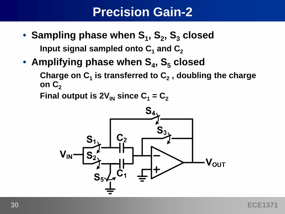
Precision Gain-2• Sampling phase when S1, S2, S3 closed
Input signal sampled onto C1 and C2
• Amplifying phase when S4, S5 closedCharge on C1 is transferred to C2 , doubling the charge on C2Final output is 2VIN since C1 = C2
ECE137131
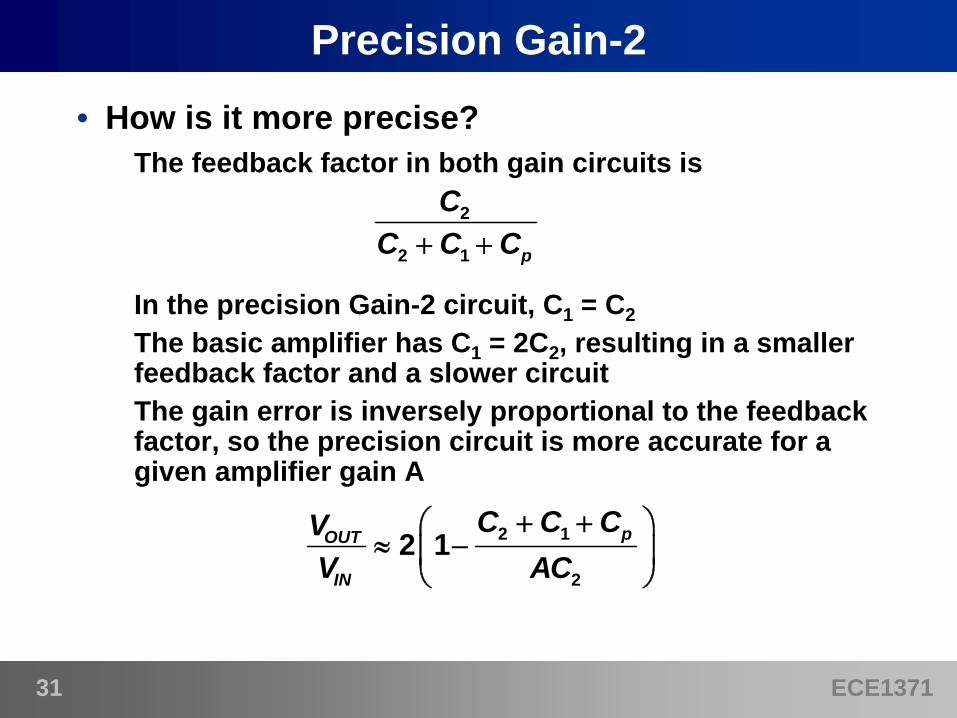
Precision Gain-2• How is it more precise?
The feedback factor in both gain circuits is
In the precision Gain-2 circuit, C1 = C2The basic amplifier has C1 = 2C2, resulting in a smaller feedback factor and a slower circuitThe gain error is inversely proportional to the feedback factor, so the precision circuit is more accurate for a given amplifier gain A
2
2 1 p
CC C C
2 1
22 1 pOUT
IN
C C CVV AC
ECE137132
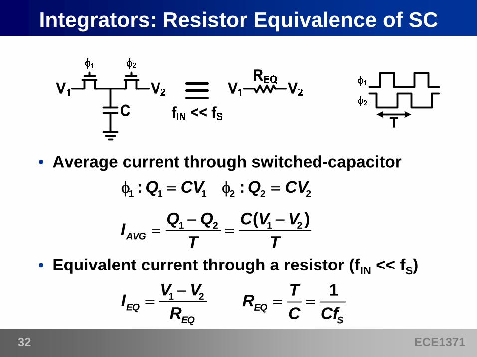
Integrators: Resistor Equivalence of SC
• Average current through switched-capacitor
• Equivalent current through a resistor (fIN << fS)
1 1 1 2 2 2: :Q CV Q CV
1 2 1 2( )AVG
Q Q C V VIT T
1 2EQ
EQ
V VIR
1
EQS
TRC Cf
ECE137133
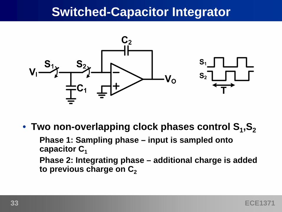
Switched-Capacitor Integrator
• Two non-overlapping clock phases control S1,S2Phase 1: Sampling phase – input is sampled onto capacitor C1Phase 2: Integrating phase – additional charge is added to previous charge on C2
ECE137134
Switched-Capacitor Integrator
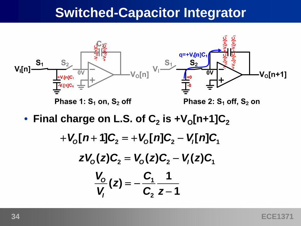
• Final charge on L.S. of C2 is +VO[n+1]C2
1
2
1( )1
O
I
V CzV C z
2 2 1( ) ( ) ( )O O IzV z C V z C V z C
2 2 1[ 1] [ ] [ ]O O IV n C V n C V n C
+VO[n
]C2
-VO[n
]C2
-VO[n
]C2+
V I[n
]C1
+VO[n
]C2-V
I[n]C
1
ECE137135
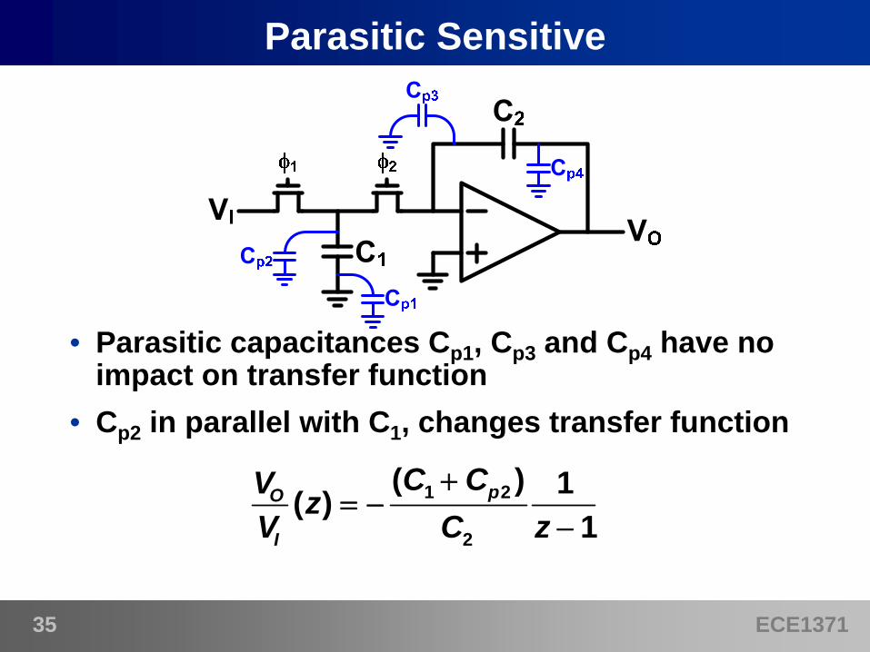
Parasitic Sensitive
• Parasitic capacitances Cp1, Cp3 and Cp4 have no impact on transfer function
• Cp2 in parallel with C1, changes transfer function
1 2
2
( ) 1( )1
pO
I
C CV zV C z

ECE137136
Parasitic Insensitive
• Transfer function is non-inverting, delaying
1
2
1( )1
O
I
V CzV C z
ECE137137
Parasitic Insensitive• Parasitics have no impact on transfer function
Better linearity since non-linear capacitors are unimportant
• Top plate on virtual ground nodeMinimizes parasitics, improves amplifier speed and resolution, reduces noise coupled to node
• Two extra switches neededMore power to drive the switches for the same on-resistance

ECE137138
Delay-Free Integrator
• Same structure, still parasitic insensitive• Transfer function is inverting, delay-free
1
2( )
1O
I
V C zzV C z

ECE137139
Bootstrapping• At low supply voltages, signal swing is limited
Maximum distortion determines the tolerable variation in RON, and this limits the signal swing
• Want to increase VGS on the sampling switchCan do this by increasing the supply voltage for the sampling switch, but this requires slower thick oxide devicesAlternatively, add a constant voltage to the input signal and use that as the gate voltage – keep VGS constant, reducing the variation in RON
ECE137140
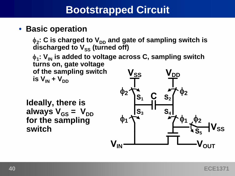
Bootstrapped Circuit• Basic operation
2: C is charged to VDD and gate of sampling switch is discharged to VSS (turned off)1: VIN is added to voltage across C, sampling switch turns on, gate voltage of the sampling switch is VIN + VDD
Ideally, there is always VGS = VDDfor the sampling switch
2
1
2
1
SS DD
SS2
OUTIN
1 2
3 4
5

ECE137141
Bootstrapped Circuit• C must be sized so that charge sharing between
gate capacitance of switch is not significant
• Rise time controlled by size of S4, fall time controlled by size of S5
• Extra transistors required to limit gate-source voltages to VDD and prevent overstress
See Dessouky, JSSC Mar.2001
( )G IN DDG
CV V VC C
ECE137142
Switched-Capacitor CMFB• Two parts to a CMFB circuit
1. Sense the common mode of the output2. Compare the common mode to the expected
common mode, and adjust the bias accordingly• Sensing
Could use 2 resistors – they are either too small and reduce the gain, or they can get prohibitively largeCould use 2 capacitors – they don’t reduce the gain, but the voltage across them is undefined and must be refreshed every clock cycle
ECE137143
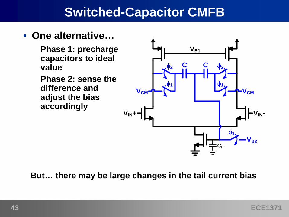
Switched-Capacitor CMFB• One alternative…
Phase 1: prechargecapacitors to ideal valuePhase 2: sense the difference and adjust the bias accordingly
But… there may be large changes in the tail current bias
2
VCM1
VB1
2
VCM1
1VB2
VIN+ VIN-
CP
CC
ECE137144
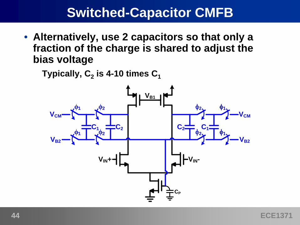
Switched-Capacitor CMFB• Alternatively, use 2 capacitors so that only a
fraction of the charge is shared to adjust the bias voltage
Typically, C2 is 4-10 times C1
VB1
1VCM
VIN+ VIN-
CP
C11
VB2
2
2C2
1VCM
C11
VB2
2
2C2
ECE137145
What You Learned Today• Errors introduced with simple sampling switch
RON variation, charge injection• Main SC Circuits – S/H, Gain and Integrators
Parasitic InsensitiveSignal-independent charge injection
• Bootstrapped Circuit• Switched Capacitor CMFB
ECE137146
Circuit of the Day: Schmitt Trigger