section 4 switched capacitor voltage converters … · switched capacitor voltage converters 4.1...
TRANSCRIPT
SWITCHED CAPACITOR VOLTAGE CONVERTERS
4.1
SECTION 4SWITCHED CAPACITOR VOLTAGECONVERTERSWalt Kester, Brian Erisman, Gurjit Thandi
INTRODUCTION
In the previous section, we saw how inductors can be used to transfer energy andperform voltage conversions. This section examines switched capacitor voltageconverters which accomplish energy transfer and voltage conversion usingcapacitors.
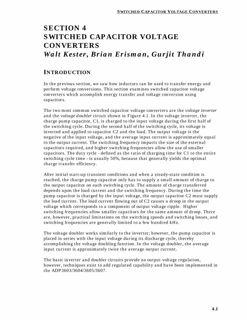
The two most common switched capacitor voltage converters are the voltage inverterand the voltage doubler circuit shown in Figure 4.1. In the voltage inverter, thecharge pump capacitor, C1, is charged to the input voltage during the first half ofthe switching cycle. During the second half of the switching cycle, its voltage isinverted and applied to capacitor C2 and the load. The output voltage is thenegative of the input voltage, and the average input current is approximately equalto the output current. The switching frequency impacts the size of the externalcapacitors required, and higher switching frequencies allow the use of smallercapacitors. The duty cycle - defined as the ratio of charging time for C1 to the entireswitching cycle time - is usually 50%, because that generally yields the optimalcharge transfer efficiency.
After initial start-up transient conditions and when a steady-state condition isreached, the charge pump capacitor only has to supply a small amount of charge tothe output capacitor on each switching cycle. The amount of charge transferreddepends upon the load current and the switching frequency. During the time thepump capacitor is charged by the input voltage, the output capacitor C2 must supplythe load current. The load current flowing out of C2 causes a droop in the outputvoltage which corresponds to a component of output voltage ripple. Higherswitching frequencies allow smaller capacitors for the same amount of droop. Thereare, however, practical limitations on the switching speeds and switching losses, andswitching frequencies are generally limited to a few hundred kHz.
The voltage doubler works similarly to the inverter; however, the pump capacitor isplaced in series with the input voltage during its discharge cycle, therebyaccomplishing the voltage doubling function. In the voltage doubler, the averageinput current is approximately twice the average output current.
The basic inverter and doubler circuits provide no output voltage regulation,however, techniques exist to add regulated capability and have been implemented inthe ADP3603/3604/3605/3607.
SWITCHED CAPACITOR VOLTAGE CONVERTERS
4.2
BASIC SWITCHED CAPACITOR VOLTAGEINVERTER AND VOLTAGE DOUBLER
VOUT ≈≈ –VIN
LOAD
VIN+
C1 C2
IOUT
INVERTER
VOUT ≈≈ 2VIN
LOAD
VIN+
C1 C2
IOUTDOUBLER
Figure 4.1
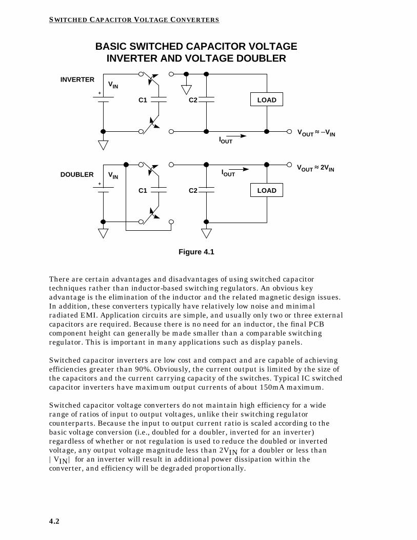
There are certain advantages and disadvantages of using switched capacitortechniques rather than inductor-based switching regulators. An obvious keyadvantage is the elimination of the inductor and the related magnetic design issues.In addition, these converters typically have relatively low noise and minimalradiated EMI. Application circuits are simple, and usually only two or three externalcapacitors are required. Because there is no need for an inductor, the final PCBcomponent height can generally be made smaller than a comparable switchingregulator. This is important in many applications such as display panels.
Switched capacitor inverters are low cost and compact and are capable of achievingefficiencies greater than 90%. Obviously, the current output is limited by the size ofthe capacitors and the current carrying capacity of the switches. Typical IC switchedcapacitor inverters have maximum output currents of about 150mA maximum.
Switched capacitor voltage converters do not maintain high efficiency for a widerange of ratios of input to output voltages, unlike their switching regulatorcounterparts. Because the input to output current ratio is scaled according to thebasic voltage conversion (i.e., doubled for a doubler, inverted for an inverter)regardless of whether or not regulation is used to reduce the doubled or invertedvoltage, any output voltage magnitude less than 2VIN for a doubler or less than|VIN| for an inverter will result in additional power dissipation within theconverter, and efficiency will be degraded proportionally.
SWITCHED CAPACITOR VOLTAGE CONVERTERS
4.3
SWITCHED CAPACITOR VOLTAGE CONVERTERS
n No Inductors!
n Minimal Radiated EMI
n Simple Implementation: Only 2 External Capacitors(Plus an Input Capacitor if Required)
n Efficiency > 90% Achievable
n Optimized for Doubling or Inverting Supply Voltage -Efficiency Degrades for Other Output Voltages
n Low Cost, Compact, Low Profile (Height)
n Parts with Voltage Regulation are Available:
ADP3603/ADP3604/ADP3605/ADP3607
Figure 4.2
The voltage inverter is useful where a relatively low current negative voltage isrequired in addition to the primary positive voltage. This may occur in a singlesupply system where only a few high performance parts require the negativevoltage. Similarly, voltage doublers are useful in low current applications where avoltage greater than the primary supply voltage is required.
CHARGE TRANSFER USING CAPACITORS
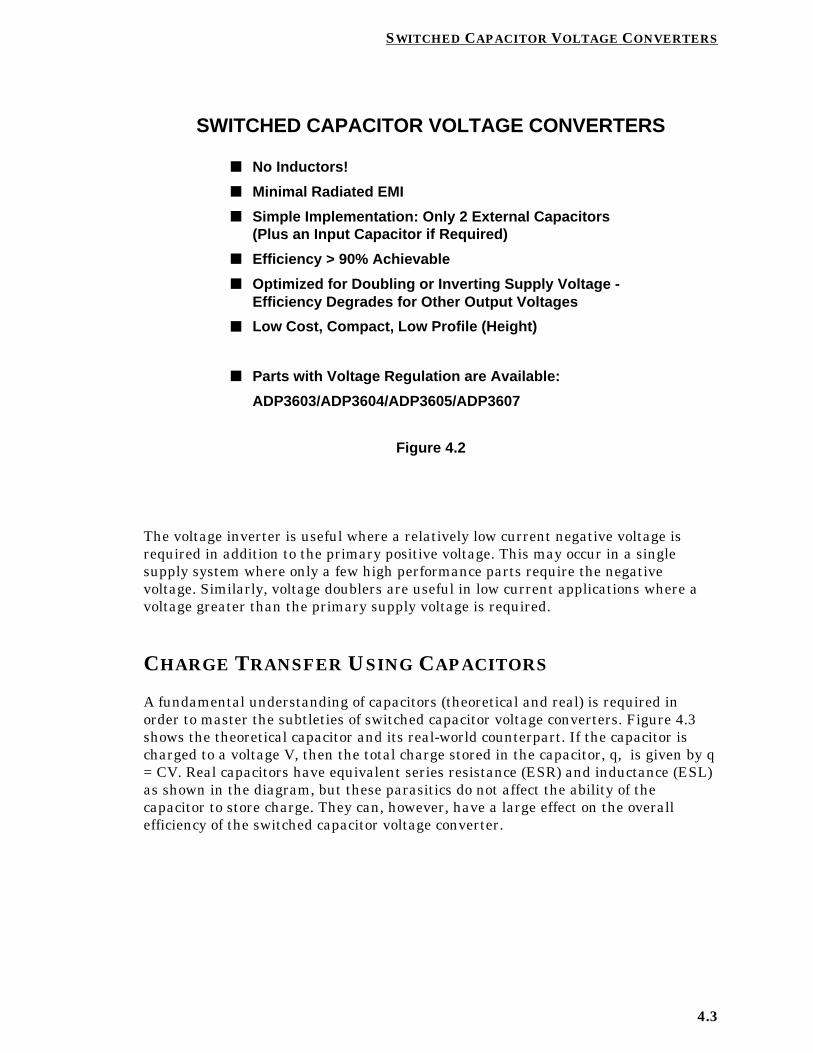
A fundamental understanding of capacitors (theoretical and real) is required inorder to master the subtleties of switched capacitor voltage converters. Figure 4.3shows the theoretical capacitor and its real-world counterpart. If the capacitor ischarged to a voltage V, then the total charge stored in the capacitor, q, is given by q= CV. Real capacitors have equivalent series resistance (ESR) and inductance (ESL)as shown in the diagram, but these parasitics do not affect the ability of thecapacitor to store charge. They can, however, have a large effect on the overallefficiency of the switched capacitor voltage converter.
SWITCHED CAPACITOR VOLTAGE CONVERTERS
4.4
STORED CHARGE IN A CAPACITOR
ESR
ESL
CC
+
V
-
STORED CHARGE
q = CV
+
V
-
IDEAL ACTUAL
Figure 4.3
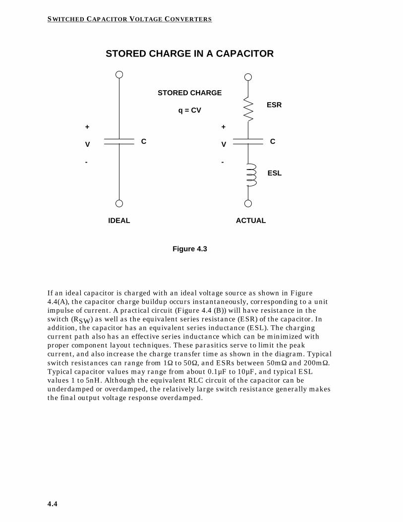
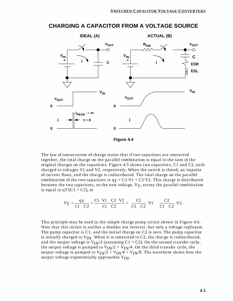
If an ideal capacitor is charged with an ideal voltage source as shown in Figure4.4(A), the capacitor charge buildup occurs instantaneously, corresponding to a unitimpulse of current. A practical circuit (Figure 4.4 (B)) will have resistance in theswitch (RSW) as well as the equivalent series resistance (ESR) of the capacitor. Inaddition, the capacitor has an equivalent series inductance (ESL). The chargingcurrent path also has an effective series inductance which can be minimized withproper component layout techniques. These parasitics serve to limit the peakcurrent, and also increase the charge transfer time as shown in the diagram. Typicalswitch resistances can range from 1Ω to 50Ω, and ESRs between 50mΩ and 200mΩ.Typical capacitor values may range from about 0.1µF to 10µF, and typical ESLvalues 1 to 5nH. Although the equivalent RLC circuit of the capacitor can beunderdamped or overdamped, the relatively large switch resistance generally makesthe final output voltage response overdamped.
SWITCHED CAPACITOR VOLTAGE CONVERTERS
4.5
CHARGING A CAPACITOR FROM A VOLTAGE SOURCE
VIN +
C
VIN +
Ci
RSW
i ESR
vOUT vOUT
0
VIN
IPEAK Õ Õ ∞∞ tÕ Õ 0
VIN
0
00
IDEAL (A) ACTUAL (B)
vOUTvOUT
ii
ESL
Figure 4.4
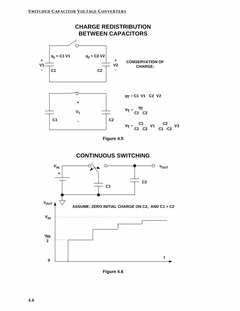
The law of conservation of charge states that if two capacitors are connectedtogether, the total charge on the parallel combination is equal to the sum of theoriginal charges on the capacitors. Figure 4.5 shows two capacitors, C1 and C2, eachcharged to voltages V1 and V2, respectively. When the switch is closed, an impulseof current flows, and the charge is redistributed. The total charge on the parallelcombination of the two capacitors is qT = C1·V1 + C2·V2. This charge is distributedbetween the two capacitors, so the new voltage, VT, across the parallel combinationis equal to qT/(C1 + C2), or
VTqT
C CC V C V
C CC
C CV
CC C
V=+
=⋅ + ⋅
+=
+
++
1 2
1 1 2 21 2
11 2
12
1 22 .
This principle may be used in the simple charge pump circuit shown in Figure 4.6.Note that this circuit is neither a doubler nor inverter, but only a voltage replicator.The pump capacitor is C1, and the initial charge on C2 is zero. The pump capacitoris initially charged to VIN. When it is connected to C2, the charge is redistributed,and the output voltage is VIN/2 (assuming C1 = C2). On the second transfer cycle,the output voltage is pumped to VIN/2 + VIN/4. On the third transfer cycle, theoutput voltage is pumped to VIN/2 + VIN/4 + VIN/8. The waveform shows how theoutput voltage exponentially approaches VIN.
SWITCHED CAPACITOR VOLTAGE CONVERTERS
4.6
CHARGE REDISTRIBUTIONBETWEEN CAPACITORS
+V1-
+V2-C1 C2
q1 = C1·V1 q2 = C2·V2
C1 C2
+
VT
-
qT C V C V
VTqT
C C
VTC
C CV
CC C
V
== ⋅⋅ ++ ⋅⋅
==++
==++
⋅⋅ ++++
⋅⋅
1 1 2 2
1 2
11 2
12
1 22
CONSERVATION OFCHARGE:
Figure 4.5
CONTINUOUS SWITCHING
C1C2
VIN
+
vOUT
VIN
0t
VIN2
vOUTASSUME: ZERO INITIAL CHARGE ON C2, AND C1 = C2
Figure 4.6
SWITCHED CAPACITOR VOLTAGE CONVERTERS
4.7
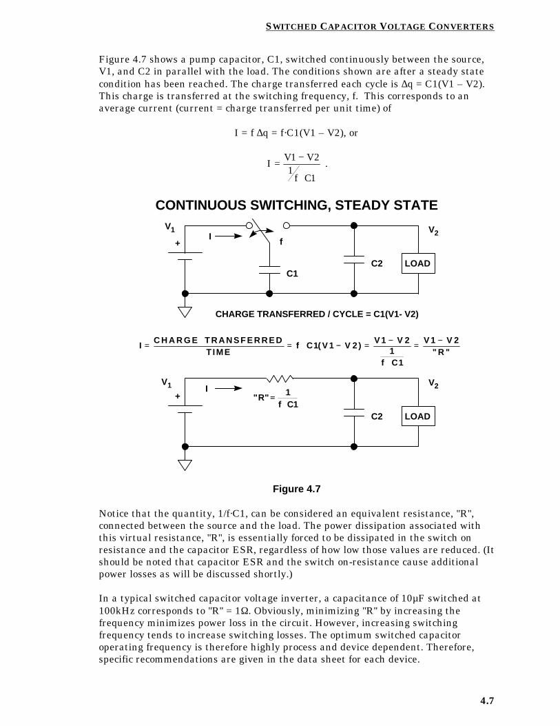
Figure 4.7 shows a pump capacitor, C1, switched continuously between the source,V1, and C2 in parallel with the load. The conditions shown are after a steady statecondition has been reached. The charge transferred each cycle is ∆q = C1(V1 – V2).This charge is transferred at the switching frequency, f. This corresponds to anaverage current (current = charge transferred per unit time) of
I = f ∆q = f·C1(V1 – V2), or
IV V
f C=
−
⋅
1 21
1 .
CONTINUOUS SWITCHING, STEADY STATE
C1C2
V1
+
V2
LOAD
C2
+
V2
LOAD
V1
" "Rf C
==⋅⋅1
1
CHARGE TRANSFERRED / CYCLE = C1(V1- V2)
IC H A R G E T R A N S F E R R E D
TIMEf C V V
V V
f C
V VR
== == ⋅⋅ −− == −−
⋅⋅
== −−1 1 2
1 21
1
1 2( )
" "
I
I
f
Figure 4.7
Notice that the quantity, 1/f·C1, can be considered an equivalent resistance, "R",connected between the source and the load. The power dissipation associated withthis virtual resistance, "R", is essentially forced to be dissipated in the switch onresistance and the capacitor ESR, regardless of how low those values are reduced. (Itshould be noted that capacitor ESR and the switch on-resistance cause additionalpower losses as will be discussed shortly.)
In a typical switched capacitor voltage inverter, a capacitance of 10µF switched at100kHz corresponds to "R" = 1Ω. Obviously, minimizing "R" by increasing thefrequency minimizes power loss in the circuit. However, increasing switchingfrequency tends to increase switching losses. The optimum switched capacitoroperating frequency is therefore highly process and device dependent. Therefore,specific recommendations are given in the data sheet for each device.
SWITCHED CAPACITOR VOLTAGE CONVERTERS
4.8
UNREGULATED SWITCHED CAPACITOR INVERTER ANDDOUBLER IMPLEMENTATIONS
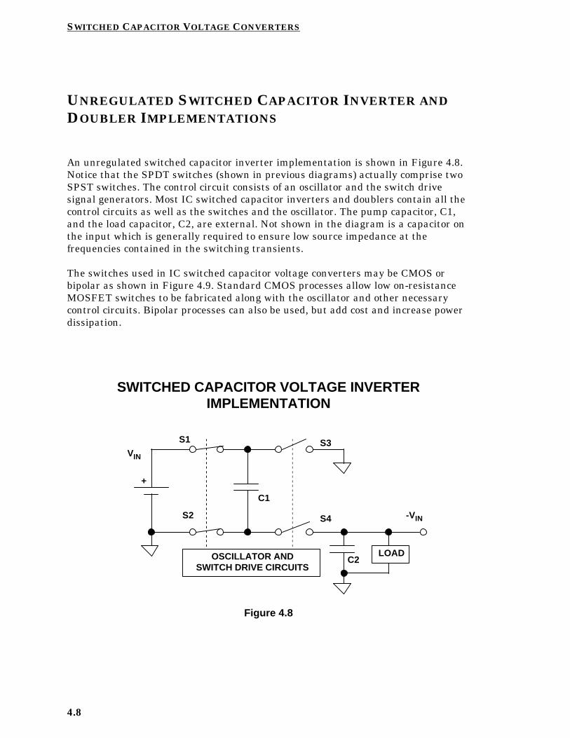
An unregulated switched capacitor inverter implementation is shown in Figure 4.8.Notice that the SPDT switches (shown in previous diagrams) actually comprise twoSPST switches. The control circuit consists of an oscillator and the switch drivesignal generators. Most IC switched capacitor inverters and doublers contain all thecontrol circuits as well as the switches and the oscillator. The pump capacitor, C1,and the load capacitor, C2, are external. Not shown in the diagram is a capacitor onthe input which is generally required to ensure low source impedance at thefrequencies contained in the switching transients.
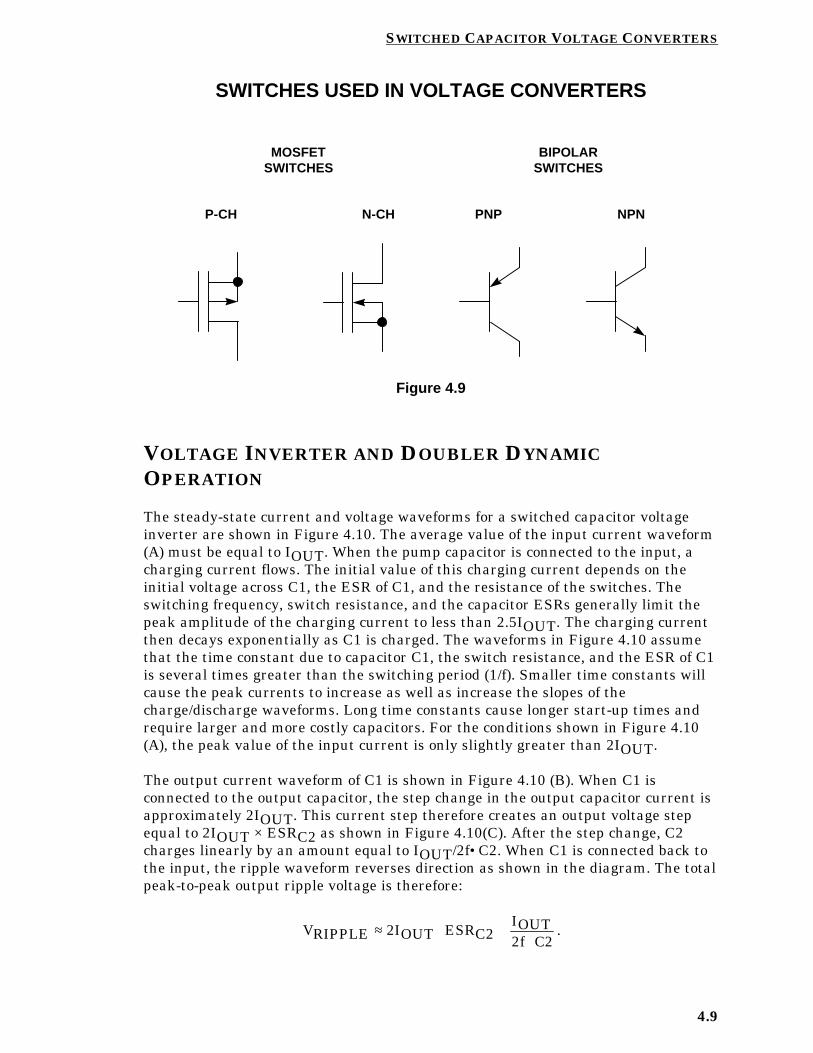
The switches used in IC switched capacitor voltage converters may be CMOS orbipolar as shown in Figure 4.9. Standard CMOS processes allow low on-resistanceMOSFET switches to be fabricated along with the oscillator and other necessarycontrol circuits. Bipolar processes can also be used, but add cost and increase powerdissipation.
SWITCHED CAPACITOR VOLTAGE INVERTERIMPLEMENTATION
LOAD
VIN
-VIN
OSCILLATOR ANDSWITCH DRIVE CIRCUITS
S1
S2
S3
S4
C1
C2
+
Figure 4.8
SWITCHED CAPACITOR VOLTAGE CONVERTERS
4.9
SWITCHES USED IN VOLTAGE CONVERTERS
MOSFETSWITCHES
BIPOLARSWITCHES
P-CH N-CH PNP NPN
Figure 4.9
VOLTAGE INVERTER AND DOUBLER DYNAMICOPERATION
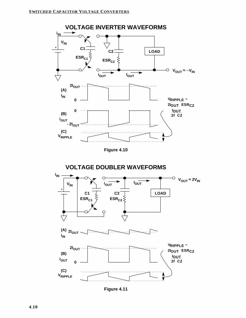
The steady-state current and voltage waveforms for a switched capacitor voltageinverter are shown in Figure 4.10. The average value of the input current waveform(A) must be equal to IOUT. When the pump capacitor is connected to the input, acharging current flows. The initial value of this charging current depends on theinitial voltage across C1, the ESR of C1, and the resistance of the switches. Theswitching frequency, switch resistance, and the capacitor ESRs generally limit thepeak amplitude of the charging current to less than 2.5IOUT. The charging currentthen decays exponentially as C1 is charged. The waveforms in Figure 4.10 assumethat the time constant due to capacitor C1, the switch resistance, and the ESR of C1is several times greater than the switching period (1/f). Smaller time constants willcause the peak currents to increase as well as increase the slopes of thecharge/discharge waveforms. Long time constants cause longer start-up times andrequire larger and more costly capacitors. For the conditions shown in Figure 4.10(A), the peak value of the input current is only slightly greater than 2IOUT.
The output current waveform of C1 is shown in Figure 4.10 (B). When C1 isconnected to the output capacitor, the step change in the output capacitor current isapproximately 2IOUT. This current step therefore creates an output voltage stepequal to 2IOUT × ESRC2 as shown in Figure 4.10(C). After the step change, C2charges linearly by an amount equal to IOUT/2f•C2. When C1 is connected back tothe input, the ripple waveform reverses direction as shown in the diagram. The totalpeak-to-peak output ripple voltage is therefore:
VRIPPLE OUT ESRCIOUT
f C≈ ⋅ +
⋅2I 2 2 2
.
SWITCHED CAPACITOR VOLTAGE CONVERTERS
4.10
VOLTAGE INVERTER WAVEFORMS
VOUT ≈≈ –VIN
LOAD
VIN+ C1
C2
IOUT
ESRC1 ESRC2
iOUT
iIN
(A)
(B)
(C)
2IOUT
0
0
- 2IOUT
iIN
iOUT
VRIPPLE
VRIPPLEIOUT ESRC
IOUTf C
==
⋅⋅
++⋅⋅
2 2
2 2
Figure 4.10
VOLTAGE DOUBLER WAVEFORMS
VOUT ≈≈ 2VIN
LOAD
VIN+
C1 C2
IOUT
ESRC1
iIN
iOUT
ESRC2
2IOUT
0
(C)VRIPPLE
(A)iIN
2IOUT
(B)iOUT
VRIPPLEIOUT ESRC
IOUTf C
==
⋅⋅
++⋅⋅
2 2
2 2
Figure 4.11
SWITCHED CAPACITOR VOLTAGE CONVERTERS
4.11
The current and voltage waveforms for a simple voltage doubler are shown in Figure4.11 and are similar to those of the inverter. Typical voltage ripple for practicalswitched capacitor voltage inverter/doublers range from 25mV to 100mV, but can bereduced by filtering techniques as described in Section 8 of this book.
Note that the input current waveform has an average value of 2IOUT because VINis connected to C1 during C1's charge cycle and to the load during C1's dischargecycle. The expression for the ripple voltage is identical to that of the voltageinverter.
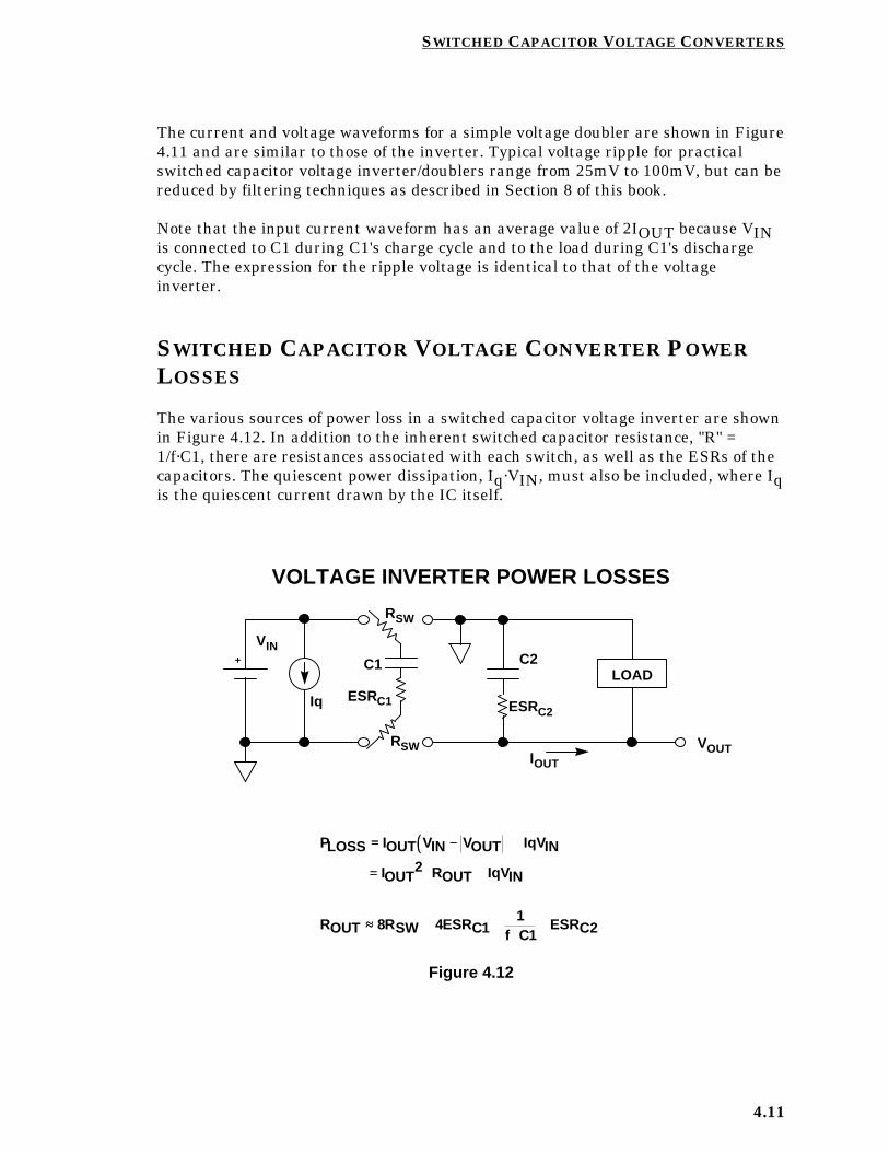
SWITCHED CAPACITOR VOLTAGE CONVERTER POWERLOSSES
The various sources of power loss in a switched capacitor voltage inverter are shownin Figure 4.12. In addition to the inherent switched capacitor resistance, "R" =1/f·C1, there are resistances associated with each switch, as well as the ESRs of thecapacitors. The quiescent power dissipation, Iq·VIN, must also be included, where Iqis the quiescent current drawn by the IC itself.
VOLTAGE INVERTER POWER LOSSES
VOUT
LOAD
VIN+ C1 C2
IOUT
ESRC1 ESRC2
RSW
RSW
Iq
(( ))PLOSS IOUT VIN VOUT IqVIN
IOUT ROUT IqVIN
ROUT RSW ESRC f CESRC
== −− ++
== ⋅⋅ ++
≈≈ ++ ++⋅⋅
++
2
8 4 11
1 2
Figure 4.12
SWITCHED CAPACITOR VOLTAGE CONVERTERS
4.12
The power dissipated in the switching arm is first calculated. When C1 is connectedto VIN, a current of 2IOUT flows through the switch resistances (2RSW) and theESR of C1, ESRC1. When C1 is connected to the output, a current of 2IOUTcontinues to flow through C1, 2RSW, and ESRC1. Therefore, there is always an rmscurrent of 2IOUT flowing through these resistances, resulting in a power dissipationin the switching arm of:
PSW = (2IOUT)2 × (2RSW + ESRC1) = IOUT2 × (8RSW + 4ESRC1).
In addition to these purely resistive losses, an rms current of IOUT flows throughthe "resistance" of the switched capacitor, C1, yielding an additional loss of:
" " " "PC IOUT RC IOUT f C12
12 1
1= × = ×
⋅.
The rms current flowing through ESRC2 is IOUT, yielding a power dissipation of:
PESRC2 = IOUT2 × ESRC2.
Adding all the resistive power dissipations to the quiescent power dissipation yields:
PLOSS IOUT RSW ESRC ESRC f CIqVIN= × + + +
⋅
+2 8 4 1 21
1.
All of the resistive losses can be grouped into an equivalent ROUT as shown in thediagram.
ROUT ≈ 8RSW + 4ESRC1 + 1/f⋅C1 + ESRC2.
Typical values for switch resistances are between 1 - 20Ω, and ESRs between 50 and200mΩ. The values of C1 and f are generally chosen such that the term, 1/f·C1, isless than 1Ω. For instance, 10µF @ 100kHz yields "R" = 1Ω. The dominant sources ofpower loss in most inverters are therefore the switch resistances and the ESRs ofthe pump capacitor and output capacitor.
The ADP3603/3604/3605/3607 series regulators have a shutdown control pin whichcan be asserted when load current is not required. When activated, the shutdownfeature reduces quiescent current to a few tens of microamperes.
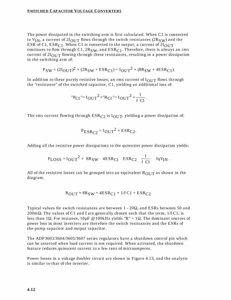
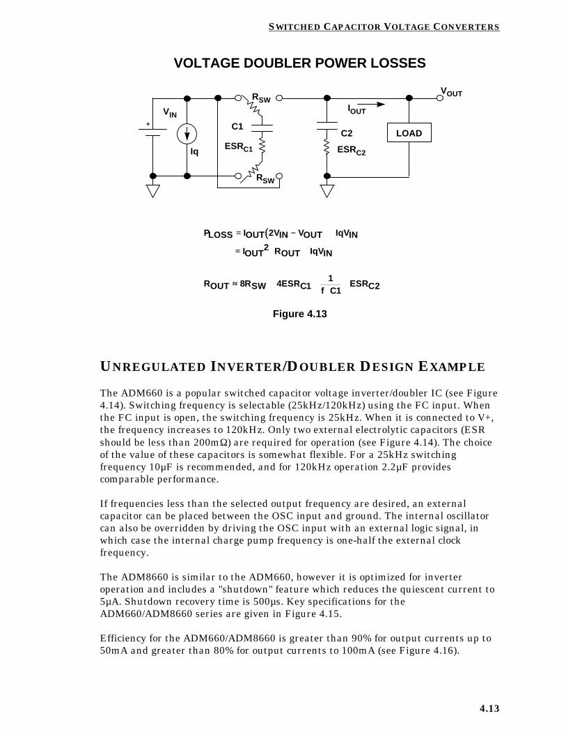
Power losses in a voltage doubler circuit are shown in Figure 4.13, and the analysisis similar to that of the inverter.
SWITCHED CAPACITOR VOLTAGE CONVERTERS
4.13
VOLTAGE DOUBLER POWER LOSSES
LOAD
VIN+ C1
C2
IOUT
ESRC1 ESRC2
VOUT
RSW
Iq
(( ))PLOSS IOUT VIN VOUT IqVIN
IOUT ROUT IqVIN
ROUT RSW ESRC f CESRC
== −− ++
== ⋅⋅ ++
≈≈ ++ ++⋅⋅
++
2
2
8 4 11
1 2
RSW
Figure 4.13
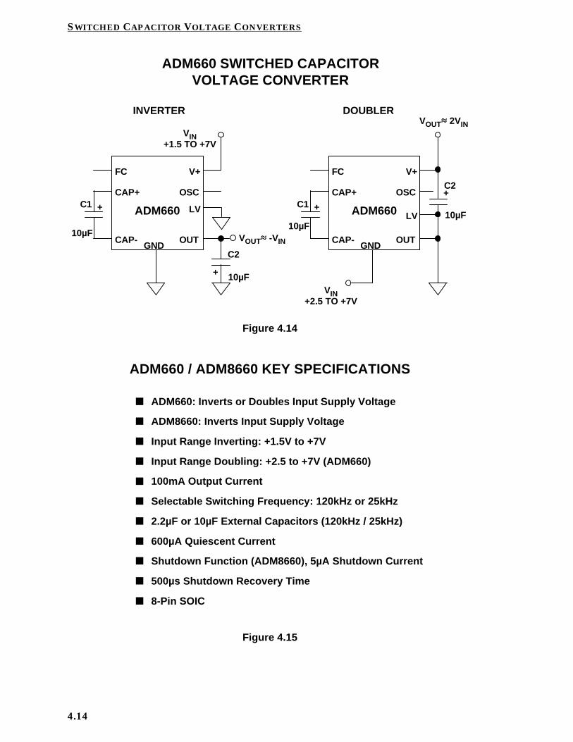
UNREGULATED INVERTER/DOUBLER DESIGN EXAMPLE
The ADM660 is a popular switched capacitor voltage inverter/doubler IC (see Figure4.14). Switching frequency is selectable (25kHz/120kHz) using the FC input. Whenthe FC input is open, the switching frequency is 25kHz. When it is connected to V+,the frequency increases to 120kHz. Only two external electrolytic capacitors (ESRshould be less than 200mΩ) are required for operation (see Figure 4.14). The choiceof the value of these capacitors is somewhat flexible. For a 25kHz switchingfrequency 10µF is recommended, and for 120kHz operation 2.2µF providescomparable performance.
If frequencies less than the selected output frequency are desired, an externalcapacitor can be placed between the OSC input and ground. The internal oscillatorcan also be overridden by driving the OSC input with an external logic signal, inwhich case the internal charge pump frequency is one-half the external clockfrequency.
The ADM8660 is similar to the ADM660, however it is optimized for inverteroperation and includes a "shutdown" feature which reduces the quiescent current to5µA. Shutdown recovery time is 500µs. Key specifications for theADM660/ADM8660 series are given in Figure 4.15.
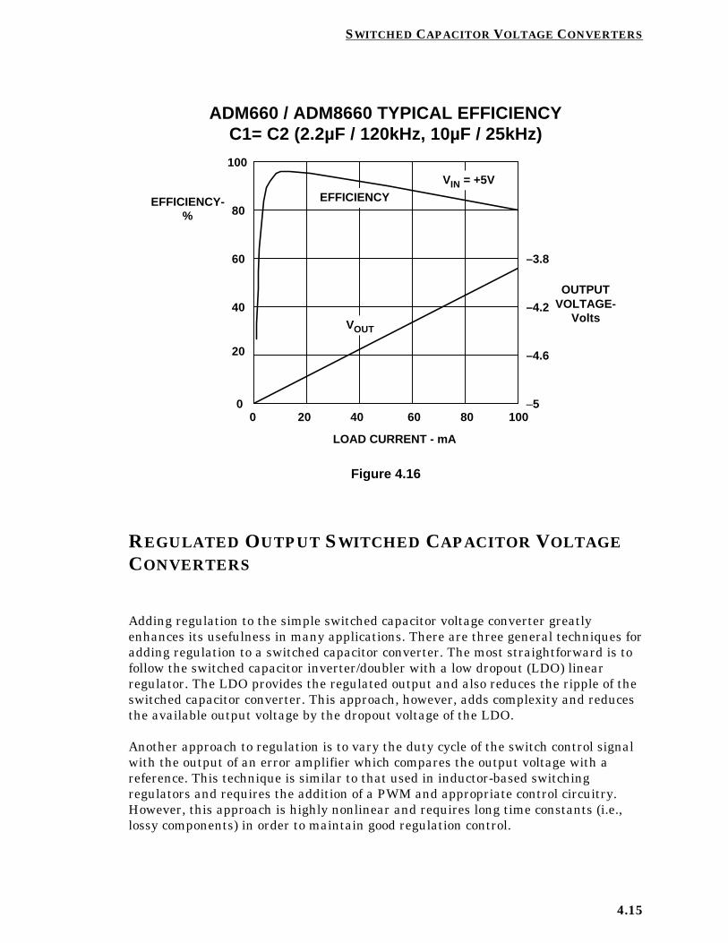
Efficiency for the ADM660/ADM8660 is greater than 90% for output currents up to50mA and greater than 80% for output currents to 100mA (see Figure 4.16).
SWITCHED CAPACITOR VOLTAGE CONVERTERS
4.14
ADM660 SWITCHED CAPACITORVOLTAGE CONVERTER
10µF
C1 +
FC
CAP+
CAP-GND
OUT
LV
OSC
V+
ADM660
+ 10µF
C2
VIN+1.5 TO +7V
VOUT≈ ≈ -VIN
10µF
C1 +
FC
CAP+
CAP-GND
OUT
LV
OSC
V+
ADM660
+
10µF
C2
VIN+2.5 TO +7V
VOUT≈ ≈ 2VIN
INVERTER DOUBLER
Figure 4.14
ADM660 / ADM8660 KEY SPECIFICATIONS
n ADM660: Inverts or Doubles Input Supply Voltage
n ADM8660: Inverts Input Supply Voltage
n Input Range Inverting: +1.5V to +7V
n Input Range Doubling: +2.5 to +7V (ADM660)
n 100mA Output Current
n Selectable Switching Frequency: 120kHz or 25kHz
n 2.2µF or 10µF External Capacitors (120kHz / 25kHz)
n 600µA Quiescent Current
n Shutdown Function (ADM8660), 5µA Shutdown Current
n 500µs Shutdown Recovery Time
n 8-Pin SOIC
Figure 4.15
SWITCHED CAPACITOR VOLTAGE CONVERTERS
4.15
ADM660 / ADM8660 TYPICAL EFFICIENCYC1= C2 (2.2µF / 120kHz, 10µF / 25kHz)
EFFICIENCY-%
0
20
40
60
80
100
–5
–4.6
–4.2
–3.8
OUTPUTVOLTAGE-
Volts
0 20 40 60 80 100
VOUT
EFFICIENCY
LOAD CURRENT - mA
VIN = +5V
Figure 4.16
REGULATED OUTPUT SWITCHED CAPACITOR VOLTAGECONVERTERS
Adding regulation to the simple switched capacitor voltage converter greatlyenhances its usefulness in many applications. There are three general techniques foradding regulation to a switched capacitor converter. The most straightforward is tofollow the switched capacitor inverter/doubler with a low dropout (LDO) linearregulator. The LDO provides the regulated output and also reduces the ripple of theswitched capacitor converter. This approach, however, adds complexity and reducesthe available output voltage by the dropout voltage of the LDO.
Another approach to regulation is to vary the duty cycle of the switch control signalwith the output of an error amplifier which compares the output voltage with areference. This technique is similar to that used in inductor-based switchingregulators and requires the addition of a PWM and appropriate control circuitry.However, this approach is highly nonlinear and requires long time constants (i.e.,lossy components) in order to maintain good regulation control.
SWITCHED CAPACITOR VOLTAGE CONVERTERS
4.16
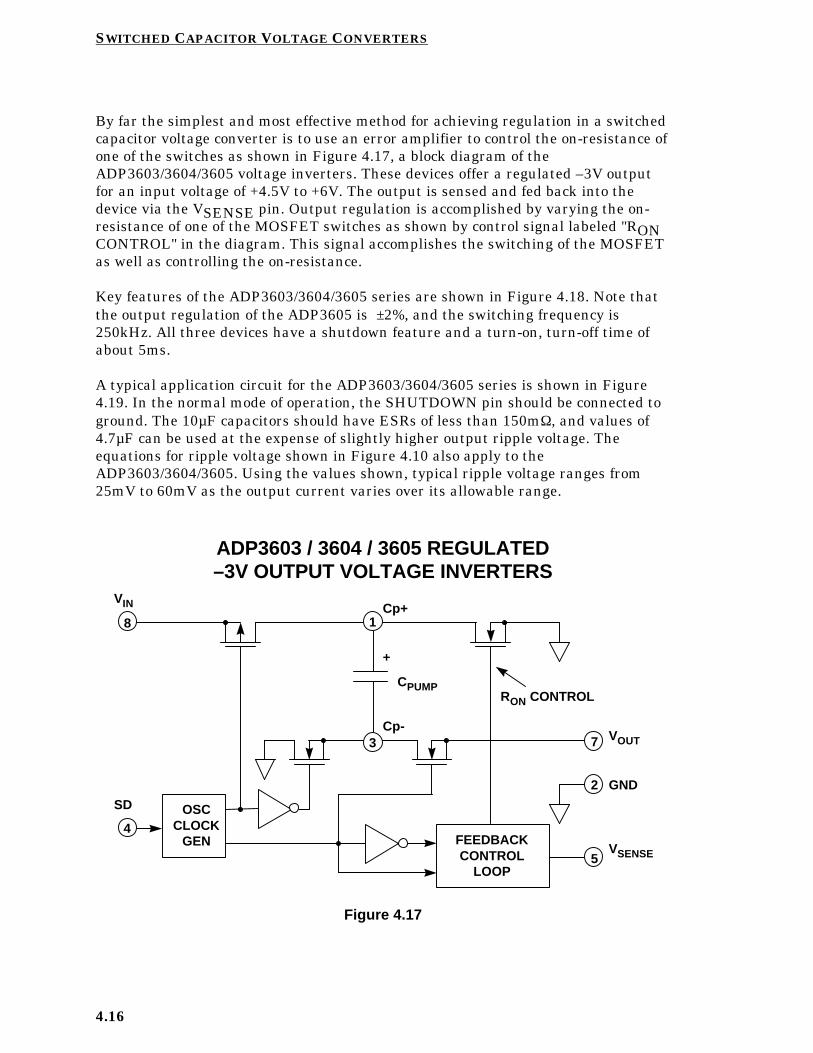
By far the simplest and most effective method for achieving regulation in a switchedcapacitor voltage converter is to use an error amplifier to control the on-resistance ofone of the switches as shown in Figure 4.17, a block diagram of theADP3603/3604/3605 voltage inverters. These devices offer a regulated –3V outputfor an input voltage of +4.5V to +6V. The output is sensed and fed back into thedevice via the VSENSE pin. Output regulation is accomplished by varying the on-resistance of one of the MOSFET switches as shown by control signal labeled "RONCONTROL" in the diagram. This signal accomplishes the switching of the MOSFETas well as controlling the on-resistance.
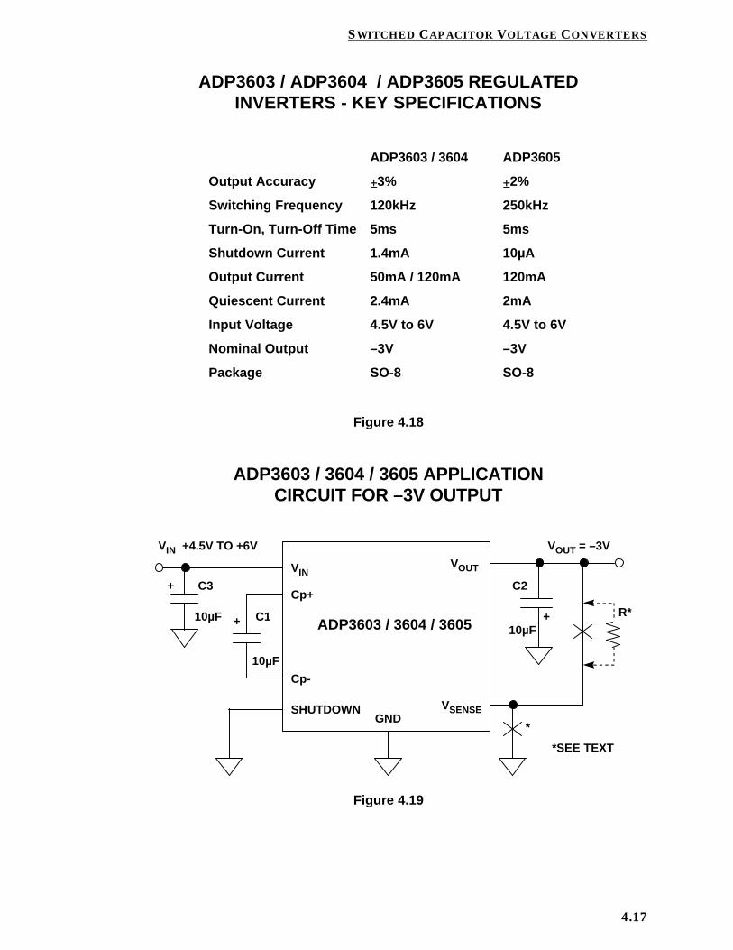
Key features of the ADP3603/3604/3605 series are shown in Figure 4.18. Note thatthe output regulation of the ADP3605 is ±2%, and the switching frequency is250kHz. All three devices have a shutdown feature and a turn-on, turn-off time ofabout 5ms.
A typical application circuit for the ADP3603/3604/3605 series is shown in Figure4.19. In the normal mode of operation, the SHUTDOWN pin should be connected toground. The 10µF capacitors should have ESRs of less than 150mΩ, and values of4.7µF can be used at the expense of slightly higher output ripple voltage. Theequations for ripple voltage shown in Figure 4.10 also apply to theADP3603/3604/3605. Using the values shown, typical ripple voltage ranges from25mV to 60mV as the output current varies over its allowable range.
ADP3603 / 3604 / 3605 REGULATED–3V OUTPUT VOLTAGE INVERTERS
+
Cp+
Cp-
VIN
SD
VOUT
GND
VSENSE
OSCCLOCK
GEN FEEDBACKCONTROL
LOOP
8
4
7
2
5
1
3
RON CONTROLCPUMP
Figure 4.17
SWITCHED CAPACITOR VOLTAGE CONVERTERS
4.17
ADP3603 / ADP3604 / ADP3605 REGULATEDINVERTERS - KEY SPECIFICATIONS
ADP3603 / 3604 ADP3605
Output Accuracy ±±3% ±±2%
Switching Frequency 120kHz 250kHz
Turn-On, Turn-Off Time 5ms 5ms
Shutdown Current 1.4mA 10µA
Output Current 50mA / 120mA 120mA
Quiescent Current 2.4mA 2mA
Input Voltage 4.5V to 6V 4.5V to 6V
Nominal Output –3V –3V
Package SO-8 SO-8
Figure 4.18
ADP3603 / 3604 / 3605 APPLICATIONCIRCUIT FOR –3V OUTPUT
VIN
Cp+
Cp-
SHUTDOWNGND
VSENSE
VOUT
ADP3603 / 3604 / 3605
VIN +4.5V TO +6V
C3
10µF
+
C1
10µF
+
C2
10µF+
VOUT = –3V
R*
*SEE TEXT
*
Figure 4.19

SWITCHED CAPACITOR VOLTAGE CONVERTERS
4.18
The regulated output voltage of the ADP3603/3604/3605 series can varied between–3V and –VIN by connecting a resistor between the output and the VSENSE pin asshown in the diagram. Regulation will be maintained for output currents up toabout 30mA. The value of the resistor is calculated from the following equation:
VOUTRk
V= − +
5
3Ω
.
The devices can be made to operate as standard inverters providing an unregulatedoutput voltage if the VSENSE pin is simply connected to ground.
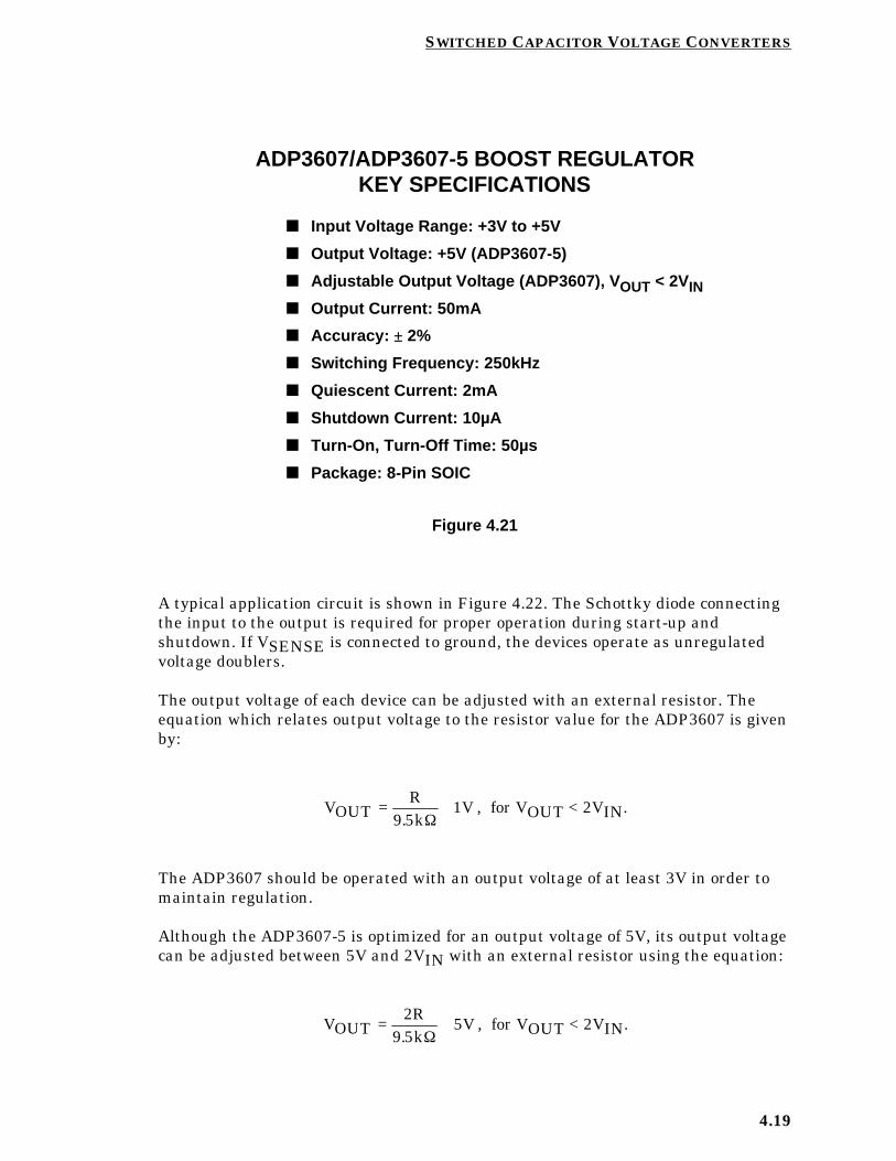
The ADP3607/ADP3607-5 are boost switched capacitor voltage regulators based ona regulated voltage doubling topology. The ADP3607-5 is optimized for an outputvoltage of +5V for inputs between +3V and +5V. The ADP3607 output is adjustablewith an external resistor. A block diagram is shown in Figure 4.20 and keyspecifications in Figure 4.21. The device uses a feedback control scheme similar tothe ADP3603/3604/3605 to maintain output voltage regulation for VOUT < 2VIN.
ADP3607 SWITCHED CAPACITOR BOOST REGULATOR
+Cp+ Cp-VIN
SD
VOUT
GND
VSENSE
OSCCLOCK
GENFEEDBACKCONTROL
LOOP
8
4
8
7
5
1
RON CONTROL
CPUMP
3
1.5VREF
Figure 4.20
SWITCHED CAPACITOR VOLTAGE CONVERTERS
4.19
ADP3607/ADP3607-5 BOOST REGULATORKEY SPECIFICATIONS
n Input Voltage Range: +3V to +5V
n Output Voltage: +5V (ADP3607-5)
n Adjustable Output Voltage (ADP3607), VOUT < 2VIN
n Output Current: 50mA
n Accuracy: ±± 2%
n Switching Frequency: 250kHz
n Quiescent Current: 2mA
n Shutdown Current: 10µA
n Turn-On, Turn-Off Time: 50µs
n Package: 8-Pin SOIC
Figure 4.21
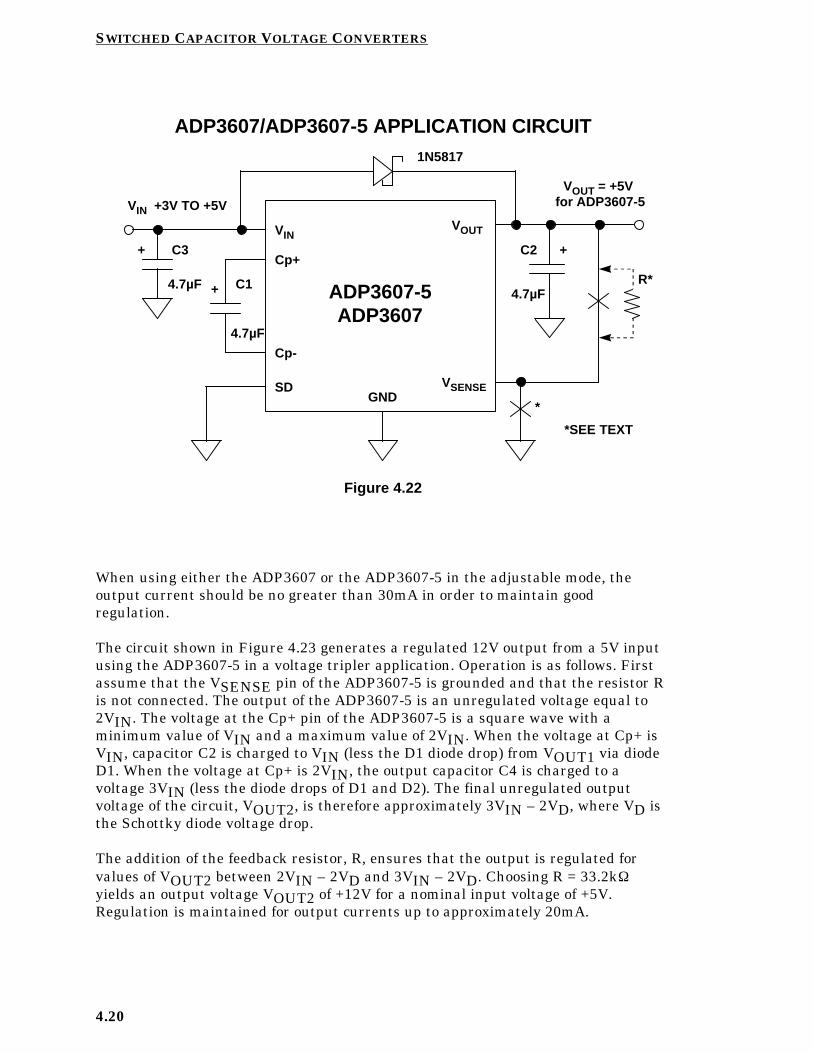
A typical application circuit is shown in Figure 4.22. The Schottky diode connectingthe input to the output is required for proper operation during start-up andshutdown. If VSENSE is connected to ground, the devices operate as unregulatedvoltage doublers.
The output voltage of each device can be adjusted with an external resistor. Theequation which relates output voltage to the resistor value for the ADP3607 is givenby:
VOUTRk
= +9 5
1V. Ω
, for VOUT < 2VIN.
The ADP3607 should be operated with an output voltage of at least 3V in order tomaintain regulation.
Although the ADP3607-5 is optimized for an output voltage of 5V, its output voltagecan be adjusted between 5V and 2VIN with an external resistor using the equation:
VOUT kV= +
2R9 5
5. Ω
, for VOUT < 2VIN.
SWITCHED CAPACITOR VOLTAGE CONVERTERS
4.20
ADP3607/ADP3607-5 APPLICATION CIRCUIT
VIN
Cp+
Cp-
SDGND
VSENSE
VOUT
ADP3607-5ADP3607
VIN +3V TO +5V
C3
4.7µF
+
C1
4.7µF
+
C2
4.7µF
+
VOUT = +5V for ADP3607-5
1N5817
R*
*SEE TEXT
*
Figure 4.22
When using either the ADP3607 or the ADP3607-5 in the adjustable mode, theoutput current should be no greater than 30mA in order to maintain goodregulation.
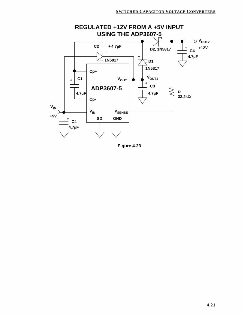
The circuit shown in Figure 4.23 generates a regulated 12V output from a 5V inputusing the ADP3607-5 in a voltage tripler application. Operation is as follows. Firstassume that the VSENSE pin of the ADP3607-5 is grounded and that the resistor Ris not connected. The output of the ADP3607-5 is an unregulated voltage equal to2VIN. The voltage at the Cp+ pin of the ADP3607-5 is a square wave with aminimum value of VIN and a maximum value of 2VIN. When the voltage at Cp+ isVIN, capacitor C2 is charged to VIN (less the D1 diode drop) from VOUT1 via diodeD1. When the voltage at Cp+ is 2VIN, the output capacitor C4 is charged to avoltage 3VIN (less the diode drops of D1 and D2). The final unregulated outputvoltage of the circuit, VOUT2, is therefore approximately 3VIN – 2VD, where VD isthe Schottky diode voltage drop.
The addition of the feedback resistor, R, ensures that the output is regulated forvalues of VOUT2 between 2VIN – 2VD and 3VIN – 2VD. Choosing R = 33.2kΩyields an output voltage VOUT2 of +12V for a nominal input voltage of +5V.Regulation is maintained for output currents up to approximately 20mA.
SWITCHED CAPACITOR VOLTAGE CONVERTERS
4.21
REGULATED +12V FROM A +5V INPUTUSING THE ADP3607-5
C1
4.7µF
+
4.7µF+
4.7µF
+
C2
C3
R33.2kΩΩ
C4
4.7µF
+D2, 1N5817
1N5817
ADP3607-5
SD GND
VIN
Cp+
Cp-
VOUT
VSENSE
C4+
4.7µF
VIN
+5V
VOUT2
+12V
1N5817 D1
VOUT1
Figure 4.23