fully integrated switched capacitor buck...
TRANSCRIPT

FULLY INTEGRATED SWITCHED CAPACITOR BUCK CONVERTER
WITH HIGH EFFICIENCY AND LOW OUTPUT RIPPLE
BY
SUDHIR REDDY GOUNI, B.Tech
A thesis submitted to the Graduate School
in partial fulfillment of the requirements
for the degree
Master of Sciences, Engineering
Specialization in: Electrical Engineering
New Mexico State University
Las Cruces, New Mexico
November 2012

“ FULLY INTEGRATED SWITCHED CAPACITOR BUCK CONVERTER WITH
HIGH EFFICIENCY AND LOW OUTPUT RIPPLE,” a thesis prepared by SUD-
HIR REDDY GOUNI in partial fulfillment of the requirements for the degree,
Master of Sciences has been approved and accepted by the following:
Linda LaceyDean of the Graduate School
Chair of the Examining Committee
Date
Committee in charge:
Dr. Paul M. Furth, Associate Professor, Chair.
Dr. Jaime Ramirez-Angulo, Professor.
Dr. Jeffrey Beasley, Professor.
ii

DEDICATION
Dedicated to my father Manikya Reddy, mother Seshamma and my brother
and sisters.
iii

ACKNOWLEDGMENTS
I would like to thank my parents and friends for their support to complete
my Master’s degree.
I would like to thank Dr. Paul Furth and Dr.Jaime Ramirez for their
support and encouragement throughout my study at New Mexico State University.
I would also like to thank Dr.Jeffrey Beasley for his valuable time and suggestions.
iv

VITA
Febraury 25, 1989 Born in Gadwal, India.
Education
2006 - 2010 B.Tech. Electronics and Communications Engineering,JNTU, India
2010 - 2012 MSEE. in Electrical Engineering,New Mexico State University, USA - GPA 3.9/4.0
Experience
Graduate Teaching Assistant, Electrical Engineering, NMSU, Fall-2010, Spring2011, Fall 2011, Spring 2012
v

ABSTRACT
FULLY INTEGRATED SWITCHED CAPACITOR BUCK CONVERTER
WITH HIGH EFFICIENCY AND LOW OUTPUT RIPPLE
BY
SUDHIR REDDY GOUNI, B.Tech
Master of Sciences, Engineering
Specialization in Electrical Engineering
New Mexico State University
Las Cruces, New Mexico, 2012
Dr. Paul M. Furth, Chair
An Integrated Power Management System is built on a single chip. The blocks
of this system include Switched Capacitor (SC) buck converter, Low Drop-Out
voltage regulator (LDO), comparator and voltage reference. A high efficiency
and extremely low ripple buck converter is designed using a switched capacitor
voltage divider which converts 3.3 V down to 1.5 V, while operating at a switching
frequency of 15 MHz and a load current range of 10µA to 1 mA. A Low Dropout
Voltage regulator (LDO) is used at the output of the SC converter, to reduce
the ripple and its output voltage is 1.2V. The LDO quiescent current is 40nA. A
control loop is implemented using a clock comparator, which helps in improving
the efficiency and regulate the output voltage of LDO. The reference voltage
vi

and currents for the comparator and the LDO are generated using a Bandgap
Reference circuit. Also a clock generator is used to generate different clocks for
the switching converter. This system has a maximum efficiency of 63% and an
output ripple of 20mV at 1mA load current. Efficiencies above 50% are achieved
for load currents in the range of 100µA to 1 mA. Compared to an only LDO design
in which the maximum possible theoretical efficiency is ratio of input to output
voltage, in this case it is about 36 %, this design has much higher efficiency.
vii

TABLE OF CONTENTS
LIST OF TABLES xi
LIST OF FIGURES xii
1 INTRODUCTION 1
1.0.1 Unique Contributions of this Thesis . . . . . . . . . . . . . 3
1.0.2 Thesis Organization . . . . . . . . . . . . . . . . . . . . . 3
2 LITERATURE REVIEW 4
2.1 Low Drop-Out Voltage Regulators(LDO) . . . . . . . . . . . . . . 4
2.2 Inductor-based Buck Converters . . . . . . . . . . . . . . . . . . . 8
2.3 Switched Capacitor(SC) Buck Converters . . . . . . . . . . . . . . 11
2.4 Bandgap References . . . . . . . . . . . . . . . . . . . . . . . . . . 14
2.4.1 Bandgap Voltage References . . . . . . . . . . . . . . . . . 14
2.4.2 Bandgap Current Reference . . . . . . . . . . . . . . . . . 19
2.5 Comparators . . . . . . . . . . . . . . . . . . . . . . . . . . . . . 19
2.5.1 Comparators with Hysteresis . . . . . . . . . . . . . . . . . 20
2.5.2 Clocked Comparators . . . . . . . . . . . . . . . . . . . . . 21
2.6 Non-Overlapping Clock Generation . . . . . . . . . . . . . . . . . 23
2.7 Controller Design . . . . . . . . . . . . . . . . . . . . . . . . . . . 23
2.7.1 Pulse Width Modulation (PWM) . . . . . . . . . . . . . . 25
viii

2.7.2 Pulse Frequency Modulation (PFM) . . . . . . . . . . . . 26
3 DESIGN AND SIMULATIONS 28
3.1 Switched Capacitor (SC) Buck Converter . . . . . . . . . . . . . . 28
3.1.1 Design of SC Buck Converter . . . . . . . . . . . . . . . . 28
3.1.2 Simulations of SC buck converter . . . . . . . . . . . . . . 30
3.1.3 Analysis . . . . . . . . . . . . . . . . . . . . . . . . . . . . 31
3.2 Non-Overlapping Clock Generator . . . . . . . . . . . . . . . . . . 35
3.2.1 Design of Non-overlapping Clock Generator . . . . . . . . 35
3.2.2 Simulations of Non-overlapping Clock Generator . . . . . . 35
3.3 Long Channel Bandgap Reference . . . . . . . . . . . . . . . . . . 36
3.3.1 Design of Bandgap reference . . . . . . . . . . . . . . . . . 36
3.3.2 Generating Bias Currents . . . . . . . . . . . . . . . . . . 40
3.3.3 Bandgap Reference Simulations . . . . . . . . . . . . . . . 41
3.4 Clocked Comparator . . . . . . . . . . . . . . . . . . . . . . . . . 42
3.4.1 Design of Clocked Comparator . . . . . . . . . . . . . . . . 42
3.4.2 Simulations of clocked comparator . . . . . . . . . . . . . . 44
3.5 Low Drop-out Voltage Regulator . . . . . . . . . . . . . . . . . . 44
3.6 Control Loop . . . . . . . . . . . . . . . . . . . . . . . . . . . . . 46
3.6.1 Design of Burst-mode PFM control loop . . . . . . . . . . 46
3.6.2 Simulations of SC Buck Converter with Control loop . . . 48
3.7 Integrated System . . . . . . . . . . . . . . . . . . . . . . . . . . . 49
3.7.1 Design and Simulations of the Integrated System . . . . . 49
4 EXPERIMENTAL RESULTS 52
4.1 Layout . . . . . . . . . . . . . . . . . . . . . . . . . . . . . . . . . 52
ix

4.2 Test Apparatus . . . . . . . . . . . . . . . . . . . . . . . . . . . . 53
4.3 Hardware Results . . . . . . . . . . . . . . . . . . . . . . . . . . . 55
4.3.1 Clock Generator . . . . . . . . . . . . . . . . . . . . . . . 56
4.3.2 SC buck converter . . . . . . . . . . . . . . . . . . . . . . 56
4.3.3 Clocked Comparator . . . . . . . . . . . . . . . . . . . . . 57
4.3.4 Bandgap Reference . . . . . . . . . . . . . . . . . . . . . . 59
4.3.5 Integrated System . . . . . . . . . . . . . . . . . . . . . . . 60
5 DISCUSSION AND CONCLUSION 61
5.1 Analysis of Simulated and Measured Results . . . . . . . . . . . . 61
5.2 Future Work . . . . . . . . . . . . . . . . . . . . . . . . . . . . . . 64
5.2.1 Time Interleaving . . . . . . . . . . . . . . . . . . . . . . . 64
5.2.2 Capacitor Banks . . . . . . . . . . . . . . . . . . . . . . . 65
5.2.3 Control Loop . . . . . . . . . . . . . . . . . . . . . . . . . 65
APPENDICES 67
A. Test Document 68
x

LIST OF TABLES
3.1 SC Buck Converter Specifications . . . . . . . . . . . . . . . . . . 29
3.2 SC Buck converter transistor sizing . . . . . . . . . . . . . . . . . 30
3.3 Non-overlapping clock generator transistor sizing . . . . . . . . . 36
3.4 Long Channel Bandgap Reference transistor sizing . . . . . . . . . 39
3.5 Long Channel Bandgap Reference Resistor Values . . . . . . . . . 40
3.6 Clocked Comparator transistor sizing . . . . . . . . . . . . . . . . 43
4.1 Bandgap reference voltage variations . . . . . . . . . . . . . . . . 59
5.1 Comparison of Simulation and Measured Results . . . . . . . . . . 62
5.2 Switched Capacitor Buck Converter Measured Results . . . . . . . 62
5.3 Integrated System Results Comparison . . . . . . . . . . . . . . . 63
xi
LIST OF FIGURES
1.1 Block Diagram of the Inegrated Power Management System . . . 2
2.1 Low Drop-Out Voltage Regulator from [2] . . . . . . . . . . . . . 6
2.2 LDO Drop-out . . . . . . . . . . . . . . . . . . . . . . . . . . . . 6
2.3 Buck Converter Block Diagram from [3] . . . . . . . . . . . . . . 8
2.4 Buck Converter Architecture from [3] . . . . . . . . . . . . . . . 9
2.5 Buck Converter timing diagram . . . . . . . . . . . . . . . . . . . 10
2.6 Switched Capacitor Voltage Divider [1] . . . . . . . . . . . . . . . 12
2.7 Different States of Switched Capacitor Voltage Divider . . . . . . 12
2.8 SC Buck converter output voltage waveform . . . . . . . . . . . . 13
2.9 Bandgap Reference Block Diagram [4] . . . . . . . . . . . . . . . . 15
2.10 CTAT Voltage Reference . . . . . . . . . . . . . . . . . . . . . . . 17
2.11 Bandgap Voltage Reference . . . . . . . . . . . . . . . . . . . . . 18
2.12 Current Reference Implementation . . . . . . . . . . . . . . . . . 20
2.13 Comparator Symbol . . . . . . . . . . . . . . . . . . . . . . . . . 20
2.14 Comparator with hysteresis . . . . . . . . . . . . . . . . . . . . . 22
2.15 Clocked comparator from [5] . . . . . . . . . . . . . . . . . . . . . 22
2.16 Non-Overlapping Clock Generator from [4] . . . . . . . . . . . . 24
2.17 Non-overlapping clocks . . . . . . . . . . . . . . . . . . . . . . . . 24
2.18 Pulse Width Modulation block diagram . . . . . . . . . . . . . . . 25
xii

2.19 Block diagram of burst-mode PFM regulator from [6] . . . . . . 26
2.20 Waveforms of burst-mode PFM . . . . . . . . . . . . . . . . . . . 27
3.1 Schematic of the SC Buck Converter . . . . . . . . . . . . . . . . 29
3.2 Output voltage waveform of SC Buck converter at 1mA load current 30
3.3 Efficiency Vs Load current plot for SC Buck converter . . . . . . . 31
3.4 Average output voltage Vs Load current plot for SC Buck converter 32
3.5 Output voltage ripple Vs Load current plot for SC Buck converter 33
3.6 Simulated waveforms of SC Buck Converter . . . . . . . . . . . . 34
3.7 Non-overlapping clock generator . . . . . . . . . . . . . . . . . . . 36
3.8 Non-overlapping clock generator waveforms . . . . . . . . . . . . . 37
3.9 Deadtime time between the Clocks . . . . . . . . . . . . . . . . . 38
3.10 Long Channel Bandgap Reference . . . . . . . . . . . . . . . . . 38
3.11 Variations with input voltage . . . . . . . . . . . . . . . . . . . . 41
3.12 Variations with temperature . . . . . . . . . . . . . . . . . . . . . 42
3.13 Schematic of Clocked Comparator . . . . . . . . . . . . . . . . . . 43
3.14 Testbench Schematic of Clocked Comparator . . . . . . . . . . . . 44
3.15 Waveforms of Clocked Comparator . . . . . . . . . . . . . . . . . 45
3.16 Schematic of the LDO . . . . . . . . . . . . . . . . . . . . . . . . 45
3.17 AC analysis of LDO . . . . . . . . . . . . . . . . . . . . . . . . . 46
3.18 Schematic of SC Buck Converter with Burst-mode PFM ControlLoop . . . . . . . . . . . . . . . . . . . . . . . . . . . . . . . . . . 47
3.19 SC Buck converter Waveforms at 100µA load current . . . . . . . 48
3.20 SC Buck converter Waveforms at 500µA load current . . . . . . . 49
3.21 Schematic of the Integrated System at 1 mA Load current . . . . 50
3.22 Simulated waveforms of the Integrated System . . . . . . . . . . . 51
xiii

4.1 Layout of the whole design . . . . . . . . . . . . . . . . . . . . . . 53
4.2 SC Buck Converter Layout . . . . . . . . . . . . . . . . . . . . . . 54
4.3 Non-Overlapping Clock Generator Layout . . . . . . . . . . . . . 55
4.4 Clocked Comparator Generator Layout . . . . . . . . . . . . . . . 55
4.5 Bandgap Reference Layout . . . . . . . . . . . . . . . . . . . . . . 56
4.6 Low Drop Voltage Regulator Layout . . . . . . . . . . . . . . . . 57
4.7 Measured Waveforms of Clock Generator . . . . . . . . . . . . . . 58
4.8 Measured Waveforms of SC buck converter . . . . . . . . . . . . . 58
4.9 Measured Waveforms of Clocked Comparator . . . . . . . . . . . . 59
4.10 Measured Waveforms of Integrated System . . . . . . . . . . . . . 60
5.1 Bottom Plate Capacitance . . . . . . . . . . . . . . . . . . . . . . 64
5.2 Implementation of time interleaving in SC converters . . . . . . . 65
5.3 Capacitor Banks . . . . . . . . . . . . . . . . . . . . . . . . . . . 66
5.4 Implementing a VCO in PFM control loop . . . . . . . . . . . . . 66
xiv

Chapter 1
INTRODUCTION
Power consumption is of a great importance in all battery powered portable elec-
tronic device. The efficiency of analog and digital circuits are generally improved
by operating at lower power supply voltages. However, due to compatability and
fabrication issues, different circuit blocks on a complex integrated circuit often
operate at different voltage levels. As such we require a chip to be powered with
several external supplies. Having several external supplies increases the manufac-
turing cost for incorporating the chip.
One solution is to have on-chip DC-DC conversion. Low drop-out voltage
regulators (LDO), inductor-based DC-DC converters and switched capacitor DC-
DC converters are the three main types of DC voltage converters.
Highest efficiencies can be achieved by inductor-based DC-DC conversion.
But inductor-based supplies are are not suitable for implementation on-chip, as
high quality large-value inductors cannot be integrated. Moreover, the use of
inductors results in magnetic coupling issues.
LDO’s are another type of DC-DC converter. They have become an impor-
tant part of battery powered systems due to their ability to regulate the output
voltage. By regulate we mean that the output voltage is constant irrespective of
changes in input voltage and output load current. LDO’s also occupy low area
and can be integrated on chip. LDO’s are generally used to drive analog and
mixed signal circuit blocks, circuits which are sensitive to power supply ripple.
1

The efficiency of an LDO is given by the ratio of the output voltage to the input
voltage. Therefore the efficiency of the LDO will be high only if the difference
between the input and output voltages is small. In addition, the quiescent current
of the LDO must be kept very low.
High efficiency on chip-chip DC-DC conversion, when the difference be-
tween the input and output voltages is high, is possible by using switched ca-
pacitor circuits. Switched capacitor circuits make use of capacitors and switches,
which can be fully integrated, for DC-DC conversion.
The main goal of this thesis is to realize on-chip DC-DC conversion with
high efficiency. Therefore we used a switchced capacitor design in a buck converter.
We selected a buck converter architecture [1] with switched capacitor design in
which Vout = 0.5Vin. An integrated power management system is designed in this
thesis. The block diagram of the integrated power management system is shown
in Fig: 1.1. Switched Capacitor buck converter, low drop out voltage regulator,
bandgap reference and comparator are the major blocks present in the system.
Figure 1.1: Block Diagram of the Inegrated Power Management System
2

In order to function as a good voltage regulator, the switched capacitor
design needs a control scheme. Pulse frequency modulation (PFM) and pulse
width modulation (PWM) are the two regulation schemes that are widely used.
We made use of the PFM scheme to regulate the output voltage, so as to achieve
the widest possible range of load currents.
1.0.1 Unique Contributions of this Thesis
1) First fully-integrated switched-capacitor DC-to-DC converter of the
NMSU VLSI laboratory.
2) First fully-implemented power management system, including:
i) Bandgap voltage reference.
ii) Current source.
iii) Switched-capacitor DC-to-DC buck converter.
Feedback Control Circuit:
iv) Low drop-out voltage regulator.
v) Non-overlapping clock generator.
vi) Clocked comparator.
1.0.2 Thesis Organization
This thesis is organized as follows. Chapter 2 introduces the three types of
DC-DC conversions available and the maximum achievable efficieny in each type.
Chapter 2 also describes the operation of different blocks used in our integrated
power management system. Chapter 3 describes the design modifications and
simulations of different blocks of the integrated sytem. Test results and the orga-
nization of the layout are shown in Chapter 4. Comparison of results and issues
that we faced are discussed in Chapter 5. Also the future work and enhancements
that can be done to this thesis are discussed.
3

Chapter 2
LITERATURE REVIEW
A DC-DC converter is a device which accepts a DC voltage and produces a dif-
ferent DC voltage. A buck converter is used to produce a lower DC voltage level
than the input. It is also called as a step down converter. These converters use
a clock signal, active elements as switches, and reactive passive elements to store
and release energy. The switches used must be very fast in order to achieve high
efficiency at high switching frequencies. There are three types of buck convert-
ers. They are the inductor-based converter, switch capacitor converters and low
drop-out voltage regulators. All these converters are discussed in this chapter.
Controller design methods, which are used to regulate the output voltage, are
also discussed.
2.1 Low Drop-Out Voltage Regulators(LDO)
A Low Drop-out Voltage Regulator (LDO) is a linear voltage regulator
which can supply regulated or constant, output voltage. It is also called as buck
converter. The basic architecture of an LDO is shown in Fig. 2.1. The important
blocks of the LDO are a voltage reference, error amplifier, pass transistor and
voltage divider.
The voltage divider can be implemented using a simple resistor divider,
Rf1 and Rf2. Output voltage is scaled according to the resistor ratio. The voltage
reference is typically generated from a Bandgap reference and is used to provide a
stable DC voltage. Another important block is the error amplifier. It can be a one-
4

stage or a multi-stage differential amplifier. The positive terminal is connected to
the resistor divider, so that it forms a negative feedback loop. Negative feedback
is achieved because the gain of the pass transistor is negative. The negative
terminal of the error amplifier is connected to the reference voltage. The error
amplifier generates a signal which is a scaled difference between the reference
voltage and the feedback voltage. This signal is given to the gate of the pass
transistor, which generates current accordingly. Therefore the output voltage will
be constant irrespective of changes in the input voltage and irrespective of changes
in the load current.
V out = V refRf1 +Rf2
Rf1(2.1)
Another important block of the LDO is the PMOS pass transistor. The
gate of the PMOS transistor is connected to the output of the error amplifier. The
source is connected to the input voltage. The drain is connected to the output
load and the feedback resistor divider network. The important characteristics of
the pass element are low voltage drop across the source-drain terminals and high
current handling capability. Therefore, the PMOS transistor is generally huge in
size.
The important specifications of the LDO are drop-out voltage, stability,
line regulation, load regulation and power supply rejection ratio (PSRR). One
definition of dropout voltage is ” The voltage difference between the input and
output voltages when the output is 100mV below its value when the input is at its
nominal value [2].” It can be found by giving a slowly varying traingular signal
to the input of the LDO.
5

Figure 2.1: Low Drop-Out Voltage Regulator from [2]
Figure 2.2: LDO Drop-out
Stability of the LDO can be found using AC analysis, and measuring the
phase and gain margins. In general the phase margin and gain margin must be
greater than 45°and 10 dB, respectively. Many possible compensation techniques
can be used to stabilize the circuit. Miller compensation is widely used. In this
technique a capacitor is added between the first and second stage to split the
poles. Also at the output of each stage, a series resistor can be added to the
capacitor to cancel the right half plane zero in the circuit.
6

Line and load regulation are other specifications of the LDO. Line regula-
tion indicates the capability of the circuit to keep the output at a steady value
irrespective of changes in the input voltage. Line regulation can be found by giving
slow variations in the input voltage and observing the change in ouput voltage.
Line regulation =∆Vout∆Vin
(2.2)
Load regulation indicates the capability of the circuit to handle steady
state changes in load values. To find the load regulation, a switch can be used to
change the load current values through a pulse. The input voltage of the LDO is
kept constant in this test. Load regulation is defined by
Load regulation =∆Vout∆IL
(2.3)
The efficiency of an LDO is given by
η =Pout
Pin
=VoutIout
Vin(Iout + Iq)(2.4)
Assuming Iq <<Iout, the efficiency simplifies to:
η =VoutVin
(2.5)
If the input voltage is 1.4 V and output voltage is 1.2 V, then the efficiency
of the LDO is reasonably good:
η =1.2
1.4= 85% (2.6)
7

By observing the ( 2.6) we can see that the efficiency of the LDO is high only
when the difference between the input and output voltages is very small. Also the
quiescent current must be very small.
2.2 Inductor-based Buck Converters
The key element of the switching converters is the switching action. Power
efficiency is critical. The available passive elements are resistive elements, capaci-
tive elements and magnetic devices. Magnetic devices are needed to produce high
efficiency converters. Ideally magnetic devices would consume zero power, as their
major role is to store and release energy. Fig. 2.3 shows the implementation of a
simple buck converter [3].
Figure 2.3: Buck Converter Block Diagram from [3]
A single pole double throw (SPDT) switch is connected between the input
and output. Maximum efficiency is achieved if the switch is ideal, meaning it
has no voltage drop across it. The ouput of the SPDT switch contains a large
AC component which has a fundamental switching frequency component, plus
harmonics. Therefore a low pass filter is placed between the switch and output.
The low pass filter is formed by using an inductor and a capacitor, with a time
constant√LC.
8

Figure 2.4: Buck Converter Architecture from [3]
The SPDT switch can be implemented using semiconductor devices. As
shown in Fig. 2.4 a PMOS transistor and a diode are used. The switching fre-
quency fs generally lies in the range of 1 kHz to 1 MHz. The duty cycle D is the
fraction of time the switch is ON.
During the first half of the cycle the PMOS switch is ON and the diode
is OFF as it is reverse-biased with a voltage of −Vin. During the second half of
the cycle, the PMOS switch is turned OFF and the diode becomes forward-biased
as the inductor current makes a path through the diode. The ouput voltage is
calculated by averaging the inductor voltage over one time period T and equating
it to zero. The average voltage across the inductor must be zero in steady-state
or else the inductor current would eventually be infinite (or zero).
The output voltage of a buck converter is given by
Vout = DVin (2.7)
As the duty cycle D is always less than one, the equation results in a step
down voltage. Some assumptions are made for deriving (2.7). PMOS switch and
9

Figure 2.5: Buck Converter timing diagram
the diode are assumed to have no voltage drop and also parasitic capacitances
are neglected. One important condition that we need to verify is the switching
period must be shorter than the time constant√LC. If the diode drop alone is
considered, then
Vout = DVin − (1−D)VD (2.8)
The input current and average inductor current are derived as
< IL > = < Iout > (2.9)
< Iin > = DIL (2.10)
< Iout > =IinD
(2.11)
The efficiency is given by:
10

η =Pout
Pin
=VoutIoutVinIin
(2.12)
By substituing (2.11) and (2.7) in (2.12) we get η as 100%. But in practical im-
plementations efficiencies of 85% to 95% are achievable for a specific load current
because of losses due to switching, parasitic capacitances and also equivalent series
resistances of the inductor and capacitor.
A controller can be designed to regulate the output by controlling the duty
cycle. The only disadvantage of this converter is that the inductor cannot be
placed on chip. But the use of an inductor helps in achieving high efficiency.
Conversion ratio is the ratio of output voltage to the input voltage. This high
efficiency is maintained even for low conversion ratios.
2.3 Switched Capacitor(SC) Buck Converters
Switched capacitor (SC) circuits perform voltage conversion using the charge
transfer method. SC circuits perform the charge transfer using capacitors and
switches. The most common switched capacitor circuits are a buck converter,
voltage doubler and voltage inverter. A voltage divider, or buck converter, shown
in Fig. 2.6 [1].
During the first half of the switching cycle, capacitor C1 is connected to the
input voltage source and during the second half of the cycle C2 will be connected
to the input source, as shown in Fig. 2.7. If we use cpacitors of same value the
average output voltage is:
Voutavg =Vin2
(2.13)
11

Figure 2.6: Switched Capacitor Voltage Divider [1]
Figure 2.7: Different States of Switched Capacitor Voltage Divider
By observing Fig 2.8 the output voltage ripple can be derived from
i = Cdv
dt(2.14)
12

Figure 2.8: SC Buck converter output voltage waveform
which can be rearranged as
∆Vout =IoutT
2C(2.15)
Assuming complete charge transfer through the switches, the efficiency is
given as
η =Pout
Pout + Ploss
(2.16)
As the ouput power is the average of the output voltage and output current, using
the (2.13) output power is
Pout =IoutVin
2(2.17)
Assuming complete charge transfer, dynamic power consumption due to switching
is given as
Ploss = fC∆V 2out (2.18)
13

Using (2.17) and (2.18), efficiency is derived as
η =
(1 +
∆VoutVin
)−1
(2.19)
From the equation above we can say that efficiency is inversely proportional to the
output voltage ripple. High efficiencies are achieved if the switching frequencies
are high, capacitors are large and loads are light. Switched capacitor techniques
have both advantages and disadvantages. The main advantage comes from the
absence of the inductor and thus, no electromagnetic coupling to other circuits.
Other important advantage is the size of the circuit becomes much smaller and
can be integrated on chip. However, it is difficult to maintain high efficiencies
over a wide conversion ratio range. Typical conversion ratios are 0.5 to 0.33.
2.4 Bandgap References
Voltage references are used to generate a constant voltage. These references
are used in LDO’s, A/D and D/A converters, RF circuits, etc. The accuracy
of these reference circuits is very important as the accuracy, of these circuits
depends on the accuracy of the reference. The reference voltage must be constant,
independent of process, power supply and temperature variations.
2.4.1 Bandgap Voltage References
The main idea in generating a temperature-inpendent reference is to add
two quantities with opposite temperature coefficients with proper weighting [4].
As shown in Fig. 2.9 a voltage reference is weighted as the sum of propor-
tional to absolute temperature (PTAT) and complementary to absolute tempera-
ture (CTAT) quantities.
14
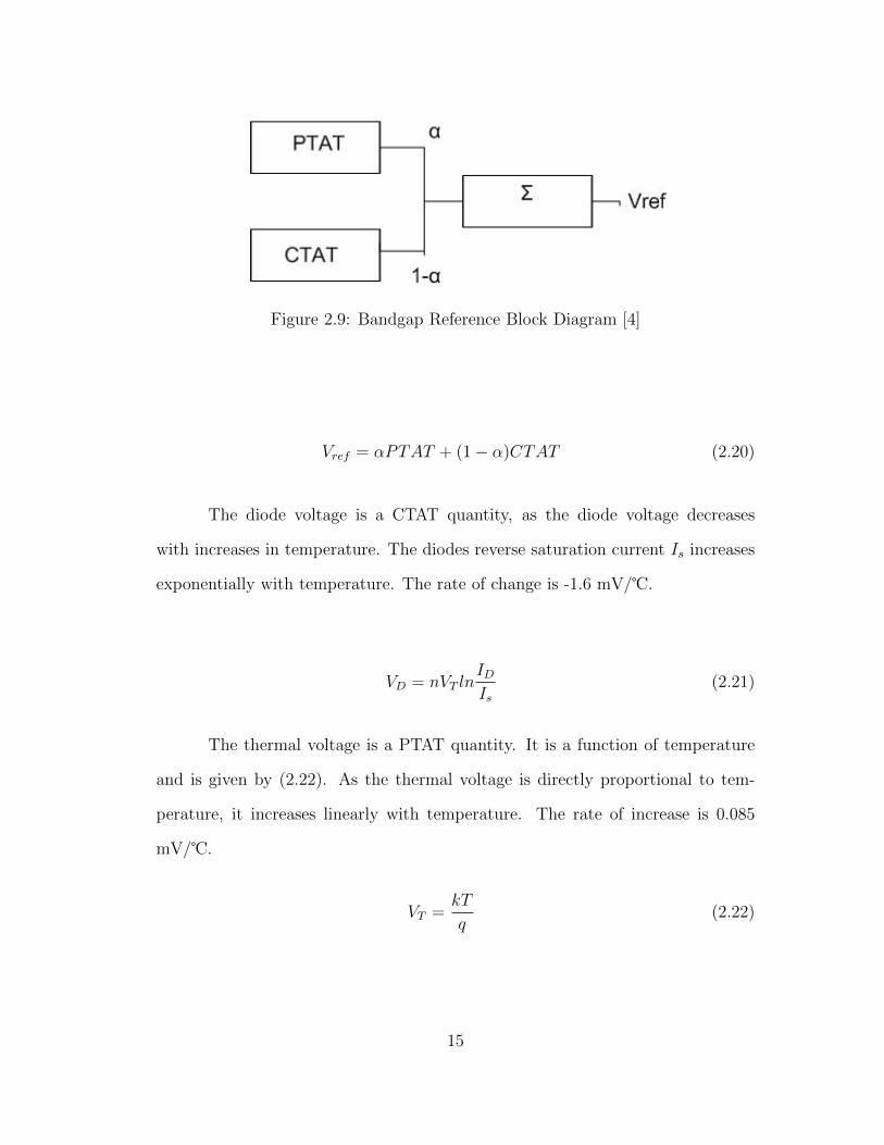
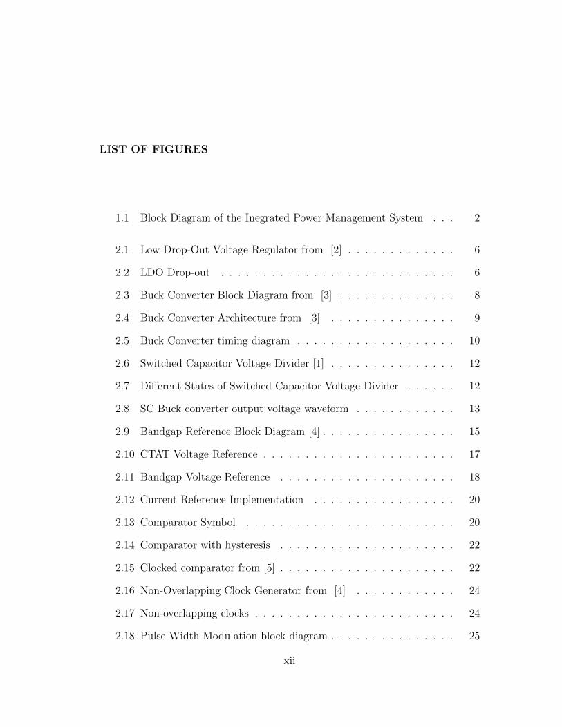
Figure 2.9: Bandgap Reference Block Diagram [4]
Vref = αPTAT + (1− α)CTAT (2.20)
The diode voltage is a CTAT quantity, as the diode voltage decreases
with increases in temperature. The diodes reverse saturation current Is increases
exponentially with temperature. The rate of change is -1.6 mV/.
VD = nVT lnIDIs
(2.21)
The thermal voltage is a PTAT quantity. It is a function of temperature
and is given by (2.22). As the thermal voltage is directly proportional to tem-
perature, it increases linearly with temperature. The rate of increase is 0.085
mV/.
VT =kT
q(2.22)
15

Fig. 2.10 shows the circuit implementation of a CTAT voltage reference. Current
mirrors are used to generate reference currents. Cascoded current mirrors are used
for good matching. A current mirror has equal currents on both sides.
A start-up circuit is used to initiate current in the current mirror. Intially
the current through the start-up circuit is zero and the voltage at the gate of tran-
sistor MSU is 0 V. As transistor MSU turns ON, this increases the gate voltage of
Mp1 and increases the gate voltage of Mn1. Therefore the current starts increasing
in each branch, including the start-up circuit. As the current increases through
the resistor Rs, and the gate of MSU is pulled high. This generates reference
currents in all branches.
First a CTAT voltage reference is formed by connecting a diode on one
side of the current mirror and resistor on the other side, as shown in Fig. 2.10. As
the output voltage Vouta, shown in (2.23) is the voltage across the resistor which
is equal to the diode voltage. As such, a CTAT voltage reference is generated.
Vouta = nVT lnIrefIs
= IrefR (2.23)
Reffering to Fig. 2.10, suppose we place K parallel diodes in series with resistor
R. Now the voltage drop across the diode can be written as the sum of the drop
across the resistor and the drop across the diodes.
Vouta = VD1 = IrefR + VD2,k (2.24)
Iref =nVT ln(K)
R(2.25)
16

Figure 2.10: CTAT Voltage Reference
From (2.25) we see that the reference current is directly proportional to absolute
temperature. Therefore it is a PTAT current reference.
In the next step we copy this current to a third branch with a resistor. As
the PTAT current passes through resistor, we generate a PTAT voltage reference.
We include a variable L in the resistor value for weighting purposes. The output
voltage can be written as
Vref = IrefLR = nLln(K)VT (2.26)
After this we place K parallel diodes in the third branch, as shown in Fig. 2.11.
17

Figure 2.11: Bandgap Voltage Reference
Now the reference voltage is sum of the drops across the resistor and parallel
diodes and is given by
Vref = IrefLR + VD3,k (2.27)
Vref = nLln(K)VT + VD3,k (2.28)
By differentiating with respect to temperature on both sides we get
∂Vref∂T
= nln(K)∂VT∂T
+∂VD3k
∂T(2.29)
18

Substituting
∂VT∂T
= 0.085mV/C (2.30)
∂VD3k
∂T= −1.6mV/C (2.31)
we can derive the relation between L and K as
L =1.6
nln(K)(0.085)(2.32)
By choosing the value of K we can compute L. n is chosen as 1. And thus
we have a reference voltage as a weighted sum of two quantities with opposite tem-
perature coefficients. Therefore the generated voltage reference will be constant
irrespective of changes in temperature and process variations.
A bandgap voltage cannot directly supply current to a load because the
reference voltage would change. Therefore a buffer is placed at the output.
2.4.2 Bandgap Current Reference
Current references can be generated using a voltage reference as shown in
Fig. 2.12
If we want Iref to be independent of T, then R must be temperature in-
dependent. This current can be copied to other branches for generating reference
currents with different multiplicities as shown in Fig 2.12.
2.5 Comparators
A comparator is a circuit which compares two analog signals and produces
a binary output signal. A differential op-amp without feedback can be used as
19

Figure 2.12: Current Reference Implementation
a simple comparator. Since comparators don’t have feedback, we don’t need any
compensation. And, as a result, comparators have wide bandwidth.
2.5.1 Comparators with Hysteresis
A comparator is considered a decision making circuit. The symbol of a
comparator is shown in Fig. 2.13.
Figure 2.13: Comparator Symbol
20

If V+ is greater than V− then Vout= VDD and if V+ is less than V− then
Vout = 0
Let V+ be the input signal and V− be a reference voltage. If the input
signal of the comparator has some noise and is close to the reference value, even
small changes in the input voltage above or below the reference value causes the
output to swith between high and low logic levels. This switching may consume
a lot of dynamic power. Therefore, a small amount of hysteresis is added to the
comparator. Hysteresis is defined as the change in threshold voltage dependent
on whether the input is rising or falling. It can be introduced by a adding two
threshold levels on either side of the zero crossings.
Hysteresis can be added using different methods. One method is to add a
positive feedback resistor as shown in Fig. 2.14. A small fraction of the output
is fed to the positive input and this adds an offset, thus increasing the threshold
value. The amount of hysteresis added in the comparator circuit shown in Fig. 2.14
is
Vhyst = VddR1
R2
(2.33)
2.5.2 Clocked Comparators
Comparators are usually classified into two types: continuous-time and
clocked, or discrete-time. Continuous-time comparators compare the signals asyn-
chronously. But clocked comparators make the decision either on the rising edge
or the falling edge of clock. Clocked comparators can be used for high speed oper-
ation. Since most IC designs have a main clock, clocked comparators are found in
21

Figure 2.14: Comparator with hysteresis
many applications such as analog-to-digital converters. Clocked comparators are
mainly used in low power applications [5]. A simple clocked comparator is shown
in Fig. 2.15.
Figure 2.15: Clocked comparator from [5]
22

The first stage of the clocked comparator is a pre-amplifier. As the com-
parator needs to compare signals which have a difference in the range of millivolts,
the signals are amplified using the pre-amplifier. The pre-amplifier is shown as a
single stage differential amplifier with diode-connected loads. The bandwidth of
the preamplifier must be as large as possible.
The second stage is the decision making circuit and is called a latch. A
simple latch can be formed by cross-coupled NMOS transistors. Two back-to-back
inverters are used in the decision circuit of Fig. 2.15. Depending on the outputs
of the first stage, one of the outputs of the latch will go high and the other low.
The second stage outputs are given to an SR latch, which acts a memory that
stores the output value for a whole clock period.
2.6 Non-Overlapping Clock Generation
A non-overlapping clock generating circuit takes a clock signal and pro-
duces two-phase non-overlapping clocks [4]. A non-overlapping clock generating
circuit is shown in Fig. 2.16. The amount of delay can be set by the delay of the
NAND gate and the chain of inverters between the NAND gate and the output.
For low frequency clocks, a large number of inverters are used to get the required
delay. This increases power consumption. The schematic of a non overlapping
clock generator is shown in Fig. 2.16. As the clock goes high φ1 goes high and
φ2 goes low and when clock goes low, φ1 goes low and then φ2 will go high. Rise
and fall times can be significant when driving large capacitance loads. Therefore
a chain of inverters can be used as a part of the delay circuit after φ1 and φ2 are
generated.
2.7 Controller Design
High efficiency power electronic circuits need an efficient controller design,
as they have to produce constant output irrespective of changes in the input
23

Figure 2.16: Non-Overlapping Clock Generator from [4]
Figure 2.17: Non-overlapping clocks
voltage and load current. A controller also contributes to power loss and ulti-
mately reduces the maximum possible efficiency. The main goal of the controller
in a DC-DC converters is to make the output voltage insensitive to changes in
input voltage, load current, process variations and temperature. This goal can
be achieved by controlling the duty cycle. Pulse width modualtion and pulse
frequency modulation are two methods that are widely used in controller designs.
24
2.7.1 Pulse Width Modulation (PWM)
PWM is widely used in inductor-based DC-DC converters used for heavy
loads. The switching frequency is held constant, but the duty cycle is varied in this
method. A block diagram of a pulse width modulator is shown in Fig. 2.18. The
different sub-blocks are sensor gain, difference amplifier, pulse width modulator
and gate driver. The PWM method is presented in [3].
Figure 2.18: Pulse Width Modulation block diagram
The sensor gain block usually consists of a resistor divider circuit built with
precisely matched resistors. The output of the sensor gain is a scaled version of
the output voltage. A differential amplifier is placed next. It compares the output
of the sensor gain to a reference voltage V ref and produces an error signal V e.
If the feedback is perfect, the error signal will be zero. To gaurantee stability
of the feedback loop, a compensation circuit is added. Different compensation
techniques, such as lead compensation and lag compensation, are used to improve
the phase margin and gain margin of the control loop.
The pulse width modulator is used to create a pulse signal that depends on
the error signal. A pulse width modulator normally consists of a ramp generator
25

and a comparator. A ramp signal has a frequency which is equal to the switching
frequency of the converter. The comparator compares the error signal with the
ramp signal and produces a pulse that has a width that is proportional to Vc.
This generated pulse signal is given to the gate of the switches in the converter.
If the switches are huge, an inverter chain must be added to drive them.
2.7.2 Pulse Frequency Modulation (PFM)
Pulse frequency modulation is more appropriate for switched capacitor DC-
to-DC converters at light loads. In this method the pulse width of the switching
signal is constant but the frequency is varied. The output voltage of the converter
is maintained at a required value by changing the frequency of the pulse signal.
This method decreases the number of switching events and helps in reducing
power consumption. PFM can be implemented as single pulse PFM, multi-pulse
PFM and burst mode PFM. The block diagram of burst mode PFM is shown in
Fig. 2.19.
Figure 2.19: Block diagram of burst-mode PFM regulator from [6]
As shown in Fig. 2.20, a gain hopping loop can be added to the control
loop. A gain hooping loop contains gain set block, comparator and up-down
counter. The gain hopping loop controls the gain based on the load current and
26

input voltage. The counter integrates the number of pulses from the comparator
and sets the gain block to increase or decrease the gain accordingly.
The PFM loop consists of an analog comparator and a voltage threshold
levels. If the output voltage is below a minimum reference voltage the switches in
the converter are turned ON until a maximum threshold voltage value is achieved
and then the switches are turned OFF. By controlling the switching, the ouput
voltage is regulated. Waveforms of a burst-mode PFM are shown in Fig. 2.20.
Figure 2.20: Waveforms of burst-mode PFM
27

Chapter 3
DESIGN AND SIMULATIONS
Design and simulations of the integrated power management system designed in
this thesis, are discussed in this chapter.
3.1 Switched Capacitor (SC) Buck Converter
This section deals with the design and simulations of the SC buck converter.
This type of converter was introduced in Section 2.3.
3.1.1 Design of SC Buck Converter
The schematic of the SC buck converter is shown in Fig. 3.1 It consists of
two capacitors and four switches. The input voltage of our system is 3.3V. The
SC buck converter circuit is designed to convert 3.3V down to 1.5V. The main
idea was that the SC buck converter must be totally integrated on a single chip.
Table 3.1 shows our system specifications.
Both capacitors,the flying capacitor C1 as well as grounded capacitor C2,
were chosen as 100pF, due to a serious constraints on chip area. In the selected
0.5-micron process, the flying capacitor C1 must be implemented using poly1 and
poly2 layers. The capacitance per unit area is 0.9fF . As such, a 100pF capacitor
occupies 111,111fF/µm2. Assuming a square layout, the capacitor would measure
0.33 mm on each side. The grounded capacitor C2, can be implemented with
a MOS capacitor, with a capacitance per unit area of 2.4 fF/µm2. Assuming a
square layout, the moscap would measure 0.2 mm on each side.
28

The switch MSW1 was chosen to be a PMOS transistor because it is con-
nected to the input voltage (3.3V) and the rest were chosen as NMOS, since they
are connected to either the output voltage (1.5V) or ground (0V). The switch sizes
and the switching frequency are optimized for maximum efficiency at a minimum
ouput voltage of 1.4 V. We also constrained the output voltage ripple to be less
than 100 mV. Using switch sizes as given in Table 3.2, the peak efficieny was 76%
at 1 mA load current and 15 MHz switching frequency. The operation of the SC
buck converter is explained in Section 2.3.
Figure 3.1: Schematic of the SC Buck Converter
Table 3.1: SC Buck Converter Specifications
C1, C2 100pF
Vin 3.3V
Average Vout 1.5V
Maximum ripple 100 mV
Max. load current 1 mA
29

Table 3.2: SC Buck converter transistor sizing
Switch size(Wµm x Lµm)
Msw1 120/0.6
Msw2 90/0.6
Msw3 90/0.6
Msw3 90/0.6
3.1.2 Simulations of SC buck converter
The input voltage of our system is 3.3V. The system clock has a frequency
of 15 MHz with rise and fall times of 5 ns each. Fig. 3.2 shows simulated waveforms
of the SC buck converter at a load current of 1 mA. The output voltage ripple is
92 mV.
Figure 3.2: Output voltage waveform of SC Buck converter at 1mA load current
30

A parametric analysis is done to find the efficiency, average output voltage
and output voltage ripple as a function of load current. As we can see from
Figure 3.3: Efficiency Vs Load current plot for SC Buck converter
Fig. 3.3, the peak efficiency is at a load current of 1 mA. Efficiencies above 50%
are achievable for a load currents ranging from of 100µA to 4 mA. Losses due to
the non-overlapping clock generator circuit are included in the simulation results.
3.1.3 Analysis
The steady-state output voltage and current waveforms are shown in Fig. 3.6
at a load current of 1mA. When the capacitor C1 is connected to the input, a large
amount of charge flows onto the capacitor. The amount of charge depends on the
intial voltage across C1 and the final voltage across C1. The peak amplitude of
the input current is limited to 2.5Iout by the switching frequency and the switch
resistance. The input current decays exponentially with time constant that de-
pends on the switch resistance, and capacitor C1 as C1 is charged. From Fig. 3.6
31
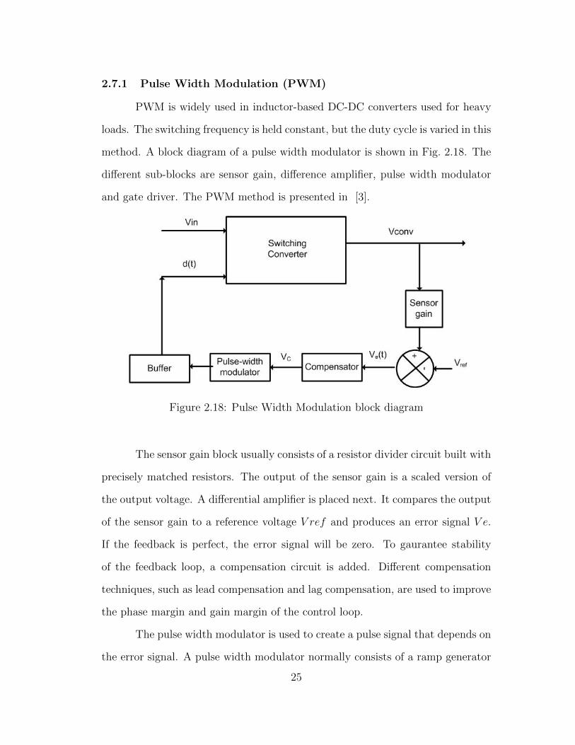
Figure 3.4: Average output voltage Vs Load current plot for SC Buck converter
we can see that the simulated peak value is about 2.8Iout, slightly higher than the
theoretical maximum of 2.5Iout.
The current through capacitor C1 is equal to the input current when it is
connected to the input and when it is disconnected from the input, we observe a
step change of 2Iout. And then IC1 starts decreasing in the other direction. The
average current through capacitor C2 is zero, as it charges and discharges over
each half cycle.
The root mean square (RMS) value of a pulsing current waveform can be
calulated using the formula
Irms =
√(I2ON + I2OFF )
2(3.1)
The RMS values for the input currents and currents through the capacitors are
calculated using (3.1).
32

Figure 3.5: Output voltage ripple Vs Load current plot for SC Buck converter
IINrms = 0.816Iout (3.2)
IC1rms = 1.15Iout (3.3)
IC2rms = 0.575Iout (3.4)
The output voltage ripple is due to the AC current through the capacitor. It is
calculated by using the formula
i = Cdv
dt(3.5)
33

Figure 3.6: Simulated waveforms of SC Buck Converter
Observing the current waveform of capacitor C2, the ( 3.5) can be used to derive
the formula
∆Vout =1
C2
T
4
Iout2
=Iout
8fC2
(3.6)
34

Substituing the capacitor value of 100pF, frequency of 15MHz and a load
current of 1mA, we get a theoretical value of 83mV of output ripple, which is very
close to our simulation results.
3.2 Non-Overlapping Clock Generator
This section deals with the design and simulations of the non-overlapping
clock generator discussed in Section 2.6.
3.2.1 Design of Non-overlapping Clock Generator
A non-overlapping clock generator is used to generate the three clocks
required by the switched capacitor buck converter. The schematic of the clock
generator is shown in Fig. 3.7. The inverters after the NAND gate are added to
generate sufficient dead time between clocks S1 and S2. To have a dead time of
roughly 1 ns, we need to add many inverters between the NAND gate and the
output, which increases power consumption. Instead resistors are added in in se-
ries with the inverters to increase the delay of each stage. As the resistor increases
the time constant, the required delay was achieved with only four inverters. Of
course we need to add resistors of the same value in the two branches in order
for the delay to be symmetric. Also buffers are placed at the output for driving
the switches in the converter. As we have one PMOS transitor in the switched
capacitor voltage divider, we need an inverted clock S1b for the first half of the
cycle. This clock is generated by taking an extra output, as shown in Fig. 3.7
PMOS and NMOS transistors are sized the same in the inverters to re-
duce power consumption. All transistor dimensions of the non-overlapping clock
generation circuit are given in Table. 3.3.
3.2.2 Simulations of Non-overlapping Clock Generator
A clock signal of frequency 15 MHz with rise and fall times of 5 ns is given
as the input. The three output clocks that are generated by the circuit are shown
35

Figure 3.7: Non-overlapping clock generator
Table 3.3: Non-overlapping clock generator transistor sizing
Component PMOS(µm x µm) NMOS(µm x µm) Mulitiplicity
Invx 1 1.5/0.6 1.5/0.6 1
Invx 4 1.5/0.6 1.5/0.6 4
Invx 8 1.5/0.6 1.5/0.6 8
NAND 2x1 1.5/0.6 1.5/0.6 1
R 30kΩ
in Fig. 3.8. Fig. 3.9 shows the primary clocks S1 and S2 with a dead time of about
1 ns between them.
3.3 Long Channel Bandgap Reference
The design procedure for generating a bandgap reference voltage, outlined
in Section 2.4, is followed. In this section we explain the procedure for generating
bias currents based on the bandgap reference.
3.3.1 Design of Bandgap reference
Diodes are not among the models in the particular 0.5 micron process we
used. Therefore, we make use of the p+ (source) to n− (well) junction of a PMOS
transistor for simulating the diode.
36

Figure 3.8: Non-overlapping clock generator waveforms
The schematic of the long channel bandgap reference is shown in Fig 3.10.
The length of the MOS devices is chosen as 3Lmin. The current mirror formed by
transistors Mp1 and Mp2 has a current of 60 nA on both sides. The transistors
Mp4 and Mp4c are sized 2x for a current of 120 nA. Transistors Mp5 and Mp6 are
sized to have two thirds the current of the first branch, that is 40 nA. The sizing
of all the MOS transistors is given in Table 3.4.
The bias resistors are calulated for a drop of
RB =VDSsat
Iref(3.7)
where VDs,sat = 0.2V and Iref = 60nA.
37

Figure 3.9: Deadtime time between the Clocks
Figure 3.10: Long Channel Bandgap Reference
38

Table 3.4: Long Channel Bandgap Reference transistor sizing
Transistor size(Wµm x Lµm) Mulitiplicity
Mp1,Mp1c 3/1.8 2
Mp2,Mp2c,Mp3,Mp3c 3/1.8 6
Mp4,Mp4c 3/1.8 12
Mp5,Mp5c,Mp6,Mp6c 3/1.8 4
Mn1,Mn1c,Mn2,Mn2c 4/1.8 2
Mp2,Mp2c,Mp3,Mp3c 3/1.8 6
MSU 1.5/0.6 1
MN3 10/0.6 6
A start-up circuit is required to initiate the current in the current mirror
branch. The current through the start-up circuit must be very low so as to con-
sume very low power. Therefore, we would require a huge resistor in the start-up
circuit. To save the area we placed an NMOS transistor with its gate connected
to the source through a resistance as shown in Fig. 3.10. The switch MSU is a
minimum-sized transistor. Sub-threshold leakage current through transistor Msu
is what feeds the start-up circuit.
Initially we chose K=8 and n=1. We have twice the current in the third
branch, therefore Iref in the third branch is given as
Iref =2nln(K
2)VT
R(3.8)
39

Using the equation above, the output reference is given as
Vref = 2nLln
(K
2
)VT + VD3,K
(3.9)
And by differentiating with respect to temperature on both sides, we have
L =1.6
2nln(K2
)0.085
(3.10)
By substituing K as 8, we get L as 6.8. Therefore we sized R as given in Table. 3.5.
And the ouput reference voltage will be the weighted sum of PTAT and CTAT
quantities and is given by (3.8).
3.3.2 Generating Bias Currents
The LDO and buffer used in our integrated system each need a bias current.
As current is relatively constant in the current mirror of our bandgap reference
circuit shown in Fig. 3.10, this current is copied into other branches for generating
these bias currents. The LDO needs a bias current of 40nA. As the current mirror
branch has a current of 60 nA, transistors Mp5 and Mp6 are sized two thirds for a
current of 40 nA.
Table 3.5: Long Channel Bandgap Reference Resistor Values
Resistor Value(Ohms)
R 1M
L ∗R 7M
RB 4M
Rn 500K
40

3.3.3 Bandgap Reference Simulations
The input voltage is 3.3 V, the same as the system input voltage. The bias
current generated for the LDO in our integrated system is also plotted.
The generated bandgap reference voltage is varied with input voltage and
temperature. Fig: 3.11 and 3.12 shows that it is constant, irrespective of the
changes in input voltage and temperature. The reference current generated for
the LDO is also plotted. The reference current varies by approximately 10% over
an input voltage range of 3.0 to 3.6 V, and by 30% over the indicated temperature
range.
Figure 3.11: Variations with input voltage
41

Figure 3.12: Variations with temperature
3.4 Clocked Comparator
The clocked comparator which is discussed in the section 2.5.2 is used.
This section explains the sizing of the transistors and simulations of the clocked
comparator.
3.4.1 Design of Clocked Comparator
The schematic of the clocked comparator is shown in Fig. 3.13. Transistors
M1 and M2 are sized are large for good matching, low noise, and to better amplify
the input signals. Transistor M5 −M8 are also sized large because they have the
same current as the differential pair. The other transistor are sized minimum, as
they act like switches. PMOS and NMOS transistors are minimum sized in the
42

SR latch to reduce power consumption. The sizes of the transistors are given in
Table 3.6.
Figure 3.13: Schematic of Clocked Comparator
Table 3.6: Clocked Comparator transistor sizing
Transistor size(Wµm x Lµm) Mulitiplicity
M1,M2,M7,M8 6/1.05 2
M5,M6 3/1.05 2
M3,M4,M9,M10 1.5/0.6 1
M11,M12,M13,M14,M15,M16,M17,M18 1.5/0.6 1
43

3.4.2 Simulations of clocked comparator
The testbench schematic of the clocked comparator is shown in Fig. 3.14.
The input clock of the comparator is the same as the system clock. A reference
voltage of 1.2V is given to the negative terminal of the comparator. The positive
terminal of the comparator is connected to a pulse of frequency 7.5MHz. The
voltage of the pulse input is 1.22 ± 50 mV From Fig. 3.15 we can see that on the
Figure 3.14: Testbench Schematic of Clocked Comparator
rising edge of the input clock, the output of the comparator is goes high or low,
depending on whether the input pulse is above or below the reference voltage.
3.5 Low Drop-out Voltage Regulator
The LDO used in our integrated was designed in [7]. The schematic of
the LDO is shown in Fig. 3.16. It has a low quiescent current of 40 nA and can
operate at a maximumload current of 5 mA. Some compensation capacitor values
were changed from the original design to improve the gain and phase margins.
The SC buck converter has an average output voltage of 1.5V over a wide
load current range. Therefore, AC analysis was done for the LDO with an input
voltage of 1.5V, for a load current range of 10µA to 1 mA. Fig 3.17 shows the
phase and gain margins for a range of load currents.
44

Figure 3.15: Waveforms of Clocked Comparator
Vs
Vref
Vbias
Vbias
Mpass
M1 M2
M3
M4
M5
M6
M14
M13
M11
M12
M18
M17
M16
M15
M19 M20 M21 M22 M23
M24
M25
M26
M27
M29M30 M31
RF1
RF2
CF1
CF2
RC1 CC1
CC2
RC3CC3
RC4CC4
CC5
M7
M8 M10
M9
CC6
Figure 3.16: Schematic of the LDO
45

Figure 3.17: AC analysis of LDO
3.6 Control Loop
A burst-mode pulse frequency modulation (PFM) control loop is designed
to regulate the output voltage of the converter. This section deals with the im-
plementation and simulations of the burst-mode PFM control loop.
3.6.1 Design of Burst-mode PFM control loop
The schematic of the PFM control loop is shown in Fig. 3.18. It consists
of a clocked comparator, resistor divider circuit, and an AND gate. The output
voltage of the converter is sampled using the resistor divider circuit and given to
the comparator. The inverted output voltage of the comparator is given to the
AND gate. The system clock is given to other input terminal of the AND gate.
The output of the AND gate is connected to the clock input of the clock generator
circuit, which generates the clocks required by the SC buck converter.
46

The resistors are sized huge, so that the current in that branch is minimal.
The resistor ratio is determined such that our system clocks are always on at 1mA
load current. For a converter ouput voltage of 1.5V, we will obtain a voltage of
1.35 at Vx and 1.2V at Vy. At this point, the comparator ouput Vcn is still high and
the clock generator will be ON. If the converter output voltage goes above 1.5 V,
then Vy goes above 1.2 V and the comparator output voltage Vcn goes low and the
clock generator will be turned OFF. Therefore our controller helps in regulating
the converter output voltage and also decreases the number of switching events
at low load currents.
Hysteresis is added to the clocked comparator in the control loop by using
two minimum sized switches. The two outputs of the comparator are fed back to
the gates of these switches creating positive feedback.
Figure 3.18: Schematic of SC Buck Converter with Burst-mode PFM ControlLoop
47

3.6.2 Simulations of SC Buck Converter with Control loop
The controller along with the SC buck converter are simulated together.
All the blocks of the controller are connected to the same input voltage Vin.
The system clock is connected to the AND gate input and also the comparator.
Fig. 3.19 shows simulated waveforms of our system at 100µA of load current.
Figure 3.19: SC Buck converter Waveforms at 100µA load current
From Fig. 3.19 we can see that the clocks are turned ON if the converter
output voltage is below 1.5V and they are turned OFF if the output voltage is
above 1.6V. From Fig. 3.20 we can see a difference in the clock pattern for a 500µA
load current. In this case the output voltage stays between 1.4V and 1.5V.
48

Figure 3.20: SC Buck converter Waveforms at 500µA load current
3.7 Integrated System
The various blocks which are designed in this chapter are combined to form
a voltage regulator, which has an input voltage of 3.3V and generates an ouput
voltage of 1.2V.
3.7.1 Design and Simulations of the Integrated System
The schematic of the integrated system is shown in Fig. 3.21. It includes
the SC buck converter, PFM controller, LDO and bangap reference. The output
of the SC buck converter is connected to input of the LDO to reduce the ripple and
also regulate the converter output voltage. The bandgap reference circuit provides
reference voltages to the comparator and the LDO. The output of the bandgap
reference is buffered to reduce noise, which might be coupled to the comparator
49

input. The bandgap reference also generates bias currents for the LDO and the
buffer.
The integrated system takes an input DC voltage of 3.3V and converts it
to an ouput voltage of 1.2V, at a switching frequency of 15 MHz. Fig 3.22 shows
the waveforms of the SC buck converter output voltage and the final LDO output
voltage, at a load current of 1 mA. The output voltage ripple is less than 20mV.
The SC buck converter converts the input voltage of 3.3V to 1.5V and then the
LDO converts the 1.5V converter output voltage to 1.2V. The control loop helps
in regulating the output voltage.
Figure 3.21: Schematic of the Integrated System at 1 mA Load current
Fig. 3.22 shows the waveforms of the final output and SC buck converter
output in the integrated system. The average of the final output voltage is 1.19
V and the ripple is 14 mV. The ouput voltage ripple has been reduced by 5 times
when compared to the SC buck converter output voltage ripple of 90 mV. The
efficieny of the integrated system is 63% at 1 mA load current.
50

Figure 3.22: Simulated waveforms of the Integrated System
51

Chapter 4
EXPERIMENTAL RESULTS
The layouts of our integrated power management system are discussed in this
chapter. The test setup and the hardware measurement results are also presented.
4.1 Layout
The layout of the chip is shown in Fig. 4.1. It consists of a closed system
which has all the blocks of the integrated syatem and an open system in which all
blocks are laid out individually.
The layout of the switched capacitor (SC) buck converter is shown in
Fig. 4.2 The SC buck converter has two capacitors of 100pF. The first capaci-
tor of 100pF was laid out using poly1 and poly2. An NMOS transistor MOSCap
is used for the layout of the second capacitor instead of poly, as we can save area.
And only 50pF of the second capacitor is laid out because of the extra capaci-
tance added by the pin package and test setup. The area of the SC converter is
approximately 356 x 518 µm2.
The layout of the clock generator is shown in Fig. 4.3. The total area of
the non-overlapping clock generator is approximately 100 x 56µm2.
The layout of the clocked comparator is shown in Fig. 4.4. The total area
of the clocked comparator is around 32 x 56µm2.
The layout of the bandgap reference circuit is shown in Fig. 4.5. The buffer
used at the output of the reference circuit is also laid out. The total area of the
clocked comparator is approximately 495 x 266µm2.
52

Figure 4.1: Layout of the whole design
The layout of the LDO circuit is shown in Fig. 4.6. A technique called
strapping was used to layout the huge pass transistor. The total area of the LDO
is approximately 410 x 390µm2.
4.2 Test Apparatus
The procedure for testing all the blocks of the integrated system is de-
scribed in Appendix A. The equipment used for testing all the blocks is given
below.
1. DC Power Supply: Agilent : E3631A: 0-6V, 5A, 0-25V, 1A triple output
DC power supply.
53
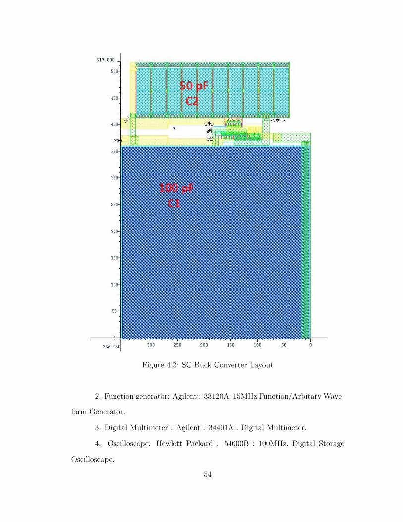
Figure 4.2: SC Buck Converter Layout
2. Function generator: Agilent : 33120A: 15MHz Function/Arbitary Wave-
form Generator.
3. Digital Multimeter : Agilent : 34401A : Digital Multimeter.
4. Oscilloscope: Hewlett Packard : 54600B : 100MHz, Digital Storage
Oscilloscope.
54

Figure 4.3: Non-Overlapping Clock Generator Layout
Figure 4.4: Clocked Comparator Generator Layout
4.3 Hardware Results
The chip is fabricated in the 0.5-micron ONSEMI process through MOSIS.
The chip is tested on a breadboard. A supply voltage of 3.3V is used as the system
55

Figure 4.5: Bandgap Reference Layout
input voltage. The system clock has a frequency of 15MHz, 3.3 Vp-p with a 1.65V
offset.
4.3.1 Clock Generator
The input of the clock generator is a 15 MHz clock with fast rise and
fall times. The three clock outputs are shown in Fig. 4.7. The measured dead
time between the clocks was about 2 ns. The waveforms do not look square due
to high operating frequency (15 MHz) on a breadboard. Testing with a custom
printed-circuit board (PCB) would result in smoother recorded waveforms.
4.3.2 SC buck converter
The breadboard and 1x probe attached to the oscilloscope were adding
a capacitance of about 100pF, for a total grounded capacitance of 150pF, if we
include the on-chip 50pF MOSCap. The output voltage waveform is shown in
Fig. 4.8. The average output voltage is 1.334V and the ripple was about 92 mV
at 1 mA load current.
56

Figure 4.6: Low Drop Voltage Regulator Layout
The average output voltage is about 70mV less than the simulated value.
On the other hand, measured output voltage ripple is within 5 mV of the simulated
value. But there was a capacitance of 100pF added due to the breadboard and 1x
probe. Also there ia a significant difference in the efficiency, due to the decrease
in average output voltage.
4.3.3 Clocked Comparator
An individual clocked comparator was laid out for testing purposes. One
input of the comparator was given to a reference voltage of 1.2 V. A pulse of
57

Figure 4.7: Measured Waveforms of Clock Generator
Figure 4.8: Measured Waveforms of SC buck converter
58

frequency 7.5MHz, average value 1.22 V and 100mVp−p was given to other input.
The comparator output waveform is shown in Fig. 4.9.
Figure 4.9: Measured Waveforms of Clocked Comparator
4.3.4 Bandgap Reference
The bandgap reference circuit was tested with an input voltage of 3.3 V.
The output reference voltage was about 1.25 V. And the bias current generated
for the LDO was exactly 40nA. The Table. 4.1 shows the variations of the bandgap
reference voltage with changes in input voltage.
Table 4.1: Bandgap reference voltage variations
Input Voltage(V) Output Reference Voltage (V)
3.000 1.253
3.300 1.2580
3.600 1.2597
59

4.3.5 Integrated System
The integrated system which has all the blocks was tested with an input
voltage of 3.3 V and a clock of frequency 15 MHz.
Figure 4.10: Measured Waveforms of Integrated System
Fig. 4.10 shows the measured waveforms of the integrated system. Average
of the final output voltage at the LDO is 1.198 V. And the output voltage ripple
is 33 mV compared to the SC buck converter output voltage ripple of 65 mV. The
measured efficiency is about 47%.
60

Chapter 5
DISCUSSION AND CONCLUSION
Comparison of simulated and measured results is done in this chapter. Issues that
we faced and also future work and enhancements that can be done are discussed.
5.1 Analysis of Simulated and Measured Results
Table. 5.1 shows the simulated and measured results of the various blocks
present in the system. The generated bandgap reference voltage is constant even
with variations in the input voltage. Its temperature sensitivity was not tested.
The comparator laid out individually was tested and it was able to detect time
varying input signals which have a 50 mV difference.
The simulated and measured results of the SC buck converter are shown
in Table. 5.2. The measured average output voltage of the SC buck converter is
70 mV less than the simulated value. Also the efficiency of the SC buck converter
had a big difference between the measured and simulated values.
The integrated system which includes all the blocks was also tested with a
single input voltage and a system clock, and the results are shown in Table. 5.3.
The output voltage ripple is about 33 mV. The measured efficieny of the integrated
system has a difference of 15% from the simulated value.
The flying capacitor in the switched capacitor buck converter was laid
out using poly1 and poly2 materials. There is a large aparasitic capacitance
added from the poly1 side to the substrate. The ratio of the poly1-to-poly2
61

Table 5.1: Comparison of Simulation and Measured Results
Simulation Measured
Non-overlapping Clock Generator
Deadtime 1.5 ns 2.5 ns
Bandgap Reference
Vref 1.198 V 1.253 V
Ibias 40 nA 39.9 nA
Low Drop-out Voltage Regulator
Drop− out 130 mV 170 mV
Table 5.2: Switched Capacitor Buck Converter Measured Results
Simulation Measured
Vin 3.3V 3.3V
Load Resistor 1.4kΩ 1.47kΩ
Average Vout 1.436V 1.332V
Output Ripple 93mV 87mV
Efficiency 75.6% 53%
capacitance to the poly1-to-substrate capacitance is approximately 998:83 in 0.5
micron process.
Therefore a parasitic capacitance of 9 pF to ground is part of the layout.
Therefore, we simulated the SC buck converter with a 9 PF capacitor from one side
of the flying capacitor to ground. We observed a 10% decrease in the efficiency of
62

Table 5.3: Integrated System Results Comparison
Simulation Measured
Vin 3.3 V 3.3 V
Load Current 1mA 1.04mA
SC Buck Converter Average Vout 1.458 V 1.383 V
SC Buck Converter Output Ripple 90.8 mV 65 mV
LDO Average Vout 1.19 V 1.98 V
LDO Output Ripple 13.8 mV 33 mV
Efficiency 62.3% 47%
the buck converter down to 66% with the addition of the 9 pF capacitor. However
the new simulated value of 66% is still much higher than the measured efficiency
of 53%.
One method to decrease the effect of the bottom plate parasitic capacitance
is to layout the capacitor in an n-well and leave the n-well floating as shown
in Fig. 5.1. By doing this there will be two parasitic capacitors in series. One
capacitor is from poly1 to the n-well and the other from the n-well to the substrate.
This adds only 4% extra parasitic capacitance, as a series capacitor is created from
n-well to substrate. Now the ratio of the poly1-to-poly2 capacitance to the poly1-
to-substrate capacitance becomes 998:43.
Another issue was a difference of about 100 mV in the average output volt-
age of the switched capacitor buck converter between the simulated and measured
results. Part of this error can be explained by the ommision of the 9 pF parasitic
63

Figure 5.1: Bottom Plate Capacitance
capacitance. The average output voltage with the 9 pF capacitor drops to 1.401
V. Still 70 mV remains unaccounted for.
We also had some issues while testing our circuit on a breadboard. Capac-
itance of about 100 pF was added due to the breadboard with 1x probe connected
to the digitizing oscilloscope. Therefore testing the chip on a printed board circuit
will produce better results, because there would be less stray capacitance.
While calculating the efficiency we placed a resistor in series with the input
voltage source to find the average current. This series resistor introduced ripple
in the input voltage of about 20mV.
5.2 Future Work
The switched capacitor buck converter can be improved using different
methods.
5.2.1 Time Interleaving
A method called time-interleaving, as shown in Fig. 5.4 where two set of
clocks are used to reduce the output voltage ripple. The flying capacitor is split
in half. The output voltage ripple will be reduced, as it is the average of two
waveforms Vcon1 and Vcon2.
64

Figure 5.2: Implementation of time interleaving in SC converters
5.2.2 Capacitor Banks
Using a capacitor bank is another method that can be used to operate
the switched capacitor circuit at wide range of load currents. We need to have
different banks of capacitors with different capacitor values and different switch
sizes. And also we need to have a sensing mechanism which switches between
different capacitor banks, for different load currents. We can operate over 3 orders
of magnitude in load currents by using capacitor bank over 2 orders of magnitude.
Efficiency at low load currents is improved.
Different conversions ratios can be achived in a single switched capacitor
circuit using a programmable switching method.
5.2.3 Control Loop
A lot of work can be done in the controller design. In particular a voltage
controlled oscillator (VCO) can be used in the feedback loop to achieve continuous
frequency control of the output voltage. The output voltage ripple will be lower
compared to the burst-mode pulse frequency modulation scheme.
65

Figure 5.3: Capacitor Banks
Figure 5.4: Implementing a VCO in PFM control loop
66

APPENDICES

APPENDIX A
Test Document

Supply voltages and currents:
VDD =3.3 V
VSS = 0 v
Ibias = 40 nA.
TEST PROCEDURE:
1. Connect VDD (pin 5) to 3.3V .
2. Also connect pin4(vss_pad), pin2(vss_main_os), pin17(vss_cmp), pin22(Vss_Ldo_os),
pin28(Vss_ref_os), pin30(Vss_main_cs), pin34(Vss_pad), pin 37 (Vss_ld0_cs) to
ground.
3. Now check whether the chip is good or fired up.
Testing the clock signals:
1 Connect Vdd_main_os (pin 3) to VDD. PIN 3 gives the Vdd supply to the clock
generator and the buck converter in the open system.
2 Connect clk_gate (pin 9) to vdd (i.e high level) for now , which is one of the inputs
for the AND gate.
3 Generate a clock of frequency 15 MHz, using function generator.( Vp-p = 3.3V,
offset= 1.65V, high Z termination) and connect to scope to check whether it is right.
4 Now connect this clock to pin10 (Clk_main_os).
5 Connect pin 7(S1) to the oscilloscope and observe the generated clock. It must be
similar to the input clock that we have generated before.
6 Connect pin 8 (S1_B) to the scope and ovelap it with S1. It must be exact opposite to
the S1 with no dead time in between.
7 Now disconnect the pin8 and connect pin 6 to the scope to observe S2. If we overlap
S1 and S2 they must opposite to each other and must have some dead time of about
1-10 ns in between.
8 We can use 1x probe for the measurements above.

Testing the Buck Converter:
1 Connect the pin 1 to a capacitor of value 23pF(50-27). And connect the other end of
the capacitor to ground.
2 Now to observe the converter output we have to generate different load currents
using different resistor values. The resistor values are calculated based on the
average output voltage at the output.
LOAD
CURRENT
RESISTOR
(ohms)
Output
Ripple
Averge
ouput
voltage
1 mA 1.4 K
500 µA 3 K
250 µA 6.2 k
100 µA 11 k
10 µA 110 K
3 110k resistor was used instead of 100k because of the 1M resistance provided in
parallel by the scope.
4 Connect these resistors to pin 1 one after the other. The other end of the resistors
goes to VSS.
5 Now observe the output voltage of the converter through the scope for different
values of load currents. Also measure the ripple, average output voltage and
tabulate the results. And save the waveforms.
6 After taking the measurements detach the resistor from the pin1.

Testing the comparator:
1. Connect pin 19 (vdd_cmp) to VDD. This pin gives the vdd supply for both the
comparators. Also connect a capacitor of value 10µF from VDD to ground.
Pin 17
1.2V DCPOWER SUPPLY
Pin 11
+HC
74
114
7
6
5
4
3
2
1.2V DCPOWER SUPPLY
INPUT CLOCK15 MHz
INPUT CLOCK15 MHz
30 K1 K
Pin 12
VSS
Pin 18 Pin 19
3.3 VVDD
SUPPLY
VDDPin 13 OSCILLOSCOPE
10μF
10μF
2. Connect pin 18 (Clk_cmp) to clock with 0- 3.3 V peak-to-peak and frequency of 15
MHz. We can use the clock generated above.
3. Connect pin 11 (vin_minus) to a DC voltage source of 1.2 V.
4. We must generate clock which goes from 1.25 V to 1.35 V at a frequency of 7.5
MHz. This clock can be generated by a divide by 2 circuit as shown in figure.
5. After generating a divide by 2 clock, it is given to a resistor divider circuit. The other
end of the resistor divider circuit is given to the 1.2 V DC supply. The output clock of
this divider circuit has a frequency of 15 MHz and goes from 1.15 V to 1.25 V.
Connect this output the oscilloscope and verify it before connecting it to pin 12.
6. Connect pin 13 (Vout_comp) to the oscilloscope and check for the output of the
comparator.
7. The output of the comparator will be a pulse which goes from 0 to 3.3V p-p
depending on whether the pin 12 clock input is higher or lower than the vref i.e
1.2V.

Testing the voltage reference:
1. Connect pin 29 to VDD. This pin provides VDD supply for the bandgap reference.
2. To sense reference current and voltage that are generated from the bandgap
reference place LMC 6482 as shown in figure below
• Pin 3 will be the input.
• Connect pin8 and pin4 of LMC 6482 to vdd and vss respectively.
• Short pin1 and pin2 of the LMC 6482.
• Connect the pin 1 of LMC 6482 to a DMM for measuring the current or voltage.
3. Connect pin 25 (vref_out_os) to pin3 of LMC 6482. This is the unbuffered voltage of
the bandgap reference. This voltage must be 1.2 V DC with noise added to it.
4. To observe the bias current coming from the bandgap reference, connect pin 26 to
resistor of value
R=𝑉𝑉𝑉𝑉𝑉𝑉𝑉𝑉𝑉𝑉𝐼𝐼𝐼𝐼𝐼𝐼𝐼𝐼𝐼𝐼
= 0.4 𝑉𝑉40 𝑛𝑛𝑛𝑛
= 10 MΩ.
The other of the resistor goes to VSS.
5. Disconnect pin25 and connect pin 26 to the pin 3 of LMC6482 and measure the current

6. Connect pin 27 to the DMM to observe the buffered reference voltage. The output
voltage must 1.2V DC.
7. Detach pin 26 from the Rsense and LMC 6482 and also pin 25 from LMC6482.
Testing the LDO:
1. Connect pin 22 to vss supply. This pin is the vss for LDO in the open system.
2. To generate the bias current for LDO. Place a resistor of value
Rbias=𝑉𝑉𝑉𝑉𝑉𝑉−𝑉𝑉𝑉𝑉𝐼𝐼𝐼𝐼𝐼𝐼𝐼𝐼𝐼𝐼𝐼𝐼
=3.3−0.6340𝑛𝑛
= 66 MΩ.
Connect one end of the resistor to VDD and other end to pin 21.
R(66Ω) = 10M+10M+10M+10M+10M+10M+4.8M+1.2M
3. Connect pin 20 (vref_ldo) to 1.2 V DC supply, which is our reference voltage.
4. Connect pin 24(vs_ldo) to 1.5 V DC supply, as our average converter output voltage
is 1.5 V and is input to the LDO.

5. To observe the output voltage
Place an IC CA 3046 and connect it as shown in the figure above, so that it forms a
current mirror :
• Connect pins 9 and 12 together, so that the gates of the BJT’s are connected
together.
• Connect the pins 9 & 11. This forms the diode connected BJT.
• If we want to generate a load current , connect a resistor Rload to the pin 11. The
other end of the resistor to the power supply VDD. The resistor value is calculated as
followed
R=𝑉𝑉𝑉𝑉𝑉𝑉−𝑉𝑉𝐼𝐼𝑉𝑉𝑉𝑉𝐼𝐼𝐼𝐼𝑉𝑉𝐼𝐼𝑉𝑉
• To sense the above generated current we need to place sensing resistors Rsense at
the bottom of the mirror. For example if we have to sense a current of 0.25 mA
place a resistor of 1kohm at pin 13 so that the drop across the resistor is a 250 mV
and it is easily detectable. The other end of these resistors must go to VSS.
Now connect the pin 14 of the main IC to the pin 1 of CA 3046 and the oscilloscope
to observe the output voltage.
6. Also connect a capacitor of value 73 pF (100-27) to pin23.
7. Now calculate the resistor values for different load currents using the equation
above and observe output voltage ripple and average output ripple for different load
currents.
8. After tabulating the results disconnect the voltage supplies at pin 24 and pin20. Also
disconnect the resistor at pin 21.
9. Detach pin 21 from Rbias and also pins 24 and 20 from the power supplies.

CONNECTING THE OPEN SYSTEM TOGETHER:
1. Connect the pin 1 (vout_main_os) to the pin 24 (Vs_LDO_os). Keep the capacitor as
it is at pin1. This connects the output of the converter to the input of the LDO in the
open system.
2. Also the connect the pin 1 to pin 15 (Vin_div) . This connects the output of the
converter to the resistor divider input.
3. Disconnect the resistor at pin 21 (Ib_LDO) and connect it to the pin 26(Ib_out_ref).
This provides the reference current for the LDO.
4. Connect pin 20 (Vref_LDO) to pin 25 (Vref_out_os) which supplies the reference
voltage to the LDO.
5. Connect pin 27 (Vref_buff_os) to pin 16(Vin_minus_comp_os). This connect the
negative input of the comparator to the buffered reference voltage.
6. Disconnect pin 9 from VDD and connect it to the pin 14(vout_comp _os). This
connects the output of the comparator to one of the AND gate inputs.
7. Now observe the output voltage at both pin1 and pin 23 through oscilloscope.
TESTING THE CLOSED SYSTEM:
1. Connect pin 31(Vdd_main_cs) and pin 40(Vdd_ref_cs) to vdd.
2. Connect pin 33 (CLK_main_cs) to a clock of 15 MHz generated from the function
generator.
3. Connect pin 38(Vref_cs) to pin 3 of LMC6482 as shown in the figure. The output of
the LMC6482 is connected to DMM to check whether we have enough reference
voltage.
4. Connect pin 32 to a capacitor of value 27 pF. Also connect it to the the oscilloscope
to observe the output voltage.
5. Connect pin 36 (Vout_ldo_cs) to a capacitor of value 77 pF also connect it to the
pin 14 of CA 3046. And observe the voltage by connecting it to the oscilloscope.

Pin 32 Pin 33Pin 30
CA 304614
1312
11
10
3.3V DCPOWER SUPPLY
3.3 V DCPOWER SUPPLY
VDD
Pin 3
Pin 2
Pin 1
VDD
VSSD M M
Rsense
Rsense
Rload
Cload
+
INPUT CLOCK15 MHz
Cconv
Pin 31 Pin 36
Pin 37
Pin 38
Pin 39Pin 40
LMC6482
6. Vary the load current by varying the resistor Rload and tabulate the results.
Load current
( mA)
Average ouput
voltage
Output ripple Input power Output power
7. To measure the efficiency
• For the input power we placed a 60 Ω resistor in series with the input voltage to
find the average input current. The input voltage is increased to 3.4 V as there is
a drop of 100mv across the resistor.
Iin_avg = ∆V/R
Pin = Iin_avg* Vin
• To find the output power, as we place a resistor at the output
Pout = Vout_avg* ∆v/R
• Efficiency = Pout/pin

REFERENCES
[1] K. L. George Patounakis, Yee William Li, “A Fully Integrated On-Chip DC-
DC Conversion and Power Management System,” IEEE Journal of Solid State
Circuits, vol. 39, no. 3, pp. 443–451, Mar. 2004.
[2] A.R.Garimella, On the Design of Analog, Mixed-signal and Power Manage-
ment Circuits for System On-chip Applications, 2010.
[3] D. M. Robert W. Erickson, Fumdamentals of Power Electronics, 2nd Edition.
Hardcover, 2001.
[4] R. J. Baker, CMOS Circuit Design, Layout, and Simulation, 3rd Edition.
Wiley-IEEE Press, 2000.
[5] K. I. Yasuyuki OKUMA, “0.5-V Input Digital Low-Dropout Regulator (LDO)
with 98.7Trans. Electron.., vol. E94-C, no. 6, pp. 938–944, Jun. 2011.
[6] U. A.Rao, W.McIntyre and G.Temes, “A Noise- Shaped Switched-Capacitor
DC-DC Voltage Regulator,” 2002, pp. 375–378.
[7] V. H. Nammi, “Design of Ultra Low Quiescent Current Low Dropout Regu-
lator (LDO),” May 2012.
77