z380 microprocessor - grauwmap.grauw.nl/resources/cpu/z380.pdf · the z380 microprocessor is an...
TRANSCRIPT

PS010002-0708
Product Specification
Data Communications Family
Z380 Microprocessor
Copyright ©2008 by Zilog®, Inc. All rights reserved.www.zilog.com

Z380 MicroprocessorProduct Specification
DO NOT USE IN LIFE SUPPORT
LIFE SUPPORT POLICYZILOG'S PRODUCTS ARE NOT AUTHORIZED FOR USE AS CRITICAL COMPONENTS IN LIFE SUPPORT DEVICES OR SYSTEMS WITHOUT THE EXPRESS PRIOR WRITTEN APPROVAL OF THE PRESIDENT AND GENERAL COUNSEL OF ZILOG CORPORATION.
As used hereinLife support devices or systems are devices which (a) are intended for surgical implant into the body, or (b) support or sustain life and whose failure to perform when properly used in accordance with instructions for use provided in the labeling can be reasonably expected to result in a significant injury to the user. A critical component is any component in a life support device or system whose failure to perform can be reasonably expected to cause the failure of the life support device or system or to affect its safety or effectiveness.
Document Disclaimer©2008 by Zilog, Inc. All rights reserved. Information in this publication concerning the devices, applications, or technology described is intended to suggest possible uses and may be superseded. ZILOG, INC. DOES NOT ASSUME LIABILITY FOR OR PROVIDE A REPRESENTATION OF ACCURACY OF THE INFORMATION, DEVICES, OR TECHNOLOGY DESCRIBED IN THIS DOCUMENT. ZILOG ALSO DOES NOT ASSUME LIABILITY FOR INTELLECTUAL PROPERTY INFRINGEMENT RELATED IN ANY MANNER TO USE OF INFORMATION, DEVICES, OR TECHNOLOGY DESCRIBED HEREIN OR OTHERWISE. The information contained within this document has been verified according to the general principles of electrical and mechanical engineering.
Z8, Z8 Encore!, Z8 Encore! XP, Z8 Encore! MC, Crimzon, eZ80, and ZNEO are trademarks or registered trademarks of Zilog, Inc. All other product or service names are the property of their respective owners.
Warning:
PS010002-0708Page 2 of 125

Z380 MicroprocessorProduct Specification
Revision HistoryEach instance in Revision History reflects a change to this document from its previous revision. For more details, refer to the corresponding pages and appropriate links in the table below.
Date Revision Level Description Page No
July 2008 02 Updated format to the latest PS template
All
March 2001 01 Original Issue All
PS010002-0708 Revision HistoryPage 3 of 125

Z380 Microprocessor Product Specification
FEATURES • Static CMOS Design with Low-Power Standby Mode Option
• 32-Bit Internal Data Paths and ALU
• Operating Frequency – DC-to-18 MHz at 5V – DC-to-10 MHz at 3.3V
• Enhanced Instruction Set that Maintains Object-Code Compatibility with Z80® and Z180 Microprocessors
• 16-Bit (64K) or 32-Bit (4G) Linear Address Space
• 16-Bit Data Bus with Dynamic Sizing
• Two-Clock Cycle Instruction Execution Minimum
• Four Banks of On-Chip Register Files
• Enhanced Interrupt Capabilities, Including 16-Bit Vector
• Undefined Opcode Trap for Z380™ Instruction Set
• On-Chip I/O Functions: – Six-Memory Chip Selects with Programmable Waits – Programmable I/O Waits – DRAM Refresh Controller
• 100-Pin QFP Package
PS010002-0708Page 4 of 125

Z380 Microprocessor Product Specification
GENERAL DESCRIPTION The Z380 Microprocessor is an integrated high-performance microprocessor with fast and efficient throughput and increased memory addressing capabilities. The Z380 offers a con-tinuing growth path for present Z80-or Z180-based designs, while maintaining Z80® CPU and Z180 MPU object-code compatibility. The Z380 MPU enhancements include an improved 280 CPU, expanded 4-Gbyte space and flexible bus interface timing.
An enhanced version of the Z80 CPU is key to the Z380 MPU. The basic addressing modes of the Z80 microprocessor have been augmented as follows: Stack Pointer Relative loads and stores, 16-bit and 24-bit indexed offsets, and more flexible Indirect Register addressing, with all of the addressing modes allowing access to the entire 32-bit address space. Additions made to the instruction set, include a full complement of 16-bit arithme-tic and logical operations, 16-bit I/O operations, multiply and divide, plus a complete set of register-to-register loads and exchanges.
The expanded basic register file of the Z80 MPU microprocessor includes alternate regis-ter versions of the IX and IY registers. There are four sets of this basic Z80 microproces-sor register file present in the Z380 MPU, along with the necessary resources to manage switching between the different register sets. All of the register-pairs and index registers in the basic Z80 microprocessor register file are expanded to 32 bits.
The Z380 MPU expands the basic 64 Kbyte Z80 and Z180 address space to a full 4 Gbyte (32-bit) address space. This address space is linear and completely accessible to the user program. The I/O address space is similarly expanded to a full 4 Gbyte (32-bit) range and 16-bit I/O, and both simple and block move are added.
Some features that have traditionally been handled by external peripheral devices have been incorporated in the design of the Z380 microprocessor. The on-chip peripherals reduce system chip count and reduce interconnection on the external bus. The Z380 MPU contains a refresh controller for DRAMs that employs a /CAS-before-/RAS refresh cycle at a programmable rate and burst size.
Six programmable memory-chip selects are available, along with programmable wait-state generators for each chip-select address range.
The Z380 MPU provides flexible bus interface timing, with separate control signals and timing for memory and I/O. The memory bus control signals provide timing references suitable for direct interface to DRAM, static RAM, EPROM, or ROM. Full control of the memory bus timing is possible because the /WAIT signal is sampled three times during a memory transaction, allowing complete user control of edge-to-edge timing between the reference signals provided by the Z380 MPU. The I/O bus control signals allow direct interface to members of the Z80 family of peripherals, the Z8000 family of peripherals, or the Z8500 series of peripherals. Figure 1 shows the Z380 block diagram; Figure 2 shows the pin assignments.
PS010002-0708Page 5 of 125

Z380 Microprocessor Product Specification
All signals with a preceding front slash, "/", are active Low e.g., B//W (WORD is active Low); B/W is active Low, only)
Power connections follow conventional descriptions below:
Figure 1. Z380 Functional Block Diagram
Connection Circuit Device
Power VCC VDD
Ground GND VSS
Note:
Clock withStandby Control
CLK
I
CLK
SEL
CLK
O
BU
SCLK
IOC
LK
/STN
BY
/HA
LT
/LM
CS/
UM
CS/
MC
S3-0
A31
-0
D15
-0
MSI
ZE
/WA
IT
MEM
BU
S C
NTL
S
I/O B
US
CN
TLS
/BR
EQ/B
AC
K
/RES
ET
/NM
I
/INT3
-0
Chip Selectsand Waits
RefreshConrol
Data (16)
Address (32)
/EV
VDD
VSS
CPU
External Interface Logic Interrupts
Figure 1. Z380 Functional Block Diagram
PS010002-0708Page 6 of 125

Z380 Microprocessor Product Specification
Figure 2. 100-Pin QFP Pin Assignments
A5
A4
A3
A2
A1
A0
VSS
VDD
VSS
VDD/TREFR
/TREFA
/TREFC
/BHEN
/BLEN
/MRD
/MWR/MSIZE
/WAIT
BUSCLKIOCLK
/M1
/IORQ
/IORD
CLKICLKO
/IOWR
VSS
VDD
VSS
5
10
15
30
25
20
Z380100-Pin QFP
1001 95 90 85 80
75
70
65
60
55
50454035
2
A23
A24
A25
A26
A27
A28
A29A30
A31
VSS
VDD
VSS
D0
D1
D2
D3
D4
D5
D6
D7
D8
D9
D10
D11
D12
D13
D14
D15
VDD
VSS
PS010002-0708Page 7 of 125
Z380 Microprocessor Product Specification
PIN DESCRIPTION A31-A0 Address Bus (outputs, activeHigh, tri-state).These non-multiplexed address sig-nals provide a linear memory address space of four gigabytes. The 32-address signals are also used to access I/O devices. /BACK Bus Acknowledge (output, active Low, tri-state). This signal, when asserted, indi-cates that the Z380 MPU has accepted an external bus request and has tri-stated its output drivers for the address bus, data bus and the bus control signals /TREFR, /TREFA, /TREFC, /BHEN, /BLEN, /MRD, /MWR, /IORQ, /IORD, and /IOWR. Note that the Z380 MPU cannot provide any DRAM refresh transactions while it is in the bus acknowledge state. /BHEN Byte High Enable (output, active Low, tri-state). This signal is asserted at the beginning of a memory, or refresh transaction to indicate that an operation on D15-D8 is requested. For a 16-bit memory transaction, if /MSIZE is asserted, indicating a byte-wide memory, another memory transaction is performed to transfer the data on D15-D8, this time through D15-D8. /BLEN Byte Low Enable (output, active Low, tri-state). This signal is asserted at the beginning of a memory or refresh transaction to indicate that an operation on D7-D0 is requested. For a 16-bit memory transaction, if /MSIZE is asserted, indicating a byte-wide memory, only the data on D7-D0 will be transferred during this transaction, and another transaction will be performed to transfer the data on D15-D8, this time through D7-D0. /BREQ Bus Request (input, active Low). When this signal is asserted, an external bus master is requesting control of the bus. /BREQ has higher priority than all nonmaskable and maskable interrupt requests. BUSCLK Bus Clock (output, active High, tri-state). This signal, output by the Z380 MPU, is the reference edge for the majority of other signals generated by the Z380 MPU. BUS-CLK is a delayed version of the CLK input. CLKI Clock/Crystal (input, active High). An externally generated direct clock can be input at this pin and the Z380 MPU would operate at the CLKI frequency. Alternatively, a crys-tal up to 20 MHz can be connected across CLKI and CLKO, and the Z380 MPU would operate at half of the crystal frequency. The two clocking options are controlled by the CLKsel input. CLKO Crystal (output, active High). Crystal oscillator connection. This pin should be left open if an externally generated direct clock is input at the CLKI pin. CLKsel Clock Option Select (input, active High). This input should be connected to VDD to select the direct clock option and should be connected to VSS for the crystal option. D15-D0 Data Bus (input/outputs, active High, tri-state). This bi-directional 16-bit data bus is used for data transfer between the Z380 MPU and memory or I/O devices. Note that for a memory word transfer, the even-addressed (A0 = 0) byte is generally transferred on D15-D8, and the odd-addressed (A0 = 1) byte on D7-D0 (see the /MSIZE pin description).
PS010002-0708Page 8 of 125

Z380 Microprocessor Product Specification
/EV Evaluation Mode (input, active Low). This input should be left unconnected for nor-mal operation. When it is driven to logic 0, the Z380 MPU conditions itself in the reset mode and tri-states all of its output pin drivers. /HALT Halt Status (output, active Low, tri-state). If the Z380 MPU standby mode option is not selected, a Sleep instruction is executed no different than a Halt instruction, and the one HALT signal goes active to indicate the CPU's HALT state. If the standby mode option is selected, this signal goes active only at the Halt instruction execution. /STNBY Standby Status (output, active Low, tri-state). If the Z380 MPU standby mode is selected, executing a sleep instruction stops clocking within the Z380 MPU and at BUS-CLK and IOCLK after which this signal is asserted. The Z380 MPU is then in the low power standby mode, with all operations suspended. /INT3-0 Interrupt Requests (inputs, active Low). These signals are four asynchronous maskable interrupt inputs. IOCLK I/O Clock (output, active High, tri-state). This signal is a program controlled divided-down version of BUSCLK. The division factor can be two, four, six or eight with I/O transactions and interrupt-acknowledge transactions occurring relative to IOCLK. /INTAK Interrupt Acknowledge Status (output, active Low, tri-state). This signal is used to distinguish between I/O and interrupt acknowledge transactions. This signal is High dur-ing I/O read and I/O write transactions and Low during interrupt acknowledge transac-tions. /IORQ Input/Output Request (output, active Low, tri-state). This signal is active during all I/O read and write transactions and interrupt acknowledge transactions. /M1 Machine Cycle One (output, active Low, tri-state). This signal is active during inter-rupt acknowledge and RETI transactions. /IORD Input, Output Read Strobe (output, active Low, tri-state). This signal is used strobe data from the peripherals during I/O read transactions. In addition, /IORD is active during the special RETI transaction and the I/O heartbeat cycle in the Z80 protocol case. /IOWR Input/Output Write Strobe (output, active Low, tri-state). This signal is used to strobe data into the peripherals during I/O write transactions. /LMCS Low Memory Chip Select (output, active Low, tri-state). This signal is activated during a memory read or memory write transaction when accessing the lower portion of the linear address space within the first 16 Mbytes, but only if this chip select function is enabled. /MCS3-/MCS0 Mid-range Memory Chip Selects (output, active Low, tri-state). These sig-nals are individually active during memory read or write transactions when accessing the mid-range portions of the linear address space within the first 16 Mbytes. These signals can be individually enabled or disabled. /MRD Memory Read (output, active Low, tri-state). This signal indicates that the addressed memory location should place its data on the data bus as specified by the /
PS010002-0708Page 9 of 125
Z380 Microprocessor Product Specification
BHEN and /BLEN control signals. /MRD is active from the end of T1 until the end of T4 during memory read transactions. /MSIZE Memory Size (input, active Low). This input, from the addressed memory loca-tion, indicates if it is word size (logic High) or byte size (logic Low). In the latter case, the addressed memory should be connected to the D15-D8 portion of the data bus, and an additional memory transaction will automatically be generated to complete a word size data transfer. /MWR Memory Write (output, active Low, tri-state). This signal indicates that the addressed memory location should store the data on the data bus, as specified by the /BHEN and /BLEN control signals. /MWR is active from the end of T2 until the end of T4 during memory write transactions. /NMI Nonmaskable Interrupt(input, falling edge-triggered). This input has higher priority than the maskable interrupt inputs /INT3-INT0. /RESET Reset (input, active Low). This input must be active for a minimum of five BUS-CLK periods to initialize the Z380 MPU. The effect of /RESET is described in detail in the Reset section. /TREFA Timing Reference A (output, active Low, tri-state). This timing reference signal goes Low at the end of T2 and returns High at the end of T4 during a memory read, mem-ory write or refresh transaction. It can be used to control the address multiplexer for a DRAM interface or as the /RAS signal at higher processor clock rates. /TREFC Timing Reference C (output, activeLow, tri-state). This timing reference signal goes Low at the end of T3 and returns High at the end of T4 during a memory read, mem-ory write or refresh transaction. It can be used as the /CAS signal for DRAM accesses. /TREFR Timing Reference R (output, active Low, tri-state). This timing reference signal goes Low at the end of T1 and returns High at the end of T4 during a memory read, mem-ory write or refresh transaction. It can be used as the /RAS signal for DRAM accesses. /UMCS Upper Memory ChipSelect (output, active Low, tri-state). This signal is activated during a memory read, memory write, or optionally a refresh transaction when accessing the highest portion of the linear address space within the first 16 Mbytes, but only if this chip select function is enabled. VDD Power Supply. These eight pins carry power to the device. They must be tied to the same voltage externally. VSS Ground. These eight pins are the ground references for the device. They must be tied to the same voltage externally. /WAIT Wait (input, active Low). This input is sampled by BUSCLK or IOCLK, as appro-priate, to insert Wait states into the current bus transaction.
The conditioning and characteristics of the Z380 MPU pins under various operation modes are defined in Table 1.
PS010002-0708Page 10 of 125

Z380 Microprocessor Product Specification
Table 1. Z380 MPU Pin Conditioning Characteristics Operation Mode Conditions
EXTERNAL INTERFACE Two kinds of operations can occur on the system bus: transactions and requests. At any given time, one device (either the CPU or a bus master) has control of the bus and is known as the bus master.
This section shows all of the transaction and request timing for the device. For the sake of clarity, there are more figures than are actually necessary. This should aid the reader rather than confuse. In all of the timing diagram figures, the row labelled STATUS encompasses /BHEN, /BLEN, and the chip select signals.
p
Normal Bus Relinquish Pin /BREQ=1,/BACK=1, /BREQ=0,/BACK=0, Names /EV=NC /EV=NC Evaluation
CLKI Input Input Input CLKO Output/No Connection Output/No Connection No Connection CLKSEL Input Input Input BUSCLK Output Output Tri-state IOCLK Output Output Tri-state A31-A0 Output Tri-state Tri-state
D15-D0 Input/Output Tri-state Tri-state /TREFR,/TREFA, Output Tri-state Tri-state /TREFC /MRD,/MWR Output Tri-state Tri-state /BHEN,/BLEN Output Tri-state Tri-state /LMCS,/UMCS, Output Tri-state Tri-state /MCS3-MCS0
/MSIZE,/WAIT Input Input Input /HALT,/STNBY Output Output Tri-state /M1,/INTAK Output Output Tri-state /IORQ,/IORD, Output Tri-state Tri-state /IOWR /BREQ Input Input Input /BACK Output Output Tri-state
/NMI,/INT3-/INT0 Input Input Input /RESET Input Input Input /EV No Connection No Connection Input VDD Power Power Power VSS Ground Ground Ground
PS010002-0708Page 11 of 125

Z380 Microprocessor Product Specification
Transactions A transaction is initiated by the bus master and is responded to by some other device on the bus. Only one transaction can proceed at a time; six kinds of transactions can occur: Memory, Refresh, I/O, Interrupt Acknowledge, RETI (Return from Interrupt), and Halt. The Z380 MPU is unique in that memory and I/O bus transactions use separate control signals. This allows the memory interface to be optimized independently of the I/O inter-face.
Memory Transactions Memory transactions move instructions or data to or from memory when the Z380 MPU performs a memory access. Thus, they are generated during program execution to fetch instructions from memory and to fetch and store memory data. They are also generated to store old program status and fetch new program status during interrupt and trap handling, and are used by DMA peripherals to transfer information. A memory transaction is two clock cycles long unless extended with wait states. Wait states may be inserted between each of the four T states in a memory transaction and are one BUSCLK cycle long per wait state. The external /WAIT input is sampled only after any internally-generated wait states are inserted. Memory transactions may transfer either bytes or words. If the Z380 MPU attempts to transfer a word to a byte-wide memory, the /MSIZE signal should be asserted Low to force this transaction to be byte-wide dynamically. The Z380 MPU will then perform another memory transaction to transfer the byte that was not transferred dur-ing the first transaction.
Read memory transactions are shown without wait states, with wait states between T1 and T2, between T2 and T3, and between T3 and T4 (Figures 3 - 6). The data bus is driven by the memory being addressed, and the memory data is latched immediately before the ris-ing edge of BUSCLK which terminates T4.
PS010002-0708Page 12 of 125

Z380 Microprocessor Product Specification
Figure 3. Read Cycle, No Waits
T1 T2 T3 T4
BUSCLK
ADDRESS
DATA
STATUS
/WAIT
/MSIZE
/TREFR
/TREFA
/TREFC
/MRD
/MWR
PS010002-0708Page 13 of 125

Z380 Microprocessor Product Specification
Figure 4. Read Cycle, T1 Wait
T1 T1L T1H T2 T3 T4
BUSCLK
ADDRESS
DATA
STATUS
/WAIT
/MSIZE
/TREFR
/TREFA
/TREFC
/MRD
/MWR
PS010002-0708Page 14 of 125

Z380 Microprocessor Product Specification
Figure 5. Read Cycle, T2 Wait
(Continued)
T1 T2 T2H T2L T3 T4
BUSCLK
ADDRESS
DATA
STATUS
/WAIT
/MSIZE
/TREFR
/TREFA
/TREFC
/MRD
/MWR
PS010002-0708Page 15 of 125

Z380 Microprocessor Product Specification
Figure 6. Read Cycle, T3 Wait
T1 T2 T3 T3L T3H T4
BUSCLK
ADDRESS
DATA
STATUS
/WAIT
/MSIZE
/TREFR
/TREFA
/TREFC
/MRD
/MWR
PS010002-0708Page 16 of 125

Z380 Microprocessor Product Specification
EXTERNAL INTERFACE (Continued)Write memory transactions are shown without wait states, with wait states between T1 and T2, between T2 and T3, and between T3 and T4 (Figures 7-10). The /MWR strobe is acti-vated at the end of T1, to allow write data setup time for the memory since the write data is driven on to the data bus at the beginning of T1.
Figure 7. Write Cycle, No Waits
T1 T2
BUSCLK
ADDRESS
DATA
STATUS
/WAIT
/MSIZE
/TREFR
/TREFA
/TREFC
/MRD
/MWR
T3 T4
PS010002-0708Page 17 of 125

Z380 Microprocessor Product Specification
Figure 8. Write Cycle, T1 Wait
T1 T1L T1H T2 T3 T4
BUSCLK
ADDRESS
DATA
STATUS
/WAIT
/MSIZE
/TREFR
/TREFA
/TREFC
/MRD
/MWR
PS010002-0708Page 18 of 125

Z380 Microprocessor Product Specification
Figure 9. Write Cycle, T2 Wait
T1 T2 T2H T2L T3 T4
BUSCLK
ADDRESS
DATA
STATUS
/WAIT
/MSIZE
/TREFR
/TREFA
/TREFC
/MRD
/MWR
PS010002-0708Page 19 of 125

Z380 Microprocessor Product Specification
Figure 10. Write Cycle, T3 Wait
T1 T2 T3 T3L T3H T4
BUSCLK
ADDRESS
DATA
STATUS
/WAIT
/MSIZE
/TREFR
/TREFA
/TREFC
/MRD
/MWR
PS010002-0708Page 20 of 125
Z380 Microprocessor Product Specification
EXTERNAL INTERFACE (Continued)
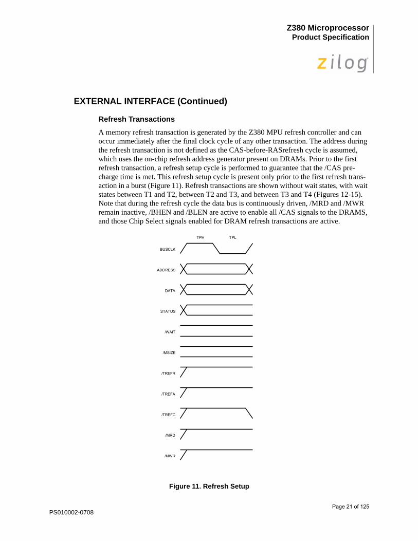
Refresh TransactionsA memory refresh transaction is generated by the Z380 MPU refresh controller and can occur immediately after the final clock cycle of any other transaction. The address during the refresh transaction is not defined as the CAS-before-RASrefresh cycle is assumed, which uses the on-chip refresh address generator present on DRAMs. Prior to the first refresh transaction, a refresh setup cycle is performed to guarantee that the /CAS pre-charge time is met. This refresh setup cycle is present only prior to the first refresh trans-action in a burst (Figure 11). Refresh transactions are shown without wait states, with wait states between T1 and T2, between T2 and T3, and between T3 and T4 (Figures 12-15). Note that during the refresh cycle the data bus is continuously driven, /MRD and /MWR remain inactive, /BHEN and /BLEN are active to enable all /CAS signals to the DRAMS, and those Chip Select signals enabled for DRAM refresh transactions are active.
Figure 11. Refresh Setup
TPH
BUSCLK
ADDRESS
DATA
STATUS
/WAIT
/MSIZE
/TREFR
/TREFA
/TREFC
/MRD
/MWR
TPL
PS010002-0708Page 21 of 125

Z380 Microprocessor Product Specification
Figure 12. Refresh Cycle, No Waits
T1 T2 T3 T4
BUSCLK
ADDRESS
DATA
STATUS
/WAIT
/MSIZE
/TREFR
/TREFA
/TREFC
/MRD
/MWR
PS010002-0708Page 22 of 125

Z380 Microprocessor Product Specification
Figure 13. Refresh Cycle, T1 Wait
T1 T1L T1H T2 T3 T4
BUSCLK
ADDRESS
DATA
STATUS
/WAIT
/MSIZE
/TREFR
/TREFA
/TREFC
/MRD
/MWR
PS010002-0708Page 23 of 125

Z380 Microprocessor Product Specification
Figure 14. Refresh Cycle, T2 Wait
T1 T2 T2H T2L T3 T4
BUSCLK
ADDRESS
DATA
STATUS
/WAIT
/MSIZE
/TREFR
/TREFA
/TREFC
/MRD
/MWR
PS010002-0708Page 24 of 125

Z380 Microprocessor Product Specification
Figure 15. Refresh Cycle, T3 Wait
T1 T2 T3 T3L T3H T4
BUSCLK
ADDRESS
DATA
STATUS
/WAIT
/MSIZE
/TREFR
/TREFA
/TREFC
/MRD
/MWR
PS010002-0708Page 25 of 125

Z380 Microprocessor Product Specification
I/O Transactions I/O transactions move data to or from an external peripheral when the Z380 MPU per-forms an I/O access. All I/O transactions occur referenced to the IOCLK signal, when it is a divided-down version of the BUSCLKsignal. BUSCLK may be divided by a factor of from two to eight to form the IOCLK, under program control. An example of this division is shown, for the four possible divisors, in Figure 16. Note that the IOCLK divider is syn-chronized (i.e., starts with a known timing relationship) at the trailing edge of /RESET. This is discussed in the Reset Section.
Figure 16. IOCLK Timing
EXTERNAL INTERFACE (Continued)The Z380 MPU is unique in that it employs separate control signals for accessing the memory and I/O. This allows the two interfaces to be optimized independent of one another. The I/O bus control signals allow direct connection to members of the Z80 family of peripherals or the Z8500 family of peripherals.
Note that because all I/O bus transactions start on a rising edge of IOCLK, there may be up to n BUSCLK cycles of latency between the execution unit request for the transaction and the transaction actually starting, where n is the programmed clock divisor for IOCLK. This implies that the lowest possible divisor should always be used for IOCLK.
All I/O transactions are four IOCLK cycles long unless extended by Wait states. Wait states may be inserted between the third and fourth IOCLK cycles in an I/O transaction and are one IOCLK cycle per wait state. The external /WAIT input is sampled only after internally-generated wait states are inserted.
BUSCLK
IOCLK (X2)
IOCLK (X4)
IOCLK (X6)
IOCLK (X8)
PS010002-0708Page 26 of 125

Z380 Microprocessor Product Specification
I/O Read transactions are shown with and without a wait state (Figures 17-18). The con-tents of the data bus is latched immediately before the falling edge of IOCLK during the last IOCLK cycle of the transaction.
Figure 17. I/0Read Cycle, No Waits
IOCLK
ADDRESS
DATA
/WAIT
/MI
/IORQ
/IORD
/IOWR
/INTAK
Fi 8A I/O R d C l N W it
PS010002-0708Page 27 of 125

Z380 Microprocessor Product Specification
Figure 18. I/O Read Cycle, T1 Wait
IOCLK
ADDRESS
DATA
/WAIT
/MI
/IORQ
/IORD
/IOWR
/INTAK
Fi 8B I/O R d C l T1 W it
PS010002-0708Page 28 of 125
Z380 Microprocessor Product Specification
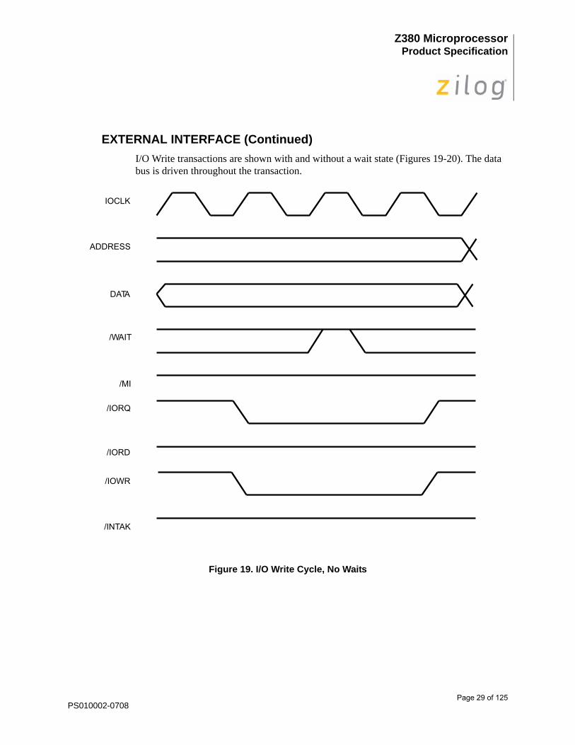
EXTERNAL INTERFACE (Continued)I/O Write transactions are shown with and without a wait state (Figures 19-20). The data bus is driven throughout the transaction.
Figure 19. I/O Write Cycle, No Waits
IOCLK
ADDRESS
DATA
/WAIT
/MI
/IORQ
/IORD
/IOWR
/INTAK
PS010002-0708Page 29 of 125

Z380 Microprocessor Product Specification
Figure 20. I/O Write Cycle, T1 Wait
ZILOG MICROPROCE
IOCLK
ADDRESS
DATA
/WAIT
/MI
/IORQ
/IORD
/IOWR
/INTAK
PS010002-0708Page 30 of 125
Z380 Microprocessor Product Specification
EXTERNAL INTERFACE (Continued)
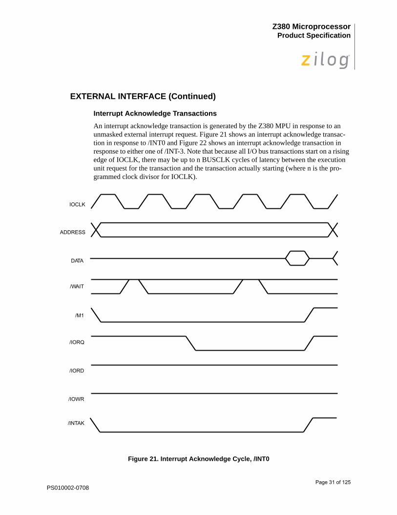
Interrupt Acknowledge Transactions An interrupt acknowledge transaction is generated by the Z380 MPU in response to an unmasked external interrupt request. Figure 21 shows an interrupt acknowledge transac-tion in response to /INT0 and Figure 22 shows an interrupt acknowledge transaction in response to either one of /INT-3. Note that because all I/O bus transactions start on a rising edge of IOCLK, there may be up to n BUSCLK cycles of latency between the execution unit request for the transaction and the transaction actually starting (where n is the pro-grammed clock divisor for IOCLK).
Figure 21. Interrupt Acknowledge Cycle, /INT0
IOCLK
ADDRESS
DATA
/WAIT
/M1
/IORQ
/IORD
/IOWR
/INTAK
PS010002-0708Page 31 of 125

Z380 Microprocessor Product Specification
Figure 22. Interrupt Acknowledge Cycle, /INT3-1
An interrupt acknowledge transaction for /INT0 is five IOCLK cycles long unless extended by Wait states. /WAIT is sampled at two separate points during the transaction. /WAIT is first sampled at the end of the first IOCLK cycle during the transaction. Wait states inserted here allow the external daisy-chain between peripherals with a longer time to settle before the interrupt vector is requested. /WAIT is then sampled at the end of the fourth IOCLK cycle to delay the point at which the interrupt vector is read by the Z380 MPU, after it has been requested.
The interrupt vector may be either eight or sixteen bits, under program control, and is latched by the falling edge of IOCLK in the last cycle of the interrupt acknowledge trans-action. When using Mode 0 interrupts, where the Z380 MPU fetches an instruction from the interrupting device, these fetches are always eight bits wide and are transferred over D7-D0.
IOCLK
ADDRESS
DATA
/WAIT
/MI
/IORQ
/IORD
/IOWR
/INTAK
PS010002-0708Page 32 of 125

Z380 Microprocessor Product Specification
An interrupt acknowledge transaction in response to one of /INT3-/INT1 is also five IOCLK cycles long, unless extended by wait states. The waits are sampled and inserted at similar locations as an interrupt acknowledge transaction is for /INT0. Note, however, only the /INTAK signal is active with /MI, /IORQ, /IORD and /IOWR held inactive.
For either type of INTACK transaction the address bus is driven with a value which indi-cates the type of interrupt being acknowledged as follows: A31-A6 are all one, and A3-A0 are one except for a single zero corresponding to the maskable interrupt being acknowl-edged. Thus an /INT3 acknowledge is signaled by A3 being zero during the interrupt acknowledge transaction, /INT2 acknowledge is signalled by A2 being zero, etc.
RETI Transactions The RETI transaction is generated whenever an RETI instruction is executed by the Z380 MPU. This transaction is necessary because Z80 family peripherals are designed to watch instruction fetches and take special action upon seeing a RETI instruction (this is the only instruction that the Z80 family peripherals watch for). Since the Z380 MPU fetches instructions using the memory control signals, a simulated RETI instruction fetch must be placed on the bus with the appropriate I/O bus control signals. This is shown in Figure 23. Again, note that because all I/O bus transactions start on a rising edge of IOCLK, there may be up to n BUSCLK cycles of latency between the execution unit request for the transaction and the transaction actually starting, where n is the programmed clock divisor for IOCLK.
PS010002-0708Page 33 of 125

Z380 Microprocessor Product Specification
Figure 23. Return From Interrupt Cycle
The RETI transaction is ten IOCLK cycles long unless extended by Wait states, and /WAIT is sampled at three separate points during the transaction. /WAIT is first sampled in the middle of the third IOCLK cycle to allow for longer/IORDLow-time requirements. /WAIT is then sampled again during the middle of the fifth IOCLK cycle to allow for lon-ger internal daisy-chain settling time within the peripheral. Wait states inserted here have the effect of separating what the peripheral sees as two separate instruction fetch cycles. Finally, /WAIT is sampled in the middle of the ninth IOCLK cycle, again to allow for lon-ger /IORD Low-time requirements.
The Z380 MPU drives the data bus throughout the RETI transaction, with EDEDH during the first half of the transaction (the first byte of a RETI instruction is EDH) and with 4D4DH during the second half of the transaction (the second byte of an RETI instruction is 4DH).
1 2 3 4 5 6 7 8 9 10
IOCLK
ADDRESS
EDED 4D4DDATA
/WAIT
/M1
/IORQ
/IORD
/IOWR
/INTAK
PS010002-0708Page 34 of 125

Z380 Microprocessor Product Specification
HALT Transactions A HALT transaction occurs whenever the Z380 MPU executes a Halt instruction, with the /HALT signal activated on the falling edge of BUSCLK. If the standby mode is not enabled, executing a Sleep instruction would also cause a Halt transaction to occur. While in the Halt state, the Z380 MPU continues to drive the address and data buses, and the /HALT signal remains active until either an interrupt request is acknowledged or a reset is received. Refresh transactions may occur while in the halt state and the bus can be granted. The timing of entry into the Halt state is shown in Figure 24, while the timing of exiting from Halt state is shown in Figure 25.
Figure 24. HALT Entry
T5 THL THH THL
BUSCLK
ADDRESS
DATA
STATUS
/WAIT
/MSIZE
/TREFR
/TREFA
/TREFC
/MRD
/MWR
/HALT
PS010002-0708Page 35 of 125

Z380 Microprocessor Product Specification
Figure 25. HALT Exit
THH THL THH THL THH T6
BUSCLK
ADDRESS
DATA
STATUS
/WAIT
/MSIZE
/TREFR
/TREFA
/TREFC
/MRD
/MWR
/HALT
/INT or /NMI
PS010002-0708Page 36 of 125

Z380 Microprocessor Product Specification
Requests A request can be initiated by a device that does not have control of the bus. Two types of request can occur: Bus request and Interrupt request. When an interrupt or bus request is made, it is answered by the CPU according to its type. For an interrupt request, the CPU initiates an interrupt acknowledge transaction and for bus requests, the CPU enters the bus disconnect state, relinquishes the bus, and activates an Acknowledge signal.
BUS Requests To generate transactions on the bus, a potential bus master (such as a DMA controller) must gain control of the bus by making a bus request. A bus request is initiated by driving /BREQ Low. Several bus requesters may be wired-OR to the /BREQ pin; priorities are resolved externally to the CPU, usually by a priority daisy chain.
The asynchronous /BREQ signal generates an internal /BUSREQ, which is synchronous. If the /BREQ is active at the beginning of any transaction, the internal /BUSREQ causes the /BACK signal to be asserted after the current transaction is completed. The Z380 MPU then enters the Bus Disconnect state and gives up control of the bus. All Z380 MPU con-trol signals, except /BACK, /MI and /INTAK are tri-stated. Note that release of the bus may be inhibited under program control to allow the Z380 MPU exclusive access to a shared resource; this is controlled by the SETC LCK and RESC LCK instructions. Entry into the Bus Disconnect state is shown in Figure 26. The Z380 MPU regains control of the bus after /BREQ is deasserted. This is shown in Figure 27.
Interrupt Requests The Z380 MPU supports two types of interrupt requests, maskable /INT3-INT0 and non-maskable (/NMI). The interrupt request line of a device that is capable of generating an interrupt can be tied to either /NMI or one of the maskable interrupt request lines, and sev-eral devices can be connected to one interrupt request line with the devices arranged in a priority daisy chain. However, because of the need for Z80 family peripheral devices to see the RETI instruction, only one daisy chain of Z80-family peripherals can be used. The Z380 MPU handles maskable and nonmaskable interrupt requests somewhat differently, as follows:
Any High-to-Low transition on the /NMI input is asynchronously edge-detected, and the internal NMI latch is set. At the beginning of the last clock cycle in the last internal machine cycle of any instruction, the maskable interrupts are sampled along with the state of the NMI latch.
If an enabled maskable interrupt is requested, at the next possible time (the next rising edge of IOCLK) an interrupt acknowledge transaction is generated to fetch the interrupt-vector from the interrupting device.For a nonmaskable interrupt, no interrupt acknowledge transaction is generated; the NMI service routine always starts at address 00000066H.
PS010002-0708Page 37 of 125

Z380 Microprocessor Product Specification
Figure 26. Bus Request/Acknowledge Cycle
T7 TBLTransaction in progress
BUSCLK
ADDRESS
DATA
STATUS
/WAIT
/MSIZE
/TREFR
/TREFA
/TREFC
/MRD
/MWR
/BREQ
/BACK
/MI
/IORQ
/IORD
/IOWR
/INTAK
PS010002-0708Page 38 of 125

Z380 Microprocessor Product Specification
Figure 27. Bus Request/Acknowledge End Cycle
TBH TBL TBH TBL TBH TIL
BUSCLK
ADDRESS
DATA
STATUS
/WAIT
/MSIZE
/TREFR
/TREFA
/TREFC
/MRD
/MWR
/BREQ
/BACK
/MI
/IORQ
/IORD
/IOWR
/INTAK
PS010002-0708Page 39 of 125
Z380 Microprocessor Product Specification
EXTERNAL INTERFACE (Continued)
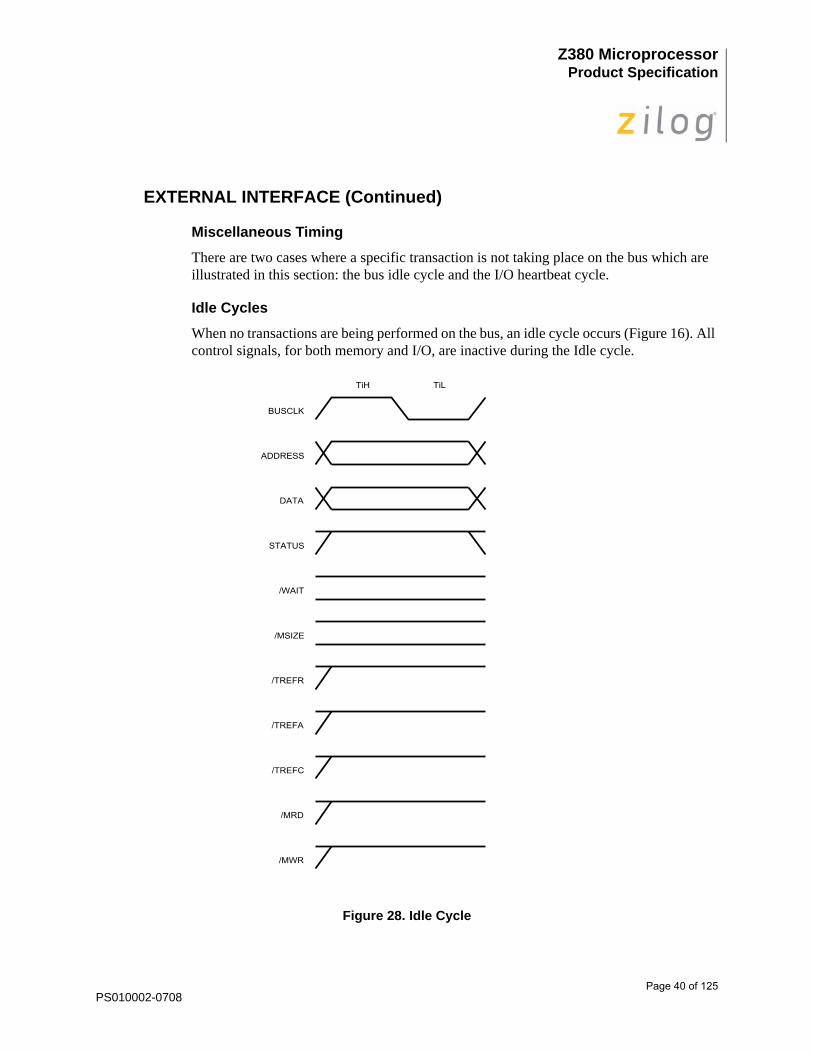
Miscellaneous TimingThere are two cases where a specific transaction is not taking place on the bus which are illustrated in this section: the bus idle cycle and the I/O heartbeat cycle.
Idle Cycles When no transactions are being performed on the bus, an idle cycle occurs (Figure 16). All control signals, for both memory and I/O, are inactive during the Idle cycle.
Figure 28. Idle Cycle
TiH TiL
BUSCLK
ADDRESS
DATA
STATUS
/WAIT
/MSIZE
/TREFR
/TREFA
/TREFC
/MRD
/MWR
PS010002-0708Page 40 of 125

Z380 Microprocessor Product Specification
I/O Heartbeat Cycle The Z380 MPU is capable of generating an I/O heartbeat cycle on the I/O bus in response to an I/O write to an on-chip control register. This cycle is most useful with Z80 family peripherals, where some members require a transaction that looks like a Z80 CPU instruc-tion fetch to perform certain interrupt functions (Figure 29).
Figure 29. I/O Heartbeat Cycle
IOCLK
ADDRESS
All ZerosDATA
/WAIT
/MI
/IORQ
/IORD
/IOWR
/ INTAK
PS010002-0708Page 41 of 125

Z380 Microprocessor Product Specification
EXTERNAL INTERFACE (Continued)
Reset Timing The timing for entering and exiting the reset state is shown in Figures 30 and 31. The effects of reset on the internal state of the Z380 MPU are detailed in the Reset section.
The synchronization of IOCLK at the end of the reset state is shown in Figure 32. Note that the IOCLK divisor is set to the maximum value (eight) by /RESET and is only syn-chronized at the end of the reset state.
Figure 30. Reset Entry
Transaction in progress
BUSCLK
ADDRESS
DATA
STATUS
/WAIT
/MSIZE
/TREFR
/TREFA
/TREFC
/MRD
/MWR
/IOCTL3-0
/RESET
T9 TRL
PS010002-0708Page 42 of 125

Z380 Microprocessor Product Specification
Figure 31. Reset Exit
TRH TRL TRH TRL TRH TiL
BUSCLK
ADDRESS
DATA
STATUS
/WAIT
/MSIZE
/TREFR
/TREFA
/TREFC
/MRD
/MWR
/IOCTL3-0
/RESET
PS010002-0708Page 43 of 125

Z380 Microprocessor Product Specification
EXTERNAL INTERFACE (Continued
Figure 32. IOCLK Reset Start-up
BUSCLK
/RESET
IOCLK
PS010002-0708Page 44 of 125

Z380 Microprocessor Product Specification
CPU ARCHITECTUREThe Central Processing Unit (CPU) of the Z380 MPU is a binary-compatible extension of the Z80 CPU and Z180 CPU architectures. High throughput rates for the Z380 CPU are achieved by a high clock rate, high bus bandwidth and instruction fetch/execute overlap. Communicating to the external world through an 8-or 16-bit data bus, the Z380 CPU is a full 32-bit machine internally, with a 32-bit ALU and 32-bit registers.
Modes Of Operation The Z380 CPU can operate in either Native or Extended mode, as controlled by a bit in the Select Register (SR). In Native mode (the Reset configuration), all address manipulations are performed modulo 65536 (16 bits). In this mode the Program Counter (PC) only incre-ments across 16 bits, all address manipulation instructions (increment, decrement, add, subtract, indexed, stack relative, and PC relative) only operate on 16 bits, and the Stack Pointer (SP) only increments and decrements across 16 bits. The program counter high-order word is left at all zeros, as is the high-order words of the stack pointer and the I reg-ister. Thus Native mode is fully compatible with the Z80 CPU's 64 Kbyte address space. It is still possible to address memory outside of the 64 Kbyte address space for data storage and retrieved in Native mode, however, direct addresses, indirect addresses, and the high-order word of the SP, I and the IX and IY registers may be loaded with non-zero values. But executed code and interrupt service routines must reside in the lowest 64 Kbytes of the address space.
In Extended mode, however, all address manipulation instructions operate on 32 bits, allowing access to the entire 4 Gbyte address space of the Z380 MPU. In both Native and Extended modes, the Z380 CPU drives all 32 bits of the address onto the external address bus; only the width of manipulated addresses distinguish Native from Extended mode. The Z380 CPU implements one instruction to allow switching from Native to Extended mode, but once in Extended mode, only Reset returns the Z380 MPU to Native mode. This restriction applies because of the possibility of "misplacing" interrupt service routines or vector tables during the translation from Extended mode back to Native mode.
In addition to Native and Extended mode, which is specific to memory space addressing, the Z380 MPU can operate in either Word or Long Word mode specific to data load and exchange operations. In Word mode (the reset configuration), all word load and exchange operations manipulate 16-bit quantities. For example, only the low-order words of the source and destination are exchanged in an exchange operation, with the high-order words unaffected. In Long Word mode, all 32 bits of the source and destination are directives to allow switching between Word and Long Word mode; SETC LW (Set Control Long Word) and RESC LW (Reset Control Long Word) perform a global switch, while DDIR W, DDIR LW and their variants are decoder directives that select a particular mode only for the instruction that they precede.
Note that all word data arithmetic (as opposed to address manipulation arithmetic), rotate, shift and logical operations are always in 16-bit quantities. They are not controlled by either the Native/Extended or Word/Long Word selections. The exceptions to the 16-bit
PS010002-0708Page 45 of 125
Z380 Microprocessor Product Specification
quantities are, of course, those multiply and divide operations with 32-bit products or div-idends.
Lastly, all word Input/Output operations are performed on 16-bit values.
Address Spaces The Z380 CPU architecture supports five distinct address spaces corresponding to the dif-ferent types of locations that can be accessed by the CPU. These five address spaces are: CPU register space, CPU control register space, memory address space, and I/O address space (on-chip and external).
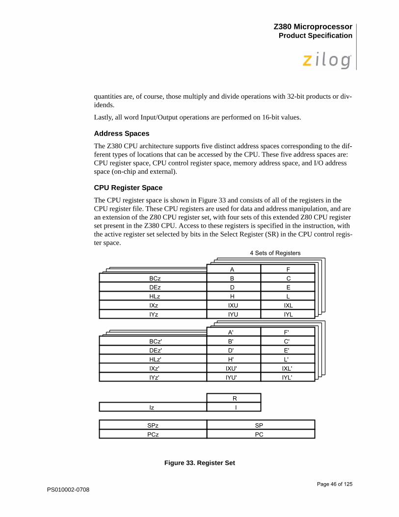
CPU Register Space The CPU register space is shown in Figure 33 and consists of all of the registers in the CPU register file. These CPU registers are used for data and address manipulation, and are an extension of the Z80 CPU register set, with four sets of this extended Z80 CPU register set present in the Z380 CPU. Access to these registers is specified in the instruction, with the active register set selected by bits in the Select Register (SR) in the CPU control regis-ter space.
Figure 33. Register Set
4 Sets of Registers
A FB CD EH L
IXU IXLIYU IYL
A' F'B' C'D' E'H' L'
IXU' IXL'IYU' IYL'
BCz'DEz'HLz'IXz'IYz'
BCzDEzHLzIXzIYz
RIIz
SPz SPPCz PC
PS010002-0708Page 46 of 125
Z380 Microprocessor Product Specification
Each register set includes the primary registers A, F, B, C, D, E, H, L, IX, and IY, as well as the alternate registers A’, F’, B’, C’, D’, E’, H’, L’, IX’, and IY’. These byte registers can be paired B with C, D with E, H with L, B’ with C’, D’ with E’ and H’ with L’ to form word registers. These word registers are extended to 32 bits with the z extension to the register. This register extension is only accessible when using the register as a 32-bit regis-ter (the Long Word mode) or when swapping between the most-significant and least-sig-nificant word of a 32-bit register. Whenever an instruction refers to a word register, the implicit size is controlled by the Word or Long Word mode. Also included are the R, I and SP registers, as well as the PC.
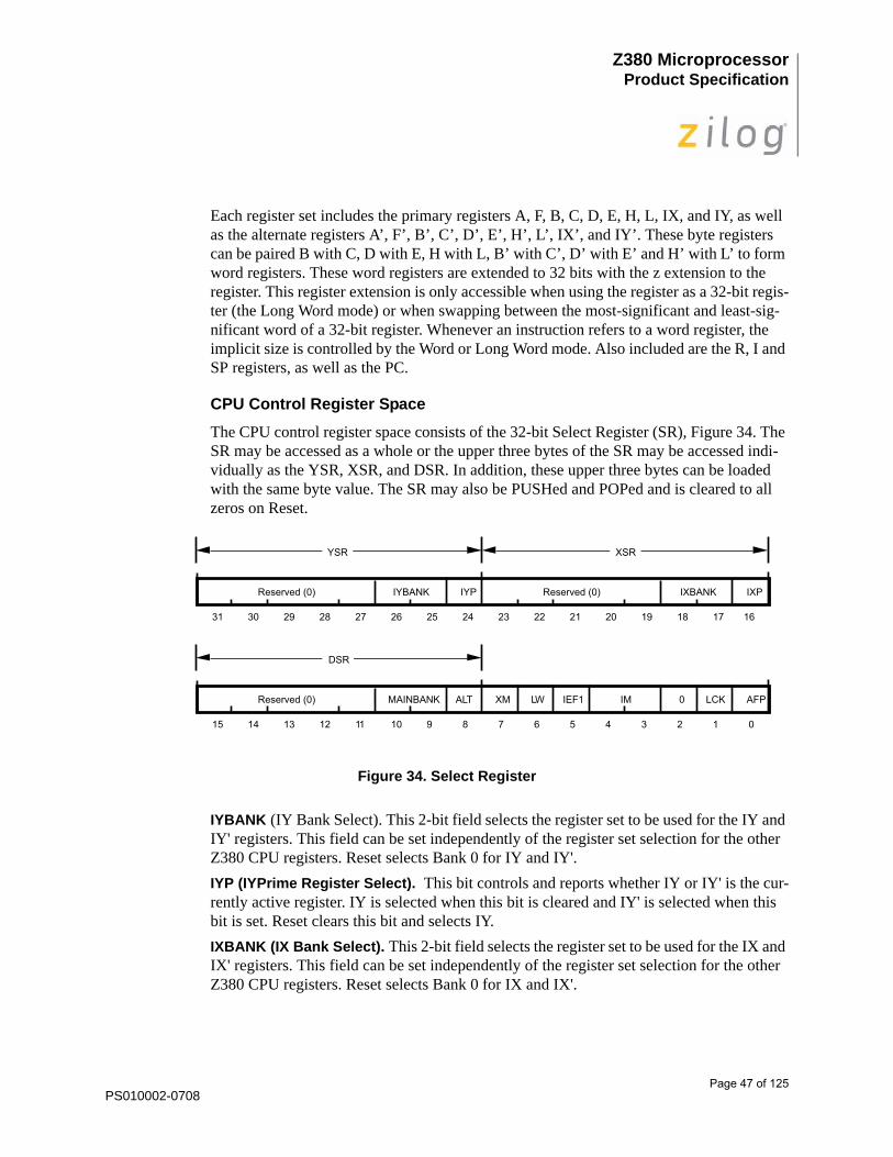
CPU Control Register Space The CPU control register space consists of the 32-bit Select Register (SR), Figure 34. The SR may be accessed as a whole or the upper three bytes of the SR may be accessed indi-vidually as the YSR, XSR, and DSR. In addition, these upper three bytes can be loaded with the same byte value. The SR may also be PUSHed and POPed and is cleared to all zeros on Reset.
Figure 34. Select Register
IYBANK (IY Bank Select). This 2-bit field selects the register set to be used for the IY and IY' registers. This field can be set independently of the register set selection for the other Z380 CPU registers. Reset selects Bank 0 for IY and IY'. IYP (IYPrime Register Select). This bit controls and reports whether IY or IY' is the cur-rently active register. IY is selected when this bit is cleared and IY' is selected when this bit is set. Reset clears this bit and selects IY. IXBANK (IX Bank Select). This 2-bit field selects the register set to be used for the IX and IX' registers. This field can be set independently of the register set selection for the other Z380 CPU registers. Reset selects Bank 0 for IX and IX'.
Reserved (0) IYBANK IYP Reserved (0) IXBANK IXP
XSRYSR
31 30 29 28 27 26 25 24 23 22 21 20 19 18 17 16
Reserved (0) MAINBANK ALT XM IM AFP
DSR
LW IEF1 0 LCK
15 14 13 12 11 10 9 8 7 6 5 4 3 2 1 0
PS010002-0708Page 47 of 125

Z380 Microprocessor Product Specification
IXP (IXPrime Register Select). This bit controls and reports whether IX or IX' is the cur-rently active register. IX is selected when this bit is cleared and IX' is selected when this bit is set. Reset clears this bit and selects IX. MAINBANK (Main Bank Select). This 2-bit field selects the register set to be used for the A, F, BC, DE, HL, A', F', BC', DE' and HL' registers. This field can be set independently of the register set selection for the other Z380 CPU registers. Reset selects Bank 0 for these registers. ALT (BC/DE/HL or BC'/DE'/HL' Register Select). This bit controls and reports whether BC/DE/HL or BC'/DE'/HL' is the currently active bank of registers. BC/DE/HL are selected when this bit is cleared and BC'/DE'/HL' are selected when this bit is set. Reset clears this bit, selecting BC/DE/HL. XM (Extended Mode). This bit controls the Extended/ Native mode selection for the Z380 CPU. This bit is set by the SETC XM instruction, and once set, it can be cleared only by a reset on the /RESET pin. When this bit is set, the Z380 CPU is in Extended mode. Reset clears this bit and the Z380 CPU is in Native mode. LW (Long Word Mode). This bit controls the Long Word/ Word mode selection for the Z380 CPU. This bit is set by the SETC LW instruction and cleared by the RESC LW instruction. When this bit is set, the Z380 CPU is in Long Word mode; when this bit is cleared, the Z380 CPU is in Word mode. Reset clears this bit. Note that individual instruc-tions may be executed in either Word or Long Word load and exchange mode, using the DDIR W and DDIR LW decoder directives. IEF1 (Interrupt Enable Flag). This bit is the master Interrupt Enable for the Z380 CPU. This bit is set by the EI instruction and cleared by the DI instruction. When this bit is set, interrupts are enabled; when this bit is cleared, interrupts are disabled. Reset clears this bit. IM (Interrupt Mode). This 2-bit field controls the interrupt mode for the /INT0 interrupt request. These bits are controlled by the IM instructions (00 = IM 0, 01 = IM 1, 10 = IM 2, 11 = IM 3). Reset clears both of these bits, selecting Interrupt Mode 0. LCK (Lock). This bit controls the Lock/Unlock status of the Z380 CPU. This bit is set by the SETC LCK instruction and cleared by the RESC LCK instruction. When this bit is set, no bus requests are accepted, providing exclusive access to the bus by the Z380 CPU. When this bit is cleared the Z380 CPU will grant bus requests in the normal fashion. Reset clears this bit. AFP (AF Prime Register Select). This bit controls and reports whether AF or AF' is the currently active pair of registers. AF is selected when this bit is cleared and AF' is selected when this bit is set. Reset clears this bit and selects AF.
Memory Address Space The memory address space can be viewed as a string of 4 Gbyte numbered consecutively in ascending order. The 8-bit byte is the basic addressable element in the Z380 MPU mem-ory address space. However, there are other addressable data elements; bits, 2-byte words, bytestrings, and 4-byte words.
PS010002-0708Page 48 of 125

Z380 Microprocessor Product Specification
The size of the data element being addressed depends on the instruction being executed as well as the Word/Long Word mode. A bit can be addressed by specifying a byte, and a bit within that byte. Bits are numbered from right to left, with the least significant bit being bit 0 (Figure 35).
The address of a multiple-byte entity is the same as the address of the byte with the lowest memory address in the entity. Multiple-byte entities can be stored beginning with either even or odd memory addresses. A word (either 2-byte or 4-byte entity) is aligned if its address is even; otherwise, it is unaligned. Multiple bus transactions, which may be required to access multiple-byte entities, can be minimized if alignment is maintained.
The formats of multiple-byte data types are also shown in Figure 35. Note that when a word is stored in memory, the least significant byte precedes the more significant byte of the word, as in the Z80 CPU architecture. Also, the lower-addressed byte is present on the upper byte of the external data bus.
Figure 35. Bit/Byte Ordering Conventions
Bits within a byte:
7 6 5 4 3 2 1 0
16-bit word at address n:
Least Significant Byte
Most Significant Byte
32-bit word at address n:
D7-0 (Least Significant Byte)
D15-8
D23-16
D31-24 (Most Significant Byte)
Memory addresses:Even address (A0=0)
Address n
Address n+1
Address n
Address n+1
Address n+2
Address n+3
Odd address (A0=1)
Least Significant Byte Most Significant Byte
15 14 13 12 11 10 9 8 7 6 5 4 3 2 1 0
PS010002-0708Page 49 of 125

Z380 Microprocessor Product Specification
CPU ARCHITECTURE (Continued)
External I/O Address Space External I/O addresses are generated by I/O instructions, except those reserved for on-chip I/O address space accesses, and can take a variety of forms (Table 2). An I/O read or write is always one transaction, regardless of the bus size and the type of I/O instruction.
On-chip I/O Address Space The Z380 MPU's on-chip peripheral functions and a portion of its interrupt functions are controlled by several on-chip registers, which occupy an On-chip I/O Address Space. This on-chip I/O address space can be accessed only with the following reserved on-chip I/O instructions.
When one of these I/O instructions is executed, the Z380 MPU outputs the register address being accessed in a pseudo transaction of two BUSCLK cycles duration, with the address signals A31-A8 all at zeros. In the pseudo transaction, all bus control signals are at their inactive states.
Table 2. External I/O Addressing Options
IN0 R, (n) OTIM
IN0 (n) OTIMR
OUT0 (n), R OTDM
TSTIO n OTDMR
Address Bus I/O Instruction A31-A24 A23-A16 A15-A8 A7-A0
IN A, (n) 00000000 00000000 Contents of A reg nIN dst,(C) BC31-BC24 BC23-BC16 BC15-BC8 BC7-BC0 IN0 dst,(n) 00000000 00000000 00000000 nINA(W) dst,(mn) 00000000 00000000 m nDDIR IB INA(W) dst,(lmn) 00000000 l m nDDIR IW INA(W) dst,(klmn) k l m nBlock Input BC31-BC24 BC23-BC16 BC15-BC8 BC7-BC0
OUT (n),A 00000000 00000000 Contents of A reg nOUT (C),dst BC31-BC24 BC23-BC16 BC15-BC8 BC7-BC0 OUT0 (n),dst 00000000 00000000 00000000 nOUTA(W) (mn),dst 00000000 00000000 m nDDIR IB OUTA(W) (lmn),dst 00000000 l m nDDIR IW OUTA(W) (klmn),dst k l m nBlock output BC31-BC24 BC23-BC16 BC15-BC8 BC7-BC0
PS010002-0708Page 50 of 125

Z380 Microprocessor Product Specification
DATA TYPES The Z380 CPU can operate on bits, Binary-Coded Decimal (BCD) digits (4 bits), bytes (8 bits), words (16 bits or 32 bits), byte strings, and word strings. Bits in registers can be set, cleared, and tested. BCD digits, packed two to a byte, can be manipulated with the Deci-mal Adjust Accumulator instruction (in conjunction with binary addition and subtraction) and the Rotate Digit instructions. Bytes are operated on by 8-bit load, arithmetic, logical, and shift and rotate instructions. Words are operated on in a similar manner by the word load, arithmetic, logical, and shift and rotate instructions. Block move and search opera-tions can manipulate byte strings and word strings up to 64 Kbytes or words long. Block I/O instructions have identical capabilities.
CPU Registers The Z380 CPU contains abundant register resources (Figure 33). At any given time, the program has immediate access to both the primary and alternate registers in the selected register set. Changing register sets is a simple matter of a LDCTL instruction.
Primary and Working Registers The working register set is divided into the two register files; the primary file and the alter-nate (designated by ‘) file. Each file contains an 8-bit Accumulator (A), a Flag register (F), and six general-purpose registers (B, C, D, E, H, and L). Only one file can be active at any given time, although data in the inactive file can still be accessed. Upon reset, the primary register file in register set 0 is active. Exchange instructions allow the programmer to exchange the active file with the inactive file.
The accumulator is the destination register for 8-bit arithmetic and logical operations. The six general-purpose registers can be paired (BC, DE, and HL), and are extended to 32 bits by the z extension to the register, to form three 32-bit general-purpose registers. The HL register serves as the 16-bit or 32-bit accumulator for word operations.
CPU Flag Register The Flag register contains six flags that are set or reset by various CPU operations. This register is illustrated in Figure 36 and the various flags are described below.
Figure 36. CPU Flag Register
S Z X H X P/V N C
7 6 5 4 3 2 1 0
PS010002-0708Page 51 of 125

Z380 Microprocessor Product Specification
Carry (C). This flag is set when an add instruction generates a carry or a subtract instruc-tion generates a borrow. Certain logical, rotate and shift instructions affect the Carry flag. Add/Subtract (N). This flag is used by the Decimal Adjust Accumulator instruction to distinguish between add and subtract operations. The flag is set for subtract operations and cleared for add operations. Parity/Overflow (P/V). During arithmetic operations this flag is set to indicate a two’s complement overflow. During logical and rotate operations, this flag is set to indicate even parity of the result or cleared to indicate odd parity. Half Carry (H). This flag is set if an 8-bit arithmetic operation generates a carry or borrow between bits 3 and 4, or if a 16-bit operation generates a carry or borrow between bits 11 and 12, or if a 32-bit operation generates a carry or borrow between bits 27 and 28. This bit is used to correct the result of a packed BCD addition or subtract operation. Zero (Z). This flag is set if the result of an arithmetic or logical operation is a zero. Sign (S). This flag stores the state of the most significant bit of the accumulator.
Index Registers The four index registers, IX, IX’, IY and IY’, each hold a 32-bit base address that is used in the Indexed addressing mode. The Index registers can also function as general-purpose registers with the upper and lower byte of the lower 16 bits being accessed individually. These byte registers are called IXU, IXU’, IXL and IXL’ for the IX and IX’ registers, and IYU, IYU’, IYL and IYL’ for the IY and IY’ registers.
Interrupt Register The Interrupt register (I) is used in interrupt modes 2 and 3 for /INT0 to generate a 32-bit indirect address to an interrupt service routine. The I register supplies the upper twenty-four or sixteen bits of the indirect address and the interrupting peripheral supplies the lower eight or sixteen bits. In the Assigned Vectors mode for /INT1-3 the upper sixteen bits of the vector are supplied by the I register; bits 15-9 are the assigned vector base and bits 8-0 are the assigned vector unique to each of /INT1-3.
Program Counter The Program Counter (PC) is used to sequence through instructions in the currently exe-cuting program and to generate relative addresses. The PC contains the 32-bit address of the current instruction being fetched from memory. In the Native mode, the PC is effec-tively only 16 bits long, as carries from bit 15 to bit 16 are inhibited in this mode. In Extended mode, the PC is allowed to increment across all 32 bits.
R Register The R register can be used as a general-purpose 8-bit read/write register. The R register is not associated with the refresh controller and its contents are changed only by the user.
PS010002-0708Page 52 of 125

Z380 Microprocessor Product Specification
Stack Pointer The Stack Pointer (SP) is used for saving information when an interrupt or trap occurs and for supporting subroutine calls and returns. Stack Pointer relative addressing allows parameter passing using the SP.
Select Register The Select Register (SR) controls the register set selection and the operating modes of the Z380 CPU. The reserved bits in the SR are for future expansion; they will always read as zeros and should be written with zeros for future compatibility. The SR is shown in Figure 34.
Addressing Modes Addressing modes are used by the Z380 CPU to calculate the effective address of an oper-and needed for execution of an instruction. Seven addressing modes are supported by the Z380 CPU. Of these seven, one is an addition to the Z80 CPU addressing modes (Stack Pointer Relative) and the remaining six modes are either existing or extensions to the Z80 CPU addressing modes. Register. The operand is one of the 8-bit registers (A, B, C, D, E, H, L, IXU, IXL, IYU, IYL, A', B', C', D', E', H' or L'); or is one of the 16-bit or 32-bit registers (BC, DE, HL, IX, IY, BC', DE', HL', IX', IY' or SP) or one of the special registers (I or R). Immediate. The operand is in the instruction itself and has no effective address. The DDIR IB and DDIR IW decoder directives allow specification of 24-bit and 32-bit imme-diate operands, respectively. Indirect Register. The contents of a register specify the effective address of an operand. The HL register is the primary register used for memory accesses, but BC and DE can also be used. (For the JP instruction, IX and IY can also be used for indirection.) The BC regis-ter is used for I/O space accesses. Direct Address. The effective address of the operand is the location whose address is contained in the instruction. Depending on the instruction, the operand is either in the I/O or memory address space. Sixteen bits of direct address is the norm, but the DDIR IB and-DDIR IW decoder directives allow 24-bit and 32-bit direct addresses, respectively. Indexed. The effective address of the operand is the location computed by adding the two's-complement signed displacement contained in the instruction to the contents of the IX or IY register. Eight bits of index is the norm, but the DDIR IB and DDIR IW decoder directives allow 16-bit and 24-bit indexes, respectively. Program Counter Relative. An 8-, 16-or 24-bit displacement contained in the instruc-tion is added to the Program Counter to generate the effective address. This mode is avail-able only for Jump and Call instructions.
PS010002-0708Page 53 of 125

Z380 Microprocessor Product Specification
Stack Pointer Relative. The effective address of the operand is the location computed by adding the two's-complement signed displacement contained in the instruction to the con-tents of the Stack Pointer. Eight bits of index is the norm, but the DDIR IB and DDIR IW decoder directives allow 16-and 24-bit indexes, respectively.
PS010002-0708Page 54 of 125

Z380 Microprocessor Product Specification
INSTRUCTION SET The Z380 CPU’s instruction set is a superset of the Z80 CPU’s; the Z380 CPU is opcode compatible with the Z80 CPU. Thus a Z80 program can be executed on a Z380 MPU with-out modification. The instruction set is divided into seventeen groups by function:
The instructions are divided into the following categories.
• 8-bit load group
• 16/32 bit load group
• Push/Pop group
• Exchanges, block transfers, and searches
• 8-bit arithmetic and logic operations
• General purpose arithmetic and CPU control
• Decoder Directive Instructions
• 16/32 bit arithmetic operations
• Multiply/Divide Instruction group
• 8-bit Rotates and shifts
• 16-bit Rotates and shifts
• 8-bit bit set, reset, and test operations
• Jumps
• Calls, returns, and restarts
• 8-bit input and output operations for External I/O address space
• 8-bit input and output operations for Internal I/O address space
• 16-bit input and output operations
Instruction Set The following is a summary of the Z380 instruction set which shows the assembly lan-guage mnemonic, the operation, the flag status, and gives comments on each instructions.
Mnemonic and object code assignment for newly added instructions (instructions in Italicface) are preliminary and subject to change without notice.
The Z380 Technical Manual will contain significantly more details for programming use. A list of instructions, as well as encoding is included in Appendix A of this document.
Note:
PS010002-0708Page 55 of 125

Z380 Microprocessor Product Specification
Instruction Set Notation Symbols. The following symbols are used to describe the instruction set.
INSTRUCTION SET (Continued) Assignment of a value is indicated by the symbol
For example,
dst dst + src
indicates that the source data is added to the destination data and the result is stored in the destination location. The notation “dst (b)” is used to refer bit “b” of a given location, “dst(m-n) is used to refer bit location m to n of the destination. For example,
HL(7) specifies bit 7 of the destination, and
HL(23-16) specifies bit location 23 to 16 of the HL register.
n An 8-bit constant
nn A 16-bit constant
d An 8-bit offset. (2’s complement)
r Any one of the CPU register A, B, C, D, E, H, L
s Any 8-bit location for all the addressing modes allowed for the particular instruction.
dd,qq,ss,tt,uu Any 16-bit location for all the addressing modes allowed for the particular instruction.
xxh MS Byte of the specified 16-bit location
xxl LS Byte of the specified 16-bit location
SR Select Register
XY Index register (IX or IY)
XYz Index Register Extend (IXz or IYz)
XYU MS Byte of index register (IXU or IYU)
XYL LS Byte of index register (IXL or IYL)
SP Current Stack Pointer
(C) I/O Port pointed by C register
cc Condition Code
[ ] Optional field
( ) Indirect Address Pointer or Direct Address
PS010002-0708Page 56 of 125

Z380 Microprocessor Product Specification
Flags. The F register contains the following flags followed by symbols.
Condition Codes. The following symbols describe the condition codes.
*Abbreviated set
S Sign flag
Z Zero flag
H Half carry flag
P/V Parity/Overflow flag
N Add/Subtract flag
C Carry Flag
The flag is affected according to the result of the operation.
• The flag is unchanged by the operation.
0 The flag is reset to 0 by operation.
1 The flag is set to 1 by operation.
V P/V flag affected according to the overflow result of the operation.
P P/V flag affected according to the parity result of the operation.
Z Zero*
NZ Not Zero*
C Carry*
NC No carry*
S Sign
NS No Sign
NV No overflow
V Overflow
PE Parity even
PO Parity odd
P Positive
M Minus
PS010002-0708Page 57 of 125
Z380 Microprocessor Product Specification
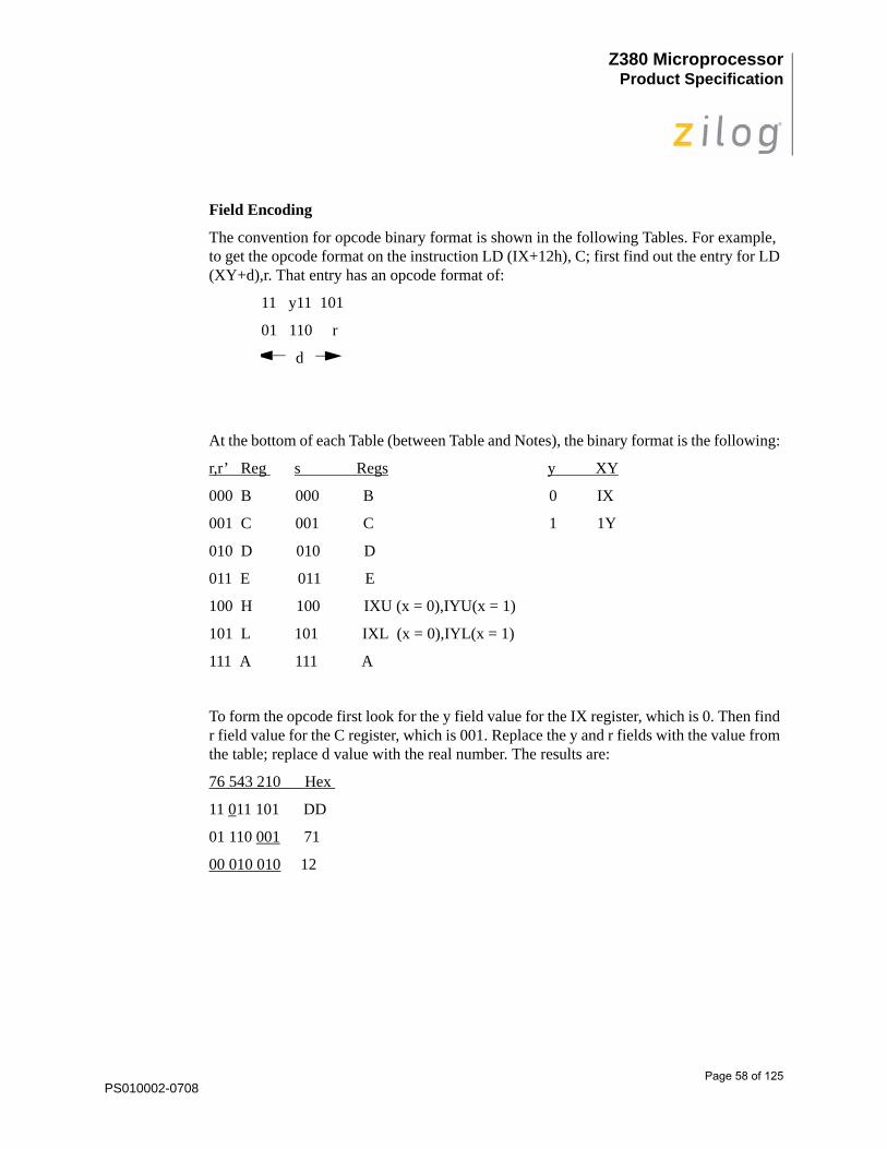
Field Encoding
The convention for opcode binary format is shown in the following Tables. For example, to get the opcode format on the instruction LD (IX+12h), C; first find out the entry for LD (XY+d),r. That entry has an opcode format of:
11 y11 101
01 110 r
d
At the bottom of each Table (between Table and Notes), the binary format is the following:
r,r’ Reg s Regs y XY
000 B 000 B 0 IX
001 C 001 C 1 1Y
010 D 010 D
011 E 011 E
100 H 100 IXU (x = 0),IYU(x = 1)
101 L 101 IXL (x = 0),IYL(x = 1)
111 A 111 A
To form the opcode first look for the y field value for the IX register, which is 0. Then find r field value for the C register, which is 001. Replace the y and r fields with the value from the table; replace d value with the real number. The results are:
76 543 210 Hex
11 011 101 DD
01 110 001 71
00 010 010 12
PS010002-0708Page 58 of 125

Z380 Microprocessor Product Specification
8-BIT LOAD GROUP
Symbolic Flags P/ Opcode # of ExecuteMnemonic Operation S Z x H x V N C 76 543 210 HEX Bytes Time Notes
LD r,r’ r ← r’ • • x • x • • • 01 r r’ 1 2LD r,n r ← n • • x • x • • • 00 r 110 2 2
←⎯ n ⎯→LD XYU,n XYU ← n • • x • x • • • 11 y11 101 3 2
00 100 110 26←⎯ n ⎯→
LD XYL,n XYL ← n • • x • x • • • 11 y11 101 3 200 101 110 2E←⎯ n ⎯→
LD r,(HL) r ← (HL) • • x • x • • • 01 r 110 1 2+rLD r,(XY+d) r ← (XY+d) • • x • x • • • 11 y11 101 3 4+r I
01 r 110←⎯ d ⎯→
LD (HL),r (HL) ← r • • x • x • • • 01 110 r 1 3+wLD (XY+d),r (XY+d) ← r • • x • x • • • 11 y11 101 3 5+w I
01 110 r←⎯ d ⎯→
LD (HL),n (HL) ← n • • x • x • • • 00 110 110 36 2 3+w←⎯ n ⎯→
LD (XY+d),n (XY+d) ← n • • x • x • • • 11 y11 101 4 5+w I00 110 110 36←⎯ d ⎯→←⎯ n ⎯→
LD A,(BC) A ← (BC) • • x • x • • • 00 001 010 0A 1 2+rLD A,(DE) A ← (DE) • • x • x • • • 00 011 010 1A 1 2+rLD A,(nn) A ← (nn) • • x • x • • • 00 111 010 3A 3 3+r I
←⎯ n ⎯→←⎯ n ⎯→
LD (BC),A (BC) ← A • • x • x • • • 00 000 010 02 1 3+wLD (DE),A (DE) ← A • • x • x • • • 00 010 010 12 1 3+wLD (nn),A (nn) ← A • • x • x • • • 00 110 010 32 3 4+w I
←⎯ n ⎯→←⎯ n ⎯→
PS010002-0708Page 59 of 125

Z380 Microprocessor Product Specification
8-BIT LOAD GROUP (Continued)
Symbolic Flags P/ Opcode # of ExecuteMnemonic Operation S Z x H x V N C 76 543 210 HEX Bytes Time Notes
LD XYU,s XYU ← s • • x • x • • • 11 y11 101 2 201 100 s
LD XYL,s XYL ← s • • x • x • • • 11 y11 101 2 201 101 s
LD s,XYU s ← XYU • • x • x • • • 11 y11 101 2 201 s 100
LD s,XYL s ← XYL • • x • x • • • 11 y11 101 2 201 s 101
LD A,I A ← I ↕ ↕ x 0 x IEF 0 • 11 101 101 ED 2 201 010 111 57
LD A,R A ← R ↕ ↕ x 0 x IEF 0 • 11 101 101 ED 2 201 011 111 5F
LD I,A I ← A • • x • x • • • 11 101 101 ED 2 201 000 111 47
LD R,A R ← A • • x • x • • • 11 101 101 ED 2 201 001 111 4F
r,r Reg s Regs y XY000 B 000 B 0 IX001 C 001 C 1 IY010 D 010 D011 E 011 E100 H 100 IXU (x = 0),IYU(x = 1)101 L 101 IXL (x = 0),IYL(x = 1)111 A 111 A
Notes:Instructions in Italic face are Z380 new instructions, instructions with underline are Z180 original instructions.I: This instruction may be used with DDIR Immediate instructions.
PS010002-0708Page 60 of 125

16/32 BIT LOAD GROUP
Symbolic Flags P/ Opcode # of ExecuteMnemonic Operation S Z x H x V N C 76 543 210 HEX Bytes Time Notes
LD dd,nn dd ← nn • • x • x • • • 00 dd0 001 3 2 L1,I← n →← n →
LD XY,nn XY ← nn • • x • x • • • 11 y11 101 4 2 L1,I00 100 001 21← n →← n →
LD HL,(nn) H ← (nn+1) • • x • x • • • 00 101 010 2A 3 3+r L1,IL ← (nn) ← n →
← n →LD dd,(nn) ddh ← (nn+1) • • x • x • • • 11 101 101 ED 4 3+r L1,I
ddl ← (nn) 01 dd1 011← n →← n →
LD XY,(nn) XYU ← (nn+1) • • x • x • • • 11 y11 101 4 3+r L1,IXYL ← (nn) 00 101 010 2A
← n →← n →
LD (nn),HL (nn+1) ← H • • x • x • • • 00 100 010 22 3 4+w L1,I(nn) ← L ← n →
← n →LD (nn),dd (nn+1) ← ddh • • x • x • • • 11 101 101 ED 4 4+w L1,I
(nn) ← ddl 01 dd0 011← n →← n →
LD (nn),XY (nn+1) ← XYU • • x • x • • • 11 y11 101 4 4+w L1,I(nn) ← XYL 00 100 010 22
← n →← n →
LD W(pp),nn (pp+1) ← nh • • x • x • • • 11 101 101 ED 4 3+w L1,I(pp) ← nl 00 pp0 110
← n →← n →
LD pp,(uu) pph ← (uu+1) • • x • x • • • 11 011 101 DD 2 2+r L1ppl ← (uu) 00 pp1 1uu
LD (pp),uu (pp+1) ← uuh • • x • x • • • 11 111 101 FD 2 3+w L1(pp) ← uul 00 pp1 1uu
LD SP,HL SP ← HL • • x • x • • • 11 111 001 F9 1 2 L1LD SP,XY SP ← XY • • x • x • • • 11 y11 101 2 2 L1
11 111 001 F9LD pp,UU pp ← UU • • x • x • • • 11 UU1 101 2 2 L1
00 pp0 010LD XY,pp XY ← pp • • x • x • • • 11 y11 101 2 2 L1
00 pp0 111LD IX,IY IX ← IY • • x • x • • • 11 011 101 DD 2 2 L1
00 100 111 27
Page 61 of 125

MICROPROCESSOR
16/32 BIT LOAD GROUP (Continued)
Symbolic Flags P/ Opcode # of ExecuteMnemonic Operation S Z x H x V N C 76 543 210 HEX Bytes Time Notes
LD IY,IX IY ← IX • • x • x • • • 11 111 101 FD 2 2 L100 100 111 27
LD pp,XY pp ← XY • • x • x • • • 11 y11 101 2 2 L100 pp1 011
LD (pp),XY (pp+1) ← XYU • • x • x • • • 11 y11 101 2 3+w L1(pp) ← XYL 00 pp0 001
LD XY,(pp) XYU ← (pp+1) • • x • x • • • 11 y11 101 2 2+r L1XYL ← (pp) 00 pp0 011
LD pp,(XY+d) pph ← (XY+d)h • • x • x • • • 11 y11 101 4 4+r L1,Ippl ← (XY+d)l 11 001 011 CB
← d →00 pp0 011
LD IX,(IY+d) IXU ← (IY+d)h • • x • x • • • 11 111 101 FD 4 4+r L1,IIXL ← (IY+d)l 11 001 011 CB
← d →00 100 011 23
LD IY,(IX+d) IYU ← (IX+d)h • • x • x • • • 11 011 101 DD 4 4+r L1,IIYL ← (IX+d)l 11 001 011 CB
← d →00 100 011 23
LD pp,(SP+d) pph ← (SP+d)h • • x • x • • • 11 011 101 DD 4 4+r L1,Ippl ← (SP+d)l 11 001 011 CB
← d →00 pp0 001
LD XY,(SP+d) XYU ← (SP+d)h • • x • x • • • 11 y11 101 4 4+r L1, IXYL ← (SP+d)l 11 001 011 CB
← d →00 100 001 21
LD (XY+d),pp (XY+d)h ← pph • • x • x • • • 11 y11 101 4 5+w L1, I(XY+d)l ← ppl 11 001 011 CB
← d →00 pp1 011
LD (IX+d),IY (IX+d)h ← IYU • • x • x • • • 11 011 101 DD 4 5+w L1, I(IX+d)l ← IYL 11 001 011 CB
← d →00 101 011 2B
LD (IY+d),IX (IY+d)h ← IXU • • x • x • • • 11 111 101 FD 4 5+w L1, I(IY+d)l ← IXL 11 001 011 CB
← d →00 101 011 2B
Page 62 of 125

Symbolic Flags P/ Opcode # of ExecuteMnemonic Operation S Z x H x V N C 76 543 210 HEX Bytes Time Notes
LD (SP+d),pp (SP+d)h ← pph • • x • x • • • 11 011 101 DD 4 5+w L1, I(SP+d)l ← ppl 11 001 011 CB
← d →00 pp1 001
LD (SP+d),XY (SP+d)h ← XYU • • x • x • • • 11 y11 101 4 5+w L1, I(SP+d)l ← XYL 11 001 011 CB
← d →00 101 001 29
LD [W] I,HL I ← HL • • x • x • • • 11 011 101 DD 2 2 L101 000 111 47
LD [W] HL,I HL ← I • • x • x • • • 11 011 101 DD 2 2 L101 010 111 57
dd Pair qq Pair pp,uu Pair y XY00 BC 00 BC 00 BC 0 IX01 DE 01 DE 01 DE 1 IY10 HL 10 HL 11 HL11 SP 11 AF
Notes:Instructions in Italic face are Z380 new instructions, instructions with underline are Z180 original instructions.I: This instruction may be used with DDIR Immediate instructions.L1: In Long Word mode, this instruction loads in 32 bits; dst(31-0) ← src(31-0)
Page 63 of 125

PUSH/POP INSTRUCTIONS
Symbolic Flags P/ Opcode # of ExecuteMnemonic Operation S Z x H x V N C 76 543 210 HEX Bytes Time Notes
PUSH qq (SP-2) ← qql • • x • x • • • 11 qq0 101 1 3+w N,L2,L4(SP-1) ← qqhSP ← SP-2
PUSH XY (SP-2) ← XYL • • x • x • • • 11 y11 101 2 3+w N, L2(SP-1) ← XYU 11 100 101 E5SP ← SP-2
PUSH nn (SP-2) ← nnl • • x • x • • • 11 111 101 FD 4 3+w N, L4,I(SP-1) ← nnh 11 110 101 F5SP ← SP-2 ← n →
← n →PUSH SR (SP-2) ← SR(7-0) • • x • x • • • 11 101 101 ED 2 3+w N, L2
(SP-1) ← SR(15-8) 11 000 101 C5SP ← SP-2
POP qq qqh ← (SP+1) • • x • x • • • 11 qq0 001 1 2+r N, L3, L5qql ← (SP)SP ← SP+2
POP XY XYU ← (SP+1) • • x • x • • • 11 y11 101 2 1+r N, L3XYL ← (SP) 11 100 001 E1SP ← SP+2
POP SR SR(6-0) ← (SP) • • x • x • • • 11 101 101 ED 2 3+r N, L6SR(15-8) ← (SP+1) 11 000 001 C1SR(23-16) ← (SP+1)SR(31-24) ← (SP+1)SP ← SP+2
qq Pair y XY00 BC 0 IX01 DE 1 IY10 HL11 AF
Notes:Instructions in Italic face are Z380 new instructions, instructions with underline are Z180 original instructions.I: This instruction may be used with DDIR Immediate instructions.L2: In Long Word mode, this instruction PUSHes the register’s extended portion (register with “z” suffix) before pushing the contents of the register
to the stack.L3: In Long Word mode, this instruction POPs the register’s extended portion (register with “z” suffix) after popping the contents of the register to the
stack.L4: In Long Word mode, PUSH AF and PUSH nn instructions push 0000h onto stack in the place of the extended register portion.L5: In Long Word mode, POP AF instruction increments SP by two after POPing 1 word of data from stack.L6: In Long Word mode, this instruction POPs one more word from stack and loads into SR(31-16), instead of duplicating (SP+1) location into SR(31-
16).N: In Native mode, this instruction uses addresses modulo 65536.
(10): In case of AF register pair, execute time is one clock less.
Page 64 of 125

EXCHANGE, BLOCK TRANSFER, BLOCK SEARCH GROUPS
Symbolic Flags P/ Opcode # of ExecuteMnemonic Operation S Z x H x V N C 76 543 210 HEX Bytes Time Notes
EX AF, AF’ SR(0) ← NOT SR(0) ↕ ↕ x ↕ x ↕ ↕ ↕ 00 001 000 08 1 3EX DE,HL DE(15-0) ↔ HL(15-0) • • x • x • • • 11 101 011 EB 1 3 L7EX BC,DE BC(15-0) ↔ DE(15-0) • • x • x • • • 11 101 101 ED 2 3 L7
00 000 101 05EX BC,HL BC(15-0) ↔ HL(15-0) • • x • x • • • 11 101 101 ED 2 3 L7
00 001 101 0DEXX SR(8) ← NOT SR(8) • • x • x • • • 11 011 001 D9 1 3EX (SP),HL H ↔ (SP+1) • • x • x • • • 11 100 011 E3 1 3+r+w N ,L7
L ↔ (SP)EX (SP),XY XYU ↔ (SP+1) • • x • x • • • 11 y11 101 2 3+r+w N ,L7
XYL ↔ (SP) 11 100 011 E3EX A,r A ↔ r • • x • x • • • 11 101 101 ED 2 3
00 r 111EX A,(HL) A ↔ (HL) • • x • x • • • 11 101 101 ED 2 3+r+w
00 110 111 37EX r,r’ r ↔ r’ • • x • x • • • 11 001 011 CB 2 3
00 110 rEX pp,pp’ pp(15-0) ↔ pp’(15-0) • • x • x • • • 11 101 101 ED 3 3 L7
11 001 011 CB00 110 0pp
EX XY,XY’ XY(15-0) ↔ XY’(15-0) • • x • x • • • 11 101 101 ED 3 3 L711 001 011 CB00 110 10y
EX pp,XY pp(15-0) ↔ XY(15-0) • • x • x • • • 11 101 101 ED 2 3 L700 ppy 011
EX IX,IY IX(15-0) ↔ IY(15-0) • • x • x • • • 11 101 101 ED 2 3 L700 101 011 2B
EXALL SR(24) ← NOT SR(24) • • x • x • • • 11 101 101 ED 2 3SR(16) ← NOT SR(16) 11 011 001 D9SR(8) ← NOT SR(8)
EXXX SR(16) ← NOT SR(16) • • x • x • • • 11 011 101 DD 2 311 011 001 D9
EXXY SR(24) ← NOT SR(24) • • x • x • • • 11 111 101 FD 2 311 011 001 D9
SWAP pp pp(31-16) ↔ pp(15-0) • • x • x • • • 11 101 101 ED 2 200 pp1 110
SWAP XY XY(31-16) ↔ XY(15-0) • • x • x • • • 11 y11 101 2 200 111 110 3E
LDI (DE) ← (HL) • • x 0 x V 0 • 11 111 101 FD 2 3+r+w NDE ← DE+1 (1) 10 100 000 A0HL ← HL+1BC(15-0) ← BC(15-0)-1
LDIR (DE) ← (HL) • • x 0 x 0 0 • 11 101 101 ED 2 (3+r+w)n NDE ← DE+1 (2) 10 110 000 B0HL ← HL+1BC(15-0) ← BC(15-0)-1Repeat until BC = 0
LDD (DE) ← (HL) • • x 0 x V 0 • 11 101 101 ED 2 3+r+w NDE ← DE-1 (1) 10 101 000 A8HL ← HL-1BC(15-0) ← BC(15-0)-1
Page 65 of 125

EXCHANGE, BLOCK TRANSFER, BLOCK SEARCH GROUPS (Continued)
Symbolic Flags P/ Opcode # of ExecuteMnemonic Operation S Z x H x V N C 76 543 210 HEX Bytes Time Notes
LDDR (DE) ← (HL) • • x 0 x 0 0 • 11 101 101 ED 2 (3+r+w)n NDE ← DE-1 (2) 10 111 000 B8HL ← HL-1BC(15-0) ← BC(15-0)-1Repeat until BC = 0
CPI A-(HL) ↕ ↕ x ↕ x V 1 • 11 101 101 ED 2 3+r N(3) (1) 10 100 001 A1
HL ← HL+1BC(15-0) ← BC(15-0)-1
CPIR A-(HL) ↕ ↕ x ↕ x 0 1 • 11 101 101 ED 2 (3+r)n N(3) (2) 10 110 001 B1
HL ← HL+1BC(15-0) ← BC(15-0)-1Repeat until A = (HL) or BC = 0
CPD A-(HL) ↕ ↕ x ↕ x V 1 • 11 101 101 ED 2 3+r N(3) (1) 10 101 001 A9
HL ← HL-1BC(15-0) ← BC(15-0)-1
CPDR A-(HL) ↕ ↕ x ↕ x 0 1 • 11 101 101 ED 2 (3+r)n N (3) (2) 10 111 001 B9
HL ← HL-1BC(15-0) ← BC(15-0)-1Repeat until A = (HL) or BC = 0
LDIW (DE) ← (HL) • • x 0 x V 0 • 11 101 101 ED 2 (3+r+w)n N,L8(4)(DE+1) ← (HL+1) (1) 11 100 000 E0DE ← DE+2HL ← HL+2BC(15-0) ← BC(15-0)-2
LDIRW (DE) ← (HL) • • x 0 x 0 0 • 11 101 101 ED 2 (3+r+w)n N,L8(4)(DE+1) ← (HL+1) (2) 11 110 000 F0DE ← DE+2HL ← HL+2BC(15-0) ← BC(15-0)-2Repeat until BC = 0
Page 66 of 125

Symbolic Flags P/ Opcode # of ExecuteMnemonic Operation S Z x H x V N C 76 543 210 HEX Bytes Time Notes
LDDW (DE) ← (HL) • • x 0 x V 0 • 11 101 101 ED 1 3+r+w N,L8(4)(DE+1) ← (HL+1) (1) 11 101 000 E8DE ← DE-2HL ← HL-2BC(15-0) ← BC(15-0)-2
LDDRW (DE) ← (HL) • • x 0 x 0 0 • 11 101 101 ED 1 (3+r+w)nN,L8(4)(DE+1) ← (HL+1) (2) 11 111 000 F8DE ← DE-2HL ← HL-2BC(15-0) ← BC(15-0)-2Repeat until BC = 0
r Reg pp Regs y XY000 B 00 BC 0 IX001 C 00 DE 1 IY010 D 11 HL011 E100 H101 L111 A
Notes:Instructions in Italic face are Z380 new instructions, instructions with underline are Z180 original instructions.L7: In Long Word mode, this instruction exchanges in 32-bits;
src(31-0) ↔ dst(31-0)L8: In Long Word mode, this instruction transfers in 2 words and BC modified by 4 instead of 2N: In Native mode, this instruction uses addresses modulo 65536.
(1): P/V flag is 0 if the result of BC-1 = 0, otherwise P/V = 1.(2): P/V flag is 0 only at completion of instruction.(3): Z Flag is 1 if A = (HL), otherwise Z = 0(4): Source, Destination address, count value must be even numbers.
Page 67 of 125

8-BIT ARITHMETIC AND LOGICAL GROUP
Symbolic Flags P/ Opcode # of ExecuteMnemonic Operation S Z x H x V N C 76 543 210 HEX Bytes Time Notes
ADD A,r A ← A + r ↕ ↕ x ↕ x V 0 ↕ 10 (000) r 1 2ADD A,n A ← A + n ↕ ↕ x ↕ x V 0 ↕ 11 (000) 110 2 2
← n →ADD A,(HL) A ← A + (HL) ↕ ↕ x ↕ x V 0 ↕ 10 (000) 110 1 2+rADD A,(XY+d) A ← A + (XY + d) ↕ ↕ x ↕ x V 0 ↕ 11 y11 101 3 4+r I
10 (000) 110← d →
ADD A,XYU A ← A + XYU ↕ ↕ x ↕ x V 0 ↕ 11 y11 101 2 210 (000) 100
ADD A,XYL A ← A + XYL ↕ ↕ x ↕ x V 0 ↕ 11 y11 101 2 210 (000) 101
ADC A,s A ← A + s + CY ↕ ↕ x ↕ x V 0 ↕ (001)SUB s A ← A - s ↕ ↕ x ↕ x V 1 ↕ (010)SBC A,s A ← A - s - CY ↕ ↕ x ↕ x V 1 ↕ (011)AND s A ← A AND s ↕ ↕ x 1 x P 0 0 (100)OR s A ← A OR s ↕ ↕ x 0 x P 0 0 (110)XOR s A ← A XOR s ↕ ↕ x 0 x P 0 0 (101)CP s A - s ↕ ↕ x ↕ x V 1 ↕ (111)s is any of r, n, XYU, XYL, (HL), (IX+d), (IY+d) as shown for ADD instruction. The indicated bits replace the (000) in theADD set above.
INCr r ← r + 1 ↕ ↕ x ↕ x V 0 • 00 r (100) 1 2/3 (5)INC (HL) (HL) ← (HL) + 1 ↕ ↕ x ↕ x V 0 • 00 110 (100) 1 2+r+wINC (XY+d) (XY + d) ← (XY + d) + 1 ↕ ↕ x ↕ x V 0 • 11 y11 101 3 4+r+w I
00 110 (100)← d →
INC XYU XYU ← XYU + 1 ↕ ↕ x ↕ x V 0 • 11 y11 101 2 200 100 (100)
INC XYL XYL ← XYL + 1 ↕ ↕ x ↕ x V 0 • 11 y11 101 2 200 101 (100)
DEC m m ← m - 1 ↕ ↕ x ↕ x V 1 • (101)m is any of r, XYU, XYL, (HL), (IX+d), (IY+d) as shown for INC instructions. The indicated bits replace (100) with (101) inoperand.
Page 68 of 125

Symbolic Flags P/ Opcode # of ExecuteMnemonic Operation S Z x H x V N C 76 543 210 HEX Bytes Time Notes
TST r A AND r ↕ ↕ x 1 x P 0 0 11 101 101 ED 2 200 r 100
TST n A AND n ↕ ↕ x 1 x P 0 0 11 101 101 ED 3 201 100 100 64← n →
TST (HL) A AND (HL) ↕ ↕ x 1 x P 0 0 11 101 101 ED 2 2+r00 110 100 34
r Reg y XY000 B 0 IX001 C 1 IY010 D011 E100 H101 L111 A
Notes:Instructions in Italic face are Z380 new instructions, instructions with underline are Z180 original instructions.I: This instruction may be used with DDIR Immediate instructions.(5): Two cycles to execute for Accumulator, three cycles to execute for any other registers.
Page 69 of 125
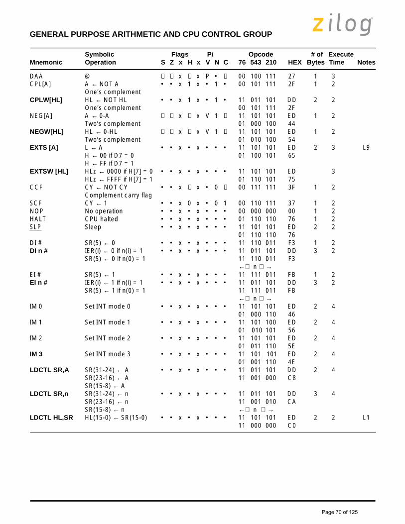
GENERAL PURPOSE ARITHMETIC AND CPU CONTROL GROUP
Symbolic Flags P/ Opcode # of ExecuteMnemonic Operation S Z x H x V N C 76 543 210 HEX Bytes Time Notes
DAA @ ↕ ↕ x ↕ x P • ↕ 00 100 111 27 1 3CPL[A] A ← NOT A • • x 1 x • 1 • 00 101 111 2F 1 2
One’s complementCPLW[HL] HL ← NOT HL • • x 1 x • 1 • 11 011 101 DD 2 2
One’s complement 00 101 111 2FNEG[A] A ← 0-A ↕ ↕ x ↕ x V 1 ↕ 11 101 101 ED 1 2
Two’s complement 01 000 100 44NEGW[HL] HL ← 0-HL ↕ ↕ x ↕ x V 1 ↕ 11 101 101 ED 1 2
Two’s complement 01 010 100 54EXTS [A] L ← A • • x • x • • • 11 101 101 ED 2 3 L9
H ← 00 if D7 = 0 01 100 101 65H ← FF if D7 = 1
EXTSW [HL] HLz ← 0000 if H[7] = 0 • • x • x • • • 11 101 101 ED 3HLz ← FFFF if H[7] = 1 01 110 101 75
CCF CY ← NOT CY • • x ↕ x • 0 ↕ 00 111 111 3F 1 2Complement carry flag
SCF CY ← 1 • • x 0 x • 0 1 00 110 111 37 1 2NOP No operation • • x • x • • • 00 000 000 00 1 2HALT CPU halted • • x • x • • • 01 110 110 76 1 2SLP Sleep • • x • x • • • 11 101 101 ED 2 2
01 110 110 76DI # SR(5) ← 0 • • x • x • • • 11 110 011 F3 1 2DI n # IER(i) ← 0 if n(i) = 1 • • x • x • • • 11 011 101 DD 3 2
SR(5) ← 0 if n(0) = 1 11 110 011 F3← n →
EI # SR(5) ← 1 • • x • x • • • 11 111 011 FB 1 2EI n # IER(i) ← 1 if n(i) = 1 • • x • x • • • 11 011 101 DD 3 2
SR(5) ← 1 if n(0) = 1 11 111 011 FB← n →
IM 0 Set INT mode 0 • • x • x • • • 11 101 101 ED 2 401 000 110 46
IM 1 Set INT mode 1 • • x • x • • • 11 101 100 ED 2 401 010 101 56
IM 2 Set INT mode 2 • • x • x • • • 11 101 101 ED 2 401 011 110 5E
IM 3 Set INT mode 3 • • x • x • • • 11 101 101 ED 2 401 001 110 4E
LDCTL SR,A SR(31-24) ← A • • x • x • • • 11 011 101 DD 2 4SR(23-16) ← A 11 001 000 C8SR(15-8) ← A
LDCTL SR,n SR(31-24) ← n • • x • x • • • 11 011 101 DD 3 4SR(23-16) ← n 11 001 010 CASR(15-8) ← n ← n →
LDCTL HL,SR HL(15-0) ← SR(15-0) • • x • x • • • 11 101 101 ED 2 2 L111 000 000 C0
Page 70 of 125
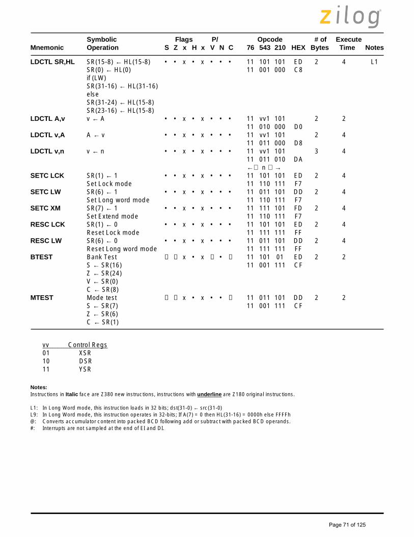
Symbolic Flags P/ Opcode # of ExecuteMnemonic Operation S Z x H x V N C 76 543 210 HEX Bytes Time Notes
LDCTL SR,HL SR(15-8) ← HL(15-8) • • x • x • • • 11 101 101 ED 2 4 L1SR(0) ← HL(0) 11 001 000 C8if (LW)SR(31-16) ← HL(31-16)elseSR(31-24) ← HL(15-8)SR(23-16) ← HL(15-8)
LDCTL A,v v ← A • • x • x • • • 11 vv1 101 2 211 010 000 D0
LDCTL v,A A ← v • • x • x • • • 11 vv1 101 2 411 011 000 D8
LDCTL v,n v ← n • • x • x • • • 11 vv1 101 3 411 011 010 DA← n →
SETC LCK SR(1) ← 1 • • x • x • • • 11 101 101 ED 2 4Set Lock mode 11 110 111 F7
SETC LW SR(6) ← 1 • • x • x • • • 11 011 101 DD 2 4Set Long word mode 11 110 111 F7
SETC XM SR(7) ← 1 • • x • x • • • 11 111 101 FD 2 4Set Extend mode 11 110 111 F7
RESC LCK SR(1) ← 0 • • x • x • • • 11 101 101 ED 2 4Reset Lock mode 11 111 111 FF
RESC LW SR(6) ← 0 • • x • x • • • 11 011 101 DD 2 4Reset Long word mode 11 111 111 FF
BTEST Bank Test ↕ ↕ x • x ↕ • ↕ 11 101 01 ED 2 2S ← SR(16) 11 001 111 CFZ ← SR(24)V ← SR(0)C ← SR(8)
MTEST Mode test ↕ ↕ x • x • • ↕ 11 011 101 DD 2 2S ← SR(7) 11 001 111 CFZ ← SR(6)C ← SR(1)
vv Control Regs01 XSR10 DSR11 YSR
Notes:Instructions in Italic face are Z380 new instructions, instructions with underline are Z180 original instructions.
L1: In Long Word mode, this instruction loads in 32 bits; dst(31-0) ← src(31-0)L9: In Long Word mode, this instruction operates in 32-bits; If A(7) = 0 then HL(31-16) = 0000h else FFFFh@: Converts accumulator content into packed BCD following add or subtract with packed BCD operands.#: Interrupts are not sampled at the end of EI and DI.
Page 71 of 125

DECODER DIRECTIVE INSTRUCTIONS
Opcode # of ExecuteMnemonic Operation 76 543 210 HEX Bytes Time Notes
DDIR W Operate following inst in word mode. 11 011 101 DD +2 011 000 000 C0
DDIR IB,W Operate following inst in word mode. 11 011 101 DD +3 0Fetching additional byte data. 11 000 001 C1
DDIR IW,W Operate following inst in word mode. 11 011 101 DD +4 0Fetching additional word data. 11 000 010 C2
DDIR IB Fetching additional byte data. 11 011 101 DD +3 011 000 011 C3
DDIR LW Operate following inst in Long Word mode. 11 111 101 FD +2 011 000 000 C0
DDIR IB,LW Operate following inst in Long Word mode. 11 111 101 FD +3 0Fetching additional byte data. 11 000 001 C1
DDIR IW,LW Operate following inst in word mode. 11 111 101 FD +4 0Fetching additional word data. 11 000 010 C2
DDIR IW Fetching additional word data. 11 111 101 FD +4 011 000 011 C3
Page 72 of 125

16/32 BIT ARITHMETIC AND LOGICAL GROUP
Symbolic Flags P/ Opcode # of ExecuteMnemonic Operation S Z x H x V N C 76 543 210 HEX Bytes Time Notes
ADD HL,dd HL ← HL+ dd • • x ↕ x • 0 ↕ 00 dd1 001 1 2 X1ADC HL, dd HL ← HL+ dd + CY ↕ ↕ x ↕ x V 0 ↕ 11 101 101 ED 2 2
01 dd1 010SBC HL,dd HL ← HL - dd - CY ↕ ↕ x ↕ x V 1 ↕ 11 101 101 ED 2 2
01 dd0 010ADD XY,qq XY ← XY + qq • • x ↕ x • 0 ↕ 11 y11 101 2 2 X1
00 qq1 001ADD XY,XY XY ← XY + XY • • x ↕ x • 0 ↕ 11 y11 101 2 X1
00 101 001 29INC[W] dd dd ← dd + 1 • • x • x • • • 00 dd0 011 1 2 X1INC[W] XY XY ← XY + 1 • • x • x • • • 11 y11 101 2 2 X1
00 100 011 23DEC[W] dd dd ← dd - 1 • • x • x • • • 00 dd1 011 1 2 X1DEC[W] XY XY ← XY - 1 • • x • x • • • 11 y11 101 2 2 X1
00 101 011 2BADD SP,nn SP ← SP + nn • • x ↕ x • 0 ↕ 11 101 101 ED 4 2 X1, I
10 000 010 82← n →← n →
SUB SP,nn SP ← SP - nn • • x ↕ x • 1 ↕ 11 101 101 ED 4 2 X1, I10 010 010 92← n →← n →
ADDW [HL,]pp HL← HL + pp ↕ ↕ x ↕ x V 0 ↕ 11 101 101 ED 2 210 (000) 1pp
Page 73 of 125

16/32 BIT ARITHMETIC AND LOGICAL GROUP (Continued)
Symbolic Flags P/ Opcode # of ExecuteMnemonic Operation S Z x H x V N C 76 543 210 HEX Bytes Time Notes
ADDW [HL,]nn HL← HL + nn ↕ ↕ x ↕ x V 0 ↕ 11 101 101 ED 4 2 I10 (000) 110 86← n →← n →
ADDW [HL,]XY HL ← HL+XY ↕ ↕ x ↕ x V 0 ↕ 11 y11 101 2 2 I10 (000) 111 87
ADDW [HL,](XY+d) HL ← HL+(XY+d) ↕ ↕ x ↕ x V 0 ↕ 11 y11 101 4 4+r I11 (000) 110 C6
ADCW [HL,]uu HL ← HL+uu+CY ↕ ↕ x ↕ x V 0 ↕ (001)SUBW [HL,]uu HL ← HL-uu ↕ ↕ x ↕ x V 1 ↕ (010)SBCW [HL,]uu HL ← HL - uu - CY ↕ ↕ x ↕ x V 1 ↕ (011)ANDW [HL,]uu HL ← HL AND uu ↕ ↕ x 1 x P 0 0 (100)ORW [HL,]uu HL ← HL OR uu ↕ ↕ x 0 x P 0 0 (110)XORW [HL,]uu HL ← HL XOR uu ↕ ↕ x 0 x P 0 0 (101)CPW [HL,]uu HL - uu ↕ ↕ x ↕ x V 1 ↕ (111)
ADD HL, (nn) HL ← HL+(nn) • • x ↕ x • 0 ↕ 11 101 101 ED 4 2+r I, X111 010 110 C6 ← n → ← n →
SUB HL, (nn) HL ← HL- (nn) • • x ↕ x • 0 ↕ 11 101 101 ED 4 2+r I, X111 010 110 D6 ← n → ← n →
uu is any of rr, nn, t, (IX+d), (IY+d) as shown for ADDW instruction. The indicated bits replace the (000) is the ADD setabove.
dd Pair pp Pair qq Pair y XY00 BC 00 BC 00 BC 0 IX01 DE 01 DE 01 DE 1 IY10 HL 11 HL 11 SP11 SP
Notes:Instructions in Italic face are Z380 new instructions, instructions with underline are Z180 original instructions.I: This instruction may be used with DDIR Immediate instructions.X1: In Extend mode, this instruction operates in 32-bits;
src(31-0) ← src(31-0) opr dst(31-0)
Page 74 of 125

MULTIPLY/DIVIDE INSTRUCTION GROUP
Symbolic Flags P/ Opcode # of ExecuteMnemonic Operation S Z x H x V N C 76 543 210 HEX Bytes Time Notes
MLT dd dd ← ddH * ddL • • x • x • • • 11 101 101 ED 2 701 dd1 100
MULTW [HL,]pp HL(31-0) ↕ ↕ x • x 0 • ↕ 11 101 101 ED 3 10← HL(15-0) * pp(15-0) 11 001 011 CB
10 (010) 0ppMULTW [HL,]XY HL(31-0) ↕ ↕ x • x 0 • ↕ 11 101 101 ED 3 10
← HL(15-0) * XY(15-0) 11 001 011 CB10 (010) 10y
MULTW [HL,]nn HL(31-0) ↕ ↕ x • x 0 • ↕ 11 101 101 ED 5 10 I← HL(15-0) * nn 11 001 011 CB
10 (010) 111 97← n →← n →
MULTW (XY+d) HL(31-0) ↕ ↕ x • x 0 • ↕ 11 y11 101 4 12+r I← HL(15-0) * (XY+d) 11 001 011 CB
← d →10 (010) 010 92
MULTUW uu HL(31-0) ↕ ↕ x • x 0 • ↕ (011)← HL(15-0) * uu
MULTUW uu instructions, uu is any of pp, nn, XY, (nn), (XY+d) as shown for MULTW instruction with replacing (010) by(010). Execute time is time required for MUTW with one more clock.
Page 75 of 125

MULTIPLY/DIVIDE INSTRUCTION GROUP (Continued)
Symbolic Flags P/ Opcode # of ExecuteMnemonic Operation S Z x H x V N C 76 543 210 HEX Bytes Time Notes
DIVUW [HL,]pp HL(15-0) 0 ↕ x • x V • • 11 101 101 ED 3 20 I← HL(31-0)/pp 11 001 011 CBHL(31-16) ← remainder 10 111 0pp
← d →DIVUW [HL,]XY HL(15-0) 0 ↕ x • x V • • 11 101 101 ED 3 20
← HL(31-0)/XY 11 001 011 CBHL(31-16) ← remainder 10 111 10y
DIVUW [HL,]nn HL(15-0) 0 ↕ x • x V • • 11 101 101 ED 5 20← HL(31-0)/nn 11 001 011 CBHL(31-16) ← remainder 10 111 111 BF
← n →← n →
DIVUW [HL,](XY+d) HL(15-0) 0 ↕ x • x V • • 11 y11 101 4 22+r I← HL(31-0)/(XY+d) 11 001 011 CBHL(31-16) ← remainder ← d →
10 111 010 BA
r Reg pp Regs y XY dd Regs000 B 00 BC 0 IX 00 BC001 C 00 DE 1 IY 01 DE010 D 11 HL 10 HL011 E 11 SP100 H101 L111 A
Notes:Instructions in Italic face are Z380 new instructions, instructions with underline are Z180 original instructions.I: This instruction may be used with DDIR Immediate instructions.
Page 76 of 125

8-BIT ROTATE AND SHIFT GROUP
Symbolic Flags P/ Opcode # of ExecuteMnemonic Operation S Z x H x V N C 76 543 210 HEX Bytes Time Notes
RLCA Rotate Left Circular • • x 0 x • 0 ↕ 00 000 111 07 1 2Accumulator
RLA Rotate Left Accumulator • • x 0 x • 0 ↕ 00 010 111 17 1 2RRCA Rotate Right Circular • • x 0 x • 0 ↕ 00 001 111 0F 1 2
AccumulatorRRA Rotate Right Accumulator • • x 0 x • 0 ↕ 00 011 111 1F 1 2RLC r Rotate Left Circular ↕ ↕ x 0 x P 0 ↕ 11 001 011 CB 2 2
register r 00 (000) rRLC (HL) Rotate Left Circular ↕ ↕ x 0 x P 0 ↕ 11 001 011 CB 2 2+r
00 (000) 110 06RLC (XY+d) Rotate Left Circular ↕ ↕ x 0 x P 0 ↕ 11 y11 101 4 4+r I
11 001 011 CB← d →00 (000) 110
RL m Rotate Left ↕ ↕ x 0 x P 0 ↕ (010)RRC m Rotate Right Circular ↕ ↕ x 0 x P 0 ↕ (001)RR m Rotate Right ↕ ↕ x 0 x P 0 ↕ (011)SLA m Shift Left Arithmetic ↕ ↕ x 0 x P 0 ↕ (100)SRA m Shift Right Arithmetic ↕ ↕ x 0 x P 0 ↕ (101)SRL m Shift Right Logical 0 ↕ x 0 x P 0 ↕ (111)Above instruction’s format and states are as shown for RLC’s. To form new opcode replace (000) of RLCs with showncode.
RLD Rotate Left Digit ↕ ↕ x 0 x P 0 • 11 101 101 ED 2 3+r (6)between the accumulator 01 101 111 6Fand location (HL)
RRD Rotate Right Digit ↕ ↕ x 0 x P 0 • 11 101 101 ED 2 3+r (6)between the accumulator 01 100 111 67and location (HL)
r Reg pp Regs y XY000 B 00 BC 0 IX001 C 00 DE 1 IY010 D 11 HL011 E100 H101 L111 A
Notes:Instructions in Italic face are Z380 new instructions, instructions with underline are Z180 original instructions.I: This instruction may be used with DDIR Immediate instructions.(6): The contents of the upper half of the accumulator is unaffected.
Page 77 of 125

16/32 BIT ROTATE AND SHIFT GROUP
Symbolic Flags P/ Opcode # of ExecuteMnemonic Operation S Z x H x V N C 76 543 210 HEX Bytes Time Notes
RLCW pp Rotate Left Circular ↕ ↕ x 0 x P 0 ↕ 11 101 101 ED 3 211 001 011 CB00 (000) 0pp
RLCW XY Rotate Left Circular ↕ ↕ x 0 x P 0 ↕ 11 101 101 ED 3 211 001 011 CB00 (000) 10y
RLCW (HL) Rotate Left Circular ↕ ↕ x 0 x P 0 ↕ 11 101 101 ED 3 2+r11 001 011 CB00 (000) 010
RLCW (XY+d) Rotate Left Circular ↕ ↕ x 0 x P 0 ↕ 11 y11 101 4 4+r I11 001 011 CB← d →00 (000) 010
RLW m Rotate Left ↕ ↕ x 0 x P 0 ↕ (010)RRCW m Rotate Right Circular ↕ ↕ x 0 x P 0 ↕ (001)RRW m Rotate Right ↕ ↕ x 0 x P 0 ↕ (011)SLAW m Shift Left Arithmetic ↕ ↕ x 0 x P 0 ↕ (100)SRAW m Shift Right Arithmetic ↕ ↕ x 0 x P 0 ↕ (101)SRLW m Shift Right Logical 0 ↕ x 0 x P 0 ↕ (111)Instruction format and states are as shown for RLCW. To form new opcode replace (000) or RLCW with shown code.
pp Regs y XY00 BC 0 IX00 DE 1 IY11 HL
Notes:Instructions in Italic face are Z380 new instructions, instructions with underline are Z180 original instructions.I: This instruction may be used with DDIR Immediate instructions.
Page 78 of 125

8-BIT BIT SET, RESET, AND TEST GROUP
Symbolic Flags P/ Opcode # of ExecuteMnemonic Operation S Z x H x V N C 76 543 210 HEX Bytes Time Notes
BIT b,r Z ← rb • ↕ x 1 x • 0 • 11 001 011 CB 201 b r
BIT b,(HL) Z ← (HL)b • ↕ x 1 x • 0 • 11 001 011 CB 201 b 110
BIT b,(XY+d) Z ← (XY+d)b • ↕ x 1 x • 0 • 11 y11 101 4 I11 001 011 CB← d →01 b 110
SET b,r rb ← 1 • • x • x • • • 11 001 011 CB 2(11) b r
SET b,(HL) (HL)b ← 1 • • x • x • • • 11 001 011 CB 2(11) b 110
SET b,(XY+d) (XY+d)b ← 1 • • x • x • • • 11 y11 101 4 I11 001 011 CB← d →(11) b 110
RES b,m mb ← 0 (10)
To form new opcode replace (11) of SET b,s with (10). s is any of r,(HL), (XY+d).The notation mb indicates location m, bit b(0~7)
r Reg y XY000 B 0 IX001 C 1 IY010 D011 E100 H101 L111 A
Notes:Instructions in Italic face are Z380 new instructions, instructions with underline are Z180 original instructions.I: This instruction may be operate with DDIR Immediate instructions.
Page 79 of 125
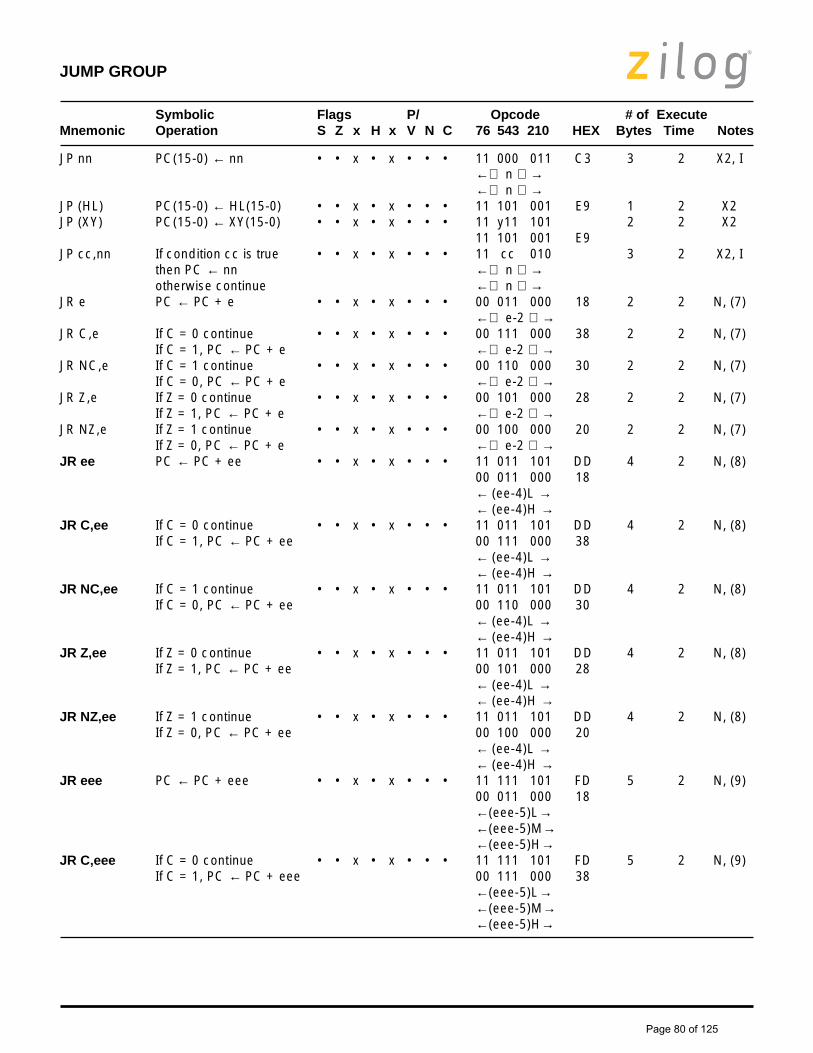
JUMP GROUP
Symbolic Flags P/ Opcode # of ExecuteMnemonic Operation S Z x H x V N C 76 543 210 HEX Bytes Time Notes
JP nn PC(15-0) ← nn • • x • x • • • 11 000 011 C3 3 2 X2, I← n →← n →
JP (HL) PC(15-0) ← HL(15-0) • • x • x • • • 11 101 001 E9 1 2 X2JP (XY) PC(15-0) ← XY(15-0) • • x • x • • • 11 y11 101 2 2 X2
11 101 001 E9JP cc,nn If condition cc is true • • x • x • • • 11 cc 010 3 2 X2, I
then PC ← nn ← n →otherwise continue ← n →
JR e PC ← PC + e • • x • x • • • 00 011 000 18 2 2 N, (7)← e-2 →
JR C,e If C = 0 continue • • x • x • • • 00 111 000 38 2 2 N, (7)If C = 1, PC ← PC + e ← e-2 →
JR NC,e If C = 1 continue • • x • x • • • 00 110 000 30 2 2 N, (7)If C = 0, PC ← PC + e ← e-2 →
JR Z,e If Z = 0 continue • • x • x • • • 00 101 000 28 2 2 N, (7)If Z = 1, PC ← PC + e ← e-2 →
JR NZ,e If Z = 1 continue • • x • x • • • 00 100 000 20 2 2 N, (7)If Z = 0, PC ← PC + e ← e-2 →
JR ee PC ← PC + ee • • x • x • • • 11 011 101 DD 4 2 N, (8)00 011 000 18← (ee-4)L →← (ee-4)H →
JR C,ee If C = 0 continue • • x • x • • • 11 011 101 DD 4 2 N, (8)If C = 1, PC ← PC + ee 00 111 000 38
← (ee-4)L →← (ee-4)H →
JR NC,ee If C = 1 continue • • x • x • • • 11 011 101 DD 4 2 N, (8)If C = 0, PC ← PC + ee 00 110 000 30
← (ee-4)L →← (ee-4)H →
JR Z,ee If Z = 0 continue • • x • x • • • 11 011 101 DD 4 2 N, (8)If Z = 1, PC ← PC + ee 00 101 000 28
← (ee-4)L →← (ee-4)H →
JR NZ,ee If Z = 1 continue • • x • x • • • 11 011 101 DD 4 2 N, (8)If Z = 0, PC ← PC + ee 00 100 000 20
← (ee-4)L →← (ee-4)H →
JR eee PC ← PC + eee • • x • x • • • 11 111 101 FD 5 2 N, (9)00 011 000 18←(eee-5)L→←(eee-5)M→←(eee-5)H→
JR C,eee If C = 0 continue • • x • x • • • 11 111 101 FD 5 2 N, (9)If C = 1, PC ← PC + eee 00 111 000 38
←(eee-5)L→←(eee-5)M→←(eee-5)H→
Page 80 of 125

Symbolic Flags P/ Opcode # of ExecuteMnemonic Operation S Z x H x V N C 76 543 210 HEX Bytes Time Notes
JR NC,eee If C = 1 continue • • x • x • • • 11 111 101 FD 5 2 N, (9)If C = 0, PC ← PC + eee 00 110 000 30
←(eee-5)L→←(eee-5)M→←(eee-5)H→
JR Z,eee If Z = 0 continue • • x • x • • • 11 111 101 FD 5 2 N, (9)If Z = 1, PC ← PC + eee 00 101 000 28
←(eee-5)L→←(eee-5)M→←(eee-5)H→
JR NZ,eee If Z = 1 continue • • x • x • • • 11 111 101 FD 5 2 N, (9)If Z = 0, PC ← PC + eee 00 100 000 20
←(eee-5)L→←(eee-5)M→←(eee-5)H→
DJNZ e B ← B - 1 • • x • x • • • 00 010 000 10 2 3/4 N, (7)If B = 0 continue ← e-2 →If B↔0, PC ← PC + e
DJNZ ee B ← B - 1 • • x • x • • • 11 011 101 DD 4 3/4 N, (8)If B = 0 continue 00 010 000 10If B ≠ 0, PC ← PC + ee ←(ee-4)L→
←(ee-4)H→DJNZ eee B ← B - 1 • • x • x • • • 11 111 101 FD 5 3/4 N, (9)
If B = 0 continue 00 010 000 10If B ≠ 0, PC ← PC + eee ←(eee-5)L→
←(eee-5)M →←(eee-5)H →
cc Condition000 NZ (Non-zero)001 Z (Zero)010 NC (Non-carry)011 C (Carry)100 PO (Parity Odd), or NV (Non-Overflow)101 PE (Parity Even), or V (Overflow)110 P (Sign positive), or NS (No sign)111 M (Sign negative), or S (Sign)
Notes:Instructions in Italic face are Z380 new instructions, instructions with underline are Z180 original instructions.I: This instruction may be used with DDIR Immediate instructions.N: In Native mode, this instruction uses addresses modulo 65536.X2: In Extend mode, this instruction loads bit 31-16 portion of the operand into PC(31-16).(7): e is a signed two’s complement number in the range [-126, 129], e-2 in the opcode provides an effective address of pc+e as PC is incremented
by 2 prior to the addition of e.(8): ee is a signed two’s complement number in the range [-32765, 32770], ee-4 in the opcode provides an effective address of pc+e as PC is
incremented by 4 prior to the addition of e.(9): eee is a signed two’s complement number in the range [-8388604, 8388611], eee-5 in the opcode provides an effective address of pc+e as PC
is incremented by 5 prior to the addition of e.
Page 81 of 125

CALL AND RETURN GROUP
Symbolic Flags P/ Opcode # of ExecuteMnemonic Operation S Z x H x V N C 76 543 210 HEX Bytes Time Notes
CALL nn (SP-1) ← PCh • • x • x • • • 11 001 101 CD 3 4+w X3, I(SP-2) ← PCl ← n →SP ← SP-2 ← n →PC ← nn
CALL cc,nn If condition cc • • x • x • • • 11 cc 100 3 2/4+w X3, Iis false continue ← n →otherwise same as CALL nn ← n →
CALR e (SP-1) ← PCh • • x • x • • • 11 101 101 ED 3 4+w N,X3,(11)(SP-2) ← PCl 11 001 101 CDSP ← SP-2PC ← PC + e ← e-3 →
CALR cc,e If condition cc • • x • x • • • 11 101 101 ED 3 2/4+w N,X3,(11)is false continue 11 cc 100otherwise same as CALR e ← e-3 →
CALR ee (SP-1) ← PCh • • x • x • • • 11 011 101 DD 4 4+w N,X3,(8)(SP-2) ← PCl 11 001 101 CDSP ← SP-2 ← (ee-4)L →PC ← PC + ee ← (ee-4)H →
CALR cc,ee If condition cc • • x • x • • • 11 011 101 DD 4 2/4+w N,X3,(8)is false continue 11 cc 100otherwise same as ← (ee-4)L →CALR ee ← (ee-4)H →
CALR eee (SP-1) ← PCh • • x • x • • • 11 111 101 FD 5 4+w N,X3,(9)(SP-2) ← PCl 11 001 101 CDSP ← SP-2 ← (eee-5)L →PC ← PC + eee ← (eee-5)M →
← (eee-5)H →CALR cc,eee If condition cc • • x • x • • • 11 111 101 FD 5 2/4+w N,X3,(9)
is false continue 11 cc 100otherwise same as ← (eee-5)L →CALR eee ← (eee-5)M →
← (eee-5)H →RET PCL ← (SP) • • x • x • • • 11 001 001 C9 1 2+r N, X4
PCH ← (SP + 1)SP ← SP+2
RET cc If condition cc • • x • x • • • 11 cc 000 1 2/2+r N, X4is false continueotherwise same as RET
RETI Return from Interrupt • • x • x • • • 11 101 101 ED 2 2+r N, X401 001 101 4D
Page 82 of 125

Symbolic Flags P/ Opcode # of ExecuteMnemonic Operation S Z x H x V N C 76 543 210 HEX Bytes Time Notes
RETN Return from NMI • • x • x • • • 11 101 101 ED 2 2+r N,X4,(10)01 000 101 45
RST p (SP-1) ← PCh • • x • x • • • 11 t 111 1 4+w N,X3,X5(SP-2) ← PClSP ← SP-2PCh ← 0PCl ← p
cc Condition t p000 NZ (Non-zero) 000 00H001 Z (Zero) 001 08H010 NC (Non-carry) 010 10H011 C (Carry) 011 18H100 PO (Parity Odd), or NV (Non-Overflow) 100 20H101 PE (Parity Even), or V (Overflow) 101 28H110 P (Sign positive), or NS (No sign) 110 30H111 M (Sign negative), or S (Sign) 111 38H
Notes:Instructions in Italic face are Z380 new instructions, instructions with underline are Z180 original instructions.
I: This instruction may be used with DDIR Immediate instructions.N: In Native mode, this instruction uses addresses modulo 65536.X3: In Extended mode, this instruction pushes PC(31-16) into the stack before pushing PC(15-0) into the stack.X4: In Extended mode, this instruction pops PC(31-16) from the stack after poping PC(15-0) from the stack.X5: In Extended mode, this instruction loads 00h into PC(31-16).(2) In Extended mode, all return instructions pops PCz from the stack after poping PC from the stack.(8): ee is a signed two’s complement number in the range [-32765, 32770], ee-4 in the opcode provides an effective address of pc+e as PC is
incremented by 4 prior to the addition of e.(9): eee is a signed two’s complement number in the range [-8388604, 8388611], eee-5 in the opcode provides an effective address of pc+e as
PC is incremented by 5 prior to the addition of e.(10) RETN loads IFF2 to IFF1.(11): e is a signed two’s complement number in the range [-127, 128], e-3 in the opcode provides an effective address of pc+e as PC is incremented
by 3 prior to the addition of e.
Page 83 of 125

8-BIT INPUT AND OUTPUT GROUP
Symbolic Flags P/ Opcode # of ExecuteMnemonic Operation S Z x H x V N C 76 543 210 HEX Bytes Time Notes
IN A,(n) A ← (n) • • x • x • • • 11 011 011 DB 2 3+i← n →
IN r,(C) r ← (C) ↕ ↕ x 0 x P 0 • 11 101 101 ED 201 r 000
INA A,(nn) A ← (nn) • • x • x • • • 11 101 101 ED 2 3+i I11 011 011 DB← n →← n →
INI (HL) ← (C) • ↕ x • x • 1 • 11 101 101 ED 2 2+i+wB ← B - 1 (1) 10 100 010 A2HL ← HL + 1
INIR (HL) ← (C) • 1 x • x • 1 • 11 101 101 ED 2 (2+i+w)B ← B-1 (2) 10 110 010 B2HL ← HL + 1Repeat until B = 0
IND (HL) ← (C) • ↕ x • x • 1 • 11 101 101 ED 2 2+i+wB ← B - 1 (1) 10 101 010 AAHL ← HL - 1
INDR (HL) ← (C) • 1 x • x • 1 • 11 101 101 ED 2 (2+i+w)nB ← B-1 (2) 10 111 010 BAHL ← HL - 1Repeat until B = 0
OUT (n),A (n) ← A • • x • x • • • 11 010 011 D3 2 3+o← n →
OUT (C),r (C) ← r • • x • x • • • 11 101 101 ED 2 3+o01 r 001
OUT (C),n (C) ← r • • x • x • • • 11 101 101 ED 3 3+o01 110 001 71← n →
OUTA (nn),A (nn) ← A • • x • x • • • 11 101 101 ED 4 2+o I11 010 011 D3← n →← n →
Page 84 of 125

Symbolic Flags P/ Opcode # of ExecuteMnemonic Operation S Z x H x V N C 76 543 210 HEX Bytes Time Notes
OUTI B ¨ B-1 • ◊ x • x • 1 • 11 101 101 ED 2 2+r+o N(C) ← (HL) (1) 10 100 011 A3HL ← HL + 1
OTIR B ← B-1 • 1 x • x • 1 • 11 101 101 ED 2 2+r+o N(C) ← (HL) (2) 10 110 011 B3HL ¨ HL + 1Repeat until B = 0
OUTD B ← B-1 • 1 x • x • 1 • 11 101 101 ED 2 2+r+o N(C) ← (HL) (2) 10 111 011 BBHL ¨ HL - 1Repeat until B = 0
OTDR B ← B-1 • 1 x • x • 1 • 11 101 101 ED 2 2+r+o N(C) ← (HL) (2) 10 111 011 BBHL ¨ HL - 1Repeat until B = 0
r Reg000 B001 C010 D011 E100 H101 L111 A
Notes:Instructions in Italic face are Z380 new instructions, instructions with underline are Z180 original instructions.I: This instruction may be used with DDIR Immediate instructions.N: In Native mode, this instruction address modulo 65536.(1): P/V flag is 0 if the result of BC-1 = 0, otherwise P/V = 1/.(2): P/V flag is 0 only at completion of instruction.
Page 85 of 125

INPUT AND OUTPUT INSTRUCTIONS FOR ON-CHIP I/O SPACE
Symbolic Flags P/ Opcode # of ExecuteMnemonic Operation S Z x H x V N C 76 543 210 HEX Bytes Time Notes
INO r,(n) r ← (n) ↕ ↕ x 0 x P 0 • 11 101 101 ED 3 3+i (3)00 r 000← n →
INO (n) r ← (n) ↕ ↕ x 0 x P 0 • 11 101 101 ED 3 3+i (3)Changes Flag only. 00 r 000 30
← n →OUT0 (n),r (n) ← r • • x • x • • • 11 101 101 ED 3 3+o (3)
00 r 001← n →
TSTIO n (C) AND n ↕ ↕ x 1 x P 0 0 11 101 101 ED 3 3+i (3)01 110 100 74← n →
OTIIM (C) ← (HL) ↕ ↕ x ↕ x P ↕ ↕ 11 101 101 ED 3 2+r+o (3),NHL ← HL + 1 10 000 011 83C ← C+1B ← B - 1
OTIIMR (C) ← (HL) 0 1 x 0 x 1 ↕ 0 11 101 101 ED 3 2+r+o (3),NHL ← HL + 1 (2) 10 010 011 93C ← C + 1B ← B -1Repeat until B = 0
OTDM (C) ← (HL) ↕ ↕ x ↕ x P ↕ ↕ 11 101 101 ED 3 2+r+o (3),NHL ← HL - 1 10 001 011 8BC ← C - 1B ← B - 1
OTDMR (C) ← (HL) 0 1 x 0 x 1 ↕ 0 11 101 101 ED 3 2+r+o (3),NHL ← HL - 1 (2) 10 011 011 9BC ← C - 1B ← B - 1Repeat until B = 0
r Reg010 D011 E100 H101 L111 A
Notes:Instructions in Italic face are Z380 new instructions, instructions with underline are Z180 original instructions.I: This instruction may be used with DDIR Immediate instructions.N: In Native mode, this instruction address modulo 65536.(1): P/V flag is 0 if the result of BC-1 = 0, otherwise P/V = 1/.(2): P/V flag is 0 only at completion of instruction.
Page 86 of 125

16-BIT INPUT AND OUTPUT GROUP
Symbolic Flags P/ Opcode # of ExecuteMnemonic Operation S Z x H x V N C 76 543 210 HEX Bytes Time Notes
INW pp,(C) pp ← (C) ↕ ↕ x 0 x P 0 • 11 011 101 DD 201 ppp 000
INAW HL,(nn) HL(15-0) ← (nn) • • x • x • • • 11 111 101 FD 4 3+i I11 011 011 DB← n →← n →
INIW (HL) ← (DE) • ↕ x • x • 1 • 11 101 101 ED 2 2+i+w NBC(15-0) ← BC(15-0) - 1 (1) 11 100 010 E2HL ← HL+2
INIRW (HL) ← (DE) • 1 x • x • 1 • 11 101 101 ED 2 (2+i+w)n NBC(15-0) ← BC(15-0) - 1 (2) 11 110 010 F2HL ← HL+2Repeat until BC = 0
INDW (HL) ← (DE) • ↕ x • x • 1 • 11 101 101 ED 2 2+i+w NBC(15-0) ← BC(15-0) - 1 (1) 11 101 010 EAHL ← HL - 2
INDRW (HL) ← (DE) • 1 x • x • 1 • 11 101 101 ED 2 (2+i+w)n NBC(15-0) ← BC(15-0) - 1 (2) 11 111 010 FAHL ← HL - 2Repeat until BC = 0
OUTW (C),pp (C) ← pp • • x • x • • • 11 011 101 DD 2 2+o01 ppp 001
OUTW (C),nn (C) ← nn • • x • x • • • 11 111 101 FD 4 2+o01 111 001 79← n →← n →
OUTAW (nn),HL (nn) ← HL(15-0) • • x • x • • • 11 111 101 FD 4 2+o I11 010 011 D3← n →← n →
OUTIW (DE) ← (HL) • ↕ x • x • 1 • 11 101 101 ED 2 2+o NBC(15-0) ← BC(15-0) - 1 (1) 11 100 011 E3HL ← HL + 2
OTIRW BC(15-0) ← BC(15-0) - 1 • 1 x • x • 1 • 11 101 101 ED 2 2+o N(DE) ← (HL) (2) 11 110 011 F3HL ← HL + 2Repeat until B = 0
Page 87 of 125

16-BIT INPUT AND OUTPUT GROUP (Continued)
Symbolic Flags P/ Opcode # of ExecuteMnemonic Operation S Z x H x V N C 76 543 210 HEX Bytes Time Notes
OUTDW BC(15-0) ← BC(15-0) - 1 • ↕ x • x • 1 • 11 101 101 ED 2 2+r+o(DE) ← (HL) (1) 11 101 011 EBHL ← HL - 2
OTDRW BC(15-0) ← BC(15-0) - 1 • 1 x • x • 1 • 11 101 101 ED 2 2+r+o(DE) ← (HL) (2) 11 111 011 FBHL ← HL - 2Repeat until B = 0
ppp Reg000 BC010 DE111 HL
Notes:Instructions in Italic face are Z380 new instructions, instructions with underline are Z180 original instructions.I: This instruction may be used with DDIR Immediate instructions.N: In Native mode, this instruction uses addresses modulo 65536.(1) If the result of B-1 is zero, the Z flag is set; otherwise it is reset.(2) Z flag is set upon instruction completion only.
Address BusI/O Instruction A31-A24 A23-A16 A15-A8 A7-A0
IN A, (n) 00000000 00000000 Contents of A reg nIN dst,(C) BC31-BC24 BC23-BC16 BC15-BC8 BC7-BC0INA(W) dst,(mn) 00000000 00000000 m nDDIR IB INA(W) dst,(lmn) 00000000 l m nDDIR IW INA(W) dst,(klmn) k l m nBlock Input BBC31-BC24 BC23-BC16 BC15-BC8 BC7-BC0
OUT (n),A 00000000 00000000 Contents of A reg nOUT (C),dst BC31-BC24 BC23-BC16 BC15-BC8 BC7-BC0OUTA(W) (mn),dst 00000000 00000000 m nDDIR IB OUTA(W) (lmn),dst 00000000 l m nDDIR IW OUTA(W) (klmn),dst k l m nBlock output BC31-BC24 BC23-BC16 BC15-BC8 BC7-BC0
Page 88 of 125

INTERRUPTS
The Z380 MPU’s interrupt structure provides compatibilitywith the existing Z80 and Z180 MPUs with the followingexception: The undefined opcode trap’s occurrence iswith respect to the Z380 instruction set, and its responseis improved (vs the Z180) to make trap handling easier.The Z380 MPU also offers additional features to enhanceflexibility in system design.
Of the five external interrupt inputs provided, the /NMI is anonmaskable interrupt. The remaining inputs, /INT3-/INT0,are four asynchronous maskable interrupt requests.
In an Interrupt Acknowledge transaction, address outputsA31-A0 are driven to logic 1's. One output among A3-A0 isdriven to logic 0 to indicate the maskable interrupt requestbeing acknowledged. If /INT0 is being acknowledged,A3-A1, is at logic 1's and A0 is at logic 0.
Interrupt modes 0 through 3 are supported for the externalmaskable interrupt request /INT0. Modes 0, 1 and 2 havethe same schemes as those in the Z80 and Z180 MPUs.Mode 3 is similar to mode 2, except that 16-bit interruptvectors are expected from the I/O devices. Note that 8-bitand 16-bit I/O devices can be intermixed in this mode byhaving external pull up resistors at the data bus signalsD15-D8, for example.
The external maskable interrupt requests /INT3-/INT1 arehandled in an assigned interrupt vectors mode.
As discussed in the CPU Architecture section, the Z380MPU can operate in either the Native or Extended Mode.In Native Mode, PUSHing and POPing of the stack to saveand retrieve interrupted PC values in interrupt handling aredone in 16-bit sizes, and the stack pointer rolls over at the64 Kbyte boundary. In Extended Mode, the PC PUSHesand POPs are done in 32-bit sizes, and the stack pointerrolls over at the 4 Gbyte memory space boundary. TheZ380 MPU provides an Interrupt Register Extension, whosecontents are always outputted as the address bus signalsA31-A16 when fetching the starting addresses of serviceroutines from memory in interrupt modes 2, 3 and theassigned vectors mode. In Native Mode, such fetches areautomatically done in 16-bit sizes and in Extended Mode,in 32-bit sizes. These starting addresses should be even-aligned in memory locations. That is, their least significantbytes should have addresses with A0 = 0.
Interrupt Priority RankingThe Z380 MPU assigns a fixed priority ranking to handle itsinterrupt sources, as shown in Table 2.
Table 2. Interrupt Priority Ranking
Priority Interrupt Sources
Highest Trap (undefined opcode)/NMI
↓ /INT0/INT1/INT2
Lowest /INT3
Page 89 of 125

the on-chip I/O address space and can be accessed onlywith reserved on-chip I/O instructions.
Table 3. Interrupt Flags and Registers
Names Mnemonics Access Methods
Interrupt Enable Flags IEF1, IEF2 EI and DI instructionsInterrupt Register I LD I,A and LD A,I instructionsInterrupt Register Extension Iz LD I,HL and LD HL,I instructions
(accessing both Iz and I)Interrupt Enable Register IER On-chip I/O instructions, addr
00000017H, EI and DI instructionsAssigned Vectors Base Register AVBR On-chip I/O instructions, addr
00000018HTrap and Break Register TRPBK On-chip I/O instructions, addr
00000019H
Interrupt ControlThe Z380 MPU’s flags and registers associated with inter-rupt processing are listed in Table 4. As discussed in theCPU Architecture section, some of the registers reside in
IEF1, IEF2IEF1 controls the overall enabling and disabling of all on-chip peripheral and external maskable interrupt requests.If IEF1 is at logic 0, all such interrupts are disabled. Thepurpose of IEF2 is to correctly manage the occurrence of/NMI. When /NMI is acknowledged, the state of IEF1 iscopied to IEF2 and then IEF1 is cleared to logic 0. At the
end of the /NMI interrupt service routine, execution of theReturn From Nonmaskable Interrupt instruction, RETN,automatically copies the state of IEF2 back to IEF1. This isa means to restore the interrupt enable condition existingbefore the occurrence of /NMI. Table 5 summarizes thestates of IEF1 and IEF2 resulting from various operations.
Table 4. Operation Effects on IEF1 and IEF2
Operation IEF1 IEF2 Comments
/RESET 0 0 Inhibits all interrupts except Trap and /NMI.Trap 0 0 Disables interrupt nesting./NMI 0 IEF1 IEF1 value copied to IEF2, then IEF1 is cleared.RETN IEF2 NC Returns from /NMI service routine./INT3-/INT0 0 0 Disables interrupt nesting.RETI NC NC Returns from service routine, Z80 I/O device.RET NC NC Returns from service routine, non-Z80 I/O device.EI 1 1DI 0 0LD A,I or LD R,I NC NC IEF2 value is copied to P/V Flag.LD HL,I NC NC
Note:NC = No Change
I, I ExtendThe 8-bit Interrupt Register and the 16-bit InterruptRegister Extension are cleared during reset.
Page 90 of 125

Interrupt Enable RegisterIE3-IE0 (Interrupt Request Enable Flags). These flagsindividually indicate F /INT3, /INT2, /INT1 or /INT0 isenabled. Note that these flags are conditioned with enableand disable interrupt instructions (with arguments).
Reserved bits 7-4. Read as 0s, should write to as 0s.
Figure 25. Interrupt Enable Register
Assigned Vectors Base RegisterAB15-AB9 (Assigned Vectors Base). The Interrupt Regis-ter Extension, Iz, together with AB15-AB9, define the baseaddress of the assigned interrupt vectors table in memoryspace (Figure 26).
Reserved Bit 0. Read as 0, should write to as 0.
AB15
7
AB14 AB13 AB12 AB11 AB10 AB9 --
00 00 00 00
0
Reset Value
AVBR: 00000018HR/W
Assigned VectorsBase
ReservedProgram as 0Read as 0
Figure 26. Assigned Vectors Base Register
--
7
IE1 IE0
10 00 00 00
0
Reset Value
IER: 00000017HRead Only
Interrupt RequestsEnable
Encoded InterruptRequests
-- -- -- IE2IE3
Page 91 of 125

Trap and Break RegisterReserved bits 7-2. Some of these bits are reserved forbreakpoint functions, including a Break-on-Halt feature.
Refer to the Z380 ICE specifications for details. Read as 0s,should write to as 0s.
7
TF TV
0 00 00 00 0
0
Reset Value
TRPBK: 00000019HR/W
Trap on Interrupt Vector
ReservedProgram as 0Read as 0
-- -- -- --
Trap on Instruction Fetch
-- --
Figure 27. Trap and Break Register
TF (Trap on Instruction Fetch). TF goes active to logic 1when an undefined opcode fetched in the instructionstream is detected. TF can be reset under program controlby writing it with a logic 0. However, it cannot be written witha logic 1.
TV (Trap on Interrupt Vector). TV goes active to logic 1when an undefined opcode is returned as a vector in aninterrupt acknowledge transaction in mode 0. TV can bereset under program control by writing it with a logic 0.However, it cannot be written with a logic 1.
Trap InterruptThe Z380 MPU generates a trap when an undefinedopcode is encountered. The trap is enabled immediatelyafter reset, and it is not maskable. This feature can be usedto increase software reliability or to implement extendedinstructions. An undefined opcode can be fetched fromthe instruction stream, or it can be returned as a vector inan interrupt acknowledge transaction in interrupt mode 0.When a trap occurs, the Z380 MPU operates as follows.
1. The TF or TV bit in the Assigned Vectors Base and TrapRegister goes active, to indicate the source of theundefined opcode.
2. If the undefined opcode was fetched from instructionstream, the starting address of the trap causing in-struction is pushed onto the stack. (Note that thestarting address of a decoder directive preceding aninstruction encoding is considered the starting ad-dress of the instruction.)
If the undefined opcode was a returned interruptvector (in interrupt mode 0), the interrupted PC valueis pushed onto the stack.
3. The states of IEF1 and IEF2 are cleared.
4. The Z380 MPU commences to fetch and executeinstructions from address 00000000H.
Note that instruction execution resumes at address 0,similar to the occurrence of a reset. Testing the TF and TVbits in the Assigned Vectors Base and Trap Register willdistinguish the two events. Even if trap handling is not inplace, repeated restarts from address 0 is an indicator ofpossible illegal instructions at system debugging.
Page 92 of 125

Nonmaskable InterruptThe nonmaskable interrupt input /NMI is edge sensitive,with the Z380 MPU internally latching the occurrence of itsfalling edge. When the latched version of /NMI is recog-nized, the following operations are performed.
1. The interrupted PC (Program Counter) value is pushedonto the stack.
2. The state of IEF1 is copied to IEF2, then IEF1 is cleared.
3. The Z380 MPU commences to fetch and execute in-structions from address 00000066H.
Interrupt Mode 0 Response ForMaskable Interrupt /INT0During the interrupt acknowledge transaction, the externalI/O device being acknowledged is expected to output avector onto the lower portion of the data bus, D7-D0. TheZ380 MPU interprets the vector as an instruction opcode,which is usually one of the single-byte Restart (RST)instructions that pushes the interrupted PC (ProgramCounter) value onto the stack and resumes execution at afixed memory location. However, the Z380 MPU will gen-erate multiple transactions to capture vectors that form amulti-byte instruction. IEF1 and IEF2 are reset to logic 0’s,disabling all further maskable interrupt requests. Note thatunlike the other interrupt responses, the PC is not automati-cally PUSHed onto the stack. Note also that a trap occursif an undefined opcode is supplied by the I/O device as avector.
Interrupt Mode 1 Response ForMaskable Interrupt /INT0An interrupt acknowledge transaction is generated, duringwhich the data bus contents are ignored by the Z380 MPU.The interrupted PC value is PUSHed onto the stack. IEF1and IEF2 are reset to logic 0’s so as to disable furthermaskable interrupt requests. Instruction fetching and ex-ecution restarts at memory location 00000038H.
Interrupt Mode 2 Response ForMaskable interrupt /INT0During the interrupt acknowledge transaction, the externalI/O device being acknowledged is expected to output avector onto the lower portion of the data bus, D7-D0. Theinterrupted PC value is PUSHed onto the stack and IEF1and IEF2 are reset to logic 0’s so as to disable furthermaskable interrupt requests. The Z380 MPU then reads anentry from a table residing in memory and loads it into thePC to resume execution. The address of the table entry iscomposed of the I Extend contents as A31-A16, the IRegister contents as A15-A8 and the vector supplied bythe I/O device as A7-A0. Note that the table entry iseffectively the starting address of the interrupt serviceroutine designed for the I/O device being acknowledged.The table, composed of starting addresses for all theinterrupt mode 2 service routines, can be referred to as theinterrupt mode two vector table. Each table entry shouldbe word-sized if the Z380 MPU is in the Native Mode andlongword-sized if in the Extended Mode, in either case it iseven-aligned (least significant byte with address A0 = 0).
Interrupt Mode 3 Response ForMaskable Interrupt /INT0Interrupt mode 3 is similar to mode 2 except that a 16-bitvector is expected to be placed on the data bus D15-D0 bythe I/O device during the interrupt acknowledge transac-tion. The interrupted PC is PUSHed onto the stack. IEF1and IEF2 are reset to logic 0’s so as to disable furthermaskable interrupt requests. The starting address of theservice routine is fetched and loaded into the PC to resumeexecution from the memory location with an addresscomposed of the I Extend contents as A31-A16 and thevector supplied by the I/O device as A15-A0. Again thestarting address of the service routine is word-sized if theZ380 MPU is in the Native Mode and longword-sized if inthe Extend Mode, in either case even-aligned.
Page 93 of 125

Assigned Interrupt Vectors Mode ForMaskable interrupt INT3-/INT1When the Z380 MPU recognizes one of the externalmaskable interrupts it generates an Interrupt Acknowl-edge transaction which is different than that for /INT0. TheInterrupt Acknowledge transaction for /INT3-/INT1 has theI/O bus signal /INTAK active, with /MI, /IORQ, /IORD and/IOWR inactive. The interrupted PC value is PUSHed ontothe stack. IEF1 and IEF2 are reset to logic 0s, disablingfurther maskable interrupt requests. The starting addressof an interrupt service routine is fetched from a table entryand loaded into the PC to resume execution. The addressof the table entry is composed of the I Extend contents asA31-A16, the AB bits of the Assigned Vectors Base Reg-ister as A15-A9 and an assigned interrupt vector specificto the request being recognized as A8-A0. The assignedvectors are defined in Table 5.
Table 5. Assigned Interrupt Vectors
Interrupt Source Assigned Interrupt Vector
/INT1 00H/INT2 04H/INT3 08H
RETI InstructionThe Z80 family I/O devices are designed to monitor theReturn from Interrupt opcodes in the instruction stream(RETI-EDH, 4DH), signifying the end of the current inter-rupt service routine. When detected, the daisy chain withinand among the device(s) resolves and the appropriateinterrupt-under-service condition clears. The Z380 MPUreproduces the opcode fetch transactions on the I/O buswhen the RETI instruction is executed. Note that the Z380MPU outputs the RETI opcodes onto both portions of thedata bus (D15-D8 and D7-D0) in the transactions.
Page 94 of 125

ON-CHIP PERIPHERAL FUNCTIONS
The Z380 MPU incorporates a number of functions to easeits interface with external I/O devices and with varioustypes of memories. The Z380 MPU's I/O bus can beprogrammed to run at a slower rate than its memory bus.In addition, a heartbeat transaction can be generated onthe I/O bus that emulates a Z80 CPU instruction fetchcycle. Such a transaction is useful for a particular Z80family I/O device to perform its interrupt functions. Memorychip select signals can be activated to access the lowest16 Mbytes of the Z380 MPU's memory address space, withwait state insertions. Lastly, a DRAM refresh function isincorporated, with programmable refresh transaction burstsize. The above functions are controlled by several on-chip registers. As described in the CPU Architecturesection, these registers together with several other regis-ters that control a portion of the interrupt functions, occupyan on-chip I/O address space. This on-chip I/O addresscan be accessed only by the following reserved on-chipI/O instructions.
Some on-chip peripherals are capable of generating inter-rupt requests, which are always handled in the assignedinterrupt vectors mode.
I/O Bus ControlThe Z380 MPU is designed to interface easily with externalI/O devices that can be of either the Z80 or Z8500 productfamily by supplying five I/O bus control signals: /M1,/IORQ, /IORD, /IOWR and /INTAK. In addition, the Z380MPU is supplying an IOCLK that is a divided down versionof its BUSCLK. Programmable wait states can be insertedin the various I/O transactions. The External Interfacesection details all the I/O transactions.
IN0 R, (n) OTIMIN0 (n) OTIMROUT0 (n), R OTDMTSTIO n OTDMR
When one of the above instructions is executed, the Z380MPU outputs the register address being accessed in apseudo transaction of two BUSCLK cycles duration, withthe address signals A31-A8 at logic 0s. In the pseudotransaction, all bus control signals are at their inactivestates. It is to be emphasized that the Z380 MPU adopts aninstruction specific scheme to access on-chip I/O regis-ters, with their unique address space. This is in contrast tomapping such registers with external peripherals in acommon I/O address space, as is done in the Z180 MPU.
I/O Bus Control Register 0CR2-CR0 (I/O Clock Rate). BUSCLK is divided down toproduce IOCLK as defined in the following.
000 divided-by-8 001 divided-by-1010 divided-by-2 011 divided-by-1100 divided-by-4 101 divided-by-1110 divided-by-6 111 divided-by-1
Note that if a clock divide rate of 1 is specified, BUSCLKshould be used to connect to I/O devices that require aclock input, since the Z380 MPU outputs a constant logic1 at IOCLK.
Reserved bits 7-3. Read as 0s, should write to as 0s.
7
CR2 CR1 CR0
0 00 00 00 0
0
<- Reset Value
IOCR0: 00000011HR/W
- - - - - - - - - -
I/O Clock
Reserved Program as 0Read as 0
Figure 28. I/O Bus Control Register 0
Page 95 of 125

I/O Bus Control Register 1When this phantom register IOCR1 with address00000012H is accessed with one of the on-chip I/O writeinstructions, a heartbeat transaction that emulates a Z80CPU instruction fetch is performed on the I/O bus. Thistransaction provides a /M1 pulse which is necessary aspart of an interrupt enable sequence for a Z80 PIO product.In the on-chip I/O write instruction, the data being "written"can be of any value. In case of an on-chip I/O read with theIOCR1 address, the data returned is unpredictable.
I/O Waits RegisterOW2-IOW0 (I/O Waits). This binary field defines up toseven wait states to be inserted in external I/O read andwrite transactions, and at the latter portions of interrupttransactions to capture interrupt vectors. The defined wait
states are also inserted in each of the opcode fetchtransactions of the Return from Interrupt (RETI) instructionreproduced on the I/O bus. When programmed with 0s, theI/O waits are disabled.
RTW1-RTW0 (RETI Waits). This binary field defines up tothree wait states to be inserted between opcode fetchtransactions of the Return from Interrupt instruction repro-duced on the I/O bus.
DCW2-DCW0 (Interrupt Daisy Chain Waits). This binaryfield defines up to seven wait states to be inserted at theearly portions of interrupt acknowledge transactions, forthe interrupt daisy chain through the external I/O devicesto settle.
Figure 29. I/O Waits Register
IOW2
7
IOW1 IOW0 RTW1 RTW0 DCW2 DCW1 DCW0
1 11 11 11 1
0
<- Reset Value
IOWR: 0000000EHR/W
Interrupt DaisyChain Waits
RET I Waits
I/O Waits
Page 96 of 125

MEMORY CHIP SELECTS AND WAITS
The Z380 MPU offers two schemes to generate chip selectsignals to access the lowest 16 Mbytes of its memoryaddress space. The first scheme provides six chip selectsignals, with the address space partitioned as shown inFigure 30. The second scheme provides three chip selectsignals, and the address space partitioning is shown inFigure 31. Note that the /MCS0 signal is used to indicateaccesses to the entire mid-range memory in the secondscheme.
A flexible wait state insertion scheme is incorporated in thechip select logic. A user can program T1, T2 and T3 waitsseparately for accesses to the lower, upper and mid-rangememory areas. If chip select scheme one is in effect,different wait states can be defined for each of the mid-range memory areas 3 through 0.
00FFFFFF
UpperMemory
Mid-rangeMemory3
Mid-rangeMemory2
Mid-rangeMemory1
Mid-rangeMemory0
LowerMemory
/UMCS
/MCS3
/MCS2
/MCS1
/MCS0
/LMCS
00000000
Memory Chip Select Scheme 1
Unused
Unused
Figure 30. Chip Select Address Space
00FFFFFF
UpperMemory
Mid-rangeMemory
LowerMemory
/UMCS
/MCS
/LMCS
00000000
Memory Chip Select Scheme 2
Figure 31. Chip Select Address Space
Page 97 of 125

Lower Memory Chip Select ControlThis memory area has its lower boundary at address000000000H. A user can define the size to be an integerpower of two, starting at 4 Kbytes. For example, the lowermemory area can be either 4 Kbytes, 8 Kbytes, 16 Kbytes,etc., starting from address 0. The /LMCS signal can beenabled to go active during refresh transactions.
Lower Memory Chip Select Register 0MA15-MA12 (Match Address Bits 15-12). If a match ad-dress bit is at logic 1, the corresponding address signal ofa memory transaction is compared for a logic 0, as acondition for /LMCS to become active. If the match ad-dress bit is at logic 0, the corresponding address signal isnot compared (don't care). For example, MA12 deter-mines if A12 should be tested for a logic 0 in memorytransactions.
Reserved bits 3-1. Read as 0s, should write to as 0s.
ERF (Enable for Refresh transactions). If this bit is pro-grammed to a logic one, /LMCS goes active during refreshtransactions.
MA15
7
MA14 MA13 MA12 - - ERF
0 00 00 00 0
0
<- Reset Value
LMCSR0: 00000000HR/W
ReservedProgram as 0Read as 0
Match Address Bits 15-12
- - - -
Enable for Refresh
Figure 32. Lower Memory Chip Select Register 0
Lower Memory Chip Select Register 1MA23-MA16 (Match Address Bits 23-16). If amatch address bit is at logic 1, the corresponding addresssignal of a memory transaction is compared for a logic 0,as a condition for /LMCS to become active. If the matchaddress bit is at logic 0, the corresponding address signalis not compared (don't care). For example, MA23 deter-mines if A23 should be tested for a logic 0 in memorytransactions. Note that in order for /LMCS to go active in amemory transaction, the /LMCS function has to be enabledin the Memory Selects Master Enable Register (describedlater), all the address signals A31-A24 at logic 0s, and allthe address signals A23-A12 programmed for addressmatching in the above registers have to be at logic 0s. Todefine the lower memory area as 4 Kbytes, MA23-MA12should be programmed with 1s. For an area larger than 4Kbytes, MA23-MA12 (in that order) should be programmedwith contiguous 1s followed by contiguous 0s. This is theintended usage to maintain the lower memory area as asingle block. Note also that /LMCS can be enabled forrefresh transactions independent of the value programmedinto the Memory Selects Master Enable Register.
7
MA23 MA22 MA21
1 11 01 00 0
0
<- Reset Value
LMCSR1: 00000001HR/W
MA20 MA19 MA18 MA17 MA16
Match AddressBits 23-16
Figure 33. Lower Memory Chip Select Register 1
Page 98 of 125

Upper Memory Chip Select ControlThe upper boundary for this memory area is address00FFFFFFH. A user can define the area immediately belowthis boundary with a size that is an integer power of two,starting at 4 Kbytes. That is, the upper memory area can beeither 4 Kbytes, 8 Kbytes, 16 Kbytes and so on. The /UMCSsignal can be enabled to go active during refresh transac-tions.
Upper Memory Chip Select Register 0MA15-MA12 (Match Address Bits 15-12). If a match ad-dress bit is at logic 1, the corresponding address signal ofa memory transaction is compared for a logic 1, as acondition for /UMCS to become active. If the match ad-dress bit is at logic 0, the corresponding address signal isnot compared (don't care). For example, MA12 deter-mines if A12 should be tested for a logic 1 in memorytransactions.
Reserved bits 3-1. Read as 0s, should write to as 0s.
ERF (Enable for Refresh Transactions). If this bit is pro-grammed to a logic 1, /UMCS goes active duringrefresh transactions.
7
MA15 MA14 MA13
0 00 00 00 0
0
<- Reset Value
UMCSR0: 00000002HR/W
MA12 ERF
Enable for Refresh
- - - - - -
ReservedProgram as 0Read as 0
Match Address Bits 15-12
Upper Memory Chip Select Register 1MA23-MA16 (Match Address Bits 23-16). If a match ad-dress bit is at logic 1, the corresponding address signal ofa memory transaction is compared for a logic 1, as acondition for /UMCS to become active. If the mask addressbit is at logic 0, the corresponding address signal is notcompared (don't care). For example, MA23 determines ifA23 should be tested for a logic 1 in memory transactions.Note that in order for/UMCS to go active in a memorytransaction, the /UMCS function has to be enabled in theMemory Selects Master Enable Register (described later),all the address signals A31-A24 at logic 0s, and all theaddress signals A23-A12 programmed for address match-ing in the above registers have to be at logic 1s. To definethe upper memory area as 4 Kbytes, MA23-MA12 shouldbe programmed with 1s. For an area larger than 4 Kbytes,MA23-MA12 (in that order) should be programmed withcontiguous 1s followed by contiguous 0s. This is theintended usage to maintain the upper memory area as asingle block. Note also that /UMCS can be enabled forrefresh transactions independent of the value programmedinto the Memory Selects Master Enable Register.
MA23
7
MA22 MA21 MA20 MA19 MA18 MA17 MA16
1 11 01 00 0
0
<- Reset Value
UMCSR1: 00000003HR/W
Match AddressBits 23-16
Figure 34. Upper Memory Chip Select Register 0
Figure 35. Upper Memory Chip Select Register 1
Page 99 of 125

Mid-range Memory Chip Select Register 1MA23-MA16 (Match Address bits). In chip select scheme1, if a match address bit is at logic 1, the correspondingaddress signal of a memory transaction is compared withthe corresponding base address bit for a match, as acondition for one of /MCS3-/MCS0 to become active. If thematch address bit is at logic 0, the corresponding addresssignal and base address bit are not compared (don'tcare). For example, MA23 determines if A23 should becompared for a match with BA23. The contents of thisregister have no effects in chip select scheme 2.
Mid-range Memory Chip Select(s) ControlIn chip select scheme 1, a user can define the baseaddress and the total size of the mid-range memory area.The /MCS0 signal would be active for the lowest quarterportion of the area defined, starting from the base address.Each of the /MCS1-/MCS3 signals would be active, corre-sponding to the successively higher quarter portions of thetotal mid-range memory area. In chip select scheme 2, themid-range memory area is between the lower and uppermemory areas. The /MCS3-/MCS0 signals can be individu-ally enabled to go active in refresh transactions.
Mid-range Memory Chip Select Register 0MA15-MA14 (Match Address Bits 15-14). In chip selectscheme 1, if a match address bit is at logic 1, the corre-sponding address signal of a memory transaction is com-pared with the corresponding base address bit for amatch, as a condition for one of /MCS3-/MCS0 to becomeactive. If the match address bit is at logic 0, the corre-sponding address signal and base address bit are notcompared (don't care). For example, MA14 determines ifA14 should be compared for a match with BA14. Thevalues of MA15-MA14 have no effects in chip selectscheme 2.
Reserved bits 5-4. Read as 0s, should write to as 0s.
ERF3-ERF0 (Enable for Refresh Transactions). The mid-range memory chip select signals can be individuallyenabled to go active during refresh transactions. As anexample, /MCS0 goes active in refresh transactions ifERF0 is programmed at logic 1.
Figure 36. Mid-range Memory Chip Select Register 0
MA15
7
MA14 - - - - ERF3 ERF2 ERF1 ERF0
0 00 00 00 0
0
<- Reset Value
MMCSR0: 00000004HR/W
Enable for RefreshTransactions
Reserved Bits
Match AddressBits 15-14
MA23
7
MA22 MA21 MA20 MA19 MA18 MA17 MA16
0 00 00 00 0
0
<- Reset Value
MMCSR1: 00000005HR/W
Match AddressBits 23-16
Figure 37. Mid-range Memory Chip Select Register 1
Mid-range Memory Chip SelectRegister 2 & 3
Figure 38. Mid-range Memory Chip Select Register 2
BA15
7
BA14
0 00 00 00 0
0
<- Reset Value
MMCSR2: 00000006HR/W
-- -- -- -- -- --
Page 100 of 125
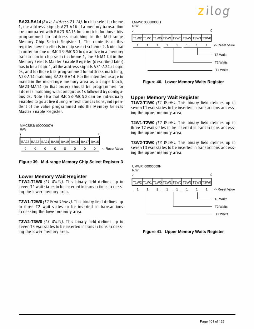
BA23-BA14 (Base Address 23-14). In chip select scheme1, the address signals A23-A16 of a memory transactionare compared with BA23-BA16 for a match, for those bitsprogrammed for address matching in the Mid-rangeMemory Chip Select Register 1. The contents of thisregister have no effects in chip select scheme 2. Note thatin order for one of /MCS3-/MCS0 to go active in a memorytransaction in chip select scheme 1, the ENM1 bit in theMemory Selects Master Enable Register (described later)has to be at logic 1, all the address signals A31-A24 at logic0s, and for those bits programmed for address matching,A23-A14 matching BA23-BA14. For the intended usage tomaintain the mid-range memory area as a single block,MA23-MA14 (in that order) should be programmed foraddress matching with contiguous 1s followed by contigu-ous 0s. Note also that /MCS3-/MCS0 can be individuallyenabled to go active during refresh transactions, indepen-dent of the value programmed into the Memory SelectsMaster Enable Register.
BA23
7
BA22 BA21 BA20 BA19 BA18 BA17 BA16
0 00 00 00 0
0
<- Reset Value
MMCSR3: 00000007HR/W
Figure 39. Mid-range Memory Chip Select Register 3
Lower Memory Wait RegisterT1W2-T1W0 (T1 Waits). This binary field defines up toseven T1 wait states to be inserted in transactions access-ing the lower memory area.
T2W1-T2W0 (T2 Wait States). This binary field defines upto three T2 wait states to be inserted in transactionsaccessing the lower memory area.
T3W2-T3W0 (T3 Waits). This binary field defines up toseven T3 wait states to be inserted in transactions access-ing the lower memory area.
T1W2
7
T1W1 T1W0 T2W1 T2W0 T3W2 T3W1 T3W0
1 11 11 11 1
0
<- Reset Value
LMWR: 00000008HR/W
T3 Waits
T2 Waits
T1 Waits
Figure 40. Lower Memory Waits Register
Upper Memory Wait RegisterT1W2-T1W0 (T1 Waits). This binary field defines up toseven T1 wait states to be inserted in transactions access-ing the upper memory area.
T2W1-T2W0 (T2 Waits). This binary field defines up tothree T2 wait states to be inserted in transactions access-ing the upper memory area.
T3W2-T3W0 (T3 Waits). This binary field defines up toseven T3 wait states to be inserted in transactions access-ing the upper memory area.
T1W2
7
T1W1 T1W0 T2W1 T2W0 T3W2 T3W1 T3W0
1 11 11 11 1
0
<- Reset Value
UMWR: 00000009HR/W
T3 Waits
T2 Waits
T1 Waits
Figure 41. Upper Memory Waits Register
Page 101 of 125
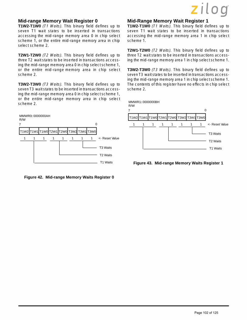
Mid-range Memory Wait Register 0T1W2-T1W0 (T1 Waits). This binary field defines up toseven T1 wait states to be inserted in transactionsaccessing the mid-range memory area 0 in chip selectscheme 1, or the entire mid-range memory area in chipselect scheme 2.
T2W1-T2W0 (T2 Waits). This binary field defines up tothree T2 wait states to be inserted in transactions access-ing the mid-range memory area 0 in chip select scheme 1,or the entire mid-range memory area in chip selectscheme 2.
T3W2-T3W0 (T3 Waits). This binary field defines up toseven T3 wait states to be inserted in transactions access-ing the mid-range memory area 0 in chip select scheme 1,or the entire mid-range memory area in chip selectscheme 2.
T1W2
7
T1W1 T1W0 T2W1 T2W0 T3W2 T3W1 T3W0
1 11 11 11 1
0
<- Reset Value
MMWR0: 0000000AHR/W
T3 Waits
T2 Waits
T1 Waits
Mid-Range Memory Wait Register 1T1W2-T1W0 (T1 Waits). This binary field defines up toseven T1 wait states to be inserted in transactionsaccessing the mid-range memory area 1 in chip selectscheme 1.
T2W1-T2W0 (T2 Waits). This binary field defines up tothree T2 wait states to be inserted in transactions access-ing the mid-range memory area 1 in chip select scheme 1.
T3W2-T3W0 (T3 Waits). This binary field defines up toseven T3 wait states to be inserted in transactions access-ing the mid-range memory area 1 in chip select scheme 1.The contents of this register have no effects in chip selectscheme 2.
T1W2
7
T1W1 T1W0 T2W1 T2W0 T3W2 T3W1 T3W0
1 11 11 11 1
0
<- Reset Value
MMWR1: 0000000BHR/W
T3 Waits
T2 Waits
T1 Waits
Figure 43. Mid-range Memory Waits Register 1
Figure 42. Mid-range Memory Waits Register 0
Page 102 of 125

Mid-Range Memory Wait Register 2T1W2-T1W0 (T1 Waits). This binary field defines up toseven T1 wait states to be inserted in transactionsaccessing the mid-range memory area 2 in chip selectscheme 1.
T2W1-T2W0 (T2 Waits). This binary field defines up tothree T2 wait states to be inserted in transactions access-ing the mid-range memory area 2 in chip select scheme 1.
T3W2-T3W0 (T3 Waits). This binary field defines up toseven T3 wait states to be inserted in transactions access-ing the mid-range memory area 2 in chip select scheme 1.The contents of this register have no effects in chip selectscheme 2.
T1W2
7
T1W1 T1W0 T2W1 T2W0 T3W2 T3W1 T3W0
1 11 11 11 1
0
<- Reset Value
MMWR2: 0000000CHR/W
T3 Waits
T2 Waits
T1 Waits
Figure 44. Mid-Range Memory Waits Register 2
Mid-range Memory Waits Register 3T1W2-T1W0 (T1 Waits). This binary field defines up toseven T1 wait states to be inserted in transactionsaccessing the mid-range memory area 3 in chip selectscheme 1.
T2W1-T2W0 (T2 Waits). This binary field defines up tothree T2 wait states to be inserted in transactions access-ing the mid-range memory area 3 in chip select scheme 1.
T3W2-T3W0 (T3 Waits). This binary field defines up toseven T3 wait states to be inserted in transactions access-ing the mid-range memory area 3 in chip select scheme 1.The contents of this register have no effects in chip selectscheme 2.
T1W2
7
T1W1 T1W0 T2W1 T2W0 T3W2 T3W1 T3W0
1 11 11 11 1
0
<- Reset Value
MMWR3: 0000000DHR/W
T3 Waits
T2 Waits
T1 Waits
Figure 45. Mid-range Memory Waits Register 3
Page 103 of 125
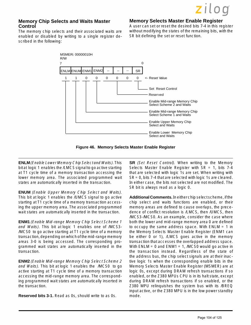
Memory Chip Selects and Waits MasterControlThe memory chip selects and their associated waits areenabled or disabled by writing to a single register de-scribed in the following:
Memory Selects Master Enable RegisterA user can set or reset the desired bits 7-4 in this registerwithout modifying the states of the remaining bits, with theSR bit defining the set or reset function.
ENLM (Enable Lower Memory Chip Select and Waits). Thisbit at logic 1 enables the /LMCS signal to go active startingat T1 cycle time of a memory transaction accessing thelower memory area. The associated programmed waitstates are automatically inserted in the transaction.
ENUM (Enable Upper Memory Chip Select and Waits).This bit at logic 1 enables the /UMCS signal to go activestarting at T1 cycle time of a memory transaction access-ing the upper memory area. The associated programmedwait states are automatically inserted in the transaction.
ENM1 (Enable Mid-range Memory Chip Select Scheme 1and Waits). This bit at logic 1 enables one of /MCS3-/MCS0 to go active starting at T1 cycle time of a memorytransaction, depending on which of the mid-range memoryareas 3-0 is being accessed. The corresponding pro-grammed wait states are automatically inserted in thetransaction.
ENM2 (Enable Mid-range Memory Chip Select Scheme 2and Waits). This bit at logic 1 enables the /MCS0 to goactive starting at T1 cycle time of a memory transactionaccessing the mid-range memory area. The correspond-ing programmed wait states are automatically inserted inthe transaction.
Reserved bits 3-1. Read as 0s, should write to as 0s.
Figure 46. Memory Selects Master Enable Register
ENLM
7
ENUM ENM1 ENM2 -- -- -- SR
1 01 00 00 0
0
<- Reset Value
MSMER: 00000010HR/W
Enable Lower Memory ChipSelect and Waits
Enable Upper Memory ChipSelect and Waits
Enable Mid-range Memory ChipSelect Scheme 1 and Waits
Enable Mid-range Memory ChipSelect Scheme 2 and Waits
Set Reset Control
Reserved
SR (Set Reset Control). When writing to the MemorySelects Master Enable Register with SR = 1, bits 7-4that are selected with logic 1s are set. When writing withSR = 0, bits 7-4 that are selected with logic 1s are cleared.In either case, the bits not selected are not modified. TheSR bit is always read as a logic 0.
Additional Comments. In either chip select scheme, if thechip select and waits functions are enabled, or theirmemory areas are defined to cause overlaps, the prece-dence of conflict resolution is /LMCS, then /UMCS, then/MCS3-/MCS0. As an example, consider the case whereboth the lower and mid-range memory area 0 are definedto occupy the same address space. With ENLM = 1 inthe Memory Selects Master Enable Register (ENM1 canbe either 0 or 1), /LMCS goes active in the memorytransaction that accesses the overlapped address space.With ENLM = 0 and ENM1 = 1, /MCS0 would go active inthe transaction instead. Regardless of the state ofthe address bus, the chip select signals are at their inac-tive logic 1s when the corresponding enable bits in theMemory Selects Master Enable Register (MSMER) are atlogic 0s, except during DRAM refresh transactions if soenabled, or the Z380 MPUs CPU is in its halt state, exceptduring DRAM refresh transactions if so enabled, or theZ380 MPU relinquishes the system bus with its /BREQinput active, or the Z380 MPU is in the low power standbymode.
Page 104 of 125
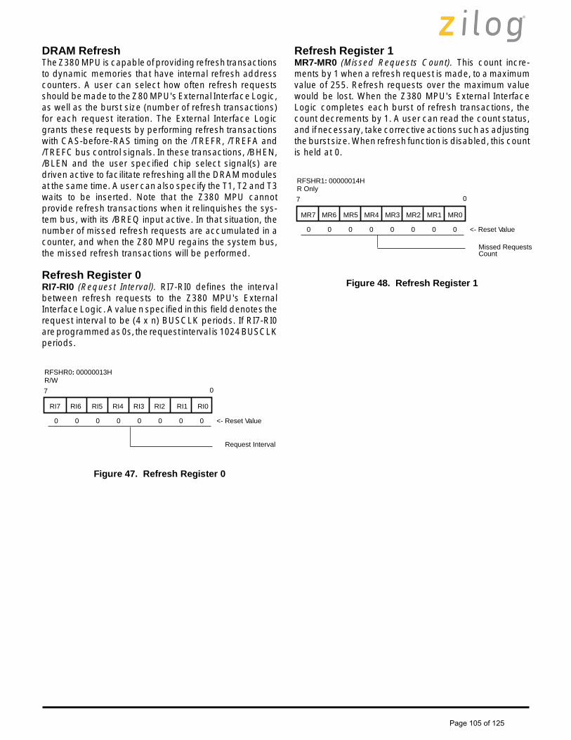
DRAM RefreshThe Z380 MPU is capable of providing refresh transactionsto dynamic memories that have internal refresh addresscounters. A user can select how often refresh requestsshould be made to the Z80 MPU's External Interface Logic,as well as the burst size (number of refresh transactions)for each request iteration. The External Interface Logicgrants these requests by performing refresh transactionswith CAS-before-RAS timing on the /TREFR, /TREFA and/TREFC bus control signals. In these transactions, /BHEN,/BLEN and the user specified chip select signal(s) aredriven active to facilitate refreshing all the DRAM modulesat the same time. A user can also specify the T1, T2 and T3waits to be inserted. Note that the Z380 MPU cannotprovide refresh transactions when it relinquishes the sys-tem bus, with its /BREQ input active. In that situation, thenumber of missed refresh requests are accumulated in acounter, and when the Z80 MPU regains the system bus,the missed refresh transactions will be performed.
Refresh Register 0RI7-RI0 (Request Interval). RI7-RI0 defines the intervalbetween refresh requests to the Z380 MPU's ExternalInterface Logic. A value n specified in this field denotes therequest interval to be (4 x n) BUSCLK periods. If RI7-RI0are programmed as 0s, the request interval is 1024 BUSCLKperiods.
RI7
7
RI6 RI5 RI4 RI3 RI2 RI1 RI0
0 00 00 00 0
0
<- Reset Value
RFSHR0: 00000013HR/W
Request Interval
Figure 47. Refresh Register 0
Refresh Register 1MR7-MR0 (Missed Requests Count). This count incre-ments by 1 when a refresh request is made, to a maximumvalue of 255. Refresh requests over the maximum valuewould be lost. When the Z380 MPU's External InterfaceLogic completes each burst of refresh transactions, thecount decrements by 1. A user can read the count status,and if necessary, take corrective actions such as adjustingthe burst size. When refresh function is disabled, this countis held at 0.
MR7
7
MR6 MR5 MR4 MR3 MR2 MR1 MR0
0 00 00 00 0
0
<- Reset Value
RFSHR1: 00000014HR Only
Missed RequestsCount
Figure 48. Refresh Register 1
Page 105 of 125
Refresh Register 2RFEN (Refresh Enable). Enables the refresh function whenprogrammed to logic 1.
Reserved bit 6. Read as 0, should write to as 0.
BS5-BS0 (Burst Size). This field defines the number ofrefresh transactions per refresh request made to the Z380MPU's External Interface Logic. The burst size ranges from1 to 64, with the highest size specified with BS5-BS0 equalto 0s.
Refresh Wait RegisterT1W2-T1W0 (T1 Waits). This binary field defines up toseven T1 wait states to be inserted in refresh transactions.
T1W1-T2W0 (T2 Waits). This binary field defines up tothree T2 wait states to be inserted in refresh transactions.
T3W2-T3W0 (T3 Waits). This binary field defines up toseven T3 wait states to be inserted in refresh transactions.Note that care should be exercised in defining refreshburst size and request intervals to avoid over-burdeningthe system bus with refresh transactions. The memory chipselect signals can be selectively enabled to go activeduring refresh transactions, such enabling is described inthe Memory Chip Selects and Waits section.
Figure 49. Refresh Register 2
Figure 50. Refresh Waits Register
RFEN
7
-- BS5 BS4 BS3 BS2 BS1 BS0
0 00 00 00 0
0
<- Reset Value
RFSHR2: 00000015HR/W
Burst Size
Reserved
Refresh EnableT1W2
7
T1W1 T1W0 T2W1 T2W0 T3W2 T3W1 T3W0
1 11 11 11 1
0
<- Reset Value
RFWR: 0000000FHR/W
T3 Waits
T2 Waits
T1 Waits
Page 106 of 125

LOW POWER STANDBY MODE
The Z380 MPU provides an optional standby mode tominimize power consumption during system idle time. Ifthis option is enabled, executing the Sleep instructionwould stop clocking internal to the Z380 MPU, as well as atthe BUSCLK and IOCLK outputs. The /STNBY signal goesto active logic 0, indicating the Z380 MPU is entering thestandby mode. All Z380 MPU operations are suspended,the bus control signals are driven inactive and the addressbus is driven to logic 1s. Note that if an external crystaloscillator is used to drive the Z380 MPU’s CLKI input,/STNBY can be used to stop its operation. This is a means
to further reduce power dissipation for the overall system.The standby mode can be exited by asserting any of the/RESET, /NMI, /INT3-/INT0 (if enabled), or optionally,/BREQ inputs.
If the standby mode option is not enabled, the Sleepinstruction is interpreted and executed no different thanthe HALT instruction, stopping the Z30 MPU from furtherinstruction execution. In this case, /HALT goes to activelogic 0 to indicate the Z380 MPU's halt status.
Standby Mode Control and EnteringSTBY (Enable Standby Mode Option). Enables the Z380MPU to go into low power standby mode when the Sleepinstruction is executed.
BRXT (Bus Request to Exit Standby Mode). If BRXT is atlogic 1, standby mode can be exited by asserting /BREQ.
Reserved Bits 5-3. Read as 0s, should write to as 0s.
WM2-WM0 (Warm-up Time Selection). WM2-WM0 deter-mines the approximate running duration of a warm-upcounter that provides a delay before the Z380 MPUresumes its clocking and operations, from the time aninterrupt or bus request (if so enabled) is asserted to exitstandby mode. In a system where an external crystaloscillator is used to drive the Z380 MPU’s CLK input, anappropriate warm-up time can be selected for the oscilla-tor to stabilize.
STBY
7
BRXT WM2 WM1 WM0
0 00 00 00 0
0
Reset Value
SMCR: 00000016HR/W
ReservedProgram as 0sRead as 0s
Bus Request to Exit Standby Mode
Enable Standby Mode Option
00 000 110 001 0
Warmup Time SelectionNo Warmup
2 16 BUSCLK Cycles
2 17 BUSCLK Cycles
2 19 BUSCLK Cycles
Figure 51. Standby Mode Control Register
Page 107 of 125

Standby Mode Exit With Bus RequestOptionally, if the BRXT bit of the Standby Mode ControlRegister (SMCR) was previously set, /STNBY goes to logic1 when the /BREQ input is asserted, allowing the externalcrystal oscillator that drives the Z380 MPU’s CLK input torestart. A warm-up counter internal to the Z380 MPUproceeds to count, for a duration long enough for theoscillator to stabilize, which was selected with the WM bitsin the SMCR. When the counter reaches its end-count,clocking resumes within the Z380 MPU and at the BUSCLKand IOCLK outputs.
The Z380 MPU relinquishes the system bus after clockingresumes, with the normal /BREQ, /BACK handshake pro-cedure. The Z380 MPU regains the system bus when/BREQ goes inactive, again going through a normal hand-shake procedure.
Note that clocking continues, and the Z380 MPU is at thehalt state.
BUSCLK
IOCLK
/STNBY
/BACK
ADDRESS
/BREQ
FFFFFFFFH
Bus Release
DATA
BUSCNTLS
HaltState
Figure 52. Standby Mode Exit with Bus Request Timing
Page 108 of 125

Standby Mode Entering TimingFigure 53 shows standby mode entering timing in anexample where IOCLK was programmed to be BUSCLK
divided-by-2. Note that clocking stops only after IOCLKhas changed to logic 0.
Standby Mode Exit With ResetWhen /RESET is asserted, /STNBY goes to logic 1, allowingthe external crystal oscillator that drives the Z380 MPU’sCLKI input to restart. The /RESET pulse provided shouldbe of a duration long enough for oscillator stabilization. TheZ380 MPU exits standby mode, and when /RESET is
deasserted, it goes through the normal reset timing to startinstruction execution at address 00000000H. Note thatclocking resumes within the Z380 MPU and at the BUSCLKand IOCLK outputs soon after /RESET is asserted, whenthe crystal oscillator is not yet stabilized.
BUSCLK
IOCLK
/STNBY
ADDRESS
DATA
/RESET
FFFFFFFFH 000000H
OPCODEFETCH
BUSCLK
IOCLK
/STNBY
ADDRESS
DATA
BUSCNTLS
(/TREFR, /TREFA, /TREFC,/MRD, /MWR, /BHEN,/BLEN, /IOCTL3-0)
FFFFFFFFH
Figure 54. Standby Mode Exit with Reset Timing
Figure 53. Standby Mode Entering Timing
Page 109 of 125

Standby Mode Exit With External InterruptsStandby mode can be exited by asserting input /NMI.Asserting the maskable interrupt inputs /INT3-/INT0 mayalso exit standby mode, if the global interrupt flag IEF1 waspreviously enabled at logic 1, and for those requestsindividually enabled, as indicated in the Interrupt EnableRegister.
When exit conditions are met, /STNBY goes to logic 1,allowing the external crystal oscillator that drives the Z380MPU’s CLK input to restart.
BUSCLK
IOCLK
/STNBY
/INT3,2,1,0
ADDRESS
/NMI
FFFFFFFFH
AppropriateAcknowledge
Figure 55. Standby Mode Exit with External Interrupts Timing
The Z380 MPU’s internal warm-up counter proceeds tocount, for a duration long enough for the oscillator tostabilize, as selected by the WM bits in the Standby ModeControl Register. When the counter reaches its end-count,clocking resumes within the Z380 MPU, as well as at theBUSCLK and IOCLK outputs. The Z380 MPU performs aninterrupt acknowledge procedure appropriate to the inter-rupt request that initiated the standby mode exit.
Page 110 of 125

Standby Mode for On-chip CrystalOscillatorThe previous discussions have been focused on situationswhere a direct clock is supplied to the Z380 MPU's CLKIinput. Such a clock may be sourced by an external crystalwith its oscillation circuit. In the case where a crystal isconnected to the Z380 MPU's on-chip oscillator, all standbyfunctions described earlier apply. Items worth noting areas follows.
1. When standby mode is entered, the feedback path forthe on-chip oscillator is disabled, reducing power con-sumption.
2. A user can select a warm-up time appropriate for thecrystal being used, by programming the WM2-WM0bits in the Standby Mode Control Register (SMCR).
Table 6. Z380 MPU On-chip I/O Registers
Register Mnemonic On-Chip I/O Address
Lower Memory Chip Select Register 0 LMCS0 00000000HLower Memory Chip Select Register 1 LMCS1 00000001HUpper Memory Chip Select Register 0 UMCS0 00000002HUpper Memory Chip Select Register 1 UMCS1 00000003HMidrange Memory Chip Select Register 0 MMCS0 00000004HMidrange Memory Chip Select Register 1 MMCS1 00000005HMidrange Memory Chip Select Register 2 MMCS2 00000006HMidrange Memory Chip Select Register 3 MMCS3 00000007H
Lower Memory Waits Register LMWR 00000008HUpper Memory Waits Register UMWR 00000009HMidrange Memory Waits Register 0 MMWR0 0000000AHMidrange Memory Waits Register 1 MMWR1 0000000BHMidrange Memory Waits Register 2 MMWR2 0000000CHMidrange Memory Waits Register 3 MMWR3 0000000DHI/O Waits Register IOWR 0000000EHRefresh Waits Register RFWR 0000000FH
Memory Selects Master Enable Register MSMER 00000010HI/O Bus Control Register 0 IOCR0 00000011HI/O Bus Control Register 1 IOCR1 00000012HRefresh Register 0 RFSHR 0 00000013HRefresh Register 1 RFSHR1 00000014HRefresh Register 2 RFSHR2 00000015HStandby Mode Control Register SMCR 00000016HInterrupt Enable Register IER 00000017H
Assigned Vectors Base Register AVBR 00000018HTrap and Break Register TRPBK 00000019H
Page 111 of 125
RESET
The Z380 MPU is placed in a dormant state when the/RESET input is asserted. All its operations are terminated,including any interrupt, bus request or bus transaction thatmay be in progress. Its IOCLK goes Low on the nextBUSCLK rising edge, and enters into the BUSCLK divided-down-by-eight mode. The address and data buses are tri-stated, and the bus control signals are driven to theirinactive states. The effect of a reset on the Z380 CPU andrelated I/O registers is depicted in Table 6, and the effecton the on-chip peripheral functions is summarized inTable 8.
The /RESET input may be asynchronous to BUSCLK,though it is sampled internally at BUSCLK’s falling edges.For proper initialization of the Z380 MPU, V
DD must be
within operating specification and its BUSCLK must bestable for more than five cycles with /RESET held Low. The/RESET input has a built-in Schmitt trigger buffer to facili-tate power-on reset generation through an RC network.
Note that if a user system has devices external to the Z380MPU that are clocked by IOCLK, these devices mayrequire a /RESET pulse width that spans over a number ofIOCLK cycles (now at BUSCLK/8) for proper initialization.
The Z380 MPU proceeds to fetch its first instruction 3.5BUSCLK cycles after /RESET is deasserted, providedsuch deassertion meets the proper setup and hold timeswith reference to the falling edge of BUSCLK, as depictedin Figure 20 in the External Interface Section. Figure 19 inthe same section indicates a synchronization of IOCLKwhen /RESET is deasserted. Again with the proper setupand hold times being met, IOCLK’s first rising edge is 11.5BUSCLK cycles after the /RESET deassertion, precededby a minimum of 4 BUSCLK cycles where IOCLK is at Low.
Note that if /BREQ is active when /RESET is deasserted, theZ380 MPU would relinquish the bus instead of fetching itsfirst instruction. IOCLK synchronization would still takeplace as described before.
Page 112 of 125

Table 7. Effect of a Reset on Z380 CPU and Related I/O Registers
Register Reset Value Comments
Program Counter 00000000 PCz, PC
Stack Pointer 00000000 SPz, SP
I 000000 Iz, IR 00
Select Register 00000000 Register Bank 0 Selected:AF, Main Bank, IX, IYNative ModeMaskable Interrupts Disabled, in Mode 0Bus Request Lock-Off
A and F Registers Register Banks 3-0:A, F, A’, F’ Unaffected
Register Extensions 0000 Register Bank 0:BCz, DEz, HLz, IYz,BCz’, DEz’, HLz’, IYz’(All “non-extended” portions unaffected.)Register Bank 3-1 Unaffected.
I/O Bus Control Register 0 00 IOCLK = BUSCLK/8
Interrupt Enable Register 01 /INT0 Enabled
Assigned Vector Base Register 00
Trap and Break Register 00
Table 8. Effect of a Reset on On-chip Peripheral Functions
Peripheral Functions Reset Conditions
Memory Chip Selects and Waits Lower Memory Chip Select Signal enabled for lowest 1 MBytes(00000000H-000FFFFFH), with 7 T1, 3 T2, and 7 T3 waits.
Upper Memory Chip Select Signal enabled for highest16th MBytes (00F00000H - 00FFFFFFH),with 7 T1, 3 T2, and 7 T3 waits.
Midrange Memory Chip Select Signal and waits disabled.
I/O Waits External I/O read, write -- 7 waits.RETI -- 3 waits.Interrupt daisy chain -- 7 waits.
DRAM Refresh Controller Disabled
Standby Mode Disabled
Page 113 of 125

ABSOLUTE MAXIMUM RATINGS
Voltage on VDD
with respect to VSS
.......... –0.3V to +7.0VVoltage on all pins,
with respect to VSS
.................... –0.3V to (VDD
+ 0.3)VOperating Ambient Temperature: .................. 0 to +70°CStorage Temperature: ........................... –55°C to +150°C
Stresses greater than those listed under Absolute Maxi-mum Ratings may cause permanent damage to the de-vice. This is a stress rating only; operation of the device atany condition above those indicated in the operationalsections of these specifications is not implied. Exposure toabsolute maximum rating conditions for extended periodsmay affect device reliability.
STANDARD TEST CONDITIONS
The AC and DC Characteristics sections below apply forthe following standard test conditions, unless otherwisenoted. All voltages are referenced to V
SS (0V). Positive
current flows into the referenced pin.
Standard conditions are as follows:4.75V < V
DD < 5.25V
Low Voltage 3.15 <3.3 <3.45V
SS = 0V
Standard test load on all outputs.
DC CHARACTERISTICSZ380™ Version
Symbol Parameter Min Max Unit Note
VIH
Input High Voltage 3.0 VDD
+ 0.3 VV
ILInput Low Voltage -0.3 0.8 V
VOH1
Output High Voltage (-4 mA IOH
) 2.4 – VV
OH2Output High Voltage (-250 µA I
OH) V
DD – 0.8 V – V
VOL
Output Low Voltage (4 mA IOL
) – 0.5 V
IIL
Input Leakage Current -10 10 µA 1ITL
Tri-State Leakage Current -10 10 µA 2IDD1
Power Supply Current (@ 18 MHz) TBS mA 3IDD3
Standby Power Supply Current TBS µA 4
CIN
Input Capacitance (f =1 MHz) 15 pF 5C
OUTOutput Capacitance (f =1 MHz) 15 pF 5
CIO
I/O Capacitance (f =1 MHz) 15 pF 5C
LOutput Load Capacitance 100 pF
CLD
AC Output Derating (Above 100 pF) 50 pS/pF
Notes:1. 0.4 V < V
IN < 2.4 V
2. 0.4 V < VOUT
< 2.4 V3. V
DD = 5.0 V, V
IH = 4.8 V, V
IL = 0.2 V
4. VDD
= 5.0 V, VIH
= 4.8 V, VIL = 0.2 V
5. Unmeasured pins returned to VSS
.
Page 114 of 125

AC CHARACTERISTICSZ380™ Version
Z8038018No. Symbol Parameter Min Max Note
1 TcC CLK Cycle Time 552 TwCh CLK Width High 24.53 TwCl CLK Width Low 24.54 TrC CLK Rise Time 35 TfC CLK Fall Time 3
6 TdCf(BCr) CLK Fall to BUSCLK Rise Delay 307 TdCr(BCf) CLK Rise to BUSCLK Fall Delay 278 TdBCr(OUT) BUSCLK Rise to Output Valid Delay 6.59 TdBCf(OUT) BUSCLK Fall to Output Valid Delay 6.510 TsIN(BCr) Input to BUSCLK Rise Setup Time 16 111 ThIN(BCr) Input to BUSCLK Rise Hold Time 0 1
12 TsBR(BCf) /BREQ to BUSCLK Fall Setup Time 16 213 ThBR(BCf) /BREQ to BUSCLK Fall Hold Time 0 214 TsMW(BCr) Mem Wait to BUSCLK Rise Setup Time 16 315 ThMW(BCr) Mem Wait to BUSCLK Rise Hold Time 0 316 TsMW(BCf) Mem Wait to BUSCLK Fall Setup Time 24 317 ThMW(BCf) Mem Wait to BUSCLK Fall Hold Time 0 3
18 TsIOW(BCr) IO Wait to BUSCLK Rise Setup Time 24 319 ThIOW(BCr) IO Wait to BUSCLK Rise Hold Time 0 320 TsIOW(BCf) IO Wait to BUSCLK Fall Setup Time 24 321 ThIOW(BCf) IO Wait to BUSCLK Fall Hold Time 0 3
22 TwNMI1 /NMI Low Width 2523 TwRES1 Reset Low Width 1024 Tx01(02) Output Skew (Same Clock Edge) –2 +2 425 Tx01(03) Output Skew (Opposite Clock Edge) –3 +3 5
Notes:1. Applicable for Data Bus and /MSIZE inputs2. /BREQ can also be asserted/deasserted asynchronously3. External waits asserted at /WAIT input4. Tx01(02) = [Output 1] TdBCr(OUT) - [Output 2] TdBCr(OUT)
or [Output 1] TdBCf(OUT) - [Output 2] TdBCf(OUT)5. Tx01(03) = [Output 1] TdBCr(OUT) - [Output 3] TdBCf(OUT)
or [Output 1] TdBCf(OUT) - [Output 3] TdBCr(OUT)
Page 115 of 125

DC CHARACTERISTICSLow Voltage Z380™ Version
Symbol Parameter Min Max Unit Note
VIH
Input High Voltage 2.0 VDD
+ 0.5 VV
ILInput Low Voltage –0.5 0.8 V
VOH1
Output High Voltage (–200 µA IOH
) 2.15 - VV
OLOutput Low Voltage (1.6 mA I
OL) - 0.4 V
IIL
Input Leakage Current –10 10 µA 1ITL
Tri-State Leakage Current –10 10 µA 2IDD1
Power Supply Current (@ 10 MHz) TBS mA 3IDD3
Standby Power Supply Current 20 µA 4
CIN
Input Capacitance (f =1 MHz) 15 pF 5C
OUTOutput Capacitance (f =1 MHz) 15 pF 5
CIO
I/O Capacitance (f =1 MHz) 15 pF 5C
LOutput Load Capacitance 100 pF
CLD
AC Output Derating (Above 100 pF) 250 pS/pF
Notes:1. V
IN = 0.4 V
2. 0.4 V < VOUT
< 2.15 V3. V
DD = 3.3 V, V
IH = 3.0 V, V
IL = 0.2 V
4. VDD
= 3.3 V, VIH
= 3.0 V, VIL = 0.2 V
5. Unmeasured pins returned to VSS
.
Page 116 of 125

AC CHARACTERISTICSLow Voltage Z380™
Z8L38010No. Symbol Parameter Min Max Note
1 TcC CLK Cycle Time 1002 TwCh CLK Width High 403 TwCl CLK Width Low 404 TrC CLK Rise Time 55 TfC CLK Fall Time 5
6 TdCf(BCr) CLK Fall to BUSCLK Rise Delay 607 TdCr(BCf) CLK Rise to BUSCLK Fall Delay 558 TdBCr(OUT) BUSCLK Rise to Output Valid Delay 159 TdBCf(OUT) BUSCLK Fall to Output Valid Delay 1510 TsIN(BCr) Input to BUSCLK Rise Setup Time 30 111 ThIN(BCr) Input to BUSCLK Rise Hold Time 0 1
12 TsBR(BCf) /BREQ to BUSCLK Fall Setup Time 30 213 ThBR(BCf) /BREQ to BUSCLK Fall Hold Time 0 214 TsMW(BCr) Mem Wait to BUSCLK Rise Setup Time 30 315 ThMW(BCr) Mem Wait to BUSCLK Rise Hold Time 0 316 TsMW(BCf) Mem Wait to BUSCLK Fall Setup Time 45 317 ThMW(BCf) Mem Wait to BUSCLK Fall Hold Time 0 3
18 TsIOW(BCr) IO Wait to BUSCLK Rise Setup Time 45 319 ThIOW(BCr) IO Wait to BUSCLK Rise Hold Time 0 320 TsIOW(BCf) IO Wait to BUSCLK Fall Setup Time 45 321 ThIOW(BCf) IO Wait to BUSCLK Fall Hold Time 0 3
22 TwNMI1 /NMI Low Width 5023 TwRES1 Reset Low Width 1024 Tx01(02) Output Skew (Same Clock Edge) –4 +4 425 Tx01(03) Output Skew (Opposite Clock Edge) –6 +6 5
Notes:1. Applicable for Data Bus and /MSIZE inputs2. /BREQ can also be asserted/deasserted asynchronously3. External waits asserted at /WAIT input4. Tx01(02) = [Output 1] TdBCr(OUT) - [Output 2] TdBCr(OUT)
or [Output 1] TdBCf(OUT) - [Output 2] TdBCf(OUT)5. Tx01(03) = [Output 1] TdBCr(OUT) - [Output 3] TdBCf(OUT)
or [Output 1] TdBCf(OUT) - [Output 3] TdBCr(OUT)
Page 117 of 125

CLK
BUSCLK
OUTPUT
OUTPUT
INPUT
/NMI
1
3 2
4
6 7
8
9
INPUT
10
5
22
14 18 11 15 19
12 16 20 13 17 21
/RESET
23
AC CHARACTERISTICS (Continued)
Figure 56. Z380™ CPU Timing
Page 118 of 125

APPENDIX A
no esc ED esc DD esc FD esc CB esc ED-CB DD-CB FD-CB
00 NOP IN0 B,(n) - - RLC B RLCW BC - -01 LD BC,nn OUT0 (n),B LD (BC),IX LD (BC),IY RLC C RLCW DE LDBC,(SP+d) -02 LD (BC),A LD BC,BC LD BC,DE LD BC,HL RLC D RLCW (HL) RLCW (IX+d) RLCW (IY+d)03 INC BC ** EX BC,IX LD IX,(BC) LD IY,(BC) RLC E RLCW HL LD BC,(IX+d) LDBC,(IY+d)04 INC B TST B - - RLC H RLCW IX - -05 DEC B EX BC,DE - - RLC L RLCW IY - -06 LD B,n LD (BC),nn - - RLC (HL) - RLC (IX+d) RLC (IY+d)07 RLCA EX A,B LD IX,BC LD IY,BC RLC A - - -08 EX AF,AF’ IN0 C,(n) - - RRC B RRCW BC - -09 ADD HL,BC ** OUT0 (n),C ADD IX,BC ** ADD IY,BC ** RRC C RRCW DE LD (SP+d),BC -0A LD A,(BC) - - - RRC D RRCW (HL) RRCW (IX+d) RRCW (IY+d)0B DEC BC ** EX BC,IY LD BC,IX LD BC,IY RRC E RRCW HL LD (IX+d),BC LD (IY+d),BC0C INC C TST C LD BC,(BC) LD (BC),BC RRC H RRCW IX - -0D DEC C EX BC,HL LD BC,(DE) LD (DE),BC RRC L RRCW IY - -0E LD C,n SWAP BC - - RRC (HL) - RRC (IX+d) RRC (IY+d)0F RRCA EX A,C LD BC,(HL) LD (HL),BC RRC A - - -10 DJNZ e IN0 D,(n) DJNZ ee DJNZ eee RL B RLW BC - -11 LD DE,nn OUT0 (n),D LD (DE),IX LD (DE),IY RL C RLW DE LD DE,(SP+d) -12 LD (DE),A LD DE,BC LD DE,DE LD DE,HL RL D RLW (HL) RLW (IX+d) RLW (IY+d)13 INC DE ** EX DE,IX LD IX,(DE) LD IY,(DE) RL E RLW HL LD DE,(IX+d) LD DE,(IY+d)14 INC D TST D - - RL H RLW IX - -15 DEC D - - - RL L RLW IY - -16 LD D,n LD (DE),nn - - RL (HL) - RL (IX+d) RL (IY+d)17 RLA EX A,D LD IX,DE LD IY,DE RL A - - -18 JR e IN0 E,(n) JR ee JR eee RR B RRW BC - -19 ADD HL,DE ** OUT0 (n),E ADD IX,DE ** ADD IY,DE ** RR C RRW DE LD (SP+d),DE -1A LD A,(DE) - - - RR D RRW (HL) RRW (IX+d) RRW (IY+d)1B DEC DE ** EX DE,IY LD DE,IX LD DE,IY RR E RRW HL LD (IX+d),DE LD (IY+d),DE1C INC E TST E LD DE,(BC) LD (BC),DE RR H RRW IX - -1D DEC E - LD DE,(DE) LD (DE),DE RR L RRW IY - -1E LD E,n SWAP DE - - RR (HL) - RR (IX+d) RR (IY+d)1F RRA EX A,E LD DE,(HL) LD (HL),DE RR A - - -20 JR NZ,e IN0 H,(n) JR NZ,ee JR NZ,eee SLA B SLAW BC - -21 LD HL,nn OUT0 (n),H LD IX,nn LD IY,nn SLA C SLAW DE LD IX,(SP+d) LD IY,(SP+d)22 LD (nn),HL - LD (nn),IX LD (nn),IY SLA D SLAW (HL) SLAW (IX+d) SLAW (IY+d)23 INC HL ** - INC IX ** INC IY ** SLA E SLAW HL LD IY,(IX+d) LD IX,(IY+d)24 INC H TST H INC IXU INC IYU SLA H SLAW IX - -25 DEC H - DEC IXU DEC IYU SLA L SLAW IY - -26 LD H,n - LD IXU,n LD IYU,n SLA (HL) - SLA (IX+d) SLA (IY+d)27 DAA EX A,H LD IX,IY LD IY,IX SLA A - - -28 JR Z,e IN0 L,(n) JR Z,ee JR Z,eee SRA B SRAW BC - -29 ADD HL,HL ** OUT0 (n),L ADD IX,IX ** ADD IY,IY ** SRA C SRAW DE LD (SP+d),IX LD (SP+d),IY2A LD HL,(nn) - LD IX,(nn) LD IY,(nn) SRA D SRAW (HL) SRAW (IX+d) SRAW (IY+d)2B DEC HL ** EX IX,IY DEC IX ** DEC IY ** SRA E SRAW HL LD (IX+d),IY LD (IY+d),IX2C INC L TST L INC IXL INC IYL SRA H SRAW IX - -2D DEC L - DEC IXL DEC IYL SRA L SRAW IY - -2E LD L,n - LD IXL,n LD IYL,n SRA (HL) - SRA (IX+d) SRA (IY+d)2F CPL EX A,L CPLW - SRA A - - -30 JR NC,e IN0 (n) JR NC,ee JR NC,eee EX B,B’ EX BC,BC’ - -
Page 119 of 125

APPENDIX A (Continued)
no esc ED esc DD esc FD esc CB esc ED-CB DD-CB FD-CB
31 LD SP,nn - LD (HL),IX LD (HL),IY EX C,C’ EX DE,DE’ LD HL,(SP+d) -32 LD (nn),A LD HL,BC LD HL,DE LD HL,HL EX D,D’ - - -33 INC SP ** EX HL,IX LD IX,(HL) LD IY,(HL) EX E,E’ EX HL,HL’ LD HL,(IX+d) LD HL,(IY+d)34 INC (HL) TST (HL) INC (IX+d) INC (IY+d) EX H,H’ EX IX,IX’- -35 DEC (HL) - DEC (IX+d) DEC (IY+d) EX L,L’ EX IY,IY’ - -36 LD (HL),n LD (HL),nn LD (IX+d),n LD (IY+d),n - - -37 SCF EX A,(HL) LD IX,HL LD IY,HL EX A,A’ - - -38 JR C,e IN0 A,(n) JR C,ee JR C,eee SRL B SRLW BC - -39 ADD HL,SP ** OUT0 (n),A ADD IX,SP ** ADD IY,SP ** SRL C SRLW DE LD (SP+d),HL-3A LD A,(nn) - - - SRL D SRLW (HL) SLRW (IX+d) SRLW (IY+d)3B DEC SP ** EX HL,IY LD HL,IX LD HL,IY SRL E SRLW HL LD (IX+d),HL LD (IY+d),HL3C INC A TST A LD HL,(BC) LD (BC),HL SRL H SRLW IX - -3D DEC A - LD HL,(DE) LD (DE),HL SRL L SRLW IY - -3E LD A,n SWAP HL SWAP IX SWAP IY SRL (HL) - SRL (IX+d) SRL (IY+d)3F CCF EX A,A LD HL,(HL) LD (HL),HL SRL A - - -40 LD B,B IN B,(C) INW BC,(C) - BIT 0,B - - -41 LD B,C OUT (C),B OUTW (C),BC - BIT 0,C - - -42 LD B,D SBC HL,BC - - BIT 0,D - - -43 LD B,E LD (nn),BC - - BIT 0,E - - -44 LD B,H NEG LD B,IXU LD B,IYU BIT 0,H - - -45 LD B,L RETN LD B,IXL LD B,IYL BIT 0,L - - -46 LD B,(HL) IM 0 LD B,(IX+d) LD B,(IY+d) BIT 0,(HL) - BIT 0,(IX+d) BIT 0,(IY+d)47 LD B,A LD I,A LD I,HL - BIT 0,A - - -48 LD C,B IN C,(C) - - BIT 1,B - - -49 LD C,C OUT (C),C - - BIT 1,C - - -4A LD C,D ADC HL,BC - - BIT 1,D - - -4B LD C,E LD BC,(nn) - - BIT 1,E - - -4C LD C,H MLT BC LD C,IXU LD C,IYU BIT 1,H - - -4D LD C,L RETI LD C,IXL LD C,IYL BIT 1,L - - -4E LD C,(HL) IM 3 LD C,(IX+d) LD C,(IY+d) BIT 1,(HL) - BIT 1,(IX+d) BIT 1,(IY+d)4F LD C,A LD R,A - - BIT 1,A - - -50 LD D,B IN D,(C) INW DE,(C) - BIT 2,B - - -51 LD D,C OUT (C),D OUTW (C),DE - BIT 2,C - - -52 LD D,D SBC HL,DE - - BIT 2,D - - -53 LD D,E LD (nn),DE - - BIT 2,E - - -54 LD D,H NEGW LD D,IXU LD D,IYU BIT 2,H - - -55 LD D,L RETB LD D,IXL LD D,IYL BIT 2,L - - -56 LD D,(HL) IM 1 LD D,(IX+d) LD D,(IY+d) BIT 2,(HL) - BIT 2,(IX+d) BIT 2,(IY+d)57 LD D,A LD A,I LD HL,I - BIT 2,A - - -58 LD E,B IN E,(C) - - BIT 3,B - - -59 LD E,C OUT (C),E - - BIT 3,C - - -5A LD E,D ADC HL,DE - - BIT 3,D - - -5B LD E,E LD DE,(nn) - - BIT 3,E - - -5C LD E,H MLT DE LD E,IXU LD E,IYU BIT 3,H - - -5D LD E,L - LD E,IXL LD E,IYL BIT 3,L - - -5E LD E,(HL) IM 2 LD E,(IX+d) LD E,(IY+d) BIT 3,(HL) - BIT 3,(IX+d) BIT 3,(IY+d)5F LD E,A LD A,R - - BIT 3,A - - -60 LD H,B IN H,(C) LD IXU,B LD IYU,B BIT 4,B - - -61 LD H,C OUT (C),H LD IXU,C LD IYU,C BIT 4,C - - -62 LD H,D SBC HL,HL LD IXU,D LD IYU,D BIT 4,D - - -63 LD H,E LD (nn),HL LD IXU,E LD IYU,E BIT 4,E - - -64 LD H,H TST m LD IXU,IXU LD IYU,IYU BIT 4,H - - -65 LD H,L EXTS LD IXU,IXL LD IYU,IYL BIT 4,L - - -
Page 120 of 125

no esc ED esc DD esc FD esc CB esc ED-CB DD-CB FD-CB
66 LD H,(HL) - LD H,(IX+d) LD H,(IY+d) BIT 4,(HL) - BIT 4,(IX+d) BIT 4,(IY+d)67 LD H,A RRD LD IXU,A LD IYU,A BIT 4,A - - -68 LD L,B IN L,(C) LD IXL,B LD IYL,B BIT 5,B - - -69 LD L,C OUT (C),L LD IXL,C LD IYL,C BIT 5,C - - -6A LD L,D ADC HL,HL LD IXL,D LD IYL,D BIT 5,D - - -6B LD L,E LD HL,(nn) LD IXL,E LD IYL,E BIT 5,E - - -6C LD L,H MLT HL LD IXL,IXU LD IYL,IYU BIT 5,H - - -6D LD L,L - LD IXL,IXL LD IYL,IYL BIT 5,L - - -6E LD L,(HL) - LD L,(IX+d) LD L,(IY+d) BIT 5,(HL) - BIT 5,(IX+d) BIT5,(IY+d)6F LD L,A RLD LD IXL,A LD IYL,A BIT 5,A - - -70 LD (HL),B - LD (IX+d),B LD (IY+d),B BIT 6,B - - -71 LD (HL),C OUT (C),n LD (IX+d),C LD (IY+d),C BIT 6,C - - -72 LD (HL),D SBC HL,SP LD (IX+d),D LD (IY+d),D BIT 6,D - - -73 LD (HL),E LD (nn),SP LD (IX+d),E LD (IY+d),E BIT 6,E - - -74 LD (HL),H TSTIO m LD (IX+d),H LD (IY+d),H BIT 6,H - - -75 LD (HL),L EXTSW LD (IX+d),L LD (IY+d),L BIT 6,L - - -76 HALT SLP - - BIT 6,(HL) - BIT 6,(IX+d) BIT 6,(IY+d)77 LD (HL),A - LD (IX+d),A LD (IY+d),A BIT 6,A - - -78 LD A,B IN A,(C) INW HL,(C) - BIT 7,B - - -79 LD A,C OUT (C),A OUTW (C),HL OUTW (C),nn BIT 7,C - - -7A LD A,D ADC HL,SP - - BIT 7,D - - -7B LD A,E LD SP,(nn) - - BIT 7,E - - -7C LD A,H MLT SP LD A,IXU LD A,IYU BIT 7,H - - -7D LD A,L - LD A,IXL LD A,IYL BIT 7,L - - -7E LD A,(HL) - LD A,(IX+d) LD A,(IY+d) BIT 7,(HL) - BIT 7,(IX+d) BIT 7,(IY+d)7F LD A,A - - - BIT 7,A - - -80 ADD A,B - - - RES 0,B - - -81 ADD A,C - - - RES 0,C - - -82 ADD A,D ADD SP,nn ** - - RES 0,D - - -83 ADD A,E OTIM - - RES 0,E - - -84 ADD A,H ADDW BC ADD IXU ADD IYU RES 0,H - - -85 ADD A,L ADDW DE ADD IXL ADD IYL RES 0,L - - -86 ADD A,(HL) ADDW nn ADD A,(IX+d) ADD A,(IY+d) RES 0,(HL) - RES 0,(IX+d) RES 0,(IY+d)87 ADD A,A ADDW HL ADDW IX ADDW IY RES 0,A - - -88 ADC A,B - - - RES 1,B - - -89 ADC A,C - - - RES 1,C - - -8A ADC A,D - - - RES 1,D - - -8B ADC A,E OTDM - - RES 1,E - - -8C ADC A,H ADCW BC ADC A,IXU ADC A,IYU RES 1,H - - -8D ADC A,L ADCW DE ADC A,IXL ADC A,IYL RES 1,L - - -8E ADC A,(HL) ADCW nn ADC A,(IX+d) ADC A,(IY+d) RES 1,(HL) - RES 1,(IX+d) RES 1,(IY+d)8F ADC A,A ADCW HL ADCW IX ADCW IY RES 1,A - - -90 SUB B - - - RES 2,B MULTW BC - -91 SUB C - - - RES 2,C MULTW DE - -92 SUB D SUB SP,nn ** - - RES 2,D - MULTW (IX+d) MULTW (IY+d)93 SUB E OTIMR - - RES 2,E MULTW HL - -94 SUB H SUBW BC SUB IXU SUB IYU RES 2,H MULTW IX - -95 SUB L SUBW DE SUB IXL SUB IYL RES 2,L MULTW IY - -96 SUB (HL) SUBW nn SUB (IX+d) SUB (IY+d) RES 2,(HL) - RES 2,(IX+d) RES 2,(IY+d)97 SUB A SUBW HL SUBW IX SUBW IY RES 2,A MULTW nn - -
Page 121 of 125

APPENDIX A (Continued)
no esc ED esc DD esc FD esc CB esc ED-CB DD-CB FD-CB
98 SBC A,B - - - RES 3,B MULTUW BC - -99 SBC A,C - - - RES 3,C MULTUW DE - -9A SBC A,D - - - RES 3,D - MULTUW (IX+d) MULTUW(IY+d)9B SBC A,E OTDMR - - RES 3,E MULTUW HL - -9C SBC A,H SBCW BC SBC A,IXU SBC A,IYU RES 3,H MULTUW IX - -9D SBC A,L SBCW DE SBC A,IXL SBC A,IYL RES 3,L MULTUW IY - -9E SBC A,(HL) SBCW nn SBC A,(IX+d) SBC A,(IY+d) RES 3,(HL) - RES 3,(IX+d) RES 3,(IY+d)9F SBC A,A SBCW HL SBCW IX SBCW IY RES 3,A MULTUW nn - -A0 AND B LDI - - RES 4,B - - -A1 AND C CPI - - RES 4,C - - -A2 AND D INI - - RES 4,D - - -A3 AND E OUTI - - RES 4,E - - -A4 AND H ANDW BC AND IXU AND IYU RES 4,H - - -A5 AND L ANDW DE AND IXL AND IYL RES 4,L - - -A6 AND (HL) ANDW nn AND (IX+d) AND (IY+d) RES 4,(HL) - RES 4,(IX+d) RES 4,(IY+d)A7 AND A ANDW HL ANDW IX ANDW IY RES 4,A - - -A8 XOR B LDD - - RES 5,B - - -A9 XOR C CPD - - RES 5,C - - -AA XOR D IND - - RES 5,D - - -AB XOR E OUTD - - RES 5,E - - -AC XOR H XORW BC XOR IXU XOR IYU RES 5,H - - -AD XOR L XORW DE XOR IXL XOR IYL RES 5,L - - -AE XOR (HL) XORW nn XOR (IX+d) XOR (IY+d) RES 5,(HL) - RES 5,(IX+d) RES 5,(IY+d)AF XOR A XORW HL XORW IX XORW IY RES 5,A - - -B0 OR B LDIR - - RES A,B - - -B1 OR C CPIR - - RES 6,C - - -B2 OR D INIR - - RES 6,D - - -B3 OR E OTIR - - RES 6,E - - -B4 OR H ORW BC OR IXU OR IYU RES 6,H - - -B5 OR L ORW DE OR IXL OR IYL RES 6,L - - -B6 OR (HL) ORW nn OR (IX+d) OR (IY+d) RES 6,(HL) - RES 6,(IX+d) RES 6,(IY+d)B7 OR A ORW HL ORW IX ORW IY RES 6,A - - -B8 CP B LDDR - - RES 7,B DIVUW BC - -B9 CP C CPDR - - RES 7,C DIVUW DE - -BA CP D INDR - - RES 7,D - DIVUW (IX+d) DIVUW (IY+d)BB CP E OTDR - - RES 7,E DIVUW HL - -BC CP H CPW BC CP IXU CP IYU RES 7,H DIVUW IX - -BD CP L CPW DE CP IXL CP IYL RES 7,L DIVUW IY - -BE CP (HL) CPW nn CP (IX+d) CP (IY+d) RES 7,(HL) - RES 7,(IX+d) RES 7,(IY+d)BF CP A CPW HL CPW IX CPW IY RES 7,A DIVUW nn - -C0 RET NZ LDCTL HL,SR DDIR W DDIR LW SET 0,B - - -C1 POP BC POP SR DDIR IB,W DDIR IB,LW SET 0,C - - -C2 JP NZ,nn - DDIR IW,W DDIR IW,LW SET 0,D - - -C3 JP nn - DDIR IB DDIR IW SET 0,E - - -C4 CALL NZ,nn CALR NZ,e CALR NZ,ee CALR NZ,eee SET 0,H - - -C5 PUSH BC PUSH SR - - SET 0,L - - -C6 ADD A,n ADD HL,(nn) ** ADDW (IX+d) ADDW (IY+d) SET 0,(HL) - SET 0,(IX+d) SET 0,(IY+d)C7 RST 0 - - - SET 0,A - - -C8 RET Z LDCTL SR,HL LDCTL SR,A - SET 1,B - - -C9 RET - - - SET 1,C - - -
Page 122 of 125

no esc ED esc DD esc FD esc CB esc ED-CB DD-CB FD-CB
CA JP Z,nn - LDCTL SR,n - SET 1,D - - -CB escape escape escape escape SET 1,E - - -CC CALL Z,nn CALR Z,e CALR Z,ee CALR Z,eee SET 1,H - - -CD CALL nn CALR e CALR ee CALR eee SET 1,L - - -CE ADC A,n - ADCW (IX+d) ADCW (IY+d) SET 1,(HL) - SET 1,(IX+d) SET 1,(IY+d)CF RST 1 BTEST MTEST - SET 1,A - - -D0 RET NC LDCTL A,DSR LDCTL A,XSR LDCTL A,YSR SET 2,B - - -D1 POP DE - - - SET 2,C - - -D2 JP NC,nn - - - SET 2,D - - -D3 OUT (n),A OUTA (nn),A - OUTAW (nn),HL SET 2,E - - -D4 CALL NC,nn CALR NC,e CALR NC,ee CALR NC,eee SET 2,H - - -D5 PUSH DE - - - SET 2,L - - -D6 SUB n SUB HL,(nn) ** SUBW (IX+d) SUBW (IY+d) SET 2,(HL) - SET 2,(IX+d) SET 2,(IY+d)D7 RST 2 - - - SET 2,A - - -D8 RET C LDCTL DSR,A LDCTL XSR,A LDCTL YSR,A SET 3,B - - -D9 EXX EXALL EXXX EXXY SET 3,C - - -DA JP C,nn LDCTL DSR,n LDCTL XSR,n LDCTL YSR,n SET 3,D - - -DB IN A,(n) INA A,(nn) - INAW HL,(nn) SET 3,E - - -DC CALL C,nn CALR C,e CALR C,ee CALR C,eee SET 3,H - - -DD escape reserved reserved reserved SET 3,L - - -DE SBC A,n - SBCW (IX+d) SBCW (IY+d) SET 3,(HL) - SET 3,(IX+d) SET 3,(IY+d)DF RST 3 - - - SET 3,A - - -E0 RET PO LDIW - - SET 4,B - - -E1 POP HL - POP IX POP IY SET 4,C - - -E2 JP PO,nn INIW - - SET 4,D - - -E3 EX (SP),HL OUTIW EX (SP),IX EX (SP),IY SET 4,E - - -E4 CALL PO,nn CALR PO,e CALR PO,ee CALR PO,eee SET 4,H - - -E5 PUSH HL - PUSH IX PUSH IY SET 4,L - - -E6 AND n - ANDW (IX+d) ANDW (IY+d) SET 4,(HL) - SET 4,(IX+d) SET 4,(IY+d)E7 RST 4 - - - SET 4,A - - -E8 RET PE LDDW - - SET 5,B - - -E9 JP (HL) - JP (IX) JP (IY) SET 5,C - - -EA JP PE,nn INDW - - SET 5,D - - -EB EX DE,HL OUTDW - - SET 5,E - - -EC CALL PE,nn CALR PE,e CALR PE,ee CALR PE,eee SET 5,H - - -ED escape reserved reserved reserved SET 5,L - - -EE XOR n - XORW (IX+d) XORW (IY+d) SET 5,(HL) - SET 5,(IX+d) SET 5,(IY+d)EF RST 5 - - - SET 5,A - - -F0 RET P LDIRW - - SET 6,B - - -F1 POP AF - - - SET 6,C - - -F2 JP P,nn INIRW - - SET 6,D - - -F3 DI OTIRW DI n - SET 6,E - - -F4 CALL P,nn CALR P,e CALR P,ee CALR P,eee SET 6,H - - -F5 PUSH AF - - PUSH nn SET 6,L - - -F6 OR n - ORW (IX+d) ORW (IY+d) SET 6,(HL) - SET 6,(IX+d) SET 6,(IY+d)F7 RST 6 SETC LCK SETC LW SETC XM SET 6,A - - -F8 RET M LDDRW - - SET 7,B - - -F9 LD SP,HL - LD SP,IX LD SP,IY SET 7,C - - -FA JP M,nn INDRW - - SET 7,D - - -FB EI OTDRW EI n - SET 7,E - - -FC CALL M,nn CALR M,e CALR M,ee CALR M,eee SET 7,H - - -FD escape reserved reserved reserved SET 7,L - - -FE CP n - CPW (IX+d) CPW (IY+d) SET 7,(HL) - SET 7,(IX+d) SET 7,(IY+d)FF RST 7 RESC LCK RESC LW - SET 7,A - - -
Page 123 of 125

PACKAGE INFORMATION
100-Lead QFP Package Diagram
Page 124 of 125

ORDERING INFORMATION
Z380 MPU
18 MHZ 10 MHz, 3 Volts100-Pin QFP 100-Pin QFPZ8038018FSC Z8L38010FSC
PackageF = Plastic Quad Flat Pack
TemperatureS = 0°C to +70°C
EnvironmentalC = Plastic Standard Flow
Example:Z 80380 18 F S C
Environmental FlowTemperaturePackageSpeedProduct NumberZilog Prefix
is a Z380, 18 MHz, Plastic Quad Flat Pack, 0°C to +70°C, Plastic Standard Flow
Zilog’s products are not authorized for use as critical compo-nents in life support devices or systems unless a specific writtenagreement pertaining to such intended use is executed betweenthe customer and Zilog prior to use. Life support devices orsystems are those which are intended for surgical implantationinto the body, or which sustains life whose failure to perform,when properly used in accordance with instructions for useprovided in the labeling, can be reasonably expected to result insignificant injury to the user.
Zilog, Inc. 210 East Hacienda Ave.Campbell, CA 95008-6600Telephone (408) 370-8000Telex 910-338-7621FAX 408 370-8056Internet: http://www.zilog.co
© 1997 by Zilog, Inc. All rights reserved. No part of this documentmay be copied or reproduced in any form or by any meanswithout the prior written consent of Zilog, Inc. The information inthis document is subject to change without notice. Devices soldby Zilog, Inc. are covered by warranty and patent indemnificationprovisions appearing in Zilog, Inc. Terms and Conditions of Saleonly.
ZILOG, INC. MAKES NO WARRANTY, EXPRESS, STATUTORY,IMPLIED OR BY DESCRIPTION, REGARDING THE INFORMA-TION SET FORTH HEREIN OR REGARDING THE FREEDOM OFTHE DESCRIBED DEVICES FROM INTELLECTUAL PROPERTYINFRINGEMENT. ZILOG, INC. MAKES NO WARRANTY OF MER-CHANTABILITY OR FITNESS FOR ANY PURPOSE.
Zilog, Inc. shall not be responsible for any errors that may appearin this document. Zilog, Inc. makes no commitment to update orkeep current the information contained in this document.
Page 125 of 125