microprocessor design - usp · contents 1. designing a microprocessor .....2
TRANSCRIPT
Microprocessor Design Principles and Practices
With VHDL
Enoch O. Hwang © Brooks / Cole 2004


To my wife and children Windy, Jonathan and Michelle

Contents 1. Designing a Microprocessor ................................................................................................................................. 2
1.1 Overview of a Microprocessor ....................................................................................................................... 2 1.2 Design Abstraction Levels.............................................................................................................................. 4 1.3 Examples for a 2-input Multiplexer................................................................................................................ 4
1.3.1 Behavioral Level.................................................................................................................................... 5 1.3.2 Gate Level.............................................................................................................................................. 6 1.3.3 Transistor Level ..................................................................................................................................... 6
1.4 VHDL ............................................................................................................................................................. 7 1.5 Synthesis......................................................................................................................................................... 8 1.6 Going Forward................................................................................................................................................ 9 1.7 Summary Checklist......................................................................................................................................... 9 Index ...................................................................................................................................................................... 11
2 Digital Circuits...................................................................................................................................................... 2 2.1 Binary Numbers............................................................................................................................................. 2 2.2 Binary Switch ................................................................................................................................................. 4 2.3 Basic Logic Operators and Logic Expressions ............................................................................................... 5 2.4 Truth Tables.................................................................................................................................................... 6 2.5 Boolean Algebra and Boolean Function ......................................................................................................... 6
2.5.1 Boolean Algebra .................................................................................................................................... 6 2.5.2 Duality Principle .................................................................................................................................... 8 2.5.3 Boolean Function and the Inverse.......................................................................................................... 9
2.6 Minterms and Maxterms............................................................................................................................... 12 2.6.1 Minterms.............................................................................................................................................. 12 2.6.2 Maxterms ............................................................................................................................................. 13
2.7 Canonical, Standard, and non-Standard Forms............................................................................................. 15 2.8 Logic Gates and Circuit Diagrams................................................................................................................ 15 2.9 Example: Designing a Car Security System ................................................................................................. 17 2.10 Introduction to VHDL .................................................................................................................................. 19
2.10.1 VHDL code for a 2-input NAND gate................................................................................................. 19 2.10.2 VHDL code for a 3-input NOR gate.................................................................................................... 20 2.10.3 VHDL code for a function ................................................................................................................... 20
2.11 Summary Checklist....................................................................................................................................... 21 2.12 Exercises....................................................................................................................................................... 23 Index ...................................................................................................................................................................... 26
3 Combinational Circuits ......................................................................................................................................... 2 3.1 Analysis of Combinational Circuits................................................................................................................ 2
3.1.1 With a Truth Table................................................................................................................................. 2 3.1.2 With a Boolean Function ....................................................................................................................... 4
3.2 Synthesis of Combinational Circuits .............................................................................................................. 5 3.3 Technology Mapping...................................................................................................................................... 6 3.4 Minimization of Combinational Circuits ........................................................................................................ 9
3.4.1 Karnaugh (K) Maps ............................................................................................................................... 9 3.4.2 Don’t-cares .......................................................................................................................................... 13 3.4.3 * Quine-McCluskey (Tabulation) Method........................................................................................... 14
3.5 * Timing Hazards and Glitches .................................................................................................................... 15 3.6 7-Segment Decoder Example ....................................................................................................................... 16 3.7 VHDL Code for Combinational Circuits ...................................................................................................... 19
3.7.1 Structural BCD to 7-Segment Decoder................................................................................................ 19 3.7.2 Dataflow BCD to 7-Segment Decoder ................................................................................................ 22 3.7.3 Behavioral BCD to 7-Segment Decoder.............................................................................................. 22
3.8 Summary Checklist....................................................................................................................................... 23 3.9 Exercises....................................................................................................................................................... 24 Index ...................................................................................................................................................................... 26
4 Combinational Components.................................................................................................................................. 2 4.1 Signal Naming Conventions ........................................................................................................................... 2 4.2 Adder .............................................................................................................................................................. 2
4.2.1 Full Adder.............................................................................................................................................. 2 4.2.2 Ripple-Carry Adder ............................................................................................................................... 3 4.2.3 Carry-Lookahead Adder ........................................................................................................................ 4
4.3 Two’s-Complement Representation for Negative Numbers........................................................................... 6 4.4 Subtractor........................................................................................................................................................ 8
4.4.1 Adder / Subtractor Combination............................................................................................................ 8 4.5 Arithmetic Logic Unit................................................................................................................................... 10 4.6 Decoder......................................................................................................................................................... 14 4.7 Encoder......................................................................................................................................................... 15
4.7.1 Priority Encoder................................................................................................................................... 16 4.8 Multiplexer ................................................................................................................................................... 17
4.8.1 Using Multiplexers to Implement a Function ...................................................................................... 20 4.9 Tri-state Buffer ............................................................................................................................................. 20 4.10 Comparators.................................................................................................................................................. 21 4.11 Shifter / Rotator ............................................................................................................................................ 23 4.12 Multiplier ...................................................................................................................................................... 25 4.13 Summary Checklist....................................................................................................................................... 26 4.14 Exercises....................................................................................................................................................... 27 Index ...................................................................................................................................................................... 28
5 Implementation Technologies ............................................................................................................................... 2 5.1 Physical Abstraction ....................................................................................................................................... 2 5.2 Metal-Oxide-Semiconductor Field-Effect Transistor (MOSFET).................................................................. 3 5.3 CMOS Logic................................................................................................................................................... 4 5.4 CMOS Circuits ............................................................................................................................................... 5
5.4.1 CMOS Inverter ...................................................................................................................................... 5 5.4.2 CMOS NAND gate................................................................................................................................ 6 5.4.3 CMOS AND gate................................................................................................................................... 7 5.4.4 CMOS NOR and OR Gates ................................................................................................................... 9 5.4.5 Transmission Gate ................................................................................................................................. 9 5.4.6 2-input Multiplexer CMOS Circuit........................................................................................................ 9 5.4.7 CMOS XOR and XNOR Gates............................................................................................................ 11
5.5 Analysis of CMOS Circuits .......................................................................................................................... 12 5.6 Using ROMs to Implement a Function......................................................................................................... 13 5.7 Using PLAs to Implement a Function .......................................................................................................... 15 5.8 Using PALs to Implement a Function .......................................................................................................... 19 5.9 Complex Programmable Logic Device (CPLD) ........................................................................................... 21 5.10 Field-Programmable Gate Array (FPGA)..................................................................................................... 23 5.11 Summary Checklist....................................................................................................................................... 24 5.12 References .................................................................................................................................................... 24 5.13 Exercises....................................................................................................................................................... 25 Index ...................................................................................................................................................................... 26
6 Latches and Flip-Flops.......................................................................................................................................... 2 6.1 Bistable Element............................................................................................................................................. 2 6.2 SR Latch ......................................................................................................................................................... 4 6.3 SR Latch with Enable ..................................................................................................................................... 6 6.4 D Latch ........................................................................................................................................................... 7 6.5 D Latch with Enable ....................................................................................................................................... 7
6.6 Clock............................................................................................................................................................... 8 6.7 D Flip-Flop ................................................................................................................................................... 10 6.8 D Flip-Flop with Enable ............................................................................................................................... 12 6.9 Asynchronus Inputs ...................................................................................................................................... 13 6.10 Description of a Flip-Flop ............................................................................................................................ 13
6.10.1 Characteristic Table ............................................................................................................................. 13 6.10.2 Characteristic Equation........................................................................................................................ 14 6.10.3 State Diagram ...................................................................................................................................... 14 6.10.4 Excitation Table................................................................................................................................... 14
6.11 Timing Issues................................................................................................................................................ 15 6.12 Example: Car Security System – Version 2.................................................................................................. 16 6.13 VHDL for Latches and Flip-Flops................................................................................................................ 16
6.13.1 Implied Memory Element.................................................................................................................... 16 6.13.2 VHDL Code for a D Latch with Enable .............................................................................................. 17 6.13.3 VHDL Code for a D Flip-Flop ............................................................................................................ 18 6.13.4 VHDL Code for a D Flip-Flop with Enable and Asynchronous Set and Clear ................................... 21
6.14 * Flip-Flop Types ......................................................................................................................................... 22 6.14.1 SR Flip-Flop ........................................................................................................................................ 22 6.14.2 JK Flip-Flop......................................................................................................................................... 23 6.14.3 T Flip-Flop........................................................................................................................................... 23
6.15 Summary Checklist....................................................................................................................................... 25 6.16 Exercises....................................................................................................................................................... 26 Index ...................................................................................................................................................................... 27
7 Sequential Circuits ................................................................................................................................................ 2 7.1 Finite-State-Machine (FSM) Model ............................................................................................................... 2 7.2 Analysis of Sequential Circuits....................................................................................................................... 3
7.2.1 Excitation Equation ............................................................................................................................... 4 7.2.2 Next-state Equation ............................................................................................................................... 5 7.2.3 Next-state Table..................................................................................................................................... 5 7.2.4 Output Equation..................................................................................................................................... 6 7.2.5 Output Table .......................................................................................................................................... 6 7.2.6 State Diagram ........................................................................................................................................ 6 7.2.7 Example: Analysis of a Moore FSM ..................................................................................................... 7 7.2.8 Example: Analysis of a Mealy FSM...................................................................................................... 9
7.3 Synthesis of Sequential Circuits ................................................................................................................... 11 7.3.1 State Diagram, Next-state and Output Tables...................................................................................... 11 7.3.2 Implementation Table.......................................................................................................................... 11 7.3.3 Examples: Synthesis of Moore FSMs.................................................................................................. 12 7.3.4 Example: Synthesis of a Mealy FSM................................................................................................... 17
7.4 * ASM Charts and State Action Tables ........................................................................................................ 19 7.4.1 ASM Charts ......................................................................................................................................... 19 7.4.2 State Action Tables.............................................................................................................................. 21
7.5 Example: Car Security System – Version 3.................................................................................................. 22 7.6 VHDL for Sequential Circuits ...................................................................................................................... 23 7.7 * Optimization for Sequential Circuits ......................................................................................................... 27
7.7.1 State Reduction.................................................................................................................................... 27 7.7.2 State Encoding ..................................................................................................................................... 28 7.7.3 Choice of Flip-Flops ............................................................................................................................ 28
7.8 Exercises....................................................................................................................................................... 32 7.9 Selected Answers.......................................................................................................................................... 33 Index ...................................................................................................................................................................... 37
8 Sequential Components......................................................................................................................................... 2 8.1 Registers ......................................................................................................................................................... 2 8.2 Register Files .................................................................................................................................................. 3
8.3 Random Access Memory................................................................................................................................ 6 8.4 Larger Memories ............................................................................................................................................ 8
8.4.1 More Memory........................................................................................................................................ 8 8.4.2 Wider Memory....................................................................................................................................... 8
8.5 Counters.......................................................................................................................................................... 9 8.5.1 Binary Up Counter............................................................................................................................... 10 8.5.2 Binary Up-Down Counter.................................................................................................................... 11 8.5.3 Binary Up-Down Counter with Parallel Load ..................................................................................... 13 8.5.4 BCD Up-Down Counter ...................................................................................................................... 14
8.6 Shift Registers............................................................................................................................................... 15 8.6.1 Serial to Parallel Shift Register............................................................................................................ 15 8.6.2 Serial-to-Parallel and Parallel-to-Serial Shift Register ........................................................................ 17
Index ...................................................................................................................................................................... 19
9 Datapaths............................................................................................................................................................... 2 9.1 General Datapath ............................................................................................................................................ 3 9.2 Using a General Datapath ............................................................................................................................... 4 9.3 Timing Issues.................................................................................................................................................. 5 9.4 A More Complex Datapath............................................................................................................................. 8 9.5 VHDL for the Complex Datapath................................................................................................................. 10 9.6 Dedicated Datapath....................................................................................................................................... 15
9.6.1 Selecting Registers............................................................................................................................... 15 9.6.2 Selecting Functional Units................................................................................................................... 15 9.6.3 Data Transfer Methods ........................................................................................................................ 16
9.7 Using a Dedicated Datapath ......................................................................................................................... 17 9.8 Examples: Designing Dedicated Datapaths .................................................................................................. 17 9.9 VHDL for a Dedicated Datapath .................................................................................................................. 22 9.10 * Optimization for Datapaths........................................................................................................................ 23
9.10.1 Functional Unit Sharing....................................................................................................................... 23 9.10.2 Register Sharing................................................................................................................................... 23 9.10.3 Bus Sharing.......................................................................................................................................... 23
9.11 Summary Checklist....................................................................................................................................... 23 Index ...................................................................................................................................................................... 24
10 Control Units......................................................................................................................................................... 2 10.1 Exercises......................................................................................................................................................... 3 10.2 Selected Answers............................................................................................................................................ 4 Index 5
11 Dedicated Microprocessors................................................................................................................................... 2 11.1 Manual Construction of a Dedicated Microprocessor .................................................................................... 3 11.2 FSM + D Model Using VHDL ..................................................................................................................... 11 11.3 FSMD Model ................................................................................................................................................ 14 11.4 Behavioral Model ......................................................................................................................................... 16 11.5 Examples ...................................................................................................................................................... 18 Index ...................................................................................................................................................................... 25
12 General-Purpose Microprocessors ........................................................................................................................ 2 12.1 Overview of the CPU Design ......................................................................................................................... 2 12.2 Instruction Set................................................................................................................................................. 2
12.2.1 Two Operand Instructions ..................................................................................................................... 3 12.2.2 One Operand Instructions ...................................................................................................................... 3 12.2.3 Instructions Using a Memory Address .................................................................................................. 3 12.2.4 Jump Instructions................................................................................................................................... 3
12.3 Datapath.......................................................................................................................................................... 5 12.3.1 Input multiplexer ................................................................................................................................... 6
12.3.2 Conditional Flags................................................................................................................................... 6 12.3.3 Accumulator .......................................................................................................................................... 6 12.3.4 Register File........................................................................................................................................... 6 12.3.5 ALU....................................................................................................................................................... 6 12.3.6 Shifter / Rotator ..................................................................................................................................... 7 12.3.7 Output Buffer......................................................................................................................................... 7 12.3.8 Control Word......................................................................................................................................... 7 12.3.9 VHDL Code for the Datapath ................................................................................................................ 8
12.4 Control Unit .................................................................................................................................................... 9 12.4.1 Reset .................................................................................................................................................... 10 12.4.2 Fetch .................................................................................................................................................... 10 12.4.3 Decode ................................................................................................................................................. 10 12.4.4 Execute ................................................................................................................................................ 10 12.4.5 VHDL Code for the Control Unit ........................................................................................................ 11
12.5 CPU .............................................................................................................................................................. 20 12.6 Top-level Computer...................................................................................................................................... 22
12.6.1 Input..................................................................................................................................................... 22 12.6.2 Output .................................................................................................................................................. 22 12.6.3 Memory ............................................................................................................................................... 22 12.6.4 Clock.................................................................................................................................................... 23 12.6.5 VHDL Code for the Complete Computer ............................................................................................ 23
12.7 Examples ...................................................................................................................................................... 24
Appendix A VHDLSummary ....................................................................................................................................... 2 A.1 Basic Language Elements............................................................................................................................... 2
A.1.1 Comments .............................................................................................................................................. 2 A.1.2 Identifiers............................................................................................................................................... 2 A.1.3 Data Objects .......................................................................................................................................... 2 A.1.4 Data Types ............................................................................................................................................. 2 A.1.5 Data Operators ....................................................................................................................................... 4 A.1.6 ENTITY................................................................................................................................................. 5 A.1.7 ARCHITECTURE................................................................................................................................. 6 A.1.8 PACKAGE ............................................................................................................................................ 7
A.2 Dataflow Model Concurrent Statements......................................................................................................... 8 A.2.1 Concurrent Signal Assignment .............................................................................................................. 8 A.2.2 Conditional Signal Assignment ............................................................................................................. 9 A.2.3 Selected Signal Assignment................................................................................................................... 9 A.2.4 Dataflow Model Example.................................................................................................................... 10
A.3 Behavioral Model Sequential Statements ..................................................................................................... 10 A.3.1 PROCESS............................................................................................................................................ 10 A.3.2 Sequential Signal Assignment ............................................................................................................. 10 A.3.3 Variable Assignment ........................................................................................................................... 11 A.3.4 WAIT................................................................................................................................................... 11 A.3.5 IF THEN ELSE.................................................................................................................................... 11 A.3.6 CASE................................................................................................................................................... 12 A.3.7 NULL................................................................................................................................................... 12 A.3.8 FOR ..................................................................................................................................................... 12 A.3.9 WHILE ................................................................................................................................................ 13 A.3.10 LOOP................................................................................................................................................... 13 A.3.11 EXIT .................................................................................................................................................... 13 A.3.12 NEXT................................................................................................................................................... 13 A.3.13 FUNCTION ......................................................................................................................................... 13 A.3.14 PROCEDURE...................................................................................................................................... 14 A.3.15 Behavioral Model Example ................................................................................................................. 15
A.4 Structural Model Statements......................................................................................................................... 16 A.4.1 COMPONENT Declaration................................................................................................................. 16
A.4.2 PORT MAP ......................................................................................................................................... 16 A.4.3 OPEN................................................................................................................................................... 17 A.4.4 GENERATE ........................................................................................................................................ 17 A.4.5 Structural Model Example ................................................................................................................... 17
A.5 Conversion Routines..................................................................................................................................... 18 A.5.1 CONV_INTEGER() ............................................................................................................................ 18 A.5.2 CONV_STD_LOGIC_VECTOR(,)..................................................................................................... 19
Index ...................................................................................................................................................................... 20
Appendix B MAX+plus II Tutorial............................................................................................................................... 2 B.1 Creating a Project and Working with Files..................................................................................................... 2
B.1.1 Starting a new project ............................................................................................................................ 2 B.1.2 Opening an existing project ................................................................................................................... 3 B.1.3 Creating a project based on an existing VHDL source file.................................................................... 3 B.1.4 Importing existing VHDL source files into the project ......................................................................... 3 B.1.5 Creating new VHDL source files for the project ................................................................................... 3
B.2 Synthesis for functional simulation ................................................................................................................ 4 B.2.1 Starting the compiler.............................................................................................................................. 4 B.2.2 Set up input signals ................................................................................................................................ 4 B.2.3 Set up and view simulation time range .................................................................................................. 6 B.2.4 Assign values to input signals................................................................................................................ 6 B.2.5 Simulation.............................................................................................................................................. 8
B.3 Synthesis for programming the FPGA............................................................................................................ 9 B.4 Programming the FPGA ............................................................................................................................... 10 B.5 References .................................................................................................................................................... 11
Max+Plus II Tutorial..................................................................................................................................................... 1 Using the VHDL Editor .............................................................................................................................................. Synthesis ..................................................................................................................................................................... Simulation ................................................................................................................................................................... Using the Floorplan Editor.......................................................................................................................................... Downloading a circuit to FPGA..................................................................................................................................
Chapter 1 − Designing a Microprocessor Page 1 of 11
Microprocessor Design – Principles and Practices with VHDL Last updated 7/16/2003 12:23 PM
Table of Content Table of Content ........................................................................................................................................................... 1 1. Designing a Microprocessor ................................................................................................................................. 2
1.1 Overview of a Microprocessor...................................................................................................................... 2 1.2 Design Abstraction Levels ............................................................................................................................ 4 1.3 Examples for a 2-input Multiplexer .............................................................................................................. 4
1.3.1 Behavioral Level ................................................................................................................................... 5 1.3.2 Gate Level ............................................................................................................................................. 6 1.3.3 Transistor Level .................................................................................................................................... 6
1.4 VHDL ........................................................................................................................................................... 7 1.5 Synthesis ....................................................................................................................................................... 8 1.6 Going Forward .............................................................................................................................................. 9 1.7 Summary Checklist ....................................................................................................................................... 9 Index ....................................................................................................................................................................... 11

Chapter 1 − Designing a Microprocessor Page 2 of 11
Microprocessor Design – Principles and Practices with VHDL Last updated 7/16/2003 12:23 PM
1. Designing a Microprocessor
Being a computer science or electrical engineering student, you have probably assembled a PC. You have gone out to purchase the motherboard, CPU, memory, disk drive, video card, sound card and other necessary parts. You have assembled them together, and have made yourself a state-of-the-art working computer. But have you ever wonder how the circuits inside those IC (integrated circuit) chips are designed? You know how the PC works at the system level by installing the operating system and seeing your machine comes to life. But have you thought about how your PC works at the circuit level? How is the memory designed or how is the CPU circuit designed?
In this book, I will show you from the ground up how to design the digital circuits inside the PC, or more precisely, the circuitry inside those black IC chips. Specifically, I will show you how to design the logic circuit for a microprocessor, which is at the heart of every electronic device. This may sound way too complicated, but don’t let that scare you because it is really not all that difficult to understand the basic principles of how a microprocessor is designed. We are not trying to design the Pentium microprocessor, but after you have learned the material presented in this book, you will have the basic knowledge to understand how it is designed. Even though the small dedicated microprocessors are not as powerful, they are being sold and used in a lot more places than the powerful general microprocessors that are used in PCs.
Dedicated microprocessors are used in every smart electronic device such as musical greeting cards, electronic toys, TVs, cell phones, microwave ovens, and the anti-lock break in your car. From this short list, I’m sure you can think of many more devices that have a microprocessor inside it.
This book will show you in an easy to understand way, starting from the basics and leading you through to the building of larger components such as the register and memory, and finally to the building of our microprocessor. Along the way, there will be lots of example circuits where you can actually try out. These circuits will be combined together at the end to produce our working microprocessor. Yes, the exciting part is that at the end, you can actually implement your microprocessor circuit in an IC and see that it can really execute a software program or make lights flash.
1.1 Overview of a Microprocessor The Von Neumann model of a computer, picture in Figure 1, consists of four main components: the input, the
output, the memory and the CPU (central processing unit). The parts that you purchased for your computer can all be categorized into one of these four groups. The keyboard and mouse are examples of input devices. The CRT (cathode ray tube) and speakers are examples of output devices. The different types of memory, cache, read-only memory (ROM) and random-access memory (RAM), and the disk drive are all consider as part of the memory box in the model. In this book, the focus is not in the mechanical aspects of the input, output and storage devices. Rather, the focus is in the design of the digital circuitry of the CPU (also referred to as the microprocessor), the memory and other supporting logical circuits.
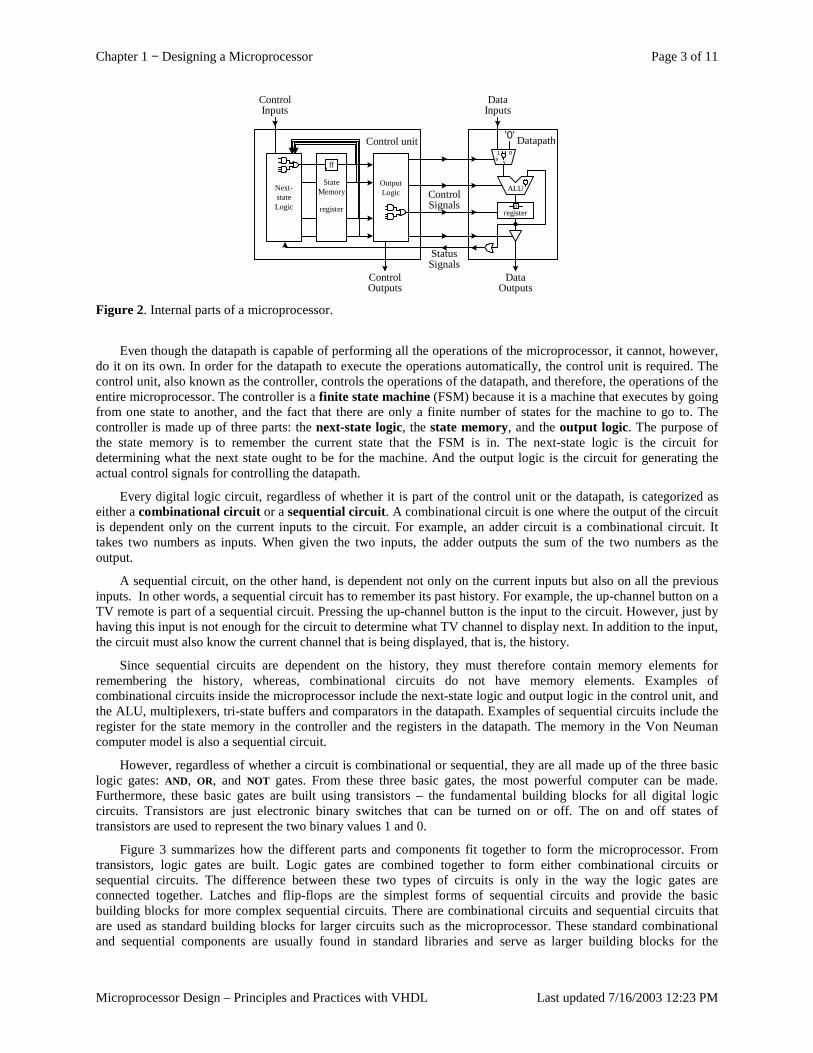
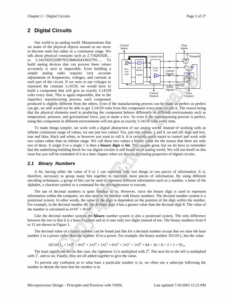
The circuit for the microprocessor can be divided into two parts: the datapath and the control unit as shown in Figure 1 and Figure 2. The datapath is responsible for the actual execution of all operations performed by the microprocessor such as the addition inside the arithmetic logic unit (ALU). The datapath also includes the registers for the temporary storage of your data. The functional units inside the datapath (ALU, shifter, counter, etc.) and the registers are connected together with multiplexers and buses to form one unit, the datapath.
Input
CPU
Memory
OutputControl
Unit Datapath
Figure 1. Von Neuman model of a computer.
Chapter 1 − Designing a Microprocessor Page 3 of 11
Microprocessor Design – Principles and Practices with VHDL Last updated 7/16/2003 12:23 PM
Even though the datapath is capable of performing all the operations of the microprocessor, it cannot, however, do it on its own. In order for the datapath to execute the operations automatically, the control unit is required. The control unit, also known as the controller, controls the operations of the datapath, and therefore, the operations of the entire microprocessor. The controller is a finite state machine (FSM) because it is a machine that executes by going from one state to another, and the fact that there are only a finite number of states for the machine to go to. The controller is made up of three parts: the next-state logic, the state memory, and the output logic. The purpose of the state memory is to remember the current state that the FSM is in. The next-state logic is the circuit for determining what the next state ought to be for the machine. And the output logic is the circuit for generating the actual control signals for controlling the datapath.
Every digital logic circuit, regardless of whether it is part of the control unit or the datapath, is categorized as either a combinational circuit or a sequential circuit. A combinational circuit is one where the output of the circuit is dependent only on the current inputs to the circuit. For example, an adder circuit is a combinational circuit. It takes two numbers as inputs. When given the two inputs, the adder outputs the sum of the two numbers as the output.
A sequential circuit, on the other hand, is dependent not only on the current inputs but also on all the previous inputs. In other words, a sequential circuit has to remember its past history. For example, the up-channel button on a TV remote is part of a sequential circuit. Pressing the up-channel button is the input to the circuit. However, just by having this input is not enough for the circuit to determine what TV channel to display next. In addition to the input, the circuit must also know the current channel that is being displayed, that is, the history.
Since sequential circuits are dependent on the history, they must therefore contain memory elements for remembering the history, whereas, combinational circuits do not have memory elements. Examples of combinational circuits inside the microprocessor include the next-state logic and output logic in the control unit, and the ALU, multiplexers, tri-state buffers and comparators in the datapath. Examples of sequential circuits include the register for the state memory in the controller and the registers in the datapath. The memory in the Von Neuman computer model is also a sequential circuit.
However, regardless of whether a circuit is combinational or sequential, they are all made up of the three basic logic gates: AND, OR, and NOT gates. From these three basic gates, the most powerful computer can be made. Furthermore, these basic gates are built using transistors – the fundamental building blocks for all digital logic circuits. Transistors are just electronic binary switches that can be turned on or off. The on and off states of transistors are used to represent the two binary values 1 and 0.
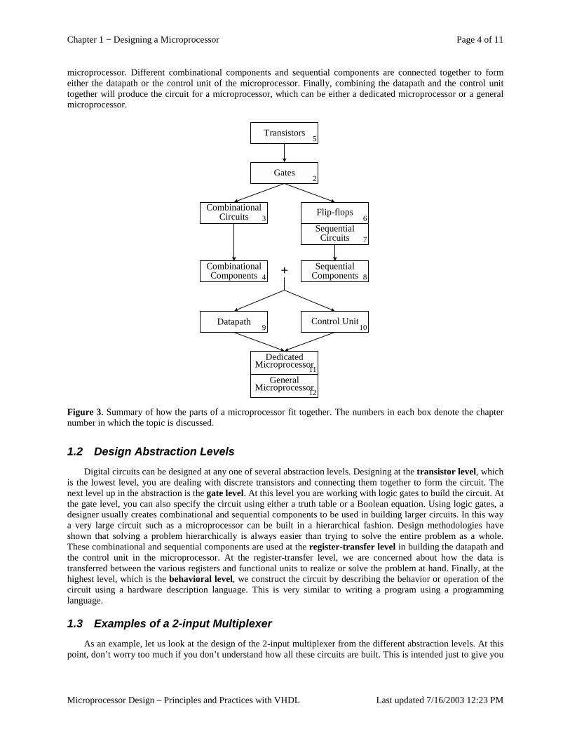
Figure 3 summarizes how the different parts and components fit together to form the microprocessor. From transistors, logic gates are built. Logic gates are combined together to form either combinational circuits or sequential circuits. The difference between these two types of circuits is only in the way the logic gates are connected together. Latches and flip-flops are the simplest forms of sequential circuits and provide the basic building blocks for more complex sequential circuits. There are combinational circuits and sequential circuits that are used as standard building blocks for larger circuits such as the microprocessor. These standard combinational and sequential components are usually found in standard libraries and serve as larger building blocks for the
ControlSignals
StatusSignals
01s y
'0'
DataInputs
DataOutputs
Datapath
ALU
registerff
OutputLogicNext-
stateLogic
ControlInputs
ControlOutputs
StateMemory
register
Control unit
ff
Figure 2. Internal parts of a microprocessor.
Chapter 1 − Designing a Microprocessor Page 4 of 11
Microprocessor Design – Principles and Practices with VHDL Last updated 7/16/2003 12:23 PM
microprocessor. Different combinational components and sequential components are connected together to form either the datapath or the control unit of the microprocessor. Finally, combining the datapath and the control unit together will produce the circuit for a microprocessor, which can be either a dedicated microprocessor or a general microprocessor.
CombinationalCircuits Flip-flops
SequentialComponents
CombinationalComponents
Datapath Control Unit
Gates
Transistors
+
5
2
3
4
6
8
9 10
11Dedicated
Microprocessor
12General
Microprocessor
SequentialCircuits 7
Figure 3. Summary of how the parts of a microprocessor fit together. The numbers in each box denote the chapter number in which the topic is discussed.
1.2 Design Abstraction Levels Digital circuits can be designed at any one of several abstraction levels. Designing at the transistor level, which
is the lowest level, you are dealing with discrete transistors and connecting them together to form the circuit. The next level up in the abstraction is the gate level. At this level you are working with logic gates to build the circuit. At the gate level, you can also specify the circuit using either a truth table or a Boolean equation. Using logic gates, a designer usually creates combinational and sequential components to be used in building larger circuits. In this way a very large circuit such as a microprocessor can be built in a hierarchical fashion. Design methodologies have shown that solving a problem hierarchically is always easier than trying to solve the entire problem as a whole. These combinational and sequential components are used at the register-transfer level in building the datapath and the control unit in the microprocessor. At the register-transfer level, we are concerned about how the data is transferred between the various registers and functional units to realize or solve the problem at hand. Finally, at the highest level, which is the behavioral level, we construct the circuit by describing the behavior or operation of the circuit using a hardware description language. This is very similar to writing a program using a programming language.
1.3 Examples of a 2-input Multiplexer As an example, let us look at the design of the 2-input multiplexer from the different abstraction levels. At this
point, don’t worry too much if you don’t understand how all these circuits are built. This is intended just to give you
Chapter 1 − Designing a Microprocessor Page 5 of 11
Microprocessor Design – Principles and Practices with VHDL Last updated 7/16/2003 12:23 PM
an idea of what the description of the circuits look like at the different abstraction levels. We will get to the details in the rest of the book.
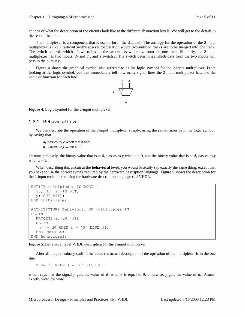
The multiplexer is a component that is used a lot in the datapath. The analogy for the operation of the 2-input multiplexer is like a railroad switch at a railroad station where two railroad tracks are to be merged into one track. The switch controls which of two trains on the two tracks will move onto the one track. Similarly, the 2-input multiplexer has two inputs, d0 and d1, and a switch s. The switch determines which data from the two inputs will pass to the output y.
Figure 4 shows the graphical symbol also referred to as the logic symbol for the 2-input multiplexer. From looking at the logic symbol, you can immediately tell how many signal lines the 2-input multiplexer has, and the name or function for each line.
y
d1 d0
s 01
Figure 4. Logic symbol for the 2-input multiplexer.
1.3.1 Behavioral Level
We can describe the operation of the 2-input multiplexer simply, using the same names as in the logic symbol, by saying that
d0 passes to y when s = 0 and d1 passes to y when s = 1
Or more precisely, the binary value that is at d0 passes to y when s = 0, and the binary value that is at d1 passes to y when s = 1.
When describing this circuit at the behavioral level, you would basically say exactly the same thing, except that you have to use the correct syntax required by the hardware description language. Figure 5 shows the description for the 2-input multiplexer using the hardware description language call VHDL.
ENTITY multiplexer IS PORT (d0, d1, s: IN BIT;y: OUT BIT);
END multiplexer;
ARCHITECTURE Behavioral OF multiplexer ISBEGIN
PROCESS(s, d0, d1)BEGINy <= d0 WHEN s = '0' ELSE d1;
END PROCESS;END Behavioral;
Figure 5. Behavioral level VHDL description for the 2-input multiplexer.
After all the preliminary stuff in the code, the actual description of the operation of the multiplexer is in the one line
y <= d0 WHEN s = '0' ELSE d1;
which says that the signal y gets the value of d0 when s is equal to 0, otherwise, y gets the value of d1. Almost exactly word for word!
Chapter 1 − Designing a Microprocessor Page 6 of 11
Microprocessor Design – Principles and Practices with VHDL Last updated 7/16/2003 12:23 PM
1.3.2 Gate Level
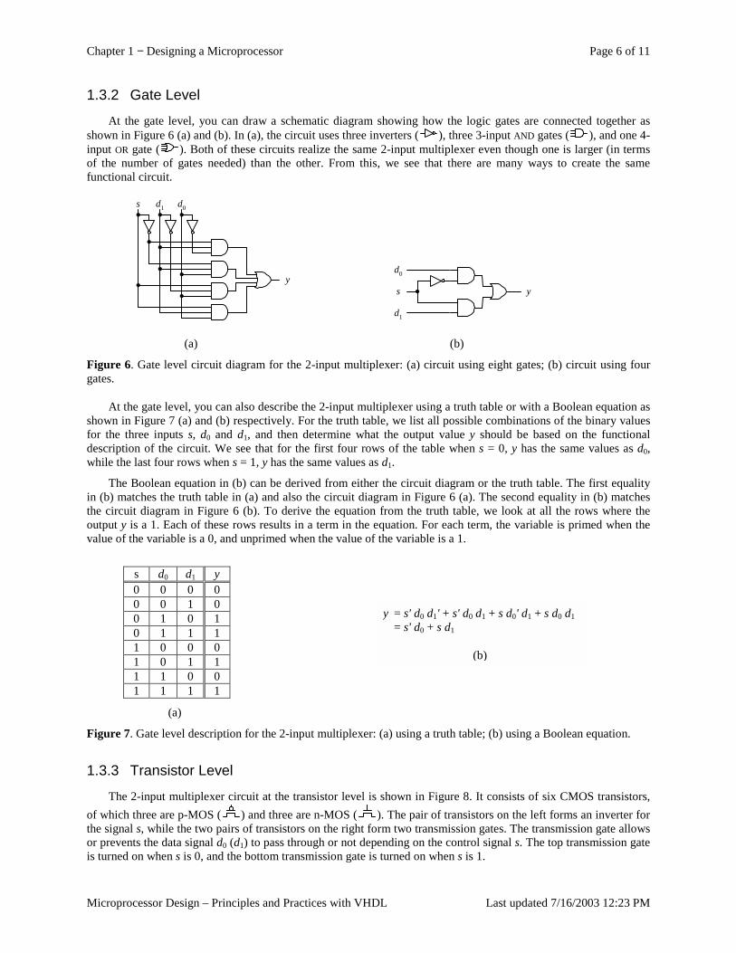
At the gate level, you can draw a schematic diagram showing how the logic gates are connected together as shown in Figure 6 (a) and (b). In (a), the circuit uses three inverters ( ), three 3-input AND gates ( ), and one 4-input OR gate ( ). Both of these circuits realize the same 2-input multiplexer even though one is larger (in terms of the number of gates needed) than the other. From this, we see that there are many ways to create the same functional circuit.
d0d1s
y
d0
d1
s y
(a) (b)
Figure 6. Gate level circuit diagram for the 2-input multiplexer: (a) circuit using eight gates; (b) circuit using four gates.
At the gate level, you can also describe the 2-input multiplexer using a truth table or with a Boolean equation as shown in Figure 7 (a) and (b) respectively. For the truth table, we list all possible combinations of the binary values for the three inputs s, d0 and d1, and then determine what the output value y should be based on the functional description of the circuit. We see that for the first four rows of the table when s = 0, y has the same values as d0, while the last four rows when s = 1, y has the same values as d1.
The Boolean equation in (b) can be derived from either the circuit diagram or the truth table. The first equality in (b) matches the truth table in (a) and also the circuit diagram in Figure 6 (a). The second equality in (b) matches the circuit diagram in Figure 6 (b). To derive the equation from the truth table, we look at all the rows where the output y is a 1. Each of these rows results in a term in the equation. For each term, the variable is primed when the value of the variable is a 0, and unprimed when the value of the variable is a 1.
s d0 d1 y 0 0 0 0 0 0 1 0 0 1 0 1 0 1 1 1 1 0 0 0 1 0 1 1 1 1 0 0 1 1 1 1
(a)
Figure 7. Gate level description for the 2-input multiplexer: (a) using a truth table; (b) using a Boolean equation.
1.3.3 Transistor Level
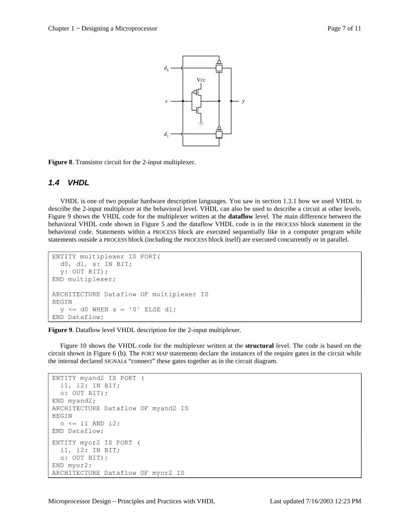
The 2-input multiplexer circuit at the transistor level is shown in Figure 8. It consists of six CMOS transistors, of which three are p-MOS ( ) and three are n-MOS ( ). The pair of transistors on the left forms an inverter for the signal s, while the two pairs of transistors on the right form two transmission gates. The transmission gate allows or prevents the data signal d0 (d1) to pass through or not depending on the control signal s. The top transmission gate is turned on when s is 0, and the bottom transmission gate is turned on when s is 1.
y = s' d0 d1' + s' d0 d1 + s d0' d1 + s d0 d1 = s' d0 + s d1
(b)
Chapter 1 − Designing a Microprocessor Page 7 of 11
Microprocessor Design – Principles and Practices with VHDL Last updated 7/16/2003 12:23 PM
Vcc
s y
d0
d1
Figure 8. Transistor circuit for the 2-input multiplexer.
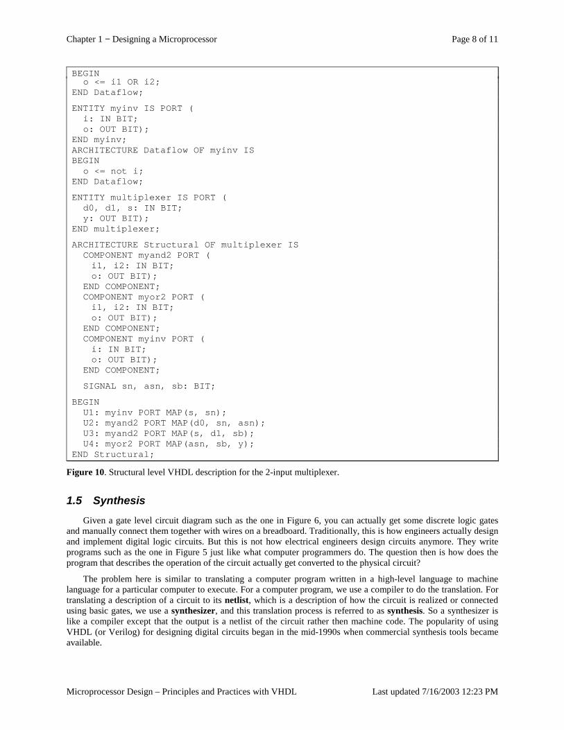
1.4 VHDL
VHDL is one of two popular hardware description languages. You saw in section 1.3.1 how we used VHDL to describe the 2-input multiplexer at the behavioral level. VHDL can also be used to describe a circuit at other levels. Figure 9 shows the VHDL code for the multiplexer written at the dataflow level. The main difference between the behavioral VHDL code shown in Figure 5 and the dataflow VHDL code is in the PROCESS block statement in the behavioral code. Statements within a PROCESS block are executed sequentially like in a computer program while statements outside a PROCESS block (including the PROCESS block itself) are executed concurrently or in parallel.
ENTITY multiplexer IS PORT(d0, d1, s: IN BIT;y: OUT BIT);
END multiplexer;
ARCHITECTURE Dataflow OF multiplexer ISBEGIN
y <= d0 WHEN s = '0' ELSE d1;END Dataflow;
Figure 9. Dataflow level VHDL description for the 2-input multiplexer.
Figure 10 shows the VHDL code for the multiplexer written at the structural level. The code is based on the circuit shown in Figure 6 (b). The PORT MAP statements declare the instances of the require gates in the circuit while the internal declared SIGNALs “connect” these gates together as in the circuit diagram.
ENTITY myand2 IS PORT (i1, i2: IN BIT;o: OUT BIT);
END myand2;ARCHITECTURE Dataflow OF myand2 ISBEGIN
o <= i1 AND i2;END Dataflow;
ENTITY myor2 IS PORT (i1, i2: IN BIT;o: OUT BIT);
END myor2;ARCHITECTURE Dataflow OF myor2 IS
Chapter 1 − Designing a Microprocessor Page 8 of 11
Microprocessor Design – Principles and Practices with VHDL Last updated 7/16/2003 12:23 PM
BEGINo <= i1 OR i2;
END Dataflow;
ENTITY myinv IS PORT (i: IN BIT;o: OUT BIT);
END myinv;ARCHITECTURE Dataflow OF myinv ISBEGIN
o <= not i;END Dataflow;
ENTITY multiplexer IS PORT (d0, d1, s: IN BIT;y: OUT BIT);
END multiplexer;
ARCHITECTURE Structural OF multiplexer ISCOMPONENT myand2 PORT (i1, i2: IN BIT;o: OUT BIT);
END COMPONENT;COMPONENT myor2 PORT (i1, i2: IN BIT;o: OUT BIT);
END COMPONENT;COMPONENT myinv PORT (i: IN BIT;o: OUT BIT);
END COMPONENT;
SIGNAL sn, asn, sb: BIT;
BEGINU1: myinv PORT MAP(s, sn);U2: myand2 PORT MAP(d0, sn, asn);U3: myand2 PORT MAP(s, d1, sb);U4: myor2 PORT MAP(asn, sb, y);
END Structural;
Figure 10. Structural level VHDL description for the 2-input multiplexer.
1.5 Synthesis Given a gate level circuit diagram such as the one in Figure 6, you can actually get some discrete logic gates
and manually connect them together with wires on a breadboard. Traditionally, this is how engineers actually design and implement digital logic circuits. But this is not how electrical engineers design circuits anymore. They write programs such as the one in Figure 5 just like what computer programmers do. The question then is how does the program that describes the operation of the circuit actually get converted to the physical circuit?
The problem here is similar to translating a computer program written in a high-level language to machine language for a particular computer to execute. For a computer program, we use a compiler to do the translation. For translating a description of a circuit to its netlist, which is a description of how the circuit is realized or connected using basic gates, we use a synthesizer, and this translation process is referred to as synthesis. So a synthesizer is like a compiler except that the output is a netlist of the circuit rather then machine code. The popularity of using VHDL (or Verilog) for designing digital circuits began in the mid-1990s when commercial synthesis tools became available.

Chapter 1 − Designing a Microprocessor Page 9 of 11
Microprocessor Design – Principles and Practices with VHDL Last updated 7/16/2003 12:23 PM
Furthermore, the netlist from the output of the synthesizer can be used directly to implement the actual circuit in a field programmable gate array (FPGA) chip. With this final step, the creation of a digital circuit fully implemented in an IC can be easily done. Appendix B gives a tutorial of the complete process from writing the VHDL code to synthesizing the circuit and uploading the netlist to the FPGA chip using Altera’s development system.
1.6 Going Forward We will now embark on a journey that will take you through from the transistor to the building of the
microprocessor and the computer. Figure 2 will serve as our guide and map. If you get lost on the way and don’t know where a particular component fits in the overall picture, just refer to this map. At the beginning of each chapter, I will refresh your memory with this map and highlighting the components in the map that the chapter will cover.
Figure 11 is an actual picture of the circuitry inside the Intel P4 CPU. When you reach the end of this book, may be you still would not be able to design this circuit for the P4, but you will certainly have the knowledge of how a microprocessor is designed because you will actually have designed and implemented a working microprocessor.
Figure 11. The internal circuitry of the Intel P4 CPU.
1.7 Summary Checklist � Microprocessor � Datapath � Control unit � Finite state machine (FSM) � Next-state logic � State memory � Output logic � Combinational circuit � Sequential circuit � Transistor level design � Gate level design � Register-transfer level design � Behavioral level design � Logic symbol

Chapter 1 − Designing a Microprocessor Page 10 of 11
Microprocessor Design – Principles and Practices with VHDL Last updated 7/16/2003 12:23 PM
� VHDL � Synthesis � Netlist
Chapter 1 − Designing a Microprocessor Page 11 of 11
Microprocessor Design – Principles and Practices with VHDL Last updated 7/16/2003 12:23 PM
Index
A
Abstraction level. See Design abstraction levels.
B
Behavioral level (VHDL), 5 See also Design abstraction levels. .
C
Combinational circuit, 3 Control unit. See Finite state machine.
D
Dataflow level (VHDL), 8 See also Design abstraction levels.
Datapath, 2 Design abstraction levels, 5
behavioral level, 5 gate level, 5 register-transfer level, 5 RTL. See Register-transfer level. transistor level, 5
F
Field programmable gate array, 9 Finite state machine, 3 FPGA. See Field programmable gate array. FSM. See Finite state machine.
G
Gate, 3 Gate level, 5, 6
See also Design abstraction levels.
L
Logic gate, 3 Logic symbol, 5
M
Microprocessor, 2
N
Netlist, 9 Next-state logic, 3
See also Finite state machine.
O
Output logic, 3 See also Finite state machine.
R
Register-transfer level, 5 See also Design abstraction levels.
RTL. See Register-transfer level.
S
Sequential circuit, 3 State memory, 3
See also Finite state machine. Structural level (VHDL), 8
See also Design abstraction levels. Synthesis, 9 Synthesizer, 9
T
Transistor, 3 Transistor level, 5, 7
See also Design abstraction levels.
V
VHDL, 7 behavioral level, 6 dataflow level, 8 structural level, 9
Chapter 2 − Digital Circuits Page 1 of 27
Microprocessor Design – Principles and Practices with VHDL Last updated 7/16/2003 12:25 PM
Table of Content Table of Content ........................................................................................................................................................... 1 2 Digital Circuits...................................................................................................................................................... 2
2.1 Binary Numbers ........................................................................................................................................... 2 2.2 Binary Switch................................................................................................................................................ 4 2.3 Basic Logic Operators and Logic Expressions.............................................................................................. 5 2.4 Truth Tables .................................................................................................................................................. 6 2.5 Boolean Algebra and Boolean Function ....................................................................................................... 6
2.5.1 Boolean Algebra.................................................................................................................................... 6 2.5.2 Duality Principle ................................................................................................................................... 8 2.5.3 Boolean Function and the Inverse ......................................................................................................... 9
2.6 Minterms and Maxterms ............................................................................................................................. 12 2.6.1 Minterms ............................................................................................................................................. 12 2.6.2 Maxterms ............................................................................................................................................ 13
2.7 Canonical, Standard, and non-Standard Forms ........................................................................................... 15 2.8 Logic Gates and Circuit Diagrams .............................................................................................................. 15 2.9 Example: Designing a Car Security System................................................................................................ 17 2.10 Introduction to VHDL................................................................................................................................. 19
2.10.1 VHDL code for a 2-input NAND gate .................................................................................................. 19 2.10.2 VHDL code for a 3-input NOR gate ..................................................................................................... 20 2.10.3 VHDL code for a function .................................................................................................................. 21
2.11 Summary Checklist ..................................................................................................................................... 21 2.12 Exercises ..................................................................................................................................................... 23
Index ........................................................................................................................................................................... 26
Chapter 2 − Digital Circuits Page 2 of 27
Microprocessor Design – Principles and Practices with VHDL Last updated 7/16/2003 12:25 PM
ControlSignals
StatusSignals
01s y
'0'
DataInputs
DataOutputs
Datapath
ALU
registerff
OutputLogicNext-
stateLogic
ControlInputs
ControlOutputs
StateMemory
register
Control unit
ff
2 Digital Circuits
Our world is an analog world. Measurements that we make of the physical objects around us are never in discrete units but rather in a continuous range. We talk about physical constants such as 2.718281828… or 3.1415926535897932384626433832795…. To build analog devices that can process these values accurately is next to impossible. Even building a simple analog radio requires very accurate adjustments of frequencies, voltages, and currents at each part of the circuit. If we were to use voltages to represent the constant 3.14159, we would have to build a component that will give us exactly 3.14159 volts every time. This is again impossible; due to the imperfect manufacturing process, each component produced is slightly different from the others. Even if the manufacturing process can be made as perfect as perfect can get, we still would not be able to get 3.14159 volts from this component every time we use it. The reason being that the physical elements used in producing the component behave differently in different environments such as temperature, pressure, and gravitational force, just to name a few. So even if the manufacturing process is perfect, using this component in different environments will not give us exactly 3.14159 volts every time.
To make things simpler, we work with a digital abstraction of our analog world. Instead of working with an infinite continuous range of values, we use just two values! Yes, just two values: 1 and 0, on and off, high and low, true and false, black and white, or however you want to call it. It is certainly much easier to control and work with two values rather than an infinite range. We call these two values a binary value for the reason that there are only two of them. A single 0 or a single 1 is then a binary digit or bit. This sounds great, but we do have to remember that the underlining building block for our digital circuits is still based on an analog world. We will not dwell on this issue but you will be reminded of it in a later chapter when we discuss the analog properties of digital circuits.
2.1 Binary Numbers A bit, having either the value of 0 or 1 can represent only two things or two pieces of information. It is,
therefore, necessary to group many bits together to represent more pieces of information. By using different encoding techniques, a group of bits can be used to represent different information such as a number, a letter of the alphabet, a character symbol or a command for the microprocessor to execute.
The use of decimal numbers is quite familiar to us. However, since the binary digit is used to represent information within the computer, we also need to be familiar with binary numbers. The decimal number system is a positional system. In other words, the value of the digit is dependent on the position of the digit within the number. For example, in the decimal number 48, the decimal digit 4 has a greater value than the decimal digit 8. The value of the number is calculated as 4×101 + 8×100.
Like the decimal number system, the binary number system is also a positional system. The only difference between the two is that it is a base-2 system and so it uses only two digits instead of ten. The binary numbers from 0 to 15 are shown in Figure 1.
The decimal value of a binary number can be found just like for a decimal number except that we raise the base number 2 to a power rather than the number 10 to a power. For example, the binary number 10110112 has the value
10110112 = 1×26 + 0×25 + 1×24 + 1×23 + 0×22 + 1×21 + 1×20 = 64 + 16 + 8 + 2 + 1 = 9110
The least significant bit (in this case, the rightmost 1) is multiplied with 20. The next bit to the left is multiplied with 21, and so on. Finally, they are all added together to give the value.
To prevent any confusion as to what base a particular number is in, we often use a subscript following the number to denote the base that the number is in.
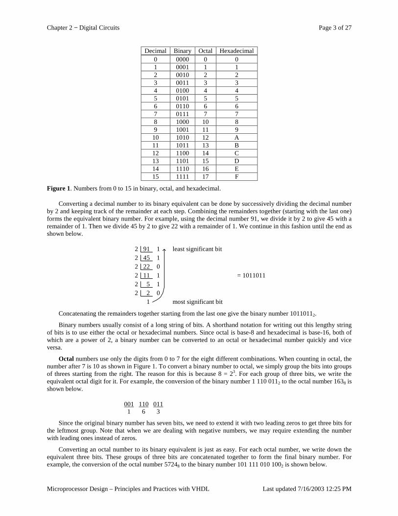
Chapter 2 − Digital Circuits Page 3 of 27
Microprocessor Design – Principles and Practices with VHDL Last updated 7/16/2003 12:25 PM
Decimal Binary Octal Hexadecimal 0 0000 0 0 1 0001 1 1 2 0010 2 2 3 0011 3 3 4 0100 4 4 5 0101 5 5 6 0110 6 6 7 0111 7 7 8 1000 10 8 9 1001 11 9
10 1010 12 A 11 1011 13 B 12 1100 14 C 13 1101 15 D 14 1110 16 E 15 1111 17 F
Figure 1. Numbers from 0 to 15 in binary, octal, and hexadecimal.
Converting a decimal number to its binary equivalent can be done by successively dividing the decimal number by 2 and keeping track of the remainder at each step. Combining the remainders together (starting with the last one) forms the equivalent binary number. For example, using the decimal number 91, we divide it by 2 to give 45 with a remainder of 1. Then we divide 45 by 2 to give 22 with a remainder of 1. We continue in this fashion until the end as shown below.
91245
12
221
211
02
51
22
12
10
most significant bit
least significant bit
= 1011011
Concatenating the remainders together starting from the last one give the binary number 10110112.
Binary numbers usually consist of a long string of bits. A shorthand notation for writing out this lengthy string of bits is to use either the octal or hexadecimal numbers. Since octal is base-8 and hexadecimal is base-16, both of which are a power of 2, a binary number can be converted to an octal or hexadecimal number quickly and vice versa.
Octal numbers use only the digits from 0 to 7 for the eight different combinations. When counting in octal, the number after 7 is 10 as shown in Figure 1. To convert a binary number to octal, we simply group the bits into groups of threes starting from the right. The reason for this is because 8 = 23. For each group of three bits, we write the equivalent octal digit for it. For example, the conversion of the binary number 1 110 0112 to the octal number 1638 is shown below.
001 110 011 1 6 3
Since the original binary number has seven bits, we need to extend it with two leading zeros to get three bits for the leftmost group. Note that when we are dealing with negative numbers, we may require extending the number with leading ones instead of zeros.
Converting an octal number to its binary equivalent is just as easy. For each octal number, we write down the equivalent three bits. These groups of three bits are concatenated together to form the final binary number. For example, the conversion of the octal number 57248 to the binary number 101 111 010 1002 is shown below.
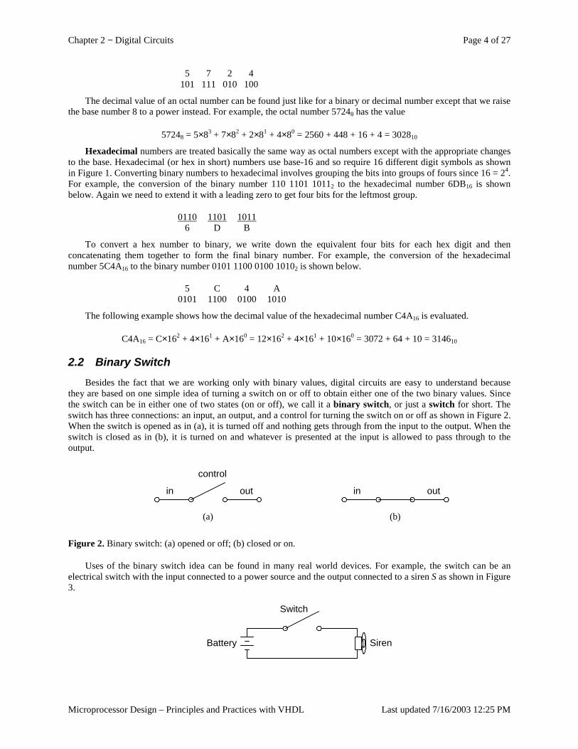
Chapter 2 − Digital Circuits Page 4 of 27
Microprocessor Design – Principles and Practices with VHDL Last updated 7/16/2003 12:25 PM
5 7 2 4 101 111 010 100
The decimal value of an octal number can be found just like for a binary or decimal number except that we raise the base number 8 to a power instead. For example, the octal number 57248 has the value
57248 = 5×83 + 7×82 + 2×81 + 4×80 = 2560 + 448 + 16 + 4 = 302810
Hexadecimal numbers are treated basically the same way as octal numbers except with the appropriate changes to the base. Hexadecimal (or hex in short) numbers use base-16 and so require 16 different digit symbols as shown in Figure 1. Converting binary numbers to hexadecimal involves grouping the bits into groups of fours since 16 = 24. For example, the conversion of the binary number 110 1101 10112 to the hexadecimal number 6DB16 is shown below. Again we need to extend it with a leading zero to get four bits for the leftmost group.
0110 1101 1011 6 D B
To convert a hex number to binary, we write down the equivalent four bits for each hex digit and then concatenating them together to form the final binary number. For example, the conversion of the hexadecimal number 5C4A16 to the binary number 0101 1100 0100 10102 is shown below.
5 C 4 A 0101 1100 0100 1010
The following example shows how the decimal value of the hexadecimal number C4A16 is evaluated.
C4A16 = C×162 + 4×161 + A×160 = 12×162 + 4×161 + 10×160 = 3072 + 64 + 10 = 314610
2.2 Binary Switch Besides the fact that we are working only with binary values, digital circuits are easy to understand because
they are based on one simple idea of turning a switch on or off to obtain either one of the two binary values. Since the switch can be in either one of two states (on or off), we call it a binary switch, or just a switch for short. The switch has three connections: an input, an output, and a control for turning the switch on or off as shown in Figure 2. When the switch is opened as in (a), it is turned off and nothing gets through from the input to the output. When the switch is closed as in (b), it is turned on and whatever is presented at the input is allowed to pass through to the output.
in out in out
(a) (b)
control
Figure 2. Binary switch: (a) opened or off; (b) closed or on.
Uses of the binary switch idea can be found in many real world devices. For example, the switch can be an electrical switch with the input connected to a power source and the output connected to a siren S as shown in Figure 3.
Battery Siren
Switch
Chapter 2 − Digital Circuits Page 5 of 27
Microprocessor Design – Principles and Practices with VHDL Last updated 7/16/2003 12:25 PM
Figure 3. A siren controlled by a switch.
When the switch is closed, the siren turns on. The usual convention is to use a 1 to mean “on” and a 0 to mean “off”. Thus, when the switch is closed the output is a 1 and the siren will turn on. We can also use a variable, say x, to denote the state of the switch. We can let x = 1 to mean the switch is closed and x = 0 to mean the switch is opened. Using this convention, we can describe the state of the siren S in terms of the variable x using a simple logic expression. Since S = 1 if x = 1 and S = 0 if x = 0, we can write
S = x
This logic expression describes the output S in terms of the input variable x.
2.3 Basic Logic Operators and Logic Expressions Two binary switches can be connected together either in series or in parallel as shown in Figure 4.
(b)
F
(a)
F
x
y
yx
Figure 4. Connection of two binary switches: (a) in series; (b) in parallel.
If two switches are connected in series as in (a), then both switches have to be on in order for the output F to be a 1. In other words, F = 1 if x = 1 AND y = 1. If either x or y is off, or both are off then F = 0. Translating this into a logic expression, we get
F = x AND y
Hence, two switches connected in series give rise to the logical AND operator. In a Boolean function (which we will explain in more detail in section 2.5) the AND operator is either denoted with a dot ( • ) or no symbol at all. Thus we can rewrite the above expression as
F = x • y
or simply F = xy
If we connect two switches in parallel as in (b), then only one switch needs to be on in order for the output F to be a 1. In other words, F = 1 if x = 1 OR y = 1. F = 0 only if both x and y are off. Translating this into a logic expression, we get
F = x OR y
and this gives rise to the logical OR operator. In a Boolean function, the OR operator is denoted with a plus symbol ( + ). Thus we can rewrite the above expression as
F = x + y
In addition to the AND and OR operators, there is another basic logic operator – the NOT operator, also known as the INVERTER. Whereas, the AND and OR operators have multiple inputs, the NOT operator has only one input and one output. The NOT operator simply inverts its input, so a 0 input will produce a 1 output, and a 1 becomes a 0. In a Boolean function, the NOT operator is either denoted with an apostrophe symbol ( ' ) or a bar on top ( ) as in
F = x' or
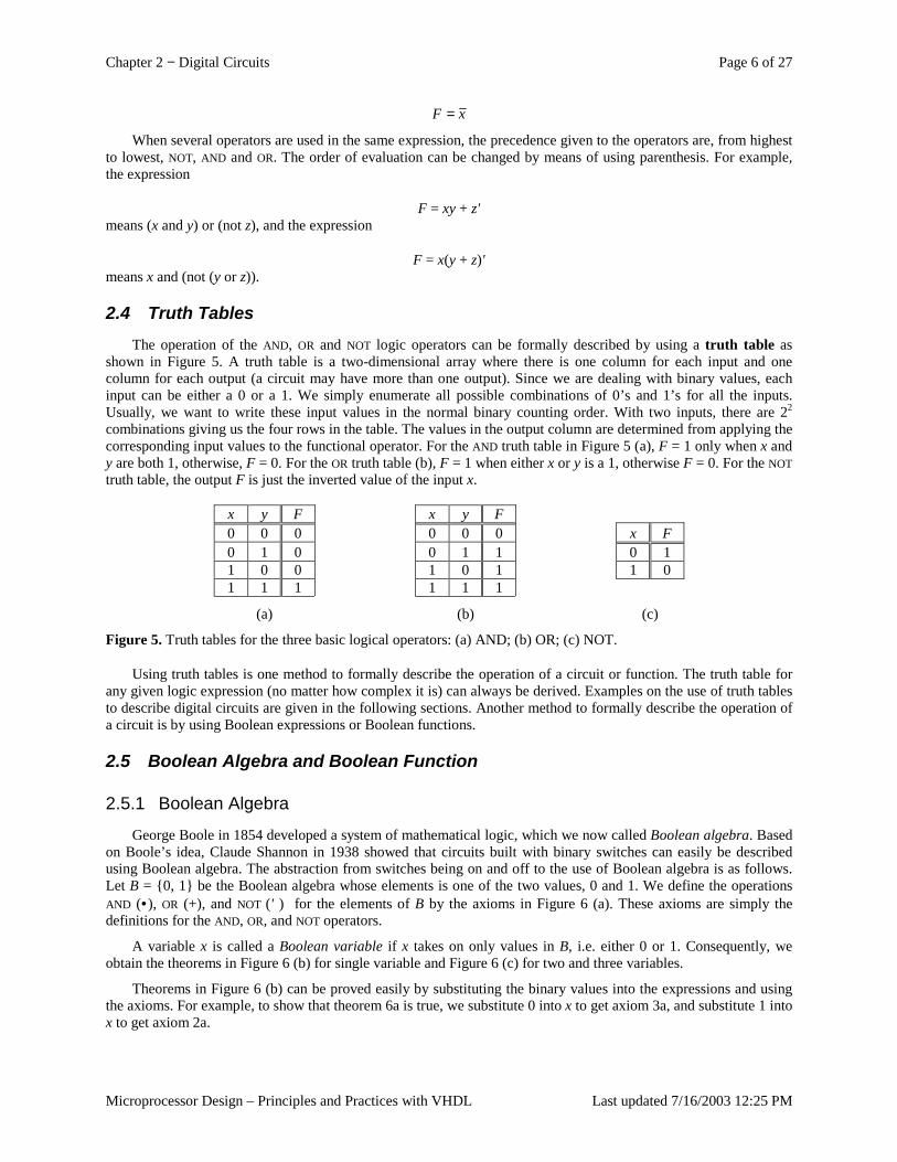
Chapter 2 − Digital Circuits Page 6 of 27
Microprocessor Design – Principles and Practices with VHDL Last updated 7/16/2003 12:25 PM
xF =
When several operators are used in the same expression, the precedence given to the operators are, from highest to lowest, NOT, AND and OR. The order of evaluation can be changed by means of using parenthesis. For example, the expression
F = xy + z' means (x and y) or (not z), and the expression
F = x(y + z)' means x and (not (y or z)).
2.4 Truth Tables The operation of the AND, OR and NOT logic operators can be formally described by using a truth table as
shown in Figure 5. A truth table is a two-dimensional array where there is one column for each input and one column for each output (a circuit may have more than one output). Since we are dealing with binary values, each input can be either a 0 or a 1. We simply enumerate all possible combinations of 0’s and 1’s for all the inputs. Usually, we want to write these input values in the normal binary counting order. With two inputs, there are 22 combinations giving us the four rows in the table. The values in the output column are determined from applying the corresponding input values to the functional operator. For the AND truth table in Figure 5 (a), F = 1 only when x and y are both 1, otherwise, F = 0. For the OR truth table (b), F = 1 when either x or y is a 1, otherwise F = 0. For the NOT truth table, the output F is just the inverted value of the input x.
x y F x y F 0 0 0 0 0 0 x F 0 1 0 0 1 1 0 1 1 0 0 1 0 1 1 0 1 1 1 1 1 1
(a) (b) (c)
Figure 5. Truth tables for the three basic logical operators: (a) AND; (b) OR; (c) NOT.
Using truth tables is one method to formally describe the operation of a circuit or function. The truth table for any given logic expression (no matter how complex it is) can always be derived. Examples on the use of truth tables to describe digital circuits are given in the following sections. Another method to formally describe the operation of a circuit is by using Boolean expressions or Boolean functions.
2.5 Boolean Algebra and Boolean Function
2.5.1 Boolean Algebra
George Boole in 1854 developed a system of mathematical logic, which we now called Boolean algebra. Based on Boole’s idea, Claude Shannon in 1938 showed that circuits built with binary switches can easily be described using Boolean algebra. The abstraction from switches being on and off to the use of Boolean algebra is as follows. Let B = {0, 1} be the Boolean algebra whose elements is one of the two values, 0 and 1. We define the operations AND (• ), OR (+), and NOT (' ) for the elements of B by the axioms in Figure 6 (a). These axioms are simply the definitions for the AND, OR, and NOT operators.
A variable x is called a Boolean variable if x takes on only values in B, i.e. either 0 or 1. Consequently, we obtain the theorems in Figure 6 (b) for single variable and Figure 6 (c) for two and three variables.
Theorems in Figure 6 (b) can be proved easily by substituting the binary values into the expressions and using the axioms. For example, to show that theorem 6a is true, we substitute 0 into x to get axiom 3a, and substitute 1 into x to get axiom 2a.
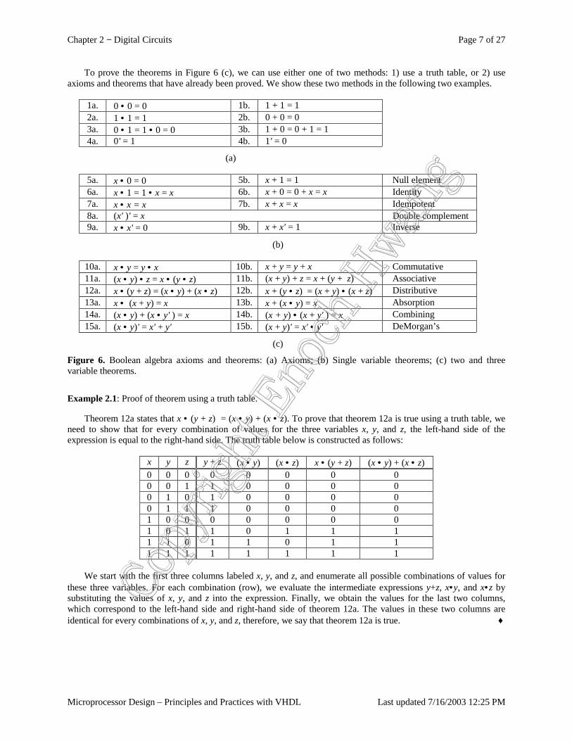
Chapter 2 − Digital Circuits Page 7 of 27
Microprocessor Design – Principles and Practices with VHDL Last updated 7/16/2003 12:25 PM
To prove the theorems in Figure 6 (c), we can use either one of two methods: 1) use a truth table, or 2) use axioms and theorems that have already been proved. We show these two methods in the following two examples.
1a. 0 • 0 = 0 1b. 1 + 1 = 1 2a. 1 • 1 = 1 2b. 0 + 0 = 0 3a. 0 • 1 = 1 • 0 = 0 3b. 1 + 0 = 0 + 1 = 1 4a. 0' = 1 4b. 1' = 0
(a)
5a. x • 0 = 0 5b. x + 1 = 1 Null element 6a. x • 1 = 1 • x = x 6b. x + 0 = 0 + x = x Identity 7a. x • x = x 7b. x + x = x Idempotent 8a. (x' )' = x Double complement 9a. x • x' = 0 9b. x + x' = 1 Inverse
(b)
10a. x • y = y • x 10b. x + y = y + x Commutative 11a. (x • y) • z = x • (y • z) 11b. (x + y) + z = x + (y + z) Associative 12a. x • (y + z) = (x • y) + (x • z) 12b. x + (y • z) = (x + y) • (x + z) Distributive 13a. x • (x + y) = x 13b. x + (x • y) = x Absorption 14a. (x • y) + (x • y' ) = x 14b. (x + y) • (x + y' ) = x Combining 15a. (x • y)' = x' + y' 15b. (x + y)' = x' • y' DeMorgan’s
(c)
Figure 6. Boolean algebra axioms and theorems: (a) Axioms; (b) Single variable theorems; (c) two and three variable theorems.
Example 2.1: Proof of theorem using a truth table.
Theorem 12a states that x • (y + z) = (x • y) + (x • z). To prove that theorem 12a is true using a truth table, we need to show that for every combination of values for the three variables x, y, and z, the left-hand side of the expression is equal to the right-hand side. The truth table below is constructed as follows:
x y z y + z (x • y) (x • z) x • (y + z) (x • y) + (x • z) 0 0 0 0 0 0 0 0 0 0 1 1 0 0 0 0 0 1 0 1 0 0 0 0 0 1 1 1 0 0 0 0 1 0 0 0 0 0 0 0 1 0 1 1 0 1 1 1 1 1 0 1 1 0 1 1 1 1 1 1 1 1 1 1
We start with the first three columns labeled x, y, and z, and enumerate all possible combinations of values for these three variables. For each combination (row), we evaluate the intermediate expressions y+z, x•y, and x• z by substituting the values of x, y, and z into the expression. Finally, we obtain the values for the last two columns, which correspond to the left-hand side and right-hand side of theorem 12a. The values in these two columns are identical for every combinations of x, y, and z, therefore, we say that theorem 12a is true. ♦

Chapter 2 − Digital Circuits Page 8 of 27
Microprocessor Design – Principles and Practices with VHDL Last updated 7/16/2003 12:25 PM
Example 2.2: Proof of theorem using axioms and theorems.
Theorem 13b states that x + (x • y) = x. To prove that theorem 13b is true using axioms and theorems, we can argue as follows:
x + (x • y) = (x • 1) + (x • y) by Identity Theorem 6a = x • (1 + y) by Distributive Theorem 12a = x • (1) by Null element Theorem 5b = x by Identity Theorem 6a ♦
Example 2.2 shows that some theorems can be derived from others that have already been proven with the truth table. Full treatment of Boolean algebra is beyond the scope of this book and can be found in the references. For our purposes, we simply assume that all the theorems are true and will just use them to show that two circuits are equivalent as depicted in the next two examples.
Example 2.3: Use Boolean algebra to reduce the equation F(x,y,z) = (x' + y' + x'y' + xy) (x' + yz) as much as possible.
F = (x' + y' + x'y' + xy) (x' + yz) = (x' • 1 + y' • 1 + x'y' + xy) (x' + yz) by Identity Theorem 6a = (x' (y + y' ) + y' (x + x' ) + x'y' + xy) (x' + yz) by Inverse Theorem 9b = (x'y + x'y' + y'x + y'x' + x'y' + xy) (x' + yz) by Distributive Theorem 12a = (x'y + x'y' + y'x + y'x' + x'y' + xy) (x' + yz) by Idempotent Theorem 7b = (x' (y + y') + x (y + y')) (x' + yz) by Distributive Theorem 12a = (x' • 1 + x • 1) (x' + yz) by Inverse Theorem 9b = (x' + x) (x' + yz) by Identity Theorem 6a = 1 (x' + yz) by Inverse Theorem 9b = (x' + yz) by Identity Theorem 6a
Since the expression (x' + y' + x'y' + xy) (x' + yz) reduces down to (x' + yz), therefore, we do want to implement the circuit for the latter expression rather then the former because the circuit size for the latter is much smaller. ♦
Example 2.4: Show using Boolean algebra that the two equations F1 = (xy' + x'y + x' + y' + z' ) (x + y' + z) and F2 = y' + x'z + xz' are equivalent.
F1 = (xy' + x'y + x' + y' + z' ) (x + y' + z) = xy'x + xy'y' + xy'z + x'yx + x'yy' + x'yz + x'x + x'y' + x'z + y'x + y'y' + y'z + z'x + z'y' + z'z = xy' + xy' + xy'z + 0 + 0 + x'yz + 0 + x'y' + x'z + xy' + y' + y'z + xz' + y'z' + 0 = xy' + xy'z + x'yz + x'y' + x'z + y' + y'z + xz' + y'z' = y'(x + xz + x' + 1 + z + z') + x'z(y + 1) + xz' = y' + x'z + xz' = F2 ♦
2.5.2 Duality Principle
Notice in Figure 6 that we have listed the axioms and theorems in pairs. Specifically, we define the dual of a logic expression as one that is obtained by changing all + operators with • operators, and vice versa, and by changing all 0’s with 1’s, and vice versa. For example, the dual of the logic expression
(xy'z) + (xyz') + (yz)
is (x'+y+z') • (x'+y'+z) • (y'+z')
The duality principle states that if a Boolean expression is true, then its dual is also true. Be careful that it does not say that a Boolean expression is equivalent to its dual. For example, theorem 5a in Figure 6 says that x • 0 = 0 is true, thus by the duality principle, its dual x + 1 = 1 is also true. However, 0 is definitely not equal to 1.
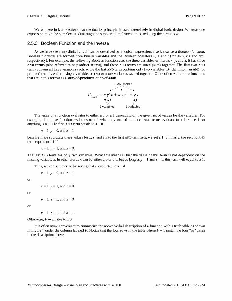
Chapter 2 − Digital Circuits Page 9 of 27
Microprocessor Design – Principles and Practices with VHDL Last updated 7/16/2003 12:25 PM
We will see in later sections that the duality principle is used extensively in digital logic design. Whereas one expression might be complex, its dual might be simpler to implement, thus, reducing the circuit size.
2.5.3 Boolean Function and the Inverse
As we have seen, any digital circuit can be described by a logical expression, also known as a Boolean function. Boolean functions are formed from binary variables and the Boolean operators • , + and ' (for AND, OR and NOT respectively). For example, the following Boolean function uses the three variables or literals x, y, and z. It has three AND terms (also referred to as product terms), and these AND terms are ORed (sum) together. The first two AND terms contain all three variables each, while the last AND term contains only two variables. By definition, an AND (or product) term is either a single variable, or two or more variables ANDed together. Quite often we refer to functions that are in this format as a sum-of-products or or-of-ands.
F(x,y,z) = x y' z + x y z' + y z
3 AND terms
3 variables 2 variables
The value of a function evaluates to either a 0 or a 1 depending on the given set of values for the variables. For example, the above function evaluates to a 1 when any one of the three AND terms evaluate to a 1, since 1 OR anything is a 1. The first AND term equals to a 1 if
x = 1, y = 0, and z = 1
because if we substitute these values for x, y, and z into the first AND term xy'z, we get a 1. Similarly, the second AND term equals to a 1 if
x = 1, y = 1, and z = 0.
The last AND term has only two variables. What this means is that the value of this term is not dependent on the missing variable x. In other words x can be either a 0 or a 1, but as long as y = 1 and z = 1, this term will equal to a 1.
Thus, we can summarize by saying that F evaluates to a 1 if
x = 1, y = 0, and z = 1
or
x = 1, y = 1, and z = 0
or
y = 1, z = 1, and x = 0
or
y = 1, z = 1, and x = 1.
Otherwise, F evaluates to a 0.
It is often more convenient to summarize the above verbal description of a function with a truth table as shown in Figure 7 under the column labeled F. Notice that the four rows in the table where F = 1 match the four “or” cases in the description above.

Chapter 2 − Digital Circuits Page 10 of 27
Microprocessor Design – Principles and Practices with VHDL Last updated 7/16/2003 12:25 PM
x y z F F' 0 0 0 0 1 0 0 1 0 1 0 1 0 0 1 0 1 1 1 0 1 0 0 0 1 1 0 1 1 0 1 1 0 1 0 1 1 1 1 0
Figure 7. Truth table for the function F = xy'z + xyz' + yz
The inverse of a function, denoted by F', can be easily obtained from the truth table for F by simply changing all the 0’s to 1’s and 1’s to 0’s as shown in the truth table in Figure 7 under the column labeled F'. Thus, we can write the Boolean function for F' in the sum-of-products format, where the AND terms are obtained from those rows where F' = 1. Thus, we get
F' = x'y'z' + x'y'z + x'yz' + xy'z'
To deduce F' algebraically from F requires the use of DeMorgan’s theorem (Theorem 15a) twice. For example, using the same function
F = xy'z + xyz' + yz
we obtain F' as follows
F' = (xy'z + xyz' + yz)' = (xy'z)' • (xyz')' • (yz)' = (x'+y+z' ) • (x'+y'+z) • (y'+z' )
There are three things to notice about this equation for F'. First, F' is just the dual of F as defined in section 2.5.2. Second, instead of being in a sum-of-products format, it is in a product-of-sums (and-of-ors) format where three OR terms (also referred to as sum terms) are ANDed together. Third, from the same original function F, we obtained two different equations for F'. From the truth table, we obtained
F' = x'y'z' + x'y'z + x'yz' + xy'z'
and from applying DeMorgan’s theorem to F, we obtained
F' = (x'+y+z' ) • (x'+y'+z) • (y'+z' )
So we must conclude that these two expressions, where one is in the sum-of-products format and the other is in the product-of-sums format, are equivalent. In general, all functions can be expressed in either the sum-of-products or product-of-sums format.
Thus, we should also be able to express the same function F = xy'z + xyz' + yz in the product-of-sums format. We can derive it using one of two methods. For method one, we can start with F' and apply DeMorgan’s theorem to it just like how we obtained F' from F.
F = F' ' = (x'y'z' + x'y'z + x'yz' + xy'z' )' = (x'y'z' )' • (x'y'z)' • (x'yz' )' • (xy'z' )' = (x+y+z) • (x+y+z' ) • (x+y'+z) • (x'+y+z)
For the second method, we start with the original F and convert it to the product-of-sums format using the Boolean theorems.
F = xy'z + xyz' + yz = (x+x+y) • (x+x+z) • (x+y+y) • (x+y+z) • (x+z'+y) • (x+z'+z) • by Theorem 12 (y'+x+y) • (y'+x+z) • (y'+y+y) • (y'+y+z) • (y'+z'+y) • (y'+z'+z) • (z+x+y) • (z+x+z) • (z+y+y) • (z+y+z) • (z+z'+y) • (z+z'+z) = (x+y) • (x+z) • (x+y) • (x+y+z) • (x+z'+y) • (y'+x+z) • (z+x+y) • (z+x) • (z+y) • (z+y) eliminate
Chapter 2 − Digital Circuits Page 11 of 27
Microprocessor Design – Principles and Practices with VHDL Last updated 7/16/2003 12:25 PM
= (x+y) • (x+z) • (x+y+z) • (x+y+z') • (x+y'+z) • (z+y) duplicates = (x+y+zz' ) • (x+yy'+z) • (x+y+z) • (x+y+z' ) • (x+y'+z) • (xx'+y+z) by Theorem 6b and 9a = (x+y+z) • (x+y+z') • (x+y+z) • (x+y'+z) • (x+y+z) • (x+y+z') • (x+y'+z) • (x+y+z) • (x'+y+z) = (x+y+z) • (x+y+z' ) • (x+y'+z) • (x'+y+z)
In the first step, we apply Theorem 12b (Distributive) to get every possible combination of sum terms. For example, the first sum term (x+x+y) is obtained from getting the first x from xy'z, the second x from xyz', and the y from yz. The second sum term (x+x+z) is obtained from getting the first x from xy'z, the second x from xyz', and the z from yz. This is repeated for all combinations. In this step, the sum terms such as (x+z'+z) where it contains variables of the form v + v' can be eliminated since v + v' = 1, and 1 • x = x.
In the second and third steps, duplicate variables and terms are eliminated.
In the fourth step, every sum term with a missing variable will have that variable added back in by using Theorems 6b and 9a which says that x + 0 = x and yy' = 0, therefore, x + yy' = x.
Step five uses the Distributive Theorem and the resulting duplicate terms are again eliminated to give us the format that we want.
Functions that are in the product-of-sums format (such as the one shown below) are more difficult to deduce when they evaluate to a 1. For example, using
F' = (x'+y+z') • (x'+y'+z) • (y'+z')
F' evaluates to a 1 when all three terms evaluate to a 1. For the first term to evaluate to a 1, x can be 0, or y can be 1, or z can be 0. For the second term to evaluate to a 1, x can be 0, or y can be 0, or z can be 1. And finally for the last term, y can be 0, or z can be 0, or x can be either a 0 or a 1. As a result, we end up with a lot more combinations to consider, even though many of the combinations are duplicates.
However, it is easier to determine when a product-of-sums format expression evaluates to a 0. For example, using the same expression
F' = (x'+y+z') • (x'+y'+z) • (y'+z')
F' evaluates to 0 when any one of the three OR terms is 0, since 0 AND anything is 0; and this happens when
x = 1, y = 0, and z = 1 for the first OR term,
or
x = 1, y = 1, and z = 0 for the second OR term,
or
y = 1, z = 1, and x can be either 0 or 1 for the last or term.
Similarly, for a sum-of-products format expression, it is easy to evaluate when it is a 1, but difficult to evaluate when it is a 0.
These four conditions for which F' evaluates to a 0 match exactly those rows in the table shown in Figure 7 where F' = 0. So we see that in general, the unique algebraic expression for any Boolean function can be specified by either (1) selecting the rows from the truth table where the function is a 1 and use the sum-of-products format, or (2) selecting the rows from the truth table where the function is a 0 and use the product-of-sums format. Whatever format we decide to use, the one thing to remember is that we are always interested in only when the function (or its inverse) is equal to a 1. Figure 8 summarizes these two formats for the function F = xy'z + xyz' + yz and its inverse. Notice that the sum-of-products format for F is the dual (i.e. by applying the duality principle) of the product-of-sums format for F'. Similarly, the product-of-sums format for F is the dual of the sum-of-products format for F'.
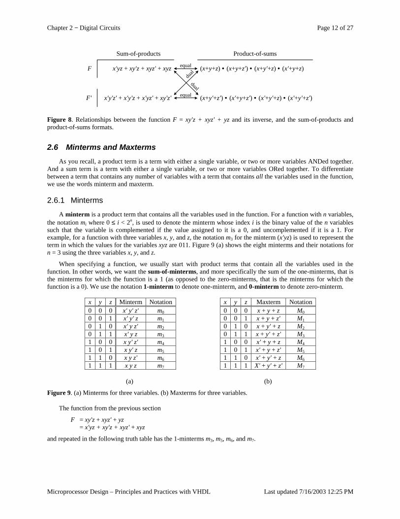
Chapter 2 − Digital Circuits Page 12 of 27
Microprocessor Design – Principles and Practices with VHDL Last updated 7/16/2003 12:25 PM
x'yz + xy'z + xyz' + xyz (x+y+z) • (x+y+z') • (x+y'+z) • (x'+y+z)
(x+y'+z') • (x'+y+z') • (x'+y'+z) • (x'+y'+z')x'y'z' + x'y'z + x'yz' + xy'z'
dual
dual
Product-of-sumsSum-of-products
F'
F equal
equal
Figure 8. Relationships between the function F = xy'z + xyz' + yz and its inverse, and the sum-of-products and product-of-sums formats.
2.6 Minterms and Maxterms As you recall, a product term is a term with either a single variable, or two or more variables ANDed together.
And a sum term is a term with either a single variable, or two or more variables ORed together. To differentiate between a term that contains any number of variables with a term that contains all the variables used in the function, we use the words minterm and maxterm.
2.6.1 Minterms
A minterm is a product term that contains all the variables used in the function. For a function with n variables, the notation mi where 0 ≤ i < 2n, is used to denote the minterm whose index i is the binary value of the n variables such that the variable is complemented if the value assigned to it is a 0, and uncomplemented if it is a 1. For example, for a function with three variables x, y, and z, the notation m3 for the minterm (x'yz) is used to represent the term in which the values for the variables xyz are 011. Figure 9 (a) shows the eight minterms and their notations for n = 3 using the three variables x, y, and z.
When specifying a function, we usually start with product terms that contain all the variables used in the function. In other words, we want the sum-of-minterms, and more specifically the sum of the one-minterms, that is the minterms for which the function is a 1 (as opposed to the zero-minterms, that is the minterms for which the function is a 0). We use the notation 1-minterm to denote one-minterm, and 0-minterm to denote zero-minterm.
x y z Minterm Notation x y z Maxterm Notation 0 0 0 x' y' z' m0 0 0 0 x + y + z M0 0 0 1 x' y' z m1 0 0 1 x + y + z' M1 0 1 0 x' y z' m2 0 1 0 x + y' + z M2 0 1 1 x' y z m3 0 1 1 x + y' + z' M3 1 0 0 x y' z' m4 1 0 0 x' + y + z M4 1 0 1 x y' z m5 1 0 1 x' + y + z' M5 1 1 0 x y z' m6 1 1 0 x' + y' + z M6 1 1 1 x y z m7 1 1 1 X' + y' + z' M7
(a) (b)
Figure 9. (a) Minterms for three variables. (b) Maxterms for three variables.
The function from the previous section
F = xy'z + xyz' + yz = x'yz + xy'z + xyz' + xyz
and repeated in the following truth table has the 1-minterms m3, m5, m6, and m7.
Chapter 2 − Digital Circuits Page 13 of 27
Microprocessor Design – Principles and Practices with VHDL Last updated 7/16/2003 12:25 PM
x y z F F' Minterm Notation 0 0 0 0 1 x' y' z' m0 0 0 1 0 1 x' y' z m1 0 1 0 0 1 x' y z' m2 0 1 1 1 0 x' y z m3 1 0 0 0 1 x y' z' m4 1 0 1 1 0 x y' z m5 1 1 0 1 0 x y z' m6 1 1 1 1 0 x y z m7
Thus, a shorthand notation for the function is
F(x, y, z) = m3 + m5 + m6 + m7
By just using the minterm notations, we do not know how many variables are in the original function thus, we need to explicitly specify the variables used. We can further simplify the notation by using the standard algebraic symbol Σ for summation. Hence we have
F(x, y, z) = Σ(3, 5, 6, 7)
These are just different ways of representing the same function.
Since a function is obtained from the sum of the 1-minterms, the inverse of the function, therefore, must be the sum of the 0-minterms. This can be easily obtained by replacing the set of indices with those that were excluded from the original set.
2.6.2 Maxterms
Analogous to a minterm, a maxterm is a sum term that contains all the variables used in the function. For a function with n variables, the notation Mi where 0 ≤ i < 2n, is used to denote the maxterm whose index i is the binary value of the n variables such that the variable is complemented if the value assigned to it is a 1, and uncomplemented if it is a 0. For example, for a function with three variables x, y, and z, the notation M3 for the maxterm (x + y' + z') is used to represent the term in which the values for the variables xyz are 011. Figure 9 (b) shows the eight maxterms and their notations for n = 3 using the three variables x, y, and z.
We have seen that a function can also be specified as a product-of-sums; more specifically, a product of 0-maxterms, that is, the maxterms for which the function is a 0. Just like the minterms, we use the notation 1-maxterm to denote one-maxterm, and 0-maxterm to denote zero-maxterm. Thus, the function
F(x, y, z) = xy'z + xyz' + yz = (x + y + z) • (x + y + z') • (x + y' + z) • (x' + y + z)
and shown in the following table
x y z F F' Maxterm Notation 0 0 0 0 1 x + y + z M0 0 0 1 0 1 x + y + z' M1 0 1 0 0 1 x + y' + z M2 0 1 1 1 0 x + y' + z' M3 1 0 0 0 1 x' + y + z M4 1 0 1 1 0 x' + y + z' M5 1 1 0 1 0 x' + y' + z M6 1 1 1 1 0 x' + y' + z' M7
can be specified as the product of the 0-maxterms M0, M1, M2, and M4. The shorthand notation for the function is
F(x, y, z) = M0 • M1 • M2 • M4
Again, by using the standard algebraic symbol Π for product, the notation is further simplified to
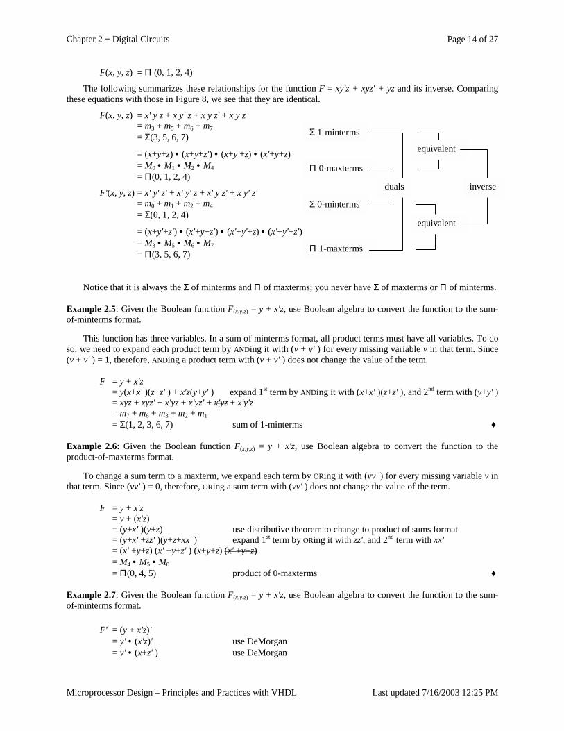
Chapter 2 − Digital Circuits Page 14 of 27
Microprocessor Design – Principles and Practices with VHDL Last updated 7/16/2003 12:25 PM
F(x, y, z) = Π (0, 1, 2, 4)
The following summarizes these relationships for the function F = xy'z + xyz' + yz and its inverse. Comparing these equations with those in Figure 8, we see that they are identical.
F(x, y, z) = x' y z + x y' z + x y z' + x y z = m3 + m5 + m6 + m7 = Σ(3, 5, 6, 7)
= (x+y+z) • (x+y+z') • (x+y'+z) • (x'+y+z) = M0 • M1 • M2 • M4 = Π(0, 1, 2, 4)
F'(x, y, z) = x' y' z' + x' y' z + x' y z' + x y' z' = m0 + m1 + m2 + m4 = Σ(0, 1, 2, 4)
= (x+y'+z') • (x'+y+z') • (x'+y'+z) • (x'+y'+z') = M3 • M5 • M6 • M7 = Π(3, 5, 6, 7)
Notice that it is always the Σ of minterms and Π of maxterms; you never have Σ of maxterms or Π of minterms.
Example 2.5: Given the Boolean function F(x,y,z) = y + x'z, use Boolean algebra to convert the function to the sum-of-minterms format.
This function has three variables. In a sum of minterms format, all product terms must have all variables. To do so, we need to expand each product term by ANDing it with (v + v' ) for every missing variable v in that term. Since (v + v' ) = 1, therefore, ANDing a product term with (v + v' ) does not change the value of the term.
F = y + x'z = y(x+x' )(z+z' ) + x'z(y+y' ) expand 1st term by ANDing it with (x+x' )(z+z' ), and 2nd term with (y+y' ) = xyz + xyz' + x'yz + x'yz' + x'yz + x'y'z = m7 + m6 + m3 + m2 + m1 = Σ(1, 2, 3, 6, 7) sum of 1-minterms ♦
Example 2.6: Given the Boolean function F(x,y,z) = y + x'z, use Boolean algebra to convert the function to the product-of-maxterms format.
To change a sum term to a maxterm, we expand each term by ORing it with (vv' ) for every missing variable v in that term. Since (vv' ) = 0, therefore, ORing a sum term with (vv' ) does not change the value of the term.
F = y + x'z = y + (x'z) = (y+x' )(y+z) use distributive theorem to change to product of sums format = (y+x' +zz' )(y+z+xx' ) expand 1st term by ORing it with zz', and 2nd term with xx' = (x' +y+z) (x' +y+z' ) (x+y+z) (x' +y+z) = M4 • M5 • M0 = Π(0, 4, 5) product of 0-maxterms ♦
Example 2.7: Given the Boolean function F(x,y,z) = y + x'z, use Boolean algebra to convert the function to the sum-of-minterms format.
F' = (y + x'z)' = y' • (x'z)' use DeMorgan = y' • (x+z' ) use DeMorgan
Π 1-maxterms
Σ 1-minterms
Σ 0-minterms
Π 0-maxterms
duals
equivalent
equivalent
inverse
Chapter 2 − Digital Circuits Page 15 of 27
Microprocessor Design – Principles and Practices with VHDL Last updated 7/16/2003 12:25 PM
= y'x + y'z' use distributive theorem to change to sum of products format = y'x(z+z' ) + y'z' (x+x' ) expand 1st term by ANDing it with (z+z' ), and 2nd term with (x+x' ) = xy'z + xy'z' + xy'z' + x'y'z' = m5 + m4 + m0 = Σ(0, 4, 5) sum of 0-minterms ♦
Example 2.8: Given the Boolean function F(x,y,z) = y + x'z, use Boolean algebra to convert the function to the product-of-maxterms format.
F' = (y + x' z)' = y' • (x' z)' use DeMorgan = y' • (x+z' ) use DeMorgan = (y' +xx' +zz' ) • (x+z' +yy' ) expand 1st term by ORing it with xx' +zz', and 2nd term with yy' = (x+y' +z) (x+y' +z' ) (x' +y' +z) (x' +y' +z' ) (x+y+z' ) (x+y' +z' ) = M2 • M3 • M6 • M7 • M1 = Π(1, 2, 3, 6, 7) product of 1-maxterms ♦
2.7 Canonical, Standard, and non-Standard Forms Any Boolean function that is expressed as a sum of minterms or as a product of maxterms is said to be in its
canonical form. As noted from the previous section, to convert a Boolean function from one canonical form to its other equivalent canonical form, simply interchange the symbols Σ with Π, and list the index numbers that were excluded from the original form. To convert a Boolean function from one canonical form to its dual (inverse), simply interchange the symbols Σ with Π, and list the same index numbers from the original form. For example, the following two expressions are in its canonical form.
F = x' y z + x y' z + x y z' + x y z
F = (x+y'+z') • (x'+y+z') • (x'+y'+z) • (x'+y'+z')
A Boolean function is said to be in a standard form if a sum-of-products (product-of-sums) expression has at least one term that is not a minterm (maxterm). In other words, at least one term in the expression is missing at least one variable. For example, the following expression is in a standard form because the last term is missing the variable x.
F = xy'z + xyz' + yz
Sometimes, common variables in a standard form expression can be factored out. The resulting expression is no longer in a sum-of-products or product-of-sums format. These expressions are in a non-standard form. For example, starting with the previous expression, if we factor out the common variable x from the first two terms, we get the following expression, which is in a non-standard form.
F = x(y'z + yz') + yz
2.8 Logic Gates and Circuit Diagrams Logic gates are the actual physical implementations of the logical operators discussed in the previous sections.
Transistors, acting as tiny electronic binary switches are connected together to form these gates. Thus, we have the AND gate, the OR gate, and the NOT gate (also called the INVERTER ) for the corresponding AND, OR, and NOT logical operators. These gates form the basic building blocks for all digital logic circuits. The name “gate” comes from the fact that these devices operate like a door or gate to let or not to let things (in our case, current) through.
In drawing digital circuit diagrams or schematics, we use special logic symbols to denote these gates as shown in Figure 10.
The AND gate, or specifically, the 2-input AND gate, in Figure 10 (a) has two input connections coming in from the left and one output connection going out on the right. Similarly, the 2-input OR gate in (b) has two input connections and one output connection. The INVERTER has one input from the left and one output going to the right. The outputs from these gates, of course, are dependent on their inputs and as defined by their logical functions.
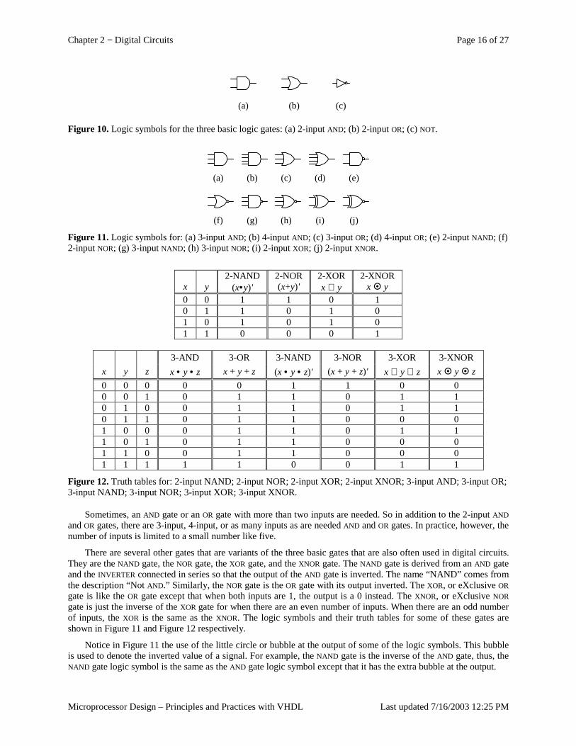
Chapter 2 − Digital Circuits Page 16 of 27
Microprocessor Design – Principles and Practices with VHDL Last updated 7/16/2003 12:25 PM
(a) (b) (c)
Figure 10. Logic symbols for the three basic logic gates: (a) 2-input AND; (b) 2-input OR; (c) NOT.
(a) (b) (c) (d) (e)
(f) (g) (h) (i) (j) Figure 11. Logic symbols for: (a) 3-input AND; (b) 4-input AND; (c) 3-input OR; (d) 4-input OR; (e) 2-input NAND; (f) 2-input NOR; (g) 3-input NAND; (h) 3-input NOR; (i) 2-input XOR; (j) 2-input XNOR.
2-NAND 2-NOR 2-XOR 2-XNOR x y (x•y)' (x+y)' x ⊕ y x � y 0 0 1 1 0 1 0 1 1 0 1 0 1 0 1 0 1 0 1 1 0 0 0 1
3-AND 3-OR 3-NAND 3-NOR 3-XOR 3-XNOR x y z x • y • z x + y + z (x • y • z)' (x + y + z)' x ⊕ y ⊕ z x � y � z 0 0 0 0 0 1 1 0 0 0 0 1 0 1 1 0 1 1 0 1 0 0 1 1 0 1 1 0 1 1 0 1 1 0 0 0 1 0 0 0 1 1 0 1 1 1 0 1 0 1 1 0 0 0 1 1 0 0 1 1 0 0 0 1 1 1 1 1 0 0 1 1
Figure 12. Truth tables for: 2-input NAND; 2-input NOR; 2-input XOR; 2-input XNOR; 3-input AND; 3-input OR; 3-input NAND; 3-input NOR; 3-input XOR; 3-input XNOR.
Sometimes, an AND gate or an OR gate with more than two inputs are needed. So in addition to the 2-input AND and OR gates, there are 3-input, 4-input, or as many inputs as are needed AND and OR gates. In practice, however, the number of inputs is limited to a small number like five.
There are several other gates that are variants of the three basic gates that are also often used in digital circuits. They are the NAND gate, the NOR gate, the XOR gate, and the XNOR gate. The NAND gate is derived from an AND gate and the INVERTER connected in series so that the output of the AND gate is inverted. The name “NAND” comes from the description “Not AND.” Similarly, the NOR gate is the OR gate with its output inverted. The XOR, or eXclusive OR gate is like the OR gate except that when both inputs are 1, the output is a 0 instead. The XNOR, or eXclusive NOR gate is just the inverse of the XOR gate for when there are an even number of inputs. When there are an odd number of inputs, the XOR is the same as the XNOR. The logic symbols and their truth tables for some of these gates are shown in Figure 11 and Figure 12 respectively.
Notice in Figure 11 the use of the little circle or bubble at the output of some of the logic symbols. This bubble is used to denote the inverted value of a signal. For example, the NAND gate is the inverse of the AND gate, thus, the NAND gate logic symbol is the same as the AND gate logic symbol except that it has the extra bubble at the output.

Chapter 2 − Digital Circuits Page 17 of 27
Microprocessor Design – Principles and Practices with VHDL Last updated 7/16/2003 12:25 PM
The notations used for these gates in a logical expression are: (xy)' for the 2-input NAND gate; (x+y)' for the 2-input NOR gate; x ⊕ y for the XOR gate; and x � y for the XNOR gate.
Looking at the truth table for the 2-input XOR gate, we can derive the equation for the 2-XOR gate as
x ⊕ y = x'y + xy'
Similarly, the equation for the 2-input XNOR gate as derived from the 2-XNOR truth table is
x � y = x'y' + xy
The equation for the 3-input XOR gate is derived as follows
x ⊕ y ⊕ z = (x ⊕ y) ⊕ z = (x'y + xy' ) ⊕ z = (x'y + xy' )z' + (x'y + xy' )'z = x'yz' + xy'z' + (x'y)' (xy' )'z = x'yz' + xy'z' + (x+y' ) (x'+y) z = x'yz' + xy'z' + xx'z + xyz + x'y'z + y'yz = x'y'z + x'yz' + xy'z' + xyz
The last four product terms in the above derivation are the four 1-minterms in the 3-input XOR truth table. For 3 or more inputs, the XOR gate has the value 1 when there is an odd number of 1’s in the inputs, otherwise, it is a 0.
Notice also that the truth tables for the 3-input XOR and XNOR gate are identical. It turns out that for an even number of inputs, XOR is the inverse of XNOR, but for an odd number of inputs, XOR is equal to XNOR.
All these gates can be interconnected together to form large complex circuits which we call networks. These networks can be described graphically using circuit diagrams, with Boolean expressions or with truth tables.
2.9 Example: Designing a Car Security System In a car security system, we usually want to connect the siren in such a way that the siren will come on when it
is triggered by one or more sensors or inputs. In addition, there will be a master switch to turn on or off the system. Let us assume that there is a car door switch D, a vibration detector switch V, and the master switch M. We will use the convention that when the door is opened D = 1, otherwise, D = 0. Similarly, when the car is being shaken, V = 1, otherwise V = 0. Thus, we want the siren S to come on, that is, set S = 1, when either D = 1 or V = 1, but this is only for when the system is turned on, that is M = 1. When M = 0 as in when we are entering the car or when we are driving, we don’t want the siren to come on.
Given the above description of a car security system, we can build a digital circuit that has the required functionality. We start by constructing a truth table, which is basically a precise way of stating the operations for the device. The table will have three input columns M, D, and V, and an output column S as shown below
M D V S 0 0 0 0 0 0 1 0 0 1 0 0 0 1 1 0 1 0 0 0 1 0 1 1 1 1 0 1 1 1 1 1
The values under the S column are obtained from interpreting the description of when we want the siren to come on. When M = 0, it doesn’t matter what the values for D and V are, we don’t want the siren to come on. When M = 1, we want the siren to come on when either or both D and V is a 1.
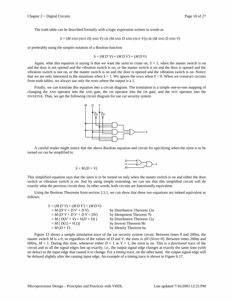
Chapter 2 − Digital Circuits Page 18 of 27
Microprocessor Design – Principles and Practices with VHDL Last updated 7/16/2003 12:25 PM
The truth table can be described formally with a logic expression written in words as
S = (M AND (NOT D) AND V) OR (M AND D AND (NOT V)) OR (M AND D AND V)
or preferably using the simpler notation of a Boolean function
S = (M D' V) + (M D V') + (M D V)
Again, what this equation is saying is that we want the siren to come on, S = 1, when the master switch is on and the door is not opened and the vibration switch is on, or the master switch is on and the door is opened and the vibration switch is not on, or the master switch is on and the door is opened and the vibration switch is on. Notice that we are only interested in the situations when S = 1. We ignore the rows when S = 0. When we construct circuits from truth tables, we always use only the rows where the output is a 1.
Finally, we can translate this equation into a circuit diagram. The translation is a simple one-to-one mapping of changing the AND operator into the AND gate, the OR operator into the OR gate, and the NOT operator into the INVERTER. Thus, we get the following circuit diagram for our car security system
S
M D V
A careful reader might notice that the above Boolean equation and circuit for specifying when the siren is to be
turned on can be simplified to
S = M (D + V)
D
MV S
This simplified equation says that the siren is to be turned on only when the master switch is on and either the door switch or vibration switch is on. Just by using simple reasoning, we can see that this simplified circuit will do exactly what the previous circuit does. In other words, both circuits are functionally equivalent.
Using the Boolean Theorems from section 2.5.1, we can show that these two equations are indeed equivalent as follows:
S = (M D' V) + (M D V') + (M D V) = M (D' V + D V' + D V) by Distributive Theorem 12a = M (D' V + D V' + D V + DV) by Idempotent Theorem 7b = M ( D(V' + V) + V(D' + D) ) by Distributive Theorem 12a = M ( D(1) + V(1)) by Inverse Theorem 9b = M (D + V) by Identity Theorem 6a
Figure 13 shows a sample simulation trace of the car security system circuit. Between times 0 and 200ns, the master switch M is a 0, so regardless of the values of D and V, the siren is off (Siren=0). Between times 200ns and 600ns, M = 1. During this time, whenever either D = 1 or V = 1, the siren is on. This is a functional trace of the circuit and so all the signal edges line up exactly, i.e., the output signal edge changes at exactly the same time (with no delay) as the input edge that caused it to change. For a timing trace, on the other hand, the output signal edge will be delayed slightly after the causing input edge. An example of a timing trace is shown in Figure 6.17.
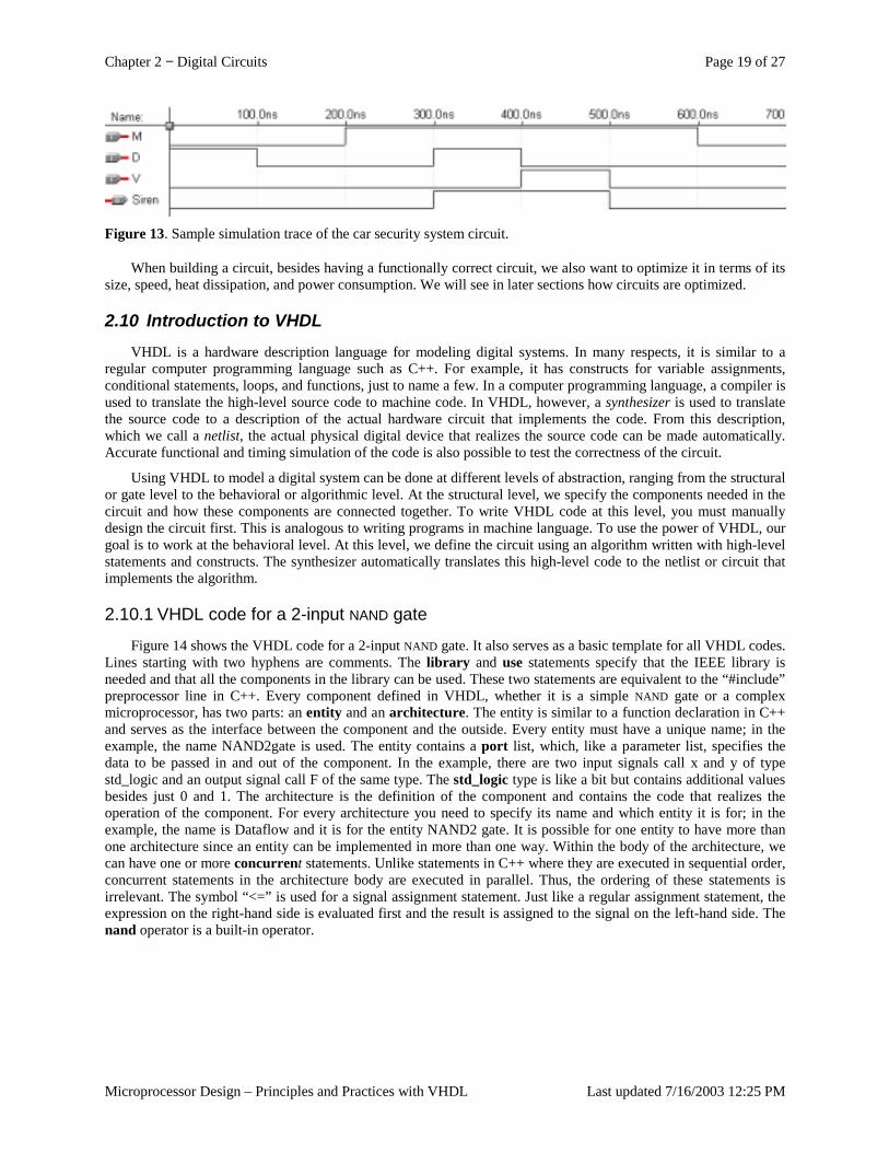
Chapter 2 − Digital Circuits Page 19 of 27
Microprocessor Design – Principles and Practices with VHDL Last updated 7/16/2003 12:25 PM
Figure 13. Sample simulation trace of the car security system circuit.
When building a circuit, besides having a functionally correct circuit, we also want to optimize it in terms of its size, speed, heat dissipation, and power consumption. We will see in later sections how circuits are optimized.
2.10 Introduction to VHDL VHDL is a hardware description language for modeling digital systems. In many respects, it is similar to a
regular computer programming language such as C++. For example, it has constructs for variable assignments, conditional statements, loops, and functions, just to name a few. In a computer programming language, a compiler is used to translate the high-level source code to machine code. In VHDL, however, a synthesizer is used to translate the source code to a description of the actual hardware circuit that implements the code. From this description, which we call a netlist, the actual physical digital device that realizes the source code can be made automatically. Accurate functional and timing simulation of the code is also possible to test the correctness of the circuit.
Using VHDL to model a digital system can be done at different levels of abstraction, ranging from the structural or gate level to the behavioral or algorithmic level. At the structural level, we specify the components needed in the circuit and how these components are connected together. To write VHDL code at this level, you must manually design the circuit first. This is analogous to writing programs in machine language. To use the power of VHDL, our goal is to work at the behavioral level. At this level, we define the circuit using an algorithm written with high-level statements and constructs. The synthesizer automatically translates this high-level code to the netlist or circuit that implements the algorithm.
2.10.1 VHDL code for a 2-input NAND gate
Figure 14 shows the VHDL code for a 2-input NAND gate. It also serves as a basic template for all VHDL codes. Lines starting with two hyphens are comments. The library and use statements specify that the IEEE library is needed and that all the components in the library can be used. These two statements are equivalent to the “#include” preprocessor line in C++. Every component defined in VHDL, whether it is a simple NAND gate or a complex microprocessor, has two parts: an entity and an architecture. The entity is similar to a function declaration in C++ and serves as the interface between the component and the outside. Every entity must have a unique name; in the example, the name NAND2gate is used. The entity contains a port list, which, like a parameter list, specifies the data to be passed in and out of the component. In the example, there are two input signals call x and y of type std_logic and an output signal call F of the same type. The std_logic type is like a bit but contains additional values besides just 0 and 1. The architecture is the definition of the component and contains the code that realizes the operation of the component. For every architecture you need to specify its name and which entity it is for; in the example, the name is Dataflow and it is for the entity NAND2 gate. It is possible for one entity to have more than one architecture since an entity can be implemented in more than one way. Within the body of the architecture, we can have one or more concurrent statements. Unlike statements in C++ where they are executed in sequential order, concurrent statements in the architecture body are executed in parallel. Thus, the ordering of these statements is irrelevant. The symbol “<=” is used for a signal assignment statement. Just like a regular assignment statement, the expression on the right-hand side is evaluated first and the result is assigned to the signal on the left-hand side. The nand operator is a built-in operator.
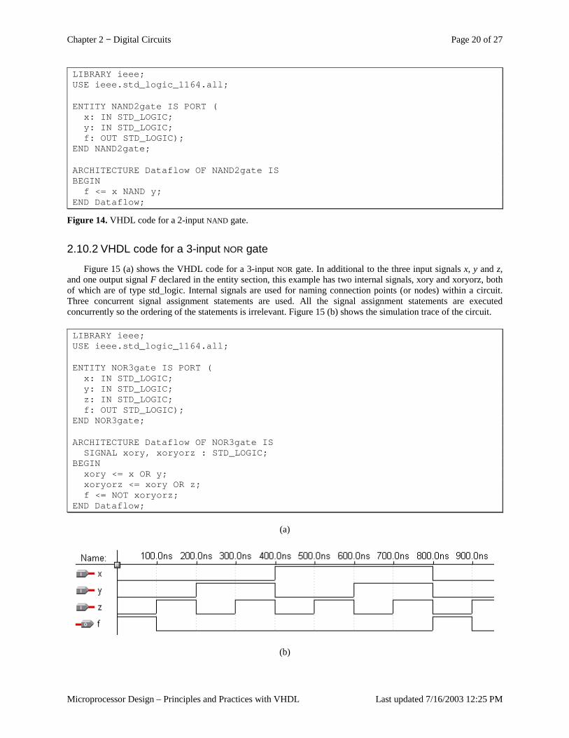
Chapter 2 − Digital Circuits Page 20 of 27
Microprocessor Design – Principles and Practices with VHDL Last updated 7/16/2003 12:25 PM
LIBRARY ieee;USE ieee.std_logic_1164.all;
ENTITY NAND2gate IS PORT (x: IN STD_LOGIC;y: IN STD_LOGIC;f: OUT STD_LOGIC);
END NAND2gate;
ARCHITECTURE Dataflow OF NAND2gate ISBEGIN
f <= x NAND y;END Dataflow;
Figure 14. VHDL code for a 2-input NAND gate.
2.10.2 VHDL code for a 3-input NOR gate
Figure 15 (a) shows the VHDL code for a 3-input NOR gate. In additional to the three input signals x, y and z, and one output signal F declared in the entity section, this example has two internal signals, xory and xoryorz, both of which are of type std_logic. Internal signals are used for naming connection points (or nodes) within a circuit. Three concurrent signal assignment statements are used. All the signal assignment statements are executed concurrently so the ordering of the statements is irrelevant. Figure 15 (b) shows the simulation trace of the circuit.
LIBRARY ieee;USE ieee.std_logic_1164.all;
ENTITY NOR3gate IS PORT (x: IN STD_LOGIC;y: IN STD_LOGIC;z: IN STD_LOGIC;f: OUT STD_LOGIC);
END NOR3gate;
ARCHITECTURE Dataflow OF NOR3gate ISSIGNAL xory, xoryorz : STD_LOGIC;
BEGINxory <= x OR y;xoryorz <= xory OR z;f <= NOT xoryorz;
END Dataflow;
(a)
(b)
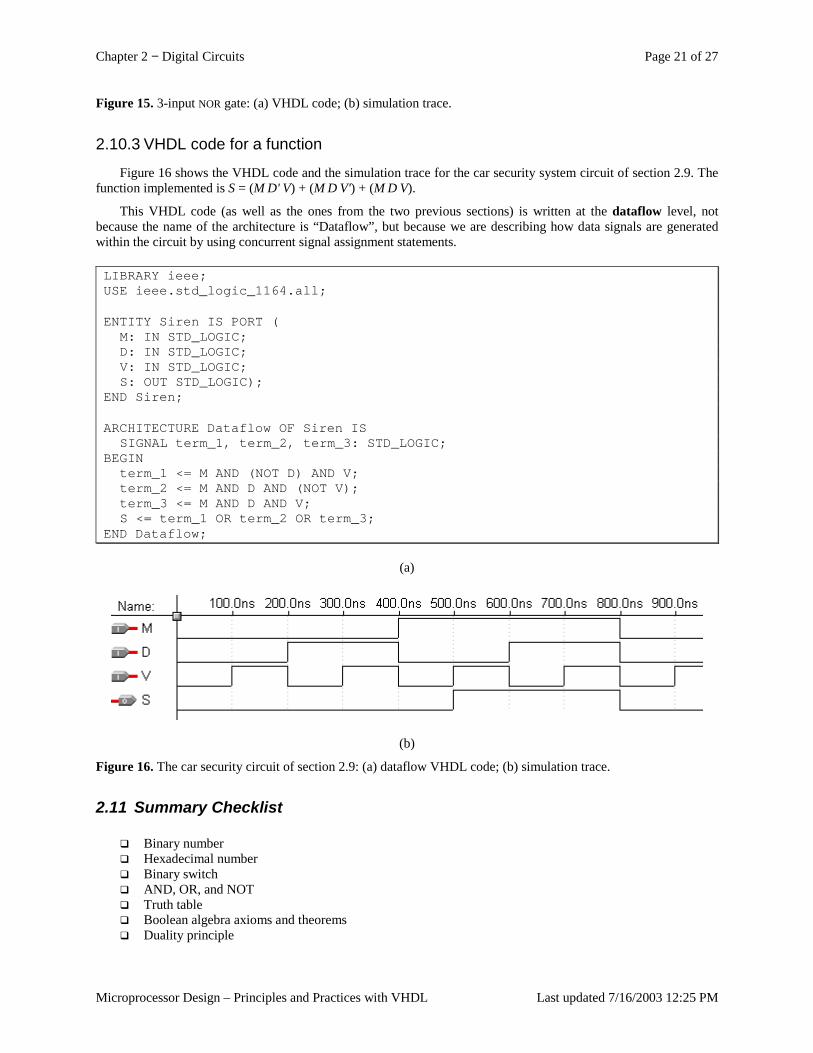
Chapter 2 − Digital Circuits Page 21 of 27
Microprocessor Design – Principles and Practices with VHDL Last updated 7/16/2003 12:25 PM
Figure 15. 3-input NOR gate: (a) VHDL code; (b) simulation trace.
2.10.3 VHDL code for a function
Figure 16 shows the VHDL code and the simulation trace for the car security system circuit of section 2.9. The function implemented is S = (M D' V) + (M D V') + (M D V).
This VHDL code (as well as the ones from the two previous sections) is written at the dataflow level, not because the name of the architecture is “Dataflow”, but because we are describing how data signals are generated within the circuit by using concurrent signal assignment statements.
LIBRARY ieee;USE ieee.std_logic_1164.all;
ENTITY Siren IS PORT (M: IN STD_LOGIC;D: IN STD_LOGIC;V: IN STD_LOGIC;S: OUT STD_LOGIC);
END Siren;
ARCHITECTURE Dataflow OF Siren ISSIGNAL term_1, term_2, term_3: STD_LOGIC;
BEGINterm_1 <= M AND (NOT D) AND V;term_2 <= M AND D AND (NOT V);term_3 <= M AND D AND V;S <= term_1 OR term_2 OR term_3;
END Dataflow;
(a)
(b)
Figure 16. The car security circuit of section 2.9: (a) dataflow VHDL code; (b) simulation trace.
2.11 Summary Checklist � Binary number � Hexadecimal number � Binary switch � AND, OR, and NOT � Truth table � Boolean algebra axioms and theorems � Duality principle
Chapter 2 − Digital Circuits Page 22 of 27
Microprocessor Design – Principles and Practices with VHDL Last updated 7/16/2003 12:25 PM
� Boolean function and the inverse � Product term � Sum term � Sum-of-products, or-of-ands � Product of sums, and-of-ors � Minterm and maxterm � Sum-of minterms � Product-of-maxterms � Canonical, standard, and non-standard form � Logic gate, logic symbol � Circuit diagram � NAND, NOR, XOR, XNOR � Network � VHDL

Chapter 2 − Digital Circuits Page 23 of 27
Microprocessor Design – Principles and Practices with VHDL Last updated 7/16/2003 12:25 PM
2.12 Exercises 2.1 Derive the truth table for a 4-input NAND gate. 2.2 Derive the truth table for a 4-input XOR gate. 2.3 Draw the schematic circuit diagrams that implements the following expressions using as few basic gates as
possible:
a) F = xy' + x'y'z + xyz' b) F = w'z' + w'xy + wx'z + wxyz c) F = w'xy'z + w'xyz + wxy'z + wxyz d) F = N3'N2'N1N0' + N3'N2'N1N0 + N3N2'N1N0' + N3N2'N1N0 + N3N2N1'N0' + N3N2N1N0 e) F = [(x � y)' + (xyz)'] (w' + x + z) f) F = x ⊕ y ⊕ z g) F = [w'xy'z + w'z (y ⊕ x)]'
2.4 Draw the schematic circuit diagrams that implement the expressions in question 2.3 using only 2-input AND, 2-input OR and NOT gates.
2.5 Draw the schematic circuit diagrams that implement the expressions in question 2.3 using only 2-input NAND gates.
2.6 Draw the schematic circuit diagrams that implement the expressions in question 2.3 using only 3-input NOR gates.
2.7 Show using the Boolean algebra axioms and theorems that (x ⊕ y) = (x � y)'
2.8 Show using Boolean algebra that XOR = XNOR for three inputs.
Answer:
x ⊕ y ⊕ z = (x ⊕ y) ⊕ z = (x'y + xy') ⊕ z = (x'y + xy')' z + (x'y + xy') z' = (x'y)' · (xy')' z + x'yz' + xy'z' = (x + y') · (x' + y) z + x'yz' + xy'z' = xx'z + xyz + x'y'z + y'yz + x'yz' + xy'z' = (xy + x'y') z + (x'y + xy') z' = (xy + x'y') z + (xy + x'y')' z' = (x�y) z + (x�y)' z' = x�y�z
2.9 Draw the schematic circuit diagrams that implements the following expressions:
a) F (x, y, z) = Σ(0, 1, 6) b) F (w,x, y, z) = Σ(0, 1, 6) c) F (w,x, y, z) = Σ(2, 6, 10, 11, 14, 15) d) F (x, y, z) = Π(0, 1, 6) e) F (w,x, y, z) = Π(0, 1, 6) f) F (w,x, y, z) = Π(2, 6, 10, 11, 14, 15)
2.10 Convert the functions in question 2.3 to the sum-of-minterms and product-of-maxterms notations. 2.11 Derive the truth tables for the expressions in question 2.3. 2.12 Derive the truth table for the logic expression F(x,y,z) = [(x+y' ) (yz)' ] (xy' + x'y).
Answer:
Chapter 2 − Digital Circuits Page 24 of 27
Microprocessor Design – Principles and Practices with VHDL Last updated 7/16/2003 12:25 PM
x y z x' y' x+y' yz (yz)' [(x+y' ) (yz)' ] xy' x'y (xy' + x'y) [(x+y' ) (yz)' ] (xy' + x'y) 0 0 0 1 1 1 0 1 1 0 0 0 0 0 0 1 1 1 1 0 1 1 0 0 0 0 0 1 0 1 0 0 0 1 0 0 1 1 0 0 1 1 1 0 0 1 0 0 0 1 1 0 1 0 0 0 1 1 0 1 1 1 0 1 1 1 0 1 0 1 1 0 1 1 1 0 1 1 1 1 0 0 0 1 0 1 1 0 0 0 0 1 1 1 0 0 1 1 0 0 0 0 0 0
2.13 Derive the Boolean function from the following truth table: a) b)
N3 N2 N1 N0 F w x y z f 0 0 0 0 0 0 0 0 0 0 0 0 0 1 0 0 0 0 1 0 0 0 1 0 1 0 0 1 0 1 0 0 1 1 1 0 0 1 1 0 0 1 0 0 0 0 1 0 0 1 0 1 0 1 0 0 1 0 1 1 0 1 1 0 1 0 1 1 0 0 0 1 1 1 0 0 1 1 1 1 1 0 0 0 0 1 0 0 0 0 1 0 0 1 0 1 0 0 1 1 1 0 1 0 1 1 0 1 0 1 1 0 1 1 1 1 0 1 1 0 1 1 0 0 1 1 1 0 0 1 1 1 0 1 0 1 1 0 1 1 1 1 1 0 0 1 1 1 0 0 1 1 1 1 1 1 1 1 1 1
2.14 Derive the Boolean function for the following circuits:
a)
x y z
F
b) w
xy
z
F
2.15 Construct a digital circuit with 4 bits input and 1 bit output such that the circuit outputs a 1 if the 4-bit input is any one of the following numbers: 2, 3, 10, 11, 12, and 15. Otherwise, it outputs a 0.
2.16 Construct a comparator circuit with a 4-bit input. The circuit outputs a 1 if the 4-bit input is a number greater than or equal to 5. Otherwise, it outputs a 0.
2.17 Construct the following circuit. The circuit has five input and one output lines. The five input lines are labeled W, X, Y, Z, and E, and the output line is labeled F. E is used to enabled (turn on) or disable (turn off) the circuit, thus when E = 0, the circuit is disabled and F is always 0. When E = 1, the circuit is enabled and F is determined by the value of the four input lines W, X, Y and Z where W is the most significant bit. If the value
Chapter 2 − Digital Circuits Page 25 of 27
Microprocessor Design – Principles and Practices with VHDL Last updated 7/16/2003 12:25 PM
is odd then F = 1, otherwise F = 0. 2.18 Use a truth table to show that the following expressions are true:
a) w'z' + w'xy + wx'z + wxyz = w'z' + xyz + wx'y'z + wyz b) z + y' + yz' = 1 c) xy'z' + x' + xyz' = x' + z' d) xy + x'z + yz = xy + x'z e) w'x'yz' + w'x'yz + wx'yz' + wx'yz + wxyz = y(x' + wz) f) w'xy'z + w'xyz + wxy'z + wxyz = xz
2.19 Show using the Boolean algebra axioms and theorems that the expressions in question 2.18 are true. 2.20 Any function can be implemented directly as specified or as its inverted form with a not gate added at the
final output. Assume that the circuit size is proportional to only the number of AND gates and OR gates, i.e. ignore the number of NOT gates in determining the circuit size. Determine which form of the function (the inverted or un-inverted) will result in a smaller circuit size for the following function. Give your reason and specify how many AND and OR gates are needed to implement the smaller circuit.
F = x'y'z' + x'y'z + xy'z + xy'z' + xyz
2.21 Given F' (x, y, z) = Σ(1, 3, 7), express the function F using a truth table.
2.22 Convert the function F(x, y, z) = Σ(3, 4, 5) to its equivalent product-of-sum canonical form using the Boolean algebra axioms and theorems.
2.23 Given F = xy'z' + xy'z + xyz' + xyz, write the expression for F ' using: (a) the AND-of-OR terms format and (b) the OR-of-AND terms format.
Chapter 2 − Digital Circuits Page 26 of 27
Microprocessor Design – Principles and Practices with VHDL Last updated 7/16/2003 12:25 PM
Index –, 5 ', 5, 6 ⊕ , 17 • , 5, 6. See Product-of-maxterms. See Sum-of-
minterms �, 17 +, 5, 6 0-maxterm. See Maxterm 0-minterm. See Minterm 1-maxterm. See Maxterm 1-minterm. See Minterm
A
Algebra. See Boolean algebra. AND
gate, 15 term. See Product term.
And-of-ors, 10 Axioms. See Boolean axioms.
B
Binary digit. See Bit Binary Number, 2 Binary switch, 4 Bit, 2 Boolean
algebra, 6 axioms, 6 function, 9 inverse function, 10 theorems, 6, 7, 8 variable, 6, 9
C
Canonical form, 15
D
Dataflow level, 20 DeMorgan’s Theorem, 7 Digital circuit, description
Boolean function, 6 truth table, 6
Duality Principle, 8
F
Function. See Boolean function.
G
Gate. See Logic gate.
H
Hex Number. See Hexadeciaml Number Hexadecimal Number, 4
I Inverse. See Boolean inverse function. INVERTER. See NOT gate.
L
Literal. See Boolean variable. Logic expression, 5 Logic gate, 15
AND, 15 INVERTER, 15 NAND, 16 NOR, 16 NOT, 15 OR, 15 XNOR, 16 XOR, 16
Logic operator, 5 AND, 5 NOT, 5 OR, 5 precedence, 6
Logic symbol, 15, 16 circle, 16
M
Maxterm, 13 Π, 13 0-maxterm, 13 1-maxterm, 13 product-of-maxterms, 13
Minterm, 12 Σ, 12 0-minterm, 12 1-minterm, 12 sum-of-minterms, 12
N
NAND gate, 16 Netlist, 19 Network, 17 Non-standard form, 15 NOR gate, 16 NOT gate, 15
Chapter 2 − Digital Circuits Page 27 of 27
Microprocessor Design – Principles and Practices with VHDL Last updated 7/16/2003 12:25 PM
O
Octal Number, 3 OR
gate, 15 term. See Sum term.
Or-of-ands, 9
P
Product term, 9 Product-of-maxterms, Π, 13 Product-of-sums, 10
S
Standard form, 15 Sum term, 10 Sum-of-minterms, Σ, 12 Sum-of-products, 9 Switch. See Binary switch. Synthesizer, 19
T
Theorems. See Boolean theorems.
Truth table, 6, 7, 16, 23
V
Variable. See Boolean variable. VHDL, 19
<=, 19 architecture, 19 concurrent statement, 19, 20 dataflow level, 20 entity, 19 library, 19 port, 19 signal assignment, 19 std_logic, 19 use, 19
VHDL code 2-input NAND gate, 19 3-input NOR gate, 20 car security system, 20 simple function, 20
X
XNOR gate, 16 XOR gate, 16
Chapter 3 − Combinational Circuits Page 1 of 26
Microprocessor Design – Principles and Practices with VHDL Last updated 7/17/2003 5:56 PM
Table of Content Table of Content ........................................................................................................................................................... 1 3 Combinational Circuits ......................................................................................................................................... 2
3.1 Analysis of Combinational Circuits .............................................................................................................. 2 3.1.1 With a Truth Table ................................................................................................................................ 2 3.1.2 With a Boolean Function....................................................................................................................... 4
3.2 Synthesis of Combinational Circuits ............................................................................................................. 5 3.3 Technology Mapping .................................................................................................................................... 6 3.4 Minimization of Combinational Circuits ...................................................................................................... 9
3.4.1 Karnaugh (K) Maps............................................................................................................................... 9 3.4.2 Don’t-cares.......................................................................................................................................... 13 3.4.3 * Quine-McCluskey (Tabulation) Method .......................................................................................... 14
3.5 * Timing Hazards and Glitches................................................................................................................... 15 3.6 7-Segment Decoder Example...................................................................................................................... 16 3.7 VHDL Code for Combinational Circuits .................................................................................................... 19
3.7.1 Structural BCD to 7-Segment Decoder ............................................................................................... 19 3.7.2 Dataflow BCD to 7-Segment Decoder................................................................................................ 22 3.7.3 Behavioral BCD to 7-Segment Decoder ............................................................................................. 22
3.8 Summary Checklist ..................................................................................................................................... 23 3.9 Exercises ..................................................................................................................................................... 24 Index ....................................................................................................................................................................... 26
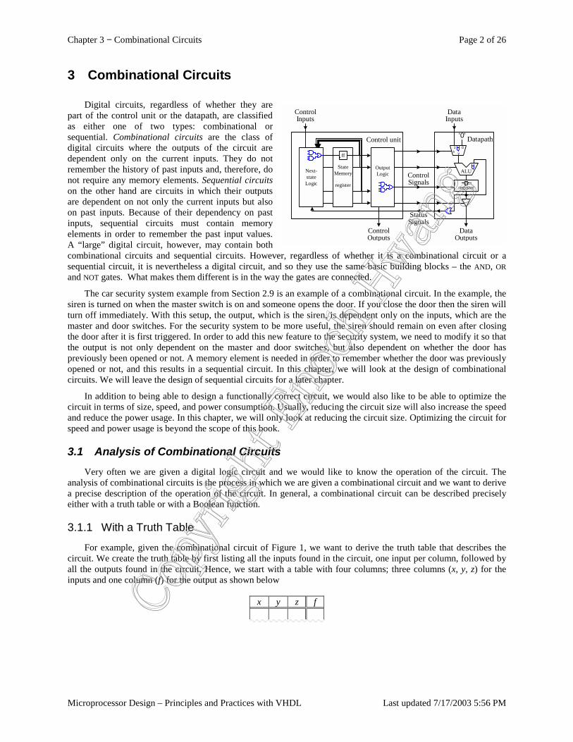
Chapter 3 − Combinational Circuits Page 2 of 26
Microprocessor Design – Principles and Practices with VHDL Last updated 7/17/2003 5:56 PM
ControlSignals
StatusSignals
01s y
'0'
DataInputs
DataOutputs
Datapath
ALU
registerff
OutputLogicNext-
stateLogic
ControlInputs
ControlOutputs
StateMemory
register
Control unit
ff
3 Combinational Circuits
Digital circuits, regardless of whether they are part of the control unit or the datapath, are classified as either one of two types: combinational or sequential. Combinational circuits are the class of digital circuits where the outputs of the circuit are dependent only on the current inputs. They do not remember the history of past inputs and, therefore, do not require any memory elements. Sequential circuits on the other hand are circuits in which their outputs are dependent on not only the current inputs but also on past inputs. Because of their dependency on past inputs, sequential circuits must contain memory elements in order to remember the past input values. A “large” digital circuit, however, may contain both combinational circuits and sequential circuits. However, regardless of whether it is a combinational circuit or a sequential circuit, it is nevertheless a digital circuit, and so they use the same basic building blocks – the AND, OR and NOT gates. What makes them different is in the way the gates are connected.
The car security system example from Section 2.9 is an example of a combinational circuit. In the example, the siren is turned on when the master switch is on and someone opens the door. If you close the door then the siren will turn off immediately. With this setup, the output, which is the siren, is dependent only on the inputs, which are the master and door switches. For the security system to be more useful, the siren should remain on even after closing the door after it is first triggered. In order to add this new feature to the security system, we need to modify it so that the output is not only dependent on the master and door switches, but also dependent on whether the door has previously been opened or not. A memory element is needed in order to remember whether the door was previously opened or not, and this results in a sequential circuit. In this chapter, we will look at the design of combinational circuits. We will leave the design of sequential circuits for a later chapter.
In addition to being able to design a functionally correct circuit, we would also like to be able to optimize the circuit in terms of size, speed, and power consumption. Usually, reducing the circuit size will also increase the speed and reduce the power usage. In this chapter, we will only look at reducing the circuit size. Optimizing the circuit for speed and power usage is beyond the scope of this book.
3.1 Analysis of Combinational Circuits Very often we are given a digital logic circuit and we would like to know the operation of the circuit. The
analysis of combinational circuits is the process in which we are given a combinational circuit and we want to derive a precise description of the operation of the circuit. In general, a combinational circuit can be described precisely either with a truth table or with a Boolean function.
3.1.1 With a Truth Table
For example, given the combinational circuit of Figure 1, we want to derive the truth table that describes the circuit. We create the truth table by first listing all the inputs found in the circuit, one input per column, followed by all the outputs found in the circuit. Hence, we start with a table with four columns; three columns (x, y, z) for the inputs and one column (f) for the output as shown below
x y z f
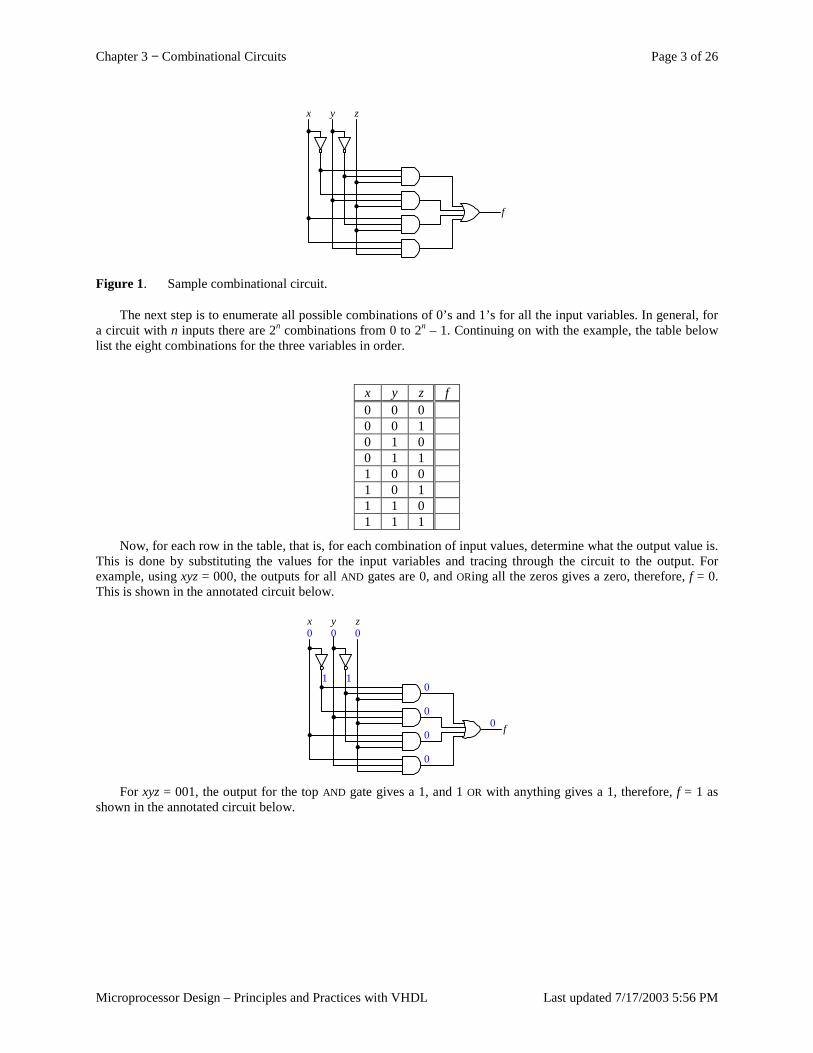
Chapter 3 − Combinational Circuits Page 3 of 26
Microprocessor Design – Principles and Practices with VHDL Last updated 7/17/2003 5:56 PM
x y z
f
Figure 1. Sample combinational circuit.
The next step is to enumerate all possible combinations of 0’s and 1’s for all the input variables. In general, for a circuit with n inputs there are 2n combinations from 0 to 2n – 1. Continuing on with the example, the table below list the eight combinations for the three variables in order.
x y z f 0 0 0 0 0 1 0 1 0 0 1 1 1 0 0 1 0 1 1 1 0 1 1 1
Now, for each row in the table, that is, for each combination of input values, determine what the output value is. This is done by substituting the values for the input variables and tracing through the circuit to the output. For example, using xyz = 000, the outputs for all AND gates are 0, and ORing all the zeros gives a zero, therefore, f = 0. This is shown in the annotated circuit below.
x y z
f0
0 0 0
1 10
0
0
0
For xyz = 001, the output for the top AND gate gives a 1, and 1 OR with anything gives a 1, therefore, f = 1 as shown in the annotated circuit below.
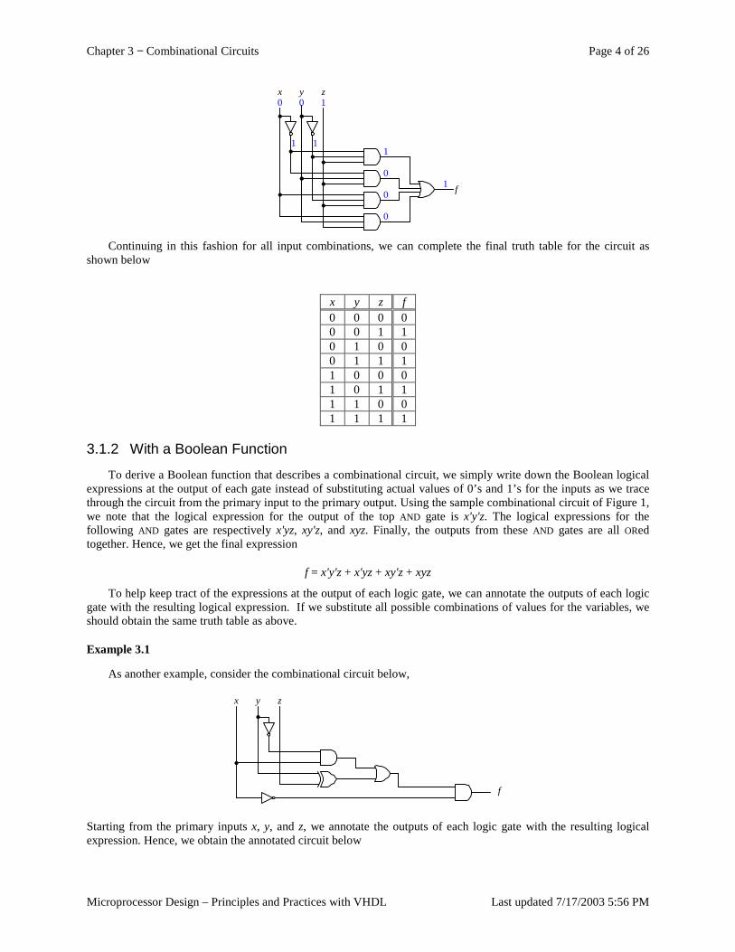
Chapter 3 − Combinational Circuits Page 4 of 26
Microprocessor Design – Principles and Practices with VHDL Last updated 7/17/2003 5:56 PM
x y z
f1
0 0 1
1 11
0
0
0
Continuing in this fashion for all input combinations, we can complete the final truth table for the circuit as shown below
x y z f 0 0 0 0 0 0 1 1 0 1 0 0 0 1 1 1 1 0 0 0 1 0 1 1 1 1 0 0 1 1 1 1
3.1.2 With a Boolean Function
To derive a Boolean function that describes a combinational circuit, we simply write down the Boolean logical expressions at the output of each gate instead of substituting actual values of 0’s and 1’s for the inputs as we trace through the circuit from the primary input to the primary output. Using the sample combinational circuit of Figure 1, we note that the logical expression for the output of the top AND gate is x'y'z. The logical expressions for the following AND gates are respectively x'yz, xy'z, and xyz. Finally, the outputs from these AND gates are all ORed together. Hence, we get the final expression
f = x'y'z + x'yz + xy'z + xyz
To help keep tract of the expressions at the output of each logic gate, we can annotate the outputs of each logic gate with the resulting logical expression. If we substitute all possible combinations of values for the variables, we should obtain the same truth table as above.
Example 3.1
As another example, consider the combinational circuit below,
x y z
f
Starting from the primary inputs x, y, and z, we annotate the outputs of each logic gate with the resulting logical expression. Hence, we obtain the annotated circuit below
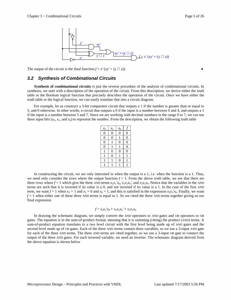
Chapter 3 − Combinational Circuits Page 5 of 26
Microprocessor Design – Principles and Practices with VHDL Last updated 7/17/2003 5:56 PM
x y z
y' xy'
y ⊕ zx'xy' + (y ⊕ z)
f = x' (xy' + (y ⊕ z))
The output of the circuit is the final function f = x' (xy' + (y ⊕ z)). ♦
3.2 Synthesis of Combinational Circuits Synthesis of combinational circuits is just the reverse procedure of the analysis of combinational circuits. In
synthesis, we start with a description of the operation of the circuit. From this description, we derive either the truth table or the Boolean logical function that precisely describes the operation of the circuit. Once we have either the truth table or the logical function, we can easily translate that into a circuit diagram.
For example, let us construct a 3-bit comparator circuit that outputs a 1 if the number is greater than or equal to 5, and 0 otherwise. In other words, a circuit that outputs a 0 if the input is a number between 0 and 4, and outputs a 1 if the input is a number between 5 and 7. Since we are working with decimal numbers in the range 0 to 7, we can use three input bits (x2, x1, and x0) to represent the number. From the description, we obtain the following truth table
x2 x1 x0 f 0 0 0 0 0 0 1 0 0 1 0 0 0 1 1 0 1 0 0 0 1 0 1 1 1 1 0 1 1 1 1 1
In constructing the circuit, we are only interested in when the output is a 1, i.e. when the function is a 1. Thus, we need only consider the rows where the output function f = 1. From the above truth table, we see that there are three rows where f = 1 which give the three AND terms x2x1'x0, x2x1x0', and x2x1x0. Notice that the variables in the AND terms are such that it is inverted if its value is a 0, and not inverted if its value is a 1. In the case of the first AND term, we want f = 1 when x2 = 1 and x1 = 0 and x0 = 1, and this is satisfied in the expression x2x1'x0. Finally, we want f = 1 when either one of these three AND terms is equal to 1. So we ORed the three AND terms together giving us our final expression
f = x2x1'x0 + x2x1x0' + x2x1x0
In drawing the schematic diagram, we simply convert the AND operators to AND gates and OR operators to OR gates. The equation is in the sum-of-product format, meaning that it is summing (ORing) the product (AND) terms. A sum-of-product equation translates to a two level circuit with the first level being made up of AND gates and the second level made up of OR gates. Each of the three AND terms contain three variables, so we use a 3-input AND gate for each of the three AND terms. The three AND terms are ORed together, so we use a 3-input OR gate to connect the output of the three AND gates. For each inverted variable, we need an inverter. The schematic diagram derived from the above equation is shown below
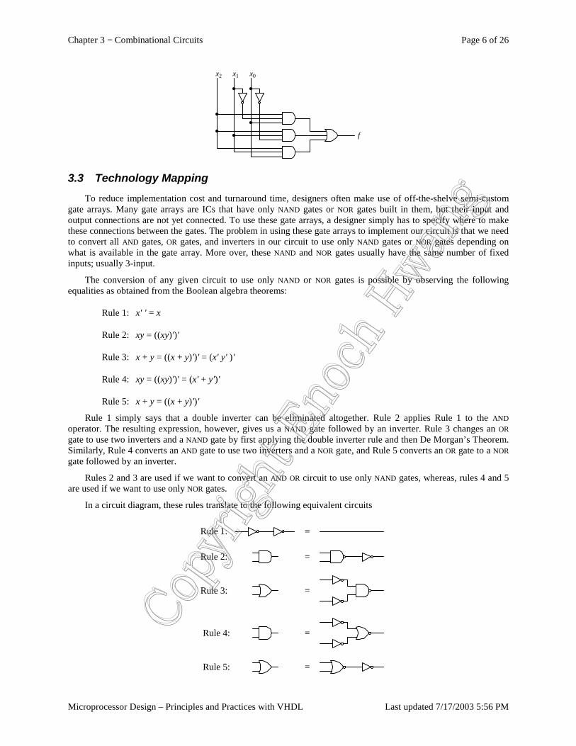
Chapter 3 − Combinational Circuits Page 6 of 26
Microprocessor Design – Principles and Practices with VHDL Last updated 7/17/2003 5:56 PM
x2 x1 x0
f
3.3 Technology Mapping To reduce implementation cost and turnaround time, designers often make use of off-the-shelve semi-custom
gate arrays. Many gate arrays are ICs that have only NAND gates or NOR gates built in them, but their input and output connections are not yet connected. To use these gate arrays, a designer simply has to specify where to make these connections between the gates. The problem in using these gate arrays to implement our circuit is that we need to convert all AND gates, OR gates, and inverters in our circuit to use only NAND gates or NOR gates depending on what is available in the gate array. More over, these NAND and NOR gates usually have the same number of fixed inputs; usually 3-input.
The conversion of any given circuit to use only NAND or NOR gates is possible by observing the following equalities as obtained from the Boolean algebra theorems:
Rule 1: x' ' = x
Rule 2: xy = ((xy)')'
Rule 3: x + y = ((x + y)')' = (x' y' )'
Rule 4: xy = ((xy)')' = (x' + y')'
Rule 5: x + y = ((x + y)')'
Rule 1 simply says that a double inverter can be eliminated altogether. Rule 2 applies Rule 1 to the AND operator. The resulting expression, however, gives us a NAND gate followed by an inverter. Rule 3 changes an OR gate to use two inverters and a NAND gate by first applying the double inverter rule and then De Morgan’s Theorem. Similarly, Rule 4 converts an AND gate to use two inverters and a NOR gate, and Rule 5 converts an OR gate to a NOR gate followed by an inverter.
Rules 2 and 3 are used if we want to convert an AND OR circuit to use only NAND gates, whereas, rules 4 and 5 are used if we want to use only NOR gates.
In a circuit diagram, these rules translate to the following equivalent circuits
Rule 2: =
Rule 3: =
Rule 4: =
Rule 5: =
Rule 1: =
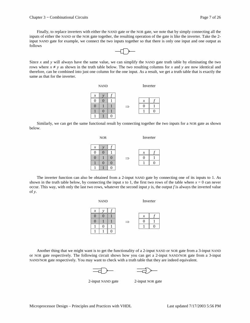
Chapter 3 − Combinational Circuits Page 7 of 26
Microprocessor Design – Principles and Practices with VHDL Last updated 7/17/2003 5:56 PM
Finally, to replace inverters with either the NAND gate or the NOR gate, we note that by simply connecting all the inputs of either the NAND or the NOR gate together, the resulting operation of the gate is like the inverter. Take the 2-input NAND gate for example, we connect the two inputs together so that there is only one input and one output as follows
Since x and y will always have the same value, we can simplify the NAND gate truth table by eliminating the two rows where x ≠ y as shown in the truth table below. The two resulting columns for x and y are now identical and therefore, can be combined into just one column for the one input. As a result, we get a truth table that is exactly the same as that for the inverter.
NAND Inverter
x y f 0 0 1 x f 0 1 1 ⇒ 0 1 1 0 1 1 0 1 1 0
Similarly, we can get the same functional result by connecting together the two inputs for a NOR gate as shown below.
NOR Inverter
x y f 0 0 1 x f 0 1 0 ⇒ 0 1 1 0 0 1 0 1 1 0
The inverter function can also be obtained from a 2-input NAND gate by connecting one of its inputs to 1. As shown in the truth table below, by connecting the input x to 1, the first two rows of the table where x = 0 can never occur. This way, with only the last two rows, whatever the second input y is, the output f is always the inverted value of y.
NAND Inverter
x y f 0 0 1 x f 0 1 1 ⇒ 0 1 1 0 1 1 0 1 1 0
Another thing that we might want is to get the functionality of a 2-input NAND or NOR gate from a 3-input NAND or NOR gate respectively. The following circuit shows how you can get a 2-input NAND/NOR gate from a 3-input NAND/NOR gate respectively. You may want to check with a truth table that they are indeed equivalent.
2-input NAND gate 2-input NOR gate
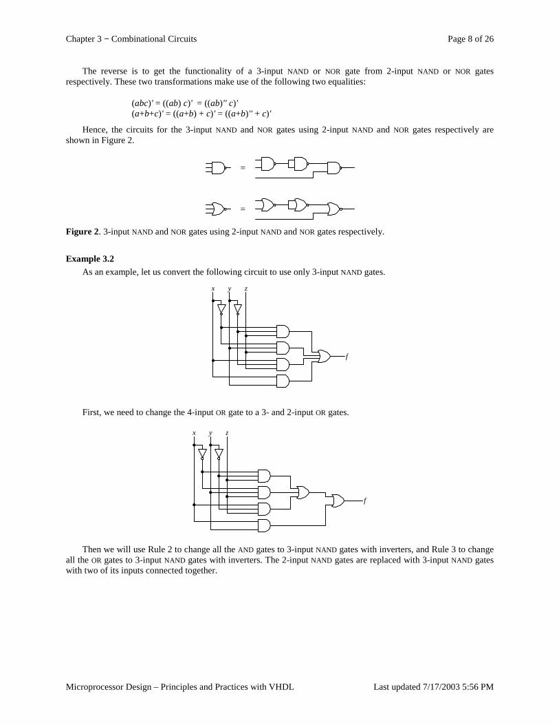
Chapter 3 − Combinational Circuits Page 8 of 26
Microprocessor Design – Principles and Practices with VHDL Last updated 7/17/2003 5:56 PM
The reverse is to get the functionality of a 3-input NAND or NOR gate from 2-input NAND or NOR gates respectively. These two transformations make use of the following two equalities:
(abc)' = ((ab) c)' = ((ab)'' c)' (a+b+c)' = ((a+b) + c)' = ((a+b)'' + c)'
Hence, the circuits for the 3-input NAND and NOR gates using 2-input NAND and NOR gates respectively are shown in Figure 2.
=
=
Figure 2. 3-input NAND and NOR gates using 2-input NAND and NOR gates respectively.
Example 3.2 As an example, let us convert the following circuit to use only 3-input NAND gates.
x y z
f
First, we need to change the 4-input OR gate to a 3- and 2-input OR gates.
x y z
f
Then we will use Rule 2 to change all the AND gates to 3-input NAND gates with inverters, and Rule 3 to change all the OR gates to 3-input NAND gates with inverters. The 2-input NAND gates are replaced with 3-input NAND gates with two of its inputs connected together.
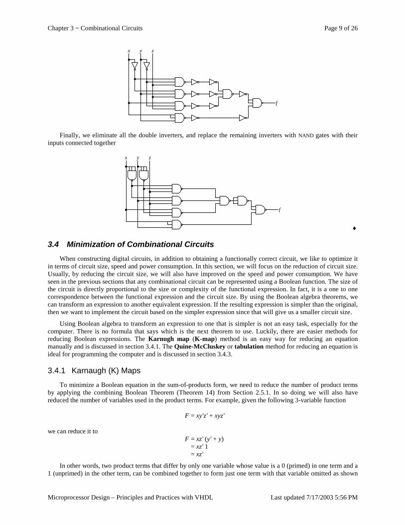
Chapter 3 − Combinational Circuits Page 9 of 26
Microprocessor Design – Principles and Practices with VHDL Last updated 7/17/2003 5:56 PM
x y z
f
Finally, we eliminate all the double inverters, and replace the remaining inverters with NAND gates with their inputs connected together
x y z
f
♦
3.4 Minimization of Combinational Circuits When constructing digital circuits, in addition to obtaining a functionally correct circuit, we like to optimize it
in terms of circuit size, speed and power consumption. In this section, we will focus on the reduction of circuit size. Usually, by reducing the circuit size, we will also have improved on the speed and power consumption. We have seen in the previous sections that any combinational circuit can be represented using a Boolean function. The size of the circuit is directly proportional to the size or complexity of the functional expression. In fact, it is a one to one correspondence between the functional expression and the circuit size. By using the Boolean algebra theorems, we can transform an expression to another equivalent expression. If the resulting expression is simpler than the original, then we want to implement the circuit based on the simpler expression since that will give us a smaller circuit size.
Using Boolean algebra to transform an expression to one that is simpler is not an easy task, especially for the computer. There is no formula that says which is the next theorem to use. Luckily, there are easier methods for reducing Boolean expressions. The Karnugh map (K-map) method is an easy way for reducing an equation manually and is discussed in section 3.4.1. The Quine-McCluskey or tabulation method for reducing an equation is ideal for programming the computer and is discussed in section 3.4.3.
3.4.1 Karnaugh (K) Maps
To minimize a Boolean equation in the sum-of-products form, we need to reduce the number of product terms by applying the combining Boolean Theorem (Theorem 14) from Section 2.5.1. In so doing we will also have reduced the number of variables used in the product terms. For example, given the following 3-variable function
F = xy'z' + xyz'
we can reduce it to F = xz' (y' + y) = xz' 1 = xz'
In other words, two product terms that differ by only one variable whose value is a 0 (primed) in one term and a 1 (unprimed) in the other term, can be combined together to form just one term with that variable omitted as shown
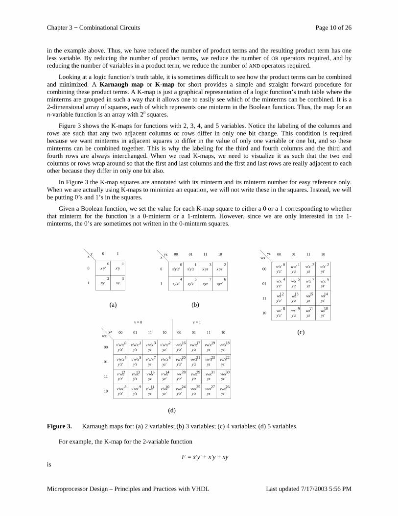
Chapter 3 − Combinational Circuits Page 10 of 26
Microprocessor Design – Principles and Practices with VHDL Last updated 7/17/2003 5:56 PM
in the example above. Thus, we have reduced the number of product terms and the resulting product term has one less variable. By reducing the number of product terms, we reduce the number of OR operators required, and by reducing the number of variables in a product term, we reduce the number of AND operators required.
Looking at a logic function’s truth table, it is sometimes difficult to see how the product terms can be combined and minimized. A Karnaugh map or K-map for short provides a simple and straight forward procedure for combining these product terms. A K-map is just a graphical representation of a logic function’s truth table where the minterms are grouped in such a way that it allows one to easily see which of the minterms can be combined. It is a 2-dimensional array of squares, each of which represents one minterm in the Boolean function. Thus, the map for an n-variable function is an array with 2n squares.
Figure 3 shows the K-maps for functions with 2, 3, 4, and 5 variables. Notice the labeling of the columns and rows are such that any two adjacent columns or rows differ in only one bit change. This condition is required because we want minterms in adjacent squares to differ in the value of only one variable or one bit, and so these minterms can be combined together. This is why the labeling for the third and fourth columns and the third and fourth rows are always interchanged. When we read K-maps, we need to visualize it as such that the two end columns or rows wrap around so that the first and last columns and the first and last rows are really adjacent to each other because they differ in only one bit also.
In Figure 3 the K-map squares are annotated with its minterm and its minterm number for easy reference only. When we are actually using K-maps to minimize an equation, we will not write these in the squares. Instead, we will be putting 0’s and 1’s in the squares.
Given a Boolean function, we set the value for each K-map square to either a 0 or a 1 corresponding to whether that minterm for the function is a 0-minterm or a 1-minterm. However, since we are only interested in the 1-minterms, the 0’s are sometimes not written in the 0-minterm squares.
1
x'y' x'y
xy' xy
0
0
1
yx
0 1
2 3
yz 01
x'y'z' x'y'z
xy'z' xy'z
00
0
1
x
0 1
4 5
1011
x'yz x'yz'
xyz xyz'
3 2
7 6
wx'y'z'
wxyz
yz 01
w'x'y'z'
w'x'y'z
w'xy'z'
w'xy'z
00
00
01
wx
0 1
4 5
1011
w'x'yz
w'x'yz'
w'xyz
w'xyz'
3 2
7 6
wxy'z'
wxy'z
wx'y'z
8 9
wxyz'
wx'yz
wx'yz'
10
11
1011
12 13 1415
(a) (b)
(c)
(d)
v = 0
v'wx'y'z'
v'wxyz
yz 01
v'w'x'y'z'
v'w'x'y'z
v'w'xy'z'
v'w'xy'z
00
00
01
wx
0 1
4 5
1011
v'w'x'yz
v'w'x'yz'
v'w'xyz
v'w'xyz'
3 2
7 6
v'wxy'z'
v'wxy'z
v'wx'y'z
8 9
v'wxyz'
v'wx'yz
v'wx'yz'
10
11
1011
12 13 1415
v = 1
vwx'y'z'
vwxyz
01
vw'x'y'z'
vw'x'y'z
vw'xy'z'
vw'xy'z
00
16
1011
vw'x'yz
vw'x'yz'
vw'xyz
vw'xyz'
wxy'z'
vwxy'z
vwx'y'z
vwxyz'
vwx'yz
vwx'yz'
17 19 18
20 21 2223
24 25 2627
28 29 3031
Figure 3. Karnaugh maps for: (a) 2 variables; (b) 3 variables; (c) 4 variables; (d) 5 variables.
For example, the K-map for the 2-variable function
F = x'y' + x'y + xy is
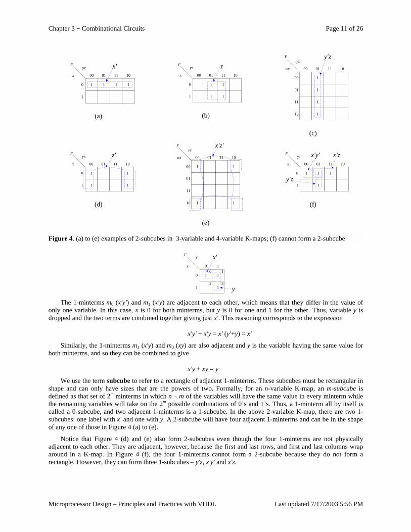
Chapter 3 − Combinational Circuits Page 11 of 26
Microprocessor Design – Principles and Practices with VHDL Last updated 7/17/2003 5:56 PM
yz
x
0 1 1
00
1 1
01 11 10
1
F x'
(a)
yz
x
0 1
00
1
1 1
01 11 10
1
F z
(b)
yz
wx
00 1
00
1
1
1
01 11 10
01
11
10
F y'z
(c)
yz
x
0 1
00
1
1 1
01 11 10
1
F z'
(d)
yz
wx
00 1
00
1
1 1
01 11 10
01
11
10
F x'z'
(e)
yz
x
0 1 1
00
1
1
01 11 10
1
F x'y' x'z
y'z
(f)
Figure 4. (a) to (e) examples of 2-subcubes in 3-variable and 4-variable K-maps; (f) cannot form a 2-subcube
x
0 1 1
0
1
10 1
2 31
F y
y
x'
The 1-minterms m0 (x'y') and m1 (x'y) are adjacent to each other, which means that they differ in the value of
only one variable. In this case, x is 0 for both minterms, but y is 0 for one and 1 for the other. Thus, variable y is dropped and the two terms are combined together giving just x'. This reasoning corresponds to the expression
x'y' + x'y = x' (y'+y) = x'
Similarly, the 1-minterms m1 (x'y) and m3 (xy) are also adjacent and y is the variable having the same value for both minterms, and so they can be combined to give
x'y + xy = y
We use the term subcube to refer to a rectangle of adjacent 1-minterms. These subcubes must be rectangular in shape and can only have sizes that are the powers of two. Formally, for an n-variable K-map, an m-subcube is defined as that set of 2m minterms in which n – m of the variables will have the same value in every minterm while the remaining variables will take on the 2m possible combinations of 0’s and 1’s. Thus, a 1-minterm all by itself is called a 0-subcube, and two adjacent 1-minterms is a 1-subcube. In the above 2-variable K-map, there are two 1-subcubes: one label with x' and one with y. A 2-subcube will have four adjacent 1-minterms and can be in the shape of any one of those in Figure 4 (a) to (e).
Notice that Figure 4 (d) and (e) also form 2-subcubes even though the four 1-minterms are not physically adjacent to each other. They are adjacent, however, because the first and last rows, and first and last columns wrap around in a K-map. In Figure 4 (f), the four 1-minterms cannot form a 2-subcube because they do not form a rectangle. However, they can form three 1-subcubes – y'z, x'y' and x'z.

Chapter 3 − Combinational Circuits Page 12 of 26
Microprocessor Design – Principles and Practices with VHDL Last updated 7/17/2003 5:56 PM
We say that a subcube is characterized by the variables having the same values for all the minterms in that subcube. In general, an m-subcube for an n-variable K-map will be characterized by n – m variables. If the value that is similar for all the variables is a 1, that variable is unprimed, whereas, if the value that is similar for all the variables is a 0, that variable is primed. In an expression, this is equivalent to the resulting smaller product term when the minterms are combined together. For example, the 2-subcube in Figure 4 (d) is characterized by z' since the value of z is 0 for all the minterms, whereas the values for x and y are not all the same for all the minterms. Similarly, the 2-subcube in Figure 4 (e) is characterized by x'z'.
For a 5-variable K-map as in Figure 3 (d), we need to visualize the right half of the array where v = 1 to be on top of the left half where v = 0. Thus, for example, minterm 20 is adjacent to minterm 4, and minterm 31 is adjacent to minterm 15.
The K-map method reduces a Boolean function from its canonical form to its standard form. The goal for the K-map method is to find as few subcubes as possible to cover all the 1-minterms in the given function. This naturally implies that the subcube size should be as big as possible. The reasoning is that each subcube gives a product term and all the subcubes (or product terms) must be ORed together to give the function. Larger subcubes require fewer AND gates because of fewer variables in the product term, and fewer subcubes will require fewer OR gates.
The procedure for using the K-map method is as follows:
1. Draw the appropriate K-map for the given function and place a 1 in the squares that correspond to the function’s 1-minterms.
2. For each 1-minterm, find the largest subcube that covers this 1-minterm. This largest subcube is known as a prime implicant (PI). By definition, a prime implicant is a subcube that is not contained within any other subcube. If there are more than one subcube that is the same size as the largest subcube, then they are all prime implicants.
3. Look for 1-minterms that are covered by only one prime implicant. Since this prime implicant is the only subcube that covers this particular 1-minterm, this prime implicant is a must have in the final solution. This prime implicant is referred to as an essential prime implicant (EPI). By definition, an essential prime implicant is a subcube that includes a 1-minterm that is not included in any other subcube.
4. Create a minimal cover list by selecting the smallest possible number of prime implicants such that every 1-minterm is contained in at least one prime implicant. This cover list must include all the essential prime implicants plus zero or more of the remaining prime implicants. It is alright that a particular 1-minterm is covered in more than one prime implicant, but all 1-minterms must be covered.
5. The final minimized function is obtained by ORing all the prime implicants from the minimal cover list.
Note that the final minimized function obtained by the K-map method may not be in its most reduced form. It is only in its most reduced standard form. Sometimes, it is possible to reduce the standard form further into a non-standard form.
Example 3.3
Use the K-map method to minimize a 4-variable (w, x, y and z) function F with the 1-minterms: m0, m2, m5, m7, m10, m13, m14, and m15. We start with the following 4-variable K-map
yz
wx
00 1
00
1
1 1
1 1 1
1
01 11 100 1 3 2
4 5 7 6
12 13 15 14
8 9 11 10
01
11
10
F
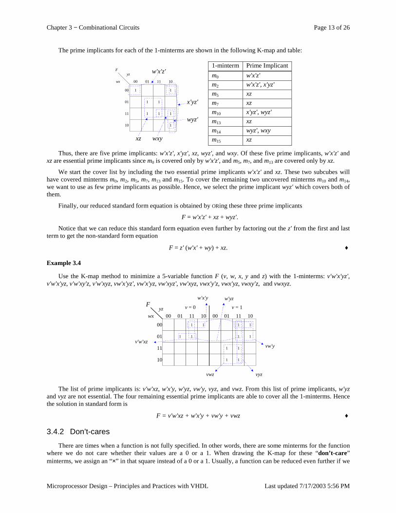
Chapter 3 − Combinational Circuits Page 13 of 26
Microprocessor Design – Principles and Practices with VHDL Last updated 7/17/2003 5:56 PM
The prime implicants for each of the 1-minterms are shown in the following K-map and table:
1-minterm Prime Implicant m0 w'x'z' m2 w'x'z', x'yz' m5 xz m7 xz m10 x'yz', wyz' m13 xz m14 wyz', wxy
yz
wx
00 1
00
1
1 1
1 1 1
1
01 11 10
01
11
10
F w'x'z'
x'yz'
xz wxy
wyz'
m15 xz
Thus, there are five prime implicants: w'x'z', x'yz', xz, wyz', and wxy. Of these five prime implicants, w'x'z' and xz are essential prime implicants since m0 is covered only by w'x'z', and m5, m7, and m13 are covered only by xz.
We start the cover list by including the two essential prime implicants w'x'z' and xz. These two subcubes will have covered minterms m0, m2, m5, m7, m13 and m15. To cover the remaining two uncovered minterms m10 and m14, we want to use as few prime implicants as possible. Hence, we select the prime implicant wyz' which covers both of them.
Finally, our reduced standard form equation is obtained by ORing these three prime implicants
F = w'x'z' + xz + wyz'.
Notice that we can reduce this standard form equation even further by factoring out the z' from the first and last term to get the non-standard form equation
F = z' (w'x' + wy) + xz. ♦
Example 3.4
Use the K-map method to minimize a 5-variable function F (v, w, x, y and z) with the 1-minterms: v'w'x'yz', v'w'x'yz, v'w'xy'z, v'w'xyz, vw'x'yz', vw'x'yz, vw'xyz', vw'xyz, vwx'y'z, vwx'yz, vwxy'z, and vwxyz.
yzwx
00
v = 0
001 1
1 1
01 11 10
01
11
10
v = 1
001 1
1 1
1 1
1 1
01 11 10
F
vwz
vw'y
w'x'y
v'w'xz
w'yz
vyz
The list of prime implicants is: v'w'xz, w'x'y, w'yz, vw'y, vyz, and vwz. From this list of prime implicants, w'yz and vyz are not essential. The four remaining essential prime implicants are able to cover all the 1-minterms. Hence the solution in standard form is
F = v'w'xz + w'x'y + vw'y + vwz ♦
3.4.2 Don’t-cares
There are times when a function is not fully specified. In other words, there are some minterms for the function where we do not care whether their values are a 0 or a 1. When drawing the K-map for these “don’t-care” minterms, we assign an “×” in that square instead of a 0 or a 1. Usually, a function can be reduced even further if we
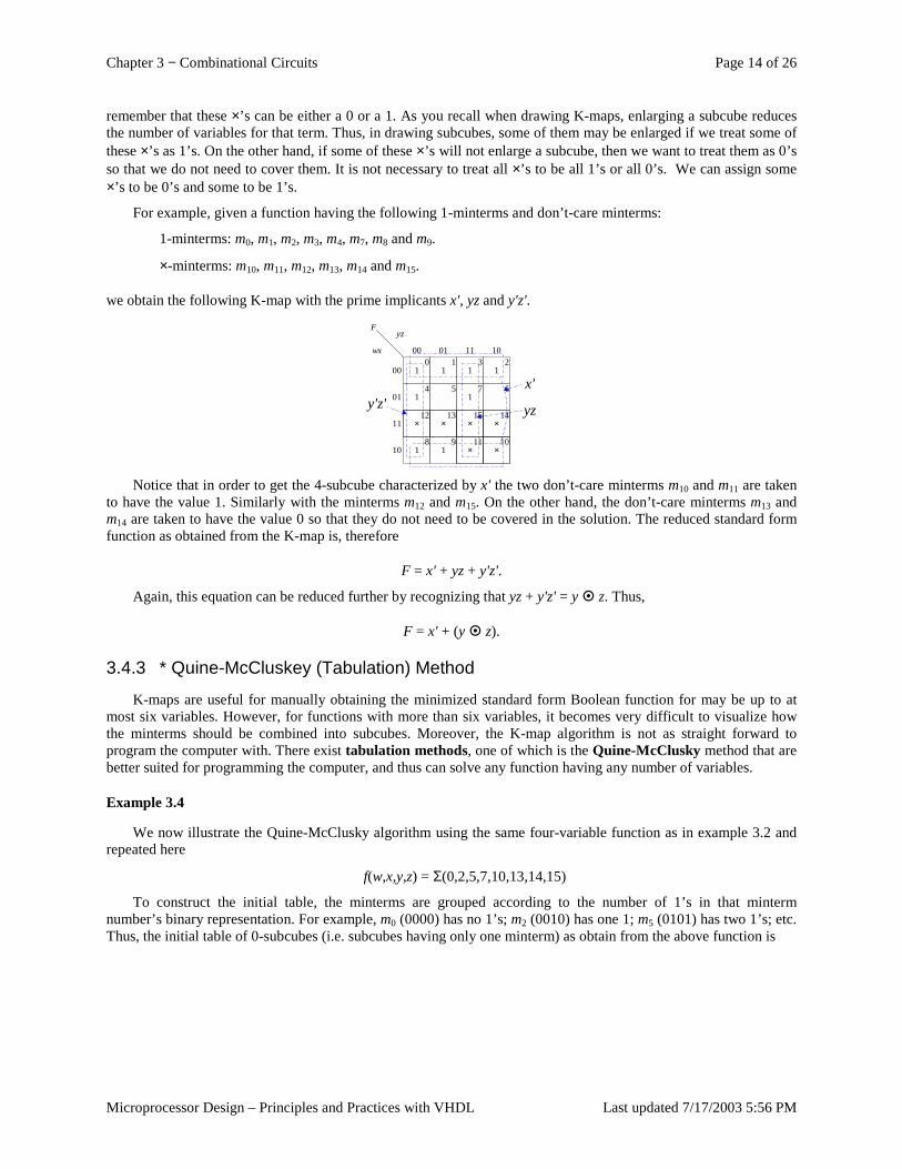
Chapter 3 − Combinational Circuits Page 14 of 26
Microprocessor Design – Principles and Practices with VHDL Last updated 7/17/2003 5:56 PM
remember that these ×’s can be either a 0 or a 1. As you recall when drawing K-maps, enlarging a subcube reduces the number of variables for that term. Thus, in drawing subcubes, some of them may be enlarged if we treat some of these ×’s as 1’s. On the other hand, if some of these ×’s will not enlarge a subcube, then we want to treat them as 0’s so that we do not need to cover them. It is not necessary to treat all ×’s to be all 1’s or all 0’s. We can assign some ×’s to be 0’s and some to be 1’s.
For example, given a function having the following 1-minterms and don’t-care minterms:
1-minterms: m0, m1, m2, m3, m4, m7, m8 and m9.
×-minterms: m10, m11, m12, m13, m14 and m15.
we obtain the following K-map with the prime implicants x', yz and y'z'.
yz
wx
00 1 1
00
1 1
1 1
1 1
01 11 100 1 3 2
4 5 7 6
12 13 15 14
8 9 11 10
01
11
10
F
×
x'
yzy'z'× × ×
××
Notice that in order to get the 4-subcube characterized by x' the two don’t-care minterms m10 and m11 are taken
to have the value 1. Similarly with the minterms m12 and m15. On the other hand, the don’t-care minterms m13 and m14 are taken to have the value 0 so that they do not need to be covered in the solution. The reduced standard form function as obtained from the K-map is, therefore
F = x' + yz + y'z'.
Again, this equation can be reduced further by recognizing that yz + y'z' = y � z. Thus,
F = x' + (y � z).
3.4.3 * Quine-McCluskey (Tabulation) Method
K-maps are useful for manually obtaining the minimized standard form Boolean function for may be up to at most six variables. However, for functions with more than six variables, it becomes very difficult to visualize how the minterms should be combined into subcubes. Moreover, the K-map algorithm is not as straight forward to program the computer with. There exist tabulation methods, one of which is the Quine-McClusky method that are better suited for programming the computer, and thus can solve any function having any number of variables.
Example 3.4
We now illustrate the Quine-McClusky algorithm using the same four-variable function as in example 3.2 and repeated here
f(w,x,y,z) = Σ(0,2,5,7,10,13,14,15)
To construct the initial table, the minterms are grouped according to the number of 1’s in that minterm number’s binary representation. For example, m0 (0000) has no 1’s; m2 (0010) has one 1; m5 (0101) has two 1’s; etc. Thus, the initial table of 0-subcubes (i.e. subcubes having only one minterm) as obtain from the above function is
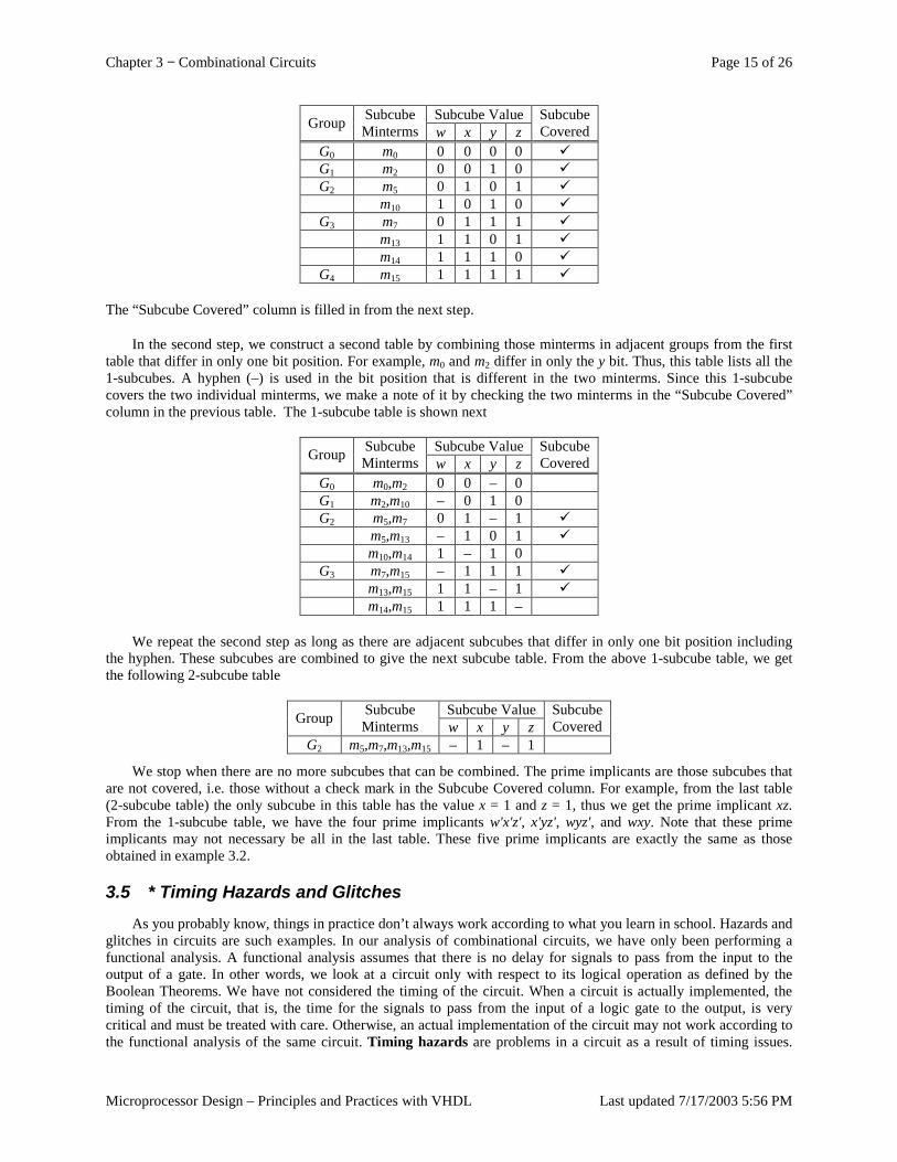
Chapter 3 − Combinational Circuits Page 15 of 26
Microprocessor Design – Principles and Practices with VHDL Last updated 7/17/2003 5:56 PM
Subcube Value Group Subcube Minterms w x y z
Subcube Covered
G0 m0 0 0 0 0 � G1 m2 0 0 1 0 � G2 m5 0 1 0 1 �
m10 1 0 1 0 � G3 m7 0 1 1 1 �
m13 1 1 0 1 � m14 1 1 1 0 �
G4 m15 1 1 1 1 �
The “Subcube Covered” column is filled in from the next step.
In the second step, we construct a second table by combining those minterms in adjacent groups from the first table that differ in only one bit position. For example, m0 and m2 differ in only the y bit. Thus, this table lists all the 1-subcubes. A hyphen (–) is used in the bit position that is different in the two minterms. Since this 1-subcube covers the two individual minterms, we make a note of it by checking the two minterms in the “Subcube Covered” column in the previous table. The 1-subcube table is shown next
Subcube Value Group Subcube
Minterms w x y z Subcube Covered
G0 m0,m2 0 0 – 0 G1 m2,m10 – 0 1 0 G2 m5,m7 0 1 – 1 �
m5,m13 – 1 0 1 � m10,m14 1 – 1 0
G3 m7,m15 – 1 1 1 � m13,m15 1 1 – 1 � m14,m15 1 1 1 –
We repeat the second step as long as there are adjacent subcubes that differ in only one bit position including the hyphen. These subcubes are combined to give the next subcube table. From the above 1-subcube table, we get the following 2-subcube table
Subcube Value Group Subcube
Minterms w x y z Subcube Covered
G2 m5,m7,m13,m15 – 1 – 1
We stop when there are no more subcubes that can be combined. The prime implicants are those subcubes that are not covered, i.e. those without a check mark in the Subcube Covered column. For example, from the last table (2-subcube table) the only subcube in this table has the value x = 1 and z = 1, thus we get the prime implicant xz. From the 1-subcube table, we have the four prime implicants w'x'z', x'yz', wyz', and wxy. Note that these prime implicants may not necessary be all in the last table. These five prime implicants are exactly the same as those obtained in example 3.2.
3.5 * Timing Hazards and Glitches As you probably know, things in practice don’t always work according to what you learn in school. Hazards and
glitches in circuits are such examples. In our analysis of combinational circuits, we have only been performing a functional analysis. A functional analysis assumes that there is no delay for signals to pass from the input to the output of a gate. In other words, we look at a circuit only with respect to its logical operation as defined by the Boolean Theorems. We have not considered the timing of the circuit. When a circuit is actually implemented, the timing of the circuit, that is, the time for the signals to pass from the input of a logic gate to the output, is very critical and must be treated with care. Otherwise, an actual implementation of the circuit may not work according to the functional analysis of the same circuit. Timing hazards are problems in a circuit as a result of timing issues.
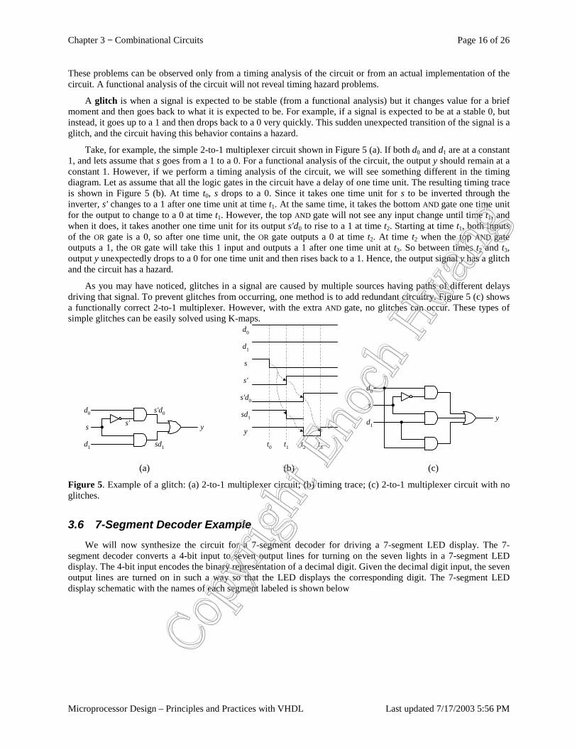
Chapter 3 − Combinational Circuits Page 16 of 26
Microprocessor Design – Principles and Practices with VHDL Last updated 7/17/2003 5:56 PM
These problems can be observed only from a timing analysis of the circuit or from an actual implementation of the circuit. A functional analysis of the circuit will not reveal timing hazard problems.
A glitch is when a signal is expected to be stable (from a functional analysis) but it changes value for a brief moment and then goes back to what it is expected to be. For example, if a signal is expected to be at a stable 0, but instead, it goes up to a 1 and then drops back to a 0 very quickly. This sudden unexpected transition of the signal is a glitch, and the circuit having this behavior contains a hazard.
Take, for example, the simple 2-to-1 multiplexer circuit shown in Figure 5 (a). If both d0 and d1 are at a constant 1, and lets assume that s goes from a 1 to a 0. For a functional analysis of the circuit, the output y should remain at a constant 1. However, if we perform a timing analysis of the circuit, we will see something different in the timing diagram. Let as assume that all the logic gates in the circuit have a delay of one time unit. The resulting timing trace is shown in Figure 5 (b). At time t0, s drops to a 0. Since it takes one time unit for s to be inverted through the inverter, s' changes to a 1 after one time unit at time t1. At the same time, it takes the bottom AND gate one time unit for the output to change to a 0 at time t1. However, the top AND gate will not see any input change until time t1, and when it does, it takes another one time unit for its output s'd0 to rise to a 1 at time t2. Starting at time t1, both inputs of the OR gate is a 0, so after one time unit, the OR gate outputs a 0 at time t2. At time t2 when the top AND gate outputs a 1, the OR gate will take this 1 input and outputs a 1 after one time unit at t3. So between times t2 and t3, output y unexpectedly drops to a 0 for one time unit and then rises back to a 1. Hence, the output signal y has a glitch and the circuit has a hazard.
As you may have noticed, glitches in a signal are caused by multiple sources having paths of different delays driving that signal. To prevent glitches from occurring, one method is to add redundant circuitry. Figure 5 (c) shows a functionally correct 2-to-1 multiplexer. However, with the extra AND gate, no glitches can occur. These types of simple glitches can be easily solved using K-maps.
d0
s y
d1
s'd0
sd1
s'
d0
d1
s
s'
s'd0
sd1
y
t0 t1 t2 t3
d0
s
yd1
(a) (b) (c)
Figure 5. Example of a glitch: (a) 2-to-1 multiplexer circuit; (b) timing trace; (c) 2-to-1 multiplexer circuit with no glitches.
3.6 7-Segment Decoder Example We will now synthesize the circuit for a 7-segment decoder for driving a 7-segment LED display. The 7-
segment decoder converts a 4-bit input to seven output lines for turning on the seven lights in a 7-segment LED display. The 4-bit input encodes the binary representation of a decimal digit. Given the decimal digit input, the seven output lines are turned on in such a way so that the LED displays the corresponding digit. The 7-segment LED display schematic with the names of each segment labeled is shown below
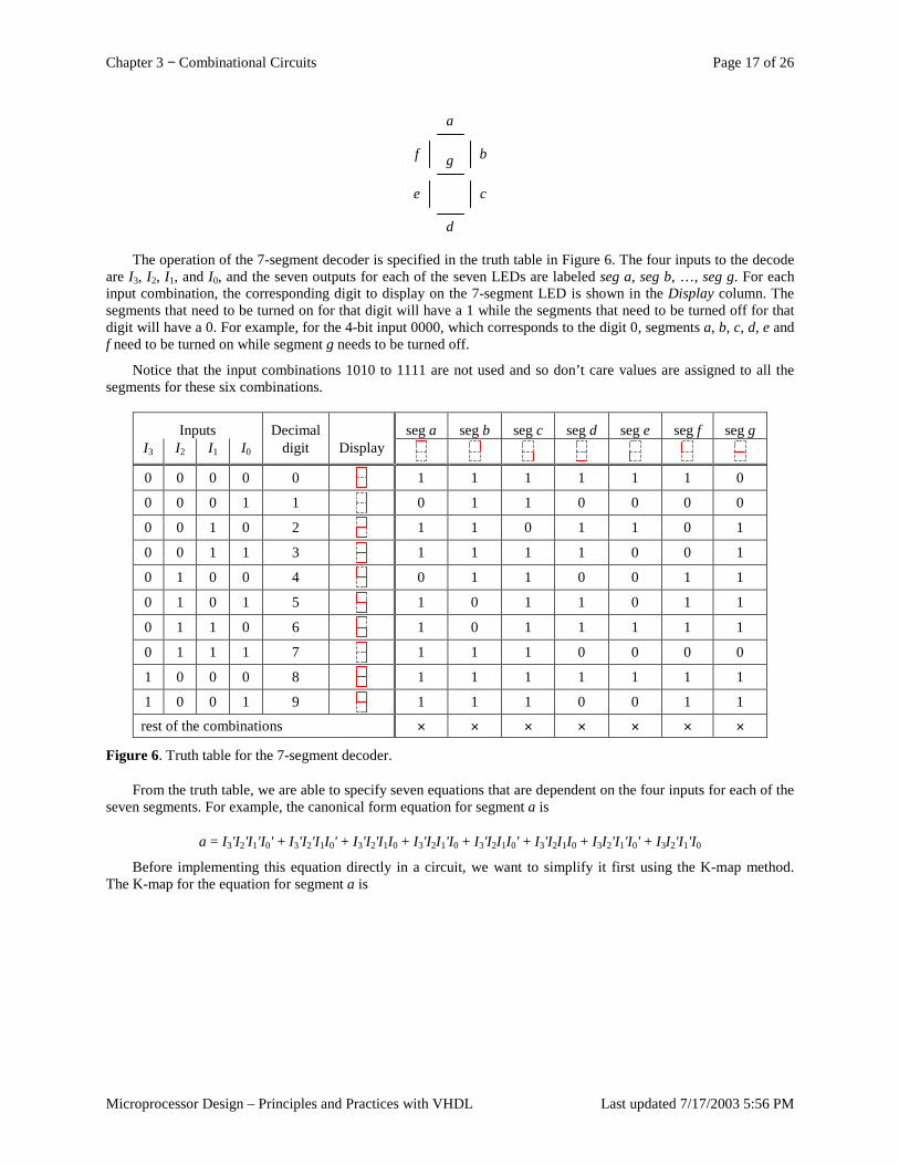
Chapter 3 − Combinational Circuits Page 17 of 26
Microprocessor Design – Principles and Practices with VHDL Last updated 7/17/2003 5:56 PM
b
a
c
d
e
f g
The operation of the 7-segment decoder is specified in the truth table in Figure 6. The four inputs to the decode
are I3, I2, I1, and I0, and the seven outputs for each of the seven LEDs are labeled seg a, seg b, …, seg g. For each input combination, the corresponding digit to display on the 7-segment LED is shown in the Display column. The segments that need to be turned on for that digit will have a 1 while the segments that need to be turned off for that digit will have a 0. For example, for the 4-bit input 0000, which corresponds to the digit 0, segments a, b, c, d, e and f need to be turned on while segment g needs to be turned off.
Notice that the input combinations 1010 to 1111 are not used and so don’t care values are assigned to all the segments for these six combinations.
Inputs Decimal seg a seg b seg c seg d seg e seg f seg g I3 I2 I1 I0 digit Display
0 0 0 0 0 1 1 1 1 1 1 0
0 0 0 1 1 0 1 1 0 0 0 0
0 0 1 0 2 1 1 0 1 1 0 1
0 0 1 1 3 1 1 1 1 0 0 1
0 1 0 0 4 0 1 1 0 0 1 1
0 1 0 1 5 1 0 1 1 0 1 1
0 1 1 0 6 1 0 1 1 1 1 1
0 1 1 1 7 1 1 1 0 0 0 0
1 0 0 0 8 1 1 1 1 1 1 1
1 0 0 1 9 1 1 1 0 0 1 1
rest of the combinations × × × × × × ×
Figure 6. Truth table for the 7-segment decoder.
From the truth table, we are able to specify seven equations that are dependent on the four inputs for each of the seven segments. For example, the canonical form equation for segment a is
a = I3'I2'I1'I0' + I3'I2'I1I0' + I3'I2'I1I0 + I3'I2I1'I0 + I3'I2I1I0' + I3'I2I1I0 + I3I2'I1'I0' + I3I2'I1'I0
Before implementing this equation directly in a circuit, we want to simplify it first using the K-map method. The K-map for the equation for segment a is
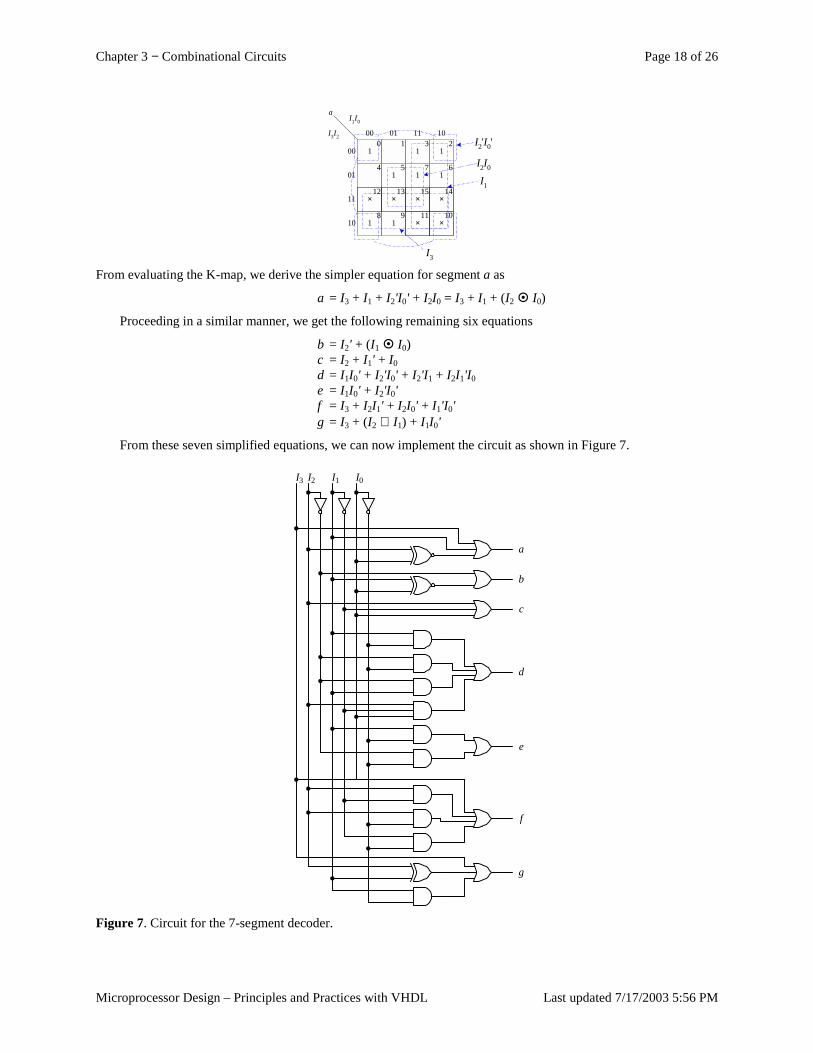
Chapter 3 − Combinational Circuits Page 18 of 26
Microprocessor Design – Principles and Practices with VHDL Last updated 7/17/2003 5:56 PM
I1I0
I3I2
00 1
00
1 1
1 1 1
1 1
01 11 100 1 3 2
4 5 7 6
12 13 15 14
8 9 11 10
01
11
10
a
× × × ×
××
I1
I3
I2I0
I2'I0'
From evaluating the K-map, we derive the simpler equation for segment a as
a = I3 + I1 + I2'I0' + I2I0 = I3 + I1 + (I2 � I0)
Proceeding in a similar manner, we get the following remaining six equations
b = I2' + (I1 � I0) c = I2 + I1' + I0 d = I1I0' + I2'I0' + I2'I1 + I2I1'I0 e = I1I0' + I2'I0' f = I3 + I2I1' + I2I0' + I1'I0' g = I3 + (I2 ⊕ I1) + I1I0'
From these seven simplified equations, we can now implement the circuit as shown in Figure 7.
I2 I1 I0I3
a
b
c
d
e
f
g
Figure 7. Circuit for the 7-segment decoder.
Chapter 3 − Combinational Circuits Page 19 of 26
Microprocessor Design – Principles and Practices with VHDL Last updated 7/17/2003 5:56 PM
3.7 VHDL Code for Combinational Circuits Writing VHDL code to describe a circuit, whether combinational or sequential, can be done at any one of three
levels: structural, dataflow, or behavioral. At the structural level, which is the lowest level, you have to first manually design the circuit. Having drawn the circuit, you use VHDL to specify the components and gates that are needed by the circuit and how they are connected together by following your circuit exactly. Synthesizing a structural VHDL description of a circuit will, of course, produce a netlist that is exactly like your original circuit. The advantage of working at the structural level is that you have full control as to what components are used and how they are connected. On the other hand, you need to first come up with the circuit and so the full capabilities of the synthesizer are not utilized.
At the dataflow level, you use the built-in logical functions of VHDL in signal assignment statements to describe a circuit, which again you have to first design manually. Boolean functions that describe a circuit can be easily converted to signal assignment statements using the built-in logical functions. The only drawback is that the built-in logical functions such as the AND and OR function only take two operands. This is like having only 2-input gates to work with.
All the statements use in the structural and dataflow level are executed concurrently. As oppose to statements in a computer program, which are usually executed in a sequential manner. In other words, the ordering of the VHDL statements written in the structural or dataflow level does not matter – the result would be exactly the same.
Describing a circuit at the behavioral level is most similar to writing a computer program. You have all the standard high-level programming constructs such as the FOR LOOP, WHILE LOOP, IF THEN ELSE, CASE, and variable assignments. The statements are enclosed in a process block and are executed sequentially.
3.7.1 Structural BCD to 7-Segment Decoder
The structural VHDL description of the BCD to 7-segment decoder is shown in Figure 8.
ENTITY myxnor2 IS PORT(i1, i2: IN BIT;o: OUT BIT);
END myxnor2;ARCHITECTURE Dataflow OF myxnor2 ISBEGIN
o <= not(i1 XOR i2);END Dataflow;
ENTITY myxor2 IS PORT(i1, i2: IN BIT;o: OUT BIT);
END myxor2;ARCHITECTURE Dataflow OF myxor2 ISBEGIN
o <= i1 XOR i2;END Dataflow;
ENTITY myand2 IS PORT(i1, i2: IN BIT;o: OUT BIT);
END myand2;ARCHITECTURE Dataflow OF myand2 ISBEGIN
o <= i1 AND i2;END Dataflow;
ENTITY myand3 IS PORT(
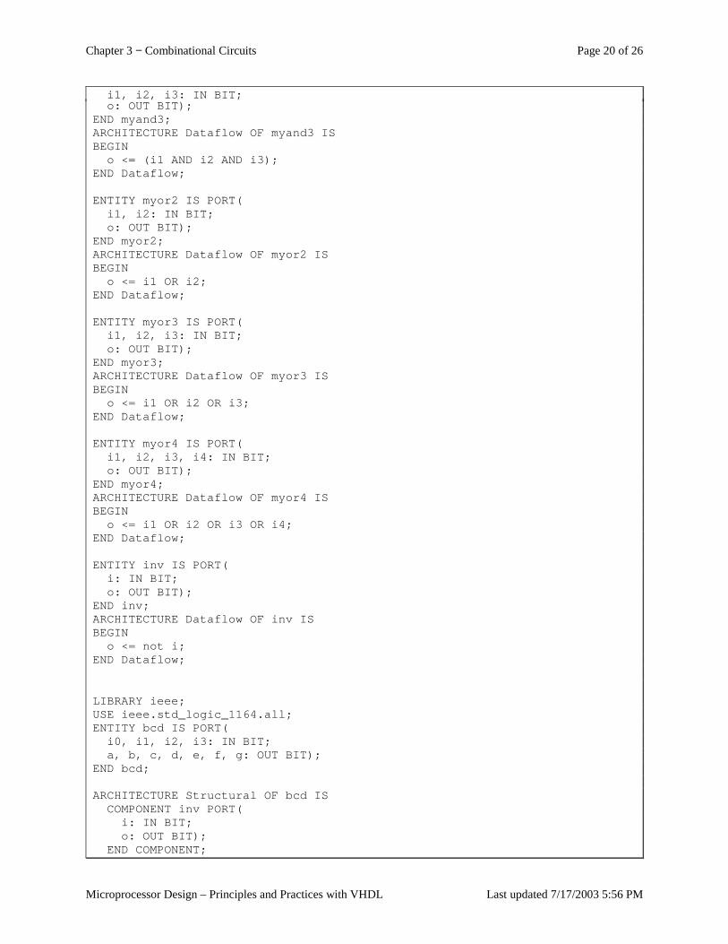
Chapter 3 − Combinational Circuits Page 20 of 26
Microprocessor Design – Principles and Practices with VHDL Last updated 7/17/2003 5:56 PM
i1, i2, i3: IN BIT;o: OUT BIT);
END myand3;ARCHITECTURE Dataflow OF myand3 ISBEGIN
o <= (i1 AND i2 AND i3);END Dataflow;
ENTITY myor2 IS PORT(i1, i2: IN BIT;o: OUT BIT);
END myor2;ARCHITECTURE Dataflow OF myor2 ISBEGIN
o <= i1 OR i2;END Dataflow;
ENTITY myor3 IS PORT(i1, i2, i3: IN BIT;o: OUT BIT);
END myor3;ARCHITECTURE Dataflow OF myor3 ISBEGIN
o <= i1 OR i2 OR i3;END Dataflow;
ENTITY myor4 IS PORT(i1, i2, i3, i4: IN BIT;o: OUT BIT);
END myor4;ARCHITECTURE Dataflow OF myor4 ISBEGIN
o <= i1 OR i2 OR i3 OR i4;END Dataflow;
ENTITY inv IS PORT(i: IN BIT;o: OUT BIT);
END inv;ARCHITECTURE Dataflow OF inv ISBEGIN
o <= not i;END Dataflow;
LIBRARY ieee;USE ieee.std_logic_1164.all;ENTITY bcd IS PORT(
i0, i1, i2, i3: IN BIT;a, b, c, d, e, f, g: OUT BIT);
END bcd;
ARCHITECTURE Structural OF bcd ISCOMPONENT inv PORT(
i: IN BIT;o: OUT BIT);
END COMPONENT;
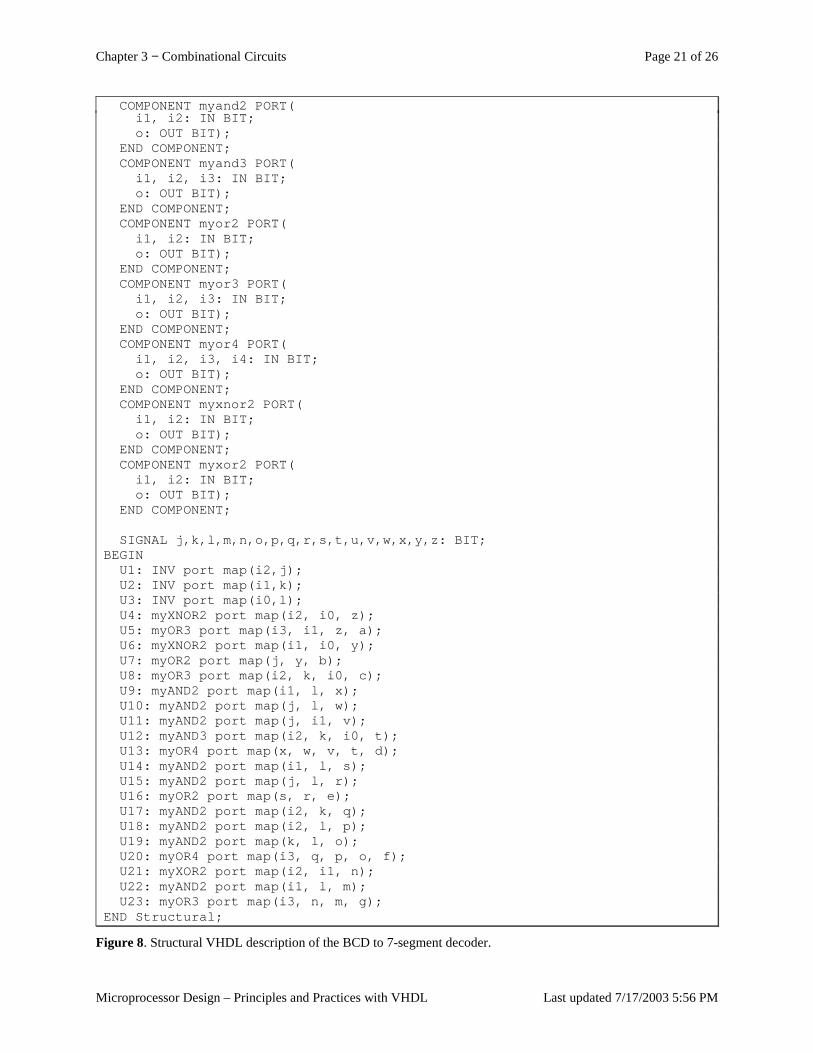
Chapter 3 − Combinational Circuits Page 21 of 26
Microprocessor Design – Principles and Practices with VHDL Last updated 7/17/2003 5:56 PM
COMPONENT myand2 PORT(i1, i2: IN BIT;o: OUT BIT);
END COMPONENT;COMPONENT myand3 PORT(
i1, i2, i3: IN BIT;o: OUT BIT);
END COMPONENT;COMPONENT myor2 PORT(
i1, i2: IN BIT;o: OUT BIT);
END COMPONENT;COMPONENT myor3 PORT(
i1, i2, i3: IN BIT;o: OUT BIT);
END COMPONENT;COMPONENT myor4 PORT(
i1, i2, i3, i4: IN BIT;o: OUT BIT);
END COMPONENT;COMPONENT myxnor2 PORT(
i1, i2: IN BIT;o: OUT BIT);
END COMPONENT;COMPONENT myxor2 PORT(
i1, i2: IN BIT;o: OUT BIT);
END COMPONENT;
SIGNAL j,k,l,m,n,o,p,q,r,s,t,u,v,w,x,y,z: BIT;BEGIN
U1: INV port map(i2,j);U2: INV port map(i1,k);U3: INV port map(i0,l);U4: myXNOR2 port map(i2, i0, z);U5: myOR3 port map(i3, i1, z, a);U6: myXNOR2 port map(i1, i0, y);U7: myOR2 port map(j, y, b);U8: myOR3 port map(i2, k, i0, c);U9: myAND2 port map(i1, l, x);U10: myAND2 port map(j, l, w);U11: myAND2 port map(j, i1, v);U12: myAND3 port map(i2, k, i0, t);U13: myOR4 port map(x, w, v, t, d);U14: myAND2 port map(i1, l, s);U15: myAND2 port map(j, l, r);U16: myOR2 port map(s, r, e);U17: myAND2 port map(i2, k, q);U18: myAND2 port map(i2, l, p);U19: myAND2 port map(k, l, o);U20: myOR4 port map(i3, q, p, o, f);U21: myXOR2 port map(i2, i1, n);U22: myAND2 port map(i1, l, m);U23: myOR3 port map(i3, n, m, g);
END Structural;
Figure 8. Structural VHDL description of the BCD to 7-segment decoder.
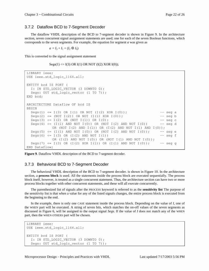
Chapter 3 − Combinational Circuits Page 22 of 26
Microprocessor Design – Principles and Practices with VHDL Last updated 7/17/2003 5:56 PM
3.7.2 Dataflow BCD to 7-Segment Decoder
The dataflow VHDL description of the BCD to 7-segment decoder is shown in Figure 9. In the architecture section, seven concurrent signal assignment statements are used; one for each of the seven Boolean functions, which corresponds to the seven segments. For example, the equation for segment a was given as
a = I3 + I1 + (I2 � I0)
This is converted to the signal assignment statement
Segs(1) <= I(3) OR I(1) OR NOT (I(2) XOR I(0));
LIBRARY ieee;USE ieee.std_logic_1164.all;
ENTITY bcd IS PORT (I: IN STD_LOGIC_VECTOR (3 DOWNTO 0);Segs: OUT std_logic_vector (1 TO 7));
END bcd;
ARCHITECTURE Dataflow OF bcd ISBEGIN
Segs(1) <= I(3) OR I(1) OR NOT (I(2) XOR I(0)); -- seg aSegs(2) <= (NOT I(2)) OR NOT (I(1) XOR I(0)); -- seg bSegs(3) <= I(2) OR (NOT I(1)) OR I(0); -- seg cSegs(4) <= (I(1) AND NOT I(0)) OR (NOT I(2) AND NOT I(0)) -- seg d
OR (NOT I(2) AND I(1)) OR (I(2) AND NOT I(1) AND I(0));Segs(5) <= (I(1) AND NOT I(0)) OR (NOT I(2) AND NOT I(0)); -- seg eSegs(6) <= I(3) OR (I(2) AND NOT I(1)) -- seg f
OR (I(2) AND NOT I(0)) OR (NOT I(1) AND NOT I(0));Segs(7) <= I(3) OR (I(2) XOR I(1)) OR (I(1) AND NOT I(0)); -- seg g
END Dataflow;
Figure 9. Dataflow VHDL description of the BCD to 7-segment decoder.
3.7.3 Behavioral BCD to 7-Segment Decoder
The behavioral VHDL description of the BCD to 7-segment decoder. is shown in Figure 10. In the architecture section, a process block is used. All the statements inside the process block are executed sequentially. The process block itself, however, is treated as a single concurrent statement. Thus, the architecture section can have two or more process blocks together with other concurrent statements, and these will all execute concurrently.
The parenthesized list of signals after the PROCESS keyword is referred to as the sensitivity list The purpose of the sensitivity list is that when a value for any of the listed signals changes, the entire process block is executed from the beginning to the end.
In the example, there is only one CASE statement inside the process block. Depending on the value of I, one of the WHEN part will be executed. A string of seven bits, which matches the on-off values of the seven segments as discussed in Figure 6, will be assigned to the output signal Segs. If the value of I does not match any of the WHEN part, then the WHEN OTHERS part will be chosen.
LIBRARY ieee;USE ieee.std_logic_1164.all;
ENTITY bcd IS PORT (I: IN STD_LOGIC_VECTOR (3 DOWNTO 0);Segs: OUT std_logic_vector (1 TO 7));
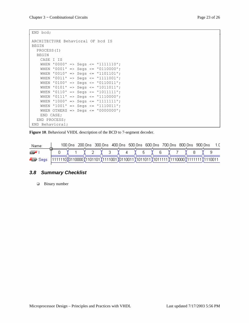
Chapter 3 − Combinational Circuits Page 23 of 26
Microprocessor Design – Principles and Practices with VHDL Last updated 7/17/2003 5:56 PM
END bcd;
ARCHITECTURE Behavioral OF bcd ISBEGIN
PROCESS(I)BEGINCASE I ISWHEN "0000" => Segs <= "1111110";WHEN "0001" => Segs <= "0110000";WHEN "0010" => Segs <= "1101101";WHEN "0011" => Segs <= "1111001";WHEN "0100" => Segs <= "0110011";WHEN "0101" => Segs <= "1011011";WHEN "0110" => Segs <= "1011111";WHEN "0111" => Segs <= "1110000";WHEN "1000" => Segs <= "1111111";WHEN "1001" => Segs <= "1110011";WHEN OTHERS => Segs <= "0000000";END CASE;
END PROCESS;END Behavioral;
Figure 10. Behavioral VHDL description of the BCD to 7-segment decoder.
3.8 Summary Checklist
� Binary number
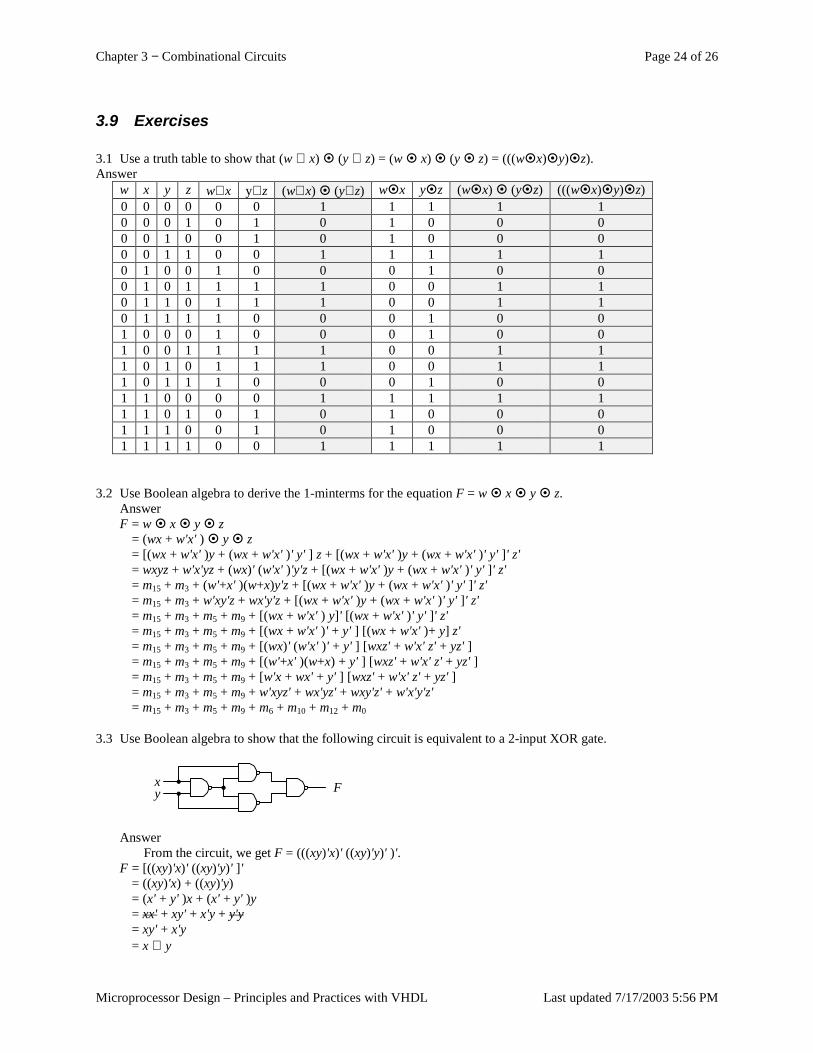
Chapter 3 − Combinational Circuits Page 24 of 26
Microprocessor Design – Principles and Practices with VHDL Last updated 7/17/2003 5:56 PM
3.9 Exercises
3.1 Use a truth table to show that (w ⊕ x) � (y ⊕ z) = (w � x) � (y � z) = (((w�x)�y)�z). Answer
w x y z w⊕ x y⊕ z (w⊕ x) � (y⊕ z) w�x y�z (w�x) � (y�z) (((w�x)�y)�z) 0 0 0 0 0 0 1 1 1 1 1 0 0 0 1 0 1 0 1 0 0 0 0 0 1 0 0 1 0 1 0 0 0 0 0 1 1 0 0 1 1 1 1 1 0 1 0 0 1 0 0 0 1 0 0 0 1 0 1 1 1 1 0 0 1 1 0 1 1 0 1 1 1 0 0 1 1 0 1 1 1 1 0 0 0 1 0 0 1 0 0 0 1 0 0 0 1 0 0 1 0 0 1 1 1 1 0 0 1 1 1 0 1 0 1 1 1 0 0 1 1 1 0 1 1 1 0 0 0 1 0 0 1 1 0 0 0 0 1 1 1 1 1 1 1 0 1 0 1 0 1 0 0 0 1 1 1 0 0 1 0 1 0 0 0 1 1 1 1 0 0 1 1 1 1 1
3.2 Use Boolean algebra to derive the 1-minterms for the equation F = w � x � y � z. Answer F = w � x � y � z = (wx + w'x' ) � y � z = [(wx + w'x' )y + (wx + w'x' )' y' ] z + [(wx + w'x' )y + (wx + w'x' )' y' ]' z' = wxyz + w'x'yz + (wx)' (w'x' )'y'z + [(wx + w'x' )y + (wx + w'x' )' y' ]' z' = m15 + m3 + (w'+x' )(w+x)y'z + [(wx + w'x' )y + (wx + w'x' )' y' ]' z' = m15 + m3 + w'xy'z + wx'y'z + [(wx + w'x' )y + (wx + w'x' )' y' ]' z' = m15 + m3 + m5 + m9 + [(wx + w'x' ) y]' [(wx + w'x' )' y' ]' z' = m15 + m3 + m5 + m9 + [(wx + w'x' )' + y' ] [(wx + w'x' )+ y] z' = m15 + m3 + m5 + m9 + [(wx)' (w'x' )' + y' ] [wxz' + w'x' z' + yz' ] = m15 + m3 + m5 + m9 + [(w'+x' )(w+x) + y' ] [wxz' + w'x' z' + yz' ] = m15 + m3 + m5 + m9 + [w'x + wx' + y' ] [wxz' + w'x' z' + yz' ] = m15 + m3 + m5 + m9 + w'xyz' + wx'yz' + wxy'z' + w'x'y'z' = m15 + m3 + m5 + m9 + m6 + m10 + m12 + m0
3.3 Use Boolean algebra to show that the following circuit is equivalent to a 2-input XOR gate.
xy F
Answer From the circuit, we get F = (((xy)'x)' ((xy)'y)' )'.
F = [((xy)'x)' ((xy)'y)' ]' = ((xy)'x) + ((xy)'y) = (x' + y' )x + (x' + y' )y = xx' + xy' + x'y + y'y = xy' + x'y = x ⊕ y
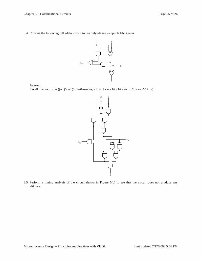
Chapter 3 − Combinational Circuits Page 25 of 26
Microprocessor Design – Principles and Practices with VHDL Last updated 7/17/2003 5:56 PM
3.4 Convert the following full adder circuit to use only eleven 2-input NAND gates.
x y
cin
cout
s Answer: Recall that wx + yz = ((wx)' (yz)')'. Furthermore, x ⊕ y ⊕ z = x � y � z and x � y = (x'y' + xy).
x y
cout
cin
s
3.5 Perform a timing analysis of the circuit shown in Figure 5(c) to see that the circuit does not produce any glitches.
Chapter 3 − Combinational Circuits Page 26 of 26
Microprocessor Design – Principles and Practices with VHDL Last updated 7/17/2003 5:56 PM
Index ×. See Don’t cares. 7-segment decoder, 15
A
Analysis combinational circuits, of, 2
C
Characterize, 11 Combinational circuit
analysis. See Analysis of. minimization. See Minimization of. synthesis. See Synthesis of.
Combinational circuits, 2
D
Don’t cares, 13
E
Essential prime implicant, 11
G
Glitch, 15
H
Hazard, 15
K
Karnaugh-map. See K-map. K-map, 8
M
Minimal cover, 11 Minimization
combinational circuits, of, 8
Minterms, 9
N
NAND gate, 5 NOR gate, 5
P
Prime implicant, 11 Process block. See VHDL:statement:process block. Product term, 11
Q
Quine-McCluskey method, 13
S
Sensitivity list. See VHDL:sensitivity list. Subcube, 10 Synthesis
combinational circuits, of, 4
T
Tabulation method, 13 See also Quine-McCluskey method.
Technology mapping, 5
V
VHDL, 18 behavioral level, 18, 21 dataflow level, 18, 21 sensitivity list, 21 structural level, 18
VHDL code 7-segment decoder, 18, 21
VHDL statement Process block, 18, 21
Chapter 4 − Combinational Components Page 1 of 28
Microprocessor Design – Principles and Practices with VHDL Last updated 7/16/2003 12:27 PM
Table of Content Table of Content ........................................................................................................................................................... 1 4 Combinational Components.................................................................................................................................. 2
4.1 Signal Naming Conventions.......................................................................................................................... 2 4.2 Adder............................................................................................................................................................. 2
4.2.1 Full Adder ............................................................................................................................................. 2 4.2.2 Ripple-Carry Adder............................................................................................................................... 3 4.2.3 Carry-Lookahead Adder........................................................................................................................ 4
4.3 Two’s-Complement Representation for Negative Numbers ......................................................................... 6 4.4 Subtractor ...................................................................................................................................................... 8
4.4.1 Adder / Subtractor Combination ........................................................................................................... 8 4.5 Arithmetic Logic Unit ................................................................................................................................. 10 4.6 Decoder ....................................................................................................................................................... 14 4.7 Encoder ....................................................................................................................................................... 15
4.7.1 Priority Encoder .................................................................................................................................. 16 4.8 Multiplexer.................................................................................................................................................. 17
4.8.1 Using Multiplexers to Implement a Function...................................................................................... 20 4.9 Tri-state Buffer............................................................................................................................................ 20 4.10 Comparators ................................................................................................................................................ 21 4.11 Shifter / Rotator........................................................................................................................................... 23 4.12 Multiplier .................................................................................................................................................... 25 4.13 Summary Checklist ..................................................................................................................................... 26 4.14 Exercises ..................................................................................................................................................... 27 Index ....................................................................................................................................................................... 28
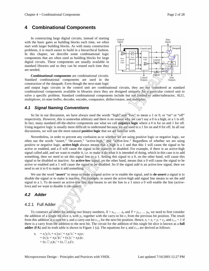
Chapter 4 − Combinational Components Page 2 of 28
Microprocessor Design – Principles and Practices with VHDL Last updated 7/16/2003 12:27 PM
ControlSignals
StatusSignals
01s y
'0'
DataInputs
DataOutputs
Datapath
ALU
registerff
OutputLogicNext-
stateLogic
ControlInputs
ControlOutputs
StateMemory
register
Control unit
ff
4 Combinational Components
In constructing large digital circuits, instead of starting with the basic gates as building blocks each time, we often start with larger building blocks. As with many construction problems, it is much easier to build in a hierarchical fashion. In this chapter, we describe some combinational logic components that are often used as building blocks for large digital circuits. These components are usually available in standard libraries and so they can be reused each time they are needed.
Combinational components are combinational circuits. Standard combinational components are used in the construction of the datapath. Even though the next-state logic and output logic circuits in the control unit are combinational circuits, they are not considered as standard combinational components available in libraries since they are designed uniquely for a particular control unit to solve a specific problem. Standard combinational components include but not limited to adder/subtractor, ALU, multiplexer, tri-state buffer, decoder, encoder, comparator, shifter/rotator, and multiplier.
4.1 Signal Naming Conventions So far in our discussion, we have always used the words “high” and “low” to mean a 1 or 0, or “on” or “off”
respectively. However, this is somewhat arbitrary and there is no reason why we can’t say a 0 is a high, or a 1 is off. In fact, many standard off-the-shelve components use what we call negative logic where a 0 is for on and 1 for off. Using negative logic is usually more difficult to understand because we are used to a 1 for on and 0 for off. In all our discussions, we will use the more natural positive logic that we are familiar with.
Nevertheless, in order to prevent any confusion as to whether we are using positive logic or negative logic, we often use the words “assert,” “de-assert,” “active-high,” and “active-low.” Regardless of whether we are using positive or negative logic, active-high always means that a high is a 1 and that this 1 will cause the signal to be active or enabled, and a 0 will cause the signal to be inactive or disabled. For example, if there is an active-high signal called add, and we want to enable it, i.e. to make it do what it is intended of doing, which in this case is to add something, then we need to set this signal line to a 1. Setting this signal to a 0, on the other hand, will cause this signal to be disabled or inactive. An active-low signal, on the other hand, means that a 0 will cause the signal to be active or enabled and a 1 will cause the signal to be disabled. So if the signal add is an active-low signal, then we need to set it to 0 to make it add something.
We use the word “assert” to mean to make a signal active or to enable the signal, and to de-assert a signal is to disable the signal or to make it inactive. For example, to assert the active-high add signal line means to set the add signal to a 1. To de-assert an active-low line also means to set the line to a 1 since a 0 will enable the line (active-low) and we want to disable it (de-assert).
4.2 Adder
4.2.1 Full Adder
To construct an adder for adding two binary numbers, X = xn-1 … x0 and Y = yn-1 … y0, we need to first consider the addition of a single bit slice xi with yi, together with the carry-in bit ci from the previous bit position. The result from this addition is a sum bit si and a carry-out bit ci+1 for the next bit position. Hence, si = xi + yi + ci, and ci+1 = 1 if there is a carry from the addition to the next bit. The circuit for the addition of this single bit slice is known as a full adder (FA) and its truth table is shown in Figure 1 (a). The equations for si and ci+1 are derived as follows:
si = xi'yi'ci + xi'yici' + xiyi'ci' + xiyici = (xi'yi + xiyi')ci' + (xi'yi' + xiyi)ci = (xi ⊕ yi)ci' + (xi ⊕ yi)'ci
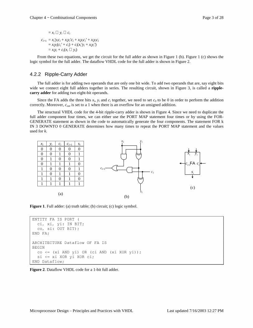
Chapter 4 − Combinational Components Page 3 of 28
Microprocessor Design – Principles and Practices with VHDL Last updated 7/16/2003 12:27 PM
= xi ⊕ yi ⊕ ci
ci+1 = xi'yici + xiyi'ci + xiyici' + xiyici = xiyi(ci' + ci) + ci(xi'yi + xiyi') = xiyi + ci(xi ⊕ yi)
From these two equations, we get the circuit for the full adder as shown in Figure 1 (b). Figure 1 (c) shows the logic symbol for the full adder. The dataflow VHDL code for the full adder is shown in Figure 2.
4.2.2 Ripple-Carry Adder
The full adder is for adding two operands that are only one bit wide. To add two operands that are, say eight bits wide we connect eight full adders together in series. The resulting circuit, shown in Figure 3, is called a ripple-carry adder for adding two eight-bit operands.
Since the FA adds the three bits xi, yi and ci together, we need to set c0 to be 0 in order to perform the addition correctly. Moreover, cout is set to a 1 when there is an overflow for an unsigned addition.
The structural VHDL code for the 4-bit ripple-carry adder is shown in Figure 4. Since we need to duplicate the full adder component four times, we can either use the PORT MAP statement four times or by using the FOR-GENERATE statement as shown in the code to automatically generate the four components. The statement FOR k IN 3 DOWNTO 0 GENERATE determines how many times to repeat the PORT MAP statement and the values used for k.
xi yi ci ci+1 si 0 0 0 0 0 0 0 1 0 1 0 1 0 0 1 0 1 1 1 0 1 0 0 0 1 1 0 1 1 0 1 1 0 1 0 1 1 1 1 1
(a)
xi yi
ci
ci+1
si (b)
FA
xi yi
cici+1
si
(c)
Figure 1. Full adder: (a) truth table; (b) circuit; (c) logic symbol.
ENTITY FA IS PORT (ci, xi, yi: IN BIT;co, si: OUT BIT);
END FA;
ARCHITECTURE Dataflow OF FA ISBEGIN
co <= (xi AND yi) OR (ci AND (xi XOR yi));si <= xi XOR yi XOR ci;
END Dataflow;
Figure 2. Dataflow VHDL code for a 1-bit full adder.
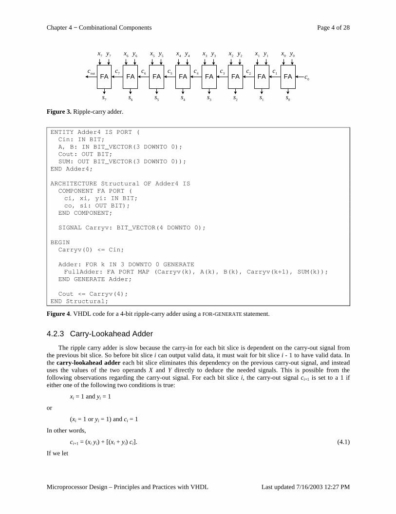
Chapter 4 − Combinational Components Page 4 of 28
Microprocessor Design – Principles and Practices with VHDL Last updated 7/16/2003 12:27 PM
x1 y1
FAc1
s1
x2 y2
FAc2
s2
x3 y3
FAc3
s3
x0 y0
FA c0
s0
x4 y4
FAc4
s4
x5 y5
FAc5
s5
x6 y6
FAc6
s6
x7 y7
FAc7
s7
cout
Figure 3. Ripple-carry adder.
ENTITY Adder4 IS PORT (Cin: IN BIT;A, B: IN BIT_VECTOR(3 DOWNTO 0);Cout: OUT BIT;SUM: OUT BIT_VECTOR(3 DOWNTO 0));
END Adder4;
ARCHITECTURE Structural OF Adder4 ISCOMPONENT FA PORT (ci, xi, yi: IN BIT;co, si: OUT BIT);
END COMPONENT;
SIGNAL Carryv: BIT_VECTOR(4 DOWNTO 0);
BEGINCarryv(0) <= Cin;
Adder: FOR k IN 3 DOWNTO 0 GENERATEFullAdder: FA PORT MAP (Carryv(k), A(k), B(k), Carryv(k+1), SUM(k));
END GENERATE Adder;
Cout <= Carryv(4);END Structural;
Figure 4. VHDL code for a 4-bit ripple-carry adder using a FOR-GENERATE statement.
4.2.3 Carry-Lookahead Adder
The ripple carry adder is slow because the carry-in for each bit slice is dependent on the carry-out signal from the previous bit slice. So before bit slice i can output valid data, it must wait for bit slice i - 1 to have valid data. In the carry-lookahead adder each bit slice eliminates this dependency on the previous carry-out signal, and instead uses the values of the two operands X and Y directly to deduce the needed signals. This is possible from the following observations regarding the carry-out signal. For each bit slice i, the carry-out signal ci+1 is set to a 1 if either one of the following two conditions is true:
xi = 1 and yi = 1
or
(xi = 1 or yi = 1) and ci = 1
In other words,
ci+1 = (xi yi) + [(xi + yi) ci]. (4.1)
If we let
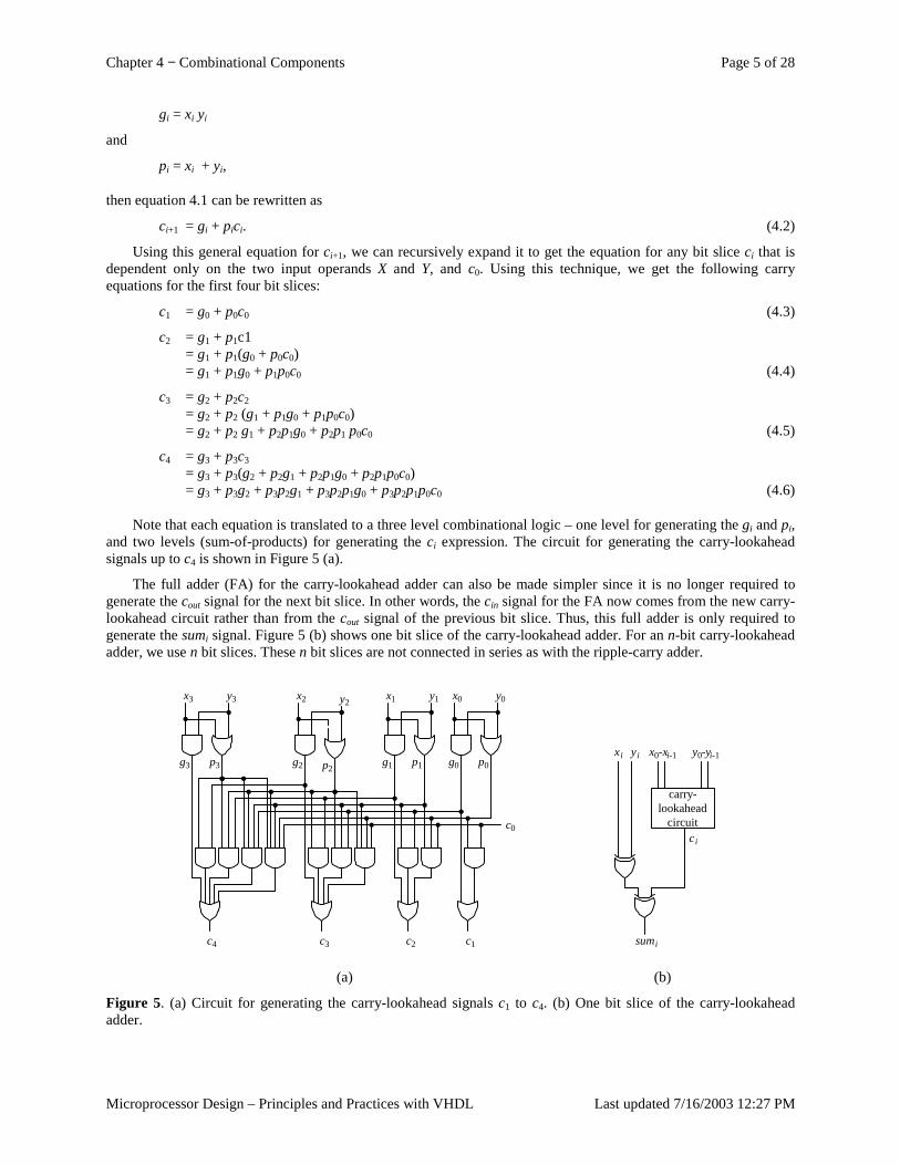
Chapter 4 − Combinational Components Page 5 of 28
Microprocessor Design – Principles and Practices with VHDL Last updated 7/16/2003 12:27 PM
gi = xi yi
and
pi = xi + yi,
then equation 4.1 can be rewritten as
ci+1 = gi + pici. (4.2)
Using this general equation for ci+1, we can recursively expand it to get the equation for any bit slice ci that is dependent only on the two input operands X and Y, and c0. Using this technique, we get the following carry equations for the first four bit slices:
c1 = g0 + p0c0 (4.3)
c2 = g1 + p1c1 = g1 + p1(g0 + p0c0) = g1 + p1g0 + p1p0c0 (4.4)
c3 = g2 + p2c2 = g2 + p2 (g1 + p1g0 + p1p0c0) = g2 + p2 g1 + p2p1g0 + p2p1 p0c0 (4.5)
c4 = g3 + p3c3 = g3 + p3(g2 + p2g1 + p2p1g0 + p2p1p0c0) = g3 + p3g2 + p3p2g1 + p3p2p1g0 + p3p2p1p0c0 (4.6)
Note that each equation is translated to a three level combinational logic – one level for generating the gi and pi, and two levels (sum-of-products) for generating the ci expression. The circuit for generating the carry-lookahead signals up to c4 is shown in Figure 5 (a).
The full adder (FA) for the carry-lookahead adder can also be made simpler since it is no longer required to generate the cout signal for the next bit slice. In other words, the cin signal for the FA now comes from the new carry-lookahead circuit rather than from the cout signal of the previous bit slice. Thus, this full adder is only required to generate the sumi signal. Figure 5 (b) shows one bit slice of the carry-lookahead adder. For an n-bit carry-lookahead adder, we use n bit slices. These n bit slices are not connected in series as with the ripple-carry adder.
c0
c1c2c3c4
x3 y3
g3 p3
x0 y0
g0 p0
x1 y1
g1 p1
x2 y2
g2 p2
carry-lookahead
circuit
xi yi
sumi
x0-xi-1 y0-yi-1
ci
(a) (b)
Figure 5. (a) Circuit for generating the carry-lookahead signals c1 to c4. (b) One bit slice of the carry-lookahead adder.
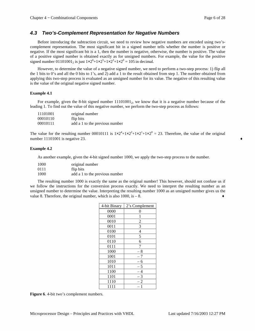
Chapter 4 − Combinational Components Page 6 of 28
Microprocessor Design – Principles and Practices with VHDL Last updated 7/16/2003 12:27 PM
4.3 Two’s-Complement Representation for Negative Numbers Before introducing the subtraction circuit, we need to review how negative numbers are encoded using two’s-
complement representation. The most significant bit in a signed number tells whether the number is positive or negative. If the most significant bit is a 1, then the number is negative, otherwise, the number is positive. The value of a positive signed number is obtained exactly as for unsigned numbers. For example, the value for the positive signed number 011010012 is just 1×26+1×25+1×23+1×20 = 105 in decimal.
However, to determine the value of a negative signed number, we need to perform a two-step process: 1) flip all the 1 bits to 0’s and all the 0 bits to 1’s, and 2) add a 1 to the result obtained from step 1. The number obtained from applying this two-step process is evaluated as an unsigned number for its value. The negative of this resulting value is the value of the original negative signed number.
Example 4.1
For example, given the 8-bit signed number 111010012, we know that it is a negative number because of the leading 1. To find out the value of this negative number, we perform the two-step process as follows:
11101001 original number 00010110 flip bits 00010111 add a 1 to the previous number
The value for the resulting number 00010111 is 1×24+1×22+1×21+1×20 = 23. Therefore, the value of the original number 11101001 is negative 23. ♦
Example 4.2
As another example, given the 4-bit signed number 1000, we apply the two-step process to the number.
1000 original number 0111 flip bits 1000 add a 1 to the previous number
The resulting number 1000 is exactly the same as the original number! This however, should not confuse us if we follow the instructions for the conversion process exactly. We need to interpret the resulting number as an unsigned number to determine the value. Interpreting the resulting number 1000 as an unsigned number gives us the value 8. Therefore, the original number, which is also 1000, is – 8. ♦
4-bit Binary 2’s Complement
0000 0 0001 1 0010 2 0011 3 0100 4 0101 5 0110 6 0111 7 1000 – 8 1001 – 7 1010 – 6 1011 – 5 1100 – 4 1101 – 3 1110 – 2 1111 – 1
Figure 6. 4-bit two’s complement numbers.
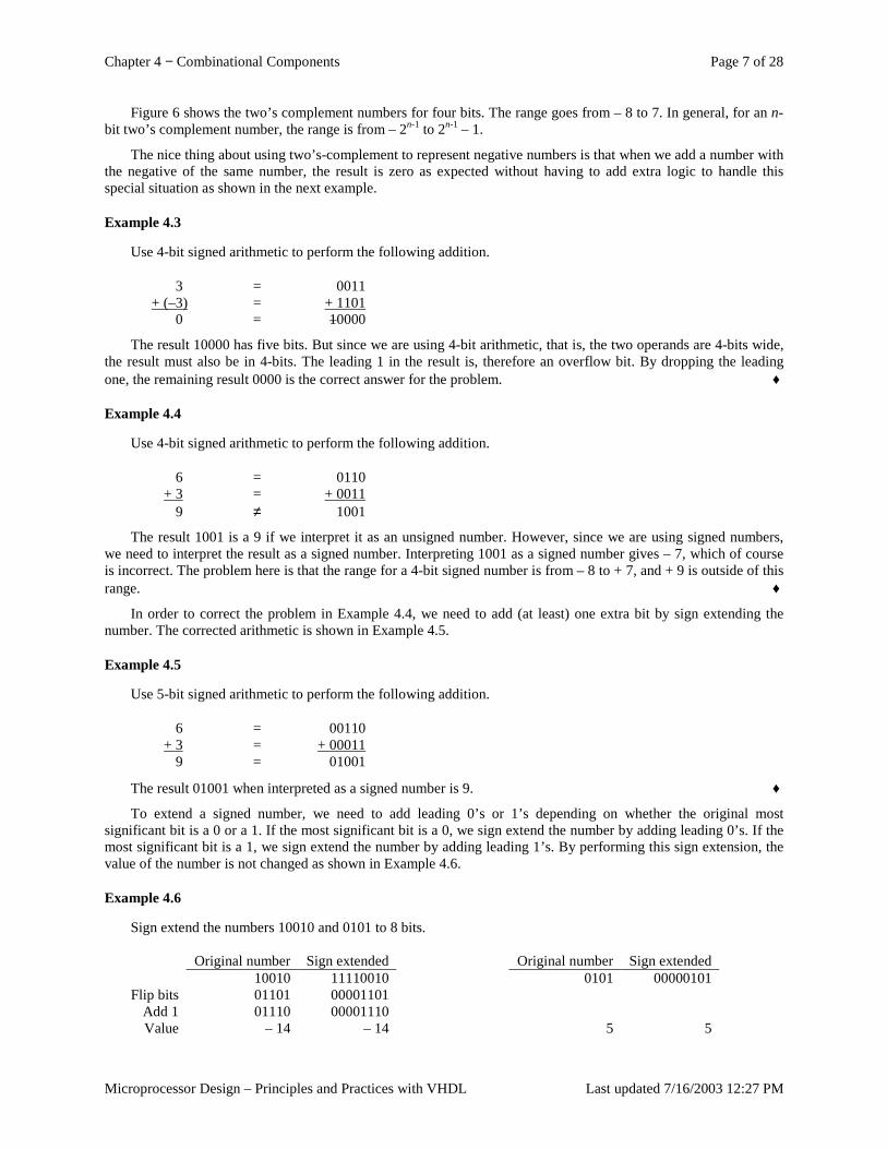
Chapter 4 − Combinational Components Page 7 of 28
Microprocessor Design – Principles and Practices with VHDL Last updated 7/16/2003 12:27 PM
Figure 6 shows the two’s complement numbers for four bits. The range goes from – 8 to 7. In general, for an n-bit two’s complement number, the range is from – 2n-1 to 2n-1 – 1.
The nice thing about using two’s-complement to represent negative numbers is that when we add a number with the negative of the same number, the result is zero as expected without having to add extra logic to handle this special situation as shown in the next example.
Example 4.3
Use 4-bit signed arithmetic to perform the following addition.
3 = 0011 + (–3) = + 1101 0 = 10000
The result 10000 has five bits. But since we are using 4-bit arithmetic, that is, the two operands are 4-bits wide, the result must also be in 4-bits. The leading 1 in the result is, therefore an overflow bit. By dropping the leading one, the remaining result 0000 is the correct answer for the problem. ♦
Example 4.4
Use 4-bit signed arithmetic to perform the following addition.
6 = 0110 + 3 = + 0011 9 ≠ 1001
The result 1001 is a 9 if we interpret it as an unsigned number. However, since we are using signed numbers, we need to interpret the result as a signed number. Interpreting 1001 as a signed number gives – 7, which of course is incorrect. The problem here is that the range for a 4-bit signed number is from – 8 to + 7, and + 9 is outside of this range. ♦
In order to correct the problem in Example 4.4, we need to add (at least) one extra bit by sign extending the number. The corrected arithmetic is shown in Example 4.5.
Example 4.5
Use 5-bit signed arithmetic to perform the following addition.
6 = 00110 + 3 = + 00011 9 = 01001
The result 01001 when interpreted as a signed number is 9. ♦
To extend a signed number, we need to add leading 0’s or 1’s depending on whether the original most significant bit is a 0 or a 1. If the most significant bit is a 0, we sign extend the number by adding leading 0’s. If the most significant bit is a 1, we sign extend the number by adding leading 1’s. By performing this sign extension, the value of the number is not changed as shown in Example 4.6.
Example 4.6
Sign extend the numbers 10010 and 0101 to 8 bits. Original number Sign extended Original number Sign extended 10010 11110010 0101 00000101 Flip bits 01101 00001101
Add 1 01110 00001110 Value – 14 – 14 5 5
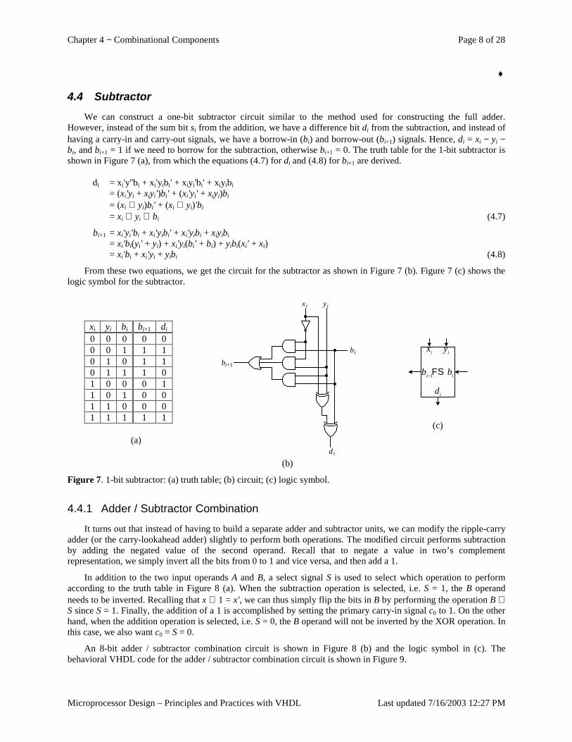
Chapter 4 − Combinational Components Page 8 of 28
Microprocessor Design – Principles and Practices with VHDL Last updated 7/16/2003 12:27 PM
♦
4.4 Subtractor We can construct a one-bit subtractor circuit similar to the method used for constructing the full adder.
However, instead of the sum bit si from the addition, we have a difference bit di from the subtraction, and instead of having a carry-in and carry-out signals, we have a borrow-in (bi) and borrow-out (bi+1) signals. Hence, di = xi − yi − bi, and bi+1 = 1 if we need to borrow for the subtraction, otherwise bi+1 = 0. The truth table for the 1-bit subtractor is shown in Figure 7 (a), from which the equations (4.7) for di and (4.8) for bi+1 are derived.
di = xi'y''bi + xi'yibi' + xiyi'bi' + xiyibi = (xi'yi + xiyi')bi' + (xi'yi' + xiyi)bi = (xi ⊕ yi)bi' + (xi ⊕ yi)'bi = xi ⊕ yi ⊕ bi (4.7)
bi+1 = xi'yi'bi + xi'yibi' + xi'yibi + xiyibi = xi'bi(yi' + yi) + xi'yi(bi' + bi) + yibi(xi' + xi) = xi'bi + xi'yi + yibi (4.8)
From these two equations, we get the circuit for the subtractor as shown in Figure 7 (b). Figure 7 (c) shows the logic symbol for the subtractor.
xi yi bi bi+1 di 0 0 0 0 0 0 0 1 1 1 0 1 0 1 1 0 1 1 1 0 1 0 0 0 1 1 0 1 0 0 1 1 0 0 0 1 1 1 1 1
(a)
xi yi
di
bi
bi+1
(b)
FS
xi yi
bibi+1
di
(c)
Figure 7. 1-bit subtractor: (a) truth table; (b) circuit; (c) logic symbol.
4.4.1 Adder / Subtractor Combination
It turns out that instead of having to build a separate adder and subtractor units, we can modify the ripple-carry adder (or the carry-lookahead adder) slightly to perform both operations. The modified circuit performs subtraction by adding the negated value of the second operand. Recall that to negate a value in two’s complement representation, we simply invert all the bits from 0 to 1 and vice versa, and then add a 1.
In addition to the two input operands A and B, a select signal S is used to select which operation to perform according to the truth table in Figure 8 (a). When the subtraction operation is selected, i.e. S = 1, the B operand needs to be inverted. Recalling that x ⊕ 1 = x', we can thus simply flip the bits in B by performing the operation B ⊕ S since S = 1. Finally, the addition of a 1 is accomplished by setting the primary carry-in signal c0 to 1. On the other hand, when the addition operation is selected, i.e. S = 0, the B operand will not be inverted by the XOR operation. In this case, we also want c0 = S = 0.
An 8-bit adder / subtractor combination circuit is shown in Figure 8 (b) and the logic symbol in (c). The behavioral VHDL code for the adder / subtractor combination circuit is shown in Figure 9.
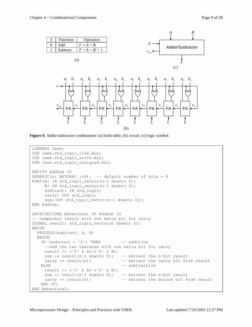
Chapter 4 − Combinational Components Page 9 of 28
Microprocessor Design – Principles and Practices with VHDL Last updated 7/16/2003 12:27 PM
S Function Operation 0 Add F = A + B 1 Subtract F = A + B' + 1
(a)
Adder/Subtractorcout
F
S
BA
(c)
a1 b1
FAc1
f1
a2 b2
FAc2
f2
a3 b3
FAc3
f3
a4 b4
FAc4
f4
a5 b5
FAc5
f5
a6 b6
FAc6
f6
a7 b7
FAc7
f7
S
cout
a0 b0
FAc0
f0 (b)
Figure 8. Adder/subtractor combination: (a) truth table; (b) circuit; (c) logic symbol.
LIBRARY ieee;USE ieee.std_logic_1164.ALL;USE ieee.std_logic_arith.ALL;USE ieee.std_logic_unsigned.ALL;
ENTITY AddSub ISGENERIC(n: NATURAL :=8); -- default number of bits = 8PORT(A: IN std_logic_vector(n-1 downto 0);
B: IN std_logic_vector(n-1 downto 0);subtract: IN std_logic;carry: OUT std_logic;sum: OUT std_logic_vector(n-1 downto 0));
END AddSub;
ARCHITECTURE Behavioral OF AddSub IS-- temporary result with one extra bit for carrySIGNAL result: std_logic_vector(n downto 0);BEGIN
PROCESS(subtract, A, B)BEGINIF (subtract = '0') THEN -- addition--add the two operands with one extra bit for carryresult <= ('0' & A)+('0' & B);sum <= result(n-1 downto 0); -- extract the n-bit resultcarry <= result(n); -- extract the carry bit from result
ELSE -- subtractionresult <= ('0' & A)-('0' & B);sum <= result(n-1 downto 0); -- extract the n-bit resultcarry <= result(n); -- extract the borrow bit from result
END IF;END Behavioral;
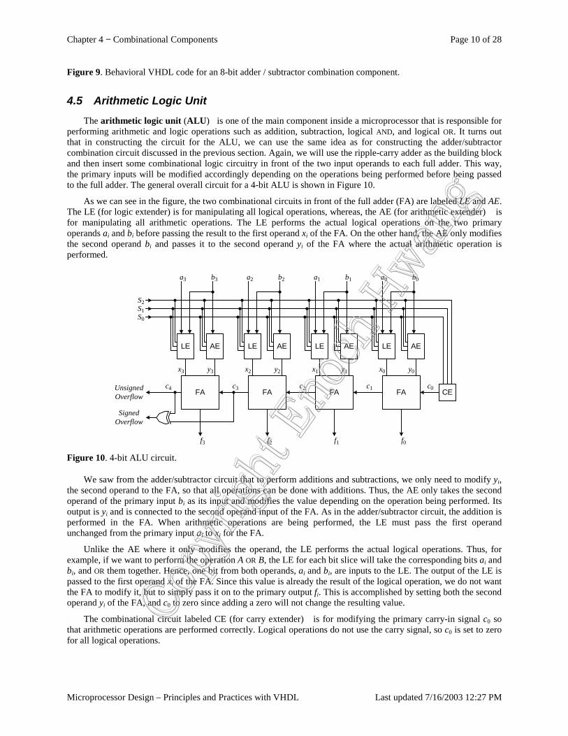
Chapter 4 − Combinational Components Page 10 of 28
Microprocessor Design – Principles and Practices with VHDL Last updated 7/16/2003 12:27 PM
Figure 9. Behavioral VHDL code for an 8-bit adder / subtractor combination component.
4.5 Arithmetic Logic Unit The arithmetic logic unit (ALU) is one of the main component inside a microprocessor that is responsible for
performing arithmetic and logic operations such as addition, subtraction, logical AND, and logical OR. It turns out that in constructing the circuit for the ALU, we can use the same idea as for constructing the adder/subtractor combination circuit discussed in the previous section. Again, we will use the ripple-carry adder as the building block and then insert some combinational logic circuitry in front of the two input operands to each full adder. This way, the primary inputs will be modified accordingly depending on the operations being performed before being passed to the full adder. The general overall circuit for a 4-bit ALU is shown in Figure 10.
As we can see in the figure, the two combinational circuits in front of the full adder (FA) are labeled LE and AE. The LE (for logic extender) is for manipulating all logical operations, whereas, the AE (for arithmetic extender) is for manipulating all arithmetic operations. The LE performs the actual logical operations on the two primary operands ai and bi before passing the result to the first operand xi of the FA. On the other hand, the AE only modifies the second operand bi and passes it to the second operand yi of the FA where the actual arithmetic operation is performed.
S1S0
SignedOverflow
UnsignedOverflow
c0FA
f0
a0 b0
c1
AELE
y0x0
FA
f1
a1 b1
c2
AELE
y1x1
FA
f2
a2 b2
c3
AELE
y2x2
FA
f3
a3 b3
c4
AELE
y3x3
CE
S2
Figure 10. 4-bit ALU circuit.
We saw from the adder/subtractor circuit that to perform additions and subtractions, we only need to modify yi, the second operand to the FA, so that all operations can be done with additions. Thus, the AE only takes the second operand of the primary input bi as its input and modifies the value depending on the operation being performed. Its output is yi and is connected to the second operand input of the FA. As in the adder/subtractor circuit, the addition is performed in the FA. When arithmetic operations are being performed, the LE must pass the first operand unchanged from the primary input ai to xi for the FA.
Unlike the AE where it only modifies the operand, the LE performs the actual logical operations. Thus, for example, if we want to perform the operation A OR B, the LE for each bit slice will take the corresponding bits ai and bi, and OR them together. Hence, one bit from both operands, ai and bi, are inputs to the LE. The output of the LE is passed to the first operand xi of the FA. Since this value is already the result of the logical operation, we do not want the FA to modify it, but to simply pass it on to the primary output fi. This is accomplished by setting both the second operand yi of the FA, and c0 to zero since adding a zero will not change the resulting value.
The combinational circuit labeled CE (for carry extender) is for modifying the primary carry-in signal c0 so that arithmetic operations are performed correctly. Logical operations do not use the carry signal, so c0 is set to zero for all logical operations.
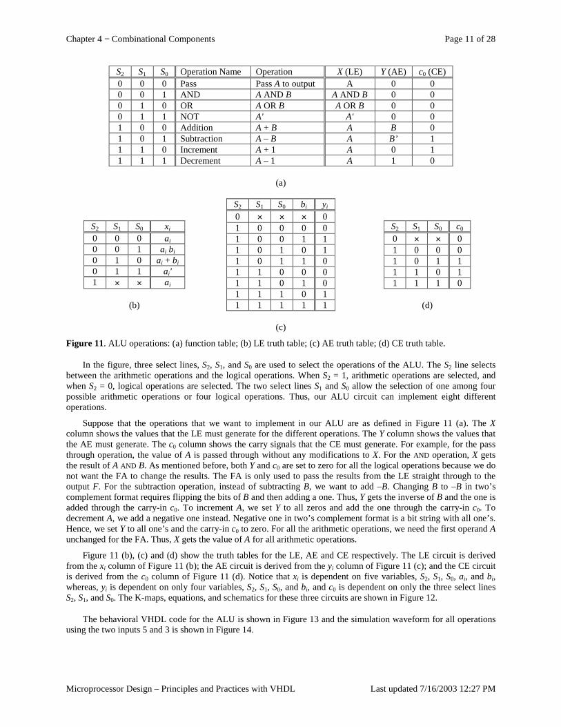
Chapter 4 − Combinational Components Page 11 of 28
Microprocessor Design – Principles and Practices with VHDL Last updated 7/16/2003 12:27 PM
S2 S1 S0 Operation Name Operation X (LE) Y (AE) c0 (CE) 0 0 0 Pass Pass A to output A 0 0 0 0 1 AND A AND B A AND B 0 0 0 1 0 OR A OR B A OR B 0 0 0 1 1 NOT A' A' 0 0 1 0 0 Addition A + B A B 0 1 0 1 Subtraction A – B A B’ 1 1 1 0 Increment A + 1 A 0 1 1 1 1 Decrement A – 1 A 1 0
(a)
S2 S1 S0 xi 0 0 0 ai 0 0 1 ai bi 0 1 0 ai + bi 0 1 1 ai' 1 × × ai
(b)
S2 S1 S0 bi yi 0 × × × 0 1 0 0 0 0 1 0 0 1 1 1 0 1 0 1 1 0 1 1 0 1 1 0 0 0 1 1 0 1 0 1 1 1 0 1 1 1 1 1 1
(c)
S2 S1 S0 c0 0 × × 0 1 0 0 0 1 0 1 1 1 1 0 1 1 1 1 0
(d)
Figure 11. ALU operations: (a) function table; (b) LE truth table; (c) AE truth table; (d) CE truth table.
In the figure, three select lines, S2, S1, and S0 are used to select the operations of the ALU. The S2 line selects between the arithmetic operations and the logical operations. When S2 = 1, arithmetic operations are selected, and when S2 = 0, logical operations are selected. The two select lines S1 and S0 allow the selection of one among four possible arithmetic operations or four logical operations. Thus, our ALU circuit can implement eight different operations.
Suppose that the operations that we want to implement in our ALU are as defined in Figure 11 (a). The X column shows the values that the LE must generate for the different operations. The Y column shows the values that the AE must generate. The c0 column shows the carry signals that the CE must generate. For example, for the pass through operation, the value of A is passed through without any modifications to X. For the AND operation, X gets the result of A AND B. As mentioned before, both Y and c0 are set to zero for all the logical operations because we do not want the FA to change the results. The FA is only used to pass the results from the LE straight through to the output F. For the subtraction operation, instead of subtracting B, we want to add –B. Changing B to –B in two’s complement format requires flipping the bits of B and then adding a one. Thus, Y gets the inverse of B and the one is added through the carry-in c0. To increment A, we set Y to all zeros and add the one through the carry-in c0. To decrement A, we add a negative one instead. Negative one in two’s complement format is a bit string with all one’s. Hence, we set Y to all one’s and the carry-in c0 to zero. For all the arithmetic operations, we need the first operand A unchanged for the FA. Thus, X gets the value of A for all arithmetic operations.
Figure 11 (b), (c) and (d) show the truth tables for the LE, AE and CE respectively. The LE circuit is derived from the xi column of Figure 11 (b); the AE circuit is derived from the yi column of Figure 11 (c); and the CE circuit is derived from the c0 column of Figure 11 (d). Notice that xi is dependent on five variables, S2, S1, S0, ai, and bi, whereas, yi is dependent on only four variables, S2, S1, S0, and bi, and c0 is dependent on only the three select lines S2, S1, and S0. The K-maps, equations, and schematics for these three circuits are shown in Figure 12.
The behavioral VHDL code for the ALU is shown in Figure 13 and the simulation waveform for all operations using the two inputs 5 and 3 is shown in Figure 14.
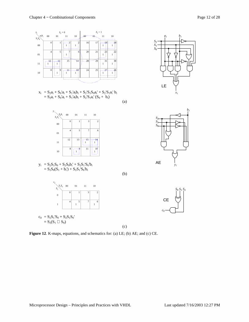
Chapter 4 − Combinational Components Page 12 of 28
Microprocessor Design – Principles and Practices with VHDL Last updated 7/16/2003 12:27 PM
S2 = 0aibi 0100
00
01
S1S0
0 1
4 5
1011
1 1
1
3 2
7 6
1 1
18 9
1 110
11
1011
12 13 14151
0100
16
1011
1 1
1 1
1
1 1
17 19 18
20 21 2223
24 25 2627
28 29 3031
S2 = 1xi
xi = S2ai + S0'ai + S1'aibi + S2'S1S0ai' + S2'S1ai' bi = S2ai + S0'ai + S1'aibi + S2'S1ai' (S0 + bi)
S1S0
ai
xi
LE
bi
S2
(a)
1
S0bi 0100
00
01
S2S1
0 1
4 5
1011
3 2
7 6
18 9
1
110
11
1011
12 13 1415
yi
yi = S2S1S0 + S2S0bi' + S2S1'S0'bi = S2S0(S1 + bi') + S2S1'S0'bi
S1S0
bi
yiAE
S2
(b)
S1S0 01
1
00
0
1
0 1
4 5
1011
1
3 2
7 6
c0
S2
c0 = S2S1'S0 + S2S1S0' = S2(S1 ⊕ S0)
S0 S1
c0
CE
S2
(c)
Figure 12. K-maps, equations, and schematics for: (a) LE; (b) AE; and (c) CE.
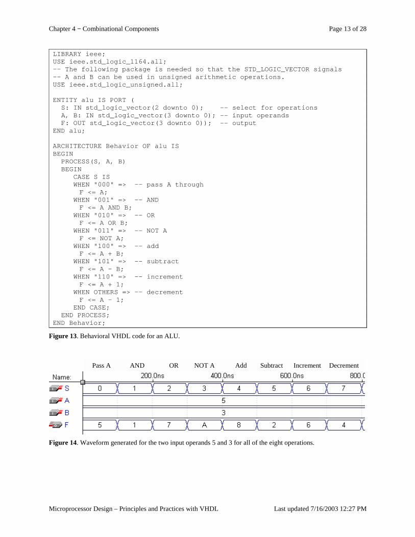
Chapter 4 − Combinational Components Page 13 of 28
Microprocessor Design – Principles and Practices with VHDL Last updated 7/16/2003 12:27 PM
LIBRARY ieee;USE ieee.std_logic_1164.all;-- The following package is needed so that the STD_LOGIC_VECTOR signals-- A and B can be used in unsigned arithmetic operations.USE ieee.std_logic_unsigned.all;
ENTITY alu IS PORT (S: IN std_logic_vector(2 downto 0); -- select for operationsA, B: IN std_logic_vector(3 downto 0); -- input operandsF: OUT std_logic_vector(3 downto 0)); -- output
END alu;
ARCHITECTURE Behavior OF alu ISBEGIN
PROCESS(S, A, B)BEGIN
CASE S ISWHEN "000" => -- pass A throughF <= A;
WHEN "001" => -- ANDF <= A AND B;
WHEN "010" => -- ORF <= A OR B;
WHEN "011" => -- NOT AF <= NOT A;
WHEN "100" => -- addF <= A + B;
WHEN "101" => -- subtractF <= A - B;
WHEN "110" => -- incrementF <= A + 1;
WHEN OTHERS => -- decrementF <= A - 1;
END CASE;END PROCESS;
END Behavior;
Figure 13. Behavioral VHDL code for an ALU.
Figure 14. Waveform generated for the two input operands 5 and 3 for all of the eight operations.
AND OR NOT A Add Subtract Increment DecrementPass A
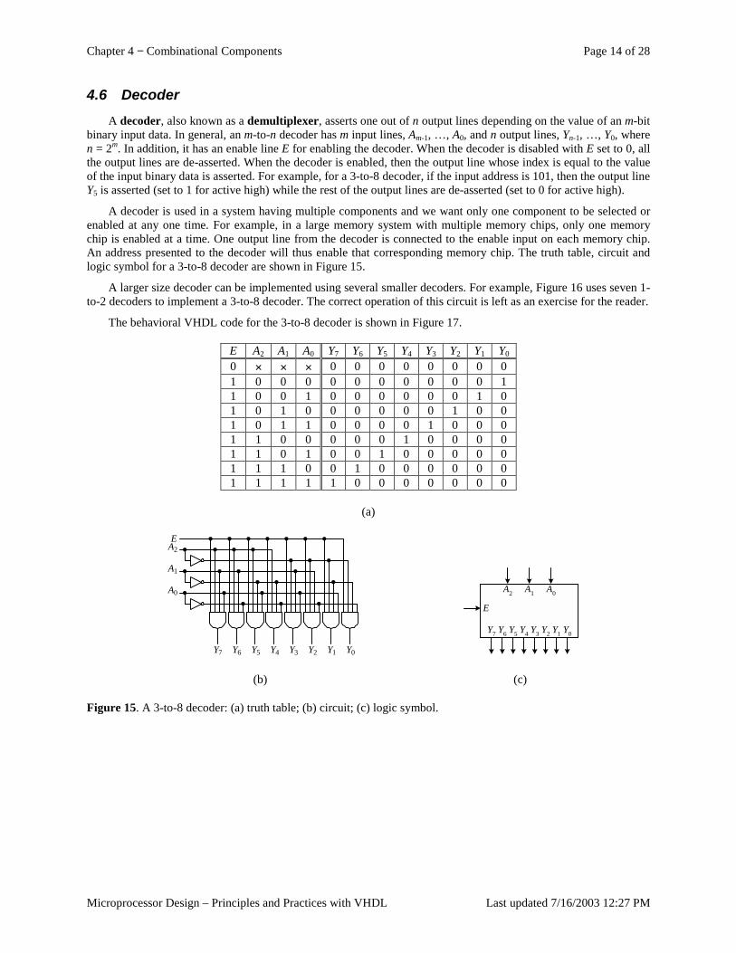
Chapter 4 − Combinational Components Page 14 of 28
Microprocessor Design – Principles and Practices with VHDL Last updated 7/16/2003 12:27 PM
4.6 Decoder A decoder, also known as a demultiplexer, asserts one out of n output lines depending on the value of an m-bit
binary input data. In general, an m-to-n decoder has m input lines, Am-1, …, A0, and n output lines, Yn-1, …, Y0, where n = 2m. In addition, it has an enable line E for enabling the decoder. When the decoder is disabled with E set to 0, all the output lines are de-asserted. When the decoder is enabled, then the output line whose index is equal to the value of the input binary data is asserted. For example, for a 3-to-8 decoder, if the input address is 101, then the output line Y5 is asserted (set to 1 for active high) while the rest of the output lines are de-asserted (set to 0 for active high).
A decoder is used in a system having multiple components and we want only one component to be selected or enabled at any one time. For example, in a large memory system with multiple memory chips, only one memory chip is enabled at a time. One output line from the decoder is connected to the enable input on each memory chip. An address presented to the decoder will thus enable that corresponding memory chip. The truth table, circuit and logic symbol for a 3-to-8 decoder are shown in Figure 15.
A larger size decoder can be implemented using several smaller decoders. For example, Figure 16 uses seven 1-to-2 decoders to implement a 3-to-8 decoder. The correct operation of this circuit is left as an exercise for the reader.
The behavioral VHDL code for the 3-to-8 decoder is shown in Figure 17.
E A2 A1 A0 Y7 Y6 Y5 Y4 Y3 Y2 Y1 Y0 0 × × × 0 0 0 0 0 0 0 0 1 0 0 0 0 0 0 0 0 0 0 1 1 0 0 1 0 0 0 0 0 0 1 0 1 0 1 0 0 0 0 0 0 1 0 0 1 0 1 1 0 0 0 0 1 0 0 0 1 1 0 0 0 0 0 1 0 0 0 0 1 1 0 1 0 0 1 0 0 0 0 0 1 1 1 0 0 1 0 0 0 0 0 0 1 1 1 1 1 0 0 0 0 0 0 0
(a)
Y7 Y6 Y5 Y4 Y3 Y2 Y1 Y0
A2
A1
A0
E
Y2 Y1 Y0Y3Y4Y5Y6Y7
A2 A1 A0
E
(b) (c)
Figure 15. A 3-to-8 decoder: (a) truth table; (b) circuit; (c) logic symbol.
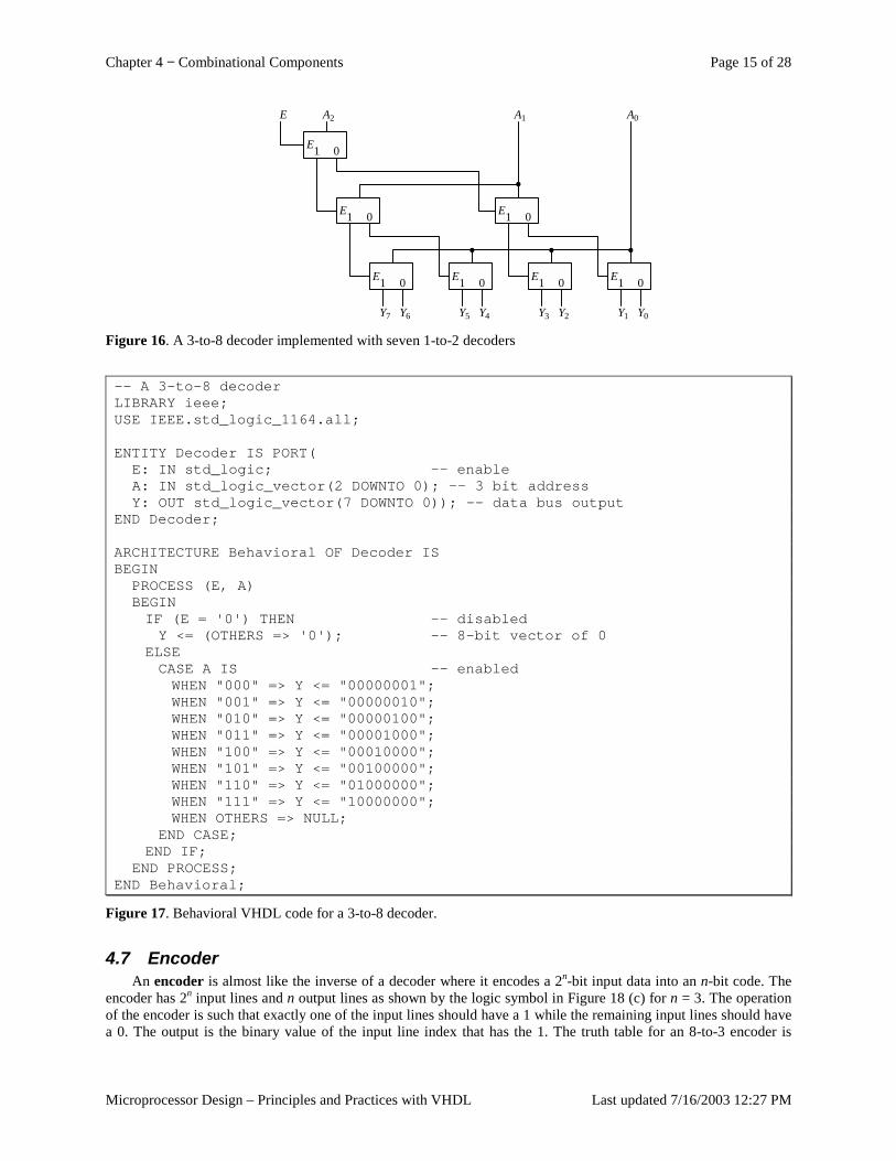
Chapter 4 − Combinational Components Page 15 of 28
Microprocessor Design – Principles and Practices with VHDL Last updated 7/16/2003 12:27 PM
Y3 Y2 Y1 Y0
A2 A1
E1 0
E1 0 E1 0
E1 0 E1 0 E1 0 E1 0
A0E
Y5 Y4Y7 Y6 Figure 16. A 3-to-8 decoder implemented with seven 1-to-2 decoders
-- A 3-to-8 decoderLIBRARY ieee;USE IEEE.std_logic_1164.all;
ENTITY Decoder IS PORT(E: IN std_logic; -- enableA: IN std_logic_vector(2 DOWNTO 0); -- 3 bit addressY: OUT std_logic_vector(7 DOWNTO 0)); -- data bus output
END Decoder;
ARCHITECTURE Behavioral OF Decoder ISBEGIN
PROCESS (E, A)BEGINIF (E = '0') THEN -- disabledY <= (OTHERS => '0'); -- 8-bit vector of 0
ELSECASE A IS -- enabledWHEN "000" => Y <= "00000001";WHEN "001" => Y <= "00000010";WHEN "010" => Y <= "00000100";WHEN "011" => Y <= "00001000";WHEN "100" => Y <= "00010000";WHEN "101" => Y <= "00100000";WHEN "110" => Y <= "01000000";WHEN "111" => Y <= "10000000";WHEN OTHERS => NULL;
END CASE;END IF;
END PROCESS;END Behavioral;
Figure 17. Behavioral VHDL code for a 3-to-8 decoder.
4.7 Encoder An encoder is almost like the inverse of a decoder where it encodes a 2n-bit input data into an n-bit code. The
encoder has 2n input lines and n output lines as shown by the logic symbol in Figure 18 (c) for n = 3. The operation of the encoder is such that exactly one of the input lines should have a 1 while the remaining input lines should have a 0. The output is the binary value of the input line index that has the 1. The truth table for an 8-to-3 encoder is
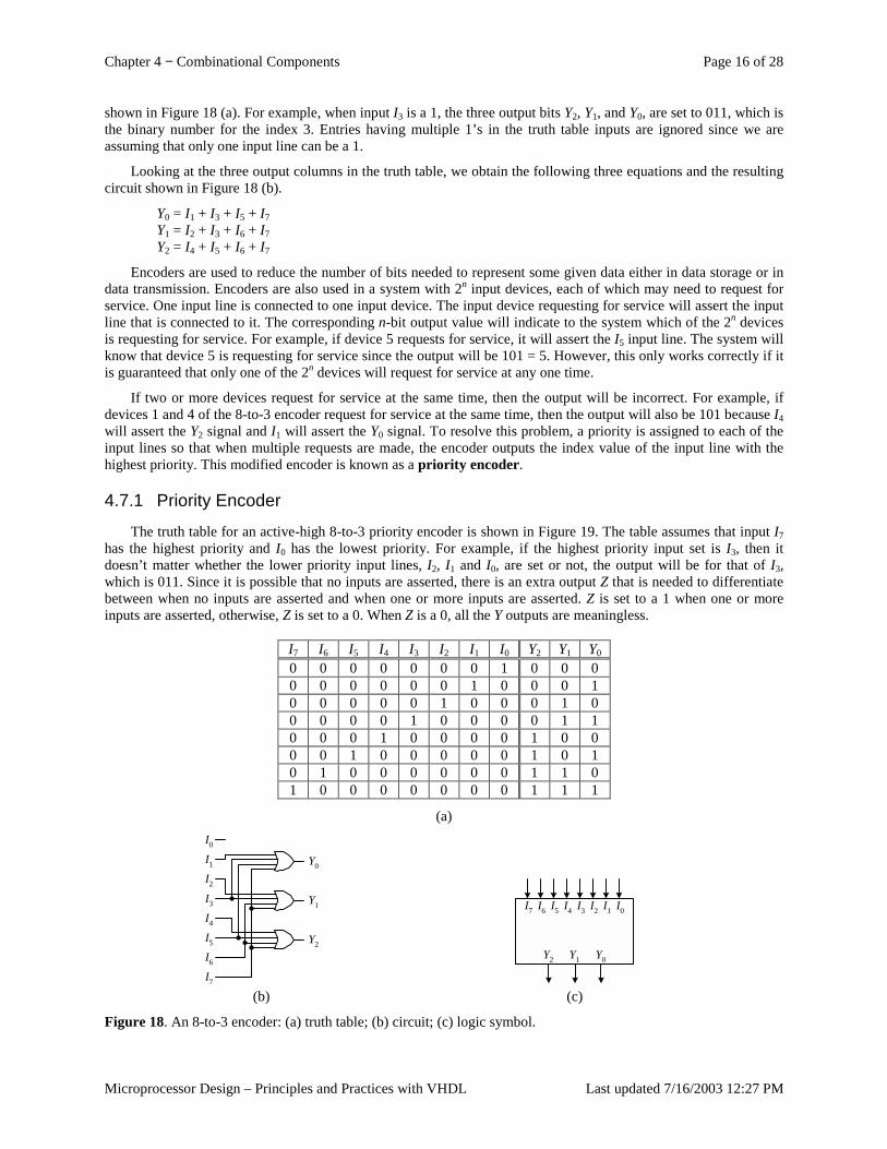
Chapter 4 − Combinational Components Page 16 of 28
Microprocessor Design – Principles and Practices with VHDL Last updated 7/16/2003 12:27 PM
shown in Figure 18 (a). For example, when input I3 is a 1, the three output bits Y2, Y1, and Y0, are set to 011, which is the binary number for the index 3. Entries having multiple 1’s in the truth table inputs are ignored since we are assuming that only one input line can be a 1.
Looking at the three output columns in the truth table, we obtain the following three equations and the resulting circuit shown in Figure 18 (b).
Y0 = I1 + I3 + I5 + I7 Y1 = I2 + I3 + I6 + I7 Y2 = I4 + I5 + I6 + I7
Encoders are used to reduce the number of bits needed to represent some given data either in data storage or in data transmission. Encoders are also used in a system with 2n input devices, each of which may need to request for service. One input line is connected to one input device. The input device requesting for service will assert the input line that is connected to it. The corresponding n-bit output value will indicate to the system which of the 2n devices is requesting for service. For example, if device 5 requests for service, it will assert the I5 input line. The system will know that device 5 is requesting for service since the output will be 101 = 5. However, this only works correctly if it is guaranteed that only one of the 2n devices will request for service at any one time.
If two or more devices request for service at the same time, then the output will be incorrect. For example, if devices 1 and 4 of the 8-to-3 encoder request for service at the same time, then the output will also be 101 because I4 will assert the Y2 signal and I1 will assert the Y0 signal. To resolve this problem, a priority is assigned to each of the input lines so that when multiple requests are made, the encoder outputs the index value of the input line with the highest priority. This modified encoder is known as a priority encoder.
4.7.1 Priority Encoder
The truth table for an active-high 8-to-3 priority encoder is shown in Figure 19. The table assumes that input I7 has the highest priority and I0 has the lowest priority. For example, if the highest priority input set is I3, then it doesn’t matter whether the lower priority input lines, I2, I1 and I0, are set or not, the output will be for that of I3, which is 011. Since it is possible that no inputs are asserted, there is an extra output Z that is needed to differentiate between when no inputs are asserted and when one or more inputs are asserted. Z is set to a 1 when one or more inputs are asserted, otherwise, Z is set to a 0. When Z is a 0, all the Y outputs are meaningless.
I7 I6 I5 I4 I3 I2 I1 I0 Y2 Y1 Y0 0 0 0 0 0 0 0 1 0 0 0 0 0 0 0 0 0 1 0 0 0 1 0 0 0 0 0 1 0 0 0 1 0 0 0 0 0 1 0 0 0 0 1 1 0 0 0 1 0 0 0 0 1 0 0 0 0 1 0 0 0 0 0 1 0 1 0 1 0 0 0 0 0 0 1 1 0 1 0 0 0 0 0 0 0 1 1 1
(a)
Y0
Y1
Y2
I0
I1
I2
I3
I4
I5
I6
I7
I2 I1 I0I3I4I5I6I7
Y2 Y1 Y0
(b) (c)
Figure 18. An 8-to-3 encoder: (a) truth table; (b) circuit; (c) logic symbol.
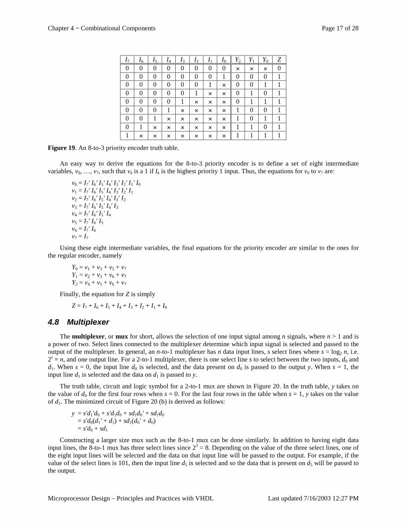
Chapter 4 − Combinational Components Page 17 of 28
Microprocessor Design – Principles and Practices with VHDL Last updated 7/16/2003 12:27 PM
I7 I6 I5 I4 I3 I2 I1 I0 Y2 Y1 Y0 Z 0 0 0 0 0 0 0 0 × × × 0 0 0 0 0 0 0 0 1 0 0 0 1 0 0 0 0 0 0 1 × 0 0 1 1 0 0 0 0 0 1 × × 0 1 0 1 0 0 0 0 1 × × × 0 1 1 1 0 0 0 1 × × × × 1 0 0 1 0 0 1 × × × × × 1 0 1 1 0 1 × × × × × × 1 1 0 1 1 × × × × × × × 1 1 1 1
Figure 19. An 8-to-3 priority encoder truth table.
An easy way to derive the equations for the 8-to-3 priority encoder is to define a set of eight intermediate variables, v0, …, v7, such that vk is a 1 if Ik is the highest priority 1 input. Thus, the equations for v0 to v7 are:
v0 = I7' I6' I5' I4' I3' I2' I1' I0 v1 = I7' I6' I5' I4' I3' I2' I1 v2 = I7' I6' I5' I4' I3' I2 v3 = I7' I6' I5' I4' I3 v4 = I7' I6' I5' I4 v5 = I7' I6' I5 v6 = I7' I6 v7 = I7
Using these eight intermediate variables, the final equations for the priority encoder are similar to the ones for the regular encoder, namely
Y0 = v1 + v3 + v5 + v7 Y1 = v2 + v3 + v6 + v7 Y2 = v4 + v5 + v6 + v7
Finally, the equation for Z is simply
Z = I7 + I6 + I5 + I4 + I3 + I2 + I1 + I0
4.8 Multiplexer The multiplexer, or mux for short, allows the selection of one input signal among n signals, where n > 1 and is
a power of two. Select lines connected to the multiplexer determine which input signal is selected and passed to the output of the multiplexer. In general, an n-to-1 multiplexer has n data input lines, s select lines where s = log2 n, i.e. 2s = n, and one output line. For a 2-to-1 multiplexer, there is one select line s to select between the two inputs, d0 and d1. When s = 0, the input line d0 is selected, and the data present on d0 is passed to the output y. When s = 1, the input line d1 is selected and the data on d1 is passed to y.
The truth table, circuit and logic symbol for a 2-to-1 mux are shown in Figure 20. In the truth table, y takes on the value of d0 for the first four rows when s = 0. For the last four rows in the table when s = 1, y takes on the value of d1. The minimized circuit of Figure 20 (b) is derived as follows:
y = s'd1'd0 + s'd1d0 + sd1d0' + sd1d0 = s'd0(d1' + d1) + sd1(d0' + d0) = s'd0 + sd1
Constructing a larger size mux such as the 8-to-1 mux can be done similarly. In addition to having eight data input lines, the 8-to-1 mux has three select lines since 23 = 8. Depending on the value of the three select lines, one of the eight input lines will be selected and the data on that input line will be passed to the output. For example, if the value of the select lines is 101, then the input line d5 is selected and so the data that is present on d5 will be passed to the output.
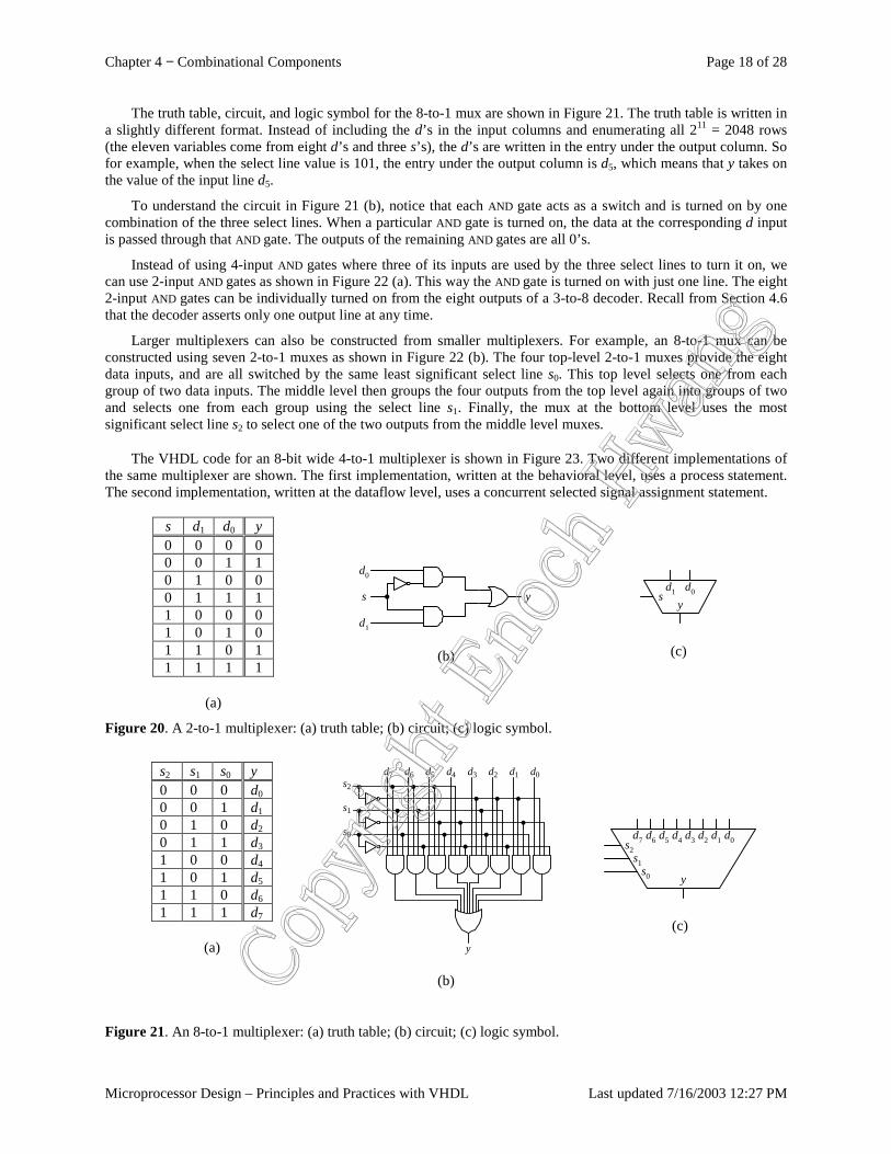
Chapter 4 − Combinational Components Page 18 of 28
Microprocessor Design – Principles and Practices with VHDL Last updated 7/16/2003 12:27 PM
The truth table, circuit, and logic symbol for the 8-to-1 mux are shown in Figure 21. The truth table is written in a slightly different format. Instead of including the d’s in the input columns and enumerating all 211 = 2048 rows (the eleven variables come from eight d’s and three s’s), the d’s are written in the entry under the output column. So for example, when the select line value is 101, the entry under the output column is d5, which means that y takes on the value of the input line d5.
To understand the circuit in Figure 21 (b), notice that each AND gate acts as a switch and is turned on by one combination of the three select lines. When a particular AND gate is turned on, the data at the corresponding d input is passed through that AND gate. The outputs of the remaining AND gates are all 0’s.
Instead of using 4-input AND gates where three of its inputs are used by the three select lines to turn it on, we can use 2-input AND gates as shown in Figure 22 (a). This way the AND gate is turned on with just one line. The eight 2-input AND gates can be individually turned on from the eight outputs of a 3-to-8 decoder. Recall from Section 4.6 that the decoder asserts only one output line at any time.
Larger multiplexers can also be constructed from smaller multiplexers. For example, an 8-to-1 mux can be constructed using seven 2-to-1 muxes as shown in Figure 22 (b). The four top-level 2-to-1 muxes provide the eight data inputs, and are all switched by the same least significant select line s0. This top level selects one from each group of two data inputs. The middle level then groups the four outputs from the top level again into groups of two and selects one from each group using the select line s1. Finally, the mux at the bottom level uses the most significant select line s2 to select one of the two outputs from the middle level muxes.
The VHDL code for an 8-bit wide 4-to-1 multiplexer is shown in Figure 23. Two different implementations of the same multiplexer are shown. The first implementation, written at the behavioral level, uses a process statement. The second implementation, written at the dataflow level, uses a concurrent selected signal assignment statement.
s d1 d0 y 0 0 0 0 0 0 1 1 0 1 0 0 0 1 1 1 1 0 0 0 1 0 1 0 1 1 0 1 1 1 1 1
(a)
s
d0
d1
y
(b)
d1 d0sy
(c)
Figure 20. A 2-to-1 multiplexer: (a) truth table; (b) circuit; (c) logic symbol.
s2 s1 s0 y 0 0 0 d0 0 0 1 d1 0 1 0 d2 0 1 1 d3 1 0 0 d4 1 0 1 d5 1 1 0 d6 1 1 1 d7
(a)
d7 d6 d5 d4 d3 d2 d1 d0s2
y
s1
s0
(b)
s2s1
d1 d0d2d3d4d5d6d7
s0 y
(c)
Figure 21. An 8-to-1 multiplexer: (a) truth table; (b) circuit; (c) logic symbol.
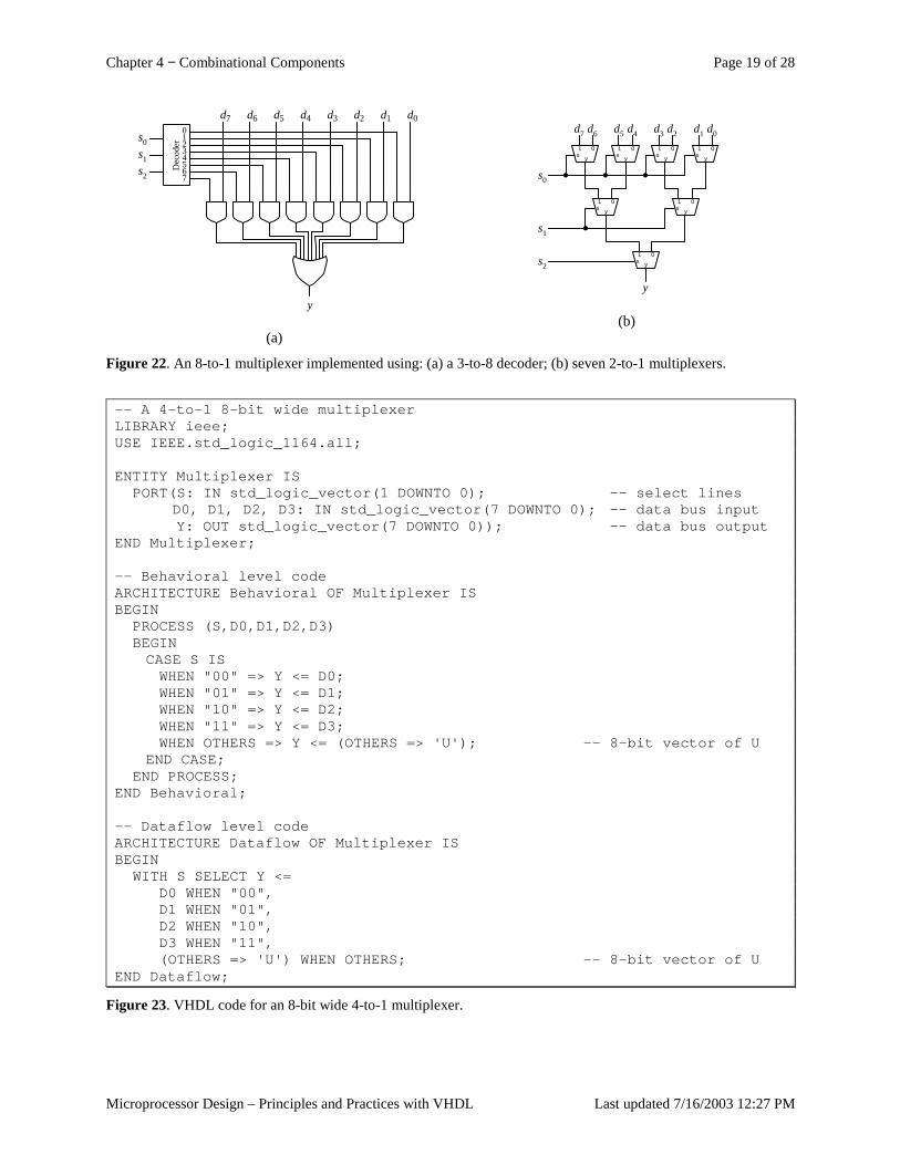
Chapter 4 − Combinational Components Page 19 of 28
Microprocessor Design – Principles and Practices with VHDL Last updated 7/16/2003 12:27 PM
d1 d0d2d3d4d5d6d701234567
s0
Dec
oder
y
s1s2
(a)
01s y
01s y
01s y
01s y
01s y
01s y
01s y
d0d1d2d3d4d5d6d7
s0
s1
s2
y
(b)
Figure 22. An 8-to-1 multiplexer implemented using: (a) a 3-to-8 decoder; (b) seven 2-to-1 multiplexers.
-- A 4-to-1 8-bit wide multiplexerLIBRARY ieee;USE IEEE.std_logic_1164.all;
ENTITY Multiplexer ISPORT(S: IN std_logic_vector(1 DOWNTO 0); -- select lines
D0, D1, D2, D3: IN std_logic_vector(7 DOWNTO 0); -- data bus inputY: OUT std_logic_vector(7 DOWNTO 0)); -- data bus output
END Multiplexer;
-- Behavioral level codeARCHITECTURE Behavioral OF Multiplexer ISBEGIN
PROCESS (S,D0,D1,D2,D3)BEGINCASE S ISWHEN "00" => Y <= D0;WHEN "01" => Y <= D1;WHEN "10" => Y <= D2;WHEN "11" => Y <= D3;WHEN OTHERS => Y <= (OTHERS => 'U'); -- 8-bit vector of U
END CASE;END PROCESS;
END Behavioral;
-- Dataflow level codeARCHITECTURE Dataflow OF Multiplexer ISBEGIN
WITH S SELECT Y <=D0 WHEN "00",D1 WHEN "01",D2 WHEN "10",D3 WHEN "11",(OTHERS => 'U') WHEN OTHERS; -- 8-bit vector of U
END Dataflow;
Figure 23. VHDL code for an 8-bit wide 4-to-1 multiplexer.
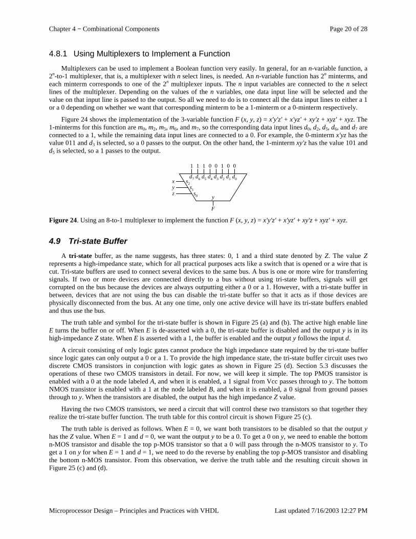
Chapter 4 − Combinational Components Page 20 of 28
Microprocessor Design – Principles and Practices with VHDL Last updated 7/16/2003 12:27 PM
4.8.1 Using Multiplexers to Implement a Function
Multiplexers can be used to implement a Boolean function very easily. In general, for an n-variable function, a 2n-to-1 multiplexer, that is, a multiplexer with n select lines, is needed. An n-variable function has 2n minterms, and each minterm corresponds to one of the 2n multiplexer inputs. The n input variables are connected to the n select lines of the multiplexer. Depending on the values of the n variables, one data input line will be selected and the value on that input line is passed to the output. So all we need to do is to connect all the data input lines to either a 1 or a 0 depending on whether we want that corresponding minterm to be a 1-minterm or a 0-minterm respectively.
Figure 24 shows the implementation of the 3-variable function F (x, y, z) = x'y'z' + x'yz' + xy'z + xyz' + xyz. The 1-minterms for this function are m0, m2, m5, m6, and m7, so the corresponding data input lines d0, d2, d5, d6, and d7 are connected to a 1, while the remaining data input lines are connected to a 0. For example, the 0-minterm x'yz has the value 011 and d3 is selected, so a 0 passes to the output. On the other hand, the 1-minterm xy'z has the value 101 and d5 is selected, so a 1 passes to the output.
s2s1
d1 d0d2d3d4d5d6d7
s0 y
yx
z
F
01 000111
Figure 24. Using an 8-to-1 multiplexer to implement the function F (x, y, z) = x'y'z' + x'yz' + xy'z + xyz' + xyz.
4.9 Tri-state Buffer A tri-state buffer, as the name suggests, has three states: 0, 1 and a third state denoted by Z. The value Z
represents a high-impedance state, which for all practical purposes acts like a switch that is opened or a wire that is cut. Tri-state buffers are used to connect several devices to the same bus. A bus is one or more wire for transferring signals. If two or more devices are connected directly to a bus without using tri-state buffers, signals will get corrupted on the bus because the devices are always outputting either a 0 or a 1. However, with a tri-state buffer in between, devices that are not using the bus can disable the tri-state buffer so that it acts as if those devices are physically disconnected from the bus. At any one time, only one active device will have its tri-state buffers enabled and thus use the bus.
The truth table and symbol for the tri-state buffer is shown in Figure 25 (a) and (b). The active high enable line E turns the buffer on or off. When E is de-asserted with a 0, the tri-state buffer is disabled and the output y is in its high-impedance Z state. When E is asserted with a 1, the buffer is enabled and the output y follows the input d.
A circuit consisting of only logic gates cannot produce the high impedance state required by the tri-state buffer since logic gates can only output a 0 or a 1. To provide the high impedance state, the tri-state buffer circuit uses two discrete CMOS transistors in conjunction with logic gates as shown in Figure 25 (d). Section 5.3 discusses the operations of these two CMOS transistors in detail. For now, we will keep it simple. The top PMOS transistor is enabled with a 0 at the node labeled A, and when it is enabled, a 1 signal from Vcc passes through to y. The bottom NMOS transistor is enabled with a 1 at the node labeled B, and when it is enabled, a 0 signal from ground passes through to y. When the transistors are disabled, the output has the high impedance Z value.
Having the two CMOS transistors, we need a circuit that will control these two transistors so that together they realize the tri-state buffer function. The truth table for this control circuit is shown Figure 25 (c).
The truth table is derived as follows. When E = 0, we want both transistors to be disabled so that the output y has the Z value. When E = 1 and d = 0, we want the output y to be a 0. To get a 0 on y, we need to enable the bottom n-MOS transistor and disable the top p-MOS transistor so that a 0 will pass through the n-MOS transistor to y. To get a 1 on y for when E = 1 and d = 1, we need to do the reverse by enabling the top p-MOS transistor and disabling the bottom n-MOS transistor. From this observation, we derive the truth table and the resulting circuit shown in Figure 25 (c) and (d).
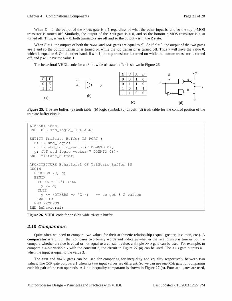
Chapter 4 − Combinational Components Page 21 of 28
Microprocessor Design – Principles and Practices with VHDL Last updated 7/16/2003 12:27 PM
When E = 0, the output of the NAND gate is a 1 regardless of what the other input is, and so the top p-MOS transistor is turned off. Similarly, the output of the AND gate is a 0, and so the bottom n-MOS transistor is also turned off. Thus, when E = 0, both transistors are off and so the output y is in the Z state.
When E = 1, the outputs of both the NAND and AND gates are equal to d'. So if d = 0, the output of the two gates are 1 and so the bottom transistor is turned on while the top transistor is turned off. Thus y will have the value 0, which is equal to d. On the other hand, if d = 1, the top transistor is turned on while the bottom transistor is turned off, and y will have the value 1.
The behavioral VHDL code for an 8-bit wide tri-state buffer is shown in Figure 26.
E Y 0 Z 1 d
(a)
E
d y
(b)
E d A B 0 0 1 0 0 1 1 0 1 0 1 1 1 1 0 0
(c)
y
Vcc
A
B
E
d
(d)
Figure 25. Tri-state buffer: (a) truth table; (b) logic symbol; (c) circuit; (d) truth table for the control portion of the tri-state buffer circuit.
LIBRARY ieee;USE IEEE.std_logic_1164.ALL;
ENTITY TriState_Buffer IS PORT (E: IN std_logic;d: IN std_logic_vector(7 DOWNTO 0);y: OUT std_logic_vector(7 DOWNTO 0));
END TriState_Buffer;
ARCHITECTURE Behavioral OF TriState_Buffer ISBEGIN
PROCESS (E, d)BEGINIF (E = '1') THENy <= d;
ELSEy <= (OTHERS => 'Z'); -- to get 8 Z values
END IF;END PROCESS;
END Behavioral;
Figure 26. VHDL code for an 8-bit wide tri-state buffer.
4.10 Comparators Quite often we need to compare two values for their arithmetic relationship (equal, greater, less than, etc.). A
comparator is a circuit that compares two binary words and indicates whether the relationship is true or not. To compare whether a value is equal or not equal to a constant value, a simple AND gate can be used. For example, to compare a 4-bit variable x with the constant 3, the circuit in Figure 27 (a) can be used. The AND gate outputs a 1 when the input is equal to the value 3.
The XOR and XNOR gates can be used for comparing for inequality and equality respectively between two values. The XOR gate outputs a 1 when its two input values are different. So we can use one XOR gate for comparing each bit pair of the two operands. A 4-bit inequality comparator is shown in Figure 27 (b). Four XOR gates are used,
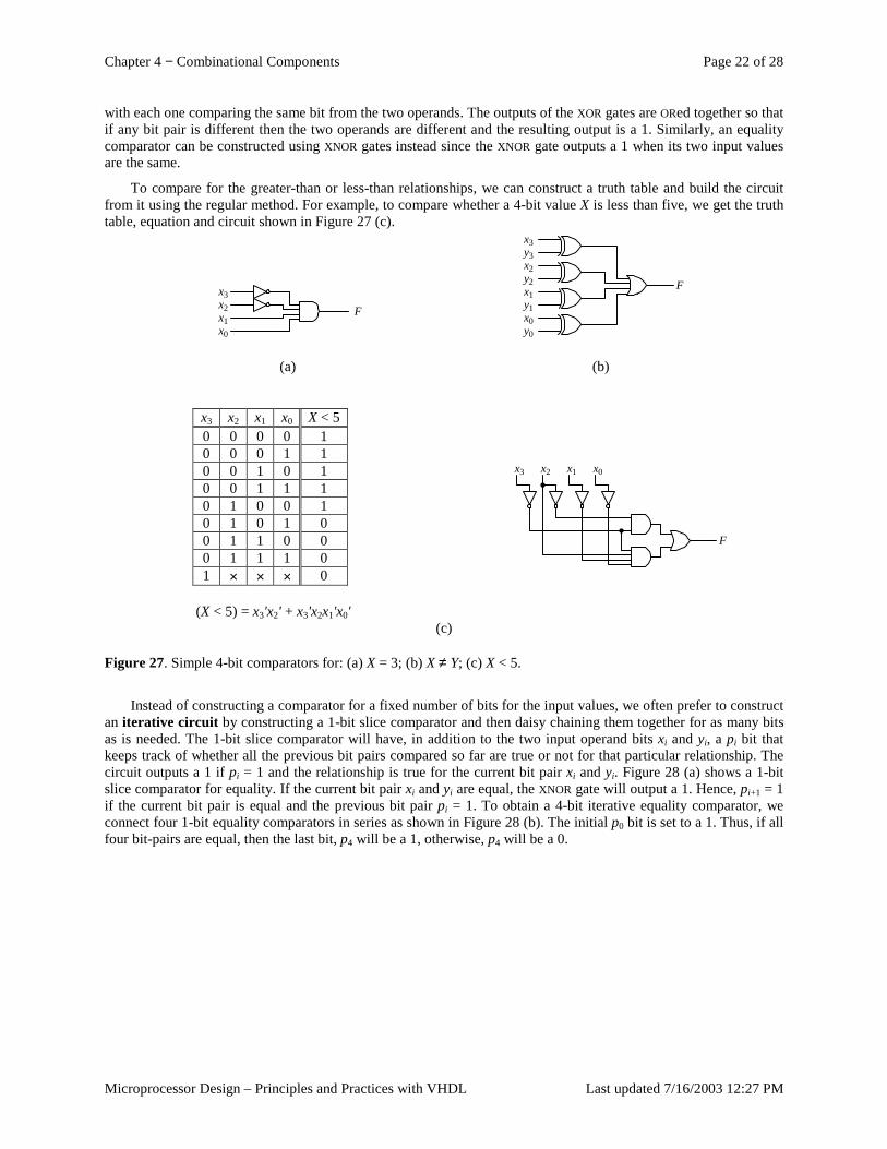
Chapter 4 − Combinational Components Page 22 of 28
Microprocessor Design – Principles and Practices with VHDL Last updated 7/16/2003 12:27 PM
with each one comparing the same bit from the two operands. The outputs of the XOR gates are ORed together so that if any bit pair is different then the two operands are different and the resulting output is a 1. Similarly, an equality comparator can be constructed using XNOR gates instead since the XNOR gate outputs a 1 when its two input values are the same.
To compare for the greater-than or less-than relationships, we can construct a truth table and build the circuit from it using the regular method. For example, to compare whether a 4-bit value X is less than five, we get the truth table, equation and circuit shown in Figure 27 (c).
x3x2x1x0
F
F
x3y3x2y2x1y1x0y0
(a) (b)
x3 x2 x1 x0 X < 5 0 0 0 0 1 0 0 0 1 1 0 0 1 0 1 0 0 1 1 1 0 1 0 0 1 0 1 0 1 0 0 1 1 0 0 0 1 1 1 0 1 × × × 0
(X < 5) = x3'x2' + x3'x2x1'x0'
x1x2 x0
F
x3
(c) Figure 27. Simple 4-bit comparators for: (a) X = 3; (b) X ≠ Y; (c) X < 5.
Instead of constructing a comparator for a fixed number of bits for the input values, we often prefer to construct an iterative circuit by constructing a 1-bit slice comparator and then daisy chaining them together for as many bits as is needed. The 1-bit slice comparator will have, in addition to the two input operand bits xi and yi, a pi bit that keeps track of whether all the previous bit pairs compared so far are true or not for that particular relationship. The circuit outputs a 1 if pi = 1 and the relationship is true for the current bit pair xi and yi. Figure 28 (a) shows a 1-bit slice comparator for equality. If the current bit pair xi and yi are equal, the XNOR gate will output a 1. Hence, pi+1 = 1 if the current bit pair is equal and the previous bit pair pi = 1. To obtain a 4-bit iterative equality comparator, we connect four 1-bit equality comparators in series as shown in Figure 28 (b). The initial p0 bit is set to a 1. Thus, if all four bit-pairs are equal, then the last bit, p4 will be a 1, otherwise, p4 will be a 0.
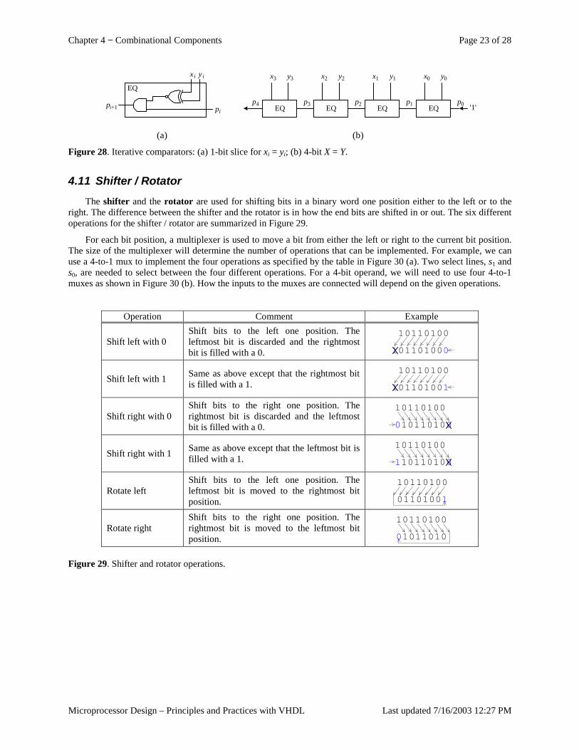
Chapter 4 − Combinational Components Page 23 of 28
Microprocessor Design – Principles and Practices with VHDL Last updated 7/16/2003 12:27 PM
EQ
pi+1 pi
xi y i
'1'
x3 y3
EQ
x2 y2 x1 y1 x0 y0
p3 p2 p1p4 p0EQEQ EQ
(a) (b)
Figure 28. Iterative comparators: (a) 1-bit slice for xi = yi; (b) 4-bit X = Y.
4.11 Shifter / Rotator The shifter and the rotator are used for shifting bits in a binary word one position either to the left or to the
right. The difference between the shifter and the rotator is in how the end bits are shifted in or out. The six different operations for the shifter / rotator are summarized in Figure 29.
For each bit position, a multiplexer is used to move a bit from either the left or right to the current bit position. The size of the multiplexer will determine the number of operations that can be implemented. For example, we can use a 4-to-1 mux to implement the four operations as specified by the table in Figure 30 (a). Two select lines, s1 and s0, are needed to select between the four different operations. For a 4-bit operand, we will need to use four 4-to-1 muxes as shown in Figure 30 (b). How the inputs to the muxes are connected will depend on the given operations.
Operation Comment Example
Shift left with 0 Shift bits to the left one position. The leftmost bit is discarded and the rightmost bit is filled with a 0.
10110100
101101000
Shift left with 1 Same as above except that the rightmost bit is filled with a 1.
10110100
101101001
Shift right with 0 Shift bits to the right one position. The rightmost bit is discarded and the leftmost bit is filled with a 0.
10110100
011010010
Shift right with 1 Same as above except that the leftmost bit is filled with a 1.
10110100
011010011
Rotate left Shift bits to the left one position. The leftmost bit is moved to the rightmost bit position.
10110100
01101001
Rotate right Shift bits to the right one position. The rightmost bit is moved to the leftmost bit position.
10110100
01101010
Figure 29. Shifter and rotator operations.
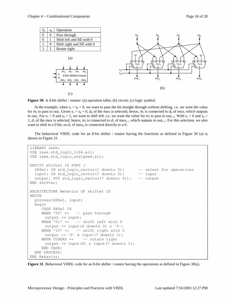
Chapter 4 − Combinational Components Page 24 of 28
Microprocessor Design – Principles and Practices with VHDL Last updated 7/16/2003 12:27 PM
S1 s0 Operation 0 0 Pass through 0 1 Shift left and fill with 0 1 0 Shift right and fill with 0 1 1 Rotate right
(a)
in0
out0out1out2out3
in1in2in3s1s0
4-bit shifter/rotator
(c)
0123s1s0 y
mux3
out3
in3
out2
in2
out1
in1
out0
in0
'0' '0'
s1s0
0123s1s0 y
mux2
0123s1s0 y
mux1
0123s1s0 y
mux1
(b)
Figure 30. A 4-bit shifter / rotator: (a) operation table; (b) circuit; (c) logic symbol.
In the example, when s1 = s0 = 0, we want to pass the bit straight through without shifting, i.e. we want the value for ini to pass to outi. Given s1 = s0 = 0, d0 of the mux is selected, hence, ini is connected to d0 of muxi which outputs to outi. For s1 = 0 and s0 = 1, we want to shift left, i.e. we want the value for ini to pass to outi+1. With s1 = 0 and s0 = 1, d1 of the mux is selected, hence, ini is connected to d1 of muxi+1 which outputs to outi+1. For this selection, we also want to shift in a 0 bit, so d1 of mux0 is connected directly to a 0.
The behavioral VHDL code for an 8-bit shifter / rotator having the functions as defined in Figure 30 (a) is shown in Figure 31.
LIBRARY ieee;USE ieee.std_logic_1164.all;USE ieee.std_logic_unsigned.all;
ENTITY shifter IS PORT (SHSel: IN std_logic_vector(1 downto 0); -- select for operationsinput: IN std_logic_vector(7 downto 0); -- inputoutput: OUT std_logic_vector(7 downto 0)); -- output
END shifter;
ARCHITECTURE Behavior OF shifter ISBEGIN
process(SHSel, input)begin
CASE SHSel ISWHEN "00" => -- pass throughoutput <= input;
WHEN "01" => -- shift left with 0output <= input(6 downto 0) & '0';
WHEN "10" => -- shift right with 0output <= '0' & input(7 downto 1);
WHEN OTHERS => -- rotate rightoutput <= input(0) & input(7 downto 1);
END CASE;END PROCESS;
END Behavior;
Figure 31. Behavioral VHDL code for an 8-bit shifter / rotator having the operations as defined in Figure 30(a).
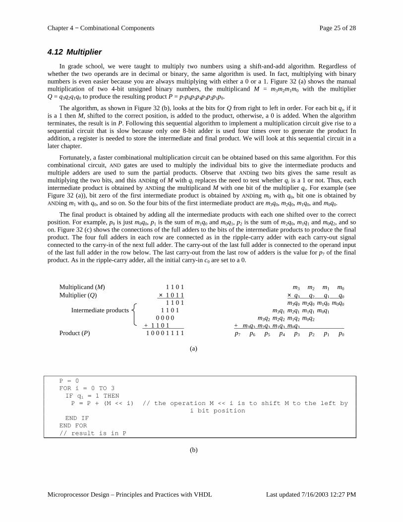
Chapter 4 − Combinational Components Page 25 of 28
Microprocessor Design – Principles and Practices with VHDL Last updated 7/16/2003 12:27 PM
4.12 Multiplier In grade school, we were taught to multiply two numbers using a shift-and-add algorithm. Regardless of
whether the two operands are in decimal or binary, the same algorithm is used. In fact, multiplying with binary numbers is even easier because you are always multiplying with either a 0 or a 1. Figure 32 (a) shows the manual multiplication of two 4-bit unsigned binary numbers, the multiplicand M = m3m2m1m0 with the multiplier Q = q3q2q1q0 to produce the resulting product P = p7p6p5p4p3p2p1p0.
The algorithm, as shown in Figure 32 (b), looks at the bits for Q from right to left in order. For each bit qi, if it is a 1 then M, shifted to the correct position, is added to the product, otherwise, a 0 is added. When the algorithm terminates, the result is in P. Following this sequential algorithm to implement a multiplication circuit give rise to a sequential circuit that is slow because only one 8-bit adder is used four times over to generate the product In addition, a register is needed to store the intermediate and final product. We will look at this sequential circuit in a later chapter.
Fortunately, a faster combinational multiplication circuit can be obtained based on this same algorithm. For this combinational circuit, AND gates are used to multiply the individual bits to give the intermediate products and multiple adders are used to sum the partial products. Observe that ANDing two bits gives the same result as multiplying the two bits, and this ANDing of M with qi replaces the need to test whether qi is a 1 or not. Thus, each intermediate product is obtained by ANDing the multiplicand M with one bit of the multiplier qi. For example (see Figure 32 (a)), bit zero of the first intermediate product is obtained by ANDing m0 with q0, bit one is obtained by ANDing m1 with q0, and so on. So the four bits of the first intermediate product are m3q0, m2q0, m1q0, and m0q0.
The final product is obtained by adding all the intermediate products with each one shifted over to the correct position. For example, p0 is just m0q0, p1 is the sum of m1q0 and m0q1, p2 is the sum of m2q0, m1q1 and m0q2, and so on. Figure 32 (c) shows the connections of the full adders to the bits of the intermediate products to produce the final product. The four full adders in each row are connected as in the ripple-carry adder with each carry-out signal connected to the carry-in of the next full adder. The carry-out of the last full adder is connected to the operand input of the last full adder in the row below. The last carry-out from the last row of adders is the value for p7 of the final product. As in the ripple-carry adder, all the initial carry-in c0 are set to a 0.
Multiplicand (M) 1 1 0 1 m3 m2 m1 m0
Multiplier (Q) × 1 0 1 1 × q3 q2 q1 q0 1 1 0 1 m3q0 m2q0 m1q0 m0q0 Intermediate products 1 1 0 1 m3q1 m2q1 m1q1 m0q1 0 0 0 0 m3q2 m2q2 m1q2 m0q2 + 1 1 0 1 + m3q3 m2q3 m1q3 m0q3 Product (P) 1 0 0 0 1 1 1 1 p7 p6 p5 p4 p3 p2 p1 p0
(a)
P = 0FOR i = 0 TO 3IF qi = 1 THENP = P + (M << i) // the operation M << i is to shift M to the left by
i bit positionEND IF
END FOR// result is in P
(b)
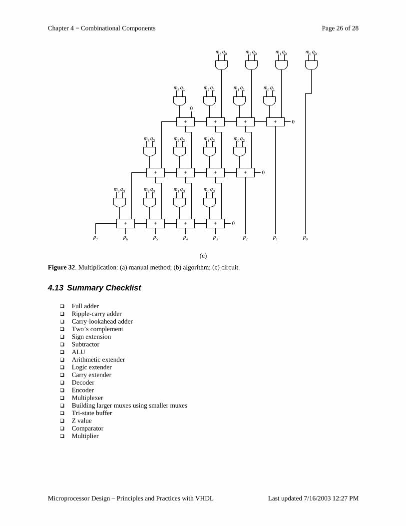
Chapter 4 − Combinational Components Page 26 of 28
Microprocessor Design – Principles and Practices with VHDL Last updated 7/16/2003 12:27 PM
p0p1p2p3p4p5p6p7
++++ 0
++++ 0
++++ 0
0
m3 q3 m2 q3 m1 q3 m0 q3
m3 q2 m2 q2 m1 q2 m0 q2
m3 q1 m2 q1 m1 q1 m0 q1
m3 q0 m2 q0 m1 q0 m0 q0
(c)
Figure 32. Multiplication: (a) manual method; (b) algorithm; (c) circuit.
4.13 Summary Checklist
� Full adder � Ripple-carry adder � Carry-lookahead adder � Two’s complement � Sign extension � Subtractor � ALU � Arithmetic extender � Logic extender � Carry extender � Decoder � Encoder � Multiplexer � Building larger muxes using smaller muxes � Tri-state buffer � Z value � Comparator � Multiplier
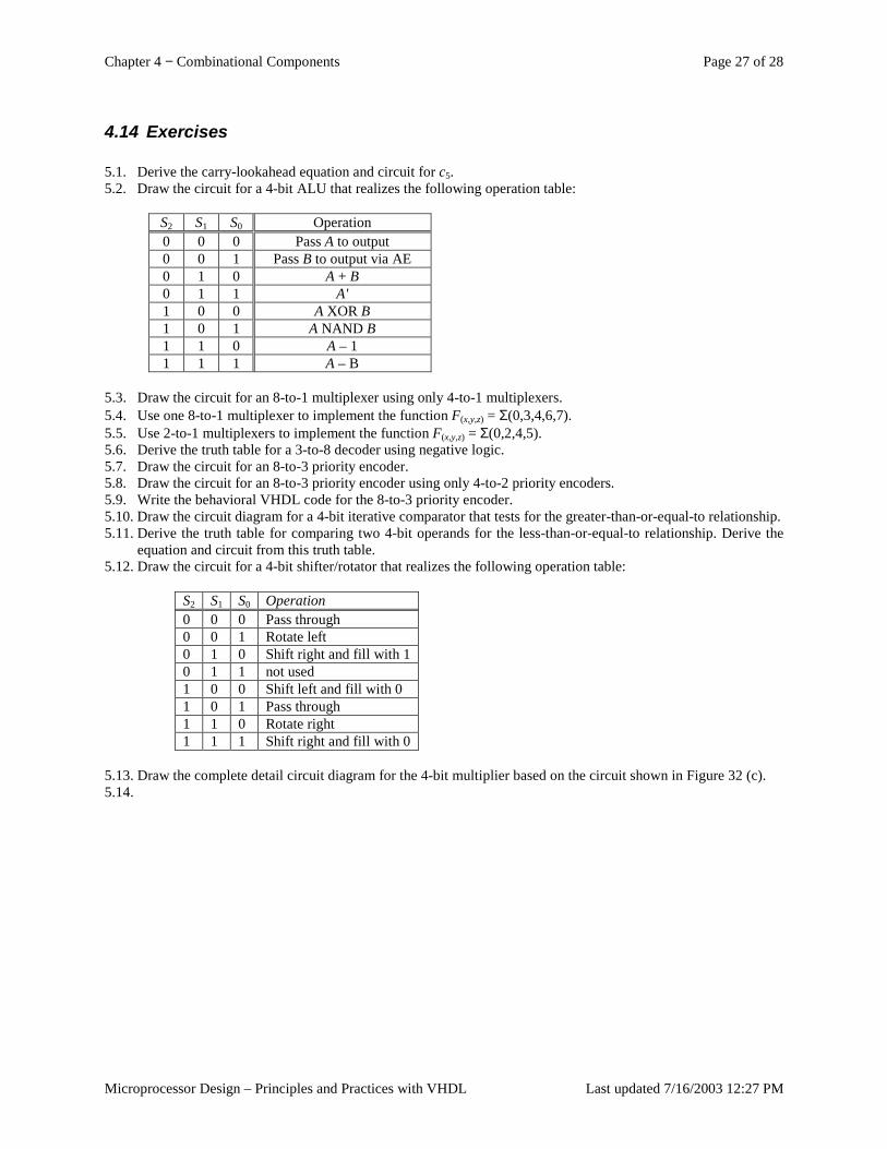
Chapter 4 − Combinational Components Page 27 of 28
Microprocessor Design – Principles and Practices with VHDL Last updated 7/16/2003 12:27 PM
4.14 Exercises
5.1. Derive the carry-lookahead equation and circuit for c5. 5.2. Draw the circuit for a 4-bit ALU that realizes the following operation table:
S2 S1 S0 Operation 0 0 0 Pass A to output 0 0 1 Pass B to output via AE 0 1 0 A + B 0 1 1 A' 1 0 0 A XOR B 1 0 1 A NAND B 1 1 0 A – 1 1 1 1 A – B
5.3. Draw the circuit for an 8-to-1 multiplexer using only 4-to-1 multiplexers. 5.4. Use one 8-to-1 multiplexer to implement the function F(x,y,z) = Σ(0,3,4,6,7). 5.5. Use 2-to-1 multiplexers to implement the function F(x,y,z) = Σ(0,2,4,5). 5.6. Derive the truth table for a 3-to-8 decoder using negative logic. 5.7. Draw the circuit for an 8-to-3 priority encoder. 5.8. Draw the circuit for an 8-to-3 priority encoder using only 4-to-2 priority encoders. 5.9. Write the behavioral VHDL code for the 8-to-3 priority encoder. 5.10. Draw the circuit diagram for a 4-bit iterative comparator that tests for the greater-than-or-equal-to relationship. 5.11. Derive the truth table for comparing two 4-bit operands for the less-than-or-equal-to relationship. Derive the
equation and circuit from this truth table. 5.12. Draw the circuit for a 4-bit shifter/rotator that realizes the following operation table:
S2 S1 S0 Operation 0 0 0 Pass through 0 0 1 Rotate left 0 1 0 Shift right and fill with 1 0 1 1 not used 1 0 0 Shift left and fill with 0 1 0 1 Pass through 1 1 0 Rotate right 1 1 1 Shift right and fill with 0
5.13. Draw the complete detail circuit diagram for the 4-bit multiplier based on the circuit shown in Figure 32 (c). 5.14.
Chapter 4 − Combinational Components Page 28 of 28
Microprocessor Design – Principles and Practices with VHDL Last updated 7/16/2003 12:27 PM
Index
A
Active-high, 2 Active-low, 2 Adder, 2, 8
carry-lookahead, 4 full, 2 ripple-carry, 3
AE. See Arithmetic logic unit. ALU. See Arithmetic logic unit. Arithmetic extender. See Arithmetic logic unit. Arithmetic logic unit, 10
AE arithmetic extender, 10 CE carry extender, 10 LE logic extender, 10
Assert, 2
C
Carry extender. See Arithmetic logic unit. Carry-lookahead adder, 4 CE. See Arithmetic logic unit. Combinational components, 2 Comparator, 21
D
De-assert, 2 Decoder, 14 Demultiplexer, 14
E
Encoder, 15 priority, 16
F
FA. See Full adder. Full adder, 2
I Iterative circuit, 22
L
LE. See Arithmetic logic unit. Logic extender. See Arithmetic logic unit.
M
Multiplexer, 17 Multiplier, 25 Mux. See Multiplexer.
N
Negative logic, 2 Negative numbers, 6
P
Positive logic, 2 Priority encoder, 16
R
Ripple-carry adder, 3 Rotator, 23
S
Shifter, 23 Sign extension, 7 Subtractor, 2, 8
T
Tri-state buffer, 20 Two’s-complement, 6
V
VHDL code 3-to-8 decoder, 15 4-to-1 multiplexer, 19 adder/subtractor, 10 arithmetic logic unit (ALU), 13 full adder, 3 shifter/rotator, 24 tri-state buffer, 21
Chapter 5 − Implementation Technologies Page 1 of 27
Microprocessor Design – Principles and Practices with VHDL Last updated 7/16/2003 12:29 PM
Table of Content Table of Content ........................................................................................................................................................... 1 5 Implementation Technologies ............................................................................................................................... 2
5.1 Physical Abstraction...................................................................................................................................... 2 5.2 Metal-Oxide-Semiconductor Field-Effect Transistor (MOSFET) ................................................................ 3 5.3 CMOS Logic ................................................................................................................................................. 4 5.4 CMOS Circuits.............................................................................................................................................. 5
5.4.1 CMOS Inverter...................................................................................................................................... 5 5.4.2 CMOS NAND gate ............................................................................................................................... 6 5.4.3 CMOS AND gate .................................................................................................................................. 7 5.4.4 CMOS NOR and OR Gates................................................................................................................... 9 5.4.5 Transmission Gate................................................................................................................................. 9 5.4.6 2-input Multiplexer CMOS Circuit ....................................................................................................... 9 5.4.7 CMOS XOR and XNOR Gates ........................................................................................................... 11
5.5 Analysis of CMOS Circuits ........................................................................................................................ 12 5.6 Using ROMs to Implement a Function ....................................................................................................... 13 5.7 Using PLAs to Implement a Function......................................................................................................... 15 5.8 Using PALs to Implement a Function......................................................................................................... 19 5.9 Complex Programmable Logic Device (CPLD) ......................................................................................... 21 5.10 Field-Programmable Gate Array (FPGA) ................................................................................................... 23 5.11 Summary Checklist ..................................................................................................................................... 24 5.12 References................................................................................................................................................... 24 5.13 Exercises ..................................................................................................................................................... 25 Index ....................................................................................................................................................................... 26
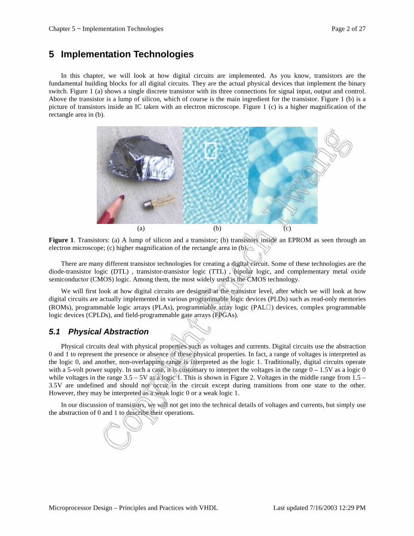
Chapter 5 − Implementation Technologies Page 2 of 27
Microprocessor Design – Principles and Practices with VHDL Last updated 7/16/2003 12:29 PM
5 Implementation Technologies
In this chapter, we will look at how digital circuits are implemented. As you know, transistors are the fundamental building blocks for all digital circuits. They are the actual physical devices that implement the binary switch. Figure 1 (a) shows a single discrete transistor with its three connections for signal input, output and control. Above the transistor is a lump of silicon, which of course is the main ingredient for the transistor. Figure 1 (b) is a picture of transistors inside an IC taken with an electron microscope. Figure 1 (c) is a higher magnification of the rectangle area in (b).
(a) (b) (c)
Figure 1. Transistors: (a) A lump of silicon and a transistor; (b) transistors inside an EPROM as seen through an electron microscope; (c) higher magnification of the rectangle area in (b).
There are many different transistor technologies for creating a digital circuit. Some of these technologies are the diode-transistor logic (DTL) , transistor-transistor logic (TTL) , bipolar logic, and complementary metal oxide semiconductor (CMOS) logic. Among them, the most widely used is the CMOS technology.
We will first look at how digital circuits are designed at the transistor level, after which we will look at how digital circuits are actually implemented in various programmable logic devices (PLDs) such as read-only memories (ROMs), programmable logic arrays (PLAs), programmable array logic (PAL ) devices, complex programmable logic devices (CPLDs), and field-programmable gate arrays (FPGAs).
5.1 Physical Abstraction Physical circuits deal with physical properties such as voltages and currents. Digital circuits use the abstraction
0 and 1 to represent the presence or absence of these physical properties. In fact, a range of voltages is interpreted as the logic 0, and another, non-overlapping range is interpreted as the logic 1. Traditionally, digital circuits operate with a 5-volt power supply. In such a case, it is customary to interpret the voltages in the range 0 – 1.5V as a logic 0 while voltages in the range 3.5 – 5V as a logic 1. This is shown in Figure 2. Voltages in the middle range from 1.5 – 3.5V are undefined and should not occur in the circuit except during transitions from one state to the other. However, they may be interpreted as a weak logic 0 or a weak logic 1.
In our discussion of transistors, we will not get into the technical details of voltages and currents, but simply use the abstraction of 0 and 1 to describe their operations.
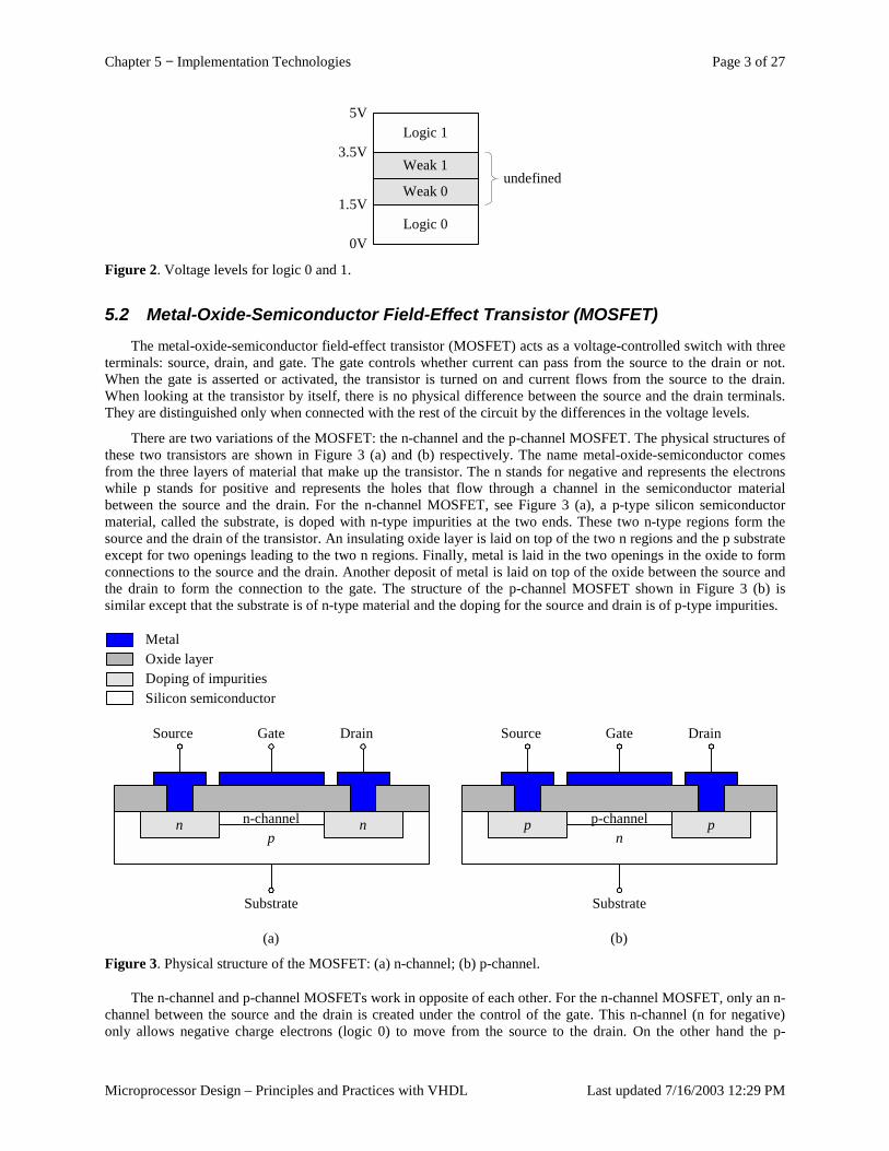
Chapter 5 − Implementation Technologies Page 3 of 27
Microprocessor Design – Principles and Practices with VHDL Last updated 7/16/2003 12:29 PM
Logic 0
Logic 1
1.5V
3.5V
5V
0V
Weak 0
Weak 1undefined
Figure 2. Voltage levels for logic 0 and 1.
5.2 Metal-Oxide-Semiconductor Field-Effect Transistor (MOSFET) The metal-oxide-semiconductor field-effect transistor (MOSFET) acts as a voltage-controlled switch with three
terminals: source, drain, and gate. The gate controls whether current can pass from the source to the drain or not. When the gate is asserted or activated, the transistor is turned on and current flows from the source to the drain. When looking at the transistor by itself, there is no physical difference between the source and the drain terminals. They are distinguished only when connected with the rest of the circuit by the differences in the voltage levels.
There are two variations of the MOSFET: the n-channel and the p-channel MOSFET. The physical structures of these two transistors are shown in Figure 3 (a) and (b) respectively. The name metal-oxide-semiconductor comes from the three layers of material that make up the transistor. The n stands for negative and represents the electrons while p stands for positive and represents the holes that flow through a channel in the semiconductor material between the source and the drain. For the n-channel MOSFET, see Figure 3 (a), a p-type silicon semiconductor material, called the substrate, is doped with n-type impurities at the two ends. These two n-type regions form the source and the drain of the transistor. An insulating oxide layer is laid on top of the two n regions and the p substrate except for two openings leading to the two n regions. Finally, metal is laid in the two openings in the oxide to form connections to the source and the drain. Another deposit of metal is laid on top of the oxide between the source and the drain to form the connection to the gate. The structure of the p-channel MOSFET shown in Figure 3 (b) is similar except that the substrate is of n-type material and the doping for the source and drain is of p-type impurities.
Oxide layerMetal
Doping of impuritiesSilicon semiconductor
pn n
Source DrainGate
Substrate
n-channel
(a)
np p
Source DrainGate
Substrate
p-channel
(b)
Figure 3. Physical structure of the MOSFET: (a) n-channel; (b) p-channel.
The n-channel and p-channel MOSFETs work in opposite of each other. For the n-channel MOSFET, only an n-channel between the source and the drain is created under the control of the gate. This n-channel (n for negative) only allows negative charge electrons (logic 0) to move from the source to the drain. On the other hand the p-
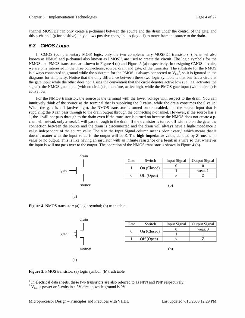
Chapter 5 − Implementation Technologies Page 4 of 27
Microprocessor Design – Principles and Practices with VHDL Last updated 7/16/2003 12:29 PM
channel MOSFET can only create a p-channel between the source and the drain under the control of the gate, and this p-channel (p for positive) only allows positive charge holes (logic 1) to move from the source to the drain.
5.3 CMOS Logic In CMOS (complementary MOS) logic, only the two complementary MOSFET transistors, (n-channel also
known as NMOS and p-channel also known as PMOS)1, are used to create the circuit. The logic symbols for the NMOS and PMOS transistors are shown in Figure 4 (a) and Figure 5 (a) respectively. In designing CMOS circuits, we are only interested in the three connections, source, drain and gate, of the transistor. The substrate for the NMOS is always connected to ground while the substrate for the PMOS is always connected to VCC
2, so it is ignored in the diagrams for simplicity. Notice that the only difference between these two logic symbols is that one has a circle at the gate input while the other does not. Using the convention that the circle denotes active low (i.e., a 0 activates the signal), the NMOS gate input (with no circle) is, therefore, active high, while the PMOS gate input (with a circle) is active low.
For the NMOS transistor, the source is the terminal with the lower voltage with respect to the drain. You can intuitively think of the source as the terminal that is supplying the 0 value, while the drain consumes the 0 value. When the gate is a 1 (active high), the NMOS transistor is turned on or enabled, and the source input that is supplying the 0 can pass through to the drain output through the connecting n-channel. However, if the source has a 1, the 1 will not pass through to the drain even if the transistor is turned on because the NMOS does not create a p-channel. Instead, only a weak 1 will pass through to the drain. If the transistor is turned off with a 0 on the gate, the connection between the source and the drain is disconnected and the drain will always have a high-impedance Z value independent of the source value The × in the Input Signal column means “don’t care,” which means that it doesn’t matter what the input value is, the output will be Z. The high-impedance value, denoted by Z, means no value or no output. This is like having an insulator with an infinite resistance or a break in a wire so that whatever the input is will not pass over to the output. The operation of the NMOS transistor is shown in Figure 4 (b).
drain
source
gate
(a)
Gate Switch Input Signal Output Signal 0 0 1 On (Closed) 1 weak 1
0 Off (Open) × Z
(b)
Figure 4. NMOS transistor: (a) logic symbol; (b) truth table.
drain
source
gate
(a)
Gate Switch Input Signal Output Signal 0 weak 0 0 On (Closed) 1 1
1 Off (Open) × Z
(b)
Figure 5. PMOS transistor: (a) logic symbol; (b) truth table. 1 In electrical data sheets, these two transistors are also referred to as NPN and PNP respectively. 2 VCC is power or 5-volts in a 5V circuit, while ground is 0V.
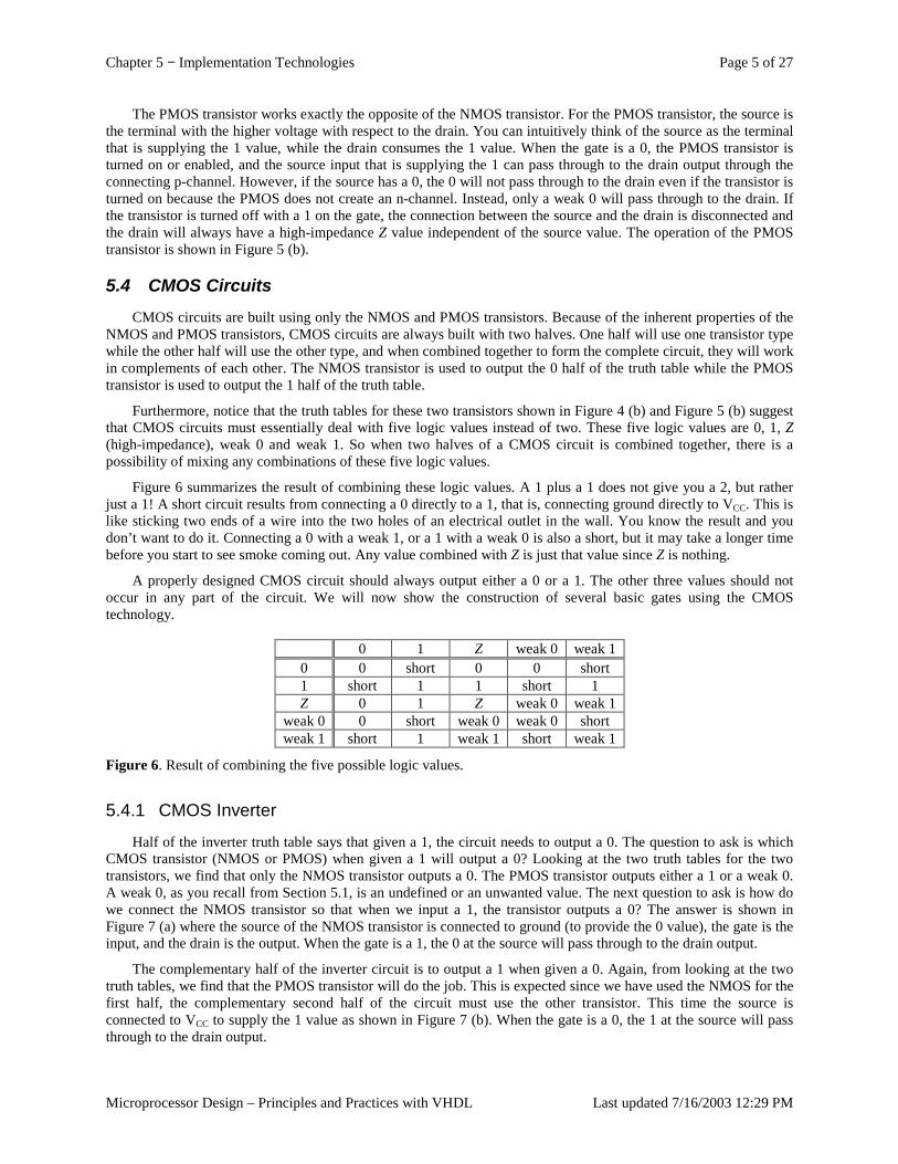
Chapter 5 − Implementation Technologies Page 5 of 27
Microprocessor Design – Principles and Practices with VHDL Last updated 7/16/2003 12:29 PM
The PMOS transistor works exactly the opposite of the NMOS transistor. For the PMOS transistor, the source is the terminal with the higher voltage with respect to the drain. You can intuitively think of the source as the terminal that is supplying the 1 value, while the drain consumes the 1 value. When the gate is a 0, the PMOS transistor is turned on or enabled, and the source input that is supplying the 1 can pass through to the drain output through the connecting p-channel. However, if the source has a 0, the 0 will not pass through to the drain even if the transistor is turned on because the PMOS does not create an n-channel. Instead, only a weak 0 will pass through to the drain. If the transistor is turned off with a 1 on the gate, the connection between the source and the drain is disconnected and the drain will always have a high-impedance Z value independent of the source value. The operation of the PMOS transistor is shown in Figure 5 (b).
5.4 CMOS Circuits CMOS circuits are built using only the NMOS and PMOS transistors. Because of the inherent properties of the
NMOS and PMOS transistors, CMOS circuits are always built with two halves. One half will use one transistor type while the other half will use the other type, and when combined together to form the complete circuit, they will work in complements of each other. The NMOS transistor is used to output the 0 half of the truth table while the PMOS transistor is used to output the 1 half of the truth table.
Furthermore, notice that the truth tables for these two transistors shown in Figure 4 (b) and Figure 5 (b) suggest that CMOS circuits must essentially deal with five logic values instead of two. These five logic values are 0, 1, Z (high-impedance), weak 0 and weak 1. So when two halves of a CMOS circuit is combined together, there is a possibility of mixing any combinations of these five logic values.
Figure 6 summarizes the result of combining these logic values. A 1 plus a 1 does not give you a 2, but rather just a 1! A short circuit results from connecting a 0 directly to a 1, that is, connecting ground directly to VCC. This is like sticking two ends of a wire into the two holes of an electrical outlet in the wall. You know the result and you don’t want to do it. Connecting a 0 with a weak 1, or a 1 with a weak 0 is also a short, but it may take a longer time before you start to see smoke coming out. Any value combined with Z is just that value since Z is nothing.
A properly designed CMOS circuit should always output either a 0 or a 1. The other three values should not occur in any part of the circuit. We will now show the construction of several basic gates using the CMOS technology.
0 1 Z weak 0 weak 1
0 0 short 0 0 short 1 short 1 1 short 1 Z 0 1 Z weak 0 weak 1
weak 0 0 short weak 0 weak 0 short weak 1 short 1 weak 1 short weak 1
Figure 6. Result of combining the five possible logic values.
5.4.1 CMOS Inverter
Half of the inverter truth table says that given a 1, the circuit needs to output a 0. The question to ask is which CMOS transistor (NMOS or PMOS) when given a 1 will output a 0? Looking at the two truth tables for the two transistors, we find that only the NMOS transistor outputs a 0. The PMOS transistor outputs either a 1 or a weak 0. A weak 0, as you recall from Section 5.1, is an undefined or an unwanted value. The next question to ask is how do we connect the NMOS transistor so that when we input a 1, the transistor outputs a 0? The answer is shown in Figure 7 (a) where the source of the NMOS transistor is connected to ground (to provide the 0 value), the gate is the input, and the drain is the output. When the gate is a 1, the 0 at the source will pass through to the drain output.
The complementary half of the inverter circuit is to output a 1 when given a 0. Again, from looking at the two truth tables, we find that the PMOS transistor will do the job. This is expected since we have used the NMOS for the first half, the complementary second half of the circuit must use the other transistor. This time the source is connected to VCC to supply the 1 value as shown in Figure 7 (b). When the gate is a 0, the 1 at the source will pass through to the drain output.
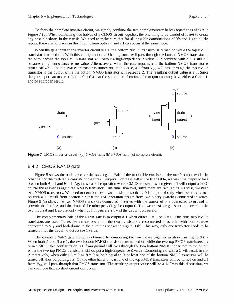
Chapter 5 − Implementation Technologies Page 6 of 27
Microprocessor Design – Principles and Practices with VHDL Last updated 7/16/2003 12:29 PM
To form the complete inverter circuit, we simply combine the two complementary halves together as shown in Figure 7 (c). When combining two halves of a CMOS circuit together, the one thing to be careful of is not to create any possible shorts in the circuit. We need to make sure that for all possible combinations of 0’s and 1’s to all the inputs, there are no places in the circuit where both a 0 and a 1 can occur at the same node.
When the gate input to the inverter circuit is a 1, the bottom NMOS transistor is turned on while the top PMOS transistor is turned off. With this configuration, a 0 from ground will pass through the bottom NMOS transistor to the output while the top PMOS transistor will output a high-impedance Z value. A Z combine with a 0 is still a 0 because a high-impedance is no value. Alternatively, when the gate input is a 0, the bottom NMOS transistor is turned off while the top PMOS transistor is turned on. In this case, a 1 from VCC will pass through the top PMOS transistor to the output while the bottom NMOS transistor will output a Z. The resulting output value is a 1. Since the gate input can never be both a 0 and a 1 at the same time, therefore, the output can only have either a 0 or a 1, and no short can result.
drain
source
gate
0
drain
source
gate
1Vcc
drain
source0
source
gate
1Vcc
input output
(a) (b) (c)
Figure 7. CMOS inverter circuit: (a) NMOS half; (b) PMOS half; (c) complete circuit.
5.4.2 CMOS NAND gate
Figure 8 shows the truth table for the NAND gate. Half of the truth table consists of the one 0 output while the other half of the truth table consists of the three 1 outputs. For the 0 half of the truth table, we want the output to be a 0 when both A = 1 and B = 1. Again, we ask the question which CMOS transistor when given a 1 will output a 0? Of course the answer is again the NMOS transistor. This time, however, since there are two inputs A and B, we need two NMOS transistors. We need to connect these two transistors so that a 0 is outputted only when both are turned on with a 1. Recall from Section 2.3 that the AND operation results from two binary switches connected in series. Figure 9 (a) shows the two NMOS transistors connected in series with the source of one connected to ground to provide the 0 value, and the drain of the other providing the output 0. The two transistor gates are connected to the two inputs A and B so that only when both inputs are a 1 will the circuit outputs a 0.
The complementary half of the NAND gate is to output a 1 when either A = 0 or B = 0. This time two PMOS transistors are used. To realize the OR operation, the two transistors are connected in parallel with both sources connected to VCC and both drains to the output as shown in Figure 9 (b). This way, only one transistor needs to be turned on for the circuit to output the 1 value.
The complete NAND gate circuit is obtained by combining the two halves together as shown in Figure 9 (c). When both A and B are 1, the two bottom NMOS transistors are turned on while the two top PMOS transistors are turned off. In this configuration, a 0 from ground will pass through the two bottom NMOS transistors to the output while the two top PMOS transistors will output a high-impedance Z value. Combining a 0 with a Z will result in a 0. Alternatively, when either A = 0 or B = 0 or both equal to 0, at least one of the bottom NMOS transistor will be turned off, thus outputting a Z. On the other hand, at least one of the top PMOS transistors will be turned on and a 1 from VCC will pass through that PMOS transistor. The resulting output value will be a 1. From this discussion, we can conclude that no short circuit can occur.
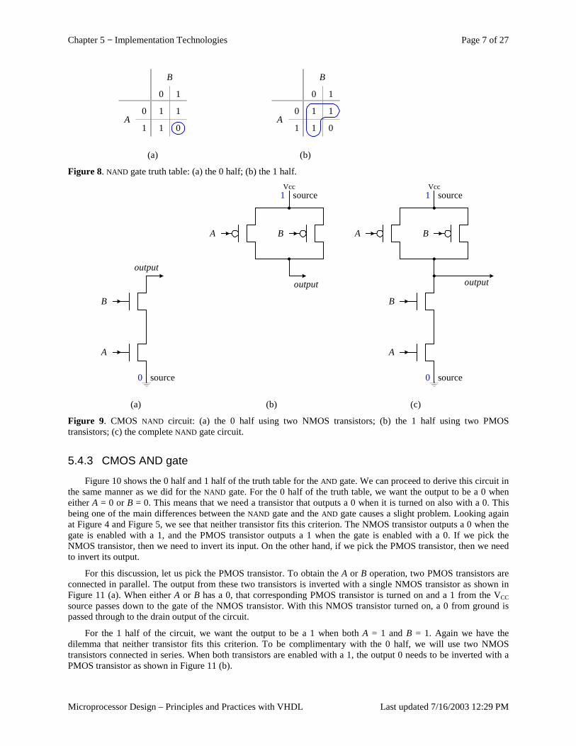
Chapter 5 − Implementation Technologies Page 7 of 27
Microprocessor Design – Principles and Practices with VHDL Last updated 7/16/2003 12:29 PM
1 1
1 0
0 1
0
1
B
A
1 1
1 0
0 1
0
1
B
A
(a) (b)
Figure 8. NAND gate truth table: (a) the 0 half; (b) the 1 half.
source
A
0
output
B
source
A
1Vcc
output
B
source
A
0
B
source
A
1Vcc
B
output
(a) (b) (c)
Figure 9. CMOS NAND circuit: (a) the 0 half using two NMOS transistors; (b) the 1 half using two PMOS transistors; (c) the complete NAND gate circuit.
5.4.3 CMOS AND gate
Figure 10 shows the 0 half and 1 half of the truth table for the AND gate. We can proceed to derive this circuit in the same manner as we did for the NAND gate. For the 0 half of the truth table, we want the output to be a 0 when either A = 0 or B = 0. This means that we need a transistor that outputs a 0 when it is turned on also with a 0. This being one of the main differences between the NAND gate and the AND gate causes a slight problem. Looking again at Figure 4 and Figure 5, we see that neither transistor fits this criterion. The NMOS transistor outputs a 0 when the gate is enabled with a 1, and the PMOS transistor outputs a 1 when the gate is enabled with a 0. If we pick the NMOS transistor, then we need to invert its input. On the other hand, if we pick the PMOS transistor, then we need to invert its output.
For this discussion, let us pick the PMOS transistor. To obtain the A or B operation, two PMOS transistors are connected in parallel. The output from these two transistors is inverted with a single NMOS transistor as shown in Figure 11 (a). When either A or B has a 0, that corresponding PMOS transistor is turned on and a 1 from the VCC source passes down to the gate of the NMOS transistor. With this NMOS transistor turned on, a 0 from ground is passed through to the drain output of the circuit.
For the 1 half of the circuit, we want the output to be a 1 when both A = 1 and B = 1. Again we have the dilemma that neither transistor fits this criterion. To be complimentary with the 0 half, we will use two NMOS transistors connected in series. When both transistors are enabled with a 1, the output 0 needs to be inverted with a PMOS transistor as shown in Figure 11 (b).
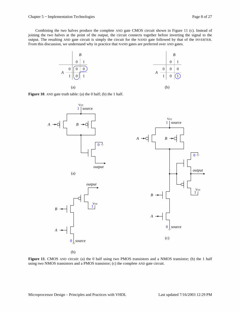
Chapter 5 − Implementation Technologies Page 8 of 27
Microprocessor Design – Principles and Practices with VHDL Last updated 7/16/2003 12:29 PM
Combining the two halves produce the complete AND gate CMOS circuit shown in Figure 11 (c). Instead of joining the two halves at the point of the output, the circuit connects together before inverting the signal to the output. The resulting AND gate circuit is simply the circuit for the NAND gate followed by that of the INVERTER. From this discussion, we understand why in practice that NAND gates are preferred over AND gates.
0 0
0 1
0 1
0
1
B
A
(a)
0 0
0 1
0 1
0
1
B
A
(b)
Figure 10. AND gate truth table: (a) the 0 half; (b) the 1 half.
source
A
1Vcc
output
B
0
(a)
source
A
0
output
BVcc
1
(b)
output
Vcc1
0
source
A
1Vcc
B
source
A
0
B
(c)
Figure 11. CMOS AND circuit: (a) the 0 half using two PMOS transistors and a NMOS transistor; (b) the 1 half using two NMOS transistors and a PMOS transistor; (c) the complete AND gate circuit.
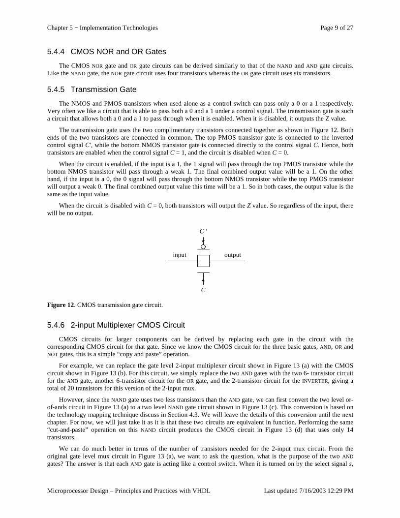
Chapter 5 − Implementation Technologies Page 9 of 27
Microprocessor Design – Principles and Practices with VHDL Last updated 7/16/2003 12:29 PM
5.4.4 CMOS NOR and OR Gates
The CMOS NOR gate and OR gate circuits can be derived similarly to that of the NAND and AND gate circuits. Like the NAND gate, the NOR gate circuit uses four transistors whereas the OR gate circuit uses six transistors.
5.4.5 Transmission Gate
The NMOS and PMOS transistors when used alone as a control switch can pass only a 0 or a 1 respectively. Very often we like a circuit that is able to pass both a 0 and a 1 under a control signal. The transmission gate is such a circuit that allows both a 0 and a 1 to pass through when it is enabled. When it is disabled, it outputs the Z value.
The transmission gate uses the two complimentary transistors connected together as shown in Figure 12. Both ends of the two transistors are connected in common. The top PMOS transistor gate is connected to the inverted control signal C', while the bottom NMOS transistor gate is connected directly to the control signal C. Hence, both transistors are enabled when the control signal C = 1, and the circuit is disabled when C = 0.
When the circuit is enabled, if the input is a 1, the 1 signal will pass through the top PMOS transistor while the bottom NMOS transistor will pass through a weak 1. The final combined output value will be a 1. On the other hand, if the input is a 0, the 0 signal will pass through the bottom NMOS transistor while the top PMOS transistor will output a weak 0. The final combined output value this time will be a 1. So in both cases, the output value is the same as the input value.
When the circuit is disabled with C = 0, both transistors will output the Z value. So regardless of the input, there will be no output.
C '
output
C
input
Figure 12. CMOS transmission gate circuit.
5.4.6 2-input Multiplexer CMOS Circuit
CMOS circuits for larger components can be derived by replacing each gate in the circuit with the corresponding CMOS circuit for that gate. Since we know the CMOS circuit for the three basic gates, AND, OR and NOT gates, this is a simple “copy and paste” operation.
For example, we can replace the gate level 2-input multiplexer circuit shown in Figure 13 (a) with the CMOS circuit shown in Figure 13 (b). For this circuit, we simply replace the two AND gates with the two 6- transistor circuit for the AND gate, another 6-transistor circuit for the OR gate, and the 2-transistor circuit for the INVERTER, giving a total of 20 transistors for this version of the 2-input mux.
However, since the NAND gate uses two less transistors than the AND gate, we can first convert the two level or-of-ands circuit in Figure 13 (a) to a two level NAND gate circuit shown in Figure 13 (c). This conversion is based on the technology mapping technique discuss in Section 4.3. We will leave the details of this conversion until the next chapter. For now, we will just take it as it is that these two circuits are equivalent in function. Performing the same “cut-and-paste” operation on this NAND circuit produces the CMOS circuit in Figure 13 (d) that uses only 14 transistors.
We can do much better in terms of the number of transistors needed for the 2-input mux circuit. From the original gate level mux circuit in Figure 13 (a), we want to ask the question, what is the purpose of the two AND gates? The answer is that each AND gate is acting like a control switch. When it is turned on by the select signal s,
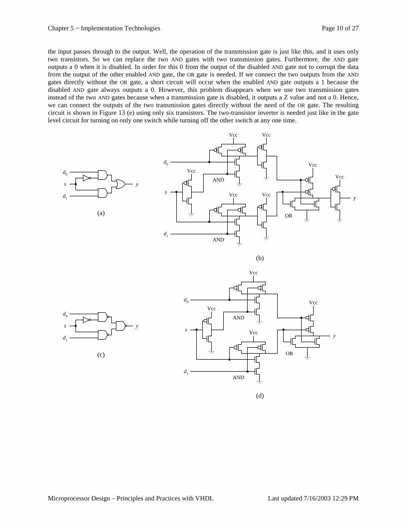
Chapter 5 − Implementation Technologies Page 10 of 27
Microprocessor Design – Principles and Practices with VHDL Last updated 7/16/2003 12:29 PM
the input passes through to the output. Well, the operation of the transmission gate is just like this, and it uses only two transistors. So we can replace the two AND gates with two transmission gates. Furthermore, the AND gate outputs a 0 when it is disabled. In order for this 0 from the output of the disabled AND gate not to corrupt the data from the output of the other enabled AND gate, the OR gate is needed. If we connect the two outputs from the AND gates directly without the OR gate, a short circuit will occur when the enabled AND gate outputs a 1 because the disabled AND gate always outputs a 0. However, this problem disappears when we use two transmission gates instead of the two AND gates because when a transmission gate is disabled, it outputs a Z value and not a 0. Hence, we can connect the outputs of the two transmission gates directly without the need of the OR gate. The resulting circuit is shown in Figure 13 (e) using only six transistors. The two-transistor inverter is needed just like in the gate level circuit for turning on only one switch while turning off the other switch at any one time.
d0
d1
s y
(a)
AND
VccVcc
AND
VccVcc
OR
Vcc
VccVcc
d0
d1
sy
(b)
d0
d1
s y
(c)
Vcc
d0
d1
sy
AND
Vcc
AND
Vcc
OR
Vcc
(d)
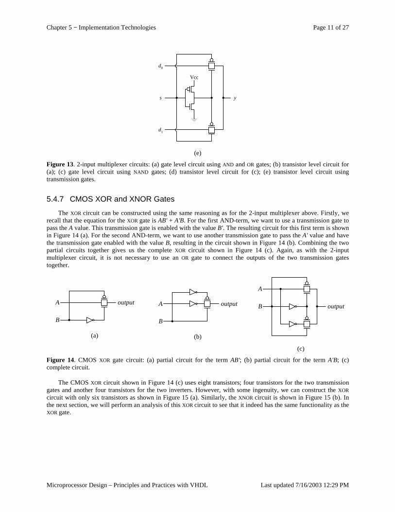
Chapter 5 − Implementation Technologies Page 11 of 27
Microprocessor Design – Principles and Practices with VHDL Last updated 7/16/2003 12:29 PM
Vcc
s y
d0
d1
(e)
Figure 13. 2-input multiplexer circuits: (a) gate level circuit using AND and OR gates; (b) transistor level circuit for (a); (c) gate level circuit using NAND gates; (d) transistor level circuit for (c); (e) transistor level circuit using transmission gates.
5.4.7 CMOS XOR and XNOR Gates
The XOR circuit can be constructed using the same reasoning as for the 2-input multiplexer above. Firstly, we recall that the equation for the XOR gate is AB' + A'B. For the first AND-term, we want to use a transmission gate to pass the A value. This transmission gate is enabled with the value B'. The resulting circuit for this first term is shown in Figure 14 (a). For the second AND-term, we want to use another transmission gate to pass the A' value and have the transmission gate enabled with the value B, resulting in the circuit shown in Figure 14 (b). Combining the two partial circuits together gives us the complete XOR circuit shown in Figure 14 (c). Again, as with the 2-input multiplexer circuit, it is not necessary to use an OR gate to connect the outputs of the two transmission gates together.
A
B
output
(a)
A
B
output
(b)
A
B output
(c)
Figure 14. CMOS XOR gate circuit: (a) partial circuit for the term AB'; (b) partial circuit for the term A'B; (c) complete circuit.
The CMOS XOR circuit shown in Figure 14 (c) uses eight transistors; four transistors for the two transmission gates and another four transistors for the two inverters. However, with some ingenuity, we can construct the XOR circuit with only six transistors as shown in Figure 15 (a). Similarly, the XNOR circuit is shown in Figure 15 (b). In the next section, we will perform an analysis of this XOR circuit to see that it indeed has the same functionality as the XOR gate.
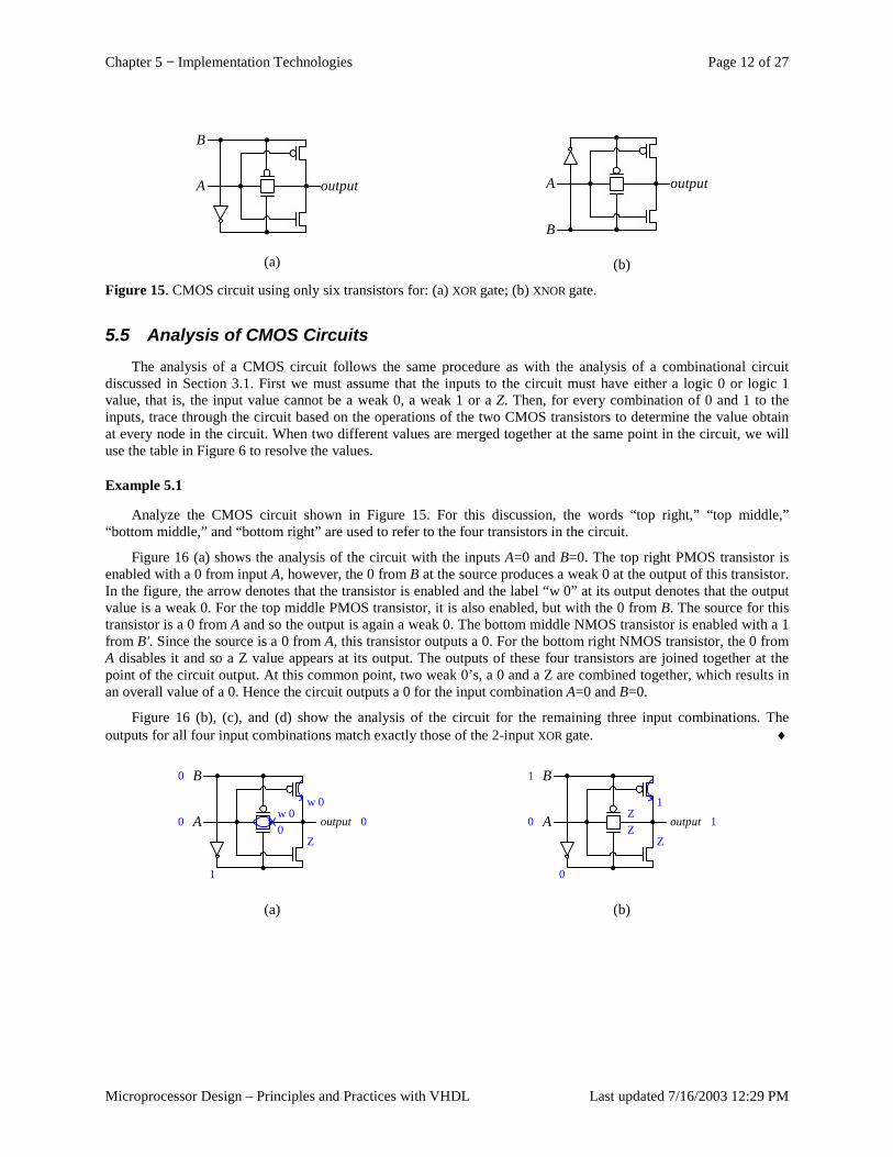
Chapter 5 − Implementation Technologies Page 12 of 27
Microprocessor Design – Principles and Practices with VHDL Last updated 7/16/2003 12:29 PM
output
B
A
(a)
output
B
A
(b)
Figure 15. CMOS circuit using only six transistors for: (a) XOR gate; (b) XNOR gate.
5.5 Analysis of CMOS Circuits The analysis of a CMOS circuit follows the same procedure as with the analysis of a combinational circuit
discussed in Section 3.1. First we must assume that the inputs to the circuit must have either a logic 0 or logic 1 value, that is, the input value cannot be a weak 0, a weak 1 or a Z. Then, for every combination of 0 and 1 to the inputs, trace through the circuit based on the operations of the two CMOS transistors to determine the value obtain at every node in the circuit. When two different values are merged together at the same point in the circuit, we will use the table in Figure 6 to resolve the values.
Example 5.1
Analyze the CMOS circuit shown in Figure 15. For this discussion, the words “top right,” “top middle,” “bottom middle,” and “bottom right” are used to refer to the four transistors in the circuit.
Figure 16 (a) shows the analysis of the circuit with the inputs A=0 and B=0. The top right PMOS transistor is enabled with a 0 from input A, however, the 0 from B at the source produces a weak 0 at the output of this transistor. In the figure, the arrow denotes that the transistor is enabled and the label “w 0” at its output denotes that the output value is a weak 0. For the top middle PMOS transistor, it is also enabled, but with the 0 from B. The source for this transistor is a 0 from A and so the output is again a weak 0. The bottom middle NMOS transistor is enabled with a 1 from B'. Since the source is a 0 from A, this transistor outputs a 0. For the bottom right NMOS transistor, the 0 from A disables it and so a Z value appears at its output. The outputs of these four transistors are joined together at the point of the circuit output. At this common point, two weak 0’s, a 0 and a Z are combined together, which results in an overall value of a 0. Hence the circuit outputs a 0 for the input combination A=0 and B=0.
Figure 16 (b), (c), and (d) show the analysis of the circuit for the remaining three input combinations. The outputs for all four input combinations match exactly those of the 2-input XOR gate. ♦
output
B
A
0
0
1
00
w 0
Z
w 0
(a)
output
B
A
1
0
0
Z1
Z
Z
1
(b)
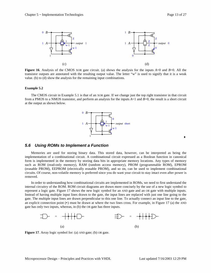
Chapter 5 − Implementation Technologies Page 13 of 27
Microprocessor Design – Principles and Practices with VHDL Last updated 7/16/2003 12:29 PM
output
B
A
0
1
1
w 11
1
w 1
Z
(c)
output
B
A
1
1
0
Z0
Z
0
Z
(d)
Figure 16. Analysis of the CMOS XOR gate circuit. (a) shows the analysis for the inputs A=0 and B=0. All the transistor outputs are annotated with the resulting output value. The letter “w” is used to signify that it is a weak value. (b) to (d) show the analysis for the remaining input combinations.
Example 5.2
The CMOS circuit in Example 5.1 is that of an XOR gate. If we change just the top right transistor in that circuit from a PMOS to a NMOS transistor, and perform an analysis for the inputs A=1 and B=0, the result is a short circuit at the output as shown below.
output
B
A
0
1
1
w 1short
1
w 1
0
♦
5.6 Using ROMs to Implement a Function Memories are used for storing binary data. This stored data, however, can be interpreted as being the
implementation of a combinational circuit. A combinational circuit expressed as a Boolean function in canonical form is implemented in the memory by storing data bits in appropriate memory locations. Any types of memory such as ROM (read-only memory), RAM (random access memory), PROM (programmable ROM), EPROM (erasable PROM), EEPROM (electrically erasable PROM), and so on, can be used to implement combinational circuits. Of course, non-volatile memory is preferred since you do want your circuit to stay intact even after power is removed.
In order to understanding how combinational circuits are implemented in ROMs, we need to first understand the internal circuitry of the ROM. ROM circuit diagrams are drawn more concisely by the use of a new logic symbol to represent a logic gate. Figure 17 shows the new logic symbol for an AND gate and an OR gate with multiple inputs. Instead of having multiple input lines drawn to the gate, the input lines are replaced with just one line going to the gate. The multiple input lines are drawn perpendicular to this one line. To actually connect an input line to the gate, an explicit connection point (• ) must be drawn at where the two lines cross. For example, in Figure 17 (a) the AND gate has only two inputs, whereas, in (b) the OR gate has three inputs.
=
=
(a) (b)
Figure 17. Array logic symbol for: (a) AND gate; (b) OR gate.
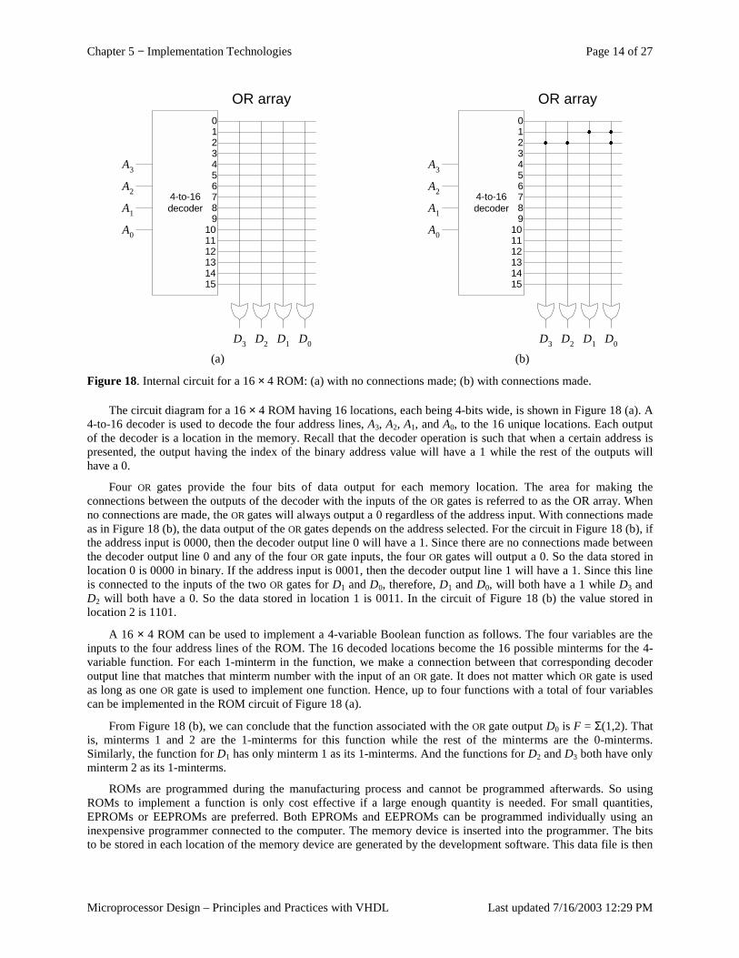
Chapter 5 − Implementation Technologies Page 14 of 27
Microprocessor Design – Principles and Practices with VHDL Last updated 7/16/2003 12:29 PM
OR array
D0D1D2D3
A3
A2
A1
A0
4-to-16decoder
0123456789
101112131415
OR array
D0D1D2D3
A3
A2
A1
A0
4-to-16decoder
0123456789
101112131415
(a) (b)
Figure 18. Internal circuit for a 16 × 4 ROM: (a) with no connections made; (b) with connections made.
The circuit diagram for a 16 × 4 ROM having 16 locations, each being 4-bits wide, is shown in Figure 18 (a). A 4-to-16 decoder is used to decode the four address lines, A3, A2, A1, and A0, to the 16 unique locations. Each output of the decoder is a location in the memory. Recall that the decoder operation is such that when a certain address is presented, the output having the index of the binary address value will have a 1 while the rest of the outputs will have a 0.
Four OR gates provide the four bits of data output for each memory location. The area for making the connections between the outputs of the decoder with the inputs of the OR gates is referred to as the OR array. When no connections are made, the OR gates will always output a 0 regardless of the address input. With connections made as in Figure 18 (b), the data output of the OR gates depends on the address selected. For the circuit in Figure 18 (b), if the address input is 0000, then the decoder output line 0 will have a 1. Since there are no connections made between the decoder output line 0 and any of the four OR gate inputs, the four OR gates will output a 0. So the data stored in location 0 is 0000 in binary. If the address input is 0001, then the decoder output line 1 will have a 1. Since this line is connected to the inputs of the two OR gates for D1 and D0, therefore, D1 and D0, will both have a 1 while D3 and D2 will both have a 0. So the data stored in location 1 is 0011. In the circuit of Figure 18 (b) the value stored in location 2 is 1101.
A 16 × 4 ROM can be used to implement a 4-variable Boolean function as follows. The four variables are the inputs to the four address lines of the ROM. The 16 decoded locations become the 16 possible minterms for the 4-variable function. For each 1-minterm in the function, we make a connection between that corresponding decoder output line that matches that minterm number with the input of an OR gate. It does not matter which OR gate is used as long as one OR gate is used to implement one function. Hence, up to four functions with a total of four variables can be implemented in the ROM circuit of Figure 18 (a).
From Figure 18 (b), we can conclude that the function associated with the OR gate output D0 is F = Σ(1,2). That is, minterms 1 and 2 are the 1-minterms for this function while the rest of the minterms are the 0-minterms. Similarly, the function for D1 has only minterm 1 as its 1-minterms. And the functions for D2 and D3 both have only minterm 2 as its 1-minterms.
ROMs are programmed during the manufacturing process and cannot be programmed afterwards. So using ROMs to implement a function is only cost effective if a large enough quantity is needed. For small quantities, EPROMs or EEPROMs are preferred. Both EPROMs and EEPROMs can be programmed individually using an inexpensive programmer connected to the computer. The memory device is inserted into the programmer. The bits to be stored in each location of the memory device are generated by the development software. This data file is then
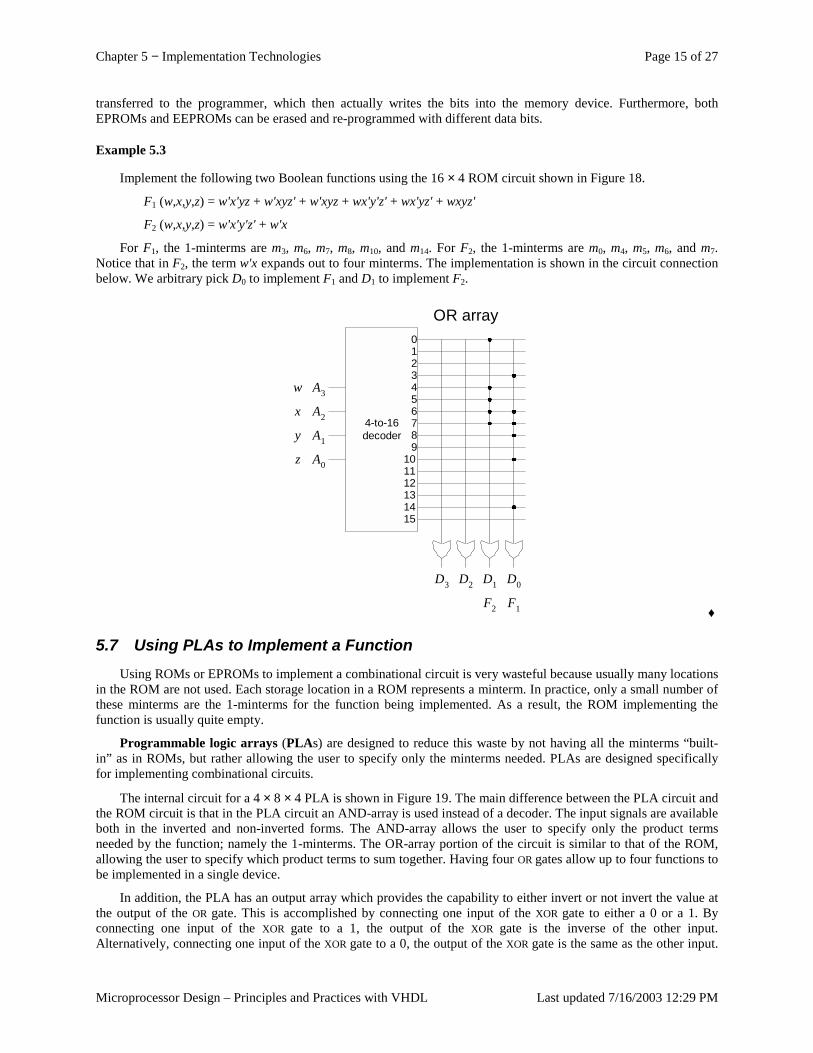
Chapter 5 − Implementation Technologies Page 15 of 27
Microprocessor Design – Principles and Practices with VHDL Last updated 7/16/2003 12:29 PM
transferred to the programmer, which then actually writes the bits into the memory device. Furthermore, both EPROMs and EEPROMs can be erased and re-programmed with different data bits.
Example 5.3
Implement the following two Boolean functions using the 16 × 4 ROM circuit shown in Figure 18.
F1 (w,x,y,z) = w'x'yz + w'xyz' + w'xyz + wx'y'z' + wx'yz' + wxyz'
F2 (w,x,y,z) = w'x'y'z' + w'x
For F1, the 1-minterms are m3, m6, m7, m8, m10, and m14. For F2, the 1-minterms are m0, m4, m5, m6, and m7. Notice that in F2, the term w'x expands out to four minterms. The implementation is shown in the circuit connection below. We arbitrary pick D0 to implement F1 and D1 to implement F2.
OR array
D0D1D2D3
A3
A2
A1
A0
4-to-16decoder
0123456789
101112131415
w
F1F2
x
y
z
♦
5.7 Using PLAs to Implement a Function Using ROMs or EPROMs to implement a combinational circuit is very wasteful because usually many locations
in the ROM are not used. Each storage location in a ROM represents a minterm. In practice, only a small number of these minterms are the 1-minterms for the function being implemented. As a result, the ROM implementing the function is usually quite empty.
Programmable logic arrays (PLAs) are designed to reduce this waste by not having all the minterms “built-in” as in ROMs, but rather allowing the user to specify only the minterms needed. PLAs are designed specifically for implementing combinational circuits.
The internal circuit for a 4 × 8 × 4 PLA is shown in Figure 19. The main difference between the PLA circuit and the ROM circuit is that in the PLA circuit an AND-array is used instead of a decoder. The input signals are available both in the inverted and non-inverted forms. The AND-array allows the user to specify only the product terms needed by the function; namely the 1-minterms. The OR-array portion of the circuit is similar to that of the ROM, allowing the user to specify which product terms to sum together. Having four OR gates allow up to four functions to be implemented in a single device.
In addition, the PLA has an output array which provides the capability to either invert or not invert the value at the output of the OR gate. This is accomplished by connecting one input of the XOR gate to either a 0 or a 1. By connecting one input of the XOR gate to a 1, the output of the XOR gate is the inverse of the other input. Alternatively, connecting one input of the XOR gate to a 0, the output of the XOR gate is the same as the other input.
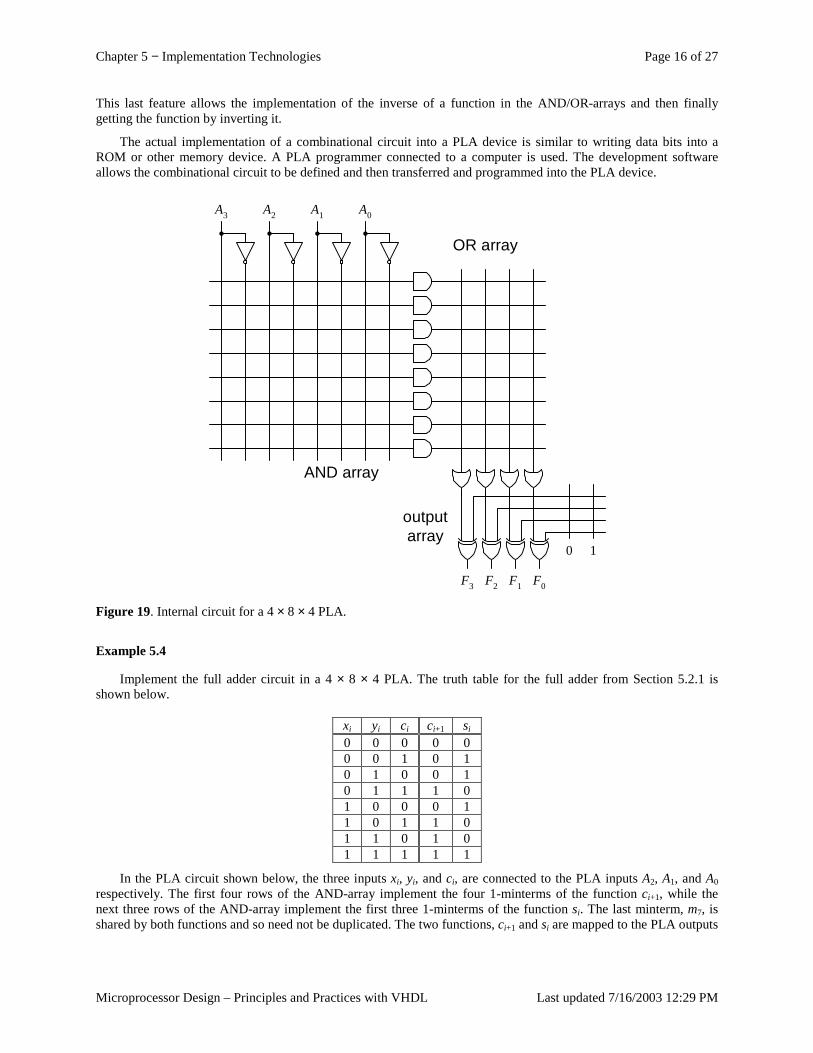
Chapter 5 − Implementation Technologies Page 16 of 27
Microprocessor Design – Principles and Practices with VHDL Last updated 7/16/2003 12:29 PM
This last feature allows the implementation of the inverse of a function in the AND/OR-arrays and then finally getting the function by inverting it.
The actual implementation of a combinational circuit into a PLA device is similar to writing data bits into a ROM or other memory device. A PLA programmer connected to a computer is used. The development software allows the combinational circuit to be defined and then transferred and programmed into the PLA device.
OR array
AND array
outputarray
1
F3 F2 F1 F0
0
A2 A0A1A3
Figure 19. Internal circuit for a 4 × 8 × 4 PLA.
Example 5.4
Implement the full adder circuit in a 4 × 8 × 4 PLA. The truth table for the full adder from Section 5.2.1 is shown below.
xi yi ci ci+1 si 0 0 0 0 0 0 0 1 0 1 0 1 0 0 1 0 1 1 1 0 1 0 0 0 1 1 0 1 1 0 1 1 0 1 0 1 1 1 1 1
In the PLA circuit shown below, the three inputs xi, yi, and ci, are connected to the PLA inputs A2, A1, and A0 respectively. The first four rows of the AND-array implement the four 1-minterms of the function ci+1, while the next three rows of the AND-array implement the first three 1-minterms of the function si. The last minterm, m7, is shared by both functions and so need not be duplicated. The two functions, ci+1 and si are mapped to the PLA outputs
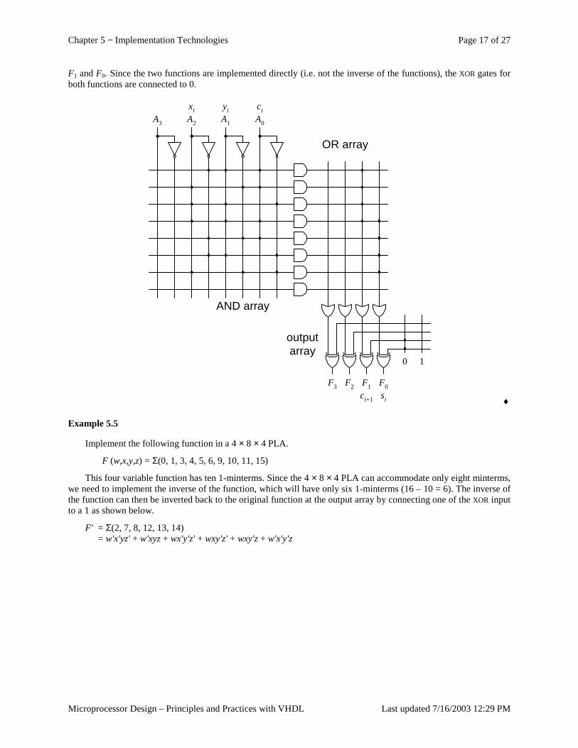
Chapter 5 − Implementation Technologies Page 17 of 27
Microprocessor Design – Principles and Practices with VHDL Last updated 7/16/2003 12:29 PM
F1 and F0. Since the two functions are implemented directly (i.e. not the inverse of the functions), the XOR gates for both functions are connected to 0.
OR array
AND array
outputarray
1
F3 F2 F1 F0
0
A2 A0A1A3
xi yi ci
sici+1 ♦
Example 5.5
Implement the following function in a 4 × 8 × 4 PLA.
F (w,x,y,z) = Σ(0, 1, 3, 4, 5, 6, 9, 10, 11, 15)
This four variable function has ten 1-minterms. Since the 4 × 8 × 4 PLA can accommodate only eight minterms, we need to implement the inverse of the function, which will have only six 1-minterms (16 – 10 = 6). The inverse of the function can then be inverted back to the original function at the output array by connecting one of the XOR input to a 1 as shown below.
F' = Σ(2, 7, 8, 12, 13, 14) = w'x'yz' + w'xyz + wx'y'z' + wxy'z' + wxy'z + w'x'y'z
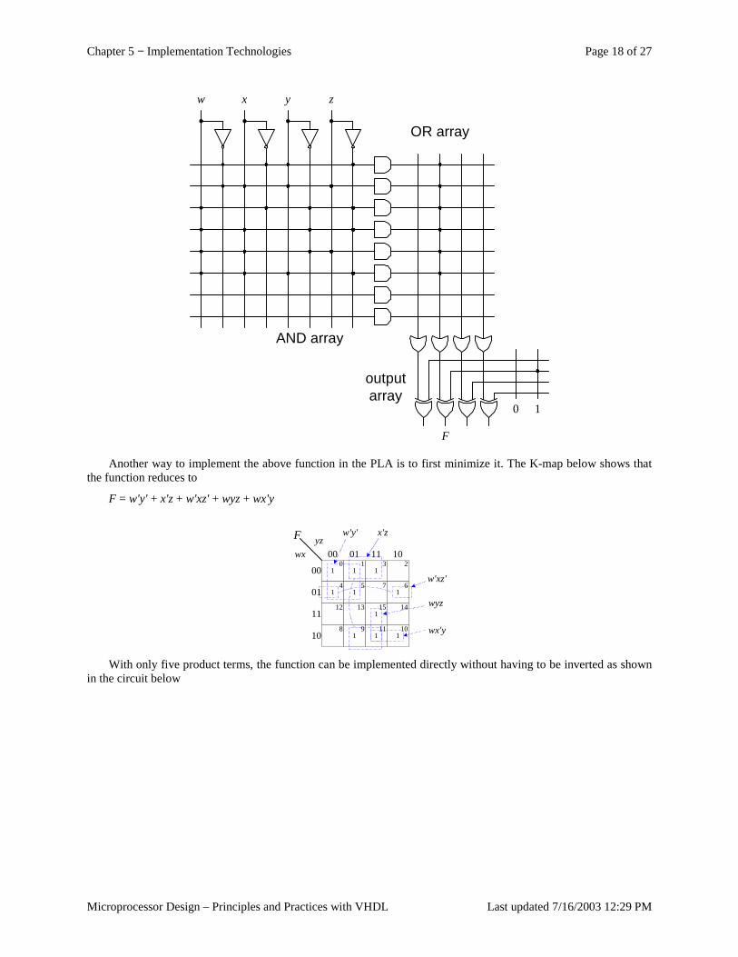
Chapter 5 − Implementation Technologies Page 18 of 27
Microprocessor Design – Principles and Practices with VHDL Last updated 7/16/2003 12:29 PM
OR array
AND array
outputarray
1
F
0
x zyw
Another way to implement the above function in the PLA is to first minimize it. The K-map below shows that
the function reduces to
F = w'y' + x'z + w'xz' + wyz + wx'y
yzwx
00 1 1
001
1 1 1
1
1 1 1
01 11 100 1 3 2
4 5 7 6
12 13 15 14
8 9 11 10
01
11
10
F w'y' x'z
w'xz'
wyz
wx'y
With only five product terms, the function can be implemented directly without having to be inverted as shown
in the circuit below

Chapter 5 − Implementation Technologies Page 19 of 27
Microprocessor Design – Principles and Practices with VHDL Last updated 7/16/2003 12:29 PM
OR array
AND array
outputarray
1
F
0
x zyw
♦
5.8 Using PALs to Implement a Function Programmable array logic (PAL®) devices are similar to PLAs except that the OR array for the PALs is not
programmable but rather fixed by the internal circuitry. Hence, they are not as flexible in terms of implementing a combinational circuit. However, because of this fixed OR array, PALs are easier to program.
The internal circuit for a four input, four output PAL is shown in Figure 20. The OR gate inputs are fixed, whereas the AND gate inputs are programmable. Each output section is from the OR of the three product terms. This means that each function can have at most three product terms. To make the device a little bit more flexible, the output F3 is fed back to the programmable inputs of the AND gates. With this connection, up to five product terms is possible for one function.
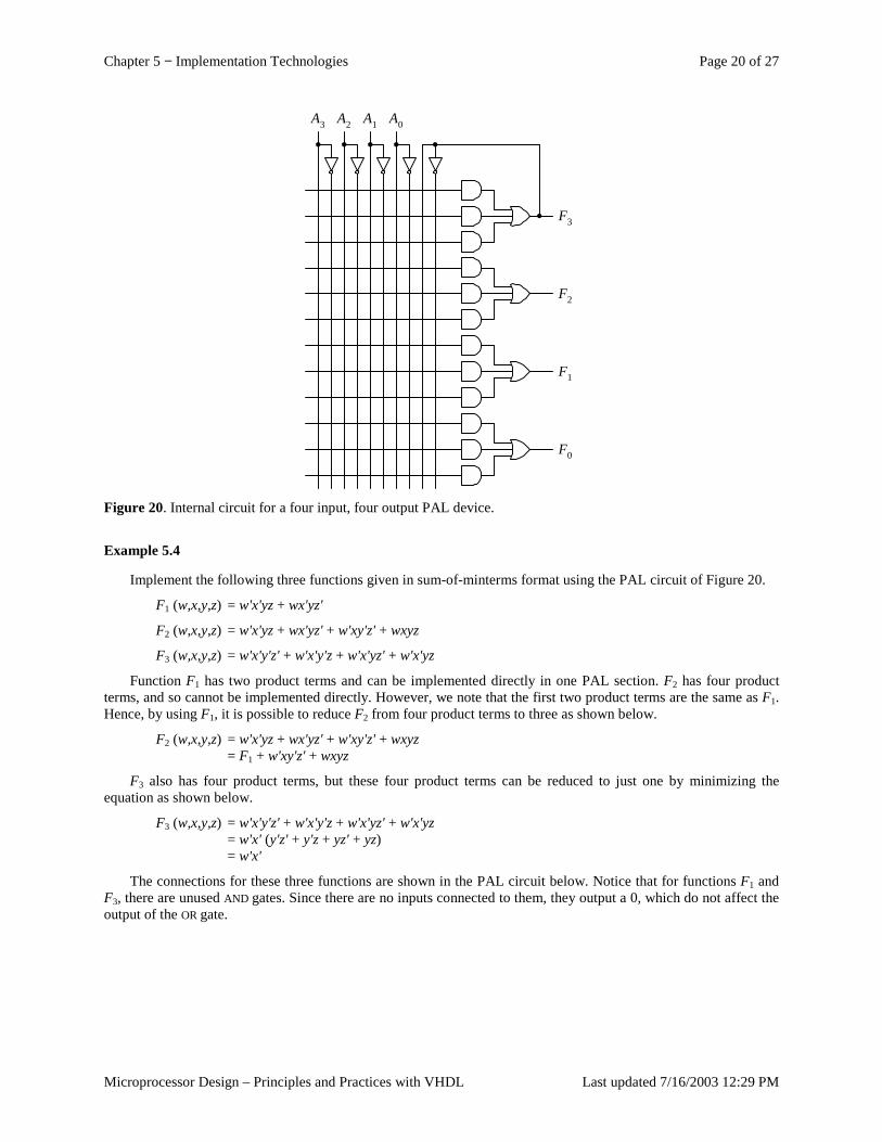
Chapter 5 − Implementation Technologies Page 20 of 27
Microprocessor Design – Principles and Practices with VHDL Last updated 7/16/2003 12:29 PM
F3
F2
F1
F0
A0A1A2A3
Figure 20. Internal circuit for a four input, four output PAL device.
Example 5.4
Implement the following three functions given in sum-of-minterms format using the PAL circuit of Figure 20.
F1 (w,x,y,z) = w'x'yz + wx'yz'
F2 (w,x,y,z) = w'x'yz + wx'yz' + w'xy'z' + wxyz
F3 (w,x,y,z) = w'x'y'z' + w'x'y'z + w'x'yz' + w'x'yz
Function F1 has two product terms and can be implemented directly in one PAL section. F2 has four product terms, and so cannot be implemented directly. However, we note that the first two product terms are the same as F1. Hence, by using F1, it is possible to reduce F2 from four product terms to three as shown below.
F2 (w,x,y,z) = w'x'yz + wx'yz' + w'xy'z' + wxyz = F1 + w'xy'z' + wxyz
F3 also has four product terms, but these four product terms can be reduced to just one by minimizing the equation as shown below.
F3 (w,x,y,z) = w'x'y'z' + w'x'y'z + w'x'yz' + w'x'yz = w'x' (y'z' + y'z + yz' + yz) = w'x'
The connections for these three functions are shown in the PAL circuit below. Notice that for functions F1 and F3, there are unused AND gates. Since there are no inputs connected to them, they output a 0, which do not affect the output of the OR gate.
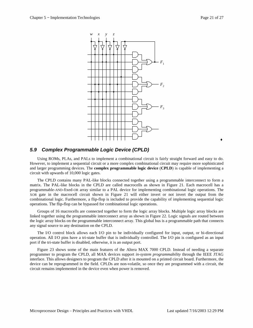
Chapter 5 − Implementation Technologies Page 21 of 27
Microprocessor Design – Principles and Practices with VHDL Last updated 7/16/2003 12:29 PM
F1
F2
F3
zyxw
♦
5.9 Complex Programmable Logic Device (CPLD) Using ROMs, PLAs, and PALs to implement a combinational circuit is fairly straight forward and easy to do.
However, to implement a sequential circuit or a more complex combinational circuit may require more sophisticated and larger programming devices. The complex programmable logic device (CPLD) is capable of implementing a circuit with upwards of 10,000 logic gates.
The CPLD contains many PAL-like blocks connected together using a programmable interconnect to form a matrix. The PAL-like blocks in the CPLD are called macrocells as shown in Figure 21. Each macrocell has a programmable-AND-fixed-OR array similar to a PAL device for implementing combinational logic operations. The XOR gate in the macrocell circuit shown in Figure 21 will either invert or not invert the output from the combinational logic. Furthermore, a flip-flop is included to provide the capability of implementing sequential logic operations. The flip-flop can be bypassed for combinational logic operations.
Groups of 16 macrocells are connected together to form the logic array blocks. Multiple logic array blocks are linked together using the programmable interconnect array as shown in Figure 22. Logic signals are routed between the logic array blocks on the programmable interconnect array. This global bus is a programmable path that connects any signal source to any destination on the CPLD.
The I/O control block allows each I/O pin to be individually configured for input, output, or bi-directional operation. All I/O pins have a tri-state buffer that is individually controlled. The I/O pin is configured as an input port if the tri-state buffer is disabled, otherwise, it is an output port.
Figure 23 shows some of the main features of the Altera MAX 7000 CPLD. Instead of needing a separate programmer to program the CPLD, all MAX devices support in-system programmability through the IEEE JTAG interface. This allows designers to program the CPLD after it is mounted on a printed circuit board. Furthermore, the device can be reprogrammed in the field. CPLDs are non-volatile, so once they are programmed with a circuit, the circuit remains implemented in the device even when power is removed.
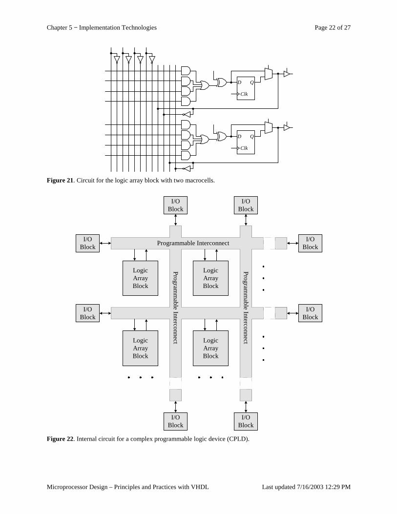
Chapter 5 − Implementation Technologies Page 22 of 27
Microprocessor Design – Principles and Practices with VHDL Last updated 7/16/2003 12:29 PM
Clk
D Q
Clk
D Q
Figure 21. Circuit for the logic array block with two macrocells.
LogicArrayBlock
Programmable Interconnect
Programm
able Interconnect
I/OBlock
I/OBlock
I/OBlock
I/OBlock
I/OBlock
I/OBlock
I/OBlock
I/OBlock
Programm
able Interconnect
LogicArrayBlock
LogicArrayBlock
LogicArrayBlock
Figure 22. Internal circuit for a complex programmable logic device (CPLD).
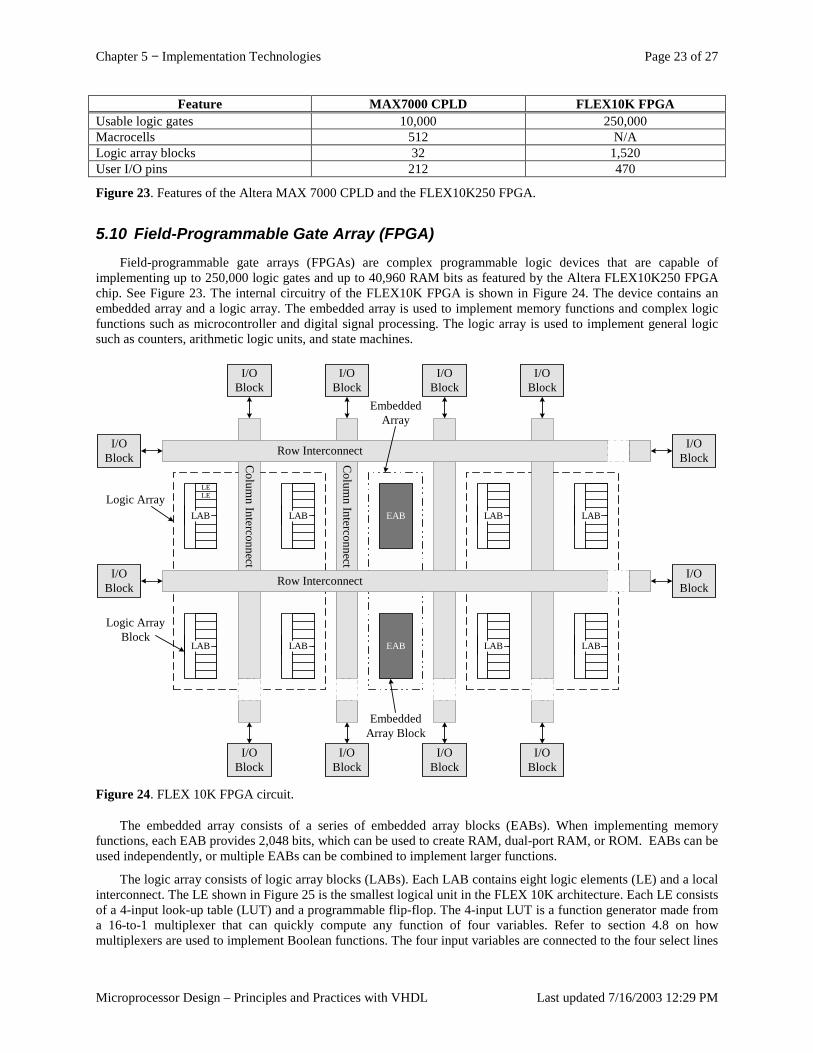
Chapter 5 − Implementation Technologies Page 23 of 27
Microprocessor Design – Principles and Practices with VHDL Last updated 7/16/2003 12:29 PM
Feature MAX7000 CPLD FLEX10K FPGA Usable logic gates 10,000 250,000 Macrocells 512 N/A Logic array blocks 32 1,520 User I/O pins 212 470
Figure 23. Features of the Altera MAX 7000 CPLD and the FLEX10K250 FPGA.
5.10 Field-Programmable Gate Array (FPGA) Field-programmable gate arrays (FPGAs) are complex programmable logic devices that are capable of
implementing up to 250,000 logic gates and up to 40,960 RAM bits as featured by the Altera FLEX10K250 FPGA chip. See Figure 23. The internal circuitry of the FLEX10K FPGA is shown in Figure 24. The device contains an embedded array and a logic array. The embedded array is used to implement memory functions and complex logic functions such as microcontroller and digital signal processing. The logic array is used to implement general logic such as counters, arithmetic logic units, and state machines.
EAB
EAB
LAB LAB
LAB LAB
LAB LAB
LAB LAB
Row Interconnect
Colum
n Interconnect
I/OBlock
I/OBlock
I/OBlock
I/OBlock
I/OBlock
I/OBlock
I/OBlock
I/OBlock
I/OBlock
I/OBlock
I/OBlock
I/OBlock Row Interconnect
Colum
n Interconnect
Logic ArrayBlock
EmbeddedArray Block
LELELogic Array
EmbeddedArray
Figure 24. FLEX 10K FPGA circuit.
The embedded array consists of a series of embedded array blocks (EABs). When implementing memory functions, each EAB provides 2,048 bits, which can be used to create RAM, dual-port RAM, or ROM. EABs can be used independently, or multiple EABs can be combined to implement larger functions.
The logic array consists of logic array blocks (LABs). Each LAB contains eight logic elements (LE) and a local interconnect. The LE shown in Figure 25 is the smallest logical unit in the FLEX 10K architecture. Each LE consists of a 4-input look-up table (LUT) and a programmable flip-flop. The 4-input LUT is a function generator made from a 16-to-1 multiplexer that can quickly compute any function of four variables. Refer to section 4.8 on how multiplexers are used to implement Boolean functions. The four input variables are connected to the four select lines
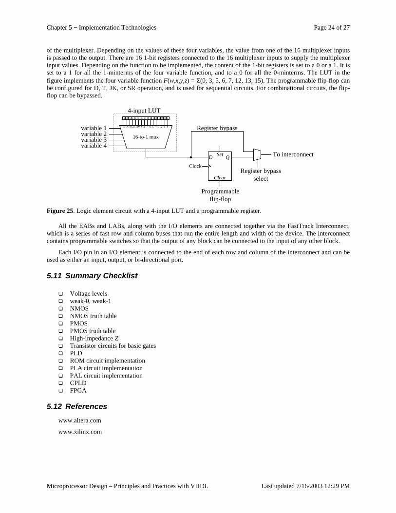
Chapter 5 − Implementation Technologies Page 24 of 27
Microprocessor Design – Principles and Practices with VHDL Last updated 7/16/2003 12:29 PM
of the multiplexer. Depending on the values of these four variables, the value from one of the 16 multiplexer inputs is passed to the output. There are 16 1-bit registers connected to the 16 multiplexer inputs to supply the multiplexer input values. Depending on the function to be implemented, the content of the 1-bit registers is set to a 0 or a 1. It is set to a 1 for all the 1-minterms of the four variable function, and to a 0 for all the 0-minterms. The LUT in the figure implements the four variable function F(w,x,y,z) = Σ(0, 3, 5, 6, 7, 12, 13, 15). The programmable flip-flop can be configured for D, T, JK, or SR operation, and is used for sequential circuits. For combinational circuits, the flip-flop can be bypassed.
1001011100001101
4-input LUT
variable 1variable 2variable 3variable 4
16-to-1 mux
D QSet
Clear
To interconnect
Register bypass
ClockRegister bypass
select
Programmableflip-flop
101112131415 02 13456789
Figure 25. Logic element circuit with a 4-input LUT and a programmable register.
All the EABs and LABs, along with the I/O elements are connected together via the FastTrack Interconnect, which is a series of fast row and column buses that run the entire length and width of the device. The interconnect contains programmable switches so that the output of any block can be connected to the input of any other block.
Each I/O pin in an I/O element is connected to the end of each row and column of the interconnect and can be used as either an input, output, or bi-directional port.
5.11 Summary Checklist
� Voltage levels � weak-0, weak-1 � NMOS � NMOS truth table � PMOS � PMOS truth table � High-impedance Z � Transistor circuits for basic gates � PLD � ROM circuit implementation � PLA circuit implementation � PAL circuit implementation � CPLD � FPGA
5.12 References www.altera.com
www.xilinx.com
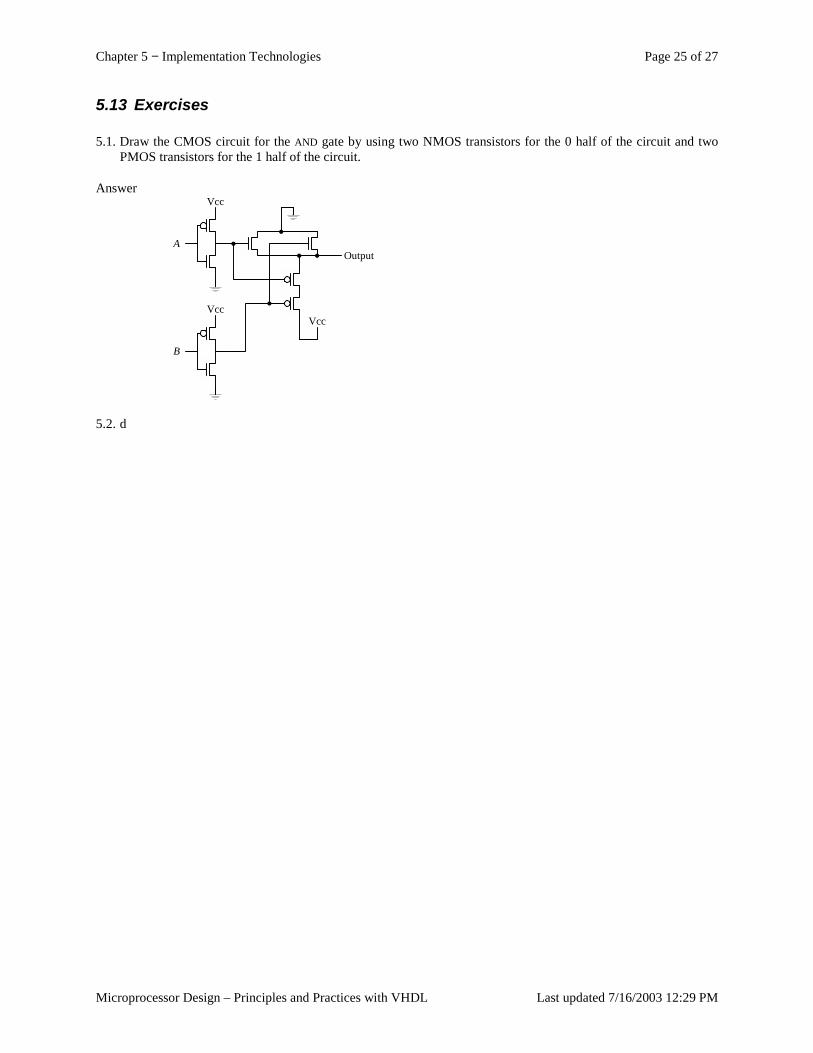
Chapter 5 − Implementation Technologies Page 25 of 27
Microprocessor Design – Principles and Practices with VHDL Last updated 7/16/2003 12:29 PM
5.13 Exercises
5.1. Draw the CMOS circuit for the AND gate by using two NMOS transistors for the 0 half of the circuit and two PMOS transistors for the 1 half of the circuit.
Answer
Output
Vcc
A
Vcc
B
Vcc
5.2. d
Chapter 5 − Implementation Technologies Page 26 of 27
Microprocessor Design – Principles and Practices with VHDL Last updated 7/16/2003 12:29 PM
Index
A
Analysis CMOS circuits, of, 12
AND CMOS circuit, 7
C
CMOS, 2, 4 AND gate, 7 circuit, 5 inverter, 5 logic, 4 multiplexer, 10 NAND gate, 6 NOR gate, 9 OR gate, 9 Transmission gate, 9 XNOR gate, 12 XOR gate, 12
Combinational circuit PAL implementation of, 19 PLA implementation of, 16 ROM implementation of, 13
Complementary metal oxide semiconductor. See CMOS
Complex programmable logic device, 21 CPLD. See Complex programmable logic device
E
EPROM. See Erasable programmable read-only memory
Erasable programmable read-only memory, 14
F
Field-programmable gate array, 23 FPGA. See Field-programmable gate array
H
High impedance, 4, 5
M
MOSFET, 3 Multiplexer
CMOS circuit, 10
N
NAND CMOS circuit, 6
n-channel, 3, 4 NMOS, 4 NOR
CMOS circuit, 9 NOT
CMOS circuit, 5
O
OR CMOS circuit, 9
P
PAL. See Programmable array logic p-channel, 3, 4 PLA. See Programmable logic array PMOS, 4, 5 Programmable array logic, 19 Programmable logic array, 16 Programmable read-only memory, 14 PROM. See Programmable read-only memory
R
Read-only memory, 13 ROM. See read-only memory
S
Short. See Short circuit Short circuit, 5, 6
T
Transistor technologies, 2 bipolar logic, 2 complementary metal oxide semiconductor logic
(CMOS), 2 diode-transistor logic, 2 transistor-transistor logic (TTL), 2
Transmission gate, 9
W
weak 0, 2, 5 weak 1, 2, 4, 5
X
XNOR CMOS circuit, 12
XOR CMOS circuit, 12

Chapter 5 − Implementation Technologies Page 27 of 27
Microprocessor Design – Principles and Practices with VHDL Last updated 7/16/2003 12:29 PM
Z Z. See High impedance
Chapter 6 – Latches and Flip-Flops Page 1 of 27
Microprocessor Design – Principles and Practices with VHDL Last updated 7/21/2003 12:48 PM
Table of Content Table of Content ........................................................................................................................................................... 1 6 Latches and Flip-Flops.......................................................................................................................................... 2
6.1 Bistable Element ........................................................................................................................................... 2 6.2 SR Latch........................................................................................................................................................ 4 6.3 SR Latch with Enable.................................................................................................................................... 6 6.4 D Latch.......................................................................................................................................................... 7 6.5 D Latch with Enable...................................................................................................................................... 7 6.6 Clock ............................................................................................................................................................. 8 6.7 D Flip-Flop.................................................................................................................................................. 10 6.8 D Flip-Flop with Enable.............................................................................................................................. 12 6.9 Asynchronus Inputs..................................................................................................................................... 13 6.10 Description of a Flip-Flop ........................................................................................................................... 13
6.10.1 Characteristic Table ............................................................................................................................ 13 6.10.2 Characteristic Equation ....................................................................................................................... 14 6.10.3 State Diagram...................................................................................................................................... 14 6.10.4 Excitation Table .................................................................................................................................. 14
6.11 Timing Issues .............................................................................................................................................. 15 6.12 Example: Car Security System – Version 2 ................................................................................................ 16 6.13 VHDL for Latches and Flip-Flops .............................................................................................................. 16
6.13.1 Implied Memory Element ................................................................................................................... 16 6.13.2 VHDL Code for a D Latch with Enable.............................................................................................. 17 6.13.3 VHDL Code for a D Flip-Flop ............................................................................................................ 18 6.13.4 VHDL Code for a D Flip-Flop with Enable and Asynchronous Set and Clear................................... 21
6.14 * Flip-Flop Types........................................................................................................................................ 22 6.14.1 SR Flip-Flop........................................................................................................................................ 22 6.14.2 JK Flip-Flop ........................................................................................................................................ 23 6.14.3 T Flip-Flop .......................................................................................................................................... 23
6.15 Summary Checklist ..................................................................................................................................... 25 6.16 Exercises ..................................................................................................................................................... 26 Index ....................................................................................................................................................................... 27
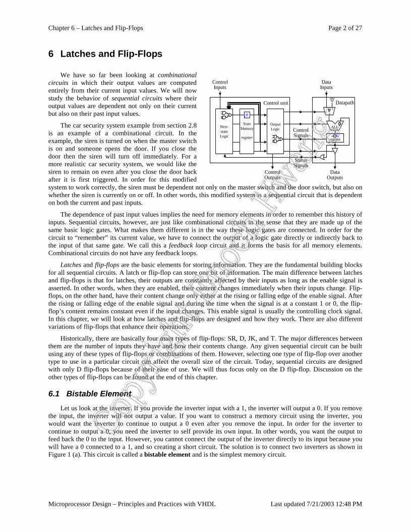
Chapter 6 – Latches and Flip-Flops Page 2 of 27
Microprocessor Design – Principles and Practices with VHDL Last updated 7/21/2003 12:48 PM
ControlSignals
StatusSignals
01s y
'0'
DataInputs
DataOutputs
Datapath
ALU
registerff
OutputLogicNext-
stateLogic
ControlInputs
ControlOutputs
StateMemory
register
Control unit
ff
6 Latches and Flip-Flops
We have so far been looking at combinational circuits in which their output values are computed entirely from their current input values. We will now study the behavior of sequential circuits where their output values are dependent not only on their current but also on their past input values.
The car security system example from section 2.8 is an example of a combinational circuit. In the example, the siren is turned on when the master switch is on and someone opens the door. If you close the door then the siren will turn off immediately. For a more realistic car security system, we would like the siren to remain on even after you close the door back after it is first triggered. In order for this modified system to work correctly, the siren must be dependent not only on the master switch and the door switch, but also on whether the siren is currently on or off. In other words, this modified system is a sequential circuit that is dependent on both the current and past inputs.
The dependence of past input values implies the need for memory elements in order to remember this history of inputs. Sequential circuits, however, are just like combinational circuits in the sense that they are made up of the same basic logic gates. What makes them different is in the way these logic gates are connected. In order for the circuit to “remember” its current value, we have to connect the output of a logic gate directly or indirectly back to the input of that same gate. We call this a feedback loop circuit and it forms the basis for all memory elements. Combinational circuits do not have any feedback loops.
Latches and flip-flops are the basic elements for storing information. They are the fundamental building blocks for all sequential circuits. A latch or flip-flop can store one bit of information. The main difference between latches and flip-flops is that for latches, their outputs are constantly affected by their inputs as long as the enable signal is asserted. In other words, when they are enabled, their content changes immediately when their inputs change. Flip-flops, on the other hand, have their content change only either at the rising or falling edge of the enable signal. After the rising or falling edge of the enable signal and during the time when the signal is at a constant 1 or 0, the flip-flop’s content remains constant even if the input changes. This enable signal is usually the controlling clock signal. In this chapter, we will look at how latches and flip-flops are designed and how they work. There are also different variations of flip-flops that enhance their operations.
Historically, there are basically four main types of flip-flops: SR, D, JK, and T. The major differences between them are the number of inputs they have and how their contents change. Any given sequential circuit can be built using any of these types of flip-flops or combinations of them. However, selecting one type of flip-flop over another type to use in a particular circuit can affect the overall size of the circuit. Today, sequential circuits are designed with only D flip-flops because of their ease of use. We will thus focus only on the D flip-flop. Discussion on the other types of flip-flops can be found at the end of this chapter.
6.1 Bistable Element Let us look at the inverter. If you provide the inverter input with a 1, the inverter will output a 0. If you remove
the input, the inverter will not output a value. If you want to construct a memory circuit using the inverter, you would want the inverter to continue to output a 0 even after you remove the input. In order for the inverter to continue to output a 0, you need the inverter to self provide its own input. In other words, you want the output to feed back the 0 to the input. However, you cannot connect the output of the inverter directly to its input because you will have a 0 connected to a 1, and so creating a short circuit. The solution is to connect two inverters as shown in Figure 1 (a). This circuit is called a bistable element and is the simplest memory circuit.
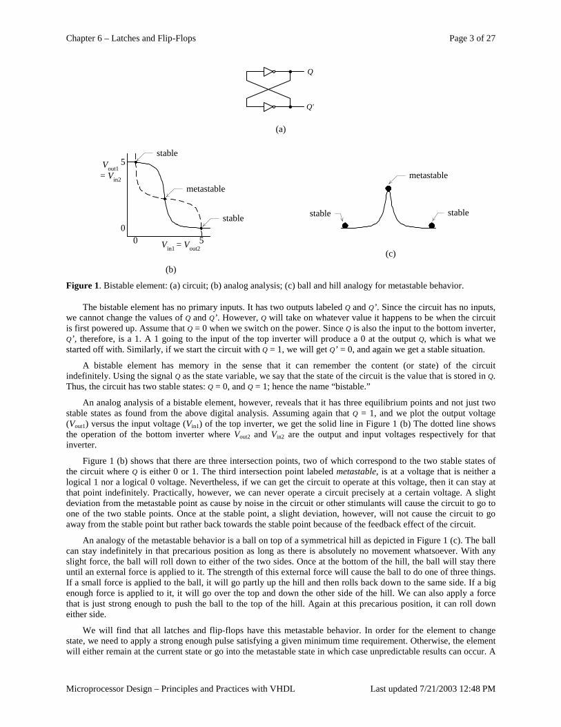
Chapter 6 – Latches and Flip-Flops Page 3 of 27
Microprocessor Design – Principles and Practices with VHDL Last updated 7/21/2003 12:48 PM
Q
Q'
(a)
Vin1 = Vout2
Vout1= Vin2
5
00 5
stable
metastable
stable
(b)
stable
metastable
stable
(c)
Figure 1. Bistable element: (a) circuit; (b) analog analysis; (c) ball and hill analogy for metastable behavior.
The bistable element has no primary inputs. It has two outputs labeled Q and Q’. Since the circuit has no inputs, we cannot change the values of Q and Q’. However, Q will take on whatever value it happens to be when the circuit is first powered up. Assume that Q = 0 when we switch on the power. Since Q is also the input to the bottom inverter, Q’, therefore, is a 1. A 1 going to the input of the top inverter will produce a 0 at the output Q, which is what we started off with. Similarly, if we start the circuit with Q = 1, we will get Q’ = 0, and again we get a stable situation.
A bistable element has memory in the sense that it can remember the content (or state) of the circuit indefinitely. Using the signal Q as the state variable, we say that the state of the circuit is the value that is stored in Q. Thus, the circuit has two stable states: Q = 0, and Q = 1; hence the name “bistable.”
An analog analysis of a bistable element, however, reveals that it has three equilibrium points and not just two stable states as found from the above digital analysis. Assuming again that Q = 1, and we plot the output voltage (Vout1) versus the input voltage (Vin1) of the top inverter, we get the solid line in Figure 1 (b) The dotted line shows the operation of the bottom inverter where Vout2 and Vin2 are the output and input voltages respectively for that inverter.
Figure 1 (b) shows that there are three intersection points, two of which correspond to the two stable states of the circuit where Q is either 0 or 1. The third intersection point labeled metastable, is at a voltage that is neither a logical 1 nor a logical 0 voltage. Nevertheless, if we can get the circuit to operate at this voltage, then it can stay at that point indefinitely. Practically, however, we can never operate a circuit precisely at a certain voltage. A slight deviation from the metastable point as cause by noise in the circuit or other stimulants will cause the circuit to go to one of the two stable points. Once at the stable point, a slight deviation, however, will not cause the circuit to go away from the stable point but rather back towards the stable point because of the feedback effect of the circuit.
An analogy of the metastable behavior is a ball on top of a symmetrical hill as depicted in Figure 1 (c). The ball can stay indefinitely in that precarious position as long as there is absolutely no movement whatsoever. With any slight force, the ball will roll down to either of the two sides. Once at the bottom of the hill, the ball will stay there until an external force is applied to it. The strength of this external force will cause the ball to do one of three things. If a small force is applied to the ball, it will go partly up the hill and then rolls back down to the same side. If a big enough force is applied to it, it will go over the top and down the other side of the hill. We can also apply a force that is just strong enough to push the ball to the top of the hill. Again at this precarious position, it can roll down either side.
We will find that all latches and flip-flops have this metastable behavior. In order for the element to change state, we need to apply a strong enough pulse satisfying a given minimum time requirement. Otherwise, the element will either remain at the current state or go into the metastable state in which case unpredictable results can occur. A
Chapter 6 – Latches and Flip-Flops Page 4 of 27
Microprocessor Design – Principles and Practices with VHDL Last updated 7/21/2003 12:48 PM
study in the electrical characteristics of digital circuits is beyond the scope of this book. The interested reader is referred to the references.
6.2 SR Latch The bistable element is able to remember or store one bit of information. However, because it does not have any
external inputs, we cannot change the bit that is stored in it. Whatever value Q contains when power is first applied to the circuit, the circuit will remain in that state indefinitely until power is removed. We cannot simply connect an external input to one of the inverter inputs because we can create a short circuit by connecting a 0 to a 1. For example, lets assume that the external input is connected to the input of the top inverter in Figure 1 (a) and that the current state of the circuit is 1, i.e. Q = 1. This implies that the input to the top inverter must be a 0. If we want to change the state to 0, then we must set the external input, which is connected to the input of the top inverter, to a 1. By doing this, the input to the top inverter will be momentarily shorted.
In order to change the information bit, we need to add external inputs to the circuit. The simplest way to add inputs is to replace the two inverters with two NAND gates as shown in Figure 2 (a). This circuit is called a SR latch. In addition to the two outputs Q and Q’, there are two inputs S' and R' for set and reset respectively. The SR latch can be in one of two states: a set state when Q = 1, or a reset state when Q = 0. Following the convention, the primes in S and R denote that these inputs are active low, i.e. a 0 asserts them and a 1 de-asserts them.
To make the SR latch go to the set state, we simply assert the S' input by setting it to 0. It doesn’t matter what the other NAND gate input is because 0 NAND anything gives a 1, hence Q = 1 and the latch is set. If S' remains at a 0 so that Q (which is connected to one input of the bottom NAND gate) remains at a 1, if we now de-assert R', i.e. R' = 1, then the output of the bottom NAND gate will be a 0, and so Q' = 0. This situation is shown in Figure 2 (d) at time t0. From this current situation, if we now de-assert S' so that S' = R' = 1, the latch will remain in the set state because Q', the second input to the top NAND gate, is 0 which will keep Q = 1 as shown at time t1. At time t2 we reset the latch by making R' = 0. With R' being a 0, Q' will go to a 1. At the top NAND gate, 1 NAND 1 is 0, thus forcing Q to go to a 0. If we de-assert R' so that again we have S' = R' = 1, this time the latch will remain in the reset state as shown at time t3.
Notice the two times (at t1 and t3) when both S' and R' are de-asserted (S' = R' = 1). At t1, Q is at a 1, whereas, at t3, Q is at a 0. Why is this so? What is different between these two times? The difference is in the value of Q immediately before those times. The value of Q right before t1 is a 1, whereas the value of Q right before t3 is a 0. When both inputs are de-asserted, the SR latch remembers its previous state. Previous to t1, Q has the value 1, so at t1, Q remains at a 1. Similarly, previous to t3, Q has the value 0, so at t3, Q remains at a 0.
Q
Q'
S'
R'
(a)
S' R' Q Qnext Qnext' 0 0 × 1 1 0 1 × 1 0 1 0 × 0 1 1 1 0 0 1 1 1 1 1 0
(b)
Q
Q'
S'
R'
(c)
S'
R'
Q
Q'
t0 t1 t2 t3 t4 t5
Undefined
Undefined
t6
(d)
Figure 2. SR latch: (a) circuit using NAND gates; (b) truth table; (c) logic symbol; (d) timing diagram.

Chapter 6 – Latches and Flip-Flops Page 5 of 27
Microprocessor Design – Principles and Practices with VHDL Last updated 7/21/2003 12:48 PM
If both S' and R' are asserted (set to a 0), then both Q and Q' are equal to a 1 as shown at time t4, since 0 NAND anything gives a 1. Note that there is nothing wrong with having Q equals to Q'. It is just because we named these two points Q and Q' that we don’t like them to be equal. But we could have used the name P instead of Q'.
If one of the input signals is de-asserted earlier than the other, the latch will end up in the state forced by the signal that is de-asserted later as shown at time t5. At t5, R' is de-asserted first, so the latch goes into the set state with Q = 1 and Q' = 0.
A problem exists if both S' and R' are de-asserted at exactly the same time as shown at time t6. Let us assume for a moment that both gates have exactly the same delay and that the two wire connections between the output of one gate to the input of the other gate also have exactly the same delay. Currently, both Q and Q' are at a 1. If we set S' and R' to a 1 at exactly the same time, then both NAND gates will perform a 1 NAND 1, and will both output a 0 at exactly the same time. The two zeros will be fed back to the two gate inputs at exactly the same time because the two wire connections have the same delay. This time round, the two NAND gates will perform a 1 NAND 0, and will both produce a 1, again at exactly the same time. This time, two ones will be fed back to the inputs, which again will produce a 0 at the outputs, and so on and on. This oscillating behavior, called the critical race, will continue forever until one out paces the other. If the two gates do not have exactly the same delay then the situation is similar to de-asserting one input before the other, and so the latch will go into one state or the other. However, since we do not know which is the faster gate, therefore, we do not know which state the latch will end up in. Thus, the latch’s next state is undefined.
Of course, in practice, it is next to impossible to manufacture two gates and make the two connections with precisely the same delay. In addition, both S' and R' need to be de-asserted at exactly the same time. Nevertheless, if this circuit is used in controlling the space shuttle, we don’t want even this slim chance to happen.
In order to avoid this non-deterministic behavior, we must make sure that the two inputs are never de-asserted at the same time. Note that we do want the situation when both of them are de-asserted as in times t1 and t3 so that the circuit can remember its current content. We want to de-assert one input after de-asserting the other, but just not de-asserting both of them at exactly the same time. In practice, it is very difficult to guarantee that these two signals are never de-asserted at the same time, so we relax the condition slightly by not having both of them asserted together. In other words, if one is asserted, then the other one cannot be asserted. So if both of them are never asserted, then they can’t be de-asserted at the same time. A minor side benefit for not having both of them asserted together is that Q and Q' are never equal to each other. Recall that from the names that we have given these two nodes, we do want them to be inverses of each other.
From the above analysis, we obtain the truth table in Figure 2 (b) for the NAND implementation of the SR latch. In the truth table, Q and Qnext actually represent the same point in the circuit. The difference is that Q is the current state or the current content of the latch and Qnext is the value to be updated in the next state or next time period. Q is the input to a gate and Qnext is the output from a gate. So the value of Q goes into a gate, and after this signal propergates through the two gates and arrives back at Q then this new signal is referred to as Qnext. Figure 2 (c) shows the logic symbol for the SR latch.
The SR latch can also be implemented using NOR gates as shown in Figure 3 (a). The truth table for this implementation is shown in Figure 3 (b). From the truth table, we see that the main difference between this implementation and the NAND implementation is that for the NOR implementation, the S and R inputs are active high, so that setting S to 1 will set the latch and setting R to 1 will reset the latch. However, just like the NAND implementation, the latch is set when Q = 1 and reset when Q = 0. The latch remembers its previous state when S = R = 0. When S = R = 1, both Q and Q' are 0. The logic symbol for the SR latch using NOR implementation is shown in Figure 3 (c).
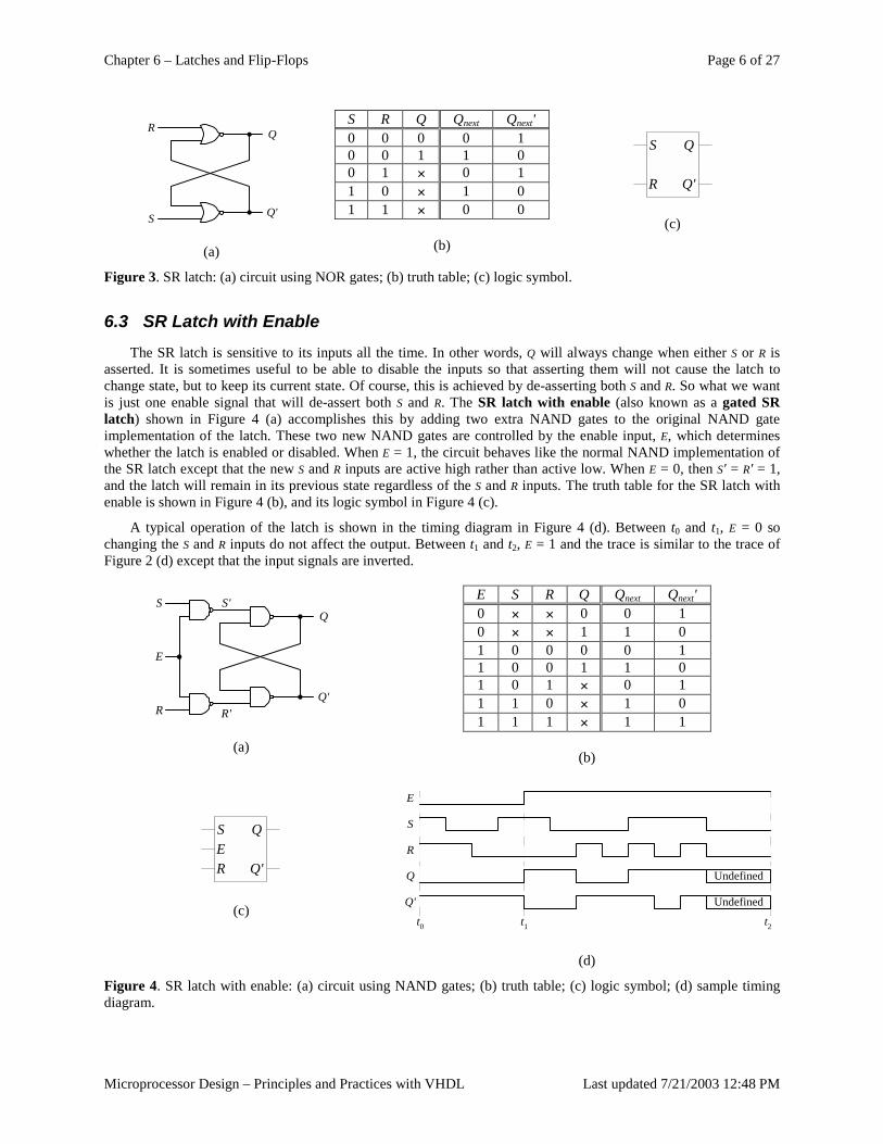
Chapter 6 – Latches and Flip-Flops Page 6 of 27
Microprocessor Design – Principles and Practices with VHDL Last updated 7/21/2003 12:48 PM
Q
Q'
R
S
(a)
S R Q Qnext Qnext' 0 0 0 0 1 0 0 1 1 0 0 1 × 0 1 1 0 × 1 0 1 1 × 0 0
(b)
Q
Q'
S
R
(c)
Figure 3. SR latch: (a) circuit using NOR gates; (b) truth table; (c) logic symbol.
6.3 SR Latch with Enable The SR latch is sensitive to its inputs all the time. In other words, Q will always change when either S or R is
asserted. It is sometimes useful to be able to disable the inputs so that asserting them will not cause the latch to change state, but to keep its current state. Of course, this is achieved by de-asserting both S and R. So what we want is just one enable signal that will de-assert both S and R. The SR latch with enable (also known as a gated SR latch) shown in Figure 4 (a) accomplishes this by adding two extra NAND gates to the original NAND gate implementation of the latch. These two new NAND gates are controlled by the enable input, E, which determines whether the latch is enabled or disabled. When E = 1, the circuit behaves like the normal NAND implementation of the SR latch except that the new S and R inputs are active high rather than active low. When E = 0, then S' = R' = 1, and the latch will remain in its previous state regardless of the S and R inputs. The truth table for the SR latch with enable is shown in Figure 4 (b), and its logic symbol in Figure 4 (c).
A typical operation of the latch is shown in the timing diagram in Figure 4 (d). Between t0 and t1, E = 0 so changing the S and R inputs do not affect the output. Between t1 and t2, E = 1 and the trace is similar to the trace of Figure 2 (d) except that the input signals are inverted.
S
R
Q
Q'
E
R'
S'
(a)
E S R Q Qnext Qnext' 0 × × 0 0 1 0 × × 1 1 0 1 0 0 0 0 1 1 0 0 1 1 0 1 0 1 × 0 1 1 1 0 × 1 0 1 1 1 × 1 1
(b)
Q
Q'
S
RE
(c)
S
R
Q
Q'
t1
Undefined
Undefined
t2
E
t0
(d)
Figure 4. SR latch with enable: (a) circuit using NAND gates; (b) truth table; (c) logic symbol; (d) sample timing diagram.
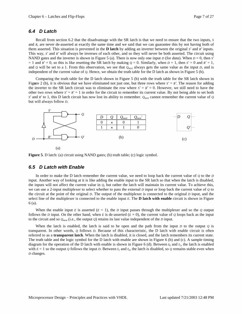
Chapter 6 – Latches and Flip-Flops Page 7 of 27
Microprocessor Design – Principles and Practices with VHDL Last updated 7/21/2003 12:48 PM
6.4 D Latch Recall from section 6.2 that the disadvantage with the SR latch is that we need to ensure that the two inputs, S
and R, are never de-asserted at exactly the same time and we said that we can guarantee this by not having both of them asserted. This situation is prevented in the D latch by adding an inverter between the original S' and R' inputs. This way, S' and R' will always be inverses of each other, and so they will never be both asserted. The circuit using NAND gates and the inverter is shown in Figure 5 (a). There is now only one input D (for data). When D = 0, then S' = 1 and R' = 0, so this is like resetting the SR latch by making Q = 0. Similarly, when D = 1, then S' = 0 and R' = 1, and Q will be set to a 1. From this observation, we see that Qnext always gets the same value as the input D, and is independent of the current value of Q. Hence, we obtain the truth table for the D latch as shown in Figure 5 (b).
Comparing the truth table for the D latch shown in Figure 5 (b) with the truth table for the SR latch shown in Figure 2 (b), it is obvious that we have eliminated not just one, but three rows where S' = R'. The reason for adding the inverter to the SR latch circuit was to eliminate the row where S' = R' = 0. However, we still need to have the other two rows where S' = R' = 1 in order for the circuit to remember its current value. By not being able to set both S' and R' to 1, this D latch circuit has now lost its ability to remember. Qnext cannot remember the current value of Q but will always follow D.
Q
Q'
S'
R'D
(a)
D Q Qnext Qnext' 0 × 0 1 1 × 1 0
(b)
Q
Q'
D
(c)
Figure 5. D latch: (a) circuit using NAND gates; (b) truth table; (c) logic symbol.
6.5 D Latch with Enable In order to make the D latch remember the current value, we need to loop back the current value of Q to the D
input. Another way of looking at it is like adding the enable input to the SR latch so that when the latch is disabled, the inputs will not affect the current value in Q, but rather the latch will maintain its current value. To achieve this, we can use a 2-input multiplexer to select whether to pass the external D input or loop back the current value of Q to the circuit at the point of the original D. The output of the multiplexer is connected to the original D input, and the select line of the multiplexer is connected to the enable input E. The D latch with enable circuit is shown in Figure 6 (a).
When the enable input E is asserted (E = 1), the D input passes through the multiplexer and so the Q output follows the D input. On the other hand, when E is de-asserted (E = 0), the current value of Q loops back as the input to the circuit and so Qnext (i.e., the output Q) retains its last value independent of the D input.
When the latch is enabled, the latch is said to be open and the path from the input D to the output Q is transparent. In other words, Q follows D. Because of this characteristic, the D latch with enable circuit is often referred to as a transparent latch. When the latch is disabled, it is closed, and the latch remembers its current state. The truth table and the logic symbol for the D latch with enable are shown in Figure 6 (b) and (c). A sample timing diagram for the operation of the D latch with enable is shown in Figure 6 (d). Between t0 and t1, the latch is enabled with E = 1 so the output Q follows the input D. Between t1 and t2, the latch is disabled, so Q remains stable even when D changes.
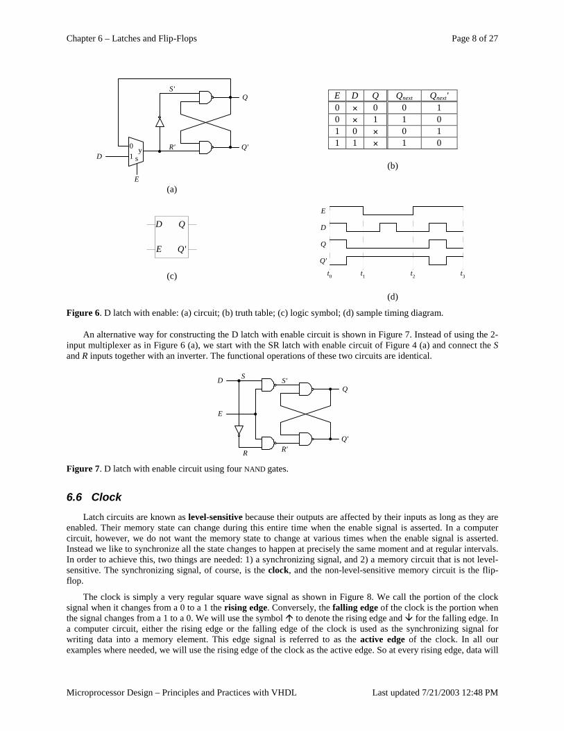
Chapter 6 – Latches and Flip-Flops Page 8 of 27
Microprocessor Design – Principles and Practices with VHDL Last updated 7/21/2003 12:48 PM
Q
Q'
S'
R'D
E
ys
01
(a)
E D Q Qnext Qnext' 0 × 0 0 1 0 × 1 1 0 1 0 × 0 1 1 1 × 1 0
(b)
Q
Q'
D
E
(c)
E
D
Q
Q'
t0 t1 t2 t3
(d)
Figure 6. D latch with enable: (a) circuit; (b) truth table; (c) logic symbol; (d) sample timing diagram.
An alternative way for constructing the D latch with enable circuit is shown in Figure 7. Instead of using the 2-input multiplexer as in Figure 6 (a), we start with the SR latch with enable circuit of Figure 4 (a) and connect the S and R inputs together with an inverter. The functional operations of these two circuits are identical.
S
R
Q
Q'
E
R'
S'D
Figure 7. D latch with enable circuit using four NAND gates.
6.6 Clock Latch circuits are known as level-sensitive because their outputs are affected by their inputs as long as they are
enabled. Their memory state can change during this entire time when the enable signal is asserted. In a computer circuit, however, we do not want the memory state to change at various times when the enable signal is asserted. Instead we like to synchronize all the state changes to happen at precisely the same moment and at regular intervals. In order to achieve this, two things are needed: 1) a synchronizing signal, and 2) a memory circuit that is not level-sensitive. The synchronizing signal, of course, is the clock, and the non-level-sensitive memory circuit is the flip-flop.
The clock is simply a very regular square wave signal as shown in Figure 8. We call the portion of the clock signal when it changes from a 0 to a 1 the rising edge. Conversely, the falling edge of the clock is the portion when the signal changes from a 1 to a 0. We will use the symbol � to denote the rising edge and � for the falling edge. In a computer circuit, either the rising edge or the falling edge of the clock is used as the synchronizing signal for writing data into a memory element. This edge signal is referred to as the active edge of the clock. In all our examples where needed, we will use the rising edge of the clock as the active edge. So at every rising edge, data will
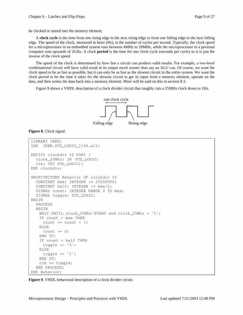
Chapter 6 – Latches and Flip-Flops Page 9 of 27
Microprocessor Design – Principles and Practices with VHDL Last updated 7/21/2003 12:48 PM
be clocked or stored into the memory element.
A clock cycle is the time from one rising edge to the next rising edge or from one falling edge to the next falling edge. The speed of the clock, measured in hertz (Hz), is the number of cycles per second. Typically, the clock speed for a microprocessor in an embedded system runs between 4MHz to 20MHz, while the microprocessor in a personal computer runs upwards of 2GHz. A clock period is the time for one clock cycle (seconds per cycle) so it is just the inverse of the clock speed.
The speed of the clock is determined by how fast a circuit can produce valid results. For example, a two-level combinational circuit will have valid result at its output much sooner than say an ALU can. Of course, we want the clock speed to be as fast as possible, but it can only be as fast as the slowest circuit in the entire system. We want the clock period to be the time it takes for the slowest circuit to get its input from a memory element, operate on the data, and then writes the data back into a memory element. More will be said on this in section 8.3.
Figure 9 shows a VHDL description of a clock divider circuit that roughly cuts a 25MHz clock down to 1Hz.
one clock cycle
Falling edge Rising edge Figure 8. Clock signal.
LIBRARY IEEE;USE IEEE.STD_LOGIC_1164.all;
ENTITY clockdiv IS PORT (clock_25Mhz: IN STD_LOGIC;clk: OUT STD_LOGIC);
END clockdiv;
ARCHITECTURE Behavior OF clockdiv ISCONSTANT max: INTEGER := 25000000;CONSTANT half: INTEGER := max/2;SIGNAL count: INTEGER RANGE 0 TO max;SIGNAL toggle: STD_LOGIC;
BEGINPROCESSBEGINWAIT UNTIL clock_25Mhz'EVENT and clock_25Mhz = '1';IF count < max THENcount <= count + 1;
ELSEcount <= 0;
END IF;IF count < half THENtoggle <= '0';
ELSEtoggle <= '1';
END IF;clk <= toggle;
END PROCESS;END Behavior;
Figure 9. VHDL behavioral description of a clock divider circuit.
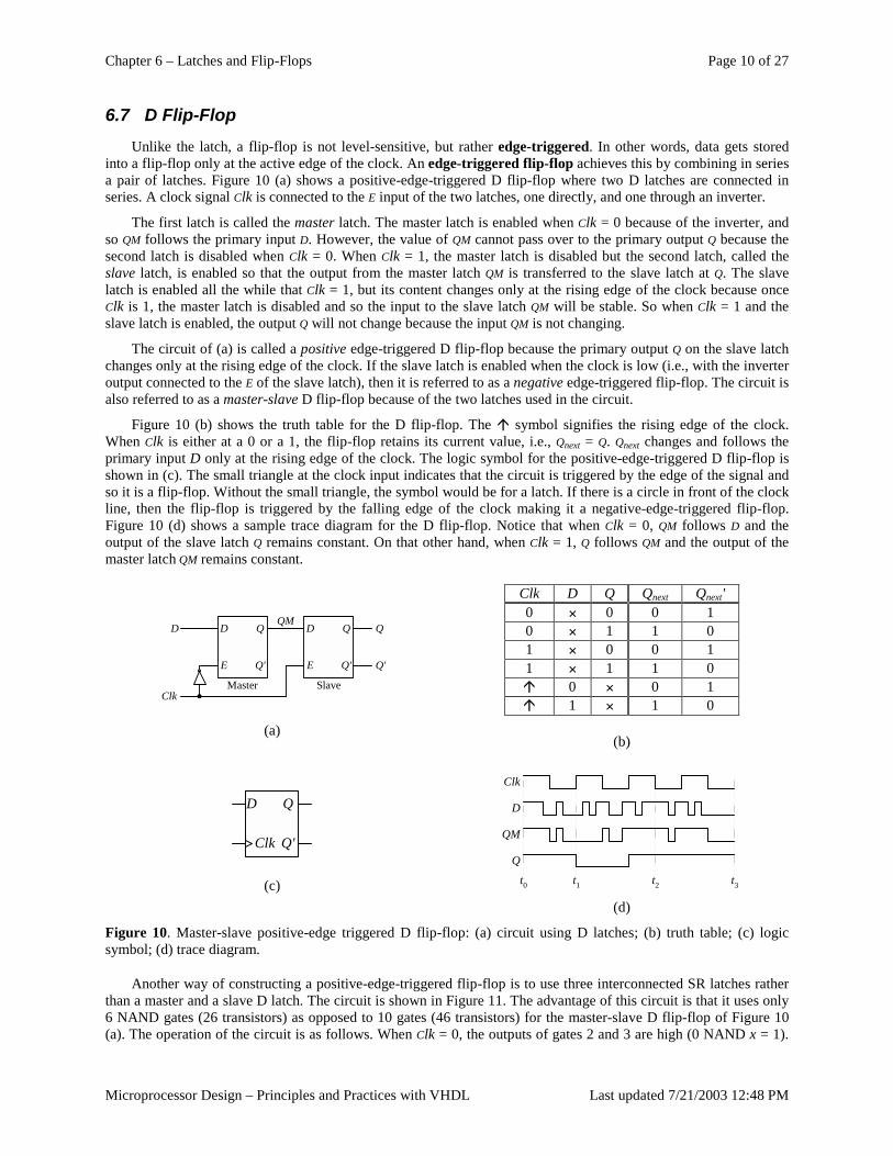
Chapter 6 – Latches and Flip-Flops Page 10 of 27
Microprocessor Design – Principles and Practices with VHDL Last updated 7/21/2003 12:48 PM
6.7 D Flip-Flop Unlike the latch, a flip-flop is not level-sensitive, but rather edge-triggered. In other words, data gets stored
into a flip-flop only at the active edge of the clock. An edge-triggered flip-flop achieves this by combining in series a pair of latches. Figure 10 (a) shows a positive-edge-triggered D flip-flop where two D latches are connected in series. A clock signal Clk is connected to the E input of the two latches, one directly, and one through an inverter.
The first latch is called the master latch. The master latch is enabled when Clk = 0 because of the inverter, and so QM follows the primary input D. However, the value of QM cannot pass over to the primary output Q because the second latch is disabled when Clk = 0. When Clk = 1, the master latch is disabled but the second latch, called the slave latch, is enabled so that the output from the master latch QM is transferred to the slave latch at Q. The slave latch is enabled all the while that Clk = 1, but its content changes only at the rising edge of the clock because once Clk is 1, the master latch is disabled and so the input to the slave latch QM will be stable. So when Clk = 1 and the slave latch is enabled, the output Q will not change because the input QM is not changing.
The circuit of (a) is called a positive edge-triggered D flip-flop because the primary output Q on the slave latch changes only at the rising edge of the clock. If the slave latch is enabled when the clock is low (i.e., with the inverter output connected to the E of the slave latch), then it is referred to as a negative edge-triggered flip-flop. The circuit is also referred to as a master-slave D flip-flop because of the two latches used in the circuit.
Figure 10 (b) shows the truth table for the D flip-flop. The � symbol signifies the rising edge of the clock. When Clk is either at a 0 or a 1, the flip-flop retains its current value, i.e., Qnext = Q. Qnext changes and follows the primary input D only at the rising edge of the clock. The logic symbol for the positive-edge-triggered D flip-flop is shown in (c). The small triangle at the clock input indicates that the circuit is triggered by the edge of the signal and so it is a flip-flop. Without the small triangle, the symbol would be for a latch. If there is a circle in front of the clock line, then the flip-flop is triggered by the falling edge of the clock making it a negative-edge-triggered flip-flop. Figure 10 (d) shows a sample trace diagram for the D flip-flop. Notice that when Clk = 0, QM follows D and the output of the slave latch Q remains constant. On that other hand, when Clk = 1, Q follows QM and the output of the master latch QM remains constant.
D
Clk
Q
Q'
QM
Master Slave
Q
Q'
D
E
Q
Q'
D
E
(a)
Clk D Q Qnext Qnext' 0 × 0 0 1 0 × 1 1 0 1 × 0 0 1 1 × 1 1 0 � 0 × 0 1 � 1 × 1 0
(b)
Q
Q'
D
Clk
(c)
Clk
D
QM
Q
t0 t1 t2 t3
(d)
Figure 10. Master-slave positive-edge triggered D flip-flop: (a) circuit using D latches; (b) truth table; (c) logic symbol; (d) trace diagram.
Another way of constructing a positive-edge-triggered flip-flop is to use three interconnected SR latches rather than a master and a slave D latch. The circuit is shown in Figure 11. The advantage of this circuit is that it uses only 6 NAND gates (26 transistors) as opposed to 10 gates (46 transistors) for the master-slave D flip-flop of Figure 10 (a). The operation of the circuit is as follows. When Clk = 0, the outputs of gates 2 and 3 are high (0 NAND x = 1).
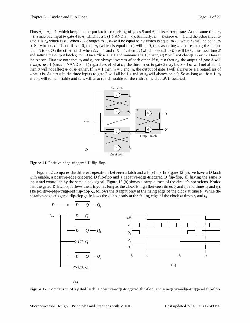
Chapter 6 – Latches and Flip-Flops Page 11 of 27
Microprocessor Design – Principles and Practices with VHDL Last updated 7/21/2003 12:48 PM
Thus n2 = n3 = 1, which keeps the output latch, comprising of gates 5 and 6, in its current state. At the same time n4 = D' since one input to gate 4 is n3 which is a 1 (1 NAND x = x'). Similarly, n1 = D since n2 = 1 and the other input to gate 1 is n4 which is D'. When Clk changes to 1, n2 will be equal to n1' which is equal to D', while n3 will be equal to D. So when Clk = 1 and if D = 0, then n3 (which is equal to D) will be 0, thus asserting R' and resetting the output latch Q to 0. On the other hand, when Clk = 1 and if D = 1, then n2 (which is equal to D') will be 0, thus asserting S' and setting the output latch Q to 1. Once Clk is at a 1 and remains at a 1, changing D will not change n2 or n3. Here is the reason. First we note that n2 and n3 are always inverses of each other. If n2 = 0 then n3, the output of gate 3 will always be a 1 (since 0 NAND x = 1) regardless of what n4, the third input to gate 3 may be. So if n4 will not affect it, then D will not affect n2 or n3 either. If n2 = 1 then n3 = 0 and n4, the output of gate 4 will always be a 1 regardless of what D is. As a result, the three inputs to gate 3 will all be 1’s and so n3 will always be a 0. So as long as Clk = 1, n2 and n3 will remain stable and so Q will also remain stable for the entire time that Clk is asserted.
D
Clk
Q
Q'3
4
6
52
1
n3
n2
Output latch
Reset latch
Set latch
R'
S'
n4
n1
Figure 11. Positive-edge-triggered D flip-flop.
Figure 12 compares the different operations between a latch and a flip-flop. In Figure 12 (a), we have a D latch with enable, a positive-edge-triggered D flip-flop and a negative-edge-triggered D flip-flop, all having the same D input and controlled by the same clock signal. Figure 12 (b) shows a sample trace of the circuit’s operations. Notice that the gated D latch Qa follows the D input as long as the clock is high (between times t0 and t1, and times t2 and t3). The positive-edge-triggered flip-flop Qb follows the D input only at the rising edge of the clock at time t2. While the negative-edge-triggered flip-flop Qc follows the D input only at the falling edge of the clock at times t1 and t3.
Q
Q'
D
Clk
Q
Q'
DD
Clk
Q
Q'
D
Clk
Qa
Qb
Qc
E
(a)
Clk
D
Qa
Qb
Qc
t0 t1 t2 t3
(b)
Figure 12. Comparison of a gated latch, a positive-edge-triggered flip-flop, and a negative-edge-triggered flip-flop:
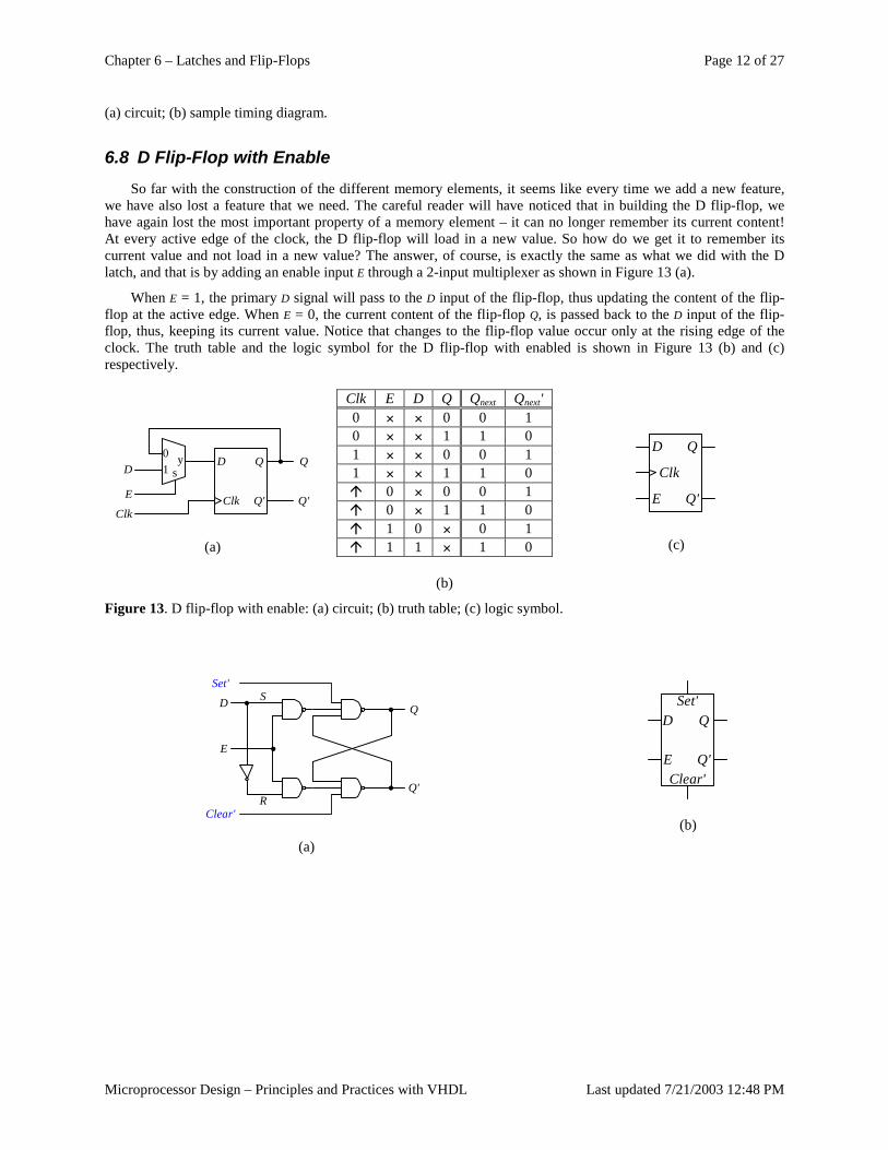
Chapter 6 – Latches and Flip-Flops Page 12 of 27
Microprocessor Design – Principles and Practices with VHDL Last updated 7/21/2003 12:48 PM
(a) circuit; (b) sample timing diagram.
6.8 D Flip-Flop with Enable So far with the construction of the different memory elements, it seems like every time we add a new feature,
we have also lost a feature that we need. The careful reader will have noticed that in building the D flip-flop, we have again lost the most important property of a memory element – it can no longer remember its current content! At every active edge of the clock, the D flip-flop will load in a new value. So how do we get it to remember its current value and not load in a new value? The answer, of course, is exactly the same as what we did with the D latch, and that is by adding an enable input E through a 2-input multiplexer as shown in Figure 13 (a).
When E = 1, the primary D signal will pass to the D input of the flip-flop, thus updating the content of the flip-flop at the active edge. When E = 0, the current content of the flip-flop Q, is passed back to the D input of the flip-flop, thus, keeping its current value. Notice that changes to the flip-flop value occur only at the rising edge of the clock. The truth table and the logic symbol for the D flip-flop with enabled is shown in Figure 13 (b) and (c) respectively.
D
E
Clk
Q
Q'
Q
Q'
D
Clk
ys
01
(a)
Clk E D Q Qnext Qnext' 0 × × 0 0 1 0 × × 1 1 0 1 × × 0 0 1 1 × × 1 1 0 � 0 × 0 0 1 � 0 × 1 1 0 � 1 0 × 0 1 � 1 1 × 1 0
(b)
Q
Q'
D
Clk
E
(c)
Figure 13. D flip-flop with enable: (a) circuit; (b) truth table; (c) logic symbol.
D Q
Q'
E
R
SSet'
Clear'
(a)
Q
Q'
D
E
Set'
Clear'
(b)
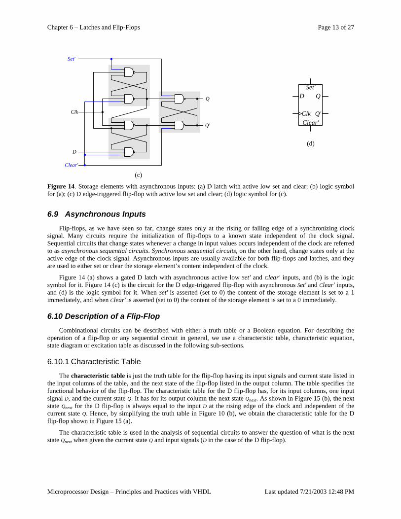
Chapter 6 – Latches and Flip-Flops Page 13 of 27
Microprocessor Design – Principles and Practices with VHDL Last updated 7/21/2003 12:48 PM
D
Clk
Q
Q'
Clear'
Set'
(c)
Q
Q'
D
Clk
Set'
Clear'
(d)
Figure 14. Storage elements with asynchronous inputs: (a) D latch with active low set and clear; (b) logic symbol for (a); (c) D edge-triggered flip-flop with active low set and clear; (d) logic symbol for (c).
6.9 Asynchronous Inputs Flip-flops, as we have seen so far, change states only at the rising or falling edge of a synchronizing clock
signal. Many circuits require the initialization of flip-flops to a known state independent of the clock signal. Sequential circuits that change states whenever a change in input values occurs independent of the clock are referred to as asynchronous sequential circuits. Synchronous sequential circuits, on the other hand, change states only at the active edge of the clock signal. Asynchronous inputs are usually available for both flip-flops and latches, and they are used to either set or clear the storage element’s content independent of the clock.
Figure 14 (a) shows a gated D latch with asynchronous active low Set' and Clear' inputs, and (b) is the logic symbol for it. Figure 14 (c) is the circuit for the D edge-triggered flip-flop with asynchronous Set' and Clear' inputs, and (d) is the logic symbol for it. When Set' is asserted (set to 0) the content of the storage element is set to a 1 immediately, and when Clear' is asserted (set to 0) the content of the storage element is set to a 0 immediately.
6.10 Description of a Flip-Flop Combinational circuits can be described with either a truth table or a Boolean equation. For describing the
operation of a flip-flop or any sequential circuit in general, we use a characteristic table, characteristic equation, state diagram or excitation table as discussed in the following sub-sections.
6.10.1 Characteristic Table
The characteristic table is just the truth table for the flip-flop having its input signals and current state listed in the input columns of the table, and the next state of the flip-flop listed in the output column. The table specifies the functional behavior of the flip-flop. The characteristic table for the D flip-flop has, for its input columns, one input signal D, and the current state Q. It has for its output column the next state Qnext. As shown in Figure 15 (b), the next state Qnext for the D flip-flop is always equal to the input D at the rising edge of the clock and independent of the current state Q. Hence, by simplifying the truth table in Figure 10 (b), we obtain the characteristic table for the D flip-flop shown in Figure 15 (a).
The characteristic table is used in the analysis of sequential circuits to answer the question of what is the next state Qnext when given the current state Q and input signals (D in the case of the D flip-flop).
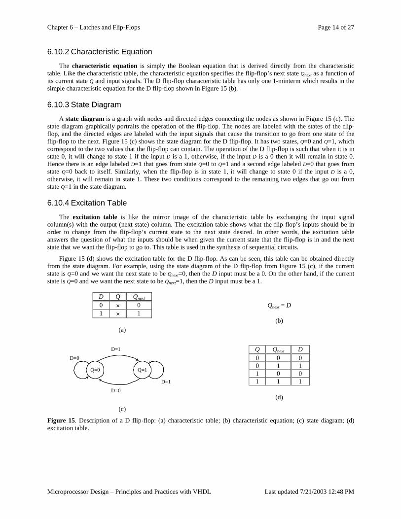
Chapter 6 – Latches and Flip-Flops Page 14 of 27
Microprocessor Design – Principles and Practices with VHDL Last updated 7/21/2003 12:48 PM
6.10.2 Characteristic Equation
The characteristic equation is simply the Boolean equation that is derived directly from the characteristic table. Like the characteristic table, the characteristic equation specifies the flip-flop’s next state Qnext as a function of its current state Q and input signals. The D flip-flop characteristic table has only one 1-minterm which results in the simple characteristic equation for the D flip-flop shown in Figure 15 (b).
6.10.3 State Diagram
A state diagram is a graph with nodes and directed edges connecting the nodes as shown in Figure 15 (c). The state diagram graphically portraits the operation of the flip-flop. The nodes are labeled with the states of the flip-flop, and the directed edges are labeled with the input signals that cause the transition to go from one state of the flip-flop to the next. Figure 15 (c) shows the state diagram for the D flip-flop. It has two states, Q=0 and Q=1, which correspond to the two values that the flip-flop can contain. The operation of the D flip-flop is such that when it is in state 0, it will change to state 1 if the input D is a 1, otherwise, if the input D is a 0 then it will remain in state 0. Hence there is an edge labeled D=1 that goes from state Q=0 to Q=1 and a second edge labeled D=0 that goes from state Q=0 back to itself. Similarly, when the flip-flop is in state 1, it will change to state 0 if the input D is a 0, otherwise, it will remain in state 1. These two conditions correspond to the remaining two edges that go out from state Q=1 in the state diagram.
6.10.4 Excitation Table
The excitation table is like the mirror image of the characteristic table by exchanging the input signal column(s) with the output (next state) column. The excitation table shows what the flip-flop’s inputs should be in order to change from the flip-flop’s current state to the next state desired. In other words, the excitation table answers the question of what the inputs should be when given the current state that the flip-flop is in and the next state that we want the flip-flop to go to. This table is used in the synthesis of sequential circuits.
Figure 15 (d) shows the excitation table for the D flip-flop. As can be seen, this table can be obtained directly from the state diagram. For example, using the state diagram of the D flip-flop from Figure 15 (c), if the current state is Q=0 and we want the next state to be Qnext=0, then the D input must be a 0. On the other hand, if the current state is Q=0 and we want the next state to be Qnext=1, then the D input must be a 1.
D Q Qnext 0 × 0 1 × 1
(a)
Qnext = D
(b)
Q=0 Q=1
D=0
D=1
D=1
D=0
(c)
Q Qnext D 0 0 0 0 1 1 1 0 0 1 1 1
(d)
Figure 15. Description of a D flip-flop: (a) characteristic table; (b) characteristic equation; (c) state diagram; (d) excitation table.
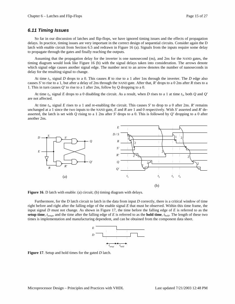
Chapter 6 – Latches and Flip-Flops Page 15 of 27
Microprocessor Design – Principles and Practices with VHDL Last updated 7/21/2003 12:48 PM
6.11 Timing Issues So far in our discussion of latches and flip-flops, we have ignored timing issues and the effects of propagation
delays. In practice, timing issues are very important in the correct design of sequential circuits. Consider again the D latch with enable circuit from Section 6.5 and redrawn in Figure 16 (a). Signals from the inputs require some delay to propagate through the gates and finally reaching the outputs.
Assuming that the propagation delay for the inverter is one nanosecond (ns), and 2ns for the NAND gates, the timing diagram would look like Figure 16 (b) with the signal delays taken into consideration. The arrows denote which signal edge causes another signal edge. The number next to an arrow denotes the number of nanoseconds in delay for the resulting signal to change.
At time t1, signal D drops to a 0. This causes R to rise to a 1 after 1ns through the inverter. The D edge also causes S' to rise to a 1, but after a delay of 2ns through the NAND gate. After that, R' drops to a 0 2ns after R rises to a 1. This in turn causes Q' to rise to a 1 after 2ns, follow by Q dropping to a 0.
At time t2, signal E drops to a 0 disabling the circuit. As a result, when D rises to a 1 at time t3, both Q and Q' are not affected.
At time t4, signal E rises to a 1 and re-enabling the circuit. This causes S' to drop to a 0 after 2ns. R' remains unchanged at a 1 since the two inputs to the NAND gate, E and R are 1 and 0 respectively. With S' asserted and R' de-asserted, the latch is set with Q rising to a 1 2ns after S' drops to a 0. This is followed by Q' dropping to a 0 after another 2ns.
S
R
Q
Q'
E
R'
S'D
(a) t1
E
D / S
R
S'
R'
Q
Q'
12
2
22
2
1 2
2
2
t2 t4t3
(b)
Figure 16. D latch with enable: (a) circuit; (b) timing diagram with delays.
Furthermore, for the D latch circuit to latch in the data from input D correctly, there is a critical window of time right before and right after the falling edge of the enable signal E that must be observed. Within this time frame, the input signal D must not change. As shown in Figure 17, the time before the falling edge of E is referred to as the setup time, tsetup, and the time after the falling edge of E is referred to as the hold time, thold. The length of these two times is implementation and manufacturing dependent, and can be obtained from the component data sheet.
E
D
tsetup thold Figure 17. Setup and hold times for the gated D latch.
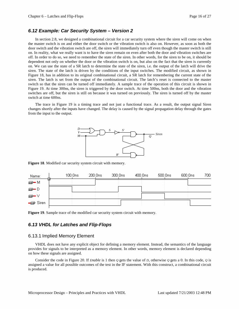
Chapter 6 – Latches and Flip-Flops Page 16 of 27
Microprocessor Design – Principles and Practices with VHDL Last updated 7/21/2003 12:48 PM
6.12 Example: Car Security System – Version 2 In section 2.8, we designed a combinational circuit for a car security system where the siren will come on when
the master switch is on and either the door switch or the vibration switch is also on. However, as soon as both the door switch and the vibration switch are off, the siren will immediately turn off even though the master switch is still on. In reality, what we really want is to have the siren remain on even after both the door and vibration switches are off. In order to do so, we need to remember the state of the siren. In other words, for the siren to be on, it should be dependent not only on whether the door or the vibration switch is on, but also on the fact that the siren is currently on. We can use the state of a SR latch to determine the state of the siren, i.e. the output of the latch will drive the siren. The state of the latch is driven by the conditions of the input switches. The modified circuit, as shown in Figure 18, has in addition to its original combinational circuit, a SR latch for remembering the current state of the siren. The latch is set from the output of the combinational circuit. The latch’s reset is connected to the master switch so that the siren can be turned off immediately. A sample trace of the operation of this circuit is shown in Figure 19. At time 300ns, the siren is triggered by the door switch. At time 500ns, both the door and the vibration switches are off, but the siren is still on because it was turned on previously. The siren is turned off by the master switch at time 600ns.
The trace in Figure 19 is a timing trace and not just a functional trace. As a result, the output signal Siren changes shortly after the inputs have changed. The delay is caused by the signal propagation delay through the gates from the input to the output.
Q
S'
R'
SirenSD
MV
Figure 18. Modified car security system circuit with memory.
Figure 19. Sample trace of the modified car security system circuit with memory.
6.13 VHDL for Latches and Flip-Flops
6.13.1 Implied Memory Element
VHDL does not have any explicit object for defining a memory element. Instead, the semantics of the language provides for signals to be interpreted as a memory element. In other words, memory element is declared depending on how these signals are assigned.
Consider the code in Figure 20. If Enable is 1 then Q gets the value of D, otherwise Q gets a 0. In this code, Q is assigned a value for all possible outcomes of the test in the IF statement. With this construct, a combinational circuit is produced.
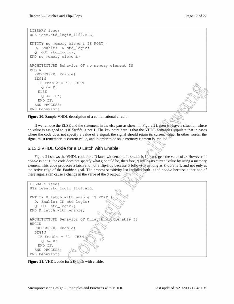
Chapter 6 – Latches and Flip-Flops Page 17 of 27
Microprocessor Design – Principles and Practices with VHDL Last updated 7/21/2003 12:48 PM
LIBRARY ieee;USE ieee.std_logic_1164.ALL;
ENTITY no_memory_element IS PORT (D, Enable: IN std_logic;Q: OUT std_logic);
END no_memory_element;
ARCHITECTURE Behavior OF no_memory_element ISBEGIN
PROCESS(D, Enable)BEGINIF Enable = '1' THENQ <= D;
ELSEQ <= '0';
END IF;END PROCESS;
END Behavior;
Figure 20. Sample VHDL description of a combinational circuit.
If we remove the ELSE and the statement in the else part as shown in Figure 21, then we have a situation where no value is assigned to Q if Enable is not 1. The key point here is that the VHDL semantics stipulate that in cases where the code does not specify a value of a signal, the signal should retain its current value. In other words, the signal must remember its current value, and in order to do so, a memory element is implied.
6.13.2 VHDL Code for a D Latch with Enable
Figure 21 shows the VHDL code for a D latch with enable. If Enable is 1 then Q gets the value of D. However, if Enable is not 1, the code does not specify what Q should be, therefore, Q retains its current value by using a memory element. This code produces a latch and not a flip-flop because Q follows D as long as Enable is 1, and not only at the active edge of the Enable signal. The process sensitivity list includes both D and Enable because either one of these signals can cause a change in the value of the Q output.
LIBRARY ieee;USE ieee.std_logic_1164.ALL;
ENTITY D_latch_with_enable IS PORT (D, Enable: IN std_logic;Q: OUT std_logic);
END D_latch_with_enable;
ARCHITECTURE Behavior OF D_latch_with_enable ISBEGIN
PROCESS(D, Enable)BEGINIF Enable = '1' THENQ <= D;
END IF;END PROCESS;
END Behavior;
Figure 21. VHDL code for a D latch with enable.
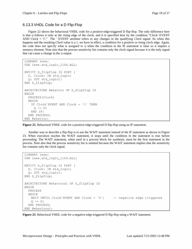
Chapter 6 – Latches and Flip-Flops Page 18 of 27
Microprocessor Design – Principles and Practices with VHDL Last updated 7/21/2003 12:48 PM
6.13.3 VHDL Code for a D Flip-Flop
Figure 22 shows the behavioral VHDL code for a positive-edge-triggered D flip-flop. The only difference here is that Q follows D only at the rising edge of the clock, and it is specified here by the condition “Clock' EVENT AND Clock = '1'.” The ' EVENT attribute refers to any changes in the qualifying Clock signal. So when this happens and the resulting Clock value is a 1, we have in effect, a condition for a positive or rising clock edge. Again, the code does not specify what is assigned to Q when the condition in the IF statement is false so it implies a memory element. Note also that the process sensitivity list contains only the clock signal because it is the only signal that can cause a change in the Q output.
LIBRARY ieee;USE ieee.std_logic_1164.ALL;
ENTITY D_flipflop IS PORT (D, Clock: IN std_logic;Q: OUT std_logic);
END D_flipflop;
ARCHITECTURE Behavior OF D_flipflop ISBEGIN
PROCESS(Clock)BEGINIF Clock’EVENT AND Clock = '1' THENQ <= D;
END IF;END PROCESS;
END Behavior;
Figure 22. Behavioral VHDL code for a positive-edge-triggered D flip-flop using an IF statement.
Another way to describe a flip-flop is to use the WAIT statement instead of the IF statement as shown in Figure 23. When execution reaches the WAIT statement, it stops until the condition in the statement is true before proceeding. The WAIT statement, when used in a process block for synthesis, must be the first statement in the process. Note also that the process sensitivity list is omitted because the WAIT statement implies that the sensitivity list contains only the clock signal.
LIBRARY ieee;USE ieee.std_logic_1164.ALL;
ENTITY D_flipflop IS PORT (D, Clock: IN std_logic;Q: OUT std_logic);
END D_flipflop;
ARCHITECTURE Behavioral OF D_flipflop ISBEGIN
PROCESSBEGINWAIT UNTIL Clock’EVENT AND Clock = '0'; -- negative edge triggeredQ <= D;
END PROCESS;END Behavioral;
Figure 23. Behavioral VHDL code for a negative-edge-triggered D flip-flop using a WAIT statement.
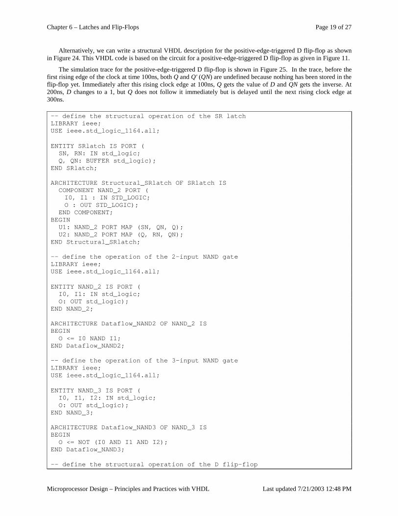
Chapter 6 – Latches and Flip-Flops Page 19 of 27
Microprocessor Design – Principles and Practices with VHDL Last updated 7/21/2003 12:48 PM
Alternatively, we can write a structural VHDL description for the positive-edge-triggered D flip-flop as shown in Figure 24. This VHDL code is based on the circuit for a positive-edge-triggered D flip-flop as given in Figure 11.
The simulation trace for the positive-edge-triggered D flip-flop is shown in Figure 25. In the trace, before the first rising edge of the clock at time 100ns, both Q and Q' (QN) are undefined because nothing has been stored in the flip-flop yet. Immediately after this rising clock edge at 100ns, Q gets the value of D and QN gets the inverse. At 200ns, D changes to a 1, but Q does not follow it immediately but is delayed until the next rising clock edge at 300ns.
-- define the structural operation of the SR latchLIBRARY ieee;USE ieee.std_logic_1164.all;
ENTITY SRlatch IS PORT (SN, RN: IN std_logic;Q, QN: BUFFER std_logic);
END SRlatch;
ARCHITECTURE Structural_SRlatch OF SRlatch ISCOMPONENT NAND_2 PORT (I0, I1 : IN STD_LOGIC;O : OUT STD_LOGIC);
END COMPONENT;BEGIN
U1: NAND_2 PORT MAP (SN, QN, Q);U2: NAND_2 PORT MAP (Q, RN, QN);
END Structural_SRlatch;
-- define the operation of the 2-input NAND gateLIBRARY ieee;USE ieee.std_logic_1164.all;
ENTITY NAND_2 IS PORT (I0, I1: IN std_logic;O: OUT std_logic);
END NAND_2;
ARCHITECTURE Dataflow_NAND2 OF NAND_2 ISBEGIN
O <= I0 NAND I1;END Dataflow_NAND2;
-- define the operation of the 3-input NAND gateLIBRARY ieee;USE ieee.std_logic_1164.all;
ENTITY NAND_3 IS PORT (I0, I1, I2: IN std_logic;O: OUT std_logic);
END NAND_3;
ARCHITECTURE Dataflow_NAND3 OF NAND_3 ISBEGIN
O <= NOT (I0 AND I1 AND I2);END Dataflow_NAND3;
-- define the structural operation of the D flip-flop
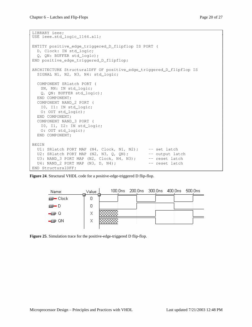
Chapter 6 – Latches and Flip-Flops Page 20 of 27
Microprocessor Design – Principles and Practices with VHDL Last updated 7/21/2003 12:48 PM
LIBRARY ieee;USE ieee.std_logic_1164.all;
ENTITY positive_edge_triggered_D_flipflop IS PORT (D, Clock: IN std_logic;Q, QN: BUFFER std_logic);
END positive_edge_triggered_D_flipflop;
ARCHITECTURE StructuralDFF OF positive_edge_triggered_D_flipflop ISSIGNAL N1, N2, N3, N4: std_logic;
COMPONENT SRlatch PORT (SN, RN: IN std_logic;Q, QN: BUFFER std_logic);
END COMPONENT;COMPONENT NAND_2 PORT (I0, I1: IN std_logic;O: OUT std_logic);
END COMPONENT;COMPONENT NAND_3 PORT (I0, I1, I2: IN std_logic;O: OUT std_logic);
END COMPONENT;
BEGINU1: SRlatch PORT MAP (N4, Clock, N1, N2); -- set latchU2: SRlatch PORT MAP (N2, N3, Q, QN); -- output latchU3: NAND_3 PORT MAP (N2, Clock, N4, N3); -- reset latchU4: NAND_2 PORT MAP (N3, D, N4); -- reset latch
END StructuralDFF;
Figure 24. Structural VHDL code for a positive-edge-triggered D flip-flop.
Figure 25. Simulation trace for the positive-edge-triggered D flip-flop.
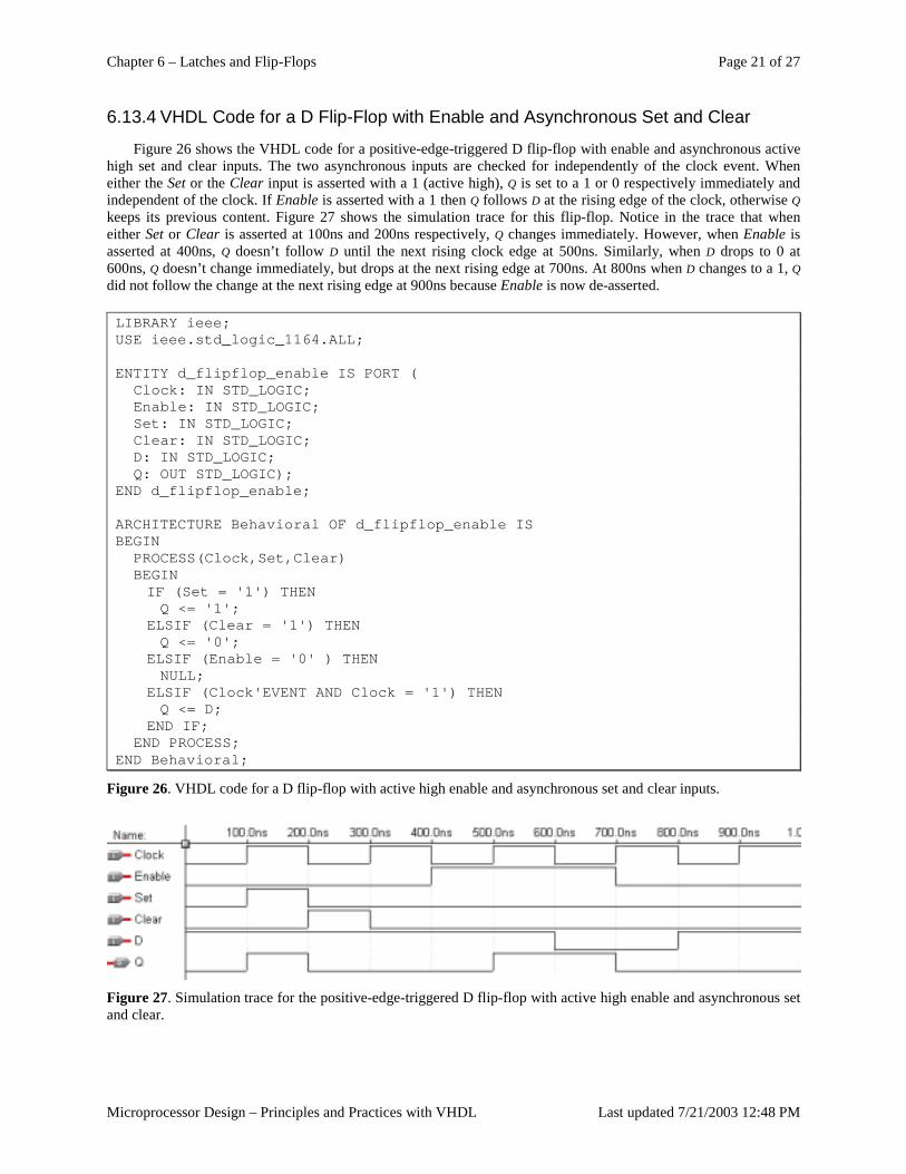
Chapter 6 – Latches and Flip-Flops Page 21 of 27
Microprocessor Design – Principles and Practices with VHDL Last updated 7/21/2003 12:48 PM
6.13.4 VHDL Code for a D Flip-Flop with Enable and Asynchronous Set and Clear
Figure 26 shows the VHDL code for a positive-edge-triggered D flip-flop with enable and asynchronous active high set and clear inputs. The two asynchronous inputs are checked for independently of the clock event. When either the Set or the Clear input is asserted with a 1 (active high), Q is set to a 1 or 0 respectively immediately and independent of the clock. If Enable is asserted with a 1 then Q follows D at the rising edge of the clock, otherwise Q keeps its previous content. Figure 27 shows the simulation trace for this flip-flop. Notice in the trace that when either Set or Clear is asserted at 100ns and 200ns respectively, Q changes immediately. However, when Enable is asserted at 400ns, Q doesn’t follow D until the next rising clock edge at 500ns. Similarly, when D drops to 0 at 600ns, Q doesn’t change immediately, but drops at the next rising edge at 700ns. At 800ns when D changes to a 1, Q did not follow the change at the next rising edge at 900ns because Enable is now de-asserted.
LIBRARY ieee;USE ieee.std_logic_1164.ALL;
ENTITY d_flipflop_enable IS PORT (Clock: IN STD_LOGIC;Enable: IN STD_LOGIC;Set: IN STD_LOGIC;Clear: IN STD_LOGIC;D: IN STD_LOGIC;Q: OUT STD_LOGIC);
END d_flipflop_enable;
ARCHITECTURE Behavioral OF d_flipflop_enable ISBEGIN
PROCESS(Clock,Set,Clear)BEGINIF (Set = '1') THENQ <= '1';
ELSIF (Clear = '1') THENQ <= '0';
ELSIF (Enable = '0' ) THENNULL;
ELSIF (Clock'EVENT AND Clock = '1') THENQ <= D;
END IF;END PROCESS;
END Behavioral;
Figure 26. VHDL code for a D flip-flop with active high enable and asynchronous set and clear inputs.
Figure 27. Simulation trace for the positive-edge-triggered D flip-flop with active high enable and asynchronous set and clear.
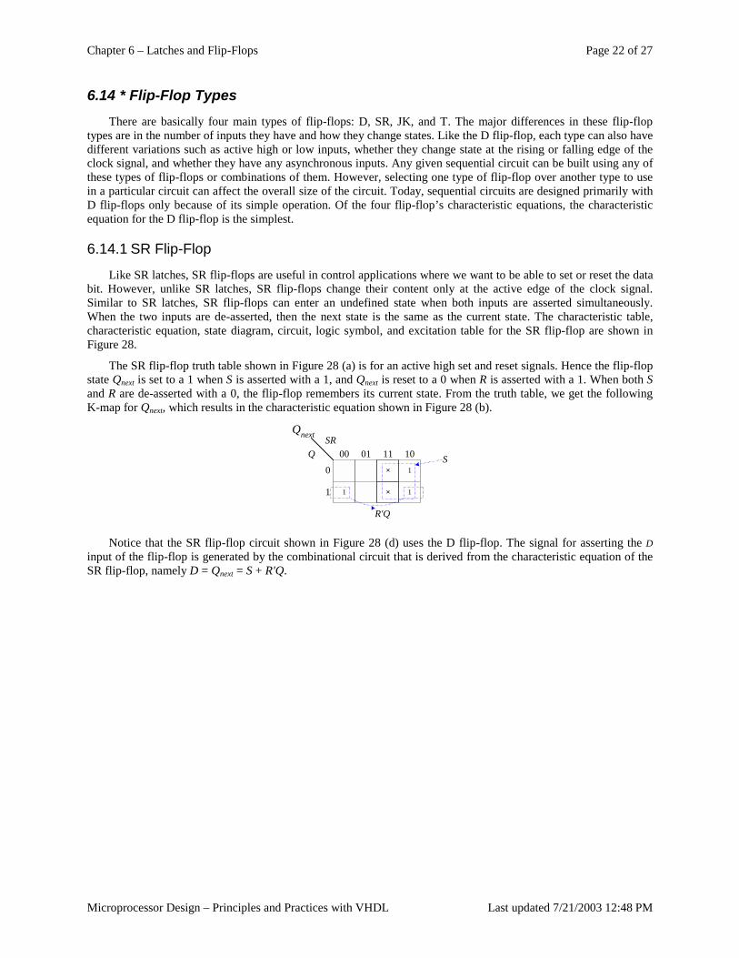
Chapter 6 – Latches and Flip-Flops Page 22 of 27
Microprocessor Design – Principles and Practices with VHDL Last updated 7/21/2003 12:48 PM
6.14 * Flip-Flop Types There are basically four main types of flip-flops: D, SR, JK, and T. The major differences in these flip-flop
types are in the number of inputs they have and how they change states. Like the D flip-flop, each type can also have different variations such as active high or low inputs, whether they change state at the rising or falling edge of the clock signal, and whether they have any asynchronous inputs. Any given sequential circuit can be built using any of these types of flip-flops or combinations of them. However, selecting one type of flip-flop over another type to use in a particular circuit can affect the overall size of the circuit. Today, sequential circuits are designed primarily with D flip-flops only because of its simple operation. Of the four flip-flop’s characteristic equations, the characteristic equation for the D flip-flop is the simplest.
6.14.1 SR Flip-Flop
Like SR latches, SR flip-flops are useful in control applications where we want to be able to set or reset the data bit. However, unlike SR latches, SR flip-flops change their content only at the active edge of the clock signal. Similar to SR latches, SR flip-flops can enter an undefined state when both inputs are asserted simultaneously. When the two inputs are de-asserted, then the next state is the same as the current state. The characteristic table, characteristic equation, state diagram, circuit, logic symbol, and excitation table for the SR flip-flop are shown in Figure 28.
The SR flip-flop truth table shown in Figure 28 (a) is for an active high set and reset signals. Hence the flip-flop state Qnext is set to a 1 when S is asserted with a 1, and Qnext is reset to a 0 when R is asserted with a 1. When both S and R are de-asserted with a 0, the flip-flop remembers its current state. From the truth table, we get the following K-map for Qnext, which results in the characteristic equation shown in Figure 28 (b).
SRQ
0
001
1 1
01 11 10
1
Qnext
×
×
S
R'Q
Notice that the SR flip-flop circuit shown in Figure 28 (d) uses the D flip-flop. The signal for asserting the D input of the flip-flop is generated by the combinational circuit that is derived from the characteristic equation of the SR flip-flop, namely D = Qnext = S + R'Q.
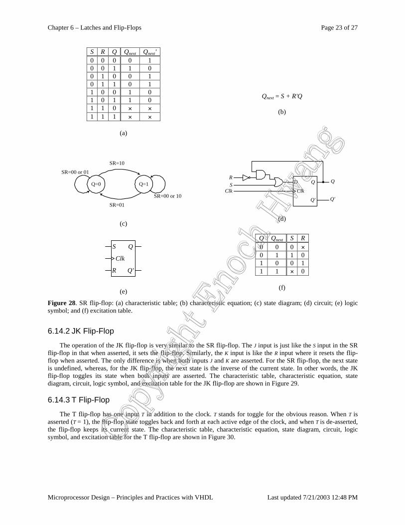
Chapter 6 – Latches and Flip-Flops Page 23 of 27
Microprocessor Design – Principles and Practices with VHDL Last updated 7/21/2003 12:48 PM
S R Q Qnext Qnext' 0 0 0 0 1 0 0 1 1 0 0 1 0 0 1 0 1 1 0 1 1 0 0 1 0 1 0 1 1 0 1 1 0 × × 1 1 1 × ×
(a)
Qnext = S + R'Q
(b)
Q=0 Q=1
SR=01
SR=10
SR=00 or 10
SR=00 or 01
(c)
Clk
D
Q'
QSR
Q
Q'Clk
(d)
Q
Q'
S
Clk
R
(e)
Q Qnext S R 0 0 0 × 0 1 1 0 1 0 0 1 1 1 × 0
(f)
Figure 28. SR flip-flop: (a) characteristic table; (b) characteristic equation; (c) state diagram; (d) circuit; (e) logic symbol; and (f) excitation table.
6.14.2 JK Flip-Flop
The operation of the JK flip-flop is very similar to the SR flip-flop. The J input is just like the S input in the SR flip-flop in that when asserted, it sets the flip-flop. Similarly, the K input is like the R input where it resets the flip-flop when asserted. The only difference is when both inputs J and K are asserted. For the SR flip-flop, the next state is undefined, whereas, for the JK flip-flop, the next state is the inverse of the current state. In other words, the JK flip-flop toggles its state when both inputs are asserted. The characteristic table, characteristic equation, state diagram, circuit, logic symbol, and excitation table for the JK flip-flop are shown in Figure 29.
6.14.3 T Flip-Flop
The T flip-flop has one input T in addition to the clock. T stands for toggle for the obvious reason. When T is asserted (T = 1), the flip-flop state toggles back and forth at each active edge of the clock, and when T is de-asserted, the flip-flop keeps its current state. The characteristic table, characteristic equation, state diagram, circuit, logic symbol, and excitation table for the T flip-flop are shown in Figure 30.
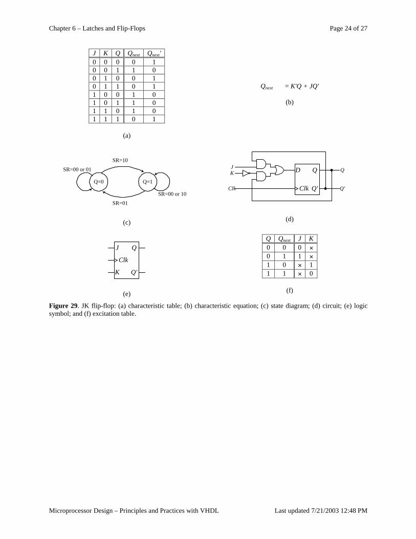
Chapter 6 – Latches and Flip-Flops Page 24 of 27
Microprocessor Design – Principles and Practices with VHDL Last updated 7/21/2003 12:48 PM
J K Q Qnext Qnext' 0 0 0 0 1 0 0 1 1 0 0 1 0 0 1 0 1 1 0 1 1 0 0 1 0 1 0 1 1 0 1 1 0 1 0 1 1 1 0 1
(a)
Qnext = K'Q + JQ'
(b)
Q=0 Q=1
SR=01
SR=10
SR=00 or 10
SR=00 or 01
(c)
K
Clk
Q
Q'
Q
Q'
D
Clk
J
(d)
Q
Q'
J
Clk
K
(e)
Q Qnext J K 0 0 0 × 0 1 1 × 1 0 × 1 1 1 × 0
(f)
Figure 29. JK flip-flop: (a) characteristic table; (b) characteristic equation; (c) state diagram; (d) circuit; (e) logic symbol; and (f) excitation table.
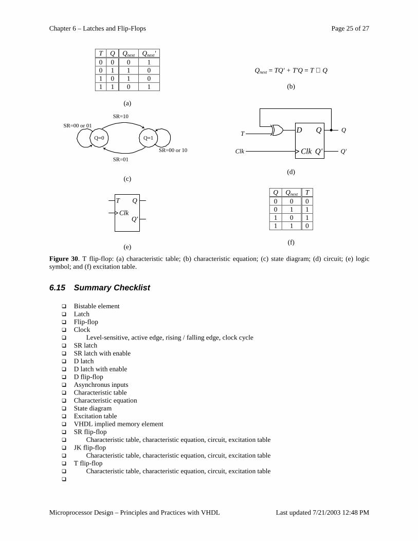
Chapter 6 – Latches and Flip-Flops Page 25 of 27
Microprocessor Design – Principles and Practices with VHDL Last updated 7/21/2003 12:48 PM
T Q Qnext Qnext' 0 0 0 1 0 1 1 0 1 0 1 0 1 1 0 1
(a)
Qnext = TQ' + T'Q = T ⊕ Q
(b)
Q=0 Q=1
SR=01
SR=10
SR=00 or 10
SR=00 or 01
(c)
Q
Q'
D
Clk
T
Clk
Q
Q'
(d)
Q
Q'
T
Clk
(e)
Q Qnext T 0 0 0 0 1 1 1 0 1 1 1 0
(f)
Figure 30. T flip-flop: (a) characteristic table; (b) characteristic equation; (c) state diagram; (d) circuit; (e) logic symbol; and (f) excitation table.
6.15 Summary Checklist � Bistable element � Latch � Flip-flop � Clock � Level-sensitive, active edge, rising / falling edge, clock cycle � SR latch � SR latch with enable � D latch � D latch with enable � D flip-flop � Asynchronus inputs � Characteristic table � Characteristic equation � State diagram � Excitation table � VHDL implied memory element � SR flip-flop � Characteristic table, characteristic equation, circuit, excitation table � JK flip-flop � Characteristic table, characteristic equation, circuit, excitation table � T flip-flop � Characteristic table, characteristic equation, circuit, excitation table �
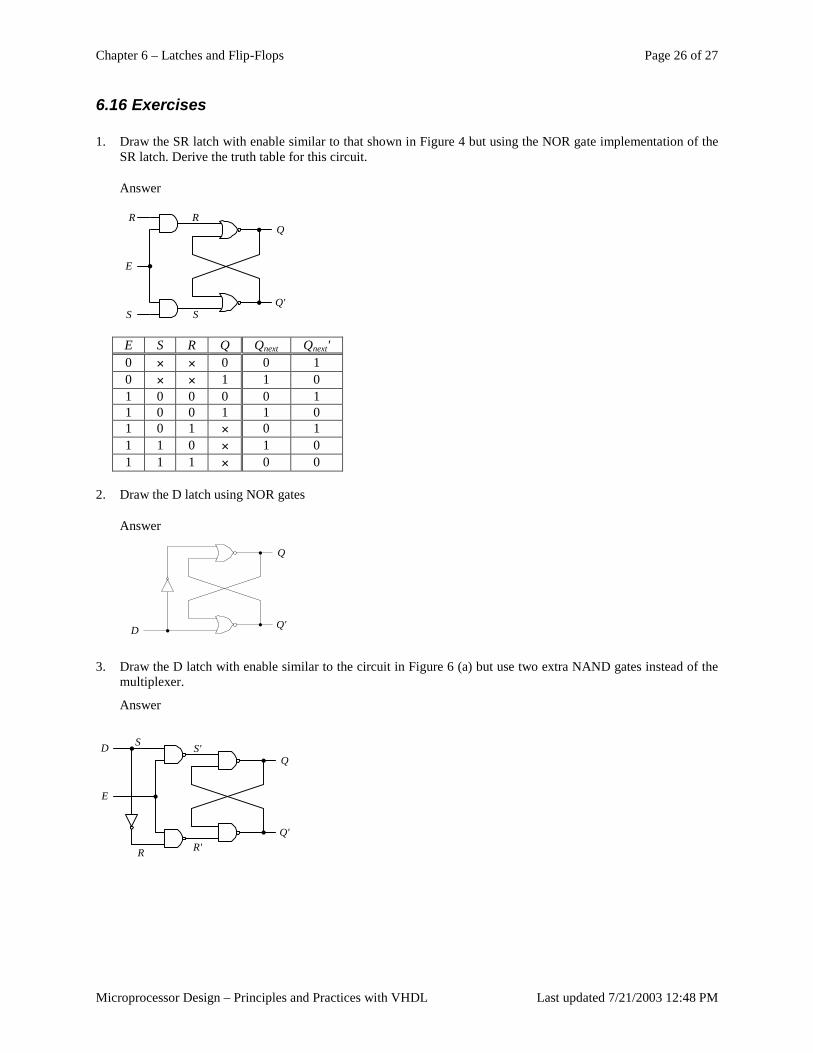
Chapter 6 – Latches and Flip-Flops Page 26 of 27
Microprocessor Design – Principles and Practices with VHDL Last updated 7/21/2003 12:48 PM
6.16 Exercises
1. Draw the SR latch with enable similar to that shown in Figure 4 but using the NOR gate implementation of the SR latch. Derive the truth table for this circuit.
Answer
R
E
S S
RQ
Q'
E S R Q Qnext Qnext' 0 × × 0 0 1 0 × × 1 1 0 1 0 0 0 0 1 1 0 0 1 1 0 1 0 1 × 0 1 1 1 0 × 1 0 1 1 1 × 0 0
2. Draw the D latch using NOR gates
Answer
D
Q
Q'
3. Draw the D latch with enable similar to the circuit in Figure 6 (a) but use two extra NAND gates instead of the multiplexer.
Answer
S
R
Q
Q'
E
R'
S'D

Chapter 6 – Latches and Flip-Flops Page 27 of 27
Microprocessor Design – Principles and Practices with VHDL Last updated 7/21/2003 12:48 PM
Index
A
Asynchronous inputs, 13
B
Bistable element, 2
C
Characteristic equation, 14 Characteristic table, 13
D
D flip-flop, 10 with enable, 12
D latch, 7 with enable, 7
E
Edge-triggered flip flop, 10 Excitation table, 14
F
Flip-flop, 2 D, 10 JK, 23 SR, 22 T, 23
G
Gated SR latch, 6
H
Hold time, 15
I Implied memory element, 16
J
JK flip-flop, 22, 23
L
Latch, 2 Level sensitive, 8 Loop back, 2
M
Metastable, 3
P
Positive edge-triggered flip flop, 10 Propagation delay, 15
S
Setup time, 15 SR flip-flop, 22 SR latch, 4
with enable, 6 State diagram, 14
T
T flip-flop, 22, 23 Timing issues, 15 Transparent latch, 7
V
VHDL, 16 Clock' EVENT, 18 Implied memory element, 16 WAIT, 18
VHDL code D flip-flop (behavioral), 18 D flip-flop (structural), 20 D flip-flop with asynchronous inputs, 21 D latch, 17
Chapter 7 − Sequential Circuits Page 1 of 44
Microprocessor Design: Principles and Practices with VHDL Last updated 3/9/2004 1:20 PM
Contents Sequential Circuits ........................................................................................................................................................ 2
7.1 Finite-State-Machine (FSM) Model.............................................................................................................. 3 7.2 Analysis of Sequential Circuits ..................................................................................................................... 4
7.2.1 Excitation Equation............................................................................................................................... 5 7.2.2 Next-state Equation............................................................................................................................... 6 7.2.3 Next-state Table .................................................................................................................................... 6 7.2.4 Output Equation .................................................................................................................................... 7 7.2.5 Output Table ......................................................................................................................................... 7 7.2.6 State Diagram........................................................................................................................................ 7 7.2.7 Example: Analysis of a Moore FSM..................................................................................................... 8 7.2.8 Example: Analysis of a Mealy FSM ................................................................................................... 10
7.3 Synthesis of Sequential Circuits.................................................................................................................. 12 7.3.1 State Diagram...................................................................................................................................... 12 7.3.2 Next-state Table .................................................................................................................................. 13 7.3.3 Implementation Table ......................................................................................................................... 15 7.3.4 Excitation Equation and Next-state Circuit ......................................................................................... 16 7.3.5 Output Table and Equation ................................................................................................................. 16 7.3.6 FSM Circuit......................................................................................................................................... 16 7.3.7 Examples: Synthesis of Moore FSMs ................................................................................................. 16 7.3.8 Example: Synthesis of a Mealy FSM .................................................................................................. 22
7.4 Unused State Encodings and the Encoding of States .................................................................................. 24 7.5 Example: Car Security System – Version 3 ................................................................................................ 26 7.6 VHDL for Sequential Circuits..................................................................................................................... 27 7.7 * Optimization for Sequential Circuits........................................................................................................ 33
7.7.1 State Reduction ................................................................................................................................... 33 7.7.2 State Encoding .................................................................................................................................... 34 7.7.3 Choice of Flip-Flops ........................................................................................................................... 34
7.8 Summary Checklist ..................................................................................................................................... 37 7.9 Problems ..................................................................................................................................................... 38 Index ....................................................................................................................................................................... 44
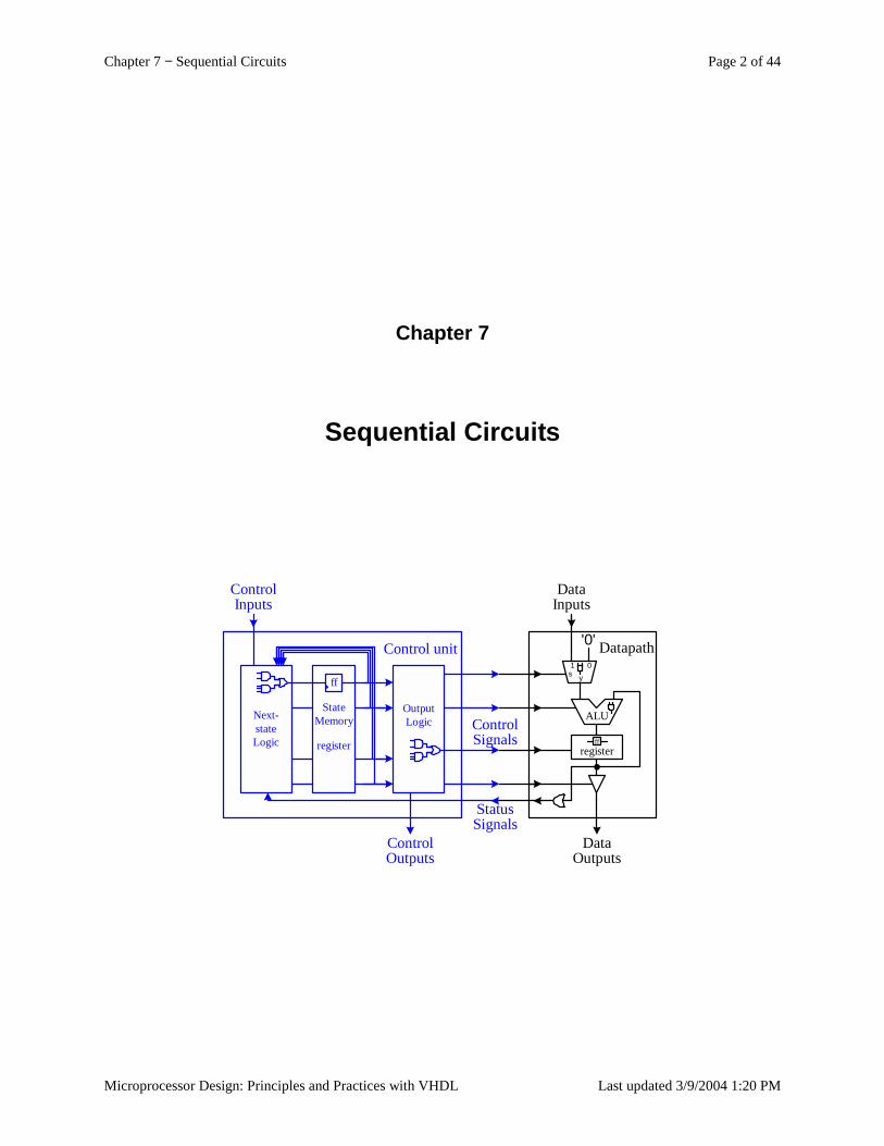
Chapter 7 − Sequential Circuits Page 2 of 44
Microprocessor Design: Principles and Practices with VHDL Last updated 3/9/2004 1:20 PM
Chapter 7
Sequential Circuits
ControlSignals
StatusSignals
01s y
'0'
DataInputs
DataOutputs
Datapath
ALU
registerff
OutputLogicNext-
stateLogic
ControlInputs
ControlOutputs
StateMemory
register
Control unit
ff
Chapter 7 − Sequential Circuits Page 3 of 44
Microprocessor Design: Principles and Practices with VHDL Last updated 3/9/2004 1:20 PM
The main difference between combinational circuits and sequential circuits is that combinational circuits are dependent only on current inputs, whereas in addition to the current inputs, sequential circuits are also dependent on the past inputs. This history of past inputs is remembered in the state memory, which is made up of one or more flip-flops. The contents of the state memory flip-flops at any instant of time represent the current state of the circuit. The circuit changes from one state to the next when the contents of the state memory change.
A sequential circuit operates by stepping through a sequence of states. Since the state memory is finite, therefore the total number of different possible states is also finite. For this reason, a sequential circuit is also referred to as a finite-state machine (FSM). Although there is only a finite number of different states, the FSM can go to any of these states as many times as necessary. Hence, the sequence of states that the FSM goes through can be infinitely long.
In addition to the state memory, a finite-state machine contains two combinational parts: the next-state logic and the output logic. Depending on the current state of the machine and the input signals, the next-state logic determines what the next state ought to be by changing the contents of the state memory. Given the current state and inputs, the next-state logic generates a new value that represents the next state of the machine. By changing the flip-flop input values, the next-state circuit causes (or excites) the state memory to change to a new state. The new value for the next state is written into the state memory at the next active edge of the clock.
The speed in which the finite-state machine sequences through the states is determined by the clock signal. At each active edge of the clock signal, the state memory register is enabled and the next-state value is stored into the flip-flops. The limiting factor for the clock speed is in the time that it takes to perform all the data operations assigned to a particular state. All data operations assigned to a state must finish their operations within one clock period so that the results can be written into the registers at the next active clock edge.
The second combinational part in a FSM is the output logic. The output logic generates the necessary output signals for the FSM. The output signals are dependent on the current state of the machine and may or may not be dependent on the input signals. Whether or not the output signal is dependent on the input gives rise to two types of FSMs. A Moore FSM is one where the output of the machine is dependent only on the current state and not on the input signals, whereas a Mealy FSM is one where the output is dependent on both the current state and the input signals.
7.1 Finite-State-Machine (FSM) Model Figure 7.1 (a) shows the general schematic for the Moore FSM where its outputs are dependent only on its
current state. Figure 7.1 (b) shows the general schematic for the Mealy FSM where its outputs are dependent on both the current state of the machine and also the inputs. In both figures, we see that the inputs to the next-state logic are the primary input signals and the current state of the machine. The next-state logic generates excitation values to change the contents of the state memory. The one difference in the two figures is that for the Moore FSM, the output logic only has the current state as its input, whereas, for the Mealy FSM, the output logic has both the current state and the input signals as its inputs.
Figure 7.2 (a) and (b) show a sample circuit of a Moore and Mealy FSM respectively. The two circuits are identical except for their outputs. For the Moore FSM, the output circuit is a 2-input AND gate that gets its input value from the outputs of the two D flip-flops. Remember that the state of the FSM is represented by the content of the state memory, which are the contents of the flip-flops. The content (or state) of a flip-flop is represented by the value at the Q (or Q' ) output. Hence, this circuit is only dependent on the current state of the machine.
For the Mealy FSM, the output circuit is a 3-input AND gate. In addition to getting its two inputs from the flip-flops, the third input to this AND gate is connected to the primary input C. With this one extra connection, this output circuit is dependent on both the current state and the input.
For both circuits, the state memory consists of two D flip-flops. Having two flip-flops, four different combinations of values can be represented. Hence, this finite-state machine can be in any one of four different states. The state that this FSM will go to next depends on the value at the D inputs of the flip-flops.
Every flip-flop in the state memory requires a combinational circuit to generate a next-state value for its input(s). Since we have two D flip-flops, each having one input (D), therefore, the next-state logic circuit consists of two combinational circuits; one for input D0 and one for D1. The inputs to these two combinational circuits are the
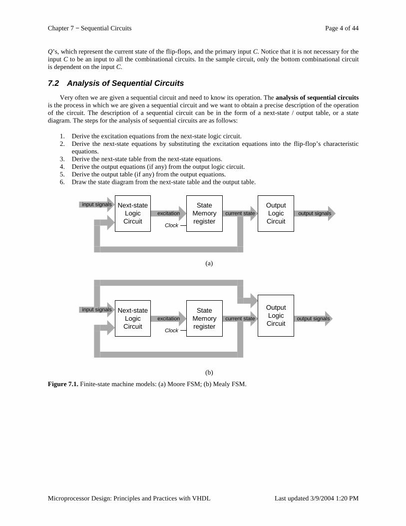
Chapter 7 − Sequential Circuits Page 4 of 44
Microprocessor Design: Principles and Practices with VHDL Last updated 3/9/2004 1:20 PM
Q’s, which represent the current state of the flip-flops, and the primary input C. Notice that it is not necessary for the input C to be an input to all the combinational circuits. In the sample circuit, only the bottom combinational circuit is dependent on the input C.
7.2 Analysis of Sequential Circuits Very often we are given a sequential circuit and need to know its operation. The analysis of sequential circuits
is the process in which we are given a sequential circuit and we want to obtain a precise description of the operation of the circuit. The description of a sequential circuit can be in the form of a next-state / output table, or a state diagram. The steps for the analysis of sequential circuits are as follows:
1. Derive the excitation equations from the next-state logic circuit. 2. Derive the next-state equations by substituting the excitation equations into the flip-flop’s characteristic
equations. 3. Derive the next-state table from the next-state equations. 4. Derive the output equations (if any) from the output logic circuit. 5. Derive the output table (if any) from the output equations. 6. Draw the state diagram from the next-state table and the output table.
Clock
current state output signalsexcitationinput signals State
Memoryregister
OutputLogicCircuit
Next-stateLogicCircuit
(a)
Clock
excitationinput signals
current state output signalsNext-state
LogicCircuit
StateMemoryregister
OutputLogicCircuit
(b)
Figure 7.1. Finite-state machine models: (a) Moore FSM; (b) Mealy FSM.
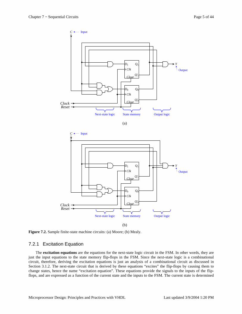
Chapter 7 − Sequential Circuits Page 5 of 44
Microprocessor Design: Principles and Practices with VHDL Last updated 3/9/2004 1:20 PM
C
Y
Input
Output
Next-state logic State memory Output logic
Clk
D0
Q'0
Q0
Clear
Clk
D1
Q'1
Q1
Clear
ClockReset
(a)
C
Y
Input
Output
Next-state logic State memory Output logic
Clk
D0
Q'0
Q0
Clear
Clk
D1
Q'1
Q1
Clear
ClockReset
(b)
Figure 7.2. Sample finite-state machine circuits: (a) Moore; (b) Mealy.
7.2.1 Excitation Equation
The excitation equations are the equations for the next-state logic circuit in the FSM. In other words, they are just the input equations to the state memory flip-flops in the FSM. Since the next-state logic is a combinational circuit, therefore, deriving the excitation equations is just an analysis of a combinational circuit as discussed in Section 3.1.2. The next-state circuit that is derived by these equations “excites” the flip-flops by causing them to change states, hence the name “excitation equation”. These equations provide the signals to the inputs of the flip-flops, and are expressed as a function of the current state and the inputs to the FSM. The current state is determined
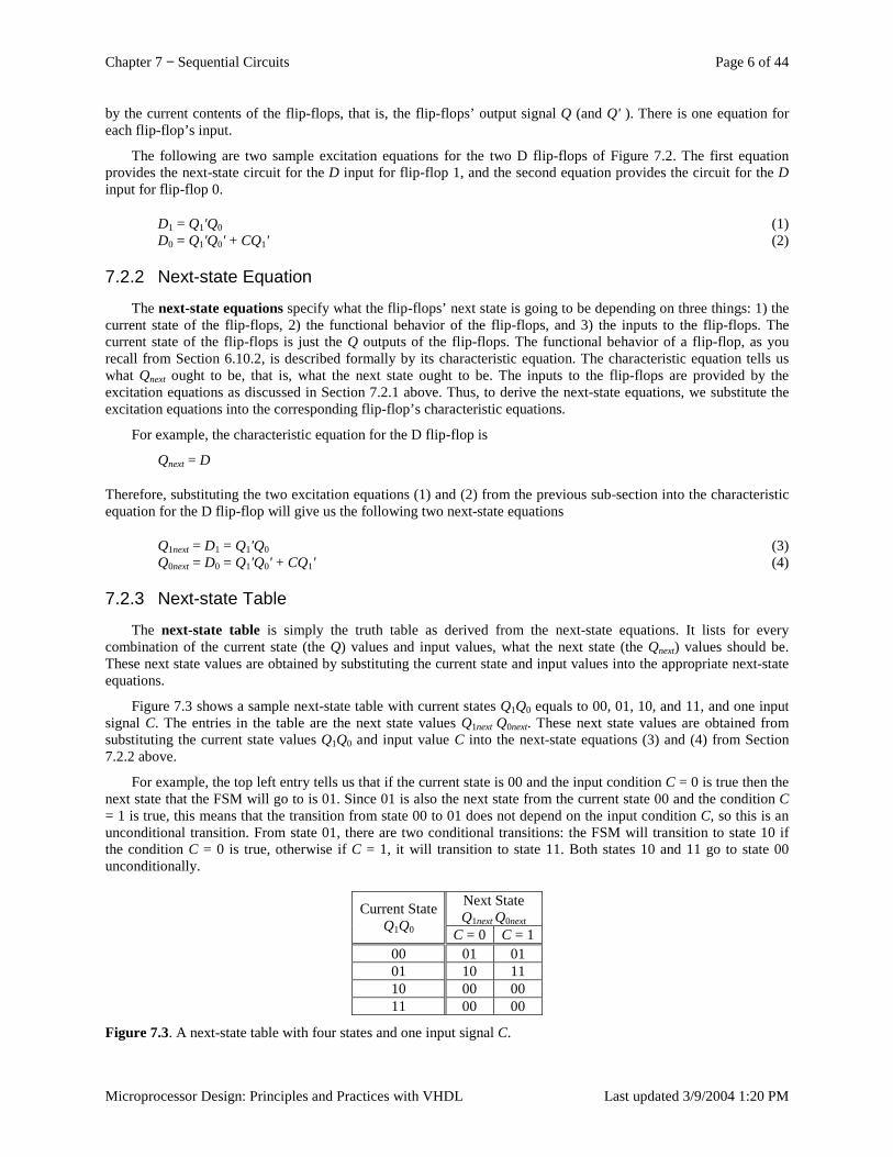
Chapter 7 − Sequential Circuits Page 6 of 44
Microprocessor Design: Principles and Practices with VHDL Last updated 3/9/2004 1:20 PM
by the current contents of the flip-flops, that is, the flip-flops’ output signal Q (and Q' ). There is one equation for each flip-flop’s input.
The following are two sample excitation equations for the two D flip-flops of Figure 7.2. The first equation provides the next-state circuit for the D input for flip-flop 1, and the second equation provides the circuit for the D input for flip-flop 0.
D1 = Q1'Q0 (1) D0 = Q1'Q0' + CQ1' (2)
7.2.2 Next-state Equation
The next-state equations specify what the flip-flops’ next state is going to be depending on three things: 1) the current state of the flip-flops, 2) the functional behavior of the flip-flops, and 3) the inputs to the flip-flops. The current state of the flip-flops is just the Q outputs of the flip-flops. The functional behavior of a flip-flop, as you recall from Section 6.10.2, is described formally by its characteristic equation. The characteristic equation tells us what Qnext ought to be, that is, what the next state ought to be. The inputs to the flip-flops are provided by the excitation equations as discussed in Section 7.2.1 above. Thus, to derive the next-state equations, we substitute the excitation equations into the corresponding flip-flop’s characteristic equations.
For example, the characteristic equation for the D flip-flop is
Qnext = D
Therefore, substituting the two excitation equations (1) and (2) from the previous sub-section into the characteristic equation for the D flip-flop will give us the following two next-state equations
Q1next = D1 = Q1'Q0 (3) Q0next = D0 = Q1'Q0' + CQ1' (4)
7.2.3 Next-state Table
The next-state table is simply the truth table as derived from the next-state equations. It lists for every combination of the current state (the Q) values and input values, what the next state (the Qnext) values should be. These next state values are obtained by substituting the current state and input values into the appropriate next-state equations.
Figure 7.3 shows a sample next-state table with current states Q1Q0 equals to 00, 01, 10, and 11, and one input signal C. The entries in the table are the next state values Q1next Q0next. These next state values are obtained from substituting the current state values Q1Q0 and input value C into the next-state equations (3) and (4) from Section 7.2.2 above.
For example, the top left entry tells us that if the current state is 00 and the input condition C = 0 is true then the next state that the FSM will go to is 01. Since 01 is also the next state from the current state 00 and the condition C = 1 is true, this means that the transition from state 00 to 01 does not depend on the input condition C, so this is an unconditional transition. From state 01, there are two conditional transitions: the FSM will transition to state 10 if the condition C = 0 is true, otherwise if C = 1, it will transition to state 11. Both states 10 and 11 go to state 00 unconditionally.
Next State Q1next Q0next
Current State Q1Q0 C = 0 C = 1
00 01 01 01 10 11 10 00 00 11 00 00
Figure 7.3. A next-state table with four states and one input signal C.
Chapter 7 − Sequential Circuits Page 7 of 44
Microprocessor Design: Principles and Practices with VHDL Last updated 3/9/2004 1:20 PM
7.2.4 Output Equation
The output equations are the equations derived from the combinational output logic circuit in the FSM. Depending on the type of FSM (Moore or Mealy), the output equations can be dependent on just the current state or on both the current state and the inputs.
For the Moore circuit of Figure 7.2 (a), the output equation is
Y = Q1'Q0 (5)
For the Mealy circuit of Figure 7.2 (b), the output equation is
Y = CQ1'Q0 (6)
A typical FSM will have many output signals, and so there will be one equation for every output signal.
7.2.5 Output Table
Like the next-state table, the output table is the truth table that is derived from the output equations. The output tables for the Moore and Mealy FSMs are slightly different from each other. For the Moore FSM, the output table lists for every combination of the current state what the output values should be. Whereas for the Mealy FSM, the output table lists for every combination of the current state and input values what the output values should be. These output values are obtained by substituting the current state and input values into the appropriate output equations.
Figure 7.4 (a) and (b) show sample output tables for the Moore and Mealy FSMs as derived from the output equations (5) and (6) respectively from Section 7.2.4 above. For the Moore FSM, the output signal Y is dependent only on the current state value Q1Q0, whereas, for the Mealy FSM, the output signal Y is dependent on both the current state and input C.
Current State Q1Q0
Output Y
00 0 01 1 10 0 11 0
(a)
Output Y Current State
Q1Q0 C = 0 C = 1 00 0 0 01 0 1 10 0 0 11 0 0
(b)
Figure 7.4. Output table: (a) for Moore FSM; (b) for Mealy FSM.
7.2.6 State Diagram
A state diagram is a graph with nodes and directed edges connecting the nodes. The state diagram graphically portraits the operation of the FSM. There is one node for every state of the FSM and these nodes are labeled with the state in which they represent. For every state transition of the FSM there is a directed edge connecting two nodes. The directed edge originates from the node that represents the current state that the FSM is transitioning from, and goes to the node that represents the next state that the FSM is transitioning to. Edges may or may not have labels on them. Edges for unconditional transitions from one state to another will not have a label. In this case, only one edge can originate from that node. Conditional transitions from a state will have two outgoing edges. The two edges from this state have the corresponding input signal conditions labeled on them – one edge with the label for when the condition is true and the other edge with the label for when the condition is false.
Figure 7.5 (a) shows a small state diagram with four states, 00, 01, 10, and 11, and one input signal C. This state diagram is derived from the next-state table shown in Figure 7.3 and the output table from Figure 7.4 (a). There are three unconditional transitions, 00 to 01, 10 to 00, and 11 to 00, and one conditional transition from 01 to 10 or 11. For the conditional transition from 01, if the condition C = 0 is true then the transition from 01 to 10 is made. Otherwise, if the condition C = 0 is false, that is C = 1 is true, then the transition from 01 to 11 is made.
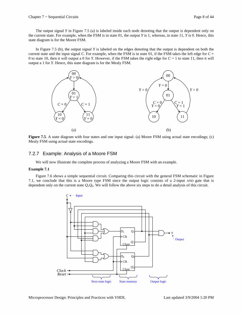
Chapter 7 − Sequential Circuits Page 8 of 44
Microprocessor Design: Principles and Practices with VHDL Last updated 3/9/2004 1:20 PM
The output signal Y in Figure 7.5 (a) is labeled inside each node denoting that the output is dependent only on the current state. For example, when the FSM is in state 01, the output Y is 1, whereas, in state 11, Y is 0. Hence, this state diagram is for the Moore FSM.
In Figure 7.5 (b), the output signal Y is labeled on the edges denoting that the output is dependent on both the current state and the input signal C. For example, when the FSM is in state 01, if the FSM takes the left edge for C = 0 to state 10, then it will output a 0 for Y. However, if the FSM takes the right edge for C = 1 to state 11, then it will output a 1 for Y. Hence, this state diagram is for the Mealy FSM.
C = 0 C = 1
00Y = 0
01Y = 1
10Y = 0
11Y = 0
(a)
C = 0 C = 1
00
01
10 11
Y = 0Y = 0 Y = 0
Y = 0 Y = 1
(b)
Figure 7.5. A state diagram with four states and one input signal: (a) Moore FSM using actual state encodings; (c) Mealy FSM using actual state encodings.
7.2.7 Example: Analysis of a Moore FSM
We will now illustrate the complete process of analyzing a Moore FSM with an example.
Example 7.1
Figure 7.6 shows a simple sequential circuit. Comparing this circuit with the general FSM schematic in Figure 7.1, we conclude that this is a Moore type FSM since the output logic consists of a 2-input AND gate that is dependent only on the current state Q1Q0. We will follow the above six steps to do a detail analysis of this circuit.
C
Y
Input
Output
Next-state logic State memory Output logic
Clk
D0
Q'0
Q0
Clear
Clk
D1
Q'1
Q1
Clear
ClockReset

Chapter 7 − Sequential Circuits Page 9 of 44
Microprocessor Design: Principles and Practices with VHDL Last updated 3/9/2004 1:20 PM
Figure 7.6. A simple Moore finite-state machine.
Step 1 is to derive the excitation equations, which are the equations for the next-state logic circuit. These equations are dependent on the current state of the flip-flops Q1 and Q0, and the input C. One equation is needed for every data input of all the flip-flops in the state memory. Our sample circuit has two flip-flops having the two inputs D1, and D0, so we get the two excitation equations as shown in Figure 7.7 (a). These two equations are obtained from analyzing the two combinational circuits that provide the inputs D1 and D0 to the two flip-flops. For this particular example, both of these combinational circuits are simple two level sum-of-products circuits.
Step 2 is to derive the next-state equations. These equations tell us what the next-state is going to be given the current state of the state memory, the functional behavior of the flip-flops and the inputs to the flip-flops. One equation is needed for every flip-flop. The functional behavior of the flip-flop is described by its characteristic equation, which for the D flip-flop, is Qnext = D. The inputs to the flip-flops are just the excitation equations derived from step 1. Hence, we simply substitute the excitation equation into the characteristic equation for each flip-flop to obtain the next-state equation for that flip-flop. With two flip-flops in the example, we get two next-state equations, one for Q1next and one for Q0next. Figure 7.7 (b) shows these two next-state equations.
Step 3 is to derive the next-state table. The next-state values in the table are obtained by substituting every combination of current state and input values into the next-state equations obtained in step 2. In our example, there are two flip-flops, Q1 and Q0, and input C. Hence the table will have eight next-state entries. There are two bits for every entry – the first bit for Q1next, and the second for Q0next.
For example, to find the Q1next value for the current state Q1Q0 = 00 and C = 1 (the blue entry), we substitute the values Q1 = 0, Q0 = 0 and C = 1 into the equation Q1next = C'Q1 + Q1Q0' + CQ1'Q0 = (1' • 0) + (0 • 0' ) + (1 • 0' • 0) to get the value 0. Similarly, we get Q0next by substituting the same values for Q1, Q0, and C into the equation Q0next = C'Q0 + CQ0' = (1' • 0) + (1 • 0' ) to get the value 1. The resulting next-state table for our example is shown in Figure 7.7 (c).
Step 4 is to derive the output equations from the output logic circuit. One output equation is needed for every output signal. For our example, there is only one output signal Y that is dependent only on the current state of the machine. The output equation for Y as derived from the sample circuit diagram is shown in Figure 7.7 (d).
Step 5 is to derive the output table. Just like the next-state table, the output table is obtained by substituting all possible combinations of the current state values into the output equation(s) for the Moore FSM. The output table for our Moore FSM example is shown in Figure 7.7 (e).
Step 6 is to draw the state diagram, which is derived directly from the next-state and output tables. Every state in the next-state table will have a corresponding node labeled with the state encoding in the state diagram. For every next state entry in the next-state table, there will be a corresponding directed edge. This edge originates from the node labeled with the current state and ends at the node labeled with the next state entry. The edge is labeled with the corresponding input conditions.
For example, in the next-state table, when the current state Q1Q0 is 00, the next state Q1next Q0next is 01 for the input C = 1. Hence, in the state diagram, there is a directed edge from node 00 to node 01 with the label C = 1. For a Moore FSM, the outputs are dependent only on the current state, thus the output values from the output table are included inside each node of the state diagram. The complete state diagram for our example is shown in Figure 7.7 (f).
A sample timing diagram for the execution of the circuit is shown in Figure 7.7 (g). The two D flip-flops used in the circuit are positive edge-triggered flip-flops so they change their states at each rising clock edge. Initially, we assume that these two flip-flops are both in state 0. The first rising clock edge is at time t0. Normally, the flip-flops will change state at this time, however, since C is a 0, the flip-flops’ values remain constant. At time t1, C changes to a 1, so that at the next rising clock edge at time t2, the flip-flop values Q1Q0 changes to 01. At the next two rising clock edges, t3 and t4, the value for Q1Q0 changes to 10, then 11 respectively. At time t4 when Q1Q0 = 11, the output Y also changes to a 1 since Y = Q1 • Q0. At time t5, input C drops back down to a 0 but the output Y remains at a 1. Q1Q0 remains the same at 11 through the next rising clock edge since C is 0. At time t6, C changes back to a 1 and so at the next rising clock edge at time t7, Q1Q0 increments again to 00 and the cycle repeats.
When C = 1, the FSM cycles through the four states in order repeatedly. When C = 0, the FSM stops at the current state until C is asserted again. If we interpret the four state encodings as a decimal number, then we can
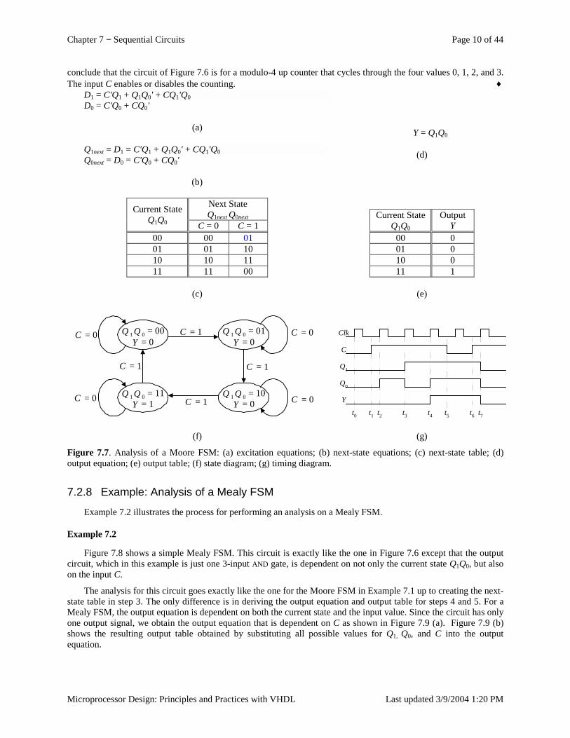
Chapter 7 − Sequential Circuits Page 10 of 44
Microprocessor Design: Principles and Practices with VHDL Last updated 3/9/2004 1:20 PM
conclude that the circuit of Figure 7.6 is for a modulo-4 up counter that cycles through the four values 0, 1, 2, and 3. The input C enables or disables the counting. ♦
Figure 7.7. Analysis of a Moore FSM: (a) excitation equations; (b) next-state equations; (c) next-state table; (d) output equation; (e) output table; (f) state diagram; (g) timing diagram.
7.2.8 Example: Analysis of a Mealy FSM
Example 7.2 illustrates the process for performing an analysis on a Mealy FSM.
Example 7.2
Figure 7.8 shows a simple Mealy FSM. This circuit is exactly like the one in Figure 7.6 except that the output circuit, which in this example is just one 3-input AND gate, is dependent on not only the current state Q1Q0, but also on the input C.
The analysis for this circuit goes exactly like the one for the Moore FSM in Example 7.1 up to creating the next-state table in step 3. The only difference is in deriving the output equation and output table for steps 4 and 5. For a Mealy FSM, the output equation is dependent on both the current state and the input value. Since the circuit has only one output signal, we obtain the output equation that is dependent on C as shown in Figure 7.9 (a). Figure 7.9 (b) shows the resulting output table obtained by substituting all possible values for Q1, Q0, and C into the output equation.
D1 = C'Q1 + Q1Q0' + CQ1'Q0 D0 = C'Q0 + CQ0'
(a)
Q1next = D1 = C'Q1 + Q1Q0' + CQ1'Q0 Q0next = D0 = C'Q0 + CQ0'
(b)
Y = Q1Q0
(d)
Next State Q1next Q0next
Current State Q1Q0 C = 0 C = 1
00 00 01 01 01 10 10 10 11 11 11 00
(c)
Current State Q1Q0
Output Y
00 0 01 0 10 0 11 1
(e)
Q 1 Q 0 = 10Q 1 Q 0 = 11
Q 1 Q 0 = 00 Q 1 Q 0 = 01Y = 0
Y = 1
Y = 0
Y = 0
C = 0
C = 0C = 1
C = 1
C = 1C = 0
C = 0
C = 1
(f)
C
Q1
Y
t1 t4
Clk
Q0
t5 t7t0 t2 t3 t6
(g)
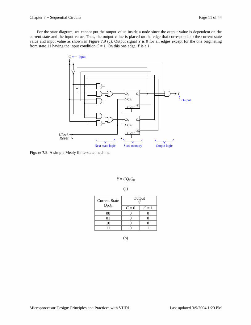
Chapter 7 − Sequential Circuits Page 11 of 44
Microprocessor Design: Principles and Practices with VHDL Last updated 3/9/2004 1:20 PM
For the state diagram, we cannot put the output value inside a node since the output value is dependent on the current state and the input value. Thus, the output value is placed on the edge that corresponds to the current state value and input value as shown in Figure 7.9 (c). Output signal Y is 0 for all edges except for the one originating from state 11 having the input condition C = 1. On this one edge, Y is a 1.
ClockReset
C
Y
Input
Output
Next-state logic State memory Output logic
Clk
D0
Q'0
Q0
Clear
Clk
D1
Q'1
Q1
Clear
Figure 7.8. A simple Mealy finite-state machine.
Y = CQ1Q0
(a)
Output Y Current State
Q1Q0 C = 0 C = 1 00 0 0 01 0 0 10 0 0 11 0 1
(b)
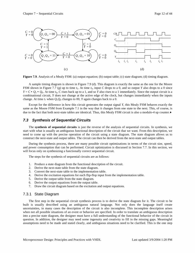
Chapter 7 − Sequential Circuits Page 12 of 44
Microprocessor Design: Principles and Practices with VHDL Last updated 3/9/2004 1:20 PM
Q 1 Q 0 = 10Q 1 Q 0 = 11
Q 1 Q 0 = 00 Q 1 Q 0 = 01Y = 0
Y = 1
Y = 0
Y = 0
C = 0
C = 0C = 1
C = 1
C = 1C = 0
C = 0
C = 1
Y = 0Y = 0Y = 0
Y = 0
(c)
C
Q1
Y
t1 t4
Clk
Q0
t5 t7t0 t2 t3 t6
(d)
Figure 7.9. Analysis of a Mealy FSM: (a) output equation; (b) output table; (c) state diagram; (d) timing diagram.
A sample timing diagram is shown in Figure 7.9 (d). This diagram is exactly the same as the one for the Moore FSM shown in Figure 7.7 (g) up to time t5. At time t5, input C drops to a 0, and so output Y also drops to a 0 since Y = C • Q1 • Q0. At time t6, C rises back up to a 1, and so Y also rises to a 1 immediately. Since the output circuit is a combinational circuit, Y does not change at the active edge of the clock, but changes immediately when the inputs change. At time t7 when Q1Q0 changes to 00, Y again changes back to a 0.
Except for the difference in how this circuit generates the output signal Y, this Mealy FSM behaves exactly the same as the Moore FSM from Example 7.1 in the way that it changes from one state to the next. This, of course, is due to the fact that both next-state tables are identical. Thus, this Mealy FSM circuit is also a modulo-4 up counter. ♦
7.3 Synthesis of Sequential Circuits The synthesis of sequential circuits is just the reverse of the analysis of sequential circuits. In synthesis, we
start with what is usually an ambiguous functional description of the circuit that we want. From this description, we need to come up with the precise operation of the circuit using a state diagram. The state diagram allows us to construct the next-state and output tables. The circuit can then be derived from the next-state and output tables.
During the synthesis process, there are many possible circuit optimizations in terms of the circuit size, speed, and power consumption that can be performed. Circuit optimization is discussed in Section 7.7. In this section, we will focus only on synthesizing a functionally correct sequential circuit.
The steps for the synthesis of sequential circuits are as follows:
1. Produce a state diagram from the functional description of the circuit. 2. Derive the next-state table from the state diagram. 3. Convert the next-state table to the implementation table. 4. Derive the excitation equations for each flip-flop input from the implementation table. 5. Derive the output table from the state diagram. 6. Derive the output equations from the output table. 7. Draw the circuit diagram based on the excitation and output equations.
7.3.1 State Diagram
The first step in the sequential circuit synthesis process is to derive the state diagram for it. The circuit to be built is usually described using an ambiguous natural language. Not only does the language itself create uncertainties, in many cases the description of the circuit is also incomplete. This incomplete description arises when not all possible situations of an event or behavior are specified. In order to translate an ambiguous description into a precise state diagram, the designer must have a full understanding of the functional behavior of the circuit in question. In addition, the designer may need some ingenuity and creativity to fill in the missing gaps. Meaningful assumptions need to be made and stated clearly, and ambiguous situations need to be clarified. This is the one step

Chapter 7 − Sequential Circuits Page 13 of 44
Microprocessor Design: Principles and Practices with VHDL Last updated 3/9/2004 1:20 PM
in the design process where there is no clear-cut answer for it. In this step, we rely on the knowledge and expertise of the designer to come up with a correct and meaningful state diagram.
Instead of using a natural language to describe the circuit, a more precise method can be used. Other ways to describe a circuit more precisely include the use of a hardware description language such as VHDL, a state action table, or an ASM chart. The use of the ASM chart and the state action table are described in Chapter 10. In this section, we will discuss the construction of the state diagram.
Before the state diagram can be drawn, we need to first determine from the circuit description the number of states needed, what are the input signals, and what are the output signals. Usually, one action is assigned to one state, unless the actions can be performed in parallel.
The state diagram is a deterministic directed graph. There is one node for every state. Figure 7.10 (a) shows a simple state diagram with four states. Initially, the nodes are given logical state names such as s0, s1, s2, and s3. These state names must be translated to their actual encoding in a subsequent step.
The nodes in the state diagram are connected with directed edges. An edge connects from the current state that the FSM is in, and connects to the next state that the FSM will go to. The edges may or may not have labels on them. The edge labels are conditions of the input signals for when an edge is to be taken. Recall that the next state of a FSM is dependent on the current state and the inputs. All outgoing edges from a state must be deterministic. In other words, no two outgoing edges from the same state can have the same condition. Alternatively, all possible input conditions must be labeled on the outgoing edges from any one state. If an edge is not labeled, or if not all possible input conditions are labeled on the outgoing edges from the same state, then these missing conditions are don’t care conditions.
In Figure 7.10 (a), there are two conditional edges labeled with the input B and B'. The remaining edges without a label are unconditional edges. An edge having a condition is taken only if the condition on it is true. From state s0, if the input B is a 0, then the edge labeled B' is taken, and the next state will be s1. Otherwise, if the input B is a 1, then the edge labeled B is taken, and the next state will be s2. An edge without a label is an unconditional edge, and so it is always taken, regardless of the input values. The next state from either s1 or s2 is always s3, regardless of the value of B.
There are two types of output signals: state only dependent, and state and input dependent. These, of course, correspond to the Moore and Mealy FSMs respectively. Output signals that are dependent only on the current state are labeled inside each node. The state diagram in Figure 7.10 (a) has one output signal Y that is dependent only on the current state. In states s0 and s1, Y is assigned the value 0. In states s2 and s3, Y is assigned a 1. Output signals that are dependent on both the current state and the input signal are labeled on the edges.
7.3.2 Next-state Table
Given a precise state diagram, it is easy to derive both the next-state and output tables from it. Since the next-state and output tables, and the state diagram portrait the same information but depicted in a different format, therefore, it requires only a straightforward translation from one to the other.
Figure 7.10 (b) shows the next-state table for the state diagram in (a). The row labels are the current state and the column labels are the input conditions. The table entries are the next states. Translating directly from the state diagram, from current state s0, if B is a 0, then the next state is s1. Correspondingly, in the next-state table, the entry for the intersection of the current state s0 and input B = 0 is s1.
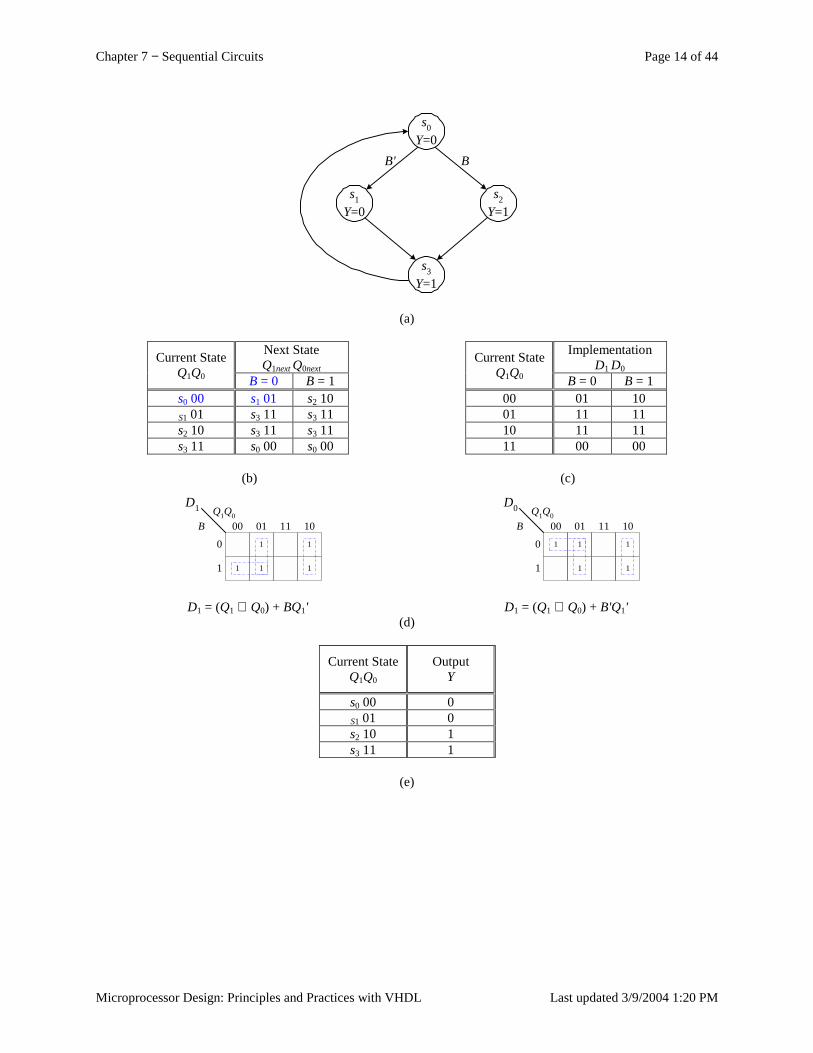
Chapter 7 − Sequential Circuits Page 14 of 44
Microprocessor Design: Principles and Practices with VHDL Last updated 3/9/2004 1:20 PM
B'
s1Y=0
s0Y=0
s2Y=1
s3Y=1
B
(a)
Next State Q1next Q0next
Current State Q1Q0 B = 0 B = 1 s0 00 s1 01 s2 10 S1 01 s3 11 s3 11 s2 10 s3 11 s3 11 s3 11 s0 00 s0 00
(b)
Implementation D1 D0
Current State Q1Q0 B = 0 B = 1
00 01 10 01 11 11 10 11 11 11 00 00
(c)
Q1Q0B
0 1
001
1 1 1
01 11 10
1
D1
D1 = (Q1 ⊕ Q0) + BQ1'
Q1Q0B
0 1 1
001
1 1
01 11 10
1
D0
D1 = (Q1 ⊕ Q0) + B'Q1' (d)
Current State Q1Q0
Output Y
s0 00 0 S1 01 0 s2 10 1 s3 11 1
(e)
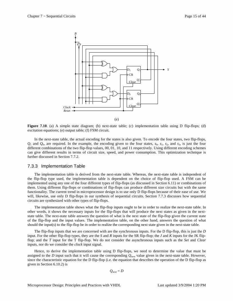
Chapter 7 − Sequential Circuits Page 15 of 44
Microprocessor Design: Principles and Practices with VHDL Last updated 3/9/2004 1:20 PM
B
Clock
Y
Reset
Clk
D0
Q'0
Q0
Clear
Clk
D1
Q'1
Q1
Clear
(e)
Figure 7.10. (a) A simple state diagram; (b) next-state table; (c) implementation table using D flip-flops; (d) excitation equations; (e) output table; (f) FSM circuit.
In the next-state table, the actual encoding for the states is also given. To encode the four states, two flip-flops, Q1 and Q0, are required. In the example, the encoding given to the four states, s0, s1, s2, and s3, is just the four different combinations of the two flip-flop values, 00, 01, 10, and 11 respectively. Using different encoding schemes can give different results in terms of circuit size, speed, and power consumption. This optimization technique is further discussed in Section 7.7.2.
7.3.3 Implementation Table
The implementation table is derived from the next-state table. Whereas, the next-state table is independent of the flip-flop type used, the implementation table is dependent on the choice of flip-flop used. A FSM can be implemented using any one of the four different types of flip-flops (as discussed in Section 6.11) or combinations of them. Using different flip-flops or combinations of flip-flops can produce different size circuits but with the same functionality. The current trend in microprocessor design is to use only D flip-flops because of their ease of use. We will, likewise, use only D flip-flops in our synthesis of sequential circuits. Section 7.7.3 discusses how sequential circuits are synthesized with other types of flip-flops.
The implementation table shows what the flip-flop inputs ought to be in order to realize the next-state table. In other words, it shows the necessary inputs for the flip-flops that will produce the next states as given in the next-state table. The next-state table answers the question of what is the next state of the flip-flop given the current state of the flip-flop and the input values. The implementation table, on the other hand, answers the question of what should the input(s) to the flip-flop be in order to realize the corresponding next state given in the next-state table.
The flip-flop inputs that we are concerned with are the synchronous inputs. For the D flip-flop, this is just the D input. For the other flip-flop types, they are the S and R inputs for the SR flip-flop; the J and K inputs for the JK flip-flop; and the T input for the T flip-flop. We do not consider the asynchronous inputs such as the Set and Clear inputs, nor do we consider the clock input signal.
Hence, to derive the implementation table using D flip-flops, we need to determine the value that must be assigned to the D input such that it will cause the corresponding Qnext value given in the next-state table. However, since the characteristic equation for the D flip-flop (i.e. the equation that describes the operation of the D flip-flop as given in Section 6.10.2) is
Qnext = D

Chapter 7 − Sequential Circuits Page 16 of 44
Microprocessor Design: Principles and Practices with VHDL Last updated 3/9/2004 1:20 PM
therefore, the values for Qnext and D are the same.
Thus, the entries in the implementation table using D flip-flops are identical to the entries in the next-state table. The only difference between the two tables is in the meaning of the entries. In the next-state table as shown in Figure 7.10 (b), the label for the entries is Qnext for the next state to go to, whereas, in the implementation table as shown in Figure 7.10 (c), the label for the entries is D for the input to the D flip-flop. Since there are two flip-flops, Q1 and Q0, each having one input D, hence the implementation table has the two corresponding inputs D1 and D0. The leftmost bit is for flip-flop 1 and the rightmost bit is for flip-flop 0. Note that if one of the other types of flip-flops is used, the two tables will not be the same as discuss in Section 7.7.3.
7.3.4 Excitation Equation and Next-state Circuit
Recall that the excitation equations are the equations for the flip-flop’s synchronous inputs. There is one excitation equation for every input of every flip-flop. Remember that we do not include the asynchronous inputs and the clock input. The excitation equations are dependent on the current state encodings, i.e., the contents of the flip-flops, and the input signals.
The excitation equations are what caused the flip-flops in the state memory to change state. The circuit that is derived from these equations is the next-state circuit in the FSM. The next-state circuit is a combinational circuit, and so deriving this circuit is the same as synthesizing any other combinational circuit as discussed in Section 3.2.
The implementation table derived from the previous step is just the truth table for the excitation equations. For our example, we need two equations for the two flip-flop inputs, D1 and D0. In the example, extracting the leftmost bit in every entry in the implementation table will give us the truth table for D1, and therefore, the excitation equation for D1. Similarly, extracting the rightmost bit in every entry in the implementation table will give us the truth table and excitation equation for D0. The truth table, in the form of a K-map, and the excitation equations for D1 and D0 are given in Figure 7.10 (d).
7.3.5 Output Table and Equation
The output table and output equations are used to derive the output circuit in the FSM. The output table can be obtained directly from the state diagram. In the state diagram of Figure 7.10 (a), the output signal Y is dependent only on the state. In states s0 and s1, Y is assigned the value 0. In states s2 and s3, Y is assigned a 1. The resulting output table is shown in Figure 7.10 (e).
The output equation as derived from the output truth table is simply
Y = Q1
7.3.6 FSM Circuit
Using Figure 7.2 (a) as a template, our FSM circuit requires two D flip-flops for its state memory. The number of flip-flops to use was determined when the states were encoded. The type of flip-flops to use was determined when deriving the implementation table. The next-state circuit is drawn from the excitation equations, while the output circuit is drawn from the output equation. Connecting these three parts, state memory, next-state circuit, and output circuit, together produces the final FSM circuit shown in Figure 7.10 (e).
7.3.7 Examples: Synthesis of Moore FSMs
We will now illustrate the synthesis of Moore FSMs with two examples. Example 7.3 illustrates the synthesis of a simple Moore FSM. Example 7.4 illustrates the synthesis of a Moore FSM that is more typical of what the control unit of a microprocessor is like.
Example 7.3
For our first synthesis example, we will design a modulo-6 up counter using D flip-flops having a count enable input C, and an output signal Y that is asserted when the count is equal to five. The count is to be represented directly by the contents of the flip-flops.
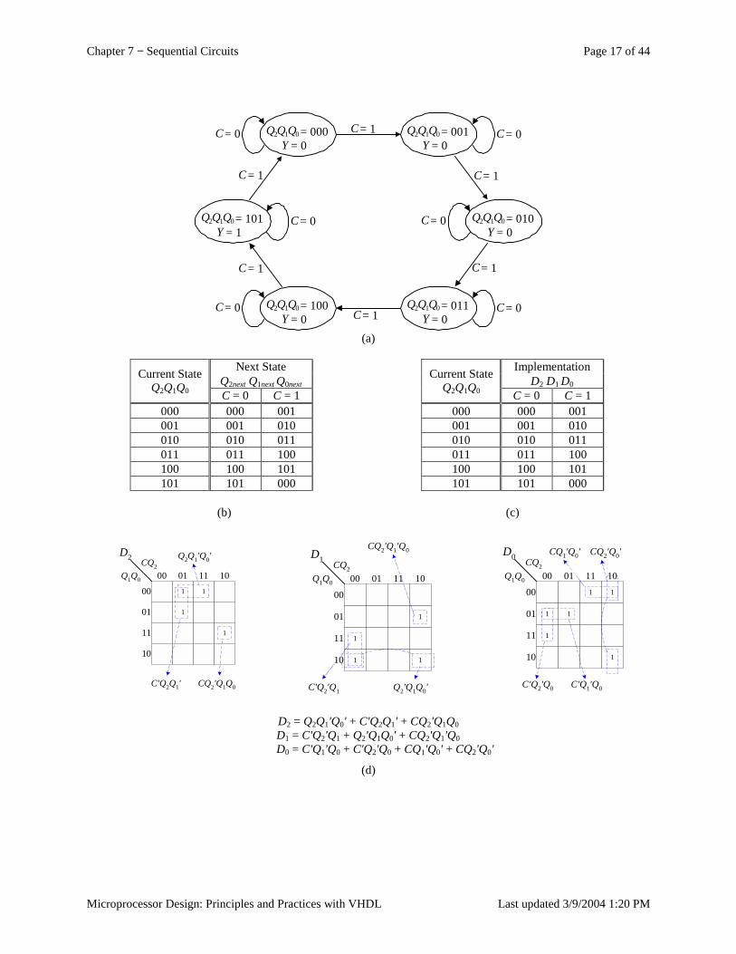
Chapter 7 − Sequential Circuits Page 17 of 44
Microprocessor Design: Principles and Practices with VHDL Last updated 3/9/2004 1:20 PM
CQ2Q1Q0
00 1
001
1
1
01 11 10
01
11
10
D2 Q2Q1'Q0'
C'Q2Q1' CQ2'Q1Q0
CQ2Q1Q0
00
00
1
1
1 1
01 11 10
01
11
10
D1
C'Q2'Q1 Q2'Q1Q0'
CQ2'Q1'Q0
CQ2Q1Q0
00
001 1
1 1
1
1
01 11 10
01
11
10
D0
C'Q1'Q0
CQ2'Q0'CQ1'Q0'
C'Q2'Q0
D2 = Q2Q1'Q0' + C'Q2Q1' + CQ2'Q1Q0 D1 = C'Q2'Q1 + Q2'Q1Q0' + CQ2'Q1'Q0 D0 = C'Q1'Q0 + C'Q2'Q0 + CQ1'Q0' + CQ2'Q0'
(d)
C= 0 = 000Q1Q0Q2
Y = 0
C= 0 = 010Q1Q0Q2
Y = 0
C= 0 = 100Q1Q0Q2
Y = 0
C= 1
C= 0= 001Q1Q0Q2
Y = 0
C= 0= 011Q1Q0Q2
Y = 0
C= 1
C= 1
C= 1
C= 1
C= 1
C= 0= 101Q1Q0Q2
Y = 1
(a)
Next State
Q2next Q1next Q0next Current State
Q2Q1Q0 C = 0 C = 1 000 000 001 001 001 010 010 010 011 011 011 100 100 100 101 101 101 000
(b)
Implementation D2 D1 D0
Current State Q2Q1Q0 C = 0 C = 1
000 000 001 001 001 010 010 010 011 011 011 100 100 100 101 101 101 000
(c)
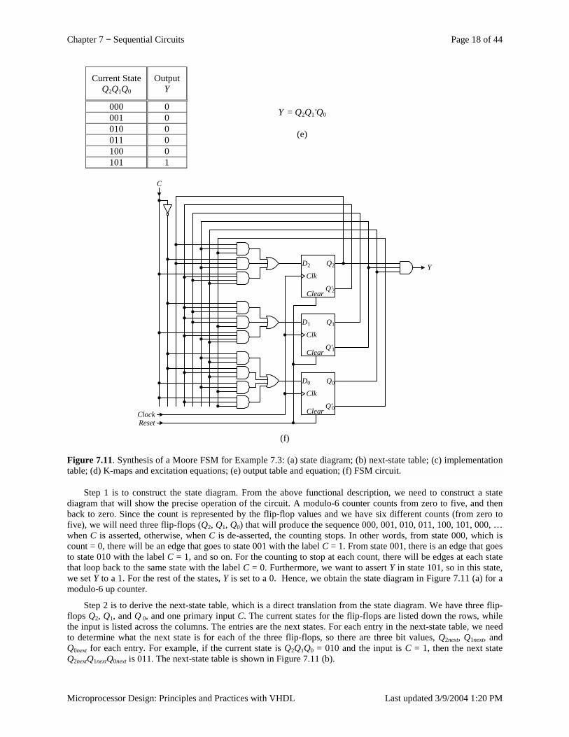
Chapter 7 − Sequential Circuits Page 18 of 44
Microprocessor Design: Principles and Practices with VHDL Last updated 3/9/2004 1:20 PM
Current State Q2Q1Q0
Output Y
000 0 001 0 010 0 011 0 100 0 101 1
Y = Q2Q1'Q0
(e)
C
Clock
Y
Clk
D0
Q'0
Q0
Clear
Clk
D1
Q'1
Q1
Clear
Clk
D2
Q'2
Q2
Clear
Reset (f)
Figure 7.11. Synthesis of a Moore FSM for Example 7.3: (a) state diagram; (b) next-state table; (c) implementation table; (d) K-maps and excitation equations; (e) output table and equation; (f) FSM circuit.
Step 1 is to construct the state diagram. From the above functional description, we need to construct a state diagram that will show the precise operation of the circuit. A modulo-6 counter counts from zero to five, and then back to zero. Since the count is represented by the flip-flop values and we have six different counts (from zero to five), we will need three flip-flops (Q2, Q1, Q0) that will produce the sequence 000, 001, 010, 011, 100, 101, 000, … when C is asserted, otherwise, when C is de-asserted, the counting stops. In other words, from state 000, which is count = 0, there will be an edge that goes to state 001 with the label C = 1. From state 001, there is an edge that goes to state 010 with the label C = 1, and so on. For the counting to stop at each count, there will be edges at each state that loop back to the same state with the label C = 0. Furthermore, we want to assert Y in state 101, so in this state, we set Y to a 1. For the rest of the states, Y is set to a 0. Hence, we obtain the state diagram in Figure 7.11 (a) for a modulo-6 up counter.
Step 2 is to derive the next-state table, which is a direct translation from the state diagram. We have three flip-flops Q2, Q1, and Q 0, and one primary input C. The current states for the flip-flops are listed down the rows, while the input is listed across the columns. The entries are the next states. For each entry in the next-state table, we need to determine what the next state is for each of the three flip-flops, so there are three bit values, Q2next, Q1next, and Q0next for each entry. For example, if the current state is Q2Q1Q0 = 010 and the input is C = 1, then the next state Q2nextQ1nextQ0next is 011. The next-state table is shown in Figure 7.11 (b).

Chapter 7 − Sequential Circuits Page 19 of 44
Microprocessor Design: Principles and Practices with VHDL Last updated 3/9/2004 1:20 PM
Step 3 is to convert the next-state table to its implementation table. Since for the D flip-flop, the implementation table is the same as the next-state table, we can simply use the next-state table and just re-label the entry heading as shown in Figure 7.11 (c).
Step 4 is to derive the excitation equations for all the flip-flop inputs in terms of the current state and the primary input. These equations are obtained directly from the implementation table. In the example, there are three flip-flops with the three inputs D2, D1, and D0, which correspond to the three bits in the entries in the implementation table. To derive the equation for D2, we consider just the leftmost bit in each entry for the truth table for D2. Looking at all the leftmost bits, there are four 1-minterms giving the canonical equation
D2 = C'Q2Q1'Q0' + C'Q2Q1'Q0 + CQ2'Q1Q0 + CQ2Q1'Q0'
Similarly, the equation for D1 is derived from considering just the middle bit for all the entries, and the equation for D0 from the rightmost bit. Since these equations will be used to construct the next-state circuit, they should be simplified. The three K-maps and simplified excitation equations for D2, D1, and D0 are shown in Figure 7.11 (d).
Steps 5 and 6 are to derive the output table and equation. There is one equation for every output signal. Since the value of Y is labeled inside each node, it is therefore dependent only on the current state. From the state diagram, Y is asserted only in state 101, so Y has a 1 only in that current state entry, while the rest of them are 0’s. The output table and equation are shown in Figure 7.11 (e).
Finally, we can draw the circuit for the FSM. We know that the circuit is a Moore FSM that uses three D flip-flops for its state memory having one primary input C and one output Y. The next-state function circuit is derived from the three excitation equations for D2, D1, and D0. The output function circuit is derived from the output equation for Y. The full circuit is shown in Figure 7.11 (f). ♦
Example 7.4
In this example, we will synthesize a Moore FSM that is more typical of what the control unit of a microprocessor is like. We start with the state diagram as shown in Figure 7.12 (a). Each state is labeled with a state name, s0, s1, s2, and s3, and has two output signals x and y. There are also two conditional status signals Start and (n=9) labeled on four of the edges, while the rest of the edges do not have any conditions. From state s0, the conditional edge labeled Start is taken when Start = 1, otherwise, the edge labeled Start' is taken. Similarly, from state s2, the edge with the label (n = 9) is taken when the condition is true, that is, when the value of variable n is equal to nine. If n is not equal to nine, then the edge with the label (n = 9)' is taken.
Two flip-flops Q0 and Q1 are needed in order to encode the four states. For simplicity, we will use the binary value of the index of the state name to be the encoding for that state. For example, the encoding for state s0 is Q1Q0 = 00 and the encoding for state s1 is Q1Q0 = 01, and so on.
From the above analysis, we are able to derive the next-state table as shown in Figure 7.12 (b). The four current states for Q1Q0 are listed down the four rows. The four columns are for the four combinations of the two conditional signals Start and (n=9). For example, the column with the value Start, (n=9) = 10 means Start = 1 and (n=9) = 0. The condition (n=9) = 0 means that the condition (n=9) is false which means (n=9)' is true. The entries in the table are the next states, Q1next Q0next, for the two flip-flops.
For example, looking at the state diagram, from state s2 we go back to state s1 when the condition (n=9)' is true independent of the Start condition. Hence, in the next-state table, for the current state row s2 (10), the two next-state entries for when the condition (n=9)' is true is s1 (01). The condition “(n=9)' is true” means (n=9) = 0. This corresponds to the two columns with the labels 00 and 10, that is, Start can be either 0 or 1, while (n=9) is 0.
Using D flip-flops to implement the FSM, we get the implementation table shown in Figure 7.12 (c). The implementation table and the next-state table are identical when D flip-flops are used. The only difference between them is the meaning given to the entries. For the next-state table, the entries are the next state of the flip-flops, whereas for the implementation table, the entries are the inputs to the flip-flops. They are the input values necessary to get to that next state. Again, since the next state is equal to the input value (Qnext = D) for a D flip-flop, therefore, the entries in these two tables are the same.
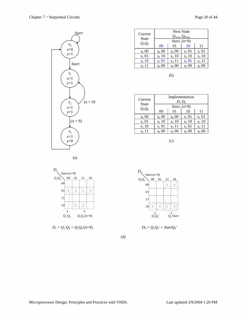
Chapter 7 − Sequential Circuits Page 20 of 44
Microprocessor Design: Principles and Practices with VHDL Last updated 3/9/2004 1:20 PM
Next State Q1next Q0next Start, (n=9)
Current State Q1Q0 00 01 10 11 s0 00 s0 00 s0 00 s1 01 s1 01 s1 01 s2 10 s2 10 s2 10 s2 10 s2 10 s1 01 s3 11 s1 01 s3 11 s3 11 s0 00 s0 00 s0 00 s0 00
(b)
Start'
Start
(n = 9)
s0x=0y=1
s1x=1y=1
s2x=1y=1
s3x=1y=0
(n = 9)'
(a)
Implementation D1 D0
Start, (n=9)
Current State Q1Q0 00 01 10 11 s0 00 s0 00 s0 00 s1 01 s1 01 s1 01 s2 10 s2 10 s2 10 s2 10 s2 10 s1 01 s3 11 s1 01 s3 11 s3 11 s0 00 s0 00 s0 00 s0 00
(c)
Start,(n=9)Q1Q0
00
00
1 1 1 1
1 1
01 11 10
01
11
10
D1
Q1'Q0 Q1Q0'(n=9)
Start,(n=9)Q1Q0
00
001 1
1 1 1 1
01 11 10
01
11
10
D0
Q0'StartQ1Q0'
D1 = Q1'Q0 + Q1Q0'(n=9) D0 = Q1Q0' + StartQ0'
(d)
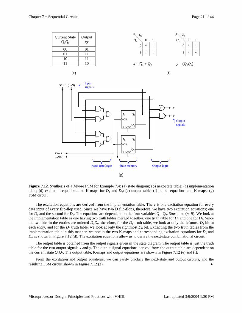
Chapter 7 − Sequential Circuits Page 21 of 44
Microprocessor Design: Principles and Practices with VHDL Last updated 3/9/2004 1:20 PM
Current State Q1Q0
Output xy
00 01 01 11 10 11 11 10
(e)
Q1
0 0 1
0
1 1
1
1
x Q0
Q1
0 1 1
0
1 0
1
1
y Q0
x = Q1 + Q0 y = (Q1Q0)'
(f)
Start (n=9)
x
y
Inputsignals
Outputsignals
Next-state logic State memory Output logic
Clk
D0
Q'0
Q0
Clear
Clk
D1
Q'1
Q1
Clear
ClockReset
(g)
Figure 7.12. Synthesis of a Moore FSM for Example 7.4: (a) state diagram; (b) next-state table; (c) implementation table; (d) excitation equations and K-maps for D1 and D0; (e) output table; (f) output equations and K-maps; (g) FSM circuit.
The excitation equations are derived from the implementation table. There is one excitation equation for every data input of every flip-flop used. Since we have two D flip-flops, therefore, we have two excitation equations; one for D1 and the second for D0. The equations are dependent on the four variables Q1, Q0, Start, and (n=9). We look at the implementation table as one having two truth tables merged together, one truth table for D1 and one for D0. Since the two bits in the entries are ordered D1D0, therefore, for the D1 truth table, we look at only the leftmost D1 bit in each entry, and for the D0 truth table, we look at only the rightmost D0 bit. Extracting the two truth tables from the implementation table in this manner, we obtain the two K-maps and corresponding excitation equations for D1 and D0 as shown in Figure 7.12 (d). The excitation equations allow us to derive the next-state combinational circuit.
The output table is obtained from the output signals given in the state diagram. The output table is just the truth table for the two output signals x and y. The output signal equations derived from the output table are dependent on the current state Q1Q0. The output table, K-maps and output equations are shown in Figure 7.12 (e) and (f).
From the excitation and output equations, we can easily produce the next-state and output circuits, and the resulting FSM circuit shown in Figure 7.12 (g). ♦
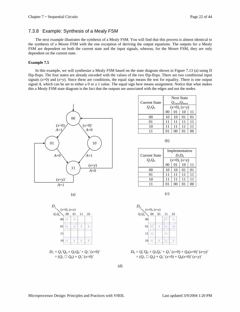
Chapter 7 − Sequential Circuits Page 22 of 44
Microprocessor Design: Principles and Practices with VHDL Last updated 3/9/2004 1:20 PM
7.3.8 Example: Synthesis of a Mealy FSM
The next example illustrates the synthesis of a Mealy FSM. You will find that this process is almost identical to the synthesis of a Moore FSM with the one exception of deriving the output equations. The outputs for a Mealy FSM are dependent on both the current state and the input signals, whereas, for the Moore FSM, they are only dependent on the current state.
Example 7.5
In this example, we will synthesize a Mealy FSM based on the state diagram shown in Figure 7.13 (a) using D flip-flops. The four states are already encoded with the values of the two flip-flops. There are two conditional input signals (x=0) and (x=y). Since these are conditions, the equal sign means the test for equality. There is one output signal A, which can be set to either a 0 or a 1 value. The equal sign here means assignment. Notice that what makes this a Mealy FSM state diagram is the fact that the outputs are associated with the edges and not the nodes.
Next State Q1nextQ0next
(x=0), (x=y) Current State
Q1Q0
00 01 10 11 00 10 10 01 01 01 11 11 11 11 10 11 11 11 11 11 01 00 01 00
(b)
00
11
01 10
(x=0)A=1
(x=0)'A=0
A=1A=0
(x=y)A=0
(x=y)'A=1
(a)
Implementation D1D0
(x=0), (x=y) Current State
Q1Q0
00 01 10 11 00 10 10 01 01 01 11 11 11 11 10 11 11 11 11 11 01 00 01 00
(c)
(x=0), (x=y)Q1Q0
00 1 1
00
1 1 1 1
1 1 1 1
01 11 10
01
11
10
D1
(x=0), (x=y)Q1Q0
00
001 1
1 1 1 1
1 1
1 1 1 1
01 11 10
01
11
10
D0
D1 = Q1'Q0 + Q1Q0' + Q1' (x=0)' D0 = Q1'Q0 + Q1Q0' + Q1' (x=0) + Q0(x=0)' (x=y)' = (Q1 ⊕ Q0) + Q1' (x=0)' = (Q1 ⊕ Q0) + Q1' (x=0) + Q0(x=0)' (x=y)'
(d)
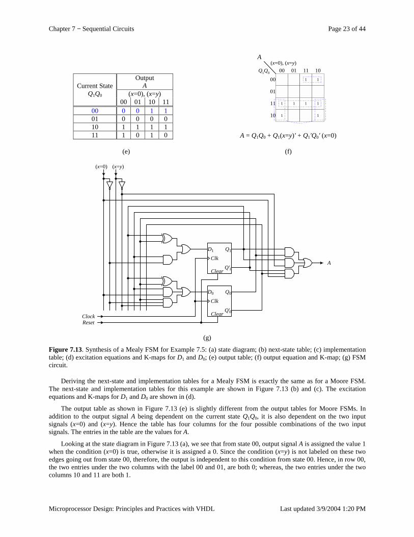
Chapter 7 − Sequential Circuits Page 23 of 44
Microprocessor Design: Principles and Practices with VHDL Last updated 3/9/2004 1:20 PM
Output A
(x=0), (x=y) Current State
Q1Q0
00 01 10 11 00 0 0 1 1 01 0 0 0 0 10 1 1 1 1 11 1 0 1 0
(e)
(x=0), (x=y)Q1Q0
00
001 1
1 1 1 1
1 1
01 11 10
01
11
10
A
A = Q1Q0 + Q1(x=y)' + Q1'Q0' (x=0)
(f)
(x=0) (x=y)
A
Clk
D0
Q'0
Q0
Clear
Clk
D1
Q'1
Q1
Clear
ClockReset
(g)
Figure 7.13. Synthesis of a Mealy FSM for Example 7.5: (a) state diagram; (b) next-state table; (c) implementation table; (d) excitation equations and K-maps for D1 and D0; (e) output table; (f) output equation and K-map; (g) FSM circuit.
Deriving the next-state and implementation tables for a Mealy FSM is exactly the same as for a Moore FSM. The next-state and implementation tables for this example are shown in Figure 7.13 (b) and (c). The excitation equations and K-maps for D1 and D0 are shown in (d).
The output table as shown in Figure 7.13 (e) is slightly different from the output tables for Moore FSMs. In addition to the output signal A being dependent on the current state Q1Q0, it is also dependent on the two input signals (x=0) and (x=y). Hence the table has four columns for the four possible combinations of the two input signals. The entries in the table are the values for A.
Looking at the state diagram in Figure 7.13 (a), we see that from state 00, output signal A is assigned the value 1 when the condition (x=0) is true, otherwise it is assigned a 0. Since the condition (x=y) is not labeled on these two edges going out from state 00, therefore, the output is independent to this condition from state 00. Hence, in row 00, the two entries under the two columns with the label 00 and 01, are both 0; whereas, the two entries under the two columns 10 and 11 are both 1.

Chapter 7 − Sequential Circuits Page 24 of 44
Microprocessor Design: Principles and Practices with VHDL Last updated 3/9/2004 1:20 PM
Using the output table as the truth table, we are able to derive the K-map and output equation for A as shown in Figure 7.13 (f). Notice that the equation is also dependent on the two input signals.
Again, using the excitation and output equations, we are able to draw the final FSM circuit shown in Figure 7.13 (g).
7.4 Unused State Encodings and the Encoding of States In a real world situation, the number of states used in the state diagram is most likely not a power of two. For
example, the state diagram shown in Figure 7.11 (a) for the modulo-6 counter uses six states. To encode six states, we need at least three flip-flops since two flip-flops can encode only four different combinations. However, three flip-flops give eight different combinations. So two combinations are not used. The question is what do we do with these unused encodings? In the next-state table, what next state values do we assigned to these unused states? Do we just ignore them?
If the FSM can never be in any of the unused states, then it does not matter what their next states are. In this case, we can put “don’t care” values for their next states. The resulting next-state circuit may be smaller because of the “don’t care” values.
But what if, by chance, the FSM enters one of these unused states? The operation of the FSM will be unpredictable because we do not know what the next state is. Well, this is not exactly true because even though we started with the “don’t cares,” we have mapped them to a fixed excitation equation. So these unused states do have definite next states. It is just that these next states are not what we wanted. Hence, the resulting FSM operation will be incorrect if it ever enters one of the unused states. If this FSM is used in a mission critical control unit, we do not want even this slight chance to occur.
One solution is to use the initialization or starting state as the next state for these unused state encodings. This way, the FSM will restart from the beginning if it ever enters one of these unused states.
So far, we have been using the sequential binary value to encode the states in order, for example, state s0 is encoded as 00, state s1 as 01, state s2 as 10, and so on. However, there is no reason why we cannot use a different encoding for the states. In fact, we do want to use a different encoding if it will result in a smaller circuit.
Example 7.6 shows a FSM with an unused state encoding, and the encoding of one state differently.
Example 7.6
In this example, we will synthesize a FSM for the one-shot circuit first discussed in Section 3.5.1. Recall that the one-shot circuit outputs a single short pulse when given an input of arbitrary time length. In this FSM circuit, the length of the single short pulse will be one clock cycle. The state diagram for this circuit is shown in Figure 7.14 (a).
State s0, encoded as 00, is the reset state, and the FSM waits for a key press in this state. When a switch is pressed, the FSM goes to state s1, encoded as 01, to output a single short pulse. From s1, the FSM unconditionally goes to state s2, encoded as 11, to turn off the one-shot pulse. Hence, the pulse only lasts for one clock cycle, irregardless of how long the key is pressed. To break the loop, and wait for another key press, the FSM has to wait for the release of the key in state s2. When the key is released, the FSM goes back to state s0 to wait for another key press.
This state diagram uses two bits to encode the three states, hence state encoding 10 is not used. The state diagram shows that if the FSM enters state 10, it will unconditionally go to the reset state 00 in the next clock cycle. Furthermore, we have encoded state s2 as 11 instead of 10 for the index two.
The corresponding next-state table is shown in Figure 7.14 (b). Using D flip-flops to implement this FSM, the implementation table, again, is like the next-state table. Therefore, we can use the next-state table directly to derive the two excitation equations for D1 and D0 as shown in (c). The output table and output equation is shown in (d), and finally the complete FSM circuit in (e).
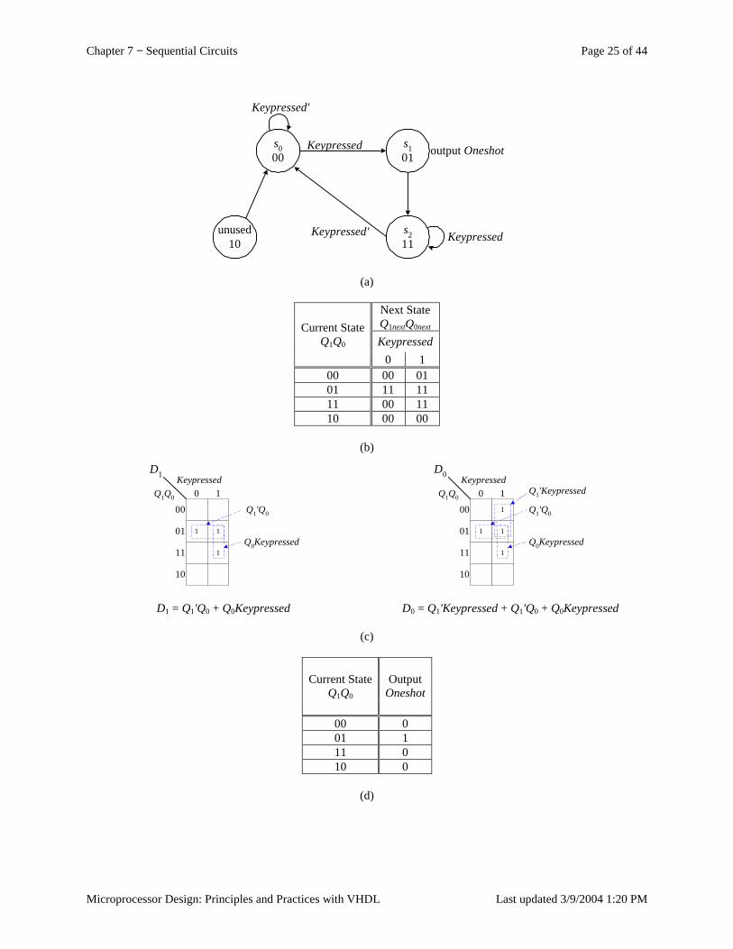
Chapter 7 − Sequential Circuits Page 25 of 44
Microprocessor Design: Principles and Practices with VHDL Last updated 3/9/2004 1:20 PM
s000
s101
s211
Keypressed'
Keypressed
KeypressedKeypressed'
output Oneshot
unused10
(a)
Next State Q1nextQ0next Keypressed
Current State Q1Q0
0 1 00 00 01 01 11 11 11 00 11 10 00 00
(b)
KeypressedQ1Q0
00
0
1 1
1
1
01
11
10
D1
Q1'Q0
Q0Keypressed
D1 = Q1'Q0 + Q0Keypressed
KeypressedQ1Q0
00 1
0
1 1
1
1
01
11
10
D0
Q1'Q0
Q0Keypressed
Q1'Keypressed
D0 = Q1'Keypressed + Q1'Q0 + Q0Keypressed
(c)
Current State Q1Q0
Output Oneshot
00 0 01 1 11 0 10 0
(d)
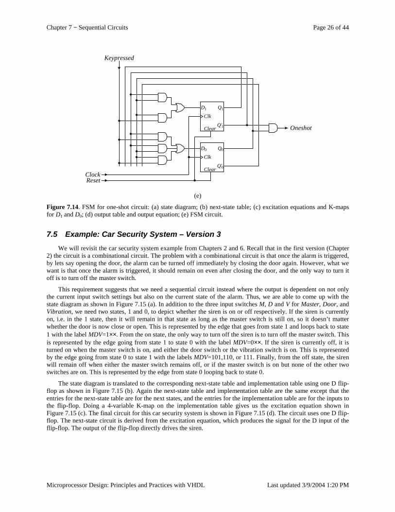
Chapter 7 − Sequential Circuits Page 26 of 44
Microprocessor Design: Principles and Practices with VHDL Last updated 3/9/2004 1:20 PM
Clk
D0
Q'0
Q0
Clear
Clk
D1
Q'1
Q1
Clear
ResetClock
Keypressed
Oneshot
(e)
Figure 7.14. FSM for one-shot circuit: (a) state diagram; (b) next-state table; (c) excitation equations and K-maps for D1 and D0; (d) output table and output equation; (e) FSM circuit.
7.5 Example: Car Security System – Version 3 We will revisit the car security system example from Chapters 2 and 6. Recall that in the first version (Chapter
2) the circuit is a combinational circuit. The problem with a combinational circuit is that once the alarm is triggered, by lets say opening the door, the alarm can be turned off immediately by closing the door again. However, what we want is that once the alarm is triggered, it should remain on even after closing the door, and the only way to turn it off is to turn off the master switch.
This requirement suggests that we need a sequential circuit instead where the output is dependent on not only the current input switch settings but also on the current state of the alarm. Thus, we are able to come up with the state diagram as shown in Figure 7.15 (a). In addition to the three input switches M, D and V for Master, Door, and Vibration, we need two states, 1 and 0, to depict whether the siren is on or off respectively. If the siren is currently on, i.e. in the 1 state, then it will remain in that state as long as the master switch is still on, so it doesn’t matter whether the door is now close or open. This is represented by the edge that goes from state 1 and loops back to state 1 with the label MDV=1××. From the on state, the only way to turn off the siren is to turn off the master switch. This is represented by the edge going from state 1 to state 0 with the label MDV=0××. If the siren is currently off, it is turned on when the master switch is on, and either the door switch or the vibration switch is on. This is represented by the edge going from state 0 to state 1 with the labels MDV=101,110, or 111. Finally, from the off state, the siren will remain off when either the master switch remains off, or if the master switch is on but none of the other two switches are on. This is represented by the edge from state 0 looping back to state 0.
The state diagram is translated to the corresponding next-state table and implementation table using one D flip-flop as shown in Figure 7.15 (b). Again the next-state table and implementation table are the same except that the entries for the next-state table are for the next states, and the entries for the implementation table are for the inputs to the flip-flop. Doing a 4-variable K-map on the implementation table gives us the excitation equation shown in Figure 7.15 (c). The final circuit for this car security system is shown in Figure 7.15 (d). The circuit uses one D flip-flop. The next-state circuit is derived from the excitation equation, which produces the signal for the D input of the flip-flop. The output of the flip-flop directly drives the siren.
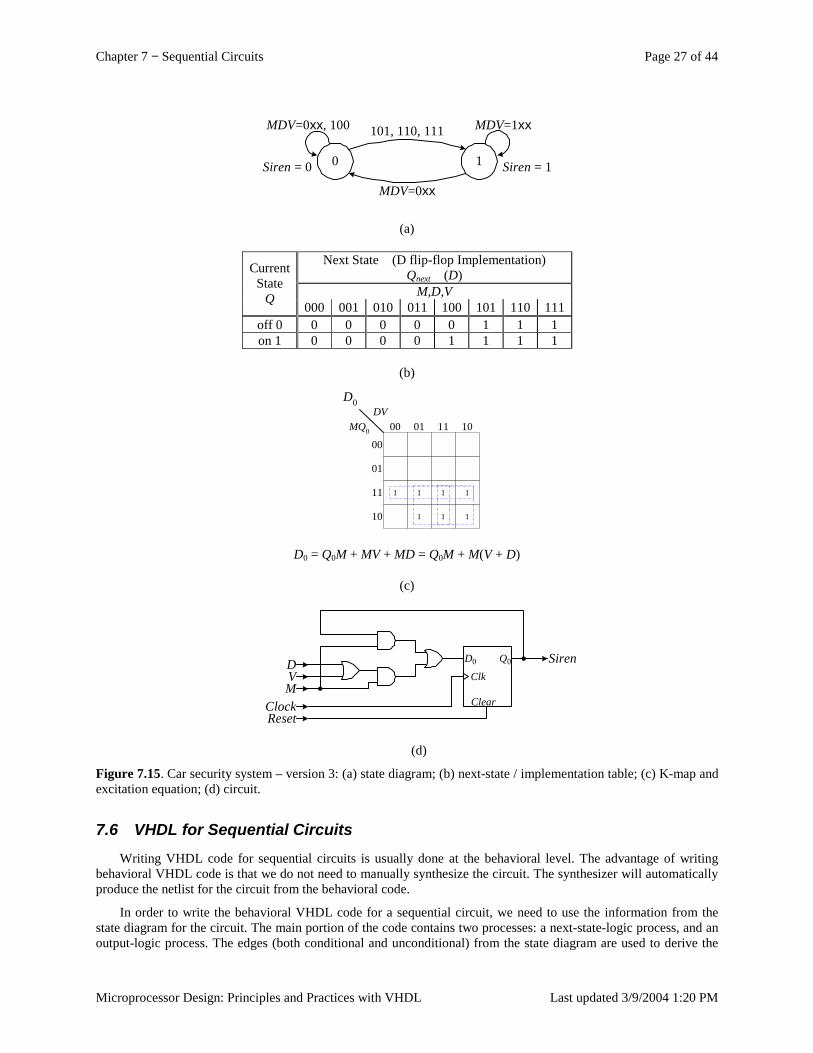
Chapter 7 − Sequential Circuits Page 27 of 44
Microprocessor Design: Principles and Practices with VHDL Last updated 3/9/2004 1:20 PM
0 1
MDV=0xx, 100 101, 110, 111 MDV=1xx
MDV=0xx
Siren = 1Siren = 0
(a)
Next State (D flip-flop Implementation) Qnext (D)
M,D,V
Current State
Q 000 001 010 011 100 101 110 111
off 0 0 0 0 0 0 1 1 1 on 1 0 0 0 0 1 1 1 1
(b)
DVMQ0
00
00
1 1 1 1
1 1 1
01 11 10
01
11
10
D0
D0 = Q0M + MV + MD = Q0M + M(V + D)
(c)
Siren
Clock
Clk
D0 Q0
ClearReset
MVD
(d)
Figure 7.15. Car security system – version 3: (a) state diagram; (b) next-state / implementation table; (c) K-map and excitation equation; (d) circuit.
7.6 VHDL for Sequential Circuits Writing VHDL code for sequential circuits is usually done at the behavioral level. The advantage of writing
behavioral VHDL code is that we do not need to manually synthesize the circuit. The synthesizer will automatically produce the netlist for the circuit from the behavioral code.
In order to write the behavioral VHDL code for a sequential circuit, we need to use the information from the state diagram for the circuit. The main portion of the code contains two processes: a next-state-logic process, and an output-logic process. The edges (both conditional and unconditional) from the state diagram are used to derive the
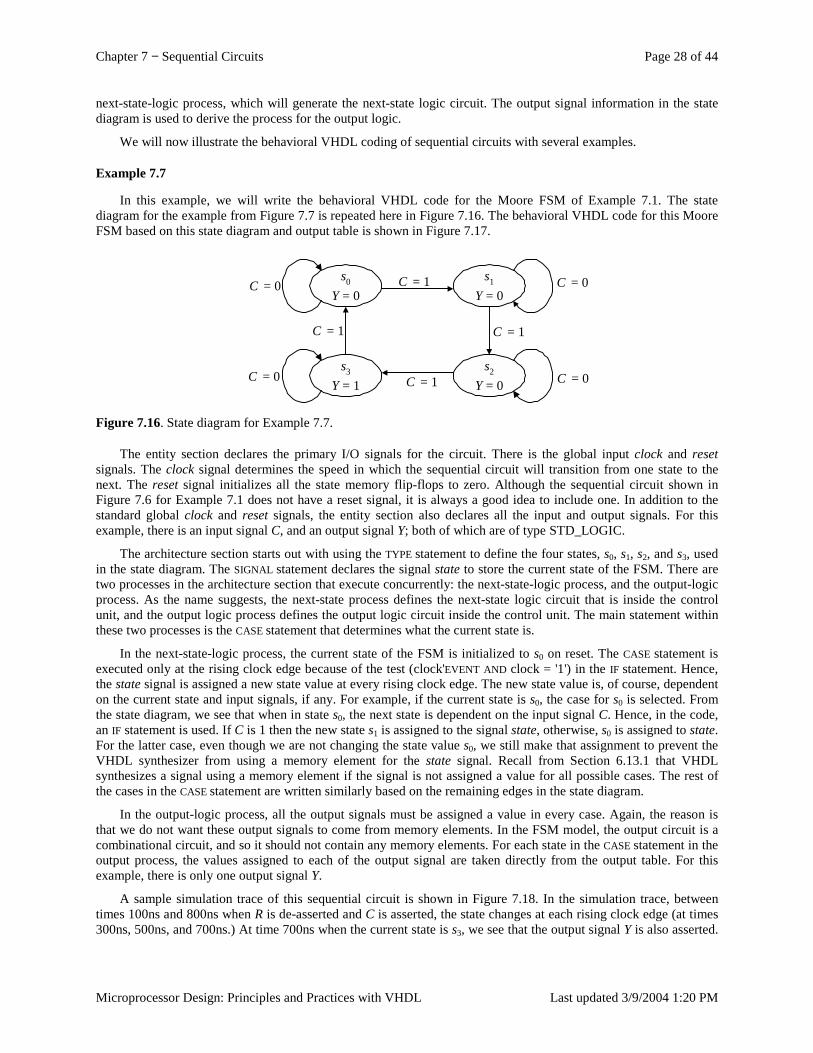
Chapter 7 − Sequential Circuits Page 28 of 44
Microprocessor Design: Principles and Practices with VHDL Last updated 3/9/2004 1:20 PM
next-state-logic process, which will generate the next-state logic circuit. The output signal information in the state diagram is used to derive the process for the output logic.
We will now illustrate the behavioral VHDL coding of sequential circuits with several examples.
Example 7.7
In this example, we will write the behavioral VHDL code for the Moore FSM of Example 7.1. The state diagram for the example from Figure 7.7 is repeated here in Figure 7.16. The behavioral VHDL code for this Moore FSM based on this state diagram and output table is shown in Figure 7.17.
Y = 0C = 0
C = 0C = 1
C = 1
C = 1C = 0
C = 0
C = 1
s0
Y = 0s1
Y = 0s2
Y = 1s3
Figure 7.16. State diagram for Example 7.7.
The entity section declares the primary I/O signals for the circuit. There is the global input clock and reset signals. The clock signal determines the speed in which the sequential circuit will transition from one state to the next. The reset signal initializes all the state memory flip-flops to zero. Although the sequential circuit shown in Figure 7.6 for Example 7.1 does not have a reset signal, it is always a good idea to include one. In addition to the standard global clock and reset signals, the entity section also declares all the input and output signals. For this example, there is an input signal C, and an output signal Y; both of which are of type STD_LOGIC.
The architecture section starts out with using the TYPE statement to define the four states, s0, s1, s2, and s3, used in the state diagram. The SIGNAL statement declares the signal state to store the current state of the FSM. There are two processes in the architecture section that execute concurrently: the next-state-logic process, and the output-logic process. As the name suggests, the next-state process defines the next-state logic circuit that is inside the control unit, and the output logic process defines the output logic circuit inside the control unit. The main statement within these two processes is the CASE statement that determines what the current state is.
In the next-state-logic process, the current state of the FSM is initialized to s0 on reset. The CASE statement is executed only at the rising clock edge because of the test (clock'EVENT AND clock = '1') in the IF statement. Hence, the state signal is assigned a new state value at every rising clock edge. The new state value is, of course, dependent on the current state and input signals, if any. For example, if the current state is s0, the case for s0 is selected. From the state diagram, we see that when in state s0, the next state is dependent on the input signal C. Hence, in the code, an IF statement is used. If C is 1 then the new state s1 is assigned to the signal state, otherwise, s0 is assigned to state. For the latter case, even though we are not changing the state value s0, we still make that assignment to prevent the VHDL synthesizer from using a memory element for the state signal. Recall from Section 6.13.1 that VHDL synthesizes a signal using a memory element if the signal is not assigned a value for all possible cases. The rest of the cases in the CASE statement are written similarly based on the remaining edges in the state diagram.
In the output-logic process, all the output signals must be assigned a value in every case. Again, the reason is that we do not want these output signals to come from memory elements. In the FSM model, the output circuit is a combinational circuit, and so it should not contain any memory elements. For each state in the CASE statement in the output process, the values assigned to each of the output signal are taken directly from the output table. For this example, there is only one output signal Y.
A sample simulation trace of this sequential circuit is shown in Figure 7.18. In the simulation trace, between times 100ns and 800ns when R is de-asserted and C is asserted, the state changes at each rising clock edge (at times 300ns, 500ns, and 700ns.) At time 700ns when the current state is s3, we see that the output signal Y is also asserted.
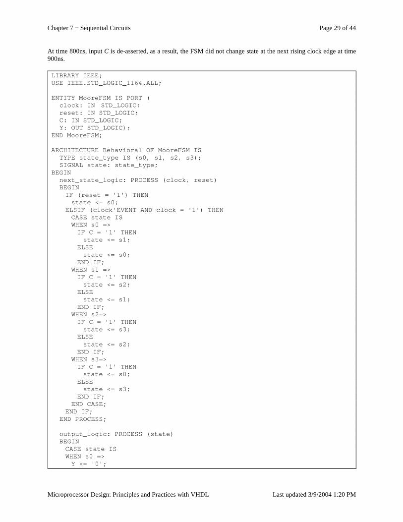
Chapter 7 − Sequential Circuits Page 29 of 44
Microprocessor Design: Principles and Practices with VHDL Last updated 3/9/2004 1:20 PM
At time 800ns, input C is de-asserted, as a result, the FSM did not change state at the next rising clock edge at time 900ns.
LIBRARY IEEE;USE IEEE.STD_LOGIC_1164.ALL;
ENTITY MooreFSM IS PORT (clock: IN STD_LOGIC;reset: IN STD_LOGIC;C: IN STD_LOGIC;Y: OUT STD_LOGIC);
END MooreFSM;
ARCHITECTURE Behavioral OF MooreFSM ISTYPE state_type IS (s0, s1, s2, s3);SIGNAL state: state_type;
BEGINnext_state_logic: PROCESS (clock, reset)BEGINIF (reset = '1') THENstate <= s0;
ELSIF (clock'EVENT AND clock = '1') THENCASE state ISWHEN s0 =>IF C = '1' THENstate <= s1;
ELSEstate <= s0;
END IF;WHEN s1 =>IF C = '1' THENstate <= s2;
ELSEstate <= s1;
END IF;WHEN s2=>IF C = '1' THENstate <= s3;
ELSEstate <= s2;
END IF;WHEN s3=>IF C = '1' THENstate <= s0;
ELSEstate <= s3;
END IF;END CASE;
END IF;END PROCESS;
output_logic: PROCESS (state)BEGINCASE state ISWHEN s0 =>Y <= '0';
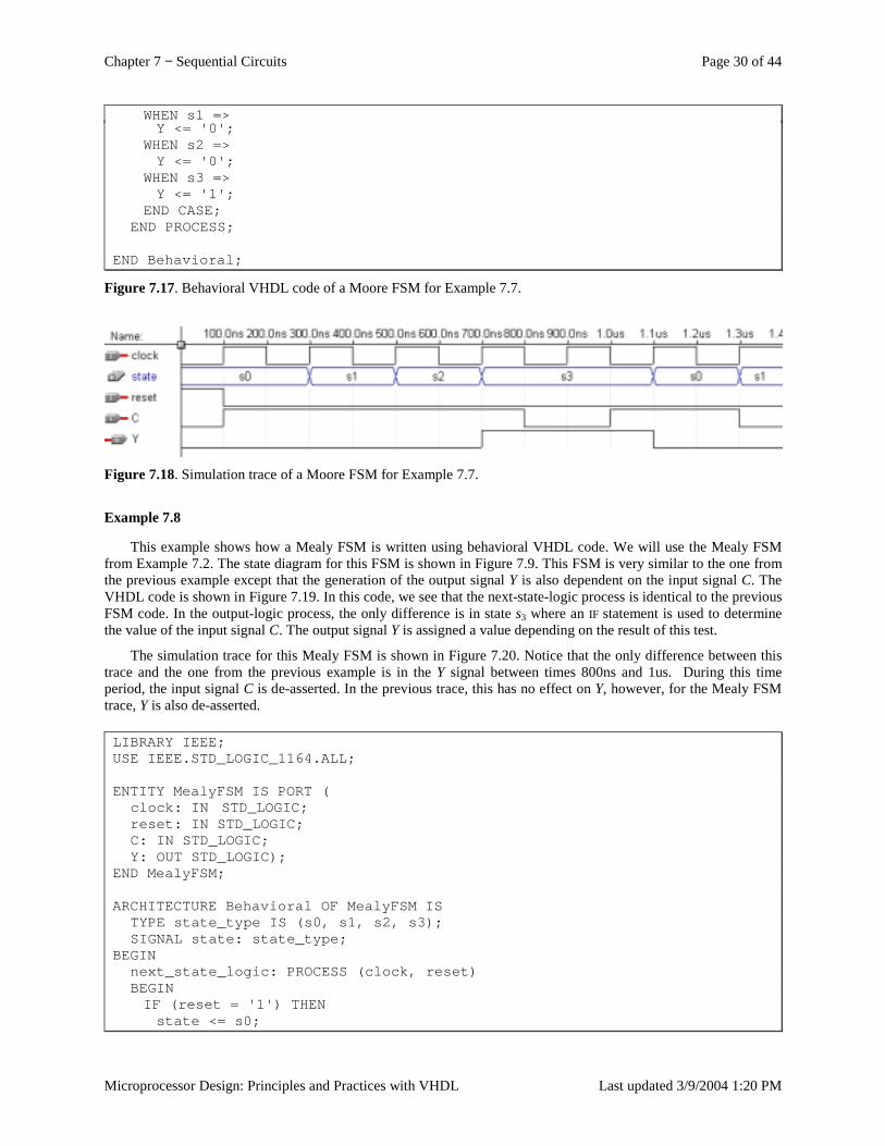
Chapter 7 − Sequential Circuits Page 30 of 44
Microprocessor Design: Principles and Practices with VHDL Last updated 3/9/2004 1:20 PM
WHEN s1 =>Y <= '0';
WHEN s2 =>Y <= '0';
WHEN s3 =>Y <= '1';
END CASE;END PROCESS;
END Behavioral;
Figure 7.17. Behavioral VHDL code of a Moore FSM for Example 7.7.
Figure 7.18. Simulation trace of a Moore FSM for Example 7.7.
Example 7.8
This example shows how a Mealy FSM is written using behavioral VHDL code. We will use the Mealy FSM from Example 7.2. The state diagram for this FSM is shown in Figure 7.9. This FSM is very similar to the one from the previous example except that the generation of the output signal Y is also dependent on the input signal C. The VHDL code is shown in Figure 7.19. In this code, we see that the next-state-logic process is identical to the previous FSM code. In the output-logic process, the only difference is in state s3 where an IF statement is used to determine the value of the input signal C. The output signal Y is assigned a value depending on the result of this test.
The simulation trace for this Mealy FSM is shown in Figure 7.20. Notice that the only difference between this trace and the one from the previous example is in the Y signal between times 800ns and 1us. During this time period, the input signal C is de-asserted. In the previous trace, this has no effect on Y, however, for the Mealy FSM trace, Y is also de-asserted.
LIBRARY IEEE;USE IEEE.STD_LOGIC_1164.ALL;
ENTITY MealyFSM IS PORT (clock: IN STD_LOGIC;reset: IN STD_LOGIC;C: IN STD_LOGIC;Y: OUT STD_LOGIC);
END MealyFSM;
ARCHITECTURE Behavioral OF MealyFSM ISTYPE state_type IS (s0, s1, s2, s3);SIGNAL state: state_type;
BEGINnext_state_logic: PROCESS (clock, reset)BEGINIF (reset = '1') THENstate <= s0;
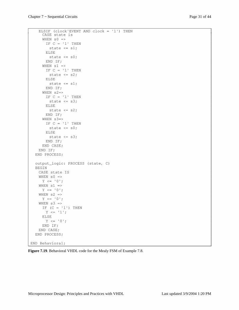
Chapter 7 − Sequential Circuits Page 31 of 44
Microprocessor Design: Principles and Practices with VHDL Last updated 3/9/2004 1:20 PM
ELSIF (clock'EVENT AND clock = '1') THENCASE state isWHEN s0 =>IF C = '1' THENstate <= s1;
ELSEstate <= s0;
END IF;WHEN s1 =>IF C = '1' THENstate <= s2;
ELSEstate <= s1;
END IF;WHEN s2=>IF C = '1' THENstate <= s3;
ELSEstate <= s2;
END IF;WHEN s3=>IF C = '1' THENstate <= s0;
ELSEstate <= s3;
END IF;END CASE;
END IF;END PROCESS;
output_logic: PROCESS (state, C)BEGINCASE state ISWHEN s0 =>Y <= '0';
WHEN s1 =>Y <= '0';
WHEN s2 =>Y <= '0';
WHEN s3 =>IF (C = '1') THENY <= '1';
ELSEY <= '0';
END IF;END CASE;
END PROCESS;
END Behavioral;
Figure 7.19. Behavioral VHDL code for the Mealy FSM of Example 7.8.
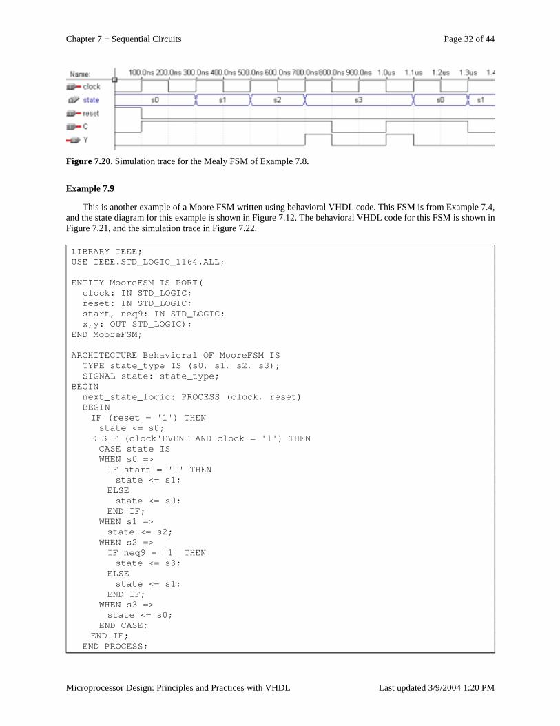
Chapter 7 − Sequential Circuits Page 32 of 44
Microprocessor Design: Principles and Practices with VHDL Last updated 3/9/2004 1:20 PM
Figure 7.20. Simulation trace for the Mealy FSM of Example 7.8.
Example 7.9
This is another example of a Moore FSM written using behavioral VHDL code. This FSM is from Example 7.4, and the state diagram for this example is shown in Figure 7.12. The behavioral VHDL code for this FSM is shown in Figure 7.21, and the simulation trace in Figure 7.22.
LIBRARY IEEE;USE IEEE.STD_LOGIC_1164.ALL;
ENTITY MooreFSM IS PORT(clock: IN STD_LOGIC;reset: IN STD_LOGIC;start, neq9: IN STD_LOGIC;x,y: OUT STD_LOGIC);
END MooreFSM;
ARCHITECTURE Behavioral OF MooreFSM ISTYPE state_type IS (s0, s1, s2, s3);SIGNAL state: state_type;
BEGINnext_state_logic: PROCESS (clock, reset)BEGINIF (reset = '1') THENstate <= s0;
ELSIF (clock'EVENT AND clock = '1') THENCASE state ISWHEN s0 =>IF start = '1' THENstate <= s1;
ELSEstate <= s0;
END IF;WHEN s1 =>state <= s2;
WHEN s2 =>IF neq9 = '1' THENstate <= s3;
ELSEstate <= s1;
END IF;WHEN s3 =>state <= s0;
END CASE;END IF;
END PROCESS;
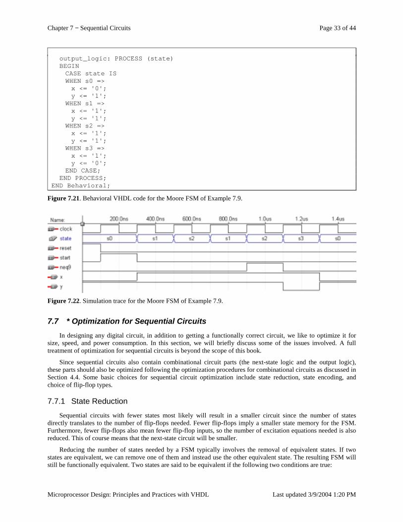
Chapter 7 − Sequential Circuits Page 33 of 44
Microprocessor Design: Principles and Practices with VHDL Last updated 3/9/2004 1:20 PM
output_logic: PROCESS (state)BEGINCASE state ISWHEN s0 =>x <= '0';y <= '1';
WHEN s1 =>x <= '1';y <= '1';
WHEN s2 =>x <= '1';y <= '1';
WHEN s3 =>x <= '1';y <= '0';
END CASE;END PROCESS;
END Behavioral;
Figure 7.21. Behavioral VHDL code for the Moore FSM of Example 7.9.
Figure 7.22. Simulation trace for the Moore FSM of Example 7.9.
7.7 * Optimization for Sequential Circuits In designing any digital circuit, in addition to getting a functionally correct circuit, we like to optimize it for
size, speed, and power consumption. In this section, we will briefly discuss some of the issues involved. A full treatment of optimization for sequential circuits is beyond the scope of this book.
Since sequential circuits also contain combinational circuit parts (the next-state logic and the output logic), these parts should also be optimized following the optimization procedures for combinational circuits as discussed in Section 4.4. Some basic choices for sequential circuit optimization include state reduction, state encoding, and choice of flip-flop types.
7.7.1 State Reduction
Sequential circuits with fewer states most likely will result in a smaller circuit since the number of states directly translates to the number of flip-flops needed. Fewer flip-flops imply a smaller state memory for the FSM. Furthermore, fewer flip-flops also mean fewer flip-flop inputs, so the number of excitation equations needed is also reduced. This of course means that the next-state circuit will be smaller.
Reducing the number of states needed by a FSM typically involves the removal of equivalent states. If two states are equivalent, we can remove one of them and instead use the other equivalent state. The resulting FSM will still be functionally equivalent. Two states are said to be equivalent if the following two conditions are true:
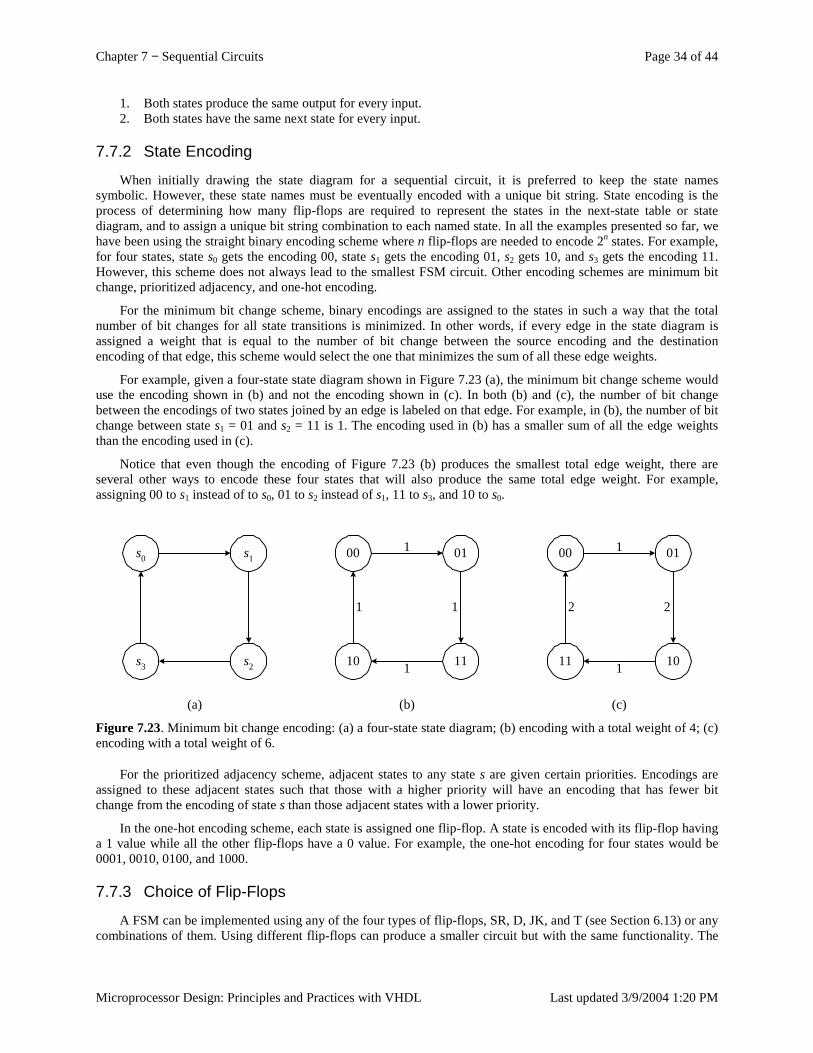
Chapter 7 − Sequential Circuits Page 34 of 44
Microprocessor Design: Principles and Practices with VHDL Last updated 3/9/2004 1:20 PM
1. Both states produce the same output for every input. 2. Both states have the same next state for every input.
7.7.2 State Encoding
When initially drawing the state diagram for a sequential circuit, it is preferred to keep the state names symbolic. However, these state names must be eventually encoded with a unique bit string. State encoding is the process of determining how many flip-flops are required to represent the states in the next-state table or state diagram, and to assign a unique bit string combination to each named state. In all the examples presented so far, we have been using the straight binary encoding scheme where n flip-flops are needed to encode 2n states. For example, for four states, state s0 gets the encoding 00, state s1 gets the encoding 01, s2 gets 10, and s3 gets the encoding 11. However, this scheme does not always lead to the smallest FSM circuit. Other encoding schemes are minimum bit change, prioritized adjacency, and one-hot encoding.
For the minimum bit change scheme, binary encodings are assigned to the states in such a way that the total number of bit changes for all state transitions is minimized. In other words, if every edge in the state diagram is assigned a weight that is equal to the number of bit change between the source encoding and the destination encoding of that edge, this scheme would select the one that minimizes the sum of all these edge weights.
For example, given a four-state state diagram shown in Figure 7.23 (a), the minimum bit change scheme would use the encoding shown in (b) and not the encoding shown in (c). In both (b) and (c), the number of bit change between the encodings of two states joined by an edge is labeled on that edge. For example, in (b), the number of bit change between state s1 = 01 and s2 = 11 is 1. The encoding used in (b) has a smaller sum of all the edge weights than the encoding used in (c).
Notice that even though the encoding of Figure 7.23 (b) produces the smallest total edge weight, there are several other ways to encode these four states that will also produce the same total edge weight. For example, assigning 00 to s1 instead of to s0, 01 to s2 instead of s1, 11 to s3, and 10 to s0.
s0 s1
s2s3
(a)
100 01
1110 1
1 1
(b)
100 01
1011 1
2 2
(c)
Figure 7.23. Minimum bit change encoding: (a) a four-state state diagram; (b) encoding with a total weight of 4; (c) encoding with a total weight of 6.
For the prioritized adjacency scheme, adjacent states to any state s are given certain priorities. Encodings are assigned to these adjacent states such that those with a higher priority will have an encoding that has fewer bit change from the encoding of state s than those adjacent states with a lower priority.
In the one-hot encoding scheme, each state is assigned one flip-flop. A state is encoded with its flip-flop having a 1 value while all the other flip-flops have a 0 value. For example, the one-hot encoding for four states would be 0001, 0010, 0100, and 1000.
7.7.3 Choice of Flip-Flops
A FSM can be implemented using any of the four types of flip-flops, SR, D, JK, and T (see Section 6.13) or any combinations of them. Using different flip-flops can produce a smaller circuit but with the same functionality. The
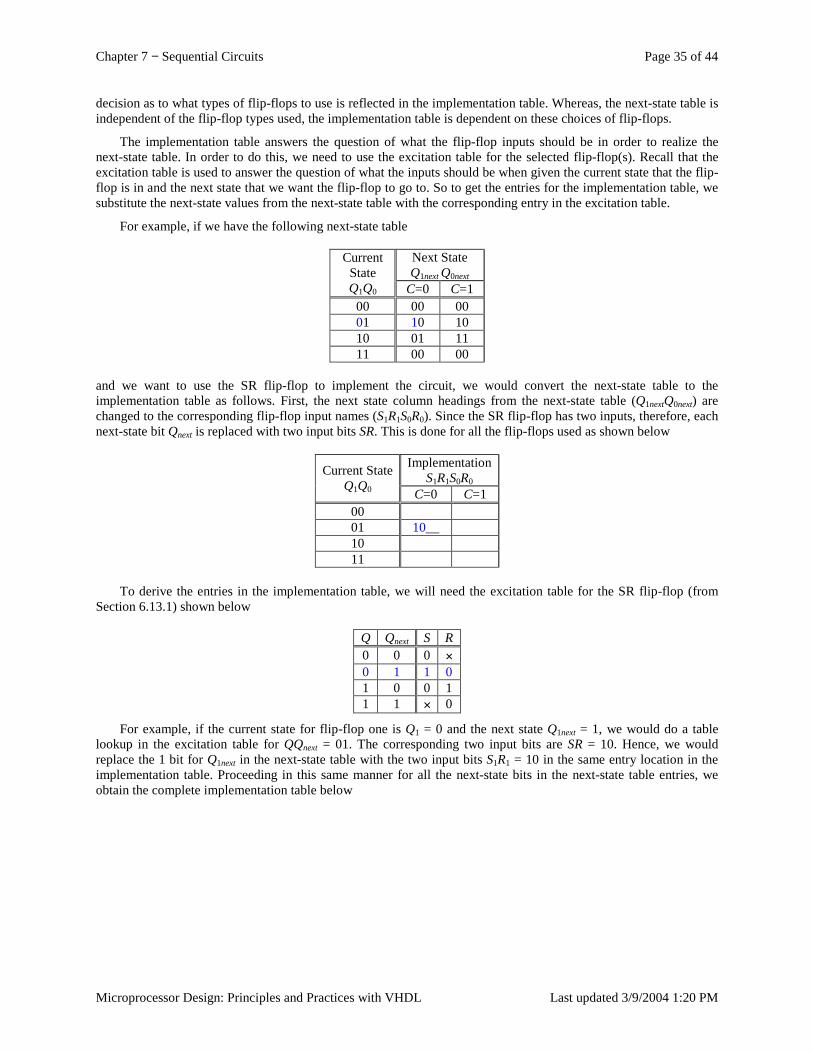
Chapter 7 − Sequential Circuits Page 35 of 44
Microprocessor Design: Principles and Practices with VHDL Last updated 3/9/2004 1:20 PM
decision as to what types of flip-flops to use is reflected in the implementation table. Whereas, the next-state table is independent of the flip-flop types used, the implementation table is dependent on these choices of flip-flops.
The implementation table answers the question of what the flip-flop inputs should be in order to realize the next-state table. In order to do this, we need to use the excitation table for the selected flip-flop(s). Recall that the excitation table is used to answer the question of what the inputs should be when given the current state that the flip-flop is in and the next state that we want the flip-flop to go to. So to get the entries for the implementation table, we substitute the next-state values from the next-state table with the corresponding entry in the excitation table.
For example, if we have the following next-state table
Next State Q1next Q0next
Current State Q1Q0 C=0 C=1
00 00 00 01 10 10 10 01 11 11 00 00
and we want to use the SR flip-flop to implement the circuit, we would convert the next-state table to the implementation table as follows. First, the next state column headings from the next-state table (Q1nextQ0next) are changed to the corresponding flip-flop input names (S1R1S0R0). Since the SR flip-flop has two inputs, therefore, each next-state bit Qnext is replaced with two input bits SR. This is done for all the flip-flops used as shown below
Implementation S1R1S0R0
Current State Q1Q0 C=0 C=1
00 01 10__ 10 11
To derive the entries in the implementation table, we will need the excitation table for the SR flip-flop (from Section 6.13.1) shown below
Q Qnext S R 0 0 0 × 0 1 1 0 1 0 0 1 1 1 × 0
For example, if the current state for flip-flop one is Q1 = 0 and the next state Q1next = 1, we would do a table lookup in the excitation table for QQnext = 01. The corresponding two input bits are SR = 10. Hence, we would replace the 1 bit for Q1next in the next-state table with the two input bits S1R1 = 10 in the same entry location in the implementation table. Proceeding in this same manner for all the next-state bits in the next-state table entries, we obtain the complete implementation table below

Chapter 7 − Sequential Circuits Page 36 of 44
Microprocessor Design: Principles and Practices with VHDL Last updated 3/9/2004 1:20 PM
Implementation S1R1S0R0
Current State Q1Q0 C=0 C=1
00 0×0× 0×0× 01 1001 1001 10 0110 ×010 11 0101 0101
Once we have the implementation table, deriving the excitation equations and drawing the next-state circuit are identical for all flip-flop types.
The output table and output equations are not affected by the change in flip-flop types, and so they remain exactly the same too.
Example 7.10
In this example, we will design a modulo-6 up counter using T flip-flops. This is similar to Example 7.3 but using T flip-flops instead of D flip-flops. The next-state table for the modulo-6 up counter as obtained from Example 7.3 is shown in Figure 7.24 (a). The excitation table for the T flip-flop as derived in Section 6.14.3 is shown in Figure 7.24 (b).
The implementation table is obtained from the next-state table by substituting each next-state bit with the corresponding input bit of the T flip-flop. This is accomplished by doing a table look-up from the T flip-flop excitation table.
For example, in the next-state table for the current state Q2Q1Q0 = 010 and the input C = 1, we want the next state Q2next Q1next Q0next to be 011. The corresponding entry in the implementation table shown in Figure 7.24 (c) using T flip-flops would be T2T1T0 = 001 because for flip-flop2 we want its content to go from Q2 = 0 to Q2next = 0. The excitation table tells us that to realize this change, the T2 input needs to be a 0. Similarly, for flip-flop1 we want its content to go from Q1 = 1 to Q1next = 1, and again the T1 input needs to be a 0 to realize this change. Finally, for flip-flop0 we want its content to go from Q0 = 0 to Q0next = 1, this time, we need T0 to be a 1. Continuing in this manner for all the entries in the next-state table, we obtain the implementation table shown in Figure 7.24 (c).
From the implementation table, we obtain the excitation equations just like before. For this example, we have the three input bits T2, T1 and T0, which results in the three equations. These equations are dependent on the four variables Q2, Q1, Q0, and C. The three K-maps and excitation equations for T2, T1, and T0 are shown in Figure 7.24 (d). The output equation is the same as before (see Figure 7.11 (e)). Finally, the complete modulo-6 up counter circuit is shown in Figure 7.24 (e).
Comparing this circuit with the circuit from Example 7.3 shown in Figure 7.11 (f) where D flip-flops are used, it is obvious that using T flip-flops for this problem result in a much smaller circuit than using D flip-flops. ♦
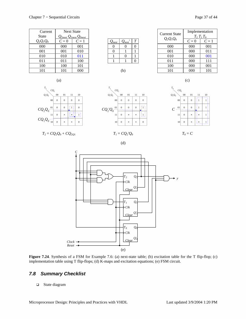
Chapter 7 − Sequential Circuits Page 37 of 44
Microprocessor Design: Principles and Practices with VHDL Last updated 3/9/2004 1:20 PM
Next State Q2next Q1next Q0next
Current State
Q2Q1Q0 C = 0 C = 1 000 000 001 001 001 010 010 010 011 011 011 100 100 100 101 101 101 000
(a)
Qnext Qnext' T 0 0 0 0 1 1 1 0 1 1 1 0
(b)
Implementation T2 T1 T0
Current State Q2Q1Q0 C = 0 C = 1
000 000 001 001 000 011 010 000 001 011 000 111 100 000 001 101 000 101
(c)
CQ2
Q1Q0
00 0 0
00
0 0
0 0 1 0
0 1
0 0
01 11 10
01
11
10
T2
CQ2Q0× ×
××CQ1Q0
T2 = CQ2Q0 + CQ2Q1
CQ2
Q1Q0
00 0 0
00
0 0
0 0 0 1
0 1
0 0
01 11 10
01
11
10
T1
CQ2'Q0× ×
××
T1 = CQ2'Q0
(d)
CQ2
Q1Q0
00 0 0
00
1 1
0 0 1 1
0 1
0 1
01 11 10
01
11
10
T0
C× ×
××
T0 = C
y
C
Clk
T1
Q'1
Q1
Clear
Clk
T2
Q'2
Q2
Clear
Clk
T0
Q'0
Q0
ClearClockReset
(e)
Figure 7.24. Synthesis of a FSM for Example 7.6: (a) next-state table; (b) excitation table for the T flip-flop; (c) implementation table using T flip-flops; (d) K-maps and excitation equations; (e) FSM circuit.
7.8 Summary Checklist � State diagram
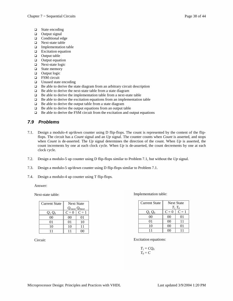
Chapter 7 − Sequential Circuits Page 38 of 44
Microprocessor Design: Principles and Practices with VHDL Last updated 3/9/2004 1:20 PM
� State encoding � Output signal � Conditional edge � Next-state table � Implementation table � Excitation equation � Output table � Output equation � Next-state logic � State memory � Output logic � FSM circuit � Unused state encoding � Be able to derive the state diagram from an arbitrary circuit description � Be able to derive the next-state table from a state diagram � Be able to derive the implementation table from a next-state table � Be able to derive the excitation equations from an implementation table � Be able to derive the output table from a state diagram � Be able to derive the output equations from an output table � Be able to derive the FSM circuit from the excitation and output equations
7.9 Problems
7.1. Design a modulo-4 up/down counter using D flip-flops. The count is represented by the content of the flip-flops. The circuit has a Count signal and an Up signal. The counter counts when Count is asserted, and stops when Count is de-asserted. The Up signal determines the direction of the count. When Up is asserted, the count increments by one at each clock cycle. When Up is de-asserted, the count decrements by one at each clock cycle.
7.2. Design a modulo-5 up counter using D flip-flops similar to Problem 7.1, but without the Up signal.
7.3. Design a modulo-5 up/down counter using D flip-flops similar to Problem 7.1.
7.4. Design a modulo-4 up counter using T flip-flops.
Answer:
Next-state table:
Current State Next State Q1next Q0next
Q1 Q0 C = 0 C = 1 00 00 01 01 01 10 10 10 11 11 11 00
Circuit:
Implementation table:
Current State Next State T1 T0
Q1 Q0 C = 0 C = 1 00 00 01 01 00 11 10 00 01 11 00 11
Excitation equations:
T1 = CQ0 T0 = C
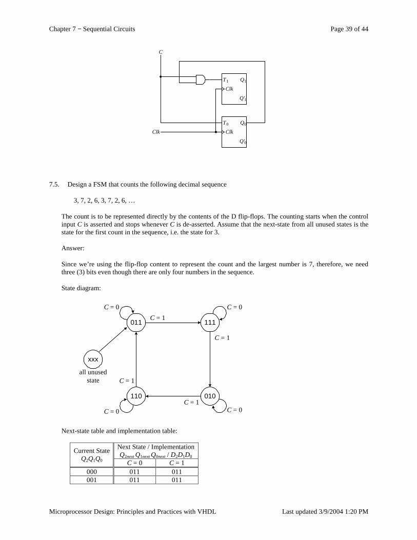
Chapter 7 − Sequential Circuits Page 39 of 44
Microprocessor Design: Principles and Practices with VHDL Last updated 3/9/2004 1:20 PM
C
Clk
Clk
T1
Q'1
Q1
Clk
T0
Q'0
Q0
7.5. Design a FSM that counts the following decimal sequence
3, 7, 2, 6, 3, 7, 2, 6, …
The count is to be represented directly by the contents of the D flip-flops. The counting starts when the control input C is asserted and stops whenever C is de-asserted. Assume that the next-state from all unused states is the state for the first count in the sequence, i.e. the state for 3.
Answer:
Since we’re using the flip-flop content to represent the count and the largest number is 7, therefore, we need three (3) bits even though there are only four numbers in the sequence.
State diagram:
011 111
010110
C = 0C = 1
C = 0
C = 0C = 0
C = 1
C = 1
C = 1
xxx
all unusedstate
Next-state table and implementation table:
Next State / Implementation Q2next Q1next Q0next / D2D1D0
Current State Q2Q1Q0 C = 0 C = 1
000 011 011 001 011 011
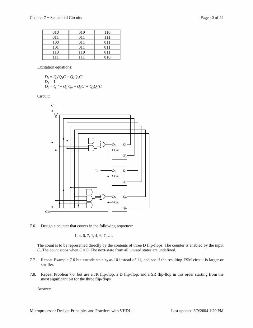
Chapter 7 − Sequential Circuits Page 40 of 44
Microprocessor Design: Principles and Practices with VHDL Last updated 3/9/2004 1:20 PM
010 010 110 011 011 111 100 011 011 101 011 011 110 110 011 111 111 010
Excitation equations:
D2 = Q2'Q1C + Q2Q1C' D1 = 1 D0 = Q1' + Q2'Q0 + Q0C' + Q2Q0'C
Circuit:
Clk
D0
Q'0
Q0
Clk
D1
Q'1
Q1
Clk
D2
Q'2
Q2
C
Clk
'1'
7.6. Design a counter that counts in the following sequence:
1, 4, 6, 7, 1, 4, 6, 7, ….
The count is to be represented directly by the contents of three D flip-flops. The counter is enabled by the input C. The count stops when C = 0. The next-state from all unused states are undefined.
7.7. Repeat Example 7.6 but encode state s2 as 10 instead of 11, and see if the resulting FSM circuit is larger or smaller.
7.8. Repeat Problem 7.6, but use a JK flip-flop, a D flip-flop, and a SR flip-flop in this order starting from the most significant bit for the three flip-flops.
Answer:
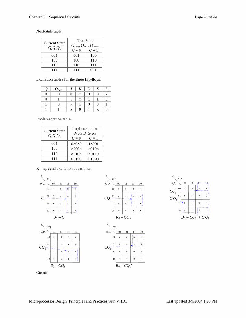
Chapter 7 − Sequential Circuits Page 41 of 44
Microprocessor Design: Principles and Practices with VHDL Last updated 3/9/2004 1:20 PM
Next-state table:
Next State Q2next Q1next Q0next
Current State Q2Q1Q0 C = 0 C = 1
001 001 100 100 100 110 110 110 111 111 111 001
Excitation tables for the three flip-flops:
Q Qnext J K D S R 0 0 0 × 0 0 × 0 1 1 × 1 1 0 1 0 × 1 0 0 1 1 1 × 0 1 × 0
Implementation table:
Implementation J2 K2 D1 S0 R0
Current State Q2Q1Q0 C = 0 C = 1
001 0×0×0 1×001 100 ×000× ×010× 110 ×010× ×0110 111 ×01×0 ×10×0
K-maps and excitation equations:
CQ2
Q1Q0
00
00
0 1
01 11 10
01
11
10
J2
×
×
×
C ×
× ×
×
×
× ×
×
× ×
×
CQ2
Q1Q0
00 0
00
0
0 1
0 0
01 11 10
01
11
10
K2
× ×
×
×
CQ0× ×
× ×
×
×
CQ2
Q1Q0
00 0
00
1
0 0
1 0
1 1
01 11 10
01
11
10
D1
× ×
××
×
× ×
×
C'Q1
CQ0'
J2 = C K2 = CQ0 D1 = CQ0' + C'Q1
CQ2
Q1Q0
00 0
00
0
0
0 1
01 11 10
01
11
10
S0
CQ1
×
× × ×
××
×
× ×
××
CQ2
Q1Q0
00
00
0 1
0 0
0
01 11 10
01
11
10
R0
CQ1'
× × × ×
××
× ×
×××
S0 = CQ1 R0 = CQ1'
Circuit:
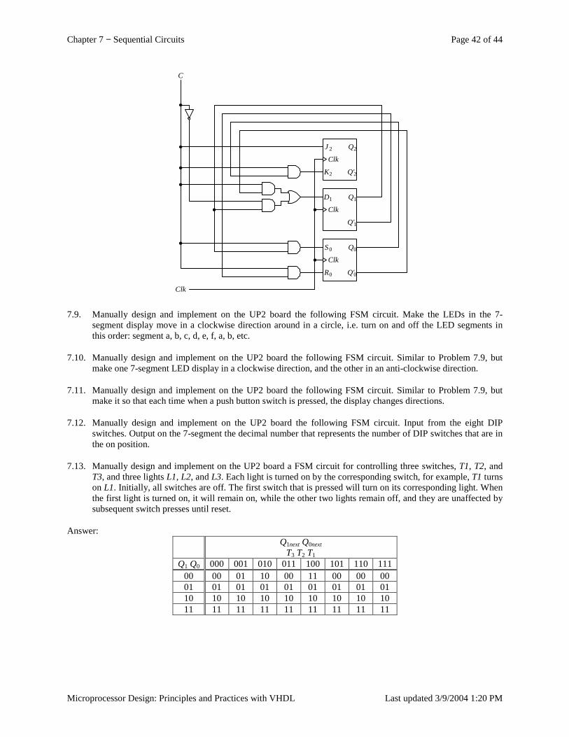
Chapter 7 − Sequential Circuits Page 42 of 44
Microprocessor Design: Principles and Practices with VHDL Last updated 3/9/2004 1:20 PM
C
Clk
Clk
D1
Q'1
Q1
Clk
S 0
R0 Q'0
Q0
Clk
J 2
K2 Q'2
Q2
7.9. Manually design and implement on the UP2 board the following FSM circuit. Make the LEDs in the 7-segment display move in a clockwise direction around in a circle, i.e. turn on and off the LED segments in this order: segment a, b, c, d, e, f, a, b, etc.
7.10. Manually design and implement on the UP2 board the following FSM circuit. Similar to Problem 7.9, but make one 7-segment LED display in a clockwise direction, and the other in an anti-clockwise direction.
7.11. Manually design and implement on the UP2 board the following FSM circuit. Similar to Problem 7.9, but make it so that each time when a push button switch is pressed, the display changes directions.
7.12. Manually design and implement on the UP2 board the following FSM circuit. Input from the eight DIP switches. Output on the 7-segment the decimal number that represents the number of DIP switches that are in the on position.
7.13. Manually design and implement on the UP2 board a FSM circuit for controlling three switches, T1, T2, and T3, and three lights L1, L2, and L3. Each light is turned on by the corresponding switch, for example, T1 turns on L1. Initially, all switches are off. The first switch that is pressed will turn on its corresponding light. When the first light is turned on, it will remain on, while the other two lights remain off, and they are unaffected by subsequent switch presses until reset.
Answer: Q1next Q0next
T3 T2 T1 Q1 Q0 000 001 010 011 100 101 110 111
00 00 01 10 00 11 00 00 00 01 01 01 01 01 01 01 01 01 10 10 10 10 10 10 10 10 10 11 11 11 11 11 11 11 11 11
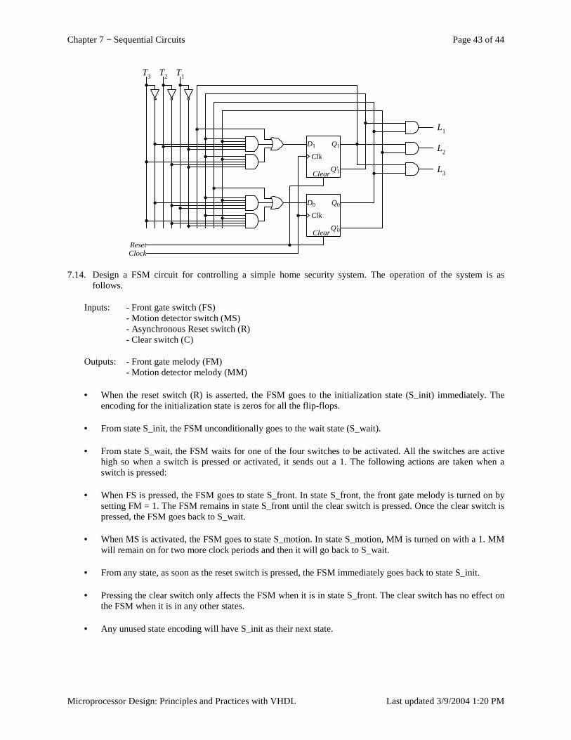
Chapter 7 − Sequential Circuits Page 43 of 44
Microprocessor Design: Principles and Practices with VHDL Last updated 3/9/2004 1:20 PM
Clk
D1
Q'1
Q1
Clear
T3
Clock
Clk
D0
Q'0
Q0
ClearReset
T2 T1
L1
L2
L3
7.14. Design a FSM circuit for controlling a simple home security system. The operation of the system is as follows.
Inputs: - Front gate switch (FS) - Motion detector switch (MS) - Asynchronous Reset switch (R) - Clear switch (C)
Outputs: - Front gate melody (FM) - Motion detector melody (MM)
• When the reset switch (R) is asserted, the FSM goes to the initialization state (S_init) immediately. The encoding for the initialization state is zeros for all the flip-flops.
• From state S_init, the FSM unconditionally goes to the wait state (S_wait).
• From state S_wait, the FSM waits for one of the four switches to be activated. All the switches are active high so when a switch is pressed or activated, it sends out a 1. The following actions are taken when a switch is pressed:
• When FS is pressed, the FSM goes to state S_front. In state S_front, the front gate melody is turned on by setting FM = 1. The FSM remains in state S_front until the clear switch is pressed. Once the clear switch is pressed, the FSM goes back to S_wait.
• When MS is activated, the FSM goes to state S_motion. In state S_motion, MM is turned on with a 1. MM will remain on for two more clock periods and then it will go back to S_wait.
• From any state, as soon as the reset switch is pressed, the FSM immediately goes back to state S_init.
• Pressing the clear switch only affects the FSM when it is in state S_front. The clear switch has no effect on the FSM when it is in any other states.
• Any unused state encoding will have S_init as their next state.
Chapter 7 − Sequential Circuits Page 44 of 44
Microprocessor Design: Principles and Practices with VHDL Last updated 3/9/2004 1:20 PM
Index
A
Analysis of sequential circuit, 4
C
Characteristic equation, 6 Choice of flip-flops, 35
E
Excitation equation, 5
F
Finite-state machine, 3 FSM. See Finite-state machine.
M
Mealy FSM, 3 Microprocessor
next-state logic, 3 state memory, 3
Moore FSM, 3
N
Next-state equation, 6 Next-state logic, 3 Next-state table, 6
O
One-shot circuit, 24 Optimization of sequential circuit, 33
choice of flip-flops, 35 state encoding, 34 state reduction, 33
Output equation, 7 Output table, 7
S
Sequential circuit analysis, 4 optimization. See Optimization of sequential
circuit synthesis, 12
State, 3 State diagram, 7 State encoding, 34 State memory, 3 State reduction, 33 Synthesis of sequential circuit, 12
V
VHDL sequential circuits, 27
Chapter 8 − Sequential Components Page 1 of 30
Microprocessor Design – Principles and Practices with VHDL Last updated 3/9/2004 1:21 PM
Contents Sequential Components................................................................................................................................................. 2
8.1 Registers........................................................................................................................................................ 3 8.2 Shift Registers ............................................................................................................................................... 4
8.2.1 Serial-to-Parallel Shift Register ............................................................................................................ 5 8.2.2 Serial-to-Parallel and Parallel-to-Serial Shift Register.......................................................................... 7
8.3 Counters ........................................................................................................................................................ 8 8.3.1 Binary Up Counter ................................................................................................................................ 9 8.3.2 Binary Up-Down Counter ................................................................................................................... 11 8.3.3 Binary Up-Down Counter with Parallel Load..................................................................................... 13 8.3.4 BCD Up Counter................................................................................................................................. 14 8.3.5 BCD Up-Down Counter...................................................................................................................... 16
8.4 Register Files............................................................................................................................................... 17 8.5 Static Random Access Memory .................................................................................................................. 21 8.6 * Larger Memories...................................................................................................................................... 25
8.6.1 More Memory Locations..................................................................................................................... 25 8.6.2 Wider Bit Width.................................................................................................................................. 25
8.7 Summary Checklist ..................................................................................................................................... 28 8.8 Problems ..................................................................................................................................................... 28 Index ....................................................................................................................................................................... 30
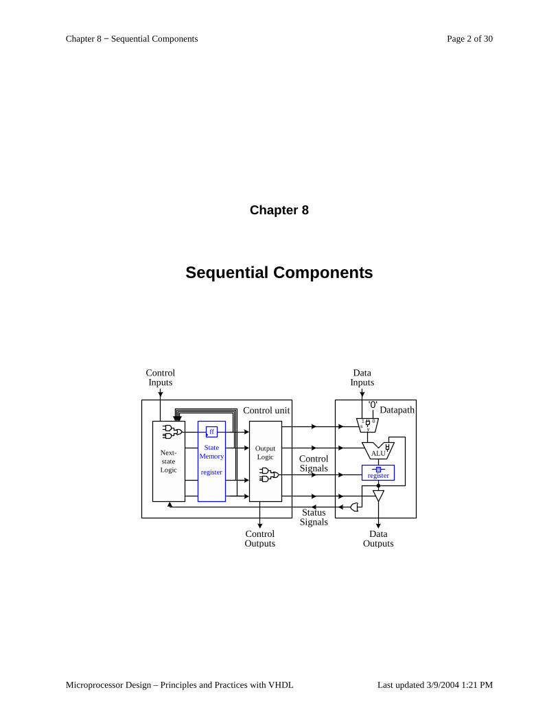
Chapter 8 − Sequential Components Page 2 of 30
Microprocessor Design – Principles and Practices with VHDL Last updated 3/9/2004 1:21 PM
Chapter 8
Sequential Components
ControlSignals
StatusSignals
01s y
'0'
DataInputs
DataOutputs
Datapath
ALU
registerff
OutputLogicNext-
stateLogic
ControlInputs
ControlOutputs
StateMemory
register
Control unit
ff
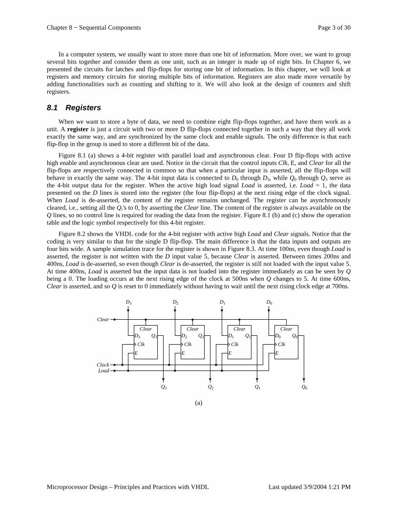
Chapter 8 − Sequential Components Page 3 of 30
Microprocessor Design – Principles and Practices with VHDL Last updated 3/9/2004 1:21 PM
In a computer system, we usually want to store more than one bit of information. More over, we want to group several bits together and consider them as one unit, such as an integer is made up of eight bits. In Chapter 6, we presented the circuits for latches and flip-flops for storing one bit of information. In this chapter, we will look at registers and memory circuits for storing multiple bits of information. Registers are also made more versatile by adding functionalities such as counting and shifting to it. We will also look at the design of counters and shift registers.
8.1 Registers When we want to store a byte of data, we need to combine eight flip-flops together, and have them work as a
unit. A register is just a circuit with two or more D flip-flops connected together in such a way that they all work exactly the same way, and are synchronized by the same clock and enable signals. The only difference is that each flip-flop in the group is used to store a different bit of the data.
Figure 8.1 (a) shows a 4-bit register with parallel load and asynchronous clear. Four D flip-flops with active high enable and asynchronous clear are used. Notice in the circuit that the control inputs Clk, E, and Clear for all the flip-flops are respectively connected in common so that when a particular input is asserted, all the flip-flops will behave in exactly the same way. The 4-bit input data is connected to D0 through D3, while Q0 through Q3 serve as the 4-bit output data for the register. When the active high load signal Load is asserted, i.e. Load = 1, the data presented on the D lines is stored into the register (the four flip-flops) at the next rising edge of the clock signal. When Load is de-asserted, the content of the register remains unchanged. The register can be asynchronously cleared, i.e., setting all the Qi's to 0, by asserting the Clear line. The content of the register is always available on the Q lines, so no control line is required for reading the data from the register. Figure 8.1 (b) and (c) show the operation table and the logic symbol respectively for this 4-bit register.
Figure 8.2 shows the VHDL code for the 4-bit register with active high Load and Clear signals. Notice that the coding is very similar to that for the single D flip-flop. The main difference is that the data inputs and outputs are four bits wide. A sample simulation trace for the register is shown in Figure 8.3. At time 100ns, even though Load is asserted, the register is not written with the D input value 5, because Clear is asserted. Between times 200ns and 400ns, Load is de-asserted, so even though Clear is de-asserted, the register is still not loaded with the input value 5. At time 400ns, Load is asserted but the input data is not loaded into the register immediately as can be seen by Q being a 0. The loading occurs at the next rising edge of the clock at 500ns when Q changes to 5. At time 600ns, Clear is asserted, and so Q is reset to 0 immediately without having to wait until the next rising clock edge at 700ns.
Clear
LoadClock
Q3 Q2 Q1 Q0
Clk
D3 Q3
E
Clear
Clk
D2 Q2
E
Clear
Clk
D1 Q1
E
Clear
Clk
D0 Q0
E
Clear
D3 D2 D1 D0
(a)
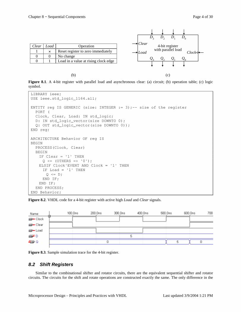
Chapter 8 − Sequential Components Page 4 of 30
Microprocessor Design – Principles and Practices with VHDL Last updated 3/9/2004 1:21 PM
Clear Load Operation 1 × Reset register to zero immediately 0 0 No change 0 1 Load in a value at rising clock edge
(b)
4-bit registerwith parallel load
Clear
Clock
D3 D2 D1 D0
Q3 Q2 Q1 Q0
Load
(c)
Figure 8.1. A 4-bit register with parallel load and asynchronous clear: (a) circuit; (b) operation table; (c) logic symbol.
LIBRARY ieee;USE ieee.std_logic_1164.all;
ENTITY reg IS GENERIC (size: INTEGER := 3);-- size of the registerPORT (Clock, Clear, Load: IN std_logic;D: IN std_logic_vector(size DOWNTO 0);Q: OUT std_logic_vector(size DOWNTO 0));
END reg;
ARCHITECTURE Behavior OF reg ISBEGIN
PROCESS(Clock, Clear)BEGINIF Clear = '1' THENQ <= (OTHERS => '0');
ELSIF Clock'EVENT AND Clock = '1' THENIF Load = '1' THENQ <= D;
END IF;END IF;
END PROCESS;END Behavior;
Figure 8.2. VHDL code for a 4-bit register with active high Load and Clear signals.
Figure 8.3. Sample simulation trace for the 4-bit register.
8.2 Shift Registers Similar to the combinational shifter and rotator circuits, there are the equivalent sequential shifter and rotator
circuits. The circuits for the shift and rotate operations are constructed exactly the same. The only difference in the
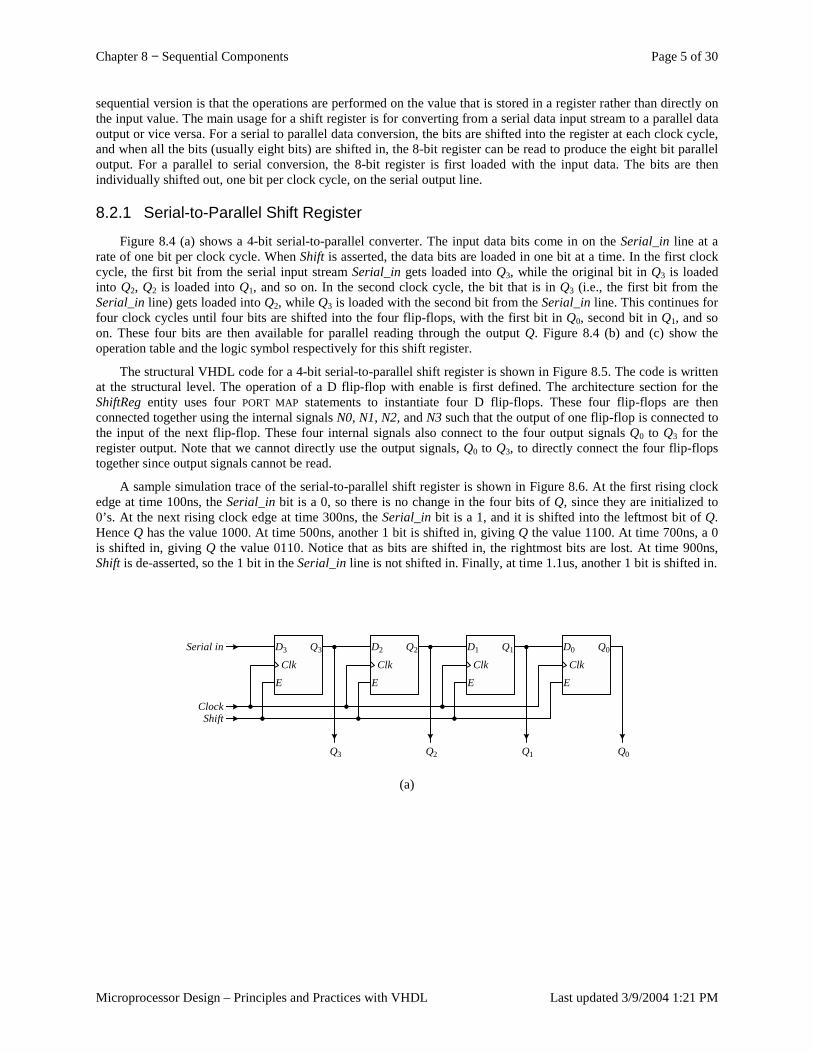
Chapter 8 − Sequential Components Page 5 of 30
Microprocessor Design – Principles and Practices with VHDL Last updated 3/9/2004 1:21 PM
sequential version is that the operations are performed on the value that is stored in a register rather than directly on the input value. The main usage for a shift register is for converting from a serial data input stream to a parallel data output or vice versa. For a serial to parallel data conversion, the bits are shifted into the register at each clock cycle, and when all the bits (usually eight bits) are shifted in, the 8-bit register can be read to produce the eight bit parallel output. For a parallel to serial conversion, the 8-bit register is first loaded with the input data. The bits are then individually shifted out, one bit per clock cycle, on the serial output line.
8.2.1 Serial-to-Parallel Shift Register
Figure 8.4 (a) shows a 4-bit serial-to-parallel converter. The input data bits come in on the Serial_in line at a rate of one bit per clock cycle. When Shift is asserted, the data bits are loaded in one bit at a time. In the first clock cycle, the first bit from the serial input stream Serial_in gets loaded into Q3, while the original bit in Q3 is loaded into Q2, Q2 is loaded into Q1, and so on. In the second clock cycle, the bit that is in Q3 (i.e., the first bit from the Serial_in line) gets loaded into Q2, while Q3 is loaded with the second bit from the Serial_in line. This continues for four clock cycles until four bits are shifted into the four flip-flops, with the first bit in Q0, second bit in Q1, and so on. These four bits are then available for parallel reading through the output Q. Figure 8.4 (b) and (c) show the operation table and the logic symbol respectively for this shift register.
The structural VHDL code for a 4-bit serial-to-parallel shift register is shown in Figure 8.5. The code is written at the structural level. The operation of a D flip-flop with enable is first defined. The architecture section for the ShiftReg entity uses four PORT MAP statements to instantiate four D flip-flops. These four flip-flops are then connected together using the internal signals N0, N1, N2, and N3 such that the output of one flip-flop is connected to the input of the next flip-flop. These four internal signals also connect to the four output signals Q0 to Q3 for the register output. Note that we cannot directly use the output signals, Q0 to Q3, to directly connect the four flip-flops together since output signals cannot be read.
A sample simulation trace of the serial-to-parallel shift register is shown in Figure 8.6. At the first rising clock edge at time 100ns, the Serial_in bit is a 0, so there is no change in the four bits of Q, since they are initialized to 0’s. At the next rising clock edge at time 300ns, the Serial_in bit is a 1, and it is shifted into the leftmost bit of Q. Hence Q has the value 1000. At time 500ns, another 1 bit is shifted in, giving Q the value 1100. At time 700ns, a 0 is shifted in, giving Q the value 0110. Notice that as bits are shifted in, the rightmost bits are lost. At time 900ns, Shift is de-asserted, so the 1 bit in the Serial_in line is not shifted in. Finally, at time 1.1us, another 1 bit is shifted in.
Clk
D3 Q3
E
Clk
D2 Q2
E
Clk
D1 Q1
E
Clk
D0 Q0
E
Serial in
ShiftClock
Q3 Q2 Q1 Q0
(a)
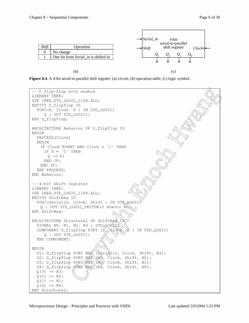
Chapter 8 − Sequential Components Page 6 of 30
Microprocessor Design – Principles and Practices with VHDL Last updated 3/9/2004 1:21 PM
Shift Operation 0 No change 1 One bit from Serial_in is shifted in
(b)
4-bitserial-to-parallel
shift register ClockQ3 Q2 Q1 Q0
Shift
Serial_in
(c)
Figure 8.4. A 4-bit serial-to-parallel shift register: (a) circuit; (b) operation table; (c) logic symbol.
-- D flip-flop with enableLIBRARY IEEE;USE IEEE.STD_LOGIC_1164.ALL;ENTITY D_flipflop IS
PORT(D, Clock, E : IN STD_LOGIC;Q : OUT STD_LOGIC);
END D_flipflop;
ARCHITECTURE Behavior OF D_flipflop ISBEGIN
PROCESS(Clock)BEGINIF Clock'EVENT AND Clock = '1' THENIF E = '1' THENQ <= D;
END IF;END IF;
END PROCESS;END Behavior;
-- 4-bit shift registerLIBRARY IEEE;USE IEEE.STD_LOGIC_1164.ALL;ENTITY ShiftReg IS
PORT(Serialin, Clock, Shift : IN STD_LOGIC;Q : OUT STD_LOGIC_VECTOR(3 downto 0));
END ShiftReg;
ARCHITECTURE Structural OF ShiftReg ISSIGNAL N0, N1, N2, N3 : STD_LOGIC;COMPONENT D_flipflop PORT (D, Clock, E : IN STD_LOGIC;
Q : OUT STD_LOGIC);END COMPONENT;
BEGINU1: D_flipflop PORT MAP (Serialin, Clock, Shift, N3);U2: D_flipflop PORT MAP (N3, Clock, Shift, N2);U3: D_flipflop PORT MAP (N2, Clock, Shift, N1);U4: D_flipflop PORT MAP (N1, Clock, Shift, N0);Q(3) <= N3;Q(2) <= N2;Q(1) <= N1;Q(0) <= N0;
END Structural;
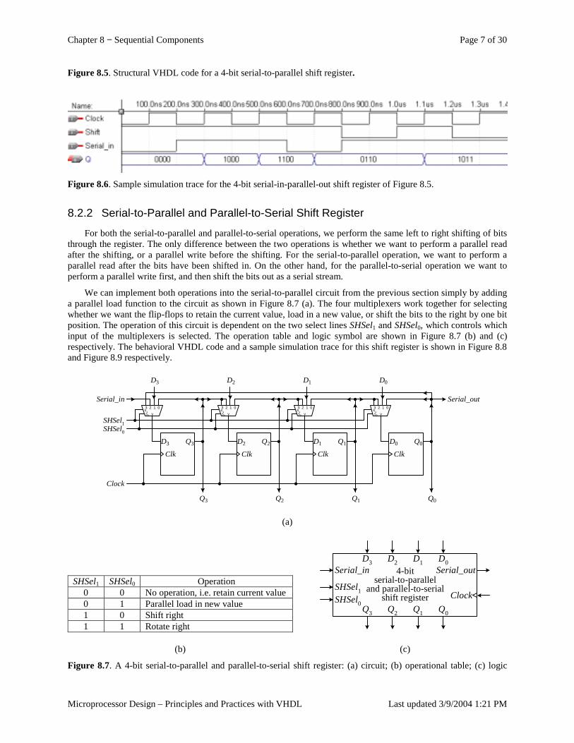
Chapter 8 − Sequential Components Page 7 of 30
Microprocessor Design – Principles and Practices with VHDL Last updated 3/9/2004 1:21 PM
Figure 8.5. Structural VHDL code for a 4-bit serial-to-parallel shift register.
Figure 8.6. Sample simulation trace for the 4-bit serial-in-parallel-out shift register of Figure 8.5.
8.2.2 Serial-to-Parallel and Parallel-to-Serial Shift Register
For both the serial-to-parallel and parallel-to-serial operations, we perform the same left to right shifting of bits through the register. The only difference between the two operations is whether we want to perform a parallel read after the shifting, or a parallel write before the shifting. For the serial-to-parallel operation, we want to perform a parallel read after the bits have been shifted in. On the other hand, for the parallel-to-serial operation we want to perform a parallel write first, and then shift the bits out as a serial stream.
We can implement both operations into the serial-to-parallel circuit from the previous section simply by adding a parallel load function to the circuit as shown in Figure 8.7 (a). The four multiplexers work together for selecting whether we want the flip-flops to retain the current value, load in a new value, or shift the bits to the right by one bit position. The operation of this circuit is dependent on the two select lines SHSel1 and SHSel0, which controls which input of the multiplexers is selected. The operation table and logic symbol are shown in Figure 8.7 (b) and (c) respectively. The behavioral VHDL code and a sample simulation trace for this shift register is shown in Figure 8.8 and Figure 8.9 respectively.
Clk
D2 Q2
Clk
D1 Q1
Clk
D0 Q0
Serial_in
SHSel1
Clock
Q3 Q2 Q1 Q0
02s1 y
13s0
Clk
D3 Q3
02s1 y
13s0
02s1 y
13s0
02s1 y
13s0
Serial_out
SHSel0
D3 D2 D1 D0
(a)
SHSel1 SHSel0 Operation 0 0 No operation, i.e. retain current value 0 1 Parallel load in new value 1 0 Shift right 1 1 Rotate right
(b)
4-bitserial-to-parallel
and parallel-to-serialshift register Clock
Serial_outD3 D2 D1 D0
Q3 Q2 Q1 Q0
Serial_in
SHSel0
SHSel1
(c)
Figure 8.7. A 4-bit serial-to-parallel and parallel-to-serial shift register: (a) circuit; (b) operational table; (c) logic
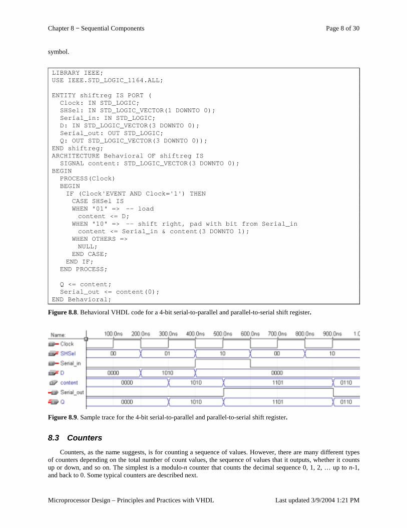
Chapter 8 − Sequential Components Page 8 of 30
Microprocessor Design – Principles and Practices with VHDL Last updated 3/9/2004 1:21 PM
symbol.
LIBRARY IEEE;USE IEEE.STD_LOGIC_1164.ALL;
ENTITY shiftreg IS PORT (Clock: IN STD_LOGIC;SHSel: IN STD_LOGIC_VECTOR(1 DOWNTO 0);Serial_in: IN STD_LOGIC;D: IN STD_LOGIC_VECTOR(3 DOWNTO 0);Serial_out: OUT STD_LOGIC;Q: OUT STD_LOGIC_VECTOR(3 DOWNTO 0));
END shiftreg;ARCHITECTURE Behavioral OF shiftreg IS
SIGNAL content: STD_LOGIC_VECTOR(3 DOWNTO 0);BEGIN
PROCESS(Clock)BEGINIF (Clock'EVENT AND Clock='1') THENCASE SHSel ISWHEN "01" => -- loadcontent <= D;
WHEN "10" => -- shift right, pad with bit from Serial_incontent <= Serial_in & content(3 DOWNTO 1);
WHEN OTHERS =>NULL;
END CASE;END IF;
END PROCESS;
Q <= content;Serial_out <= content(0);
END Behavioral;
Figure 8.8. Behavioral VHDL code for a 4-bit serial-to-parallel and parallel-to-serial shift register.
Figure 8.9. Sample trace for the 4-bit serial-to-parallel and parallel-to-serial shift register.
8.3 Counters Counters, as the name suggests, is for counting a sequence of values. However, there are many different types
of counters depending on the total number of count values, the sequence of values that it outputs, whether it counts up or down, and so on. The simplest is a modulo-n counter that counts the decimal sequence 0, 1, 2, … up to n-1, and back to 0. Some typical counters are described next.
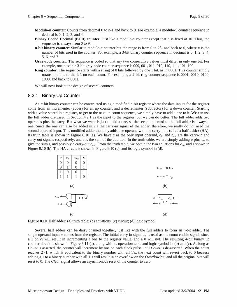
Chapter 8 − Sequential Components Page 9 of 30
Microprocessor Design – Principles and Practices with VHDL Last updated 3/9/2004 1:21 PM
Modulo-n counter: Counts from decimal 0 to n-1 and back to 0. For example, a modulo-5 counter sequence in decimal is 0, 1, 2, 3, and 4.
Binary Coded Decimal (BCD) counter: Just like a modulo-n counter except that n is fixed at 10. Thus, the sequence is always from 0 to 9.
n-bit binary counter: Similar to modulo-n counter but the range is from 0 to 2n-1and back to 0, where n is the number of bits used in the counter. For example, a 3-bit binary counter sequence in decimal is 0, 1, 2, 3, 4, 5, 6, and 7.
Gray-code counter: The sequence is coded so that any two consecutive values must differ in only one bit. For example, one possible 3-bit gray-code counter sequence is 000, 001, 011, 010, 110, 111, 101, 100.
Ring counter: The sequence starts with a string of 0 bits followed by one 1 bit, as in 0001. This counter simply rotates the bits to the left on each count. For example, a 4-bit ring counter sequence is 0001, 0010, 0100, 1000, and back to 0001.
We will now look at the design of several counters.
8.3.1 Binary Up Counter
An n-bit binary counter can be constructed using a modified n-bit register where the data inputs for the register come from an incrementer (adder) for an up counter, and a decrementer (subtractor) for a down counter. Starting with a value stored in a register, to get to the next up count sequence, we simply have to add a one to it. We can use the full adder discussed in Section 4.2.1 as the input to the register, but we can do better. The full adder adds two operands plus the carry. But what we want is just to add a one, so the second operand to the full adder is always a one. Since the one can also be added in via the carry-in signal of the adder, therefore, we really do not need the second operand input. This modified adder that only adds one operand with the carry-in is called a half adder (HA). Its truth table is shown in Figure 8.10 (a). We have a as the only input operand, cin and cout are the carry-in and carry-out signals respectively, and s is the sum of the addition. In the truth table, we are simply adding a plus cin to give the sum s, and possibly a carry-out cout. From the truth table, we obtain the two equations for cout and s shown in Figure 8.10 (b). The HA circuit is shown in Figure 8.10 (c), and its logic symbol in (d).
a cin cout s 0 0 0 0 0 1 0 1 1 0 0 1 1 1 1 0
(a)
cout = a cin
s = a ⊕ cin
(b)
cina
s
cout
(c)
s a
cout cinHA
(d)
Figure 8.10. Half adder: (a) truth table; (b) equations; (c) circuit; (d) logic symbol.
Several half adders can be daisy chained together, just like with the full adders to form an n-bit adder. The single operand input a comes from the register. The initial carry-in signal c0 is used as the count enable signal, since a 1 on c0 will result in incrementing a one to the register value, and a 0 will not. The resulting 4-bit binary up counter circuit is shown in Figure 8.11 (a), along with its operation table and logic symbol in (b) and (c). As long as Count is asserted, the counter will increment by one on each clock pulse until Count is de-asserted. When the count reaches 2n-1, which is equivalent to the binary number with all 1’s, the next count will revert back to 0 because adding a 1 to a binary number with all 1’s will result in an overflow on the Overflow bit, and all the original bits will reset to 0. The Clear signal allows an asynchronous reset of the counter to zero.
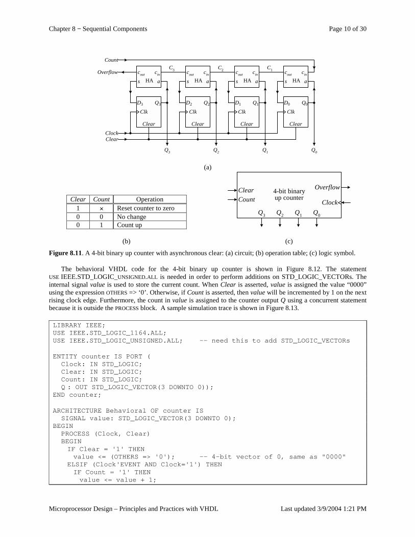
Chapter 8 − Sequential Components Page 10 of 30
Microprocessor Design – Principles and Practices with VHDL Last updated 3/9/2004 1:21 PM
Clk
D1 Q1
Clear
C2
s a
cout cin
HA
Clk
D2 Q2
Clear
C3
s a
cout cin
HA
Clk
D3 Q3
Clear
s a
cout cin
HA
ClockClear
Overflow
Clk
D0 Q0
Clear
C1
s a
cout cin
HA
Count
Q3 Q2 Q1 Q0
(a)
Clear Count Operation 1 × Reset counter to zero 0 0 No change 0 1 Count up
(b)
4-bit binaryup counter
Clock
Overflow
Q3 Q2 Q1 Q0
ClearCount
(c)
Figure 8.11. A 4-bit binary up counter with asynchronous clear: (a) circuit; (b) operation table; (c) logic symbol.
The behavioral VHDL code for the 4-bit binary up counter is shown in Figure 8.12. The statement USE IEEE.STD_LOGIC_UNSIGNED.ALL is needed in order to perform additions on STD_LOGIC_VECTORs. The internal signal value is used to store the current count. When Clear is asserted, value is assigned the value “0000” using the expression OTHERS => ‘0’. Otherwise, if Count is asserted, then value will be incremented by 1 on the next rising clock edge. Furthermore, the count in value is assigned to the counter output Q using a concurrent statement because it is outside the PROCESS block. A sample simulation trace is shown in Figure 8.13.
LIBRARY IEEE;USE IEEE.STD_LOGIC_1164.ALL;USE IEEE.STD_LOGIC_UNSIGNED.ALL; -- need this to add STD_LOGIC_VECTORs
ENTITY counter IS PORT (Clock: IN STD_LOGIC;Clear: IN STD_LOGIC;Count: IN STD_LOGIC;Q : OUT STD_LOGIC_VECTOR(3 DOWNTO 0));
END counter;
ARCHITECTURE Behavioral OF counter ISSIGNAL value: STD_LOGIC_VECTOR(3 DOWNTO 0);
BEGINPROCESS (Clock, Clear)BEGINIF Clear = '1' THENvalue <= (OTHERS => '0'); -- 4-bit vector of 0, same as "0000"
ELSIF (Clock'EVENT AND Clock='1') THENIF Count = '1' THENvalue <= value + 1;
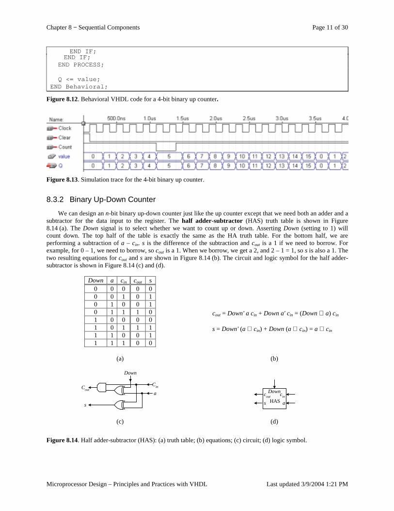
Chapter 8 − Sequential Components Page 11 of 30
Microprocessor Design – Principles and Practices with VHDL Last updated 3/9/2004 1:21 PM
END IF;END IF;
END PROCESS;
Q <= value;END Behavioral;
Figure 8.12. Behavioral VHDL code for a 4-bit binary up counter.
Figure 8.13. Simulation trace for the 4-bit binary up counter.
8.3.2 Binary Up-Down Counter
We can design an n-bit binary up-down counter just like the up counter except that we need both an adder and a subtractor for the data input to the register. The half adder-subtractor (HAS) truth table is shown in Figure 8.14 (a). The Down signal is to select whether we want to count up or down. Asserting Down (setting to 1) will count down. The top half of the table is exactly the same as the HA truth table. For the bottom half, we are performing a subtraction of a – cin. s is the difference of the subtraction and cout is a 1 if we need to borrow. For example, for 0 – 1, we need to borrow, so cout is a 1. When we borrow, we get a 2, and 2 – 1 = 1, so s is also a 1. The two resulting equations for cout and s are shown in Figure 8.14 (b). The circuit and logic symbol for the half adder-subtractor is shown in Figure 8.14 (c) and (d).
Down a cin cout s 0 0 0 0 0 0 0 1 0 1 0 1 0 0 1 0 1 1 1 0 1 0 0 0 0 1 0 1 1 1 1 1 0 0 1 1 1 1 0 0
(a)
cout = Down' a cin + Down a' cin = (Down ⊕ a) cin
s = Down' (a ⊕ cin) + Down (a ⊕ cin) = a ⊕ cin
(b)
Down
Cin
aCout
s
(c)
s a
cout cinDown
HAS
(d)
Figure 8.14. Half adder-subtractor (HAS): (a) truth table; (b) equations; (c) circuit; (d) logic symbol.
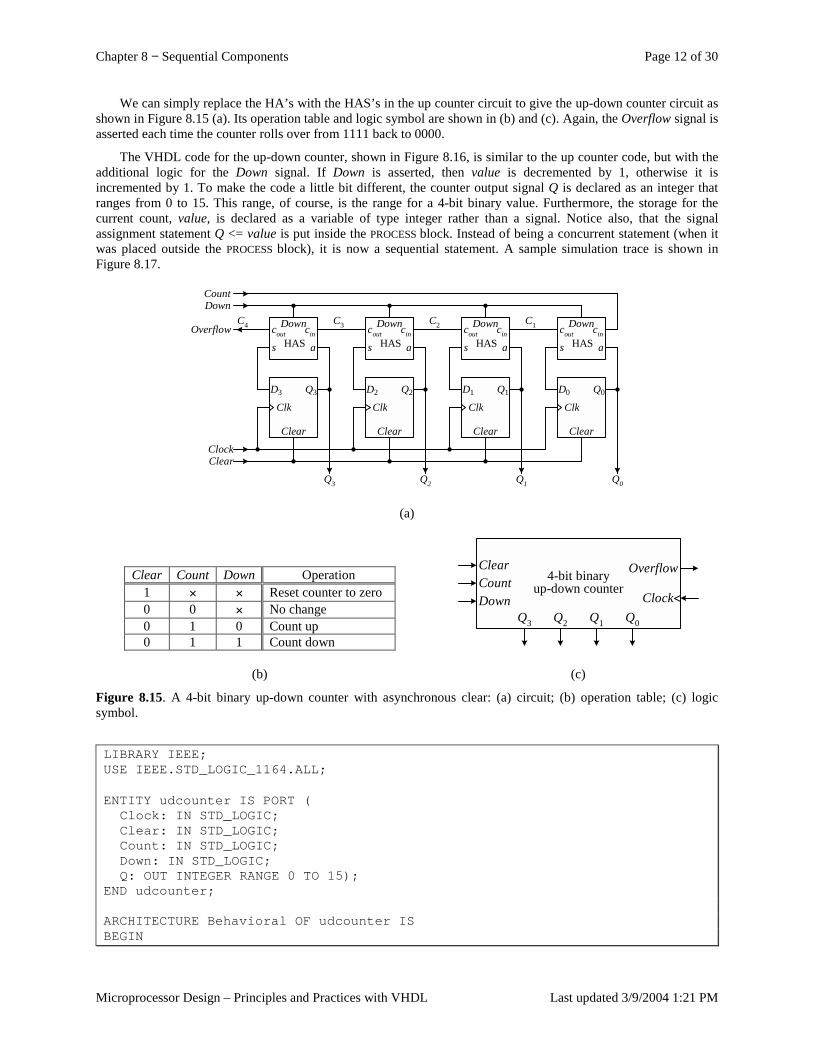
Chapter 8 − Sequential Components Page 12 of 30
Microprocessor Design – Principles and Practices with VHDL Last updated 3/9/2004 1:21 PM
We can simply replace the HA’s with the HAS’s in the up counter circuit to give the up-down counter circuit as shown in Figure 8.15 (a). Its operation table and logic symbol are shown in (b) and (c). Again, the Overflow signal is asserted each time the counter rolls over from 1111 back to 0000.
The VHDL code for the up-down counter, shown in Figure 8.16, is similar to the up counter code, but with the additional logic for the Down signal. If Down is asserted, then value is decremented by 1, otherwise it is incremented by 1. To make the code a little bit different, the counter output signal Q is declared as an integer that ranges from 0 to 15. This range, of course, is the range for a 4-bit binary value. Furthermore, the storage for the current count, value, is declared as a variable of type integer rather than a signal. Notice also, that the signal assignment statement Q <= value is put inside the PROCESS block. Instead of being a concurrent statement (when it was placed outside the PROCESS block), it is now a sequential statement. A sample simulation trace is shown in Figure 8.17.
Q3 Q2 Q1 Q0
ClockClear
Overflow
Count
Clk
D0 Q0
Clear
C1
s a
cout cinDown
HAS
Down
Clk
D1 Q1
Clear
C2
s a
cout cinDown
HAS
Clk
D2 Q2
Clear
C3
s a
cout cinDown
HAS
Clk
D3 Q3
Clear
C4
s a
cout cinDown
HAS
(a)
Clear Count Down Operation
1 × × Reset counter to zero 0 0 × No change 0 1 0 Count up 0 1 1 Count down
(b)
4-bit binaryup-down counter
Clock
Overflow
Q3 Q2 Q1 Q0
ClearCountDown
(c)
Figure 8.15. A 4-bit binary up-down counter with asynchronous clear: (a) circuit; (b) operation table; (c) logic symbol.
LIBRARY IEEE;USE IEEE.STD_LOGIC_1164.ALL;
ENTITY udcounter IS PORT (Clock: IN STD_LOGIC;Clear: IN STD_LOGIC;Count: IN STD_LOGIC;Down: IN STD_LOGIC;Q: OUT INTEGER RANGE 0 TO 15);
END udcounter;
ARCHITECTURE Behavioral OF udcounter ISBEGIN
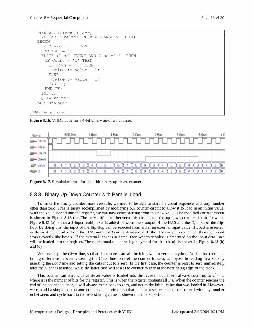
Chapter 8 − Sequential Components Page 13 of 30
Microprocessor Design – Principles and Practices with VHDL Last updated 3/9/2004 1:21 PM
PROCESS (Clock, Clear)VARIABLE value: INTEGER RANGE 0 TO 15;
BEGINIF Clear = '1' THENvalue := 0;
ELSIF (Clock'EVENT AND Clock='1') THENIF Count = '1' THENIF Down = '0' THENvalue := value + 1;
ELSEvalue := value - 1;
END IF;END IF;
END IF;Q <= value;
END PROCESS;
END Behavioral;
Figure 8.16. VHDL code for a 4-bit binary up-down counter.
Figure 8.17. Simulation trace for the 4-bit binary up-down counter.
8.3.3 Binary Up-Down Counter with Parallel Load
To make the binary counter more versatile, we need to be able to start the count sequence with any number other than zero. This is easily accomplished by modifying our counter circuit to allow it to load in an initial value. With the value loaded into the register, we can now count starting from this new value. The modified counter circuit is shown in Figure 8.18 (a). The only difference between this circuit and the up-down counter circuit shown in Figure 8.15 (a) is that a 2-input multiplexer is added between the s output of the HAS and the Di input of the flip-flop. By doing this, the input of the flip-flop can be selected from either an external input value, if Load is asserted, or the next count value from the HAS output if Load is de-asserted. If the HAS output is selected, then the circuit works exactly like before. If the external input is selected, then whatever value is presented on the input data lines will be loaded into the register. The operational table and logic symbol for this circuit is shown in Figure 8.18 (b) and (c).
We have kept the Clear line, so that the counter can still be initialized to zero at anytime. Notice that there is a timing difference between asserting the Clear line to reset the counter to zero, as oppose to loading in a zero by asserting the Load line and setting the data input to a zero. In the first case, the counter is reset to zero immediately after the Clear is asserted, while the latter case will reset the counter to zero at the next rising edge of the clock.
This counter can start with whatever value is loaded into the register, but it will always count up to 2n – 1, where n is the number of bits for the register. This is when the register contains all 1’s. When the counter reaches the end of the count sequence, it will always cycle back to zero, and not to the initial value that was loaded in. However, we can add a simple comparator to this counter circuit so that the count sequence can start or end with any number in between, and cycle back to the new starting value as shown in the next section.
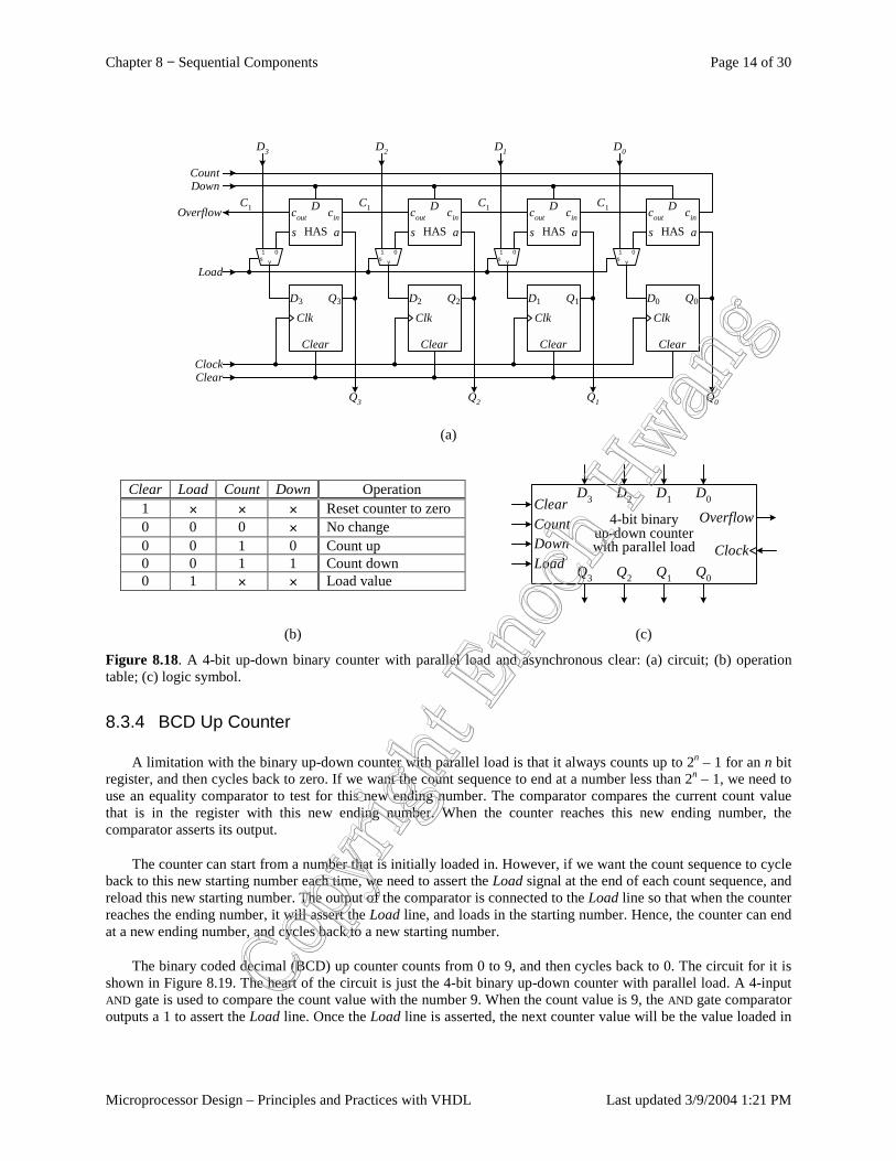
Chapter 8 − Sequential Components Page 14 of 30
Microprocessor Design – Principles and Practices with VHDL Last updated 3/9/2004 1:21 PM
ClockClear
Overflow
CountDown
Q3 Q2 Q1 Q0
Clk
D1 Q1
Clear
C1
s a
cout cin
HAS
D
01s y
Clk
D0 Q0
Clear
C1
s a
cout cin
HAS
D
01s y
Clk
D2 Q2
Clear
C1
s a
cout cin
HAS
D
01s y
Clk
D3 Q3
Clear
C1
s a
cout cin
HAS
D
01s y
D3 D2 D1 D0
Load
(a)
Clear Load Count Down Operation
1 × × × Reset counter to zero 0 0 0 × No change 0 0 1 0 Count up 0 0 1 1 Count down 0 1 × × Load value
(b)
4-bit binaryup-down counterwith parallel load
ClearCountDown Clock
Overflow
D3 D2 D1 D0
Q3 Q2 Q1 Q0Load
(c)
Figure 8.18. A 4-bit up-down binary counter with parallel load and asynchronous clear: (a) circuit; (b) operation table; (c) logic symbol.
8.3.4 BCD Up Counter
A limitation with the binary up-down counter with parallel load is that it always counts up to 2n – 1 for an n bit register, and then cycles back to zero. If we want the count sequence to end at a number less than 2n – 1, we need to use an equality comparator to test for this new ending number. The comparator compares the current count value that is in the register with this new ending number. When the counter reaches this new ending number, the comparator asserts its output.
The counter can start from a number that is initially loaded in. However, if we want the count sequence to cycle back to this new starting number each time, we need to assert the Load signal at the end of each count sequence, and reload this new starting number. The output of the comparator is connected to the Load line so that when the counter reaches the ending number, it will assert the Load line, and loads in the starting number. Hence, the counter can end at a new ending number, and cycles back to a new starting number.
The binary coded decimal (BCD) up counter counts from 0 to 9, and then cycles back to 0. The circuit for it is shown in Figure 8.19. The heart of the circuit is just the 4-bit binary up-down counter with parallel load. A 4-input AND gate is used to compare the count value with the number 9. When the count value is 9, the AND gate comparator outputs a 1 to assert the Load line. Once the Load line is asserted, the next counter value will be the value loaded in
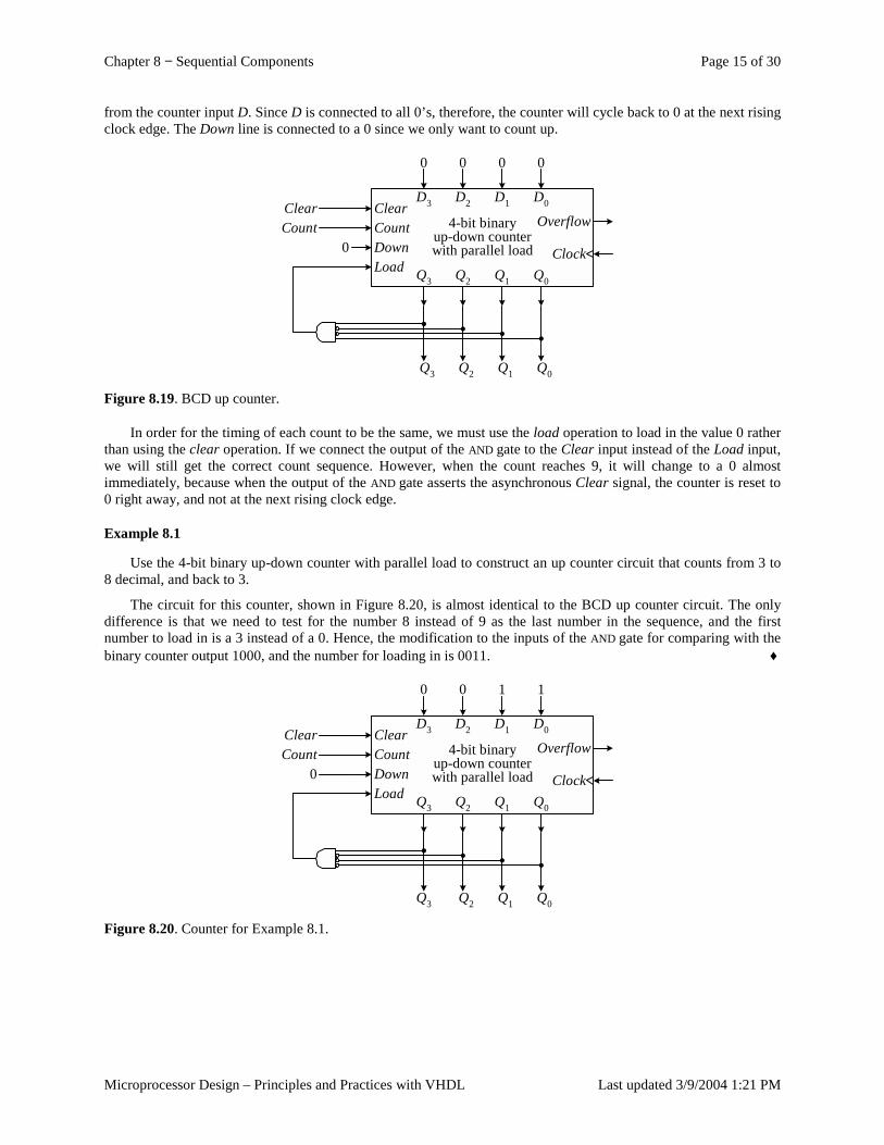
Chapter 8 − Sequential Components Page 15 of 30
Microprocessor Design – Principles and Practices with VHDL Last updated 3/9/2004 1:21 PM
from the counter input D. Since D is connected to all 0’s, therefore, the counter will cycle back to 0 at the next rising clock edge. The Down line is connected to a 0 since we only want to count up.
4-bit binaryup-down counterwith parallel load
ClearCountDown Clock
Overflow
D3 D2 D1 D0
Q3 Q2 Q1 Q0Load
0 0 0 0
ClearCount
0
Q3 Q2 Q1 Q0 Figure 8.19. BCD up counter.
In order for the timing of each count to be the same, we must use the load operation to load in the value 0 rather than using the clear operation. If we connect the output of the AND gate to the Clear input instead of the Load input, we will still get the correct count sequence. However, when the count reaches 9, it will change to a 0 almost immediately, because when the output of the AND gate asserts the asynchronous Clear signal, the counter is reset to 0 right away, and not at the next rising clock edge.
Example 8.1
Use the 4-bit binary up-down counter with parallel load to construct an up counter circuit that counts from 3 to 8 decimal, and back to 3.
The circuit for this counter, shown in Figure 8.20, is almost identical to the BCD up counter circuit. The only difference is that we need to test for the number 8 instead of 9 as the last number in the sequence, and the first number to load in is a 3 instead of a 0. Hence, the modification to the inputs of the AND gate for comparing with the binary counter output 1000, and the number for loading in is 0011. ♦
4-bit binaryup-down counterwith parallel load
ClearCountDown Clock
Overflow
D3 D2 D1 D0
Q3 Q2 Q1 Q0Load
ClearCount
Q3 Q2 Q1 Q0
1
0
100
Figure 8.20. Counter for Example 8.1.
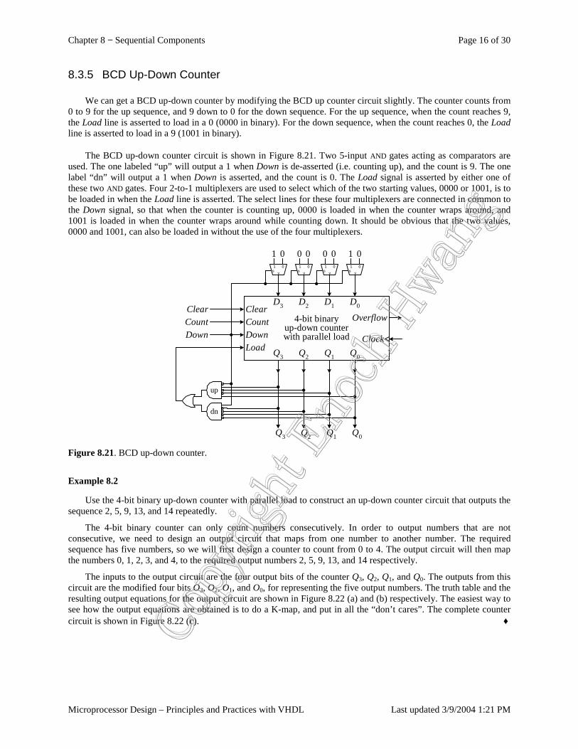
Chapter 8 − Sequential Components Page 16 of 30
Microprocessor Design – Principles and Practices with VHDL Last updated 3/9/2004 1:21 PM
8.3.5 BCD Up-Down Counter
We can get a BCD up-down counter by modifying the BCD up counter circuit slightly. The counter counts from 0 to 9 for the up sequence, and 9 down to 0 for the down sequence. For the up sequence, when the count reaches 9, the Load line is asserted to load in a 0 (0000 in binary). For the down sequence, when the count reaches 0, the Load line is asserted to load in a 9 (1001 in binary).
The BCD up-down counter circuit is shown in Figure 8.21. Two 5-input AND gates acting as comparators are used. The one labeled “up” will output a 1 when Down is de-asserted (i.e. counting up), and the count is 9. The one label “dn” will output a 1 when Down is asserted, and the count is 0. The Load signal is asserted by either one of these two AND gates. Four 2-to-1 multiplexers are used to select which of the two starting values, 0000 or 1001, is to be loaded in when the Load line is asserted. The select lines for these four multiplexers are connected in common to the Down signal, so that when the counter is counting up, 0000 is loaded in when the counter wraps around, and 1001 is loaded in when the counter wraps around while counting down. It should be obvious that the two values, 0000 and 1001, can also be loaded in without the use of the four multiplexers.
4-bit binaryup-down counterwith parallel load
ClearCountDown Clock
Overflow
D3 D2 D1 D0
Q3 Q2 Q1 Q0Load
ClearCount
Q3 Q2 Q1 Q0
0 0 0 001
s y01
s y01
s y01
s y
1 0 0 1
dn
up
Down
Figure 8.21. BCD up-down counter.
Example 8.2
Use the 4-bit binary up-down counter with parallel load to construct an up-down counter circuit that outputs the sequence 2, 5, 9, 13, and 14 repeatedly.
The 4-bit binary counter can only count numbers consecutively. In order to output numbers that are not consecutive, we need to design an output circuit that maps from one number to another number. The required sequence has five numbers, so we will first design a counter to count from 0 to 4. The output circuit will then map the numbers 0, 1, 2, 3, and 4, to the required output numbers 2, 5, 9, 13, and 14 respectively.
The inputs to the output circuit are the four output bits of the counter Q3, Q2, Q1, and Q0. The outputs from this circuit are the modified four bits O3, O2, O1, and O0, for representing the five output numbers. The truth table and the resulting output equations for the output circuit are shown in Figure 8.22 (a) and (b) respectively. The easiest way to see how the output equations are obtained is to do a K-map, and put in all the “don’t cares”. The complete counter circuit is shown in Figure 8.22 (c). ♦
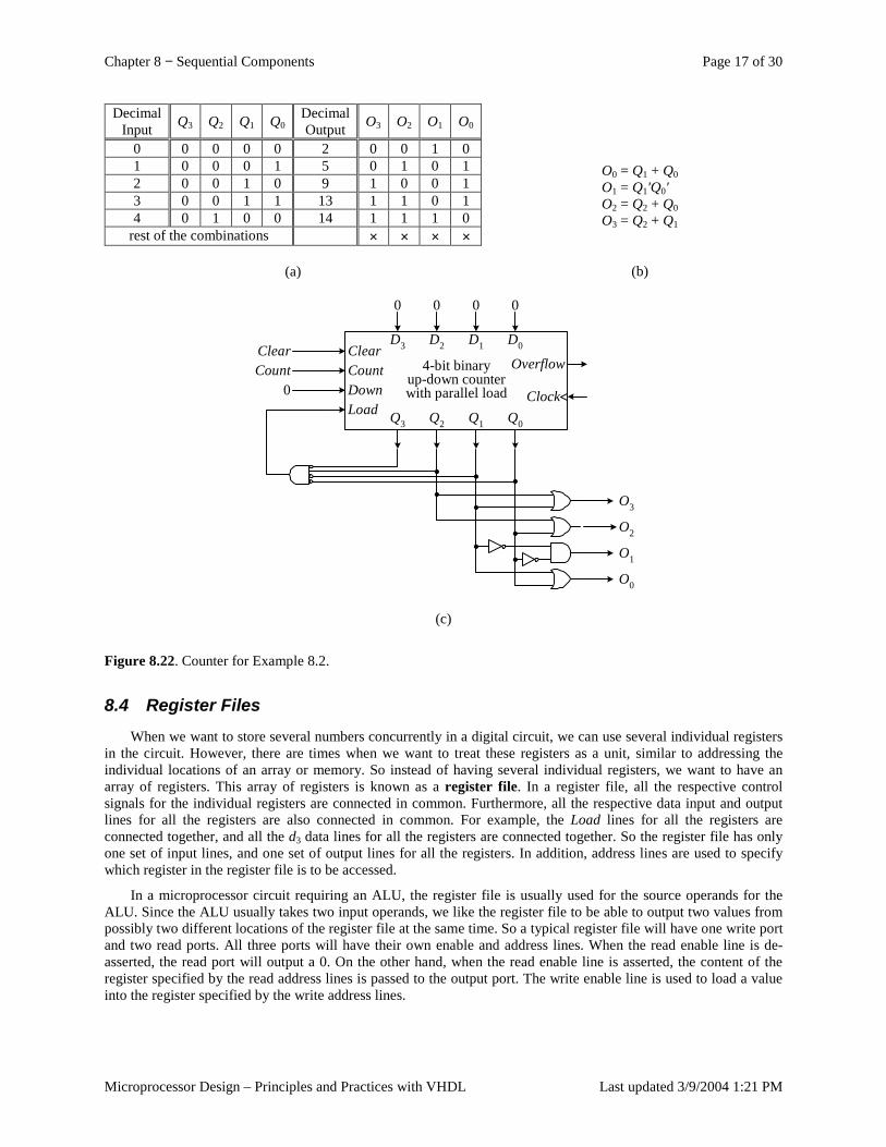
Chapter 8 − Sequential Components Page 17 of 30
Microprocessor Design – Principles and Practices with VHDL Last updated 3/9/2004 1:21 PM
Decimal Input Q3 Q2 Q1 Q0
Decimal Output O3 O2 O1 O0
0 0 0 0 0 2 0 0 1 0 1 0 0 0 1 5 0 1 0 1 2 0 0 1 0 9 1 0 0 1 3 0 0 1 1 13 1 1 0 1 4 0 1 0 0 14 1 1 1 0
rest of the combinations × × × ×
(a)
O0 = Q1 + Q0 O1 = Q1'Q0' O2 = Q2 + Q0 O3 = Q2 + Q1
(b)
4-bit binaryup-down counterwith parallel load
ClearCountDown Clock
Overflow
D3 D2 D1 D0
Q3 Q2 Q1 Q0Load
ClearCount
O3
0
0
000
O2
O1
O0
(c)
Figure 8.22. Counter for Example 8.2.
8.4 Register Files When we want to store several numbers concurrently in a digital circuit, we can use several individual registers
in the circuit. However, there are times when we want to treat these registers as a unit, similar to addressing the individual locations of an array or memory. So instead of having several individual registers, we want to have an array of registers. This array of registers is known as a register file. In a register file, all the respective control signals for the individual registers are connected in common. Furthermore, all the respective data input and output lines for all the registers are also connected in common. For example, the Load lines for all the registers are connected together, and all the d3 data lines for all the registers are connected together. So the register file has only one set of input lines, and one set of output lines for all the registers. In addition, address lines are used to specify which register in the register file is to be accessed.
In a microprocessor circuit requiring an ALU, the register file is usually used for the source operands for the ALU. Since the ALU usually takes two input operands, we like the register file to be able to output two values from possibly two different locations of the register file at the same time. So a typical register file will have one write port and two read ports. All three ports will have their own enable and address lines. When the read enable line is de-asserted, the read port will output a 0. On the other hand, when the read enable line is asserted, the content of the register specified by the read address lines is passed to the output port. The write enable line is used to load a value into the register specified by the write address lines.
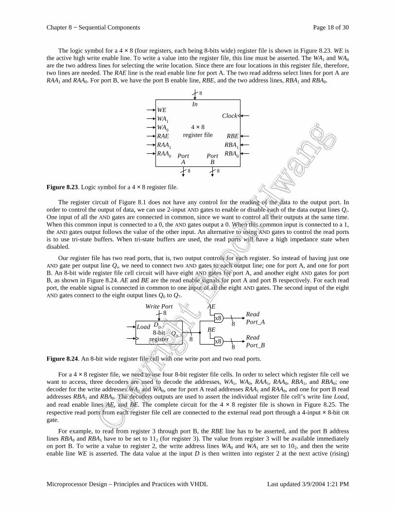
Chapter 8 − Sequential Components Page 18 of 30
Microprocessor Design – Principles and Practices with VHDL Last updated 3/9/2004 1:21 PM
The logic symbol for a 4 × 8 (four registers, each being 8-bits wide) register file is shown in Figure 8.23. WE is the active high write enable line. To write a value into the register file, this line must be asserted. The WA1 and WA0 are the two address lines for selecting the write location. Since there are four locations in this register file, therefore, two lines are needed. The RAE line is the read enable line for port A. The two read address select lines for port A are RAA1 and RAA0. For port B, we have the port B enable line, RBE, and the two address lines, RBA1 and RBA0.
8
WEWA1WA0
RAA1
RAE
RAA0
RBA1
RBE
RBA0
Clock
In
PortA
PortB
4 × 8register file
88
Figure 8.23. Logic symbol for a 4 × 8 register file.
The register circuit of Figure 8.1 does not have any control for the reading of the data to the output port. In order to control the output of data, we can use 2-input AND gates to enable or disable each of the data output lines Qi. One input of all the AND gates are connected in common, since we want to control all their outputs at the same time. When this common input is connected to a 0, the AND gates output a 0. When this common input is connected to a 1, the AND gates output follows the value of the other input. An alternative to using AND gates to control the read ports is to use tri-state buffers. When tri-state buffers are used, the read ports will have a high impedance state when disabled.
Our register file has two read ports, that is, two output controls for each register. So instead of having just one AND gate per output line Qi, we need to connect two AND gates to each output line; one for port A, and one for port B. An 8-bit wide register file cell circuit will have eight AND gates for port A, and another eight AND gates for port B, as shown in Figure 8.24. AE and BE are the read enable signals for port A and port B respectively. For each read port, the enable signal is connected in common to one input of all the eight AND gates. The second input of the eight AND gates connect to the eight output lines Q0 to Q7.
8
8
8
ReadPort_A
AE
BE
8
D0-78-bit
register
LoadQ0-7
x8
x8
Write Port
ReadPort_B
Figure 8.24. An 8-bit wide register file cell with one write port and two read ports.
For a 4 × 8 register file, we need to use four 8-bit register file cells. In order to select which register file cell we want to access, three decoders are used to decode the addresses, WA1, WA0, RAA1, RAA0, RBA1, and RBA0; one decoder for the write addresses WA1 and WA0, one for port A read addresses RAA1 and RAA0, and one for port B read addresses RBA1 and RBA0. The decoders outputs are used to assert the individual register file cell’s write line Load, and read enable lines AE, and BE. The complete circuit for the 4 × 8 register file is shown in Figure 8.25. The respective read ports from each register file cell are connected to the external read port through a 4-input × 8-bit OR gate.
For example, to read from register 3 through port B, the RBE line has to be asserted, and the port B address lines RBA0 and RBA1 have to be set to 112 (for register 3). The value from register 3 will be available immediately on port B. To write a value to register 2, the write address lines WA0 and WA1 are set to 102, and then the write enable line WE is asserted. The data value at the input D is then written into register 2 at the next active (rising)
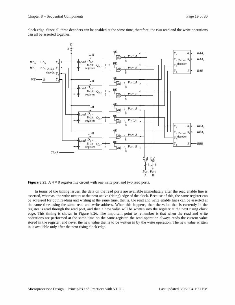
Chapter 8 − Sequential Components Page 19 of 30
Microprocessor Design – Principles and Practices with VHDL Last updated 3/9/2004 1:21 PM
clock edge. Since all three decoders can be enabled at the same time, therefore, the two read and the write operations can all be asserted together.
8
8
8
Port_AAE
BE
8
D0-78-bit
register
LoadQ0-7
x8
x8 Port_B
8
8
8
Port_AAE
BE
8
D0-78-bit
register
LoadQ0-7
x8
x8 Port_B
8
8
8
Port_AAE
BE
8
D0-78-bit
register
LoadQ0-7
x8
x8 Port_B
8
8
8
Port_AAE
BE
8
D0-78-bit
register
LoadQ0-7
x8
x8 Port_B
2-to-4decoder
A0
A1
Y0
Y1
Y2
Y3E
WA0
WA1
WE
2-to-4decoder
A0
A1
Y0
Y1
Y2
Y3 E
PortB
PortA
2-to-4decoder
A0
A1
Y0
Y1
Y2
Y3 E
RBA0
RBA1
RBE
RAA0
RAA1
RAE
D
Clock
8 8
8
x8 x8
Figure 8.25. A 4 × 8 register file circuit with one write port and two read ports.
In terms of the timing issues, the data on the read ports are available immediately after the read enable line is asserted, whereas, the write occurs at the next active (rising) edge of the clock. Because of this, the same register can be accessed for both reading and writing at the same time, that is, the read and write enable lines can be asserted at the same time using the same read and write address. When this happens, then the value that is currently in the register is read through the read port, and then a new value will be written into the register at the next rising clock edge. This timing is shown in Figure 8.26. The important point to remember is that when the read and write operations are performed at the same time on the same register, the read operation always reads the current value stored in the register, and never the new value that is to be written in by the write operation. The new value written in is available only after the next rising clock edge.
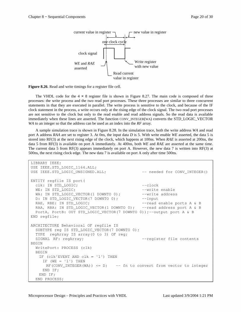
Chapter 8 − Sequential Components Page 20 of 30
Microprocessor Design – Principles and Practices with VHDL Last updated 3/9/2004 1:21 PM
clock signal
WE and RAEasserted
Write registerwith new value
one clock cycle
Read currentvalue in register
current value in register new value in register
Figure 8.26. Read and write timings for a register file cell.
The VHDL code for the 4 × 8 register file is shown in Figure 8.27. The main code is composed of three processes: the write process and the two read port processes. These three processes are similar to three concurrent statements in that they are executed in parallel. The write process is sensitive to the clock, and because of the IF clock statement in the process, a write occurs only at the rising edge of the clock signal. The two read port processes are not sensitive to the clock but only to the read enable and read address signals. So the read data is available immediately when these lines are asserted. The function CONV_INTEGER(WA) converts the STD_LOGIC_VECTOR WA to an integer so that the address can be used as an index into the RF array.
A sample simulation trace is shown in Figure 8.28. In the simulation trace, both the write address WA and read port A address RAA are set to register 3. At 0ns, the input data D is 5. With write enable WE asserted, the data 5 is stored into RF(3) at the next rising edge of the clock, which happens at 100ns. When RAE is asserted at 200ns, the data 5 from RF(3) is available on port A immediately. At 400ns, both WE and RAE are asserted at the same time. The current data 5 from RF(3) appears immediately on port A. However, the new data 7 is written into RF(3) at 500ns, the next rising clock edge. The new data 7 is available on port A only after time 500ns.
LIBRARY IEEE;USE IEEE.STD_LOGIC_1164.ALL;USE IEEE.STD_LOGIC_UNSIGNED.ALL; -- needed for CONV_INTEGER()
ENTITY regfile IS port(clk: IN STD_LOGIC; --clockWE: IN STD_LOGIC; --write enableWA: IN STD_LOGIC_VECTOR(1 DOWNTO 0); --write addressD: IN STD_LOGIC_VECTOR(7 DOWNTO 0); --inputRAE, RBE: IN STD_LOGIC; --read enable ports A & BRAA, RBA: IN STD_LOGIC_VECTOR(1 DOWNTO 0); --read address port A & BPortA, PortB: OUT STD_LOGIC_VECTOR(7 DOWNTO 0));--output port A & B
END regfile;
ARCHITECTURE Behavioral OF regfile ISSUBTYPE reg IS STD_LOGIC_VECTOR(7 DOWNTO 0);TYPE regArray IS array(0 to 3) OF reg;SIGNAL RF: regArray; --register file contents
BEGINWritePort: PROCESS (clk)BEGINIF (clk'EVENT AND clk = '1') THENIF (WE = '1') THENRF(CONV_INTEGER(WA)) <= D; -- fn to convert from vector to integer
END IF;END IF;
END PROCESS;
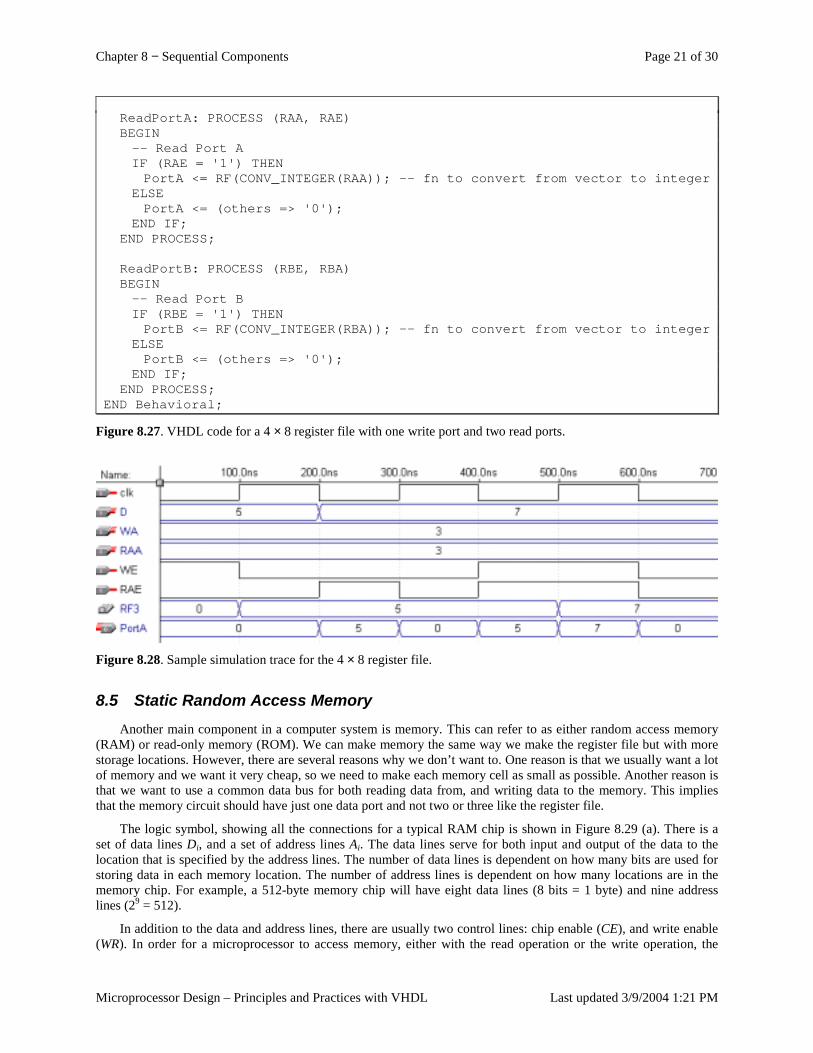
Chapter 8 − Sequential Components Page 21 of 30
Microprocessor Design – Principles and Practices with VHDL Last updated 3/9/2004 1:21 PM
ReadPortA: PROCESS (RAA, RAE)BEGIN-- Read Port AIF (RAE = '1') THENPortA <= RF(CONV_INTEGER(RAA)); -- fn to convert from vector to integer
ELSEPortA <= (others => '0');
END IF;END PROCESS;
ReadPortB: PROCESS (RBE, RBA)BEGIN-- Read Port BIF (RBE = '1') THENPortB <= RF(CONV_INTEGER(RBA)); -- fn to convert from vector to integer
ELSEPortB <= (others => '0');
END IF;END PROCESS;
END Behavioral;
Figure 8.27. VHDL code for a 4 × 8 register file with one write port and two read ports.
Figure 8.28. Sample simulation trace for the 4 × 8 register file.
8.5 Static Random Access Memory Another main component in a computer system is memory. This can refer to as either random access memory
(RAM) or read-only memory (ROM). We can make memory the same way we make the register file but with more storage locations. However, there are several reasons why we don’t want to. One reason is that we usually want a lot of memory and we want it very cheap, so we need to make each memory cell as small as possible. Another reason is that we want to use a common data bus for both reading data from, and writing data to the memory. This implies that the memory circuit should have just one data port and not two or three like the register file.
The logic symbol, showing all the connections for a typical RAM chip is shown in Figure 8.29 (a). There is a set of data lines Di, and a set of address lines Ai. The data lines serve for both input and output of the data to the location that is specified by the address lines. The number of data lines is dependent on how many bits are used for storing data in each memory location. The number of address lines is dependent on how many locations are in the memory chip. For example, a 512-byte memory chip will have eight data lines (8 bits = 1 byte) and nine address lines (29 = 512).
In addition to the data and address lines, there are usually two control lines: chip enable (CE), and write enable (WR). In order for a microprocessor to access memory, either with the read operation or the write operation, the
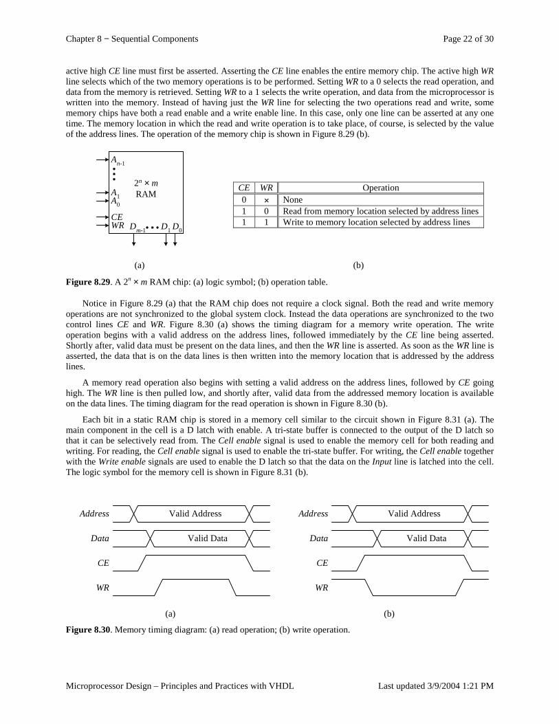
Chapter 8 − Sequential Components Page 22 of 30
Microprocessor Design – Principles and Practices with VHDL Last updated 3/9/2004 1:21 PM
active high CE line must first be asserted. Asserting the CE line enables the entire memory chip. The active high WR line selects which of the two memory operations is to be performed. Setting WR to a 0 selects the read operation, and data from the memory is retrieved. Setting WR to a 1 selects the write operation, and data from the microprocessor is written into the memory. Instead of having just the WR line for selecting the two operations read and write, some memory chips have both a read enable and a write enable line. In this case, only one line can be asserted at any one time. The memory location in which the read and write operation is to take place, of course, is selected by the value of the address lines. The operation of the memory chip is shown in Figure 8.29 (b).
CEWR
A0
A1
An-1
D0D1Dm-1
2n × mRAM
(a)
CE WR Operation 0 × None 1 0 Read from memory location selected by address lines 1 1 Write to memory location selected by address lines
(b)
Figure 8.29. A 2n × m RAM chip: (a) logic symbol; (b) operation table.
Notice in Figure 8.29 (a) that the RAM chip does not require a clock signal. Both the read and write memory operations are not synchronized to the global system clock. Instead the data operations are synchronized to the two control lines CE and WR. Figure 8.30 (a) shows the timing diagram for a memory write operation. The write operation begins with a valid address on the address lines, followed immediately by the CE line being asserted. Shortly after, valid data must be present on the data lines, and then the WR line is asserted. As soon as the WR line is asserted, the data that is on the data lines is then written into the memory location that is addressed by the address lines.
A memory read operation also begins with setting a valid address on the address lines, followed by CE going high. The WR line is then pulled low, and shortly after, valid data from the addressed memory location is available on the data lines. The timing diagram for the read operation is shown in Figure 8.30 (b).
Each bit in a static RAM chip is stored in a memory cell similar to the circuit shown in Figure 8.31 (a). The main component in the cell is a D latch with enable. A tri-state buffer is connected to the output of the D latch so that it can be selectively read from. The Cell enable signal is used to enable the memory cell for both reading and writing. For reading, the Cell enable signal is used to enable the tri-state buffer. For writing, the Cell enable together with the Write enable signals are used to enable the D latch so that the data on the Input line is latched into the cell. The logic symbol for the memory cell is shown in Figure 8.31 (b).
Address
CE
WR
Data
Valid Address
Valid Data
(a)
Address
CE
WR
Data
Valid Address
Valid Data
(b)
Figure 8.30. Memory timing diagram: (a) read operation; (b) write operation.
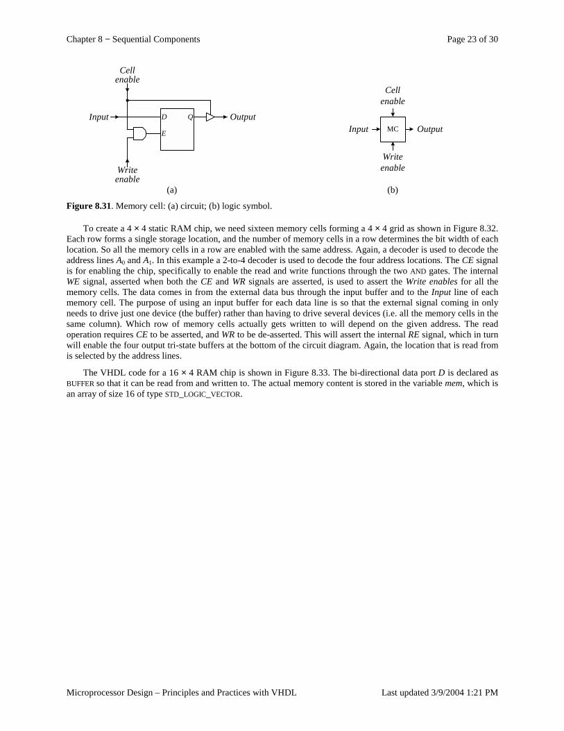
Chapter 8 − Sequential Components Page 23 of 30
Microprocessor Design – Principles and Practices with VHDL Last updated 3/9/2004 1:21 PM
E
D QInput Output
Cellenable
Writeenable
(a)
MC
Cellenable
Writeenable
OutputInput
(b)
Figure 8.31. Memory cell: (a) circuit; (b) logic symbol.
To create a 4 × 4 static RAM chip, we need sixteen memory cells forming a 4 × 4 grid as shown in Figure 8.32. Each row forms a single storage location, and the number of memory cells in a row determines the bit width of each location. So all the memory cells in a row are enabled with the same address. Again, a decoder is used to decode the address lines A0 and A1. In this example a 2-to-4 decoder is used to decode the four address locations. The CE signal is for enabling the chip, specifically to enable the read and write functions through the two AND gates. The internal WE signal, asserted when both the CE and WR signals are asserted, is used to assert the Write enables for all the memory cells. The data comes in from the external data bus through the input buffer and to the Input line of each memory cell. The purpose of using an input buffer for each data line is so that the external signal coming in only needs to drive just one device (the buffer) rather than having to drive several devices (i.e. all the memory cells in the same column). Which row of memory cells actually gets written to will depend on the given address. The read operation requires CE to be asserted, and WR to be de-asserted. This will assert the internal RE signal, which in turn will enable the four output tri-state buffers at the bottom of the circuit diagram. Again, the location that is read from is selected by the address lines.
The VHDL code for a 16 × 4 RAM chip is shown in Figure 8.33. The bi-directional data port D is declared as BUFFER so that it can be read from and written to. The actual memory content is stored in the variable mem, which is an array of size 16 of type STD_LOGIC_VECTOR.
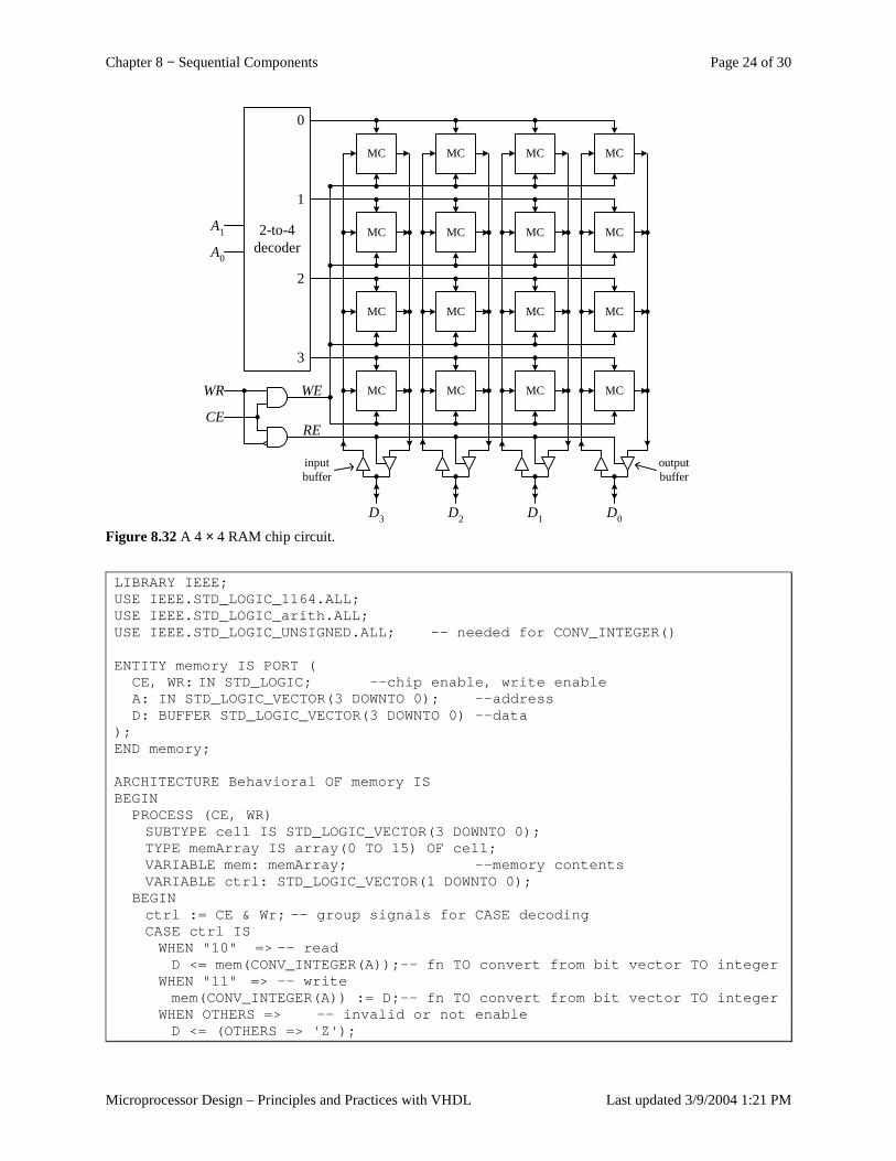
Chapter 8 − Sequential Components Page 24 of 30
Microprocessor Design – Principles and Practices with VHDL Last updated 3/9/2004 1:21 PM
MC MC MC MC
MC MC MC MC
MC MC MCMC
MC MC MC MC2-to-4decoder
0
1
2
3
WR WE
RECE
D3 D2 D1 D0
A0
A1
inputbuffer
outputbuffer
Figure 8.32 A 4 × 4 RAM chip circuit.
LIBRARY IEEE;USE IEEE.STD_LOGIC_1164.ALL;USE IEEE.STD_LOGIC_arith.ALL;USE IEEE.STD_LOGIC_UNSIGNED.ALL; -- needed for CONV_INTEGER()
ENTITY memory IS PORT (CE, WR: IN STD_LOGIC; --chip enable, write enableA: IN STD_LOGIC_VECTOR(3 DOWNTO 0); --addressD: BUFFER STD_LOGIC_VECTOR(3 DOWNTO 0) --data
);END memory;
ARCHITECTURE Behavioral OF memory ISBEGIN
PROCESS (CE, WR)SUBTYPE cell IS STD_LOGIC_VECTOR(3 DOWNTO 0);TYPE memArray IS array(0 TO 15) OF cell;VARIABLE mem: memArray; --memory contentsVARIABLE ctrl: STD_LOGIC_VECTOR(1 DOWNTO 0);
BEGINctrl := CE & Wr; -- group signals for CASE decodingCASE ctrl ISWHEN "10" => -- readD <= mem(CONV_INTEGER(A));-- fn TO convert from bit vector TO integer
WHEN "11" => -- writemem(CONV_INTEGER(A)) := D;-- fn TO convert from bit vector TO integer
WHEN OTHERS => -- invalid or not enableD <= (OTHERS => 'Z');

Chapter 8 − Sequential Components Page 25 of 30
Microprocessor Design – Principles and Practices with VHDL Last updated 3/9/2004 1:21 PM
END CASE;END PROCESS;
END Behavioral;
Figure 8.33. VHDL code for a 16 × 4 RAM chip
8.6 * Larger Memories In general, there is always a need for larger memories. Because of product availability constraints, we need to
construct these larger memories from multiple smaller memory chips. Larger memory requirements can be for either more memory locations, or wider bit widths for each location, or both.
8.6.1 More Memory Locations
For example, we may want to have 1K × 8-bit of memory built using multiple 256 × 8-bit memory chips. Using such small numbers are archaic but you get the idea. In this case, we would need four of these 256 × 8-bit memory chips since 1K = 4 × 256. A 256 × 8-bit memory chip has eight address lines since 28 = 256. To decode four chips, we need an additional two address lines to enable which of the four chips we want to address. Thus, we need a total of ten address lines, with the first eight, A0 to A7, connected respectively in common directly to the eight address lines on the four chips, and the last two lines, A8 and A9, connected to the address inputs of a 2-to-4 decoder. The four outputs from the decoder are used to assert the chip enable CE line of the four memory chips RAM0 to RAM3. The data lines and the write enable lines are all connected respectively in common. The circuit is shown in Figure 8.34 (a).
The 256-byte memory chip RAM0 is enabled when the address bits A8 and A9 are 00. Hence, the address range for RAM0 is from 0 to 255 (0000000000 to 0011111111 in binary). Similarly, RAM1 is enabled when the address bits A8 and A9 are 01. Hence, the address range for RAM1 is from 256 to 511 (0100000000 to 0111111111 in binary). The address range for RAM2 is from 512 to 767 (1000000000 to 1011111111 in binary), and the address range for RAM3 is from 768 to 1023 (1100000000 to 1111111111 in binary).
A particular memory location is accessed as follows. If we want to write to memory location 717, which is binary 1011001101, the Y2 line of the decoder would be asserted since bits 8 and 9 is “10.” This Y2 line in turn asserts the CE line of the third RAM chip from the top, while the remaining chips are disabled. Finally, within this RAM chip that is enabled, location 205, which is binary 11001101 from bits 0 to 7 of the original address, is selected. Location 205 in the third RAM chip is location 717 for the entire memory since 256+256+205 = 717.
8.6.2 Wider Bit Width
We may also want to have wider bit width for each memory location made from smaller ones. For example, we may want to have a memory that is 512 locations × 16-bit wide made from 256 × 8-bit memory chips. Again, we would need four 256 byte memory chips, but connected as shown in Figure 8.34 (b). For 512 locations, only nine address lines are needed, with the first eight, A0 to A7, connected respectively in common directly to the eight address lines on the four chips, and the last line A8 connected to the address input of a 1-to-2 decoder. For a 16-bit wide data bus, we need to connect two 8-bit wide chips in parallel so that each two similar 8-bit wide locations in the two chips can be combined together to form a 16-bit wide location. Since these two chips need to work together, therefore, their chip enable CE lines are connected in common, and asserted by the same output from the decoder.
Memory chips RAM0 and RAM2 are for storing the data bits D0 to D7, while memory chips RAM1 and RAM3 are for storing the data bits D8 to D15. The address range for RAM0 and RAM1 is from 0 to 255 (000000000 to 011111111 in binary), and the address range for RAM2 and RAM3 is from 256 to 511 (100000000 to 111111111 in binary).
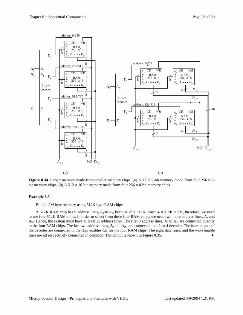
Chapter 8 − Sequential Components Page 26 of 30
Microprocessor Design – Principles and Practices with VHDL Last updated 3/9/2004 1:21 PM
WR D7-0A7-0
Y0
2-to-4decoder
A1 Y1
A0
E
Y2
Y3
A9
A8
E
CE WR
A0
A7
D0D7
RAM3
8256 x 8
8
CE WR
A0
A7
D0D7
RAM1
8256 x 8
8
CE WR
A0
A7
D0D7
RAM2
8256 x 8
8
CE WR
A0
A7
D0D7
RAM0
8256 x 8
8
address: 0-255
address: 256-511
address: 512-767
address: 768-1023
(a)
CE WR
A0
A7
D0D7
RAM1
8256 x 8
8
CE WR
A0
A7
D0D7
RAM0
8256 x 8
8 D7-0
D15-8
CE WR
A0
A7
D0D7
RAM3
8256 x 8
8
CE WR
A0
A7
D0D7
RAM2
8256 x 8
8 D7-0
D15-8
WR D15-0A7-0
Y0
1-to-2decoder
Y1
A0
E
A8
E
16
address: 0-255
address: 256-511
(b)
Figure 8.34. Larger memory made from smaller memory chips: (a) A 1K × 8-bit memory made from four 256 × 8-bit memory chips; (b) A 512 × 16-bit memory made from four 256 × 8-bit memory chips.
Example 8.3
Build a 2M byte memory using 512K byte RAM chips.
A 512K RAM chip has 9 address lines, A0 to A8, because 29 = 512K. Since 4 × 512K = 2M, therefore, we need to use four 512K RAM chips. In order to select from these four RAM chips, we need two more address lines, A9 and A10. Hence, the system must have at least 11 address lines. The first 9 address lines, A0 to A8, are connected directly to the four RAM chips. The last two address lines, A9 and A10, are connected to a 2-to-4 decoder. The four outputs of the decoder are connected to the chip enables CE for the four RAM chips. The eight data lines, and the write enable lines are all respectively connected in common. The circuit is shown in Figure 8.35. ♦
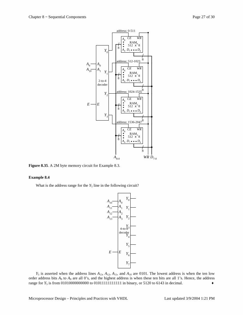
Chapter 8 − Sequential Components Page 27 of 30
Microprocessor Design – Principles and Practices with VHDL Last updated 3/9/2004 1:21 PM
WR D7-0A8-0
CE WR
A0
A8
D0D7
RAM3
8512 x 8
8
CE WR
A0
A8
D0D7
RAM1
8512 x 8
8
CE WR
A0
A8
D0D7
RAM2
8512 x 8
8
CE WR
A0
A8
D0D7
RAM0
8512 x 8
8
address: 0-511
address: 512-1023
address: 1024-1535
address: 1536-2047
Y0
2-to-4decoder
A1 Y1
A0
E
Y2
Y3
A10
A9
E
Figure 8.35. A 2M byte memory circuit for Example 8.3.
Example 8.4
What is the address range for the Y5 line in the following circuit?
Y0
4-to-8decoder
A3
Y1A2
E
Y3
Y7
A13
A12
E
A1
A0A11
A10
Y6
Y5
Y4
Y2
Y5 is asserted when the address lines A13, A12, A11, and A10 are 0101. The lowest address is when the ten low
order address bits A9 to A0 are all 0’s, and the highest address is when these ten bits are all 1’s. Hence, the address range for Y5 is from 01010000000000 to 01011111111111 in binary, or 5120 to 6143 in decimal. ♦
Chapter 8 − Sequential Components Page 28 of 30
Microprocessor Design – Principles and Practices with VHDL Last updated 3/9/2004 1:21 PM
8.7 Summary Checklist � Registers
� Operation � Circuit
� Serial-to-Parallel Shift Registers � Parallel-to-Serial Shift Registers
� Operation � Circuit
� Binary counters � Binary up-down counters
� Operation � Circuit
� BCD counters � BCD up-down counters
� Circuit � Counters for random sequences
� Circuit � Register files
� Operation � Circuit
� Random access memories � Operation � Circuit
� Building more memory locations using smaller RAM chips � Building wider bit width memories using smaller RAM chips
8.8 Problems
8.1. The 4-bit binary up counter VHDL code shown in Figure 8.12 does not have the Overflow output signal. Modify the code to include the Overflow signal.
8.2. For the BCD up counter circuit shown in Figure 8.19, what happens if the output of the AND gate comparator is connected to the Clear signal instead of to the Load signal? Will it produce the same waveform? Explain your observations.
8.3. In the BCD up-down counter circuit shown in Figure 8.21, four 2-input multiplexers are used to select the correct value to be loaded in. Modify the circuit so that the multiplexers are not needed.
8.4. Write the behavioral VHDL code for the BCD up-down counter.
8.5. Use the 4-bit binary up-down counter with parallel load to construct an up-down counter circuit that counts from 0 to 7 decimal, and back to 0.
8.6. Use the 4-bit binary up-down counter with parallel load to construct an up-down counter circuit that counts from 5 to 13 decimal, and back to 5.
8.7. Use the 4-bit binary up-down counter with parallel load to construct an up-down counter circuit that outputs the sequence 7, 12, 19, 36, 42, 58, and 57 repeatedly.
8.8. Use the 4-bit binary up-down counter with parallel load to construct an up-down counter circuit that outputs the sequence 4, 8, 5, 3, 16, and 7 repeatedly.
8.9. Write the behavioral VHDL code for the BCD up-down counter.
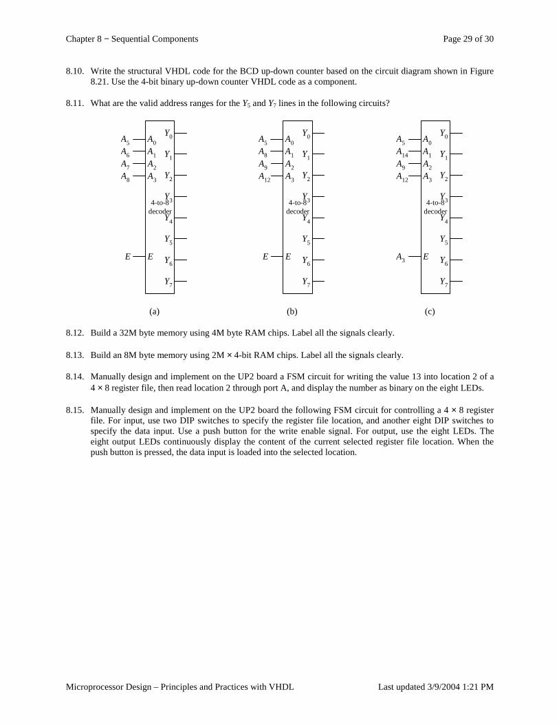
Chapter 8 − Sequential Components Page 29 of 30
Microprocessor Design – Principles and Practices with VHDL Last updated 3/9/2004 1:21 PM
8.10. Write the structural VHDL code for the BCD up-down counter based on the circuit diagram shown in Figure 8.21. Use the 4-bit binary up-down counter VHDL code as a component.
8.11. What are the valid address ranges for the Y5 and Y7 lines in the following circuits?
Y0
4-to-8decoder
A3
Y1A2
E
Y3
Y7
A8
A7
E
A1
A0A6
A5
Y6
Y5
Y4
Y2
(a)
Y0
4-to-8decoder
A3
Y1A2
E
Y3
Y7
A12
A9
E
A1
A0A8
A5
Y6
Y5
Y4
Y2
(b)
Y0
4-to-8decoder
A3
Y1A2
E
Y3
Y7
A12
A9
A1
A0A14
A5
Y6
Y5
Y4
Y2
A3
(c)
8.12. Build a 32M byte memory using 4M byte RAM chips. Label all the signals clearly.
8.13. Build an 8M byte memory using 2M × 4-bit RAM chips. Label all the signals clearly.
8.14. Manually design and implement on the UP2 board a FSM circuit for writing the value 13 into location 2 of a 4 × 8 register file, then read location 2 through port A, and display the number as binary on the eight LEDs.
8.15. Manually design and implement on the UP2 board the following FSM circuit for controlling a 4 × 8 register file. For input, use two DIP switches to specify the register file location, and another eight DIP switches to specify the data input. Use a push button for the write enable signal. For output, use the eight LEDs. The eight output LEDs continuously display the content of the current selected register file location. When the push button is pressed, the data input is loaded into the selected location.
Chapter 8 − Sequential Components Page 30 of 30
Microprocessor Design – Principles and Practices with VHDL Last updated 3/9/2004 1:21 PM
Index
B
BCD up counter, 14 BCD up-down counter, 14 Binary up counter, 9 Binary up-down counter, 11 Binary up-down counter with parallel load, 13
C
Counter, 8 BCD up counter, 14 BCD up-down counter, 14 binary up counter, 9 binary up-down counter, 11 binary up-down counter with parallel load, 13
H
Half adder, 9 Half adder-subtractor, 11
M
Memory. See Random access memory.
P
Parallel-to-serial shift register, 7
R
RAM. See Random access memory. Random access memory, 21
larger memory, 25 Register, 3 Register file, 17
S
Sequential components, 3 Serial-to-parallel shift register, 5 Shift register, 4
serial-to-parallel, 5 serial-to-parallel and parallel-to-serial, 7
V
VHDL GENERIC, 4
VHDL code binary up counter, 11 binary up-down counter, 13 memory, 25 RAM, 25 register, 4 register file, 21 shift register, 7, 8
Chapter 9 − Datapaths Page 1 of 24
Microprocessor Design – Principles and Practices with VHDL Last updated 7/16/2003 12:32 PM
Table of Content Table of Content ........................................................................................................................................................... 1 9 Datapaths............................................................................................................................................................... 2
9.1 General Datapath........................................................................................................................................... 3 9.2 Using a General Datapath ............................................................................................................................. 4 9.3 Timing Issues ................................................................................................................................................ 5 9.4 A More Complex Datapath ........................................................................................................................... 8 9.5 VHDL for the Complex Datapath ............................................................................................................... 10 9.6 Dedicated Datapath ..................................................................................................................................... 15
9.6.1 Selecting Registers .............................................................................................................................. 15 9.6.2 Selecting Functional Units .................................................................................................................. 15 9.6.3 Data Transfer Methods........................................................................................................................ 16
9.7 Using a Dedicated Datapath........................................................................................................................ 17 9.8 Examples: Designing Dedicated Datapaths ................................................................................................ 17 9.9 VHDL for a Dedicated Datapath................................................................................................................. 22 9.10 * Optimization for Datapaths ...................................................................................................................... 23
9.10.1 Functional Unit Sharing ...................................................................................................................... 23 9.10.2 Register Sharing .................................................................................................................................. 23 9.10.3 Bus Sharing ......................................................................................................................................... 23
9.11 Summary Checklist ..................................................................................................................................... 23 Index ....................................................................................................................................................................... 24
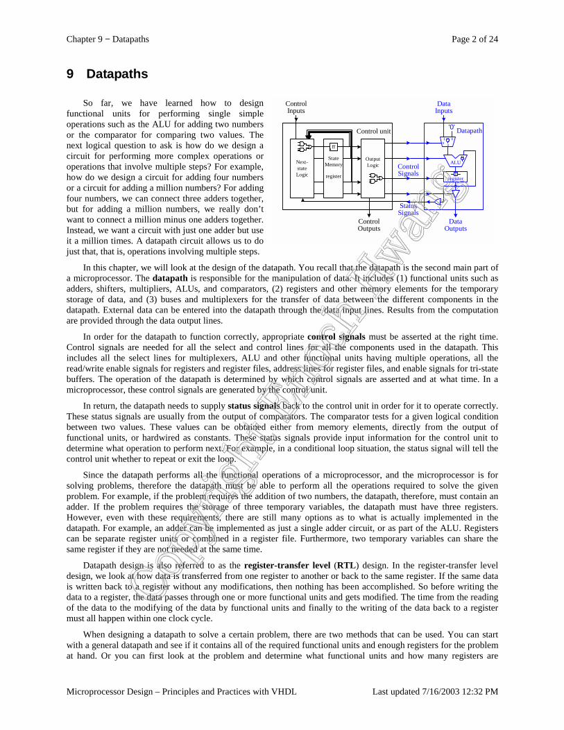
Chapter 9 − Datapaths Page 2 of 24
Microprocessor Design – Principles and Practices with VHDL Last updated 7/16/2003 12:32 PM
ControlSignals
StatusSignals
01s y
'0'
DataInputs
DataOutputs
Datapath
ALU
registerff
OutputLogicNext-
stateLogic
ControlInputs
ControlOutputs
StateMemory
register
Control unit
ff
9 Datapaths
So far, we have learned how to design functional units for performing single simple operations such as the ALU for adding two numbers or the comparator for comparing two values. The next logical question to ask is how do we design a circuit for performing more complex operations or operations that involve multiple steps? For example, how do we design a circuit for adding four numbers or a circuit for adding a million numbers? For adding four numbers, we can connect three adders together, but for adding a million numbers, we really don’t want to connect a million minus one adders together. Instead, we want a circuit with just one adder but use it a million times. A datapath circuit allows us to do just that, that is, operations involving multiple steps.
In this chapter, we will look at the design of the datapath. You recall that the datapath is the second main part of a microprocessor. The datapath is responsible for the manipulation of data. It includes (1) functional units such as adders, shifters, multipliers, ALUs, and comparators, (2) registers and other memory elements for the temporary storage of data, and (3) buses and multiplexers for the transfer of data between the different components in the datapath. External data can be entered into the datapath through the data input lines. Results from the computation are provided through the data output lines.
In order for the datapath to function correctly, appropriate control signals must be asserted at the right time. Control signals are needed for all the select and control lines for all the components used in the datapath. This includes all the select lines for multiplexers, ALU and other functional units having multiple operations, all the read/write enable signals for registers and register files, address lines for register files, and enable signals for tri-state buffers. The operation of the datapath is determined by which control signals are asserted and at what time. In a microprocessor, these control signals are generated by the control unit.
In return, the datapath needs to supply status signals back to the control unit in order for it to operate correctly. These status signals are usually from the output of comparators. The comparator tests for a given logical condition between two values. These values can be obtained either from memory elements, directly from the output of functional units, or hardwired as constants. These status signals provide input information for the control unit to determine what operation to perform next. For example, in a conditional loop situation, the status signal will tell the control unit whether to repeat or exit the loop.
Since the datapath performs all the functional operations of a microprocessor, and the microprocessor is for solving problems, therefore the datapath must be able to perform all the operations required to solve the given problem. For example, if the problem requires the addition of two numbers, the datapath, therefore, must contain an adder. If the problem requires the storage of three temporary variables, the datapath must have three registers. However, even with these requirements, there are still many options as to what is actually implemented in the datapath. For example, an adder can be implemented as just a single adder circuit, or as part of the ALU. Registers can be separate register units or combined in a register file. Furthermore, two temporary variables can share the same register if they are not needed at the same time.
Datapath design is also referred to as the register-transfer level (RTL) design. In the register-transfer level design, we look at how data is transferred from one register to another or back to the same register. If the same data is written back to a register without any modifications, then nothing has been accomplished. So before writing the data to a register, the data passes through one or more functional units and gets modified. The time from the reading of the data to the modifying of the data by functional units and finally to the writing of the data back to a register must all happen within one clock cycle.
When designing a datapath to solve a certain problem, there are two methods that can be used. You can start with a general datapath and see if it contains all of the required functional units and enough registers for the problem at hand. Or you can first look at the problem and determine what functional units and how many registers are
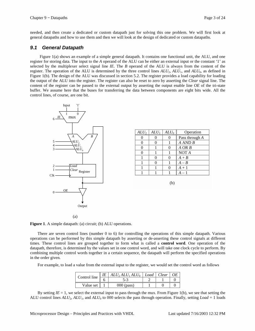
Chapter 9 − Datapaths Page 3 of 24
Microprocessor Design – Principles and Practices with VHDL Last updated 7/16/2003 12:32 PM
needed, and then create a dedicated or custom datapath just for solving this one problem. We will first look at general datapaths and how to use them and then we will look at the design of dedicated or custom datapaths.
9.1 General Datapath Figure 1(a) shows an example of a simple general datapath. It contains one functional unit, the ALU, and one
register for storing data. The input to the A operand of the ALU can be either an external input or the constant ‘1’ as selected by the multiplexer select signal line IE. The B operand of the ALU is always from the content of the register. The operation of the ALU is determined by the three control lines ALU2, ALU1, and ALU0, as defined in Figure 1(b). The design of the ALU was discussed in section 5.2. The register provides a load capability for loading the output of the ALU into the register. The register can also be reset to zero by asserting the Clear signal line. The content of the register can be passed to the external output by asserting the output enable line OE of the tri-state buffer. We assume here that the buses for transferring the data between components are eight bits wide. All the control lines, of course, are one bit.
6
Input
mux01
0
LoadClear Register
2
Clk
543
'1'
IE
OE
1
ALU0
ALU1
ALU2
A B
Output
(a)
Figure 1. A simple datapath: (a) circuit; (b) ALU operations.
There are seven control lines (number 0 to 6) for controlling the operations of this simple datapath. Various operations can be performed by this simple datapath by asserting or de-asserting these control signals at different times. These control lines are grouped together to form what is called a control word. One operation of the datapath, therefore, is determined by the values set in one control word, and will take one clock cycle to perform. By combining multiple control words together in a certain sequence, the datapath will perform the specified operations in the order given.
For example, to load a value from the external input to the register, we would set the control word as follows
IE ALU2 ALU1 ALU0 Load Clear OE Control line 6 5-3 2 1 0 Value set 1 000 (pass) 1 0 0
By setting IE = 1, we select the external input to pass through the mux. From Figure 1(b), we see that setting the ALU control lines ALU2, ALU1, and ALU0 to 000 selects the pass through operation. Finally, setting Load = 1 loads
ALU2 ALU1 ALU0 Operation 0 0 0 Pass through A 0 0 1 A AND B 0 1 0 A OR B 0 1 1 NOT A 1 0 0 A + B 1 0 1 A – B 1 1 0 A + 1 1 1 1 A – 1
(b)
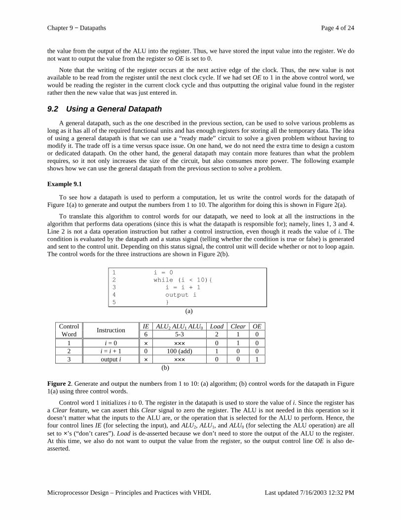
Chapter 9 − Datapaths Page 4 of 24
Microprocessor Design – Principles and Practices with VHDL Last updated 7/16/2003 12:32 PM
the value from the output of the ALU into the register. Thus, we have stored the input value into the register. We do not want to output the value from the register so OE is set to 0.
Note that the writing of the register occurs at the next active edge of the clock. Thus, the new value is not available to be read from the register until the next clock cycle. If we had set OE to 1 in the above control word, we would be reading the register in the current clock cycle and thus outputting the original value found in the register rather then the new value that was just entered in.
9.2 Using a General Datapath A general datapath, such as the one described in the previous section, can be used to solve various problems as
long as it has all of the required functional units and has enough registers for storing all the temporary data. The idea of using a general datapath is that we can use a “ready made” circuit to solve a given problem without having to modify it. The trade off is a time versus space issue. On one hand, we do not need the extra time to design a custom or dedicated datapath. On the other hand, the general datapath may contain more features than what the problem requires, so it not only increases the size of the circuit, but also consumes more power. The following example shows how we can use the general datapath from the previous section to solve a problem.
Example 9.1
To see how a datapath is used to perform a computation, let us write the control words for the datapath of Figure 1(a) to generate and output the numbers from 1 to 10. The algorithm for doing this is shown in Figure 2(a).
To translate this algorithm to control words for our datapath, we need to look at all the instructions in the algorithm that performs data operations (since this is what the datapath is responsible for); namely, lines 1, 3 and 4. Line 2 is not a data operation instruction but rather a control instruction, even though it reads the value of i. The condition is evaluated by the datapath and a status signal (telling whether the condition is true or false) is generated and sent to the control unit. Depending on this status signal, the control unit will decide whether or not to loop again. The control words for the three instructions are shown in Figure 2(b).
Figure 2. Generate and output the numbers from 1 to 10: (a) algorithm; (b) control words for the datapath in Figure 1(a) using three control words.
Control word 1 initializes i to 0. The register in the datapath is used to store the value of i. Since the register has a Clear feature, we can assert this Clear signal to zero the register. The ALU is not needed in this operation so it doesn’t matter what the inputs to the ALU are, or the operation that is selected for the ALU to perform. Hence, the four control lines IE (for selecting the input), and ALU2, ALU1, and ALU0 (for selecting the ALU operation) are all set to ×’s (“don’t cares”). Load is de-asserted because we don’t need to store the output of the ALU to the register. At this time, we also do not want to output the value from the register, so the output control line OE is also de-asserted.
1 i = 02 while (i < 10){3 i = i + 14 output i5 }
(a)
Control IE ALU2 ALU1 ALU0 Load Clear OE Word Instruction 6 5-3 2 1 0
1 i = 0 × ××× 0 1 0 2 i = i + 1 0 100 (add) 1 0 0 3 output i × ××× 0 0 1
(b)
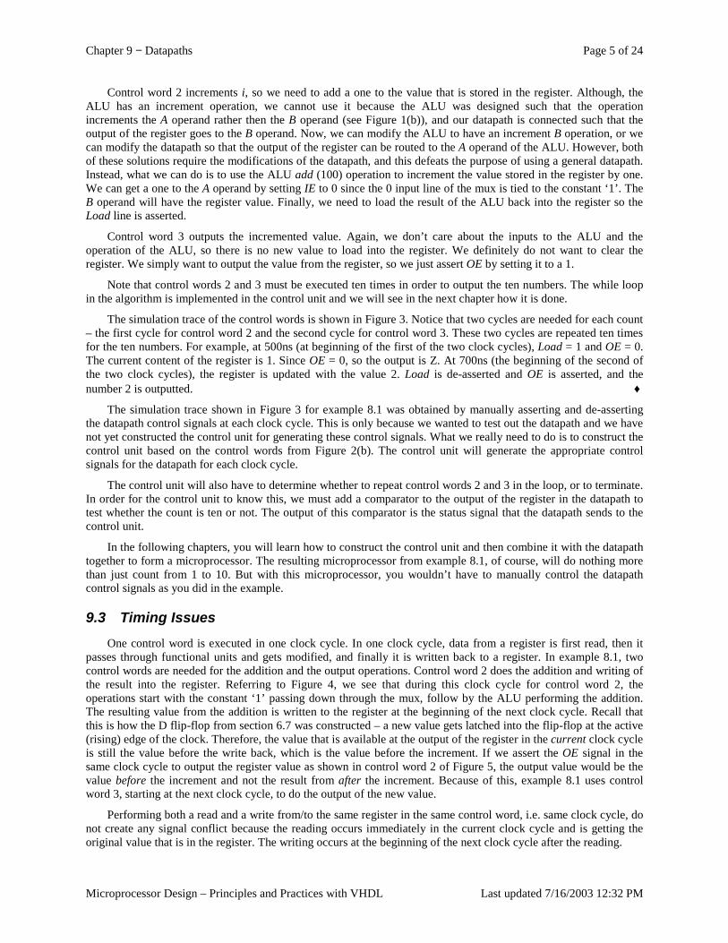
Chapter 9 − Datapaths Page 5 of 24
Microprocessor Design – Principles and Practices with VHDL Last updated 7/16/2003 12:32 PM
Control word 2 increments i, so we need to add a one to the value that is stored in the register. Although, the ALU has an increment operation, we cannot use it because the ALU was designed such that the operation increments the A operand rather then the B operand (see Figure 1(b)), and our datapath is connected such that the output of the register goes to the B operand. Now, we can modify the ALU to have an increment B operation, or we can modify the datapath so that the output of the register can be routed to the A operand of the ALU. However, both of these solutions require the modifications of the datapath, and this defeats the purpose of using a general datapath. Instead, what we can do is to use the ALU add (100) operation to increment the value stored in the register by one. We can get a one to the A operand by setting IE to 0 since the 0 input line of the mux is tied to the constant ‘1’. The B operand will have the register value. Finally, we need to load the result of the ALU back into the register so the Load line is asserted.
Control word 3 outputs the incremented value. Again, we don’t care about the inputs to the ALU and the operation of the ALU, so there is no new value to load into the register. We definitely do not want to clear the register. We simply want to output the value from the register, so we just assert OE by setting it to a 1.
Note that control words 2 and 3 must be executed ten times in order to output the ten numbers. The while loop in the algorithm is implemented in the control unit and we will see in the next chapter how it is done.
The simulation trace of the control words is shown in Figure 3. Notice that two cycles are needed for each count – the first cycle for control word 2 and the second cycle for control word 3. These two cycles are repeated ten times for the ten numbers. For example, at 500ns (at beginning of the first of the two clock cycles), Load = 1 and OE = 0. The current content of the register is 1. Since OE = 0, so the output is Z. At 700ns (the beginning of the second of the two clock cycles), the register is updated with the value 2. Load is de-asserted and OE is asserted, and the number 2 is outputted. ♦
The simulation trace shown in Figure 3 for example 8.1 was obtained by manually asserting and de-asserting the datapath control signals at each clock cycle. This is only because we wanted to test out the datapath and we have not yet constructed the control unit for generating these control signals. What we really need to do is to construct the control unit based on the control words from Figure 2(b). The control unit will generate the appropriate control signals for the datapath for each clock cycle.
The control unit will also have to determine whether to repeat control words 2 and 3 in the loop, or to terminate. In order for the control unit to know this, we must add a comparator to the output of the register in the datapath to test whether the count is ten or not. The output of this comparator is the status signal that the datapath sends to the control unit.
In the following chapters, you will learn how to construct the control unit and then combine it with the datapath together to form a microprocessor. The resulting microprocessor from example 8.1, of course, will do nothing more than just count from 1 to 10. But with this microprocessor, you wouldn’t have to manually control the datapath control signals as you did in the example.
9.3 Timing Issues One control word is executed in one clock cycle. In one clock cycle, data from a register is first read, then it
passes through functional units and gets modified, and finally it is written back to a register. In example 8.1, two control words are needed for the addition and the output operations. Control word 2 does the addition and writing of the result into the register. Referring to Figure 4, we see that during this clock cycle for control word 2, the operations start with the constant ‘1’ passing down through the mux, follow by the ALU performing the addition. The resulting value from the addition is written to the register at the beginning of the next clock cycle. Recall that this is how the D flip-flop from section 6.7 was constructed – a new value gets latched into the flip-flop at the active (rising) edge of the clock. Therefore, the value that is available at the output of the register in the current clock cycle is still the value before the write back, which is the value before the increment. If we assert the OE signal in the same clock cycle to output the register value as shown in control word 2 of Figure 5, the output value would be the value before the increment and not the result from after the increment. Because of this, example 8.1 uses control word 3, starting at the next clock cycle, to do the output of the new value.
Performing both a read and a write from/to the same register in the same control word, i.e. same clock cycle, do not create any signal conflict because the reading occurs immediately in the current clock cycle and is getting the original value that is in the register. The writing occurs at the beginning of the next clock cycle after the reading.
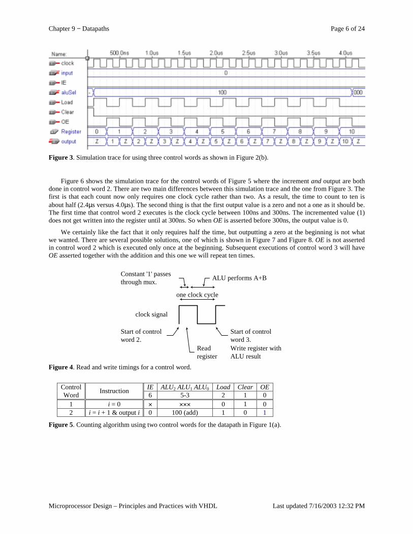
Chapter 9 − Datapaths Page 6 of 24
Microprocessor Design – Principles and Practices with VHDL Last updated 7/16/2003 12:32 PM
Figure 3. Simulation trace for using three control words as shown in Figure 2(b).
Figure 6 shows the simulation trace for the control words of Figure 5 where the increment and output are both done in control word 2. There are two main differences between this simulation trace and the one from Figure 3. The first is that each count now only requires one clock cycle rather than two. As a result, the time to count to ten is about half (2.4µs versus 4.0µs). The second thing is that the first output value is a zero and not a one as it should be. The first time that control word 2 executes is the clock cycle between 100ns and 300ns. The incremented value (1) does not get written into the register until at 300ns. So when OE is asserted before 300ns, the output value is 0.
We certainly like the fact that it only requires half the time, but outputting a zero at the beginning is not what we wanted. There are several possible solutions, one of which is shown in Figure 7 and Figure 8. OE is not asserted in control word 2 which is executed only once at the beginning. Subsequent executions of control word 3 will have OE asserted together with the addition and this one we will repeat ten times.
clock signal
Start of controlword 2.
Start of controlword 3.Write register withALU result
Constant '1' passesthrough mux. ALU performs A+B
one clock cycle
Readregister
Figure 4. Read and write timings for a control word.
Control IE ALU2 ALU1 ALU0 Load Clear OE Word Instruction 6 5-3 2 1 0
1 i = 0 × ××× 0 1 0 2 i = i + 1 & output i 0 100 (add) 1 0 1
Figure 5. Counting algorithm using two control words for the datapath in Figure 1(a).
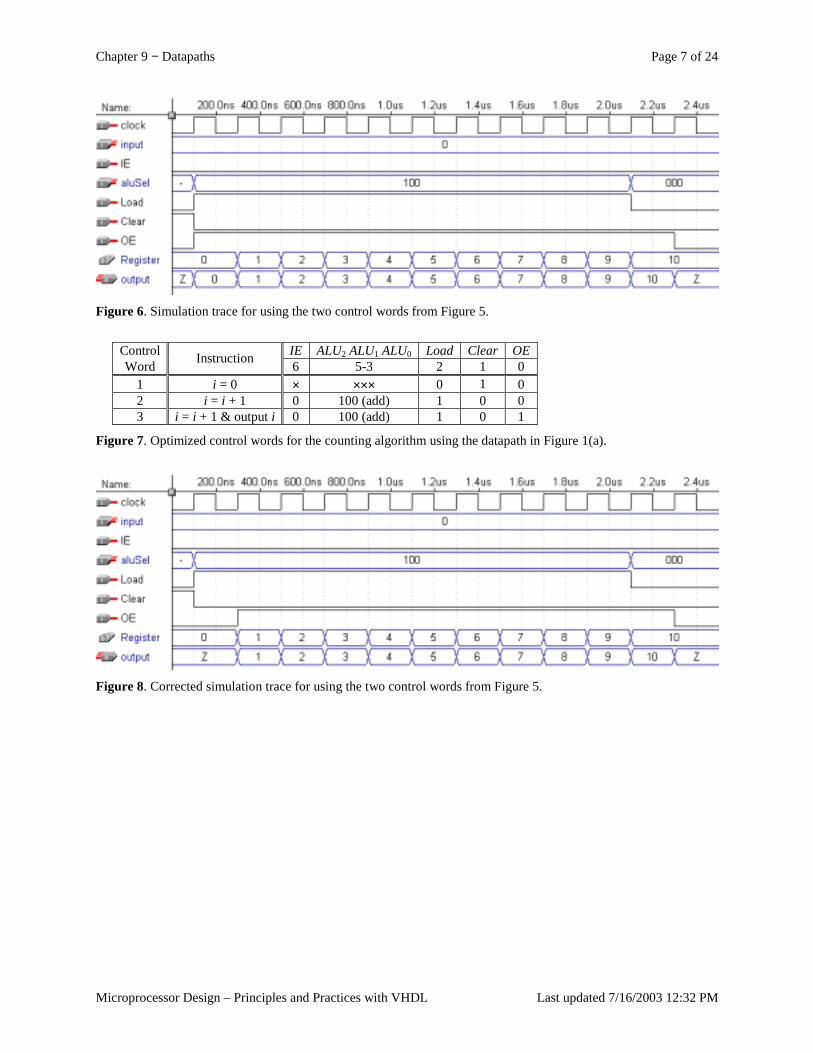
Chapter 9 − Datapaths Page 7 of 24
Microprocessor Design – Principles and Practices with VHDL Last updated 7/16/2003 12:32 PM
Figure 6. Simulation trace for using the two control words from Figure 5.
Control IE ALU2 ALU1 ALU0 Load Clear OE Word Instruction 6 5-3 2 1 0
1 i = 0 × ××× 0 1 0 2 i = i + 1 0 100 (add) 1 0 0 3 i = i + 1 & output i 0 100 (add) 1 0 1
Figure 7. Optimized control words for the counting algorithm using the datapath in Figure 1(a).
Figure 8. Corrected simulation trace for using the two control words from Figure 5.
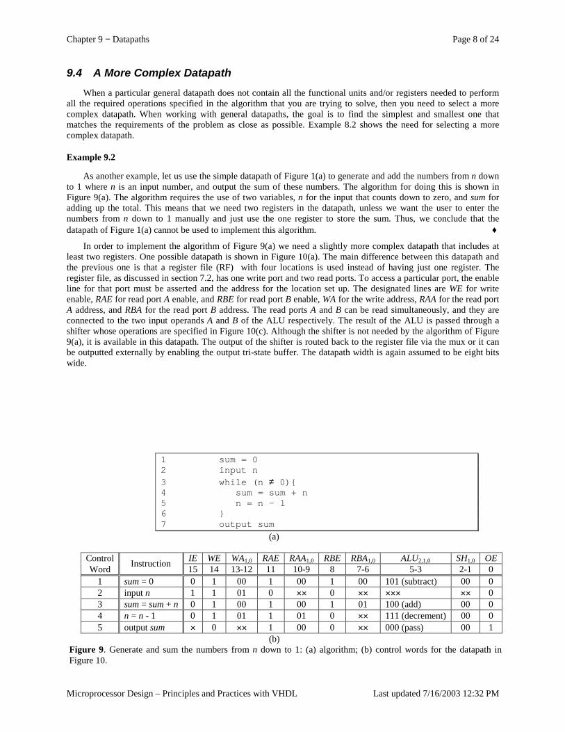
Chapter 9 − Datapaths Page 8 of 24
Microprocessor Design – Principles and Practices with VHDL Last updated 7/16/2003 12:32 PM
9.4 A More Complex Datapath When a particular general datapath does not contain all the functional units and/or registers needed to perform
all the required operations specified in the algorithm that you are trying to solve, then you need to select a more complex datapath. When working with general datapaths, the goal is to find the simplest and smallest one that matches the requirements of the problem as close as possible. Example 8.2 shows the need for selecting a more complex datapath.
Example 9.2
As another example, let us use the simple datapath of Figure 1(a) to generate and add the numbers from n down to 1 where n is an input number, and output the sum of these numbers. The algorithm for doing this is shown in Figure 9(a). The algorithm requires the use of two variables, n for the input that counts down to zero, and sum for adding up the total. This means that we need two registers in the datapath, unless we want the user to enter the numbers from n down to 1 manually and just use the one register to store the sum. Thus, we conclude that the datapath of Figure 1(a) cannot be used to implement this algorithm. ♦
In order to implement the algorithm of Figure 9(a) we need a slightly more complex datapath that includes at least two registers. One possible datapath is shown in Figure 10(a). The main difference between this datapath and the previous one is that a register file (RF) with four locations is used instead of having just one register. The register file, as discussed in section 7.2, has one write port and two read ports. To access a particular port, the enable line for that port must be asserted and the address for the location set up. The designated lines are WE for write enable, RAE for read port A enable, and RBE for read port B enable, WA for the write address, RAA for the read port A address, and RBA for the read port B address. The read ports A and B can be read simultaneously, and they are connected to the two input operands A and B of the ALU respectively. The result of the ALU is passed through a shifter whose operations are specified in Figure 10(c). Although the shifter is not needed by the algorithm of Figure 9(a), it is available in this datapath. The output of the shifter is routed back to the register file via the mux or it can be outputted externally by enabling the output tri-state buffer. The datapath width is again assumed to be eight bits wide.
1 sum = 02 input n3 while (n ≠ 0){4 sum = sum + n5 n = n - 16 }7 output sum
(a)
Control IE WE WA1,0 RAE RAA1,0 RBE RBA1,0 ALU2,1,0 SH1,0 OE Word Instruction 15 14 13-12 11 10-9 8 7-6 5-3 2-1 0
1 sum = 0 0 1 00 1 00 1 00 101 (subtract) 00 0 2 input n 1 1 01 0 ×× 0 ×× ××× ×× 0 3 sum = sum + n 0 1 00 1 00 1 01 100 (add) 00 0 4 n = n - 1 0 1 01 1 01 0 ×× 111 (decrement) 00 0 5 output sum × 0 ×× 1 00 0 ×× 000 (pass) 00 1
(b) Figure 9. Generate and sum the numbers from n down to 1: (a) algorithm; (b) control words for the datapath in Figure 10.
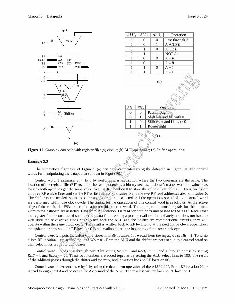
Chapter 9 − Datapaths Page 9 of 24
Microprocessor Design – Principles and Practices with VHDL Last updated 7/16/2003 12:32 PM
ALU0
ALU1
ALU2
A B
15
Input
mux01
WEWA 4x8
RFRAERAA
RBERBA
1413-12
1110-9
87-6
Clk
543
0
IE
OE
ShifterSH1SH0
21
(a)
Figure 10. Complex datapath with register file: (a) circuit; (b) ALU operations; (c) Shifter operations.
Example 9.3
The summation algorithm of Figure 9 (a) can be implemented using the datapath in Figure 10. The control words for manipulating the datapath are shown in Figure 9(b).
Control word 1 initializes sum to 0 by performing a subtraction where the two operands are the same. The location of the register file (RF) used for the two operands is arbitrary because it doesn’t matter what the value is as long as both operands get the same value. We use RF location 0 to store the value of variable sum. Thus, we assert all three RF enable lines and set the RF write address to location 0 and the two RF read addresses also to location 0. The shifter is not needed, so the pass through operation is selected. All the operations specified by a control word are performed within one clock cycle. The timing for the operations of this control word is as follows. At the active edge of the clock, the FSM enters the state for this control word. The appropriate control signals for this control word to the datapath are asserted. Data from RF location 0 is read for both ports and passed to the ALU. Recall that the register file is constructed such that the data from reading a port is available immediately and does not have to wait until the next active clock edge. Since both the ALU and the Shifter are combinational circuits, they will operate within the same clock cycle. The result is written back to RF location 0 at the next active clock edge. Thus, the updated or new value in RF location 0 is not available until the beginning of the next clock cycle.
Control word 2 inputs the value n and stores it in RF location 1. To read from the input, we set IE = 1. To write n into RF location 1 we set WE = 1 and WA = 01. Both the ALU and the shifter are not used in this control word so their select lines are set to don’t cares.
Control word 3 reads sum through port A by setting RAE = 1 and RAA1,0 = 00, and n through port B by setting RBE = 1 and RBA1,0 = 01. These two numbers are added together by setting the ALU select lines to 100. The result of the addition passes through the shifter and the mux, and is written back to RF location 00.
Control word 4 decrements n by 1 by using the decrement operation of the ALU (111). From RF location 01, n is read through port A and passes to the A operand of the ALU. The result is written back to RF location 1.
ALU2 ALU1 ALU0 Operation 0 0 0 Pass through A 0 0 1 A AND B 0 1 0 A OR B 0 1 1 NOT A 1 0 0 A + B 1 0 1 A – B 1 1 0 A + 1 1 1 1 A – 1
(b)
SH1 SH0 Operation 0 0 Pass through 0 1 Shift left and fill with 0 1 0 Shift right and fill with 0 1 1 Rotate right
(c)
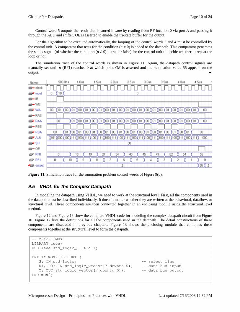
Chapter 9 − Datapaths Page 10 of 24
Microprocessor Design – Principles and Practices with VHDL Last updated 7/16/2003 12:32 PM
Control word 5 outputs the result that is stored in sum by reading from RF location 0 via port A and passing it through the ALU and shifter. OE is asserted to enable the tri-state buffer for the output.
For the algorithm to be executed automatically, the looping of the control words 3 and 4 must be controlled by the control unit. A comparator that tests for the condition (n ≠ 0) is added to the datapath. This comparator generates the status signal (of whether the condition (n ≠ 0) is true or false) for the control unit to decide whether to repeat the loop or not.
The simulation trace of the control words is shown in Figure 11. Again, the datapath control signals are manually set until n (RF1) reaches 0 at which point OE is asserted and the summation value 55 appears on the output. ♦
Figure 11. Simulation trace for the summation problem control words of Figure 9(b).
9.5 VHDL for the Complex Datapath In modeling the datapath using VHDL, we need to work at the structural level. First, all the components used in
the datapath must be described individually. It doesn’t matter whether they are written at the behavioral, dataflow, or structural level. These components are then connected together in an enclosing module using the structural level method.
Figure 12 and Figure 13 show the complete VHDL code for modeling the complex datapath circuit from Figure 10. Figure 12 lists the definitions for all the components used in the datapath. The detail constructions of these components are discussed in previous chapters. Figure 13 shows the enclosing module that combines these components together at the structural level to form the datapath.
-- 2-to-1 MUXLIBRARY ieee;USE ieee.std_logic_1164.all;
ENTITY mux2 IS PORT (S: IN std_logic; -- select lineD1, D0: IN std_logic_vector(7 downto 0); -- data bus inputY: OUT std_logic_vector(7 downto 0)); -- data bus output
END mux2;
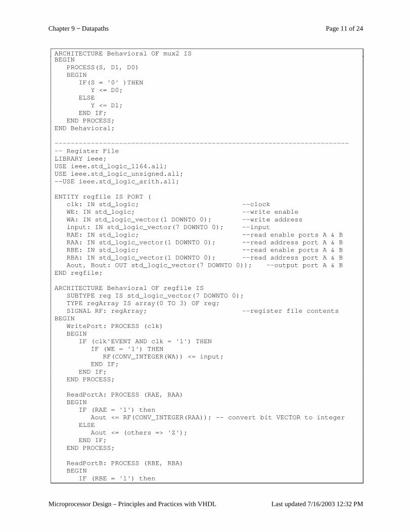
Chapter 9 − Datapaths Page 11 of 24
Microprocessor Design – Principles and Practices with VHDL Last updated 7/16/2003 12:32 PM
ARCHITECTURE Behavioral OF mux2 ISBEGIN
PROCESS(S, D1, D0)BEGIN
IF(S = '0' )THENY <= D0;
ELSEY <= D1;
END IF;END PROCESS;
END Behavioral;
--------------------------------------------------------------------------- Register FileLIBRARY ieee;USE ieee.std_logic_1164.all;USE ieee.std_logic_unsigned.all;--USE ieee.std_logic_arith.all;
ENTITY regfile IS PORT (clk: IN std_logic; --clockWE: IN std_logic; --write enableWA: IN std_logic_vector(1 DOWNTO 0); --write addressinput: IN std_logic_vector(7 DOWNTO 0); --inputRAE: IN std_logic; --read enable ports A & BRAA: IN std_logic_vector(1 DOWNTO 0); --read address port A & BRBE: IN std_logic; --read enable ports A & BRBA: IN std_logic_vector(1 DOWNTO 0); --read address port A & BAout, Bout: OUT std_logic_vector(7 DOWNTO 0)); --output port A & B
END regfile;
ARCHITECTURE Behavioral OF regfile ISSUBTYPE reg IS std_logic_vector(7 DOWNTO 0);TYPE regArray IS array(0 TO 3) OF reg;SIGNAL RF: regArray; --register file contents
BEGINWritePort: PROCESS (clk)BEGIN
IF (clk'EVENT AND clk = '1') THENIF (WE = '1') THEN
RF(CONV_INTEGER(WA)) <= input;END IF;
END IF;END PROCESS;
ReadPortA: PROCESS (RAE, RAA)BEGIN
IF (RAE = '1') thenAout <= RF(CONV_INTEGER(RAA)); -- convert bit VECTOR to integer
ELSEAout <= (others => 'Z');
END IF;END PROCESS;
ReadPortB: PROCESS (RBE, RBA)BEGIN
IF (RBE = '1') then
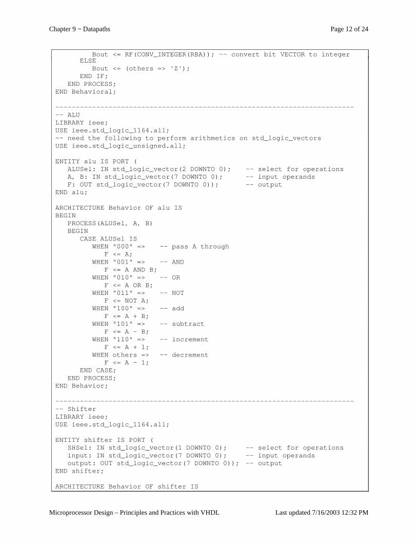
Chapter 9 − Datapaths Page 12 of 24
Microprocessor Design – Principles and Practices with VHDL Last updated 7/16/2003 12:32 PM
Bout <= RF(CONV_INTEGER(RBA)); -- convert bit VECTOR to integerELSE
Bout <= (others => 'Z');END IF;
END PROCESS;END Behavioral;
--------------------------------------------------------------------------- ALULIBRARY ieee;USE ieee.std_logic_1164.all;-- need the following to perform arithmetics on std_logic_vectorsUSE ieee.std_logic_unsigned.all;
ENTITY alu IS PORT (ALUSel: IN std_logic_vector(2 DOWNTO 0); -- select for operationsA, B: IN std_logic_vector(7 DOWNTO 0); -- input operandsF: OUT std_logic_vector(7 DOWNTO 0)); -- output
END alu;
ARCHITECTURE Behavior OF alu ISBEGIN
PROCESS(ALUSel, A, B)BEGIN
CASE ALUSel ISWHEN "000" => -- pass A through
F <= A;WHEN "001" => -- AND
F <= A AND B;WHEN "010" => -- OR
F <= A OR B;WHEN "011" => -- NOT
F <= NOT A;WHEN "100" => -- add
F <= A + B;WHEN "101" => -- subtract
F <= A - B;WHEN "110" => -- increment
F <= A + 1;WHEN others => -- decrement
F <= A - 1;END CASE;
END PROCESS;END Behavior;
--------------------------------------------------------------------------- ShifterLIBRARY ieee;USE ieee.std_logic_1164.all;
ENTITY shifter IS PORT (SHSel: IN std_logic_vector(1 DOWNTO 0); -- select for operationsinput: IN std_logic_vector(7 DOWNTO 0); -- input operandsoutput: OUT std_logic_vector(7 DOWNTO 0)); -- output
END shifter;
ARCHITECTURE Behavior OF shifter IS
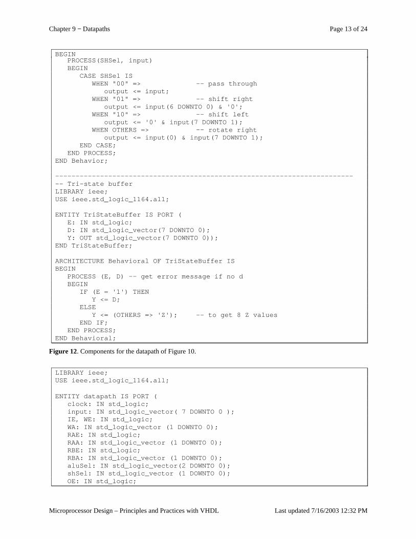
Chapter 9 − Datapaths Page 13 of 24
Microprocessor Design – Principles and Practices with VHDL Last updated 7/16/2003 12:32 PM
BEGINPROCESS(SHSel, input)BEGIN
CASE SHSel ISWHEN "00" => -- pass through
output <= input;WHEN "01" => -- shift right
output <= input(6 DOWNTO 0) & '0';WHEN "10" => -- shift left
output <= '0' & input(7 DOWNTO 1);WHEN OTHERS => -- rotate right
output <= input(0) & input(7 DOWNTO 1);END CASE;
END PROCESS;END Behavior;
--------------------------------------------------------------------------- Tri-state bufferLIBRARY ieee;USE ieee.std_logic_1164.all;
ENTITY TriStateBuffer IS PORT (E: IN std_logic;D: IN std_logic_vector(7 DOWNTO 0);Y: OUT std_logic_vector(7 DOWNTO 0));
END TriStateBuffer;
ARCHITECTURE Behavioral OF TriStateBuffer ISBEGIN
PROCESS (E, D) -- get error message if no dBEGIN
IF (E = '1') THENY <= D;
ELSEY <= (OTHERS => 'Z'); -- to get 8 Z values
END IF;END PROCESS;
END Behavioral;
Figure 12. Components for the datapath of Figure 10.
LIBRARY ieee;USE ieee.std_logic_1164.all;
ENTITY datapath IS PORT (clock: IN std_logic;input: IN std_logic_vector( 7 DOWNTO 0 );IE, WE: IN std_logic;WA: IN std_logic_vector (1 DOWNTO 0);RAE: IN std_logic;RAA: IN std_logic_vector (1 DOWNTO 0);RBE: IN std_logic;RBA: IN std_logic_vector (1 DOWNTO 0);aluSel: IN std_logic_vector(2 DOWNTO 0);shSel: IN std_logic_vector (1 DOWNTO 0);OE: IN std_logic;
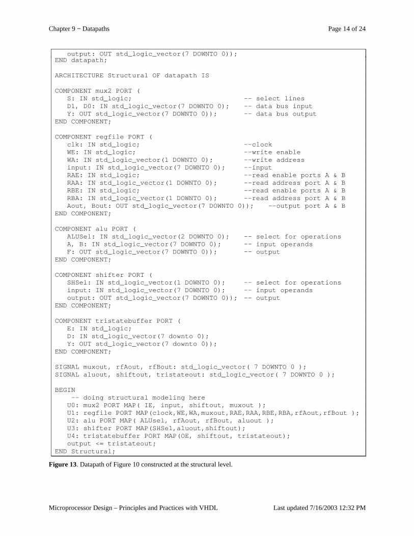
Chapter 9 − Datapaths Page 14 of 24
Microprocessor Design – Principles and Practices with VHDL Last updated 7/16/2003 12:32 PM
output: OUT std_logic_vector(7 DOWNTO 0));END datapath;
ARCHITECTURE Structural OF datapath IS
COMPONENT mux2 PORT (S: IN std_logic; -- select linesD1, D0: IN std_logic_vector(7 DOWNTO 0); -- data bus inputY: OUT std_logic_vector(7 DOWNTO 0)); -- data bus output
END COMPONENT;
COMPONENT regfile PORT (clk: IN std_logic; --clockWE: IN std_logic; --write enableWA: IN std_logic_vector(1 DOWNTO 0); --write addressinput: IN std_logic_vector(7 DOWNTO 0); --inputRAE: IN std_logic; --read enable ports A & BRAA: IN std_logic_vector(1 DOWNTO 0); --read address port A & BRBE: IN std_logic; --read enable ports A & BRBA: IN std_logic_vector(1 DOWNTO 0); --read address port A & BAout, Bout: OUT std_logic_vector(7 DOWNTO 0)); --output port A & B
END COMPONENT;
COMPONENT alu PORT (ALUSel: IN std_logic_vector(2 DOWNTO 0); -- select for operationsA, B: IN std_logic_vector(7 DOWNTO 0); -- input operandsF: OUT std_logic_vector(7 DOWNTO 0)); -- output
END COMPONENT;
COMPONENT shifter PORT (SHSel: IN std_logic_vector(1 DOWNTO 0); -- select for operationsinput: IN std_logic_vector(7 DOWNTO 0); -- input operandsoutput: OUT std_logic_vector(7 DOWNTO 0)); -- output
END COMPONENT;
COMPONENT tristatebuffer PORT (E: IN std_logic;D: IN std_logic_vector(7 downto 0);Y: OUT std_logic_vector(7 downto 0));
END COMPONENT;
SIGNAL muxout, rfAout, rfBout: std_logic_vector( 7 DOWNTO 0 );SIGNAL aluout, shiftout, tristateout: std_logic_vector( 7 DOWNTO 0 );
BEGIN-- doing structural modeling here
U0: mux2 PORT MAP( IE, input, shiftout, muxout );U1: regfile PORT MAP(clock,WE,WA,muxout,RAE,RAA,RBE,RBA,rfAout,rfBout );U2: alu PORT MAP( ALUsel, rfAout, rfBout, aluout );U3: shifter PORT MAP(SHSel,aluout,shiftout);U4: tristatebuffer PORT MAP(OE, shiftout, tristateout);output <= tristateout;
END Structural;
Figure 13. Datapath of Figure 10 constructed at the structural level.
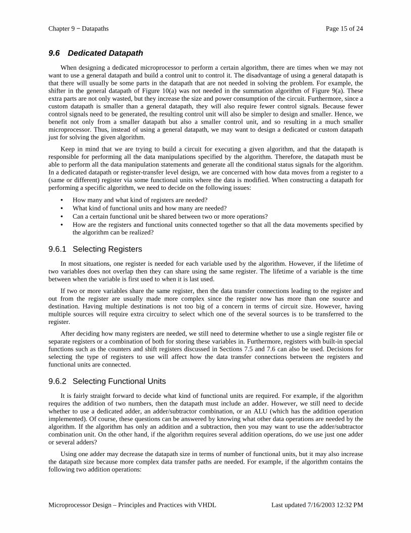
Chapter 9 − Datapaths Page 15 of 24
Microprocessor Design – Principles and Practices with VHDL Last updated 7/16/2003 12:32 PM
9.6 Dedicated Datapath When designing a dedicated microprocessor to perform a certain algorithm, there are times when we may not
want to use a general datapath and build a control unit to control it. The disadvantage of using a general datapath is that there will usually be some parts in the datapath that are not needed in solving the problem. For example, the shifter in the general datapath of Figure 10(a) was not needed in the summation algorithm of Figure 9(a). These extra parts are not only wasted, but they increase the size and power consumption of the circuit. Furthermore, since a custom datapath is smaller than a general datapath, they will also require fewer control signals. Because fewer control signals need to be generated, the resulting control unit will also be simpler to design and smaller. Hence, we benefit not only from a smaller datapath but also a smaller control unit, and so resulting in a much smaller microprocessor. Thus, instead of using a general datapath, we may want to design a dedicated or custom datapath just for solving the given algorithm.
Keep in mind that we are trying to build a circuit for executing a given algorithm, and that the datapath is responsible for performing all the data manipulations specified by the algorithm. Therefore, the datapath must be able to perform all the data manipulation statements and generate all the conditional status signals for the algorithm. In a dedicated datapath or register-transfer level design, we are concerned with how data moves from a register to a (same or different) register via some functional units where the data is modified. When constructing a datapath for performing a specific algorithm, we need to decide on the following issues:
• How many and what kind of registers are needed? • What kind of functional units and how many are needed? • Can a certain functional unit be shared between two or more operations? • How are the registers and functional units connected together so that all the data movements specified by
the algorithm can be realized?
9.6.1 Selecting Registers
In most situations, one register is needed for each variable used by the algorithm. However, if the lifetime of two variables does not overlap then they can share using the same register. The lifetime of a variable is the time between when the variable is first used to when it is last used.
If two or more variables share the same register, then the data transfer connections leading to the register and out from the register are usually made more complex since the register now has more than one source and destination. Having multiple destinations is not too big of a concern in terms of circuit size. However, having multiple sources will require extra circuitry to select which one of the several sources is to be transferred to the register.
After deciding how many registers are needed, we still need to determine whether to use a single register file or separate registers or a combination of both for storing these variables in. Furthermore, registers with built-in special functions such as the counters and shift registers discussed in Sections 7.5 and 7.6 can also be used. Decisions for selecting the type of registers to use will affect how the data transfer connections between the registers and functional units are connected.
9.6.2 Selecting Functional Units
It is fairly straight forward to decide what kind of functional units are required. For example, if the algorithm requires the addition of two numbers, then the datapath must include an adder. However, we still need to decide whether to use a dedicated adder, an adder/subtractor combination, or an ALU (which has the addition operation implemented). Of course, these questions can be answered by knowing what other data operations are needed by the algorithm. If the algorithm has only an addition and a subtraction, then you may want to use the adder/subtractor combination unit. On the other hand, if the algorithm requires several addition operations, do we use just one adder or several adders?
Using one adder may decrease the datapath size in terms of number of functional units, but it may also increase the datapath size because more complex data transfer paths are needed. For example, if the algorithm contains the following two addition operations:

Chapter 9 − Datapaths Page 16 of 24
Microprocessor Design – Principles and Practices with VHDL Last updated 7/16/2003 12:32 PM
a = b + c d = e + f
Using two separate adders will result in the datapath shown in Figure 14(a), whereas, using one adder will require the use of two extra 2-to-1 multiplexers to select which register will supply the input to the adder operands as shown in Figure 14(b).
+
cb
a
+
fe
d
+
01s y
b e c f
a d
01s y
(a) (b)
Figure 14. Datapaths for realizing two addition operations: (a) using two separate adders; (b) using one adder.
9.6.3 Data Transfer Methods
There are several methods in which the registers and functional units can be connected together so that the correct data transfers between the units are made.
Multiple Sources
If the input to a unit has more than one source, then a multiplexer can be used to select which one of the multiple sources to use. The sources can be from registers, constant values, or outputs from other functional units. Figure 15 shows two such examples. In Figure 15(a), the left operand of the adder has four sources: two from registers, one from the constant 1, and one from the output of an ALU. In Figure 15(b), register a has two sources: one from the constant 1, and one from the output of an adder.
b
+
'1'
02s1 y
13s0
ALUa
+'1'
01s y
a
(a) (b)
Figure 15. Examples of multiple sources using multiplexers.
Multiple Destinations
A source having multiple destinations does not require any extra circuitry. The one source can be connected directly to the different destinations, and all the destinations where the data is not needed would simply ignore the data source. For example, in Figure 14(b), the output of the adder has two destinations: register a and register d. If the output of the current addition is for register a, then the Load line for register a is asserted while the Load line for register d is not, and if the output is for register d, then the Load line for register d is asserted while the Load line for register a is not. In either case, only the correct register will take the data while the other units will simply ignore the data.
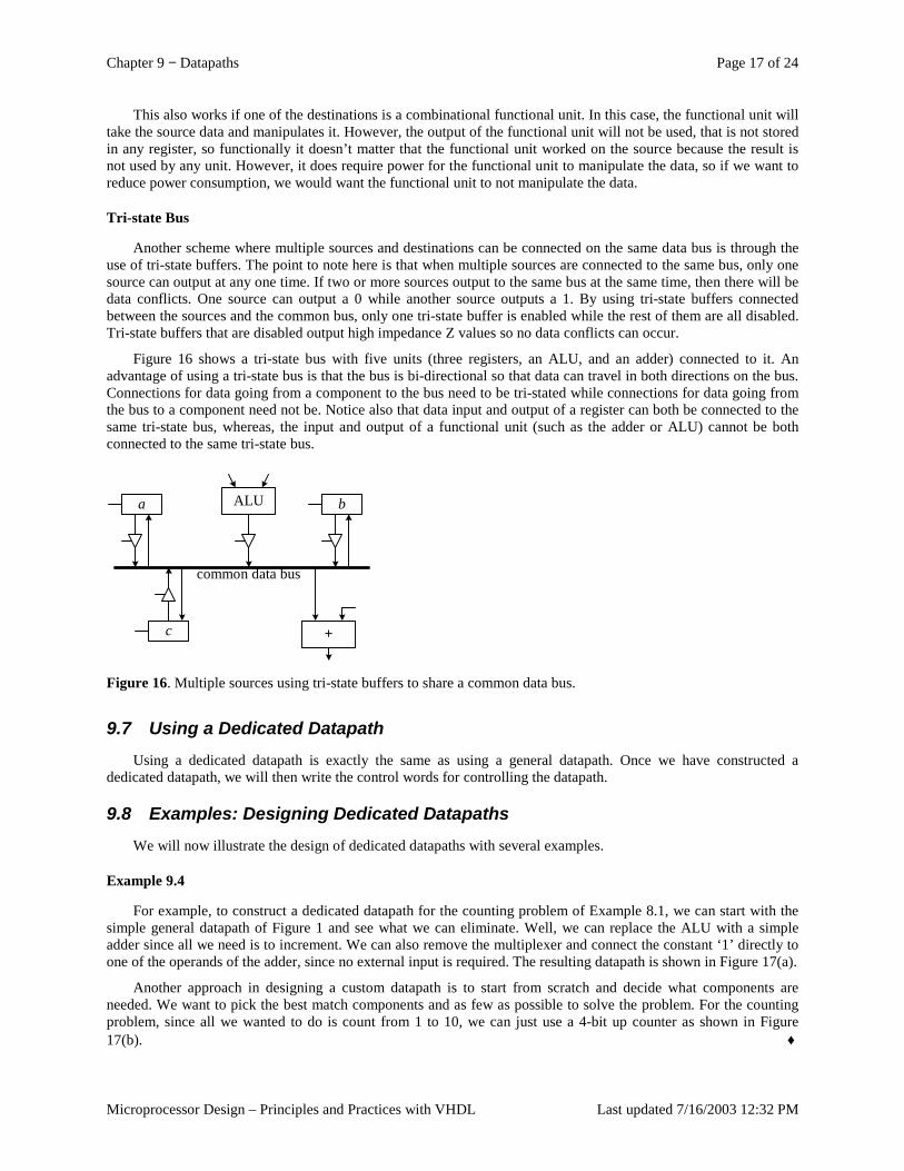
Chapter 9 − Datapaths Page 17 of 24
Microprocessor Design – Principles and Practices with VHDL Last updated 7/16/2003 12:32 PM
This also works if one of the destinations is a combinational functional unit. In this case, the functional unit will take the source data and manipulates it. However, the output of the functional unit will not be used, that is not stored in any register, so functionally it doesn’t matter that the functional unit worked on the source because the result is not used by any unit. However, it does require power for the functional unit to manipulate the data, so if we want to reduce power consumption, we would want the functional unit to not manipulate the data.
Tri-state Bus
Another scheme where multiple sources and destinations can be connected on the same data bus is through the use of tri-state buffers. The point to note here is that when multiple sources are connected to the same bus, only one source can output at any one time. If two or more sources output to the same bus at the same time, then there will be data conflicts. One source can output a 0 while another source outputs a 1. By using tri-state buffers connected between the sources and the common bus, only one tri-state buffer is enabled while the rest of them are all disabled. Tri-state buffers that are disabled output high impedance Z values so no data conflicts can occur.
Figure 16 shows a tri-state bus with five units (three registers, an ALU, and an adder) connected to it. An advantage of using a tri-state bus is that the bus is bi-directional so that data can travel in both directions on the bus. Connections for data going from a component to the bus need to be tri-stated while connections for data going from the bus to a component need not be. Notice also that data input and output of a register can both be connected to the same tri-state bus, whereas, the input and output of a functional unit (such as the adder or ALU) cannot be both connected to the same tri-state bus.
ALU
common data bus
+
a b
c
Figure 16. Multiple sources using tri-state buffers to share a common data bus.
9.7 Using a Dedicated Datapath Using a dedicated datapath is exactly the same as using a general datapath. Once we have constructed a
dedicated datapath, we will then write the control words for controlling the datapath.
9.8 Examples: Designing Dedicated Datapaths We will now illustrate the design of dedicated datapaths with several examples.
Example 9.4
For example, to construct a dedicated datapath for the counting problem of Example 8.1, we can start with the simple general datapath of Figure 1 and see what we can eliminate. Well, we can replace the ALU with a simple adder since all we need is to increment. We can also remove the multiplexer and connect the constant ‘1’ directly to one of the operands of the adder, since no external input is required. The resulting datapath is shown in Figure 17(a).
Another approach in designing a custom datapath is to start from scratch and decide what components are needed. We want to pick the best match components and as few as possible to solve the problem. For the counting problem, since all we wanted to do is count from 1 to 10, we can just use a 4-bit up counter as shown in Figure 17(b). ♦
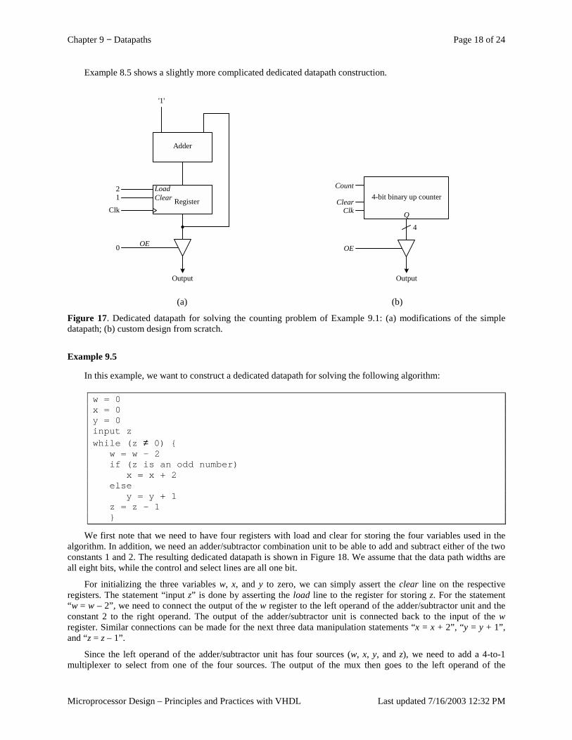
Chapter 9 − Datapaths Page 18 of 24
Microprocessor Design – Principles and Practices with VHDL Last updated 7/16/2003 12:32 PM
Example 8.5 shows a slightly more complicated dedicated datapath construction.
0
LoadClear Register
2
Clk
'1'
OE
1
Output
Adder
ClkClear
4-bit binary up counter
Q
4
Count
OE
Output
(a) (b)
Figure 17. Dedicated datapath for solving the counting problem of Example 9.1: (a) modifications of the simple datapath; (b) custom design from scratch.
Example 9.5
In this example, we want to construct a dedicated datapath for solving the following algorithm:
w = 0x = 0y = 0input zwhile (z ≠ 0) {
w = w – 2if (z is an odd number)
x = x + 2else
y = y + 1z = z – 1}
We first note that we need to have four registers with load and clear for storing the four variables used in the algorithm. In addition, we need an adder/subtractor combination unit to be able to add and subtract either of the two constants 1 and 2. The resulting dedicated datapath is shown in Figure 18. We assume that the data path widths are all eight bits, while the control and select lines are all one bit.
For initializing the three variables w, x, and y to zero, we can simply assert the clear line on the respective registers. The statement “input z” is done by asserting the load line to the register for storing z. For the statement “w = w – 2”, we need to connect the output of the w register to the left operand of the adder/subtractor unit and the constant 2 to the right operand. The output of the adder/subtractor unit is connected back to the input of the w register. Similar connections can be made for the next three data manipulation statements “x = x + 2”, “y = y + 1”, and “z = z – 1”.
Since the left operand of the adder/subtractor unit has four sources (w, x, y, and z), we need to add a 4-to-1 multiplexer to select from one of the four sources. The output of the mux then goes to the left operand of the
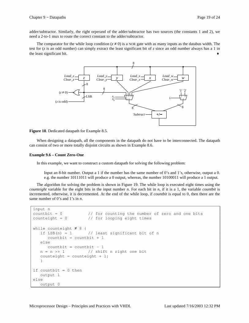
Chapter 9 − Datapaths Page 19 of 24
Microprocessor Design – Principles and Practices with VHDL Last updated 7/16/2003 12:32 PM
adder/subtractor. Similarly, the right orperand of the adder/subtractor has two sources (the constants 1 and 2), we need a 2-to-1 mux to route the correct constant to the adder/subtractor.
The comparator for the while loop condition (z ≠ 0) is a NOR gate with as many inputs as the databus width. The test for (z is an odd number) can simply extract the least significant bit of z since an odd number always has a 1 in the least significant bit. ♦
8
yLoad_yClear_yzLoad_z
Clear_z xLoad_xClear_x wLoad_w
Clear_w
02s1 y
13s0
8
(z ≠ 0)
(z is odd)LSB s1s0
+/−−−−
01s y
'1' '2'
8 8
s
Subtract
8
Figure 18. Dedicated datapath for Example 8.5.
When designing a datapath, all the components in the datapath do not have to be interconnected. The datapath can consist of two or more totally disjoint circuits as shown in Example 8.6.
Example 9.6 – Count Zero-One
In this example, we want to construct a custom datapath for solving the following problem:
Input an 8-bit number. Output a 1 if the number has the same number of 0’s and 1’s, otherwise, output a 0. e.g. the number 10111011 will produce a 0 output, whereas, the number 10100011 will produce a 1 output.
The algorithm for solving the problem is shown in Figure 19. The while loop is executed eight times using the counteight variable for the eight bits in the input number n. For each bit in n, if it is a 1, the variable countbit is incremented, otherwise, it is decremented. At the end of the while loop, if countbit is equal to 0, then there are the same number of 0’s and 1’s in n.
input ncountbit = 0 // for counting the number of zero and one bitscounteight = 0 // for looping eight times
while counteight ≠ 8 {if LSB(n) = 1 // least significant bit of n
countbit = countbit + 1else
countbit = countbit - 1n = n >> 1 // shift n right one bitcounteight = counteight + 1;}
if countbit = 0 thenoutput 1
elseoutput 0
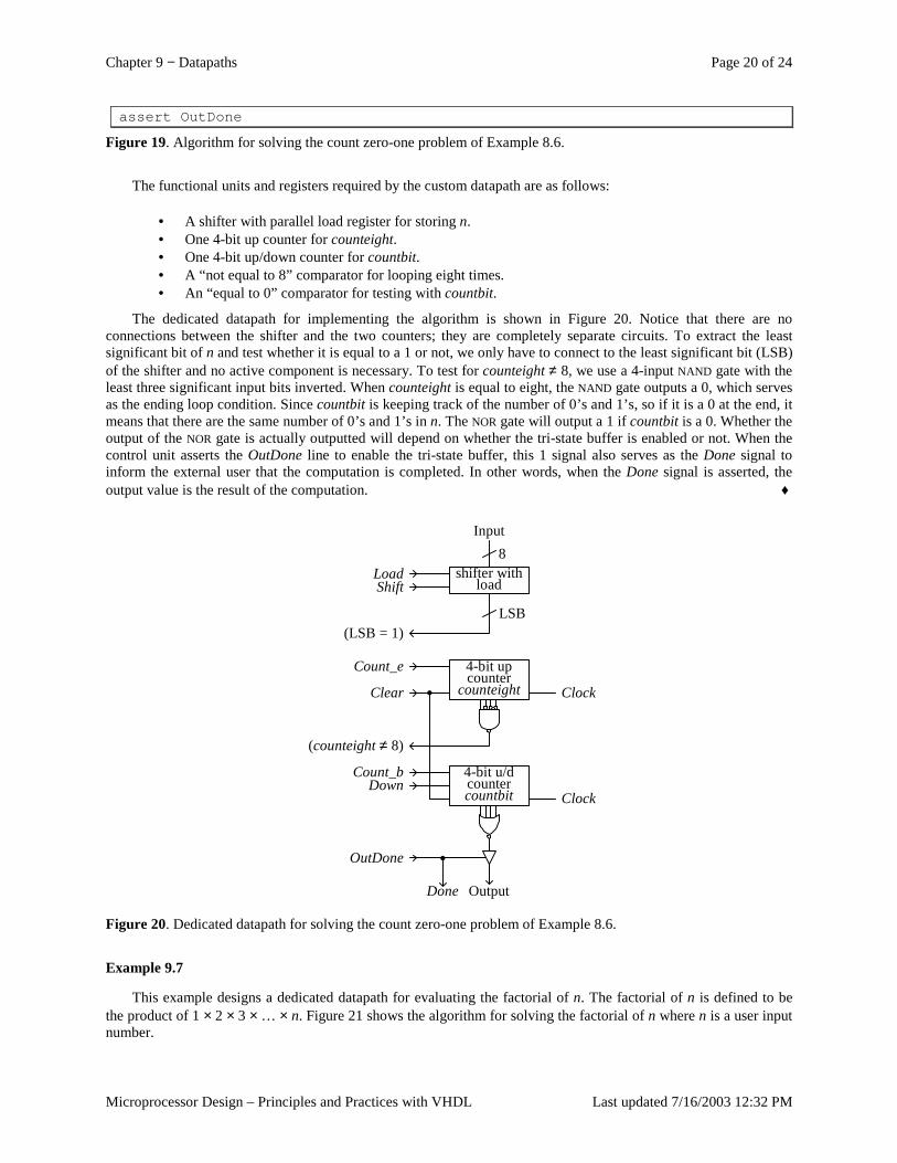
Chapter 9 − Datapaths Page 20 of 24
Microprocessor Design – Principles and Practices with VHDL Last updated 7/16/2003 12:32 PM
assert OutDone
Figure 19. Algorithm for solving the count zero-one problem of Example 8.6.
The functional units and registers required by the custom datapath are as follows:
• A shifter with parallel load register for storing n. • One 4-bit up counter for counteight. • One 4-bit up/down counter for countbit. • A “not equal to 8” comparator for looping eight times. • An “equal to 0” comparator for testing with countbit.
The dedicated datapath for implementing the algorithm is shown in Figure 20. Notice that there are no connections between the shifter and the two counters; they are completely separate circuits. To extract the least significant bit of n and test whether it is equal to a 1 or not, we only have to connect to the least significant bit (LSB) of the shifter and no active component is necessary. To test for counteight ≠ 8, we use a 4-input NAND gate with the least three significant input bits inverted. When counteight is equal to eight, the NAND gate outputs a 0, which serves as the ending loop condition. Since countbit is keeping track of the number of 0’s and 1’s, so if it is a 0 at the end, it means that there are the same number of 0’s and 1’s in n. The NOR gate will output a 1 if countbit is a 0. Whether the output of the NOR gate is actually outputted will depend on whether the tri-state buffer is enabled or not. When the control unit asserts the OutDone line to enable the tri-state buffer, this 1 signal also serves as the Done signal to inform the external user that the computation is completed. In other words, when the Done signal is asserted, the output value is the result of the computation. ♦
shifter withload
4-bit u/dcountercountbit
Output
OutDone
(LSB = 1)
Down
Input
Done
LoadShift
LSB
Count_b
Clock
4-bit upcounter
counteightClear
Count_e
Clock
(counteight ≠ 8)
8
Figure 20. Dedicated datapath for solving the count zero-one problem of Example 8.6.
Example 9.7
This example designs a dedicated datapath for evaluating the factorial of n. The factorial of n is defined to be the product of 1 × 2 × 3 × … × n. Figure 21 shows the algorithm for solving the factorial of n where n is a user input number.
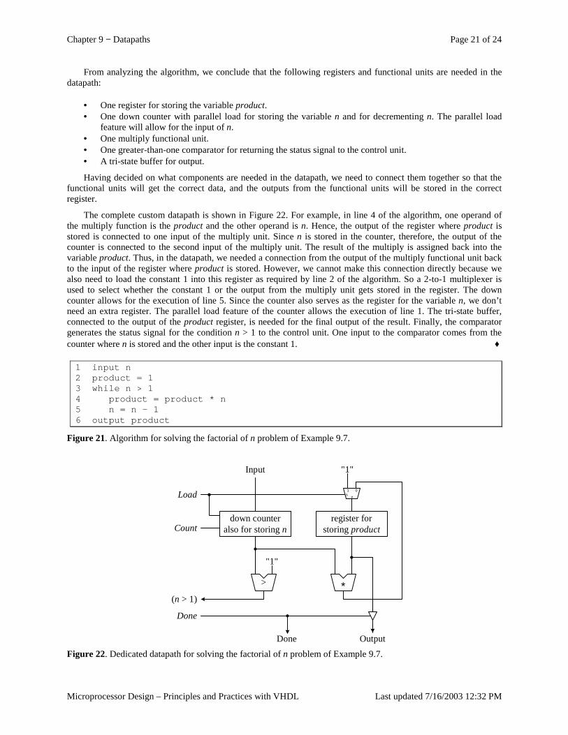
Chapter 9 − Datapaths Page 21 of 24
Microprocessor Design – Principles and Practices with VHDL Last updated 7/16/2003 12:32 PM
From analyzing the algorithm, we conclude that the following registers and functional units are needed in the datapath:
• One register for storing the variable product. • One down counter with parallel load for storing the variable n and for decrementing n. The parallel load
feature will allow for the input of n. • One multiply functional unit. • One greater-than-one comparator for returning the status signal to the control unit. • A tri-state buffer for output.
Having decided on what components are needed in the datapath, we need to connect them together so that the functional units will get the correct data, and the outputs from the functional units will be stored in the correct register.
The complete custom datapath is shown in Figure 22. For example, in line 4 of the algorithm, one operand of the multiply function is the product and the other operand is n. Hence, the output of the register where product is stored is connected to one input of the multiply unit. Since n is stored in the counter, therefore, the output of the counter is connected to the second input of the multiply unit. The result of the multiply is assigned back into the variable product. Thus, in the datapath, we needed a connection from the output of the multiply functional unit back to the input of the register where product is stored. However, we cannot make this connection directly because we also need to load the constant 1 into this register as required by line 2 of the algorithm. So a 2-to-1 multiplexer is used to select whether the constant 1 or the output from the multiply unit gets stored in the register. The down counter allows for the execution of line 5. Since the counter also serves as the register for the variable n, we don’t need an extra register. The parallel load feature of the counter allows the execution of line 1. The tri-state buffer, connected to the output of the product register, is needed for the final output of the result. Finally, the comparator generates the status signal for the condition n > 1 to the control unit. One input to the comparator comes from the counter where n is stored and the other input is the constant 1. ♦
1 input n2 product = 13 while n > 14 product = product * n5 n = n – 16 output product
Figure 21. Algorithm for solving the factorial of n problem of Example 9.7.
*>
"1"
01s y
"1"Input
(n > 1)
Output
Done
Done
Count
Load
down counteralso for storing n
register forstoring product
Figure 22. Dedicated datapath for solving the factorial of n problem of Example 9.7.
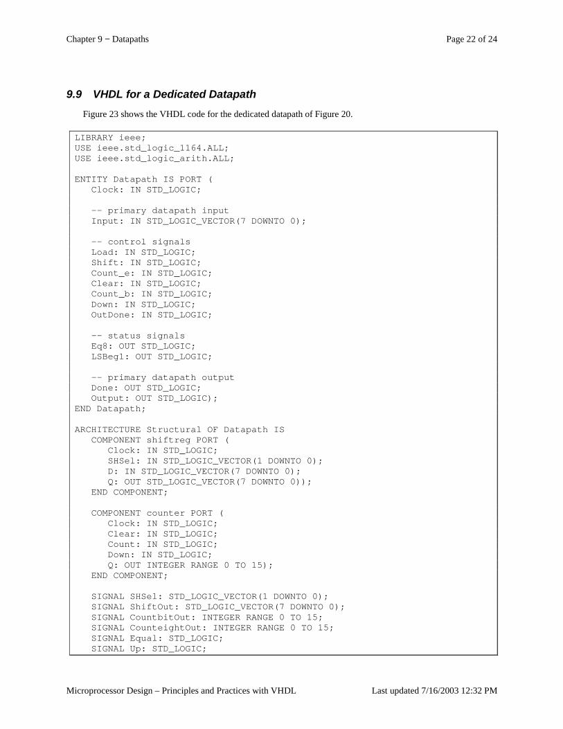
Chapter 9 − Datapaths Page 22 of 24
Microprocessor Design – Principles and Practices with VHDL Last updated 7/16/2003 12:32 PM
9.9 VHDL for a Dedicated Datapath Figure 23 shows the VHDL code for the dedicated datapath of Figure 20.
LIBRARY ieee;USE ieee.std_logic_1164.ALL;USE ieee.std_logic_arith.ALL;
ENTITY Datapath IS PORT (Clock: IN STD_LOGIC;
-- primary datapath inputInput: IN STD_LOGIC_VECTOR(7 DOWNTO 0);
-- control signalsLoad: IN STD_LOGIC;Shift: IN STD_LOGIC;Count_e: IN STD_LOGIC;Clear: IN STD_LOGIC;Count_b: IN STD_LOGIC;Down: IN STD_LOGIC;OutDone: IN STD_LOGIC;
-- status signalsEq8: OUT STD_LOGIC;LSBeg1: OUT STD_LOGIC;
-- primary datapath outputDone: OUT STD_LOGIC;Output: OUT STD_LOGIC);
END Datapath;
ARCHITECTURE Structural OF Datapath ISCOMPONENT shiftreg PORT (
Clock: IN STD_LOGIC;SHSel: IN STD_LOGIC_VECTOR(1 DOWNTO 0);D: IN STD_LOGIC_VECTOR(7 DOWNTO 0);Q: OUT STD_LOGIC_VECTOR(7 DOWNTO 0));
END COMPONENT;
COMPONENT counter PORT (Clock: IN STD_LOGIC;Clear: IN STD_LOGIC;Count: IN STD_LOGIC;Down: IN STD_LOGIC;Q: OUT INTEGER RANGE 0 TO 15);
END COMPONENT;
SIGNAL SHSel: STD_LOGIC_VECTOR(1 DOWNTO 0);SIGNAL ShiftOut: STD_LOGIC_VECTOR(7 DOWNTO 0);SIGNAL CountbitOut: INTEGER RANGE 0 TO 15;SIGNAL CounteightOut: INTEGER RANGE 0 TO 15;SIGNAL Equal: STD_LOGIC;SIGNAL Up: STD_LOGIC;
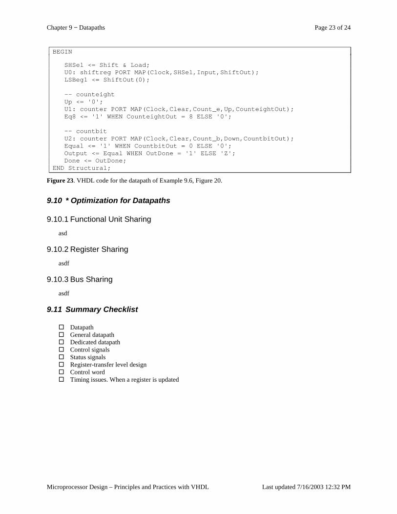
Chapter 9 − Datapaths Page 23 of 24
Microprocessor Design – Principles and Practices with VHDL Last updated 7/16/2003 12:32 PM
BEGIN
SHSel <= Shift & Load;U0: shiftreg PORT MAP(Clock,SHSel,Input,ShiftOut);LSBeg1 <= ShiftOut(0);
-- counteightUp <= '0';U1: counter PORT MAP(Clock,Clear,Count_e,Up,CounteightOut);Eq8 <= '1' WHEN CounteightOut = 8 ELSE '0';
-- countbitU2: counter PORT MAP(Clock,Clear,Count_b,Down,CountbitOut);Equal <= '1' WHEN CountbitOut = 0 ELSE '0';Output <= Equal WHEN OutDone = '1' ELSE 'Z';Done <= OutDone;
END Structural;
Figure 23. VHDL code for the datapath of Example 9.6, Figure 20.
9.10 * Optimization for Datapaths
9.10.1 Functional Unit Sharing
asd
9.10.2 Register Sharing
asdf
9.10.3 Bus Sharing
asdf
9.11 Summary Checklist
� Datapath � General datapath � Dedicated datapath � Control signals � Status signals � Register-transfer level design � Control word � Timing issues. When a register is updated
Chapter 9 − Datapaths Page 24 of 24
Microprocessor Design – Principles and Practices with VHDL Last updated 7/16/2003 12:32 PM
Index
C
Control signal, 2, 3 Control word, 3
D
Data transfer methods, 16 multiple destinations, 16 multiple sources, 16 tri-state bus, 17
Datapath, 2 complex example, 8 dedicated. See Dedicated datapath. general. See General datapath. simple example, 3 timing issues, 5
Dedicated datapath, 15 data transfer methods, 16 examples, 17 selecting functional units, 15 selecting registers, 15
timing issues, 5 using a, 17
G
General datapath, 3 timing issues, 5 using a, 4
R
Register file, 8 Register transfer level, 2 RTL. See Register transfer level.
S
Status signal, 2, 5
T
Timing issues, 5 Tri-state bus, 17

Chapter 10 − Control Units Page 1 of 5
Principles of Digital Logic Design Enoch Hwang Last updated 3/18/2003 7:54 PM
Table of Content Table of Content ........................................................................................................................................................... 1 10 Control Units..................................................................................................................................................... 2
10.1 Exercises ....................................................................................................................................................... 3 10.2 Selected Answers .......................................................................................................................................... 4
Index ............................................................................................................................................................................. 5
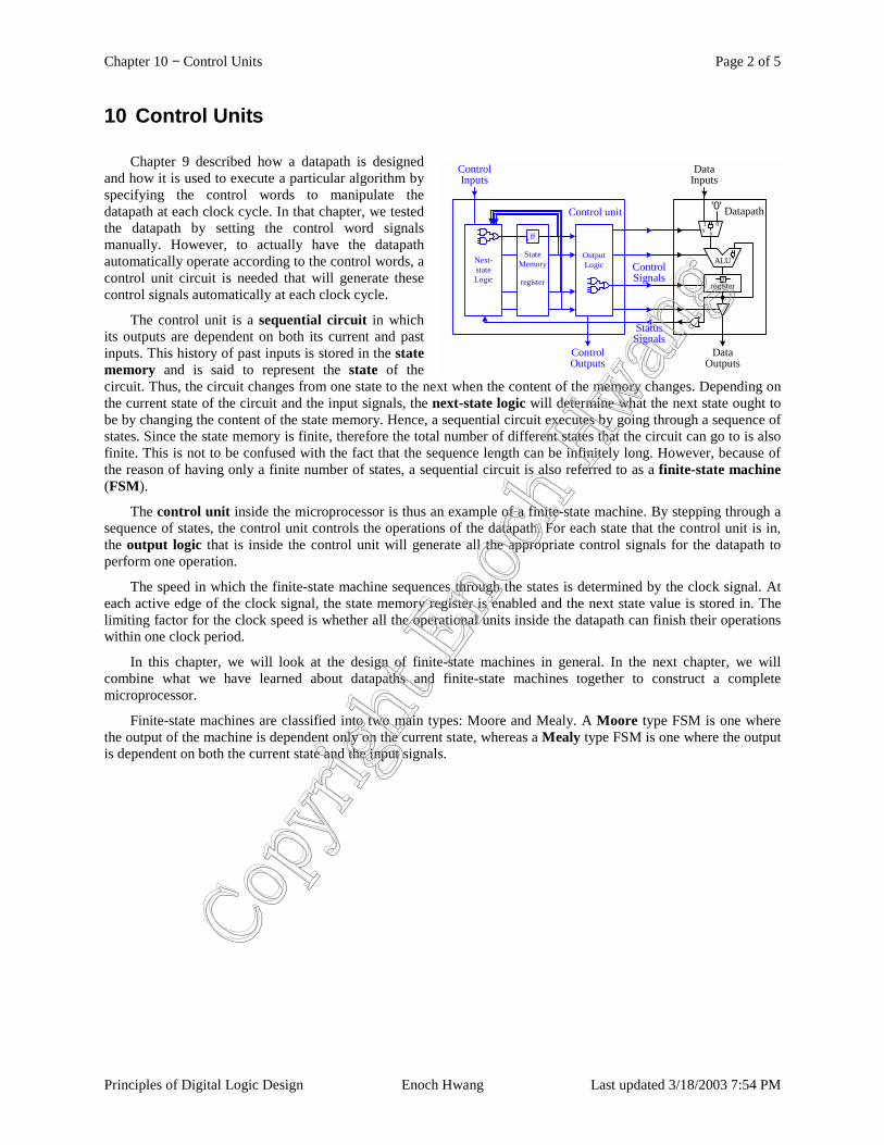
Chapter 10 − Control Units Page 2 of 5
Principles of Digital Logic Design Enoch Hwang Last updated 3/18/2003 7:54 PM
ControlSignals
StatusSignals
01s y
'0'
DataInputs
DataOutputs
Datapath
ALU
registerff
OutputLogicNext-
stateLogic
ControlInputs
ControlOutputs
StateMemory
register
Control unit
ff
10 Control Units
Chapter 9 described how a datapath is designed and how it is used to execute a particular algorithm by specifying the control words to manipulate the datapath at each clock cycle. In that chapter, we tested the datapath by setting the control word signals manually. However, to actually have the datapath automatically operate according to the control words, a control unit circuit is needed that will generate these control signals automatically at each clock cycle.
The control unit is a sequential circuit in which its outputs are dependent on both its current and past inputs. This history of past inputs is stored in the state memory and is said to represent the state of the circuit. Thus, the circuit changes from one state to the next when the content of the memory changes. Depending on the current state of the circuit and the input signals, the next-state logic will determine what the next state ought to be by changing the content of the state memory. Hence, a sequential circuit executes by going through a sequence of states. Since the state memory is finite, therefore the total number of different states that the circuit can go to is also finite. This is not to be confused with the fact that the sequence length can be infinitely long. However, because of the reason of having only a finite number of states, a sequential circuit is also referred to as a finite-state machine (FSM).
The control unit inside the microprocessor is thus an example of a finite-state machine. By stepping through a sequence of states, the control unit controls the operations of the datapath. For each state that the control unit is in, the output logic that is inside the control unit will generate all the appropriate control signals for the datapath to perform one operation.
The speed in which the finite-state machine sequences through the states is determined by the clock signal. At each active edge of the clock signal, the state memory register is enabled and the next state value is stored in. The limiting factor for the clock speed is whether all the operational units inside the datapath can finish their operations within one clock period.
In this chapter, we will look at the design of finite-state machines in general. In the next chapter, we will combine what we have learned about datapaths and finite-state machines together to construct a complete microprocessor.
Finite-state machines are classified into two main types: Moore and Mealy. A Moore type FSM is one where the output of the machine is dependent only on the current state, whereas a Mealy type FSM is one where the output is dependent on both the current state and the input signals.

Chapter 10 − Control Units Page 3 of 5
Principles of Digital Logic Design Enoch Hwang Last updated 3/18/2003 7:54 PM
10.1 Exercises

Chapter 10 − Control Units Page 4 of 5
Principles of Digital Logic Design Enoch Hwang Last updated 3/18/2003 7:54 PM
10.2 Selected Answers
Chapter 10 − Control Units Page 5 of 5
Principles of Digital Logic Design Enoch Hwang Last updated 3/18/2003 7:54 PM
Index
C
Control unit, 2
F
Finite-state machine, 2 FSM. See Finite-state machine.
M
Mealy FSM, 2 Microprocessor
control unit, 2 next-state logic, 2 output logic, 2
state memory, 2 Moore FSM, 2
N
Next-state logic, 2
O
Output logic, 2
S
Sequential circuit, 2 State, 2 State memory, 2
Chapter 11 – Dedicated Microprocessors Page 1 of 25
Microprocessor Design – Principles and Practices with VHDL Last updated 3/18/2003 7:58 PM
Table of Content Table of Content ........................................................................................................................................................... 1 11 Dedicated Microprocessors............................................................................................................................... 2
11.1 Manual Construction of a Dedicated Microprocessor................................................................................... 3 11.2 FSM + D Model Using VHDL.................................................................................................................... 11 11.3 FSMD Model .............................................................................................................................................. 14 11.4 Behavioral Model........................................................................................................................................ 16 11.5 Examples..................................................................................................................................................... 18
Index ........................................................................................................................................................................... 25
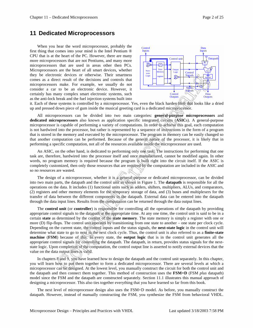
Chapter 11 – Dedicated Microprocessors Page 2 of 25
Microprocessor Design – Principles and Practices with VHDL Last updated 3/18/2003 7:58 PM
ControlSignals
StatusSignals
01s y
'0'
DataInputs
DataOutputs
Datapath
ALU
registerff
OutputLogicNext-
stateLogic
ControlInputs
ControlOutputs
StateMemory
register
Control unit
ff
11 Dedicated Microprocessors
When you hear the word microprocessor, probably the first thing that comes into your mind is the Intel Pentium ® CPU that is at the heart of the PC. However, there are many more microprocessors that are not Pentiums, and many more microprocessors that are used in areas other then PCs. Microprocessors are the heart of all smart devices, whether they be electronic devices or otherwise. Their smartness comes as a direct result of the decisions and controls that microprocessors make. For example, we usually do not consider a car to be an electronic device. However, it certainly has many complex smart electronic systems, such as the anti-lock break and the fuel injection systems built into it. Each of these systems is controlled by a microprocessor. Yes, even the black harden blob that looks like a dried up and pressed down piece of gum inside the musical greeting card is a dedicated microprocessor.
All microprocessors can be divided into two main categories: general-purpose microprocessors and dedicated microprocessors also known as application specific integrated circuits (ASICs). A general-purpose microprocessor is capable of performing a variety of computations. In order to achieve this goal, each computation is not hardwired into the processor, but rather is represented by a sequence of instructions in the form of a program that is stored in the memory and executed by the microprocessor. The program in memory can be easily changed so that another computation can be performed. Because of the general nature of the processor, it is likely that in performing a specific computation, not all of the resources available inside the microprocessor are used.
An ASIC, on the other hand, is dedicated to performing only one task. The instructions for performing that one task are, therefore, hardwired into the processor itself and once manufactured, cannot be modified again. In other words, no program memory is required because the program is built right into the circuit itself. If the ASIC is completely customized, then only those resources that are required by the computation are included in the ASIC and so no resources are wasted.
The design of a microprocessor, whether it is a general purpose or dedicated microprocessor, can be divided into two main parts, the datapath and the control unit as shown in Figure 1. The datapath is responsible for all the operations on the data. It includes (1) functional units such as adders, shifters, multipliers, ALUs, and comparators, (2) registers and other memory elements for the temporary storage of data, and (3) buses and multiplexers for the transfer of data between the different components in the datapath. External data can be entered into the datapath through the data input lines. Results from the computation can be returned through the data output lines.
The control unit (or controller) is responsible for controlling all the operations of the datapath by providing appropriate control signals to the datapath at the appropriate time. At any one time, the control unit is said to be in a certain state as determined by the content of the state memory. The state memory is simply a register with one or more (D) flip-flops. The control unit operates by transitioning from one state to another – one state per clock cycle. Depending on the current state, the control inputs and the status signals, the next-state logic in the control unit will determine what state to go to next in the next clock cycle. Thus, the control unit is also referred to as a finite-state machine (FSM) because of this. In every state, the output logic that is in the control unit generates all the appropriate control signals for controlling the datapath. The datapath, in return, provides status signals for the next-state logic. Upon completion of the computation, the control output line is asserted to notify external devices that the value on the data output lines is valid.
In chapters 8 and 9, you have learned how to design the datapath and the control unit separately. In this chapter, you will learn how to put them together to form a dedicated microprocessor. There are several levels at which a microprocessor can be designed. At the lowest level, you manually construct the circuit for both the control unit and the datapath and then connect them together. This method of construction uses the FSM+D (FSM plus datapath) model since the FSM and the datapath are constructed separately. Section 11.1 illustrates this manual approach of designing a microprocessor. This also ties together everything that you have learned so far from this book.
The next level of microprocessor design also uses the FSM+D model. As before, you manually construct the datapath. However, instead of manually constructing the FSM, you synthesize the FSM from behavioral VHDL.
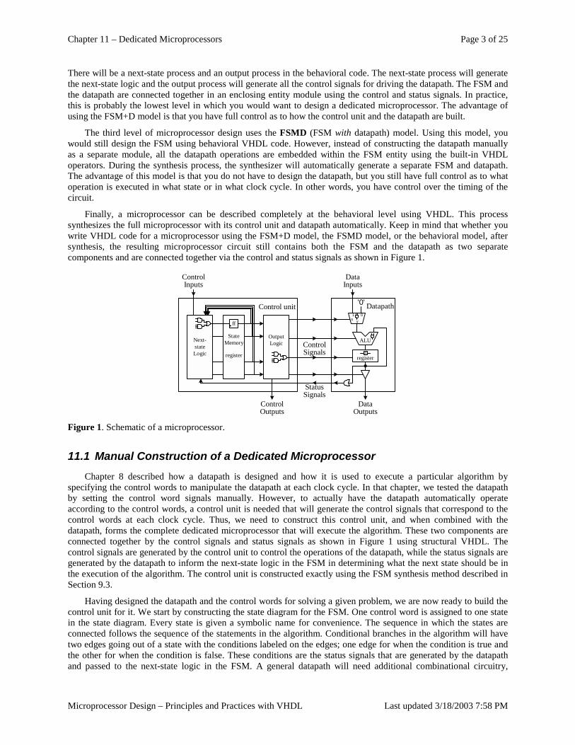
Chapter 11 – Dedicated Microprocessors Page 3 of 25
Microprocessor Design – Principles and Practices with VHDL Last updated 3/18/2003 7:58 PM
There will be a next-state process and an output process in the behavioral code. The next-state process will generate the next-state logic and the output process will generate all the control signals for driving the datapath. The FSM and the datapath are connected together in an enclosing entity module using the control and status signals. In practice, this is probably the lowest level in which you would want to design a dedicated microprocessor. The advantage of using the FSM+D model is that you have full control as to how the control unit and the datapath are built.
The third level of microprocessor design uses the FSMD (FSM with datapath) model. Using this model, you would still design the FSM using behavioral VHDL code. However, instead of constructing the datapath manually as a separate module, all the datapath operations are embedded within the FSM entity using the built-in VHDL operators. During the synthesis process, the synthesizer will automatically generate a separate FSM and datapath. The advantage of this model is that you do not have to design the datapath, but you still have full control as to what operation is executed in what state or in what clock cycle. In other words, you have control over the timing of the circuit.
Finally, a microprocessor can be described completely at the behavioral level using VHDL. This process synthesizes the full microprocessor with its control unit and datapath automatically. Keep in mind that whether you write VHDL code for a microprocessor using the FSM+D model, the FSMD model, or the behavioral model, after synthesis, the resulting microprocessor circuit still contains both the FSM and the datapath as two separate components and are connected together via the control and status signals as shown in Figure 1.
ControlSignals
StatusSignals
01s y
'0'
DataInputs
DataOutputs
Datapath
ALU
registerff
OutputLogicNext-
stateLogic
ControlInputs
ControlOutputs
StateMemory
register
Control unit
ff
Figure 1. Schematic of a microprocessor.
11.1 Manual Construction of a Dedicated Microprocessor Chapter 8 described how a datapath is designed and how it is used to execute a particular algorithm by
specifying the control words to manipulate the datapath at each clock cycle. In that chapter, we tested the datapath by setting the control word signals manually. However, to actually have the datapath automatically operate according to the control words, a control unit is needed that will generate the control signals that correspond to the control words at each clock cycle. Thus, we need to construct this control unit, and when combined with the datapath, forms the complete dedicated microprocessor that will execute the algorithm. These two components are connected together by the control signals and status signals as shown in Figure 1 using structural VHDL. The control signals are generated by the control unit to control the operations of the datapath, while the status signals are generated by the datapath to inform the next-state logic in the FSM in determining what the next state should be in the execution of the algorithm. The control unit is constructed exactly using the FSM synthesis method described in Section 9.3.
Having designed the datapath and the control words for solving a given problem, we are now ready to build the control unit for it. We start by constructing the state diagram for the FSM. One control word is assigned to one state in the state diagram. Every state is given a symbolic name for convenience. The sequence in which the states are connected follows the sequence of the statements in the algorithm. Conditional branches in the algorithm will have two edges going out of a state with the conditions labeled on the edges; one edge for when the condition is true and the other for when the condition is false. These conditions are the status signals that are generated by the datapath and passed to the next-state logic in the FSM. A general datapath will need additional combinational circuitry,

Chapter 11 – Dedicated Microprocessors Page 4 of 25
Microprocessor Design – Principles and Practices with VHDL Last updated 3/18/2003 7:58 PM
comparators to be more precise, that checks for these conditions and when the condition is true, it will assert that corresponding status signal to be used by the next-state logic. There are also conditions from external inputs such as the Start signal for starting the execution of the algorithm/circuit. In addition, an external Reset signal is used to reset the FSM to its starting state.
From the state diagram, we construct the next-state table, which has the same information as the state diagram but with the actual bit encodings assigned to the states. The total number of states in the state diagram will determine the number of flop-flops needed for the state memory. Assigning different encodings to the states may produce a more optimized circuit. Optimizing the state encodings is discussed in Section 9.5.2. Like the state diagram, the next-state table tells us what the next state of the FSM is to be, given the current state that the FSM is in and the current values of the status and input signals.
Up until this point, the FSM design has been independent of what flip-flop type is used. However, a FSM can be implemented using any of the four types of flip-flops (see Sections 6.13 and 9.5.3) or combinations of them, and using different flip-flops can produce a smaller circuit. We will however, use only D flip-flops because of their ease of use and because this is the current trend in microprocessor design. We need to convert the next-state table to the implementation table for the D flip-flop. The implementation table shows the necessary inputs for the (D) flip-flops that will produce the next states as given in the next-state table.
It turns out that the implementation table for the D flip-flop is identical to the next-state table except for the labeling of the entries. In the next-state table (see Figure 3(b)), the label for the entries is Qnext for the next state to go to, whereas, in the implementation table (see Figure 3(c)), the label for the entries is D for the input to the flip-flop. We want to assign to the input D the value that will cause the corresponding Qnext value in the next-state table. However, since the characteristic equation for the D flip-flop (i.e. the equation that describes the operation of the D flip-flop) is
Qnext = D
therefore, the entries in these two tables are the same. If one of the other types of flip-flops is used, the two tables will not be the same. See Section 9.5.3 for an example.
The implementation table is used to derive the excitation equations (i.e. the equation that causes the flip-flop to change state) for all the inputs of all the flip-flops. These equations are dependent on the current state encodings and the values of the status signals (see Figure 3(d)). The next-state logic circuit, which is a combinational circuit, is then constructed from these equations.
From each state of the FSM, control output signals are generated. These signals are the control word signals for manipulating the datapath. Since each control word is executed in one state of the FSM, therefore, these control signals are dependent only on the state. In other words, the output logic equations are dependent on the state value, which is the content of the flip-flops. The truth tables for these control signals are, therefore, just the control word table with the actual state encodings.
In the last state when the resulting data from the computation of the algorithm is outputted from the datapath, it is common practice for the control unit to also output a Done signal to notify the external user that the operation is completed and that the data outputted by the datapath is valid. Example 10.1 shows the entire process for manually constructing the dedicated microprocessor for the summation algorithm of Example 8.3.
Example 11.1
We will manually construct the FSM for the summation algorithm of Example 8.3, which is based on the general datapath shown in Figure 8.10. Recall that the problem is to generate and add the numbers from n down to 1 where n is an input number. The algorithm, control words and datapath used for solving the summation algorithm are repeated here in Figure 2 for convenience.
Figure 2(b) shows that five control words are needed. In the state diagram as shown in Figure 3(a), we have six states; five for the five control words and another one for the starting reset state. The states are given the symbolic names s0, s1, and so on, and are annotated with the control word that it is assigned to execute for easy reference. The sequence in which the states are connected follows the sequence of the statements in the algorithm of Figure 2(a). State s0 is the starting reset state. On reset, the FSM goes to this state and waits for the Start signal. The FSM also goes to this state if it ever happens to enter one of the unused states. An unused state is a combination of the contents
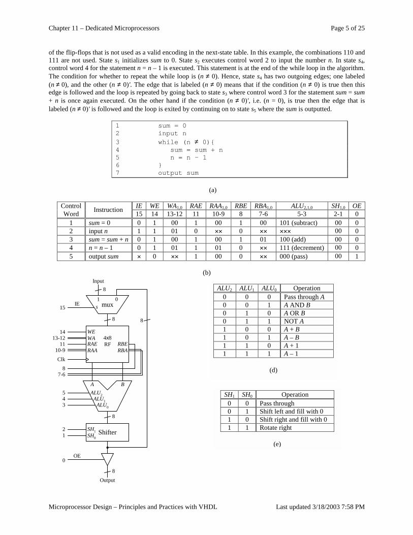
Chapter 11 – Dedicated Microprocessors Page 5 of 25
Microprocessor Design – Principles and Practices with VHDL Last updated 3/18/2003 7:58 PM
of the flip-flops that is not used as a valid encoding in the next-state table. In this example, the combinations 110 and 111 are not used. State s1 initializes sum to 0. State s2 executes control word 2 to input the number n. In state s4, control word 4 for the statement n = n – 1 is executed. This statement is at the end of the while loop in the algorithm. The condition for whether to repeat the while loop is (n ≠ 0). Hence, state s4 has two outgoing edges; one labeled (n ≠ 0), and the other (n ≠ 0)'. The edge that is labeled (n ≠ 0) means that if the condition (n ≠ 0) is true then this edge is followed and the loop is repeated by going back to state s3 where control word 3 for the statement sum = sum + n is once again executed. On the other hand if the condition (n ≠ 0)', i.e. (n = 0), is true then the edge that is labeled (n ≠ 0)' is followed and the loop is exited by continuing on to state s5 where the sum is outputted.
1 sum = 02 input n3 while (n ≠ 0){4 sum = sum + n5 n = n - 16 }7 output sum
(a)
Control IE WE WA1,0 RAE RAA1,0 RBE RBA1,0 ALU2,1,0 SH1,0 OE Word Instruction 15 14 13-12 11 10-9 8 7-6 5-3 2-1 0
1 sum = 0 0 1 00 1 00 1 00 101 (subtract) 00 0 2 input n 1 1 01 0 ×× 0 ×× ××× 00 0 3 sum = sum + n 0 1 00 1 00 1 01 100 (add) 00 0 4 n = n – 1 0 1 01 1 01 0 ×× 111 (decrement) 00 0 5 output sum × 0 ×× 1 00 0 ×× 000 (pass) 00 1
(b)
ALU0
ALU1
ALU2
A B
15
Input
mux01
WEWA 4x8
RFRAERAA
RBERBA
1413-12
1110-9
87-6
Clk
543
0
IE
OE
ShifterSH1SH0
21
Output
8
8
8
8
8
s
ALU2 ALU1 ALU0 Operation 0 0 0 Pass through A 0 0 1 A AND B 0 1 0 A OR B 0 1 1 NOT A 1 0 0 A + B 1 0 1 A – B 1 1 0 A + 1 1 1 1 A – 1
(d)
SH1 SH0 Operation 0 0 Pass through 0 1 Shift left and fill with 0 1 0 Shift right and fill with 0 1 1 Rotate right
(e)
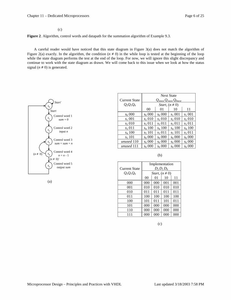
Chapter 11 – Dedicated Microprocessors Page 6 of 25
Microprocessor Design – Principles and Practices with VHDL Last updated 3/18/2003 7:58 PM
(c)
Figure 2. Algorithm, control words and datapath for the summation algorithm of Example 9.3.
A careful reader would have noticed that this state diagram in Figure 3(a) does not match the algorithm of Figure 2(a) exactly. In the algorithm, the condition (n ≠ 0) in the while loop is tested at the beginning of the loop while the state diagram performs the test at the end of the loop. For now, we will ignore this slight discrepancy and continue to work with the state diagram as drawn. We will come back to this issue when we look at how the status signal (n ≠ 0) is generated.
s1
s2
s3
Start
Control word 2input n
Start'
Control word 3sum = sum + n
Control word 4n = n - 1
Control word 5output sum
Control word 1sum = 0
s4
s5
(n ≠ 0)
(n ≠ 0)'
s0
(a)
Next State Q2next Q1next Q0next
Start, (n ≠ 0) Current State
Q2Q1Q0 00 01 10 11
s0 000 s0 000 s0 000 s1 001 s1 001 s1 001 s2 010 s2 010 s2 010 s2 010 s2 010 s3 011 s3 011 s3 011 s3 011 s3 011 s4 100 s4 100 s4 100 s4 100 s4 100 s5 101 s3 011 s5 101 s3 011 s5 101 s0 000 s0 000 s0 000 s0 000
unused 110 s0 000 s0 000 s0 000 s0 000 unused 111 s0 000 s0 000 s0 000 s0 000
(b)
Implementation D2 D1 D0
Start, (n ≠ 0) Current State
Q2Q1Q0 00 01 10 11
000 000 000 001 001 001 010 010 010 010 010 011 011 011 011 011 100 100 100 100 100 101 011 101 011 101 000 000 000 000 110 000 000 000 000 111 000 000 000 000
(c)
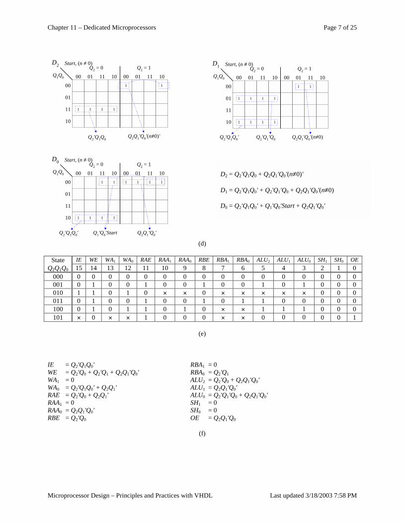
Chapter 11 – Dedicated Microprocessors Page 7 of 25
Microprocessor Design – Principles and Practices with VHDL Last updated 3/18/2003 7:58 PM
Start, (n ≠ 0)
Q1Q0
Q2 = 1
1
001
01 11 10
00
Q2 = 0
00
1 1 1 1
01 11 10
01
11
10
D2
Q2'Q1Q0Q2Q1'Q0'(n≠0)'
Start, (n ≠ 0)
Q1Q0
Q2 = 1
1
001
01 11 10
00
Q2 = 0
00
1 1 1 1
1 1 1 1
01 11 10
01
11
10
D1
Q2'Q1Q0' Q2Q1'Q0'(n≠0)Q2'Q1'Q0
Start, (n ≠ 0)
Q1Q0
Q2 = 1
1 1
001 1
01 11 10
00
Q2 = 0
001 1
1 1 1 1
01 11 10
01
11
10
D0
Q2'Q1Q0' Q2Q1'Q0'Q1'Q0'Start
(d)
(e)
IE = Q2'Q1Q0' RBA1 = 0 WE = Q2'Q0 + Q2'Q1 + Q2Q1'Q0' RBA0 = Q2'Q1 WA1 = 0 ALU2 = Q2'Q0 + Q2Q1'Q0' WA0 = Q2'Q1Q0' + Q2Q1' ALU1 = Q2Q1'Q0' RAE = Q2'Q0 + Q2Q1' ALU0 = Q2'Q1'Q0 + Q2Q1'Q0' RAA1 = 0 SH1 = 0 RAA0 = Q2Q1'Q0' SH0 = 0 RBE = Q2'Q0 OE = Q2Q1'Q0
(f)
State IE WE WA1 WA0 RAE RAA1 RAA0 RBE RBA1 RBA0 ALU2 ALU1 ALU0 SH1 SH0 OE Q2Q1Q0 15 14 13 12 11 10 9 8 7 6 5 4 3 2 1 0
000 0 0 0 0 0 0 0 0 0 0 0 0 0 0 0 0 001 0 1 0 0 1 0 0 1 0 0 1 0 1 0 0 0 010 1 1 0 1 0 × × 0 × × × × × 0 0 0 011 0 1 0 0 1 0 0 1 0 1 1 0 0 0 0 0 100 0 1 0 1 1 0 1 0 × × 1 1 1 0 0 0 101 × 0 × × 1 0 0 0 × × 0 0 0 0 0 1
D2 = Q2'Q1Q0 + Q2Q1'Q0'(n≠0)'
D1 = Q2'Q1Q0' + Q2'Q1'Q0 + Q2Q1'Q0'(n≠0)
D0 = Q2'Q1Q0' + Q1'Q0'Start + Q2Q1'Q0'
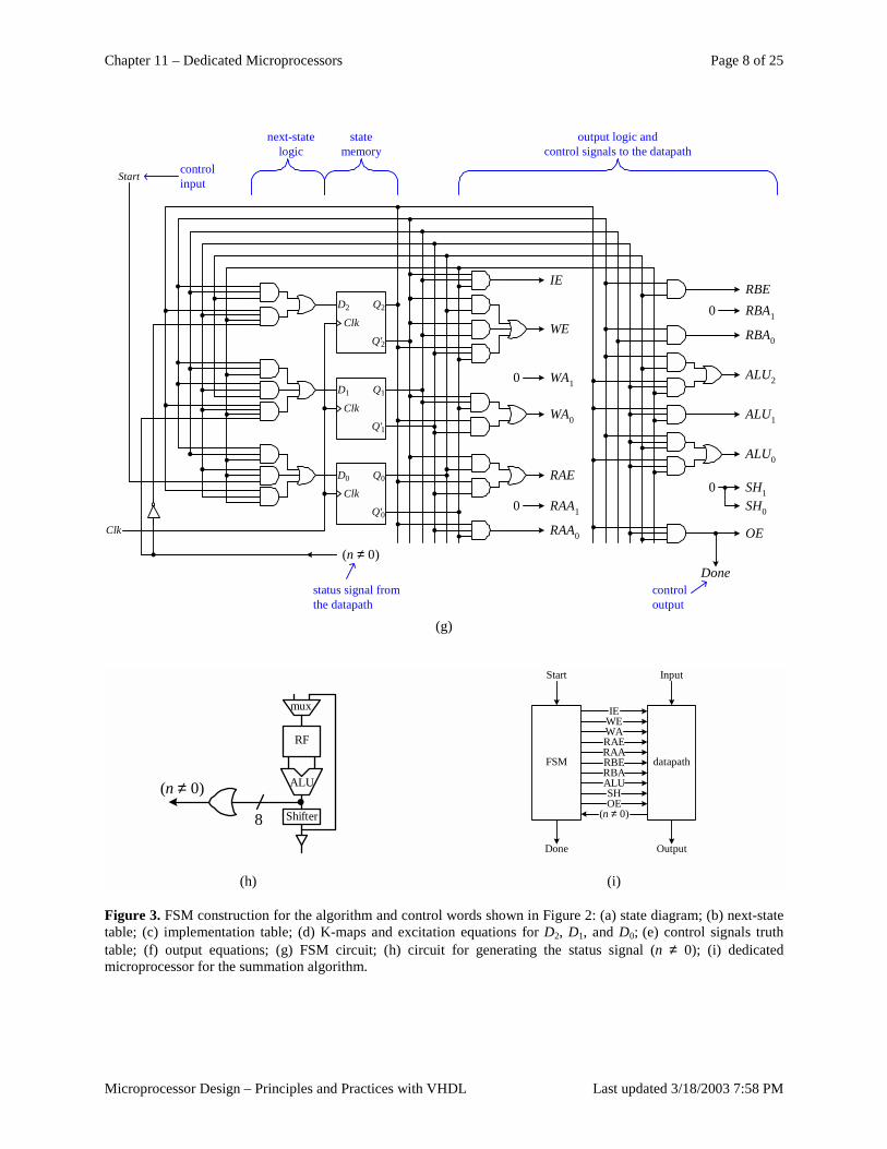
Chapter 11 – Dedicated Microprocessors Page 8 of 25
Microprocessor Design – Principles and Practices with VHDL Last updated 3/18/2003 7:58 PM
(n ≠ 0)Done
output logic andcontrol signals to the datapath
controloutput
controlinput
statememory
next-statelogic
IE
WE
WA1
WA0
RAE
RAA1
RAA0
0
0RBE
RBA0
RBA1
ALU2
ALU1
ALU0
SH1SH0
OE
status signal fromthe datapath
Clk
D0
Q'0
Q0
Clk
D1
Q'1
Q1
Clk
D2
Q'2
Q2
Start
Clk
0
0
(g)
8
(n ≠ 0) ALU
RF
Shifter
mux
FSM
Start Input
OutputDone
datapath
IEWEWARAERAARBERBAALUSHOE
(n ≠ 0)
(h) (i)
Figure 3. FSM construction for the algorithm and control words shown in Figure 2: (a) state diagram; (b) next-state table; (c) implementation table; (d) K-maps and excitation equations for D2, D1, and D0; (e) control signals truth table; (f) output equations; (g) FSM circuit; (h) circuit for generating the status signal (n ≠ 0); (i) dedicated microprocessor for the summation algorithm.

Chapter 11 – Dedicated Microprocessors Page 9 of 25
Microprocessor Design – Principles and Practices with VHDL Last updated 3/18/2003 7:58 PM
The next-state table as shown in Figure 3(b) is derived directly from the state diagram of Figure 3(a). Three flip-flops, Q2, Q1, and Q0, are needed to encode the six states. The six rows represent these six states by the current contents of these flip-flops. For simplicity, the straight binary encoding is used for encoding the states. In other words, we will simply use the encoding 000 for s0, 001 for s1, and so on. In addition to the current states as listed down the rows of the table, the next state is also dependent on the control input signal Start and the status signal (n ≠ 0), from which we get the four columns. For example, the column labeled 10 means that the input signal Start is true (i.e. Start = 1) and the status signal (n ≠ 0) is false (i.e. (n ≠ 0) = 0), which implies that (n ≠ 0)' is true. The three flip-flops and two input/status signals give us a total of five variables or 25 different combinations to consider in the next-state table. Each next-state entry is obtained by looking at the corresponding current state and input/status signals in the state diagram and see what the next state is. For example, looking at the state diagram for the current state s4, when the status signal (n ≠ 0) is false, i.e. the condition (n ≠ 0)' is true, the next state is s5. In the next-state table, this corresponds to the column where (n ≠ 0) = 0. Since the transition from state s4 is independent of the Start signal, therefore, Start can be either 0 or 1. Hence, the entries in row s4 (100) and the two columns labeled 00 and 10 have s5 (101) as the next state.
In normal circumstances, the FSM should never get to one of the unused states. In this example, the unused state encodings are 110 and 111. However, due to noises or glitches in the circuit, the FSM may end up in one of these unused states. Because of this, it is a good idea to set the next state for all the unused states to the reset state. In this example, the reset state is 000. On the other hand, if you don’t care what the next state is for these unused states, then don’t-care values can be used and thus may result in a simpler equation.
From the next-state table, we get the implementation table as shown in Figure 3(c). Using D flip-flops to implement the FSM, the implementation table is the same as the next-state table because the characteristic equation for the D flip-flop is Qnext = D. The only difference between the two tables is that the bits in the entries mean something different. In the next-state table, the bits in the entries (labeled Q2next Q1next Q0next) are the next state for the FSM to go to. In the implementation table, the bits (labeled D2D1D0) are the inputs necessary to result in that next state.
From the implementation table, we derive the excitation equations. The excitation equations form the next-state circuits for the inputs to the flip-flops. Since there are three D flip-flops used, there are three excitation equations; one for D2, one for D1, and one for D0, as shown in Figure 3(d). The three corresponding K-maps for these three excitation equations are obtained from extracting the corresponding bits from the implementation table. For example, the leftmost bit in each entry in the implementation table is for the D2 K-map and equation, the middle bit in each entry is for the D1 equation, and the rightmost bit is for the D0 equation. All these equations are dependent on the five variables Q2, Q1, Q0, Start, and (n ≠ 0), which represent the current state, and input and status signals. Having derived the excitation equations, it is trivial to draw the next-state circuit based on these equations.
The output logic circuit is constructed from the output table, which is just the control word table with the actual state encoding information added in. Recall that the control word signals control the operation of the datapath, and now we are constructing the control unit to control the datapath. So what the control unit needs to do is to generate and output the appropriate control word signals at each state. To get the output table, we take the control word table and replace all the control word numbers with the actual encoding of the state in which that control word is performed. The output table is shown in Figure 3(e). For example, control word 1 is executed in state 001, so we put in 001 in place of the control word number 1. 001 of course, represents the current state value of the three flip-flops Q2, Q1, and Q0. Notice that we also had to add in state 000 for the reset state where all the control signals are set to a value that reflects a reset operation. The output equations are the equations for all the control word signals as a function of the current state values Q2, Q1, and Q0. These output equations, shown in Figure 3(f), are derived from the output table – one equation for one control signal. For example, to derive the output signal equation for IE, we look at the IE column in the output table, which in this example, contains only one 1-minterm. Hence, the equation for IE is IE = Q2'Q1Q0'. We are assuming here that the output signal values for the unused states are all 0’s. Of course, we can also assume that they are all don’t-cares instead, in which case the equations might be simpler. Since we are the designer, we can decide on what we want to do.
Having derived the excitation equations for the next-state logic circuit and the output equations for the output circuit, we can now draw the complete FSM circuit. The complete FSM circuit, with its next-state logic circuit, the three D flip-flop state memory, and the output logic circuit, is shown in Figure 3(g).

Chapter 11 – Dedicated Microprocessors Page 10 of 25
Microprocessor Design – Principles and Practices with VHDL Last updated 3/18/2003 7:58 PM
The status signal (n ≠ 0) is generated by an inequality comparator. The question is where do we get the value for n in the datapath? We have to remember that at different clock cycles, different values pass through different points in the datapath. For example, in one clock cycle, the ALU may be outputting the result for the operation sum + n for control word 3, and in another clock cycle, it may be outputting the result for the operation n – 1 for control word 4. In determining where the comparator input should be connected to, we look at the state diagram to determine what state the status signal is needed, and in that state, what data is available on the datapath. In the example, the status signal (n ≠ 0) is needed at the end of state s4. In state s4, the control word for n = n – 1 is executed. In order for the datapath to execute n – 1, the value n must be present at the A operand of the ALU, and the result of n – 1 is available at the output of the ALU. Since we want to test for n after the decrement, therefore, the comparator input should be connected to the output of the ALU. A simple OR gate can be used to test for the inequality with zero. The comparator circuit and how it is connected to the datapath is shown in Figure 3(h).
Finally, the FSM and the datapath circuits are connected together using the control and status signals to form the complete dedicated microprocessor shown in Figure 3(i). This dedicated microprocessor, of course, does nothing more then to sum the numbers from n down to 1. ♦
Generating Status Signals
We saw in the previous example how the status signal for (n ≠ 0) is generated. The status signal is needed in state s4 and in state s4 the value of n after the decrement is available at the output of the ALU, so we tapped into the datapath at the output of the ALU for the value of n needed by the comparator. Since the comparator is a combinational circuit, it continuously outputs a value. At other times, that is, a state other than s4, the comparator would be comparing another variable with 0. For instance, in state s3, the output of the ALU is the result of sum + n, so the comparator would be comparing the resulting sum with 0, and not n with 0.
The corrected state diagram for the previous example is shown in Figure 4. Since the beginning of the while loop occurs immediately after control word 2, we need to also test for the condition (n ≠ 0) after state s2. If the condition (n ≠ 0) is true, we will go to state s3, otherwise, we will go to state s5. This means that we also need to get the value of n in state s2. The problem is that the value of n is not available at the output of the ALU in state s2. In state s2, the instruction “input n” is executed and n is being stored in the register file. Remember that for a write operation, the register file is updated with the value at the next active edge of the clock. So the value of n is not going to be available at the output of the register file in that same clock cycle, let alone at the output of the ALU. As a result, the output of the comparator during state s2 will not be for the condition (n ≠ 0).
In order to get the correct comparison for (n ≠ 0) in state s2, we can tapped into the datapath at the output of the mux. At this point, it is also correct for the comparison in state s4 since the result of the operation n – 1 at the output of the ALU will be routed back to the output of the mux in the same clock cycle.
There might be situations when no place in the datapath can be found for getting the correct value of a variable during the correct clock cycle or state. In such a situation, an extra state must be added. This new state will do nothing but to read the value from the register where this variable is stored so that the value is available throughout the datapath.
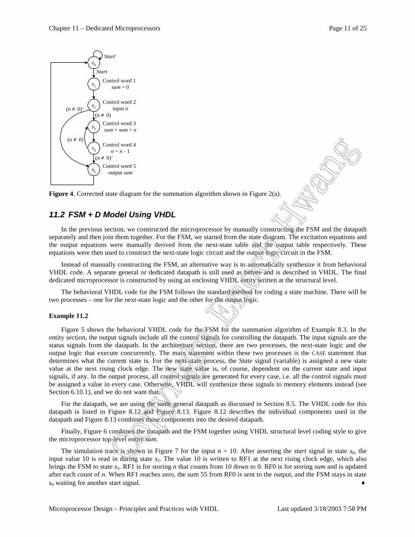
Chapter 11 – Dedicated Microprocessors Page 11 of 25
Microprocessor Design – Principles and Practices with VHDL Last updated 3/18/2003 7:58 PM
s1
s2
s3
Start
Control word 2input n
Start'
Control word 3sum = sum + n
Control word 4n = n - 1
Control word 5output sum
Control word 1sum = 0
s4
s5
(n ≠ 0)
(n ≠ 0)'
s0
(n ≠ 0)(n ≠ 0)'
Figure 4. Corrected state diagram for the summation algorithm shown in Figure 2(a).
11.2 FSM + D Model Using VHDL In the previous section, we constructed the microprocessor by manually constructing the FSM and the datapath
separately and then join them together. For the FSM, we started from the state diagram. The excitation equations and the output equations were manually derived from the next-state table and the output table respectively. These equations were then used to construct the next-state logic circuit and the output logic circuit in the FSM.
Instead of manually constructing the FSM, an alternative way is to automatically synthesize it from behavioral VHDL code. A separate general or dedicated datapath is still used as before and is described in VHDL. The final dedicated microprocessor is constructed by using an enclosing VHDL entity written at the structural level.
The behavioral VHDL code for the FSM follows the standard method for coding a state machine. There will be two processes – one for the next-state logic and the other for the output logic.
Example 11.2
Figure 5 shows the behavioral VHDL code for the FSM for the summation algorithm of Example 8.3. In the entity section, the output signals include all the control signals for controlling the datapath. The input signals are the status signals from the datapath. In the architecture section, there are two processes, the next-state logic and the output logic that execute concurrently. The main statement within these two processes is the CASE statement that determines what the current state is. For the next-state process, the State signal (variable) is assigned a new state value at the next rising clock edge. The new state value is, of course, dependent on the current state and input signals, if any. In the output process, all control signals are generated for every case, i.e. all the control signals must be assigned a value in every case. Otherwise, VHDL will synthesize these signals to memory elements instead (see Section 6.10.1), and we do not want that.
For the datapath, we are using the same general datapath as discussed in Section 8.5. The VHDL code for this datapath is listed in Figure 8.12 and Figure 8.13. Figure 8.12 describes the individual components used in the datapath and Figure 8.13 combines these components into the desired datapath.
Finally, Figure 6 combines the datapath and the FSM together using VHDL structural level coding style to give the microprocessor top-level entity sum.
The simulation trace is shown in Figure 7 for the input n = 10. After asserting the start signal in state s0, the input value 10 is read in during state s2. The value 10 is written to RF1 at the next rising clock edge, which also brings the FSM to state s3. RF1 is for storing n that counts from 10 down to 0. RF0 is for storing sum and is updated after each count of n. When RF1 reaches zero, the sum 55 from RF0 is sent to the output, and the FSM stays in state s0 waiting for another start signal. ♦
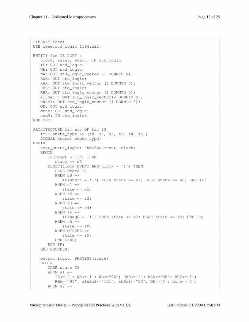
Chapter 11 – Dedicated Microprocessors Page 12 of 25
Microprocessor Design – Principles and Practices with VHDL Last updated 3/18/2003 7:58 PM
LIBRARY ieee;USE ieee.std_logic_1164.all;
ENTITY fsm IS PORT (clock, reset, start: IN std_logic;IE: OUT std_logic;WE: OUT std_logic;WA: OUT std_logic_vector (1 DOWNTO 0);RAE: OUT std_logic;RAA: OUT std_logic_vector (1 DOWNTO 0);RBE: OUT std_logic;RBA: OUT std_logic_vector (1 DOWNTO 0);aluSel : OUT std_logic_vector(2 DOWNTO 0);shSel: OUT std_logic_vector (1 DOWNTO 0);OE: OUT std_logic;done: OUT std_logic;neq0: IN std_logic);
END fsm;
ARCHITECTURE fsm_arc OF fsm ISTYPE state_type IS (s0, s1, s2, s3, s4, s5);SIGNAL state: state_type;
BEGINnext_state_logic: PROCESS(reset, clock)BEGIN
IF(reset = '1') THENstate <= s0;
ELSIF(clock'EVENT AND clock = '1') THENCASE state ISWHEN s0 =>
IF(start = '1') THEN state <= s1; ELSE state <= s0; END IF;WHEN s1 =>
state <= s2;WHEN s2 =>
state <= s3;WHEN s3 =>
state <= s4;WHEN s4 =>
IF(neq0 = '1') THEN state <= s3; ELSE state <= s5; END IF;WHEN s5 =>
state <= s0;WHEN OTHERS =>
state <= s0;END CASE;
END IF;END PROCESS;
output_logic: PROCESS(state)BEGIN
CASE state ISWHEN s1 =>
IE<='0'; WE<='1'; WA<="00"; RAE<='1'; RAA<="00"; RBE<='1';RBA<="00"; aluSel<="101"; shSel<="00"; OE<='0'; done<='0';
WHEN s2 =>
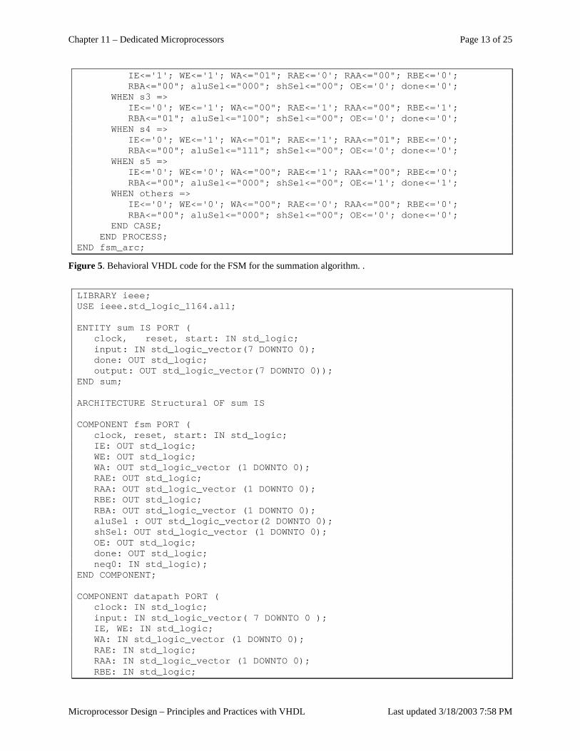
Chapter 11 – Dedicated Microprocessors Page 13 of 25
Microprocessor Design – Principles and Practices with VHDL Last updated 3/18/2003 7:58 PM
IE<='1'; WE<='1'; WA<="01"; RAE<='0'; RAA<="00"; RBE<='0';RBA<="00"; aluSel<="000"; shSel<="00"; OE<='0'; done<='0';
WHEN s3 =>IE<='0'; WE<='1'; WA<="00"; RAE<='1'; RAA<="00"; RBE<='1';RBA<="01"; aluSel<="100"; shSel<="00"; OE<='0'; done<='0';
WHEN s4 =>IE<='0'; WE<='1'; WA<="01"; RAE<='1'; RAA<="01"; RBE<='0';RBA<="00"; aluSel<="111"; shSel<="00"; OE<='0'; done<='0';
WHEN s5 =>IE<='0'; WE<='0'; WA<="00"; RAE<='1'; RAA<="00"; RBE<='0';RBA<="00"; aluSel<="000"; shSel<="00"; OE<='1'; done<='1';
WHEN others =>IE<='0'; WE<='0'; WA<="00"; RAE<='0'; RAA<="00"; RBE<='0';RBA<="00"; aluSel<="000"; shSel<="00"; OE<='0'; done<='0';
END CASE;END PROCESS;
END fsm_arc;
Figure 5. Behavioral VHDL code for the FSM for the summation algorithm. .
LIBRARY ieee;USE ieee.std_logic_1164.all;
ENTITY sum IS PORT (clock, reset, start: IN std_logic;input: IN std_logic_vector(7 DOWNTO 0);done: OUT std_logic;output: OUT std_logic_vector(7 DOWNTO 0));
END sum;
ARCHITECTURE Structural OF sum IS
COMPONENT fsm PORT (clock, reset, start: IN std_logic;IE: OUT std_logic;WE: OUT std_logic;WA: OUT std_logic_vector (1 DOWNTO 0);RAE: OUT std_logic;RAA: OUT std_logic_vector (1 DOWNTO 0);RBE: OUT std_logic;RBA: OUT std_logic_vector (1 DOWNTO 0);aluSel : OUT std_logic_vector(2 DOWNTO 0);shSel: OUT std_logic_vector (1 DOWNTO 0);OE: OUT std_logic;done: OUT std_logic;neq0: IN std_logic);
END COMPONENT;
COMPONENT datapath PORT (clock: IN std_logic;input: IN std_logic_vector( 7 DOWNTO 0 );IE, WE: IN std_logic;WA: IN std_logic_vector (1 DOWNTO 0);RAE: IN std_logic;RAA: IN std_logic_vector (1 DOWNTO 0);RBE: IN std_logic;
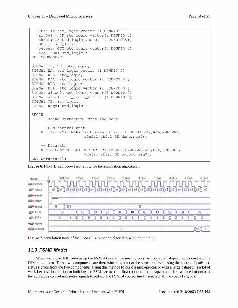
Chapter 11 – Dedicated Microprocessors Page 14 of 25
Microprocessor Design – Principles and Practices with VHDL Last updated 3/18/2003 7:58 PM
RBA: IN std_logic_vector (1 DOWNTO 0);aluSel : IN std_logic_vector(2 DOWNTO 0);shSel: IN std_logic_vector (1 DOWNTO 0);OE: IN std_logic;output: OUT std_logic_vector(7 DOWNTO 0);neq0: OUT std_logic);
END COMPONENT;
SIGNAL IE, WE: std_logic;SIGNAL WA: std_logic_vector (1 DOWNTO 0);SIGNAL RAE: std_logic;SIGNAL RAA: std_logic_vector (1 DOWNTO 0);SIGNAL RBE: std_logic;SIGNAL RBA: std_logic_vector (1 DOWNTO 0);SIGNAL aluSel: std_logic_vector(2 DOWNTO 0);SIGNAL shSel: std_logic_vector (1 DOWNTO 0);SIGNAL OE: std_logic;SIGNAL neq0: std_logic;
BEGIN-- doing structural modeling here
-- FSM control unitU0: fsm PORT MAP(clock,reset,start,IE,WE,WA,RAE,RAA,RBE,RBA,
aluSel,shSel,OE,done,neq0);
-- DatapathU1: datapath PORT MAP (clock,input,IE,WE,WA,RAE,RAA,RBE,RBA,
aluSel,shSel,OE,output,neq0);END Structural;
Figure 6. FSM+D microprocessor entity for the summation algorithm. .
Figure 7. Simulation trace of the FSM+D summation algorithm with input n = 10.
11.3 FSMD Model When writing VHDL code using the FSM+D model, we need to construct both the datapath component and the
FSM component. These two components are then joined together at the structural level using the control signals and status signals from the two components. Using this method to build a microprocessor with a large datapath is a lot of work because in addition to building the FSM, we need to first construct the datapath and then we need to connect the numerous control and status signals together. The FSM of course, has to generate all the control signals.
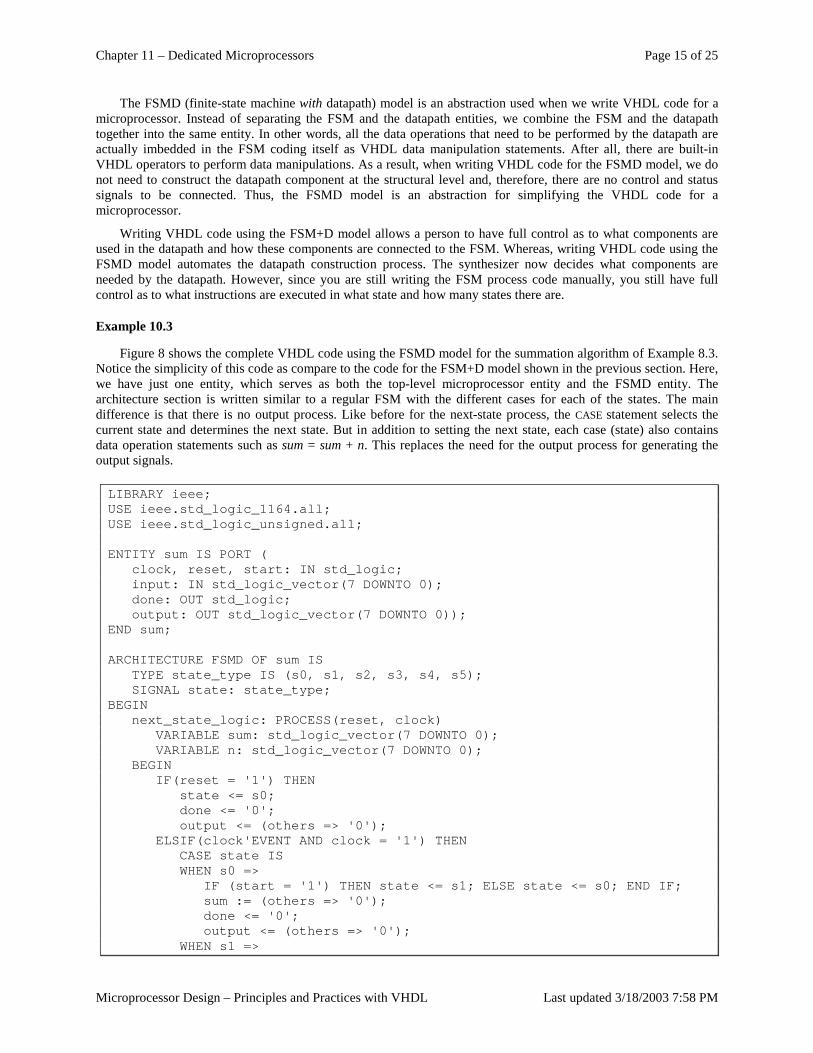
Chapter 11 – Dedicated Microprocessors Page 15 of 25
Microprocessor Design – Principles and Practices with VHDL Last updated 3/18/2003 7:58 PM
The FSMD (finite-state machine with datapath) model is an abstraction used when we write VHDL code for a microprocessor. Instead of separating the FSM and the datapath entities, we combine the FSM and the datapath together into the same entity. In other words, all the data operations that need to be performed by the datapath are actually imbedded in the FSM coding itself as VHDL data manipulation statements. After all, there are built-in VHDL operators to perform data manipulations. As a result, when writing VHDL code for the FSMD model, we do not need to construct the datapath component at the structural level and, therefore, there are no control and status signals to be connected. Thus, the FSMD model is an abstraction for simplifying the VHDL code for a microprocessor.
Writing VHDL code using the FSM+D model allows a person to have full control as to what components are used in the datapath and how these components are connected to the FSM. Whereas, writing VHDL code using the FSMD model automates the datapath construction process. The synthesizer now decides what components are needed by the datapath. However, since you are still writing the FSM process code manually, you still have full control as to what instructions are executed in what state and how many states there are.
Example 10.3
Figure 8 shows the complete VHDL code using the FSMD model for the summation algorithm of Example 8.3. Notice the simplicity of this code as compare to the code for the FSM+D model shown in the previous section. Here, we have just one entity, which serves as both the top-level microprocessor entity and the FSMD entity. The architecture section is written similar to a regular FSM with the different cases for each of the states. The main difference is that there is no output process. Like before for the next-state process, the CASE statement selects the current state and determines the next state. But in addition to setting the next state, each case (state) also contains data operation statements such as sum = sum + n. This replaces the need for the output process for generating the output signals.
LIBRARY ieee;USE ieee.std_logic_1164.all;USE ieee.std_logic_unsigned.all;
ENTITY sum IS PORT (clock, reset, start: IN std_logic;input: IN std_logic_vector(7 DOWNTO 0);done: OUT std_logic;output: OUT std_logic_vector(7 DOWNTO 0));
END sum;
ARCHITECTURE FSMD OF sum ISTYPE state_type IS (s0, s1, s2, s3, s4, s5);SIGNAL state: state_type;
BEGINnext_state_logic: PROCESS(reset, clock)
VARIABLE sum: std_logic_vector(7 DOWNTO 0);VARIABLE n: std_logic_vector(7 DOWNTO 0);
BEGINIF(reset = '1') THEN
state <= s0;done <= '0';output <= (others => '0');
ELSIF(clock'EVENT AND clock = '1') THENCASE state ISWHEN s0 =>
IF (start = '1') THEN state <= s1; ELSE state <= s0; END IF;sum := (others => '0');done <= '0';output <= (others => '0');
WHEN s1 =>
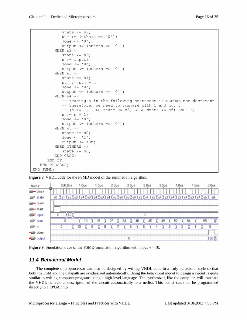
Chapter 11 – Dedicated Microprocessors Page 16 of 25
Microprocessor Design – Principles and Practices with VHDL Last updated 3/18/2003 7:58 PM
state <= s2;sum := (others => '0');done <= '0';output <= (others => '0');
WHEN s2 =>state <= s3;n := input;done <= '0';output <= (others => '0');
WHEN s3 =>state <= s4;sum := sum + n;done <= '0';output <= (others => '0');
WHEN s4 =>-- reading n in the following statement is BEFORE the decrement-- therefore, we need to compare with 1 and not 0IF (n /= 1) THEN state <= s3; ELSE state <= s5; END IF;n := n - 1;done <= '0';output <= (others => '0');
WHEN s5 =>state <= s0;done <= '1';output <= sum;
WHEN OTHERS =>state <= s0;
END CASE;END IF;
END PROCESS;END FSMD;
Figure 8. VHDL code for the FSMD model of the summation algorithm.
Figure 9. Simulation trace of the FSMD summation algorithm with input n = 10.
11.4 Behavioral Model The complete microprocessor can also be designed by writing VHDL code in a truly behavioral style so that
both the FSM and the datapath are synthesized automatically. Using the behavioral model to design a circuit is quite similar to writing computer programs using a high-level language. The synthesizer, like the compiler, will translate the VHDL behavioral description of the circuit automatically to a netlist. This netlist can then be programmed directly to a FPGA chip.
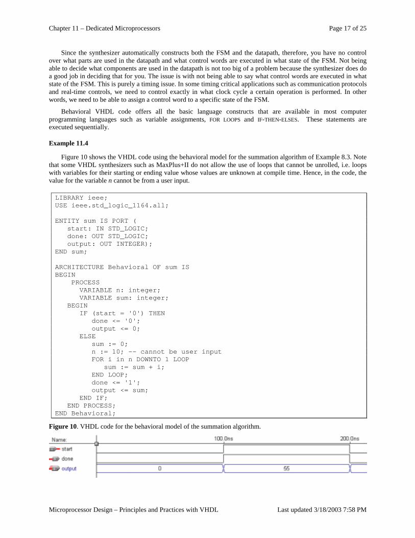
Chapter 11 – Dedicated Microprocessors Page 17 of 25
Microprocessor Design – Principles and Practices with VHDL Last updated 3/18/2003 7:58 PM
Since the synthesizer automatically constructs both the FSM and the datapath, therefore, you have no control over what parts are used in the datapath and what control words are executed in what state of the FSM. Not being able to decide what components are used in the datapath is not too big of a problem because the synthesizer does do a good job in deciding that for you. The issue is with not being able to say what control words are executed in what state of the FSM. This is purely a timing issue. In some timing critical applications such as communication protocols and real-time controls, we need to control exactly in what clock cycle a certain operation is performed. In other words, we need to be able to assign a control word to a specific state of the FSM.
Behavioral VHDL code offers all the basic language constructs that are available in most computer programming languages such as variable assignments, FOR LOOPS and IF-THEN-ELSES. These statements are executed sequentially.
Example 11.4
Figure 10 shows the VHDL code using the behavioral model for the summation algorithm of Example 8.3. Note that some VHDL synthesizers such as MaxPlus+II do not allow the use of loops that cannot be unrolled, i.e. loops with variables for their starting or ending value whose values are unknown at compile time. Hence, in the code, the value for the variable n cannot be from a user input.
LIBRARY ieee;USE ieee.std_logic_1164.all;
ENTITY sum IS PORT (start: IN STD_LOGIC;done: OUT STD_LOGIC;output: OUT INTEGER);
END sum;
ARCHITECTURE Behavioral OF sum ISBEGIN
PROCESSVARIABLE n: integer;VARIABLE sum: integer;
BEGINIF (start = '0') THEN
done <= '0';output <= 0;
ELSEsum := 0;n := 10; -- cannot be user inputFOR i in n DOWNTO 1 LOOP
sum := sum + i;END LOOP;done <= '1';output <= sum;
END IF;END PROCESS;
END Behavioral;
Figure 10. VHDL code for the behavioral model of the summation algorithm.
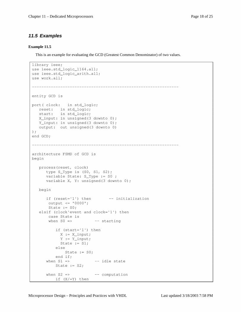
Chapter 11 – Dedicated Microprocessors Page 18 of 25
Microprocessor Design – Principles and Practices with VHDL Last updated 3/18/2003 7:58 PM
11.5 Examples
Example 11.5
This is an example for evaluating the GCD (Greatest Common Denominator) of two values.
library ieee;use ieee.std_logic_1164.all;use ieee.std_logic_arith.all;use work.all;
--------------------------------------------------------------
entity GCD is
port( clock: in std_logic;reset: in std_logic;start: in std_logic;X_input: in unsigned(3 downto 0);Y_input: in unsigned(3 downto 0);output: out unsigned(3 downto 0)
);end GCD;
--------------------------------------------------------------
architecture FSMD of GCD isbegin
process(reset, clock)type S_Type is (S0, S1, S2);variable State: S_Type := S0 ;variable X, Y: unsigned(3 downto 0);
begin
if (reset='1') then -- initializationoutput <= "0000";State := S0;
elsif (clock'event and clock='1') thencase State iswhen S0 => -- starting
if (start='1') thenX := X_input;Y := Y_input;State := S1;
elseState := S0;
end if;when S1 => -- idle state
State := S2;
when S2 => -- computationif (X/=Y) then
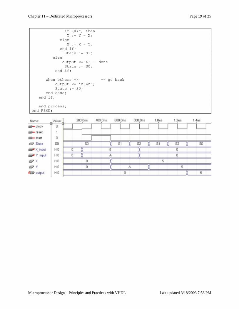
Chapter 11 – Dedicated Microprocessors Page 19 of 25
Microprocessor Design – Principles and Practices with VHDL Last updated 3/18/2003 7:58 PM
if (X<Y) thenY := Y - X;
elseX := X - Y;
end if;State := S1;
elseoutput <= X; -- doneState := S0;
end if;
when others => -- go backoutput <= "ZZZZ";State := S0;
end case;end if;
end process;end FSMD;
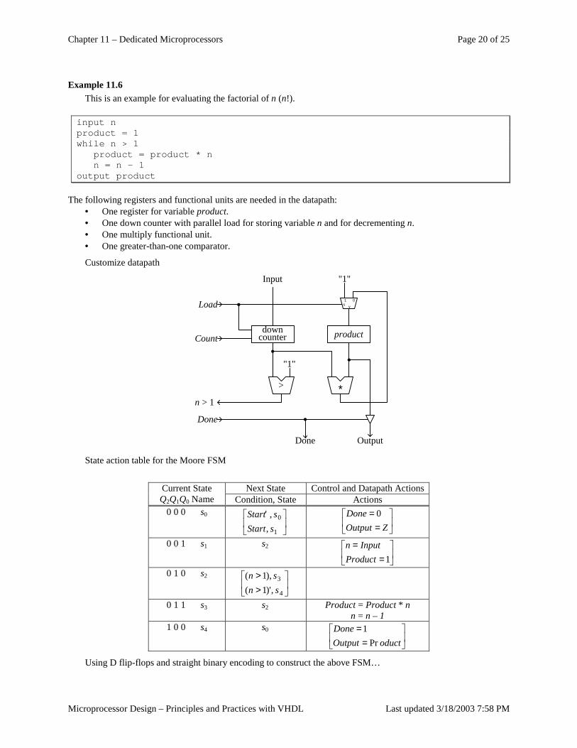
Chapter 11 – Dedicated Microprocessors Page 20 of 25
Microprocessor Design – Principles and Practices with VHDL Last updated 3/18/2003 7:58 PM
Example 11.6 This is an example for evaluating the factorial of n (n!).
input nproduct = 1while n > 1
product = product * nn = n – 1
output product
The following registers and functional units are needed in the datapath: • One register for variable product. • One down counter with parallel load for storing variable n and for decrementing n. • One multiply functional unit. • One greater-than-one comparator.
Customize datapath
downcounter product
*>
"1"
01s y
"1"Input
n > 1
Output
Done
Done
Count
Load
State action table for the Moore FSM
Next State Control and Datapath Actions Current State
Q2Q1Q0 Name Condition, State Actions 0 0 0 s0
1
0
,,sStartsStart'
==
ZOutputDone 0
0 0 1 s1 s2
==
1ProductInputn
0 1 0 s2
>>
4
3
,)1(),1(
s'nsn
0 1 1 s3 s2 Product = Product * n n = n – 1
1 0 0 s4 s0
==
oductOutputDone
Pr1
Using D flip-flops and straight binary encoding to construct the above FSM…
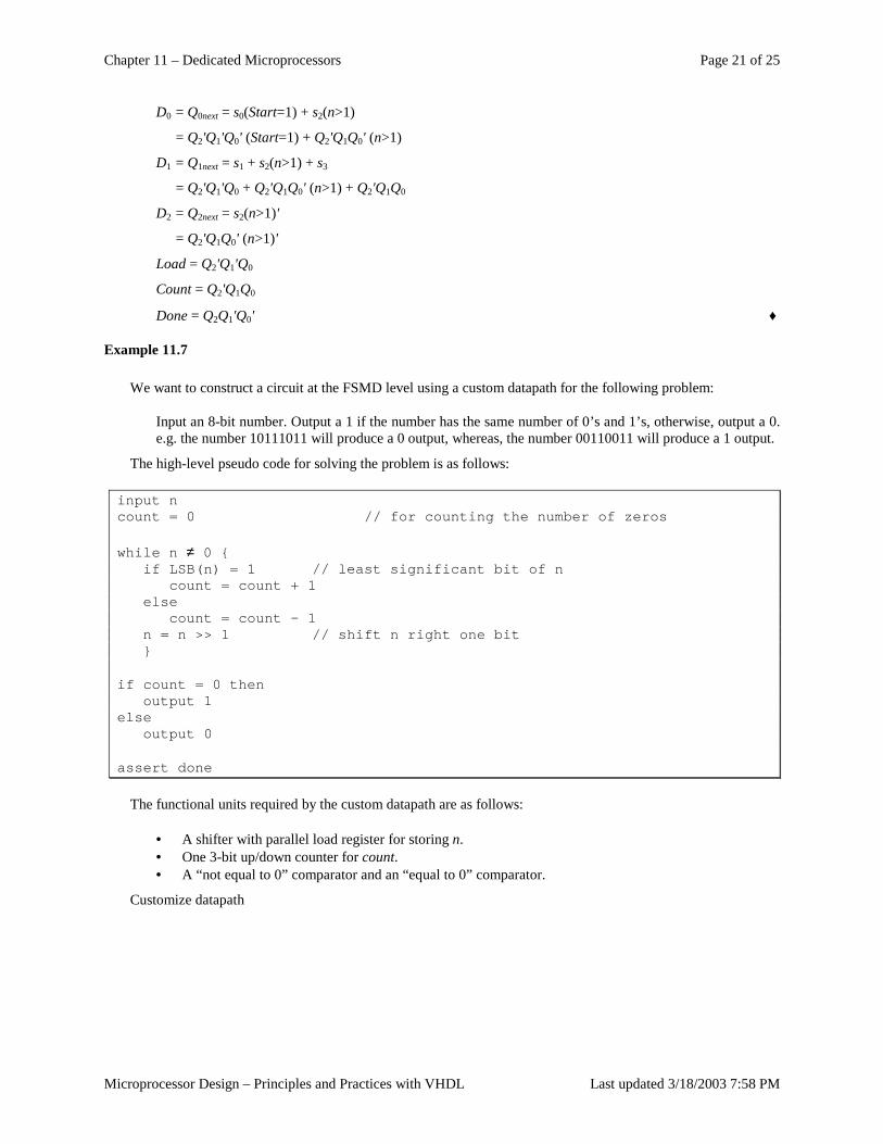
Chapter 11 – Dedicated Microprocessors Page 21 of 25
Microprocessor Design – Principles and Practices with VHDL Last updated 3/18/2003 7:58 PM
D0 = Q0next = s0(Start=1) + s2(n>1)
= Q2'Q1'Q0' (Start=1) + Q2'Q1Q0' (n>1)
D1 = Q1next = s1 + s2(n>1) + s3
= Q2'Q1'Q0 + Q2'Q1Q0' (n>1) + Q2'Q1Q0
D2 = Q2next = s2(n>1)'
= Q2'Q1Q0' (n>1)'
Load = Q2'Q1'Q0
Count = Q2'Q1Q0
Done = Q2Q1'Q0' ♦
Example 11.7
We want to construct a circuit at the FSMD level using a custom datapath for the following problem:
Input an 8-bit number. Output a 1 if the number has the same number of 0’s and 1’s, otherwise, output a 0. e.g. the number 10111011 will produce a 0 output, whereas, the number 00110011 will produce a 1 output.
The high-level pseudo code for solving the problem is as follows:
input ncount = 0 // for counting the number of zeros
while n ≠ 0 {if LSB(n) = 1 // least significant bit of n
count = count + 1else
count = count - 1n = n >> 1 // shift n right one bit}
if count = 0 thenoutput 1
elseoutput 0
assert done
The functional units required by the custom datapath are as follows:
• A shifter with parallel load register for storing n. • One 3-bit up/down counter for count. • A “not equal to 0” comparator and an “equal to 0” comparator.
Customize datapath
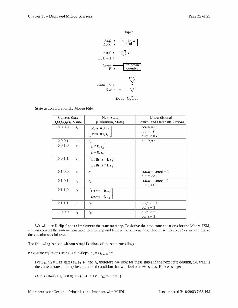
Chapter 11 – Dedicated Microprocessors Page 22 of 25
Microprocessor Design – Principles and Practices with VHDL Last updated 3/18/2003 7:58 PM
shifter wload
up/downcounter
Output
Out
n ≠ 0LSB = 1
ClearE
Input
Done
Load
count = 0
Shift
State-action table for the Moore FSM
Current State Q3Q2Q1Q0 Name
Next State [Condition, State]
Unconditional Control and Datapath Actions
0 0 0 0 s0
==
1
0
,1,0sstartsstart
count = 0 done = 0 output = Z
0 0 0 1 s1 s2 n = input 0 0 1 0 s2
=≠
6
3
,0,0snsn
0 0 1 1 s3
≠=
5
4
,1)(LSB,1)(LSBsnsn
0 1 0 0 s4 s2 count = count + 1 n = n >> 1
0 1 0 1 s5 s2 count = count – 1 n = n >> 1
0 1 1 0 s6
==
8
7
,1,0scountscount
0 1 1 1 s7 s0 output = 1 done = 1
1 0 0 0 s8 s0 output = 0 done = 1
We will use D flip-flops to implement the state memory. To derive the next-state equations for the Moore FSM, we can convert the state-action table to a K-map and follow the steps as described in section 6.3?? or we can derive the equations as follows:
The following is done without simplifications of the state encodings.
Next-state equations using D flip-flops, Di = Qi(next) are:
For D0, Q0 = 1 in states s1, s3, s5, and s7, therefore, we look for these states in the next state column, i.e. what is the current state and may be an optional condition that will lead to these states. Hence, we get
D0 = s0(start) + s2(n ≠ 0) + s3(LSB = 1)' + s6(count = 0)
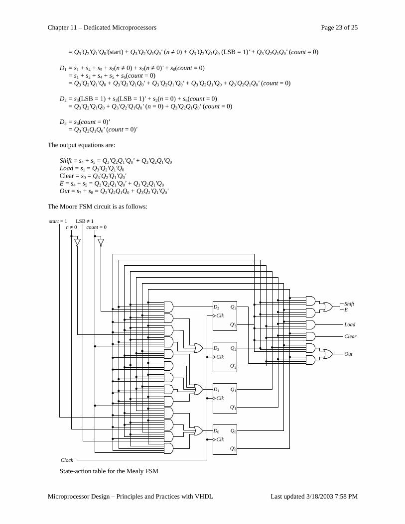
Chapter 11 – Dedicated Microprocessors Page 23 of 25
Microprocessor Design – Principles and Practices with VHDL Last updated 3/18/2003 7:58 PM
= Q3'Q2'Q1'Q0'(start) + Q3'Q2'Q1Q0' (n ≠ 0) + Q3'Q2'Q1Q0 (LSB = 1)' + Q3'Q2Q1Q0' (count = 0)
D1 = s1 + s4 + s5 + s2(n ≠ 0) + s2(n ≠ 0)' + s6(count = 0) = s1 + s2 + s4 + s5 + s6(count = 0) = Q3'Q2'Q1'Q0 + Q3'Q2'Q1Q0' + Q3'Q2Q1'Q0' + Q3'Q2Q1'Q0 + Q3'Q2Q1Q0' (count = 0)
D2 = s3(LSB = 1) + s3(LSB = 1)' + s2(n = 0) + s6(count = 0) = Q3'Q2'Q1Q0 + Q3'Q2'Q1Q0' (n = 0) + Q3'Q2Q1Q0' (count = 0)
D3 = s6(count = 0)' = Q3'Q2Q1Q0' (count = 0)'
The output equations are:
Shift = s4 + s5 = Q3'Q2Q1'Q0' + Q3'Q2Q1'Q0 Load = s1 = Q3'Q2'Q1'Q0 Clear = s0 = Q3'Q2'Q1'Q0' E = s4 + s5 = Q3'Q2Q1'Q0' + Q3'Q2Q1'Q0 Out = s7 + s8 = Q3'Q2Q1Q0 + Q3Q2'Q1'Q0'
The Moore FSM circuit is as follows:
ClkD3
Q'3
Q3
Clk
D2
Q'2
Q2
Clk
D1
Q'1
Q1
Clk
D0
Q'0
Q0
count = 0LSB ≠ 1start = 1
n ≠ 0
Clock
ShiftE
Load
Clear
Out
State-action table for the Mealy FSM
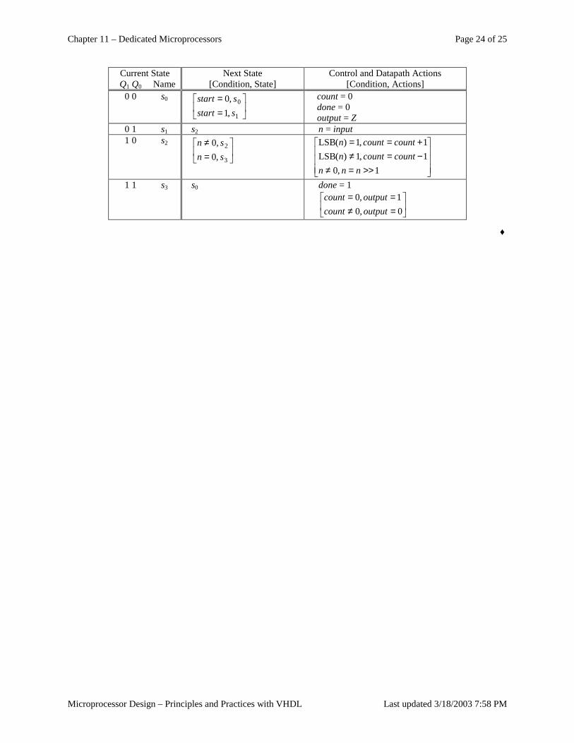
Chapter 11 – Dedicated Microprocessors Page 24 of 25
Microprocessor Design – Principles and Practices with VHDL Last updated 3/18/2003 7:58 PM
Current State Q1 Q0 Name
Next State [Condition, State]
Control and Datapath Actions [Condition, Actions]
0 0 s0
==
1
0
,1,0sstartsstart
count = 0 done = 0 output = Z
0 1 s1 s2 n = input 1 0 s2
=≠
3
2
,0,0snsn
>>=≠−=≠+==
1,01,1)(LSB1,1)(LSB
nnncountcountncountcountn
1 1 s3 s0 done = 1
=≠==
0,01,0
outputcountoutputcount
♦
Chapter 11 – Dedicated Microprocessors Page 25 of 25
Microprocessor Design – Principles and Practices with VHDL Last updated 3/18/2003 7:58 PM
Index
A
Application specific integrated circuit. See ASIC ASIC, 2
B
Behavioral model, 17
C
Control signal, 2, 3 Control unit, 2, 9
See also Finite-state machine. Controller. See Control unit
D
Datapath, 2 Dedicated microprocessor, 2
E
Excitation equation, 4
F
Finite-state machine, 2 See also Control unit.
FSM. See Finite-state machine FSM+D model, 2, 3, 11 FSMD model, 3, 14
G
General-purpose microprocessor, 2
Generating status signal. See Status signal
I Implementation table, 4, 9
N
Next-state logic, 2, 9 Next-state table, 4, 9
O
Output logic, 2, 9
S
State memory, 2 Status signal, 2, 3, 10
generating, 10
U
Unused state encoding, 9
V
VHDL code dedicated microprocessor (behavioral) for
summation algorithm, 17 dedicated microprocessor (FSM+D) for summation
algorithm, 14 dedicated microprocessor (FSMD) for summation
algorithm, 16 FSM for summation algorithm, 13
Chapter 12 − General-Purpose Microprocessors Page 1 of 25
Microprocessor Design – Principles and Practices with VHDL Last updated 3/18/2003 8:01 PM
Table of Content Table of Content ........................................................................................................................................................... 1 12 General-Purpose Microprocessors .................................................................................................................... 2
12.1 Overview of the CPU Design........................................................................................................................ 2 12.2 Instruction Set ............................................................................................................................................... 2
12.2.1 Two Operand Instructions..................................................................................................................... 3 12.2.2 One Operand Instructions...................................................................................................................... 3 12.2.3 Instructions Using a Memory Address .................................................................................................. 3 12.2.4 Jump Instructions .................................................................................................................................. 3
12.3 Datapath ........................................................................................................................................................ 5 12.3.1 Input multiplexer ................................................................................................................................... 6 12.3.2 Conditional Flags .................................................................................................................................. 6 12.3.3 Accumulator.......................................................................................................................................... 6 12.3.4 Register File .......................................................................................................................................... 6 12.3.5 ALU ...................................................................................................................................................... 6 12.3.6 Shifter / Rotator..................................................................................................................................... 7 12.3.7 Output Buffer ........................................................................................................................................ 7 12.3.8 Control Word ........................................................................................................................................ 7 12.3.9 VHDL Code for the Datapath ............................................................................................................... 8
12.4 Control Unit .................................................................................................................................................. 9 12.4.1 Reset.................................................................................................................................................... 10 12.4.2 Fetch.................................................................................................................................................... 10 12.4.3 Decode ................................................................................................................................................ 10 12.4.4 Execute................................................................................................................................................ 10 12.4.5 VHDL Code for the Control Unit........................................................................................................ 11
12.5 CPU............................................................................................................................................................. 20 12.6 Top-level Computer .................................................................................................................................... 22
12.6.1 Input .................................................................................................................................................... 22 12.6.2 Output ................................................................................................................................................. 22 12.6.3 Memory............................................................................................................................................... 22 12.6.4 Clock ................................................................................................................................................... 23 12.6.5 VHDL Code for the Complete Computer ........................................................................................... 23
12.7 Examples..................................................................................................................................................... 24
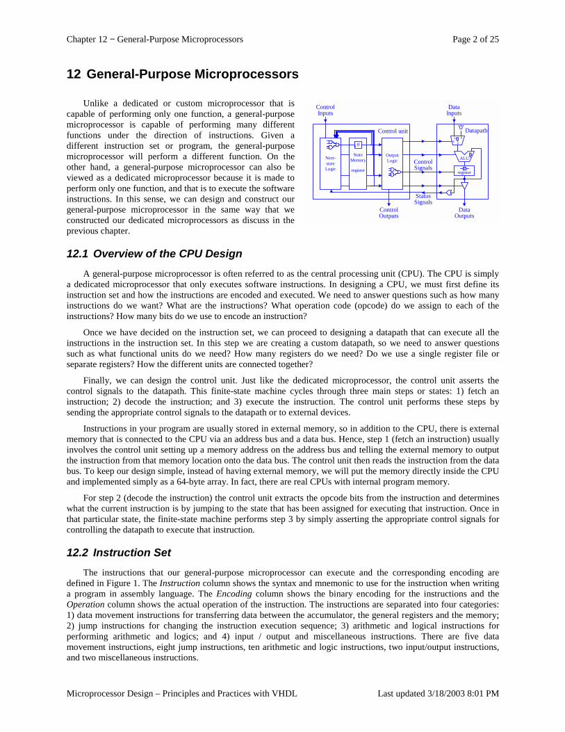
Chapter 12 − General-Purpose Microprocessors Page 2 of 25
Microprocessor Design – Principles and Practices with VHDL Last updated 3/18/2003 8:01 PM
ControlSignals
StatusSignals
01s y
'0'
DataInputs
DataOutputs
Datapath
ALU
registerff
OutputLogicNext-
stateLogic
ControlInputs
ControlOutputs
StateMemory
register
Control unit
ff
12 General-Purpose Microprocessors
Unlike a dedicated or custom microprocessor that is capable of performing only one function, a general-purpose microprocessor is capable of performing many different functions under the direction of instructions. Given a different instruction set or program, the general-purpose microprocessor will perform a different function. On the other hand, a general-purpose microprocessor can also be viewed as a dedicated microprocessor because it is made to perform only one function, and that is to execute the software instructions. In this sense, we can design and construct our general-purpose microprocessor in the same way that we constructed our dedicated microprocessors as discuss in the previous chapter.
12.1 Overview of the CPU Design A general-purpose microprocessor is often referred to as the central processing unit (CPU). The CPU is simply
a dedicated microprocessor that only executes software instructions. In designing a CPU, we must first define its instruction set and how the instructions are encoded and executed. We need to answer questions such as how many instructions do we want? What are the instructions? What operation code (opcode) do we assign to each of the instructions? How many bits do we use to encode an instruction?
Once we have decided on the instruction set, we can proceed to designing a datapath that can execute all the instructions in the instruction set. In this step we are creating a custom datapath, so we need to answer questions such as what functional units do we need? How many registers do we need? Do we use a single register file or separate registers? How the different units are connected together?
Finally, we can design the control unit. Just like the dedicated microprocessor, the control unit asserts the control signals to the datapath. This finite-state machine cycles through three main steps or states: 1) fetch an instruction; 2) decode the instruction; and 3) execute the instruction. The control unit performs these steps by sending the appropriate control signals to the datapath or to external devices.
Instructions in your program are usually stored in external memory, so in addition to the CPU, there is external memory that is connected to the CPU via an address bus and a data bus. Hence, step 1 (fetch an instruction) usually involves the control unit setting up a memory address on the address bus and telling the external memory to output the instruction from that memory location onto the data bus. The control unit then reads the instruction from the data bus. To keep our design simple, instead of having external memory, we will put the memory directly inside the CPU and implemented simply as a 64-byte array. In fact, there are real CPUs with internal program memory.
For step 2 (decode the instruction) the control unit extracts the opcode bits from the instruction and determines what the current instruction is by jumping to the state that has been assigned for executing that instruction. Once in that particular state, the finite-state machine performs step 3 by simply asserting the appropriate control signals for controlling the datapath to execute that instruction.
12.2 Instruction Set The instructions that our general-purpose microprocessor can execute and the corresponding encoding are
defined in Figure 1. The Instruction column shows the syntax and mnemonic to use for the instruction when writing a program in assembly language. The Encoding column shows the binary encoding for the instructions and the Operation column shows the actual operation of the instruction. The instructions are separated into four categories: 1) data movement instructions for transferring data between the accumulator, the general registers and the memory; 2) jump instructions for changing the instruction execution sequence; 3) arithmetic and logical instructions for performing arithmetic and logics; and 4) input / output and miscellaneous instructions. There are five data movement instructions, eight jump instructions, ten arithmetic and logic instructions, two input/output instructions, and two miscellaneous instructions.
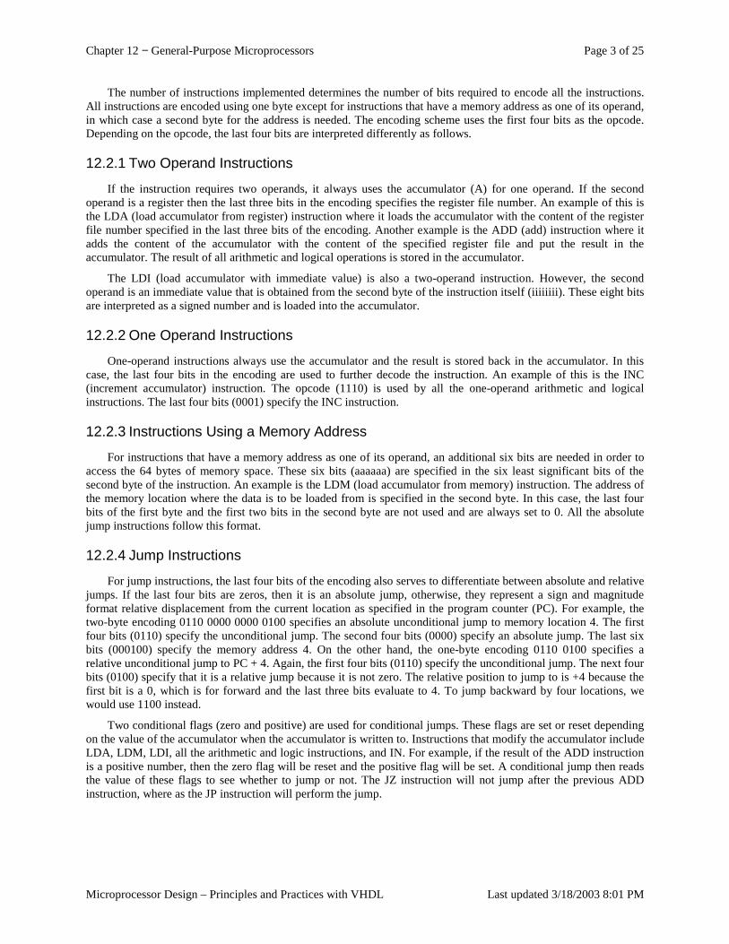
Chapter 12 − General-Purpose Microprocessors Page 3 of 25
Microprocessor Design – Principles and Practices with VHDL Last updated 3/18/2003 8:01 PM
The number of instructions implemented determines the number of bits required to encode all the instructions. All instructions are encoded using one byte except for instructions that have a memory address as one of its operand, in which case a second byte for the address is needed. The encoding scheme uses the first four bits as the opcode. Depending on the opcode, the last four bits are interpreted differently as follows.
12.2.1 Two Operand Instructions
If the instruction requires two operands, it always uses the accumulator (A) for one operand. If the second operand is a register then the last three bits in the encoding specifies the register file number. An example of this is the LDA (load accumulator from register) instruction where it loads the accumulator with the content of the register file number specified in the last three bits of the encoding. Another example is the ADD (add) instruction where it adds the content of the accumulator with the content of the specified register file and put the result in the accumulator. The result of all arithmetic and logical operations is stored in the accumulator.
The LDI (load accumulator with immediate value) is also a two-operand instruction. However, the second operand is an immediate value that is obtained from the second byte of the instruction itself (iiiiiiii). These eight bits are interpreted as a signed number and is loaded into the accumulator.
12.2.2 One Operand Instructions
One-operand instructions always use the accumulator and the result is stored back in the accumulator. In this case, the last four bits in the encoding are used to further decode the instruction. An example of this is the INC (increment accumulator) instruction. The opcode (1110) is used by all the one-operand arithmetic and logical instructions. The last four bits (0001) specify the INC instruction.
12.2.3 Instructions Using a Memory Address
For instructions that have a memory address as one of its operand, an additional six bits are needed in order to access the 64 bytes of memory space. These six bits (aaaaaa) are specified in the six least significant bits of the second byte of the instruction. An example is the LDM (load accumulator from memory) instruction. The address of the memory location where the data is to be loaded from is specified in the second byte. In this case, the last four bits of the first byte and the first two bits in the second byte are not used and are always set to 0. All the absolute jump instructions follow this format.
12.2.4 Jump Instructions
For jump instructions, the last four bits of the encoding also serves to differentiate between absolute and relative jumps. If the last four bits are zeros, then it is an absolute jump, otherwise, they represent a sign and magnitude format relative displacement from the current location as specified in the program counter (PC). For example, the two-byte encoding 0110 0000 0000 0100 specifies an absolute unconditional jump to memory location 4. The first four bits (0110) specify the unconditional jump. The second four bits (0000) specify an absolute jump. The last six bits (000100) specify the memory address 4. On the other hand, the one-byte encoding 0110 0100 specifies a relative unconditional jump to PC + 4. Again, the first four bits (0110) specify the unconditional jump. The next four bits (0100) specify that it is a relative jump because it is not zero. The relative position to jump to is +4 because the first bit is a 0, which is for forward and the last three bits evaluate to 4. To jump backward by four locations, we would use 1100 instead.
Two conditional flags (zero and positive) are used for conditional jumps. These flags are set or reset depending on the value of the accumulator when the accumulator is written to. Instructions that modify the accumulator include LDA, LDM, LDI, all the arithmetic and logic instructions, and IN. For example, if the result of the ADD instruction is a positive number, then the zero flag will be reset and the positive flag will be set. A conditional jump then reads the value of these flags to see whether to jump or not. The JZ instruction will not jump after the previous ADD instruction, where as the JP instruction will perform the jump.
Chapter 12 − General-Purpose Microprocessors Page 4 of 25
Microprocessor Design – Principles and Practices with VHDL Last updated 3/18/2003 8:01 PM
Instruction Encoding Operation Comment
Data movement instructions LDA A,rrr 0001 0rrr A ← R[rrr] Load accumulator from register STA rrr,A 0010 0rrr R[rrr] ← A Load register from accumulator LDM A,aaaaaa 0011 0000
00aaaaaa A ← M[aaaaaa] Load accumulator from memory
STM aaaaaa,A 0100 0000 00 aaaaaa
M[aaaaaa] ← A Load memory from accumulator
LDI A,iiiiiiii 0101 0000 iiiiiiii
A ← iiiiiiii Load accumulator with immediate value (iiiiiiii is a signed number)
Jump instructions JMP absolute 0110 0000
00 aaaaaa PC = aaaaaa Absolute unconditional jump
JMPR relative 0110 smmm if (smmm != 0) then if (s == 0) then PC = PC + mmm else PC = PC – mmm
Relative unconditional jump (smmm is in sign and magnitude format)
JZ absolute 0111 0000 00 aaaaaa
if (A == 0) then PC = aaaaaa Absolute jump if A is zero
JZR relative 0111 smmm if (A == 0 and smmm != 0) then if (s == 0) then PC = PC + mmm else PC = PC – mmm
Relative jump if A is zero (smmm is in sign and magnitude format)
JNZ absolute 1000 0000 00 aaaaaa
if (A != 0) then PC = aaaaaa Absolute jump if A is not zero
JNZR relative 1000 smmm if (A != 0 and smmm != 0) then if (s == 0) then PC = PC + mmm else PC = PC – mmm
Relative jump if A is not zero (smmm is in sign and magnitude format)
JP absolute 1001 0000 00 aaaaaa
if(A == positive) then PC = aaaaaa Absolute jump if A is positive
JPR relative 1001 smmm if(A == positive and smmm != 0) then if (s == 0) then PC = PC + mmm else PC = PC – mmm
Relative jump if A is positive (smmm is in sign and magnitude format)
Arithmetic and logical instructions AND A,rrr 1010 0rrr A ← A AND R[rrr] Accumulator AND register OR A,rrr 1011 0rrr A ← A OR R[rrr] Accumulator OR register ADD A,rrr 1100 0rrr A ← A + R[rrr] Accumulator + register SUB A,rrr 1101 0rrr A ← A − R[rrr] Accumulator − register NOT A 1110 0000 A ← NOT A Invert accumulator INC A 1110 0001 A ← A + 1 Increment accumulator DEC A 1110 0010 A ← A − 1 Decrement accumulator SHFL A 1110 0011 A ← A << 1 Shift accumulator left SHFR A 1110 0100 A ← A >> 1 Shift accumulator right ROTR A 1110 0101 A ← Rotate_right(A) Rotate accumulator right
Input / Output and Miscellaneous In A 1111 0000 A ← input Input to accumulator Out A 1111 0001 output ← A Output from accumulator HALT 1111 0010 Halt Halt execution NOP 0000 0000 no operation No operation
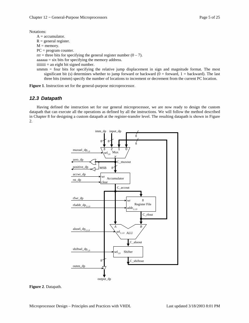
Chapter 12 − General-Purpose Microprocessors Page 5 of 25
Microprocessor Design – Principles and Practices with VHDL Last updated 3/18/2003 8:01 PM
Notations: A = accumulator. R = general register. M = memory. PC = program counter. rrr = three bits for specifying the general register number (0 – 7). aaaaaa = six bits for specifying the memory address. iiiiiiii = an eight bit signed number. smmm = four bits for specifying the relative jump displacement in sign and magnitude format. The most
significant bit (s) determines whether to jump forward or backward (0 = forward, 1 = backward). The last three bits (mmm) specify the number of locations to increment or decrement from the current PC location.
Figure 1. Instruction set for the general-purpose microprocessor.
12.3 Datapath Having defined the instruction set for our general microprocessor, we are now ready to design the custom
datapath that can execute all the operations as defined by all the instructions. We will follow the method described in Chapter 8 for designing a custom datapath at the register-transfer level. The resulting datapath is shown in Figure 2.
imm_dp input_dp
muxsel_dp1,0
accwr_dp
rfwr_dp
rfaddr_dp2,1,0
alusel_dp2,1,0
shiftsel_dp1,0
1 023
y
Accumulator
A Bsel2,1,0
Shiftersel1,0
Mux
C_muxout
C_accout
C_aluout
C_shiftout
C_rfout
output_dp
addr2,1,0
wr
wr
sel1,0
ALU
8Register File
zero_dp
positive_dp MSB
8 8
8
8
8
8
clearrst_dp
outen_dp
Figure 2. Datapath.
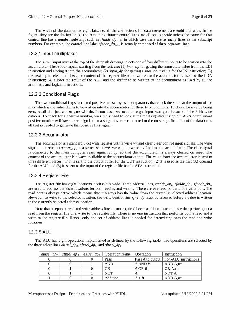
Chapter 12 − General-Purpose Microprocessors Page 6 of 25
Microprocessor Design – Principles and Practices with VHDL Last updated 3/18/2003 8:01 PM
The width of the datapath is eight bits, i.e. all the connections for data movement are eight bits wide. In the figure, they are the thicker lines. The remaining thinner control lines are all one bit wide unless the name for that control line has a number subscript such as rfaddr_dp2,1,0, in which case there are as many lines as the subscript numbers. For example, the control line label rfaddr_dp2,1,0 is actually composed of three separate lines.
12.3.1 Input multiplexer
The 4-to-1 input mux at the top of the datapath drawing selects one of four different inputs to be written into the accumulator. These four inputs, starting from the left, are: (1) imm_dp for getting the immediate value from the LDI instruction and storing it into the accumulator; (2) input_dp for getting a user input value for the IN instruction; (3) the next input selection allows the content of the register file to be written to the accumulator as used by the LDA instruction; (4) allows the result of the ALU and the shifter to be written to the accumulator as used by all the arithmetic and logical instructions.
12.3.2 Conditional Flags
The two conditional flags, zero and positive, are set by two comparators that check the value at the output of the mux which is the value that is to be written into the accumulator for these two conditions. To check for a value being zero, recall that just a NOR gate will do. In our case, we need an eight-input NOR gate because of the 8-bit wide databus. To check for a positive number, we simply need to look at the most significant sign bit. A 2’s complement positive number will have a zero sign bit, so a single inverter connected to the most significant bit of the databus is all that is needed to generate this positive flag signal.
12.3.3 Accumulator
The accumulator is a standard 8-bit wide register with a write wr and clear clear control input signals. The write signal, connected to accwr_dp, is asserted whenever we want to write a value into the accumulator. The clear signal is connected to the main computer reset signal rst_dp, so that the accumulator is always cleared on reset. The content of the accumulator is always available at the accumulator output. The value from the accumulator is sent to three different places: (1) it is sent to the output buffer for the OUT instruction; (2) it is used as the first (A) operand for the ALU; and (3) it is sent to the input of the register file for the STA instruction.
12.3.4 Register File
The register file has eight locations, each 8-bits wide. Three address lines, rfaddr_dp2, rfaddr_dp1, rfaddr_dp0, are used to address the eight locations for both reading and writing. There are one read port and one write port. The read port is always active which means that it always has the value from the currently selected address location. However, to write to the selected location, the write control line rfwr_dp must be asserted before a value is written to the currently selected address location.
Note that a separate read and write address lines is not required because all the instructions either perform just a read from the register file or a write to the register file. There is no one instruction that performs both a read and a write to the register file. Hence, only one set of address lines is needed for determining both the read and write locations.
12.3.5 ALU
The ALU has eight operations implemented as defined by the following table. The operations are selected by the three select lines alusel_dp2, alusel_dp1, and alusel_dp0.
alusel_dp2 alusel_dp 1 alusel_dp 0 Operation Name Operation Instruction
0 0 0 Pass Pass A to output non-ALU instructions 0 0 1 AND A AND B AND A,rrr 0 1 0 OR A OR B OR A,rrr 0 1 1 NOT A' NOT A 1 0 0 Addition A + B ADD A,rrr
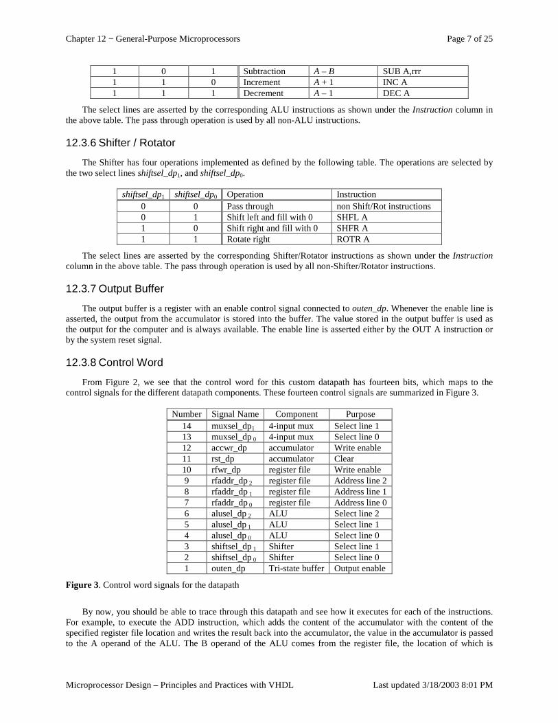
Chapter 12 − General-Purpose Microprocessors Page 7 of 25
Microprocessor Design – Principles and Practices with VHDL Last updated 3/18/2003 8:01 PM
1 0 1 Subtraction A – B SUB A,rrr 1 1 0 Increment A + 1 INC A 1 1 1 Decrement A – 1 DEC A
The select lines are asserted by the corresponding ALU instructions as shown under the Instruction column in the above table. The pass through operation is used by all non-ALU instructions.
12.3.6 Shifter / Rotator
The Shifter has four operations implemented as defined by the following table. The operations are selected by the two select lines shiftsel_dp1, and shiftsel_dp0.
shiftsel_dp1 shiftsel_dp0 Operation Instruction
0 0 Pass through non Shift/Rot instructions 0 1 Shift left and fill with 0 SHFL A 1 0 Shift right and fill with 0 SHFR A 1 1 Rotate right ROTR A
The select lines are asserted by the corresponding Shifter/Rotator instructions as shown under the Instruction column in the above table. The pass through operation is used by all non-Shifter/Rotator instructions.
12.3.7 Output Buffer
The output buffer is a register with an enable control signal connected to outen_dp. Whenever the enable line is asserted, the output from the accumulator is stored into the buffer. The value stored in the output buffer is used as the output for the computer and is always available. The enable line is asserted either by the OUT A instruction or by the system reset signal.
12.3.8 Control Word
From Figure 2, we see that the control word for this custom datapath has fourteen bits, which maps to the control signals for the different datapath components. These fourteen control signals are summarized in Figure 3.
Number Signal Name Component Purpose
14 muxsel_dp1 4-input mux Select line 1 13 muxsel_dp 0 4-input mux Select line 0 12 accwr_dp accumulator Write enable 11 rst_dp accumulator Clear 10 rfwr_dp register file Write enable 9 rfaddr_dp 2 register file Address line 2 8 rfaddr_dp 1 register file Address line 1 7 rfaddr_dp 0 register file Address line 0 6 alusel_dp 2 ALU Select line 2 5 alusel_dp 1 ALU Select line 1 4 alusel_dp 0 ALU Select line 0 3 shiftsel_dp 1 Shifter Select line 1 2 shiftsel_dp 0 Shifter Select line 0 1 outen_dp Tri-state buffer Output enable
Figure 3. Control word signals for the datapath
By now, you should be able to trace through this datapath and see how it executes for each of the instructions. For example, to execute the ADD instruction, which adds the content of the accumulator with the content of the specified register file location and writes the result back into the accumulator, the value in the accumulator is passed to the A operand of the ALU. The B operand of the ALU comes from the register file, the location of which is
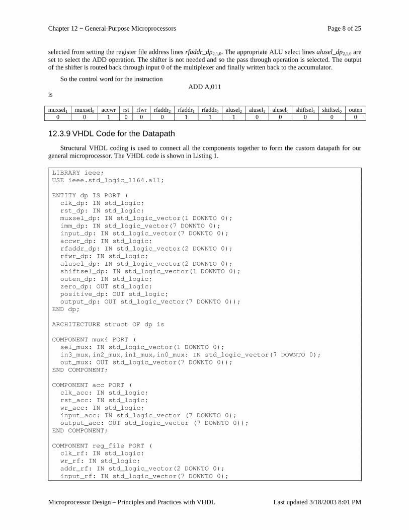
Chapter 12 − General-Purpose Microprocessors Page 8 of 25
Microprocessor Design – Principles and Practices with VHDL Last updated 3/18/2003 8:01 PM
selected from setting the register file address lines rfaddr_dp2,1,0. The appropriate ALU select lines alusel_dp2,1,0 are set to select the ADD operation. The shifter is not needed and so the pass through operation is selected. The output of the shifter is routed back through input 0 of the multiplexer and finally written back to the accumulator.
So the control word for the instruction ADD A,011
is muxsel1 muxsel0 accwr rst rfwr rfaddr2 rfaddr1 rfaddr0 alusel2 alusel1 alusel0 shiftsel1 shiftsel0 outen
0 0 1 0 0 0 1 1 1 0 0 0 0 0
12.3.9 VHDL Code for the Datapath
Structural VHDL coding is used to connect all the components together to form the custom datapath for our general microprocessor. The VHDL code is shown in Listing 1.
LIBRARY ieee;USE ieee.std_logic_1164.all;
ENTITY dp IS PORT (clk_dp: IN std_logic;rst_dp: IN std_logic;muxsel_dp: IN std_logic_vector(1 DOWNTO 0);imm_dp: IN std_logic_vector(7 DOWNTO 0);input_dp: IN std_logic_vector(7 DOWNTO 0);accwr_dp: IN std_logic;rfaddr_dp: IN std_logic_vector(2 DOWNTO 0);rfwr_dp: IN std_logic;alusel_dp: IN std_logic_vector(2 DOWNTO 0);shiftsel_dp: IN std_logic_vector(1 DOWNTO 0);outen_dp: IN std_logic;zero_dp: OUT std_logic;positive_dp: OUT std_logic;output_dp: OUT std_logic_vector(7 DOWNTO 0));
END dp;
ARCHITECTURE struct OF dp is
COMPONENT mux4 PORT (sel_mux: IN std_logic_vector(1 DOWNTO 0);in3_mux,in2_mux,in1_mux,in0_mux: IN std_logic_vector(7 DOWNTO 0);out_mux: OUT std_logic_vector(7 DOWNTO 0));
END COMPONENT;
COMPONENT acc PORT (clk_acc: IN std_logic;rst_acc: IN std_logic;wr_acc: IN std_logic;input_acc: IN std_logic_vector (7 DOWNTO 0);output_acc: OUT std_logic_vector (7 DOWNTO 0));
END COMPONENT;
COMPONENT reg_file PORT (clk_rf: IN std_logic;wr_rf: IN std_logic;addr_rf: IN std_logic_vector(2 DOWNTO 0);input_rf: IN std_logic_vector(7 DOWNTO 0);
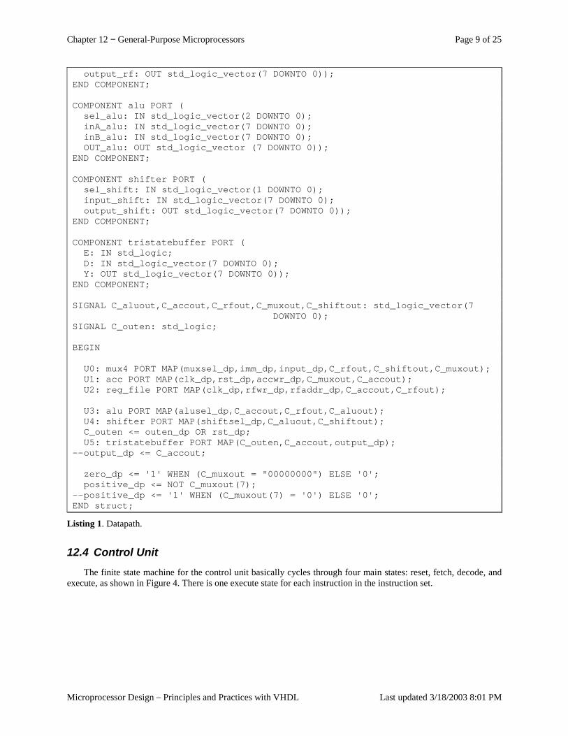
Chapter 12 − General-Purpose Microprocessors Page 9 of 25
Microprocessor Design – Principles and Practices with VHDL Last updated 3/18/2003 8:01 PM
output_rf: OUT std_logic_vector(7 DOWNTO 0));END COMPONENT;
COMPONENT alu PORT (sel_alu: IN std_logic_vector(2 DOWNTO 0);inA_alu: IN std_logic_vector(7 DOWNTO 0);inB_alu: IN std_logic_vector(7 DOWNTO 0);OUT_alu: OUT std_logic_vector (7 DOWNTO 0));
END COMPONENT;
COMPONENT shifter PORT (sel_shift: IN std_logic_vector(1 DOWNTO 0);input_shift: IN std_logic_vector(7 DOWNTO 0);output_shift: OUT std_logic_vector(7 DOWNTO 0));
END COMPONENT;
COMPONENT tristatebuffer PORT (E: IN std_logic;D: IN std_logic_vector(7 DOWNTO 0);Y: OUT std_logic_vector(7 DOWNTO 0));
END COMPONENT;
SIGNAL C_aluout,C_accout,C_rfout,C_muxout,C_shiftout: std_logic_vector(7DOWNTO 0);
SIGNAL C_outen: std_logic;
BEGIN
U0: mux4 PORT MAP(muxsel_dp,imm_dp,input_dp,C_rfout,C_shiftout,C_muxout);U1: acc PORT MAP(clk_dp,rst_dp,accwr_dp,C_muxout,C_accout);U2: reg_file PORT MAP(clk_dp,rfwr_dp,rfaddr_dp,C_accout,C_rfout);
U3: alu PORT MAP(alusel_dp,C_accout,C_rfout,C_aluout);U4: shifter PORT MAP(shiftsel_dp,C_aluout,C_shiftout);C_outen <= outen_dp OR rst_dp;U5: tristatebuffer PORT MAP(C_outen,C_accout,output_dp);
--output_dp <= C_accout;
zero_dp <= '1' WHEN (C_muxout = "00000000") ELSE '0';positive_dp <= NOT C_muxout(7);
--positive_dp <= '1' WHEN (C_muxout(7) = '0') ELSE '0';END struct;
Listing 1. Datapath.
12.4 Control Unit The finite state machine for the control unit basically cycles through four main states: reset, fetch, decode, and
execute, as shown in Figure 4. There is one execute state for each instruction in the instruction set.
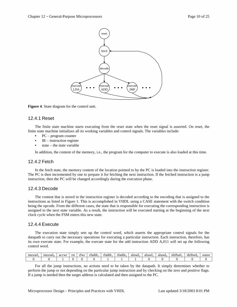
Chapter 12 − General-Purpose Microprocessors Page 10 of 25
Microprocessor Design – Principles and Practices with VHDL Last updated 3/18/2003 8:01 PM
executeLDA
decode
fetch
reset
executeJMP
executeADD
Figure 4. State diagram for the control unit.
12.4.1 Reset
The finite state machine starts executing from the reset state when the reset signal is asserted. On reset, the finite state machine initializes all its working variables and control signals. The variables include:
• PC – program counter • IR – instruction register • state – the state variable
In addition, the content of the memory, i.e., the program for the computer to execute is also loaded at this time.
12.4.2 Fetch
In the fetch state, the memory content of the location pointed to by the PC is loaded into the instruction register. The PC is then incremented by one to prepare it for fetching the next instruction. If the fetched instruction is a jump instruction, then the PC will be changed accordingly during the execution phase.
12.4.3 Decode
The content that is stored in the instruction register is decoded according to the encoding that is assigned to the instructions as listed in Figure 1. This is accomplished in VHDL using a CASE statement with the switch condition being the opcode. From the different cases, the state that is responsible for executing the corresponding instruction is assigned to the next state variable. As a result, the instruction will be executed starting at the beginning of the next clock cycle when the FSM enters this new state.
12.4.4 Execute
The execution state simply sets up the control word, which asserts the appropriate control signals for the datapath to carry out the necessary operations for executing a particular instruction. Each instruction, therefore, has its own execute state. For example, the execute state for the add instruction ADD A,011 will set up the following control word.
muxsel1 muxsel0 accwr rst rfwr rfaddr2 rfaddr1 rfaddr0 alusel2 alusel1 alusel0 shiftsel1 shiftsel0 outen
0 0 1 0 0 0 1 1 1 0 0 0 0 0
For all the jump instructions, no actions need to be taken by the datapath. It simply determines whether to perform the jump or not depending on the particular jump instruction and by checking on the zero and positive flags. If a jump is needed then the target address is calculated and then assigned to the PC.
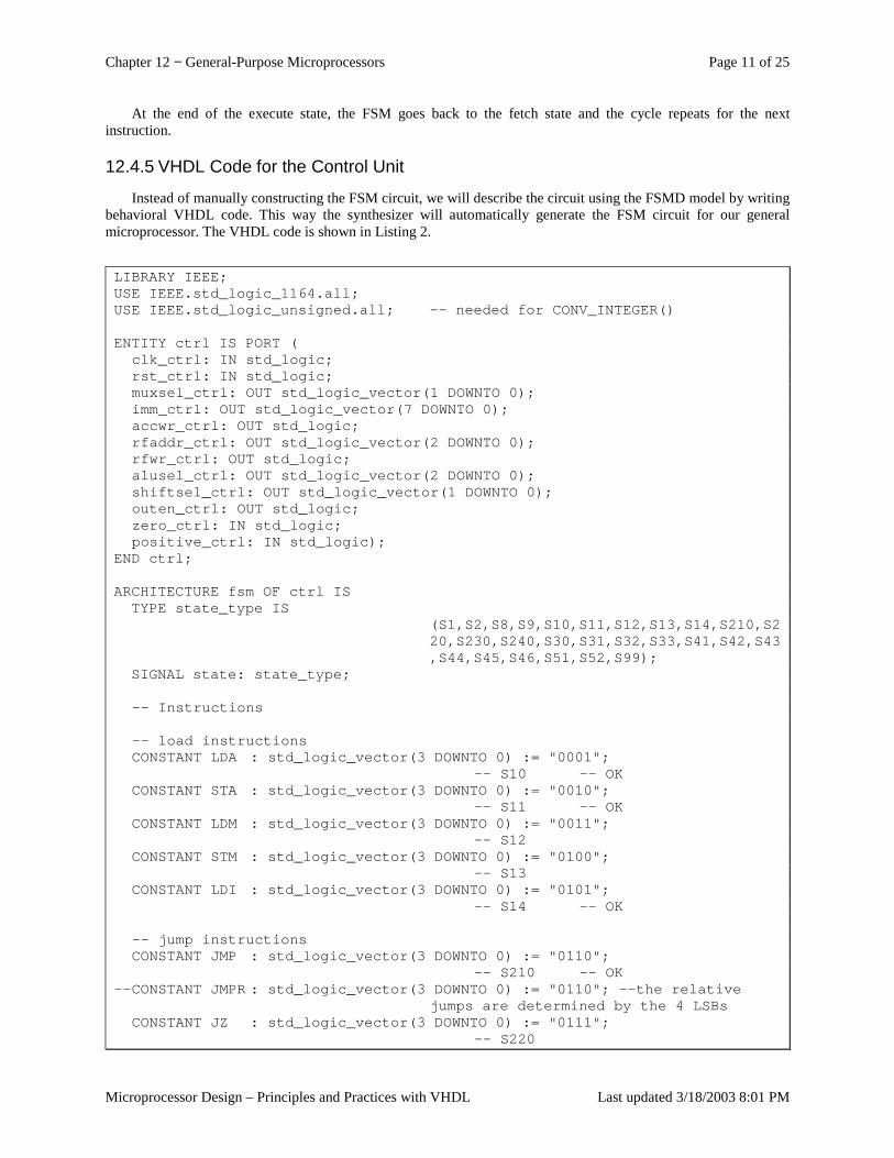
Chapter 12 − General-Purpose Microprocessors Page 11 of 25
Microprocessor Design – Principles and Practices with VHDL Last updated 3/18/2003 8:01 PM
At the end of the execute state, the FSM goes back to the fetch state and the cycle repeats for the next instruction.
12.4.5 VHDL Code for the Control Unit
Instead of manually constructing the FSM circuit, we will describe the circuit using the FSMD model by writing behavioral VHDL code. This way the synthesizer will automatically generate the FSM circuit for our general microprocessor. The VHDL code is shown in Listing 2.
LIBRARY IEEE;USE IEEE.std_logic_1164.all;USE IEEE.std_logic_unsigned.all; -- needed for CONV_INTEGER()
ENTITY ctrl IS PORT (clk_ctrl: IN std_logic;rst_ctrl: IN std_logic;muxsel_ctrl: OUT std_logic_vector(1 DOWNTO 0);imm_ctrl: OUT std_logic_vector(7 DOWNTO 0);accwr_ctrl: OUT std_logic;rfaddr_ctrl: OUT std_logic_vector(2 DOWNTO 0);rfwr_ctrl: OUT std_logic;alusel_ctrl: OUT std_logic_vector(2 DOWNTO 0);shiftsel_ctrl: OUT std_logic_vector(1 DOWNTO 0);outen_ctrl: OUT std_logic;zero_ctrl: IN std_logic;positive_ctrl: IN std_logic);
END ctrl;
ARCHITECTURE fsm OF ctrl ISTYPE state_type IS
(S1,S2,S8,S9,S10,S11,S12,S13,S14,S210,S220,S230,S240,S30,S31,S32,S33,S41,S42,S43,S44,S45,S46,S51,S52,S99);
SIGNAL state: state_type;
-- Instructions
-- load instructionsCONSTANT LDA : std_logic_vector(3 DOWNTO 0) := "0001";
-- S10 -- OKCONSTANT STA : std_logic_vector(3 DOWNTO 0) := "0010";
-- S11 -- OKCONSTANT LDM : std_logic_vector(3 DOWNTO 0) := "0011";
-- S12CONSTANT STM : std_logic_vector(3 DOWNTO 0) := "0100";
-- S13CONSTANT LDI : std_logic_vector(3 DOWNTO 0) := "0101";
-- S14 -- OK
-- jump instructionsCONSTANT JMP : std_logic_vector(3 DOWNTO 0) := "0110";
-- S210 -- OK--CONSTANT JMPR : std_logic_vector(3 DOWNTO 0) := "0110"; --the relative
jumps are determined by the 4 LSBsCONSTANT JZ : std_logic_vector(3 DOWNTO 0) := "0111";
-- S220
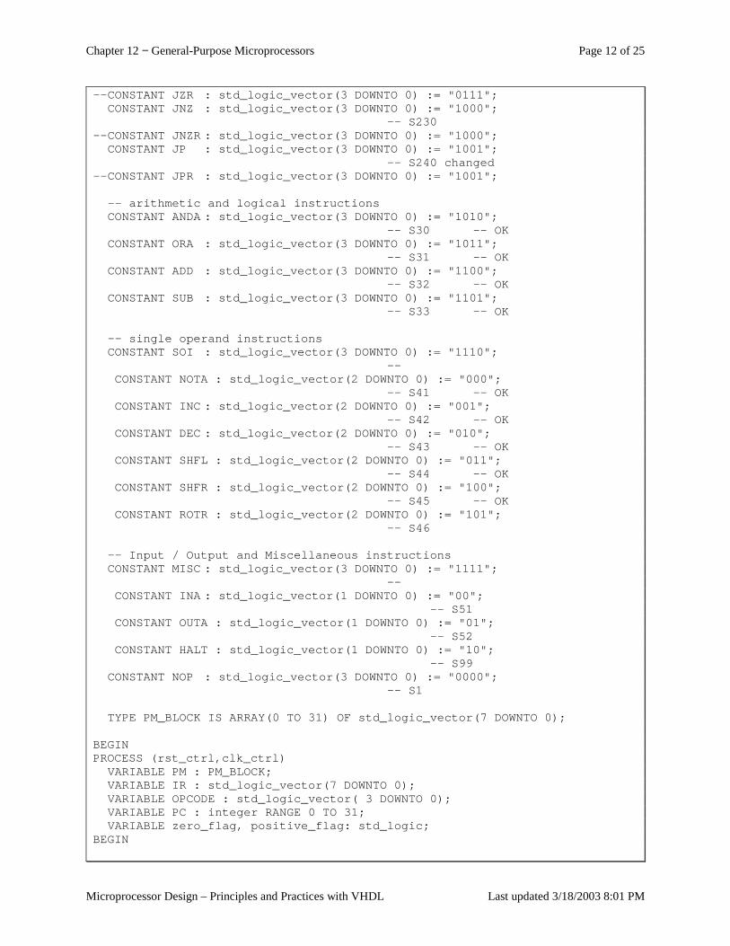
Chapter 12 − General-Purpose Microprocessors Page 12 of 25
Microprocessor Design – Principles and Practices with VHDL Last updated 3/18/2003 8:01 PM
--CONSTANT JZR : std_logic_vector(3 DOWNTO 0) := "0111";CONSTANT JNZ : std_logic_vector(3 DOWNTO 0) := "1000";
-- S230--CONSTANT JNZR : std_logic_vector(3 DOWNTO 0) := "1000";
CONSTANT JP : std_logic_vector(3 DOWNTO 0) := "1001";-- S240 changed
--CONSTANT JPR : std_logic_vector(3 DOWNTO 0) := "1001";
-- arithmetic and logical instructionsCONSTANT ANDA : std_logic_vector(3 DOWNTO 0) := "1010";
-- S30 -- OKCONSTANT ORA : std_logic_vector(3 DOWNTO 0) := "1011";
-- S31 -- OKCONSTANT ADD : std_logic_vector(3 DOWNTO 0) := "1100";
-- S32 -- OKCONSTANT SUB : std_logic_vector(3 DOWNTO 0) := "1101";
-- S33 -- OK
-- single operand instructionsCONSTANT SOI : std_logic_vector(3 DOWNTO 0) := "1110";
--CONSTANT NOTA : std_logic_vector(2 DOWNTO 0) := "000";
-- S41 -- OKCONSTANT INC : std_logic_vector(2 DOWNTO 0) := "001";
-- S42 -- OKCONSTANT DEC : std_logic_vector(2 DOWNTO 0) := "010";
-- S43 -- OKCONSTANT SHFL : std_logic_vector(2 DOWNTO 0) := "011";
-- S44 -- OKCONSTANT SHFR : std_logic_vector(2 DOWNTO 0) := "100";
-- S45 -- OKCONSTANT ROTR : std_logic_vector(2 DOWNTO 0) := "101";
-- S46
-- Input / Output and Miscellaneous instructionsCONSTANT MISC : std_logic_vector(3 DOWNTO 0) := "1111";
--CONSTANT INA : std_logic_vector(1 DOWNTO 0) := "00";
-- S51CONSTANT OUTA : std_logic_vector(1 DOWNTO 0) := "01";
-- S52CONSTANT HALT : std_logic_vector(1 DOWNTO 0) := "10";
-- S99CONSTANT NOP : std_logic_vector(3 DOWNTO 0) := "0000";
-- S1
TYPE PM_BLOCK IS ARRAY(0 TO 31) OF std_logic_vector(7 DOWNTO 0);
BEGINPROCESS (rst_ctrl,clk_ctrl)
VARIABLE PM : PM_BLOCK;VARIABLE IR : std_logic_vector(7 DOWNTO 0);VARIABLE OPCODE : std_logic_vector( 3 DOWNTO 0);VARIABLE PC : integer RANGE 0 TO 31;VARIABLE zero_flag, positive_flag: std_logic;
BEGIN
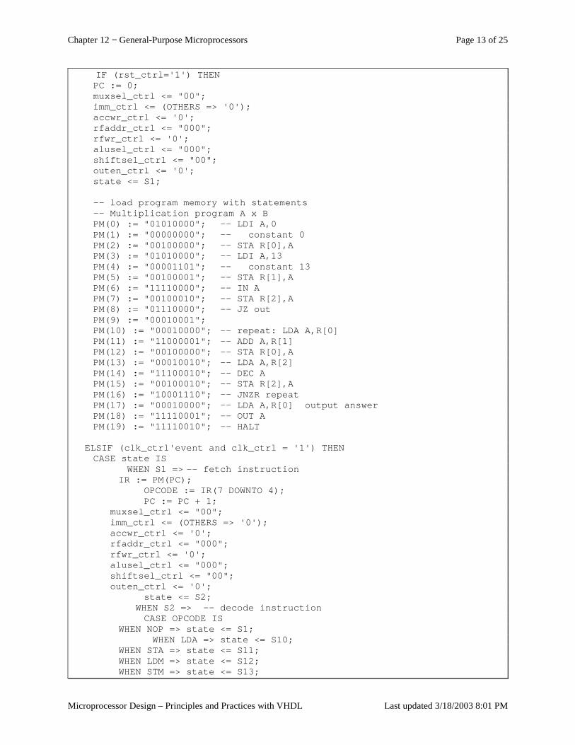
Chapter 12 − General-Purpose Microprocessors Page 13 of 25
Microprocessor Design – Principles and Practices with VHDL Last updated 3/18/2003 8:01 PM
IF (rst_ctrl='1') THENPC := 0;muxsel_ctrl <= "00";imm_ctrl <= (OTHERS => '0');accwr_ctrl <= '0';rfaddr_ctrl <= "000";rfwr_ctrl <= '0';alusel_ctrl <= "000";shiftsel_ctrl <= "00";outen_ctrl <= '0';state <= S1;
-- load program memory with statements-- Multiplication program A x BPM(0) := "01010000"; -- LDI A,0PM(1) := "00000000"; -- constant 0PM(2) := "00100000"; -- STA R[0],APM(3) := "01010000"; -- LDI A,13PM(4) := "00001101"; -- constant 13PM(5) := "00100001"; -- STA R[1],APM(6) := "11110000"; -- IN APM(7) := "00100010"; -- STA R[2],APM(8) := "01110000"; -- JZ outPM(9) := "00010001";PM(10) := "00010000"; -- repeat: LDA A,R[0]PM(11) := "11000001"; -- ADD A,R[1]PM(12) := "00100000"; -- STA R[0],APM(13) := "00010010"; -- LDA A,R[2]PM(14) := "11100010"; -- DEC APM(15) := "00100010"; -- STA R[2],APM(16) := "10001110"; -- JNZR repeatPM(17) := "00010000"; -- LDA A,R[0] output answerPM(18) := "11110001"; -- OUT APM(19) := "11110010"; -- HALT
ELSIF (clk_ctrl'event and clk_ctrl = '1') THENCASE state IS
WHEN S1 => -- fetch instructionIR := PM(PC);
OPCODE := IR(7 DOWNTO 4);PC := PC + 1;
muxsel_ctrl <= "00";imm_ctrl <= (OTHERS => '0');accwr_ctrl <= '0';rfaddr_ctrl <= "000";rfwr_ctrl <= '0';alusel_ctrl <= "000";shiftsel_ctrl <= "00";outen_ctrl <= '0';
state <= S2;WHEN S2 => -- decode instructionCASE OPCODE IS
WHEN NOP => state <= S1;WHEN LDA => state <= S10;
WHEN STA => state <= S11;WHEN LDM => state <= S12;WHEN STM => state <= S13;
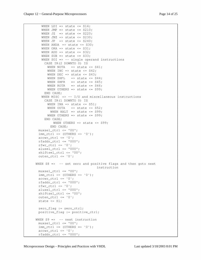
Chapter 12 − General-Purpose Microprocessors Page 14 of 25
Microprocessor Design – Principles and Practices with VHDL Last updated 3/18/2003 8:01 PM
WHEN LDI => state <= S14;WHEN JMP => state <= S210;WHEN JZ => state <= S220;WHEN JNZ => state <= S230;WHEN JP => state <= S240;WHEN ANDA => state <= S30;WHEN ORA => state <= S31;WHEN ADD => state <= S32;WHEN SUB => state <= S33;WHEN SOI => -- single operand instructionsCASE IR(2 DOWNTO 0) ISWHEN NOTA => state <= S41;WHEN INC => state <= S42;WHEN DEC => state <= S43;WHEN SHFL => state <= S44;WHEN SHFR => state <= S45;WHEN ROTR => state <= S46;WHEN OTHERS => state <= S99;
END CASE;WHEN MISC => -- I/O and miscellaneous instructionsCASE IR(1 DOWNTO 0) ISWHEN INA => state <= S51;WHEN OUTA => state <= S52;WHEN HALT => state <= S99;
WHEN OTHERS => state <= S99;END CASE;
WHEN OTHERS => state <= S99;END CASE;
muxsel_ctrl <= "00";imm_ctrl <= (OTHERS => '0');accwr_ctrl <= '0';rfaddr_ctrl <= "000";rfwr_ctrl <= '0';alusel_ctrl <= "000";shiftsel_ctrl <= "00";outen_ctrl <= '0';
WHEN S8 => -- set zero and positive flags and then goto nextinstruction
muxsel_ctrl <= "00";imm_ctrl <= (OTHERS => '0');accwr_ctrl <= '0';rfaddr_ctrl <= "000";rfwr_ctrl <= '0';alusel_ctrl <= "000";shiftsel_ctrl <= "00";outen_ctrl <= '0';state <= S1;
zero_flag := zero_ctrl;positive_flag := positive_ctrl;
WHEN S9 => -- next instructionmuxsel_ctrl <= "00";imm_ctrl <= (OTHERS => '0');accwr_ctrl <= '0';rfaddr_ctrl <= "000";
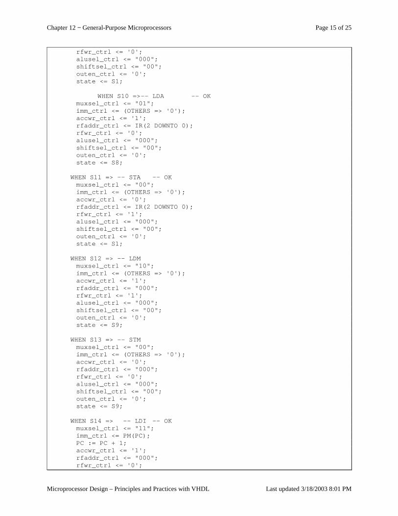
Chapter 12 − General-Purpose Microprocessors Page 15 of 25
Microprocessor Design – Principles and Practices with VHDL Last updated 3/18/2003 8:01 PM
rfwr_ctrl <= '0';alusel_ctrl <= "000";shiftsel_ctrl <= "00";outen_ctrl <= '0';state <= S1;
WHEN S10 =>-- LDA -- OKmuxsel_ctrl <= "01";imm_ctrl <= (OTHERS => '0');accwr_ctrl <= '1';rfaddr_ctrl <= IR(2 DOWNTO 0);rfwr_ctrl <= '0';alusel_ctrl <= "000";shiftsel_ctrl <= "00";outen_ctrl <= '0';state <= S8;
WHEN S11 => -- STA -- OKmuxsel_ctrl <= "00";imm_ctrl <= (OTHERS => '0');accwr_ctrl <= '0';rfaddr_ctrl <= IR(2 DOWNTO 0);rfwr_ctrl <= '1';alusel_ctrl <= "000";shiftsel_ctrl <= "00";outen_ctrl <= '0';state <= S1;
WHEN S12 => -- LDMmuxsel_ctrl <= "10";imm_ctrl <= (OTHERS => '0');accwr_ctrl <= '1';rfaddr_ctrl <= "000";rfwr_ctrl <= '1';alusel_ctrl <= "000";shiftsel_ctrl <= "00";outen_ctrl <= '0';state <= S9;
WHEN S13 => -- STMmuxsel_ctrl <= "00";imm_ctrl <= (OTHERS => '0');accwr_ctrl <= '0';rfaddr_ctrl <= "000";rfwr_ctrl <= '0';alusel_ctrl <= "000";shiftsel_ctrl <= "00";outen_ctrl <= '0';state <= S9;
WHEN S14 => -- LDI -- OKmuxsel_ctrl <= "11";imm_ctrl <= PM(PC);PC := PC + 1;accwr_ctrl <= '1';rfaddr_ctrl <= "000";rfwr_ctrl <= '0';
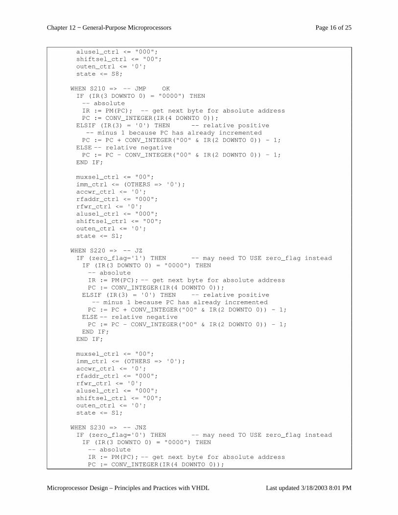
Chapter 12 − General-Purpose Microprocessors Page 16 of 25
Microprocessor Design – Principles and Practices with VHDL Last updated 3/18/2003 8:01 PM
alusel_ctrl <= "000";shiftsel_ctrl <= "00";outen_ctrl <= '0';state <= S8;
WHEN S210 => -- JMP OKIF (IR(3 DOWNTO 0) = "0000") THEN-- absoluteIR := PM(PC); -- get next byte for absolute addressPC := CONV_INTEGER(IR(4 DOWNTO 0));
ELSIF (IR(3) = '0') THEN -- relative positive-- minus 1 because PC has already incremented
PC := PC + CONV_INTEGER("00" & IR(2 DOWNTO 0)) - 1;ELSE -- relative negativePC := PC - CONV_INTEGER("00" & IR(2 DOWNTO 0)) - 1;
END IF;
muxsel_ctrl <= "00";imm_ctrl <= (OTHERS => '0');accwr_ctrl <= '0';rfaddr_ctrl <= "000";rfwr_ctrl <= '0';alusel_ctrl <= "000";shiftsel_ctrl <= "00";outen_ctrl <= '0';state <= S1;
WHEN S220 => -- JZIF (zero_flag='1') THEN -- may need TO USE zero_flag insteadIF (IR(3 DOWNTO 0) = "0000") THEN-- absoluteIR := PM(PC); -- get next byte for absolute addressPC := CONV_INTEGER(IR(4 DOWNTO 0));
ELSIF (IR(3) = '0') THEN -- relative positive-- minus 1 because PC has already incremented
PC := PC + CONV_INTEGER("00" & IR(2 DOWNTO 0)) - 1;ELSE -- relative negativePC := PC - CONV_INTEGER("00" & IR(2 DOWNTO 0)) - 1;
END IF;END IF;
muxsel_ctrl <= "00";imm_ctrl <= (OTHERS => '0');accwr_ctrl <= '0';rfaddr_ctrl <= "000";rfwr_ctrl <= '0';alusel_ctrl <= "000";shiftsel_ctrl <= "00";outen_ctrl <= '0';state <= S1;
WHEN S230 => -- JNZIF (zero_flag='0') THEN -- may need TO USE zero_flag insteadIF (IR(3 DOWNTO 0) = "0000") THEN-- absoluteIR := PM(PC); -- get next byte for absolute addressPC := CONV_INTEGER(IR(4 DOWNTO 0));
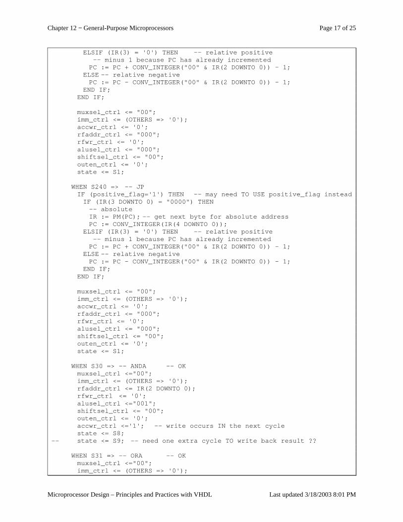
Chapter 12 − General-Purpose Microprocessors Page 17 of 25
Microprocessor Design – Principles and Practices with VHDL Last updated 3/18/2003 8:01 PM
ELSIF (IR(3) = '0') THEN -- relative positive-- minus 1 because PC has already incremented
PC := PC + CONV_INTEGER("00" & IR(2 DOWNTO 0)) - 1;ELSE -- relative negativePC := PC - CONV_INTEGER("00" & IR(2 DOWNTO 0)) - 1;
END IF;END IF;
muxsel_ctrl <= "00";imm_ctrl <= (OTHERS => '0');accwr_ctrl <= '0';rfaddr_ctrl <= "000";rfwr_ctrl <= '0';alusel_ctrl <= "000";shiftsel_ctrl <= "00";outen_ctrl <= '0';state <= S1;
WHEN S240 => -- JPIF (positive_flag='1') THEN -- may need TO USE positive_flag insteadIF (IR(3 DOWNTO 0) = "0000") THEN-- absoluteIR := PM(PC); -- get next byte for absolute addressPC := CONV_INTEGER(IR(4 DOWNTO 0));
ELSIF (IR(3) = '0') THEN -- relative positive-- minus 1 because PC has already incremented
PC := PC + CONV_INTEGER("00" & IR(2 DOWNTO 0)) - 1;ELSE -- relative negativePC := PC - CONV_INTEGER("00" & IR(2 DOWNTO 0)) - 1;
END IF;END IF;
muxsel_ctrl <= "00";imm_ctrl <= (OTHERS => '0');accwr_ctrl <= '0';rfaddr_ctrl <= "000";rfwr_ctrl <= '0';alusel_ctrl <= "000";shiftsel_ctrl <= "00";outen_ctrl <= '0';state <= S1;
WHEN S30 => -- ANDA -- OKmuxsel_ctrl <="00";imm_ctrl <= (OTHERS => '0');rfaddr_ctrl <= IR(2 DOWNTO 0);rfwr_ctrl <= '0';alusel_ctrl <="001";shiftsel_ctrl <= "00";outen_ctrl <= '0';accwr_ctrl <='1'; -- write occurs IN the next cyclestate <= S8;
-- state <= S9; -- need one extra cycle TO write back result ??
WHEN S31 => -- ORA -- OKmuxsel_ctrl <="00";imm_ctrl <= (OTHERS => '0');
Chapter 12 − General-Purpose Microprocessors Page 18 of 25
Microprocessor Design – Principles and Practices with VHDL Last updated 3/18/2003 8:01 PM
rfaddr_ctrl <= IR(2 DOWNTO 0);rfwr_ctrl <= '0';alusel_ctrl <="010";shiftsel_ctrl <= "00";outen_ctrl <= '0';accwr_ctrl <='1'; -- write occurs IN the next cyclestate <= S8;
-- state <= S9; -- need one extra cycle TO write back result
WHEN S32 => -- ADD -- OKmuxsel_ctrl <="00";imm_ctrl <= (OTHERS => '0');rfaddr_ctrl <= IR(2 DOWNTO 0);rfwr_ctrl <= '0';alusel_ctrl <="100";shiftsel_ctrl <= "00";outen_ctrl <= '0';accwr_ctrl <='1'; -- write occurs IN the next cyclestate <= S8;
-- state <= S9; -- need one extra cycle TO write back result
WHEN S33 => -- SUB -- OKmuxsel_ctrl <="00";imm_ctrl <= (OTHERS => '0');rfaddr_ctrl <= IR(2 DOWNTO 0);rfwr_ctrl <= '0';alusel_ctrl <="101";shiftsel_ctrl <= "00";outen_ctrl <= '0';accwr_ctrl <='1'; -- write occurs IN the next cyclestate <= S8;
-- state <= S9; -- need one extra cycle TO write back result
WHEN S41 => -- NOTA -- OKmuxsel_ctrl <="00";imm_ctrl <= (OTHERS => '0');rfaddr_ctrl <= "000";rfwr_ctrl <= '0';alusel_ctrl <="011";shiftsel_ctrl <= "00";outen_ctrl <= '0';accwr_ctrl <='1'; -- write occurs IN the next cyclestate <= S8;
-- state <= S9; -- need one extra cycle TO write back result
WHEN S42 => -- INC -- OKmuxsel_ctrl <="00";imm_ctrl <= (OTHERS => '0');rfaddr_ctrl <= "000";rfwr_ctrl <= '0';alusel_ctrl <="110";shiftsel_ctrl <= "00";outen_ctrl <= '0';accwr_ctrl <='1'; -- write occurs IN the next cyclestate <= S8;
-- state <= S9; -- need one extra cycle TO write back result
Chapter 12 − General-Purpose Microprocessors Page 19 of 25
Microprocessor Design – Principles and Practices with VHDL Last updated 3/18/2003 8:01 PM
WHEN S43 => -- DEC -- OKmuxsel_ctrl <="00";imm_ctrl <= (OTHERS => '0');rfaddr_ctrl <= "000";rfwr_ctrl <= '0';alusel_ctrl <="111";shiftsel_ctrl <= "00";outen_ctrl <= '0';accwr_ctrl <='1'; -- write occurs IN the next cyclestate <= S8;
-- state <= S9; -- need one extra cycle TO write back result
WHEN S44 => -- SHFLmuxsel_ctrl <="00";imm_ctrl <= (OTHERS => '0');rfaddr_ctrl <= "000";rfwr_ctrl <= '0';alusel_ctrl <= "000"; -- passshiftsel_ctrl <= "01";outen_ctrl <= '0';accwr_ctrl <='1'; -- write occurs IN the next cyclestate <= S8;
-- state <= S9; -- need one extra cycle TO write back result
WHEN S45 => -- SHFR -- OKmuxsel_ctrl <="00";imm_ctrl <= (OTHERS => '0');rfaddr_ctrl <= "000";rfwr_ctrl <= '0';alusel_ctrl <= "000"; -- passshiftsel_ctrl <= "10";outen_ctrl <= '0';accwr_ctrl <='1'; -- write occurs IN the next cyclestate <= S8;
-- state <= S9; -- need one extra cycle TO write back result
WHEN S46 => -- ROTR -- ??muxsel_ctrl <="00";imm_ctrl <= (OTHERS => '0');rfaddr_ctrl <= "000";rfwr_ctrl <= '0';alusel_ctrl <= "000"; -- passshiftsel_ctrl <= "11";outen_ctrl <= '0';accwr_ctrl <='1'; -- write occurs IN the next cyclestate <= S8;
-- state <= S9; -- need one extra cycle TO write back result
WHEN S51 => -- INAmuxsel_ctrl <= "10";imm_ctrl <= (OTHERS => '0');accwr_ctrl <= '1';rfaddr_ctrl <= "000";rfwr_ctrl <= '0';alusel_ctrl <= "000";shiftsel_ctrl <= "00";outen_ctrl <= '0';
Chapter 12 − General-Purpose Microprocessors Page 20 of 25
Microprocessor Design – Principles and Practices with VHDL Last updated 3/18/2003 8:01 PM
state <= S8;-- state <= S9;
WHEN S52 => -- OUTAmuxsel_ctrl <= "00";imm_ctrl <= (OTHERS => '0');accwr_ctrl <= '0';rfaddr_ctrl <= "000";rfwr_ctrl <= '0';alusel_ctrl <= "000";shiftsel_ctrl <= "00";outen_ctrl <= '1';state <= S1;
-- state <= S9;
WHEN S99 => -- HALTmuxsel_ctrl <= "00";imm_ctrl <= (OTHERS => '0');accwr_ctrl <= '0';rfaddr_ctrl <= "000";rfwr_ctrl <= '0';alusel_ctrl <= "000";shiftsel_ctrl <= "00";outen_ctrl <= '0';
state <= S99;
WHEN OTHERS =>muxsel_ctrl <= "00";imm_ctrl <= (OTHERS => '0');accwr_ctrl <= '0';rfaddr_ctrl <= "000";rfwr_ctrl <= '0';alusel_ctrl <= "000";shiftsel_ctrl <= "00";outen_ctrl <= '0';state <= S99;END CASE;
END IF;END PROCESS;END fsm;
Listing 2. Control unit.
12.5 CPU Now that we have defined both the datapath and the control unit, we are ready to connect the two together to
create our very own custom general microprocessor. The necessary signals that need to be connected between the two units are just the control word signals, shown in Figure 3, that the control unit has to generate for controlling the datapath. In addition to the control signals, there are also two conditional flag signals (zero and positive) that the datapath generates as status signals for the control unit to use. The interface between the datapath and the control unit is shown in Figure 5.
The primary inputs to the CPU module are clock, reset, and data input. The primary output from the CPU module is the data output, address???.
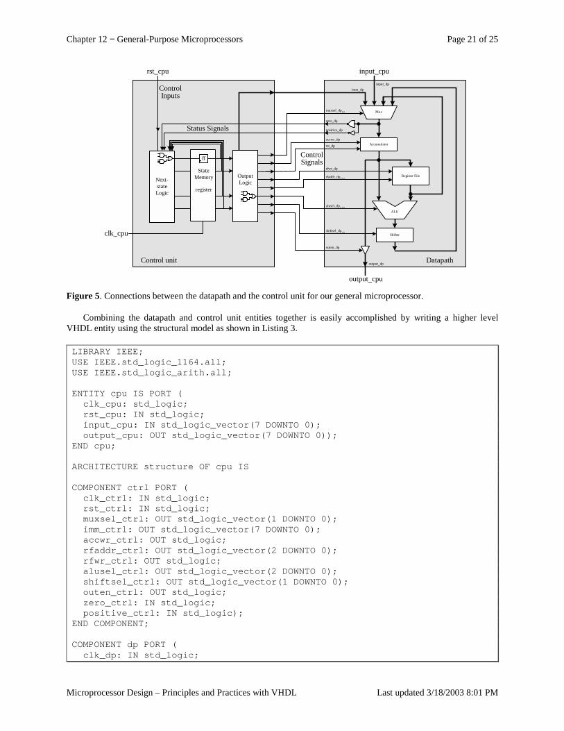
Chapter 12 − General-Purpose Microprocessors Page 21 of 25
Microprocessor Design – Principles and Practices with VHDL Last updated 3/18/2003 8:01 PM
Next-stateLogic
imm_dpinput_dp
muxsel_dp1,0
accwr_dp
rfwr_dp
rfaddr_dp2,1,0
alusel_dp2,1,0
shiftsel_dp1,0
Accumulator
Shifter
Mux
ALU
Register File
zero_dp
positive_dp
rst_dp
outen_dp
output_dp
ControlSignals
Status Signals
ControlInputs
OutputLogic
StateMemory
register
Control unit
ff
Datapath
rst_cpu
clk_cpu
input_cpu
output_cpu Figure 5. Connections between the datapath and the control unit for our general microprocessor.
Combining the datapath and control unit entities together is easily accomplished by writing a higher level VHDL entity using the structural model as shown in Listing 3.
LIBRARY IEEE;USE IEEE.std_logic_1164.all;USE IEEE.std_logic_arith.all;
ENTITY cpu IS PORT (clk_cpu: std_logic;rst_cpu: IN std_logic;input_cpu: IN std_logic_vector(7 DOWNTO 0);output_cpu: OUT std_logic_vector(7 DOWNTO 0));
END cpu;
ARCHITECTURE structure OF cpu IS
COMPONENT ctrl PORT (clk_ctrl: IN std_logic;rst_ctrl: IN std_logic;muxsel_ctrl: OUT std_logic_vector(1 DOWNTO 0);imm_ctrl: OUT std_logic_vector(7 DOWNTO 0);accwr_ctrl: OUT std_logic;rfaddr_ctrl: OUT std_logic_vector(2 DOWNTO 0);rfwr_ctrl: OUT std_logic;alusel_ctrl: OUT std_logic_vector(2 DOWNTO 0);shiftsel_ctrl: OUT std_logic_vector(1 DOWNTO 0);outen_ctrl: OUT std_logic;zero_ctrl: IN std_logic;positive_ctrl: IN std_logic);
END COMPONENT;
COMPONENT dp PORT (clk_dp: IN std_logic;
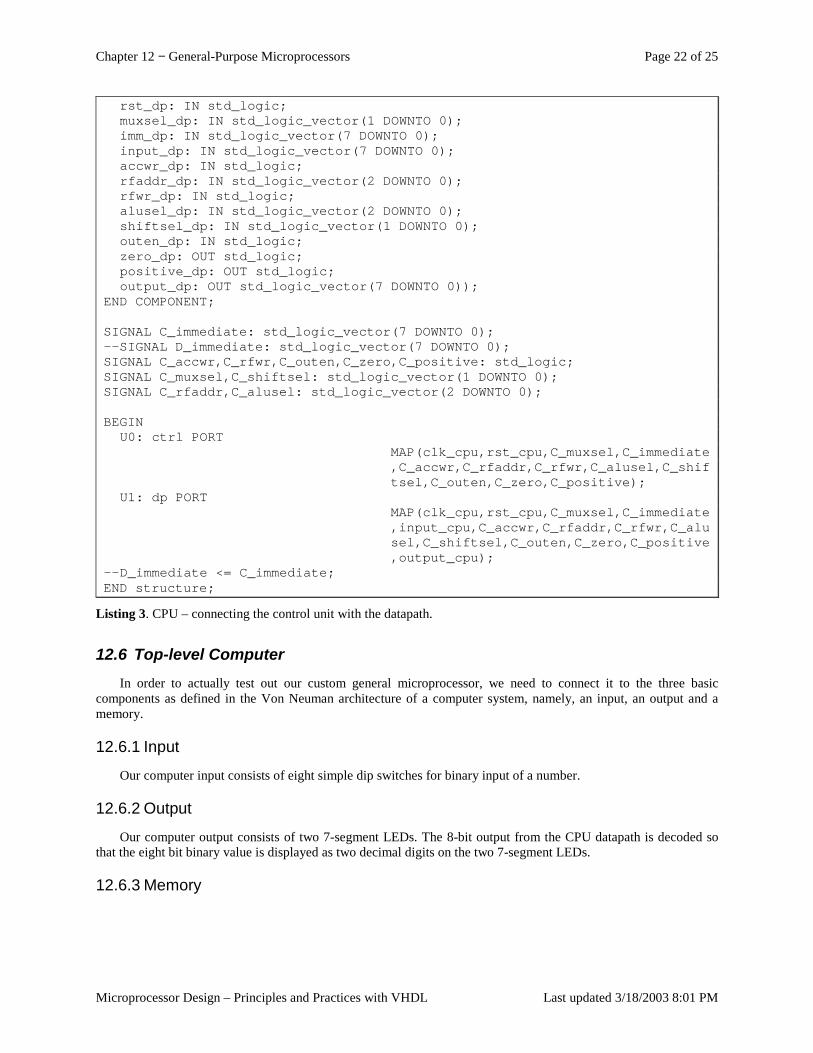
Chapter 12 − General-Purpose Microprocessors Page 22 of 25
Microprocessor Design – Principles and Practices with VHDL Last updated 3/18/2003 8:01 PM
rst_dp: IN std_logic;muxsel_dp: IN std_logic_vector(1 DOWNTO 0);imm_dp: IN std_logic_vector(7 DOWNTO 0);input_dp: IN std_logic_vector(7 DOWNTO 0);accwr_dp: IN std_logic;rfaddr_dp: IN std_logic_vector(2 DOWNTO 0);rfwr_dp: IN std_logic;alusel_dp: IN std_logic_vector(2 DOWNTO 0);shiftsel_dp: IN std_logic_vector(1 DOWNTO 0);outen_dp: IN std_logic;zero_dp: OUT std_logic;positive_dp: OUT std_logic;output_dp: OUT std_logic_vector(7 DOWNTO 0));
END COMPONENT;
SIGNAL C_immediate: std_logic_vector(7 DOWNTO 0);--SIGNAL D_immediate: std_logic_vector(7 DOWNTO 0);SIGNAL C_accwr,C_rfwr,C_outen,C_zero,C_positive: std_logic;SIGNAL C_muxsel,C_shiftsel: std_logic_vector(1 DOWNTO 0);SIGNAL C_rfaddr,C_alusel: std_logic_vector(2 DOWNTO 0);
BEGINU0: ctrl PORT
MAP(clk_cpu,rst_cpu,C_muxsel,C_immediate,C_accwr,C_rfaddr,C_rfwr,C_alusel,C_shiftsel,C_outen,C_zero,C_positive);
U1: dp PORTMAP(clk_cpu,rst_cpu,C_muxsel,C_immediate,input_cpu,C_accwr,C_rfaddr,C_rfwr,C_alusel,C_shiftsel,C_outen,C_zero,C_positive,output_cpu);
--D_immediate <= C_immediate;END structure;
Listing 3. CPU – connecting the control unit with the datapath.
12.6 Top-level Computer In order to actually test out our custom general microprocessor, we need to connect it to the three basic
components as defined in the Von Neuman architecture of a computer system, namely, an input, an output and a memory.
12.6.1 Input
Our computer input consists of eight simple dip switches for binary input of a number.
12.6.2 Output
Our computer output consists of two 7-segment LEDs. The 8-bit output from the CPU datapath is decoded so that the eight bit binary value is displayed as two decimal digits on the two 7-segment LEDs.
12.6.3 Memory
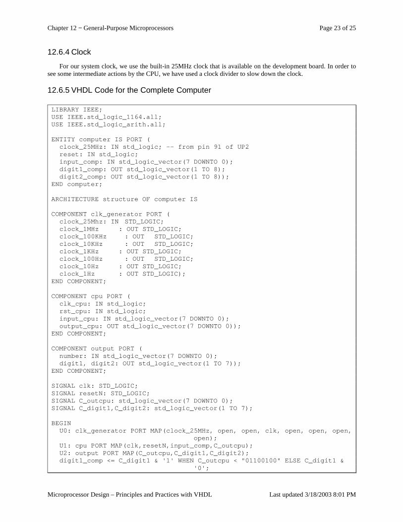
Chapter 12 − General-Purpose Microprocessors Page 23 of 25
Microprocessor Design – Principles and Practices with VHDL Last updated 3/18/2003 8:01 PM
12.6.4 Clock
For our system clock, we use the built-in 25MHz clock that is available on the development board. In order to see some intermediate actions by the CPU, we have used a clock divider to slow down the clock.
12.6.5 VHDL Code for the Complete Computer
LIBRARY IEEE;USE IEEE.std_logic_1164.all;USE IEEE.std_logic_arith.all;
ENTITY computer IS PORT (clock_25MHz: IN std_logic; -- from pin 91 of UP2reset: IN std_logic;input_comp: IN std_logic_vector(7 DOWNTO 0);digit1_comp: OUT std_logic_vector(1 TO 8);digit2_comp: OUT std_logic_vector(1 TO 8));
END computer;
ARCHITECTURE structure OF computer IS
COMPONENT clk_generator PORT (clock_25Mhz: IN STD_LOGIC;clock_1MHz : OUT STD_LOGIC;clock_100KHz : OUT STD_LOGIC;clock_10KHz : OUT STD_LOGIC;clock_1KHz : OUT STD_LOGIC;clock_100Hz : OUT STD_LOGIC;clock_10Hz : OUT STD_LOGIC;clock_1Hz : OUT STD_LOGIC);
END COMPONENT;
COMPONENT cpu PORT (clk_cpu: IN std_logic;rst_cpu: IN std_logic;input_cpu: IN std_logic_vector(7 DOWNTO 0);output_cpu: OUT std_logic_vector(7 DOWNTO 0));
END COMPONENT;
COMPONENT output PORT (number: IN std_logic_vector(7 DOWNTO 0);digit1, digit2: OUT std_logic_vector(1 TO 7));
END COMPONENT;
SIGNAL clk: STD_LOGIC;SIGNAL resetN: STD_LOGIC;SIGNAL C_outcpu: std_logic_vector(7 DOWNTO 0);SIGNAL C_digit1,C_digit2: std_logic_vector(1 TO 7);
BEGINU0: clk_generator PORT MAP(clock_25MHz, open, open, clk, open, open, open,
open);U1: cpu PORT MAP(clk,resetN,input_comp,C_outcpu);U2: output PORT MAP(C_outcpu,C_digit1,C_digit2);digit1_comp <= C_digit1 & '1' WHEN C_outcpu < "01100100" ELSE C_digit1 &
'0';
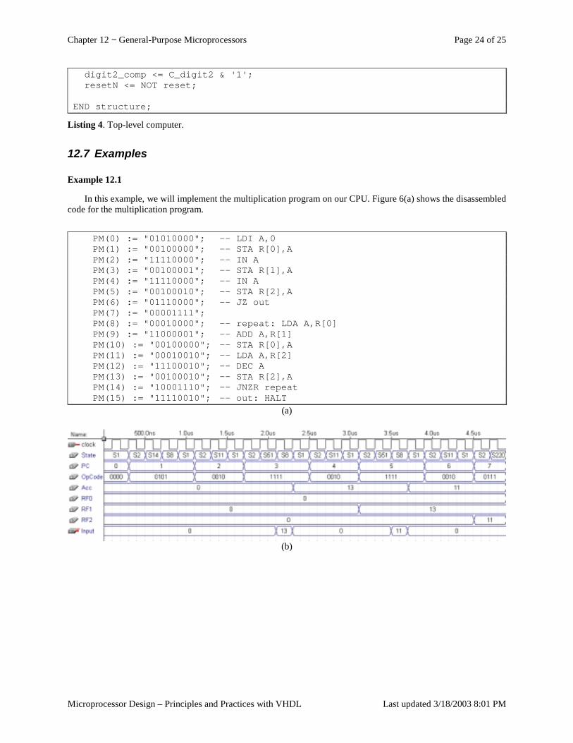
Chapter 12 − General-Purpose Microprocessors Page 24 of 25
Microprocessor Design – Principles and Practices with VHDL Last updated 3/18/2003 8:01 PM
digit2_comp <= C_digit2 & '1';resetN <= NOT reset;
END structure;
Listing 4. Top-level computer.
12.7 Examples
Example 12.1
In this example, we will implement the multiplication program on our CPU. Figure 6(a) shows the disassembled code for the multiplication program.
PM(0) := "01010000"; -- LDI A,0PM(1) := "00100000"; -- STA R[0],APM(2) := "11110000"; -- IN APM(3) := "00100001"; -- STA R[1],APM(4) := "11110000"; -- IN APM(5) := "00100010"; -- STA R[2],APM(6) := "01110000"; -- JZ outPM(7) := "00001111";PM(8) := "00010000"; -- repeat: LDA A,R[0]PM(9) := "11000001"; -- ADD A,R[1]PM(10) := "00100000"; -- STA R[0],APM(11) := "00010010"; -- LDA A,R[2]PM(12) := "11100010"; -- DEC APM(13) := "00100010"; -- STA R[2],APM(14) := "10001110"; -- JNZR repeatPM(15) := "11110010"; -- out: HALT
(a)
(b)
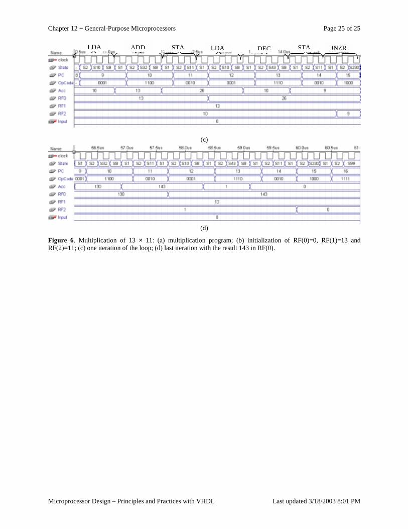
Chapter 12 − General-Purpose Microprocessors Page 25 of 25
Microprocessor Design – Principles and Practices with VHDL Last updated 3/18/2003 8:01 PM
(c)
(d)
Figure 6. Multiplication of 13 × 11: (a) multiplication program; (b) initialization of RF(0)=0, RF(1)=13 and RF(2)=11; (c) one iteration of the loop; (d) last iteration with the result 143 in RF(0).
LDA ADD STA LDA DEC STA JNZR
Appendix A − VHDL Summary Page 1 of 21
Principles of Digital Logic Design Enoch Hwang Last updated 3/5/2003 5:22 PM
Appendix A VHDL Summary ............................................................................................................................... 2 A.1 Basic Language Elements ............................................................................................................................. 2
A.1.1 Comments ............................................................................................................................................. 2 A.1.2 Identifiers .............................................................................................................................................. 2 A.1.3 Data Objects.......................................................................................................................................... 2 A.1.4 Data Types ............................................................................................................................................ 2 A.1.5 Data Operators ...................................................................................................................................... 4 A.1.6 ENTITY ................................................................................................................................................ 5 A.1.7 ARCHITECTURE ................................................................................................................................ 6 A.1.8 PACKAGE............................................................................................................................................ 7
A.2 Dataflow Model Concurrent Statements ....................................................................................................... 8 A.2.1 Concurrent Signal Assignment.............................................................................................................. 8 A.2.2 Conditional Signal Assignment............................................................................................................. 9 A.2.3 Selected Signal Assignment .................................................................................................................. 9 A.2.4 Dataflow Model Example ................................................................................................................... 10
A.3 Behavioral Model Sequential Statements.................................................................................................... 10 A.3.1 PROCESS ........................................................................................................................................... 10 A.3.2 Sequential Signal Assignment............................................................................................................. 10 A.3.3 Variable Assignment ........................................................................................................................... 11 A.3.4 WAIT .................................................................................................................................................. 11 A.3.5 IF THEN ELSE................................................................................................................................... 11 A.3.6 CASE .................................................................................................................................................. 12 A.3.7 NULL.................................................................................................................................................. 12 A.3.8 FOR..................................................................................................................................................... 12 A.3.9 WHILE................................................................................................................................................ 13 A.3.10 LOOP .................................................................................................................................................. 13 A.3.11 EXIT ................................................................................................................................................... 13 A.3.12 NEXT.................................................................................................................................................. 13 A.3.13 FUNCTION ........................................................................................................................................ 13 A.3.14 PROCEDURE..................................................................................................................................... 14 A.3.15 Behavioral Model Example................................................................................................................. 15
A.4 Structural Model Statements ....................................................................................................................... 16 A.4.1 COMPONENT Declaration ................................................................................................................ 16 A.4.2 PORT MAP......................................................................................................................................... 16 A.4.3 OPEN .................................................................................................................................................. 17 A.4.4 GENERATE........................................................................................................................................ 17 A.4.5 Structural Model Example .................................................................................................................. 17
A.5 Conversion Routines ................................................................................................................................... 18 A.5.1 CONV_INTEGER()............................................................................................................................ 18 A.5.2 CONV_STD_LOGIC_VECTOR(,) .................................................................................................... 19
Index ....................................................................................................................................................................... 20

Appendix A − VHDL Summary Page 2 of 21
Principles of Digital Logic Design Enoch Hwang Last updated 3/5/2003 5:22 PM
Appendix A VHDL Summary
VHDL is a hardware description language for modeling digital circuits that can range from simple connection of gates to complex systems. VHDL is an acronym for VHSIC Hardware Description Language, and VHSIC in turn is an acronym for Very High Speed Integrated Circuits. This appendix gives a brief summary of the basic VHDL elements and its syntax. Many advance features of the language are omitted. Interested readers should refer to other references for detail coverage.
A.1 Basic Language Elements
A.1.1 Comments
Comments are preceded by two consecutive hyphens ( -- ) and are terminated at the end of the line.
Example:
-- This is a comment
A.1.2 Identifiers
VHDL identifier syntax: • A sequence of one or more upper case letters, lower case letters, digits, and the underscore. • Upper and lower case letters are treated the same, i.e. case insensitive. • The first character must be a letter. • The last character cannot be the underscore. • Two underscores cannot be together.
A.1.3 Data Objects
There are three kinds of data objects: signals, variables, and constants.
The data object SIGNAL represents logic signals on a wire in the circuit. A signal does not have memory, thus, if the source of the signal is removed, the signal will not have a value.
A VARIABLE object remembers its content and is used for computations in a behavioral model.
A CONSTANT object must be initialized with a value when declared and this value cannot be changed.
Example:
SIGNAL x: BIT;VARIABLE y: INTEGER;CONSTANT one: STD_LOGIC_VECTOR(3 DOWNTO 0) := "0001";
A.1.4 Data Types
BIT and BIT_VECTOR
The BIT and BIT_VECTOR types are predefined in VHDL. Objects of these types can have the values ‘0’ or ‘1’. The BIT_VECTOR type is simply a vector of type BIT.
Example:
SIGNAL x: BIT;SIGNAL y: BIT_VECTOR(7 DOWNTO 0);
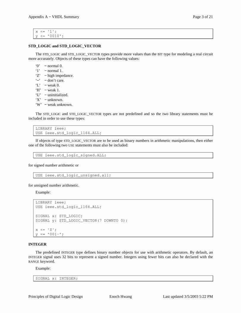
Appendix A − VHDL Summary Page 3 of 21
Principles of Digital Logic Design Enoch Hwang Last updated 3/5/2003 5:22 PM
x <= '1';y <= "0010";
STD_LOGIC and STD_LOGIC_VECTOR
The STD_LOGIC and STD_LOGIC_VECTOR types provide more values than the BIT type for modeling a real circuit more accurately. Objects of these types can have the following values:
‘0’ − normal 0. ‘1’ − normal 1. ‘Z’ − high impedance. ‘−’ − don’t care. ‘L’ − weak 0. ‘H’ − weak 1. ‘U’ − uninitialized. ‘X’ − unknown. ‘W’ − weak unknown.
The STD_LOGIC and STD_LOGIC_VECTOR types are not predefined and so the two library statements must be included in order to use these types:
LIBRARY ieee;USE ieee.std_logic_1164.ALL;
If objects of type STD_LOGIC_VECTOR are to be used as binary numbers in arithmetic manipulations, then either one of the following two USE statements must also be included:
USE ieee.std_logic_signed.ALL;
for signed number arithmetic or
USE ieee.std_logic_unsigned.all;
for unsigned number arithmetic.
Example:
LIBRARY ieee;USE ieee.std_logic_1164.ALL;
SIGNAL x: STD_LOGIC;SIGNAL y: STD_LOGIC_VECTOR(7 DOWNTO 0);
x <= 'Z';y <= "001-";
INTEGER
The predefined INTEGER type defines binary number objects for use with arithmetic operators. By default, an INTEGER signal uses 32 bits to represent a signed number. Integers using fewer bits can also be declared with the RANGE keyword.
Example:
SIGNAL x: INTEGER;
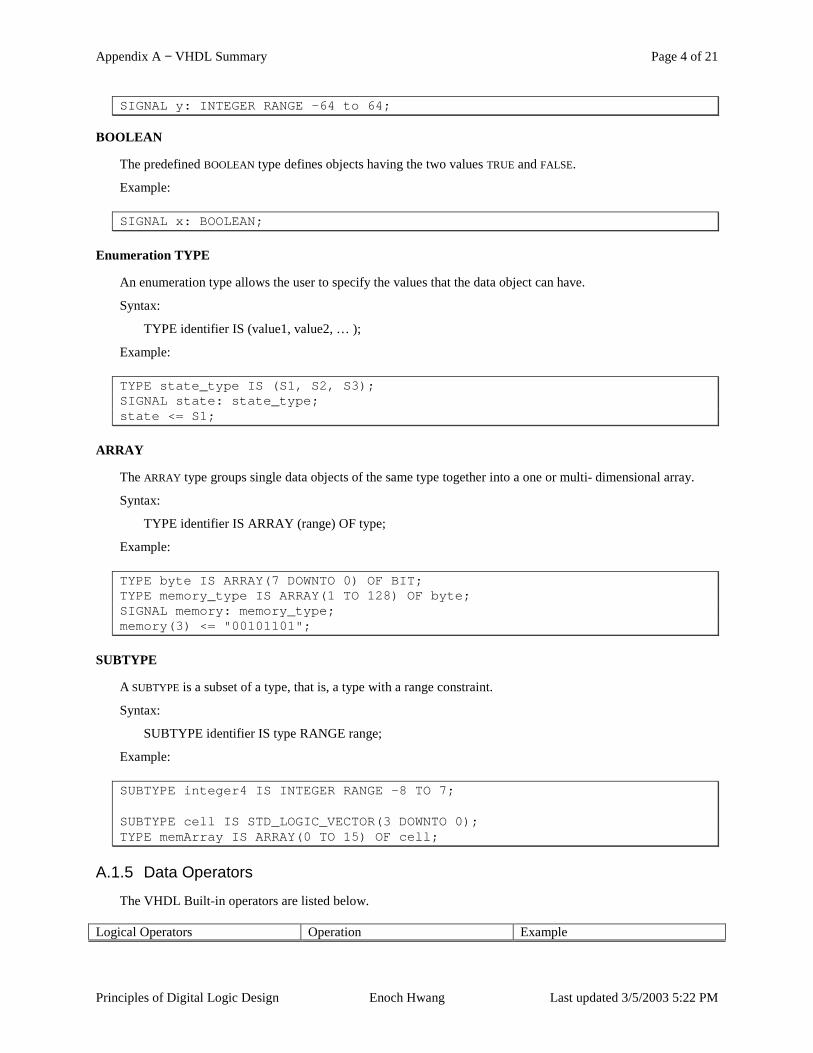
Appendix A − VHDL Summary Page 4 of 21
Principles of Digital Logic Design Enoch Hwang Last updated 3/5/2003 5:22 PM
SIGNAL y: INTEGER RANGE –64 to 64;
BOOLEAN
The predefined BOOLEAN type defines objects having the two values TRUE and FALSE.
Example:
SIGNAL x: BOOLEAN;
Enumeration TYPE
An enumeration type allows the user to specify the values that the data object can have.
Syntax:
TYPE identifier IS (value1, value2, … );
Example:
TYPE state_type IS (S1, S2, S3);SIGNAL state: state_type;state <= S1;
ARRAY
The ARRAY type groups single data objects of the same type together into a one or multi- dimensional array.
Syntax:
TYPE identifier IS ARRAY (range) OF type;
Example:
TYPE byte IS ARRAY(7 DOWNTO 0) OF BIT;TYPE memory_type IS ARRAY(1 TO 128) OF byte;SIGNAL memory: memory_type;memory(3) <= "00101101";
SUBTYPE
A SUBTYPE is a subset of a type, that is, a type with a range constraint.
Syntax:
SUBTYPE identifier IS type RANGE range;
Example:
SUBTYPE integer4 IS INTEGER RANGE –8 TO 7;
SUBTYPE cell IS STD_LOGIC_VECTOR(3 DOWNTO 0);TYPE memArray IS ARRAY(0 TO 15) OF cell;
A.1.5 Data Operators
The VHDL Built-in operators are listed below.
Logical Operators Operation Example
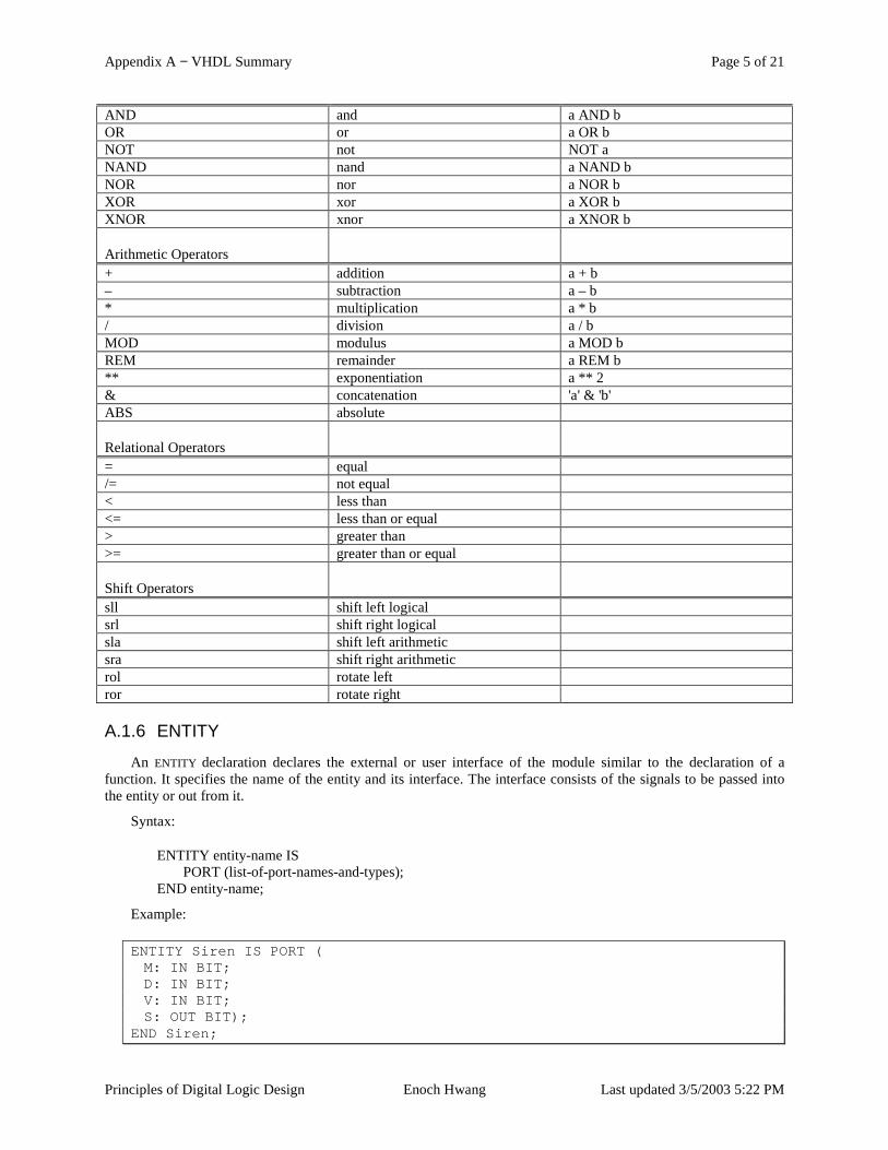
Appendix A − VHDL Summary Page 5 of 21
Principles of Digital Logic Design Enoch Hwang Last updated 3/5/2003 5:22 PM
AND and a AND b OR or a OR b NOT not NOT a NAND nand a NAND b NOR nor a NOR b XOR xor a XOR b XNOR xnor a XNOR b
Arithmetic Operators
+ addition a + b – subtraction a – b * multiplication a * b / division a / b MOD modulus a MOD b REM remainder a REM b ** exponentiation a ** 2 & concatenation 'a' & 'b' ABS absolute
Relational Operators
= equal /= not equal < less than <= less than or equal > greater than >= greater than or equal
Shift Operators
sll shift left logical srl shift right logical sla shift left arithmetic sra shift right arithmetic rol rotate left ror rotate right
A.1.6 ENTITY
An ENTITY declaration declares the external or user interface of the module similar to the declaration of a function. It specifies the name of the entity and its interface. The interface consists of the signals to be passed into the entity or out from it.
Syntax:
ENTITY entity-name IS PORT (list-of-port-names-and-types); END entity-name;
Example:
ENTITY Siren IS PORT (M: IN BIT;D: IN BIT;V: IN BIT;S: OUT BIT);
END Siren;
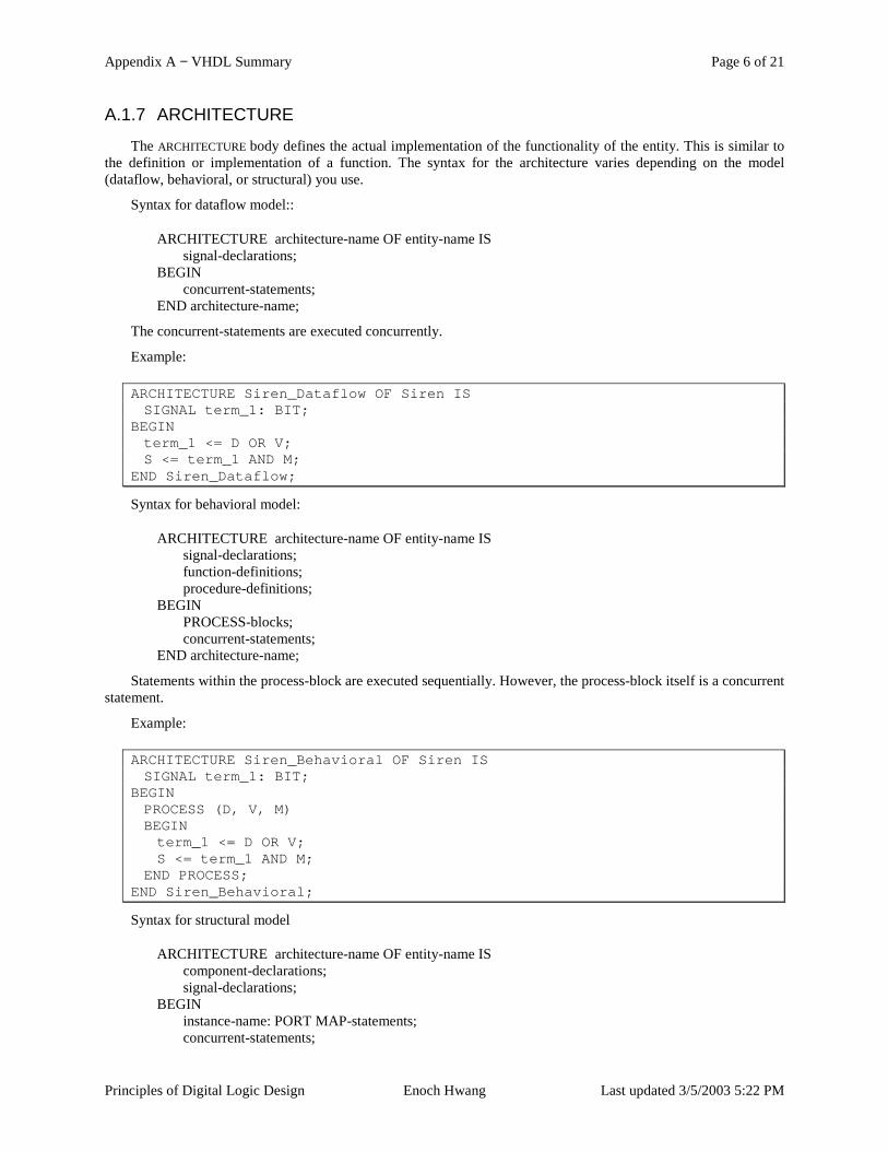
Appendix A − VHDL Summary Page 6 of 21
Principles of Digital Logic Design Enoch Hwang Last updated 3/5/2003 5:22 PM
A.1.7 ARCHITECTURE
The ARCHITECTURE body defines the actual implementation of the functionality of the entity. This is similar to the definition or implementation of a function. The syntax for the architecture varies depending on the model (dataflow, behavioral, or structural) you use.
Syntax for dataflow model::
ARCHITECTURE architecture-name OF entity-name IS signal-declarations; BEGIN concurrent-statements; END architecture-name;
The concurrent-statements are executed concurrently.
Example:
ARCHITECTURE Siren_Dataflow OF Siren ISSIGNAL term_1: BIT;
BEGINterm_1 <= D OR V;S <= term_1 AND M;
END Siren_Dataflow;
Syntax for behavioral model:
ARCHITECTURE architecture-name OF entity-name IS signal-declarations; function-definitions; procedure-definitions; BEGIN PROCESS-blocks; concurrent-statements; END architecture-name;
Statements within the process-block are executed sequentially. However, the process-block itself is a concurrent statement.
Example:
ARCHITECTURE Siren_Behavioral OF Siren ISSIGNAL term_1: BIT;
BEGINPROCESS (D, V, M)BEGINterm_1 <= D OR V;S <= term_1 AND M;
END PROCESS;END Siren_Behavioral;
Syntax for structural model
ARCHITECTURE architecture-name OF entity-name IS component-declarations; signal-declarations; BEGIN instance-name: PORT MAP-statements; concurrent-statements;
Appendix A − VHDL Summary Page 7 of 21
Principles of Digital Logic Design Enoch Hwang Last updated 3/5/2003 5:22 PM
END architecture-name;
For each component declaration used, there must be a corresponding entity and architecture for that component. The PORT MAP statements are concurrent statements.
Example:
ARCHITECTURE Siren_Structural OF Siren ISCOMPONENT myOR PORT (in1, in2: IN BIT;out1: OUT BIT);
END COMPONENT;
SIGNAL term1: BIT;
BEGINU0: myOR PORT MAP (D, V, term1);S <= term1 AND M;
END Siren_Structural;
A.1.8 PACKAGE
A PACKAGE provides a mechanism to group together and share declarations that are used by several entity units. A package itself includes a declaration and, optionally, a body. The package declaration and body are usually stored together in a separate file from the rest of the design units. The file name given for this file must be the same as the package name. In order for the complete design to synthesize correctly using MAX+PLUS II, you must first synthesize the package as a separate unit. After that you can synthesize the unit that uses that package.
PACKAGE Declaration and Body
The PACKAGE declaration contains declarations that may be shared between different entity units. It provides the interface, that is, items that are visible to the other entity units. The optional PACKAGE BODY contains the implementations of the functions and procedures that are declared in the PACKAGE declaration.
Syntax for PACKAGE declaration:
PACKAGE package-name IS type-declarations; subtype-declarations; signal-declarations; variable-declarations; constant-declarations; component-declarations; function-declarations; procedure-declarations; END package-name;
Syntax for PACKAGE body:
PACKAGE BODY package-name IS function-definitions; -- for functions declared in the package declaration procedure-definitions; -- for procedures declared in the package declaration END package-name;
Example:
LIBRARY ieee;USE ieee.std_logic_1164.ALL;
Appendix A − VHDL Summary Page 8 of 21
Principles of Digital Logic Design Enoch Hwang Last updated 3/5/2003 5:22 PM
PACKAGE my_package ISSUBTYPE bit4 IS std_logic_vector(3 DOWNTO 0);FUNCTION Shiftright (input: IN bit4) RETURN bit4; -- declare a functionSIGNAL mysignal: bit4; -- a global signal
END my_package;
PACKAGE BODY my_package IS-- implementation of the Shiftright functionFUNCTION Shiftright (input: IN bit4) RETURN bit4 ISBEGINRETURN '0' & input(3 DOWNTO 1);
END shiftright;END my_package;
Using a PACKAGE
To use a package, you simply include a LIBRARY and USE statement for that package. Before synthesizing the module that uses the package, you need to first synthesize the package by itself as a top-level entity.
Syntax:
LIBRARY WORK; USE WORK.package-name.ALL;
Example:
LIBRARY work;USE work.my_package.ALL;
ENTITY test_package IS PORT (x: IN bit4;z: OUT bit4);
END test_package;
ARCHITECTURE Behavioral OF test_package ISBEGINmysignal <= x;z <= Shiftright(mysignal);
END Behavioral;
A.2 Dataflow Model Concurrent Statements Concurrent statements used in the dataflow model are executed concurrently. Hence, the ordering of these
statements does not affect the resulting output.
A.2.1 Concurrent Signal Assignment
Assigns a value or the result of evaluating an expression to a signal. This statement is executed whenever a signal in its expression changes value. However, the actual assignment of the value to the signal takes place after a certain delay and not instantaneously as for variable assignments.
Syntax:
signal <= expression;
Example:
Appendix A − VHDL Summary Page 9 of 21
Principles of Digital Logic Design Enoch Hwang Last updated 3/5/2003 5:22 PM
y <= '1';z <= y AND (NOT x);
A.2.2 Conditional Signal Assignment
Selects one of several different values to assign to a signal based on different conditions. This statement is executed whenever a signal in any one of the value or condition changes.
Syntax:
signal <= value1 WHEN condition ELSE value2 WHEN condition ELSE … value3;
Example:
z <= in0 WHEN sel = "00" ELSEin1 WHEN sel = "01" ELSEin2 WHEN sel = "10" ELSEin3;
A.2.3 Selected Signal Assignment
Selects one of several different values to assign to a signal based on the value of a select expression. This statement is executed whenever a signal in the expression or any one of the value changes.
Syntax:
WITH expression SELECT signal <= value1 WHEN choice1, value2 WHEN choice2 | choice3, … value4 WHEN choice4;
All possible choices for the expression must be given. The keyword OTHERS can be used to denote all remaining choices.
Example:
WITH sel SELECTz <= in0 WHEN "00",
in1 WHEN "01",in2 WHEN "10",in3 WHEN OTHERS;
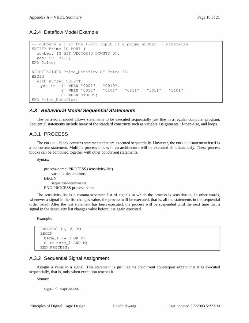
Appendix A − VHDL Summary Page 10 of 21
Principles of Digital Logic Design Enoch Hwang Last updated 3/5/2003 5:22 PM
A.2.4 Dataflow Model Example
-- outputs a 1 if the 4-bit input is a prime number, 0 otherwiseENTITY Prime IS PORT (
number: IN BIT_VECTOR(3 DOWNTO 0);yes: OUT BIT);
END Prime;
ARCHITECTURE Prime_Dataflow OF Prime ISBEGIN
WITH number SELECTyes <= '1' WHEN "0001" | "0010",
'1' WHEN "0011" | "0101" | "0111" | "1011" | "1101",'0' WHEN OTHERS;
END Prime_Dataflow;
A.3 Behavioral Model Sequential Statements The behavioral model allows statements to be executed sequentially just like in a regular computer program.
Sequential statements include many of the standard constructs such as variable assignments, if-then-else, and loops.
A.3.1 PROCESS
The PROCESS block contains statements that are executed sequentially. However, the PROCESS statement itself is a concurrent statement. Multiple process blocks in an architecture will be executed simultaneously. These process blocks can be combined together with other concurrent statements.
Syntax:
process-name: PROCESS (sensitivity-list) variable-declarations; BEGIN sequential-statements; END PROCESS process-name;
The sensitivity-list is a comma-separated list of signals in which the process is sensitive to. In other words, whenever a signal in the list changes value, the process will be executed, that is, all the statements in the sequential order listed. After the last statement has been executed, the process will be suspended until the next time that a signal in the sensitivity list changes value before it is again executed.
Example:
PROCESS (D, V, M)BEGINterm_1 <= D OR V;S <= term_1 AND M;
END PROCESS;
A.3.2 Sequential Signal Assignment
Assigns a value to a signal. This statement is just like its concurrent counterpart except that it is executed sequentially, that is, only when execution reaches it.
Syntax:
signal <= expression;
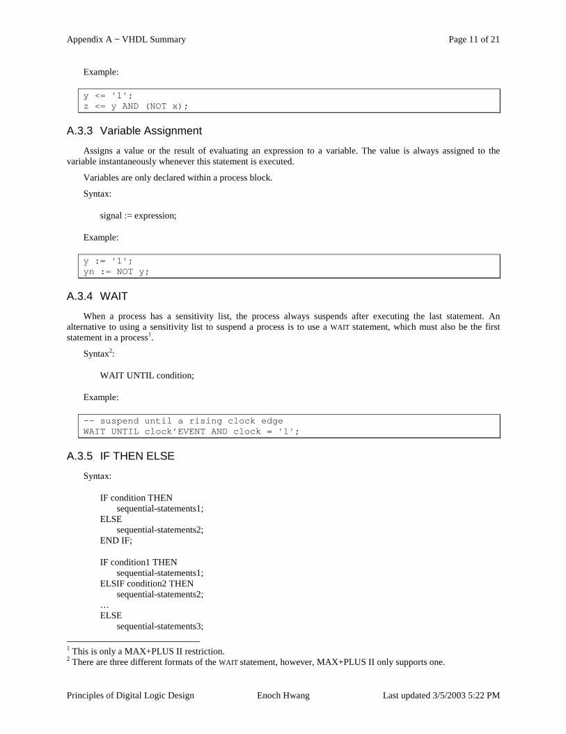
Appendix A − VHDL Summary Page 11 of 21
Principles of Digital Logic Design Enoch Hwang Last updated 3/5/2003 5:22 PM
Example:
y <= '1';z <= y AND (NOT x);
A.3.3 Variable Assignment
Assigns a value or the result of evaluating an expression to a variable. The value is always assigned to the variable instantaneously whenever this statement is executed.
Variables are only declared within a process block.
Syntax:
signal := expression;
Example:
y := '1';yn := NOT y;
A.3.4 WAIT
When a process has a sensitivity list, the process always suspends after executing the last statement. An alternative to using a sensitivity list to suspend a process is to use a WAIT statement, which must also be the first statement in a process1.
Syntax2:
WAIT UNTIL condition;
Example:
-- suspend until a rising clock edgeWAIT UNTIL clock’EVENT AND clock = '1';
A.3.5 IF THEN ELSE
Syntax:
IF condition THEN sequential-statements1; ELSE sequential-statements2; END IF;
IF condition1 THEN sequential-statements1; ELSIF condition2 THEN sequential-statements2; … ELSE sequential-statements3;
1 This is only a MAX+PLUS II restriction. 2 There are three different formats of the WAIT statement, however, MAX+PLUS II only supports one.
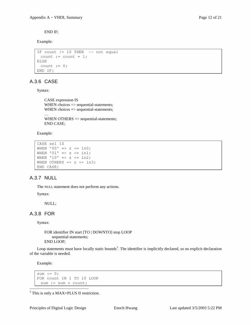
Appendix A − VHDL Summary Page 12 of 21
Principles of Digital Logic Design Enoch Hwang Last updated 3/5/2003 5:22 PM
END IF;
Example:
IF count /= 10 THEN -- not equalcount := count + 1;
ELSEcount := 0;
END IF;
A.3.6 CASE
Syntax:
CASE expression IS WHEN choices => sequential-statements; WHEN choices => sequential-statements; … WHEN OTHERS => sequential-statements; END CASE;
Example:
CASE sel ISWHEN "00" => z <= in0;WHEN "01" => z <= in1;WHEN "10" => z <= in2;WHEN OTHERS => z <= in3;END CASE;
A.3.7 NULL
The NULL statement does not perform any actions.
Syntax:
NULL;
A.3.8 FOR
Syntax:
FOR identifier IN start [TO | DOWNTO] stop LOOP sequential-statements; END LOOP;
Loop statements must have locally static bounds3. The identifier is implicitly declared, so no explicit declaration of the variable is needed.
Example:
sum := 0;FOR count IN 1 TO 10 LOOPsum := sum + count;
3 This is only a MAX+PLUS II restriction.
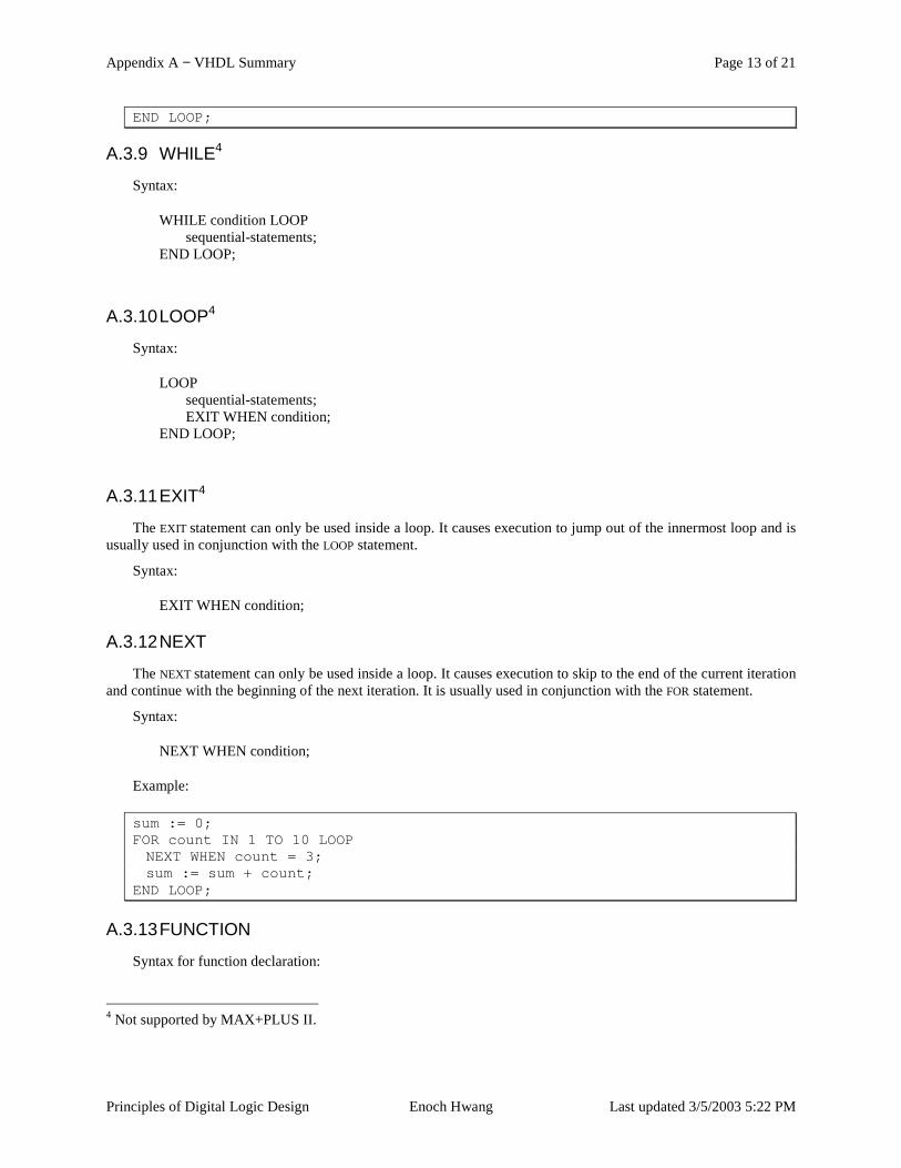
Appendix A − VHDL Summary Page 13 of 21
Principles of Digital Logic Design Enoch Hwang Last updated 3/5/2003 5:22 PM
END LOOP;
A.3.9 WHILE4
Syntax:
WHILE condition LOOP sequential-statements; END LOOP;
A.3.10 LOOP4
Syntax:
LOOP sequential-statements; EXIT WHEN condition; END LOOP;
A.3.11 EXIT4
The EXIT statement can only be used inside a loop. It causes execution to jump out of the innermost loop and is usually used in conjunction with the LOOP statement.
Syntax:
EXIT WHEN condition;
A.3.12 NEXT
The NEXT statement can only be used inside a loop. It causes execution to skip to the end of the current iteration and continue with the beginning of the next iteration. It is usually used in conjunction with the FOR statement.
Syntax:
NEXT WHEN condition;
Example:
sum := 0;FOR count IN 1 TO 10 LOOPNEXT WHEN count = 3;sum := sum + count;
END LOOP;
A.3.13 FUNCTION
Syntax for function declaration:
4 Not supported by MAX+PLUS II.
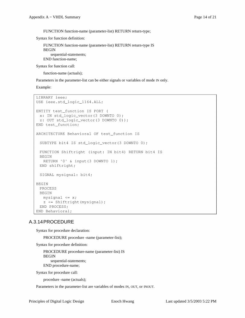
Appendix A − VHDL Summary Page 14 of 21
Principles of Digital Logic Design Enoch Hwang Last updated 3/5/2003 5:22 PM
FUNCTION function-name (parameter-list) RETURN return-type;
Syntax for function definition:
FUNCTION function-name (parameter-list) RETURN return-type IS BEGIN sequential-statements; END function-name;
Syntax for function call:
function-name (actuals);
Parameters in the parameter-list can be either signals or variables of mode IN only.
Example:
LIBRARY ieee;USE ieee.std_logic_1164.ALL;
ENTITY test_function IS PORT (x: IN std_logic_vector(3 DOWNTO 0);z: OUT std_logic_vector(3 DOWNTO 0));
END test_function;
ARCHITECTURE Behavioral OF test_function IS
SUBTYPE bit4 IS std_logic_vector(3 DOWNTO 0);
FUNCTION Shiftright (input: IN bit4) RETURN bit4 ISBEGINRETURN '0' & input(3 DOWNTO 1);
END shiftright;
SIGNAL mysignal: bit4;
BEGINPROCESSBEGINmysignal <= x;z <= Shiftright(mysignal);
END PROCESS;END Behavioral;
A.3.14 PROCEDURE
Syntax for procedure declaration:
PROCEDURE procedure -name (parameter-list);
Syntax for procedure definition:
PROCEDURE procedure-name (parameter-list) IS BEGIN sequential-statements; END procedure-name;
Syntax for procedure call:
procedure -name (actuals);
Parameters in the parameter-list are variables of modes IN, OUT, or INOUT.
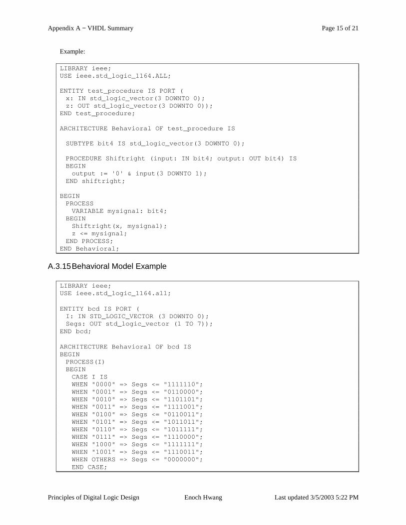
Appendix A − VHDL Summary Page 15 of 21
Principles of Digital Logic Design Enoch Hwang Last updated 3/5/2003 5:22 PM
Example:
LIBRARY ieee;USE ieee.std_logic_1164.ALL;
ENTITY test_procedure IS PORT (x: IN std_logic_vector(3 DOWNTO 0);z: OUT std_logic_vector(3 DOWNTO 0));
END test_procedure;
ARCHITECTURE Behavioral OF test_procedure IS
SUBTYPE bit4 IS std_logic_vector(3 DOWNTO 0);
PROCEDURE Shiftright (input: IN bit4; output: OUT bit4) ISBEGINoutput := '0' & input(3 DOWNTO 1);
END shiftright;
BEGINPROCESSVARIABLE mysignal: bit4;
BEGINShiftright(x, mysignal);z <= mysignal;
END PROCESS;END Behavioral;
A.3.15 Behavioral Model Example
LIBRARY ieee;USE ieee.std_logic_1164.all;
ENTITY bcd IS PORT (I: IN STD_LOGIC_VECTOR (3 DOWNTO 0);Segs: OUT std_logic_vector (1 TO 7));
END bcd;
ARCHITECTURE Behavioral OF bcd ISBEGINPROCESS(I)BEGINCASE I ISWHEN "0000" => Segs <= "1111110";WHEN "0001" => Segs <= "0110000";WHEN "0010" => Segs <= "1101101";WHEN "0011" => Segs <= "1111001";WHEN "0100" => Segs <= "0110011";WHEN "0101" => Segs <= "1011011";WHEN "0110" => Segs <= "1011111";WHEN "0111" => Segs <= "1110000";WHEN "1000" => Segs <= "1111111";WHEN "1001" => Segs <= "1110011";WHEN OTHERS => Segs <= "0000000";END CASE;
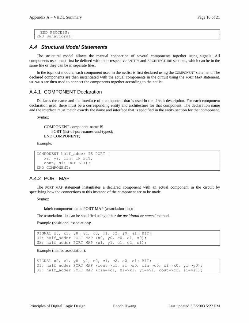
Appendix A − VHDL Summary Page 16 of 21
Principles of Digital Logic Design Enoch Hwang Last updated 3/5/2003 5:22 PM
END PROCESS;END Behavioral;
A.4 Structural Model Statements The structural model allows the manual connection of several components together using signals. All
components used must first be defined with their respective ENTITY and ARCHITECTURE sections, which can be in the same file or they can be in separate files.
In the topmost module, each component used in the netlist is first declared using the COMPONENT statement. The declared components are then instantiated with the actual components in the circuit using the PORT MAP statement. SIGNALs are then used to connect the components together according to the netlist.
A.4.1 COMPONENT Declaration
Declares the name and the interface of a component that is used in the circuit description. For each component declaration used, there must be a corresponding entity and architecture for that component. The declaration name and the interface must match exactly the name and interface that is specified in the entity section for that component.
Syntax:
COMPONENT component-name IS PORT (list-of-port-names-and-types); END COMPONENT;
Example:
COMPONENT half_adder IS PORT (xi, yi, cin: IN BIT;cout, si: OUT BIT);
END COMPONENT;
A.4.2 PORT MAP
The PORT MAP statement instantiates a declared component with an actual component in the circuit by specifying how the connections to this instance of the component are to be made.
Syntax:
label: component-name PORT MAP (association-list);
The association-list can be specified using either the positional or named method.
Example (positional association):
SIGNAL x0, x1, y0, y1, c0, c1, c2, s0, s1: BIT;U1: half_adder PORT MAP (x0, y0, c0, c1, s0);U2: half_adder PORT MAP (x1, y1, c1, c2, s1);
Example (named association):
SIGNAL x0, x1, y0, y1, c0, c1, c2, s0, s1: BIT;U1: half_adder PORT MAP (cout=>c1, si=>s0, cin=>c0, xi=>x0, yi=>y0);U2: half_adder PORT MAP (cin=>c1, xi=>x1, yi=>y1, cout=>c2, si=>s1);
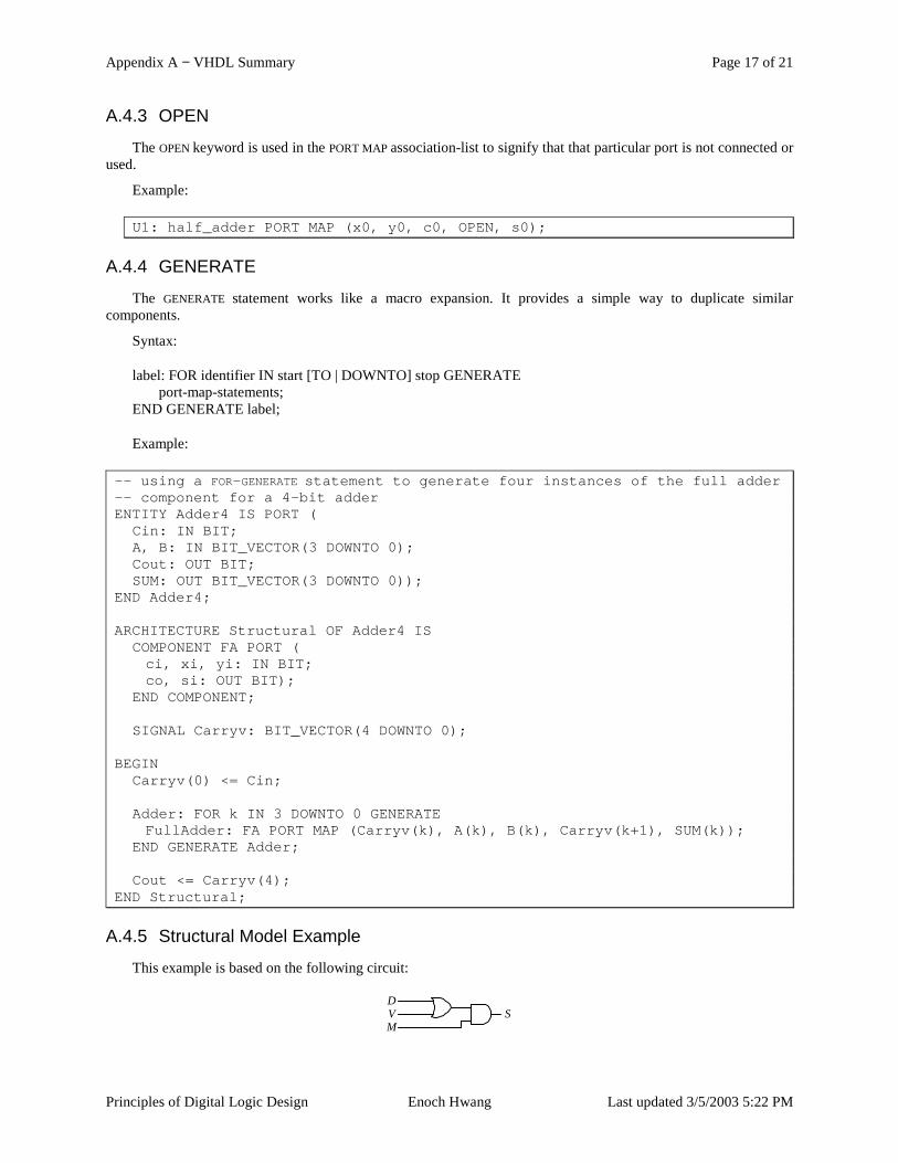
Appendix A − VHDL Summary Page 17 of 21
Principles of Digital Logic Design Enoch Hwang Last updated 3/5/2003 5:22 PM
A.4.3 OPEN
The OPEN keyword is used in the PORT MAP association-list to signify that that particular port is not connected or used.
Example:
U1: half_adder PORT MAP (x0, y0, c0, OPEN, s0);
A.4.4 GENERATE
The GENERATE statement works like a macro expansion. It provides a simple way to duplicate similar components.
Syntax:
label: FOR identifier IN start [TO | DOWNTO] stop GENERATE port-map-statements; END GENERATE label;
Example:
-- using a FOR-GENERATE statement to generate four instances of the full adder-- component for a 4-bit adderENTITY Adder4 IS PORT (
Cin: IN BIT;A, B: IN BIT_VECTOR(3 DOWNTO 0);Cout: OUT BIT;SUM: OUT BIT_VECTOR(3 DOWNTO 0));
END Adder4;
ARCHITECTURE Structural OF Adder4 ISCOMPONENT FA PORT (ci, xi, yi: IN BIT;co, si: OUT BIT);
END COMPONENT;
SIGNAL Carryv: BIT_VECTOR(4 DOWNTO 0);
BEGINCarryv(0) <= Cin;
Adder: FOR k IN 3 DOWNTO 0 GENERATEFullAdder: FA PORT MAP (Carryv(k), A(k), B(k), Carryv(k+1), SUM(k));
END GENERATE Adder;
Cout <= Carryv(4);END Structural;
A.4.5 Structural Model Example
This example is based on the following circuit:
D
MV S
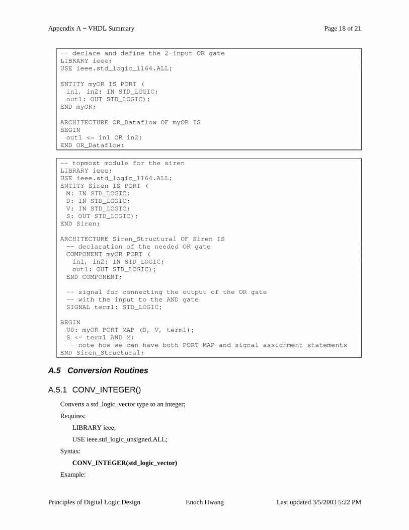
Appendix A − VHDL Summary Page 18 of 21
Principles of Digital Logic Design Enoch Hwang Last updated 3/5/2003 5:22 PM
-- declare and define the 2-input OR gateLIBRARY ieee;USE ieee.std_logic_1164.ALL;
ENTITY myOR IS PORT (in1, in2: IN STD_LOGIC;out1: OUT STD_LOGIC);
END myOR;
ARCHITECTURE OR_Dataflow OF myOR ISBEGINout1 <= in1 OR in2;
END OR_Dataflow;
-- topmost module for the sirenLIBRARY ieee;USE ieee.std_logic_1164.ALL;ENTITY Siren IS PORT (M: IN STD_LOGIC;D: IN STD_LOGIC;V: IN STD_LOGIC;S: OUT STD_LOGIC);
END Siren;
ARCHITECTURE Siren_Structural OF Siren IS-- declaration of the needed OR gateCOMPONENT myOR PORT (in1, in2: IN STD_LOGIC;out1: OUT STD_LOGIC);
END COMPONENT;
-- signal for connecting the output of the OR gate-- with the input to the AND gateSIGNAL term1: STD_LOGIC;
BEGINU0: myOR PORT MAP (D, V, term1);S <= term1 AND M;-- note how we can have both PORT MAP and signal assignment statements
END Siren_Structural;
A.5 Conversion Routines
A.5.1 CONV_INTEGER()
Converts a std_logic_vector type to an integer;
Requires:
LIBRARY ieee;
USE ieee.std_logic_unsigned.ALL;
Syntax:
CONV_INTEGER(std_logic_vector)
Example:

Appendix A − VHDL Summary Page 19 of 21
Principles of Digital Logic Design Enoch Hwang Last updated 3/5/2003 5:22 PM
LIBRARY ieee;USE ieee.std_logic_unsigned.ALL;
SIGNAL four_bit: STD_LOGIC_VECTOR(3 DOWNTO 0);SIGNAL n: INTEGER;
n := CONV_INTEGER(four_bit);
A.5.2 CONV_STD_LOGIC_VECTOR(,)
Converts an integer type to a std_logic_vector type.
Requires:
LIBRARY ieee;
USE ieee.std_logic_arith.ALL;
Syntax:
CONV_STD_LOGIC_VECTOR (integer, number_of_bits)
Example:
LIBRARY ieee;USE ieee.std_logic_arith.ALL;
SIGNAL four_bit: std_logic_vector(3 DOWNTO 0);SIGNAL n: INTEGER;
four_bit := CONV_STD_LOGIC_VECTOR(n, 4);
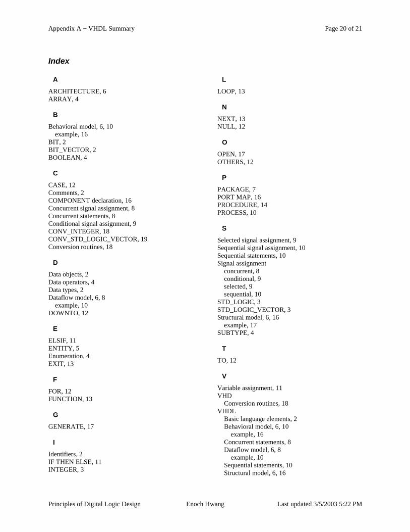
Appendix A − VHDL Summary Page 20 of 21
Principles of Digital Logic Design Enoch Hwang Last updated 3/5/2003 5:22 PM
Index
A
ARCHITECTURE, 6 ARRAY, 4
B
Behavioral model, 6, 10 example, 16
BIT, 2 BIT_VECTOR, 2 BOOLEAN, 4
C
CASE, 12 Comments, 2 COMPONENT declaration, 16 Concurrent signal assignment, 8 Concurrent statements, 8 Conditional signal assignment, 9 CONV_INTEGER, 18 CONV_STD_LOGIC_VECTOR, 19 Conversion routines, 18
D
Data objects, 2 Data operators, 4 Data types, 2 Dataflow model, 6, 8
example, 10 DOWNTO, 12
E
ELSIF, 11 ENTITY, 5 Enumeration, 4 EXIT, 13
F
FOR, 12 FUNCTION, 13
G
GENERATE, 17
I Identifiers, 2 IF THEN ELSE, 11 INTEGER, 3
L
LOOP, 13
N
NEXT, 13 NULL, 12
O
OPEN, 17 OTHERS, 12
P
PACKAGE, 7 PORT MAP, 16 PROCEDURE, 14 PROCESS, 10
S
Selected signal assignment, 9 Sequential signal assignment, 10 Sequential statements, 10 Signal assignment
concurrent, 8 conditional, 9 selected, 9 sequential, 10
STD_LOGIC, 3 STD_LOGIC_VECTOR, 3 Structural model, 6, 16
example, 17 SUBTYPE, 4
T
TO, 12
V
Variable assignment, 11 VHD
Conversion routines, 18 VHDL
Basic language elements, 2 Behavioral model, 6, 10
example, 16 Concurrent statements, 8 Dataflow model, 6, 8
example, 10 Sequential statements, 10 Structural model, 6, 16

Appendix A − VHDL Summary Page 21 of 21
Principles of Digital Logic Design Enoch Hwang Last updated 3/5/2003 5:22 PM
example, 17 VHDL syntax
ARCHITECTURE, 6 ARRAY, 4 BIT, 2 BIT_VECTOR, 2 BOOLEAN, 4 CASE, 12 Comments, 2 COMPONENT declaration, 16 CONV_INTEGER, 18 CONV_STD_LOGIC_VECTOR, 19 Data objects, 2 Data operators, 4 Data types, 2 DOWNTO, 12 ELSIF, 11 ENTITY, 5 Enumberation, 4 EXIT, 13 FOR, 12 FUNCTION, 13 GENERATE, 17 Identifiers, 2 IF THEN ELSE, 11 INTEGER, 3 LOOP, 13
NEXT, 13 NULL, 12 OPEN, 17 OTHERS, 12 PACKAGE, 7 PORT MAP, 16 PROCEDURE, 14 PROCESS, 10 Signal assignment
concurrent, 8 conditional, 9 selected, 9 sequential, 10
STD_LOGIC, 3 STD_LOGIC_VECTOR, 3 SUBTYPE, 4 TO, 12 Variable assignment, 11 WAIT, 11 WHEN, 12 WHILE, 13
W
WAIT, 11 WHEN, 12 WHILE, 13
Appendix B− MAX+plus II Tutorial Page 1 of 11
Principles of Digital Logic Design Enoch Hwang Last updated 2/19/2003 3:02 PM
Table of Content Table of Content ........................................................................................................................................................... 1 Appendix B MAX+plus II Tutorial ....................................................................................................................... 2
B.1 Creating a Project and Working with Files ................................................................................................... 2 B.1.1 Starting a new project............................................................................................................................ 2 B.1.2 Opening an existing project................................................................................................................... 3 B.1.3 Creating a project based on an existing VHDL source file ................................................................... 3 B.1.4 Importing existing VHDL source files into the project......................................................................... 3 B.1.5 Creating new VHDL source files for the project................................................................................... 3
B.2 Synthesis for functional simulation............................................................................................................... 4 B.2.1 Starting the compiler ............................................................................................................................. 4 B.2.2 Set up input signals ............................................................................................................................... 4 B.2.3 Set up and view simulation time range ................................................................................................. 6 B.2.4 Assign values to input signals ............................................................................................................... 6 B.2.5 Simulation ............................................................................................................................................. 8
B.3 Synthesis for programming the FPGA .......................................................................................................... 9 B.4 Programming the FPGA.............................................................................................................................. 10 B.5 References................................................................................................................................................... 11

Appendix B− MAX+plus II Tutorial Page 2 of 11
Principles of Digital Logic Design Enoch Hwang Last updated 2/19/2003 3:02 PM
Appendix B MAX+plus II Tutorial
This appendix contains instructions for using the MAX+plus II synthesis software and the UP2 development board by Altera. This package provides all the necessary tools for implementing and trying out all the examples, including building the final general microprocessor, mentioned in this book. A student edition version of the MAX+plus II software is included in the CD-ROM and can also be downloaded for free from www.altera.com. The hardware can be purchased directly from Altera. The full User Guide for using the UP2 board can be downloaded from http://www.altera.com/literature/univ/upds.pdf.
This tutorial assumes that you are familiar with working under the Windows’ environment.
The UP2 FPGA development board is shown in Figure 1. The following tutorial uses the FSM+D summation VHDL design presented in Section 8.3.
Figure 1. Altera’s UP1 FPGA development board.
B.1 Creating a Project and Working with Files
B.1.1 Starting a new project
1. Using Windows File Manager, create a new folder for your new project. Each new project should be placed in its own folder since the synthesizer creates many working files for a project.
2. From the MAX+plus II menu, select File | Project | Name or simply click on the icon . You will see the Project Name window as shown below.

Appendix B− MAX+plus II Tutorial Page 3 of 11
Principles of Digital Logic Design Enoch Hwang Last updated 2/19/2003 3:02 PM
3. In the box labeled Directories, move to the directory that you have created in step 1.
4. In the box labeled Project Name, type the name of your project. Note that the project name must be the same as the top-level entity name, which must also be the same as that file’s name.
5. Click OK.
B.1.2 Opening an existing project
1. From the MAX+plus II menu, select File | Project | Name or click on the icon . Select either the top-level entity VHDL source file (with the extension .vhd) or the top-level name project file (with the extension .pof) and clock OK.
B.1.3 Creating a project based on an existing VHDL source file
1. Alternatively you can open any VHDL entity source file using the menu commands File | Open. While the VHDL entity source file is in the active editor window, select File | Project | Set Project to Current File or click
on the icon to make that particular file the top-level project file.
B.1.4 Importing existing VHDL source files into the project
1. If you already have your VHDL source files, then you can just use Windows’ File Manager and simply copy all your VHDL source files into your project directory. Each entity can be stored in its own separate file. The name of the file where an entity is stored must be the same as the entity name.
2. If a source file is not opened in a text editor window, you can select File | Open and select the VHDL file that you want to view and / or edit.
B.1.5 Creating new VHDL source files for the project
1. If you need to type in a new VHDL source file, then you can do that using MAX+plus’ text editor. From the
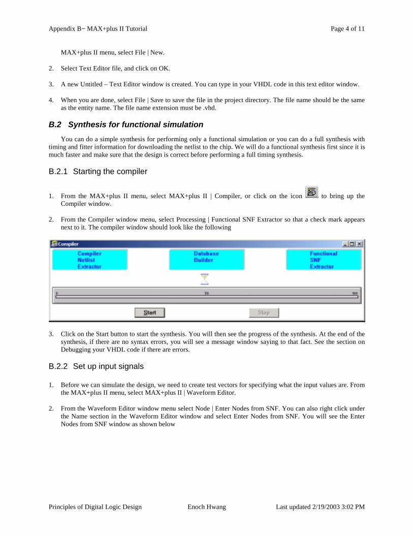
Appendix B− MAX+plus II Tutorial Page 4 of 11
Principles of Digital Logic Design Enoch Hwang Last updated 2/19/2003 3:02 PM
MAX+plus II menu, select File | New.
2. Select Text Editor file, and click on OK.
3. A new Untitled – Text Editor window is created. You can type in your VHDL code in this text editor window.
4. When you are done, select File | Save to save the file in the project directory. The file name should be the same as the entity name. The file name extension must be .vhd.
B.2 Synthesis for functional simulation You can do a simple synthesis for performing only a functional simulation or you can do a full synthesis with
timing and fitter information for downloading the netlist to the chip. We will do a functional synthesis first since it is much faster and make sure that the design is correct before performing a full timing synthesis.
B.2.1 Starting the compiler
1. From the MAX+plus II menu, select MAX+plus II | Compiler, or click on the icon to bring up the Compiler window.
2. From the Compiler window menu, select Processing | Functional SNF Extractor so that a check mark appears next to it. The compiler window should look like the following
3. Click on the Start button to start the synthesis. You will then see the progress of the synthesis. At the end of the synthesis, if there are no syntax errors, you will see a message window saying to that fact. See the section on Debugging your VHDL code if there are errors.
B.2.2 Set up input signals
1. Before we can simulate the design, we need to create test vectors for specifying what the input values are. From the MAX+plus II menu, select MAX+plus II | Waveform Editor.
2. From the Waveform Editor window menu select Node | Enter Nodes from SNF. You can also right click under the Name section in the Waveform Editor window and select Enter Nodes from SNF. You will see the Enter Nodes from SNF window as shown below

Appendix B− MAX+plus II Tutorial Page 5 of 11
Principles of Digital Logic Design Enoch Hwang Last updated 2/19/2003 3:02 PM
3. Click on the List button and a list of available nodes and groups will be displayed in the Available Nodes & Groups box.
4. Select the signals that you want to see in the simulation trace and click on the => button. The selected nodes will be moved to the Selected Nodes & Groups box. You can select multiple nodes together by holding down the Ctrl or Shift key while clicking on the signals.
5. Click on OK when you are finished. The selected signals will now be inserted in the Waveform Editor window as shown below. You can drag the vertical separator lines so that the whole signal name can be displayed.
6. To delete a signal, just select the signal by clicking on its name and press the Delete key.
7. You can arrange the ordering of the signals by dragging the signal icons like up or down.
8. For signals that are composed of a group of bits (such as the regfile RF), you can separate them into individual bits or change the radix for the displayed value by first selecting that signal and then right click the mouse. A drop down menu appears. Select Ungroup to separate the bits. Select Enter Group to change the radix or the displayed signal name. Signal bits that are separated can be regroup by first selecting all the signal bits that you want to regroup and then right click on the mouse and select Enter Group.
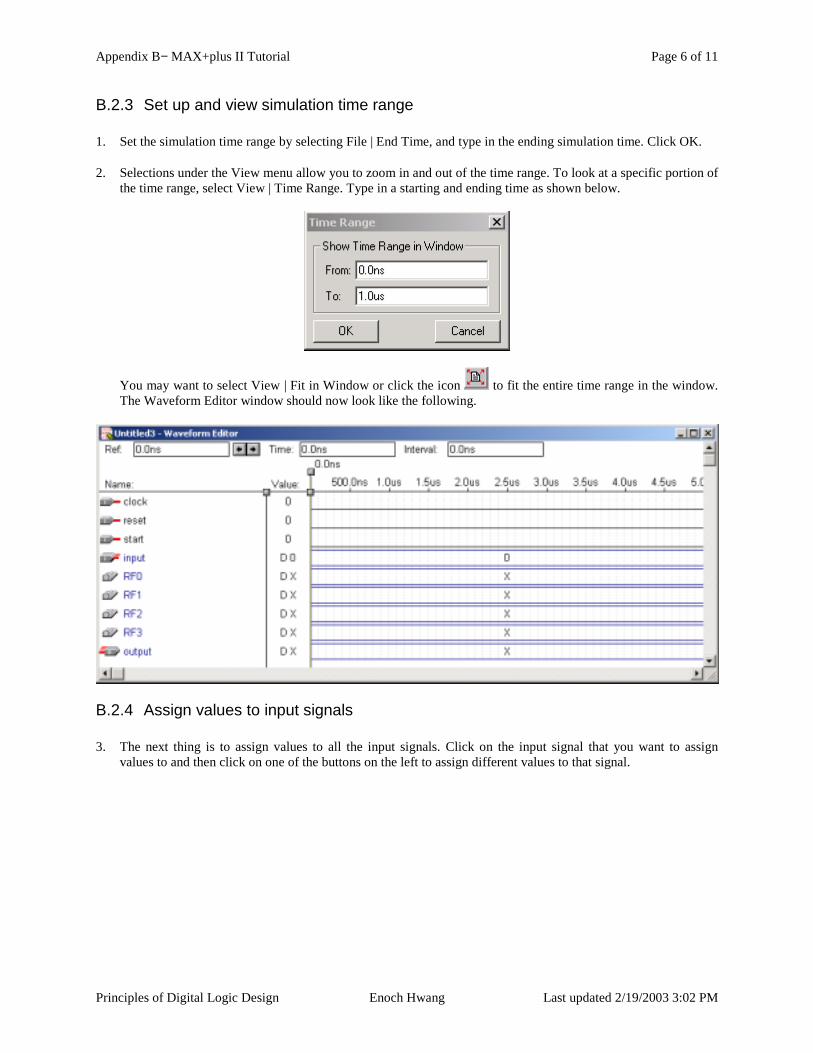
Appendix B− MAX+plus II Tutorial Page 6 of 11
Principles of Digital Logic Design Enoch Hwang Last updated 2/19/2003 3:02 PM
B.2.3 Set up and view simulation time range
1. Set the simulation time range by selecting File | End Time, and type in the ending simulation time. Click OK.
2. Selections under the View menu allow you to zoom in and out of the time range. To look at a specific portion of the time range, select View | Time Range. Type in a starting and ending time as shown below.
You may want to select View | Fit in Window or click the icon to fit the entire time range in the window. The Waveform Editor window should now look like the following.
B.2.4 Assign values to input signals
3. The next thing is to assign values to all the input signals. Click on the input signal that you want to assign values to and then click on one of the buttons on the left to assign different values to that signal.
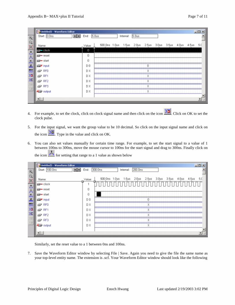
Appendix B− MAX+plus II Tutorial Page 7 of 11
Principles of Digital Logic Design Enoch Hwang Last updated 2/19/2003 3:02 PM
4. For example, to set the clock, click on clock signal name and then click on the icon . Click on OK to set the clock pulse.
5. For the input signal, we want the group value to be 10 decimal. So click on the input signal name and click on
the icon . Type in the value and click on OK.
6. You can also set values manually for certain time range. For example, to set the start signal to a value of 1 between 100ns to 300ns, move the mouse cursor to 100ns for the start signal and drag to 300ns. Finally click on
the icon for setting that range to a 1 value as shown below
Similarly, set the reset value to a 1 between 0ns and 100ns.
7. Save the Waveform Editor window by selecting File | Save. Again you need to give the file the same name as your top-level entity name. The extension is .scf. Your Waveform Editor window should look like the following
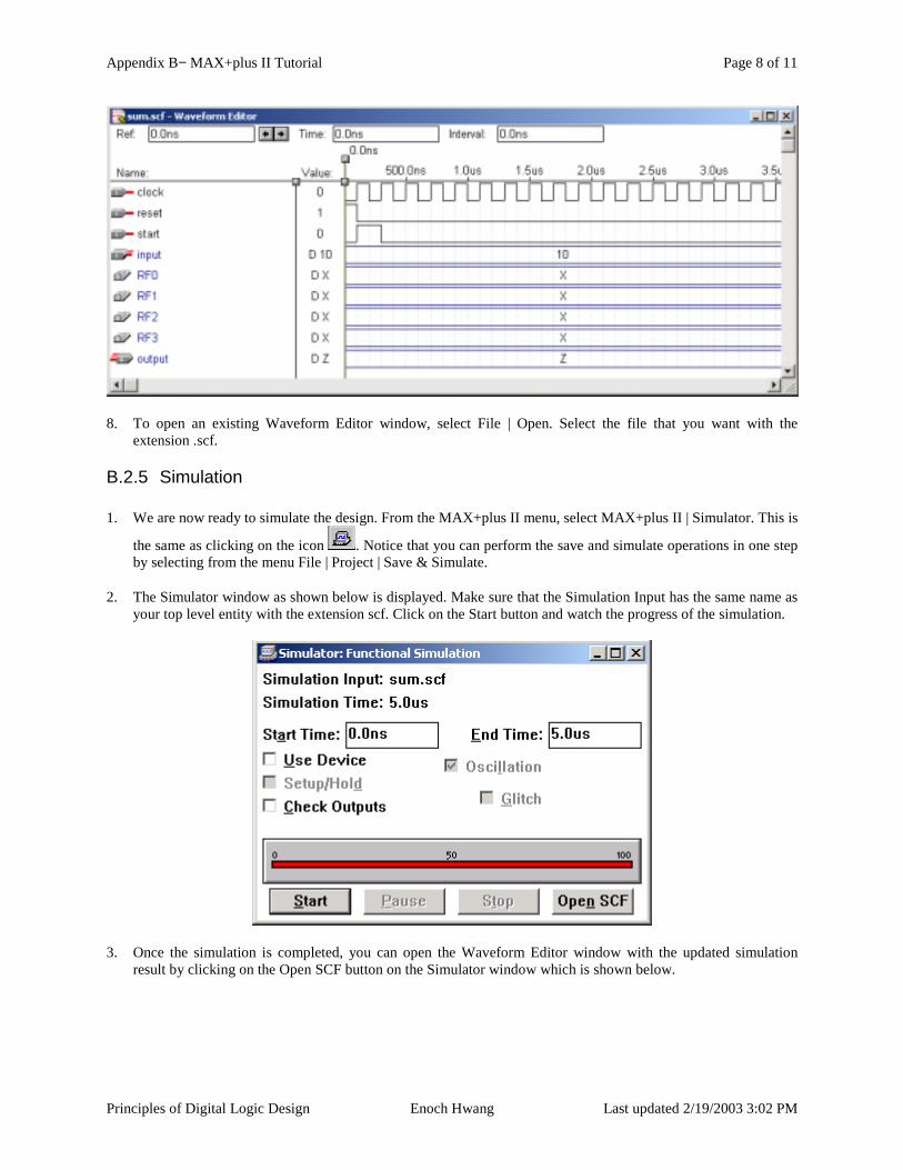
Appendix B− MAX+plus II Tutorial Page 8 of 11
Principles of Digital Logic Design Enoch Hwang Last updated 2/19/2003 3:02 PM
8. To open an existing Waveform Editor window, select File | Open. Select the file that you want with the extension .scf.
B.2.5 Simulation
1. We are now ready to simulate the design. From the MAX+plus II menu, select MAX+plus II | Simulator. This is
the same as clicking on the icon . Notice that you can perform the save and simulate operations in one step by selecting from the menu File | Project | Save & Simulate.
2. The Simulator window as shown below is displayed. Make sure that the Simulation Input has the same name as your top level entity with the extension scf. Click on the Start button and watch the progress of the simulation.
3. Once the simulation is completed, you can open the Waveform Editor window with the updated simulation result by clicking on the Open SCF button on the Simulator window which is shown below.
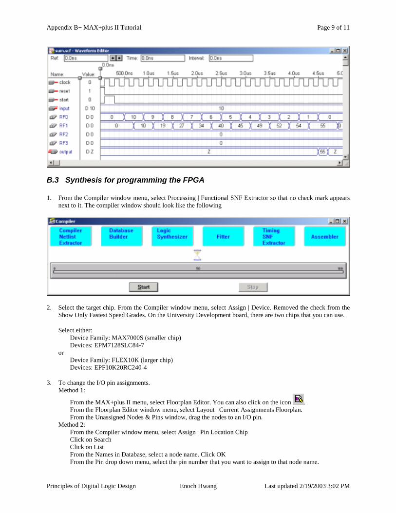
Appendix B− MAX+plus II Tutorial Page 9 of 11
Principles of Digital Logic Design Enoch Hwang Last updated 2/19/2003 3:02 PM
B.3 Synthesis for programming the FPGA
1. From the Compiler window menu, select Processing | Functional SNF Extractor so that no check mark appears next to it. The compiler window should look like the following
2. Select the target chip. From the Compiler window menu, select Assign | Device. Removed the check from the Show Only Fastest Speed Grades. On the University Development board, there are two chips that you can use.
Select either: Device Family: MAX7000S (smaller chip) Devices: EPM7128SLC84-7 or Device Family: FLEX10K (larger chip) Devices: EPF10K20RC240-4
3. To change the I/O pin assignments. Method 1:
From the MAX+plus II menu, select Floorplan Editor. You can also click on the icon . From the Floorplan Editor window menu, select Layout | Current Assignments Floorplan. From the Unassigned Nodes & Pins window, drag the nodes to an I/O pin.
Method 2: From the Compiler window menu, select Assign | Pin Location Chip
Click on Search Click on List From the Names in Database, select a node name. Click OK From the Pin drop down menu, select the pin number that you want to assign to that node name.
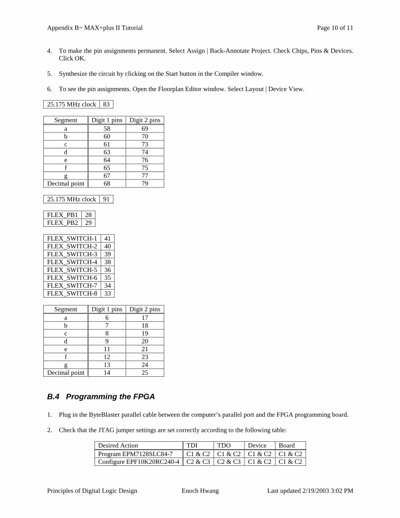
Appendix B− MAX+plus II Tutorial Page 10 of 11
Principles of Digital Logic Design Enoch Hwang Last updated 2/19/2003 3:02 PM
4. To make the pin assignments permanent. Select Assign | Back-Annotate Project. Check Chips, Pins & Devices. Click OK.
5. Synthesize the circuit by clicking on the Start button in the Compiler window.
6. To see the pin assignments. Open the Floorplan Editor window. Select Layout | Device View. 25.175 MHz clock 83
Segment Digit 1 pins Digit 2 pins a 58 69 b 60 70 c 61 73 d 63 74 e 64 76 f 65 75 g 67 77
Decimal point 68 79 25.175 MHz clock 91 FLEX_PB1 28 FLEX_PB2 29 FLEX_SWITCH-1 41 FLEX_SWITCH-2 40 FLEX_SWITCH-3 39 FLEX_SWITCH-4 38 FLEX_SWITCH-5 36 FLEX_SWITCH-6 35 FLEX_SWITCH-7 34 FLEX_SWITCH-8 33
Segment Digit 1 pins Digit 2 pins a 6 17 b 7 18 c 8 19 d 9 20 e 11 21 f 12 23 g 13 24
Decimal point 14 25
B.4 Programming the FPGA
1. Plug in the ByteBlaster parallel cable between the computer’s parallel port and the FPGA programming board.
2. Check that the JTAG jumper settings are set correctly according to the following table:
Desired Action TDI TDO Device Board Program EPM7128SLC84-7 C1 & C2 C1 & C2 C1 & C2 C1 & C2 Configure EPF10K20RC240-4 C2 & C3 C2 & C3 C1 & C2 C1 & C2

Appendix B− MAX+plus II Tutorial Page 11 of 11
Principles of Digital Logic Design Enoch Hwang Last updated 2/19/2003 3:02 PM
3. Plug in the 9V power for the board.
4. Select MAX+plusII | Programmer window or click on the icon . Select Options | Hardware Setup and select ByteBlaster and the correct parallel port (usually LPT1).
5. Click on the Program button to start the download.
B.5 References The online documentation for the UP2 board can be found at http://www.altera.com/literature/univ/upds.pdf.