wideband if receiver subsystem data sheet ad6676...wideband if receiver subsystem data sheet ad6676...
TRANSCRIPT
Wideband IF Receiver SubsystemData Sheet AD6676
Rev. D Document Feedback Information furnished by Analog Devices is believed to be accurate and reliable. However, no responsibility is assumed by Analog Devices for its use, nor for any infringements of patents or other rights of third parties that may result from its use. Specifications subject to change without notice. No license is granted by implication or otherwise under any patent or patent rights of Analog Devices. Trademarks and registered trademarks are the property of their respective owners.
One Technology Way, P.O. Box 9106, Norwood, MA 02062-9106, U.S.A.Tel: 781.329.4700 ©2014–2017 Analog Devices, Inc. All rights reserved. Technical Support www.analog.com
FEATURES High instantaneous dynamic range
Noise figure (NF) as low as 13 dB Noise spectral density (NSD) as low as −159 dBFS/Hz IIP3 up to 36.9 dBm with spurious tones <−99 dBFS
Tunable band-pass Σ-Δ analog-to-digital converter (ADC) 20 MHz to 160 MHz signal bandwidth 70 MHz to 450 MHz IF center frequency Configurable input full-scale level of −2 dBm to −14 dBm
Easy to drive resistive IF input Gain flatness of 1 dB with under 0.5 dB out-of-band peaking
Alias rejection greater than 50 dB 2.0 GSPS to 3.2 GSPS ADC clock rate
On-chip PLL clock multiplier 16-bit I/Q rate up to 266 MSPS
On-chip digital signal processing NCO and quadrature digital downconverter (QDDC) Selectable decimation factor of 12, 16, 24, and 32
Automatic gain control (AGC) support On-chip attenuator with 27 dB span in 1 dB steps Fast attenuator control via configurable AGC data port Peak detection flags with programmable thresholds
Single or dual lane, JESD204B capable Low power consumption: 1.20 W
1.1 V and 2.5 V supply voltage TDD power saving up to 60%
4.3 mm × 5.0 mm WLCSP
APPLICATIONS Wideband cellular infrastructure equipment and repeaters Point-to-point microwave equipment Instrumentation
Spectrum and communication analyzers Software defined radio
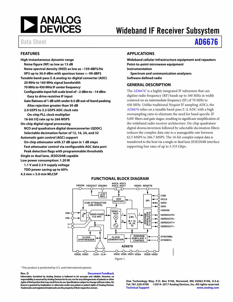
GENERAL DESCRIPTION The AD66761 is a highly integrated IF subsystem that can digitize radio frequency (RF) bands up to 160 MHz in width centered on an intermediate frequency (IF) of 70 MHz to 450 MHz. Unlike traditional Nyquist IF sampling ADCs, the AD6676 relies on a tunable band-pass Σ-Δ ADC with a high oversampling ratio to eliminate the need for band specific IF SAW filters and gain stages, resulting in significant simplification of the wideband radio receiver architecture. On-chip quadrature digital downconversion followed by selectable decimation filters reduces the complex data rate to a manageable rate between 62.5 MSPS to 266.7 MSPS. The 16-bit complex output data is transferred to the host via a single or dual lane JESD204B interface supporting line rates of up to 5.333 Gbps.
FUNCTIONAL BLOCK DIAGRAM
L–L+
RESETBVDDIOAGC4, AGC3AGC2, AGC1VDD2NV
VSSAVDD2 VDDD VSSD
SPI
CSB
SCLK
SDIO
SDO
SERDOUT0+
SERDOUT0–
SERDOUT1+
SERDOUT1–
VDDHSI
SYNCINB±
SYSREF±
AGCSUPPORT
CLOCKGENERATION
–2.0VREG
JES
D20
4BS
ER
IAL
IZE
RT
x O
UT
PU
TS
Mx
M = 12,16, 24,
32
I
Q
QDDC +NCO I
Q
BAND-PASSΣ-∆ ADC
VIN–
VIN+
27dB ATTENUATOR(1dB STEPS)
CLOCKSYNTHESIZER
JESD204BSUBCLASS 1
CONTROL
CLK+ CLK–VDDCVDDQ
AD6676
1234
8-00
1
VDDL VDD1
VSS2OUTVSS2IN
Figure 1.
1 This product is protected by U.S. and international patents.
AD6676 Data Sheet
Rev. D | Page 2 of 90
TABLE OF CONTENTS Features .............................................................................................. 1
Applications ....................................................................................... 1
General Description ......................................................................... 1
Functional Block Diagram .............................................................. 1
Revision History ............................................................................... 3
Product Highlights ........................................................................... 4
Specifications ..................................................................................... 5
Digital High Speed SERDES Specifications .............................. 7
CLK± to SYSREF± Timing Diagram ......................................... 8
Digital CMOS Input/Output Specifications ............................. 8
Absolute Maximum Ratings ............................................................ 9
Thermal Resistance ...................................................................... 9
ESD Caution .................................................................................. 9
Pin Configuration and Function Descriptions ........................... 10
Typical Performance Characteristics ........................................... 12
Nominal Performance for IF = 115 MHz (Direct Sampling VHF Receiver) ............................................................................ 12
Nominal Performance for IF = 140 MHz (μW Point-to-Point Receivers) ..................................................................................... 14
Nominal Performance for IF = 181 MHz (Wireless Infrastructure Receiver)............................................................. 15
Nominal Performance for IF = 250 MHz AND BW = 75 MHz ....................................................................................................... 17
Nominal Performance for IF = 350 MHz AND BW = 160 MHz ...................................................................................... 19
Equivalent Circuits ......................................................................... 21
Terminology .................................................................................... 22
Theory of Operation ...................................................................... 23
Overview ...................................................................................... 23
Band-Pass Σ-Δ ADC Architecture ........................................... 24
Σ-Δ ADC Configuration Considerations ................................ 28
Attenuator.................................................................................... 33
Clock Synthesizer ....................................................................... 35
Digital Processing Blocks .............................................................. 38
Digital Signal Processing Path .................................................. 39
AGC Features and Peak Detection ........................................... 42
GPIO Functionality .................................................................... 44
Power Saving Modes .................................................................. 44
Introduction to the JESD204B Interface ................................. 45
Functional Overview ................................................................. 47
JESD204B Link Establishment ................................................. 47
Physical Layer Input/Outputs ................................................... 49
Configuring the JESD204B Link .............................................. 50
Synchronization Using SYSREF± ............................................. 51
Applications Information .............................................................. 53
Analog Input Considerations ................................................... 53
Clock Input Considerations ...................................................... 54
IF Frequency Planning .............................................................. 56
PCB Design Guidelines ............................................................. 57
Powering the AD6676 ................................................................ 59
AD6676 Start-Up Initialization ................................................ 61
Serial Port Interface (SPI) .............................................................. 64
SPI Register Map Description .................................................. 64
SPI Operation ............................................................................. 64
Register Memory Map and Details .............................................. 66
Register Memory Map ............................................................... 66
Register Details ........................................................................... 68
Outline Dimensions ....................................................................... 90
Ordering Guide .......................................................................... 90
Data Sheet AD6676
Rev. D | Page 3 of 90
REVISION HISTORY 5/2017—Rev. C to Rev. D Change to Differential Output Voltage Parameter, Table 2 ......... 7 Changes to Figure 147 .................................................................... 65 3/2017—Rev. B to Rev. C Added Endnote 1, Table 12 ............................................................ 36 Changes to Synchronization Using SYSREF ± Section .............. 51 Added Table 123; Renumbered Sequentially ............................... 87 4/2016—Rev. A to Rev. B Changes to Figure 3 and Table 6 ................................................... 10 Changes to Clock Input Considerations Section and Figure 133 ......................................................................................... 55 9/2015—Rev. 0 to Rev. A Changes to Product Highlights Section ......................................... 4 Changes to Clock Synthesizer Enabled Parameter, Table 1 and Out-of-Range Recovery Time Parameter Unit, Table 1 ............... 5 Changes to Differential Output Voltage, Table 2 .......................... 7 Changes to Table 3 ............................................................................ 8 Changes to Figure 3 ......................................................................... 10 Changes to Figure 4, Figure 8 Caption, and Figure 9 ................. 12 Changes to Figure 26 ...................................................................... 15 Changes to Figure 36 and Figure 38 ............................................. 17 Changes to Figure 40, Figure 41, and Figure 44 .......................... 18 Changes to Figure 50 ...................................................................... 19 Changes to Attenuator Section ...................................................... 33 Changes to Table 12 ........................................................................ 36 Changes to Phase Noise Performance Section, Figure 101, and Figure 102 ......................................................................................... 37 Changes to Quadrature Digital Downconversion Section ........ 39
Changes to Synchronization Using SYSREF± Section ............... 51 Added Figure 127; Renumbered Sequentially ............................. 52 Changes to Input Driver Filter Considerations Section and Figure 130 ......................................................................................... 54 Changes to Clock Input Considerations Section and Figure 133 to Figure 135 .................................................................................... 55 Changes to PCB Design Guidelines Section ............................... 57 Added Figure 141; Renumbered Sequentially ............................. 58 Changes to Power the AD6676 Section and Figure 142 ............ 59 Changes to AD6676 Start-Up Initialization Section and Table 25 ............................................................................................. 61 Changes to Table 26 ........................................................................ 62 Changes to Table 27 and Table 29 ................................................. 63 Changes to Table 32 ........................................................................ 66 Changes to Coarse NCO Tuning Register Section and Table 57 ............................................................................................. 72 Changes to Fine NCO Tuning Register Section and Table 58 .. 73 Changes to Table 70 to Table 72 .................................................... 75 Changes to Table 73 ........................................................................ 76 Changes to Table 109 ...................................................................... 84 Added Physical Control 1 Register Section and Table 116 ........ 85 Changes to Table 120 ...................................................................... 86 Changes to Table 121 and Table 123, and Table 125 .................. 87 Changes to CLKSYN Reference Divider and SYSREF Control Register Section, Table 128, CLKSYN Status Register Section, and Table 129 ................................................................................... 88 JESDSYN Status Register Section, Table 130, and Table 131 to Table 133 ........................................................................................... 89 10/2014—Revision 0: Initial Version

AD6676 Data Sheet
Rev. D | Page 4 of 90
The band-pass Σ-Δ ADC of the AD6676, which operates between 2.0 GHz to 3.2 GHz, provides exceptional instantaneous dynamic range and inherent antialiasing capability. Its in-band frequency response typically maintains better than 1 dB pass band flatness with out-of-band peaking better than 0.5 dB. An integrated digital peak detector enables the instantaneous signal power to be monitored over a wide band (shortly after digitization), thus providing AGC capability to cope quickly with large in-band or out-of-band blockers.
The AD6676 includes various AGC monitoring and control features along with an internal 27 dB step attenuator in 1 dB steps. A flexible AGC port with digital input/output pins allows fast control of the AD6676 on-chip step attenuator and/or updates on the input signal via status flags. These features, along with the high instantaneous dynamic range, can significantly simplify AGC implementation compared to traditional narrow-band IF approaches that often require separate AGC capability for RF and IF protection.
In addition to reducing system complexity, the AD6676 enables significant space and power consumption savings for next generation multiple input/multiple output (MIMO) receiver architectures. The AD6676 is available in an 8 × 10 ball array WLCSP package that is approximately 4.3 mm × 5.0 mm, with a JESD204B serial interface that allows simple interfacing to the host processor.
Its low power consumption of 1.2 W compares favorably to IF sampling ADCs with similar bandwidth (BW) and dynamic range capabilities even without considering the added power savings from the elimination of an entire IF strip. The AD6676 features multichip synchronization that allows synchronization to within a fraction of an output data sample. For time-domain duplex (TDD) applications, the AD6676 features a fast power-up/power-down mode that further reduces power consumption while still maintaining multichip synchronization. Power savings of up to 60% or 42% is achievable with recovery times of 11.5 μs or 2.5 μs, depending on the device configuration.
Auxiliary blocks include an on-chip PLL clock multiplier to generate the Σ-Δ ADC clock. For applications that require better phase noise performance, an external differential RF clock source may also be used. The SPI port programs numerous parameters of the AD6676, allowing the device to be optimized for a variety of applications.
The AD6676 is available in an 80-ball WLCSP package with an optimized pinout that enables low cost printed circuit board (PCB) manufacturing. The device operates from a 1.1 V and 2.5 V supply with a total typical power consumption of 1.2 W at 3.2 GSPS operation. This product is protected by several United States patents. Contact Analog Devices, Inc., for further information.
PRODUCT HIGHLIGHTS 1. Industry leading dynamic range enables high performance,
reconfigurable heterodyne (or direct sampling VHF) software defined radios with high AGC-free range.
2. Continuous time, band-pass Σ-Δ ADC supports IFs from 70 MHz to 450 MHz with IF signal bandwidths of up to 160 MHz and reduces IF filtering requirements.
3. The high instantaneous dynamic range and oversampling nature of the Σ-Δ ADC significantly reduces the IF filter complexity.
4. On-chip 27 dB digital attenuator with easy to drive resistive input simplifies interface to RF/IF components.
5. Small 4.3 mm × 5.0 mm package, simple interface, and integrated digital attenuator and clock synthesizer save PCB space.
6. Low input full-scale level of −2 dBm (or less) enables 3.3 V RF/IF component lineups at reduced P1dB and power.
7. Fast power saving mode supports TDD protocols. 8. Unique profile mode allows the AD6676 to switch between
up to four different ADC IF/BW configurations in 1 μs.

Data Sheet AD6676
Rev. D | Page 5 of 90
SPECIFICATIONS VDD1 = VDDL = VDDC = VDDQ = 1.1 V, VDDD = VDDHSI = 1.1 V, VDD2 = 2.5 V, VDDIO = 1.8 V, FIF = 250 MHz, BW = 75 MHz, FADC = 3.2 GHz, attenuator = 0 dB, L± (inductor values) = 19 nH, maximum PIN_0dBFS setting with IDAC1FS = 4 mA, fDATA_IQ = 200 MSPS, shuffler enabled (every clock cycle) with default threshold of 5, unless otherwise noted.
Table 1. Parameter Temperature Test Conditions/Comments Min Typ Max Unit SYSTEM DYNAMIC PERFORMANCE
Full-Scale Input Power Level (PIN_0dBFS)1 −2 dBm Maximum Continuous Wave (CW) Input
Power2 −2 −1 dBFS
Noise Figure (NF) No signal and measured 17 dB Worst In-Band Noise Spectral Density Full Over a 5 MHz bandwidth −155 −152.5 dBFS/Hz
Noise Figure at IF Center (NF) No signal and measured 13 dB In-Band Noise Spectral Density (NSD) Over a 5 MHz bandwidth −159 dBFS/Hz
Input Second-Order Intercept (IIP2) −6 dBFS tones 60 dBm Second-Order Intermodulation
Distortion (IMD) (IMD2) See Table 20 −68.3 dBc
Input Third-Order Intercept (IIP3) Full −8 dBFS tones 36.9 dBm Third-Order IMD (IMD3) Full −8 dBFS tones −95 −84.2 dBc
Worst In-Band Spur for Swept CW Tone Full −2 dBFS tone −99 −93.5 dBFS −10 dBFS tone −109.6 dBFS In-Band Noise Full −2 dBFS tone −75.5 −73.7 dBFS Full No CW tone −78.5 −76.5 dBFS Gain Variation Full 0.5 dB
IF INPUT (VIN±) Input Span 0 dBFS
0 dB Attenuator Setting 0.48 V p-p 12 dB Attenuator Setting 1.92 V p-p
Common-Mode Input Voltage Self biased 1.0 V Differential Input Impedance 25°C 60||2 Ω||pF Common-Mode Input Impedance 25°C 3.5 kΩ Full-Scale Input Power Adjustment
(PIN_0dBFS) IDAC1FS span of 1 mA to 4 mA 12 dB
DIGITAL STEP ATTENUATOR (VIN±) Attenuation Range Full 27 dB Step Size Full 1 dB Input Return Loss Full 20 dB Input Return Loss Variation vs. Attenuator
Setting Full 2 dB
CLOCK INPUT (CLK±) Clock Synthesizer Disabled
Frequency Range Full 2.0 3.2 GHz Amplitude Range Full 0.4 0.8 2.0 V p-p Differential Input Impedance 25°C At 3 GHz 86||0.3 Ω||pF Common Mode Impedance 25°C At 3 GHz 700||0.8 Ω||pF Input Return Loss 25°C With 1:2 balun 15 dB Common-Mode Voltage 25°C Self biased 0.70 V
Clock Synthesizer Enabled Frequency Range3 Full 10 320 MHz Amplitude Range Full Single-ended into CLK+ 0.4 0.8 1.1 V p-p CLK+ Input Impedance 25°C 1.4||1.0 kΩ||pF Minimum Slew Rate 12 V/μs Common-Mode Voltage 25°C Self biased 0.55 V
AD6676 Data Sheet
Rev. D | Page 6 of 90
Parameter Temperature Test Conditions/Comments Min Typ Max Unit CLOCK SYNTHESIZER
Phase Detector Frequency Full 10 80 MHz Minimum Charge Pump Output Current Full 0.1 mA Maximum Charge Pump Output Current Full 6.4 mA VCO Tuning Range Full 2.94 3.2 GHz
Σ-∆ ADC AND DIGITAL DOWNCONVERTER Resolution Full 16 Bits Clock Frequency (FADC) Full 2.0 3.2 GHz IF Center Frequency (FIF) Full 70 450 MHz IF Bandwidth Maximum BW applies to
higher FIF 0.005 × FADC
0.05 × FADC
IF Pass Band Gain Flatness Full FADC, FIF, and BW dependent 1.0 dB Out-of-Band Peaking Depends on FADC, FIF, and BW 0.5 dB Alias Rejection Regions of FADC ± FIF 51 dB Fixed Decimation Factors Full 12, 16, 24,
32
NCO Tuning Resolution Decimate by 12 or 24 FADC/3072 Decimate by 16 or 32 FADC/4096 Out-of-Range Recovery Time Full Relative to ADC clock cycles 52 1/FADC
POWER SUPPLY AND CONSUMPTION Analog Supply Voltage
VDD1, VDDL, VDDQ, VDDC Full 1.0725 1.1 1.1275 V VDD2, VDD2NV Full 2.4375 2.5 2.5625 V VSS2IN Use on-chip regulator, tie to
VSS2OUT −2.0 V
Digital Supply Voltage (VDDD) Full 1.0725 1.1 1.1275 V JESD204B Supply Voltage (VDDHSI) Full 1.0725 1.1 1.1275 V SPI Interface Supply Voltage (VDDIO) Full 1.7 1.8 2.5625 V Analog Supply Current
IVDD1 + IVDDL Full 368 397 mA IVDDC + IVDDQ Full CLK synthesizer disabled 57 68 mA IVDDC
4 + IVDDQ Full CLK synthesizer enabled 93 106 mA IVDD2 + IVDD2NV Full 145 165 mA
Digital Supply Current (IVDDD) Full 141 208 mA JESD204B Supply Current (IVDDHSI) Full 164 190 mA SPI Interface Supply Current (IVDDIO) Full 0.4 1 mA Power Consumption Full
With CLK SYN Disabled 1.16 1.31 W With CLK SYN Enabled 1.20 1.34 W Standby5 Full 0.44 W Power-Down Full 66 177 mW
OPERATING TEMPERATURE RANGE −40 +85 °C 1 Extrapolated input power level is measured at the center of IF pass band that results in a 0 dBFS power level. 2 The overload level of the Σ-Δ ADC for a CW tone is guaranteed up to −2 dBFS back off from full scale but typically exceeds −1 dBFS. Input signals that have a higher
peak-to-average ratio (PAR) than a CW tone (PAR = 3 dB) must apply additional back off based on the difference in PAR. 3 The clock synthesizer reference divider (Register 0x2BB, Bits[7:6]) must be set to divide by 4 or by 2 to ensure that its phase detector frequency remains ≤40 MHz. 4 fCLK = 200 MHz, FADC = 3.2 GHz. 5 The AD6676 is configured for recovery time of 11.5 μs with VSS2 generator/ digital data in standby (Register 0x150 = 0x40) and low power ADC state (Register 0x250 = 0x95).
Data Sheet AD6676
Rev. D | Page 7 of 90
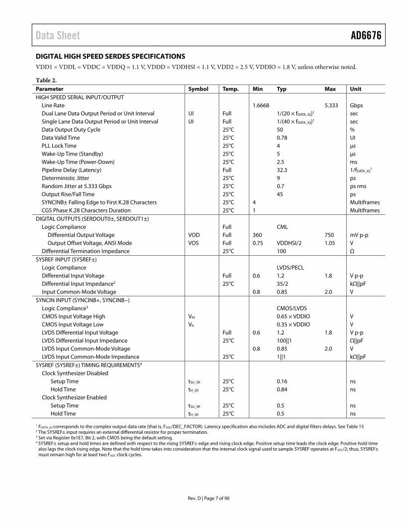
DIGITAL HIGH SPEED SERDES SPECIFICATIONS VDD1 = VDDL = VDDC = VDDQ = 1.1 V, VDDD = VDDHSI = 1.1 V, VDD2 = 2.5 V, VDDIO = 1.8 V, unless otherwise noted.
Table 2. Parameter Symbol Temp. Min Typ Max Unit HIGH SPEED SERIAL INPUT/OUTPUT
Line Rate 1.6668 5.333 Gbps Dual Lane Data Output Period or Unit Interval UI Full 1/(20 × fDATA_IQ)1 sec Single Lane Data Output Period or Unit Interval UI Full 1/(40 × fDATA_IQ)1 sec Data Output Duty Cycle 25°C 50 % Data Valid Time 25°C 0.78 UI PLL Lock Time 25°C 4 μs Wake-Up Time (Standby) 25°C 5 μs Wake-Up Time (Power-Down) 25°C 2.5 ms Pipeline Delay (Latency) Full 32.3 1/fDATA_IQ
1 Deterministic Jitter 25°C 9 ps Random Jitter at 5.333 Gbps 25°C 0.7 ps rms Output Rise/Fall Time 25°C 45 ps SYNCINB± Falling Edge to First K.28 Characters 25°C 4 Multiframes CGS Phase K.28 Characters Duration 25°C 1 Multiframes
DIGITAL OUTPUTS (SERDOUT0±, SERDOUT1±) Logic Compliance Full CML
Differential Output Voltage VOD Full 360 750 mV p-p Output Offset Voltage, ANSI Mode VOS Full 0.75 VDDHSI/2 1.05 V
Differential Termination Impedance 25°C 100 Ω SYSREF INPUT (SYSREF±)
Logic Compliance LVDS/PECL Differential Input Voltage Full 0.6 1.2 1.8 V p-p Differential Input Impedance2 25°C 35/2 kΩ||pF Input Common-Mode Voltage 0.8 0.85 2.0 V
SYNCIN INPUT (SYNCINB+, SYNCINB−) Logic Compliance3 CMOS/LVDS CMOS Input Voltage High VIH 0.65 × VDDIO V CMOS Input Voltage Low VIL 0.35 × VDDIO V LVDS Differential Input Voltage Full 0.6 1.2 1.8 V p-p LVDS Differential Input Impedance 25°C 100||1 Ω||pF LVDS Input Common-Mode Voltage 0.8 0.85 2.0 V LVDS Input Common-Mode Impedance 25°C 1||1 kΩ||pF
SYSREF (SYSREF±) TIMING REQUIREMENTS4 Clock Synthesizer Disabled
Setup Time tSU_SR 25°C 0.16 ns Hold Time tH_SR 25°C 0.84 ns
Clock Synthesizer Enabled Setup Time tSU_SR 25°C 0.5 ns Hold Time tH_SR 25°C 0.5 ns
1 FDATA_IQ corresponds to the complex output data rate (that is, FADC/DEC_FACTOR). Latency specification also includes ADC and digital filters delays. See Table 15 2 The SYSREF± input requires an external differential resistor for proper termination. 3 Set via Register 0x1E7, Bit 2, with CMOS being the default setting. 4 SYSREF± setup and hold times are defined with respect to the rising SYSREF± edge and rising clock edge. Positive setup time leads the clock edge. Positive hold time
also lags the clock rising edge. Note that the hold time takes into consideration that the internal clock signal used to sample SYSREF operates at FADC/2; thus, SYSREF± must remain high for at least two FADC clock cycles.
AD6676 Data Sheet
Rev. D | Page 8 of 90
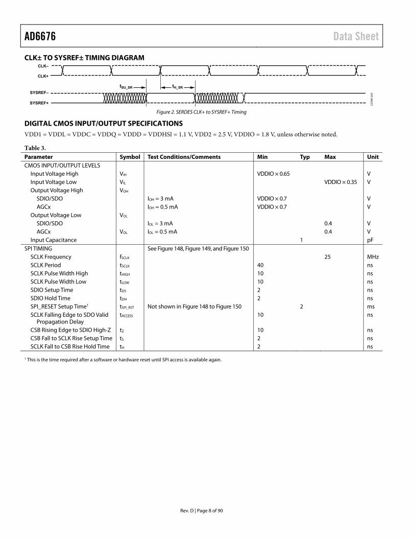
CLK± TO SYSREF± TIMING DIAGRAM
CLK+
CLK–
SYSREF+
SYSREF–
tSU_SR tH_SR
1234
8-10
2
Figure 2. SERDES CLK+ to SYSREF+ Timing
DIGITAL CMOS INPUT/OUTPUT SPECIFICATIONS VDD1 = VDDL = VDDC = VDDQ = VDDD = VDDHSI = 1.1 V, VDD2 = 2.5 V, VDDIO = 1.8 V, unless otherwise noted.
Table 3. Parameter Symbol Test Conditions/Comments Min Typ Max Unit CMOS INPUT/OUTPUT LEVELS
Input Voltage High VIH VDDIO × 0.65 V Input Voltage Low VIL VDDIO × 0.35 V Output Voltage High VOH
SDIO/SDO IOH = 3 mA VDDIO × 0.7 V AGCx IOH = 0.5 mA VDDIO × 0.7 V
Output Voltage Low VOL SDIO/SDO IOL = 3 mA 0.4 V AGCx VOL IOL = 0.5 mA 0.4 V
Input Capacitance 1 pF SPI TIMING See Figure 148, Figure 149, and Figure 150
SCLK Frequency fSCLK 25 MHz SCLK Period tSCLK 40 ns SCLK Pulse Width High tHIGH 10 ns SCLK Pulse Width Low tLOW 10 ns SDIO Setup Time tDS 2 ns SDIO Hold Time tDH 2 ns SPI_RESET Setup Time1 tSPI_RST Not shown in Figure 148 to Figure 150 2 ms SCLK Falling Edge to SDO Valid
Propagation Delay tACCESS 10 ns
CSB Rising Edge to SDIO High-Z tZ 10 ns CSB Fall to SCLK Rise Setup Time tS 2 ns SCLK Fall to CSB Rise Hold Time tH 2 ns
1 This is the time required after a software or hardware reset until SPI access is available again.
Data Sheet AD6676
Rev. D | Page 9 of 90
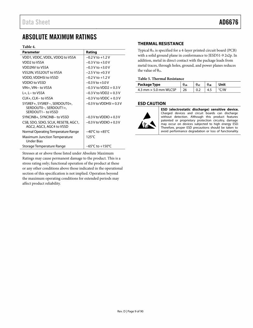
ABSOLUTE MAXIMUM RATINGS Table 4. Parameter Rating VDD1, VDDC, VDDL, VDDQ to VSSA −0.2 V to +1.2 V VDD2 to VSSA −0.3 V to +3.0 V VDD2NV to VSSA −0.3 V to +3.0 V VSS2IN, VSS2OUT to VSSA −2.5 V to +0.3 V VDDD, VDDHSI to VSSD −0.2 V to +1.2 V VDDIO to VSSD −0.3 V to +3.0 V VIN+, VIN− to VSSA −0.3 V to VDD2 + 0.3 V
L+, L− to VSSA −0.3 V to VDD2 + 0.3 V
CLK+, CLK− to VSSA −0.3 V to VDDC + 0.3 V
SYSREF+, SYSREF−, SERDOUT0+, SERDOUT0−, SERDOUT1+, SERDOUT1− to VSSD
−0.3 V to VDDHSI + 0.3 V
SYNCINB+, SYNCINB− to VSSD −0.3 V to VDDIO + 0.3 V
CSB, SDO, SDIO, SCLK, RESETB, AGC1, AGC2, AGC3, AGC4 to VSSD
−0.3 V to VDDIO + 0.3 V
Normal Operating Temperature Range −40°C to +85°C
Maximum Junction Temperature Under Bias
125°C
Storage Temperature Range −65°C to +150°C
Stresses at or above those listed under Absolute Maximum Ratings may cause permanent damage to the product. This is a stress rating only; functional operation of the product at these or any other conditions above those indicated in the operational section of this specification is not implied. Operation beyond the maximum operating conditions for extended periods may affect product reliability.
THERMAL RESISTANCE Typical θJA is specified for a 4-layer printed circuit board (PCB) with a solid ground plane in conformance to JESD51-9 2s2p. In addition, metal in direct contact with the package leads from metal traces, through holes, ground, and power planes reduces the value of θJA.
Table 5. Thermal Resistance Package Type JA JC JB Unit 4.3 mm × 5.0 mm WLCSP 26 0.2 4.5 °C/W
ESD CAUTION
AD6676 Data Sheet
Rev. D | Page 10 of 90
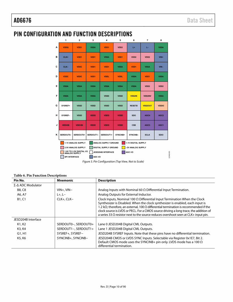
PIN CONFIGURATION AND FUNCTION DESCRIPTIONS
VDDQ VDD1 VSSA VDD1 VDD2 L+ L– VSSA
1 2 3 4 5 6 7 8
CLK+ VDD1 VDD1 VSSA VDD1 VDD2 VDD2 VIN+
CLK– VDDC VDD1 VDD1 VSSA VDD1 VSSA VIN–
VDDC VDDC VDD1 VDDL VDDL VSSA VDD1 VSSA
VSSA VSSA VSSA VSSA VSSA VSSA VDD2 VDD2
VSSA VSSA VSSA VSSD VSSD VSS2IN VDD2NV VSSA
SYSREF+ VSSD VSSD VSSD VSSD RESETB VSS2OUT VDDIO
SYSREF– VSSD VDDD VDDD VDDD SDO AGC4 AGC2
VDDHSI VDDHSI VDDD VDDD VDDD CSB AGC3 AGC1
SERDOUT0–
1.1V ANALOG SUPPLY
SERDOUT0+ SERDOUT1– SERDOUT1+ SYNCINB+ SYNCINB– SCLK SDIO
A
B
C
D
E
F
G
H
J
K
1234
8-00
3
1.1V DIGITAL SUPPLYANALOG SUPPLY GROUND
2.5V ANALOG SUPPLY –2V ANALOG SUPPLYDIGITAL SUPPLY GROUND
SPI INTERFACE ADC I/O
1.8V TO 2.5V DIGITAL I/OANALOG SUPPLY
AGC I/OJESD204B INTERFACE
Figure 3. Pin Configuration (Top View, Not to Scale)
Table 6. Pin Function Descriptions Pin No. Mnemonic Description Σ-Δ ADC Modulator
B8, C8 VIN+, VIN− Analog Inputs with Nominal 60 Ω Differential Input Termination. A6, A7 L+, L− Analog Outputs for External Inductor. B1, C1 CLK+, CLK− Clock Inputs, Nominal 100 Ω Differential Input Termination When the Clock
Synthesizer is Disabled. When the clock synthesizer is enabled, each input is 1.2 kΩ; therefore, an external, 100 Ω differential termination is recommended if the clock source is LVDS or PECL. For a CMOS source driving a long trace, the addition of a series 33 Ω resistor next to the source reduces overshoot seen at CLK+ input pin.
JESD204B Interface K1, K2 SERDOUT0−, SERDOUT0+ Lane 0 JESD204B Digital CML Outputs. K3, K4 SERDOUT1−, SERDOUT1+ Lane 1 JESD204B Digital CML Outputs. G1, H1 SYSREF+, SYSREF− JESD204B SYSREF Inputs. Note that these pins have no differential termination. K5, K6 SYNCINB+, SYNCINB− JESD204B CMOS or LVDS SYNC Inputs. Selectable via Register 0x1E7, Bit 2.
Default CMOS mode uses the SYNCINB+ pin only. LVDS mode has a 100 Ω differential termination.
Data Sheet AD6676
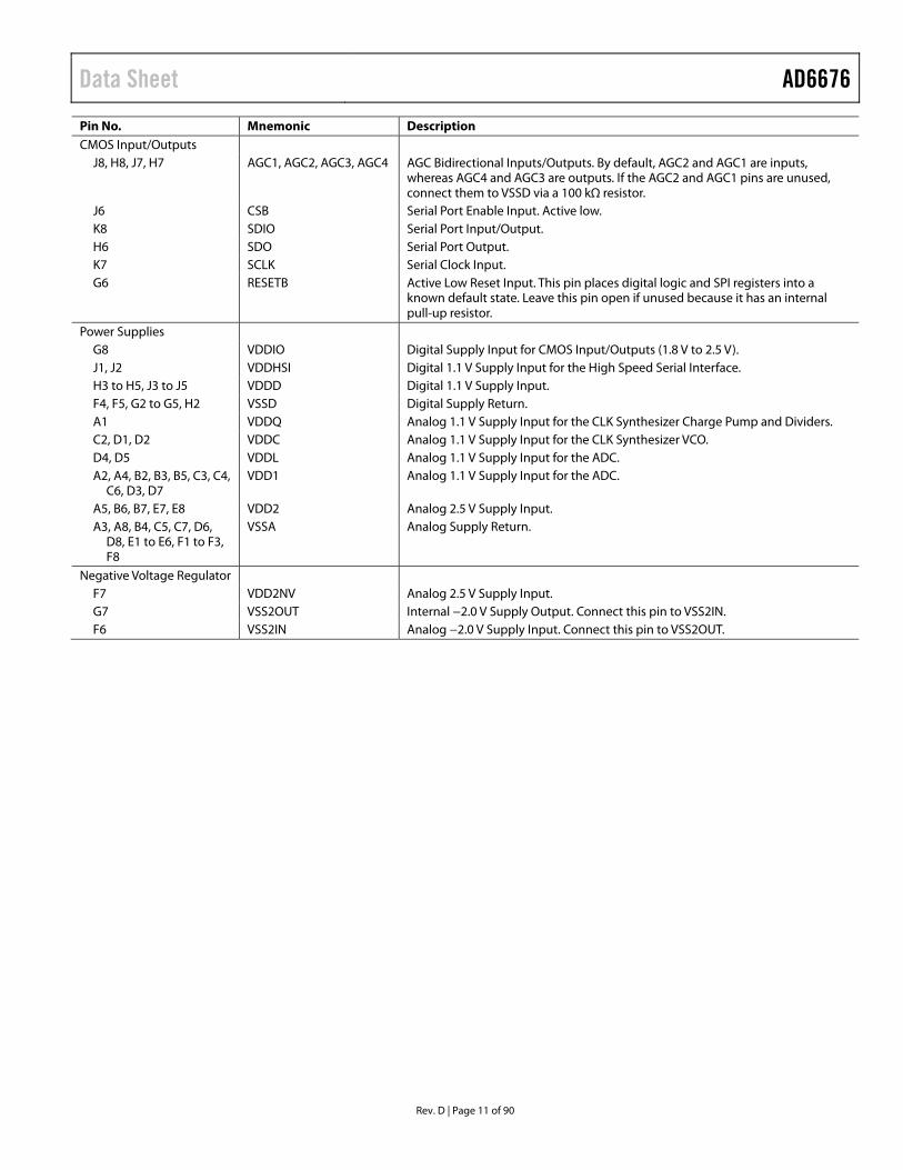
Rev. D | Page 11 of 90
Pin No. Mnemonic Description CMOS Input/Outputs
J8, H8, J7, H7 AGC1, AGC2, AGC3, AGC4 AGC Bidirectional Inputs/Outputs. By default, AGC2 and AGC1 are inputs, whereas AGC4 and AGC3 are outputs. If the AGC2 and AGC1 pins are unused, connect them to VSSD via a 100 kΩ resistor.
J6 CSB Serial Port Enable Input. Active low. K8 SDIO Serial Port Input/Output. H6 SDO Serial Port Output. K7 SCLK Serial Clock Input. G6 RESETB Active Low Reset Input. This pin places digital logic and SPI registers into a
known default state. Leave this pin open if unused because it has an internal pull-up resistor.
Power Supplies G8 VDDIO Digital Supply Input for CMOS Input/Outputs (1.8 V to 2.5 V). J1, J2 VDDHSI Digital 1.1 V Supply Input for the High Speed Serial Interface. H3 to H5, J3 to J5 VDDD Digital 1.1 V Supply Input. F4, F5, G2 to G5, H2 VSSD Digital Supply Return. A1 VDDQ Analog 1.1 V Supply Input for the CLK Synthesizer Charge Pump and Dividers. C2, D1, D2 VDDC Analog 1.1 V Supply Input for the CLK Synthesizer VCO. D4, D5 VDDL Analog 1.1 V Supply Input for the ADC. A2, A4, B2, B3, B5, C3, C4,
C6, D3, D7 VDD1 Analog 1.1 V Supply Input for the ADC.
A5, B6, B7, E7, E8 VDD2 Analog 2.5 V Supply Input. A3, A8, B4, C5, C7, D6,
D8, E1 to E6, F1 to F3, F8
VSSA Analog Supply Return.
Negative Voltage Regulator F7 VDD2NV Analog 2.5 V Supply Input. G7 VSS2OUT Internal −2.0 V Supply Output. Connect this pin to VSS2IN. F6 VSS2IN Analog −2.0 V Supply Input. Connect this pin to VSS2OUT.

AD6676 Data Sheet
Rev. D | Page 12 of 90
TYPICAL PERFORMANCE CHARACTERISTICS NOMINAL PERFORMANCE FOR IF = 115 MHz (DIRECT SAMPLING VHF RECEIVER) FIF = 115 MHz, BW = 20 MHz, FADC = 2.4 GHz, attenuator = 0 dB, LEXT = 100 nH, maximum PIN_0dBFS setting, fDATA_IQ = 75 MSPS, nominal supplies, shuffler enabled (every 4 clock cycles), with default threshold settings, unless otherwise noted.
0.50
–1.50
–1.25
–1.00
–0.75
–0.50
–0.25
0
0.25
80 15014013012011010090
NO
RM
ALI
ZED
STF
RES
PON
SE (d
BFS
)
FREQUENCY (MHz) 1234
8-60
7
Figure 4. IF Pass Band Flatness (Includes Digital Filter)
–153
–163
–162
–161
–160
–159
–158
–157
–156
–155
–154
105 125120115110
NSD
(dB
FS/H
z)
INPUT FREQUENCY (MHz)
NSD (–1dBFS SIGNAL)NSD (NO SIGNAL)
1234
8-60
8
Figure 5. NSD With and Without Full-Scale CW at 108 MHz
0
–130
–90
–100
–110
–120
–80
–70
–60
–50
–40
–30
–20
–10
105 125120115110
AM
PLIT
UD
E (d
BFS
/NB
W)
INPUT FREQUENCY (MHz)
NBW = 3.4kHzIF PASS BAND REGION
–1dBFSAT 108MHz
1234
8-60
9
Figure 6. Spectral Plot of IF Pass Band Region with −1 dBFS CW at 108 MHz
5
–35
–30
–25
–20
–15
–10
–5
0
0 600450300150 550400250100 50035020050
NO
RM
ALI
ZED
STF
RES
PON
SE (d
BFS
)
FREQUENCY (MHz) 1234
8-61
0
Figure 7. Wideband Frequency Response (Before Digital Filter)
–153
–163
–162
–161
–160
–159
–158
–157
–156
–155
–154
–44 –2–5–8–11–14–17–20–23–26–29–32–35–38–41
NSD
(dB
FS/H
z)
INPUT POWER (dBm)
PIN_0dBFS = –2.9dBm
SHUFFLER DISABLED
SHUFFLE-EVERY-4TH CLOCK
1234
8-61
1
Figure 8. NSD vs. CW Input Power, CW at 108 MHz (NSD Measured at IF Center of 115 MHz)
–85
–95
–94
–93
–92
–91
–90
–89
–88
–87
–86
–44 –2–5–8–11–14–17–20–23–26–29–32–35–38–41
IBN
(dB
FS)
INPUT POWER (dBm)
PIN_0dBFS = –2.9dBm
1234
8-61
2
SHUFFLER DISABLED
SHUFFLE-EVERY-4TH CLOCK
Figure 9. Integrated In-Band Noise (IBN) in IF Pass Band Region of 10 MHz vs. Swept Single Tone Input Power with CW at 130 MHz

Data Sheet AD6676
Rev. D | Page 13 of 90
0
–130
–90
–100
–110
–120
–80
–70
–60
–50
–40
–30
–20
–10
80 90 100 110 120 130 140 150
AM
PL
ITU
DE
(d
BF
S)
INPUT FREQUENCY (MHz)
IF PASS BANDREGION = 20MHz
WORST SWEPTSPUR FOR–1dBFS CWAT –3dBm
2 × fDATA-IQCLOCK SPUR
AT 150MHz, AT –87dBFS
–1dBFSAT 101.6MHz
–111dBFS
1234
8-61
3
Figure 10. Worst Spur Falling in 75 MHz Pass Band for Swept CW from 77.5 MHz to 152.5 MHz
105 125120115110
AM
PL
ITU
DE
(d
BF
S/N
BW
)
INPUT FREQUENCY (MHz)
NBW = 3.4kHz
1234
8-61
40
–130
–90
–100
–110
–120
–80
–70
–60
–50
–40
–30
–20
–10
TWO TONES AT–8dBFS (–10.9dBm)
AT 114MHz AND 116MHz
–95dBFS –94dBFS
Figure 11. Two-Tone IMD Performance (f1 = 114 MHz, f2 = 116 MHz)
WO
RS
T I
MD
3 (d
BF
S)
INPUT AMPLITUDE (dBFS)
–39 –6–9–12–15–18–21–24–27–30–33–36
–80
–85
–90
–95
–100
–105
–110
–115
–120
–125
–130
1234
8-61
5
Figure 12. Swept Two-Tone Worst IMD3 vs. Tone Input Amplitude (f1 = 113 MHz, f2 =118 MHz)
WO
RS
T P
AS
S B
AN
D S
PU
R (
dB
FS
)
INPUT FREQUENCY (MHz)
77.5 87.5 97.5 107.5 117.5 127.5 137.5 147.5 152.5
–100
–103
–106
–109
–112
–115
–1dBFS–6dBFS–12dBFS–18dBFS
1234
8-61
6
Figure 13. Worst Pass Band Spur with Swept CW from 77.5 MHz to 150 MHz, over PIN = −1 dBFS, −6 dBFS, −12 dBFS, and −18 dBFS
0
–130
–90
–100
–110
–120
–80
–70
–60
–50
–40
–30
–20
–10
105 125120115110
AM
PL
ITU
DE
(d
BF
S/N
BW
)
INPUT FREQUENCY (MHz)
–95dBFS–95dBFS
TWO TONES AT–8dBFS (–10.9dBm)
AT 108MHz AND 110MHz
NBW = 3.4kHz
1234
8-61
7
Figure 14. Two-Tone IMD Performance (f1 = 108 MHz, f2 = 110 MHz)
WO
RS
T I
MD
3 (d
BF
S)
FREQUENCY (MHz)
110 135130125120115
–80
–85
–90
–95
–100
–105
–110
–20dBFS
–14dBFS
–8dBFS
1234
8-61
8
Figure 15. Swept Two Tone Worst IMD3 vs. Frequency over Pass Band (∆f = 5 MHz for Two Tones, PIN = −8 dBFS, −14 dBFS, and −20 dBFS)

AD6676 Data Sheet
Rev. D | Page 14 of 90
NOMINAL PERFORMANCE FOR IF = 140 MHz (μW POINT-TO-POINT RECEIVERS) FIF = 140 MHz, BW = 56 MHz or 112 MHz, FADC = 3.2 GHz, attenuator = 0 dB, LEXT = 43 nH, maximum PIN_0dBFS setting, fDATA_IQ = 200 MSPS, nominal supplies, shuffler enabled (every clock cycle), with default threshold settings, unless otherwise noted.
0.5
–2.0
–1.5
–1.0
–0.5
0
80 200170150130 19018016014012011010090
NO
RM
ALI
ZED
STF
RES
PON
SE (d
BFS
)
FREQUENCY (MHz)
56MHz BW SETTING
112MHz BW SETTING
1234
8-61
9
Figure 16. IF Pass Band Flatness (Includes Digital Filter)
NSD
(dB
FS/H
z)
INPUT FREQUENCY (MHz)80 90 100 110 120 130 140 150 160 170 180 190 200
–162
–160
–158
–156
–154
–152
–150
–148
–146
–144 BW SETTING OF 112MHz(IBN = –72.2dBFS)BW SETTING OF 56MHz(IBN = –80.5dBFS)
1234
8-62
0
Figure 17. NSD with No Signal, IBN = 112 MHz and 56 MHz
0
–90
–100
–110
–120
–80
–70
–60
–50
–40
–30
–20
–10
40 24014060 16080 180100 200120 220
AM
PLIT
UD
E (d
BFS
)
INPUT FREQUENCY (MHz)
NBW = 9.2kHz
IBN = –88dBFS
14MHzQAM1024
AT –52dBFSCNR = 36dB
2.5× CH BW =35MHZ
–19.7dBm CW INTERFERER TONE AT –22dBFS
1234
8-62
1
Figure 18. Spectral Plot of CW Interferer Dynamic Range for QAM1024, Channel BW = 14 MHz at Sensitivity Level with CW Interferer 30 dB Higher at
35 MHz Offset
5
0
–5
–10
–15
–20
–25
–30
–350 600450350250 55050040030020015010050
NO
RM
ALI
ZED
STF
RES
PON
SE (d
BFS
)
FREQUENCY (MHz)
56MHz BW SETTING
112MHz BW SETTING
1234
8-62
2
Figure 19. Wideband Frequency Response (Before Digital Filter)
–75
–80
–85
–90
–95–44 –2–5–8–11–14–17–20–23–26–29–32–35–38–41
IBN
(dB
FS)
INPUT POWER (dBm)
PIN_0dBFS = –2.7dBm
CH BW = 56MHz
CH BW = 28MHz
CH BW = 14MHz
CH BW = 7MHz
1234
8-62
3
Figure 20. IBN vs. Swept Single Tone Input Power over Channel BW = 7 MHz, 14 MHz, 28 MHz, and 56 MHz, CW Blocker at 350 MHz
0
–90
–100
–110
–120
–130
–80
–70
–60
–50
–40
–30
–20
–10
AM
PLIT
UD
E (d
BFS
)
INPUT FREQUENCY (MHz)
NBW = 9.6kHz
TWO TONES AT–8dBFS (–10.7dBm)
AT 137.5MHzAND 142.5MHz
115 120 125 130 135 140 145 150 155 160 165
–101dBFS–100dBFS
1234
8-62
4
Figure 21. Two-Tone IMD Performance (f1 = 137.5 MHz, f2 = 142.5 MHz)
Data Sheet AD6676
Rev. D | Page 15 of 90
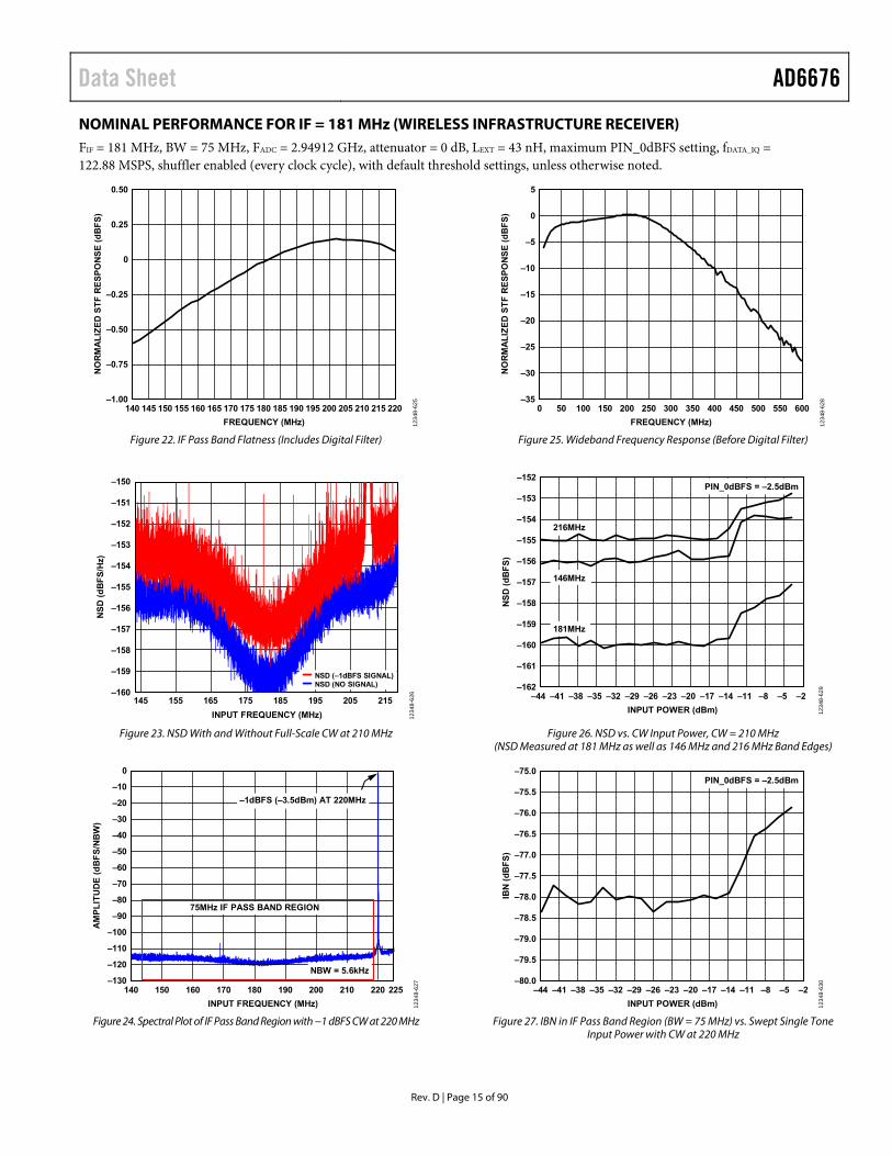
NOMINAL PERFORMANCE FOR IF = 181 MHz (WIRELESS INFRASTRUCTURE RECEIVER) FIF = 181 MHz, BW = 75 MHz, FADC = 2.94912 GHz, attenuator = 0 dB, LEXT = 43 nH, maximum PIN_0dBFS setting, fDATA_IQ = 122.88 MSPS, shuffler enabled (every clock cycle), with default threshold settings, unless otherwise noted.
0.50
–1.00
–0.75
–0.50
–0.25
0
0.25
140 145 150 155 160 165 170 175 180 185 190 195 200 205 210 220215
NO
RM
AL
IZE
D S
TF
RE
SP
ON
SE
(d
BF
S)
FREQUENCY (MHz) 1234
8-62
5
Figure 22. IF Pass Band Flatness (Includes Digital Filter)
NS
D (
dB
FS
/Hz)
INPUT FREQUENCY (MHz)
145 155 165 175 185 195 205 215–160
–150
–151
–152
–153
–154
–155
–156
–157
–158
–159 NSD (–1dBFS SIGNAL)NSD (NO SIGNAL)
1234
8-62
6
Figure 23. NSD With and Without Full-Scale CW at 210 MHz
0
–90
–100
–110
–120
–130
–80
–70
–60
–50
–40
–30
–20
–10
AM
PL
ITU
DE
(d
BF
S/N
BW
)
INPUT FREQUENCY (MHz)
NBW = 5.6kHz
–1dBFS (–3.5dBm) AT 220MHz
140 150 160 170 180 190 200 210 220 225
75MHz IF PASS BAND REGION
1234
8-62
7
Figure 24. Spectral Plot of IF Pass Band Region with −1 dBFS CW at 220 MHz
5
0
–5
–10
–15
–20
–25
–30
–350 600450350250 55050040030020015010050
NO
RM
AL
IZE
D S
TF
RE
SP
ON
SE
(d
BF
S)
FREQUENCY (MHz) 1234
8-62
8
Figure 25. Wideband Frequency Response (Before Digital Filter)
–152
–153
–154
–155
–156
–157
–158
–159
–160
–161
–162–44 –2–5–8–11–14–17–20–23–26–29–32–35–38–41
NS
D (
dB
FS
)
INPUT POWER (dBm)
PIN_0dBFS = –2.5dBm
216MHz
146MHz
181MHz
1234
8-62
9
Figure 26. NSD vs. CW Input Power, CW = 210 MHz (NSD Measured at 181 MHz as well as 146 MHz and 216 MHz Band Edges)
–75.0
–75.5
–76.0
–76.5
–77.0
–77.5
–78.0
–78.5
–79.0
–79.5
–80.0–44 –2–5–8–11–14–17–20–23–26–29–32–35–38–41
IBN
(d
BF
S)
INPUT POWER (dBm)
PIN_0dBFS = –2.5dBm
1234
8-63
0
Figure 27. IBN in IF Pass Band Region (BW = 75 MHz) vs. Swept Single Tone Input Power with CW at 220 MHz
AD6676 Data Sheet
Rev. D | Page 16 of 90
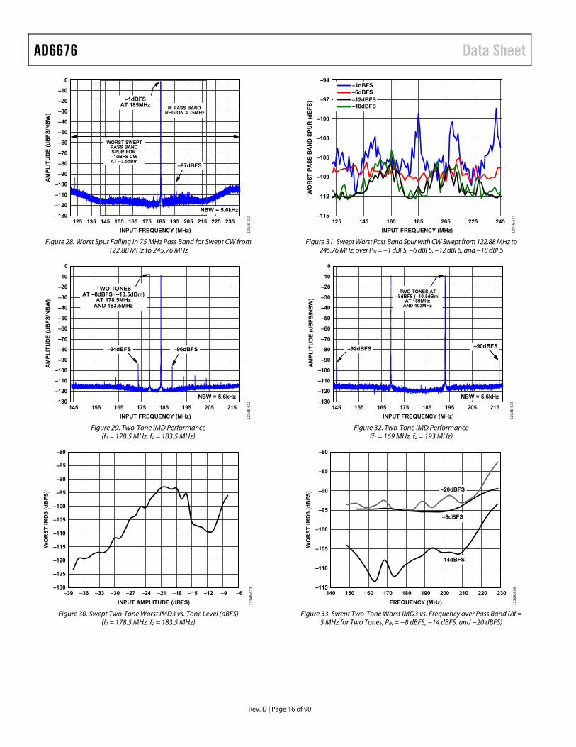
0
–130
–90
–100
–110
–120
–80
–70
–60
–50
–40
–30
–20
–10
125 135 145 155 165 175 185 195 205 215 225 235
AM
PL
ITU
DE
(d
BF
S/N
BW
)
INPUT FREQUENCY (MHz)
WORST SWEPTPASS BANDSPUR FOR–1dBFS CWAT –3.5dBm
IF PASS BANDREGION = 75MHz
–97dBFS
NBW = 5.6kHz
–1dBFSAT 185MHz
1234
8-63
1Figure 28. Worst Spur Falling in 75 MHz Pass Band for Swept CW from
122.88 MHz to 245.76 MHz
0
–130
–90
–100
–110
–120
–80
–70
–60
–50
–40
–30
–20
–10
145 155 165 175 185 195 205 215
AM
PL
ITU
DE
(d
BF
S/N
BW
)
INPUT FREQUENCY (MHz)
–96dBFS–94dBFS
NBW = 5.6kHz
TWO TONESAT –8dBFS (–10.5dBm)
AT 178.5MHzAND 183.5MHz
1234
8-63
2
Figure 29. Two-Tone IMD Performance (f1 = 178.5 MHz, f2 = 183.5 MHz)
WO
RS
T I
MD
3 (d
BF
S)
INPUT AMPLITUDE (dBFS)
–39 –6–9–12–15–18–21–24–27–30–33–36
–80
–85
–90
–95
–100
–105
–110
–115
–120
–125
–130
1234
8-63
3
Figure 30. Swept Two-Tone Worst IMD3 vs. Tone Level (dBFS) (f1 = 178.5 MHz, f2 = 183.5 MHz)
–94
–97
–100
–103
–106
–109
–112
–115
WO
RS
T P
AS
S B
AN
D S
PU
R (
dB
FS
)
INPUT FREQUENCY (MHz)
125 145 165 185 205 225 245
–1dBFS–6dBFS–12dBFS–18dBFS
1234
8-63
4
Figure 31. Swept Worst Pass Band Spur with CW Swept from 122.88 MHz to 245.76 MHz, over PIN = −1 dBFS, −6 dBFS, −12 dBFS, and −18 dBFS
0
–130
–90
–100
–110
–120
–80
–70
–60
–50
–40
–30
–20
–10
145 155 165 175 185 195 205 215
AM
PL
ITU
DE
(d
BF
S/N
BW
)
INPUT FREQUENCY (MHz)
–90dBFS–92dBFS
NBW = 5.6kHz
TWO TONES AT–8dBFS (–10.5dBm)
AT 169MHzAND 193MHz
1234
8-63
5
Figure 32. Two-Tone IMD Performance (f1 = 169 MHz, f2 = 193 MHz)
WO
RS
T I
MD
3 (d
BF
S)
FREQUENCY (MHz)
140 150 160 170 180 190 200 210 220 230
–80
–85
–90
–95
–100
–105
–115
–110
–20dBFS
–14dBFS
–8dBFS12
348-
636
Figure 33. Swept Two-Tone Worst IMD3 vs. Frequency over Pass Band (∆f = 5 MHz for Two Tones, PIN = −8 dBFS, −14 dBFS, and −20 dBFS)
Data Sheet AD6676
Rev. D | Page 17 of 90
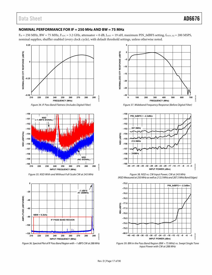
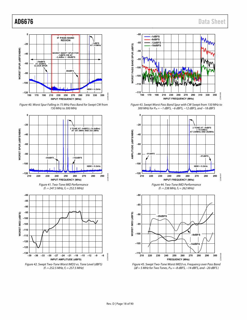
NOMINAL PERFORMANCE FOR IF = 250 MHz AND BW = 75 MHz FIF = 250 MHz, BW = 75 MHz, FADC = 3.2 GHz, attenuator = 0 dB, LEXT = 19 nH, maximum PIN_0dBFS setting, fDATA_IQ = 200 MSPS, nominal supplies, shuffler enabled (every clock cycle), with default threshold settings, unless otherwise noted.
0.25
–0.50
–0.25
0
210 220 230 240 250 260 270 280 290
NO
RM
AL
IZE
D S
TF
RE
SP
ON
SE
(d
BF
S)
FREQUENCY (MHz) 1234
8-63
7
Figure 34. IF Pass Band Flatness (Includes Digital Filter)
–150
–151
–152
–153
–154
–155
–156
–157
–158
–159
–160210 220 230 240 250 260 270 280 290
NS
D (
dB
FS
/Hz)
INPUT FREQUENCY (MHz)
NSD(–1 dBFS SIGNAL)
NSD(NO SIGNAL)
1234
8-63
8
Figure 35. NSD With and Without Full-Scale CW at 243 MHz
0
–120
–100
–80
–60
–40
–20
210 220 230 240 250 260 270 280 290
AM
PL
ITU
DE
(d
BF
S/N
BW
)
INPUT FREQUENCY (MHz)
–1 dBFSAT 288MHz
NBW = 9.2kHz
IF PASS BAND REGION
1234
8-63
9
Figure 36. Spectral Plot of IF Pass Band Region with −1 dBFS CW at 288 MHz
5
–30
–25
–20
–15
–10
–5
0
0 100 200 300 400 500 600 700
NO
RM
AL
IZE
D S
TF
RE
SP
ON
SE
(d
BF
S)
FREQUENCY (MHz) 1234
8-64
0
Figure 37. Wideband Frequency Response (Before Digital Filter)
–150
–151
–152
–153
–154
–155
–156
–157
–158
–159
–160–44 –3–5–8–11–14–17–20–23–26–29–32–35–38–41
NS
D (
dB
FS
)
INPUT POWER (dBm)
PIN_0dBFS = –2.3dBm
287.5MHz
212.5MHz
250MHz
1234
8-64
1
Figure 38. NSD vs. CW Input Power, CW at 243 MHz (NSD Measured at 250 MHz as well as 212.5 MHz and 287.5 MHz Band Edges)
–75.0
–75.5
–76.0
–76.5
–77.0
–77.5
–78.0
–78.5
–79.0
–79.5
–80.0–45 –3–6–9–12–15–18–21–24–27–30–33–36–39–42
IBN
(d
BF
S)
INPUT POWER (dBm)
PIN_0dBFS = –2.3dBm
1234
8-64
2
Figure 39. IBN in the Pass Band Region (BW = 75 MHz) vs. Swept Single Tone Input Power with CW at 288 MHz
AD6676 Data Sheet
Rev. D | Page 18 of 90
0
–120
–100
–80
–60
–40
–20
150 170 190 210 230 250 270 290 310 330 350
WO
RS
T S
PU
R (
dB
FS
/NB
W)
INPUT FREQUENCY (MHz)
IF PASS BANDREGION
WORST SWEPT SPUR FOR–1dBFS CW AT
–3.4dBm < –88dBFS
–1dBFSAT 315MHz
–79dBFSAT 200MHz
CLOCK SPUR
–88dBFS
1234
8-64
3
NBW = 9.2kHz
Figure 40. Worst Spur Falling in 75 MHz Pass Band for Swept CW from 150 MHz to 300 MHz
0
–120
–100
–80
–60
–40
–20
210 290280270260250240230220
WO
RS
T S
PU
R (
dB
FS
/NB
W)
INPUT FREQUENCY (MHz)
2 TONE AT –8dBFS (–10.4dBm)AT 247.5MHz AND 252.2MHz
–94dBFS –102dBFS
1234
8-64
4
NBW = 9.2kHz
Figure 41. Two-Tone IMD Performance (f1 = 247.5 MHz, f2 = 252.5 MHz)
WO
RS
T I
MD
3 (d
BF
S)
INPUT AMPLITUDE (dBFS)
–39 –6–9–12–15–18–21–24–27–30–33–36
–80
–85
–90
–95
–100
–105
–110
–115
–120
–125
–130
1234
8-64
5
Figure 42. Swept Two-Tone Worst IMD3 vs. Tone Level (dBFS) (f1 = 252.5 MHz, f2 = 257.5 MHz)
–80
–85
–90
–95
–100
–105
–110
–115
WO
RS
T P
AS
S B
AN
D S
PU
R (
dB
FS
)
INPUT FREQUENCY (MHz)
150 170 190 210 230 250 270 290 310 330 350
–1dBFS–6dBFS–12dBFS–18dBFS
1234
8-64
6
Figure 43. Swept Worst Pass Band Spur with CW Swept from 150 MHz to 300 MHz for PIN = −1 dBFS, −6 dBFS, −12 dBFS, and −18 dBFS
0
–120
–100
–80
–60
–40
–20
210 290280270260250240230220
AM
PL
ITU
DE
(d
BF
S/N
BW
)
INPUT FREQUENCY (MHz)
–91dBFS–91dBFS
2 TONE AT –8dBFS(–10.4dBm)
AT 238MHz AND 262MHz
1234
8-64
7
NBW = 9.2kHz
Figure 44. Two-Tone IMD Performance (f1 = 238 MHz, f2 = 262 MHz)
WO
RS
T I
MD
3 (d
BF
S)
FREQUENCY (MHz)
210 220 230 240 250 260 270 280 290 300
–80
–85
–90
–95
–100
–105
–110
–20dBFS
–14dBFS
–8dBFS
1234
8-64
8
Figure 45. Swept Two-Tone Worst IMD3 vs. Frequency over Pass Band (∆f = 5 MHz for Two Tones, PIN =−8 dBFS, −14 dBFS, and −20 dBFS )
Data Sheet AD6676
Rev. D | Page 19 of 90
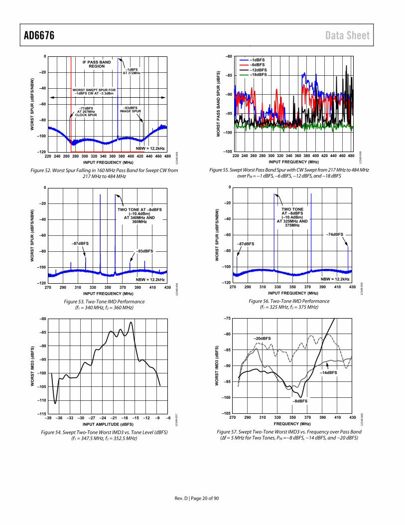
NOMINAL PERFORMANCE FOR IF = 350 MHZ AND BW = 160 MHZ FIF = 350 MHz, BW = 160 MHz, FADC = 3.2 GHz, attenuator = 0 dB, LEXT = 10 nH, maximum PIN_0dBFS setting, fDATA_IQ = 266.7 MSPS, shuffler enabled (every clock cycle), with default threshold settings, unless otherwise noted.
1.00
0.75
0.50
0.25
–0.50
–0.25
0
270 290 310 330 350 370 390 410 430
NO
RM
AL
IZE
D S
TF
RE
SP
ON
SE
(d
BF
S)
FREQUENCY (MHz) 1234
8-64
9
Figure 46. IF Pass Band Flatness (Includes Digital Filter)
–140
–142
–144
–146
–148
–150
–152
–154
–156270 290 310 330 350 370 390 410 430
NS
D (
dB
FS
)
INPUT FREQUENCY (MHz)
NSD(–1 dBFS SIGNAL)
NSD(NO SIGNAL)
1234
8-65
0
Figure 47. NSD With and Without Full-Scale CW at 355 MHz
0
–120
–100
–80
–60
–40
–20
260 280 300 320 340 360 380 400 440420
AM
PL
ITU
DE
(d
BF
S/N
BW
)
INPUT FREQUENCY (MHz)
–1 dBFSAT 431MHz
NBW = 12.2kHz
IF PASS BAND REGION
1234
8-65
1
Figure 48. Spectral Plot of IF Pass Band Region with −1 dBFS CW at 431 MHz
5
–35
–30
–25
–20
–15
–10
–5
0
0 1000900800700600500400300200100
NO
RM
AL
IZE
D S
TF
RE
SP
ON
SE
(d
BF
S)
FREQUENCY (MHz) 1234
8-65
2
Figure 49. Wideband Frequency Response (Before Digital Filter)
–140
–142
–144
–146
–148
–150
–152
–154
–156–44 –3–5–8–11–14–17–20–23–26–29–32–35–38–41
NS
D (
dB
FS
)
INPUT POWER (dBm)
PIN_0dBFS = –2.3dBm
310MHz
400MHz
350MHz
1234
8-65
3
Figure 50. NSD vs. CW Input Power, CW at 355 MHz (NSD Measured at 350 MHz as well as 350 MHz and 400 MHz Band Edges)
–60
–61
–62
–63
–64
–65
–66
–67
–68
–69
–70–45 –3–6–9–12–15–18–21–24–27–30–33–36–39–42
IBN
(d
BF
S)
INPUT POWER (dBm)
PIN_0dBFS = –2.3dBm
1234
8-65
4
Figure 51. IBN in IF Pass Band Region (BW = 160 MHz) vs. Swept Single Tone Input Power with CW at 431 MHz
AD6676 Data Sheet
Rev. D | Page 20 of 90
0
–120
–100
–80
–60
–40
–20
220 480460440420400380360340320300280260240
WO
RS
T S
PU
R (
dB
FS
/NB
W)
INPUT FREQUENCY (MHz)
IF PASS BANDREGION
WORST SWEPT SPUR FOR–1dBFS CW AT –3.3dBm
–1dBFSAT 372MHz
–77dBFSAT 267MHz
CLOCK SPUR
–83dBFSIMAGE SPUR
NBW = 12.2kHz
1234
8-65
5
Figure 52. Worst Spur Falling in 160 MHz Pass Band for Swept CW from 217 MHz to 484 MHz
0
–120
–100
–80
–60
–40
–20
270 290 310 330 350 370 390 410 430
WO
RS
T S
PU
R (
dB
FS
/NB
W)
INPUT FREQUENCY (MHz)
TWO TONE AT –8dBFS(–10.4dBm)
AT 340MHz AND360MHz
–93dBFS
–87dBFS
NBW = 12.2kHz
1234
8-65
6
Figure 53. Two-Tone IMD Performance (f1 = 340 MHz, f2 = 360 MHz)
WO
RS
T I
MD
3 (d
BF
S)
INPUT AMPLITUDE (dBFS)
–39 –6–9–12–15–18–21–24–27–30–33–36
–80
–85
–90
–95
–100
–105
–110
–115
1234
8-65
7
Figure 54. Swept Two-Tone Worst IMD3 vs. Tone Level (dBFS) (f1 = 347.5 MHz, f2 = 352.5 MHz)
–80
–85
–90
–95
–105
–100
WO
RS
T P
AS
S B
AN
D S
PU
R (
dB
FS
)
INPUT FREQUENCY (MHz)
220 240 260 280 300 320 340 360 380 400 420 440 460 480
–1dBFS–6dBFS–12dBFS–18dBFS
1234
8-65
8
Figure 55. Swept Worst Pass Band Spur with CW Swept from 217 MHz to 484 MHz over PIN = −1 dBFS, −6 dBFS, −12 dBFS, and −18 dBFS
0
–120
–100
–80
–60
–40
–20
270 290 310 330 350 370 390 410 430
WO
RS
T S
PU
R (
dB
FS
/NB
W)
INPUT FREQUENCY (MHz)
TWO TONEAT –8dBFS(–10.4dBm)
AT 325MHz AND375MHz
–74dBFS
–87dBFS
NBW = 12.2kHz
1234
8-65
9
Figure 56. Two-Tone IMD Performance (f1 = 325 MHz, f2 = 375 MHz)
WO
RS
T I
MD
3 (d
BF
S)
FREQUENCY (MHz)
270 290 310 330 350 370 390 410 430
–75
–80
–85
–90
–95
–100
–105
–20dBFS
–14dBFS
–8dBFS
1234
8-66
0
Figure 57. Swept Two-Tone Worst IMD3 vs. Frequency over Pass Band (∆f = 5 MHz for Two Tones, PIN =−8 dBFS, −14 dBFS, and −20 dBFS)

Data Sheet AD6676
Rev. D | Page 21 of 90
EQUIVALENT CIRCUITS
1234
8-01
7
CSB, SCLKOR SDI
1kΩ
VDDIO
Figure 58. Equivalent CSB or SCLK Input Circuit
DC
AC
VIN+
VIN–
RIN = 60ΩVCM = 1.0V
1234
8-40
1
Figure 59. Equivalent Analog Input
+
–
CLK+
CLK–
NC
TO CLK SYN
TO BAND-PASSΣ-∆ ADC
50Ω 50Ω
VDD1
1234
8-01
1
Figure 60. Equivalent Clock Input Circuit
SYSREF+
VDDHSI
1kΩ
SYSREF–
VDDHSI
1kΩ
10kΩ
10kΩ
LEVELTRANSLATOR VCM = 0.55V
1234
8-01
2
Figure 61. Equivalent SYSREF± Input
1234
8-01
5
1kΩ
VDDIOVDDIO
SDIOOR
AGCx
I/O
ESDPROTECTED
ESDPROTECTED
Figure 62. Equivalent SDIO or AGCx Input/Output Circuit
1234
8-01
6
RESETB1kΩ
VDDIO
25kΩ
Figure 63. Equivalent RESETB Input Circuit
20kΩ
20kΩ
LEVELTRANSLATOR VCM = 0.85V
SYNCINB± PINCONTROL (SPI)
SYNCINB+
VDDIO
1kΩ
DGND
SYNCINB–
VDDIO
1kΩ
DGND
VCM
1234
8-01
3
Figure 64. Equivalent SYNCINB± Input
SERDOUTx+
SERDOUTx–
DATA+
DATA–
x = 0, 1
x = 0, 1
VDDHSI
VDDHSIOUTPUTDRIVER
EMPHASIS/SWINGCONTROL (SPI)
1234
8-01
4
Figure 65. Digital CML Output Circuit
AD6676 Data Sheet
Rev. D | Page 22 of 90
TERMINOLOGY Noise Figure (NF) NF is the degradation in SNR performance (in dB) of an input signal having a noise density of −174 dBm/Hz after it passes through a component or system. Mathematically,
NF = 10 × log(SNRIN/SNROUT)
The noise figure of the AD6676 is determined by the equation
NF = PIN − (10 × log(BW)) − (−174.0 dBm/Hz) − SNR
where: PIN is the input power of an unmodulated carrier. BW is the noise measurement bandwidth. −174.0 dBm/Hz is the thermal noise floor at 290 K. SNR is the measured signal-to-noise ratio in dB of the AD6676.
Note that PIN is set to a low level (that is, <−40 dBm) to minimize any degradation in measured SNR due to phase noise from either the input signal or Σ-Δ ADC clock source.
Noise Spectral Density (NSD) NSD is the noise power normalized to 1 Hz bandwidth (at a particular frequency) relative to the full scale of the ADC (dBFS) and hence is given in units of dBFS/Hz. The AD6676, being a Σ-Δ ADC, displays a uneven NSD across its IF pass band. Both the worst-case NSD as well as NSD at the pass band center are reported. Note that NSD is calculated from the IBN measured over a 5 MHz bandwidth.
In-Band Noise (IBN) IBN is the integrated noise power measured over a user defined bandwidth relative to the full scale of the ADC (dBFS). This bandwidth is typically equal to the IF pass band setting (BW) of the AD6676, unless otherwise noted.
Input Second-Order Intercept (IIP2) IIP2 is a figure of merit used to quantify the second-order intermodulation distortion (IMD2) of a component or system. Two equal amplitude unmodulated carriers at specified frequencies (f1 and f2) injected into a nonlinear system exhibiting second-order nonlinearities produce IMD components at f1 − f2 and f1 + f2. For the AD6676, the two frequencies are situated at ½ the IF frequency (with a 2 MHz offset) at a power level corresponding to −6 dBFS at the IF center frequency with only the intermodulation term at f1 + f2 considered. IIP2 is the extrapolated tone power at which the intermodulation terms and the input tones have equal amplitude.
IIP2 = PIN − IMD2
Input Third-Order Intercept (IIP3) IIP3 is a figure of merit used to quantify the third-order intermodulation distortion (IMD3) of a component or system. Two equal amplitude unmodulated carriers at specified frequencies (f1 and f2) injected into a nonlinear system exhibiting third-order nonlinearities produce IMD components at 2 f1 − f2 and 2 f2 − f1. IIP3 is the extrapolated tone power at which the intermodulation terms and the input tones have equal amplitude.
IIP3 = PIN – IMD3/2
Note that the third-order IMD performance of an ADC does not necessarily follow the 3:1 rule that is typical of RF/IF linear devices. IMD performance is dependent on the dual tone frequencies, signal input levels, and ADC clock rate.
Worst In-Band Spur (SFDR) Worst in-band spur is the worst spur falling in the IF pass band relative to the full scale of the ADC (dBFS) when a single tone with defined power level is stepped (typically 1 MHz increments) across a user defined frequency range. Note that this worst spur can often be an image (or clock) related spur depending on the IF, BW, and IQ output data rate setting of the AD6676 and on the sweep range.
Signal Transfer Function (STF) STF is the frequency response of the output signal of the ADC relative to a swept single tone at its input. The STF presented for different AD6676 setup conditions in the Typical Performance Characteristics section shows the STF over the IF pass band after the digital filter to highlight pass band flatness. The wideband STF response is measured before the digital filter to highlight the pass band response of the AD6676 Σ-Δ ADC.
Data Sheet AD6676
Rev. D | Page 23 of 90
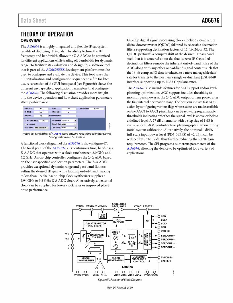
THEORY OF OPERATION OVERVIEW The AD6676 is a highly integrated and flexible IF subsystem capable of digitizing IF signals. The ability to tune the IF frequency and bandwidth allows the Σ-Δ ADC to be optimized for different applications while trading off bandwidth for dynamic range. To facilitate its evaluation and design in, a software tool that is part of the AD6676EBZ development platform must be used to configure and evaluate the device. This tool saves the SPI initialization and configuration sequence to a file for later use. A screenshot of the GUI front panel (see Figure 66) shows the different user specified application parameters that configure the AD6676. The following discussion provides more insight into the device operation and how these application parameters affect performance.
1234
8-01
8
Figure 66. Screenshot of AD6676 GUI Software Tool that Facilitates Device
Configuration and Evaluation
A functional block diagram of the AD6676 is shown Figure 67. The focal point of the AD6676 is its continuous time, band-pass Σ-Δ ADC that operates with a clock rate between 2.0 GHz and 3.2 GHz. An on-chip controller configures the Σ-Δ ADC based on the user specified application parameters. The Σ-Δ ADC provides exceptional dynamic range and pass band flatness within the desired IF span while limiting out-of-band peaking to less than 0.5 dB. An on-chip clock synthesizer supplies a 2.94 GHz to 3.2 GHz Σ-Δ ADC clock. Alternatively, an external clock can be supplied for lower clock rates or improved phase noise performance.
On-chip digital signal processing blocks include a quadrature digital downconverter (QDDC) followed by selectable decimation filters supporting decimation factors of 12, 16, 24, or 32. The QDDC performs a complex shift of the desired IF pass band such that it is centered about dc, that is, zero IF. Cascaded decimation filters remove the inherent out-of-band noise of the ADC along with any other out-of-band signal content such that the 16-bit complex IQ data is reduced to a more manageable data rate for transfer to the host via a single or dual lane JESD204B interface supporting up to 5.333 Gbps lane rates.
The AD6676 also includes features for AGC support and/or level-planning optimization. AGC support includes the ability to monitor peak power at the Σ-Δ ADC output or rms power after the first internal decimation stage. The host can initiate fast AGC action by configuring various flags whose status are made available on the AGC4 to AGC1 pins. Flags can be set with programmable thresholds indicating whether the signal level is above or below a defined level. A 27 dB attenuator with a step size of 1 dB is available for IF AGC control or level planning optimization during initial system calibration. Alternatively, the nominal 0 dBFS full-scale input power level (PIN_0dBFS) of −2 dBm can be reduced by up to 12 dB thus further reducing the RF/IF gain requirements. The SPI programs numerous parameters of the AD6676, allowing the device to be optimized for a variety of applications.
L–L+
RESETBVDDIOAGC4, AGC3AGC2, AGC1VDD2NV
VSSAVDD2 VDDD VSSD
SPI
CSB
SCLK
SDIO
SDO
SERDOUT0+
SERDOUT0–
SERDOUT1+
SERDOUT1–
VDDHSI
SYNCINB±
SYSREF±
AGCSUPPORT
CLOCKGENERATION
–2.0VREG
JES
D20
4BS
ER
IAL
IZE
RT
x O
UT
PU
TS
Mx
M = 12,16, 24,
32
I
Q
QDDC +NCO I
Q
BAND-PASSΣ-∆ ADC
VIN–
VIN+
27dB ATTENUATOR(1dB STEPS)
CLOCKSYNTHESIZER
JESD204BSUBCLASS 1
CONTROL
CLK+ CLK–VDDCVDDQ
AD6676
1234
8-40
0
VDDL VDD1
VSS2OUTVSS2IN
Figure 67. Functional Block Diagram
AD6676 Data Sheet
Rev. D | Page 24 of 90
RINVIN
IDA
C3
IDA
C1
CARRAY LEXT
RESON1 RESON2 RESON3
AV
IDAC1FSADJUST
C3
G31
IDA
C4
C4
G43
IDA
C5
C5
G54
IDA
C6
C6
G65
–G34 –G56
G53
17-LEVELFLASH
ADC 17 5
17OPTIONALSHUFFLER
ENCODER DOUT
1234
8-02
0
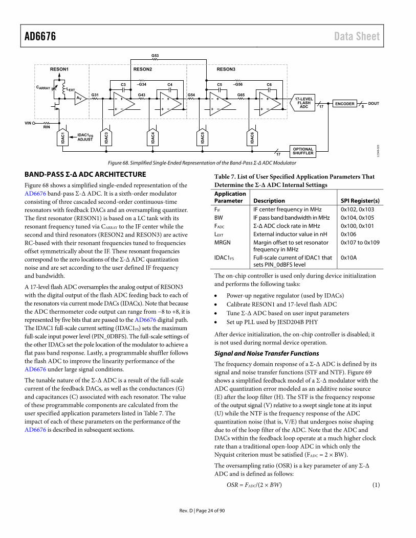
Figure 68. Simplified Single-Ended Representation of the Band-Pass Σ-Δ ADC Modulator
BAND-PASS Σ-Δ ADC ARCHITECTURE Figure 68 shows a simplified single-ended representation of the AD6676 band-pass Σ-Δ ADC. It is a sixth-order modulator consisting of three cascaded second-order continuous-time resonators with feedback DACs and an oversampling quantizer. The first resonator (RESON1) is based on a LC tank with its resonant frequency tuned via CARRAY to the IF center while the second and third resonators (RESON2 and RESON3) are active RC-based with their resonant frequencies tuned to frequencies offset symmetrically about the IF. These resonant frequencies correspond to the zero locations of the Σ-Δ ADC quantization noise and are set according to the user defined IF frequency and bandwidth.
A 17-level flash ADC oversamples the analog output of RESON3 with the digital output of the flash ADC feeding back to each of the resonators via current mode DACs (IDACx). Note that because the ADC thermometer code output can range from −8 to +8, it is represented by five bits that are passed to the AD6676 digital path. The IDAC1 full-scale current setting (IDAC1FS) sets the maximum full-scale input power level (PIN_0DBFS). The full-scale settings of the other IDACs set the pole location of the modulator to achieve a flat pass band response. Lastly, a programmable shuffler follows the flash ADC to improve the linearity performance of the AD6676 under large signal conditions.
The tunable nature of the Σ-Δ ADC is a result of the full-scale current of the feedback DACs, as well as the conductances (G) and capacitances (C) associated with each resonator. The value of these programmable components are calculated from the user specified application parameters listed in Table 7. The impact of each of these parameters on the performance of the AD6676 is described in subsequent sections.
Table 7. List of User Specified Application Parameters That Determine the Σ-Δ ADC Internal Settings Application Parameter Description SPI Register(s) FIF IF center frequency in MHz 0x102, 0x103 BW IF pass band bandwidth in MHz 0x104, 0x105 FADC Σ-Δ ADC clock rate in MHz 0x100, 0x101 LEXT External inductor value in nH 0x106 MRGN Margin offset to set resonator
frequency in MHz 0x107 to 0x109
IDAC1FS Full-scale current of IDAC1 that sets PIN_0dBFS level
0x10A
The on-chip controller is used only during device initialization and performs the following tasks:
Power-up negative regulator (used by IDACs) Calibrate RESON1 and 17-level flash ADC Tune Σ-Δ ADC based on user input parameters Set up PLL used by JESD204B PHY
After device initialization, the on-chip controller is disabled; it is not used during normal device operation.
Signal and Noise Transfer Functions
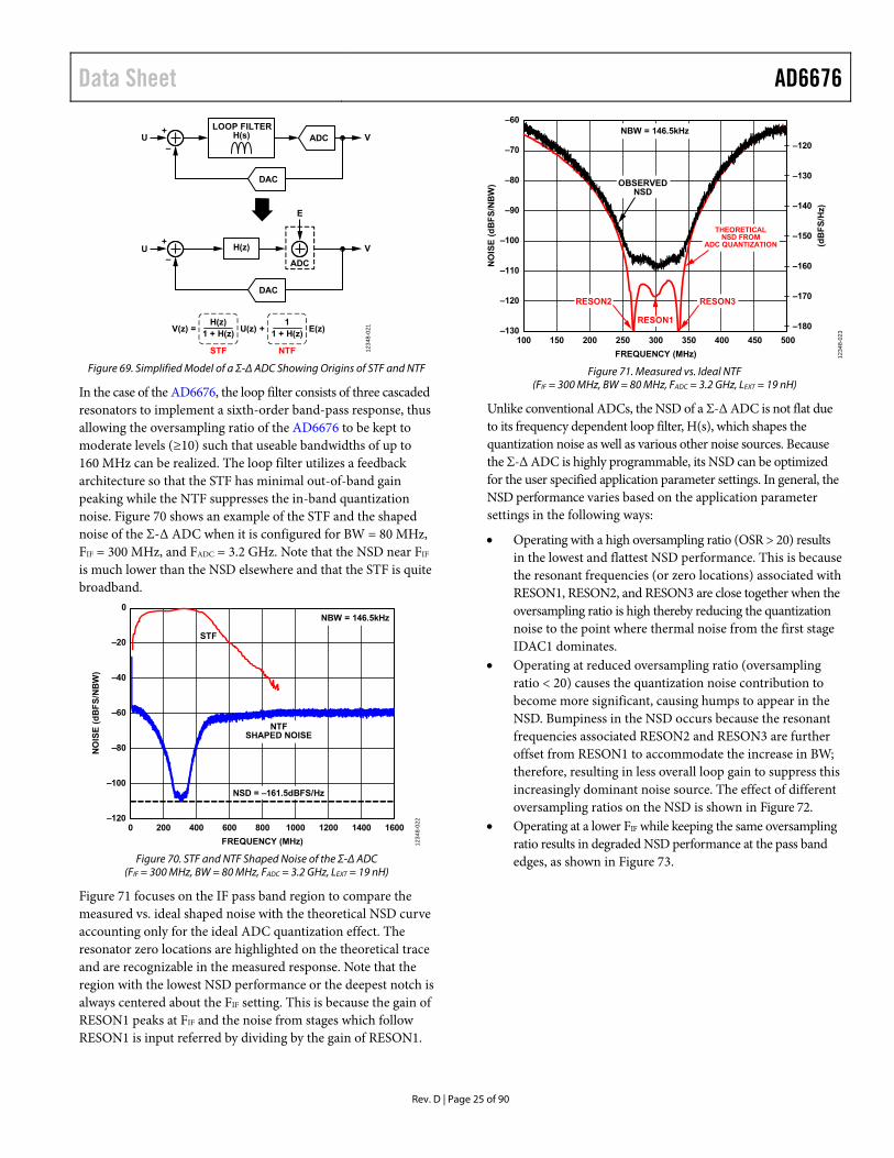
The frequency domain response of a Σ-Δ ADC is defined by its signal and noise transfer functions (STF and NTF). Figure 69 shows a simplified feedback model of a Σ-Δ modulator with the ADC quantization error modeled as an additive noise source (E) after the loop filter (H). The STF is the frequency response of the output signal (V) relative to a swept single tone at its input (U) while the NTF is the frequency response of the ADC quantization noise (that is, V/E) that undergoes noise shaping due to of the loop filter of the ADC. Note that the ADC and DACs within the feedback loop operate at a much higher clock rate than a traditional open-loop ADC in which only the Nyquist criterion must be satisfied (FADC = 2 × BW).
The oversampling ratio (OSR) is a key parameter of any Σ-Δ ADC and is defined as follows:
OSR = FADC/(2 × BW) (1)
Data Sheet AD6676
Rev. D | Page 25 of 90
DAC
ADCLOOP FILTER
H(s)+
–U
U
V
DAC
H(z)+
–V
ADC
E
U(z)V(z) =H(z)
1 + H(z)
STF
E(z) +1
1 + H(z)
NTF 1234
8-02
1
Figure 69. Simplified Model of a Σ-Δ ADC Showing Origins of STF and NTF
In the case of the AD6676, the loop filter consists of three cascaded resonators to implement a sixth-order band-pass response, thus allowing the oversampling ratio of the AD6676 to be kept to moderate levels (≥10) such that useable bandwidths of up to 160 MHz can be realized. The loop filter utilizes a feedback architecture so that the STF has minimal out-of-band gain peaking while the NTF suppresses the in-band quantization noise. Figure 70 shows an example of the STF and the shaped noise of the Σ-Δ ADC when it is configured for BW = 80 MHz, FIF = 300 MHz, and FADC = 3.2 GHz. Note that the NSD near FIF
is much lower than the NSD elsewhere and that the STF is quite broadband.
0
–120
–100
–80
–60
–40
–20
0 200 400 600 800 1000 1200 1400 1600
NO
ISE
(d
BF
S/N
BW
)
FREQUENCY (MHz)
STF
NSD = –161.5dBFS/Hz
NTFSHAPED NOISE
NBW = 146.5kHz
1234
8-02
2
Figure 70. STF and NTF Shaped Noise of the Σ-Δ ADC
(FIF = 300 MHz, BW = 80 MHz, FADC = 3.2 GHz, LEXT = 19 nH)
Figure 71 focuses on the IF pass band region to compare the measured vs. ideal shaped noise with the theoretical NSD curve accounting only for the ideal ADC quantization effect. The resonator zero locations are highlighted on the theoretical trace and are recognizable in the measured response. Note that the region with the lowest NSD performance or the deepest notch is always centered about the FIF setting. This is because the gain of RESON1 peaks at FIF and the noise from stages which follow RESON1 is input referred by dividing by the gain of RESON1.
–60
–130
–120
–130
–140
–150
–160
–170
–180
–120
–110
–100
–90
–80
–70
100 150 200 250 300 350 400 450 500
NO
ISE
(d
BF
S/N
BW
)
(dB
FS
/Hz)
FREQUENCY (MHz)
RESON2
RESON1
RESON3
THEORETICALNSD FROM
ADC QUANTIZATION
OBSERVEDNSD
NBW = 146.5kHz
1234
8-02
3
Figure 71. Measured vs. Ideal NTF
(FIF = 300 MHz, BW = 80 MHz, FADC = 3.2 GHz, LEXT = 19 nH)
Unlike conventional ADCs, the NSD of a Σ-Δ ADC is not flat due to its frequency dependent loop filter, H(s), which shapes the quantization noise as well as various other noise sources. Because the Σ-Δ ADC is highly programmable, its NSD can be optimized for the user specified application parameter settings. In general, the NSD performance varies based on the application parameter settings in the following ways:
Operating with a high oversampling ratio (OSR > 20) results in the lowest and flattest NSD performance. This is because the resonant frequencies (or zero locations) associated with RESON1, RESON2, and RESON3 are close together when the oversampling ratio is high thereby reducing the quantization noise to the point where thermal noise from the first stage IDAC1 dominates.
Operating at reduced oversampling ratio (oversampling ratio < 20) causes the quantization noise contribution to become more significant, causing humps to appear in the NSD. Bumpiness in the NSD occurs because the resonant frequencies associated RESON2 and RESON3 are further offset from RESON1 to accommodate the increase in BW; therefore, resulting in less overall loop gain to suppress this increasingly dominant noise source. The effect of different oversampling ratios on the NSD is shown in Figure 72.
Operating at a lower FIF while keeping the same oversampling ratio results in degraded NSD performance at the pass band edges, as shown in Figure 73.
AD6676 Data Sheet
Rev. D | Page 26 of 90
–130
–160
–155
–150
–145
–140
–135
200 220 240 260 280 300 320 360 400340 380
NO
ISE
(d
BF
S/H
z)
FREQUENCY (MHz)
OSR = 10(BW = 160MHz)OSR = 20(BW = 80MHz)OSR = 40(BW = 40MHz)OSR = 80(BW = 20MHz)
1234
8-02
4
Figure 72. NSD vs. Oversampling Ratio (FIF = 300 MHz, FADC = 3.2 GHz, LEXT = 19 nH)
–140
–160
–158
–156
–154
–152
–150
–148
–146
–144
–142
–100 –80 –60 –40 –20 0 20 60 10040 80
NO
ISE
(d
BF
S/H
z)
NORMALIZED ZERO IF FREQUENCY (MHz)
IF = 100MHzWITH LEXT = 100nH
IF = 200MHzWITH LEXT = 43nH
IF = 300MHzWITH LEXT = 19nH
1234
8-02
5
Figure 73. NSD at Pass Band Edge Improvement as FIF Is Increased from
100 MHz to 300 MHz with Fixed Oversampling Ratio = 16 (BW = 100 MHz, FADC = 3.2 GHz)
The impact of a uneven NSD profile on a particular application depends on the bandwidth and modulation characteristics of the IF signal being digitized and demodulated. For example, a multimode software defined radio containing narrow-band carriers situated anywhere across the pass band must consider the NSD performance at the highest levels across the pass band because this represents the worst-case NSD when calculating the in-band noise for a narrow-band signal in this region. Conversely, a single wideband QAM signal falling at the center of the IF pass band benefits from excellent in-band noise performance because the NSD remains the lowest in this region. Note that the AD6676 specified NF is measured in the region where its NSD is highest.
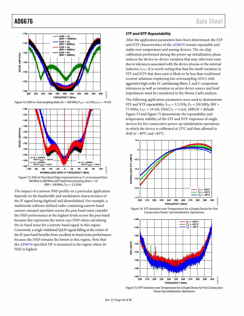
STF and NTF Repeatability
After the application parameters have been determined, the STF and NTF characteristics of the AD6676 remain repeatable and stable over temperature and among devices. The on-chip calibration performed during the power-up initialization phase reduces the device-to-device variation that may otherwise exist due to tolerances associated with the device process or the external inductor, LEXT. It is worth noting that that the small variation in STF and NTF that does exist is likely to be less than traditional receiver solutions employing low oversampling ADCs with aggressive high order LC antialiasing filters. L and C component tolerances as well as variation in active device source and load impedances must be considered in the Monte Carlo analysis.
The following application parameters were used to demonstrate STF and NTF repeatability: fCLK = 3.2 GHz, FIF = 250 MHz, BW = 75 MHz, LEXT = 19 nH, IDAC1FS = 4 mA, MRGN = default. Figure 74 and Figure 75 demonstrate the repeatability and temperature stability of the STF and NTF responses of single devices for five consecutive power-up initialization operations in which the device is calibrated at 25°C and then allowed to drift to −40°C and +85°C.
0.2
–1.0
–0.8
–0.6
–0.4
–0.2
0
200 210 220 230 240 250 260 280 300270 290
NO
RM
AL
IZE
D S
TF
(d
BF
S)
FREQUENCY (MHz) 1234
8-70
0
TA = –40°CTA = +25°CTA = +85°C
Figure 74. STF Variation over Temperature for a Single Device for Five
Consecutive Power-Up Initialization Operations
–146
–148
–150
–152
–154
–156
–158
–160200 210 220 230 240 250 260 280 300270 290
NS
D (
dB
FS
)
FREQUENCY (MHz) 1234
8-70
1
TA = –40°CTA = +25°CTA = +85°C
Figure 75. NTF Variation over Temperature for a Single Device for Five Consecutive
Power-Up Initialization Operations
Data Sheet AD6676
Rev. D | Page 27 of 90
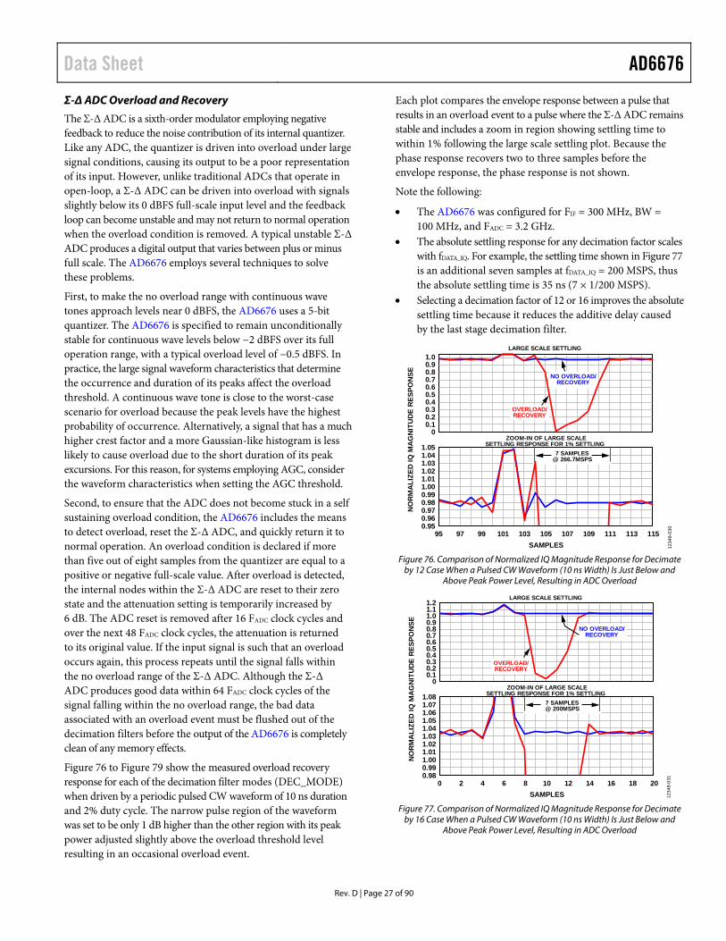
Σ-Δ ADC Overload and Recovery
The Σ-Δ ADC is a sixth-order modulator employing negative feedback to reduce the noise contribution of its internal quantizer. Like any ADC, the quantizer is driven into overload under large signal conditions, causing its output to be a poor representation of its input. However, unlike traditional ADCs that operate in open-loop, a Σ-Δ ADC can be driven into overload with signals slightly below its 0 dBFS full-scale input level and the feedback loop can become unstable and may not return to normal operation when the overload condition is removed. A typical unstable Σ-Δ ADC produces a digital output that varies between plus or minus full scale. The AD6676 employs several techniques to solve these problems.
First, to make the no overload range with continuous wave tones approach levels near 0 dBFS, the AD6676 uses a 5-bit quantizer. The AD6676 is specified to remain unconditionally stable for continuous wave levels below −2 dBFS over its full operation range, with a typical overload level of −0.5 dBFS. In practice, the large signal waveform characteristics that determine the occurrence and duration of its peaks affect the overload threshold. A continuous wave tone is close to the worst-case scenario for overload because the peak levels have the highest probability of occurrence. Alternatively, a signal that has a much higher crest factor and a more Gaussian-like histogram is less likely to cause overload due to the short duration of its peak excursions. For this reason, for systems employing AGC, consider the waveform characteristics when setting the AGC threshold.
Second, to ensure that the ADC does not become stuck in a self sustaining overload condition, the AD6676 includes the means to detect overload, reset the Σ-Δ ADC, and quickly return it to normal operation. An overload condition is declared if more than five out of eight samples from the quantizer are equal to a positive or negative full-scale value. After overload is detected, the internal nodes within the Σ-Δ ADC are reset to their zero state and the attenuation setting is temporarily increased by 6 dB. The ADC reset is removed after 16 FADC clock cycles and over the next 48 FADC clock cycles, the attenuation is returned to its original value. If the input signal is such that an overload occurs again, this process repeats until the signal falls within the no overload range of the Σ-Δ ADC. Although the Σ-Δ ADC produces good data within 64 FADC clock cycles of the signal falling within the no overload range, the bad data associated with an overload event must be flushed out of the decimation filters before the output of the AD6676 is completely clean of any memory effects.
Figure 76 to Figure 79 show the measured overload recovery response for each of the decimation filter modes (DEC_MODE) when driven by a periodic pulsed CW waveform of 10 ns duration and 2% duty cycle. The narrow pulse region of the waveform was set to be only 1 dB higher than the other region with its peak power adjusted slightly above the overload threshold level resulting in an occasional overload event.
Each plot compares the envelope response between a pulse that results in an overload event to a pulse where the Σ-Δ ADC remains stable and includes a zoom in region showing settling time to within 1% following the large scale settling plot. Because the phase response recovers two to three samples before the envelope response, the phase response is not shown.
Note the following:
The AD6676 was configured for FIF = 300 MHz, BW = 100 MHz, and FADC = 3.2 GHz.
The absolute settling response for any decimation factor scales with fDATA_IQ. For example, the settling time shown in Figure 77 is an additional seven samples at fDATA_IQ = 200 MSPS, thus the absolute settling time is 35 ns (7 × 1/200 MSPS).
Selecting a decimation factor of 12 or 16 improves the absolute settling time because it reduces the additive delay caused by the last stage decimation filter.
1.0
0.950.960.970.980.991.001.011.021.031.041.05
00.10.20.30.40.50.60.70.80.9
95 97 99 101 103 105 107 109 111 113 115
NO
RM
ALI
ZED
IQ M
AG
NIT
UD
E R
ESPO
NSE
SAMPLES
ZOOM-IN OF LARGE SCALESETTLING RESPONSE FOR 1% SETTLING
LARGE SCALE SETTLING
NO OVERLOAD/RECOVERY
OVERLOAD/RECOVERY
7 SAMPLES@ 266.7MSPS
1234
8-03
0
Figure 76. Comparison of Normalized IQ Magnitude Response for Decimate
by 12 Case When a Pulsed CW Waveform (10 ns Width) Is Just Below and Above Peak Power Level, Resulting in ADC Overload
1.11.2
1.0
0.980.991.001.011.021.031.041.051.061.071.08
00.10.20.30.40.50.60.70.80.9
0 2 4 6 8 10 12 14 16 18 20
NO
RM
ALI
ZED
IQ M
AG
NIT
UD
E R
ESPO
NSE
SAMPLES
ZOOM-IN OF LARGE SCALESETTLING RESPONSE FOR 1% SETTLING
LARGE SCALE SETTLING
NO OVERLOAD/RECOVERY
OVERLOAD/RECOVERY
7 SAMPLES@ 200MSPS
1234
8-03
1
Figure 77. Comparison of Normalized IQ Magnitude Response for Decimate
by 16 Case When a Pulsed CW Waveform (10 ns Width) Is Just Below and Above Peak Power Level, Resulting in ADC Overload
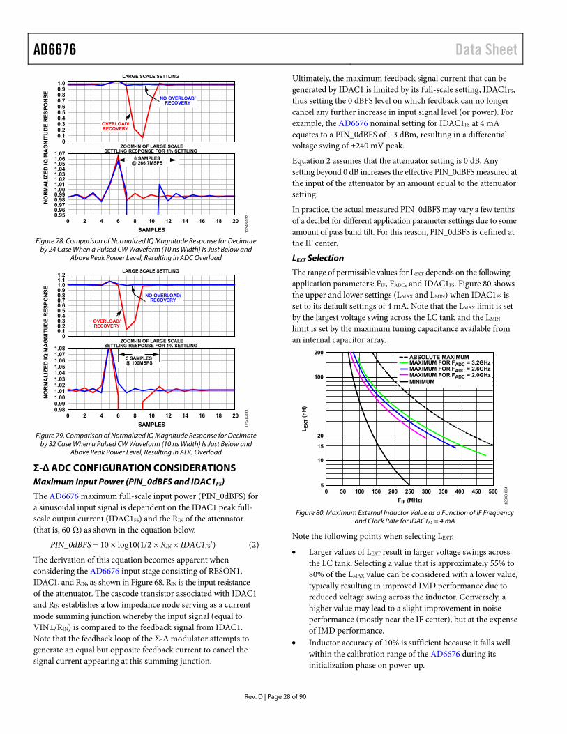
AD6676 Data Sheet
Rev. D | Page 28 of 90
1.0
0.950.960.970.980.991.001.011.021.031.041.051.061.07
00.10.20.30.40.50.60.70.80.9
0 2 4 6 108 12 14 16 18 20
NO
RM
AL
IZE
D I
Q M
AG
NIT
UD
E R
ES
PO
NS
E
SAMPLES
ZOOM-IN OF LARGE SCALESETTLING RESPONSE FOR 1% SETTLING
LARGE SCALE SETTLING
NO OVERLOAD/RECOVERY
OVERLOAD/RECOVERY
6 SAMPLES@ 266.7MSPS
1234
8-03
2
Figure 78. Comparison of Normalized IQ Magnitude Response for Decimate
by 24 Case When a Pulsed CW Waveform (10 ns Width) Is Just Below and Above Peak Power Level, Resulting in ADC Overload
1.11.2
1.0
0.980.991.001.011.021.031.041.051.061.071.08
00.10.20.30.40.50.60.70.80.9
0 2 4 6 8 10 12 14 16 18 20
NO
RM
AL
IZE
D I
Q M
AG
NIT
UD
E R
ES
PO
NS
E
SAMPLES
ZOOM-IN OF LARGE SCALESETTLING RESPONSE FOR 1% SETTLING
LARGE SCALE SETTLING
NO OVERLOAD/RECOVERY
OVERLOAD/RECOVERY
5 SAMPLES@ 100MSPS
1234
8-03
3
Figure 79. Comparison of Normalized IQ Magnitude Response for Decimate
by 32 Case When a Pulsed CW Waveform (10 ns Width) Is Just Below and Above Peak Power Level, Resulting in ADC Overload
Σ-Δ ADC CONFIGURATION CONSIDERATIONS Maximum Input Power (PIN_0dBFS and IDAC1FS)
The AD6676 maximum full-scale input power (PIN_0dBFS) for a sinusoidal input signal is dependent on the IDAC1 peak full-scale output current (IDAC1FS) and the RIN of the attenuator (that is, 60 Ω) as shown in the equation below.
PIN_0dBFS = 10 × log10(1/2 × RIN × IDAC1FS2) (2)
The derivation of this equation becomes apparent when considering the AD6676 input stage consisting of RESON1, IDAC1, and RIN, as shown in Figure 68. RIN is the input resistance of the attenuator. The cascode transistor associated with IDAC1 and RIN establishes a low impedance node serving as a current mode summing junction whereby the input signal (equal to VIN±/RIN) is compared to the feedback signal from IDAC1. Note that the feedback loop of the Σ-Δ modulator attempts to generate an equal but opposite feedback current to cancel the signal current appearing at this summing junction.
Ultimately, the maximum feedback signal current that can be generated by IDAC1 is limited by its full-scale setting, IDAC1FS, thus setting the 0 dBFS level on which feedback can no longer cancel any further increase in input signal level (or power). For example, the AD6676 nominal setting for IDAC1FS at 4 mA equates to a PIN_0dBFS of −3 dBm, resulting in a differential voltage swing of ±240 mV peak.
Equation 2 assumes that the attenuator setting is 0 dB. Any setting beyond 0 dB increases the effective PIN_0dBFS measured at the input of the attenuator by an amount equal to the attenuator setting.
In practice, the actual measured PIN_0dBFS may vary a few tenths of a decibel for different application parameter settings due to some amount of pass band tilt. For this reason, PIN_0dBFS is defined at the IF center.
LEXT Selection
The range of permissible values for LEXT depends on the following application parameters: FIF, FADC, and IDAC1FS. Figure 80 shows the upper and lower settings (LMAX and LMIN) when IDAC1FS is set to its default settings of 4 mA. Note that the LMAX limit is set by the largest voltage swing across the LC tank and the LMIN limit is set by the maximum tuning capacitance available from an internal capacitor array.
200
5
10
20
15
100
0 100 200 300 400 50050 150 250 350 450
LE
XT (
nH
)
FIF (MHz)
ABSOLUTE MAXIMUMMAXIMUM FOR FADC = 3.2GHzMAXIMUM FOR FADC = 2.6GHzMAXIMUM FOR FADC = 2.0GHzMINIMUM
1234
8-03
4
Figure 80. Maximum External Inductor Value as a Function of IF Frequency and Clock Rate for IDAC1FS = 4 mA
Note the following points when selecting LEXT:
Larger values of LEXT result in larger voltage swings across the LC tank. Selecting a value that is approximately 55% to 80% of the LMAX value can be considered with a lower value, typically resulting in improved IMD performance due to reduced voltage swing across the inductor. Conversely, a higher value may lead to a slight improvement in noise performance (mostly near the IF center), but at the expense of IMD performance.
Inductor accuracy of 10% is sufficient because it falls well within the calibration range of the AD6676 during its initialization phase on power-up.
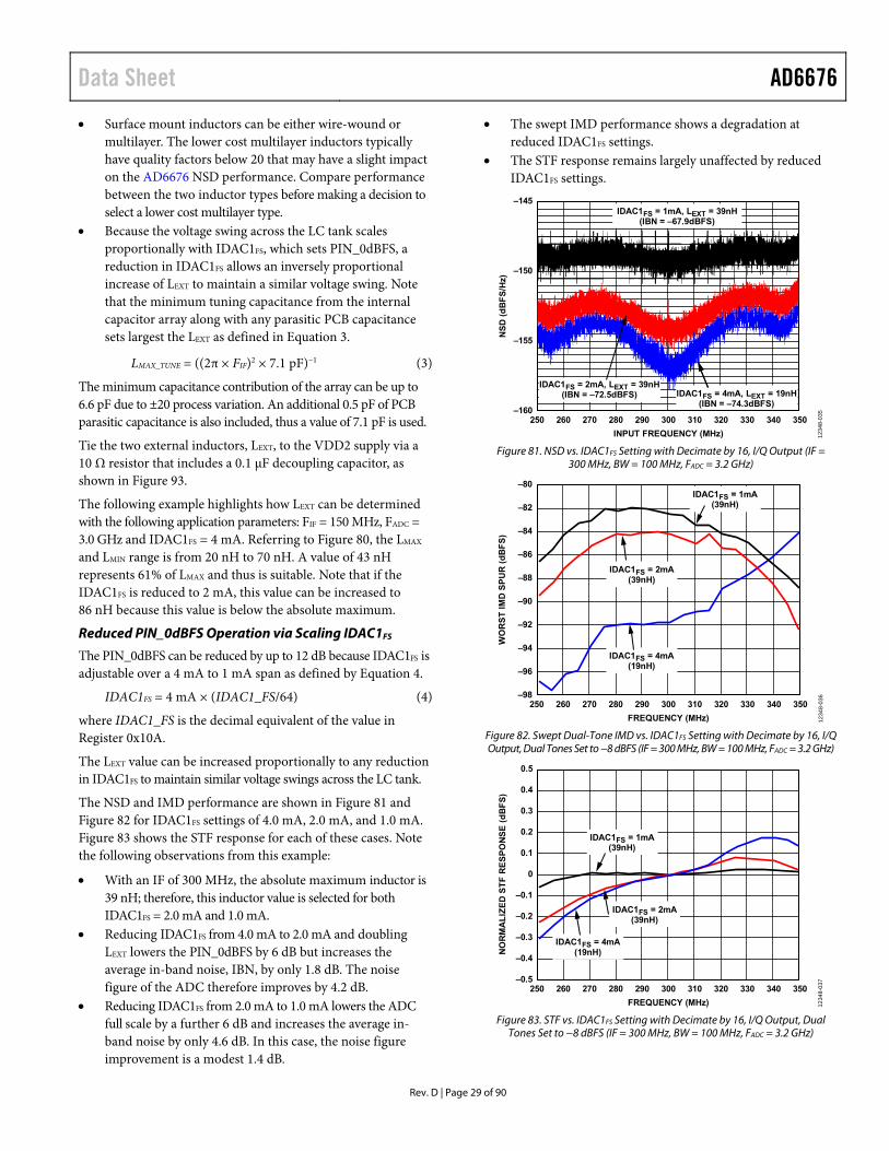
Data Sheet AD6676
Rev. D | Page 29 of 90
Surface mount inductors can be either wire-wound or multilayer. The lower cost multilayer inductors typically have quality factors below 20 that may have a slight impact on the AD6676 NSD performance. Compare performance between the two inductor types before making a decision to select a lower cost multilayer type.
Because the voltage swing across the LC tank scales proportionally with IDAC1FS, which sets PIN_0dBFS, a reduction in IDAC1FS allows an inversely proportional increase of LEXT to maintain a similar voltage swing. Note that the minimum tuning capacitance from the internal capacitor array along with any parasitic PCB capacitance sets largest the LEXT as defined in Equation 3.
LMAX_TUNE = ((2π × FIF)2 × 7.1 pF)−1 (3)
The minimum capacitance contribution of the array can be up to 6.6 pF due to ±20 process variation. An additional 0.5 pF of PCB parasitic capacitance is also included, thus a value of 7.1 pF is used.
Tie the two external inductors, LEXT, to the VDD2 supply via a 10 Ω resistor that includes a 0.1 μF decoupling capacitor, as shown in Figure 93.
The following example highlights how LEXT can be determined with the following application parameters: FIF = 150 MHz, FADC = 3.0 GHz and IDAC1FS = 4 mA. Referring to Figure 80, the LMAX and LMIN range is from 20 nH to 70 nH. A value of 43 nH represents 61% of LMAX and thus is suitable. Note that if the IDAC1FS is reduced to 2 mA, this value can be increased to 86 nH because this value is below the absolute maximum.
Reduced PIN_0dBFS Operation via Scaling IDAC1FS
The PIN_0dBFS can be reduced by up to 12 dB because IDAC1FS is adjustable over a 4 mA to 1 mA span as defined by Equation 4.
IDAC1FS = 4 mA × (IDAC1_FS/64) (4)
where IDAC1_FS is the decimal equivalent of the value in Register 0x10A.
The LEXT value can be increased proportionally to any reduction in IDAC1FS to maintain similar voltage swings across the LC tank.
The NSD and IMD performance are shown in Figure 81 and Figure 82 for IDAC1FS settings of 4.0 mA, 2.0 mA, and 1.0 mA. Figure 83 shows the STF response for each of these cases. Note the following observations from this example:
With an IF of 300 MHz, the absolute maximum inductor is 39 nH; therefore, this inductor value is selected for both IDAC1FS = 2.0 mA and 1.0 mA.
Reducing IDAC1FS from 4.0 mA to 2.0 mA and doubling LEXT lowers the PIN_0dBFS by 6 dB but increases the average in-band noise, IBN, by only 1.8 dB. The noise figure of the ADC therefore improves by 4.2 dB.
Reducing IDAC1FS from 2.0 mA to 1.0 mA lowers the ADC full scale by a further 6 dB and increases the average in-band noise by only 4.6 dB. In this case, the noise figure improvement is a modest 1.4 dB.
The swept IMD performance shows a degradation at reduced IDAC1FS settings.
The STF response remains largely unaffected by reduced IDAC1FS settings. –145
–160
–155
–150
250 260 270 280 290 300 310 320 330 340 350
NS
D (
dB
FS
/Hz)
INPUT FREQUENCY (MHz)
IDAC1FS = 1mA, LEXT = 39nH(IBN = –67.9dBFS)
IDAC1FS = 2mA, LEXT = 39nH(IBN = –72.5dBFS) IDAC1FS = 4mA, LEXT = 19nH
(IBN = –74.3dBFS)
1234
8-03
5
Figure 81. NSD vs. IDAC1FS Setting with Decimate by 16, I/Q Output (IF =
300 MHz, BW = 100 MHz, FADC = 3.2 GHz)
–80
–98
–92
–86
–82
–94
–88
–84
–96
–90
250 260 270 280 290 300 310 320 330 340 350
WO
RS
T I
MD
SP
UR
(d
BF
S)
FREQUENCY (MHz)
IDAC1FS = 4mA(19nH)
IDAC1FS = 2mA(39nH)
IDAC1FS = 1mA(39nH)
1234
8-03
6
Figure 82. Swept Dual-Tone IMD vs. IDAC1FS Setting with Decimate by 16, I/Q Output, Dual Tones Set to −8 dBFS (IF = 300 MHz, BW = 100 MHz, FADC = 3.2 GHz)
0.5
–0.5
–0.1
0.2
0.4
–0.2
0.1
0.3
–0.3
–0.4
0
250 260 270 280 290 300 310 320 330 340 350
NO
RM
AL
IZE
D S
TF
RE
SP
ON
SE
(d
BF
S)
FREQUENCY (MHz)
IDAC1FS = 4mA(19nH)
IDAC1FS = 2mA(39nH)
IDAC1FS = 1mA(39nH)
1234
8-03
7
Figure 83. STF vs. IDAC1FS Setting with Decimate by 16, I/Q Output, Dual
Tones Set to −8 dBFS (IF = 300 MHz, BW = 100 MHz, FADC = 3.2 GHz)

AD6676 Data Sheet
Rev. D | Page 30 of 90
Some applications may benefit from a reduced IDAC1FS setting because a reduction in the PIN_0dBFS levels results in a decibel per decibel reduction in the gain and linearity (P1dB, IIP3) requirements of the front-end driver. This enables a lower power RF line-up with the possibility of 3.3 V operations. Alternatively, it can allow a greater IF AGC operation range from the AD6676 when the previous stages output (P1dB) level is set by its power supply setting. Carefully evaluate the trade-off in the ac performance of the AD6676 when deciding to operate at reduced IDAC1FS settings.
Using the MRGN Parameter to Optimize NTF
The MRGN application parameters provide an additional degree of freedom when trying to optimize the NTF for a particular application. This feature is particularly useful when the AD6676 operates with a low oversampling ratio where the quantization noise contribution begins to limit the NSD performance. In such cases, the default MRGN settings may not be adequate, resulting in regions of the pass band (typically at the edges) where the worst-case NSD is higher than in other regions. For these cases, the NTF can be optimized by adjusting the Σ-Δ ADC resonator frequencies in such a way that that result in a more optimally distributed NSD over the entire pass band.
The MRGN_L, MRGN_U, and MRGN_IF parameters are located in Register 0x107 through Register 0x109. MRGN_L and MRGN_U specify the number of megahertz by which the lower and upper edges of the target pass band are extended, whereas MRGN_IF specifies the resonance frequency offset of RESON1 from the center of the target pass band. The maximum setting in these registers must be in the range of 10 MHz to 20 MHz because higher offset settings can adversely affect the STF. The MRGN parameter is represented as an array equal to [MRGN_L, MRGN_U, MRGN_IF].
The following example using a low oversampling ratio of 10 highlights the effects of the MRGN parameters on the NTF and STF. In this example, the goal is to optimize the worst-case NSD performance across a 160 MHz pass band region with FADC = 3.2 GHz and IF = 300 MHz while trying to preserve a flat STF. Figure 84 shows the corresponding NTF performance for different MRGN settings, and Table 8 lists the resonant frequencies of RESON1, RESON3, and RESON3 that pertain to these settings. Note that the default setting of [5 5 0] results in the upper half of the pass band having the worst NSD (−141 dBFS/Hz at 380 MHz). Symmetrical MRGN settings of [10 10 0] and [15 15 0] are shown to highlight how the NTF varies as only the resonant frequencies of RESON2 and RESON3 are increasingly offset symmetrically about the IF center of 300 MHz. To improve on the default setting of [5 5 0], an asymmetrical setting of [8 16 2] that is weighted towards the upper half of the pass band region was found to achieve a more distributed worst-case NSD of −145 dBFS/Hz.
Table 8. Resonator Frequencies vs. MRGN Settings (FADC = 3.2 GHz, FIF = 300 MHz, BW = 160 MHz)
MRGN_L MRGN_U MRGN_IF RESON2 (MHz)
RESON1(MHz)
RESON3(MHz)
5 5 0 233 298 365 10 10 0 229 299 370 15 15 0 227 298 373 8 16 2 230 306 374
–140
–155
–150
–145
220 240 260 280 300 320 340 360 380
NS
D (
dB
FS
/Hz)
INPUT FREQUENCY (MHz)
MRGN = [5 5 0]
MRGN = [15 15 0]
MRGN = [10 10 0]
MRGN = [8 16 2]
1234
8-03
8
Figure 84. NSD Performance for MRGN Settings Shown in Table 8
Maintaining a flat STF across the pass band is also desirable when modifying the MRGN settings. Figure 84 shows how each of the different MRGN settings affects the STF. Note that the asymmetrical MRGN setting of [8 16 2] results in an STF that is slightly skewed above IF center but still maintains ±0.5 dB flatness.
0.25
–1.25
–0.75
–0.25
0
–1.00
–0.50
220 240 260 280 300 320 340 360 380
NO
RM
AL
IZE
D S
TF
RE
SP
ON
SE
(d
BF
S)
FREQUENCY (MHz)
MRGN = [8 16 2]
MRGN = [10 10 2]
MRGN = [15 15 2]
MRGN = [5 5 0]
1234
8-03
9
Figure 85. STF for Four Different MRGN Settings
Whereas the previous example represents an extreme case, other cases having higher oversampling ratio can also potentially benefit from optimization. After the values of fCLK, IF, and BW have been determined for a particular application, it may be advantageous to explore whether a different MRGN setting yields any improvement. It is important to note that this sort of optimization is based on an iterative trial and error method. However, after the MRGN setting has been determined, both the STF and NTF remain repeatable.

Data Sheet AD6676
Rev. D | Page 31 of 90
Σ-Δ ADC Adaptive Shuffler
The AD6676 includes a programmable adaptive shuffler that improves the SFDR and IMD performance of the Σ-Δ ADC under large signal conditions. As shown in Figure 68, the adaptive shuffler randomizes the selection of the unit elements used by the feedback DACs to reconstruct the output signal of the quantizer. Both static and dynamic mismatch errors associated with the quantizer and feedback DACs are dithered such that the spurious contribution is spread across a wider frequency span. Figure 86 compares the improved IMD performance for a two tone excitation when the shuffler is enabled and disabled.
0
–120
–100
–80
–60
–40
–20
0
–120
–100
–80
–60
–40
–20
140 150 160 170 180 190 200 210 220
AM
PL
ITU
DE
(dB
FS
)A
MP
LIT
UD
E(d
BF
S)
FREQUENCY (MHz)
ADAPTIVE SHUFFLINGDISABLED
ADAPTIVE SHUFFLING ENABLEDSHUFFLE EVERY
ONE ADC CLOCK CYCLE(0x342 = 0xF5, 0x343 = 0xFF)
1234
8-04
0
Figure 86. IMD Performance when Shuffler Is Disabled vs. Enabled for Two
CW Tones at −8 dBFS, (FIF = 180 MHz, BW = 80 MHz, FADC = 3.2 GHz, LEXT = 43 nH)
Although the shuffler improves the SFDR and IMD performance, it does so at the expense of the in-band NSD performance. For this reason, both the degree of shuffling as well as the enabling threshold relative to the quantizer output code is user programmable, allowing optimization for a target application. The shuffling rate is variable from 1 to 4 ADC clock cycles (1/FADC). The shuffler remains enabled for a fixed amount of clock cycles from the instant that the input signal falls below this threshold and remains below it.
The enabling threshold is relative to the quantizer code and represents the peak absolute value that triggers the shuffler. The quantizer can produce an output code ranging from −8 to +8, therefore the threshold can assume a value between 0 to 8. The 4-bit value is set via Register 0x342 or Register 0x343. A hexadecimal value of 0x0 sets the shuffler to always enabled whereas a value of 0xF effectively disables the shuffler.
The 4-bit fields in Register 0x342 and Register 0x343 set the threshold value based on the shuffling rate selected. Set only the 4-bit field pertaining to the selected shuffling rate while the remaining nonapplicable 4-bit fields set to 0xF. Disable the shuffler by setting all the 4-bit fields to 0xF, the highest threshold setting. Table 9 shows the SPI register settings for the various shuffling modes when the threshold is set to its default setting of 5. Other threshold values ranging from 3 to 8 are also possible. Table 10 shows the input power level that triggers the shuffler for different threshold value settings when driven by a continuous wave tone.
Table 9. Default SPI Register Settings for Adaptive Shuffling Shuffling Rate Register 0x342 Register 0x343 FADC 0xF5 0xFF FADC/2 0x5F 0xFF FADC/3 0xFF 0xF5 FADC/4 0xFF 0x5F Disable shuffler 0xFF 0xFF
Table 10. Threshold Setting Values that Trigger the Shuffler for a Continuous Wave Tone PIN (dBFS) Threshold Setting −3 8 −5 7 −7 6 −10 5 −14 4 −20 3
When enabled, the shuffler can introduce colored noise into the pass band spectrum. This additional noise is a result of the increased switching activity within the Σ-Δ ADC core along with the pseudorandom element selection process, thus resulting in signal level dependent colored noise at frequency offsets related to the shuffling rate. Figure 87 highlights the effect of the colored noise between shuffle every four clock cycles vs. one cycle with and without a large signal continuous wave tone present and the shuffling threshold set to 0.
Typically, the shuffling threshold is set in the range of 4 to 6. This example serves to highlight the colored noise effects of shuffling. Selecting a higher threshold setting is preferable when trying to preserve the NSD performance. For this reason, the AD6676 default threshold setting is 5 with the shuffle every clock cycle option.
The four-cycle option introduces visible noise humps with a −1 dBFS signal level. This colored noise is at an offset of fCLK/128, resulting from the pseudorandom element selection process. Other shuffling options also introduce colored noise but at a greater frequency offset that are related to the shuffling rate factor (SRF) as described by the following equation:
Frequency Offset = fCLK/(32 × SRF) (5)
The effect of this colored noise is worthy of consideration when selecting the shuffling rate and threshold. For example, sweeping a −1 dBFS continuous wave tone across the usable IF pass band region while monitoring the NSD characteristics is helpful to identify what shuffling rate may have the least impact on the NSD performance.
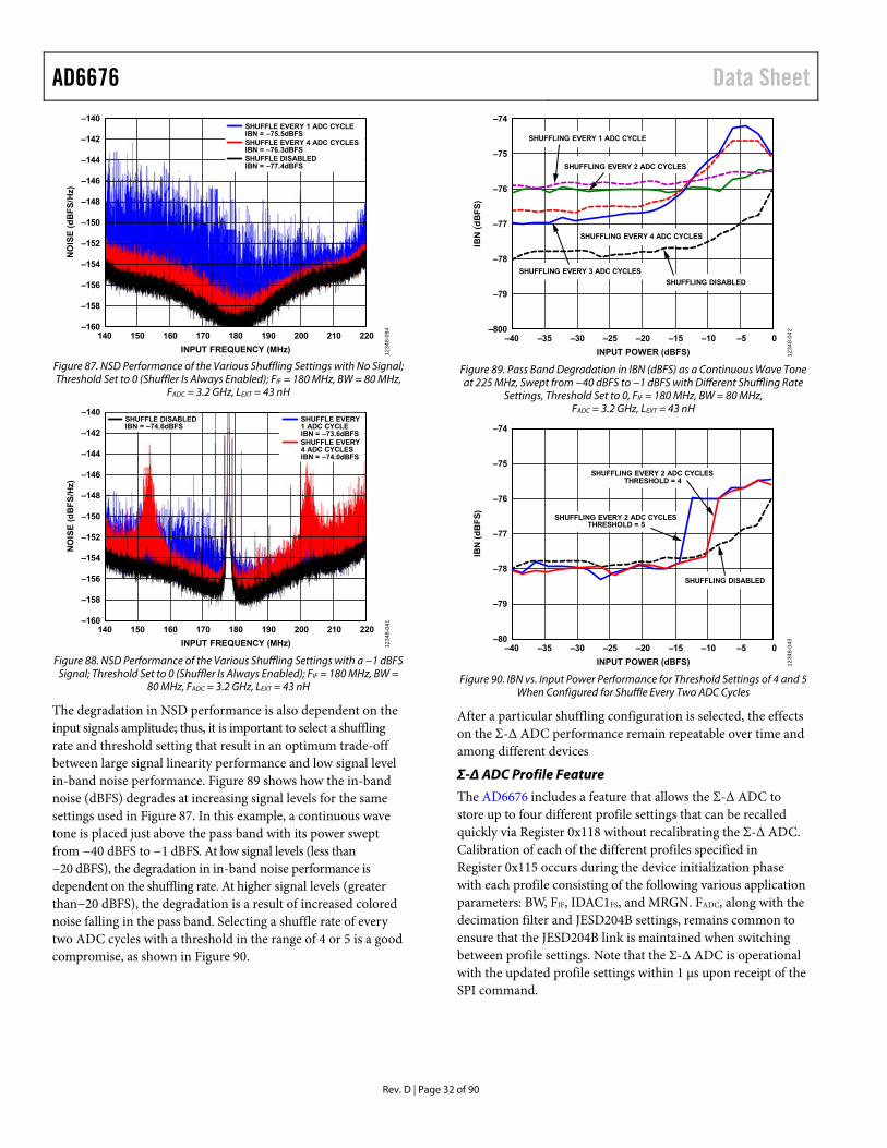
AD6676 Data Sheet
Rev. D | Page 32 of 90
–140
–142
–144
–146
–148
–150
–152
–154
–156
–158
–160140 150 160 170 180 190 200 210 220
NO
ISE
(d
BF
S/H
z)
INPUT FREQUENCY (MHz)
SHUFFLE EVERY 1 ADC CYCLEIBN = –75.5dBFSSHUFFLE EVERY 4 ADC CYCLESIBN = –76.3dBFSSHUFFLE DISABLEDIBN = –77.4dBFS
1234
8-09
4
Figure 87. NSD Performance of the Various Shuffling Settings with No Signal; Threshold Set to 0 (Shuffler Is Always Enabled); FIF = 180 MHz, BW = 80 MHz,
FADC = 3.2 GHz, LEXT = 43 nH
–140
–142
–144
–146
–148
–150
–152
–154
–156
–158
–160140 150 160 170 180 190 200 210 220
NO
ISE
(d
BF
S/H
z)
INPUT FREQUENCY (MHz)
SHUFFLE EVERY1 ADC CYCLEIBN = –73.6dBFSSHUFFLE EVERY4 ADC CYCLESIBN = –74.0dBFS
SHUFFLE DISABLEDIBN = –74.6dBFS
1234
8-04
1
Figure 88. NSD Performance of the Various Shuffling Settings with a −1 dBFS
Signal; Threshold Set to 0 (Shuffler Is Always Enabled); FIF = 180 MHz, BW = 80 MHz, FADC = 3.2 GHz, LEXT = 43 nH
The degradation in NSD performance is also dependent on the input signals amplitude; thus, it is important to select a shuffling rate and threshold setting that result in an optimum trade-off between large signal linearity performance and low signal level in-band noise performance. Figure 89 shows how the in-band noise (dBFS) degrades at increasing signal levels for the same settings used in Figure 87. In this example, a continuous wave tone is placed just above the pass band with its power swept from −40 dBFS to −1 dBFS. At low signal levels (less than −20 dBFS), the degradation in in-band noise performance is dependent on the shuffling rate. At higher signal levels (greater than−20 dBFS), the degradation is a result of increased colored noise falling in the pass band. Selecting a shuffle rate of every two ADC cycles with a threshold in the range of 4 or 5 is a good compromise, as shown in Figure 90.
–74
–75
–76
–77
–78
–79
–800–40 –35 –30 –25 –20 –15 –10 –5 0
IBN
(d
BF
S)
INPUT POWER (dBFS)
SHUFFLING EVERY 1 ADC CYCLE
SHUFFLING EVERY 2 ADC CYCLES
SHUFFLING EVERY 4 ADC CYCLES
SHUFFLING EVERY 3 ADC CYCLES
SHUFFLING DISABLED
1234
8-04
2
Figure 89. Pass Band Degradation in IBN (dBFS) as a Continuous Wave Tone at 225 MHz, Swept from −40 dBFS to −1 dBFS with Different Shuffling Rate
Settings, Threshold Set to 0, FIF = 180 MHz, BW = 80 MHz, FADC = 3.2 GHz, LEXT = 43 nH
–74
–75
–76
–77
–78
–79
–80–40 –35 –30 –25 –20 –15 –10 –5 0
IBN
(d
BF
S)
INPUT POWER (dBFS)
SHUFFLING DISABLED
SHUFFLING EVERY 2 ADC CYCLESTHRESHOLD = 4
SHUFFLING EVERY 2 ADC CYCLESTHRESHOLD = 5
1234
8-04
3
Figure 90. IBN vs. Input Power Performance for Threshold Settings of 4 and 5
When Configured for Shuffle Every Two ADC Cycles
After a particular shuffling configuration is selected, the effects on the Σ-Δ ADC performance remain repeatable over time and among different devices
Σ-Δ ADC Profile Feature
The AD6676 includes a feature that allows the Σ-Δ ADC to store up to four different profile settings that can be recalled quickly via Register 0x118 without recalibrating the Σ-Δ ADC. Calibration of each of the different profiles specified in Register 0x115 occurs during the device initialization phase with each profile consisting of the following various application parameters: BW, FIF, IDAC1FS, and MRGN. FADC, along with the decimation filter and JESD204B settings, remains common to ensure that the JESD204B link is maintained when switching between profile settings. Note that the Σ-Δ ADC is operational with the updated profile settings within 1 μs upon receipt of the SPI command.

Data Sheet AD6676
Rev. D | Page 33 of 90
The following example highlights how this feature is used for applications that require wide bandwidth capability but not necessarily instantaneous bandwidth. In these applications, it may be possible to divide the required IF bandwidth into narrow subbands where the Σ-Δ ADC can provide higher dynamic range. For instance, in an application that requires 120 MHz of IF bandwidth, consider dividing this bandwidth into three contiguous blocks of 40 MHz, with each IF being offset by 40 MHz. Figure 91 shows that the worst-case NSD is limited to −149 dBFS/Hz when the AD6676 is configured for the wider bandwidth of 120 MHz. Figure 92 shows how the NSD performance is improved by 10 dB when the 120 MHz bandwidth is subdivided into three 40 MHz bands.
–145
–160
–155
–150
200 220 240 260 280 300 320
NO
ISE
SP
EC
TR
AL
DE
NS
ITY
(d
BF
S/H
z)
INPUT FREQUENCY (MHz)
PROFILE = 0(IF = 260MHz, BW = 120MHz)
1234
8-10
0–149dBFS/Hz
Figure 91. NSD Performance with Wideband Profile (FIF = 260 MHz, BW =
120 MHz, FADC = 3.2 GHz, LEXT = 27 nH)
–145
–160
–155
–150
200 220 240 260 280 300 320
NO
ISE
SP
EC
TR
AL
DE
NS
ITY
(d
BF
S/H
z)
INPUT FREQUENCY (MHz)
PROFILE = 1(IF = 260MHz,BW = 40MHz)
PROFILE = 2(IF = 300MHz,BW = 40MHz)
PROFILE = 0(IF = 220MHz,BW = 40MHz)
1234
8-10
1
–159dBFS/Hz
Figure 92. NSD Performance with Narrow-Band Profiles (FIF = 220 MHz,
260 MHz, and 300 MHz, BW = 120 MHz, FADC = 3.2 GHz, LEXT = 27 nH)
In this example, the frequency and phase settings of the digital mixer remained common among the various profiles such that it remained centered upon 260 MHz. It is also possible to provide a unique digital mixer setting for each profile if it is desirable to re-center the digital IF frequency. This feature is desirable in instances where the range of IFs cannot be supported by the pass band response of the digital decimation filter.
ATTENUATOR The AD6676 includes an on-chip differential 27 dB attenuator with a resolution of 1 dB. The attenuator can be used to rescale the full-scale input level into the ADC for system calibration or for optimization purposes or to prevent possible overload of the Σ-Δ ADC when used with external AGC control. Figure 93 shows a simplified equivalent circuit of the AD6676 input stage, which includes RESON1 and IDAC1. The attenuator provides a nominal input resistance (RIN) of 60 Ω to the signal source to facilitate its interface to external driver circuitry. The attenuator is configurable via Register 0x181 to Register 0x183 and includes options for fast external gain control via the AGC pins. Note that the latency from when an external CMOS signal is applied to the AGC pins to when the attenuator changes state is within 5 ns.
0.1µF
DC
AC
IDAC1
ATTENUATOR0dB TO 27dB
∆ = 1dB
REG 0x180TO 0x181
VIN+
L–L+
VIN–
RIN = 60ΩVCM = 1.0V
CARRAY
SUMMINGJUNCTION
10ΩVDD2 = 2.5V
LEXTLEXT
AD6676
1234
8-04
4
Figure 93. Simplified Equivalent Input
Attenuation is achieved by a programmable shunt and series resistor network that steers some designated amount of input current away from the summing junction while keeping the nominal input resistance near 60 Ω over the full attenuation span. For a 0 dB setting, no shunt resistance exists; therefore, all of the input current is fed into the summing junction. For a 6 dB setting, the attenuator is configured with a 120 Ω shunt resistor operating in parallel with two 60 Ω series resistors such that half of the signal input current is directed into the summing junction while maintaining a nominal 60 Ω input resistance. Other settings function in a similar manner with resistor values modified to achieve the desired attenuation value while maintaining the nominal RIN. Figure 94 shows the differential S11 of the AD6676 input for different attenuator settings.
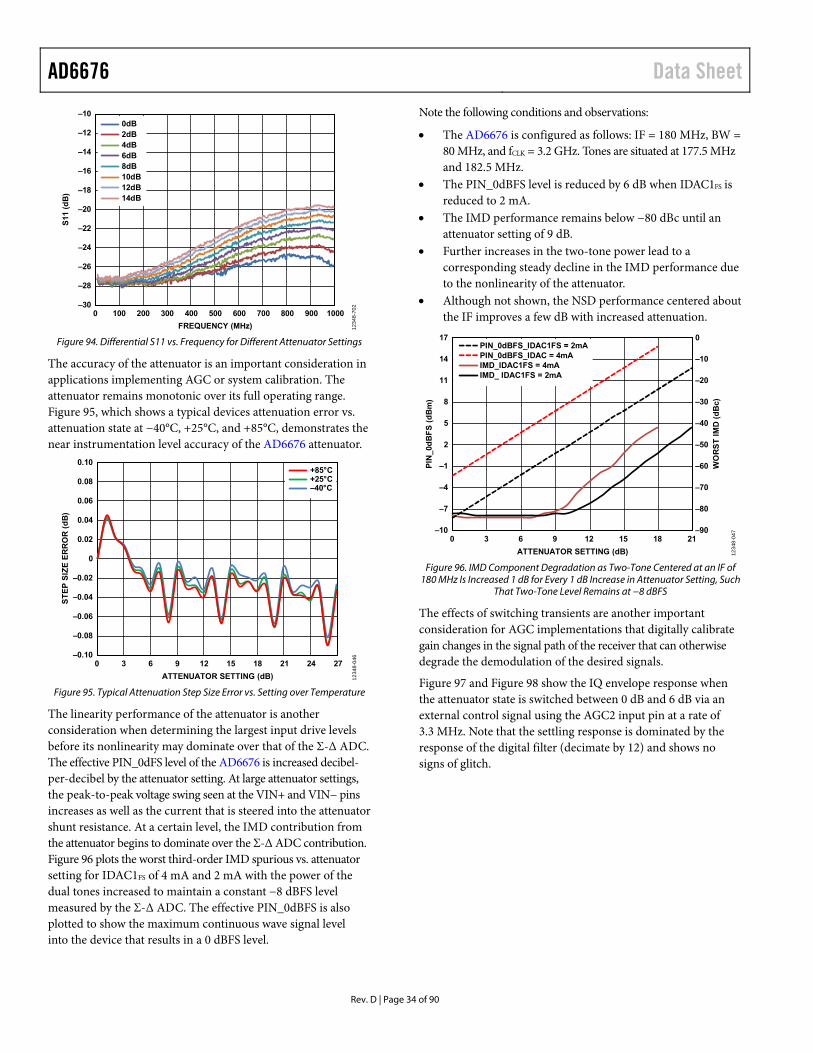
AD6676 Data Sheet
Rev. D | Page 34 of 90
–10
–12
–14
–16
–18
–20
–22
–24
–26
–28
–300 100 200 300 400 500 600 800 1000700 900
S11
(d
B)
FREQUENCY (MHz) 1234
8-70
2
0dB2dB4dB6dB8dB10dB12dB14dB
Figure 94. Differential S11 vs. Frequency for Different Attenuator Settings
The accuracy of the attenuator is an important consideration in applications implementing AGC or system calibration. The attenuator remains monotonic over its full operating range. Figure 95, which shows a typical devices attenuation error vs. attenuation state at −40°C, +25°C, and +85°C, demonstrates the near instrumentation level accuracy of the AD6676 attenuator.
0.10
–0.10
–0.08
–0.06
–0.04
–0.02
0
0.02
0.04
0.06
0.08
0 272421181512963
ST
EP
SIZ
E E
RR
OR
(d
B)
ATTENUATOR SETTING (dB)
–40°C+25°C+85°C
1234
8-04
6
Figure 95. Typical Attenuation Step Size Error vs. Setting over Temperature
The linearity performance of the attenuator is another consideration when determining the largest input drive levels before its nonlinearity may dominate over that of the Σ-Δ ADC. The effective PIN_0dFS level of the AD6676 is increased decibel-per-decibel by the attenuator setting. At large attenuator settings, the peak-to-peak voltage swing seen at the VIN+ and VIN− pins increases as well as the current that is steered into the attenuator shunt resistance. At a certain level, the IMD contribution from the attenuator begins to dominate over the Σ-Δ ADC contribution. Figure 96 plots the worst third-order IMD spurious vs. attenuator setting for IDAC1FS of 4 mA and 2 mA with the power of the dual tones increased to maintain a constant −8 dBFS level measured by the Σ-Δ ADC. The effective PIN_0dBFS is also plotted to show the maximum continuous wave signal level into the device that results in a 0 dBFS level.
Note the following conditions and observations:
The AD6676 is configured as follows: IF = 180 MHz, BW = 80 MHz, and fCLK = 3.2 GHz. Tones are situated at 177.5 MHz and 182.5 MHz.
The PIN_0dBFS level is reduced by 6 dB when IDAC1FS is reduced to 2 mA.
The IMD performance remains below −80 dBc until an attenuator setting of 9 dB.
Further increases in the two-tone power lead to a corresponding steady decline in the IMD performance due to the nonlinearity of the attenuator.
Although not shown, the NSD performance centered about the IF improves a few dB with increased attenuation.
17
–10
0
–90
–80
–70
–60
–50
–40
–30
–20
–10
–7
–4
–1
2
5
8
11
14
0 21181512963
PIN
_0d
BF
S (
dB
m)
WO
RS
T I
MD
(d
Bc)
ATTENUATOR SETTING (dB)
PIN_0dBFS_IDAC1FS = 2mAPIN_0dBFS_IDAC = 4mAIMD_IDAC1FS = 4mAIMD_ IDAC1FS = 2mA
1234
8-04
7
Figure 96. IMD Component Degradation as Two-Tone Centered at an IF of
180 MHz Is Increased 1 dB for Every 1 dB Increase in Attenuator Setting, Such That Two-Tone Level Remains at −8 dBFS
The effects of switching transients are another important consideration for AGC implementations that digitally calibrate gain changes in the signal path of the receiver that can otherwise degrade the demodulation of the desired signals.
Figure 97 and Figure 98 show the IQ envelope response when the attenuator state is switched between 0 dB and 6 dB via an external control signal using the AGC2 input pin at a rate of 3.3 MHz. Note that the settling response is dominated by the response of the digital filter (decimate by 12) and shows no signs of glitch.
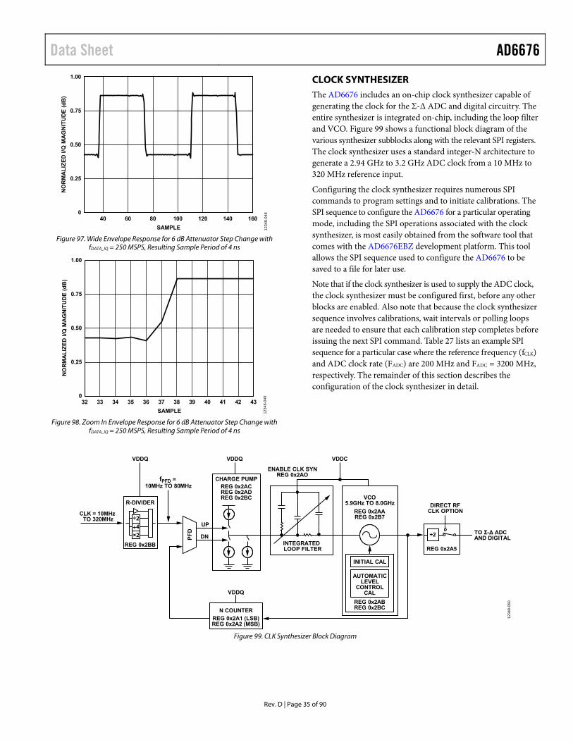
Data Sheet AD6676
Rev. D | Page 35 of 90
1.00
0
0.25
0.50
0.75
160140120100806040
NO
RM
AL
IZE
D I
/Q M
AG
NIT
UD
E (
dB
)
SAMPLE 1234
8-04
8
Figure 97. Wide Envelope Response for 6 dB Attenuator Step Change with
fDATA_IQ = 250 MSPS, Resulting Sample Period of 4 ns
1.00
0
0.25
0.50
0.75
434241403938373635343332
NO
RM
AL
IZE
D I
/Q M
AG
NIT
UD
E (
dB
)
SAMPLE 1234
8-04
9
Figure 98. Zoom In Envelope Response for 6 dB Attenuator Step Change with
fDATA_IQ = 250 MSPS, Resulting Sample Period of 4 ns
CLOCK SYNTHESIZER The AD6676 includes an on-chip clock synthesizer capable of generating the clock for the Σ-Δ ADC and digital circuitry. The entire synthesizer is integrated on-chip, including the loop filter and VCO. Figure 99 shows a functional block diagram of the various synthesizer subblocks along with the relevant SPI registers. The clock synthesizer uses a standard integer-N architecture to generate a 2.94 GHz to 3.2 GHz ADC clock from a 10 MHz to 320 MHz reference input.
Configuring the clock synthesizer requires numerous SPI commands to program settings and to initiate calibrations. The SPI sequence to configure the AD6676 for a particular operating mode, including the SPI operations associated with the clock synthesizer, is most easily obtained from the software tool that comes with the AD6676EBZ development platform. This tool allows the SPI sequence used to configure the AD6676 to be saved to a file for later use.
Note that if the clock synthesizer is used to supply the ADC clock, the clock synthesizer must be configured first, before any other blocks are enabled. Also note that because the clock synthesizer sequence involves calibrations, wait intervals or polling loops are needed to ensure that each calibration step completes before issuing the next SPI command. Table 27 lists an example SPI sequence for a particular case where the reference frequency (fCLK) and ADC clock rate (FADC) are 200 MHz and FADC = 3200 MHz, respectively. The remainder of this section describes the configuration of the clock synthesizer in detail.
INTEGRATED LOOP FILTER
TO Σ-∆ ADCAND DIGITAL
N COUNTER
REG 0x2A1 (LSB)REG 0x2A2 (MSB)
VDDQ
ENABLE CLK SYNREG 0x2AO
÷2
REG 0x2A5
DIRECT RFCLK OPTION
REG 0x2BB
VDDQ VDDQ VDDC
R-DIVIDER
CHARGE PUMPREG 0x2ACREG 0x2ADREG 0x2BC
PF
D
UP
DN
2
4
×2
fPFD =10MHz TO 80MHz
CLK = 10MHzTO 320MHz
INITIAL CAL
AUTOMATICLEVEL
CONTROLCAL
REG 0x2ABREG 0x2BC
VCO5.9GHz TO 8.0GHz
REG 0x2AAREG 0x2B7÷
÷
1234
8-05
0
Figure 99. CLK Synthesizer Block Diagram
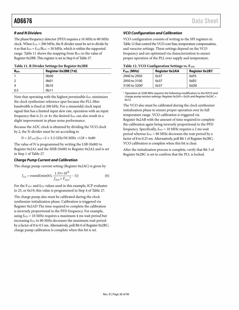
AD6676 Data Sheet
Rev. D | Page 36 of 90
R and N Dividers
The phase/frequency detector (PFD) requires a 10 MHz to 80 MHz clock. When fCLK = 200 MHz, the R divider must be set to divide by 4 so that fPFD = fCLK/RDIV = 50 MHz, which is within the supported range. Table 11 shows the mapping from RDIV to the value of Register 0x2BB. This register is set in Step 6 of Table 27.
Table 11. R Divider Settings for Register 0x2BB RDIV Register 0x2BB [7:6] 1 0b00 2 0b01 4 0b10 0.5 0b11
Note that operating with the highest permissible fPFD minimizes the clock synthesizer reference spur because the PLL filter bandwidth is fixed at 200 kHz. For a sinusoidal clock input signal that has a limited input slew rate, operation with an input frequency that is 2× or 4× the desired fPFD can also result in a slight improvement in phase noise performance.
Because the ADC clock is obtained by dividing the VCO clock by 2, the N-divider must be set according to
N = 2FADC/fPFD =2 × 3.2 GHz/50 MHz =128 = 0x80
The value of N is programmed by writing the LSB (0x80) to Register 0x2A1 and the MSB (0x00) to Register 0x2A2 and is set in Step 1 of Table 27.
Charge Pump Current and Calibration
The charge pump current setting (Register 0x2AC) is given by
))11033.1,63(min(round2
28
ADCPFD
CP FfI (6)
For the FADC and fPFD values used in this example, ICP evaluates to 25, or 0x19; this value is programmed in Step 4 of Table 27.
The charge pump also must be calibrated during the clock synthesizer initialization phase. Calibration is triggered via Register 0x2AD The time required to complete the calibration is inversely proportional to the PFD frequency. For example, using fPFD = 10 MHz requires a maximum 4 ms wait period but increasing fPFD to 80 MHz decreases the maximum wait period by a factor of 8 to 0.5 ms. Alternatively, poll Bit 0 of Register 0x2BC; charge pump calibration is complete when this bit is set.
VCO Configuration and Calibration
VCO configuration consists of writing to the SPI registers in Table 12 that control the VCO core bias, temperature compensation, and varactor settings. These settings depend on the VCO frequency and are optimized via characterization to ensure proper operation of the PLL over supply and temperature.
Table 12. VCO Configuration Settings vs. FADC FADC (MHz) Register 0x2AA Register 0x2B7 2940 to 2950 0x37 0xF0 2950 to 3100 0x37 0xE0 3100 to 32001 0x37 0xD0 1. Operation at 3200 MHz requires the following modification to the KVCO and
charge pump resistor settings: Register 0x2A9 = 0x2A and Register 0x2AC = 0x12.
The VCO also must be calibrated during the clock synthesizer initialization phase to ensure proper operation over its full temperature range. VCO calibration is triggered via Register 0x2AB with the amount of time required to complete the calibration again being inversely proportional to the PFD frequency. Specifically, fPFD = 10 MHz requires a 2 ms wait period whereas fPFD = 80 MHz decreases the wait period by a factor of 8 to 0.25 ms. Alternatively, poll Bit 1 of Register 0x2BC; VCO calibration is complete when this bit is clear.
After the initialization process is complete, verify that Bit 3 of Register 0x2BC is set to confirm that the PLL is locked.
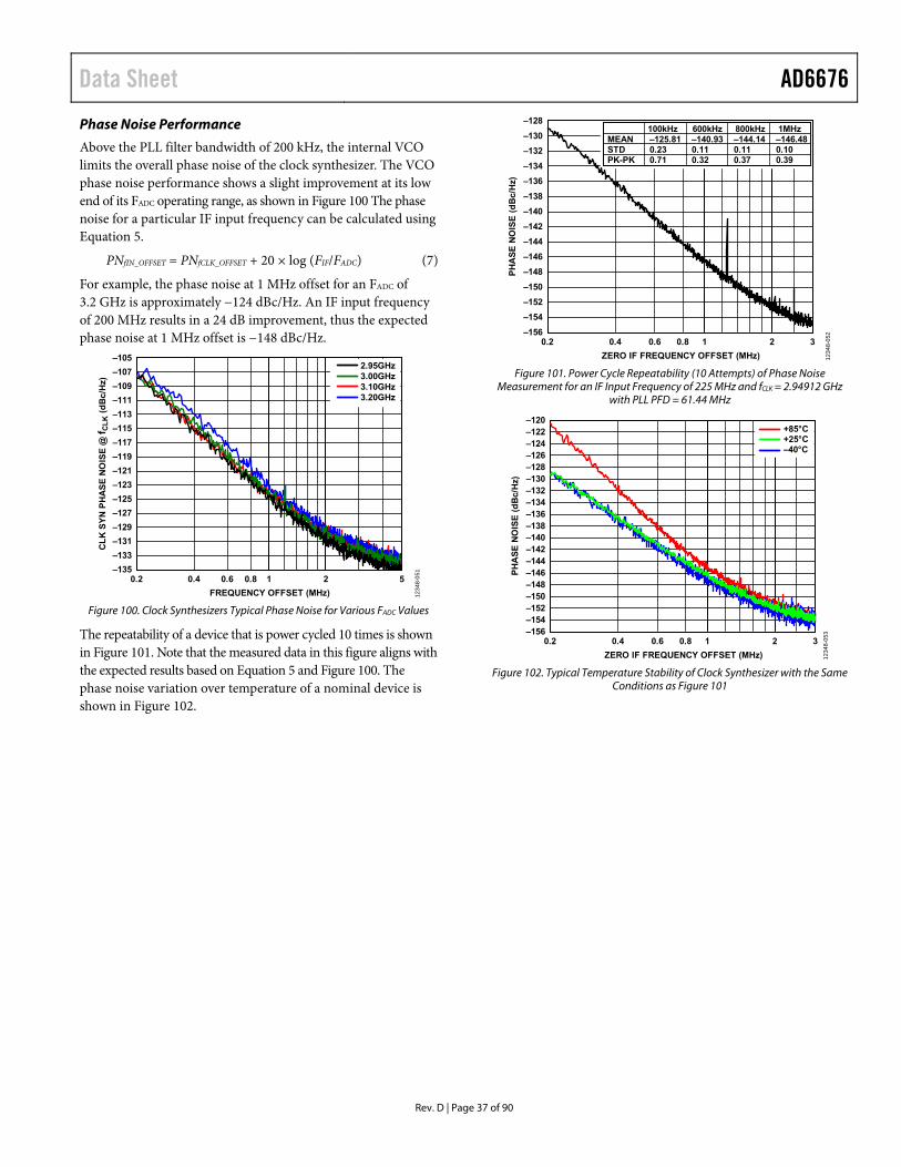
Data Sheet AD6676
Rev. D | Page 37 of 90
Phase Noise Performance
Above the PLL filter bandwidth of 200 kHz, the internal VCO limits the overall phase noise of the clock synthesizer. The VCO phase noise performance shows a slight improvement at its low end of its FADC operating range, as shown in Figure 100 The phase noise for a particular IF input frequency can be calculated using Equation 5.
PNfIN_OFFSET = PNfCLK_OFFSET + 20 × log (FIF/FADC) (7)
For example, the phase noise at 1 MHz offset for an FADC of 3.2 GHz is approximately −124 dBc/Hz. An IF input frequency of 200 MHz results in a 24 dB improvement, thus the expected phase noise at 1 MHz offset is −148 dBc/Hz.
–105
–107
–109
–111
–113
–115
–117
–119
–121
–123
–125
–127
–129
–131
–133
–1355210.2 0.4 0.6 0.8
CL
K S
YN
PH
AS
E N
OIS
E @
f CL
K (
dB
c/H
z)
FREQUENCY OFFSET (MHz)
2.95GHz3.00GHz3.10GHz3.20GHz
1234
8-05
1
Figure 100. Clock Synthesizers Typical Phase Noise for Various FADC Values
The repeatability of a device that is power cycled 10 times is shown in Figure 101. Note that the measured data in this figure aligns with the expected results based on Equation 5 and Figure 100. The phase noise variation over temperature of a nominal device is shown in Figure 102.
–128
–130
–132
–134
–136
–138
–140
–142
–144
–146
–148
–150
–152
–154
–156320.2 0.4 0.6 0.8 1
PH
AS
E N
OIS
E (
dB
c/H
z)
ZERO IF FREQUENCY OFFSET (MHz) 1234
8-05
2
MEAN –125.81 –140.93 –144.14 –146.48STD 0.23 0.11 0.11 0.10PK-PK 0.71 0.32 0.37 0.39
100kHz 600kHz 800kHz 1MHz
Figure 101. Power Cycle Repeatability (10 Attempts) of Phase Noise
Measurement for an IF Input Frequency of 225 MHz and fCLK = 2.94912 GHz with PLL PFD = 61.44 MHz
–120
–124
–128
–132
–122
–126
–130
–134–136–138–140–142–144–146–148–150–152–154–156
320.2 0.4 0.6 0.8 1
PH
AS
E N
OIS
E (
dB
c/H
z)
ZERO IF FREQUENCY OFFSET (MHz)
–40°C+25°C+85°C
1234
8-05
3
Figure 102. Typical Temperature Stability of Clock Synthesizer with the Same
Conditions as Figure 101
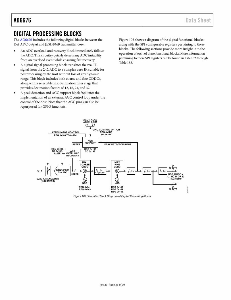
AD6676 Data Sheet
Rev. D | Page 38 of 90
DIGITAL PROCESSING BLOCKS The AD6676 includes the following digital blocks between the Σ-Δ ADC output and JESD204B transmitter core:
An ADC overload and recovery block immediately follows the ADC. This circuitry quickly detects any ADC instability from an overload event while ensuring fast recovery.
A digital signal processing block translates the real IF signal from the Σ-Δ ADC to a complex zero IF, suitable for postprocessing by the host without loss of any dynamic range. This block includes both coarse and fine QDDCs, along with a selectable FIR decimation filter stage that provides decimation factors of 12, 16, 24, and 32.
A peak detection and AGC support block facilitates the implementation of an external AGC control loop under the control of the host. Note that the AGC pins can also be repurposed for GPIO functions.
Figure 103 shows a diagram of the digital functional blocks along with the SPI configurable registers pertaining to these blocks. The following sections provide more insight into the operation of each of these functional blocks. More information pertaining to these SPI registers can be found in Table 32 through Table 135.
BAND-PASSΣ-∆ ADC
AGCSUPPORT
AGC4, AGC3AGC2, AGC1
REG 0x193TO 0x19E
RESET PEAK DETECTOR INPUT
ADCOVERLOADRECOVERY
MIX1COARSE
QDDC
NCO
REG 0x141REG 0x143
MIX2FINE
QDDC
NCO
REG 0x142REG 0x144REG 0x145
5 BITS
2×16 BITS
2×16 BITS
27dB ATTENUATOR(1dB STEPS)
2× 2× 2×3×OR 4×
REG 0x188TO 0x18B,
0x18F
GPIO CONTROL OPTIONREG 0x1B0TO 0x1B4
ATTENUATOR CONTROLREG 0x180 TO 0x184
DEC_MODE =12, 16, 24 OR 32
REG 0x140
1234
8-05
4
Figure 103. Simplified Block Diagram of Digital Processing Blocks

Data Sheet AD6676
Rev. D | Page 39 of 90
DIGITAL SIGNAL PROCESSING PATH The Σ-Δ ADC provides a highly oversampled 5-bit digital output representing the desired IF signal pass band as well as the out-of-band shaped noise described earlier. Referring to Figure 104, the digital signal processing path translates this oversampled real IF signal to a complex dc centered IF signal, having a more manageable data rate suitable for transfer via the JESD204B interface. The QDDC performs the real-to-complex frequency translation followed by digital filtering to remove the ADC out-of-band noise, as well as any other undesired signal content, before decimation to a lower data rate without any loss of dynamic range.
DC–FADC/2 FADC/2
COMPLEX OUTPUT AFTER QDDC
–fIF fIFDC–FADC/2 FADC/2
ADC REAL OUTPUTDESIRED
SIGNALADC NOISE
IMAGESIGNAL
COMPLEX OUTPUT AFTER DECIMATION
–fDATA_IQ/2 fDATA_IQ/2DC
COMPLEX OUTPUT AFTER FILTERING
–FADC/2 FADC/2
DIGITAL FILTER RESPONSE
1234
8-05
5
Figure 104. Digital Signal Processing Path Performs Frequency Translation to
a Zero IF as well as Filtering and Downsampling
Quadrature Digital Downconversion
Digital downconversion occurs in two stages using a coarse and a fine QDDC. As shown in Figure 103, the coarse QDDC resides immediately after the Σ-Δ ADC and the fine QDDC follows the first decimation stage. The coarse QDDC provides 6-bit tuning resolution whereas the fine QDDC provides 10-bit tuning resolution. The composite tuning resolution is either FADC/3072 or FADC/4096, depending on whether the first decimation stage is configured for 3× or 4× decimation, which in turn depends on the decimation mode selected as described in Table 13. For applications requiring finer tuning resolution to position the IF signal exactly about dc, consider adding a finer resolution QDDC in the host processor.
Table 13. Finite Composite Tuning Resolution of Coarse and Fine NCO DEC_MODE (Register 0x140, Bits[2:0])
Decimation Factor
Tuning Resolution
Tuning Res. (MHz) at FADC = 3.072 GSPS
1 32 FADC/4096 0.75 2 24 FADC/3072 1.00 3 16 FADC/4096 0.75 4 12 FADC/3072 1.00
The tuning frequency settings of the combined coarse and fine NCO (SPI Register 0x141 and SPI Register 0x142) are automatically calculated and set by the AD6676 during the device SPI initialization phase. The user defined FADC and IF settings (SPI Register 0x100 thru SPI Register 0x103) are used to calculate the settings such that the center of the IF pass band is centered about dc. The coarse tuning NCO is set via MIX1_TUNING[5:0], whereas the fine tuning NCO is set via MIX2_TUNING[7:0]. The decimal equivalent frequency setting of each NCO register is based on the following equations.
ADC
IF
FFMIX1 64Round (8)
where: MIX1 is a 6-bit binary number representing the NCO frequency setting in MIX1_TUNING. FIF is the desired carrier frequency in hertz (Hz). FADC is the ADC clock rate in hertz (Hz).
64Round MIX1
FFMMIX2ADC
IF (9)
where: MIX2 is a 8-bit twos complement number representing the NCO frequency setting in MIX2_TUNING. M is 3072 for DEC_MODE = 2 and 4, or 4096 for DEC_MODE = 1 and 3.
It is important to note the residue, fOFFSET, between the desired FIF and the AD6676 composite NCO setting, FIF_NCO, because any offset may need to be compensated with an additional fine QDDC located in the host processor. Use the following equations to calculate both parameters:
ADCNCOIF FM
MIX2MIX1F
64_ (10)
fOFFSET = FIF – FIF_NCO (11)

AD6676 Data Sheet
Rev. D | Page 40 of 90
Example
Calculate the NCO MIX1 and MIX2 values along with FIF_NCO and fOFFSET with the following AD6676 configuration: FIF = 140 MHz, FADC = 3200 MHz, and decimation factor of 16 (that is, fDATA_IQ = 200 MSPS).
Substituting FIF and FADC values in Equation 8 results in MIX1 = 3.
Substituting these values in Equation 9 (noting that M = 4096 for DEC_MODE = 3 results in MIX2 = −13).
Substituting MIX1 and MIX2 values into Equation 10 results in FIF_NCO = 139.84375 MHz.
Substituting FIF and FIF_NCO values in Equation 11 results in fOFFSET = 156.25 kHz.
NCO Phase Synchronization
The AD6676 coarse and fine tuning NCOs can be set to an initial phase after synchronization with an external SYSREF signal. The initial phase of the coarse tuning NCO is set via MIX1_INIT, with an LSB corresponding to 1/64th of a cycle. The initial phase of the fine tuning NCO is set via MIX2_INIT_x, with an LSB corresponding to 1/1024th of a cycle.
Digital Filter Modes
The AD6676 digital filter path is designed to provide sufficient stop band rejection of the Σ-Δ ADC shaped out-of-band noise as well as any spurious noise that otherwise might alias back into the desired pass band region after decimation and limit the actual NSD performance. The filter path supports decimation factors of 12, 16, 24, and 32 depending on the DEC_MODE setting. The complex output of the coarse QDDC feeds a pair of symmetrical FIR decimation filters divided into three stages, as shown in Figure 103. The first stage is a decimate by 3 or by 4 filter, depending on whether the desired decimation factor is divisible by three. The second and third stages consists of two cascaded decimate by 2 filters with the third stage outputs supporting the decimate by 12 and by 16 options. A bypassable fourth stage provides the decimate by 24 and by 32 options.
The normalized pass band and wideband folded frequency response for each filter mode are shown in Figure 105 through Figure 113. Note the following observations:
All filter responses provide a linear phase response over its pass band.
The usable IF bandwidth depends on the DEC_MODE as well as the minimum acceptable pass band ripple and stop band rejection requirements. Table 14 provides the normalized usable complex bandwidth vs. DEC_MODE for stop band rejections of greater than 85 dB and 60 dB.
The last filter stage sets the usable bandwidth and stop band rejection because it has the most aggressive transition band specifications. For this reason, the decimation factors of 12 and 16 have the same normalized usable bandwidths as does decimation factors of 24 and 32.
Wide IF bandwidths (MHz) are supported when operating at lower decimation factors along with a high FADC.
It is worth noting that many applications requiring wider IF bandwidth may tolerate reduced ripple and rejection as the digital filter response enters its transition region. The reason is that the Σ-Δ ADC achievable NSD performance at the IF pass band edges also degrades as its oversampling ratio is reduced, thus still dominating relative to any aliased noise due to reduced filter stop band rejection.
Table 14. Usable Normalized Complex Bandwidth vs. Decimation Factor
DEC_MODE Decimation Factor fDATA_IQ
BW (>85 dB Rejection)
BW (>60 dB Rejection)
1 32 1 0.814 0.834 2 24 1 0.814 0.834 3 16 1 0.571 0.617 4 12 1 0.571 0.617
Total Pipeline Latency
The digital filter path dominates the latency of the AD6676 whereas the JESD204B PHY adds a few samples of delay and the ADC delay is a fraction of an output sample. The latency between the ADC and digital filter output is fixed with the only nondeterministic delay being associated with the JESD204B PHY clock and lane FIFOs before synchronization. See the Synchronization Using SYSREF section for additional information. Table 15 provides the nominal pipeline delay associated with each DEC_MODE. Note that although all DEC_MODE settings provide similar delays relative to the output data rate, fDATA_IQ, applications that require shorter absolute time delays may consider using a lower decimation factor to reduce the absolute delay by 2×.
Table 15. Nominal Pipeline Latency vs. DEC_MODE (Sample Delay Relative to 1/fDATA_IQ)
DEC_MODE Decimation Factor
JESD204B Lanes
IQ Data Output Sample Delay
1 32 1 34.2 2 24 1 34.2 3 16 2 32.3 4 12 2 32.3

Data Sheet AD6676
Rev. D | Page 41 of 90
0.5
–0.5
–0.4
–0.3
–0.2
–0.1
0
0.1
0.2
0.3
0.4
0 0.05 0.10 0.15 0.20 0.25 0.30 0.35 0.40 0.45 0.50
MA
GN
ITU
DE
(d
B)
FREQUENCY NORMALIZED TO fDATA_IQ 1234
8-05
6
Figure 105. Pass Band Frequency Response of Decimate by 12
0.5
–0.5
–0.4
–0.3
–0.2
–0.1
0
0.1
0.2
0.3
0.4
0 0.05 0.10 0.15 0.20 0.25 0.30 0.35 0.40 0.45 0.50
MA
GN
ITU
DE
(d
B)
FREQUENCY NORMALIZED TO fDATA_IQ 1234
8-05
7
Figure 106. Pass Band Frequency Response of Decimate by 16
0.5
–0.5
–0.4
–0.3
–0.2
–0.1
0
0.1
0.2
0.3
0.4
0 0.05 0.10 0.15 0.20 0.25 0.30 0.35 0.40 0.45 0.50
MA
GN
ITU
DE
(d
B)
FREQUENCY NORMALIZED TO fDATA_IQ 1234
8-05
8
Figure 107. Pass Band Frequency Response of Decimate by 24
0
–120
–100
–80
–60
–40
–20
0 0.05 0.10 0.15 0.20 0.25 0.30 0.35 0.40 0.45 0.50
MA
GN
ITU
DE
(d
B)
FREQUENCY NORMALIZED TO fDATA_IQ
MINIMUM ALIAS ATTENUATION 85.5dB
1234
8-05
9
Figure 108. Folded Frequency Response of Decimate by 12 Shows Alias Rejection
0
–120
–100
–80
–60
–40
–20
0 0.05 0.10 0.15 0.20 0.25 0.30 0.35 0.40 0.45 0.50
MA
GN
ITU
DE
(d
B)
FREQUENCY NORMALIZED TO fDATA_IQ
MINIMUM ALIAS ATTENUATION 85.5dB
1234
8-06
0
Figure 109. Folded Frequency Response of Decimate by 16 Shows Alias Rejection
0
–120
–100
–80
–60
–40
–20
0 0.05 0.10 0.15 0.20 0.25 0.30 0.35 0.40 0.45 0.50
MA
GN
ITU
DE
(d
B)
FREQUENCY NORMALIZED TO fDATA_IQ
MINIMUM ALIAS ATTENUATION 85.5dB
1234
8-06
1
Figure 110. Folded Frequency Response of Decimate by 24 Shows Alias Rejection
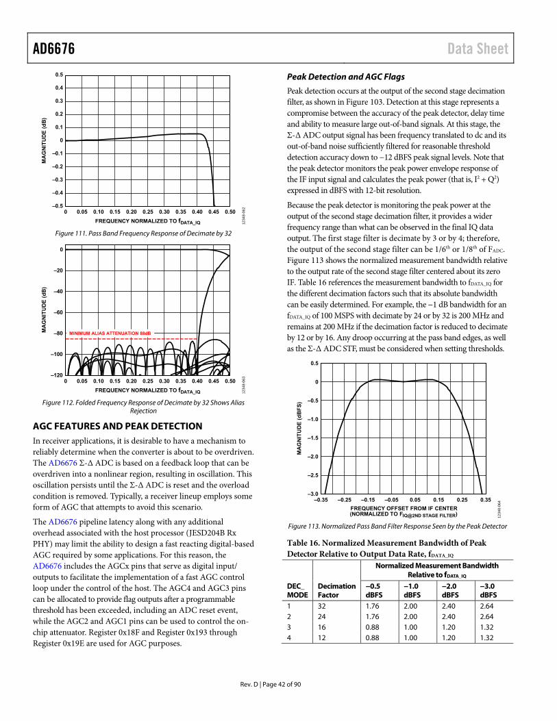
AD6676 Data Sheet
Rev. D | Page 42 of 90
0.5
–0.5
–0.4
–0.3
–0.2
–0.1
0
0.1
0.2
0.3
0.4
0 0.05 0.10 0.15 0.20 0.25 0.30 0.35 0.40 0.45 0.50
MA
GN
ITU
DE
(d
B)
FREQUENCY NORMALIZED TO fDATA_IQ 1234
8-06
2
Figure 111. Pass Band Frequency Response of Decimate by 32
0
–120
–100
–80
–60
–40
–20
0 0.05 0.10 0.15 0.20 0.25 0.30 0.35 0.40 0.45 0.50
MA
GN
ITU
DE
(d
B)
FREQUENCY NORMALIZED TO fDATA_IQ
MINIMUM ALIAS ATTENUATION 88dB
1234
8-06
3
Figure 112. Folded Frequency Response of Decimate by 32 Shows Alias
Rejection
AGC FEATURES AND PEAK DETECTION In receiver applications, it is desirable to have a mechanism to reliably determine when the converter is about to be overdriven. The AD6676 Σ-Δ ADC is based on a feedback loop that can be overdriven into a nonlinear region, resulting in oscillation. This oscillation persists until the Σ-Δ ADC is reset and the overload condition is removed. Typically, a receiver lineup employs some form of AGC that attempts to avoid this scenario.
The AD6676 pipeline latency along with any additional overhead associated with the host processor (JESD204B Rx PHY) may limit the ability to design a fast reacting digital-based AGC required by some applications. For this reason, the AD6676 includes the AGCx pins that serve as digital input/ outputs to facilitate the implementation of a fast AGC control loop under the control of the host. The AGC4 and AGC3 pins can be allocated to provide flag outputs after a programmable threshold has been exceeded, including an ADC reset event, while the AGC2 and AGC1 pins can be used to control the on-chip attenuator. Register 0x18F and Register 0x193 through Register 0x19E are used for AGC purposes.
Peak Detection and AGC Flags
Peak detection occurs at the output of the second stage decimation filter, as shown in Figure 103. Detection at this stage represents a compromise between the accuracy of the peak detector, delay time and ability to measure large out-of-band signals. At this stage, the Σ-Δ ADC output signal has been frequency translated to dc and its out-of-band noise sufficiently filtered for reasonable threshold detection accuracy down to −12 dBFS peak signal levels. Note that the peak detector monitors the peak power envelope response of the IF input signal and calculates the peak power (that is, I2 + Q2) expressed in dBFS with 12-bit resolution.
Because the peak detector is monitoring the peak power at the output of the second stage decimation filter, it provides a wider frequency range than what can be observed in the final IQ data output. The first stage filter is decimate by 3 or by 4; therefore, the output of the second stage filter can be 1/6th or 1/8th of FADC. Figure 113 shows the normalized measurement bandwidth relative to the output rate of the second stage filter centered about its zero IF. Table 16 references the measurement bandwidth to fDATA_IQ for the different decimation factors such that its absolute bandwidth can be easily determined. For example, the −1 dB bandwidth for an fDATA_IQ of 100 MSPS with decimate by 24 or by 32 is 200 MHz and remains at 200 MHz if the decimation factor is reduced to decimate by 12 or by 16. Any droop occurring at the pass band edges, as well as the Σ-Δ ADC STF, must be considered when setting thresholds.
0.5
–3.0
–2.5
–2.0
–1.5
–1.0
–0.5
0
MA
GN
ITU
DE
(d
BF
S)
FREQUENCY OFFSET FROM IF CENTER(NORMALIZED TO FIQ@2ND STAGE FILTER)
–0.35 –0.25 –0.15 –0.05 0.05 0.15 0.25 0.3512
348-
064
Figure 113. Normalized Pass Band Filter Response Seen by the Peak Detector
Table 16. Normalized Measurement Bandwidth of Peak Detector Relative to Output Data Rate, fDATA_IQ
DEC_ MODE
Decimation Factor
Normalized Measurement Bandwidth Relative to fDATA_IQ
−0.5 dBFS
−1.0 dBFS
−2.0 dBFS
−3.0 dBFS
1 32 1.76 2.00 2.40 2.64 2 24 1.76 2.00 2.40 2.64 3 16 0.88 1.00 1.20 1.32 4 12 0.88 1.00 1.20 1.32
Data Sheet AD6676
Rev. D | Page 43 of 90
The AD6676 allows the user to set three threshold settings that can trigger one of two possible flags. PKTHRH0 and PKTHRH1 are two upper threshold settings while LOWTHRH is a lower threshold setting. The threshold settings are 12 bits with an MSB and LSB register assigned to each threshold. The 12-bit decimal equivalent value can be calculated using Equation 12.
Threshold = 3584 + (Threshold Setting in dBFS) × 256/3 (12)
where 0 dBFS corresponds to 3584 (0xE00) and −6 dBFS corresponds to 3072 (0xC00).
In the time domain, a 0 dBFS setting corresponds to a signal whose peaks observed at the I and Q outputs can reach plus or minus full scale. Meaning, if the 16-bit I and Q output data are normalized such that its peak values correspond to ±1, a 0 dBFS setting corresponds to a signal whose peak can reach the unit circle of a normalized I/Q constellation diagram.
The LOWTHRH_x register has an associated dwell time of which the signal must remain below this threshold before a flag can be set. The dwell time is represented in exponential form to realize long dwell periods because the counter operates at FADC/12 for decimate by 12 or 24 settings or FADC/16 for decimate by 16 or 32 settings. The dwell time is set in the DWELL_TIME_ MANTISSA register and DWELL_TIME_EXP register using Equation 13 relative to 1/FADC.
Dwell Time = N × [DWELL_TIME_MANTISSA] × 2(DWELL_TIME_EXP) (13)
where: N = 12 for decimate by 12 or 24. N = 16 for decimate by 16 or 32.
A flag function can be assigned using the FLAG0_SEL register and FLAG1_SEL register to indicate when any of the thresholds have been exceeded or if an ADC reset event has occurred. These flags must also be enabled via the EN_FLAG register such that a CMOS level signal appears on the AGC4 and AGC3 pins where a logic high indicates when a threshold has been exceeded.
The delay relative to the ADC input when an AGC threshold is exceeded to when the flag signal goes high is dependent on the DEC_MODE setting selected. For a DEC_MODE value of 1 or 2 (decimate by 32 or 24), the delay equates to 8 to 9 output samples (1/fDATA_IQ). For DEC_MODE values of 3 or 4 (decimate by 16 or 12), the delay is 16 to 18 samples. The delay associated with an ADC reset event is much shorter because it avoids the digital filter path. This delay is 1 sample for DEC_MODE values of 1 or 2 and 2 samples for DEC_MODE values of 3 and 4.
Note that the EN_FLAGx bits provide the additional option of logically OR’ing an ADC reset event with an upper peak threshold event to provide an even faster output flag to the host processor indicating that the attenuation must be applied. This scenario applies to the extreme case where the envelope response of a blocker is exceedingly fast, such that the AGC cannot react fast enough to the upper peak threshold setting flag to prevent overloading the Σ-Δ ADC.
Figure 114 provides an example of how the Flag 0 and Flag 1 assigned pins behave to the envelope response of an arbitrary IF input signal. Flag 1 is assigned an upper threshold set by PKTHRH1_x, and Flag 0 is assigned a lower threshold and dwell time set by LOWTHRH_x and DWELL_TIME_x. The Flag 1 indicator goes high when the PKTTHR1_x threshold is exceeded and returns low when the signal envelope falls below this threshold. The Flag 0 indicator goes high only when the envelope of the signal remains below the LOWTHRH_x threshold for the designated dwell time. If the signal level exceeds the LOWTHRH_x threshold before the dwell time counter has expired, the dwell time counter resets again and the Flag 0 indicator remains low until the conditions has been met.
By offsetting the PKTTHR1_x and LOWTHRH_x threshold settings as well as optimizing the dwell time setting, it may be possible to optimize the operation of an AGC so that it reacts to signal strength variation due to fading conditions as opposed to the peak to minimum response associated with digital modulated signals.
IF Attenuator Control via the AGC2 and AGC1 Pins
Many AGC implementations require fast gain control if the AGC threshold is exceeded. The AD6676 provides two modes in which the IF attenuator can be quickly changed via the AGCx pins. Use Register 0x180, Bit 0, to select the mode. The first mode uses the AGC2 pin to switch between two attenuator settings that are user defined in Register 0x181 and Register 0x182. The second mode uses the AGC2 and AGC1 pins to decrement and increment respectively the attenuation value in 1 dB steps with pulsed inputs. The starting attenuator value is defined in Register 0x183. The actual attenuator value can be read back via Register 0x184.
The first mode is used for the default AD6676 power-up setting with both Register 0x181 and Register 0x182 set to 0x0C. For applications that do not require IF attenuator control but require a different attenuator setting, update both registers with the desired attenuator setting value such that the attenuator remains independent of the AGC2 pin state, if it is left floating. Note that connecting the unused AGC2 and AGC1 pins to VSSD via 100 kΩ pull-down resistors is still the preferred method if these pins are unused.

AD6676 Data Sheet
Rev. D | Page 44 of 90
UPPER THRESHOLD (PKTTHR1)
LOWER THRESHOLD (LOWTHRH)
FLAG1
FLAG0
MID
SC
AL
E
DWELL TIME
TIMER RESET BYRISE ABOVE
LOWERTHRESHOLD
TIMER COMPLETES BEFORESIGNAL RISES ABOVELOWER THRESHOLD
DWELL TIME
1234
8-06
5
Figure 114. Example of Flag Behavior as Signal Envelope Crosses Upper and Lower Threshold Settings
Table 17. Power Saving for 3.0 GSPS Operation with CLKSYN Enabled and 125 MSPS IQ Rate (Single JESD204B Lane) Power State at 3 GSPS IVDD2 (mA) IVDD1+, IVDDC+ IVDDL (mA) IVDDD (mA) PTOTAL (mW) Percent (%) Power Savings STDBY_SLOW 18 162 216 461 61 STDBY_FAST 95 175 221 673 43 Power Down 2.6 25 29 64 Not applicable Power Up 146 433 310 1182 Not applicable
GPIO FUNCTIONALITY The AGCx pins can also be configured for basic GPIO functionality via Register 0x1B0 to Register 0x1B4. Register 0x1B0 determines which pins are used for GPIO functionality, whereas Register 0x1B1 determines if an AGC pin serves as input or output. If the pin serves as an output, Register 0x1B2 determines the high or low state, and Register 0x1B3 reads back the state of these designated output pins. Lastly, if an AGCx pin serves as an input, Register 0x1B4 reads back the state of this pin.
POWER SAVING MODES The AD6676 features two SPI configurable and selectable power savings modes. The first mode is a sleep mode where the AD6676 is placed in a low power state for extended periods, and the second mode is a standby mode where the AD6676 enters a reduced power state but still keeps the JESD204B link and digital clocks active to ensure multichip synchronization (or fixed latency) during fast power cycling. Both sleep mode and standby mode can be entered via a SPI write operation to the PD_MODE bits in the DEVICE_CONFIG register (Register 0x002; Bits[1:0]). Note that, depending on whether sleep or standby mode is selected, various functional blocks within the Σ-Δ ADC itself are either powered down, placed in a low bias state, or remain powered.
The standby mode is also controllable via a user designated AGCx pin for faster and more precise power cycling. This feature is particularly useful for TDD-based communication protocols, allowing the host processor to quickly power cycle the AD6676 during transmit bursts. The PD_PIN_CTRL register (Register 0x152) enables this feature as well as designates the AGC pin.
The standby register (Register 0x150) powers down different functional blocks during standby mode. However, all functional blocks that affect the clock generation, distribution and the JESD204B link remain enabled to maintain constant latency while in standby. The only exception is STBY_VSS2GEN (Register 0x150, Bit 6) where a trade-off exists in power savings vs. wake-up time, depending on whether the negative voltage generator is placed in standby.
Table 17 shows the realized power savings for the different power savings modes at 3.0 GSPS operation with the AD6676 configured for 125 MSPS IQ output and the internal clock synthesizer enabled. Note that STDBY_FAST and STDBY_SLOW correspond to whether the STBY_VSS2GEN bit is enabled or disabled during standby. Note that an additional 18% power savings can be achieved when powering down the STBY_VSS2GEN bit.
Although the AD6676 can enter into standby quickly, it does require a few microseconds to exit standby. Figure 115 shows that the AD6676 can achieve a low power state within 100 ns. Figure 116 and Figure 117 show the wake-up time between the STDBY_FAST and STDBY_SLOW cases to achieve 1% envelope settling accuracy being around 2.5 μs and 11.5 μs, respectively. The phase response is not shown because it settles faster than the envelope response. Note that the digital data path is enabled for these time domain figures such that the setting time responses can be observed.
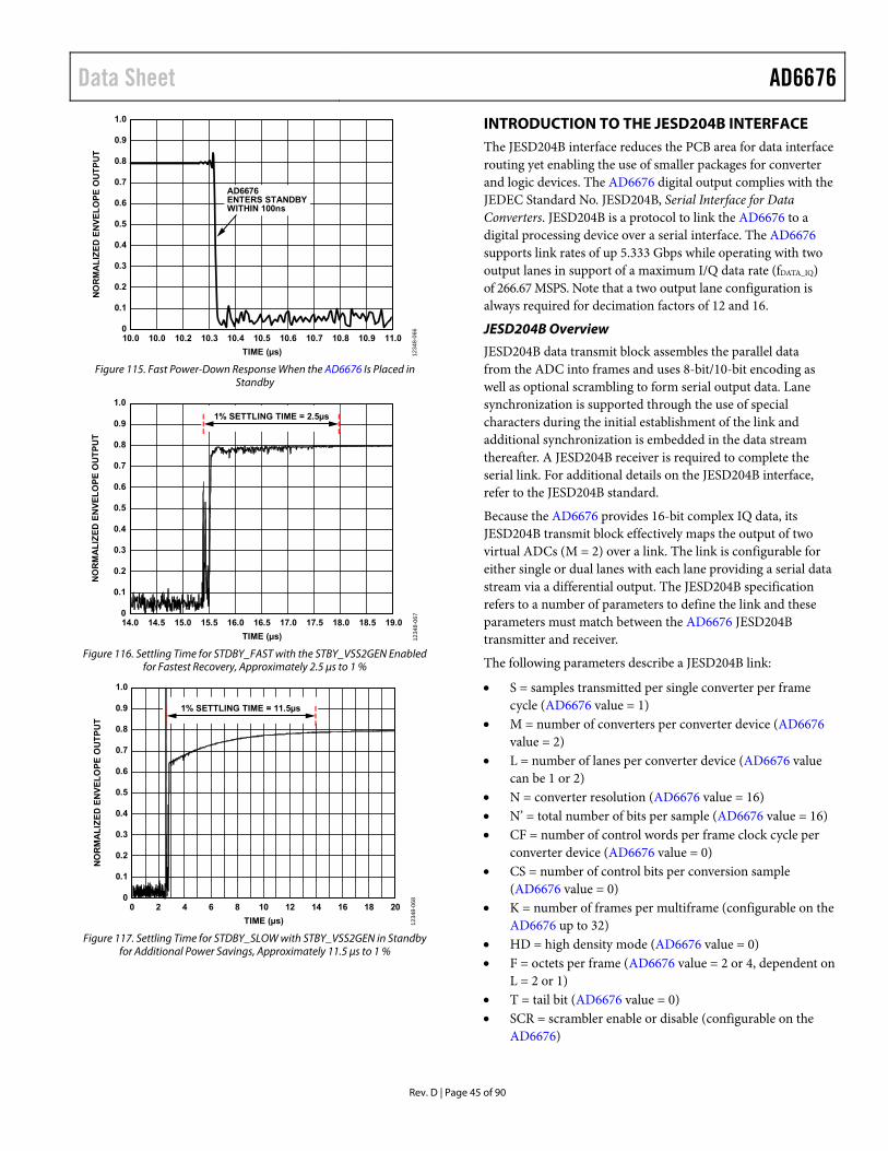
Data Sheet AD6676
Rev. D | Page 45 of 90
1.0
0
0.1
0.2
0.3
0.4
0.5
0.6
0.7
0.8
0.9
10.0 10.0 10.2 10.3 10.4 10.5 10.6 10.7 10.8 10.9 11.0
NO
RM
AL
IZE
D E
NV
EL
OP
E O
UT
PU
T
TIME (µs)
AD6676ENTERS STANDBYWITHIN 100ns
1234
8-06
6
Figure 115. Fast Power-Down Response When the AD6676 Is Placed in
Standby
1.0
0
0.1
0.2
0.3
0.4
0.5
0.6
0.7
0.8
0.9
14.0 14.5 15.0 15.5 16.0 16.5 17.0 17.5 18.0 18.5 19.0
NO
RM
AL
IZE
D E
NV
EL
OP
E O
UT
PU
T
TIME (µs)
1% SETTLING TIME = 2.5µs12
348-
067
Figure 116. Settling Time for STDBY_FAST with the STBY_VSS2GEN Enabled
for Fastest Recovery, Approximately 2.5 μs to 1 %
1.0
0
0.1
0.2
0.3
0.4
0.5
0.6
0.7
0.8
0.9
0 2 4 6 8 10 12 14 16 18 20
NO
RM
AL
IZE
D E
NV
EL
OP
E O
UT
PU
T
TIME (µs)
1% SETTLING TIME = 11.5µs
1234
8-06
8
Figure 117. Settling Time for STDBY_SLOW with STBY_VSS2GEN in Standby
for Additional Power Savings, Approximately 11.5 μs to 1 %
INTRODUCTION TO THE JESD204B INTERFACE The JESD204B interface reduces the PCB area for data interface routing yet enabling the use of smaller packages for converter and logic devices. The AD6676 digital output complies with the JEDEC Standard No. JESD204B, Serial Interface for Data Converters. JESD204B is a protocol to link the AD6676 to a digital processing device over a serial interface. The AD6676 supports link rates of up 5.333 Gbps while operating with two output lanes in support of a maximum I/Q data rate (fDATA_IQ) of 266.67 MSPS. Note that a two output lane configuration is always required for decimation factors of 12 and 16.
JESD204B Overview
JESD204B data transmit block assembles the parallel data from the ADC into frames and uses 8-bit/10-bit encoding as well as optional scrambling to form serial output data. Lane synchronization is supported through the use of special characters during the initial establishment of the link and additional synchronization is embedded in the data stream thereafter. A JESD204B receiver is required to complete the serial link. For additional details on the JESD204B interface, refer to the JESD204B standard.
Because the AD6676 provides 16-bit complex IQ data, its JESD204B transmit block effectively maps the output of two virtual ADCs (M = 2) over a link. The link is configurable for either single or dual lanes with each lane providing a serial data stream via a differential output. The JESD204B specification refers to a number of parameters to define the link and these parameters must match between the AD6676 JESD204B transmitter and receiver.
The following parameters describe a JESD204B link:
S = samples transmitted per single converter per frame cycle (AD6676 value = 1)
M = number of converters per converter device (AD6676 value = 2)
L = number of lanes per converter device (AD6676 value can be 1 or 2)
N = converter resolution (AD6676 value = 16) N’ = total number of bits per sample (AD6676 value = 16) CF = number of control words per frame clock cycle per
converter device (AD6676 value = 0) CS = number of control bits per conversion sample
(AD6676 value = 0) K = number of frames per multiframe (configurable on the
AD6676 up to 32) HD = high density mode (AD6676 value = 0) F = octets per frame (AD6676 value = 2 or 4, dependent on
L = 2 or 1) T = tail bit (AD6676 value = 0) SCR = scrambler enable or disable (configurable on the
AD6676)
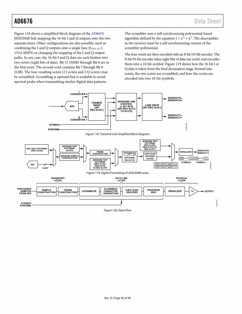
AD6676 Data Sheet
Rev. D | Page 46 of 90
Figure 118 shows a simplified block diagram of the AD6676 JESD204B link mapping the 16-bit I and Q outputs onto the two separate lanes. Other configurations are also possible, such as combining the I and Q outputs onto a single lane (fDATA_IQ ≤ 153.6 MSPS) or changing the mapping of the I and Q output paths. In any case, the 16-bit I and Q data are each broken into two octets (eight bits of data). Bit 15 (MSB) through Bit 8 are in the first octet. The second octet contains Bit 7 through Bit 0 (LSB). The four resulting octets (2 I octets and 2 Q octets) may be scrambled. Scrambling is optional but is available to avoid spectral peaks when transmitting similar digital data patterns.
The scrambler uses a self synchronizing polynomial-based algorithm defined by the equation 1 + x14 + x15. The descrambler in the receiver must be a self synchronizing version of the scrambler polynomial.
The four octets are then encoded with an 8-bit/10-bit encoder. The 8-bit/10-bit encoder takes eight bits of data (an octet) and encodes them into a 10-bit symbol. Figure 119 shows how the 16-bit I or Q data is taken from the final decimation stage, formed into octets, the two octets are scrambled, and how the octets are encoded into two 10-bit symbols.
ADC
SYSREF±
SYNCINB±
ICONVERTER 0
QCONVERTER 1
SERDOUT0–,SERDOUT0+
SERDOUT1–,SERDOUT1+
LANE SWAP(SPI REG 0x1E1)
JESD204B LINKCONTROL(L.M.F.M.S)
(SPI REG 0x1C3TO 0x1C9)
FRAMERSWAP(SPI
REG 0x1E1)
1234
8-06
9
Figure 118. Transmit Link Simplified Block Diagram
8-BIT/10-BITENCODER
(0x1E4)
SERDOUT0±SERDOUT1±SERIALIZER
ADCSYMBOL0 SYMBOL1
ADC TEST PATTERNS(REG 0x1E5)
JESD204B SAMPLECONSTRUCTION
JESD204B TESTPATTERNS
(0x1E5)FRAME
CONSTRUCTION
JESD204B TESTPATTERNS(REG 0x1E5,REG 0x1F8
TO REG 0x1FF)
JESD204B TESTPATTERNS
(REG 0x1E5,REG 0x1F8 TO
REG 0x1FF)
SCRAMBLER1 + x14 + x15
(OPTIONALVIA 0x1C3)
a b c d e f g h i j
a b c d e f g h i j
a b i j a b i j
16-BIT 1234
8-07
0
Figure 119. Digital Formatting of JESD204B Lanes
TRANSPORTLAYER
PHYSICALLAYER
DATA LINKLAYER
Tx OUTPUTSAMPLE
CONSTRUCTIONFRAME
CONSTRUCTION SCRAMBLERALIGNMENTCHARACTERGENERATION
8-BIT/10-BITENCODER
CROSSBARMUX SERIALIZER
PROCESSEDSAMPLES
FROM ADC
SYSREF±SYNCINB± 12
348-
071
Figure 120. Data Flow

Data Sheet AD6676
Rev. D | Page 47 of 90
FUNCTIONAL OVERVIEW The flowchart in Figure 120 shows the flow of data through the JESD204B hardware from the sample input to the physical output. The processing is divided into layers that are derived from the OSI model widely used to describe the abstraction layers of communications systems. These are the transport layer, the data link layer, and the physical layer (serializer and output driver).
Transport Layer
The transport layer packs the data into JESD204B frames, which are mapped to 8-bit octets that are sent to the data link layer. The transport layer mapping is controlled by rules derived from the link parameters. The AD6676 uses no tail bits in the transport layer because the output of its IQ digital data path is considered two virtual 16-bit converters.
Data Link Layer
The data link layer is responsible for the low level functions of passing data across the link. These include optional data scrambling, inserting control characters for lane alignment/ monitoring, and encoding 8-bit octets into 10-bit symbols. The data link layer also sends the initial lane alignment sequence (ILAS), which contains the link configuration data, and is used by the receiver to verify the settings in the transport layer.
Physical Layer
The physical layer consists of the high speed circuitry clocked at the serial clock rate. For the AD6676, the 16-bit I and Q data are converted into one or two lanes of high speed differential serial data.
JESD204B LINK ESTABLISHMENT The AD6676 JESD204B Tx interface operates in Subclass 0 or Subclass 1 as defined in the JEDEC Standard No. 204B (July 2011) specification. The link establishment process is divided into the following steps: code group synchronization, ILAS, and user data.
Code Group Synchronization (CGS) and SYNCINB
Code group synchronization (CGS) is the process where the JESD204B receiver finds the boundaries between the 10-bit symbols in the stream of data. During the CGS phase, the JESD204B transmit (JESD Tx) block transmits /K28.5/ characters. The receiver must locate /K28.5/ characters in its input data stream using clock and data recovery (CDR) techniques.
The receiver issues a synchronization request by asserting a low signal on the SYNCINB± pins of the AD6676. The JESD Tx begins to send /K/ characters. After the receiver has synchronized, it then deasserts its SYNCINB signal, causing it to go high. The AD6676 then transmits an ILAS on the following LMFC boundary.
For more information on the CGS phase, see the JEDEC Standard No. 204B (July 2011), Section 5.3.3.1.
The SYNCINB± pin operation options are controllable via SPI registers. Although the SYNCINB input is configured for a CMOS logic level on its positive pin by default, it can also be configured for a differential LVDS input signal on its positive/ negative pins via Register 0x1E7. The polarity of the SYNCINB input signal can also be inverted via Register 0x1E4.
Initial Lane Alignment Sequence (ILAS)
The ILAS phase follows the CGS phase and begins on the next LMFC boundary. The ILAS consists of four multiframes, with a /R/ character marking the beginning and an /A/ character marking the end. The ILAS begins by sending an /R/ character followed by a data ramp starting with the value, 0, over four multiframes. On the second multiframe, the link configuration data is sent, starting with the third character. The second character in the second multiframe is a /Q/ character to confirm that the link configuration data follows. All undefined data slots are filled with ramp data. The ILAS sequence is never scrambled.
The ILAS sequence construction is shown in Figure 121. The four multiframes include the following:
Multiframe 1: Begins with an /R/ character (/K28.0/) and ends with an /A/ character (/K28.3/).
Multiframe 2: Begins with an /R/ character followed by a /Q/ (/K28.4/) character, followed by link configuration parameters over 14 configuration octets (see Table 18), and ends with an /A/ character. Many of the parameter values are of the notation of n − 1.
Multiframe 3: Begins with an /R/ character (/K28.0/) and ends with an /A/ character (/K28.3/).
Multiframe 4: Begins with an /R/ character (/K28.0/) and ends with an /A/ character (/K28.3/).
User Data and Error Detection
After the ILAS is complete, the user data is sent. Normally, in a frame all characters are user data. However, to monitor the frame clock and multiframe clock synchronization, there is a mechanism for replacing characters with /F/ or /A/ alignment characters when the data meets certain conditions. These conditions are different for unscrambled and scrambled data. The scrambling operation is disabled by default, but may be enabled via Register 0x1C3.
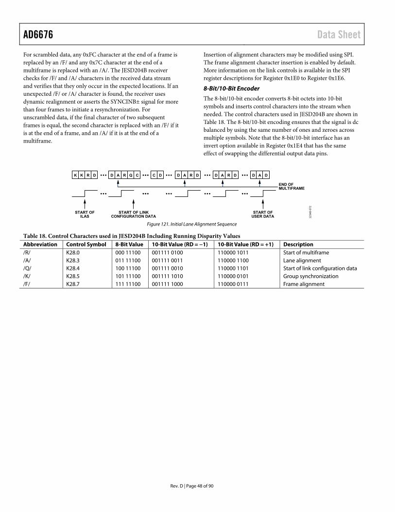
AD6676 Data Sheet
Rev. D | Page 48 of 90
For scrambled data, any 0xFC character at the end of a frame is replaced by an /F/ and any 0x7C character at the end of a multiframe is replaced with an /A/. The JESD204B receiver checks for /F/ and /A/ characters in the received data stream and verifies that they only occur in the expected locations. If an unexpected /F/ or /A/ character is found, the receiver uses dynamic realignment or asserts the SYNCINB± signal for more than four frames to initiate a resynchronization. For unscrambled data, if the final character of two subsequent frames is equal, the second character is replaced with an /F/ if it is at the end of a frame, and an /A/ if it is at the end of a multiframe.
Insertion of alignment characters may be modified using SPI. The frame alignment character insertion is enabled by default. More information on the link controls is available in the SPI register descriptions for Register 0x1E0 to Register 0x1E6.
8-Bit/10-Bit Encoder
The 8-bit/10-bit encoder converts 8-bit octets into 10-bit symbols and inserts control characters into the stream when needed. The control characters used in JESD204B are shown in Table 18. The 8-bit/10-bit encoding ensures that the signal is dc balanced by using the same number of ones and zeroes across multiple symbols. Note that the 8-bit/10-bit interface has an invert option available in Register 0x1E4 that has the same effect of swapping the differential output data pins.
K K R D D A R Q C C D D A R D D A R D D A D
START OFILAS
START OF LINKCONFIGURATION DATA
END OFMULTIFRAME
START OFUSER DATA 12
348-
072
Figure 121. Initial Lane Alignment Sequence
Table 18. Control Characters used in JESD204B Including Running Disparity Values Abbreviation Control Symbol 8-Bit Value 10-Bit Value (RD = −1) 10-Bit Value (RD = +1) Description /R/ K28.0 000 11100 001111 0100 110000 1011 Start of multiframe /A/ K28.3 011 11100 001111 0011 110000 1100 Lane alignment /Q/ K28.4 100 11100 001111 0010 110000 1101 Start of link configuration data /K/ K28.5 101 11100 001111 1010 110000 0101 Group synchronization /F/ K28.7 111 11100 001111 1000 110000 0111 Frame alignment
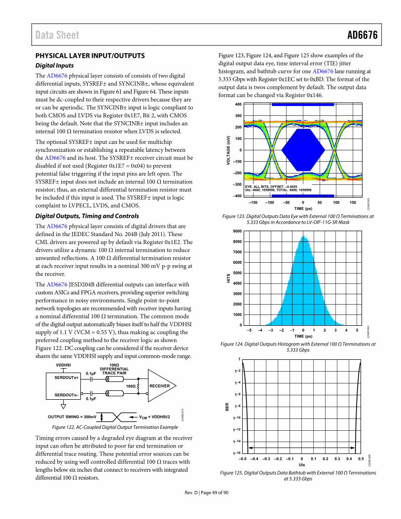
Data Sheet AD6676
Rev. D | Page 49 of 90
PHYSICAL LAYER INPUT/OUTPUTS Digital Inputs
The AD6676 physical layer consists of consists of two digital differential inputs, SYSREF± and SYNCINB±, whose equivalent input circuits are shown in Figure 61 and Figure 64. These inputs must be dc-coupled to their respective drivers because they are or can be aperiodic. The SYNCINB± input is logic compliant to both CMOS and LVDS via Register 0x1E7, Bit 2, with CMOS being the default. Note that the SYNCINB± input includes an internal 100 Ω termination resistor when LVDS is selected.
The optional SYSREF± input can be used for multichip synchronization or establishing a repeatable latency between the AD6676 and its host. The SYSREF± receiver circuit must be disabled if not used (Register 0x1E7 = 0x04) to prevent potential false triggering if the input pins are left open. The SYSREF± input does not include an internal 100 Ω termination resistor; thus, an external differential termination resistor must be included if this input is used. The SYSREF± input is logic complaint to LVPECL, LVDS, and CMOS.
Digital Outputs, Timing and Controls
The AD6676 physical layer consists of digital drivers that are defined in the JEDEC Standard No. 204B (July 2011). These CML drivers are powered up by default via Register 0x1E2. The drivers utilize a dynamic 100 Ω internal termination to reduce unwanted reflections. A 100 Ω differential termination resistor at each receiver input results in a nominal 300 mV p-p swing at the receiver.
The AD6676 JESD204B differential outputs can interface with custom ASICs and FPGA receivers, providing superior switching performance in noisy environments. Single point-to-point network topologies are recommended with receiver inputs having a nominal differential 100 Ω termination. The common mode of the digital output automatically biases itself to half the VDDHSI supply of 1.1 V (VCM = 0.55 V), thus making ac coupling the preferred coupling method to the receiver logic as shown Figure 122. DC coupling can be considered if the receiver device shares the same VDDHSI supply and input common-mode range.
SERDOUTx+
VDDHSI
SERDOUTx–
OUTPUT SWING = 300mV VCM = VDDHSI/2
100Ω RECEIVER
100ΩDIFFERENTIALTRACE PAIR0.1µF
0.1µF
1234
8-07
3
Figure 122. AC-Coupled Digital Output Termination Example
Timing errors caused by a degraded eye diagram at the receiver input can often be attributed to poor far end termination or differential trace routing. These potential error sources can be reduced by using well controlled differential 100 Ω traces with lengths below six inches that connect to receivers with integrated differential 100 Ω resistors.
Figure 123, Figure 124, and Figure 125 show examples of the digital output data eye, time interval error (TIE) jitter histogram, and bathtub curve for one AD6676 lane running at 5.333 Gbps with Register 0x1EC set to 0xBD. The format of the output data is twos complement by default. The output data format can be changed via Register 0x146.
400
–400
–300
–200
–100
0
100
200
300
–150 150100500–50–100
VO
LT
AG
E (
mV
)
TIME (ps) 1234
8-50
3
EYE: ALL BITS, OFFSET: –0.0055UIs: 4000; 1059998, TOTAL: 4000; 1059998
Figure 123. Digital Outputs Data Eye with External 100 Ω Terminations at
5.333 Gbps in Accordance to LV-OIF-11G-SR Mask
9000
8000
7000
6000
5000
4000
3000
2000
1000
0–5 –4 –3 –2 –1 0 54321
HIT
S
TIME (ps) 1234
8-50
4
Figure 124. Digital Outputs Histogram with External 100 Ω Terminations at
5.333 Gbps
1
1–2
1–4
1–6
1–8
1–10
1–12
1–16
1–14
–0.5 –0.4 –0.3 –0.2 –0.1 0 0.50.40.30.20.1
BE
R
UIs 1234
8-50
5
Figure 125. Digital Outputs Data Bathtub with External 100 Ω Terminations
at 5.333 Gbps

AD6676 Data Sheet
Rev. D | Page 50 of 90
Preemphasis
Preemphasis enables the receiver eye diagram mask to be met in conditions where the interconnect insertion loss does not meet the JESD204B specification. The preemphasis feature is controlled via Register 0x1EF and must be used only when the receiver cannot recover the clock due to excessive insertion loss. Under normal conditions, it is disabled to conserve power. Additionally, enabling and setting too high a deemphasis value on a short link may cause the receiver eye diagram to fail or lead to potential EMI issues. For these reasons, consider the use of preemphasis only in instances where meeting the receiver eye diagram mask is a challenge. See the Register Memory Map section for details.
Serializer PLL
This PLL generates the serializer clock that is equal to the JESD204B lane rate. The on-chip controller automatically configures the PLL parameters based on the user specified IQ data rate (FADC/M) and number of lanes. The status of the PLL lock can be checked via the PLL_LCK status bit in Register 0x2DC. This read only bit lets the user know if the PLL has achieved a lock for the specific setup.
CONFIGURING THE JESD204B LINK The AD6676 has one JESD204B link. The serial outputs (SERDOUT0± and SERDOUT1±) are part of one JESD204B link. The basic parameters that determine the link setup are:
L is the number of lanes per link M is the number of converters per link F is the number of octets per frame
The maximum and minimum specified lane rates for the AD6676 are 5.333 Gbps and 3.072 Gbps, respectively. For this reason, the AD6676 supports a single lane interface for IQ data rates (fDATA_IQ) from 76.8 MSPS to 133.3 MSPS and a two lane interface from 153.6 MSPS to 266.7 MSPS.
The lane line rate is related to the JESD204B parameters using the following equation:
LFRateLineLane DATA_IQ
40 (14)
where:
DECF
F ADCDATA_IQ
The decimation ratio (DEC) is the parameter programmed into Register 0x140.
Table 19 shows the JESD204B output configurations supported based on fDATA_IQ.
Table 19. JESD204B Output Configurations No. Virtual Converters Supported (same as M) fDATA_IQ (MSPS) JESD Serial Line Rate L M F S HD N N' K 2 76.8 to 133.3 40 × fDATA_IQ 1 2 4 1 0 16 16 For F = 4, K ≥ 5 153.6 to 266.7 20 × fDATA_IQ 2 2 2 1 0 16 16 For F = 2, K ≥ 9
Data Sheet AD6676
Rev. D | Page 51 of 90
SYNCHRONIZATION USING SYSREF± The AD6676 uses the SYSREF± input to provide synchronization for the JESD204B serial output and to establish a fixed phase reference for the decimation filters and the NCO within the QDDC. Synchronization options are configurable via Register 0x1E8. When initially synchronizing, the absolute phase offset relative to the input clock applied to the CLK± pins depends on internal clock phases and therefore has an uncertainty of ±1 ADC clock cycles.
A clock tree diagram is shown in Figure 126 with an internal clock signal, DIG_CLK, used to ultimately sample the SYSREF± signal. Note that the SYSREF± setup and hold times are defined with respect to the rising SYSREF± edge and rising CLK± (or CLK+ with the clock synthesizer disabled) edge, as shown in Figure 2. After the SYSREF± signal is sampled, the phase remains locked to the same relative internal ADC_CLK phase offset until the AD6676 is intentionally reset or its clock or power interrupted.
Note the following considerations when using SYSREF± for synchronization.
The SYSREF± pulse width must be at least two ADC_CLK periods.
Bit 3 of Register 0x2BB must be set low when synchronizing with the clock synthesizer enabled. In this case, that SYSREF± is sampled on the rising edge of REF_CLK to allow for significant margin in setup and hold time. This synchronization signal is then sampled again with the internally generated DIG_CLK.
Because SYSREF± is ultimately sampled with an internal clock greater than 1 GHz, it can be difficult to maintain synchronization of the clock and SYSREF± distribution in a system over supply and temperature variations, as well as
cumulative jitter affects. Use the one shot with the second SYSREF pulse to avoid unnecessary resetting of the JES204B link by setting Register 0x1E8 to 0x06. A minimum of two SYSREF pulses are required.
The coarse and fine digital NCOs can be reset to an initial phase defined in Register 0x143 through Register 0x145 upon receiving SYSREF±. For the recommended one shot with the second SYSREF pulse, set Register 0x1E8 to 0x26 so that the same SYSREF pulse that is used to reset the JESD204 internal dividers is used to reset the NCO phases.
If continuous SYSREF± is still preferred, it is recommended to use the SYSREF_WIN_NEG and SYSREF_WIN_POS bits in Register 0x1EA to allow for slight variation in SYSREF± timing relative to DIG_CLK.
A phase variance of ±1 ADC clock cycles ultimately results in fractions of a sample when referenced to the IQ output data rate, fDATA_IQ, depending on the decimation factor. For example, for a decimation factor of 32, the phase uncertainty is expressed as ±1/32 samples relative to fDATA_IQ.
The course and fine digital NCOs are also set to an initial phase up defined in Register 0x143 thru Register 0x145 upon receiving SYSREF±.
Figure 127 shows how the HMC7044 (or the AD9528) can be used for mulichip synchronization. The HMC7044 is best suited for delivering a low phase noise RF clock source for each AD6676 (refer to Figure 135). In addition, its ability to individually control the delays of both the CLK and SYSREF signals to each AD6676 device allows compensation of PCB skew delays.
CLOCKSYNTHESIZER
fOUT =5.9GHz TO 6.4GHz
÷2
D Q
QD Q
Q
CLK±
SYSREF±
RF_CLK
REG 0x2A5
ADC_CLK
DIG_CLK
TO Σ-∆ ADCAND DIGITAL
TO DIGITAL
TO SYNCHRONIZATIONCIRCUITRY
REG 0x2BB
REF_CLK
÷2
1234
8-13
1
Figure 126. Block Diagram Showing Options of Sampling the SYSREF Input Signal with the Clock Synthesizer Disabled or Enabled

AD6676 Data Sheet
Rev. D | Page 52 of 90
CLK+
CLK–
CLKOUT0 1nF
1nF
HMC7044(OR AD9528) AD6676
SYSREF
240Ω240ΩSYSREF–
SYSREF+
1nF
1nF
240Ω240ΩCLKOUT0
SCLKOUT1
CLKOUT
CLKOUT2 1nF
1nF
AD6676
240Ω240Ω
1nF
1nF
240Ω240ΩCLKOUT2
SCLKOUT3
SCLKOUT3
SCLKOUT1
1234
8-72
7
CLK+
CLK–
SYSREF–
SYSREF+
Figure 127. Example of Multichip Synchronization of the AD6676 Using the HMC7044 or the AD9528
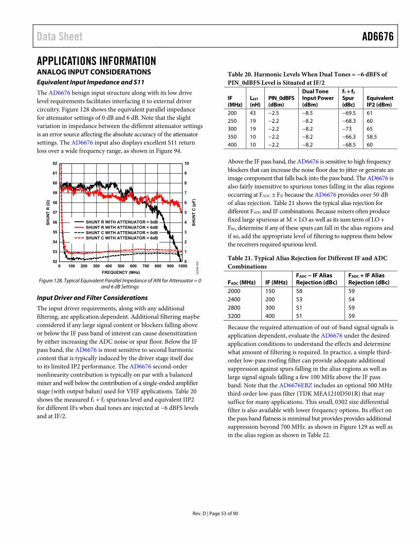
Data Sheet AD6676
Rev. D | Page 53 of 90
APPLICATIONS INFORMATION ANALOG INPUT CONSIDERATIONS Equivalent Input Impedance and S11
The AD6676 benign input structure along with its low drive level requirements facilitates interfacing it to external driver circuitry. Figure 128 shows the equivalent parallel impedance for attenuator settings of 0 dB and 6 dB. Note that the slight variation in impedance between the different attenuator settings is an error source affecting the absolute accuracy of the attenuator settings. The AD6676 input also displays excellent S11 return loss over a wide frequency range, as shown in Figure 94.
62
61
60
59
58
57
56
55
54
53
52
10
9
8
7
6
5
4
3
2
1
00 100 200 300 400 500 600 800 1000700 900
SH
UN
T R
(Ω
)
SH
UN
T C
(p
F)
FREQUENCY (MHz) 1234
8-70
3
SHUNT R WITH ATTENUATOR = 0dBSHUNT R WITH ATTENUATOR = 6dBSHUNT C WITH ATTENUATOR = 0dBSHUNT C WITH ATTENUATOR = 6dB
Figure 128. Typical Equivalent Parallel Impedance of AIN for Attenuator = 0
and 6 dB Settings
Input Driver and Filter Considerations
The input driver requirements, along with any additional filtering, are application dependent. Additional filtering maybe considered if any large signal content or blockers falling above or below the IF pass band of interest can cause desensitization by either increasing the ADC noise or spur floor. Below the IF pass band, the AD6676 is most sensitive to second harmonic content that is typically induced by the driver stage itself due to its limited IP2 performance. The AD6676 second-order nonlinearity contribution is typically on par with a balanced mixer and well below the contribution of a single-ended amplifier stage (with output balun) used for VHF applications. Table 20 shows the measured f1 + f2 spurious level and equivalent IIP2 for different IFs when dual tones are injected at −6 dBFS levels and at IF/2.
Table 20. Harmonic Levels When Dual Tones = −6 dBFS of PIN_0dBFS Level is Situated at IF/2
IF (MHz)
LEXT (nH)
PIN_0dBFS (dBm)
Dual Tone Input Power (dBm)
f1 + f2 Spur (dBc)
Equivalent IP2 (dBm)
200 43 −2.5 −8.5 −69.5 61 250 19 −2.2 −8.2 −68.3 60 300 19 −2.2 −8.2 −73 65 350 10 −2.2 −8.2 −66.3 58.5 400 10 −2.2 −8.2 −68.5 60
Above the IF pass band, the AD6676 is sensitive to high frequency blockers that can increase the noise floor due to jitter or generate an image component that falls back into the pass band. The AD6676 is also fairly insensitive to spurious tones falling in the alias regions occurring at FADC ± FIF because the AD6676 provides over 50 dB of alias rejection. Table 21 shows the typical alias rejection for different FADC and IF combinations. Because mixers often produce fixed large spurious at M × LO as well as its sum term of LO + FRF, determine if any of these spurs can fall in the alias regions and if so, add the appropriate level of filtering to suppress them below the receivers required spurious level.
Table 21. Typical Alias Rejection for Different IF and ADC Combinations
FADC (MHz) IF (MHz) FADC − IF Alias Rejection (dBc)
FADC + IF Alias Rejection (dBc)
2000 150 58 59 2400 200 53 54 2800 300 51 59 3200 400 51 59
Because the required attenuation of out-of-band signal signals is application dependent, evaluate the AD6676 under the desired application conditions to understand the effects and determine what amount of filtering is required. In practice, a simple third-order low-pass roofing filter can provide adequate additional suppression against spurs falling in the alias regions as well as large signal signals falling a few 100 MHz above the IF pass band. Note that the AD6676EBZ includes an optional 500 MHz third-order low-pass filter (TDK MEA1210D501R) that may suffice for many applications. This small, 0302 size differential filter is also available with lower frequency options. Its effect on the pass band flatness is mimimal but provides provides additional suppression beyond 700 MHz. as shown in Figure 129 as well as in the alias region as shown in Table 22.
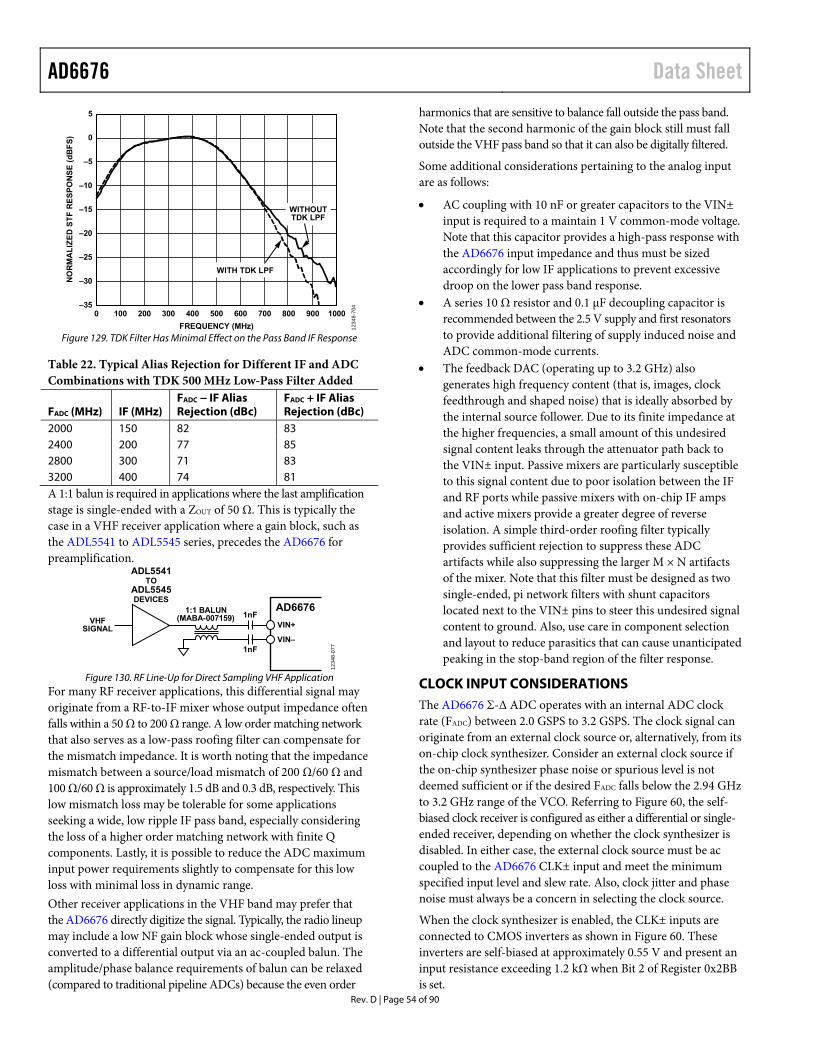
AD6676 Data Sheet
Rev. D | Page 54 of 90
5
0
–5
–10
–15
–20
–25
–30
–350 100 200 300 400 500 600 800 1000700 900
NO
RM
AL
IZE
D S
TF
RE
SP
ON
SE
(d
BF
S)
FREQUENCY (MHz) 1234
8-70
4
WITHOUTTDK LPF
WITH TDK LPF
Figure 129. TDK Filter Has Minimal Effect on the Pass Band IF Response
Table 22. Typical Alias Rejection for Different IF and ADC Combinations with TDK 500 MHz Low-Pass Filter Added
FADC (MHz) IF (MHz) FADC − IF Alias Rejection (dBc)
FADC + IF Alias Rejection (dBc)
2000 150 82 83 2400 200 77 85 2800 300 71 83 3200 400 74 81 A 1:1 balun is required in applications where the last amplification stage is single-ended with a ZOUT of 50 Ω. This is typically the case in a VHF receiver application where a gain block, such as the ADL5541 to ADL5545 series, precedes the AD6676 for preamplification.
VIN+
VIN–
1nF
1nF
ADL5541TO
ADL5545DEVICES
VHFSIGNAL
1:1 BALUN(MABA-007159)
AD6676
1234
8-07
7
Figure 130. RF Line-Up for Direct Sampling VHF Application
For many RF receiver applications, this differential signal may originate from a RF-to-IF mixer whose output impedance often falls within a 50 Ω to 200 Ω range. A low order matching network that also serves as a low-pass roofing filter can compensate for the mismatch impedance. It is worth noting that the impedance mismatch between a source/load mismatch of 200 Ω/60 Ω and 100 Ω/60 Ω is approximately 1.5 dB and 0.3 dB, respectively. This low mismatch loss may be tolerable for some applications seeking a wide, low ripple IF pass band, especially considering the loss of a higher order matching network with finite Q components. Lastly, it is possible to reduce the ADC maximum input power requirements slightly to compensate for this low loss with minimal loss in dynamic range. Other receiver applications in the VHF band may prefer that the AD6676 directly digitize the signal. Typically, the radio lineup may include a low NF gain block whose single-ended output is converted to a differential output via an ac-coupled balun. The amplitude/phase balance requirements of balun can be relaxed (compared to traditional pipeline ADCs) because the even order
harmonics that are sensitive to balance fall outside the pass band. Note that the second harmonic of the gain block still must fall outside the VHF pass band so that it can also be digitally filtered.
Some additional considerations pertaining to the analog input are as follows:
AC coupling with 10 nF or greater capacitors to the VIN± input is required to a maintain 1 V common-mode voltage. Note that this capacitor provides a high-pass response with the AD6676 input impedance and thus must be sized accordingly for low IF applications to prevent excessive droop on the lower pass band response.
A series 10 Ω resistor and 0.1 μF decoupling capacitor is recommended between the 2.5 V supply and first resonators to provide additional filtering of supply induced noise and ADC common-mode currents.
The feedback DAC (operating up to 3.2 GHz) also generates high frequency content (that is, images, clock feedthrough and shaped noise) that is ideally absorbed by the internal source follower. Due to its finite impedance at the higher frequencies, a small amount of this undesired signal content leaks through the attenuator path back to the VIN± input. Passive mixers are particularly susceptible to this signal content due to poor isolation between the IF and RF ports while passive mixers with on-chip IF amps and active mixers provide a greater degree of reverse isolation. A simple third-order roofing filter typically provides sufficient rejection to suppress these ADC artifacts while also suppressing the larger M × N artifacts of the mixer. Note that this filter must be designed as two single-ended, pi network filters with shunt capacitors located next to the VIN± pins to steer this undesired signal content to ground. Also, use care in component selection and layout to reduce parasitics that can cause unanticipated peaking in the stop-band region of the filter response.
CLOCK INPUT CONSIDERATIONS The AD6676 Σ-Δ ADC operates with an internal ADC clock rate (FADC) between 2.0 GSPS to 3.2 GSPS. The clock signal can originate from an external clock source or, alternatively, from its on-chip clock synthesizer. Consider an external clock source if the on-chip synthesizer phase noise or spurious level is not deemed sufficient or if the desired FADC falls below the 2.94 GHz to 3.2 GHz range of the VCO. Referring to Figure 60, the self-biased clock receiver is configured as either a differential or single-ended receiver, depending on whether the clock synthesizer is disabled. In either case, the external clock source must be ac coupled to the AD6676 CLK± input and meet the minimum specified input level and slew rate. Also, clock jitter and phase noise must always be a concern in selecting the clock source.
When the clock synthesizer is enabled, the CLK± inputs are connected to CMOS inverters as shown in Figure 60. These inverters are self-biased at approximately 0.55 V and present an input resistance exceeding 1.2 kΩ when Bit 2 of Register 0x2BB is set.

Data Sheet AD6676
Rev. D | Page 55 of 90
A single-ended clock source need only be ac coupled to the CLK+ input because the inverter output for CLK− input is not used. For CMOS drivers, the addition of a 33 Ω series resistor is recommended to dampen the response for long trace lengths. For a differential clock source, such as an LVDS or PECL source, the addition of a 100 Ω external termination resistor across the CLK± pins is recommended to minimize any reflections that result from distorting the clock input waveform.
When the clock synthesizer is disabled, the CLK± inputs are connected to a high speed differential clock receiver with on-chip 100 Ω termination to simplify interfacing to CML, LVPECL, or sinusoidal clock sources. The clock signal is typically ac-coupled to the CLK+ and CLK− pins via an RF balun or capacitors. These pins are biased internally (see Figure 60) at approximately 700 mV and require no external bias. The equivalent shunt impedance of the CLK± input is shown in Figure 131. It is recommended to use a 100 Ω differential transmission line to route the clock signal to the CLK+ and CLK− pins due to the high frequency nature of the signal.
130
50
60
70
80
90
100
110
120
1.0
–0.4
–0.2
0
0.2
0.4
0.6
0.8
2.0 2.5 3.5 4.03.0
RE
AL
SH
UN
T (Ω
)
CA
PA
CIT
AN
CE
(p
F)
FREQUENCY (GHz) 1234
8-70
5
REAL SHUNTCAPACITANCE SHUNT
Figure 131. Equivalent Shunt Differential Input Impedance of the CLK± Pins
with the Clock Synthesizer Disabled
Figure 132 shows a single-ended clock solution for the AD6676 when its clock synthesizer is disabled. The low phase noise single-ended source can be from an external VCXO. A ceramic RF chip 1:2 ratio balun creates the differential clock input signal. The balun must be specified to have low loss (that is, less than 2 dB) at the clock frequency of interest. The single-ended clock source must be capable of 0 dBm drive capability to ensure adequate signal swing into the clock input.
AD6676CLK+
CLK–
CLOCKINPUT
100pF100pF
100pFJT 4000BL14100 1234
8-07
8
Figure 132. Balun Coupled Differential Clock
A single-ended CMOS or differential ac-coupled PECL/HSTL clock signal can be delivered via clock generation and distribution ICs such as the Analog Devices HMC7044, AD9528, and ADCLK925. A PECL clock signal is recommended when providing an RF clock input signal to the AD6676 or in applications that require deterministic latency or synchronization while using the internal clock synthesizer of the AD6676. Figure 133 shows a simple differential interface in which the AD6676 interfaces to the PECL output available from these ICs. The HMC7044 is an excellent choice for JESD204B clock generation and multichip synchronization because it also generates a very low phase noise RF clock from 2.4 GHz to 3.2 GHz for multiple AD6676 devices.
AD6676
CLK+
CLK–
10nF
240Ω 240Ω
PECLDRIVER
1234
8-08
1
10nF
HMC7044,AD9528 ORADCLK925
INSTALL 100ΩDIFFERENTIAL RESISTOR
ONLY WHEN CLK SYNIS ENABLED
Figure 133. Differential PECL Sample Clock Using the HMC7044, AD9528, and
ADCLK925
Alternatively, PLL clock synthesizers with on-chip VCOs such as the ADF4351, the ADF4355-2, and HMC1034 also make excellent RF clock sources when multichip synchronization is not required. The CML outputs of these devices allow a simple interface as shown in Figure 134. Figure 135 compares the close in phase noise between the ADF4351, the ADF4355-2, the HMC7044, the AD6676 clock synthesizer, and the R&S SMA100A for a near full-scale sine wave at 300 MHz. Note that the phase noise improvement offered by the high quality RF generator only becomes evident below 400 kHz when compared to the ADF4351.
CLK+
CLK–
REFOUTA+
REFOUTA–
REFOUTB+
REFOUTB–
1nF
1nF
ADF4351ADF4355-2
3.9nHAD6676
0.8V p-p
DIV
-BY
-2N
PLL VCO
FREF
VVCO
1234
8-07
9
Figure 134. Differential CML Driver from the ADF4351 and the ADF4355-2

AD6676 Data Sheet
Rev. D | Page 56 of 90
–110
–115
–120
–125
–130
–135
–140
–145
–150
–1550.01 0.1 1
PH
AS
E N
OIS
E @
IF
= 3
00M
Hz
(dB
c/H
z)
FREQUENCY OFFSET (MHz) 1234
8-08
0
AD6676 CLK SYN
ADF4351
ADF4355-2
HMC7044
R&S SMA100A
AVG = 300
Figure 135. Close In Phase Noise Comparison for Different Analog Devices
Clock Sources when Compared to the R&S SMA100A and the AD6676 Clock Synthesizer (IF = 300 MHz, BW = 40 MHz, FADC = 3.2 GHz, L = 19 nH)
IF FREQUENCY PLANNING The Σ-Δ ADC can achieve exceptional SFDR performance over a wide IF frequency range because its high oversampling ratio prevents low order harmonics from aliasing into the IF pass band. Higher order harmonics that do alias back are typically of much lower magnitude, with the shuffling option further reducing their levels. However, finite isolation between the Σ-Δ ADC and the digital block causes additional spurious signals that are a function of the output data rate, fDATA_IQ, and input frequency, fIN. Specifically, the feedback DACs in the Σ-Δ ADC suffer from digital contamination of its clock signal. Therefore, the same equation used to predict spurious locations on high speed DACs with digital interpolation filters applies.
Equation 15 defines this relationship with the spur location falling at fMN.
fMN = ±(M × fDATA_IQ) ± (N × fIN) (15)
where: M is the digital induced harmonic content from internal clocks. N is the harmonics from the Σ-Δ ADC.
When N = 0, signal independent spurs fall at integer multiples of fDATA_IQ. Table 23 shows the measured M × fDATA_IQ spurious levels (dBFS) for different IF frequencies and decimation factors with fDATA_IQ equal to 100 MSPS and 200 MSPS. All of the M × fDATA_IQ regions display low spurious with the exception of 200 MHz. This is because a large portion of digital circuitry is clocked at FADC/16 for DEC_MODES of 1 and 3 or FADC/12 for DEC_MODES of 2 and 4. As a result, the M = 2 spur is dominant when operating at the higher decimation factors of 32 and 24 whereas the M = 1 spur is dominant when operating at the lower decimation factors of 16 and 12.
When N = 1, signal dependent spurs falls at integer multiples of fDATA_IQ. These M × N spurs are called images because they have a 1:1 relationship in amplitude and frequency with the input signal, fIN. Note that the magnitude of some images can also vary slightly between power cycles, due to different phase relationships among internal clock dividers upon device initialization.
Figure 136 shows a normalized image graph (relative to fDATA_IQ) showing the image location relative for a given input frequency.
When N > 1, spurious content is often at lower magnitude than other spurious thus often can be ignored. The exception is when fIN falls below the IF pass band such that its lower order harmonics may fall within the pass band (that is, IF/2 and IF/3).
4.5
0.5
1.0
1.5
2.0
2.5
3.0
3.5
4.0
0.5 1.0 1.5 2.0 2.5 3.0 3.5 4.0 4.5
NO
RM
AL
IZE
D I
MA
GE
LO
CA
TIO
NNORMALIZED INPUT FREQUENCY
M = 6
M = 7
M = 8
M = 5M = 3 M = 4M = 2
M = 2M = 3 M = 1
1234
8-08
2
Figure 136. Image Location for Different M Factors Normalized to fDATA_IQ
Table 23. Measured Spurious Levels at Different IFs Where M × fDATA_IQ Falls On for fDATA_IQ of 100 MSPS and 200 MSPS
fDATA_IQ
Spurious Levels (dBFS) IF = 100 MHz
IF = 200 MHz
IF = 300 MHz
IF = 400 MHz
100 MSPS DEC_MODE = 1 <−100 −81 <−110 −97 DEC_MODE = 2 −100 −79 <−110 N/A1
200 MSPS DEC_MODE = 3 <−110 −81 <−110 −90 DEC_MODE = 4 <−110 −77 <−110 N/A1
1 N/A means not applicable.
Because the image spurs are also at low levels, the AD6676 offers a wide range of suitable IFs for a given output data rate, fDATA_IQ. Even IFs that are situated in a region where the worst M × fDATA_IQ spurious condition described in Table 23 can be used because they remain at a fixed location and remain signal independent. Similar to the LO feedthrough issue in a direct conversion IQ receiver, a slow digital tracking loop in the host processor can be used to nullify it. Figure 137 and Figure 138 show a case where the IF of 200 MHz was selected for an fDATA_IQ of 200 MSPS and 100 MSPS such that dominant spur falls exactly at the IF center. As shown in Figure 136, the IF is positioned at a normalized fDATA_IQ of 1 or 2 for 200 MSPS and 100 MSPS operation, thus explaining why the image term is M = 2 or 4. Note that the image spur is quite low for M = 2 and can be further improved by selecting a higher decimation factor (DEC_MODE of 3 vs. 1) that results in the M = 4 image.
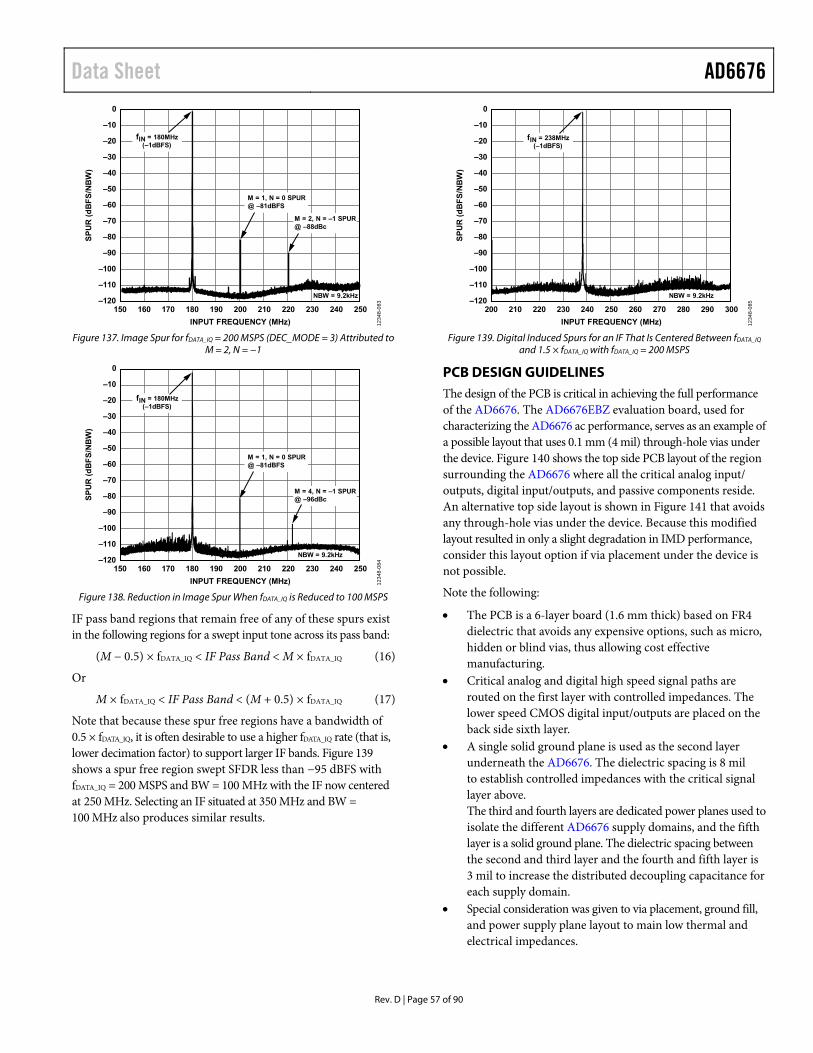
Data Sheet AD6676
Rev. D | Page 57 of 90
0
–120
–110
–100
–90
–80
–70
–60
–50
–40
–30
–20
–10
150 160 170 180 190 200 210 220 230 240 250
SP
UR
(d
BF
S/N
BW
)
INPUT FREQUENCY (MHz)
fIN = 180MHz(–1dBFS)
M = 2, N = –1 SPUR@ –88dBc
M = 1, N = 0 SPUR@ –81dBFS
NBW = 9.2kHz
1234
8-08
3
Figure 137. Image Spur for fDATA_IQ = 200 MSPS (DEC_MODE = 3) Attributed to
M = 2, N = −1
0
–120
–110
–100
–90
–80
–70
–60
–50
–40
–30
–20
–10
150 160 170 180 190 200 210 220 230 240 250
SP
UR
(d
BF
S/N
BW
)
INPUT FREQUENCY (MHz)
fIN = 180MHz(–1dBFS)
M = 4, N = –1 SPUR@ –96dBc
M = 1, N = 0 SPUR@ –81dBFS
NBW = 9.2kHz
1234
8-08
4
Figure 138. Reduction in Image Spur When fDATA_IQ is Reduced to 100 MSPS
IF pass band regions that remain free of any of these spurs exist in the following regions for a swept input tone across its pass band:
(M − 0.5) × fDATA_IQ < IF Pass Band < M × fDATA_IQ (16)
Or
M × fDATA_IQ < IF Pass Band < (M + 0.5) × fDATA_IQ (17)
Note that because these spur free regions have a bandwidth of 0.5 × fDATA_IQ, it is often desirable to use a higher fDATA_IQ rate (that is, lower decimation factor) to support larger IF bands. Figure 139 shows a spur free region swept SFDR less than −95 dBFS with fDATA_IQ = 200 MSPS and BW = 100 MHz with the IF now centered at 250 MHz. Selecting an IF situated at 350 MHz and BW = 100 MHz also produces similar results.
0
–120
–110
–100
–90
–80
–70
–60
–50
–40
–30
–20
–10
200 210 220 230 240 250 260 270 280 290 300
SP
UR
(d
BF
S/N
BW
)
INPUT FREQUENCY (MHz)
fIN = 238MHz(–1dBFS)
NBW = 9.2kHz
1234
8-08
5
Figure 139. Digital Induced Spurs for an IF That Is Centered Between fDATA_IQ
and 1.5 × fDATA_IQ with fDATA_IQ = 200 MSPS
PCB DESIGN GUIDELINES The design of the PCB is critical in achieving the full performance of the AD6676. The AD6676EBZ evaluation board, used for characterizing the AD6676 ac performance, serves as an example of a possible layout that uses 0.1 mm (4 mil) through-hole vias under the device. Figure 140 shows the top side PCB layout of the region surrounding the AD6676 where all the critical analog input/ outputs, digital input/outputs, and passive components reside. An alternative top side layout is shown in Figure 141 that avoids any through-hole vias under the device. Because this modified layout resulted in only a slight degradation in IMD performance, consider this layout option if via placement under the device is not possible.
Note the following:
The PCB is a 6-layer board (1.6 mm thick) based on FR4 dielectric that avoids any expensive options, such as micro, hidden or blind vias, thus allowing cost effective manufacturing.
Critical analog and digital high speed signal paths are routed on the first layer with controlled impedances. The lower speed CMOS digital input/outputs are placed on the back side sixth layer.
A single solid ground plane is used as the second layer underneath the AD6676. The dielectric spacing is 8 mil to establish controlled impedances with the critical signal layer above. The third and fourth layers are dedicated power planes used to isolate the different AD6676 supply domains, and the fifth layer is a solid ground plane. The dielectric spacing between the second and third layer and the fourth and fifth layer is 3 mil to increase the distributed decoupling capacitance for each supply domain.
Special consideration was given to via placement, ground fill, and power supply plane layout to main low thermal and electrical impedances.
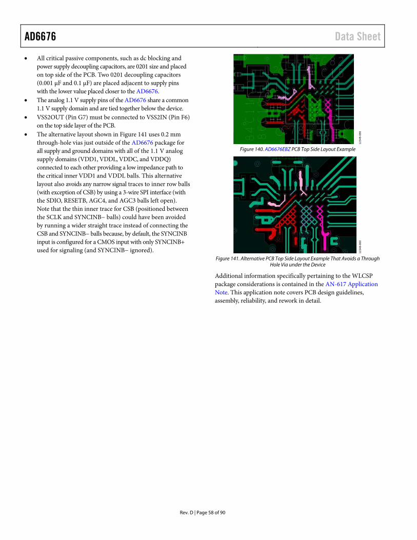
AD6676 Data Sheet
Rev. D | Page 58 of 90
All critical passive components, such as dc blocking and power supply decoupling capacitors, are 0201 size and placed on top side of the PCB. Two 0201 decoupling capacitors (0.001 μF and 0.1 μF) are placed adjacent to supply pins with the lower value placed closer to the AD6676.
The analog 1.1 V supply pins of the AD6676 share a common 1.1 V supply domain and are tied together below the device.
VSS2OUT (Pin G7) must be connected to VSS2IN (Pin F6) on the top side layer of the PCB.
The alternative layout shown in Figure 141 uses 0.2 mm through-hole vias just outside of the AD6676 package for all supply and ground domains with all of the 1.1 V analog supply domains (VDD1, VDDL, VDDC, and VDDQ) connected to each other providing a low impedance path to the critical inner VDD1 and VDDL balls. This alternative layout also avoids any narrow signal traces to inner row balls (with exception of CSB) by using a 3-wire SPI interface (with the SDIO, RESETB, AGC4, and AGC3 balls left open). Note that the thin inner trace for CSB (positioned between the SCLK and SYNCINB− balls) could have been avoided by running a wider straight trace instead of connecting the CSB and SYNCINB− balls because, by default, the SYNCINB input is configured for a CMOS input with only SYNCINB+ used for signaling (and SYNCINB− ignored).
1234
8-08
6
Figure 140. AD6676EBZ PCB Top Side Layout Example
1234
8-80
0
Figure 141. Alternative PCB Top Side Layout Example That Avoids a Through
Hole Via under the Device
Additional information specifically pertaining to the WLCSP package considerations is contained in the AN-617 Application Note. This application note covers PCB design guidelines, assembly, reliability, and rework in detail.

Data Sheet AD6676
Rev. D | Page 59 of 90
POWERING THE AD6676 The AD6676 requires the following analog and digital power supplies with no restrictions on the power supply sequencing order:
An analog 2.5 V and 1.1 V supply A digital 1.1 V and digital input/output supply of 1.8 V to 2.5 V
The current consumption from the different analog and digital supply domains does not vary much over the specified 2.0 GHz to 3.2 GHz ADC clock rate range nor the digital decimation factor and number of JESD204B lanes used. Table 24 shows the dependency of a typical device as these settings are modified with the IF and BW remaining fixed at 250 MHz and 75 MHz, respectively.
Figure 142 shows the recommended method used on the AD6676EBZ where a universal 3.3 V supply is available. Note that various analog and digital supply domains within the AD6676 are grouped together to reduce the external LDO requirements. A high efficiency step-down regulator, such as the ADP2164, is used to generate a 1.6 V output that drives separate low drop-out LDOs for the analog VDD1 and digital VDDD supplies.
ADP2164
ADP1752-2.5
ADP1752-1.8
ADP1752-1.1 VDDD, VDDHSI
VDD2, VDD2NV
VDDIO
ADP1752-1.1 VDD1, VDDL, VDDC, VDDQ
1.6V
3.3V
1234
8-08
7
Figure 142. Low Noise Power Solution for the AD6676
Separate LDOs for the 1.1 V analog and digital supplies provide greater isolation between these critical supply domains as well as reduce the IR drops across ferrite beads that provide further isolation. High quality LDOs that exhibit better PSSR characteristics at the switching regulators operating frequency are preferable. Note that the digital VDDIO supply of the AD6676 is only used for the CMOS SPI and AGCx input/output pins thus it can be tied to the same supply domain used by the host that is connected to these pins. Alternatively, the ADP223 dual output LDO can be used instead of the ADP1752-2.5 and ADP1752-1.8.
On the analog 1.1 V supply, amplitude modulation can result in phase modulation via the clock supplies of the AD6676 (VDDC, VDDQ).
Table 24. Current Consumption Variation as FADC Is Varied from 3.2 GHz to 2.0 GHz
Supply Current Conditions fCLK
Unit 3.2 GHz 2.8 GHz 2.4 GHz 2.0 GHz IVDD1+ IVDDL Not applicable 371 364 357 351 mA IVDDC + IVDDQ Not applicable 60 59 56 52 mA IVDD2 + IVDD2NV Not applicable 143 140 139 139 mA IVDDD Decimate by 16 152 144 131 100 mA Decimate by 32 155 150 135 106 mA IVDDHSI Two lane 168 168 168 158 mA One lane 166 167 167 161 mA

AD6676 Data Sheet
Rev. D | Page 60 of 90
Figure 143 and Figure 144 show the measured sideband level in dBc that results if a 1 mV p-p continuous wave tone has frequencies common among switching regulators are injected onto the 1.1 V and 2.5 V analog supplies. Note that the sideband level increases at roughly 6 dB per octave in IF frequency for the 1.1 V supply domain case because the supply noise results in PM modulation that affects the clock jitter.
–74
–76
–78
–80
–82
–84
–86
–88
–90100 200 400 500300150 350 450250
SID
EB
AN
D L
EV
EL
(d
Bc)
IF INPUT FREQUENCY (MHz) 1234
8-70
6
400MHz800MHz1600MHz3200MHz
Figure 143. Sideband Spur Level for 1 mV p-p, Continuous Wave Tone
Injected on Analog 1.1 V Supply Domain
–94
–96
–98
–100
–102
–104
–106
–108
–110100 200 400 500300150 350 450250
SID
EB
AN
D L
EV
EL
(d
Bc)
IF INPUT FREQUENCY (MHz) 1234
8-70
7
400MHz800MHz1600MHz3200MHz
Figure 144. Sideband Spur Level for 1 mV p-p, Continuous Wave Tone
Injected on Analog 2.5 V Supply Domain
On the digital 1.1 V supply, amplitude modulation on the JESD204B high speed serializer supply (VDDHSI) can negatively impact the eye opening of the digital data output stream. For these reasons, low noise LDOs, such as the ADP1752, that have a worst-case accuracy of 2% over line, load, and temperature are used for the analog VDD2 and VDD1 supplies. The same regulator is used for the digital VDDD for its low dropout characteristics, power supply rejection ratio, and load capability. Although the digital VDDD is used for the less critical VDDIO supply, a smaller, lower cost regulator such as the ADP121, can also be used to supply 1.8 V.

Data Sheet AD6676
Rev. D | Page 61 of 90
AD6676 START-UP INITIALIZATION On power-up of the AD6676, a host processor is required to initialize and configure the AD6676 via its SPI port. Figure 145 shows a flowchart of the sequential steps required to bring the AD6676 to an operational state. The number of SPI writes and total initialization time is dependent on whether the clock synthesizer is used, as well as any additional configuration associated with the AGC features or its pin configurations. Note that wait states are required during different steps in the initialization process to allow various actions, such as calibration and tuning, to be completed before moving to the next step.
Table 26 shows the minimum SPI writes required to enable the AD6676. Note the following in the sequence of steps shown in Table 26:
The example SPI writes pertain to the following settings: FADC = 3.200 GHz, FO = 250 MHz, BW = 100 MHz, IDAC1FS = 2 mA, MRGN_L = MRGN_U = 10 MHz, MRGN_IF = 1 MHz, fDATA_IQ = 200 MSPS with decimate by 16, and fREF = 200 MHz with the clock synthesizer enabled.
Step 3 refers to Table 28 for the necessary SPI writes when the clock synthesizer is enabled or disabled, respectively. Example AGC parameters are included in Table 29 but are nonessential to device operation.
The RESON1 calibration for the ADC occurs first with default DEC_MODE setting. DEC_MODE is updated to the user specified setting prior to JESD204B calibration.
ADC and JESD204B calibration and initialization must be successful on first attempt. However, Step 24 and Step 30 are included to provide coverage against external events (supply or clock glitch) that can corrupt this process.
The AD6676EVB software GUI has an option that automatically generates and saves the series of SPI writes in the .csv file format, as shown in Table 25, which is the preferred method for generating the AD6676 SPI write initialization sequence. Note the following: The SPI sequence can be shorter when the AD6676EVB
development platform is connected to the PC because the software also performs a SPI read back and then only writes to those SPI registers that have been changed from its default setting.
To generate a SPI initialization sequence for an alternative development platform, ensure that the AD6676EVB development platform is disconnected from the PC
When the software GUI is configured for the profile feature, Register 0x115 and Register 0x118 specify the calibration and ADC profile, respectively, that pertain to the specific ADC application parameter settings in Register 0x100 thru Register 0x109 that follow. A SPI write of 0x01 to Register 0x116 follows to initiate the ADC tuning. This process repeats itself for the remaining specified profiles.
1234
8-08
8
HARDWARE ORSOFTWARE
RESET
AD6676OPERATIONAL
PROGRAM CONFIGURATION SETTINGS
JESD204B CONFIGURATIONADC PARAMETERS
RUN ADC CAL + JESD204BINITIALIZATION
CALIBRATION + TUNING
INITIALIZECLK SYN
INITIALIZERF CLKPATH
WAIT(2ms)
WAIT(400ms)
CLK SYN?NO YES
CAL OK?NO
YES
ADC CAL/TUNE ERROR(MAKE TWO MORE
ATTEMPTS)
ALL REGISTERSRETURNED
TO DEFAULT
PROGRAM OPTIONAL SETTINGS
AGC CONFIGURATIONADC SHUFFLER
RUN RESON1 CALWITH DEC_MODE=1
WAIT(400ms)
CAL OK?NO
YES
RESON1 TUNE ERROR(MAKE TWO MORE
ATTEMPTS)
PROGRAM DECIMATION MODE
Figure 145. Flowchart for Initialization and Configuration of the AD6676
Table 25. Example of Saved .CSV File Format Register Address Write 0x000 0x99 0x2A5 0x05 0x2A0 0xC0 … … … …
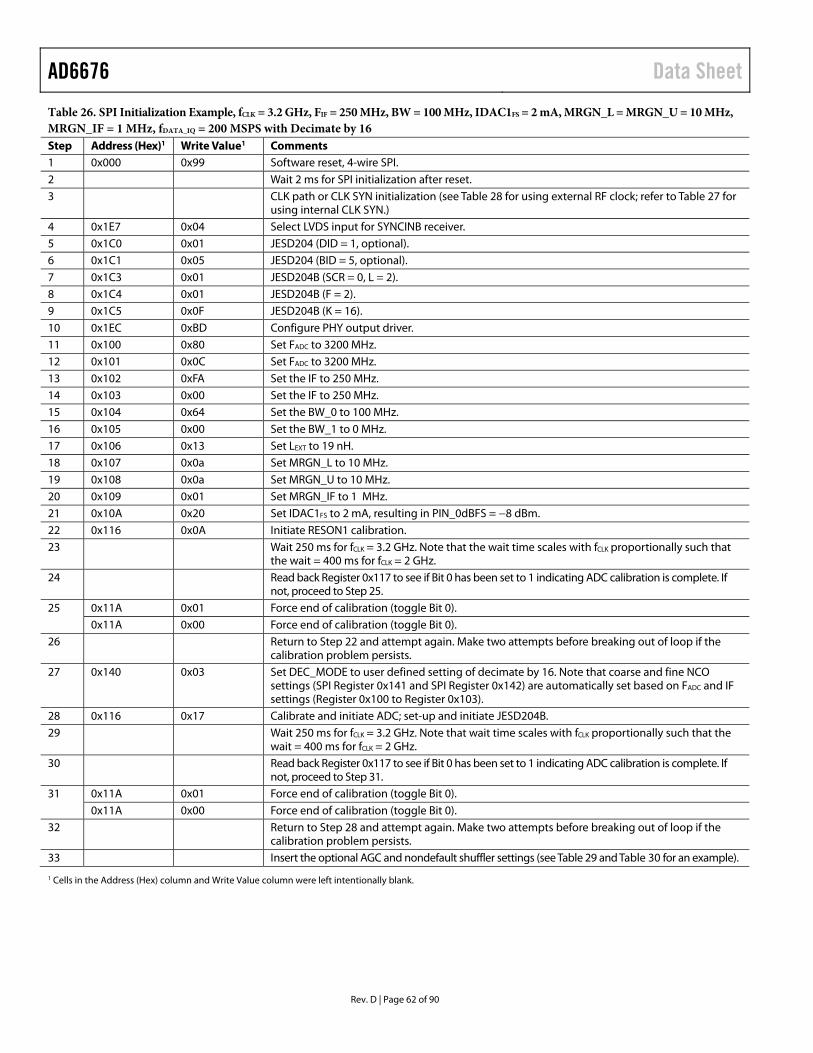
AD6676 Data Sheet
Rev. D | Page 62 of 90
Table 26. SPI Initialization Example, fCLK = 3.2 GHz, FIF = 250 MHz, BW = 100 MHz, IDAC1FS = 2 mA, MRGN_L = MRGN_U = 10 MHz, MRGN_IF = 1 MHz, fDATA_IQ = 200 MSPS with Decimate by 16 Step Address (Hex)1 Write Value1 Comments 1 0x000 0x99 Software reset, 4-wire SPI. 2 Wait 2 ms for SPI initialization after reset. 3 CLK path or CLK SYN initialization (see Table 28 for using external RF clock; refer to Table 27 for
using internal CLK SYN.) 4 0x1E7 0x04 Select LVDS input for SYNCINB receiver. 5 0x1C0 0x01 JESD204 (DID = 1, optional). 6 0x1C1 0x05 JESD204 (BID = 5, optional). 7 0x1C3 0x01 JESD204B (SCR = 0, L = 2). 8 0x1C4 0x01 JESD204B (F = 2). 9 0x1C5 0x0F JESD204B (K = 16). 10 0x1EC 0xBD Configure PHY output driver. 11 0x100 0x80 Set FADC to 3200 MHz. 12 0x101 0x0C Set FADC to 3200 MHz. 13 0x102 0xFA Set the IF to 250 MHz. 14 0x103 0x00 Set the IF to 250 MHz. 15 0x104 0x64 Set the BW_0 to 100 MHz. 16 0x105 0x00 Set the BW_1 to 0 MHz. 17 0x106 0x13 Set LEXT to 19 nH. 18 0x107 0x0a Set MRGN_L to 10 MHz. 19 0x108 0x0a Set MRGN_U to 10 MHz. 20 0x109 0x01 Set MRGN_IF to 1 MHz. 21 0x10A 0x20 Set IDAC1FS to 2 mA, resulting in PIN_0dBFS = −8 dBm. 22 0x116 0x0A Initiate RESON1 calibration. 23 Wait 250 ms for fCLK = 3.2 GHz. Note that the wait time scales with fCLK proportionally such that
the wait = 400 ms for fCLK = 2 GHz. 24 Read back Register 0x117 to see if Bit 0 has been set to 1 indicating ADC calibration is complete. If
not, proceed to Step 25. 25 0x11A 0x01 Force end of calibration (toggle Bit 0). 0x11A 0x00 Force end of calibration (toggle Bit 0). 26 Return to Step 22 and attempt again. Make two attempts before breaking out of loop if the
calibration problem persists. 27 0x140 0x03 Set DEC_MODE to user defined setting of decimate by 16. Note that coarse and fine NCO
settings (SPI Register 0x141 and SPI Register 0x142) are automatically set based on FADC and IF settings (Register 0x100 to Register 0x103).
28 0x116 0x17 Calibrate and initiate ADC; set-up and initiate JESD204B. 29 Wait 250 ms for fCLK = 3.2 GHz. Note that wait time scales with fCLK proportionally such that the
wait = 400 ms for fCLK = 2 GHz. 30 Read back Register 0x117 to see if Bit 0 has been set to 1 indicating ADC calibration is complete. If
not, proceed to Step 31. 31 0x11A 0x01 Force end of calibration (toggle Bit 0). 0x11A 0x00 Force end of calibration (toggle Bit 0). 32 Return to Step 28 and attempt again. Make two attempts before breaking out of loop if the
calibration problem persists. 33 Insert the optional AGC and nondefault shuffler settings (see Table 29 and Table 30 for an example).
1 Cells in the Address (Hex) column and Write Value column were left intentionally blank.
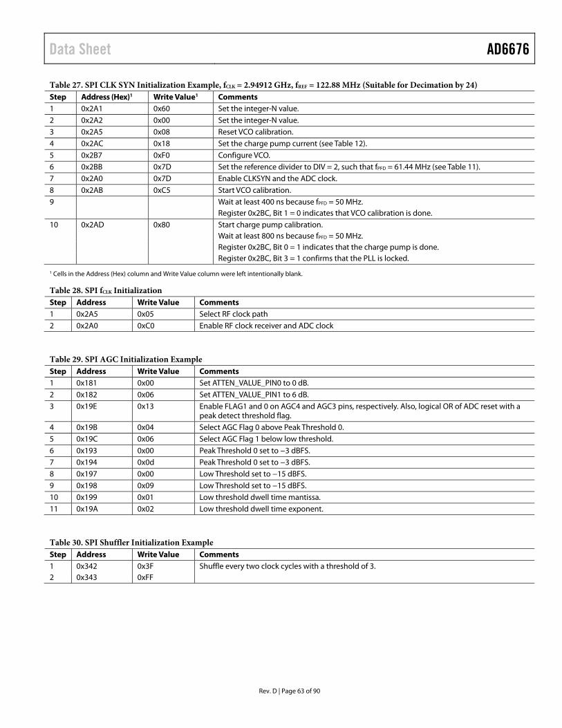
Data Sheet AD6676
Rev. D | Page 63 of 90
Table 27. SPI CLK SYN Initialization Example, fCLK = 2.94912 GHz, fREF = 122.88 MHz (Suitable for Decimation by 24) Step Address (Hex)1 Write Value1 Comments 1 0x2A1 0x60 Set the integer-N value. 2 0x2A2 0x00 Set the integer-N value. 3 0x2A5 0x08 Reset VCO calibration. 4 0x2AC 0x18 Set the charge pump current (see Table 12). 5 0x2B7 0xF0 Configure VCO. 6 0x2BB 0x7D Set the reference divider to DIV = 2, such that fPFD = 61.44 MHz (see Table 11). 7 0x2A0 0x7D Enable CLKSYN and the ADC clock. 8 0x2AB 0xC5 Start VCO calibration. 9 Wait at least 400 ns because fPFD = 50 MHz. Register 0x2BC, Bit 1 = 0 indicates that VCO calibration is done. 10 0x2AD 0x80 Start charge pump calibration. Wait at least 800 ns because fPFD = 50 MHz. Register 0x2BC, Bit 0 = 1 indicates that the charge pump is done. Register 0x2BC, Bit 3 = 1 confirms that the PLL is locked.
1 Cells in the Address (Hex) column and Write Value column were left intentionally blank.
Table 28. SPI fCLK Initialization Step Address Write Value Comments 1 0x2A5 0x05 Select RF clock path 2 0x2A0 0xC0 Enable RF clock receiver and ADC clock
Table 29. SPI AGC Initialization Example Step Address Write Value Comments 1 0x181 0x00 Set ATTEN_VALUE_PIN0 to 0 dB. 2 0x182 0x06 Set ATTEN_VALUE_PIN1 to 6 dB. 3 0x19E 0x13 Enable FLAG1 and 0 on AGC4 and AGC3 pins, respectively. Also, logical OR of ADC reset with a
peak detect threshold flag. 4 0x19B 0x04 Select AGC Flag 0 above Peak Threshold 0. 5 0x19C 0x06 Select AGC Flag 1 below low threshold. 6 0x193 0x00 Peak Threshold 0 set to −3 dBFS. 7 0x194 0x0d Peak Threshold 0 set to −3 dBFS. 8 0x197 0x00 Low Threshold set to −15 dBFS. 9 0x198 0x09 Low Threshold set to −15 dBFS. 10 0x199 0x01 Low threshold dwell time mantissa. 11 0x19A 0x02 Low threshold dwell time exponent.
Table 30. SPI Shuffler Initialization Example Step Address Write Value Comments 1 0x342 0x3F Shuffle every two clock cycles with a threshold of 3. 2 0x343 0xFF
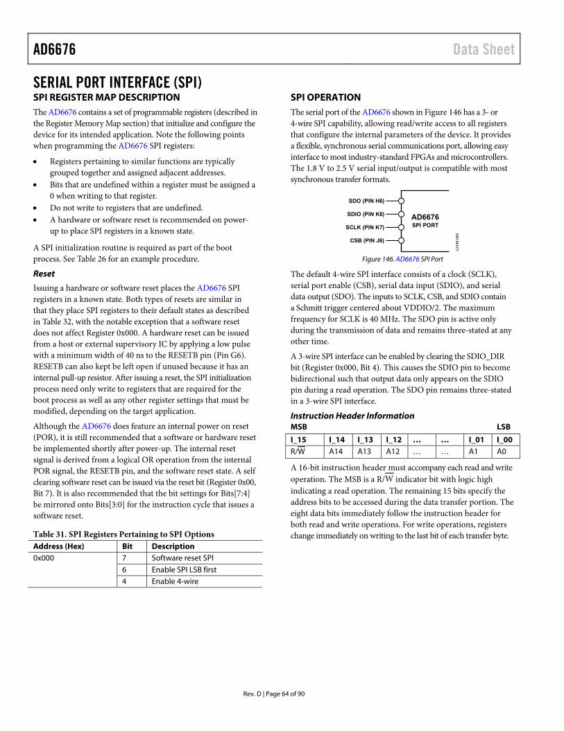
AD6676 Data Sheet
Rev. D | Page 64 of 90
SERIAL PORT INTERFACE (SPI) SPI REGISTER MAP DESCRIPTION The AD6676 contains a set of programmable registers (described in the Register Memory Map section) that initialize and configure the device for its intended application. Note the following points when programming the AD6676 SPI registers:
Registers pertaining to similar functions are typically grouped together and assigned adjacent addresses.
Bits that are undefined within a register must be assigned a 0 when writing to that register.
Do not write to registers that are undefined. A hardware or software reset is recommended on power-
up to place SPI registers in a known state.
A SPI initialization routine is required as part of the boot process. See Table 26 for an example procedure.
Reset
Issuing a hardware or software reset places the AD6676 SPI registers in a known state. Both types of resets are similar in that they place SPI registers to their default states as described in Table 32, with the notable exception that a software reset does not affect Register 0x000. A hardware reset can be issued from a host or external supervisory IC by applying a low pulse with a minimum width of 40 ns to the RESETB pin (Pin G6). RESETB can also kept be left open if unused because it has an internal pull-up resistor. After issuing a reset, the SPI initialization process need only write to registers that are required for the boot process as well as any other register settings that must be modified, depending on the target application.
Although the AD6676 does feature an internal power on reset (POR), it is still recommended that a software or hardware reset be implemented shortly after power-up. The internal reset signal is derived from a logical OR operation from the internal POR signal, the RESETB pin, and the software reset state. A self clearing software reset can be issued via the reset bit (Register 0x00, Bit 7). It is also recommended that the bit settings for Bits[7:4] be mirrored onto Bits[3:0] for the instruction cycle that issues a software reset.
Table 31. SPI Registers Pertaining to SPI Options Address (Hex) Bit Description 0x000 7 Software reset SPI 6 Enable SPI LSB first 4 Enable 4-wire
SPI OPERATION The serial port of the AD6676 shown in Figure 146 has a 3- or 4-wire SPI capability, allowing read/write access to all registers that configure the internal parameters of the device. It provides a flexible, synchronous serial communications port, allowing easy interface to most industry-standard FPGAs and microcontrollers. The 1.8 V to 2.5 V serial input/output is compatible with most synchronous transfer formats.
AD6676SPI PORT
SDO (PIN H6)
SDIO (PIN K8)
SCLK (PIN K7)
CSB (PIN J6)
1234
8-08
9
Figure 146. AD6676 SPI Port
The default 4-wire SPI interface consists of a clock (SCLK), serial port enable (CSB), serial data input (SDIO), and serial data output (SDO). The inputs to SCLK, CSB, and SDIO contain a Schmitt trigger centered about VDDIO/2. The maximum frequency for SCLK is 40 MHz. The SDO pin is active only during the transmission of data and remains three-stated at any other time.
A 3-wire SPI interface can be enabled by clearing the SDIO_DIR bit (Register 0x000, Bit 4). This causes the SDIO pin to become bidirectional such that output data only appears on the SDIO pin during a read operation. The SDO pin remains three-stated in a 3-wire SPI interface.
Instruction Header Information MSB LSB I_15 I_14 I_13 I_12 … … I_01 I_00 R/W A14 A13 A12 … … A1 A0
A 16-bit instruction header must accompany each read and write operation. The MSB is a R/W indicator bit with logic high indicating a read operation. The remaining 15 bits specify the address bits to be accessed during the data transfer portion. The eight data bits immediately follow the instruction header for both read and write operations. For write operations, registers change immediately on writing to the last bit of each transfer byte.
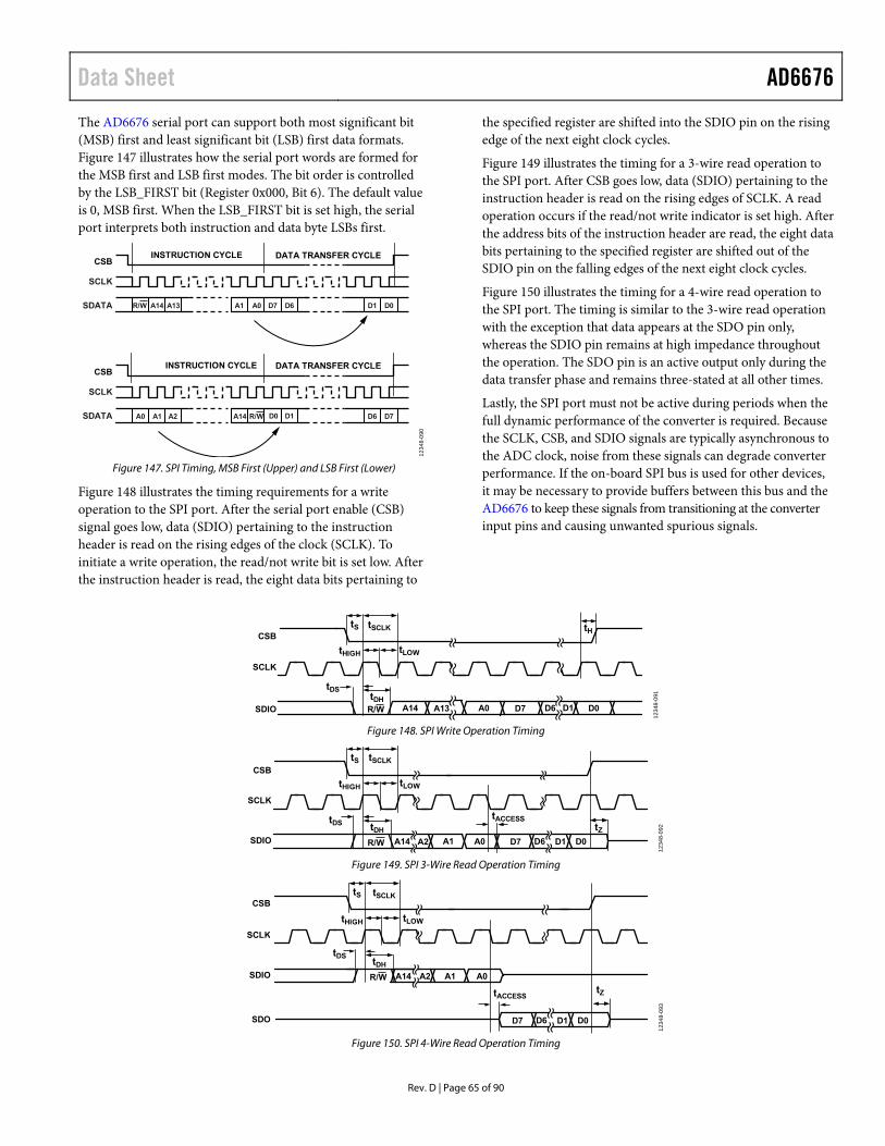
Data Sheet AD6676
Rev. D | Page 65 of 90
The AD6676 serial port can support both most significant bit (MSB) first and least significant bit (LSB) first data formats. Figure 147 illustrates how the serial port words are formed for the MSB first and LSB first modes. The bit order is controlled by the LSB_FIRST bit (Register 0x000, Bit 6). The default value is 0, MSB first. When the LSB_FIRST bit is set high, the serial port interprets both instruction and data byte LSBs first.
SCLK
SDATA R/W A1 A0 D7 D6 D1 D0
DATA TRANSFER CYCLEINSTRUCTION CYCLECSB
A14 A13
SCLK
SDATA R/WA1A0 D7D6D1D0
DATA TRANSFER CYCLEINSTRUCTION CYCLECSB
A14A212
348-
090
Figure 147. SPI Timing, MSB First (Upper) and LSB First (Lower)
Figure 148 illustrates the timing requirements for a write operation to the SPI port. After the serial port enable (CSB) signal goes low, data (SDIO) pertaining to the instruction header is read on the rising edges of the clock (SCLK). To initiate a write operation, the read/not write bit is set low. After the instruction header is read, the eight data bits pertaining to
the specified register are shifted into the SDIO pin on the rising edge of the next eight clock cycles.
Figure 149 illustrates the timing for a 3-wire read operation to the SPI port. After CSB goes low, data (SDIO) pertaining to the instruction header is read on the rising edges of SCLK. A read operation occurs if the read/not write indicator is set high. After the address bits of the instruction header are read, the eight data bits pertaining to the specified register are shifted out of the SDIO pin on the falling edges of the next eight clock cycles.
Figure 150 illustrates the timing for a 4-wire read operation to the SPI port. The timing is similar to the 3-wire read operation with the exception that data appears at the SDO pin only, whereas the SDIO pin remains at high impedance throughout the operation. The SDO pin is an active output only during the data transfer phase and remains three-stated at all other times.
Lastly, the SPI port must not be active during periods when the full dynamic performance of the converter is required. Because the SCLK, CSB, and SDIO signals are typically asynchronous to the ADC clock, noise from these signals can degrade converter performance. If the on-board SPI bus is used for other devices, it may be necessary to provide buffers between this bus and the AD6676 to keep these signals from transitioning at the converter input pins and causing unwanted spurious signals.
D7 D6A0 D1A14
tS
SCLK
SDIO
tSCLK
tLOWtHIGH
tDStDH
R/W D0
tHCSB
A13
1234
8-09
1
Figure 148. SPI Write Operation Timing
D7 D6A0 D1A14
tS
SCLK
SDIO
tSCLK
tLOWtHIGH
tDS tDH
R/W D0
tZ
A2 A1
tACCESS
CSB
1234
8-09
2
Figure 149. SPI 3-Wire Read Operation Timing
A0
CSB
A14
tS
SCLK
SDIO
tSCLK
tLOWtHIGH
tDStDH
R/W A2 A1
tACCESS
D7 D6 D1SDO D0
tZ
1234
8-09
3
Figure 150. SPI 4-Wire Read Operation Timing
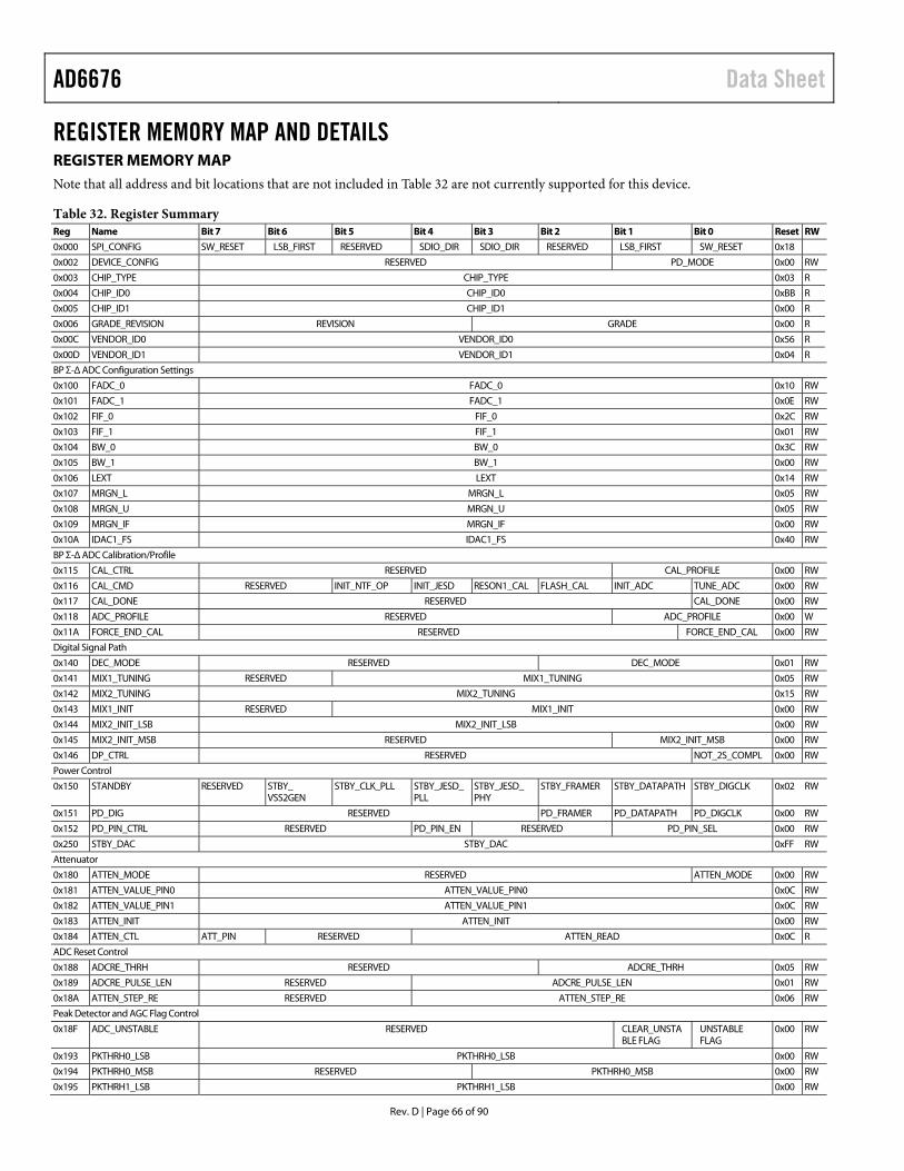
AD6676 Data Sheet
Rev. D | Page 66 of 90
REGISTER MEMORY MAP AND DETAILS REGISTER MEMORY MAP Note that all address and bit locations that are not included in Table 32 are not currently supported for this device.
Table 32. Register Summary Reg Name Bit 7 Bit 6 Bit 5 Bit 4 Bit 3 Bit 2 Bit 1 Bit 0 Reset RW
0x000 SPI_CONFIG SW_RESET LSB_FIRST RESERVED SDIO_DIR SDIO_DIR RESERVED LSB_FIRST SW_RESET 0x18
0x002 DEVICE_CONFIG RESERVED PD_MODE 0x00 RW
0x003 CHIP_TYPE CHIP_TYPE 0x03 R
0x004 CHIP_ID0 CHIP_ID0 0xBB R
0x005 CHIP_ID1 CHIP_ID1 0x00 R
0x006 GRADE_REVISION REVISION GRADE 0x00 R
0x00C VENDOR_ID0 VENDOR_ID0 0x56 R
0x00D VENDOR_ID1 VENDOR_ID1 0x04 R
BP Σ-Δ ADC Configuration Settings
0x100 FADC_0 FADC_0 0x10 RW
0x101 FADC_1 FADC_1 0x0E RW
0x102 FIF_0 FIF_0 0x2C RW
0x103 FIF_1 FIF_1 0x01 RW
0x104 BW_0 BW_0 0x3C RW
0x105 BW_1 BW_1 0x00 RW
0x106 LEXT LEXT 0x14 RW
0x107 MRGN_L MRGN_L 0x05 RW
0x108 MRGN_U MRGN_U 0x05 RW
0x109 MRGN_IF MRGN_IF 0x00 RW
0x10A IDAC1_FS IDAC1_FS 0x40 RW
BP Σ-Δ ADC Calibration/Profile
0x115 CAL_CTRL RESERVED CAL_PROFILE 0x00 RW
0x116 CAL_CMD RESERVED INIT_NTF_OP INIT_JESD RESON1_CAL FLASH_CAL INIT_ADC TUNE_ADC 0x00 RW
0x117 CAL_DONE RESERVED CAL_DONE 0x00 RW
0x118 ADC_PROFILE RESERVED ADC_PROFILE 0x00 W
0x11A FORCE_END_CAL RESERVED FORCE_END_CAL 0x00 RW
Digital Signal Path
0x140 DEC_MODE RESERVED DEC_MODE 0x01 RW
0x141 MIX1_TUNING RESERVED MIX1_TUNING 0x05 RW
0x142 MIX2_TUNING MIX2_TUNING 0x15 RW
0x143 MIX1_INIT RESERVED MIX1_INIT 0x00 RW
0x144 MIX2_INIT_LSB MIX2_INIT_LSB 0x00 RW
0x145 MIX2_INIT_MSB RESERVED MIX2_INIT_MSB 0x00 RW
0x146 DP_CTRL RESERVED NOT_2S_COMPL 0x00 RW
Power Control
0x150 STANDBY RESERVED STBY_ VSS2GEN
STBY_CLK_PLL STBY_JESD_ PLL
STBY_JESD_ PHY
STBY_FRAMER STBY_DATAPATH STBY_DIGCLK 0x02 RW
0x151 PD_DIG RESERVED PD_FRAMER PD_DATAPATH PD_DIGCLK 0x00 RW
0x152 PD_PIN_CTRL RESERVED PD_PIN_EN RESERVED PD_PIN_SEL 0x00 RW
0x250 STBY_DAC STBY_DAC 0xFF RW
Attenuator
0x180 ATTEN_MODE RESERVED ATTEN_MODE 0x00 RW
0x181 ATTEN_VALUE_PIN0 ATTEN_VALUE_PIN0 0x0C RW
0x182 ATTEN_VALUE_PIN1 ATTEN_VALUE_PIN1 0x0C RW
0x183 ATTEN_INIT ATTEN_INIT 0x00 RW
0x184 ATTEN_CTL ATT_PIN RESERVED ATTEN_READ 0x0C R
ADC Reset Control
0x188 ADCRE_THRH RESERVED ADCRE_THRH 0x05 RW
0x189 ADCRE_PULSE_LEN RESERVED ADCRE_PULSE_LEN 0x01 RW
0x18A ATTEN_STEP_RE RESERVED ATTEN_STEP_RE 0x06 RW
Peak Detector and AGC Flag Control
0x18F ADC_UNSTABLE RESERVED CLEAR_UNSTABLE FLAG
UNSTABLE FLAG
0x00 RW
0x193 PKTHRH0_LSB PKTHRH0_LSB 0x00 RW
0x194 PKTHRH0_MSB RESERVED PKTHRH0_MSB 0x00 RW
0x195 PKTHRH1_LSB PKTHRH1_LSB 0x00 RW

Data Sheet AD6676
Rev. D | Page 67 of 90
Reg Name Bit 7 Bit 6 Bit 5 Bit 4 Bit 3 Bit 2 Bit 1 Bit 0 Reset RW
0x196 PKTHRH1_MSB RESERVED PKTHRH1_MSB 0x00 RW
0x197 LOWTHRH_LSB LOWTHRH_LSB 0x00 RW
0x198 LOWTHRH_MSB RESERVED LOWTHRH_MSB 0x00 RW
0x199 DWELL_TIME_MANTISSA DWELL_TIME_MANTISSA 0x00 RW
0x19A DWELL_TIME_EXP RESERVED DWELL_TIME_EXP 0x00 RW
0x19B FLAG0_SEL RESERVED FLAG0_SEL 0x00 RW
0x19C FLAG1_SEL RESERVED FLAG1_SEL 0x00 RW
0x19E EN_FLAG RESERVED EN_OR RESERVED EN_FLAG1 EN_FLAG0 0x00 RW
GPIO Configuration
0x1B0 FORCE_GPIO RESERVED FORCE_GPIO 0x00 RW
0x1B1 FORCE_GPIO_OUT RESERVED FORCE_GPIO_OUT 0x00 RW
0x1B2 FORCE_GPIO_VAL RESERVED FORCE_GPIO_VAL 0x00 RW
0x1B3 READ_GPO RESERVED READ_GPO 0x00 R
0x1B4 READ_GPI RESERVED READ_GPI 0x00 R
JESD204B Interface
0x1C0 DID DID 0x00 RW
0x1C1 BID RESERVED BID 0x00 RW
0x1C3 L SCR RESERVED L 0x00 RW
0x1C4 F F 0x03 RW
0x1C5 K RESERVED K 0x1F RW
0x1C6 M M 0x01 RW
0x1C9 S RESERVED S 0x00 RW
0x1CB RES1 RES1 0x00 RW
0x1CC RES2 RES2 0x00 RW
0x1D0 LID0 RESERVED LID0 0x00 RW
0x1D1 LID1 RESERVED LID1 0x01 RW
0x1D8 FCHK0 FCHK0 0x44 RW
0x1D9 FCHK1 FCHK1 0x45 RW
0x1E0 EN_LFIFO RESERVED EN_LFIFO 0x00 RW
0x1E1 SWAP RESERVED SWAP_CONV RESERVED SWAP_LANE 0x00 RW
0x1E2 LANE_PD ILAS_DELAY RESERVED LANE_PD 0x00 RW
0x1E3 MIS1 RESERVED TEST_SAMPLE_EN LSYNC_EN ILAS_MODE FACI_DISABLE RESERVED 0x14 RW
0x1E4 SYNC_PIN RESERVED SYNC_PIN_INV RESERVED INV_10B RESERVED 0x00 RW
0x1E5 TEST_GEN RESERVED TEST_GEN_SEL TEST_GEN_MODE 0x00 RW
0x1E6 KF_ILAS KF_ILAS 0x00 RW
0x1E7 SYNCINB_CTRL RESERVED PD_SYSREF_RX LVDS_SYNCINB RESERVED 0x00 RW
0x1E8 MIX_CTRL RESERVED MIX_USE_2ND MIX_NEXT MIX_ALL RESERVED USE_2ND_ SYSREF
NEXT_SYSREF ALL_SYSREF 0x00 RW
0x1E9 K_OFFSET RESERVED K_OFFSET 0x00 RW
0x1EA SYSREF SYSREF_WIN_NEG SYSREF_WIN_POS 0x00 RW
0x1EB SER1 SER_DRV_PS RESERVED 0x1C RW
0x1EC SER2 SER_ITRIM SER_RTRIM 0x9B RW
0x1EF PRE-EMPHASIS SER_EMP_PS1 SER_EMP_IDAC1 SER_EMP_PS0 SER_EMP_IDAC0 0x00 RW
ADC Clock Synthesizer
0x2A0 CLKSYN_ENABLE EN_EXTCK EN_ADC_CK EN_SYNTH EN_VCO_ PTAT
EN_VCO _ALC
EN_VCO EN_OVERRIDE_CAL
EN_OVERRIDE 0x00 RW
0x2A1 CLKSYN_INT_N_LSB INT_N_LSB[7:0] 0x80 RW
0x2A2 CLKSYN_INT_N_MSB RESERVED INT_N_MSB[10:8] 0x00 RW
0x2A5 VCO_CAL_RESET RESERVED VCO_CAL_ RESET
RESERVED 0x00 RW
0x2AA CLKSYN_VCO_BIAS RESERVED BIAS_TEMPCO RESERVED BIAS 0x37 RW
0x2AB CLKSYN_VCO_CAL INIT_ALC_VALUE ALC_DIS RESERVED ID_SYNTH 0xC0 RW
0x2AC CLKSYN_I_CP RESERVED I_CP 0x19 RW
0x2AD EN_CP_CAL EN_CP_CAL RESERVED 0x00
0x2B7 CLKSYN_VCO_VAR VCO_VAR RESERVED 0xD0 RW
0x2BB CLKSYN_R_DIV R_DIV RESERVED SYSREF_ CTRL
CLKIN_IMPED RESERVED 0xB9 RW
0x2BC CLKSYN_STATUS RESERVED PLL_LCK RESERVED VCO CAL BUSY CP CAL DONE 0x80 R
0x2DC JESDSYN_STATUS RESERVED PLL_LCK RESERVED VCO CAL BUSY CP CAL DONE 0x80 R
ADC Adaptive Shuffler Control
0x340 SHUFFLE_CTRL RESERVED EN_ADAPTIVE_SHUFFLE
0x03 RW
0x342 SHUFFLE_THREG_0 SHUFFLE_TH2 SHUFFLE_TH1 0xF5 RW
0x343 SHUFFLE_THREG_1 SHUFFLE_TH4 SHUFFLE_TH3 0xFF RW
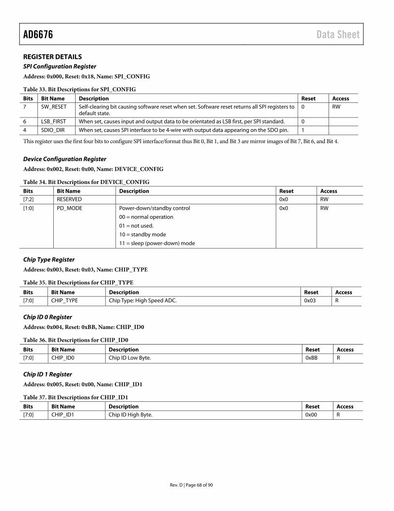
AD6676 Data Sheet
Rev. D | Page 68 of 90
REGISTER DETAILS SPI Configuration Register
Address: 0x000, Reset: 0x18, Name: SPI_CONFIG
Table 33. Bit Descriptions for SPI_CONFIG Bits Bit Name Description Reset Access 7 SW_RESET Self-clearing bit causing software reset when set. Software reset returns all SPI registers to
default state. 0 RW
6 LSB_FIRST When set, causes input and output data to be orientated as LSB first, per SPI standard. 0
4 SDIO_DIR When set, causes SPI interface to be 4-wire with output data appearing on the SDO pin. 1
This register uses the first four bits to configure SPI interface/format thus Bit 0, Bit 1, and Bit 3 are mirror images of Bit 7, Bit 6, and Bit 4.
Device Configuration Register
Address: 0x002, Reset: 0x00, Name: DEVICE_CONFIG
Table 34. Bit Descriptions for DEVICE_CONFIG Bits Bit Name Description Reset Access [7:2] RESERVED 0x0 RW
[1:0] PD_MODE Power-down/standby control 0x0 RW
00 = normal operation
01 = not used.
10 = standby mode
11 = sleep (power-down) mode
Chip Type Register
Address: 0x003, Reset: 0x03, Name: CHIP_TYPE
Table 35. Bit Descriptions for CHIP_TYPE Bits Bit Name Description Reset Access [7:0] CHIP_TYPE Chip Type: High Speed ADC. 0x03 R
Chip ID 0 Register
Address: 0x004, Reset: 0xBB, Name: CHIP_ID0
Table 36. Bit Descriptions for CHIP_ID0 Bits Bit Name Description Reset Access [7:0] CHIP_ID0 Chip ID Low Byte. 0xBB R
Chip ID 1 Register
Address: 0x005, Reset: 0x00, Name: CHIP_ID1
Table 37. Bit Descriptions for CHIP_ID1 Bits Bit Name Description Reset Access [7:0] CHIP_ID1 Chip ID High Byte. 0x00 R
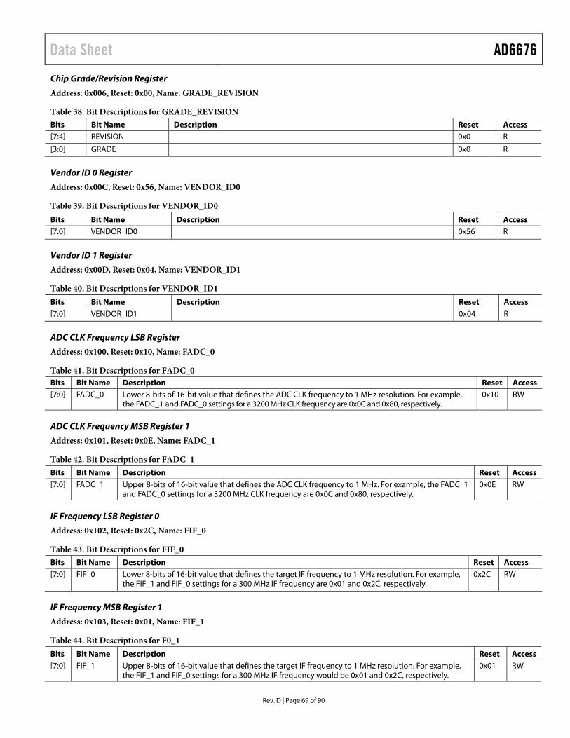
Data Sheet AD6676
Rev. D | Page 69 of 90
Chip Grade/Revision Register
Address: 0x006, Reset: 0x00, Name: GRADE_REVISION
Table 38. Bit Descriptions for GRADE_REVISION Bits Bit Name Description Reset Access [7:4] REVISION 0x0 R
[3:0] GRADE 0x0 R
Vendor ID 0 Register
Address: 0x00C, Reset: 0x56, Name: VENDOR_ID0
Table 39. Bit Descriptions for VENDOR_ID0 Bits Bit Name Description Reset Access [7:0] VENDOR_ID0 0x56 R
Vendor ID 1 Register
Address: 0x00D, Reset: 0x04, Name: VENDOR_ID1
Table 40. Bit Descriptions for VENDOR_ID1 Bits Bit Name Description Reset Access [7:0] VENDOR_ID1 0x04 R
ADC CLK Frequency LSB Register
Address: 0x100, Reset: 0x10, Name: FADC_0
Table 41. Bit Descriptions for FADC_0 Bits Bit Name Description Reset Access [7:0] FADC_0 Lower 8-bits of 16-bit value that defines the ADC CLK frequency to 1 MHz resolution. For example,
the FADC_1 and FADC_0 settings for a 3200 MHz CLK frequency are 0x0C and 0x80, respectively. 0x10 RW
ADC CLK Frequency MSB Register 1
Address: 0x101, Reset: 0x0E, Name: FADC_1
Table 42. Bit Descriptions for FADC_1 Bits Bit Name Description Reset Access [7:0] FADC_1 Upper 8-bits of 16-bit value that defines the ADC CLK frequency to 1 MHz. For example, the FADC_1
and FADC_0 settings for a 3200 MHz CLK frequency are 0x0C and 0x80, respectively. 0x0E RW
IF Frequency LSB Register 0
Address: 0x102, Reset: 0x2C, Name: FIF_0
Table 43. Bit Descriptions for FIF_0 Bits Bit Name Description Reset Access [7:0] FIF_0 Lower 8-bits of 16-bit value that defines the target IF frequency to 1 MHz resolution. For example,
the FIF_1 and FIF_0 settings for a 300 MHz IF frequency are 0x01 and 0x2C, respectively. 0x2C RW
IF Frequency MSB Register 1
Address: 0x103, Reset: 0x01, Name: FIF_1
Table 44. Bit Descriptions for F0_1 Bits Bit Name Description Reset Access [7:0] FIF_1 Upper 8-bits of 16-bit value that defines the target IF frequency to 1 MHz resolution. For example,
the FIF_1 and FIF_0 settings for a 300 MHz IF frequency would be 0x01 and 0x2C, respectively. 0x01 RW
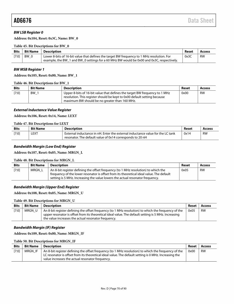
AD6676 Data Sheet
Rev. D | Page 70 of 90
BW LSB Register 0
Address: 0x104, Reset: 0x3C, Name: BW_0
Table 45. Bit Descriptions for BW_0 Bits Bit Name Description Reset Access [7:0] BW_0 Lower 8-bits of 16-bit value that defines the target BW frequency to 1 MHz resolution. For
example, the BW_1 and BW_0 settings for a 60 MHz BW would be 0x00 and 0x3C, respectively. 0x3C RW
BW MSB Register 1
Address: 0x105, Reset: 0x00, Name: BW_1
Table 46. Bit Descriptions for BW_1 Bits Bit Name Description Reset Access [7:0] BW_1 Upper 8-bits of 16-bit value that defines the target BW frequency to 1 MHz
resolution. This register should be kept to 0x00 default setting because maximum BW should be no greater than 160 MHz.
0x00 RW
External Inductance Value Register
Address: 0x106, Reset: 0x14, Name: LEXT
Table 47. Bit Descriptions for LEXT Bits Bit Name Description Reset Access [7:0] LEXT External inductance in nH. Enter the external inductance value for the LC tank
resonator. The default value of 0x14 corresponds to 20 nH 0x14 RW
Bandwidth Margin (Low End) Register
Address: 0x107, Reset: 0x05, Name: MRGN_L
Table 48. Bit Descriptions for MRGN_L Bits Bit Name Description Reset Access [7:0] MRGN_L An 8-bit register defining the offset frequency (to 1 MHz resolution) to which the
frequency of the lower resonator is offset from its theoretical ideal value. The default setting is 5 MHz. Increasing the value lowers the actual resonator frequency.
0x05 RW
Bandwidth Margin (Upper End) Register
Address: 0x108, Reset: 0x05, Name: MRGN_U
Table 49. Bit Descriptions for MRGN_U Bits Bit Name Description Reset Access [7:0] MRGN_U An 8-bit register defining the offset frequency (to 1 MHz resolution) to which the frequency of the
upper resonator is offset from its theoretical ideal value. The default setting is 5 MHz. Increasing the value increases the actual resonator frequency.
0x05 RW
Bandwidth Margin (IF) Register
Address: 0x109, Reset: 0x00, Name: MRGN_IF
Table 50. Bit Descriptions for MRGN_IF Bits Bit Name Description Reset Access [7:0] MRGN_IF An 8-bit register defining the offset frequency (to 1 MHz resolution) to which the frequency of the
LC resonator is offset from its theoretical ideal value. The default setting is 0 MHz. Increasing the value increases the actual resonator frequency.
0x00 RW

Data Sheet AD6676
Rev. D | Page 71 of 90
IDAC1FS Gain Scaling Register
Address: 0x10A, Reset: 0x40, Name: IDAC1_FS
Table 51. Bit Descriptions for IDAC1_FS Bits Bit Name Description Reset Access [7:0] IDAC1_FS This parameter allows adjustment of the full-scale input power level of the ADC by adjusting the
full-scale current of IDAC1. The nominal setting of 0x40 sets IDAC1FS value to 4 mA and corresponds to the largest full-scale level of approximately −3 dBm (with the IF attenuator set to 0 dB.) A setting of 0x20 or 0x10 results IDAC1FS value to 2 mA or 1 mA, thus resulting in a 6 dB or 12 dB reduction in PIN_0dBFS. Settings resulting in more than 12 dB reduction are not recommended.
0x40 RW
Calibration Control Register
Address: 0x115, Reset: 0x00, Name: CAL_CTRL
Table 52. Bit Descriptions for CAL_CTRL Bits Bit Name Description Reset Access [7:2] RESERVED 0x00 RW
[1:0] CAL_PROFILE ADC profile to be calibrated. Select one of the four ADC profiles in which to store the results of the calibration. For example, to support multiple IF settings, the four profiles cover all registers in the range of 0x141 to 0x145.
RW
Calibration Command Register
Address: 0x116, Reset: 0x00, Name: CAL_CMD
Table 53. Bit Descriptions for CAL_CMD Bits Bit Name Description Reset Access [7:6] RESERVED 0x0 RWAC
5 INIT_NTF_OP 0x0 RWAC
4 INIT_JESD 0x0 RWAC
3 RESON1_CAL 0x0 RWAC
2 FLASH_CAL 0x0 RWAC
1 INIT_ADC 0x0 RWAC
0 TUNE_ADC 0x0 RWAC
Setting a 1 in one or more of the bits in this register initiates the internal calibration. This register is cleared automatically at the end of calibration or by setting the FORCE_END_CAL bit.
Calibration Done Register
Address: 0x117, Reset: 0x00, Name: CAL_DONE
Table 54. Bit Descriptions for ADC_PROFILE Bits Bit Name Description Reset Access [7:1] RESERVED 0x00 RW
[0] CAL_DONE This bit indicates that the microcontroller has completed its calibration. It is automatically cleared by a new CAL_CMD.
0x0 RW
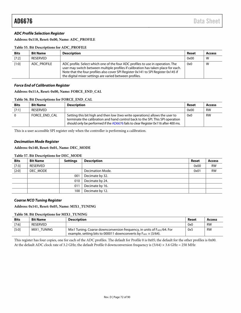
AD6676 Data Sheet
Rev. D | Page 72 of 90
ADC Profile Selection Register
Address: 0x118, Reset: 0x00, Name: ADC_PROFILE
Table 55. Bit Descriptions for ADC_PROFILE Bits Bit Name Description Reset Access [7:2] RESERVED 0x00 W
[1:0] ADC_PROFILE ADC profile. Select which one of the four ADC profiles to use in operation. The user may switch between multiple profiles if calibration has taken place for each. Note that the four profiles also cover SPI Register 0x141 to SPI Register 0x145 if the digital mixer settings are varied between profiles.
0x0 W
Force End of Calibration Register
Address: 0x11A, Reset: 0x00, Name: FORCE_END_CAL
Table 56. Bit Descriptions for FORCE_END_CAL Bits Bit Name Description Reset Access [7:1] RESERVED 0x00 RW
0 FORCE_END_CAL Setting this bit high and then low (two write operations) allows the user to terminate the calibration and hand control back to the SPI. This SPI operation should only be performed if the AD6676 fails to clear Register 0x116 after 400 ms.
0x0 RW
This is a user accessible SPI register only when the controller is performing a calibration.
Decimation Mode Register
Address: 0x140, Reset: 0x01, Name: DEC_MODE
Table 57. Bit Descriptions for DEC_MODE Bits Bit Name Settings Description Reset Access [7:3] RESERVED 0x00 RW [2:0] DEC_MODE Decimation Mode. 0x01 RW 001 Decimate by 32. 010 Decimate by 24. 011 Decimate by 16. 100 Decimate by 12.
Coarse NCO Tuning Register
Address: 0x141, Reset: 0x05, Name: MIX1_TUNING
Table 58. Bit Descriptions for MIX1_TUNING Bits Bit Name Description Reset Access [7:6] RESERVED 0x0 RW [5:0] MIX1_TUNING Mix1 Tuning. Coarse downconversion frequency, in units of FADC/64. For
example, setting bits to 000011 downconverts by FADC × (3/64). 0x5 RW
This register has four copies, one for each of the ADC profiles. The default for Profile 0 is 0x05; the default for the other profiles is 0x00. At the default ADC clock rate of 3.2 GHz; the default Profile 0 downconversion frequency is (5/64) × 3.6 GHz = 250 MHz
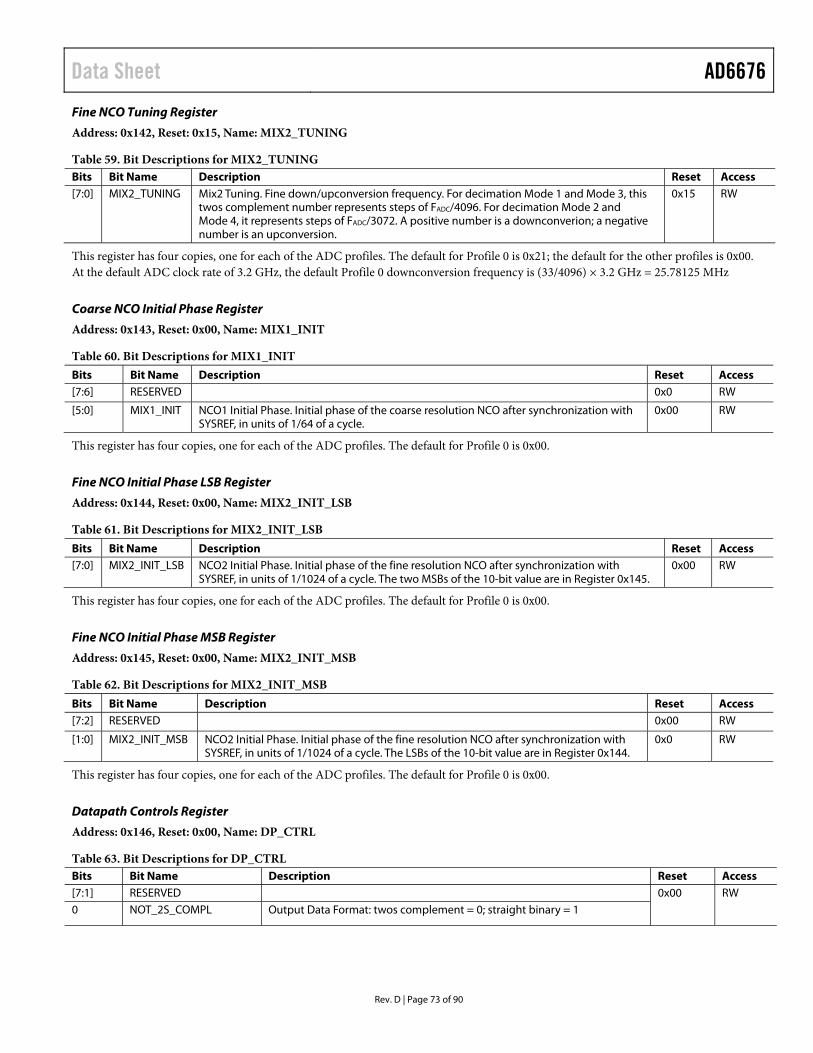
Data Sheet AD6676
Rev. D | Page 73 of 90
Fine NCO Tuning Register
Address: 0x142, Reset: 0x15, Name: MIX2_TUNING
Table 59. Bit Descriptions for MIX2_TUNING Bits Bit Name Description Reset Access [7:0] MIX2_TUNING Mix2 Tuning. Fine down/upconversion frequency. For decimation Mode 1 and Mode 3, this
twos complement number represents steps of FADC/4096. For decimation Mode 2 and Mode 4, it represents steps of FADC/3072. A positive number is a downconverion; a negative number is an upconversion.
0x15 RW
This register has four copies, one for each of the ADC profiles. The default for Profile 0 is 0x21; the default for the other profiles is 0x00. At the default ADC clock rate of 3.2 GHz, the default Profile 0 downconversion frequency is (33/4096) × 3.2 GHz = 25.78125 MHz
Coarse NCO Initial Phase Register
Address: 0x143, Reset: 0x00, Name: MIX1_INIT
Table 60. Bit Descriptions for MIX1_INIT Bits Bit Name Description Reset Access [7:6] RESERVED 0x0 RW
[5:0] MIX1_INIT NCO1 Initial Phase. Initial phase of the coarse resolution NCO after synchronization with SYSREF, in units of 1/64 of a cycle.
0x00 RW
This register has four copies, one for each of the ADC profiles. The default for Profile 0 is 0x00.
Fine NCO Initial Phase LSB Register
Address: 0x144, Reset: 0x00, Name: MIX2_INIT_LSB
Table 61. Bit Descriptions for MIX2_INIT_LSB Bits Bit Name Description Reset Access [7:0] MIX2_INIT_LSB NCO2 Initial Phase. Initial phase of the fine resolution NCO after synchronization with
SYSREF, in units of 1/1024 of a cycle. The two MSBs of the 10-bit value are in Register 0x145. 0x00 RW
This register has four copies, one for each of the ADC profiles. The default for Profile 0 is 0x00.
Fine NCO Initial Phase MSB Register
Address: 0x145, Reset: 0x00, Name: MIX2_INIT_MSB
Table 62. Bit Descriptions for MIX2_INIT_MSB Bits Bit Name Description Reset Access [7:2] RESERVED 0x00 RW
[1:0] MIX2_INIT_MSB NCO2 Initial Phase. Initial phase of the fine resolution NCO after synchronization with SYSREF, in units of 1/1024 of a cycle. The LSBs of the 10-bit value are in Register 0x144.
0x0 RW
This register has four copies, one for each of the ADC profiles. The default for Profile 0 is 0x00.
Datapath Controls Register
Address: 0x146, Reset: 0x00, Name: DP_CTRL
Table 63. Bit Descriptions for DP_CTRL Bits Bit Name Description Reset Access [7:1] RESERVED 0x00 RW 0 NOT_2S_COMPL Output Data Format: twos complement = 0; straight binary = 1
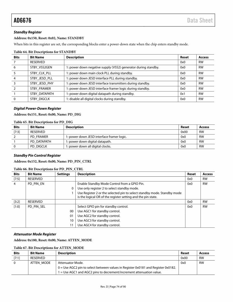
AD6676 Data Sheet
Rev. D | Page 74 of 90
Standby Register
Address: 0x150, Reset: 0x02, Name: STANDBY
When bits in this register are set, the corresponding blocks enter a power-down state when the chip enters standby mode.
Table 64. Bit Descriptions for STANDBY Bits Bit Name Description Reset Access 7 RESERVED 0x0 RW
6 STBY_VSS2GEN 1: power down negative supply (VSS2) generator during standby. 0x0 RW
5 STBY_CLK_PLL 1: power down main clock PLL during standby. 0x0 RW
4 STBY_JESD_PLL 1: power down JESD interface PLL during standby. 0x0 RW
3 STBY_JESD_PHY 1: power down JESD interface transmitters during standby. 0x0 RW
2 STBY_FRAMER 1: power down JESD interface framer logic during standby. 0x0 RW
1 STBY_DATAPATH 1: power down digital datapath during standby. 0x1 RW
0 STBY_DIGCLK 1: disable all digital clocks during standby. 0x0 RW
Digital Power-Down Register
Address: 0x151, Reset: 0x00, Name: PD_DIG
Table 65. Bit Descriptions for PD_DIG Bits Bit Name Description Reset Access [7:3] RESERVED 0x00 RW 2 PD_FRAMER 1: power down JESD interface framer logic. 0x0 RW 1 PD_DATAPATH 1: power down digital datapath. 0x0 RW 0 PD_DIGCLK 1: power down all digital clocks. 0x0 RW
Standby Pin Control Register
Address: 0x152, Reset: 0x00, Name: PD_PIN_CTRL
Table 66. Bit Descriptions for PD_PIN_CTRL Bits Bit Name Settings Description Reset Access [7:5] RESERVED 0x0 RW 4 PD_PIN_EN Enable Standby Mode Control from a GPIO Pin. 0x0 RW 0 Use only register 2 to select standby mode. 1 Use Register 2 or the selected pin to select standby mode. Standby mode
is the logical OR of the register setting and the pin state.
[3:2] RESERVED 0x0 RW [1:0] PD_PIN_SEL Select GPIO pin for standby control. 0x0 RW 00 Use AGC1 for standby control. 01 Use AGC2 for standby control. 10 Use AGC3 for standby control. 11 Use AGC4 for standby control.
Attenuator Mode Register
Address: 0x180, Reset: 0x00, Name: ATTEN_MODE
Table 67. Bit Descriptions for ATTEN_MODE Bits Bit Name Description Reset Access [7:1] RESERVED 0x00 RW 0 ATTEN_MODE Attenuator Mode. 0x0 RW 0 = Use AGC2 pin to select between values in Register 0x0181 and Register 0x0182. 1 = Use AGC1 and AGC2 pins to decrement/increment attenuation value.
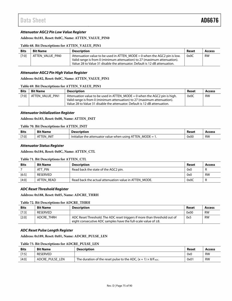
Data Sheet AD6676
Rev. D | Page 75 of 90
Attenuator AGC2 Pin Low Value Register
Address: 0x181, Reset: 0x0C, Name: ATTEN_VALUE_PIN0
Table 68. Bit Descriptions for ATTEN_VALUE_PIN1 Bits Bit Name Description Reset Access [7:0] ATTEN_VALUE_PIN0 Attenuation value to be used in ATTEN_MODE = 0 when the AGC2 pin is low.
Valid range is from 0 (minimum attenuation) to 27 (maximum attenuation). Value 28 to Value 31 disable the attenuator. Default is 12 dB attenuation.
0x0C RW
Attenuator AGC2 Pin High Value Register
Address: 0x182, Reset: 0x0C, Name: ATTEN_VALUE_PIN1
Table 69. Bit Descriptions for ATTEN_VALUE_PIN1 Bits Bit Name Description Reset Access [7:0] ATTEN_VALUE_PIN1 Attenuation value to be used in ATTEN_MODE = 0 when the AGC2 pin is high.
Valid range is from 0 (minimum attenuation) to 27 (maximum attenuation). Value 28 to Value 31 disable the attenuator. Default is 12 dB attenuation.
0x0C RW
Attenuator Initialization Register
Address: 0x183, Reset: 0x00, Name: ATTEN_INIT
Table 70. Bit Descriptions for ATTEN_INIT Bits Bit Name Description Reset Access [7:0] ATTEN_INIT Initialize the attenuator value when using ATTEN_MODE = 1. 0x00 RW
Attenuator Status Register
Address: 0x184, Reset: 0x0C, Name: ATTEN_CTL
Table 71. Bit Descriptions for ATTEN_CTL Bits Bit Name Description Reset Access 7 ATT_PIN Read back the state of the AGC2 pin. 0x0 R
[6:5] RESERVED 0x0 RW
[4:0] ATTEN_READ Read back the actual attenuation value in ATTEN_MODE. 0x0C R
ADC Reset Threshold Register
Address: 0x188, Reset: 0x05, Name: ADCRE_THRH
Table 72. Bit Descriptions for ADCRE_THRH Bits Bit Name Description Reset Access [7:3] RESERVED 0x00 RW
[2:0] ADCRE_THRH ADC Reset Threshold. The ADC reset triggers if more than threshold out of eight consecutive ADC samples have the full-scale value of ±8.
0x5 RW
ADC Reset Pulse Length Register
Address: 0x189, Reset: 0x01, Name: ADCRE_PULSE_LEN
Table 73. Bit Descriptions for ADCRE_PULSE_LEN Bits Bit Name Description Reset Access [7:5] RESERVED 0x0 RW
[4:0] ADCRE_PULSE_LEN The duration of the reset pulse to the ADC, (x + 1) × 8/FADC. 0x01 RW

AD6676 Data Sheet
Rev. D | Page 76 of 90
ADC Reset Attenuation Step Register
Address: 0x18A, Reset: 0x06, Name: ATTEN_STEP_RE
Table 74. Bit Descriptions for ATTEN_STEP_RE Bits Bit Name Description Reset Access [7:5] RESERVED 0x0 RW
[4:0] ATTEN_STEP_RE The size of the increase in attenuation after a reset event, in dB. The attenuation is clipped to a maximum value of 27 dB.
0x06 RW
ADC Unstable Flag Control Register
Address: 0x18F, Reset: 0x00, Name: ADC_UNSTABLE
Table 75. Bit Descriptions for ADC_UNSTABLE Bits Bit Name Description Reset Access [7:2] RESERVED 0x00 RW 1 CLEAR_UNSTABLE_FLAG Clear unstable flag. Writing a 1 to this bit clears the UNSTABLE_FLAG. This
bit is self clearing. 0x0 RW
0 UNSTABLE_FLAG Unstable flag. This is a sticky flag that indicates if an ADC reset condition has been detected. It is cleared only by the CLEAR_UNSTABLE_FLAG bit and the hardware/software resets.
0x0 R
Peak Threshold 0 LSB Register
Address: 0x193, Reset: 0x00, Name: PKTHRH0_LSB
Table 76. Bit Descriptions for PKTHRH0_LSB Bits Bit Name Settings Description Reset Access [7:0] PKTHRH0_LSB Peak Threshold 0 LSB. 0x00 RW
Peak Threshold 0 MSB Register
Address: 0x194, Reset: 0x00, Name: PKTHRH0_MSB
Table 77. Bit Descriptions for PKTHRH0_MSB Bits Bit Name Settings Description Reset Access [7:4] RESERVED 0x0 RW [3:0] PKTHRH0_MSB Peak Threshold 0 MSB. 0x0 RW
Peak Threshold 1 LSB Register
Address: 0x195, Reset: 0x00, Name: PKTHRH1_LSB
Table 78. Bit Descriptions for PKTHRH1_LSB Bits Bit Name Settings Description Reset Access [7:0] PKTHRH1_LSB Peak Threshold 1 LSB. 0x00 RW
Peak Threshold 1 MSB Register
Address: 0x196, Reset: 0x00, Name: PKTHRH1_MSB
Table 79. Bit Descriptions for PKTHRH1_MSB Bits Bit Name Settings Description Reset Access [7:4] RESERVED 0x0 RW [3:0] PKTHRH1_MSB Peak Threshold 1 MSB. 0x0 RW
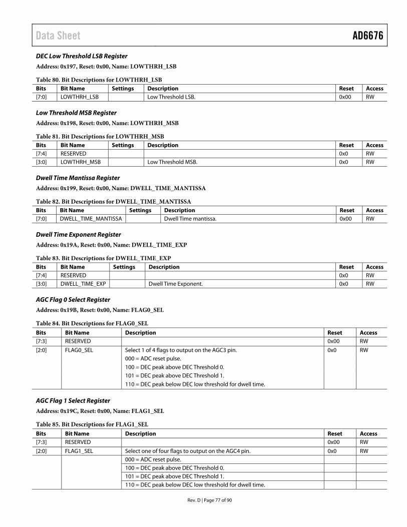
Data Sheet AD6676
Rev. D | Page 77 of 90
DEC Low Threshold LSB Register
Address: 0x197, Reset: 0x00, Name: LOWTHRH_LSB
Table 80. Bit Descriptions for LOWTHRH_LSB Bits Bit Name Settings Description Reset Access [7:0] LOWTHRH_LSB Low Threshold LSB. 0x00 RW
Low Threshold MSB Register
Address: 0x198, Reset: 0x00, Name: LOWTHRH_MSB
Table 81. Bit Descriptions for LOWTHRH_MSB Bits Bit Name Settings Description Reset Access [7:4] RESERVED 0x0 RW [3:0] LOWTHRH_MSB Low Threshold MSB. 0x0 RW
Dwell Time Mantissa Register
Address: 0x199, Reset: 0x00, Name: DWELL_TIME_MANTISSA
Table 82. Bit Descriptions for DWELL_TIME_MANTISSA Bits Bit Name Settings Description Reset Access [7:0] DWELL_TIME_MANTISSA Dwell Time mantissa. 0x00 RW
Dwell Time Exponent Register
Address: 0x19A, Reset: 0x00, Name: DWELL_TIME_EXP
Table 83. Bit Descriptions for DWELL_TIME_EXP Bits Bit Name Settings Description Reset Access [7:4] RESERVED 0x0 RW [3:0] DWELL_TIME_EXP Dwell Time Exponent. 0x0 RW
AGC Flag 0 Select Register
Address: 0x19B, Reset: 0x00, Name: FLAG0_SEL
Table 84. Bit Descriptions for FLAG0_SEL Bits Bit Name Description Reset Access [7:3] RESERVED 0x00 RW
[2:0] FLAG0_SEL Select 1 of 4 flags to output on the AGC3 pin. 0x0 RW 000 = ADC reset pulse.
100 = DEC peak above DEC Threshold 0. 101 = DEC peak above DEC Threshold 1.
110 = DEC peak below DEC low threshold for dwell time.
AGC Flag 1 Select Register
Address: 0x19C, Reset: 0x00, Name: FLAG1_SEL
Table 85. Bit Descriptions for FLAG1_SEL Bits Bit Name Description Reset Access [7:3] RESERVED 0x00 RW
[2:0] FLAG1_SEL Select one of four flags to output on the AGC4 pin. 0x0 RW 000 = ADC reset pulse. 100 = DEC peak above DEC Threshold 0. 101 = DEC peak above DEC Threshold 1. 110 = DEC peak below DEC low threshold for dwell time.
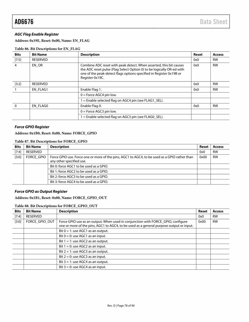
AD6676 Data Sheet
Rev. D | Page 78 of 90
AGC Flag Enable Register
Address: 0x19E, Reset: 0x00, Name: EN_FLAG
Table 86. Bit Descriptions for EN_FLAG Bits Bit Name Description Reset Access [7:5] RESERVED 0x0 RW
4 EN_OR Combine ADC reset with peak detect. When asserted, this bit causes the ADC reset pulse (Flag Select Option 0) to be logically OR-ed with one of the peak-detect flags options specified in Register 0x19B or Register 0x19C.
0x0 RW
[3:2] RESERVED 0x0 RW
1 EN_FLAG1 Enable Flag 1. 0x0 RW
0 = Force AGC4 pin low.
1 = Enable selected flag on AGC4 pin (see FLAG1_SEL).
0 EN_FLAG0 Enable Flag 0. 0x0 RW
0 = Force AGC3 pin low.
1 = Enable selected flag on AGC3 pin (see FLAG0_SEL).
Force GPIO Register
Address: 0x1B0, Reset: 0x00, Name: FORCE_GPIO
Table 87. Bit Descriptions for FORCE_GPIO Bits Bit Name Description Reset Access [7:4] RESERVED 0x0 RW [3:0] FORCE_GPIO Force GPIO use. Force one or more of the pins, AGC1 to AGC4, to be used as a GPIO rather than
any other specified use. 0x00 RW
Bit 0: force AGC1 to be used as a GPIO. Bit 1: force AGC2 to be used as a GPIO. Bit 2: force AGC3 to be used as a GPIO. Bit 3: force AGC4 to be used as a GPIO.
Force GPIO as Output Register
Address: 0x1B1, Reset: 0x00, Name: FORCE_GPIO_OUT
Table 88. Bit Descriptions for FORCE_GPIO_OUT Bits Bit Name Description Reset Access [7:4] RESERVED 0x0 RW [3:0] FORCE_GPIO_OUT Force GPIO use as an output. When used in conjunction with FORCE_GPIO, configure
one or more of the pins, AGC1 to AGC4, to be used as a general purpose output or input. 0x00 RW
Bit 0 = 1: use AGC1 as an output. Bit 0 = 0: use AGC1 as an input. Bit 1 = 1: use AGC2 as an output. Bit 1 = 0: use AGC2 as an input. Bit 2 = 1: use AGC3 as an output. Bit 2 = 0: use AGC3 as an input. Bit 3 = 1: use AGC4 as an output. Bit 3 = 0: use AGC4 as an input.
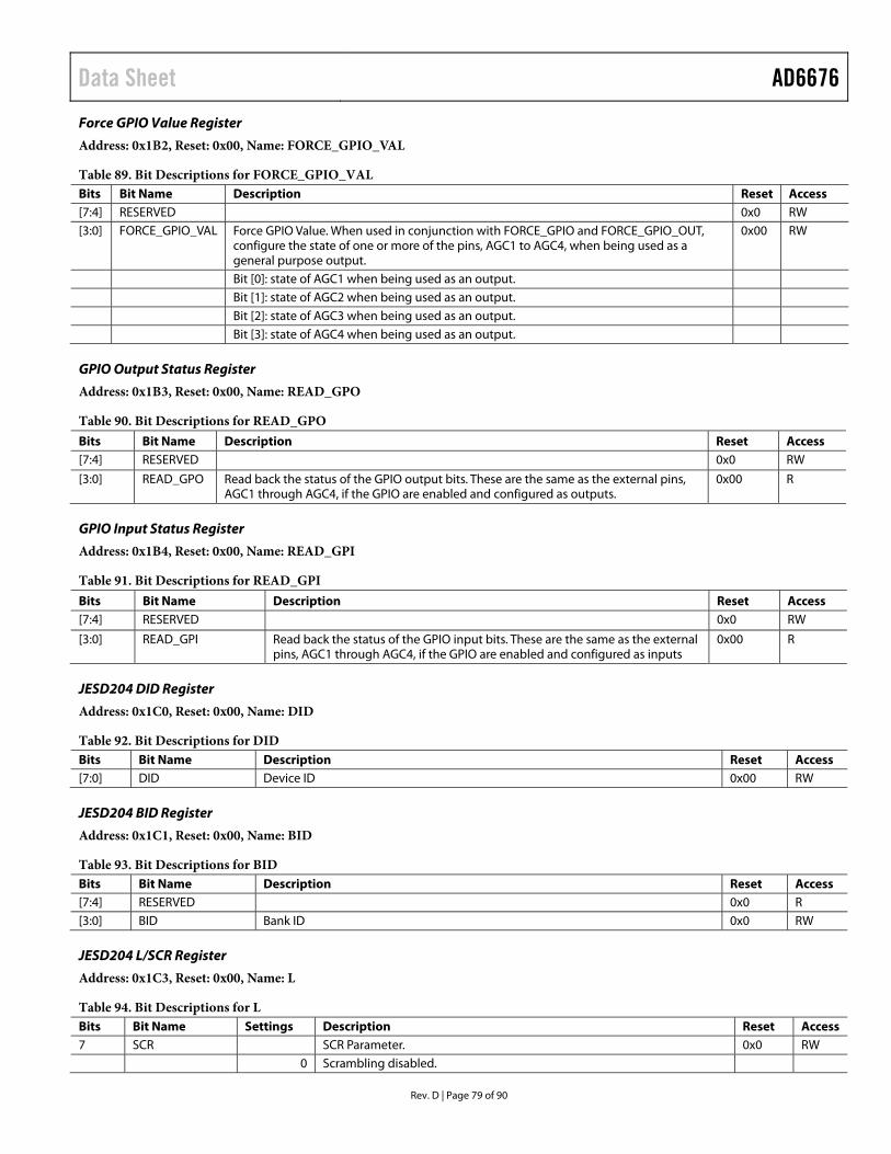
Data Sheet AD6676
Rev. D | Page 79 of 90
Force GPIO Value Register
Address: 0x1B2, Reset: 0x00, Name: FORCE_GPIO_VAL
Table 89. Bit Descriptions for FORCE_GPIO_VAL Bits Bit Name Description Reset Access [7:4] RESERVED 0x0 RW [3:0] FORCE_GPIO_VAL Force GPIO Value. When used in conjunction with FORCE_GPIO and FORCE_GPIO_OUT,
configure the state of one or more of the pins, AGC1 to AGC4, when being used as a general purpose output.
0x00 RW
Bit [0]: state of AGC1 when being used as an output. Bit [1]: state of AGC2 when being used as an output. Bit [2]: state of AGC3 when being used as an output. Bit [3]: state of AGC4 when being used as an output.
GPIO Output Status Register
Address: 0x1B3, Reset: 0x00, Name: READ_GPO
Table 90. Bit Descriptions for READ_GPO Bits Bit Name Description Reset Access [7:4] RESERVED 0x0 RW
[3:0] READ_GPO Read back the status of the GPIO output bits. These are the same as the external pins, AGC1 through AGC4, if the GPIO are enabled and configured as outputs.
0x00 R
GPIO Input Status Register
Address: 0x1B4, Reset: 0x00, Name: READ_GPI
Table 91. Bit Descriptions for READ_GPI Bits Bit Name Description Reset Access [7:4] RESERVED 0x0 RW
[3:0] READ_GPI Read back the status of the GPIO input bits. These are the same as the external pins, AGC1 through AGC4, if the GPIO are enabled and configured as inputs
0x00 R
JESD204 DID Register
Address: 0x1C0, Reset: 0x00, Name: DID
Table 92. Bit Descriptions for DID Bits Bit Name Description Reset Access [7:0] DID Device ID 0x00 RW
JESD204 BID Register
Address: 0x1C1, Reset: 0x00, Name: BID
Table 93. Bit Descriptions for BID Bits Bit Name Description Reset Access [7:4] RESERVED 0x0 R [3:0] BID Bank ID 0x0 RW
JESD204 L/SCR Register
Address: 0x1C3, Reset: 0x00, Name: L
Table 94. Bit Descriptions for L Bits Bit Name Settings Description Reset Access 7 SCR SCR Parameter. 0x0 RW 0 Scrambling disabled.
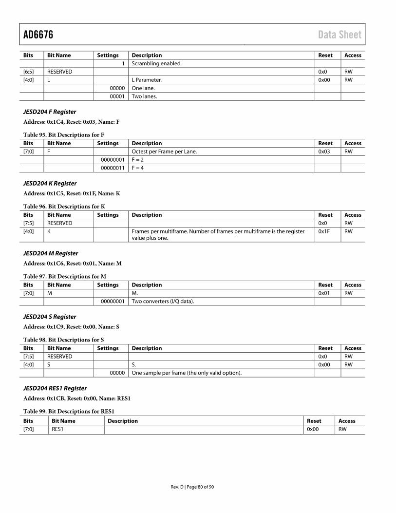
AD6676 Data Sheet
Rev. D | Page 80 of 90
Bits Bit Name Settings Description Reset Access 1 Scrambling enabled. [6:5] RESERVED 0x0 RW [4:0] L L Parameter. 0x00 RW 00000 One lane. 00001 Two lanes.
JESD204 F Register
Address: 0x1C4, Reset: 0x03, Name: F
Table 95. Bit Descriptions for F Bits Bit Name Settings Description Reset Access [7:0] F Octest per Frame per Lane. 0x03 RW 00000001 F = 2 00000011 F = 4
JESD204 K Register
Address: 0x1C5, Reset: 0x1F, Name: K
Table 96. Bit Descriptions for K Bits Bit Name Settings Description Reset Access [7:5] RESERVED 0x0 RW [4:0] K Frames per multiframe. Number of frames per multiframe is the register
value plus one. 0x1F RW
JESD204 M Register
Address: 0x1C6, Reset: 0x01, Name: M
Table 97. Bit Descriptions for M Bits Bit Name Settings Description Reset Access [7:0] M M. 0x01 RW 00000001 Two converters (I/Q data).
JESD204 S Register
Address: 0x1C9, Reset: 0x00, Name: S
Table 98. Bit Descriptions for S Bits Bit Name Settings Description Reset Access [7:5] RESERVED 0x0 RW [4:0] S S. 0x00 RW 00000 One sample per frame (the only valid option).
JESD204 RES1 Register
Address: 0x1CB, Reset: 0x00, Name: RES1
Table 99. Bit Descriptions for RES1 Bits Bit Name Description Reset Access [7:0] RES1 0x00 RW
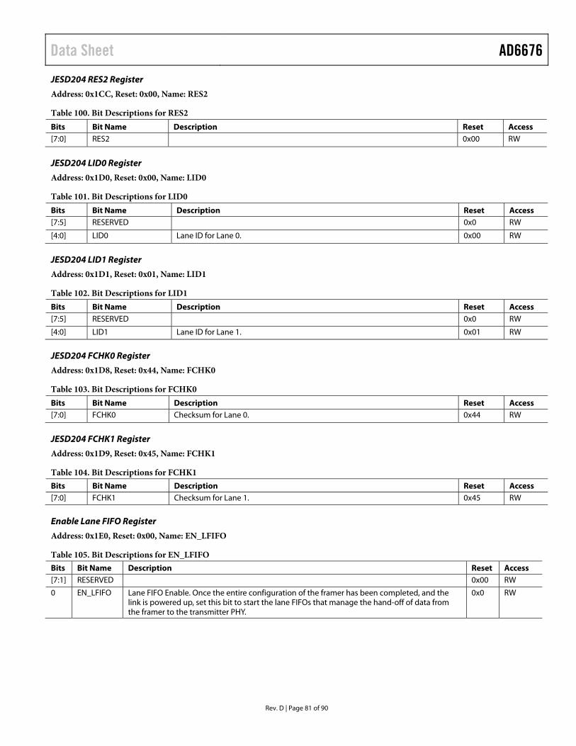
Data Sheet AD6676
Rev. D | Page 81 of 90
JESD204 RES2 Register
Address: 0x1CC, Reset: 0x00, Name: RES2
Table 100. Bit Descriptions for RES2 Bits Bit Name Description Reset Access [7:0] RES2 0x00 RW
JESD204 LID0 Register
Address: 0x1D0, Reset: 0x00, Name: LID0
Table 101. Bit Descriptions for LID0 Bits Bit Name Description Reset Access [7:5] RESERVED 0x0 RW
[4:0] LID0 Lane ID for Lane 0. 0x00 RW
JESD204 LID1 Register
Address: 0x1D1, Reset: 0x01, Name: LID1
Table 102. Bit Descriptions for LID1 Bits Bit Name Description Reset Access [7:5] RESERVED 0x0 RW
[4:0] LID1 Lane ID for Lane 1. 0x01 RW
JESD204 FCHK0 Register
Address: 0x1D8, Reset: 0x44, Name: FCHK0
Table 103. Bit Descriptions for FCHK0 Bits Bit Name Description Reset Access [7:0] FCHK0 Checksum for Lane 0. 0x44 RW
JESD204 FCHK1 Register
Address: 0x1D9, Reset: 0x45, Name: FCHK1
Table 104. Bit Descriptions for FCHK1 Bits Bit Name Description Reset Access [7:0] FCHK1 Checksum for Lane 1. 0x45 RW
Enable Lane FIFO Register
Address: 0x1E0, Reset: 0x00, Name: EN_LFIFO
Table 105. Bit Descriptions for EN_LFIFO Bits Bit Name Description Reset Access [7:1] RESERVED 0x00 RW
0 EN_LFIFO Lane FIFO Enable. Once the entire configuration of the framer has been completed, and the link is powered up, set this bit to start the lane FIFOs that manage the hand-off of data from the framer to the transmitter PHY.
0x0 RW
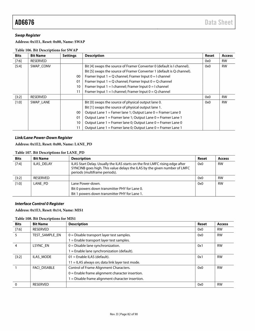
AD6676 Data Sheet
Rev. D | Page 82 of 90
Swap Register
Address: 0x1E1, Reset: 0x00, Name: SWAP
Table 106. Bit Descriptions for SWAP Bits Bit Name Settings Description Reset Access [7:6] RESERVED 0x0 RW [5:4] SWAP_CONV Bit [4] swaps the source of Framer Converter 0 (default is I channel). 0x0 RW Bit [5] swaps the source of Framer Converter 1 (default is Q channel). 00 Framer Input 1 = Q channel; Framer Input 0 = I channel 01 Framer Input 1 = Q channel; Framer Input 0 = Q channel 10 Framer Input 1 = I channel; Framer Input 0 = I channel 11 Framer Input 1 = I channel; Framer Input 0 = Q channel [3:2] RESERVED 0x0 RW [1:0] SWAP_LANE Bit [0] swaps the source of physical output lane 0. 0x0 RW Bit [1] swaps the source of physical output lane 1. 00 Output Lane 1 = Famer lane 1; Output Lane 0 = Framer Lane 0 01 Output Lane 1 = Framer lane 1; Output Lane 0 = Framer Lane 1 10 Output Lane 1 = Framer lane 0; Output Lane 0 = Framer Lane 0 11 Output Lane 1 = Framer lane 0; Output Lane 0 = Framer Lane 1
Link/Lane Power-Down Register
Address: 0x1E2, Reset: 0x00, Name: LANE_PD
Table 107. Bit Descriptions for LANE_PD Bits Bit Name Description Reset Access [7:4] ILAS_DELAY ILAS Start Delay. Usually the ILAS starts on the first LMFC rising edge after
SYNCINB goes high. This value delays the ILAS by the given number of LMFC periods (multiframe periods).
0x0 RW
[3:2] RESERVED 0x0 RW
[1:0] LANE_PD Lane Power-down. 0x0 RW Bit 0 powers down transmitter PHY for Lane 0. Bit 1 powers down transmitter PHY for Lane 1.
Interface Control 0 Register
Address: 0x1E3, Reset: 0x14, Name: MIS1
Table 108. Bit Descriptions for MIS1 Bits Bit Name Description Reset Access [7:6] RESERVED 0x0 RW
5 TEST_SAMPLE_EN 0 = Disable transport layer test samples. 0x0 RW 1 = Enable transport layer test samples. 4 LSYNC_EN 0 = Disable lane synchronization. 0x1 RW
1 = Enable lane synchronization (default).
[3:2] ILAS_MODE 01 = Enable ILAS (default). 0x1 RW
11 = ILAS always on; data link layer test mode. 1 FACI_DISABLE Control of Frame Alignment Characters. 0x0 RW
0 = Enable frame alignment character insertion.
1 = Disable frame alignment character insertion.
0 RESERVED 0x0 RW
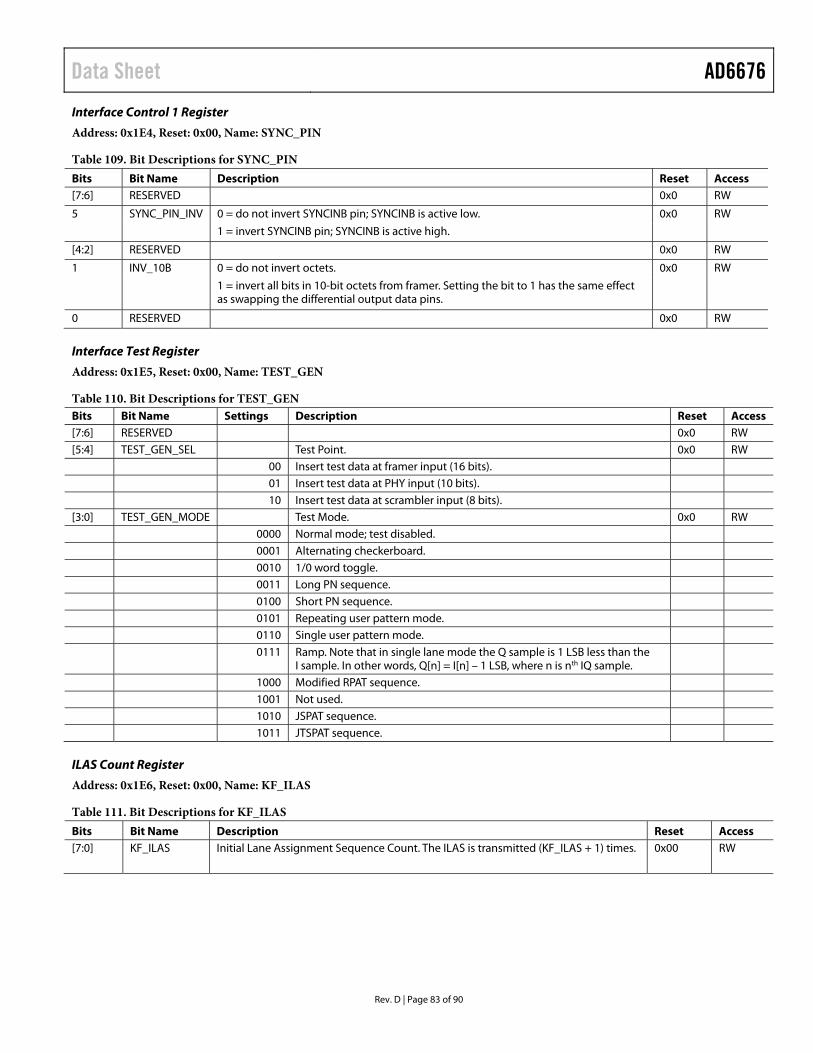
Data Sheet AD6676
Rev. D | Page 83 of 90
Interface Control 1 Register
Address: 0x1E4, Reset: 0x00, Name: SYNC_PIN
Table 109. Bit Descriptions for SYNC_PIN Bits Bit Name Description Reset Access [7:6] RESERVED 0x0 RW
5 SYNC_PIN_INV 0 = do not invert SYNCINB pin; SYNCINB is active low. 0x0 RW
1 = invert SYNCINB pin; SYNCINB is active high.
[4:2] RESERVED 0x0 RW
1 INV_10B 0 = do not invert octets. 0x0 RW
1 = invert all bits in 10-bit octets from framer. Setting the bit to 1 has the same effect as swapping the differential output data pins.
0 RESERVED 0x0 RW
Interface Test Register
Address: 0x1E5, Reset: 0x00, Name: TEST_GEN
Table 110. Bit Descriptions for TEST_GEN Bits Bit Name Settings Description Reset Access [7:6] RESERVED 0x0 RW [5:4] TEST_GEN_SEL Test Point. 0x0 RW 00 Insert test data at framer input (16 bits). 01 Insert test data at PHY input (10 bits). 10 Insert test data at scrambler input (8 bits). [3:0] TEST_GEN_MODE Test Mode. 0x0 RW 0000 Normal mode; test disabled. 0001 Alternating checkerboard. 0010 1/0 word toggle. 0011 Long PN sequence. 0100 Short PN sequence. 0101 Repeating user pattern mode. 0110 Single user pattern mode. 0111 Ramp. Note that in single lane mode the Q sample is 1 LSB less than the
I sample. In other words, Q[n] = I[n] – 1 LSB, where n is nth IQ sample.
1000 Modified RPAT sequence. 1001 Not used. 1010 JSPAT sequence. 1011 JTSPAT sequence.
ILAS Count Register
Address: 0x1E6, Reset: 0x00, Name: KF_ILAS
Table 111. Bit Descriptions for KF_ILAS Bits Bit Name Description Reset Access [7:0] KF_ILAS Initial Lane Assignment Sequence Count. The ILAS is transmitted (KF_ILAS + 1) times. 0x00 RW
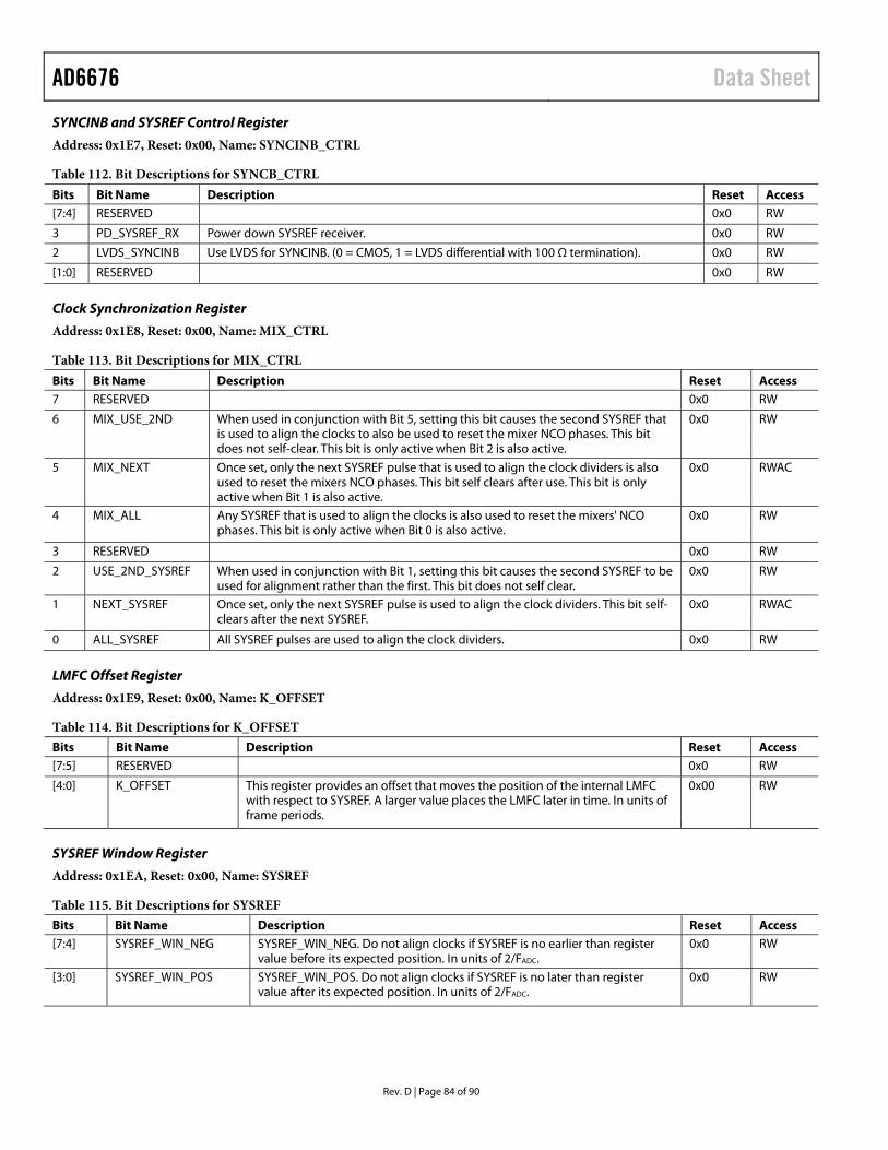
AD6676 Data Sheet
Rev. D | Page 84 of 90
SYNCINB and SYSREF Control Register
Address: 0x1E7, Reset: 0x00, Name: SYNCINB_CTRL
Table 112. Bit Descriptions for SYNCB_CTRL Bits Bit Name Description Reset Access [7:4] RESERVED 0x0 RW
3 PD_SYSREF_RX Power down SYSREF receiver. 0x0 RW
2 LVDS_SYNCINB Use LVDS for SYNCINB. (0 = CMOS, 1 = LVDS differential with 100 Ω termination). 0x0 RW
[1:0] RESERVED 0x0 RW
Clock Synchronization Register
Address: 0x1E8, Reset: 0x00, Name: MIX_CTRL
Table 113. Bit Descriptions for MIX_CTRL Bits Bit Name Description Reset Access 7 RESERVED 0x0 RW
6 MIX_USE_2ND When used in conjunction with Bit 5, setting this bit causes the second SYSREF that is used to align the clocks to also be used to reset the mixer NCO phases. This bit does not self-clear. This bit is only active when Bit 2 is also active.
0x0 RW
5 MIX_NEXT Once set, only the next SYSREF pulse that is used to align the clock dividers is also used to reset the mixers NCO phases. This bit self clears after use. This bit is only active when Bit 1 is also active.
0x0 RWAC
4 MIX_ALL Any SYSREF that is used to align the clocks is also used to reset the mixers' NCO phases. This bit is only active when Bit 0 is also active.
0x0 RW
3 RESERVED 0x0 RW
2 USE_2ND_SYSREF When used in conjunction with Bit 1, setting this bit causes the second SYSREF to be used for alignment rather than the first. This bit does not self clear.
0x0 RW
1 NEXT_SYSREF Once set, only the next SYSREF pulse is used to align the clock dividers. This bit self-clears after the next SYSREF.
0x0 RWAC
0 ALL_SYSREF All SYSREF pulses are used to align the clock dividers. 0x0 RW
LMFC Offset Register
Address: 0x1E9, Reset: 0x00, Name: K_OFFSET
Table 114. Bit Descriptions for K_OFFSET Bits Bit Name Description Reset Access [7:5] RESERVED 0x0 RW
[4:0] K_OFFSET This register provides an offset that moves the position of the internal LMFC with respect to SYSREF. A larger value places the LMFC later in time. In units of frame periods.
0x00 RW
SYSREF Window Register
Address: 0x1EA, Reset: 0x00, Name: SYSREF
Table 115. Bit Descriptions for SYSREF Bits Bit Name Description Reset Access [7:4] SYSREF_WIN_NEG SYSREF_WIN_NEG. Do not align clocks if SYSREF is no earlier than register
value before its expected position. In units of 2/FADC. 0x0 RW
[3:0] SYSREF_WIN_POS SYSREF_WIN_POS. Do not align clocks if SYSREF is no later than register value after its expected position. In units of 2/FADC.
0x0 RW
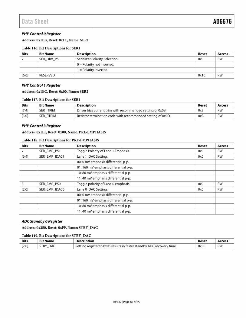
Data Sheet AD6676
Rev. D | Page 85 of 90
PHY Control 0 Register
Address: 0x1EB, Reset: 0x1C, Name: SER1
Table 116. Bit Descriptions for SER1 Bits Bit Name Description Reset Access 7 SER_DRV_PS Serializer Polarity Selection. 0x0 RW
0 = Polarity not inverted.
1 = Polarity inverted.
[6:0] RESERVED 0x1C RW
PHY Control 1 Register
Address: 0x1EC, Reset: 0x00, Name: SER2
Table 117. Bit Descriptions for SER1 Bits Bit Name Description Reset Access [7:4] SER_ITRIM Driver bias current trim with recommended setting of 0x0B. 0x9 RW
[3:0] SER_RTRIM Resistor termination code with recommended setting of 0x0D. 0xB RW
PHY Control 3 Register
Address: 0x1EF, Reset: 0x00, Name: PRE-EMPHASIS
Table 118. Bit Descriptions for PRE-EMPHASIS Bits Bit Name Description Reset Access 7 SER_EMP_PS1 Toggle Polarity of Lane 1 Emphasis. 0x0 RW
[6:4] SER_EMP_IDAC1 Lane 1 IDAC Setting. 0x0 RW
00: 0 mV emphasis differential p-p.
01: 160 mV emphasis differential p-p.
10: 80 mV emphasis differential p-p.
11: 40 mV emphasis differential p-p.
3 SER_EMP_PS0 Toggle polarity of Lane 0 emphasis. 0x0 RW
[2:0] SER_EMP_IDAC0 Lane 0 IDAC Setting. 0x0 RW
00: 0 mV emphasis differential p-p.
01: 160 mV emphasis differential p-p.
10: 80 mV emphasis differential p-p.
11: 40 mV emphasis differential p-p.
ADC Standby 0 Register
Address: 0x250, Reset: 0xFF, Name: STBY_DAC
Table 119. Bit Descriptions for STBY_DAC Bits Bit Name Description Reset Access [7:0] STBY_DAC Setting register to 0x95 results in faster standby ADC recovery time. 0xFF RW
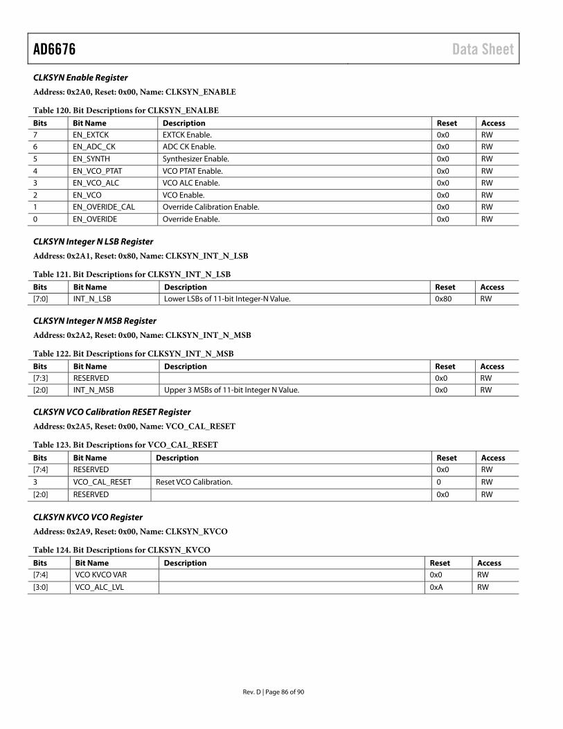
AD6676 Data Sheet
Rev. D | Page 86 of 90
CLKSYN Enable Register
Address: 0x2A0, Reset: 0x00, Name: CLKSYN_ENABLE
Table 120. Bit Descriptions for CLKSYN_ENALBE Bits Bit Name Description Reset Access 7 EN_EXTCK EXTCK Enable. 0x0 RW
6 EN_ADC_CK ADC CK Enable. 0x0 RW
5 EN_SYNTH Synthesizer Enable. 0x0 RW
4 EN_VCO_PTAT VCO PTAT Enable. 0x0 RW
3 EN_VCO_ALC VCO ALC Enable. 0x0 RW
2 EN_VCO VCO Enable. 0x0 RW
1 EN_OVERIDE_CAL Override Calibration Enable. 0x0 RW
0 EN_OVERIDE Override Enable. 0x0 RW
CLKSYN Integer N LSB Register
Address: 0x2A1, Reset: 0x80, Name: CLKSYN_INT_N_LSB
Table 121. Bit Descriptions for CLKSYN_INT_N_LSB Bits Bit Name Description Reset Access [7:0] INT_N_LSB Lower LSBs of 11-bit Integer-N Value. 0x80 RW
CLKSYN Integer N MSB Register
Address: 0x2A2, Reset: 0x00, Name: CLKSYN_INT_N_MSB
Table 122. Bit Descriptions for CLKSYN_INT_N_MSB Bits Bit Name Description Reset Access [7:3] RESERVED 0x0 RW
[2:0] INT_N_MSB Upper 3 MSBs of 11-bit Integer N Value. 0x0 RW
CLKSYN VCO Calibration RESET Register
Address: 0x2A5, Reset: 0x00, Name: VCO_CAL_RESET
Table 123. Bit Descriptions for VCO_CAL_RESET Bits Bit Name Description Reset Access [7:4] RESERVED 0x0 RW
3 VCO_CAL_RESET Reset VCO Calibration. 0 RW
[2:0] RESERVED 0x0 RW
CLKSYN KVCO VCO Register
Address: 0x2A9, Reset: 0x00, Name: CLKSYN_KVCO
Table 124. Bit Descriptions for CLKSYN_KVCO Bits Bit Name Description Reset Access [7:4] VCO KVCO VAR 0x0 RW
[3:0] VCO_ALC_LVL 0xA RW

Data Sheet AD6676
Rev. D | Page 87 of 90
CLKSYN VCO Bias Register
Address: 0x2AA, Reset: 0x37, Name: CLKSYN_VCO_BIAS
Table 125. Bit Descriptions for CLKSYN_VCO_BIAS Bits Bit Name Description Reset Access [7:6] RESERVED 0 RW
[5:4] BIAS_TEMPCO VCO Bias Tempco Setting. 0x3 RW
3 RESERVED 0 RW
[2:0] BIAS VCO Bias Setting. 0x7 RW
CLKSYN VCO Calibration Register
Address: 0x2AB, Reset: 0xC0, Name: CLKSYN_VCO_CAL
Table 126. Bit Descriptions for CLKSYN_VCO_CAL Bits Bit Name Description Reset Access [7:4] INIT_ALC_VALUE Initial Automatic Level Control Value. 0xC RW
3 ALC_DIS ALC calibration Test Bit. 0 RW
[2:1] RESERVED 0 RW
0 ID_SYNTH Initiates VCO Calibration. 0 RW
CLKSYN Charge Pump Register
Address: 0x2AC, Reset: 0x19, Name: CLKSYN_I_CP
Table 127. Bit Descriptions for CLKSYN_I_CP Bits Bit Name Description Reset Access [7:6] RESERVED 0x0 RW
[5:0] I_CP Charge Pump Current = min(63, 1.33 × 1028/(fPFD × FCLK2) − 1). 0x19 RW
CLKSYN Charge Pump Calibration Register
Address: 0x2AD, Reset: 0x00, Name: EN_CP_CAL
Table 128. Bit Descriptions for EN_CP_CAL Bits Bit Name Description Reset Access [7:6] EN_CP_CAL 0x0 RW
[6:0] RESERVED 0x0 RW
CLKSYN VCO Varactor Register
Address: 0x2B7, Reset: 0xD0, Name: CLKSYN_VCO_VAR
Table 129. Bit Descriptions for CLKSYN_VCO_VAR Bits Bit Name Description Reset Access [7:4] VCO_VAR VCO Varactor Setting. 0xD0 RW
[3:0] RESERVED
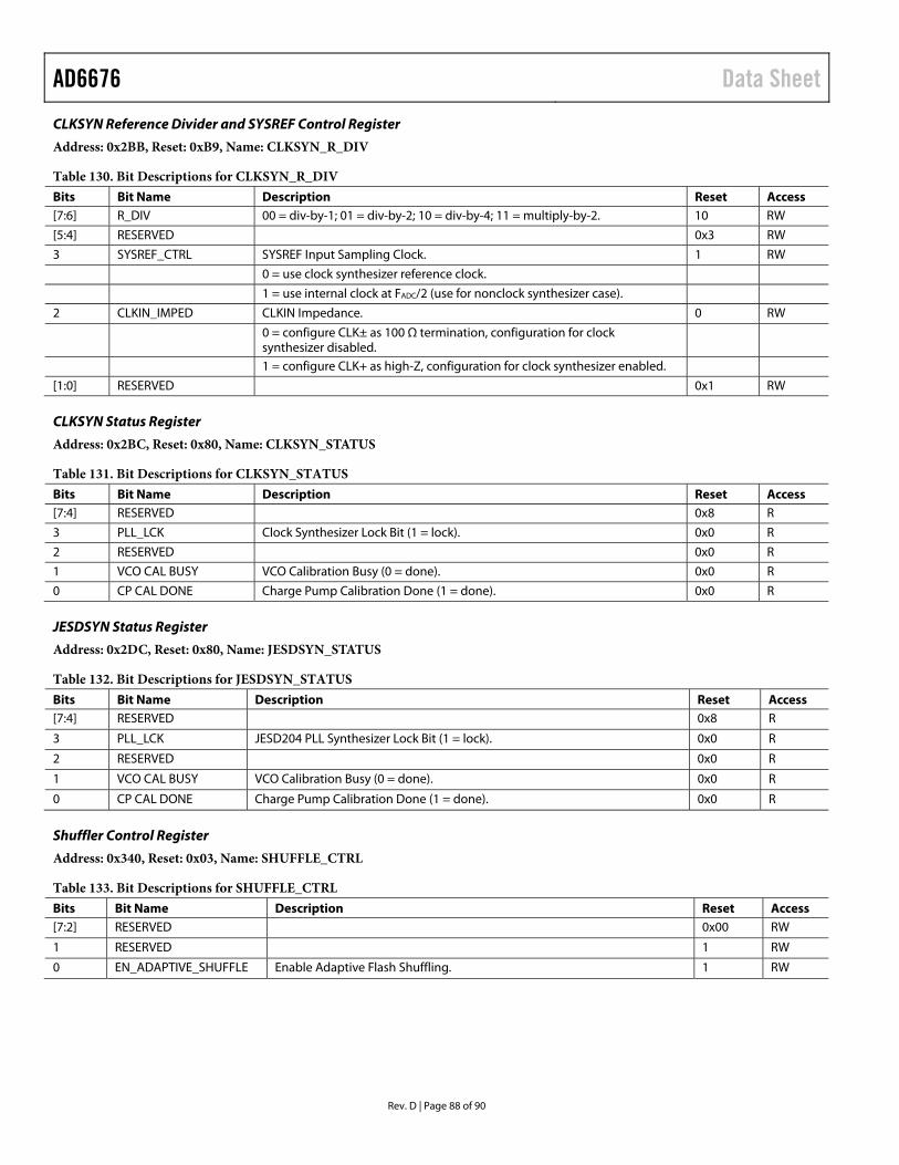
AD6676 Data Sheet
Rev. D | Page 88 of 90
CLKSYN Reference Divider and SYSREF Control Register
Address: 0x2BB, Reset: 0xB9, Name: CLKSYN_R_DIV
Table 130. Bit Descriptions for CLKSYN_R_DIV Bits Bit Name Description Reset Access [7:6] R_DIV 00 = div-by-1; 01 = div-by-2; 10 = div-by-4; 11 = multiply-by-2. 10 RW
[5:4] RESERVED 0x3 RW
3 SYSREF_CTRL SYSREF Input Sampling Clock. 1 RW
0 = use clock synthesizer reference clock.
1 = use internal clock at FADC/2 (use for nonclock synthesizer case).
2 CLKIN_IMPED CLKIN Impedance. 0 RW
0 = configure CLK± as 100 Ω termination, configuration for clock synthesizer disabled.
1 = configure CLK+ as high-Z, configuration for clock synthesizer enabled.
[1:0] RESERVED 0x1 RW
CLKSYN Status Register
Address: 0x2BC, Reset: 0x80, Name: CLKSYN_STATUS
Table 131. Bit Descriptions for CLKSYN_STATUS Bits Bit Name Description Reset Access [7:4] RESERVED 0x8 R
3 PLL_LCK Clock Synthesizer Lock Bit (1 = lock). 0x0 R
2 RESERVED 0x0 R
1 VCO CAL BUSY VCO Calibration Busy (0 = done). 0x0 R
0 CP CAL DONE Charge Pump Calibration Done (1 = done). 0x0 R
JESDSYN Status Register
Address: 0x2DC, Reset: 0x80, Name: JESDSYN_STATUS
Table 132. Bit Descriptions for JESDSYN_STATUS Bits Bit Name Description Reset Access [7:4] RESERVED 0x8 R
3 PLL_LCK JESD204 PLL Synthesizer Lock Bit (1 = lock). 0x0 R
2 RESERVED 0x0 R
1 VCO CAL BUSY VCO Calibration Busy (0 = done). 0x0 R
0 CP CAL DONE Charge Pump Calibration Done (1 = done). 0x0 R
Shuffler Control Register
Address: 0x340, Reset: 0x03, Name: SHUFFLE_CTRL
Table 133. Bit Descriptions for SHUFFLE_CTRL Bits Bit Name Description Reset Access [7:2] RESERVED 0x00 RW
1 RESERVED 1 RW
0 EN_ADAPTIVE_SHUFFLE Enable Adaptive Flash Shuffling. 1 RW
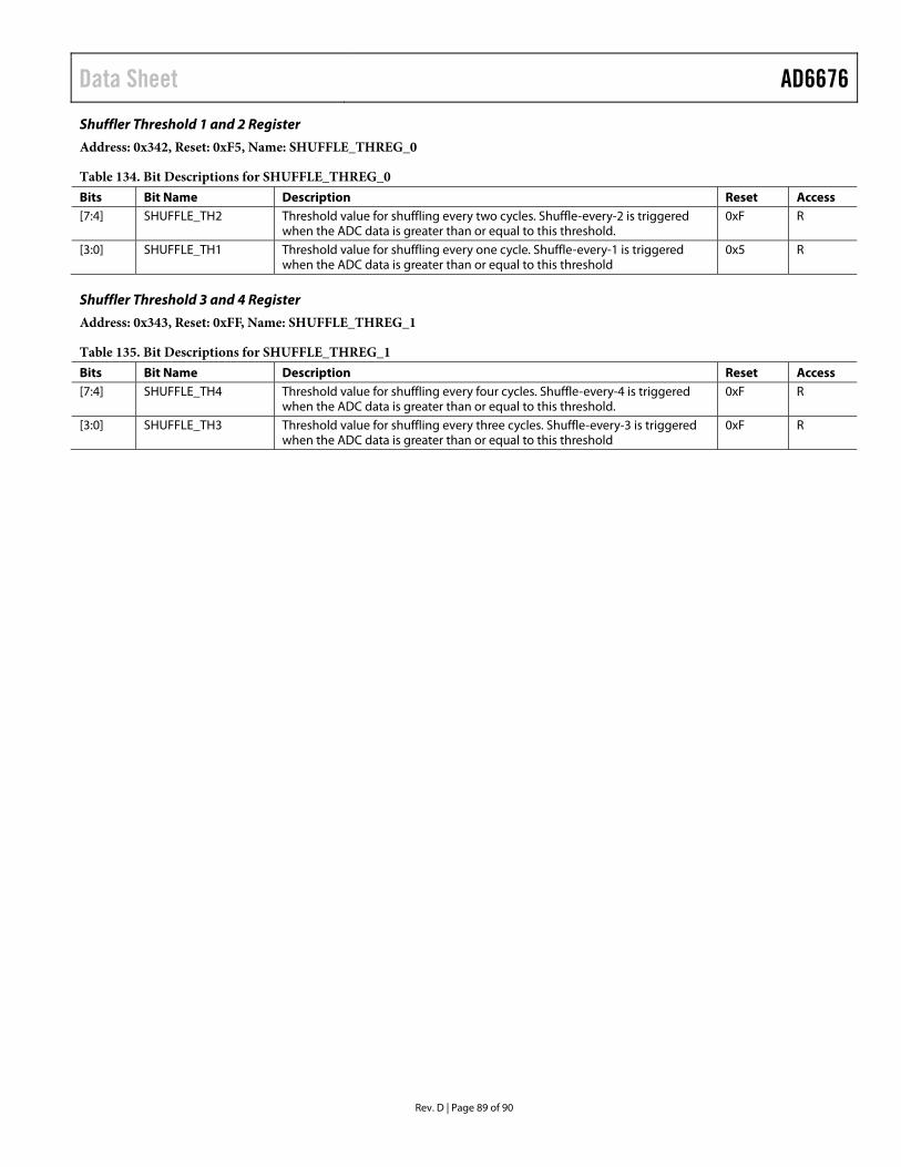
Data Sheet AD6676
Rev. D | Page 89 of 90
Shuffler Threshold 1 and 2 Register
Address: 0x342, Reset: 0xF5, Name: SHUFFLE_THREG_0
Table 134. Bit Descriptions for SHUFFLE_THREG_0 Bits Bit Name Description Reset Access [7:4] SHUFFLE_TH2 Threshold value for shuffling every two cycles. Shuffle-every-2 is triggered
when the ADC data is greater than or equal to this threshold. 0xF R
[3:0] SHUFFLE_TH1 Threshold value for shuffling every one cycle. Shuffle-every-1 is triggered when the ADC data is greater than or equal to this threshold
0x5 R
Shuffler Threshold 3 and 4 Register
Address: 0x343, Reset: 0xFF, Name: SHUFFLE_THREG_1
Table 135. Bit Descriptions for SHUFFLE_THREG_1 Bits Bit Name Description Reset Access [7:4] SHUFFLE_TH4 Threshold value for shuffling every four cycles. Shuffle-every-4 is triggered
when the ADC data is greater than or equal to this threshold. 0xF R
[3:0] SHUFFLE_TH3 Threshold value for shuffling every three cycles. Shuffle-every-3 is triggered when the ADC data is greater than or equal to this threshold
0xF R
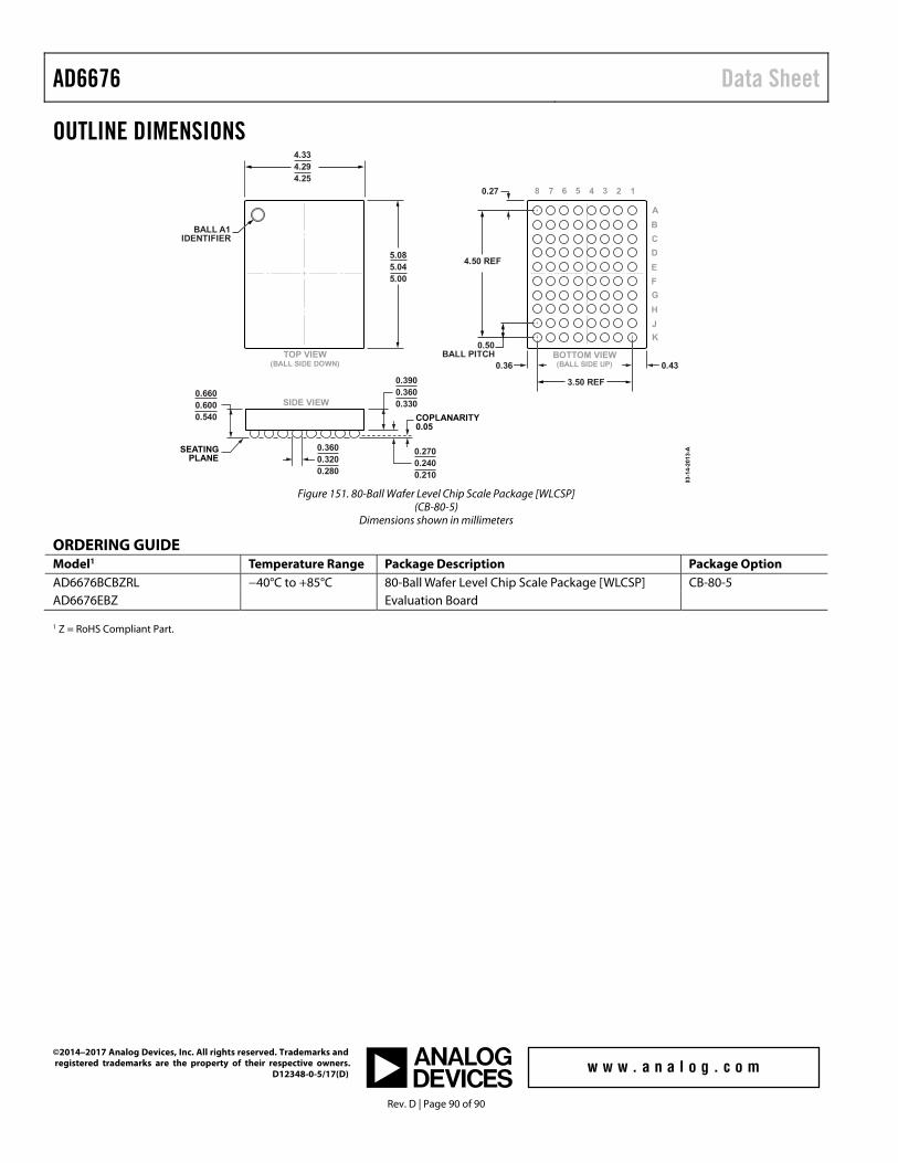
AD6676 Data Sheet
Rev. D | Page 90 of 90
OUTLINE DIMENSIONS
03-1
4-2
013
-A
A
B
C
D
E
F
G
H
J
K
0.6600.6000.540
4.334.294.25
5.085.045.00
BOTTOM VIEW(BALL SIDE UP)
TOP VIEW(BALL SIDE DOWN)
SIDE VIEW
0.2700.2400.210
0.3900.3600.330
0.3600.3200.280
4.50 REF
3.50 REF
0.50BALL PITCH
0.36
0.27
0.43
BALL A1IDENTIFIER
12345678
COPLANARITY0.05
SEATINGPLANE
Figure 151. 80-Ball Wafer Level Chip Scale Package [WLCSP]
(CB-80-5) Dimensions shown in millimeters
ORDERING GUIDE Model1 Temperature Range Package Description Package Option AD6676BCBZRL −40°C to +85°C 80-Ball Wafer Level Chip Scale Package [WLCSP] CB-80-5 AD6676EBZ Evaluation Board 1 Z = RoHS Compliant Part.
©2014–2017 Analog Devices, Inc. All rights reserved. Trademarks and registered trademarks are the property of their respective owners. D12348-0-5/17(D)