ltm9001-ga - 16-bit if/baseband receiver subsystem
TRANSCRIPT
LTM9001-GA
19001gaf
TYPICAL APPLICATION
FEATURES
APPLICATIONS
DESCRIPTION
16-Bit IF/Baseband Receiver Subsystem
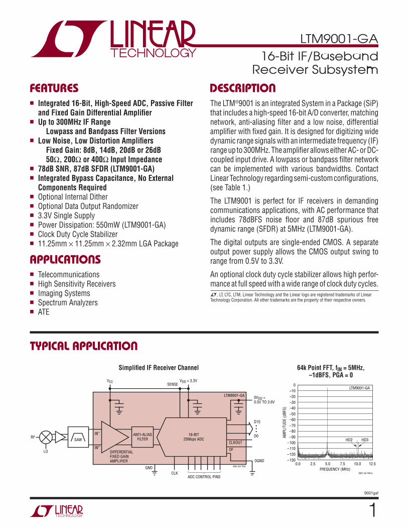
The LTM®9001 is an integrated System in a Package (SiP) that includes a high-speed 16-bit A/D converter, matching network, anti-aliasing fi lter and a low noise, differential amplifi er with fi xed gain. It is designed for digitizing wide dynamic range signals with an intermediate frequency (IF) range up to 300MHz. The amplifi er allows either AC- or DC-coupled input drive. A lowpass or bandpass fi lter network can be implemented with various bandwidths. Contact Linear Technology regarding semi-custom confi gurations, (see Table 1.)
The LTM9001 is perfect for IF receivers in demanding communications applications, with AC performance that includes 78dBFS noise fl oor and 87dB spurious free dynamic range (SFDR) at 5MHz (LTM9001-GA).
The digital outputs are single-ended CMOS. A separate output power supply allows the CMOS output swing to range from 0.5V to 3.3V.
An optional clock duty cycle stabilizer allows high perfor-mance at full speed with a wide range of clock duty cycles.
Simplifi ed IF Receiver Channel
n Integrated 16-Bit, High-Speed ADC, Passive Filter and Fixed Gain Differential Amplifi er
n Up to 300MHz IF Range Lowpass and Bandpass Filter Versionsn Low Noise, Low Distortion Amplifi ers
Fixed Gain: 8dB, 14dB, 20dB or 26dB 50Ω, 200Ω or 400Ω Input Impedance
n 78dB SNR, 87dB SFDR (LTM9001-GA)n Integrated Bypass Capacitance, No External
Components Requiredn Optional Internal Dithern Optional Data Output Randomizern 3.3V Single Supplyn Power Dissipation: 550mW (LTM9001-GA)n Clock Duty Cycle Stabilizern 11.25mm × 11.25mm × 2.32mm LGA Package
n Telecommunicationsn High Sensitivity Receiversn Imaging Systemsn Spectrum Analyzersn ATE
64k Point FFT, fIN = 5MHz, –1dBFS, PGA = 0
9001-GA TA01
CLKOUT
OFLO
VCC VDD = 3.3V
CLKADC CONTROL PINS
DIFFERENTIALFIXED GAINAMPLIFIER
16-BIT25Msps ADC
RFIN–
IN+
LTM9001-GA
SENSE
GND
D15 • • •
D0
0VDD = 0.5V TO 3.6V
OGND
SAW
ANTI-ALIASFILTER
L, LT, LTC, LTM, Linear Technology and the Linear logo are registered trademarks of Linear Technology Corporation. All other trademarks are the property of their respective owners.
FREQUENCY (MHz)
AM
PLIT
UD
E (
dB
FS)
0
–10
–20
9001-GA TA01a
–130
–60
–70
–80
–90
–100
–110
–120
–40
–50
–30
0.0 2.5 5.0 7.5 10.0 12.5
LTM9001-GA
HD2 HD3

LTM9001-GA
29001gaf
PIN CONFIGURATION ABSOLUTE MAXIMUM RATINGS
Supply Voltage (VCC) ................................ –0.3V to 3.6VSupply Voltage (VDD) ................................... –0.3V to 4VDigital Output Supply Voltage (OVDD) .......... –0.3V to 4VAnalog Input Current (IN+, IN–) ............................±10mADigital Input Voltage
(Except AMPSHDN) ................. –0.3V to (VDD + 0.3V)Digital Input Voltage
(AMPSHDN) ..............................–0.3V to (VCC + 0.3V)Digital Output Voltage ................–0.3V to (OVDD + 0.3V)Operating Temperature Range
LTM9001C................................................ 0°C to 70°CLTM9001I .............................................–40°C to 85°C
Storage Temperature Range ...................–45°C to 125°CMaximum Junction Temperature........................... 125°C
(Notes 1, 2)
ORDER INFORMATIONLEAD FREE FINISH TRAY PART MARKING* PACKAGE DESCRIPTION TEMPERATURE RANGE
LTM9001CV-GA#PBF LTM9001CV-GA#PBF LTM9001V-GA 81-Lead (11.25mm × 11.25mm × 2.3mm) LGA 0°C to 70°C
LTM9001IV-GA#PBF LTM9001IV-GA#PBF LTM9001V-GA 81-Lead (11.25mm × 11.25mm × 2.3mm) LGA –40°C to 85°C
Consult LTC Marketing for parts specifi ed with wider operating temperature ranges. *The temperature grade is identifi ed by a label on the shipping container.
Consult LTC Marketing for information on non-standard lead based fi nish parts.
For more information on lead free part marking, go to: http://www.linear.com/leadfree/ This product is only offered in trays. For more information go to: http://www.linear.com/packaging/
ELECTRICAL CHARACTERISTICSSYMBOL PARAMETER CONDITIONS MIN TYP MAX UNITS
GDIFF Gain DC, LTM9001-GAfIN = 5MHz
l 7.2 88
8.8 dB
GTEMP Gain Temperature Drift VIN = Maximum, (Note 3) 2 mdB/°C
VINCM Input Common Mode Voltage Range (IN+ + IN–)/2 1.0–1.6 V
VIN Input Voltage Range at –1dBFS LTM9001-GA at 5MHz 900 mVP-P
RINDIFF Differential Input Impedance LTM9001-GA 400 Ω
CINDIFF Differential Input Capacitance Includes Parasitic 1 pF
VOS Offset Error (Note 6) Including Amplifi er and ADC (LTM9001-GA) l –50 –10 mV
Offset Drift Including Amplifi er and ADC ±10 μV/°C
Full-Scale Drift Internal ReferenceExternal Reference
±30±15
ppm/°Cppm/°C
The l denotes the specifi cations which apply over the full operating temperature range, otherwise specifi cations are at TA = 25°C. (Note 4)
IN–
1
J
H
G
F
E
D
C
B
A
2 3 4
LGA PACKAGETJMAX = 125°C, JA = 15°C/W, JC = 19°C/W
JA DERIVED FROM 60mm 70mm PCB WITH 4 LAYERS WEIGHT = 0.71g
5 6 7 8 9DATA
TOP VIEWALL ELSE= GND
CONTROL
OGND
OVDD
VCC
DNC
VDD OGNDCONTROL OVDD
OGND
IN+
CLK

LTM9001-GA
39001gaf
SYMBOL PARAMETER CONDITIONS MIN TYP MAX UNITS
CMRR Common Mode Rejection Ratio 60 dB
ISENSE SENSE Input Leakage Current 0V < SENSE < VDD (Note 9) l –3 3 μA
IMODE MODE Pin Pull-Down Current to GND 10 μA
IOE OE Pin Pull-Down Current to GND 10 μA
tAP Sample-and-Hold Acquisition Delay Time 1 ns
tJITTER Sample-and-Hold Acquisition Delay Time Jitter 70 fsRMS
ELECTRICAL CHARACTERISTICS The l denotes the specifi cations which apply over the full operating temperature range, otherwise specifi cations are at TA = 25°C. (Note 4)
PARAMETER CONDITIONS MIN TYP MAX UNITS
Resolution (No Missing Codes) l 16 Bits
Integral Linearity Error Differential Input LTM9001-GA (Note 5) l ±2.4 ±8 LSB
Differential Linearity Error Differential Input l ±0.3 ±1 LSB
Transition Noise External Reference 1 LSBRMS
CONVERTER CHARACTERISTICS The l indicates specifi cations which apply over the full operating temperature range, otherwise specifi cations are at TA = 25°C.
SYMBOL PARAMETER CONDITIONS MIN TYP MAX UNITS
SNR Signal-to-Noise Ratio 5MHz Input (PGA = 0)5MHz Input (PGA = 1)
l 76 7875.4
dBFSdBFS
SFDR Spurious Free Dynamic Range, 2nd or 3rd Harmonic
5MHz Input (PGA = 0)5MHz Input (PGA = 1)
l 76 8789.8
dBcdBc
SFDR Spurious Free Dynamic Range 4th or Higher 5MHz Input (PGA = 0)5MHz Input (PGA = 1)
l 91 10099
dBcdBc
S/(N+D) Signal-to-Noise Plus Distortion Ratio 5MHz Input (PGA = 0)5MHz Input (PGA = 1)
l 75 77.474.8
dBFSdBFS
SFDR Spurious Free Dynamic Range at –15dBFS, Dither “OFF”
5MHz Input (PGA = 0)5MHz Input (PGA = 1)
l 91 105107.5
dBFSdBFS
SFDR Spurious Free Dynamic Range at –15dBFS, Dither “ON”
5MHz Input (PGA = 0)5MHz Input (PGA = 1)
l 93 107109
dBFSdBFS
IMD3 Third Order Intermodulation Distortion; 1MHz Tone Spacing, 2 Tones at –7dBFS
fIN = 5MHz 85 dB
IIP3 Equivalent Third Order Input Intercept Point, 2 Tone
fIN = 5MHz 36.5 dBm
DYNAMIC ACCURACY The l indicates specifi cations which apply over the full operating temperature range, otherwise specifi cations are at TA = 25°C. AIN = –1dBFS. (Note 4)

LTM9001-GA
49001gaf
The l denotes the specifi cations which apply over the full operating temperature range, otherwise specifi cations are at TA = 25°C. (Note 4)POWER REQUIREMENTS
SYMBOL PARAMETER CONDITIONS MIN TYP MAX UNITS
Logic Inputs (DITH, PGA, ADCSHDN, RAND, CLK, OE)
VIH High Level Input Voltage VDD = 3.3V l 2 V
VIL Low Level Input Voltage VDD = 3.3V l 0.8 V
IIN Input Current VIN = 0V to VDD l ±10 μA
CIN Input Capacitance (Note 7) 1.5 pF
Logic Inputs (AMPSHDN)
VIH High Level Input Voltage VCC = 3.3V l 2 V
VIL Low Level Input Voltage VCC = 3.3V l 0.8 V
IIH Input High Current VIN = 2V 1.3 μA
IIL Input Low Current VIN = 0.8V 0.1 μA
CIN Input Capacitance (Note 7) 1.5 pF
Logic Outputs
OVDD = 3.3V
VOH High Level Output Voltage VDD = 3.3V, IO = –10μAVDD = 3.3V, IO = –200μA l 3.1
3.2993.29
VV
VOL Low Level Output Voltage VDD = 3.3V, IO = 10μAVDD = 3.3V, IO = 1.6mA l
0.010.1 0.4
VV
ISOURCE Output Source Current VOUT = 0V –50 mA
ISINK Output Sink Current VOUT = 3.3V 50 mA
OVDD = 2.5V
VOH High Level Output Voltage VDD = 3.3V, IO = –200μA 2.49 V
VOL Low Level Output Voltage VDD = 3.3V, IO = 1.6mA 0.1 V
OVDD = 1.8V
VOH High Level Output Voltage VDD = 3.3V, IO = –200μA 1.79 V
VOL Low Level Output Voltage VDD = 3.3V, IO = 1.6μA 0.1 V
DIGITAL INPUTS AND OUTPUTS The l denotes the specifi cations which apply over the full operating temperature range, otherwise specifi cations are at TA = 25°C. (Note 4)
SYMBOL PARAMETER CONDITIONS MIN TYP MAX UNITS
VDD ADC Analog Supply Voltage (Note 8) l 3.135 3.3 3.465 V
VCC Amplifi er Supply Voltage l 2.85 3.5 V
ICC Amplifi er Supply Current l 100 136 mA
PSHDN Total Shutdown Power AMPSHDN = ADCSHDN = 3.3V 10 mW
OVDD Output Supply Voltage (Note 8) l 0.5 3.6 V
IVDD Analog Supply Current LTM9001-GA l 66 80 mA
PDISS ADC Power Dissipation LTM9001-GA l 220 265 mW
PDISS(TOTAL) Total Power Dissipation LTM9001-GA 550 mW
LTM9001-GA
59001gaf
SYMBOL PARAMETER CONDITIONS MIN TYP MAX UNITS
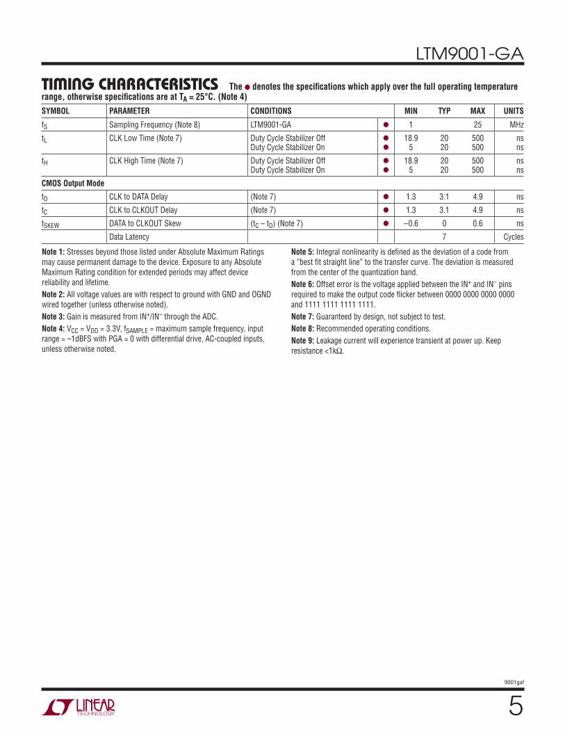
fS Sampling Frequency (Note 8) LTM9001-GA l 1 25 MHz
tL CLK Low Time (Note 7) Duty Cycle Stabilizer OffDuty Cycle Stabilizer On
l
l
18.95
2020
500500
nsns
tH CLK High Time (Note 7) Duty Cycle Stabilizer OffDuty Cycle Stabilizer On
l
l
18.95
2020
500500
nsns
CMOS Output Mode
tD CLK to DATA Delay (Note 7) l 1.3 3.1 4.9 ns
tC CLK to CLKOUT Delay (Note 7) l 1.3 3.1 4.9 ns
tSKEW DATA to CLKOUT Skew (tC – tD) (Note 7) l –0.6 0 0.6 ns
Data Latency 7 Cycles
The l denotes the specifi cations which apply over the full operating temperature range, otherwise specifi cations are at TA = 25°C. (Note 4)TIMING CHARACTERISTICS
Note 1: Stresses beyond those listed under Absolute Maximum Ratings
may cause permanent damage to the device. Exposure to any Absolute
Maximum Rating condition for extended periods may affect device
reliability and lifetime.
Note 2: All voltage values are with respect to ground with GND and OGND
wired together (unless otherwise noted).
Note 3: Gain is measured from IN+/IN– through the ADC.
Note 4: VCC = VDD = 3.3V, fSAMPLE = maximum sample frequency, input
range = –1dBFS with PGA = 0 with differential drive, AC-coupled inputs,
unless otherwise noted.
Note 5: Integral nonlinearity is defi ned as the deviation of a code from
a “best fi t straight line” to the transfer curve. The deviation is measured
from the center of the quantization band.
Note 6: Offset error is the voltage applied between the IN+ and IN– pins
required to make the output code fl icker between 0000 0000 0000 0000
and 1111 1111 1111 1111.
Note 7: Guaranteed by design, not subject to test.
Note 8: Recommended operating conditions.
Note 9: Leakage current will experience transient at power up. Keep
resistance <1kΩ.

LTM9001-GA
69001gaf
TIMING DIAGRAM
tAP
ANALOGINPUT
tH
tD
tC
tL
N – 7 N – 6 N – 5 N – 4 N – 3
CLK
CLKOUT+
CLKOUT–
D0-D15, OF
9001GA TD03
N + 1
N + 2
N + 4
N + 3N

LTM9001-GA
79001gaf
TYPICAL PERFORMANCE CHARACTERISTICS
Integral Non-Linearity (INL)vs Output Code
Differential Non-Linearity (DNL) vs Output Code
64k Point FFT, fIN = 5MHz, –15dBFS,PGA = 0, RAND “0n”, Dither “On”
64k Point FFT, fIN = 5MHz, –1dBFS, PGA = 0, RAND “Off”, Dither “Off”
64k Point FFT, fIN = 5MHz, –1dBFS, PGA = 1, RAND “Off”, Dither “Off”
IF Frequency Response Input Impedance vs Frequency SNR vs Frequency
FREQUENCY (MHz)
FILT
ER
GA
IN (
dB
)
0
–1
–2
–3
–4
–5
–6
–7
–8
–9
9001-GA G01
–100 1 10 100
FREQUENCY (MHz)
IMP
ED
AN
CE M
AG
NIT
UD
E (
Ω)
400
350
300
250
150
50
200
100
9001-GA G02
0
IMP
ED
AN
CE P
HA
SE (°C
)
40
32
24
16
0
–16
–24
8
–8
–321 10 100 1000
MAGNITUDEPHASE
FREQUENCY (MHz)
SN
R (
dB
)
80
79
78
77
75
73
72
71
76
74
9001-GA G03
700 1 10 100
OUTPUT CODE
INL E
RR
OR
(LS
B)
4.03.53.02.5
1.51.0
0.00.5
–0.5–1.0–1.5–2.0–2.5–3.0–3.5
2.0
9001-GA G04
–4.00 16384 32768 49152 65536
OUTPUT CODE
DN
L E
RR
OR
(LS
B)
1.0
0.8
0.6
0.4
0.2
0.0
–0.2
–0.4
–0.6
–0.8
9001-GA G05
–1.00 16384 32768 49152 65536
FREQUENCY (MHz)
AM
PLIT
UD
E (
dB
FS)
0
–10
–20
9001-GA G06
–130
–60
–70
–80
–90
–100
–110
–120
–40
–50
–30
0.0 2.5 5.0 7.5 10.0 12.5
FREQUENCY (MHz)
AM
PLIT
UD
E (
dB
FS)
0
–10
–20
9001-GA G07
–130
–60
–70
–80
–90
–100
–110
–120
–40
–50
–30
0.0 2.5 5.0 7.5 10.0 12.5
HD2 HD3
FREQUENCY (MHz)
AM
PLIT
UD
E (
dB
FS)
0
–10
–20
9001-GA G08
–130
–60
–70
–80
–90
–100
–110
–120
–40
–50
–30
0.0 2.5 5.0 7.5 10.0 12.5
HD2 HD3
FREQUENCY (MHz)
0.0
AM
PLIT
UD
E (
dB
FS)
–80
–90
–60
–70
–40
–50
–20
–30
–10
0
5.0
9001-GA G09
–100
–110
–120
–1302.5 7.5 10 12.5
64k Point 2-Tone FFT, fIN = 4.9MHz, and fIN = 5.1MHz, –7dBFS Per Tone, PGA = 0, RAND “Off”, Dither “Off”
LTM9001-GA
89001gaf
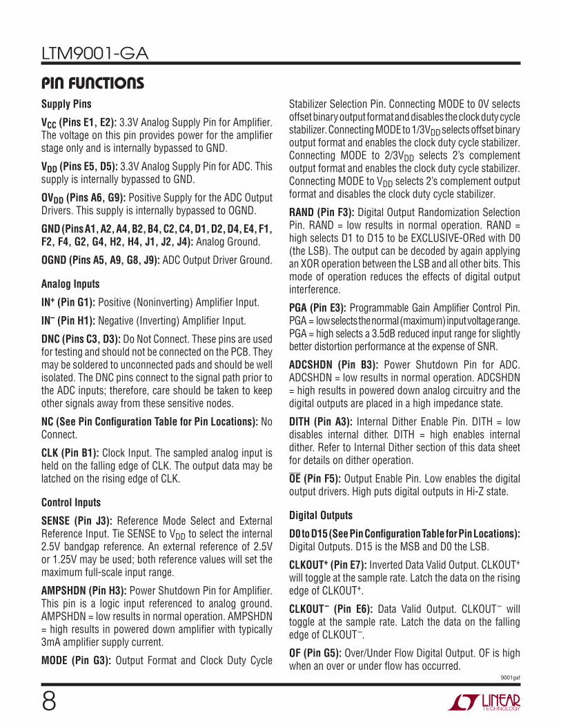
Supply Pins
VCC (Pins E1, E2): 3.3V Analog Supply Pin for Amplifi er. The voltage on this pin provides power for the amplifi er stage only and is internally bypassed to GND.
VDD (Pins E5, D5): 3.3V Analog Supply Pin for ADC. This supply is internally bypassed to GND.
OVDD (Pins A6, G9): Positive Supply for the ADC Output Drivers. This supply is internally bypassed to OGND.
GND (Pins A1, A2, A4, B2, B4, C2, C4, D1, D2, D4, E4, F1, F2, F4, G2, G4, H2, H4, J1, J2, J4): Analog Ground.
OGND (Pins A5, A9, G8, J9): ADC Output Driver Ground.
Analog Inputs
IN+ (Pin G1): Positive (Noninverting) Amplifi er Input.
IN– (Pin H1): Negative (Inverting) Amplifi er Input.
DNC (Pins C3, D3): Do Not Connect. These pins are used for testing and should not be connected on the PCB. They may be soldered to unconnected pads and should be well isolated. The DNC pins connect to the signal path prior to the ADC inputs; therefore, care should be taken to keep other signals away from these sensitive nodes.
NC (See Pin Confi guration Table for Pin Locations): No Connect.
CLK (Pin B1): Clock Input. The sampled analog input is held on the falling edge of CLK. The output data may be latched on the rising edge of CLK.
Control Inputs
SENSE (Pin J3): Reference Mode Select and External Reference Input. Tie SENSE to VDD to select the internal 2.5V bandgap reference. An external reference of 2.5V or 1.25V may be used; both reference values will set the maximum full-scale input range.
AMPSHDN (Pin H3): Power Shutdown Pin for Amplifi er. This pin is a logic input referenced to analog ground. AMPSHDN = low results in normal operation. AMPSHDN = high results in powered down amplifi er with typically 3mA amplifi er supply current.
MODE (Pin G3): Output Format and Clock Duty Cycle
Stabilizer Selection Pin. Connecting MODE to 0V selects offset binary output format and disables the clock duty cycle stabilizer. Connecting MODE to 1/3VDD selects offset binary output format and enables the clock duty cycle stabilizer. Connecting MODE to 2/3VDD selects 2’s complement output format and enables the clock duty cycle stabilizer. Connecting MODE to VDD selects 2’s complement output format and disables the clock duty cycle stabilizer.
RAND (Pin F3): Digital Output Randomization Selection Pin. RAND = low results in normal operation. RAND = high selects D1 to D15 to be EXCLUSIVE-ORed with D0 (the LSB). The output can be decoded by again applying an XOR operation between the LSB and all other bits. This mode of operation reduces the effects of digital output interference.
PGA (Pin E3): Programmable Gain Amplifi er Control Pin. PGA = low selects the normal (maximum) input voltage range. PGA = high selects a 3.5dB reduced input range for slightly better distortion performance at the expense of SNR.
ADCSHDN (Pin B3): Power Shutdown Pin for ADC. ADCSHDN = low results in normal operation. ADCSHDN = high results in powered down analog circuitry and the digital outputs are placed in a high impedance state.
DITH (Pin A3): Internal Dither Enable Pin. DITH = low disables internal dither. DITH = high enables internal dither. Refer to Internal Dither section of this data sheet for details on dither operation.
OE (Pin F5): Output Enable Pin. Low enables the digital output drivers. High puts digital outputs in Hi-Z state.
Digital Outputs
D0 to D15 (See Pin Confi guration Table for Pin Locations): Digital Outputs. D15 is the MSB and D0 the LSB.
CLKOUT+ (Pin E7): Inverted Data Valid Output. CLKOUT+ will toggle at the sample rate. Latch the data on the rising edge of CLKOUT+.
CLKOUT– (Pin E6): Data Valid Output. CLKOUT– will toggle at the sample rate. Latch the data on the falling edge of CLKOUT–.
OF (Pin G5): Over/Under Flow Digital Output. OF is high when an over or under fl ow has occurred.
PIN FUNCTIONS

LTM9001-GA
99001gaf
PIN FUNCTIONSPin Confi guration
1 2 3 4 5 6 7 8 9
J GND GND SENSE GND D14 NC D12 NC OGND
H IN– GND AMPSHDN GND NC NC NC NC D11
G IN+ GND MODE GND OF D15 D13 OGND OVDD
F GND GND RAND GND OE NC D9 NC D10
E VCC VCC PGA GND VDD CLKOUT– CLKOUT NC D8
D GND GND DNC GND VDD NC D6 NC D7
C NC GND DNC GND D0 NC D4 NC D5
B CLK GND ADCSHDN GND NC NC D1 D3 NC
A GND GND DITH GND OGND OVDD NC D2 OGND
Top View of LGA Pinout (Looking Through Component)
9001-GA LGA01
IN–
1
J
H
G
F
E
D
C
B
A
2 3 4 5 6 7 8 9DATA
TOP VIEWALL ELSE= GND
CONTROL
OGND
OVDD
VCC
DNC
VDD OGNDCONTROL OVDD
OGND
IN+
CLK

LTM9001-GA
109001gaf
FUNCTIONAL BLOCK DIAGRAM
90
01
-GA
BD
CLK
OU
T+
CLK
OU
T–
VD
D
OV
DD
AD
C-
SH
DN
RA
ND
MO
DE
OE
DIT
HO
GN
DC
LK
INP
UT
AM
PLIF
IER
PG
A
AD
CR
EFE
REN
CE
INP
UT
S/H
CO
NTR
OL
LO
GIC
OU
TP
UT
DR
IVER
SLO
W J
ITTER
CLO
CK
DR
IVER
INTER
NA
LC
LO
CK
SIG
NA
LS
IN+
IN–
SEN
SE
AM
PS
HD
N
VC
C
VC
C
D0…
D15
OF
AN
TI-
ALIA
SFI
LTER
FIR
ST
PIP
ELIN
ED
AD
C S
TAG
E
VO
LTA
GE
REFE
REN
CE
DIT
HER
SIG
NA
LG
EN
ER
ATO
R
SH
IFT R
EG
ISTER
AN
D E
RR
OR
CO
RR
EC
TIO
N
SEC
ON
DP
IPELIN
ED
AD
C S
TAG
E
TH
IRD
PIP
ELIN
ED
AD
C S
TAG
E
FOU
RTH
PIP
ELIN
ED
AD
C S
TAG
E
FIFT
HP
IPELIN
ED
AD
C S
TAG
E
GN
DP
GA
RA
NG
ES
ELEC
T
VD
D
LTM9001-GA
119001gaf
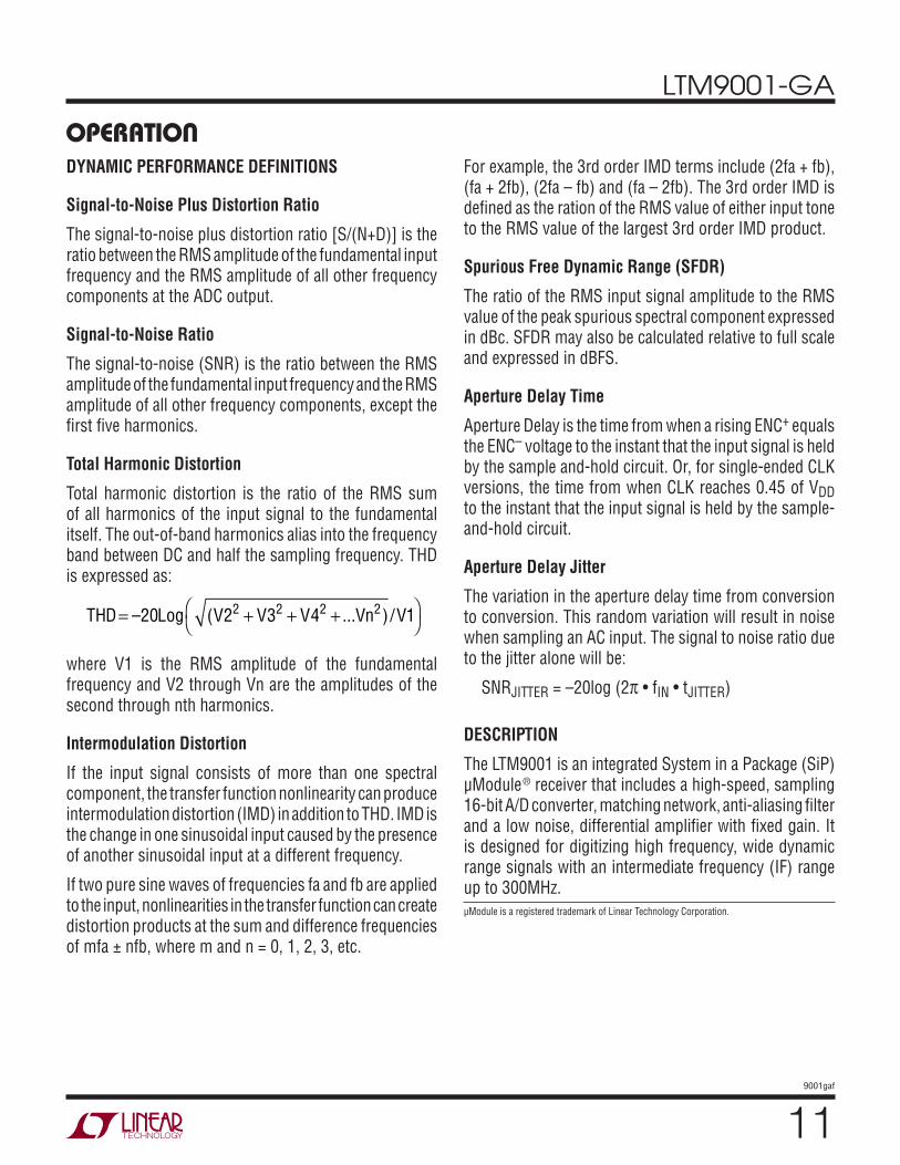
OPERATIONDYNAMIC PERFORMANCE DEFINITIONS
Signal-to-Noise Plus Distortion Ratio
The signal-to-noise plus distortion ratio [S/(N+D)] is the ratio between the RMS amplitude of the fundamental input frequency and the RMS amplitude of all other frequency components at the ADC output.
Signal-to-Noise Ratio
The signal-to-noise (SNR) is the ratio between the RMS amplitude of the fundamental input frequency and the RMS amplitude of all other frequency components, except the fi rst fi ve harmonics.
Total Harmonic Distortion
Total harmonic distortion is the ratio of the RMS sum of all harmonics of the input signal to the fundamental itself. The out-of-band harmonics alias into the frequency band between DC and half the sampling frequency. THD is expressed as:
THD = –20Log (V22 + V32 + V42 + ...Vn2) /V1⎛
⎝⎞⎠
where V1 is the RMS amplitude of the fundamental frequency and V2 through Vn are the amplitudes of the second through nth harmonics.
Intermodulation Distortion
If the input signal consists of more than one spectral component, the transfer function nonlinearity can produce intermodulation distortion (IMD) in addition to THD. IMD is the change in one sinusoidal input caused by the presence of another sinusoidal input at a different frequency.
If two pure sine waves of frequencies fa and fb are applied to the input, nonlinearities in the transfer function can create distortion products at the sum and difference frequencies of mfa ± nfb, where m and n = 0, 1, 2, 3, etc.
For example, the 3rd order IMD terms include (2fa + fb), (fa + 2fb), (2fa – fb) and (fa – 2fb). The 3rd order IMD is defi ned as the ration of the RMS value of either input tone to the RMS value of the largest 3rd order IMD product.
Spurious Free Dynamic Range (SFDR)
The ratio of the RMS input signal amplitude to the RMS value of the peak spurious spectral component expressed in dBc. SFDR may also be calculated relative to full scale and expressed in dBFS.
Aperture Delay Time
Aperture Delay is the time from when a rising ENC+ equals the ENC– voltage to the instant that the input signal is held by the sample and-hold circuit. Or, for single-ended CLK versions, the time from when CLK reaches 0.45 of VDD to the instant that the input signal is held by the sample-and-hold circuit.
Aperture Delay Jitter
The variation in the aperture delay time from conversion to conversion. This random variation will result in noise when sampling an AC input. The signal to noise ratio due to the jitter alone will be:
SNRJITTER = –20log (2π • fIN • tJITTER)
DESCRIPTION
The LTM9001 is an integrated System in a Package (SiP) μModule® receiver that includes a high-speed, sampling 16-bit A/D converter, matching network, anti-aliasing fi lter and a low noise, differential amplifi er with fi xed gain. It is designed for digitizing high frequency, wide dynamic range signals with an intermediate frequency (IF) range up to 300MHz.
μModule is a registered trademark of Linear Technology Corporation.

LTM9001-GA
129001gaf
Figure 1. Basic Functional Elements
9001-GA F01
AMPLIFIER ADCADC
INPUTNETWORK
OPERATIONThe following sections describe in further detail the functional operation of the LTM9001. The SiP technology allows the LTM9001 to be customized and this is described in the fi rst section. The remaining outline follows the basic functional elements as shown in Figure 1.
Note that not all combinations of options in Table 1 are possible at this time and specifi ed performance may differ signifi cantly from existing values. The higher speed options support LVDS or CMOS outputs and are available on a separate data sheet. This data sheet discusses CMOS only versions which have a different pin assignment.
AMPLIFIER INFORMATION
The amplifi ers used in the LTM9001 are low noise and low distortion fully differential ADC drivers. The amplifi ers are very fl exible in terms of I/O coupling. They can be AC- or DC-coupled at the inputs. Users are advised to keep the input common mode voltage between 1V and 1.6V for proper operation. If the inputs are AC-coupled, the input common mode voltage is automatically biased. The input signal can be either single-ended or differential with almost no difference in distortion performance.
ADC INPUT NETWORK
The passive network between the amplifi er output stage and the ADC input stage can be confi gured for bandpass or lowpass response with different cutoff frequencies and bandwidths. The LTM9001-GA, for example, implements a 1-pole lowpass fi lter with 10MHz bandwidth. Note that the fi lter attenuates the signal at 10MHz by 0.2dB, making the overall gain of the subsystem 7.8dB.
For production test purposes the fi lter is designed to allow DC inputs into the ADC.
CONVERTER INFORMATION
The analog-to-digital converter (ADC) is a CMOS pipelined multistep converter with a front-end PGA. As shown in the Functional Block Diagram, the converter has fi ve pipelined ADC stages; a sampled analog input will result in a digitized value seven cycles later (see the Timing Diagram section). The encode input is differential for improved common mode noise immunity.
SEMI-CUSTOM OPTIONS
The μModule construction affords a new level of fl exibility in application-specifi c standard products. Standard ADC and amplifi er components can be integrated regardless of their process technology and matched with passive components to a particular application. The LTM9001-AA, on a separate data sheet, is confi gured with a 16-bit ADC sampling at rates up to 130Msps. The amplifi er gain is 20dB with an input impedance of 200Ω and an input range of 233mVP-P. The matching network is designed to optimize the interface between the amplifi er output and the ADC under these conditions. Additionally, there is a 2-pole bandpass fi lter designed for 162.5MHz ±25MHz.
However, other options are possible through Linear Technology’s semi-custom development program. Linear Technology has in place a program to deliver other speed, resolution, IF range, gain and fi lter confi gurations for a wide range of applications. See Table 1 for the LTM9001 confi guration and potential options. These semi-custom designs are based on existing ADCs and amplifi ers with an appropriately modifi ed matching network. The fi nal subsystem is then tested to the exact parameters defi ned for the application. The fi nal result is a fully integrated, accurately tested and reliable solution. For more details on the semi-custom receiver subsystem program, contact Linear Technology.

LTM9001-GA
139001gaf
Table 1. Semi-Custom Options
AMPLIFIER IF RANGE
AMPLIFIER INPUT IMPEDANCE
AMPLIFIER GAIN
FILTER ADC SAMPLE RATE ADC RESOLUTION
OUTPUT PART NUMBER
300MHz 200Ω 20dB 162.5MHz BPF, 50MHz BW 130Msps 16-bit LVDS/CMOS LTM9001-AA
300MHz 200Ω 14dB 70MHz BPF, 25MHz BW 130Msps 16-bit LVDS/CMOS LTM9001-AD
300MHz 400Ω 8dB DC-300MHz LPF 160Msps 16-bit LVDS/CMOS LTM9001-BA
300MHz 400Ω 8dB DC-10MHz LPF 25Msps 16-bit CMOS LTM9001-GA
Select Combination of Options from Columns Below
DC-300MHz 50Ω 26dB LPF TBD 160Msps 16-bit LVDS/CMOS
DC-140MHz 200Ω 20dB BPF TBD 130Msps 14-bit LVDS/CMOS
DC-70MHz 200Ω 14dB 105Msps CMOS
DC-35MHz 400Ω 8dB 80Msps CMOS
200Ω 6dB 65Msps CMOS
40Msps CMOS
25Msps CMOS
10Msps CMOS
OPERATION
LTM9001-GA
149001gaf
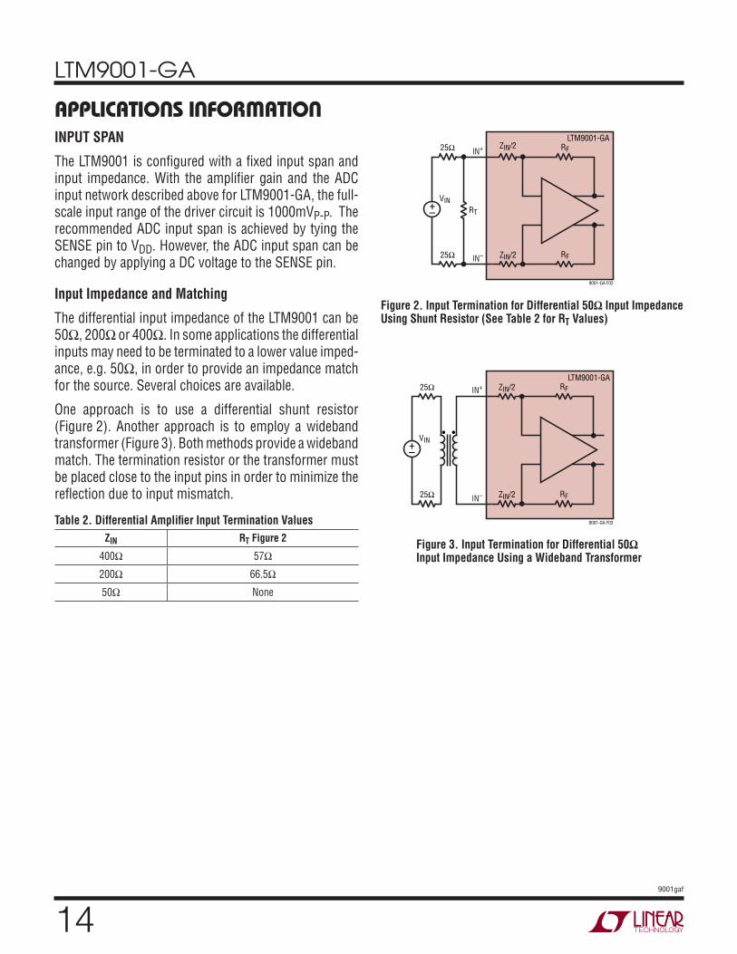
INPUT SPAN
The LTM9001 is confi gured with a fi xed input span and input impedance. With the amplifi er gain and the ADC input network described above for LTM9001-GA, the full-scale input range of the driver circuit is 1000mVP-P. The recommended ADC input span is achieved by tying the SENSE pin to VDD. However, the ADC input span can be changed by applying a DC voltage to the SENSE pin.
Input Impedance and Matching
The differential input impedance of the LTM9001 can be 50Ω, 200Ω or 400Ω. In some applications the differential inputs may need to be terminated to a lower value imped-ance, e.g. 50Ω, in order to provide an impedance match for the source. Several choices are available.
One approach is to use a differential shunt resistor (Figure 2). Another approach is to employ a wideband transformer (Figure 3). Both methods provide a wideband match. The termination resistor or the transformer must be placed close to the input pins in order to minimize the refl ection due to input mismatch.
Table 2. Differential Amplifi er Input Termination Values
ZIN RT Figure 2
400Ω 57Ω
200Ω 66.5Ω
50Ω None
9001-GA F02
ZIN/2
RT
RF
LTM9001-GA
ZIN/2
25Ω
25Ω
VIN
RF
IN+
IN–
+–
9001-GA F03
ZIN/2 RF
LTM9001-GA
ZIN/2
25Ω
25Ω
VIN
RF
+–
••
IN+
IN–
Figure 2. Input Termination for Differential 50Ω Input Impedance Using Shunt Resistor (See Table 2 for RT Values)
Figure 3. Input Termination for Differential 50Ω Input Impedance Using a Wideband Transformer
APPLICATIONS INFORMATION

LTM9001-GA
159001gaf
APPLICATIONS INFORMATION
9001-GA F04
ZIN/2
0.1μF
0.1μFRF
LTM9001-GA
ZIN/2
RS50Ω
RS/RT
VIN
RF
+–
0.1μF
RT
IN+
IN–
Figure 4. Input Termination for Differential 50Ω Input Impedance Using Shunt Resistor
Alternatively, one could apply a narrowband impedance match at the inputs for frequency selection and/or noise reduction.
Referring to Figure 4, amplifi er inputs can be easily confi gured for single-ended input without a balun. The signal is fed to one of the inputs through a matching network while the other input is connected to the same impedance. In general, the single-ended input impedance and termination resistor RT are determined by the combination of RS, ZIN/2 and RF.
Table 3. Single-Ended Amplifi er Input Termination Values
ZIN RT Figure 4
400Ω 59Ω
200Ω 68.5Ω
50Ω 150Ω
The LTM9001 amplifi er is stable with all source impedances. The overall differential gain is affected by the source impedance in Figure 5:
AV = | VOUT/VIN | = (1000/(RS + ZIN/2))
The noise performance of the amplifi er also depends upon the source impedance and termination. For example, an input 1:4 transformer in Figure 3 improves the input noise fi gure by adding 6dB voltage gain at the inputs.
Reference and SENSE Pin Operation
Figure 6 shows the converter reference circuitry consisting of a 2.5V bandgap reference, a programmable gain amplifi er and control circuit. There are three modes of reference operation: Internal Reference, 1.25V external reference or 2.5V external reference. To use the internal reference, tie the SENSE pin to VDD. To use an external reference, simply apply either a 1.25V or 2.5V reference voltage to the SENSE input pin. Both 1.25V and 2.5V applied to SENSE will result in the maximum full-scale range.
Figure 5. Calculate Differential Gain
9001-GA F05
ZIN/2
RT
RF
LTM9001-GA
ZIN/2
Rs/2
Rs/2
VIN
RF
IN+
IN–
+–
Figure 6. Reference Circuit
PGA
SENSE
INTERNALADC
REFERENCE
RANGESELECT
AND GAINCONTROL
2.5VBANDGAP
REFERENCE
TIE TO VDD TO USE INTERNAL 2.5V
REFERENCEOR INPUT FOR
EXTERNAL 2.5V REFERENCE
OR INPUT FOR EXTERNAL 1.25V
REFERENCE
9001-GA F06

LTM9001-GA
169001gaf
APPLICATIONS INFORMATIONPGA Pin
The PGA pin selects between two gain settings for the ADC front-end. PGA = low selects the maximum input span; PGA = high selects a 3.5dB lower input span. The high input range has the best SNR. For applications with high linearity requirements, the low input range will have improved distortion; however, the SNR will be 1.8dB worse. See the Typical Performance Characteristics section.
Driving the Clock or Encode Inputs
Certain versions of LTM9001 have differential encode inputs, others have a single-ended clock input.The noise performance of the converter can depend on the encode signal quality as much as the analog input. The encode inputs are intended to be driven differentially, primarily for noise immunity from common mode noise sources. Each input is biased through a 6k resistor to a 1.6V bias. The bias resistors set the DC operating point for transformer coupled drive circuits and can set the logic threshold for single-ended drive circuits.
Any noise present on the encode signal will result in additional aperture jitter that will be RMS summed with the inherent ADC aperture jitter. In applications where jitter is critical (high input frequencies), take the following into consideration:
1. Differential drive should be used.
2. Use the largest amplitude possible. If using transformer coupling, use a higher turns ratio to increase the amplitude.
3. If the ADC is clocked with a fi xed frequency sinusoidal signal, fi lter the encode signal to reduce wideband noise.
4. Balance the capacitance and series resistance at both encode inputs such that any coupled noise will appear at both inputs as common mode noise.
The encode inputs have a common mode range of 1.2V to VDD. Each input may be driven from ground to VDD for single-ended drive.
The encode clock inputs have a differential 100Ω input impedance. For 50Ω inputs e.g. signal generators, an additional 100Ω impedance will provide an impedance match, as shown in Figure 7b.
The single-ended CLK input on LTM9001-GA can be driven directly with a CMOS or TTL level signal. A sinusoidal clock can be used along with a low-jitter squaring circuit before the CLK pin (Figure 8).
VDD
VDDLTM9001-TBD
9001-GA F07a
VDD
ENC–
ENC+
100Ω
1.6V
1.6V
6k
6k
TO INTERNALADC CLOCK
DRIVERS
50Ω
8.2pF
0.1μF
0.1μF
0.1μF
T1
T1 = M/A-COM ETC1-1-13
50Ω
LTM9001-TBD
9001-GA F07b
ENC–
ENC+
100Ω
• •
Figure 7a. Equivalent Encode Input Circuit
Figure 7b. Transformer Driven Encode
CLK0.1μF
0.1μF
4.7μF
1k
1k
FERRITEBEAD
CLEAN 3.3VSUPPLY
SINUSOIDALCLOCKINPUT
9001-GA F09a
NC7SVU04
LTM9001-GA
56Ω
Figure 8. Sinusoidal Single-Ended CLK Drive

LTM9001-GA
179001gaf
APPLICATIONS INFORMATIONMaximum and Minimum Encode Rates
The maximum encode rate for the LTM9001-GA is 25Msps. For the ADC to operate properly the CLK signal should have a 50% (±5%) duty cycle. Each half cycle must have at least 18.9ns (LTM9001-GA) for the ADC internal circuitry to have enough settling time for proper operation.
An optional clock duty cycle stabilizer can be used if the input clock does not have a 50% duty cycle. This circuit uses the rising edge of CLK or ENC to sample the analog input. The falling edge of CLK or ENC is ignored and an internal falling edge is generated by a phase-locked loop. The input clock duty cycle can vary from 30% to 70% and the clock duty cycle stabilizer will maintain a constant 50% internal duty cycle. If the clock is turned off for a long period of time, the duty cycle stabilizer circuit will require one hundred clock cycles for the PLL to lock onto the input clock. To use the clock duty cycle stabilizer, the MODE pin must be connected to 1/3VDD or 2/3VDD using external resistors.
The lower limit of the sample rate is determined by the droop of the sample and hold circuits. The pipelined architecture of this ADC relies on storing analog signals on small valued capacitors. Junction leakage will discharge the capacitors. The specifi ed minimum operating frequency for the LTM9001 is 1Msps.
DIGITAL OUTPUTS
Digital Output Buffers
Figure 9 shows an equivalent circuit for a single output buffer in CMOS mode. Each buffer is powered by OVDD and OGND, isolated from the ADC power and ground. The additional N-channel transistor in the output driver allows operation down to low voltages. The internal resistor in series with the output makes the output appear as 50Ω to external circuitry and eliminates the need for external damping resistors.
9001-GA F10
OVDD
VDD VDD
TYPICALDATAOUTPUT
OGND
43Ω
OVDD 0.5VTO 3.6V
PREDRIVERLOGIC
DATAFROM
LATCH
LTM9001-GA
Figure 9. Equivalent Circuit for a Digital Output Buffer
LTM9001-GA
189001gaf
APPLICATIONS INFORMATIONAs with all high speed/high resolution converters, the digital output loading can affect the performance. The digital outputs of the LTM9001 should drive a minimum capacitive load to avoid possible interaction between the digital outputs and sensitive input circuitry. The output should be buffered with a device such as an ALVCH16373 CMOS latch. For full speed operation the capacitive load should be kept under 10pF. A resistor in series with the output may be used but is not required since the ADC has a series resistor of 43Ω on chip.
Lower OVDD voltages will also help reduce interference from the digital outputs.
Data Format
The LTM9001 parallel digital output can be selected for offset binary or 2’s complement format. The format is selected with the MODE pin. This pin has a four level logic input, centered at 0, 1/3VDD, 2/3VDD and VDD. An external resistive divider can be used to set the 1/3VDD and 2/3VDD logic levels. Table 5 shows the logic states for the MODE pin.
Table 5. MODE Pin Function
MODE OUTPUT FORMAT CLOCK DUTY CYCLE STABILIZER
0V(GND) Offset Binary Off
1/3VDD Offset Binary On
2/3VDD 2’s Complement On
VDD 2’s Complement Off
Overfl ow Bit
An overfl ow output bit (OF) indicates when the converter is over-ranged or under-ranged. A logic high on the OF pin indicates an overfl ow or underfl ow.
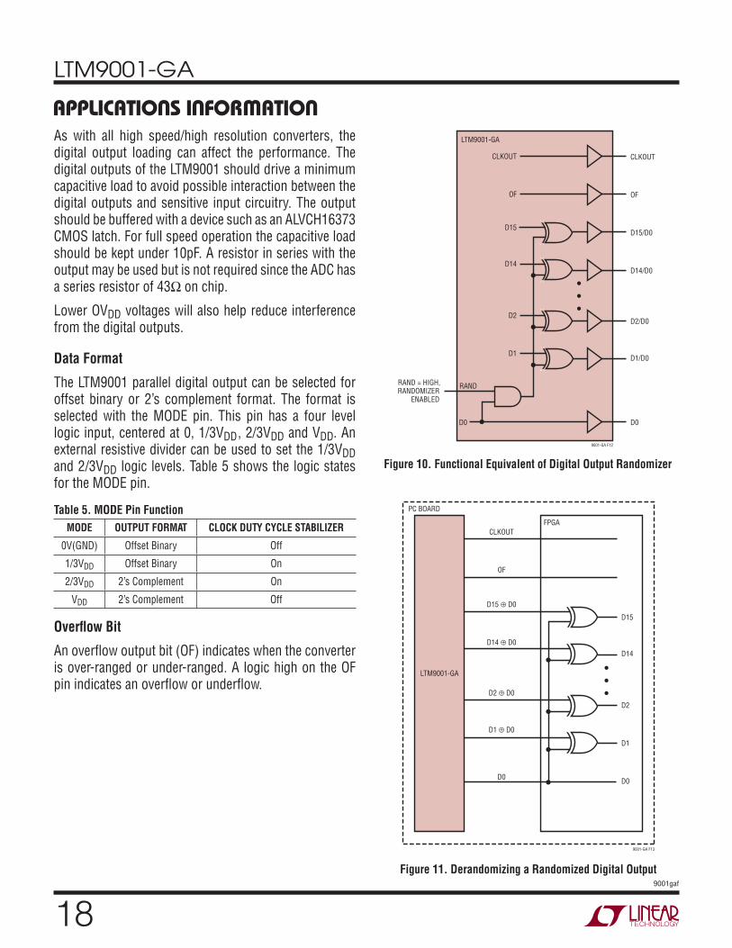
Figure 10. Functional Equivalent of Digital Output Randomizer
Figure 11. Derandomizing a Randomized Digital Output
•••
CLKOUT
OF
D15/D0
D14/D0
D2/D0
D1/D0
D0D0
D1
RAND = HIGH,RANDOMIZER
ENABLED
D2
D14
D15
OF
CLKOUT
RAND
9001-GA F12
LTM9001-GA
•••
D1
D0
D2
D14
D15
PC BOARD
FPGACLKOUT
OF
D15 D0
D14 D0
D2 D0
D1 D0
D0
9001-GA F13
LTM9001-GA
LTM9001-GA
199001gaf
APPLICATIONS INFORMATIONOutput Clock
The ADC has a delayed version of the encode input available as a digital output. Both a non-inverted version, CLKOUT+, and an inverted version, CLKOUT–, are provided. The CLKOUT pins can be used to synchronize the converter data to the digital system. This is necessary when using a sinusoidal encode. Data will be updated as CLKOUT+ falls and CLKOUT– rises. Data may be latched on the rising edge of CLKOUT+ or the falling edge of CLKOUT–.
Digital Output Randomizer
Interference from the ADC digital outputs is sometimes unavoidable. Interference from the digital outputs may be from capacitive or inductive coupling or coupling through the ground plane. Even a tiny coupling factor can result in discernible unwanted tones in the ADC output spectrum.
By randomizing the digital output before it is transmitted off chip, these unwanted tones can be randomized, trading a slight increase in the noise fl oor for a large reduction in unwanted tone amplitude.
The digital output is randomized by applying an exclusive-OR logic operation between the LSB and all other data output bits (see fi gure 10). To decode, the reverse operation is applied; that is, an exclusive-OR operation
is applied between the LSB and all other bits (see fi gure 11). The LSB, OF and CLKOUT output are not affected. The output randomizer function is active when the RAND pin is high.
Output Driver Power
Separate output power and ground pins allow the output drivers to be isolated from the analog circuitry. The power supply for the digital output buffers, OVDD, should be tied to the same power supply as for the logic being driven. For example, if the converter is driving a DSP powered by a 1.8V supply, then OVDD should be tied to that same 1.8V supply. OVDD can be powered with any logic voltage up to the 3.6V. OGND can be powered with any voltage from ground up to 1V and must be less than OVDD. The logic outputs will swing between OGND and OVDD.
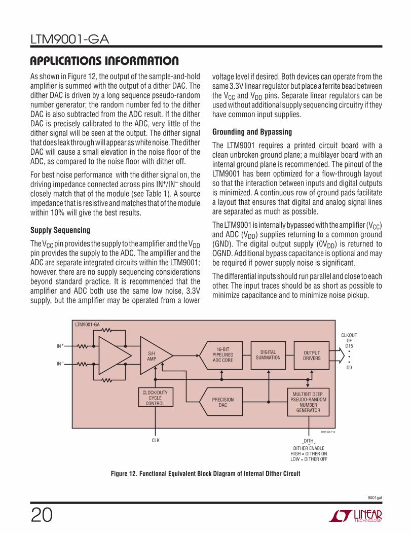
Internal Dither
The LTM9001 is a 16-bit receiver subsystem with a very linear transfer function; however, at low input levels even slight imperfections in the transfer function will result in unwanted tones. Small errors in the transfer function are usually a result of ADC element mismatches. An optional internal dither mode can be enabled to randomize the input location on the ADC transfer curve, resulting in improved SFDR for low signal levels.
LTM9001-GA
209001gaf
As shown in Figure 12, the output of the sample-and-hold amplifi er is summed with the output of a dither DAC. The dither DAC is driven by a long sequence pseudo-random number generator; the random number fed to the dither DAC is also subtracted from the ADC result. If the dither DAC is precisely calibrated to the ADC, very little of the dither signal will be seen at the output. The dither signal that does leak through will appear as white noise. The dither DAC will cause a small elevation in the noise fl oor of the ADC, as compared to the noise fl oor with dither off.
For best noise performance with the dither signal on, the driving impedance connected across pins IN+/IN– should closely match that of the module (see Table 1). A source impedance that is resistive and matches that of the module within 10% will give the best results.
Supply Sequencing
The VCC pin provides the supply to the amplifi er and the VDD pin provides the supply to the ADC. The amplifi er and the ADC are separate integrated circuits within the LTM9001; however, there are no supply sequencing considerations beyond standard practice. It is recommended that the amplifi er and ADC both use the same low noise, 3.3V supply, but the amplifi er may be operated from a lower
APPLICATIONS INFORMATIONvoltage level if desired. Both devices can operate from the same 3.3V linear regulator but place a ferrite bead between the VCC and VDD pins. Separate linear regulators can be used without additional supply sequencing circuitry if they have common input supplies.
Grounding and Bypassing
The LTM9001 requires a printed circuit board with a clean unbroken ground plane; a multilayer board with an internal ground plane is recommended. The pinout of the LTM9001 has been optimized for a fl ow-through layout so that the interaction between inputs and digital outputs is minimized. A continuous row of ground pads facilitate a layout that ensures that digital and analog signal lines are separated as much as possible.
The LTM9001 is internally bypassed with the amplifi er (VCC) and ADC (VDD) supplies returning to a common ground (GND). The digital output supply (0VDD) is returned to OGND. Additional bypass capacitance is optional and may be required if power supply noise is signifi cant.
The differential inputs should run parallel and close to each other. The input traces should be as short as possible to minimize capacitance and to minimize noise pickup.
Figure 12. Functional Equivalent Block Diagram of Internal Dither Circuit
IN –
IN +
S/HAMP
DIGITALSUMMATION
OUTPUTDRIVERS
MULTIBIT DEEPPSEUDO-RANDOM
NUMBERGENERATOR
16-BITPIPELINEDADC CORE
PRECISIONDAC
CLOCK/DUTYCYCLE
CONTROL
CLKOUTOF
D15•••
D0
CLK
DITHER ENABLEHIGH = DITHER ONLOW = DITHER OFF
DITH
9001-GA F14
LTM9001-GA

LTM9001-GA
219001gaf
APPLICATIONS INFORMATIONHeat Transfer
Most of the heat generated by the LTM9001 is transferred through the bottom-side ground pads. For good electrical and thermal performance, it is critical that all ground pins are connected to a ground plane of suffi cient area with as many vias as possible.
Recommended Layout
The high integration of the LTM9001 makes the PC board layout very simple and easy. However, to optimize its electrical and thermal performance, some layout considerations are still necessary, see Figures 13 to 16.
• Use large PCB copper areas for ground. This helps to dissipate heat in the package through the board and also helps to shield sensitive on-board analog signals. Common ground (GND) and output ground (OGND) are electrically isolated on the LTM9001, but can be connected on the PCB underneath the part to provide a common return path.
• Use multiple ground vias. Using as many vias as possible helps to improve the thermal performance of the board and creates necessary barriers separating analog and digital traces on the board at high frequencies.
• Separate analog and digital traces as much as possible, using vias to create high frequency barriers. This will reduce digital feedback that can reduce the signal-to-noise ratio (SNR) and dynamic range of the LTM9001.
The quality of the paste print is an important factor in producing high yield assemblies. It is recommended to use a type 3 or 4 printing no-clean solder paste. The solder stencil design should follow the guidelines outlined in Application Note 100. The μModule LGA Packaging Care and Assembly Instructions is available at http://www.linear.com/designtools/packaging/uModule_Instructions.
The LTM9001 employs gold-fi nished pads for use with Pb-based or tin-based solder paste. It is inherently Pb-free and complies with the JEDEC (e4) standard. The materials declaration is available online at http://www.linear.com/designtools/leadfree/mat_dec.jsp.

LTM9001-GA
229001gaf
APPLICATIONS INFORMATION
Figure 13. Layer 1
Figure 15. Layer 3
Figure 14. Layer 2
Figure 16. Layer 4
LTM9001-GA
239001gaf
Information furnished by Linear Technology Corporation is believed to be accurate and reliable. However, no responsibility is assumed for its use. Linear Technology Corporation makes no representa-tion that the interconnection of its circuits as described herein will not infringe on existing patent rights.
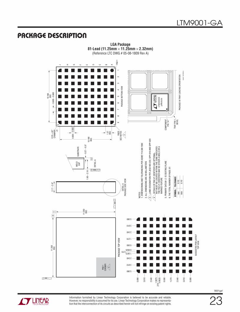
PACKAGE DESCRIPTIONLGA Package
81-Lead (11.25mm × 11.25mm × 2.32mm)(Reference LTC DWG # 05-08-1809 Rev A)
NO
TES
:1.
DIM
EN
SIO
NIN
G A
ND
TO
LER
AN
CIN
G P
ER
AS
ME Y
14.5
M-1
994
2. A
LL D
IMEN
SIO
NS
AR
E I
N M
ILLIM
ETER
S
LA
ND
DES
IGN
ATIO
N P
ER
JES
D M
O-2
22, S
PP
-010 A
ND
SP
P-0
20
5.
PR
IMA
RY
DA
TU
M -
Z-
IS S
EA
TIN
G P
LA
NE
6. TH
E T
OTA
L N
UM
BER
OF
PA
DS
: 81
43
DETA
ILS
OF
PA
D #
1 I
DEN
TIF
IER
AR
E O
PTIO
NA
L,
BU
T M
US
T B
E L
OC
ATED
WIT
HIN
TH
E Z
ON
E I
ND
ICA
TED
.TH
E P
AD
#1 I
DEN
TIF
IER
MA
Y B
E E
ITH
ER
A M
OLD
OR
A
MA
RK
ED
FEA
TU
RE
SY
MB
OL
aaa
bbb
TO
LER
AN
CE
0.1
5
0.1
0
11
.25
0B
SC
PA
CK
AG
E T
OP
VIE
W
LG
A 8
1 1
107 R
EV
A
11
.25
0B
SC
4
PA
D 1
CO
RN
ER
3PA
DS
SE
E N
OT
ES
XY
aaa Z
aaa
Z
2.1
7 –
2.4
7
DE
TAIL
AP
AC
KA
GE
SID
E V
IEW
DE
TAIL
A
SU
BS
TR
AT
EM
OL
DC
AP
0.2
7 –
0.3
71
.90
– 2
.10
bbb Z
Z
1.2
7B
SC
0.6
05
– 0
.66
5
0.2
5 4
5°
CH
AM
FER 3
0.6
05
– 0
.66
5
10
.16
0B
SC
10
.16
0B
SC
PA
D 1
67
89
51
23
4
PA
CK
AG
E B
OTT
OM
VIE
W
5.080
5.080
3.810
3.810
2.540
2.540
0.000
1.270
1.270
0.9525
1.5875
5.0
80
2.5
40
3.8
10
5.0
80
3.8
10
1.2
70
2.5
40
.27
0
0.0
00
1.5
87
5
0.9
52
5
SU
GG
ES
TE
D P
CB
LA
YO
UT
TO
P V
IEW
LTM
XX
XX
XX
μM
od
ule
TR
AY
PIN
1B
EV
EL
CO
MP
ON
EN
TP
IN “
A1
”
PA
CK
AG
E I
N T
RA
Y L
OA
DIN
G O
RIE
NTA
TIO
N
J H B AD CEFG

LTM9001-GA
249001gaf
Linear Technology Corporation1630 McCarthy Blvd., Milpitas, CA 95035-7417 (408) 432-1900 ● FAX: (408) 434-0507 ● www.linear.com © LINEAR TECHNOLOGY CORPORATION 2008
LT 0809 • PRINTED IN USA
RELATED PARTSPART NUMBER DESCRIPTION COMMENTS
LTC2202 16-Bit, 10Msps ADC 140mW, 81.6dB SNR, 100dB SFDR
LTC2203 16-Bit, 25Msps ADC 220mW, 81.6dB SNR, 100dB SFDR
LTC2204 16-Bit, 40Msps ADC 480mW, 79.1dB SNR, 100dB SFDR
LTC2205 16-Bit, 65Msps ADC 610mW, 79dB SNR, 100dB SFDR
LTC2206 16-Bit, 80Msps ADC 725mW, 77.9dB SNR, 100dB SFDR
LTC2207 16-Bit, 105Msps ADC 900mW, 77.9dB SNR, 100dB SFDR
LTC2208 16-Bit, 130Msps ADC 1250mW, 77.7dB SNR, 100dB SFDR
LTC2209 16-Bit, 160Msps ADC 1450mW, 77.1dB SNR, 100dB SFDR
LTC6400-8/LTC6400-14/LTC6400-20/LTC6400-26
Low Noise, Low Distortion Differential Amplifi er for 300MHz IF, Fixed Gain of 8dB, 14dB, 20dB or 26dB
3V, 90mA, 39.5dBm OIP3 at 300MHz, 6dB NF
LTC6401-8/LTC6401-14/LTC6401-20/LTC6401-26
Low Noise, Low Distortion Differential Amplifi er for 140MHz IF, Fixed Gain of 8dB, 14dB, 20dB or 26dB
3V, 45mA, 45.5dBm OIP3 at 140MHz, 6dB NF
0V
75ΩRS50Ω
9001-GA TA02
GROUND–REFERENCEDSOURCE +–
75Ω
51.1Ω
3.3V
VCC
LTM9001-GA
IN+
IN–
LTM9001 with Ground-Referenced Single-Ended Input
TYPICAL APPLICATION