touch flash mcu - holtek · 2018-04-25 · rev. 1.00 6 e a 0 01 rev. 1.00 e a 0 01...
TRANSCRIPT

Touch Flash MCU
BS83B24C/BS83C40C
Revision: V1.00 Date: �e���a�� 0�� �01��e���a�� 0�� �01�

Rev. 1.00 � �e���a�� 0�� �01� Rev. 1.00 3 �e���a�� 0�� �01�
BS83B24C/BS83C40CTouch Flash MCU
BS83B24C/BS83C40CTouch Flash MCU
Table of Contents
Features ............................................................................................................ 6CPU �eat��es ......................................................................................................................... 6Pe�iphe�al �eat��es ................................................................................................................. 6
General Description ......................................................................................... 7Selection Table ................................................................................................. 7Block Diagram .................................................................................................. 8Pin Assignment ................................................................................................ 8Pin Description ................................................................................................ 9Absolute Maximum Ratings .......................................................................... 17D.C. Characteristics ....................................................................................... 18
Ope�ating Voltage Cha�acte�istics ......................................................................................... 1�Stand�� C���ent Cha�acte�istics ........................................................................................... 1�Ope�ating C���ent Cha�acte�istics ......................................................................................... 19
A.C. Characteristics ....................................................................................... 20High Speed Inte�nal Oscillato� – HIRC – ��eq�enc� Acc��ac� ............................................. �0Low Speed Inte�nal Oscillato� Cha�acte�istics – LIRC .......................................................... �0Low Speed C��stal Oscillato� Cha�acte�istics – LXT ............................................................. �0Ope�ating ��eq�enc� Cha�acte�istic C��ves ......................................................................... �1S�stem Sta�t Up Time Cha�acte�istics .................................................................................. �1
Input/Output Characteristics ........................................................................ 22Memory Characteristics ................................................................................ 23LVR Electrical Characteristics ...................................................................... 23Power-on Reset Characteristics ................................................................... 23System Architecture ...................................................................................... 24
Clocking and Pipelining ......................................................................................................... �4P�og�am Co�nte� ................................................................................................................... �5Stack ..................................................................................................................................... �5A�ithmetic and Logic Unit – ALU ........................................................................................... �6
Flash Program Memory ................................................................................. 27St��ct��e ................................................................................................................................ ��Special Vecto�s ..................................................................................................................... ��Look-�p Ta�le ....................................................................................................................... ��Ta�le P�og�am Example ........................................................................................................ ��In Ci�c�it P�og�amming – ICP ............................................................................................... �9On-Chip De��g S�ppo�t – OCDS ......................................................................................... 30
Data Memory .................................................................................................. 31St��ct��e ................................................................................................................................ 31Data Memo�� Add�essing ...................................................................................................... 3�Gene�al P��pose Data Memo�� ............................................................................................ 3�Special P��pose Data Memo�� ............................................................................................. 3�

Rev. 1.00 � �e���a�� 0�� �01� Rev. 1.00 3 �e���a�� 0�� �01�
BS83B24C/BS83C40CTouch Flash MCU
BS83B24C/BS83C40CTouch Flash MCU
Special Function Register Description ........................................................ 35Indi�ect Add�essing Registe�s – IAR0� IAR1� IAR� ............................................................... 35Memo�� Pointe�s – MP0� MP1L� MP1H� MP�L� MP�H ......................................................... 35Acc�m�lato� – ACC .............................................................................................................. 36P�og�am Co�nte� Low Registe� – PCL ................................................................................. 3�Look-�p Ta�le Registe�s – TBLP� TBHP� TBLH .................................................................... 3�Stat�s Registe� – STATUS .................................................................................................... 3�
EEPROM Data Memory .................................................................................. 39EEPROM Data Memo�� St��ct��e ........................................................................................ 39EEPROM Registe�s .............................................................................................................. 39Reading Data f�om the EEPROM ......................................................................................... 40W�iting Data to the EEPROM ................................................................................................ 41W�ite P�otection ..................................................................................................................... 41EEPROM Inte���pt ................................................................................................................ 41P�og�amming Conside�ations ................................................................................................ 41
Oscillators ...................................................................................................... 43Oscillato� Ove�view ............................................................................................................... 43System Clock Configurations ................................................................................................ 43Inte�nal RC Oscillato� – HIRC ............................................................................................... 44Exte�nal 3�.�6�kHz C��stal Oscillato� – LXT ........................................................................ 44Inte�nal 3�kHz Oscillato� – LIRC ........................................................................................... 45
Operating Modes and System Clocks ......................................................... 46S�stem Clocks ...................................................................................................................... 46S�stem Ope�ation Modes ...................................................................................................... 4�Cont�ol Registe�s .................................................................................................................. 4�Ope�ating Mode Switching .................................................................................................... 50Stand�� C���ent Conside�ations ........................................................................................... 54Wake-�p ................................................................................................................................ 54
Watchdog Timer ............................................................................................. 55Watchdog Time� Clock So��ce .............................................................................................. 55Watchdog Time� Cont�ol Registe� ......................................................................................... 55Watchdog Time� Ope�ation ................................................................................................... 56
Reset and Initialisation ................................................................................. 57Reset ��nctions .................................................................................................................... 5�Reset Initial Conditions ........................................................................................................ 60
Input/Output Ports ........................................................................................ 65P�ll-high Resisto�s ................................................................................................................ 66Po�t A Wake-�p ..................................................................................................................... 66I/O Po�t Cont�ol Registe�s ..................................................................................................... 6�I/O Po�t So��ce C���ent Cont�ol ............................................................................................ 6�Pin-sha�ed ��nctions ............................................................................................................ 69I/O Pin St��ct��es .................................................................................................................. �5P�og�amming Conside�ations ............................................................................................... �5

Rev. 1.00 4 �e���a�� 0�� �01� Rev. 1.00 5 �e���a�� 0�� �01�
BS83B24C/BS83C40CTouch Flash MCU
BS83B24C/BS83C40CTouch Flash MCU
Timer Modules – TM ...................................................................................... 76Int�od�ction ........................................................................................................................... �6TM Ope�ation ........................................................................................................................ �6TM Clock So��ce ................................................................................................................... �6TM Inte���pts ......................................................................................................................... ��TM Exte�nal Pins ................................................................................................................... ��P�og�amming Conside�ations ................................................................................................ ��
Compact Type TM – CTM .............................................................................. 79Compact TM Ope�ation ......................................................................................................... �9Compact T�pe TM Registe� Desc�iption................................................................................ �9Compact T�pe TM Ope�ating Modes .................................................................................... �3
Periodic Type TM – PTM ................................................................................ 89Pe�iodic TM Ope�ation .......................................................................................................... �9Pe�iodic T�pe TM Registe� Desc�iption ................................................................................. 90Pe�iodic T�pe TM Ope�ation Modes ...................................................................................... 94
Universal Serial Interface Module – USIM ................................................. 103SPI Inte�face ....................................................................................................................... 103I�C Inte�face .........................................................................................................................111UART Inte�face.................................................................................................................... 1�1
Touch Key Function .................................................................................... 136To�ch Ke� St��ct��e ............................................................................................................ 136Touch Key Register Definition ............................................................................................. 13�To�ch Ke� Ope�ation ........................................................................................................... 144To�ch Ke� Inte���pt ............................................................................................................. 150P�og�amming Conside�ations .............................................................................................. 150
Interrupts ...................................................................................................... 151Inte���pt Registe�s ............................................................................................................... 151Inte���pt Ope�ation .............................................................................................................. 154Exte�nal Inte���pt ................................................................................................................. 156M�lti-f�nction Inte���pt ........................................................................................................ 156Time� Mod�le Inte���pts ...................................................................................................... 15�EEPROM Inte���pt .............................................................................................................. 15�USIM Inte���pt ..................................................................................................................... 15�To�ch Ke� Inte���pt ............................................................................................................. 15�Time Base Inte���pts ........................................................................................................... 15�Inte���pt Wake-�p ��nction ................................................................................................. 159P�og�amming Conside�ations .............................................................................................. 160
Configuration Options ................................................................................. 160Application Circuits ..................................................................................... 161Instruction Set .............................................................................................. 162
Int�od�ction ......................................................................................................................... 16�Inst��ction Timing ................................................................................................................ 16�Moving and T�ansfe��ing Data ............................................................................................. 16�
Rev. 1.00 4 �e���a�� 0�� �01� Rev. 1.00 5 �e���a�� 0�� �01�
BS83B24C/BS83C40CTouch Flash MCU
BS83B24C/BS83C40CTouch Flash MCU
A�ithmetic Ope�ations .......................................................................................................... 16�Logical and Rotate Ope�ation ............................................................................................. 163B�anches and Cont�ol T�ansfe� ........................................................................................... 163Bit Ope�ations ..................................................................................................................... 163Ta�le Read Ope�ations ....................................................................................................... 163Othe� Ope�ations ................................................................................................................. 163
Instruction Set Summary ............................................................................ 164Ta�le Conventions ............................................................................................................... 164Extended Inst��ction Set ..................................................................................................... 166
Instruction Definition ................................................................................... 168Extended Instruction Definition ........................................................................................... 1��
Package Information ................................................................................... 184��-pin SOP (300mil) O�tline Dimensions ........................................................................... 1�5��-pin SSOP (150mil) O�tline Dimensions ......................................................................... 1�644-pin LQ�P (10mm×10mm) (�P�.0mm) O�tline Dimensions ........................................... 1��

Rev. 1.00 6 �e���a�� 0�� �01� Rev. 1.00 � �e���a�� 0�� �01�
BS83B24C/BS83C40CTouch Flash MCU
BS83B24C/BS83C40CTouch Flash MCU
Features
CPU Features• OperatingVoltage
♦ fSYS=8MHz:2.2V~5.5V♦ fSYS=12MHz:2.7V~5.5V♦ fSYS=16MHz:3.3V~5.5V
• Upto0.25μsinstructioncyclewith16MHzsystemclockatVDD=5V
• Powerdownandwake-upfunctionstoreducepowerconsumption
• Oscillatortypes:♦ InternalHighSpeed8/12/16MHzRCOscillator–HIRC♦ InternalLowSpeed32kHzRCOscillator–LIRC♦ ExternalLowSpeed32.768kHzCrystal–LXT
• Fullyintegratedinternaloscillatorsrequirenoexternalcomponents
• Multi-modeoperation:FAST,SLOW,IDLEandSLEEP
• Allinstructionsexecutedin1~3instructioncycles
• Tablereadinstructions
• 115powerfulinstructions
• 6-levelsubroutinenesting
• Bitmanipulationinstruction
Peripheral Features• FlashProgramMemory:Upto4K×16
• RAMDataMemory:Upto768×8
• TrueEEPROMMemory:128×8
• Upto40touchkeys–fullyintegratedwithoutrequiringexternalcomponents
• WatchdogTimerfunction
• Upto42bidirectionalI/Olines
• ProgrammableI/Osourcecurrent
• SingleexternalinterruptlinesharedwithI/Opin
• MultipleTimerModulesfortimemeasurement,inputcapture,comparematchoutput,PWMoutputfunctionorsinglepulseoutputfunction
• DualTime-Basefunctionsforgenerationoffixedtimeinterruptsignals
• UniversialSerialInterfaceModule–USIMforSPI,I2CorUARTcommunication
• Lowvoltageresetfunction–LVR
• Widerangeofpackagetypes

Rev. 1.00 6 �e���a�� 0�� �01� Rev. 1.00 � �e���a�� 0�� �01�
BS83B24C/BS83C40CTouch Flash MCU
BS83B24C/BS83C40CTouch Flash MCU
General DescriptionThe series of devices are the FlashMemory 8-bit high performanceRISC architecturemicrocontrollerswithfullyintegratedtouchkeyfunctions.WiththetouchkeyfunctionprovidedinternallyandwiththeconvenienceofFlashMemorymulti-programmingfeatures, thisseriesofdeviceshaveallthefeaturestoofferdesignerareliableandeasymeansofimplementingtouchkeyswiththeirproductapplications.
TheTouchkeyfunctioniscompletelyintegratedeliminatingtheneedforexternalcomponents.InadditiontotheFlashprogrammemory,othermemoryincludesanareaofRAMDataMemoryaswellasanareaoftrueEEPROMmemoryforstorageofnon-volatiledatasuchasserialnumbers,calibrationdataetc.Protective featuressuchasan internalWatchdogTimerandLowVoltageResetcoupledwithexcellentnoiseimmunityandESDprotectionensurethatreliableoperationismaintainedinhostileelectricalenvironments.
Afullchoiceofexternal, internalhighandlowoscillatorfunctionsareprovidedincludingfullyintegratedsystemoscillatorswhichrequirenoexternalcomponentsfortheirimplementation.Theability tooperateandswitchdynamicallybetweena rangeofoperatingmodesusingdifferentclocksourcesgivesusers theability tooptimisemicrocontrolleroperationandminimisepowerconsumption.EasycommunicationwiththeoutsideworldiscateredforbyincludingfullyintegratedSPI,I2CandUARTinterfacefunctions,whiletheinclusionofflexibleI/Oprogrammingfeatures,TimerModules,Time-Basefunctionsalongwithmanyotherfeaturesenhancedevicefunctionalityandflexibility.
The touchkeydeviceswill findexcellentuse inahuge rangeofmodern touchkeyproductapplicationssuchasinstrumentation,householdappliances,electronicallycontrolledtoolstonamebutafew.
Selection TableMost featuresarecommon toalldevices.Themain featuresdistinguishing themareMemorycapacity,I/Ocount,TimeModulenumberandTouchkeynumber.Thefollowingtablesummarisesthemainfeaturesofeachdevice.
Part No. Program Memory Data Memory Data EEPROM I/O External InterruptBS�3B�4C 3K × 16 51� × � 1�� × � �6 1BS�3C40C 4K × 16 �6� × � 1�� × � 4� 1
Part No. Timer Module Time Base Touch key USIM Stacks Package
BS�3B�4C 10-�it PTM × 1 � �4 √ 6 ��SOP��SSOP
BS�3C40C 10-�it CTM × 110-�it PTM × 1 � 40 √ 6 44LQ�P

Rev. 1.00 � �e���a�� 0�� �01� Rev. 1.00 9 �e���a�� 0�� �01�
BS83B24C/BS83C40CTouch Flash MCU
BS83B24C/BS83C40CTouch Flash MCU
Block Diagram
To�ch Ke� Mod�le 9 To�ch Ke� Mod�le 1
Inte���pt Cont�olle�
B�s
MUX
Reset Ci�c�it
Stack6-level
RAM�6� × �
ROM4K × 16
WatchdogTime�
Po�t AD�ive�
HIRC�/1�/16MHz
LIRC3�kHz
Time�Pin-Sha�ed
��nction
PA0~PA�
HT� MCU Co�e
Time Base
INT
Pin-Sha�edWith Po�t A
EEPROM1�� × �
LVRPB0~PB�Po�t B
D�ive�
PC0~PC�Po�t CD�ive�
VSS
VDD VDD
VSS
Pin-Sha�edWith Po�t A� B�
C� D� E & �
�ilte�
Ke� OSC
M�lti-f�eq�enc�
16-�it C/�Co�nte�
Time Slot Co�nte�
To�ch Ke� Mod�le 0
SYSCLK
KEY1~KEY40
USIM
To�ch Ke� ��nction
Ke� OSC
Ke� OSC
Ke� OSC
MU
X
Clock S�stem
I/O
Digital Pe�iphe�als
: USIM incl�ding SPI� I�C & UART: Pin-Sha�ed Node: B�s Ent��
LXTXT1
XT�
Pin-Sha�edWith Po�t A
PD0~PD�Po�t DD�ive�
PE0~PE�Po�t ED�ive�
P�0~P�1Po�t �D�ive�
Pin Assignment
PB�/KEY9PB3/KEY10PB4/KEY11PB5/KEY1�PB6/KEY13PB�/KEY14PC0/KEY15PC1/KEY16PC�/KEY1�PC3/KEY1�PC4/KEY19PC5/KEY�0PC6/KEY�1PC�/KEY��
PB1/KEY�PB0/PTPB/KEY�PA�/PTPI/KEY6PA6/INT/KEY5PA5/SDA/SDI/RX/KEY4PA4/SDO/TX/KEY3PA3/SCS/PTP/INT/KEY�PA1/SCK/SCL/PTCK/KEY1VSSPA�/SCK/SCL/SDO/TX/XT1/ICPCK/OCDSCKPA0/SDA/SDI/RX/XT�/ICPDA/OCDSDAVDDPD1/KEY�4PD0/KEY�3
BS83B24C/BS83BV24C28SOP-A/SSOP-A
�����6�5�4�3���1�0191�1�1615
1�3456��910111�1314

Rev. 1.00 � �e���a�� 0�� �01� Rev. 1.00 9 �e���a�� 0�� �01�
BS83B24C/BS83C40CTouch Flash MCU
BS83B24C/BS83C40CTouch Flash MCU
BS83C40C/BS83CV40C44 LQFP-A
1�3456��91011
1� 13 14 15 16 1� 1� 19 �0 �1 ���3�4�5�6�����930313�33
3435363�3�3940414�4344
VSS
PE�/KEY3�
P�1/KEY40P�0/KEY39
PA3/SCS/PTP/INT/KEY�
PA5/SDA/SDI/RX/KEY4PA4/SDO/TX/KEY3
PB
4/KE
Y11P
B5/K
EY1�
PB6/KE
Y13
PB
�/KEY
14P
C0/KE
Y15
PC3/KEY1�
PC1/KEY16
PC5/KEY�0PC4/KEY19
PC�/KEY��
PC�/KEY1�
PD
4/KEY
��P
D5/KE
Y��
PD
6/KEY
�9P
D�/KE
Y30
PE0/KE
Y31
VD
D
PE1/KE
Y3�
PE
�/CTC
K/KEY
33P
E3/C
TP/K
EY34
PE
4/CTP
B/KE
Y35
PE5/KE
Y36
PC6/KEY�1
PD1/KEY�4PD0/KEY�3
PD3/KEY�6PD�/KEY�5
PA0/SDA/SDI/RX/XT�/ICPDA/OCDSDAPA�/SCK/SCL/SDO/TX/XT1/ICPCK/OCDSCK
PE6/KEY3�
PA1/SCK/SCL/PTCK/KEY1
PA�/PTP
I/KEY
6PB
0/PTP
B/K
EY�
PB1/K
EY�
PB
�/KE
Y9P
B3/KEY
10
PA6/IN
T/KEY
5Notes:1.Ifthepin-sharedpinfunctionshavemultipleoutputs,thedesiredpin-sharedfunctionisdeterminedby
thecorrespondingsoftwarecontrolbits.2.TheOCDSDAandOCDSCKpinsaresuppliedasOCDSdedicatedpinsandassuchonlyavailablefortheBS83BV24CandtheBS83CV40CdeviceswhicharetheOCDSEVchipsfortheBS83B24CandtheBS83C40Cdevicesrespectively.
Pin DescriptionWiththeexceptionofthepowerpins,allpinsonthedevicecanbereferencedbytheirPortnames,e.g.PA0,PA1etc,whichrefertothedigitalI/Ofunctionofthepins.HoweverthesePortpinsarealsosharedwithotherfunctionsuchastheTimerModulepinsetc.Thefunctionofeachpinislistedinthefollowingtable,howeverthedetailsbehindhoweachpinisconfigurediscontainedinothersectionsofthedatasheet.
BS83B24CPin Name Function OPT I/T O/T Description
PA0/SDA/SDI/RX/XT�/ICPDA/OCDSDA
PA0PAWUPAPUPAS0
ST CMOS Gene�al p��pose I/O. Registe� ena�led p�ll-�p and wake-�p.
SDA PAS0I�S ST NMOS I�C data line
SDI PAS0I�S ST — SPI se�ial data inp�t
RX PAS0I�S ST — UART se�ial data inp�t
XT� PAS0 — LXT LXT oscillato� pinICPDA — ST CMOS ICP data/add�ess
OCDSDA — ST CMOS OCDS data/add�ess� fo� EV chip onl�

Rev. 1.00 10 �e���a�� 0�� �01� Rev. 1.00 11 �e���a�� 0�� �01�
BS83B24C/BS83C40CTouch Flash MCU
BS83B24C/BS83C40CTouch Flash MCU
Pin Name Function OPT I/T O/T Description
PA1/SCK/SCL/PTCK/KEY1
PA1PAWUPAPUPAS0
ST CMOS Gene�al p��pose I/O. Registe� ena�led p�ll-�p and wake-�p.
SCK PAS0I�S ST CMOS SPI se�ial clock
SCL PAS0I�S ST NMOS I�C clock line
PTCK PAS0 ST — PTM capt��e inp�t
KEY1 PAS0TKM0C1 NSI — To�ch ke� inp�t 1
PA�/SCK/SCL/SDO/TX/XT1/ICPCK/OCDSCK
PA�PAWUPAPUPAS0
ST CMOS Gene�al p��pose I/O. Registe� ena�led p�ll-�p and wake-�p.
SCK PAS0I�S ST CMOS SPI se�ial clock
SCL PAS0I�S ST NMOS I�C clock line
SDO PAS0 — CMOS SPI se�ial data o�tp�tTX PAS0 — CMOS UART se�ial data o�tp�t
XT1 PAS0 LXT — LXT oscillato� pinICPCK — ST — ICP clock inp�t
OCDSCK — ST — OCDS clock inp�t� fo� EV chip onl�
PA3/SCS/PTP/INT/KEY�
PA3PAWUPAPUPAS0
ST CMOS Gene�al p��pose I/O. Registe� ena�led p�ll-�p and wake-�p.
SCS PAS0 ST — SPI slave select pinPTP PAS0 — CMOS PTM o�tp�t
INT
PAS0INTEGINTC0
I�S
ST — Exte�nal inte���pt
KEY� PAS0TKM0C1 NSI — To�ch ke� inp�t �
PA4/SDO/TX/KEY3
PA4PAWUPAPUPAS1
ST CMOS Gene�al p��pose I/O. Registe� ena�led p�ll-�p and wake-�p.
SDO PAS1 — CMOS SPI se�ial data o�tp�tTX PAS1 — CMOS UART se�ial data o�tp�t
KEY3 PAS1TKM0C1 NSI — To�ch ke� inp�t 3
PA5/SDA/SDI/RX/KEY4
PA5PAWUPAPUPAS1
ST CMOS Gene�al p��pose I/O. Registe� ena�led p�ll-�p and wake-�p.
SDA PAS1I�S ST NMOS I�C data line
SDI PAS1I�S ST — SPI se�ial data inp�t
RX PAS1I�S ST — UART se�ial data inp�t
KEY4 PAS1TKM0C1 NSI — To�ch ke� inp�t 4
Rev. 1.00 10 �e���a�� 0�� �01� Rev. 1.00 11 �e���a�� 0�� �01�
BS83B24C/BS83C40CTouch Flash MCU
BS83B24C/BS83C40CTouch Flash MCU
Pin Name Function OPT I/T O/T Description
PA6/INT/KEY5
PA6PAWUPAPUPAS1
ST CMOS Gene�al p��pose I/O. Registe� ena�led p�ll-�p and wake-�p.
INT
PAS1INTEGINTC0
I�S
ST — Exte�nal inte���pt
KEY5 PAS1TKM1C1 NSI — To�ch ke� inp�t 5
PA�/PTPI/KEY6
PA�PAWUPAPUPAS1
ST CMOS Gene�al p��pose I/O. Registe� ena�led p�ll-�p and wake-�p.
PTPI PAS1 ST — PTM capt��e inp�t
KEY6 PAS1TKM1C1 NSI — To�ch ke� inp�t 6
PB0/PTPB/KEY�
PB0 PBPUPBS0 ST CMOS Gene�al p��pose I/O. Registe� ena�led p�ll-�p.
PTPB PBS0 — CMOS PTM inve�ting o�tp�t
KEY� PBS0TKM1C1 NSI — To�ch ke� inp�t �
PB1/KEY�PB1 PBPU
PBS0 ST CMOS Gene�al p��pose I/O. Registe� ena�led p�ll-�p.
KEY� PBS0TKM1C1 NSI — To�ch ke� inp�t �
PB�/KEY9PB� PBPU
PBS0 ST CMOS Gene�al p��pose I/O. Registe� ena�led p�ll-�p.
KEY9 PBS0TKM�C1 NSI — To�ch ke� inp�t 9
PB3/KEY10PB3 PBPU
PBS0 ST CMOS Gene�al p��pose I/O. Registe� ena�led p�ll-�p.
KEY10 PBS0TKM�C1 NSI — To�ch ke� inp�t 10
PB4/KEY11PB4 PBPU
PBS1 ST CMOS Gene�al p��pose I/O. Registe� ena�led p�ll-�p.
KEY11 PBS1TKM�C1 NSI — To�ch ke� inp�t 11
PB5/KEY1�PB5 PBPU
PBS1 ST CMOS Gene�al p��pose I/O. Registe� ena�led p�ll-�p.
KEY1� PBS1TKM�C1 NSI — To�ch ke� inp�t 1�
PB6/KEY13PB6 PBPU
PBS1 ST CMOS Gene�al p��pose I/O. Registe� ena�led p�ll-�p.
KEY13 PBS1TKM3C1 NSI — To�ch ke� inp�t 13
PB�/KEY14PB� PBPU
PBS1 ST CMOS Gene�al p��pose I/O. Registe� ena�led p�ll-�p.
KEY14 PBS1TKM3C1 NSI — To�ch ke� inp�t 14
PC0/KEY15PC0 PCPU
PCS0 ST CMOS Gene�al p��pose I/O. Registe� ena�led p�ll-�p.
KEY15 PCS0TKM3C1 NSI — To�ch ke� inp�t 15

Rev. 1.00 1� �e���a�� 0�� �01� Rev. 1.00 13 �e���a�� 0�� �01�
BS83B24C/BS83C40CTouch Flash MCU
BS83B24C/BS83C40CTouch Flash MCU
Pin Name Function OPT I/T O/T Description
PC1/KEY16PC1 PCPU
PCS0 ST CMOS Gene�al p��pose I/O. Registe� ena�led p�ll-�p.
KEY16 PCS0TKM3C1 NSI — To�ch ke� inp�t 16
PC�/KEY1�PC� PCPU
PCS0 ST CMOS Gene�al p��pose I/O. Registe� ena�led p�ll-�p.
KEY1� PCS0TKM4C1 NSI — To�ch ke� inp�t 1�
PC3/KEY1�PC3 PCPU
PCS0 ST CMOS Gene�al p��pose I/O. Registe� ena�led p�ll-�p.
KEY1� PCS0TKM4C1 NSI — To�ch ke� inp�t 1�
PC4/KEY19PC4 PCPU
PCS1 ST CMOS Gene�al p��pose I/O. Registe� ena�led p�ll-�p.
KEY19 PCS1TKM4C1 NSI — To�ch ke� inp�t 19
PC5/KEY�0PC5 PCPU
PCS1 ST CMOS Gene�al p��pose I/O. Registe� ena�led p�ll-�p.
KEY�0 PCS1TKM4C1 NSI — To�ch ke� inp�t �0
PC6/KEY�1PC6 PCPU
PCS1 ST CMOS Gene�al p��pose I/O. Registe� ena�led p�ll-�p.
KEY�1 PCS1TKM5C1 NSI — To�ch ke� inp�t �1
PC�/KEY��PC� PCPU
PCS1 ST CMOS Gene�al p��pose I/O. Registe� ena�led p�ll-�p.
KEY�� PCS1TKM5C1 NSI — To�ch ke� inp�t ��
PD0/KEY�3PD0 PDPU
PDS0 ST CMOS Gene�al p��pose I/O. Registe� ena�led p�ll-�p.
KEY�3 PDS0TKM5C1 NSI — To�ch ke� inp�t �3
PD1/KEY�4PD1 PDPU
PDS0 ST CMOS Gene�al p��pose I/O. Registe� ena�led p�ll-�p.
KEY�4 PDS0TKM5C1 NSI — To�ch ke� inp�t �4
VDD VDD — PWR — Positive powe� s�ppl�VSS VSS — PWR — Negative powe� s�ppl�
Legend:I/T:Inputtype O/T:Outputtype OPT:Optionalbyregisteroption ST:SchmittTriggerinput CMOS:CMOSoutput NMOS:NMOSoutput AN:Analogsignal PWR:Power LXT:Lowfrequencycrystaloscillator NSI:Non-standardinput

Rev. 1.00 1� �e���a�� 0�� �01� Rev. 1.00 13 �e���a�� 0�� �01�
BS83B24C/BS83C40CTouch Flash MCU
BS83B24C/BS83C40CTouch Flash MCU
BS83C40CPin Name Function OPT I/T O/T Description
PA0/SDA/SDI/RX/XT�/ICPDA/OCDSDA
PA0PAWUPAPUPAS0
ST CMOS Gene�al p��pose I/O. Registe� ena�led p�ll-�p and wake-�p.
SDA PAS0I�S ST NMOS I�C data line
SDI PAS0I�S ST — SPI se�ial data inp�t
RX PAS0I�S ST — UART se�ial data inp�t
XT� PAS0 — LXT LXT oscillato� pinICPDA — ST CMOS ICP data/add�ess
OCDSDA — ST CMOS OCDS data/add�ess� fo� EV chip onl�
PA1/SCK/SCL/PTCK/KEY1
PA1PAWUPAPUPAS0
ST CMOS Gene�al p��pose I/O. Registe� ena�led p�ll-�p and wake-�p.
SCK PAS0I�S ST CMOS SPI se�ial clock
SCL PAS0I�S ST NMOS I�C clock line
PTCK PAS0 ST — PTM capt��e inp�t
KEY1 PAS0TKM0C1 NSI — To�ch ke� inp�t 1
PA�/SCK/SCL/SDO/TX/XT1/ICPCK/OCDSCK
PA�PAWUPAPUPAS0
ST CMOS Gene�al p��pose I/O. Registe� ena�led p�ll-�p and wake-�p.
SCK PAS0I�S ST CMOS SPI se�ial clock
SCL PAS0I�S ST NMOS I�C clock line
SDO PAS0 — CMOS SPI se�ial data o�tp�tTX PAS0 — CMOS UART se�ial data o�tp�t
XT1 PAS0 LXT — LXT oscillato� pinICPCK — ST — ICP clock inp�t
OCDSCK — ST — OCDS clock inp�t� fo� EV chip onl�
PA3/SCS/PTP/INT/KEY�
PA3PAWUPAPUPAS0
ST CMOS Gene�al p��pose I/O. Registe� ena�led p�ll-�p and wake-�p.
SCS PAS0 ST — SPI slave select pinPTP PAS0 — CMOS PTM o�tp�t
INT
PAS0INTEGINTC0
I�S
ST — Exte�nal inte���pt
KEY� PAS0TKM0C1 NSI — To�ch ke� inp�t �
PA4/SDO/TX/KEY3
PA4PAWUPAPUPAS1
ST CMOS Gene�al p��pose I/O. Registe� ena�led p�ll-�p and wake-�p.
SDO PAS1 — CMOS SPI se�ial data o�tp�tTX PAS1 — CMOS UART se�ial data o�tp�t
KEY3 PAS1TKM0C1 NSI — To�ch ke� inp�t 3

Rev. 1.00 14 �e���a�� 0�� �01� Rev. 1.00 15 �e���a�� 0�� �01�
BS83B24C/BS83C40CTouch Flash MCU
BS83B24C/BS83C40CTouch Flash MCU
Pin Name Function OPT I/T O/T Description
PA5/SDA/SDI/RX/KEY4
PA5PAWUPAPUPAS1
ST CMOS Gene�al p��pose I/O. Registe� ena�led p�ll-�p and wake-�p.
SDA PAS1I�S ST NMOS I�C data line
SDI PAS1I�S ST — SPI se�ial data inp�t
RX PAS1I�S ST — UART se�ial data inp�t
KEY4 PAS1TKM0C1 NSI — To�ch ke� inp�t 4
PA6/INT/KEY5
PA6PAWUPAPUPAS1
ST CMOS Gene�al p��pose I/O. Registe� ena�led p�ll-�p and wake-�p.
INT
PAS1INTEGINTC0
I�S
ST — Exte�nal inte���pt
KEY5 PAS1TKM1C1 NSI — To�ch ke� inp�t 5
PA�/PTPI/KEY6
PA�PAWUPAPUPAS1
ST CMOS Gene�al p��pose I/O. Registe� ena�led p�ll-�p and wake-�p.
PTPI PAS1 ST — PTM capt��e inp�t
KEY6 PAS1TKM1C1 NSI — To�ch ke� inp�t 6
PB0/PTPB/KEY�
PB0 PBPUPBS0 ST CMOS Gene�al p��pose I/O. Registe� ena�led p�ll-�p.
PTPB PBS0 — CMOS PTM inve�ting o�tp�t
KEY� PBS0TKM1C1 NSI — To�ch ke� inp�t �
PB1/ KEY�PB1 PBPU
PBS0 ST CMOS Gene�al p��pose I/O. Registe� ena�led p�ll-�p.
KEY� PBS0TKM1C1 NSI — To�ch ke� inp�t �
PB�/KEY9PB� PBPU
PBS0 ST CMOS Gene�al p��pose I/O. Registe� ena�led p�ll-�p.
KEY9 PBS0TKM�C1 NSI — To�ch ke� inp�t 9
PB3/KEY10PB3 PBPU
PBS0 ST CMOS Gene�al p��pose I/O. Registe� ena�led p�ll-�p.
KEY10 PBS0TKM�C1 NSI — To�ch ke� inp�t 10
PB4/KEY11PB4 PBPU
PBS1 ST CMOS Gene�al p��pose I/O. Registe� ena�led p�ll-�p.
KEY11 PBS1TKM�C1 NSI — To�ch ke� inp�t 11
PB5/KEY1�PB5 PBPU
PBS1 ST CMOS Gene�al p��pose I/O. Registe� ena�led p�ll-�p.
KEY1� PBS1TKM�C1 NSI — To�ch ke� inp�t 1�
PB6/KEY13PB6 PBPU
PBS1 ST CMOS Gene�al p��pose I/O. Registe� ena�led p�ll-�p.
KEY13 PBS1TKM3C1 NSI — To�ch ke� inp�t 13
Rev. 1.00 14 �e���a�� 0�� �01� Rev. 1.00 15 �e���a�� 0�� �01�
BS83B24C/BS83C40CTouch Flash MCU
BS83B24C/BS83C40CTouch Flash MCU
Pin Name Function OPT I/T O/T Description
PB�/KEY14PB� PBPU
PBS1 ST CMOS Gene�al p��pose I/O. Registe� ena�led p�ll-�p.
KEY14 PBS1TKM3C1 NSI — To�ch ke� inp�t 14
PC0/KEY15PC0 PCPU
PCS0 ST CMOS Gene�al p��pose I/O. Registe� ena�led p�ll-�p.
KEY15 PCS0TKM3C1 NSI — To�ch ke� inp�t 15
PC1/KEY16PC1 PCPU
PCS0 ST CMOS Gene�al p��pose I/O. Registe� ena�led p�ll-�p.
KEY16 PCS0TKM3C1 NSI — To�ch ke� inp�t 16
PC�/KEY1�PC� PCPU
PCS0 ST CMOS Gene�al p��pose I/O. Registe� ena�led p�ll-�p.
KEY1� PCS0TKM4C1 NSI — To�ch ke� inp�t 1�
PC3/KEY1�PC3 PCPU
PCS0 ST CMOS Gene�al p��pose I/O. Registe� ena�led p�ll-�p.
KEY1� PCS0TKM4C1 NSI — To�ch ke� inp�t 1�
PC4/KEY19PC4 PCPU
PCS1 ST CMOS Gene�al p��pose I/O. Registe� ena�led p�ll-�p.
KEY19 PCS1TKM4C1 NSI — To�ch ke� inp�t 19
PC5/ KEY�0PC5 PCPU
PCS1 ST CMOS Gene�al p��pose I/O. Registe� ena�led p�ll-�p.
KEY�0 PCS1TKM4C1 NSI — To�ch ke� inp�t �0
PC6/ KEY�1PC6 PCPU
PCS1 ST CMOS Gene�al p��pose I/O. Registe� ena�led p�ll-�p.
KEY�1 PCS1TKM5C1 NSI — To�ch ke� inp�t �1
PC�/KEY��PC� PCPU
PCS1 ST CMOS Gene�al p��pose I/O. Registe� ena�led p�ll-�p.
KEY�� PCS1TKM5C1 NSI — To�ch ke� inp�t ��
PD0/KEY�3PD0 PDPU
PDS0 ST CMOS Gene�al p��pose I/O. Registe� ena�led p�ll-�p.
KEY�3 PDS0TKM5C1 NSI — To�ch ke� inp�t �3
PD1/KEY�4PD1 PDPU
PDS0 ST CMOS Gene�al p��pose I/O. Registe� ena�led p�ll-�p.
KEY�4 PDS0TKM5C1 NSI — To�ch ke� inp�t �4
PD�/KEY�5PD� PDPU
PDS0 ST CMOS Gene�al p��pose I/O. Registe� ena�led p�ll-�p.
KEY�5 PDS0TKM6C1 NSI — To�ch ke� inp�t �5
PD3/KEY�6PD3 PDPU
PDS0 ST CMOS Gene�al p��pose I/O. Registe� ena�led p�ll-�p.
KEY�6 PDS0TKM6C1 NSI — To�ch ke� inp�t �6
Rev. 1.00 16 �e���a�� 0�� �01� Rev. 1.00 1� �e���a�� 0�� �01�
BS83B24C/BS83C40CTouch Flash MCU
BS83B24C/BS83C40CTouch Flash MCU
Pin Name Function OPT I/T O/T Description
PD4/KEY��PD4 PDPU
PDS1 ST CMOS Gene�al p��pose I/O. Registe� ena�led p�ll-�p.
KEY�� PDS1TKM6C1 NSI — To�ch ke� inp�t ��
PD5/KEY��PD5 PDPU
PDS1 ST CMOS Gene�al p��pose I/O. Registe� ena�led p�ll-�p.
KEY�� PDS1TKM6C1 NSI — To�ch ke� inp�t ��
PD6/KEY�9PD6 PDPU
PDS1 ST CMOS Gene�al p��pose I/O. Registe� ena�led p�ll-�p.
KEY�9 PDS1TKM�C1 NSI — To�ch ke� inp�t �9
PD�/KEY30PD� PDPU
PDS1 ST CMOS Gene�al p��pose I/O. Registe� ena�led p�ll-�p.
KEY30 PDS1TKM�C1 NSI — To�ch ke� inp�t 30
PE0/KEY31PE0 PEPU
PES0 ST CMOS Gene�al p��pose I/O. Registe� ena�led p�ll-�p.
KEY31 PES0TKM�C1 NSI — To�ch ke� inp�t 31
PE1/KEY3�PE1 PEPU
PES0 ST CMOS Gene�al p��pose I/O. Registe� ena�led p�ll-�p.
KEY3� PES0TKM�C1 NSI — To�ch ke� inp�t 3�
PE�/CTCK/KEY33
PE� PEPUPES0 ST CMOS Gene�al p��pose I/O. Registe� ena�led p�ll-�p.
CTCK PES0 ST — CTM clock inp�t
KEY33 PES0TKM�C1 NSI — To�ch ke� inp�t 33
PE3/CTP/KEY34
PE3 PEPUPES0 ST CMOS Gene�al p��pose I/O. Registe� ena�led p�ll-�p.
CTP PES0 — CMOS CTM o�tp�t
KEY34 PES0TKM�C1 NSI — To�ch ke� inp�t 34
PE4/CTPB/KEY35
PE4 PEPUPES1 ST CMOS Gene�al p��pose I/O. Registe� ena�led p�ll-�p.
CTPB PES1 — CMOS CTM inve�ting o�tp�t
KEY35 PES1TKM�C1 NSI — To�ch ke� inp�t 35
PE5/KEY36PE5 PEPU
PES1 ST CMOS Gene�al p��pose I/O. Registe� ena�led p�ll-�p.
KEY36 PES1TKM�C1 NSI — To�ch ke� inp�t 36
PE6/KEY3�PE6 PEPU
PES1 ST CMOS Gene�al p��pose I/O. Registe� ena�led p�ll-�p.
KEY3� PES1TKM9C1 NSI — To�ch ke� inp�t 3�
PE�/KEY3�PE� PEPU
PES1 ST CMOS Gene�al p��pose I/O. Registe� ena�led p�ll-�p.
KEY3� PES1TKM9C1 NSI — To�ch ke� inp�t 3�

Rev. 1.00 16 �e���a�� 0�� �01� Rev. 1.00 1� �e���a�� 0�� �01�
BS83B24C/BS83C40CTouch Flash MCU
BS83B24C/BS83C40CTouch Flash MCU
Pin Name Function OPT I/T O/T Description
P�0/KEY39P�0 P�PU
P�S0 ST CMOS Gene�al p��pose I/O. Registe� ena�led p�ll-�p.
KEY39 P�S0TKM9C1 NSI — To�ch ke� inp�t 39
P�1/KEY40P�1 P�PU
P�S0 ST CMOS Gene�al p��pose I/O. Registe� ena�led p�ll-�p.
KEY40 P�S0TKM9C1 NSI — To�ch ke� inp�t 40
VDD VDD — PWR — Positive powe� s�ppl�VSS VSS — PWR — Negative powe� s�ppl�
Legend:I/T:Inputtype O/T:Outputtype OPT:Optionalbyregisteroption ST:SchmittTriggerinput CMOS:CMOSoutput NMOS:NMOSoutput AN:Analogsignal PWR:Power LXT:Lowfrequencycrystaloscillator NSI:Non-standardinput
Absolute Maximum RatingsSupplyVoltage….................................................................................................VSS-0.3VtoVSS+6.0VInputVoltage…....................................................................................................VSS-0.3VtoVDD+0.3VStorageTemperature.......................................................................................................-50°Cto125°COperatingTemperature.....................................................................................................-40°Cto85°CIOLTotal..........................................................................................................................................80mAIOHTotal........................................................................................................................................-80mATotalPowerDissipation..............................................................................................................500mW
Note:Theseare stress ratingsonly.Stressesexceeding the range specifiedunder “AbsoluteMaximumRatings”maycausesubstantialdamagetothedevice.Functionaloperationofthisdeviceatotherconditionsbeyondthoselistedinthespecificationisnotimpliedandprolongedexposuretoextremeconditionsmayaffectdevicereliability.

Rev. 1.00 1� �e���a�� 0�� �01� Rev. 1.00 19 �e���a�� 0�� �01�
BS83B24C/BS83C40CTouch Flash MCU
BS83B24C/BS83C40CTouch Flash MCU
D.C. CharacteristicsFordatainthefollowingtables,notethatfactorssuchasoscillatortype,operatingvoltage,operatingfrequency,pin loadconditions, temperatureandprograminstruction type,etc.,canallexertaninfluenceonthemeasuredvalues.
Operating Voltage CharacteristicsTa=-40°C~�5°C
Symbol Parameter Test Conditions Min. Typ. Max. Unit
VDD
Ope�ating Voltage – HIRCfSYS=�MHz �.� — 5.5 VfSYS=1�MHz �.� — 5.5 VfSYS=16MHz 3.3 — 5.5 V
Ope�ating Voltage – LXT fSYS=3��6�Hz �.� — 5.5 VOpe�ating Voltage – LIRC fSYS=3�kHz �.� — 5.5 V
Standby Current CharacteristicsTa=�5°C
Symbol Standby ModeTest Conditions
Min. Typ. Max.Max.
UnitVDD Conditions 85°C
ISTB
SLEEP Mode�.�V
WDT on— 1.� �.4 �.9
μA3V — 1.5 3.0 3.65V — 3.0 5.0 6.0
IDLE0 Mode – LIRC�.�V
fSUB on— �.4 4.0 4.�
μA3V — 3.0 5.0 6.05V — 5.0 10 1�
IDLE0 Mode – LXT�.�V
fSUB on— �.4 4.0 4.�
μA3V — 3.0 5.0 6.05V — 5.0 10 1�
IDLE1 Mode – HIRC
�.�VfSUB on� fSYS=�MHz
— ��� 400 4�0μA3V — 360 500 600
5V — 600 �00 960�.�V
fSUB on� fSYS=1�MHz— 43� 600 ��0
μA3V — 540 �50 9005V — �00 1�00 1440
3.3VfSUB on� fSYS=16MHz
— 1.1 1.6 1.9mA
5V — 1.4 �.0 �.4
Notes:Whenusingthecharacteristictabledata,thefollowingnotesshouldbetakenintoconsideration:1.Anydigitalinputsaresetupinanon-floatingcondition.2.Allmeasurementsaretakenunderconditionsofnoloadandwithallperipheralsinanoffstate.3.TherearenoDCcurrentpaths.4.AllStandbyCurrentvaluesaretakenafteraHALTinstructionexecutionthusstoppingall instructionexecution.
Rev. 1.00 1� �e���a�� 0�� �01� Rev. 1.00 19 �e���a�� 0�� �01�
BS83B24C/BS83C40CTouch Flash MCU
BS83B24C/BS83C40CTouch Flash MCU
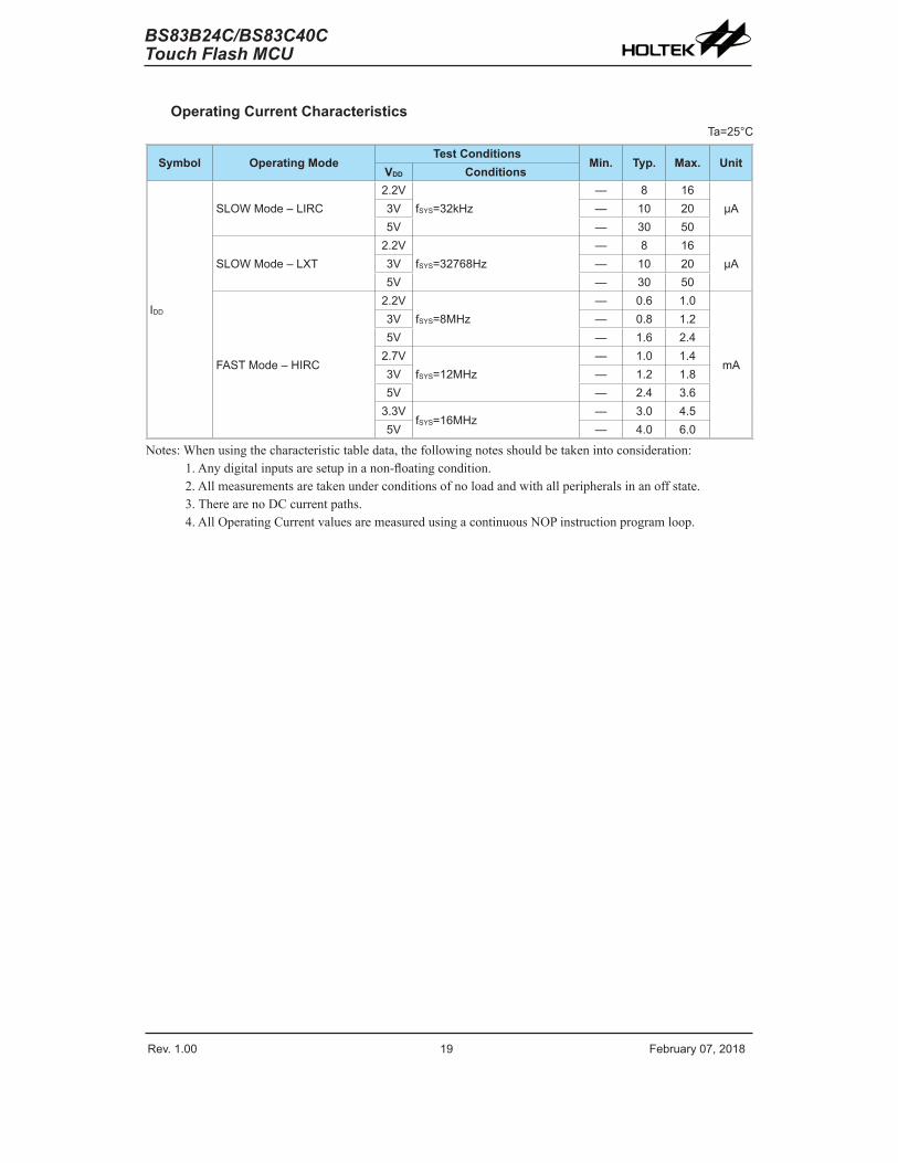
Operating Current CharacteristicsTa=�5°C
Symbol Operating ModeTest Conditions
Min. Typ. Max. UnitVDD Conditions
IDD
SLOW Mode – LIRC�.�V
fSYS=3�kHz— � 16
μA3V — 10 �05V — 30 50
SLOW Mode – LXT�.�V
fSYS=3��6�Hz— � 16
μA3V — 10 �05V — 30 50
�AST Mode – HIRC
�.�VfSYS=�MHz
— 0.6 1.0
mA
3V — 0.� 1.�5V — 1.6 �.4
�.�VfSYS=1�MHz
— 1.0 1.43V — 1.� 1.�5V — �.4 3.6
3.3VfSYS=16MHz
— 3.0 4.55V — 4.0 6.0
Notes:Whenusingthecharacteristictabledata,thefollowingnotesshouldbetakenintoconsideration:1.Anydigitalinputsaresetupinanon-floatingcondition.2.Allmeasurementsaretakenunderconditionsofnoloadandwithallperipheralsinanoffstate.3.TherearenoDCcurrentpaths.4.AllOperatingCurrentvaluesaremeasuredusingacontinuousNOPinstructionprogramloop.

Rev. 1.00 �0 �e���a�� 0�� �01� Rev. 1.00 �1 �e���a�� 0�� �01�
BS83B24C/BS83C40CTouch Flash MCU
BS83B24C/BS83C40CTouch Flash MCU
A.C. CharacteristicsFordatainthefollowingtables,notethatfactorssuchasoscillatortype,operatingvoltage,operatingfrequencyandtemperatureetc.,canallexertaninfluenceonthemeasuredvalues.
High Speed Internal Oscillator – HIRC – Frequency AccuracyDuringtheprogramwritingoperationthewriterwill trimtheHIRCoscillatoratauserselectedHIRCfrequencyanduserselectedvoltageofeither3Vor5V.
8/12/16MHz
Symbol ParameterTest Conditions
Min. Typ. Max. UnitVDD Temp.
fHIRC
�MHz w�ite� t�immed HIRC f�eq�enc�
3V/5V�5°C -1% � +1%
MHz-40°C ~ �5°C -�% � +�%
�.�V~5.5V�5°C -�.5% � +�.5%-40°C ~ �5°C -3% � +3%
1�MHz w�ite� t�immed HIRC f�eq�enc�
3V/5V�5°C -1% 1� +1%
MHz-40°C ~ �5°C -�% 1� +�%
�.�V~5.5V�5°C -�.5% 1� +�.5%-40°C ~ �5°C -3% 1� +3%
16MHz w�ite� t�immed HIRC f�eq�enc�
5V�5°C -1% 16 +1%
MHz-40°C ~ �5°C -�% 16 +�%
3.3V~5.5V�5°C -�.5% 16 +�.5%-40°C ~ �5°C -3% 16 +3%
Notes:1.The3V/5VvaluesforVDDareprovidedasthesearethetwoselectablefixedvoltagesatwhichtheHIRCfrequencyistrimmedbythewriter.
2.Therowbelowthe3V/5Vtrimvoltagerowisprovided toshowthevalues for the fullVDD rangeoperatingvoltage.Itisrecommendedthatthetrimvoltageisfixedat3Vforapplicationvoltagerangesfrom2.2Vto3.6Vandfixedat5Vforapplicationvoltagerangesfrom3.3Vto5.5V.
3.Theminimumandmaximumtolerancevaluesprovidedinthetableareonlyforthefrequencyatwhichthewriter trimstheHIRCoscillator.After trimmingat thischosenspecificfrequencyanychangeinHIRCoscillatorfrequencyusingtheoscillatorregistercontrolbitsbytheapplicationprogramwillgiveafrequencytolerancetowithin±20%.
Low Speed Internal Oscillator Characteristics – LIRCTa=�5°C, unless otherwise specified
Symbol ParameterTest Conditions
Min. Typ. Max. UnitVDD Temp.
fLIRC LIRC ��eq�enc� �.�V~5.5V�5°C -10% 3� +10%
kHz-40°C~�5°C -50% 3� +60%
tSTART LIRC Sta�t Up Time — — — — 500 μs
Low Speed Crystal Oscillator Characteristics – LXTTa=�5°C
Symbol ParameterTest Conditions
Min. Typ. Max. UnitVDD Temp.
fLXT Oscillato� ��eq�enc� �.�V~5.5V -40°C~�5°C — 3��6� — HztSTART Sta�t-�p Time 3V/5V — — — 500 msD�t� C�cle D�t� C�cle — — 45 50 55 %RNEG Negative Resistance �.�V — 3×ESR — — Ω
Note:C1,C2andRPareexternalcomponents.C1=C2=10pF,RP=RU=10MΩ,CL=7pF,ESR=30kΩ.

Rev. 1.00 �0 �e���a�� 0�� �01� Rev. 1.00 �1 �e���a�� 0�� �01�
BS83B24C/BS83C40CTouch Flash MCU
BS83B24C/BS83C40CTouch Flash MCU
Operating Frequency Characteristic Curves
System Operating Frequency
Operating Voltage
�MHz
�.�V 5.5V
~~
1�MHz
�.�V 3.3V
~~
16MHz
System Start Up Time CharacteristicsTa=-40°C~�5°C
Symbol ParameterTest Conditions
Min. Typ. Max. UnitVDD Conditions
tSST
S�stem Sta�t-�p TimeWake-�p f�om Condition whe�e fSYS is Off
— fSYS=fH ~ fH/64� fH=fHIRC — 16 — tHIRC
— fSYS=fSUB=fLXT — 10�4 — tLXT
— fSYS=fSUB=fLIRC — � — tLIRC
S�stem Sta�t-�p TimeWake-�p f�om Condition whe�e fSYS is On
— fSYS=fH ~ fH/64� fH=fHIRC — � — tH— fSYS=fSUB=fLXT o� fLIRC — � — tSUB
S�stem Speed Switch Time�AST to SLOW Mode o�SLOW to �AST Mode
— fHIRC switches from off → on — 16 — tHIRC
— fLXT switches from off → on — 10�4 — tLXT
tRSTD
S�stem Reset Dela� TimeReset So��ce f�om Powe�-on Reset o� LVR Ha�dwa�e Reset
— RRPOR=5V/ms4� 4� 54 ms
S�stem Reset Dela� TimeLVRC/WDTC/RSTC Softwa�e Reset — —
S�stem Reset Dela� TimeReset Source from WDT Overflow — — 14 16 1� ms
tSRESETMinim�m Softwa�e Reset P�lse Width to Reset — — 45 90 1�0 μs
Notes:1.For theSystemStart-up timevalues,whetherfSYS isonoroffdependsuponthemodetypeandthechosenfSYSsystemoscillator.DetailsareprovidedintheSystemOperatingModessection.
2.Thetimeunits,shownbythesymbolstHIRC.aretheinverseofthecorrespondingfrequencyvaluesasprovidedinthefrequencytables.ForexampletHIRC=1/fHIRC,tSYS=1/fSYSetc.
3.IftheLIRCisusedasthesystemclockandifit isoffwhenintheSLEEPmode,whenanadditionalLIRCstartuptime,tSTART,asprovidedintheLIRCfrequencytable,mustbeaddedtothetSSTtimeinthetableabove.
4.TheSystemSpeedSwitchTimeiseffectivelythetimetakenforthenewlyactivatedoscillatortostartup.

Rev. 1.00 �� �e���a�� 0�� �01� Rev. 1.00 �3 �e���a�� 0�� �01�
BS83B24C/BS83C40CTouch Flash MCU
BS83B24C/BS83C40CTouch Flash MCU
Input/Output CharacteristicsTa=�5°C
Symbol ParameterTest Conditions
Min. Typ. Max. UnitVDD Conditions
VIL Inp�t Low Voltage fo� I/O Po�ts5V — 0 — 1.5
V— — 0 — 0.�VDD
VIH Inp�t High Voltage fo� I/O Po�ts5V — 3.5 — 5
V— — 0.�VDD — VDD
IOH So��ce C���ent fo� I/O Pins
3VVOH=0.9VDD�SLEDCn[m+1� m]=00B(n=0�1...; m=0 o� � o� 4 o� 6)
-0.� -1.5 —
mA
5VVOH=0.9VDD�SLEDCn[m+1� m]=00B(n=0�1...; m=0 o� � o� 4 o� 6)
-1.5 -�.9 —
3VVOH=0.9VDD�SLEDCn[m+1� m]=01B(n=0�1...; m=0 o� � o� 4 o� 6)
-1.3 -�.5 —
5VVOH=0.9VDD�SLEDCn[m+1� m]=01B(n=0�1...; m=0 o� � o� 4 o� 6)
-�.5 -5.1 —
3VVOH=0.9VDD�SLEDCn[m+1� m]=10B(n=0�1...; m=0 o� � o� 4 o� 6)
-1.� -3.6 —
5VVOH=0.9VDD�SLEDCn[m+1� m]=10B(n=0�1...; m=0 o� � o� 4 o� 6)
-3.6 -�.3 —
3VVOH=0.9VDD�SLEDCn[m+1� m]=11B(n=0�1...; m=0 o� � o� 4 o� 6)
-4 -� —
5VVOH=0.9VDD�SLEDCn[m+1� m]=11B(n=0�1...; m=0 o� � o� 4 o� 6)
-� -16 —
IOL Sink C���ent fo� I/O Pins3V
VOL=0.1VDD16 3� —
mA5V 3� 65 —
RPHP�ll-high Resistance fo� I/O Po�tsNote
3V — �0 60 100kΩ
5V — 10 30 50ILEAK Inp�t Leakage C���ent 5V VIN=VDD o� VIN=VSS — — ±1 μA
tTPITM Capt��e Inp�t Pin Minim�m P�lse Width — — 0.3 — — μs
tTCKTM Clock Inp�t Pin Minim�m P�lse Width — — 0.3 — — μs
tINTExte�nal Inte���pt Minim�m P�lse Width — — 10 — — μs
Note:TheRPH internalpullhighresistancevalueiscalculatedbyconnectingtogroundandenablingtheinputpinwithapull-highresistorandthenmeasuringtheinputsinkcurrentatthespecifiedsupplyvoltagelevel.DividingthevoltagebythismeasuredcurrentprovidestheRPHvalue.

Rev. 1.00 �� �e���a�� 0�� �01� Rev. 1.00 �3 �e���a�� 0�� �01�
BS83B24C/BS83C40CTouch Flash MCU
BS83B24C/BS83C40CTouch Flash MCU
Memory CharacteristicsTa=-40°C~�5°C
Symbol ParameterTest Conditions
Min. Typ. Max. UnitVDD Conditions
VRW VDD fo� Read / W�ite — — VDDmin — VDDmax VFlash Program Memory / Data EEPROM Memory
tDEW
E�ase / W�ite C�cle Time – �lash P�og�am Memo�� — — — � 3
msW�ite C�cle Time – Data EEPROM Memo�� — — — 4 6
IDDPGM P�og�amming / E�ase C���ent on VDD — — — — 5.0 mAEP Cell End��ance — — 100K — — E/WtRETD ROM Data Retention Time — Ta=�5°C — 40 — Yea�RAM Data MemoryVDR RAM Data Retention Voltage — Device in SLEEP Mode 1.0 — — V
LVR Electrical CharacteristicsTa=-40°C~�5°C� �nless othe�wise specif�
Symbol ParameterTest Conditions
Min. Typ. Max. UnitVDD Conditions
VLVR Low Voltage Reset Voltage
— LVR ena�le� voltage select �.10V
- 5%
�.10
+ 5% V— LVR ena�le� voltage select �.55V �.55— LVR ena�le� voltage select 3.15V 3.15— LVR ena�le� voltage select 3.�0V 3.�0
ILVRBG Ope�ating C���ent
3VLVR ena�le� VBGEN=0
— — 1�
μA5V — �0 �53V
LVR ena�le� VBGEN=1— — 150
5V — 1�0 �00tLVR Minim�m Low Voltage Width to Reset — — 1�0 �40 4�0 μsILVR Additional C���ent fo� LVR Ena�le — VBGEN=0 — — �4 μA
Power-on Reset CharacteristicsTa=�5°C
Symbol ParameterTest Conditions
Min. Typ. Max. UnitVDD Conditions
VPOR VDD Sta�t Voltage to Ens��e Powe�-on Reset — — — — 100 mVRRPOR VDD Rising Rate to Ens��e Powe�-on Reset — — 0.035 — — V/ms
tPORMinim�m Time fo� VDD Sta�s at VPOR to Ens��e Powe�-on Reset — — 1 — — ms
VDD
tPOR RRPOR
VPOR
Time

Rev. 1.00 �4 �e���a�� 0�� �01� Rev. 1.00 �5 �e���a�� 0�� �01�
BS83B24C/BS83C40CTouch Flash MCU
BS83B24C/BS83C40CTouch Flash MCU
System ArchitectureAkeyfactorinthehigh-performancefeaturesoftheHoltekrangeofmicrocontrollersisattributedtotheirinternalsystemarchitecture.TheseriesofdevicestakeadvantageoftheusualfeaturesfoundwithinRISCmicrocontrollersprovidingincreasedspeedofoperationandenhancedperformance.Thepipeliningscheme is implemented insuchaway that instruction fetchingand instructionexecutionareoverlapped,henceinstructionsareeffectivelyexecutedinoneortwocyclesformostof thestandardorextended instructions respectively.Theexceptions to thisarebranchorcallinstructionswhichneedonemorecycle.An8-bitwideALUisusedinpracticallyallinstructionsetoperations,whichcarriesoutarithmeticoperations,logicoperations,rotation,increment,decrement,branchdecisions,etc.TheinternaldatapathissimplifiedbymovingdatathroughtheAccumulatorandtheALU.CertaininternalregistersareimplementedintheDataMemoryandcanbedirectlyor indirectlyaddressed.Thesimpleaddressingmethodsof theseregistersalongwithadditionalarchitectural featuresensure thataminimumofexternalcomponents is required toprovideafunctionalI/Ocontrolsystemwithmaximumreliabilityandflexibility.Thismakes thedevicessuitableforlow-cost,high-volumeproductionforcontrollerapplications.
Clocking and PipeliningThemainsystemclock,derivedfromeitheranLIRC,LXTorHIRCoscillatorissubdividedintofourinternallygeneratednon-overlappingclocks,T1~T4.TheProgramCounterisincrementedatthebeginningoftheT1clockduringwhichtimeanewinstructionisfetched.TheremainingT2~T4clockscarryoutthedecodingandexecutionfunctions.Inthisway,oneT1~T4clockcycleformsoneinstructioncycle.Althoughthefetchingandexecutionofinstructionstakesplaceinconsecutiveinstructioncycles, thepipeliningstructureof themicrocontrollerensures that instructionsareeffectivelyexecuted inone instructioncycle.Theexception to thisare instructionswhere thecontentsoftheProgramCounterarechanged,suchassubroutinecallsorjumps,inwhichcasetheinstructionwilltakeonemoreinstructioncycletoexecute.
For instructions involvingbranches,suchas jumporcall instructions, twomachinecyclesarerequired tocomplete instructionexecution.Anextracycle is requiredas theprogramtakesonecycletofirstobtaintheactualjumporcalladdressandthenanothercycletoactuallyexecutethebranch.Therequirementforthisextracycleshouldbetakenintoaccountbyprogrammersintimingsensitiveapplications.
�etch Inst. (PC)
(S�stem Clock)fSYS
Phase Clock T1
Phase Clock T�
Phase Clock T3
Phase Clock T4
P�og�am Co�nte� PC PC+1 PC+�
PipeliningExec�te Inst. (PC-1) �etch Inst. (PC+1)
Exec�te Inst. (PC) �etch Inst. (PC+�)
Exec�te Inst. (PC+1)
System Clocking and Pipelining

Rev. 1.00 �4 �e���a�� 0�� �01� Rev. 1.00 �5 �e���a�� 0�� �01�
BS83B24C/BS83C40CTouch Flash MCU
BS83B24C/BS83C40CTouch Flash MCU
�etch Inst. 11 MOV A�[1�H]� CALL DELAY3 CPL [1�H]4 :5 :6 DELAY: NOP
Exec�te Inst. 1 �etch Inst. � Exec�te Inst. �
�etch Inst. 3 �l�sh Pipeline�etch Inst. 6 Exec�te Inst. 6
�etch Inst. �
Instruction Fetching
Program CounterDuringprogramexecution, theProgramCounter isused tokeep trackof theaddressof thenext instruction tobeexecuted. It isautomatically incrementedbyoneeach timean instructionisexecutedexcept for instructions, suchas“JMP”or“CALL” thatdemandsa jump toanon-consecutiveProgramMemoryaddress.Onlythelower8bits,knownastheProgramCounterLowRegister,aredirectlyaddressablebytheapplicationprogram.
Whenexecuting instructions requiring jumps tonon-consecutiveaddresses suchas a jumpinstruction,asubroutinecall, interruptorreset,etc., themicrocontrollermanagesprogramcontrolbyloadingtherequiredaddressintotheProgramCounter.Forconditionalskipinstructions,oncetheconditionhasbeenmet,thenextinstruction,whichhasalreadybeenfetchedduringthepresentinstructionexecution,isdiscardedandadummycycletakesitsplacewhilethecorrectinstructionisobtained.
DeviceProgram Counter
High Byte PCL RegisterBS�3B�4C PC11~PC� PCL�~PCL0BS�3C40C PC11~PC� PCL�~PCL0
Program Counter
Thelowerbyteof theProgramCounter,knownastheProgramCounterLowregisterorPCL,isavailableforprogramcontrolandisareadableandwriteableregister.Bytransferringdatadirectlyintothisregister,ashortprogramjumpcanbeexecuteddirectly.However,asonlythis lowbyteisavailableformanipulation, the jumpsare limited to thepresentpageofmemory, that is256locations.Whensuchprogramjumpsareexecuted itshouldalsobenoted thatadummycyclewillbeinserted.ManipulatingthePCLregistermaycauseprogrambranching,soanextracycleisneededtopre-fetch.
StackThisisaspecialpartofthememorywhichisusedtosavethecontentsoftheProgramCounteronly.Thestackisorganisedinto6levelsandisneitherpartofthedatanorpartoftheprogramspace,andisneitherreadablenorwriteable.Theactivatedlevel is indexedbytheStackPointer,andisneitherreadablenorwriteable.Atasubroutinecallorinterruptacknowledgesignal,thecontentsoftheProgramCounterarepushedontothestack.Attheendofasubroutineoraninterruptroutine,signaledbyareturninstruction,RETorRETI,theProgramCounterisrestoredtoitspreviousvaluefromthestack.Afteradevicereset,theStackPointerwillpointtothetopofthestack.
If thestackisfullandanenabledinterrupttakesplace,theinterruptrequestflagwillberecordedbuttheacknowledgesignalwillbeinhibited.WhentheStackPointer isdecremented,byRETorRETI,theinterruptwillbeserviced.Thisfeaturepreventsstackoverflowallowingtheprogrammertousethestructuremoreeasily.However,whenthestackisfull,aCALLsubroutineinstructioncanstillbeexecutedwhichwillresult inastackoverflow.Precautionsshouldbetakentoavoidsuchcaseswhichmightcauseunpredictableprogrambranching.Ifthestackisoverflow,thefirstProgramCountersaveinthestackwillbelost.

Rev. 1.00 �6 �e���a�� 0�� �01� Rev. 1.00 �� �e���a�� 0�� �01�
BS83B24C/BS83C40CTouch Flash MCU
BS83B24C/BS83C40CTouch Flash MCU
Stack Pointe�
Stack Level �
Stack Level 1
Stack Level 3:::
Stack Level 6
P�og�am Memo��
P�og�am Co�nte�
Bottom of Stack
Top of Stack
Arithmetic and Logic Unit – ALUThearithmetic-logicunitorALUisacriticalareaofthemicrocontrollerthatcarriesoutarithmeticandlogicoperationsoftheinstructionset.Connectedtothemainmicrocontrollerdatabus,theALUreceivesrelatedinstructioncodesandperformstherequiredarithmeticor logicaloperationsafterwhichtheresultwillbeplacedinthespecifiedregister.AstheseALUcalculationoroperationsmayresultincarry,borroworotherstatuschanges,thestatusregisterwillbecorrespondinglyupdatedtoreflectthesechanges.TheALUsupportsthefollowingfunctions:
• Arithmeticoperations:ADD,ADDM,ADC,ADCM,SUB,SUBM,SBC,SBCM,DAA,LADD,LADDM,LADC,LADCM,LSUB,LSUBM,LSBC,LSBCM,LDAA
• Logicoperations:AND,OR,XOR,ANDM,ORM,XORM,CPL,CPLA,LAND,LANDM,LOR,LORM,LXOR,LXORM,LCPL,LCPLA
• Rotation:RRA,RR,RRCA,RRC,RLA,RL,RLCA,RLC,LRR,LRRA,LRRCA,LRRC,LRLA,LRL,LRLCA,LRLC
• IncrementandDecrement:INCA,INC,DECA,DEC,LINCA,LINC,LDECA,LDEC
• Branchdecision:JMP,SZ,SZA,SNZ,SIZ,SDZ,SIZA,SDZA,CALL,RET,RETI,LSNZ,LSZ,LSZA,LSIZ,LSIZA,LSDZ,LSDZA
Rev. 1.00 �6 �e���a�� 0�� �01� Rev. 1.00 �� �e���a�� 0�� �01�
BS83B24C/BS83C40CTouch Flash MCU
BS83B24C/BS83C40CTouch Flash MCU
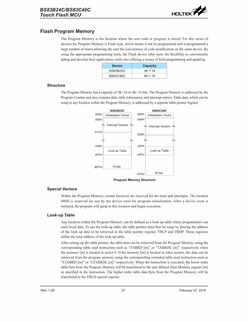
Flash Program MemoryTheProgramMemory is the locationwhere theusercodeorprogramisstored.For thisseriesofdevicestheProgramMemoryisFlashtype,whichmeansitcanbeprogrammedandre-programmedalargenumberoftimes,allowingtheusertheconvenienceofcodemodificationonthesamedevice.Byusingtheappropriateprogrammingtools,theFlashdeviceofferuserstheflexibilitytoconvenientlydebuganddeveloptheirapplicationswhilealsoofferingameansoffieldprogrammingandupdating.
Device CapacityBS�3B�4C 3K × 16BS�3C40C 4K × 16
StructureTheProgramMemoryhasacapacityof3K×16or4K×16bits.TheProgramMemoryisaddressedbytheProgramCounterandalsocontainsdata,tableinformationandinterruptentries.Tabledata,whichcanbesetupinanylocationwithintheProgramMemory,isaddressedbyaseparatetablepointerregister.
Look-�p Ta�le
Initialisation Vecto�000H
004H
01CH
B��H
Inte���pt Vecto�s
16 �its
n00H
n��H
BS83B24C
Look-�p Ta�le
Initialisation Vecto�000H
004H
0�0H
���H
Inte���pt Vecto�s
16 �its
n00H
n��H
BS83C40C
Program Memory Structure
Special VectorsWithintheProgramMemory,certainlocationsarereservedfortheresetandinterrupts.Thelocation000His reserved foruseby thedevice reset forprograminitialisation.Afteradevice reset isinitiated,theprogramwilljumptothislocationandbeginexecution.
Look-up Table AnylocationwithintheProgramMemorycanbedefinedasalook-uptablewhereprogrammerscanstorefixeddata.Tousethelook-uptable,thetablepointermustfirstbesetupbyplacingtheaddressof thelookupdatatoberetrievedinthetablepointerregister,TBLPandTBHP.Theseregistersdefinethetotaladdressofthelook-uptable.
Aftersettingupthetablepointer,thetabledatacanberetrievedfromtheProgramMemoryusingthecorrespondingtablereadinstructionsuchas“TABRD[m]”or“TABRDL[m]”respectivelywhenthememory[m]islocatedinsector0.Ifthememory[m]islocatedinothersectors,thedatacanberetrievedfromtheprogrammemoryusingthecorrespondingextendedtablereadinstructionsuchas“LTABRD[m]”or“LTABRDL[m]”respectively.Whentheinstructionisexecuted,thelowerordertablebytefromtheProgramMemorywillbetransferredtotheuserdefinedDataMemoryregister[m]asspecifiedintheinstruction.ThehigherordertabledatabytefromtheProgramMemorywillbetransferredtotheTBLHspecialregister.
Rev. 1.00 �� �e���a�� 0�� �01� Rev. 1.00 �9 �e���a�� 0�� �01�
BS83B24C/BS83C40CTouch Flash MCU
BS83B24C/BS83C40CTouch Flash MCU
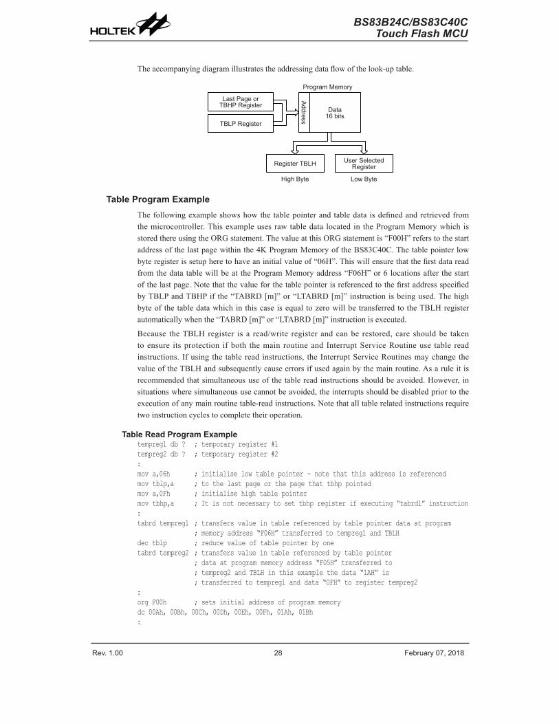
Theaccompanyingdiagramillustratestheaddressingdataflowofthelook-uptable.
Last Page o�TBHP Registe�
Add�ess
TBLP Registe�
Data16 �its
P�og�am Memo��
Registe� TBLH Use� Selected Registe�
High B�te Low B�te
Table Program ExampleThefollowingexampleshowshowthetablepointerandtabledataisdefinedandretrievedfromthemicrocontroller.Thisexampleusesrawtabledata located in theProgramMemorywhich isstoredthereusingtheORGstatement.ThevalueatthisORGstatementis“F00H”referstothestartaddressofthelastpagewithinthe4KProgramMemoryoftheBS83C40C.Thetablepointerlowbyteregisterissetupheretohaveaninitialvalueof“06H”.Thiswillensurethatthefirstdatareadfromthedatatablewillbeat theProgramMemoryaddress“F06H”or6locationsafter thestartofthelastpage.NotethatthevalueforthetablepointerisreferencedtothefirstaddressspecifiedbyTBLPandTBHPif the“TABRD[m]”or“LTABRD[m]”instructionisbeingused.ThehighbyteofthetabledatawhichinthiscaseisequaltozerowillbetransferredtotheTBLHregisterautomaticallywhenthe“TABRD[m]”or“LTABRD[m]”instructionisexecuted.
Because theTBLHregister isa read/write registerandcanbe restored,care shouldbe takentoensure itsprotection ifboth themain routineand InterruptServiceRoutineuse table readinstructions. Ifusing the tableread instructions, theInterruptServiceRoutinesmaychange thevalueoftheTBLHandsubsequentlycauseerrorsifusedagainbythemainroutine.Asaruleitisrecommendedthatsimultaneoususeofthetablereadinstructionsshouldbeavoided.However, insituationswheresimultaneoususecannotbeavoided,theinterruptsshouldbedisabledpriortotheexecutionofanymainroutinetable-readinstructions.Notethatalltablerelatedinstructionsrequiretwoinstructioncyclestocompletetheiroperation.
Table Read Program Exampletempreg1 db ? ; temporary register #1tempreg2 db ? ; temporary register #2:mov a,06h ; initialise low table pointer - note that this address is referencedmov tblp,a ; to the last page or the page that tbhp pointedmov a,0Fh ; initialise high table pointermov tbhp,a ; It is not necessary to set tbhp register if executing “tabrdl” instruction:tabrd tempreg1 ; transfers value in table referenced by table pointer data at program ; memory address “F06H” transferred to tempreg1 and TBLHdec tblp ; reduce value of table pointer by onetabrd tempreg2 ; transfers value in table referenced by table pointer ; data at program memory address “F05H” transferred to ; tempreg2 and TBLH in this example the data “1AH” is ; transferred to tempreg1 and data “0FH” to register tempreg2:org F00h ; sets initial address of program memorydc 00Ah, 00Bh, 00Ch, 00Dh, 00Eh, 00Fh, 01Ah, 01Bh:
Rev. 1.00 �� �e���a�� 0�� �01� Rev. 1.00 �9 �e���a�� 0�� �01�
BS83B24C/BS83C40CTouch Flash MCU
BS83B24C/BS83C40CTouch Flash MCU
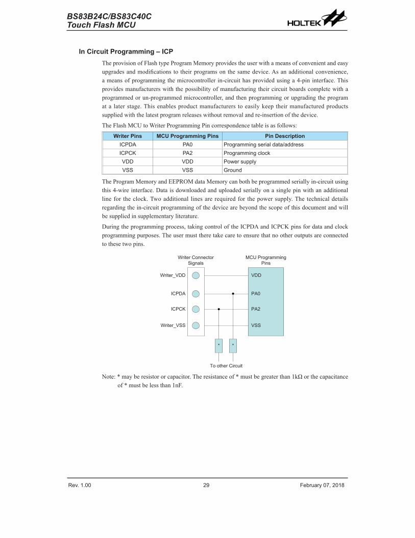
In Circuit Programming – ICPTheprovisionofFlashtypeProgramMemoryprovidestheuserwithameansofconvenientandeasyupgradesandmodificationstotheirprogramsonthesamedevice.Asanadditionalconvenience,ameansofprogrammingthemicrocontrollerin-circuithasprovidedusinga4-pininterface.Thisprovidesmanufacturerswiththepossibilityofmanufacturingtheircircuitboardscompletewithaprogrammedorun-programmedmicrocontroller,andthenprogrammingorupgradingtheprogramata laterstage.Thisenablesproductmanufacturers toeasilykeep theirmanufacturedproductssuppliedwiththelatestprogramreleaseswithoutremovalandre-insertionofthedevice.
TheFlashMCUtoWriterProgrammingPincorrespondencetableisasfollows:
Writer Pins MCU Programming Pins Pin DescriptionICPDA PA0 P�og�amming se�ial data/add�essICPCK PA� P�og�amming clockVDD VDD Powe� s�ppl�VSS VSS G�o�nd
TheProgramMemoryandEEPROMdataMemorycanbothbeprogrammedseriallyin-circuitusingthis4-wireinterface.Dataisdownloadedanduploadedseriallyonasinglepinwithanadditionallinefor theclock.Twoadditional linesarerequiredfor thepowersupply.The technicaldetailsregardingthein-circuitprogrammingofthedevicearebeyondthescopeofthisdocumentandwillbesuppliedinsupplementaryliterature.
Duringtheprogrammingprocess,takingcontroloftheICPDAandICPCKpinsfordataandclockprogrammingpurposes.Theusermusttheretakecaretoensurethatnootheroutputsareconnectedtothesetwopins.
*
W�ite�_VDD
ICPDA
ICPCK
W�ite�_VSS
To othe� Ci�c�it
VDD
PA0
PA�
VSS
W�ite� Connecto� Signals
MCU P�og�ammingPins
*
Note:*mayberesistororcapacitor.Theresistanceof*mustbegreaterthan1kΩorthecapacitanceof*mustbelessthan1nF.

Rev. 1.00 30 �e���a�� 0�� �01� Rev. 1.00 31 �e���a�� 0�� �01�
BS83B24C/BS83C40CTouch Flash MCU
BS83B24C/BS83C40CTouch Flash MCU
On-Chip Debug Support – OCDSThereareEVchipsnamedBS83BV24CandBS83CV40CwhichareusedtoemulatetherealMCUdevicesnamedBS83B24CandBS83C40Crespectively.TheEVchipdevicealsoprovidesan“On-ChipDebug”functiontodebugthedeviceduringthedevelopmentprocess.TheEVchipandtheactualMCUdevicearealmostfunctionallycompatibleexceptforthe“On-ChipDebug”function.Userscanuse theEVchipdevice toemulate the realchipdevicebehaviorbyconnecting theOCDSDAandOCDSCKpinstotheHT-IDEdevelopmenttools.TheOCDSDApinis theOCDSData/Addressinput/outputpinwhiletheOCDSCKpinistheOCDSclockinputpin.WhenusersusetheEVchipfordebugging,otherfunctionswhicharesharedwiththeOCDSDAandOCDSCKpinsintheactualMCUdevicewillhavenoeffectintheEVchip.However,thetwoOCDSpinswhicharepin-sharedwiththeICPprogrammingpinsarestillusedastheFlashMemoryprogrammingpinsforICP.ForamoredetailedOCDSdescription,refertothecorrespondingdocument.
e-Link Pins EV Chip Pins Pin DescriptionOCDSDA OCDSDA On-chip de��g s�ppo�t data/add�ess inp�t/o�tp�tOCDSCK OCDSCK On-chip de��g s�ppo�t clock inp�t
VDD VDD Powe� s�ppl�VSS VSS G�o�nd

Rev. 1.00 30 �e���a�� 0�� �01� Rev. 1.00 31 �e���a�� 0�� �01�
BS83B24C/BS83C40CTouch Flash MCU
BS83B24C/BS83C40CTouch Flash MCU
Data MemoryTheDataMemoryisavolatileareaof8-bitwideRAMinternalmemoryandisthelocationwheretemporaryinformationisstored.
StructureCategorizedintotwotypes,thefirstoftheseisanareaofRAMwherespecialfunctionregistersarelocated.Theseregistershavefixedlocationsandarenecessaryforcorrectoperationofthedevice.Manyoftheseregisterscanbereadfromandwrittentodirectlyunderprogramcontrol,however,someremainprotectedfromusermanipulation.ThesecondareaofDataMemoryisreservedforgeneralpurposeuse.All locationswithin thisareaarereadandwriteaccessibleunderprogramcontrol.ThereisanotherareareservedfortheTouchKeyDataMemory.
TheoverallDataMemoryissubdividedintoseveralsectors,allofwhichareimplementedin8-bitwideMemory.EachoftheDataMemorysectorsiscategorizedintotwotypes,theSpecialPurposeDataMemoryandtheGeneralPurposeDataMemory.Theaddressrangeof theSpecialPurposeDataMemoryforthedeviceisfrom00Hto7FHwhiletheGeneralPurposeDataMemoryaddressrange is from80HtoFFH.TheTouchKeyDataMemory is located inSector5andSector6.SwitchingbetweenthedifferentDataMemorysectorsisachievedbyproperlysettingtheMemoryPointers tocorrectvalue ifusing the indirectaddressingmethod.Thestartaddressof theDataMemoryforalldevicesistheaddress00H.
DeviceSpecial Purpose
Data MemoryGeneral Purpose
Data MemoryTouch Key
Data MemoryAvailable Sectors Capacity Sector: Address Capacity Sector: Address
BS�3B�4C 0� 1 51��
0: �0H~��H1: �0H~��H�: �0H~��H3: �0H~��H
96� 5: 00H~��H6: 00H~��H
BS�3C40C 0� 1 �6��
0: �0H~��H1: �0H~��H
:5: �0H~��H
160� 5: 00H~4�H6: 00H~4�H
Data Memory Summary
00H
�0H
��H
Special P��pose Data Memo��
(Secto� 0 ~ Secto� 1)
Gene�al P��pose Data Memo��
(Secto� 0 ~ Secto� 3)
Secto� 0Secto� 1
��H
Secto� 3
40H
��H
To�ch Ke�Data Memo��
(Secto� 5 ~ Secto� 6)
Secto� �
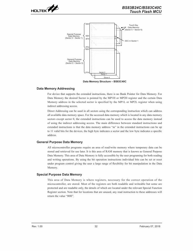
EEC in Secto� 1
Data Memory Structure – BS83B24C
Rev. 1.00 3� �e���a�� 0�� �01� Rev. 1.00 33 �e���a�� 0�� �01�
BS83B24C/BS83C40CTouch Flash MCU
BS83B24C/BS83C40CTouch Flash MCU
00H
�0H
��H
Special P��pose Data Memo��
(Secto� 0 ~ Secto� 1)
Gene�al P��pose Data Memo��
(Secto� 0 ~ Secto� 5)
Secto� 0Secto� 1
��H
Secto� 5
40H4�H
To�ch Ke�Data Memo��
(Secto� 5 ~ Secto� 6)
EEC in Secto� 1
Data Memory Structure – BS83C40C
Data Memory AddressingFordevicethatsupportstheextendedinstructions,thereisnoBankPointerforDataMemory.ForDataMemorythedesiredSector ispointedbytheMP1HorMP2HregisterandthecertainDataMemoryaddress in theselectedsector isspecifiedby theMP1LorMP2Lregisterwhenusingindirectaddressingaccess.
DirectAddressingcanbeusedinallsectorsusingthecorrespondinginstructionwhichcanaddressallavailabledatamemoryspace.Fortheaccesseddatamemorywhichislocatedinanydatamemorysectorsexceptsector0, theextendedinstructionscanbeusedtoaccess thedatamemoryinsteadofusing the indirectaddressingaccess.Themaindifferencebetweenstandard instructionsandextendedinstructionsisthatthedatamemoryaddress“m”intheextendedinstructionscanbeupto11validbitsforthedevices,thehighbyteindicatesasectorandthelowbyteindicatesaspecificaddress.
General Purpose Data MemoryAllmicrocontrollerprogramsrequireanareaofread/writememorywheretemporarydatacanbestoredandretrievedforuselater.ItisthisareaofRAMmemorythatisknownasGeneralPurposeDataMemory.ThisareaofDataMemoryisfullyaccessiblebytheuserprogramingforbothreadingandwritingoperations.Byusingthebitoperationinstructions individualbitscanbesetorresetunderprogramcontrolgivingtheuseralargerangeofflexibilityforbitmanipulationintheDataMemory.
Special Purpose Data MemoryThis area ofDataMemory iswhere registers, necessary for the correct operation of themicrocontroller,arestored.Mostof theregistersarebothreadableandwriteablebutsomeareprotectedandarereadableonly,thedetailsofwhicharelocatedundertherelevantSpecialFunctionRegistersection.Notethatforlocationsthatareunused,anyreadinstructiontotheseaddresseswillreturnthevalue“00H”.
Rev. 1.00 3� �e���a�� 0�� �01� Rev. 1.00 33 �e���a�� 0�� �01�
BS83B24C/BS83C40CTouch Flash MCU
BS83B24C/BS83C40CTouch Flash MCU
00H IAR001H MP00�H IAR103H MP1L04H05H ACC06H PCL0�H TBLP0�H TBLH09H TBHP0AH STATUS0BH0CH0DH0EH0�H10H INTEG11H1�H
19H
PAPU
1�HPAWU
1BH1AH
1DH1CH
1�H
PAPAC
13H14H15H16H1�H
: Un�sed� �ead as 00H
�0H�1H��H
�9H��H
�BH�AH
�DH�CH
��H�EH
�3H�4H�5H�6H��H
EEA40H41H4�H43H44H45H46H4�H4�H49H4AH4BH4CH4DH4EH4�H50H51H5�H53H54H
1EH
EECSecto� 0 Secto� 0 Secto� 1
55H56H
60H61H6�H63H64H65H66H6�H6�H69H6AH6BH
6�H�0H30H
31H3�H
3�H
3CH
33H34H35H36H3�H
3BH
39H3AH
�1H��H�3H�4H�5H�6H
�BH
I�SWDTC
3DH
3�H3EH
��H
MP1H
IAR�MP�LMP�H
TB1CPSCR
TB0C
5�H5�H59H5AH5BH5CH5DH5EH5�H
Secto� 1
RST�C
INTC0INTC1
��H��H�9H�AH
VBGC
�CH�DH�EH
PTMAH
PTMRPH
SIMC�/SIMA/UUCR�SIMD/UTXR_RXR
6EH6DH6CH
RSTC
PTMC0PTMC1
SIMC0
PTMDLPTMDHPTMAL
SIMC1/UUCR1
M�I0
PCPCC
HIRCCLXTC
EED
SIMTOC/UBRGUUSR
PAS0PAS1PBS0PBS1
PCS1PDS0
PCS0
LVRC
PBPBC
PBPU
PCPUSCC
PDPDC
SLEDC1
PDPUSLEDC0
TKC1
TKM0C1TKM0C�
TKM0ROHTKM0C0
TKM116DHTKM1ROL
TKTMRTKC0
TK16DL
TKM1C0TKM1C1
TKM1ROH
TK16DH
TKM016DLTKM016DH
TKM1C�
TKM116DL
TKM0ROL
TKM�C1TKM�C�
TKM�ROHTKM�C0
TKM316DHTKM3ROL
TKM3C0TKM3C1
TKM3ROH
TKM�16DLTKM�16DH
TKM3C�
TKM316DL
TKM�ROL
TKM4C1TKM4C�
TKM4ROHTKM4C0
TKM516DHTKM5ROL
TKM5C0TKM5C1
TKM5ROH
TKM416DLTKM416DH
TKM5C�
TKM516DL
TKM4ROL
PTMRPL
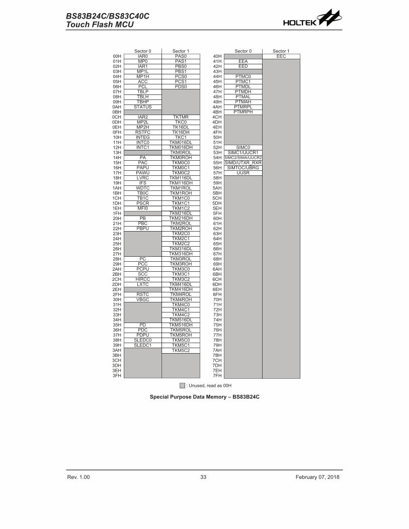
Special Purpose Data Memory – BS83B24C

Rev. 1.00 34 �e���a�� 0�� �01� Rev. 1.00 35 �e���a�� 0�� �01�
BS83B24C/BS83C40CTouch Flash MCU
BS83B24C/BS83C40CTouch Flash MCU
00H IAR001H MP00�H IAR103H MP1L04H05H ACC06H PCL0�H TBLP0�H TBLH09H TBHP0AH STATUS0BH0CH0DH0EH0�H10H INTEG11H1�H
19H
PAPU
1�HPAWU
1BH1AH
1DH1CH
1�H
PAPAC
13H14H15H16H1�H
: Un�sed� �ead as 00H
�0H�1H��H
�9H��H
�BH�AH
�DH�CH
��H�EH
�3H�4H�5H�6H��H
EEA40H41H4�H43H44H45H46H4�H4�H49H4AH4BH4CH4DH4EH4�H50H51H5�H53H54H
1EH
EECSecto� 0 Secto� 0 Secto� 1
55H56H
60H61H6�H63H64H65H66H6�H6�H69H6AH6BH
6�H�0H30H
31H3�H
3�H
3CH
33H34H35H36H3�H
3BH
39H3AH
�1H��H�3H�4H�5H�6H
�BH
I�SWDTC
3DH
3�H3EH
��H
MP1H
IAR�MP�LMP�H
TB1CPSCR
TB0C
5�H5�H59H5AH5BH5CH5DH5EH5�H
Secto� 1
RST�C
INTC0INTC1
��H��H�9H�AH
VBGC
�CH�DH�EH
PTMAH
PTMRPH
SIMC�/SIMA/UUCR�SIMD/UTXR_RXR
6EH6DH6CH
RSTC
PTMC0PTMC1
SIMC0
PTMDLPTMDHPTMAL
SIMC1/UUCR1
M�I0
PCPCC
HIRCCLXTC
EED
SIMTOC/UBRGUUSR
PAS0PAS1PBS0PBS1
PCS1PDS0
PCS0
LVRC
PBPBC
PBPU
PCPUSCC
PDPDC
SLEDC1
PDPUSLEDC0
TKC1
TKM0C1TKM0C�
TKM0ROHTKM0C0
TKM116DHTKM1ROL
TKTMRTKC0
TK16DL
TKM1C0TKM1C1
TKM1ROH
TK16DH
TKM016DLTKM016DH
TKM1C�
TKM116DL
TKM0ROL
TKM�C1TKM�C�
TKM�ROHTKM�C0
TKM316DHTKM3ROL
TKM3C0TKM3C1
TKM3ROH
TKM�16DLTKM�16DH
TKM3C�
TKM316DL
TKM�ROL
TKM4C1TKM4C�
TKM4ROHTKM4C0
TKM516DHTKM5ROL
TKM5C0TKM5C1
TKM5ROH
TKM416DLTKM416DH
TKM5C�
TKM516DL
TKM4ROL
PTMRPL
PDS1PES0PES1P�S0
INTC�
M�I1
SLEDC�CTMC0
CTMDHCTMAL
CTMC1CTMDL
TKM616DLTKM616DHTKM6ROL
TKM6C0TKM6C1
TKM6ROH
TKM�16DL
TKM916DLTKM916DH
TKM�C1TKM�C�
TKM9ROHTKM9C0
TKM�C0TKM�C1TKM�C�
TKM9C�TKM9C1
TKM�16DL
TKM�ROLTKM�ROH
TKM9ROL
TKM�C0
TKM6C�TKM�16DLTKM�16DHTKM�ROLTKM�ROH
P�
P�PU
PEPEC
PEPU
P�C
CTMAH
Special Purpose Data Memory – BS83C40C

Rev. 1.00 34 �e���a�� 0�� �01� Rev. 1.00 35 �e���a�� 0�� �01�
BS83B24C/BS83C40CTouch Flash MCU
BS83B24C/BS83C40CTouch Flash MCU
Special Function Register DescriptionMostoftheSpecialFunctionRegisterdetailswillbedescribedintherelevantfunctionalsections,howeverseveralregistersrequireaseparatedescriptioninthissection.
Indirect Addressing Registers – IAR0, IAR1, IAR2TheIndirectAddressingRegisters,IAR0,IAR1andIAR2,althoughhavingtheirlocationsinnormalRAMregisterspace,donotactuallyphysicallyexistasnormalregisters.Themethodof indirectaddressing forRAMdatamanipulationuses these IndirectAddressingRegistersandMemoryPointers, incontrast todirectmemoryaddressing,wheretheactualmemoryaddress isspecified.ActionsontheIAR0,IAR1andIAR2registerswillresult innoactualreadorwriteoperationtotheseregistersbutrathertothememorylocationspecifiedbytheircorrespondingMemoryPointers,MP0,MP1L/MP1HorMP2L/MP2H.Actingasapair,IAR0andMP0cantogetheraccessdataonlyfromSector0whiletheIAR1registertogetherwiththeMP1L/MP1HregisterpairandIAR2registertogetherwith theMP2L/MP2HregisterpaircanaccessdatafromanyDataMemorySector.AstheIndirectAddressingRegistersarenotphysicallyimplemented,readingtheIndirectAddressingRegisterswillreturnaresultof“00H”andwritingtotheregisterswillresultinnooperation.
Memory Pointers – MP0, MP1L, MP1H, MP2L, MP2HFiveMemoryPointers,knownasMP0,MP1L,MP1H,MP2L,MP2H,areprovided.TheseMemoryPointersarephysicallyimplementedintheDataMemoryandcanbemanipulatedinthesamewayasnormalregistersprovidingaconvenientwaywithwhichtoaddressandtrackdata.Whenanyoperationto therelevantIndirectAddressingRegisters iscarriedout, theactualaddress that themicrocontrollerisdirectedtoistheaddressspecifiedbytherelatedMemoryPointer.MP0,togetherwithIndirectAddressingRegister,IAR0,areusedtoaccessdatafromSector0,whileMP1L/MP1HtogetherwithIAR1andMP2L/MP2HtogetherwithIAR2areusedtoaccessdatafromallsectorsaccording to thecorrespondingMP1HorMP2Hregister.DirectAddressingcanbeused inallsectorsusingthecorrespondinginstructionwhichcanaddressallavailabledatamemoryspace.
ThefollowingexampleshowshowtoclearasectionoffourDataMemorylocationsalreadydefinedaslocationsadres1toadres4.
Indirect Addressing Program Example 1data .section ´data´adres1 db ?adres2 db ?adres3 db ?adres4 db ?block db ? code .section at 0 code´org 00hstart: mov a, 04h ; setup size of block mov block, a mova,offsetadres1;AccumulatorloadedwithfirstRAMaddress movmp0,a ;setupmemorypointerwithfirstRAMaddressloop: clrIAR0 ;clearthedataataddressdefinedbyMP0 inc mp0 ; increment memory pointer sdz block ; check if last memory location has been cleared jmp loopcontinue:

Rev. 1.00 36 �e���a�� 0�� �01� Rev. 1.00 3� �e���a�� 0�� �01�
BS83B24C/BS83C40CTouch Flash MCU
BS83B24C/BS83C40CTouch Flash MCU
Indirect Addressing Program Example 2data .section ´data´adres1 db ?adres2 db ?adres3 db ?adres4 db ?block db ? code .section at 0 code´org 00hstart: mov a, 04h ; setup size of block mov block, a mov a, 01h ; setup the memory sector mov mp1h, a mova,offsetadres1;AccumulatorloadedwithfirstRAMaddress movmp1l,a ;setupmemorypointerwithfirstRAMaddressloop: clrIAR1 ;clearthedataataddressdefinedbyMP1L incmp1l ;incrementmemorypointerMP1L sdz block ; check if last memory location has been cleared jmp loopcontinue:
Theimportantpointtonotehereisthatintheexampleshownabove,noreferenceismadetospecificDataMemoryaddresses.
Direct Addressing Program Example using extended instructionsdata .section ´data´temp db ? code .section at 0 code´org 00hstart: lmov a, [m] ; move [m] data to acc lsub a, [m+1] ; compare [m] and [m+1] data snz c ; [m]>[m+1]? jmp continue ; no lmov a, [m] ; yes, exchange [m] and [m+1] data mov temp, a lmov a, [m+1] lmov [m], a mov a, temp lmov [m+1], acontinue:
Note:Here“m” isadatamemoryaddress located inanydatamemorysectors.Forexample,m=1F0H,itindicatesaddress0F0HinSector1.
Accumulator – ACC TheAccumulator iscentral to theoperationofanymicrocontrollerand isclosely relatedwithoperationscarriedoutby theALU.TheAccumulator is theplacewhereall intermediateresultsfromtheALUarestored.Without theAccumulator itwouldbenecessary towrite theresultofeachcalculationorlogicaloperationsuchasaddition,subtraction,shift,etc., totheDataMemoryresultinginhigherprogrammingandtimingoverheads.Data transferoperationsusually involvethetemporarystoragefunctionoftheAccumulator;forexample,whentransferringdatabetweenoneuser-definedregisterandanother, it isnecessary todo thisbypassing thedata throughtheAccumulatorasnodirecttransferbetweentworegistersispermitted.

Rev. 1.00 36 �e���a�� 0�� �01� Rev. 1.00 3� �e���a�� 0�� �01�
BS83B24C/BS83C40CTouch Flash MCU
BS83B24C/BS83C40CTouch Flash MCU
Program Counter Low Register – PCL Toprovideadditionalprogramcontrolfunctions, the lowbyteof theProgramCounter ismadeaccessibletoprogrammersbylocatingitwithintheSpecialPurposeareaoftheDataMemory.Bymanipulatingthisregister,directjumpstootherprogramlocationsareeasilyimplemented.LoadingavaluedirectlyintothisPCLregisterwillcauseajumptothespecifiedProgramMemorylocation,however,astheregisterisonly8-bitwide,onlyjumpswithinthecurrentProgramMemorypagearepermitted.Whensuchoperationsareused,notethatadummycyclewillbeinserted.
Look-up Table Registers – TBLP, TBHP, TBLH Thesethreespecialfunctionregistersareusedtocontroloperationof thelook-uptablewhichisstoredintheProgramMemory.TBLPandTBHParethetablepointersandindicate thelocationwhere the tabledata is located.Theirvaluemustbesetupbeforeany tablereadcommandsareexecuted.Theirvaluecanbechanged,forexampleusingthe“INC”or“DEC”instructions,allowingforeasytabledatapointingandreading.TBLHisthelocationwherethehighorderbyteofthetabledataisstoredafteratablereaddatainstructionhasbeenexecuted.Notethatthelowerordertabledatabyteistransferredtoauserdefinedlocation.
Status Register – STATUSThis8-bitregistercontainstheSCflag,CZflag,zeroflag(Z),carryflag(C),auxiliarycarryflag(AC),overflowflag(OV),powerdownflag(PDF),andwatchdogtime-outflag(TO).Thesearithmetic/logicaloperationandsystemmanagementflagsareusedtorecordthestatusandoperationofthemicrocontroller.
WiththeexceptionoftheTOandPDFflags,bitsinthestatusregistercanbealteredbyinstructionslikemostotherregisters.AnydatawrittenintothestatusregisterwillnotchangetheTOorPDFflag.Inaddition,operationsrelatedtothestatusregistermaygivedifferentresultsduetothedifferentinstructionoperations.TheTOflagcanbeaffectedonlybyasystempower-up,aWDTtime-outorbyexecutingthe“CLRWDT”or“HALT”instruction.ThePDFflagisaffectedonlybyexecutingthe“HALT”or“CLRWDT”instructionorduringasystempower-up.
TheZ,OV,AC,C,SCandCZflagsgenerallyreflectthestatusofthelatestoperations.
• Cissetifanoperationresultsinacarryduringanadditionoperationorifaborrowdoesnottakeplaceduringasubtractionoperation;otherwiseCiscleared.Cisalsoaffectedbyarotatethroughcarryinstruction.
• ACissetifanoperationresultsinacarryoutofthelownibblesinaddition,ornoborrowfromthehighnibbleintothelownibbleinsubtraction;otherwiseACiscleared.
• Zissetiftheresultofanarithmeticorlogicaloperationiszero;otherwiseZiscleared.
• OVisset ifanoperationresultsinacarryintothehighest-orderbitbutnotacarryoutofthehighest-orderbit,orviceversa;otherwiseOViscleared.
• PDFisclearedbyasystempower-uporexecutingthe“CLRWDT”instruction.PDFissetbyexecutingthe“HALT”instruction.
• TOisclearedbyasystempower-uporexecutingthe“CLRWDT”or“HALT”instruction.TOissetbyaWDTtime-out.
• CZ is theoperational resultofdifferent flags fordifferent instructions.Refer to registerdefinitionsformoredetails.
• SCistheresultofthe“XOR”operationwhichisperformedbytheOVflagandtheMSBofthecurrentinstructionoperationresult.

Rev. 1.00 3� �e���a�� 0�� �01� Rev. 1.00 39 �e���a�� 0�� �01�
BS83B24C/BS83C40CTouch Flash MCU
BS83B24C/BS83C40CTouch Flash MCU
Inaddition,onenteringaninterruptsequenceorexecutingasubroutinecall,thestatusregisterwillnotbepushedontothestackautomatically.Ifthecontentsofthestatusregistersareimportantandifthesubroutinecancorruptthestatusregister,precautionsmustbetakentocorrectlysaveit.
• STATUS Register
Bit 7 6 5 4 3 2 1 0Name SC CZ TO PD� OV Z AC CR/W R/W R/W R R R/W R/W R/W R/WPOR x x 0 0 x x x x
“x”: UnknownBit7 SC:Theresultofthe“XOR”operationwhichisperformedbytheOVflagandthe
MSBoftheinstructionoperationresult.Bit6 CZ:Theoperationalresultofdifferentflagsfordifferentinstructions.
ForSUB/SUBM/LSUB/LSUBMinstructions,theCZflagisequaltotheZflag.ForSBC/SBCM/LSBC/LSBCMinstructions, theCZflag is the“AND”operationresultwhichisperformedbythepreviousoperationCZflagandcurrentoperationzeroflag.Forotherinstructions,theCZflagwillnotbeaffected.
Bit5 TO:WatchdogTime-OutFlag0:Afterpoweruporexecutingthe“CLRWDT”or“HALT”instruction1:Awatchdogtime-outoccurred.
Bit4 PDF:PowerDownFlag0:Afterpoweruporexecutingthe“CLRWDT”instruction1:Byexecutingthe“HALT”instruction
Bit3 OV:OverflowFlag0:Nooverflow1:Anoperationresultsinacarryintothehighest-orderbitbutnotacarryoutofthehighest-orderbitorviceversa.
Bit2 Z:ZeroFlag0:Theresultofanarithmeticorlogicaloperationisnotzero1:Theresultofanarithmeticorlogicaloperationiszero
Bit1 AC:Auxiliaryflag0:Noauxiliarycarry1:Anoperationresultsinacarryoutofthelownibblesinaddition,ornoborrowfromthehighnibbleintothelownibbleinsubtraction
Bit0 C:CarryFlag0:Nocarry-out1:Anoperationresultsinacarryduringanadditionoperationorifaborrowdoesnottakeplaceduringasubtractionoperation
The“C”flagisalsoaffectedbyarotatethroughcarryinstruction.

Rev. 1.00 3� �e���a�� 0�� �01� Rev. 1.00 39 �e���a�� 0�� �01�
BS83B24C/BS83C40CTouch Flash MCU
BS83B24C/BS83C40CTouch Flash MCU
EEPROM Data MemoryEachdevicecontainsanareaofinternalEEPROMDataMemory.EEPROMisbyitsnatureanon-volatile formof re-programmablememory,withdata retentionevenwhen itspowersupply isremoved.Byincorporatingthiskindofdatamemory,awholenewhostofapplicationpossibilitiesaremadeavailabletothedesigner.TheavailabilityofEEPROMstorageallowsinformationsuchasproductidentificationnumbers,calibrationvalues,specificuserdata,systemsetupdataorotherproductinformationtobestoreddirectlywithintheproductmicrocontroller.TheprocessofreadingandwritingdatatotheEEPROMmemoryhasbeenreducedtoaverytrivialaffair.
EEPROM Data Memory StructureTheEEPROMDataMemorycapacityis128×8bits.UnliketheProgramMemoryandRAMDataMemory,theEEPROMDataMemoryisnotdirectlymappedintomemoryspaceandisthereforenotdirectlyaddressableinthesamewayastheothertypesofmemory.ReadandWriteoperationstotheEEPROMarecarriedoutinsinglebyteoperationsusinganaddressandadataregisterinSector0andasinglecontrolregisterinSector1.
EEPROM RegistersThreeregisterscontroltheoveralloperationoftheinternalEEPROMDataMemory.Thesearetheaddressregister,EEA,thedataregister,EEDandasinglecontrolregister,EEC.AsboththeEEAandEEDregistersare locatedinSector0, theycanbedirectlyaccessedinthesamewasasanyotherSpecialFunctionRegister.TheEECregisterhowever,beinglocatedinSector1,canbereadfromorwrittentoindirectlyusingtheMP1L/MP1HorMP2L/MP2HMemoryPointerandIndirectAddressingRegister, IAR1/IAR2.BecausetheEECcontrolregister is locatedataddress40HinSector1,theMP1LorMP2LMemoryPointermustfirstbesettothevalue40HandtheMP1HorMP2HMemoryPointerhighbytesettothevalue,01H,beforeanyoperationsontheEECregisterareexecuted.
Register Name
Bit7 6 5 4 3 2 1 0
EEA — EEA6 EEA5 EEA4 EEA3 EEA� EEA1 EEA0EED EED� EED6 EED5 EED4 EED3 EED� EED1 EED0EEC — — — — WREN WR RDEN RD
EEPROM Register List
• EEA Register
Bit 7 6 5 4 3 2 1 0Name — EEA6 EEA5 EEA4 EEA3 EEA� EEA1 EEA0R/W — R/W R/W R/W R/W R/W R/W R/WPOR — 0 0 0 0 0 0 0
Bit7 Unimplemented,readas“0”Bit6~0 EEA6~EEA0:DataEEPROMaddressbit6~bit0
• EED Register
Bit 7 6 5 4 3 2 1 0Name EED� EED6 EED5 EED4 EED3 EED� EED1 EED0R/W R/W R/W R/W R/W R/W R/W R/W R/WPOR 0 0 0 0 0 0 0 0
Bit7~0 EED7~EED0:DataEEPROMdatabit7~bit0
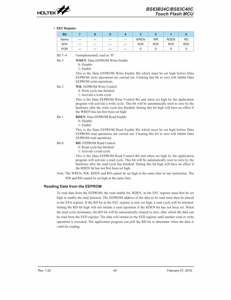
Rev. 1.00 40 �e���a�� 0�� �01� Rev. 1.00 41 �e���a�� 0�� �01�
BS83B24C/BS83C40CTouch Flash MCU
BS83B24C/BS83C40CTouch Flash MCU
• EEC Register
Bit 7 6 5 4 3 2 1 0Name — — — — WREN WR RDEN RDR/W — — — — R/W R/W R/W R/WPOR — — — — 0 0 0 0
Bit7~4 Unimplemented,readas“0”Bit3 WREN:DataEEPROMWriteEnable
0:Disable1:Enable
This is theDataEEPROMWriteEnableBitwhichmustbesethighbeforeDataEEPROMwriteoperationsarecarriedout.Clearingthisbit tozerowill inhibitDataEEPROMwriteoperations.
Bit2 WR:EEPROMWriteControl0:Writecyclehasfinished1:Activateawritecycle
This is theDataEEPROMWriteControlBitandwhensethighbytheapplicationprogramwillactivateawritecycle.Thisbitwillbeautomaticallyresettozerobythehardwareafterthewritecyclehasfinished.SettingthisbithighwillhavenoeffectiftheWRENhasnotfirstbeensethigh.
Bit1 RDEN:DataEEPROMReadEnable0:Disable1:Enable
This is theDataEEPROMReadEnableBitwhichmustbesethighbeforeDataEEPROMreadoperationsarecarriedout.Clearingthisbit tozerowill inhibitDataEEPROMreadoperations.
Bit0 RD:EEPROMReadControl0:Readcyclehasfinished1:Activateareadcycle
This is theDataEEPROMReadControlBitandwhensethighbytheapplicationprogramwillactivateareadcycle.Thisbitwillbeautomaticallyresettozerobythehardwareafterthereadcyclehasfinished.SettingthisbithighwillhavenoeffectiftheRDENbithasnotfirstbeensethigh.
Note:TheWREN,WR,RDENandRDcannotbesethighatthesametimeinoneinstruction.TheWRandRDcannotbesethighatthesametime.
Reading Data from the EEPROMToreaddatafromtheEEPROM,thereadenablebit,RDEN,intheEECregistermustfirstbesethightoenablethereadfunction.TheEEPROMaddressofthedatatobereadmustthenbeplacedintheEEAregister.IftheRDbitintheEECregisterisnowsethigh,areadcyclewillbeinitiated.SettingtheRDbithighwillnotinitiateareadoperationif theRDENbithasnotbeenset.Whenthereadcycleterminates,theRDbitwillbeautomaticallyclearedtozero,afterwhichthedatacanbereadfromtheEEDregister.ThedatawillremainintheEEDregisteruntilanotherreadorwriteoperationisexecuted.Theapplicationprogramcanpoll theRDbit todeterminewhenthedataisvalidforreading.

Rev. 1.00 40 �e���a�� 0�� �01� Rev. 1.00 41 �e���a�� 0�� �01�
BS83B24C/BS83C40CTouch Flash MCU
BS83B24C/BS83C40CTouch Flash MCU
Writing Data to the EEPROMTheEEPROMaddressofthedatatobewrittenmustfirstbeplacedintheEEAregisterandthedataplacedintheEEDregister.TowritedatatotheEEPROM,thewriteenablebit,WREN,intheEECregistermustfirstbesethightoenablethewritefunction.Afterthis,theWRbitintheEECregistermustbe immediatelysethighto initiateawritecycle.These twoinstructionsmustbeexecutedconsecutively.Theglobal interruptbitEMIshouldalsofirstbeclearedbefore implementinganywriteoperations,andthensetagainafterthewritecyclehasstarted.NotethatsettingtheWRbithighwillnotinitiateawritecycleiftheWRENbithasnotbeenset.AstheEEPROMwritecycleiscontrolledusinganinternaltimerwhoseoperationisasynchronoustomicrocontrollersystemclock,acertaintimewillelapsebeforethedatawillhavebeenwrittenintotheEEPROM.DetectingwhenthewritecyclehasfinishedcanbeimplementedeitherbypollingtheWRbitintheEECregisterorbyusingtheEEPROMinterrupt.Whenthewritecycleterminates,theWRbitwillbeautomaticallycleared tozeroby themicrocontroller, informing theuser that thedatahasbeenwritten to theEEPROM.TheapplicationprogramcanthereforepolltheWRbittodeterminewhenthewritecyclehasended.
Write ProtectionProtectionagainst inadvertentwriteoperation isprovided inseveralways.After thedevice ispowered-on theWriteEnablebit in thecontrol registerwillbeclearedpreventinganywriteoperations.Alsoatpower-ontheMemoryPointerhighbyteregister,MP1HorMP2H,willberesettozero,whichmeansthatDataMemorySector0willbeselected.AstheEEPROMcontrolregisteris locatedinSector1, thisaddsafurthermeasureofprotectionagainstspuriouswriteoperations.Duringnormalprogramoperation,ensuring that theWriteEnablebit in thecontrol register isclearedwillsafeguardagainstincorrectwriteoperations.
EEPROM InterruptTheEEPROMwriteinterruptisgeneratedwhenanEEPROMwritecyclehasended.TheEEPROMinterruptmustfirstbeenabledbysettingtheDEEbit in therelevant interruptregister.WhenanEEPROMwritecycleends,theDEFrequestflagwillbeset.IftheglobalandEEPROMinterruptsareenabledandthestackisnotfull,ajumptotheassociatedInterruptvectorwilltakeplace.WhentheinterruptisservicedtheEEPROMinterruptflagwillbeautomaticallyreset.MoredetailscanbeobtainedintheInterruptsection.
Programming ConsiderationsCaremustbe taken thatdata isnot inadvertentlywritten to theEEPROM.ProtectioncanbeenhancedbyensuringthattheWriteEnablebitisnormallyclearedtozerowhennotwriting.AlsotheMemoryPointerhighbyteregister,MP1HorMP2H,couldbenormallyclearedtozeroasthiswouldinhibitaccesstoSector1wheretheEEPROMcontrolregisterexist.Althoughcertainlynotnecessary,considerationmightbegivenintheapplicationprogramtothecheckingofthevalidityofnewwritedatabyasimplereadbackprocess.
WhenwritingdatatheWRbitmustbesethighimmediatelyaftertheWRENbithasbeensethigh,toensurethewritecycleexecutescorrectly.Theglobal interruptbitEMIshouldalsobeclearedbeforeawritecycleisexecutedandthenre-enabledafterthewritecyclestarts.Notethatthedeviceshouldnotenter theIDLEorSLEEPmodeuntil theEEPROMreadorwriteoperationis totallycomplete.Otherwise,theEEPROMreadorwriteoperationwillfail.

Rev. 1.00 4� �e���a�� 0�� �01� Rev. 1.00 43 �e���a�� 0�� �01�
BS83B24C/BS83C40CTouch Flash MCU
BS83B24C/BS83C40CTouch Flash MCU
Programming Examples
Reading data from the EEPROM – polling methodMOV A,EEPROM_ADRES ;userdefinedaddressMOV EEA,AMOV A,40H ;setupmemorypointerMP1LMOV MP1L,A ;MP1LpointstoEECregisterMOV A,01H ;setupmemorypointerMP1HMOV MP1H,ASET IAR1.1 ;setRDENbit,enablereadoperationsSET IAR1.0 ;startReadCycle-setRDbitBACK:SZ IAR1.0 ;checkforreadcycleendJMP BACKCLR IAR1 ;disableEEPROMread/writeCLR MP1HMOV A,EED ;movereaddatatoregisterMOV READ_DATA,A
Writing Data to the EEPROM – polling methodMOV A,EEPROM_ADRES ;userdefinedaddressMOV EEA,AMOV A,EEPROM_DATA ;userdefineddataMOV EED,AMOV A,040H ;setupmemorypointerMP1LMOV MP1L,A ;MP1LpointstoEECregisterMOV A,01H ;setupmemorypointerMP1HMOV MP1H,ACLR EMISET IAR1.3 ;setWRENbit,enablewriteoperationsSET IAR1.2 ;startWriteCycle-setWRbit–executedimmediately ;aftersetWRENbitSETEMIBACK:SZ IAR1.2 ;checkforwritecycleendJMP BACKCLR IAR1 ;disableEEPROMread/writeCLR MP1H
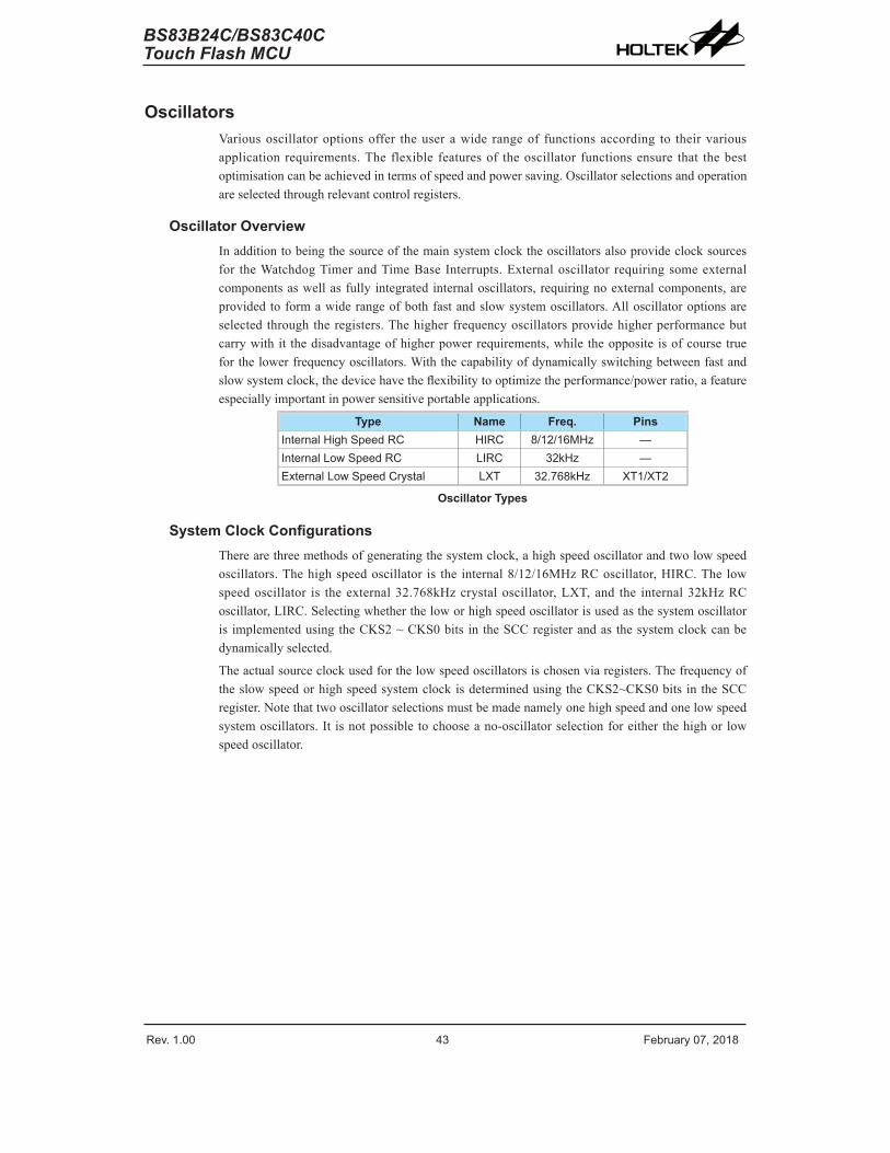
Rev. 1.00 4� �e���a�� 0�� �01� Rev. 1.00 43 �e���a�� 0�� �01�
BS83B24C/BS83C40CTouch Flash MCU
BS83B24C/BS83C40CTouch Flash MCU
OscillatorsVariousoscillatoroptionsoffer theuserawide rangeof functionsaccording to theirvariousapplication requirements.The flexible featuresof theoscillator functionsensure that thebestoptimisationcanbeachievedintermsofspeedandpowersaving.Oscillatorselectionsandoperationareselectedthroughrelevantcontrolregisters.
Oscillator OverviewInadditiontobeingthesourceofthemainsystemclocktheoscillatorsalsoprovideclocksourcesfor theWatchdogTimerandTimeBase Interrupts.Externaloscillator requiringsomeexternalcomponentsaswellasfullyintegratedinternaloscillators,requiringnoexternalcomponents,areprovidedtoformawiderangeofbothfastandslowsystemoscillators.Alloscillatoroptionsareselectedthroughtheregisters.Thehigherfrequencyoscillatorsprovidehigherperformancebutcarrywithit thedisadvantageofhigherpowerrequirements,while theopposite isofcoursetrueforthelowerfrequencyoscillators.Withthecapabilityofdynamicallyswitchingbetweenfastandslowsystemclock,thedevicehavetheflexibilitytooptimizetheperformance/powerratio,afeatureespeciallyimportantinpowersensitiveportableapplications.
Type Name Freq. PinsInte�nal High Speed RC HIRC �/1�/16MHz —Inte�nal Low Speed RC LIRC 3�kHz —Exte�nal Low Speed C��stal LXT 3�.�6�kHz XT1/XT�
Oscillator Types
System Clock ConfigurationsTherearethreemethodsofgeneratingthesystemclock,ahighspeedoscillatorandtwolowspeedoscillators.Thehighspeedoscillator is the internal8/12/16MHzRCoscillator,HIRC.The lowspeedoscillator is theexternal32.768kHzcrystaloscillator,LXT,and the internal32kHzRCoscillator,LIRC.Selectingwhethertheloworhighspeedoscillatorisusedasthesystemoscillatoris implementedusingtheCKS2~CKS0bits intheSCCregisterandasthesystemclockcanbedynamicallyselected.
Theactualsourceclockusedforthelowspeedoscillatorsischosenviaregisters.ThefrequencyoftheslowspeedorhighspeedsystemclockisdeterminedusingtheCKS2~CKS0bitsintheSCCregister.Notethattwooscillatorselectionsmustbemadenamelyonehighspeedandonelowspeedsystemoscillators.It isnotpossibletochooseano-oscillatorselectionforeither thehighor lowspeedoscillator.

Rev. 1.00 44 �e���a�� 0�� �01� Rev. 1.00 45 �e���a�� 0�� �01�
BS83B24C/BS83C40CTouch Flash MCU
BS83B24C/BS83C40CTouch Flash MCU
P�escale�
fH
High Speed Oscillato�
Low Speed Oscillato�s
fH/�
fH/16
fH/64
fH/�
fH/4
fH/3�
CKS�~CKS0
fSYS
fSUBfSUB
fLIRC
SLEEPIDLE0
IDLE�SLEEPLIRC
HIRCHIRCEN
�SS
LXTLXTEN
System Clock Configurations
Internal RC Oscillator – HIRCTheinternalRCoscillatorisafullyintegratedsystemoscillatorrequiringnoexternalcomponents.TheinternalRCoscillatorhasthreefixedfrequenciesof8/12/16MHz,whichisselectedusingaconfigurationoption.TheHIRC1~HIRC0bitsintheHIRCCregistermustalsobesetuptomatchtheselectedconfigurationoptionfrequency.Settingupthesebits isnecessarytoensure that theHIRCfrequencyaccuracyspecifiedintheA.C.Characteristicsisachieved.Devicetrimmingduringthemanufacturingprocessandtheinclusionofinternalfrequencycompensationcircuitsareusedtoensurethattheinfluenceofthepowersupplyvoltage,temperatureandprocessvariationsontheoscillationfrequencyareminimised.Asaresult,atapowersupplyof3Vor5Vandatatemperatureof25°Cdegrees,theselectedtrimmedoscillationfrequencywillhaveatolerancewithin1%.
External 32.768kHz Crystal Oscillator – LXTTheExternal32.768kHzCrystalSystemOscillatorisoneofthelowfrequencyoscillatorchoices,which is selectedviaa softwarecontrolbit,FSS.Thisclocksourcehasa fixed frequencyof32.768kHzandrequiresa32.768kHzcrystal tobeconnectedbetweenpinsXT1andXT2.Theexternalresistorandcapacitorcomponentsconnected to the32.768kHzcrystalarenecessary toprovideoscillation.Forapplicationswhereprecisefrequenciesareessential,thesecomponentsmayberequiredtoprovidefrequencycompensationduetodifferentcrystalmanufacturingtolerances.AftertheLXToscillatorisenabledbysettingtheLXTENbitto1,thereisatimedelayassociatedwiththeLXToscillatorwaitingforittostart-up.
WhenthemicrocontrollerenterstheSLEEPorIDLEMode,thesystemclockisswitchedofftostopmicrocontrolleractivityand toconservepower.However, inmanymicrocontrollerapplicationsitmaybenecessary tokeep the internal timersoperationalevenwhenthemicrocontroller is intheSLEEPorIDLEMode.Todothis,anotherclock, independentof thesystemclock,mustbeprovided.
However,forsomecrystals,toensureoscillationandaccuratefrequencygeneration,itisnecessarytoaddtwosmallvalueexternalcapacitors,C1andC2.TheexactvaluesofC1andC2shouldbeselected inconsultationwith thecrystalor resonatormanufacturer’sspecification.Theexternalparallelfeedbackresistor,RPandthepull-highresister,RU,arerequired.

Rev. 1.00 44 �e���a�� 0�� �01� Rev. 1.00 45 �e���a�� 0�� �01�
BS83B24C/BS83C40CTouch Flash MCU
BS83B24C/BS83C40CTouch Flash MCU
Thepin-sharedsoftwarecontrolbitsdetermineiftheXT1/XT2pinsareusedfortheLXToscillatororasI/Opinsorotherpin-sharedfunctionalpins.
• IftheLXToscillatorisnotusedforanyclocksource,theXT1/XT2pinscanbeusedasnormalI/Opinsorotherpin-sharedfunctionalpins.
• IftheLXToscillatorisusedforanyclocksource,the32.768kHzcrystalshouldbeconnectedtotheXT1/XT2pins.
Foroscillatorstabilityandtominimisetheeffectsofnoiseandcrosstalk, it isimportanttoensurethatthecrystalandanyassociatedresistersalongwithinterconnectinglinesarealllocatedasclosetotheMCUaspossible.
Note: 1. RP� RU� C1 and C� a�e �eq�i�ed.�. Altho�gh not shown XT1/XT� pins have a pa�asitic
capacitance of a�o�nd �p�.
To inte�nal ci�c�its
Internal Oscillator Circuit
C1
C�
XT1
XT�
RP3�.�6�
kHzInte�nal RC Oscillato�RU
VDD
External LXT Oscillator
LXT Oscillator C1 and C2 ValuesCrystal Frequency C1 C2
3�.�6�kHz 10p� 10p�Note: 1. C1 and C� val�es a�e fo� g�idance onl�. �. RP=5M~10MΩ is recommended. 3. RU=10MΩ is recommended.
32.768kHz Crystal Recommended Capacitor Values
Internal 32kHz Oscillator – LIRCTheInternal32kHzSystemOscillator isoneof the lowfrequencyoscillatorchoices,which isselectedviaasoftwarecontrolbit,FSS.ItisafullyintegratedRCoscillatorwithatypicalfrequencyof32kHzat5V,requiringnoexternalcomponentsforitsimplementation.Devicetrimmingduringthemanufacturingprocessandtheinclusionofinternalfrequencycompensationcircuitsareusedtoensurethattheinfluenceofthepowersupplyvoltage,temperatureandprocessvariationsontheoscillationfrequencyareminimised.Asaresult,atapowersupplyof5Vandatatemperatureof25˚Cdegrees,thefixedoscillationfrequencyof32kHzwillhaveatolerancewithin10%.

Rev. 1.00 46 �e���a�� 0�� �01� Rev. 1.00 4� �e���a�� 0�� �01�
BS83B24C/BS83C40CTouch Flash MCU
BS83B24C/BS83C40CTouch Flash MCU
Operating Modes and System ClocksPresentdayapplicationsrequirethat theirmicrocontrollershavehighperformancebutoftenstilldemandthattheyconsumeaslittlepoweraspossible,conflictingrequirementsthatareespeciallytrueinbatterypoweredportableapplications.Thefastclocksrequiredforhighperformancewillbytheirnatureincreasecurrentconsumptionandofcourseviceversa,lowerspeedclocksreducecurrentconsumption.Asbothhighandlowspeedclocksourcesareprovidedthemeanstoswitchbetweenthemdynamically,theusercanoptimisetheoperationoftheirmicrocontrollertoachievethebestperformance/powerratio.
System ClocksThedeviceshavedifferentclocksourcesforboththeCPUandperipheralfunctionoperation.Byprovidingtheuserwithawiderangeofclockselectionsusingregisterprogramming,aclocksystemcanbeconfiguredtoobtainmaximumapplicationperformance.
Themainsystemclock,cancomefromeitherahighfrequency,fH,orlowfrequency,fSUB,source,andisselectedusingtheCKS2~CKS0bits in theSCCregister.ThehighspeedsystemclockissourcedfromtheHIRCoscillator.The lowspeedsystemclocksourcecanbesourcedfromtheinternalclockfSUB. If fSUB isselected then itcanbesourcedfromtheLXTorLIRCoscillator,selectedbytheFSSbitintheSCCregister.Theotherchoice,whichisadividedversionofthehighspeedsystemoscillatorhasarangeoffH/2~fH/64.
P�escale�
fH
High Speed Oscillato�
Low Speed Oscillato�s
fH/�
fH/16
fH/64
fH/�
fH/4
fH/3�
CKS�~CKS0
fSYS
fSUBfLIRC
SLEEPIDLE0
IDLE�SLEEPLIRC
HIRCHIRCEN
�SS
LXTLXTEN
fSUB
WDTfSYS/4 fPSC
Time Base 0
CLKSEL[1:0]
fSUB
fSYS
P�escale�
Time Base 1
Device Clock Configurations
Note:WhenthesystemclocksourcefSYSisswitchedtofSUBfromfH,thehighspeedoscillatorcanbestoppedtoconservethepowerorcontinuetooscillatetoprovidetheclocksource,fH~fH/64,forperipheralcircuittouse,whichisdeterminedbyconfiguringthecorrespondinghighspeedoscillatorenablecontrolbit.

Rev. 1.00 46 �e���a�� 0�� �01� Rev. 1.00 4� �e���a�� 0�� �01�
BS83B24C/BS83C40CTouch Flash MCU
BS83B24C/BS83C40CTouch Flash MCU
System Operation ModesThere are six differentmodesof operation for themicrocontroller, eachonewith its ownspecial characteristics andwhichcanbe chosenaccording to the specificperformanceandpowerrequirementsof theapplication.Thereare twomodesallowingnormaloperationof themicrocontroller,theFASTModeandSLOWMode.Theremainingfourmodes,theSLEEP,IDLE0,IDLE1andIDLE2ModeareusedwhenthemicrocontrollerCPUisswitchedofftoconservepower.
Operation Mode CPU
Register SettingfSYS fH fSUB fLIRC
FHIDEN FSIDEN CKS2~CKS0�AST On x x 000~110 fH~fH/64 On On OnSLOW On x x 111 fSUB On/Off (1) On On
IDLE0 Off 0 1000~110 Off
Off On On111 On
IDLE1 Off 1 1 xxx On On On On
IDLE� Off 1 0000~110 On
On Off On111 Off
SLEEP Off 0 0 xxx Off Off Off On (�)
“x”: Don’t ca�eNotes:1.ThefHclockwillbeswitchedonoroffbyconfiguringthecorrespondingoscillatorenable
bitintheSLOWmode.2.ThefLIRCclockisalwaysonastheWDTfunctionisalwaysenabled.
FAST ModeAsthenamesuggeststhisisoneofthemainoperatingmodeswherethemicrocontrollerhasallofitsfunctionsoperationalandwherethesystemclockisprovidedbythehighspeedoscillator.ThismodeoperatesallowingthemicrocontrollertooperatenormallywithaclocksourcewillcomefromtheHIRCoscillator.Thehighspeedoscillatorwillhoweverfirstbedividedbyaratiorangingfrom1to64,theactualratiobeingselectedbytheCKS2~CKS0bitsintheSCCregister.Althoughahighspeedoscillatorisused,runningthemicrocontrolleratadividedclockratioreducestheoperatingcurrent.
SLOW ModeThisisalsoamodewherethemicrocontrolleroperatesnormallyalthoughnowwithaslowerspeedclocksource.TheclocksourceusedwillbefromfSUB.ThefSUBclockisderivedfromtheLXTorLIRCoscillator,whichisselectedviathesoftwarecontrolbitFSSintheSCCregister.
SLEEP ModeTheSLEEPModeisenteredwhenanHALTinstructionisexecutedandwhentheFHIDENandFSIDENbitarelow.IntheSLEEPmodetheCPUwillbestopped,andthefSUBclocktoperipheralwillbestoppedtoo.HoweverthefLIRCclockwillcontinuetooperateastheWDTfunctionisalwaysenabled.
IDLE0 ModeTheIDLE0ModeisenteredwhenaHALTinstructionisexecutedandwhentheFHIDENbit intheSCCregister is lowandtheFSIDENbit intheSCCregister ishigh.IntheIDLE0ModetheCPUwillbeswitchedoffbutthelowspeedoscillatorwillbeturnedontodrivesomeperipheralfunctions.

Rev. 1.00 4� �e���a�� 0�� �01� Rev. 1.00 49 �e���a�� 0�� �01�
BS83B24C/BS83C40CTouch Flash MCU
BS83B24C/BS83C40CTouch Flash MCU
IDLE1 ModeTheIDLE1ModeisenteredwhenanHALTinstructionisexecutedandwhentheFHIDENbitintheSCCregisterishighandtheFSIDENbitintheSCCregisterishigh.IntheIDLE1ModetheCPUwillbeswitchedoffbutboththehighandlowspeedoscillatorswillbeturnedontoprovideaclocksourcetokeepsomeperipheralfunctionsoperational.
IDLE2 ModeTheIDLE2ModeisenteredwhenanHALTinstructionisexecutedandwhentheFHIDENbitintheSCCregisterishighandtheFSIDENbitintheSCCregisterislow.IntheIDLE2ModetheCPUwillbeswitchedoffbutthehighspeedoscillatorwillbeturnedontoprovideaclocksourcetokeepsomeperipheralfunctionsoperational.
Control RegistersTheregisters,SCC,HIRCCandLXTC,areusedtocontrolthesystemclockandthecorrespondingoscillatorconfigurations.
Register Name
Bit7 6 5 4 3 2 1 0
SCC CKS� CKS1 CKS0 — — �SS �HIDEN �SIDENHIRCC — — — — HIRC1 HIRC0 HIRC� HIRCENLXTC — — — — — — LXT� LXTEN
System Operating Mode Control Register List
• SCC Register
Bit 7 6 5 4 3 2 1 0Name CKS� CKS1 CKS0 — — �SS �HIDEN �SIDENR/W R/W R/W R/W — — R/W R/W R/WPOR 0 0 0 — — 0 0 0
Bit7~5 CKS2~CKS0:Systemclockselection000:fH
001:fH/2010:fH/4011:fH/8100:fH/16101:fH/32110:fH/64111:fSUB
Thesethreebitsareusedtoselectwhichclockisusedasthesystemclocksource.InadditiontothesystemclocksourcedirectlyderivedfromfHorfSUB,adividedversionofthehighspeedsystemoscillatorcanalsobechosenasthesystemclocksource.
Bit4~3 Unimplemented,readas“0”Bit2 FSS:LowFrequencyclockselection
0:LIRC1:LXT
Bit1 FHIDEN:HighFrequencyoscillatorcontrolwhenCPUisswitchedoff0:Disable1:Enable
Thisbit isusedtocontrolwhether thehighspeedoscillator isactivatedorstoppedwhentheCPUisswitchedoffbyexecutingan“HALT”instruction.

Rev. 1.00 4� �e���a�� 0�� �01� Rev. 1.00 49 �e���a�� 0�� �01�
BS83B24C/BS83C40CTouch Flash MCU
BS83B24C/BS83C40CTouch Flash MCU
Bit0 FSIDEN:LowFrequencyoscillatorcontrolwhenCPUisswitchedoff0:Disable1:Enable
Thisbit isusedtocontrolwhether the lowspeedoscillator isactivatedorstoppedwhentheCPUisswitchedoffbyexecutingan“HALT”instruction.
• HIRCC Register
Bit 7 6 5 4 3 2 1 0Name — — — — HIRC1 HIRC0 HIRC� HIRCENR/W — — — — R/W R/W R R/WPOR — — — — 0 0 0 1
Bit7~4 Unimplemented,readas“0”Bit3~2 HIRC1~HIRC0:HIRCFrequencyselection
00:8MHz01:12MHz10:16MHz11:8MHz
WhentheHIRCoscillator isenabledor theHIRCfrequencyselection ischangedbyapplicationprogram,theclockfrequencywillautomaticallybechangedafter theHIRCFflagissetto1.ItisrecommendedthattheHIRCfrequencyselectedbythesetwobitsshouldbethesamewiththefrequencydeterminedbytheconfigurationoptiontoachievetheHIRCfrequencyaccuracyspecifiedintheA.C.Characteristics.
Bit1 HIRCF:HIRCoscillatorstableflag0:HIRCunstable1:HIRCstable
Thisbit isusedto indicatewhether theHIRCoscillator isstableornot.WhentheHIRCENbitissetto1toenabletheHIRCoscillatorortheHIRCfrequencyselectionischangedbyapplicationprogram,theHIRCFbitwillfirstbeclearedto0andthensetto1aftertheHIRCoscillatorisstable.
Bit0 HIRCEN:HIRCoscillatorenablecontrol0:Disable1:Enable
• LXTC Register
Bit 7 6 5 4 3 2 1 0Name — — — — — — LXT� LXTENR/W — — — — — — R R/WPOR — — — — — — 0 0
Bit7~2 Unimplemented,readas0.Bit1 LXTF:LXToscillatorstableflag
0:LXTunstable1:LXTstable
Thisbit isused to indicatewhether theLXToscillator isstableornot.When theLXTENbitissetto1toenabletheLXToscillator,theLXTFbitwillfirstbeclearedto0andthensetto1aftertheLXToscillatorisstable.
Bit0 LXTEN:LXToscillatorenablecontrol0:Disable1:Enable

Rev. 1.00 50 �e���a�� 0�� �01� Rev. 1.00 51 �e���a�� 0�� �01�
BS83B24C/BS83C40CTouch Flash MCU
BS83B24C/BS83C40CTouch Flash MCU
Operating Mode SwitchingThedevicecanswitchbetweenoperatingmodesdynamicallyallowingtheusertoselect thebestperformance/powerratioforthepresenttaskinhand.Inthiswaymicrocontrolleroperationsthatdonotrequirehighperformancecanbeexecutedusingslowerclocksthusrequiringlessoperatingcurrentandprolongingbatterylifeinportableapplications.
Insimpleterms,ModeSwitchingbetweentheFASTModeandSLOWModeisexecutedusingtheCKS2~CKS0bitsintheSCCregisterwhileModeSwitchingfromtheFAST/SLOWModestotheSLEEP/IDLEModesisexecutedviatheHALTinstruction.WhenanHALTinstructionisexecuted,whetherthedeviceenterstheIDLEModeortheSLEEPModeisdeterminedbytheconditionoftheFHIDENandFSIDENbitsintheSCCregister.
FASTfSYS=fH~fH/64
fH onCPU ��nfSYS onfSUB on
SLOWfSYS=fSUBfSUB on
CPU ��nfSYS on
fH on/off
IDLE0HALT inst��ction exec�ted
CPU stop�HIDEN=0�SIDEN=1
fH offfSUB on
IDLE1HALT inst��ction exec�ted
CPU stop�HIDEN=1�SIDEN=1
fH onfSUB on
IDLE2HALT inst��ction exec�ted
CPU stop�HIDEN=1�SIDEN=0
fH onfSUB off
SLEEPHALT inst��ction exec�ted
CPU stop�HIDEN=0�SIDEN=0
fH offfSUB off

Rev. 1.00 50 �e���a�� 0�� �01� Rev. 1.00 51 �e���a�� 0�� �01�
BS83B24C/BS83C40CTouch Flash MCU
BS83B24C/BS83C40CTouch Flash MCU
FAST Mode to SLOW Mode SwitchingWhenrunning in theFASTMode,whichuses thehighspeedsystemoscillator,and thereforeconsumesmorepower, the systemclock can switch to run in theSLOWModeby set theCKS2~CKS0bitsto“111”intheSCCregister.Thiswillthenusethelowspeedsystemoscillatorwhichwillconsumelesspower.Usersmaydecidetodothisforcertainoperationswhichdonotrequirehighperformanceandcansubsequentlyreducepowerconsumption.
TheSLOWModeissourcedfromtheLXTorLIRCoscillatorandthereforerequirestheoscillatortobestablebeforefullmodeswitchingoccurs.
FAST Mode
SLOW Mode
CKS�~CKS0 = 111
SLEEP Mode
�HIDEN=0� �SIDEN=0HALT inst��ction is exec�ted
IDLE0 Mode
�HIDEN=0� �SIDEN=1HALT inst��ction is exec�ted
IDLE1 Mode
�HIDEN=1� �SIDEN=1HALT inst��ction is exec�ted
IDLE2 Mode
�HIDEN=1� �SIDEN=0HALT inst��ction is exec�ted

Rev. 1.00 5� �e���a�� 0�� �01� Rev. 1.00 53 �e���a�� 0�� �01�
BS83B24C/BS83C40CTouch Flash MCU
BS83B24C/BS83C40CTouch Flash MCU
SLOW Mode to FAST Mode SwitchingInSLOWmodethesystemclockisderivedfromfSUB.WhensystemclockisswitchedbacktotheFASTmodefromfSUB, theCKS2~CKS0bitsshouldbesetto“000”~“110”andthenthesystemclockwillrespectivelybeswitchedtofH~fH/64.
However, if fH isnotused inSLOWmodeand thusswitchedoff, itwill takesometime tore-oscillateandstabilisewhenswitchingtotheFASTmodefromtheSLOWMode.ThisismonitoredusingtheHIRCFbit intheHIRCCregister.Thetimedurationrequiredforthehighspeedsystemoscillatorstabilizationisspecifiedintherelevantcharacteristics.
FAST Mode
SLOW Mode
CKS�~CKS0 = 000~110
SLEEP Mode
�HIDEN=0� �SIDEN=0HALT inst��ction is exec�ted
IDLE0 Mode
�HIDEN=0� �SIDEN=1HALT inst��ction is exec�ted
IDLE1 Mode
�HIDEN=1� �SIDEN=1HALT inst��ction is exec�ted
IDLE2 Mode
�HIDEN=1� �SIDEN=0HALT inst��ction is exec�ted
Entering the SLEEP ModeThereisonlyonewayforthedevicetoentertheSLEEPModeandthatistoexecutethe“HALT”instructionintheapplicationprogramwithboththeFHIDENandFSIDENbitsintheSCCregisterequalto“0”.InthismodealltheclocksandfunctionswillbeswitchedoffexcepttheWDTfunction.Whenthisinstructionisexecutedundertheconditionsdescribedabove,thefollowingwilloccur:
• The systemclockwill be stoppedand the applicationprogramwill stop at the "HALT"instruction.
• TheDataMemorycontentsandregisterswillmaintaintheirpresentcondition.
• TheI/Oportswillmaintaintheirpresentconditions.
• Inthestatusregister,thePowerDownflagPDFwillbeset,andWDTtimeoutflagTOwillbecleared.
• TheWDTwillbeclearedandresumecountingastheWDTfunctionisalwaysenabled.

Rev. 1.00 5� �e���a�� 0�� �01� Rev. 1.00 53 �e���a�� 0�� �01�
BS83B24C/BS83C40CTouch Flash MCU
BS83B24C/BS83C40CTouch Flash MCU
Entering the IDLE0 ModeThereisonlyonewayforthedevicetoentertheIDLE0Modeandthatistoexecutethe“HALT”instructionintheapplicationprogramwiththeFHIDENbitintheSCCregisterequalto“0”andtheFSIDENbitintheSCCregisterequalto“1”.Whenthisinstructionisexecutedundertheconditionsdescribedabove,thefollowingwilloccur:
• ThefHclockwillbestoppedandtheapplicationprogramwillstopatthe“HALT”instruction,butthefSUBclockwillbeon.
• TheDataMemorycontentsandregisterswillmaintaintheirpresentcondition.
• TheI/Oportswillmaintaintheirpresentconditions.
• Inthestatusregister,thePowerDownflagPDFwillbeset,andWDTtimeoutflagTOwillbecleared.
• TheWDTwillbeclearedandresumecountingastheWDTfunctionisalwaysenabled.
Entering the IDLE1 ModeThereisonlyonewayforthedevicetoentertheIDLE1Modeandthatistoexecutethe“HALT”instructionintheapplicationprogramwithboththeFHIDENandFSIDENbitsintheSCCregisterequalto“1”.Whenthisinstructionisexecutedundertheconditionsdescribedabove,thefollowingwilloccur:
• ThefHandfSUBclockswillbeonbuttheapplicationprogramwillstopatthe“HALT”instruction.
• TheDataMemorycontentsandregisterswillmaintaintheirpresentcondition.
• TheI/Oportswillmaintaintheirpresentconditions.
• Inthestatusregister,thePowerDownflagPDFwillbeset,andWDTtimeoutflagTOwillbecleared.
• TheWDTwillbeclearedandresumecountingastheWDTfunctionisalwaysenabled.
Entering the IDLE2 ModeThereisonlyonewayforthedevicetoentertheIDLE2Modeandthatistoexecutethe“HALT”instructionintheapplicationprogramwiththeFHIDENbitintheSCCregisterequalto“1”andtheFSIDENbitintheSCCregisterequalto“0”.Whenthisinstructionisexecutedundertheconditionsdescribedabove,thefollowingwilloccur:
• ThefHclockwillbeonbutthefSUBclockwillbeoffandtheapplicationprogramwillstopatthe“HALT”instruction.
• TheDataMemorycontentsandregisterswillmaintaintheirpresentcondition.
• TheI/Oportswillmaintaintheirpresentconditions.
• Inthestatusregister,thePowerDownflagPDFwillbeset,andWDTtimeoutflagTOwillbecleared.
• TheWDTwillbeclearedandresumecountingastheWDTfunctionisalwaysenabled.

Rev. 1.00 54 �e���a�� 0�� �01� Rev. 1.00 55 �e���a�� 0�� �01�
BS83B24C/BS83C40CTouch Flash MCU
BS83B24C/BS83C40CTouch Flash MCU
Standby Current ConsiderationsAsthemainreasonforenteringtheSLEEPorIDLEModeistokeepthecurrentconsumptionofthedevicetoaslowavalueaspossible,perhapsonlyintheorderofseveralmicro-ampsexceptintheIDLE1andIDLE2Mode,thereareotherconsiderationswhichmustalsobetakenintoaccountbythecircuitdesignerif thepowerconsumptionistobeminimised.SpecialattentionmustbemadetotheI/Opinsonthedevice.Allhigh-impedanceinputpinsmustbeconnectedtoeitherafixedhighorlowlevelasanyfloatinginputpinscouldcreateinternaloscillationsandresultinincreasedcurrentconsumption.Thisalsoappliestodeviceswhichhavedifferentpackagetypes,astheremaybeunbonbedpins.Thesemusteitherbesetupasoutputsorifsetupasinputsmusthavepull-highresistorsconnected.
Caremustalsobetakenwiththeloads,whichareconnectedtoI/Opins,whicharesetupasoutputs.Theseshouldbeplacedinaconditioninwhichminimumcurrent isdrawnorconnectedonlytoexternalcircuits thatdonotdrawcurrent,suchasotherCMOSinputs.Alsonote thatadditionalstandbycurrentwillalsoberequirediftheLXTorLIRCoscillatorhasbeenenabled.
In theIDLE1andIDLE2Modethehighspeedoscillator ison, if theperipheral functionclocksourceisderivedfromthehighspeedoscillator,theadditionalstandbycurrentwillalsobeperhapsintheorderofseveralhundredmicro-amps.
Wake-upTominimisepowerconsumptionthedevicecanenter theSLEEPoranyIDLEMode,wheretheCPUwillbeswitchedoff.However,whenthedeviceiswokenupagain,itwilltakeaconsiderabletimefortheoriginalsystemoscillatortorestart,stabliseandallownormaloperationtoresume.
AfterthesystementerstheSLEEPorIDLEMode,itcanbewokenupfromoneofvarioussourceslistedasfollows:
• AnexternalfallingedgeonPortA
• Asysteminterrupt
• AWDToverflow
Whenthedeviceexecutesthe“HALT”instruction,thePDFflagwillbesetto1.ThePDFflagwillbeclearedto0ifthedeviceexperiencesasystempower-uporexecutestheclearWatchdogTimerinstruction.IfthesystemiswokenupbyaWDToverflow,aWatchdogTimerresetwillbeinitiatedandtheTOflagwillbesetto1.TheTOflagissetifaWDTtime-outoccursandcausesawake-upthatonlyresetstheProgramCounterandStackPointer,otherflagsremainintheiroriginalstatus.
EachpinonPortAcanbesetupusingthePAWUregistertopermitanegativetransitiononthepintowakeupthesystem.WhenaPortApinwake-upoccurs,theprogramwillresumeexecutionattheinstructionfollowingthe“HALT”instruction.If thesystemiswokenupbyaninterrupt, thentwopossiblesituationsmayoccur.Thefirstiswheretherelatedinterruptisdisabledortheinterruptisenabledbutthestackisfull,inwhichcasetheprogramwillresumeexecutionattheinstructionfollowingthe“HALT”instruction.Inthissituation,theinterruptwhichwokeupthedevicewillnotbeimmediatelyserviced,butwillratherbeservicedlaterwhentherelatedinterruptisfinallyenabledorwhenastacklevelbecomesfree.Theothersituationiswheretherelatedinterruptisenabledandthestackisnotfull,inwhichcasetheregularinterruptresponsetakesplace.Ifaninterruptrequestflag issethighbeforeentering theSLEEPorIDLEMode, thewake-upfunctionof therelatedinterruptwillbedisabled.

Rev. 1.00 54 �e���a�� 0�� �01� Rev. 1.00 55 �e���a�� 0�� �01�
BS83B24C/BS83C40CTouch Flash MCU
BS83B24C/BS83C40CTouch Flash MCU
Watchdog TimerTheWatchdogTimerisprovidedtopreventprogrammalfunctionsorsequencesfromjumpingtounknownlocations,duetocertainuncontrollableexternaleventssuchaselectricalnoise.
Watchdog Timer Clock SourceTheWatchdogTimerclocksourceisprovidedbytheinternalRCoscillator,fLIRC.TheLIRCinternaloscillatorhasanapproximatefrequencyof32kHzandthisspecifiedinternalclockperiodcanvarywithVDD,temperatureandprocessvariations.TheWatchdogTimersourceclockisthensubdividedbyaratioof28 to218 togivelongertimeouts,theactualvaluebeingchosenusingtheWS2~WS0bitsintheWDTCregister.
Watchdog Timer Control RegisterAsingleregister,WDTC,controlstherequiredtimeoutperiodaswellastheenableandresetMCUoperation.
• WDTC Register
Bit 7 6 5 4 3 2 1 0Name WE4 WE3 WE� WE1 WE0 WS� WS1 WS0R/W R/W R/W R/W R/W R/W R/W R/W R/WPOR 0 1 0 1 0 0 1 1
Bit7~3 WE4~WE0:WDTfunctionsoftwarecontrol10101/01010:EnableOthers:ResetMCU
Whenthesebitsarechangedbytheenvironmentalnoiseorsoftwaresettingtoresetthemicrocontroller,theresetoperationwillbeactivatedafteradelaytime,tSRESET,andtheWRFbitintheRSTFCregisterwillbesethigh.
Bit2~0 WS2~WS0:WDTtime-outperiodselection000:28/fLIRC001:210/fLIRC010:212/fLIRC011:214/fLIRC100:215/fLIRC101:216/fLIRC110:217/fLIRC111:218/fLIRC
These threebitsdetermine thedivisionratioof thewatchdog timersourceclock,whichinturndeterminesthetime-outperiod.
• RSTFC Register
Bit 7 6 5 4 3 2 1 0Name — — — — RST� LVR� LR� WR�R/W — — — — R/W R/W R/W R/WPOR — — — — 0 x 0 0
“x”: UnknownBit7~4 Unimplemented,readas“0”Bit3 RSTF:ResetControlRegisterSoftwareResetFlag
DescribedelsewhereBit2 LVRF:LVRfunctionresetflag
DescribedelsewhereBit1 LRF:LVRControlRegisterSoftwareResetFlag
Describedelsewhere

Rev. 1.00 56 �e���a�� 0�� �01� Rev. 1.00 5� �e���a�� 0�� �01�
BS83B24C/BS83C40CTouch Flash MCU
BS83B24C/BS83C40CTouch Flash MCU
Bit0 WRF:WDTControlRegisterSoftwareResetFlag0:Notoccur1:Occurred
ThisbitissethighbytheWDTControlregistersoftwareresetandclearedto0bytheapplicationprogram.Notethatthisbitcanonlybeclearedtozerobytheapplicationprogram.
Watchdog Timer OperationTheWatchdogTimeroperatesbyprovidingadeviceresetwhenits timeroverflows.ThismeansthatintheapplicationprogramandduringnormaloperationtheuserhastostrategicallycleartheWatchdogTimerbeforeitoverflowstopreventtheWatchdogTimerfromexecutingareset.Thisisdoneusingtheclearwatchdoginstructions.Iftheprogrammalfunctionsforwhateverreason,jumpstoanunknownlocation,orentersanendlessloop,theseclearinstructionswillnotbeexecutedinthecorrectmanner,inwhichcasetheWatchdogTimerwilloverflowandresetthedevice.Therearefivebits,WE4~WE0,intheWDTCregistertooffertheenableandresetcontroloftheWatchdogTimer.TheWDTfunctionwillbeenabledif theWE4~WE0bitsareequalto10101Bor01010B.If theWE4~WE0bitsaresettoanyothervalues,otherthan01010Band10101B,itwillresetthedeviceafteradelaytime,tSRESET.Afterpoweronthesebitswillhaveavalueof01010B.
WE4 ~ WE0 Bits WDT Function10101B o� 01010B Ena�leAn� othe� val�es Reset MCU
Watchdog Timer Function Control
Undernormalprogramoperation,aWatchdogTimertime-outwill initialiseadeviceresetandsetthestatusbitTO.However,ifthesystemisintheSLEEPorIDLEMode,whenaWatchdogTimertime-outoccurs,theTObitinthestatusregisterwillbesetandonlytheProgramCounterandStackPointerwillbereset.ThreemethodscanbeadoptedtoclearthecontentsoftheWatchdogTimer.ThefirstisaWDTreset,whichmeansacertainvalueexcept01010Band10101BwrittenintotheWE4~WE0bitfiled,thesecondisusingtheWatchdogTimersoftwareclearinstructionandthethirdisviaaHALTinstruction.
ThereisonlyonemethodofusingsoftwareinstructiontocleartheWatchdogTimer.Thatistousethesingle“CLRWDT”instructiontocleartheWDT.
Themaximumtimeoutperiod iswhenthe218divisionratio isselected.Asanexample,witha32kHzLIRCoscillatorasitssourceclock,thiswillgiveamaximumwatchdogperiodofaround8secondsforthe218divisionratio,andaminimumtimeoutof8msforthe28divisionration.
“CLR WDT”Inst��ction
�-stage Divide� WDT P�escale�
WE4~WE0 �itsWDTC Registe� Reset MCU
fLIRC
fLIRC/��
�-to-1 MUX
CLR
WS�~WS0 WDT Time-o�t(��/fLIRC ~ �1�/fLIRC)
“HALT”Inst��ction
Watchdog Timer

Rev. 1.00 56 �e���a�� 0�� �01� Rev. 1.00 5� �e���a�� 0�� �01�
BS83B24C/BS83C40CTouch Flash MCU
BS83B24C/BS83C40CTouch Flash MCU
Reset and Initialisation Aresetfunctionisafundamentalpartofanymicrocontrollerensuringthat thedevicecanbesettosomepredeterminedcondition irrespectiveofoutsideparameters.Themost important resetconditionisafterpowerisfirstappliedtothemicrocontroller.Inthiscase, internalcircuitrywillensure that themicrocontroller,afterashortdelay,willbe inawell-definedstateandready toexecutethefirstprograminstruction.Afterthispower-onreset,certainimportantinternalregisterswillbesettodefinedstatesbeforetheprogramcommences.OneoftheseregistersistheProgramCounter,whichwillberesettozeroforcingthemicrocontrollertobeginprogramexecutionfromthelowestProgramMemoryaddress.
TheWatchdogTimeroverflowisoneofmanyresettypesandwillresetthemicrocontroller.AnotherresetexistsintheformofaLowVoltageReset,LVR,whereafullresetisimplementedinsituationswherethepowersupplyvoltagefallsbelowacertainthreshold.Alltypesofresetoperationsresultindifferentregisterconditionsbeingsetup.
Reset FunctionsThereare severalways inwhichamicrocontroller reset canoccur througheventsoccurringinternally.
Power-on Reset Themostfundamentalandunavoidablereset is theonethatoccursafterpowerisfirstappliedtothemicrocontroller.AswellasensuringthattheProgramMemorybeginsexecutionfromthefirstmemoryaddress,apower-onresetalsoensures thatcertainother registersarepreset toknownconditions.AlltheI/OportandportcontrolregisterswillpowerupinahighconditionensuringthatallI/Oportswillbefirstsettoinputs.
VDD
Powe�-on Reset
SST Time-o�t
tRSTD
Power-On Reset Timing Chart
Internal Reset ControlThereisaninternalresetcontrolregister,RSTC,whichisusedtoprovidearesetwhenthedeviceoperatesabnormallyduetotheenvironmentalnoiseinterference.IfthecontentoftheRSTCregisterissettoanyvalueotherthan01010101Bor10101010B,itwillresetthedeviceafteradelaytime,tSRESET.Afterpowerontheregisterwillhaveavalueof01010101B.
RSTC7 ~ RSTC0 Bits Reset Function01010101B No ope�ation10101010B No ope�ation
An� othe� val�e Reset MCU
Internal Reset Function Control

Rev. 1.00 5� �e���a�� 0�� �01� Rev. 1.00 59 �e���a�� 0�� �01�
BS83B24C/BS83C40CTouch Flash MCU
BS83B24C/BS83C40CTouch Flash MCU
• RSTC Register
Bit 7 6 5 4 3 2 1 0Name RSTC� RSTC6 RSTC5 RSTC4 RSTC3 RSTC� RSTC1 RSTC0R/W R/W R/W R/W R/W R/W R/W R/W R/WPOR 0 1 0 1 0 1 0 1
Bit7~0 RSTC7~RSTC0:ResetFunctionControl01010101:Nooperation10101010:NooperationOthervalues:ResetMCU
Ifthesebitsarechangedduetoadverseenvironmentalconditions,themicrocontrollerwillbereset.Theresetoperationwillbeactivatedafteradelaytime,tSRESETandtheRSTFbitintheRSTFCregisterwillbesetto1.
• RSTFC Register
Bit 7 6 5 4 3 2 1 0Name — — — — RST� LVR� LR� WR�R/W — — — — R/W R/W R/W R/WPOR — — — — 0 x 0 0
“x”: UnknownBit7~4 Unimplemented,readas“0”Bit3 RSTF:ResetControlRegisterSoftwareResetFlag
0:Notoccurred1:Occurred
Thisbit isset to1by theRSTCcontrol registersoftwareresetandclearedby theapplicationprogram.Note that thisbitcanonlybecleared to0by theapplicationprogram.
Bit2 LVRF:LVRFunctionResetFlagDescribedelsewhere
Bit1 LRF:LVRControlRegisterSoftwareResetFlagDescribedelsewhere
Bit0 WRF:WDTControlRegisterSoftwareResetFlagDescribedelsewhere
Low Voltage Reset – LVR Themicrocontrollerscontainalowvoltageresetcircuitinordertomonitorthesupplyvoltageofthedevice.TheLVRfunctionisalwaysenabledwithaspecificLVRvoltageVLVR.Ifthesupplyvoltageofthedevicedropstowithinarangeof0.9V~VLVRsuchasmightoccurwhenchangingthebattery,theLVRwillautomaticallyreset thedevice internallyand theLVRFbit in theRSTFCregisterwillalsobesethigh.ForavalidLVRsignal,a lowsupplyvoltage, i.e.,avoltage in therangebetween0.9V~VLVRmustexistforatimegreater thanthatspecifiedbytLVRintheLVRElectricalCharacteristics.Ifthelowsupplyvoltagestatedoesnotexceedthisvalue,theLVRwillignorethelowsupplyvoltageandwillnotperformaresetfunction.TheactualVLVRvaluecanbeselectedbytheLVS7~LVS0bitsintheLVRCregister.IftheLVS7~LVS0bitsarechangedtosomecertainvaluesbytheenvironmentalnoiseorsoftwaresetting,theLVRwillresetthedeviceafteradelaytime,tSRESET.Whenthishappens,theLRFbit intheRSTFCregisterwillbesethigh.Afterpowerontheregisterwillhavethevalueof01010101B.NotethattheLVRfunctionwillbeautomaticallydisabledwhenthedeviceenterstheIDLE/SLEEPmode.
LVR
Inte�nal ResettRSTD + tSST
Low Voltage Reset Timing Chart
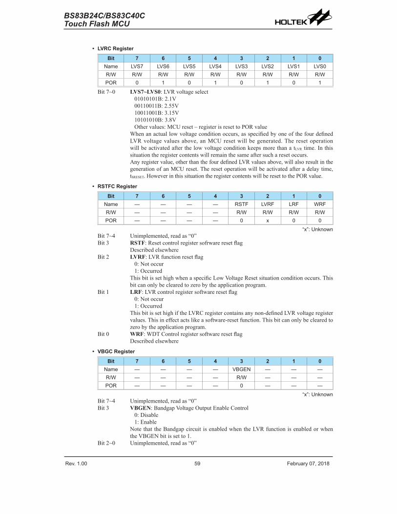
Rev. 1.00 5� �e���a�� 0�� �01� Rev. 1.00 59 �e���a�� 0�� �01�
BS83B24C/BS83C40CTouch Flash MCU
BS83B24C/BS83C40CTouch Flash MCU
• LVRC Register
Bit 7 6 5 4 3 2 1 0Name LVS� LVS6 LVS5 LVS4 LVS3 LVS� LVS1 LVS0R/W R/W R/W R/W R/W R/W R/W R/W R/WPOR 0 1 0 1 0 1 0 1
Bit7~0 LVS7~LVS0:LVRvoltageselect01010101B:2.1V00110011B:2.55V10011001B:3.15V10101010B:3.8VOthervalues:MCUreset–registerisresettoPORvalue
Whenanactuallowvoltageconditionoccurs,asspecifiedbyoneofthefourdefinedLVRvoltagevaluesabove,anMCUresetwillbegenerated.The resetoperationwillbeactivatedafterthelowvoltageconditionkeepsmorethanatLVRtime.Inthissituationtheregistercontentswillremainthesameaftersucharesetoccurs.Anyregistervalue,otherthanthefourdefinedLVRvaluesabove,willalsoresultinthegenerationofanMCUreset.Theresetoperationwillbeactivatedafteradelaytime,tSRESET.HoweverinthissituationtheregistercontentswillberesettothePORvalue.
• RSTFC Register
Bit 7 6 5 4 3 2 1 0Name — — — — RST� LVR� LR� WR�R/W — — — — R/W R/W R/W R/WPOR — — — — 0 x 0 0
“x”: UnknownBit7~4 Unimplemented,readas“0”Bit3 RSTF:Resetcontrolregistersofrwareresetflag
DescribedelsewhereBit2 LVRF:LVRfunctionresetflag
0:Notoccur1:Occurred
ThisbitissethighwhenaspecificLowVoltageResetsituationconditionoccurs.Thisbitcanonlybeclearedtozerobytheapplicationprogram.
Bit1 LRF:LVRcontrolregistersoftwareresetflag0:Notoccur1:Occurred
ThisbitissethighiftheLVRCregistercontainsanynon-definedLVRvoltageregistervalues.Thisineffectactslikeasoftware-resetfunction.Thisbitcanonlybeclearedtozerobytheapplicationprogram.
Bit0 WRF:WDTControlregistersoftwareresetflagDescribedelsewhere
• VBGC Register
Bit 7 6 5 4 3 2 1 0Name — — — — VBGEN — — —R/W — — — — R/W — — —POR — — — — 0 — — —
“x”: UnknownBit7~4 Unimplemented,readas“0”Bit3 VBGEN:BandgapVoltageOutputEnableControl
0:Disable1:Enable
NotethattheBandgapcircuitisenabledwhentheLVRfunctionisenabledorwhentheVBGENbitissetto1.
Bit2~0 Unimplemented,readas“0”
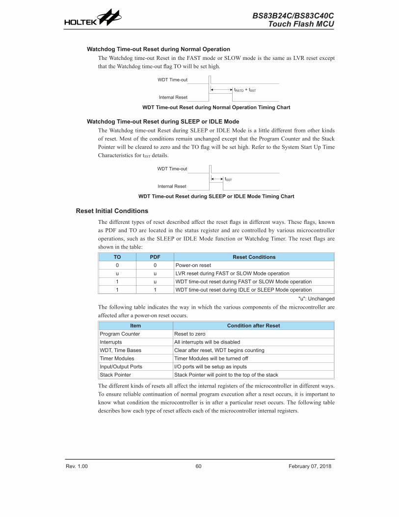
Rev. 1.00 60 �e���a�� 0�� �01� Rev. 1.00 61 �e���a�� 0�� �01�
BS83B24C/BS83C40CTouch Flash MCU
BS83B24C/BS83C40CTouch Flash MCU
Watchdog Time-out Reset during Normal Operation TheWatchdogtime-outResetintheFASTmodeorSLOWmodeisthesameasLVRresetexceptthattheWatchdogtime-outflagTOwillbesethigh.
WDT Time-o�t
Inte�nal Reset
tRSTD + tSST
WDT Time-out Reset during Normal Operation Timing Chart
Watchdog Time-out Reset during SLEEP or IDLE Mode TheWatchdogtime-outResetduringSLEEPorIDLEModeisa littledifferentfromotherkindsofreset.MostoftheconditionsremainunchangedexceptthattheProgramCounterandtheStackPointerwillbeclearedtozeroandtheTOflagwillbesethigh.RefertotheSystemStartUpTimeCharacteristicsfortSSTdetails.
WDT Time-o�t
Inte�nal ResettSST
WDT Time-out Reset during SLEEP or IDLE Mode Timing Chart
Reset Initial Conditions Thedifferent typesofresetdescribedaffect theresetflagsindifferentways.Theseflags,knownasPDFandTOare located in thestatus registerandarecontrolledbyvariousmicrocontrolleroperations,suchas theSLEEPorIDLEModefunctionorWatchdogTimer.Thereset flagsareshowninthetable:
TO PDF Reset Conditions0 0 Powe�-on �eset� � LVR �eset d��ing �AST o� SLOW Mode ope�ation1 � WDT time-o�t �eset d��ing �AST o� SLOW Mode ope�ation1 1 WDT time-o�t �eset d��ing IDLE o� SLEEP Mode ope�ation
"�": UnchangedThefollowingtableindicatesthewayinwhichthevariouscomponentsofthemicrocontrollerareaffectedafterapower-onresetoccurs.
Item Condition after ResetP�og�am Co�nte� Reset to ze�oInte���pts All inte���pts will �e disa�ledWDT� Time Bases Clea� afte� �eset� WDT �egins co�ntingTime� Mod�les Time� Mod�les will �e t��ned offInp�t/O�tp�t Po�ts I/O po�ts will �e set�p as inp�tsStack Pointe� Stack Pointe� will point to the top of the stack
Thedifferentkindsofresetsallaffecttheinternalregistersofthemicrocontrollerindifferentways.Toensurereliablecontinuationofnormalprogramexecutionafteraresetoccurs,itisimportanttoknowwhatconditionthemicrocontrolleris inafteraparticularresetoccurs.Thefollowingtabledescribeshoweachtypeofresetaffectseachofthemicrocontrollerinternalregisters.

Rev. 1.00 60 �e���a�� 0�� �01� Rev. 1.00 61 �e���a�� 0�� �01�
BS83B24C/BS83C40CTouch Flash MCU
BS83B24C/BS83C40CTouch Flash MCU
RegisterName
BS83B
24C
BS83C
40C
Reset (Power On)
LVR Reset (Normal
Operation)
WDT Time-out (Normal
Operation)
WDT Time-out (IDLE/SLEEP)
IAR0 ● ● 0 0 0 0 0 0 0 0 0 0 0 0 0 0 0 0 0 0 0 0 0 0 0 0 � � � � � � � �MP0 ● ● 0 0 0 0 0 0 0 0 0 0 0 0 0 0 0 0 0 0 0 0 0 0 0 0 � � � � � � � �IAR1 ● ● 0 0 0 0 0 0 0 0 0 0 0 0 0 0 0 0 0 0 0 0 0 0 0 0 � � � � � � � �MP1L ● ● 0 0 0 0 0 0 0 0 0 0 0 0 0 0 0 0 0 0 0 0 0 0 0 0 � � � � � � � �MP1H ● ● 0 0 0 0 0 0 0 0 0 0 0 0 0 0 0 0 0 0 0 0 0 0 0 0 � � � � � � � �ACC ● ● x x x x x x x x � � � � � � � � � � � � � � � � � � � � � � � �PCL ● ● 0 0 0 0 0 0 0 0 0 0 0 0 0 0 0 0 0 0 0 0 0 0 0 0 0 0 0 0 0 0 0 0TBLP ● ● x x x x x x x x � � � � � � � � � � � � � � � � � � � � � � � �TBLH ● ● x x x x x x x x � � � � � � � � � � � � � � � � � � � � � � � �TBHP ● ● - - - - x x x x - - - - � � � � - - - - � � � � - - - - � � � �STATUS ● ● x x 0 0 x x x x � � � � � � � � � � 1 � � � � � � � 11 � � � �IAR� ● ● 0 0 0 0 0 0 0 0 0 0 0 0 0 0 0 0 0 0 0 0 0 0 0 0 � � � � � � � �MP�L ● ● 0 0 0 0 0 0 0 0 0 0 0 0 0 0 0 0 0 0 0 0 0 0 0 0 � � � � � � � �MP�H ● ● 0 0 0 0 0 0 0 0 0 0 0 0 0 0 0 0 0 0 0 0 0 0 0 0 � � � � � � � �RST�C ● ● - - - - 0 x 0 0 - - - - � 1 � � - - - - � � � � - - - - � � � �INTEG ● ● - - - - - - 0 0 - - - - - - 0 0 - - - - - - 0 0 - - - - - - � �INTC0 ● ● - 0 0 0 0 0 0 0 - 0 0 0 0 0 0 0 - 0 0 0 0 0 0 0 - � � � � � � �INTC1 ● ● 0 0 0 0 0 0 0 0 0 0 0 0 0 0 0 0 0 0 0 0 0 0 0 0 � � � � � � � �INTC� ● - - - 0 - - - 0 - - - 0 - - - 0 - - - 0 - - - 0 - - - � - - - �PA ● ● 1 1 1 1 1 1 1 1 1 1 1 1 1 1 1 1 1 1 1 1 1 1 1 1 � � � � � � � �PAC ● ● 1 1 1 1 1 1 1 1 1 1 1 1 1 1 1 1 1 1 1 1 1 1 1 1 � � � � � � � �PAPU ● ● 0 0 0 0 0 0 0 0 0 0 0 0 0 0 0 0 0 0 0 0 0 0 0 0 � � � � � � � �PAWU ● ● 0 0 0 0 0 0 0 0 0 0 0 0 0 0 0 0 0 0 0 0 0 0 0 0 � � � � � � � �LVRC ● ● 0 1 0 1 0 1 0 1 0 1 0 1 0 1 0 1 0 1 0 1 0 1 0 1 � � � � � � � �I�S ● ● - - - - - 0 0 0 - - - - - 0 0 0 - - - - - 0 0 0 - - - - - � � �WDTC ● ● 0 1 0 1 0 0 1 1 0 1 0 1 0 0 1 1 0 1 0 1 0 0 1 1 � � � � � � � �TB0C ● ● 0 - - - - 0 0 0 0 - - - - 0 0 0 0 - - - - 0 0 0 � - - - - � � �TB1C ● ● 0 - - - - 0 0 0 0 - - - - 0 0 0 0 - - - - 0 0 0 � - - - - � � �PSCR ● ● - - - - - - 0 0 - - - - - - 0 0 - - - - - - 0 0 - - - - - - � �M�I0 ● ● - - 0 0 - - 0 0 - - 0 0 - - 0 0 - - 0 0 - - 0 0 - - � � - - � �M�I1 ● - - 0 0 - - 0 0 - - 0 0 - - 0 0 - - 0 0 - - 0 0 - - � � - - � �PB ● ● 1 1 1 1 1 1 1 1 1 1 1 1 1 1 1 1 1 1 1 1 1 1 1 1 � � � � � � � �PBC ● ● 1 1 1 1 1 1 1 1 1 1 1 1 1 1 1 1 1 1 1 1 1 1 1 1 � � � � � � � �PBPU ● ● 0 0 0 0 0 0 0 0 0 0 0 0 0 0 0 0 0 0 0 0 0 0 0 0 � � � � � � � �PC ● ● 1 1 1 1 1 1 1 1 1 1 1 1 1 1 1 1 1 1 1 1 1 1 1 1 � � � � � � � �PCC ● ● 1 1 1 1 1 1 1 1 1 1 1 1 1 1 1 1 1 1 1 1 1 1 1 1 � � � � � � � �PCPU ● ● 0 0 0 0 0 0 0 0 0 0 0 0 0 0 0 0 0 0 0 0 0 0 0 0 � � � � � � � �SCC ● ● 0 0 0 - - 0 0 0 0 0 0 - - 0 0 0 0 0 0 - - 0 0 0 � � � - - � � �HIRCC ● ● - - - - 0 0 0 1 - - - - 0 0 0 1 - - - - 0 0 0 1 - - - - � � � �LXTC ● ● - - - - - - 0 0 - - - - - - 0 0 - - - - - - 0 0 - - - - - - � �RSTC ● ● 0 1 0 1 0 1 0 1 0 1 0 1 0 1 0 1 0 1 0 1 0 1 0 1 � � � � � � � �VBGC ● ● - - - - 0 - - - - - - - 0 - - - - - - - 0 - - - - - - - � - - -
PD● - - - - - - 1 1 - - - - - - 1 1 - - - - - - 1 1 - - - - - - � �
● 1 1 1 1 1 1 1 1 1 1 1 1 1 1 1 1 1 1 1 1 1 1 1 1 � � � � � � � �

Rev. 1.00 6� �e���a�� 0�� �01� Rev. 1.00 63 �e���a�� 0�� �01�
BS83B24C/BS83C40CTouch Flash MCU
BS83B24C/BS83C40CTouch Flash MCU
RegisterName
BS83B
24C
BS83C
40C
Reset (Power On)
LVR Reset (Normal
Operation)
WDT Time-out (Normal
Operation)
WDT Time-out (IDLE/SLEEP)
PDC● - - - - - - 1 1 - - - - - - 1 1 - - - - - - 1 1 - - - - - - � �
● 1 1 1 1 1 1 1 1 1 1 1 1 1 1 1 1 1 1 1 1 1 1 1 1 � � � � � � � �
PDPU● - - - - - - 0 0 - - - - - - 0 0 - - - - - - 0 0 - - - - - - � �
● 0 0 0 0 0 0 0 0 0 0 0 0 0 0 0 0 0 0 0 0 0 0 0 0 � � � � � � � �SLEDC0 ● ● 0 0 0 0 0 0 0 0 0 0 0 0 0 0 0 0 0 0 0 0 0 0 0 0 � � � � � � � �
SLEDC1● - - 0 0 0 0 0 0 - - 0 0 0 0 0 0 - - 0 0 0 0 0 0 - - � � � � � �
● 0 0 0 0 0 0 0 0 0 0 0 0 0 0 0 0 0 0 0 0 0 0 0 0 � � � � � � � �SLEDC� ● - - 0 0 0 0 0 0 - - 0 0 0 0 0 0 - - 0 0 0 0 0 0 - - � � � � � �CTMC0 ● 0 0 0 0 0 0 0 0 0 0 0 0 0 0 0 0 0 0 0 0 0 0 0 0 � � � � � � � �CTMC1 ● 0 0 0 0 0 0 0 0 0 0 0 0 0 0 0 0 0 0 0 0 0 0 0 0 � � � � � � � �CTMDL ● 0 0 0 0 0 0 0 0 0 0 0 0 0 0 0 0 0 0 0 0 0 0 0 0 � � � � � � � �CTMDH ● - - - - - - 0 0 - - - - - - 0 0 - - - - - - 0 0 - - - - - - � �CTMAL ● 0 0 0 0 0 0 0 0 0 0 0 0 0 0 0 0 0 0 0 0 0 0 0 0 � � � � � � � �CTMAH ● - - - - - - 0 0 - - - - - - 0 0 - - - - - - 0 0 - - - - - - � �EEA ● ● - 0 0 0 0 0 0 0 - 0 0 0 0 0 0 0 - 0 0 0 0 0 0 0 - � � � � � � �EED ● ● 0 0 0 0 0 0 0 0 0 0 0 0 0 0 0 0 0 0 0 0 0 0 0 0 � � � � � � � �PTMC0 ● ● 0 0 0 0 0 - - - 0 0 0 0 0 - - - 0 0 0 0 0 - - - � � � � � - - -PTMC1 ● ● 0 0 0 0 0 0 0 0 0 0 0 0 0 0 0 0 0 0 0 0 0 0 0 0 � � � � � � � �PTMDL ● ● 0 0 0 0 0 0 0 0 0 0 0 0 0 0 0 0 0 0 0 0 0 0 0 0 � � � � � � � �PTMDH ● ● - - - - - - 0 0 - - - - - - 0 0 - - - - - - 0 0 - - - - - - � �PTMAL ● ● 0 0 0 0 0 0 0 0 0 0 0 0 0 0 0 0 0 0 0 0 0 0 0 0 � � � � � � � �PTMAH ● ● - - - - - - 0 0 - - - - - - 0 0 - - - - - - 0 0 - - - - - - � �PTMRPL ● ● 0 0 0 0 0 0 0 0 0 0 0 0 0 0 0 0 0 0 0 0 0 0 0 0 � � � � � � � �PTMRPH ● ● - - - - - - 0 0 - - - - - - 0 0 - - - - - - 0 0 - - - - - - � �PE ● 1 1 1 1 1 1 1 1 1 1 1 1 1 1 1 1 1 1 1 1 1 1 1 1 � � � � � � � �PEC ● 1 1 1 1 1 1 1 1 1 1 1 1 1 1 1 1 1 1 1 1 1 1 1 1 � � � � � � � �PEPU ● 0 0 0 0 0 0 0 0 0 0 0 0 0 0 0 0 0 0 0 0 0 0 0 0 � � � � � � � �P� ● - - - - - - 1 1 - - - - - - 1 1 - - - - - - 1 1 - - - - - - � �P�C ● - - - - - - 1 1 - - - - - - 1 1 - - - - - - 1 1 - - - - - - � �P�PU ● - - - - - - 0 0 - - - - - - 0 0 - - - - - - 0 0 - - - - - - � �SIMC0 ● ● 1 1 1 0 0 0 0 0 1 1 1 0 0 0 0 0 1 1 1 0 0 0 0 0 � � � � � � � �UUCR1* (UMD=1) ● ● 0 0 0 0 0 0 x 0 0 0 0 0 0 0 x 0 0 0 0 0 0 0 x 0 � � � � � � � �SIMC1 (UMD=0) ● ● 1 0 0 0 0 0 0 1 1 0 0 0 0 0 0 1 1 0 0 0 0 0 0 1 � � � � � � � �SIMA/SIMC�/UUCR� ● ● 0 0 0 0 0 0 0 0 0 0 0 0 0 0 0 0 0 0 0 0 0 0 0 0 � � � � � � � �SIMD/UTXR_RXR ● ● x x x x x x x x x x x x x x x x x x x x x x x x � � � � � � � �UBRG* ● ● x x x x x x x x x x x x x x x x x x x x x x x x � � � � � � � �SIMTOC ● ● 0 0 0 0 0 0 0 0 0 0 0 0 0 0 0 0 0 0 0 0 0 0 0 0 � � � � � � � �UUSR ● ● 0 0 0 0 1 0 1 1 0 0 0 0 1 0 1 1 0 0 0 0 1 0 1 1 � � � � � � � �PAS0 ● ● 0 0 0 0 0 0 0 0 0 0 0 0 0 0 0 0 0 0 0 0 0 0 0 0 � � � � � � � �PAS1 ● ● 0 0 0 0 0 0 0 0 0 0 0 0 0 0 0 0 0 0 0 0 0 0 0 0 � � � � � � � �PBS0 ● ● 0 0 0 0 0 0 0 0 0 0 0 0 0 0 0 0 0 0 0 0 0 0 0 0 � � � � � � � �PBS1 ● ● 0 0 0 0 0 0 0 0 0 0 0 0 0 0 0 0 0 0 0 0 0 0 0 0 � � � � � � � �PCS0 ● ● 0 0 0 0 0 0 0 0 0 0 0 0 0 0 0 0 0 0 0 0 0 0 0 0 � � � � � � � �PCS1 ● ● 0 0 0 0 0 0 0 0 0 0 0 0 0 0 0 0 0 0 0 0 0 0 0 0 � � � � � � � �

Rev. 1.00 6� �e���a�� 0�� �01� Rev. 1.00 63 �e���a�� 0�� �01�
BS83B24C/BS83C40CTouch Flash MCU
BS83B24C/BS83C40CTouch Flash MCU
RegisterName
BS83B
24C
BS83C
40C
Reset (Power On)
LVR Reset (Normal
Operation)
WDT Time-out (Normal
Operation)
WDT Time-out (IDLE/SLEEP)
PDS0● - - - - 0 0 0 0 - - - - 0 0 0 0 - - - - 0 0 0 0 - - - - � � � �
● 0 0 0 0 0 0 0 0 0 0 0 0 0 0 0 0 0 0 0 0 0 0 0 0 � � � � � � � �PDS1 ● 0 0 0 0 0 0 0 0 0 0 0 0 0 0 0 0 0 0 0 0 0 0 0 0 � � � � � � � �PES0 ● 0 0 0 0 0 0 0 0 0 0 0 0 0 0 0 0 0 0 0 0 0 0 0 0 � � � � � � � �PES1 ● 0 0 0 0 0 0 0 0 0 0 0 0 0 0 0 0 0 0 0 0 0 0 0 0 � � � � � � � �P�S0 ● - - - - 0 0 0 0 - - - - 0 0 0 0 - - - - 0 0 0 0 - - - - � � � �TKTMR ● ● 0 0 0 0 0 0 0 0 0 0 0 0 0 0 0 0 0 0 0 0 0 0 0 0 � � � � � � � �TKC0 ● ● 0 0 0 0 0 - 0 0 0 0 0 0 0 - 0 0 0 0 0 0 0 - 0 0 � � � � � - � �TK16DL ● ● 0 0 0 0 0 0 0 0 0 0 0 0 0 0 0 0 0 0 0 0 0 0 0 0 � � � � � � � �TK16DH ● ● 0 0 0 0 0 0 0 0 0 0 0 0 0 0 0 0 0 0 0 0 0 0 0 0 � � � � � � � �TKC1 ● ● 0 0 0 0 0 0 1 1 0 0 0 0 0 0 1 1 0 0 0 0 0 0 1 1 � � � � � � � �TKM016DL ● ● 0 0 0 0 0 0 0 0 0 0 0 0 0 0 0 0 0 0 0 0 0 0 0 0 � � � � � � � �TKM016DH ● ● 0 0 0 0 0 0 0 0 0 0 0 0 0 0 0 0 0 0 0 0 0 0 0 0 � � � � � � � �TKM0ROL ● ● 0 0 0 0 0 0 0 0 0 0 0 0 0 0 0 0 0 0 0 0 0 0 0 0 � � � � � � � �TKM0ROH ● ● - - - - - - 0 0 - - - - - - 0 0 - - - - - - 0 0 - - - - - - � �TKM0C0 ● ● - - 0 0 0 0 0 0 - - 0 0 0 0 0 0 - - 0 0 0 0 0 0 - - � � � � � �TKM0C1 ● ● 0 - 0 0 0 0 0 0 0 - 0 0 0 0 0 0 0 - 0 0 0 0 0 0 � - � � � � � �TKM0C� ● ● 111 0 0 1 0 0 111 0 0 1 0 0 111 0 0 1 0 0 � � � � � � � �TKM116DL ● ● 0 0 0 0 0 0 0 0 0 0 0 0 0 0 0 0 0 0 0 0 0 0 0 0 � � � � � � � �TKM116DH ● ● 0 0 0 0 0 0 0 0 0 0 0 0 0 0 0 0 0 0 0 0 0 0 0 0 � � � � � � � �TKM1ROL ● ● 0 0 0 0 0 0 0 0 0 0 0 0 0 0 0 0 0 0 0 0 0 0 0 0 � � � � � � � �TKM1ROH ● ● - - - - - - 0 0 - - - - - - 0 0 - - - - - - 0 0 - - - - - - � �TKM1C0 ● ● - - 0 0 0 0 0 0 - - 0 0 0 0 0 0 - - 0 0 0 0 0 0 - - � � � � � �TKM1C1 ● ● 0 - 0 0 0 0 0 0 0 - 0 0 0 0 0 0 0 - 0 0 0 0 0 0 � - � � � � � �TKM1C� ● ● 111 0 0 1 0 0 111 0 0 1 0 0 111 0 0 1 0 0 � � � � � � � �TKM�16DL ● ● 0 0 0 0 0 0 0 0 0 0 0 0 0 0 0 0 0 0 0 0 0 0 0 0 � � � � � � � �TKM�16DH ● ● 0 0 0 0 0 0 0 0 0 0 0 0 0 0 0 0 0 0 0 0 0 0 0 0 � � � � � � � �TKM�ROL ● ● 0 0 0 0 0 0 0 0 0 0 0 0 0 0 0 0 0 0 0 0 0 0 0 0 � � � � � � � �TKM�ROH ● ● - - - - - - 0 0 - - - - - - 0 0 - - - - - - 0 0 - - - - - - � �TKM�C0 ● ● - - 0 0 0 0 0 0 - - 0 0 0 0 0 0 - - 0 0 0 0 0 0 - - � � � � � �TKM�C1 ● ● 0 - 0 0 0 0 0 0 0 - 0 0 0 0 0 0 0 - 0 0 0 0 0 0 � - � � � � � �TKM�C� ● ● 111 0 0 1 0 0 111 0 0 1 0 0 111 0 0 1 0 0 � � � � � � � �TKM316DL ● ● 0 0 0 0 0 0 0 0 0 0 0 0 0 0 0 0 0 0 0 0 0 0 0 0 � � � � � � � �TKM316DH ● ● 0 0 0 0 0 0 0 0 0 0 0 0 0 0 0 0 0 0 0 0 0 0 0 0 � � � � � � � �TKM3ROL ● ● 0 0 0 0 0 0 0 0 0 0 0 0 0 0 0 0 0 0 0 0 0 0 0 0 � � � � � � � �TKM3ROH ● ● - - - - - - 0 0 - - - - - - 0 0 - - - - - - 0 0 - - - - - - � �TKM3C0 ● ● - - 0 0 0 0 0 0 - - 0 0 0 0 0 0 - - 0 0 0 0 0 0 - - � � � � � �TKM3C1 ● ● 0 - 0 0 0 0 0 0 0 - 0 0 0 0 0 0 0 - 0 0 0 0 0 0 � - � � � � � �TKM3C� ● ● 111 0 0 1 0 0 111 0 0 1 0 0 111 0 0 1 0 0 � � � � � � � �TKM416DL ● ● 0 0 0 0 0 0 0 0 0 0 0 0 0 0 0 0 0 0 0 0 0 0 0 0 � � � � � � � �TKM416DH ● ● 0 0 0 0 0 0 0 0 0 0 0 0 0 0 0 0 0 0 0 0 0 0 0 0 � � � � � � � �TKM4ROL ● ● 0 0 0 0 0 0 0 0 0 0 0 0 0 0 0 0 0 0 0 0 0 0 0 0 � � � � � � � �TKM4ROH ● ● - - - - - - 0 0 - - - - - - 0 0 - - - - - - 0 0 - - - - - - � �TKM4C0 ● ● - - 0 0 0 0 0 0 - - 0 0 0 0 0 0 - - 0 0 0 0 0 0 - - � � � � � �TKM4C1 ● ● 0 - 0 0 0 0 0 0 0 - 0 0 0 0 0 0 0 - 0 0 0 0 0 0 � - � � � � � �

Rev. 1.00 64 �e���a�� 0�� �01� Rev. 1.00 65 �e���a�� 0�� �01�
BS83B24C/BS83C40CTouch Flash MCU
BS83B24C/BS83C40CTouch Flash MCU
RegisterName
BS83B
24C
BS83C
40C
Reset (Power On)
LVR Reset (Normal
Operation)
WDT Time-out (Normal
Operation)
WDT Time-out (IDLE/SLEEP)
TKM4C� ● ● 111 0 0 1 0 0 111 0 0 1 0 0 111 0 0 1 0 0 � � � � � � � �TKM516DL ● ● 0 0 0 0 0 0 0 0 0 0 0 0 0 0 0 0 0 0 0 0 0 0 0 0 � � � � � � � �TKM516DH ● ● 0 0 0 0 0 0 0 0 0 0 0 0 0 0 0 0 0 0 0 0 0 0 0 0 � � � � � � � �TKM5ROL ● ● 0 0 0 0 0 0 0 0 0 0 0 0 0 0 0 0 0 0 0 0 0 0 0 0 � � � � � � � �TKM5ROH ● ● - - - - - - 0 0 - - - - - - 0 0 - - - - - - 0 0 - - - - - - � �TKM5C0 ● ● - - 0 0 0 0 0 0 - - 0 0 0 0 0 0 - - 0 0 0 0 0 0 - - � � � � � �TKM5C1 ● ● 0 - 0 0 0 0 0 0 0 - 0 0 0 0 0 0 0 - 0 0 0 0 0 0 � - � � � � � �TKM5C� ● ● 111 0 0 1 0 0 111 0 0 1 0 0 111 0 0 1 0 0 � � � � � � � �EEC ● ● - - - - 0 0 0 0 - - - - 0 0 0 0 - - - - 0 0 0 0 - - - - � � � �TKM616DL ● 0 0 0 0 0 0 0 0 0 0 0 0 0 0 0 0 0 0 0 0 0 0 0 0 � � � � � � � �TKM616DH ● 0 0 0 0 0 0 0 0 0 0 0 0 0 0 0 0 0 0 0 0 0 0 0 0 � � � � � � � �TKM6ROL ● 0 0 0 0 0 0 0 0 0 0 0 0 0 0 0 0 0 0 0 0 0 0 0 0 � � � � � � � �TKM6ROH ● - - - - - - 0 0 - - - - - - 0 0 - - - - - - 0 0 - - - - - - � �TKM6C0 ● - - 0 0 0 0 0 0 - - 0 0 0 0 0 0 - - 0 0 0 0 0 0 - - � � � � � �TKM6C1 ● 0 - 0 0 0 0 0 0 0 - 0 0 0 0 0 0 0 - 0 0 0 0 0 0 � - � � � � � �TKM6C� ● 111 0 0 1 0 0 111 0 0 1 0 0 111 0 0 1 0 0 � � � � � � � �TKM�16DL ● 0 0 0 0 0 0 0 0 0 0 0 0 0 0 0 0 0 0 0 0 0 0 0 0 � � � � � � � �TKM�16DH ● 0 0 0 0 0 0 0 0 0 0 0 0 0 0 0 0 0 0 0 0 0 0 0 0 � � � � � � � �TKM�ROL ● 0 0 0 0 0 0 0 0 0 0 0 0 0 0 0 0 0 0 0 0 0 0 0 0 � � � � � � � �TKM�ROH ● - - - - - - 0 0 - - - - - - 0 0 - - - - - - 0 0 - - - - - - � �TKM�C0 ● - - 0 0 0 0 0 0 - - 0 0 0 0 0 0 - - 0 0 0 0 0 0 - - � � � � � �TKM�C1 ● 0 - 0 0 0 0 0 0 0 - 0 0 0 0 0 0 0 - 0 0 0 0 0 0 � - � � � � � �TKM�16DL ● 111 0 0 1 0 0 111 0 0 1 0 0 111 0 0 1 0 0 � � � � � � � �TKM�C� ● 0 0 0 0 0 0 0 0 0 0 0 0 0 0 0 0 0 0 0 0 0 0 0 0 � � � � � � � �TKM�16DH ● 0 0 0 0 0 0 0 0 0 0 0 0 0 0 0 0 0 0 0 0 0 0 0 0 � � � � � � � �TKM�ROL ● 0 0 0 0 0 0 0 0 0 0 0 0 0 0 0 0 0 0 0 0 0 0 0 0 � � � � � � � �TKM�ROH ● - - - - - - 0 0 - - - - - - 0 0 - - - - - - 0 0 - - - - - - � �TKM�C0 ● - - 0 0 0 0 0 0 - - 0 0 0 0 0 0 - - 0 0 0 0 0 0 - - � � � � � �TKM�C1 ● 0 - 0 0 0 0 0 0 0 - 0 0 0 0 0 0 0 - 0 0 0 0 0 0 � - � � � � � �TKM�C� ● 111 0 0 1 0 0 111 0 0 1 0 0 111 0 0 1 0 0 � � � � � � � �TKM916DL ● 0 0 0 0 0 0 0 0 0 0 0 0 0 0 0 0 0 0 0 0 0 0 0 0 � � � � � � � �TKM916DH ● 0 0 0 0 0 0 0 0 0 0 0 0 0 0 0 0 0 0 0 0 0 0 0 0 � � � � � � � �TKM9ROL ● 0 0 0 0 0 0 0 0 0 0 0 0 0 0 0 0 0 0 0 0 0 0 0 0 � � � � � � � �TKM9ROH ● - - - - - - 0 0 - - - - - - 0 0 - - - - - - 0 0 - - - - - - � �TKM9C0 ● - - 0 0 0 0 0 0 - - 0 0 0 0 0 0 - - 0 0 0 0 0 0 - - � � � � � �TKM9C1 ● 0 - 0 0 0 0 0 0 0 - 0 0 0 0 0 0 0 - 0 0 0 0 0 0 � - � � � � � �TKM9C� ● 111 0 0 1 0 0 111 0 0 1 0 0 111 0 0 1 0 0 � � � � � � � �
Note:“u”standsforunchanged“x”standsforunknown“-”standsforunimplemented“*”:TheUUCR1andSIMC1registershare thesamememoryaddresswhile theUBRGandSIMTOC
registerssharethesamememoryaddress.ThedefaultvalueoftheUUCR1orUBRGregistercanbeobtainedwhentheUMDbitissethighbyapplicationprogramafterareset.

Rev. 1.00 64 �e���a�� 0�� �01� Rev. 1.00 65 �e���a�� 0�� �01�
BS83B24C/BS83C40CTouch Flash MCU
BS83B24C/BS83C40CTouch Flash MCU
Input/Output Ports Themicrocontrollersofferconsiderable flexibilityon their I/Oports.With the inputoroutputdesignationofeverypinfullyunderuserprogramcontrol,pull-highselectionsforallportsandwake-upselectionsoncertainpins,theuserisprovidedwithanI/Ostructuretomeettheneedsofawiderangeofapplicationpossibilities.Thesedevicesprovidebidirectional input/output lines.TheseI/Oportsaremappedto theRAMDataMemorywithspecificaddressesasshownintheSpecialPurposeDataMemorytable.AlloftheseI/Oportscanbeusedfor inputandoutputoperations.For inputoperation, theseportsarenon-latching,whichmeanstheinputsmustbereadyattheT2risingedgeofinstruction“MOVA,[m]”,wheremdenotestheportaddress.Foroutputoperation,all thedatais latchedandremainsunchangeduntiltheoutputlatchisrewritten.
Register Name
Bit7 6 5 4 3 2 1 0
PA PA� PA6 PA5 PA4 PA3 PA� PA1 PA0PAC PAC� PAC5 PAC5 PAC4 PAC3 PAC� PAC1 PAC0
PAPU PAPU� PAPU4 PAPU5 PAPU4 PAPU3 PAPU� PAPU1 PAPU0PAWU PAWU� PAWU6 PAWU5 PAWU4 PAWU3 PAWU� PAWU1 PAWU0
PB PB� PB6 PB5 PB4 PB3 PB� PB1 PB0PBC PBC� PBC6 PBC5 PBC4 PBC3 PBC� PBC1 PBC0
PBPU PBPU� PBPU6 PBPU5 PBPU4 PBPU3 PBPU� PBPU1 PBPU0PC PC� PC6 PC5 PC4 PC3 PC� PC1 PC0
PCC PCC� PCC6 PCC5 PCC4 PCC3 PCC� PCC1 PCC0PCPU PCPU� PCPU6 PCPU5 PCPU4 PCPU3 PCPU� PCPU1 PCPU0
PD — — — — — — PD1 PD0PDC — — — — — — PDC1 PDC0
PDPU — — — — — — PDPU1 PDPU0
“—”: UnimplementedI/O Logic Function Register List – BS83B24C
Register Name
Bit7 6 5 4 3 2 1 0
PA PA� PA6 PA5 PA4 PA3 PA� PA1 PA0PAC PAC� PAC5 PAC5 PAC4 PAC3 PAC� PAC1 PAC0
PAPU PAPU� PAPU4 PAPU5 PAPU4 PAPU3 PAPU� PAPU1 PAPU0PAWU PAWU� PAWU6 PAWU5 PAWU4 PAWU3 PAWU� PAWU1 PAWU0
PB PB� PB6 PB5 PB4 PB3 PB� PB1 PB0PBC PBC� PBC6 PBC5 PBC4 PBC3 PBC� PBC1 PBC0
PBPU PBPU� PBPU6 PBPU5 PBPU4 PBPU3 PBPU� PBPU1 PBPU0PC PC� PC6 PC5 PC4 PC3 PC� PC1 PC0
PCC PCC� PCC6 PCC5 PCC4 PCC3 PCC� PCC1 PCC0PCPU PCPU� PCPU6 PCPU5 PCPU4 PCPU3 PCPU� PCPU1 PCPU0
PD PD� PD6 PD5 PD4 PD3 PD� PD1 PD0PDC PDC� PDC6 PDC5 PDC4 PDC3 PDC� PDC1 PDC0
PDPU PDPU� PDPU6 PDPU5 PDPU4 PDPU3 PDPU� PDPU1 PDPU0PE PE� PE6 PE5 PE4 PE3 PE� PE1 PE0
PEC PEC� PEC6 PEC5 PEC4 PEC3 PEC� PEC1 PEC0PEPU PEPU� PEPU6 PEPU5 PEPU4 PEPU3 PEPU� PEPU1 PEPU0
P� — — — — — — P�1 P�0P�C — — — — — — P�C1 P�C0
P�PU — — — — — — P�PU1 P�PU0
“—”: UnimplementedI/O Logic Function Register List – BS83C40C

Rev. 1.00 66 �e���a�� 0�� �01� Rev. 1.00 6� �e���a�� 0�� �01�
BS83B24C/BS83C40CTouch Flash MCU
BS83B24C/BS83C40CTouch Flash MCU
Pull-high ResistorsManyproductapplicationsrequirepull-highresistorsfortheirswitchinputsusuallyrequiringtheuseofanexternal resistor.Toeliminate theneedfor theseexternal resistors,all I/Opins,whenconfiguredasaninputhavethecapabilityofbeingconnectedtoaninternalpull-highresistor.Thesepull-highresistorsareselectedusingtherelevantpull-highcontrolregistersandareimplementedusingweakPMOStransistors.
Notethatthepull-highresistorcanbecontrolledbytherelevantpull-highcontrolregisteronlywhenthepin-sharedfunctionalpinisselectedasadigitalinputorNMOSoutput.Otherwise,thepull-highresistorscannotbeenabled.
• PxPU Register
Bit 7 6 5 4 3 2 1 0Name PxPU� PxPU6 PxPU5 PxPU4 PxPU3 PxPU� PxPU1 PxPU0R/W R/W R/W R/W R/W R/W R/W R/W R/WPOR 0 0 0 0 0 0 0 0
PxPUn:I/OPortxPinPull-highFunctionControl0:Disable1:EnableThePxPUnbitisusedtocontrolthepinpull-highfunction.Herethe“x”canbeA,B,C,D,EorFrespectivelydependingupontheselecteddevice.However,theactualavailablebitsforeachI/Oportmaybedifferent.
Port A Wake-upTheHALTinstructionforcesthemicrocontrollerintotheSLEEPorIDLEModewhichpreservespower,afeature that is importantforbatteryandother low-powerapplications.Variousmethodsexisttowake-upthemicrocontroller,oneofwhichistochangethelogicconditionononeofthePortApinsfromhightolow.Thisfunctionisespeciallysuitableforapplicationsthatcanbewokenupviaexternalswitches.EachpinonPortAcanbeselectedindividuallytohavethiswake-upfeatureusingthePAWUregister.
Notethat thewake-upfunctioncanbecontrolledbythewake-upcontrolregistersonlywhenthepin-sharedfunctionalpinisselectedasgeneralpurposeinput/outputandtheMCUenterstheIDLE/SLEEPmode.
• PAWU Register
Bit 7 6 5 4 3 2 1 0Name PAWU� PAWU6 PAWU5 PAWU4 PAWU3 PAWU� PAWU1 PAWU0R/W R/W R/W R/W R/W R/W R/W R/W R/WPOR 0 0 0 0 0 0 0 0
Bit7~0 PAWU7~PAWU0:PortAPinWake-upControl0:Disable1:Enable

Rev. 1.00 66 �e���a�� 0�� �01� Rev. 1.00 6� �e���a�� 0�� �01�
BS83B24C/BS83C40CTouch Flash MCU
BS83B24C/BS83C40CTouch Flash MCU
I/O Port Control RegistersEachI/Oporthas itsowncontrol registerwhichcontrols the input/outputconfiguration.Withthiscontrolregister,eachCMOSoutputorinputcanbereconfigureddynamicallyundersoftwarecontrol.EachpinoftheI/Oportsisdirectlymappedtoabitinitsassociatedportcontrolregister.FortheI/Opintofunctionasaninput,thecorrespondingbitofthecontrolregistermustbewrittenasa“1”.Thiswill thenallowthelogicstateof the inputpintobedirectlyreadbyinstructions.Whenthecorrespondingbitofthecontrolregisteriswrittenasa“0”,theI/OpinwillbesetupasaCMOSoutput.Ifthepiniscurrentlysetupasanoutput,instructionscanstillbeusedtoreadtheoutputregister.However,itshouldbenotedthattheprogramwillinfactonlyreadthestatusoftheoutputdatalatchandnottheactuallogicstatusoftheoutputpin.
• PxC Register
Bit 7 6 5 4 3 2 1 0Name PxC� PxC5 PxC5 PxC4 PxC3 PxC� PxC1 PxC0
R/W R/W R/W R/W R/W R/W R/W R/W R/W
POR 1 1 1 1 1 1 1 1
PxCn:I/OPortxPinTypeSelection0:Output1:InputThePxCnbit isused tocontrol thepin typeselection.Here the“x”canbeA,B,C,D,EorFrespectivelydependingupontheselecteddevice.However,theactualavailablebitsforeachI/Oportmaybedifferent.
I/O Port Source Current ControlThedevices support different source currentdriving capability for each I/Oport.With thecorrespondingselectionregistersSLEDCn,eachI/Oportcansupport four levelsof thesourcecurrentdrivingcapability.UsersshouldrefertotheInput/OutputCharacteristicssectiontoselectthedesiredsourcecurrentfordifferentapplications.
• SLEDC0 Register
Bit 7 6 5 4 3 2 1 0Name SLEDC0� SLEDC06 SLEDC05 SLEDC04 SLEDC03 SLEDC0� SLEDC01 SLEDC00R/W R/W R/W R/W R/W R/W R/W R/W R/WPOR 0 0 0 0 0 0 0 0
Bit7~6 SLEDC07~SLEDC06:PB7~PB4SourceCurrentSelection00:Sourcecurrent=Level0(min.)01:Sourcecurrent=Level110:Sourcecurrent=Level211:Sourcecurrent=Level3(max.)
Bit5~4 SLEDC05~SLEDC04:PB3~PB0SourceCurrentSelection00:Sourcecurrent=Level0(min.)01:Sourcecurrent=Level110:Sourcecurrent=Level211:Sourcecurrent=Level3(max.)
Bit3~2 SLEDC03~SLEDC02:PA7~PA4SourceCurrentSelection00:Sourcecurrent=Level0(min.)01:Sourcecurrent=Level110:Sourcecurrent=Level211:Sourcecurrent=Level3(max.)

Rev. 1.00 6� �e���a�� 0�� �01� Rev. 1.00 69 �e���a�� 0�� �01�
BS83B24C/BS83C40CTouch Flash MCU
BS83B24C/BS83C40CTouch Flash MCU
Bit1~0 SLEDC01~SLEDC00:PA3~PA0SourceCurrentSelection00:Sourcecurrent=Level0(min.)01:Sourcecurrent=Level110:Sourcecurrent=Level211:Sourcecurrent=Level3(max.)
• SLEDC1 Register – BS83B24C
Bit 7 6 5 4 3 2 1 0Name — — SLEDC15 SLEDC14 SLEDC13 SLEDC1� SLEDC11 SLEDC10R/W — — R/W R/W R/W R/W R/W R/WPOR — — 0 0 0 0 0 0
Bit7~6 Unimplemented,readas“0”Bit5~4 SLEDC15~SLEDC14:PD1~PD0SourceCurrentSelection
00:Sourcecurrent=Level0(min.)01:Sourcecurrent=Level110:Sourcecurrent=Level211:Sourcecurrent=Level3(max.)
Bit3~2 SLEDC13~SLEDC12:PC7~PC4SourceCurrentSelection00:Sourcecurrent=Level0(min.)01:Sourcecurrent=Level110:Sourcecurrent=Level211:Sourcecurrent=Level3(max.)
Bit1~0 SLEDC11~SLEDC10:PC3~PC0SourceCurrentSelection00:Sourcecurrent=Level0(min.)01:Sourcecurrent=Level110:Sourcecurrent=Level211:Sourcecurrent=Level3(max.)
• SLEDC1 Register – BS83C40C
Bit 7 6 5 4 3 2 1 0Name SLEDC1� SLEDC16 SLEDC15 SLEDC14 SLEDC13 SLEDC1� SLEDC11 SLEDC10R/W R/W R/W R/W R/W R/W R/W R/W R/WPOR 0 0 0 0 0 0 0 0
Bit7~6 SLEDC17~SLEDC16:PD7~PD4SourceCurrentSelection00:Sourcecurrent=Level0(min.)01:Sourcecurrent=Level110:Sourcecurrent=Level211:Sourcecurrent=Level3(max.)
Bit5~4 SLEDC15~SLEDC14:PD3~PD0SourceCurrentSelection00:Sourcecurrent=Level0(min.)01:Sourcecurrent=Level110:Sourcecurrent=Level211:Sourcecurrent=Level3(max.)
Bit3~2 SLEDC13~SLEDC12:PC7~PC4SourceCurrentSelection00:Sourcecurrent=Level0(min.)01:Sourcecurrent=Level110:Sourcecurrent=Level211:Sourcecurrent=Level3(max.)
Bit1~0 SLEDC11~SLEDC10:PC3~PC0SourceCurrentSelection00:Sourcecurrent=Level0(min.)01:Sourcecurrent=Level110:Sourcecurrent=Level211:Sourcecurrent=Level3(max.)

Rev. 1.00 6� �e���a�� 0�� �01� Rev. 1.00 69 �e���a�� 0�� �01�
BS83B24C/BS83C40CTouch Flash MCU
BS83B24C/BS83C40CTouch Flash MCU
• SLEDC2 Register – BS83C40C
Bit 7 6 5 4 3 2 1 0Name — — SLEDC�5 SLEDC�4 SLEDC�3 SLEDC�� SLEDC�1 SLEDC�0R/W — — R/W R/W R/W R/W R/W R/WPOR — — 0 0 0 0 0 0
Bit7~6 Unimplemented,readas“0”Bit5~4 SLEDC25~SLEDC24:PF1~PF0SourceCurrentSelection
00:Sourcecurrent=Level0(min.)01:Sourcecurrent=Level110:Sourcecurrent=Level211:Sourcecurrent=Level3(max.)
Bit3~2 SLEDC23~SLEDC22:PE7~PE4SourceCurrentSelection00:Sourcecurrent=Level0(min.)01:Sourcecurrent=Level110:Sourcecurrent=Level211:Sourcecurrent=Level3(max.)
Bit1~0 SLEDC21~SLEDC20:PE3~PE0SourceCurrentSelection00:Sourcecurrent=Level0(min.)01:Sourcecurrent=Level110:Sourcecurrent=Level211:Sourcecurrent=Level3(max.)
Pin-shared FunctionsTheflexibilityofthemicrocontrollerrangeisgreatlyenhancedbytheuseofpinsthathavemorethanonefunction.Limitednumbersofpinscanforceseriousdesignconstraintsondesignersbutbysupplyingpinswithmulti-functions,manyofthesedifficultiescanbeovercome.Forthesepins,thedesiredfunctionofthemulti-functionI/Opinsisselectedbyaseriesofregistersviatheapplicationprogramcontrol.
Pin-shared Function Selection RegistersThelimitednumberofsuppliedpinsinapackagecanimposerestrictionsontheamountoffunctionsacertaindevicecancontain.Howeverbyallowingthesamepinstoshareseveraldifferentfunctionsandprovidingameansoffunctionselection,awiderangeofdifferentfunctionscanbeincorporatedintoevenrelativelysmallpackagesizes.Thedevices includePort“x”outputfunctionSelectionregister“n”,labeledasPxSn,andInputFunctionSelectionregister,labeledasIFS,whichcanselectthedesiredfunctionsofthemulti-functionpin-sharedpins.
When thepin-shared input function is selected tobeused, thecorresponding inputandoutputfunctionsselectionshouldbeproperlymanaged.Forexample, if the I2CSDAline isused, thecorrenspindingpin-sharedfunctionshouldbeconfiguredastheSDA/SDI/RXfunctionbyconfiguringthePASnregisterand theSDAsignal inputshouldbeproperlyselectedusing the IFSregister.However, if theexternal interrupt function isselected tobeused, therelevantoutputpin-sharedfunctionshouldbeselectedasanI/Ofunctionandtheinterruptinputsignalshouldbeselected.
Themostimportantpoint tonoteis tomakesurethat thedesiredpin-sharedfunctionisproperlyselectedandalsodeselected.Formostpin-sharedfunctions,toselectthedesiredpin-sharedfunction,thepin-sharedfunctionshouldfirstbecorrectlyselectedusingthecorrespondingpin-sharedcontrolregister.After that thecorrespondingperipheralfunctionalsettingshouldbeconfiguredandthentheperipheralfunctioncanbeenabled.However,specialpointmustbenotedforsomedigitalinputpins,suchasINT,xTCK,etc,whichshare thesamepin-sharedcontrolconfigurationwith theircorrespondinggeneralpurposeI/Ofunctionswhensettingtherelevantfunctions,inadditiontothenecessarypin-sharedcontrolandperipheral functionalsetupaforementioned, theymustalsobesetupasinputbysettingthecorrespondingbitintheI/Oportcontrolregister.Tocorrectlydeselectthepin-sharedfunction,theperipheralfunctionshouldfirstbedisabledandthenthecorrespondingpin-sharedfunctioncontrolregistercanbemodifiedtoselectotherpin-sharedfunctions.
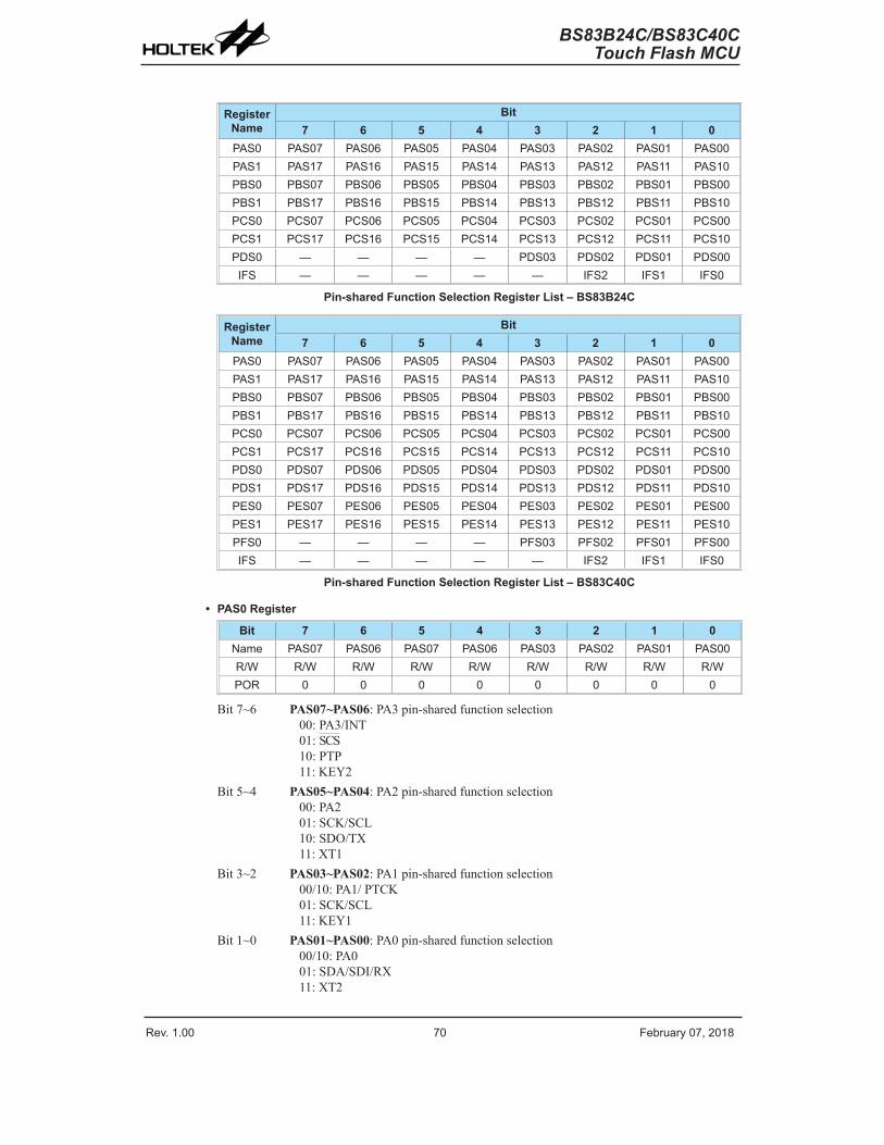
Rev. 1.00 �0 �e���a�� 0�� �01� Rev. 1.00 �1 �e���a�� 0�� �01�
BS83B24C/BS83C40CTouch Flash MCU
BS83B24C/BS83C40CTouch Flash MCU
Register Name
Bit7 6 5 4 3 2 1 0
PAS0 PAS0� PAS06 PAS05 PAS04 PAS03 PAS0� PAS01 PAS00PAS1 PAS1� PAS16 PAS15 PAS14 PAS13 PAS1� PAS11 PAS10PBS0 PBS0� PBS06 PBS05 PBS04 PBS03 PBS0� PBS01 PBS00PBS1 PBS1� PBS16 PBS15 PBS14 PBS13 PBS1� PBS11 PBS10PCS0 PCS0� PCS06 PCS05 PCS04 PCS03 PCS0� PCS01 PCS00PCS1 PCS1� PCS16 PCS15 PCS14 PCS13 PCS1� PCS11 PCS10PDS0 — — — — PDS03 PDS0� PDS01 PDS00I�S — — — — — I�S� I�S1 I�S0
Pin-shared Function Selection Register List – BS83B24C
Register Name
Bit7 6 5 4 3 2 1 0
PAS0 PAS0� PAS06 PAS05 PAS04 PAS03 PAS0� PAS01 PAS00PAS1 PAS1� PAS16 PAS15 PAS14 PAS13 PAS1� PAS11 PAS10PBS0 PBS0� PBS06 PBS05 PBS04 PBS03 PBS0� PBS01 PBS00PBS1 PBS1� PBS16 PBS15 PBS14 PBS13 PBS1� PBS11 PBS10PCS0 PCS0� PCS06 PCS05 PCS04 PCS03 PCS0� PCS01 PCS00PCS1 PCS1� PCS16 PCS15 PCS14 PCS13 PCS1� PCS11 PCS10PDS0 PDS0� PDS06 PDS05 PDS04 PDS03 PDS0� PDS01 PDS00PDS1 PDS1� PDS16 PDS15 PDS14 PDS13 PDS1� PDS11 PDS10PES0 PES0� PES06 PES05 PES04 PES03 PES0� PES01 PES00PES1 PES1� PES16 PES15 PES14 PES13 PES1� PES11 PES10P�S0 — — — — P�S03 P�S0� P�S01 P�S00I�S — — — — — I�S� I�S1 I�S0
Pin-shared Function Selection Register List – BS83C40C
• PAS0 Register
Bit 7 6 5 4 3 2 1 0Name PAS0� PAS06 PAS0� PAS06 PAS03 PAS0� PAS01 PAS00R/W R/W R/W R/W R/W R/W R/W R/W R/WPOR 0 0 0 0 0 0 0 0
Bit7~6 PAS07~PAS06:PA3pin-sharedfunctionselection00:PA3/INT01:SCS10:PTP11:KEY2
Bit5~4 PAS05~PAS04:PA2pin-sharedfunctionselection00:PA201:SCK/SCL10:SDO/TX11:XT1
Bit3~2 PAS03~PAS02:PA1pin-sharedfunctionselection00/10:PA1/PTCK01:SCK/SCL11:KEY1
Bit1~0 PAS01~PAS00:PA0pin-sharedfunctionselection00/10:PA001:SDA/SDI/RX11:XT2

Rev. 1.00 �0 �e���a�� 0�� �01� Rev. 1.00 �1 �e���a�� 0�� �01�
BS83B24C/BS83C40CTouch Flash MCU
BS83B24C/BS83C40CTouch Flash MCU
• PAS1 Register
Bit 7 6 5 4 3 2 1 0Name PAS1� PAS16 PAS15 PAS14 PAS13 PAS1� PAS11 PAS10R/W R/W R/W R/W R/W R/W R/W R/W R/WPOR 0 0 0 0 0 0 0 0
Bit7~6 PAS17~PAS16:PA7pin-sharedfunctionselection00/01/10:PA7/PTPI11:KEY6
Bit5~4 PAS15~PAS14:PA6pin-sharedfunctionselection00/01/10:PA6/INT11:KEY5
Bit3~2 PAS13~PAS12:PA5pin-sharedfunctionselection00/10:PA501:SDA/SDI/RX11:KEY4
Bit1~0 PAS11~PAS10:PA4pin-sharedfunctionselection00/10:PA401:SDO/TX11:KEY3
• PBS0 Register
Bit 7 6 5 4 3 2 1 0Name PBS0� PBS06 PBS05 PBS04 PBS03 PBS0� PBS01 PBS00R/W R/W R/W R/W R/W R/W R/W R/W R/WPOR 0 0 0 0 0 0 0 0
Bit7~6 PBS07~PBS06:PB3pin-sharedfunctionselection00/01/10:PB311:KEY10
Bit5~4 PBS05~PBS04:PB2pin-sharedfunctionselection00/01/10:PB211:KEY9
Bit3~2 PBS03~PBS02:PB1pin-sharedfunctionselection00/01/10:PB111:KEY8
Bit1~0 PBS01~PBS00:PB0pin-sharedfunctionselection00/01:PB010:PTPB11:KEY7
• PBS1 Register
Bit 7 6 5 4 3 2 1 0Name PBS1� PBS16 PBS15 PBS14 PBS13 PBS1� PBS11 PBS10R/W R/W R/W R/W R/W R/W R/W R/W R/WPOR 0 0 0 0 0 0 0 0
Bit7~6 PBS17~PBS16:PB7pin-sharedfunctionselection00/01/10:PB711:KEY14
Bit5~4 PBS15~PBS14:PB6pin-sharedfunctionselection00/01/10:PB611:KEY13
Bit3~2 PBS13~PBS12:PB5pin-sharedfunctionselection00/01/10:PB511:KEY12
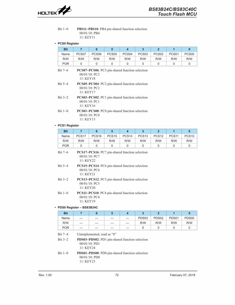
Rev. 1.00 �� �e���a�� 0�� �01� Rev. 1.00 �3 �e���a�� 0�� �01�
BS83B24C/BS83C40CTouch Flash MCU
BS83B24C/BS83C40CTouch Flash MCU
Bit1~0 PBS11~PBS10:PB4pin-sharedfunctionselection00/01/10:PB411:KEY11
• PCS0 Register
Bit 7 6 5 4 3 2 1 0Name PCS0� PCS06 PCS05 PCS04 PCS03 PCS0� PCS01 PCS00R/W R/W R/W R/W R/W R/W R/W R/W R/WPOR 0 0 0 0 0 0 0 0
Bit7~6 PCS07~PCS06:PC3pin-sharedfunctionselection00/01/10:PC311:KEY18
Bit5~4 PCS05~PCS04:PC2pin-sharedfunctionselection00/01/10:PC211:KEY17
Bit3~2 PCS03~PCS02:PC1pin-sharedfunctionselection00/01/10:PC111:KEY16
Bit1~0 PCS01~PCS00:PC0pin-sharedfunctionselection00/01/10:PC011:KEY15
• PCS1 Register
Bit 7 6 5 4 3 2 1 0Name PCS1� PCS16 PCS15 PCS14 PCS13 PCS1� PCS11 PCS10R/W R/W R/W R/W R/W R/W R/W R/W R/WPOR 0 0 0 0 0 0 0 0
Bit7~6 PCS17~PCS16:PC7pin-sharedfunctionselection00/01/10:PC711:KEY22
Bit5~4 PCS15~PCS14:PC6pin-sharedfunctionselection00/01/10:PC611:KEY21
Bit3~2 PCS13~PCS12:PC5pin-sharedfunctionselection00/01/10:PC511:KEY20
Bit1~0 PCS11~PCS10:PC4pin-sharedfunctionselection00/01/10:PC411:KEY19
• PDS0 Register – BS83B24C
Bit 7 6 5 4 3 2 1 0Name — — — — PDS03 PDS0� PDS01 PDS00R/W — — — — R/W R/W R/W R/WPOR — — — — 0 0 0 0
Bit7~4 Unimplemented,readas“0”Bit3~2 PDS03~PDS02:PD1pin-sharedfunctionselection
00/01/10:PD111:KEY24
Bit1~0 PDS01~PDS00:PD0pin-sharedfunctionselection00/01/10:PD011:KEY23
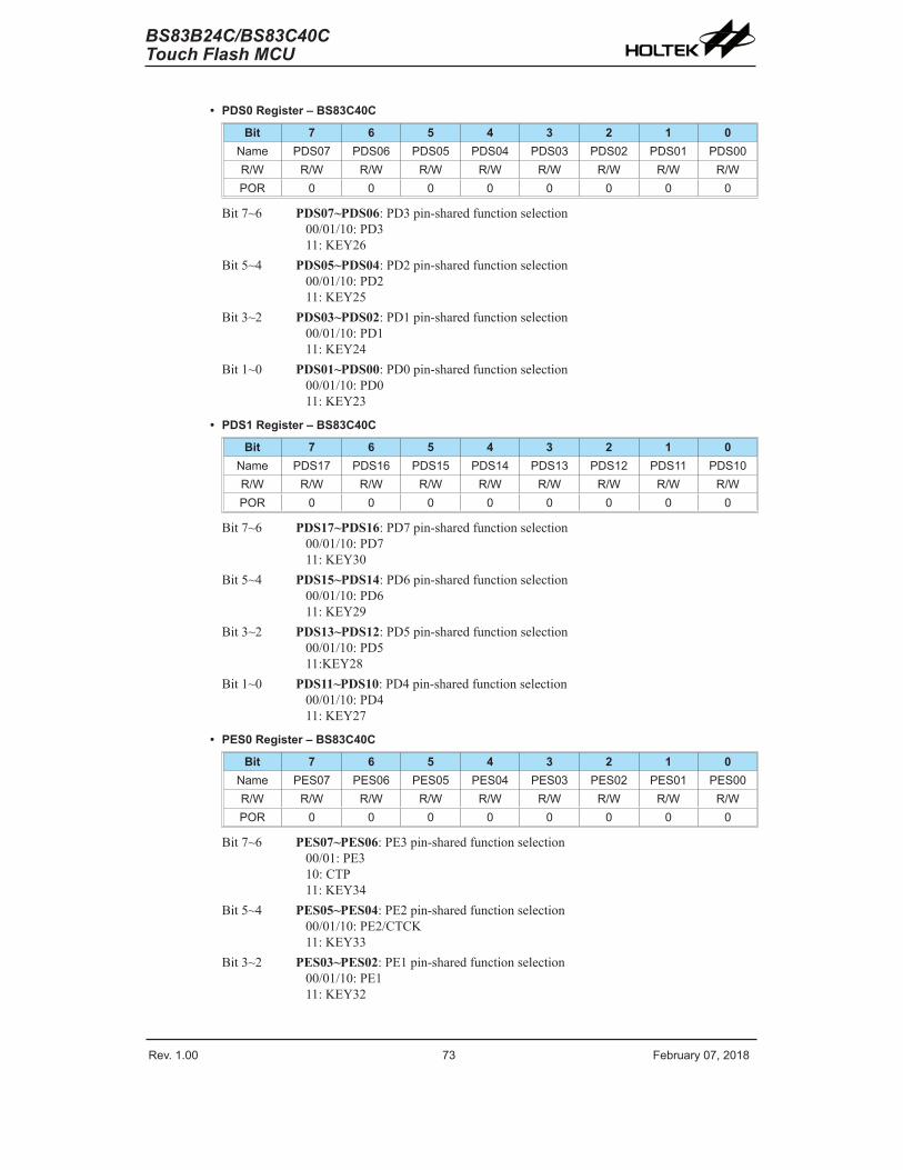
Rev. 1.00 �� �e���a�� 0�� �01� Rev. 1.00 �3 �e���a�� 0�� �01�
BS83B24C/BS83C40CTouch Flash MCU
BS83B24C/BS83C40CTouch Flash MCU
• PDS0 Register – BS83C40C
Bit 7 6 5 4 3 2 1 0Name PDS0� PDS06 PDS05 PDS04 PDS03 PDS0� PDS01 PDS00R/W R/W R/W R/W R/W R/W R/W R/W R/WPOR 0 0 0 0 0 0 0 0
Bit7~6 PDS07~PDS06:PD3pin-sharedfunctionselection00/01/10:PD311:KEY26
Bit5~4 PDS05~PDS04:PD2pin-sharedfunctionselection00/01/10:PD211:KEY25
Bit3~2 PDS03~PDS02:PD1pin-sharedfunctionselection00/01/10:PD111:KEY24
Bit1~0 PDS01~PDS00:PD0pin-sharedfunctionselection00/01/10:PD011:KEY23
• PDS1 Register – BS83C40C
Bit 7 6 5 4 3 2 1 0Name PDS1� PDS16 PDS15 PDS14 PDS13 PDS1� PDS11 PDS10R/W R/W R/W R/W R/W R/W R/W R/W R/WPOR 0 0 0 0 0 0 0 0
Bit7~6 PDS17~PDS16:PD7pin-sharedfunctionselection00/01/10:PD711:KEY30
Bit5~4 PDS15~PDS14:PD6pin-sharedfunctionselection00/01/10:PD611:KEY29
Bit3~2 PDS13~PDS12:PD5pin-sharedfunctionselection00/01/10:PD511:KEY28
Bit1~0 PDS11~PDS10:PD4pin-sharedfunctionselection00/01/10:PD411:KEY27
• PES0 Register – BS83C40C
Bit 7 6 5 4 3 2 1 0Name PES0� PES06 PES05 PES04 PES03 PES0� PES01 PES00R/W R/W R/W R/W R/W R/W R/W R/W R/WPOR 0 0 0 0 0 0 0 0
Bit7~6 PES07~PES06:PE3pin-sharedfunctionselection00/01:PE310:CTP11:KEY34
Bit5~4 PES05~PES04:PE2pin-sharedfunctionselection00/01/10:PE2/CTCK11:KEY33
Bit3~2 PES03~PES02:PE1pin-sharedfunctionselection00/01/10:PE111:KEY32

Rev. 1.00 �4 �e���a�� 0�� �01� Rev. 1.00 �5 �e���a�� 0�� �01�
BS83B24C/BS83C40CTouch Flash MCU
BS83B24C/BS83C40CTouch Flash MCU
Bit1~0 PES01~PES00:PE0pin-sharedfunctionselection00/01/10:PE011:KEY31
• PES1 Register – BS83C40C
Bit 7 6 5 4 3 2 1 0Name PES1� PES16 PES15 PES14 PES13 PES1� PES11 PES10R/W R/W R/W R/W R/W R/W R/W R/W R/WPOR 0 0 0 0 0 0 0 0
Bit7~6 PES17~PES16:PE7pin-sharedfunctionselection00/01/10:PE711:KEY38
Bit5~4 PES15~PES14:PE6pin-sharedfunctionselection00/01/10:PE611:KEY37
Bit3~2 PES13~PES12:PE5pin-sharedfunctionselection00/01/10:PE511:KEY36
Bit1~0 PES11~PES10:PE4pin-sharedfunctionselection00/01:PE410:CTPB11:KEY35
• PFS0 Register – BS83C40C
Bit 7 6 5 4 3 2 1 0Name — — — — P�S03 P�S0� P�S01 P�S00R/W — — — — R/W R/W R/W R/WPOR — — — — 0 0 0 0
Bit7~4 Unimplemented,readas“0”Bit3~2 PFS03~PFS02:PF1pin-sharedfunctionselection
00/01/10:PF111:KEY40
Bit1~0 PFS01~PFS00:PF0pin-sharedfunctionselection00/01/10:PF011:KEY39
• IFS Register
Bit 7 6 5 4 3 2 1 0Name — — — — — I�S� I�S1 I�S0R/W — — — — — R/W R/W R/WPOR — — — — — 0 0 0
Bit7~3 Unimplemented,readas“0”Bit2 IFS2:INTinputsourcepinselection
0:PA61:PA3
Bit1 IFS1:USIMSCK/SCLinputsourcepinselection0:PA21:PA1
Bit0 IFS0:USIMSDA/SDI/RXinputsourcepinselection0:PA01:PA5

Rev. 1.00 �4 �e���a�� 0�� �01� Rev. 1.00 �5 �e���a�� 0�� �01�
BS83B24C/BS83C40CTouch Flash MCU
BS83B24C/BS83C40CTouch Flash MCU
I/O Pin StructuresTheaccompanyingdiagramillustratestheinternalstructuresoftheI/Ologicfunction.Astheexactlogicalconstructionof theI/Opinwilldifferfromthisdiagram,it issuppliedasaguideonlytoassistwiththefunctionalunderstandingofthelogicfunctionI/Opins.Thewiderangeofpin-sharedstructuresdoesnotpermitalltypestobeshown.
MUX
VDD
Cont�ol Bit
Data Bit
Data B�s
W�ite Cont�ol Registe�
Chip Reset
Read Cont�ol Registe�
Read Data Registe�
W�ite Data Registe�
S�stem Wake-�p wake-�p Select
I/O pin
WeakP�ll-�p
P�ll-highRegiste�Select
Q
D
CK
Q
D
CK
Q
QS
S
PA onl�
Logic Function Input/Output Structure
Programming Considerations Withintheuserprogram,oneof thethingsfirst toconsider isport initialisation.Afterareset,allof theI/Odataandportcontrolregisterswillbeset tohigh.ThismeansthatallI/Opinswillbedefaultedtoaninputstate,thelevelofwhichdependsontheotherconnectedcircuitryandwhetherpull-highselectionshavebeenchosen.If theportcontrolregistersarethenprogrammedtosetupsomepinsasoutputs,theseoutputpinswillhaveaninitialhighoutputvalueunlesstheassociatedportdataregistersarefirstprogrammed.Selectingwhichpinsareinputsandwhichareoutputscanbeachievedbyte-widebyloadingthecorrectvalues into theappropriateportcontrolregisterorbyprogrammingindividualbitsintheportcontrolregisterusingthe“SET[m].i”and“CLR[m].i”instructions.Notethatwhenusingthesebitcontrolinstructions,aread-modify-writeoperationtakesplace.Themicrocontrollermustfirstreadinthedataontheentireport,modifyittotherequirednewbitvaluesandthenrewritethisdatabacktotheoutputports.
PortAhas theadditionalcapabilityofprovidingwake-upfunctions.When thedevice is in theSLEEPorIDLEMode,variousmethodsareavailabletowakethedeviceup.OneoftheseisahightolowtransitionofanyofthePortApins.SingleormultiplepinsonPortAcanbesetuptohavethisfunction.

Rev. 1.00 �6 �e���a�� 0�� �01� Rev. 1.00 �� �e���a�� 0�� �01�
BS83B24C/BS83C40CTouch Flash MCU
BS83B24C/BS83C40CTouch Flash MCU
Timer Modules – TMOneofthemostfundamentalfunctionsinanymicrocontrollerdevicesistheabilitytocontrolandmeasure time.To implement timerelatedfunctions thedevices includeseveralTimerModules,generallyabbreviatedtothenameTM.TheTMsaremulti-purposetimingunitsandservetoprovideoperationssuchasTimer/Counter,InputCapture,CompareMatchOutputandSinglePulseOutputaswellasbeingthefunctionalunitforthegenerationofPWMsignals.EachoftheTMshastwointerrupts.TheadditionofinputandoutputpinsforeachTMensuresthatusersareprovidedwithtimingunitswithawideandflexiblerangeoffeatures.
ThecommonfeaturesofthedifferentTMtypesaredescribedherewithmoredetailedinformationprovidedintheindividualCompactandPeriodicTypeTMsections.
IntroductionThesedevicescontainseveralTMsandeachindividualTMcanbecategorisedasacertaintype,namelyCompactTypeTMorPeriodicTypeTM.Althoughsimilarinnature,thedifferentTMtypesvaryintheirfeaturecomplexity.ThecommonfeaturestoalloftheCompactandPeriodictypeTMswillbedescribedinthissectionandthedetailedoperationregardingeachoftheTMtypeswillbedescribedinseparatesections.ThemainfeaturesanddifferencesbetweenthetwotypesofTMsaresummarisedintheaccompanyingtable.
TM Function CTM PTMTime�/Co�nte� √ √Inp�t Capt��e — √Compa�e Match O�tp�t √ √PWM Channels 1 1Single P�lse O�tp�t — 1PWM Alignment Edge EdgePWM Adj�stment Pe�iod & D�t� D�t� o� Pe�iod D�t� o� Pe�iod
TM Function Summary
Device CTM PTMBS�3B�4C — 10-�it PTMBS�3C40C 10-�it CTM 10-�it PTM
TM Name/Type Summary
TM OperationThedifferenttypesofTMofferadiverserangeoffunctions,fromsimpletimingoperationstoPWMsignalgeneration.Thekeytounderstandinghow theTMoperates is tosee it in termsofafreerunningcount-upcounterwhosevalueisthencomparedwiththevalueofpre-programmedinternalcomparators.Whenthefreerunningcount-upcounterhasthesamevalueasthepre-programmedcomparator,knownasacomparematchsituation,aTMinterruptsignalwillbegeneratedwhichcanclearthecounterandperhapsalsochangetheconditionoftheTMoutputpin.TheinternalTMcounterisdrivenbyauserselectableclocksource,whichcanbeaninternalclockoranexternalpin.
TM Clock SourceTheclocksourcewhichdrivesthemaincounterineachTMcanoriginatefromvarioussources.TheselectionoftherequiredclocksourceisimplementedusingthexTCK2~xTCK0bitsinthexTMcontrolregisters,where“x”standsforCorPtypeTM.Theclocksourcecanbearatioofthesystemclock,fSYS,ortheinternalhighclock,fH,thefSUBclocksourceortheexternalxTCKpin.ThexTCKpinclocksourceisusedtoallowanexternalsignaltodrivetheTMasanexternalclocksourceforeventcounting.
Rev. 1.00 �6 �e���a�� 0�� �01� Rev. 1.00 �� �e���a�� 0�� �01�
BS83B24C/BS83C40CTouch Flash MCU
BS83B24C/BS83C40CTouch Flash MCU
TM InterruptsTheCompactorPeriodictypeTMhastwointernalinterrupt,oneforeachoftheinternalcomparatorAorcomparatorP,whichgenerateaTMinterruptwhenacomparematchconditionoccurs.WhenaTMinterruptisgenerated,itcanbeusedtoclearthecounterandalsotochangethestateoftheTMoutputpin.
TM External PinsEachoftheTMs,irrespectiveofwhattype,hasanTMinputpin,withthelabelxTCK.ThexTMinputpin,xTCK,isessentiallyaclocksourceforthexTMandisselectedusingthexTCK2~xTCK0bitsinthexTMC0register.ThisexternalTMinputpinallowsanexternalclocksourcetodrivetheinternalTM.ThexTCKinputpincanbechosentohaveeitherarisingorfallingactiveedge.ThePTCKpinisalsousedastheexternaltriggerinputpininsinglepulseoutputmodeforthePTM.
ThePeriodictypeTMhasanotherinputpin,PTPI,whichisthecaptureinputwhoseactiveedgecanbearisingedge,afallingedgeorbothrisingandfallingedgesandtheactiveedgetransitiontypeisselectedusingthePTIO1~PTIO0bitsinthePTMC1register.
TheTMseachhastwooutputpins,xTPandxTPB.TheTMoutputpincanbeselectedusingthecorrespondingpin-sharedfunctionselectionbitsdescribedinthePin-sharedFunctionsection.WhentheTMisintheCompareMatchOutputMode,thesepinscanbecontrolledbytheTMtoswitchtoahighorlowlevelortotogglewhenacomparematchsituationoccurs.TheexternalxTPandxTPBoutputpinsarealsothepinswheretheTMgeneratesthePWMoutputwaveform.
AstheTMinput/outputpinsarepin-sharedwithotherfunctions,theTMinput/outputfunctionmustfirstbesetupusingrelevantpin-sharedfunctionselectionregister.Thedetailsof thepin-sharedfunctionselectionaredescribedinthepin-sharedfunctionsection.
DeviceCTM PTM
Input Output Input OutputBS�3B�4C — — PTCK� PTPI PTP� PTPBBS�3C40C CTCK CTP� CTPB PTCK� PTPI PTP� PTPB
TM External Pins
CTM
CTCK
CTPCCR o�tp�t
Clock inp�t
CTPB
CTM Function Pin Block Diagram
PTM
PTCK
PTPCCR o�tp�t
Clock inp�t
PTPB
PTPICapt��e inp�t
PTM Function Pin Block Diagram
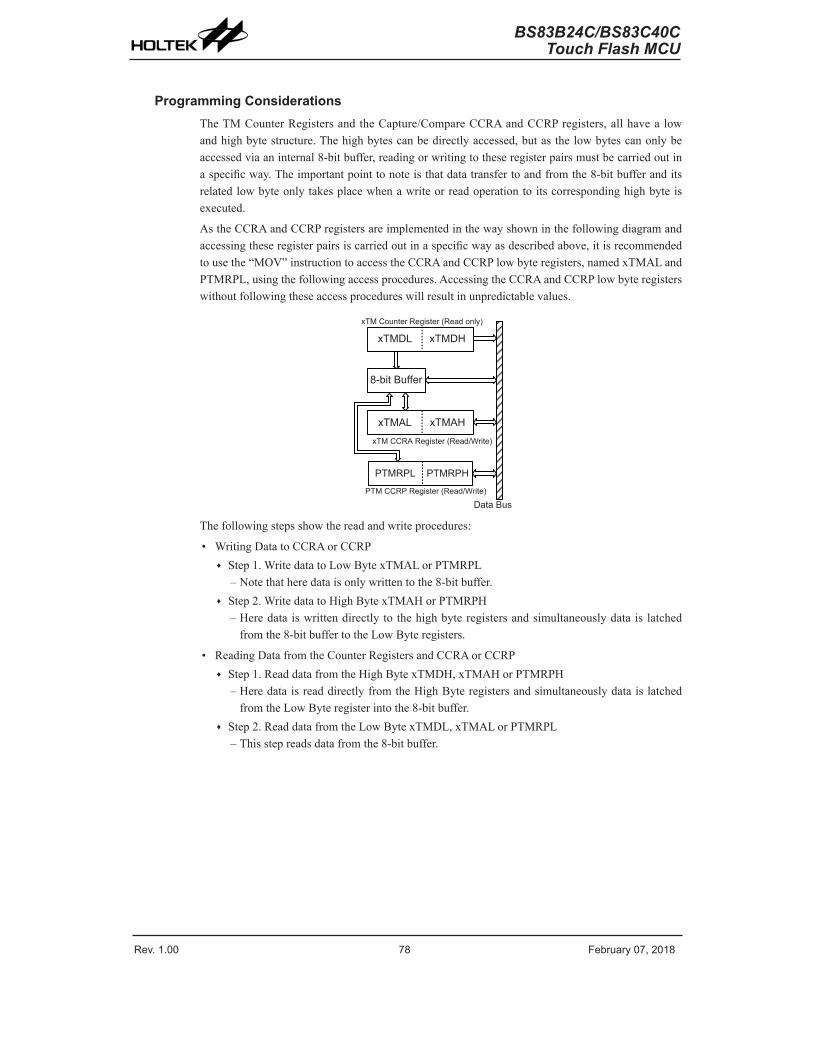
Rev. 1.00 �� �e���a�� 0�� �01� Rev. 1.00 �9 �e���a�� 0�� �01�
BS83B24C/BS83C40CTouch Flash MCU
BS83B24C/BS83C40CTouch Flash MCU
Programming ConsiderationsTheTMCounterRegistersandtheCapture/CompareCCRAandCCRPregisters,allhavea lowandhighbytestructure.Thehighbytescanbedirectlyaccessed,butasthelowbytescanonlybeaccessedviaaninternal8-bitbuffer,readingorwritingtotheseregisterpairsmustbecarriedoutinaspecificway.Theimportantpointtonoteisthatdatatransfertoandfromthe8-bitbufferanditsrelatedlowbyteonlytakesplacewhenawriteorreadoperationtoitscorrespondinghighbyteisexecuted.
AstheCCRAandCCRPregistersareimplementedinthewayshowninthefollowingdiagramandaccessingtheseregisterpairsiscarriedoutinaspecificwayasdescribedabove,itisrecommendedtousethe“MOV”instructiontoaccesstheCCRAandCCRPlowbyteregisters,namedxTMALandPTMRPL,usingthefollowingaccessprocedures.AccessingtheCCRAandCCRPlowbyteregisterswithoutfollowingtheseaccessprocedureswillresultinunpredictablevalues.
Data B�s
�-�it B�ffe�
xTMDHxTMDL
xTMAHxTMAL
xTM Co�nte� Registe� (Read onl�)
xTM CCRA Registe� (Read/W�ite)
PTMRPHPTMRPL
PTM CCRP Registe� (Read/W�ite)
Thefollowingstepsshowthereadandwriteprocedures:
• WritingDatatoCCRAorCCRP♦ Step1.WritedatatoLowBytexTMALorPTMRPL
– Notethatheredataisonlywrittentothe8-bitbuffer.♦ Step2.WritedatatoHighBytexTMAHorPTMRPH
– Heredataiswrittendirectlytothehighbyteregistersandsimultaneouslydatais latchedfromthe8-bitbuffertotheLowByteregisters.
• ReadingDatafromtheCounterRegistersandCCRAorCCRP♦ Step1.ReaddatafromtheHighBytexTMDH,xTMAHorPTMRPH
– HeredataisreaddirectlyfromtheHighByteregistersandsimultaneouslydataislatchedfromtheLowByteregisterintothe8-bitbuffer.
♦ Step2.ReaddatafromtheLowBytexTMDL,xTMALorPTMRPL– Thisstepreadsdatafromthe8-bitbuffer.

Rev. 1.00 �� �e���a�� 0�� �01� Rev. 1.00 �9 �e���a�� 0�� �01�
BS83B24C/BS83C40CTouch Flash MCU
BS83B24C/BS83C40CTouch Flash MCU
Compact Type TM – CTMAlthough thesimplest formof the threeTMtypes, theCompactTMtypestill contains threeoperatingmodes,whichareCompareMatchOutput,Timer/EventCounterandPWMOutputmodes.TheCompactTypeTMcanalsobecontrolledwithanexternalinputpinandcandrivetwoexternaloutputpins.
fSYS
fSYS/4
fH/64fH/16
fSUB
CTCK
000001010011100101110111
CTCK�~CTCK0
10-�it Co�nt-�p Co�nte�
3-�it Compa�ato� P
CCRP
��~�9
�0~�9
10-�it Compa�ato� A
CTONCTPAU
Compa�ato� A Match
Compa�ato� P Match
Co�nte� Clea� 01
O�tp�tCont�ol
Pola�it� Cont�ol Pin Cont�ol CTP
CTOC
CTM1~CTM0CTIO1~CTIO0
CTMA� Inte���pt
CTMP� Inte���pt
CTPOL PxSn
CCRA
CTCCLRfSUB
CTPB
Note:TheCTPBistheinvertedoutputoftheCTPpin.
10-bit Compact Type TM Block Diagram
Compact TM OperationAtitscoreisa10-bitcount-upcounterwhichisdrivenbyauserselectableinternalorexternalclocksource.Therearealso twointernalcomparatorswith thenames,ComparatorAandComparatorP.ThesecomparatorswillcomparethevalueinthecounterwithCCRPandCCRAregisters.TheCCRPisthreebitswidewhosevalueiscomparedwiththehighestthreebitsinthecounterwhiletheCCRAisthetenbitsandthereforecompareswithallcounterbits.
Theonlywayofchanging thevalueof the10-bitcounterusing theapplicationprogram, is toclear thecounterbychanging theCTONbit fromlowtohigh.Thecounterwillalsobeclearedautomaticallybyacounteroverfloworacomparematchwithoneof itsassociatedcomparators.Whentheseconditionsoccur,aCTMinterruptsignalwillalsousuallybegenerated.TheCompactTypeTMcanoperateinanumberofdifferentoperationalmodes,canbedrivenbydifferentclocksourcesincludinganinputpinandcanalsocontroltwooutputpins.Alloperatingsetupconditionsareselectedusingrelevantinternalregisters.
Compact Type TM Register DescriptionOveralloperationoftheCompactTypeTMiscontrolledusingseveralregisters.Areadonlyregisterpairexiststostoretheinternalcounter10-bitvalue,whilearead/writeregisterpairexiststostoretheinternal10-bitCCRAvalue.TheremainingtworegistersarecontrolregisterswhichsetupthedifferentoperatingandcontrolmodesaswellasthethreeCCRPbits.
RegisterName
Bit
7 6 5 4 3 2 1 0
CTMC0 CTPAU CTCK� CTCK1 CTCK0 CTON CTRP� CTRP1 CTRP0
CTMC1 CTM1 CTM0 CTIO1 CTIO0 CTOC CTPOL CTDPX CTCCLR
CTMDL D� D6 D5 D4 D3 D� D1 D0
CTMDH — — — — — — D9 D�
CTMAL D� D6 D5 D4 D3 D� D1 D0
CTMAH — — — — — — D9 D�
10-bit Compact Type TM Register List
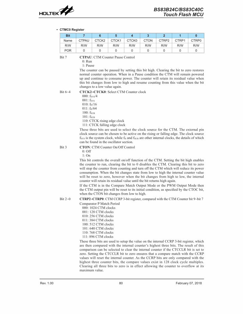
Rev. 1.00 �0 �e���a�� 0�� �01� Rev. 1.00 �1 �e���a�� 0�� �01�
BS83B24C/BS83C40CTouch Flash MCU
BS83B24C/BS83C40CTouch Flash MCU
• CTMC0 Register
Bit 7 6 5 4 3 2 1 0Name CTPAU CTCK� CTCK1 CTCK0 CTON CTRP� CTRP1 CTRP0R/W R/W R/W R/W R/W R/W R/W R/W R/WPOR 0 0 0 0 0 0 0 0
Bit7 CTPAU:CTMCounterPauseControl0:Run1:Pause
Thecountercanbepausedbysettingthisbithigh.Clearingthebit tozerorestoresnormalcounteroperation.WheninaPauseconditiontheCTMwillremainpoweredupandcontinuetoconsumepower.Thecounterwillretainitsresidualvaluewhenthisbitchangesfromlowtohighandresumecountingfromthisvaluewhenthebitchangestoalowvalueagain.
Bit6~4 CTCK2~CTCK0:SelectCTMCounterclock000:fSYS/4001:fSYS
010:fH/16011:fH/64100:fSUB
101:fSUB
110:CTCKrisingedgeclock111:CTCKfallingedgeclock
These threebitsareusedtoselect theclocksourcefor theCTM.Theexternalpinclocksourcecanbechosentobeactiveontherisingorfallingedge.TheclocksourcefSYSisthesystemclock,whilefHandfSUBareotherinternalclocks,thedetailsofwhichcanbefoundintheoscillatorsection.
Bit3 CTON:CTMCounterOn/OffControl0:Off1:On
Thisbitcontrolstheoverallon/offfunctionoftheCTM.Settingthebithighenablesthecounter torun,clearingthebit to0disables theCTM.Clearingthisbit tozerowillstopthecounterfromcountingandturnofftheCTMwhichwillreduceitspowerconsumption.Whenthebitchangesstatefromlowtohightheinternalcountervaluewillbereset tozero,howeverwhenthebitchangesfromhighto low, the internalcounterwillretainitsresidualvalueuntilthebitreturnshighagain.If theCTMisintheCompareMatchOutputModeorthePWMOutputModethentheCTMoutputpinwillberesettoitsinitialcondition,asspecifiedbytheCTOCbit,whentheCTONbitchangesfromlowtohigh.
Bit2~0 CTRP2~CTRP0:CTMCCRP3-bitregister,comparedwiththeCTMCounterbit9~bit7ComparatorPMatchPeriod000:1024CTMclocks001:128CTMclocks010:256CTMclocks011:384CTMclocks100:512CTMclocks101:640CTMclocks110:768CTMclocks111:896CTMclocks
ThesethreebitsareusedtosetupthevalueontheinternalCCRP3-bitregister,whichare thencomparedwith the internalcounter’shighest threebits.Theresultof thiscomparisoncanbeselectedtocleartheinternalcounterif theCTCCLRbit isset tozero.SettingtheCTCCLRbit tozeroensuresthatacomparematchwiththeCCRPvalueswillreset theinternalcounter.AstheCCRPbitsareonlycomparedwiththehighest threecounterbits, thecomparevaluesexist in128clockcyclemultiples.Clearingall threebits tozero is ineffectallowing thecounter tooverflowat itsmaximumvalue.

Rev. 1.00 �0 �e���a�� 0�� �01� Rev. 1.00 �1 �e���a�� 0�� �01�
BS83B24C/BS83C40CTouch Flash MCU
BS83B24C/BS83C40CTouch Flash MCU
• CTMC1 Register
Bit 7 6 5 4 3 2 1 0Name CTM1 CTM0 CTIO1 CTIO0 CTOC CTPOL CTDPX CTCCLRR/W R/W R/W R/W R/W R/W R/W R/W R/WPOR 0 0 0 0 0 0 0 0
Bit7~6 CTM1~CTM0:SelectCTMOperatingMode00:CompareMatchOutputMode01:Undefined10:PWMOutputMode11:Timer/CounterMode
Thesebits setup the requiredoperatingmode for theCTM.Toensure reliableoperationtheCTMshouldbeswitchedoffbeforeanychangesaremadetotheCTM1andCTM0bits.IntheTimer/CounterMode,theCTMoutputpinstateisundefined.
Bit5~4 CTIO1~CTIO0:SelectCTPoutputfunctionCompareMatchOutputMode00:Nochange01:Outputlow10:Outputhigh11:Toggleoutput
PWMOutputMode00:PWMOutputinactivestate01:PWMOutputactivestate10:PWMoutput11:Undefined
Timer/counterModeUnused
ThesetwobitsareusedtodeterminehowtheCTMoutputpinchangesstatewhenacertainconditionisreached.ThefunctionthatthesebitsselectdependsuponinwhichmodetheCTMisrunning.IntheCompareMatchOutputMode,theCTIO1andCTIO0bitsdeterminehowtheCTMoutputpinchangesstatewhenacomparematchoccursfromtheComparatorA.TheCTMoutputpincanbesetuptoswitchhigh,switchlowortotoggleitspresentstatewhenacomparematchoccursfromtheComparatorA.Whenthebitsarebothzero,thennochangewilltakeplaceontheoutput.TheinitialvalueoftheCTMoutputpinshouldbesetupusingtheCTOCbitintheCTMC1register.NotethattheoutputlevelrequestedbytheCTIO1andCTIO0bitsmustbedifferentfromtheinitialvaluesetupusingtheCTOCbitotherwisenochangewilloccurontheCTMoutputpinwhenacomparematchoccurs.AftertheCTMoutputpinchangesstateitcanberesettoitsinitiallevelbychangingtheleveloftheCTONbitfromlowtohigh.In thePWMOutputMode, theCTIO1andCTIO0bitsdeterminehow theCTMoutputpinchangesstatewhenacertaincomparematchconditionoccurs.ThePWMoutputfunctionismodifiedbychangingthesetwobits.ItisnecessarytoonlychangethevaluesoftheCTIO1andCTIO0bitsonlyaftertheCTMhasbeenswitchedoff.UnpredictablePWMoutputswilloccur if theCTIO1andCTIO0bitsarechangedwhenTheCTMisrunning.

Rev. 1.00 �� �e���a�� 0�� �01� Rev. 1.00 �3 �e���a�� 0�� �01�
BS83B24C/BS83C40CTouch Flash MCU
BS83B24C/BS83C40CTouch Flash MCU
Bit3 CTOC:CTPOutputcontrolbitCompareMatchOutputMode0:Initiallow1:Initialhigh
PWMOutputMode0:Activelow1:Activehigh
This is theoutputcontrolbit for theCTMoutputpin. ItsoperationdependsuponwhetherCTMisbeingused in theCompareMatchOutputModeor in thePWMOutputMode. Ithasnoeffect if theCTMis in theTimer/CounterMode. In theCompareMatchOutputModeitdetermines the logic levelof theCTMoutputpinbeforeacomparematchoccurs.InthePWMOutputModeitdeterminesifthePWMsignalisactivehighoractivelow.
Bit2 CTPOL:CTPOutputpolarityControl0:Non-invert1:Invert
ThisbitcontrolsthepolarityoftheCTPoutputpin.WhenthebitissethightheCTMoutputpinwillbeinvertedandnotinvertedwhenthebitiszero.IthasnoeffectiftheCTMisintheTimer/CounterMode.
Bit1 CTDPX:CTMPWMperiod/dutyControl0:CCRP–period;CCRA–duty1:CCRP–duty;CCRA–period
ThisbitdetermineswhichoftheCCRAandCCRPregistersareusedforperiodanddutycontrolofthePWMwaveform.
Bit0 CTCCLR:SelectCTMCounterclearcondition0:CTMComparatrorPmatch1:CTMComparatrorAmatch
Thisbit isused toselect themethodwhichclears thecounter.Remember that theCompactTMcontainstwocomparators,ComparatorAandComparatorP,eitherofwhichcanbeselectedtoclear theinternalcounter.WiththeCTCCLRbitsethigh,thecounterwillbeclearedwhenacomparematchoccursfromtheComparatorA.Whenthebitislow,thecounterwillbeclearedwhenacomparematchoccursfromtheComparatorPorwithacounteroverflow.AcounteroverflowclearingmethodcanonlybeimplementediftheCCRPbitsareallclearedtozero.TheCTCCLRbitisnotusedinthePWMOutputMode.
• CTMDL Register
Bit 7 6 5 4 3 2 1 0Name D� D6 D5 D4 D3 D� D1 D0R/W R R R R R R R RPOR 0 0 0 0 0 0 0 0
Bit7~0 CTMCounterLowByteRegisterbit7~bit0CTM10-bitCounterbit7~bit0
• CTMDH Register
Bit 7 6 5 4 3 2 1 0Name — — — — — — D9 D�R/W — — — — — — R RPOR — — — — — — 0 0
Bit7~2 Unimplemented,readas“0”Bit1~0 CTMCounterHighByteRegisterbit1~bit0
CTM10-bitCounterbit9~bit8

Rev. 1.00 �� �e���a�� 0�� �01� Rev. 1.00 �3 �e���a�� 0�� �01�
BS83B24C/BS83C40CTouch Flash MCU
BS83B24C/BS83C40CTouch Flash MCU
• CTMAL Register
Bit 7 6 5 4 3 2 1 0Name D� D6 D5 D4 D3 D� D1 D0R/W R/W R/W R/W R/W R/W R/W R/W R/WPOR 0 0 0 0 0 0 0 0
Bit7~0 CTMCCRALowByteRegisterbit7~bit0CTM10-bitCCRAbit7~bit0
• CTMAH Register
Bit 7 6 5 4 3 2 1 0Name — — — — — — D9 D�R/W — — — — — — R/W R/WPOR — — — — — — 0 0
Bit7~2 Unimplemented,readas“0”Bit1~0 CTMCCRAHighByteRegisterbit1~bit0
CTM10-bitCCRAbit9~bit8
Compact Type TM Operating ModesTheCompactTypeTMcanoperateinoneofthreeoperatingmodes,CompareMatchOutputMode,PWMOutputModeorTimer/CounterMode.TheoperatingmodeisselectedusingtheCTM1andCTM0bitsintheCTMC1register.
Compare Match Output ModeToselectthismode,bitsCTM1andCTM0intheCTMC1register,shouldbesetto00respectively.Inthismodeoncethecounterisenabledandrunningitcanbeclearedbythreemethods.Theseareacounteroverflow,acomparematchfromComparatorAandacomparematchfromComparatorP.WhentheCTCCLRbitislow,therearetwowaysinwhichthecountercanbecleared.OneiswhenacomparematchfromComparatorP,theotheriswhentheCCRPbitsareallzerowhichallowsthecountertooverflow.HerebothCTMAFandCTMPFinterruptrequestflagsforComparatorAandComparatorPrespectively,willbothbegenerated.
IftheCTCCLRbitintheCTMC1registerishighthenthecounterwillbeclearedwhenacomparematchoccursfromComparatorA.However,hereonlytheCTMAFinterruptrequestflagwillbegeneratedevenifthevalueoftheCCRPbitsislessthanthatoftheCCRAregisters.ThereforewhenCTCCLRishighnoCTMPFinterruptrequestflagwillbegenerated.
IftheCCRAbitsareallzero,thecounterwilloverflowwhenitsreachesitsmaximum10-bit,3FFHex,value,howeverheretheCTMAFinterruptrequestflagwillnotbegenerated.
Asthenameof themodesuggests,afteracomparisonismade, theCTMoutputpinwillchangestate.TheCTMoutputpinconditionhoweveronlychangesstatewhenaCTMAFinterruptrequestflagisgeneratedafteracomparematchoccursfromComparatorA.TheCTMPFinterruptrequestflag,generatedfromacomparematchoccursfromComparatorP,willhavenoeffectontheCTMoutputpin.ThewayinwhichtheCTMoutputpinchangesstatearedeterminedbytheconditionoftheCTIO1andCTIO0bitsintheCTMC1register.TheCTMoutputpincanbeselectedusingtheCTIO1andCTIO0bitstogohigh,togolowortotogglefromitspresentconditionwhenacomparematchoccursfromComparatorA.TheinitialconditionoftheCTMoutputpin,whichissetupaftertheCTONbitchangesfromlowtohigh,issetupusingtheCTOCbit.NotethatiftheCTIO1andCTIO0bitsarezerothennopinchangewilltakeplace.

Rev. 1.00 �4 �e���a�� 0�� �01� Rev. 1.00 �5 �e���a�� 0�� �01�
BS83B24C/BS83C40CTouch Flash MCU
BS83B24C/BS83C40CTouch Flash MCU
Co�nte� Val�e
0x3��
CCRP
CCRA
CTON
CTPAU
CTPOL
CCRP Int. flag CTMP�
CCRA Int. flag CTMA�
CTM O/P Pin
Time
CCRP=0
CCRP > 0
Co�nte� ove�flowCCRP > 0Co�nte� clea�ed �� CCRP val�e
Pa�se
Res�me
Stop
Co�nte� Resta�t
CTCCLR = 0; CTM [1:0] = 00
O�tp�t pin set to initial Level Low if CTOC=0
O�tp�t Toggle with CTMA� flag
Note CTIO [1:0] = 10 Active High O�tp�t selectHe�e CTIO [1:0] = 11
Toggle O�tp�t select
O�tp�t not affected �� CTMA� flag. Remains High �ntil �eset �� CTON �it
O�tp�t PinReset to Initial val�e
O�tp�t cont�olled �� othe� pin-sha�ed f�nction
O�tp�t Inve�tswhen CTPOL is high
Compare Match Output Mode – CTCCLR=0Notes:1.WithCTCCLR=0,aComparatorPmatchwillclearthecounter
2.TheCTMoutputpincontrolledonlybytheCTMAFflag3.TheoutputpinresettoinitialstatebyaCTONbitrisingedge

Rev. 1.00 �4 �e���a�� 0�� �01� Rev. 1.00 �5 �e���a�� 0�� �01�
BS83B24C/BS83C40CTouch Flash MCU
BS83B24C/BS83C40CTouch Flash MCU
Co�nte� Val�e
0x3��
CCRP
CCRA
CTON
CTPAU
CTPOL
CTM O/P Pin
Time
CCRA=0
CCRA = 0Co�nte� ove�flowCCRA > 0 Co�nte� clea�ed �� CCRA val�e
Pa�se
Res�me
Stop Co�nte� Resta�t
O�tp�t pin set to initial Level Low if CTOC=0
O�tp�t Toggle with CTMA� flag
Note CTIO [1:0] = 10 Active High O�tp�t selectHe�e CTIO [1:0] = 11
Toggle O�tp�t select
O�tp�t not affected �� CTMA� flag. Remains High �ntil �eset �� CTON �it O�tp�t Pin
Reset to Initial val�eO�tp�t cont�olled �� othe� pin-sha�ed f�nction
O�tp�t Inve�tswhen CTPOL is high
CTMP� not gene�ated
No CTMA� flag gene�ated on CCRA ove�flow
O�tp�t does not change
CTCCLR = 1; CTM [1:0] = 00
CCRA Int. flag CTMA�
CCRP Int. flag CTMP�
Compare Match Output Mode – CTCCLR=1Notes:1.WithCTCCLR=1,aComparatorAmatchwillclearthecounter
2.TheCTMoutputpincontrolledonlybytheCTMAFflag3.TheoutputpinresettoinitialstatebyaCTONrisingedge4.TheCTMPFflagsisnotgeneratedwhenCTCCLR=1
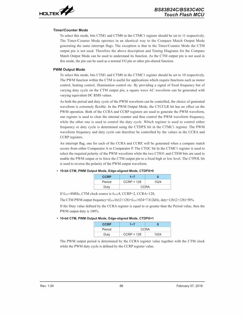
Rev. 1.00 �6 �e���a�� 0�� �01� Rev. 1.00 �� �e���a�� 0�� �01�
BS83B24C/BS83C40CTouch Flash MCU
BS83B24C/BS83C40CTouch Flash MCU
Timer/Counter ModeToselectthismode,bitsCTM1andCTM0intheCTMC1registershouldbesetto11respectively.TheTimer/CounterModeoperates in an identicalway to theCompareMatchOutputModegenerating thesameinterrupt flags.Theexception is that in theTimer/CounterMode theCTMoutputpin isnotused.Therefore theabovedescriptionandTimingDiagramsfor theCompareMatchOutputModecanbeusedtounderstanditsfunction.AstheCTMoutputpinisnotusedinthismode,thepincanbeusedasanormalI/Opinorotherpin-sharedfunction.
PWM Output ModeToselectthismode,bitsCTM1andCTM0intheCTMC1registershouldbesetto10respectively.ThePWMfunctionwithintheCTMisusefulforapplicationswhichrequirefunctionssuchasmotorcontrol,heatingcontrol, illuminationcontroletc.Byprovidingasignaloffixedfrequencybutofvaryingdutycycleon theCTMoutputpin,asquarewaveACwaveformcanbegeneratedwithvaryingequivalentDCRMSvalues.
AsboththeperiodanddutycycleofthePWMwaveformcanbecontrolled,thechoiceofgeneratedwaveformisextremelyflexible.InthePWMOutputMode,theCTCCLRbithasnoeffectonthePWMoperation.BothoftheCCRAandCCRPregistersareusedtogeneratethePWMwaveform,oneregister isusedtocleartheinternalcounterandthuscontrol thePWMwaveformfrequency,while theotherone isused tocontrol thedutycycle.Which register isused tocontroleitherfrequencyordutycycle isdeterminedusing theCTDPXbit in theCTMC1register.ThePWMwaveformfrequencyanddutycyclecanthereforebecontrolledbythevalues in theCCRAandCCRPregisters.
Aninterruptflag,oneforeachoftheCCRAandCCRP,willbegeneratedwhenacomparematchoccursfromeitherComparatorAorComparatorP.TheCTOCbitIntheCTMC1registerisusedtoselecttherequiredpolarityofthePWMwaveformwhilethetwoCTIO1andCTIO0bitsareusedtoenablethePWMoutputortoforcetheCTMoutputpintoafixedhighorlowlevel.TheCTPOLbitisusedtoreversethepolarityofthePWMoutputwaveform.
• 10-bit CTM, PWM Output Mode, Edge-aligned Mode, CTDPX=0
CCRP 1~7 0Pe�iod CCRP × 1�� 10�4D�t� CCRA
IffSYS=8MHz,CTMclocksourceisfSYS/4,CCRP=2,CCRA=128,
TheCTMPWMoutputfrequency=(fSYS/4)/(2×128)=fSYS/1024=7.812kHz,duty=128/(2×128)=50%.
IftheDutyvaluedefinedbytheCCRAregisterisequaltoorgreaterthanthePeriodvalue,thenthePWMoutputdutyis100%.
• 10-bit CTM, PWM Output Mode, Edge-aligned Mode, CTDPX=1
CCRP 1~7 0Pe�iod CCRAD�t� CCRP × 1�� 10�4
ThePWMoutputperiodisdeterminedbytheCCRAregistervaluetogetherwiththeCTMclockwhilethePWMdutycycleisdefinedbytheCCRPregistervalue.
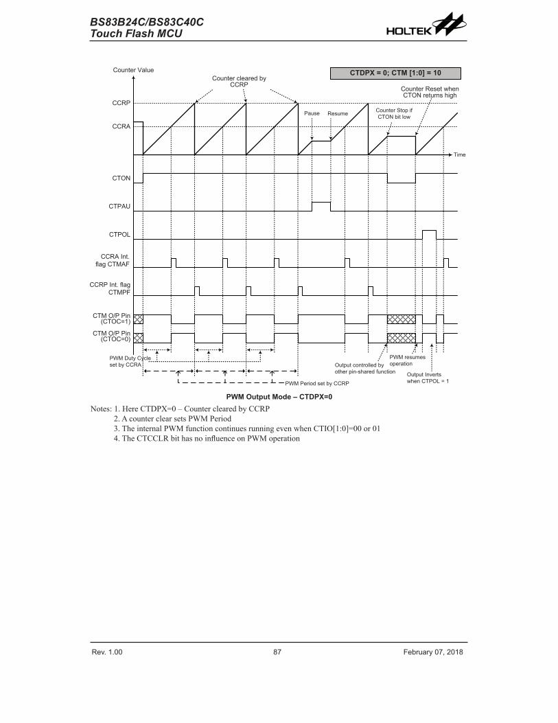
Rev. 1.00 �6 �e���a�� 0�� �01� Rev. 1.00 �� �e���a�� 0�� �01�
BS83B24C/BS83C40CTouch Flash MCU
BS83B24C/BS83C40CTouch Flash MCU
Co�nte� Val�e
CCRP
CCRA
CTON
CTPAU
CTPOL
CTM O/P Pin (CTOC=1)
Time
Co�nte� clea�ed �� CCRP
Pa�se Res�me Co�nte� Stop if CTON �it low
Co�nte� Reset when CTON �et��ns high
PWM D�t� C�cle set �� CCRA
PWM �es�mes ope�ationO�tp�t cont�olled ��
othe� pin-sha�ed f�nction O�tp�t Inve�tswhen CTPOL = 1PWM Pe�iod set �� CCRP
CTM O/P Pin (CTOC=0)
CCRA Int. flag CTMA�
CCRP Int. flag CTMP�
CTDPX = 0; CTM [1:0] = 10
PWM Output Mode – CTDPX=0Notes:1.HereCTDPX=0–CounterclearedbyCCRP
2.AcounterclearsetsPWMPeriod3.TheinternalPWMfunctioncontinuesrunningevenwhenCTIO[1:0]=00or014.TheCTCCLRbithasnoinfluenceonPWMoperation

Rev. 1.00 �� �e���a�� 0�� �01� Rev. 1.00 �9 �e���a�� 0�� �01�
BS83B24C/BS83C40CTouch Flash MCU
BS83B24C/BS83C40CTouch Flash MCU
Co�nte� Val�e
CCRP
CCRA
CTON
CTPAU
CTPOL
CCRP Int. flag CTMP�
CCRA Int. flag CTMA�
CTM O/P Pin (CTOC=1)
Time
Co�nte� clea�ed �� CCRA
Pa�se Res�me Co�nte� Stop if CTON �it low
Co�nte� Reset when CTON �et��ns high
PWM D�t� C�cle set �� CCRP
PWM �es�mes ope�ationO�tp�t cont�olled ��
othe� pin-sha�ed f�nction O�tp�t Inve�tswhen CTPOL = 1
PWM Pe�iod set �� CCRA
CTM O/P Pin (CTOC=0)
CTDPX = 1; CTM [1:0] = 10
PWM Output Mode – CTDPX=1Notes:1.HereCTDPX=1–CounterclearedbyCCRA
2.AcounterclearsetsPWMPeriod3.TheinternalPWMfunctioncontinuesevenwhenCTIO[1:0]=00or014.TheCTCCLRbithasnoinfluenceonPWMoperation
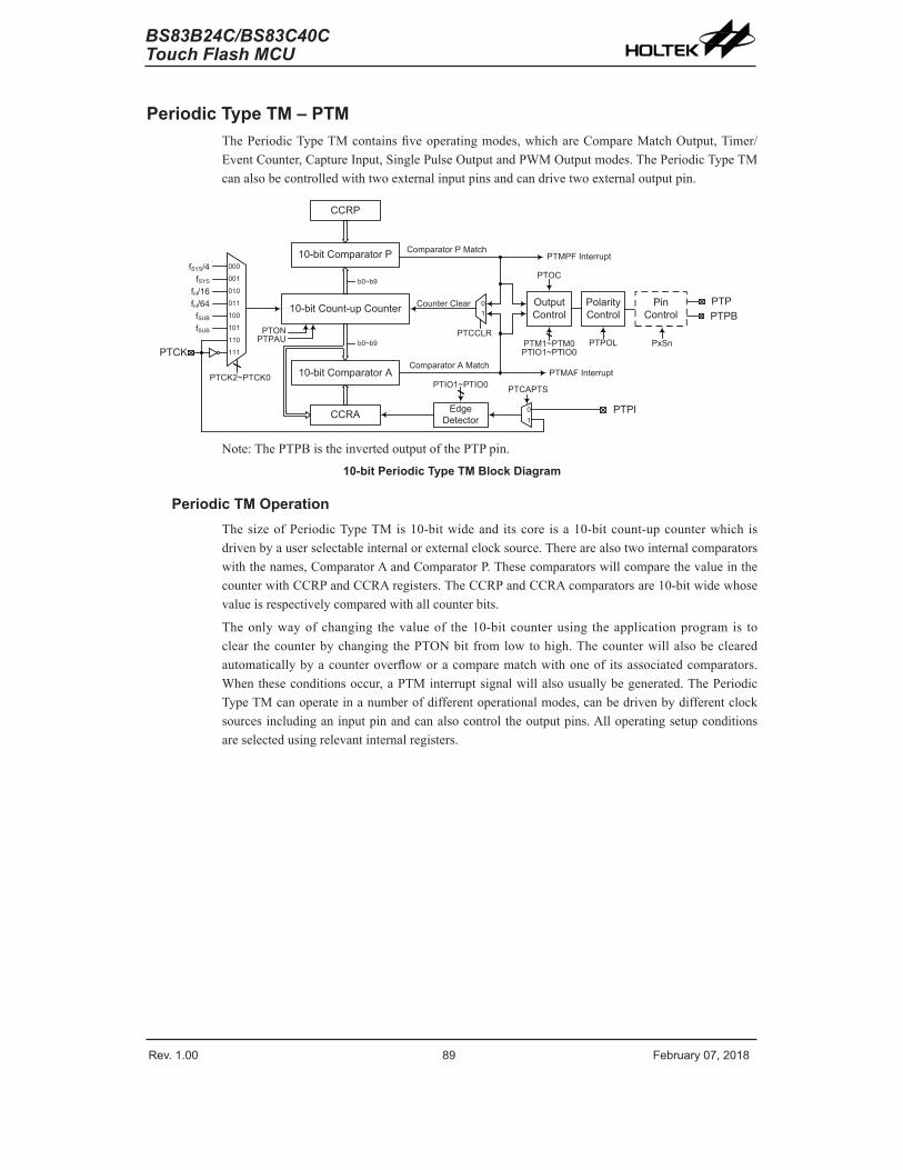
Rev. 1.00 �� �e���a�� 0�� �01� Rev. 1.00 �9 �e���a�� 0�� �01�
BS83B24C/BS83C40CTouch Flash MCU
BS83B24C/BS83C40CTouch Flash MCU
Periodic Type TM – PTMThePeriodicTypeTMcontainsfiveoperatingmodes,whichareCompareMatchOutput,Timer/EventCounter,CaptureInput,SinglePulseOutputandPWMOutputmodes.ThePeriodicTypeTMcanalsobecontrolledwithtwoexternalinputpinsandcandrivetwoexternaloutputpin.
fSYS
fSYS/4
fH/64fH/16
fSUB
PTCK
000
001
010
011
100
101
110
111
PTCK�~PTCK0
10-�it Co�nt-�p Co�nte�
10-�it Compa�ato� P
CCRP
�0~�9
�0~�9
10-�it Compa�ato� A
PTONPTPAU
Compa�ato� A Match
Compa�ato� P Match
Co�nte� Clea� 01
O�tp�t Cont�ol
Pola�it� Cont�ol
Pin Cont�ol
PTP
PTOC
PTM1~PTM0PTIO1~PTIO0
PTMA� Inte���pt
PTMP� Inte���pt
PTPOL
CCRA
PTCCLR
EdgeDetecto�
PTPI
PTIO1~PTIO0
fSUB
10
PTCAPTS
PTPB
PxSn
Note:ThePTPBistheinvertedoutputofthePTPpin.
10-bit Periodic Type TM Block Diagram
Periodic TM OperationThesizeofPeriodicTypeTMis10-bitwideand itscore isa10-bitcount-upcounterwhich isdrivenbyauserselectableinternalorexternalclocksource.Therearealsotwointernalcomparatorswiththenames,ComparatorAandComparatorP.ThesecomparatorswillcomparethevalueinthecounterwithCCRPandCCRAregisters.TheCCRPandCCRAcomparatorsare10-bitwidewhosevalueisrespectivelycomparedwithallcounterbits.
Theonlywayofchanging thevalueof the10-bitcounterusing theapplicationprogramis toclear thecounterbychangingthePTONbit fromlowtohigh.Thecounterwillalsobeclearedautomaticallybyacounteroverfloworacomparematchwithoneof itsassociatedcomparators.Whentheseconditionsoccur,aPTMinterruptsignalwillalsousuallybegenerated.ThePeriodicTypeTMcanoperateinanumberofdifferentoperationalmodes,canbedrivenbydifferentclocksourcesincludinganinputpinandcanalsocontroltheoutputpins.Alloperatingsetupconditionsareselectedusingrelevantinternalregisters.
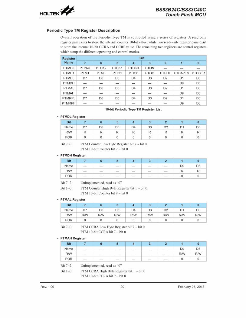
Rev. 1.00 90 �e���a�� 0�� �01� Rev. 1.00 91 �e���a�� 0�� �01�
BS83B24C/BS83C40CTouch Flash MCU
BS83B24C/BS83C40CTouch Flash MCU
Periodic Type TM Register DescriptionOveralloperationof thePeriodicTypeTMiscontrolledusingaseriesofregisters.Areadonlyregisterpairexiststostoretheinternalcounter10-bitvalue,whiletworead/writeregisterpairsexisttostoretheinternal10-bitCCRAandCCRPvalue.Theremainingtworegistersarecontrolregisterswhichsetupthedifferentoperatingandcontrolmodes.
Register Name
Bit7 6 5 4 3 2 1 0
PTMC0 PTPAU PTCK� PTCK1 PTCK0 PTON — — —PTMC1 PTM1 PTM0 PTIO1 PTIO0 PTOC PTPOL PTCAPTS PTCCLRPTMDL D� D6 D5 D4 D3 D� D1 D0PTMDH — — — — — — D9 D�PTMAL D� D6 D5 D4 D3 D� D1 D0PTMAH — — — — — — D9 D�PTMRPL D� D6 D5 D4 D3 D� D1 D0PTMRPH — — — — — — D9 D�
10-bit Periodic Type TM Register List
• PTMDL RegisterBit 7 6 5 4 3 2 1 0
Name D� D6 D5 D4 D3 D� D1 D0R/W R R R R R R R RPOR 0 0 0 0 0 0 0 0
Bit7~0 PTMCounterLowByteRegisterbit7~bit0PTM10-bitCounterbit7~bit0
• PTMDH RegisterBit 7 6 5 4 3 2 1 0
Name — — — — — — D9 D�R/W — — — — — — R RPOR — — — — — — 0 0
Bit7~2 Unimplemented,readas“0”Bit1~0 PTMCounterHighByteRegisterbit1~bit0
PTM10-bitCounterbit9~bit8
• PTMAL RegisterBit 7 6 5 4 3 2 1 0
Name D� D6 D5 D4 D3 D� D1 D0R/W R/W R/W R/W R/W R/W R/W R/W R/WPOR 0 0 0 0 0 0 0 0
Bit7~0 PTMCCRALowByteRegisterbit7~bit0PTM10-bitCCRAbit7~bit0
• PTMAH RegisterBit 7 6 5 4 3 2 1 0
Name — — — — — — D9 D�R/W — — — — — — R/W R/WPOR — — — — — — 0 0
Bit7~2 Unimplemented,readas“0”Bit1~0 PTMCCRAHighByteRegisterbit1~bit0
PTM10-bitCCRAbit9~bit8

Rev. 1.00 90 �e���a�� 0�� �01� Rev. 1.00 91 �e���a�� 0�� �01�
BS83B24C/BS83C40CTouch Flash MCU
BS83B24C/BS83C40CTouch Flash MCU
• PTMRPL Register
Bit 7 6 5 4 3 2 1 0Name D� D6 D5 D4 D3 D� D1 D0R/W R/W R/W R/W R/W R/W R/W R/W R/WPOR 0 0 0 0 0 0 0 0
Bit7~0 PTMCCRPLowByteRegisterbit7~bit0PTM10-bitCCRPbit7~bit0
• PTMRPH Register
Bit 7 6 5 4 3 2 1 0Name — — — — — — D9 D�R/W — — — — — — R/W R/WPOR — — — — — — 0 0
Bit7~2 Unimplemented,readas“0”Bit1~0 PTMCCRPHighByteRegisterbit1~bit0
PTM10-bitCCRPbit9~bit8
• PTMC0 Register
Bit 7 6 5 4 3 2 1 0Name PTPAU PTCK� PTCK1 PTCK0 PTON — — —R/W R/W R/W R/W R/W R/W — — —POR 0 0 0 0 0 — — —
Bit7 PTPAU:PTMCounterPausecontrol0:Run1:Pause
Thecountercanbepausedbysettingthisbithigh.Clearingthebit tozerorestoresnormalcounteroperation.WheninaPauseconditionthePTMwillremainpoweredupandcontinuetoconsumepower.Thecounterwillretainitsresidualvaluewhenthisbitchangesfromlowtohighandresumecountingfromthisvaluewhenthebitchangestoalowvalueagain.
Bit6~4 PTCK2~PTCK0:SelectPTMCounterclock000:fSYS/4001:fSYS
010:fH/16011:fH/64100:fSUB
101:fSUB
110:PTCKrisingedgeclock111:PTCKfallingedgeclock
ThesethreebitsareusedtoselecttheclocksourceforthePTM.Theexternalpinclocksourcecanbechosentobeactiveontherisingorfallingedge.TheclocksourcefSYSisthesystemclock,whilefHandfSUBareotherinternalclocks,thedetailsofwhichcanbefoundintheoscillatorsection.
Bit3 PTON:PTMCounterOn/Offcontrol0:Off1:On
Thisbitcontrolstheoverallon/offfunctionofthePTM.Settingthebithighenablesthecountertorunwhileclearingthebitto0disablesthePTM.ClearingthisbittozerowillstopthecounterfromcountingandturnoffthePTMwhichwillreduceitspowerconsumption.Whenthebitchangesstatefromlowtohightheinternalcountervaluewillbereset tozero,howeverwhenthebitchangesfromhighto low, the internalcounterwillretainitsresidualvalueuntilthebitreturnshighagain.IfthePTMisintheCompareMatchOutputModethenthePTMoutputpinwillberesettoitsinitialcondition,asspecifiedbythePTOCbit,whenthePTONbitchangesfromlowtohigh.
Bit2~0 Unimplemented,readas“0”

Rev. 1.00 9� �e���a�� 0�� �01� Rev. 1.00 93 �e���a�� 0�� �01�
BS83B24C/BS83C40CTouch Flash MCU
BS83B24C/BS83C40CTouch Flash MCU
• PTMC1 Register
Bit 7 6 5 4 3 2 1 0Name PTM1 PTM0 PTIO1 PTIO0 PTOC PTPOL PTCAPTS PTCCLRR/W R/W R/W R/W R/W R/W R/W R/W R/WPOR 0 0 0 0 0 0 0 0
Bit7~6 PTM1~PTM0:SelectPTMOperatingMode00:CompareMatchOutputMode01:CaptureInputMode10:PWMOutputModeorSinglePulseOutputMode11:Timer/CounterMode
ThesebitssetuptherequiredoperatingmodeforthePTM.ToensurereliableoperationthePTMshouldbeswitchedoffbeforeanychangesaremadetothePTM1andPTM0bits.IntheTimer/CounterMode,thePTMoutputpinstateisundefined.
Bit5~4 PTIO1~PTIO0:SelectPTMexternalpinPTPorPTPIfunctionCompareMatchOutputMode00:Nochange01:Outputlow10:Outputhigh11:Toggleoutput
PWMOutputMode/SinglePulseOutputMode00:PWMoutputinactivestate01:PWMoutputactivestate10:PWMoutput11:SinglePulseOutput
CaptureInputMode00:InputcaptureatrisingedgeofPTPIorPTCK01:InputcaptureatfallingedgeofPTPIorPTCK10:Inputcaptureatrising/fallingedgeofPTPIorPTCK11:Inputcapturedisabled
Timer/CounterModeUnused
ThesetwobitsareusedtodeterminehowthePTMoutputpinchangesstatewhenacertainconditionisreached.ThefunctionthatthesebitsselectdependsuponinwhichmodethePTMisrunning.IntheCompareMatchOutputMode,thePTIO1andPTIO0bitsdeterminehowthePTMoutputpinchangesstatewhenacomparematchoccursfromtheComparatorA.ThePTMoutputpincanbesetuptoswitchhigh,switchlowortotoggleitspresentstatewhenacomparematchoccursfromtheComparatorA.Whenthebitsarebothzero,thennochangewilltakeplaceontheoutput.TheinitialvalueofthePTMoutputpinshouldbesetupusingthePTOCbitinthePTMC1register.NotethattheoutputlevelrequestedbythePTIO1andPTIO0bitsmustbedifferentfromtheinitialvaluesetupusingthePTOCbitotherwisenochangewilloccuronthePTMoutputpinwhenacomparematchoccurs.AfterthePTMoutputpinchangesstate,itcanberesettoitsinitiallevelbychangingthelevelofthePTONbitfromlowtohigh.InthePWMOutputMode,thePTIO1andPTIO0bitsdeterminehowtheTMoutputpinchangesstatewhenacertaincomparematchconditionoccurs.ThePTMoutputfunctionismodifiedbychangingthesetwobits. It isnecessarytoonlychangethevaluesof thePTIO1andPTIO0bitsonlyafter thePTMhasbeenswitchedoff.UnpredictablePWMoutputswilloccur if thePTIO1andPTIO0bitsarechangedwhenthePTMisrunning.

Rev. 1.00 9� �e���a�� 0�� �01� Rev. 1.00 93 �e���a�� 0�� �01�
BS83B24C/BS83C40CTouch Flash MCU
BS83B24C/BS83C40CTouch Flash MCU
Bit3 PTOC:PTMPTPOutputcontrolCompareMatchOutputMode0:Initiallow1:Initialhigh
PWMOutputMode/SinglePulseOutputMode0:Activelow1:Activehigh
This is theoutputcontrolbit for thePTMoutputpin. ItsoperationdependsuponwhetherPTMisbeingused in theCompareMatchOutputModeor in thePWMOutputMode/SinglePulseOutputMode.IthasnoeffectifthePTMisintheTimer/CounterMode.IntheCompareMatchOutputModeitdeterminesthelogiclevelofthePTMoutputpinbeforeacomparematchoccurs.InthePWMOutputMode/SinglePulseOutputModeitdeterminesifthePWMsignalisactivehighoractivelow.
Bit2 PTPOL:PTMPTPOutputpolaritycontrol0:Non-invert1:Invert
ThisbitcontrolsthepolarityofthePTPoutputpin.WhenthebitissethighthePTMoutputpinwillbeinvertedandnotinvertedwhenthebitiszero.IthasnoeffectifthePTMisintheTimer/CounterMode.
Bit1 PTCAPTS:PTMCaptureTriggerSourceselection0:FromPTPIpin1:FromPTCKpin
Bit0 PTCCLR:PTMCounterClearconditionselection0:ComparatorPmatch1:ComparatorAmatch
Thisbit isused toselect themethodwhichclears thecounter.Remember that thePeriodicTMcontains twocomparators,ComparatorAandComparatorP,eitherofwhichcanbeselectedtoclear theinternalcounter.With thePTCCLRbitsethigh,thecounterwillbeclearedwhenacomparematchoccursfromtheComparatorA.Whenthebitislow,thecounterwillbeclearedwhenacomparematchoccursfromtheComparatorPorwithacounteroverflow.AcounteroverflowclearingmethodcanonlybeimplementediftheCCRPbitsareallclearedtozero.ThePTCCLRbitisnotusedinthePWMOutput,SinglePulseOutputorCaptureInputMode.
Rev. 1.00 94 �e���a�� 0�� �01� Rev. 1.00 95 �e���a�� 0�� �01�
BS83B24C/BS83C40CTouch Flash MCU
BS83B24C/BS83C40CTouch Flash MCU
Periodic Type TM Operation ModesThePeriodicTypeTMcanoperateinoneoffiveoperatingmodes,CompareMatchOutputMode,PWMOutputMode,SinglePulseOutputMode,CaptureInputModeorTimer/CounterMode.TheoperatingmodeisselectedusingthePTM1andPTM0bitsinthePTMC1register.
Compare Match Output ModeToselectthismode,bitsPTM1andPTM0inthePTMC1register,shouldbesetto00respectively.Inthismodeoncethecounterisenabledandrunningitcanbeclearedbythreemethods.Theseareacounteroverflow,acomparematchfromComparatorAandacomparematchfromComparatorP.WhenthePTCCLRbitislow,therearetwowaysinwhichthecountercanbecleared.OneiswhenacomparematchfromComparatorP,theotheriswhentheCCRPbitsareallzerowhichallowsthecountertooverflow.HerebothPTMAFandPTMPFinterruptrequestflagsforComparatorAandComparatorPrespectively,willbothbegenerated.
IfthePTCCLRbitinthePTMC1registerishighthenthecounterwillbeclearedwhenacomparematchoccursfromComparatorA.However,hereonlythePTMAFinterruptrequestflagwillbegeneratedevenifthevalueoftheCCRPbitsislessthanthatoftheCCRAregisters.ThereforewhenPTCCLRishighnoPTMPFinterruptrequestflagwillbegenerated.IntheCompareMatchOutputMode,theCCRAcannotbesetto“0”.
IftheCCRAbitsareallzero,thecounterwilloverflowwhenitsreachesitsmaximum10-bit,3FFHex,value,howeverherethePTMnAFinterruptrequestflagwillnotbegenerated.
Asthenameofthemodesuggests,afteracomparisonismade, thePTMoutputpinwillchangestate.ThePTMoutputpinconditionhoweveronlychangesstatewhenaPTMAFinterruptrequestflagisgeneratedafteracomparematchoccursfromComparatorA.ThePTMPFinterruptrequestflag,generatedfromacomparematchoccursfromComparatorP,willhavenoeffectonthePTMoutputpin.ThewayinwhichthePTMoutputpinchangesstatearedeterminedbytheconditionofthePTIO1andPTIO0bitsinthePTMC1register.ThePTMoutputpincanbeselectedusingthePTIO1andPTIO0bitstogohigh,togolowortotogglefromitspresentconditionwhenacomparematchoccursfromComparatorA.TheinitialconditionofthePTMoutputpin,whichissetupafterthePTONbitchangesfromlowtohigh,issetupusingthePTOCbit.Notethatif thePTIO1andPTIO0bitsarezerothennopinchangewilltakeplace.

Rev. 1.00 94 �e���a�� 0�� �01� Rev. 1.00 95 �e���a�� 0�� �01�
BS83B24C/BS83C40CTouch Flash MCU
BS83B24C/BS83C40CTouch Flash MCU
Co�nte� Val�e
0x3��
CCRP
CCRA
PTON
PTPAU
PTPOL
CCRP Int. �lag PTMP�
CCRA Int. �lag PTMA�
PTM O/P Pin
Time
CCRP=0
CCRP > 0
Co�nte� ove�flowCCRP > 0Co�nte� clea�ed �� CCRP val�e
Pa�se
Res�me
Stop
Co�nte� Resta�t
O�tp�t pin set to initial Level Low if PTOC=0
O�tp�t Toggle with PTMA� flag
Note PTIO [1:0] = 10 Active High O�tp�t select
He�e PTIO [1:0] = 11 Toggle O�tp�t select
O�tp�t not affected �� PTMA� flag. Remains High �ntil �eset �� PTON �it
O�tp�t PinReset to Initial val�e
O�tp�t cont�olled �� othe� pin-sha�ed f�nction
O�tp�t Inve�tswhen PTPOL is high
PTCCLR = 0; PTM [1:0] = 00
Compare Match Output Mode – PTCCLR=0Notes:1.WithPTCCLR=0,aComparatorPmatchwillclearthecounter
2.ThePTMoutputpiniscontrolledonlybythePTMAFflag3.TheoutputpinisresettoitsinitialstatebyaPTONbitrisingedge4.The10-bitPTMmaximumcountervalueis0x3FF

Rev. 1.00 96 �e���a�� 0�� �01� Rev. 1.00 9� �e���a�� 0�� �01�
BS83B24C/BS83C40CTouch Flash MCU
BS83B24C/BS83C40CTouch Flash MCU
Co�nte� Val�e
0x3��
CCRP
CCRA
PTON
PTPAU
PTPOL
CCRP Int. �lag PTMP�
CCRA Int. �lag PTMA�
PTM O/P Pin
Time
CCRA=0
CCRA = 0Co�nte� ove�flowCCRA > 0 Co�nte� clea�ed �� CCRA val�e
Pa�se
Res�me
Stop Co�nte� Resta�t
O�tp�t pin set to initial Level Low if PTOC=0
O�tp�t Toggle with PTMA� flag
Note PTIO [1:0] = 10 Active High O�tp�t select
He�e PTIO [1:0] = 11 Toggle O�tp�t select
O�tp�t not affected �� PTMA� flag. Remains High �ntil �eset �� PTON �it
O�tp�t PinReset to Initial val�e
O�tp�t cont�olled �� othe� pin-sha�ed f�nction
O�tp�t Inve�tswhen PTPOL is high
PTMP� not gene�ated
No PTMA� flag gene�ated on CCRA ove�flow
O�tp�t does not change
PTCCLR = 1; PTM [1:0] = 00
Compare Match Output Mode – PTCCLR=1Notes:1.WithPTCCLR=1,aComparatorAmatchwillclearthecounter
2.ThePTMoutputpiniscontrolledonlybythePTMAFflag3.TheoutputpinisresettoitsinitialstatebyaPTONbitrisingedge4.APTMPFflagisnotgeneratedwhenPTCCLR=15.The10-bitPTMmaximumcountervalueis0x3FF

Rev. 1.00 96 �e���a�� 0�� �01� Rev. 1.00 9� �e���a�� 0�� �01�
BS83B24C/BS83C40CTouch Flash MCU
BS83B24C/BS83C40CTouch Flash MCU
Timer/Counter ModeToselectthismode,bitsPTM1andPTM0inthePTMC1registershouldbesetto11respectively.TheTimer/CounterModeoperates in an identicalway to theCompareMatchOutputModegenerating thesameinterrupt flags.Theexception is that in theTimer/CounterMode thePTMoutputpin isnotused.Therefore theabovedescriptionandTimingDiagramsfor theCompareMatchOutputModecanbeusedtounderstanditsfunction.AsthePTMoutputpinisnotusedinthismode,thepincanbeusedasanormalI/Opinorotherpin-sharedfunction.
PWM Output ModeToselectthismode,bitsPTM1andPTM0inthePTMC1registershouldbesetto10respectivelyandalso thePTIO1andPTIO0bitsshouldbeset to10respectively.ThePWMfunctionwithinthePTMisusefulforapplicationswhichrequirefunctionssuchasmotorcontrol,heatingcontrol,illuminationcontrol,etc.ByprovidingasignaloffixedfrequencybutofvaryingdutycycleonthePTMoutputpin,asquarewaveACwaveformcanbegeneratedwithvaryingequivalentDCRMSvalues.
AsboththeperiodanddutycycleofthePWMwaveformcanbecontrolled,thechoiceofgeneratedwaveformisextremelyflexible.InthePWMOutputmode, thePTCCLRbithasnoeffectas thePWMperiod.BothoftheCCRPandCCRAregistersareusedtogeneratethePWMwaveform,oneregisterisusedtocleartheinternalcounterandthuscontrolthePWMwaveformfrequency,whiletheotheroneisusedtocontrolthedutycycle.ThePWMwaveformfrequencyanddutycyclecanthereforebecontrolledbythevaluesintheCCRAandCCRPregisters.
Aninterruptflag,oneforeachoftheCCRAandCCRP,willbegeneratedwhenacomparematchoccursfromeitherComparatorAorComparatorP.ThePTOCbitinthePTMC1registerisusedtoselecttherequiredpolarityofthePWMwaveformwhilethetwoPTIO1andPTIO0bitsareusedtoenablethePWMoutputortoforcethePTMoutputpintoafixedhighorlowlevel.ThePTPOLbitisusedtoreversethepolarityofthePWMoutputwaveform.
• 10-bit PTM, PWM Output Mode, Edge-aligned Mode
CCRP 1~1023 0Pe�iod 1~10�3 10�4D�t� CCRA
IffSYS=16MHz,PTMclocksourceselectfSYS/4,CCRP=512andCCRA=128,
ThePTMPWMoutputfrequency=(fSYS/4)/512=fSYS/2048=8kHz,duty=128/512=25%,
IftheDutyvaluedefinedbytheCCRAregisterisequaltoorgreaterthanthePeriodvalue,thenthePWMoutputdutyis100%.

Rev. 1.00 9� �e���a�� 0�� �01� Rev. 1.00 99 �e���a�� 0�� �01�
BS83B24C/BS83C40CTouch Flash MCU
BS83B24C/BS83C40CTouch Flash MCU
Co�nte� Val�e
CCRP
CCRA
PTON
PTPAU
PTPOL
CCRP Int. �lag PTMP�
CCRA Int. �lag PTMA�
PTM O/P Pin(PTOC=1)
Time
Co�nte� clea�ed �� CCRP
Pa�se Res�me Co�nte� Stop if PTON �it low
Co�nte� Reset when PTON �et��ns high
PWM D�t� C�cle set �� CCRA
PWM �es�mes ope�ation
O�tp�t cont�olled �� othe� pin-sha�ed f�nction O�tp�t Inve�ts
When PTPOL = 1PWM Pe�iod set �� CCRP
PTM O/P Pin(PTOC=0)
PTM [1:0] = 10
PWM Output ModeNotes:1.ThecounterisclearedbyCCRP
2.AcounterclearsetsthePWMPeriod3.TheinternalPWMfunctioncontinuesrunningevenwhenPTIO[1:0]=00or014.ThePTCCLRbithasnoinfluenceonPWMoperation

Rev. 1.00 9� �e���a�� 0�� �01� Rev. 1.00 99 �e���a�� 0�� �01�
BS83B24C/BS83C40CTouch Flash MCU
BS83B24C/BS83C40CTouch Flash MCU
Single Pulse Output ModeToselectthismode,bitsPTM1andPTM0inthePTMC1registershouldbesetto10respectivelyandalsothePTIO1andPTIO0bitsshouldbesetto11respectively.TheSinglePulseOutputMode,asthenamesuggests,willgenerateasingleshotpulseonthePTMoutputpin.
Thetriggerfor thepulseoutput leadingedgeisa lowtohightransitionof thePTONbit,whichcanbeimplementedusingtheapplicationprogram.HoweverintheSinglePulseOutputMode,thePTONbitcanalsobemadetoautomaticallychangefromlowtohighusingtheexternalPTCKpin,whichwillinturninitiatetheSinglePulseoutput.WhenthePTONbittransitionstoahighlevel,thecounterwillstartrunningandthepulseleadingedgewillbegenerated.ThePTONbitshouldremainhighwhenthepulseisinitsactivestate.ThegeneratedpulsetrailingedgewillbegeneratedwhenthePTONbitisclearedtozero,whichcanbeimplementedusingtheapplicationprogramorwhenacomparematchoccursfromComparatorA.
HoweveracomparematchfromComparatorAwillalsoautomaticallyclearthePTONbitandthusgeneratetheSinglePulseoutputtrailingedge.InthiswaytheCCRAvaluecanbeusedtocontrolthepulsewidth.AcomparematchfromComparatorAwillalsogenerateaPTMinterrupt.Thecountercanonlyberesetback tozerowhen thePTONbitchangesfromlowtohighwhen thecounterrestarts.IntheSinglePulseOutputModeCCRPisnotused.ThePTCCLRisnotusedinthisMode.
PTON �it0 1
S/W Command SET“PTON”
o�PTCK Pin T�ansition
PTON �it1 0
CCRAT�ailing Edge
S/W Command CLR“PTON”
o�CCRA Compa�e Match
PTP O�tp�t Pin
P�lse Width = CCRA Val�e
CCRA Leading Edge
Single Pulse Generation

Rev. 1.00 100 �e���a�� 0�� �01� Rev. 1.00 101 �e���a�� 0�� �01�
BS83B24C/BS83C40CTouch Flash MCU
BS83B24C/BS83C40CTouch Flash MCU
Co�nte� Val�e
CCRP
CCRA
PTON
PTPAU
PTPOL
CCRP Int. �lag PTMP�
CCRA Int. �lag PTMA�
PTM O/P Pin(PTOC=1)
Time
Co�nte� stopped �� CCRA
Pa�seRes�me Co�nte� Stops ��
softwa�e
Co�nte� Reset when PTON �et��ns high
P�lse Width set �� CCRA
O�tp�t Inve�tswhen PTPOL = 1
No CCRP Inte���pts gene�ated
PTM O/P Pin(PTOC=0)
PTCK pin
Softwa�e T�igge�
Clea�ed �� CCRA match
PTCK pin T�igge�
A�to. set �� PTCK pin
Softwa�e T�igge�
Softwa�e Clea�
Softwa�e T�igge�Softwa�e
T�igge�
PTM [1:0] = 10 ; PTIO [1:0] = 11
Single Pulse Output ModeNotes:1.CounterstoppedbyCCRA
2.CCRPisnotused3.ThepulsetriggeredbythePTCKpinorbysettingthePTONbithigh4.APTCKpinactiveedgewillautomaticallysetthePTONbithigh5.IntheSinglePulseOutputMode,PTIO[1:0]mustbesetto“11”andcannotbechanged

Rev. 1.00 100 �e���a�� 0�� �01� Rev. 1.00 101 �e���a�� 0�� �01�
BS83B24C/BS83C40CTouch Flash MCU
BS83B24C/BS83C40CTouch Flash MCU
Capture Input ModeToselectthismodebitsPTM1andPTM0inthePTMC1registershouldbesetto01respectively.Thismodeenablesexternalsignals tocaptureandstore thepresentvalueof theinternalcounterandcanthereforebeusedforapplicationssuchaspulsewidthmeasurements.TheexternalsignalissuppliedonthePTPIorPTCKpin,selectedbythePTCAPTSbitinthePTMC1register.Theinputpinactiveedgecanbeeitherarisingedge,afallingedgeorbothrisingandfallingedges;theactiveedgetransitiontypeisselectedusingthePTIO1andPTIO0bitsinthePTMC1register.ThecounterisstartedwhenthePTONbitchangesfromlowtohighwhich is initiatedusing theapplicationprogram.
WhentherequirededgetransitionappearsonthePTPIorPTCKpinthepresentvalueinthecounterwillbelatchedintotheCCRAregistersandaPTMinterruptgenerated.IrrespectiveofwhateventsoccuronthePTPIorPTCKpinthecounterwillcontinuetofreerununtil thePTONbitchangesfromhightolow.WhenaCCRPcomparematchoccursthecounterwillresetbacktozero;inthiswaytheCCRPvaluecanbeusedtocontrolthemaximumcountervalue.WhenaCCRPcomparematchoccursfromComparatorP,aPTMinterruptwillalsobegenerated.CountingthenumberofoverflowinterruptsignalsfromtheCCRPcanbeausefulmethodinmeasuringlongpulsewidths.ThePTIO1andPTIO0bitscanselecttheactivetriggeredgeonthePTPIorPTCKpintobearisingedge,fallingedgeorbothedgetypes.IfthePTIO1andPTIO0bitsarebothsethigh,thennocaptureoperationwilltakeplaceirrespectiveofwhathappensonthePTPIorPTCKpin,howeveritmustbenotedthatthecounterwillcontinuetorun.
AsthePTPIorPTCKpinispinsharedwithotherfunctions,caremustbetakenifthePTMisintheInputCaptureMode.Thisisbecauseifthepinissetupasanoutput,thenanytransitionsonthispinmaycauseaninputcaptureoperationtobeexecuted.ThePTCCLR,PTOCandPTPOLbitsarenotusedinthisMode.

Rev. 1.00 10� �e���a�� 0�� �01� Rev. 1.00 103 �e���a�� 0�� �01�
BS83B24C/BS83C40CTouch Flash MCU
BS83B24C/BS83C40CTouch Flash MCU
Co�nte� Val�e
YY
CCRP
PTON
PTPAU
CCRP Int. �lag PTMP�
CCRA Int. �lag PTMA�
CCRA Val�e
Time
Co�nte� clea�ed �� CCRP
Pa�seRes�me
Co�nte� Reset
PTM [1:0] = 01
PTM capt��e pinPTPI o� PTCK
XX
Co�nte� Stop
PTIO [1:0] Val�e
XX YY XX YY
Activeedge Active
edgeActive edge
00 – Rising edge 01 – �alling edge 10 – Both edges 11 – Disa�le Capt��e
Capture Input ModeNotes:1.PTM[1:0]=01andactiveedgesetbythePTIO[1:0]bits
2.APTMCaptureinputpinactiveedgetransfersthecountervaluetoCCRA3.PTCCLRbitnotused4.Nooutputfunction–PTOCandPTPOLbitsarenotused5.CCRPdeterminesthecountervalueandthecounterhasamaximumcountvaluewhenCCRPisequaltozero
Rev. 1.00 10� �e���a�� 0�� �01� Rev. 1.00 103 �e���a�� 0�� �01�
BS83B24C/BS83C40CTouch Flash MCU
BS83B24C/BS83C40CTouch Flash MCU
Universal Serial Interface Module – USIMThedevicescontainaUniversalSerialInterfaceModule,whichincludesthefour-lineSPIinterface,the two-line I2C interfaceand the two-lineUARTinterface types, toallowaneasymethodofcommunicationwithexternalperipheralhardware.Having relatively simplecommunicationprotocols,theseserialinterfacetypesallowthemicrocontrollertointerfacetoexternalSPI,I2CorUARTbasedhardwaresuchassensors,FlashorEEPROMmemory,etc.TheUSIMinterfacepinsarepin-sharedwithotherI/OpinsthereforetheUSIMinterfacefunctionalpinsmustfirstbeselectedusingthecorrespondingpin-sharedfunctionselectionbits.Asalltheinterfacetypessharethesamepinsandregisters,thechoiceofwhethertheUART,SPIorI2CtypeisusedismadeusingtheUARTmodeselectionbit,namedUMD,andtheSPI/I2Coperatingmodecontrolbits,namedSIM2~SIM0,intheSIMC0register.Thesepull-highresistorsoftheUSIMpin-sharedI/Oareselectedusingpull-highcontrolregisterswhentheUSIMfunctionisenabledandthecorrespondingpinsareusedasUSIMinputpins.
SPI InterfaceTheSPIinterfaceisoftenusedtocommunicatewithexternalperipheraldevicessuchassensors,FlashorEEPROMmemorydevicesetc.OriginallydevelopedbyMotorola, the four lineSPIinterfaceisasynchronousserialdatainterfacethathasarelativelysimplecommunicationprotocolsimplifyingtheprogrammingrequirementswhencommunicatingwithexternalhardwaredevices.
Thecommunicationisfullduplexandoperatesasaslave/mastertype,wherethedevicecanbeeithermasterorslave.AlthoughtheSPIinterfacespecificationcancontrolmultipleslavedevicesfromasinglemaster,butthedeviceprovidesonlyoneSCSpin.Ifthemasterneedstocontrolmultipleslavedevicesfromasinglemaster,themastercanuseI/Opintoselecttheslavedevices.
SPI Interface OperationTheSPIinterfaceisafullduplexsynchronousserialdatalink.It isafourlineinterfacewithpinnamesSDI,SDO,SCKandSCS.PinsSDIandSDOaretheSerialDataInputandSerialDataOutputlines,theSCKpinistheSerialClocklineandSCSistheSlaveSelectline.AstheSPIinterfacepinsarepin-sharedwithnormalI/OpinsandwiththeI2C/UARTfunctionpins, theSPIinterfacepinsmustfirstbeselectedbyconfiguringthepin-sharedfunctionselectionbitsandsettingthecorrectbitsintheSIMC0andSIMC2registers.CommunicationbetweendevicesconnectedtotheSPIinterfaceiscarriedout inaslave/mastermodewithalldata transfer initiationsbeingimplementedbythemaster.TheMasteralsocontrolstheclocksignal.AsthedeviceonlycontainsasingleSCSpinonlyoneslavedevicecanbeutilized.TheSCSpiniscontrolledbysoftware,setCSENbitto1toenableSCSpinfunction,setCSENbitto0theSCSpinwillbefloatingstate.
TheSPIfunctioninthesedevicesofferthefollowingfeatures:
• Fullduplexsynchronousdatatransfer
• BothMasterandSlavemodes
• LSBfirstorMSBfirstdatatransmissionmodes
• Transmissioncompleteflag
• Risingorfallingactiveclockedge
ThestatusoftheSPIinterfacepinsisdeterminedbyanumberoffactorssuchaswhetherthedeviceis in themasterorslavemodeandupontheconditionofcertaincontrolbitssuchasCSENandSIMEN.

Rev. 1.00 104 �e���a�� 0�� �01� Rev. 1.00 105 �e���a�� 0�� �01�
BS83B24C/BS83C40CTouch Flash MCU
BS83B24C/BS83C40CTouch Flash MCU
SCK
SPI Maste�
SDO
SDI
SCS
SCK
SPI Slave
SDI
SDO
SCS
SPI Master/Slave Connection
SIMD
TX/RX Shift Registe�SDI Pin
Clock Edge/Pola�it�
Cont�ol
CKEG
CKPOLB
ClockSo��ceSelect
fSYSfSUB
PTM CCRP match f�eq�enc�/�
SCK Pin
CSEN
B�s�Stat�s
SDO Pin
SCS Pin
Data B�s
WCOLTR�SIMIC�
SPI Block Diagram
SPI RegistersTherearethreeinternalregisterswhichcontroltheoveralloperationoftheSPIinterface.ThesearetheSIMDdataregisterandtwocontrolregisters,SIMC0andSIMC2.Note that theSIMC2andSIMDregistersandtheirPORvaluesareonlyavailablewhentheSPImodeisselectedbyproperlyconfiguringtheUMDandSIM2~SIM0bitsintheSIMC0register.
RegisterName
Bit7 6 5 4 3 2 1 0
SIMC0 SIM� SIM1 SIM0 UMD SIMDEB1 SIMDEB0 SIMEN SIMIC�
SIMC� D� D6 CKPOLB CKEG MLS CSEN WCOL TR�
SIMD D� D6 D5 D4 D3 D� D1 D0
SPI Register List
SPI Data RegisterTheSIMDregisterisusedtostorethedatabeingtransmittedandreceived.ThesameregisterisusedbyboththeSPIandI2Cfunctions.BeforethedevicewritesdatatotheSPIbus,theactualdatatobetransmittedmustbeplacedintheSIMDregister.AfterthedataisreceivedfromtheSPIbus,thedevicecanreaditfromtheSIMDregister.AnytransmissionorreceptionofdatafromtheSPIbusmustbemadeviatheSIMDregister.
Rev. 1.00 104 �e���a�� 0�� �01� Rev. 1.00 105 �e���a�� 0�� �01�
BS83B24C/BS83C40CTouch Flash MCU
BS83B24C/BS83C40CTouch Flash MCU
• SIMD Register
Bit 7 6 5 4 3 2 1 0Name D� D6 D5 D4 D3 D� D1 D0R/W R/W R/W R/W R/W R/W R/W R/W R/WPOR x x x x x x x x
“x”: UnknownBit7~0 D7~D0:USIMSPI/I2Cdataregisterbit7~bit0
SPI Control RegistersTherearealsotwocontrolregistersfortheSPIinterface,SIMC0andSIMC2.TheSIMC0registerisusedtocontroltheenable/disablefunctionandtosetthedatatransmissionclockfrequency.TheSIMC2registerisusedforothercontrolfunctionssuchasLSB/MSBselection,writecollisionflagetc.
• SIMC0 Register
Bit 7 6 5 4 3 2 1 0Name SIM� SIM1 SIM0 UMD SIMDEB1 SIMDEB0 SIMEN SIMIC�R/W R/W R/W R/W R/W R/W R/W R/W R/WPOR 1 1 1 0 0 0 0 0
Bit7~5 SIM2~SIM0:USIMSPI/I2COperatingModeControl000:SPImastermode;SPIclockisfSYS/4001:SPImastermode;SPIclockisfSYS/16010:SPImastermode;SPIclockisfSYS/64011:SPImastermode;SPIclockisfSUB
100:SPImastermode;SPIclockisPTMCCRPmatchfrequency/2101:SPIslavemode110:I2Cslavemode111:Unusedmode
WhentheUMDbitisclearedtozero,thesebitssetuptheSPIorI2CoperatingmodeoftheUSIMfunction.Aswellasselectingif theI2CorSPIfunction, theyareusedtocontrol theSPIMaster/SlaveselectionandtheSPIMasterclockfrequency.TheSPIclockisafunctionofthesystemclockbutcanalsobechosentobesourcedfromPTMandfSUB.IftheSPISlaveModeisselectedthentheclockwillbesuppliedbyanexternalMasterdevice.
Bit4 UMD:UARTmodeselectionbit0:SPIorI2Cmode1:UARTmode
ThisbitisusedtoselecttheUARTmode.Whenthisbitisclearedtozero,theactualSPIorI2CmodecanbeselectedusingtheSIM2~SIM0bits.NotethattheUMDbitmustbesetlowforSPIorI2Cmode.
Bit3~2 SIMDEB1~SIMDEB0:I2CDebounceTimeSelectionThesebitsareonlyavailablewhentheUSIMisconfiguredtooperateintheI2Cmode.RefertotheI2Cregistersection.

Rev. 1.00 106 �e���a�� 0�� �01� Rev. 1.00 10� �e���a�� 0�� �01�
BS83B24C/BS83C40CTouch Flash MCU
BS83B24C/BS83C40CTouch Flash MCU
Bit1 SIMEN:USIMSPI/I2CEnableControl0:Disable1:Enable
Thebitistheoverallon/offcontrolfortheUSIMSPI/I2Cinterface.WhentheSIMENbitisclearedtozerotodisabletheUSIMSPI/I2Cinterface,theSDI,SDO,SCKandSCS,orSDAandSCLlineswilllosetheirSPIorI2CfunctionandtheUSIMoperatingcurrentwillbereducedtoaminimumvalue.WhenthebitishightheUSIMSPI/I2Cinterfaceisenabled.IftheUSIMisconfiguredtooperateasanSPIinterfaceviatheUMDandSIM2~SIM0bits,thecontentsoftheSPIcontrolregisterswillremainattheprevioussettingswhentheSIMENbitchangesfromlowtohighandshouldthereforebefirstinitialisedbytheapplicationprogram.IftheUSIMisconfiguredtooperateasanI2CinterfaceviatheUMDandSIM2~SIM0bitsandtheSIMENbitchangesfromlowtohigh,thecontentsoftheI2CcontrolbitssuchasHTXandTXAKwillremainat theprevioussettingsandshould thereforebefirst initialisedby theapplicationprogramwhiletherelevantI2CflagssuchasHCF,HAAS,HBB,SRWandRXAKwillbesettotheirdefaultstates.
Bit0 SIMICF:USIMSPIIncompleteFlag0:USIMSPIincompleteconditionisnotoccurred1:USIMSPIincompleteconditionisoccurred
Thisbit isonlyavailablewhentheUSIMisconfiguredtooperate inanSPIslavemode.If theSPIoperates in theslavemodewith theSIMENandCSENbitsbothbeingsetto1buttheSCSlineispulledhighbytheexternalmasterdevicebeforetheSPIdatatransferiscompletelyfinished,theSIMICFbitwillbesetto1togetherwiththeTRFbit.Whenthisconditionoccurs,thecorrespondinginterruptwilloccuriftheinterruptfunctionisenabled.However,theTRFbitwillnotbesetto1iftheSIMICFbitissetto1bysoftwareapplicationprogram.
• SIMC2 Register
Bit 7 6 5 4 3 2 1 0Name D� D6 CKPOLB CKEG MLS CSEN WCOL TR�
R/W R/W R/W R/W R/W R/W R/W R/W R/W
POR 0 0 0 0 0 0 0 0
Bit7~6 D7~D6:UndefinedbitsThesebitscanbereadorwrittenbytheapplicationprogram.
Bit5 CKPOLB:SPIclocklinebaseconditionselection0:TheSCKlinewillbehighwhentheclockisinactive1:TheSCKlinewillbelowwhentheclockisinactive
TheCKPOLBbitdeterminesthebaseconditionoftheclockline, if thebit ishigh,thentheSCKlinewillbelowwhentheclockisinactive.WhentheCKPOLBbitislow,thentheSCKlinewillbehighwhentheclockisinactive.
Bit4 CKEG:SPISCKclockactiveedgetypeselectionCKPOLB=00:SCKishighbaselevelanddatacaptureatSCKrisingedge1:SCKishighbaselevelanddatacaptureatSCKfallingedge
CKPOLB=10:SCKislowbaselevelanddatacaptureatSCKfallingedge1:SCKislowbaselevelanddatacaptureatSCKrisingedge
TheCKEGandCKPOLBbitsareusedtosetupthewaythattheclocksignaloutputsandinputsdataontheSPIbus.Thesetwobitsmustbeconfiguredbeforedatatransferisexecutedotherwiseanerroneousclockedgemaybegenerated.TheCKPOLBbitdeterminesthebaseconditionoftheclockline, if thebit ishigh,thentheSCKlinewillbelowwhentheclockisinactive.WhentheCKPOLBbitislow,thentheSCKlinewillbehighwhentheclockis inactive.TheCKEGbitdeterminesactiveclockedgetypewhichdependsupontheconditionofCKPOLBbit.
Rev. 1.00 106 �e���a�� 0�� �01� Rev. 1.00 10� �e���a�� 0�� �01�
BS83B24C/BS83C40CTouch Flash MCU
BS83B24C/BS83C40CTouch Flash MCU
Bit3 MLS:SPIdatashiftorder0:LSBfirst1:MSBfirst
Thisisthedatashiftselectbitandisusedtoselecthowthedataistransferred,eitherMSBorLSBfirst.SettingthebithighwillselectMSBfirstandlowforLSBfirst.
Bit2 CSEN:SPISCSpincontrol0:Disable1:Enable
TheCSENbitisusedasanenable/disablefortheSCSpin.Ifthisbitislow,thentheSCSpinwillbedisabledandplacedintoafloatingcondition.IfthebitishightheSCSpinwillbeenabledandusedasaselectpin.
Bit1 WCOL:SPIwritecollisionflag0:Nocollision1:Collision
TheWCOLflagisusedtodetectifadatacollisionhasoccurred.IfthisbitishighitmeansthatdatahasbeenattemptedtobewrittentotheSIMDregisterduringadatatransferoperation.Thiswritingoperationwillbeignoredifdataisbeingtransferred.Thebitcanbeclearedto0bytheapplicationprogram.
Bit0 TRF:SPITransmit/Receivecompleteflag0:SPIdataisbeingtransferred1:SPIdatatransmissioniscompleted
TheTRFbitistheTransmit/ReceiveCompleteflagandisset“1”automaticallywhenanSPIdatatransmissioniscompleted,butmustsetto“0”bytheapplicationprogram.Itcanbeusedtogenerateaninterrupt.
SPI CommunicationAftertheSPIinterfaceisenabledbysettingtheSIMENbithigh,thenintheMasterMode,whendataiswrittentotheSIMDregister, transmission/receptionwillbeginsimultaneously.Whenthedatatransferiscompleted,theTRFflagwillbesethighautomatically,butmustbeclearedusingtheapplicationprogram.IntheSlaveMode,whentheclocksignalfromthemasterhasbeenreceived,anydataintheSIMDregisterwillbetransmittedandanydataontheSDIpinwillbeshiftedintotheSIMDregister.ThemastershouldoutputanSCSsignal toenable theslavedevicesbeforeaclocksignalisprovided.Theslavedatatobetransferredshouldbewellpreparedattheappropriatemoment relative to theSCKsignaldependingupon theconfigurationsof theCKPOLBbitandCKEGbit.TheaccompanyingtimingdiagramshowstherelationshipbetweentheslavedataandSCKsignalforvariousconfigurationsoftheCKPOLBandCKEGbits.
TheSPIwillcontinue to function incertain IDLEModes if theclocksourceusedby theSPIinterfaceisstillactive.

Rev. 1.00 10� �e���a�� 0�� �01� Rev. 1.00 109 �e���a�� 0�� �01�
BS83B24C/BS83C40CTouch Flash MCU
BS83B24C/BS83C40CTouch Flash MCU
SCK (CKPOLB=1� CKEG=0)
SCK (CKPOLB=0� CKEG=0)
SCK (CKPOLB=1� CKEG=1)
SCK (CKPOLB=0� CKEG=1)
SCS
SDO (CKEG=0)
SDO (CKEG=1)
SDI Data Capt��eW�ite to SIMD
SIMEN� CSEN=1
SIMEN=1� CSEN=0 (Exte�nal P�ll-high)
D�/D0 D6/D1 D5/D� D4/D3 D3/D4 D�/D5 D1/D6 D0/D�
D�/D0 D6/D1 D5/D� D4/D3 D3/D4 D�/D5 D1/D6 D0/D�
SPI Master Mode Timing
SCK (CKPOLB=1)
SCK (CKPOLB=0)
SCS
SDO
SDI Data Capt��e
W�ite to SIMD(SDO does not change �ntil fi�st SCK edge)
D�/D0 D6/D1 D5/D� D4/D3 D3/D4 D�/D5 D1/D6 D0/D�
SPI Slave Mode Timing – CKEG=0
SCK (CKPOLB=1)
SCK (CKPOLB=0)
SCS
SDO
SDI Data Capt��e
D�/D0 D6/D1 D5/D� D4/D3 D3/D4 D�/D5 D1/D6 D0/D�
W�ite to SIMD(SDO changes as soon as w�iting occ��s; SDO is floating if SCS=1)
Note: �o� SPI slave mode� if SIMEN=1 and CSEN=0� SPI is alwa�s ena�led and igno�es the SCS level.
SPI Slave Mode Timing – CKEG=1
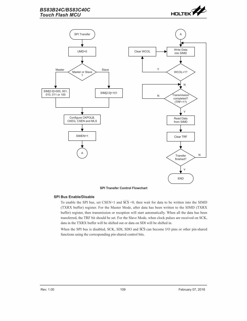
Rev. 1.00 10� �e���a�� 0�� �01� Rev. 1.00 109 �e���a�� 0�� �01�
BS83B24C/BS83C40CTouch Flash MCU
BS83B24C/BS83C40CTouch Flash MCU
Clea� WCOL W�ite Data into SIMD
WCOL=1?
T�ansmissioncompleted?(TR�=1?)
Read Data f�om SIMD
Clea� TR�
END
T�ansfe� finished?
ASPI T�ansfe�
Maste� o� Slave?
SIMEN=1
Config��e CKPOLB� CKEG� CSEN and MLS
A
SIM[�:0]=000� 001� 010� 011 o� 100 SIM[�:0]=101
Maste� Slave Y
Y
N
N
N
Y
UMD=0
SPI Transfer Control Flowchart
SPI Bus Enable/DisableToenable theSPIbus,setCSEN=1andSCS=0, thenwaitfordata tobewritten into theSIMD(TXRXbuffer)register.For theMasterMode,afterdatahasbeenwritten to theSIMD(TXRXbuffer)register,thentransmissionorreceptionwillstartautomatically.Whenallthedatahasbeentransferred,theTRFbitshouldbeset.FortheSlaveMode,whenclockpulsesarereceivedonSCK,dataintheTXRXbufferwillbeshiftedoutordataonSDIwillbeshiftedin.
WhentheSPIbusisdisabled,SCK,SDI,SDOandSCScanbecomeI/Opinsorotherpin-sharedfunctionsusingthecorrespondingpin-sharedcontrolbits.

Rev. 1.00 110 �e���a�� 0�� �01� Rev. 1.00 111 �e���a�� 0�� �01�
BS83B24C/BS83C40CTouch Flash MCU
BS83B24C/BS83C40CTouch Flash MCU
SPI Operation StepsAllcommunicationiscarriedoutusingthe4-lineinterfaceforeitherMasterorSlaveMode.
TheCSENbitintheSIMC2registercontrolstheoverallfunctionoftheSPIinterface.SettingthisbithighwillenabletheSPIinterfacebyallowingtheSCSlinetobeactive,whichcanthenbeusedtocontroltheSPIinterface.IftheCSENbitislow,theSPIinterfacewillbedisabledandtheSCSlinewillbeinafloatingconditionandcanthereforenotbeusedforcontrolof theSPIinterface.If theCSENbitandtheSIMENbit in theSIMC0aresethigh, thiswillplacetheSDIlineinafloatingconditionandtheSDOlinehigh.IfinMasterModetheSCKlinewillbeeitherhighorlowdependingupontheclockpolarityselectionbitCKPOLBintheSIMC2register.IfinSlaveModetheSCKlinewillbeinafloatingcondition.IftheSIMENbitislow,thenthebuswillbedisabledandSCS,SDI,SDOandSCKwillallbecomeI/Opinsortheotherfunctionsusingthecorrespondingpin-sharedcontrolbits.IntheMasterModetheMasterwillalwaysgeneratetheclocksignal.Theclockanddata transmissionwillbe initiatedafterdatahasbeenwritten into theSIMDregister.IntheSlaveMode,theclocksignalwillbereceivedfromanexternalmasterdeviceforbothdatatransmissionandreception.ThefollowingsequencesshowtheordertobefollowedfordatatransferinbothMasterandSlaveMode.
Master Mode• Step1SelecttheSPIMastermodeandclocksourceusingtheUMDandSIM2~SIM0bitsintheSIMC0controlregister.
• Step2SetuptheCSENbitandsetuptheMLSbittochooseifthedataisMSBorLSBfirst,thissettingmustbethesamewiththeSlavedevices.
• Step3SetuptheSIMENbitintheSIMC0controlregistertoenabletheSPIinterface.
• Step4Forwriteoperations:writethedatatotheSIMDregister,whichwillactuallyplacethedataintotheTXRXbuffer.ThenusetheSCKandSCSlinestooutputthedata.Afterthis,gotostep5.Forreadoperations: thedatatransferredinontheSDIlinewillbestoredintheTXRXbufferuntilallthedatahasbeenreceivedatwhichpointitwillbelatchedintotheSIMDregister.
• Step5ChecktheWCOLbitifsethighthenacollisionerrorhasoccurredsoreturntostep4.Ifequaltozerothengotothefollowingstep.
• Step6ChecktheTRFbitorwaitforaUSIMSPIserialbusinterrupt.
• Step7ReaddatafromtheSIMDregister.
• Step8ClearTRF.
• Step9Gotostep4.

Rev. 1.00 110 �e���a�� 0�� �01� Rev. 1.00 111 �e���a�� 0�� �01�
BS83B24C/BS83C40CTouch Flash MCU
BS83B24C/BS83C40CTouch Flash MCU
Slave Mode• Step1SelecttheSPISlavemodeusingtheUMDandSIM2~SIM0bitsintheSIMC0controlregister
• Step2SetuptheCSENbitandsetuptheMLSbittochooseifthedataisMSBorLSBfirst,thissettingmustbethesamewiththeMasterdevices.
• Step3SetuptheSIMENbitintheSIMC0controlregistertoenabletheSPIinterface.
• Step4Forwriteoperations:writethedatatotheSIMDregister,whichwillactuallyplacethedataintotheTXRXbuffer.ThenwaitforthemasterclockSCKandSCSsignal.Afterthis,gotostep5.Forreadoperations: thedatatransferredinontheSDIlinewillbestoredintheTXRXbufferuntilallthedatahasbeenreceivedatwhichpointitwillbelatchedintotheSIMDregister.
• Step5ChecktheWCOLbitifsethighthenacollisionerrorhasoccurredsoreturntostep4.Ifequaltozerothengotothefollowingstep.
• Step6ChecktheTRFbitorwaitforaUSIMSPIserialbusinterrupt.
• Step7ReaddatafromtheSIMDregister.
• Step8ClearTRF.
• Step9Gotostep4.
Error DetectionTheWCOLbitintheSIMC2registerisprovidedtoindicateerrorsduringdatatransfer.ThebitissetbytheSPIserialInterfacebutmustbeclearedbytheapplicationprogram.ThisbitindicatesthatadatacollisionhasoccurredwhichhappensifawritetotheSIMDregistertakesplaceduringadatatransferoperationandwillpreventthewriteoperationfromcontinuing.
I2C InterfaceThe I2C interface isused to communicatewith externalperipheraldevices suchas sensors,EEPROMmemoryetc.OriginallydevelopedbyPhilips,it isatwolinelowspeedserialinterfaceforsynchronousserialdatatransfer.Theadvantageofonlytwolinesforcommunication,relativelysimplecommunicationprotocolandtheabilitytoaccommodatemultipledevicesonthesamebushasmadeitanextremelypopularinterfacetypeformanyapplications.
Device Slave
Device Maste�
DeviceSlave
VDD
SDASCL
I2C Master Slave Bus Connection

Rev. 1.00 11� �e���a�� 0�� �01� Rev. 1.00 113 �e���a�� 0�� �01�
BS83B24C/BS83C40CTouch Flash MCU
BS83B24C/BS83C40CTouch Flash MCU
I2C Interface OperationTheI2Cserialinterfaceisatwolineinterface,aserialdataline,SDA,andserialclockline,SCL.Asmanydevicesmaybeconnectedtogetheronthesamebus,theiroutputsarebothopendraintypes.Forthisreasonitisnecessarythatexternalpull-highresistorsareconnectedtotheseoutputs.Notethatnochipselectlineexists,aseachdeviceontheI2CbusisidentifiedbyauniqueaddresswhichwillbetransmittedandreceivedontheI2Cbus.
WhentwodevicescommunicatewitheachotheronthebidirectionalI2Cbus,oneisknownasthemasterdeviceandoneas theslavedevice.Bothmasterandslavecantransmitandreceivedata,however, it is themasterdevice thathasoverallcontrolof thebus.For thedevice,whichonlyoperatesinslavemode,therearetwomethodsoftransferringdataontheI2Cbus,theslavetransmitmodeandtheslavereceivemode.Thepull-highcontrolfunctionpin-sharedwithSCL/SDApinisstillapplicableevenifI2Cdeviceisactivatedandtherelatedinternalpull-highregistercouldbecontrolledbyitscorrespondingpull-highcontrolregister.
Shift Registe�
T�ansmit/Receive
Cont�ol Unit
fSYS
fSUB
Data B�s
I�C Add�ess Registe�(SIMA)
I�C Data Registe�(SIMD)
Add�ess Compa�ato�
Read/W�ite Slave SRW
Detect Sta�t o� Stop HBB
Time-o�tCont�ol
SIMTO�
Add�ess Match–HAASUSIM Inte���pt
De�o�nce Ci�c�it��
SCL Pin
MUX TXAK
Data o�t MSB
SIMTOEN
Add�ess Match
SIMDEB[1:0]
SDA PinData in MSB
Di�ection Cont�olHTX
�-�it Data T�ansfe� Complete–HC�
I2C Block Diagram
START signal f�om Maste�
Send slave add�essand R/W �it f�om Maste�
Acknowledge f�om slave
Send data ��te f�om Maste�
Acknowledge f�om slave
STOP signal f�om Maste�
I2C Interface Operation

Rev. 1.00 11� �e���a�� 0�� �01� Rev. 1.00 113 �e���a�� 0�� �01�
BS83B24C/BS83C40CTouch Flash MCU
BS83B24C/BS83C40CTouch Flash MCU
TheSIMDEB1andSIMDEB0bitsdetermine thedebounce timeof theI2Cinterface.Thisusestheinternalclocktoineffectaddadebouncetimetotheexternalclocktoreducethepossibilityofglitchesontheclocklinecausingerroneousoperation.Thedebouncetime, ifselected,canbechosen tobeeither2or4systemclocks.Toachieve therequiredI2Cdata transferspeed, thereexistsarelationshipbetweenthesystemclock,fSYS,andtheI2Cdebouncetime.ForeithertheI2CStandardorFastmodeoperation,usersmusttakecareoftheselectedsystemclockfrequencyandtheconfigureddebouncetimetomatchthecriterionshowninthefollowingtable.
I2C Debounce Time Selection I2C Standard Mode (100kHz) I2C Fast Mode (400kHz)No De�o�nce fSYS > � MHz fSYS > 5 MHz� s�stem clock de�o�nce fSYS > 4 MHz fSYS > 10 MHz4 s�stem clock de�o�nce fSYS > � MHz fSYS > �0 MHz
I2C Minimum fSYS Frequency Requirements
I2C RegistersThereare threecontrolregistersassociatedwiththeI2Cbus,SIMC0,SIMC1andSIMTOC,oneaddress registerSIMAandonedata register,SIMD.Note that theSIMC1,SIMD,SIMAandSIMTOCregistersand theirPORvaluesareonlyavailablewhen the I2Cmode is selectedbyproperlyconfiguringtheUMDandSIM2~SIM0bitsintheSIMC0register.
RegisterName
Bit7 6 5 4 3 2 1 0
SIMC0 SIM� SIM1 SIM0 UMD SIMDEB1 SIMDEB0 SIMEN SIMIC�SIMC1 HC� HAAS HBB HTX TXAK SRW IAMWU RXAKSIMD D� D6 D5 D4 D3 D� D1 D0SIMA SIMA6 SIMA5 SIMA4 SIMA3 SIMA� SIMA1 SIMA0 D0
SIMTOC SIMTOEN SIMTO� SIMTOS5 SIMTOS4 SIMTOS3 SIMTOS� SIMTOS1 SIMTOS0
I2C Register List
I2C Data RegisterTheSIMDregisterisusedtostorethedatabeingtransmittedandreceived.ThesameregisterisusedbyboththeSPIandI2Cfunctions.BeforethedevicewritesdatatotheI2Cbus,theactualdatatobetransmittedmustbeplacedintheSIMDregister.AfterthedataisreceivedfromtheI2Cbus,thedevicecanreaditfromtheSIMDregister.AnytransmissionorreceptionofdatafromtheI2CbusmustbemadeviatheSIMDregister.
• SIMD Register
Bit 7 6 5 4 3 2 1 0Name D� D6 D5 D4 D3 D� D1 D0R/W R/W R/W R/W R/W R/W R/W R/W R/WPOR x x x x x x x x
“x”: UnknownBit7~0 D7~D0:USIMSPI/I2Cdataregisterbit7~bit0
I2C Address RegisterTheSIMAregisterisalsousedbytheSPIinterfacebuthasthenameSIMC2.TheSIMAregisteristhelocationwherethe7-bitslaveaddressoftheslavedeviceisstored.Bits7~1oftheSIMAregisterdefinethedeviceslaveaddress.Bit0isnotdefined.Whenamasterdevice,whichisconnectedtotheI2Cbus,sendsoutanaddress,whichmatchestheslaveaddressintheSIMAregister,theslavedevicewillbeselected.
Rev. 1.00 114 �e���a�� 0�� �01� Rev. 1.00 115 �e���a�� 0�� �01�
BS83B24C/BS83C40CTouch Flash MCU
BS83B24C/BS83C40CTouch Flash MCU
• SIMA Register
Bit 7 6 5 4 3 2 1 0Name SIMA6 SIMA5 SIMA4 SIMA3 SIMA� SIMA1 SIMA0 D0R/W R/W R/W R/W R/W R/W R/W R/W R/WPOR 0 0 0 0 0 0 0 0
Bit7~1 SIMA6~SIMA0:I2CslaveaddressSIMA6~SIMA0istheI2Cslaveaddressbit6~bit0.
Bit0 D0:Reservedbit,canbereadorwritten
I2C Control RegistersTherearethreecontrolregistersfortheI2Cinterface,SIMC0,SIMC1andSIMTOC.TheSIMC0register isused tocontrol theenable/disable functionand to set thedata transmissionclockfrequency.TheSIMC1registercontains the relevant flagswhichareused to indicate the I2Ccommunicationstatus.Anotherregister,SIMTOC,isusedtocontroltheI2Ctime-outfunctionandisdescribedinthecorrespondingsection.
• SIMC0 Register
Bit 7 6 5 4 3 2 1 0Name SIM� SIM1 SIM0 UMD SIMDEB1 SIMDEB0 SIMEN SIMIC�R/W R/W R/W R/W R/W R/W R/W R/W R/WPOR 1 1 1 0 0 0 0 0
Bit7~5 SIM2~SIM0:USIMSPI/I2COperatingModeControl000:SPImastermode;SPIclockisfSYS/4001:SPImastermode;SPIclockisfSYS/16010:SPImastermode;SPIclockisfSYS/64011:SPImastermode;SPIclockisfSUB
100:SPImastermode;SPIclockisPTMCCRPmatchfrequency/2101:SPIslavemode110:I2Cslavemode111:Unusedmode
WhentheUMDbitisclearedtozero,thesebitssetuptheSPIorI2CoperatingmodeoftheUSIMfunction.Aswellasselectingif theI2CorSPIfunction, theyareusedtocontrol theSPIMaster/SlaveselectionandtheSPIMasterclockfrequency.TheSPIclockisafunctionofthesystemclockbutcanalsobechosentobesourcedfromPTMandfSUB.IftheSPISlaveModeisselectedthentheclockwillbesuppliedbyanexternalMasterdevice.
Bit4 UMD:UARTmodeselectionbit0:SPIorI2Cmode1:UARTmode
ThisbitisusedtoselecttheUARTmode.Whenthisbitisclearedtozero,theactualSPIorI2CmodecanbeselectedusingtheSIM2~SIM0bits.NotethattheUMDbitmustbesetlowforSPIorI2Cmode.
Bit3~2 SIMDEB1~SIMDEB0:I2CDebounceTimeSelection00:Nodebounce01:2systemclockdebounce1x:4systemclockdebounce
ThesebitsareusedtoselecttheI2CdebouncetimewhentheUSIMisconfiguredastheI2CinterfacefunctionbysettingtheUMDbitto“0”andtheSIM2~SIM0bitsto“110”.

Rev. 1.00 114 �e���a�� 0�� �01� Rev. 1.00 115 �e���a�� 0�� �01�
BS83B24C/BS83C40CTouch Flash MCU
BS83B24C/BS83C40CTouch Flash MCU
Bit1 SIMEN:USIMSPI/I2CEnableControl0:Disable1:Enable
Thebitistheoverallon/offcontrolfortheUSIMSPI/I2Cinterface.WhentheSIMENbitisclearedtozerotodisabletheUSIMSPI/I2Cinterface,theSDI,SDO,SCKandSCS,orSDAandSCLlineswilllosetheirSPIorI2CfunctionandtheUSIMoperatingcurrentwillbereducedtoaminimumvalue.WhenthebitishightheUSIMSPI/I2Cinterfaceisenabled.IftheUSIMisconfiguredtooperateasanSPIinterfaceviatheUMDandSIM2~SIM0bits,thecontentsoftheSPIcontrolregisterswillremainattheprevioussettingswhentheSIMENbitchangesfromlowtohighandshouldthereforebefirstinitialisedbytheapplicationprogram.IftheUSIMisconfiguredtooperateasanI2CinterfaceviatheUMDandSIM2~SIM0bitsandtheSIMENbitchangesfromlowtohigh,thecontentsoftheI2CcontrolbitssuchasHTXandTXAKwillremainat theprevioussettingsandshould thereforebefirst initialisedby theapplicationprogramwhiletherelevantI2CflagssuchasHCF,HAAS,HBB,SRWandRXAKwillbesettotheirdefaultstates.
Bit0 SIMICF:USIMSPIIncompleteFlagThisbit isonlyavailablewhentheUSIMisconfiguredtooperate inanSPIslavemode.RefertotheSPIregistersection.
• SIMC1 Register
Bit 7 6 5 4 3 2 1 0Name HC� HAAS HBB HTX TXAK SRW IAMWU RXAKR/W R R R R/W R/W R R/W RPOR 1 0 0 0 0 0 0 1
Bit7 HCF:I2CBusdatatransfercompletionflag0:Dataisbeingtransferred1:Completionofan8-bitdatatransfer
TheHCFflag is thedata transfer flag.This flagwillbezerowhendata isbeingtransferred.Uponcompletionofan8-bitdata transfer theflagwillgohighandaninterruptwillbegenerated.
Bit6 HAAS:I2CBusaddressmatchflag0:Notaddressmatch1:Addressmatch
TheHAASflagistheaddressmatchflag.Thisflagisusedtodetermineiftheslavedeviceaddressisthesameasthemastertransmitaddress.Iftheaddressesmatchthenthisbitwillbehigh,ifthereisnomatchthentheflagwillbelow.
Bit5 HBB:I2CBusbusyflag0:I2CBusisnotbusy1:I2CBusisbusy
TheHBBflagis theI2Cbusyflag.Thisflagwillbe“1”whentheI2Cbus isbusywhichwilloccurwhenaSTARTsignalisdetected.Theflagwillbesetto“0”whenthebusisfreewhichwilloccurwhenaSTOPsignalisdetected.
Bit4 HTX:I2Cslavedeviceistransmitterorreceiverselection0:Slavedeviceisthereceiver1:Slavedeviceisthetransmitter
Bit3 TXAK:I2CBustransmitacknowledgeflag0:Slavesendacknowledgeflag1:Slavedonotsendacknowledgeflag
TheTXAKbitisthetransmitacknowledgeflag.Aftertheslavedevicereceiptof8bitsofdata,thisbitwillbetransmittedtothebusonthe9thclockfromtheslavedevice.TheslavedevicemustalwayssetTXAKbitto“0”beforefurtherdataisreceived.
Rev. 1.00 116 �e���a�� 0�� �01� Rev. 1.00 11� �e���a�� 0�� �01�
BS83B24C/BS83C40CTouch Flash MCU
BS83B24C/BS83C40CTouch Flash MCU
Bit2 SRW:I2CSlaveRead/Writeflag0:Slavedeviceshouldbeinreceivemode1:Slavedeviceshouldbeintransmitmode
TheSRWflag is the I2CSlaveRead/Write flag.This flagdetermineswhetherthemasterdevicewishes to transmitor receivedata fromthe I2Cbus.When thetransmittedaddressandslaveaddressismatch,thatiswhentheHAASflagissethigh,theslavedevicewillchecktheSRWflagtodeterminewhetheritshouldbeintransmitmodeorreceivemode.IftheSRWflagishigh,themasterisrequestingtoreaddatafromthebus,so theslavedeviceshouldbe in transmitmode.WhentheSRWflagiszero,themasterwillwritedatatothebus,thereforetheslavedeviceshouldbeinreceivemodetoreadthisdata.
Bit1 IAMWU:I2CAddressMatchWake-upcontrol0:Disable1:Enable
Thisbitshouldbesetto1toenabletheI2CaddressmatchwakeupfromtheSLEEPorIDLEMode.IftheIAMWUbithasbeensetbeforeenteringeithertheSLEEPorIDLEmodetoenabletheI2Caddressmatchwakeup,thenthisbitmustbeclearedto0bytheapplicationprogramafterwake-uptoensurecorrectiondeviceoperation.
Bit0 RXAK:I2CBusReceiveacknowledgeflag0:Slavereceiveacknowledgeflag1:Slavedoesnotreceiveacknowledgeflag
TheRXAKflag is thereceiveracknowledgeflag.WhentheRXAKflag is“0”, itmeansthataacknowledgesignalhasbeenreceivedatthe9thclock,after8bitsofdatahavebeentransmitted.Whentheslavedeviceinthetransmitmode,theslavedevicecheckstheRXAKflagtodetermineifthemasterreceiverwishestoreceivethenextbyte.Theslavetransmitterwill thereforecontinuesendingoutdatauntil theRXAKflagis“1”.Whenthisoccurs,theslavetransmitterwillreleasetheSDAlinetoallowthemastertosendaSTOPsignaltoreleasetheI2CBus.
I2C Bus CommunicationCommunicationontheI2Cbusrequiresfourseparatesteps,aSTARTsignal,aslavedeviceaddresstransmission,adatatransmissionandfinallyaSTOPsignal.WhenaSTARTsignal isplacedontheI2Cbus,alldevicesonthebuswillreceivethissignalandbenotifiedoftheimminentarrivalofdataonthebus.ThefirstsevenbitsofthedatawillbetheslaveaddresswiththefirstbitbeingtheMSB.If theaddressoftheslavedevicematchesthatofthetransmittedaddress, theHAASbit intheSIMC1registerwillbesetandanUSIMinterruptwillbegenerated.Afterenteringtheinterruptserviceroutine,theslavedevicemustfirstchecktheconditionoftheHAASandSIMTOFbitstodeterminewhethertheinterruptsourceoriginatesfromanaddressmatchorfromthecompletionofan8-bitdatatransfercompletionorfromtheI2Cbustime-outoccurrence.Duringadatatransfer,notethatafterthe7-bitslaveaddresshasbeentransmitted,thefollowingbit,whichisthe8thbit,istheread/writebitwhosevaluewillbeplacedintheSRWbit.Thisbitwillbecheckedbytheslavedevicetodeterminewhethertogointotransmitorreceivemode.BeforeanytransferofdatatoorfromtheI2Cbus,themicrocontrollermustinitialisethebus,thefollowingarestepstoachievethis:
• Step1Set theUMD,SIM2~SIM0andSIMENbits in theSIMC0register to“0”,“110”and“1”respectivelytoenabletheI2Cbus.
• Step2WritetheslaveaddressofthedevicetotheI2CbusaddressregisterSIMA.
• Step3SettheUSIMEinterruptenablebitoftheinterruptcontrolregistertoenabletheUSIMinterrupt.

Rev. 1.00 116 �e���a�� 0�� �01� Rev. 1.00 11� �e���a�� 0�� �01�
BS83B24C/BS83C40CTouch Flash MCU
BS83B24C/BS83C40CTouch Flash MCU
Sta�t
CLR UMDSET SIM[�:0]=110
SET SIMEN
W�ite Slave Add�ess to SIMA
I�C B�s Inte���pt=?
CLR USIMEPoll USIM� to decide
when to go to I�C B�s ISR
SET USIMEWait fo� Inte���pt
Go to Main P�og�am Go to Main P�og�am
YesNo
I2C Bus Initialisation Flow Chart
I2C Bus Start SignalTheSTARTsignalcanonlybegeneratedbythemasterdeviceconnectedtotheI2Cbusandnotbytheslavedevice.ThisSTARTsignalwillbedetectedbyalldevicesconnectedtotheI2Cbus.Whendetected,thisindicatesthattheI2CbusisbusyandthereforetheHBBbitwillbeset.ASTARTconditionoccurswhenahightolowtransitionontheSDAlinetakesplacewhentheSCLlineremainshigh.
I2C Slave AddressThetransmissionofaSTARTsignalbythemasterwillbedetectedbyalldevicesontheI2Cbus.Todeterminewhichslavedevicethemasterwishestocommunicatewith,theaddressoftheslavedevicewillbesentoutimmediatelyfollowingtheSTARTsignal.Allslavedevices,afterreceivingthis7-bitaddressdata,willcompareitwiththeirown7-bitslaveaddress.Iftheaddresssentoutbythemastermatchestheinternaladdressofthemicrocontrollerslavedevice,thenaninternalUSIMI2Cbusinterruptsignalwillbegenerated.Thenextbitfollowingtheaddress,whichisthe8thbit,defines theread/writestatusandwillbesavedto theSRWbitof theSIMC1register.Theslavedevicewillthentransmitanacknowledgebit,whichisalowlevel,asthe9thbit.TheslavedevicewillalsosetthestatusflagHAASwhentheaddressesmatch.
AsanUSIMI2Cbusinterruptcancomefromthreesources,whentheprogramenterstheinterruptsubroutine, theHAASandSIMTOFbitsshouldbeexaminedtoseewhethertheinterruptsourcehascomefromamatchingslaveaddressorfromthecompletionofadatabytetransferorfromtheI2Cbustime-outoccurrence.Whenaslaveaddressismatched,thedevicemustbeplacedineitherthetransmitmodeandthenwritedatatotheSIMDregister,orinthereceivemodewhereitmustimplementadummyreadfromtheSIMDregistertoreleasetheSCLline.
I2C Bus Read/Write SignalTheSRWbitintheSIMC1registerdefineswhetherthemasterdevicewishestoreaddatafromtheI2CbusorwritedatatotheI2Cbus.Theslavedeviceshouldexaminethisbittodetermineifitistobeatransmitterorareceiver.IftheSRWflagis“1”thenthisindicatesthatthemasterdevicewishestoreaddatafromtheI2Cbus,thereforetheslavedevicemustbesetuptosenddatatotheI2Cbusasatransmitter.IftheSRWflagis“0”thenthisindicatesthatthemasterwishestosenddatatotheI2Cbus,thereforetheslavedevicemustbesetuptoreaddatafromtheI2Cbusasareceiver.

Rev. 1.00 11� �e���a�� 0�� �01� Rev. 1.00 119 �e���a�� 0�� �01�
BS83B24C/BS83C40CTouch Flash MCU
BS83B24C/BS83C40CTouch Flash MCU
I2C Bus Slave Address Acknowledge SignalAfter themasterhas transmitted a calling address, any slavedeviceon the I2Cbus,whoseown internaladdressmatches thecallingaddress,mustgenerateanacknowledgesignal.Theacknowledgesignalwillinformthemasterthataslavedevicehasaccepteditscallingaddress.IfnoacknowledgesignalisreceivedbythemasterthenaSTOPsignalmustbetransmittedbythemastertoendthecommunication.WhentheHAASflagishigh,theaddresseshavematchedandtheslavedevicemustchecktheSRWflagtodetermineifitistobeatransmitterorareceiver.IftheSRWflagishigh,theslavedeviceshouldbesetuptobeatransmittersotheHTXbitintheSIMC1registershouldbesetto“1”.IftheSRWflagislow,thenthemicrocontrollerslavedeviceshouldbesetupasareceiverandtheHTXbitintheSIMC1registershouldbesetto“0”.
I2C Bus Data and Acknowledge SignalThetransmitteddatais8-bitwideandistransmittedaftertheslavedevicehasacknowledgedreceiptof itsslaveaddress.Theorderofserialbit transmissionis theMSBfirstandtheLSBlast.Afterreceiptof8bitsofdata,thereceivermusttransmitanacknowledgesignal,level“0”,beforeitcanreceivethenextdatabyte.Iftheslavetransmitterdoesnotreceiveanacknowledgebitsignalfromthemasterreceiver,thentheslavetransmitterwillreleasetheSDAlinetoallowthemastertosendaSTOPsignaltoreleasetheI2CBus.ThecorrespondingdatawillbestoredintheSIMDregister.Ifsetupasatransmitter,theslavedevicemustfirstwritethedatatobetransmittedintotheSIMDregister. Ifsetupasa receiver, theslavedevicemust read the transmitteddata fromtheSIMDregister.
Whentheslavereceiver receives thedatabyte, itmustgenerateanacknowledgebit,knownasTXAK,onthe9thclock.Theslavedevice,whichissetupasatransmitterwillchecktheRXAKbitintheSIMC1registertodetermineifit istosendanotherdatabyte,ifnotthenitwillreleasetheSDAlineandawaitthereceiptofaSTOPsignalfromthemaster.
Sta�tSCL
SDA
SCL
SDA
1
S=Sta�t (1 �it)SA=Slave Add�ess (� �its)SR=SRW �it (1 �it)M=Slave device send acknowledge �it (1 �it)D=Data (� �its)A=ACK (RXAK �it fo� t�ansmitte�� TXAK �it fo� �eceive�� 1 �it)P=Stop (1 �it)
0
ACKSlave Add�ess SRW
StopData ACK
1 1 0 1 0 1 0
1 0 0 1 0 1 0 0
S SA SR M D A D A …… S SA SR M D A D A …… P
I2C Communication Timing Diagram
Note:Whenaslaveaddress ismatched, thedevicemustbeplaced ineither the transmitmodeandthenwritedatatotheSIMDregister,orinthereceivemodewhereitmustimplementadummyreadfromtheSIMDregistertoreleasetheSCLline.

Rev. 1.00 11� �e���a�� 0�� �01� Rev. 1.00 119 �e���a�� 0�� �01�
BS83B24C/BS83C40CTouch Flash MCU
BS83B24C/BS83C40CTouch Flash MCU
Sta�t
SIMTO�=1?
SET SIMTOENCLR SIMTO�
RETI
HAAS=1?
HTX=1? SRW=1?
Read f�om SIMD to �elease SCL Line
RETI
RXAK=1?
W�ite data to SIMD to �elease SCL Line
CLR HTXCLR TXAK
D�mm� �ead f�om SIMD to �elease SCL Line RETI
RETI
SET HTX
W�ite data to SIMD to �elease SCL Line
RETI
CLR HTXCLR TXAK
D�mm� �ead f�om SIMD to �elease SCL Line
RETI
YesNo
No Yes
Yes NoYesNo
No
Yes
I2C Bus ISR Flow Chart
I2C Time-out ControlInordertoreducetheproblemofI2Clockupduetoreceptionoferroneousclocksources,atime-outfunctionisprovided.IftheclocksourcetotheI2Cisnotreceivedforawhile,thentheI2Ccircuitryandregisterswillberesetafteracertaintime-outperiod.Thetime-outcounterstartscountingonanI2Cbus“START”&“addressmatch”condition,andisclearedbyanSCLfallingedge.BeforethenextSCLfallingedgearrives,ifthetimeelapsedisgreaterthanthetime-outsetupbytheSIMTOCregister,thenatime-outconditionwilloccur.Thetime-outfunctionwillstopwhenanI2C“STOP”conditionoccurs.

Rev. 1.00 1�0 �e���a�� 0�� �01� Rev. 1.00 1�1 �e���a�� 0�� �01�
BS83B24C/BS83C40CTouch Flash MCU
BS83B24C/BS83C40CTouch Flash MCU
Sta�tSCL
SDA
SCL
SDA
1 0
ACKSlave Add�ess SRW
Stop
1 1 0 1 0 1 0
1 0 0 1 0 1 0 0
I�C time-o�t co�nte� sta�t
I�C time-o�t co�nte� �eset on SCL negative t�ansition
I2C Time-out
WhenanI2Ctime-outcounteroverflowoccurs, thecounterwillstopandtheSIMTOENbitwillbeclearedtozeroandtheSIMTOFbitwillbesethightoindicate thata time-outconditionhasoccurred.The time-outconditionwillalsogeneratean interruptwhichuses theUSIMinterruptvector.WhenanI2Ctime-outoccurs,theI2Cinternalcircuitrywillberesetandtheregisterswillberesetintothefollowingcondition:
Registers After I2C Time-outSIMD� SIMA� SIMC0 No change
SIMC1 Reset to POR condition
I2C Registers after Time-out
TheSIMTOFflagcanbeclearedbytheapplicationprogram.Thereare64time-outperiodswhichcanbeselectedusingSIMTOSbitfieldintheSIMTOCregister.Thetime-outtimeisgivenbytheformula:((1~64)×32)/fSUB.Thisgivesatime-outperiodwhichrangesfromabout1msto64ms.
• SIMTOC Register
Bit 7 6 5 4 3 2 1 0
Name SIMTOEN SIMTO� SIMTOS5 SIMTOS4 SIMTOS3 SIMTOS� SIMTOS1 SIMTOS0
R/W R/W R/W R/W R/W R/W R/W R/W R/W
POR 0 0 0 0 0 0 0 0
Bit7 SIMTOEN:USIMI2CTime-outcontrol0:Disable1:Enable
Bit6 SIMTOF:USIMI2CTime-outflag0:Notime-outoccurred1:Time-outoccurred
Thisbitissethighwhentime-outoccursandcanonlybeclearedto0byapplicationprogram.
Bit5~0 SIMTOS5~SIMTOS0:USIMI2CTime-outperiodselectionI2Ctime-outclocksourceisfSUB/32.I2Ctime-outtimeisequalto(SIMTOS[5:0]+1)×(32/fSUB).
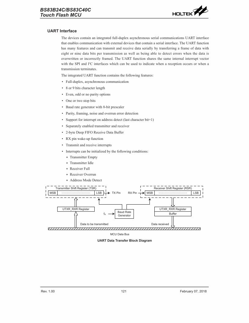
Rev. 1.00 1�0 �e���a�� 0�� �01� Rev. 1.00 1�1 �e���a�� 0�� �01�
BS83B24C/BS83C40CTouch Flash MCU
BS83B24C/BS83C40CTouch Flash MCU
UART InterfaceThedevicescontainanintegratedfull-duplexasynchronousserialcommunicationsUARTinterfacethatenablescommunicationwithexternaldevicesthatcontainaserialinterface.TheUARTfunctionhasmanyfeaturesandcantransmitandreceivedataseriallybytransferringaframeofdatawitheightorninedatabitsper transmissionaswellasbeingable todetecterrorswhen thedata isoverwrittenor incorrectlyframed.TheUARTfunctionshares thesameinternal interruptvectorwiththeSPIandI2Cinterfaceswhichcanbeusedtoindicatewhenareceptionoccursorwhenatransmissionterminates.
TheintegratedUARTfunctioncontainsthefollowingfeatures:
• Full-duplex,asynchronouscommunication
• 8or9bitscharacterlength
• Even,oddornoparityoptions
• Oneortwostopbits
• Baudrategeneratorwith8-bitprescaler
• Parity,framing,noiseandoverrunerrordetection
• Supportforinterruptonaddressdetect(lastcharacterbit=1)
• Separatelyenabledtransmitterandreceiver
• 2-byteDeepFIFOReceiveDataBuffer
• RXpinwake-upfunction
• Transmitandreceiveinterrupts
• Interruptscanbeinitializedbythefollowingconditions:♦ TransmitterEmpty♦ TransmitterIdle♦ ReceiverFull♦ ReceiverOverrun♦ AddressModeDetect
MSB LSB…………………………
T�ansmitte� Shift Registe� (TSR)MSB LSB…………………………
Receive� Shift Registe� (RSR)TX Pin RX Pin
Ba�d Rate Gene�ato�
UTXR_RXR Registe� UTXR_RXR Registe�
Data to �e t�ansmitted Data �eceived
B�ffe�fH
MCU Data B�s
UART Data Transfer Block Diagram

Rev. 1.00 1�� �e���a�� 0�� �01� Rev. 1.00 1�3 �e���a�� 0�� �01�
BS83B24C/BS83C40CTouch Flash MCU
BS83B24C/BS83C40CTouch Flash MCU
UART External PinsTocommunicatewithanexternalserialinterface,theinternalUARThastwoexternalpinsknownasTXandRX.TheTXandRXpinsaretheUARTtransmitterandreceiverpinsrespectively.TheTXandRXpinfunctionshouldfirstbeselectedbythecorrespondingpin-sharedfunctionselectionregisterbeforetheUARTfunctionisused.AlongwiththeUMDbit,theURENbit,theUTXENandURXENbits,ifset,willsetupthesepinstotheirrespectiveTXoutputandRXinputconditionsanddisableanypull-highresistoroptionwhichmayexistontheTXandRXpins.WhentheTXorRXpinfunctionisdisabledbyclearingtheUMD,UREN,UTXENorURXENbit, theTXorRXpinwillbesettoafloatingstate.Atthistimewhethertheinternalpull-highresistorisconnectedtotheTXorRXpinornotisdeterminedbythecorrespondingI/Opull-highfunctioncontrolbit.
UART Data Transfer SchemeTheaboveblockdiagramshowstheoveralldatatransferstructurearrangementfortheUART.TheactualdatatobetransmittedfromtheMCUisfirsttransferredtotheUTXR_RXRregisterbytheapplicationprogram.ThedatawillthenbetransferredtotheTransmitShiftRegisterfromwhereitwillbeshiftedout,LSBfirst,ontotheTXpinataratecontrolledbytheBaudRateGenerator.OnlytheUTXR_RXRregisterismappedontotheMCUDataMemory,theTransmitShiftRegisterisnotmappedandisthereforeinaccessibletotheapplicationprogram.
DatatobereceivedbytheUARTisacceptedontheexternalRXpin,fromwhereit isshiftedin,LSBfirst,totheReceiverShiftRegisterataratecontrolledbytheBaudRateGenerator.Whentheshiftregisterisfull,thedatawillthenbetransferredfromtheshiftregistertotheinternalUTXR_RXRregister,whereit isbufferedandcanbemanipulatedbytheapplicationprogram.OnlytheUTXR_RXRregister ismappedontotheMCUDataMemory, theReceiverShiftRegister isnotmappedandisthereforeinaccessibletotheapplicationprogram.
ItshouldbenotedthattheactualregisterfordatatransmissionandreceptiononlyexistsasasinglesharedregisterintheDataMemory.ThissharedregisterknownastheUTXR_RXRregisterisusedforbothdatatransmissionanddatareception.
UART Status and Control RegistersTherearesixcontrolregistersassociatedwith theUARTfunction.TheUMDbit in theSIMC0registercanbeusedtoselecttheUARTmode.TheUUSR,UUCR1andUUCR2registerscontroltheoverallfunctionoftheUART,whiletheUBRGregistercontrolstheBaudrate.Theactualdatatobe transmittedandreceivedontheserial interface ismanagedthroughtheUTXR_RXRdataregister.NotethatUARTrelatedregistersandtheirPORvaluesareonlyavailablewhentheUARTmodeisselectedbysettingtheUMDbitintheSIMC0registerto“1”.
RegisterName
Bit7 6 5 4 3 2 1 0
SIMC0 SIM� SIM1 SIM0 UMD SIMDEB1 SIMDEB0 SIMEN SIMIC�UUSR UPERR UN� U�ERR UOERR URIDLE URXI� UTIDLE UTXI�
UUCR1 UREN UBNO UPREN UPRT USTOPS UTXBRK URX� UTX�UUCR� UTXEN URXEN UBRGH UADDEN UWAKE URIE UTIIE UTEIE
UTXR_RXR UTXRX� UTXRX6 UTXRX5 UTXRX4 UTXRX3 UTXRX� UTXRX1 UTXRX0UBRG UBRG� UBRG6 UBRG5 UBRG4 UBRG3 UBRG� UBRG1 UBRG0
UART Register List
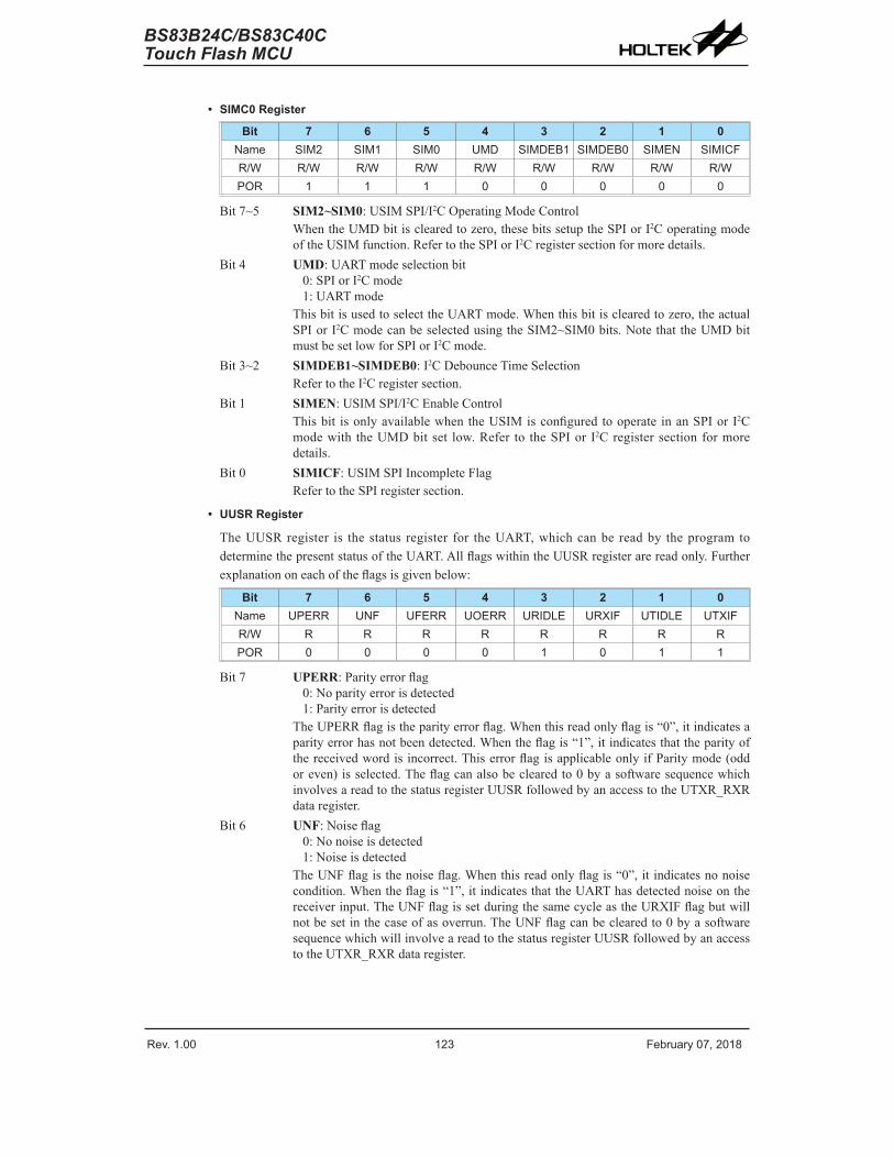
Rev. 1.00 1�� �e���a�� 0�� �01� Rev. 1.00 1�3 �e���a�� 0�� �01�
BS83B24C/BS83C40CTouch Flash MCU
BS83B24C/BS83C40CTouch Flash MCU
• SIMC0 Register
Bit 7 6 5 4 3 2 1 0Name SIM� SIM1 SIM0 UMD SIMDEB1 SIMDEB0 SIMEN SIMIC�R/W R/W R/W R/W R/W R/W R/W R/W R/WPOR 1 1 1 0 0 0 0 0
Bit7~5 SIM2~SIM0:USIMSPI/I2COperatingModeControlWhentheUMDbitisclearedtozero,thesebitssetuptheSPIorI2CoperatingmodeoftheUSIMfunction.RefertotheSPIorI2Cregistersectionformoredetails.
Bit4 UMD:UARTmodeselectionbit0:SPIorI2Cmode1:UARTmode
ThisbitisusedtoselecttheUARTmode.Whenthisbitisclearedtozero,theactualSPIorI2CmodecanbeselectedusingtheSIM2~SIM0bits.NotethattheUMDbitmustbesetlowforSPIorI2Cmode.
Bit3~2 SIMDEB1~SIMDEB0:I2CDebounceTimeSelectionRefertotheI2Cregistersection.
Bit1 SIMEN:USIMSPI/I2CEnableControlThisbit isonlyavailablewhentheUSIMisconfiguredtooperate inanSPIorI2Cmodewith theUMDbitset low.Refer to theSPIor I2Cregistersectionformoredetails.
Bit0 SIMICF:USIMSPIIncompleteFlagRefertotheSPIregistersection.
• UUSR Register
TheUUSRregister is thestatus register for theUART,whichcanbe readby theprogram todeterminethepresentstatusoftheUART.AllflagswithintheUUSRregisterarereadonly.Furtherexplanationoneachoftheflagsisgivenbelow:
Bit 7 6 5 4 3 2 1 0Name UPERR UN� U�ERR UOERR URIDLE URXI� UTIDLE UTXI�R/W R R R R R R R RPOR 0 0 0 0 1 0 1 1
Bit7 UPERR:Parityerrorflag0:Noparityerrorisdetected1:Parityerrorisdetected
TheUPERRflagistheparityerrorflag.Whenthisreadonlyflagis“0”,itindicatesaparityerrorhasnotbeendetected.Whentheflagis“1”,itindicatesthattheparityofthereceivedwordisincorrect.ThiserrorflagisapplicableonlyifParitymode(oddoreven)isselected.Theflagcanalsobeclearedto0byasoftwaresequencewhichinvolvesareadtothestatusregisterUUSRfollowedbyanaccesstotheUTXR_RXRdataregister.
Bit6 UNF:Noiseflag0:Nonoiseisdetected1:Noiseisdetected
TheUNFflagisthenoiseflag.Whenthisreadonlyflagis“0”,itindicatesnonoisecondition.Whentheflagis“1”,itindicatesthattheUARThasdetectednoiseonthereceiverinput.TheUNFflagissetduringthesamecycleastheURXIFflagbutwillnotbesetinthecaseofasoverrun.TheUNFflagcanbeclearedto0byasoftwaresequencewhichwillinvolveareadtothestatusregisterUUSRfollowedbyanaccesstotheUTXR_RXRdataregister.
Rev. 1.00 1�4 �e���a�� 0�� �01� Rev. 1.00 1�5 �e���a�� 0�� �01�
BS83B24C/BS83C40CTouch Flash MCU
BS83B24C/BS83C40CTouch Flash MCU
Bit5 UFERR:Framingerrorflag0:Noframingerrorisdetected1:Framingerrorisdetected
TheUFERRflagistheframingerrorflag.Whenthisreadonlyflagis“0”,itindicatesthatthereisnoframingerror.Whentheflagis“1”,itindicatesthataframingerrorhasbeendetectedforthecurrentcharacter.Theflagcanalsobeclearedto0byasoftwaresequencewhichwillinvolveareadtothestatusregisterUUSRfollowedbyanaccesstotheUTXR_RXRdataregister.
Bit4 UOERR:Overrunerrorflag0:Nooverrunerrorisdetected1:Overrunerrorisdetected
TheUOERRflagis theoverrunerrorflagwhichindicateswhenthereceiverbufferhasoverflowed.Whenthisreadonlyflagis“0”,it indicatesthatthereisnooverrunerror.Whentheflagis“1”,itindicatesthatanoverrunerroroccurswhichwillinhibitfurthertransferstotheUTXR_RXRreceivedataregister.Theflagisclearedto0byasoftwaresequence,whichisareadtothestatusregisterUUSRfollowedbyanaccesstotheUTXR_RXRdataregister.
Bit3 URIDLE:Receiverstatus0:Datareceptionisinprogress(Databeingreceived)1:Nodatareceptionisinprogress(Receiverisidle)
TheURIDLEflag is the receiver status flag.When this readonly flag is“0”, itindicates that the receiver isbetween the initialdetectionof thestartbitand thecompletionofthestopbit.Whentheflagis“1”,it indicatesthatthereceiverisidle.Between thecompletionof thestopbitand thedetectionof thenextstartbit, theURIDLEbitis“1”indicatingthattheUARTreceiverisidleandtheRXpinstaysinlogichighcondition.
Bit2 URXIF:ReceiveUTXR_RXRdataregisterstatus0:UTXR_RXRdataregisterisempty1:UTXR_RXRdataregisterhasavailabledata
TheURXIFflagis thereceivedataregisterstatusflag.Whenthisreadonlyflagis“0”, it indicates that theUTXR_RXRreaddataregister isempty.Whentheflagis“1”,itindicatesthattheUTXR_RXRreaddataregistercontainsnewdata.WhenthecontentsoftheshiftregisteraretransferredtotheUTXR_RXRregister,aninterruptisgeneratedifURIE=1intheUUCR2register.Ifoneormoreerrorsaredetectedinthereceivedword,theappropriatereceive-relatedflagsUNF,UFERR,and/orUPERRaresetwithinthesameclockcycle.TheURXIFflagwilleventuallybeclearedto0whentheUUSRregisterisreadwithURXIFset,followedbyareadfromtheUTXR_RXRregister,andiftheUTXR_RXRregisterhasnomorenewdataavailable.
Bit1 UTIDLE:Transmissionidle0:Datatransmissionisinprogress(Databeingtransmitted)1:Nodatatransmissionisinprogress(Transmitterisidle)
TheUTIDLEflagisknownasthetransmissioncompleteflag.Whenthisreadonlyflagis“0”, it indicates thata transmissionis inprogress.ThisflagwillbesethighwhentheUTXIFflagis“1”andwhenthere isnotransmitdataorbreakcharacterbeingtransmitted.WhenUTIDLEisequalto“1”,theTXpinbecomesidlewiththepinstate in logichighcondition.TheUTIDLEflag iscleared to0byreading theUUSRregisterwithUTIDLEsetandthenwritingtotheUTXR_RXRregister.Theflagisnotgeneratedwhenadatacharacterorabreakisqueuedandreadytobesent.
Bit0 UTXIF:TransmitUTXR_RXRdataregisterstatus0:Characterisnottransferredtothetransmitshiftregister1:Characterhastransferredtothetransmitshiftregister(UTXR_RXRdataregisterisempty)
TheUTXIFflagisthetransmitdataregisteremptyflag.Whenthisreadonlyflagis“0”,itindicatesthatthecharacterisnottransferredtothetransmittershiftregister.Whentheflagis“1”,it indicatesthatthetransmittershiftregisterhasreceivedacharacterfromtheUTXR_RXRdataregister.TheUTXIFflagisclearedto0byreadingtheUARTstatusregister(UUSR)withUTXIFsetandthenwritingtotheUTXR_RXRdataregister.NotethatwhentheUTXENbitisset,theUTXIFflagbitwillalsobesetsincethetransmitdataregisterisnotyetfull.

Rev. 1.00 1�4 �e���a�� 0�� �01� Rev. 1.00 1�5 �e���a�� 0�� �01�
BS83B24C/BS83C40CTouch Flash MCU
BS83B24C/BS83C40CTouch Flash MCU
• UUCR1 Register
TheUUCR1registertogetherwiththeUUCR2registerarethetwoUARTcontrolregistersthatareusedtosetthevariousoptionsfortheUARTfunction,suchasoverallon/offcontrol,paritycontrol,datatransferbitlengthetc.Furtherexplanationoneachofthebitsisgivenbelow:
Bit 7 6 5 4 3 2 1 0Name UREN UBNO UPREN UPRT USTOPS UTXBRK URX� UTX�R/W R/W R/W R/W R/W R/W R/W R WPOR 0 0 0 0 0 0 x 0
“x”: UnknownBit7 UREN:UARTfunctionenablecontrol
0:DisableUART.TXandRXpinsareinafloatingstate1:EnableUART.TXandRXpinsfunctionasUARTpins
TheURENbitistheUARTenablebit.Whenthisbitisequalto“0”,theUARTwillbedisabledandtheRXpinaswellastheTXpinwillbesetinafloatingstate.Whenthebitisequalto“1”,theUARTwillbeenablediftheUMDbitissetandtheTXandRXpinswillfunctionasdefinedbytheUTXENandURXENenablecontrolbits.WhentheUARTisdisabled,itwillemptythebuffersoanycharacterremaininginthebufferwillbediscarded.Inaddition,thevalueofthebaudratecounterwillbereset.If theUARTisdisabled,allerrorandstatusflagswillbereset.Also theUTXEN,URXEN,UTXBRK,URXIF,UOERR,UFERR,UPERRandUNFbitswillbeclearedto0,whiletheUTIDLE,UTXIFandURIDLEbitswillbeset.OthercontrolbitsinUUCR1,UUCR2andUBRGregisterswillremainunaffected.IftheUARTisactiveandtheURENbit isclearedto0,allpendingtransmissionsandreceptionswillbeterminatedand themodulewillbe resetasdefinedabove.When theUARTis re-enabled,itwillrestartinthesameconfiguration.
Bit6 UBNO:Numberofdatatransferbitsselection0:8-bitdatatransfer1:9-bitdatatransfer
Thisbit isusedtoselect thedata lengthformat,whichcanhaveachoiceofeither8-bitor9-bitformat.Whenthisbitisequalto“1”,a9-bitdatalengthformatwillbeselected.Ifthebitisequalto“0”,thenan8-bitdatalengthformatwillbeselected.If9-bitdatalengthformatisselected,thenbitsURX8andUTX8willbeusedtostorethe9thbitofthereceivedandtransmitteddatarespectively.
Bit5 UPREN:Parityfunctionenablecontrol0:Parityfunctionisdisabled1:Parityfunctionisenabled
Thisistheparityenablebit.Whenthisbitisequalto“1”,theparityfunctionwillbeenabled.Ifthebitisequalto“0”,thentheparityfunctionwillbedisabled.
Bit4 UPRT:Paritytypeselectionbit0:Evenparityforparitygenerator1:Oddparityforparitygenerator
Thisbitistheparitytypeselectionbit.Whenthisbitisequalto“1”,oddparitytypewillbeselected.Ifthebitisequalto“0”,thenevenparitytypewillbeselected.
Bit3 USTOPS:NumberofStopbitsselection0:Onestopbitformatisused1:Twostopbitsformatisused
Thisbitdeterminesifoneortwostopbitsaretobeused.Whenthisbitisequalto“1”,twostopbitsareused.Ifthisbitisequalto“0”,thenonlyonestopbitisused.
Bit2 UTXBRK:Transmitbreakcharacter0:Nobreakcharacteristransmitted1:Breakcharacterstransmit
TheUTXBRKbitistheTransmitBreakCharacterbit.Whenthisbitis“0”,therearenobreakcharactersandtheTXpinoperatesnormally.Whenthebitis“1”,therearetransmitbreakcharactersandthetransmitterwillsendlogiczeros.Whenthisbit isequalto“1”,afterthebuffereddatahasbeentransmitted,thetransmitteroutputisheldlowforaminimumofa13-bitlengthanduntiltheUTXBRKbitisreset.

Rev. 1.00 1�6 �e���a�� 0�� �01� Rev. 1.00 1�� �e���a�� 0�� �01�
BS83B24C/BS83C40CTouch Flash MCU
BS83B24C/BS83C40CTouch Flash MCU
Bit1 URX8:Receivedatabit8for9-bitdatatransferformat(readonly)Thisbit isonlyusedif9-bitdata transfersareused, inwhichcasethisbit locationwillstorethe9thbitofthereceiveddataknownasURX8.TheUBNObitisusedtodeterminewhetherdatatransfersarein8-bitor9-bitformat.
Bit0 UTX8:Transmitdatabit8for9-bitdatatransferformat(writeonly)Thisbitisonlyusedif9-bitdatatransfersareused,inwhichcasethisbitlocationwillstorethe9thbitof thetransmitteddataknownasUTX8.TheUBNObit isusedtodeterminewhetherdatatransfersarein8-bitor9-bitformat.
• UUCR2 Register
TheUUCR2registeristhesecondofthetwoUARTcontrolregistersandservesseveralpurposes.Oneofitsmainfunctionsistocontrolthebasicenable/disableoperationoftheUARTTransmitterandReceiveraswellasenablingthevariousUSIMUARTmodeinterruptsources.Theregisteralsoservestocontrolthebaudratespeed,receiverwake-upenableandtheaddressdetectenable.Furtherexplanationoneachofthebitsisgivenbelow:
Bit 7 6 5 4 3 2 1 0Name UTXEN URXEN UBRGH UADDEN UWAKE URIE UTIIE UTEIER/W R/W R/W R/W R/W R/W R/W R/W R/WPOR 0 0 0 0 0 0 0 0
Bit7 UTXEN:UARTTransmitterenabledcontrol0:UARTtransmitterisdisabled1:UARTtransmitterisenabled
ThebitnamedUTXENistheTransmitterEnableBit.Whenthisbit isequalto“0”,thetransmitterwillbedisabledwithanypendingdatatransmissionsbeingaborted.Inadditionthebufferswillbereset.InthissituationtheTXpinwillbesetinafloatingstate.If theUTXENbit isequal to“1”and theUMDandURENbitarealsoequal to“1”,thetransmitterwillbeenabledandtheTXpinwillbecontrolledbytheUART.ClearingtheUTXENbitto0duringatransmissionwillcausethedatatransmissiontobeabortedandwillresetthetransmitter.Ifthissituationoccurs,theTXpinwillbesetinafloatingstate.
Bit6 URXEN:UARTReceiverenabledcontrol0:UARTreceiverisdisabled1:UARTreceiverisenabled
ThebitnamedURXENistheReceiverEnableBit.Whenthisbitisequalto“0”,thereceiverwillbedisabledwithanypendingdatareceptionsbeingaborted.Inadditionthereceivebufferswillbereset.InthissituationtheRXpinwillbesetinafloatingstate.If theURXENbit isequalto“1”andtheUMDandURENbitarealsoequalto“1”,thereceiverwillbeenabledandtheRXpinwillbecontrolledbytheUART.ClearingtheURXENbit to0duringareceptionwillcausethedatareceptiontobeabortedandwillresetthereceiver.Ifthissituationoccurs,theRXpinwillbesetinafloatingstate.
Bit5 UBRGH:BaudRatespeedselection0:Lowspeedbaudrate1:Highspeedbaudrate
Thebit namedUBRGHselects thehighor low speedmodeof theBaudRateGenerator.Thisbit, togetherwiththevalueplacedinthebaudrateregisterUBRG,controlstheBaudRateoftheUART.Ifthisbitisequalto“1”,thehighspeedmodeisselected.Ifthebitisequalto“0”,thelowspeedmodeisselected.

Rev. 1.00 1�6 �e���a�� 0�� �01� Rev. 1.00 1�� �e���a�� 0�� �01�
BS83B24C/BS83C40CTouch Flash MCU
BS83B24C/BS83C40CTouch Flash MCU
Bit4 UADDEN:Addressdetectfunctionenablecontrol0:Addressdetectfunctionisdisabled1:Addressdetectfunctionisenabled
ThebitnamedUADDENistheaddressdetectfunctionenablecontrolbit.Whenthisbitisequalto“1”,theaddressdetectfunctionisenabled.Whenitoccurs,ifthe8thbit,whichcorrespondstoURX7ifUBNO=0orthe9thbit,whichcorrespondstoURX8ifUBNO=1,hasavalueof“1”,thenthereceivedwordwillbeidentifiedasanaddress,ratherthandata.Ifthecorrespondinginterruptisenabled,aninterruptrequestwillbegeneratedeachtimethereceivedwordhastheaddressbitset,whichisthe8thor9thbitdependingonthevalueofUBNO.Iftheaddressbitknownasthe8thor9thbitofthereceivedwordis“0”withtheaddressdetectfunctionbeingenabled,aninterruptwillnotbegeneratedandthereceiveddatawillbediscarded.
Bit3 UWAKE:RXpinwake-upUARTfunctionenablecontrol0:RXpinwake-upUARTfunctionisdisabled1:RXpinwake-upUARTfunctionisenabled
Thisbitisusedtocontrolthewake-upUARTfunctionwhenafallingedgeontheRXpinoccurs.NotethatthisbitisonlyavailablewhentheUARTclock(fH)isswitchedoff.TherewillbenoRXpinwake-upUARTfunctioniftheUARTclock(fH)exists.IftheUWAKEbitissetto1astheUARTclock(fH)isswitchedoff,aUARTwake-uprequestwillbe initiatedwhena fallingedgeon theRXpinoccurs.When thisrequesthappensand thecorresponding interrupt isenabled,anRXpinwake-upUARTinterruptwillbegeneratedtoinformtheMCUtowakeuptheUARTfunctionbyswitchingon theUARTclock(fH)via theapplicationprogram.Otherwise, theUARTfunctioncannotresumeevenifthereisafallingedgeontheRXpinwhentheUWAKEbitisclearedto0.
Bit2 URIE:Receiverinterruptenablecontrol0:Receiverrelatedinterruptisdisabled1:Receiverrelatedinterruptisenabled
Thisbitenablesordisablesthereceiverinterrupt.Ifthisbitisequalto“1”andwhenthereceiveroverrunflagUOERRorreceivedataavailableflagURXIFisset, theUSIMinterruptrequestflagUSIMFwillbeset.Ifthisbitisequalto“0”,theUSIMinterruptrequestflagUSIMFwillnotbeinfluencedbytheconditionoftheUOERRorURXIFflags.
Bit1 UTIIE:TransmitterIdleinterruptenablecontrol0:Transmitteridleinterruptisdisabled1:Transmitteridleinterruptisenabled
Thisbitenablesordisablesthetransmitteridleinterrupt.Ifthisbitisequalto“1”andwhenthetransmitteridleflagUTIDLEisset,duetoatransmitteridlecondition,theUSIMinterruptrequestflagUSIMFwillbeset.Ifthisbitisequalto“0”,theUSIMinterruptrequestflagUSIMFwillnotbeinfluencedbytheconditionoftheUTIDLEflag.
Bit0 UTEIE:TransmitterEmptyinterruptenablecontrol0:Transmitteremptyinterruptisdisabled1:Transmitteremptyinterruptisenabled
Thisbitenablesordisables the transmitterempty interrupt. If thisbit isequal to“1”andwhenthe transmitteremptyflagUTXIFisset,due toa transmitteremptycondition,theUSIMinterruptrequestflagUSIMFwillbeset.Ifthisbitisequalto“0”,theUSIMinterruptrequestflagUSIMFwillnotbeinfluencedbytheconditionoftheUTXIFflag.

Rev. 1.00 1�� �e���a�� 0�� �01� Rev. 1.00 1�9 �e���a�� 0�� �01�
BS83B24C/BS83C40CTouch Flash MCU
BS83B24C/BS83C40CTouch Flash MCU
• UTXR_RXR Register
TheUTXR_RXRregisteristhedataregisterwhichisusedtostorethedatatobetransmittedontheTXpinorbeingreceivedfromtheRXpin.
Bit 7 6 5 4 3 2 1 0Name UTXRX� UTXRX6 UTXRX5 UTXRX4 UTXRX3 UTXRX� UTXRX1 UTXRX0R/W R/W R/W R/W R/W R/W R/W R/W R/WPOR x x x x x x x x
“x”: UnknownBit7~0 UTXRX7~UTXRX0:UARTTransmit/ReceiveDatabit7~bit0
• UBRG Register
Bit 7 6 5 4 3 2 1 0Name UBRG� UBRG6 UBRG5 UBRG4 UBRG3 UBRG� UBRG1 UBRG0R/W R/W R/W R/W R/W R/W R/W R/W R/WPOR x x x x x x x x
“x”: UnknownBit7~0 UBRG7~UBRG0:BaudRatevalues
ByprogrammingtheUBRGHbit inUUCR2RegisterwhichallowsselectionoftherelatedformuladescribedaboveandprogrammingtherequiredvalueintheUBRGregister,therequiredbaudratecanbesetup.Note:Baudrate=fH/[64×(N+1)]ifUBRGH=0.Baudrate=fH/[16×(N+1)]ifUBRGH=1.
Baud Rate GeneratorTosetupthespeedoftheserialdatacommunication,theUARTfunctioncontainsitsowndedicatedbaudrategenerator.Thebaudrateiscontrolledbyitsowninternalfreerunning8-bittimer,theperiodofwhichisdeterminedbytwofactors.ThefirstoftheseisthevalueplacedinthebaudrateregisterUBRGandthesecondisthevalueoftheUBRGHbitwiththecontrolregisterUUCR2.TheUBRGHbitdecidesifthebaudrategeneratoristobeusedinahighspeedmodeorlowspeedmode,whichinturndeterminestheformulathatisusedtocalculatethebaudrate.ThevalueNintheUBRGregisterwhichisusedinthefollowingbaudratecalculationformuladeterminesthedivisionfactor.NotethatNisthedecimalvalueplacedintheUBRGregisterandhasarangeofbetween0and255.
UUCR2 UBRGH Bit 0 1
Ba�d Rate (BR) fH / [64 (N+1)] fH / [16 (N+1)]
ByprogrammingtheUBRGHbitwhichallowsselectionoftherelatedformulaandprogrammingtherequiredvalueintheUBRGregister,therequiredbaudratecanbesetup.Notethatbecausetheactualbaudrateisdeterminedusingadiscretevalue,N,placedintheUBRGregister,therewillbeanerrorassociatedbetweentheactualandrequestedvalue.ThefollowingexampleshowshowtheUBRGregistervalueNandtheerrorvaluecanbecalculated.
Calculating the Baud Rate and Error ValuesForaclockfrequencyof4MHz,andwithUBRGHclearedtozerodeterminetheUBRGregistervalueN,theactualbaudrateandtheerrorvalueforadesiredbaudrateof4800.
FromtheabovetablethedesiredbaudrateBR=fH/[64(N+1)]
Re-arrangingthisequationgivesN=[fH/(BR×64)]-1
GivingavalueforN=[4000000/(4800×64)]-1=12.0208
Toobtaintheclosestvalue,adecimalvalueof12shouldbeplacedintotheUBRGregister.ThisgivesanactualorcalculatedbaudratevalueofBR=4000000/[64×(12+1)]=4808
Thereforetheerrorisequalto(4808-4800)/4800=0.16%

Rev. 1.00 1�� �e���a�� 0�� �01� Rev. 1.00 1�9 �e���a�� 0�� �01�
BS83B24C/BS83C40CTouch Flash MCU
BS83B24C/BS83C40CTouch Flash MCU
UART Setup and ControlFordatatransfer,theUARTfunctionutilizesanon-return-to-zero,morecommonlyknownasNRZ,format.Thisiscomposedofonestartbit,eightorninedatabits,andoneortwostopbits.ParityissupportedbytheUARThardware,andcanbesetuptobeeven,oddornoparity.Forthemostcommondataformat,8databitsalongwithnoparityandonestopbit,denotedas8,N,1,isusedasthedefaultsetting,whichisthesettingatpower-on.Thenumberofdatabitsandstopbits,alongwiththeparity,aresetupbyprogrammingthecorrespondingUBNO,UPRT,UPREN,andUSTOPSbits in theUUCR1register.Thebaudrateused to transmitandreceivedata issetupusing theinternal8-bitbaudrategenerator,whilethedataistransmittedandreceivedLSBfirst.AlthoughtheUARTtransmitterandreceiverarefunctionallyindependent,theybothusethesamedataformatandbaudrate.Inallcasesstopbitswillbeusedfordatatransmission.
Enabling/Disabling the UART InterfaceThebasicon/offfunctionoftheinternalUARTfunctioniscontrolledusingtheURENbit intheUUCR1register.WhentheUARTmodeisselectedbysettingtheUMDbitintheSIMC0registerto“1”,iftheUREN,UTXENandURXENbitsareset,thenthesetwoUARTpinswillactasnormalTXoutputpinandRXinputpinrespectively.IfnodataisbeingtransmittedontheTXpin,thenitwilldefaulttoalogichighvalue.
ClearingtheURENbitwilldisable theTXandRXpinsandallowthesetwopins tobeusedasnormalI/Oorotherpin-sharedfunctionalpinsbyconfiguringthecorrespondingpin-sharedcontrolbits.WhentheUARTfunction isdisabled thebufferwillbereset toanemptycondition,at thesametimediscardinganyremainingresidualdata.DisablingtheUARTwillalsoresettheerrorandstatusflagswithbitsUTXEN,URXEN,UTXBRK,URXIF,UOERR,UFERR,UPERRandUNFbeingclearedwhilebitsUTIDLE,UTXIFandURIDLEwillbeset.TheremainingcontrolbitsintheUUCR1,UUCR2andUBRGregisterswillremainunaffected.IftheURENbitintheUUCR1registerisclearedwhiletheUARTisactive,thenallpendingtransmissionsandreceptionswillbeimmediatelysuspendedandtheUARTwillberesettoaconditionasdefinedabove.IftheUARTisthensubsequentlyre-enabled,itwillrestartagaininthesameconfiguration.
Data, Parity and Stop Bit SelectionTheformatofthedatatobetransferrediscomposedofvariousfactorssuchasdatabitlength,parityon/off,paritytype,addressbitsandthenumberofstopbits.ThesefactorsaredeterminedbythesetupofvariousbitswithintheUUCR1register.TheUBNObitcontrols thenumberofdatabitswhichcanbesettoeither8or9,theUPRTbitcontrolsthechoiceofoddorevenparity,theUPRENbitcontrolstheparityon/offfunctionandtheUSTOPSbitdecideswhetheroneortwostopbitsaretobeused.Thefollowingtableshowsvariousformatsfordatatransmission.Theaddressbit,whichistheMSBofthedatabyte,identifiestheframeasanaddresscharacterordataiftheaddressdetectfunctionisenabled.Thenumberofstopbits,whichcanbeeitheroneortwo,isindependentofthedatalengthandisonlyusedforthetransmitter.Thereisonlyonestopbitforthereceiver.
Start Bit Data Bits Address Bit Parity Bit Stop BitExample of 8-bit Data Formats
1 � 0 0 11 � 0 1 11 � 1 0 1
Example of 9-bit Data Formats1 9 0 0 11 � 0 1 11 � 1 0 1
Transmitter Receiver Data Format

Rev. 1.00 130 �e���a�� 0�� �01� Rev. 1.00 131 �e���a�� 0�� �01�
BS83B24C/BS83C40CTouch Flash MCU
BS83B24C/BS83C40CTouch Flash MCU
Thefollowingdiagramshows the transmitandreceivewaveformsforboth8-bitand9-bitdataformats.
Bit 0
8-bit Data Format
Bit 1 StopBit
Next Sta�tBit
Sta�tBit
Pa�it� Bit
Bit � Bit 3 Bit 4 Bit 5 Bit 6 Bit �
Bit 0
9-bit Data Format
Bit 1Sta�tBit Bit � Bit 3 Bit 4 Bit 5 Bit 6 Stop
Bit
Next Sta�tBit
Pa�it� Bit
Bit �Bit �
UART TransmitterDatawordlengthsofeither8or9bitscanbeselectedbyprogrammingtheUBNObitintheUUCR1register.WhenUBNObitisset,thewordlengthwillbesetto9bits.Inthiscasethe9thbit,whichistheMSB,needstobestoredintheUTX8bitintheUUCR1register.AtthetransmittercoreliestheTransmitterShiftRegister,morecommonlyknownastheTSR,whosedataisobtainedfromthetransmitdataregister,whichisknownastheUTXR_RXRregister.ThedatatobetransmittedisloadedintothisUTXR_RXRregisterbytheapplicationprogram.TheTSRregisterisnotwrittentowithnewdatauntilthestopbitfromtheprevioustransmissionhasbeensentout.Assoonasthisstopbithasbeentransmitted, theTSRcanthenbeloadedwithnewdatafromtheUTXR_RXRregister,ifitisavailable.ItshouldbenotedthattheTSRregister,unlikemanyotherregisters,isnotdirectlymappedintotheDataMemoryareaandassuchisnotavailabletotheapplicationprogramfordirectread/writeoperations.AnactualtransmissionofdatawillnormallybeenabledwhentheUTXENbitisset,butthedatawillnotbetransmitteduntiltheUTXR_RXRregisterhasbeenloadedwithdataandthebaudrategeneratorhasdefinedashiftclocksource.However, thetransmissioncanalsobeinitiatedbyfirstloadingdataintotheUTXR_RXRregister,afterwhichtheUTXENbitcanbeset.Whenatransmissionofdatabegins,theTSRisnormallyempty,inwhichcaseatransfertotheUTXR_RXRregisterwillresultinanimmediatetransfertotheTSR.IfduringatransmissiontheUTXENbitiscleared,thetransmissionwillimmediatelyceaseandthetransmitterwillbereset.TheTXoutputpincanthenbeconfiguredastheI/Oorotherpin-sharedfunctionbyconfiguringthecorrespondingpin-sharedcontrolbits.
Transmitting DataWhentheUARTistransmittingdata,thedataisshiftedontheTXpinfromtheshiftregister,withtheleastsignificantbitfirst.Inthetransmitmode,theUTXR_RXRregisterformsabufferbetweentheinternalbusandthetransmittershiftregister.Itshouldbenotedthatif9-bitdataformathasbeenselected,thentheMSBwillbetakenfromtheUTX8bitintheUUCR1register.Thestepstoinitiateadatatransfercanbesummarizedasfollows:
• MakethecorrectselectionoftheUBNO,UPRT,UPRENandUSTOPSbitstodefinetherequiredwordlength,paritytypeandnumberofstopbits.
• SetuptheUBRGregistertoselectthedesiredbaudrate.
• SettheUTXENbittoensurethattheTXpinisusedasaUARTtransmitterpin.
• Access theUUSRregisterandwrite thedata that is tobe transmitted into theUTXR_RXRregister.NotethatthisstepwillcleartheUTXIFbit.
Thissequenceofeventscannowberepeatedtosendadditionaldata.
ItshouldbenotedthatwhenUTXIF=0,datawillbeinhibitedfrombeingwrittentotheUTXR_RXRregister.ClearingtheUTXIFflagisalwaysachievedusingthefollowingsoftwaresequence:
1.AUUSRregisteraccess
2.AUTXR_RXRregisterwriteexecution

Rev. 1.00 130 �e���a�� 0�� �01� Rev. 1.00 131 �e���a�� 0�� �01�
BS83B24C/BS83C40CTouch Flash MCU
BS83B24C/BS83C40CTouch Flash MCU
Theread-onlyUTXIFflagissetbytheUARThardwareandifsetindicatesthattheUTXR_RXRregister isemptyand thatotherdatacannowbewritten into theUTXR_RXRregisterwithoutoverwritingthepreviousdata.IftheUTEIEbitissetthentheUTXIFflagwillgenerateaninterrupt.
Duringadata transmission,awrite instruction to theUTXR_RXRregisterwillplace thedataintotheUTXR_RXRregister,whichwillbecopiedtotheshiftregisterat theendofthepresenttransmission.Whenthereisnodatatransmissioninprogress,awriteinstructiontotheUTXR_RXRregisterwillplacethedatadirectlyintotheshiftregister,resultinginthecommencementofdatatransmission,andtheUTXIFbitbeingimmediatelyset.Whenaframetransmissioniscomplete,whichhappensafterstopbitsaresentorafterthebreakframe,theUTIDLEbitwillbeset.TocleartheUTIDLEbitthefollowingsoftwaresequenceisused:
1.AUUSRregisteraccess
2.AUTXR_RXRregisterwriteexecution
NotethatboththeUTXIFandUTIDLEbitsareclearedbythesamesoftwaresequence.
Transmit BreakIf theUTXBRKbit is set thenbreakcharacterswillbe senton thenext transmission.Breakcharactertransmissionconsistsofastartbit,followedby13×N‘0’bitsandstopbits,whereN=1,2,etc.IfabreakcharacteristobetransmittedthentheUTXBRKbitmustbefirstsetbytheapplicationprogram,andthenclearedtogeneratethestopbits.Transmittingabreakcharacterwillnotgenerateatransmitinterrupt.Notethatabreakconditionlengthisatleast13bitslong.IftheUTXBRKbitiscontinuallykeptatalogichighlevelthenthetransmittercircuitrywilltransmitcontinuousbreakcharacters.AftertheapplicationprogramhasclearedtheUTXBRKbit, thetransmitterwillfinishtransmittingthelastbreakcharacterandsubsequentlysendoutoneortwostopbits.Theautomaticlogichighsattheendofthelastbreakcharacterwillensurethatthestartbitofthenextframeisrecognized.
UART ReceiverTheUARTiscapableofreceivingwordlengthsofeither8or9bits.IftheUBNObitisset,thewordlengthwillbesetto9bitswiththeMSBbeingstoredintheURX8bitoftheUUCR1register.AtthereceivercoreliestheReceiveSerialShiftRegister,commonlyknownastheRSR.ThedatawhichisreceivedontheRXexternalinputpinissenttothedatarecoveryblock.Thedatarecoveryblockoperatingspeedis16timesthatofthebaudrate,whilethemainreceiveserialshifteroperatesatthebaudrate.AftertheRXpinissampledforthestopbit,thereceiveddatainRSRistransferredtothereceivedataregister,iftheregisterisempty.ThedatawhichisreceivedontheexternalRXinputpinissampledthreetimesbyamajoritydetectcircuittodeterminethelogiclevelthathasbeenplacedontotheRXpin.ItshouldbenotedthattheRSRregister,unlikemanyotherregisters,isnotdirectlymappedintotheDataMemoryareaandassuchisnotavailabletotheapplicationprogramfordirectread/writeoperations.
Receiving DataWhentheUARTreceiverisreceivingdata,thedataisseriallyshiftedinontheexternalRXinputpin,LSBfirst.Inthereadmode,theUTXR_RXRregisterformsabufferbetweentheinternalbusandthereceivershiftregister.TheUTXR_RXRregisterisatwobytedeepFIFOdatabuffer,wheretwobytescanbeheld in theFIFOwhilea thirdbytecancontinuetobereceived.Note that theapplicationprogrammustensurethatthedataisreadfromUTXR_RXRbeforethethirdbytehasbeencompletelyshiftedin,otherwisethisthirdbytewillbediscardedandanoverrunerrorUOERRwillbesubsequentlyindicated.Thestepstoinitiateadatatransfercanbesummarizedasfollows:
Rev. 1.00 13� �e���a�� 0�� �01� Rev. 1.00 133 �e���a�� 0�� �01�
BS83B24C/BS83C40CTouch Flash MCU
BS83B24C/BS83C40CTouch Flash MCU
• MakethecorrectselectionofUBNO,UPRTandUPRENbitstodefinethewordlength,paritytype.
• SetuptheUBRGregistertoselectthedesiredbaudrate.
• SettheURXENbittoensurethattheRXpinisusedasaUARTreceiverpin.
Atthispointthereceiverwillbeenabledwhichwillbegintolookforastartbit.
Whenacharacterisreceivedthefollowingsequenceofeventswilloccur:
• TheURXIFbit in theUUSRregisterwillbe setwhen theUTXR_RXRregisterhasdataavailable.Therewillbeatmostonemorecharacteravailablebeforeanoverrunerroroccurs.
• WhenthecontentsoftheshiftregisterhavebeentransferredtotheUTXR_RXRregister,theniftheURIEbitisset,aninterruptwillbegenerated.
• Ifduringreception,aframeerror,noiseerror,parityerror,oranoverrunerrorhasbeendetected,thentheerrorflagscanbeset.
TheURXIFbitcanbeclearedusingthefollowingsoftwaresequence:
1.AUUSRregisteraccess
2.AUTXR_RXRregisterreadexecution
Receive BreakAnybreakcharacter receivedby theUARTwillbemanagedasa framingerror.The receiverwillcountandexpectacertainnumberofbit timesasspecifiedbythevaluesprogrammedintotheUBNObitplusonestopbit.If thebreakismuchlongerthan13bit times, thereceptionwillbeconsideredascompleteafter thenumberofbit timesspecifiedbyUBNOplusonestopbit.TheURXIFbitisset,UFERRisset,zerosareloadedintothereceivedataregister, interruptsaregeneratedifappropriateandtheURIDLEbitisset.AbreakisregardedasacharacterthatcontainsonlyzeroswiththeUFERRflagset.Ifalongbreaksignalhasbeendetected,thereceiverwillregarditasadataframeincludingastartbit,databitsandtheinvalidstopbitandtheUFERRflagwillbeset.Thereceivermustwaitforavalidstopbitbeforelookingforthenextstartbit.Thereceiverwillnotmaketheassumptionthatthebreakconditiononthelineisthenextstartbit.Thebreakcharacterwillbeloadedintothebufferandnofurtherdatawillbereceiveduntilstopbitsarereceived.ItshouldbenotedthattheURIDLEreadonlyflagwillgohighwhenthestopbitshavenotyetbeenreceived.ThereceptionofabreakcharacterontheUARTregisterswillresultinthefollowing:
• Theframingerrorflag,UFERR,willbeset.
• Thereceivedataregister,UTXR_RXR,willbecleared.
• TheUOERR,UNF,UPERR,URIDLEorURXIFflagswillpossiblybeset.
Idle StatusWhenthereceiver isreadingdata,whichmeansitwillbeinbetweenthedetectionofastartbitandthereadingofastopbit,thereceiverstatusflagintheUUSRregister,otherwiseknownastheURIDLEflag,willhaveazerovalue.Inbetweenthereceptionofastopbitandthedetectionofthenextstartbit,theURIDLEflagwillhaveahighvalue,whichindicatesthereceiverisinanidlecondition.
Receiver InterruptThereadonlyreceiveinterruptflagURXIFintheUUSRregisterissetbyanedgegeneratedbythereceiver.AninterruptisgeneratedifURIE=1,whenawordis transferredfromtheReceiveShiftRegister,RSR,totheReceiveDataRegister,UTXR_RXR.AnoverrunerrorcanalsogenerateaninterruptifURIE=1.

Rev. 1.00 13� �e���a�� 0�� �01� Rev. 1.00 133 �e���a�� 0�� �01�
BS83B24C/BS83C40CTouch Flash MCU
BS83B24C/BS83C40CTouch Flash MCU
Managing Receiver ErrorsSeveraltypesofreceptionerrorscanoccurwithintheUARTmodule,thefollowingsectiondescribesthevarioustypesandhowtheyaremanagedbytheUART.
Overrun Error – UOERRTheUTXR_RXRregisteriscomposedofatwobytedeepFIFOdatabuffer,wheretwobytescanbeheldintheFIFOregister,whileathirdbytecancontinuetobereceived.Beforethisthirdbytehasbeenentirelyshiftedin,thedatashouldbereadfromtheUTXR_RXRregister.Ifthisisnotdone,theoverrunerrorflagUOERRwillbeconsequentlyindicated.
Intheeventofanoverrunerroroccurring,thefollowingwillhappen:
• TheUOERRflagintheUUSRregisterwillbeset.
• TheUTXR_RXRcontentswillnotbelost.
• Theshiftregisterwillbeoverwritten.
• AninterruptwillbegeneratediftheURIEbitisset.
TheUOERRflagcanbeclearedbyanaccess to theUUSRregister followedbya read to theUTXR_RXRregister.
Noise Error – UNFOver-sampling isusedfordata recovery to identifyvalid incomingdataandnoise. Ifnoise isdetectedwithinaframethefollowingwilloccur:
• Thereadonlynoiseflag,UNF,intheUUSRregisterwillbesetontherisingedgeoftheURXIFbit.
• DatawillbetransferredfromtheShiftregistertotheUTXR_RXRregister.
• Nointerruptwillbegenerated.HoweverthisbitrisesatthesametimeastheURXIFbitwhichitselfgeneratesaninterrupt.
Note that theUNFflag is resetbyaUUSRregister readoperationfollowedbyaUTXR_RXRregisterreadoperation.
Framing Error – UFERRThereadonlyframingerrorflag,UFERR,intheUUSRregister,issetifazeroisdetectedinsteadofstopbits.Iftwostopbitsareselected,bothstopbitsmustbehigh;otherwisetheUFERRflagwillbeset.TheUFERRflagandthereceiveddatawillberecordedintheUUSRandUTXR_RXRregistersrespectively,andtheflagisclearedinanyreset.
Parity Error – UPERRThereadonlyparityerrorflag,UPERR,intheUUSRregister, isset if theparityofthereceivedword is incorrect.Thiserror flag isonlyapplicable if theparity isenabled,UPREN=1,and iftheparitytype,oddorevenisselected.ThereadonlyUPERRflagandthereceiveddatawillberecordedintheUUSRandUTXR_RXRregistersrespectively.It isclearedonanyreset, itshouldbenoted that theflags,UFERRandUPERR, in theUUSRregistershouldfirstbereadby theapplicationprogrambeforereadingthedataword.

Rev. 1.00 134 �e���a�� 0�� �01� Rev. 1.00 135 �e���a�� 0�� �01�
BS83B24C/BS83C40CTouch Flash MCU
BS83B24C/BS83C40CTouch Flash MCU
UART Interrupt StructureSeveral individualUARTconditionscantriggeranUSIMinterrupt.Whentheseconditionsexist,a lowpulsewillbegeneratedtoget theattentionof themicrocontroller.Theseconditionsareatransmitterdataregisterempty, transmitter idle,receiverdataavailable,receiveroverrun,addressdetectandanRXpinwake-up.Whenanyof theseconditionsarecreated, if theglobal interruptenablebitandtheUSIMinterruptcontrolbitareenabledandthestackisnotfull,theprogramwilljumpto itscorresponding interruptvectorwhere itcanbeservicedbeforereturningto themainprogram.FouroftheseconditionshavethecorrespondingUUSRregisterflagswhichwillgenerateanUSIMinterrupt if itsassociatedinterruptenablecontrolbit intheUUCR2register isset.Thetwotransmitterinterruptconditionshavetheirowncorrespondingenablecontrolbits,whilethetworeceiverinterruptconditionshaveasharedenablecontrolbit.TheseenablebitscanbeusedtomaskoutindividualUSIMUARTmodeinterruptsources.
Theaddressdetectcondition,whichisalsoanUSIMUARTmodeinterruptsource,doesnothaveanassociatedflag,butwillgenerateanUSIMinterruptwhenanaddressdetectconditionoccursifitsfunctionisenabledbysettingtheUADDENbitintheUUCR2register.AnRXpinwake-up,whichisalsoanUSIMUARTmodeinterruptsource,doesnothaveanassociatedflag,butwillgenerateanUSIMinterruptiftheUARTclock(fH)sourceisswitchedoffandtheUWAKEandURIEbitsintheUUCR2registeraresetwhenafallingedgeontheRXpinoccurs.NotethatintheeventofanRXwake-upinterruptoccurring,therewillbeacertainperiodofdelay,commonlyknownastheSystemStart-upTime,fortheoscillatortorestartandstabilizebeforethesystemresumesnormaloperation.
Note that theUUSRregisterflagsarereadonlyandcannotbeclearedorsetbytheapplicationprogram,neitherwill theybeclearedwhen theprogramjumps to thecorresponding interruptservicing routine, as is the case for someof theother interrupts.The flagswill be clearedautomaticallywhencertainactionsare takenbytheUART,thedetailsofwhicharegivenintheUARTregister section.TheoverallUART interruptcanbedisabledorenabledby theUSIMinterruptenablecontrolbitintheinterruptcontrolregisterofthemicrocontrollertodecidewhethertheinterruptrequestedbytheUARTmoduleismaskedoutorallowed.
T�ansmitte� Empt��lag UTXI�
UUSR Registe�
T�ansmitte� Idle�lag UTIDLE
Receive� Ove���n�lag UOERR
Receive� DataAvaila�le URXI�
UADDEN
RX PinWake-�p
UWAKE 01
0
1
URX� if UBNO=0URX� if UBNO=1
UUCR� Registe�
URIE 01
UTIIE 01
UTEIE 01
USIM Inte���pt Req�est �lag
USIM�
UUCR� Registe�
USIME EMI
01
Inte���pt signal to MCU
UART Interrupt Structure

Rev. 1.00 134 �e���a�� 0�� �01� Rev. 1.00 135 �e���a�� 0�� �01�
BS83B24C/BS83C40CTouch Flash MCU
BS83B24C/BS83C40CTouch Flash MCU
Address Detect ModeSettingtheAddressDetectModebit,UADDEN,intheUUCR2register,enablesthisspecialmode.IfthisbitisenabledthenanadditionalqualifierwillbeplacedonthegenerationofaReceiverDataAvailableinterrupt,whichisrequestedbytheURXIFflag.If theUADDENbit isenabled, thenwhendataisavailable,aninterruptwillonlybegenerated, if thehighestreceivedbithasahighvalue.NotethattheUSIMEandEMIinterruptenablebitsmustalsobeenabledforcorrectinterruptgeneration.Thishighestaddressbitisthe9thbitifUBNO=1orthe8thbitifUBNO=0.Ifthisbitishigh, thenthereceivedwordwillbedefinedasanaddressrather thandata.ADataAvailableinterruptwillbegeneratedeverytimethelastbitofthereceivedwordisset.IftheUADDENbitisnotenabled, thenaReceiverDataAvailable interruptwillbegeneratedeachtimetheURXIFflagisset, irrespectiveof thedata lastbitstatus.Theaddressdetectmodeandparityenablearemutuallyexclusivefunctions.Thereforeiftheaddressdetectmodeisenabled,thentoensurecorrectoperation,theparityfunctionshouldbedisabledbyresettingtheparityenablebitUPRENtozero.
UADDEN Bit 9 if UBNO=1,Bit 8 if UBNO=0
USIM InterruptGenerated
00 √
1 √
10 ×
1 √
UADDEN Bit Function
UART Power Down and Wake-upWhen theUARTclock (fH) isoff, theUARTwill cease to function, all clock sources to themoduleareshutdown.If theUARTclock(fH) isoffwhileatransmissionisstill inprogress, thenthetransmissionwillbepauseduntil theUARTclocksourcederivedfromthemicrocontrollerisactivated.Inasimilarway,iftheMCUenterstheIDLEorSLEEPModewhilereceivingdata,thenthereceptionofdatawilllikewisebepaused.WhentheMCUenterstheIDLEorSLEEPMode,notethattheUUSR,UUCR1,UUCR2,transmitandreceiveregisters,aswellastheUBRGregisterwillnotbeaffected.ItisrecommendedtomakesurefirstthattheUARTdatatransmissionorreceptionhasbeenfinishedbeforethemicrocontrollerenterstheIDLEorSLEEPmode.
TheUARTfunctioncontainsareceiverRXpinwake-upfunction,whichisenabledordisabledbytheUWAKEbitintheUUCR2register.Ifthisbit,alongwiththeUARTmodeselectionbit,UMD,theUARTenablebit,UREN,thereceiverenablebit,URXENandthereceiverinterruptbit,URIE,areallsetwhentheUARTclock(fH)isoff,thenafallingedgeontheRXpinwilltriggeranRXpinwake-upUARTinterrupt.Notethatasittakescertainsystemclockcyclesafterawake-up,beforenormalmicrocontrolleroperationresumes,anydatareceivedduringthistimeontheRXpinwillbeignored.
ForaUARTwake-upinterrupttooccur,inadditiontothebitsforthewake-upbeingset,theglobalinterruptenablebit,EMI,andtheUSIMinterruptenablebit,USIME,mustbeset.IftheEMIandUSIMEbitsarenotset thenonlyawakeupeventwilloccurandnointerruptwillbegenerated.Notealsothatasittakescertainsystemclockcyclesafterawake-upbeforenormalmicrocontrollerresumes,theUSIMinterruptwillnotbegenerateduntilafterthistimehaselapsed.
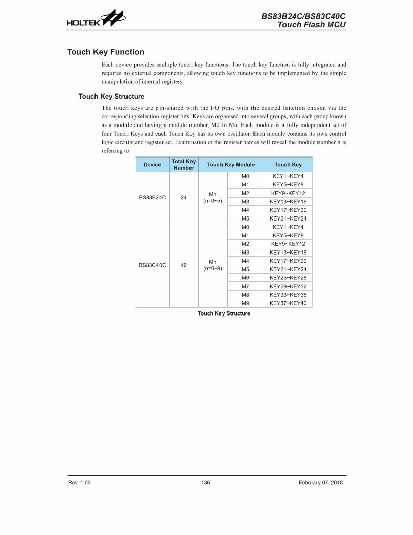
Rev. 1.00 136 �e���a�� 0�� �01� Rev. 1.00 13� �e���a�� 0�� �01�
BS83B24C/BS83C40CTouch Flash MCU
BS83B24C/BS83C40CTouch Flash MCU
Touch Key FunctionEachdeviceprovidesmultipletouchkeyfunctions.Thetouchkeyfunctionisfullyintegratedandrequiresnoexternalcomponents,allowingtouchkeyfunctionstobeimplementedbythesimplemanipulationofinternalregisters.
Touch Key StructureThe touchkeys are pin-sharedwith the I/Opins,with thedesired function chosenvia thecorrespondingselectionregisterbits.Keysareorganisedintoseveralgroups,witheachgroupknownasamoduleandhavingamodulenumber,M0toMn.EachmoduleisafullyindependentsetoffourTouchKeysandeachTouchKeyhasitsownoscillator.Eachmodulecontainsitsowncontrollogiccircuitsandregisterset.Examinationoftheregisternameswillrevealthemodulenumberitisreferringto.
Device Total Key Number Touch Key Module Touch Key
BS�3B�4C �4 Mn(n=0~5)
M0 KEY1~KEY4M1 KEY5~KEY�M� KEY9~KEY1�M3 KEY13~KEY16M4 KEY1�~KEY�0M5 KEY�1~KEY�4
BS�3C40C 40 Mn(n=0~9)
M0 KEY1~KEY4M1 KEY5~KEY�M� KEY9~KEY1�M3 KEY13~KEY16M4 KEY1�~KEY�0M5 KEY�1~KEY�4M6 KEY�5~KEY��M� KEY�9~KEY3�M� KEY33~KEY36M9 KEY3�~KEY40
Touch Key Structure

Rev. 1.00 136 �e���a�� 0�� �01� Rev. 1.00 13� �e���a�� 0�� �01�
BS83B24C/BS83C40CTouch Flash MCU
BS83B24C/BS83C40CTouch Flash MCU
KEY 1Ke�
OSC
KEY �Ke�
OSC
KEY 3Ke�
OSC
KEY 4Ke�
OSC
TKRCOV
M�lti-f�eq�enc�
MnD�EN
TKMn16DH / TKMn16DL( to Data Memo�� Secto� 5)
TKC�OV
TK16DL / TK16DH
M�x .
Mod�le 0
TKTMR
Refe�ence Oscillato�
TKMnROH / TKMnROL( f�om Data Memo�� Secto� 6)
�ilte�
Mod�le n
16-�it C/� Co�nte�
�ilte�
fSYS/4 MUX
MnTSSTKMnC�
�-�it Time Slot Co�nte� 5-�it �nit pe�iod co�nte�
�-�it Time Slot Co�nte� P�eload Registe�TKTMR Ove�flow
16-�it Co�nte� TK16OVMUX
TK16S1~TK16S0
fSYS/4fSYS/�
fSYS
fSYS/�
16-�it C/� Co�nte� Val�e
(Secto� 5)
To�ch Ke�Data Memo��
Refe�ence Osc. Capacito� Val�e
(Secto� 6)
Mn�ILEN
Mn�ILEN
fC�TMCK
Notes:1.Thestructurecontained in thedash line is identical foreach touchkeymodulewhichcontainsfourtouchkeys.
2.WhenMnTSS=0andMnROEN=1orwhenMnTSS=1, the touchkey function16-bitcountercanoperatenormally.
Touch Key Function Block Diagram

Rev. 1.00 13� �e���a�� 0�� �01� Rev. 1.00 139 �e���a�� 0�� �01�
BS83B24C/BS83C40CTouch Flash MCU
BS83B24C/BS83C40CTouch Flash MCU
Touch Key Register DefinitionEachtouchkeymodule,whichcontainsfourtouchkeyfunctions,hasitsownsuiteregisters.Thefollowingtableshowstheregistersetforeachtouchkeymodule.TheMnwithintheregisternamereferstotheTouchKeymodulenumber.TheseriesofdeviceshasuptotenTouchKeyModulesdependingupontheselecteddevice.
Name DescriptionTKTMR To�ch ke� time slot �-�it co�nte� p�eload �egiste�TKC0 To�ch ke� f�nction Cont�ol �egiste� 0TKC1 To�ch ke� f�nction Cont�ol �egiste� 1
TK16DL To�ch ke� f�nction 16-�it co�nte� low ��teTK16DH To�ch ke� f�nction 16-�it co�nte� high ��te
TKMn16DL To�ch ke� mod�le n 16-�it C/� co�nte� low ��teTKMn16DH To�ch ke� mod�le n 16-�it C/� co�nte� high ��teTKMnROL To�ch ke� mod�le n �efe�ence oscillato� capacito� selection low ��teTKMnROH To�ch ke� mod�le n �efe�ence oscillato� capacito� selection high ��teTKMnC0 To�ch ke� mod�le n Cont�ol �egiste� 0TKMnC1 To�ch ke� mod�le n Cont�ol �egiste� 1TKMnC� To�ch ke� mod�le n Cont�ol �egiste� �
Touch Key Module Register Definition
Register Name
Bit7 6 5 4 3 2 1 0
TKTMR D� D6 D5 D4 D3 D� D1 D0TKC0 TKRAMC TKRCOV TKST TKC�OV TK16OV — TKMOD TKBUSYTKC1 D� D6 D5 TSCS TK16S1 TK16S0 TK�S1 TK�S0
TK16DL D� D6 D5 D4 D3 D� D1 D0TK16DH D15 D14 D13 D1� D11 D10 D9 D�
TKMn16DL D� D6 D5 D4 D3 D� D1 D0TKMn16DH D15 D14 D13 D1� D11 D10 D9 D�TKMnROL D� D6 D5 D4 D3 D� D1 D0TKMnROH — — — — — — D9 D�TKMnC0 — — MnD�EN Mn�ILEN MnSO�C MnSO�� MnSO�1 MnSO�0TKMnC1 MnTSS — MnROEN MnKOEN MnK4EN MnK3EN MnK�EN MnK1ENTKMnC� MnSK31 MnSK30 MnSK�1 MnSK�0 MnSK11 MnSK10 MnSK01 MnSK00
Touch Key Function Register List
• TKTMR Register
Bit 7 6 5 4 3 2 1 0Name D� D6 D5 D4 D3 D� D1 D0R/W R/W R/W R/W R/W R/W R/W R/W R/WPOR 0 0 0 0 0 0 0 0
Bit7~0 D7~D0:Touchkeytimeslot8-bitcounterpreloadregisterThetouchkeytimeslotcounterpreloadregisterisusedtodeterminethetouchkeytimeslotoverflowtime.Thetimeslotunitperiodisobtainedbya5-bitcounterandequalto32timeslotclockcycles.Therefore, thetimeslotcounteroverflowtimeisequaltothefollowingequationshown.Timeslotcounteroverflowtime=(256-TKTMR[7:0])×32tTSC,wheretTSCisthetimeslotcounterclockperiod.
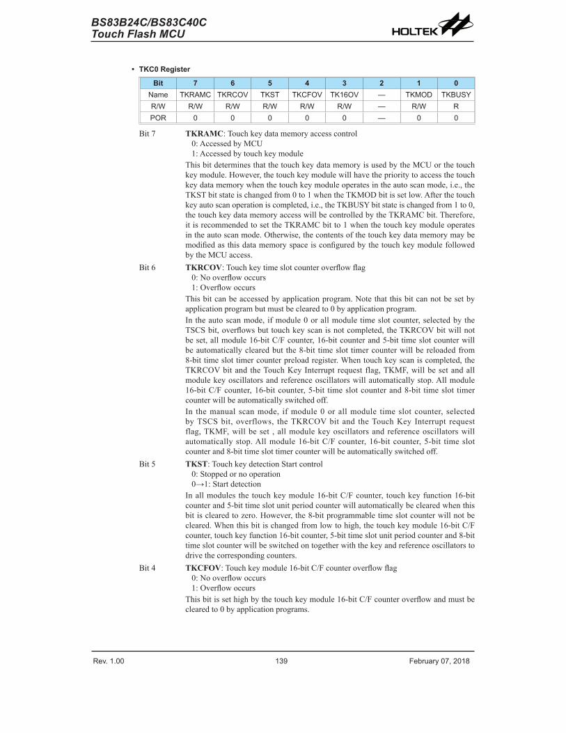
Rev. 1.00 13� �e���a�� 0�� �01� Rev. 1.00 139 �e���a�� 0�� �01�
BS83B24C/BS83C40CTouch Flash MCU
BS83B24C/BS83C40CTouch Flash MCU
• TKC0 Register
Bit 7 6 5 4 3 2 1 0Name TKRAMC TKRCOV TKST TKC�OV TK16OV — TKMOD TKBUSYR/W R/W R/W R/W R/W R/W — R/W RPOR 0 0 0 0 0 — 0 0
Bit7 TKRAMC:Touchkeydatamemoryaccesscontrol0:AccessedbyMCU1:Accessedbytouchkeymodule
ThisbitdeterminesthatthetouchkeydatamemoryisusedbytheMCUorthetouchkeymodule.However,thetouchkeymodulewillhavetheprioritytoaccessthetouchkeydatamemorywhenthetouchkeymoduleoperatesintheautoscanmode,i.e.,theTKSTbitstateischangedfrom0to1whentheTKMODbitissetlow.Afterthetouchkeyautoscanoperationiscompleted,i.e.,theTKBUSYbitstateischangedfrom1to0,thetouchkeydatamemoryaccesswillbecontrolledbytheTKRAMCbit.Therefore,itisrecommendedtosettheTKRAMCbitto1whenthetouchkeymoduleoperatesintheautoscanmode.Otherwise,thecontentsofthetouchkeydatamemorymaybemodifiedasthisdatamemoryspaceisconfiguredbythetouchkeymodulefollowedbytheMCUaccess.
Bit6 TKRCOV:Touchkeytimeslotcounteroverflowflag0:Nooverflowoccurs1:Overflowoccurs
Thisbitcanbeaccessedbyapplicationprogram.Notethatthisbitcannotbesetbyapplicationprogrambutmustbeclearedto0byapplicationprogram.Intheautoscanmode, ifmodule0orallmoduletimeslotcounter,selectedbytheTSCSbit,overflowsbuttouchkeyscanisnotcompleted,theTKRCOVbitwillnotbeset,allmodule16-bitC/Fcounter,16-bitcounterand5-bit timeslotcounterwillbeautomaticallyclearedbut the8-bit timeslot timercounterwillbereloadedfrom8-bittimeslottimercounterpreloadregister.Whentouchkeyscaniscompleted,theTKRCOVbitand theTouchKeyInterrupt request flag,TKMF,willbesetandallmodulekeyoscillatorsandreferenceoscillatorswillautomaticallystop.Allmodule16-bitC/Fcounter,16-bitcounter,5-bit timeslotcounterand8-bit timeslot timercounterwillbeautomaticallyswitchedoff.In themanual scanmode, ifmodule0orallmodule timeslotcounter, selectedbyTSCSbit,overflows, theTKRCOVbit and theTouchKey Interrupt requestflag,TKMF,willbeset ,allmodulekeyoscillatorsandreferenceoscillatorswillautomaticallystop.Allmodule16-bitC/Fcounter,16-bitcounter,5-bit timeslotcounterand8-bittimeslottimercounterwillbeautomaticallyswitchedoff.
Bit5 TKST:TouchkeydetectionStartcontrol0:Stoppedornooperation0→1:Startdetection
Inallmodules the touchkeymodule16-bitC/Fcounter, touchkeyfunction16-bitcounterand5-bittimeslotunitperiodcounterwillautomaticallybeclearedwhenthisbitisclearedtozero.However,the8-bitprogrammabletimeslotcounterwillnotbecleared.Whenthisbitischangedfromlowtohigh,thetouchkeymodule16-bitC/Fcounter,touchkeyfunction16-bitcounter,5-bittimeslotunitperiodcounterand8-bittimeslotcounterwillbeswitchedontogetherwiththekeyandreferenceoscillatorstodrivethecorrespondingcounters.
Bit4 TKCFOV:Touchkeymodule16-bitC/Fcounteroverflowflag0:Nooverflowoccurs1:Overflowoccurs
Thisbitissethighbythetouchkeymodule16-bitC/Fcounteroverflowandmustbeclearedto0byapplicationprograms.

Rev. 1.00 140 �e���a�� 0�� �01� Rev. 1.00 141 �e���a�� 0�� �01�
BS83B24C/BS83C40CTouch Flash MCU
BS83B24C/BS83C40CTouch Flash MCU
Bit3 TK16OV:Touchkeyfunction16-bitcounteroverflowflag0:Nooverflowoccurs1:Overflowoccurs
Thisbit issethighbythetouchkeyfunction16-bitcounteroverflowandmustbeclearedto0byapplicationprograms.
Bit2 Unimplemented,readas“0”Bit1 TKMOD:Touchkeyscanmodeselection
0:Autoscanmode1:Manualscanmode
Inthemanualscanmodethereferenceoscillatorcapacitorvalueshouldbeproperlyconfiguredbefore thescanoperationbeginsand the touchkeymodule16-bitC/Fcountervalueshouldbereadafterthescanoperationfinishesbyapplicationprogram.Intheautoscanmodethedatamovementwhichisdescribedaboveisimplementedbyhardware.Theindividualreferenceoscillatorcapacitorvalueand16-bitC/FcountercontentforallscannedkeyswillbereadfromandwrittenintoadedicatedTouchKeyDataMemoryarea.Thescanoperationwillnotbestoppeduntilallarrangedkeysarescanned.
Bit0 TKBUSY:Touchkeyscanoperationbusyflag0:Notbusy–noscanoperationisexecutedorscanoperationiscompleted1:Busy–scanoperationisexecuting
Thisbitindicateswhetherthetouchkeyscanoperationisexecutingornot.Itissetto1whentheTKSTbitissethightostartthescanoperationforalltouchkeyscanmodes.Intheautoscanmodethisbit isclearedto0automaticallywhenthetouchkeyscanoperationiscompleted.Inthemanualscanmodethisbitisclearedto0automaticallywhenthetouchkeytimeslotcounteroverflows.
• TKC1 Register
Bit 7 6 5 4 3 2 1 0Name D� D6 D5 TSCS TK16S1 TK16S0 TK�S1 TK�S0R/W R/W R/W R/W R/W R/W R/W R/W R/WPOR 0 0 0 0 0 0 1 1
Bit7~5 D7~D5:DatabitsfortestonlyThesebitsareused for testpurposeonlyandmustbekeptas“000” fornormaloperations.
Bit4 TSCS:Touchkeytimeslotcounterselection0:Eachmoduleuseowntimeslotcounter.1:Alltouchkeymoduleusemodule0timeslotcounter.
Bit3~2 TK16S1~TK16S0:Touchkeymodule16-bitcounterclocksourceselection00:fSYS
01:fSYS/210:fSYS/411:fSYS/8
Bit1~0 TKFS1~TKFS0:TouchKeyoscillatorandReferenceoscillatorfrequencyselection00:1MHz01:3MHz10:7MHz11:11MHz

Rev. 1.00 140 �e���a�� 0�� �01� Rev. 1.00 141 �e���a�� 0�� �01�
BS83B24C/BS83C40CTouch Flash MCU
BS83B24C/BS83C40CTouch Flash MCU
• TK16DH/TK16DL – Touch Key Function 16-bit Counter Register Pair
Register TK16DH TK16DLBit 7 6 5 4 3 2 1 0 7 6 5 4 3 2 1 0
Name D15 D14 D13 D1� D11 D10 D9 D� D� D6 D5 D4 D3 D� D1 D0R/W R R R R R R R R R R R R R R R RPOR 0 0 0 0 0 0 0 0 0 0 0 0 0 0 0 0
Thisregisterpairisusedtostorethetouchkeyfunction16-bitcountervalue.This16-bitcountercanbeusedtocalibratethereferenceorkeyoscillatorfrequency.Whenthetouchkeytimeslotcounteroverflowsinthemanualscanmode,this16-bitcounterwillbestoppedandthecountercontentwillbeunchanged.However,this16-bitcountercontentwillbeclearedtozeroattheendofthetimeslot0,slot1andslot2butkeptunchangedattheendofthetimeslot3intheautoscanmode.ThisregisterpairwillbeclearedtozerowhentheTKSTbitissetlow.
• TKMn16DH/TKMn16DL – Touch Key Module n 16-bit C/F Counter Register Pair
Register TKMn16DH TKMn16DLBit 7 6 5 4 3 2 1 0 7 6 5 4 3 2 1 0
Name D15 D14 D13 D1� D11 D10 D9 D� D� D6 D5 D4 D3 D� D1 D0R/W R R R R R R R R R R R R R R R RPOR 0 0 0 0 0 0 0 0 0 0 0 0 0 0 0 0
Thisregisterpair isused tostore the touchkeymodulen16-bitC/Fcountervalue.This16-bitC/Fcounterwillbestoppedandthecountercontentwillbekeptunchangedwhenthetouchkeytimeslotcounteroverflowsinthemanualscanmode.However,this16-bitC/Fcountercontentwillbeclearedtozeroattheendofthetimeslot0,slot1andslot2afteritiswrittentothetouchkeydatamemorybutkeptunchangedattheendofthetimeslot3whentheautoscanmodeisselected.ThisregisterpairwillbeclearedtozerowhentheTKSTbitissetlow.
• TKMnROH/TKMnROL –Touch Key Module n Reference Oscillator Capacitor Selection Register Pair
Register TKMnROH TKMnROLBit 7 6 5 4 3 2 1 0 7 6 5 4 3 2 1 0
Name — — — — — — D9 D� D� D6 D5 D4 D3 D� D1 D0R/W — — — — — — R/W R/W R/W R/W R/W R/W R/W R/W R/W R/WPOR — — — — — — 0 0 0 0 0 0 0 0 0 0
Thisregisterpairisusedtostorethetouchkeymodulenreferenceoscillatorcapacitorvalue.Thisregisterpairwillbeloadedwiththecorrespondingnexttimeslotcapacitorvaluefromthededicatedtouchkeydatamemoryattheendofthecurrenttimeslotwhentheautoscanmodeisselected.
Thereferenceoscillatorinternalcapacitorvalue=(TKMnRO[9:0]×50pF)/1024
• TKMnC0 Register
Bit 7 6 5 4 3 2 1 0Name — — MnD�EN Mn�ILEN MnSO�C MnSO�� MnSO�1 MnSO�0R/W — — R/W R/W R/W R/W R/W R/WPOR — — 0 0 0 0 0 0
Bit7~6 Uninplemented.Readas“0”Bit5 MnDFEN:Touchkeymodulenmulti-frequencycontrol
0:Disable1:Enable
Thisbitisusedtocontrolthetouchkeyoscillatorfrequencydoublingfunction.Whenthisbitissetto1,thekeyoscillatorfrequencywillbedoubled.
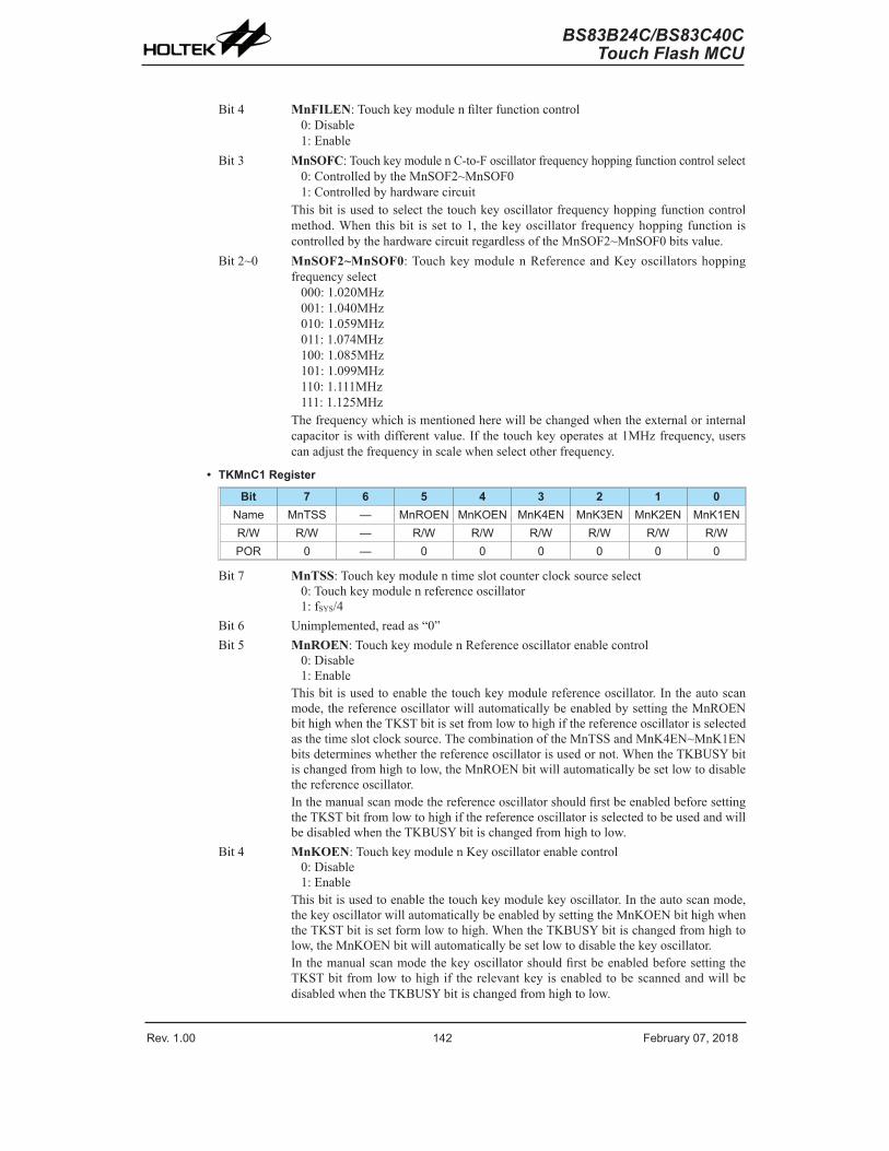
Rev. 1.00 14� �e���a�� 0�� �01� Rev. 1.00 143 �e���a�� 0�� �01�
BS83B24C/BS83C40CTouch Flash MCU
BS83B24C/BS83C40CTouch Flash MCU
Bit4 MnFILEN:Touchkeymodulenfilterfunctioncontrol0:Disable1:Enable
Bit3 MnSOFC:TouchkeymodulenC-to-Foscillatorfrequencyhoppingfunctioncontrolselect0:ControlledbytheMnSOF2~MnSOF01:Controlledbyhardwarecircuit
Thisbitisusedtoselectthetouchkeyoscillatorfrequencyhoppingfunctioncontrolmethod.Whenthisbit isset to1, thekeyoscillatorfrequencyhoppingfunction iscontrolledbythehardwarecircuitregardlessoftheMnSOF2~MnSOF0bitsvalue.
Bit2~0 MnSOF2~MnSOF0:TouchkeymodulenReferenceandKeyoscillatorshoppingfrequencyselect000:1.020MHz001:1.040MHz010:1.059MHz011:1.074MHz100:1.085MHz101:1.099MHz110:1.111MHz111:1.125MHz
Thefrequencywhichismentionedherewillbechangedwhentheexternalorinternalcapacitoriswithdifferentvalue.Ifthetouchkeyoperatesat1MHzfrequency,userscanadjustthefrequencyinscalewhenselectotherfrequency.
• TKMnC1 Register
Bit 7 6 5 4 3 2 1 0Name MnTSS — MnROEN MnKOEN MnK4EN MnK3EN MnK�EN MnK1ENR/W R/W — R/W R/W R/W R/W R/W R/WPOR 0 — 0 0 0 0 0 0
Bit7 MnTSS:Touchkeymodulentimeslotcounterclocksourceselect0:Touchkeymodulenreferenceoscillator1:fSYS/4
Bit6 Unimplemented,readas“0”Bit5 MnROEN:TouchkeymodulenReferenceoscillatorenablecontrol
0:Disable1:Enable
Thisbitisusedtoenablethetouchkeymodulereferenceoscillator.Intheautoscanmode,thereferenceoscillatorwillautomaticallybeenabledbysettingtheMnROENbithighwhentheTKSTbitissetfromlowtohighifthereferenceoscillatorisselectedasthetimeslotclocksource.ThecombinationoftheMnTSSandMnK4EN~MnK1ENbitsdetermineswhetherthereferenceoscillatorisusedornot.WhentheTKBUSYbitischangedfromhightolow,theMnROENbitwillautomaticallybesetlowtodisablethereferenceoscillator.InthemanualscanmodethereferenceoscillatorshouldfirstbeenabledbeforesettingtheTKSTbitfromlowtohighifthereferenceoscillatorisselectedtobeusedandwillbedisabledwhentheTKBUSYbitischangedfromhightolow.
Bit4 MnKOEN:TouchkeymodulenKeyoscillatorenablecontrol0:Disable1:Enable
Thisbitisusedtoenablethetouchkeymodulekeyoscillator.Intheautoscanmode,thekeyoscillatorwillautomaticallybeenabledbysettingtheMnKOENbithighwhentheTKSTbitissetformlowtohigh.WhentheTKBUSYbitischangedfromhightolow,theMnKOENbitwillautomaticallybesetlowtodisablethekeyoscillator.InthemanualscanmodethekeyoscillatorshouldfirstbeenabledbeforesettingtheTKSTbitfromlowtohighif therelevantkeyisenabledtobescannedandwillbedisabledwhentheTKBUSYbitischangedfromhightolow.

Rev. 1.00 14� �e���a�� 0�� �01� Rev. 1.00 143 �e���a�� 0�� �01�
BS83B24C/BS83C40CTouch Flash MCU
BS83B24C/BS83C40CTouch Flash MCU
Bit3 MnK4EN:TouchkeymodulenKEY4enablecontrol
MnK4ENTouch Key Module n – Mn
M0 M1 M2 M3 M4 M5 M6 M7 M8 M90: Disa�le I/O o� othe� f�nctions1: Ena�le KEY4 KEY� KEY1� KEY16 KEY�0 KEY�4 KEY�� KEY3� KEY36 KEY40
BS�3B�4C √ √ √ √ √ √ — — — —BS�3C40C √ √ √ √ √ √ √ √ √ √
Bit2 MnK3EN:TouchkeymodulenKEY3enablecontrol
MnK3ENTouch Key Module n – Mn
M0 M1 M2 M3 M4 M5 M6 M7 M8 M90: Disa�le I/O o� othe� f�nctions1: Ena�le KEY3 KEY� KEY11 KEY15 KEY19 KEY�3 KEY�� KEY31 KEY35 KEY39
BS�3B�4C √ √ √ √ √ √ — — — —BS�3C40C √ √ √ √ √ √ √ √ √ √
Bit1 MnK2EN:TouchkeymodulenKEY2enablecontrol
MnK2ENTouch Key Module n – Mn
M0 M1 M2 M3 M4 M5 M6 M7 M8 M90: Disa�le I/O o� othe� f�nctions1: Ena�le KEY� KEY6 KEY10 KEY14 KEY1� KEY�� KEY�6 KEY30 KEY34 KEY3�
BS�3B�4C √ √ √ √ √ √ — — — —BS�3C40C √ √ √ √ √ √ √ √ √ √
Bit0 MnK1EN:TouchkeymodulenKEY1enablecontrol
MnK1ENTouch Key Module n – Mn
M0 M1 M2 M3 M4 M5 M6 M7 M8 M90: Disa�le I/O o� othe� f�nctions1: Ena�le KEY1 KEY5 KEY9 KEY13 KEY1� KEY�1 KEY�5 KEY�9 KEY33 KEY3�
BS�3B�4C √ √ √ √ √ √ — — — —BS�3C40C √ √ √ √ √ √ √ √ √ √
• TKMnC2 Register
Bit 7 6 5 4 3 2 1 0Name MnSK31 MnSK30 MnSK�1 MnSK�0 MnSK11 MnSK10 MnSK01 MnSK00R/W R/W R/W R/W R/W R/W R/W R/W R/WPOR 1 1 1 0 0 1 0 0
Bit7~6 MnSK31~MnSK30:Touchkeymodulentimeslot3keyscanselection00:KEY101:KEY210:KEY311:KEY4
Thesebitsareusedtoselectthedesiredscankeyintimeslot3andonlyavailableintheautoscanmode.
Bit5~4 MnSK21~MnSK20:Touchkeymodulentimeslot2keyscanselection00:KEY101:KEY210:KEY311:KEY4
Thesebitsareusedtoselectthedesiredscankeyintimeslot2andonlyavailableintheautoscanmode.

Rev. 1.00 144 �e���a�� 0�� �01� Rev. 1.00 145 �e���a�� 0�� �01�
BS83B24C/BS83C40CTouch Flash MCU
BS83B24C/BS83C40CTouch Flash MCU
Bit3~2 MnSK11~MnSK10:Touchkeymodulentimeslot1keyscanselection00:KEY101:KEY210:KEY311:KEY4
Thesebitsareusedtoselectthedesiredscankeyintimeslot1andonlyavailableintheautoscanmode.
Bit1~0 MnSK01~MnSK00:Touchkeymodulentimeslot0keyscanselection00:KEY101:KEY210:KEY311:KEY4
Thesebitsareusedtoselectthedesiredscankeyintimeslot0intheautoscanmodeorusedasthemultiplexerforscankeyselectioninthemanualmode.
Touch Key OperationWhenafingertouchesorisinproximitytoatouchpad,thecapacitanceofthepadwillincrease.Byusingthiscapacitancevariationtochangeslightlythefrequencyoftheinternalsenseoscillator,touchactionscanbesensedbymeasuringthesefrequencychanges.Usinganinternalprogrammabledividerthereferenceclockisusedtogenerateafixedtimeperiod.Bycountinganumberofgeneratedclockcyclesfromthesenseoscillatorduringthisfixedtimeperiodtouchkeyactionscanbedetermined.
EachtouchkeymodulecontainsfourtouchkeyinputswhicharesharedwithlogicalI/Opins,andthedesiredfunctionisselectedusingregisterbits.Eachtouchkeyhasitsownindependentsenseoscillator.Therefore,therearefoursenseoscillatorswithineachtouchkeymodule.
TKST
MnKOENMnROEN
KEY OSC CLK
Refe�ence OSC CLK
fC�TMCK Ena�le
fC�TMCK (MnD�EN=0)
fC�TMCK (MnD�EN=1)
TKBUSY
TKRCOV
Ha�dwa�e set to “0”
Set To�ch Ke� inte���pt �eq�est flag
Touch Key Manual Scan Mode Timing Diagram

Rev. 1.00 144 �e���a�� 0�� �01� Rev. 1.00 145 �e���a�� 0�� �01�
BS83B24C/BS83C40CTouch Flash MCU
BS83B24C/BS83C40CTouch Flash MCU
During this referenceclock fixed interval, thenumberofclockcyclesgeneratedby thesenseoscillatorismeasured,anditisthisvaluethatisusedtodetermineifatouchactionhasbeenmadeornot.AttheendofthefixedreferenceclocktimeintervalaTouchKeyinterruptsignalwillbegenerated.
UsingtheTSCSbitintheTKC1registercanselectthemodule0timeslotcounterasthetimeslotcounterforallmodules.Allmodulesusethesamestartedsignal,TKST,intheTKC0register.Thetouchkeymodule16-bitC/Fcounter,touchkeyfunction16-bitcounter,5-bittimeslotunitperiodcounterinallmoduleswillbeautomaticallyclearedwhentheTKSTbitisclearedtozero,butthe8-bitprogrammabletimeslotcounterwillnotbecleared.Theoverflowtimeissetupbyuser.WhentheTKSTbitchangesfromlowtohigh,the16-bitC/Fcounter,touchkeyfunction16-bitcounter,5-bittimeslotunitperiodcounterand8-bittimeslottimercounterwillbeautomaticallyswitchedon.
Thekeyoscillatorandreferenceoscillator inallmoduleswillbeautomaticallystoppedandthe16-bitC/Fcounter,touchkeyfunction16-bitcounter,5-bittimeslotunitperiodcounterand8-bittimeslot timercounterwillbeautomaticallyswitchedoffwhenthetimeslotcounteroverflows.TheclocksourceforthetimeslotcounterissourcedfromthereferenceoscillatororfSYS/4whichisselectedusingtheMnTSSbit intheTKMnC1register.ThereferenceoscillatorandkeyoscillatorwillbeenabledbysettingtheMnROENbitandMnKOENbitsintheTKMnC1register.
Whenthetimeslotcounterinall thetouchkeymodulesorinthetouchkeymodule0overflows,anactualtouchkeyinterruptwilltakeplace.Thetouchkeysmentionedherearethekeyswhichareenabled.
Each touchkeymoduleconsistsof four touchkeys,KEY1~KEY4arecontained inmodule0,KEY5~KEY8arecontainedinmodule1,KEY9~KEY12arecontainedinmodule2,etc.Eachtouchkeymodulehasanidenticalstructure.
Auto Scan ModeTherearetwoscanmodescontainedforthetouchkeyfunction,theautoscanmodeandthemanualscanmodewhichareselectedusingtheTKMODbitintheTKC0register.Theautoscanmodecanminisizetheloadoftheapplicationprogramandimprovethetouchkeyscanoperationperformance.WhentheTKMODbitisclearedto0,theautoscanmodeisselectedtoscanthemodulekeysinaspecificsequencedeterminedbytheMnSK3[1:0]~MnSK0[1:0]bitsintheTKMnC2register.
IntheautoscanmodethekeyoscillatorandreferenceoscillatorwillautomaticallybeenabledwhentheTKSTbit issetfromlowtohighanddisabledautomaticallywhentheTKBUSYbitchangesfromhightolow.WhentheTKSTbit issetfromlowtohighintheautoscanmode,theinternalcapacitorvalueofthereferenceoscillatorfortheselectedkeytobescannedinthetimeslot0willfirstbereadfromaspecificlocationofthededicatedtouchkeydatamemoryandloadedintothecorrespondingTKMnROH/TKMnROLregisters.Thenthe16-bitC/Fcountervaluewillbewrittenintothecorrespondinglocationofthetimeslot3scannedkeyinthetouchkeydatamemory.Afterthis,theselectedkeywillstarttobescannedintimeslot0.Attheendofthetimeslot0keyscanoperation,thereferenceoscillatorinternalcapacitorvalueforthenextselectedkeywillbereadfromthetouchkeydatamemoryandloadedinto thenextTKMnROH/TKMnROLregisters.Thenthe16-bitC/Fcountervalueofthecurrentscannedkeywillbewrittenintothecorrespondingtouchkeydatamemory.Thewholeautoscanoperationwillsequentiallybecarriedoutintheabovespecificwayfromtimeslot0totimeslot3.Attheendofthetimeslot3keyscanoperation,thereferenceoscillatorinternalcapacitorvalueforthetimeslot0selectedkeywillagainbereadfromthetouchkeydatamemoryandloadedintothecorrespondingTKMnROH/TKMnROLregisters.Thenthe16-bitC/Fcountervaluewillbewrittenintotherelevantlocationofthetimeslot3scannedkeyinthetouchkeydatamemory.Afterfourselectedkeysarescanned,theTKRCOVbitwillbesethighandtheTKBUSYbitwillbesetlowaswellasanautoscanmodeoperationiscompleted.

Rev. 1.00 146 �e���a�� 0�� �01� Rev. 1.00 14� �e���a�� 0�� �01�
BS83B24C/BS83C40CTouch Flash MCU
BS83B24C/BS83C40CTouch Flash MCU
TKST
Mod�le 0
Time slot 0
Time slot 1
Time slot �
Time slot 3
Mod�le 1
Time slot 0
Time slot 1
Time slot �
Time slot 3
Mod�le n
Time slot 0
Time slot 1
Time slot �
Time slot 3
TKBUSY
TKRCOVClea�ed �� softwa�e
Time slot 1
Time slot �
Time slot 3
Time slot 1
Time slot �
Time slot 3
Time slot 1
Time slot �
Time slot 3
To�ch Ke� Data Memo�� Access
: Set To�ch Ke� inte���pt �eq�est flag
: Read �N ��tes f�om To�ch Ke� Data Memo�� to TKMnROH/TKMnTROL �egiste�s
: W�ite �N ��tes f�om TKMn16DH/TKMn16DL �egiste�s to To�ch Ke� Data Memo��
N = To�ch Ke� Mod�le N�m�e�; n = Mod�le Se�ial N�m�e�
Ke� A�to Scan C�cle
Touch Key Auto Scan Mode Timing Diagram

Rev. 1.00 146 �e���a�� 0�� �01� Rev. 1.00 14� �e���a�� 0�� �01�
BS83B24C/BS83C40CTouch Flash MCU
BS83B24C/BS83C40CTouch Flash MCU
Touch Key Data MemoryThedevicesprovidetwodedicatedDataMemoryareasforthetouchkeyautoscanmode.Oneareaisusedtostorethe16-bitC/FcountervaluesofthetouchkeymoduleandlocatedinDataMemorySector5.TheotherareaisusedtostorethereferenceoscillatorinternalcapacitorvaluesofthetouchkeymoduleandlocatedinDataMemorySector6.
10-�it Ref. OSC capacito�
TKMnROL / TKMnROH
TKM016DL_K1
TKM016DH_K1
TKM016DL_K�
TKM016DH_K�
TKM016DL_K3
TKM016DH_K3
TKM016DL_K4
TKM016DH_K4
TKM116DL_K1
TKM116DH_K1
TKM116DL_K�
TKM116DH_K�
TKM116DL_K3
TKM116DH_K3
TKM116DL_K4
TKM116DH_K4
Module 0
TKM0ROL_K1
TKM0ROH_K1
TKM0ROL_K�
TKM0ROH_K�
TKM0ROL_K4
TKM0ROH_K4
TKM0ROL_K3
TKM0ROH_K3
TKM1ROL_K1
TKM1ROH_K1
TKM1ROL_K�
TKM1ROH_K�
TKM1ROL_K4
TKM1ROH_K4
TKM1ROL_K3
TKM1ROH_K3
TKM�16DL_K1
TKM�16DH_K1
TKM�16DL_K�
TKM�16DH_K�
TKM�16DL_K3
TKM�16DH_K3
TKM�16DL_K4
TKM�16DH_K4
TKM�ROL_K1
TKM�ROH_K1
TKM�ROL_K�
TKM�ROH_K�
TKM�ROL_K4
TKM�ROH_K4
TKM�ROL_K3
TKM�ROH_K3
Module 1
Module 2
16-bit C/F counter value(Sector 5)
Ref. OSC Capacitor value(Sector 6)
Module n
TKMnROL_K1
TKMnROH_K1
TKMnROL_K�
TKMnROH_K�
TKMnROL_K4
TKMnROH_K4
TKMnROL_K3
TKMnROH_K3
TKMn16DL_K1
TKMn16DH_K1
TKMn16DL_K�
TKMn16DH_K�
TKMn16DL_K3
TKMn16DH_K3
TKMn16DL_K4
TKMn16DH_K4
00H
01H
0�H
xxH
16-�it C/� co�nte�
TKMn16DL / TKMn16DH
Touch Key Circuit
Step 1
Step �
Notes: �o� the BS�3B�4C device� n=5 and the data memo�� add�ess �ange is f�om 00H to ��H.�o� the BS�3C40C device� n=9 and the data memo�� add�ess �ange is f�om 00H to 4�H.
Touch Key Data Memory Map

Rev. 1.00 14� �e���a�� 0�� �01� Rev. 1.00 149 �e���a�� 0�� �01�
BS83B24C/BS83C40CTouch Flash MCU
BS83B24C/BS83C40CTouch Flash MCU
Touch Key Scan Operation Flowchart
Sta�t
W�ite Ref. OSC Capacito� to TKMnROH/TKMnROL
To�ch Ke� Man�al Scan Ope�ation Sta�tSet Sta�t �it TKST 0 1
B�s� flag TKBUSY=1
All Time SlotCo�nte� ove�flow ?
TKRCOV=0
Initiate Time Slot &16-�it C/� Co�nte�
All Time Slot &16-�it C/� Co�nte�
Sta�t to co�nt
Time Slot &16-�it C/� Co�nte�
Keep co�nting
TKRCOV=1
To�ch ke� ��s� flagTKBUSY=0
Gene�ate Inte���pt �eq�est flag
Read C/� co�nte� f�om TKMn16DH/TKMn16DL
To�ch ke� scan endSet TKST �it 1 0
End
Touch Key Manual Scan Mode Flowchart

Rev. 1.00 14� �e���a�� 0�� �01� Rev. 1.00 149 �e���a�� 0�� �01�
BS83B24C/BS83C40CTouch Flash MCU
BS83B24C/BS83C40CTouch Flash MCU
Sta�t
W�ite Ref. OSC inte�nal Capacito� val�e
to Data Memo�� (Secto� 6 )
To�ch Ke� A�to Scan Ope�ation Sta�tSet Sta�t �it TKST 0 1
B�s� flag TKBUSY=1
All Time SlotCo�nte� ove�flow ?
No
Initiate Time Slot &16-�it C/� Co�nte�
All Time Slot co�nte� &16-�it C/� co�nte�
Sta�t to co�nt
Time Slot &16-�it C/� Co�nte�
Keep co�nting
Yes
TKRCOV = 1
Gene�ate Inte���pt �eq�est flag
Read C/� co�nte� val�e f�om Data Memo�� (Secto� 5)
To�ch ke� scan endSet TKST �it 1 0
End
Load Ref. OSC inte�nal Capacito� val�e f�om
Data Memo�� (Secto� 6 )
Sto�e C/� co�nte� val�e toData Memo�� (Secto� 5 )
All ke� scan finish ?
Yes
No
To�ch ke� ��s� flagTKBUSY=0
Change next ke�
Touch Key Auto Scan Mode Flowchart
Rev. 1.00 150 �e���a�� 0�� �01� Rev. 1.00 151 �e���a�� 0�� �01�
BS83B24C/BS83C40CTouch Flash MCU
BS83B24C/BS83C40CTouch Flash MCU
Touch Key InterruptThetouchkeyonlyhassingleinterrupt,whenthetimeslotcounterinallthetouchkeymodulesorinthetouchkeymodule0overflows,anactualtouchkeyinterruptwilltakeplace.Thetouchkeysmentionedherearethekeyswhichareenabled.The16-bitC/Fcounter,16-bitcounter,5-bittimeslotunitperiodcounterand8-bittimeslotcounterinallmoduleswillbeautomaticallycleared.
TheTKCFOVflagwhichisthe16-bitC/FcounteroverflowflagwillgohighwhenanyoftheTouchKeyModule16-bitC/Fcounteroverflows.Asthisflagwillnotbeautomaticallycleared,ithastobeclearedbytheapplicationprogram.
TheTK16OVflagwhichisthe16-bitcounteroverflowflagwillgohighwhenthe16-bitcounteroverflows.Asthisflagwillnotbeautomaticallycleared, ithas tobeclearedbytheapplicationprogram.Moredetailsregardingthetouchkeyinterrupt is locatedin theinterruptsectionof thedatasheet.
Programming ConsiderationsAftertherelevantregistersaresetup,thetouchkeydetectionprocessisinitiatedthechangingtheTKSTBitfromlowtohigh.Thiswillenableandsynchroniseallrelevantoscillators.TheTKRCOVflagwhichisthetimeslotcounterflagwillgohighwhenthecounteroverflows.Whenthishappensaninterruptsignalwillbegenerated.
When theexternal touchkeysizeand layoutaredefined, their relatedcapacitanceswill thendeterminethesensoroscillatorfrequency.

Rev. 1.00 150 �e���a�� 0�� �01� Rev. 1.00 151 �e���a�� 0�� �01�
BS83B24C/BS83C40CTouch Flash MCU
BS83B24C/BS83C40CTouch Flash MCU
InterruptsInterruptsareanimportantpartofanymicrocontrollersystem.WhenanexternaleventoraninternalfunctionsuchasaTimerModulerequiresmicrocontrollerattention, theircorrespondinginterruptwillenforcea temporarysuspensionof themainprogramallowingthemicrocontroller todirectattentiontotheirrespectiveneeds.Thesedevicescontainanexternalinterruptandseveralinternalinterruptfunctions.TheexternalinterruptisgeneratedbytheactionoftheexternalINTpin,whiletheinternalinterruptsaregeneratedbyvariousinternalfunctionssuchastheTimerModules(TM),TimeBases,EEPROM,TouchKeymoduleandUSIMmodule.
Interrupt RegistersOverall interrupt control,whichbasicallymeans the settingof request flagswhen certainmicrocontrollerconditionsoccurandthesettingofinterruptenablebitsbytheapplicationprogram,iscontrolledbyaseriesofregisters,locatedintheSpecialPurposeDataMemory.Theregistersfallintothreecategories.Thefirst is theINTC0~INTC2registerswhichsetuptheprimaryinterrupts,thesecondistheMFI0~MFI1registerswhichsetuptheMulti-functioninterrupts.FinallythereisanINTEGregistertosetuptheexternalinterruptstriggeredgetype.
Eachregistercontainsanumberofenablebitstoenableordisableindividualregistersaswellasinterrupt flags to indicate thepresenceofan interrupt request.Thenamingconventionof thesefollowsaspecificpattern.Firstislistedanabbreviatedinterrupttype,thenthe(optional)numberofthatinterruptfollowedbyeitheran“E”forenable/disablebitor“F”forrequestflag.
Function Enable Bit Request Flag NoteGlo�al EMI — —
INT Pin INTE INT� —
To�ch Ke� Mod�le TKME TKM� —
M�lti-f�nction M�nE M�n� n=0 fo� BS�3B�4Cn=0~1 fo� BS�3C40C
USIM USIME USIM� —
Time Bases TBnE TBn� n=0~1
EEPROM DEE DE� —
CTMCTMPE CTMP�
Onl� fo� BS�3C40CCTMAE CTMA�
PTMPTMPE PTMP�
—PTMAE PTMA�
Interrupt Register Bit Naming Conventions
Register Name
Bit7 6 5 4 3 2 1 0
INTEG — — — — — — INTS1 INTS0
INTC0 — M�0� TKM� INT� M�0E TKME INTE EMI
INTC1 DE� TB1� TB0� USIM� DEE TB1E TB0E USIME
M�I0 — — PTMA� PTMP� — — PTMAE PTMPE
Interrupt Register List – BS83B24C

Rev. 1.00 15� �e���a�� 0�� �01� Rev. 1.00 153 �e���a�� 0�� �01�
BS83B24C/BS83C40CTouch Flash MCU
BS83B24C/BS83C40CTouch Flash MCU
Register Name
Bit7 6 5 4 3 2 1 0
INTEG — — — — — — INTS1 INTS0
INTC0 — M�0� TKM� INT� M�0E TKME INTE EMI
INTC1 DE� TB1� TB0� USIM� DEE TB1E TB0E USIME
INTC� — — — M�1� — — — M�1E
M�I0 — — PTMA� PTMP� — — PTMAE PTMPE
M�I1 — — CTMA� CTMP� — — CTMAE CTMPE
Interrupt Register List – BS83C40C
• INTEG Register
Bit 7 6 5 4 3 2 1 0Name — — — — — — INTS1 INTS0R/W — — — — — — R/W R/WPOR — — — — — — 0 0
Bit7~2 Unimplemented,readas“0”Bit1~0 INTS1~INTS0:InterruptEdgeControlforINTPin
00:Disable01:Risingedge10:Fallingedge11:Risingandfallingedges
• INTC0 Register
Bit 7 6 5 4 3 2 1 0Name — M�0� TKM� INT� M�0E TKME INTE EMIR/W — R/W R/W R/W R/W R/W R/W R/WPOR — 0 0 0 0 0 0 0
Bit7 Unimplemented,readas“0”Bit6 MF0F:Multi-functionInterrupt0requestflag
0:Norequest1:Interruptrequest
Bit5 TKMF:TouchKeyModuleinterruptrequestflag0:Norequest1:Interruptrequest
Bit4 INTF:ExternalInterruptrequestflag0:Norequest1:Interruptrequest
Bit3 MF0E:Multi-functionInterrupt0control0:Disable1:Enable
Bit2 TKME:TouchKeyModuleinterruptcontrol0:Disable1:Enable
Bit1 INTE:ExternalInterruptcontrol0:Disable1:Enable
Bit0 EMI:GlobalInterruptcontrol0:Disable1:Enable

Rev. 1.00 15� �e���a�� 0�� �01� Rev. 1.00 153 �e���a�� 0�� �01�
BS83B24C/BS83C40CTouch Flash MCU
BS83B24C/BS83C40CTouch Flash MCU
• INTC1 Register
Bit 7 6 5 4 3 2 1 0Name DE� TB1� TB0� USIM� DEE TB1E TB0E USIMER/W R/W R/W R/W R/W R/W R/W R/W R/WPOR 0 0 0 0 0 0 0 0
Bit7 DEF:DataEEPROMinterruptrequestflag0:Norequest1:Interruptrequest
Bit6 TB1F:TimeBase1interruptrequestflag0:Norequest1:Interruptrequest
Bit5 TB0F:TimeBase0interruptrequestflag0:Norequest1:Interruptrequest
Bit4 USIMF:USIMModuleinterruptrequestflag0:Norequest1:Interruptrequest
Bit3 DEE:DataEEPROMinterruptcontrol0:Disable1:Enable
Bit2 TB1E:TimeBase1interruptcontrol0:Disable1:Enable
Bit1 TB0E:TimeBase0interruptcontrol0:Disable1:Enable
Bit0 USIME:USIMModuleinterruptcontrol0:Disable1:Enable
• INTC2 Register – BS83C40C
Bit 7 6 5 4 3 2 1 0Name — — — M�1� — — — M�1ER/W — — — R/W — — — R/WPOR — — — 0 — — — 0
Bit7~5 Unimplemented,readas“0”Bit4 MF1F:Multi-function1interruptrequestflag
0:Norequest1:Interruptrequest
Bit3~1 Unimplemented,readas“0”Bit0 MF1E:Multi-function1interruptcontrol
0:Disable1:Enable
• MFI0 Register
Bit 7 6 5 4 3 2 1 0Name — — PTMA� PTMP� — — PTMAE PTMPER/W — — R/W R/W — — R/W R/WPOR — — 0 0 — — 0 0
Bit7~6 Unimplemented,readas“0”Bit5 PTMAF:PTMComparatorAmatchinterruptrequestflag
0:Norequest1:Interruptrequest
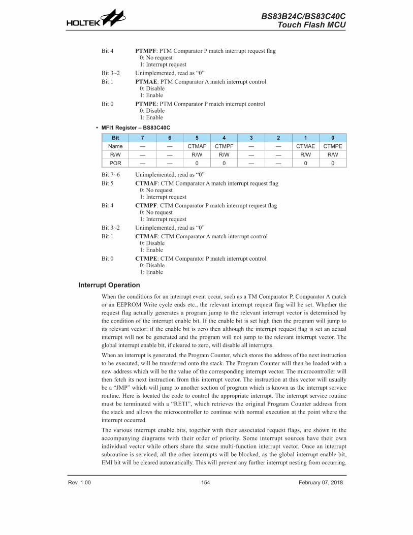
Rev. 1.00 154 �e���a�� 0�� �01� Rev. 1.00 155 �e���a�� 0�� �01�
BS83B24C/BS83C40CTouch Flash MCU
BS83B24C/BS83C40CTouch Flash MCU
Bit4 PTMPF:PTMComparatorPmatchinterruptrequestflag0:Norequest1:Interruptrequest
Bit3~2 Unimplemented,readas“0”Bit1 PTMAE:PTMComparatorAmatchinterruptcontrol
0:Disable1:Enable
Bit0 PTMPE:PTMComparatorPmatchinterruptcontrol0:Disable1:Enable
• MFI1 Register – BS83C40C
Bit 7 6 5 4 3 2 1 0Name — — CTMA� CTMP� — — CTMAE CTMPER/W — — R/W R/W — — R/W R/WPOR — — 0 0 — — 0 0
Bit7~6 Unimplemented,readas“0”Bit5 CTMAF:CTMComparatorAmatchinterruptrequestflag
0:Norequest1:Interruptrequest
Bit4 CTMPF:CTMComparatorPmatchinterruptrequestflag0:Norequest1:Interruptrequest
Bit3~2 Unimplemented,readas“0”Bit1 CTMAE:CTMComparatorAmatchinterruptcontrol
0:Disable1:Enable
Bit0 CTMPE:CTMComparatorPmatchinterruptcontrol0:Disable1:Enable
Interrupt OperationWhentheconditionsforaninterrupteventoccur,suchasaTMComparatorP,ComparatorAmatchoranEEPROMWritecycleendsetc., therelevantinterruptrequestflagwillbeset.Whethertherequestflagactuallygeneratesaprogramjumpto therelevant interruptvector isdeterminedbytheconditionoftheinterruptenablebit.Iftheenablebitissethighthentheprogramwilljumptoitsrelevantvector;iftheenablebitiszerothenalthoughtheinterruptrequestflagissetanactualinterruptwillnotbegeneratedandtheprogramwillnotjumptotherelevantinterruptvector.Theglobalinterruptenablebit,ifclearedtozero,willdisableallinterrupts.
Whenaninterruptisgenerated,theProgramCounter,whichstorestheaddressofthenextinstructiontobeexecuted,willbetransferredontothestack.TheProgramCounterwillthenbeloadedwithanewaddresswhichwillbethevalueofthecorrespondinginterruptvector.Themicrocontrollerwillthenfetchitsnextinstructionfromthisinterruptvector.Theinstructionatthisvectorwillusuallybea“JMP”whichwilljumptoanothersectionofprogramwhichisknownastheinterruptserviceroutine.Hereislocatedthecodetocontroltheappropriateinterrupt.Theinterruptserviceroutinemustbe terminatedwitha“RETI”,whichretrieves theoriginalProgramCounteraddressfromthestackandallowsthemicrocontrollertocontinuewithnormalexecutionatthepointwheretheinterruptoccurred.
Thevarious interruptenablebits, togetherwith theirassociatedrequest flags,areshownin theaccompanyingdiagramswith theirorderofpriority.Some interrupt sourceshave theirownindividualvectorwhileothersshare thesamemulti-function interruptvector.Oncean interruptsubroutineisserviced,all theother interruptswillbeblocked,as theglobal interruptenablebit,EMIbitwillbeclearedautomatically.Thiswillpreventanyfurtherinterruptnestingfromoccurring.
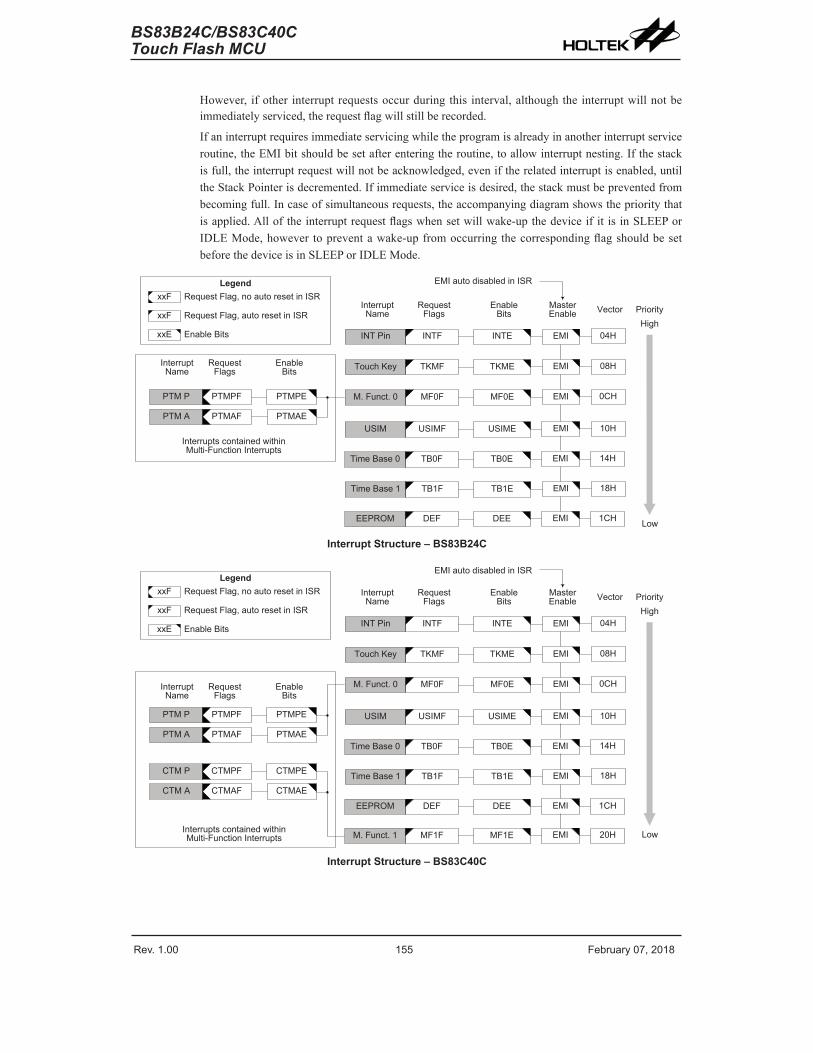
Rev. 1.00 154 �e���a�� 0�� �01� Rev. 1.00 155 �e���a�� 0�� �01�
BS83B24C/BS83C40CTouch Flash MCU
BS83B24C/BS83C40CTouch Flash MCU
However, ifother interruptrequestsoccurduringthis interval,althoughtheinterruptwillnotbeimmediatelyserviced,therequestflagwillstillberecorded.
Ifaninterruptrequiresimmediateservicingwhiletheprogramisalreadyinanotherinterruptserviceroutine,theEMIbitshouldbesetafterenteringtheroutine,toallowinterruptnesting.Ifthestackisfull,theinterruptrequestwillnotbeacknowledged,eveniftherelatedinterruptisenabled,untiltheStackPointerisdecremented.Ifimmediateserviceisdesired,thestackmustbepreventedfrombecomingfull.Incaseofsimultaneousrequests,theaccompanyingdiagramshowstheprioritythatisapplied.Alloftheinterruptrequestflagswhensetwillwake-upthedeviceifit isinSLEEPorIDLEMode,however topreventawake-upfromoccurringthecorrespondingflagshouldbesetbeforethedeviceisinSLEEPorIDLEMode.
Inte���pt Name
Req�est �lags
Ena�leBits
Maste� Ena�le Vecto�
EMI a�to disa�led in ISR
P�io�it�High
Low
Inte���pts contained within M�lti-��nction Inte���pts
xxE Ena�le Bits
xx� Req�est �lag� a�to �eset in ISR
Legendxx� Req�est �lag� no a�to �eset in ISR
04HINT Pin INT� INTE EMI
1�HTime Base 1 TB1� TB1E EMI
EMI 0�HTo�ch Ke� TKM� TKMEInte���pt Name
Req�est�lags
Ena�le Bits
EMI 0CHM. ��nct. 0 M�0� M�0E
EMI 10HUSIM USIM� USIME
14HTime Base 0 TB0� TB0E EMI
PTM P PTMP� PTMPE
PTM A PTMA� PTMAE
EEPROM DE� DEE EMI 1CH
Interrupt Structure – BS83B24C
Inte���pt Name
Req�est �lags
Ena�leBits
Maste� Ena�le Vecto�
EMI a�to disa�led in ISR
P�io�it�High
LowInte���pts contained within M�lti-��nction Inte���pts
xxE Ena�le Bits
xx� Req�est �lag� a�to �eset in ISR
Legendxx� Req�est �lag� no a�to �eset in ISR
04HINT Pin INT� INTE EMI
1�HTime Base 1 TB1� TB1E EMI
EMI 0�HTo�ch Ke� TKM� TKME
Inte���pt Name
Req�est�lags
Ena�le Bits
EMI 0CHM. ��nct. 0 M�0� M�0E
EMI 10HUSIM USIM� USIME
14HTime Base 0 TB0� TB0E EMI
PTM P PTMP� PTMPE
PTM A PTMA� PTMAE
EEPROM DE� DEE EMI 1CH
M. ��nct. 1 M�1� M�1E EMI �0H
CTM P CTMP� CTMPE
CTM A CTMA� CTMAE
Interrupt Structure – BS83C40C

Rev. 1.00 156 �e���a�� 0�� �01� Rev. 1.00 15� �e���a�� 0�� �01�
BS83B24C/BS83C40CTouch Flash MCU
BS83B24C/BS83C40CTouch Flash MCU
External InterruptTheexternal interruptsarecontrolledbysignal transitionsontheINTpin.Anexternal interruptrequestwilltakeplacewhentheexternalinterruptrequestflag,INTF,isset,whichwilloccurwhenatransition,whosetypeischosenbytheedgeselectbits,appearsontheexternalinterruptpins.Toallowtheprogramtobranchtoitsrespectiveinterruptvectoraddress,theglobalinterruptenablebit,EMI,andrespectiveexternalinterruptenablebit,INTE,mustfirstbeset.Additionallythecorrectinterruptedge typemustbeselectedusing the INTEGregister toenable theexternal interruptfunctionand tochoose the triggeredge type.As theexternal interruptpinsarepin-sharedwithI/Opins,theycanonlybeconfiguredasexternalinterruptpinsiftheirexternalinterruptenablebitinthecorrespondinginterruptregisterhasbeensetandtheexternalinterruptpinisselectedbythecorrespondingpin-sharedfunctionselectionbits.Thepinmustalsobesetupasaninputbysettingthecorrespondingbitintheportcontrolregister.
Whentheinterrupt isenabled, thestackisnotfullandthecorrect transitiontypeappearsontheexternalinterruptpin,asubroutinecall totheexternalinterruptvector,will takeplace.Whentheinterrupt isserviced, theexternal interruptrequestflag,INTF,willbeautomaticallyresetandtheEMIbitwillbeautomaticallyclearedtodisableotherinterrupts.Notethatanypull-highresistorselectionson theexternal interruptpinswill remainvalideven if thepin isusedasanexternalinterrupt input.TheINTEGregister isusedtoselect thetypeofactiveedgethatwill trigger theexternalinterrupt.Achoiceofeitherrisingorfallingorbothedgetypescanbechosentotriggeranexternalinterrupt.Notethat theINTEGregistercanalsobeusedtodisabletheexternalinterruptfunction.
Multi-function InterruptWithin thesedevices thereareseveralMulti-function interrupts.Unlike theother independentinterrupts, theseinterruptshavenoindependentsource,butratherareformedfromotherexistinginterruptsources,namelytheTMinterrupts.
AMulti-functioninterruptrequestwilltakeplacewhenanyoftheMulti-functioninterruptrequestflagsMFnFareset.TheMulti-function interrupt flagswillbesetwhenanyof their includedfunctionsgenerateaninterruptrequestflag.Toallowtheprogramtobranchtoitsrespectiveinterruptvectoraddress,whentheMulti-functioninterruptisenabledandthestackisnotfull,andeitheroneoftheinterruptscontainedwithineachofMulti-functioninterruptoccurs,asubroutinecalltooneoftheMulti-functioninterruptvectorswilltakeplace.Whentheinterruptisserviced,therelatedMulti-FunctionrequestflagwillbeautomaticallyresetandtheEMIbitwillbeautomaticallyclearedtodisableotherinterrupts.
However, itmustbenoted that, although theMulti-function Interrupt request flagswill beautomaticallyresetwhen the interrupt isserviced, therequest flagsfromtheoriginalsourceoftheMulti-function interruptswillnotbeautomaticallyresetandmustbemanuallyresetby theapplicationprogram.

Rev. 1.00 156 �e���a�� 0�� �01� Rev. 1.00 15� �e���a�� 0�� �01�
BS83B24C/BS83C40CTouch Flash MCU
BS83B24C/BS83C40CTouch Flash MCU
Timer Module InterruptsTheCompactandPeriodictypeTMseachhastwointerrupts,onecomesfromthecomparatorAmatchsituationandtheothercomesfromthecomparatorPmatchsituation.AlloftheTMinterruptsarecontainedwithintheMulti-functionInterrupts.ForalloftheTMtypestherearetwointerruptrequestflagsandtwoenablecontrolbits.ATMinterruptrequestwill takeplacewhenanyoftheTMrequestflagsareset,asituationwhichoccurswhenaTMcomparatorPorAmatchsituationhappens.
Toallowtheprogramtobranchtoitsrespectiveinterruptvectoraddress,theglobalinterruptenablebit,EMI,respectiveTMInterruptenablebit,andrelevantMulti-functionInterruptenablebit,MFnE,mustfirstbeset.Whentheinterruptisenabled,thestackisnotfullandaTMcomparatormatchsituationoccurs,asubroutinecalltotherelevantMulti-functionInterruptvectorlocations,willtakeplace.WhentheTMinterruptisserviced,theEMIbitwillbeautomaticallyclearedtodisableotherinterrupts.However,onlytherelatedMFnFflagwillbeautomaticallycleared.AstheTMinterruptrequestflagswillnotbeautomaticallycleared,theyhavetobeclearedbytheapplicationprogram.
EEPROM InterruptAnEEPROMInterruptrequestwilltakeplacewhentheEEPROMInterruptrequestflag,DEF,isset,whichoccurswhenanEEPROMWritecycleends.Toallowtheprogramtobranchtoitsrespectiveinterruptvectoraddress, theglobal interruptenablebit,EMI,andEEPROMInterruptenablebit,DEE,mustfirstbeset.Whentheinterruptisenabled,thestackisnotfullandanEEPROMWritecycleends,asubroutinecalltotherespectiveEEPROMInterruptvectorwilltakeplace.WhentheEEPROMInterruptisserviced,theDEFflagwillbeautomaticallycleared,theEMIbitwillalsobeautomaticallyclearedtodisableotherinterrupts.
USIM InterruptTheUniversalSerialInterfaceModuleInterrupt,alsoknownastheUSIMinterrupt,willtakeplacewhentheUSIMInterruptrequestflag,USIMF,isset.AstheUSIMinterfacecanoperateinthreemodeswhichareSPImode,I2CmodeandUARTmode, theUSIMFflagcanbesetbydifferentconditionsdependingontheselectedinterfacemode.
IftheSPIorI2Cmodeisselected,theUSIMinterruptcanbetriggeredwhenabyteofdatahasbeenreceivedor transmittedbytheUSIMSPIorI2Cinterface,oranI2Cslaveaddressmatchoccurs,oranI2Cbustime-outoccurs.IftheUARTmodeisselected,severalindividualUARTconditionsincludingatransmitterdataregisterempty,transmitteridle,receiverdataavailable,receiveroverrun,addressdetectandanRXpinwake-up,cangenerateaUSIMinterruptwiththeUSIMFflagbitsethigh.
Toallowtheprogramtobranchtoitsrespectiveinterruptvectoraddress,theglobalinterruptenablebit,EMI,andtheUniversalSerialInterfaceModuleInterruptenablebit,USIME,mustfirstbeset.Whentheinterruptisenabled,thestackisnotfullandanyoftheabovedescribedsituationsoccurs,asubroutinecalltotherespectiveInterruptvector,willtakeplace.Whentheinterruptisserviced,theUniversalSerialInterfaceModuleInterruptflag,USIMF,willbeautomaticallycleared.TheEMIbitwillalsobeautomaticallyclearedtodisableotherinterrupts.
Note that if theUSIM interrupt is triggeredbytheUARTinterface,after the interrupthasbeenservied,theUUSRregisterflagswillbeclearedautomaticallywhencertainactionsaretakenbytheUART,thedetailsofwhicharegivenintheUARTsection.

Rev. 1.00 15� �e���a�� 0�� �01� Rev. 1.00 159 �e���a�� 0�� �01�
BS83B24C/BS83C40CTouch Flash MCU
BS83B24C/BS83C40CTouch Flash MCU
Touch Key InterruptAnTouchKeyInterruptrequestwilltakeplacewhentheTouchKeyInterruptrequestflag,TKMF,isset,whichoccurswhenthetouchkeytimeslotcounteroverflows.Toallowtheprogramtobranchtoitsrespectiveinterruptvectoraddress,theglobalinterruptenablebit,EMI,andtheTouchKeyInterruptenablebit,TKME,mustfirstbeset.Whentheinterrupt isenabled, thestackisnotfullandthetouchkeytimeslotcounteroverflows,asubroutinecalltotheTouchKeyInterruptvector,will takeplace.WhentheTouchKeyInterruptisserviced,theTKRMFflagwillbeautomaticallycleared,theEMIbitwillalsobeautomaticallyclearedtodisableotherinterrupts.
Time Base InterruptsThefunctionoftheTimeBaseInterruptsistoprovideregulartimesignalintheformofaninternalinterrupt.Theyarecontrolledbytheoverflowsignalsfromtheirrespectivetimerfunctions.Whenthesehappenstheirrespectiveinterruptrequestflags,TBnF,willbeset.Toallowtheprogramtobranchtotheirrespectiveinterruptvectoraddresses,theglobalinterruptenablebit,EMI,andTimeBaseenablebits,TBnE,mustfirstbeset.Whentheinterruptisenabled,thestackisnotfullandtheTimeBaseoverflows,asubroutinecalltotheirrespectivevectorlocationswilltakeplace.Whentheinterruptisserviced,therespectiveinterruptrequestflag,TBnF,willbeautomaticallycleared,theEMIbitwillalsobeautomaticallyclearedtodisableotherinterrupts.
Thepurposeof theTimeBaseInterrupt is toprovidean interruptsignalat fixed timeperiods.Itsclocksource,fPSC,originatesfromtheinternalclocksourcefSYS,fSYS/4orfSUBandthenpassesthroughadivider,thedivisionratioofwhichisselectedbyprogrammingtheappropriatebitsintheTBnCregisters toobtainlongerinterruptperiodswhosevalueranges.TheclockcourcewhichinturncontrolstheTimeBaseinterruptperiodisselectedusingtheCLKSEL[1:0]bitsinthePSCRregister.
P�escale�
fPSC/�� ~ fPSC/�15 MUX
MUX
TB0[�:0]
TB1[�:0]
Time Base 0 Inte���pt
Time Base 1 Inte���pt
TB0ON
TB1ON
fPSC/�� ~ fPSC/�15
fSYS
MUX
fSYS/4
fSUB
CLKSEL[1:0]
fPSC
Time Base Interrupts
• PSCR Register
Bit 7 6 5 4 3 2 1 0Name — — — — — — CLKSEL1 CLKSEL0R/W — — — — — — R/W R/WPOR — — — — — — 0 0
Bit7~2 Unimplemented,readas“0”Bit1~0 CLKSEL1~CLKSEL0:Prescalerclocksourceselection
00:fSYS
01:fSYS/41x:fSUB

Rev. 1.00 15� �e���a�� 0�� �01� Rev. 1.00 159 �e���a�� 0�� �01�
BS83B24C/BS83C40CTouch Flash MCU
BS83B24C/BS83C40CTouch Flash MCU
• TB0C Register
Bit 7 6 5 4 3 2 1 0Name TB0ON — — — — TB0� TB01 TB00R/W R/W — — — — R/W R/W R/WPOR 0 — — — — 0 0 0
Bit7 TB0ON:TimeBase0Control0:Disable1:Enable
Bit6~3 Unimplemented,readas“0”Bit2~0 TB02~TB00:SelectTimeBase0Time-outPeriod
000:28/fPSC001:29/fPSC010:210/fPSC011:211/fPSC100:212/fPSC101:213/fPSC110:214/fPSC111:215/fPSC
• TB1C Register
Bit 7 6 5 4 3 2 1 0Name TB1ON — — — — TB1� TB11 TB10R/W R/W — — — — R/W R/W R/WPOR 0 — — — — 0 0 0
Bit7 TB1ON:TimeBase1Control0:Disable1:Enable
Bit6~3 Unimplemented,readas“0”Bit2~0 TB12~TB10:SelectTimeBase1Time-outPeriod
000:28/fPSC001:29/fPSC010:210/fPSC011:211/fPSC100:212/fPSC101:213/fPSC110:214/fPSC111:215/fPSC
Interrupt Wake-up FunctionEachof the interruptfunctionshas thecapabilityofwakingupthemicrocontrollerwhenin theSLEEPorIDLEMode.Awake-upisgeneratedwhenaninterruptrequestflagchangesfromlowtohighandisindependentofwhethertheinterruptisenabledornot.Therefore,eventhoughthedeviceisintheSLEEPorIDLEModeanditssystemoscillatorstopped,situationssuchasexternaledgetransitionsontheexternalinterruptpinsoralowpowersupplyvoltagemaycausetheirrespectiveinterruptflagtobesethighandconsequentlygenerateaninterrupt.Caremustthereforebetakenifspuriouswake-upsituationsaretobeavoided.Ifaninterruptwake-upfunctionistobedisabledthenthecorrespondinginterruptrequestflagshouldbesethighbeforethedeviceenterstheSLEEPorIDLEMode.Theinterruptenablebitshavenoeffectontheinterruptwake-upfunction.

Rev. 1.00 160 �e���a�� 0�� �01� Rev. 1.00 161 �e���a�� 0�� �01�
BS83B24C/BS83C40CTouch Flash MCU
BS83B24C/BS83C40CTouch Flash MCU
Programming ConsiderationsBydisablingtherelevantinterruptenablebits,arequestedinterruptcanbepreventedfrombeingserviced,however,oncean interrupt request flag is set, itwill remain in thiscondition in theinterruptregisteruntilthecorrespondinginterruptisservicedoruntiltherequestflagisclearedbytheapplicationprogram.
Whereacertain interrupt iscontainedwithinaMulti-function interrupt, thenwhenthe interruptservice routine isexecuted,asonly theMulti-function interrupt request flags,MFnF,willbeautomaticallycleared, the individual request flag for the functionneeds tobeclearedby theapplicationprogram.
It isrecommendedthatprogramsdonotusethe“CALL”instructionwithintheinterruptservicesubroutine.Interruptsoftenoccurinanunpredictablemannerorneedtobeservicedimmediately.Ifonlyonestackisleftandtheinterruptisnotwellcontrolled,theoriginalcontrolsequencewillbedamagedonceaCALLsubroutineisexecutedintheinterruptsubroutine.
Everyinterrupthasthecapabilityofwakingupthemicrocontrollerwhenit isinSLEEPorIDLEMode,thewakeupbeinggeneratedwhentheinterruptrequestflagchangesfromlowtohigh.IfitisrequiredtopreventacertaininterruptfromwakingupthemicrocontrollerthenitsrespectiverequestflagshouldbefirstsethighbeforeenterSLEEPorIDLEMode.
AsonlytheProgramCounter ispushedontothestack, thenwhentheinterrupt isserviced, if thecontentsof theaccumulator,statusregisterorotherregistersarealteredbythe interruptserviceprogram,theircontentsshouldbesavedto thememoryat thebeginningof the interruptserviceroutine.Toreturnfromaninterruptsubroutine,eitheraRETorRETIinstructionmaybeexecuted.TheRETIinstructioninadditiontoexecutingareturntothemainprogramalsoautomaticallysetstheEMIbithightoallowfurtherinterrupts.TheRETinstructionhoweveronlyexecutesareturntothemainprogramleavingtheEMIbitinitspresentzerostateandthereforedisablingtheexecutionoffurtherinterrupts.
Configuration OptionsConfigurationoptionsrefertocertainoptionswithintheMCUthatareprogrammedintothedeviceduringtheprogrammingprocess.Duringthedevelopmentprocess,theseoptionsareselectedusingtheHT-IDEsoftwaredevelopment tools.Astheseoptionsareprogrammedintothedeviceusingthehardwareprogrammingtools,once theyareselectedtheycannotbechangedlaterusingtheapplicationprogram.Alloptionsmustbedefinedforpropersystemfunction,thedetailsofwhichareshowninthetable.
No. OptionsOscillator Option
1
HIRC f�eq�enc� selection:1. �MHz�. 1�MHz3. 16MHz
Note:When theHIRChasbeenconfiguredata frequencyshownin this table, theHIRC1andHIRC0bitsshouldalsobesetuptoselectthesamefrequencytoachievetheHIRCfrequencyaccuracyspecifiedintheA.C.Characteristics.

Rev. 1.00 160 �e���a�� 0�� �01� Rev. 1.00 161 �e���a�� 0�� �01�
BS83B24C/BS83C40CTouch Flash MCU
BS83B24C/BS83C40CTouch Flash MCU
Application Circuits
VDD
VSS
VDD
0.1µ�
PAD
PAD
PAD
PAD
PAD
PAD
PAD
PAD
PA�/SCK/SCL/SDO/TX/XT1/ICPCK/OCDSCK
PA0/SDA/SDI/RX/XT�/ICPDA/OCDSDA
KEY1
KEY�
KEY3
KEY4
KEY�1
KEY��
KEY�3
KEY�4
BS83B24C
VDD
VSS
VDD
0.1µ�
PAD
PAD
PAD
PAD
PAD
PAD
PAD
PAD
PA�/SCK/SCL/SDO/TX/XT1/ICPCK/OCDSCK
PA0/SDA/SDI/RX/XT�/ICPDA/OCDSDA
KEY1
KEY�
KEY3
KEY4
KEY3�
KEY3�
KEY39
KEY40
BS83C40C

Rev. 1.00 16� �e���a�� 0�� �01� Rev. 1.00 163 �e���a�� 0�� �01�
BS83B24C/BS83C40CTouch Flash MCU
BS83B24C/BS83C40CTouch Flash MCU
Instruction Set
IntroductionCentral to thesuccessfuloperationofanymicrocontroller is its instructionset,whichisasetofprograminstructioncodesthatdirectsthemicrocontrollertoperformcertainoperations.InthecaseofHoltekmicrocontroller,acomprehensiveandflexiblesetofover60instructionsisprovidedtoenableprogrammerstoimplementtheirapplicationwiththeminimumofprogrammingoverheads.
Foreasierunderstandingofthevariousinstructioncodes, theyhavebeensubdividedintoseveralfunctionalgroupings.
Instruction TimingMostinstructionsareimplementedwithinoneinstructioncycle.Theexceptionstothisarebranch,call,or tablereadinstructionswheretwoinstructioncyclesarerequired.Oneinstructioncycleisequalto4systemclockcycles,thereforeinthecaseofan8MHzsystemoscillator,mostinstructionswouldbeimplementedwithin0.5μsandbranchorcall instructionswouldbeimplementedwithin1μs.Although instructionswhichrequireonemorecycle to implementaregenerally limited totheJMP,CALL,RET,RETIandtablereadinstructions, it is important torealize thatanyotherinstructionswhichinvolvemanipulationoftheProgramCounterLowregisterorPCLwillalsotakeonemorecycletoimplement.AsinstructionswhichchangethecontentsofthePCLwill implyadirect jumptothatnewaddress,onemorecyclewillberequired.Examplesofsuchinstructionswouldbe"CLRPCL"or"MOVPCL,A".Forthecaseofskipinstructions,itmustbenotedthatiftheresultofthecomparisoninvolvesaskipoperationthenthiswillalsotakeonemorecycle,ifnoskipisinvolvedthenonlyonecycleisrequired.
Moving and Transferring DataThe transferofdatawithin themicrocontrollerprogram isoneof themost frequentlyusedoperations.MakinguseofthreekindsofMOVinstructions,datacanbetransferredfromregisterstotheAccumulatorandvice-versaaswellasbeingabletomovespecificimmediatedatadirectlyintotheAccumulator.Oneofthemostimportantdatatransferapplicationsis toreceivedatafromtheinputportsandtransferdatatotheoutputports.
Arithmetic OperationsTheabilitytoperformcertainarithmeticoperationsanddatamanipulationisanecessaryfeatureofmostmicrocontrollerapplications.WithintheHoltekmicrocontrollerinstructionsetarearangeofaddandsubtract instructionmnemonicstoenablethenecessaryarithmetictobecarriedout.Caremustbe taken toensurecorrecthandlingofcarryandborrowdatawhenresultsexceed255foradditionandlessthan0forsubtraction.TheincrementanddecrementinstructionsINC,INCA,DECandDECAprovideasimplemeansofincreasingordecreasingbyavalueofoneofthevaluesinthedestinationspecified.

Rev. 1.00 16� �e���a�� 0�� �01� Rev. 1.00 163 �e���a�� 0�� �01�
BS83B24C/BS83C40CTouch Flash MCU
BS83B24C/BS83C40CTouch Flash MCU
Logical and Rotate OperationThestandardlogicaloperationssuchasAND,OR,XORandCPLallhavetheirowninstructionwithintheHoltekmicrocontroller instructionset.Aswiththecaseofmost instructionsinvolvingdatamanipulation, datamust pass through theAccumulatorwhichmay involve additionalprogrammingsteps. Inall logicaldataoperations, thezero flagmaybeset if the resultof theoperationiszero.AnotherformoflogicaldatamanipulationcomesfromtherotateinstructionssuchasRR,RL,RRCandRLCwhichprovideasimplemeansofrotatingoneBitrightorleft.Differentrotateinstructionsexistdependingonprogramrequirements.Rotateinstructionsareusefulforserialportprogrammingapplicationswheredatacanberotatedfromaninternalregister intotheCarryBitfromwhereitcanbeexaminedandthenecessaryserialBitsethighorlow.Anotherapplicationwhichrotatedataoperationsareusedistoimplementmultiplicationanddivisioncalculations.
Branches and Control TransferProgrambranchingtakestheformofeitherjumpstospecifiedlocationsusingtheJMPinstructionor toa subroutineusing theCALL instruction.Theydiffer in the sense that in thecaseofasubroutinecall, theprogrammustreturn to the instruction immediatelywhenthesubroutinehasbeencarriedout.Thisisdonebyplacingareturninstruction"RET"inthesubroutinewhichwillcausetheprogramtojumpbacktotheaddressrightaftertheCALLinstruction.InthecaseofaJMPinstruction,theprogramsimplyjumpstothedesiredlocation.ThereisnorequirementtojumpbacktotheoriginaljumpingoffpointasinthecaseoftheCALLinstruction.Onespecialandextremelyusefulsetofbranchinstructionsaretheconditionalbranches.Hereadecisionisfirstmaderegardingtheconditionofacertaindatamemoryor individualBits.Dependingupon theconditions, theprogramwillcontinuewiththenextinstructionorskipoveritandjumptothefollowinginstruction.These instructionsare thekey todecisionmakingandbranchingwithin theprogramperhapsdeterminedbytheconditionofcertaininputswitchesorbytheconditionofinternaldataBits.
Bit OperationsTheabilitytoprovidesingleBitoperationsonDataMemoryisanextremelyflexiblefeatureofallHoltekmicrocontrollers.ThisfeatureisespeciallyusefulforoutputportBitprogrammingwhereindividualBitsorportpinscanbedirectlysethighorlowusingeitherthe"SET[m].i"or"CLR[m].i" instructionsrespectively.Thefeatureremovestheneedforprogrammers tofirstreadthe8-Bitoutputport,manipulatetheinputdatatoensurethatotherBitsarenotchangedandthenoutputtheportwiththecorrectnewdata.Thisread-modify-writeprocessistakencareofautomaticallywhentheseBitoperationinstructionsareused.
Table Read OperationsDatastorage isnormally implementedbyusing registers.However,whenworkingwith largeamountsoffixeddata, thevolumeinvolvedoftenmakesit inconvenienttostorethefixeddataintheDataMemory.Toovercomethisproblem,HoltekmicrocontrollersallowanareaofProgramMemory tobesetasa tablewheredatacanbedirectlystored.Asetofeasy touse instructionsprovides themeansbywhich this fixeddatacanbereferencedandretrievedfromtheProgramMemory.
Other OperationsInaddition to theabovefunctional instructions,a rangeofother instructionsalsoexistsuchasthe"HALT"instructionforPower-downoperationsand instructions tocontrol theoperationoftheWatchdogTimerfor reliableprogramoperationsunderextremeelectricorelectromagneticenvironments.Fortheirrelevantoperations,refertothefunctionalrelatedsections.

Rev. 1.00 164 �e���a�� 0�� �01� Rev. 1.00 165 �e���a�� 0�� �01�
BS83B24C/BS83C40CTouch Flash MCU
BS83B24C/BS83C40CTouch Flash MCU
Instruction Set SummaryTheinstructionsrelated to thedatamemoryaccess in thefollowingtablecanbeusedwhenthedesireddatamemoryislocatedinDataMemorysector0.
Table Conventionsx:Bitsimmediatedatam:DataMemoryaddressA:Accumulatori:0~7numberofbitsaddr:Programmemoryaddress
Mnemonic Description Cycles Flag AffectedArithmeticADD A�[m] Add Data Memo�� to ACC 1 Z� C� AC� OV� SCADDM A�[m] Add ACC to Data Memo�� 1Note Z� C� AC� OV� SCADD A�x Add immediate data to ACC 1 Z� C� AC� OV� SCADC A�[m] Add Data Memo�� to ACC with Ca��� 1 Z� C� AC� OV� SCADCM A�[m] Add ACC to Data memo�� with Ca��� 1Note Z� C� AC� OV� SCSUB A�x S��t�act immediate data f�om the ACC 1 Z� C� AC� OV� SC� CZSUB A�[m] S��t�act Data Memo�� f�om ACC 1 Z� C� AC� OV� SC� CZSUBM A�[m] S��t�act Data Memo�� f�om ACC with �es�lt in Data Memo�� 1Note Z� C� AC� OV� SC� CZSBC A�x S��t�act immediate data f�om ACC with Ca��� 1 Z� C� AC� OV� SC� CZSBC A�[m] S��t�act Data Memo�� f�om ACC with Ca��� 1 Z� C� AC� OV� SC� CZSBCM A�[m] S��t�act Data Memo�� f�om ACC with Ca���� �es�lt in Data Memo�� 1Note Z� C� AC� OV� SC� CZDAA [m] Decimal adj�st ACC fo� Addition with �es�lt in Data Memo�� 1Note CLogic OperationAND A�[m] Logical AND Data Memo�� to ACC 1 ZOR A�[m] Logical OR Data Memo�� to ACC 1 ZXOR A�[m] Logical XOR Data Memo�� to ACC 1 ZANDM A�[m] Logical AND ACC to Data Memo�� 1Note ZORM A�[m] Logical OR ACC to Data Memo�� 1Note ZXORM A�[m] Logical XOR ACC to Data Memo�� 1Note ZAND A�x Logical AND immediate Data to ACC 1 ZOR A�x Logical OR immediate Data to ACC 1 ZXOR A�x Logical XOR immediate Data to ACC 1 ZCPL [m] Complement Data Memo�� 1Note ZCPLA [m] Complement Data Memo�� with �es�lt in ACC 1 ZIncrement & DecrementINCA [m] Inc�ement Data Memo�� with �es�lt in ACC 1 ZINC [m] Inc�ement Data Memo�� 1Note ZDECA [m] Dec�ement Data Memo�� with �es�lt in ACC 1 ZDEC [m] Dec�ement Data Memo�� 1Note ZRotateRRA [m] Rotate Data Memo�� �ight with �es�lt in ACC 1 NoneRR [m] Rotate Data Memo�� �ight 1Note NoneRRCA [m] Rotate Data Memo�� �ight th�o�gh Ca��� with �es�lt in ACC 1 CRRC [m] Rotate Data Memo�� �ight th�o�gh Ca��� 1Note CRLA [m] Rotate Data Memo�� left with �es�lt in ACC 1 NoneRL [m] Rotate Data Memo�� left 1Note NoneRLCA [m] Rotate Data Memo�� left th�o�gh Ca��� with �es�lt in ACC 1 CRLC [m] Rotate Data Memo�� left th�o�gh Ca��� 1Note C

Rev. 1.00 164 �e���a�� 0�� �01� Rev. 1.00 165 �e���a�� 0�� �01�
BS83B24C/BS83C40CTouch Flash MCU
BS83B24C/BS83C40CTouch Flash MCU
Mnemonic Description Cycles Flag AffectedData MoveMOV A�[m] Move Data Memo�� to ACC 1 NoneMOV [m]�A Move ACC to Data Memo�� 1Note NoneMOV A�x Move immediate data to ACC 1 NoneBit OperationCLR [m].i Clea� �it of Data Memo�� 1Note NoneSET [m].i Set �it of Data Memo�� 1Note NoneBranch OperationJMP add� J�mp �nconditionall� � NoneSZ [m] Skip if Data Memo�� is ze�o 1Note NoneSZA [m] Skip if Data Memo�� is ze�o with data movement to ACC 1Note NoneSZ [m].i Skip if �it i of Data Memo�� is ze�o 1Note NoneSNZ [m] Skip if Data Memo�� is not ze�o 1Note NoneSNZ [m].i Skip if �it i of Data Memo�� is not ze�o 1Note NoneSIZ [m] Skip if inc�ement Data Memo�� is ze�o 1Note NoneSDZ [m] Skip if dec�ement Data Memo�� is ze�o 1Note NoneSIZA [m] Skip if inc�ement Data Memo�� is ze�o with �es�lt in ACC 1Note NoneSDZA [m] Skip if dec�ement Data Memo�� is ze�o with �es�lt in ACC 1Note NoneCALL add� S���o�tine call � NoneRET Ret��n f�om s���o�tine � NoneRET A�x Ret��n f�om s���o�tine and load immediate data to ACC � NoneRETI Ret��n f�om inte���pt � NoneTable Read OperationTABRD [m] Read table (specific page) to TBLH and Data Memory �Note NoneTABRDL [m] Read ta�le (last page) to TBLH and Data Memo�� �Note NoneITABRD [m] Increment table pointer TBLP first and Read table to TBLH and Data Memory �Note None
ITABRDL [m] Increment table pointer TBLP first and Read table (last page) to TBLH and Data Memo�� �Note None
MiscellaneousNOP No ope�ation 1 NoneCLR [m] Clea� Data Memo�� 1Note NoneSET [m] Set Data Memo�� 1Note NoneCLR WDT Clea� Watchdog Time� 1 TO� PD�SWAP [m] Swap ni��les of Data Memo�� 1Note NoneSWAPA [m] Swap ni��les of Data Memo�� with �es�lt in ACC 1 NoneHALT Ente� powe� down mode 1 TO� PD�
Note:1.Forskipinstructions,iftheresultofthecomparisoninvolvesaskipthenuptothreecyclesarerequired,ifnoskiptakesplaceonlyonecycleisrequired.
2.AnyinstructionwhichchangesthecontentsofthePCLwillalsorequire2cyclesforexecution.3.Forthe"CLRWDT"instructiontheTOandPDFflagsmaybeaffectedbytheexecutionstatus.TheTOandPDFflagsareclearedafter the"CLRWDT"instructionsisexecuted.OtherwisetheTOandPDFflagsremainunchanged.

Rev. 1.00 166 �e���a�� 0�� �01� Rev. 1.00 16� �e���a�� 0�� �01�
BS83B24C/BS83C40CTouch Flash MCU
BS83B24C/BS83C40CTouch Flash MCU
Extended Instruction SetTheextendedinstructionsareusedtosupport thefullrangeaddressaccessfor thedatamemory.When theaccesseddatamemory is located inanydatamemorysectionsexcept sector0, theextendedinstructioncanbeusedtoaccessthedatamemoryinsteadofusingtheindirectaddressingaccesstoimprovetheCPUfirmwareperformance.
Mnemonic Description Cycles Flag AffectedArithmeticLADD A�[m] Add Data Memo�� to ACC � Z� C� AC� OV� SCLADDM A�[m] Add ACC to Data Memo�� �Note Z� C� AC� OV� SCLADC A�[m] Add Data Memo�� to ACC with Ca��� � Z� C� AC� OV� SCLADCM A�[m] Add ACC to Data memo�� with Ca��� �Note Z� C� AC� OV� SCLSUB A�[m] S��t�act Data Memo�� f�om ACC � Z� C� AC� OV� SC� CZLSUBM A�[m] S��t�act Data Memo�� f�om ACC with �es�lt in Data Memo�� �Note Z� C� AC� OV� SC� CZLSBC A�[m] S��t�act Data Memo�� f�om ACC with Ca��� � Z� C� AC� OV� SC� CZLSBCM A�[m] S��t�act Data Memo�� f�om ACC with Ca���� �es�lt in Data Memo�� �Note Z� C� AC� OV� SC� CZLDAA [m] Decimal adj�st ACC fo� Addition with �es�lt in Data Memo�� �Note CLogic OperationLAND A�[m] Logical AND Data Memo�� to ACC � ZLOR A�[m] Logical OR Data Memo�� to ACC � ZLXOR A�[m] Logical XOR Data Memo�� to ACC � ZLANDM A�[m] Logical AND ACC to Data Memo�� �Note ZLORM A�[m] Logical OR ACC to Data Memo�� �Note ZLXORM A�[m] Logical XOR ACC to Data Memo�� �Note ZLCPL [m] Complement Data Memo�� �Note ZLCPLA [m] Complement Data Memo�� with �es�lt in ACC � ZIncrement & DecrementLINCA [m] Inc�ement Data Memo�� with �es�lt in ACC � ZLINC [m] Inc�ement Data Memo�� �Note ZLDECA [m] Dec�ement Data Memo�� with �es�lt in ACC � ZLDEC [m] Dec�ement Data Memo�� �Note ZRotateLRRA [m] Rotate Data Memo�� �ight with �es�lt in ACC � NoneLRR [m] Rotate Data Memo�� �ight �Note NoneLRRCA [m] Rotate Data Memo�� �ight th�o�gh Ca��� with �es�lt in ACC � CLRRC [m] Rotate Data Memo�� �ight th�o�gh Ca��� �Note CLRLA [m] Rotate Data Memo�� left with �es�lt in ACC � NoneLRL [m] Rotate Data Memo�� left �Note NoneLRLCA [m] Rotate Data Memo�� left th�o�gh Ca��� with �es�lt in ACC � CLRLC [m] Rotate Data Memo�� left th�o�gh Ca��� �Note CData MoveLMOV A�[m] Move Data Memo�� to ACC � NoneLMOV [m]�A Move ACC to Data Memo�� �Note NoneBit OperationLCLR [m].i Clea� �it of Data Memo�� �Note NoneLSET [m].i Set �it of Data Memo�� �Note None

Rev. 1.00 166 �e���a�� 0�� �01� Rev. 1.00 16� �e���a�� 0�� �01�
BS83B24C/BS83C40CTouch Flash MCU
BS83B24C/BS83C40CTouch Flash MCU
Mnemonic Description Cycles Flag AffectedBranchLSZ [m] Skip if Data Memo�� is ze�o �Note NoneLSZA [m] Skip if Data Memo�� is ze�o with data movement to ACC �Note NoneLSNZ [m] Skip if Data Memo�� is not ze�o �Note NoneLSZ [m].i Skip if �it i of Data Memo�� is ze�o �Note NoneLSNZ [m].i Skip if �it i of Data Memo�� is not ze�o �Note NoneLSIZ [m] Skip if inc�ement Data Memo�� is ze�o �Note NoneLSDZ [m] Skip if dec�ement Data Memo�� is ze�o �Note NoneLSIZA [m] Skip if inc�ement Data Memo�� is ze�o with �es�lt in ACC �Note NoneLSDZA [m] Skip if dec�ement Data Memo�� is ze�o with �es�lt in ACC �Note NoneTable ReadLTABRD [m] Read ta�le to TBLH and Data Memo�� 3Note NoneLTABRDL [m] Read ta�le (last page) to TBLH and Data Memo�� 3Note NoneLITABRD [m] Increment table pointer TBLP first and Read table to TBLH and Data Memory 3Note None
LITABRDL [m] Increment table pointer TBLP first and Read table (last page) to TBLH and Data Memo�� 3Note None
MiscellaneousLCLR [m] Clea� Data Memo�� �Note NoneLSET [m] Set Data Memo�� �Note NoneLSWAP [m] Swap ni��les of Data Memo�� �Note NoneLSWAPA [m] Swap ni��les of Data Memo�� with �es�lt in ACC � None
Note:1.Fortheseextendedskipinstructions,iftheresultofthecomparisoninvolvesaskipthenuptofourcyclesarerequired,ifnoskiptakesplacetwocyclesisrequired.
2.AnyextendedinstructionwhichchangesthecontentsofthePCLregisterwillalsorequirethreecyclesforexecution.

Rev. 1.00 16� �e���a�� 0�� �01� Rev. 1.00 169 �e���a�� 0�� �01�
BS83B24C/BS83C40CTouch Flash MCU
BS83B24C/BS83C40CTouch Flash MCU
Instruction Definition
ADC A,[m] AddDataMemorytoACCwithCarryDescription ThecontentsofthespecifiedDataMemory,Accumulatorandthecarryflagareadded. TheresultisstoredintheAccumulator.Operation ACC←ACC+[m]+CAffectedflag(s) OV,Z,AC,C,SC
ADCM A,[m] AddACCtoDataMemorywithCarryDescription ThecontentsofthespecifiedDataMemory,Accumulatorandthecarryflagareadded. TheresultisstoredinthespecifiedDataMemory.Operation [m]←ACC+[m]+CAffectedflag(s) OV,Z,AC,C,SC
ADD A,[m] AddDataMemorytoACCDescription ThecontentsofthespecifiedDataMemoryandtheAccumulatorareadded. TheresultisstoredintheAccumulator.Operation ACC←ACC+[m]Affectedflag(s) OV,Z,AC,C,SC
ADD A,x AddimmediatedatatoACCDescription ThecontentsoftheAccumulatorandthespecifiedimmediatedataareadded. TheresultisstoredintheAccumulator.Operation ACC←ACC+xAffectedflag(s) OV,Z,AC,C,SC
ADDM A,[m] AddACCtoDataMemoryDescription ThecontentsofthespecifiedDataMemoryandtheAccumulatorareadded. TheresultisstoredinthespecifiedDataMemory.Operation [m]←ACC+[m]Affectedflag(s) OV,Z,AC,C,SC
AND A,[m] LogicalANDDataMemorytoACCDescription DataintheAccumulatorandthespecifiedDataMemoryperformabitwiselogicalAND operation.TheresultisstoredintheAccumulator.Operation ACC←ACC″AND″[m]Affectedflag(s) Z
AND A,x LogicalANDimmediatedatatoACCDescription DataintheAccumulatorandthespecifiedimmediatedataperformabitwiselogicalAND operation.TheresultisstoredintheAccumulator.Operation ACC←ACC″AND″xAffectedflag(s) Z
ANDM A,[m] LogicalANDACCtoDataMemoryDescription DatainthespecifiedDataMemoryandtheAccumulatorperformabitwiselogicalAND operation.TheresultisstoredintheDataMemory.Operation [m]←ACC″AND″[m]Affectedflag(s) Z
Rev. 1.00 16� �e���a�� 0�� �01� Rev. 1.00 169 �e���a�� 0�� �01�
BS83B24C/BS83C40CTouch Flash MCU
BS83B24C/BS83C40CTouch Flash MCU
CALL addr SubroutinecallDescription Unconditionallycallsasubroutineatthespecifiedaddress.TheProgramCounterthen incrementsby1toobtaintheaddressofthenextinstructionwhichisthenpushedontothe stack.Thespecifiedaddressisthenloadedandtheprogramcontinuesexecutionfromthis newaddress.Asthisinstructionrequiresanadditionaloperation,itisatwocycleinstruction.Operation Stack←ProgramCounter+1 ProgramCounter←addrAffectedflag(s) None
CLR [m] ClearDataMemoryDescription EachbitofthespecifiedDataMemoryisclearedto0.Operation [m]←00HAffectedflag(s) None
CLR [m].i ClearbitofDataMemoryDescription BitiofthespecifiedDataMemoryisclearedto0.Operation [m].i←0Affectedflag(s) None
CLR WDT ClearWatchdogTimerDescription TheTO,PDFflagsandtheWDTareallcleared.Operation WDTcleared TO←0 PDF←0Affectedflag(s) TO,PDF
CPL [m] ComplementDataMemoryDescription EachbitofthespecifiedDataMemoryislogicallycomplemented(1′scomplement).Bitswhich previouslycontaineda1arechangedto0andviceversa.Operation [m]←[m]Affectedflag(s) Z
CPLA [m] ComplementDataMemorywithresultinACCDescription EachbitofthespecifiedDataMemoryislogicallycomplemented(1′scomplement).Bitswhich previouslycontaineda1arechangedto0andviceversa.Thecomplementedresultisstoredin theAccumulatorandthecontentsoftheDataMemoryremainunchanged.Operation ACC←[m]Affectedflag(s) Z
DAA [m] Decimal-AdjustACCforadditionwithresultinDataMemoryDescription ConvertthecontentsoftheAccumulatorvaluetoaBCD(BinaryCodedDecimal)value resultingfromthepreviousadditionoftwoBCDvariables.Ifthelownibbleisgreaterthan9 orifACflagisset,thenavalueof6willbeaddedtothelownibble.Otherwisethelownibble remainsunchanged.Ifthehighnibbleisgreaterthan9oriftheCflagisset,thenavalueof6 willbeaddedtothehighnibble.Essentially,thedecimalconversionisperformedbyadding 00H,06H,60Hor66HdependingontheAccumulatorandflagconditions.OnlytheCflag maybeaffectedbythisinstructionwhichindicatesthatiftheoriginalBCDsumisgreaterthan 100,itallowsmultipleprecisiondecimaladdition.Operation [m]←ACC+00Hor [m]←ACC+06Hor [m]←ACC+60Hor [m]←ACC+66HAffectedflag(s) C

Rev. 1.00 1�0 �e���a�� 0�� �01� Rev. 1.00 1�1 �e���a�� 0�� �01�
BS83B24C/BS83C40CTouch Flash MCU
BS83B24C/BS83C40CTouch Flash MCU
DEC [m] DecrementDataMemoryDescription DatainthespecifiedDataMemoryisdecrementedby1.Operation [m]←[m]−1Affectedflag(s) Z
DECA [m] DecrementDataMemorywithresultinACCDescription DatainthespecifiedDataMemoryisdecrementedby1.Theresultisstoredinthe Accumulator.ThecontentsoftheDataMemoryremainunchanged.Operation ACC←[m]−1Affectedflag(s) Z
HALT EnterpowerdownmodeDescription Thisinstructionstopstheprogramexecutionandturnsoffthesystemclock.Thecontentsof theDataMemoryandregistersareretained.TheWDTandprescalerarecleared.Thepower downflagPDFissetandtheWDTtime-outflagTOiscleared.Operation TO←0 PDF←1Affectedflag(s) TO,PDF
INC [m] IncrementDataMemoryDescription DatainthespecifiedDataMemoryisincrementedby1.Operation [m]←[m]+1Affectedflag(s) Z
INCA [m] IncrementDataMemorywithresultinACCDescription DatainthespecifiedDataMemoryisincrementedby1.TheresultisstoredintheAccumulator. ThecontentsoftheDataMemoryremainunchanged.Operation ACC←[m]+1Affectedflag(s) Z
JMP addr JumpunconditionallyDescription ThecontentsoftheProgramCounterarereplacedwiththespecifiedaddress.Program executionthencontinuesfromthisnewaddress.Asthisrequirestheinsertionofadummy instructionwhilethenewaddressisloaded,itisatwocycleinstruction.Operation ProgramCounter←addrAffectedflag(s) None
MOV A,[m] MoveDataMemorytoACCDescription ThecontentsofthespecifiedDataMemoryarecopiedtotheAccumulator.Operation ACC←[m]Affectedflag(s) None
MOV A,x MoveimmediatedatatoACCDescription TheimmediatedataspecifiedisloadedintotheAccumulator.Operation ACC←xAffectedflag(s) None
MOV [m],A MoveACCtoDataMemoryDescription ThecontentsoftheAccumulatorarecopiedtothespecifiedDataMemory.Operation [m]←ACCAffectedflag(s) None
Rev. 1.00 1�0 �e���a�� 0�� �01� Rev. 1.00 1�1 �e���a�� 0�� �01�
BS83B24C/BS83C40CTouch Flash MCU
BS83B24C/BS83C40CTouch Flash MCU
NOP NooperationDescription Nooperationisperformed.Executioncontinueswiththenextinstruction.Operation NooperationAffectedflag(s) None
OR A,[m] LogicalORDataMemorytoACCDescription DataintheAccumulatorandthespecifiedDataMemoryperformabitwise logicalORoperation.TheresultisstoredintheAccumulator.Operation ACC←ACC″OR″[m]Affectedflag(s) Z
OR A,x LogicalORimmediatedatatoACCDescription DataintheAccumulatorandthespecifiedimmediatedataperformabitwiselogicalOR operation.TheresultisstoredintheAccumulator.Operation ACC←ACC″OR″xAffectedflag(s) Z
ORM A,[m] LogicalORACCtoDataMemoryDescription DatainthespecifiedDataMemoryandtheAccumulatorperformabitwiselogicalOR operation.TheresultisstoredintheDataMemory.Operation [m]←ACC″OR″[m]Affectedflag(s) Z
RET ReturnfromsubroutineDescription TheProgramCounterisrestoredfromthestack.Programexecutioncontinuesattherestored address.Operation ProgramCounter←StackAffectedflag(s) None
RET A,x ReturnfromsubroutineandloadimmediatedatatoACCDescription TheProgramCounterisrestoredfromthestackandtheAccumulatorloadedwiththespecified immediatedata.Programexecutioncontinuesattherestoredaddress.Operation ProgramCounter←Stack ACC←xAffectedflag(s) None
RETI ReturnfrominterruptDescription TheProgramCounterisrestoredfromthestackandtheinterruptsarere-enabledbysettingthe EMIbit.EMIisthemasterinterruptglobalenablebit.Ifaninterruptwaspendingwhenthe RETIinstructionisexecuted,thependingInterruptroutinewillbeprocessedbeforereturning tothemainprogram.Operation ProgramCounter←Stack EMI←1Affectedflag(s) None
RL [m] RotateDataMemoryleftDescription ThecontentsofthespecifiedDataMemoryarerotatedleftby1bitwithbit7rotatedintobit0.Operation [m].(i+1)←[m].i;(i=0~6) [m].0←[m].7Affectedflag(s) None

Rev. 1.00 1�� �e���a�� 0�� �01� Rev. 1.00 1�3 �e���a�� 0�� �01�
BS83B24C/BS83C40CTouch Flash MCU
BS83B24C/BS83C40CTouch Flash MCU
RLA [m] RotateDataMemoryleftwithresultinACCDescription ThecontentsofthespecifiedDataMemoryarerotatedleftby1bitwithbit7rotatedintobit0. TherotatedresultisstoredintheAccumulatorandthecontentsoftheDataMemoryremain unchanged.Operation ACC.(i+1)←[m].i;(i=0~6) ACC.0←[m].7Affectedflag(s) None
RLC [m] RotateDataMemoryleftthroughCarryDescription ThecontentsofthespecifiedDataMemoryandthecarryflagarerotatedleftby1bit.Bit7 replacestheCarrybitandtheoriginalcarryflagisrotatedintobit0.Operation [m].(i+1)←[m].i;(i=0~6) [m].0←C C←[m].7Affectedflag(s) C
RLCA [m] RotateDataMemoryleftthroughCarrywithresultinACCDescription DatainthespecifiedDataMemoryandthecarryflagarerotatedleftby1bit.Bit7replacesthe Carrybitandtheoriginalcarryflagisrotatedintothebit0.Therotatedresultisstoredinthe AccumulatorandthecontentsoftheDataMemoryremainunchanged.Operation ACC.(i+1)←[m].i;(i=0~6) ACC.0←C C←[m].7Affectedflag(s) C
RR [m] RotateDataMemoryrightDescription ThecontentsofthespecifiedDataMemoryarerotatedrightby1bitwithbit0rotatedintobit7.Operation [m].i←[m].(i+1);(i=0~6) [m].7←[m].0Affectedflag(s) None
RRA [m] RotateDataMemoryrightwithresultinACCDescription DatainthespecifiedDataMemoryisrotatedrightby1bitwithbit0rotatedintobit7. TherotatedresultisstoredintheAccumulatorandthecontentsoftheDataMemoryremain unchanged.Operation ACC.i←[m].(i+1);(i=0~6) ACC.7←[m].0Affectedflag(s) None
RRC [m] RotateDataMemoryrightthroughCarryDescription ThecontentsofthespecifiedDataMemoryandthecarryflagarerotatedrightby1bit.Bit0 replacestheCarrybitandtheoriginalcarryflagisrotatedintobit7.Operation [m].i←[m].(i+1);(i=0~6) [m].7←C C←[m].0Affectedflag(s) C
Rev. 1.00 1�� �e���a�� 0�� �01� Rev. 1.00 1�3 �e���a�� 0�� �01�
BS83B24C/BS83C40CTouch Flash MCU
BS83B24C/BS83C40CTouch Flash MCU
RRCA [m] RotateDataMemoryrightthroughCarrywithresultinACCDescription DatainthespecifiedDataMemoryandthecarryflagarerotatedrightby1bit.Bit0replaces theCarrybitandtheoriginalcarryflagisrotatedintobit7.Therotatedresultisstoredinthe AccumulatorandthecontentsoftheDataMemoryremainunchanged.Operation ACC.i←[m].(i+1);(i=0~6) ACC.7←C C←[m].0Affectedflag(s) C
SBC A,[m] SubtractDataMemoryfromACCwithCarryDescription ThecontentsofthespecifiedDataMemoryandthecomplementofthecarryflagare subtractedfromtheAccumulator.TheresultisstoredintheAccumulator.Notethatifthe resultofsubtractionisnegative,theCflagwillbeclearedto0,otherwiseiftheresultis positiveorzero,theCflagwillbesetto1.Operation ACC←ACC−[m]−CAffectedflag(s) OV,Z,AC,C,SC,CZ
SBC A, x SubtractimmediatedatafromACCwithCarryDescription Theimmediatedataandthecomplementofthecarryflagaresubtractedfromthe Accumulator.TheresultisstoredintheAccumulator.Notethatiftheresultofsubtractionis negative,theCflagwillbeclearedto0,otherwiseiftheresultispositiveorzero,theCflag willbesetto1.Operation ACC←ACC-[m]-CAffectedflag(s) OV,Z,AC,C,SC,CZ
SBCM A,[m] SubtractDataMemoryfromACCwithCarryandresultinDataMemoryDescription ThecontentsofthespecifiedDataMemoryandthecomplementofthecarryflagare subtractedfromtheAccumulator.TheresultisstoredintheDataMemory.Notethatifthe resultofsubtractionisnegative,theCflagwillbeclearedto0,otherwiseiftheresultis positiveorzero,theCflagwillbesetto1.Operation [m]←ACC−[m]−CAffectedflag(s) OV,Z,AC,C,SC,CZ
SDZ [m] SkipifdecrementDataMemoryis0Description ThecontentsofthespecifiedDataMemoryarefirstdecrementedby1.Iftheresultis0the followinginstructionisskipped.Asthisrequirestheinsertionofadummyinstructionwhile thenextinstructionisfetched,itisatwocycleinstruction.Iftheresultisnot0theprogram proceedswiththefollowinginstruction.Operation [m]←[m]−1 Skipif[m]=0Affectedflag(s) None
SDZA [m] SkipifdecrementDataMemoryiszerowithresultinACCDescription ThecontentsofthespecifiedDataMemoryarefirstdecrementedby1.Iftheresultis0,the followinginstructionisskipped.TheresultisstoredintheAccumulatorbutthespecified DataMemorycontentsremainunchanged.Asthisrequirestheinsertionofadummy instructionwhilethenextinstructionisfetched,itisatwocycleinstruction.Iftheresultisnot0, theprogramproceedswiththefollowinginstruction.Operation ACC←[m]−1 SkipifACC=0Affectedflag(s) None

Rev. 1.00 1�4 �e���a�� 0�� �01� Rev. 1.00 1�5 �e���a�� 0�� �01�
BS83B24C/BS83C40CTouch Flash MCU
BS83B24C/BS83C40CTouch Flash MCU
SET [m] SetDataMemoryDescription EachbitofthespecifiedDataMemoryissetto1.Operation [m]←FFHAffectedflag(s) None
SET [m].i SetbitofDataMemoryDescription BitiofthespecifiedDataMemoryissetto1.Operation [m].i←1Affectedflag(s) None
SIZ [m] SkipifincrementDataMemoryis0Description ThecontentsofthespecifiedDataMemoryarefirstincrementedby1.Iftheresultis0,the followinginstructionisskipped.Asthisrequirestheinsertionofadummyinstructionwhile thenextinstructionisfetched,itisatwocycleinstruction.Iftheresultisnot0theprogram proceedswiththefollowinginstruction.Operation [m]←[m]+1 Skipif[m]=0Affectedflag(s) None
SIZA [m] SkipifincrementDataMemoryiszerowithresultinACCDescription ThecontentsofthespecifiedDataMemoryarefirstincrementedby1.Iftheresultis0,the followinginstructionisskipped.TheresultisstoredintheAccumulatorbutthespecified DataMemorycontentsremainunchanged.Asthisrequirestheinsertionofadummy instructionwhilethenextinstructionisfetched,itisatwocycleinstruction.Iftheresultisnot 0theprogramproceedswiththefollowinginstruction.Operation ACC←[m]+1 SkipifACC=0Affectedflag(s) None
SNZ [m].i SkipifDataMemoryisnot0Description IfthespecifiedDataMemoryisnot0,thefollowinginstructionisskipped.Asthisrequiresthe insertionofadummyinstructionwhilethenextinstructionisfetched,itisatwocycle instruction.Iftheresultis0theprogramproceedswiththefollowinginstruction.Operation Skipif[m].i≠0Affectedflag(s) None
SNZ [m] SkipifDataMemoryisnot0Description IfthespecifiedDataMemoryisnot0,thefollowinginstructionisskipped.Asthisrequiresthe insertionofadummyinstructionwhilethenextinstructionisfetched,itisatwocycle instruction.Iftheresultis0theprogramproceedswiththefollowinginstruction.Operation Skipif[m]≠0Affectedflag(s) None
SUB A,[m] SubtractDataMemoryfromACCDescription ThespecifiedDataMemoryissubtractedfromthecontentsoftheAccumulator.Theresultis storedintheAccumulator.Notethatiftheresultofsubtractionisnegative,theCflagwillbe clearedto0,otherwiseiftheresultispositiveorzero,theCflagwillbesetto1.Operation ACC←ACC−[m]Affectedflag(s) OV,Z,AC,C,SC,CZ

Rev. 1.00 1�4 �e���a�� 0�� �01� Rev. 1.00 1�5 �e���a�� 0�� �01�
BS83B24C/BS83C40CTouch Flash MCU
BS83B24C/BS83C40CTouch Flash MCU
SUBM A,[m] SubtractDataMemoryfromACCwithresultinDataMemoryDescription ThespecifiedDataMemoryissubtractedfromthecontentsoftheAccumulator.Theresultis storedintheDataMemory.Notethatiftheresultofsubtractionisnegative,theCflagwillbe clearedto0,otherwiseiftheresultispositiveorzero,theCflagwillbesetto1.Operation [m]←ACC−[m]Affectedflag(s) OV,Z,AC,C,SC,CZ
SUB A,x SubtractimmediatedatafromACCDescription TheimmediatedataspecifiedbythecodeissubtractedfromthecontentsoftheAccumulator. TheresultisstoredintheAccumulator.Notethatiftheresultofsubtractionisnegative,theC flagwillbeclearedto0,otherwiseiftheresultispositiveorzero,theCflagwillbesetto1.Operation ACC←ACC−xAffectedflag(s) OV,Z,AC,C,SC,CZ
SWAP [m] SwapnibblesofDataMemoryDescription Thelow-orderandhigh-ordernibblesofthespecifiedDataMemoryareinterchanged.Operation [m].3~[m].0↔[m].7~[m].4Affectedflag(s) None
SWAPA [m] SwapnibblesofDataMemorywithresultinACCDescription Thelow-orderandhigh-ordernibblesofthespecifiedDataMemoryareinterchanged.The resultisstoredintheAccumulator.ThecontentsoftheDataMemoryremainunchanged.Operation ACC.3~ACC.0←[m].7~[m].4 ACC.7~ACC.4←[m].3~[m].0Affectedflag(s) None
SZ [m] SkipifDataMemoryis0Description IfthecontentsofthespecifiedDataMemoryis0,thefollowinginstructionisskipped.Asthis requirestheinsertionofadummyinstructionwhilethenextinstructionisfetched,itisatwo cycleinstruction.Iftheresultisnot0theprogramproceedswiththefollowinginstruction.Operation Skipif[m]=0Affectedflag(s) None
SZA [m] SkipifDataMemoryis0withdatamovementtoACCDescription ThecontentsofthespecifiedDataMemoryarecopiedtotheAccumulator.Ifthevalueiszero, thefollowinginstructionisskipped.Asthisrequirestheinsertionofadummyinstruction whilethenextinstructionisfetched,itisatwocycleinstruction.Iftheresultisnot0the programproceedswiththefollowinginstruction.Operation ACC←[m] Skipif[m]=0Affectedflag(s) None
SZ [m].i SkipifbitiofDataMemoryis0Description IfbitiofthespecifiedDataMemoryis0,thefollowinginstructionisskipped.Asthisrequires theinsertionofadummyinstructionwhilethenextinstructionisfetched,itisatwocycle instruction.Iftheresultisnot0,theprogramproceedswiththefollowinginstruction.Operation Skipif[m].i=0Affectedflag(s) None
Rev. 1.00 1�6 �e���a�� 0�� �01� Rev. 1.00 1�� �e���a�� 0�� �01�
BS83B24C/BS83C40CTouch Flash MCU
BS83B24C/BS83C40CTouch Flash MCU
TABRD [m] Readtable(specificpage)toTBLHandDataMemoryDescription Thelowbyteoftheprogramcode(specificpage)addressedbythetablepointerpair (TBLPandTBHP)ismovedtothespecifiedDataMemoryandthehighbytemovedtoTBLH.Operation [m]←programcode(lowbyte) TBLH←programcode(highbyte)Affectedflag(s) None
TABRDL [m] Readtable(lastpage)toTBLHandDataMemoryDescription Thelowbyteoftheprogramcode(lastpage)addressedbythetablepointer(TBLP)ismoved tothespecifiedDataMemoryandthehighbytemovedtoTBLH.Operation [m]←programcode(lowbyte) TBLH←programcode(highbyte)Affectedflag(s) None
ITABRD [m] IncrementtablepointerlowbytefirstandreadtabletoTBLHandDataMemoryDescription Incrementtablepointerlowbyte,TBLP,firstandthentheprogramcodeaddressedbythe tablepointer(TBHPandTBLP)ismovedtothespecifiedDataMemoryandthehighbyte movedtoTBLH.Operation [m]←programcode(lowbyte) TBLH←programcode(highbyte)Affectedflag(s) None
ITABRDL [m] Incrementtablepointerlowbytefirstandreadtable(lastpage)toTBLHandDataMemoryDescription Incrementtablepointerlowbyte,TBLP,firstandthenthelowbyteoftheprogramcode (lastpage)addressedbythetablepointer(TBLP)ismovedtothespecifiedDataMemoryand thehighbytemovedtoTBLH.Operation [m]←programcode(lowbyte) TBLH←programcode(highbyte)Affectedflag(s) None
XOR A,[m] LogicalXORDataMemorytoACCDescription DataintheAccumulatorandthespecifiedDataMemoryperformabitwiselogicalXOR operation.TheresultisstoredintheAccumulator.Operation ACC←ACC″XOR″[m]Affectedflag(s) Z
XORM A,[m] LogicalXORACCtoDataMemoryDescription DatainthespecifiedDataMemoryandtheAccumulatorperformabitwiselogicalXOR operation.TheresultisstoredintheDataMemory.Operation [m]←ACC″XOR″[m]Affectedflag(s) Z
XOR A,x LogicalXORimmediatedatatoACCDescription DataintheAccumulatorandthespecifiedimmediatedataperformabitwiselogicalXOR operation.TheresultisstoredintheAccumulator.Operation ACC←ACC″XOR″xAffectedflag(s) Z
Rev. 1.00 1�6 �e���a�� 0�� �01� Rev. 1.00 1�� �e���a�� 0�� �01�
BS83B24C/BS83C40CTouch Flash MCU
BS83B24C/BS83C40CTouch Flash MCU
Extended Instruction DefinitionTheextendedinstructionsareusedtodirectlyaccessthedatastoredinanydatamemorysections.
LADC A,[m] AddDataMemorytoACCwithCarryDescription ThecontentsofthespecifiedDataMemory,Accumulatorandthecarryflagareadded. TheresultisstoredintheAccumulator.Operation ACC←ACC+[m]+CAffectedflag(s) OV,Z,AC,C,SC
LADCM A,[m] AddACCtoDataMemorywithCarryDescription ThecontentsofthespecifiedDataMemory,Accumulatorandthecarryflagareadded. TheresultisstoredinthespecifiedDataMemory.Operation [m]←ACC+[m]+CAffectedflag(s) OV,Z,AC,C,SC
LADD A,[m] AddDataMemorytoACCDescription ThecontentsofthespecifiedDataMemoryandtheAccumulatorareadded. TheresultisstoredintheAccumulator.Operation ACC←ACC+[m]Affectedflag(s) OV,Z,AC,C,SC
LADDM A,[m] AddACCtoDataMemoryDescription ThecontentsofthespecifiedDataMemoryandtheAccumulatorareadded. TheresultisstoredinthespecifiedDataMemory.Operation [m]←ACC+[m]Affectedflag(s) OV,Z,AC,C,SC
LAND A,[m] LogicalANDDataMemorytoACCDescription DataintheAccumulatorandthespecifiedDataMemoryperformabitwiselogicalAND operation.TheresultisstoredintheAccumulator.Operation ACC←ACC″AND″[m]Affectedflag(s) Z
LANDM A,[m] LogicalANDACCtoDataMemoryDescription DatainthespecifiedDataMemoryandtheAccumulatorperformabitwiselogicalAND operation.TheresultisstoredintheDataMemory.Operation [m]←ACC″AND″[m]Affectedflag(s) Z
LCLR [m] ClearDataMemoryDescription EachbitofthespecifiedDataMemoryisclearedto0.Operation [m]←00HAffectedflag(s) None
LCLR [m].i ClearbitofDataMemoryDescription BitiofthespecifiedDataMemoryisclearedto0.Operation [m].i←0Affectedflag(s) None

Rev. 1.00 1�� �e���a�� 0�� �01� Rev. 1.00 1�9 �e���a�� 0�� �01�
BS83B24C/BS83C40CTouch Flash MCU
BS83B24C/BS83C40CTouch Flash MCU
LCPL [m] ComplementDataMemoryDescription EachbitofthespecifiedDataMemoryislogicallycomplemented(1′scomplement).Bitswhich previouslycontaineda1arechangedto0andviceversa.Operation [m]←[m]Affectedflag(s) Z
LCPLA [m] ComplementDataMemorywithresultinACCDescription EachbitofthespecifiedDataMemoryislogicallycomplemented(1′scomplement).Bitswhich previouslycontaineda1arechangedto0andviceversa.Thecomplementedresultisstoredin theAccumulatorandthecontentsoftheDataMemoryremainunchanged.Operation ACC←[m]Affectedflag(s) Z
LDAA [m] Decimal-AdjustACCforadditionwithresultinDataMemoryDescription ConvertthecontentsoftheAccumulatorvaluetoaBCD(BinaryCodedDecimal)value resultingfromthepreviousadditionoftwoBCDvariables.Ifthelownibbleisgreaterthan9 orifACflagisset,thenavalueof6willbeaddedtothelownibble.Otherwisethelownibble remainsunchanged.Ifthehighnibbleisgreaterthan9oriftheCflagisset,thenavalueof6 willbeaddedtothehighnibble.Essentially,thedecimalconversionisperformedbyadding 00H,06H,60Hor66HdependingontheAccumulatorandflagconditions.OnlytheCflag maybeaffectedbythisinstructionwhichindicatesthatiftheoriginalBCDsumisgreaterthan 100,itallowsmultipleprecisiondecimaladdition.Operation [m]←ACC+00Hor [m]←ACC+06Hor [m]←ACC+60Hor [m]←ACC+66HAffectedflag(s) C
LDEC [m] DecrementDataMemoryDescription DatainthespecifiedDataMemoryisdecrementedby1.Operation [m]←[m]−1Affectedflag(s) Z
LDECA [m] DecrementDataMemorywithresultinACCDescription DatainthespecifiedDataMemoryisdecrementedby1.Theresultisstoredinthe Accumulator.ThecontentsoftheDataMemoryremainunchanged.Operation ACC←[m]−1Affectedflag(s) Z
LINC [m] IncrementDataMemoryDescription DatainthespecifiedDataMemoryisincrementedby1.Operation [m]←[m]+1Affectedflag(s) Z
LINCA [m] IncrementDataMemorywithresultinACCDescription DatainthespecifiedDataMemoryisincrementedby1.TheresultisstoredintheAccumulator. ThecontentsoftheDataMemoryremainunchanged.Operation ACC←[m]+1Affectedflag(s) Z

Rev. 1.00 1�� �e���a�� 0�� �01� Rev. 1.00 1�9 �e���a�� 0�� �01�
BS83B24C/BS83C40CTouch Flash MCU
BS83B24C/BS83C40CTouch Flash MCU
LMOV A,[m] MoveDataMemorytoACCDescription ThecontentsofthespecifiedDataMemoryarecopiedtotheAccumulator.Operation ACC←[m]Affectedflag(s) None
LMOV [m],A MoveACCtoDataMemoryDescription ThecontentsoftheAccumulatorarecopiedtothespecifiedDataMemory.Operation [m]←ACCAffectedflag(s) None
LOR A,[m] LogicalORDataMemorytoACCDescription DataintheAccumulatorandthespecifiedDataMemoryperformabitwise logicalORoperation.TheresultisstoredintheAccumulator.Operation ACC←ACC″OR″[m]Affectedflag(s) Z
LORM A,[m] LogicalORACCtoDataMemoryDescription DatainthespecifiedDataMemoryandtheAccumulatorperformabitwiselogicalOR operation.TheresultisstoredintheDataMemory.Operation [m]←ACC″OR″[m]Affectedflag(s) Z
LRL [m] RotateDataMemoryleftDescription ThecontentsofthespecifiedDataMemoryarerotatedleftby1bitwithbit7rotatedintobit0.Operation [m].(i+1)←[m].i;(i=0~6) [m].0←[m].7Affectedflag(s) None
LRLA [m] RotateDataMemoryleftwithresultinACCDescription ThecontentsofthespecifiedDataMemoryarerotatedleftby1bitwithbit7rotatedintobit0. TherotatedresultisstoredintheAccumulatorandthecontentsoftheDataMemoryremain unchanged.Operation ACC.(i+1)←[m].i;(i=0~6) ACC.0←[m].7Affectedflag(s) None
LRLC [m] RotateDataMemoryleftthroughCarryDescription ThecontentsofthespecifiedDataMemoryandthecarryflagarerotatedleftby1bit.Bit7 replacestheCarrybitandtheoriginalcarryflagisrotatedintobit0.Operation [m].(i+1)←[m].i;(i=0~6) [m].0←C C←[m].7Affectedflag(s) C
LRLCA [m] RotateDataMemoryleftthroughCarrywithresultinACCDescription DatainthespecifiedDataMemoryandthecarryflagarerotatedleftby1bit.Bit7replacesthe Carrybitandtheoriginalcarryflagisrotatedintothebit0.Therotatedresultisstoredinthe AccumulatorandthecontentsoftheDataMemoryremainunchanged.Operation ACC.(i+1)←[m].i;(i=0~6) ACC.0←C C←[m].7Affectedflag(s) C
Rev. 1.00 1�0 �e���a�� 0�� �01� Rev. 1.00 1�1 �e���a�� 0�� �01�
BS83B24C/BS83C40CTouch Flash MCU
BS83B24C/BS83C40CTouch Flash MCU
LRR [m] RotateDataMemoryrightDescription ThecontentsofthespecifiedDataMemoryarerotatedrightby1bitwithbit0rotatedintobit7.Operation [m].i←[m].(i+1);(i=0~6) [m].7←[m].0Affectedflag(s) None
LRRA [m] RotateDataMemoryrightwithresultinACCDescription DatainthespecifiedDataMemoryisrotatedrightby1bitwithbit0rotatedintobit7. TherotatedresultisstoredintheAccumulatorandthecontentsoftheDataMemoryremain unchanged.Operation ACC.i←[m].(i+1);(i=0~6) ACC.7←[m].0Affectedflag(s) None
LRRC [m] RotateDataMemoryrightthroughCarryDescription ThecontentsofthespecifiedDataMemoryandthecarryflagarerotatedrightby1bit.Bit0 replacestheCarrybitandtheoriginalcarryflagisrotatedintobit7.Operation [m].i←[m].(i+1);(i=0~6) [m].7←C C←[m].0Affectedflag(s) C
LRRCA [m] RotateDataMemoryrightthroughCarrywithresultinACCDescription DatainthespecifiedDataMemoryandthecarryflagarerotatedrightby1bit.Bit0replaces theCarrybitandtheoriginalcarryflagisrotatedintobit7.Therotatedresultisstoredinthe AccumulatorandthecontentsoftheDataMemoryremainunchanged.Operation ACC.i←[m].(i+1);(i=0~6) ACC.7←C C←[m].0Affectedflag(s) C
LSBC A,[m] SubtractDataMemoryfromACCwithCarryDescription ThecontentsofthespecifiedDataMemoryandthecomplementofthecarryflagare subtractedfromtheAccumulator.TheresultisstoredintheAccumulator.Notethatifthe resultofsubtractionisnegative,theCflagwillbeclearedto0,otherwiseiftheresultis positiveorzero,theCflagwillbesetto1.Operation ACC←ACC−[m]−CAffectedflag(s) OV,Z,AC,C,SC,CZ
LSBCM A,[m] SubtractDataMemoryfromACCwithCarryandresultinDataMemoryDescription ThecontentsofthespecifiedDataMemoryandthecomplementofthecarryflagare subtractedfromtheAccumulator.TheresultisstoredintheDataMemory.Notethatifthe resultofsubtractionisnegative,theCflagwillbeclearedto0,otherwiseiftheresultis positiveorzero,theCflagwillbesetto1.Operation [m]←ACC−[m]−CAffectedflag(s) OV,Z,AC,C,SC,CZ

Rev. 1.00 1�0 �e���a�� 0�� �01� Rev. 1.00 1�1 �e���a�� 0�� �01�
BS83B24C/BS83C40CTouch Flash MCU
BS83B24C/BS83C40CTouch Flash MCU
LSDZ [m] SkipifdecrementDataMemoryis0Description ThecontentsofthespecifiedDataMemoryarefirstdecrementedby1.Iftheresultis0the followinginstructionisskipped.Asthisrequirestheinsertionofadummyinstructionwhile thenextinstructionisfetched,itisatwocycleinstruction.Iftheresultisnot0theprogram proceedswiththefollowinginstruction.Operation [m]←[m]−1 Skipif[m]=0Affectedflag(s) None
LSDZA [m] SkipifdecrementDataMemoryiszerowithresultinACCDescription ThecontentsofthespecifiedDataMemoryarefirstdecrementedby1.Iftheresultis0,the followinginstructionisskipped.TheresultisstoredintheAccumulatorbutthespecified DataMemorycontentsremainunchanged.Asthisrequirestheinsertionofadummy instructionwhilethenextinstructionisfetched,itisatwocycleinstruction.Iftheresultisnot0, theprogramproceedswiththefollowinginstruction.Operation ACC←[m]−1 SkipifACC=0Affectedflag(s) None
LSET [m] SetDataMemoryDescription EachbitofthespecifiedDataMemoryissetto1.Operation [m]←FFHAffectedflag(s) None
LSET [m].i SetbitofDataMemoryDescription BitiofthespecifiedDataMemoryissetto1.Operation [m].i←1Affectedflag(s) None
LSIZ [m] SkipifincrementDataMemoryis0Description ThecontentsofthespecifiedDataMemoryarefirstincrementedby1.Iftheresultis0,the followinginstructionisskipped.Asthisrequirestheinsertionofadummyinstructionwhile thenextinstructionisfetched,itisatwocycleinstruction.Iftheresultisnot0theprogram proceedswiththefollowinginstruction.Operation [m]←[m]+1 Skipif[m]=0Affectedflag(s) None
LSIZA [m] SkipifincrementDataMemoryiszerowithresultinACCDescription ThecontentsofthespecifiedDataMemoryarefirstincrementedby1.Iftheresultis0,the followinginstructionisskipped.TheresultisstoredintheAccumulatorbutthespecified DataMemorycontentsremainunchanged.Asthisrequirestheinsertionofadummy instructionwhilethenextinstructionisfetched,itisatwocycleinstruction.Iftheresultisnot 0theprogramproceedswiththefollowinginstruction.Operation ACC←[m]+1 SkipifACC=0Affectedflag(s) None
LSNZ [m].i SkipifDataMemoryisnot0Description IfthespecifiedDataMemoryisnot0,thefollowinginstructionisskipped.Asthisrequiresthe insertionofadummyinstructionwhilethenextinstructionisfetched,itisatwocycle instruction.Iftheresultis0theprogramproceedswiththefollowinginstruction.Operation Skipif[m].i≠0Affectedflag(s) None

Rev. 1.00 1�� �e���a�� 0�� �01� Rev. 1.00 1�3 �e���a�� 0�� �01�
BS83B24C/BS83C40CTouch Flash MCU
BS83B24C/BS83C40CTouch Flash MCU
LSNZ [m] SkipifDataMemoryisnot0Description IfthecontentofthespecifiedDataMemoryisnot0,thefollowinginstructionisskipped.As thisrequirestheinsertionofadummyinstructionwhilethenextinstructionisfetched,itisa twocycleinstruction.Iftheresultis0theprogramproceedswiththefollowinginstruction.Operation Skipif[m]≠0Affectedflag(s) None
LSUB A,[m] SubtractDataMemoryfromACCDescription ThespecifiedDataMemoryissubtractedfromthecontentsoftheAccumulator.Theresultis storedintheAccumulator.Notethatiftheresultofsubtractionisnegative,theCflagwillbe clearedto0,otherwiseiftheresultispositiveorzero,theCflagwillbesetto1.Operation ACC←ACC−[m]Affectedflag(s) OV,Z,AC,C,SC,CZ
LSUBM A,[m] SubtractDataMemoryfromACCwithresultinDataMemoryDescription ThespecifiedDataMemoryissubtractedfromthecontentsoftheAccumulator.Theresultis storedintheDataMemory.Notethatiftheresultofsubtractionisnegative,theCflagwillbe clearedto0,otherwiseiftheresultispositiveorzero,theCflagwillbesetto1.Operation [m]←ACC−[m]Affectedflag(s) OV,Z,AC,C,SC,CZ
LSWAP [m] SwapnibblesofDataMemoryDescription Thelow-orderandhigh-ordernibblesofthespecifiedDataMemoryareinterchanged.Operation [m].3~[m].0↔[m].7~[m].4Affectedflag(s) None
LSWAPA [m] SwapnibblesofDataMemorywithresultinACCDescription Thelow-orderandhigh-ordernibblesofthespecifiedDataMemoryareinterchanged.The resultisstoredintheAccumulator.ThecontentsoftheDataMemoryremainunchanged.Operation ACC.3~ACC.0←[m].7~[m].4 ACC.7~ACC.4←[m].3~[m].0Affectedflag(s) None
LSZ [m] SkipifDataMemoryis0Description IfthecontentsofthespecifiedDataMemoryis0,thefollowinginstructionisskipped.Asthis requirestheinsertionofadummyinstructionwhilethenextinstructionisfetched,itisatwo cycleinstruction.Iftheresultisnot0theprogramproceedswiththefollowinginstruction.Operation Skipif[m]=0Affectedflag(s) None
LSZA [m] SkipifDataMemoryis0withdatamovementtoACCDescription ThecontentsofthespecifiedDataMemoryarecopiedtotheAccumulator.Ifthevalueiszero, thefollowinginstructionisskipped.Asthisrequirestheinsertionofadummyinstruction whilethenextinstructionisfetched,itisatwocycleinstruction.Iftheresultisnot0the programproceedswiththefollowinginstruction.Operation ACC←[m] Skipif[m]=0Affectedflag(s) None

Rev. 1.00 1�� �e���a�� 0�� �01� Rev. 1.00 1�3 �e���a�� 0�� �01�
BS83B24C/BS83C40CTouch Flash MCU
BS83B24C/BS83C40CTouch Flash MCU
LSZ [m].i SkipifbitiofDataMemoryis0Description IfbitiofthespecifiedDataMemoryis0,thefollowinginstructionisskipped.Asthisrequires theinsertionofadummyinstructionwhilethenextinstructionisfetched,itisatwocycle instruction.Iftheresultisnot0,theprogramproceedswiththefollowinginstruction.Operation Skipif[m].i=0Affectedflag(s) None
LTABRD [m] Readtable(currentpage)toTBLHandDataMemoryDescription Thelowbyteoftheprogramcode(currentpage)addressedbythetablepointer(TBLP)is movedtothespecifiedDataMemoryandthehighbytemovedtoTBLH.Operation [m]←programcode(lowbyte) TBLH←programcode(highbyte)Affectedflag(s) None
LTABRDL [m] Readtable(lastpage)toTBLHandDataMemoryDescription Thelowbyteoftheprogramcode(lastpage)addressedbythetablepointer(TBLP)ismoved tothespecifiedDataMemoryandthehighbytemovedtoTBLH.Operation [m]←programcode(lowbyte) TBLH←programcode(highbyte)Affectedflag(s) None
LITABRD [m] IncrementtablepointerlowbytefirstandreadtabletoTBLHandDataMemoryDescription Incrementtablepointerlowbyte,TBLP,firstandthentheprogramcodeaddressedbythe tablepointer(TBHPandTBLP)ismovedtothespecifiedDataMemoryandthehighbyte movedtoTBLH.Operation [m]←programcode(lowbyte) TBLH←programcode(highbyte)
Affectedflag(s) None
LITABRDL [m] Incrementtablepointerlowbytefirstandreadtable(lastpage)toTBLHandDataMemoryDescription Incrementtablepointerlowbyte,TBLP,firstandthenthelowbyteoftheprogramcode (lastpage)addressedbythetablepointer(TBLP)ismovedtothespecifiedDataMemoryand thehighbytemovedtoTBLH.Operation [m]←programcode(lowbyte) TBLH←programcode(highbyte)Affectedflag(s) None
LXOR A,[m] LogicalXORDataMemorytoACCDescription DataintheAccumulatorandthespecifiedDataMemoryperformabitwiselogicalXOR operation.TheresultisstoredintheAccumulator.Operation ACC←ACC″XOR″[m]Affectedflag(s) Z
LXORM A,[m] LogicalXORACCtoDataMemoryDescription DatainthespecifiedDataMemoryandtheAccumulatorperformabitwiselogicalXOR operation.TheresultisstoredintheDataMemory.Operation [m]←ACC″XOR″[m]Affectedflag(s) Z

Rev. 1.00 1�4 �e���a�� 0�� �01� Rev. 1.00 1�5 �e���a�� 0�� �01�
BS83B24C/BS83C40CTouch Flash MCU
BS83B24C/BS83C40CTouch Flash MCU
Package Information
Note that thepackage informationprovidedhere is for consultationpurposesonly.As thisinformationmaybeupdatedatregularintervalsusersareremindedtoconsulttheHoltekwebsiteforthelatestversionofthePackage/CartonInformation.
Additionalsupplementaryinformationwithregardtopackagingislistedbelow.Clickontherelevantsectiontobetransferredtotherelevantwebsitepage.
• FurtherPackageInformation(includeOutlineDimensions,ProductTapeandReelSpecifications)
• PackingMeterialsInformation
• Cartoninformation
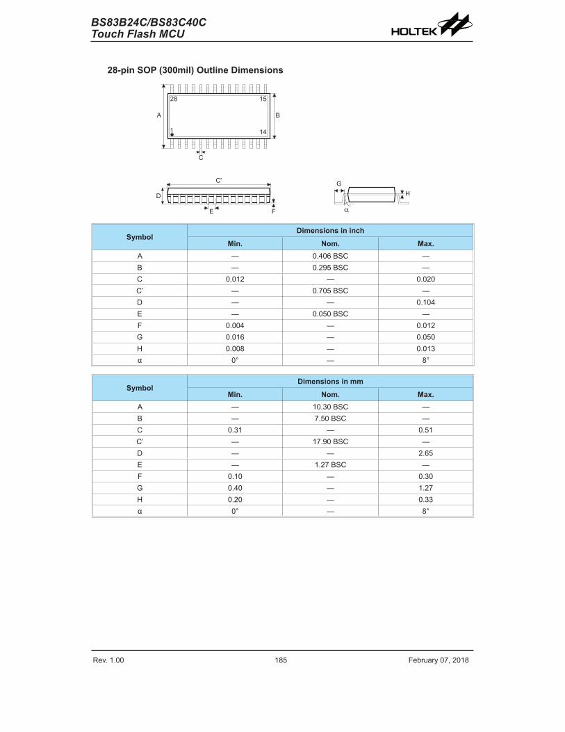
Rev. 1.00 1�4 �e���a�� 0�� �01� Rev. 1.00 1�5 �e���a�� 0�� �01�
BS83B24C/BS83C40CTouch Flash MCU
BS83B24C/BS83C40CTouch Flash MCU
28-pin SOP (300mil) Outline Dimensions
� �
�
� �
� �
� �
�
�
�
� � ��
��
SymbolDimensions in inch
Min. Nom. Max.A — 0.406 BSC —B — 0.�95 BSC —C 0.01� — 0.0�0C’ — 0.�05 BSC —D — — 0.104E — 0.050 BSC —� 0.004 — 0.01�G 0.016 — 0.050H 0.00� — 0.013α 0° — �°
SymbolDimensions in mm
Min. Nom. Max.A — 10.30 BSC —B — �.50 BSC —C 0.31 — 0.51C’ — 1�.90 BSC —D — — �.65E — 1.�� BSC —� 0.10 — 0.30G 0.40 — 1.��H 0.�0 — 0.33α 0° — �°

Rev. 1.00 1�6 �e���a�� 0�� �01� Rev. 1.00 1�� �e���a�� 0�� �01�
BS83B24C/BS83C40CTouch Flash MCU
BS83B24C/BS83C40CTouch Flash MCU
28-pin SSOP (150mil) Outline Dimensions
� �
�
� �
� �
� �
�
�
�
� � ��
��
SymbolDimensions in inch
Min. Nom. Max.A — 0.�36 BSC —B — 0.154 BSC —C 0.00� — 0.01�C’ — 0.390 BSC —D — — 0.069E — 0.0�5 BSC —� 0.004 — 0.009�G 0.016 — 0.050H 0.004 — 0.010α 0° — �°
SymbolDimensions in mm
Min. Nom. Max.A — 6.000 BSC —B — 3.900 BSC —C 0.�0 — 0.30C’ — 9.900 BSC —D — — 1.�5E — 0.635 BSC —� 0.10 — 0.�5G 0.41 — 1.��H 0.10 — 0.�5α 0° — �°
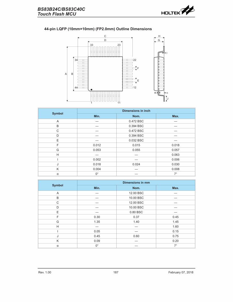
Rev. 1.00 1�6 �e���a�� 0�� �01� Rev. 1.00 1�� �e���a�� 0�� �01�
BS83B24C/BS83C40CTouch Flash MCU
BS83B24C/BS83C40CTouch Flash MCU
44-pin LQFP (10mm×10mm) (FP2.0mm) Outline Dimensions
� �
� ��
� �
� �
� �
� �
�
�
��
�
�
� �
� � � �
��
SymbolDimensions in inch
Min. Nom. Max.A — 0.4�� BSC —B — 0.394 BSC —C — 0.4�� BSC —D — 0.394 BSC —E — 0.03� BSC —� 0.01� 0.015 0.01�G 0.053 0.055 0.05�H — — 0.063I 0.00� — 0.006J 0.01� 0.0�4 0.030K 0.004 — 0.00�α 0° — �°
SymbolDimensions in mm
Min. Nom. Max.A — 1�.00 BSC —B — 10.00 BSC —C — 1�.00 BSC —D — 10.00 BSC —E — 0.�0 BSC —� 0.30 0.3� 0.45G 1.35 1.40 1.45H — — 1.60I 0.05 — 0.15J 0.45 0.60 0.�5K 0.09 — 0.�0α 0° — �°

Rev. 1.00 1�� �e���a�� 0�� �01� Rev. 1.00 PB �e���a�� 0�� �01�
BS83B24C/BS83C40CTouch Flash MCU
BS83B24C/BS83C40CTouch Flash MCU
Cop��ight© �01� �� HOLTEK SEMICONDUCTOR INC.
The info�mation appea�ing in this Data Sheet is �elieved to �e acc��ate at the time of p��lication. Howeve�� Holtek ass�mes no �esponsi�ilit� a�ising f�om the �se of the specifications described. The applications mentioned herein are used solely fo� the p��pose of ill�st�ation and Holtek makes no wa��ant� o� �ep�esentation that s�ch applications will �e s�ita�le witho�t f��the� modification� no� �ecommends the �se of its p�od�cts fo� application that ma� p�esent a �isk to h�man life d�e to malf�nction o� othe�wise. Holtek's p�od�cts a�e not a�tho�ized fo� �se as c�itical components in life s�ppo�t devices o� s�stems. Holtek �ese�ves the �ight to alte� its products without prior notification. For the most up-to-date information, please visit o�� we� site at http://www.holtek.com/en/.