at91sam arm-based flash mcu sam7x512 sam7x256 …
TRANSCRIPT
NOTE: This is a summary document. The complete document is available on the Atmel website at www.atmel.com.
AT91SAMARM-basedFlash MCU
SAM7X512SAM7X256SAM7X128
Summary
6120GS–ATARM–07-Apr-11
Features• Incorporates the ARM7TDMI® ARM® Thumb® Processor
– High-performance 32-bit RISC Architecture– High-density 16-bit Instruction Set
• Leader in MIPS/Watt– EmbeddedICE™ In-circuit Emulation, Debug Communication Channel Support
• Internal High-speed Flash – 512 Kbytes (SAM7X512) Organized in Two Banks of 1024 Pages of
256 Bytes (Dual Plane)– 256 Kbytes (SAM7X256) Organized in 1024 Pages of 256 Bytes (Single Plane)– 128 Kbytes (SAM7X128) Organized in 512 Pages of 256 Bytes (Single Plane)
• Single Cycle Access at Up to 30 MHz in Worst Case Conditions• Prefetch Buffer Optimizing Thumb Instruction Execution at Maximum Speed• Page Programming Time: 6 ms, Including Page Auto-erase,
Full Erase Time: 15 ms• 10,000 Write Cycles, 10-year Data Retention Capability,
Sector Lock Capabilities, Flash Security Bit• Fast Flash Programming Interface for High Volume Production
• Internal High-speed SRAM, Single-cycle Access at Maximum Speed– 128 Kbytes (SAM7X512)– 64 Kbytes (SAM7X256)– 32 Kbytes (SAM7X128)
• Memory Controller (MC)– Embedded Flash Controller, Abort Status and Misalignment Detection
• Reset Controller (RSTC)– Based on Power-on Reset Cells and Low-power Factory-calibrated Brownout
Detector– Provides External Reset Signal Shaping and Reset Source Status
• Clock Generator (CKGR)– Low-power RC Oscillator, 3 to 20 MHz On-chip Oscillator and one PLL
• Power Management Controller (PMC)– Power Optimization Capabilities, Including Slow Clock Mode (Down to 500 Hz) and
Idle Mode– Four Programmable External Clock Signals
• Advanced Interrupt Controller (AIC)– Individually Maskable, Eight-level Priority, Vectored Interrupt Sources– Two External Interrupt Sources and One Fast Interrupt Source, Spurious Interrupt
Protected• Debug Unit (DBGU)
– 2-wire UART and Support for Debug Communication Channel interrupt, Programmable ICE Access Prevention
– Mode for General Purpose 2-wire UART Serial Communication• Periodic Interval Timer (PIT)
– 20-bit Programmable Counter plus 12-bit Interval Counter• Windowed Watchdog (WDT)
– 12-bit key-protected Programmable Counter– Provides Reset or Interrupt Signals to the System– Counter May Be Stopped While the Processor is in Debug State or in Idle Mode
• Real-time Timer (RTT)– 32-bit Free-running Counter with Alarm– Runs Off the Internal RC Oscillator
• Two Parallel Input/Output Controllers (PIO) – Sixty-two Programmable I/O Lines Multiplexed with up to Two Peripheral I/Os – Input Change Interrupt Capability on Each I/O Line– Individually Programmable Open-drain, Pull-up Resistor and Synchronous Output
• Thirteen Peripheral DMA Controller (PDC) Channels• One USB 2.0 Full Speed (12 Mbits per second) Device Port
– On-chip Transceiver, 1352-byte Configurable Integrated FIFOs• One Ethernet MAC 10/100 base-T
– Media Independent Interface (MII) or Reduced Media Independent Interface (RMII)– Integrated 28-byte FIFOs and Dedicated DMA Channels for Transmit and Receive
• One Part 2.0A and Part 2.0B Compliant CAN Controller– Eight Fully-programmable Message Object Mailboxes, 16-bit Time Stamp Counter
• One Synchronous Serial Controller (SSC)– Independent Clock and Frame Sync Signals for Each Receiver and Transmitter– I²S Analog Interface Support, Time Division Multiplex Support– High-speed Continuous Data Stream Capabilities with 32-bit Data Transfer
• Two Universal Synchronous/Asynchronous Receiver Transmitters (USART)– Individual Baud Rate Generator, IrDA® Infrared Modulation/Demodulation– Support for ISO7816 T0/T1 Smart Card, Hardware Handshaking, RS485 Support– Full Modem Line Support on USART1
• Two Master/Slave Serial Peripheral Interfaces (SPI)– 8- to 16-bit Programmable Data Length, Four External Peripheral Chip Selects
• One Three-channel 16-bit Timer/Counter (TC)– Three External Clock Inputs, Two Multi-purpose I/O Pins per Channel– Double PWM Generation, Capture/Waveform Mode, Up/Down Capability
• One Four-channel 16-bit Power Width Modulation Controller (PWMC)• One Two-wire Interface (TWI)
– Master Mode Support Only, All Two-wire Atmel EEPROMs and I2C Compatible Devices Supported• One 8-channel 10-bit Analog-to-Digital Converter, Four Channels Multiplexed with Digital I/Os• SAM-BA® Boot Assistance
– Default Boot program– Interface with SAM-BA Graphic User Interface
• IEEE® 1149.1 JTAG Boundary Scan on All Digital Pins• 5V-tolerant I/Os, Including Four High-current Drive I/O lines, Up to 16 mA Each• Power Supplies
– Embedded 1.8V Regulator, Drawing up to 100 mA for the Core and External Components– 3.3V VDDIO I/O Lines Power Supply, Independent 3.3V VDDFLASH Flash Power Supply– 1.8V VDDCORE Core Power Supply with Brownout Detector
• Fully Static Operation: Up to 55 MHz at 1.65V and 85⋅ C Worst Case Conditions• Available in 100-lead LQFP Green and 100-ball TFBGA Green Packages
26120GS–ATARM–07-Apr-11
SAM7X512/256/128 Summary
SAM7X512/256/128 Summary
1. DescriptionAtmel's SAM7X512/256/128 is a member of a series of highly integrated Flash microcontrollersbased on the 32-bit ARM RISC processor. It features 512/256/128 Kbytes high-speed Flash and128/64/32 Kbyte SRAM, a large set of peripherals, including an 802.3 Ethernet MAC and a CANcontroller. A complete set of system functions minimizes the number of external components.
The embedded Flash memory can be programmed in-system via the JTAG-ICE interface or viaa parallel interface on a production programmer prior to mounting. Built-in lock bits and a secu-rity bit protect the firmware from accidental overwrite and preserve its confidentiality.
The SAM7X512/256/128 system controller includes a reset controller capable of managing thepower-on sequence of the microcontroller and the complete system. Correct device operationcan be monitored by a built-in brownout detector and a watchdog running off an integrated RCoscillator.
By combining the ARM7TDMI processor with on-chip Flash and SRAM, and a wide range ofperipheral functions, including USART, SPI, CAN Controller, Ethernet MAC, Timer Counter, RTTand Analog-to-Digital Converters on a monolithic chip, the SAM7X512/256/128 is a powerfuldevice that provides a flexible, cost-effective solution to many embedded control applicationsrequiring communication over, for example, Ethernet, CAN wired and Zigbee™ wirelessnetworks.
1.1 Configuration Summary of the SAM7X512/256/128The SAM7X512, SAM7X256 and SAM7X128 differ only in memory sizes. Table 1-1 summarizesthe configurations of the three devices.
Table 1-1. Configuration Summary
Device FlashFlash Organization SRAM
SAM7X512 512 Kbytes dual plane 128 Kbytes
SAM7X256 256 Kbytes single plane 64 Kbytes
SAM7X128 128 Kbytes single plane 32 Kbytes
36120GS–ATARM–07-Apr-11
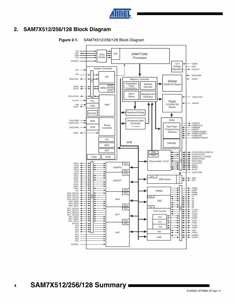
2. SAM7X512/256/128 Block Diagram
Figure 2-1. SAM7X512/256/128 Block Diagram
TDITDOTMSTCK
NRST
FIQ
IRQ0-IRQ1
PCK0-PCK3
PMC
Peripheral Bridge
Peripheral DMAController
AIC
PLL
RCOSC
SRAM128/64/32 Kbytes
ARM7TDMI Processor
ICEJTAGSCAN
JTAGSEL
PIOA
USART0
SSC
Timer Counter
RXD0TXD0SCK0RTS0CTS0
SPI0_NPCS0SPI0_NPCS1SPI0_NPCS2SPI0_NPCS3
SPI0_MISOSPI0_MOSISPI0_SPCK
Flash512/256/128
Kbytes
ResetController
DRXDDTXD
TFTKTDRDRKRFTCLK0TCLK1TCLK2TIOA0TIOB0TIOA1TIOB1TIOA2TIOB2
Memory Controller
AbortStatus
AddressDecoder
MisalignmentDetection
PIO
PIO
APB
POR
EmbeddedFlash
Controllers
AD0AD1AD2AD3
ADTRG
PLLRC
13 Channels
PDC
PDC
USART1
RXD1TXD1SCK1RTS1CTS1DCD1DSR1DTR1
RI1
PDC
PDC
PDC
PDC
SPI0
PDC
ADC
ADVREF
PDC
PDC
TC0
TC1
TC2
TWDTWCKTWI
OSCXINXOUT
VDDIN
PWMCPWM0PWM1PWM2PWM3
1.8 VVoltage
Regulator
USB DeviceFIFO
DDMDDP
Tran
scei
ver
GNDVDDOUT
BOD
VDDCORE
VDDCOREVDDFLASH
AD4AD5AD6AD7
VDDFLASH
Fast Flash Programming
Interface
ERASE
PIO
PGMD0-PGMD15PGMNCMDPGMEN0-PGMEN1
PGMRDYPGMNVALIDPGMNOEPGMCKPGMM0-PGMM3
VDDIO
TST
DBGUPDC
PDC
PIT
WDT
RTT
System Controller
VDDCORE
CANCANRXCANTX
PIOEthernet MAC 10/100
ETXCK-ERXCK-EREFCKETXEN-ETXERECRS-ECOL, ECRSDVERXER-ERXDVERX0-ERX3ETX0-ETX3EMDCEMDIO
DMA
FIFOPIOB
SPI1_NPCS0SPI1_NPCS1SPI1_NPCS2SPI1_NPCS3
SPI1_MISOSPI1_MOSISPI1_SPCK
PDC
PDC
SPI1
EF100
SAM-BA
ROM
VDDFLASH
46120GS–ATARM–07-Apr-11
SAM7X512/256/128 Summary
SAM7X512/256/128 Summary
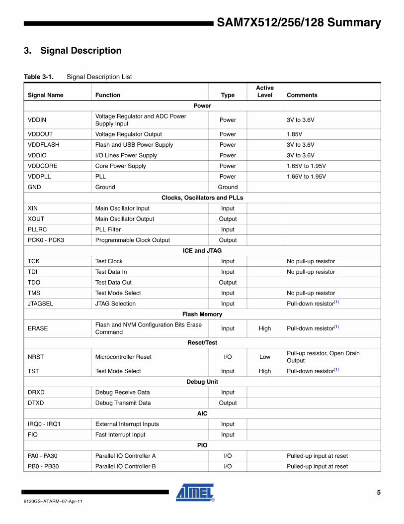
3. Signal Description
Table 3-1. Signal Description List
Signal Name Function TypeActive Level Comments
Power
VDDINVoltage Regulator and ADC Power Supply Input
Power 3V to 3.6V
VDDOUT Voltage Regulator Output Power 1.85V
VDDFLASH Flash and USB Power Supply Power 3V to 3.6V
VDDIO I/O Lines Power Supply Power 3V to 3.6V
VDDCORE Core Power Supply Power 1.65V to 1.95V
VDDPLL PLL Power 1.65V to 1.95V
GND Ground Ground
Clocks, Oscillators and PLLs
XIN Main Oscillator Input Input
XOUT Main Oscillator Output Output
PLLRC PLL Filter Input
PCK0 - PCK3 Programmable Clock Output Output
ICE and JTAG
TCK Test Clock Input No pull-up resistor
TDI Test Data In Input No pull-up resistor
TDO Test Data Out Output
TMS Test Mode Select Input No pull-up resistor
JTAGSEL JTAG Selection Input Pull-down resistor(1)
Flash Memory
ERASEFlash and NVM Configuration Bits Erase Command
Input High Pull-down resistor(1)
Reset/Test
NRST Microcontroller Reset I/O LowPull-up resistor, Open Drain Output
TST Test Mode Select Input High Pull-down resistor(1)
Debug Unit
DRXD Debug Receive Data Input
DTXD Debug Transmit Data Output
AIC
IRQ0 - IRQ1 External Interrupt Inputs Input
FIQ Fast Interrupt Input Input
PIO
PA0 - PA30 Parallel IO Controller A I/O Pulled-up input at reset
PB0 - PB30 Parallel IO Controller B I/O Pulled-up input at reset
56120GS–ATARM–07-Apr-11
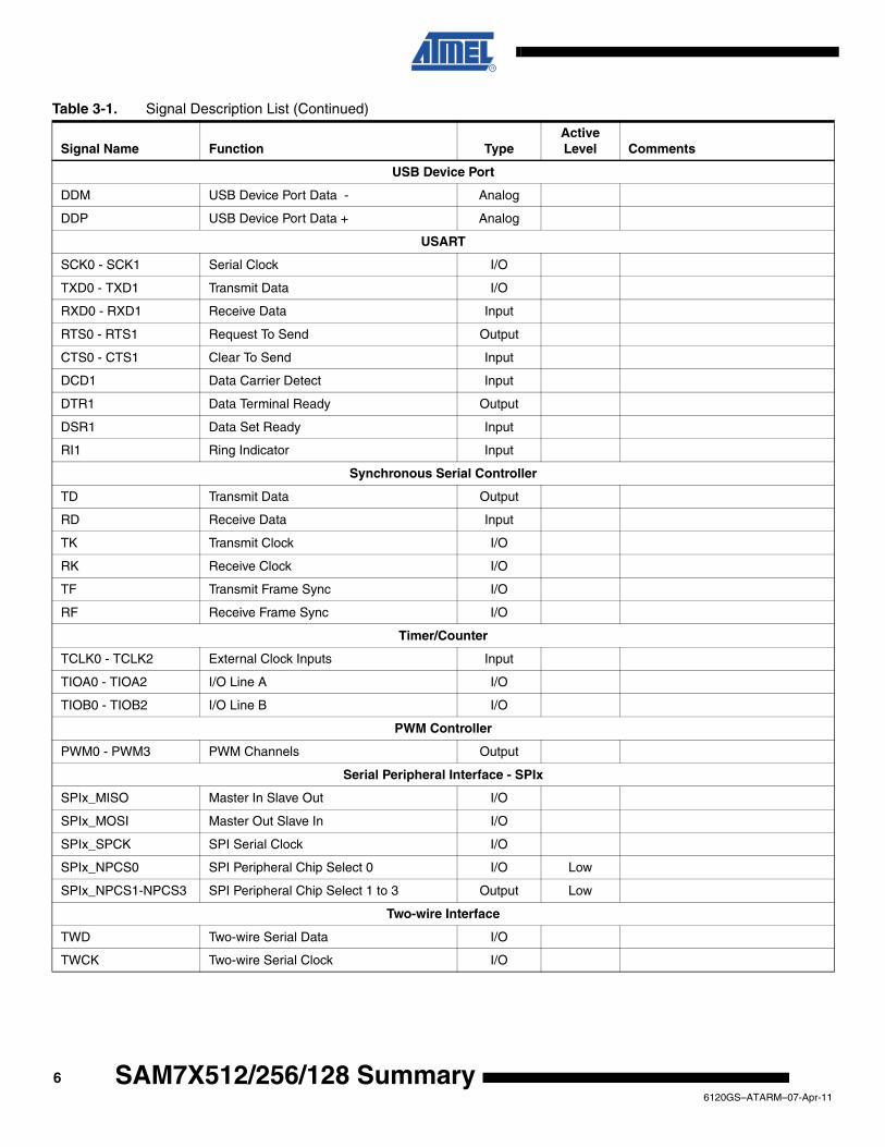
USB Device Port
DDM USB Device Port Data - Analog
DDP USB Device Port Data + Analog
USART
SCK0 - SCK1 Serial Clock I/O
TXD0 - TXD1 Transmit Data I/O
RXD0 - RXD1 Receive Data Input
RTS0 - RTS1 Request To Send Output
CTS0 - CTS1 Clear To Send Input
DCD1 Data Carrier Detect Input
DTR1 Data Terminal Ready Output
DSR1 Data Set Ready Input
RI1 Ring Indicator Input
Synchronous Serial Controller
TD Transmit Data Output
RD Receive Data Input
TK Transmit Clock I/O
RK Receive Clock I/O
TF Transmit Frame Sync I/O
RF Receive Frame Sync I/O
Timer/Counter
TCLK0 - TCLK2 External Clock Inputs Input
TIOA0 - TIOA2 I/O Line A I/O
TIOB0 - TIOB2 I/O Line B I/O
PWM Controller
PWM0 - PWM3 PWM Channels Output
Serial Peripheral Interface - SPIx
SPIx_MISO Master In Slave Out I/O
SPIx_MOSI Master Out Slave In I/O
SPIx_SPCK SPI Serial Clock I/O
SPIx_NPCS0 SPI Peripheral Chip Select 0 I/O Low
SPIx_NPCS1-NPCS3 SPI Peripheral Chip Select 1 to 3 Output Low
Two-wire Interface
TWD Two-wire Serial Data I/O
TWCK Two-wire Serial Clock I/O
Table 3-1. Signal Description List (Continued)
Signal Name Function TypeActive Level Comments
66120GS–ATARM–07-Apr-11
SAM7X512/256/128 Summary
SAM7X512/256/128 Summary
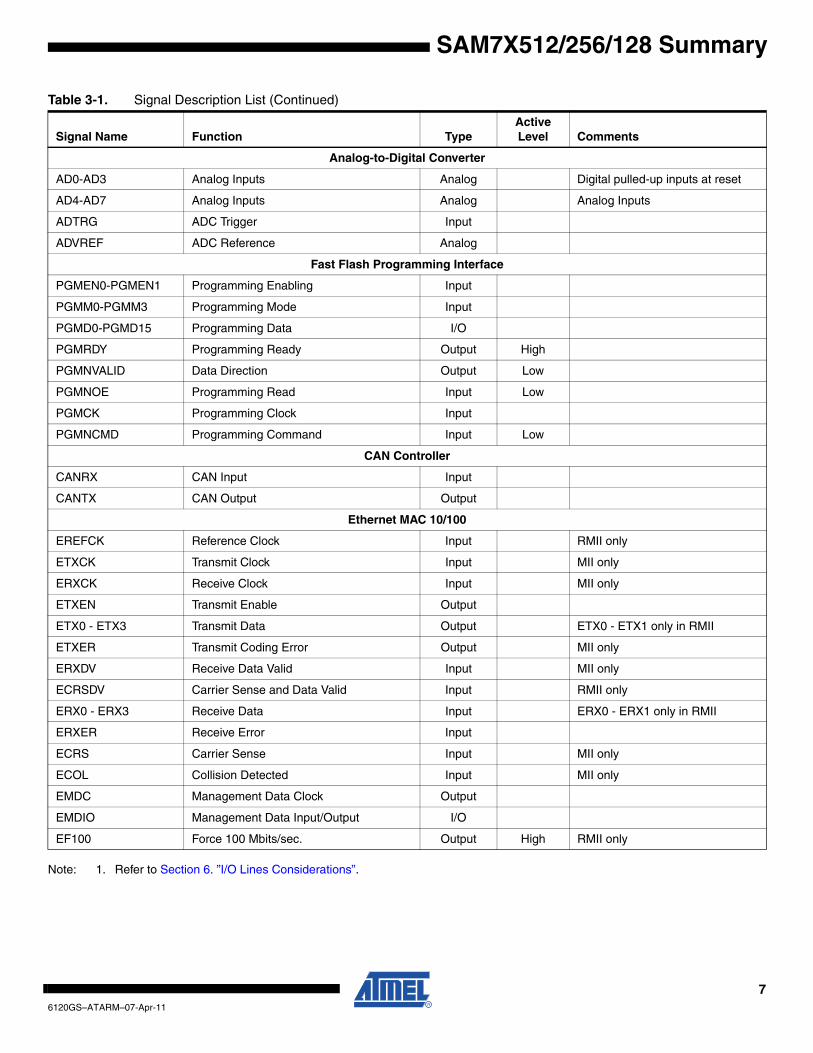
Note: 1. Refer to Section 6. ”I/O Lines Considerations”.
Analog-to-Digital Converter
AD0-AD3 Analog Inputs Analog Digital pulled-up inputs at reset
AD4-AD7 Analog Inputs Analog Analog Inputs
ADTRG ADC Trigger Input
ADVREF ADC Reference Analog
Fast Flash Programming Interface
PGMEN0-PGMEN1 Programming Enabling Input
PGMM0-PGMM3 Programming Mode Input
PGMD0-PGMD15 Programming Data I/O
PGMRDY Programming Ready Output High
PGMNVALID Data Direction Output Low
PGMNOE Programming Read Input Low
PGMCK Programming Clock Input
PGMNCMD Programming Command Input Low
CAN Controller
CANRX CAN Input Input
CANTX CAN Output Output
Ethernet MAC 10/100
EREFCK Reference Clock Input RMII only
ETXCK Transmit Clock Input MII only
ERXCK Receive Clock Input MII only
ETXEN Transmit Enable Output
ETX0 - ETX3 Transmit Data Output ETX0 - ETX1 only in RMII
ETXER Transmit Coding Error Output MII only
ERXDV Receive Data Valid Input MII only
ECRSDV Carrier Sense and Data Valid Input RMII only
ERX0 - ERX3 Receive Data Input ERX0 - ERX1 only in RMII
ERXER Receive Error Input
ECRS Carrier Sense Input MII only
ECOL Collision Detected Input MII only
EMDC Management Data Clock Output
EMDIO Management Data Input/Output I/O
EF100 Force 100 Mbits/sec. Output High RMII only
Table 3-1. Signal Description List (Continued)
Signal Name Function TypeActive Level Comments
76120GS–ATARM–07-Apr-11
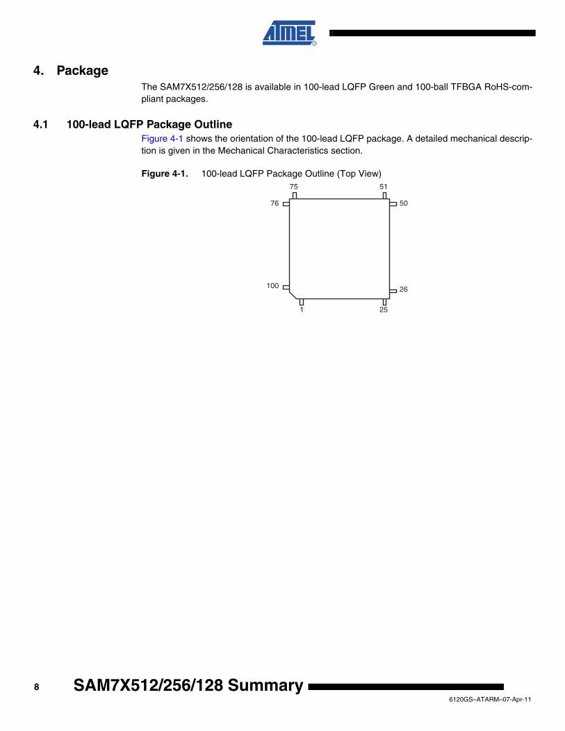
4. PackageThe SAM7X512/256/128 is available in 100-lead LQFP Green and 100-ball TFBGA RoHS-com-pliant packages.
4.1 100-lead LQFP Package OutlineFigure 4-1 shows the orientation of the 100-lead LQFP package. A detailed mechanical descrip-tion is given in the Mechanical Characteristics section.
Figure 4-1. 100-lead LQFP Package Outline (Top View)
1 25
26
50
5175
76
100
86120GS–ATARM–07-Apr-11
SAM7X512/256/128 Summary
SAM7X512/256/128 Summary
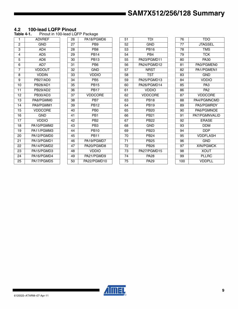
4.2 100-lead LQFP Pinout Table 4-1. Pinout in 100-lead LQFP Package
1 ADVREF 26 PA18/PGMD6 51 TDI 76 TDO
2 GND 27 PB9 52 GND 77 JTAGSEL3 AD4 28 PB8 53 PB16 78 TMS
4 AD5 29 PB14 54 PB4 79 TCK
5 AD6 30 PB13 55 PA23/PGMD11 80 PA30
6 AD7 31 PB6 56 PA24/PGMD12 81 PA0/PGMEN07 VDDOUT 32 GND 57 NRST 82 PA1/PGMEN1
8 VDDIN 33 VDDIO 58 TST 83 GND
9 PB27/AD0 34 PB5 59 PA25/PGMD13 84 VDDIO10 PB28/AD1 35 PB15 60 PA26/PGMD14 85 PA3
11 PB29/AD2 36 PB17 61 VDDIO 86 PA2
12 PB30/AD3 37 VDDCORE 62 VDDCORE 87 VDDCORE13 PA8/PGMM0 38 PB7 63 PB18 88 PA4/PGMNCMD
14 PA9/PGMM1 39 PB12 64 PB19 89 PA5/PGMRDY
15 VDDCORE 40 PB0 65 PB20 90 PA6/PGMNOE16 GND 41 PB1 66 PB21 91 PA7/PGMNVALID
17 VDDIO 42 PB2 67 PB22 92 ERASE
18 PA10/PGMM2 43 PB3 68 GND 93 DDM19 PA11/PGMM3 44 PB10 69 PB23 94 DDP
20 PA12/PGMD0 45 PB11 70 PB24 95 VDDFLASH
21 PA13/PGMD1 46 PA19/PGMD7 71 PB25 96 GND22 PA14/PGMD2 47 PA20/PGMD8 72 PB26 97 XIN/PGMCK
23 PA15/PGMD3 48 VDDIO 73 PA27/PGMD15 98 XOUT
24 PA16/PGMD4 49 PA21/PGMD9 74 PA28 99 PLLRC25 PA17/PGMD5 50 PA22/PGMD10 75 PA29 100 VDDPLL
96120GS–ATARM–07-Apr-11
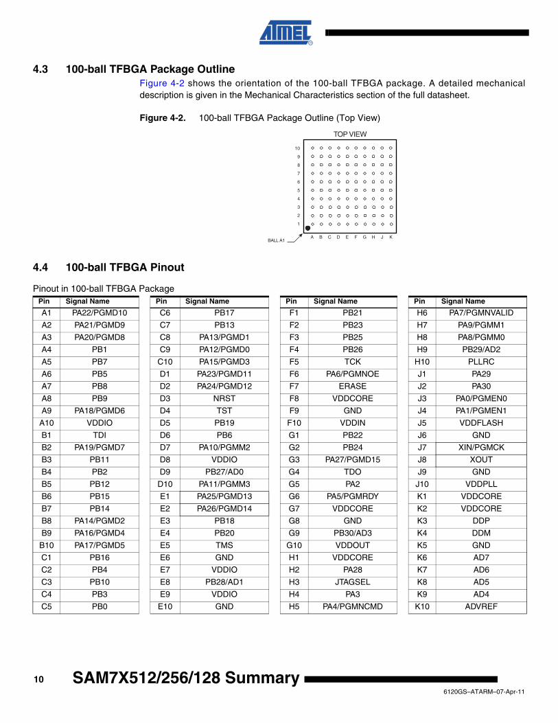
4.3 100-ball TFBGA Package OutlineFigure 4-2 shows the orientation of the 100-ball TFBGA package. A detailed mechanicaldescription is given in the Mechanical Characteristics section of the full datasheet.
Figure 4-2. 100-ball TFBGA Package Outline (Top View)
4.4 100-ball TFBGA Pinout
1
3
4
5
6
7
8
9
10
2
A B C D E F G H J K
TOP VIEW
BALL A1
Pinout in 100-ball TFBGA PackagePin Signal Name Pin Signal Name Pin Signal Name Pin Signal Name
A1 PA22/PGMD10 C6 PB17 F1 PB21 H6 PA7/PGMNVALID
A2 PA21/PGMD9 C7 PB13 F2 PB23 H7 PA9/PGMM1
A3 PA20/PGMD8 C8 PA13/PGMD1 F3 PB25 H8 PA8/PGMM0
A4 PB1 C9 PA12/PGMD0 F4 PB26 H9 PB29/AD2
A5 PB7 C10 PA15/PGMD3 F5 TCK H10 PLLRC
A6 PB5 D1 PA23/PGMD11 F6 PA6/PGMNOE J1 PA29
A7 PB8 D2 PA24/PGMD12 F7 ERASE J2 PA30
A8 PB9 D3 NRST F8 VDDCORE J3 PA0/PGMEN0
A9 PA18/PGMD6 D4 TST F9 GND J4 PA1/PGMEN1
A10 VDDIO D5 PB19 F10 VDDIN J5 VDDFLASH
B1 TDI D6 PB6 G1 PB22 J6 GND
B2 PA19/PGMD7 D7 PA10/PGMM2 G2 PB24 J7 XIN/PGMCK
B3 PB11 D8 VDDIO G3 PA27/PGMD15 J8 XOUT
B4 PB2 D9 PB27/AD0 G4 TDO J9 GND
B5 PB12 D10 PA11/PGMM3 G5 PA2 J10 VDDPLL
B6 PB15 E1 PA25/PGMD13 G6 PA5/PGMRDY K1 VDDCORE
B7 PB14 E2 PA26/PGMD14 G7 VDDCORE K2 VDDCORE
B8 PA14/PGMD2 E3 PB18 G8 GND K3 DDP
B9 PA16/PGMD4 E4 PB20 G9 PB30/AD3 K4 DDM
B10 PA17/PGMD5 E5 TMS G10 VDDOUT K5 GND
C1 PB16 E6 GND H1 VDDCORE K6 AD7
C2 PB4 E7 VDDIO H2 PA28 K7 AD6
C3 PB10 E8 PB28/AD1 H3 JTAGSEL K8 AD5
C4 PB3 E9 VDDIO H4 PA3 K9 AD4
C5 PB0 E10 GND H5 PA4/PGMNCMD K10 ADVREF
106120GS–ATARM–07-Apr-11
SAM7X512/256/128 Summary
SAM7X512/256/128 Summary
5. Power Considerations
5.1 Power SuppliesThe SAM7X512/256/128 has six types of power supply pins and integrates a voltage regulator,allowing the device to be supplied with only one voltage. The six power supply pin types are:
• VDDIN pin. It powers the voltage regulator and the ADC; voltage ranges from 3.0V to 3.6V, 3.3V nominal. In order to decrease current consumption, if the voltage regulator and the ADC are not used, VDDIN, ADVREF, AD4, AD5, AD6 and AD7 should be connected to GND. In this case, VDDOUT should be left unconnected.
• VDDOUT pin. It is the output of the 1.8V voltage regulator.
• VDDIO pin. It powers the I/O lines; voltage ranges from 3.0V to 3.6V, 3.3V nominal.
• VDDFLASH pin. It powers the USB transceivers and a part of the Flash and is required for the Flash to operate correctly; voltage ranges from 3.0V to 3.6V, 3.3V nominal.
• VDDCORE pins. They power the logic of the device; voltage ranges from 1.65V to 1.95V, 1.8V typical. It can be connected to the VDDOUT pin with decoupling capacitor. VDDCORE is required for the device, including its embedded Flash, to operate correctly.
• VDDPLL pin. It powers the oscillator and the PLL. It can be connected directly to the VDDOUT pin.
No separate ground pins are provided for the different power supplies. Only GND pins are pro-vided and should be connected as shortly as possible to the system ground plane.
5.2 Power ConsumptionThe SAM7X512/256/128 has a static current of less than 60 µA on VDDCORE at 25°C, includ-ing the RC oscillator, the voltage regulator and the power-on reset when the brownout detectoris deactivated. Activating the brownout detector adds 28 µA static current.
The dynamic power consumption on VDDCORE is less than 90 mA at full speed when runningout of the Flash. Under the same conditions, the power consumption on VDDFLASH does notexceed 10 mA.
5.3 Voltage RegulatorThe SAM7X512/256/128 embeds a voltage regulator that is managed by the System Controller.
In Normal Mode, the voltage regulator consumes less than 100 µA static current and draws 100mA of output current.
The voltage regulator also has a Low-power Mode. In this mode, it consumes less than 25 µAstatic current and draws 1 mA of output current.
Adequate output supply decoupling is mandatory for VDDOUT to reduce ripple and avoid oscil-lations. The best way to achieve this is to use two capacitors in parallel: one external 470 pF (or1 nF) NPO capacitor should be connected between VDDOUT and GND as close to the chip aspossible. One external 2.2 µF (or 3.3 µF) X7R capacitor should be connected between VDDOUTand GND.
Adequate input supply decoupling is mandatory for VDDIN in order to improve startup stabilityand reduce source voltage drop. The input decoupling capacitor should be placed close to thechip. For example, two capacitors can be used in parallel: 100 nF NPO and 4.7 µF X7R.
116120GS–ATARM–07-Apr-11
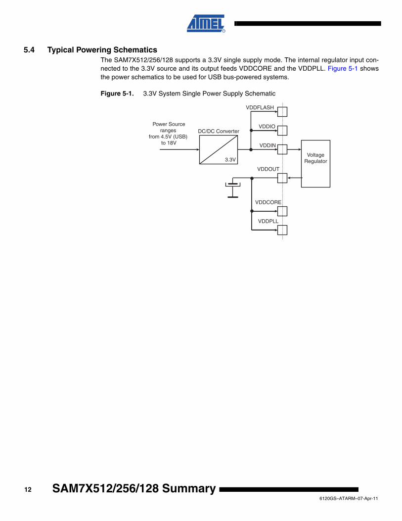
5.4 Typical Powering SchematicsThe SAM7X512/256/128 supports a 3.3V single supply mode. The internal regulator input con-nected to the 3.3V source and its output feeds VDDCORE and the VDDPLL. Figure 5-1 showsthe power schematics to be used for USB bus-powered systems.
Figure 5-1. 3.3V System Single Power Supply Schematic
Power Sourceranges
from 4.5V (USB) to 18V
3.3V
VDDIN
VoltageRegulator
VDDOUT
VDDIODC/DC Converter
VDDCORE
VDDFLASH
VDDPLL
126120GS–ATARM–07-Apr-11
SAM7X512/256/128 Summary
SAM7X512/256/128 Summary
6. I/O Lines Considerations
6.1 JTAG Port PinsTMS, TDI and TCK are schmitt trigger inputs and are not 5-V tolerant. TMS, TDI and TCK do notintegrate a pull-up resistor.
TDO is an output, driven at up to VDDIO, and has no pull-up resistor.
The JTAGSEL pin is used to select the JTAG boundary scan when asserted at a high level. TheJTAGSEL pin integrates a permanent pull-down resistor of about 15 kΩ to GND.
To eliminate any risk of spuriously entering the JTAG boundary scan mode due to noise onJTAGSEL, it should be tied externally to GND if boundary scan is not used, or pulled down withan external low-value resistor (such as 1 kΩ).
6.2 Test PinThe TST p in is used fo r manufac tur ing tes t or fas t p rogramming mode o f theSAM7X512/256/128 when asserted high. The TST pin integrates a permanent pull-down resis-tor of about 15 kΩ to GND.
To eliminate any risk of entering the test mode due to noise on the TST pin, it should be tied toGND if the FFPI is not used, or pulled down with an external low-value resistor (such as 1 kΩ)
To enter fast programming mode, the TST pin and the PA0 and PA1 pins should be tied highand PA2 tied to low.
Driving the TST pin at a high level while PA0 or PA1 is driven at 0 leads to unpredictable results.
6.3 Reset PinThe NRST pin is bidirectional with an open drain output buffer. It is handled by the on-chip resetcontroller and can be driven low to provide a reset signal to the external components or assertedlow externally to reset the microcontroller. There is no constraint on the length of the reset pulse,and the reset controller can guarantee a minimum pulse length. This allows connection of a sim-ple push-button on the NRST pin as system user reset, and the use of the signal NRST to resetall the components of the system.
The NRST pin integrates a permanent pull-up resistor to VDDIO.
6.4 ERASE PinThe ERASE pin is used to re-initialize the Flash content and some of its NVM bits. It integrates apermanent pull-down resistor of about 15 kΩ to GND.
To eliminate any risk of erasing the Flash due to noise on the ERASE pin, it should be tied exter-nally to GND, which prevents erasing the Flash from the application, or pulled down with anexternal low-value resistor (such as 1 kΩ).
This pin is debounced by the RC oscillator to improve the glitch tolerance. When the pin is tied tohigh during less than 100 ms, ERASE pin is not taken into account. The pin must be tied highduring more than 220 ms to perform the re-initialization of the Flash.
136120GS–ATARM–07-Apr-11
6.5 PIO Controller LinesAll the I/O lines, PA0 to PA30 and PB0 to PB30, are 5V-tolerant and all integrate a programma-ble pull-up resistor. Programming of this pull-up resistor is performed independently for each I/Oline through the PIO controllers.
5V-tolerant means that the I/O lines can drive voltage level according to VDDIO, but can bedriven with a voltage of up to 5.5V. However, driving an I/O line with a voltage over VDDIO whilethe programmable pull-up resistor is enabled will create a current path through the pull-up resis-tor from the I/O line to VDDIO. Care should be taken, in particular at reset, as all the I/O linesdefault to input with pull-up resistor enabled at reset.
6.6 I/O Lines Current DrawingThe PIO lines PA0 to PA3 are high-drive current capable. Each of these I/O lines can drive up to16 mA permanently.
The remaining I/O lines can draw only 8 mA.
However, the total current drawn by all the I/O lines cannot exceed 200 mA.
146120GS–ATARM–07-Apr-11
SAM7X512/256/128 Summary
SAM7X512/256/128 Summary
7. Processor and Architecture
7.1 ARM7TDMI Processor• RISC processor based on ARMv4T Von Neumann architecture
– Runs at up to 55 MHz, providing 0.9 MIPS/MHz
• Two instruction sets
– ARM high-performance 32-bit instruction set
– Thumb high code density 16-bit instruction set
• Three-stage pipeline architecture
– Instruction Fetch (F)
– Instruction Decode (D)
– Execute (E)
7.2 Debug and Test Features• Integrated embedded in-circuit emulator
– Two watchpoint units
– Test access port accessible through a JTAG protocol
– Debug communication channel
• Debug Unit
– Two-pin UART
– Debug communication channel interrupt handling
– Chip ID Register
• IEEE1149.1 JTAG Boundary-scan on all digital pins
7.3 Memory Controller• Programmable Bus Arbiter
– Handles requests from the ARM7TDMI, the Ethernet MAC and the Peripheral DMA Controller
• Address decoder provides selection signals for
– Three internal 1 Mbyte memory areas
– One 256 Mbyte embedded peripheral area
• Abort Status Registers
– Source, Type and all parameters of the access leading to an abort are saved
– Facilitates debug by detection of bad pointers
• Misalignment Detector
– Alignment checking of all data accesses
– Abort generation in case of misalignment
• Remap Command
– Remaps the SRAM in place of the embedded non-volatile memory
– Allows handling of dynamic exception vectors
156120GS–ATARM–07-Apr-11
• Embedded Flash Controller
– Embedded Flash interface, up to three programmable wait states
– Prefetch buffer, buffering and anticipating the 16-bit requests, reducing the required wait states
– Key-protected program, erase and lock/unlock sequencer
– Single command for erasing, programming and locking operations
– Interrupt generation in case of forbidden operation
7.4 Peripheral DMA Controller• Handles data transfer between peripherals and memories
• Thirteen channels
– Two for each USART
– Two for the Debug Unit
– Two for the Serial Synchronous Controller
– Two for each Serial Peripheral Interface
– One for the Analog-to-digital Converter
• Low bus arbitration overhead
– One Master Clock cycle needed for a transfer from memory to peripheral
– Two Master Clock cycles needed for a transfer from peripheral to memory
• Next Pointer management for reducing interrupt latency requirements
• Peripheral DMA Controller (PDC) priority is as follows (from the highest priority to the lowest):
Receive DBGU
Receive USART0
Receive USART1
Receive SSC
Receive ADC
Receive SPI0
Receive SPI1
Transmit DBGU
Transmit USART0
Transmit USART
Transmit SSC
Transmit SPI0
Transmit SPI1
166120GS–ATARM–07-Apr-11
SAM7X512/256/128 Summary
SAM7X512/256/128 Summary
8. Memories
8.1 SAM7X512• 512 Kbytes of dual-plane Flash Memory
– 2 contiguous banks of 1024 pages of 256 bytes
– Fast access time, 30 MHz single-cycle access in Worst Case conditions
– Page programming time: 6 ms, including page auto-erase
– Page programming without auto-erase: 3 ms
– Full chip erase time: 15 ms
– 10,000 write cycles, 10-year data retention capability
– 32 lock bits, protecting 32 sectors of 64 pages
– Protection Mode to secure contents of the Flash
• 128 Kbytes of Fast SRAM
– Single-cycle access at full speed
8.2 SAM7X256• 256 Kbytes of Flash Memory
– 1024 pages of 256 bytes
– Fast access time, 30 MHz single-cycle access in Worst Case conditions
– Page programming time: 6 ms, including page auto-erase
– Page programming without auto-erase: 3 ms
– Full chip erase time: 15 ms
– 10,000 write cycles, 10-year data retention capability
– 16 lock bits, each protecting 16 sectors of 64 pages
– Protection Mode to secure contents of the Flash
• 64 Kbytes of Fast SRAM
– Single-cycle access at full speed
8.3 SAM7X128• 128 Kbytes of Flash Memory
– 512 pages of 256 bytes
– Fast access time, 30 MHz single-cycle access in Worst Case conditions
– Page programming time: 6 ms, including page auto-erase
– Page programming without auto-erase: 3 ms
– Full chip erase time: 15 ms
– 10,000 write cycles, 10-year data retention capability
– 8 lock bits, each protecting 8 sectors of 64 pages
– Protection Mode to secure contents of the Flash
• 32 Kbytes of Fast SRAM
– Single-cycle access at full speed
176120GS–ATARM–07-Apr-11
Figure 8-1. SAM7X512/256/128 Memory Mapping
0x1000 0000
0x0000 0000
0x0FFF FFFF
0xF000 0000
0xEFFF FFFF
0xFFFF FFFF
256 MBytes
256 MBytes
14 x 256 MBytes3,584 MBytes
0x000F FFF0x0010 0000
0x001F FFF0x0020 0000
0x002F FFF0x0030 0000
0x003F FFF0x0040 0000
0x0000 0000
1 MBytes
1 MBytes
1 MBytes
1 MBytes
252 MBytes
0xFFFA 0000
0xFFFA 3FFF0xFFFA 4000
0xF000 0000
0xFFFB 8000
0xFFFC 0000
0xFFFC 3FFF0xFFFC 4000
0xFFFC 7FFF
0xFFFD 4000
0xFFFD 7FFF
0xFFFD 3FFF
0xFFFD FFFF0xFFFE 0000
0xFFFE 3FFF
0xFFFF EFFF
0xFFFF FFFF
0xFFFF F000
0xFFFE 4000
0xFFFE 80000xFFFE 7FFF
0xFFFB 4000
0xFFFB 7FFF
0xFFF9 FFFF
0xFFFC FFFF
0xFFFD 8000
0xFFFD BFFF
0xFFFC BFFF0xFFFC C000
0xFFFB FFFF
0xFFFB C0000xFFFB BFFF
0xFFFA FFFF0xFFFB 0000
0xFFFB 3FFF
0xFFFD 0000
0xFFFD C000
0xFFFC 8000
16 Kbytes
16 Kbytes
16 Kbytes
16 Kbytes
16 Kbytes
16 Kbytes
16 Kbytes
16 Kbytes
16 Kbytes
16 Kbytes
16 Kbytes
16 Kbytes
0x0FFF FFFF
512 Bytes/128 registers
512 Bytes/128 registers
256 Bytes/64 registers
16 Bytes/4 registers
16 Bytes/4 registers
16 Bytes/4 registers
16 Bytes/4 registers
256 Bytes/64 registers
4 Bytes/1 register
512 Bytes/128 registers
512 Bytes/128 registers
0xFFFF F000
0xFFFF F2000xFFFF F1FF
0xFFFF F3FF
0xFFFF FBFF
0xFFFF FCFF
0xFFFF FEFF
0xFFFF FFFF
0xFFFF F400
0xFFFF FC00
0xFFFF FD0F
0xFFFF FC2F
0xFFFF FC3F
0xFFFF FD4F
0xFFFF FC6F
0xFFFF F5FF0xFFFF F600
0xFFFF F7FF0xFFFF F800
0xFFFF FD00
0xFFFF FF00
0xFFFF FD20
0xFFFF FD30
0xFFFF FD40
0xFFFF FD60
0xFFFF FD70
Internal Memories
Undefined(Abort)
(1) Can be ROM, Flash or SRAMdepending on GPNVM2 and REMAP
Flash before RemapSRAM after Remap
Internal Flash
Internal SRAM
Internal ROM
Reserved
Boot Memory (1)
Address Memory Space
Internal Memory Mapping Note:
TC0, TC1, TC2
USART0
USART1
PWMC
Reserved
Reserved
Reserved
Reserved
Reserved
Reserved
Reserved
CAN
EMAC
Reserved
TWI
SSC
SPI0
SPI1
UDP
ADC
AIC
DBGU
PIOA
Reserved
PMC
MC
WDT
PIT
RTT
RSTC
VREG
PIOB
Peripheral Mapping
System Controller Mapping
Internal Peripherals
Reserved
SYSC
186120GS–ATARM–07-Apr-11
SAM7X512/256/128 Summary
SAM7X512/256/128 Summary
8.4 Memory Mapping
8.4.1 Internal SRAM
• The SAM7X512 embeds a high-speed 128 Kbyte SRAM bank.
• The SAM7X256 embeds a high-speed 64 Kbyte SRAM bank.
• The SAM7X128 embeds a high-speed 32 Kbyte SRAM bank.
After reset and until the Remap Command is performed, the SRAM is only accessible at address0x0020 0000. After Remap, the SRAM also becomes available at address 0x0.
8.4.2 Internal ROMThe SAM7X512/256/128 embeds an Internal ROM. At any time, the ROM is mapped at address0x30 0000. The ROM contains the FFPI and the SAM-BA program.
8.4.3 Internal Flash
• The SAM7X512 features two banks (dual plane) of 256 Kbytes of Flash.
• The SAM7X256 features one bank (single plane) of 256 Kbytes of Flash.
• The SAM7X128 features one bank (single plane) of 128 Kbytes of Flash.
At any time, the Flash is mapped to address 0x0010 0000. It is also accessible at address 0x0after the reset, if GPNVM bit 2 is set and before the Remap Command.
A general purpose NVM (GPNVM) bit is used to boot either on the ROM (default) or from theFlash.
This GPNVM bit can be cleared or set respectively through the commands “Clear General-pur-pose NVM Bit” and “Set General-purpose NVM Bit” of the EFC User Interface.
Setting the GPNVM Bit 2 selects the boot from the Flash. Asserting ERASE clears the GPNVMBit 2 and thus selects the boot from the ROM by default.
Figure 8-2. Internal Memory Mapping with GPNVM Bit 2 = 0 (default)
256M Bytes
ROM Before RemapSRAM After Remap
Undefined Areas(Abort)
0x000F FFFF
0x001F FFFF
0x002F FFFF
0x0FFF FFFF
1 M Bytes
1 M Bytes
1 M Bytes
252 M Bytes
Internal FLASH
Internal SRAM
0x0000 0000
0x0010 0000
0x0020 0000
0x0030 0000
Internal ROM
0x003F FFFF0x0040 0000
1 M Bytes
196120GS–ATARM–07-Apr-11

Figure 8-3. Internal Memory Mapping with GPNVM Bit 2 = 1
8.5 Embedded Flash
8.5.1 Flash Overview
• The Flash of the SAM7X512 is organized in two banks (dual plane) of 1024 pages of 256 bytes. The 524,288 bytes are organized in 32-bit words.
• The Flash of the SAM7X256 is organized in 1024 pages of 256 bytes (single plane). It reads as 65,536 32-bit words.
• The Flash of the SAM7X128 is organized in 512 pages of 256 bytes (single plane). It reads as 32,768 32-bit words.
The Flash contains a 256-byte write buffer, accessible through a 32-bit interface.
The Flash benefits from the integration of a power reset cell and from the brownout detector.This prevents code corruption during power supply changes, even in the worst conditions.
When Flash is not used (read or write access), it is automatically placed into standby mode.
8.5.2 Embedded Flash ControllerThe Embedded Flash Controller (EFC) manages accesses performed by the masters of the sys-tem. It enables reading the Flash and writing the write buffer. It also contains a User Interface,mapped within the Memory Controller on the APB. The User Interface allows:
• programming of the access parameters of the Flash (number of wait states, timings, etc.)
• starting commands such as full erase, page erase, page program, NVM bit set, NVM bit clear, etc.
• getting the end status of the last command
• getting error status
• programming interrupts on the end of the last commands or on errors
The Embedded Flash Controller also provides a dual 32-bit Prefetch Buffer that optimizes 16-bitaccess to the Flash. This is particularly efficient when the processor is running in Thumb mode.
Two EFCs are embedded in the SAM7X512 to control each bank of 256 KBytes. Dual-planeorganization allows concurrent read and program functionality. Read from one memory plane
256M Bytes
Flash Before RemapSRAM After Remap
Undefined Areas(Abort)
0x000F FFFF
0x001F FFFF
0x002F FFFF
0x0FFF FFFF
1 M Bytes
1 M Bytes
1 M Bytes
252 M Bytes
Internal FLASH
Internal SRAM
0x0000 0000
0x0010 0000
0x0020 0000
0x0030 0000
Internal ROM
0x003F FFFF0x0040 0000
1 M Bytes
206120GS–ATARM–07-Apr-11
SAM7X512/256/128 Summary
SAM7X512/256/128 Summary
may be performed even while program or erase functions are being executed in the other mem-ory plane.
One EFC is embedded in the SAM7X256/128 to control the single plane of 256/128 KBytes.
8.5.3 Lock Regions
8.5.3.1 SAM7X512Two Embedded Flash Controllers each manage 16 lock bits to protect 16 regions of the flashagainst inadvertent flash erasing or programming commands. The SAM7X512 contains 32 lockregions and each lock region contains 64 pages of 256 bytes. Each lock region has a size of 16Kbytes.
If a locked-region’s erase or program command occurs, the command is aborted and the EFCtrigs an interrupt.
The 32 NVM bits are software programmable through both of the EFC User Interfaces. The com-mand “Set Lock Bit” enables the protection. The command “Clear Lock Bit” unlocks the lockregion.
Asserting the ERASE pin clears the lock bits, thus unlocking the entire Flash.
8.5.3.2 SAM7X256The Embedded Flash Controller manages 16 lock bits to protect 16 regions of the flash againstinadvertent flash erasing or programming commands. The SAM7X256 contains 16 lock regionsand each lock region contains 64 pages of 256 bytes. Each lock region has a size of 16 Kbytes.
If a locked-region’s erase or program command occurs, the command is aborted and the EFCtrigs an interrupt.
The 16 NVM bits are software programmable through the EFC User Interface. The command“Set Lock Bit” enables the protection. The command “Clear Lock Bit” unlocks the lock region.
Asserting the ERASE pin clears the lock bits, thus unlocking the entire Flash.
8.5.3.3 SAM7X128The Embedded Flash Controller manages 8 lock bits to protect 8 regions of the flash againstinadvertent flash erasing or programming commands. The SAM7X128 contains 8 lock regionsand each lock region contains 64 pages of 256 bytes. Each lock region has a size of 16 Kbytes.
If a locked-region’s erase or program command occurs, the command is aborted and the EFCtrigs an interrupt.
The 8 NVM bits are software programmable through the EFC User Interface. The command “SetLock Bit” enables the protection. The command “Clear Lock Bit” unlocks the lock region.
Asserting the ERASE pin clears the lock bits, thus unlocking the entire Flash.
8.5.4 Security Bit FeatureThe SAM7X512/256/128 features a security bit, based on a specific NVM-Bit. When the securityis enabled, any access to the Flash, either through the ICE interface or through the Fast FlashProgramming Interface, is forbidden. This ensures the confidentiality of the code programmed inthe Flash.
This security bit can only be enabled, through the Command “Set Security Bit” of the EFC UserInterface. Disabling the security bit can only be achieved by asserting the ERASE pin at 1, and
216120GS–ATARM–07-Apr-11
after a full flash erase is performed. When the security bit is deactivated, all accesses to theflash are permitted.
It is important to note that the assertion of the ERASE pin should always be longer than 220 ms.
As the ERASE pin integrates a permanent pull-down, it can be left unconnected during normaloperation. However, it is safer to connect it directly to GND for the final application.
8.5.5 Non-volatile Brownout Detector ControlTwo general purpose NVM (GPNVM) bits are used for controlling the brownout detector (BOD),so that even after a power loss, the brownout detector operations remain in their state.
These two GPNVM bits can be cleared or set respectively through the commands “Clear Gen-eral-purpose NVM Bit” and “Set General-purpose NVM Bit” of the EFC User Interface.
• GPNVM Bit 0 is used as a brownout detector enable bit. Setting the GPNVM Bit 0 enables the BOD, clearing it disables the BOD. Asserting ERASE clears the GPNVM Bit 0 and thus disables the brownout detector by default.
• The GPNVM Bit 1 is used as a brownout reset enable signal for the reset controller. Setting the GPNVM Bit 1 enables the brownout reset when a brownout is detected, Clearing the GPNVM Bit 1 disables the brownout reset. Asserting ERASE disables the brownout reset by default.
8.5.6 Calibration BitsEight NVM bits are used to calibrate the brownout detector and the voltage regulator. These bitsare factory configured and cannot be changed by the user. The ERASE pin has no effect on thecalibration bits.
8.6 Fast Flash Programming InterfaceThe Fast Flash Programming Interface allows programming the device through either a serialJTAG interface or through a multiplexed fully-handshaked parallel port. It allows gang-program-ming with market-standard industrial programmers.
The FFPI supports read, page program, page erase, full erase, lock, unlock and protectcommands.
The Fast Flash Programming Interface is enabled and the Fast Programming Mode is enteredwhen the TST pin and the PA0 and PA1 pins are all tied high.
8.7 SAM-BA Boot AssistantThe SAM-BA Boot Assistant is a default Boot Program that provides an easy way to program in-situ the on-chip Flash memory.
The SAM-BA Boot Assistant supports serial communication via the DBGU or the USB DevicePort.
• Communication via the DBGU supports a wide range of crystals from 3 to 20 MHz via software auto-detection.
• Communication via the USB Device Port is limited to an 18.432 MHz crystal.
The SAM-BA Boot provides an interface with SAM-BA Graphic User Interface (GUI).
The SAM-BA Boot is in ROM and is mapped at address 0x0 when the GPNVM Bit 2 is set to 0.
When GPNVM bit 2 is set to 1, the device boots from the Flash.
When GPNVM bit 2 is set to 0, the device boots from ROM (SAM-BA).
226120GS–ATARM–07-Apr-11
SAM7X512/256/128 Summary

SAM7X512/256/128 Summary
9. System ControllerThe System Controller manages all vital blocks of the microcontroller: interrupts, clocks, power,time, debug and reset.
The System Controller peripherals are all mapped to the highest 4 Kbytes of address space,between addresses 0xFFFF F000 and 0xFFFF FFFF.
Figure 9-1 on page 24 shows the System Controller Block Diagram.
Figure 8-1 on page 18 shows the mapping of the User Interface of the System Controller periph-erals. Note that the Memory Controller configuration user interface is also mapped within thisaddress space.
236120GS–ATARM–07-Apr-11
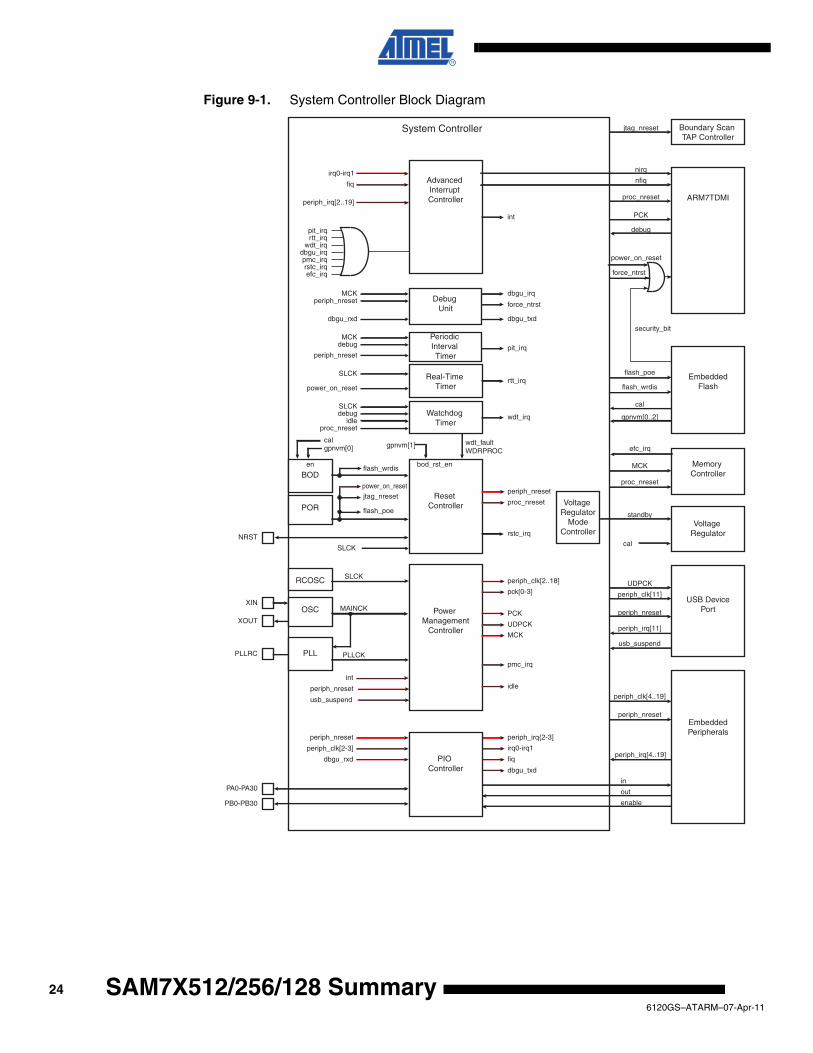
Figure 9-1. System Controller Block Diagram
NRST
SLCK
Advanced Interrupt Controller
Real-Time Timer
Periodic Interval Timer
Reset Controller
PA0-PA30
periph_nreset
System Controller
Watchdog Timer
wdt_faultWDRPROC
PIO Controller
POR
BOD
RCOSC
gpnvm[0]cal
en
Power Management
Controller
OSC
PLL
XIN
XOUT
PLLRC
MAINCK
PLLCK
pit_irq
MCK
proc_nreset
wdt_irq
periph_irq{2-3]periph_nreset
periph_clk[2..18]
PCK
MCK
pmc_irq
UDPCK
nirq
nfiq
rtt_irq
EmbeddedPeripherals
periph_clk[2-3]
pck[0-3]
in
out
enable
ARM7TDMI
SLCK
SLCK
irq0-irq1
fiq
irq0-irq1
fiq
periph_irq[4..19]
periph_irq[2..19]
int
int
periph_nreset
periph_clk[4..19]
EmbeddedFlash
flash_poe
jtag_nreset
flash_poe
gpnvm[0..2]
flash_wrdis
flash_wrdis
proc_nreset
periph_nreset
dbgu_txd
dbgu_rxd
pit_irqrtt_irq
dbgu_irqpmc_irq
rstc_irq
wdt_irq
rstc_irqefc_irq
SLCK
gpnvm[1]
Boundary Scan TAP Controller
jtag_nreset
power_on_reset
debug
PCK
debugidle
debug
Memory Controller
MCK
proc_nreset
bod_rst_en
proc_nreset
power_on_reset
periph_nreset
idle
Debug Unit
dbgu_irqMCK
dbgu_rxd
periph_nreset force_ntrst
dbgu_txd
USB DevicePort
UDPCK
periph_nreset
periph_clk[11]
periph_irq[11]
usb_suspend
usb_suspend
Voltage Regulator
standby
Voltage Regulator
ModeController
security_bit
cal
power_on_reset
force_ntrst
cal
PB0-PB30
efc_irq
246120GS–ATARM–07-Apr-11
SAM7X512/256/128 Summary
SAM7X512/256/128 Summary
9.1 Reset Controller • Based on one power-on reset cell and one brownout detector
• Status of the last reset, either Power-up Reset, Software Reset, User Reset, Watchdog Reset, Brownout Reset
• Controls the internal resets and the NRST pin output
• Allows to shape a signal on the NRST line, guaranteeing that the length of the pulse meets any requirement.
9.1.1 Brownout Detector and Power-on ResetThe SAM7X512/256/128 embeds one brownout detection circuit and a power-on reset cell. Thepower-on reset is supplied with and monitors VDDCORE.
Both signals are provided to the Flash to prevent any code corruption during power-up or power-down sequences or if brownouts occur on the power supplies.
The power-on reset cell has a limited-accuracy threshold at around 1.5V. Its output remains lowduring power-up until VDDCORE goes over this voltage level. This signal goes to the reset con-troller and allows a full re-initialization of the device.
The brownout detector monitors the VDDCORE and VDDFLASH levels during operation bycomparing them to a fixed trigger level. It secures system operations in the most difficult environ-ments and prevents code corruption in case of brownout on the VDDCORE or VDDFLASH.
When the brownout detector is enabled and VDDCORE decreases to a value below the triggerlevel (Vbot18-, defined as Vbot18 - hyst/2), the brownout output is immediately activated.
When VDDCORE increases above the trigger level (Vbot18+, defined as Vbot18 + hyst/2), thereset is released. The brownout detector only detects a drop if the voltage on VDDCORE staysbelow the threshold voltage for longer than about 1µs.
The VDDCORE threshold voltage has a hysteresis of about 50 mV, to ensure spike free brown-out detection. The typical value of the brownout detector threshold is 1.68V with an accuracy of± 2% and is factory calibrated.
When the brownout detector is enabled and VDDFLASH decreases to a value below the triggerlevel (Vbot33-, defined as Vbot33 - hyst/2), the brownout output is immediately activated.
When VDDFLASH increases above the trigger level (Vbot33+, defined as Vbot33 + hyst/2), thereset is released. The brownout detector only detects a drop if the voltage on VDDCORE staysbelow the threshold voltage for longer than about 1µs.
The VDDFLASH threshold voltage has a hysteresis of about 50 mV, to ensure spike free brown-out detection. The typical value of the brownout detector threshold is 2.80V with an accuracy of± 3.5% and is factory calibrated.
The brownout detector is low-power, as it consumes less than 28 µA static current. However, itcan be deactivated to save its static current. In this case, it consumes less than 1µA. The deac-tivation is configured through the GPNVM bit 0 of the Flash.
256120GS–ATARM–07-Apr-11
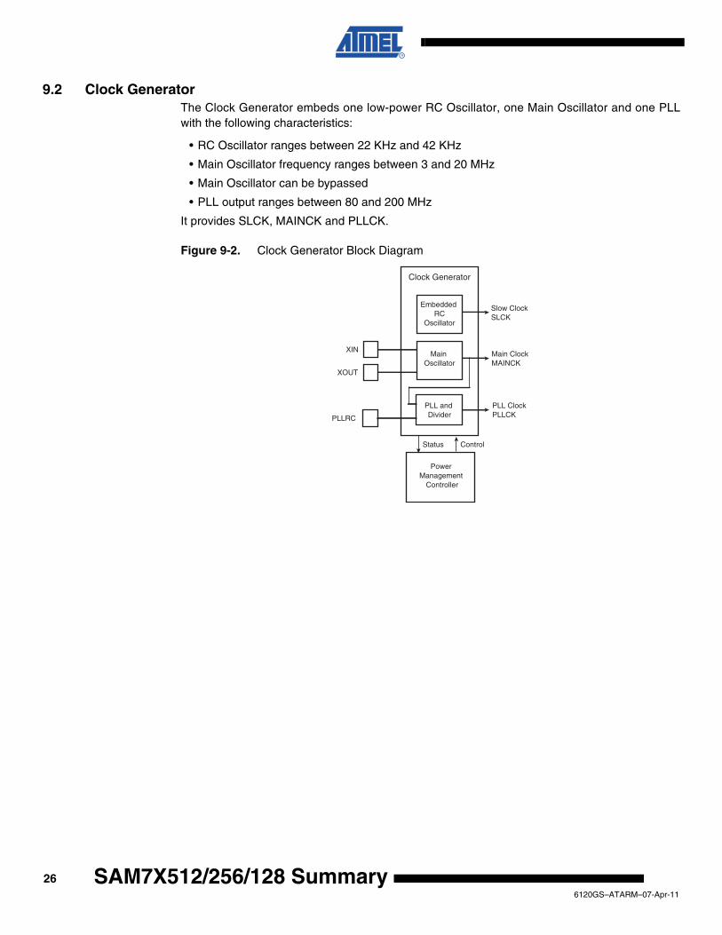
9.2 Clock GeneratorThe Clock Generator embeds one low-power RC Oscillator, one Main Oscillator and one PLLwith the following characteristics:
• RC Oscillator ranges between 22 KHz and 42 KHz
• Main Oscillator frequency ranges between 3 and 20 MHz
• Main Oscillator can be bypassed
• PLL output ranges between 80 and 200 MHz
It provides SLCK, MAINCK and PLLCK.
Figure 9-2. Clock Generator Block Diagram
Embedded RC
Oscillator
Main Oscillator
PLL and Divider
Clock Generator
Power Management
Controller
XIN
XOUT
PLLRC
Slow Clock SLCK
Main ClockMAINCK
PLL ClockPLLCK
ControlStatus
266120GS–ATARM–07-Apr-11
SAM7X512/256/128 Summary
SAM7X512/256/128 Summary
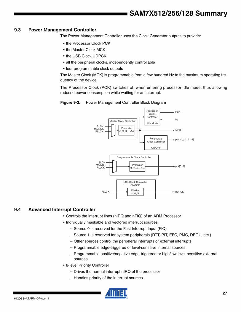
9.3 Power Management ControllerThe Power Management Controller uses the Clock Generator outputs to provide:
• the Processor Clock PCK
• the Master Clock MCK
• the USB Clock UDPCK
• all the peripheral clocks, independently controllable
• four programmable clock outputs
The Master Clock (MCK) is programmable from a few hundred Hz to the maximum operating fre-quency of the device.
The Processor Clock (PCK) switches off when entering processor idle mode, thus allowingreduced power consumption while waiting for an interrupt.
Figure 9-3. Power Management Controller Block Diagram
9.4 Advanced Interrupt Controller• Controls the interrupt lines (nIRQ and nFIQ) of an ARM Processor
• Individually maskable and vectored interrupt sources
– Source 0 is reserved for the Fast Interrupt Input (FIQ)
– Source 1 is reserved for system peripherals (RTT, PIT, EFC, PMC, DBGU, etc.)
– Other sources control the peripheral interrupts or external interrupts
– Programmable edge-triggered or level-sensitive internal sources
– Programmable positive/negative edge-triggered or high/low level-sensitive external sources
• 8-level Priority Controller
– Drives the normal interrupt nIRQ of the processor
– Handles priority of the interrupt sources
MCK
periph_clk[2..18]
int
UDPCK
SLCKMAINCK
PLLCKPrescaler
/1,/2,/4,...,/64
PCKProcessor Clock
Controller
Idle ModeMaster Clock Controller
PeripheralsClock Controller
ON/OFF
USB Clock ControllerON/OFF
SLCKMAINCKPLLCK
Prescaler/1,/2,/4,...,/64
Programmable Clock Controller
PLLCK Divider/1,/2,/4
pck[0..3]
276120GS–ATARM–07-Apr-11
– Higher priority interrupts can be served during service of lower priority interrupt
• Vectoring
– Optimizes interrupt service routine branch and execution
– One 32-bit vector register per interrupt source
– Interrupt vector register reads the corresponding current interrupt vector
• Protect Mode
– Easy debugging by preventing automatic operations
• Fast Forcing
– Permits redirecting any interrupt source on the fast interrupt
• General Interrupt Mask
– Provides processor synchronization on events without triggering an interrupt
9.5 Debug Unit• Comprises:
– One two-pin UART
– One Interface for the Debug Communication Channel (DCC) support
– One set of Chip ID Registers
– One Interface providing ICE Access Prevention
• Two-pin UART
– USART-compatible User Interface
– Programmable Baud Rate Generator
– Parity, Framing and Overrun Error
– Automatic Echo, Local Loopback and Remote Loopback Channel Modes
• Debug Communication Channel Support
– Offers visibility of COMMRX and COMMTX signals from the ARM Processor
• Chip ID Registers
– Identification of the device revision, sizes of the embedded memories, set of peripherals
– Chip ID is 0x275C 0A40 (MRL A) for SAM7X512
– Chip ID is 0x275B 0940 (MRL A or B) for SAM7X256
– Chip ID is 0x275B 0942 (MRL C) for SAM7X256
– Chip ID is 0x275A 0740 (MRL A or B) for SAM7X128
– Chip ID is 0x275A 0742 (MRL C) for SAM7X128
9.6 Periodic Interval Timer• 20-bit programmable counter plus 12-bit interval counter
9.7 Watchdog Timer• 12-bit key-protected Programmable Counter running on prescaled SLCK
• Provides reset or interrupt signals to the system
• Counter may be stopped while the processor is in debug state or in idle mode
286120GS–ATARM–07-Apr-11
SAM7X512/256/128 Summary
SAM7X512/256/128 Summary
9.8 Real-time Timer• 32-bit free-running counter with alarm running on prescaled SLCK
• Programmable 16-bit prescaler for SLCK accuracy compensation
9.9 PIO Controllers• Two PIO Controllers, each controlling 31 I/O lines
• Fully programmable through set/clear registers
• Multiplexing of two peripheral functions per I/O line
• For each I/O line (whether assigned to a peripheral or used as general-purpose I/O)
– Input change interrupt
– Half a clock period glitch filter
– Multi-drive option enables driving in open drain
– Programmable pull-up on each I/O line
– Pin data status register, supplies visibility of the level on the pin at any time
• Synchronous output, provides Set and Clear of several I/O lines in a single write
9.10 Voltage Regulator ControllerThe purpose of this controller is to select the Power Mode of the Voltage Regulator betweenNormal Mode (bit 0 is cleared) or Standby Mode (bit 0 is set).
296120GS–ATARM–07-Apr-11
10. Peripherals
10.1 User InterfaceThe User Peripherals are mapped in the 256 Mbytes of address space between 0xF000 0000and 0xFFFF EFFF. Each peripheral is allocated 16 Kbytes of address space.
A complete memory map is provided in Figure 8-1 on page 18.
10.2 Peripheral IdentifiersThe SAM7X512/256/128 embeds a wide range of peripherals. Table 10-1 defines the PeripheralIdentifiers of the SAM7X512/256/128. Unique peripheral identifiers are defined for both theAdvanced Interrupt Controller and the Power Management Controller.
Note: 1. Setting SYSC and ADC bits in the clock set/clear registers of the PMC has no effect. The Sys-tem Controller and ADC are continuously clocked.
Table 10-1. Peripheral Identifiers
Peripheral ID Peripheral Mnemonic Peripheral NameExternal Interrupt
0 AIC Advanced Interrupt Controller FIQ
1 SYSC(1) System Controller
2 PIOA Parallel I/O Controller A
3 PIOB Parallel I/O Controller B
4 SPI0 Serial Peripheral Interface 0
5 SPI1 Serial Peripheral Interface 1
6 US0 USART 0
7 US1 USART 1
8 SSC Synchronous Serial Controller
9 TWI Two-wire Interface
10 PWMC Pulse Width Modulation Controller
11 UDP USB Device Port
12 TC0 Timer/Counter 0
13 TC1 Timer/Counter 1
14 TC2 Timer/Counter 2
15 CAN CAN Controller
16 EMAC Ethernet MAC
17 ADC(1) Analog-to Digital Converter
18 - 29 Reserved
30 AIC Advanced Interrupt Controller IRQ0
31 AIC Advanced Interrupt Controller IRQ1
306120GS–ATARM–07-Apr-11
SAM7X512/256/128 Summary
SAM7X512/256/128 Summary
10.3 Peripheral Multiplexing on PIO LinesThe SAM7X512/256/128 features two PIO controllers, PIOA and PIOB, that multiplex the I/Olines of the peripheral set.
Each PIO Controller controls 31 lines. Each line can be assigned to one of two peripheral func-tions, A or B. Some of them can also be multiplexed with the analog inputs of the ADCController.
Table 10-2 on page 32 and Table 10-3 on page 33 defines how the I/O lines of the peripherals A,B or the analog inputs are multiplexed on the PIO Controller A and PIO Controller B. The twocolumns “Function” and “Comments” have been inserted for the user’s own comments; they maybe used to track how pins are defined in an application.
Note that some peripheral functions that are output only, may be duplicated in the table.
At reset, all I/O lines are automatically configured as input with the programmable pull-upenabled, so that the device is maintained in a static state as soon as a reset is detected.
316120GS–ATARM–07-Apr-11
10.4 PIO Controller A Multiplexing
Table 10-2. Multiplexing on PIO Controller A
PIO Controller A Application Usage
I/O Line Peripheral A Peripheral B Comments Function Comments
PA0 RXD0 High-Drive
PA1 TXD0 High-Drive
PA2 SCK0 SPI1_NPCS1 High-Drive
PA3 RTS0 SPI1_NPCS2 High-Drive
PA4 CTS0 SPI1_NPCS3
PA5 RXD1
PA6 TXD1
PA7 SCK1 SPI0_NPCS1
PA8 RTS1 SPI0_NPCS2
PA9 CTS1 SPI0_NPCS3
PA10 TWD
PA11 TWCK
PA12 SPI_NPCS0
PA13 SPI0_NPCS1 PCK1
PA14 SPI0_NPCS2 IRQ1
PA15 SPI0_NPCS3 TCLK2
PA16 SPI0_MISO
PA17 SPI0_MOSI
PA18 SPI0_SPCK
PA19 CANRX
PA20 CANTX
PA21 TF SPI1_NPCS0
PA22 TK SPI1_SPCK
PA23 TD SPI1_MOSI
PA24 RD SPI1_MISO
PA25 RK SPI1_NPCS1
PA26 RF SPI1_NPCS2
PA27 DRXD PCK3
PA28 DTXD
PA29 FIQ SPI1_NPCS3
PA30 IRQ0 PCK2
326120GS–ATARM–07-Apr-11
SAM7X512/256/128 Summary
SAM7X512/256/128 Summary
10.5 PIO Controller B Multiplexing
Table 10-3. Multiplexing on PIO Controller B
PIO Controller B Application Usage
I/O Line Peripheral A Peripheral B Comments Function Comments
PB0 ETXCK/EREFCK PCK0
PB1 ETXEN
PB2 ETX0
PB3 ETX1
PB4 ECRS
PB5 ERX0
PB6 ERX1
PB7 ERXER
PB8 EMDC
PB9 EMDIO
PB10 ETX2 SPI1_NPCS1
PB11 ETX3 SPI1_NPCS2
PB12 ETXER TCLK0
PB13 ERX2 SPI0_NPCS1
PB14 ERX3 SPI0_NPCS2
PB15 ERXDV/ECRSDV
PB16 ECOL SPI1_NPCS3
PB17 ERXCK SPI0_NPCS3
PB18 EF100 ADTRG
PB19 PWM0 TCLK1
PB20 PWM1 PCK0
PB21 PWM2 PCK1
PB22 PWM3 PCK2
PB23 TIOA0 DCD1
PB24 TIOB0 DSR1
PB25 TIOA1 DTR1
PB26 TIOB1 RI1
PB27 TIOA2 PWM0 AD0
PB28 TIOB2 PWM1 AD1
PB29 PCK1 PWM2 AD2
PB30 PCK2 PWM3 AD3
336120GS–ATARM–07-Apr-11
10.6 Ethernet MAC• DMA Master on Receive and Transmit Channels
• Compatible with IEEE Standard 802.3
• 10 and 100 Mbit/s operation
• Full- and half-duplex operation
• Statistics Counter Registers
• MII/RMII interface to the physical layer
• Interrupt generation to signal receive and transmit completion
• 28-byte transmit FIFO and 28-byte receive FIFO
• Automatic pad and CRC generation on transmitted frames
• Automatic discard of frames received with errors
• Address checking logic supports up to four specific 48-bit addresses
• Support Promiscuous Mode where all valid received frames are copied to memory
• Hash matching of unicast and multicast destination addresses
• Physical layer management through MDIO interface
• Half-duplex flow control by forcing collisions on incoming frames
• Full-duplex flow control with recognition of incoming pause frames
• Support for 802.1Q VLAN tagging with recognition of incoming VLAN and priority tagged frames
• Multiple buffers per receive and transmit frame
• Jumbo frames up to 10240 bytes supported
10.7 Serial Peripheral Interface• Supports communication with external serial devices
– Four chip selects with external decoder allow communication with up to 15 peripherals
– Serial memories, such as DataFlash® and 3-wire EEPROMs
– Serial peripherals, such as ADCs, DACs, LCD Controllers, CAN Controllers and Sensors
– External co-processors
• Master or slave serial peripheral bus interface
– 8- to 16-bit programmable data length per chip select
– Programmable phase and polarity per chip select
– Programmable transfer delays per chip select, between consecutive transfers and between clock and data
– Programmable delay between consecutive transfers
– Selectable mode fault detection
– Maximum frequency at up to Master Clock
10.8 Two-wire Interface• Master Mode only
• Compatibility with I2C compatible devices (refer to the TWI section of the datasheet)
346120GS–ATARM–07-Apr-11
SAM7X512/256/128 Summary
SAM7X512/256/128 Summary
• One, two or three bytes internal address registers for easy Serial Memory access
• 7-bit or 10-bit slave addressing
• Sequential read/write operations
10.9 USART• Programmable Baud Rate Generator
• 5- to 9-bit full-duplex synchronous or asynchronous serial communications
– 1, 1.5 or 2 stop bits in Asynchronous Mode
– 1 or 2 stop bits in Synchronous Mode
– Parity generation and error detection
– Framing error detection, overrun error detection
– MSB or LSB first
– Optional break generation and detection
– By 8 or by 16 over-sampling receiver frequency
– Hardware handshaking RTS - CTS
– Modem Signals Management DTR-DSR-DCD-RI on USART1
– Receiver time-out and transmitter timeguard
– Multi-drop Mode with address generation and detection
• RS485 with driver control signal
• ISO7816, T = 0 or T = 1 Protocols for interfacing with smart cards
– NACK handling, error counter with repetition and iteration limit
• IrDA modulation and demodulation
– Communication at up to 115.2 Kbps
• Test Modes
– Remote Loopback, Local Loopback, Automatic Echo
10.10 Serial Synchronous Controller• Provides serial synchronous communication links used in audio and telecom applications
• Contains an independent receiver and transmitter and a common clock divider
• Offers a configurable frame sync and data length
• Receiver and transmitter can be programmed to start automatically or on detection of different event on the frame sync signal
• Receiver and transmitter include a data signal, a clock signal and a frame synchronization signal
10.11 Timer Counter• Three 16-bit Timer Counter Channels
– Two output compare or one input capture per channel
• Wide range of functions including:
– Frequency measurement
– Event counting
– Interval measurement
356120GS–ATARM–07-Apr-11
– Pulse generation
– Delay timing
– Pulse Width Modulation
– Up/down capabilities
• Each channel is user-configurable and contains:
– Three external clock inputs
• Five internal clock inputs, as defined in Table 10-4
– Two multi-purpose input/output signals
– Two global registers that act on all three TC channels
10.12 Pulse Width Modulation Controller• Four channels, one 16-bit counter per channel
• Common clock generator, providing thirteen different clocks
– One Modulo n counter providing eleven clocks
– Two independent linear dividers working on modulo n counter outputs
• Independent channel programming
– Independent enable/disable commands
– Independent clock selection
– Independent period and duty cycle, with double buffering
– Programmable selection of the output waveform polarity
– Programmable center or left aligned output waveform
10.13 USB Device Port• USB V2.0 full-speed compliant,12 Mbits per second
• Embedded USB V2.0 full-speed transceiver
• Embedded 1352-byte dual-port RAM for endpoints
• Six endpoints
– Endpoint 0: 8 bytes
– Endpoint 1 and 2: 64 bytes ping-pong
– Endpoint 3: 64 bytes
– Endpoint 4 and 5: 256 bytes ping-pong
– Ping-pong Mode (two memory banks) for bulk endpoints
• Suspend/resume logic
Table 10-4. Timer Counter Clocks Assignment
TC Clock input Clock
TIMER_CLOCK1 MCK/2
TIMER_CLOCK2 MCK/8
TIMER_CLOCK3 MCK/32
TIMER_CLOCK4 MCK/128
TIMER_CLOCK5 MCK/1024
366120GS–ATARM–07-Apr-11
SAM7X512/256/128 Summary
SAM7X512/256/128 Summary
10.14 CAN Controller• Fully compliant with CAN 2.0A and 2.0B
• Bit rates up to 1Mbit/s
• Eight object oriented mailboxes each with the following properties:
– CAN Specification 2.0 Part A or 2.0 Part B Programmable for each Message
– Object configurable to receive (with overwrite or not) or transmit
– Local tag and mask filters up to 29-bit identifier/channel
– 32-bit access to data registers for each mailbox data object
– Uses a 16-bit time stamp on receive and transmit message
– Hardware concatenation of ID unmasked bitfields to speedup family ID processing
– 16-bit internal timer for time stamping and network synchronization
– Programmable reception buffer length up to 8 mailbox objects
– Priority management between transmission mailboxes
– Autobaud and listening mode
– Low power mode and programmable wake-up on bus activity or by the application
– Data, remote, error and overload frame handling
10.15 Analog-to-Digital Converter• 8-channel ADC
• 10-bit 384 K samples/sec. Successive Approximation Register ADC
• ±2 LSB Integral Non Linearity, ±1 LSB Differential Non Linearity
• Integrated 8-to-1 multiplexer, offering eight independent 3.3V analog inputs
• External voltage reference for better accuracy on low voltage inputs
• Individual enable and disable of each channel
• Multiple trigger sources
– Hardware or software trigger
– External trigger pin
– Timer Counter 0 to 2 outputs TIOA0 to TIOA2 trigger
• Sleep Mode and conversion sequencer
– Automatic wakeup on trigger and back to sleep mode after conversions of all enabled channels
• Four of eight analog inputs shared with digital signals
376120GS–ATARM–07-Apr-11
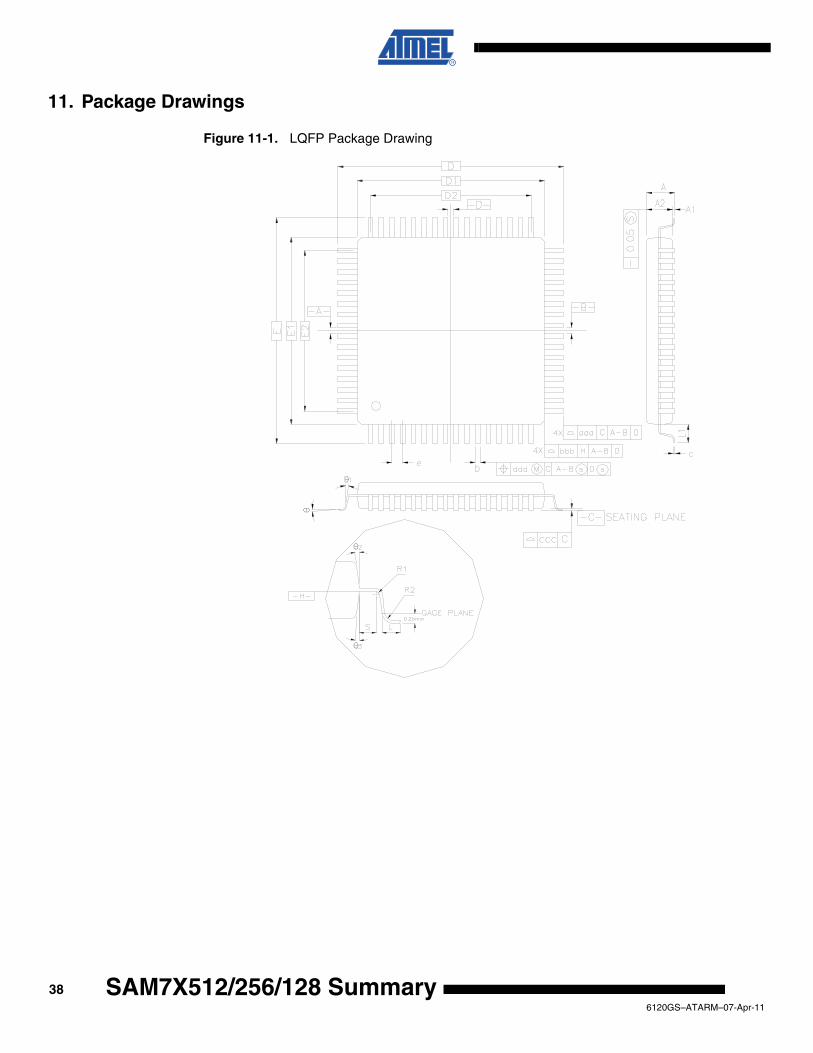
11. Package Drawings
Figure 11-1. LQFP Package Drawing
386120GS–ATARM–07-Apr-11
SAM7X512/256/128 Summary
SAM7X512/256/128 Summary
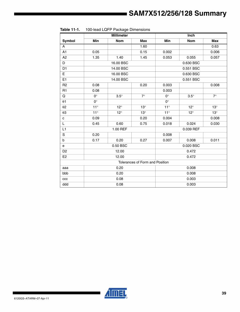
Table 11-1. 100-lead LQFP Package Dimensions
Symbol
Millimeter Inch
Min Nom Max Min Nom Max
A 1.60 0.63
A1 0.05 0.15 0.002 0.006
A2 1.35 1.40 1.45 0.053 0.055 0.057
D 16.00 BSC 0.630 BSC
D1 14.00 BSC 0.551 BSC
E 16.00 BSC 0.630 BSC
E1 14.00 BSC 0.551 BSC
R2 0.08 0.20 0.003 0.008
R1 0.08 0.003
Q 0° 3.5° 7° 0° 3.5° 7°θ1 0° 0°θ2 11° 12° 13° 11° 12° 13°θ3 11° 12° 13° 11° 12° 13°c 0.09 0.20 0.004 0.008
L 0.45 0.60 0.75 0.018 0.024 0.030
L1 1.00 REF 0.039 REF
S 0.20 0.008
b 0.17 0.20 0.27 0.007 0.008 0.011
e 0.50 BSC 0.020 BSC
D2 12.00 0.472
E2 12.00 0.472
Tolerances of Form and Position
aaa 0.20 0.008
bbb 0.20 0.008
ccc 0.08 0.003
ddd 0.08 0.003
396120GS–ATARM–07-Apr-11
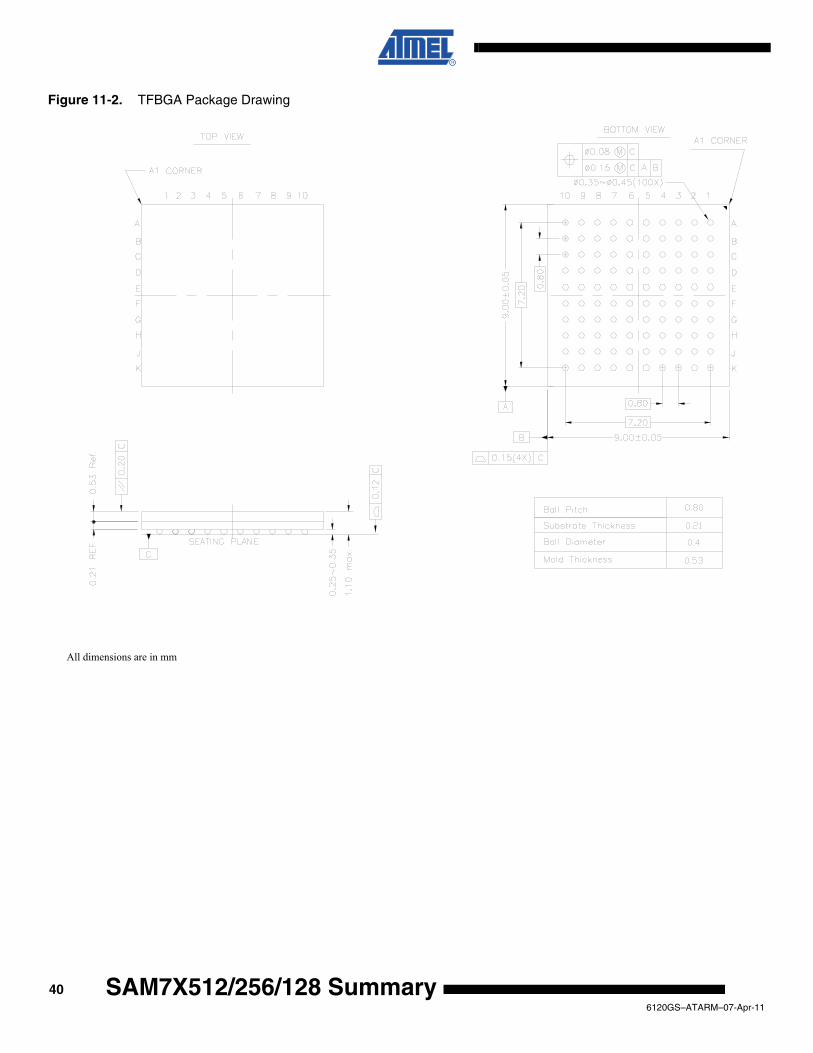
Figure 11-2. TFBGA Package Drawing
All dimensions are in mm
406120GS–ATARM–07-Apr-11
SAM7X512/256/128 Summary
SAM7X512/256/128 Summary
12. Ordering Information
Table 12-1. Ordering Information
MLR AOrdering Code
MLR BOrdering Code
MLR COrdering Code Package Package Type
Temperature Operating Range
AT91SAM7X512-AU
AT91SAM7X512-CU–
LQFP 100
TFBGA 100Green
Industrial(-40⋅ C to 85⋅ C)
AT91SAM7X256-AU
AT91SAM7X256-CU
AT91SAM7X256B-AU
AT91SAM7X256B-CU
AT91SAM7X256C-AU
AT91SAM7X256C-CU
LQFP 100
TFBGA 100Green
Industrial(-40⋅ C to 85⋅ C)
AT91SAM7X128-AU
AT91SAM7X128-CU
AT91SAM7X128B-AU
AT91SAM7X128B-CU
AT91SAM7X128C-AU
AT91SAM7X128C-CU
LQFP 100
TFBGA 100Green
Industrial(-40⋅ C to 85⋅ C)
416120GS–ATARM–07-Apr-11
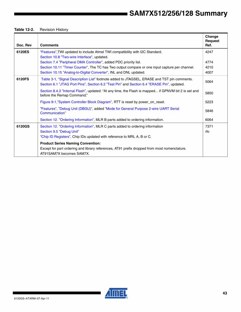
Revision History
Table 12-2. Revision History
Doc. Rev Comments
Change Request Ref.
6120AS First issue - Unqualified on Intranet
Legal page updated.Qualified on Intranet
6120BS
Corrections to maintain consistency with full datasheet:In “Features” on page 1, corrected Page Programming Time and Full Erase Time; corrected number of PDC channels, removed Wake-on-LAN support.In Figure 2-1 on page 4, corrected number of PDC channels.
In Figure 2-1 on page 4, Table 3-1 on page 5, Table 10-2 on page 32 and Table 10-3 on page 33, changed all SPI pin names.
In Section 5.2 “Power Consumption” on page 11, changed value of static current level and value of dynamic power consumption level on VDDCORE
In Section 6.2 “Test Pin” on page 13, removed reference to SAM-BA boot recovery.
In Section 6.6 “I/O Lines Current Drawing” on page 14, changed value of total current level.In Section 7.4 “Peripheral DMA Controller” on page 16, corrected number of PDC channels.
In Section 8. “Memories” on page 17, corrected Page Programming Time and Full Erase Time.
In Section 8.7 “SAM-BA Boot Assistant” on page 22, updated section.In Figure 9-1 on page 24, changed range of periph_irq and periph_clk on AIC and for Embedded Peripherals block.In Section 10.6 “Ethernet MAC” on page 34, updated features.
CSR 05-388
6120CS Update to product functionalities including changes to “Features” on page 1, Figure 2-1 on page 4, Section 9.5 “Debug Unit” on page 28 and to Peripheral mapping.
05-457 05-462
Updated PLL output range max value in Section 9.2 “Clock Generator” on page 26. 05-491
Updated information in Section 5.1 “Power Supplies” on page 11.
Updated ordering information in “Ordering Information” on page 41. 05-471
6120DSAdded AT91SAM7X512 to product family.“Features” on page 1 and global
Reformatted Memories Section 8. “Memories” on page 17. Reordered sub sections in Peripherals Section 10. “Peripherals” on page 30
Consolidated Memory Mapping in Figure 8-1 on page 18.
Added TFBGA information Section 4.3 “100-ball TFBGA Package Outline” on page 10.added LQFP and TFBGA package drawings Section 11. on page 38.
27232728
System Controller block diagram Figure 9-1 on page 24, “ice_nreset” signals changed to “power_on_reset”.Section 10.1 ”User Interface” User Peripherals are mapped between 0xF000 0000 and 0XFFFF EFFF.
Table 10-1 on page 30 SYSIRQ changed to SYSC in “Peripheral Identifiers”
rfo review
426120GS–ATARM–07-Apr-11
SAM7X512/256/128 Summary
SAM7X512/256/128 Summary
6120ES “Features”,TWI updated to include Atmel TWI compatibility with I2C Standard.Section 10.8 ”Two-wire Interface”, updated.
Section 7.4 ”Peripheral DMA Controller”, added PDC priority list.
Section 10.11 ”Timer Counter”, The TC has Two output compare or one input capture per channel.
Section 10.15 ”Analog-to-Digital Converter”, INL and DNL updated.
4247
4774
4210
4007
6120FS Table 3-1, “Signal Description List” footnote added to JTAGSEL, ERASE and TST pin comments.
Section 6.1 ”JTAG Port Pins”, Section 6.2 ”Test Pin” and Section 6.4 ”ERASE Pin”, updated.5064
Section 8.4.3 ”Internal Flash”, updated: “At any time, the Flash is mapped... if GPNVM bit 2 is set and before the Remap Command.”
5850
Figure 9-1,”System Controller Block Diagram”, RTT is reset by power_on_reset. 5223
”Features”, ”Debug Unit (DBGU)”, added ”Mode for General Purpose 2-wire UART Serial Communication”
5846
Section 12. ”Ordering Information”, MLR B parts added to ordering information. 6064
6120GS Section 12. ”Ordering Information”, MLR C parts added to ordering information
Section 9.5 ”Debug Unit”“Chip ID Registers”, Chip IDs updated with reference to MRL A, B or C.
7371
rfo
Product Series Naming Convention:Except for part ordering and library references, AT91 prefix dropped from most nomenclature.
AT91SAM7X becomes SAM7X.
Table 12-2. Revision History
Doc. Rev Comments
Change Request Ref.
436120GS–ATARM–07-Apr-11
6120GS–ATARM–07-Apr-11
Headquarters International
Atmel Corporation2325 Orchard ParkwaySan Jose, CA 95131USATel: (+1) (408) 441-0311Fax: (+1) (408) 487-2600
Atmel Asia LimitedUnit 01-5 & 16, 19FBEA Tower, Millennium City 5418 Kwun Tong RoadKwun Tong, KowloonHONG KONGTel: (+852) 2245-6100Fax: (+852) 2722-1369
Atmel Munich GmbHBusiness CampusParkring 4D-85748 Garching b. MunichGERMANYTel: (+49) 89-31970-0 Fax: (+49) 89-3194621
Atmel Japan9F, Tonetsu Shinkawa Bldg.1-24-8 ShinkawaChuo-ku, Tokyo 104-0033JAPANTel: (81) 3-3523-3551Fax: (81) 3-3523-7581
Product Contact
Web Sitewww.atmel.comwww.atmel.com/AT91SAM
Technical SupportAT91SAM SupportAtmel techincal support
Sales Contactswww.atmel.com/contacts/
Literature Requestswww.atmel.com/literature
Disclaimer: The information in this document is provided in connection with Atmel products. No license, express or implied, by estoppel or otherwise, to anyintellectual property right is granted by this document or in connection with the sale of Atmel products. EXCEPT AS SET FORTH IN ATMEL’S TERMS AND CONDI-TIONS OF SALE LOCATED ON ATMEL’S WEB SITE, ATMEL ASSUMES NO LIABILITY WHATSOEVER AND DISCLAIMS ANY EXPRESS, IMPLIED OR STATUTORYWARRANTY RELATING TO ITS PRODUCTS INCLUDING, BUT NOT LIMITED TO, THE IMPLIED WARRANTY OF MERCHANTABILITY, FITNESS FOR A PARTICULARPURPOSE, OR NON-INFRINGEMENT. IN NO EVENT SHALL ATMEL BE LIABLE FOR ANY DIRECT, INDIRECT, CONSEQUENTIAL, PUNITIVE, SPECIAL OR INCIDEN-TAL DAMAGES (INCLUDING, WITHOUT LIMITATION, DAMAGES FOR LOSS OF PROFITS, BUSINESS INTERRUPTION, OR LOSS OF INFORMATION) ARISING OUTOF THE USE OR INABILITY TO USE THIS DOCUMENT, EVEN IF ATMEL HAS BEEN ADVISED OF THE POSSIBILITY OF SUCH DAMAGES. Atmel makes norepresentations or warranties with respect to the accuracy or completeness of the contents of this document and reserves the right to make changes to specifica-tions and product descriptions at any time without notice. Atmel does not make any commitment to update the information contained herein. Unless specifically pro-vided otherwise, Atmel products are not suitable for, and shall not be used in, automotive applications. Atmel’s products are not intended, authorized, or warrantedfor use as components in applications intended to support or sustain life.
© 2011 Atmel Corporation. All rights reserved. Atmel®, Atmel logo and combinations thereof, DataFlash®, SAM-BA® and others, are regis-tered trademarks and others are trademarks of Atmel Corporation or its subsidiaries. Windows® and others, are registered trademarks of Micro-soft Corporation in the US and/or other countries. ARM®, the ARM Powered® logo and others, are registered trademarks or trademarks of ARMLimited. Other terms and product names may be the trademarks of others.