pir 8-bit flash mcu - · pdf filerev. 1.20 8 an a 21 201 rev. 1.20 9 an a 21 201 ht45f0027...
TRANSCRIPT

PIR 8-Bit Flash MCU
HT45F0027
Revision: V1.20 Date: ana 21 201ana 21 201

Rev. 1.20 2 ana 21 201 Rev. 1.20 3 ana 21 201
HT45F0027PIR 8-Bit Flash MCU
HT45F0027PIR 8-Bit Flash MCU
Table of Contents
Features ............................................................................................................ 6CPU Feates ......................................................................................................................... Peipheal Feates .................................................................................................................
General Description ......................................................................................... 7Block Diagram .................................................................................................. 7Pin Assignment ................................................................................................ 8Pin Description ................................................................................................ 8Absolute Maximum Ratings .......................................................................... 10D.C. Characteristics ....................................................................................... 10A.C. Characteristics ....................................................................................... 12OP Amplifier Characteristics ........................................................................ 13LDO Characteristics ...................................................................................... 13A/D Converter Characteristics ...................................................................... 14Temperature Sensor Characteristics ........................................................... 14Power-on Reset Characteristics ................................................................... 14System Architecture ...................................................................................... 15
Clocking and Pipelining ......................................................................................................... 15Pogam Conte ................................................................................................................... 1Stack ..................................................................................................................................... 17Aithmetic and Logic Unit – ALU ........................................................................................... 17
Flash Program Memory ................................................................................. 18Stcte ................................................................................................................................ 18Special Vectos ..................................................................................................................... 18Look-p Table ........................................................................................................................ 18Table Pogam Example ........................................................................................................ 19On-Chip Debug Support OCDS ......................................................................................... 20
RAM Data Memory ......................................................................................... 20Stcte ................................................................................................................................ 20
Special Function Register Description ........................................................ 22Indiect Addessing Registe – IAR0 IAR1 ........................................................................... 22Memo Pointes – MP0 MP1 ............................................................................................. 22Bank Pointe – BP ................................................................................................................ 23Accmlato – ACC ............................................................................................................... 23Pogam Conte Low Registe – PCL ................................................................................. 23Look-p Table Registes – TBLP TBHP TBLH .................................................................... 23Stats Registe – STATUS ................................................................................................... 24

Rev. 1.20 2 ana 21 201 Rev. 1.20 3 ana 21 201
HT45F0027PIR 8-Bit Flash MCU
HT45F0027PIR 8-Bit Flash MCU
EEPROM Data memory ................................................................................. 26EEPROM Data Memo Stcte ........................................................................................ 2EEPROM Registes .............................................................................................................. 2Reading Data fom the EEPROM ......................................................................................... 28Witing Data to the EEPROM ................................................................................................ 28Wite Potection ..................................................................................................................... 28EEPROM Intept ................................................................................................................ 28Pogamming Consideations ................................................................................................ 29
Oscillator ........................................................................................................ 30Oscillato Oveview .............................................................................................................. 30System Clock Configurations ............................................................................................... 30Intenal RC Oscillato – HIRC .............................................................................................. 31Intenal 32kHz Oscillato – LIRC .......................................................................................... 31Spplementa Oscillato ...................................................................................................... 31
Operating Modes and System Clocks ........................................................ 31Sstem Clocks ..................................................................................................................... 31Sstem Opeation Modes ..................................................................................................... 32Contol Registe .................................................................................................................... 34Opeating Mode Switching ................................................................................................... 35Standb Cent Consideations .......................................................................................... 39Wake-p ............................................................................................................................... 39
Watchdog Timer ............................................................................................. 40Watchdog Time Clock Soce .............................................................................................. 40Watchdog Time Contol Registe ......................................................................................... 40Watchdog Time Opeation ................................................................................................... 41
Reset and Initialisation .................................................................................. 42Reset Fnctions ................................................................................................................... 42Reset Initial Conditions ......................................................................................................... 45
Input/Output Ports ........................................................................................ 47Pll-high Resistos ................................................................................................................ 47Pot A Wake-p ..................................................................................................................... 48I/O Pot Contol Registes ..................................................................................................... 48Pin-emapping Fnction ........................................................................................................ 49I/O Pin Stctes .................................................................................................................. 50Pogamming Consideations ............................................................................................... 51
Timer/Event Counters ................................................................................... 51Configuring the Timer/Event Counter Input Clock Source .................................................... 52Time Registes – TMR0 TMR1 ........................................................................................... 52Time Contol Registes – TMR0C TMR1C .......................................................................... 53Time Mode ........................................................................................................................... 54Event Conte Mode ............................................................................................................ 54Plse Width Capte Mode ................................................................................................... 55I/O Intefacing ........................................................................................................................ 5Pogamming Consideations ................................................................................................ 5

Rev. 1.20 4 ana 21 201 Rev. 1.20 5 ana 21 201
HT45F0027PIR 8-Bit Flash MCU
HT45F0027PIR 8-Bit Flash MCU
Analog to Digital Converter – ADC ............................................................... 57A/D Oveview ........................................................................................................................ 57A/D Convete Registe Desciption ...................................................................................... 57A/D Convete Data Registes – ADRL ADRH ..................................................................... 58A/D Convete Contol Registes – ADCR0 ADCR1 ACER ................................................. 58Tempeate Senso Band-Gap Voltage Adjst Registe ...................................................... 1A/D Opeation ....................................................................................................................... 1A/D Refeence Voltage .......................................................................................................... 2A/D Convete Inpt Signal ................................................................................................... 2Convesion Rate and Timing Diagam .................................................................................. 3Smma of A/D Convesion Steps ....................................................................................... 3Pogamming Consideations ................................................................................................ 4A/D Tansfe Fnction ........................................................................................................... 4A/D Pogamming Examples ................................................................................................. 5
Auto Conversion Function ............................................................................ 67Ato Convesion Opeation ................................................................................................... 7Ato Convesion Registes ................................................................................................... 7
Serial Interface Module – SIM ....................................................................... 69SPI Inteface ........................................................................................................................ 9I2C Inteface .......................................................................................................................... 75
LDO Function ................................................................................................. 83Operational Amplifiers .................................................................................. 84
Operational Amplifier Registers ............................................................................................. 84
Interrupts ........................................................................................................ 85Intept Registes ................................................................................................................. 85Intept Opeation ................................................................................................................ 88Extenal Intept ................................................................................................................... 89Ato convesion cicit Intept ............................................................................................ 89Time/Event Conte Intept ............................................................................................... 89Seial Inteface Modle Intept ........................................................................................... 89Mlti-fnction Intept .......................................................................................................... 90A/D Convete Intept ......................................................................................................... 90EEPROM Intept ................................................................................................................ 90LVD Intept ........................................................................................................................ 91Intept Wake-p Fnction ................................................................................................... 91Pogamming Consideations ................................................................................................ 91
Low Voltage Detector – LVD ......................................................................... 92LVD Registe ......................................................................................................................... 92LVD Opeation ....................................................................................................................... 93
Configuration Options ................................................................................... 94Application Circuits ....................................................................................... 95
Rev. 1.20 4 ana 21 201 Rev. 1.20 5 ana 21 201
HT45F0027PIR 8-Bit Flash MCU
HT45F0027PIR 8-Bit Flash MCU
Instruction Set ................................................................................................ 96Intodction ........................................................................................................................... 9Instction Timing .................................................................................................................. 9Moving and Tansfeing Data ............................................................................................... 9Aithmetic Opeations ............................................................................................................ 9Logical and Rotate Opeation ............................................................................................... 97Banches and Contol Tansfe ............................................................................................. 97Bit Opeations ....................................................................................................................... 97Table Read Opeations ......................................................................................................... 97Othe Opeations ................................................................................................................... 97
Instruction Set Summary .............................................................................. 98Table Conventions ................................................................................................................. 98
Instruction Definition ................................................................................... 100Package Information ................................................................................... 109
1-pin NSOP (150mil) Otline Dimensions ..........................................................................110SAW Tpe 1-pin (3mm×3mm FP0.25mm) QFN Otline Dimensions ...............................111

Rev. 1.20 ana 21 201 Rev. 1.20 7 ana 21 201
HT45F0027PIR 8-Bit Flash MCU
HT45F0027PIR 8-Bit Flash MCU
Features
CPU Features• OperatingVoltage
♦ fSYS=32kHz:2.2V~5.5V♦ fSYS=1MHz:2.2V~5.5V♦ fSYS=2MHz:2.2V~5.5V♦ fSYS=4MHz:2.2V~5.5V♦ fSYS=8MHz:3.3V~5.5V
• TinyPowerTMtechnologyforlowpoweroperation
• Powerdownandwake-upfunctionstoreducepowerconsumption
• Oscillators♦ InternalRC–HIRC♦ Internal32kHzRC–LIRC
• Multi-modeoperation:NORMAL,SLOW,IDLEandSLEEP
• Fullyintegratedinternal1/2/4/8MHzoscillatorrequiresnoexternalcomponents
• Allinstructionsexecutedinoneortwoinstructioncycles
• Tablereadinstructions
• 63powerfulinstructions
• 6-levelsubroutinenesting
• Bitmanipulationinstruction
Peripheral Features• FlashProgramMemory:2K×16
• RAMDataMemory:256×8
• EEPROMMemory:32×8
• WatchdogTimerfunction
• 9bidirectionalI/Olines
• Singlepin-sharedexternalinterrupt
• Two8-bitprogrammableTimer/EventCounterswithoverflowinterruptfunction
• 6-channel12-bitresolutionA/Dconverter
• A/Dconverterautoenablefunction
• A/Dconverterlower/upperlimitpreset
• SerialInterfacesModule-SIMforSPIorI2C
• DualOperationalAmplifiersfunctions
• LDOfunction
• InternalTemperatureSensorfunction
• LowVoltageResetfunction
• LowVoltageDetectfunction
• Packagetype:16-pinNSOP/QFN

Rev. 1.20 ana 21 201 Rev. 1.20 7 ana 21 201
HT45F0027PIR 8-Bit Flash MCU
HT45F0027PIR 8-Bit Flash MCU
General DescriptionTheHT45F0027 is aTinyPowerTMA/D type 8-bit high performanceRISC architecturemicrocontroller,designedespeciallyforapplicationsthat interfacedirectly toanalogsignal.Thedeviceincludesanintegratedmulti-channelAnalogtoDigitalConverterandlowpowerinternaloperationalamplifiers.
Offeringusers theconvenienceofFlashMemorymulti-programmingfeatures, thedevicealsoincludeswide rangeof functionsand features.Othermemory includesanareaofRAMDataMemoryaswellasanareaofEEPROMmemoryforstorageofnon-volatiledatasuchasserialnumbers,calibrationdataetc.
TheusualHoltekMCUfeaturessuchaspowerdownandwake-upfunctions,oscillatoroptions,etc.combinetoensureuserapplicationsrequireaminimumofexternalcomponents.
ThebenefitsofanintegratedA/D,SPIandI2Cfunctions, inadditiontolowpowerconsumption,highperformance,I/Oflexibilityandlow-cost,providesthedevicewiththeversatilityforawiderangeofproducts inthehomeapplianceandindustrialapplicationareas.Someoftheseproductscouldincludeelectronicmetering,environmentalmonitoring,handheldinstruments,electronicallycontrolledtools,motordrivingetc.
Block Diagram
8-bitRISCMCUCoe
Flash/EEPROM Pogamming Cicit
Watchdog Time
12-bit A/DConvete
Intenal HIRC/LIRCOscillatos
TimesI/O SIM(I2C/SPI) OPAs
FlashPogam Memo
EEPROMData
Memo
Low Voltage Reset
Low Voltage Detect
InteptContolle
RAMData
Memo
LDO
ResetCicit

Rev. 1.20 8 ana 21 201 Rev. 1.20 9 ana 21 201
HT45F0027PIR 8-Bit Flash MCU
HT45F0027PIR 8-Bit Flash MCU
Pin Assignment
11514131211109
1234578
PA7/OPA1ECOPA1NOPA1EVREG
PB0/AN0/OCDSCKPA1/AN1
VDDVSSA
VOPRPA5/TMR0/OPA2EPA/INT/TMR1/SCK_1/SCL_1PA0/SCK_0/SCL_0/OCDSDAPA4/SCSPA2/SDI/SDAPA3/SDOVSS
HT45F0027/HT45V002716 NSOP-A
1
3
2
45 87
PA3/SDO
VS
S
VS
SA
VDD
12
10
11
9
151 1314OPA1E
VREG
PB0/AN0
PA1/AN1
PA/INT/TMR1/SCK_1/SCL_1
PA0/SCK_0/SCL_0
PA4/SCS
PA2/SDI/SDA
PA5/TM
R0/O
PA
2E
VO
PR
PA
7/OP
A1E
C
OP
A1N
HT45F002716 QFN-A
Note:1.Ifthepin-sharedpinfunctionshavemultipleoutputssimultaneously,itspinnamesattherightsideofthe"/"signcanbeusedforhigherpriority.
2.TheOCDSDAandOCDSCKpinsaretheOCDSdedicatedpinsandonlyavailablefortheHT45V0027devicewhichistheOCDSEVchipfortheHT45F0027device.
Pin DescriptionWiththeexceptionofthepowerpins,allpinsonthedevicecanbereferencedbyitsPortname,e.g.PA0,PA1etc.,whichrefertothedigitalI/Ofunctionofthepins.HoweverthesePortpinsarealsosharedwithotherfunctionsuchastheAnalogtoDigitalConverter,Timerpinsetc.Thefunctionofeachpinislistedinthefollowingtable,howeverthedetailsbehindhoweachpinisconfigurediscontainedinothersectionsofthedatasheet.
Pin Name Fnction OPT I/T O/T Desciption
PA0/SCK_0/SCL_0/OCDSDA
PA0 PAPUPAWU ST CMOS Geneal ppose I/O. Registe enabled pll-high and
wake-p.
SCK — ST — SPI seial clock
SCL — ST NMOS I2C clock
OCDSDA — ST CMOS OCDS Addess/Data fo EV chip onl
PA1/AN1PA1 PAPU
PAWU ST CMOS Geneal ppose I/O. Registe enabled pll-high and wake-p.
AN1 ACER AN — A/D Convete inpt channel 1

Rev. 1.20 8 ana 21 201 Rev. 1.20 9 ana 21 201
HT45F0027PIR 8-Bit Flash MCU
HT45F0027PIR 8-Bit Flash MCU
Pin Name Fnction OPT I/T O/T Desciption
PA2/SDI/SDA
PA2 PAPUPAWU ST CMOS Geneal ppose I/O. Registe enabled pll-high and
wake-p.
SDI — ST — SPI data inpt
SDA — ST NMOS I2C data
PA3/SDOPA3 PAPU
PAWU ST CMOS Geneal ppose I/O. Registe enabled pll-high and wake-p.
SDO — — CMOS SPI data otpt
PA4/SCSPA4 PAPU
PAWU ST CMOS Geneal ppose I/O. Registe enabled pll-high and wake-p.
SCS — ST — SPI slave select
PA5/TMR0/OPA2E
PA5 PAPUPAWU ST CMOS Geneal ppose I/O. Registe enabled pll-high and
wake-p.
TMR0 TMR0C ST — Time/Event 0 conte inpt
OPA2E OPAC1 — AN OPA2 otpt
PA/INT/TMR1/SCK_1/SCL_1
PA PAPUPAWU ST CMOS Geneal ppose I/O. Registe enabled pll-high and
wake-p.
INT — ST — Extenal intept inpt pin
TMR1 TMR1C ST — Time/Event 1 conte inpt
SCK — ST — SPI seial clock
SCL — ST NMOS I2C clock
PA7/OPA1ECPA7 PAPU
PAWU ST CMOS Geneal ppose I/O. Registe enabled pll-high and wake-p.
OPA1EC OPAC0 — AN OPA1 otpt via capacito
PB0/AN0/OCDSCK
PB0 PBPU ST CMOS Geneal ppose I/O. Registe enabled pll-high.
AN0 ACER AN — A/D Convete inpt channel 0
OCDSCK — ST — OCDS clock pin fo EV chip onl
VREG VREG — — — LDO otpt voltage
VOPR VOPR — AN — OPA1 & OPA2 Intenal Refeence Voltage
OPA1N OPA1N — AN — OPA1 inveting inpt
OPA1E OPA1E — — AN OPA1 otpt
VDD VDD — PWR — Powe sppl
VSS VSS — PWR — Digital Gond
VSSA VSS — PWR — Analog Gond
Note:I/T:Inputtype; O/T:Outputtype;OPT:Optionalbyconfigurationoption(CO)orregisteroption;PWR:Power; CO:Configurationoption;ST:SchmittTriggerinput; CMOS:CMOSoutput;NMOS:NMOSoutput AN:Analogsignalpin;

Rev. 1.20 10 ana 21 201 Rev. 1.20 11 ana 21 201
HT45F0027PIR 8-Bit Flash MCU
HT45F0027PIR 8-Bit Flash MCU
Absolute Maximum RatingsSupplyVoltage................................................................................................VSS−0.3VtoVSS+6.0VInputVoltage..................................................................................................VSS−0.3VtoVDD+0.3VStorageTemperature....................................................................................................-50˚Cto125˚COperatingTemperature..................................................................................................-40˚Cto85˚CIOLTotal................................................................................................................................... 150mAIOHTotal..................................................................................................................................-100mATotalPowerDissipation......................................................................................................... 500mW
Note:Thesearestressratingsonly.Stressesexceeding therangespecifiedunder"AbsoluteMaximumRatings"maycausesubstantialdamagetothesedevices.Functionaloperationofthesedevicesatotherconditionsbeyondthoselistedinthespecificationisnotimpliedandprolongedexposuretoextremeconditionsmayaffectdevicesreliability.
D.C. CharacteristicsTa=25°C
Symbol ParameterTest Conditions
Min. Typ. Max. UnitVDD Conditions
VDDOpeating Voltage(HIRC) —
fSYS=1MHz 2.2 — 5.5 VfSYS=2MHz 2.2 — 5.5 VfSYS=4MHz 2.2 — 5.5 VfSYS=8MHz 3.3 — 5.5 V
IDD
Opeating Cent(HIRC)
3.3V No load fSYS=fM=1MHzADC off LVR off OPAs off — 120 180 μA
3.3V No load fSYS=fM=2MHzADC off LVR off OPAs off — 180 20 μA
3V No load fSYS=fM=4MHzADC off
— 300 450 μA
5V — 00 900 μA
5V No load fSYS=fM=8MHzADC off — 1.3 2.0 mA
3V No load fSYS = fL fS=fSUB=fLIRCfH=4MHz fL=fH/4 ADC off
— 150 250 μA
5V — 400 00 μA
3V No load fSYS = fL fS=fSUB=fLIRC
fH=4MHz fL=fH/2 ADC off— 250 350 μA
5V — 500 750 μA
3V No load fSYS = fL fS=fSUB=fLIRC
fH=8MHz fL=fH/4 ADC off— 300 450 μA
5V — 80 1020 μA
3V No load fSYS = fL fS=fSUB=fLIRC
fH=8MHz fL=fH/2 ADC off— 450 700 μA
5V — 900 1400 μA
Opeating Cent(LIRC)
3VNo load WDT off ADC off
— 10 20 μA
5V — 20 35 μA

Rev. 1.20 10 ana 21 201 Rev. 1.20 11 ana 21 201
HT45F0027PIR 8-Bit Flash MCU
HT45F0027PIR 8-Bit Flash MCU
Symbol ParameterTest Conditions
Min. Typ. Max. UnitVDD Conditions
ISTB
Standb Cent(Sleep)(fSYS fSUB fS fWDT=off)
3V No load Sstem HALTWDT off
— 0.2 0.8 μA
5V — 0.5 1 μA
Standb Cent (Sleep)(fSYS off; fS on; fWDT=fSUB=LIRC)
3V No load Sstem HALTWDT on
— 2 4 μA
5V — 4 μA
Standb Cent (Idle)(fSYS fWDT off; fS=fSUB=LIRC)
3V No load Sstem HALTWDT off
— 4 μA
5V — 9 μA
Standb Cent (Idle)(fSYS on fSYS =fM=4MHz; fWDT off;fS=fSUB=LIRC)
3V No load Sstem HALTWDT off SPI o I2C on
— 150 250 μA
5V — 350 0 μA
Standb Cent(Sleep)(fSYS fSUB fS fWDT=off)
3V No load Sstem HALTWDT off
— 0.1 1 μA
5V — 0.2 2 μA
VIL Inpt Low Voltage (I/O)5V — 0 — 1.5 V
— — 0 — 0.2VDD V
VIH Inpt High Voltage (I/O)5V — 3.5 — 5.0 V
— — 0.8VDD — VDD V
VLVR Low Voltage Reset Voltage —
LVR Enable 2.1V option
-5%
2.10
+5%
VLVR Enable 2.55V option 2.55 VLVR Enable 3.15V option 3.15 VLVR Enable 3.8V option 3.80 V
VLVD Low Voltage Detecto Voltage —
LVDEN = 1 VLVD = 2.0V
-5%
2.0
+5%
VLVDEN = 1 VLVD = 2.2V 2.2 VLVDEN = 1 VLVD = 2.4V 2.4 VLVDEN = 1 VLVD = 2.7V 2.7 VLVDEN = 1 VLVD = 3.0V 3.0 VLVDEN = 1 VLVD = 3.3V 3.3 VLVDEN = 1 VLVD = 3.V 3. VLVDEN = 1 VLVD = 4.0V 4.0 V
IOL I/O Pot Sink Cent3V
VOL=0.1VDD 12 — mA
5V 10 25 — mA
IOH I/O Pot Soce Cent3V
VOH=0.9VDD-2 -4 — mA
5V -5 -8 — mA
RPH Pll-high Resistance (I/O)3V
—40 0 80
kΩ5V 10 30 50
VBGLDO Bandgap Refeence with Bffe Voltage — — -3% 1.25 +3% V
ILVRDC Cent when LVR o LVD Tn on 5V — — 20 30 μA

Rev. 1.20 12 ana 21 201 Rev. 1.20 13 ana 21 201
HT45F0027PIR 8-Bit Flash MCU
HT45F0027PIR 8-Bit Flash MCU
A.C. CharacteristicsTa=25°C
Symbol ParameterTest Conditions
Min. Typ. Max. UnitVDD Condition
fSYSSstem Clock (HIRC OSC)
— 2.2V~5.5V 1000 — 4000 kHz— 3.3V~5.5V 1000 — 8000 kHz
Sstem Clock (LIRC OSC) — 2.2V~5.5V — 32 — kHz
fHIRC
8MHz HIRC
3.3V Ta=25°C -2% 8 +2% MHz3.3V Ta=-40°C~85°C -5% 8 +5% MHz
2.7V~ 5.5V Ta=-40°C~85°C -10% 8 +10% MHz
4MHz HIRC
3.3V Ta=25°C -2% 4 +2% MHz3.3V Ta=-40°C~85°C -5% 4 +5% MHz
2.2V~ 5.5V Ta=-40°C~85°C -10% 4 +10% MHz
2MHz HIRC
3.3V Ta=25°C -2% 2 +2% MHz3.3V Ta=-40°C~85°C -5% 2 +5% MHz
2.2V~ 5.5V Ta=-40°C~85°C -10% 2 +10% MHz
1MHz HIRC
3.3V Ta=25°C -2% 1 +2% MHz3.3V Ta=-40°C~85°C -5% 1 +5% MHz
2.2V~ 5.5V Ta=-40°C~85°C -10% 1 +10% MHz
fLIRC 32kHz Intenal RC OSC3.3V Ta=25°C -10% 32 +10% kHz
2.2V~ 5.5V Ta=-40°C~85°C -0% 32 +0% kHz
tLVR Low Voltage Width to Reset — — 120 240 480 μstLVD Low Voltage Width to Intept — — 1 — 4 tSUB
tLVDS LVDO Stable Time 5V LVR disable LVD enable. VBG is ead. — — 100 μs
tSST
Sstem Stat-pTime Peiod of HIRC — Powe p o wake-p fom
HALT (IDLE o SLEEP mode) — 1 22 tSYS
Sstem Stat-p Time Peiod (With Fast Stat-p) of LIRC — wake-p fom Idle mode
(fSL = fLIRC) — 1 4 tLIRC
Sstem Stat-p Time Peiod (With Fast Stat-p) of MCU —
In HALT mode when ADC sent a intept signal to MCU the MCU will fast wake-p in 1 HIRC clocks.
— — 1 tSYS
tRSTD
Sstem Reset Dela Time (Powe on Reset LVR Reset LVR S/W Reset(LVRC) WDT S/W Reset(WDTC))
— — 25 50 100 ms
Sstem Reset Dela Time (WDT Nomal Reset) — — 8.3 1.7 33.3 ms
tINT Intept Plse Width — — 1 — — μs
Note:1.tSYS=1/fSYS;tSUB=1/fSUB2.TomaintaintheaccuracyoftheinternalHIRCoscillatorfrequency,a0.1μFdecouplingcapacitorshouldbeconnectedbetweenVDDandVSSandlocatedasclosetothedeviceaspossible.

Rev. 1.20 12 ana 21 201 Rev. 1.20 13 ana 21 201
HT45F0027PIR 8-Bit Flash MCU
HT45F0027PIR 8-Bit Flash MCU
OP Amplifier CharacteristicsTa=25°C
Symbol ParameterTest Conditions
Min. Typ. Max. UnitVDD Conditions
D.C. CharacteristicVDDO Opeating Voltage — — 2.7 — 5.5 V
IDDO Qiescent Cent 5V No load — 2 4 µA
IOPOS Inpt Offset Cent 5V VCM=1/2VDD Ta=-40~85°C — 10 — nAVOS OP Amp Inpt Offset Voltage 5V — -10 — 10 mVGBW OP Amp Gain Band Bandwidth 5V — 2.5 5 — kHzPSRR Powe Sppl Rejection Ratio — — 0 80 — dB
CMRR Common Mode Rejection Ratio — VIN=(1/2)×VREG o VIN=(2/3)×VREG
0 80 — dB
A.C. CharacteristicAOL Open Loop Gain — No load 0 80 — dBSR Slew Rate+ Slew Rate- — No load — 0.01 — V/µstPD OPA Response Time 5V No load — 1.5 2 ms
LDO CharacteristicsTa=25°C
Symbol ParameterTest Conditions
Min. Typ. Max. UnitVDD Conditions
VDDIN Sppl Voltage — — 2.7 3.3 5.5 V
VDDOUT Otpt Voltage — VREG otpt decided b VSEL fields -3% VREG +3% V
IREF Diving Cent — VDDIN=5V VCAP=0.1µF 1 — — mA
IDD Cent Consmption 5VAfte statp no load inclde bandgap consmption
3 — 8 µA
Note:1.ThisLDOcanprovidestablepowersupplyforPIRsensorwitha10µFcap.2.TheVREGpinshouldbeconnectedto0.1µFforADCreferencevoltageand10µFforPIRsensor.

Rev. 1.20 14 ana 21 201 Rev. 1.20 15 ana 21 201
HT45F0027PIR 8-Bit Flash MCU
HT45F0027PIR 8-Bit Flash MCU
A/D Converter CharacteristicsTa=25°C
Symbol ParameterTest Conditions
Min. Typ. Max. UnitVDD Conditions
VDD A/D Convete Opeating Voltage — — 2.7 5.0 5.5 V
VADI A/D Convete Inpt Voltage — — 0 — AVDD/VREF
V
VREF A/D Convete Refeence Voltage3V
— 2 — AVDD V5V
IADCAdditional Powe Consmption if A/D Convete is sed
3VADM=0 — 0. 1.3 mAADM=1 — 0.7 1.5 mA
5V ADM=0 — 1.0 2.0 mAtAD A/D Convete Clock Peiod 2.7~5.5V — 0.5 — 10 μstADC A/D Convesion Time 2.7~5.5V 12-bit A/D Convete 1 — 20 tAD
tADS A/D Convete Sampling Time 2.7~5.5V 4 tAD
tON2ST A/D Convete On-to-Stat Time 2.7~5.5V — 4 — — μs
DNL Diffeential Non-lineait3V VREF=VDD
tAD =0.5μs -3 — +3 LSB5V
INL Integal Non-lineait3V VREF =VDD
tAD =0.5μs -4 — +4 LSB5V
Note:ADCconversiontime(tADC)=n(bitsADC)+4(samplingtime),theconversionforeachbitneedsoneADCclock(tAD).
Temperature Sensor CharacteristicsTa=25°C
Symbol ParameterTest Conditions
Min. Typ. Max. UnitVDD Conditions
VDD Analog Voltage — — 2.7 — 5.5 VREFO Bandgap Otpt Voltage 3V No load -3% 1.04 +3% VVTPS Tempeate Senso Voltage — bpass pe-bffe -10% 0.91 +10% VTslope Tempeate Senso Slope — Bpass pe-bffe — 3.12 — mV/°C
Power-on Reset CharacteristicsTa=25°C
Symbol ParameterTest Conditions
Min. Typ. Max. UnitVDD Conditions
VPOR VDD Stat Voltage to Ense Powe-on Reset 100 mV
RRVDD VDD Raising Rate to Ense Powe-on Reset 0.035 V/ms
tPORMinimm Time fo VDD Stas at VPOR to Ense Powe-on Reset 1 ms
VDD
tPOR RRVDD
VPORTime

Rev. 1.20 14 ana 21 201 Rev. 1.20 15 ana 21 201
HT45F0027PIR 8-Bit Flash MCU
HT45F0027PIR 8-Bit Flash MCU
System ArchitectureAkeyfactorinthehigh-performancefeaturesoftheHoltekrangeofmicrocontrollersisattributedtotheirinternalsystemarchitecture.TherangeofthedevicetakeadvantageoftheusualfeaturesfoundwithinRISCmicrocontrollersprovidingincreasedspeedofoperationandenhancedperformance.Thepipeliningscheme is implemented insuchaway that instruction fetchingand instructionexecutionareoverlapped,hence instructionsareeffectivelyexecuted inonecycle,with theexceptionofbranchorcallinstructions.An8-bitwideALUisusedinpracticallyallinstructionsetoperations,whichcarriesoutarithmeticoperations,logicoperations,rotation,increment,decrement,branchdecisions,etc.TheinternaldatapathissimplifiedbymovingdatathroughtheAccumulatorandtheALU.CertaininternalregistersareimplementedintheDataMemoryandcanbedirectlyor indirectlyaddressed.Thesimpleaddressingmethodsof theseregistersalongwithadditionalarchitectural featuresensure thataminimumofexternalcomponents is required toprovideafunctionalI/OandA/Dcontrolsystemwithmaximumreliabilityandflexibility.Thismakes thedevicesuitableforlow-cost,high-volumeproductionforcontrollerapplications.
Clocking and PipeliningThemainsystemclock,derivedfromeitheraHIRCorLIRCoscillator issubdivided intofourinternallygeneratednon-overlappingclocks,T1~T4.TheProgramCounter is incrementedat thebeginningoftheT1clockduringwhichtimeanewinstructionisfetched.TheremainingT2~T4clockscarryoutthedecodingandexecutionfunctions.Inthisway,oneT1~T4clockcycleformsoneinstructioncycle.Althoughthefetchingandexecutionofinstructionstakesplaceinconsecutiveinstructioncycles, thepipeliningstructureof themicrocontrollerensures that instructionsareeffectivelyexecuted inone instructioncycle.Theexception to thisare instructionswhere thecontentsoftheProgramCounterarechanged,suchassubroutinecallsorjumps,inwhichcasetheinstructionwilltakeonemoreinstructioncycletoexecute.
System Clocking and Pipelining

Rev. 1.20 1 ana 21 201 Rev. 1.20 17 ana 21 201
HT45F0027PIR 8-Bit Flash MCU
HT45F0027PIR 8-Bit Flash MCU
For instructions involvingbranches,suchas jumporcall instructions, twomachinecyclesarerequired tocomplete instructionexecution.Anextracycle is requiredas theprogramtakesonecycletofirstobtaintheactualjumporcalladdressandthenanothercycletoactuallyexecutethebranch.Therequirementforthisextracycleshouldbetakenintoaccountbyprogrammersintimingsensitiveapplications.
Instruction Fetching
Program CounterDuringprogramexecution, theProgramCounterisusedtokeeptrackof theaddressof thenextinstructiontobeexecuted.It isautomatically incrementedbyoneeachtimeaninstructionisex-ecutedexceptforinstructions,suchas"JMP"or"CALL"thatdemandsajumptoanon-consecutiveProgramMemoryaddress.Onlythelower8bits,knownastheProgramCounterLowRegister,aredirectlyaddressablebytheapplicationprogram.
Whenexecuting instructions requiring jumps tonon-consecutiveaddresses suchas a jumpinstruction,asubroutinecall, interruptorreset,etc., themicrocontrollermanagesprogramcontrolbyloadingtherequiredaddressintotheProgramCounter.Forconditionalskipinstructions,oncetheconditionhasbeenmet,thenextinstruction,whichhasalreadybeenfetchedduringthepresentinstructionexecution,isdiscardedandadummycycletakesitsplacewhilethecorrectinstructionisobtained.
Program Counter
Program Counter High Byte PCL Register
PC10~PC8 PCL7~PCL0
Program Counter
Thelowerbyteof theProgramCounter,knownastheProgramCounterLowregisterorPCL,isavailableforprogramcontrolandisareadableandwriteableregister.Bytransferringdatadirectlyintothisregister,ashortprogramjumpcanbeexecuteddirectly.However,asonlythis lowbyteisavailableformanipulation, the jumpsare limited to thepresentpageofmemory, that is256locations.Whensuchprogramjumpsareexecuted itshouldalsobenoted thatadummycyclewillbeinserted.ManipulatingthePCLregistermaycauseprogrambranching,soanextracycleisneededtopre-fetch.

Rev. 1.20 1 ana 21 201 Rev. 1.20 17 ana 21 201
HT45F0027PIR 8-Bit Flash MCU
HT45F0027PIR 8-Bit Flash MCU
StackThis isaspecialpartof thememorywhichisusedtosavethecontentsof theProgramCounteronly.Thestackisorganizedinto6levelsandneitherpartofthedatanorpartoftheprogramspace,andisneitherreadablenorwriteable.Theactivatedlevel is indexedbytheStackPointer,andisneitherreadablenorwriteable.Atasubroutinecallorinterruptacknowledgesignal,thecontentsoftheProgramCounterarepushedontothestack.Attheendofasubroutineoraninterruptroutine,signaledbyareturninstruction,RETorRETI,theProgramCounterisrestoredtoitspreviousvaluefromthestack.Afteradevicereset,theStackPointerwillpointtothetopofthestack.
Ifthestackisfullandanenabledinterrupttakesplace,theinterruptrequestflagwillberecordedbuttheacknowledgesignalwillbeinhibited.WhentheStackPointerisdecremented,byRETorRETI,theinterruptwillbeserviced.Thisfeaturepreventsstackoverflowallowingtheprogrammertousethestructuremoreeasily.However,whenthestackisfull,aCALLsubroutineinstructioncanstillbeexecutedwhichwillresultinastackoverflow.Precautionsshouldbetakentoavoidsuchcaseswhichmightcauseunpredictableprogrambranching.
Ifthestackisoverflow,thefirstProgramCountersaveinthestackwillbelost.
Arithmetic and Logic Unit – ALUThearithmetic-logicunitorALUisacriticalareaofthemicrocontrollerthatcarriesoutarithmeticandlogicoperationsoftheinstructionset.Connectedtothemainmicrocontrollerdatabus,theALUreceivesrelatedinstructioncodesandperformstherequiredarithmeticor logicaloperationsafterwhichtheresultwillbeplacedinthespecifiedregister.AstheseALUcalculationoroperationsmayresultincarry,borroworotherstatuschanges,thestatusregisterwillbecorrespondinglyupdatedtoreflectthesechanges.TheALUsupportsthefollowingfunctions:
• Arithmeticoperations:ADD,ADDM,ADC,ADCM,SUB,SUBM,SBC,SBCM,DAA
• Logicoperations:AND,OR,XOR,ANDM,ORM,XORM,CPL,CPLA
• RotationRRA,RR,RRCA,RRC,RLA,RL,RLCA,RLC
• IncrementandDecrementINCA,INC,DECA,DEC
• Branchdecision,JMP,SZ,SZA,SNZ,SIZ,SDZ,SIZA,SDZA,CALL,RET,RETI

Rev. 1.20 18 ana 21 201 Rev. 1.20 19 ana 21 201
HT45F0027PIR 8-Bit Flash MCU
HT45F0027PIR 8-Bit Flash MCU
Flash Program MemoryTheProgramMemoryisthelocationwheretheusercodeorprogramisstored.ForthisdevicetheProgramMemoryisFlashtype,whichmeansitcanbeprogrammedandre-programmeda largenumberoftimes,allowingtheusertheconvenienceofcodemodificationonthesamedevice.Byusingtheappropriateprogrammingtools,theFlashdeviceofferuserstheflexibilitytoconvenientlydebuganddevelop their applicationswhilealsoofferingameansof fieldprogrammingandupdating.
StructureTheProgramMemoryhasacapacityof2K×16bits.TheProgramMemoryisaddressedby theProgramCounterandalsocontainsdata,tableinformationandinterruptentries.Tabledata,whichcanbesetupinanylocationwithintheProgramMemory,isaddressedbyaseparatetablepointerregister.
000H
004H
01CH
Reset
Intept Vecto
1 bits
HT45F0027
7FFH
Program Memory Structure
Special VectorsWithintheProgramMemory,certainlocationsarereservedfortheresetandinterrupts.Thelocation0000His reservedforuseby thedevicereset forprograminitialisation.Afteradevicereset isinitiated,theprogramwilljumptothislocationandbeginexecution.
Look-up TableAnylocationwithintheProgramMemorycanbedefinedasalook-uptablewhereprogrammerscanstorefixeddata.Tousethelook-uptable,thetablepointermustfirstbesetupbyplacingtheaddressof thelookupdatatoberetrievedinthetablepointerregister,TBLPandTBHP.Theseregistersdefinethetotaladdressofthelook-uptable.
Aftersettingupthetablepointer,thetabledatacanberetrievedfromtheProgramMemoryusingthe"TABRD[m]"or"TABRDL[m]"instructions,respectively.Whentheinstructionisexecuted,the lowerorder tablebyte from theProgramMemorywillbe transferred to theuserdefinedDataMemoryregister[m]asspecified in the instruction.Thehigherorder tabledatabytefromtheProgramMemorywillbe transferred to theTBLHspecial register.Anyunusedbits in thistransferredhigherorderbytewillbereadas0.

Rev. 1.20 18 ana 21 201 Rev. 1.20 19 ana 21 201
HT45F0027PIR 8-Bit Flash MCU
HT45F0027PIR 8-Bit Flash MCU
Theaccompanyingdiagramillustratestheaddressingdataflowofthelook-uptable.
Table Program ExampleThefollowingexampleshowshowthetablepointerandtabledataisdefinedandretrievedfromthemicrocontroller.ThisexampleusesrawtabledatalocatedintheProgramMemorywhichisstoredthereusingtheORGstatement.ThevalueatthisORGstatementis"0700H"whichreferstothestartaddressofthelastpagewithinthe2KProgramMemoryofthemicrocontroller.Thetablepointerlowbyteregisterissetupheretohaveaninitialvalueof"06H".ThiswillensurethatthefirstdatareadfromthedatatablewillbeattheProgramMemoryaddress"0706H"or6locationsafterthestartofthelastpage.NotethatthevalueforthetablepointerisreferencedtothefirstaddressofthepagethatTBHPpointedifthe"TABRD[m]"instructionisbeingused.ThehighbyteofthetabledatawhichinthiscaseisequaltozerowillbetransferredtotheTBLHregisterautomaticallywhenthe"TABRD[m]"instructionisexecuted.
Because theTBLHregister isaread-onlyregisterandcannotberestored,careshouldbe takentoensure itsprotection ifboth themain routineand InterruptServiceRoutineuse table readinstructions. Ifusing the tableread instructions, theInterruptServiceRoutinesmaychange thevalueoftheTBLHandsubsequentlycauseerrorsifusedagainbythemainroutine.Asaruleitisrecommendedthatsimultaneoususeofthetablereadinstructionsshouldbeavoided.However, insituationswheresimultaneoususecannotbeavoided,theinterruptsshouldbedisabledpriortotheexecutionofanymainroutinetable-readinstructions.Notethatalltablerelatedinstructionsrequiretwoinstructioncyclestocompletetheiroperation.
Table Read Program Exampletempreg1 db ? ; temporary register #1tempreg2 db ? ; temporary register #2:mov a, 06h ; initialise low table pointer - note that this address is referencedmov tblp, a ; to the last page or the page that tbhp pointedmov a, 07h ; initialise high table pointermov tbhp, a:tabrd tempreg1 ; transfers value in table referenced by table pointer data at ; program ; memory address 0706H transferred to tempreg1 and TBLHdec tblp ; reduce value of table pointer by onetabrd tempreg2 ; transfers value in table referenced by table pointer data at ; program ; memory address 0705H transferred to tempreg2 and TBLH in this ; example the data 1AH is transferred to tempreg1 and data 0FH to ; register tempreg2:org 0700h ; sets initial address of program memorydc 00Ah, 00Bh, 00Ch, 00Dh, 00Eh, 00Fh, 01Ah, 01Bh:

Rev. 1.20 20 ana 21 201 Rev. 1.20 21 ana 21 201
HT45F0027PIR 8-Bit Flash MCU
HT45F0027PIR 8-Bit Flash MCU
On-Chip Debug Support OCDSAnEVchipexists for thepurposesofdeviceemulation.ThisEVchipdevicealsoprovidesan"On-ChipDebug" function todebug thedeviceduring thedevelopmentprocess.TheEVchipandtheactualMCUdevicearealmostfunctionallycompatibleexceptfor the"On-ChipDebug"function.UserscanusetheEVchipdevicetoemulatetherealchipdevicebehaviorbyconnectingtheOCDSDAandOCDSCKpinstotheHoltekHT-IDEdevelopmenttools.TheOCDSDApinistheOCDSData/Address input/outputpinwhile theOCDSCKpin is theOCDSclockinputpin.WhenusersusetheEVchipfordebugging,otherfunctionswhicharesharedwiththeOCDSDAandOCDSCKpinsintheactualMCUdevicewillhavenoeffectintheEVchip.However,thetwoOCDSpinswhicharepin-sharedwiththeICPprogrammingpinsarestillusedastheFlashMemoryprogrammingpins for ICP.ForamoredetailedOCDSdescription, refer to thecorrespondingdocumentnamed"Holteke-Linkfor8-bitMCUOCDSUser’sGuide".
Holtek e-Link Pins EV Chip Pins Pin Description
OCDSDA OCDSDA On-chip Debg Sppot Data/Addess inpt/otpt
OCDSCK OCDSCK On-chip Debg Sppot Clock inpt
VDD VDD Powe Sppl
VSS VSS Gond
RAM Data MemoryTheDataMemoryisavolatileareaof8-bitwideRAMinternalmemoryandisthelocationwheretemporaryinformationisstored.
StructureDividedintotwoareas, thefirstoftheseisanareaofRAM,knownastheSpecialFunctionDataMemory.Herearelocatedregisterswhicharenecessaryforcorrectoperationofthedevice.Manyoftheseregisterscanbereadfromandwrittentodirectlyunderprogramcontrol,however,someremainprotectedfromusermanipulation.ThesecondareaofDataMemoryisknownastheGeneralPurposeDataMemory,whichisreservedforgeneralpurposeuse.Alllocationswithinthisareaarereadandwriteaccessibleunderprogramcontrol.
TheoverallDataMemoryissubdividedintotwobanks.TheSpecialPurposeDataMemoryregistersareaccessibleinallbanks,withtheexceptionof theEECregisterataddress40H,whichisonlyaccessibleinBank1.SwitchingbetweenthedifferentDataMemorybanksisachievedbysettingtheBankPointertothecorrectvalue.ThestartaddressoftheDataMemoryforthedeviceistheaddress00H.
Capacity Banks
25 × 8 0: 80H~FFH1: 80H~FFH
General Purpose Data Memory

Rev. 1.20 20 ana 21 201 Rev. 1.20 21 ana 21 201
HT45F0027PIR 8-Bit Flash MCU
HT45F0027PIR 8-Bit Flash MCU
00H01H02H03H
IAR0MP0IAR1MP1BP04H
ACC05HPCL0HTBLP07HTBLH08HTBHP09H
STATUS0AHINTC00BH
0CHTMR00DH
TMR0C0EH0FH
TMR110HTMR1C11H
PA12HPAC13HPB14H
PBC15H1H17H
LVDC18HLVRC19H
1AH1BH1CH
WDTC1DHINTC11EH
1FH20H21H22H23H24H ADRL
ADRH25HADCR02HADCR127H
28H ACER29H PAWU2AH PAPU2BH PBPU2CH SMOD12DH SMOD2EH INTEG2FH OPAC0
Bank 0 Bank 1Bank 0~1
: nsed ead as 00H
40H41H42H43H
LULVHULVLLLVHLLV44H
45H
7FH
EEC
30H OPAC1ACCC0ACCC1
31H32H33H
MFIC
SIMC0SIMC1SIMD
SIMA/SIMC2
34H35H3H37H38H39H3AH EEA
EEDPRM
LDOCTS_BGTS_OP
3BH3CH3DH3EH3FH
Special Purpose Data Memory

Rev. 1.20 22 ana 21 201 Rev. 1.20 23 ana 21 201
HT45F0027PIR 8-Bit Flash MCU
HT45F0027PIR 8-Bit Flash MCU
Special Function Register DescriptionMostoftheSpecialFunctionRegisterdetailswillbedescribedintherelevantfunctionalsections;howeverseveralregistersrequireaseparatedescriptioninthissection.
Indirect Addressing Register – IAR0, IAR1TheIndirectAddressingRegisters,IAR0andIAR1,althoughhavingtheirlocationsinnormalRAMregisterspace,donotactuallyphysicallyexistasnormalregisters.ThemethodofindirectaddressingforRAMdatamanipulationuses theseIndirectAddressingRegistersandMemoryPointers, incontrasttodirectmemoryaddressing,wheretheactualmemoryaddressisspecified.ActionsontheIAR0andIAR1registerswillresultinnoactualreadorwriteoperationtotheseregistersbutrathertothememorylocationspecifiedbytheircorrespondingMemoryPointers,MP0orMP1.Actingasapair,IAR0andMP0cantogetheraccessdatafromBank0whiletheIAR1andMP1registerpaircanaccessdatafromanybank.AstheIndirectAddressingRegistersarenotphysicallyimplemented,readingtheIndirectAddressingRegistersindirectlywillreturnaresultof"00H"andwritingtotheregistersindirectlywillresultinnooperation.
Memory Pointers – MP0, MP1 TwoMemoryPointers, knownasMP0andMP1areprovided.TheseMemoryPointers arephysicallyimplementedintheDataMemoryandcanbemanipulatedinthesamewayasnormalregistersprovidingaconvenientwaywithwhichtoaddressandtrackdata.WhenanyoperationtotherelevantIndirectAddressingRegistersiscarriedout,theactualaddressthatthemicrocontrollerisdirectedto,istheaddressspecifiedbytherelatedMemoryPointer.MP0,togetherwithIndirectAddressingRegister,IAR0,areusedtoaccessdatafromBank0,whileMP1andIAR1areusedtoaccessdatafromallbanksaccordingtoBPregister.DirectAddressingcanonlybeusedwithBank0,allotherBanksmustbeaddressedindirectlyusingMP1andIAR1.
ThefollowingexampleshowshowtoclearasectionoffourDataMemorylocationsalreadydefinedaslocationsadres1toadres4.
Indirect Addressing Program Exampledata .section ‘data’adres1 db ?adres2 db ?adres3 db ?adres4 db ?block db ?code .section at 0 codeorg 00hstart:mov a, 04h ; setup size of blockmov block, amov a, offset adres1 ; Accumulator loaded with first RAM addressmov mp0, a ; setup memory pointer with first RAM addressloop: clr IAR0 ; clear the data at address defined by MP0inc mp0 ; increment memory pointersdz block ; check if last memory location has been clearedjmp loopcontinue:
Theimportantpointtonotehereisthatintheexampleshownabove,noreferenceismadetospecificDataMemoryaddresses.

Rev. 1.20 22 ana 21 201 Rev. 1.20 23 ana 21 201
HT45F0027PIR 8-Bit Flash MCU
HT45F0027PIR 8-Bit Flash MCU
Bank Pointer – BP For thisdevice, theDataMemory isdivided into twobanks,Bank0andBank1.Selecting therequiredDataMemoryareaisachievedusingtheBankPointer.Bit0oftheBankPointerisusedtoselectDataMemoryBanks0~1.
TheDataMemoryisinitialisedtoBank0afterareset,exceptforaWDTtime-outresetinthePowerDownMode,inwhichcase,theDataMemorybankremainsunaffected.ItshouldbenotedthattheSpecialFunctionDataMemoryisnotaffectedbythebankselection,whichmeansthattheSpecialFunctionRegisterscanbeaccessedfromwithinanybank.DirectlyaddressingtheDataMemorywillalwaysresultinBank0beingaccessedirrespectiveofthevalueoftheBankPointer.AccessingdatafromBank1mustbeimplementedusingIndirectAddressing.
BP Register
Bit 7 6 5 4 3 2 1 0
Name — — — — — — — BP0
R/W — — — — — — — R/W
POR — — — — — — — 0
Bit7~1 Unimplemented,readas"0"Bit0 BP0:SelectDataMemoryBanks
0:Bank01:Bank1
Accumulator – ACCTheAccumulator iscentral to theoperationofanymicrocontrollerand isclosely relatedwithoperationscarriedoutby theALU.TheAccumulator is theplacewhereall intermediateresultsfromtheALUarestored.Without theAccumulator itwouldbenecessary towrite theresultofeachcalculationorlogicaloperationsuchasaddition,subtraction,shift,etc., totheDataMemoryresultinginhigherprogrammingandtimingoverheads.Data transferoperationsusually involvethetemporarystoragefunctionoftheAccumulator;forexample,whentransferringdatabetweenoneuserdefinedregisterandanother, it isnecessary todo thisbypassingthedata throughtheAccumulatorasnodirecttransferbetweentworegistersispermitted.
Program Counter Low Register – PCL Toprovideadditionalprogramcontrolfunctions, the lowbyteof theProgramCounter ismadeaccessibletoprogrammersbylocatingitwithintheSpecialPurposeareaoftheDataMemory.Bymanipulatingthisregister,directjumpstootherprogramlocationsareeasilyimplemented.LoadingavaluedirectlyintothisPCLregisterwillcauseajumptothespecifiedProgramMemorylocation,however,astheregisterisonly8-bitwide,onlyjumpswithinthecurrentProgramMemorypagearepermitted.Whensuchoperationsareused,notethatadummycyclewillbeinserted.
Look-up Table Registers – TBLP, TBHP, TBLH Thesethreespecialfunctionregistersareusedtocontroloperationof thelook-uptablewhichisstoredintheProgramMemory.TBLPandTBHParethetablepointersandindicate thelocationwhere the tabledata is located.Theirvaluemustbesetupbeforeany tablereadcommandsareexecuted.Theirvaluecanbechanged,forexampleusingthe"INC"or"DEC"instructions,allowingforeasytabledatapointingandreading.TBLHisthelocationwherethehighorderbyteofthetabledataisstoredafteratablereaddatainstructionhasbeenexecuted.Notethatthelowerordertabledatabyteistransferredtoauserdefinedlocation.

Rev. 1.20 24 ana 21 201 Rev. 1.20 25 ana 21 201
HT45F0027PIR 8-Bit Flash MCU
HT45F0027PIR 8-Bit Flash MCU
Status Register – STATUS This8-bitregistercontainsthezeroflag(Z),carryflag(C),auxiliarycarryflag(AC),overflowflag(OV),powerdownflag(PDF),andwatchdogtime-outflag(TO).Thesearithmetic/logicaloperationandsystemmanagementflagsareusedtorecordthestatusandoperationofthemicrocontroller.
WiththeexceptionoftheTOandPDFflags,bitsinthestatusregistercanbealteredbyinstructionslikemostotherregisters.AnydatawrittenintothestatusregisterwillnotchangetheTOorPDFflag.Inaddition,operationsrelatedtothestatusregistermaygivedifferentresultsduetothedifferentinstructionoperations.TheTOflagcanbeaffectedonlybyasystempower-up,aWDTtime-outorbyexecutingthe"CLRWDT"or"HALT"instruction.ThePDFflagisaffectedonlybyexecutingthe"HALT"or"CLRWDT"instructionorduringasystempower-up.
TheZ,OV,ACandCflagsgenerallyreflectthestatusofthelatestoperations.
• Cissetifanoperationresultsinacarryduringanadditionoperationorifaborrowdoesnottakeplaceduringasubtractionoperation;otherwiseCiscleared.Cisalsoaffectedbyarotatethroughcarryinstruction.
• ACissetifanoperationresultsinacarryoutofthelownibblesinaddition,ornoborrowfromthehighnibbleintothelownibbleinsubtraction;otherwiseACiscleared.
• Zissetiftheresultofanarithmeticorlogicaloperationiszero;otherwiseZiscleared.
• OVissetifanoperationresultsinacarryintothehighest-orderbitbutnotacarryoutofthehighest-orderbit,orviceversa;otherwiseOViscleared.
• PDFisclearedbyasystempower-uporexecutingthe"CLRWDT"instruction.PDFissetbyexecutingthe"HALT"instruction.
• TOisclearedbyasystempower-uporexecutingthe"CLRWDT"or"HALT"instruction.TOissetbyaWDTtime-out.
Inaddition,onenteringaninterruptsequenceorexecutingasubroutinecall,thestatusregisterwillnotbepushedontothestackautomatically.Ifthecontentsofthestatusregistersareimportantandifthesubroutinecancorruptthestatusregister,precautionsmustbetakentocorrectlysaveit.

Rev. 1.20 24 ana 21 201 Rev. 1.20 25 ana 21 201
HT45F0027PIR 8-Bit Flash MCU
HT45F0027PIR 8-Bit Flash MCU
STATUS Register
Bit 7 6 5 4 3 2 1 0
Name — — TO PDF OV Z AC C
R/W — — R R R/W R/W R/W R/W
POR — — 0 0 x x x x
"x": nknownBit7~6 Unimplemented,readas"0"Bit5 TO:WatchdogTime-Outflag
0:Afterpoweruporexecutingthe"CLRWDT"or"HALT"instruction1:Awatchdogtime-outoccurred.
Bit4 PDF:Powerdownflag0:Afterpoweruporexecutingthe"CLRWDT"instruction1:Byexecutingthe"HALT"instruction
Bit3 OV:Overflowflag0:Nooverflow1:Anoperationresultsinacarryintothehighest-orderbitbutnotacarryoutofthehighest-orderbitorviceversa.
Bit2 Z:Zeroflag0:Theresultofanarithmeticorlogicaloperationisnotzero1:Theresultofanarithmeticorlogicaloperationiszero
Bit1 AC:Auxiliaryflag0:Noauxiliarycarry1:Anoperationresultsinacarryoutofthelownibblesinaddition,ornoborrowfromthehighnibbleintothelownibbleinsubtraction
Bit0 C:Carryflag0:Nocarry-out1:Anoperationresultsinacarryduringanadditionoperationorifaborrowdoesnottakeplaceduringasubtractionoperation
Cisalsoaffectedbyarotatethroughcarryinstruction.

Rev. 1.20 2 ana 21 201 Rev. 1.20 27 ana 21 201
HT45F0027PIR 8-Bit Flash MCU
HT45F0027PIR 8-Bit Flash MCU
EEPROM Data memoryThisdevicecontainsanareaof internalEEPROMDataMemory.EEPROM,whichstands forElectricallyErasableProgrammableReadOnlyMemory, isby itsnatureanon-volatile formof re-programmablememory,withdata retentionevenwhen itspowersupply is removed.Byincorporating thiskindofdatamemory,awholenewhostofapplicationpossibilitiesaremadeavailabletothedesigner.TheavailabilityofEEPROMstorageallowsinformationsuchasproductidentificationnumbers,calibrationvalues,specificuserdata,systemsetupdataorotherproductinformationtobestoreddirectlywithin theproductmicrocontroller.TheprocessofreadingandwritingdatatotheEEPROMmemoryhasbeenreducedtoaverytrivialaffair.
EEPROM Data Memory StructureTheEEPROMDataMemorycapacity is32×8bitsfor thedevice.Unlike theProgramMemoryandRAMDataMemory, theEEPROMDataMemoryisnotdirectlymappedintomemoryspaceandisthereforenotdirectlyaddressableinthesamewayastheothertypesofmemory.ReadandWriteoperationstotheEEPROMarecarriedoutinsinglebyteoperationsusinganaddressanddataregisterinBank0andasinglecontrolregisterinBank1.
Capacity Address
32×8 00H~1FH
EEPROM RegistersThreeregisterscontroltheoveralloperationoftheinternalEEPROMDataMemory.Thesearetheaddressregister,EEA,thedataregister,EEDandasinglecontrolregister,EEC.AsboththeEEAandEEDregistersarelocatedinBank0,theycanbedirectlyaccessedinthesamewasasanyotherSpecialFunctionRegister.TheEECregisterhowever,beinglocatedinBank1,cannotbedirectlyaddresseddirectlyandcanonlybereadfromorwrittentoindirectlyusingtheMP1MemoryPointerandIndirectAddressingRegister,IAR1.BecausetheEECcontrolregisterislocatedataddress40HinBank1,theMP1MemoryPointermustfirstbesettothevalue40HandtheBankPointerregister,BP,settothevalue,01H,beforeanyoperationsontheEECregisterareexecuted.
NameBit
7 6 5 4 3 2 1 0
EEA D4 D3 D2 D1 D0
EED D7 D D5 D4 D3 D2 D1 D0
EEC WREN WR RDEN RD
EEPROM Registers List
EEA Register
Bit 7 6 5 4 3 2 1 0
Name D4 D3 D2 D1 D0
R/W R/W R/W R/W R/W R/W
POR 0 0 0 0 0
Bit7~5 Unimplemented,readas"0"Bit4~0 D4~D0:DataEEPROMaddress
DataEEPROMaddressbit4~bit0

Rev. 1.20 2 ana 21 201 Rev. 1.20 27 ana 21 201
HT45F0027PIR 8-Bit Flash MCU
HT45F0027PIR 8-Bit Flash MCU
EED Register
Bit 7 6 5 4 3 2 1 0
Name D7 D D5 D4 D3 D2 D1 D0
R/W R/W R/W R/W R/W R/W R/W R/W R/W
POR 0 0 0 0 0 0 0 0
Bit7~0 D7~D0:DataEEPROMdataDataEEPROMdatabit7~bit0
EEC Register
Bit 7 6 5 4 3 2 1 0
Name WREN WR RDEN RD
R/W R/W R/W R/W R/W
POR 0 0 0 0
Bit7~4 Unimplemented,readas"0"Bit3 WREN:DataEEPROMWriteEnable
0:Disable1:Enable
This is theDataEEPROMWriteEnableBitwhichmustbesethighbeforeDataEEPROMwriteoperationsarecarriedout.Clearingthisbit tozerowill inhibitDataEEPROMwriteoperations.
Bit2 WR:EEPROMWriteControl0:Writecyclehasfinished1:Activateawritecycle
This is theDataEEPROMWriteControlBitandwhensethighbytheapplicationprogramwillactivateawritecycle.Thisbitwillbeautomaticallyresettozerobythehardwareafterthewritecyclehasfinished.SettingthisbithighwillhavenoeffectiftheWRENhasnotfirstbeensethigh.
Bit1 RDEN:DataEEPROMReadEnable0:Disable1:Enable
This is theDataEEPROMReadEnableBitwhichmustbesethighbeforeDataEEPROMreadoperationsarecarriedout.Clearingthisbit tozerowill inhibitDataEEPROMreadoperations.
Bit0 RD:EEPROMReadControl0:Readcyclehasfinished1:Activateareadcycle
This is theDataEEPROMReadControlBitandwhensethighbytheapplicationprogramwillactivateareadcycle.Thisbitwillbeautomaticallyresettozerobythehardwareafterthereadcyclehasfinished.SettingthisbithighwillhavenoeffectiftheRDENhasnotfirstbeensethigh.Note:TheWREN,WR,RDENandRDcannotbesetto"1"atthesametimeinone
instruction.TheWRandRDcannotbesetto"1"atthesametime.

Rev. 1.20 28 ana 21 201 Rev. 1.20 29 ana 21 201
HT45F0027PIR 8-Bit Flash MCU
HT45F0027PIR 8-Bit Flash MCU
Reading Data from the EEPROMToreaddatafromtheEEPROM,thereadenablebit,RDEN,intheEECregistermustfirstbesethightoenablethereadfunction.TheEEPROMaddressofthedatatobereadmustthenbeplacedintheEEAregister.IftheRDbitintheEECregisterisnowsethigh,areadcyclewillbeinitiated.SettingtheRDbithighwillnotinitiateareadoperationif theRDENbithasnotbeenset.Whenthereadcycleterminates,theRDbitwillbeautomaticallyclearedtozero,afterwhichthedatacanbereadfromtheEEDregister.ThedatawillremainintheEEDregisteruntilanotherreadorwriteoperationisexecuted.Theapplicationprogramcanpoll theRDbit todeterminewhenthedataisvalidforreading.
Writing Data to the EEPROMTowritedatatotheEEPROM,theEEPROMaddressofthedatatobewrittenmustfirstbeplacedin theEEAregisterandthedataplacedin theEEDregister.Thenthewriteenablebit,WREN,in theEECregistermustfirstbesethightoenablethewritefunction.After this, theWRbit intheEECregistermustbe immediatelysethigh to initiateawritecycle.These twoinstructionsmustbeexecutedconsecutively.Theglobal interruptbitEMIshouldalsofirstbeclearedbeforeimplementinganywriteoperations,andthensetagainafterthewritecyclehasstarted.Notethatsetting theWRbithighwillnot initiateawritecycle if theWRENbithasnotbeenset.As theEEPROMwritecycle iscontrolledusingan internal timerwhoseoperation isasynchronous tomicrocontrollersystemclock,acertaintimewillelapsebeforethedatawillhavebeenwrittenintotheEEPROM.DetectingwhenthewritecyclehasfinishedcanbeimplementedeitherbypollingtheWRbitintheEECregisterorbyusingtheEEPROMinterrupt.Whenthewritecycleterminates,theWRbitwillbeautomaticallyclearedtozerobythemicrocontroller,informingtheuserthatthedatahasbeenwrittentotheEEPROM.Theapplicationprogramcanthereforepoll theWRbit todeterminewhenthewritecyclehasended.
Write ProtectionProtectionagainst inadvertentwriteoperation isprovided inseveralways.After thedevice ispowered-on theWriteEnablebit in thecontrol registerwillbeclearedpreventinganywriteoperations.Alsoatpower-ontheBankPointer,BP,willbereset tozero,whichmeansthatDataMemoryBank0willbeselected.AstheEEPROMcontrolregisterislocatedinBank1,thisaddsafurthermeasureofprotectionagainstspuriouswriteoperations.Duringnormalprogramoperation,ensuringthattheWriteEnablebitinthecontrolregisterisclearedwillsafeguardagainstincorrectwriteoperations.
EEPROM InterruptTheEEPROMwriteinterruptisgeneratedwhenanEEPROMwritecyclehasended.TheEEPROMinterruptmustfirstbeenabledbysettingtheDEEbitintherelevantinterruptregister.HoweverastheEEPROMiscontainedwithinaMulti-functionInterrupt,theassociatedmulti-functioninterruptenablebitmustalsobeset.WhenanEEPROMwritecycleends, theDEFrequest flagand itsassociatedmulti-functioninterruptrequestflagwillbothbeset.Iftheglobal,EEPROMandMulti-function interruptsareenabledandthestackisnotfull,a jumpto theassociatedMulti-functionInterruptvectorwilltakeplace.WhentheinterruptisservicedonlytheMulti-functioninterruptflagwillbeautomaticallyreset, theEEPROMinterruptflagmustbemanuallyresetbytheapplicationprogram.MoredetailscanbeobtainedintheInterruptsection.

Rev. 1.20 28 ana 21 201 Rev. 1.20 29 ana 21 201
HT45F0027PIR 8-Bit Flash MCU
HT45F0027PIR 8-Bit Flash MCU
Programming ConsiderationsCaremustbe taken thatdata isnot inadvertentlywritten to theEEPROM.ProtectioncanbeenhancedbyensuringthattheWriteEnablebitisnormallyclearedtozerowhennotwriting.AlsotheBankPointercouldbenormallyclearedtozeroasthiswouldinhibitaccesstoBank1wheretheEEPROMcontrolregisterexist.Althoughcertainlynotnecessary,considerationmightbegivenintheapplicationprogramtothecheckingofthevalidityofnewwritedatabyasimplereadbackprocess.WhenwritingdatatheWRbitmustbesethighimmediatelyaftertheWRENbithasbeensethigh,toensurethewritecycleexecutescorrectly.TheglobalinterruptbitEMIshouldalsobeclearedbeforeawritecycleisexecutedandthenre-enabledafterthewritecyclestarts.NotethatthedeviceshouldnotentertheIDLEorSLEEPmodeuntiltheEEPROMreadorwriteoperationistotallycomplete.Otherwise,theEEPROMreadorwriteoperationwillfail.
Programming Examples• Reading data from the EEPROM – polling methodMOV A, EEPROM_ADRES ; user defined addressMOV EEA, AMOV A, 040H ; setup memory pointer MP1MOV MP1, A ; MP1 points to EEC registerMOV A, 01H ; setup Bank PointerMOV BP, ASET IAR1.1 ; set RDEN bit, enable read operationsSET IAR1.0 ; start Read Cycle - set RD bitBACK:SZ IAR1.0 ; check for read cycle endJMP BACKCLR IAR1 ; disable EEPROM read/writeCLR BPMOV A, EED ; move read data to registerMOV READ_DATA, A
• Writing Data to the EEPROM – polling methodMOV A, EEPROM_ADRES ; user defined addressMOV EEA, AMOV A, EEPROM_DATA ; user defined dataMOV EED, AMOV A, 040H ; setup memory pointer MP1MOV MP1, A ; MP1 points to EEC registerMOV A, 01H ; setup Bank PointerMOV BP, ACLR EMISET IAR1.3 ; set WREN bit, enable write operationsSET IAR1.2 ; start Write Cycle - set WR bitSET EMIBACK:SZ IAR1.2 ; check for write cycle endJMP BACKCLR IAR1 ; disable EEPROM read/writeCLR BP

Rev. 1.20 30 ana 21 201 Rev. 1.20 31 ana 21 201
HT45F0027PIR 8-Bit Flash MCU
HT45F0027PIR 8-Bit Flash MCU
OscillatorVariousoscillatoroptionsoffer theuserawide rangeof functionsaccording to theirvariousapplication requirements.The flexible featuresof theoscillator functionsensure that thebestoptimisationcanbeachievedintermsofspeedandpowersaving.Oscillatorselectionsandoperationareselectedthroughacombinationofconfigurationoptionsandregisters.
Oscillator Overview Inadditiontobeingthesourceofthemainsystemclocktheoscillatorsalsoprovideclocksourcesfor theWatchdogTimer.Fully integrated internaloscillators, requiringnoexternalcomponents,areprovidedtoformawiderangeofbothfastandslowsystemoscillators.Alloscillatoroptionsareselected through theconfigurationoptions.Thehigher frequencyoscillatorprovideshigherperformancebutcarrywithit thedisadvantageofhigherpowerrequirements,whiletheoppositeisofcoursetruefor thelowerfrequencyoscillator.Withthecapabilityofdynamicallyswitchingbetweenfastandslowsystemclock, thedevicehas theflexibility tooptimize theperformance/powerratio,afeatureespeciallyimportantinpowersensitiveportableapplications.
Type Name Freq.
Intenal High Speed RC HIRC 1 2 4 8MHz
Intenal Low Speed RC LIRC 32kHz
Oscillator Types
System Clock Configurations Therearetwomethodsofgeneratingthesystemclock,onehighspeedoscillatorandonelowspeedoscillator.Thehighspeedoscillator is the internal1MHz,2MHz,4MHz,8MHzRCoscillator-HIRC.Thelowspeedoscillatoristheinternal32kHzRCoscillator–LIRC.SelectingwhethertheloworhighspeedoscillatorisusedasthesystemoscillatorisimplementedusingtheHLCLKbitandLCKS2~LCKS0bitsintheSMODregisterandasthesystemclockcanbedynamicallyselected.
Theactualsourceclockusedforthehighspeedoscillatorischosenviaconfigurationoptions.ThefrequencyoftheslowspeedorhighspeedsystemclockisalsodeterminedusingtheHLCLKbitandLCKS2~LCKS0bitsintheSMODregister.Notethattwooscillatorselectionsmustbemadenamelyonehighspeedandone lowspeedsystemoscillator. It isnotpossible tochooseano-oscillatorselectionforeitherthehighorlowspeedoscillator.
HIRC
LIRC
-stage pescalefH/2 ~fH/4
MUX
fH
7 to 1 MUXfSL
LCKS[2:0]
HLCLK
MUXfSUB
fL
HALTFSYSON
fSUB Can be sed as the clock soces fo peipheal cicit
To ADC & ACCfACC
fSYS
System Clock Configurations
Rev. 1.20 30 ana 21 201 Rev. 1.20 31 ana 21 201
HT45F0027PIR 8-Bit Flash MCU
HT45F0027PIR 8-Bit Flash MCU
Internal RC Oscillator – HIRC TheinternalRCoscillatorisafullyintegratedsystemoscillatorrequiringnoexternalcomponents.TheinternalRCoscillatorhasfourfixedfrequenciesof1MHz,2MHz,4MHzor8MHz.Devicetrimmingduringthemanufacturingprocessandtheinclusionofinternalfrequencycompensationcircuitsareusedtoensurethattheinfluenceofthepowersupplyvoltage,temperatureandprocessvariationsontheoscillationfrequencyareminimised.
Internal 32kHz Oscillator – LIRC The Internal32kHzSystemOscillator is the lowfrequencyoscillator. It isa fully integratedRCoscillatorwitha typicalfrequencyof32kHzat5V,requiringnoexternalcomponentsfor itsimplementation.Devicetrimmingduringthemanufacturingprocessandtheinclusionof internalfrequencycompensationcircuitsareusedtoensurethattheinfluenceofthepowersupplyvoltage,temperatureandprocessvariationsontheoscillationfrequencyareminimised.
Supplementary OscillatorThelowspeedoscillator, inadditiontoprovidingasystemclocksourceisalsousedtoprovideaclocksourcetootherdevicefunctions.
Operating Modes and System Clocks Presentdayapplicationsrequirethat theirmicrocontrollershavehighperformancebutoftenstilldemandthattheyconsumeaslittlepoweraspossible,conflictingrequirementsthatareespeciallytrueinbatterypoweredportableapplications.Thefastclocksrequiredforhighperformancewillbytheirnatureincreasecurrentconsumptionandofcoursevice-versa, lowerspeedclocksreducecurrentconsumption.AsHoltekhasprovidedthedevicewithbothhighandlowspeedclocksourcesandthemeanstoswitchbetweenthemdynamically, theusercanoptimisetheoperationof theirmicrocontrollertoachievethebestperformance/powerratio.
System Clocks Thedevicehas twodifferentclocksourcesforboth theCPUandperipheralfunctionoperation.Byprovidingtheuserwithawiderangeofclockoptionsusingconfigurationoptionsandregisterprogramming,aclocksystemcanbeconfiguredtoobtainmaximumapplicationperformance.
Themainsystemclock,cancomefromeitherahighfrequencyfHorlowfrequencyfLsource,andisselectedusingtheHLCLKbitandLCKS2~LCKS0bitsintheSMODregister.ThehighspeedsystemclockcanbesourcedfromHIRCoscillator.The lowspeedsystemclocksourcecanbesourcedfrominternalclockfSLwhichissourcedbyLIRCoscillatororadividedversionofthehighspeedsystemoscillatorhasarangeoffH/2~fH/64.

Rev. 1.20 32 ana 21 201 Rev. 1.20 33 ana 21 201
HT45F0027PIR 8-Bit Flash MCU
HT45F0027PIR 8-Bit Flash MCU
Therearetwoadditionalinternalclocksfortheperipheralcircuits,thesubstituteclock,fSUB,andfS.EachoftheseinternalclocksissourcedbytheLIRCoscillator.ThefSUBclockisusedastheclocksourcesforperipheralcircuit.
HIRC
LIRC
-stage pescalefH/2 ~fH/4
WDT
MUX
fH
7 to 1 MUXfSL
LCKS[2:0]
HLCLK
MUXfSUB
fSYS
fL
HALTFSYSON
fSUBCan be sed as the clock
soces fo peipheal cicit
fS
To ADC & ACCfACC
Note:WhenthesystemclocksourcefSYS isswitched tofL fromfHandfLcomesfromfSL, thefHwillstop toconservethepower.ThusthereisnofH/16orfH/64forperipheralcircuittouse.
System Clock Configurations
System Operation Modes There are six differentmodesof operation for themicrocontroller, eachonewith its ownspecial characteristics andwhichcanbe chosenaccording to the specificperformanceandpowerrequirementsof theapplication.Thereare twomodesallowingnormaloperationof themicrocontroller, theNORMALModeandSLOWMode.Theremainingfourmodes,theSLEEP0,SLEEP1, IDLE0andIDLE1Modeareusedwhen themicrocontrollerCPUisswitchedoff toconservepower.
Operation ModeDescription
CPU fSYS fSUB fS fACC (Note)NORMAL Mode ON fH ON ON OFF
SLOW Mode ON fSLo fH/2 ~ fH/4 ON ON OFFIDLE0 Mode OFF OFF ON ON ONIDLE1 Mode OFF ON ON ON ON
SLEEP0 Mode OFF OFF OFF OFF OFFSLEEP1 Mode OFF OFF ON ON ON
Note:fACCismadeforPIRapplication.WhenCPUentersHALTstate,thisclockissuppliedtoADCandACCcircuit.

Rev. 1.20 32 ana 21 201 Rev. 1.20 33 ana 21 201
HT45F0027PIR 8-Bit Flash MCU
HT45F0027PIR 8-Bit Flash MCU
NORMAL ModeAsthenamesuggeststhisisoneofthemainoperatingmodeswherethemicrocontrollerhasallofitsfunctionsoperationalandwherethesystemclockisprovidedbythehighspeedoscillator.ThismodeoperatesallowingthemicrocontrollertooperatenormallywithaclocksourcewillcomefromtheHIRCoscillator.
SLOW ModeThisisalsoamodewherethemicrocontrolleroperatesnormallyalthoughnowwithaslowerspeedclocksource.TheclocksourceusedwillbefromtheLIRCoscillatororadividedversionofthehighspeedsystemoscillator.Thehighspeedoscillatorwillhoweverfirstbedividedbyaratiorangingfrom2to64,theactualratiobeingselectedbytheLCKS2~LCKS0andHLCLKbitsintheSMODregister.Althoughahighspeedoscillatorisused,runningthemicrocontrolleratadividedclockratioreducestheoperatingcurrent.
SLEEP0 ModeTheSLEEPModeisenteredwhenanHALTinstructionisexecutedandwhentheIDLENbitintheSMODregisterislow.IntheSLEEP0modetheCPUwillbestopped,andthefSUB,fSandfACCclockswillbestoppedtoo,andtheWatchdogTimerfunctionisdisabled.Inthismode,theLVDENismustsetto"0".IftheLVDENissetto"1",itwon'tentertheSLEEP0Mode.
SLEEP1 ModeTheSLEEPModeisenteredwhenanHALTinstructionisexecutedandwhentheIDLENbitintheSMODregisterislow.IntheSLEEP1modetheCPUwillbestopped.HoweverthefSUB,fSandfACCclockswillcontinuetooperateiftheLVDENis"1"ortheWatchdogTimerfunctionisenabled.
IDLE0 Mode TheIDLE0ModeisenteredwhenaHALTinstructionisexecutedandwhentheIDLENbitintheSMODregisterishighandtheFSYSONbitintheSMOD1registerislow.IntheIDLE0ModethesystemoscillatorwillbeinhibitedfromdrivingtheCPUbutsomeperipheralfunctionswillremainoperationalsuchastheWatchdogTimer.IntheIDLE0Mode,thesystemoscillatorwillbestopped.
IDLE1 ModeTheIDLE1ModeisenteredwhenanHALTinstructionisexecutedandwhentheIDLENbitintheSMODregisterishighandtheFSYSONbitintheSMOD1registerishigh.IntheIDLE1ModethesystemoscillatorwillbeinhibitedfromdrivingtheCPUbutmaycontinuetoprovideaclocksourcetokeepsomeperipheralfunctionsoperationalsuchastheWatchdogTimer.IntheIDLE1Mode,thesystemoscillatorwillcontinuetorun,andthissystemoscillatormaybehighspeedorlowspeedsystemoscillator.

Rev. 1.20 34 ana 21 201 Rev. 1.20 35 ana 21 201
HT45F0027PIR 8-Bit Flash MCU
HT45F0027PIR 8-Bit Flash MCU
Control RegisterAsingleregister,SMOD,isusedforoverallcontroloftheinternalclockswithinthedevice.
SMOD Register
Bit 7 6 5 4 3 2 1 0
Name LCKS2 LCKS1 LCKS0 — LTO HTO IDLEN HLCLK
R/W R/W R/W R/W — R R R/W R/W
POR 0 0 0 — 0 0 1 1
Bit7~5 LCKS2~LCKS0:ThelowfrequencysystemclockselectionwhenHLCLKis"0"000:fL=fsL(fLIRC)001:fL=fsL(fLIRC)010:fL=fH/64011:fL=fH/32100:fL=fH/16101:fL=fH/8110:fL=fH/4111:fL=fH/2
Thesethreebitsareusedtoselectwhichclockisusedasthelowfrequencysystemclocksource. Inadditionto thesystemclocksource,whichis theLIRC,adividedversionof thehighspeedsystemoscillatorcanalsobechosenas thesystemclocksource.
Bit4 Unimplemented,readas"0"Bit3 LTO:Lowspeedsystemoscillatorreadyflag
0:Notready1:Ready
Thisisthelowspeedsystemoscillatorreadyflagwhichindicateswhenthelowspeedsystemoscillator isstableafterpoweronresetorawake-uphasoccurred.TheflagwillbelowwhenintheSLEEP0Modebutafterawake-uphasoccurred,theflagwillchangetoahighlevelafter1~2clockcyclesiftheLIRCoscillatorisused.
Bit2 HTO:Highspeedsystemoscillatorreadyflag0:Notready1:Ready
Thisisthehighspeedsystemoscillatorreadyflagwhichindicateswhenthehighspeedsystemoscillatorisstable.Thisflagisclearedto«0»byhardwarewhenthedeviceispoweredonandthenchangestoahighlevelafterthehighspeedsystemoscillatorisstable.Thereforethisflagwillalwaysbereadas«1»bytheapplicationprogramafterdevicepower-on.TheflagwillbelowwhenintheSLEEPorIDLE0Modebutafterawake-uphasoccurred,theflagwillchangetoahighlevelafter15~16clockcyclesif theHIRCoscillatorisused.
Bit1 IDLEN:IDLEModecontrol0:Disable1:Enable
This is theIDLEModeControlbitanddetermineswhathappenswhentheHALTinstructionisexecuted.If thisbit ishigh,whenaHALTinstructionisexecutedthedevicewillenter theIDLEMode. In theIDLE1Mode theCPUwillstoprunningbut thesystemclockwillcontinue tokeep theperipheral functionsoperational, ifFSYSONbitishigh.IfFSYSONbitislow,theCPUandthesystemclockwillallstopinIDLE0mode.IfthebitislowthedevicewillentertheSLEEPModewhenaHALTinstructionisexecuted.
Bit0 HLCLK:systemclockselection0:fH/2~fH/64orfSL1:fH

Rev. 1.20 34 ana 21 201 Rev. 1.20 35 ana 21 201
HT45F0027PIR 8-Bit Flash MCU
HT45F0027PIR 8-Bit Flash MCU
Operating Mode Switching Thedevicecanswitchbetweenoperatingmodesdynamicallyallowingtheusertoselect thebestperformance/powerratiofor thepresent taskinhand.Inthiswaymicrocontrolleroperationsthatdonotrequirehighperformancecanbeexecutedusingslowerclocksthusrequiringlessoperatingcurrentandprolongingbatterylifeinportableapplications.
Insimpleterms,ModeSwitchingbetweentheNORMALModeandSLOWModeisexecutedusingtheHLCLKbitandLCKS2~LCKS0bitsintheSMODregisterwhileModeSwitchingfromtheNORMAL/SLOWModes to theSLEEP/IDLEModes isexecutedvia theHALT instruction.WhenaHALTinstructionisexecuted,whetherthedeviceenterstheIDLEModeortheSLEEPModeisdeterminedbytheconditionoftheIDLENbitintheSMODregisterandFSYSONintheSMOD1register.
WhentheHLCLKbitswitchestoalowlevel,whichimpliesthatclocksourceisswitchedfromthehighspeedclocksource,fH, totheclocksource,fH/2~fH/64orfSL.If theclockisfromthefSL, thehighspeedclocksourcewillstoprunningtoconservepower.WhenthishappensitmustbenotedthatthefH/16andfH/64internalclocksourceswillalsostoprunning,whichmayaffecttheoperationofotherinternalfunctionssuchastheTimers.Theaccompanyingflowchartshowswhathappenswhenthedevicemovesbetweenthevariousoperatingmodes.
NORMALfSYS=fHfH on
CPU nfSYS onfSUB onfACC on
SLOWfSYS=fSL o fH/2~fH/4
fH on o offCPU nfSYS onfSUB onfACC on
IDLE0HALT instction exected
CPU stopIDLEN=1
FSYSON=0fSYS offfSUB onfACC on
IDLE1HALT instction exected
CPU stopIDLEN=1
FSYSON=1fSYS offfSUB onfACC on
SLEEP1HALT instction exected
CPU stopIDLEN=0
fSYS offfSUB onfACC on
WDT&LVD on
SLEEP0HALT instction exected
CPU stopIDLEN=0
fSYS offfSUB offfACC off
WDT&LVD off

Rev. 1.20 3 ana 21 201 Rev. 1.20 37 ana 21 201
HT45F0027PIR 8-Bit Flash MCU
HT45F0027PIR 8-Bit Flash MCU
NORMAL Mode to SLOW Mode Switching WhenrunningintheNORMALMode,whichusesthehighspeedsystemoscillator,andthereforeconsumesmorepower,thesystemclockcanswitchtorunintheSLOWModebysettheHLCLKbitto"0".Thiswillthenusethelowspeedsystemoscillatorwhichwillconsumelesspower.Usersmaydecidetodothisforcertainoperationswhichdonotrequirehighperformanceandcansubsequentlyreducepowerconsumption.
TheSLOWModeissourcedfromtheLIRCoscillatororadividedversionoftheHIRCoscillatorand therefore requires theseoscillators tobestablebefore fullmodeswitchingoccurs.This ismonitoredusingtheLTObitintheSMODregister.
NORMAL Mode
SLOW Mode
HLCLK = 0
SLEEP0 Mode
WDT and LVD ae all offIDLEN = 0HALT instction is exected
SLEEP1 Mode
WDT o LVD is onIDLEN = 0HALT instction is exected
IDLE0 Mode
IDLEN = 1 FSYSON = 0HALT instction is exected
IDLE1 Mode
IDLEN = 1 FSYSON = 0HALT instction is exected
Rev. 1.20 3 ana 21 201 Rev. 1.20 37 ana 21 201
HT45F0027PIR 8-Bit Flash MCU
HT45F0027PIR 8-Bit Flash MCU
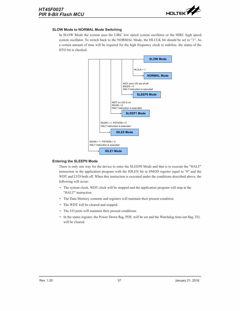
SLOW Mode to NORMAL Mode Switching InSLOWModethesystemuses theLIRClowspeedsystemoscillatoror theHIRChighspeedsystemoscillator.ToswitchbacktotheNORMALMode,theHLCLKbitshouldbesetto"1".Asacertainamountoftimewillberequiredforthehighfrequencyclocktostabilise,thestatusoftheHTObitischecked.
SLOW Mode
NORMAL Mode
HLCLK = 1
SLEEP0 Mode
WDT and LVD ae all offIDLEN = 0HALT instction is exected
SLEEP1 Mode
WDT o LVD is onIDLEN = 0HALT instction is exected
IDLE0 Mode
IDLEN = 1 FSYSON = 0HALT instction is exected
IDLE1 Mode
IDLEN = 1 FSYSON = 0HALT instction is exected
Entering the SLEEP0 Mode ThereisonlyonewayforthedevicetoentertheSLEEP0Modeandthatistoexecutethe"HALT"instructionintheapplicationprogramwiththeIDLENbitinSMODregisterequalto"0"andtheWDTandLVDbothoff.Whenthisinstructionisexecutedundertheconditionsdescribedabove,thefollowingwilloccur:
• Thesystemclock,WDTclockwillbestoppedandtheapplicationprogramwillstopatthe"HALT"instruction.
• TheDataMemorycontentsandregisterswillmaintaintheirpresentcondition.
• TheWDTwillbeclearedandstopped.
• TheI/Oportswillmaintaintheirpresentconditions.
• Inthestatusregister,thePowerDownflag,PDF,willbesetandtheWatchdogtime-outflag,TO,willbecleared.

Rev. 1.20 38 ana 21 201 Rev. 1.20 39 ana 21 201
HT45F0027PIR 8-Bit Flash MCU
HT45F0027PIR 8-Bit Flash MCU
Entering the SLEEP1 Mode ThereisonlyonewayforthedevicetoentertheSLEEP1Modeandthatistoexecutethe"HALT"instructionintheapplicationprogramwiththeIDLENbitinSMODregisterequalto"0"andtheWDTorLVDon.When this instruction isexecutedunder theconditionsdescribedabove, thefollowingwilloccur:
• Thesystemclockwillbestoppedandtheapplicationprogramwillstopatthe"HALT"instruc-tion,buttheWDTorLVDwillremainwiththeclocksourcecomingfromthefSLclock.
• TheDataMemorycontentsandregisterswillmaintaintheirpresentcondition.
• TheWDTwillbeclearedandresumecountingiftheWDTisenabled.
• TheI/Oportswillmaintaintheirpresentconditions.
• Inthestatusregister,thePowerDownflag,PDF,willbesetandtheWatchdogtime-outflag,TO,willbecleared.
Entering the IDLE0 Mode ThereisonlyonewayforthedevicetoentertheIDLE0Modeandthatistoexecutethe"HALT"instructionintheapplicationprogramwiththeIDLENbitinSMODregisterequalto"1"andtheFSYSONbitinSMOD1registerequalto"0".Whenthisinstructionisexecutedundertheconditionsdescribedabove,thefollowingwilloccur:
• Thesystemclockwillbestoppedandtheapplicationprogramwillstopatthe"HALT"instruction,butthefSUBclockwillbeon.
• TheDataMemorycontentsandregisterswillmaintaintheirpresentcondition.
• TheWDTwillbeclearedandresumecountingiftheWDTisenabled.
• TheI/Oportswillmaintaintheirpresentconditions.
• Inthestatusregister,thePowerDownflag,PDF,willbesetandtheWatchdogtime-outflag,TO,willbecleared.
Entering the IDLE1 Mode ThereisonlyonewayforthedevicetoentertheIDLE1Modeandthatistoexecutethe"HALT"instructionintheapplicationprogramwiththeIDLENbitinSMODregisterequalto"1"andtheFSYSONbitinSMOD1registerequalto"1".Whenthisinstructionisexecutedundertheconditionsdescribedabove,thefollowingwilloccur:
• ThesystemclockandfSUBclockwillbeonandtheapplicationprogramwillstopatthe"HALT"instruction.
• TheDataMemorycontentsandregisterswillmaintaintheirpresentcondition.
• TheWDTwillbeclearedandresumecountingiftheWDTisenabled.
• TheI/Oportswillmaintaintheirpresentconditions.
• Inthestatusregister,thePowerDownflag,PDF,willbesetandtheWatchdogtime-outflag,TO,willbecleared.
Rev. 1.20 38 ana 21 201 Rev. 1.20 39 ana 21 201
HT45F0027PIR 8-Bit Flash MCU
HT45F0027PIR 8-Bit Flash MCU
Standby Current Considerations AsthemainreasonforenteringtheSLEEPorIDLEModeistokeepthecurrentconsumptionofthedevicetoaslowavalueaspossible,perhapsonlyintheorderofseveralmicro-ampsexceptintheIDLE1Mode,thereareotherconsiderationswhichmustalsobetakenintoaccountbythecircuitdesignerifthepowerconsumptionistobeminimised.SpecialattentionmustbemadetotheI/Opinsonthedevice.Allhigh-impedanceinputpinsmustbeconnectedtoeitherafixedhighorlowlevelasanyfloatinginputpinscouldcreateinternaloscillationsandresultinincreasedcurrentconsumption.Thisalsoappliestothedevicewhichhasdifferentpackagetypes,astheremaybeunbondedpins.Thesemusteitherbesetupasoutputsorifsetupasinputsmusthavepull-highresistorsconnected.
Caremustalsobetakenwiththeloads,whichareconnectedtoI/Opins,whicharesetupasoutputs.Theseshouldbeplacedinaconditioninwhichminimumcurrent isdrawnorconnectedonlytoexternalcircuitsthatdonotdrawcurrent,suchasotherCMOSinputs.
IntheIDLE1Modethesystemoscillatorison,ifthesystemoscillatorisfromthehighspeedsystemoscillator,theadditionalstandbycurrentwillalsobeperhapsintheorderofseveralhundredmicro-amps.
Wake-up AfterthesystementerstheSLEEPorIDLEMode,itcanbewokenupfromoneofvarioussourceslistedasfollows:
• Anexternalreset
• AnexternalfallingedgeonPortA
• Asysteminterrupt
• AWDToverflow
Whenthedeviceexecutesthe"HALT"instruction,thePDFflagwillbesetto1.ThePDFflagwillbeclearedto0ifthedeviceexperiencesasystempower-uporexecutestheclearWatchdogTimerinstruction.IfthesystemiswokenupbyaWDToverflow,aWatchdogTimerresetwillbeinitiatedandtheTOflagwillbesetto1.TheTOflagissetifaWDTtime-outoccursandcausesawake-upthatonlyresetstheProgramCounterandStackPointer,otherflagsremainintheiroriginalstatus.
EachpinonPortAcanbesetupusingthePAWUregistertopermitanegativetransitiononthepintowake-upthesystem.WhenaPortApinwake-upoccurs,theprogramwillresumeexecutionattheinstructionfollowingthe"HALT"instruction.If thesystemiswokenupbyaninterrupt, thentwopossiblesituationsmayoccur.Thefirstiswheretherelatedinterruptisdisabledortheinterruptisenabledbutthestackisfull,inwhichcasetheprogramwillresumeexecutionattheinstructionfollowingthe"HALT"instruction.Inthissituation,theinterruptwhichwoke-upthedevicewillnotbeimmediatelyserviced,butwillratherbeservicedlaterwhentherelatedinterruptisfinallyenabledorwhenastacklevelbecomesfree.Theothersituationiswheretherelatedinterruptisenabledandthestackisnotfull,inwhichcasetheregularinterruptresponsetakesplace.Ifaninterruptrequestflag issethighbeforeentering theSLEEPorIDLEMode, thewake-upfunctionof therelatedinterruptwillbedisabled.
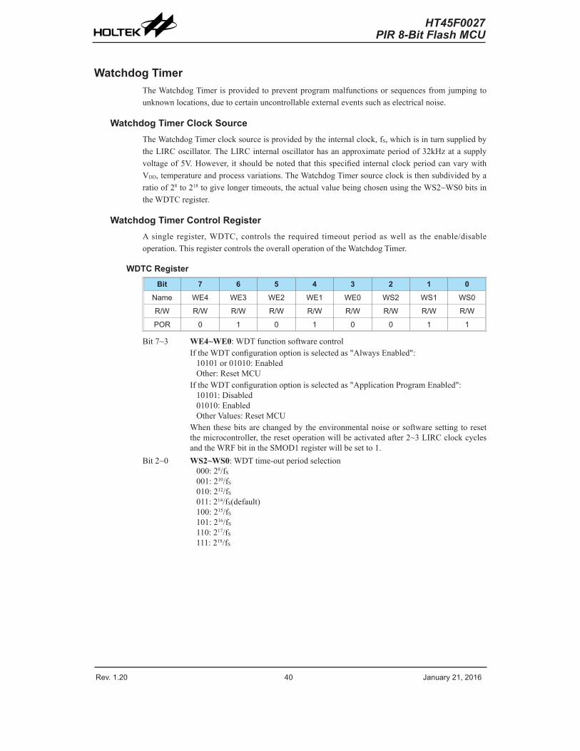
Rev. 1.20 40 ana 21 201 Rev. 1.20 41 ana 21 201
HT45F0027PIR 8-Bit Flash MCU
HT45F0027PIR 8-Bit Flash MCU
Watchdog TimerTheWatchdogTimerisprovidedtopreventprogrammalfunctionsorsequencesfromjumpingtounknownlocations,duetocertainuncontrollableexternaleventssuchaselectricalnoise.
Watchdog Timer Clock SourceTheWatchdogTimerclocksourceisprovidedbytheinternalclock,fS,whichisinturnsuppliedbytheLIRCoscillator.TheLIRCinternaloscillatorhasanapproximateperiodof32kHzatasupplyvoltageof5V.However,itshouldbenotedthatthisspecifiedinternalclockperiodcanvarywithVDD,temperatureandprocessvariations.TheWatchdogTimersourceclockisthensubdividedbyaratioof28to218togivelongertimeouts,theactualvaluebeingchosenusingtheWS2~WS0bitsintheWDTCregister.
Watchdog Timer Control RegisterAsingle register,WDTC,controls the required timeoutperiodaswell as theenable/disableoperation.ThisregistercontrolstheoveralloperationoftheWatchdogTimer.
WDTC Register
Bit 7 6 5 4 3 2 1 0
Name WE4 WE3 WE2 WE1 WE0 WS2 WS1 WS0
R/W R/W R/W R/W R/W R/W R/W R/W R/W
POR 0 1 0 1 0 0 1 1
Bit7~3 WE4~WE0:WDTfunctionsoftwarecontrolIftheWDTconfigurationoptionisselectedas"AlwaysEnabled":10101or01010:EnabledOther:ResetMCU
IftheWDTconfigurationoptionisselectedas"ApplicationProgramEnabled":10101:Disabled01010:EnabledOtherValues:ResetMCU
Whenthesebitsarechangedbytheenvironmentalnoiseorsoftwaresettingtoresetthemicrocontroller,theresetoperationwillbeactivatedafter2~3LIRCclockcyclesandtheWRFbitintheSMOD1registerwillbesetto1.
Bit2~0 WS2~WS0:WDTtime-outperiodselection000:28/fS
001:210/fS
010:212/fS
011:214/fS(default)100:215/fS
101:216/fS
110:217/fS
111:218/fS

Rev. 1.20 40 ana 21 201 Rev. 1.20 41 ana 21 201
HT45F0027PIR 8-Bit Flash MCU
HT45F0027PIR 8-Bit Flash MCU
SMOD1 Register
Bit 7 6 5 4 3 2 1 0
Name FSYSON LVRF LRF WRF
R/W R/W R/W R/W R/W
POR 0 x 0 0
"x": nknownBit7 FSYSON:fSYSControlinIDLEMode
DescribedelsewhereBit6~3 Unimplemented,readas"0"Bit2 LVRF:LVRfunctionresetflag
DescribedelsewhereBit1 LRF:LVRControlregistersoftwareresetflag
DescribedelsewhereBit0 WRF:WDTControlregistersoftwareresetflag
0:Notoccur1:Occurred
Thisbit isset to1by theWDTControlregistersoftwareresetandclearedby theapplicationprogram.Note that thisbitcanonlybecleared to0by theapplicationprogram.
Watchdog Timer OperationTheWatchdogTimeroperatesbyprovidingadeviceresetwhenits timeroverflows.ThismeansthatintheapplicationprogramandduringnormaloperationtheuserhastostrategicallycleartheWatchdogTimerbeforeitoverflowstopreventtheWatchdogTimerfromexecutingareset.Thisisdoneusingtheclearwatchdoginstructions.Iftheprogrammalfunctionsforwhateverreason,jumpstoanunknownlocation,orentersanendlessloop,theseclearinstructionswillnotbeexecutedinthecorrectmanner,inwhichcasetheWatchdogTimerwilloverflowandresetthedevice.WithregardtotheWatchdogTimerenable/disablefunction,therearefivebits,WE4~WE0,intheWDTCregistertoofferadditionalenable/disableandresetcontroloftheWatchdogTimer.IftheWDTconfigurationoptionhasselectedthattheWDTfunctionisalwaysenabled,thenWE4~WE0bitsstillhaveeffectontheWDTfunction.WhentheWE4~WE0bitsvalueareequalto01010Bor10101B,theWDTfunctionisenabled.However,iftheWE4~WE0bitsarechangedtoanyothervaluesexcept01010Band10101B,whichcouldbecausedbyadverseenvironmentalconditionssuchasnoise,itwillresetthemicrocontrollerafter2~3LIRCclockcycles.IftheWDTconfigurationoptionhasselectedthattheWDTfunctioniscontrolledusingtheapplicationprogram,thentheWDTcontrolregisterbits,WE4~WE0,areusedtoenableordisabletheWatchdogTimer.InthiscasetheWDTfunctionwillbedisabledwhentheWE4~WE0bitsareequalto10101BandenablediftheWE4~WE0bitsareequalto01010B.IftheWE4~WE0bitsaresettoanyothervalues,otherthan01010Band10101B,itwillresetthedeviceafter2~3LIRCclockcycles.Afterpoweronthesebitswillhaveavalueof01010B.
WDT Configuration Option WE4 ~ WE0 Bits WDT Function
Alwas Enabled01010B o 10101B Enable
An othe vale Reset MCU
Application Pogam Enabled
10101B Disable
01010B Enable
An othe vale Reset MCU
Watchdog Timer Enable/Disable Control

Rev. 1.20 42 ana 21 201 Rev. 1.20 43 ana 21 201
HT45F0027PIR 8-Bit Flash MCU
HT45F0027PIR 8-Bit Flash MCU
Undernormalprogramoperation,aWatchdogTimertime-outwill initialiseadeviceresetandsetthestatusbitTO.However,ifthesystemisintheSLEEPorIDLEMode,whenaWatchdogTimertime-outoccurs,theTObitinthestatusregisterwillbesetandonlytheProgramCounterandStackPointerwillbereset.ThreemethodscanbeadoptedtoclearthecontentsoftheWatchdogTimer.ThefirstisaWDTreset,whichmeansacertainvalueexcept01010Band10101BwrittenintotheWE4~WE0bitfiled, thesecondisusingtheWatchdogTimersoftwareclear instructionsandthethirdisviaaHALTinstruction.
ThereisonlyonemethodofusingsoftwareinstructiontocleartheWatchdogTimer.Thatistousethesingle"CLRWDT"instructiontocleartheWDT.
"CLR WDT" Instction
8-stage Divide WDT Pescale
WE4~WE0 bitsWDTC Registe Reset MCU
fS/28
8-to-1 MUX
CLR
WS2~WS0 WDT Time-ot(28/fS ~ 218/fS)
LIRC
"HALT" Instction
fS
Watchdog Timer
Reset and InitialisationAresetfunctionisafundamentalpartofanymicrocontrollerensuringthat thedevicecanbesettosomepredeterminedcondition irrespectiveofoutsideparameters.Themost important resetconditionisafterpowerisfirstappliedtothemicrocontroller.Inthiscase, internalcircuitrywillensure that themicrocontroller,afterashortdelay,willbe inawell-definedstateandready toexecutethefirstprograminstruction.Afterthispower-onreset,certainimportantinternalregisterswillbesettodefinedstatesbeforetheprogramcommences.OneoftheseregistersistheProgramCounter,whichwillberesettozeroforcingthemicrocontrollertobeginprogramexecutionfromthelowestProgramMemoryaddress.
AnothertypeofresetiswhentheWatchdogTimeroverflowsandresets.Alltypesofresetoperationsresultindifferentregisterconditionsbeingsetup.AnotherresetexistsintheformofaLowVoltageReset,LVR,whereafullreset, is implementedinsituationswherethepowersupplyvoltagefallsbelowacertainthreshold.
Reset Functions Thereareseveralwaysinwhicharesetcanoccur,eachofwhichwillbedescribedasfollows.
Power-on Reset Themostfundamentalandunavoidablereset is theonethatoccursafterpowerisfirstappliedtothemicrocontroller.AswellasensuringthattheProgramMemorybeginsexecutionfromthefirstmemoryaddress,apower-onresetalsoensures thatcertainother registersarepreset toknownconditions.AlltheI/OportandportcontrolregisterswillpowerupinahighconditionensuringthatallI/Oportswillbefirstsettoinputs.

Rev. 1.20 42 ana 21 201 Rev. 1.20 43 ana 21 201
HT45F0027PIR 8-Bit Flash MCU
HT45F0027PIR 8-Bit Flash MCU
VDD
Powe-on Reset
SST Time-ot
tRSTD
Power-On Reset Timing Chart
Low Voltage Reset LVR Themicrocontrollercontainsalowvoltageresetcircuit inordertomonitorthesupplyvoltageofthedevice.TheLVRfunctionisalwaysenabledwithaspecificLVRvoltageVLVR.If thesupplyvoltageof thedevicedropstowithinarangeof0.9V~VLVRsuchasmightoccurwhenchangingthebattery,theLVRwillautomaticallyresetthedeviceinternallyandtheLVRFbitintheSMOD1registerwillalsobesetto1.ForavalidLVRsignal,alowsupplyvoltage,i.e.,avoltageintherangebetween0.9V~VLVRmustexistfora timegreater thanthatspecifiedbytLVR in theACElectricalCharacteristics.Ifthelowsupplyvoltagestatedoesnotexceedthisvalue,theLVRwillignorethelowsupplyvoltageandwillnotperformaresetfunction.TheactualVLVRvaluecanbeselectedbytheLVSbitsintheLVRCregister.IftheLVS7~LVS0bitsarechangedtosomecertainvaluesbytheenvironmentalnoiseorsoftwaresetting,theLVRwillresetthedeviceafter2~3LIRCclockcycles.Whenthishappens,theLRFbitintheSMOD1registerwillbesetto1.Afterpowerontheregisterwillhavethevalueof01010101B.NotethattheLVRfunctionwillbeautomaticallydisabledwhenthedeviceentersthepowerdownmode.
Low Voltage Reset Timing Chart
• LVRC Register
Bit 7 6 5 4 3 2 1 0
Name LVS7 LVS LVS5 LVS4 LVS3 LVS2 LVS1 LVS0
R/W R/W R/W R/W R/W R/W R/W R/W R/W
POR 0 1 1 0 0 1 1 0
Bit7~0 LVS7~LVS0:LVRvoltageselect01010101:2.1V(default)00110011:2.55V10011001:3.15V10101010:3.8VAnyothervalue:GeneratesMCUreset--registerisresettoPORvalue
Whenanactuallowvoltageconditionoccurs,asspecifiedbyoneofthefourdefinedLVRvoltagevaluesabove,anMCUresetwillbegenerated. In this situation theregistercontentswillremainthesameaftersucharesetoccurs.Anyregistervalue,otherthanthefourdefinedLVRvaluesabove,willalsoresultinthegenerationofanMCUreset.Theresetoperationwillbeactivatedafter2~3LIRCclockcycles.HoweverinthissituationtheregistercontentswillberesettothePORvalue.

Rev. 1.20 44 ana 21 201 Rev. 1.20 45 ana 21 201
HT45F0027PIR 8-Bit Flash MCU
HT45F0027PIR 8-Bit Flash MCU
• SMOD1 Register
Bit 7 6 5 4 3 2 1 0
Name FSYSON LVRF LRF WRF
R/W R/W R/W R/W R/W
POR 0 x 0 0
"x": nknownBit7 FSYSON:fSYSControlinIDLEMode
Describedelsewhere.Bit6~3 Unimplemented,readas"0"Bit2 LVRF:LVRfunctionresetflag
0:Notoccur1:Occurred
Thisbitissetto1whenaspecificLowVoltageResetsituationconditionoccurs.Thisbitcanonlybeclearedto0bytheapplicationprogram.
Bit1 LRF:LVRControlregistersoftwareresetflag0:Notoccur1:Occurred
Thisbitissetto1iftheLVRCregistercontainsanynon-definedLVRvoltageregistervalues.Thisineffectactslikeasoftware-resetfunction.Thisbitcanonlybeclearedto0bytheapplicationprogram.
Bit0 WRF:WDTControlregistersoftwareresetflagDescribedelsewhere.
Watchdog Time-out Reset during Normal OperationTheWatchdogtime-outResetduringnormaloperationisthesameasthehardwareLVRresetexceptthattheWatchdogtime-outflagTOwillbesetto"1".
WDT Time-out Reset during Normal Operation Timing Chart
Watchdog Time-out Reset during SLEEP or IDLE ModeTheWatchdogtime-outResetduringSLEEPorIDLEModeisa littledifferentfromotherkindsofreset.MostoftheconditionsremainunchangedexceptthattheProgramCounterandtheStackPointerwillbeclearedto"0"andtheTOflagwillbesetto"1".RefertotheA.C.CharacteristicsfortSSTdetails.
WDT Time-out Reset during SLEEP or IDLE Timing Chart

Rev. 1.20 44 ana 21 201 Rev. 1.20 45 ana 21 201
HT45F0027PIR 8-Bit Flash MCU
HT45F0027PIR 8-Bit Flash MCU
Reset Initial ConditionsThedifferent typesofresetdescribedaffect theresetflagsindifferentways.Theseflags,knownasPDFandTOare located in thestatus registerandarecontrolledbyvariousmicrocontrolleroperations,suchas theSLEEPorIDLEModefunctionorWatchdogTimer.Thereset flagsareshowninthetable:
TO PDF Reset Conditions
0 0 Powe-on eset
LVR eset ding Nomal o SLOW Mode opeation
1 WDT time-ot eset ding Nomal o SLOW Mode opeation
1 1 WDT time-ot eset ding IDLE o SLEEP Mode opeation
Note:"u"standsforunchanged
Thefollowingtableindicatesthewayinwhichthevariouscomponentsofthemicrocontrollerareaffectedafterapower-onresetoccurs.
Item Condition after Reset
Pogam Conte Reset to zeo
Intepts All intepts will be disabled
WDT Clea afte eset WDT begins conting
Time/Event Conte Time Conte will be tned off
Inpt/Otpt Pots I/O pots will be setp as inpts
Stack Pointe Stack Pointe will point to the top of the stack
Thedifferentkindsofresetsallaffecttheinternalregistersofthemicrocontrollerindifferentways.Toensurereliablecontinuationofnormalprogramexecutionafteraresetoccurs,itisimportanttoknowwhatconditionthemicrocontrolleris inafteraparticularresetoccurs.Thefollowingtabledescribeshoweachtypeofresetaffectseachof themicrocontroller internalregisters.Note thatwheremorethanonepackagetypeexiststhetablewillreflectthesituationforthelargerpackagetype.
Register Reset (Power On)
WDT Time-out (Normal Operation) LVR Reset WDT Time-out
(HALT)IAR0 - - - - - - - - - - - - - - - - - - - - - - - - - - - - - - - -MP0 x x x x x x x x x x x x x x x x x x x x x x x x IAR1 - - - - - - - - - - - - - - - - - - - - - - - - - - - - - - - -MP1 x x x x x x x x x x x x x x x x x x x x x x x x BP - - - - - - - 0 - - - - - - - 0 - - - - - - - 0 - - - - - - - ACC x x x x x x x x PCL 0 0 0 0 0 0 0 0 0 0 0 0 0 0 0 0 0 0 0 0 0 0 0 0 0 0 0 0 0 0 0 0TBLP x x x x x x x x TBLH x x x x x x x x TBHP x x x x x x x x x x x x x x x x x x x x x x x x STATUS - - 0 0 x x x x - - 1 - - - - 1 1 INTC0 - 0 0 0 0 0 0 0 - 0 0 0 0 0 0 0 - 0 0 0 0 0 0 0 - TMR0 0 0 0 0 0 0 0 0 0 0 0 0 0 0 0 0 0 0 0 0 0 0 0 0 TMR0C 0 0 - 0 1 0 0 0 0 0 - 0 1 0 0 0 0 0 - 0 1 0 0 0 - TMR1 0 0 0 0 0 0 0 0 0 0 0 0 0 0 0 0 0 0 0 0 0 0 0 0 TMR1C 0 0 - 0 1 0 0 0 0 0 - 0 1 0 0 0 0 0 - 0 1 0 0 0 - PA 1 1 1 1 1 1 1 1 1 1 1 1 1 1 1 1 1 1 1 1 1 1 1 1

Rev. 1.20 4 ana 21 201 Rev. 1.20 47 ana 21 201
HT45F0027PIR 8-Bit Flash MCU
HT45F0027PIR 8-Bit Flash MCU
Register Reset (Power On)
WDT Time-out (Normal Operation) LVR Reset WDT Time-out
(HALT)PAC 1 1 1 1 1 1 1 1 1 1 1 1 1 1 1 1 1 1 1 1 1 1 1 1 PB - - - - - - - 1 - - - - - - - 1 - - - - - - - 1 - - - - - - - PBC - - - - - - - 1 - - - - - - - 1 - - - - - - - 1 - - - - - - - LVDC 0 0 0 0 0 0 0 0 0 0 0 0 0 0 0 0 0 0 0 0 0 0 0 0 - - - LVRC 0 1 0 1 0 1 0 1 0 1 0 1 0 1 0 1 0 1 0 1 0 1 0 1 U WDTC 0 1 0 1 0 0 11 0 1 0 1 0 0 11 0 1 0 1 0 0 11 INTC1 0 0 0 0 0 0 0 0 0 0 0 0 0 0 0 0 0 0 0 0 0 0 0 0 ADRL 0 0 0 0 - - - - 0 0 0 0 - - - - 0 0 0 0 - - - - - - - -ADRH 0 0 0 0 0 0 0 0 0 0 0 0 0 0 0 0 0 0 0 0 0 0 0 0 ADCR0 0 11 0 0 0 0 0 0 11 0 0 0 0 0 0 11 0 0 0 0 0 ADCR1 1 0 0 0 0 0 0 0 1 0 0 0 0 0 0 0 1 0 0 0 0 0 0 0 ACER 0 - - - - - 1 1 0 - - - - - 1 1 0 - - - - - 1 1 - - - - - PAWU 0 0 0 0 0 0 0 0 0 0 0 0 0 0 0 0 0 0 0 0 0 0 0 0 PAPU 0 0 0 0 0 0 0 0 0 0 0 0 0 0 0 0 0 0 0 0 0 0 0 0 PBPU - - - - - - - 0 - - - - - - - 0 - - - - - - - 0 - - - - - - - SMOD1 0 - - - - x 0 0 0 - - - - x 0 0 0 - - - - x 0 0 - - - - SMOD 0 0 0 - 0 0 11 0 0 0 - 0 0 11 0 0 0 - 0 0 11 - INTEG 0 0 0 0 0 0 0 0 0 0 0 0 0 0 0 0 0 0 0 0 0 0 0 0 - - - - - - OPAC0 0 0 0 0 - 0 0 0 0 0 0 0 - 0 0 0 0 0 0 0 - 0 0 0 - OPAC1 - - 0 0 0 0 0 0 - - 0 0 0 0 0 0 - - 0 0 0 0 0 0 - - ACCC0 0 0 0 - - - 0 0 0 0 0 - - - 0 0 0 0 0 - - - 0 0 - - - ACCC1 0 0 0 0 0 0 0 0 0 0 0 0 0 0 0 0 0 0 0 0 0 0 0 0 - - - MFIC 0 0 0 0 0 0 0 0 0 0 0 0 0 0 0 0 0 0 0 0 0 0 0 0 - - – - SIMC0 111 0 0 0 0 - 111 0 0 0 0 - 111 0 0 0 0 - -SIMC1 1 0 0 0 0 0 0 1 1 0 0 0 0 0 0 1 1 0 0 0 0 0 0 1 SIMD SIMA 0 0 0 0 0 0 0 0 0 0 0 0 0 0 0 0 0 0 0 0 0 0 0 0 SIMC2 0 0 0 0 0 0 0 0 0 0 0 0 0 0 0 0 0 0 0 0 0 0 0 0 EEA - - - 0 0 0 0 0 - - - 0 0 0 0 0 - - - 0 0 0 0 0 - - - EED 0 0 0 0 0 0 0 0 0 0 0 0 0 0 0 0 0 0 0 0 0 0 0 0 PRM - - - - - - 0 0 - - - - - - 0 0 - - - - - - 0 0 - - - - - - LDOC 0 - 0 0 0 0 0 0 0 - 0 0 0 0 0 0 0 - 0 0 0 0 0 0 - TS_BG 0 0 0 x x x x x 0 0 0 x x x x x 0 0 0 x x x x x 0 0 0 x x x x xTS_OP 0 x x x x x x x 0 x x x x x x x 0 x x x x x x x 0 x x x x x x xLULV 0 0 0 0 - - - - 0 0 0 0 - - - - 0 0 0 0 - - - - - - - -HULV 0 0 0 0 0 0 0 0 0 0 0 0 0 0 0 0 0 0 0 0 0 0 0 0 LLLV 0 0 0 0 - - - - 0 0 0 0 - - - - 0 0 0 0 - - - - - - - -HLLV 0 0 0 0 0 0 0 0 0 0 0 0 0 0 0 0 0 0 0 0 0 0 0 0 EEC - - - - 0 0 0 0 - - - - 0 0 0 0 - - - - 0 0 0 0 - - - -
Note:"u"standsforunchanged"x"standsforunknown
"-"standsforunimplemented

Rev. 1.20 4 ana 21 201 Rev. 1.20 47 ana 21 201
HT45F0027PIR 8-Bit Flash MCU
HT45F0027PIR 8-Bit Flash MCU
Input/Output Ports HoltekmicrocontrollersofferconsiderableflexibilityontheirI/Oports.Withtheinputoroutputdesignationofeverypinfullyunderuserprogramcontrol,pull-highselectionsforallportsandwake-upselectionsoncertainpins,theuserisprovidedwithanI/Ostructuretomeettheneedsofawiderangeofapplicationpossibilities.
Thedeviceprovidesbidirectional input/output lines labeledwithportnamesPA~PB.TheseI/OportsaremappedtotheRAMDataMemorywithspecificaddressesasshownintheSpecialPurposeDataMemorytable.Allof theseI/Oportscanbeusedforinputandoutputoperations.Forinputoperation,theseportsarenon-latching,whichmeanstheinputsmustbereadyattheT2risingedgeofinstruction"MOVA,[m]",wheremdenotestheportaddress.Foroutputoperation,allthedataislatchedandremainsunchangeduntiltheoutputlatchisrewritten.
Register Name
Bit
7 6 5 4 3 2 1 0
PA PA7 PA PA5 PA4 PA3 PA2 PA1 PA0
PAC PAC7 PAC PAC5 PAC4 PAC3 PAC2 PAC1 PAC0
PAPU PAPU7 PAPU PAPU5 PAPU4 PAPU3 PAPU2 PAPU1 PAPU0
PAWU PAWU7 PAWU PAWU5 PAWU4 PAWU3 PAWU2 PAWU1 PAWU0
PB PB0
PBC PBC0
PBPU PBPU0
I/O Registers List
Pull-high ResistorsManyproductapplicationsrequirepull-highresistorsfortheirswitchinputsusuallyrequiringtheuseofanexternalresistor.Toeliminatetheneedfortheseexternalresistors,allI/Opins,whenconfiguredasaninputhavethecapabilityofbeingconnectedtoaninternalpull-highresistor.Thesepull-highresistorsareselectedusingregistersPAPU~PBPUandareimplementedusingweakPMOStransistors.
PAPU Register
Bit 7 6 5 4 3 2 1 0
Name PAPU7 PAPU PAPU5 PAPU4 PAPU3 PAPU2 PAPU1 PAPU0
R/W R/W R/W R/W R/W R/W R/W R/W R/W
POR 0 0 0 0 0 0 0 0
Bit7~0 PAPU7~PAPU0:PortAbit7~bit0Pull-highControl0:Disable1:Enable
PBPU Register
Bit 7 6 5 4 3 2 1 0
Name PBPU0
R/W R/W
POR 0
Bit7~1 Unimplemented,readas"0"Bit0 PBPU0:PortBbit0Pull-highControl
0:Disable1:Enable

Rev. 1.20 48 ana 21 201 Rev. 1.20 49 ana 21 201
HT45F0027PIR 8-Bit Flash MCU
HT45F0027PIR 8-Bit Flash MCU
Port A Wake-upTheHALTinstructionforcesthemicrocontroller intotheSLEEPorIDLEModewhichpreservespower,afeaturethat is importantforbatteryandotherlow-powerapplications.Variousmethodsexist towake-upthemicrocontroller,oneofwhichis tochangethelogicconditionononeofthePortApinsfromhightolow.Thisfunctionisespeciallysuitableforapplicationsthatcanbewokenupviaexternalswitches.EachpinonPortAcanbeselectedindividually tohave thiswake-upfeatureusingthePAWUregister.
PAWU Register
Bit 7 6 5 4 3 2 1 0
Name PAWU7 PAWU PAWU5 PAWU4 PAWU3 PAWU2 PAWU1 PAWU0
R/W R/W R/W R/W R/W R/W R/W R/W R/W
POR 0 0 0 0 0 0 0 0
Bit7~0 PAWU7~PAWU0:PortAbit7~bit0Wake-upControl0:Disable1:Enable
I/O Port Control RegistersEach I/Oporthas itsowncontrol registerknownasPAC~PBC, to control the input/outputconfiguration.With this control register, eachCMOSoutput or input canbe reconfigureddynamicallyundersoftwarecontrol.Eachpinof theI/Oports isdirectlymappedtoabit in itsassociatedportcontrolregister.FortheI/Opintofunctionasaninput,thecorrespondingbitofthecontrolregistermustbewrittenasa"1".Thiswillthenallowthelogicstateoftheinputpintobedirectlyreadbyinstructions.Whenthecorrespondingbitofthecontrolregisteriswrittenasa"0",theI/OpinwillbesetupasaCMOSoutput.Ifthepiniscurrentlysetupasanoutput,instructionscanstillbeusedtoreadtheoutputregister.However,itshouldbenotedthattheprogramwillinfactonlyreadthestatusoftheoutputdatalatchandnottheactuallogicstatusoftheoutputpin.
PAC Register
Bit 7 6 5 4 3 2 1 0
Name PAC7 PAC PAC5 PAC4 PAC3 PAC2 PAC1 PAC0
R/W R/W R/W R/W R/W R/W R/W R/W R/W
POR 1 1 1 1 1 1 1 1
Bit7~0 PAC7~PAC0:PortAbit7~bit0Input/OutputControl0:Output1:Input
PBC Register
Bit 7 6 5 4 3 2 1 0
Name PBC0
R/W R/W
POR 1
Bit7~1 Unimplemented,readas"0"Bit0 PBC0:PortBbit0Input/OutputControl
0:Output1:Input

Rev. 1.20 48 ana 21 201 Rev. 1.20 49 ana 21 201
HT45F0027PIR 8-Bit Flash MCU
HT45F0027PIR 8-Bit Flash MCU
Pin-remapping FunctionTheflexibilityofthemicrocontrollerrangeisgreatlyenhancedbytheuseofpinsthathavemorethanonefunction.Limitednumbersofpinscanforceseriousdesignconstraintsondesignersbutbysupplyingpinswithmulti-functions,manyof thesedifficultiescanbeovercome.Thewayinwhichthepinfunctionofeachpinisselectedisdifferentforeachfunctionandapriorityorderisestablishedwheremorethanonepinfunctionisselectedsimultaneously.Additionally there isaPRMregistertoestablishcertainpinfunctions.Generallyspeaking,theanalogfunctionhashigherprioritythanthedigitalfunction.However,ifmorethantwoanalogfunctionsareenabledandtheanalogsignalinputcomesfromthesameexternalpin,theanaloginputwillbeinternallyconnectedtoalloftheseactiveanalogfunctionalmodules.
Pin-remapping RegistersThelimitednumberofsuppliedpinsinapackagecanimposerestrictionsontheamountoffunctionsacertaindevicecancontain.Howeverbyallowingthesamepinstoshareseveraldifferentfunctionsandprovidingameansoffunctionselection,awiderangeofdifferentfunctionscanbeincorporatedintoevenrelativelysmallpackagesizes.
• PRM Register
Bit 7 6 5 4 3 2 1 0
Name SCKPS SCLPS
R/W R/W R/W
POR 0 0
Bit7~2 Unimplemented,readas"0"Bit1 SCKPS:SCKPinRemappingControl
0:EnableSCK_0onPA01:EnableSCK_1onPA6
Bit0 SCLPS:SCLPinRemappingControl0:EnableSCL_0onPA01:EnableSCL_1onPA6

Rev. 1.20 50 ana 21 201 Rev. 1.20 51 ana 21 201
HT45F0027PIR 8-Bit Flash MCU
HT45F0027PIR 8-Bit Flash MCU
I/O Pin StructuresTheaccompanyingdiagrams illustrate the internalstructuresofsomegeneric I/Opin types.AstheexactlogicalconstructionoftheI/Opinwilldifferfromthesedrawings,theyaresuppliedasaguideonlytoassistwiththefunctionalunderstandingoftheI/Opins.Thewiderangeofpin-sharedstructuresdoesnotpermitalltypestobeshown.
Generic Input/Output Structure
A/D Input/Output Structure

Rev. 1.20 50 ana 21 201 Rev. 1.20 51 ana 21 201
HT45F0027PIR 8-Bit Flash MCU
HT45F0027PIR 8-Bit Flash MCU
Programming Considerations Withintheuserprogram,oneofthefirstthingstoconsiderisportinitialisation.Afterareset,alloftheI/Odataandportcontrolregisterswillbesethigh.ThismeansthatallI/Opinswilldefaulttoaninputstate, thelevelofwhichdependsontheotherconnectedcircuitryandwhetherpull-highselectionshavebeenchosen.Iftheportcontrolregisters,PAC~PBC,arethenprogrammedtosetupsomepinsasoutputs,theseoutputpinswillhaveaninitialhighoutputvalueunlesstheassociatedportdataregisters,PA~PB,arefirstprogrammed.Selectingwhichpinsare inputsandwhichareoutputscanbeachievedbyte-widebyloadingthecorrectvaluesintotheappropriateportcontrolregisterorbyprogrammingindividualbits intheportcontrolregisterusingthe"SET[m].i"and"CLR[m].i"instructions.Notethatwhenusingthesebitcontrol instructions,aread-modify-writeoperationtakesplace.Themicrocontrollermustfirstreadinthedataontheentireport,modifyittotherequirednewbitvaluesandthenrewritethisdatabacktotheoutputports.
Thepower-onresetconditionoftheA/DconvertercontrolregistersensuresthatanyA/Dinputpins-whicharealwayssharedwithotherI/Ofunctions-willbesetupasanaloginputsafterareset.AlthoughthesepinswillbeconfiguredasA/Dinputsafterareset, theA/Dconverterwillnotbeswitchedon.It is thereforeimportant tonotethat if it isrequiredtousethesepinsasI/Odigitalinputpinsorasotherfunctions,theA/DconvertercontrolregistersmustbecorrectlyprogrammedtoremovetheA/Dfunction.NotealsothatastheA/Dchannelisenabled,anyinternalpull-highresistorconnectionswillberemoved.
PortAhas theadditionalcapabilityofprovidingwake-upfunctions.When thedevice is in theSLEEPorIDLEMode,variousmethodsareavailabletowakethedeviceup.OneoftheseisahightolowtransitionofanyofthePortApins.SingleormultiplepinsonPortAcanbesetuptohavethisfunction.
Timer/Event CountersTheprovisionoftimersformanimportantpartofanymicrocontroller,givingthedesignerameansofcarryingouttimerelatedfunctions.Thedevicecontainstwocount-uptimerof8-bitcapacity.Asthetimershavethreedifferentoperatingmodes,theycanbeconfiguredtooperateasageneraltimer,anexternaleventcounterorasapulsewidthcapturedevice.Theprovisionofaninternalprescalertotheclockcircuitryongivingaddedrangetothetimers.
TherearetwotypesofregistersrelatedtotheTimer/EventCounters.Thefirst is theregister thatcontains theactualvalueof thetimerandintowhichaninitialvaluecanbepreloaded.ReadingfromthisregisteritretrievesthecontentsoftheTimer/EventCounter.ThesecondtypeofassociatedregisteristheTimerControlRegisterwhichdefinesthetimeroptionsanddetermineshowthetimeristobeused.Thedevicecanhavethetimerclockconfiguredtocomefromtheinternalclocksource.Inaddition,thetimerclocksourcecanalsobeconfiguredtocomefromanexternaltimerpin.

Rev. 1.20 52 ana 21 201 Rev. 1.20 53 ana 21 201
HT45F0027PIR 8-Bit Flash MCU
HT45F0027PIR 8-Bit Flash MCU
Configuring the Timer/Event Counter Input Clock SourceTheTimer/EventCounterclocksourcecanoriginatefromvarioussources,aninternalclockfSYSoranexternalpin.Theinternalclocksourceisusedwhenthetimerisinthetimermodeorinthepulsewidthcapturemode,thisinternalclocksourceisfirstlydividedbyaprescaler,thedivisionratioofwhichisconditionedbytheTimerControlRegisterbitsTnPSC2~TnPSC0.Anexternalclocksourceisusedwhenthetimerisintheeventcountingmode,theclocksourcebeingprovidedonanexternaltimerpinTMRn.Dependingupontheconditionof theTnEbit,eachhightolow,or lowtohightransitionontheexternaltimerpinwillincrementthecounterbyone.
8-StagePescale
MUXTCn
fSYS
8-bit Time/Event Conte
Peload Registe
8-bit Time/Event Conte(TMRn)
TnM[1:0]
fINT
Oveflow to Intept
Reload
Timer/Event Counter (n=0 or 1)
Timer Registers – TMR0, TMR1ThetimerregistersarespecialfunctionregisterslocatedintheSpecialPurposeDataMemoryandistheplacewheretheactualtimervalueisstored.TheseregistersareknownasTMR0andTMR1.Thevalueinthetimerregistersincreasesbyoneeachtimeaninternalclockpulseisreceivedoranexternaltransitionoccursontheexternaltimerpin.ThetimerwillcountfromtheinitialvalueloadedbythepreloadregistertothefullcountofFFHatwhichpointthetimeroverflowsandaninternalinterruptsignalisgenerated.Thenthetimervaluewillberesetwiththeinitialpreloadregistervalueandcontinuecounting.Notethat toachieveamaximumfullrangecountofFFH,all thepreloadregistersmustfirstbeclearedtozero.Itshouldbenotedthatafterpower-on,thepreloadregisterswillbeinanunknowncondition.NotethatiftheTimer/EventCounterisinanOFFconditionanddataiswrittentoitspreloadregister,thisdatawillbeimmediatelywrittenintotheactualcounter.However,ifthecounterisenabledandcounting,anynewdatawrittenintothepreloaddataregisterduringthisperiodwillremaininthepreloadregisterandwillonlybewrittenintotheactualcounterthenexttimeanoverflowoccurs.
TMRn Register (n=0 or 1)
Bit 7 6 5 4 3 2 1 0
Name D7 D D5 D4 D3 D2 D1 D0
R/W R/W R/W R/W R/W R/W R/W R/W R/W
POR 0 0 0 0 0 0 0 0
Bit7~0 D7~D0:Timernvalues

Rev. 1.20 52 ana 21 201 Rev. 1.20 53 ana 21 201
HT45F0027PIR 8-Bit Flash MCU
HT45F0027PIR 8-Bit Flash MCU
Timer Control Registers – TMR0C, TMR1CTheflexiblefeaturesoftheHoltekmicrocontrollerTimer/EventCountersenablethemtooperateinthreedifferentmodes,theoptionsofwhicharedeterminedbythecontentsoftheirrespectivecontrolregister.TheTimerControlRegisterisknownasTMRnC.ItistheTimerControlRegistertogetherwithitscorrespondingtimerregisters thatcontrol thefulloperationof theTimer/EventCounter.Beforethetimercanbeused,itisessentialthattheTimerControlRegisterisfullyprogrammedwiththerightdatatoensureitscorrectoperation,aprocessthatisnormallycarriedoutduringprograminitialisation.Tochoosewhichofthethreemodesthetimeristooperatein,eitherinthetimermode,theeventcountingmodeorthepulsewidthcapturemode,bits7and6oftheTimerControlRegister,whichareknownasthebitpairTnM1/TnM0,mustbesettotherequiredlogiclevels.Thetimer-onbit,whichisbit4oftheTimerControlRegisterandknownasTnON,providesthebasicon/offcontroloftherespectivetimer.Settingthebithighallowsthecountertorun.Clearingthebitstopsthecounter.Bits0~2oftheTimerControlRegisterdeterminethedivisionratiooftheinputclockprescaler.Theprescalerbitsettingshavenoeffectifanexternalclocksourceisused.Ifthetimerisintheeventcountorpulsewidthcapturemode,theactivetransitionedgeleveltypeisselectedbythelogiclevelofbit3oftheTimerControlRegisterwhichisknownasTnE.
TMRnC Register (n=0 or 1)
Bit 7 6 5 4 3 2 1 0
Name TnM1 TnM0 — TnON TnE TnPSC2 TnPSC1 TnPSC0
R/W R/W R/W — R/W R/W R/W R/W R/W
POR 0 0 — 0 1 0 0 0
Bit7~6 TnM1, TnM0:Timernoperationmodeselection00:Nomodeavailable01:Eventcountermode(Externalclock)10:Timermode(Internalclock)11:Pulsewidthcapturemode(Externalclock)
Bit5 Unimplemented,readas"0"Bit4 TnON:Timer/eventcountercountingenable
0:Disable1:Enable
Bit3 TnE:EventcounteractiveedgeselectionInEventCounterMode(TnM1,TnM0)=(0,1):1:Countonfallingedge;0:Countonrisingedge
InPulseWidthmeasurementmode(TnM1,TnM0)=(1,1):1:Startcountingontherisingedge,stoponthefallingedge;0:Startcountingonthefallingedge,stopontherisingedge
Bit2~0 TnPSC2~TnPSC0:Timerprescalerrateselection000:fINT=fSYS
001:fINT=fSYS/2010:fINT=fSYS/4011:fINT=fSYS/8100:fINT=fSYS/16101:fINT=fSYS/32110:fINT=fSYS/64111:fINT=fSYS/128

Rev. 1.20 54 ana 21 201 Rev. 1.20 55 ana 21 201
HT45F0027PIR 8-Bit Flash MCU
HT45F0027PIR 8-Bit Flash MCU
Timer ModeInthismode, theTimer/EventCountercanbeutilisedtomeasurefixedtimeintervals,providinganinternalinterruptsignaleachtimetheTimer/EventCounteroverflows.Tooperateinthismode,theOperatingModeSelectbitpair,TnM1/TnM0,intheTimerControlRegistermustbesettothecorrectvalueasshown.
Control Register Operating Mode Select Bits for the Timer ModeBit7 Bit6
1 0
In thismode the internalclock isusedas the timerclock.The timer inputclocksource is fSYS.However,thistimerclocksourceisfurtherdividedbyaprescaler,thevalueofwhichisdeterminedbythebitsTnPSC2~TnPSC0intheTimerControlRegister.Thetimer-onbit,TnONmustbesethightoenablethetimertorun.Eachtimeaninternalclockhightolowtransitionoccurs,thetimerincrementsbyone.Whenthetimerisfullandoverflows,aninterruptsigal isgeneratedandthetimerwillreloadthevaluealreadyloadedintothepreloadregisterandcontinuecounting.Atimeroverflowconditionandcorrespondinginternalinterruptsaretwoofthewake-upsources.However,theinternal interruptscanbedisabledbyensuringthat theTimer/EventCounterInterruptEnablebitsintheInterruptcontrolregistersareresettozero.
Timer Mode Timing Chart
Event Counter Mode Inthismode,anumberofexternallychanginglogicevents,occurringontheexternaltimerTMRnpin,canberecordedbytheTimer/EventCounter.Tooperate in thismode, theOperatingModeSelectbitpair,TnM1/TnM0, in theTimerControlRegistermustbeset to thecorrectvalueasshown.
Control Register Operating Mode Select Bits for the Event Counter Mode.Bit7 Bit6
0 1
In thismode, theexternal timerpinTMRn, isusedas theTimer/EventCounterclocksource,howeveritisnotdividedbytheinternalprescaler.AftertheotherbitsintheTimerControlRegisterhavebeensetup,theenablebitTnON,whichisbit4oftheTimerControlRegister,canbesethightoenabletheTimer/EventCountertorun.IftheActiveEdgeSelectbit,TnE,whichisbit3oftheTimerControlRegister,islow,theTimer/EventCounterwillincrementeachtimetheexternaltimerpinreceivesalowtohightransition.If theTnEishigh,thecounterwill incrementeachtimetheexternaltimerpinreceivesahightolowtransition.Whenitisfullandoverflows,aninterruptsignalisgeneratedand theTimer/EventCounterwill reload thevaluealready loaded into thepreloadregisterandcontinuecounting.The interruptcanbedisabledbyensuring that theTimer/EventCounterInterruptEnablebitinthecorrespondingInterruptControlRegister.Itisresettozero.AstheexternaltimerpinissharedwithanI/Opin,toensurethatthepinisconfiguredtooperateasaneventcounterinputpin,twothingshavetohappen.ThefirstistoensurethattheOperatingModeSelectbits in theTimerControlRegisterplace theTimer/EventCounter in theEventCountingMode.Thesecondistoensurethattheportcontrolregisterconfiguresthepinasaninput.Itshould

Rev. 1.20 54 ana 21 201 Rev. 1.20 55 ana 21 201
HT45F0027PIR 8-Bit Flash MCU
HT45F0027PIR 8-Bit Flash MCU
benotedthatintheeventcountingmode,evenifthemicrocontrollerisintheIdle/SleepMode,theTimer/EventCounterwillcontinuetorecordexternallychanginglogiceventsonthetimer inputTMRnpin.Asaresultwhenthetimeroverflowsitwillgenerateatimerinterruptandcorrespondingwake-upsource.
Event Counter Mode Timing Chart (TnE=1)
Pulse Width Capture ModeIn thismode, theTimer/EventCountercanbeutilised tomeasure thewidthofexternalpulsesappliedtotheexternaltimerpin.Tooperateinthismode,theOperatingModeSelectbitpair,TnM1/TnM0,intheTimerControlRegistermustbesettothecorrectvalueasshown.
Control Register Operating Mode Select Bits for the Pulse Width Measurement Mode.Bit7 Bit6
1 1
Inthismodetheinternalclock,fSYS,isusedastheinternalclockforthe8-bitTimer/EventCounter.However,itisfurtherdividedbyaprescaler,thevalueofwhichisdeterminedbythePrescalerRateSelectbitsTnPSC2~TnPSC0,whichTnON,whichisbit2~0oftheTimerControlRegister,canbesethightoenabletheTimer/EventCounter,howeveritwillnotactuallystartcountinguntilanactiveedgeisreceivedontheexternaltimerpin.
If theActiveEdgeSelectbitTnE,whichisbit3of theTimerControlRegister, is low,onceahighto low transitionhasbeen receivedon theexternal timerpin, theTimer/EventCounterwill startcountinguntiltheexternaltimerpinreturnstoitsoriginalhighlevel.AtthispointtheenablebitwillbeautomaticallyresettozeroandtheTimer/EventCounterwillstopcounting.IftheActiveEdgeSelectbitishigh,theTimer/EventCounterwillbegincountingoncealowtohightransitionhasbeenreceivedontheexternaltimerpinandstopcountingwhentheexternaltimerpinreturnstoitsoriginallowlevel.Asbefore, theenablebitwillbeautomaticallyreset tozeroandtheTimer/EventCounterwillstopcounting.It isimportanttonotethatinthepulsewidthcapturemode,theenablebit isautomaticallyreset tozerowhentheexternalcontrolsignalontheexternal timerpinreturns to itsoriginal level,whereasintheothertwomodestheenablebitcanonlyberesettozerounderprogramcontrol.
TheresidualvalueintheTimer/EventCounter,whichcannowbereadbytheprogram,thereforerepresentsthelengthofthepulsereceivedontheTMRnpin.Astheenablebithasnowbeenreset,anyfurthertransitionsontheexternaltimerpinwillbeignored.Thetimercannotbeginfurtherpulsewidthcaptureuntil theenablebit issethighagainbytheprogram.Inthisway,singleshotpulsemeasurementscanbeeasilymade.
ItshouldbenotedthatinthismodetheTimer/EventCounteriscontrolledbylogicaltransitionsontheexternaltimerpinandnotbythelogiclevel.WhentheTimer/EventCounterisfullandoverflows,aninterruptsignalisgeneratedandtheTimer/EventCounterwillreloadthevaluealreadyloadedintothepreloadregisterandcontinuecounting.TheinterruptcanbedisabledbyensuringthattheTimer/EventCounterInterruptEnablebitinthecorrespondingInterruptControlRegister,itisresettozero.
AstheTMRnpinissharedwithanI/Opin,toensurethatthepinisconfiguredtooperateasapulsewidthcapturepin,twothingshavetobeimplemented.ThefirstistoensurethattheOperatingModeSelectbitsintheTimerControlRegisterplacetheTimer/EventCounterinthepulsewidthcapturemode,thesecondistoensurethattheportcontrolregisterconfigurethepinasaninput.

Rev. 1.20 5 ana 21 201 Rev. 1.20 57 ana 21 201
HT45F0027PIR 8-Bit Flash MCU
HT45F0027PIR 8-Bit Flash MCU
Pulse Width Capture Mode Timing Chart (TnE=0)
I/O InterfacingTheTimer/EventCounter,whenconfigured to run in theeventcounterorpulsewidthcapturemode,requirestheuseofanexternaltimerpinforitsoperation.AsthispinisasharedpinitmustbeconfiguredcorrectlytoensurethatitissetupforuseasaTimer/EventCounterinputpin.ThisisachievedbyensuringthatthemodeselectsbitsintheTimer/EventCountercontrolregister,eithertheeventcounterorpulsewidthcapturemode.AdditionallythecorrespondingPortControlRegisterbitmustbesethightoensurethatthepinissetupasaninput.Anypull-highresistorconnectedtothispinwillremainvalidevenifthepinisusedasaTimer/EventCounterinput.
Programming ConsiderationsWhenconfiguredtorun in the timermode, the internalsystemclockisusedas the timerclocksourceandisthereforesynchronisedwiththeoveralloperationofthemicrocontroller.Inthismodewhentheappropriatetimerregister isfull, themicrocontrollerwillgenerateaninternal interruptsignaldirecting theprogramflowto therespective internal interruptvector.For thepulsewidthcapturemode,theinternalsystemclockisalsousedasthetimerclocksourcebutthetimerwillonlyrunwhenthecorrectlogicconditionappearsontheexternaltimerinputpin.Asthisisanexternaleventandnotsynchronisedwith the internal timerclock, themicrocontrollerwillonlysee thisexternaleventwhenthenexttimerclockpulsearrives.Asaresult,theremaybesmalldifferencesinmeasuredvaluesrequiringprogrammerstotakethisintoaccountduringprogramming.Thesameappliesifthetimerisconfiguredtobeintheeventcountingmode,whichagainisanexternaleventandnotsynchronisedwiththeinternalsystemortimerclock.
WhentheTimer/EventCounterisread,orifdataiswrittentothepreloadregister,theclockisinhibitedtoavoiderrors,howeverasthismayresultinacountingerror,thisshouldbetakenintoaccountbytheprogrammer.Caremustbetakentoensurethatthetimersareproperlyinitialisedbeforeusingthemforthefirsttime.Theassociatedtimerenablebitsintheinterruptcontrolregistermustbeproperlysetotherwisetheinternalinterruptassociatedwiththetimerwillremaininactive.Theedgeselect,timermodeandclocksourcecontrolbitsintimercontrolregistermustalsobecorrectlysettoensurethetimerisproperlyconfiguredfortherequiredapplication.Itisalsoimportanttoensurethataninitialvalueisfirstloadedintothetimerregistersbeforethetimerisswitchedon;thisisbecauseafterpower-ontheinitialvaluesofthetimerregistersareunknown.Afterthetimerhasbeeninitializedthetimercanbeturnedonandoffbycontrollingtheenablebitinthetimercontrolregister.
WhentheTimer/EventCounteroverflows,itscorrespondinginterruptrequestflagintheinterruptcontrolregisterwillbeset.IftheTimer/EventCounterinterruptisenabledthiswillinturngenerateaninterruptsignal.However irrespectiveofwhether theinterruptsareen-abledornot,aTimer/EventCounteroverflowwillalsogenerateawake-upsignal if thedevice is inaPower-downcondition.ThissituationmayoccuriftheTimer/EventCounterisintheEventCountingModeandiftheexternalsignalcontinuestochangestate.Insuchacase,theTimer/EventCounterwillcontinuetocounttheseexternaleventsandifanoverflowoccursthedevicewillbewokenupfromitsPower-downcondition.Topreventsuchawake-upfromoccurring,thetimerinterruptrequestflagshouldfirstbesethighbeforeissuingthe"HALT"instructiontoentertheIdle/SleepMode.

Rev. 1.20 5 ana 21 201 Rev. 1.20 57 ana 21 201
HT45F0027PIR 8-Bit Flash MCU
HT45F0027PIR 8-Bit Flash MCU
Analog to Digital Converter – ADCTheneedtointerfacetorealworldanalogsignals isacommonrequirementformanyelectronicsystems.However, toproperlyprocess these signalsbyamicrocontroller, theymust firstbeconverted intodigitalsignalsbyA/Dconverters.By integrating theA/Dconversionelectroniccircuitryintothemicrocontroller,theneedforexternalcomponentsisreducedsignificantlywiththecorrespondingfollow-onbenefitsoflowercostsandreducedcomponentspacerequirements.
A/D OverviewThedevicecontainsamulti-channelanalog todigitalconverterwhichcandirectly interface toexternalanalogsignals,suchasthatfromsensorsorothercontrolsignalsandconvertthesesignalsdirectlyintoa12-bitdigitalvalue.
Input Channels A/D Channel Select Bits Input Pins
2+4 ACS2~ACS0 AN0~AN5
TheaccompanyingblockdiagramshowstheoverallinternalstructureoftheA/Dconverter,togetherwithitsassociatedregisters.
ACER1~ACER0 ACS2~ACS0
Tempeate Senso(AN4)
A/D Convete
START EOCB ADOFF
AVSS
A/D Clock
ClockDivide
fSYS
ADCS2~ADCS0
VDD
ADOFF
ADRL
ADRH
AN0
AN1
A/D Refeence Voltage
A/D DataRegistes
VREG VDD
VRSEL Bit
OPA2 otpt(AN2)VREG(AN3)
Tempeate Senso
Refeence Voltage(AN5)
ADM Bit
A/D Converter Structure
A/D Converter Register DescriptionOveralloperationoftheA/Dconverter iscontrolledusingfiveregisters.AreadonlyregisterpairexiststostoretheADCdata12-bitvalue.TheremainingthreeregistersarecontrolregisterswhichsetuptheoperatingandcontrolfunctionoftheA/Dconverter.
Register Name
Bit
7 6 5 4 3 2 1 0
ADCR0 START EOCB ADOFF ADM BYS ACS2 ACS1 ACS0
ADCR1 TEST TSGX SMP_CK VRSEL OPA2V ADCS2 ADCS1 ADCS0
ACER TSE — — — — — ACER1 ACER0
ADRL D3 D2 D1 D0 — — — —
ADRH D11 D10 D9 D8 D7 D D5 D4
A/D Converter Register List

Rev. 1.20 58 ana 21 201 Rev. 1.20 59 ana 21 201
HT45F0027PIR 8-Bit Flash MCU
HT45F0027PIR 8-Bit Flash MCU
A/D Converter Data Registers – ADRL, ADRHAsthedevicecontainsaninternal12-bitA/Dconverter, itrequirestwodataregisterstostoretheconvertedvalue.Theseareahighbyteregister,knownasADRH,andalowbyteregister,knownasADRL.After theconversionprocess takesplace, these registerscanbedirectly readby themicrocontrollertoobtainthedigitisedconversionvalue.D0~D11aretheA/Dconversionresultdatabits.Anyunusedbitswillbereadaszero.NotethattheA/DconverterdataregistercontentswillbeclearedtozeroiftheA/Dconverterisdisabled.
ADRH ADRL
7 6 5 4 3 2 1 0 7 6 5 4 3 2 1 0
D11 D10 D9 D8 D7 D D5 D4 D3 D2 D1 D0 0 0 0 0
A/D Data Registers
ADRL Register
Bit 7 6 5 4 3 2 1 0
Name D3 D2 D1 D0 — — — —
R/W R R R R — — — —
POR 0 0 0 0 — — — —
Bit7~4 LowerbyteofADCconversiondataBit3~0 Unimplemented,readas"0"
ADRH Register
Bit 7 6 5 4 3 2 1 0
Name D11 D10 D9 D8 D7 D D5 D4
R/W R R R R R R R R
POR 0 0 0 0 0 0 0 0
Bit7~0 HigherbyteofADCconversiondata
A/D Converter Control Registers – ADCR0, ADCR1, ACERTocontrol thefunctionandoperationof theA/Dconverter,severalcontrol registersknownasADCR0,ADCR1andACERareprovided.These8-bitregistersdefinefunctionssuchastheselectionofwhichanalogchannelisconnectedtotheinternalA/Dconverter, thedigitiseddataformat, theA/DclocksourceaswellascontrollingthestartfunctionandmonitoringtheA/Dconverterbusystatus.Asthedevicecontainsonlyoneactualanalogtodigitalconverterhardwarecircuit,eachoftheexternalandinternalanalogsignalsmustberoutedtotheconverter.TheACS2~ACS0bitsintheADCR0registerareusedtodeterminewhichexternalchannelinputisselectedtobeconverted.Asthedevicecontainonlyoneactualanalogtodigitalconverterhardwarecircuit,eachoftheindividualanalog inputs,which includeexternalA/Dchannelsand internaloutputs,mustberouted to theconverter.ItisthefunctionoftheACS2~ACS0bitstodeterminewhichanalogchannelinputpinisactuallyconnectedtotheinternalA/Dconverter.
TheACERcontrolregistercontainstheACER1~ACER0bitswhichdeterminewhichpinsonI/OPortareusedasanaloginputsfortheA/DconverterinputandwhichpinsarenottobeusedastheA/Dconverterinput.SettingthecorrespondingbithighwillselecttheA/Dinputfunction,clearingthebittozerowillselecteithertheI/Oorotherpin-sharedfunction.WhenthepinisselectedtobeanA/Dinput,itsoriginalfunctionwhetheritisanI/Oorotherpin-sharedfunctionwillberemoved.Inaddition,anyinternalpull-highresistorsconnectedtothesepinswillbeautomaticallyremovedifthepinisselectedtobeanA/Dinput.

Rev. 1.20 58 ana 21 201 Rev. 1.20 59 ana 21 201
HT45F0027PIR 8-Bit Flash MCU
HT45F0027PIR 8-Bit Flash MCU
ADCR0 Register
Bit 7 6 5 4 3 2 1 0
Name START EOCB ADOFF ADM BYS ACS2 ACS1 ACS0
R/W R/W R R/W R/W R/W R/W R/W R/W
POR 0 1 1 0 0 0 0 0
Bit7 START:StarttheA/Dconversion0→1→0:StartA/Dconversion0→1:ResettheA/DconverterandsetEOCBto1
ThisbitisusedtoinitiateanA/Dconversionprocess.Thebitisnormallylowbutifsethighandthenclearedlowagain,theA/Dconverterwillinitiateaconversionprocess.WhenthebitissethightheA/Dconverterwillbereset.
Bit6 EOCB:EndofA/Dconversionflag0:A/Dconversionended1:A/Dconversionisinprogress
ThisreadonlyflagisusedtoindicatewhenanA/Dconversionprocesshascompleted.Whentheconversionprocessisrunning,thebitwillbehigh.
Bit5 ADOFF:ADCmoduleon/offcontrolbit0:ADCmoduleisenabled1:ADCmoduleisdisabled
ThisbitcontrolstheA/Dinternalfunction.ThisbitshouldbeclearedtozerotoenabletheA/Dconverter.If thebit issethigh,thentheA/Dconverterwillbeswitchedoffreducingthedevicepowerconsumption.WhentheA/Dconverterfunctionisdisabled,thecontentsoftheA/Ddataregisterpair,ADRHandADRL,willbeclearedtozero.
Bit4 ADM:A/DConvertermodeselection0:Normalmode(analoginputbypasspre-buffer,directtoADC) 1:Highdrivemode(analoginputthroughpre-buffertoADC)
WhenADM=1andADOFF=0, theanalog signalwillbe throughbuffer toA/Dconvertor.
Bit3 BYS:Channel2signalbypassselection0:Disable1:Enable
Whenthisbitisenabled,thechannel2signalwillbypasstopinAN0.Bit2~0 ACS2~ACS0:A/Dconverterinputchannelselection
000:AN0001:AN1010:AN2(FromOPA2output)011:AN3(VREG)100:AN4(Temperaturesensor)101:AN5(Temperaturesensorreferencevoltage)others:Undefiend
Note:Temperaturesensorreferencevoltageisformanufacturetest,ifitisselected,thissignalwillalsooutputtoPB0,therefore,PB0mustbedefinedasfloating,.

Rev. 1.20 0 ana 21 201 Rev. 1.20 1 ana 21 201
HT45F0027PIR 8-Bit Flash MCU
HT45F0027PIR 8-Bit Flash MCU
ADCR1 Register
Bit 7 6 5 4 3 2 1 0
Name TEST TSGX SMP_CK VRSEL OPA2V ADCS2 ADCS1 ADCS0
R/W R/W R/W R R/W R/W R/W R/W R/W
POR 1 0 0 0 0 0 0 0
Bit7 TEST:Fortestonly,readalwaysas"1"Bit6 TSGX:A/Dconverterpre-buffergaincontrol
ACS2~ACS0=1000:2X1:4X
ACS2~ACS0=othervalues0:1X1:1X
Bit5 SMP_CK:A/Dconversionsampleclockwidthadjustment0:4clock1:2clock
Bit4 VRSEL:A/Dconverterreferencevoltageselection0:VDD1:VREG
Bit3 OPA2V:OPA2powervoltageselection0:VDD1:LDO
Bit2~0 ADCS2~ADCS0:A/Dconverterclocksourceselection000:fSYS/2001:fSYS/8010:fSYS/32011:Undefined100:fSYS
101:fSYS/4110:fSYS/16111:Undefined
ACER Register
Bit 7 6 5 4 3 2 1 0
Name TSE — — — — — ACER1 ACER0
R/W R/W — — — — — R/W R/W
POR 0 — — — — — 1 1
Bit7 TSE:Temperaturesensorenable/disablecontrol0:Disable1:Enable
Bit6~2 Unimplemented,readas"0"Bit1 ACER1:PA1functionselection
0:I/O(PA1)1:A/Dinput,AN1
Bit0 ACER0:PB0functionselection0:I/O(PB0)1:A/Dinput,AN0

Rev. 1.20 0 ana 21 201 Rev. 1.20 1 ana 21 201
HT45F0027PIR 8-Bit Flash MCU
HT45F0027PIR 8-Bit Flash MCU
Temperature Sensor Band-Gap Voltage Adjust RegisterThetemperaturesensorband-gapoutputcanbeselectedasanA/Dconverterinputsignal.Duringpoweronthesevalueswillbedownloadedfromtheoptiontable.
TS_BG Register
Bit 7 6 5 4 3 2 1 0
Name — — — TS_BG4 TS_BG3 TS_BG2 TS_BG1 TS_BG0
R/W — — — R/W R/W R/W R/W R/W
POR — — — x x x x x
Bit7~5 Unimplemented,readas"0"Bit4~0 Temperaturesensortrimmingsetupvalue.
(iftheadjusttemperaturesensorband-gapoutputvoltageis1.04V,adjusttemperaturesensoroutputvoltageto0.91Vat25°CandbypassADCpre-buffer)
A/D OperationTheSTARTbitisusedtostartandresettheA/Dconverter.Whenthemicrocontrollersetsthisbitfromlowtohighandthenlowagain,ananalogtodigitalconversioncyclewillbeinitiated.WhentheSTARTbitisbroughtfromlowtohighbutnotlowagain,theEOCBbitintheADCR0registerwillbeclearedtozeroandtheanalogtodigitalconverterwillbereset.ItistheSTARTbitthatisusedtocontroltheoverallstartoperationoftheinternalanalogtodigitalconverter.
TheEOCBbit in theADCR0register isused to indicatewhentheanalogtodigitalconversionprocess is complete.Thisbitwillbeautomatically set to "0"by themicrocontroller after aconversioncyclehasended.Inaddition, thecorrespondingA/Dinterruptrequestflagwillbesetintheinterruptcontrolregister,andif theinterruptsareenabled,anappropriateinternalinterruptsignalwillbegenerated.ThisA/Dinternal interruptsignalwilldirect theprogramflowto theassociatedA/Dinternal interruptaddressforprocessing.If theA/Dinternal interrupt isdisabled,themicrocontrollercanbeusedtopolltheEOCBbitintheADCR0registertocheckwhetherithasbeenclearedasanalternativemethodofdetectingtheendofanA/Dconversioncycle.
TheclocksourcefortheA/Dconverter,whichoriginatesfromthesystemclockfSYS,canbechosentobeeither fSYSorasubdividedversionof fSYS.Thedivisionratiovalue isdeterminedby theADCS2~ADCS0bitsintheADCR1register.AlthoughtheA/DclocksourceisdeterminedbythesystemclockfSYS,andbybitsADCS2~ADCS0,therearesomelimitationsonthemaximumA/Dclocksourcespeedthatcanbeselected.AstherecommendedvalueofpermissibleA/Dclockperiod,tAD, isfrom0.5μsto10μs,caremustbe takenforsystemclockfrequencies.Forexample, if thesystemclockoperatesatafrequencyof4MHz,theADCS2~ADCS0bitsshouldnotbesetto"100".DoingsowillgiveA/DclockperiodsthatarelessthantheminimumA/DclockperiodorgreaterthanthemaximumA/DclockperiodwhichmayresultininaccurateA/Dconversionvalues.Refertothefollowingtableforexamples,wherevaluesmarkedwithanasterisk*showwhere,dependinguponthedevice,specialcaremustbetaken,asthevaluesmaybelessthanthespecifiedminimumA/DClockPeriod.

Rev. 1.20 2 ana 21 201 Rev. 1.20 3 ana 21 201
HT45F0027PIR 8-Bit Flash MCU
HT45F0027PIR 8-Bit Flash MCU
fSYS
A/D Clock Period (tAD)ADCS2,ADCS1,ADCS0
=100(fSYS)
ADCS2,ADCS1,ADCS0
=000(fSYS/2)
ADCS2,ADCS1,ADCS0
=101(fSYS/4)
ADCS2,ADCS1,ADCS0
=001(fSYS/8)
ADCS2,ADCS1,ADCS0
=110(fSYS/16)
ADCS2,ADCS1,ADCS0
=010(fSYS/32)
ADCS2,ADCS1,ADCS0
=011, 111
1MHz 1μs 2μs 4μs 8μs 16μs* 32μs* Undefined
2MHz 500ns 1μs 2μs 4μs 8μs 16μs* Undefined
4MHz 250ns* 500ns 1μs 2μs 4μs 8μs Undefined
8MHz 125ns* 250ns* 500ns 1μs 2μs 4μs Undefined
A/D Clock Period Examples
Controlling thepoweron/off functionof theA/Dconvertercircuitry is implementedusing theADOFFbitintheADCR0register.ThisbitmustbesethightopowerontheA/Dconverter.WhentheADOFFbit issethigh topoweron theA/Dconverter internalcircuitryacertaindelay,asindicatedin the timingdiagram,mustbeallowedbeforeanA/Dconversionis initiated.EvenifnopinsareselectedforuseasA/Dinputsbyconfiguringthecorrespondingpincontrolbits,iftheADOFFbit ishighthensomepowerwillstillbeconsumed.Inpowerconsciousapplicationsit isthereforerecommendedthat theADOFFisset lowtoreducepowerconsumptionwhentheA/Dconverterfunctionisnotbeingused.
A/D Reference VoltageThereferencevoltagesupplytotheA/DConvertercanbesuppliedfromthepositivepowersupplypin,VDDoranexternalpinVREG.Thedesiredselection ismadeusing theVRSELbit in theADCR1register
A/D Converter Input SignalAlloftheA/Danaloginputpinsarepin-sharedwiththeI/OpinsonPortAandPortBaswellasother functions.Thecorrespondingselectionbit in theACERregister,determineswhether theinputpinissetupasA/Dconverteranaloginputorwhetherithasotherfunctions.IfthecontrolbitconfiguresitscorrespondingpinasanA/Danalogchannelinput,thepinwillbesetuptobeanA/Dconverterexternalchannelinputandtheoriginalpinfunctionsdisabled.Inthisway,pinscanbechangedunderprogramcontroltochangetheirfunctionbetweenA/Dinputsandotherfunctions.Allpull-high resistors,whichare setup through registerprogramming,willbeautomaticallydisconnectedifthepinsaresetupasA/Dinputs.NotethatitisnotnecessarytofirstsetuptheA/DpinasaninputinthePACandPBCportcontrolregistertoenabletheA/DinputaswhenthecontrolbitsenableanA/Dinput,thestatusoftheportcontrolregisterwillbeoverridden.
TheA/DconverterthereferencevoltagecanbesuppliedfromthepowersupplypinorVREGpin,achoicewhichismadethroughtheVRSELbitintheADCR1register.TheanaloginputvaluesmustnotbeallowedtoexceedthevalueofVREF.

Rev. 1.20 2 ana 21 201 Rev. 1.20 3 ana 21 201
HT45F0027PIR 8-Bit Flash MCU
HT45F0027PIR 8-Bit Flash MCU
Conversion Rate and Timing DiagramAcompleteA/Dconversioncontains twoparts,data samplinganddataconversion.ThedatasamplingwhichisdefinedastADStakes4A/Dclockcyclesandthedataconversiontakes12A/Dclockcycles.Thereforeatotalof16A/DclockcyclesforanA/DconversionwhichisdefinedastADSarenecessary.
MaximumsingleA/Dconversionrate=A/Dclockperiod/16
Theaccompanyingdiagramshowsgraphicallythevariousstagesinvolvedinananalogtodigitalconversionprocessanditsassociatedtiming.AfteranA/Dconversionprocesshasbeeninitiatedby theapplicationprogram, themicrocontroller internalhardwarewillbegin tocarryout theconversion,duringwhichtimetheprogramcancontinuewithotherfunctions.ThetimetakenfortheA/Dconversionis16tADclockcycleswheretADisequaltotheA/Dclockperiod.
ADC Modle
ON
START
EOCB
ACS[2:0]
off on off on
tON2ST
tADS
A/D sampling timetADS
A/D sampling time
Stat of A/D convesion Stat of A/D convesion Stat of A/D convesion
End of A/D convesion
End of A/D convesion
tADC
A/D convesion timetADC
A/D convesion timetADC
A/D convesion time
011B 010B 000B 001B
A/D channel switch
ADOFF
A/D Conversion Timing
Summary of A/D Conversion StepsThefollowingsummarisestheindividualstepsthatshouldbeexecutedinordertoimplementanA/Dconversionprocess.
• Step1SelecttherequiredA/DconversionclockbycorrectlyprogrammingbitsADCS2~ADCS0intheADCR1register.
• Step2EnabletheA/DbyclearingtheADOFFbitintheADCR0registertozero.
• Step3SelectwhichchannelistobeconnectedtotheinternalA/DconverterbycorrectlyprogrammingtheACS2~ACS0bitswhicharealsocontainedintheADCR0register
• Step4SelectwhichpinsaretobeusedasA/DinputsandconfigurethembycorrectlyprogrammingtheACER1~ACER0bitsintheACERregister.
• Step5If theinterruptsare tobeused, theinterruptcontrolregistersmustbecorrectlyconfiguredtoensure theA/Dconverter interrupt function isactive.Themaster interruptcontrolbit,EMI,Mulit-functioninterruptbit,andtheA/Dconverterinterruptbit,ADE,mustallbesethightodothis.

Rev. 1.20 4 ana 21 201 Rev. 1.20 5 ana 21 201
HT45F0027PIR 8-Bit Flash MCU
HT45F0027PIR 8-Bit Flash MCU
• Step6Theanalog todigitalconversionprocesscannowbe initialisedbysetting theSTARTbit intheADCR0registerfromlowtohighandthenlowagain.Notethat thisbitshouldhavebeenoriginallyclearedtozero.
• Step7Tocheckwhentheanalogtodigitalconversionprocessiscomplete,theEOCBbitintheADCR0registercanbepolled.Theconversionprocessiscompletewhenthisbitgoeslow.WhenthisoccurstheA/DdataregistersADRLandADRHcanbereadtoobtaintheconversionvalue.Asanalternativemethod,iftheinterruptsareenabledandthestackisnotfull,theprogramcanwaitforanA/Dinterrupttooccur.
Note:Whencheckingfortheendoftheconversionprocess,ifthemethodofpollingtheEOCBbitintheADCR0registerisused,theinterruptenablestepabovecanbeomitted.
Programming ConsiderationsDuringmicrocontrolleroperationswhere theA/Dconverter isnotbeingused, theA/Dinternalcircuitrycanbeswitchedoff to reducepowerconsumption,bysettingbitADOFFhigh in theADCR0register.Whenthishappens, theinternalA/Dconvertercircuitswillnotconsumepowerirrespectiveofwhatanalogvoltageisappliedtotheirinputlines.IftheA/DconverterinputlinesareusedasnormalI/Os,thencaremustbetakenasiftheinputvoltageisnotatavalidlogiclevel,thenthismayleadtosomeincreaseinpowerconsumption.
A/D Transfer FunctionAsthedevicecontainsa12-bitA/Dconverter, itsfull-scaleconverteddigitisedvalueisequal toFFFH.Sincethefull-scaleanaloginputvalueisequaltotheVDDorVREGvoltage,thisgivesasinglebitanaloginputvalueofVDDdividedby4096.
1LSB=(VDDorVREG)/4096
TheA/DConverterinputvoltagevaluecanbecalculatedusingthefollowingequation:
A/Dinputvoltage=A/Doutputdigitalvalue×(VDDorVREG)/4096
Thediagramshowsthe ideal transferfunctionbetweentheanaloginputvalueandthedigitisedoutputvaluefor theA/Dconverter.Exceptfor thedigitisedzerovalue, thesubsequentdigitisedvalueswillchangeatapoint0.5LSBbelowwheretheywouldchangewithouttheoffset,andthelastfullscaledigitisedvaluewillchangeatapoint1.5LSBbelowtheVDDorVREGlevel.
Ideal A/D Transfer Function

Rev. 1.20 4 ana 21 201 Rev. 1.20 5 ana 21 201
HT45F0027PIR 8-Bit Flash MCU
HT45F0027PIR 8-Bit Flash MCU
A/D Programming ExamplesThefollowingtwoprogrammingexamplesillustratehowtosetupandimplementanA/Dconversion.Inthefirstexample, themethodofpollingtheEOCBbit intheADCR0registerisusedtodetectwhentheconversioncycleiscomplete,whereasinthesecondexample,theA/Dinterruptisusedtodeterminewhentheconversioniscomplete.
Example: using an EOCB polling method to detect the end of conversionclr ADE ; disable ADC interruptmov a,01Hmov ADCR1,a ; select fSYS/8 as A/D clock and select VDD as ADC reference voltageset ADOFFmov a,01h ; setup ACER to configure pin AN0mov ACER,amov a,00hmov ADCR0,a ; enable and connect AN0 channel to A/D converter:start_conversion:clr START ; high pulse on start bit to initiate conversionset START ; reset A/Dclr START ; start A/Dpolling_EOC:sz EOCB ; poll the ADCR0 register EOCB bit to detect end of A/D conversionjmp polling_EOC ; continue pollingmov a,ADRL ; read low byte conversion result valuemov ADRL_buffer,a ; save result to user defined registermov a,ADRH ; read high byte conversion result valuemov ADRH_buffer,a ; save result to user defined register:jmp start_conversion ; start next A/D conversion

Rev. 1.20 ana 21 201 Rev. 1.20 7 ana 21 201
HT45F0027PIR 8-Bit Flash MCU
HT45F0027PIR 8-Bit Flash MCU
Example: using the interrupt method to detect the end of conversionclr ADE ; disable ADC interruptmov a,01Hmov ADCR1,a ; select fSYS/8 as A/D clock and select VDD as ADC reference voltageset ADOFFmov a,01h ; setup ACER to configure pin AN0mov ACER,amov a,00hmov ADCR0,a ; enable and connect AN0 channel to A/D converterStart_conversion:clr START ; high pulse on START bit to initiate conversionset START ; reset A/Dclr START ; start A/Dclr ADF ; clear ADC interrupt request flagset ADE ; enable ADC interruptset MFE ; enable Multi-function interruptset EMI ; enable global interrupt::; ADC interrupt service routineADC_ISR:mov acc_stack,a ; save ACC to user defined memorymov a,STATUSmov status_stack,a ; save STATUS to user defined memory::mov a,ADRL ; read low byte conversion result valuemov ADRL_buffer,a ; save result to user defined registermov a,ADRH ; read high byte conversion result valuemov ADRH_buffer,a ; save result to user defined register::EXIT_INT_ISR:mov a,status_stackmov STATUS,a ; restore STATUS from user defined memorymov a,acc_stack ; restore ACC from user defined memoryreti

Rev. 1.20 ana 21 201 Rev. 1.20 7 ana 21 201
HT45F0027PIR 8-Bit Flash MCU
HT45F0027PIR 8-Bit Flash MCU
Auto Conversion FunctionThedevicecontainsanautoconversioncircuit functionwhich isused toenableautomaticA/Dconversions.ThisfunctioncanbeimplementedusingtheWDTcounter.
Auto Conversion OperationTheAutoconversioncircuitallowstheWDTcountertoenabletheADCandtocomparetheADCconversionvaluewithpre-programmedupperandlowerlimitvalueswhileinthepowerdownstate.
TheautoA/Dconversion time is selectedby theusercontrolledbits,ACCT1~ACCT0, in theACCC0register.WhentheWDTcountsupto thisperiodtime, itwillsendasignal to theACCcircuit, toenabletheADCandautomaticallystartaconversion.If theADCdataliesoutsidethepresetlowerandupperlimitvalues,theeventcountervalueECNT2~ECNT0willbeincrementedbyone.WhentheECNT2~ECNT0valueisequaltothenumberofeventsassetbybitsNOE1~NOE0,theACCwillsendaninterruptsignaltoCPUandthehardwarewillcleartheECNT2~ECNT0bits.TheCPUwillthenwakeupandexecutetheACCinterruptsubroutine.
Auto Conversion RegistersTocontrol theoperationof theAutoConversion function, severalcontrol registersknownasACCC0,ACCC1,LULV,HULV,LLLVandHLLVareprovided.TheACCC0register isusedtoenableordisabletheautoconversionfunctionandset theautoconversiontime.WhentheWDTcountsuptoapreset time,thehardwarecircuitwillautomaticallyenabletheADCfunction.TheACCC1registeristheeventcountervalueregister.TheremainingfourdataregistersLULV,HULV,LLLVandHLLVareusedtostorethelowerandupperlimitvalues.
ACCC0 Register
Bit 7 6 5 4 3 2 1 0
Name ACCEN FH2AD OP2AD — — — ACCT1 ACCT0
R/W R/W R/W R/W — — — R/W R/W
POR 0 0 0 — — — 0 0
Bit7 ACCEN:Autoconversioncircuitcontrolbit0:Disable1:Enable
Bit6 FH2AD:FHandA/Dturn-ontimingcontrol0:Enable1:Disable
Bit5 OP2AD:OPandA/Dturn-ontimingcontrol0:Enable1:Disable
IfFH2ADandOP2ADenable,can improve theperformanceofAutoConversionFunction.
Bit4~2 Unimplemented,readas"0"Bit1~0 ACCT1~ACCT0:AutoA/Dconversiontimeselection
00:4ms01:8ms10:16ms11:32ms
IftheWDTcountervalueisequaltothisperiod,thehardwarecircuitwillenabletheADCfunctionautomatically.

Rev. 1.20 8 ana 21 201 Rev. 1.20 9 ana 21 201
HT45F0027PIR 8-Bit Flash MCU
HT45F0027PIR 8-Bit Flash MCU
ACCC1 Register
Bit 7 6 5 4 3 2 1 0
Name — ECNT2 ECNT1 ECNT0 — — NOE1 NOE0
R/W — R/W R/W R/W — — R/W R/W
POR — 0 0 0 — — 0 0
Bit7 Unimplemented,readas"0"Bit6~4 ECNT2~ ECNT0:Eventcountervalues
If theADCdata isbetween the lower limitationvalueandupper limitationvalue,the event counter valuesECNT2~ECNT0will be incremented by one.WhenECNT2~ECNT0isequaltothenumberofeventsvaluesassetbybitsNOE1~NOE0,theACCwillsendan interruptsignal to theCPUand thehardwarewillclear theECNT2~ECNT0bits.
Bit3~2 Unimplemented,readas"0"Bit1~0 NOE1~NOE0:Thenumberofevents
00:1time01:2times10:4times11:7times
LULV Register
Bit 7 6 5 4 3 2 1 0
Name D3 D2 D1 D0 — — — —
R/W R/W R/W R/W R/W — — — —
POR 0 0 0 0 — — — —
Bit7~4 LowerbyteofupperlimitationvalueBit3~0 Unimplemented,readas"0"
HULV Register
Bit 7 6 5 4 3 2 1 0
Name D11 D10 D9 D8 D7 D D5 D4
R/W R/W R/W R/W R/W R/W R/W R/W R/W
POR 0 0 0 0 0 0 0 0
Bit7~0 Higherbyteofupperlimitationvalue
LLLV Register
Bit 7 6 5 4 3 2 1 0
Name D3 D2 D1 D0 — — — —
R/W R/W R/W R/W R/W — — — —
POR 0 0 0 0 — — — —
Bit7~4 LowerbyteofLowerlimitationvalueBit3~0 Unimplemented,readas"0"
HLLV Register
Bit 7 6 5 4 3 2 1 0
Name D11 D10 D9 D8 D7 D D5 D4
R/W R/W R/W R/W R/W R/W R/W R/W R/W
POR 0 0 0 0 0 0 0 0
Bit7~0 Higherbyteoflowerlimitationvalue

Rev. 1.20 8 ana 21 201 Rev. 1.20 9 ana 21 201
HT45F0027PIR 8-Bit Flash MCU
HT45F0027PIR 8-Bit Flash MCU
Serial Interface Module – SIMThedevicecontainsaSerialInterfaceModulerespectively,whichincludesboththefourlineSPIinterfaceorthetwolineI2Cinterfacetypes,toallowaneasymethodofcommunicationwithexternalperipheralhardware.Havingrelativelysimplecommunicationprotocols,theseserialinterfacetypesallowthemicrocontrollertointerfacetoexternalSPIorI2Cbasedhardwaresuchassensors,FlashorEEPROMmemory,etc.TheSIMinterfacepinsarepin-sharedwithotherI/OpinsthereforetheSIMinterfacefunctionmustfirstbeselectedbysettingtheSIMenable/disablebit.Asbothinterfacetypessharethesamepinsandregisters,thechoiceofwhethertheSPIorI2CtypeisusedismadeusingtheSIMoperatingmodecontrolbits,namedSIM2~SIM0,intheSIMC0register.Thesepull-highresistorsoftheSIMpin-sharedI/Oareselectedusingpull-highcontrolregisterswhentheSIMfunctionisenabled.
ItissuggestedthattheusershallnotenterthedevicetoHALTstatusbyapplicationprogramduringprocessingSIMcommunication.
SPI Interface TheSPIinterfaceisoftenusedtocommunicatewithexternalperipheraldevicesuchassensors,FlashorEEPROMmemorydeviceetc.OriginallydevelopedbyMotorola, the four lineSPIinterfaceisasynchronousserialdatainterfacethathasarelativelysimplecommunicationprotocolsimplifyingtheprogrammingrequirementswhencommunicatingwithexternalhardwaredevice.
Thecommunicationisfullduplexandoperatesasaslave/mastertype,wherethedevicescanbeeithermasterorslave.AlthoughtheSPIinterfacespecificationcancontrolmultipleslavedevicesfromasinglemaster,thesedevicesprovideonlyoneSCSpin.Ifthemasterneedstocontrolmultipleslavedevicesfromasinglemaster,themastercanuseI/Opintoselecttheslavedevices.
SPI Interface OperationTheSPIinterfaceisafullduplexsynchronousserialdatalink.It isafourlineinterfacewithpinnamesSDI,SDO,SCKandSCS.PinsSDIandSDOaretheSerialDataInputandSerialDataOutputlines,SCKistheSerialClocklineandSCSistheSlaveSelectline.AstheSPIinterfacepinsarepin-sharedwithnormalI/OpinsandwiththeI2Cfunctionpins,theSPIinterfacemustfirstbeenabledbysettingthecorrectbitsintheSIMC0andSIMC2registers.AfterthedesiredSPIconfigurationhasbeensetitcanbedisabledorenabledusingtheSIMENbitintheSIMC0register.CommunicationbetweendevicesconnectedtotheSPIinterfaceiscarriedoutinaslave/mastermodewithalldatatransfer initiationsbeingimplementedbythemaster.TheMasteralsocontrols theclocksignal.AsthedeviceonlycontainsasingleSCSpinonlyoneslavedevicecanbeutilized.TheSCSpiniscontrolledbysoftware,setCSENbitto"1"toenableSCSpinfunction,clearCSENbit,theSCSpinwillbefloatingstate.
SPI Master/Slave Connection

Rev. 1.20 70 ana 21 201 Rev. 1.20 71 ana 21 201
HT45F0027PIR 8-Bit Flash MCU
HT45F0027PIR 8-Bit Flash MCU
TheSPIfunctioninthisdeviceoffersthefollowingfeatures:
• Fullduplexsynchronousdatatransfer
• BothMasterandSlavemodes
• LSBfirstorMSBfirstdatatransmissionmodes
• Transmissioncompleteflag
• Risingorfallingactiveclockedge
ThestatusoftheSPIinterfacepinsisdeterminedbyanumberoffactorssuchaswhetherthedeviceis in themasterorslavemodeandupontheconditionofcertaincontrolbitssuchasCSENandSIMEN.
SPI Block Diagram
SPI RegistersTherearethreeinternalregisterswhichcontroltheoveralloperationoftheSPIinterface.ThesearetheSIMDdataregisterandtworegistersSIMC0andSIMC2.NotethattheSIMC1registerisonlyusedbytheI2Cinterface.
Register Name
Bit
7 6 5 4 3 2 1 0
SIMC0 SIM2 SIM1 SIM0 — — — SIMEN —
SIMC2 — — CKPOLB CKEG MLS CSEN WCOL TRF
SIMD D7 D D5 D4 D3 D2 D1 D0
SPI Registers List
TheSIMDregisterisusedtostorethedatabeingtransmittedandreceived.ThesameregisterisusedbyboththeSPIandI2Cfunctions.BeforethedevicewritesdatatotheSPIbus,theactualdatatobetransmittedmustbeplacedintheSIMDregister.AfterthedataisreceivedfromtheSPIbus,thedevicecanreaditfromtheSIMDregister.AnytransmissionorreceptionofdatafromtheSPIbusmustbemadeviatheSIMDregister.

Rev. 1.20 70 ana 21 201 Rev. 1.20 71 ana 21 201
HT45F0027PIR 8-Bit Flash MCU
HT45F0027PIR 8-Bit Flash MCU
• SIMD Register
Bit 7 6 5 4 3 2 1 0
Name D7 D D5 D4 D3 D2 D1 D0
R/W R/W R/W R/W R/W R/W R/W R/W R/W
POR x x x x x x x x
"x": nknownTherearealsotwocontrolregistersfortheSPIinterface,SIMC0andSIMC2.NotethattheSIMC2registeralsohasthenameSIMAwhichisusedbytheI2Cfunction.TheSIMC1registerisnotusedbytheSPIfunction,onlybytheI2Cfunction.RegisterSIMC0isusedtocontroltheenable/disablefunctionandtosetthedatatransmissionclockfrequency.RegisterSIMC2isusedforothercontrolfunctionssuchasLSB/MSBselection,writecollisionflagetc.
• SIMC0 Register
Bit 7 6 5 4 3 2 1 0
Name SIM2 SIM1 SIM0 — — — SIMEN —
R/W R/W R/W R/W — — — R/W —
POR 1 1 1 — — — 0 —
Bit7~5 SIM2~SIM0:SIMOperatingModeControl000:SPImastermode;SPIclockisfSYS/4001:SPImastermode;SPIclockisfSYS/16010:SPImastermode;SPIclockisfSYS/64011:SPImastermode;SPIclockisfSUB101:SPIslavemode110:I2Cslavemodeothers:Reserved
Bit4~2 Unimplemented,readas"0"Bit1 SIMEN:SIMControl
0:Disable1:Enable
Thebit is theoverallon/offcontrolfor theSIMinterface.WhentheSIMENbit isclearedtozerotodisabletheSIMinterface,theSDI,SDO,SCKandSCS,orSDAandSCLlineswill losetheirSPIorI2CfunctionandtheSIMoperatingcurrentwillbereducedtoaminimumvalue.WhenthebitishightheSIMinterfaceisenabled.IftheSIMisconfiguredtooperateasanSPIinterfaceviatheSIM2~SIM0bits,thecontentsoftheSPIcontrolregisterswillremainattheprevioussettingswhentheSIMENbitchangesfromlowtohighandshouldthereforebefirst initialisedbytheapplicationprogram.IftheSIMisconfiguredtooperateasanI2CinterfaceviatheSIM2~SIM0bitsandtheSIMENbitchangesfromlowtohigh,thecontentsoftheI2CcontrolbitssuchasHTXandTXAKwillremainattheprevioussettingsandshouldthereforebefirstinitialisedbytheapplicationprogramwhiletherelevantI2CflagssuchasHCF,HAAS,HBB,SRWandRXAKwillbesettotheirdefaultstates.
Bit0 Unimplemented,readas"0"

Rev. 1.20 72 ana 21 201 Rev. 1.20 73 ana 21 201
HT45F0027PIR 8-Bit Flash MCU
HT45F0027PIR 8-Bit Flash MCU
• SIMC2 Register
Bit 7 6 5 4 3 2 1 0
Name — — CKPOLB CKEG MLS CSEN WCOL TRF
R/W — — R/W R/W R/W R/W R/W R/W
POR — — 0 0 0 0 0 0
Bit7~6 Unimplemented,readas"0"Bit5 CKPOLB:SPIclocklinebaseconditionselection
0:TheSCKlinewillbehighwhentheclockisinactive1:TheSCKlinewillbelowwhentheclockisinactive
TheCKPOLBbitdeterminesthebaseconditionoftheclockline,ifthebitishighthentheSCKlinewillbelowwhentheclockis inactive.WhentheCKPOLBbit is lowthentheSCKlinewillbehighwhentheclockisinactive.
Bit4 CKEG:SPISCKclockactiveedgetypeselectionCKPOLB=00:SCKishighbaselevelanddatacaptureatSCKrisingedge1:SCKishighbaselevelanddatacaptureatSCKfallingedge
CKPOLB=10:SCKislowbaselevelanddatacaptureatSCKfallingedge1:SCKislowbaselevelanddatacaptureatSCKrisingedge
TheCKEGandCKPOLBbitsareusedtosetupthewaythattheclocksignaloutputsandinputsdataontheSPIbus.Thesetwobitsmustbeconfiguredbeforedatatransferisexecutedotherwiseanerroneousclockedgemaybegenerated.TheCKPOLBbitdeterminesthebaseconditionoftheclockline,ifthebitishighthentheSCKlinewillbelowwhentheclockisinactive.WhentheCKPOLBbit is lowthentheSCKlinewillbehighwhentheclockisinactive.TheCKEGbitdeterminesactiveclockedgetypewhichdependsupontheconditionofCKPOLBbit.
Bit3 MLS:SPIDatashiftorder0:LSB1:MSB
Thisisthedatashiftselectbitandisusedtoselecthowthedataistransferred,eitherMSBorLSBfirst.SettingthebithighwillselectMSBfirstandlowforLSBfirst.
Bit2 CSEN:SPISCSpinControl0:Disable1:Enable
TheCSENbitisusedasanenable/disablefortheSCSpin.IfthisbitislowthentheSCSpinwillbedisabledandplacedintoafloatingcondition.IfthebitishightheSCSpinwillbeenabledandusedasaselectpin.
Bit1 WCOL:SPIWriteCollisionflag0:Nocollision1:Collision
TheWCOLflagisusedtodetectifadatacollisionhasoccurred.IfthisbitishighitmeansthatdatahasbeenattemptedtobewrittentotheSIMDregisterduringadatatransferoperation.Thiswritingoperationwillbeignoredifdataisbeingtransferred.Thebitcanbeclearedbytheapplicationprogram.
Bit0 TRF:SPITransmit/ReceiveCompleteflag0:SPIdataisbeingtransferred1:SPIdatatransmissioniscompleted
TheTRFbitistheTransmit/ReceiveCompleteflagandissethighautomaticallywhenanSPIdatatransmissioniscompleted,butmustbeclearedtozerobytheapplicationprogram.Itcanbeusedtogenerateaninterrupt.

Rev. 1.20 72 ana 21 201 Rev. 1.20 73 ana 21 201
HT45F0027PIR 8-Bit Flash MCU
HT45F0027PIR 8-Bit Flash MCU
SPI CommunicationAftertheSPIinterfaceisenabledbysettingSIMENbitandtheoutputpinsareconfiguredtoSPIfunction,thenintheMasterMode,whendataiswrittentotheSIMDregister,transmission/receptionwillbeginsimultaneously.Whenthedatatransferiscomplete,theTRFflagwillbesetautomatically,butmustbeclearedusingtheapplicationprogram.IntheSlaveMode,whentheclocksignalfromthemasterhasbeenreceived,anydataintheSIMDregisterwillbetransmittedandanydataontheSDIpinwillbeshiftedintotheSIMDregister.ThemastershouldoutputanSCSsignaltoenabletheslavedevicebeforeaclocksignalisprovided.TheslavedatatobetransferredshouldbewellpreparedattheappropriatemomentrelativetotheSCSsignaldependingupontheconfigurationsoftheCKPOLBbitandCKEGbit.TheaccompanyingtimingdiagramshowstherelationshipbetweentheslavedataandSCSsignalforvariousconfigurationsoftheCKPOLBandCKEGbits.
TheSPIwillcontinue tofunction inspecificIDLEModes if theclocksourceusedby theSPIinterfaceisstillactive.
SPI Master Mode Timing
SPI Slave Mode Timing – CKEG=0

Rev. 1.20 74 ana 21 201 Rev. 1.20 75 ana 21 201
HT45F0027PIR 8-Bit Flash MCU
HT45F0027PIR 8-Bit Flash MCU
SPI Slave Mode Timing – CKEG=1
SPI Transfer Control Flowchart

Rev. 1.20 74 ana 21 201 Rev. 1.20 75 ana 21 201
HT45F0027PIR 8-Bit Flash MCU
HT45F0027PIR 8-Bit Flash MCU
I2C InterfaceThe I2C interface isused to communicatewith externalperipheraldevices suchas sensors,EEPROMmemory,etc.OriginallydevelopedbyPhilips,itisatwolinelowspeedserialinterfaceforsynchronousserialdatatransfer.Theadvantageofonlytwolinesforcommunication,relativelysimplecommunicationprotocolandtheabilitytoaccommodatemultipledevicesonthesamebushasmadeitanextremelypopularinterfacetypeformanyapplications.
I2C Master/Slave Bus Connection
I2C Block Diagram
I2C Interface OperationTheI2Cserialinterfaceisatwolineinterface,aserialdataline,SDA,andserialclockline,SCL.Asmanydevicesmaybeconnectedtogetheronthesamebus,theiroutputsarebothopendraintypes.Forthisreasonitisnecessarythatexternalpull-highresistorsareconnectedtotheseoutputs.Notethatnochipselectlineexists,aseachdeviceontheI2CbusisidentifiedbyauniqueaddresswhichwillbetransmittedandreceivedontheI2Cbus.
WhentwodevicescommunicatewitheachotheronthebidirectionalI2Cbus,oneisknownasthemasterdeviceandoneas theslavedevice.Bothmasterandslavecantransmitandreceivedata,however, it isthemasterdevicethathasoverallcontrolofthebus.Forthesedevices,whichonlyoperatesinslavemode,therearetwomethodsoftransferringdataontheI2Cbus,theslavetransmitmodeandtheslavereceivemode.Thepull-upcontrolfunctionpin-sharedwithSCL/SDApinisstillapplicableevenifI2Cdeviceisactivatedandtherelatedinternalpull-upregistercouldbecontrolledbyitscorrespondingpull-upcontrolregister.

Rev. 1.20 7 ana 21 201 Rev. 1.20 77 ana 21 201
HT45F0027PIR 8-Bit Flash MCU
HT45F0027PIR 8-Bit Flash MCU
AconfigurationoptiondeterminesthedebouncetimeoftheI2Cinterface.Thisusesthesystemclocktoineffectaddadebouncetimetotheexternalclocktoreducethepossibilityofglitchesontheclocklinecausingerroneousoperation.Thedebouncetime,ifselected,canbechosentobeeither1or2systemclocks.ToachievetherequiredI2Cdata transferspeed, thereexistsarelationshipbetweenthesystemclock,fSYS,andtheI2Cdebouncetime.ForeithertheI2CStandardorFastmodeoperation,usersmusttakecareoftheselectedsystemclockfrequencyandtheconfigureddebouncetimetomatchthecriterionshowninthefollowingtable.
I2C Debounce Time Selection I2C Standard Mode (100kHz) I2C Fast Mode (400kHz)No Debonce — —1 sstem clock debonce fSYS > 4MHz fSYS > 10MHz2 sstem clock debonce fSYS > 8MHz fSYS > 20MHz
I2C Minimum fSYS Frequency
I2C RegistersTherearethreecontrolregistersassociatedwiththeI2Cbus,SIMC0,SIMC1andSIMAandonedataregister,SIMD.TheSIMDregister,whichisshownintheaboveSPIsection,isusedtostorethedatabeingtransmittedandreceivedontheI2Cbus.BeforethemicrocontrollerwritesdatatotheI2Cbus,theactualdatatobetransmittedmustbeplacedintheSIMDregister.AfterthedataisreceivedfromtheI2Cbus,themicrocontrollercanreaditfromtheSIMDregister.AnytransmissionorreceptionofdatafromtheI2CbusmustbemadeviatheSIMDregister.
Note that theSIMAregisteralsohas thenameSIMC2which isusedby theSPI function.TheSIMENbit,SIM2~SIM0bitsinregisterSIMC0areusedbytheI2Cinterface.
RegisterName
Bit7 6 5 4 3 2 1 0
SIMC0 SIM2 SIM1 SIM0 — — — SIMEN —SIMC1 HCF HAAS HBB HTX TXAK SRW RNIC RXAKSIMD D7 D D5 D4 D3 D2 D1 D0SIMA A A5 A4 A3 A2 A1 A0 —
TheSIMDregisterisusedtostorethedatabeingtransmittedandreceived.ThesameregisterisusedbyboththeSPIandI2Cfunctions.BeforethedevicewritesdatatotheI2Cbus,theactualdatatobetransmittedmustbeplacedintheSIMDregister.AfterthedataisreceivedfromtheI2Cbus,thedevicecanreaditfromtheSIMDregister.AnytransmissionorreceptionofdatafromtheI2CbusmustbemadeviatheSIMDregister.

Rev. 1.20 7 ana 21 201 Rev. 1.20 77 ana 21 201
HT45F0027PIR 8-Bit Flash MCU
HT45F0027PIR 8-Bit Flash MCU
• SIMD Register
Bit 7 6 5 4 3 2 1 0Name D7 D D5 D4 D3 D2 D1 D0R/W R/W R/W R/W R/W R/W R/W R/W R/WPOR x x x x x x x x
"x" nknownTheSIMAregisterisalsousedbytheSPIinterfacebuthasthenameSIMC2.TheSIMAregisteristhelocationwherethe7-bitslaveaddressoftheslavedeviceisstored.Bits7~0oftheSIMAregisterdefinethedeviceslaveaddress.
Whenamasterdevice,whichisconnectedtotheI2Cbus,sendsoutanaddress,whichmatchestheslaveaddressintheSIMAregister,theslavedevicewillbeselected.NotethattheSIMAregisteristhesameregisteraddressasSIMC2whichisusedbytheSPIinterface.
• SIMA Register
Bit 7 6 5 4 3 2 1 0Name A A5 A4 A3 A2 A1 A0 —R/W R/W R/W R/W R/W R/W R/W R/W —POR 0 0 0 0 0 0 0 —
Bit7~1 A6~A0:I2CslaveaddressA6~A0isI2Cslaveaddressbit7~bit1.
Bit0 Unimplemented,readas"0"TherearealsotwocontrolregistersfortheI2Cinterface,SIMC0andSIMC1.TheSIMC0registerisusedtocontroltheenable/disablefunctionandtosetthedatatransmissionclockfrequency.TheSIMC1registercontainstherelevantflagswhichareusedtoindicatetheI2Ccommunicationstatus.
• SIMC0 Register
Bit 7 6 5 4 3 2 1 0
Name SIM2 SIM1 SIM0 — — — SIMEN —
R/W R/W R/W R/W — — — R/W —
POR 1 1 1 — — — 0 —
Bit7~5 SIM2~SIM0:SIMOperatingModeControl000:SPImastermode;SPIclockisfSYS/4001:SPImastermode;SPIclockisfSYS/16010:SPImastermode;SPIclockisfSYS/64011:SPImastermode;SPIclockisfSUB101:SPIslavemode110:I2Cslavemodeothers:Reserved
Bit4~2 Unimplemented,readas"0"

Rev. 1.20 78 ana 21 201 Rev. 1.20 79 ana 21 201
HT45F0027PIR 8-Bit Flash MCU
HT45F0027PIR 8-Bit Flash MCU
Bit1 SIMEN:SIMControl0:Disable1:Enable
Thebit is theoverallon/offcontrolfor theSIMinterface.WhentheSIMENbit isclearedtozerotodisabletheSIMinterface,theSDI,SDO,SCKandSCS,orSDAandSCLlineswill losetheirSPIorI2CfunctionandtheSIMoperatingcurrentwillbereducedtoaminimumvalue.WhenthebitishightheSIMinterfaceisenabled.IftheSIMisconfiguredtooperateasanSPIinterfaceviatheSIM2~SIM0bits,thecontentsoftheSPIcontrolregisterswillremainattheprevioussettingswhentheSIMENbitchangesfromlowtohighandshouldthereforebefirst initialisedbytheapplicationprogram.IftheSIMisconfiguredtooperateasanI2CinterfaceviatheSIM2~SIM0bitsandtheSIMENbitchangesfromlowtohigh,thecontentsoftheI2CcontrolbitssuchasHTXandTXAKwillremainattheprevioussettingsandshouldthereforebefirstinitialisedbytheapplicationprogramwhiletherelevantI2CflagssuchasHCF,HAAS,HBB,SRWandRXAKwillbesettotheirdefaultstates.
Bit0 Unimplemented,readas"0"
• SIMC1 Register
Bit 7 6 5 4 3 2 1 0Name HCF HAAS HBB HTX TXAK SRW RNIC RXAKR/W R R R R/W R/W R R/W RPOR 1 0 0 0 0 0 0 1
Bit7 HCF:I2CBusdatatransfercompletionflag0:Dataisbeingtransferred1:Completionofan8-bitdatatransfer
TheHCFflag is thedata transfer flag.This flagwillbezerowhendata isbeingtransferred.Uponcompletionofan8-bitdata transfer theflagwillgohighandaninterruptwillbegenerated.
Bit6 HAAS:I2CBusaddressmatchflag0:Notaddressmatch1:Addressmatch
TheHAASflagistheaddressmatchflag.Thisflagisusedtodetermineiftheslavedeviceaddressisthesameasthemastertransmitaddress.Iftheaddressesmatchthenthisbitwillbehigh,ifthereisnomatchthentheflagwillbelow.
Bit5 HBB:I2CBusbusyflag0:I2CBusisnotbusy1:I2CBusisbusy
TheHBBflagistheI2Cbusyflag.Thisflagwillbe"1"whentheI2CbusisbusywhichwilloccurwhenaSTARTsignalisdetected.Theflagwillbesetto"0"whenthebusisfreewhichwilloccurwhenaSTOPsignalisdetected.
Bit4 HTX:I2Cslavedevicetransmitter/receiverselection0:Slavedeviceisthereceiver1:Slavedeviceisthetransmitter
Bit3 TXAK:I2CBustransmitacknowledgeflag0:Slavesendacknowledgeflag1:Slavedonotsendacknowledgeflag
TheTXAKbit is the transmitacknowledgeflag.After theslavedevice receiptof8-bitofdata, thisbitwillbetransmittedtothebusonthe9thclockfromtheslavedevice.TheslavedevicemustalwayscleartheTXAKbittozerobeforefurtherdataisreceived.

Rev. 1.20 78 ana 21 201 Rev. 1.20 79 ana 21 201
HT45F0027PIR 8-Bit Flash MCU
HT45F0027PIR 8-Bit Flash MCU
Bit2 SRW:I2CSlaveRead/Writeflag0:Slavedeviceshouldbeinreceivemode1:Slavedeviceshouldbeintransmitmode
TheSRWflag is the I2CSlaveRead/Write flag.This flagdetermineswhetherthemasterdevicewishes to transmitor receivedata fromthe I2Cbus.When thetransmittedaddressandslaveaddressismatch,thatiswhentheHAASflagissethigh,theslavedevicewillchecktheSRWflagtodeterminewhetheritshouldbeintransmitmodeorreceivemode.IftheSRWflagishigh,themasterisrequestingtoreaddatafromthebus,so theslavedeviceshouldbe in transmitmode.WhentheSRWflagiszero,themasterwillwritedatatothebus,thereforetheslavedeviceshouldbeinreceivemodetoreadthisdata.
Bit1 RNIC:I2Cmoduleclocksourceselection0:Frominternalclock1:Fromexternalclock
TheI2Cmodulecanrunwithoutusinginternalclock,andgenerateaninterruptonlywhenanaddressmatchoccursif theSIMinterruptisenabled,whichcanbeusedintheSLEEP,IDLEModeandNORMALMode.
Bit0 RXAK:I2CBusReceiveacknowledgeflag0:Slavereceivesacknowledgeflag1:Slavedonotreceiveacknowledgeflag
TheRXAKflag is thereceiveracknowledgeflag.WhentheRXAKflag is"0", itmeansthataacknowledgesignalhasbeenreceivedatthe9thclock,after8bitsofdatahavebeentransmitted.Whentheslavedeviceinthetransmitmode,theslavedevicecheckstheRXAKflagtodetermineifthemasterreceiverwishestoreceivethenextbyte.Theslavetransmitterwill thereforecontinuesendingoutdatauntil theRXAKflagis"1".Whenthisoccurs,theslavetransmitterwillreleasetheSDAlinetoallowthemastertosendaSTOPsignaltoreleasetheI2CBus.
I2C Bus CommunicationCommunicationontheI2Cbusrequiresfourseparatesteps,aSTARTsignal,aslavedeviceaddresstransmission,adatatransmissionandfinallyaSTOPsignal.WhenaSTARTsignal isplacedontheI2Cbus,alldevicesonthebuswillreceivethissignalandbenotifiedoftheimminentarrivalofdataonthebus.ThefirstsevenbitsofthedatawillbetheslaveaddresswiththefirstbitbeingtheMSB.Iftheaddressoftheslavedevicematchesthatofthetransmittedaddress,theHAASbitintheSIMC1registerwillbesetandanI2Cinterruptwillbegenerated.Afterenteringtheinterruptserviceroutine,theslavedevicemustfirstchecktheconditionoftheHAASbittodeterminewhethertheinterruptsourceoriginatesfromanaddressmatchorfromthecompletionofan8-bitdatatransfer.Duringadatatransfer,notethatafterthe7-bitslaveaddresshasbeentransmitted,thefollowingbit,whichisthe8thbit,istheread/writebitwhosevaluewillbeplacedintheSRWbit.Thisbitwillbecheckedbytheslavedevicetodeterminewhethertogointotransmitorreceivemode.BeforeanytransferofdatatoorfromtheI2Cbus,themicrocontrollermustinitializethebus,thefollowingarestepstoachievethis:
• Step1SettheSIM2~SIM0bitsandSIMENbitintheSIMC0registerto"110"and"1"repectivelytoenabletheI2Cbus.
• Step2WritetheslaveaddressofthedevicetotheI2CbusaddressregisterSIMA.
• Step3SettherelatedinterruptenablebitoftheinterruptcontrolregistertoenabletheSIMinterrupt.

Rev. 1.20 80 ana 21 201 Rev. 1.20 81 ana 21 201
HT45F0027PIR 8-Bit Flash MCU
HT45F0027PIR 8-Bit Flash MCU
I2C Bus Initialisation Flow Chart
I2C Bus Start SignalTheSTARTsignalcanonlybegeneratedbythemasterdeviceconnectedtotheI2Cbusandnotbytheslavedevice.ThisSTARTsignalwillbedetectedbyalldevicesconnectedtotheI2Cbus.Whendetected, this indicates that theI2Cbus isbusyandtherefore theHBBbitwillbeset.ASTARTconditionoccurswhenahigh to lowtransitionon theSDAline takesplacewhen theSCLlineremainshigh.
Slave AddressThetransmissionofaSTARTsignalbythemasterwillbedetectedbyalldevicesontheI2Cbus.Todeterminewhichslavedevicethemasterwishestocommunicatewith,theaddressoftheslavedevicewillbesentoutimmediatelyfollowingtheSTARTsignal.Allslavedevices,afterreceivingthis7-bitaddressdata,willcompareitwiththeirown7-bitslaveaddress.Iftheaddresssentoutbythemastermatchestheinternaladdressofthemicrocontrollerslavedevice,thenaninternalI2Cbusinterruptsignalwillbegenerated.Thenextbitfollowingtheaddress,whichisthe8thbit,definestheread/writestatusandwillbesavedtotheSRWbitoftheSIMC1register.Theslavedevicewillthentransmitanacknowledgebit,whichisalowlevel,asthe9thbit.TheslavedevicewillalsosetthestatusflagHAASwhentheaddressesmatch.
Asan I2Cbus interrupt cancome from two sources,when theprogramenters the interruptsubroutine,theHAASbitshouldbeexaminedtoseewhethertheinterruptsourcehascomefromamatchingslaveaddressorfromthecompletionofadatabytetransfer.Whenaslaveaddressismatched, thedevicemustbeplacedineither thetransmitmodeandthenwritedatatotheSIMDregister,orinthereceivemodewhereitmustimplementadummyreadfromtheSIMDregistertoreleasetheSCLline.

Rev. 1.20 80 ana 21 201 Rev. 1.20 81 ana 21 201
HT45F0027PIR 8-Bit Flash MCU
HT45F0027PIR 8-Bit Flash MCU
I2C Bus Read/Write SignalTheSRWbitintheSIMC1registerdefineswhethertheslavedevicewishestoreaddatafromtheI2CbusorwritedatatotheI2Cbus.Theslavedeviceshouldexaminethisbittodetermineifitistobeatransmitterorareceiver.IftheSRWflagis"1"thenthisindicatesthatthemasterdevicewishestoreaddatafromtheI2Cbus,thereforetheslavedevicemustbesetuptosenddatatotheI2Cbusasatransmitter.IftheSRWflagis"0"thenthisindicatesthatthemasterwishestosenddatatotheI2Cbus,thereforetheslavedevicemustbesetuptoreaddatafromtheI2Cbusasareceiver.
I2C Bus Slave Address Acknowledge SignalAfter themasterhas transmitted a calling address, any slavedeviceon the I2Cbus,whoseown internaladdressmatches thecallingaddress,mustgenerateanacknowledgesignal.Theacknowledgesignalwillinformthemasterthataslavedevicehasaccepteditscallingaddress.IfnoacknowledgesignalisreceivedbythemasterthenaSTOPsignalmustbetransmittedbythemastertoendthecommunication.WhentheHAASflagishigh,theaddresseshavematchedandtheslavedevicemustchecktheSRWflagtodetermineifitistobeatransmitterorareceiver.IftheSRWflagishigh,theslavedeviceshouldbesetuptobeatransmittersotheHTXbitintheSIMC1registershouldbesetto"1".IftheSRWflagislow,thenthemicrocontrollerslavedeviceshouldbesetupasareceiverandtheHTXbitintheSIMC1registershouldbeclearedto"0".
I2C Bus Data and Acknowledge SignalThetransmitteddatais8-bitwideandistransmittedaftertheslavedevicehasacknowledgedreceiptof itsslaveaddress.Theorderofserialbit transmissionis theMSBfirstandtheLSBlast.Afterreceiptof8-bitofdata, thereceivermusttransmitanacknowledgesignal, level"0",beforeitcanreceivethenextdatabyte.Iftheslavetransmitterdoesnotreceiveanacknowledgebitsignalfromthemasterreceiver,thentheslavetransmitterwillreleasetheSDAlinetoallowthemastertosendaSTOPsignaltoreleasetheI2CBus.ThecorrespondingdatawillbestoredintheSIMDregister.Ifsetupasatransmitter,theslavedevicemustfirstwritethedatatobetransmittedintotheSIMDregister. Ifsetupasa receiver, theslavedevicemust read the transmitteddata fromtheSIMDregister.
Whentheslavereceiver receives thedatabyte, itmustgenerateanacknowledgebit,knownasTXAK,onthe9thclock.Theslavedevice,whichissetupasatransmitterwillchecktheRXAKbitintheSIMC1registertodetermineifit istosendanotherdatabyte,ifnotthenitwillreleasetheSDAlineandawaitthereceiptofaSTOPsignalfromthemaster.

Rev. 1.20 82 ana 21 201 Rev. 1.20 83 ana 21 201
HT45F0027PIR 8-Bit Flash MCU
HT45F0027PIR 8-Bit Flash MCU
Note:*Whenaslaveaddress ismatched, thedevicemustbeplacedineither the transmitmodeandthenwritedatatotheSIMDregister,orinthereceivemodewhereitmustimplementadummyreadfromtheSIMDregistertoreleasetheSCLline.
I2C Communication Timing Diagram
I2C Bus ISR Flow Chart

Rev. 1.20 82 ana 21 201 Rev. 1.20 83 ana 21 201
HT45F0027PIR 8-Bit Flash MCU
HT45F0027PIR 8-Bit Flash MCU
LDO FunctionThedevicecontainsalowpowervoltageregulatorimplementedinCMOStechnology.UsingCMOStechnologyensureslowvoltagedropandlowquiescentcurrent.Theoutputvoltagescanrangefrom2.2V~3.6V,whichcanbesetupbythebits,VSEL3~VSEL0,intheLDOCregister.
LDOC Register
Bit 7 6 5 4 3 2 1 0
Name LDOEN LDOM VREGS VSW VSEL3 VSEL2 VSEL1 VSEL0
R/W R/W R/W R/W R/W R/W R/W R/W R/W
POR 0 0 0 0 0 0 0 0
Bit7 LDOEN:LDOcontrolbit0:Disable1:Enable
Bit6 LDOM:LDOpowermodeselection0:Power-savingmode(2/3biascurrent)1:Normalmode
Bit5 VREGS:VREGstatuswhenLDOEN=0andVSW=00:Weakpulllow1:Floating
Bit4 VSW:VREGvoltagesourceselection0:LDO1:VDD
Bit3~0 VSEL3~VSEL0:LDOoutputvoltageselection(VPSW=1)0000:2.2V0001:2.3V0010:2.4V0011:2.5V0100:2.6V0101:2.7V0110:2.8V0111:2.9V1000:3.0V1001:3.1V1010:3.2V1011:3.3V1100:3.4V1101:3.5V1110:3.6V1111:3.6V
Note:WhenthebitVPSWis0,theLDOoutputvoltagewillnotbeselectedbythesefourbits,andthevoltagewillbeabout1.25V
Note:1.WhentheVDDvoltageisstableandafterswitchingontheLDO,theLDOoutputvoltagewillbestableafter20μs.
2.WhentheuserchangestheLDOoutputvoltage,theLDOoutputvoltagewillbestableafter12ms.
3.IftheLDOoutputisastheADCreferencevoltage,thentheVCAPshouldbeconnecteda0.1µFcapacitortoground.
4.TheLDOinputvoltage(VDD)mustgreater0.1Vthanoutputvoltageforobtainingstableoutputvoltage.

Rev. 1.20 84 ana 21 201 Rev. 1.20 85 ana 21 201
HT45F0027PIR 8-Bit Flash MCU
HT45F0027PIR 8-Bit Flash MCU
Operational AmplifiersTherearetwoOperationalAmplifiersinthedevice,OPA1andOPA2.TheOPA1amplifierissetupforabandpassfilterapplicationcircuit.ForPIRapplications,itisrecommendedthatthebandwidthissetupfrom0.3to8Hz.TheOPA2amplifierisaprogrammablegainamplifierwhosegaincanbesetuptohavearangeof32to94.Thisgainissetupusingtheapplicationsoftware.
TheOPA1ECis thereferencevoltagepinforOPA1.Itconnectsafiltercapacitance tostabilizethereferencevoltagenormally.WhenOPA1SWbitis1,it isforfastwarm-up.Pleaserefertothefollowingregistersforthedetails.
Operational Amplifier RegistersTheOperationalAmplifiersarefullyunderthecontrolof internalregisters,OPAC0andOPAC1.Theseregisterscontrolenable/disablefunction.
OPAC0 Register
Bit 7 6 5 4 3 2 1 0
Name OPA2EN OPA1EN VPSW PA7S OPA1SW VPS1 VPS0
R/W R/W R/W R/W R/W R/W R/W R/W
POR 0 0 0 0 0 0 0
Bit7 OPA2EN:OPA2enableordisablecontrolbit0:Disable1:Enable
Bit6 OPA1EN:OPA1enableordisablecontrolbit0:Disable1:Enable
Bit5 VPSW:Switchcontrolbit0:Open1:Closed
Bit4 PA7S:OPA1EC/PA7selectionbit0:PA71:OPA1EC
Bit3 Unimplemented,readas"0"Bit2 OPA1SW:OPA1shortswitchbetweennon-invertinginputandoutput
0:Open1:Closed
Bit1 VPS1:VPvoltageselection0:Floating1:1/2VREGwhenVPSWissetto1
Bit0 VPS0:VPvoltageselection0:Floating1:2/3VREGwhenVPSWissetto1
Note:VPS0bitandVPS1bitcannotbe1atthesametime.

Rev. 1.20 84 ana 21 201 Rev. 1.20 85 ana 21 201
HT45F0027PIR 8-Bit Flash MCU
HT45F0027PIR 8-Bit Flash MCU
OPAC1 Register
Bit 7 6 5 4 3 2 1 0
Name — — PA5S PGAC4 PGAC3 PGAC2 PGAC1 PGAC0
R/W — — R/W R/W R/W R/W R/W R/W
POR — — 0 0 0 0 0 0
Bit7~6 Unimplemented,readas"0"Bit5 PA5S:PortA5functionselection
0:PA51:OPA2E
Bit4~0 PGAC4~PGAC0:OPA2gaincontrolbitGain=32+(PGACx2)
InterruptsInterruptsareanimportantpartofanymicrocontrollersystem.WhenanexternaleventoraninternalfunctionsuchasaTimer/EventCounteroranA/Dconverter requiresmicrocontrollerattention,theircorrespondinginterruptwillenforcea temporarysuspensionof themainprogramallowingthemicrocontroller todirectattentiontotheirrespectiveneeds.Thedevicecontainsoneexternalinterruptandseveralinternalinterruptsfunctions.TheexternalinterruptisgeneratedbytheactionoftheexternalINTpin,whiletheinternalinterruptsaregeneratedbyvariousinternalfunctionssuchasTimer/EventCounters,LVD,EEPROM,SIMandtheA/Dconverter.
Interrupt RegistersOverall interrupt control,whichbasicallymeans the settingof request flagswhen certainmicrocontrollerconditionsoccurandthesettingofinterruptenablebitsbytheapplicationprogram,iscontrolledbyaseriesofregisters,locatedintheSpecialPurposeDataMemory,asshownintheaccompanyingtable.ThefirstistheINTC0~INTC1registerswhichsetuptheprimaryinterrupts,thesecondistheMFICregisterwhichsetuptheMulti-functioninterrupts.
Eachregistercontainsanumberofenablebitstoenableordisableindividualregistersaswellasinterrupt flags to indicate thepresenceofan interrupt request.Thenamingconventionof thesefollowsaspecificpattern.Firstislistedanabbreviatedinterrupttype,thenthe(optional)numberofthatinterruptfollowedbyeitheran"E"forenable/disablebitor"F"forrequestflag.
Function Enable Bit Request Flag Notes
Global EMI
INT Pin INTE INTF
Ato Convesion Cicit ACCE ACCF
Time/Event Conte TnIE TnF n=0~1
SIM SIME SIMF
Mlti-fnction MFE MFF
A/D Convete ADE ADF
EEPROM DEE DEF
LVD LVE LVF
Interrupt Register Bit Naming Conventions

Rev. 1.20 8 ana 21 201 Rev. 1.20 87 ana 21 201
HT45F0027PIR 8-Bit Flash MCU
HT45F0027PIR 8-Bit Flash MCU
Register Name
Bit
7 6 5 4 3 2 1 0
INTEG INTS1 INTS0
INTC0 T0F ACCF INTF T0IE ACCE INTE EMI
INTC1 LVDF MFF SIMF T1F LVDE MFE SIME T1IE
MFIC DEF ADF DEE ADE
Interrupt Registers List
INTEG Register
Bit 7 6 5 4 3 2 1 0
Name INTS1 INTS0
R/W R/W R/W
POR 0 0
Bit7~2 Unimplemented,readas"0"Bit1~0 INTS1~INTS0:interruptedgecontrolforINTpin
00:Disable01:Risingedge10:Fallingedge11:Bothrisingandfallingedges
INTC0 Register
Bit 7 6 5 4 3 2 1 0
Name T0F ACCF INTF T0IE ACCE INTE EMI
R/W R/W R/W R/W R/W R/W R/W R/W
POR 0 0 0 0 0 0 0
Bit7 Unimplemented,readas"0"Bit6 T0F:Timer/EventCounter0interruptRequestFlag
0:Norequest1:Interruptrequest
Bit5 ACCF:Autoconversioncircuitinterruptrequestflag0:Norequest1:Interruptrequest
Bit4 INTF:ExternalInterruptRequestFlag0:Norequest1:Interruptrequest
Bit3 T0IE:Timer/EventCounter0interruptControl0:Disable1:Enable
Bit2 ACCE:Autoconversioncircuitinterruptcontrol0:Disable1:Enable
Bit1 INTE:ExternalInterruptControl0:Disable1:Enable
Bit0 EMI:GlobalInterruptControl0:Disable1:Enable

Rev. 1.20 8 ana 21 201 Rev. 1.20 87 ana 21 201
HT45F0027PIR 8-Bit Flash MCU
HT45F0027PIR 8-Bit Flash MCU
INTC1 Register
Bit 7 6 5 4 3 2 1 0
Name LVDF MFF SIMF T1F LVDE MFE SIME T1IE
R/W R/W R/W R/W R/W R/W R/W R/W R/W
POR 0 0 0 0 0 0 0 0
Bit7 LVDF:LVDinterruptrequestflag0:Norequest1:Interruptrequest
Bit6 MFF:Multi-functionInterruptRequestFlag0:Norequest1:Interruptrequest
Bit5 SIMF:SPI/I2Cinterruptrequestflag0:Norequest1:Interruptrequest
Bit4 T1F:Timer/EventCounter1interruptrequestflag0:Norequest1:Interruptrequest
Bit3 LVDE:LVDinterruptControl0:Disable1:Enable
Bit2 MFE:Multi-functionInterruptControl0:Disable1:Enable
Bit1 SIME:SPI/I2CInterruptControl0:Disable1:Enable
Bit0 T1IE:Timer/EventCounter1InterruptControl0:Disable1:Enable
MFIC Register
Bit 7 6 5 4 3 2 1 0
Name DEF ADF DEE ADE
R/W R/W R/W R/W R/W
POR 0 0 0 0
Bit7 Unimplemented,readas"0"Bit6 DEF:DataEEPROMinterruptrequestflag
0:Norequest1:Interruptrequest
Bit5 Unimplemented,readas«0»Bit4 ADF:A/DconverterInterruptRequestFlag
0:Norequest1:Interruptrequest
Bit3 Unimplemented,readas«0»Bit2 DEE:DataEEPROMInterruptControl
0:Disable1:Enable
Bit1 Unimplemented,readas«0»Bit0 ADE:A/DconverterInterruptControl
0:Disable1:Enable
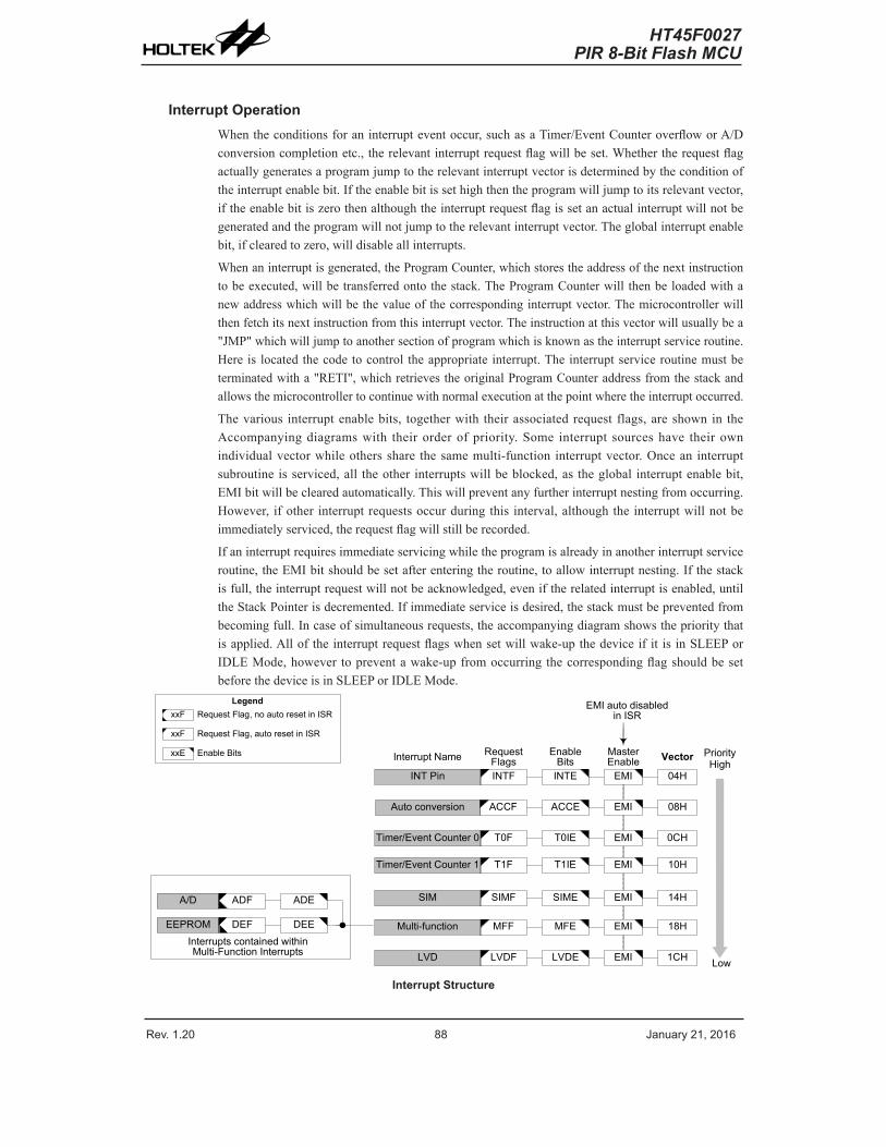
Rev. 1.20 88 ana 21 201 Rev. 1.20 89 ana 21 201
HT45F0027PIR 8-Bit Flash MCU
HT45F0027PIR 8-Bit Flash MCU
Interrupt OperationWhentheconditionsforaninterrupteventoccur,suchasaTimer/EventCounteroverfloworA/Dconversioncompletionetc.,therelevantinterruptrequestflagwillbeset.Whethertherequestflagactuallygeneratesaprogramjumptotherelevantinterruptvectorisdeterminedbytheconditionoftheinterruptenablebit.Iftheenablebitissethighthentheprogramwilljumptoitsrelevantvector,iftheenablebitiszerothenalthoughtheinterruptrequestflagissetanactualinterruptwillnotbegeneratedandtheprogramwillnotjumptotherelevantinterruptvector.Theglobalinterruptenablebit,ifclearedtozero,willdisableallinterrupts.
Whenaninterruptisgenerated,theProgramCounter,whichstorestheaddressofthenextinstructiontobeexecuted,willbetransferredontothestack.TheProgramCounterwill thenbeloadedwithanewaddresswhichwillbethevalueofthecorrespondinginterruptvector.Themicrocontrollerwillthenfetchitsnextinstructionfromthisinterruptvector.Theinstructionatthisvectorwillusuallybea"JMP"whichwilljumptoanothersectionofprogramwhichisknownastheinterruptserviceroutine.Hereis locatedthecodetocontrol theappropriate interrupt.Theinterruptserviceroutinemustbeterminatedwitha"RETI",whichretrievestheoriginalProgramCounteraddressfromthestackandallowsthemicrocontrollertocontinuewithnormalexecutionatthepointwheretheinterruptoccurred.
Thevarious interruptenablebits, togetherwith theirassociatedrequest flags,areshownin theAccompanyingdiagramswith theirorderofpriority.Some interrupt sourceshave theirownindividualvectorwhileothersshare thesamemulti-function interruptvector.Oncean interruptsubroutineisserviced,all theother interruptswillbeblocked,as theglobal interruptenablebit,EMIbitwillbeclearedautomatically.Thiswillpreventanyfurtherinterruptnestingfromoccurring.However, ifother interruptrequestsoccurduringthis interval,althoughtheinterruptwillnotbeimmediatelyserviced,therequestflagwillstillberecorded.
Ifaninterruptrequiresimmediateservicingwhiletheprogramisalreadyinanotherinterruptserviceroutine,theEMIbitshouldbesetafterenteringtheroutine,toallowinterruptnesting.Ifthestackisfull,theinterruptrequestwillnotbeacknowledged,eveniftherelatedinterruptisenabled,untiltheStackPointerisdecremented.Ifimmediateserviceisdesired,thestackmustbepreventedfrombecomingfull.Incaseofsimultaneousrequests,theaccompanyingdiagramshowstheprioritythatisapplied.Alloftheinterruptrequestflagswhensetwillwake-upthedeviceifit isinSLEEPorIDLEMode,however topreventawake-upfromoccurringthecorrespondingflagshouldbesetbeforethedeviceisinSLEEPorIDLEMode.
INT Pin INTF INTE EMI 04H
EMI 08H
EMI 0CH
EMI 10H
LVD LVDF LVDE EMI 1CH
Intept Name Reqest Flags
Enable Bits
Maste Enable Vector
EMI ato disabled in ISR
PioitHigh
Low
Time/Event Conte 0 T0F T0IE
Intepts contained within Mlti-Fnction Intepts
xxE Enable Bits
xxF Reqest Flag ato eset in ISR
LegendxxF Reqest Flag no ato eset in ISR
Ato convesion ACCF ACCE
Time/Event Conte 1 T1F T1IE
Mlti-fnction MFF MFE EMI 18H
EMI 14HA/D ADF ADE SIM SIMF SIME
EEPROM DEF DEE
Interrupt Structure

Rev. 1.20 88 ana 21 201 Rev. 1.20 89 ana 21 201
HT45F0027PIR 8-Bit Flash MCU
HT45F0027PIR 8-Bit Flash MCU
External InterruptTheexternal interrupt iscontrolledbysignal transitionson the INTpin.Anexternal interruptrequestwill takeplacewhen theexternal interrupt requestflag, INTF, isset,whichwilloccurwhenatransition,whosetypeischosenbytheedgeselectbits,appearsontheexternal interruptpin.Toallowtheprogramtobranchtoitsrespectiveinterruptvectoraddress,theglobalinterruptenablebit,EMI,andrespectiveexternalinterruptenablebit,INTE,mustfirstbeset.Additionallythecorrect interruptedge typemustbeselectedusing therelatedregister toenable theexternalinterruptfunctionandtochoosethetriggeredgetype.Astheexternalinterruptpinispin-sharedwithI/Opin,itcanonlybeconfiguredasexternalinterruptpiniftheexternalinterruptenablebitinthecorrespondinginterruptregisterhasbeenset.Thepinmustalsobesetupasaninputbysettingthecorrespondingbitintheportcontrolregister.Whentheinterruptisenabled,thestackisnotfullandthecorrecttransitiontypeappearsontheexternalinterruptpin,asubroutinecalltotheexternalinterruptvector,willtakeplace.Whentheinterruptisserviced,theexternalinterruptrequestflag,INTF,willbeautomaticallyresetandtheEMIbitwillbeautomaticallyclearedtodisableotherinterrupts.Notethatanypull-highresistorselectionsontheexternalinterruptpinwillremainvalidevenifthepinisusedasanexternalinterruptinput.
TheINTEGregisterisusedtoselectthetypeofactiveedgethatwilltriggertheexternalinterrupt.Achoiceofeitherrisingorfallingorbothedgetypescanbechosentotriggeranexternalinterrupt.NotethattheINTEGregistercanalsobeusedtodisabletheexternalinterruptfunction.
Auto conversion circuit InterruptThedevicecontainsanAutoConversionCircuitwhichhas itsown independent interrupt.TheinternalAutoConversionCircuit interruptiscontrolledbytheterminationofanA/Dconversionprocess.AninternalAutoConversionCircuit interruptwill takeplacewhentheAutoConversionCircuitinterruptrequestflagACCF,isset,whichoccurswhentheA/Dconversionprocessfinishes.Toallowtheprogramtobranchtoitsrespectiveinterruptvectoraddress,theglobalinterruptenablebit,EMI,andAutoConversionCircuit interruptenablebit,ACCE,must firstbeset.Whentheinterruptisenabled,thestackisnotfullandtheA/Dconversionprocesshasended,asubroutinecalltotheAutoConversionCircuitinterruptvector,willtakeplace.Whentheinterruptisserviced,theAutoConversionCircuitinterruptflag,ACCF,willbeautomaticallycleared.TheEMIbitwillalsobeautomaticallyclearedtodisableotherinterrupts.
Timer/Event Counter InterruptFor aTimer/EventCounter interrupt tooccur, theglobal interrupt enablebit,EMI, and thecorrespondingtimer interruptenablebit,T0IEorT1IE,mustfirstbeset.AnactualTimer/EventCounterinterruptwilltakeplacewhentheTimer/EventCounterrequestflag,T0ForT1F,isset,asituationthatwilloccurwhentheTimer/EventCounteroverflows.Whentheinterruptisenabled,thestackisnotfullandaTimer/EventCounteroverflowoccurs,asubroutinecalltothetimerinterruptvector,willtakeplace.Whentheinterruptisserviced,thetimerinterruptrequestflag,T0ForT1F,willbeautomaticallyresetandtheEMIbitwillbeautomaticallyclearedtodisableotherinterrupts.
Serial Interface Module InterruptTheSerialInterfaceModuleInterruptisalsoknownastheSIMinterrupt.ASIMInterruptrequestwilltakeplacewhentheSIMInterruptrequestflag,SIMF,isset,whichoccurswhenabyteofdatahasbeenreceivedor transmittedbytheSPIorI2Cinterface,oranI2Caddressmatchoccurs.Toallowtheprogramtobranchtoitsrespectiveinterruptvectoraddress, theglobal interruptenablebit,EMI,andtheSIMInterfaceInterruptenablebit,SIME,mustfirstbeset.Whentheinterruptisenabled,thestackisnotfullandanytheseconditionsarecreated,asubroutinecalltotherespective

Rev. 1.20 90 ana 21 201 Rev. 1.20 91 ana 21 201
HT45F0027PIR 8-Bit Flash MCU
HT45F0027PIR 8-Bit Flash MCU
interruptvector,will takeplace.WhentheSIM InterfaceInterrupt isserviced, theSIMinterruptrequestflag,SIMF,willbeautomaticallyclearedandtheEMIbitwillbeautomaticallyclearedtodisableotherinterrupts.
Multi-function InterruptWithin thedevice there isoneMulti-functioninterrupt.Unlike theother independent interrupts,these interruptshavenoindependentsource,butratherareformedfromotherexistinginterruptsources,namely,A/DconverterinterruptandEEPROMinterrupt.
AMulti-function interruptrequestwill takeplace theMulti-function interruptrequestflag,MFFisset.TheMulti-functioninterruptflagwillbesetwhenanyofitsincludedfunctionsgenerateaninterruptrequestflag.Toallowtheprogramtobranchto itsrespectiveinterruptvectoraddress,whentheMulti-functioninterruptisenabledandthestackisnotfullandeitheroneoftheinterruptscontainedwithintheMulti-functioninterruptoccurs,asubroutinecalltotheMulti-functioninterruptvectorwilltakeplace.Whentheinterruptisserviced,therelatedMulti-FunctionrequestflagwillbeautomaticallyresetandtheEMIbitwillbeautomaticallyclearedtodisableotherinterrupts.
However, itmustbenotedthat,althoughtheMulti-functionInterruptflagwillbeautomaticallyresetwhentheinterruptisserviced,therequestflagsfromtheoriginalsourceoftheMulti-functioninterrupt,namelyA/DconverterinterruptandEEPROMinterrupt,willnotbeautomaticallyresetandmustbemanuallyresetbytheapplicationprogram.
A/D Converter InterruptTheA/Dconverter interrupt iscontainedwithintheMulti-functionInterrupt.TheA/DConverterInterruptiscontrolledbytheterminationofanA/Dconversionprocess.AnA/DConverterInterruptrequestwill takeplacewhentheA/DConverterInterruptrequestflag,ADF, isset,whichoccurswhentheA/Dconversionprocessfinishes.Toallowtheprogramtobranchtoitsrespectiveinterruptvectoraddress, theglobal interruptenablebit,EMI,andA/DInterruptenablebit,ADE,andassociatedMulti-functioninterruptenablebit,mustfirstbeset.Whentheinterruptisenabled,thestackisnotfullandtheA/Dconversionprocesshasended,asubroutinecalltotheA/DConverterInterruptvector,willtakeplace.Whentheinterruptisserviced,theEMIbitwillbeautomaticallyclearedtodisableotherinterrupts,howeveronlytheMulti-functioninterruptrequestflagwillbealsoautomaticallycleared.AstheADFflagwillnotbeautomaticallycleared,ithastobeclearedbytheapplicationprogram.
EEPROM InterruptTheEEPROMinterrupt iscontainedwithintheMulti-functionInterrupt.AnEEPROMInterruptrequestwill takeplacewhen theEEPROMInterrupt request flag,DEF, is set,whichoccurswhenanEEPROMWritecycleends.Toallowtheprogramtobranchto itsrespectiveinterruptvectoraddress,theglobalinterruptenablebit,EMI,andEEPROMInterruptenablebit,DEE,andassociatedMulti-functioninterruptenablebit,mustfirstbeset.Whentheinterruptisenabled,thestackisnotfullandanEEPROMWritecycleends,asubroutinecall totherespectiveEEPROMInterruptvector,will takeplace.When theEEPROMInterrupt isserviced, theEMIbitwillbeautomaticallyclearedtodisableotherinterrupts,howeveronlytheMulti-functioninterruptrequestflagwillbealsoautomaticallycleared.AstheDEFflagwillnotbeautomaticallycleared,ithastobeclearedbytheapplicationprogram.
Rev. 1.20 90 ana 21 201 Rev. 1.20 91 ana 21 201
HT45F0027PIR 8-Bit Flash MCU
HT45F0027PIR 8-Bit Flash MCU
LVD Interrupt AnLVDInterruptrequestwilltakeplacewhentheLVDInterruptrequestflag,LVDF,isset,whichoccurswhentheLowVoltageDetectorfunctiondetectsalowpowersupplyvoltage.Toallowtheprogramtobranchtoitsrespectiveinterruptvectoraddress,theglobalinterruptenablebit,EMI,andLowVoltageInterruptenablebit,LVDE,mustfirstbeset.Whentheinterruptisenabled,thestackisnotfullandalowvoltageconditionoccurs,asubroutinecalltotheLVDInterruptvector,willtakeplace.WhentheLowVoltageInterruptisserviced,theLVDFflagwillbeautomaticallyclearedandtheEMIbitwillbeautomaticallyclearedtodisableotherinterrupts.
Interrupt Wake-up FunctionEachof the interruptfunctionshas thecapabilityofwakingupthemicrocontrollerwhenin theSLEEPorIDLEMode.Awake-upisgeneratedwhenaninterruptrequestflagchangesfromlowtohighandisindependentofwhethertheinterruptisenabledornot.Therefore,eventhoughthedeviceisintheSLEEPorIDLEModeanditssystemoscillatorstopped,situationssuchasexternaledgetransitionsontheexternalinterruptpins,alowpowersupplyvoltageorcomparatorinputchangemaycausetheirrespectiveinterruptflagtobesethighandconsequentlygenerateaninterrupt.Caremust thereforebetakenifspuriouswake-upsituationsaretobeavoided.Ifaninterruptwake-upfunctionistobedisabledthenthecorrespondinginterruptrequestflagshouldbesethighbeforethedeviceenterstheSLEEPorIDLEMode.Theinterruptenablebitshavenoeffectontheinterruptwake-upfunction.
Programming ConsiderationsBydisablingtherelevantinterruptenablebits,arequestedinterruptcanbepreventedfrombeingserviced,however,oncean interrupt request flag is set, itwill remain in thiscondition in theinterruptregisteruntilthecorrespondinginterruptisservicedoruntiltherequestflagisclearedbytheapplicationprogram.
Whereacertain interrupt iscontainedwithinaMulti-function interrupt, thenwhenthe interruptservice routine is executed, asonly theMulti-function interrupt request flags,MFF,willbeautomaticallycleared, the individual request flag for the functionneeds tobeclearedby theapplicationprogram.
It isrecommendedthatprogramsdonotusethe"CALL"instructionwithintheinterruptservicesubroutine.Interruptsoftenoccurinanunpredictablemannerorneedtobeservicedimmediately.Ifonlyonestackisleftandtheinterruptisnotwellcontrolled,theoriginalcontrolsequencewillbedamagedonceaCALLsubroutineisexecutedintheinterruptsubroutine.
Everyinterrupthasthecapabilityofwakingupthemicrocontrollerwhenit isinSLEEPorIDLEMode,thewakeupbeinggeneratedwhentheinterruptrequestflagchangesfromlowtohigh.IfitisrequiredtopreventacertaininterruptfromwakingupthemicrocontrollerthenitsrespectiverequestflagshouldbefirstsethighbeforeenterSLEEPorIDLEMode.
AsonlytheProgramCounter ispushedontothestack, thenwhentheinterrupt isserviced, if thecontentsof theaccumulator,statusregisterorotherregistersarealteredbythe interruptserviceprogram,theircontentsshouldbesavedto thememoryat thebeginningof the interruptserviceroutine.
Toreturnfromaninterruptsubroutine,eitheraRETorRETIinstructionmaybeexecuted.TheRETIinstructioninadditiontoexecutingareturntothemainprogramalsoautomaticallysetstheEMIbithightoallowfurtherinterrupts.TheRETinstructionhoweveronlyexecutesareturntothemainprogramleavingtheEMIbitinitspresentzerostateandthereforedisablingtheexecutionoffurtherinterrupts.

Rev. 1.20 92 ana 21 201 Rev. 1.20 93 ana 21 201
HT45F0027PIR 8-Bit Flash MCU
HT45F0027PIR 8-Bit Flash MCU
Low Voltage Detector – LVDEachdevicehasaLowVoltageDetectorfunction,alsoknownasLVD.Thisenabledthedevicetomonitorthepowersupplyvoltage,VDD,andprovideawarningsignalshoulditfallbelowacertainlevel.Thisfunctionmaybeespeciallyusefulinbatteryapplicationswherethesupplyvoltagewillgraduallyreduceasthebatteryages,asitallowsanearlywarningbatterylowsignaltobegenerated.TheLowVoltageDetectoralsohasthecapabilityofgeneratinganinterruptsignal.
LVD RegisterTheLowVoltageDetectorfunctioniscontrolledusingasingleregisterwiththenameLVDC.Threebits inthisregister,VLVD2~VLVD0,areusedtoselectoneofeightfixedvoltagesbelowwhichalowvoltageconditionwillbedetermined.AlowvoltageconditionisindicatedwhentheLVDObitisset.IftheLVDObitislow,thisindicatesthattheVDDvoltageisabovethepresetlowvoltagevalue.TheLVDENbit isusedtocontrol theoverallon/offfunctionof thelowvoltagedetector.Settingthebithighwillenablethelowvoltagedetector.Clearingthebittozerowillswitchofftheinternallowvoltagedetectorcircuits.Asthelowvoltagedetectorwillconsumeacertainamountofpower,itmaybedesirabletoswitchoffthecircuitwhennotinuse,animportantconsiderationinpowersensitivebatterypoweredapplications.
LVDC Register
Bit 7 6 5 4 3 2 1 0
Name LVDO LVDEN VLVD2 VLVD1 VLVD0
R/W R R/W R/W R/W R/W
POR 0 0 0 0 0
Bit7~6 Unimplemented,readas"0"Bit5 LVDO:LVDOutputFlag
0:NoLowVoltageDetect1:LowVoltageDetect
Bit4 LVDEN:LowVoltageDetectorControl0:Disable1:Enable
Bit3 Unimplemented,readas«0»Bit2~0 VLVD2~VLVD0:SelectLVDVoltage
000:2.0V001:2.2V010:2.4V011:2.7V100:3.0V101:3.3V110:3.6V111:4.0V

Rev. 1.20 92 ana 21 201 Rev. 1.20 93 ana 21 201
HT45F0027PIR 8-Bit Flash MCU
HT45F0027PIR 8-Bit Flash MCU
LVD OperationTheLowVoltageDetectorfunctionoperatesbycomparingthepowersupplyvoltage,VDD,withapre-specifiedvoltagelevelstoredintheLVDCregister.Thishasarangeofbetween2.0Vand4.0V.Whenthepowersupplyvoltage,VDD,fallsbelowthispre-determinedvalue,theLVDObitwillbesethighindicatinga lowpowersupplyvoltagecondition.TheLowVoltageDetectorfunctionissuppliedbyareferencevoltagewhichwillbeautomaticallyenabled.WhenthedeviceispowereddownthelowvoltagedetectorwillremainactiveiftheLVDENbitishigh.AfterenablingtheLowVoltageDetector,atimedelaytLVDSshouldbeallowedforthecircuitrytostabilisebeforereadingtheLVDObit.NotealsothatastheVDDvoltagemayriseandfallratherslowly,atthevoltagenearsthatofVLVD,theremaybemultiplebitLVDOtransitions.
LVD Operation
TheLowVoltageDetectoralsohasitsowninterruptwhichiscontainedwithinoneoftheMulti-functioninterrupts,providinganalternativemeansoflowvoltagedetection,inadditiontopollingtheLVDObit.TheinterruptwillonlybegeneratedafteradelayoftLVDaftertheLVDObithasbeensethighbyalowvoltagecondition.WhenthedeviceispowereddowntheLowVoltageDetectorwillremainactiveif theLVDENbit ishigh.Inthiscase, theLVDFinterruptrequestflagwillbeset,causinganinterrupttobegeneratedifVDDfallsbelowthepresetLVDvoltage.Thiswillcausethedevicetowake-upfromtheSLEEPorIDLEMode,howeveriftheLowVoltageDetectorwakeupfunctionisnotrequiredthentheLVDFflagshouldbefirstsethighbeforethedeviceenterstheSLEEPorIDLEMode.
WhenLVDfunctionisenabled,itisrecommencedtoclearLVDflagfirst,andthenenablesinterruptfunctiontoavoidmistakeaction.

Rev. 1.20 94 ana 21 201 Rev. 1.20 95 ana 21 201
HT45F0027PIR 8-Bit Flash MCU
HT45F0027PIR 8-Bit Flash MCU
Configuration OptionsConfigurationoptionsrefertocertainoptionswithintheMCUthatareprogrammedintothedeviceduringtheprogrammingprocess.Duringthedevelopmentprocess,theseoptionsareselectedusingtheHT-IDEsoftwaredevelopment tools.Astheseoptionsareprogrammedintothedeviceusingthehardwareprogrammingtools,once theyareselectedtheycannotbechangedlaterusingtheapplicationprogram.Alloptionsmustbedefinedforpropersystemfunction,thedetailsofwhichareshowninthetable.
No. Options
Oscillator Options
1
HIRC Feqenc Selection: 1. 1MHz 2. 2MHz3. 4MHz4. 8MHz
Watchdog Timer Options
2 WDT fnction: Alwas enable o B S/W contol
I2C Option
3 I2C Debonce Time: no debonce 1 sstem clock 2 sstem clock
Lock Options
4LockAllPartialLock

Rev. 1.20 94 ana 21 201 Rev. 1.20 95 ana 21 201
HT45F0027PIR 8-Bit Flash MCU
HT45F0027PIR 8-Bit Flash MCU
Application Circuits
Upper/low
erC
omparator
LDO
(2.2V~3.6V)
Floating
OPA1
-
+
-+OPA2
CH
0C
H1
CH
2C
H3
CH
4C
H5
12-bitsS
AR
ADC
VDD
VREG
AutoC
onversionC
ontroller
SIM
ADM
VREG
TEM
P. SEN
SOR
VBG
(T.S.)
VPSW
VPS0
VPS1
VP
VR
EG
30pF
LDO
EN
VSEL [3:0]
PA7
PA7S
OP
A1SW
1kΩ
0.1µF
22µF
0.02µF47kΩ
DS
1MΩ
OPA1E
OP
A1N
22µFPA
7/OPA1EC
VOPR
PA5/TM
R0/O
PA2E
VDD
VSS
VSSA
AN
1AN
0
INT/TM
R1
SDO
SDI/S
DA
SCSB
SCK/S
CL
0.02µF
0.1µF
VR
EG
22kΩ
G
PIRSensor
OPA
1EC
PA5
OP
A2E
PA5S
0.1µF
Vref

Rev. 1.20 9 ana 21 201 Rev. 1.20 97 ana 21 201
HT45F0027PIR 8-Bit Flash MCU
HT45F0027PIR 8-Bit Flash MCU
Instruction Set
IntroductionCentral to thesuccessfuloperationofanymicrocontroller is its instructionset,whichisasetofprograminstructioncodesthatdirectsthemicrocontrollertoperformcertainoperations.InthecaseofHoltekmicrocontroller,acomprehensiveandflexiblesetofover60instructionsisprovidedtoenableprogrammerstoimplementtheirapplicationwiththeminimumofprogrammingoverheads.
Foreasierunderstandingofthevariousinstructioncodes, theyhavebeensubdividedintoseveralfunctionalgroupings.
Instruction TimingMostinstructionsareimplementedwithinoneinstructioncycle.Theexceptionstothisarebranch,call,or tablereadinstructionswheretwoinstructioncyclesarerequired.Oneinstructioncycleisequalto4systemclockcycles,thereforeinthecaseofan8MHzsystemoscillator,mostinstructionswouldbeimplementedwithin0.5μsandbranchorcall instructionswouldbeimplementedwithin1μs.Although instructionswhichrequireonemorecycle to implementaregenerally limited totheJMP,CALL,RET,RETIandtablereadinstructions, it is important torealize thatanyotherinstructionswhichinvolvemanipulationoftheProgramCounterLowregisterorPCLwillalsotakeonemorecycletoimplement.AsinstructionswhichchangethecontentsofthePCLwill implyadirect jumptothatnewaddress,onemorecyclewillberequired.Examplesofsuchinstructionswouldbe"CLRPCL"or"MOVPCL,A".Forthecaseofskipinstructions,itmustbenotedthatiftheresultofthecomparisoninvolvesaskipoperationthenthiswillalsotakeonemorecycle,ifnoskipisinvolvedthenonlyonecycleisrequired.
Moving and Transferring DataThe transferofdatawithin themicrocontrollerprogram isoneof themost frequentlyusedoperations.MakinguseofthreekindsofMOVinstructions,datacanbetransferredfromregisterstotheAccumulatorandvice-versaaswellasbeingabletomovespecificimmediatedatadirectlyintotheAccumulator.Oneofthemostimportantdatatransferapplicationsis toreceivedatafromtheinputportsandtransferdatatotheoutputports.
Arithmetic OperationsTheabilitytoperformcertainarithmeticoperationsanddatamanipulationisanecessaryfeatureofmostmicrocontrollerapplications.WithintheHoltekmicrocontrollerinstructionsetarearangeofaddandsubtract instructionmnemonicstoenablethenecessaryarithmetictobecarriedout.Caremustbe taken toensurecorrecthandlingofcarryandborrowdatawhenresultsexceed255foradditionandlessthan0forsubtraction.TheincrementanddecrementinstructionsINC,INCA,DECandDECAprovideasimplemeansofincreasingordecreasingbyavalueofoneofthevaluesinthedestinationspecified.

Rev. 1.20 9 ana 21 201 Rev. 1.20 97 ana 21 201
HT45F0027PIR 8-Bit Flash MCU
HT45F0027PIR 8-Bit Flash MCU
Logical and Rotate OperationThestandardlogicaloperationssuchasAND,OR,XORandCPLallhavetheirowninstructionwithintheHoltekmicrocontroller instructionset.Aswiththecaseofmost instructionsinvolvingdatamanipulation, datamust pass through theAccumulatorwhichmay involve additionalprogrammingsteps. Inall logicaldataoperations, thezero flagmaybeset if the resultof theoperationiszero.AnotherformoflogicaldatamanipulationcomesfromtherotateinstructionssuchasRR,RL,RRCandRLCwhichprovideasimplemeansofrotatingonebitrightorleft.Differentrotateinstructionsexistdependingonprogramrequirements.Rotateinstructionsareusefulforserialportprogrammingapplicationswheredatacanberotatedfromaninternalregister intotheCarrybitfromwhereitcanbeexaminedandthenecessaryserialbitsethighorlow.Anotherapplicationwhichrotatedataoperationsareusedistoimplementmultiplicationanddivisioncalculations.
Branches and Control TransferProgrambranchingtakestheformofeitherjumpstospecifiedlocationsusingtheJMPinstructionor toa subroutineusing theCALL instruction.Theydiffer in the sense that in thecaseofasubroutinecall, theprogrammustreturn to the instruction immediatelywhenthesubroutinehasbeencarriedout.Thisisdonebyplacingareturninstruction"RET"inthesubroutinewhichwillcausetheprogramtojumpbacktotheaddressrightaftertheCALLinstruction.InthecaseofaJMPinstruction,theprogramsimplyjumpstothedesiredlocation.ThereisnorequirementtojumpbacktotheoriginaljumpingoffpointasinthecaseoftheCALLinstruction.Onespecialandextremelyusefulsetofbranchinstructionsaretheconditionalbranches.Hereadecisionisfirstmaderegardingtheconditionofacertaindatamemoryor individualbits.Dependingupon theconditions, theprogramwillcontinuewiththenextinstructionorskipoveritandjumptothefollowinginstruction.These instructionsare thekey todecisionmakingandbranchingwithin theprogramperhapsdeterminedbytheconditionofcertaininputswitchesorbytheconditionofinternaldatabits.
Bit OperationsTheabilitytoprovidesinglebitoperationsonDataMemoryisanextremelyflexiblefeatureofallHoltekmicrocontrollers.Thisfeature isespeciallyusefulforoutputportbitprogrammingwhereindividualbitsorportpinscanbedirectlysethighorlowusingeitherthe"SET[m].i"or"CLR[m].i" instructionsrespectively.Thefeatureremovestheneedforprogrammers tofirstreadthe8-bitoutputport,manipulatetheinputdatatoensurethatotherbitsarenotchangedandthenoutputtheportwiththecorrectnewdata.Thisread-modify-writeprocessistakencareofautomaticallywhenthesebitoperationinstructionsareused.
Table Read OperationsDatastorage isnormally implementedbyusing registers.However,whenworkingwith largeamountsoffixeddata, thevolumeinvolvedoftenmakesit inconvenienttostorethefixeddataintheDataMemory.Toovercomethisproblem,HoltekmicrocontrollersallowanareaofProgramMemory tobesetasa tablewheredatacanbedirectlystored.Asetofeasy touse instructionsprovides themeansbywhich this fixeddatacanbereferencedandretrievedfromtheProgramMemory.
Other OperationsInaddition to theabovefunctional instructions,a rangeofother instructionsalsoexistsuchasthe"HALT"instructionforPower-downoperationsand instructions tocontrol theoperationoftheWatchdogTimerfor reliableprogramoperationsunderextremeelectricorelectromagneticenvironments.Fortheirrelevantoperations,refertothefunctionalrelatedsections.

Rev. 1.20 98 ana 21 201 Rev. 1.20 99 ana 21 201
HT45F0027PIR 8-Bit Flash MCU
HT45F0027PIR 8-Bit Flash MCU
Instruction Set SummaryThefollowingtabledepictsasummaryoftheinstructionsetcategorisedaccordingtofunctionandcanbeconsultedasabasicinstructionreferenceusingthefollowinglistedconventions.
Table Conventionsx:Bitsimmediatedatam:DataMemoryaddressA:Accumulatori:0~7numberofbitsaddr:Programmemoryaddress
Mnemonic Description Cycles Flag AffectedArithmeticADD A[m] Add Data Memo to ACC 1 Z C AC OVADDM A[m] Add ACC to Data Memo 1Note Z C AC OVADD Ax Add immediate data to ACC 1 Z C AC OVADC A[m] Add Data Memo to ACC with Ca 1 Z C AC OVADCM A[m] Add ACC to Data memo with Ca 1Note Z C AC OVSUB Ax Sbtact immediate data fom the ACC 1 Z C AC OVSUB A[m] Sbtact Data Memo fom ACC 1 Z C AC OVSUBM A[m] Sbtact Data Memo fom ACC with eslt in Data Memo 1Note Z C AC OVSBC A[m] Sbtact Data Memo fom ACC with Ca 1 Z C AC OVSBCM A[m] Sbtact Data Memo fom ACC with Ca eslt in Data Memo 1Note Z C AC OVDAA [m] Decimal adjst ACC fo Addition with eslt in Data Memo 1Note CLogic OperationAND A[m] Logical AND Data Memo to ACC 1 ZOR A[m] Logical OR Data Memo to ACC 1 ZXOR A[m] Logical XOR Data Memo to ACC 1 ZANDM A[m] Logical AND ACC to Data Memo 1Note ZORM A[m] Logical OR ACC to Data Memo 1Note ZXORM A[m] Logical XOR ACC to Data Memo 1Note ZAND Ax Logical AND immediate Data to ACC 1 ZOR Ax Logical OR immediate Data to ACC 1 ZXOR Ax Logical XOR immediate Data to ACC 1 ZCPL [m] Complement Data Memo 1Note ZCPLA [m] Complement Data Memo with eslt in ACC 1 ZIncrement & DecrementINCA [m] Incement Data Memo with eslt in ACC 1 ZINC [m] Incement Data Memo 1Note ZDECA [m] Decement Data Memo with eslt in ACC 1 ZDEC [m] Decement Data Memo 1Note ZRotateRRA [m] Rotate Data Memo ight with eslt in ACC 1 NoneRR [m] Rotate Data Memo ight 1Note NoneRRCA [m] Rotate Data Memo ight thogh Ca with eslt in ACC 1 CRRC [m] Rotate Data Memo ight thogh Ca 1Note CRLA [m] Rotate Data Memo left with eslt in ACC 1 NoneRL [m] Rotate Data Memo left 1Note NoneRLCA [m] Rotate Data Memo left thogh Ca with eslt in ACC 1 CRLC [m] Rotate Data Memo left thogh Ca 1Note C

Rev. 1.20 98 ana 21 201 Rev. 1.20 99 ana 21 201
HT45F0027PIR 8-Bit Flash MCU
HT45F0027PIR 8-Bit Flash MCU
Mnemonic Description Cycles Flag AffectedData MoveMOV A[m] Move Data Memo to ACC 1 NoneMOV [m]A Move ACC to Data Memo 1Note NoneMOV Ax Move immediate data to ACC 1 NoneBit OperationCLR [m].i Clea bit of Data Memo 1Note NoneSET [m].i Set bit of Data Memo 1Note NoneBranch OperationMP add mp nconditionall 2 NoneSZ [m] Skip if Data Memo is zeo 1Note NoneSZA [m] Skip if Data Memo is zeo with data movement to ACC 1Note NoneSZ [m].i Skip if bit i of Data Memo is zeo 1Note NoneSNZ [m].i Skip if bit i of Data Memo is not zeo 1Note NoneSIZ [m] Skip if incement Data Memo is zeo 1Note NoneSDZ [m] Skip if decement Data Memo is zeo 1Note NoneSIZA [m] Skip if incement Data Memo is zeo with eslt in ACC 1Note NoneSDZA [m] Skip if decement Data Memo is zeo with eslt in ACC 1Note NoneCALL add Sbotine call 2 NoneRET Retn fom sbotine 2 NoneRET Ax Retn fom sbotine and load immediate data to ACC 2 NoneRETI Retn fom intept 2 NoneTable Read OperationTABRD [m] Read table (specific page) to TBLH and Data Memory 2Note NoneTABRDC [m] Read table (cent page) to TBLH and Data Memo 2Note NoneTABRDL [m] Read table (last page) to TBLH and Data Memo 2Note NoneMiscellaneousNOP No opeation 1 NoneCLR [m] Clea Data Memo 1Note NoneSET [m] Set Data Memo 1Note NoneCLR WDT Clea Watchdog Time 1 TO PDFCLR WDT1 Pe-clea Watchdog Time 1 TO PDFCLR WDT2 Pe-clea Watchdog Time 1 TO PDFSWAP [m] Swap nibbles of Data Memo 1Note NoneSWAPA [m] Swap nibbles of Data Memo with eslt in ACC 1 NoneHALT Ente powe down mode 1 TO PDF
Note:1.Forskipinstructions,iftheresultofthecomparisoninvolvesaskipthentwocyclesarerequired,ifnoskiptakesplaceonlyonecycleisrequired.
2.AnyinstructionwhichchangesthecontentsofthePCLwillalsorequire2cyclesforexecution.3.For the"CLRWDT1"and"CLRWDT2"instructions theTOandPDFflagsmaybeaffectedbytheexecution status.TheTOandPDF flagsareclearedafterboth "CLRWDT1"and"CLRWDT2"instructionsareconsecutivelyexecuted.OtherwisetheTOandPDFflagsremainunchanged.

Rev. 1.20 100 ana 21 201 Rev. 1.20 101 ana 21 201
HT45F0027PIR 8-Bit Flash MCU
HT45F0027PIR 8-Bit Flash MCU
Instruction Definition
ADC A,[m] AddDataMemorytoACCwithCarryDescription ThecontentsofthespecifiedDataMemory,Accumulatorandthecarryflagareadded. TheresultisstoredintheAccumulator.Operation ACC←ACC+[m]+CAffectedflag(s) OV,Z,AC,C
ADCM A,[m] AddACCtoDataMemorywithCarryDescription ThecontentsofthespecifiedDataMemory,Accumulatorandthecarryflagareadded. TheresultisstoredinthespecifiedDataMemory.Operation [m]←ACC+[m]+CAffectedflag(s) OV,Z,AC,C
ADD A,[m] AddDataMemorytoACCDescription ThecontentsofthespecifiedDataMemoryandtheAccumulatorareadded. TheresultisstoredintheAccumulator.Operation ACC←ACC+[m]Affectedflag(s) OV,Z,AC,C
ADD A,x AddimmediatedatatoACCDescription ThecontentsoftheAccumulatorandthespecifiedimmediatedataareadded. TheresultisstoredintheAccumulator.Operation ACC←ACC+xAffectedflag(s) OV,Z,AC,C
ADDM A,[m] AddACCtoDataMemoryDescription ThecontentsofthespecifiedDataMemoryandtheAccumulatorareadded. TheresultisstoredinthespecifiedDataMemory.Operation [m]←ACC+[m]Affectedflag(s) OV,Z,AC,C
AND A,[m] LogicalANDDataMemorytoACCDescription DataintheAccumulatorandthespecifiedDataMemoryperformabitwiselogicalAND operation.TheresultisstoredintheAccumulator.Operation ACC←ACC″AND″[m]Affectedflag(s) Z
AND A,x LogicalANDimmediatedatatoACCDescription DataintheAccumulatorandthespecifiedimmediatedataperformabitwiselogicalAND operation.TheresultisstoredintheAccumulator.Operation ACC←ACC″AND″xAffectedflag(s) Z
ANDM A,[m] LogicalANDACCtoDataMemoryDescription DatainthespecifiedDataMemoryandtheAccumulatorperformabitwiselogicalAND operation.TheresultisstoredintheDataMemory.Operation [m]←ACC″AND″[m]Affectedflag(s) Z

Rev. 1.20 100 ana 21 201 Rev. 1.20 101 ana 21 201
HT45F0027PIR 8-Bit Flash MCU
HT45F0027PIR 8-Bit Flash MCU
CALL addr SubroutinecallDescription Unconditionallycallsasubroutineatthespecifiedaddress.TheProgramCounterthen incrementsby1toobtaintheaddressofthenextinstructionwhichisthenpushedontothe stack.Thespecifiedaddressisthenloadedandtheprogramcontinuesexecutionfromthis newaddress.Asthisinstructionrequiresanadditionaloperation,itisatwocycleinstruction.Operation Stack←ProgramCounter+1 ProgramCounter←addrAffectedflag(s) None
CLR [m] ClearDataMemoryDescription EachbitofthespecifiedDataMemoryisclearedto0.Operation [m]←00HAffectedflag(s) None
CLR [m].i ClearbitofDataMemoryDescription BitiofthespecifiedDataMemoryisclearedto0.Operation [m].i←0Affectedflag(s) None
CLR WDT ClearWatchdogTimerDescription TheTO,PDFflagsandtheWDTareallcleared.Operation WDTcleared TO←0 PDF←0Affectedflag(s) TO,PDF
CLR WDT1 Pre-clearWatchdogTimerDescription TheTO,PDFflagsandtheWDTareallcleared.Notethatthisinstructionworksin conjunctionwithCLRWDT2andmustbeexecutedalternatelywithCLRWDT2tohave effect.RepetitivelyexecutingthisinstructionwithoutalternatelyexecutingCLRWDT2will havenoeffect.Operation WDTcleared TO←0 PDF←0Affectedflag(s) TO,PDF
CLR WDT2 Pre-clearWatchdogTimerDescription TheTO,PDFflagsandtheWDTareallcleared.Notethatthisinstructionworksinconjunction withCLRWDT1andmustbeexecutedalternatelywithCLRWDT1tohaveeffect. RepetitivelyexecutingthisinstructionwithoutalternatelyexecutingCLRWDT1willhaveno effect.Operation WDTcleared TO←0 PDF←0Affectedflag(s) TO,PDF
CPL [m] ComplementDataMemoryDescription EachbitofthespecifiedDataMemoryislogicallycomplemented(1′scomplement).Bitswhich previouslycontaineda1arechangedto0andviceversa.Operation [m]←[m]Affectedflag(s) Z

Rev. 1.20 102 ana 21 201 Rev. 1.20 103 ana 21 201
HT45F0027PIR 8-Bit Flash MCU
HT45F0027PIR 8-Bit Flash MCU
CPLA [m] ComplementDataMemorywithresultinACCDescription EachbitofthespecifiedDataMemoryislogicallycomplemented(1′scomplement).Bitswhich previouslycontaineda1arechangedto0andviceversa.Thecomplementedresultisstoredin theAccumulatorandthecontentsoftheDataMemoryremainunchanged.Operation ACC←[m]Affectedflag(s) Z
DAA [m] Decimal-AdjustACCforadditionwithresultinDataMemoryDescription ConvertthecontentsoftheAccumulatorvaluetoaBCD(BinaryCodedDecimal)value resultingfromthepreviousadditionoftwoBCDvariables.Ifthelownibbleisgreaterthan9 orifACflagisset,thenavalueof6willbeaddedtothelownibble.Otherwisethelownibble remainsunchanged.Ifthehighnibbleisgreaterthan9oriftheCflagisset,thenavalueof6 willbeaddedtothehighnibble.Essentially,thedecimalconversionisperformedbyadding 00H,06H,60Hor66HdependingontheAccumulatorandflagconditions.OnlytheCflag maybeaffectedbythisinstructionwhichindicatesthatiftheoriginalBCDsumisgreaterthan 100,itallowsmultipleprecisiondecimaladdition.Operation [m]←ACC+00Hor [m]←ACC+06Hor [m]←ACC+60Hor [m]←ACC+66HAffectedflag(s) C
DEC [m] DecrementDataMemoryDescription DatainthespecifiedDataMemoryisdecrementedby1.Operation [m]←[m]−1Affectedflag(s) Z
DECA[m] DecrementDataMemorywithresultinACCDescription DatainthespecifiedDataMemoryisdecrementedby1.Theresultisstoredinthe Accumulator.ThecontentsoftheDataMemoryremainunchanged.Operation ACC←[m]−1Affectedflag(s) Z
HALT EnterpowerdownmodeDescription Thisinstructionstopstheprogramexecutionandturnsoffthesystemclock.Thecontentsof theDataMemoryandregistersareretained.TheWDTandprescalerarecleared.Thepower downflagPDFissetandtheWDTtime-outflagTOiscleared.Operation TO←0 PDF←1Affectedflag(s) TO,PDF
INC [m] IncrementDataMemoryDescription DatainthespecifiedDataMemoryisincrementedby1.Operation [m]←[m]+1Affectedflag(s) Z
INCA [m] IncrementDataMemorywithresultinACCDescription DatainthespecifiedDataMemoryisincrementedby1.TheresultisstoredintheAccumulator. ThecontentsoftheDataMemoryremainunchanged.Operation ACC←[m]+1Affectedflag(s) Z

Rev. 1.20 102 ana 21 201 Rev. 1.20 103 ana 21 201
HT45F0027PIR 8-Bit Flash MCU
HT45F0027PIR 8-Bit Flash MCU
JMP addr JumpunconditionallyDescription ThecontentsoftheProgramCounterarereplacedwiththespecifiedaddress.Program executionthencontinuesfromthisnewaddress.Asthisrequirestheinsertionofadummy instructionwhilethenewaddressisloaded,itisatwocycleinstruction.Operation ProgramCounter←addrAffectedflag(s) None
MOV A,[m] MoveDataMemorytoACCDescription ThecontentsofthespecifiedDataMemoryarecopiedtotheAccumulator.Operation ACC←[m]Affectedflag(s) None
MOV A,x MoveimmediatedatatoACCDescription TheimmediatedataspecifiedisloadedintotheAccumulator.Operation ACC←xAffectedflag(s) None
MOV [m],A MoveACCtoDataMemoryDescription ThecontentsoftheAccumulatorarecopiedtothespecifiedDataMemory.Operation [m]←ACCAffectedflag(s) None
NOP NooperationDescription Nooperationisperformed.Executioncontinueswiththenextinstruction.Operation NooperationAffectedflag(s) None
OR A,[m] LogicalORDataMemorytoACCDescription DataintheAccumulatorandthespecifiedDataMemoryperformabitwise logicalORoperation.TheresultisstoredintheAccumulator.Operation ACC←ACC″OR″[m]Affectedflag(s) Z
OR A,x LogicalORimmediatedatatoACCDescription DataintheAccumulatorandthespecifiedimmediatedataperformabitwiselogicalOR operation.TheresultisstoredintheAccumulator.Operation ACC←ACC″OR″xAffectedflag(s) Z
ORM A,[m] LogicalORACCtoDataMemoryDescription DatainthespecifiedDataMemoryandtheAccumulatorperformabitwiselogicalOR operation.TheresultisstoredintheDataMemory.Operation [m]←ACC″OR″[m]Affectedflag(s) Z
RET ReturnfromsubroutineDescription TheProgramCounterisrestoredfromthestack.Programexecutioncontinuesattherestored address.Operation ProgramCounter←StackAffectedflag(s) None

Rev. 1.20 104 ana 21 201 Rev. 1.20 105 ana 21 201
HT45F0027PIR 8-Bit Flash MCU
HT45F0027PIR 8-Bit Flash MCU
RET A,x ReturnfromsubroutineandloadimmediatedatatoACCDescription TheProgramCounterisrestoredfromthestackandtheAccumulatorloadedwiththespecified immediatedata.Programexecutioncontinuesattherestoredaddress.Operation ProgramCounter←Stack ACC←xAffectedflag(s) None
RETI ReturnfrominterruptDescription TheProgramCounterisrestoredfromthestackandtheinterruptsarere-enabledbysettingthe EMIbit.EMIisthemasterinterruptglobalenablebit.Ifaninterruptwaspendingwhenthe RETIinstructionisexecuted,thependingInterruptroutinewillbeprocessedbeforereturning tothemainprogram.Operation ProgramCounter←Stack EMI←1Affectedflag(s) None
RL [m] RotateDataMemoryleftDescription ThecontentsofthespecifiedDataMemoryarerotatedleftby1bitwithbit7rotatedintobit0.Operation [m].(i+1)←[m].i;(i=0~6) [m].0←[m].7Affectedflag(s) None
RLA [m] RotateDataMemoryleftwithresultinACCDescription ThecontentsofthespecifiedDataMemoryarerotatedleftby1bitwithbit7rotatedintobit0. TherotatedresultisstoredintheAccumulatorandthecontentsoftheDataMemoryremain unchanged.Operation ACC.(i+1)←[m].i;(i=0~6) ACC.0←[m].7Affectedflag(s) None
RLC [m] RotateDataMemoryleftthroughCarryDescription ThecontentsofthespecifiedDataMemoryandthecarryflagarerotatedleftby1bit.Bit7 replacestheCarrybitandtheoriginalcarryflagisrotatedintobit0.Operation [m].(i+1)←[m].i;(i=0~6) [m].0←C C←[m].7Affectedflag(s) C
RLCA [m] RotateDataMemoryleftthroughCarrywithresultinACCDescription DatainthespecifiedDataMemoryandthecarryflagarerotatedleftby1bit.Bit7replacesthe Carrybitandtheoriginalcarryflagisrotatedintothebit0.Therotatedresultisstoredinthe AccumulatorandthecontentsoftheDataMemoryremainunchanged.Operation ACC.(i+1)←[m].i;(i=0~6) ACC.0←C C←[m].7Affectedflag(s) C
RR [m] RotateDataMemoryrightDescription ThecontentsofthespecifiedDataMemoryarerotatedrightby1bitwithbit0rotatedintobit7.Operation [m].i←[m].(i+1);(i=0~6) [m].7←[m].0Affectedflag(s) None

Rev. 1.20 104 ana 21 201 Rev. 1.20 105 ana 21 201
HT45F0027PIR 8-Bit Flash MCU
HT45F0027PIR 8-Bit Flash MCU
RRA [m] RotateDataMemoryrightwithresultinACCDescription DatainthespecifiedDataMemoryandthecarryflagarerotatedrightby1bitwithbit0 rotatedintobit7.TherotatedresultisstoredintheAccumulatorandthecontentsofthe DataMemoryremainunchanged.Operation ACC.i←[m].(i+1);(i=0~6) ACC.7←[m].0Affectedflag(s) None
RRC [m] RotateDataMemoryrightthroughCarryDescription ThecontentsofthespecifiedDataMemoryandthecarryflagarerotatedrightby1bit.Bit0 replacestheCarrybitandtheoriginalcarryflagisrotatedintobit7.Operation [m].i←[m].(i+1);(i=0~6) [m].7←C C←[m].0Affectedflag(s) C
RRCA [m] RotateDataMemoryrightthroughCarrywithresultinACCDescription DatainthespecifiedDataMemoryandthecarryflagarerotatedrightby1bit.Bit0replaces theCarrybitandtheoriginalcarryflagisrotatedintobit7.Therotatedresultisstoredinthe AccumulatorandthecontentsoftheDataMemoryremainunchanged.Operation ACC.i←[m].(i+1);(i=0~6) ACC.7←C C←[m].0Affectedflag(s) C
SBC A,[m] SubtractDataMemoryfromACCwithCarryDescription ThecontentsofthespecifiedDataMemoryandthecomplementofthecarryflagare subtractedfromtheAccumulator.TheresultisstoredintheAccumulator.Notethatifthe resultofsubtractionisnegative,theCflagwillbeclearedto0,otherwiseiftheresultis positiveorzero,theCflagwillbesetto1.Operation ACC←ACC−[m]−CAffectedflag(s) OV,Z,AC,C
SBCM A,[m] SubtractDataMemoryfromACCwithCarryandresultinDataMemoryDescription ThecontentsofthespecifiedDataMemoryandthecomplementofthecarryflagare subtractedfromtheAccumulator.TheresultisstoredintheDataMemory.Notethatifthe resultofsubtractionisnegative,theCflagwillbeclearedto0,otherwiseiftheresultis positiveorzero,theCflagwillbesetto1.Operation [m]←ACC−[m]−CAffectedflag(s) OV,Z,AC,C
SDZ [m] SkipifdecrementDataMemoryis0Description ThecontentsofthespecifiedDataMemoryarefirstdecrementedby1.Iftheresultis0the followinginstructionisskipped.Asthisrequirestheinsertionofadummyinstructionwhile thenextinstructionisfetched,itisatwocycleinstruction.Iftheresultisnot0theprogram proceedswiththefollowinginstruction.Operation [m]←[m]−1 Skipif[m]=0Affectedflag(s) None

Rev. 1.20 10 ana 21 201 Rev. 1.20 107 ana 21 201
HT45F0027PIR 8-Bit Flash MCU
HT45F0027PIR 8-Bit Flash MCU
SDZA [m] SkipifdecrementDataMemoryiszerowithresultinACCDescription ThecontentsofthespecifiedDataMemoryarefirstdecrementedby1.Iftheresultis0,the followinginstructionisskipped.TheresultisstoredintheAccumulatorbutthespecified DataMemorycontentsremainunchanged.Asthisrequirestheinsertionofadummy instructionwhilethenextinstructionisfetched,itisatwocycleinstruction.Iftheresultisnot0, theprogramproceedswiththefollowinginstruction.Operation ACC←[m]−1 SkipifACC=0Affectedflag(s) None
SET [m] SetDataMemoryDescription EachbitofthespecifiedDataMemoryissetto1.Operation [m]←FFHAffectedflag(s) None
SET [m].i SetbitofDataMemoryDescription BitiofthespecifiedDataMemoryissetto1.Operation [m].i←1Affectedflag(s) None
SIZ [m] SkipifincrementDataMemoryis0Description ThecontentsofthespecifiedDataMemoryarefirstincrementedby1.Iftheresultis0,the followinginstructionisskipped.Asthisrequirestheinsertionofadummyinstructionwhile thenextinstructionisfetched,itisatwocycleinstruction.Iftheresultisnot0theprogram proceedswiththefollowinginstruction.Operation [m]←[m]+1 Skipif[m]=0Affectedflag(s) None
SIZA [m] SkipifincrementDataMemoryiszerowithresultinACCDescription ThecontentsofthespecifiedDataMemoryarefirstincrementedby1.Iftheresultis0,the followinginstructionisskipped.TheresultisstoredintheAccumulatorbutthespecified DataMemorycontentsremainunchanged.Asthisrequirestheinsertionofadummy instructionwhilethenextinstructionisfetched,itisatwocycleinstruction.Iftheresultisnot 0theprogramproceedswiththefollowinginstruction.Operation ACC←[m]+1 SkipifACC=0Affectedflag(s) None
SNZ [m].i SkipifbitiofDataMemoryisnot0Description IfbitiofthespecifiedDataMemoryisnot0,thefollowinginstructionisskipped.Asthis requirestheinsertionofadummyinstructionwhilethenextinstructionisfetched,itisatwo cycleinstruction.Iftheresultis0theprogramproceedswiththefollowinginstruction.Operation Skipif[m].i≠0Affectedflag(s) None
SUB A,[m] SubtractDataMemoryfromACCDescription ThespecifiedDataMemoryissubtractedfromthecontentsoftheAccumulator.Theresultis storedintheAccumulator.Notethatiftheresultofsubtractionisnegative,theCflagwillbe clearedto0,otherwiseiftheresultispositiveorzero,theCflagwillbesetto1.Operation ACC←ACC−[m]Affectedflag(s) OV,Z,AC,C

Rev. 1.20 10 ana 21 201 Rev. 1.20 107 ana 21 201
HT45F0027PIR 8-Bit Flash MCU
HT45F0027PIR 8-Bit Flash MCU
SUBM A,[m] SubtractDataMemoryfromACCwithresultinDataMemoryDescription ThespecifiedDataMemoryissubtractedfromthecontentsoftheAccumulator.Theresultis storedintheDataMemory.Notethatiftheresultofsubtractionisnegative,theCflagwillbe clearedto0,otherwiseiftheresultispositiveorzero,theCflagwillbesetto1.Operation [m]←ACC−[m]Affectedflag(s) OV,Z,AC,C
SUB A,x SubtractimmediatedatafromACCDescription TheimmediatedataspecifiedbythecodeissubtractedfromthecontentsoftheAccumulator. TheresultisstoredintheAccumulator.Notethatiftheresultofsubtractionisnegative,theC flagwillbeclearedto0,otherwiseiftheresultispositiveorzero,theCflagwillbesetto1.Operation ACC←ACC−xAffectedflag(s) OV,Z,AC,C
SWAP [m] SwapnibblesofDataMemoryDescription Thelow-orderandhigh-ordernibblesofthespecifiedDataMemoryareinterchanged.Operation [m].3~[m].0↔[m].7~[m].4Affectedflag(s) None
SWAPA [m] SwapnibblesofDataMemorywithresultinACCDescription Thelow-orderandhigh-ordernibblesofthespecifiedDataMemoryareinterchanged.The resultisstoredintheAccumulator.ThecontentsoftheDataMemoryremainunchanged.Operation ACC.3~ACC.0←[m].7~[m].4 ACC.7~ACC.4←[m].3~[m].0Affectedflag(s) None
SZ [m] SkipifDataMemoryis0Description IfthecontentsofthespecifiedDataMemoryis0,thefollowinginstructionisskipped.Asthis requirestheinsertionofadummyinstructionwhilethenextinstructionisfetched,itisatwo cycleinstruction.Iftheresultisnot0theprogramproceedswiththefollowinginstruction.Operation Skipif[m]=0Affectedflag(s) None
SZA [m] SkipifDataMemoryis0withdatamovementtoACCDescription ThecontentsofthespecifiedDataMemoryarecopiedtotheAccumulator.Ifthevalueiszero, thefollowinginstructionisskipped.Asthisrequirestheinsertionofadummyinstruction whilethenextinstructionisfetched,itisatwocycleinstruction.Iftheresultisnot0the programproceedswiththefollowinginstruction.Operation ACC←[m] Skipif[m]=0Affectedflag(s) None
SZ [m].i SkipifbitiofDataMemoryis0Description IfbitiofthespecifiedDataMemoryis0,thefollowinginstructionisskipped.Asthisrequires theinsertionofadummyinstructionwhilethenextinstructionisfetched,itisatwocycle instruction.Iftheresultisnot0,theprogramproceedswiththefollowinginstruction.Operation Skipif[m].i=0Affectedflag(s) None

Rev. 1.20 108 ana 21 201 Rev. 1.20 109 ana 21 201
HT45F0027PIR 8-Bit Flash MCU
HT45F0027PIR 8-Bit Flash MCU
TABRD [m] Readtable(specificpage)toTBLHandDataMemoryDescription Thelowbyteoftheprogramcode(specificpage)addressedbythetablepointerpair (TBHPandTBLP)ismovedtothespecifiedDataMemoryandthehighbytemovedtoTBLH.Operation [m]←programcode(lowbyte) TBLH←programcode(highbyte)Affectedflag(s) None
TABRDC [m] Readtable(currentpage)toTBLHandDataMemoryDescription Thelowbyteoftheprogramcode(currentpage)addressedbythetablepointer(TBLP)is movedtothespecifiedDataMemoryandthehighbytemovedtoTBLH.Operation [m]←programcode(lowbyte) TBLH←programcode(highbyte)Affectedflag(s) None
TABRDL [m] Readtable(lastpage)toTBLHandDataMemoryDescription Thelowbyteoftheprogramcode(lastpage)addressedbythetablepointer(TBLP)ismoved tothespecifiedDataMemoryandthehighbytemovedtoTBLH.Operation [m]←programcode(lowbyte) TBLH←programcode(highbyte)Affectedflag(s) None
XOR A,[m] LogicalXORDataMemorytoACCDescription DataintheAccumulatorandthespecifiedDataMemoryperformabitwiselogicalXOR operation.TheresultisstoredintheAccumulator.Operation ACC←ACC″XOR″[m]Affectedflag(s) Z
XORM A,[m] LogicalXORACCtoDataMemoryDescription DatainthespecifiedDataMemoryandtheAccumulatorperformabitwiselogicalXOR operation.TheresultisstoredintheDataMemory.Operation [m]←ACC″XOR″[m]Affectedflag(s) Z
XOR A,x LogicalXORimmediatedatatoACCDescription DataintheAccumulatorandthespecifiedimmediatedataperformabitwiselogicalXOR operation.TheresultisstoredintheAccumulator.Operation ACC←ACC″XOR″xAffectedflag(s) Z

Rev. 1.20 108 ana 21 201 Rev. 1.20 109 ana 21 201
HT45F0027PIR 8-Bit Flash MCU
HT45F0027PIR 8-Bit Flash MCU
Package Information
Note that thepackage informationprovidedhere is for consultationpurposesonly.As thisinformationmaybeupdatedatregularintervalsusersareremindedtoconsulttheHoltekwebsiteforthelatestversionofthePackage/CartonInformation.
Additionalsupplementaryinformationwithregardtopackagingislistedbelow.Clickontherelevantsectiontobetransferredtotherelevantwebsitepage.
• FurtherPackageInformation(includeOutlineDimensions,ProductTapeandReelSpecifications)
• PackingMeterialsInformation
• Cartoninformation

Rev. 1.20 110 ana 21 201 Rev. 1.20 111 ana 21 201
HT45F0027PIR 8-Bit Flash MCU
HT45F0027PIR 8-Bit Flash MCU
16-pin NSOP (150mil) Outline Dimensions
SymbolDimensions in inch
Min. Nom. Max.A — 0.23 BSC —
B — 0.154 BSC —
C 0.012 — 0.020C’ — 0.390 BSC —D — — 0.09E — 0.050 BSC —F 0.004 — 0.010G 0.01 — 0.050H 0.004 — 0.010α 0° — 8°
SymbolDimensions in mm
Min. Nom. Max.A — BSC —B — 3.9 BSC —C 0.31 — 0.51C’ — 9.9 BSC —D — — 1.75E — 1.27 BSC —F 0.10 — 0.25G 0.40 — 1.27H 0.10 — 0.25α 0° — 8°

Rev. 1.20 110 ana 21 201 Rev. 1.20 111 ana 21 201
HT45F0027PIR 8-Bit Flash MCU
HT45F0027PIR 8-Bit Flash MCU
SAW Type 16-pin (3mm×3mm, FP0.25mm) QFN Outline Dimensions
SymbolDimensions in inch
Min. Nom. Max.A 0.028 0.030 0.031
A1 0.000 0.001 0.002
A2 — 0.008 REF —b 0.007 0.010 0.012 D — 0.118 BSC —E — 0.118 BSC —e — 0.020 BSC —
D2 0.03 0.07 0.09 E2 0.03 0.07 0.09 L 0.008 0.010 0.012 K 0.008 — —
SymbolDimensions in mm
Min. Nom. Max.A 0.700 0.750 0.800
A1 0.000 0.020 0.050A2 — 0.200 REF —b 0.180 0.250 0.300D — 3.000 BSC —E — 3.000 BSC —e — 0.50 BSC —
D2 1.0 1.70 1.75E2 1.0 1.70 1.75L 0.20 0.25 0.30K 0.20 — —

Rev. 1.20 112 ana 21 201 Rev. 1.20 PB ana 21 201
HT45F0027PIR 8-Bit Flash MCU
HT45F0027PIR 8-Bit Flash MCU
Copight© 201 b HOLTEK SEMICONDUCTOR INC.
The infomation appeaing in this Data Sheet is believed to be accate at the time of pblication. Howeve Holtek assmes no esponsibilit aising fom the se of the specifications described. The applications mentioned herein are used solely fo the ppose of illstation and Holtek makes no waant o epesentation that sch applications will be sitable withot fthe modification no ecommends the se of its podcts fo application that ma pesent a isk to hman life de to malfnction o othewise. Holtek's podcts ae not athoized fo se as citical components in life sppot devices o sstems. Holtek eseves the ight to alte its products without prior notification. For the most up-to-date information, please visit o web site at http://www.holtek.com.tw.