a/d flash mcu with eeprom€¦ · rev. 1.60 10 november 19, 2019 rev. 1.60 11 november 19, 2019...
TRANSCRIPT

A/D Flash MCU with EEPROM
HT66F0175/HT66F0185
Revision: V1.60 Date: November 19, 2019
Rev. 1.60 2 November 19, 2019 Rev. 1.60 3 November 19, 2019
HT66F0175/HT66F0185A/D Flash MCU with EEPROM
HT66F0175/HT66F0185A/D Flash MCU with EEPROM
Table of ContentsFeatures ................................................................................................................ 7
CPU Features ..............................................................................................................................7Peripheral Features ......................................................................................................................7
General Description ............................................................................................. 8Selection Table ..................................................................................................... 8Block Diagram ...................................................................................................... 9Pin Assignment .................................................................................................... 9Pin Descriptions ................................................................................................ 11Absolute Maximum Ratings .............................................................................. 17D.C. Characteristics ........................................................................................... 17A.C. Characteristics ........................................................................................... 19HIRC Electrical Characteristics ........................................................................ 20A/D Converter Electrical Characteristics ......................................................... 21LVD/LVR Electrical Characteristics .................................................................. 22Comparator Electrical Characteristics ............................................................ 22Software Controlled LCD Driver Electrical Characteristics ........................... 23Power-on Reset Characteristics ....................................................................... 23System Architecture .......................................................................................... 24
Clocking and Pipelining ..............................................................................................................24Program Counter ........................................................................................................................25Stack ..........................................................................................................................................26Arithmetic and Logic Unit – ALU ................................................................................................26
Flash Program Memory ..................................................................................... 27Structure .....................................................................................................................................27Special Vectors ..........................................................................................................................27Look-up Table .............................................................................................................................28Table Program Example .............................................................................................................28In Circuit Programming – ICP ....................................................................................................29On-Chip Debug Support – OCDS ..............................................................................................30
Data Memory ...................................................................................................... 31Structure .....................................................................................................................................31
Special Function Register Description ............................................................ 33Indirect Addressing Registers – IAR0, IAR1 ..............................................................................33Memory Pointers – MP0, MP1 ...................................................................................................33Bank Pointer – BP ......................................................................................................................34Accumulator – ACC ....................................................................................................................34Program Counter Low Register – PCL .......................................................................................34Look-up Table Registers – TBLP, TBHP, TBLH ..........................................................................34Status Register – STATUS .........................................................................................................35
Rev. 1.60 2 November 19, 2019 Rev. 1.60 3 November 19, 2019
HT66F0175/HT66F0185A/D Flash MCU with EEPROM
HT66F0175/HT66F0185A/D Flash MCU with EEPROM
EEPROM Data Memory ...................................................................................... 37EEPROM Data Memory Structure .............................................................................................37EEPROM Registers ...................................................................................................................37Reading Data from the EEPROM ..............................................................................................39Writing Data to the EEPROM .....................................................................................................39Write Protection ..........................................................................................................................39EEPROM Interrupt .....................................................................................................................39Programming Considerations .....................................................................................................40
Oscillator ............................................................................................................ 41Oscillator Overview ....................................................................................................................41System Clock Configurations .....................................................................................................41External Crystal/Ceramic Oscillator – HXT ................................................................................42Internal High Speed RC Oscillator – HIRC ................................................................................43External 32.768 kHz Crystal Oscillator – LXT ............................................................................43Internal 32kHz Oscillator – LIRC ................................................................................................44Supplementary Oscillators .........................................................................................................44
Operating Modes and System Clocks ............................................................. 45System Clocks ...........................................................................................................................45System Operation Modes ...........................................................................................................46Control Registers .......................................................................................................................47Fast Wake-up .............................................................................................................................49Operating Mode Switching .........................................................................................................50Standby Current Considerations ................................................................................................54Wake-up .....................................................................................................................................54Programming Considerations .....................................................................................................55
Watchdog Timer ................................................................................................. 55Watchdog Timer Clock Source ...................................................................................................55Watchdog Timer Control Register ..............................................................................................55Watchdog Timer Operation ........................................................................................................57
Reset and Initialisation ...................................................................................... 58Reset Functions .........................................................................................................................58Reset Initial Conditions ..............................................................................................................60
Input/Output Ports ............................................................................................. 64Pull-high Resistors .....................................................................................................................65Port A Wake-up ..........................................................................................................................65I/O Port Control Registers ..........................................................................................................66I/O Port Source Current Control .................................................................................................66Pin-remapping Functions ...........................................................................................................68I/O Pin Structures .......................................................................................................................69Programming Considerations .....................................................................................................70
Rev. 1.60 4 November 19, 2019 Rev. 1.60 5 November 19, 2019
HT66F0175/HT66F0185A/D Flash MCU with EEPROM
HT66F0175/HT66F0185A/D Flash MCU with EEPROM
Timer Modules – TM .......................................................................................... 71Introduction ................................................................................................................................71TM Operation .............................................................................................................................71TM Clock Source ........................................................................................................................72TM Interrupts ..............................................................................................................................72TM External Pins ........................................................................................................................72TM Input/Output Pin Control Register ........................................................................................73Programming Considerations .....................................................................................................75
Compact Type TM – CTM .................................................................................. 76Compact TM Operation ..............................................................................................................76Compact Type TM Register Description.....................................................................................77Compact Type TM Operation Modes .........................................................................................81
Standard Type TM – STM .................................................................................. 87Standard TM Operation ..............................................................................................................87Standard Type TM Register Description ....................................................................................88Standard Type TM Operation Modes .........................................................................................92
Periodic Type TM – PTM .................................................................................. 102Periodic TM Operation .............................................................................................................102Periodic Type TM Register Description ....................................................................................103Periodic Type TM Operation Modes .........................................................................................108
Analog to Digital Converter ............................................................................ 117A/D Overview ........................................................................................................................... 117A/D Converter Register Description ......................................................................................... 118A/D Input Pins ..........................................................................................................................124A/D Reference Voltage .............................................................................................................124A/D Operation ..........................................................................................................................124Conversion Rate and Timing Diagram .....................................................................................125Summary of A/D Conversion Steps ..........................................................................................126Programming Considerations ...................................................................................................127A/D Transfer Function ..............................................................................................................127A/D Programming Examples ....................................................................................................128
Serial Interface Module – SIM ......................................................................... 130SPI Interface ............................................................................................................................130SPI Registers ...........................................................................................................................131SPI Communication .................................................................................................................134I2C Interface .............................................................................................................................136I2C Registers ............................................................................................................................137I2C Bus Communication ...........................................................................................................141I2C Time-out Control .................................................................................................................144
Rev. 1.60 4 November 19, 2019 Rev. 1.60 5 November 19, 2019
HT66F0175/HT66F0185A/D Flash MCU with EEPROM
HT66F0175/HT66F0185A/D Flash MCU with EEPROM
Comparators .................................................................................................... 146Comparator Operation .............................................................................................................146Comparator Interrupt ................................................................................................................146Programming Considerations ...................................................................................................146
SCOM/SSEG Function for LCD ....................................................................... 148LCD Operation .........................................................................................................................148LCD Control Registers .............................................................................................................150
UART Interface ................................................................................................. 155UART External Pin ...................................................................................................................156UART Data Transfer Scheme...................................................................................................156UART Status and Control Registers.........................................................................................156Baud Rate Generator ...............................................................................................................162UART Setup and Control..........................................................................................................163UART Transmitter.....................................................................................................................164UART Receiver ........................................................................................................................165Managing Receiver Errors .......................................................................................................167UART Interrupt Structure..........................................................................................................168UART Power Down and Wake-up ............................................................................................169
Low Voltage Detector – LVD ........................................................................... 170LVD Register ............................................................................................................................170LVD Operation ..........................................................................................................................171
Interrupts .......................................................................................................... 172Interrupt Registers ....................................................................................................................172Interrupt Operation ...................................................................................................................179External Interrupt ......................................................................................................................181Comparator Interrupt – HT66F0185 .........................................................................................181Multi-function Interrupt .............................................................................................................181A/D Converter Interrupt ............................................................................................................182Time Base Interrupt ..................................................................................................................182Serial Interface Module Interrupt ..............................................................................................183UART Transfer Interrupt – HT66F0185 ....................................................................................183LVD Interrupt ............................................................................................................................184EEPROM Interrupt ...................................................................................................................184TM Interrupt ..............................................................................................................................184Interrupt Wake-up Function ......................................................................................................185Programming Considerations ...................................................................................................185
Configuration Options ..................................................................................... 186Application Circuits ......................................................................................... 186
Rev. 1.60 6 November 19, 2019 Rev. 1.60 7 November 19, 2019
HT66F0175/HT66F0185A/D Flash MCU with EEPROM
HT66F0175/HT66F0185A/D Flash MCU with EEPROM
Instruction Set .................................................................................................. 187Introduction ..............................................................................................................................187Instruction Timing .....................................................................................................................187Moving and Transferring Data ..................................................................................................187Arithmetic Operations ...............................................................................................................187Logical and Rotate Operation ..................................................................................................188Branches and Control Transfer ................................................................................................188Bit Operations ..........................................................................................................................188Table Read Operations ............................................................................................................188Other Operations ......................................................................................................................188
Instruction Set Summary ................................................................................ 189Table Conventions ....................................................................................................................189
Instruction Definition ....................................................................................... 191Package Information ....................................................................................... 200
20-pin SOP (300mil) Outline Dimensions ................................................................................20120-pin SSOP (150mil) Outline Dimensions ..............................................................................20224-pin SOP (300mil) Outline Dimensions ................................................................................20324-pin SSOP (150mil) Outline Dimensions ..............................................................................20428-pin SOP (300mil) Outline Dimensions ................................................................................20528-pin SSOP (150mil) Outline Dimensions ..............................................................................206
Rev. 1.60 6 November 19, 2019 Rev. 1.60 7 November 19, 2019
HT66F0175/HT66F0185A/D Flash MCU with EEPROM
HT66F0175/HT66F0185A/D Flash MCU with EEPROM
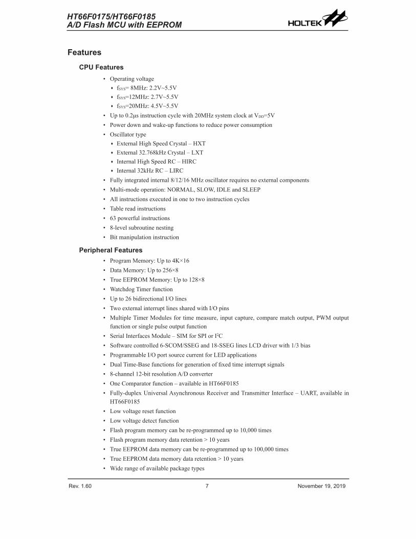
FeaturesCPU Features
• Operating voltage ♦ fSYS= 8MHz: 2.2V~5.5V ♦ fSYS=12MHz: 2.7V~5.5V ♦ fSYS=20MHz: 4.5V~5.5V
• Up to 0.2μs instruction cycle with 20MHz system clock at VDD=5V• Power down and wake-up functions to reduce power consumption• Oscillator type
♦ External High Speed Crystal – HXT ♦ External 32.768kHz Crystal – LXT ♦ Internal High Speed RC – HIRC ♦ Internal 32kHz RC – LIRC
• Fully integrated internal 8/12/16 MHz oscillator requires no external components• Multi-mode operation: NORMAL, SLOW, IDLE and SLEEP• All instructions executed in one to two instruction cycles• Table read instructions• 63 powerful instructions• 8-level subroutine nesting• Bit manipulation instruction
Peripheral Features• Program Memory: Up to 4K×16• Data Memory: Up to 256×8• True EEPROM Memory: Up to 128×8• Watchdog Timer function• Up to 26 bidirectional I/O lines• Two external interrupt lines shared with I/O pins• Multiple Timer Modules for time measure, input capture, compare match output, PWM output
function or single pulse output function• Serial Interfaces Module – SIM for SPI or I2C• Software controlled 6-SCOM/SSEG and 18-SSEG lines LCD driver with 1/3 bias• Programmable I/O port source current for LED applications• Dual Time-Base functions for generation of fixed time interrupt signals• 8-channel 12-bit resolution A/D converter• One Comparator function – available in HT66F0185• Fully-duplex Universal Asynchronous Receiver and Transmitter Interface – UART, available in
HT66F0185• Low voltage reset function• Low voltage detect function• Flash program memory can be re-programmed up to 10,000 times• Flash program memory data retention > 10 years• True EEPROM data memory can be re-programmed up to 100,000 times• True EEPROM data memory data retention > 10 years• Wide range of available package types
Rev. 1.60 8 November 19, 2019 Rev. 1.60 9 November 19, 2019
HT66F0175/HT66F0185A/D Flash MCU with EEPROM
HT66F0175/HT66F0185A/D Flash MCU with EEPROM
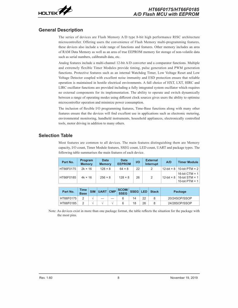
General DescriptionThe series of devices are Flash Memory A/D type 8-bit high performance RISC architecture microcontroller. Offering users the convenience of Flash Memory multi-programming features, these devices also include a wide range of functions and features. Other memory includes an area of RAM Data Memory as well as an area of true EEPROM memory for storage of non-volatile data such as serial numbers, calibratuib data, etc.
Analog features include a multi-channel 12-bit A/D converter and a comparator functions. Multiple and extremely flexible Timer Modules provide timing, pulse generation and PWM generation functions. Protective features such as an internal Watchdog Timer, Low Voltage Reset and Low Voltage Detector coupled with excellent noise immunity and ESD protection ensure that reliable operation is maintained in hostile electrical environments. A full choice of HXT, LXT, HIRC and LIRC oscillator functions are provided including a fully integrated system oscillator which requires no external components for its implementation. The ability to operate and switch dynamically between a range of operating modes using different clock sources gives users the ability to optimise microcontroller operation and minimize power consumption.
The inclusion of flexible I/O programming features, Time-Base functions along with many other features ensure that the devices will find excellent use in applications such as electronic metering, environmental monitoring, handheld instruments, household appliances, electronically controlled tools, motor driving in addition to many others.
Selection TableMost features are common to all devices. The main features distinguishing them are Memory capacity, I/O count, Timer Module features, SSEG count, LED count, UART and package types. The following table summarises the main features of each device.
Part No. Program Memory
Data Memory
Data EEPROM I/O External
Interrupt A/D Timer Module
HT66F0175 2k × 16 128 × 8 64 × 8 22 2 12-bit × 8 10-bit PTM × 2
HT66F0185 4k × 16 256 × 8 128 × 8 26 2 12-bit × 816-bit CTM × 116-bit STM × 110-bit PTM × 1
Part No. Time Base SIM UART CMP SCOM/
SSEG SSEG LED Stack Package
HT66F0175 2 √ — — 6 14 22 8 20/24SOP/SSOPHT66F0185 2 √ √ √ 6 18 26 8 24/28SOP/SSOP
Note: As devices exist in more than one package format, the table reflects the situation for the package with the most pins.
Rev. 1.60 8 November 19, 2019 Rev. 1.60 9 November 19, 2019
HT66F0175/HT66F0185A/D Flash MCU with EEPROM
HT66F0175/HT66F0185A/D Flash MCU with EEPROM
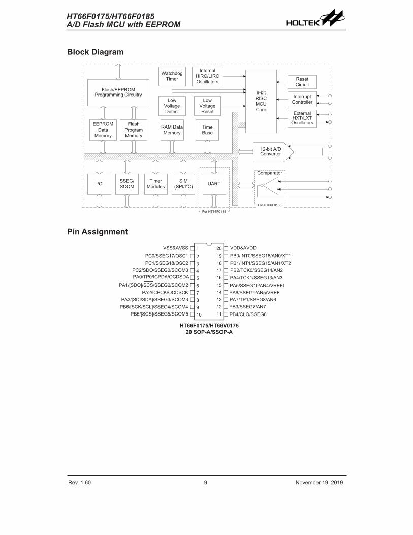
Block Diagram
8-bitRISCMCUCore
I/O Timer Modules
Flash Program Memory
EEPROMData
Memory
Flash/EEPROM Programming Circuitry
TimeBase
SIM(SPI/I2C)
Low Voltage Reset
Watchdog Timer
Low Voltage Detect
InterruptController
ResetCircuit
External HXT/LXT
Oscillators
12-bit A/DConverter
RAM Data Memory
SSEG/SCOM UART
Internal HIRC/LIRCOscillators
For HT66F0185
+─
For HT66F0185
Comparator
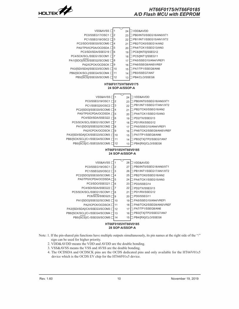
Pin Assignment
HT66F0175/HT66V017520 SOP-A/SSOP-A
20191817161514131211
12345678910
VSS&AVSSPC0/SSEG17/OSC1PC1/SSEG18/OSC2
PC2/SDO/SSEG0/SCOM0PA0/TP0/ICPDA/OCDSDA
PA2/ICPCK/OCDSCKPA3/[SDI/SDA]/SSEG3/SCOM3
PB6/[SCK/SCL]/SSEG4/SCOM4
PA1/[SDO]/SCS/SSEG2/SCOM2
PB5/[SCS]/SSEG5/SCOM5
VDD&AVDDPB0/INT0/SSEG16/AN0/XT1PB1/INT1/SSEG15/AN1/XT2PB2/TCK0/SSEG14/AN2PA4/TCK1/SSEG13/AN3PA5/SSEG10/AN4/VREFIPA6/SSEG9/AN5/VREFPA7/TP1/SSEG8/AN6PB3/SSEG7/AN7PB4/CLO/SSEG6
Rev. 1.60 10 November 19, 2019 Rev. 1.60 11 November 19, 2019
HT66F0175/HT66F0185A/D Flash MCU with EEPROM
HT66F0175/HT66F0185A/D Flash MCU with EEPROM
HT66F0175/HT66V017524 SOP-A/SSOP-A
242322212019181716151413
123456789101112
VDD&AVDDPB0/INT0/SSEG16/AN0/XT1PB1/INT1/SSEG15/AN1/XT2PB2/TCK0/SSEG14/AN2PA4/TCK1/SSEG13/AN3
PA5/SSEG10/AN4/VREFIPA6/SSEG9/AN5/VREFPA7/TP1/SSEG8/AN6PB3/SSEG7/AN7PB4/CLO/SSEG6
PC5/[INT1]/SSEG11PC6/[INT0]/SSEG12
VSS&AVSSPC0/SSEG17/OSC1PC1/SSEG18/OSC2
PC2/SDO/SSEG0/SCOM0PA0/TP0/ICPDA/OCDSDA
PA1/[SDO]/SCS/SSEG2/SCOM2PA2/ICPCK/OCDSCK
PA3/[SDI/SDA]/SSEG3/SCOM3PB6/[SCK/SCL]/SSEG4/SCOM4
PB5/[SCS]/SSEG5/SCOM5
PC3/SDI/SDA/SSEG19PC4/SCK/SCL/SSEG1/SCOM1
HT66F0185/HT66V018524 SOP-A/SSOP-A
242322212019181716151413
123456789101112
VDD&AVDDPB0/INT0/SSEG18/AN0/XT1PB1/INT1/SSEG17/AN1/XT2PB2/TCK0/SSEG16/AN2PA4/TCK1/SSEG15/AN3
PA5/SSEG10/AN4/VREFIPA6/TCK2/SSEG9/AN5/VREFPA7/TP1/SSEG8/AN6PB3/[TX]/TP2/SSEG7/AN7PB4/[RX]/CLO/SSEG6
PD1/RX/SSEG12PD2/TX/SSEG13
VSS&AVSSPC0/SSEG19/OSC1PC1/SSEG20/OSC2
PC2/[SDO]/SSEG0/SCOM0PA0/TP0/ICPDA/OCDSDA
PA1/[SDO]/SSEG2/SCOM2PA2/ICPCK/OCDSCK
PA3/[SDI/SDA]/CX/SSEG3/SCOM3PB6/[SCK/SCL]/C+/SSEG4/SCOM4
PB5/[SCS]/C-/SSEG5/SCOM5
PC4/SDI/SDA/SSEG22PC5/SCK/SCL/SSEG1/SCOM1
HT66F0185/HT66V018528 SOP-A/SSOP-A
2827262524232221201918171615
1234567891011121314
VDD&AVDDPB0/INT0/SSEG18/AN0/XT1PB1/INT1/SSEG17/AN1/XT2PB2/TCK0/SSEG16/AN2PA4/TCK1/SSEG15/AN3
PA5/SSEG10/AN4/VREFIPA6/TCK2/SSEG9/AN5/VREFPA7/TP1/SSEG8/AN6PB3/[TX]/TP2/SSEG7/AN7PB4/[RX]/CLO/SSEG6
PD0/SSEG11PD1/RX/SSEG12PD2/TX/SSEG13PD3/SSEG14
VSS&AVSSPC0/SSEG19/OSC1PC1/SSEG20/OSC2
PC2/[SDO]/SSEG0/SCOM0PA0/TP0/ICPDA/OCDSDA
PA1/[SDO]/SSEG2/SCOM2PA2/ICPCK/OCDSCK
PA3/[SDI/SDA]/CX/SSEG3/SCOM3PB6/[SCK/SCL]/C+/SSEG4/SCOM4
PB5/[SCS]/C-/SSEG5/SCOM5
PC3/SDO/SSEG21PC4/SDI/SDA/SSEG22
PC5/SCK/SCL/SSEG1/SCOM1PC6/SCS/SSEG23
Note: 1. If the pin-shared pin functions have multiple outputs simultaneously, its pin names at the right side of the “/” sign can be used for higher priority.
2. VDD&AVDD means the VDD and AVDD are the double bonding.3. VSS&AVSS means the VSS and AVSS are the double bonding.4. The OCDSDA and OCDSCK pins are the OCDS dedicated pins and only available for the HT66V01x5
device which is the OCDS EV chip for the HT66F01x5 device.
Rev. 1.60 10 November 19, 2019 Rev. 1.60 11 November 19, 2019
HT66F0175/HT66F0185A/D Flash MCU with EEPROM
HT66F0175/HT66F0185A/D Flash MCU with EEPROM
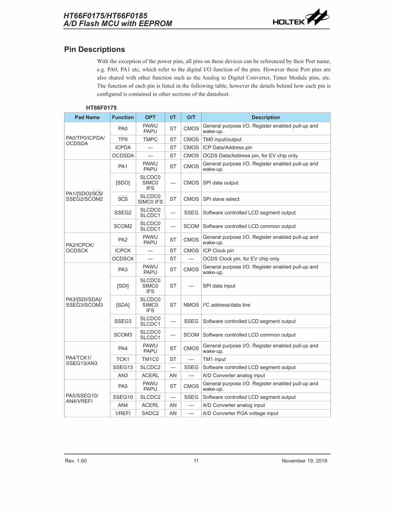
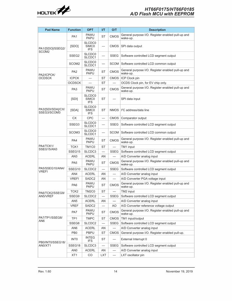
Pin DescriptionsWith the exception of the power pins, all pins on these devices can be referenced by their Port name, e.g. PA0, PA1 etc, which refer to the digital I/O function of the pins. However these Port pins are also shared with other function such as the Analog to Digital Converter, Timer Module pins, etc. The function of each pin is listed in the following table, however the details behind how each pin is configured is contained in other sections of the datasheet.
HT66F0175Pad Name Function OPT I/T O/T Description
PA0/TP0/ICPDA/OCDSDA
PA0 PAWUPAPU ST CMOS General purpose I/O. Register enabled pull-up and
wake-up.TP0 TMPC ST CMOS TM0 input/output
ICPDA — ST CMOS ICP Data/Address pinOCDSDA — ST CMOS OCDS Data/Address pin, for EV chip only.
PA1/[SDO]/SCS/SSEG2/SCOM2
PA1 PAWUPAPU ST CMOS General purpose I/O. Register enabled pull-up and
wake-up.
[SDO]SLCDC0SIMC0
IFS— CMOS SPI data output
SCS SLCDC0SIMC0 IFS ST CMOS SPI slave select
SSEG2 SLCDC0SLCDC1 — SSEG Software controlled LCD segment output
SCOM2 SLCDC0SLCDC1 — SCOM Software controlled LCD common output
PA2/ICPCK/OCDSCK
PA2 PAWUPAPU ST CMOS General purpose I/O. Register enabled pull-up and
wake-up.ICPCK — ST CMOS ICP Clock pin
OCDSCK — ST — OCDS Clock pin, for EV chip only.
PA3/[SDI/SDA]/SSEG3/SCOM3
PA3 PAWUPAPU ST CMOS General purpose I/O. Register enabled pull-up and
wake-up.
[SDI]SLCDC0SIMC0
IFSST — SPI data input
[SDA]SLCDC0SIMC0
IFSST NMOS I2C address/data line
SSEG3 SLCDC0SLCDC1 — SSEG Software controlled LCD segment output
SCOM3 SLCDC0SLCDC1 — SCOM Software controlled LCD common output
PA4/TCK1/SSEG13/AN3
PA4 PAWUPAPU ST CMOS General purpose I/O. Register enabled pull-up and
wake-up.TCK1 TM1C0 ST — TM1 input
SSEG13 SLCDC2 — SSEG Software controlled LCD segment outputAN3 ACERL AN — A/D Converter analog input
PA5/SSEG10/AN4/VREFI
PA5 PAWUPAPU ST CMOS General purpose I/O. Register enabled pull-up and
wake-up.SSEG10 SLCDC2 — SSEG Software controlled LCD segment output
AN4 ACERL AN — A/D Converter analog inputVREFI SADC2 AN — A/D Converter PGA voltage input
Rev. 1.60 12 November 19, 2019 Rev. 1.60 13 November 19, 2019
HT66F0175/HT66F0185A/D Flash MCU with EEPROM
HT66F0175/HT66F0185A/D Flash MCU with EEPROM
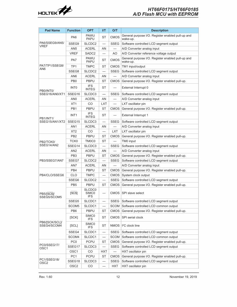
Pad Name Function OPT I/T O/T Description
PA6/SSEG9/AN5/VREF
PA6 PAWUPAPU ST CMOS General purpose I/O. Register enabled pull-up and
wake-up.SSEG9 SLCDC2 — SSEG Software controlled LCD segment output
AN5 ACERL AN — A/D Converter analog inputVREF SADC2 — AO A/D Converter reference voltage output
PA7/TP1/SSEG8/AN6
PA7 PAWUPAPU ST CMOS General purpose I/O. Register enabled pull-up and
wake-up.TP1 TMPC ST CMOS TM1 input/output
SSEG8 SLCDC2 — SSEG Software controlled LCD segment outputAN6 ACERL AN — A/D Converter analog input
PB0/INT0/SSEG16/AN0/XT1
PB0 PBPU ST CMOS General purpose I/O. Register enabled pull-up.
INT0 IFSINTEG ST — External Interrupt 0
SSEG16 SLCDC3 — SSEG Software controlled LCD segment outputAN0 ACERL AN — A/D Converter analog inputXT1 CO LXT — LXT oscillator pin
PB1/INT1/SSEG15/AN1/XT2
PB1 PBPU ST CMOS General purpose I/O. Register enabled pull-up.
INT1 IFSINTEG ST — External Interrupt 1
SSEG15 SLCDC3 — SSEG Software controlled LCD segment outputAN1 ACERL AN — A/D Converter analog inputXT2 CO — LXT LXT oscillator pin
PB2/TCK0/SSEG14/AN2
PB2 PBPU ST CMOS General purpose I/O. Register enabled pull-up.TCK0 TM0C0 ST — TM0 input
SSEG14 SLCDC3 — SSEG Software controlled LCD segment outputAN2 ACERL AN — A/D Converter analog input
PB3/SSEG7/AN7PB3 PBPU ST CMOS General purpose I/O. Register enabled pull-up.
SSEG7 SLCDC2 — SSEG Software controlled LCD segment outputAN7 ACERL AN — A/D Converter analog input
PB4/CLO/SSEG6PB4 PBPU ST CMOS General purpose I/O. Register enabled pull-up.CLO TMPC — CMOS System clock output
SSEG6 SLCDC2 — SSEG Software controlled LCD segment output
PB5/[SCS]/SSEG5/SCOM5
PB5 PBPU ST CMOS General purpose I/O. Register enabled pull-up.
[SCS]SLCDC0SIMC0
IFS— CMOS SPI slave select
SSEG5 SLCDC1 — SSEG Software controlled LCD segment outputSCOM5 SLCDC1 — SCOM Software controlled LCD common output
PB6/[SCK/SCL]/SSEG4/SCOM4
PB6 PBPU ST CMOS General purpose I/O. Register enabled pull-up.
[SCK] SIMC0IFS ST CMOS SPI serial clock
[SCL] SIMC0IFS ST NMOS I2C clock line
SSEG4 SLCDC1 — SSEG Software controlled LCD segment outputSCOM4 SLCDC1 — SCOM Software controlled LCD common output
PC0/SSEG17/OSC1
PC0 PCPU ST CMOS General purpose I/O. Register enabled pull-up.SSEG17 SLCDC3 — SSEG Software controlled LCD segment output
OSC1 CO HXT — HXT oscillator pin
PC1/SSEG18/OSC2
PC1 PCPU ST CMOS General purpose I/O. Register enabled pull-up.SSEG18 SLCDC3 — SSEG Software controlled LCD segment output
OSC2 CO — HXT HXT oscillator pin
Rev. 1.60 12 November 19, 2019 Rev. 1.60 13 November 19, 2019
HT66F0175/HT66F0185A/D Flash MCU with EEPROM
HT66F0175/HT66F0185A/D Flash MCU with EEPROM
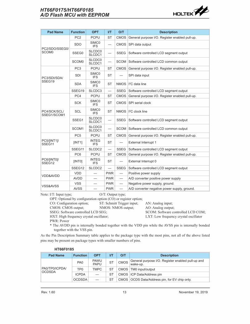
Pad Name Function OPT I/T O/T Description
PC2/SDO/SSEG0/SCOM0
PC2 PCPU ST CMOS General purpose I/O. Register enabled pull-up.
SDO SIMC0IFS — CMOS SPI data output
SSEG0 SLCDC0SLCDC1 — SSEG Software controlled LCD segment output
SCOM0 SLCDC0SLCDC1 — SCOM Software controlled LCD common output
PC3/SDI/SDA/SSEG19
PC3 PCPU ST CMOS General purpose I/O. Register enabled pull-up.
SDI SIMC0IFS ST — SPI data input
SDA SIMC0IFS ST NMOS I2C data line
SSEG19 SLCDC3 — SSEG Software controlled LCD segment output
PC4/SCK/SCL/SSEG1/SCOM1
PC4 PCPU ST CMOS General purpose I/O. Register enabled pull-up.
SCK SIMC0IFS ST CMOS SPI serial clock
SCL SIMC0IFS ST NMOS I2C clock line
SSEG1 SLCDC0SLCDC1 — SSEG Software controlled LCD segment output
SCOM1 SLCDC0SLCDC1 — SCOM Software controlled LCD common output
PC5/[INT1]/SSEG11
PC5 PCPU ST CMOS General purpose I/O. Register enabled pull-up.
[INT1] INTEGIFS ST — External Interrupt 1
SSEG11 SLCDC2 — SSEG Software controlled LCD segment output
PC6/[INT0]/SSEG12
PC6 PCPU ST CMOS General purpose I/O. Register enabled pull-up.
[INT0] INTEGIFS ST — External Interrupt 0
SSEG12 SLCDC2 — SSEG Software controlled LCD segment output
VDD&AVDDVDD — PWR — Positive power supply
AVDD — PWR — A/D converter positive power supply
VSS&AVSSVSS — PWR — Negative power supply, ground.
AVSS — PWR — A/D converter negative power supply, ground.
Note: I/T: Input type; O/T: Output type;OPT: Optional by configuration option (CO) or register option; CO: Configuration option; ST: Schmitt Trigger input; AN: Analog input;CMOS: CMOS output; NMOS: NMOS output; AO: Analog output;SSEG: Software controlled LCD SEG; SCOM: Software controlled LCD COM;HXT: High frequency crystal oscillator; LXT: Low frequency crystal oscillatorPWR: Power* The AVDD pin is internally bonded together with the VDD pin while the AVSS pin is internally bonded
together with the VSS pin.As the Pin Description Summary table applies to the package type with the most pins, not all of the above listed pins may be present on package types with smaller numbers of pins.
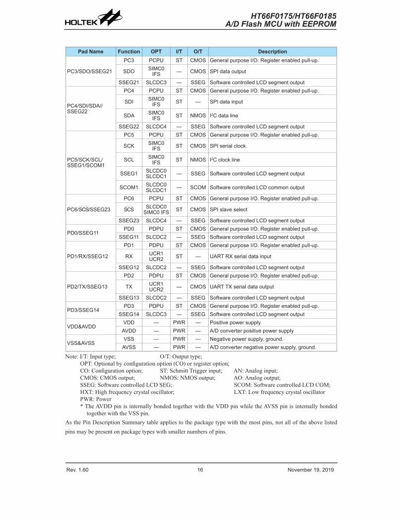
HT66F0185Pad Name Function OPT I/T O/T Description
PA0/TP0/ICPDA/OCDSDA
PA0 PAWUPAPU ST CMOS General purpose I/O. Register enabled pull-up and
wake-up.TP0 TMPC ST CMOS TM0 input/output
ICPDA — ST CMOS ICP Data/Address pinOCDSDA — ST CMOS OCDS Data/Address pin, for EV chip only.
Rev. 1.60 14 November 19, 2019 Rev. 1.60 15 November 19, 2019
HT66F0175/HT66F0185A/D Flash MCU with EEPROM
HT66F0175/HT66F0185A/D Flash MCU with EEPROM
Pad Name Function OPT I/T O/T Description
PA1/[SDO]/SSEG2/SCOM2
PA1 PAWUPAPU ST CMOS General purpose I/O. Register enabled pull-up and
wake-up.
[SDO]SLCDC0SIMC0
IFS— CMOS SPI data output
SSEG2 SLCDC0SLCDC1 — SSEG Software controlled LCD segment output
SCOM2 SLCDC0SLCDC1 — SCOM Software controlled LCD common output
PA2/ICPCK/OCDSCK
PA2 PAWUPAPU ST CMOS General purpose I/O. Register enabled pull-up and
wake-up.ICPCK — ST CMOS ICP Clock pin
OCDSCK — ST — OCDS Clock pin, for EV chip only.
PA3/[SDI/SDA]/CX/SSEG3/SCOM3
PA3 PAWUPAPU ST CMOS General purpose I/O. Register enabled pull-up and
wake-up.
[SDI]SLCDC0SIMC0
IFSST — SPI data input
[SDA]SLCDC0SIMC0
IFSST NMOS I2C address/data line
CX CPC — CMOS Comparator output
SSEG3 SLCDC0SLCDC1 — SSEG Software controlled LCD segment output
SCOM3 SLCDC0SLCDC1 — SCOM Software controlled LCD common output
PA4/TCK1/SSEG15/AN3
PA4 PAWUPAPU ST CMOS General purpose I/O. Register enabled pull-up and
wake-up.TCK1 TM1C0 ST — TM1 input
SSEG15 SLCDC3 — SSEG Software controlled LCD segment outputAN3 ACERL AN — A/D Converter analog input
PA5/SSEG10/AN4/VREFI
PA5 PAWUPAPU ST CMOS General purpose I/O. Register enabled pull-up and
wake-up.SSEG10 SLCDC2 — SSEG Software controlled LCD segment output
AN4 ACERL AN — A/D Converter analog inputVREFI SADC2 AN — A/D Converter PGA voltage input
PA6/TCK2/SSEG9/AN5/VREF
PA6 PAWUPAPU ST CMOS General purpose I/O. Register enabled pull-up and
wake-up.TCK2 TM2C0 ST — TM2 input
SSEG9 SLCDC2 — SSEG Software controlled LCD segment outputAN5 ACERL AN — A/D Converter analog input
VREF SADC2 — AO A/D Converter reference voltage output
PA7/TP1/SSEG8/AN6
PA7 PAWUPAPU ST CMOS General purpose I/O. Register enabled pull-up and
wake-up.TP1 TMPC ST CMOS TM1 input/output
SSEG8 SLCDC2 — SSEG Software controlled LCD segment outputAN6 ACERL AN — A/D Converter analog input
PB0/INT0/SSEG18/AN0/XT1
PB0 PBPU ST CMOS General purpose I/O. Register enabled pull-up.
INT0 INTEGIFS ST — External Interrupt 0
SSEG18 SLCDC3 — SSEG Software controlled LCD segment outputAN0 ACERL AN — A/D Converter analog inputXT1 CO LXT — LXT oscillator pin
Rev. 1.60 14 November 19, 2019 Rev. 1.60 15 November 19, 2019
HT66F0175/HT66F0185A/D Flash MCU with EEPROM
HT66F0175/HT66F0185A/D Flash MCU with EEPROM
Pad Name Function OPT I/T O/T Description
PB1/INT1/SSEG17/AN1/XT2
PB1 PBPU ST CMOS General purpose I/O. Register enabled pull-up.
INT1 INTEGIFS ST — External Interrupt 1
SSEG17 SLCDC3 — SSEG Software controlled LCD segment outputAN1 ACERL AN — A/D Converter analog inputXT2 CO — LXT LXT oscillator pin
PB2/TCK0/SSEG16/AN2
PB2 PBPU ST CMOS General purpose I/O. Register enabled pull-up.TCK0 TM0C0 ST — TM0 input
SSEG16 SLCDC3 — SSEG Software controlled LCD segment outputAN2 ACERL AN — A/D Converter analog input
PB3/[TX]/TP2/SSEG7/AN7
PB3 PBPU ST CMOS General purpose I/O. Register enabled pull-up.
[TX] UCR1UCR2 — CMOS UART TX serial data output
TP2 TMPC ST CMOS TM2 input/outputSSEG7 SLCDC2 — SSEG Software controlled LCD segment output
AN7 ACERL AN — A/D Converter analog input
PB4/[RX]/CLO/SSEG6
PB4 PBPU ST CMOS General purpose I/O. Register enabled pull-up.
[RX] UCR1UCR2 ST — UART RX serial data input
CLO TMPC — CMOS System clock outputSSEG6 SLCDC2 — SSEG Software controlled LCD segment output
PB5/[SCS]/C-/SSEG5/SCOM5
PB5 PBPU ST CMOS General purpose I/O. Register enabled pull-up.
[SCS]SLCDC0SIMC0
IFSST CMOS SPI slave select
C- CPC AN — Comparator inputSSEG5 SLCDC1 — SSEG Software controlled LCD segment outputSCOM5 SLCDC1 — SCOM Software controlled LCD common output
PB6/[SCK/SCL]/C+/SSEG4/SCOM4
PB6 PBPU ST CMOS General purpose I/O. Register enabled pull-up.
[SCK] SIMC0IFS ST CMOS SPI serial clock
[SCL] SIMC0IFS ST NMOS I2C clock line
C+ CPC AN — Comparator inputSSEG4 SLCDC1 — SSEG Software controlled LCD segment outputSCOM4 SLCDC1 — SCOM Software controlled LCD common output
PC0/SSEG19/OSC1
PC0 PCPU ST CMOS General purpose I/O. Register enabled pull-up.SSEG19 SLCDC3 — SSEG Software controlled LCD segment output
OSC1 CO HXT — HXT oscillator pin
PC1/SSEG20/OSC2
PC1 PCPU ST CMOS General purpose I/O. Register enabled pull-up.SSEG20 SLCDC3 — SSEG Software controlled LCD segment output
OSC2 CO — HXT HXT oscillator pin
PC2/[SDO]/SSEG0/SCOM0
PC2 PCPU ST CMOS General purpose I/O. Register enabled pull-up.
[SDO] SIMC0IFS — CMOS SPI data output
SSEG0 SLCDC0SLCDC1 — SSEG Software controlled LCD segment output
SCOM0 SLCDC0SLCDC1 — SCOM Software controlled LCD common output
Rev. 1.60 16 November 19, 2019 Rev. 1.60 17 November 19, 2019
HT66F0175/HT66F0185A/D Flash MCU with EEPROM
HT66F0175/HT66F0185A/D Flash MCU with EEPROM
Pad Name Function OPT I/T O/T Description
PC3/SDO/SSEG21
PC3 PCPU ST CMOS General purpose I/O. Register enabled pull-up.
SDO SIMC0IFS — CMOS SPI data output
SSEG21 SLCDC3 — SSEG Software controlled LCD segment output
PC4/SDI/SDA//SSEG22
PC4 PCPU ST CMOS General purpose I/O. Register enabled pull-up.
SDI SIMC0IFS ST — SPI data input
SDA SIMC0IFS ST NMOS I2C data line
SSEG22 SLCDC4 — SSEG Software controlled LCD segment output
PC5/SCK/SCL/SSEG1/SCOM1
PC5 PCPU ST CMOS General purpose I/O. Register enabled pull-up.
SCK SIMC0IFS ST CMOS SPI serial clock
SCL SIMC0IFS ST NMOS I2C clock line
SSEG1 SLCDC0SLCDC1 — SSEG Software controlled LCD segment output
SCOM1 SLCDC0SLCDC1 — SCOM Software controlled LCD common output
PC6/SCS/SSEG23
PC6 PCPU ST CMOS General purpose I/O. Register enabled pull-up.
SCS SLCDC0SIMC0 IFS ST CMOS SPI slave select
SSEG23 SLCDC4 — SSEG Software controlled LCD segment output
PD0/SSEG11PD0 PDPU ST CMOS General purpose I/O. Register enabled pull-up.
SSEG11 SLCDC2 — SSEG Software controlled LCD segment output
PD1/RX/SSEG12
PD1 PDPU ST CMOS General purpose I/O. Register enabled pull-up.
RX UCR1UCR2 ST — UART RX serial data input
SSEG12 SLCDC2 — SSEG Software controlled LCD segment output
PD2/TX/SSEG13
PD2 PDPU ST CMOS General purpose I/O. Register enabled pull-up.
TX UCR1UCR2 — CMOS UART TX serial data output
SSEG13 SLCDC2 — SSEG Software controlled LCD segment output
PD3/SSEG14PD3 PDPU ST CMOS General purpose I/O. Register enabled pull-up.
SSEG14 SLCDC3 — SSEG Software controlled LCD segment output
VDD&AVDDVDD — PWR — Positive power supply
AVDD — PWR — A/D converter positive power supply
VSS&AVSSVSS — PWR — Negative power supply, ground.
AVSS — PWR — A/D converter negative power supply, ground.
Note: I/T: Input type; O/T: Output type;OPT: Optional by configuration option (CO) or register option; CO: Configuration option; ST: Schmitt Trigger input; AN: Analog input;CMOS: CMOS output; NMOS: NMOS output; AO: Analog output;SSEG: Software controlled LCD SEG; SCOM: Software controlled LCD COM;HXT: High frequency crystal oscillator; LXT: Low frequency crystal oscillatorPWR: Power* The AVDD pin is internally bonded together with the VDD pin while the AVSS pin is internally bonded
together with the VSS pin.As the Pin Description Summary table applies to the package type with the most pins, not all of the above listed pins may be present on package types with smaller numbers of pins.
Rev. 1.60 16 November 19, 2019 Rev. 1.60 17 November 19, 2019
HT66F0175/HT66F0185A/D Flash MCU with EEPROM
HT66F0175/HT66F0185A/D Flash MCU with EEPROM
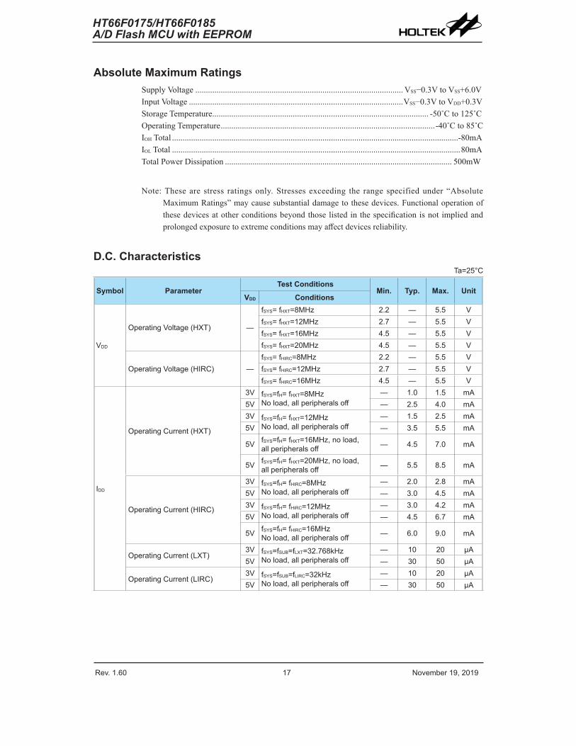
Absolute Maximum RatingsSupply Voltage .................................................................................................. VSS−0.3V to VSS+6.0VInput Voltage .....................................................................................................VSS−0.3V to VDD+0.3VStorage Temperature ...................................................................................................... -50˚C to 125˚COperating Temperature .....................................................................................................-40˚C to 85˚CIOH Total .......................................................................................................................................-80mAIOL Total ........................................................................................................................................80mATotal Power Dissipation ........................................................................................................... 500mW
Note: These are stress ratings only. Stresses exceeding the range specified under “Absolute Maximum Ratings” may cause substantial damage to these devices. Functional operation of these devices at other conditions beyond those listed in the specification is not implied and prolonged exposure to extreme conditions may affect devices reliability.
D.C. CharacteristicsTa=25°C
Symbol ParameterTest Conditions
Min. Typ. Max. UnitVDD Conditions
VDD
Operating Voltage (HXT) —
fSYS= fHXT=8MHz 2.2 — 5.5 VfSYS= fHXT=12MHz 2.7 — 5.5 VfSYS= fHXT=16MHz 4.5 — 5.5 VfSYS= fHXT=20MHz 4.5 — 5.5 V
Operating Voltage (HIRC) —fSYS= fHIRC=8MHz 2.2 — 5.5 VfSYS= fHIRC=12MHz 2.7 — 5.5 VfSYS= fHIRC=16MHz 4.5 — 5.5 V
IDD
Operating Current (HXT)
3V fSYS=fH= fHXT=8MHzNo load, all peripherals off
— 1.0 1.5 mA5V — 2.5 4.0 mA3V fSYS=fH= fHXT=12MHz
No load, all peripherals off— 1.5 2.5 mA
5V — 3.5 5.5 mA
5V fSYS=fH= fHXT=16MHz, no load, all peripherals off — 4.5 7.0 mA
5V fSYS=fH= fHXT=20MHz, no load, all peripherals off — 5.5 8.5 mA
Operating Current (HIRC)
3V fSYS=fH= fHIRC=8MHzNo load, all peripherals off
— 2.0 2.8 mA5V — 3.0 4.5 mA3V fSYS=fH= fHIRC=12MHz
No load, all peripherals off— 3.0 4.2 mA
5V — 4.5 6.7 mA
5V fSYS=fH= fHIRC=16MHzNo load, all peripherals off — 6.0 9.0 mA
Operating Current (LXT)3V fSYS=fSUB=fLXT=32.768kHz
No load, all peripherals off— 10 20 μA
5V — 30 50 μA
Operating Current (LIRC)3V fSYS=fSUB=fLIRC=32kHz
No load, all peripherals off— 10 20 μA
5V — 30 50 μA
Rev. 1.60 18 November 19, 2019 Rev. 1.60 19 November 19, 2019
HT66F0175/HT66F0185A/D Flash MCU with EEPROM
HT66F0175/HT66F0185A/D Flash MCU with EEPROM
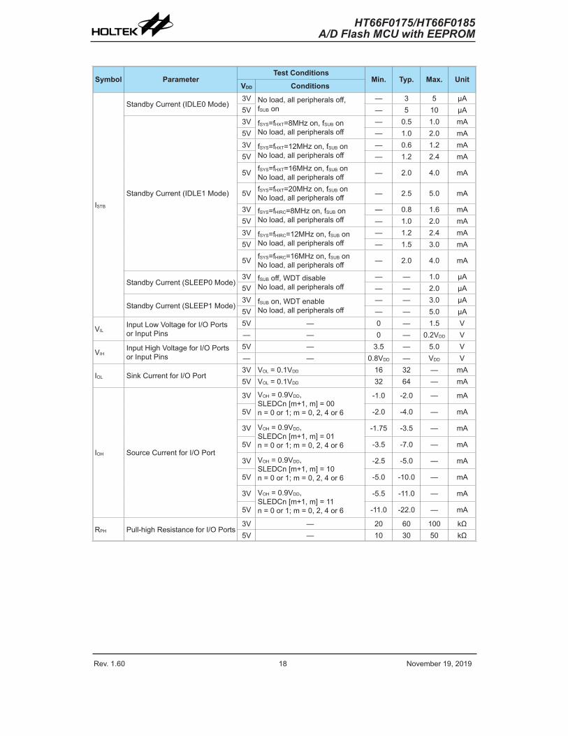
Symbol ParameterTest Conditions
Min. Typ. Max. UnitVDD Conditions
ISTB
Standby Current (IDLE0 Mode)3V No load, all peripherals off,
fSUB on— 3 5 μA
5V — 5 10 μA
Standby Current (IDLE1 Mode)
3V fSYS=fHXT=8MHz on, fSUB onNo load, all peripherals off
— 0.5 1.0 mA5V — 1.0 2.0 mA3V fSYS=fHXT=12MHz on, fSUB on
No load, all peripherals off— 0.6 1.2 mA
5V — 1.2 2.4 mA
5V fSYS=fHXT=16MHz on, fSUB onNo load, all peripherals off — 2.0 4.0 mA
5V fSYS=fHXT=20MHz on, fSUB onNo load, all peripherals off — 2.5 5.0 mA
3V fSYS=fHIRC=8MHz on, fSUB onNo load, all peripherals off
— 0.8 1.6 mA5V — 1.0 2.0 mA3V fSYS=fHIRC=12MHz on, fSUB on
No load, all peripherals off— 1.2 2.4 mA
5V — 1.5 3.0 mA
5V fSYS=fHIRC=16MHz on, fSUB onNo load, all peripherals off — 2.0 4.0 mA
Standby Current (SLEEP0 Mode)3V fSUB off, WDT disable
No load, all peripherals off— — 1.0 μA
5V — — 2.0 μA
Standby Current (SLEEP1 Mode)3V fSUB on, WDT enable
No load, all peripherals off— — 3.0 μA
5V — — 5.0 μA
VILInput Low Voltage for I/O Ports or Input Pins
5V — 0 — 1.5 V— — 0 — 0.2VDD V
VIHInput High Voltage for I/O Ports or Input Pins
5V — 3.5 — 5.0 V— — 0.8VDD — VDD V
IOL Sink Current for I/O Port3V VOL = 0.1VDD 16 32 — mA5V VOL = 0.1VDD 32 64 — mA
IOH Source Current for I/O Port
3V VOH = 0.9VDD, SLEDCn [m+1, m] = 00n = 0 or 1; m = 0, 2, 4 or 6
-1.0 -2.0 — mA
5V -2.0 -4.0 — mA
3V VOH = 0.9VDD, SLEDCn [m+1, m] = 01n = 0 or 1; m = 0, 2, 4 or 6
-1.75 -3.5 — mA
5V -3.5 -7.0 — mA
3V VOH = 0.9VDD, SLEDCn [m+1, m] = 10n = 0 or 1; m = 0, 2, 4 or 6
-2.5 -5.0 — mA
5V -5.0 -10.0 — mA
3V VOH = 0.9VDD, SLEDCn [m+1, m] = 11n = 0 or 1; m = 0, 2, 4 or 6
-5.5 -11.0 — mA
5V -11.0 -22.0 — mA
RPH Pull-high Resistance for I/O Ports3V — 20 60 100 kΩ5V — 10 30 50 kΩ
Rev. 1.60 18 November 19, 2019 Rev. 1.60 19 November 19, 2019
HT66F0175/HT66F0185A/D Flash MCU with EEPROM
HT66F0175/HT66F0185A/D Flash MCU with EEPROM
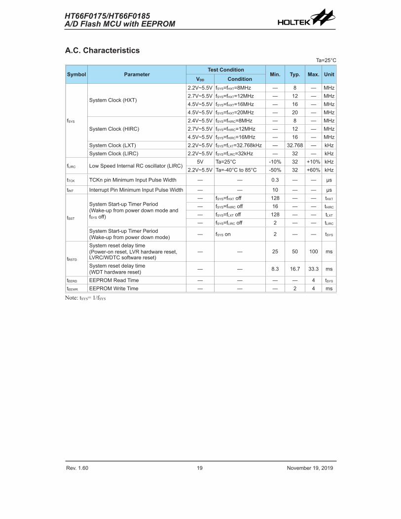
A.C. CharacteristicsTa=25°C
Symbol ParameterTest Condition
Min. Typ. Max. UnitVDD Condition
fSYS
System Clock (HXT)
2.2V~5.5V fSYS=fHXT=8MHz — 8 — MHz2.7V~5.5V fSYS=fHXT=12MHz — 12 — MHz4.5V~5.5V fSYS=fHXT=16MHz — 16 — MHz4.5V~5.5V fSYS=fHXT=20MHz — 20 — MHz
System Clock (HIRC)2.4V~5.5V fSYS=fHIRC=8MHz — 8 — MHz2.7V~5.5V fSYS=fHIRC=12MHz — 12 — MHz4.5V~5.5V fSYS=fHIRC=16MHz — 16 — MHz
System Clock (LXT) 2.2V~5.5V fSYS=fLXT=32.768kHz — 32.768 — kHzSystem Clock (LIRC) 2.2V~5.5V fSYS=fLIRC=32kHz — 32 — kHz
fLIRC Low Speed Internal RC oscillator (LIRC)5V Ta=25°C -10% 32 +10% kHz
2.2V~5.5V Ta=-40°C to 85°C -50% 32 +60% kHz
tTCK TCKn pin Minimum Input Pulse Width — — 0.3 — — μs
tINT Interrupt Pin Minimum Input Pulse Width — — 10 — — μs
tSST
System Start-up Timer Period(Wake-up from power down mode and fSYS off)
— fSYS=fHXT off 128 — — tHXT
— fSYS=fHIRC off 16 — — tHIRC
— fSYS=fLXT off 128 — — tLXT
— fSYS=fLIRC off 2 — — tLIRC
System Start-up Timer Period(Wake-up from power down mode) — fSYS on 2 — — tSYS
tRSTD
System reset delay time(Power-on reset, LVR hardware reset, LVRC/WDTC software reset)
— — 25 50 100 ms
System reset delay time(WDT hardware reset) — — 8.3 16.7 33.3 ms
tEERD EEPROM Read Time — — — — 4 tSYS
tEEWR EEPROM Write Time — — — 2 4 ms
Note: tSYS= 1/fSYS
Rev. 1.60 20 November 19, 2019 Rev. 1.60 21 November 19, 2019
HT66F0175/HT66F0185A/D Flash MCU with EEPROM
HT66F0175/HT66F0185A/D Flash MCU with EEPROM
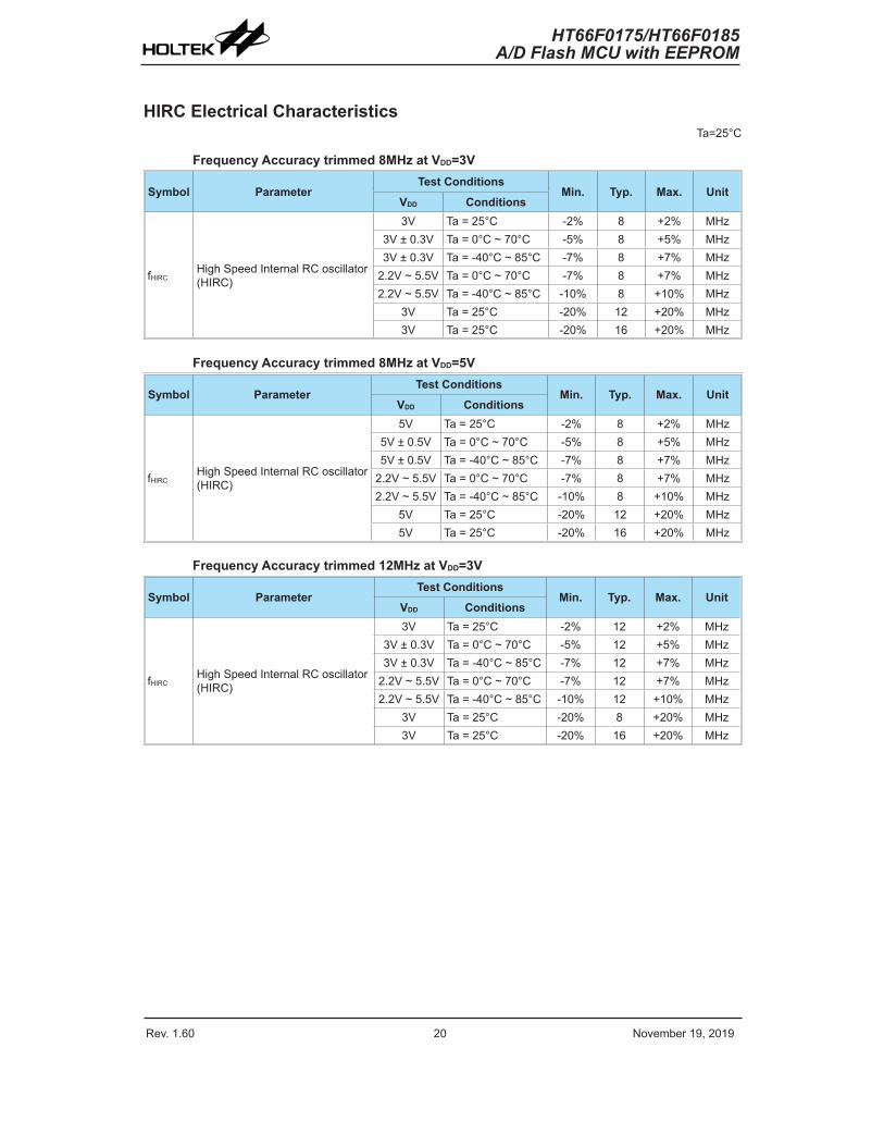
HIRC Electrical CharacteristicsTa=25°C
Frequency Accuracy trimmed 8MHz at VDD=3V
Symbol ParameterTest Conditions
Min. Typ. Max. UnitVDD Conditions
fHIRCHigh Speed Internal RC oscillator (HIRC)
3V Ta = 25°C -2% 8 +2% MHz3V ± 0.3V Ta = 0°C ~ 70°C -5% 8 +5% MHz3V ± 0.3V Ta = -40°C ~ 85°C -7% 8 +7% MHz
2.2V ~ 5.5V Ta = 0°C ~ 70°C -7% 8 +7% MHz2.2V ~ 5.5V Ta = -40°C ~ 85°C -10% 8 +10% MHz
3V Ta = 25°C -20% 12 +20% MHz3V Ta = 25°C -20% 16 +20% MHz
Frequency Accuracy trimmed 8MHz at VDD=5V
Symbol ParameterTest Conditions
Min. Typ. Max. UnitVDD Conditions
fHIRCHigh Speed Internal RC oscillator (HIRC)
5V Ta = 25°C -2% 8 +2% MHz5V ± 0.5V Ta = 0°C ~ 70°C -5% 8 +5% MHz5V ± 0.5V Ta = -40°C ~ 85°C -7% 8 +7% MHz
2.2V ~ 5.5V Ta = 0°C ~ 70°C -7% 8 +7% MHz2.2V ~ 5.5V Ta = -40°C ~ 85°C -10% 8 +10% MHz
5V Ta = 25°C -20% 12 +20% MHz5V Ta = 25°C -20% 16 +20% MHz
Frequency Accuracy trimmed 12MHz at VDD=3V
Symbol ParameterTest Conditions
Min. Typ. Max. UnitVDD Conditions
fHIRCHigh Speed Internal RC oscillator (HIRC)
3V Ta = 25°C -2% 12 +2% MHz3V ± 0.3V Ta = 0°C ~ 70°C -5% 12 +5% MHz3V ± 0.3V Ta = -40°C ~ 85°C -7% 12 +7% MHz
2.2V ~ 5.5V Ta = 0°C ~ 70°C -7% 12 +7% MHz2.2V ~ 5.5V Ta = -40°C ~ 85°C -10% 12 +10% MHz
3V Ta = 25°C -20% 8 +20% MHz3V Ta = 25°C -20% 16 +20% MHz
Rev. 1.60 20 November 19, 2019 Rev. 1.60 21 November 19, 2019
HT66F0175/HT66F0185A/D Flash MCU with EEPROM
HT66F0175/HT66F0185A/D Flash MCU with EEPROM
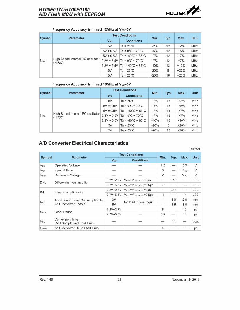
Frequency Accuracy trimmed 12MHz at VDD=5V
Symbol ParameterTest Conditions
Min. Typ. Max. UnitVDD Conditions
fHIRCHigh Speed Internal RC oscillator (HIRC)
5V Ta = 25°C -2% 12 +2% MHz5V ± 0.5V Ta = 0°C ~ 70°C -5% 12 +5% MHz5V ± 0.5V Ta = -40°C ~ 85°C -7% 12 +7% MHz
2.2V ~ 5.5V Ta = 0°C ~ 70°C -7% 12 +7% MHz2.2V ~ 5.5V Ta = -40°C ~ 85°C -10% 12 +10% MHz
5V Ta = 25°C -20% 8 +20% MHz5V Ta = 25°C -20% 16 +20% MHz
Frequency Accuracy trimmed 16MHz at VDD=5V
Symbol ParameterTest Conditions
Min. Typ. Max. UnitVDD Conditions
fHIRCHigh Speed Internal RC oscillator (HIRC)
5V Ta = 25°C -2% 16 +2% MHz5V ± 0.5V Ta = 0°C ~ 70°C -5% 16 +5% MHz5V ± 0.5V Ta = -40°C ~ 85°C -7% 16 +7% MHz
2.2V ~ 5.5V Ta = 0°C ~ 70°C -7% 16 +7% MHz2.2V ~ 5.5V Ta = -40°C ~ 85°C -10% 16 +10% MHz
5V Ta = 25°C -20% 8 +20% MHz5V Ta = 25°C -20% 12 +20% MHz
A/D Converter Electrical CharacteristicsTa=25°C
Symbol ParameterTest Conditions
Min. Typ. Max. UnitVDD Conditions
VDD Operating Voltage — — 2.2 — 5.5 VVADI Input Voltage — — 0 — VR\EF VVREF Reference Voltage — — 2 — VDD V
DNL Differential non-linearity2.2V~2.7V VREF=VDD, tADCK=8μs — ±15 — LSB2.7V~5.5V VREF=VDD, tADCK=0.5μs -3 — +3 LSB
INL Integral non-linearity2.2V~2.7V VREF=VDD, tADCK=8μs — ±16 — LSB2.7V~5.5V VREF=VDD, tADCK=0.5μs -4 — +4 LSB
IADCAdditional Current Consumption for A/D Converter Enable
3VNo load, tADCK=0.5μs
— 1.0 2.0 mA5V — 1.5 3.0 mA
tADCK Clock Period2.2V~2.7V — 8 — 10 μs2.7V~5.5V — 0.5 — 10 μs
tADCConversion Time (A/D Sample and Hold Time) — — — 16 — tADCK
tON2ST A/D Converter On-to-Start Time — — 4 — — μs
Rev. 1.60 22 November 19, 2019 Rev. 1.60 23 November 19, 2019
HT66F0175/HT66F0185A/D Flash MCU with EEPROM
HT66F0175/HT66F0185A/D Flash MCU with EEPROM
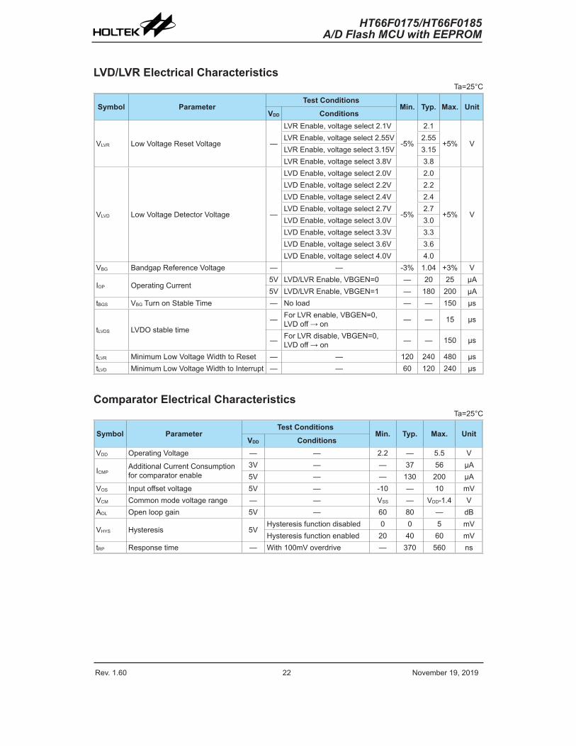
LVD/LVR Electrical CharacteristicsTa=25°C
Symbol ParameterTest Conditions
Min. Typ. Max. UnitVDD Conditions
VLVR Low Voltage Reset Voltage —
LVR Enable, voltage select 2.1V
-5%
2.1
+5% VLVR Enable, voltage select 2.55V 2.55LVR Enable, voltage select 3.15V 3.15LVR Enable, voltage select 3.8V 3.8
VLVD Low Voltage Detector Voltage —
LVD Enable, voltage select 2.0V
-5%
2.0
+5% V
LVD Enable, voltage select 2.2V 2.2LVD Enable, voltage select 2.4V 2.4LVD Enable, voltage select 2.7V 2.7LVD Enable, voltage select 3.0V 3.0LVD Enable, voltage select 3.3V 3.3LVD Enable, voltage select 3.6V 3.6LVD Enable, voltage select 4.0V 4.0
VBG Bandgap Reference Voltage — — -3% 1.04 +3% V
IOP Operating Current5V LVD/LVR Enable, VBGEN=0 — 20 25 μA5V LVD/LVR Enable, VBGEN=1 — 180 200 μA
tBGS VBG Turn on Stable Time — No load — — 150 μs
tLVDS LVDO stable time— For LVR enable, VBGEN=0,
LVD off → on — — 15 μs
— For LVR disable, VBGEN=0,LVD off → on — — 150 μs
tLVR Minimum Low Voltage Width to Reset — — 120 240 480 μstLVD Minimum Low Voltage Width to Interrupt — — 60 120 240 μs
Comparator Electrical CharacteristicsTa=25°C
Symbol ParameterTest Conditions
Min. Typ. Max. UnitVDD Conditions
VDD Operating Voltage — — 2.2 — 5.5 V
ICMPAdditional Current Consumption for comparator enable
3V — — 37 56 μA5V — — 130 200 μA
VOS Input offset voltage 5V — -10 — 10 mVVCM Common mode voltage range — — VSS — VDD-1.4 VAOL Open loop gain 5V — 60 80 — dB
VHYS Hysteresis 5VHysteresis function disabled 0 0 5 mVHysteresis function enabled 20 40 60 mV
tRP Response time — With 100mV overdrive — 370 560 ns
Rev. 1.60 22 November 19, 2019 Rev. 1.60 23 November 19, 2019
HT66F0175/HT66F0185A/D Flash MCU with EEPROM
HT66F0175/HT66F0185A/D Flash MCU with EEPROM
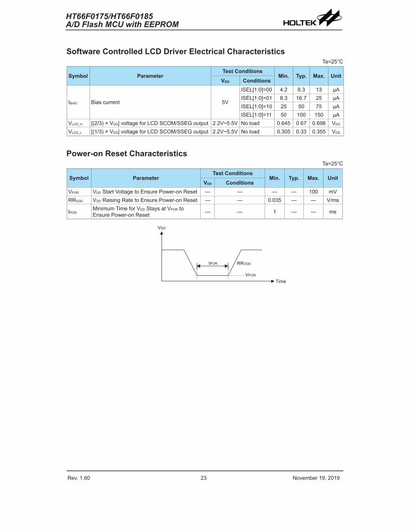
Software Controlled LCD Driver Electrical CharacteristicsTa=25°C
Symbol ParameterTest Conditions
Min. Typ. Max. UnitVDD Conditions
IBIAS Bias current 5V
ISEL[1:0]=00 4.2 8.3 13 μAISEL[1:0]=01 8.3 16.7 25 μAISEL[1:0]=10 25 50 75 μAISEL[1:0]=11 50 100 150 μA
VLCD_H [(2/3) × VDD] voltage for LCD SCOM/SSEG output 2.2V~5.5V No load 0.645 0.67 0.698 VDD
VLCD_L [(1/3) × VDD] voltage for LCD SCOM/SSEG output 2.2V~5.5V No load 0.305 0.33 0.355 VDD
Power-on Reset CharacteristicsTa=25°C
Symbol ParameterTest Conditions
Min. Typ. Max. UnitVDD Conditions
VPOR VDD Start Voltage to Ensure Power-on Reset — — — — 100 mVRRVDD VDD Raising Rate to Ensure Power-on Reset — — 0.035 — — V/ms
tPORMinimum Time for VDD Stays at VPOR to Ensure Power-on Reset — — 1 — — ms
� � � �
� � �
� � � �
� � � � �� � � �

Rev. 1.60 24 November 19, 2019 Rev. 1.60 25 November 19, 2019
HT66F0175/HT66F0185A/D Flash MCU with EEPROM
HT66F0175/HT66F0185A/D Flash MCU with EEPROM
System ArchitectureA key factor in the high-performance features of the Holtek range of microcontrollers is attributed to their internal system architecture. The range of devices take advantage of the usual features found within RISC microcontrollers providing increased speed of operation and enhanced performance. The pipelining scheme is implemented in such a way that instruction fetching and instruction execution are overlapped, hence instructions are effectively executed in one cycle, with the exception of branch or call instructions. An 8-bit wide ALU is used in practically all instruction set operations, which carries out arithmetic operations, logic operations, rotation, increment, decrement, branch decisions, etc. The internal data path is simplified by moving data through the Accumulator and the ALU. Certain internal registers are implemented in the Data Memory and can be directly or indirectly addressed. The simple addressing methods of these registers along with additional architectural features ensure that a minimum of external components is required to provide a functional I/O and A/D control system with maximum reliability and flexibility. This makes these devices suitable for low-cost, high-volume production for controller applications.
Clocking and PipeliningThe main system clock, derived from either a HXT, LXT, HIRC or LIRC oscillator is subdivided into four internally generated non-overlapping clocks, T1~T4. The Program Counter is incremented at the beginning of the T1 clock during which time a new instruction is fetched. The remaining T2~T4 clocks carry out the decoding and execution functions. In this way, one T1~T4 clock cycle forms one instruction cycle. Although the fetching and execution of instructions takes place in consecutive instruction cycles, the pipelining structure of the microcontroller ensures that instructions are effectively executed in one instruction cycle. The exception to this are instructions where the contents of the Program Counter are changed, such as subroutine calls or jumps, in which case the instruction will take one more instruction cycle to execute.
� � � � � � � � � � � � � � � �� � � � � � � � � � � � � � � � � � � � � � � � � � � � � � � � � � � �
� � � � � � � � � � � � � � � � � � � � � � � � � � � � � � � � � � � �� � � � � � � � � � � � � � � � � � �
� � � � � � � � �
� � � � � � � � � � � � � �
� � � � � � � � � � � � �
� � � � � � � � � � � � � � �
� � � � � � � � � � � � � �
� � � � � � � � � � � � � �
� � � � � � � � � � � � � �
� � � � � � � � � �
System Clocking and Pipelining
Rev. 1.60 24 November 19, 2019 Rev. 1.60 25 November 19, 2019
HT66F0175/HT66F0185A/D Flash MCU with EEPROM
HT66F0175/HT66F0185A/D Flash MCU with EEPROM
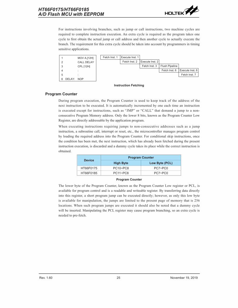
For instructions involving branches, such as jump or call instructions, two machine cycles are required to complete instruction execution. An extra cycle is required as the program takes one cycle to first obtain the actual jump or call address and then another cycle to actually execute the branch. The requirement for this extra cycle should be taken into account by programmers in timing sensitive applications.
� � � � � � � � � � � � � � � � � � � � � � � � � � � �� � � � � � � � � � � � �
� � � � � � � � � � � � �
���� � � � � � �
� � � � � � � � � � �� � � � � � � � � �� � � � � � � � ���� � �
� � � � � � � � � � � � � � �� � � � � � � � � � � � �
� � � � � � � � � � � � � � � � � � � � � � � � � � � � � � � � � � � � � �
Instruction Fetching
Program CounterDuring program execution, the Program Counter is used to keep track of the address of the next instruction to be executed. It is automatically incremented by one each time an instruction is executed except for instructions, such as “JMP” or “CALL” that demand a jump to a non-consecutive Program Memory address. Only the lower 8 bits, known as the Program Counter Low Register, are directly addressable by the application program.
When executing instructions requiring jumps to non-consecutive addresses such as a jump instruction, a subroutine call, interrupt or reset, etc., the microcontroller manages program control by loading the required address into the Program Counter. For conditional skip instructions, once the condition has been met, the next instruction, which has already been fetched during the present instruction execution, is discarded and a dummy cycle takes its place while the correct instruction is obtained.
DeviceProgram Counter
High Byte Low Byte (PCL)HT66F0175 PC10~PC8 PC7~PC0HT66F0185 PC11~PC8 PC7~PC0
Program Counter
The lower byte of the Program Counter, known as the Program Counter Low register or PCL, is available for program control and is a readable and writeable register. By transferring data directly into this register, a short program jump can be executed directly; however, as only this low byte is available for manipulation, the jumps are limited to the present page of memory that is 256 locations. When such program jumps are executed it should also be noted that a dummy cycle will be inserted. Manipulating the PCL register may cause program branching, so an extra cycle is needed to pre-fetch.
Rev. 1.60 26 November 19, 2019 Rev. 1.60 27 November 19, 2019
HT66F0175/HT66F0185A/D Flash MCU with EEPROM
HT66F0175/HT66F0185A/D Flash MCU with EEPROM
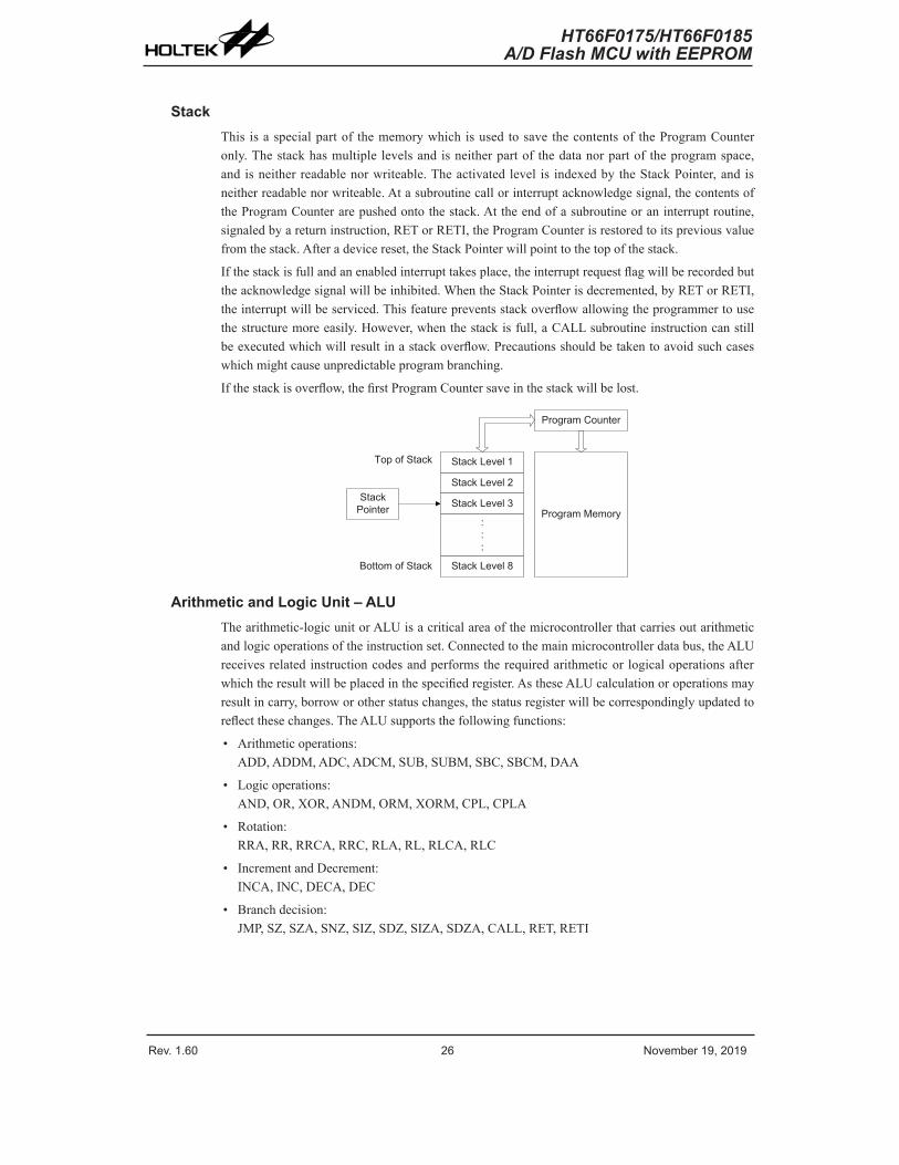
StackThis is a special part of the memory which is used to save the contents of the Program Counter only. The stack has multiple levels and is neither part of the data nor part of the program space, and is neither readable nor writeable. The activated level is indexed by the Stack Pointer, and is neither readable nor writeable. At a subroutine call or interrupt acknowledge signal, the contents of the Program Counter are pushed onto the stack. At the end of a subroutine or an interrupt routine, signaled by a return instruction, RET or RETI, the Program Counter is restored to its previous value from the stack. After a device reset, the Stack Pointer will point to the top of the stack.
If the stack is full and an enabled interrupt takes place, the interrupt request flag will be recorded but the acknowledge signal will be inhibited. When the Stack Pointer is decremented, by RET or RETI, the interrupt will be serviced. This feature prevents stack overflow allowing the programmer to use the structure more easily. However, when the stack is full, a CALL subroutine instruction can still be executed which will result in a stack overflow. Precautions should be taken to avoid such cases which might cause unpredictable program branching.
If the stack is overflow, the first Program Counter save in the stack will be lost.
StackPointer
Stack Level 2
Stack Level 1
Stack Level 3
:::
Stack Level 8
Program Memory
Program Counter
Bottom of Stack
Top of Stack
Arithmetic and Logic Unit – ALUThe arithmetic-logic unit or ALU is a critical area of the microcontroller that carries out arithmetic and logic operations of the instruction set. Connected to the main microcontroller data bus, the ALU receives related instruction codes and performs the required arithmetic or logical operations after which the result will be placed in the specified register. As these ALU calculation or operations may result in carry, borrow or other status changes, the status register will be correspondingly updated to reflect these changes. The ALU supports the following functions:
• Arithmetic operations:ADD, ADDM, ADC, ADCM, SUB, SUBM, SBC, SBCM, DAA
• Logic operations:AND, OR, XOR, ANDM, ORM, XORM, CPL, CPLA
• Rotation:RRA, RR, RRCA, RRC, RLA, RL, RLCA, RLC
• Increment and Decrement:INCA, INC, DECA, DEC
• Branch decision:JMP, SZ, SZA, SNZ, SIZ, SDZ, SIZA, SDZA, CALL, RET, RETI
Rev. 1.60 26 November 19, 2019 Rev. 1.60 27 November 19, 2019
HT66F0175/HT66F0185A/D Flash MCU with EEPROM
HT66F0175/HT66F0185A/D Flash MCU with EEPROM
Flash Program MemoryThe Program Memory is the location where the user code or program is stored. For these devices series the Program Memory are Flash type, which means it can be programmed and re-programmed a large number of times, allowing the user the convenience of code modification on the same device. By using the appropriate programming tools, these Flash devices offer users the flexibility to conveniently debug and develop their applications while also offering a means of field programming and updating.
Device CapacityHT66F0175 2K × 16HT66F0185 4K × 16
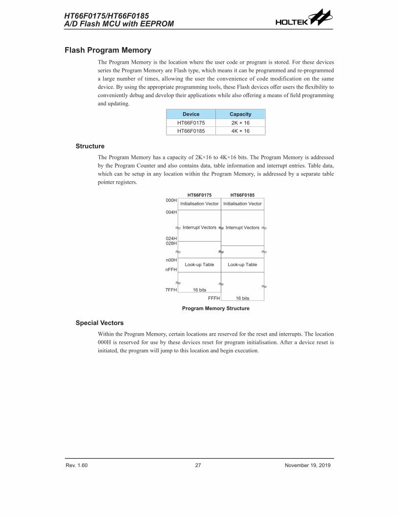
StructureThe Program Memory has a capacity of 2K×16 to 4K×16 bits. The Program Memory is addressed by the Program Counter and also contains data, table information and interrupt entries. Table data, which can be setup in any location within the Program Memory, is addressed by a separate table pointer registers.
000HInitialisation Vector
004H
FFFH 16 bits
Interrupt Vectors
024H
Look-up Tablen00H
nFFH
HT66F0185
Initialisation Vector
16 bits
Interrupt Vectors
Look-up Table
HT66F0175
028H
7FFH
Program Memory Structure
Special VectorsWithin the Program Memory, certain locations are reserved for the reset and interrupts. The location 000H is reserved for use by these devices reset for program initialisation. After a device reset is initiated, the program will jump to this location and begin execution.
Rev. 1.60 28 November 19, 2019 Rev. 1.60 29 November 19, 2019
HT66F0175/HT66F0185A/D Flash MCU with EEPROM
HT66F0175/HT66F0185A/D Flash MCU with EEPROM
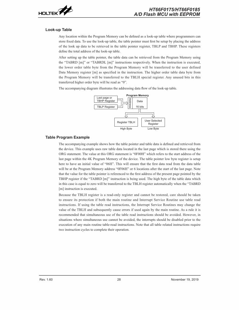
Look-up TableAny location within the Program Memory can be defined as a look-up table where programmers can store fixed data. To use the look-up table, the table pointer must first be setup by placing the address of the look up data to be retrieved in the table pointer register, TBLP and TBHP. These registers define the total address of the look-up table.
After setting up the table pointer, the table data can be retrieved from the Program Memory using the “TABRD [m]” or “TABRDL [m]” instructions respectively. When the instruction is executed, the lower order table byte from the Program Memory will be transferred to the user defined Data Memory register [m] as specified in the instruction. The higher order table data byte from the Program Memory will be transferred to the TBLH special register. Any unused bits in this transferred higher order byte will be read as “0”.
The accompanying diagram illustrates the addressing data flow of the look-up table.
� � � � � � � � � � � � � � � � � � � � � � � � � �� � � � � � � �
� � � � � � � � � � � � � � �
� � � � � � � � � � � �
� � �
������� � � � � � � �
� � � � � � � � � � � � � �� � � � � � � � � � � �� � � � � � � � � � � �
Table Program ExampleThe accompanying example shows how the table pointer and table data is defined and retrieved from the device. This example uses raw table data located in the last page which is stored there using the ORG statement. The value at this ORG statement is “0F00H” which refers to the start address of the last page within the 4K Program Memory of the device. The table pointer low byte register is setup here to have an initial value of “06H”. This will ensure that the first data read from the data table will be at the Program Memory address “0F06H” or 6 locations after the start of the last page. Note that the value for the table pointer is referenced to the first address of the present page pointed by the TBHP register if the “TABRD [m]” instruction is being used. The high byte of the table data which in this case is equal to zero will be transferred to the TBLH register automatically when the “TABRD [m] instruction is executed.
Because the TBLH register is a read-only register and cannot be restored, care should be taken to ensure its protection if both the main routine and Interrupt Service Routine use table read instructions. If using the table read instructions, the Interrupt Service Routines may change the value of the TBLH and subsequently cause errors if used again by the main routine. As a rule it is recommended that simultaneous use of the table read instructions should be avoided. However, in situations where simultaneous use cannot be avoided, the interrupts should be disabled prior to the execution of any main routine table-read instructions. Note that all table related instructions require two instruction cycles to complete their operation.
Rev. 1.60 28 November 19, 2019 Rev. 1.60 29 November 19, 2019
HT66F0175/HT66F0185A/D Flash MCU with EEPROM
HT66F0175/HT66F0185A/D Flash MCU with EEPROM
Table Read Program Exampletempreg1 db ? ; temporary register #1 tempreg2 db ? ; temporary register #2 :mov a,06h ; initialise low table pointer - note that this address is referenced mov tblp,a ; to the last page or the page that tbhp pointedmov a,0fh ; initialise high table pointer mov tbhp,a:tabrd tempreg1 ; transfers value in table referenced by table pointer data at program ; memory address “0F06H” transferred to tempreg1 and TBLH dec tblp ; reduce value of table pointer by one tabrd tempreg2 ; transfers value in table referenced by table pointer data at program ; memory address “0F05H” transferred to tempreg2 and TBLH in this ; example the data “1AH” is transferred to tempreg1 and data “0FH” to ; register tempreg2:org 0F00h ; sets initial address of program memory dc 00Ah, 00Bh, 00Ch, 00Dh, 00Eh, 00Fh, 01Ah, 01Bh:
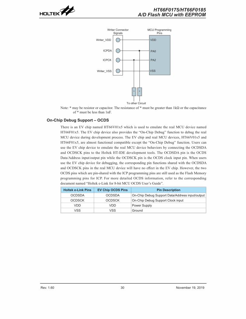
In Circuit Programming – ICPThe provision of Flash type Program Memory provides the user with a means of convenient and easy upgrades and modifications to their programs on the same device.
As an additional convenience, Holtek has provided a means of programming the microcontroller in-circuit using a 4-pin interface. This provides manufacturers with the possibility of manufacturing their circuit boards complete with a programmed or un-programmed microcontroller, and then programming or upgrading the program at a later stage. This enables product manufacturers to easily keep their manufactured products supplied with the latest program releases without removal and re-insertion of the device.
Holtek Writer Pins MCU Programming Pins Pin DescriptionICPDA PA0 Programming Serial Data/AddressICPCK PA2 Programming ClockVDD VDD Power SupplyVSS VSS Ground
The Program Memory and EEPROM data memory can be programmed serially in-circuit using this 4-wire interface. Data is downloaded and uploaded serially on a single pin with an additional line for the clock. Two additional lines are required for the power supply. The technical details regarding the in-circuit programming of the device are beyond the scope of this document and will be supplied in supplementary literature.
During the programming process, the user must take care of the ICPDA and ICPCK pins for data and clock programming purposes to ensure that no other outputs are connected to these two pins.
Rev. 1.60 30 November 19, 2019 Rev. 1.60 31 November 19, 2019
HT66F0175/HT66F0185A/D Flash MCU with EEPROM
HT66F0175/HT66F0185A/D Flash MCU with EEPROM
� �
� � � � � � � � � �
� � � � �
� � � � �
� � � � � � � � � �
� � � � � � � � � � � � � � �
� �
� � �
� � �
� � � � � � � � � � � � � �� � � � � �
� � � � � � � � � � � � � �� � �
� � �
Note: * may be resistor or capacitor. The resistance of * must be greater than 1kΩ or the capacitance of * must be less than 1nF.
On-Chip Debug Support – OCDSThere is an EV chip named HT66V01x5 which is used to emulate the real MCU device named HT66F01x5. The EV chip device also provides the “On-Chip Debug” function to debug the real MCU device during development process. The EV chip and real MCU devices, HT66V01x5 and HT66F01x5, are almost functional compatible except the “On-Chip Debug” function. Users can use the EV chip device to emulate the real MCU device behaviors by connecting the OCDSDA and OCDSCK pins to the Holtek HT-IDE development tools. The OCDSDA pin is the OCDS Data/Address input/output pin while the OCDSCK pin is the OCDS clock input pin. When users use the EV chip device for debugging, the corresponding pin functions shared with the OCDSDA and OCDSCK pins in the real MCU device will have no effect in the EV chip. However, the two OCDS pins which are pin-shared with the ICP programming pins are still used as the Flash Memory programming pins for ICP. For more detailed OCDS information, refer to the corresponding document named “Holtek e-Link for 8-bit MCU OCDS User’s Guide”.
Holtek e-Link Pins EV Chip OCDS Pins Pin DescriptionOCDSDA OCDSDA On-Chip Debug Support Data/Address input/outputOCDSCK OCDSCK On-Chip Debug Support Clock input
VDD VDD Power SupplyVSS VSS Ground
Rev. 1.60 30 November 19, 2019 Rev. 1.60 31 November 19, 2019
HT66F0175/HT66F0185A/D Flash MCU with EEPROM
HT66F0175/HT66F0185A/D Flash MCU with EEPROM
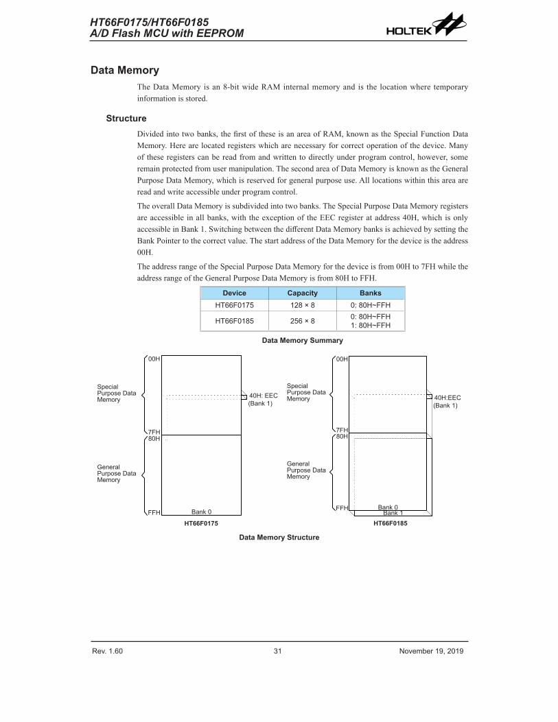
Data MemoryThe Data Memory is an 8-bit wide RAM internal memory and is the location where temporary information is stored.
StructureDivided into two banks, the first of these is an area of RAM, known as the Special Function Data Memory. Here are located registers which are necessary for correct operation of the device. Many of these registers can be read from and written to directly under program control, however, some remain protected from user manipulation. The second area of Data Memory is known as the General Purpose Data Memory, which is reserved for general purpose use. All locations within this area are read and write accessible under program control.
The overall Data Memory is subdivided into two banks. The Special Purpose Data Memory registers are accessible in all banks, with the exception of the EEC register at address 40H, which is only accessible in Bank 1. Switching between the different Data Memory banks is achieved by setting the Bank Pointer to the correct value. The start address of the Data Memory for the device is the address 00H.
The address range of the Special Purpose Data Memory for the device is from 00H to 7FH while the address range of the General Purpose Data Memory is from 80H to FFH.
Device Capacity BanksHT66F0175 128 × 8 0: 80H~FFH
HT66F0185 256 × 8 0: 80H~FFH1: 80H~FFH
Data Memory Summary
00H
7FH80H
FFH
Special Purpose Data Memory
General Purpose Data Memory
Bank 0
40H: EEC
HT66F0175
(Bank 1)
00H
7FH80H
FFH
Special Purpose Data Memory
General Purpose Data Memory
Bank 0Bank 1
40H:EEC(Bank 1)
HT66F0185
Data Memory Structure
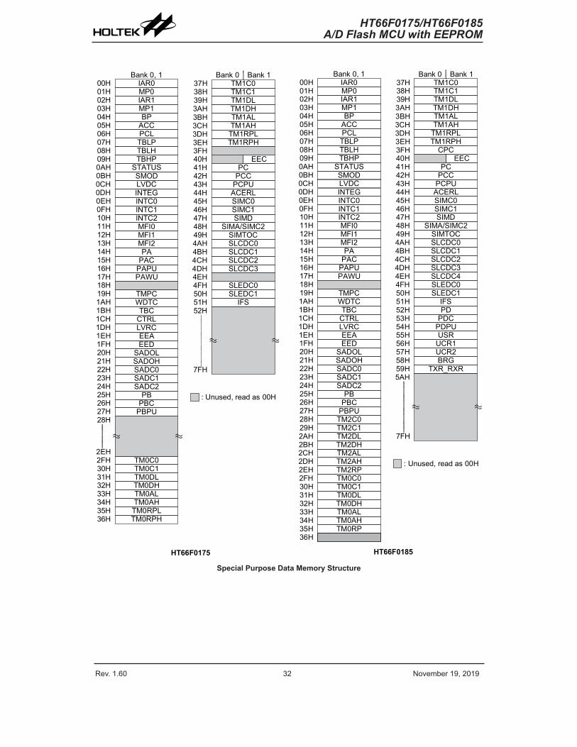
Rev. 1.60 32 November 19, 2019 Rev. 1.60 33 November 19, 2019
HT66F0175/HT66F0185A/D Flash MCU with EEPROM
HT66F0175/HT66F0185A/D Flash MCU with EEPROM
00H IAR001H MP002H IAR103H MP104H05H ACC06H PCL07H TBLP08H TBLH09H TBHP0AH STATUS0BH0CH0DH0EH0FH10H
INTC0
11H12H
19H
PAPU
18HPAWU
1BH1AH
1DH1CH
1FH
PAPAC
13H14H15H16H17H
EEA
20H21H22H
28H
23H24H25H26H27H
40H41H42H43H44H45H46H47H48H49H4AH4BH4CH4DH4EH4FH50H51H
1EH
EEC
Bank 0, 1
PBCPBPU
PB
7FH
BP
LVDC
LVRC
EEDSADOL
SADC0
PCCPCPU
PC
SADOH
52H
SMOD
INTEG
INTC1INTC2MFI0MFI1MFI2
TMPCWDTCTBC
CTRL
SADC1SADC2
Bank 0 Bank 1
SLEDC0SLEDC1
ACERL
SIMTOC
SIMC0SIMC1SIMD
SIMA/SIMC2
SLCDC0SLCDC1SLCDC2SLCDC3
IFS
2EH
38H37H
39H3AH
3CH3BH
3DH
3FH3EH
TM1C0TM1C1TM1DLTM1DHTM1ALTM1AHTM1RPLTM1RPH
2FH30H31H32H33H34H35H
HT66F0175
TM0C0TM0C1TM0DLTM0DHTM0ALTM0AHTM0RPLTM0RPH
: Unused, read as 00H
36H
00H IAR001H MP002H IAR103H MP104H05H ACC06H PCL07H TBLP08H TBLH09H TBHP0AH STATUS0BH0CH0DH0EH0FH10H
INTC0
11H12H
19H
PAPU
18HPAWU
1BH1AH
1DH1CH
1FH
PAPAC
13H14H15H16H17H
EEA
20H21H22H
28H
23H24H25H26H27H
40H41H42H43H44H45H46H47H48H49H4AH4BH4CH4DH4EH4FH50H51H
53H54H
1EH
EEC
Bank 0, 1
55H56H
PBCPBPU
PB
7FH
BP
LVDC
LVRC
EEDSADOL
SADC0
PCCPCPU
PC
57H58H59H5AH
SADOH
52H
SMOD
INTEG
INTC1INTC2MFI0MFI1MFI2
TMPCWDTCTBC
CTRL
SADC1SADC2
Bank 0 Bank 1
SLEDC0
USRUCR1UCR2
TXR_RXRBRG
SLEDC1
ACERL
SIMTOC
SIMC0SIMC1SIMD
SIMA/SIMC2
SLCDC0SLCDC1SLCDC2SLCDC3
IFS
SLCDC4
PDPDC
PDPU
TM2C0TM2C1TM2DLTM2DHTM2ALTM2AHTM2RP
29H2AH2BH2CH2DH2EH
38H37H
39H3AH
3CH3BH
3DH
3FH3EH
TM1C0TM1C1TM1DLTM1DHTM1ALTM1AH
TM1RPLTM1RPH
CPC
2FH30H31H32H33H34H35H
HT66F0185
TM0C0TM0C1TM0DLTM0DHTM0ALTM0AHTM0RP
: Unused, read as 00H
36H
Special Purpose Data Memory Structure
Rev. 1.60 32 November 19, 2019 Rev. 1.60 33 November 19, 2019
HT66F0175/HT66F0185A/D Flash MCU with EEPROM
HT66F0175/HT66F0185A/D Flash MCU with EEPROM
Special Function Register DescriptionMost of the Special Function Register details will be described in the relevant functional section. However, several registers require a separate description in this section.
Indirect Addressing Registers – IAR0, IAR1The Indirect Addressing Registers, IAR0 and IAR1, although having their locations in normal RAM register space, do not actually physically exist as normal registers. The method of indirect addressing for RAM data manipulation uses these Indirect Addressing Registers and Memory Pointers, in contrast to direct memory addressing, where the actual memory address is specified. Actions on the IAR0 and IAR1 registers will result in no actual read or write operation to these registers but rather to the memory location specified by their corresponding Memory Pointers, MP0 or MP1. Acting as a pair, IAR0 and MP0 can together access data only from Bank 0 while the IAR1 register together with MP1 register pair can access data from any Data Memory bank. As the Indirect Addressing Registers are not physically implemented, reading the Indirect Addressing Registers indirectly will return a result of “00H” and writing to the registers indirectly will result in no operation.
Memory Pointers – MP0, MP1The Memory Pointers, known as MP0 and MP1, are provided. These Memory Pointers are physically implemented in the Data Memory and can be manipulated in the same way as normal registers providing a convenient way with which to address and track data. When any operation to the relevant Indirect Addressing Registers is carried out, the actual address that the microcontroller is directed to is the address specified by the related Memory Pointer. MP0, together with Indirect Addressing Register, IAR0, are used to access data from Bank 0, while MP1 together with IAR1 are used to access data from all data banks according to the corresponding BP register.
The following example shows how to clear a section of four Data Memory locations already defined as locations adres1 to adres4.
Indirect Addressing Program Exampledata .section ‘data’adres1 db ? adres2 db ? adres3 db ? adres4 db ? block db ? code .section at 0 ‘code’org 00h start: mov a,04h ; setup size of block mov block,a mov a,offset adres1 ; Accumulator loaded with first RAM address mov mp0,a ; setup memory pointer with first RAM address loop: clr IAR0 ; clear the data at address defined by MP0 inc mp0 ; increment memory pointer sdz block ; check if last memory location has been cleared jmp loop continue: :
The important point to note here is that in the example shown above, no reference is made to specific RAM addresses.
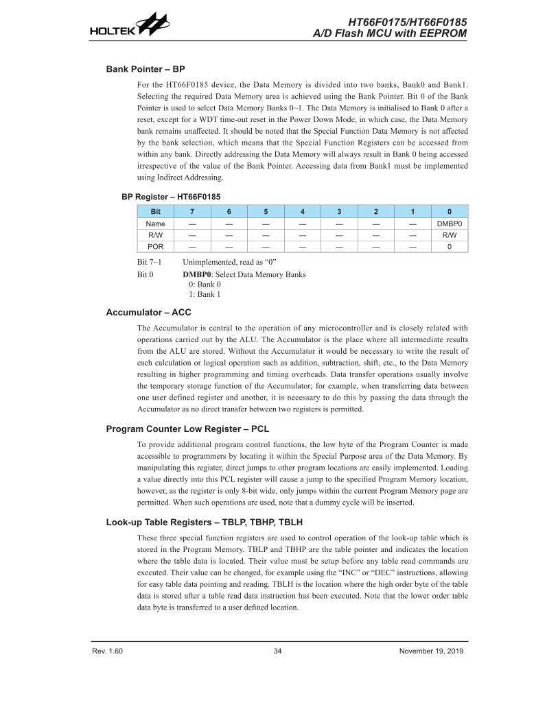
Rev. 1.60 34 November 19, 2019 Rev. 1.60 35 November 19, 2019
HT66F0175/HT66F0185A/D Flash MCU with EEPROM
HT66F0175/HT66F0185A/D Flash MCU with EEPROM
Bank Pointer – BPFor the HT66F0185 device, the Data Memory is divided into two banks, Bank0 and Bank1. Selecting the required Data Memory area is achieved using the Bank Pointer. Bit 0 of the Bank Pointer is used to select Data Memory Banks 0~1. The Data Memory is initialised to Bank 0 after a reset, except for a WDT time-out reset in the Power Down Mode, in which case, the Data Memory bank remains unaffected. It should be noted that the Special Function Data Memory is not affected by the bank selection, which means that the Special Function Registers can be accessed from within any bank. Directly addressing the Data Memory will always result in Bank 0 being accessed irrespective of the value of the Bank Pointer. Accessing data from Bank1 must be implemented using Indirect Addressing.
BP Register – HT66F0185Bit 7 6 5 4 3 2 1 0
Name — — — — — — — DMBP0R/W — — — — — — — R/WPOR — — — — — — — 0
Bit 7~1 Unimplemented, read as “0”Bit 0 DMBP0: Select Data Memory Banks
0: Bank 01: Bank 1
Accumulator – ACCThe Accumulator is central to the operation of any microcontroller and is closely related with operations carried out by the ALU. The Accumulator is the place where all intermediate results from the ALU are stored. Without the Accumulator it would be necessary to write the result of each calculation or logical operation such as addition, subtraction, shift, etc., to the Data Memory resulting in higher programming and timing overheads. Data transfer operations usually involve the temporary storage function of the Accumulator; for example, when transferring data between one user defined register and another, it is necessary to do this by passing the data through the Accumulator as no direct transfer between two registers is permitted.
Program Counter Low Register – PCLTo provide additional program control functions, the low byte of the Program Counter is made accessible to programmers by locating it within the Special Purpose area of the Data Memory. By manipulating this register, direct jumps to other program locations are easily implemented. Loading a value directly into this PCL register will cause a jump to the specified Program Memory location, however, as the register is only 8-bit wide, only jumps within the current Program Memory page are permitted. When such operations are used, note that a dummy cycle will be inserted.
Look-up Table Registers – TBLP, TBHP, TBLHThese three special function registers are used to control operation of the look-up table which is stored in the Program Memory. TBLP and TBHP are the table pointer and indicates the location where the table data is located. Their value must be setup before any table read commands are executed. Their value can be changed, for example using the “INC” or “DEC” instructions, allowing for easy table data pointing and reading. TBLH is the location where the high order byte of the table data is stored after a table read data instruction has been executed. Note that the lower order table data byte is transferred to a user defined location.
Rev. 1.60 34 November 19, 2019 Rev. 1.60 35 November 19, 2019
HT66F0175/HT66F0185A/D Flash MCU with EEPROM
HT66F0175/HT66F0185A/D Flash MCU with EEPROM
Status Register – STATUSThis 8-bit register contains the zero flag (Z), carry flag (C), auxiliary carry flag (AC), overflow flag (OV), power down flag (PDF), and watchdog time-out flag (TO). These arithmetic/logical operation and system management flags are used to record the status and operation of the microcontroller.
With the exception of the TO and PDF flags, bits in the status register can be altered by instructions like most other registers. Any data written into the status register will not change the TO or PDF flag. In addition, operations related to the status register may give different results due to the different instruction operations. The TO flag can be affected only by a system power-up, a WDT time-out or by executing the “CLR WDT” or “HALT” instruction. The PDF flag is affected only by executing the “HALT” or “CLR WDT” instruction or during a system power-up.
The Z, OV, AC, and C flags generally reflect the status of the latest operations.
• C is set if an operation results in a carry during an addition operation or if a borrow does not take place during a subtraction operation; otherwise C is cleared. C is also affected by a rotate through carry instruction.
• AC is set if an operation results in a carry out of the low nibbles in addition, or no borrow from the high nibble into the low nibble in subtraction; otherwise AC is cleared.
• Z is set if the result of an arithmetic or logical operation is zero; otherwise Z is cleared.
• OV is set if an operation results in a carry into the highest-order bit but not a carry out of the highest-order bit, or vice versa; otherwise OV is cleared.
• PDF is cleared by a system power-up or executing the “CLR WDT” instruction. PDF is set by executing the “HALT” instruction.
• TO is cleared by a system power-up or executing the “CLR WDT” or “HALT” instruction. TO is set by a WDT time-out.
In addition, on entering an interrupt sequence or executing a subroutine call, the status register will not be pushed onto the stack automatically. If the contents of the status registers are important and if the subroutine can corrupt the status register, precautions must be taken to correctly save it.
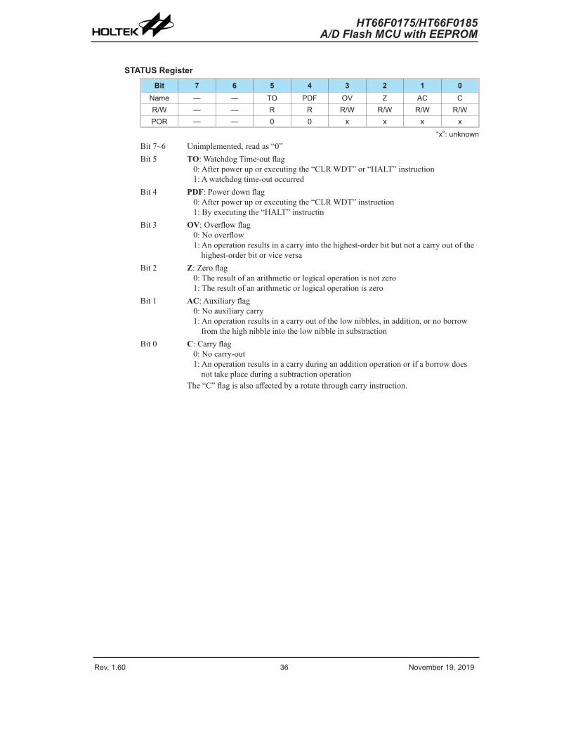
Rev. 1.60 36 November 19, 2019 Rev. 1.60 37 November 19, 2019
HT66F0175/HT66F0185A/D Flash MCU with EEPROM
HT66F0175/HT66F0185A/D Flash MCU with EEPROM
STATUS RegisterBit 7 6 5 4 3 2 1 0
Name — — TO PDF OV Z AC CR/W — — R R R/W R/W R/W R/WPOR — — 0 0 x x x x
“x”: unknownBit 7~6 Unimplemented, read as “0”Bit 5 TO: Watchdog Time-out flag
0: After power up or executing the “CLR WDT” or “HALT” instruction1: A watchdog time-out occurred
Bit 4 PDF: Power down flag0: After power up or executing the “CLR WDT” instruction1: By executing the “HALT” instructin
Bit 3 OV: Overflow flag0: No overflow1: An operation results in a carry into the highest-order bit but not a carry out of the
highest-order bit or vice versaBit 2 Z: Zero flag
0: The result of an arithmetic or logical operation is not zero1: The result of an arithmetic or logical operation is zero
Bit 1 AC: Auxiliary flag0: No auxiliary carry1: An operation results in a carry out of the low nibbles, in addition, or no borrow
from the high nibble into the low nibble in substractionBit 0 C: Carry flag
0: No carry-out1: An operation results in a carry during an addition operation or if a borrow does
not take place during a subtraction operationThe “C” flag is also affected by a rotate through carry instruction.
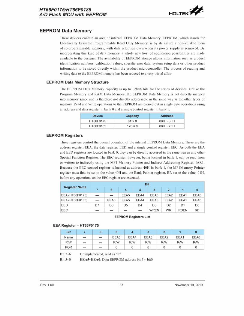
Rev. 1.60 36 November 19, 2019 Rev. 1.60 37 November 19, 2019
HT66F0175/HT66F0185A/D Flash MCU with EEPROM
HT66F0175/HT66F0185A/D Flash MCU with EEPROM
EEPROM Data MemoryThese devices contain an area of internal EEPROM Data Memory. EEPROM, which stands for Electrically Erasable Programmable Read Only Memory, is by its nature a non-volatile form of re-programmable memory, with data retention even when its power supply is removed. By incorporating this kind of data memory, a whole new host of application possibilities are made available to the designer. The availability of EEPROM storage allows information such as product identification numbers, calibration values, specific user data, system setup data or other product information to be stored directly within the product microcontroller. The process of reading and writing data to the EEPROM memory has been reduced to a very trivial affair.
EEPROM Data Memory StructureThe EEPROM Data Memory capacity is up to 128×8 bits for the series of devices. Unlike the Program Memory and RAM Data Memory, the EEPROM Data Memory is not directly mapped into memory space and is therefore not directly addressable in the same way as the other types of memory. Read and Write operations to the EEPROM are carried out in single byte operations using an address and data register in bank 0 and a single control register in bank 1.
Device Capacity AddressHT66F0175 64 × 8 00H ~ 3FHHT66F0185 128 × 8 00H ~ 7FH
EEPROM RegistersThree registers control the overall operation of the internal EEPROM Data Memory. These are the address register, EEA, the data register, EED and a single control register, EEC. As both the EEA and EED registers are located in bank 0, they can be directly accessed in the same was as any other Special Function Register. The EEC register, however, being located in bank 1, can be read from or written to indirectly using the MP1 Memory Pointer and Indirect Addressing Register, IAR1. Because the EEC control register is located at address 40H in bank 1, the MP1Memory Pointer register must first be set to the value 40H and the Bank Pointer register, BP, set to the value, 01H, before any operations on the EEC register are executed.
Register NameBit
7 6 5 4 3 2 1 0EEA (HT66F0175) — — EEA5 EEA4 EEA3 EEA2 EEA1 EEA0EEA (HT66F0185) — EEA6 EEA5 EEA4 EEA3 EEA2 EEA1 EEA0EED D7 D6 D5 D4 D3 D2 D1 D0EEC — — — — WREN WR RDEN RD
EEPROM Registers List
EEA Register – HT66F0175Bit 7 6 5 4 3 2 1 0
Name — — EEA5 EEA4 EEA3 EEA2 EEA1 EEA0R/W — — R/W R/W R/W R/W R/W R/WPOR — — 0 0 0 0 0 0
Bit 7~6 Unimplemented, read as “0”Bit 5~0 EEA5~EEA0: Data EEPROM address bit 5 ~ bit0
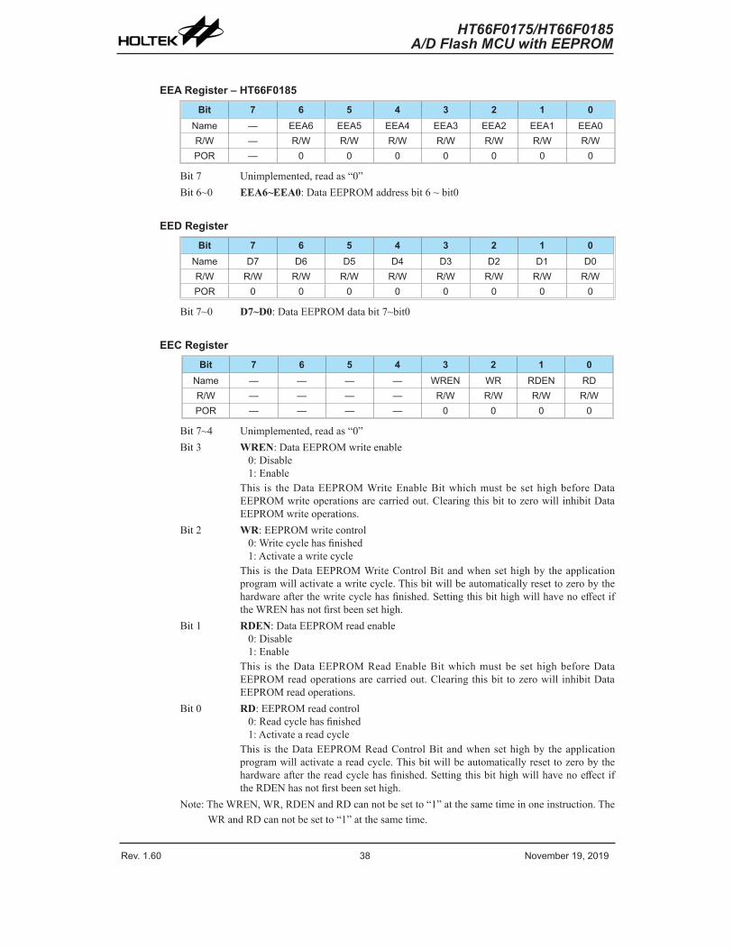
Rev. 1.60 38 November 19, 2019 Rev. 1.60 39 November 19, 2019
HT66F0175/HT66F0185A/D Flash MCU with EEPROM
HT66F0175/HT66F0185A/D Flash MCU with EEPROM
EEA Register – HT66F0185Bit 7 6 5 4 3 2 1 0
Name — EEA6 EEA5 EEA4 EEA3 EEA2 EEA1 EEA0R/W — R/W R/W R/W R/W R/W R/W R/WPOR — 0 0 0 0 0 0 0
Bit 7 Unimplemented, read as “0”Bit 6~0 EEA6~EEA0: Data EEPROM address bit 6 ~ bit0
EED RegisterBit 7 6 5 4 3 2 1 0
Name D7 D6 D5 D4 D3 D2 D1 D0R/W R/W R/W R/W R/W R/W R/W R/W R/WPOR 0 0 0 0 0 0 0 0
Bit 7~0 D7~D0: Data EEPROM data bit 7~bit0
EEC RegisterBit 7 6 5 4 3 2 1 0
Name — — — — WREN WR RDEN RDR/W — — — — R/W R/W R/W R/WPOR — — — — 0 0 0 0
Bit 7~4 Unimplemented, read as “0”Bit 3 WREN: Data EEPROM write enable
0: Disable1: Enable
This is the Data EEPROM Write Enable Bit which must be set high before Data EEPROM write operations are carried out. Clearing this bit to zero will inhibit Data EEPROM write operations.
Bit 2 WR: EEPROM write control0: Write cycle has finished1: Activate a write cycle
This is the Data EEPROM Write Control Bit and when set high by the application program will activate a write cycle. This bit will be automatically reset to zero by the hardware after the write cycle has finished. Setting this bit high will have no effect if the WREN has not first been set high.
Bit 1 RDEN: Data EEPROM read enable0: Disable1: Enable
This is the Data EEPROM Read Enable Bit which must be set high before Data EEPROM read operations are carried out. Clearing this bit to zero will inhibit Data EEPROM read operations.
Bit 0 RD: EEPROM read control0: Read cycle has finished1: Activate a read cycle
This is the Data EEPROM Read Control Bit and when set high by the application program will activate a read cycle. This bit will be automatically reset to zero by the hardware after the read cycle has finished. Setting this bit high will have no effect if the RDEN has not first been set high.
Note: The WREN, WR, RDEN and RD can not be set to “1” at the same time in one instruction. The WR and RD can not be set to “1” at the same time.
Rev. 1.60 38 November 19, 2019 Rev. 1.60 39 November 19, 2019
HT66F0175/HT66F0185A/D Flash MCU with EEPROM
HT66F0175/HT66F0185A/D Flash MCU with EEPROM
Reading Data from the EEPROMTo read data from the EEPROM, the read enable bit, RDEN, in the EEC register must first be set high to enable the read function. The EEPROM address of the data to be read must then be placed in the EEA register. If the RD bit in the EEC register is now set high, a read cycle will be initiated. Setting the RD bit high will not initiate a read operation if the RDEN bit has not been set. When the read cycle terminates, the RD bit will be automatically cleared to zero, after which the data can be read from the EED register. The data will remain in the EED register until another read or write operation is executed. The application program can poll the RD bit to determine when the data is valid for reading.
Writing Data to the EEPROMTo write data to the EEPROM, the EEPROM address of the data to be written must first be placed in the EEA register and the data placed in the EED register. Then the write enable bit, WREN, in the EEC register must first be set high to enable the write function. After this, the WR bit in the EEC register must be immediately set high to initiate a write cycle. These two instructions must be executed consecutively. The global interrupt bit EMI should also first be cleared before implementing any write operations, and then set again after the write cycle has started. Note that setting the WR bit high will not initiate a write cycle if the WREN bit has not been set. As the EEPROM write cycle is controlled using an internal timer whose operation is asynchronous to microcontroller system clock, a certain time will elapse before the data will have been written into the EEPROM. Detecting when the write cycle has finished can be implemented either by polling the WR bit in the EEC register or by using the EEPROM interrupt. When the write cycle terminates, the WR bit will be automatically cleared to zero by the microcontroller, informing the user that the data has been written to the EEPROM. The application program can therefore poll the WR bit to determine when the write cycle has ended.
Write ProtectionProtection against inadvertent write operation is provided in several ways. After the device is powered on, the Write Enable bit in the control register will be cleared preventing any write operations. Also at power-on the Bank Pointer register, BP, will be reset to zero, which means that Data Memory bank 0 will be selected. As the EEPROM control register is located in bank 1, this adds a further measure of protection against spurious write operations. During normal program operation, ensuring that the Write Enable bit in the control register is cleared will safeguard against incorrect write operations.
EEPROM InterruptThe EEPROM write interrupt is generated when an EEPROM write cycle has ended. The EEPROM interrupt must first be enabled by setting the DEE bit in the relevant interrupt register. However, as the EEPROM is contained within a Multi-function Interrupt, the associated multi-function interrupt enable bit must also be set. When an EEPROM write cycle ends, the DEF request flag and its associated multi-function interrupt request flag will both be set. If the global, EEPROM and Multi-function interrupts are enabled and the stack is not full, a jump to the associated Multi-function Interrupt vector will take place. When the interrupt is serviced only the Multi-function interrupt flag will be automatically reset, the EEPROM interrupt flag must be manually reset by the application program.
Rev. 1.60 40 November 19, 2019 Rev. 1.60 41 November 19, 2019
HT66F0175/HT66F0185A/D Flash MCU with EEPROM
HT66F0175/HT66F0185A/D Flash MCU with EEPROM
Programming ConsiderationsCare must be taken that data is not inadvertently written to the EEPROM. Protection can be Periodic by ensuring that the Write Enable bit is normally cleared to zero when not writing. Also the Bank Pointer register could be normally cleared to zero as this would inhibit access to bank 1 where the EEPROM control register exist. Although certainly not necessary, consideration might be given in the application program to the checking of the validity of new write data by a simple read back process. When writing data the WR bit must be set high immediately after the WREN bit has been set high, to ensure the write cycle executes correctly. The global interrupt bit EMI should also be cleared before a write cycle is executed and then re-enabled after the write cycle starts. Note that the device should not enter the IDLE or SLEEP mode until the EEPROM read or write operation is totally complete. Otherwise, the EEPROM read or write operation will fail.
Programming Example
Reading data from the EEPROM − polling methodMOV A, EEPROM_ADRES ; user defined addressMOV EEA, AMOV A, 040H ; setup memory pointer MP1MOV MP1, A ; MP1 points to EEC registerMOV A, 01H ; setup Bank Pointer BPMOV BP, ASET IAR1.1 ; set RDEN bit, enable read operationsSET IAR1.0 ; start Read Cycle - set RD bitBACK:SZ IAR1.0 ; check for read cycle endJMP BACKCLR IAR1 ; disable EEPROM writeCLR BPMOV A, EED ; move read data to registerMOV READ_DATA, A
Writing Data to the EEPROM − polling methodMOV A, EEPROM_ADRES ; user defined addressMOV EEA, AMOV A, EEPROM_DATA ; user defined dataMOV EED, AMOV A, 040H ; setup memory pointer MP1MOV MP1, A ; MP1 points to EEC registerMOV A, 01H ; setup Bank Pointer BPMOV BP, ACLR EMISET IAR1.3 ; set WREN bit, enable write operationsSET IAR1.2 ; start Write Cycle - set WR bitSET EMIBACK:SZ IAR1.2 ; check for write cycle endJMP BACKCLR IAR1 ; disable EEPROM writeCLR BP
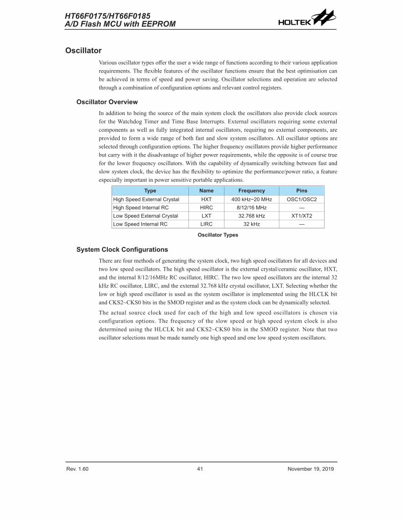
Rev. 1.60 40 November 19, 2019 Rev. 1.60 41 November 19, 2019
HT66F0175/HT66F0185A/D Flash MCU with EEPROM
HT66F0175/HT66F0185A/D Flash MCU with EEPROM
OscillatorVarious oscillator types offer the user a wide range of functions according to their various application requirements. The flexible features of the oscillator functions ensure that the best optimisation can be achieved in terms of speed and power saving. Oscillator selections and operation are selected through a combination of configuration options and relevant control registers.
Oscillator OverviewIn addition to being the source of the main system clock the oscillators also provide clock sources for the Watchdog Timer and Time Base Interrupts. External oscillators requiring some external components as well as fully integrated internal oscillators, requiring no external components, are provided to form a wide range of both fast and slow system oscillators. All oscillator options are selected through configuration options. The higher frequency oscillators provide higher performance but carry with it the disadvantage of higher power requirements, while the opposite is of course true for the lower frequency oscillators. With the capability of dynamically switching between fast and slow system clock, the device has the flexibility to optimize the performance/power ratio, a feature especially important in power sensitive portable applications.
Type Name Frequency PinsHigh Speed External Crystal HXT 400 kHz~20 MHz OSC1/OSC2High Speed Internal RC HIRC 8/12/16 MHz —Low Speed External Crystal LXT 32.768 kHz XT1/XT2Low Speed Internal RC LIRC 32 kHz —
Oscillator Types
System Clock ConfigurationsThere are four methods of generating the system clock, two high speed oscillators for all devices and two low speed oscillators. The high speed oscillator is the external crystal/ceramic oscillator, HXT, and the internal 8/12/16MHz RC oscillator, HIRC. The two low speed oscillators are the internal 32 kHz RC oscillator, LIRC, and the external 32.768 kHz crystal oscillator, LXT. Selecting whether the low or high speed oscillator is used as the system oscillator is implemented using the HLCLK bit and CKS2~CKS0 bits in the SMOD register and as the system clock can be dynamically selected.
The actual source clock used for each of the high and low speed oscillators is chosen via configuration options. The frequency of the slow speed or high speed system clock is also determined using the HLCLK bit and CKS2~CKS0 bits in the SMOD register. Note that two oscillator selections must be made namely one high speed and one low speed system oscillators.
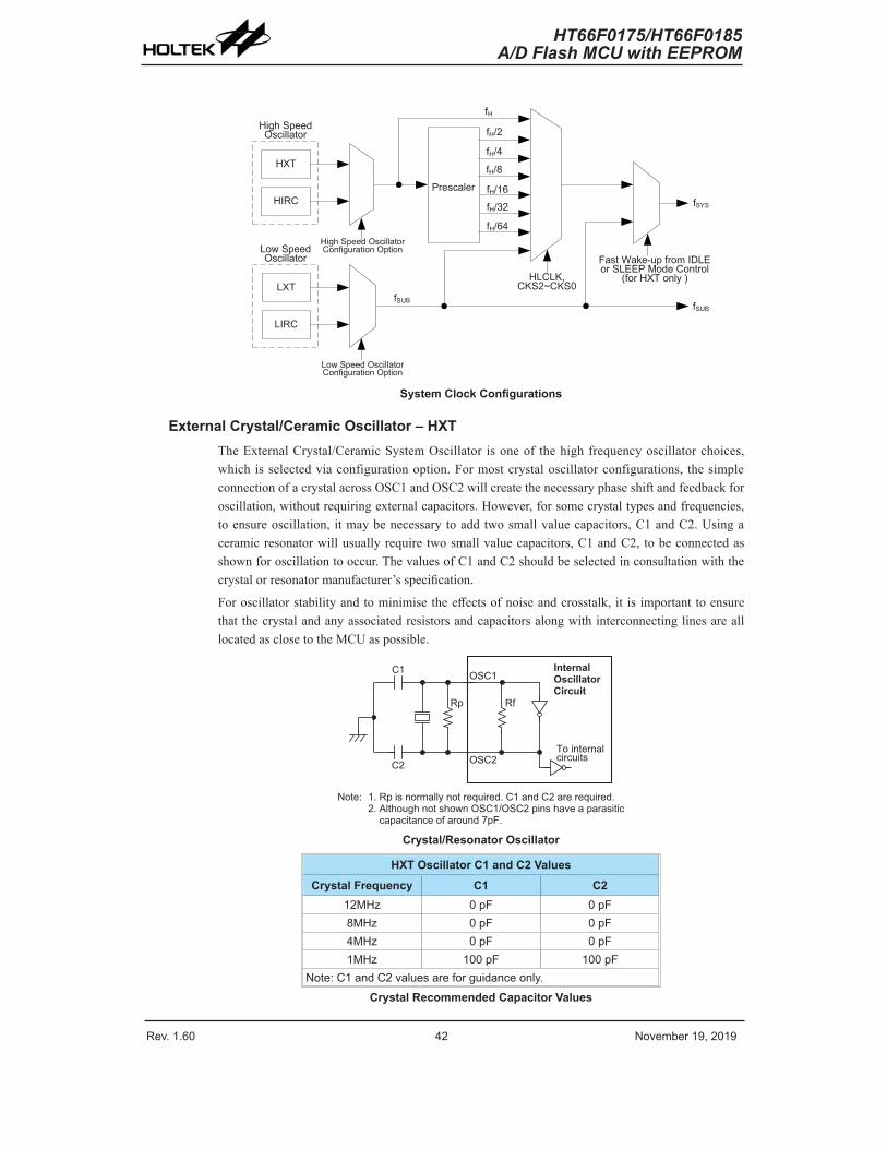
Rev. 1.60 42 November 19, 2019 Rev. 1.60 43 November 19, 2019
HT66F0175/HT66F0185A/D Flash MCU with EEPROM
HT66F0175/HT66F0185A/D Flash MCU with EEPROM
HIRCPrescaler
fH
LXT
High Speed Oscillator
Low Speed Oscillator
fH/2
fH/16
fH/64
fH/8
fH/4
fH/32
HLCLK,CKS2~CKS0
fSYS
fSUB fSUB
LIRC
HXT
fH
High Speed Oscillator Configuration Option
Low Speed Oscillator Configuration Option
Fast Wake-up from IDLE or SLEEP Mode Control
(for HXT only )
System Clock Configurations
External Crystal/Ceramic Oscillator – HXTThe External Crystal/Ceramic System Oscillator is one of the high frequency oscillator choices, which is selected via configuration option. For most crystal oscillator configurations, the simple connection of a crystal across OSC1 and OSC2 will create the necessary phase shift and feedback for oscillation, without requiring external capacitors. However, for some crystal types and frequencies, to ensure oscillation, it may be necessary to add two small value capacitors, C1 and C2. Using a ceramic resonator will usually require two small value capacitors, C1 and C2, to be connected as shown for oscillation to occur. The values of C1 and C2 should be selected in consultation with the crystal or resonator manufacturer’s specification.
For oscillator stability and to minimise the effects of noise and crosstalk, it is important to ensure that the crystal and any associated resistors and capacitors along with interconnecting lines are all located as close to the MCU as possible.
� � � �
� � � �
� �
� � � � � � � � � � �� � � � � � �
� � � � � � � �� � � � � � � � � �� � � � � � �
� �
� �
� �
� � � � � � � � � � � � � � � � � � � � � � � � � � � � � � � � � � � � � � � � � � � � � � � � � � � � � � � �� � � � � � � � � � � � � � � � � � � � � � � � � � � � � � � � � � � � � � � � � � � � � � � � � � � �� � � � � � � � � � � � � � � � � � � � � � � � � � � � �
Crystal/Resonator Oscillator
HXT Oscillator C1 and C2 ValuesCrystal Frequency C1 C2
12MHz 0 pF 0 pF8MHz 0 pF 0 pF4MHz 0 pF 0 pF1MHz 100 pF 100 pF
Note: C1 and C2 values are for guidance only.Crystal Recommended Capacitor Values
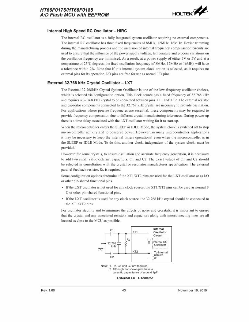
Rev. 1.60 42 November 19, 2019 Rev. 1.60 43 November 19, 2019
HT66F0175/HT66F0185A/D Flash MCU with EEPROM
HT66F0175/HT66F0185A/D Flash MCU with EEPROM
Internal High Speed RC Oscillator – HIRCThe internal RC oscillator is a fully integrated system oscillator requiring no external components. The internal RC oscillator has three fixed frequencies of 8MHz, 12MHz, 16MHz. Device trimming during the manufacturing process and the inclusion of internal frequency compensation circuits are used to ensure that the influence of the power supply voltage, temperature and process variations on the oscillation frequency are minimised. As a result, at a power supply of either 3V or 5V and at a temperature of 25°C degrees, the fixed oscillation frequency of 8MHz, 12MHz or 16MHz will have a tolerance within 2%. Note that if this internal system clock option is selected, as it requires no external pins for its operation, I/O pins are free for use as normal I/O pins.
External 32.768 kHz Crystal Oscillator – LXTThe External 32.768kHz Crystal System Oscillator is one of the low frequency oscillator choices, which is selected via configuration option. This clock source has a fixed frequency of 32.768 kHz and requires a 32.768 kHz crystal to be connected between pins XT1 and XT2. The external resistor and capacitor components connected to the 32.768 kHz crystal are necessary to provide oscillation. For applications where precise frequencies are essential, these components may be required to provide frequency compensation due to different crystal manufacturing tolerances. During power-up there is a time delay associated with the LXT oscillator waiting for it to start-up.
When the microcontroller enters the SLEEP or IDLE Mode, the system clock is switched off to stop microcontroller activity and to conserve power. However, in many microcontroller applications it may be necessary to keep the internal timers operational even when the microcontroller is in the SLEEP or IDLE Mode. To do this, another clock, independent of the system clock, must be provided.
However, for some crystals, to ensure oscillation and accurate frequency generation, it is necessary to add two small value external capacitors, C1 and C2. The exact values of C1 and C2 should be selected in consultation with the crystal or resonator manufacturer specification. The external parallel feedback resistor, RP, is required.
Some configuration options determine if the XT1/XT2 pins are used for the LXT oscillator or as I/O or other pin-shared functional pins.
• If the LXT oscillator is not used for any clock source, the XT1/XT2 pins can be used as normal I/O or other pin-shared functional pins.
• If the LXT oscillator is used for any clock source, the 32.768 kHz crystal should be connected to the XT1/XT2 pins.
For oscillator stability and to minimise the effects of noise and crosstalk, it is important to ensure that the crystal and any associated resistors and capacitors along with interconnecting lines are all located as close to the MCU as possible.
� � � � � � � � � � �� � � � � � � �
� � � � � � � �� � � � � � � � � �� � � � � � �
� �
� �
� �
� � � � � � � � � � � � � � � � � � � � � � � � � � � � � � �� � � � � � � � � � � � � � � � � � � � � � � � � � � � � � � � �� � � � � � � � � � � � � � � � � � � � � � � � � � � � � � � � � � � � � � �
� � � � � � � � � � �� � � � � � � � � �� � � � � �
�
� � �
� � �
External LXT Oscillator
Rev. 1.60 44 November 19, 2019 Rev. 1.60 45 November 19, 2019
HT66F0175/HT66F0185A/D Flash MCU with EEPROM
HT66F0175/HT66F0185A/D Flash MCU with EEPROM
LXT Oscillator C1 and C2 ValuesCrystal Frequency C1 C2
32.768kHz 10pF 10pFNote: 1. C1 and C2 values are for guidance only.
2. RP=5MΩ~10MΩ is recommended.
32.768kHz Crystal Recommended Capacitor Values
LXT Oscillator Low Power FunctionThe LXT oscillator can function in one of two modes, the Quick Start Mode and the Low Power Mode. The mode selection is executed using the LXTLP bit in the TBC register.
LXTLP LXT Operating Mode0 Quick Start1 Low-Power
After power on, the LXTLP bit will be automatically cleared to zero ensuring that the LXT oscillator is in the Quick Start operating mode. In the Quick Start Mode the LXT oscillator will power up and stabilise quickly. However, after the LXT oscillator has fully powered up it can be placed into the Low-power mode by setting the LXTLP bit high. The oscillator will continue to run but with reduced current consumption, as the higher current consumption is only required during the LXT oscillator start-up. In power sensitive applications, such as battery applications, where power consumption must be kept to a minimum, it is therefore recommended that the application program sets the LXTLP bit high about 2 seconds after power-on. It should be noted that, no matter what condition the LXTLP bit is set to, the LXT oscillator will always function normally and the only difference is that it will take more time to start up if in the Low-power mode.
Internal 32kHz Oscillator – LIRCThe Internal 32kHz System Oscillator is one of the low frequency oscillator choices, which is selected via configuration option. It is a fully integrated RC oscillator with a typical frequency of 32kHz at 5V, requiring no external components for its implementation. Device trimming during the manufacturing process and the inclusion of internal frequency compensation circuits are used to ensure that the influence of the power supply voltage, temperature and process variations on the oscillation frequency are minimised. As a result, at a power supply of 5V and at a temperature of 25°C degrees, the fixed oscillation frequency of 32kHz will have a tolerance within 10%.
Supplementary OscillatorsThe low speed oscillators, in addition to providing a system clock source are also used to provide a clock source to two other device functions. These are the Watchdog Timer and the Time Base Interrupts.
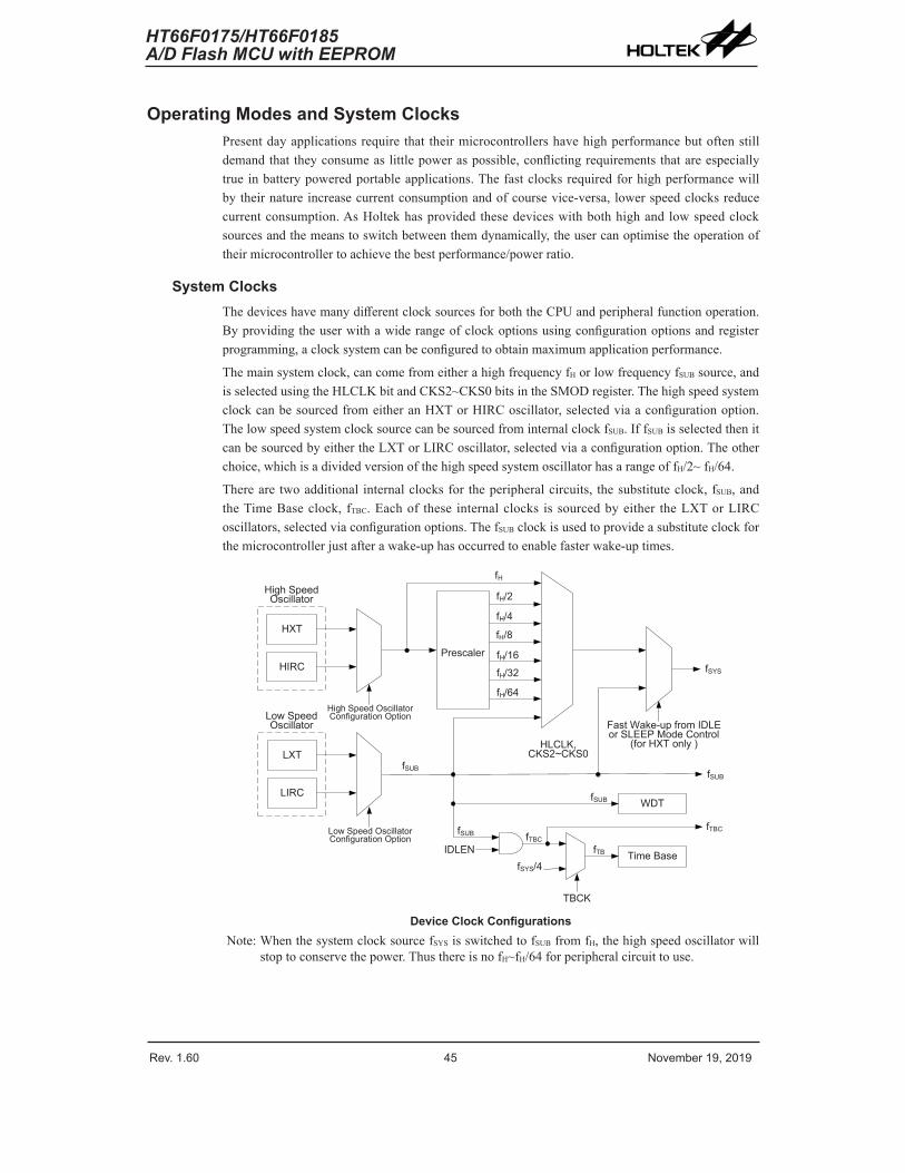
Rev. 1.60 44 November 19, 2019 Rev. 1.60 45 November 19, 2019
HT66F0175/HT66F0185A/D Flash MCU with EEPROM
HT66F0175/HT66F0185A/D Flash MCU with EEPROM
Operating Modes and System ClocksPresent day applications require that their microcontrollers have high performance but often still demand that they consume as little power as possible, conflicting requirements that are especially true in battery powered portable applications. The fast clocks required for high performance will by their nature increase current consumption and of course vice-versa, lower speed clocks reduce current consumption. As Holtek has provided these devices with both high and low speed clock sources and the means to switch between them dynamically, the user can optimise the operation of their microcontroller to achieve the best performance/power ratio.
System ClocksThe devices have many different clock sources for both the CPU and peripheral function operation. By providing the user with a wide range of clock options using configuration options and register programming, a clock system can be configured to obtain maximum application performance.
The main system clock, can come from either a high frequency fH or low frequency fSUB source, and is selected using the HLCLK bit and CKS2~CKS0 bits in the SMOD register. The high speed system clock can be sourced from either an HXT or HIRC oscillator, selected via a configuration option. The low speed system clock source can be sourced from internal clock fSUB. If fSUB is selected then it can be sourced by either the LXT or LIRC oscillator, selected via a configuration option. The other choice, which is a divided version of the high speed system oscillator has a range of fH/2~ fH/64.
There are two additional internal clocks for the peripheral circuits, the substitute clock, fSUB, and the Time Base clock, fTBC. Each of these internal clocks is sourced by either the LXT or LIRC oscillators, selected via configuration options. The fSUB clock is used to provide a substitute clock for the microcontroller just after a wake-up has occurred to enable faster wake-up times.
HIRCPrescaler
fH
LXT
High Speed Oscillator
Low Speed Oscillator
fH/2
fH/16
fH/64
fH/8
fH/4
fH/32
HLCLK,CKS2~CKS0
fSYS
fSUB fSUB
LIRC
HXT
fH
High Speed Oscillator Configuration Option
Low Speed Oscillator Configuration Option
Fast Wake-up from IDLE or SLEEP Mode Control
(for HXT only )
fSUB
IDLENfTBC
fSYS/4
TBCK
fTB Time Base
WDTfSUB
fTBC
Device Clock ConfigurationsNote: When the system clock source fSYS is switched to fSUB from fH, the high speed oscillator will
stop to conserve the power. Thus there is no fH~fH/64 for peripheral circuit to use.
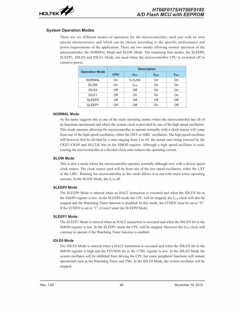
Rev. 1.60 46 November 19, 2019 Rev. 1.60 47 November 19, 2019
HT66F0175/HT66F0185A/D Flash MCU with EEPROM
HT66F0175/HT66F0185A/D Flash MCU with EEPROM
System Operation ModesThere are six different modes of operation for the microcontroller, each one with its own special characteristics and which can be chosen according to the specific performance and power requirements of the application. There are two modes allowing normal operation of the microcontroller, the NORMAL Mode and SLOW Mode. The remaining four modes, the SLEEP0, SLEEP1, IDLE0 and IDLE1 Mode, are used when the microcontroller CPU is switched off to conserve power.
Operation ModeDescription
CPU fSYS fSUB fTBC
NORMAL On fH~fH/64 On OnSLOW On fSUB On OnIDLE0 Off Off On OnIDLE1 Off On On On
SLEEP0 Off Off Off OffSLEEP1 Off Off On Off
NORMAL ModeAs the name suggests this is one of the main operating modes where the microcontroller has all of its functions operational and where the system clock is provided by one of the high speed oscillators. This mode operates allowing the microcontroller to operate normally with a clock source will come from one of the high speed oscillators, either the HXT or HIRC oscillators. The high speed oscillator will however first be divided by a ratio ranging from 1 to 64, the actual ratio being selected by the CKS2~CKS0 and HLCLK bits in the SMOD register. Although a high speed oscillator is used, running the microcontroller at a divided clock ratio reduces the operating current.
SLOW ModeThis is also a mode where the microcontroller operates normally although now with a slower speed clock source. The clock source used will be from one of the low speed oscillators, either the LXT or the LIRC. Running the microcontroller in this mode allows it to run with much lower operating currents. In the SLOW Mode, the fH is off.
SLEEP0 ModeThe SLEEP0 Mode is entered when an HALT instruction is executed and when the IDLEN bit in the SMOD register is low. In the SLEEP0 mode the CPU will be stopped, the fSUB clock will also be stopped and the Watchdog Timer function is disabled. In this mode, the LVDEN must be set to “0”. If the LVDEN is set to “1”, it won’t enter the SLEEP0 Mode.
SLEEP1 ModeThe SLEEP1 Mode is entered when an HALT instruction is executed and when the IDLEN bit in the SMOD register is low. In the SLEEP1 mode the CPU will be stopped. However the fSUB clock will continue to operate if the Watchdog Timer function is enabled.
IDLE0 ModeThe IDLE0 Mode is entered when a HALT instruction is executed and when the IDLEN bit in the SMOD register is high and the FSYSON bit in the CTRL register is low. In the IDLE0 Mode the system oscillator will be inhibited from driving the CPU but some peripheral functions will remain operational such as the Watchdog Timer and TMs. In the IDLE0 Mode, the system oscillator will be stopped.
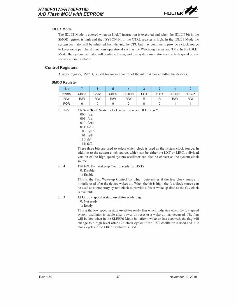
Rev. 1.60 46 November 19, 2019 Rev. 1.60 47 November 19, 2019
HT66F0175/HT66F0185A/D Flash MCU with EEPROM
HT66F0175/HT66F0185A/D Flash MCU with EEPROM
IDLE1 ModeThe IDLE1 Mode is entered when an HALT instruction is executed and when the IDLEN bit in the SMOD register is high and the FSYSON bit in the CTRL register is high. In the IDLE1 Mode the system oscillator will be inhibited from driving the CPU but may continue to provide a clock source to keep some peripheral functions operational such as the Watchdog Timer and TMs. In the IDLE1 Mode, the system oscillator will continue to run, and this system oscillator may be high speed or low speed system oscillator.
Control RegistersA single register, SMOD, is used for overall control of the internal clocks within the devices.
SMOD RegisterBit 7 6 5 4 3 2 1 0
Name CKS2 CKS1 CKS0 FSTEN LTO HTO IDLEN HLCLKR/W R/W R/W R/W R/W R R R/W R/WPOR 0 0 0 0 0 0 1 1
Bit 7~5 CKS2~CKS0: System clock selection when HLCLK is “0”000: fSUB
001: fSUB
010: fH/64011: fH/32100: fH/16101: fH/8110: fH/4111: fH/2
These three bits are used to select which clock is used as the system clock source. In addition to the system clock source, which can be either the LXT or LIRC, a divided version of the high speed system oscillator can also be chosen as the system clock source.
Bit 4 FSTEN: Fast Wake-up Control (only for HXT)0: Disable1: Enable
This is the Fast Wake-up Control bit which determines if the fSUB clock source is initially used after the device wakes up. When the bit is high, the fSUB clock source can be used as a temporary system clock to provide a faster wake up time as the fSUB clock is available.
Bit 3 LTO: Low speed system oscillator ready flag0: Not ready1: Ready
This is the low speed system oscillator ready flag which indicates when the low speed system oscillator is stable after power on reset or a wake-up has occurred. The flag will be low when in the SLEEP0 Mode but after a wake-up has occurred, the flag will change to a high level after 128 clock cycles if the LXT oscillator is used and 1~2 clock cycles if the LIRC oscillator is used.
Rev. 1.60 48 November 19, 2019 Rev. 1.60 49 November 19, 2019
HT66F0175/HT66F0185A/D Flash MCU with EEPROM
HT66F0175/HT66F0185A/D Flash MCU with EEPROM
Bit 2 HTO: High speed system oscillator ready flag0: Not ready1: Ready
This is the high speed system oscillator ready flag which indicates when the high speed system oscillator is stable. This flag is cleared to “0” by hardware when the devices are powered on and then changes to a high level after the high speed system oscillator is stable.Therefore this flag will always be read as “1” by the application program after device power-on. The flag will be low when in the SLEEP or IDLE0 Mode but after a wake-up has occurred, the flag will change to a high level after 512 clock cycles if the HXT oscillator is used and after 15~16 clock cycles if the HIRC oscillator is used.
Bit 1 IDLEN: IDLE mode control0: Disable1: Enable
This is the IDLE mode control bit and determines what happens when the HALT instruction is executed. If this bit is high, when a HALT instruction is execured, the device will enter the IDLE mode. In the IDLE mode the CPU will stop running but the system clock will continye to keep the peripheral functions operational, if the FSYSON bit is high. If the FSYSON bit is low, the CPU and the system clock will all stop in IDLE0 mode. If the bit is low, the devices will enter the SLEEP mode when a HALT instruction is executed.
Bit 0 HLCLK: System clock selection0: fH/2~fH/64 or fSUB
1: fH
This bit is used to select if the fH clock or the fH/2~fH/64 or fSUB clock is used as the system clock. When the bit is high the fH clock will be selected and if low the fH/2~fH/64 or fSUB clock will be selected. When system clock switches from the fH clock to the fSUB clock and the fH clock will be automatically switched off to conserve power.
CTRL RegisterBit 7 6 5 4 3 2 1 0
Name FSYSON — — — — LVRF LRF WRFR/W R/W — — — — R/W R/W R/WPOR 0 — — — — x 0 0
“x”: unknownBit 7 FSYSON: fSYS Control in IDLE Mode
0: Disable1: Enable
This bit is used to control whether the system clock is switched on or not in the IDLE Mode. If this bit is set to “0”, the system clock will be switched off in the IDLE Mode. However, the system clock will be switched on in the IDLE Mode when the FSYSON bit is set to “1”.
Bit 6~3 Unimplemented, read as “0”Bit 2 LVRF: LVR function reset flag
Described elsewhere.Bit 1 LRF: LVR control register software reset flag
Described elsewhere.Bit 0 WRF: WDT control register software reset flag
Described elsewhere.
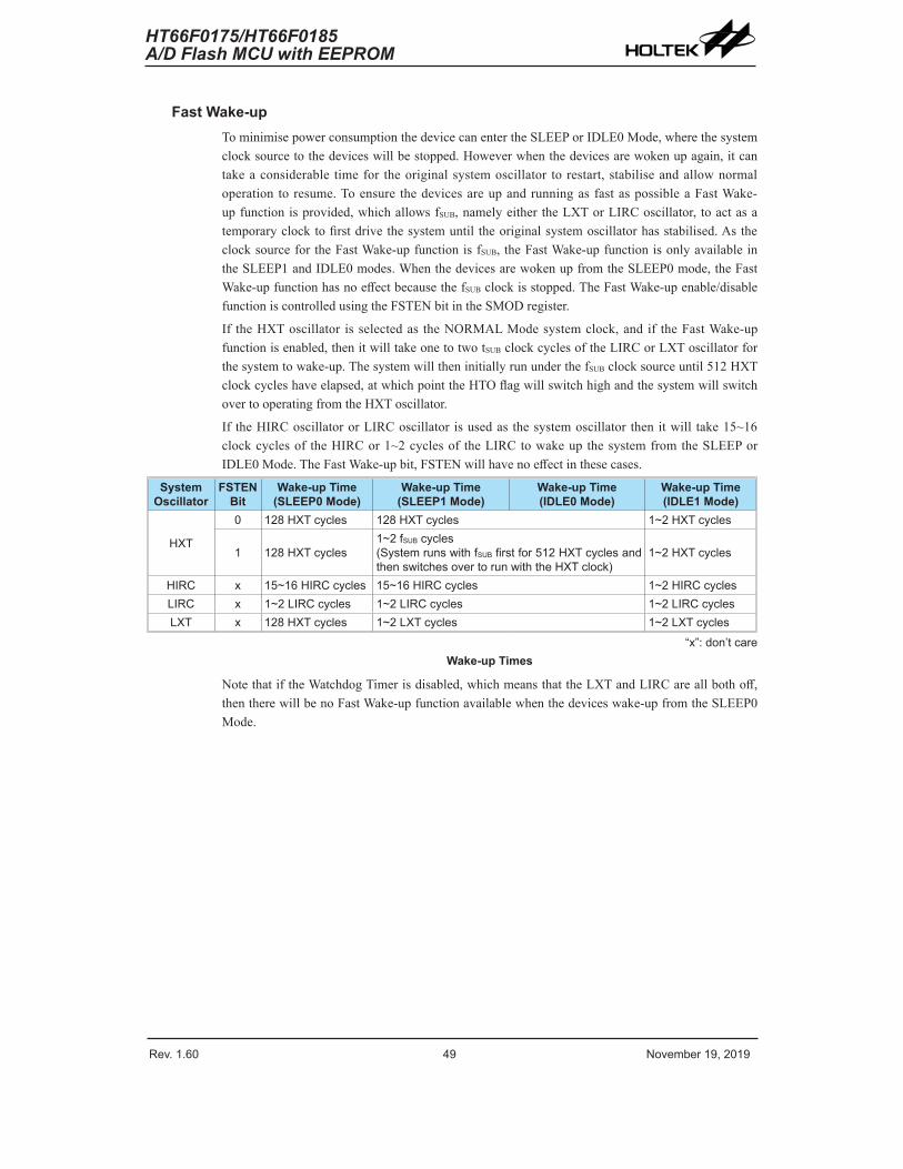
Rev. 1.60 48 November 19, 2019 Rev. 1.60 49 November 19, 2019
HT66F0175/HT66F0185A/D Flash MCU with EEPROM
HT66F0175/HT66F0185A/D Flash MCU with EEPROM
Fast Wake-upTo minimise power consumption the device can enter the SLEEP or IDLE0 Mode, where the system clock source to the devices will be stopped. However when the devices are woken up again, it can take a considerable time for the original system oscillator to restart, stabilise and allow normal operation to resume. To ensure the devices are up and running as fast as possible a Fast Wake-up function is provided, which allows fSUB, namely either the LXT or LIRC oscillator, to act as a temporary clock to first drive the system until the original system oscillator has stabilised. As the clock source for the Fast Wake-up function is fSUB, the Fast Wake-up function is only available in the SLEEP1 and IDLE0 modes. When the devices are woken up from the SLEEP0 mode, the Fast Wake-up function has no effect because the fSUB clock is stopped. The Fast Wake-up enable/disable function is controlled using the FSTEN bit in the SMOD register.
If the HXT oscillator is selected as the NORMAL Mode system clock, and if the Fast Wake-up function is enabled, then it will take one to two tSUB clock cycles of the LIRC or LXT oscillator for the system to wake-up. The system will then initially run under the fSUB clock source until 512 HXT clock cycles have elapsed, at which point the HTO flag will switch high and the system will switch over to operating from the HXT oscillator.
If the HIRC oscillator or LIRC oscillator is used as the system oscillator then it will take 15~16 clock cycles of the HIRC or 1~2 cycles of the LIRC to wake up the system from the SLEEP or IDLE0 Mode. The Fast Wake-up bit, FSTEN will have no effect in these cases.
System Oscillator
FSTEN Bit
Wake-up Time (SLEEP0 Mode)
Wake-up Time (SLEEP1 Mode)
Wake-up Time (IDLE0 Mode)
Wake-up Time (IDLE1 Mode)
HXT
0 128 HXT cycles 128 HXT cycles 1~2 HXT cycles
1 128 HXT cycles1~2 fSUB cycles(System runs with fSUB first for 512 HXT cycles and then switches over to run with the HXT clock)
1~2 HXT cycles
HIRC x 15~16 HIRC cycles 15~16 HIRC cycles 1~2 HIRC cyclesLIRC x 1~2 LIRC cycles 1~2 LIRC cycles 1~2 LIRC cyclesLXT x 128 HXT cycles 1~2 LXT cycles 1~2 LXT cycles
“x”: don’t careWake-up Times
Note that if the Watchdog Timer is disabled, which means that the LXT and LIRC are all both off, then there will be no Fast Wake-up function available when the devices wake-up from the SLEEP0 Mode.
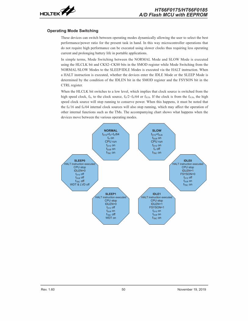
Rev. 1.60 50 November 19, 2019 Rev. 1.60 51 November 19, 2019
HT66F0175/HT66F0185A/D Flash MCU with EEPROM
HT66F0175/HT66F0185A/D Flash MCU with EEPROM
Operating Mode SwitchingThese devices can switch between operating modes dynamically allowing the user to select the best performance/power ratio for the present task in hand. In this way microcontroller operations that do not require high performance can be executed using slower clocks thus requiring less operating current and prolonging battery life in portable applications.
In simple terms, Mode Switching between the NORMAL Mode and SLOW Mode is executed using the HLCLK bit and CKS2~CKS0 bits in the SMOD register while Mode Switching from the NORMAL/SLOW Modes to the SLEEP/IDLE Modes is executed via the HALT instruction. When a HALT instruction is executed, whether the devices enter the IDLE Mode or the SLEEP Mode is determined by the condition of the IDLEN bit in the SMOD register and the FSYSON bit in the CTRL register.
When the HLCLK bit switches to a low level, which implies that clock source is switched from the high speed clock, fH, to the clock source, fH/2~fH/64 or fSUB. If the clock is from the fSUB, the high speed clock source will stop running to conserve power. When this happens, it must be noted that the fH/16 and fH/64 internal clock sources will also stop running, which may affect the operation of other internal functions such as the TMs. The accompamying chart shows what happens when the devices move between the various operating modes.
NORMALfSYS=fH~fH/64
fH onCPU runfSYS onfSUB onfTBC on
SLOWfSYS=fSUBfSUB on
CPU runfSYS onfH off
fTBC on
IDLE0HALT instruction executed
CPU stopIDLEN=1
FSYSON=0fSYS offfSUB onfTBC on
IDLE1HALT instruction executed
CPU stopIDLEN=1
FSYSON=1fSYS onfSUB onfTBC on
SLEEP1HALT instruction executed
CPU stopIDLEN=0
fSYS offfSUB onfTBC offWDT on
SLEEP0HALT instruction executed
CPU stopIDLEN=0
fSYS offfSUB offfTBC off
WDT & LVD off
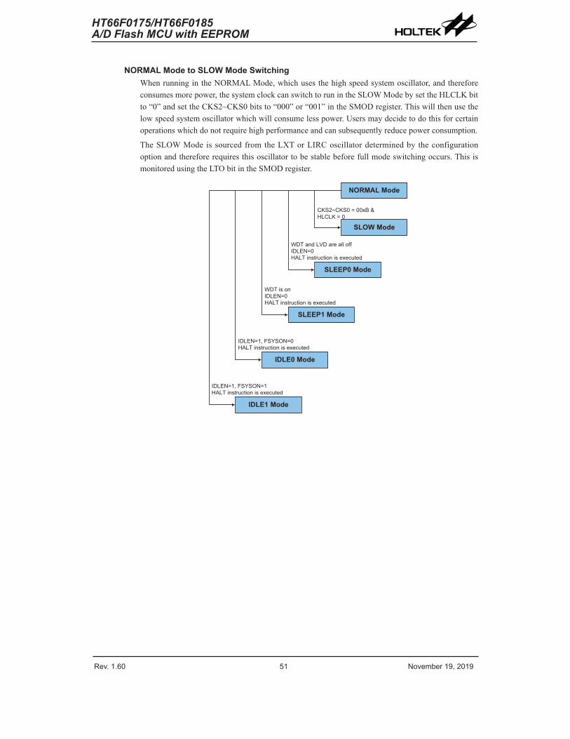
Rev. 1.60 50 November 19, 2019 Rev. 1.60 51 November 19, 2019
HT66F0175/HT66F0185A/D Flash MCU with EEPROM
HT66F0175/HT66F0185A/D Flash MCU with EEPROM
NORMAL Mode to SLOW Mode SwitchingWhen running in the NORMAL Mode, which uses the high speed system oscillator, and therefore consumes more power, the system clock can switch to run in the SLOW Mode by set the HLCLK bit to “0” and set the CKS2~CKS0 bits to “000” or “001” in the SMOD register. This will then use the low speed system oscillator which will consume less power. Users may decide to do this for certain operations which do not require high performance and can subsequently reduce power consumption.
The SLOW Mode is sourced from the LXT or LIRC oscillator determined by the configuration option and therefore requires this oscillator to be stable before full mode switching occurs. This is monitored using the LTO bit in the SMOD register.
NORMAL Mode
SLOW Mode
CKS2~CKS0 = 00xB &HLCLK = 0
SLEEP0 Mode
IDLEN=0HALT instruction is executed
SLEEP1 Mode
IDLE0 Mode
IDLE1 Mode
WDT and LVD are all off
IDLEN=0HALT instruction is executed
WDT is on
IDLEN=1, FSYSON=0HALT instruction is executed
IDLEN=1, FSYSON=1HALT instruction is executed
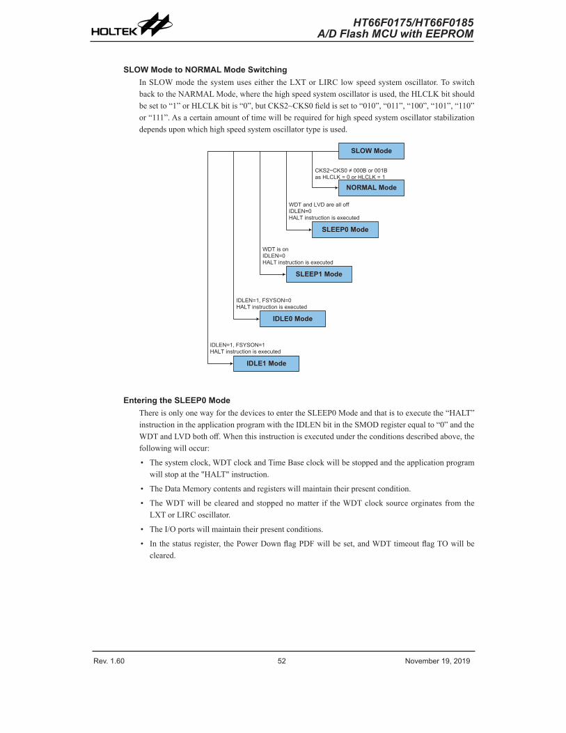
Rev. 1.60 52 November 19, 2019 Rev. 1.60 53 November 19, 2019
HT66F0175/HT66F0185A/D Flash MCU with EEPROM
HT66F0175/HT66F0185A/D Flash MCU with EEPROM
SLOW Mode to NORMAL Mode SwitchingIn SLOW mode the system uses either the LXT or LIRC low speed system oscillator. To switch back to the NARMAL Mode, where the high speed system oscillator is used, the HLCLK bit should be set to “1” or HLCLK bit is “0”, but CKS2~CKS0 field is set to “010”, “011”, “100”, “101”, “110” or “111”. As a certain amount of time will be required for high speed system oscillator stabilization depends upon which high speed system oscillator type is used.
NORMAL Mode
SLOW Mode
CKS2~CKS0 ≠ 000B or 001B as HLCLK = 0 or HLCLK = 1
SLEEP0 Mode
IDLEN=0HALT instruction is executed
SLEEP1 Mode
IDLE0 Mode
IDLE1 Mode
WDT and LVD are all off
IDLEN=0HALT instruction is executed
WDT is on
IDLEN=1, FSYSON=0HALT instruction is executed
IDLEN=1, FSYSON=1HALT instruction is executed
Entering the SLEEP0 ModeThere is only one way for the devices to enter the SLEEP0 Mode and that is to execute the “HALT” instruction in the application program with the IDLEN bit in the SMOD register equal to “0” and the WDT and LVD both off. When this instruction is executed under the conditions described above, the following will occur:
• The system clock, WDT clock and Time Base clock will be stopped and the application program will stop at the "HALT" instruction.
• The Data Memory contents and registers will maintain their present condition.
• The WDT will be cleared and stopped no matter if the WDT clock source orginates from the LXT or LIRC oscillator.
• The I/O ports will maintain their present conditions.
• In the status register, the Power Down flag PDF will be set, and WDT timeout flag TO will be cleared.
Rev. 1.60 52 November 19, 2019 Rev. 1.60 53 November 19, 2019
HT66F0175/HT66F0185A/D Flash MCU with EEPROM
HT66F0175/HT66F0185A/D Flash MCU with EEPROM
Entering the SLEEP1 ModeThere is only one way for the devices to enter the SLEEP1 Mode and that is to execute the “HALT” instruction in the application program with the IDLEN bit in the SMOD register equal to “0” and the WDT on. When this instruction is executed under the conditions described above, the following will occur:
• The system clock and Time Base clock will be stopped and the application program will stop at the "HALT" instruction, but the WDT will remain with the clock source coming from the fSUB clock.
• The Data Memory contents and registers will maintain their present condition.
• The WDT will be cleared and resume counting if the WDT function is enabled.
• The I/O ports will maintain their present conditions.
• In the status register, the Power Down flag PDF will be set, and WDT timeout flag TO will be cleared.
Entering the IDLE0 ModeThere is only one way for the devices to enter the IDLE0 Mode and that is to execute the “HALT” instruction in the application program with the IDLEN bit in the SMOD register equal to “1” and the FSYSON bit in the CTRL register equal to “0”. When this instruction is executed under the conditions described above, the following will occur:
• The system clock will be stopped and the application program will stop at the “HALT” instruction, but the fTBC and fSUB clocks will be on.
• The Data Memory contents and registers will maintain their present condition.
• The WDT will be cleared and resume counting if the WDT function is enabled.
• The I/O ports will maintain their present conditions.
• In the status register, the Power Down flag PDF will be set, and WDT timeout flag TO will be cleared.
Entering the IDLE1 ModeThere is only one way for the devices to enter the IDLE1 Mode and that is to execute the “HALT” instruction in the application program with the IDLEN bit in the SMOD register equal to “1” and the FSYSON bit in the CTRL register equal to “1”. When this instruction is executed under the conditions described above, the following will occur:
• The system clock, fTBC and fSUB clocks will be on but the application program will stop at the “HALT” instruction.
• The Data Memory contents and registers will maintain their present condition.
• The WDT will be cleared and resume counting if the WDT function is enabled.
• The I/O ports will maintain their present conditions.
• In the status register, the Power Down flag PDF will be set, and WDT timeout flag TO will be cleared.
Rev. 1.60 54 November 19, 2019 Rev. 1.60 55 November 19, 2019
HT66F0175/HT66F0185A/D Flash MCU with EEPROM
HT66F0175/HT66F0185A/D Flash MCU with EEPROM
Standby Current ConsiderationsAs the main reason for entering the SLEEP or IDLE Mode is to keep the current consumption of the device to as low a value as possible, perhaps only in the order of several micro-amps except in the IDLE1 Mode, there are other considerations which must also be taken into account by the circuit designer if the power consumption is to be minimised. Special attention must be made to the I/O pins on the device. All high-impedance input pins must be connected to either a fixed high or low level as any floating input pins could create internal oscillations and result in increased current consumption. This also applies to devices which have different package types, as there may be unbonbed pins. These must either be setup as outputs or if setup as inputs must have pull-high resistors connected.
Care must also be taken with the loads, which are connected to I/O pins, which are setup as outputs. These should be placed in a condition in which minimum current is drawn or connected only to external circuits that do not draw current, such as other CMOS inputs. Also note that additional standby current will also be required if the LIRC oscillator has enabled.
In the IDLE1 Mode the system oscillator is on, if the system oscillator is from the high speed oscillator, the additional standby current will also be perhaps in the order of several hundred micro-amps.
Wake-upTo minimise power consumption the device can enter the SLEEP or any IDLE Mode, where the CPU will be switched off. However, when the device is woken up again, it will take a considerable time for the original system oscillator to restart, stablise and allow normal operation to resume.
After the system enters the SLEEP or IDLE Mode, it can be woken up from one of various sources listed as follows:
• An external falling edge on Port A
• A system interrupt
• A WDT overflow
When the devices execute the “HALT” instruction, it will enter the Power down mode and the PDF flag will be set to 1. The PDF flag will be cleared to 0 if the devices experience a system power-up or executes the clear Watchdog Timer instruction. If the system is woken up by a WDT overflow, a Watchdog Timer reset will be initiated and the TO flag will be set to 1. The TO flag is set if a WDT time-out occurs and causes a wake-up that only resets the Program Counter and Stack Pointer, other flags remain in their original status.
Each pin on Port A can be setup using the PAWU register to permit a negative transition on the pin to wake up the system. When a Port A pin wake-up occurs, the program will resume execution at the instruction following the “HALT” instruction. If the system is woken up by an interrupt, then two possible situations may occur. The first is where the related interrupt is disabled or the interrupt is enabled but the stack is full, in which case the program will resume execution at the instruction following the “HALT” instruction. In this situation, the interrupt which woke up the devices will not be immediately serviced, but will rather be serviced later when the related interrupt is finally enabled or when a stack level becomes free. The other situation is where the related interrupt is enabled and the stack is not full, in which case the regular interrupt response takes place. If an interrupt request flag is set high before entering the SLEEP or IDLE Mode, the wake-up function of the related interrupt will be disabled.
Rev. 1.60 54 November 19, 2019 Rev. 1.60 55 November 19, 2019
HT66F0175/HT66F0185A/D Flash MCU with EEPROM
HT66F0175/HT66F0185A/D Flash MCU with EEPROM
Programming ConsiderationsThe high speed and low speed oscillators both use the same SST counter. For example, if the system is woken up from the SLEEP0 Mode and both the HIRC and LXT oscillators need to start-up from an off state. The LXT oscillator uses the SST counter after the HIRC oscillator has finished its SST period.
• If the devices are woken up from the SLEEP0 Mode to the NORMAL Mode, the high speed system oscillator needs an SST period. The devices will execute first instruction after HTO is “1”. At this time, the LXT oscillator may not be stability if fSUB is from LXT oscillator. The same situation occurs in the power-on state. The LXT oscillator is not ready yet when the first instruction is executed.
• If the devices are woken up from the SLEEP1 Mode to NORMAL Mode, and the system clock source is from the HXT oscillator and FSTEN is “1”, the system clock can be switched to the LIRC oscillator after wake up.
• There are peripheral functions, such as WDT and TMs, for which the fSYS is used. If the system clock source is switched from fH to fSUB, the clock source to the peripheral functions mentioned above will change accordingly.
• The on/off condition of fSUB and fS depends upon whether the WDT is enabled or disabled as the WDT clock source is selected from fSUB.
Watchdog TimerThe Watchdog Timer is provided to prevent program malfunctions or sequences from jumping to unknown locations, due to certain uncontrollable external events such as electrical noise.
Watchdog Timer Clock SourceThe Watchdog Timer clock source is provided by the internal clock, fSUB, which is in turn supplied by the LIRC or LXT oscillator. The LXT oscillator is supplied by an external 32.768 kHz crystal. The LIRC internal oscillator has an approximate frequency of 32 kHz at a supply voltage of 5V. However, it should be noted that this specified internal clock frequency can vary with VDD, temperature and process variations. The Watchdog Timer source clock is then subdivided by a ratio of 28 to 218 to give longer timeouts, the actual value being chosen using the WS2~WS0 bits in the WDTC register.
Watchdog Timer Control RegisterA single register, WDTC, controls the required timeout period as well as the enable/disable operation. This register controls the overall operation of the Watchdog Timer.
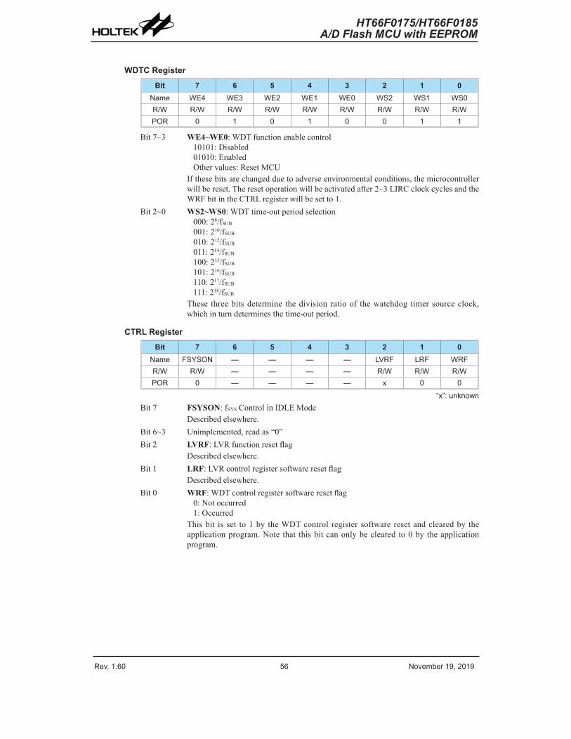
Rev. 1.60 56 November 19, 2019 Rev. 1.60 57 November 19, 2019
HT66F0175/HT66F0185A/D Flash MCU with EEPROM
HT66F0175/HT66F0185A/D Flash MCU with EEPROM
WDTC RegisterBit 7 6 5 4 3 2 1 0
Name WE4 WE3 WE2 WE1 WE0 WS2 WS1 WS0R/W R/W R/W R/W R/W R/W R/W R/W R/WPOR 0 1 0 1 0 0 1 1
Bit 7~3 WE4~WE0: WDT function enable control10101: Disabled01010: EnabledOther values: Reset MCU
If these bits are changed due to adverse environmental conditions, the microcontroller will be reset. The reset operation will be activated after 2~3 LIRC clock cycles and the WRF bit in the CTRL register will be set to 1.
Bit 2~0 WS2~WS0: WDT time-out period selection000: 28/fSUB
001: 210/fSUB
010: 212/fSUB
011: 214/fSUB
100: 215/fSUB
101: 216/fSUB
110: 217/fSUB
111: 218/fSUB
These three bits determine the division ratio of the watchdog timer source clock, which in turn determines the time-out period.
CTRL RegisterBit 7 6 5 4 3 2 1 0
Name FSYSON — — — — LVRF LRF WRFR/W R/W — — — — R/W R/W R/WPOR 0 — — — — x 0 0
“x”: unknownBit 7 FSYSON: fSYS Control in IDLE Mode
Described elsewhere.Bit 6~3 Unimplemented, read as “0”Bit 2 LVRF: LVR function reset flag
Described elsewhere.Bit 1 LRF: LVR control register software reset flag
Described elsewhere.Bit 0 WRF: WDT control register software reset flag
0: Not occurred1: Occurred
This bit is set to 1 by the WDT control register software reset and cleared by the application program. Note that this bit can only be cleared to 0 by the application program.
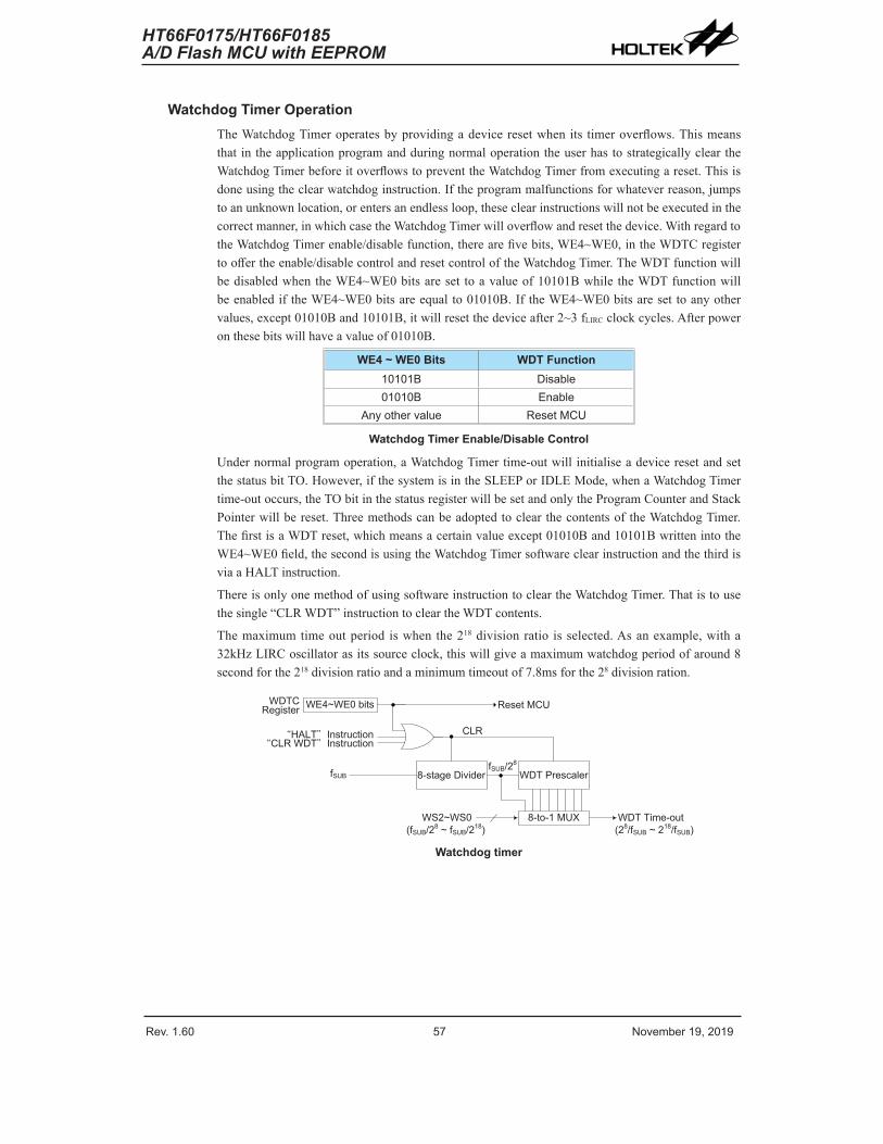
Rev. 1.60 56 November 19, 2019 Rev. 1.60 57 November 19, 2019
HT66F0175/HT66F0185A/D Flash MCU with EEPROM
HT66F0175/HT66F0185A/D Flash MCU with EEPROM
Watchdog Timer OperationThe Watchdog Timer operates by providing a device reset when its timer overflows. This means that in the application program and during normal operation the user has to strategically clear the Watchdog Timer before it overflows to prevent the Watchdog Timer from executing a reset. This is done using the clear watchdog instruction. If the program malfunctions for whatever reason, jumps to an unknown location, or enters an endless loop, these clear instructions will not be executed in the correct manner, in which case the Watchdog Timer will overflow and reset the device. With regard to the Watchdog Timer enable/disable function, there are five bits, WE4~WE0, in the WDTC register to offer the enable/disable control and reset control of the Watchdog Timer. The WDT function will be disabled when the WE4~WE0 bits are set to a value of 10101B while the WDT function will be enabled if the WE4~WE0 bits are equal to 01010B. If the WE4~WE0 bits are set to any other values, except 01010B and 10101B, it will reset the device after 2~3 fLIRC clock cycles. After power on these bits will have a value of 01010B.
WE4 ~ WE0 Bits WDT Function10101B Disable01010B Enable
Any other value Reset MCU
Watchdog Timer Enable/Disable Control
Under normal program operation, a Watchdog Timer time-out will initialise a device reset and set the status bit TO. However, if the system is in the SLEEP or IDLE Mode, when a Watchdog Timer time-out occurs, the TO bit in the status register will be set and only the Program Counter and Stack Pointer will be reset. Three methods can be adopted to clear the contents of the Watchdog Timer. The first is a WDT reset, which means a certain value except 01010B and 10101B written into the WE4~WE0 field, the second is using the Watchdog Timer software clear instruction and the third is via a HALT instruction.
There is only one method of using software instruction to clear the Watchdog Timer. That is to use the single “CLR WDT” instruction to clear the WDT contents.
The maximum time out period is when the 218 division ratio is selected. As an example, with a 32kHz LIRC oscillator as its source clock, this will give a maximum watchdog period of around 8 second for the 218 division ratio and a minimum timeout of 7.8ms for the 28 division ration.
“CLR WDT”Instruction
8-stage Divider WDT Prescaler
WE4~WE0 bitsWDTC Register Reset MCU
fSUBfSUB/28
8-to-1 MUX
CLR
WS2~WS0(fSUB/28 ~ fSUB/218)
WDT Time-out(28/fSUB ~ 218/fSUB)
“HALT”Instruction
Watchdog timer
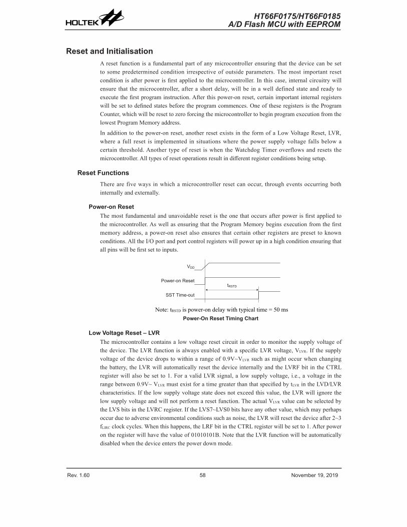
Rev. 1.60 58 November 19, 2019 Rev. 1.60 59 November 19, 2019
HT66F0175/HT66F0185A/D Flash MCU with EEPROM
HT66F0175/HT66F0185A/D Flash MCU with EEPROM
Reset and InitialisationA reset function is a fundamental part of any microcontroller ensuring that the device can be set to some predetermined condition irrespective of outside parameters. The most important reset condition is after power is first applied to the microcontroller. In this case, internal circuitry will ensure that the microcontroller, after a short delay, will be in a well defined state and ready to execute the first program instruction. After this power-on reset, certain important internal registers will be set to defined states before the program commences. One of these registers is the Program Counter, which will be reset to zero forcing the microcontroller to begin program execution from the lowest Program Memory address.
In addition to the power-on reset, another reset exists in the form of a Low Voltage Reset, LVR, where a full reset is implemented in situations where the power supply voltage falls below a certain threshold. Another type of reset is when the Watchdog Timer overflows and resets the microcontroller. All types of reset operations result in different register conditions being setup.
Reset FunctionsThere are five ways in which a microcontroller reset can occur, through events occurring both internally and externally.
Power-on ResetThe most fundamental and unavoidable reset is the one that occurs after power is first applied to the microcontroller. As well as ensuring that the Program Memory begins execution from the first memory address, a power-on reset also ensures that certain other registers are preset to known conditions. All the I/O port and port control registers will power up in a high condition ensuring that all pins will be first set to inputs.
VDD
Power-on Reset
SST Time-out
tRSTD
Note: tRSTD is power-on delay with typical time = 50 msPower-On Reset Timing Chart
Low Voltage Reset – LVRThe microcontroller contains a low voltage reset circuit in order to monitor the supply voltage of the device. The LVR function is always enabled with a specific LVR voltage, VLVR. If the supply voltage of the device drops to within a range of 0.9V~VLVR such as might occur when changing the battery, the LVR will automatically reset the device internally and the LVRF bit in the CTRL register will also be set to 1. For a valid LVR signal, a low supply voltage, i.e., a voltage in the range between 0.9V~ VLVR must exist for a time greater than that specified by tLVR in the LVD/LVR characteristics. If the low supply voltage state does not exceed this value, the LVR will ignore the low supply voltage and will not perform a reset function. The actual VLVR value can be selected by the LVS bits in the LVRC register. If the LVS7~LVS0 bits have any other value, which may perhaps occur due to adverse environmental conditions such as noise, the LVR will reset the device after 2~3 fLIRC clock cycles. When this happens, the LRF bit in the CTRL register will be set to 1. After power on the register will have the value of 01010101B. Note that the LVR function will be automatically disabled when the device enters the power down mode.
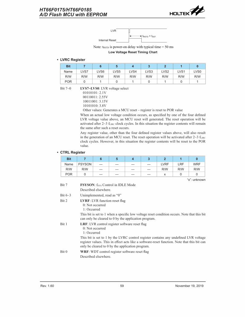
Rev. 1.60 58 November 19, 2019 Rev. 1.60 59 November 19, 2019
HT66F0175/HT66F0185A/D Flash MCU with EEPROM
HT66F0175/HT66F0185A/D Flash MCU with EEPROM
LVR
Internal ResettRSTD + tSST
Note: tRSTD is power-on delay with typical time = 50 msLow Voltage Reset Timing Chart
• LVRC RegisterBit 7 6 5 4 3 2 1 0
Name LVS7 LVS6 LVS5 LVS4 LVS3 LVS2 LVS1 LVS0R/W R/W R/W R/W R/W R/W R/W R/W R/WPOR 0 1 0 1 0 1 0 1
Bit 7~0 LVS7~LVS0: LVR voltage select01010101: 2.1V00110011: 2.55V10011001: 3.15V10101010: 3.8VOther values: Generates a MCU reset – register is reset to POR value
When an actual low voltage condition occurs, as specified by one of the four defined LVR voltage value above, an MCU reset will generated. The reset operation will be activated after 2~3 fLIRC clock cycles. In this situation the register contents will remain the same after such a reset occurs.Any register value, other than the four defined register values above, will also result in the generation of an MCU reset. The reset operation will be activated after 2~3 fLIRC clock cycles. However, in this situation the register contents will be reset to the POR value.
• CTRL RegisterBit 7 6 5 4 3 2 1 0
Name FSYSON — — — — LVRF LRF WRFR/W R/W — — — — R/W R/W R/WPOR 0 — — — — x 0 0
“x”: unknownBit 7 FSYSON: fSYS Control in IDLE Mode
Described elsewhere.Bit 6~3 Unimplemented, read as “0”Bit 2 LVRF: LVR function reset flag
0: Not occurred1: Occurred
This bit is set to 1 when a specific low voltage reset condition occurs. Note that this bit can only be cleared to 0 by the application program.
Bit 1 LRF: LVR control register software reset flag0: Not occurred1: Occurred
This bit is set to 1 by the LVRC control register contains any undefined LVR voltage register values. This in effect acts like a software-reset function. Note that this bit can only be cleared to 0 by the application program.
Bit 0 WRF: WDT control register software reset flagDescribed elsewhere.
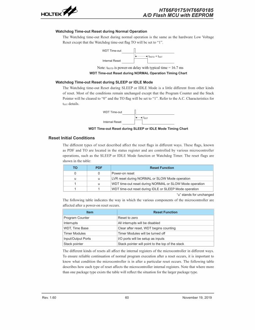
Rev. 1.60 60 November 19, 2019 Rev. 1.60 61 November 19, 2019
HT66F0175/HT66F0185A/D Flash MCU with EEPROM
HT66F0175/HT66F0185A/D Flash MCU with EEPROM
Watchdog Time-out Reset during Normal OperationThe Watchdog time-out Reset during normal operation is the same as the hardware Low Voltage Reset except that the Watchdog time-out flag TO will be set to “1”.
WDT Time-out
Internal ResettRSTD + tSST
Note: tRSTD is power-on delay with typical time = 16.7 msWDT Time-out Reset during NORMAL Operation Timing Chart
Watchdog Time-out Reset during SLEEP or IDLE ModeThe Watchdog time-out Reset during SLEEP or IDLE Mode is a little different from other kinds of reset. Most of the conditions remain unchanged except that the Program Counter and the Stack Pointer will be cleared to “0” and the TO flag will be set to “1”. Refer to the A.C. Characteristics for tSST details.
WDT Time-out
Internal ResettSST
WDT Time-out Reset during SLEEP or IDLE Mode Timing Chart
Reset Initial ConditionsThe different types of reset described affect the reset flags in different ways. These flags, known as PDF and TO are located in the status register and are controlled by various microcontroller operations, such as the SLEEP or IDLE Mode function or Watchdog Timer. The reset flags are shown in the table:
TO PDF Reset Function0 0 Power-on resetu u LVR reset during NORMAL or SLOW Mode operation1 u WDT time-out reset during NORMAL or SLOW Mode operation1 1 WDT time-out reset during IDLE or SLEEP Mode operation
“u” stands for unchangedThe following table indicates the way in which the various components of the microcontroller are affected after a power-on reset occurs.
Item Reset FunctionProgram Counter Reset to zeroInterrupts All interrupts will be disabledWDT, Time Base Clear after reset, WDT begins countingTimer Modules Timer Modules will be turned offInput/Output Ports I/O ports will be setup as inputsStack pointer Stack pointer will point to the top of the stack
The different kinds of resets all affect the internal registers of the microcontroller in different ways. To ensure reliable continuation of normal program execution after a reset occurs, it is important to know what condition the microcontroller is in after a particular reset occurs. The following table describes how each type of reset affects the microcontroller internal registers. Note that where more than one package type exists the table will reflect the situation for the larger package type.
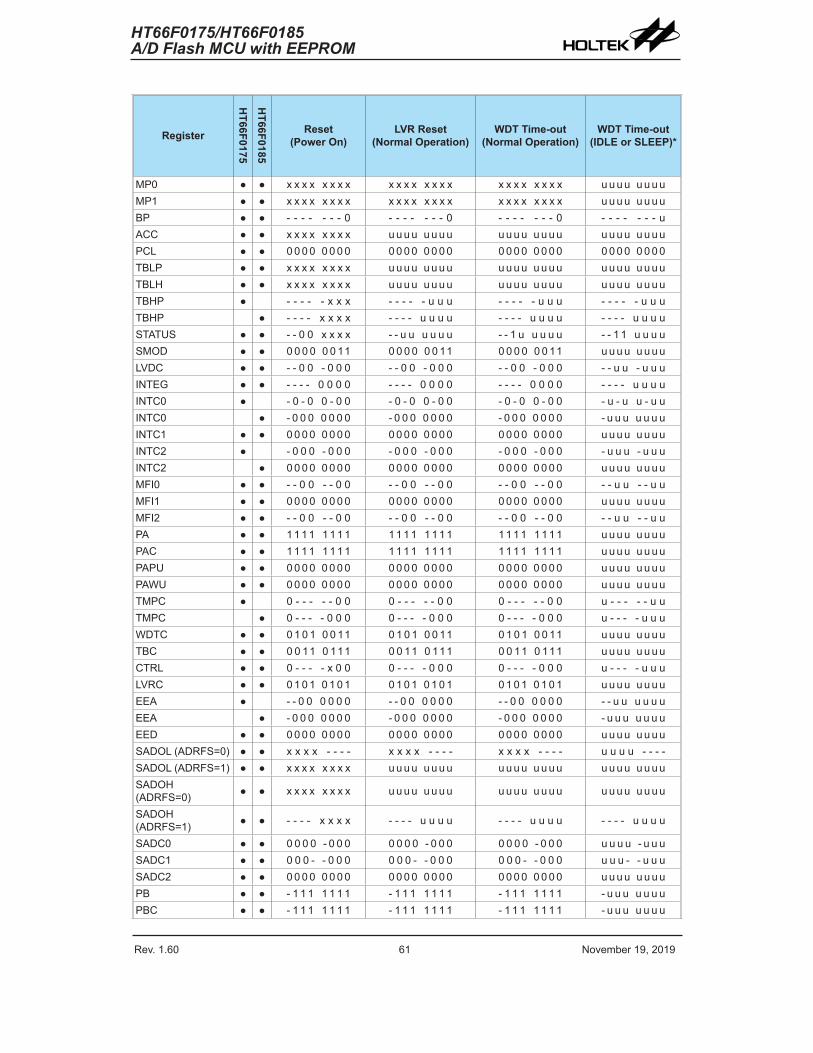
Rev. 1.60 60 November 19, 2019 Rev. 1.60 61 November 19, 2019
HT66F0175/HT66F0185A/D Flash MCU with EEPROM
HT66F0175/HT66F0185A/D Flash MCU with EEPROM
Register
HT66F0175
HT66F0185
Reset(Power On)
LVR Reset(Normal Operation)
WDT Time-out(Normal Operation)
WDT Time-out(IDLE or SLEEP)*
MP0 ● ● x x x x x x x x x x x x x x x x x x x x x x x x u u u u u u u uMP1 ● ● x x x x x x x x x x x x x x x x x x x x x x x x u u u u u u u uBP ● ● - - - - - - - 0 - - - - - - - 0 - - - - - - - 0 - - - - - - - uACC ● ● x x x x x x x x u u u u u u u u u u u u u u u u u u u u u u u uPCL ● ● 0 0 0 0 0 0 0 0 0 0 0 0 0 0 0 0 0 0 0 0 0 0 0 0 0 0 0 0 0 0 0 0TBLP ● ● x x x x x x x x u u u u u u u u u u u u u u u u u u u u u u u uTBLH ● ● x x x x x x x x u u u u u u u u u u u u u u u u u u u u u u u uTBHP ● - - - - - x x x - - - - - u u u - - - - - u u u - - - - - u u uTBHP ● - - - - x x x x - - - - u u u u - - - - u u u u - - - - u u u uSTATUS ● ● - - 0 0 x x x x - - u u u u u u - - 1 u u u u u - - 1 1 u u u uSMOD ● ● 0 0 0 0 0 0 11 0 0 0 0 0 0 11 0 0 0 0 0 0 11 u u u u u u u uLVDC ● ● - - 0 0 - 0 0 0 - - 0 0 - 0 0 0 - - 0 0 - 0 0 0 - - u u - u u uINTEG ● ● - - - - 0 0 0 0 - - - - 0 0 0 0 - - - - 0 0 0 0 - - - - u u u uINTC0 ● - 0 - 0 0 - 0 0 - 0 - 0 0 - 0 0 - 0 - 0 0 - 0 0 - u - u u - u uINTC0 ● - 0 0 0 0 0 0 0 - 0 0 0 0 0 0 0 - 0 0 0 0 0 0 0 - u u u u u u uINTC1 ● ● 0 0 0 0 0 0 0 0 0 0 0 0 0 0 0 0 0 0 0 0 0 0 0 0 u u u u u u u uINTC2 ● - 0 0 0 - 0 0 0 - 0 0 0 - 0 0 0 - 0 0 0 - 0 0 0 - u u u - u u uINTC2 ● 0 0 0 0 0 0 0 0 0 0 0 0 0 0 0 0 0 0 0 0 0 0 0 0 u u u u u u u uMFI0 ● ● - - 0 0 - - 0 0 - - 0 0 - - 0 0 - - 0 0 - - 0 0 - - u u - - u uMFI1 ● ● 0 0 0 0 0 0 0 0 0 0 0 0 0 0 0 0 0 0 0 0 0 0 0 0 u u u u u u u uMFI2 ● ● - - 0 0 - - 0 0 - - 0 0 - - 0 0 - - 0 0 - - 0 0 - - u u - - u uPA ● ● 1 1 1 1 1 1 1 1 1 1 1 1 1 1 1 1 1 1 1 1 1 1 1 1 u u u u u u u uPAC ● ● 1 1 1 1 1 1 1 1 1 1 1 1 1 1 1 1 1 1 1 1 1 1 1 1 u u u u u u u uPAPU ● ● 0 0 0 0 0 0 0 0 0 0 0 0 0 0 0 0 0 0 0 0 0 0 0 0 u u u u u u u uPAWU ● ● 0 0 0 0 0 0 0 0 0 0 0 0 0 0 0 0 0 0 0 0 0 0 0 0 u u u u u u u uTMPC ● 0 - - - - - 0 0 0 - - - - - 0 0 0 - - - - - 0 0 u - - - - - u uTMPC ● 0 - - - - 0 0 0 0 - - - - 0 0 0 0 - - - - 0 0 0 u - - - - u u uWDTC ● ● 0 1 0 1 0 0 11 0 1 0 1 0 0 11 0 1 0 1 0 0 11 u u u u u u u uTBC ● ● 0 0 11 0 111 0 0 11 0 111 0 0 11 0 111 u u u u u u u uCTRL ● ● 0 - - - - x 0 0 0 - - - - 0 0 0 0 - - - - 0 0 0 u - - - - u u uLVRC ● ● 0 1 0 1 0 1 0 1 0 1 0 1 0 1 0 1 0 1 0 1 0 1 0 1 u u u u u u u uEEA ● - - 0 0 0 0 0 0 - - 0 0 0 0 0 0 - - 0 0 0 0 0 0 - - u u u u u uEEA ● - 0 0 0 0 0 0 0 - 0 0 0 0 0 0 0 - 0 0 0 0 0 0 0 - u u u u u u uEED ● ● 0 0 0 0 0 0 0 0 0 0 0 0 0 0 0 0 0 0 0 0 0 0 0 0 u u u u u u u uSADOL (ADRFS=0) ● ● x x x x - - - - x x x x - - - - x x x x - - - - u u u u - - - -SADOL (ADRFS=1) ● ● x x x x x x x x u u u u u u u u u u u u u u u u u u u u u u u uSADOH (ADRFS=0) ● ● x x x x x x x x u u u u u u u u u u u u u u u u u u u u u u u u
SADOH (ADRFS=1) ● ● - - - - x x x x - - - - u u u u - - - - u u u u - - - - u u u u
SADC0 ● ● 0 0 0 0 - 0 0 0 0 0 0 0 - 0 0 0 0 0 0 0 - 0 0 0 u u u u - u u uSADC1 ● ● 0 0 0 - - 0 0 0 0 0 0 - - 0 0 0 0 0 0 - - 0 0 0 u u u - - u u uSADC2 ● ● 0 0 0 0 0 0 0 0 0 0 0 0 0 0 0 0 0 0 0 0 0 0 0 0 u u u u u u u uPB ● ● - 1 1 1 1 1 1 1 - 1 1 1 1 1 1 1 - 1 1 1 1 1 1 1 - u u u u u u uPBC ● ● - 1 1 1 1 1 1 1 - 1 1 1 1 1 1 1 - 1 1 1 1 1 1 1 - u u u u u u u
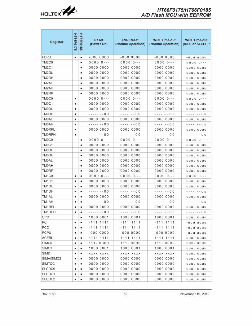
Rev. 1.60 62 November 19, 2019 Rev. 1.60 63 November 19, 2019
HT66F0175/HT66F0185A/D Flash MCU with EEPROM
HT66F0175/HT66F0185A/D Flash MCU with EEPROM
Register
HT66F0175
HT66F0185
Reset(Power On)
LVR Reset(Normal Operation)
WDT Time-out(Normal Operation)
WDT Time-out(IDLE or SLEEP)*
PBPU ● ● - 0 0 0 0 0 0 0 - 0 0 0 0 0 0 0 - 0 0 0 0 0 0 0 - u u u u u u uTM2C0 ● 0 0 0 0 0 - - - 0 0 0 0 0 - - - 0 0 0 0 0 - - - u u u u u - - -TM2C1 ● 0 0 0 0 0 0 0 0 0 0 0 0 0 0 0 0 0 0 0 0 0 0 0 0 u u u u u u u uTM2DL ● 0 0 0 0 0 0 0 0 0 0 0 0 0 0 0 0 0 0 0 0 0 0 0 0 u u u u u u u uTM2DH ● 0 0 0 0 0 0 0 0 0 0 0 0 0 0 0 0 0 0 0 0 0 0 0 0 u u u u u u u uTM2AL ● 0 0 0 0 0 0 0 0 0 0 0 0 0 0 0 0 0 0 0 0 0 0 0 0 u u u u u u u uTM2AH ● 0 0 0 0 0 0 0 0 0 0 0 0 0 0 0 0 0 0 0 0 0 0 0 0 u u u u u u u uTM2RP ● 0 0 0 0 0 0 0 0 0 0 0 0 0 0 0 0 0 0 0 0 0 0 0 0 u u u u u u u uTM0C0 ● 0 0 0 0 0 - - - 0 0 0 0 0 - - - 0 0 0 0 0 - - - u u u u u - - -TM0C1 ● 0 0 0 0 0 0 0 0 0 0 0 0 0 0 0 0 0 0 0 0 0 0 0 0 u u u u u u u uTM0DL ● 0 0 0 0 0 0 0 0 0 0 0 0 0 0 0 0 0 0 0 0 0 0 0 0 u u u u u u u uTM0DH ● - - - - - - - 0 0 - - - - - - 0 0 - - - - - - 0 0 - - - - - - u uTM0AL ● 0 0 0 0 0 0 0 0 0 0 0 0 0 0 0 0 0 0 0 0 0 0 0 0 u u u u u u u uTM0AH ● - - - - - - - 0 0 - - - - - - 0 0 - - - - - - 0 0 - - - - - - u uTM0RPL ● 0 0 0 0 0 0 0 0 0 0 0 0 0 0 0 0 0 0 0 0 0 0 0 0 u u u u u u u uTM0RPH ● - - - - - - - 0 0 - - - - - - 0 0 - - - - - - 0 0 - - - - - - u uTM0C0 ● 0 0 0 0 0 - - - 0 0 0 0 0 - - - 0 0 0 0 0 - - - u u u u u - - -TM0C1 ● 0 0 0 0 0 0 0 0 0 0 0 0 0 0 0 0 0 0 0 0 0 0 0 0 u u u u u u u uTM0DL ● 0 0 0 0 0 0 0 0 0 0 0 0 0 0 0 0 0 0 0 0 0 0 0 0 u u u u u u u uTM0DH ● 0 0 0 0 0 0 0 0 0 0 0 0 0 0 0 0 0 0 0 0 0 0 0 0 u u u u u u u uTM0AL ● 0 0 0 0 0 0 0 0 0 0 0 0 0 0 0 0 0 0 0 0 0 0 0 0 u u u u u u u uTM0AH ● 0 0 0 0 0 0 0 0 0 0 0 0 0 0 0 0 0 0 0 0 0 0 0 0 u u u u u u u uTM0RP ● 0 0 0 0 0 0 0 0 0 0 0 0 0 0 0 0 0 0 0 0 0 0 0 0 u u u u u u u uTM1C0 ● ● 0 0 0 0 0 - - - 0 0 0 0 0 - - - 0 0 0 0 0 - - - u u u u u - - -TM1C1 ● ● 0 0 0 0 0 0 0 0 0 0 0 0 0 0 0 0 0 0 0 0 0 0 0 0 u u u u u u u uTM1DL ● ● 0 0 0 0 0 0 0 0 0 0 0 0 0 0 0 0 0 0 0 0 0 0 0 0 u u u u u u u uTM1DH ● ● - - - - - - - 0 0 - - - - - - 0 0 - - - - - - 0 0 - - - - - - u uTM1AL ● ● 0 0 0 0 0 0 0 0 0 0 0 0 0 0 0 0 0 0 0 0 0 0 0 0 u u u u u u u uTM1AH ● ● - - - - - - - 0 0 - - - - - - 0 0 - - - - - - 0 0 - - - - - - u uTM1RPL ● ● 0 0 0 0 0 0 0 0 0 0 0 0 0 0 0 0 0 0 0 0 0 0 0 0 u u u u u u u uTM1RPH ● ● - - - - - - - 0 0 - - - - - - 0 0 - - - - - - 0 0 - - - - - - u uCPC ● 1 0 0 0 0 0 0 1 1 0 0 0 0 0 0 1 1 0 0 0 0 0 0 1 u u u u u u u uPC ● ● - 1 1 1 1 1 1 1 - 1 1 1 1 1 1 1 - 1 1 1 1 1 1 1 - u u u u u u uPCC ● ● - 1 1 1 1 1 1 1 - 1 1 1 1 1 1 1 - 1 1 1 1 1 1 1 - u u u u u u uPCPU ● ● - 0 0 0 0 0 0 0 - 0 0 0 0 0 0 0 - 0 0 0 0 0 0 0 - u u u u u u uACERL ● ● 1 1 1 1 1 1 1 1 1 1 1 1 1 1 1 1 1 1 1 1 1 1 1 1 u u u u u u u uSIMC0 ● ● 111 - 0 0 0 0 111 - 0 0 0 0 111 - 0 0 0 0 u u u - u u u uSIMC1 ● ● 1 0 0 0 0 0 0 1 1 0 0 0 0 0 0 1 1 0 0 0 0 0 0 1 u u u u u u u uSIMD ● ● x x x x x x x x x x x x x x x x x x x x x x x x u u u u u u u uSIMA/SIMC2 ● ● 0 0 0 0 0 0 0 0 0 0 0 0 0 0 0 0 0 0 0 0 0 0 0 0 u u u u u u u uSIMTOC ● ● 0 0 0 0 0 0 0 0 0 0 0 0 0 0 0 0 0 0 0 0 0 0 0 0 u u u u u u u uSLCDC0 ● ● 0 0 0 0 0 0 0 0 0 0 0 0 0 0 0 0 0 0 0 0 0 0 0 0 u u u u u u u uSLCDC1 ● ● 0 0 0 0 0 0 0 0 0 0 0 0 0 0 0 0 0 0 0 0 0 0 0 0 u u u u u u u uSLCDC2 ● ● 0 0 0 0 0 0 0 0 0 0 0 0 0 0 0 0 0 0 0 0 0 0 0 0 u u u u u u u u
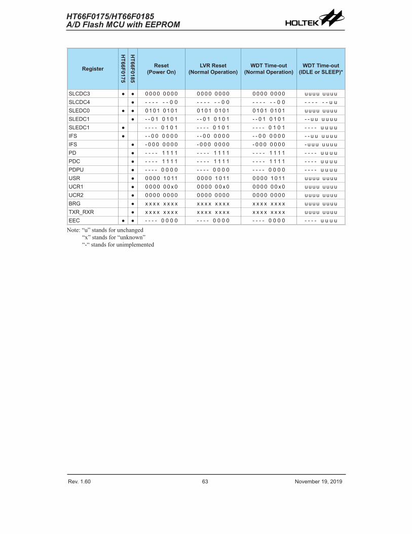
Rev. 1.60 62 November 19, 2019 Rev. 1.60 63 November 19, 2019
HT66F0175/HT66F0185A/D Flash MCU with EEPROM
HT66F0175/HT66F0185A/D Flash MCU with EEPROM
Register
HT66F0175
HT66F0185
Reset(Power On)
LVR Reset(Normal Operation)
WDT Time-out(Normal Operation)
WDT Time-out(IDLE or SLEEP)*
SLCDC3 ● ● 0 0 0 0 0 0 0 0 0 0 0 0 0 0 0 0 0 0 0 0 0 0 0 0 u u u u u u u uSLCDC4 ● - - - - - - 0 0 - - - - - - 0 0 - - - - - - 0 0 - - - - - - u uSLEDC0 ● ● 0 1 0 1 0 1 0 1 0 1 0 1 0 1 0 1 0 1 0 1 0 1 0 1 u u u u u u u uSLEDC1 ● - - 0 1 0 1 0 1 - - 0 1 0 1 0 1 - - 0 1 0 1 0 1 - - u u u u u uSLEDC1 ● - - - - 0 1 0 1 - - - - 0 1 0 1 - - - - 0 1 0 1 - - - - u u u uIFS ● - - 0 0 0 0 0 0 - - 0 0 0 0 0 0 - - 0 0 0 0 0 0 - - u u u u u uIFS ● - 0 0 0 0 0 0 0 - 0 0 0 0 0 0 0 - 0 0 0 0 0 0 0 - u u u u u u uPD ● - - - - 1 1 1 1 - - - - 1 1 1 1 - - - - 1 1 1 1 - - - - u u u uPDC ● - - - - 1 1 1 1 - - - - 1 1 1 1 - - - - 1 1 1 1 - - - - u u u uPDPU ● - - - - 0 0 0 0 - - - - 0 0 0 0 - - - - 0 0 0 0 - - - - u u u uUSR ● 0 0 0 0 1 0 11 0 0 0 0 1 0 11 0 0 0 0 1 0 11 u u u u u u u uUCR1 ● 0 0 0 0 0 0 x 0 0 0 0 0 0 0 x 0 0 0 0 0 0 0 x 0 u u u u u u u uUCR2 ● 0 0 0 0 0 0 0 0 0 0 0 0 0 0 0 0 0 0 0 0 0 0 0 0 u u u u u u u uBRG ● x x x x x x x x x x x x x x x x x x x x x x x x u u u u u u u uTXR_RXR ● x x x x x x x x x x x x x x x x x x x x x x x x u u u u u u u uEEC ● ● - - - - 0 0 0 0 - - - - 0 0 0 0 - - - - 0 0 0 0 - - - - u u u u
Note: “u” stands for unchanged“x” stands for “unknown”“-“ stands for unimplemented
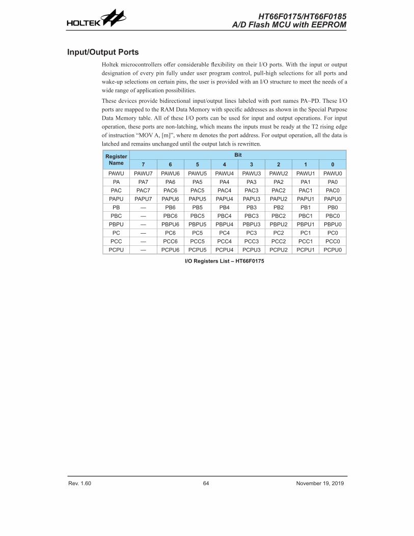
Rev. 1.60 64 November 19, 2019 Rev. 1.60 65 November 19, 2019
HT66F0175/HT66F0185A/D Flash MCU with EEPROM
HT66F0175/HT66F0185A/D Flash MCU with EEPROM
Input/Output PortsHoltek microcontrollers offer considerable flexibility on their I/O ports. With the input or output designation of every pin fully under user program control, pull-high selections for all ports and wake-up selections on certain pins, the user is provided with an I/O structure to meet the needs of a wide range of application possibilities.
These devices provide bidirectional input/output lines labeled with port names PA~PD. These I/O ports are mapped to the RAM Data Memory with specific addresses as shown in the Special Purpose Data Memory table. All of these I/O ports can be used for input and output operations. For input operation, these ports are non-latching, which means the inputs must be ready at the T2 rising edge of instruction “MOV A, [m]”, where m denotes the port address. For output operation, all the data is latched and remains unchanged until the output latch is rewritten.
Register Name
Bit7 6 5 4 3 2 1 0
PAWU PAWU7 PAWU6 PAWU5 PAWU4 PAWU3 PAWU2 PAWU1 PAWU0PA PA7 PA6 PA5 PA4 PA3 PA2 PA1 PA0
PAC PAC7 PAC6 PAC5 PAC4 PAC3 PAC2 PAC1 PAC0PAPU PAPU7 PAPU6 PAPU5 PAPU4 PAPU3 PAPU2 PAPU1 PAPU0
PB — PB6 PB5 PB4 PB3 PB2 PB1 PB0PBC — PBC6 PBC5 PBC4 PBC3 PBC2 PBC1 PBC0
PBPU — PBPU6 PBPU5 PBPU4 PBPU3 PBPU2 PBPU1 PBPU0PC — PC6 PC5 PC4 PC3 PC2 PC1 PC0
PCC — PCC6 PCC5 PCC4 PCC3 PCC2 PCC1 PCC0PCPU — PCPU6 PCPU5 PCPU4 PCPU3 PCPU2 PCPU1 PCPU0
I/O Registers List – HT66F0175
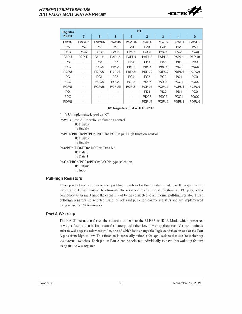
Rev. 1.60 64 November 19, 2019 Rev. 1.60 65 November 19, 2019
HT66F0175/HT66F0185A/D Flash MCU with EEPROM
HT66F0175/HT66F0185A/D Flash MCU with EEPROM
Register Name
Bit7 6 5 4 3 2 1 0
PAWU PAWU7 PAWU6 PAWU5 PAWU4 PAWU3 PAWU2 PAWU1 PAWU0PA PA7 PA6 PA5 PA4 PA3 PA2 PA1 PA0
PAC PAC7 PAC6 PAC5 PAC4 PAC3 PAC2 PAC1 PAC0PAPU PAPU7 PAPU6 PAPU5 PAPU4 PAPU3 PAPU2 PAPU1 PAPU0
PB — PB6 PB5 PB4 PB3 PB2 PB1 PB0PBC — PBC6 PBC5 PBC4 PBC3 PBC2 PBC1 PBC0
PBPU — PBPU6 PBPU5 PBPU4 PBPU3 PBPU2 PBPU1 PBPU0PC — PC6 PC5 PC4 PC3 PC2 PC1 PC0
PCC — PCC6 PCC5 PCC4 PCC3 PCC2 PCC1 PCC0PCPU — PCPU6 PCPU5 PCPU4 PCPU3 PCPU2 PCPU1 PCPU0
PD — — — — PD3 PD2 PD1 PD0PDC — — — — PDC3 PDC2 PDC1 PDC0
PDPU — — — — PDPU3 PDPU2 PDPU1 PDPU0
I/O Registers List – HT66F0185
“—”: Unimplemented, read as “0”.PAWUn: Port A Pin wake-up function control
0: Disable1: Enable
PAPUn/PBPUn/PCPUn/PDPUn: I/O Pin pull-high function control0: Disable1: Enable
PAn/PBn/PCn/PDn: I/O Port Data bit0: Data 01: Data 1
PACn/PBCn/PCCn/PDCn: I/O Pin type selection0: Output1: Input
Pull-high ResistorsMany product applications require pull-high resistors for their switch inputs usually requiring the use of an external resistor. To eliminate the need for these external resistors, all I/O pins, when configured as an input have the capability of being connected to an internal pull-high resistor. These pull-high resistors are selected using the relevant pull-high control registers and are implemented using weak PMOS transistors.
Port A Wake-upThe HALT instruction forces the microcontroller into the SLEEP or IDLE Mode which preserves power, a feature that is important for battery and other low-power applications. Various methods exist to wake-up the microcontroller, one of which is to change the logic condition on one of the Port A pins from high to low. This function is especially suitable for applications that can be woken up via external switches. Each pin on Port A can be selected individually to have this wake-up feature using the PAWU register.
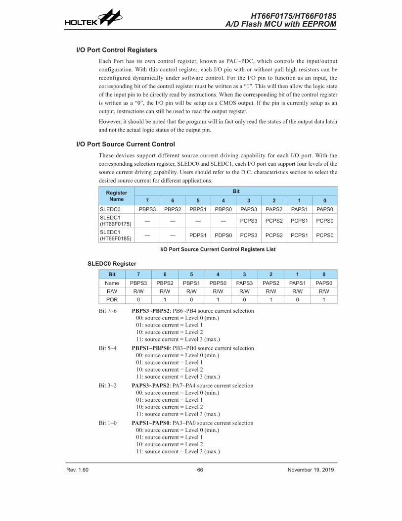
Rev. 1.60 66 November 19, 2019 Rev. 1.60 67 November 19, 2019
HT66F0175/HT66F0185A/D Flash MCU with EEPROM
HT66F0175/HT66F0185A/D Flash MCU with EEPROM
I/O Port Control RegistersEach Port has its own control register, known as PAC~PDC, which controls the input/output configuration. With this control register, each I/O pin with or without pull-high resistors can be reconfigured dynamically under software control. For the I/O pin to function as an input, the corresponding bit of the control register must be written as a “1”. This will then allow the logic state of the input pin to be directly read by instructions. When the corresponding bit of the control register is written as a “0”, the I/O pin will be setup as a CMOS output. If the pin is currently setup as an output, instructions can still be used to read the output register.
However, it should be noted that the program will in fact only read the status of the output data latch and not the actual logic status of the output pin.
I/O Port Source Current ControlThese devices support different source current driving capability for each I/O port. With the corresponding selection register, SLEDC0 and SLEDC1, each I/O port can support four levels of the source current driving capability. Users should refer to the D.C. characteristics section to select the desired source current for different applications.
Register Name
Bit7 6 5 4 3 2 1 0
SLEDC0 PBPS3 PBPS2 PBPS1 PBPS0 PAPS3 PAPS2 PAPS1 PAPS0SLEDC1 (HT66F0175) — — — — PCPS3 PCPS2 PCPS1 PCPS0
SLEDC1 (HT66F0185) — — PDPS1 PDPS0 PCPS3 PCPS2 PCPS1 PCPS0
I/O Port Source Current Control Registers List
SLEDC0 RegisterBit 7 6 5 4 3 2 1 0
Name PBPS3 PBPS2 PBPS1 PBPS0 PAPS3 PAPS2 PAPS1 PAPS0R/W R/W R/W R/W R/W R/W R/W R/W R/WPOR 0 1 0 1 0 1 0 1
Bit 7~6 PBPS3~PBPS2: PB6~PB4 source current selection00: source current = Level 0 (min.)01: source current = Level 110: source current = Level 211: source current = Level 3 (max.)
Bit 5~4 PBPS1~PBPS0: PB3~PB0 source current selection00: source current = Level 0 (min.)01: source current = Level 110: source current = Level 211: source current = Level 3 (max.)
Bit 3~2 PAPS3~PAPS2: PA7~PA4 source current selection00: source current = Level 0 (min.)01: source current = Level 110: source current = Level 211: source current = Level 3 (max.)
Bit 1~0 PAPS1~PAPS0: PA3~PA0 source current selection00: source current = Level 0 (min.)01: source current = Level 110: source current = Level 211: source current = Level 3 (max.)
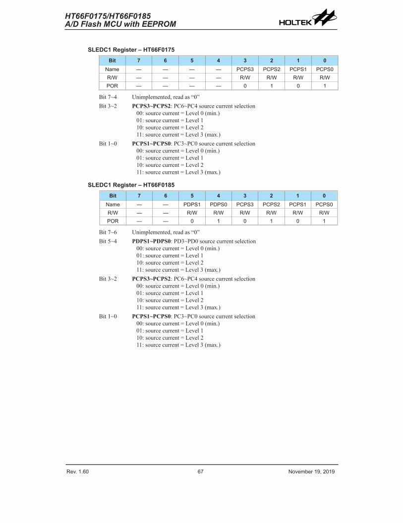
Rev. 1.60 66 November 19, 2019 Rev. 1.60 67 November 19, 2019
HT66F0175/HT66F0185A/D Flash MCU with EEPROM
HT66F0175/HT66F0185A/D Flash MCU with EEPROM
SLEDC1 Register – HT66F0175Bit 7 6 5 4 3 2 1 0
Name — — — — PCPS3 PCPS2 PCPS1 PCPS0R/W — — — — R/W R/W R/W R/WPOR — — — — 0 1 0 1
Bit 7~4 Unimplemented, read as “0”Bit 3~2 PCPS3~PCPS2: PC6~PC4 source current selection
00: source current = Level 0 (min.)01: source current = Level 110: source current = Level 211: source current = Level 3 (max.)
Bit 1~0 PCPS1~PCPS0: PC3~PC0 source current selection00: source current = Level 0 (min.)01: source current = Level 110: source current = Level 211: source current = Level 3 (max.)
SLEDC1 Register – HT66F0185Bit 7 6 5 4 3 2 1 0
Name — — PDPS1 PDPS0 PCPS3 PCPS2 PCPS1 PCPS0R/W — — R/W R/W R/W R/W R/W R/WPOR — — 0 1 0 1 0 1
Bit 7~6 Unimplemented, read as “0”Bit 5~4 PDPS1~PDPS0: PD3~PD0 source current selection
00: source current = Level 0 (min.)01: source current = Level 110: source current = Level 211: source current = Level 3 (max.)
Bit 3~2 PCPS3~PCPS2: PC6~PC4 source current selection00: source current = Level 0 (min.)01: source current = Level 110: source current = Level 211: source current = Level 3 (max.)
Bit 1~0 PCPS1~PCPS0: PC3~PC0 source current selection00: source current = Level 0 (min.)01: source current = Level 110: source current = Level 211: source current = Level 3 (max.)
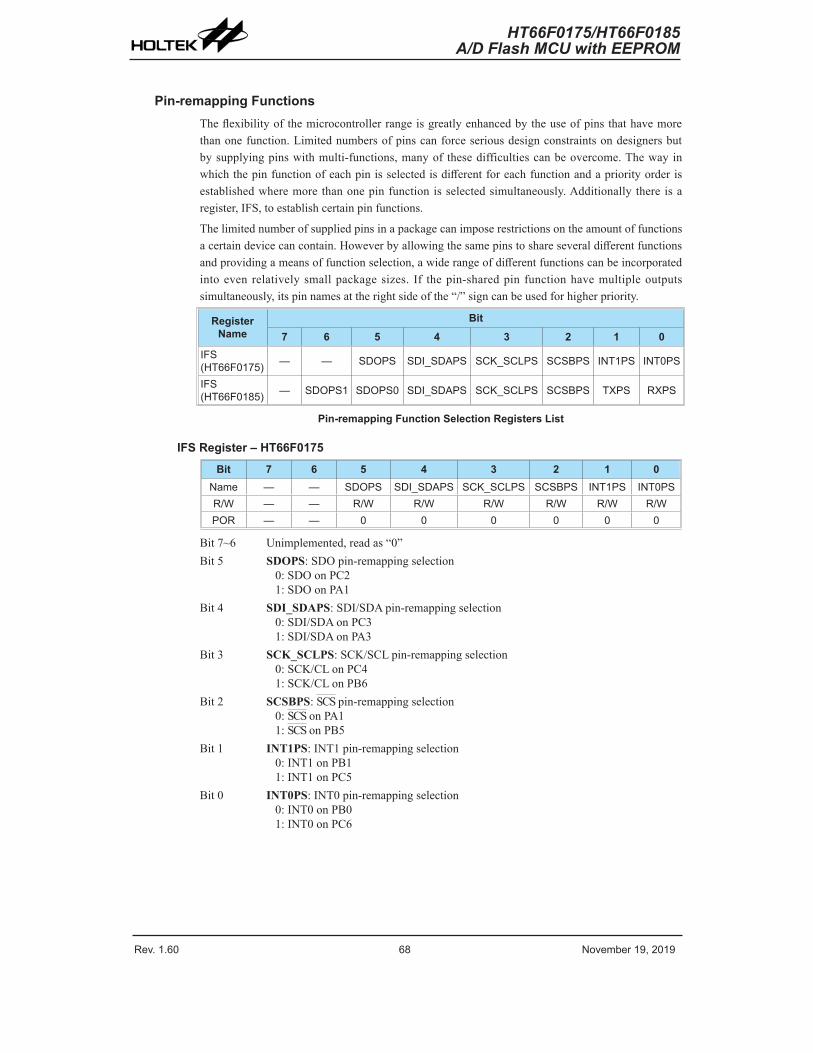
Rev. 1.60 68 November 19, 2019 Rev. 1.60 69 November 19, 2019
HT66F0175/HT66F0185A/D Flash MCU with EEPROM
HT66F0175/HT66F0185A/D Flash MCU with EEPROM
Pin-remapping FunctionsThe flexibility of the microcontroller range is greatly enhanced by the use of pins that have more than one function. Limited numbers of pins can force serious design constraints on designers but by supplying pins with multi-functions, many of these difficulties can be overcome. The way in which the pin function of each pin is selected is different for each function and a priority order is established where more than one pin function is selected simultaneously. Additionally there is a register, IFS, to establish certain pin functions.
The limited number of supplied pins in a package can impose restrictions on the amount of functions a certain device can contain. However by allowing the same pins to share several different functions and providing a means of function selection, a wide range of different functions can be incorporated into even relatively small package sizes. If the pin-shared pin function have multiple outputs simultaneously, its pin names at the right side of the “/” sign can be used for higher priority.
Register Name
Bit7 6 5 4 3 2 1 0
IFS (HT66F0175) — — SDOPS SDI_SDAPS SCK_SCLPS SCSBPS INT1PS INT0PS
IFS (HT66F0185) — SDOPS1 SDOPS0 SDI_SDAPS SCK_SCLPS SCSBPS TXPS RXPS
Pin-remapping Function Selection Registers List
IFS Register – HT66F0175Bit 7 6 5 4 3 2 1 0
Name — — SDOPS SDI_SDAPS SCK_SCLPS SCSBPS INT1PS INT0PSR/W — — R/W R/W R/W R/W R/W R/WPOR — — 0 0 0 0 0 0
Bit 7~6 Unimplemented, read as “0”Bit 5 SDOPS: SDO pin-remapping selection
0: SDO on PC21: SDO on PA1
Bit 4 SDI_SDAPS: SDI/SDA pin-remapping selection0: SDI/SDA on PC31: SDI/SDA on PA3
Bit 3 SCK_SCLPS: SCK/SCL pin-remapping selection0: SCK/CL on PC41: SCK/CL on PB6
Bit 2 SCSBPS: SCS pin-remapping selection0: SCS on PA11: SCS on PB5
Bit 1 INT1PS: INT1 pin-remapping selection0: INT1 on PB11: INT1 on PC5
Bit 0 INT0PS: INT0 pin-remapping selection0: INT0 on PB01: INT0 on PC6
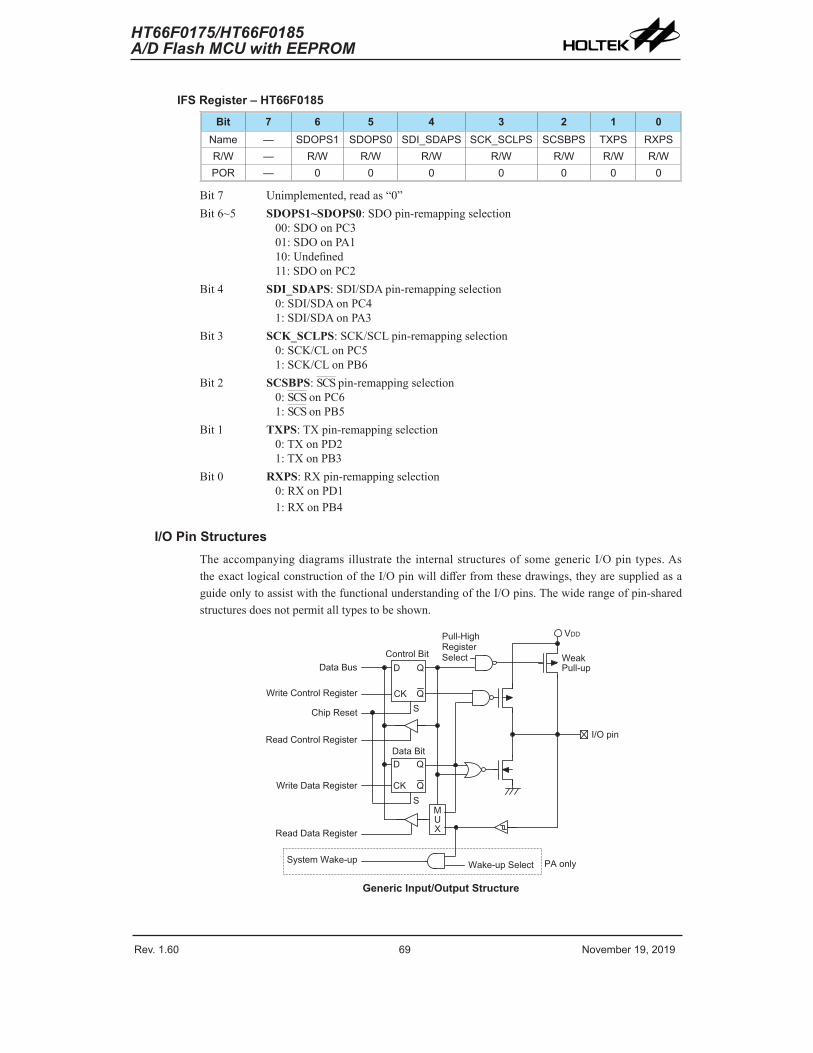
Rev. 1.60 68 November 19, 2019 Rev. 1.60 69 November 19, 2019
HT66F0175/HT66F0185A/D Flash MCU with EEPROM
HT66F0175/HT66F0185A/D Flash MCU with EEPROM
IFS Register – HT66F0185Bit 7 6 5 4 3 2 1 0
Name — SDOPS1 SDOPS0 SDI_SDAPS SCK_SCLPS SCSBPS TXPS RXPSR/W — R/W R/W R/W R/W R/W R/W R/WPOR — 0 0 0 0 0 0 0
Bit 7 Unimplemented, read as “0”Bit 6~5 SDOPS1~SDOPS0: SDO pin-remapping selection
00: SDO on PC301: SDO on PA110: Undefined11: SDO on PC2
Bit 4 SDI_SDAPS: SDI/SDA pin-remapping selection0: SDI/SDA on PC41: SDI/SDA on PA3
Bit 3 SCK_SCLPS: SCK/SCL pin-remapping selection0: SCK/CL on PC51: SCK/CL on PB6
Bit 2 SCSBPS: SCS pin-remapping selection0: SCS on PC61: SCS on PB5
Bit 1 TXPS: TX pin-remapping selection0: TX on PD21: TX on PB3
Bit 0 RXPS: RX pin-remapping selection0: RX on PD11: RX on PB4
I/O Pin StructuresThe accompanying diagrams illustrate the internal structures of some generic I/O pin types. As the exact logical construction of the I/O pin will differ from these drawings, they are supplied as a guide only to assist with the functional understanding of the I/O pins. The wide range of pin-shared structures does not permit all types to be shown.
� � �
���
� � � � � � � � � � � � � �� � � � � � � � � � � � �
� � � � � � � � � � � � � � �
� �
� ��
� �
� ��
� � � � � � � � � � �� � � � � � �
� � � � � � � � � � � � � � � � � � � �
� � � � � � � � �
� � � � � � � � � � � � � � � � � �
� � � � � � � � � � � � � � � � �
� � � � � � � �
� � � � � � �
�
�
� � � � � � �
� � � �� � � � � � �
� � � � � � �� � � � � �� � � � � �
Generic Input/Output Structure
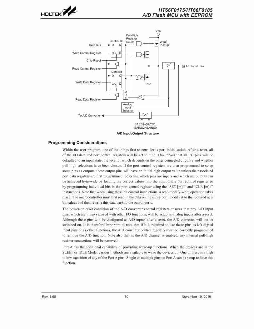
Rev. 1.60 70 November 19, 2019 Rev. 1.60 71 November 19, 2019
HT66F0175/HT66F0185A/D Flash MCU with EEPROM
HT66F0175/HT66F0185A/D Flash MCU with EEPROM
� � �
���� � � � � � � � � � � � � � � � � �
� � � � � � � � � �� � � � � � � �
� � � � � � � � � � � � � � � � � � � �
� � � � � � � � �
� � � � � � � � � � � � � � � � � � � �
� � � � � � � � � � � � � � � � � �
� � � � � � � �
� � � � � � � � � � � � � �
� � � � � � � � � � � � �� � � � � � � � � � � � �
� � � � � � � � � � � � � � � �
� � �� � � �
� � � � �� � � � �
� � � � � �
� �
� ��
�
� �
� ��
�
� � � � � � � � � � � � �� � � �
A/D Input/Output Structure
Programming ConsiderationsWithin the user program, one of the things first to consider is port initialisation. After a reset, all of the I/O data and port control registers will be set to high. This means that all I/O pins will be defaulted to an input state, the level of which depends on the other connected circuitry and whether pull-high selections have been chosen. If the port control registers are then programmed to setup some pins as outputs, these output pins will have an initial high output value unless the associated port data registers are first programmed. Selecting which pins are inputs and which are outputs can be achieved byte-wide by loading the correct values into the appropriate port control register or by programming individual bits in the port control register using the “SET [m].i” and “CLR [m].i” instructions. Note that when using these bit control instructions, a read-modify-write operation takes place. The microcontroller must first read in the data on the entire port, modify it to the required new bit values and then rewrite this data back to the output ports.
The power-on reset condition of the A/D converter control registers ensures that any A/D input pins, which are always shared with other I/O functions, will be setup as analog inputs after a reset. Although these pins will be configured as A/D inputs after a reset, the A/D converter will not be switched on. It is therefore important to note that if it is required to use these pins as I/O digital input pins or as other functions, the A/D converter control registers must be correctly programmed to remove the A/D function. Note also that as the A/D channel is enabled, any internal pull-high resistor connections will be removed.
Port A has the additional capability of providing wake-up functions. When the devices are in the SLEEP or IDLE Mode, various methods are available to wake the devices up. One of these is a high to low transition of any of the Port A pins. Single or multiple pins on Port A can be setup to have this function.
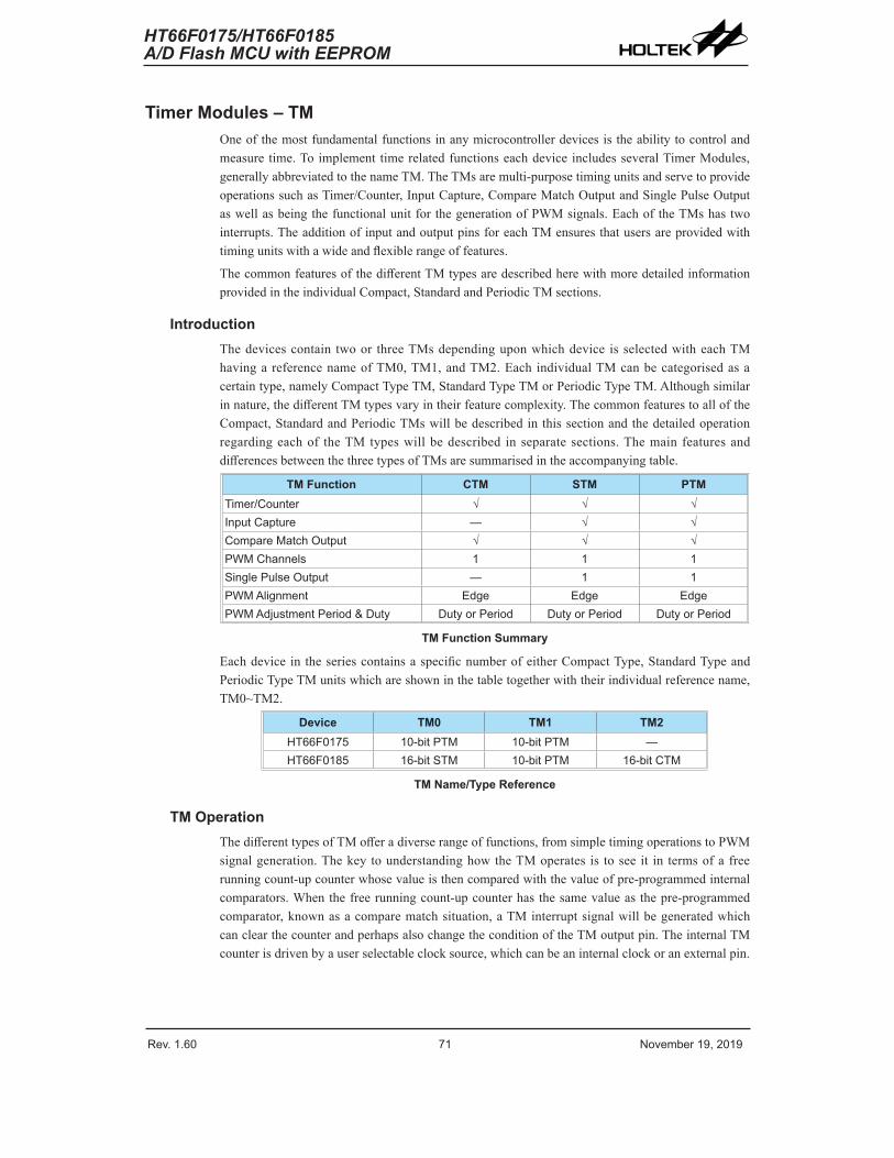
Rev. 1.60 70 November 19, 2019 Rev. 1.60 71 November 19, 2019
HT66F0175/HT66F0185A/D Flash MCU with EEPROM
HT66F0175/HT66F0185A/D Flash MCU with EEPROM
Timer Modules – TMOne of the most fundamental functions in any microcontroller devices is the ability to control and measure time. To implement time related functions each device includes several Timer Modules, generally abbreviated to the name TM. The TMs are multi-purpose timing units and serve to provide operations such as Timer/Counter, Input Capture, Compare Match Output and Single Pulse Output as well as being the functional unit for the generation of PWM signals. Each of the TMs has two interrupts. The addition of input and output pins for each TM ensures that users are provided with timing units with a wide and flexible range of features.
The common features of the different TM types are described here with more detailed information provided in the individual Compact, Standard and Periodic TM sections.
IntroductionThe devices contain two or three TMs depending upon which device is selected with each TM having a reference name of TM0, TM1, and TM2. Each individual TM can be categorised as a certain type, namely Compact Type TM, Standard Type TM or Periodic Type TM. Although similar in nature, the different TM types vary in their feature complexity. The common features to all of the Compact, Standard and Periodic TMs will be described in this section and the detailed operation regarding each of the TM types will be described in separate sections. The main features and differences between the three types of TMs are summarised in the accompanying table.
TM Function CTM STM PTMTimer/Counter √ √ √Input Capture — √ √Compare Match Output √ √ √PWM Channels 1 1 1Single Pulse Output — 1 1PWM Alignment Edge Edge EdgePWM Adjustment Period & Duty Duty or Period Duty or Period Duty or Period
TM Function Summary
Each device in the series contains a specific number of either Compact Type, Standard Type and Periodic Type TM units which are shown in the table together with their individual reference name, TM0~TM2.
Device TM0 TM1 TM2HT66F0175 10-bit PTM 10-bit PTM —HT66F0185 16-bit STM 10-bit PTM 16-bit CTM
TM Name/Type Reference
TM OperationThe different types of TM offer a diverse range of functions, from simple timing operations to PWM signal generation. The key to understanding how the TM operates is to see it in terms of a free running count-up counter whose value is then compared with the value of pre-programmed internal comparators. When the free running count-up counter has the same value as the pre-programmed comparator, known as a compare match situation, a TM interrupt signal will be generated which can clear the counter and perhaps also change the condition of the TM output pin. The internal TM counter is driven by a user selectable clock source, which can be an internal clock or an external pin.
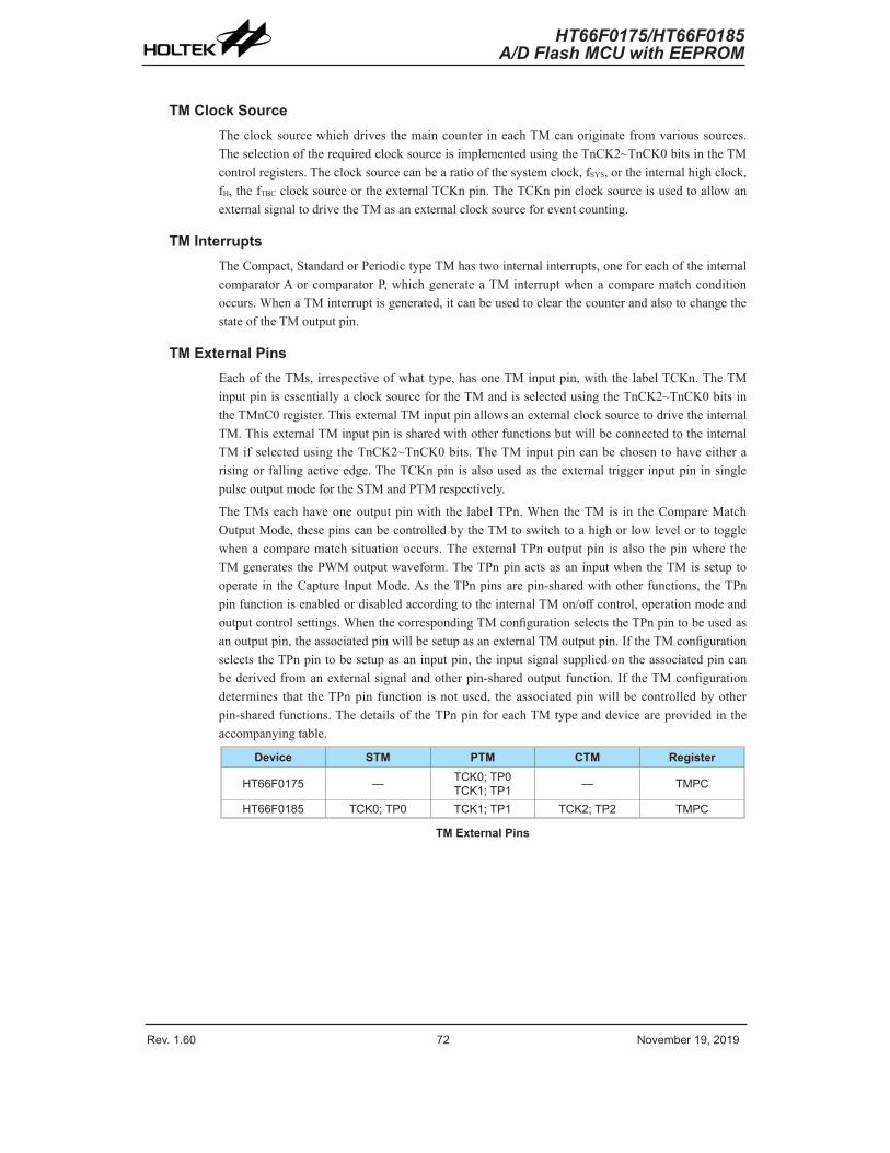
Rev. 1.60 72 November 19, 2019 Rev. 1.60 73 November 19, 2019
HT66F0175/HT66F0185A/D Flash MCU with EEPROM
HT66F0175/HT66F0185A/D Flash MCU with EEPROM
TM Clock SourceThe clock source which drives the main counter in each TM can originate from various sources. The selection of the required clock source is implemented using the TnCK2~TnCK0 bits in the TM control registers. The clock source can be a ratio of the system clock, fSYS, or the internal high clock, fH, the fTBC clock source or the external TCKn pin. The TCKn pin clock source is used to allow an external signal to drive the TM as an external clock source for event counting.
TM InterruptsThe Compact, Standard or Periodic type TM has two internal interrupts, one for each of the internal comparator A or comparator P, which generate a TM interrupt when a compare match condition occurs. When a TM interrupt is generated, it can be used to clear the counter and also to change the state of the TM output pin.
TM External PinsEach of the TMs, irrespective of what type, has one TM input pin, with the label TCKn. The TM input pin is essentially a clock source for the TM and is selected using the TnCK2~TnCK0 bits in the TMnC0 register. This external TM input pin allows an external clock source to drive the internal TM. This external TM input pin is shared with other functions but will be connected to the internal TM if selected using the TnCK2~TnCK0 bits. The TM input pin can be chosen to have either a rising or falling active edge. The TCKn pin is also used as the external trigger input pin in single pulse output mode for the STM and PTM respectively.
The TMs each have one output pin with the label TPn. When the TM is in the Compare Match Output Mode, these pins can be controlled by the TM to switch to a high or low level or to toggle when a compare match situation occurs. The external TPn output pin is also the pin where the TM generates the PWM output waveform. The TPn pin acts as an input when the TM is setup to operate in the Capture Input Mode. As the TPn pins are pin-shared with other functions, the TPn pin function is enabled or disabled according to the internal TM on/off control, operation mode and output control settings. When the corresponding TM configuration selects the TPn pin to be used as an output pin, the associated pin will be setup as an external TM output pin. If the TM configuration selects the TPn pin to be setup as an input pin, the input signal supplied on the associated pin can be derived from an external signal and other pin-shared output function. If the TM configuration determines that the TPn pin function is not used, the associated pin will be controlled by other pin-shared functions. The details of the TPn pin for each TM type and device are provided in the accompanying table.
Device STM PTM CTM Register
HT66F0175 — TCK0; TP0TCK1; TP1 — TMPC
HT66F0185 TCK0; TP0 TCK1; TP1 TCK2; TP2 TMPC
TM External Pins
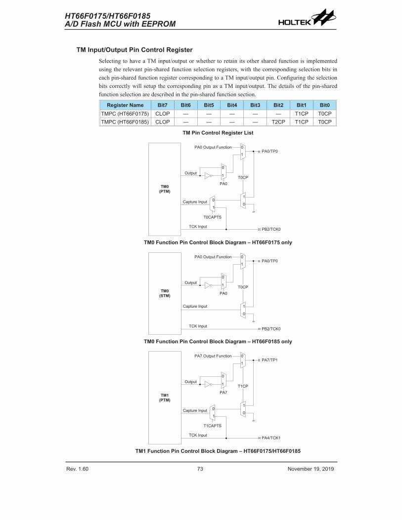
Rev. 1.60 72 November 19, 2019 Rev. 1.60 73 November 19, 2019
HT66F0175/HT66F0185A/D Flash MCU with EEPROM
HT66F0175/HT66F0185A/D Flash MCU with EEPROM
TM Input/Output Pin Control RegisterSelecting to have a TM input/output or whether to retain its other shared function is implemented using the relevant pin-shared function selection registers, with the corresponding selection bits in each pin-shared function register corresponding to a TM input/output pin. Configuring the selection bits correctly will setup the corresponding pin as a TM input/output. The details of the pin-shared function selection are described in the pin-shared function section.
Register Name Bit7 Bit6 Bit5 Bit4 Bit3 Bit2 Bit1 Bit0TMPC (HT66F0175) CLOP — — — — — T1CP T0CPTMPC (HT66F0185) CLOP — — — — T2CP T1CP T0CP
TM Pin Control Register List
TM0(PTM)
PA0/TP0
T0CP
PA0 Output Function 0
1
Output
Capture Input
T0CAPTS
PB2/TCK0TCK Input
0
1
PA0
0
1
1
0
TM0 Function Pin Control Block Diagram – HT66F0175 only
TM0(STM)
PA0/TP0
T0CP
PA0 Output Function 0
1
Output
Capture Input
PB2/TCK0TCK Input
0
1
PA0
1
0
TM0 Function Pin Control Block Diagram – HT66F0185 only
TM1(PTM)
PA7/TP1
T1CP
PA7 Output Function 0
1
Output
Capture Input
T1CAPTS
PA4/TCK1TCK Input
0
1
PA7
0
1
1
0
TM1 Function Pin Control Block Diagram – HT66F0175/HT66F0185
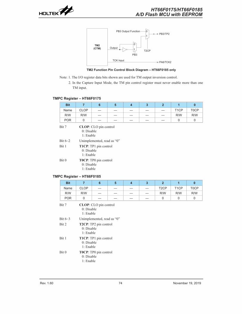
Rev. 1.60 74 November 19, 2019 Rev. 1.60 75 November 19, 2019
HT66F0175/HT66F0185A/D Flash MCU with EEPROM
HT66F0175/HT66F0185A/D Flash MCU with EEPROM
TM2(CTM)
PB3/TP2
T2CP
PB3 Output Function 0
1
Output
PA6/TCK2TCK Input
0
1
PB3
TM2 Function Pin Control Block Diagram – HT66F0185 only
Note: 1. The I/O register data bits shown are used for TM output inversion control.2. In the Capture Input Mode, the TM pin control register must never enable more than one
TM input.
TMPC Register – HT66F0175Bit 7 6 5 4 3 2 1 0
Name CLOP — — — — — T1CP T0CPR/W R/W — — — — — R/W R/WPOR 0 — — — — — 0 0
Bit 7 CLOP: CLO pin control0: Disable1: Enable
Bit 6~2 Unimplemented, read as “0”Bit 1 T1CP: TP1 pin control
0: Disable1: Enable
Bit 0 T0CP: TP0 pin control0: Disable1: Enable
TMPC Register – HT66F0185Bit 7 6 5 4 3 2 1 0
Name CLOP — — — — T2CP T1CP T0CPR/W R/W — — — — R/W R/W R/WPOR 0 — — — — 0 0 0
Bit 7 CLOP: CLO pin control0: Disable1: Enable
Bit 6~3 Unimplemented, read as “0”Bit 2 T2CP: TP2 pin control
0: Disable1: Enable
Bit 1 T1CP: TP1 pin control0: Disable1: Enable
Bit 0 T0CP: TP0 pin control0: Disable1: Enable
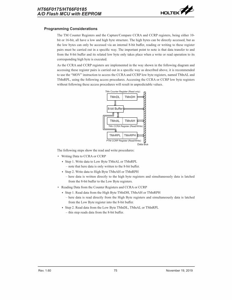
Rev. 1.60 74 November 19, 2019 Rev. 1.60 75 November 19, 2019
HT66F0175/HT66F0185A/D Flash MCU with EEPROM
HT66F0175/HT66F0185A/D Flash MCU with EEPROM
Programming ConsiderationsThe TM Counter Registers and the Capture/Compare CCRA and CCRP registers, being either 10-bit or 16-bit, all have a low and high byte structure. The high bytes can be directly accessed, but as the low bytes can only be accessed via an internal 8-bit buffer, reading or writing to these register pairs must be carried out in a specific way. The important point to note is that data transfer to and from the 8-bit buffer and its related low byte only takes place when a write or read operation to its corresponding high byte is executed.
As the CCRA and CCRP registers are implemented in the way shown in the following diagram and accessing these register pairs is carried out in a specific way as described above, it is recommended to use the “MOV” instruction to access the CCRA and CCRP low byte registers, named TMnAL and TMnRPL, using the following access procedures. Accessing the CCRA or CCRP low byte registers without following these access procedures will result in unpredictable values.
Data Bus
8-bit Buffer
TMnDHTMnDL
TMnAHTMnAL
TMn Counter Register (Read only)
TMn CCRA Register (Read/Write)
TMnRPHTMnRPL
PTM CCRP Register (Read/Write)
The following steps show the read and write procedures:
• Writing Data to CCRA or CCRP ♦ Step 1. Write data to Low Byte TMnAL or TMnRPL
– note that here data is only written to the 8-bit buffer. ♦ Step 2. Write data to High Byte TMnAH or TMnRPH
– here data is written directly to the high byte registers and simultaneously data is latched from the 8-bit buffer to the Low Byte registers.
• Reading Data from the Counter Registers and CCRA or CCRP ♦ Step 1. Read data from the High Byte TMnDH, TMnAH or TMnRPH
– here data is read directly from the High Byte registers and simultaneously data is latched from the Low Byte register into the 8-bit buffer.
♦ Step 2. Read data from the Low Byte TMnDL, TMnAL or TMnRPL – this step reads data from the 8-bit buffer.
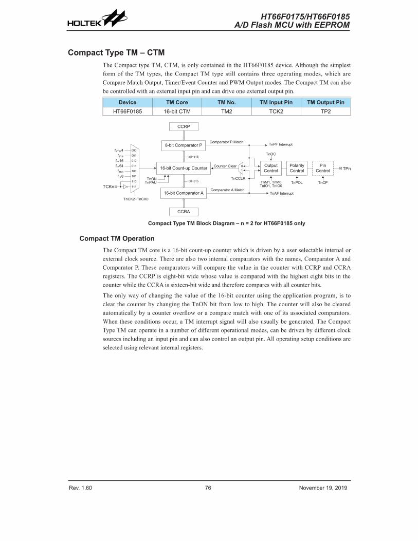
Rev. 1.60 76 November 19, 2019 Rev. 1.60 77 November 19, 2019
HT66F0175/HT66F0185A/D Flash MCU with EEPROM
HT66F0175/HT66F0185A/D Flash MCU with EEPROM
Compact Type TM – CTMThe Compact type TM, CTM, is only contained in the HT66F0185 device. Although the simplest form of the TM types, the Compact TM type still contains three operating modes, which are Compare Match Output, Timer/Event Counter and PWM Output modes. The Compact TM can also be controlled with an external input pin and can drive one external output pin.
Device TM Core TM No. TM Input Pin TM Output PinHT66F0185 16-bit CTM TM2 TCK2 TP2
fSYS
fSYS/4
fH/64fH/16
fTBC
TCKn
000
001
010
011
100
101
110
111
TnCK2~TnCK0
16-bit Count-up Counter
8-bit Comparator P
CCRP
b8~b15
b0~b15
16-bit Comparator A
TnONTnPAU
Comparator A Match
Comparator P Match
Counter Clear 01
Output Control
Polarity Control
Pin Control TPn
TnOC
TnM1, TnM0TnIO1, TnIO0
TnAF Interrupt
TnPF Interrupt
TnPOL TnCP
CCRA
TnCCLRfH/8
Compact Type TM Block Diagram – n = 2 for HT66F0185 only
Compact TM OperationThe Compact TM core is a 16-bit count-up counter which is driven by a user selectable internal or external clock source. There are also two internal comparators with the names, Comparator A and Comparator P. These comparators will compare the value in the counter with CCRP and CCRA registers. The CCRP is eight-bit wide whose value is compared with the highest eight bits in the counter while the CCRA is sixteen-bit wide and therefore compares with all counter bits.
The only way of changing the value of the 16-bit counter using the application program, is to clear the counter by changing the TnON bit from low to high. The counter will also be cleared automatically by a counter overflow or a compare match with one of its associated comparators. When these conditions occur, a TM interrupt signal will also usually be generated. The Compact Type TM can operate in a number of different operational modes, can be driven by different clock sources including an input pin and can also control an output pin. All operating setup conditions are selected using relevant internal registers.
Rev. 1.60 76 November 19, 2019 Rev. 1.60 77 November 19, 2019
HT66F0175/HT66F0185A/D Flash MCU with EEPROM
HT66F0175/HT66F0185A/D Flash MCU with EEPROM
Compact Type TM Register DescriptionOverall operation of the Compact TM is controlled using a series of registers. A read only register pair exists to store the internal counter 16-bit value, while a read/write register pair exists to store the internal 16-bit CCRA value. There is also a read/write register used to store the internal 8-bit CCRP value. The remaining two registers are control registers which setup the different operating and control modes.
Register Name Bit7 Bit6 Bit5 Bit4 Bit3 Bit2 Bit1 Bit0
TMnC0 TnPAU TnCK2 TnCK1 TnCK0 TnON — — —TMnC1 TnM1 TnM0 TnIO1 TnIO0 TnOC TnPOL TnDPX TnCCLRTMnDL D7 D6 D5 D4 D3 D2 D1 D0TMnDH D15 D14 D13 D12 D11 D10 D9 D8TMnAL D7 D6 D5 D4 D3 D2 D1 D0TMnAH D15 D14 D13 D12 D11 D10 D9 D8TMnRP TnRP7 TnRP6 TnRP5 TnRP4 TnRP3 TnRP2 TnRP1 TnRP0
16-bit Compact TM Registers List – n = 2 for for HT66F0185 only
TMnDL RegisterBit 7 6 5 4 3 2 1 0
Name D7 D6 D5 D4 D3 D2 D1 D0R/W R R R R R R R RPOR 0 0 0 0 0 0 0 0
Bit 7~0 TMn Counter Low Byte Register bit 7 ~ bit 0TMn 16-bit Counter bit 7 ~ bit 0
TMnDH RegisterBit 7 6 5 4 3 2 1 0
Name D15 D14 D13 D12 D11 D10 D9 D8R/W R R R R R R R RPOR 0 0 0 0 0 0 0 0
Bit 7~0 TMn Counter High Byte Register bit 7 ~ bit 0TMn 16-bit Counter bit 15 ~ bit 8
TMnAL RegisterBit 7 6 5 4 3 2 1 0
Name D7 D6 D5 D4 D3 D2 D1 D0R/W R/W R/W R/W R/W R/W R/W R/W R/WPOR 0 0 0 0 0 0 0 0
Bit 7~0 TMn CCRA Low Byte Register bit 7 ~ bit 0TMn 16-bit CCRA bit 7 ~ bit 0
TMnAH RegisterBit 7 6 5 4 3 2 1 0
Name D15 D14 D13 D12 D11 D10 D9 D8R/W R/W R/W R/W R/W R/W R/W R/W R/WPOR 0 0 0 0 0 0 0 0
Bit 7~0 TMn CCRA High Byte Register bit 7 ~ bit 0TMn 16-bit CCRA bit 15 ~ bit 8
Rev. 1.60 78 November 19, 2019 Rev. 1.60 79 November 19, 2019
HT66F0175/HT66F0185A/D Flash MCU with EEPROM
HT66F0175/HT66F0185A/D Flash MCU with EEPROM
TMnC0 RegisterBit 7 6 5 4 3 2 1 0
Name TnPAU TnCK2 TnCK1 TnCK0 TnON — — —R/W R/W R/W R/W R/W R/W — — —POR 0 0 0 0 0 — — —
Bit 7 TnPAU: TMn Counter Pause control0: Run1: Pause
The counter can be paused by setting this bit high. Clearing the bit to zero restores normal counter operation. When in a Pause condition the TMn will remain powered up and continue to consume power. The counter will retain its residual value when this bit changes from low to high and resume counting from this value when the bit changes to a low value again.
Bit 6~4 TnCK2~TnCK0: Select TMn Counter clock000: fSYS/4001: fSYS
010: fH/16011: fH/64100: fTBC
101: fH
110: TCKn rising edge clock111: TCKn falling edge clock
These three bits are used to select the clock source for the TMn. The external pin clock source can be chosen to be active on the rising or falling edge. The clock source fSYS is the system clock, while fH and fTBC are other internal clocks, the details of which can be found in the oscillator section.
Bit 3 TnON: TMn Counter On/Off control0: Off1: On
This bit controls the overall on/off function of the TMn. Setting the bit high enables the counter to run while clearing the bit disables the TMn. Clearing this bit to zero will stop the counter from counting and turn off the TMn which will reduce its power consumption. When the bit changes state from low to high the internal counter value will be reset to zero, however when the bit changes from high to low, the internal counter will retain its residual value until the bit returns high again. If the TMn is in the Compare Match Output Mode then the TMn output pin will be reset to its initial condition, as specified by the TnOC bit, when the TnON bit changes from low to high.
Bit 2~0 Unimplemented, read as “0”
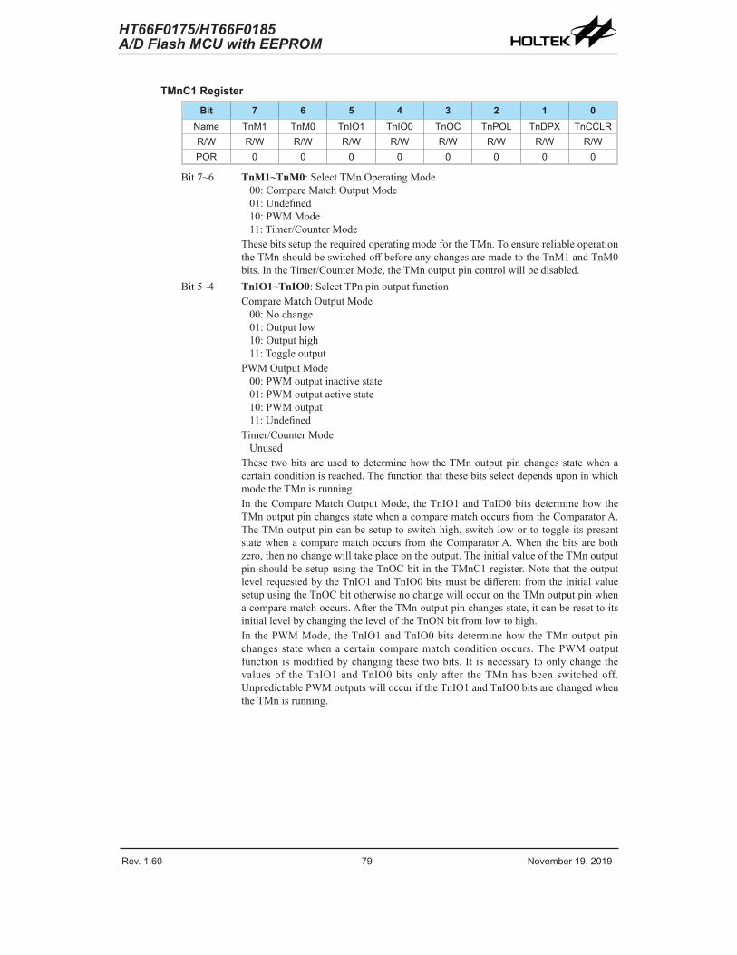
Rev. 1.60 78 November 19, 2019 Rev. 1.60 79 November 19, 2019
HT66F0175/HT66F0185A/D Flash MCU with EEPROM
HT66F0175/HT66F0185A/D Flash MCU with EEPROM
TMnC1 RegisterBit 7 6 5 4 3 2 1 0
Name TnM1 TnM0 TnIO1 TnIO0 TnOC TnPOL TnDPX TnCCLRR/W R/W R/W R/W R/W R/W R/W R/W R/WPOR 0 0 0 0 0 0 0 0
Bit 7~6 TnM1~TnM0: Select TMn Operating Mode00: Compare Match Output Mode01: Undefined10: PWM Mode11: Timer/Counter Mode
These bits setup the required operating mode for the TMn. To ensure reliable operation the TMn should be switched off before any changes are made to the TnM1 and TnM0 bits. In the Timer/Counter Mode, the TMn output pin control will be disabled.
Bit 5~4 TnIO1~TnIO0: Select TPn pin output functionCompare Match Output Mode
00: No change01: Output low10: Output high11: Toggle output
PWM Output Mode00: PWM output inactive state01: PWM output active state10: PWM output11: Undefined
Timer/Counter ModeUnused
These two bits are used to determine how the TMn output pin changes state when a certain condition is reached. The function that these bits select depends upon in which mode the TMn is running.In the Compare Match Output Mode, the TnIO1 and TnIO0 bits determine how the TMn output pin changes state when a compare match occurs from the Comparator A. The TMn output pin can be setup to switch high, switch low or to toggle its present state when a compare match occurs from the Comparator A. When the bits are both zero, then no change will take place on the output. The initial value of the TMn output pin should be setup using the TnOC bit in the TMnC1 register. Note that the output level requested by the TnIO1 and TnIO0 bits must be different from the initial value setup using the TnOC bit otherwise no change will occur on the TMn output pin when a compare match occurs. After the TMn output pin changes state, it can be reset to its initial level by changing the level of the TnON bit from low to high.In the PWM Mode, the TnIO1 and TnIO0 bits determine how the TMn output pin changes state when a certain compare match condition occurs. The PWM output function is modified by changing these two bits. It is necessary to only change the values of the TnIO1 and TnIO0 bits only after the TMn has been switched off. Unpredictable PWM outputs will occur if the TnIO1 and TnIO0 bits are changed when the TMn is running.
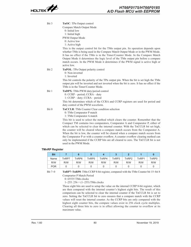
Rev. 1.60 80 November 19, 2019 Rev. 1.60 81 November 19, 2019
HT66F0175/HT66F0185A/D Flash MCU with EEPROM
HT66F0175/HT66F0185A/D Flash MCU with EEPROM
Bit 3 TnOC: TPn Output controlCompare Match Output Mode
0: Initial low1: Initial high
PWM Output Mode0: Active low1: Active high
This is the output control bit for the TMn output pin. Its operation depends upon whether TMn is being used in the Compare Match Output Mode or in the PWM Mode. It has no effect if the TMn is in the Timer/Counter Mode. In the Compare Match Output Mode it determines the logic level of the TMn output pin before a compare match occurs. In the PWM Mode it determines if the PWM signal is active high or active low.
Bit 2 TnPOL: TPn Output polarity control0: Non-inverted1: Inverted
This bit controls the polarity of the TPn output pin. When the bit is set high the TMn output pin will be inverted and not inverted when the bit is zero. It has no effect if the TMn is in the Timer/Counter Mode.
Bit 1 TnDPX: TMn PWM duty/period control0: CCRP – period; CCRA – duty1: CCRP – duty; CCRA – period
This bit determines which of the CCRA and CCRP registers are used for period and duty control of the PWM waveform.
Bit 0 TnCCLR: TMn Counter Clear condition selection0: TMn Comparator P match1: TMn Comparator A match
This bit is used to select the method which clears the counter. Remember that the Compact TM contains two comparators, Comparator A and Comparator P, either of which can be selected to clear the internal counter. With the TnCCLR bit set high, the counter will be cleared when a compare match occurs from the Comparator A. When the bit is low, the counter will be cleared when a compare match occurs from the Comparator P or with a counter overflow. A counter overflow clearing method can only be implemented if the CCRP bits are all cleared to zero. The TnCCLR bit is not used in the PWM Mode.
TMnRP RegisterBit 7 6 5 4 3 2 1 0
Name TnRP7 TnRP6 TnRP5 TnRP4 TnRP3 TnRP2 TnRP1 TnRP0R/W R/W R/W R/W R/W R/W R/W R/W R/WPOR 0 0 0 0 0 0 0 0
Bit 7~0 TnRP7~TnRP0: TMn CCRP 8-bit register, compared with the TMn Counter bit 15~bit 8Comprartor P Match Period
0: 65535 TMn clocks1~255: 256 × (1~255) TMn clocks
These eight bits are used to setup the value on the internal CCRP 8-bit register, which are then compared with the internal counter’s highest eight bits. The result of this comparison can be selected to clear the internal counter if the TnCCLR bit is set to zero. Setting the TnCCLR bit to zero ensures that a compare match with the CCRP values will reset the internal counter. As the CCRP bits are only compared with the highest eight counter bits, the compare values exist in 256 clock cycle multiples. Clearing all three bits to zero is in effect allowing the counter to overflow at its maximum value.
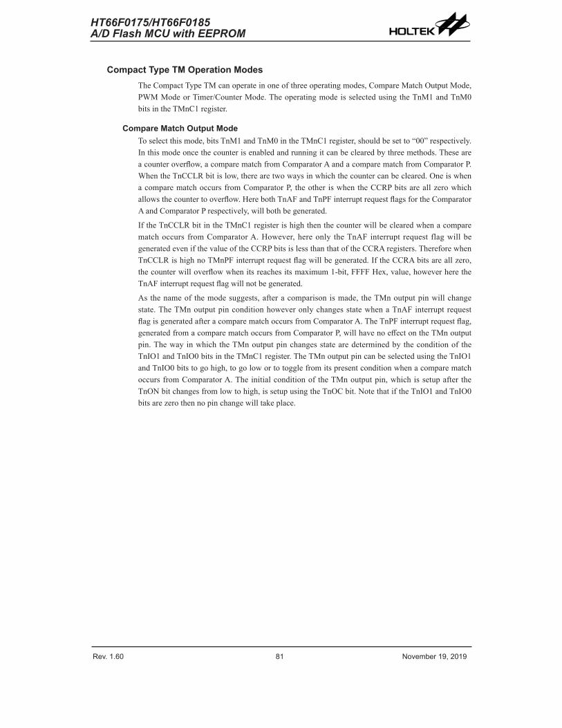
Rev. 1.60 80 November 19, 2019 Rev. 1.60 81 November 19, 2019
HT66F0175/HT66F0185A/D Flash MCU with EEPROM
HT66F0175/HT66F0185A/D Flash MCU with EEPROM
Compact Type TM Operation ModesThe Compact Type TM can operate in one of three operating modes, Compare Match Output Mode, PWM Mode or Timer/Counter Mode. The operating mode is selected using the TnM1 and TnM0 bits in the TMnC1 register.
Compare Match Output ModeTo select this mode, bits TnM1 and TnM0 in the TMnC1 register, should be set to “00” respectively. In this mode once the counter is enabled and running it can be cleared by three methods. These are a counter overflow, a compare match from Comparator A and a compare match from Comparator P. When the TnCCLR bit is low, there are two ways in which the counter can be cleared. One is when a compare match occurs from Comparator P, the other is when the CCRP bits are all zero which allows the counter to overflow. Here both TnAF and TnPF interrupt request flags for the Comparator A and Comparator P respectively, will both be generated.
If the TnCCLR bit in the TMnC1 register is high then the counter will be cleared when a compare match occurs from Comparator A. However, here only the TnAF interrupt request flag will be generated even if the value of the CCRP bits is less than that of the CCRA registers. Therefore when TnCCLR is high no TMnPF interrupt request flag will be generated. If the CCRA bits are all zero, the counter will overflow when its reaches its maximum 1-bit, FFFF Hex, value, however here the TnAF interrupt request flag will not be generated.
As the name of the mode suggests, after a comparison is made, the TMn output pin will change state. The TMn output pin condition however only changes state when a TnAF interrupt request flag is generated after a compare match occurs from Comparator A. The TnPF interrupt request flag, generated from a compare match occurs from Comparator P, will have no effect on the TMn output pin. The way in which the TMn output pin changes state are determined by the condition of the TnIO1 and TnIO0 bits in the TMnC1 register. The TMn output pin can be selected using the TnIO1 and TnIO0 bits to go high, to go low or to toggle from its present condition when a compare match occurs from Comparator A. The initial condition of the TMn output pin, which is setup after the TnON bit changes from low to high, is setup using the TnOC bit. Note that if the TnIO1 and TnIO0 bits are zero then no pin change will take place.
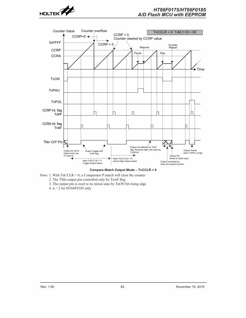
Rev. 1.60 82 November 19, 2019 Rev. 1.60 83 November 19, 2019
HT66F0175/HT66F0185A/D Flash MCU with EEPROM
HT66F0175/HT66F0185A/D Flash MCU with EEPROM
Counter Value
0xFFFF
CCRPCCRA
TnON
TnPAU
TnPOL
CCRP Int. flag TnPF
CCRA Int. flag TnAF
TMn O/P Pin
Time
CCRP=0
CCRP > 0
Counter overflowCCRP > 0Counter cleared by CCRP value
Pause
Resume
Stop
Counter Restart
TnCCLR = 0; TnM [1:0] = 00
Output pin set to initial Level Low if TnOC=0
Output Toggle with TnAF flag
Note TnIO [1:0] = 10 Active High Output selectHere TnIO [1:0] = 11
Toggle Output select
Output not affected by TnAF flag. Remains High until reset by TnON bit
Output PinReset to Initial value
Output controlled by other pin-shared function
Output Invertswhen TnPOL is high
Compare Match Output Mode – TnCCLR = 0Note: 1. With TnCCLR = 0, a Comparator P match will clear the counter
2. The TMn output pin controlled only by TnAF flag3. The output pin is reset to its initial state by TnON bit rising edge4. n = 2 for HT66F0185 only
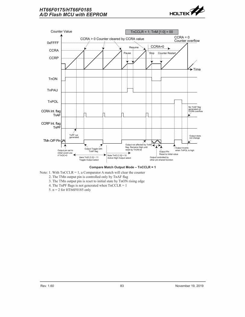
Rev. 1.60 82 November 19, 2019 Rev. 1.60 83 November 19, 2019
HT66F0175/HT66F0185A/D Flash MCU with EEPROM
HT66F0175/HT66F0185A/D Flash MCU with EEPROM
Counter Value
0xFFFF
CCRP
CCRA
TnON
TnPAU
TnPOL
TMn O/P Pin
Time
CCRA=0
CCRA = 0Counter overflowCCRA > 0 Counter cleared by CCRA value
Pause
Resume
Stop Counter Restart
TnCCLR = 1; TnM [1:0] = 00
Output pin set to initial Level Low if TnOC=0
Output Toggle with TnAF flag
Note TnIO [1:0] = 10 Active High Output selectHere TnIO [1:0] = 11
Toggle Output select
Output not affected by TnAF flag. Remains High until reset by TnON bit
Output PinReset to Initial value
Output controlled by other pin-shared function
Output Invertswhen TnPOL is high
TnPF not generated
No TnAF flag generated on CCRA overflow
Output does not change
CCRA Int. flag TnAF
CCRP Int. flag TnPF
Compare Match Output Mode – TnCCLR = 1Note: 1. With TnCCLR = 1, a Comparator A match will clear the counter
2. The TMn output pin is controlled only by TnAF flag3. The TMn output pin is reset to initial state by TnON rising edge4. The TnPF flags is not generated when TnCCLR = 15. n = 2 for HT66F0185 only
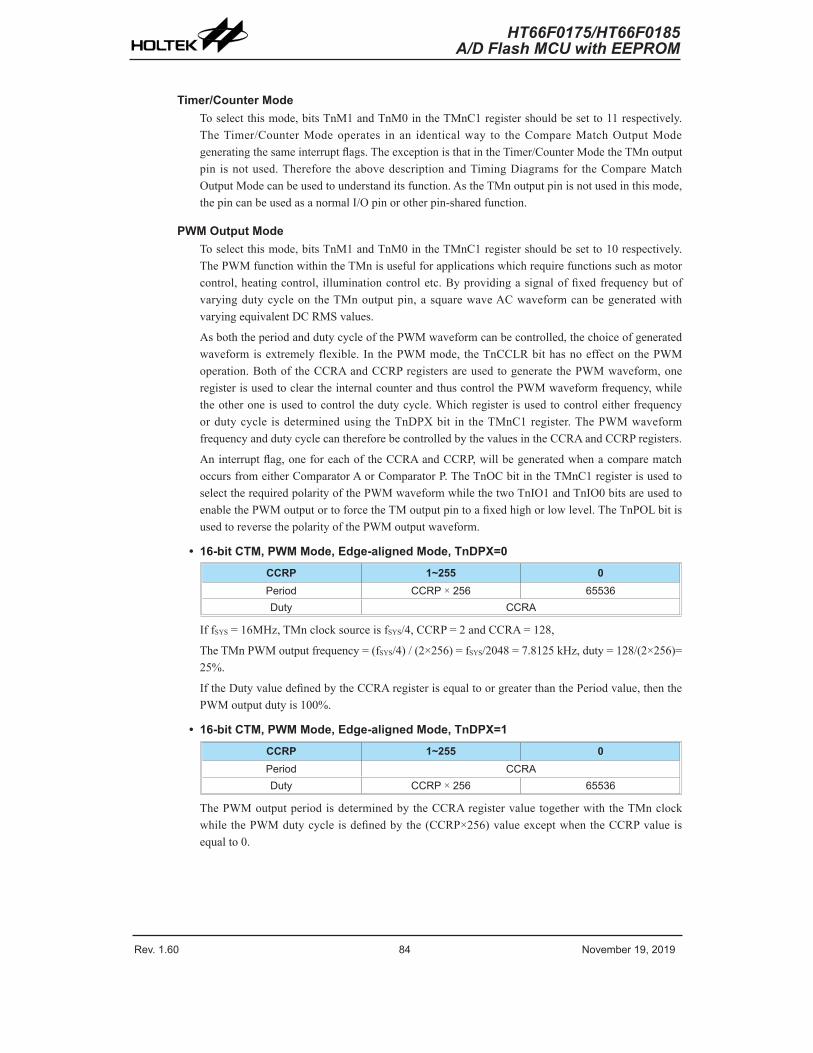
Rev. 1.60 84 November 19, 2019 Rev. 1.60 85 November 19, 2019
HT66F0175/HT66F0185A/D Flash MCU with EEPROM
HT66F0175/HT66F0185A/D Flash MCU with EEPROM
Timer/Counter ModeTo select this mode, bits TnM1 and TnM0 in the TMnC1 register should be set to 11 respectively. The Timer/Counter Mode operates in an identical way to the Compare Match Output Mode generating the same interrupt flags. The exception is that in the Timer/Counter Mode the TMn output pin is not used. Therefore the above description and Timing Diagrams for the Compare Match Output Mode can be used to understand its function. As the TMn output pin is not used in this mode, the pin can be used as a normal I/O pin or other pin-shared function.
PWM Output ModeTo select this mode, bits TnM1 and TnM0 in the TMnC1 register should be set to 10 respectively. The PWM function within the TMn is useful for applications which require functions such as motor control, heating control, illumination control etc. By providing a signal of fixed frequency but of varying duty cycle on the TMn output pin, a square wave AC waveform can be generated with varying equivalent DC RMS values.
As both the period and duty cycle of the PWM waveform can be controlled, the choice of generated waveform is extremely flexible. In the PWM mode, the TnCCLR bit has no effect on the PWM operation. Both of the CCRA and CCRP registers are used to generate the PWM waveform, one register is used to clear the internal counter and thus control the PWM waveform frequency, while the other one is used to control the duty cycle. Which register is used to control either frequency or duty cycle is determined using the TnDPX bit in the TMnC1 register. The PWM waveform frequency and duty cycle can therefore be controlled by the values in the CCRA and CCRP registers.
An interrupt flag, one for each of the CCRA and CCRP, will be generated when a compare match occurs from either Comparator A or Comparator P. The TnOC bit in the TMnC1 register is used to select the required polarity of the PWM waveform while the two TnIO1 and TnIO0 bits are used to enable the PWM output or to force the TM output pin to a fixed high or low level. The TnPOL bit is used to reverse the polarity of the PWM output waveform.
• 16-bit CTM, PWM Mode, Edge-aligned Mode, TnDPX=0CCRP 1~255 0Period CCRP × 256 65536Duty CCRA
If fSYS = 16MHz, TMn clock source is fSYS/4, CCRP = 2 and CCRA = 128,
The TMn PWM output frequency = (fSYS/4) / (2×256) = fSYS/2048 = 7.8125 kHz, duty = 128/(2×256)= 25%.
If the Duty value defined by the CCRA register is equal to or greater than the Period value, then the PWM output duty is 100%.
• 16-bit CTM, PWM Mode, Edge-aligned Mode, TnDPX=1CCRP 1~255 0Period CCRADuty CCRP × 256 65536
The PWM output period is determined by the CCRA register value together with the TMn clock while the PWM duty cycle is defined by the (CCRP×256) value except when the CCRP value is equal to 0.
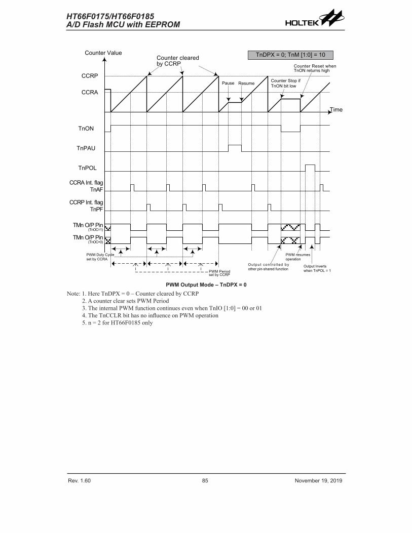
Rev. 1.60 84 November 19, 2019 Rev. 1.60 85 November 19, 2019
HT66F0175/HT66F0185A/D Flash MCU with EEPROM
HT66F0175/HT66F0185A/D Flash MCU with EEPROM
Counter Value
CCRP
CCRA
TnON
TnPAU
TnPOL
TMn O/P Pin (TnOC=1)
Time
Counter cleared by CCRP
Pause Resume Counter Stop if TnON bit low
Counter Reset when TnON returns high
TnDPX = 0; TnM [1:0] = 10
PWM Duty Cycle set by CCRA
PWM resumes operation
Outpu t con t ro l led by other pin-shared function
Output Invertswhen TnPOL = 1PWM Period
set by CCRP
TMn O/P Pin (TnOC=0)
CCRA Int. flag TnAF
CCRP Int. flag TnPF
PWM Output Mode – TnDPX = 0Note: 1. Here TnDPX = 0 – Counter cleared by CCRP
2. A counter clear sets PWM Period3. The internal PWM function continues even when TnIO [1:0] = 00 or 014. The TnCCLR bit has no influence on PWM operation5. n = 2 for HT66F0185 only
Rev. 1.60 86 November 19, 2019 Rev. 1.60 87 November 19, 2019
HT66F0175/HT66F0185A/D Flash MCU with EEPROM
HT66F0175/HT66F0185A/D Flash MCU with EEPROM
Counter Value
CCRP
CCRA
TnON
TnPAU
TnPOL
CCRP Int. flag TnPF
CCRA Int. flag TnAF
TMn O/P Pin (TnOC=1)
Time
Counter cleared by CCRA
Pause Resume Counter Stop if TnON bit low
Counter Reset when TnON returns high
TnDPX = 1; TnM [1:0] = 10
PWM Duty Cycle set by CCRP
PWM resumes operation
Output controlled by other pin-shared function Output Inverts
when TnPOL = 1PWM Period set by CCRA
TMn O/P Pin (TnOC=0)
PWM Output Mode – TnDPX = 1Note: 1. Here TnDPX = 1 – Counter cleared by CCRA
2. A counter clear sets PWM Period3. The internal PWM function continues even when TnIO [1:0] = 00 or 014. The TnCCLR bit has no influence on PWM operation5. n = 2 for HT66F0185 only
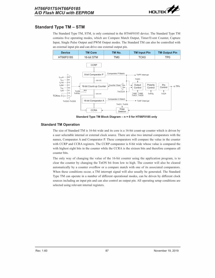
Rev. 1.60 86 November 19, 2019 Rev. 1.60 87 November 19, 2019
HT66F0175/HT66F0185A/D Flash MCU with EEPROM
HT66F0175/HT66F0185A/D Flash MCU with EEPROM
Standard Type TM – STMThe Standard Type TM, STM, is only contained in the HT66F0185 device. The Standard Type TM contains five operating modes, which are Compare Match Output, Timer/Event Counter, Capture Input, Single Pulse Output and PWM Output modes. The Standard TM can also be controlled with an external input pin and can drive one external output pin.
Device TM Core TM No. TM Input Pin TM Output PinHT66F0185 16-bit STM TM0 TCK0 TP0
fSYS
fSYS/4
fH/64fH/16
fTBC
TCKn
000
001
010
011
100
101
110
111
TnCK2~TnCK0
16-bit Count-up Counter
8-bit Comparator P
CCRP
b8~b15
b0~b15
16-bit Comparator A
TnONTnPAU
Comparator A Match
Comparator P Match
Counter Clear 01
Output Control
Polarity Control
Pin Control TPn
TnOC
TnM1, TnM0TnIO1, TnIO0
TnAF Interrupt
TnPF Interrupt
TnPOL TnCP
CCRA
TnCCLR
EdgeDetector
TnIO1, TnIO0
fH/8
Standard Type TM Block Diagram – n = 0 for HT66F0185 only
Standard TM OperationThe size of Standard TM is 16-bit wide and its core is a 16-bit count-up counter which is driven by a user selectable internal or external clock source. There are also two internal comparators with the names, Comparator A and Comparator P. These comparators will compare the value in the counter with CCRP and CCRA registers. The CCRP comparator is 8-bit wide whose value is compared the with highest eight bits in the counter while the CCRA is the sixteen bits and therefore compares all counter bits.
The only way of changing the value of the 16-bit counter using the application program, is to clear the counter by changing the TnON bit from low to high. The counter will also be cleared automatically by a counter overflow or a compare match with one of its associated comparators. When these conditions occur, a TM interrupt signal will also usually be generated. The Standard Type TM can operate in a number of different operational modes, can be driven by different clock sources including an input pin and can also control an output pin. All operating setup conditions are selected using relevant internal registers.
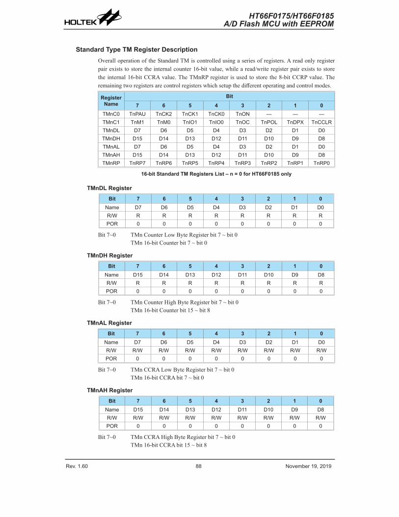
Rev. 1.60 88 November 19, 2019 Rev. 1.60 89 November 19, 2019
HT66F0175/HT66F0185A/D Flash MCU with EEPROM
HT66F0175/HT66F0185A/D Flash MCU with EEPROM
Standard Type TM Register DescriptionOverall operation of the Standard TM is controlled using a series of registers. A read only register pair exists to store the internal counter 16-bit value, while a read/write register pair exists to store the internal 16-bit CCRA value. The TMnRP register is used to store the 8-bit CCRP value. The remaining two registers are control registers which setup the different operating and control modes.
RegisterName
Bit7 6 5 4 3 2 1 0
TMnC0 TnPAU TnCK2 TnCK1 TnCK0 TnON — — —TMnC1 TnM1 TnM0 TnIO1 TnIO0 TnOC TnPOL TnDPX TnCCLRTMnDL D7 D6 D5 D4 D3 D2 D1 D0TMnDH D15 D14 D13 D12 D11 D10 D9 D8TMnAL D7 D6 D5 D4 D3 D2 D1 D0TMnAH D15 D14 D13 D12 D11 D10 D9 D8TMnRP TnRP7 TnRP6 TnRP5 TnRP4 TnRP3 TnRP2 TnRP1 TnRP0
16-bit Standard TM Registers List – n = 0 for HT66F0185 only
TMnDL RegisterBit 7 6 5 4 3 2 1 0
Name D7 D6 D5 D4 D3 D2 D1 D0R/W R R R R R R R RPOR 0 0 0 0 0 0 0 0
Bit 7~0 TMn Counter Low Byte Register bit 7 ~ bit 0TMn 16-bit Counter bit 7 ~ bit 0
TMnDH RegisterBit 7 6 5 4 3 2 1 0
Name D15 D14 D13 D12 D11 D10 D9 D8R/W R R R R R R R RPOR 0 0 0 0 0 0 0 0
Bit 7~0 TMn Counter High Byte Register bit 7 ~ bit 0TMn 16-bit Counter bit 15 ~ bit 8
TMnAL RegisterBit 7 6 5 4 3 2 1 0
Name D7 D6 D5 D4 D3 D2 D1 D0R/W R/W R/W R/W R/W R/W R/W R/W R/WPOR 0 0 0 0 0 0 0 0
Bit 7~0 TMn CCRA Low Byte Register bit 7 ~ bit 0TMn 16-bit CCRA bit 7 ~ bit 0
TMnAH RegisterBit 7 6 5 4 3 2 1 0
Name D15 D14 D13 D12 D11 D10 D9 D8R/W R/W R/W R/W R/W R/W R/W R/W R/WPOR 0 0 0 0 0 0 0 0
Bit 7~0 TMn CCRA High Byte Register bit 7 ~ bit 0TMn 16-bit CCRA bit 15 ~ bit 8

Rev. 1.60 88 November 19, 2019 Rev. 1.60 89 November 19, 2019
HT66F0175/HT66F0185A/D Flash MCU with EEPROM
HT66F0175/HT66F0185A/D Flash MCU with EEPROM
TMnC0 RegisterBit 7 6 5 4 3 2 1 0
Name TnPAU TnCK2 TnCK1 TnCK0 TnON — — —R/W R/W R/W R/W R/W R/W — — —POR 0 0 0 0 0 — — —
Bit 7 TnPAU: TMn Counter Pause control0: Run1: Pause
The counter can be paused by setting this bit high. Clearing the bit to zero restores normal counter operation. When in a Pause condition the TMn will remain powered up and continue to consume power. The counter will retain its residual value when this bit changes from low to high and resume counting from this value when the bit changes to a low value again.
Bit 6~4 TnCK2~TnCK0: Select TMn Counter clock000: fSYS/4001: fSYS
010: fH/16011: fH/64100: fTBC
101: fH
110: TCKn rising edge clock111: TCKn falling edge clock
These three bits are used to select the clock source for the TMn. The external pin clock source can be chosen to be active on the rising or falling edge. The clock source fSYS is the system clock, while fH and fTBC are other internal clocks, the details of which can be found in the oscillator section.
Bit 3 TnON: TMn Counter On/Off control0: Off1: On
This bit controls the overall on/off function of the TMn. Setting the bit high enables the counter to run while clearing the bit disables the TMn. Clearing this bit to zero will stop the counter from counting and turn off the TMn which will reduce its power consumption. When the bit changes state from low to high the internal counter value will be reset to zero, however when the bit changes from high to low, the internal counter will retain its residual value until the bit returns high again. If the TMn is in the Compare Match Output Mode then the TMn output pin will be reset to its initial condition, as specified by the TnOC bit, when the TnON bit changes from low to high.
Bit 2~0 Unimplemented, read as “0”
Rev. 1.60 90 November 19, 2019 Rev. 1.60 91 November 19, 2019
HT66F0175/HT66F0185A/D Flash MCU with EEPROM
HT66F0175/HT66F0185A/D Flash MCU with EEPROM
TMnC1 RegisterBit 7 6 5 4 3 2 1 0
Name TnM1 TnM0 TnIO1 TnIO0 TnOC TnPOL TnDPX TnCCLRR/W R/W R/W R/W R/W R/W R/W R/W R/WPOR 0 0 0 0 0 0 0 0
Bit 7~6 TnM1~TnM0: Select TMn Operating Mode00: Compare Match Output Mode01: Capture Input Mode10: PWM Mode or Single Pulse Output Mode11: Timer/Counter Mode
These bits setup the required operating mode for the TMn. To ensure reliable operation the TMn should be switched off before any changes are made to the TnM1 and TnM0 bits. In the Timer/Counter Mode, the TMn output pin control will be disabled.
Bit 5~4 TnIO1~TnIO0: Select TPn pin output functionCompare Match Output Mode
00: No change01: Output low10: Output high11: Toggle output
PWM Output Mode/Single Pulse Output Mode00: PWM output inactive state01: PWM output active state10: PWM output11: Single Pulse Output
Capture Input Mode00: Input capture at rising edge of TPn01: Input capture at falling edge of TPn10: Input capture at rising/falling edge of TPn11: Input capture disabled
Timer/Counter ModeUnused
These two bits are used to determine how the TMn output pin changes state when a certain condition is reached. The function that these bits select depends upon in which mode the TMn is running.In the Compare Match Output Mode, the TnIO1 and TnIO0 bits determine how the TMn output pin changes state when a compare match occurs from the Comparator A. The TM output pin can be setup to switch high, switch low or to toggle its present state when a compare match occurs from the Comparator A. When the bits are both zero, then no change will take place on the output. The initial value of the TMn output pin should be setup using the TnOC bit in the TMnC1 register. Note that the output level requested by the TnIO1 and TnIO0 bits must be different from the initial value setup using the TnOC bit otherwise no change will occur on the TMn output pin when a compare match occurs. After the TMn output pin changes state, it can be reset to its initial level by changing the level of the TnON bit from low to high.In the PWM Mode, the TnIO1 and TnIO0 bits determine how the TMn output pin changes state when a certain compare match condition occurs. The PWM output function is modified by changing these two bits. It is necessary to only change the values of the TnIO1 and TnIO0 bits only after the TMn has been switched off. Unpredictable PWM outputs will occur if the TnIO1 and TnIO0 bits are changed when the TMn is running.
Rev. 1.60 90 November 19, 2019 Rev. 1.60 91 November 19, 2019
HT66F0175/HT66F0185A/D Flash MCU with EEPROM
HT66F0175/HT66F0185A/D Flash MCU with EEPROM
Bit 3 TnOC: TMn TPn Output controlCompare Match Output Mode
0: Initial low1: Initial high
PWM Output Mode/Single Pulse Output Mode0: Active low1: Active high
This is the output control bit for the TMn output pin. Its operation depends upon whether TMn is being used in the Compare Match Output Mode or in the PWM Mode/Single Pulse Output Mode. It has no effect if the TMn is in the Timer/Counter Mode. In the Compare Match Output Mode it determines the logic level of the TMn output pin before a compare match occurs. In the PWM Mode/Single Pulse Output Mode it determines if the PWM signal is active high or active low.
Bit 2 TnPOL: TMn TPn Output polarity control0: Non-inverted1: Inverted
This bit controls the polarity of the TPn output pin. When the bit is set high the TMn output pin will be inverted and not inverted when the bit is zero. It has no effect if the TMn is in the Timer/Counter Mode.
Bit 1 TnDPX: TMn PWM duty/period control0: CCRP – period; CCRA – duty1: CCRP – duty; CCRA – period
This bit determines which of the CCRA and CCRP registers are used for period and duty control of the PWM waveform.
Bit 0 TnCCLR: TMn Counter Clear condition selection0: Comparator P match1: Comparator A match
This bit is used to select the method which clears the counter. Remember that the Standard TM contains two comparators, Comparator A and Comparator P, either of which can be selected to clear the internal counter. With the TnCCLR bit set high, the counter will be cleared when a compare match occurs from the Comparator A. When the bit is low, the counter will be cleared when a compare match occurs from the Comparator P or with a counter overflow. A counter overflow clearing method can only be implemented if the CCRP bits are all cleared to zero. The TnCCLR bit is not used in the PWM Output, Single Pulse Output or Capture Input Mode.
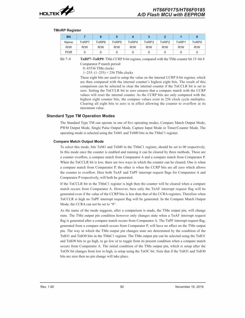
Rev. 1.60 92 November 19, 2019 Rev. 1.60 93 November 19, 2019
HT66F0175/HT66F0185A/D Flash MCU with EEPROM
HT66F0175/HT66F0185A/D Flash MCU with EEPROM
TMnRP RegisterBit 7 6 5 4 3 2 1 0
Name TnRP7 TnRP6 TnRP5 TnRP4 TnRP3 TnRP2 TnRP1 TnRP0R/W R/W R/W R/W R/W R/W R/W R/W R/WPOR 0 0 0 0 0 0 0 0
Bit 7~0 TnRP7~TnRP0: TMn CCRP 8-bit register, compared with the TMn counter bit 15~bit 8Comparator P match period:
0: 65536 TMn clocks1~255: (1~255) × 256 TMn clocks
These eight bits are used to setup the value on the internal CCRP 8-bit register, which are then compared with the internal counter’s highest eight bits. The result of this comparison can be selected to clear the internal counter if the TnCCLR bit is set to zero. Setting the TnCCLR bit to zero ensures that a compare match with the CCRP values will reset the internal counter. As the CCRP bits are only compared with the highest eight counter bits, the compare values exist in 256 clock cycle multiples. Clearing all eight bits to zero is in effect allowing the counter to overflow at its maximum value.
Standard Type TM Operation ModesThe Standard Type TM can operate in one of five operating modes, Compare Match Output Mode, PWM Output Mode, Single Pulse Output Mode, Capture Input Mode or Timer/Counter Mode. The operating mode is selected using the TnM1 and TnM0 bits in the TMnC1 register.
Compare Match Output ModeTo select this mode, bits TnM1 and TnM0 in the TMnC1 register, should be set to 00 respectively. In this mode once the counter is enabled and running it can be cleared by three methods. These are a counter overflow, a compare match from Comparator A and a compare match from Comparator P. When the TnCCLR bit is low, there are two ways in which the counter can be cleared. One is when a compare match from Comparator P, the other is when the CCRP bits are all zero which allows the counter to overflow. Here both TnAF and TnPF interrupt request flags for Comparator A and Comparator P respectively, will both be generated.
If the TnCCLR bit in the TMnC1 register is high then the counter will be cleared when a compare match occurs from Comparator A. However, here only the TnAF interrupt request flag will be generated even if the value of the CCRP bits is less than that of the CCRA registers. Therefore when TnCCLR is high no TnPF interrupt request flag will be generated. In the Compare Match Output Mode, the CCRA can not be set to “0”.
As the name of the mode suggests, after a comparison is made, the TMn output pin, will change state. The TMn output pin condition however only changes state when a TnAF interrupt request flag is generated after a compare match occurs from Comparator A. The TnPF interrupt request flag, generated from a compare match occurs from Comparator P, will have no effect on the TMn output pin. The way in which the TMn output pin changes state are determined by the condition of the TnIO1 and TnIO0 bits in the TMnC1 register. The TMn output pin can be selected using the TnIO1 and TnIO0 bits to go high, to go low or to toggle from its present condition when a compare match occurs from Comparator A. The initial condition of the TMn output pin, which is setup after the TnON bit changes from low to high, is setup using the TnOC bit. Note that if the TnIO1 and TnIO0 bits are zero then no pin change will take place.
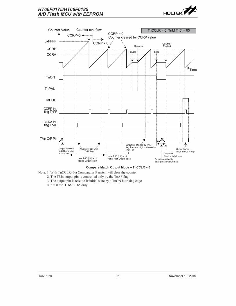
Rev. 1.60 92 November 19, 2019 Rev. 1.60 93 November 19, 2019
HT66F0175/HT66F0185A/D Flash MCU with EEPROM
HT66F0175/HT66F0185A/D Flash MCU with EEPROM
Counter Value
0xFFFF
CCRPCCRA
TnON
TnPAU
TnPOL
CCRP Int. flag TnPF
CCRA Int. flag TnAF
TMn O/P Pin
Time
CCRP=0
CCRP > 0
Counter overflowCCRP > 0Counter cleared by CCRP value
Pause
Resume
Stop
Counter Restart
TnCCLR = 0; TnM [1:0] = 00
Output pin set to initial Level Low if TnOC=0
Output Toggle with TnAF flag
Note TnIO [1:0] = 10 Active High Output selectHere TnIO [1:0] = 11
Toggle Output select
Output not affected by TnAF flag. Remains High until reset by TnON bit
Output PinReset to Initial value
Output controlled by other pin-shared function
Output Invertswhen TnPOL is high
Compare Match Output Mode – TnCCLR = 0Note: 1. With TnCCLR=0 a Comparator P match will clear the counter
2. The TMn output pin is controlled only by the TnAF flag3. The output pin is reset to itsinitial state by a TnON bit rising edge4. n = 0 for HT66F0185 only
Rev. 1.60 94 November 19, 2019 Rev. 1.60 95 November 19, 2019
HT66F0175/HT66F0185A/D Flash MCU with EEPROM
HT66F0175/HT66F0185A/D Flash MCU with EEPROM
Counter Value
0xFFFF
CCRP
CCRA
TnON
TnPAU
TnPOL
CCRP Int. flag TnPF
CCRA Int. flag TnAF
TMn O/P Pin
Time
CCRA=0
CCRA = 0Counter overflowCCRA > 0 Counter cleared by CCRA value
Pause
Resume
Stop Counter Restart
TnCCLR = 1; TnM [1:0] = 00
Output pin set to initial Level Low if TnOC=0
Output Toggle with TnAF flag
Note TnIO [1:0] = 10 Active High Output selectHere TnIO [1:0] = 11
Toggle Output select
Output not affected by TnAF flag. Remains High until reset by TnON bit
Output PinReset to Initial value
Output controlled by other pin-shared function
Output Invertswhen TnPOL is high
TnPF not generated
No TnAF flag generated on CCRA overflow
Output does not change
Compare Match Output Mode – TnCCLR = 1Note: 1. With TnCCLR=1 a Comparator A match will clear the counter
2. The TMn output pin is controlled only by the TnAF flag3. The output pin is reset to its initial state by a TnON bit rising edge4. A TnPF flag is not generated when TnCCLR=15. n = 0 for HT66F0185 only
Rev. 1.60 94 November 19, 2019 Rev. 1.60 95 November 19, 2019
HT66F0175/HT66F0185A/D Flash MCU with EEPROM
HT66F0175/HT66F0185A/D Flash MCU with EEPROM
Timer/Counter ModeTo select this mode, bits TnM1 and TnM0 in the TMnC1 register should be set to 11 respectively. The Timer/Counter Mode operates in an identical way to the Compare Match Output Mode generating the same interrupt flags. The exception is that in the Timer/Counter Mode the TMn output pin is not used. Therefore the above description and Timing Diagrams for the Compare Match Output Mode can be used to understand its function. As the TMn output pin is not used in this mode, the pin can be used as a normal I/O pin or other pin-shared function.
PWM Output ModeTo select this mode, bits TnM1 and TnM0 in the TMnC1 register should be set to 10 respectively and also the TnIO1 and TnIO0 bits should be set to 10 respectively. The PWM function within the TMn is useful for applications which require functions such as motor control, heating control, illumination control etc. By providing a signal of fixed frequency but of varying duty cycle on the TMn output pin, a square wave AC waveform can be generated with varying equivalent DC RMS values.
As both the period and duty cycle of the PWM waveform can be controlled, the choice of generated waveform is extremely flexible. In the PWM mode, the TnCCLR bit has no effect as the PWM period. Both of the CCRA and CCRP registers are used to generate the PWM waveform, one register is used to clear the internal counter and thus control the PWM waveform frequency, while the other one is used to control the duty cycle. Which register is used to control either frequency or duty cycle is determined using the TnDPX bit in the TMnC1 register. The PWM waveform frequency and duty cycle can therefore be controlled by the values in the CCRA and CCRP registers.
An interrupt flag, one for each of the CCRA and CCRP, will be generated when a compare match occurs from either Comparator A or Comparator P. The TnOC bit in the TMnC1 register is used to select the required polarity of the PWM waveform while the two TnIO1 and TnIO0 bits are used to enable the PWM output or to force the TMn output pin to a fixed high or low level. The TnPOL bit is used to reverse the polarity of the PWM output waveform.
• 16-bit STM, PWM Mode, Edge-aligned Mode, TnDPX=0CCRP 1~255 0Period CCRP×256 65536Duty CCRA
If fSYS = 16MHz, TMn clock source is fSYS/4, CCRP = 2 and CCRA = 128,
The TMn PWM output frequency = (fSYS/4) / (2×256) = fSYS/2048 = 7.8125 kHz, duty = 128/(2×256)= 25%.
If the Duty value defined by the CCRA register is equal to or greater than the Period value, then the PWM output duty is 100%.
• 16-bit STM, PWM Mode, Edge-aligned Mode, TnDPX=1CCRP 1~255 0Period CCRADuty CCRP×256 65536
The PWM output period is determined by the CCRA register value together with the TM clock while the PWM duty cycle is defined by the (CCRP×256) value except when the CCRP value is equal to 0.
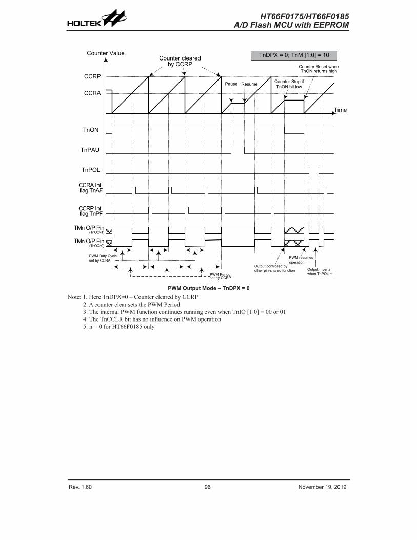
Rev. 1.60 96 November 19, 2019 Rev. 1.60 97 November 19, 2019
HT66F0175/HT66F0185A/D Flash MCU with EEPROM
HT66F0175/HT66F0185A/D Flash MCU with EEPROM
Counter Value
CCRP
CCRA
TnON
TnPAU
TnPOL
CCRP Int. flag TnPF
CCRA Int. flag TnAF
TMn O/P Pin(TnOC=1)
Time
Counter cleared by CCRP
Pause Resume Counter Stop if TnON bit low
Counter Reset when TnON returns high
TnDPX = 0; TnM [1:0] = 10
PWM Duty Cycle set by CCRA
PWM resumes operation
Output controlled by other pin-shared function Output Inverts
when TnPOL = 1PWM Period set by CCRP
TMn O/P Pin(TnOC=0)
PWM Output Mode – TnDPX = 0Note: 1. Here TnDPX=0 – Counter cleared by CCRP
2. A counter clear sets the PWM Period3. The internal PWM function continues running even when TnIO [1:0] = 00 or 014. The TnCCLR bit has no influence on PWM operation5. n = 0 for HT66F0185 only
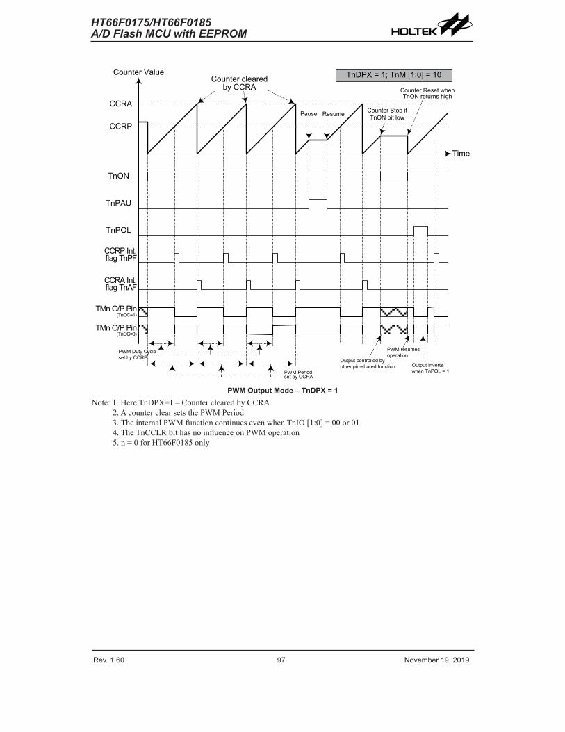
Rev. 1.60 96 November 19, 2019 Rev. 1.60 97 November 19, 2019
HT66F0175/HT66F0185A/D Flash MCU with EEPROM
HT66F0175/HT66F0185A/D Flash MCU with EEPROM
Counter Value
CCRP
CCRA
TnON
TnPAU
TnPOL
CCRP Int. flag TnPF
CCRA Int. flag TnAF
TMn O/P Pin (TnOC=1)
Time
Counter cleared by CCRA
Pause Resume Counter Stop if TnON bit low
Counter Reset when TnON returns high
TnDPX = 1; TnM [1:0] = 10
PWM Duty Cycle set by CCRP
PWM resumes operation
Output controlled by other pin-shared function Output Inverts
when TnPOL = 1PWM Period set by CCRA
TMn O/P Pin (TnOC=0)
PWM Output Mode – TnDPX = 1Note: 1. Here TnDPX=1 – Counter cleared by CCRA
2. A counter clear sets the PWM Period3. The internal PWM function continues even when TnIO [1:0] = 00 or 014. The TnCCLR bit has no influence on PWM operation5. n = 0 for HT66F0185 only
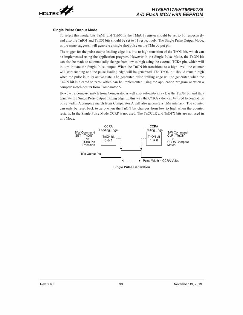
Rev. 1.60 98 November 19, 2019 Rev. 1.60 99 November 19, 2019
HT66F0175/HT66F0185A/D Flash MCU with EEPROM
HT66F0175/HT66F0185A/D Flash MCU with EEPROM
Single Pulse Output ModeTo select this mode, bits TnM1 and TnM0 in the TMnC1 register should be set to 10 respectively and also the TnIO1 and TnIO0 bits should be set to 11 respectively. The Single Pulse Output Mode, as the name suggests, will generate a single shot pulse on the TMn output pin.
The trigger for the pulse output leading edge is a low to high transition of the TnON bit, which can be implemented using the application program. However in the Single Pulse Mode, the TnON bit can also be made to automatically change from low to high using the external TCKn pin, which will in turn initiate the Single Pulse output. When the TnON bit transitions to a high level, the counter will start running and the pulse leading edge will be generated. The TnON bit should remain high when the pulse is in its active state. The generated pulse trailing edge will be generated when the TnON bit is cleared to zero, which can be implemented using the application program or when a compare match occurs from Comparator A.
However a compare match from Comparator A will also automatically clear the TnON bit and thus generate the Single Pulse output trailing edge. In this way the CCRA value can be used to control the pulse width. A compare match from Comparator A will also generate a TMn interrupt. The counter can only be reset back to zero when the TnON bit changes from low to high when the counter restarts. In the Single Pulse Mode CCRP is not used. The TnCCLR and TnDPX bits are not used in this Mode.
TnON bit0 à 1
S/W Command SET“TnON”
orTCKn Pin Transition
TnON bit1 à 0
CCRA Trailing Edge
S/W Command CLR“TnON”
orCCRA Compare Match
TPn Output Pin
Pulse Width = CCRA Value
CCRA Leading Edge
Single Pulse Generation
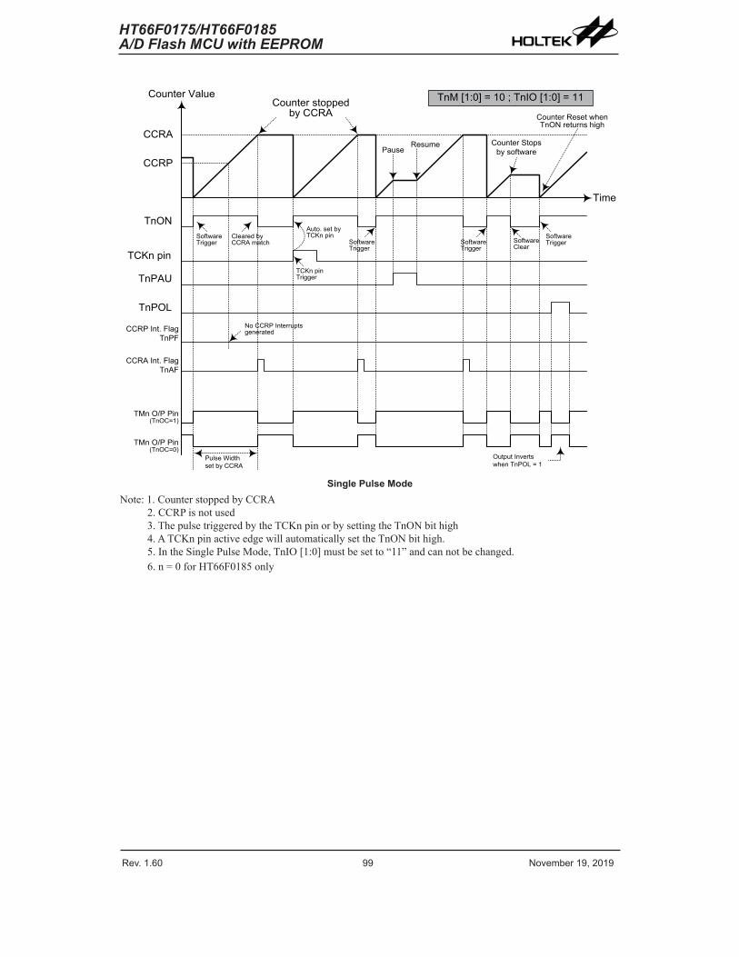
Rev. 1.60 98 November 19, 2019 Rev. 1.60 99 November 19, 2019
HT66F0175/HT66F0185A/D Flash MCU with EEPROM
HT66F0175/HT66F0185A/D Flash MCU with EEPROM
Counter Value
CCRP
CCRA
TnON
TnPAU
TnPOL
CCRP Int. Flag TnPF
CCRA Int. Flag TnAF
TMn O/P Pin(TnOC=1)
Time
Counter stopped by CCRA
PauseResume Counter Stops
by software
Counter Reset when TnON returns high
TnM [1:0] = 10 ; TnIO [1:0] = 11
Pulse Width set by CCRA
Output Invertswhen TnPOL = 1
No CCRP Interrupts generated
TMn O/P Pin(TnOC=0)
TCKn pin
Software Trigger
Cleared by CCRA match
TCKn pin Trigger
Auto. set by TCKn pin
Software Trigger
Software Clear
Software TriggerSoftware
Trigger
Single Pulse ModeNote: 1. Counter stopped by CCRA
2. CCRP is not used3. The pulse triggered by the TCKn pin or by setting the TnON bit high4. A TCKn pin active edge will automatically set the TnON bit high.5. In the Single Pulse Mode, TnIO [1:0] must be set to “11” and can not be changed.6. n = 0 for HT66F0185 only
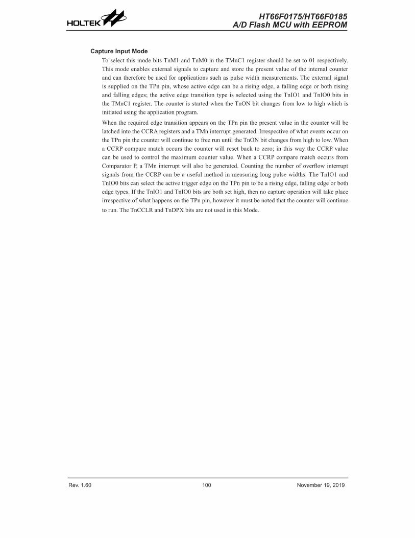
Rev. 1.60 100 November 19, 2019 Rev. 1.60 101 November 19, 2019
HT66F0175/HT66F0185A/D Flash MCU with EEPROM
HT66F0175/HT66F0185A/D Flash MCU with EEPROM
Capture Input ModeTo select this mode bits TnM1 and TnM0 in the TMnC1 register should be set to 01 respectively. This mode enables external signals to capture and store the present value of the internal counter and can therefore be used for applications such as pulse width measurements. The external signal is supplied on the TPn pin, whose active edge can be a rising edge, a falling edge or both rising and falling edges; the active edge transition type is selected using the TnIO1 and TnIO0 bits in the TMnC1 register. The counter is started when the TnON bit changes from low to high which is initiated using the application program.
When the required edge transition appears on the TPn pin the present value in the counter will be latched into the CCRA registers and a TMn interrupt generated. Irrespective of what events occur on the TPn pin the counter will continue to free run until the TnON bit changes from high to low. When a CCRP compare match occurs the counter will reset back to zero; in this way the CCRP value can be used to control the maximum counter value. When a CCRP compare match occurs from Comparator P, a TMn interrupt will also be generated. Counting the number of overflow interrupt signals from the CCRP can be a useful method in measuring long pulse widths. The TnIO1 and TnIO0 bits can select the active trigger edge on the TPn pin to be a rising edge, falling edge or both edge types. If the TnIO1 and TnIO0 bits are both set high, then no capture operation will take place irrespective of what happens on the TPn pin, however it must be noted that the counter will continue to run. The TnCCLR and TnDPX bits are not used in this Mode.
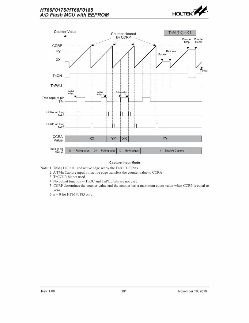
Rev. 1.60 100 November 19, 2019 Rev. 1.60 101 November 19, 2019
HT66F0175/HT66F0185A/D Flash MCU with EEPROM
HT66F0175/HT66F0185A/D Flash MCU with EEPROM
Counter Value
YYCCRP
TnON
TnPAU
CCRP Int. Flag TnPF
CCRA Int. Flag TnAF
CCRA Value
Time
Counter cleared by CCRP
PauseResume
Counter Reset
TnM [1:0] = 01
TMn capture pin TPn
XX
Counter Stop
TnIO [1:0] Value
XX YY XX YY
Active edge Active
edgeActive edge
00 – Rising edge 01 – Falling edge 10 – Both edges 11 – Disable Capture
Capture Input ModeNote: 1. TnM [1:0] = 01 and active edge set by the TnIO [1:0] bits
2. A TMn Capture input pin active edge transfers the counter value to CCRA3. TnCCLR bit not used4. No output function -- TnOC and TnPOL bits are not used5. CCRP determines the counter value and the counter has a maximum count value when CCRP is equal to
zero.6. n = 0 for HT66F0185 only
Rev. 1.60 102 November 19, 2019 Rev. 1.60 103 November 19, 2019
HT66F0175/HT66F0185A/D Flash MCU with EEPROM
HT66F0175/HT66F0185A/D Flash MCU with EEPROM
Periodic Type TM – PTMThe Periodic Type TM contains five operating modes, which are Compare Match Output, Timer/Event Counter, Capture Input, Single Pulse Output and PWM Output modes. The Periodic TM can also be controlled with one external input pin and can drive one external output pin.
Device TM Core TM No. TM Input Pin TM Output PinHT66F0175 10-bit PTM TM0, TM1 TCK0, TCK1 TP0, TP1HT66F0185 10-bit PTM TM1 TCK1 TP1
fSYS
fSYS/4
fH/64fH/16
fTBC
TCKn
000
001
010
011
100
101
110
111
TnCK2~TnCK0
10-bit Count-up Counter
10-bit Comparator P
CCRP
b0~b9
b0~b9
10-bit Comparator A
TnONTnPAU
Comparator A Match
Comparator P Match
Counter Clear 01
Output Control
Polarity Control
Pin Control TPn
TnOC
TnM1, TnM0TnIO1, TnIO0
TnAF Interrupt
TnPF Interrupt
TnPOL TnCP
CCRA
TnCCLR
EdgeDetector
TnIO1, TnIO0
fH
10
TnCAPTS
Periodic Type TM Block Diagram – n = 0 or 1
Periodic TM OperationThe size of Periodic TM is 10-bit wide and its core is a 10-bit count-up counter which is driven by a user selectable internal or external clock source. There are also two internal comparators with the names, Comparator A and Comparator P. These comparators will compare the value in the counter with CCRP and CCRA registers. The CCRP and CCRA comparators are 10-bit wide whose value is respectively compared with all counter bits.
The only way of changing the value of the 10-bit counter using the application program is to clear the counter by changing the TnON bit from low to high. The counter will also be cleared automatically by a counter overflow or a compare match with one of its associated comparators. When these conditions occur, a TM interrupt signal will also usually be generated. The Periodic Type TM can operate in a number of different operational modes, can be driven by different clock sources including an input pin and can also control the output pins. All operating setup conditions are selected using relevant internal registers.
Rev. 1.60 102 November 19, 2019 Rev. 1.60 103 November 19, 2019
HT66F0175/HT66F0185A/D Flash MCU with EEPROM
HT66F0175/HT66F0185A/D Flash MCU with EEPROM
Periodic Type TM Register DescriptionOverall operation of the Periodic TM is controlled using a series of registers. A read only register pair exists to store the internal counter 10-bit value, while two read/write register pairs exist to store the internal 10-bit CCRA and CCRP value. The remaining two registers are control registers which setup the different operating and control modes.
Register Name Bit 7 Bit 6 Bit 5 Bit 4 Bit 3 Bit 2 Bit 1 Bit 0
TMnC0 TnPAU TnCK2 TnCK1 TnCK0 TnON — — —TMnC1 TnM1 TnM0 TnIO1 TnIO0 TnOC TnPOL TnCAPTS TnCCLRTMnDL D7 D6 D5 D4 D3 D2 D1 D0TMnDH — — — — — — D9 D8TMnAL D7 D6 D5 D4 D3 D2 D1 D0TMnAH — — — — — — D9 D8TMnRPL TnRP7 TnRP6 TnRP5 TnRP4 TnRP3 TnRP2 TnRP1 TnRP0TMnRPH — — — — — — TnRP9 TnRP8
Periodic TM Registers List – n = 0 or 1
TMnDL RegisterBit 7 6 5 4 3 2 1 0
Name D7 D6 D5 D4 D3 D2 D1 D0R/W R R R R R R R RPOR 0 0 0 0 0 0 0 0
Bit 7~0 TMn Counter Low Byte Register bit 7 ~ bit 0TMn 10-bit Counter bit 7 ~ bit 0
TMnDH RegisterBit 7 6 5 4 3 2 1 0
Name — — — — — — D9 D8R/W — — — — — — R RPOR — — — — — — 0 0
Bit 7~2 Unimplemented, read as “0”Bit 1~0 TMn Counter High Byte Register bit 1 ~ bit 0
TMn 10-bit Counter bit 9 ~ bit 8
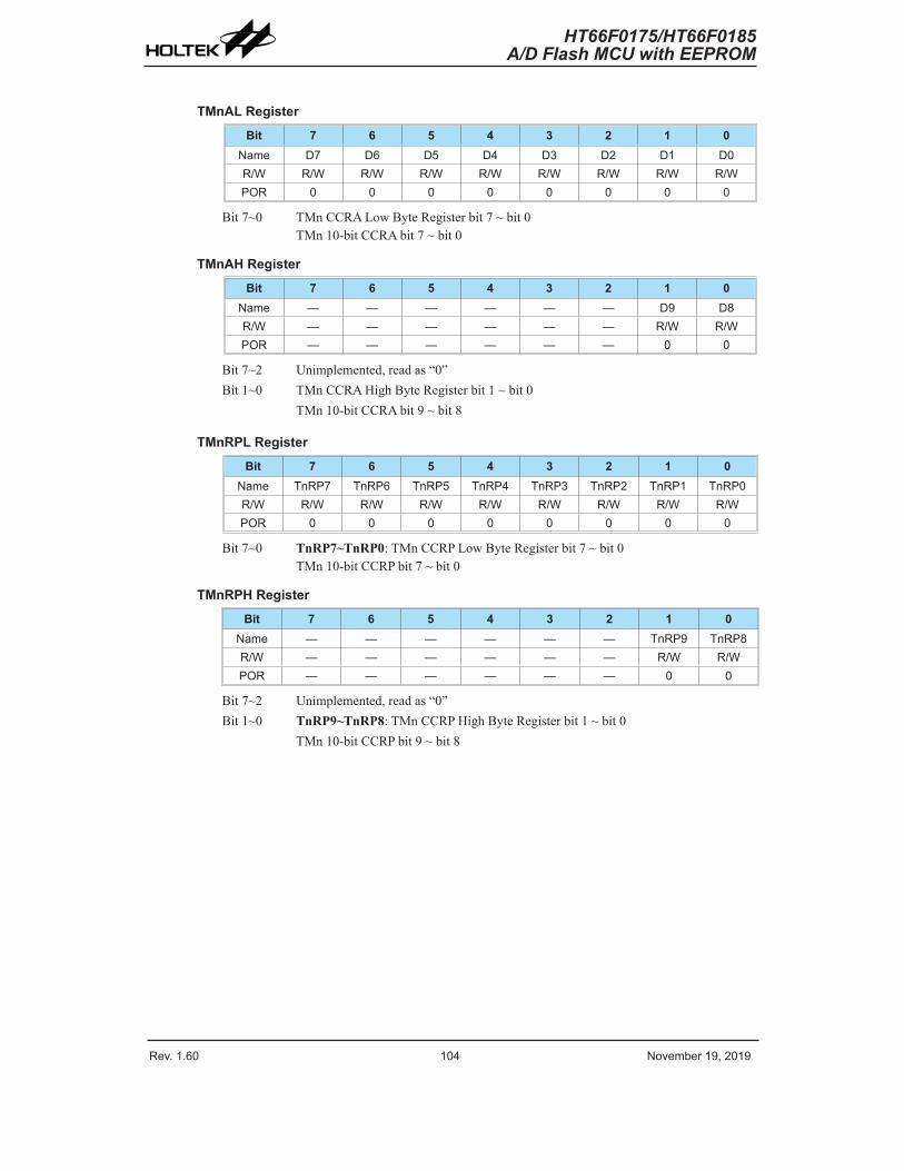
Rev. 1.60 104 November 19, 2019 Rev. 1.60 105 November 19, 2019
HT66F0175/HT66F0185A/D Flash MCU with EEPROM
HT66F0175/HT66F0185A/D Flash MCU with EEPROM
TMnAL RegisterBit 7 6 5 4 3 2 1 0
Name D7 D6 D5 D4 D3 D2 D1 D0R/W R/W R/W R/W R/W R/W R/W R/W R/WPOR 0 0 0 0 0 0 0 0
Bit 7~0 TMn CCRA Low Byte Register bit 7 ~ bit 0TMn 10-bit CCRA bit 7 ~ bit 0
TMnAH RegisterBit 7 6 5 4 3 2 1 0
Name — — — — — — D9 D8R/W — — — — — — R/W R/WPOR — — — — — — 0 0
Bit 7~2 Unimplemented, read as “0”Bit 1~0 TMn CCRA High Byte Register bit 1 ~ bit 0
TMn 10-bit CCRA bit 9 ~ bit 8
TMnRPL RegisterBit 7 6 5 4 3 2 1 0
Name TnRP7 TnRP6 TnRP5 TnRP4 TnRP3 TnRP2 TnRP1 TnRP0R/W R/W R/W R/W R/W R/W R/W R/W R/WPOR 0 0 0 0 0 0 0 0
Bit 7~0 TnRP7~TnRP0: TMn CCRP Low Byte Register bit 7 ~ bit 0TMn 10-bit CCRP bit 7 ~ bit 0
TMnRPH RegisterBit 7 6 5 4 3 2 1 0
Name — — — — — — TnRP9 TnRP8R/W — — — — — — R/W R/WPOR — — — — — — 0 0
Bit 7~2 Unimplemented, read as “0”Bit 1~0 TnRP9~TnRP8: TMn CCRP High Byte Register bit 1 ~ bit 0
TMn 10-bit CCRP bit 9 ~ bit 8
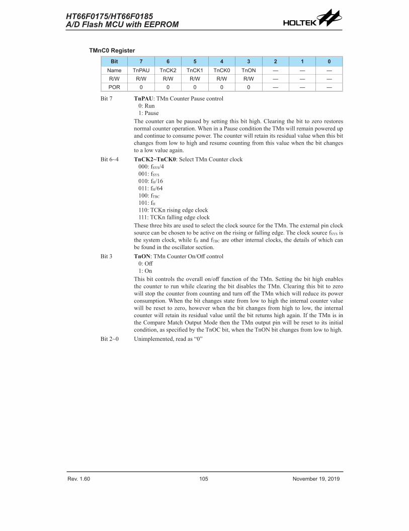
Rev. 1.60 104 November 19, 2019 Rev. 1.60 105 November 19, 2019
HT66F0175/HT66F0185A/D Flash MCU with EEPROM
HT66F0175/HT66F0185A/D Flash MCU with EEPROM
TMnC0 RegisterBit 7 6 5 4 3 2 1 0
Name TnPAU TnCK2 TnCK1 TnCK0 TnON — — —R/W R/W R/W R/W R/W R/W — — —POR 0 0 0 0 0 — — —
Bit 7 TnPAU: TMn Counter Pause control0: Run1: Pause
The counter can be paused by setting this bit high. Clearing the bit to zero restores normal counter operation. When in a Pause condition the TMn will remain powered up and continue to consume power. The counter will retain its residual value when this bit changes from low to high and resume counting from this value when the bit changes to a low value again.
Bit 6~4 TnCK2~TnCK0: Select TMn Counter clock000: fSYS/4001: fSYS
010: fH/16011: fH/64100: fTBC
101: fH
110: TCKn rising edge clock111: TCKn falling edge clock
These three bits are used to select the clock source for the TMn. The external pin clock source can be chosen to be active on the rising or falling edge. The clock source fSYS is the system clock, while fH and fTBC are other internal clocks, the details of which can be found in the oscillator section.
Bit 3 TnON: TMn Counter On/Off control0: Off1: On
This bit controls the overall on/off function of the TMn. Setting the bit high enables the counter to run while clearing the bit disables the TMn. Clearing this bit to zero will stop the counter from counting and turn off the TMn which will reduce its power consumption. When the bit changes state from low to high the internal counter value will be reset to zero, however when the bit changes from high to low, the internal counter will retain its residual value until the bit returns high again. If the TMn is in the Compare Match Output Mode then the TMn output pin will be reset to its initial condition, as specified by the TnOC bit, when the TnON bit changes from low to high.
Bit 2~0 Unimplemented, read as “0”
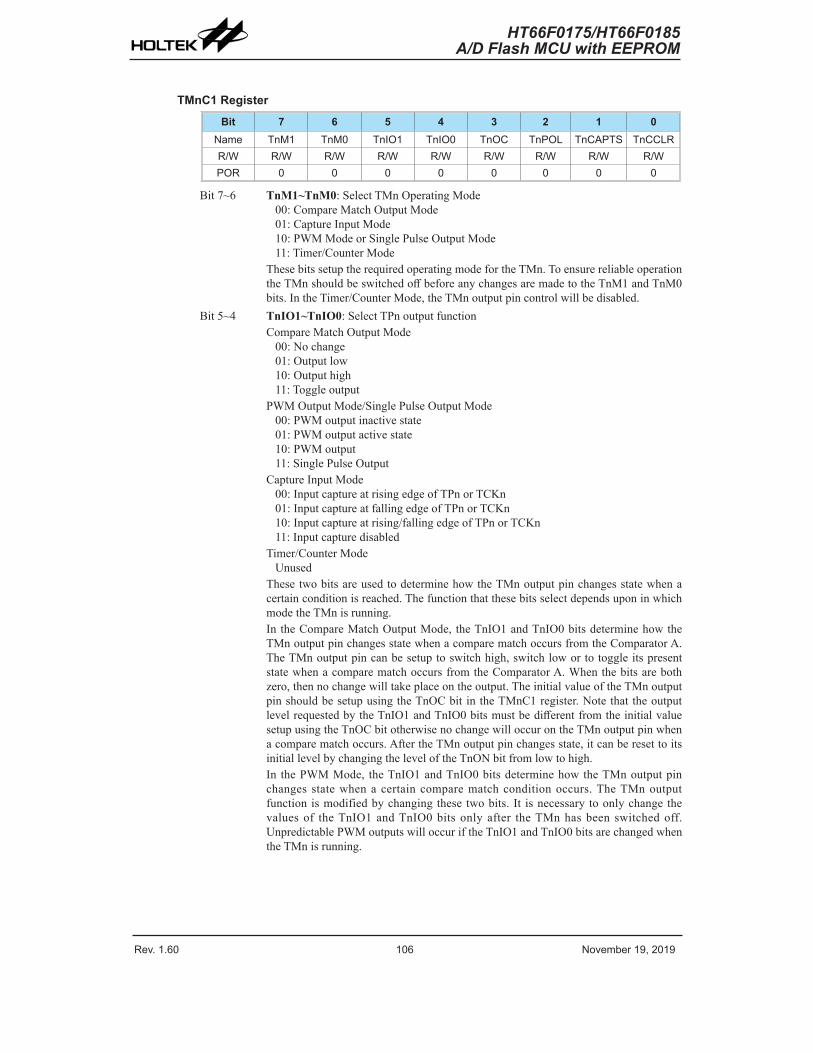
Rev. 1.60 106 November 19, 2019 Rev. 1.60 107 November 19, 2019
HT66F0175/HT66F0185A/D Flash MCU with EEPROM
HT66F0175/HT66F0185A/D Flash MCU with EEPROM
TMnC1 RegisterBit 7 6 5 4 3 2 1 0
Name TnM1 TnM0 TnIO1 TnIO0 TnOC TnPOL TnCAPTS TnCCLRR/W R/W R/W R/W R/W R/W R/W R/W R/WPOR 0 0 0 0 0 0 0 0
Bit 7~6 TnM1~TnM0: Select TMn Operating Mode00: Compare Match Output Mode01: Capture Input Mode10: PWM Mode or Single Pulse Output Mode11: Timer/Counter Mode
These bits setup the required operating mode for the TMn. To ensure reliable operation the TMn should be switched off before any changes are made to the TnM1 and TnM0 bits. In the Timer/Counter Mode, the TMn output pin control will be disabled.
Bit 5~4 TnIO1~TnIO0: Select TPn output functionCompare Match Output Mode
00: No change01: Output low10: Output high11: Toggle output
PWM Output Mode/Single Pulse Output Mode00: PWM output inactive state01: PWM output active state10: PWM output11: Single Pulse Output
Capture Input Mode00: Input capture at rising edge of TPn or TCKn01: Input capture at falling edge of TPn or TCKn10: Input capture at rising/falling edge of TPn or TCKn11: Input capture disabled
Timer/Counter ModeUnused
These two bits are used to determine how the TMn output pin changes state when a certain condition is reached. The function that these bits select depends upon in which mode the TMn is running.In the Compare Match Output Mode, the TnIO1 and TnIO0 bits determine how the TMn output pin changes state when a compare match occurs from the Comparator A. The TMn output pin can be setup to switch high, switch low or to toggle its present state when a compare match occurs from the Comparator A. When the bits are both zero, then no change will take place on the output. The initial value of the TMn output pin should be setup using the TnOC bit in the TMnC1 register. Note that the output level requested by the TnIO1 and TnIO0 bits must be different from the initial value setup using the TnOC bit otherwise no change will occur on the TMn output pin when a compare match occurs. After the TMn output pin changes state, it can be reset to its initial level by changing the level of the TnON bit from low to high.In the PWM Mode, the TnIO1 and TnIO0 bits determine how the TMn output pin changes state when a certain compare match condition occurs. The TMn output function is modified by changing these two bits. It is necessary to only change the values of the TnIO1 and TnIO0 bits only after the TMn has been switched off. Unpredictable PWM outputs will occur if the TnIO1 and TnIO0 bits are changed when the TMn is running.
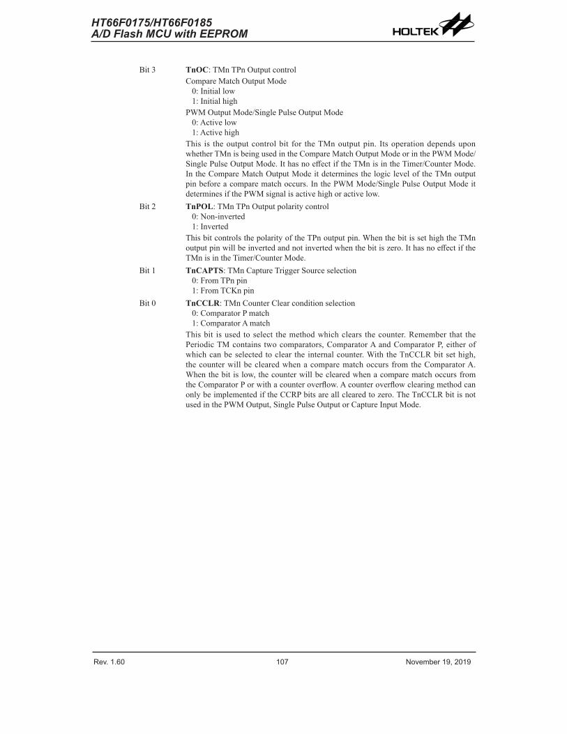
Rev. 1.60 106 November 19, 2019 Rev. 1.60 107 November 19, 2019
HT66F0175/HT66F0185A/D Flash MCU with EEPROM
HT66F0175/HT66F0185A/D Flash MCU with EEPROM
Bit 3 TnOC: TMn TPn Output controlCompare Match Output Mode
0: Initial low1: Initial high
PWM Output Mode/Single Pulse Output Mode0: Active low1: Active high
This is the output control bit for the TMn output pin. Its operation depends upon whether TMn is being used in the Compare Match Output Mode or in the PWM Mode/Single Pulse Output Mode. It has no effect if the TMn is in the Timer/Counter Mode. In the Compare Match Output Mode it determines the logic level of the TMn output pin before a compare match occurs. In the PWM Mode/Single Pulse Output Mode it determines if the PWM signal is active high or active low.
Bit 2 TnPOL: TMn TPn Output polarity control0: Non-inverted1: Inverted
This bit controls the polarity of the TPn output pin. When the bit is set high the TMn output pin will be inverted and not inverted when the bit is zero. It has no effect if the TMn is in the Timer/Counter Mode.
Bit 1 TnCAPTS: TMn Capture Trigger Source selection0: From TPn pin1: From TCKn pin
Bit 0 TnCCLR: TMn Counter Clear condition selection0: Comparator P match1: Comparator A match
This bit is used to select the method which clears the counter. Remember that the Periodic TM contains two comparators, Comparator A and Comparator P, either of which can be selected to clear the internal counter. With the TnCCLR bit set high, the counter will be cleared when a compare match occurs from the Comparator A. When the bit is low, the counter will be cleared when a compare match occurs from the Comparator P or with a counter overflow. A counter overflow clearing method can only be implemented if the CCRP bits are all cleared to zero. The TnCCLR bit is not used in the PWM Output, Single Pulse Output or Capture Input Mode.
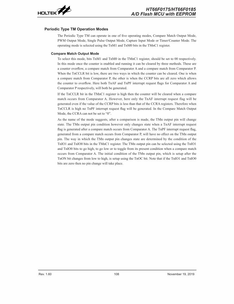
Rev. 1.60 108 November 19, 2019 Rev. 1.60 109 November 19, 2019
HT66F0175/HT66F0185A/D Flash MCU with EEPROM
HT66F0175/HT66F0185A/D Flash MCU with EEPROM
Periodic Type TM Operation ModesThe Periodic Type TM can operate in one of five operating modes, Compare Match Output Mode, PWM Output Mode, Single Pulse Output Mode, Capture Input Mode or Timer/Counter Mode. The operating mode is selected using the TnM1 and TnM0 bits in the TMnC1 register.
Compare Match Output ModeTo select this mode, bits TnM1 and TnM0 in the TMnC1 register, should be set to 00 respectively. In this mode once the counter is enabled and running it can be cleared by three methods. These are a counter overflow, a compare match from Comparator A and a compare match from Comparator P. When the TnCCLR bit is low, there are two ways in which the counter can be cleared. One is when a compare match from Comparator P, the other is when the CCRP bits are all zero which allows the counter to overflow. Here both TnAF and TnPF interrupt request flags for Comparator A and Comparator P respectively, will both be generated.
If the TnCCLR bit in the TMnC1 register is high then the counter will be cleared when a compare match occurs from Comparator A. However, here only the TnAF interrupt request flag will be generated even if the value of the CCRP bits is less than that of the CCRA registers. Therefore when TnCCLR is high no TnPF interrupt request flag will be generated. In the Compare Match Output Mode, the CCRA can not be set to “0”.
As the name of the mode suggests, after a comparison is made, the TMn output pin will change state. The TMn output pin condition however only changes state when a TnAF interrupt request flag is generated after a compare match occurs from Comparator A. The TnPF interrupt request flag, generated from a compare match occurs from Comparator P, will have no effect on the TMn output pin. The way in which the TMn output pin changes state are determined by the condition of the TnIO1 and TnIO0 bits in the TMnC1 register. The TMn output pin can be selected using the TnIO1 and TnIO0 bits to go high, to go low or to toggle from its present condition when a compare match occurs from Comparator A. The initial condition of the TMn output pin, which is setup after the TnON bit changes from low to high, is setup using the TnOC bit. Note that if the TnIO1 and TnIO0 bits are zero then no pin change will take place.
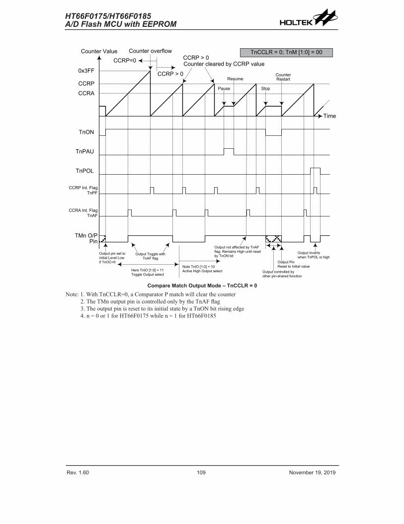
Rev. 1.60 108 November 19, 2019 Rev. 1.60 109 November 19, 2019
HT66F0175/HT66F0185A/D Flash MCU with EEPROM
HT66F0175/HT66F0185A/D Flash MCU with EEPROM
Counter Value
0x3FF
CCRPCCRA
TnON
TnPAU
TnPOL
CCRP Int. Flag TnPF
CCRA Int. Flag TnAF
TMn O/P Pin
Time
CCRP=0
CCRP > 0
Counter overflowCCRP > 0Counter cleared by CCRP value
Pause
Resume
Stop
Counter Restart
TnCCLR = 0; TnM [1:0] = 00
Output pin set to initial Level Low if TnOC=0
Output Toggle with TnAF flag
Note TnIO [1:0] = 10 Active High Output selectHere TnIO [1:0] = 11
Toggle Output select
Output not affected by TnAF flag. Remains High until reset by TnON bit
Output PinReset to Initial value
Output controlled by other pin-shared function
Output Invertswhen TnPOL is high
Compare Match Output Mode – TnCCLR = 0Note: 1. With TnCCLR=0, a Comparator P match will clear the counter
2. The TMn output pin is controlled only by the TnAF flag3. The output pin is reset to its initial state by a TnON bit rising edge4. n = 0 or 1 for HT66F0175 while n = 1 for HT66F0185
Rev. 1.60 110 November 19, 2019 Rev. 1.60 111 November 19, 2019
HT66F0175/HT66F0185A/D Flash MCU with EEPROM
HT66F0175/HT66F0185A/D Flash MCU with EEPROM
Counter Value
0x3FF
CCRP
CCRA
TnON
TnPAU
TnPOL
CCRP Int. Flag TnPF
CCRA Int. Flag TnAF
TMn O/P Pin
Time
CCRA=0
CCRA = 0Counter overflowCCRA > 0 Counter cleared by CCRA value
Pause
Resume
Stop Counter Restart
TnCCLR = 1; TnM [1:0] = 00
Output pin set to initial Level Low if TnOC=0
Output Toggle with TnAF flag
Note TnIO [1:0] = 10 Active High Output selectHere TnIO [1:0] = 11
Toggle Output select
Output not affected by TnAF flag. Remains High until reset by TnON bit
Output PinReset to Initial value
Output controlled by other pin-shared function
Output Invertswhen TnPOL is high
TnPF not generated
No TnAF flag generated on CCRA overflow
Output does not change
Compare Match Output Mode - TnCCLR = 1Note: 1. With TnCCLR=1, a Comparator A match will clear the counter
2. The TMn output pin is controlled only by the TnAF flag3. The output pin is reset to its initial state by a TnON bit rising edge4. A TnPF flag is not generated when TnCCLR =15. n = 0 or 1 for HT66F0175 while n = 1 for HT66F0185
Rev. 1.60 110 November 19, 2019 Rev. 1.60 111 November 19, 2019
HT66F0175/HT66F0185A/D Flash MCU with EEPROM
HT66F0175/HT66F0185A/D Flash MCU with EEPROM
Timer/Counter ModeTo select this mode, bits TnM1 and TnM0 in the TMnC1 register should be set to 11 respectively. The Timer/Counter Mode operates in an identical way to the Compare Match Output Mode generating the same interrupt flags. The exception is that in the Timer/Counter Mode the TMn output pin is not used. Therefore the above description and Timing Diagrams for the Compare Match Output Mode can be used to understand its function. As the TMn output pin is not used in this mode, the pin can be used as a normal I/O pin or other pin-shared function.
PWM Output ModeTo select this mode, bits TnM1 and TnM0 in the TMnC1 register should be set to 10 respectively and also the TnIO1 and TnIO0 bits should be set to 10 respectively. The PWM function within the TMn is useful for applications which require functions such as motor control, heating control, illumination control, etc. By providing a signal of fixed frequency but of varying duty cycle on the TMn output pin, a square wave AC waveform can be generated with varying equivalent DC RMS values.
As both the period and duty cycle of the PWM waveform can be controlled, the choice of generated waveform is extremely flexible. In the PWM mode, the TnCCLR bit has no effect as the PWM period. Both of the CCRP and CCRA registers are used to generate the PWM waveform, one register is used to clear the internal counter and thus control the PWM waveform frequency, while the other one is used to control the duty cycle. The PWM waveform frequency and duty cycle can therefore be controlled by the values in the CCRA and CCRP registers.
An interrupt flag, one for each of the CCRA and CCRP, will be generated when a compare match occurs from either Comparator A or Comparator P. The TnOC bit in the TMnC1 register is used to select the required polarity of the PWM waveform while the two TnIO1 and TnIO0 bits are used to enable the PWM output or to force the TMn output pin to a fixed high or low level. The TnPOL bit is used to reverse the polarity of the PWM output waveform.
• 10-bit PTM, PWM ModeCCRP 1~1023 0Period 1~1023 1024Duty CCRA
If fSYS=16MHz, TM clock source select fSYS/4, CCRP=512 and CCRA=128,
The TMn PWM output frequency = (fSYS/4)/512 = fSYS/2048 = 7.8125kHz, duty=128/512=25%,
If the Duty value defined by the CCRA register is equal to or greater than the Period value, then the PWM output duty is 100%.
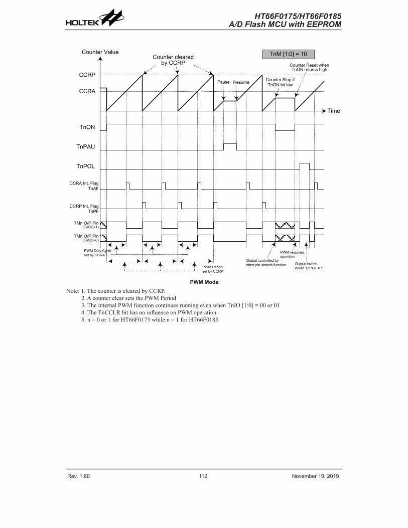
Rev. 1.60 112 November 19, 2019 Rev. 1.60 113 November 19, 2019
HT66F0175/HT66F0185A/D Flash MCU with EEPROM
HT66F0175/HT66F0185A/D Flash MCU with EEPROM
Counter Value
CCRP
CCRA
TnON
TnPAU
TnPOL
CCRP Int. Flag TnPF
CCRA Int. Flag TnAF
TMn O/P Pin(TnOC=1)
Time
Counter cleared by CCRP
Pause Resume Counter Stop if TnON bit low
Counter Reset when TnON returns high
TnM [1:0] = 10
PWM Duty Cycle set by CCRA
PWM resumes operation
Output controlled by other pin-shared function Output Inverts
When TnPOL = 1PWM Period set by CCRP
TMn O/P Pin(TnOC=0)
PWM ModeNote: 1. The counter is cleared by CCRP.
2. A counter clear sets the PWM Period3. The internal PWM function continues running even when TnIO [1:0] = 00 or 014. The TnCCLR bit has no influence on PWM operation5. n = 0 or 1 for HT66F0175 while n = 1 for HT66F0185
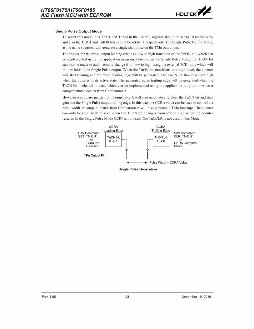
Rev. 1.60 112 November 19, 2019 Rev. 1.60 113 November 19, 2019
HT66F0175/HT66F0185A/D Flash MCU with EEPROM
HT66F0175/HT66F0185A/D Flash MCU with EEPROM
Single Pulse Output ModeTo select this mode, bits TnM1 and TnM0 in the TMnC1 register should be set to 10 respectively and also the TnIO1 and TnIO0 bits should be set to 11 respectively. The Single Pulse Output Mode, as the name suggests, will generate a single shot pulse on the TMn output pin.
The trigger for the pulse output leading edge is a low to high transition of the TnON bit, which can be implemented using the application program. However in the Single Pulse Mode, the TnON bit can also be made to automatically change from low to high using the external TCKn pin, which will in turn initiate the Single Pulse output. When the TnON bit transitions to a high level, the counter will start running and the pulse leading edge will be generated. The TnON bit should remain high when the pulse is in its active state. The generated pulse trailing edge will be generated when the TnON bit is cleared to zero, which can be implemented using the application program or when a compare match occurs from Comparator A.
However a compare match from Comparator A will also automatically clear the TnON bit and thus generate the Single Pulse output trailing edge. In this way the CCRA value can be used to control the pulse width. A compare match from Comparator A will also generate a TMn interrupt. The counter can only be reset back to zero when the TnON bit changes from low to high when the counter restarts. In the Single Pulse Mode CCRP is not used. The TnCCLR is not used in this Mode.
TnON bit0 à 1
S/W Command SET“TnON”
orTCKn Pin Transition
TnON bit1 à 0
CCRA Trailing Edge
S/W Command CLR“TnON”
orCCRA Compare Match
TPn Output Pin
Pulse Width = CCRA Value
CCRA Leading Edge
Single Pulse Generation
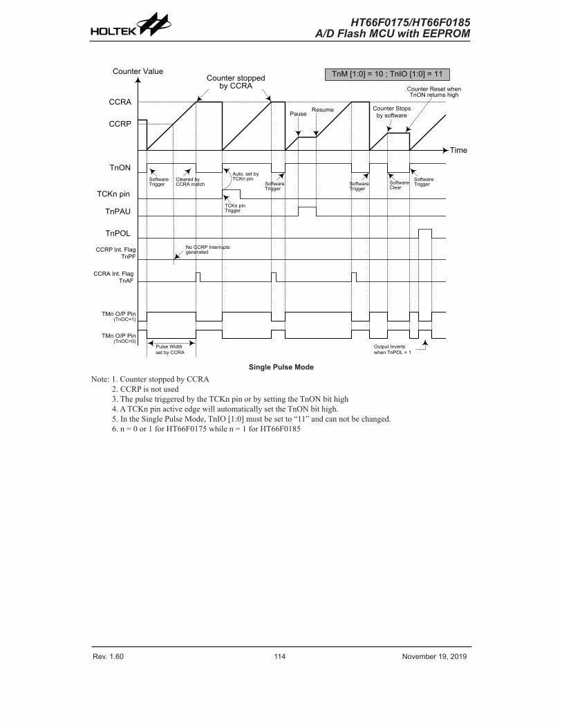
Rev. 1.60 114 November 19, 2019 Rev. 1.60 115 November 19, 2019
HT66F0175/HT66F0185A/D Flash MCU with EEPROM
HT66F0175/HT66F0185A/D Flash MCU with EEPROM
Counter Value
CCRP
CCRA
TnON
TnPAU
TnPOL
CCRP Int. Flag TnPF
CCRA Int. Flag TnAF
TMn O/P Pin(TnOC=1)
Time
Counter stopped by CCRA
PauseResume Counter Stops
by software
Counter Reset when TnON returns high
TnM [1:0] = 10 ; TnIO [1:0] = 11
Pulse Width set by CCRA
Output Invertswhen TnPOL = 1
No CCRP Interrupts generated
TMn O/P Pin(TnOC=0)
TCKn pin
Software Trigger
Cleared by CCRA match
TCKn pin Trigger
Auto. set by TCKn pin
Software Trigger
Software Clear
Software TriggerSoftware
Trigger
Single Pulse ModeNote: 1. Counter stopped by CCRA
2. CCRP is not used3. The pulse triggered by the TCKn pin or by setting the TnON bit high4. A TCKn pin active edge will automatically set the TnON bit high.5. In the Single Pulse Mode, TnIO [1:0] must be set to “11” and can not be changed.6. n = 0 or 1 for HT66F0175 while n = 1 for HT66F0185
Rev. 1.60 114 November 19, 2019 Rev. 1.60 115 November 19, 2019
HT66F0175/HT66F0185A/D Flash MCU with EEPROM
HT66F0175/HT66F0185A/D Flash MCU with EEPROM
Capture Input ModeTo select this mode bits TnM1 and TnM0 in the TMnC1 register should be set to 01 respectively. This mode enables external signals to capture and store the present value of the internal counter and can therefore be used for applications such as pulse width measurements. The external signal is supplied on the TPn or TCKn pin, selected by the TnCAPTS bit in the TMnC1 register. The input pin active edge can be either a rising edge, a falling edge or both rising and falling edges; the active edge transition type is selected using the TnIO1 and TnIO0 bits in the TMnC1 register. The counter is started when the TnON bit changes from low to high which is initiated using the application program.
When the required edge transition appears on the TPn or TCKn pin the present value in the counter will be latched into the CCRA registers and a TMn interrupt generated. Irrespective of what events occur on the TPn or TCKn pin the counter will continue to free run until the TnON bit changes from high to low. When a CCRP compare match occurs the counter will reset back to zero; in this way the CCRP value can be used to control the maximum counter value. When a CCRP compare match occurs from Comparator P, a TMn interrupt will also be generated. Counting the number of overflow interrupt signals from the CCRP can be a useful method in measuring long pulse widths. The TnIO1 and TnIO0 bits can select the active trigger edge on the TPn or TCKn pin to be a rising edge, falling edge or both edge types. If the TnIO1 and TnIO0 bits are both set high, then no capture operation will take place irrespective of what happens on the TPn or TCKn pin, however it must be noted that the counter will continue to run.
As the TPn or TCKn pin is pin shared with other functions, care must be taken if the TMn is in the Input Capture Mode. This is because if the pin is setup as an output, then any transitions on this pin may cause an input capture operation to be executed. The TnCCLR, TnOC and TnPOL bits are not used in this Mode.
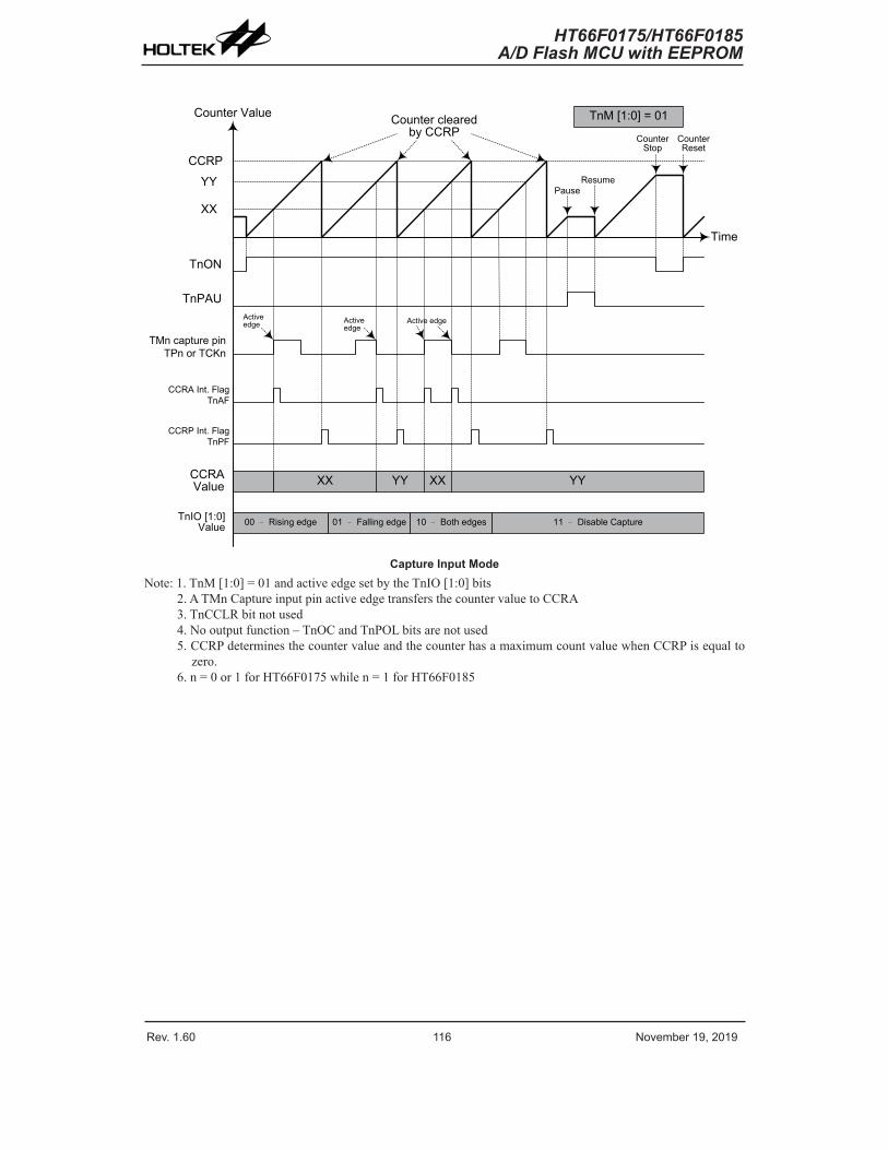
Rev. 1.60 116 November 19, 2019 Rev. 1.60 117 November 19, 2019
HT66F0175/HT66F0185A/D Flash MCU with EEPROM
HT66F0175/HT66F0185A/D Flash MCU with EEPROM
Counter Value
YYCCRP
TnON
TnPAU
CCRP Int. Flag TnPF
CCRA Int. Flag TnAF
CCRA Value
Time
Counter cleared by CCRP
PauseResume
Counter Reset
TnM [1:0] = 01
TMn capture pinTPn or TCKn
XX
Counter Stop
TnIO [1:0] Value
XX YY XX YY
Active edge Active
edgeActive edge
00 – Rising edge 01 – Falling edge 10 – Both edges 11 – Disable Capture
Capture Input ModeNote: 1. TnM [1:0] = 01 and active edge set by the TnIO [1:0] bits
2. A TMn Capture input pin active edge transfers the counter value to CCRA3. TnCCLR bit not used4. No output function – TnOC and TnPOL bits are not used5. CCRP determines the counter value and the counter has a maximum count value when CCRP is equal to
zero.6. n = 0 or 1 for HT66F0175 while n = 1 for HT66F0185
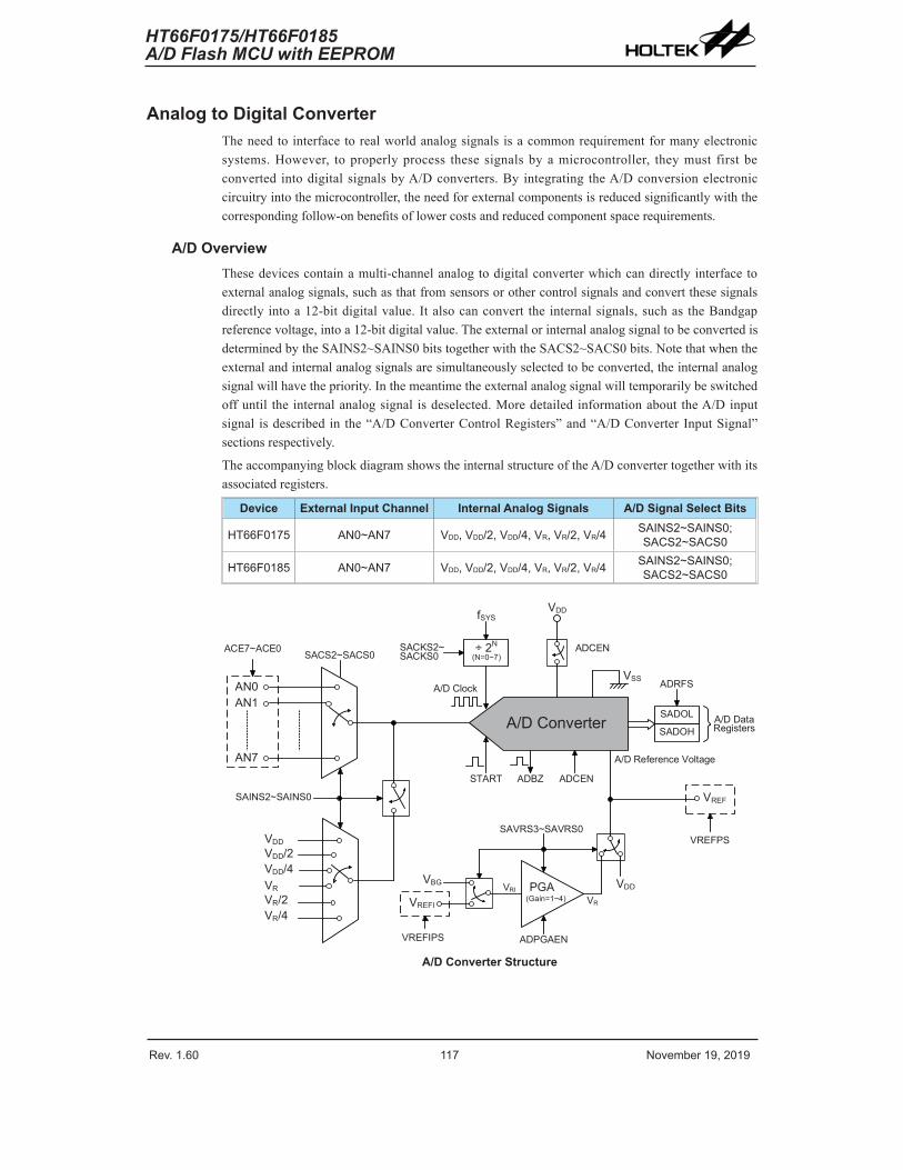
Rev. 1.60 116 November 19, 2019 Rev. 1.60 117 November 19, 2019
HT66F0175/HT66F0185A/D Flash MCU with EEPROM
HT66F0175/HT66F0185A/D Flash MCU with EEPROM
Analog to Digital ConverterThe need to interface to real world analog signals is a common requirement for many electronic systems. However, to properly process these signals by a microcontroller, they must first be converted into digital signals by A/D converters. By integrating the A/D conversion electronic circuitry into the microcontroller, the need for external components is reduced significantly with the corresponding follow-on benefits of lower costs and reduced component space requirements.
A/D OverviewThese devices contain a multi-channel analog to digital converter which can directly interface to external analog signals, such as that from sensors or other control signals and convert these signals directly into a 12-bit digital value. It also can convert the internal signals, such as the Bandgap reference voltage, into a 12-bit digital value. The external or internal analog signal to be converted is determined by the SAINS2~SAINS0 bits together with the SACS2~SACS0 bits. Note that when the external and internal analog signals are simultaneously selected to be converted, the internal analog signal will have the priority. In the meantime the external analog signal will temporarily be switched off until the internal analog signal is deselected. More detailed information about the A/D input signal is described in the “A/D Converter Control Registers” and “A/D Converter Input Signal” sections respectively.
The accompanying block diagram shows the internal structure of the A/D converter together with its associated registers.
Device External Input Channel Internal Analog Signals A/D Signal Select Bits
HT66F0175 AN0~AN7 VDD, VDD/2, VDD/4, VR, VR/2, VR/4 SAINS2~SAINS0; SACS2~SACS0
HT66F0185 AN0~AN7 VDD, VDD/2, VDD/4, VR, VR/2, VR/4 SAINS2~SAINS0; SACS2~SACS0
ACE7~ACE0 SACS2~SACS0
SAINS2~SAINS0
A/D Converter
START ADBZ ADCEN
VSSA/D Clock
÷ 2N
(N=0~7)
fSYS
SACKS2~SACKS0
VDD
ADCEN
SADOL
SADOH
AN0AN1
AN7 A/D Reference Voltage
A/D DataRegisters
VDDVDD/2VDD/4VRVR/2VR/4
ADRFS
PGAVRI
VREFI
VBG
(Gain=1~4)
SAVRS3~SAVRS0
ADPGAEN
VREF
VR
VDD
VREFPS
VREFIPS
A/D Converter Structure
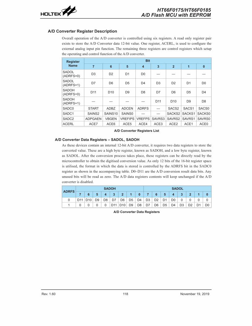
Rev. 1.60 118 November 19, 2019 Rev. 1.60 119 November 19, 2019
HT66F0175/HT66F0185A/D Flash MCU with EEPROM
HT66F0175/HT66F0185A/D Flash MCU with EEPROM
A/D Converter Register DescriptionOverall operation of the A/D converter is controlled using six registers. A read only register pair exists to store the A/D Converter data 12-bit value. One register, ACERL, is used to configure the external analog input pin function. The remaining three registers are control registers which setup the operating and control function of the A/D converter.
Register Name
Bit7 6 5 4 3 2 1 0
SADOL (ADRFS=0) D3 D2 D1 D0 — — — —
SADOL (ADRFS=1) D7 D6 D5 D4 D3 D2 D1 D0
SADOH (ADRFS=0) D11 D10 D9 D8 D7 D6 D5 D4
SADOH (ADRFS=1) — — — — D11 D10 D9 D8
SADC0 START ADBZ ADCEN ADRFS — SACS2 SACS1 SACS0SADC1 SAINS2 SAINS10 SAINS0 — — SACKS2 SACKS1 SACKS0SADC2 ADPGAEN VBGEN VREFIPS VREFPS SAVRS3 SAVRS2 SAVRS1 SAVRS0ACERL ACE7 ACE6 ACE5 ACE4 ACE3 ACE2 ACE1 ACE0
A/D Converter Registers List
A/D Converter Data Registers – SADOL, SADOHAs these devices contain an internal 12-bit A/D converter, it requires two data registers to store the converted value. These are a high byte register, known as SADOH, and a low byte register, known as SADOL. After the conversion process takes place, these registers can be directly read by the microcontroller to obtain the digitised conversion value. As only 12 bits of the 16-bit register space is utilised, the format in which the data is stored is controlled by the ADRFS bit in the SADC0 register as shown in the accompanying table. D0~D11 are the A/D conversion result data bits. Any unused bits will be read as zero. The A/D data registers contents will keep unchanged if the A/D converter is disabled.
ADRFSSADOH SADOL
7 6 5 4 3 2 1 0 7 6 5 4 3 2 1 00 D11 D10 D9 D8 D7 D6 D5 D4 D3 D2 D1 D0 0 0 0 01 0 0 0 0 D11 D10 D9 D8 D7 D6 D5 D4 D3 D2 D1 D0
A/D Converter Data Registers
Rev. 1.60 118 November 19, 2019 Rev. 1.60 119 November 19, 2019
HT66F0175/HT66F0185A/D Flash MCU with EEPROM
HT66F0175/HT66F0185A/D Flash MCU with EEPROM
A/D Converter Control Registers – SADC0, SADC1, SADC2, ACERLTo control the function and operation of the A/D converter, three control registers known as SADC0, SADC1 and SADC2 are provided. These 8-bit registers define functions such as the selection of which analog channel is connected to the internal A/D converter, the digitised data format, the A/D clock source as well as controlling the start function and monitoring the A/D converter busy status. As these devices contain only one actual analog to digital converter hardware circuit, each of the external and internal analog signals must be routed to the converter. The SACS2~SACS0 bits in the SADC0 register are used to determine which external channel input is selected to be converted. The SAINS2~SAINS0 bits in the SADC1 register are used to determine that the analog signal to be converted comes from the internal analog signal or external analog channel input. If the SAINS2~SAINS0 bits are set to “000” or “100”, the external analog channel input will be selected to be converted and the SACS2~SACS0 bits can deternine which external channel is selected to be converted. If the SAINS2~SAINS0 bits are set to any other values except “000” and “100”, one of the internal analog signals can be selected to be converted. The internal analog signals can be derived from the A/D converter supply power, VDD, or internal reference voltage, VR, with a specific ratio of 1, 1/2 or 1/4. If the internal analog signal is selected to be converted, the external channel signal input will automatically be switched off to avoid the signal contention.
SAINS [2:0] SACS [2:0] Input Signals Description000, 100 000~111 AN0~AN7 External channel analog input
001 xxx VDD A/D converter power supply voltage010 xxx VDD/2 A/D converter power supply voltage/2011 xxx VDD/4 A/D converter power supply voltage/4101 xxx VR Internal reference voltage110 xxx VR/2 Internal reference voltage/2111 xxx VR/4 Internal reference voltage/4
A/D Converter Input Signal Selection
The analog input pin function selection bits in the ACERL register determine which pins on I/O Ports are used as external analog channels for the A/D converter input and which pins are not to be used as the A/D converter input. When the pin is selected to be an A/D input, its original function whether it is an I/O or other pin-shared functions will be removed. In addition, any internal pull-high resistor connected to the pin will be automatically removed if the pin is selected to be an A/D converter input.
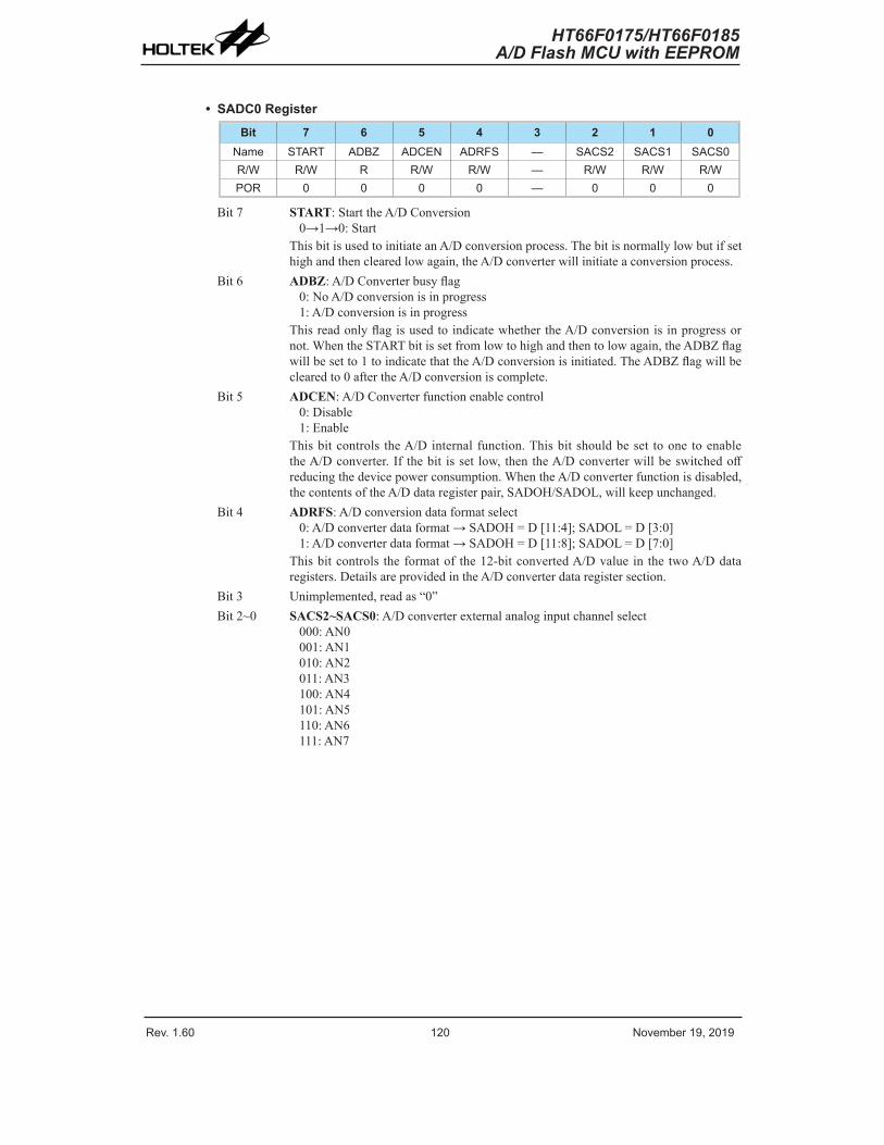
Rev. 1.60 120 November 19, 2019 Rev. 1.60 121 November 19, 2019
HT66F0175/HT66F0185A/D Flash MCU with EEPROM
HT66F0175/HT66F0185A/D Flash MCU with EEPROM
• SADC0 RegisterBit 7 6 5 4 3 2 1 0
Name START ADBZ ADCEN ADRFS — SACS2 SACS1 SACS0R/W R/W R R/W R/W — R/W R/W R/WPOR 0 0 0 0 — 0 0 0
Bit 7 START: Start the A/D Conversion0→1→0: Start
This bit is used to initiate an A/D conversion process. The bit is normally low but if set high and then cleared low again, the A/D converter will initiate a conversion process.
Bit 6 ADBZ: A/D Converter busy flag0: No A/D conversion is in progress1: A/D conversion is in progress
This read only flag is used to indicate whether the A/D conversion is in progress or not. When the START bit is set from low to high and then to low again, the ADBZ flag will be set to 1 to indicate that the A/D conversion is initiated. The ADBZ flag will be cleared to 0 after the A/D conversion is complete.
Bit 5 ADCEN: A/D Converter function enable control0: Disable1: Enable
This bit controls the A/D internal function. This bit should be set to one to enable the A/D converter. If the bit is set low, then the A/D converter will be switched off reducing the device power consumption. When the A/D converter function is disabled, the contents of the A/D data register pair, SADOH/SADOL, will keep unchanged.
Bit 4 ADRFS: A/D conversion data format select0: A/D converter data format → SADOH = D [11:4]; SADOL = D [3:0]1: A/D converter data format → SADOH = D [11:8]; SADOL = D [7:0]
This bit controls the format of the 12-bit converted A/D value in the two A/D data registers. Details are provided in the A/D converter data register section.
Bit 3 Unimplemented, read as “0”Bit 2~0 SACS2~SACS0: A/D converter external analog input channel select
000: AN0001: AN1010: AN2011: AN3100: AN4101: AN5110: AN6111: AN7
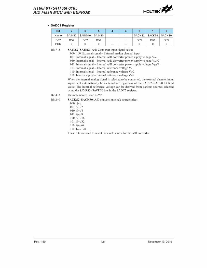
Rev. 1.60 120 November 19, 2019 Rev. 1.60 121 November 19, 2019
HT66F0175/HT66F0185A/D Flash MCU with EEPROM
HT66F0175/HT66F0185A/D Flash MCU with EEPROM
• SADC1 RegisterBit 7 6 5 4 3 2 1 0
Name SAINS2 SAINS10 SAINS0 — — SACKS2 SACKS1 SACKS0R/W R/W R/W R/W — — R/W R/W R/WPOR 0 0 0 — — 0 0 0
Bit 7~5 SAINS2~SAINS0: A/D Converter input signal select000, 100: External signal – External analog channel input001: Internal signal – Internal A/D converter power supply voltage VDD
010: Internal signal – Internal A/D converter power supply voltage VDD/2011: Internal signal – Internal A/D converter power supply voltage VDD/4101: Internal signal – Internal reference voltage VR
110: Internal signal – Internal reference voltage VR/2111: Internal signal – Internal reference voltage VR/4
When the internal analog signal is selected to be converted, the external channel input signal will automatically be switched off regardless of the SACS2~SACS0 bit field value. The internal reference voltage can be derived from various sources selected using the SAVRS3~SAVRS0 bits in the SADC2 register.
Bit 4~3 Unimplemented, read as “0”Bit 2~0 SACKS2~SACKS0: A/D conversion clock source select
000: fSYS
001: fSYS/2010: fSYS/4011: fSYS/8100: fSYS/16101: fSYS/32110: fSYS/64111: fSYS/128
These bits are used to select the clock source for the A/D converter.
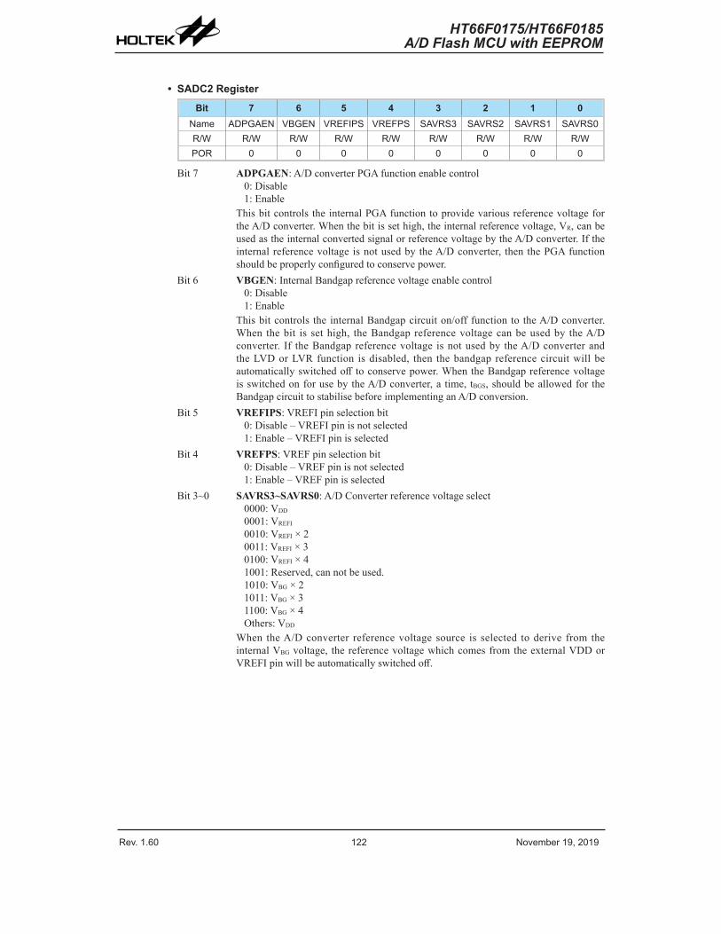
Rev. 1.60 122 November 19, 2019 Rev. 1.60 123 November 19, 2019
HT66F0175/HT66F0185A/D Flash MCU with EEPROM
HT66F0175/HT66F0185A/D Flash MCU with EEPROM
• SADC2 RegisterBit 7 6 5 4 3 2 1 0
Name ADPGAEN VBGEN VREFIPS VREFPS SAVRS3 SAVRS2 SAVRS1 SAVRS0R/W R/W R/W R/W R/W R/W R/W R/W R/WPOR 0 0 0 0 0 0 0 0
Bit 7 ADPGAEN: A/D converter PGA function enable control0: Disable1: Enable
This bit controls the internal PGA function to provide various reference voltage for the A/D converter. When the bit is set high, the internal reference voltage, VR, can be used as the internal converted signal or reference voltage by the A/D converter. If the internal reference voltage is not used by the A/D converter, then the PGA function should be properly configured to conserve power.
Bit 6 VBGEN: Internal Bandgap reference voltage enable control0: Disable1: Enable
This bit controls the internal Bandgap circuit on/off function to the A/D converter. When the bit is set high, the Bandgap reference voltage can be used by the A/D converter. If the Bandgap reference voltage is not used by the A/D converter and the LVD or LVR function is disabled, then the bandgap reference circuit will be automatically switched off to conserve power. When the Bandgap reference voltage is switched on for use by the A/D converter, a time, tBGS, should be allowed for the Bandgap circuit to stabilise before implementing an A/D conversion.
Bit 5 VREFIPS: VREFI pin selection bit0: Disable – VREFI pin is not selected1: Enable – VREFI pin is selected
Bit 4 VREFPS: VREF pin selection bit0: Disable – VREF pin is not selected1: Enable – VREF pin is selected
Bit 3~0 SAVRS3~SAVRS0: A/D Converter reference voltage select0000: VDD
0001: VREFI
0010: VREFI × 20011: VREFI × 30100: VREFI × 41001: Reserved, can not be used.1010: VBG × 21011: VBG × 31100: VBG × 4Others: VDD
When the A/D converter reference voltage source is selected to derive from the internal VBG voltage, the reference voltage which comes from the external VDD or VREFI pin will be automatically switched off.
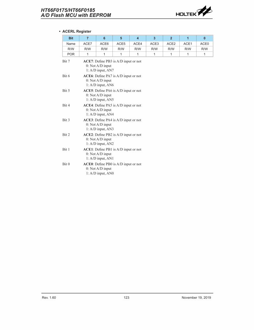
Rev. 1.60 122 November 19, 2019 Rev. 1.60 123 November 19, 2019
HT66F0175/HT66F0185A/D Flash MCU with EEPROM
HT66F0175/HT66F0185A/D Flash MCU with EEPROM
• ACERL RegisterBit 7 6 5 4 3 2 1 0
Name ACE7 ACE6 ACE5 ACE4 ACE3 ACE2 ACE1 ACE0R/W R/W R/W R/W R/W R/W R/W R/W R/WPOR 1 1 1 1 1 1 1 1
Bit 7 ACE7: Define PB3 is A/D input or not 0: Not A/D input 1: A/D input, AN7
Bit 6 ACE6: Define PA7 is A/D input or not 0: Not A/D input 1: A/D input, AN6
Bit 5 ACE5: Define PA6 is A/D input or not 0: Not A/D input 1: A/D input, AN5
Bit 4 ACE4: Define PA5 is A/D input or not 0: Not A/D input 1: A/D input, AN4
Bit 3 ACE3: Define PA4 is A/D input or not 0: Not A/D input 1: A/D input, AN3
Bit 2 ACE2: Define PB2 is A/D input or not 0: Not A/D input 1: A/D input, AN2
Bit 1 ACE1: Define PB1 is A/D input or not 0: Not A/D input 1: A/D input, AN1
Bit 0 ACE0: Define PB0 is A/D input or not 0: Not A/D input 1: A/D input, AN0
Rev. 1.60 124 November 19, 2019 Rev. 1.60 125 November 19, 2019
HT66F0175/HT66F0185A/D Flash MCU with EEPROM
HT66F0175/HT66F0185A/D Flash MCU with EEPROM
A/D Input PinsAll of the A/D analog input pins are pin-shared with the I/O pins as well as other functions. The corresponding pin-shared function selection bits in the ACERL register determine which external input pins are selected as A/D converter analog channel inputs or other functional pins. If the corresponding pin is setup to be an A/D converter analog channel input, the original pin functions will be disabled. In this way, pins can be changed under program control to change their function between A/D inputs and other functions. All pull-high resistors, which are setup through register programming, will be automatically disconnected if the pins are setup as A/D inputs. Note that it is not necessary to first setup the A/D pin as an input in the port control register to enable the A/D input as when the relevant A/D input function selection bits enable an A/D input, the status of the port control register will be overridden.
The A/D converter has its own reference voltage input pin, VREFI. However, the reference voltage can also be supplied from the power supply pin or an internal Bandgap circuit, a choice which is made through the SAVRS3~SAVRS0 bits in the SADC2 register. The selected A/D reference voltage can be output on the VREF pin. The analog input values must not be allowed to exceed the value of VREF. Note that the VREFI or VREF pin function selection bit in the SADC2 register must be properly configured before the reference voltage pin function is used.
A/D Reference VoltageThe reference voltage supply to the A/D Converter can be supplied from the positive power supply pin, VDD, an external reference source supplied on pin VREFI or an internal reference source derived from the Bandgap circuit. Then the selected reference voltage source can be amplified through a programmable gain amplifier except the voltage sourced from VDD. The PGA gain can be equal to 1, 2, 3 or 4. The desired selection is made using the SAVRS3~SAVRS0 bits in the SADC2 register and relevant pin-shared function selection bits. Note that the desired selected reference voltage will be output on the VREF pin which is pin-shared with other functions. As the VREFI and VREF pins both are pin-shared with other functions, when the VREFI or VREF pin is selected as the reference voltage supply pin, the VREFI or VREF pin-shared function selection bit should be properly configured to disable other pin-shared functions.
A/D OperationThe START bit in the SADC0 register is used to start the AD conversion. When the microcontroller sets this bit from low to high and then low again, an analog to digital conversion cycle will be initiated.
The ADBZ bit in the SADC0 register is used to indicate whether the analog to digital conversion process is in progress or not. This bit will be automatically set to 1 by the microcontroller after an A/D conversion is successfully initiated. When the A/D conversion is complete, the ADBZ will be cleared to 0. In addition, the corresponding A/D interrupt request flag will be set in the interrupt control register, and if the corresponding interrupt control bits are enabled, an internal interrupt signal will be generated. This A/D internal interrupt signal will direct the program flow to the associated A/D internal interrupt address for processing. If the A/D internal interrupt is disabled, the microcontroller can poll the ADBZ bit in the SADC0 register to check whether it has been cleared as an alternative method of detecting the end of an A/D conversion cycle.
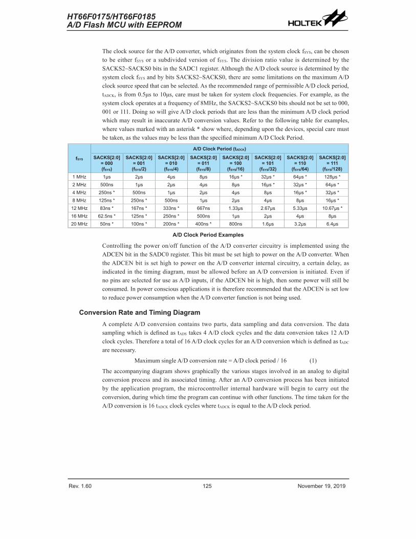
Rev. 1.60 124 November 19, 2019 Rev. 1.60 125 November 19, 2019
HT66F0175/HT66F0185A/D Flash MCU with EEPROM
HT66F0175/HT66F0185A/D Flash MCU with EEPROM
The clock source for the A/D converter, which originates from the system clock fSYS, can be chosen to be either fSYS or a subdivided version of fSYS. The division ratio value is determined by the SACKS2~SACKS0 bits in the SADC1 register. Although the A/D clock source is determined by the system clock fSYS and by bits SACKS2~SACKS0, there are some limitations on the maximum A/D clock source speed that can be selected. As the recommended range of permissible A/D clock period, tADCK, is from 0.5μs to 10μs, care must be taken for system clock frequencies. For example, as the system clock operates at a frequency of 8MHz, the SACKS2~SACKS0 bits should not be set to 000, 001 or 111. Doing so will give A/D clock periods that are less than the minimum A/D clock period which may result in inaccurate A/D conversion values. Refer to the following table for examples, where values marked with an asterisk * show where, depending upon the devices, special care must be taken, as the values may be less than the specified minimum A/D Clock Period.
fSYS
A/D Clock Period (tADCK)
SACKS[2:0]= 000(fSYS)
SACKS[2:0]= 001(fSYS/2)
SACKS[2:0]= 010(fSYS/4)
SACKS[2:0]= 011
(fSYS/8)
SACKS[2:0]= 100
(fSYS/16)
SACKS[2:0]= 101
(fSYS/32)
SACKS[2:0]= 110
(fSYS/64)
SACKS[2:0]= 111
(fSYS/128)1 MHz 1μs 2μs 4μs 8μs 16μs * 32μs * 64μs * 128μs *2 MHz 500ns 1μs 2μs 4μs 8μs 16μs * 32μs * 64μs *4 MHz 250ns * 500ns 1μs 2μs 4μs 8μs 16μs * 32μs *8 MHz 125ns * 250ns * 500ns 1μs 2μs 4μs 8μs 16μs *
12 MHz 83ns * 167ns * 333ns * 667ns 1.33μs 2.67μs 5.33μs 10.67μs *16 MHz 62.5ns * 125ns * 250ns * 500ns 1μs 2μs 4μs 8μs20 MHz 50ns * 100ns * 200ns * 400ns * 800ns 1.6μs 3.2μs 6.4μs
A/D Clock Period Examples
Controlling the power on/off function of the A/D converter circuitry is implemented using the ADCEN bit in the SADC0 register. This bit must be set high to power on the A/D converter. When the ADCEN bit is set high to power on the A/D converter internal circuitry, a certain delay, as indicated in the timing diagram, must be allowed before an A/D conversion is initiated. Even if no pins are selected for use as A/D inputs, if the ADCEN bit is high, then some power will still be consumed. In power conscious applications it is therefore recommended that the ADCEN is set low to reduce power consumption when the A/D converter function is not being used.
Conversion Rate and Timing DiagramA complete A/D conversion contains two parts, data sampling and data conversion. The data sampling which is defined as tADS takes 4 A/D clock cycles and the data conversion takes 12 A/D clock cycles. Therefore a total of 16 A/D clock cycles for an A/D conversion which is defined as tADC are necessary.
Maximum single A/D conversion rate = A/D clock period / 16 (1)
The accompanying diagram shows graphically the various stages involved in an analog to digital conversion process and its associated timing. After an A/D conversion process has been initiated by the application program, the microcontroller internal hardware will begin to carry out the conversion, during which time the program can continue with other functions. The time taken for the A/D conversion is 16 tADCK clock cycles where tADCK is equal to the A/D clock period.
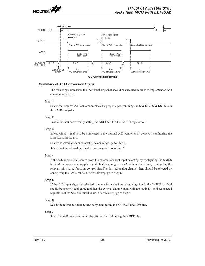
Rev. 1.60 126 November 19, 2019 Rev. 1.60 127 November 19, 2019
HT66F0175/HT66F0185A/D Flash MCU with EEPROM
HT66F0175/HT66F0185A/D Flash MCU with EEPROM
ADCEN
START
ADBZ
SACS[2:0]
off on off on
tON2ST
tADS
A/D sampling timetADS
A/D sampling time
Start of A/D conversion Start of A/D conversion Start of A/D conversion
End of A/D conversion
End of A/D conversion
tADC
A/D conversion timetADC
A/D conversion timetADC
A/D conversion time
011B 010B 000B 001B
A/D channel switch
(SAINS =000B)
A/D Conversion Timing
Summary of A/D Conversion StepsThe following summarises the individual steps that should be executed in order to implement an A/D conversion process.
Step 1Select the required A/D conversion clock by properly programming the SACKS2~SACKS0 bits in the SADC1 register.
Step 2Enable the A/D converter by setting the ADCEN bit in the SADC0 register to 1.
Step 3Select which signal is to be connected to the internal A/D converter by correctly configuring the SAINS2~SAINS0 bits
Select the external channel input to be converted, go to Step 4.
Select the internal analog signal to be converted, go to Step 5.
Step 4If the A/D input signal comes from the external channel input selecting by configuring the SAINS bit field, the corresponding pins should first be configured as A/D input function by configuring the relevant pin-shared function control bits. The desired analog channel then should be selected by configuring the SACS bit field. After this step, go to Step 6.
Step 5If the A/D input signal is selected to come from the internal analog signal, the SAINS bit field should be properly configured and then the external channel input will automatically be disconnected regardless of the SACS bit field value. After this step, go to Step 6.
Step 6Select the reference voltgage source by configuring the SAVRS3~SAVRS0 bits.
Step 7Select the A/D converter output data format by configuring the ADRFS bit.
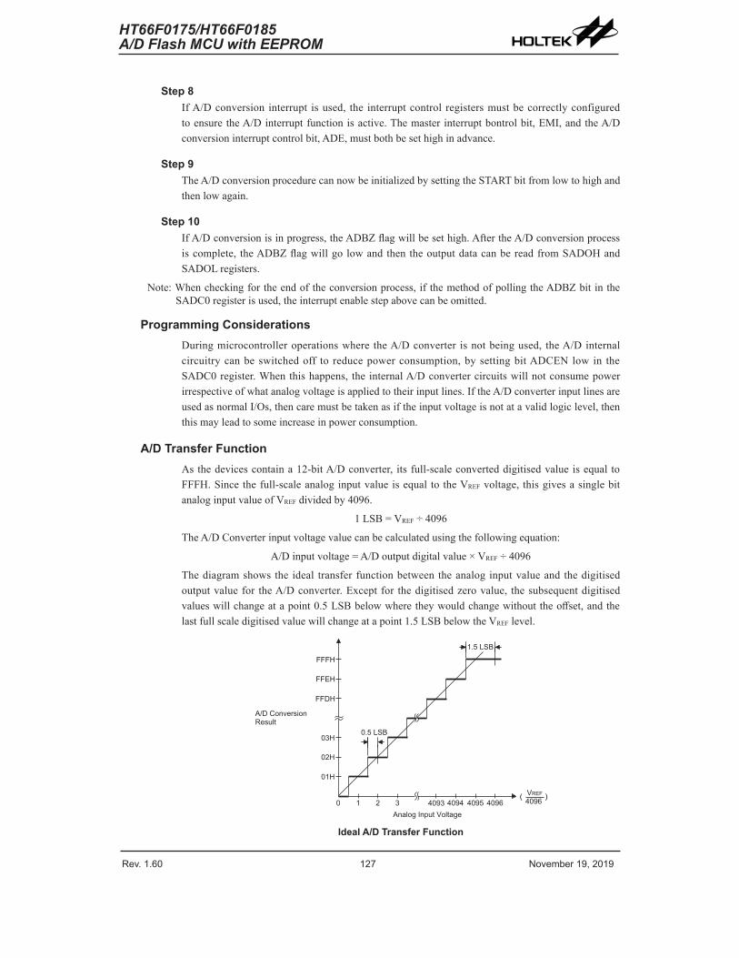
Rev. 1.60 126 November 19, 2019 Rev. 1.60 127 November 19, 2019
HT66F0175/HT66F0185A/D Flash MCU with EEPROM
HT66F0175/HT66F0185A/D Flash MCU with EEPROM
Step 8If A/D conversion interrupt is used, the interrupt control registers must be correctly configured to ensure the A/D interrupt function is active. The master interrupt bontrol bit, EMI, and the A/D conversion interrupt control bit, ADE, must both be set high in advance.
Step 9The A/D conversion procedure can now be initialized by setting the START bit from low to high and then low again.
Step 10If A/D conversion is in progress, the ADBZ flag will be set high. After the A/D conversion process is complete, the ADBZ flag will go low and then the output data can be read from SADOH and SADOL registers.
Note: When checking for the end of the conversion process, if the method of polling the ADBZ bit in the SADC0 register is used, the interrupt enable step above can be omitted.
Programming ConsiderationsDuring microcontroller operations where the A/D converter is not being used, the A/D internal circuitry can be switched off to reduce power consumption, by setting bit ADCEN low in the SADC0 register. When this happens, the internal A/D converter circuits will not consume power irrespective of what analog voltage is applied to their input lines. If the A/D converter input lines are used as normal I/Os, then care must be taken as if the input voltage is not at a valid logic level, then this may lead to some increase in power consumption.
A/D Transfer FunctionAs the devices contain a 12-bit A/D converter, its full-scale converted digitised value is equal to FFFH. Since the full-scale analog input value is equal to the VREF voltage, this gives a single bit analog input value of VREF divided by 4096.
1 LSB = VREF ÷ 4096
The A/D Converter input voltage value can be calculated using the following equation:
A/D input voltage = A/D output digital value × VREF ÷ 4096
The diagram shows the ideal transfer function between the analog input value and the digitised output value for the A/D converter. Except for the digitised zero value, the subsequent digitised values will change at a point 0.5 LSB below where they would change without the offset, and the last full scale digitised value will change at a point 1.5 LSB below the VREF level.
� � � �
� � � � � � � � � � � �
� � � � � � � � � � � � � �� � � � �
� � � �
� � � �
�
� �
� �
� � � � � �
� � � � � � � � � � � � �� � � � � � � � � � � � � � � � � �
� � � � � � �
� � � �� � �
Ideal A/D Transfer Function
Rev. 1.60 128 November 19, 2019 Rev. 1.60 129 November 19, 2019
HT66F0175/HT66F0185A/D Flash MCU with EEPROM
HT66F0175/HT66F0185A/D Flash MCU with EEPROM
A/D Programming ExamplesThe following two programming examples illustrate how to setup and implement an A/D conversion. In the first example, the method of polling the ADBZ bit in the SADC0 register is used to detect when the conversion cycle is complete, whereas in the second example, the A/D interrupt is used to determine when the conversion is complete.
Example: using an ADBZ polling method to detect the end of conversionclr ADE ; disable ADC interruptmov a,03Hmov SADC1,a ; select fSYS/8 as A/D clock and switch off VBG voltageset ADCENmov a,03H ; setup ACERL to configure pin AN0mov ACERL,amov a,00Hmov SADC0,a ; enable and connect AN0 channel to A/D converter:start_conversion:clr START ; high pulse on start bit to initiate conversionset START ; reset A/Dclr START ; start A/D:polling_EOC:sz ADBZ ; poll the SADC0 register ADBZ bit to detect end of A/D conversionjmp polling_EOC ; continue polling:mov a,SADOL ; read low byte conversion result valuemov SADOL_buffer,a ; save result to user defined registermov a,SADOH ; read high byte conversion result valuemov SADOH_buffer,a ; save result to user defined register:jmp start_conversion ; start next A/D conversion
Rev. 1.60 128 November 19, 2019 Rev. 1.60 129 November 19, 2019
HT66F0175/HT66F0185A/D Flash MCU with EEPROM
HT66F0175/HT66F0185A/D Flash MCU with EEPROM
Example: using the interrupt method to detect the end of conversionclr ADE ; disable ADC interruptmov a,03Hmov SADC1,a ; select fSYS/8 as A/D clock and switch off VBG voltageset ADCENmov a,03h ; setup ACERL to configure pin AN0mov ACERL,amov a,00hmov SADC0,a ; enable and connect AN0 channel to A/D converter:Start_conversion:clr START ; high pulse on START bit to initiate conversionset START ; reset A/Dclr START ; start A/Dclr ADF ; clear ADC interrupt request flagset ADE ; enable ADC interruptset EMI ; enable global interrupt::ADC_ISR: ; ADC interrupt service routinemov acc_stack,a ; save ACC to user defined memorymov a,STATUSmov status_stack,a ; save STATUS to user defined memory:mov a, SADOL ; read low byte conversion result valuemov SADOL_buffer,a ; save result to user defined registermov a, SADOH ; read high byte conversion result valuemov SADOH_buffer,a ; save result to user defined register:EXIT_INT_ISR:mov a,status_stackmov STATUS,a ; restore STATUS from user defined memorymov a,acc_stack ; restore ACC from user defined memoryreti
Rev. 1.60 130 November 19, 2019 Rev. 1.60 131 November 19, 2019
HT66F0175/HT66F0185A/D Flash MCU with EEPROM
HT66F0175/HT66F0185A/D Flash MCU with EEPROM
Serial Interface Module – SIMThese devices contain a Serial Interface Module, which includes both the four-line SPI interface or two-line I2C interface types, to allow an easy method of communication with external peripheral hardware. Having relatively simple communication protocols, these serial interface types allow the microcontroller to interface to external SPI or I2C based hardware such as sensors, Flash or EEPROM memory, etc. The SIM interface pins are pin-shared with other I/O pins and therefore the SIM interface functional pins must first be selected using the corresponding pin-shared function selection bits. As both interface types share the same pins and registers, the choice of whether the SPI or I2C type is used is made using the SIM operating mode control bits, named SIM2~SIM0, in the SIMC0 register. These pull-high resistors of the SIM pin-shared I/O pins are selected using pull-high control registers when the SIM function is enabled and the corresponding pins are used as SIM input pins.
SPI InterfaceThe SPI interface is often used to communicate with external peripheral devices such as sensors, Flash or EEPROM memory devices, etc. Originally developed by Motorola, the four line SPI interface is a synchronous serial data interface that has a relatively simple communication protocol simplifying the programming requirements when communicating with external hardware devices.
The communication is full duplex and operates as a slave/master type, where the devices can be either master or slave. Although the SPI interface specification can control multiple slave devices from a single master, these devices provided only one SCS pin. If the master needs to control multiple slave devices from a single master, the master can use I/O pin to select the slave devices.
SPI Interface OperationThe SPI interface is a full duplex synchronous serial data link. It is a four line interface with pin names SDI, SDO, SCK and SCS. Pins SDI and SDO are the Serial Data Input and Serial Data Output lines, SCK is the Serial Clock line and SCS is the Slave Select line. As the SPI interface pins are pin-shared with normal I/O pins and with the I2C function pins, the SPI interface pins must first be selected by configuring the pin-shared function selection bits and setting the correct bits in the SIMC0 and SIMC2 registers. After the desired SPI configuration has been set it can be disabled or enabled using the SIMEN bit in the SIMC0 register. Communication between devices connected to the SPI interface is carried out in a slave/master mode with all data transfer initiations being implemented by the master. The Master also controls the clock signal. As the devices only contain a single SCS pin only one slave device can be utilized. The SCS pin is controlled by software, set CSEN bit to 1 to enable SCS pin function, set CSEN bit to 0 the SCS pin will be floating state.
The SPI function in these devices offer the following features:
• Full duplex synchronous data transfer
• Both Master and Slave modes
• LSB first or MSB first data transmission modes
• Transmission complete flag
• Rising or falling active clock edge
The status of the SPI interface pins is determined by a number of factors such as whether the devices are in the master or slave mode and upon the condition of certain control bits such as CSEN and SIMEN.
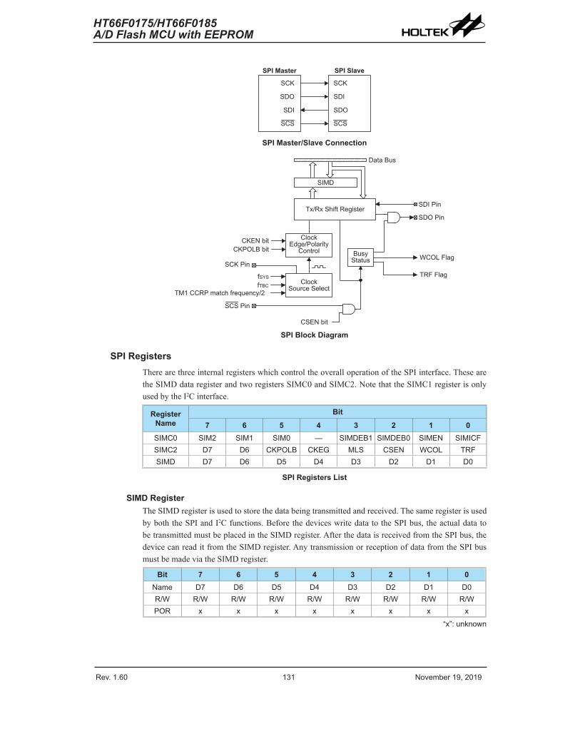
Rev. 1.60 130 November 19, 2019 Rev. 1.60 131 November 19, 2019
HT66F0175/HT66F0185A/D Flash MCU with EEPROM
HT66F0175/HT66F0185A/D Flash MCU with EEPROM
� � � � � � � � � � � � � � � � � � �
� � �
� � �
� � �
� � �
� � �
� � �
� � �
� � �
SPI Master/Slave Connection
� � � � � � � �
� � � � � � �
� � � � � � �
� � � �
� � � � � � � � � � � � � � � � �
� � � �� � � � � �
� � � � � � �
� � � � � � � �
� � � � �� � � � � � � � � � �
� � � � � �
� � � � �� � � � � � � � � � � �
� � � �� � � �
� � � � � � � � � � � � � � � � � � � � � �
� � � � � � �
� � � � � � �
� � � � � � � �
� � � � � � � �� � � � � � � � � �
SPI Block Diagram
SPI RegistersThere are three internal registers which control the overall operation of the SPI interface. These are the SIMD data register and two registers SIMC0 and SIMC2. Note that the SIMC1 register is only used by the I2C interface.
Register Name
Bit7 6 5 4 3 2 1 0
SIMC0 SIM2 SIM1 SIM0 — SIMDEB1 SIMDEB0 SIMEN SIMICFSIMC2 D7 D6 CKPOLB CKEG MLS CSEN WCOL TRFSIMD D7 D6 D5 D4 D3 D2 D1 D0
SPI Registers List
SIMD RegisterThe SIMD register is used to store the data being transmitted and received. The same register is used by both the SPI and I2C functions. Before the devices write data to the SPI bus, the actual data to be transmitted must be placed in the SIMD register. After the data is received from the SPI bus, the device can read it from the SIMD register. Any transmission or reception of data from the SPI bus must be made via the SIMD register.
Bit 7 6 5 4 3 2 1 0Name D7 D6 D5 D4 D3 D2 D1 D0R/W R/W R/W R/W R/W R/W R/W R/W R/WPOR x x x x x x x x
“x”: unknown
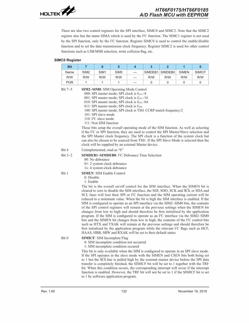
Rev. 1.60 132 November 19, 2019 Rev. 1.60 133 November 19, 2019
HT66F0175/HT66F0185A/D Flash MCU with EEPROM
HT66F0175/HT66F0185A/D Flash MCU with EEPROM
There are also two control registers for the SPI interface, SIMC0 and SIMC2. Note that the SIMC2 register also has the name SIMA which is used by the I2C function. The SIMC1 register is not used by the SPI function, only by the I2C function. Register SIMC0 is used to control the enable/disable function and to set the data transmission clock frequency. Register SIMC2 is used for other control functions such as LSB/MSB selection, write collision flag, etc.
SIMC0 RegisterBit 7 6 5 4 3 2 1 0
Name SIM2 SIM1 SIM0 — SIMDEB1 SIMDEB0 SIMEN SIMICFR/W R/W R/W R/W — R/W R/W R/W R/WPOR 1 1 1 — 0 0 0 0
Bit 7~5 SIM2~SIM0: SIM Operating Mode Control000: SPI master mode; SPI clock is fSYS /4001: SPI master mode; SPI clock is fSYS /16010: SPI master mode; SPI clock is fSYS /64011: SPI master mode; SPI clock is fTBC
100: SPI master mode; SPI clock is TM1 CCRP match frequency/2101: SPI slave mode110: I2C slave mode111: Non SIM function
These bits setup the overall operating mode of the SIM function. As well as selecting if the I2C or SPI function, they are used to control the SPI Master/Slave selection and the SPI Master clock frequency. The SPI clock is a function of the system clock but can also be chosen to be sourced from TM1. If the SPI Slave Mode is selected then the clock will be supplied by an external Master device.
Bit 4 Unimplemented, read as “0”Bit 3~2 SIMDEB1~SIMDEB0: I2C Debounce Time Selection
00: No debounce01: 2 system clock debounce1x: 4 system clock debounce
Bit 1 SIMEN: SIM Enable Control0: Disable1: Enable
The bit is the overall on/off control for the SIM interface. When the SIMEN bit is cleared to zero to disable the SIM interface, the SDI, SDO, SCK and SCS, or SDA and SCL lines will lose their SPI or I2C function and the SIM operating current will be reduced to a minimum value. When the bit is high the SIM interface is enabled. If the SIM is configured to operate as an SPI interface via the SIM2~SIM0 bits, the contents of the SPI control registers will remain at the previous settings when the SIMEN bit changes from low to high and should therefore be first initialised by the application program. If the SIM is configured to operate as an I2C interface via the SIM2~SIM0 bits and the SIMEN bit changes from low to high, the contents of the I2C control bits such as HTX and TXAK will remain at the previous settings and should therefore be first initialised by the application program while the relevant I2C flags such as HCF, HAAS, HBB, SRW and RXAK will be set to their default states.
Bit 0 SIMICF: SIM Incomplete Flag0: SIM incomplete condition not occurred1: SIM incomplete condition occured
This bit is only available when the SIM is configured to operate in an SPI slave mode. If the SPI operates in the slave mode with the SIMEN and CSEN bits both being set to 1 but the SCS line is pulled high by the external master device before the SPI data transfer is completely finished, the SIMICF bit will be set to 1 together with the TRF bit. When this condition occurs, the corresponding interrupt will occur if the interrupt function is enabled. However, the TRF bit will not be set to 1 if the SIMICF bit is set to 1 by software application program.
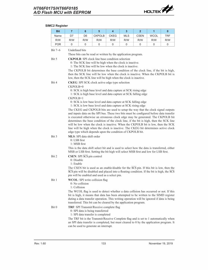
Rev. 1.60 132 November 19, 2019 Rev. 1.60 133 November 19, 2019
HT66F0175/HT66F0185A/D Flash MCU with EEPROM
HT66F0175/HT66F0185A/D Flash MCU with EEPROM
SIMC2 RegisterBit 7 6 5 4 3 2 1 0
Name D7 D6 CKPOLB CKEG MLS CSEN WCOL TRFR/W R/W R/W R/W R/W R/W R/W R/W R/WPOR 0 0 0 0 0 0 0 0
Bit 7~6 Undefined bitsThese bits can be read or written by the application program.
Bit 5 CKPOLB: SPI clock line base condition selection0: The SCK line will be high when the clock is inactive.1: The SCK line will be low when the clock is inactive.
The CKPOLB bit determines the base condition of the clock line, if the bit is high, then the SCK line will be low when the clock is inactive. When the CKPOLB bit is low, then the SCK line will be high when the clock is inactive.
Bit 4 CKEG: SPI SCK clock active edge type selectionCKPOLB=0
0: SCK is high base level and data capture at SCK rising edge1: SCK is high base level and data capture at SCK falling edge
CKPOLB=10: SCK is low base level and data capture at SCK falling edge1: SCK is low base level and data capture at SCK rising edge
The CKEG and CKPOLB bits are used to setup the way that the clock signal outputs and inputs data on the SPI bus. These two bits must be configured before data transfer is executed otherwise an erroneous clock edge may be generated. The CKPOLB bit determines the base condition of the clock line, if the bit is high, then the SCK line will be low when the clock is inactive. When the CKPOLB bit is low, then the SCK line will be high when the clock is inactive. The CKEG bit determines active clock edge type which depends upon the condition of CKPOLB bit.
Bit 3 MLS: SPI data shift order0: LSB first1: MSB first
This is the data shift select bit and is used to select how the data is transferred, either MSB or LSB first. Setting the bit high will select MSB first and low for LSB first.
Bit 2 CSEN: SPI SCS pin control0: Disable1: Enable
The CSEN bit is used as an enable/disable for the SCS pin. If this bit is low, then the SCS pin will be disabled and placed into a floating condition. If the bit is high, the SCS pin will be enabled and used as a select pin.
Bit 1 WCOL: SPI write collision flag0: No collision1: Collision
The WCOL flag is used to detect whether a data collision has occurred or not. If this bit is high, it means that data has been attempted to be written to the SIMD register duting a data transfer operation. This writing operation will be ignored if data is being transferred. This bit can be cleared by the application program.
Bit 0 TRF: SPI Transmit/Receive complete flag0: SPI data is being transferred1: SPI data transfer is completed
The TRF bit is the Transmit/Receive Complete flag and is set to 1 automatically when an SPI data transfer is completed, but must cleared to 0 by the application program. It can be used to generate an interrupt.
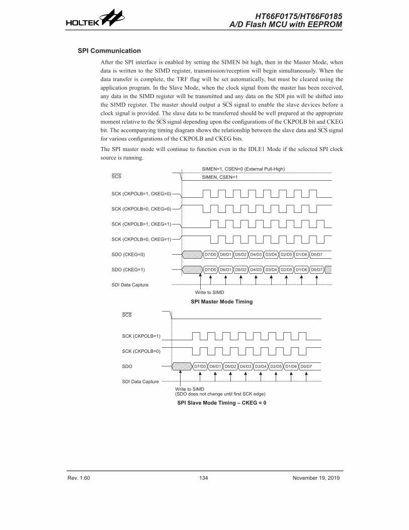
Rev. 1.60 134 November 19, 2019 Rev. 1.60 135 November 19, 2019
HT66F0175/HT66F0185A/D Flash MCU with EEPROM
HT66F0175/HT66F0185A/D Flash MCU with EEPROM
SPI CommunicationAfter the SPI interface is enabled by setting the SIMEN bit high, then in the Master Mode, when data is written to the SIMD register, transmission/reception will begin simultaneously. When the data transfer is complete, the TRF flag will be set automatically, but must be cleared using the application program. In the Slave Mode, when the clock signal from the master has been received, any data in the SIMD register will be transmitted and any data on the SDI pin will be shifted into the SIMD register. The master should output a SCS signal to enable the slave devices before a clock signal is provided. The slave data to be transferred should be well prepared at the appropriate moment relative to the SCS signal depending upon the configurations of the CKPOLB bit and CKEG bit. The accompanying timing diagram shows the relationship between the slave data and SCS signal for various configurations of the CKPOLB and CKEG bits.
The SPI master mode will continue to function even in the IDLE1 Mode if the selected SPI clock source is running.
� � � � � � � � � � � � � � � � � � � � � �
� � � � � � � � � � �� � � � � � � � � � � � � � � � � � � � � � � � � � � � � � � �
� � � � � � � � � � � � � � � � � � � � � �
� � � � � � � � � � � � � � � � � � � � � �
� � � � � � � � � � � � � � � � � � � � � �
� � � � � � � � � � � �
� � � � � � � � � � � �
� � �
� � � � � � � � � � � � � �
� � � � � � � � � � � � � � � � � � � � � � � � � � � � � � � � � � � �
� � � � � � � � � � � � � � � � � � � � � � � � � � � � � � � � � � � �
� � � � � � � � � � �
SPI Master Mode Timing
� � � � � � � � � � � � � �
� � � � � � � � � � � � � �
� � �
� � �
� � � � � � � � � � � � � � �
� � � � � � � � � � � � � � � � � � � � � � � � � � � � � �
� � � � � � � � � � � � �� � � � � � � � � � � � � � � � � � � � � � � � � � � � � � � � � � � � � �
SPI Slave Mode Timing – CKEG = 0
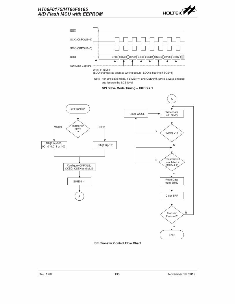
Rev. 1.60 134 November 19, 2019 Rev. 1.60 135 November 19, 2019
HT66F0175/HT66F0185A/D Flash MCU with EEPROM
HT66F0175/HT66F0185A/D Flash MCU with EEPROM
� � � � � � � � � � � � � �
� � � � � � � � � � � � � �
� � �
� � �
� � � � � � � � � � � � � � �
� � � � � � � � � � � � � � � � � � � � � � � � � � � � � �
� � � � � � � � � � � � �� � � � � � � � � � � � � � � � � � � � � � � � � � � � � � � � � � � � � � � � � � � � � � � � � � � � � � � � � � � � � �
� � � � � � � � � � � � � � � � � � � � � � � � � � � � � � � � � � � � � � � � � � � � � � � � � � � � � � � � � � � � � � � � � � � �� � � � � � � � � � � � � � � � � � � � � � � � � �
SPI Slave Mode Timing – CKEG = 1
� � � � � � � �
� � � � � � � � � �� � � � � � � � �
� � � � � �
� � � � � � � �
� � � � � � � � � � � �� � � � � � � � � �� � � � � � � � � �
�
� � � � � � � � �� � � � � � � � �
� � � � � � � �
� � � � � � � �� � � � � � � � �
�
� � �
� � � � � � � � �� � � ��
� � � � � � � � � �
�
�
� � � � � � � � � � � �
� � � � � � � � � � � � � �� � � � � � � � � � � � � � � � � � �
� � � � � � � � � � � � �� � � � � � � � � � � � � � � � � � � � � � � � � � � � � � � �
SPI Transfer Control Flow Chart
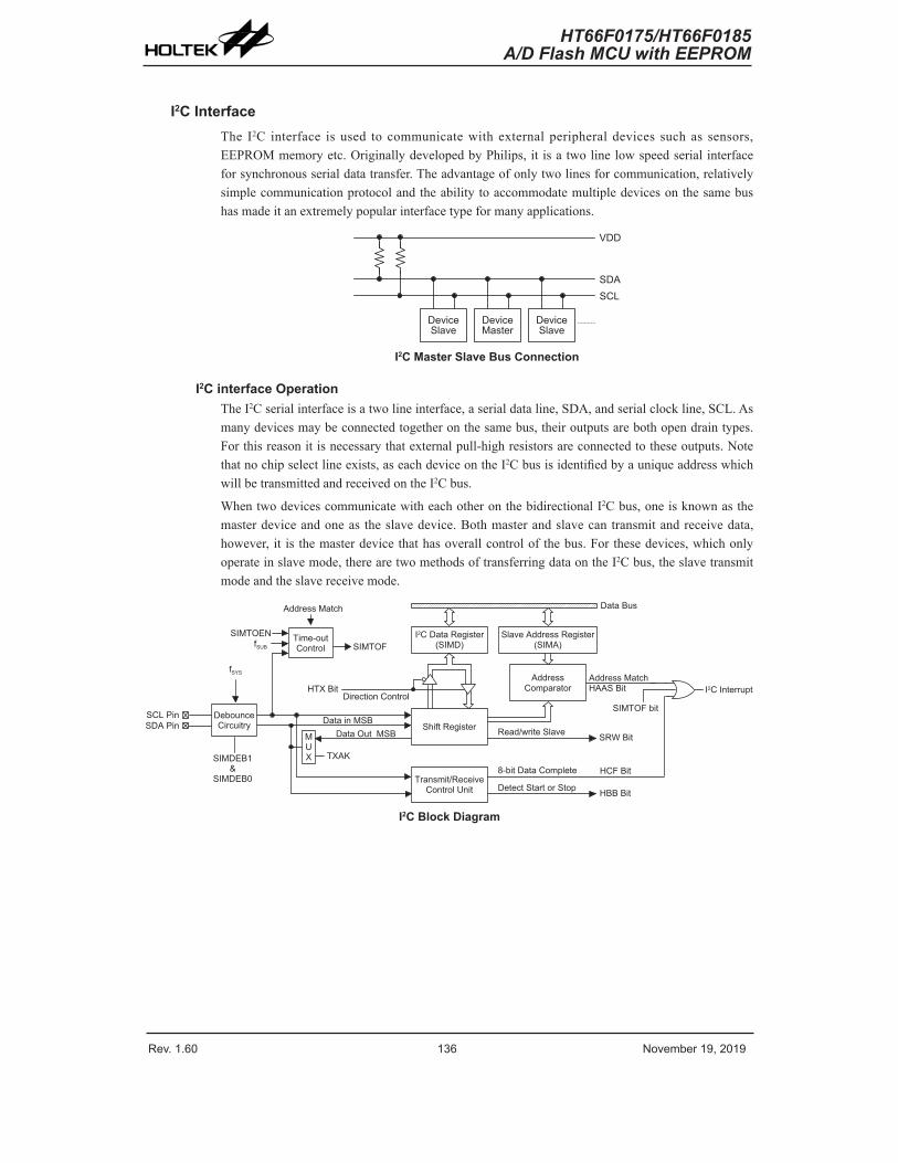
Rev. 1.60 136 November 19, 2019 Rev. 1.60 137 November 19, 2019
HT66F0175/HT66F0185A/D Flash MCU with EEPROM
HT66F0175/HT66F0185A/D Flash MCU with EEPROM
I2C InterfaceThe I2C interface is used to communicate with external peripheral devices such as sensors, EEPROM memory etc. Originally developed by Philips, it is a two line low speed serial interface for synchronous serial data transfer. The advantage of only two lines for communication, relatively simple communication protocol and the ability to accommodate multiple devices on the same bus has made it an extremely popular interface type for many applications.
� � � � � �� � � � �
� � � � � �� � � � � �
� � � � � �� � � � �
� � �
� � �� � �
I2C Master Slave Bus Connection
I2C interface OperationThe I2C serial interface is a two line interface, a serial data line, SDA, and serial clock line, SCL. As many devices may be connected together on the same bus, their outputs are both open drain types. For this reason it is necessary that external pull-high resistors are connected to these outputs. Note that no chip select line exists, as each device on the I2C bus is identified by a unique address which will be transmitted and received on the I2C bus.
When two devices communicate with each other on the bidirectional I2C bus, one is known as the master device and one as the slave device. Both master and slave can transmit and receive data, however, it is the master device that has overall control of the bus. For these devices, which only operate in slave mode, there are two methods of transferring data on the I2C bus, the slave transmit mode and the slave receive mode.
� � � � � � � � � � � � � � � � �� � � � � �
� � � � � � � � � � � � � � � � � � � � �� � � � � �
� � � � � � � � � � � �
� � � � � � � � � � � � � � � � �
���
� � � � � � � � � � � � � � � � � � � � � � � � � � � � � � � � �
� � � � � � � � � � � �� � � � � � � � � � � � �
� � � � � � � � � � � � � � �� � � � � � � � � � � �
� � � � � � � � � � � � � � � � �
� � � � � � � � � � � � � � � � � � � �
� � � � � � � �
� � � � � � �� � � � � � � � � �
� � � �
� � � � � � � � � � � � � � � � � � � � � �
� � � � � � �
� � � � � � �
� � � � � � �
� � � � � � �� � � � � � � � �
� � � � � � �� � � � � � �
� � �
� � � � � � ��
� � � � � � �
� � � � � � � � �
� � � � � � �� � � � � � � � � � � � �
� � � � � � � � � � � �
� � � � � � � � � �
I2C Block Diagram
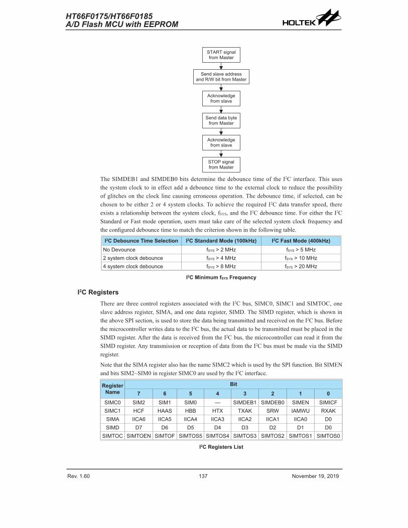
Rev. 1.60 136 November 19, 2019 Rev. 1.60 137 November 19, 2019
HT66F0175/HT66F0185A/D Flash MCU with EEPROM
HT66F0175/HT66F0185A/D Flash MCU with EEPROM
� � � � � � � � � � � �� � � � � � � � � � �
� � � � � � � � � � � � � � �� � � � � � � � � � � � � � � � � � � �
� � � � � � � � � �� � � � � � � � � �
� � � � � � � � � � �� � � � � � � � � � �
� � � � � � � � � �� � � � � � � � � �
� � � � � � � � � � �� � � � � � � � � � �
The SIMDEB1 and SIMDEB0 bits determine the debounce time of the I2C interface. This uses the system clock to in effect add a debounce time to the external clock to reduce the possibility of glitches on the clock line causing erroneous operation. The debounce time, if selected, can be chosen to be either 2 or 4 system clocks. To achieve the required I2C data transfer speed, there exists a relationship between the system clock, fSYS, and the I2C debounce time. For either the I2C Standard or Fast mode operation, users must take care of the selected system clock frequency and the configured debounce time to match the criterion shown in the following table.
I2C Debounce Time Selection I2C Standard Mode (100kHz) I2C Fast Mode (400kHz)No Devounce fSYS > 2 MHz fSYS > 5 MHz2 system clock debounce fSYS > 4 MHz fSYS > 10 MHz4 system clock debounce fSYS > 8 MHz fSYS > 20 MHz
I2C Minimum fSYS Frequency
I2C RegistersThere are three control registers associated with the I2C bus, SIMC0, SIMC1 and SIMTOC, one slave address register, SIMA, and one data register, SIMD. The SIMD register, which is shown in the above SPI section, is used to store the data being transmitted and received on the I2C bus. Before the microcontroller writes data to the I2C bus, the actual data to be transmitted must be placed in the SIMD register. After the data is received from the I2C bus, the microcontroller can read it from the SIMD register. Any transmission or reception of data from the I2C bus must be made via the SIMD register.
Note that the SIMA register also has the name SIMC2 which is used by the SPI function. Bit SIMEN and bits SIM2~SIM0 in register SIMC0 are used by the I2C interface.
Register Name
Bit7 6 5 4 3 2 1 0
SIMC0 SIM2 SIM1 SIM0 — SIMDEB1 SIMDEB0 SIMEN SIMICFSIMC1 HCF HAAS HBB HTX TXAK SRW IAMWU RXAKSIMA IICA6 IICA5 IICA4 IICA3 IICA2 IICA1 IICA0 D0SIMD D7 D6 D5 D4 D3 D2 D1 D0
SIMTOC SIMTOEN SIMTOF SIMTOS5 SIMTOS4 SIMTOS3 SIMTOS2 SIMTOS1 SIMTOS0
I2C Registers List
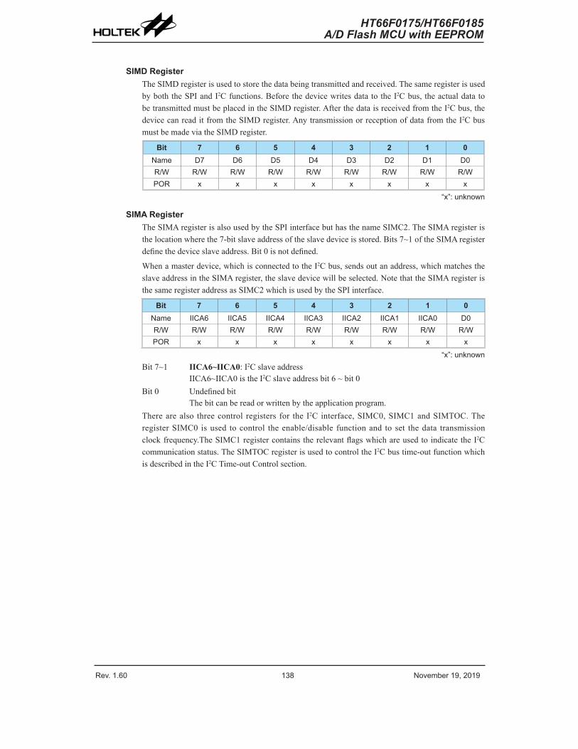
Rev. 1.60 138 November 19, 2019 Rev. 1.60 139 November 19, 2019
HT66F0175/HT66F0185A/D Flash MCU with EEPROM
HT66F0175/HT66F0185A/D Flash MCU with EEPROM
SIMD RegisterThe SIMD register is used to store the data being transmitted and received. The same register is used by both the SPI and I2C functions. Before the device writes data to the I2C bus, the actual data to be transmitted must be placed in the SIMD register. After the data is received from the I2C bus, the device can read it from the SIMD register. Any transmission or reception of data from the I2C bus must be made via the SIMD register.
Bit 7 6 5 4 3 2 1 0Name D7 D6 D5 D4 D3 D2 D1 D0R/W R/W R/W R/W R/W R/W R/W R/W R/WPOR x x x x x x x x
“x”: unknown
SIMA RegisterThe SIMA register is also used by the SPI interface but has the name SIMC2. The SIMA register is the location where the 7-bit slave address of the slave device is stored. Bits 7~1 of the SIMA register define the device slave address. Bit 0 is not defined.
When a master device, which is connected to the I2C bus, sends out an address, which matches the slave address in the SIMA register, the slave device will be selected. Note that the SIMA register is the same register address as SIMC2 which is used by the SPI interface.
Bit 7 6 5 4 3 2 1 0Name IICA6 IICA5 IICA4 IICA3 IICA2 IICA1 IICA0 D0R/W R/W R/W R/W R/W R/W R/W R/W R/WPOR x x x x x x x x
“x”: unknownBit 7~1 IICA6~IICA0: I2C slave address
IICA6~IICA0 is the I2C slave address bit 6 ~ bit 0Bit 0 Undefined bit
The bit can be read or written by the application program.There are also three control registers for the I2C interface, SIMC0, SIMC1 and SIMTOC. The register SIMC0 is used to control the enable/disable function and to set the data transmission clock frequency.The SIMC1 register contains the relevant flags which are used to indicate the I2C communication status. The SIMTOC register is used to control the I2C bus time-out function which is described in the I2C Time-out Control section.
Rev. 1.60 138 November 19, 2019 Rev. 1.60 139 November 19, 2019
HT66F0175/HT66F0185A/D Flash MCU with EEPROM
HT66F0175/HT66F0185A/D Flash MCU with EEPROM
SIMC0 RegisterBit 7 6 5 4 3 2 1 0
Name SIM2 SIM1 SIM0 — SIMDEB1 SIMDEB0 SIMEN SIMICFR/W R/W R/W R/W — R/W R/W R/W R/WPOR 1 1 1 — 0 0 0 0
Bit 7~5 SIM2~SIM0: SIM Operating Mode Control000: SPI master mode; SPI clock is fSYS /4001: SPI master mode; SPI clock is fSYS /16010: SPI master mode; SPI clock is fSYS /64011: SPI master mode; SPI clock is fTBC
100: SPI master mode; SPI clock is TM1 CCRP match frequency/2101: SPI slave mode110: I2C slave mode111: Non SIM function
These bits setup the overall operating mode of the SIM function. As well as selecting if the I2C or SPI function, they are used to control the SPI Master/Slave selection and the SPI Master clock frequency. The SPI clock is a function of the system clock but can also be chosen to be sourced from TM1. If the SPI Slave Mode is selected then the clock will be supplied by an external Master device.
Bit 4 Unimplemented, read as “0”Bit 3~2 SIMDEB1~SIMDEB0: I2C Debounce Time Selection
00: No debounce01: 2 system clock debounce1x: 4 system clock debounce
Bit 1 SIMEN: SIM Enable Control0: Disable1: Enable
The bit is the overall on/off control for the SIM interface. When the SIMEN bit is cleared to zero to disable the SIM interface, the SDI, SDO, SCK and SCS, or SDA and SCL lines will lose their SPI or I2C function and the SIM operating current will be reduced to a minimum value. When the bit is high the SIM interface is enabled. If the SIM is configured to operate as an SPI interface via the SIM2~SIM0 bits, the contents of the SPI control registers will remain at the previous settings when the SIMEN bit changes from low to high and should therefore be first initialised by the application program. If the SIM is configured to operate as an I2C interface via the SIM2~SIM0 bits and the SIMEN bit changes from low to high, the contents of the I2C control bits such as HTX and TXAK will remain at the previous settings and should therefore be first initialised by the application program while the relevant I2C flags such as HCF, HAAS, HBB, SRW and RXAK will be set to their default states.
Bit 0 SIMICF: SIM Incomplete Flag0: SIM incomplete condition not occurred1: SIM incomplete condition occured
This bit is only available when the SIM is configured to operate in an SPI slave mode. If the SPI operates in the slave mode with the SIMEN and CSEN bits both being set to 1 but the SCS line is pulled high by the external master device before the SPI data transfer is completely finished, the SIMICF bit will be set to 1 together with the TRF bit. When this condition occurs, the corresponding interrupt will occur if the interrupt function is enabled. However, the TRF bit will not be set to 1 if the SIMICF bit is set to 1 by software application program.
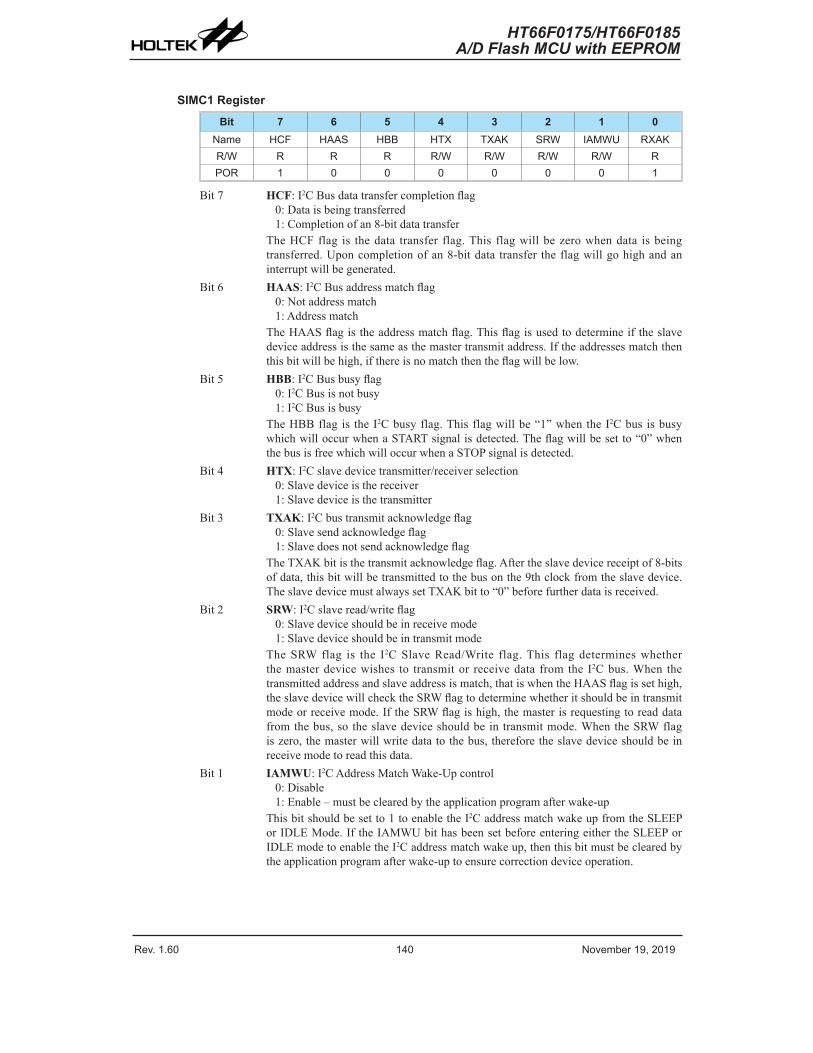
Rev. 1.60 140 November 19, 2019 Rev. 1.60 141 November 19, 2019
HT66F0175/HT66F0185A/D Flash MCU with EEPROM
HT66F0175/HT66F0185A/D Flash MCU with EEPROM
SIMC1 RegisterBit 7 6 5 4 3 2 1 0
Name HCF HAAS HBB HTX TXAK SRW IAMWU RXAKR/W R R R R/W R/W R/W R/W RPOR 1 0 0 0 0 0 0 1
Bit 7 HCF: I2C Bus data transfer completion flag0: Data is being transferred1: Completion of an 8-bit data transfer
The HCF flag is the data transfer flag. This flag will be zero when data is being transferred. Upon completion of an 8-bit data transfer the flag will go high and an interrupt will be generated.
Bit 6 HAAS: I2C Bus address match flag0: Not address match1: Address match
The HAAS flag is the address match flag. This flag is used to determine if the slave device address is the same as the master transmit address. If the addresses match then this bit will be high, if there is no match then the flag will be low.
Bit 5 HBB: I2C Bus busy flag0: I2C Bus is not busy1: I2C Bus is busy
The HBB flag is the I2C busy flag. This flag will be “1” when the I2C bus is busy which will occur when a START signal is detected. The flag will be set to “0” when the bus is free which will occur when a STOP signal is detected.
Bit 4 HTX: I2C slave device transmitter/receiver selection0: Slave device is the receiver1: Slave device is the transmitter
Bit 3 TXAK: I2C bus transmit acknowledge flag0: Slave send acknowledge flag1: Slave does not send acknowledge flag
The TXAK bit is the transmit acknowledge flag. After the slave device receipt of 8-bits of data, this bit will be transmitted to the bus on the 9th clock from the slave device. The slave device must always set TXAK bit to “0” before further data is received.
Bit 2 SRW: I2C slave read/write flag0: Slave device should be in receive mode1: Slave device should be in transmit mode
The SRW flag is the I2C Slave Read/Write flag. This flag determines whether the master device wishes to transmit or receive data from the I2C bus. When the transmitted address and slave address is match, that is when the HAAS flag is set high, the slave device will check the SRW flag to determine whether it should be in transmit mode or receive mode. If the SRW flag is high, the master is requesting to read data from the bus, so the slave device should be in transmit mode. When the SRW flag is zero, the master will write data to the bus, therefore the slave device should be in receive mode to read this data.
Bit 1 IAMWU: I2C Address Match Wake-Up control0: Disable1: Enable – must be cleared by the application program after wake-up
This bit should be set to 1 to enable the I2C address match wake up from the SLEEP or IDLE Mode. If the IAMWU bit has been set before entering either the SLEEP or IDLE mode to enable the I2C address match wake up, then this bit must be cleared by the application program after wake-up to ensure correction device operation.
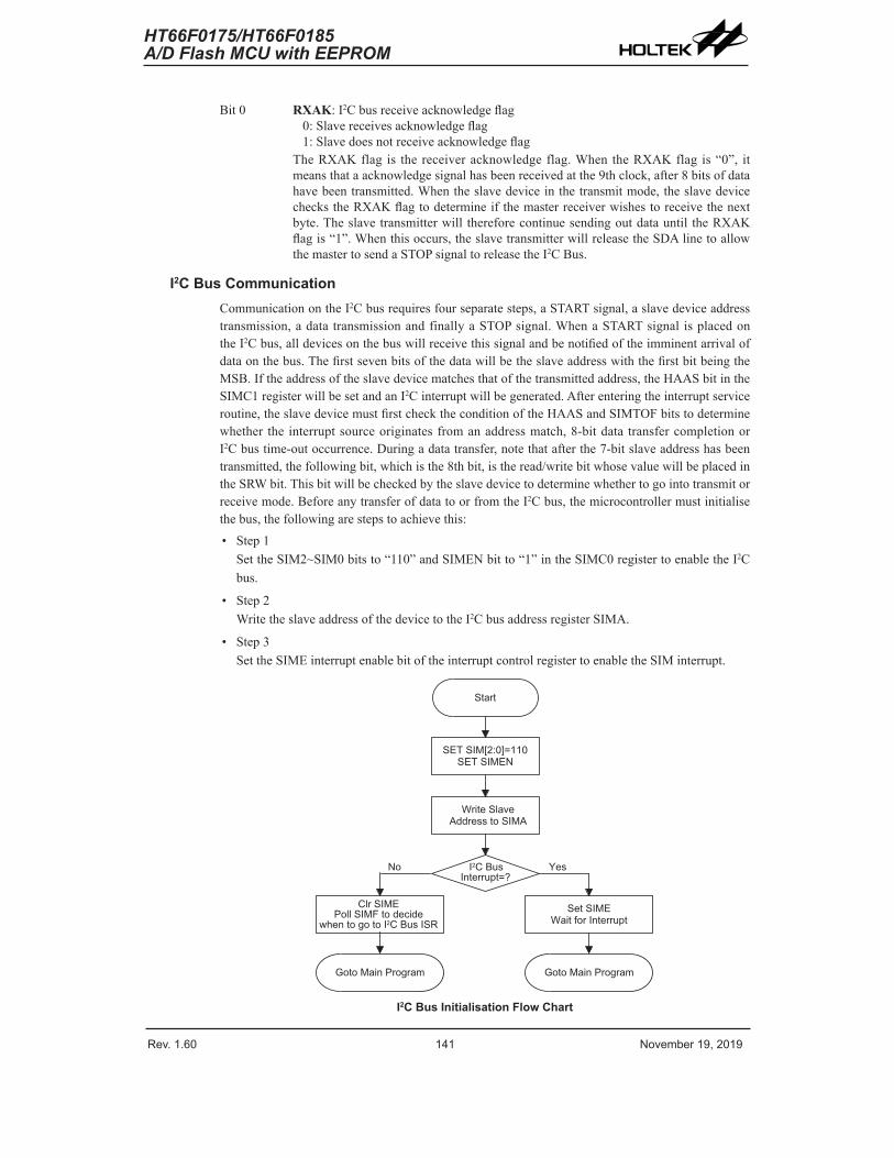
Rev. 1.60 140 November 19, 2019 Rev. 1.60 141 November 19, 2019
HT66F0175/HT66F0185A/D Flash MCU with EEPROM
HT66F0175/HT66F0185A/D Flash MCU with EEPROM
Bit 0 RXAK: I2C bus receive acknowledge flag0: Slave receives acknowledge flag1: Slave does not receive acknowledge flag
The RXAK flag is the receiver acknowledge flag. When the RXAK flag is “0”, it means that a acknowledge signal has been received at the 9th clock, after 8 bits of data have been transmitted. When the slave device in the transmit mode, the slave device checks the RXAK flag to determine if the master receiver wishes to receive the next byte. The slave transmitter will therefore continue sending out data until the RXAK flag is “1”. When this occurs, the slave transmitter will release the SDA line to allow the master to send a STOP signal to release the I2C Bus.
I2C Bus CommunicationCommunication on the I2C bus requires four separate steps, a START signal, a slave device address transmission, a data transmission and finally a STOP signal. When a START signal is placed on the I2C bus, all devices on the bus will receive this signal and be notified of the imminent arrival of data on the bus. The first seven bits of the data will be the slave address with the first bit being the MSB. If the address of the slave device matches that of the transmitted address, the HAAS bit in the SIMC1 register will be set and an I2C interrupt will be generated. After entering the interrupt service routine, the slave device must first check the condition of the HAAS and SIMTOF bits to determine whether the interrupt source originates from an address match, 8-bit data transfer completion or I2C bus time-out occurrence. During a data transfer, note that after the 7-bit slave address has been transmitted, the following bit, which is the 8th bit, is the read/write bit whose value will be placed in the SRW bit. This bit will be checked by the slave device to determine whether to go into transmit or receive mode. Before any transfer of data to or from the I2C bus, the microcontroller must initialise the bus, the following are steps to achieve this:• Step 1
Set the SIM2~SIM0 bits to “110” and SIMEN bit to “1” in the SIMC0 register to enable the I2C bus.
• Step 2Write the slave address of the device to the I2C bus address register SIMA.
• Step 3Set the SIME interrupt enable bit of the interrupt control register to enable the SIM interrupt.
� � � � �
� � � � � � � � � � � � �� � � � � � � � � � � � � � � � �
� � � � � � � � � � � � � � � � � � � � �
� � � � � � � � � �� � � � � � � � � � �
�
� � �� �
� � � � � � � �� � � � � � � � � � � � � � � � � �
� � � � � � � � � � � � � � � �
� � � � � � � � �� � � � � � � � � � � � � � � � � � �
� � � � � � � � � � � � � � � � � � � � � � � � � �
� � � � � � � � � � � � � � � �
I2C Bus Initialisation Flow Chart
Rev. 1.60 142 November 19, 2019 Rev. 1.60 143 November 19, 2019
HT66F0175/HT66F0185A/D Flash MCU with EEPROM
HT66F0175/HT66F0185A/D Flash MCU with EEPROM
I2C Bus Start SignalThe START signal can only be generated by the master device connected to the I2C bus and not by the slave device. This START signal will be detected by all devices connected to the I2C bus. When detected, this indicates that the I2C bus is busy and therefore the HBB bit will be set. A START condition occurs when a high to low transition on the SDA line takes place when the SCL line remains high.
I2C Slave AddressThe transmission of a START signal by the master will be detected by all devices on the I2C bus. To determine which slave device the master wishes to communicate with, the address of the slave device will be sent out immediately following the START signal. All slave devices, after receiving this 7-bit address data, will compare it with their own 7-bit slave address. If the address sent out by the master matches the internal address of the microcontroller slave device, then an internal I2C bus interrupt signal will be generated. The next bit following the address, which is the 8th bit, defines the read/write status and will be saved to the SRW bit of the SIMC1 register. The slave device will then transmit an acknowledge bit, which is a low level, as the 9th bit. The slave device will also set the status flag HAAS when the addresses match.
As an I2C bus interrupt can come from three sources, when the program enters the interrupt subroutine, the HAAS and SIMTOF bits should be examined to see whether the interrupt source has come from a matching slave address, the completion of a data byte transfer or the I2C bus time-out occurrence. When a slave address is matched, the devices must be placed in either the transmit mode and then write data to the SIMD register, or in the receive mode where it must implement a dummy read from the SIMD register to release the SCL line.
I2C Bus Read/Write SignalThe SRW bit in the SIMC1 register defines whether the master device wishes to read data from the I2C bus or write data to the I2C bus. The slave device should examine this bit to determine if it is to be a transmitter or a receiver. If the SRW flag is “1” then this indicates that the master device wishes to read data from the I2C bus, therefore the slave device must be setup to send data to the I2C bus as a transmitter. If the SRW flag is “0” then this indicates that the master wishes to send data to the I2C bus, therefore the slave device must be setup to read data from the I2C bus as a receiver.
I2C Bus Slave Address Acknowledge SignalAfter the master has transmitted a calling address, any slave device on the I2C bus, whose own internal address matches the calling address, must generate an acknowledge signal. The acknowledge signal will inform the master that a slave device has accepted its calling address. If no acknowledge signal is received by the master then a STOP signal must be transmitted by the master to end the communication. When the HAAS flag is high, the addresses have matched and the slave device must check the SRW flag to determine if it is to be a transmitter or a receiver. If the SRW flag is high, the slave device should be setup to be a transmitter so the HTX bit in the SIMC1 register should be set to “1”. If the SRW flag is low, then the microcontroller slave device should be setup as a receiver and the HTX bit in the SIMC1 register should be set to “0”.
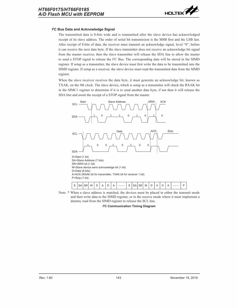
Rev. 1.60 142 November 19, 2019 Rev. 1.60 143 November 19, 2019
HT66F0175/HT66F0185A/D Flash MCU with EEPROM
HT66F0175/HT66F0185A/D Flash MCU with EEPROM
I2C Bus Data and Acknowledge SignalThe transmitted data is 8-bits wide and is transmitted after the slave device has acknowledged receipt of its slave address. The order of serial bit transmission is the MSB first and the LSB last. After receipt of 8-bits of data, the receiver must transmit an acknowledge signal, level “0”, before it can receive the next data byte. If the slave transmitter does not receive an acknowledge bit signal from the master receiver, then the slave transmitter will release the SDA line to allow the master to send a STOP signal to release the I2C Bus. The corresponding data will be stored in the SIMD register. If setup as a transmitter, the slave device must first write the data to be transmitted into the SIMD register. If setup as a receiver, the slave device must read the transmitted data from the SIMD register.
When the slave receiver receives the data byte, it must generate an acknowledge bit, known as TXAK, on the 9th clock. The slave device, which is setup as a transmitter will check the RXAK bit in the SIMC1 register to determine if it is to send another data byte, if not then it will release the SDA line and await the receipt of a STOP signal from the master.
� � � �
� � � � � � � � � �� � � � � � � � � � ��
� � � � � � �� �
� � � � � � � � � � � � � � �� � � � � � � � � � � � � � � � � � � � � �� � � � � � � � � � � � � � � � � � � � � � � � � � � � � � � � � � � � � � � � � � � � � � � � � � � � � � � � � �� � � � � � � � � � � � � �� � � � � � � � � � � � � � � � � � � � � � � � � � � � � � � � � � � � � � � � � � � � � � � � � � � � � � � � � � � � � � � � � � � � � � � �
� � �� � � � �
� � �
� � � � �
� � � � � � � � �
� � �
� � � � � � � � � � �
� � � � � � � � � � � � � � � � � �
Note: * When a slave address is matched, the devices must be placed in either the transmit mode and then write data to the SIMD register, or in the receive mode where it must implement a dummy read from the SIMD register to release the SCL line.
I2C Communication Timing Diagram
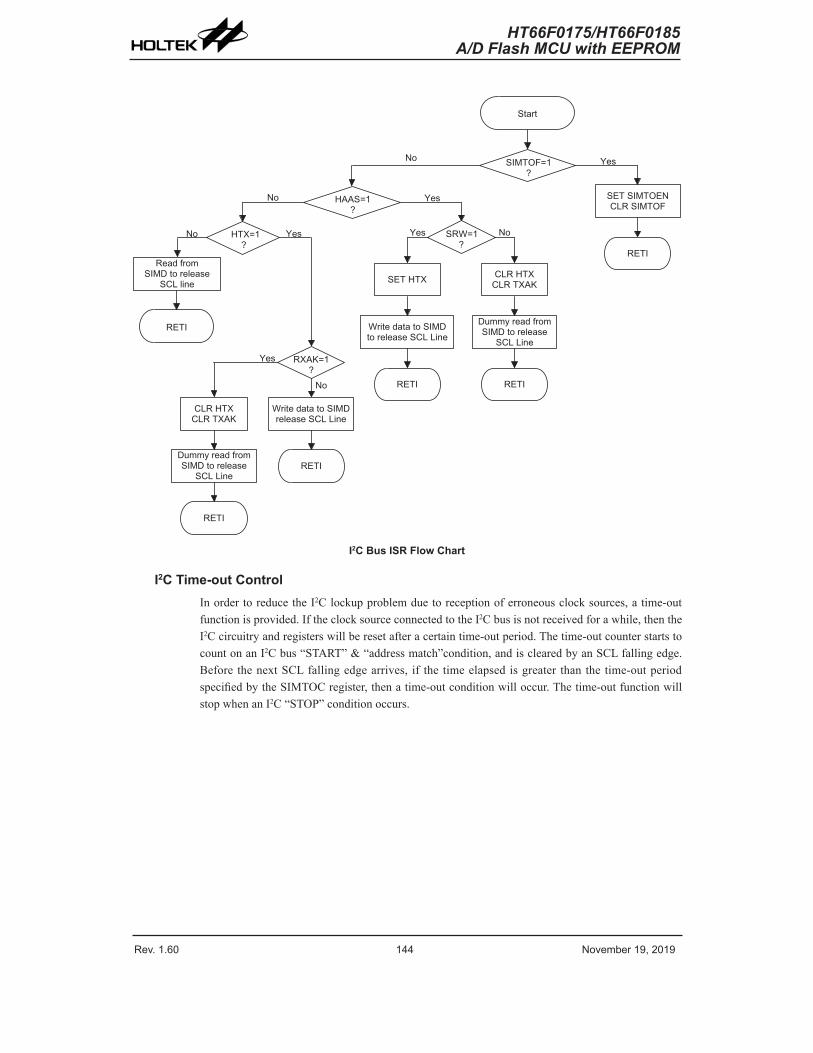
Rev. 1.60 144 November 19, 2019 Rev. 1.60 145 November 19, 2019
HT66F0175/HT66F0185A/D Flash MCU with EEPROM
HT66F0175/HT66F0185A/D Flash MCU with EEPROM
� � � � � ��
� � � � �� � � � �
� � � � �� � � � � �
� � �� �
� � � � �
� � � � � ��
� � �
� �
� �
� � � � � � � � � � � � � � � � � � � � �
� � � � � � � �
� � �
� � �
� � � � � � � � � � � � � � � � � � � � � � � � �
� � � � � � � �
� � �
� � �
� � � � � � � � � � � � � � � �� � � � � � � � � � � � � � � �
� � � � � � �
� � � � � � � � � � � � � � � �� � � � � � � � � � � � � � � � � � �
� � �
� � � � � � �� � � � � � � �
� � � � � � � � � � � � � � � � � � � � � � � � �
� � � � � � � �
� � � � � � �� � � � � � � �
� � �
� � � � �
� � � � � � ��
� � �� �
� � � � � � � � � �� � � � � � � � �
� � �
I2C Bus ISR Flow Chart
I2C Time-out ControlIn order to reduce the I2C lockup problem due to reception of erroneous clock sources, a time-out function is provided. If the clock source connected to the I2C bus is not received for a while, then the I2C circuitry and registers will be reset after a certain time-out period. The time-out counter starts to count on an I2C bus “START” & “address match”condition, and is cleared by an SCL falling edge. Before the next SCL falling edge arrives, if the time elapsed is greater than the time-out period specified by the SIMTOC register, then a time-out condition will occur. The time-out function will stop when an I2C “STOP” condition occurs.
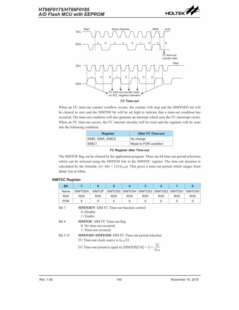
Rev. 1.60 144 November 19, 2019 Rev. 1.60 145 November 19, 2019
HT66F0175/HT66F0185A/D Flash MCU with EEPROM
HT66F0175/HT66F0185A/D Flash MCU with EEPROM
� � � � � � � � � � � �� � � � � � � � � � � � �
� � � � � � � � � � � � � � � � � � � � � � � � � �� � � � � � � � � � � � � � � � � � � � � � � � �
� � � � � � � � � �� � � � � � � � � � ��
� � � � � � �� �
� � �� � � � �
�
� � � � �
� � � �� � �
�
� � � � � � � � � � �
�
�
I2C Time-out
When an I2C time-out counter overflow occurs, the counter will stop and the SIMTOEN bit will be cleared to zero and the SIMTOF bit will be set high to indicate that a time-out condition has occurred. The time-out condition will also generate an interrupt which uses the I2C interrrupt vector. When an I2C time-out occurs, the I2C internal circuitry will be reset and the registers will be reset into the following condition:
Register After I2C Time-outSIMD, SIMA, SIMC0 No changeSIMC1 Reset to POR condition
I2C Register after Time-out
The SIMTOF flag can be cleared by the application program. There are 64 time-out period selections which can be selected using the SIMTOS bits in the SIMTOC register. The time-out duration is calculated by the formula: ((1~64) × (32/fSUB)). This gives a time-out period which ranges from about 1ms to 64ms.
SIMTOC RegisterBit 7 6 5 4 3 2 1 0
Name SIMTOEN SIMTOF SIMTOS5 SIMTOS4 SIMTOS3 SIMTOS2 SIMTOS1 SIMTOS0R/W R/W R/W R/W R/W R/W R/W R/W R/WPOR 0 0 0 0 0 0 0 0
Bit 7 SIMTOEN: SIM I2C Time-out function control0: Disable1: Enable
Bit 6 SIMTOF: SIM I2C Time-out flag0: No time-out occurred1: Time-out occurred
Bit 5~0 SIMTOS5~SIMTOS0: SIM I2C Time-out period selectionI2C Time-out clock source is fSUB/32
I2C Time-out period is equal to (SIMTOS[5:0] + 1) × 32fSUB
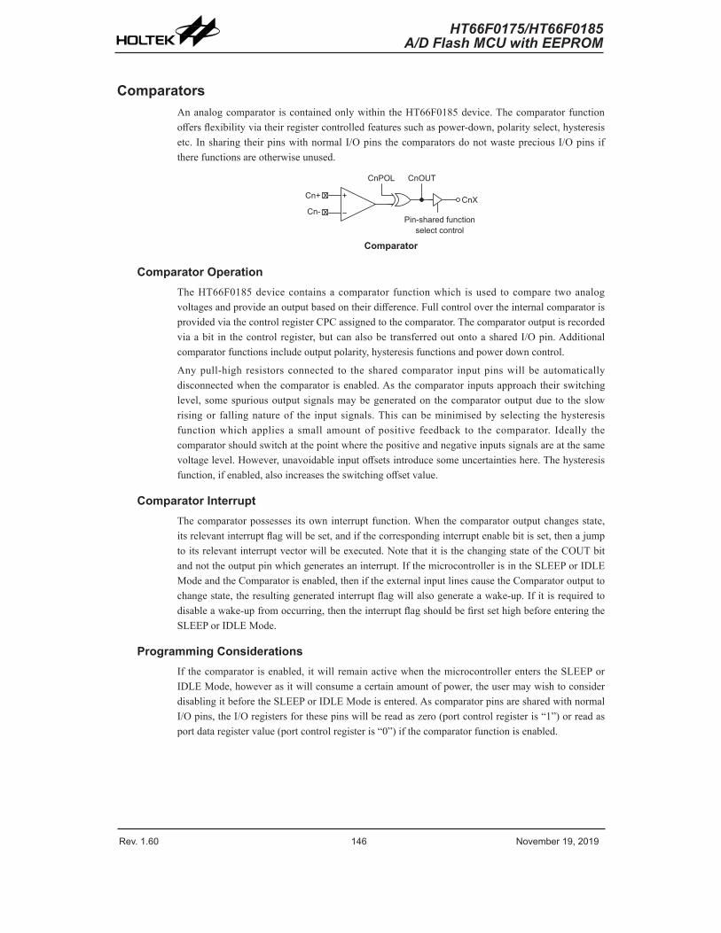
Rev. 1.60 146 November 19, 2019 Rev. 1.60 147 November 19, 2019
HT66F0175/HT66F0185A/D Flash MCU with EEPROM
HT66F0175/HT66F0185A/D Flash MCU with EEPROM
ComparatorsAn analog comparator is contained only within the HT66F0185 device. The comparator function offers flexibility via their register controlled features such as power-down, polarity select, hysteresis etc. In sharing their pins with normal I/O pins the comparators do not waste precious I/O pins if there functions are otherwise unused.
� � �
� � �
� � � � � � � � � �
� � �
� � � � � � � � � � � � � � � �� � � � � � � � � �
Comparator
Comparator OperationThe HT66F0185 device contains a comparator function which is used to compare two analog voltages and provide an output based on their difference. Full control over the internal comparator is provided via the control register CPC assigned to the comparator. The comparator output is recorded via a bit in the control register, but can also be transferred out onto a shared I/O pin. Additional comparator functions include output polarity, hysteresis functions and power down control.
Any pull-high resistors connected to the shared comparator input pins will be automatically disconnected when the comparator is enabled. As the comparator inputs approach their switching level, some spurious output signals may be generated on the comparator output due to the slow rising or falling nature of the input signals. This can be minimised by selecting the hysteresis function which applies a small amount of positive feedback to the comparator. Ideally the comparator should switch at the point where the positive and negative inputs signals are at the same voltage level. However, unavoidable input offsets introduce some uncertainties here. The hysteresis function, if enabled, also increases the switching offset value.
Comparator InterruptThe comparator possesses its own interrupt function. When the comparator output changes state, its relevant interrupt flag will be set, and if the corresponding interrupt enable bit is set, then a jump to its relevant interrupt vector will be executed. Note that it is the changing state of the COUT bit and not the output pin which generates an interrupt. If the microcontroller is in the SLEEP or IDLE Mode and the Comparator is enabled, then if the external input lines cause the Comparator output to change state, the resulting generated interrupt flag will also generate a wake-up. If it is required to disable a wake-up from occurring, then the interrupt flag should be first set high before entering the SLEEP or IDLE Mode.
Programming ConsiderationsIf the comparator is enabled, it will remain active when the microcontroller enters the SLEEP or IDLE Mode, however as it will consume a certain amount of power, the user may wish to consider disabling it before the SLEEP or IDLE Mode is entered. As comparator pins are shared with normal I/O pins, the I/O registers for these pins will be read as zero (port control register is “1”) or read as port data register value (port control register is “0”) if the comparator function is enabled.
Rev. 1.60 146 November 19, 2019 Rev. 1.60 147 November 19, 2019
HT66F0175/HT66F0185A/D Flash MCU with EEPROM
HT66F0175/HT66F0185A/D Flash MCU with EEPROM
CPC RegisterBit 7 6 5 4 3 2 1 0
Name CSEL CEN CPOL COUT COS CMPEG1 CMPEG0 CHYENR/W R/W R/W R/W R R/W R/W R/W R/WPOR 1 0 0 0 0 0 0 1
Bit 7 CSEL: Select Comparator pins or I/O pins0: I/O pin selected1: Comparator input pins C+ and C- selected
This is the Comparator input pin or I/O pin select bit. If the bit is high, the comparator input pins will be enabled. As a result, these two pins will lose their I/O pin functions. Any pull-high configuration options associated with the comparator shared pins will also be automatically disconnected.
Bit 6 CEN: Comparator ON/Off control0: Off1: On
This is the Comparator on/off control bit. If the bit is zero the comparator will be switched off and no power consumed even if analog voltages are applied to its inputs. For power sensitive applications this bit should be cleared to zero if the comparator is not used or before the device enters the SLEEP or IDLE mode.
Bit 5 CPOL: Comparator Output polarity0: Output not inverted1: Output inverted
This is the comparator polarity bit. If the bit is zero then the COUT bit will reflect the non-inverted output condition of the comparator. If the bit is high the comparator COUT bit will be inverted.
Bit 4 COUT: Comparator Output bitCPOL = 0
0: C+ < C-1: C+ > C-
CPOL = 10: C+ > C-1: C+ < C-
This bit stores the comparator output bit. The polarity of the bit is determined by the voltages on the comparator inputs and by the condition of the CPOL bit.
Bit 3 COS: Comparator Output path select0: CX pin selected (compare output can output to CX pin)1: I/O pin selected (compare output only internal use)
Bit 2~1 CMPEG1~CMPEG0: Comparator output interrupt trigger edge select00: rising edge → comparator interrupt trigger signal generated if COUT changed
state from 0 to 101: falling edge → comparator interrupt trigger signal generated if COUT changed
state from 1 to 01x: both edge → comparator interrupt trigger signal generated if COUT changed
state from 0 to 1 or 1 to 0Bit 0 CHYEN: Comparator Hysteresis function control
0: Off1: On
This is the hysteresis control bit and if set high will apply a limited amount of hysteresis to the comparator, as specified in the Comparator Electrical Characteristics table. The positive feedback induced by hysteresis reduces the effect of spurious switching near the comparator threshold.
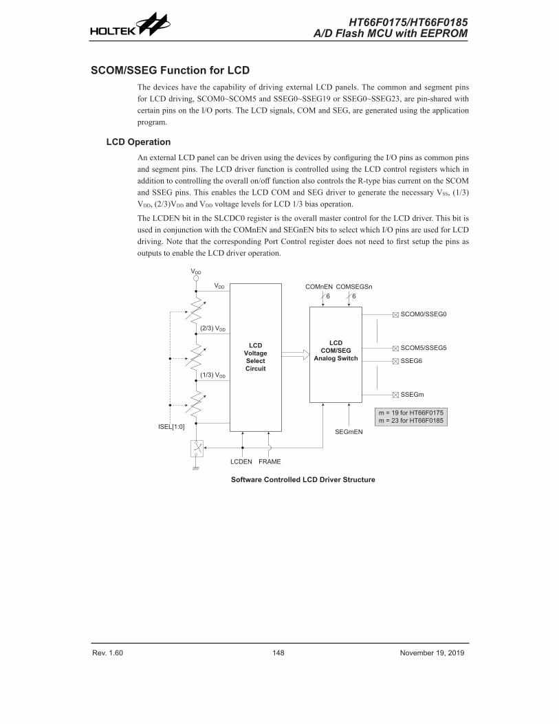
Rev. 1.60 148 November 19, 2019 Rev. 1.60 149 November 19, 2019
HT66F0175/HT66F0185A/D Flash MCU with EEPROM
HT66F0175/HT66F0185A/D Flash MCU with EEPROM
SCOM/SSEG Function for LCDThe devices have the capability of driving external LCD panels. The common and segment pins for LCD driving, SCOM0~SCOM5 and SSEG0~SSEG19 or SSEG0~SSEG23, are pin-shared with certain pins on the I/O ports. The LCD signals, COM and SEG, are generated using the application program.
LCD OperationAn external LCD panel can be driven using the devices by configuring the I/O pins as common pins and segment pins. The LCD driver function is controlled using the LCD control registers which in addition to controlling the overall on/off function also controls the R-type bias current on the SCOM and SSEG pins. This enables the LCD COM and SEG driver to generate the necessary VSS, (1/3)VDD, (2/3)VDD and VDD voltage levels for LCD 1/3 bias operation.
The LCDEN bit in the SLCDC0 register is the overall master control for the LCD driver. This bit is used in conjunction with the COMnEN and SEGnEN bits to select which I/O pins are used for LCD driving. Note that the corresponding Port Control register does not need to first setup the pins as outputs to enable the LCD driver operation.
VDD
(2/3) VDD
(1/3) VDD
VDD
LCDVoltageSelectCircuit
LCDCOM/SEG
Analog Switch
LCDEN
ISEL[1:0]
COMnEN COMSEGSn66
SEGmEN
FRAME
SCOM0/SSEG0
SCOM5/SSEG5
SSEG6
SSEGm
m = 19 for HT66F0175m = 23 for HT66F0185
Software Controlled LCD Driver Structure
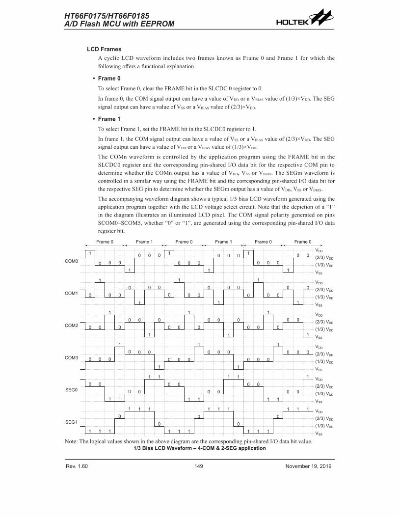
Rev. 1.60 148 November 19, 2019 Rev. 1.60 149 November 19, 2019
HT66F0175/HT66F0185A/D Flash MCU with EEPROM
HT66F0175/HT66F0185A/D Flash MCU with EEPROM
LCD FramesA cyclic LCD waveform includes two frames known as Frame 0 and Frame 1 for which the following offers a functional explanation.
• Frame 0To select Frame 0, clear the FRAME bit in the SLCDC 0 register to 0.
In frame 0, the COM signal output can have a value of VDD or a VBIAS value of (1/3)×VDD. The SEG signal output can have a value of VSS or a VBIAS value of (2/3)×VDD.
• Frame 1To select Frame 1, set the FRAME bit in the SLCDC0 register to 1.
In frame 1, the COM signal output can have a value of VSS or a VBIAS value of (2/3)×VDD. The SEG signal output can have a value of VDD or a VBIAS value of (1/3)×VDD.
The COMn waveform is controlled by the application program using the FRAME bit in the SLCDC0 register and the corresponding pin-shared I/O data bit for the respective COM pin to determine whether the COMn output has a value of VDD, VSS or VBIAS. The SEGm waveform is controlled in a similar way using the FRAME bit and the corresponding pin-shared I/O data bit for the respective SEG pin to determine whether the SEGm output has a value of VDD, VSS or VBIAS.
The accompanying waveform diagram shows a typical 1/3 bias LCD waveform generated using the application program together with the LCD voltage select circuit. Note that the depiction of a “1” in the diagram illustrates an illuminated LCD pixel. The COM signal polarity generated on pins SCOM0~SCOM5, whether “0” or “1”, are generated using the corresponding pin-shared I/O data register bit.
COM0
VDD
(2/3) VDD
(1/3) VDD
VSS
VDD
(2/3) VDD
(1/3) VDD
VSS
COM1
COM2
VDD
(2/3) VDD
(1/3) VDD
VSS
VDD
(2/3) VDD
(1/3) VDD
VSS
COM3
VDD
(2/3) VDD
(1/3) VDD
VSS
SEG0
VDD
(2/3) VDD
(1/3) VDD
VSS
SEG1
Frame 0 Frame 1 Frame 0 Frame 1 Frame 0 Frame 0
1
0 0 01
0 0 0 1
0 0 01
0 0 0 1
0 0 01
0 0
0
1
0 00 0 0
1
0
1
0 00 0 0
10
1
0 00 0
1
0 0
1
00 0 0
10 0
1
00 0 0
1
0 0
1
00 0
1
0 0 0
10 0 0
10 0 0
10 0 0
10 0 0
10 0 0
0 0
1 10 0
1 10 0
1 10 0
1 10 0
1 10 0
1
1 1 1
01 1 1
01 1 1
01 1 1
01 1 1
01 1 1
Note: The logical values shown in the above diagram are the corresponding pin-shared I/O data bit value.1/3 Bias LCD Waveform – 4-COM & 2-SEG application
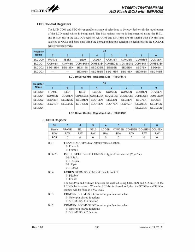
Rev. 1.60 150 November 19, 2019 Rev. 1.60 151 November 19, 2019
HT66F0175/HT66F0185A/D Flash MCU with EEPROM
HT66F0175/HT66F0185A/D Flash MCU with EEPROM
LCD Control RegistersThe LCD COM and SEG driver enables a range of selections to be provided to suit the requirement of the LCD panel which is being used. The bias resistor choice is implemented using the ISEL1 and ISEL0 bits in the SLCDC0 register. All COM and SEG pins are pin-shared with I/O pins and selected as COM and SEG pins using the corresponding pin function selection bits in the SLCDCn registers respectively.
Register Name
Bit7 6 5 4 3 2 1 0
SLCDC0 FRAME ISEL1 ISEL0 LCDEN COM3EN COM2EN COM1EN COM0ENSLCDC1 COM5EN COM4EN COMSEGS5 COMSEGS4 COMSEGS3 COMSEGS2 COMSEGS1 COMSEGS0SLCDC2 SEG13EN SEG12EN SEG11EN SEG10EN SEG9EN SEG8EN SEG7EN SEG6ENSLCDC3 — — SEG19EN SEG18EN SEG17EN SEG16EN SEG15EN SEG14EN
LCD Driver Control Registers List – HT66F0175
Register Name
Bit7 6 5 4 3 2 1 0
SLCDC0 FRAME ISEL1 ISEL0 LCDEN COM3EN COM2EN COM1EN COM0ENSLCDC1 COM5EN COM4EN COMSEGS5 COMSEGS4 COMSEGS3 COMSEGS2 COMSEGS1 COMSEGS0SLCDC2 SEG13EN SEG12EN SEG11EN SEG10EN SEG9EN SEG8EN SEG7EN SEG6ENSLCDC3 SEG21EN SEG20EN SEG19EN SEG18EN SEG17EN SEG16EN SEG15EN SEG14ENSLCDC4 — — — — — — SEG23EN SEG22EN
LCD Driver Control Registers List – HT66F0185
SLCDC0 RegisterBit 7 6 5 4 3 2 1 0
Name FRAME ISEL1 ISEL0 LCDEN COM3EN COM2EN COM1EN COM0ENR/W R/W R/W R/W R/W R/W R/W R/W R/WPOR 0 0 0 0 0 0 0 0
Bit 7 FRAME: SCOM/SSEG Output Frame selection0: Frame 01: Frame 1
Bit 6~5 ISEL1~ISEL0: Select SCOM/SSEG typical bias current (VDD=5V)00: 8.3μA01: 16.7μA10: 50μA11: 100μA
Bit 4 LCDEN: SCOM/SSEG Module enable control0: Disable1: Enable
The SCOMn and SSEGm lines can be enabled using COMnEN and SEGmEN if the LCDEN bit is set to 1. When the LCD bit is cleared to 0, then the SCOMn and SSEGm outputs will be fixed at a VSS level.
Bit 3 COM3EN: SCOM3/SSEG3 or other pin function select0: Other pin-shared functions1: SCOM3/SSEG3 function
Bit 2 COM2EN: SCOM2/SSEG2 or other pin function select0: Other pin-shared functions1: SCOM2/SSEG2 function
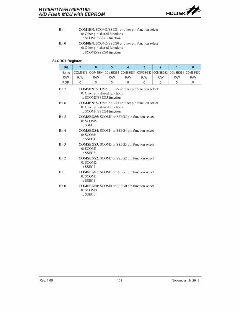
Rev. 1.60 150 November 19, 2019 Rev. 1.60 151 November 19, 2019
HT66F0175/HT66F0185A/D Flash MCU with EEPROM
HT66F0175/HT66F0185A/D Flash MCU with EEPROM
Bit 1 COM1EN: SCOM1/SSEG1 or other pin function select0: Other pin-shared functions1: SCOM1/SSEG1 function
Bit 0 COM0EN: SCOM0/SSEG0 or other pin function select0: Other pin-shared functions1: SCOM0/SSEG0 function
SLCDC1 RegisterBit 7 6 5 4 3 2 1 0
Name COM5EN COM4EN COMSEGS5 COMSEGS4 COMSEGS3 COMSEGS2 COMSEGS1 COMSEGS0R/W R/W R/W R/W R/W R/W R/W R/W R/WPOR 0 0 0 0 0 0 0 0
Bit 7 COM5EN: SCOM5/SSEG5 or other pin function select0: Other pin-shared functions1: SCOM5/SSEG5 function
Bit 6 COM4EN: SCOM4/SSEG4 or other pin function select0: Other pin-shared functions1: SCOM4/SSEG4 function
Bit 5 COMSEGS5: SCOM5 or SSEG5 pin function select0: SCOM51: SSEG5
Bit 4 COMSEGS4: SCOM4 or SSEG4 pin function select0: SCOM41: SSEG4
Bit 3 COMSEGS3: SCOM3 or SSEG3 pin function select0: SCOM31: SSEG3
Bit 2 COMSEGS2: SCOM2 or SSEG2 pin function select0: SCOM21: SSEG2
Bit 1 COMSEGS1: SCOM1 or SSEG1 pin function select0: SCOM11: SSEG1
Bit 0 COMSEGS0: SCOM0 or SSEG0 pin function select0: SCOM01: SSEG0
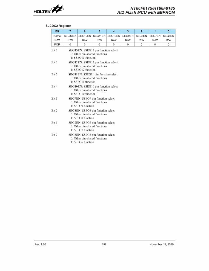
Rev. 1.60 152 November 19, 2019 Rev. 1.60 153 November 19, 2019
HT66F0175/HT66F0185A/D Flash MCU with EEPROM
HT66F0175/HT66F0185A/D Flash MCU with EEPROM
SLCDC2 RegisterBit 7 6 5 4 3 2 1 0
Name SEG13EN SEG12EN SEG11EN SEG10EN SEG9EN SEG8EN SEG7EN SEG6ENR/W R/W R/W R/W R/W R/W R/W R/W R/WPOR 0 0 0 0 0 0 0 0
Bit 7 SEG13EN: SSEG13 pin function select0: Other pin-shared functions1: SSEG13 function
Bit 6 SEG12EN: SSEG12 pin function select0: Other pin-shared functions1: SSEG12 function
Bit 5 SEG11EN: SSEG11 pin function select0: Other pin-shared functions1: SSEG11 function
Bit 4 SEG10EN: SSEG10 pin function select0: Other pin-shared functions1: SSEG10 function
Bit 3 SEG9EN: SSEG9 pin function select0: Other pin-shared functions1: SSEG9 function
Bit 2 SEG8EN: SSEG8 pin function select0: Other pin-shared functions1: SSEG8 function
Bit 1 SEG7EN: SSEG7 pin function select0: Other pin-shared functions1: SSEG7 function
Bit 0 SEG6EN: SSEG6 pin function select0: Other pin-shared functions1: SSEG6 function
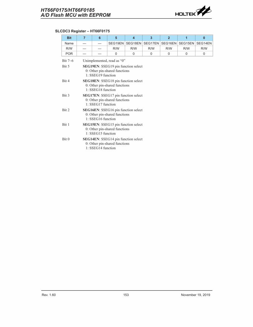
Rev. 1.60 152 November 19, 2019 Rev. 1.60 153 November 19, 2019
HT66F0175/HT66F0185A/D Flash MCU with EEPROM
HT66F0175/HT66F0185A/D Flash MCU with EEPROM
SLCDC3 Register – HT66F0175Bit 7 6 5 4 3 2 1 0
Name — — SEG19EN SEG18EN SEG17EN SEG16EN SEG15EN SEG14ENR/W — — R/W R/W R/W R/W R/W R/WPOR — — 0 0 0 0 0 0
Bit 7~6 Unimplemented, read as “0”Bit 5 SEG19EN: SSEG19 pin function select
0: Other pin-shared functions1: SSEG19 function
Bit 4 SEG18EN: SSEG18 pin function select0: Other pin-shared functions1: SSEG18 function
Bit 3 SEG17EN: SSEG17 pin function select0: Other pin-shared functions1: SSEG17 function
Bit 2 SEG16EN: SSEG16 pin function select0: Other pin-shared functions1: SSEG16 function
Bit 1 SEG15EN: SSEG15 pin function select0: Other pin-shared functions1: SSEG15 function
Bit 0 SEG14EN: SSEG14 pin function select0: Other pin-shared functions1: SSEG14 function
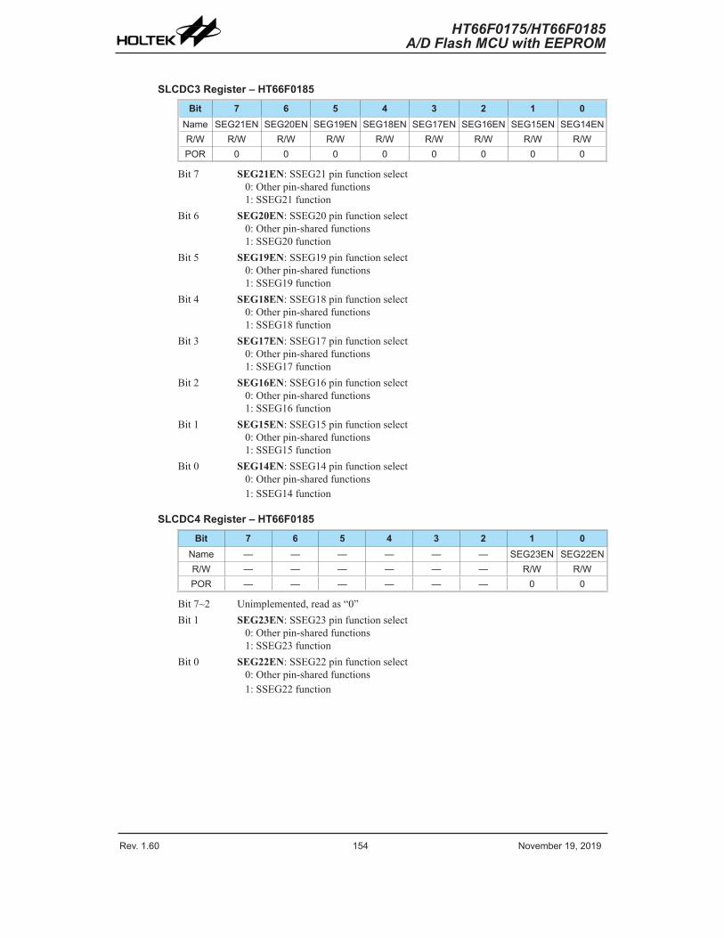
Rev. 1.60 154 November 19, 2019 Rev. 1.60 155 November 19, 2019
HT66F0175/HT66F0185A/D Flash MCU with EEPROM
HT66F0175/HT66F0185A/D Flash MCU with EEPROM
SLCDC3 Register – HT66F0185Bit 7 6 5 4 3 2 1 0
Name SEG21EN SEG20EN SEG19EN SEG18EN SEG17EN SEG16EN SEG15EN SEG14ENR/W R/W R/W R/W R/W R/W R/W R/W R/WPOR 0 0 0 0 0 0 0 0
Bit 7 SEG21EN: SSEG21 pin function select0: Other pin-shared functions1: SSEG21 function
Bit 6 SEG20EN: SSEG20 pin function select0: Other pin-shared functions1: SSEG20 function
Bit 5 SEG19EN: SSEG19 pin function select0: Other pin-shared functions1: SSEG19 function
Bit 4 SEG18EN: SSEG18 pin function select0: Other pin-shared functions1: SSEG18 function
Bit 3 SEG17EN: SSEG17 pin function select0: Other pin-shared functions1: SSEG17 function
Bit 2 SEG16EN: SSEG16 pin function select0: Other pin-shared functions1: SSEG16 function
Bit 1 SEG15EN: SSEG15 pin function select0: Other pin-shared functions1: SSEG15 function
Bit 0 SEG14EN: SSEG14 pin function select0: Other pin-shared functions1: SSEG14 function
SLCDC4 Register – HT66F0185Bit 7 6 5 4 3 2 1 0
Name — — — — — — SEG23EN SEG22ENR/W — — — — — — R/W R/WPOR — — — — — — 0 0
Bit 7~2 Unimplemented, read as “0”Bit 1 SEG23EN: SSEG23 pin function select
0: Other pin-shared functions1: SSEG23 function
Bit 0 SEG22EN: SSEG22 pin function select0: Other pin-shared functions1: SSEG22 function
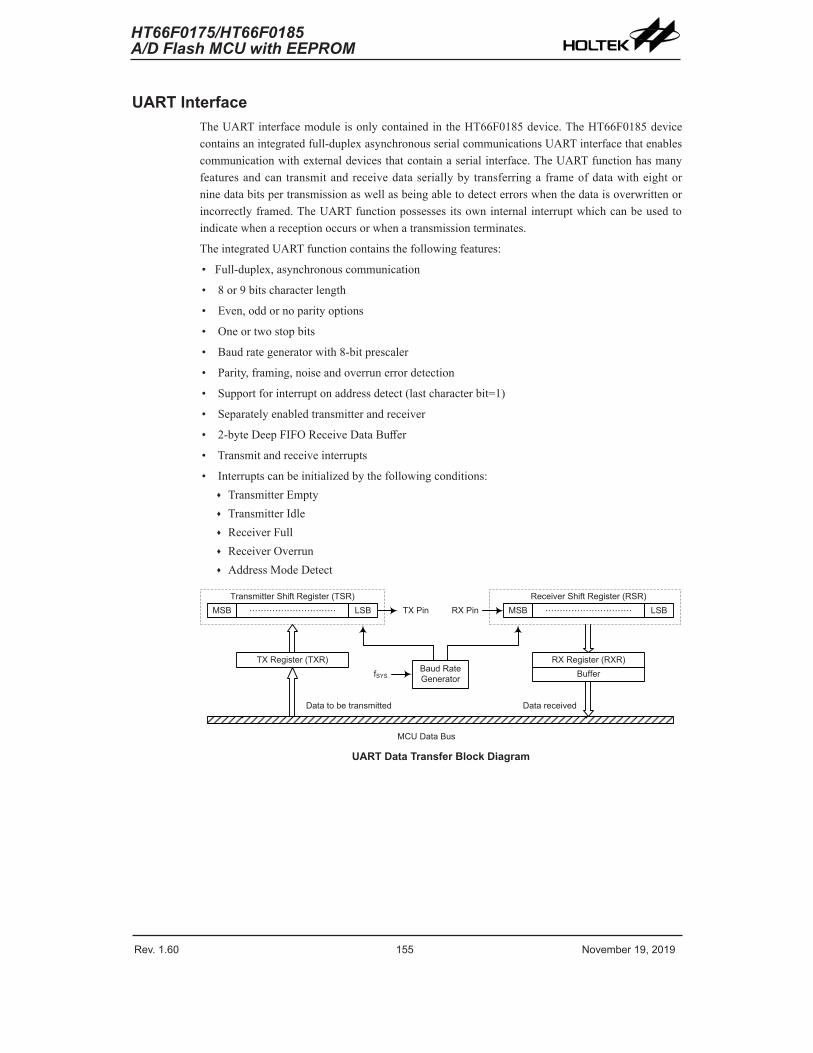
Rev. 1.60 154 November 19, 2019 Rev. 1.60 155 November 19, 2019
HT66F0175/HT66F0185A/D Flash MCU with EEPROM
HT66F0175/HT66F0185A/D Flash MCU with EEPROM
UART InterfaceThe UART interface module is only contained in the HT66F0185 device. The HT66F0185 device contains an integrated full-duplex asynchronous serial communications UART interface that enables communication with external devices that contain a serial interface. The UART function has many features and can transmit and receive data serially by transferring a frame of data with eight or nine data bits per transmission as well as being able to detect errors when the data is overwritten or incorrectly framed. The UART function possesses its own internal interrupt which can be used to indicate when a reception occurs or when a transmission terminates.
The integrated UART function contains the following features:
• Full-duplex, asynchronous communication
• 8 or 9 bits character length
• Even, odd or no parity options
• One or two stop bits
• Baud rate generator with 8-bit prescaler
• Parity, framing, noise and overrun error detection
• Support for interrupt on address detect (last character bit=1)
• Separately enabled transmitter and receiver
• 2-byte Deep FIFO Receive Data Buffer
• Transmit and receive interrupts
• Interrupts can be initialized by the following conditions: ♦ Transmitter Empty ♦ Transmitter Idle ♦ Receiver Full ♦ Receiver Overrun ♦ Address Mode Detect
MSB LSB…………………………
Transmitter Shift Register (TSR)MSB LSB…………………………
Receiver Shift Register (RSR)TX Pin RX Pin
Baud Rate Generator
TX Register (TXR) RX Register (RXR)
Data to be transmitted Data received
BufferfSYS
MCU Data Bus
UART Data Transfer Block Diagram
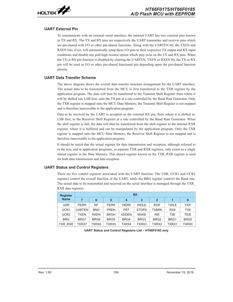
Rev. 1.60 156 November 19, 2019 Rev. 1.60 157 November 19, 2019
HT66F0175/HT66F0185A/D Flash MCU with EEPROM
HT66F0175/HT66F0185A/D Flash MCU with EEPROM
UART External PinTo communicate with an external serial interface, the internal UART has two external pins known as TX and RX. The TX and RX pins are respectively the UART transmitter and receiver pins which are pin-shared with I/O or other pin-shared functions. Along with the UARTEN bit, the TXEN and RXEN bits, if set, will automatically setup these I/O pins to their respective TX output and RX input conditions and disable any pull-high resistor option which may exist on the TX and RX pins. When the TX or RX pin function is disabled by clearing the UARTEN, TXEN or RXEN bit, the TX or RX pin will be used as I/O or other pin-shared functional pin depending upon the pin-shared function priority.
UART Data Transfer SchemeThe above diagram shows the overall data transfer structure arrangement for the UART interface. The actual data to be transmitted from the MCU is first transferred to the TXR register by the application program. The data will then be transferred to the Transmit Shift Register from where it will be shifted out, LSB first, onto the TX pin at a rate controlled by the Baud Rate Generator. Only the TXR register is mapped onto the MCU Data Memory, the Transmit Shift Register is not mapped and is therefore inaccessible to the application program.
Data to be received by the UART is accepted on the external RX pin, from where it is shifted in, LSB first, to the Receiver Shift Register at a rate controlled by the Baud Rate Generator. When the shift register is full, the data will then be transferred from the shift register to the internal RXR register, where it is buffered and can be manipulated by the application program. Only the TXR register is mapped onto the MCU Data Memory, the Receiver Shift Register is not mapped and is therefore inaccessible to the application program.
It should be noted that the actual register for data transmission and reception, although referred to in the text, and in application programs, as separate TXR and RXR registers, only exists as a single shared register in the Data Memory. This shared register known as the TXR_RXR register is used for both data transmission and data reception.
UART Status and Control RegistersThere are five control registers associated with the UART function. The USR, UCR1 and UCR2 registers control the overall function of the UART, while the BRG register controls the Baud rate. The actual data to be transmitted and received on the serial interface is managed through the TXR_RXR data registers.
Register Name
Bit7 6 5 4 3 2 1 0
USR PERR NF FERR OERR RIDLE RXIF TIDLE TXIFUCR1 UARTEN BNO PREN PRT STOPS TXBRK RX8 TX8UCR2 TXEN RXEN BRGH ADDEN WAKE RIE TIIE TEIEBRG BRG7 BRG6 BRG5 BRG4 BRG3 BRG2 BRG1 BRG0
TXR_RXR TXRX7 TXRX6 TXRX5 TXRX4 TXRX3 TXRX2 TXRX1 TXRX0
UART Status and Control Registers List – HT66F0185 only
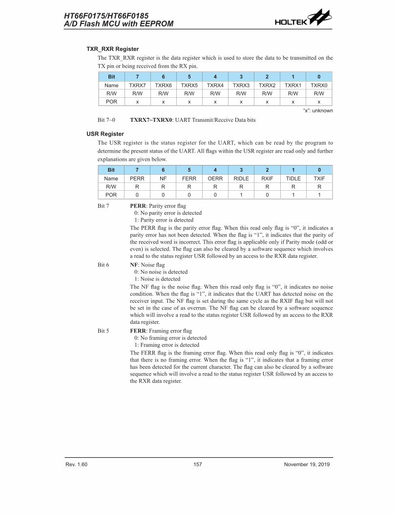
Rev. 1.60 156 November 19, 2019 Rev. 1.60 157 November 19, 2019
HT66F0175/HT66F0185A/D Flash MCU with EEPROM
HT66F0175/HT66F0185A/D Flash MCU with EEPROM
TXR_RXR RegisterThe TXR_RXR register is the data register which is used to store the data to be transmitted on the TX pin or being received from the RX pin.
Bit 7 6 5 4 3 2 1 0Name TXRX7 TXRX6 TXRX5 TXRX4 TXRX3 TXRX2 TXRX1 TXRX0R/W R/W R/W R/W R/W R/W R/W R/W R/WPOR x x x x x x x x
“x”: unknown
Bit 7~0 TXRX7~TXRX0: UART Transmit/Receive Data bits
USR RegisterThe USR register is the status register for the UART, which can be read by the program to determine the present status of the UART. All flags within the USR register are read only and further explanations are given below.
Bit 7 6 5 4 3 2 1 0Name PERR NF FERR OERR RIDLE RXIF TIDLE TXIFR/W R R R R R R R RPOR 0 0 0 0 1 0 1 1
Bit 7 PERR: Parity error flag0: No parity error is detected1: Parity error is detected
The PERR flag is the parity error flag. When this read only flag is “0”, it indicates a parity error has not been detected. When the flag is “1”, it indicates that the parity of the received word is incorrect. This error flag is applicable only if Parity mode (odd or even) is selected. The flag can also be cleared by a software sequence which involves a read to the status register USR followed by an access to the RXR data register.
Bit 6 NF: Noise flag0: No noise is detected1: Noise is detected
The NF flag is the noise flag. When this read only flag is “0”, it indicates no noise condition. When the flag is “1”, it indicates that the UART has detected noise on the receiver input. The NF flag is set during the same cycle as the RXIF flag but will not be set in the case of as overrun. The NF flag can be cleared by a software sequence which will involve a read to the status register USR followed by an access to the RXR data register.
Bit 5 FERR: Framing error flag0: No framing error is detected1: Framing error is detected
The FERR flag is the framing error flag. When this read only flag is “0”, it indicates that there is no framing error. When the flag is “1”, it indicates that a framing error has been detected for the current character. The flag can also be cleared by a software sequence which will involve a read to the status register USR followed by an access to the RXR data register.
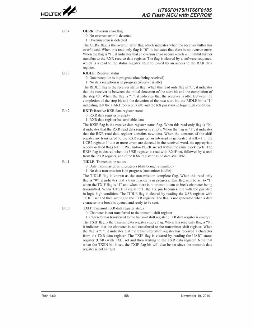
Rev. 1.60 158 November 19, 2019 Rev. 1.60 159 November 19, 2019
HT66F0175/HT66F0185A/D Flash MCU with EEPROM
HT66F0175/HT66F0185A/D Flash MCU with EEPROM
Bit 4 OERR: Overrun error flag0: No overrun error is detected1: Overrun error is detected
The OERR flag is the overrun error flag which indicates when the receiver buffer has overflowed. When this read only flag is “0”, it indicates that there is no overrun error. When the flag is “1”, it indicates that an overrun error occurs which will inhibit further transfers to the RXR receive data register. The flag is cleared by a software sequence, which is a read to the status register USR followed by an access to the RXR data register.
Bit 3 RIDLE: Receiver status0: Data reception is in progress (data being received)1: No data reception is in progress (receiver is idle)
The RIDLE flag is the receiver status flag. When this read only flag is “0”, it indicates that the receiver is between the initial detection of the start bit and the completion of the stop bit. When the flag is “1”, it indicates that the receiver is idle. Between the completion of the stop bit and the detection of the next start bit, the RIDLE bit is “1” indicating that the UART receiver is idle and the RX pin stays in logic high condition.
Bit 2 RXIF: Receive RXR data register status0: RXR data register is empty1: RXR data register has available data
The RXIF flag is the receive data register status flag. When this read only flag is “0”, it indicates that the RXR read data register is empty. When the flag is “1”, it indicates that the RXR read data register contains new data. When the contents of the shift register are transferred to the RXR register, an interrupt is generated if RIE=1 in the UCR2 register. If one or more errors are detected in the received word, the appropriate receive-related flags NF, FERR, and/or PERR are set within the same clock cycle. The RXIF flag is cleared when the USR register is read with RXIF set, followed by a read from the RXR register, and if the RXR register has no data available.
Bit 1 TIDLE: Transmission status0: Data transmission is in progress (data being transmitted)1: No data transmission is in progress (transmitter is idle)
The TIDLE flag is known as the transmission complete flag. When this read only flag is “0”, it indicates that a transmission is in progress. This flag will be set to “1” when the TXIF flag is “1” and when there is no transmit data or break character being transmitted. When TIDLE is equal to 1, the TX pin becomes idle with the pin state in logic high condition. The TIDLE flag is cleared by reading the USR register with TIDLE set and then writing to the TXR register. The flag is not generated when a data character or a break is queued and ready to be sent.
Bit 0 TXIF: Transmit TXR data register status0: Character is not transferred to the transmit shift register1: Character has transferred to the transmit shift register (TXR data register is empty)
The TXIF flag is the transmit data register empty flag. When this read only flag is “0”, it indicates that the character is not transferred to the transmitter shift register. When the flag is “1”, it indicates that the transmitter shift register has received a character from the TXR data register. The TXIF flag is cleared by reading the UART status register (USR) with TXIF set and then writing to the TXR data register. Note that when the TXEN bit is set, the TXIF flag bit will also be set since the transmit data register is not yet full.
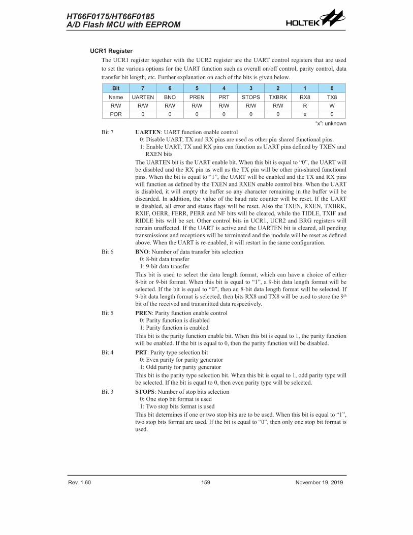
Rev. 1.60 158 November 19, 2019 Rev. 1.60 159 November 19, 2019
HT66F0175/HT66F0185A/D Flash MCU with EEPROM
HT66F0175/HT66F0185A/D Flash MCU with EEPROM
UCR1 RegisterThe UCR1 register together with the UCR2 register are the UART control registers that are used to set the various options for the UART function such as overall on/off control, parity control, data transfer bit length, etc. Further explanation on each of the bits is given below.
Bit 7 6 5 4 3 2 1 0Name UARTEN BNO PREN PRT STOPS TXBRK RX8 TX8R/W R/W R/W R/W R/W R/W R/W R WPOR 0 0 0 0 0 0 x 0
“x”: unknownBit 7 UARTEN: UART function enable control
0: Disable UART; TX and RX pins are used as other pin-shared functional pins.1: Enable UART; TX and RX pins can function as UART pins defined by TXEN and
RXEN bitsThe UARTEN bit is the UART enable bit. When this bit is equal to “0”, the UART will be disabled and the RX pin as well as the TX pin will be other pin-shared functional pins. When the bit is equal to “1”, the UART will be enabled and the TX and RX pins will function as defined by the TXEN and RXEN enable control bits. When the UART is disabled, it will empty the buffer so any character remaining in the buffer will be discarded. In addition, the value of the baud rate counter will be reset. If the UART is disabled, all error and status flags will be reset. Also the TXEN, RXEN, TXBRK, RXIF, OERR, FERR, PERR and NF bits will be cleared, while the TIDLE, TXIF and RIDLE bits will be set. Other control bits in UCR1, UCR2 and BRG registers will remain unaffected. If the UART is active and the UARTEN bit is cleared, all pending transmissions and receptions will be terminated and the module will be reset as defined above. When the UART is re-enabled, it will restart in the same configuration.
Bit 6 BNO: Number of data transfer bits selection0: 8-bit data transfer1: 9-bit data transfer
This bit is used to select the data length format, which can have a choice of either 8-bit or 9-bit format. When this bit is equal to “1”, a 9-bit data length format will be selected. If the bit is equal to “0”, then an 8-bit data length format will be selected. If 9-bit data length format is selected, then bits RX8 and TX8 will be used to store the 9th bit of the received and transmitted data respectively.
Bit 5 PREN: Parity function enable control0: Parity function is disabled1: Parity function is enabled
This bit is the parity function enable bit. When this bit is equal to 1, the parity function will be enabled. If the bit is equal to 0, then the parity function will be disabled.
Bit 4 PRT: Parity type selection bit0: Even parity for parity generator1: Odd parity for parity generator
This bit is the parity type selection bit. When this bit is equal to 1, odd parity type will be selected. If the bit is equal to 0, then even parity type will be selected.
Bit 3 STOPS: Number of stop bits selection0: One stop bit format is used1: Two stop bits format is used
This bit determines if one or two stop bits are to be used. When this bit is equal to “1”, two stop bits format are used. If the bit is equal to “0”, then only one stop bit format is used.
Rev. 1.60 160 November 19, 2019 Rev. 1.60 161 November 19, 2019
HT66F0175/HT66F0185A/D Flash MCU with EEPROM
HT66F0175/HT66F0185A/D Flash MCU with EEPROM
Bit 2 TXBRK: Transmit break character0: No break character is transmitted1: Break characters transmit
The TXBRK bit is the Transmit Break Character bit. When this bit is equal to “0”, there are no break characters and the TX pin operats normally. When the bit is equal to “1”, there are transmit break characters and the transmitter will send logic zeros. When this bit is equal to “1”, after the buffered data has been transmitted, the transmitter output is held low for a minimum of a 13-bit length and until the TXBRK bit is reset.
Bit 1 RX8: Receive data bit 8 for 9-bit data transfer format (read only)This bit is only used if 9-bit data transfers are used, in which case this bit location will store the 9th bit of the received data known as RX8. The BNO bit is used to determine whether data transfes are in 8-bit or 9-bit format.
Bit 0 TX8: Transmit data bit 8 for 9-bit data transfer format (write only)This bit is only used if 9-bit data transfers are used, in which case this bit location will store the 9th bit of the transmitted data known as TX8. The BNO bit is used to determine whether data transfes are in 8-bit or 9-bit format.
UCR2 RegisterThe UCR2 register is the second of the UART control registers and serves several purposes. One of its main functions is to control the basic enable/disable operation if the UART Transmitter and Receiver as well as enabling the various UART interrupt sources. The register also serves to control the baud rate speed, receiver wake-up function enable and the address detect function enable. Further explanation on each of the bits is given below.
Bit 7 6 5 4 3 2 1 0Name TXEN RXEN BRGH ADDEN WAKE RIE TIIE TEIER/W R/W R/W R/W R/W R/W R/W R/W R/WPOR 0 0 0 0 0 0 0 0
Bit 7 TXEN: UART Transmitter enable control0: UART Transmitter is disabled1: UART Transmitter is enabled
The TXEN bit is the Transmitter Enable Bit. When this bit is equal to “0”, the transmitter will be disabled with any pending data transmissions being aborted. In addition the buffers will be reset. In this situation the TX pin will be other pin-shared functional pin. If the TXEN bit is equal to “1” and the UARTEN bit is also equal to 1, the transmitter will be enabled and the TX pin will be controlled by the UART. Clearing the TXEN bit during a transmission will cause the data transmission to be aborted and will reset the transmitter. If this situation occurs, the TX pin will be other pin-shared functional pin.
Bit 6 RXEN: UART Receiver enable control0: UART Receiver is disabled1: UART Receiver is enabled
The RXEN bit is the Receiver Enable Bit. When this bit is equal to “0”, the receiver will be disabled with any pending data receptions being aborted. In addition the receiver buffers will be reset. In this situation the RX pin will be other pin-shared functional pin. If the RXEN bit is equal to “1” and the UARTEN bit is also equal to 1, the receiver will be enabled and the RX pin will be controlled by the UART. Clearing the RXEN bit during a reception will cause the data reception to be aborted and will reset the receiver. If this situation occurs, the RX pin will be other pin-shared functional pin.
Rev. 1.60 160 November 19, 2019 Rev. 1.60 161 November 19, 2019
HT66F0175/HT66F0185A/D Flash MCU with EEPROM
HT66F0175/HT66F0185A/D Flash MCU with EEPROM
Bit 5 BRGH: Baud Rate speed selection0: Low speed baud rate1: High speed baud rate
The bit named BRGH selects the high or low speed mode of the Baud Rate Generator. This bit, together with the value placed in the baud rate register, BRG, controls the baud rate of the UART. If the bit is equal to 0, the low speed mode is selected.
Bit 4 ADDEN: Address detect function enable control0: Address detection function is disabled1: Address detection function is enabled
The bit named ADDEN is the address detection function enable control bit. When this bit is equal to 1, the address detection function is enabled. When it occurs, if the 8th bit, which corresponds to RX7 if BNO=0, or the 9th bit, which corresponds to RX8 if BNO=1, has a value of “1”, then the received word will be identified as an address, rather than data. If the corresponding interrupt is enabled, an interrupt request will be generated each time the received word has the address bit set, which is the 8th or 9th bit depending on the value of the BNO bit. If the address bit known as the 8th or 9th bit of the received word is “0” with the address detection function being enabled, an interrupt will not be generated and the received data will be discarded.
Bit 3 WAKE: RX pin falling edge wake-up function enable control0: RX pin wake-up function is disabled1: RX pin wake-up function is enabled
The bit enables or disables the receiver wake-up function. If this bit is equal to 1 and the device is in IDLE0 or SLEEP mode, a falling edge on the RX pin will wake up the device. If this bit is equal to 0 and the device is in the power down mode, any edge transitions on the RX pin will not wake up the device.
Bit 2 RIE: Receiver interrupt enable control0: Receiver related interrupt is disabled1: Receiver related interrupt is enabled
The bit enables or disables the receiver interrupt. If this bit is equal to 1 and when the receiver overrun flag OERR or received data available flag RXIF is set, the UART interrupt request flag will be set. If this bit is equal to 0, the UART interrupt request flag will not be influenced by the condition of the OERR or RXIF flags.
Bit 1 TIIE: Transmitter Idle interrupt enable control0: Transmitter idle interrupt is disabled1: Transmitter idle interrupt is enabled
The bit enables or disables the transmitter idle interrupt. If this bit is equal to 1 and when the transmitter idle flag TIDLE is set, due to a transmitter idle condition, the UART interrupt request flag will be set. If this bit is equal to 0, the UART interrupt request flag will not be influenced by the condition of the TIDLE flag.
Bit 0 TEIE: Transmitter Empty interrupt enable control0: Transmitter empty interrupt is disabled1: Transmitter empty interrupt is enabled
The bit enables or disables the transmitter empty interrupt. If this bit is equal to 1 and when the transmitter empty flag TXIF is set, due to a transmitter empty condition, the UART interrupt request flag will be set. If this bit is equal to 0, the UART interrupt request flag will not be influenced by the condition of the TXIF flag.
Rev. 1.60 162 November 19, 2019 Rev. 1.60 163 November 19, 2019
HT66F0175/HT66F0185A/D Flash MCU with EEPROM
HT66F0175/HT66F0185A/D Flash MCU with EEPROM
Baud Rate GeneratorTo setup the speed of the serial data communication, the UART function contains its own dedicated baud rate generator. The baud rate is controlled by its own internal free running 8-bit counter, the period of which is determined by two factors. The first of these is the value placed in the BRG register and the second is the value of the BRGH bit within the UCR2 control register. The BRGH bit decides, if the baud rate generator is to be used in a high speed mode or low speed mode, which in turn determines the formula that is used to calculate the baud rate. The value in the BRG register, N, which is used in the following baud rate calculation formula determines the division factor. Note that N is the decimal value placed in the BRG register and has a range of between 0 and 255.
UCR2 BRGH Bit 0 1
Baud Rate (BR)fSYS
[64(N+1)]fSYS
[16(N+1)]
By programming the BRGH bit which allows selection of the related formula and programming the required value in the BRG register, the required baud rate can be setup. Note that because the actual baud rate is determined using a discrete value, N, placed in the BRG register, there will be an error associated between the actual and requested value. The following example shows how the BRG register value N and the error value can be calculated.
BRG RegisterBit 7 6 5 4 3 2 1 0
Name BRG7 BRG6 BRG5 BRG4 BRG3 BRG2 BRG1 BRG0R/W R/W R/W R/W R/W R/W R/W R/W R/WPOR x x x x x x x x
“x”: unknownBit 7~0 BRG7~BRG0: Baud Rate values
By programming the BRGH bit in the UCR2 register which allows selection of the related formula described above and programming the required value in the BRG register, the required baud rate can be setup.
Calculating the Baud Rate and Error ValuesFor a clock frequency of 4MHz, and with BRGH set to 0 determine the BRG register value N, the actual baud rate and the error value for a desired baud rate of 4800.
From the above table the desired baud rate BR = fSYS
[64(N+1)]
Re-arranging this equation gives N = fSYS
(BR×64) - 1
Giving a value for N = 4000000(4800×64) - 1 = 12.0208
To obtain the closest value, a decimal value of 12 should be placed into the BRG register. This gives an actual or calculated baud rate value of BR = 4000000
[64(12+1)] = 4808
Therefore the error is equal to 4808-48004800
= 0.16%
Rev. 1.60 162 November 19, 2019 Rev. 1.60 163 November 19, 2019
HT66F0175/HT66F0185A/D Flash MCU with EEPROM
HT66F0175/HT66F0185A/D Flash MCU with EEPROM
UART Setup and ControlFor data transfer, the UART function utilizes a non-return-to-zero, more commonly known as NRZ, format. This is composed of one start bit, eight or nine data bits and one or two stop bits. Parity is supported by the UART hardware and can be setup to be even, odd or no parity. For the most common data format, 8 data bits along with no parity and one stop bit, denoted as 8, N, 1, is used as the default setting, which is the setting at power-on. The number of data bits and stop bits, along with the parity, are setup by programming the corresponding BNO, PRT, PREN and STOPS bits in the UCR1 register. The baud rate used to transmit and receive data is setup using the internal 8-bit baud rate generator, while the data is transmitted and received LSB first. Although the transmitter and receiver of the UART are functionally independent, they both use the same data format and baud rate. In all cases stop bits will be used for data transmission.
Enabling/Disabling the UART InterfaceThe basic on/off function of the internal UART function is controlled using the UARTEN bit in the UCR1 register. If the UARTEN, TXEN and RXEN bits are set, then these two UART pins will act as normal TX output pin and RX input pin respectively. If no data is being transmitted on the TX pin, then it will default to a logic high value.
Clearing the UARTEN bit will disable the TX and RX pins and these two pins will be used as I/O or other pin-shared functional pins. When the UART function is disabled, the buffer will be reset to an empty condition, at the same time discarding any remaining residual data. Disabling the UART will also reset the enable control, the error and status flags with bits TXEN, RXEN, TXBRK, RXIF, OERR, FERR, PERR and NF being cleared while bits TIDLE, TXIF and RIDLE will be set. The remaining control bits in the UCR1, UCR2 and BRG registers will remain unaffected. If the UARTEN bit in the UCR1 register is cleared while the UART is active, then all pending transmissions and receptions will be immediately suspended and the UART will be reset to a condition as defined above. If the UART is then subsequently re-enabled, it will restart again in the same configuration.
Data, Parity and Stop Bit SelectionThe format of the data to be transferred is composed of various factors such as data bit length, parity on/off, parity type, address bits and the number of stop bits. These factors are determined by the setup of various bits within the UCR1 register. The BNO bit controls the number of data bits which can be set to either 8 or 9. The PRT bit controls the choice if odd or even parity. The PREN bit controls the parity on/off function. The STOPS bit decides whether one or two stop bits are to be used. The following table shows various formats for data transmission. The address detect mode control bit identifies the frame as an address character. The number of stop bits, which can be either one or two, is independent of the data length.
Start Bit Data Bits Address Bits Parity Bit Stop BitExample of 8-bit Data Formats
1 8 0 0 11 7 0 1 11 7 1 0 1
Example of 9-bit Data Formats1 9 0 0 11 8 0 1 11 8 1 0 1
Transmitter Receiver Data Format
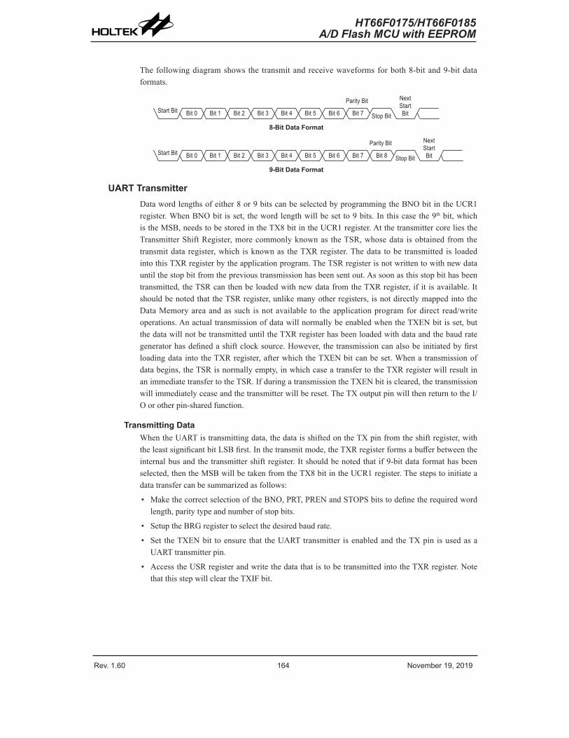
Rev. 1.60 164 November 19, 2019 Rev. 1.60 165 November 19, 2019
HT66F0175/HT66F0185A/D Flash MCU with EEPROM
HT66F0175/HT66F0185A/D Flash MCU with EEPROM
The following diagram shows the transmit and receive waveforms for both 8-bit and 9-bit data formats.
� � � � � � � � � � � � � � � � � � � � � � � � � � � � � � � � � � � � � � � � � � � � � � � � � � � � � � � � �
� � �� � � � �� � �
� � � � � � � � �
� � � � � � � � � � � � � � � � �
� � � � � � � � � � � � � � � � � � � � � � � � � � � � � � � � � � � � � � � � � � � � � � � � � � � � � � � � �
� � �� � � � �� � �
� � � � � � � � �
� � � � � � � � � � � � � � � � �
� � � �
UART TransmitterData word lengths of either 8 or 9 bits can be selected by programming the BNO bit in the UCR1 register. When BNO bit is set, the word length will be set to 9 bits. In this case the 9th bit, which is the MSB, needs to be stored in the TX8 bit in the UCR1 register. At the transmitter core lies the Transmitter Shift Register, more commonly known as the TSR, whose data is obtained from the transmit data register, which is known as the TXR register. The data to be transmitted is loaded into this TXR register by the application program. The TSR register is not written to with new data until the stop bit from the previous transmission has been sent out. As soon as this stop bit has been transmitted, the TSR can then be loaded with new data from the TXR register, if it is available. It should be noted that the TSR register, unlike many other registers, is not directly mapped into the Data Memory area and as such is not available to the application program for direct read/write operations. An actual transmission of data will normally be enabled when the TXEN bit is set, but the data will not be transmitted until the TXR register has been loaded with data and the baud rate generator has defined a shift clock source. However, the transmission can also be initiated by first loading data into the TXR register, after which the TXEN bit can be set. When a transmission of data begins, the TSR is normally empty, in which case a transfer to the TXR register will result in an immediate transfer to the TSR. If during a transmission the TXEN bit is cleared, the transmission will immediately cease and the transmitter will be reset. The TX output pin will then return to the I/O or other pin-shared function.
Transmitting DataWhen the UART is transmitting data, the data is shifted on the TX pin from the shift register, with the least significant bit LSB first. In the transmit mode, the TXR register forms a buffer between the internal bus and the transmitter shift register. It should be noted that if 9-bit data format has been selected, then the MSB will be taken from the TX8 bit in the UCR1 register. The steps to initiate a data transfer can be summarized as follows:
• Make the correct selection of the BNO, PRT, PREN and STOPS bits to define the required word length, parity type and number of stop bits.
• Setup the BRG register to select the desired baud rate.
• Set the TXEN bit to ensure that the UART transmitter is enabled and the TX pin is used as a UART transmitter pin.
• Access the USR register and write the data that is to be transmitted into the TXR register. Note that this step will clear the TXIF bit.
Rev. 1.60 164 November 19, 2019 Rev. 1.60 165 November 19, 2019
HT66F0175/HT66F0185A/D Flash MCU with EEPROM
HT66F0175/HT66F0185A/D Flash MCU with EEPROM
This sequence of events can now be repeated to send additional data. It should be noted that when TXIF=0, data will be inhibited from being written to the TXR register. Clearing the TXIF flag is always achieved using the following software sequence:
1. A USR register access
2. A TXR register write execution
The read-only TXIF flag is set by the UART hardware and if set indicates that the TXR register is empty and that other data can now be written into the TXR register without overwriting the previous data. If the TEIE bit is set, then the TXIF flag will generate an interrupt. During a data transmission, a write instruction to the TXR register will place the data into the TXR register, which will be copied to the shift register at the end of the present transmission. When there is no data transmission in progress, a write instruction to the TXR register will place the data directly into the shift register, resulting in the commencement of data transmission, and the TXIF bit being immediately set. When a frame transmission is complete, which happens after stop bits are sent or after the break frame, the TIDLE bit will be set. To clear the TIDLE bit the following software sequence is used:
1. A USR register access
2. A TXR register write execution
Note that both the TXIF and TIDLE bits are cleared by the same software sequence.
Transmitting BreakIf the TXBRK bit is set, then the break characters will be sent on the next transmission. Break character transmission consists of a start bit, followed by 13xN “0” bits, where N=1, 2, etc. If a break character is to be transmitted, then the TXBRK bit must be first set by the application program and then cleared to generate the stop bits. Transmitting a break character will not generate a transmit interrupt. Note that a break condition length is at least 13 bits long. If the TXBRK bit is continually kept at a logic high level, then the transmitter circuitry will transmit continuous break characters. After the application program has cleared the TXBRK bit, the transmitter will finish transmitting the last break character and subsequently send out one or two stop bits. The automatic logic high at the end of the last break character will ensure that the start bit of the next frame is recognized.
UART ReceiverThe UART is capable of receiving word lengths of either 8 or 9 bits can be selected by programming the BNO bit in the UCR1 register. When BNO bit is set, the word length will be set to 9 bits. In this case the 9th bit, which is the MSB, will be stored in the RX8 bit in the UCR1 register. At the receiver core lies the Receiver Shift Register more commonly known as the RSR. The data which is received on the RX external input pin is sent to the data recovery block. The data recovery block operating speed is 16 times that of the baud rate, while the main receive serial shifter operates at the baud rate. After the RX pin is sampled for the stop bit, the received data in RSR is transferred to the receive data register, if the register is empty. The data which is received on the external RX input pin is sampled three times by a majority detect circuit to determine the logic level that has been placed onto the RX pin. It should be noted that the RSR register, unlike many other registers, is not directly mapped into the Data Memory area and as such is not available to the application program for direct read/write operations.
Receiving DataWhen the UART receiver is receiving data, the data is serially shifted in on the external RX input pin to the shift register, with the least significant bit LSB first. The RXR register is a two byte deep FIFO data buffer, where two bytes can be held in the FIFO while the 3rd byte can continue to be received. Note that the application program must ensure that the data is read from RXR before the
Rev. 1.60 166 November 19, 2019 Rev. 1.60 167 November 19, 2019
HT66F0175/HT66F0185A/D Flash MCU with EEPROM
HT66F0175/HT66F0185A/D Flash MCU with EEPROM
3rd byte has been completely shifted in, otherwise the 3rd byte will be discarded and an overrun error OERR will be subsequently indicated. The steps to initiate a data transfer can be summarized as follows:
• Make the correct selection of the BNO, PRT, PREN and STOPS bits to define the required word length, parity type and number of stop bits.
• Setup the BRG register to select the desired baud rate.
• Set the RXEN bit to ensure that the UART receiver is enabled and the RX pin is used as a UART receiver pin.
At this point the receiver will be enabled which will begin to look for a start bit.
When a character is received, the following sequence of events will occur:
• The RXIF bit in the USR register will be set then RXR register has data available, at least one more character can be read.
• When the contents of the shift register have been transferred to the RXR register and if the RIE bit is set, then an interrupt will be generated.
• If during reception, a frame error, noise error, parity error or an overrun error has been detected, then the error flags can be set.
The RXIF bit can be cleared using the following software sequence:
1. A USR register access
2. A RXR register read execution
Receiving BreakAny break character received by the UART will be managed as a framing error. The receiver will count and expect a certain number of bit times as specified by the values programmed into the BNO and STOPS bits. If the break is much longer than 13 bit times, the reception will be considered as complete after the number of bit times specified by BNO and STOPS. The RXIF bit is set, FERR is set, zeros are loaded into the receive data register, interrupts are generated if appropriate and the RIDLE bit is set. If a long break signal has been detected and the receiver has received a start bit, the data bits and the invalid stop bit, which sets the FERR flag, the receiver must wait for a valid stop bit before looking for the next start bit. The receiver will not make the assumption that the break condition on the line is the next start bit. A break is regarded as a character that contains only zeros with the FERR flag set. The break character will be loaded into the buffer and no further data will be received until stop bits are received. It should be noted that the RIDLE read only flag will go high when the stop bits have not yet been received. The reception of a break character on the UART registers will result in the following:
• The framing error flag, FERR, will be set.
• The receive data register, RXR, will be cleared.
• The OERR, NF, PERR, RIDLE or RXIF flags will possibly be set.
Idle StatusWhen the receiver is reading data, which means it will be in between the detection of a start bit and the reading of a stop bit, the receiver status flag in the USR register, otherwise known as the RIDLE flag, will have a zero value. In between the reception of a stop bit and the detection of the next start bit, the RIDLE flag will have a high value, which indicates the receiver is in an idle condition.
Rev. 1.60 166 November 19, 2019 Rev. 1.60 167 November 19, 2019
HT66F0175/HT66F0185A/D Flash MCU with EEPROM
HT66F0175/HT66F0185A/D Flash MCU with EEPROM
Receiver InterruptThe read only receive interrupt flag, RXIF, in the USR register is set by an edge generated by the receiver. An interrupt is generated if RIE=1, when a word is transferred from the Receive Shift Register, RSR, to the Receive Data Register, RXR. An overrun error can also generate an interrupt if RIE=1.
Managing Receiver ErrorsSeveral types of reception errors can occur within the UART module, the following section describes the various types and how they are managed by the UART.
Overrun Error – OERRThe RXR register is composed of a two byte deep FIFO data buffer, where two bytes can be held in the FIFO register, while a 3th byte can continue to be received. Before the 3th byte has been entirely shifted in, the data should be read from the RXR register. If this is not done, the overrun error flag OERR will be consequently indicated.
In the event of an overrun error occurring, the following will happen:
• The OERR flag in the USR register will be set.
• The RXR contents will not be lost.
• The shift register will be overwritten.
• An interrupt will be generated if the RIE bit is set.
The OERR flag can be cleared by an access to the USR register followed by a read to the RXR register.
Noise Error – NFOver-sampling is used for data recovery to identify valid incoming data and noise. If noise is detected within a frame, the following will occur:
• The read only noise flag, NF, in the USR register will be set on the rising edge of the RXIF bit.
• Data will be transferred from the shift register to the RXR register.
• No interrupt will be generated. However this bit rises at the same time as the RXIF bit which itself generates an interrupt.
Note that the NF flag is reset by a USR register read operation followed by an RXR register read operation.
Framing Error – FERRThe read only framing error flag, FERR, in the USR register, is set if a zero is detected instead of stop bits. If two stop bits are selected, both stop bits must be high. Otherwise the FERR flag will be set. The FERR flag is buffered along with the received data and is cleared in any reset.
Parity Error – PERRThe read only parity error flag, PERR, in the USR register, is set if the parity of the received word is incorrect. This error flag is only applicable if the parity function is enabled, PREN=1, and if the parity type, odd or even, is selected. The read only PERR flag is buffered along with the received data bytes. It is cleared on any reset, it should be noted that the FERR and PERR flags are buffered along with the corresponding word and should be read before reading the data word.
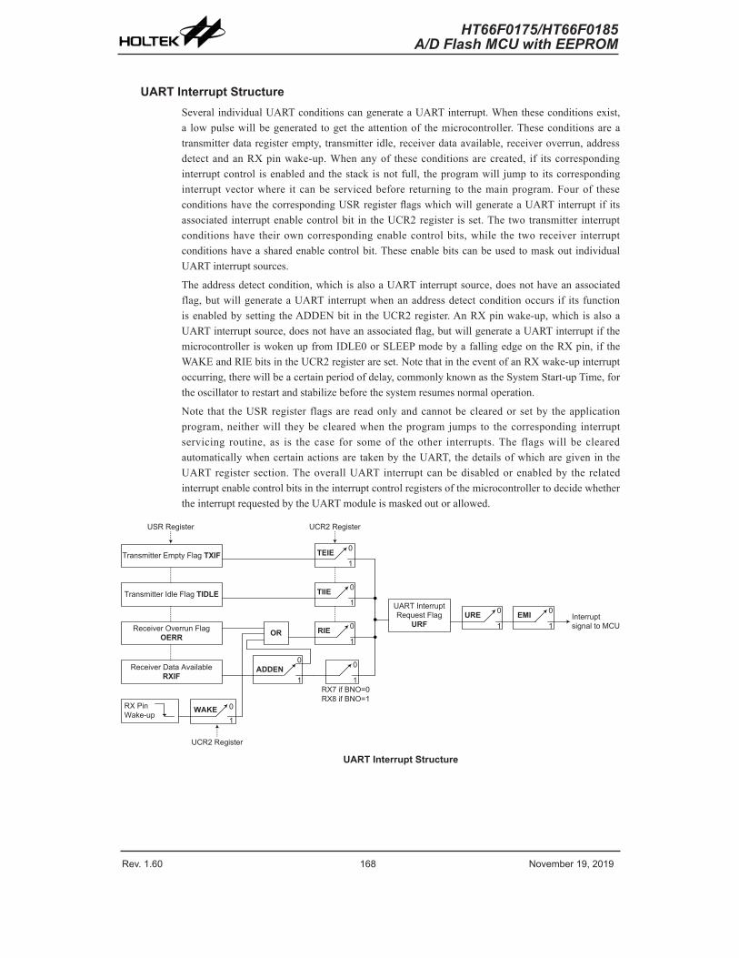
Rev. 1.60 168 November 19, 2019 Rev. 1.60 169 November 19, 2019
HT66F0175/HT66F0185A/D Flash MCU with EEPROM
HT66F0175/HT66F0185A/D Flash MCU with EEPROM
UART Interrupt StructureSeveral individual UART conditions can generate a UART interrupt. When these conditions exist, a low pulse will be generated to get the attention of the microcontroller. These conditions are a transmitter data register empty, transmitter idle, receiver data available, receiver overrun, address detect and an RX pin wake-up. When any of these conditions are created, if its corresponding interrupt control is enabled and the stack is not full, the program will jump to its corresponding interrupt vector where it can be serviced before returning to the main program. Four of these conditions have the corresponding USR register flags which will generate a UART interrupt if its associated interrupt enable control bit in the UCR2 register is set. The two transmitter interrupt conditions have their own corresponding enable control bits, while the two receiver interrupt conditions have a shared enable control bit. These enable bits can be used to mask out individual UART interrupt sources.
The address detect condition, which is also a UART interrupt source, does not have an associated flag, but will generate a UART interrupt when an address detect condition occurs if its function is enabled by setting the ADDEN bit in the UCR2 register. An RX pin wake-up, which is also a UART interrupt source, does not have an associated flag, but will generate a UART interrupt if the microcontroller is woken up from IDLE0 or SLEEP mode by a falling edge on the RX pin, if the WAKE and RIE bits in the UCR2 register are set. Note that in the event of an RX wake-up interrupt occurring, there will be a certain period of delay, commonly known as the System Start-up Time, for the oscillator to restart and stabilize before the system resumes normal operation.
Note that the USR register flags are read only and cannot be cleared or set by the application program, neither will they be cleared when the program jumps to the corresponding interrupt servicing routine, as is the case for some of the other interrupts. The flags will be cleared automatically when certain actions are taken by the UART, the details of which are given in the UART register section. The overall UART interrupt can be disabled or enabled by the related interrupt enable control bits in the interrupt control registers of the microcontroller to decide whether the interrupt requested by the UART module is masked out or allowed.
USR Register
Transmitter Empty Flag TXIF
0
1WAKE
Interrupt signal to MCU
Transmitter Idle Flag TIDLE
Receiver Overrun Flag OERR
Receiver Data Available RXIF
RX PinWake-up
UCR2 Register
OR
0
1ADDEN
0
1RIE
0
1TIIE
0
1TEIE
0
1RX7 if BNO=0RX8 if BNO=1
UCR2 Register
UART Interrupt Request Flag
URF
0
1URE 0
1EMI
UART Interrupt Structure
Rev. 1.60 168 November 19, 2019 Rev. 1.60 169 November 19, 2019
HT66F0175/HT66F0185A/D Flash MCU with EEPROM
HT66F0175/HT66F0185A/D Flash MCU with EEPROM
Address Detect ModeSetting the Address Detect function enable control bit, ADDEN, in the UCR2 register, enables this special function. If this bit is set to 1, then an additional qualifier will be placed on the generation of a Receiver Data Available interrupt, which is requested by the RXIF flag. If the ADDEN bit is equal to 1, then when the data is available, an interrupt will only be generated, if the highest received bit has a high value. Note that the related interrupt enable control bit and the EMI bit of the microcontroller must also be enabled for correct interrupt generation. The highest address bit is the 9th bit if the bit BNO=1 or the 8th bit if the bit BNO=0. If the highest bit is high, then the received word will be defined as an address rather than data. A Data Available interrupt will be generated every time the last bit of the received word is set. If the ADDEN bit is equal to 0, then a Receive Data Available interrupt will be generated each time the RXIF flag is set, irrespective of the data last but status. The address detection and parity functions are mutually exclusive functions. Therefore, if the address detect function is enabled, then to ensure correct operation, the parity function should be disabled by resetting the parity function enable bit PREN to zero.
ADDEN Bit 9 if BNO=1Bit 8 if BNO=0
UART Interrupt Generated
00 √1 √
10 X1 √
ADDEN Bit Function
UART Power Down and Wake-upWhen the MCU system clock is switched off, the UART will cease to function. If the MCU executes the “HALT” instruction and switches off the system clock while a transmission is still in progress, then the transmission will be paused until the UART clock source derived from the microcontroller is activated. In a similar way, if the MCU executes the “HALT” instruction and switches off the system clock while receiving data, then the reception of data will likewise be paused. When the MCU enters the IDLE or SLEEP Mode, note that the USR, UCR1, UCR2, transmit and receive registers, as well as the BRG register will not be affected. It is recommended to make sure first that the UART data transmission or reception has been finished before the microcontroller enters the power down mode.
The UART function contains a receiver RX pin wake-up function, which is enabled or disabled by the WAKE bit in the UCR2 register. If this bit, along with the UART enable bit, UARTEN, the receiver enable bit, RXEN and the receiver interrupt bit, RIE, are all set before the MCU enters the IDLE0 or SLEEP Mode, then a falling edge on the RX pin will wake up the MCU from the IDLE0 or SLEEP Mode. Note that as it takes certain system clock cycles after a wake-up, before normal microcontroller operation resumes, any data received during this time on the RX pin will be ignored.
For a UART wake-up interrupt to occur, in addition to the bits for the wake-up being set, the global interrupt enable bit, EMI, and the UART interrupt enable bit, URE, must be set. If the EMI and URE bits are not set then only a wake up event will occur and no interrupt will be generated. Note also that as it takes certain system clock cycles after a wake-up before normal microcontroller resumes, the UART interrupt will not be generated until after this time has elapsed.
Rev. 1.60 170 November 19, 2019 Rev. 1.60 171 November 19, 2019
HT66F0175/HT66F0185A/D Flash MCU with EEPROM
HT66F0175/HT66F0185A/D Flash MCU with EEPROM
Low Voltage Detector – LVDEach device has a Low Voltage Detector function, also known as LVD. This enabled the device to monitor the power supply voltage, VDD, and provide a warning signal should it fall below a certain level. This function may be especially useful in battery applications where the supply voltage will gradually reduce as the battery ages, as it allows an early warning battery low signal to be generated. The Low Voltage Detector also has the capability of generating an interrupt signal.
LVD RegisterThe Low Voltage Detector function is controlled using a single register with the name LVDC. Three bits in this register, VLVD2~VLVD0, are used to select one of eight fixed voltages below which a low voltage condition will be determined. A low voltage condition is indicated when the LVDO bit is set. If the LVDO bit is low, this indicates that the VDD voltage is above the preset low voltage value. The LVDEN bit is used to control the overall on/off function of the low voltage detector. Setting the bit high will enable the low voltage detector. Clearing the bit to zero will switch off the internal low voltage detector circuits. As the low voltage detector will consume a certain amount of power, it may be desirable to switch off the circuit when not in use, an important consideration in power sensitive battery powered applications.
LVDC RegisterBit 7 6 5 4 3 2 1 0
Name — — LVDO LVDEN — VLVD2 VLVD1 VLVD0R/W — — R R/W — R/W R/W R/WPOR — — 0 0 — 0 0 0
Bit 7~6 Unimplemented, read as “0”Bit 5 LVDO: LVD output flag
0: No Low Voltage Detected1: Low Voltage Detected
Bit 4 LVDEN: Low Voltage Detector Enable control0: Disable1: Enable
Bit 3 Unimplemented, read as “0”Bit 2~0 VLVD2~VLVD0: LVD Voltage selection
000: 2.0V001: 2.2V010: 2.4V011: 2.7V100: 3.0V101: 3.3V110: 3.6V111: 4.0V
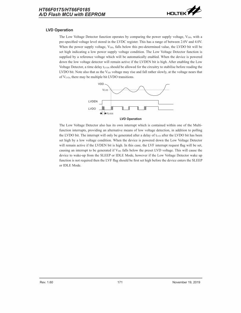
Rev. 1.60 170 November 19, 2019 Rev. 1.60 171 November 19, 2019
HT66F0175/HT66F0185A/D Flash MCU with EEPROM
HT66F0175/HT66F0185A/D Flash MCU with EEPROM
LVD OperationThe Low Voltage Detector function operates by comparing the power supply voltage, VDD, with a pre-specified voltage level stored in the LVDC register. This has a range of between 2.0V and 4.0V. When the power supply voltage, VDD, falls below this pre-determined value, the LVDO bit will be set high indicating a low power supply voltage condition. The Low Voltage Detector function is supplied by a reference voltage which will be automatically enabled. When the device is powered down the low voltage detector will remain active if the LVDEN bit is high. After enabling the Low Voltage Detector, a time delay tLVDS should be allowed for the circuitry to stabilise before reading the LVDO bit. Note also that as the VDD voltage may rise and fall rather slowly, at the voltage nears that of VLVD, there may be multiple bit LVDO transitions.
� � �
� � � �
� � � � �
� � � �� � � � �
LVD Operation
The Low Voltage Detector also has its own interrupt which is contained within one of the Multi-function interrupts, providing an alternative means of low voltage detection, in addition to polling the LVDO bit. The interrupt will only be generated after a delay of tLVD after the LVDO bit has been set high by a low voltage condition. When the device is powered down the Low Voltage Detector will remain active if the LVDEN bit is high. In this case, the LVF interrupt request flag will be set, causing an interrupt to be generated if VDD falls below the preset LVD voltage. This will cause the device to wake-up from the SLEEP or IDLE Mode, however if the Low Voltage Detector wake up function is not required then the LVF flag should be first set high before the device enters the SLEEP or IDLE Mode.
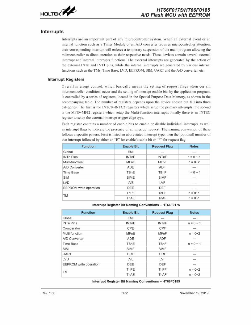
Rev. 1.60 172 November 19, 2019 Rev. 1.60 173 November 19, 2019
HT66F0175/HT66F0185A/D Flash MCU with EEPROM
HT66F0175/HT66F0185A/D Flash MCU with EEPROM
InterruptsInterrupts are an important part of any microcontroller system. When an external event or an internal function such as a Timer Module or an A/D converter requires microcontroller attention, their corresponding interrupt will enforce a temporary suspension of the main program allowing the microcontroller to direct attention to their respective needs. These devices contain several external interrupt and internal interrupts functions. The external interrupts are generated by the action of the external INT0 and INT1 pins, while the internal interrupts are generated by various internal functions such as the TMs, Time Base, LVD, EEPROM, SIM, UART and the A/D converter, etc.
Interrupt RegistersOverall interrupt control, which basically means the setting of request flags when certain microcontroller conditions occur and the setting of interrupt enable bits by the application program, is controlled by a series of registers, located in the Special Purpose Data Memory, as shown in the accompanying table. The number of registers depends upon the device chosen but fall into three categories. The first is the INTC0~INTC2 registers which setup the primary interrupts, the second is the MFI0~MFI2 registers which setup the Multi-function interrupts. Finally there is an INTEG register to setup the external interrupt trigger edge type.
Each register contains a number of enable bits to enable or disable individual interrupts as well as interrupt flags to indicate the presence of an interrupt request. The naming convention of these follows a specific pattern. First is listed an abbreviated interrupt type, then the (optional) number of that interrupt followed by either an “E” for enable/disable bit or “F” for request flag.
Function Enable Bit Request Flag NotesGlobal EMI — —INTn Pins INTnE INTnF n = 0 ~ 1Multi-function MFnE MFnF n = 0~2A/D Converter ADE ADF —Time Base TBnE TBnF n = 0 ~ 1SIM SIME SIMF —LVD LVE LVF —EEPROM write operation DEE DEF —
TMTnPE TnPF n = 0~1TnAE TnAF n = 0~1
Interrupt Register Bit Naming Conventions – HT66F0175
Function Enable Bit Request Flag NotesGlobal EMI — —INTn Pins INTnE INTnF n = 0 ~ 1Comparator CPE CPF —Multi-function MFnE MFnF n = 0~2A/D Converter ADE ADF —Time Base TBnE TBnF n = 0 ~ 1SIM SIME SIMF —UART URE URF —LVD LVE LVF —EEPROM write operation DEE DEF —
TMTnPE TnPF n = 0~2TnAE TnAF n = 0~2
Interrupt Register Bit Naming Conventions – HT66F0185
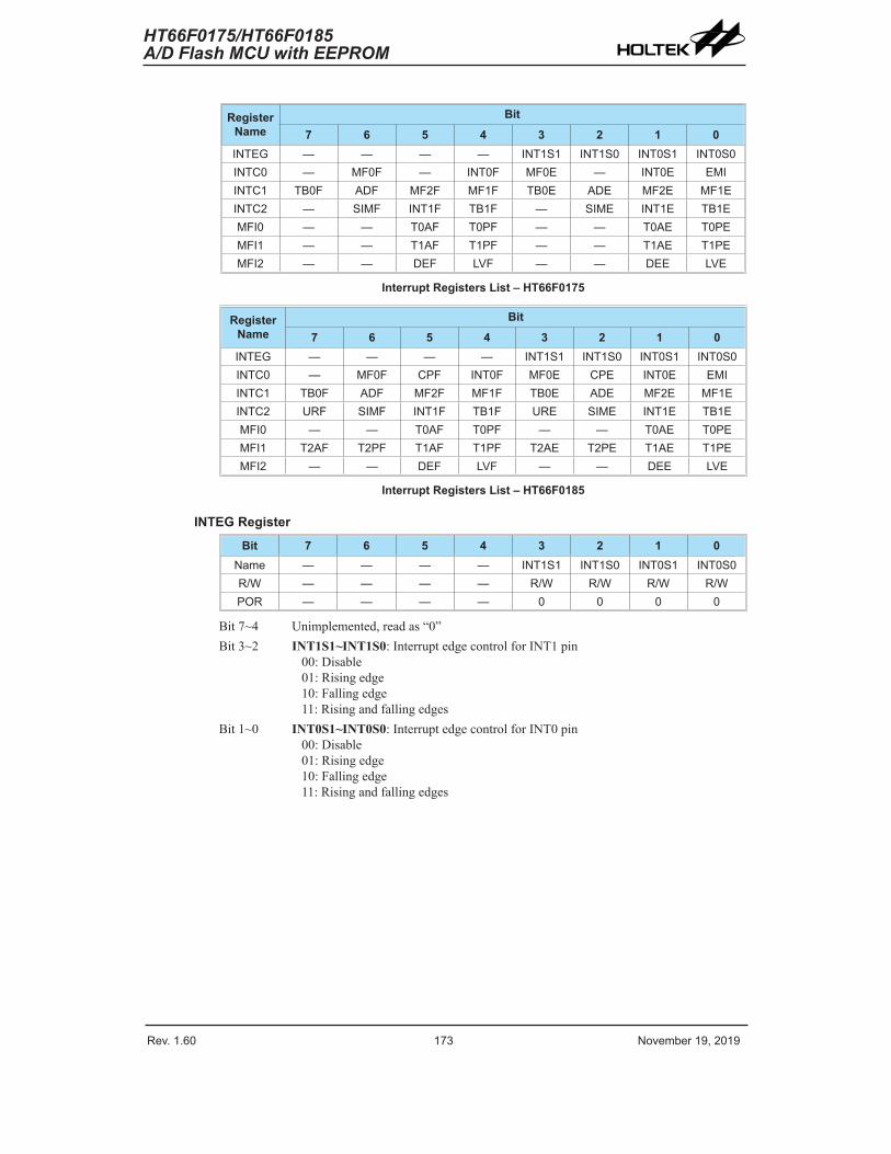
Rev. 1.60 172 November 19, 2019 Rev. 1.60 173 November 19, 2019
HT66F0175/HT66F0185A/D Flash MCU with EEPROM
HT66F0175/HT66F0185A/D Flash MCU with EEPROM
Register Name
Bit7 6 5 4 3 2 1 0
INTEG — — — — INT1S1 INT1S0 INT0S1 INT0S0INTC0 — MF0F — INT0F MF0E — INT0E EMIINTC1 TB0F ADF MF2F MF1F TB0E ADE MF2E MF1EINTC2 — SIMF INT1F TB1F — SIME INT1E TB1EMFI0 — — T0AF T0PF — — T0AE T0PEMFI1 — — T1AF T1PF — — T1AE T1PEMFI2 — — DEF LVF — — DEE LVE
Interrupt Registers List – HT66F0175
Register Name
Bit7 6 5 4 3 2 1 0
INTEG — — — — INT1S1 INT1S0 INT0S1 INT0S0INTC0 — MF0F CPF INT0F MF0E CPE INT0E EMIINTC1 TB0F ADF MF2F MF1F TB0E ADE MF2E MF1EINTC2 URF SIMF INT1F TB1F URE SIME INT1E TB1EMFI0 — — T0AF T0PF — — T0AE T0PEMFI1 T2AF T2PF T1AF T1PF T2AE T2PE T1AE T1PEMFI2 — — DEF LVF — — DEE LVE
Interrupt Registers List – HT66F0185
INTEG RegisterBit 7 6 5 4 3 2 1 0
Name — — — — INT1S1 INT1S0 INT0S1 INT0S0R/W — — — — R/W R/W R/W R/WPOR — — — — 0 0 0 0
Bit 7~4 Unimplemented, read as “0”Bit 3~2 INT1S1~INT1S0: Interrupt edge control for INT1 pin
00: Disable01: Rising edge10: Falling edge11: Rising and falling edges
Bit 1~0 INT0S1~INT0S0: Interrupt edge control for INT0 pin00: Disable01: Rising edge10: Falling edge11: Rising and falling edges
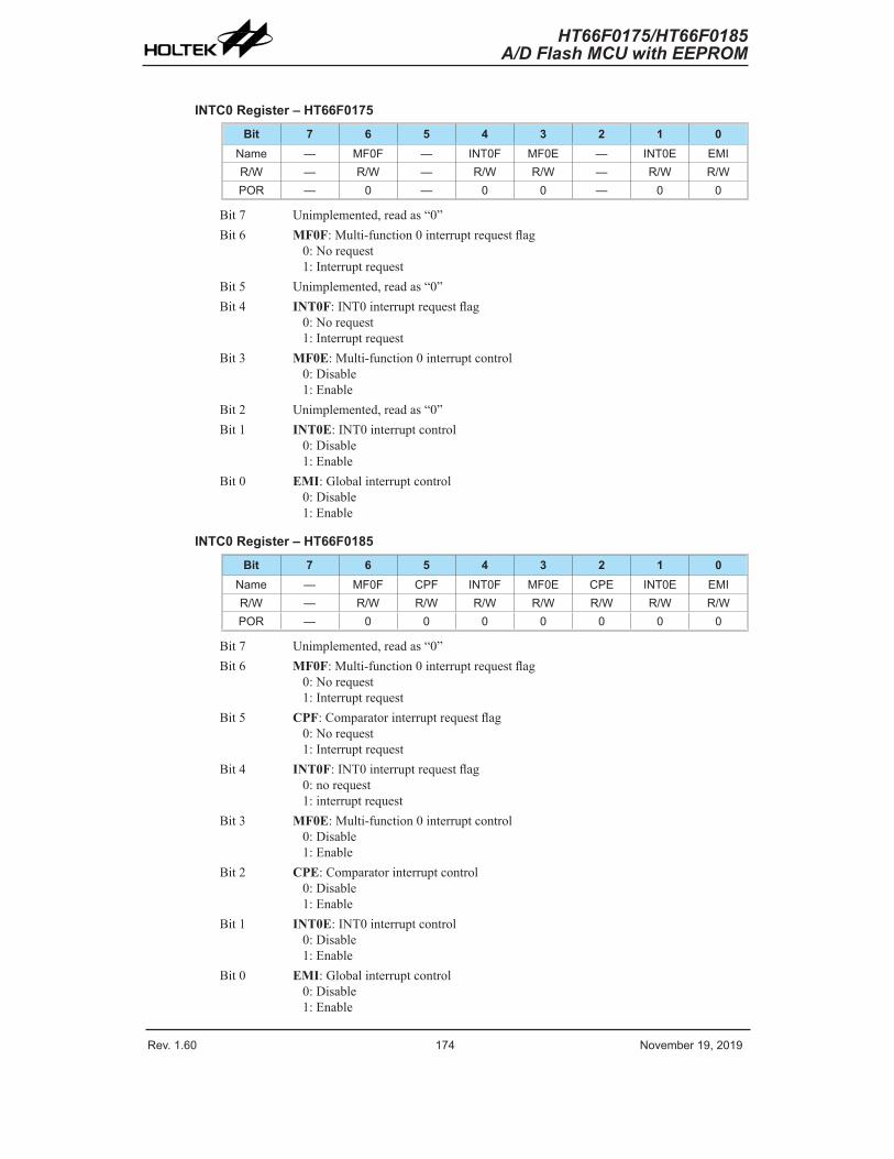
Rev. 1.60 174 November 19, 2019 Rev. 1.60 175 November 19, 2019
HT66F0175/HT66F0185A/D Flash MCU with EEPROM
HT66F0175/HT66F0185A/D Flash MCU with EEPROM
INTC0 Register – HT66F0175Bit 7 6 5 4 3 2 1 0
Name — MF0F — INT0F MF0E — INT0E EMIR/W — R/W — R/W R/W — R/W R/WPOR — 0 — 0 0 — 0 0
Bit 7 Unimplemented, read as “0”Bit 6 MF0F: Multi-function 0 interrupt request flag
0: No request1: Interrupt request
Bit 5 Unimplemented, read as “0”Bit 4 INT0F: INT0 interrupt request flag
0: No request1: Interrupt request
Bit 3 MF0E: Multi-function 0 interrupt control0: Disable1: Enable
Bit 2 Unimplemented, read as “0”Bit 1 INT0E: INT0 interrupt control
0: Disable1: Enable
Bit 0 EMI: Global interrupt control0: Disable1: Enable
INTC0 Register – HT66F0185Bit 7 6 5 4 3 2 1 0
Name — MF0F CPF INT0F MF0E CPE INT0E EMIR/W — R/W R/W R/W R/W R/W R/W R/WPOR — 0 0 0 0 0 0 0
Bit 7 Unimplemented, read as “0”Bit 6 MF0F: Multi-function 0 interrupt request flag
0: No request1: Interrupt request
Bit 5 CPF: Comparator interrupt request flag0: No request1: Interrupt request
Bit 4 INT0F: INT0 interrupt request flag0: no request1: interrupt request
Bit 3 MF0E: Multi-function 0 interrupt control0: Disable1: Enable
Bit 2 CPE: Comparator interrupt control0: Disable1: Enable
Bit 1 INT0E: INT0 interrupt control0: Disable1: Enable
Bit 0 EMI: Global interrupt control0: Disable1: Enable
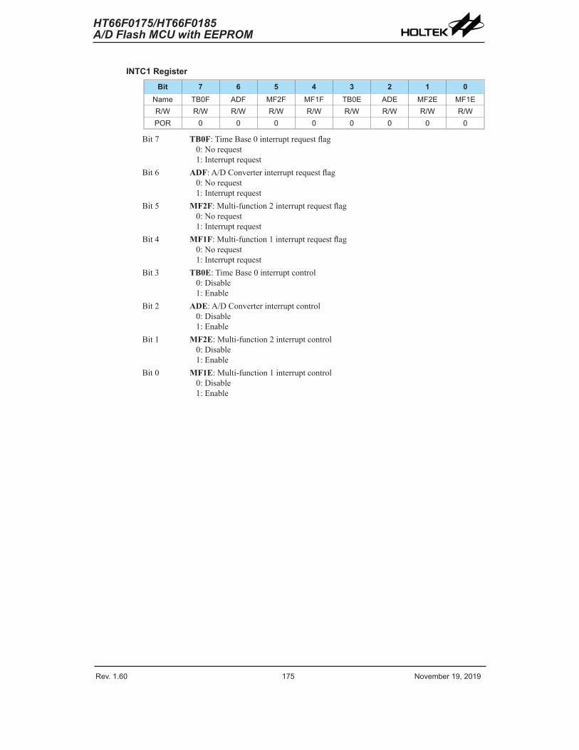
Rev. 1.60 174 November 19, 2019 Rev. 1.60 175 November 19, 2019
HT66F0175/HT66F0185A/D Flash MCU with EEPROM
HT66F0175/HT66F0185A/D Flash MCU with EEPROM
INTC1 RegisterBit 7 6 5 4 3 2 1 0
Name TB0F ADF MF2F MF1F TB0E ADE MF2E MF1ER/W R/W R/W R/W R/W R/W R/W R/W R/WPOR 0 0 0 0 0 0 0 0
Bit 7 TB0F: Time Base 0 interrupt request flag0: No request1: Interrupt request
Bit 6 ADF: A/D Converter interrupt request flag0: No request1: Interrupt request
Bit 5 MF2F: Multi-function 2 interrupt request flag0: No request1: Interrupt request
Bit 4 MF1F: Multi-function 1 interrupt request flag0: No request1: Interrupt request
Bit 3 TB0E: Time Base 0 interrupt control0: Disable1: Enable
Bit 2 ADE: A/D Converter interrupt control0: Disable1: Enable
Bit 1 MF2E: Multi-function 2 interrupt control0: Disable1: Enable
Bit 0 MF1E: Multi-function 1 interrupt control0: Disable1: Enable
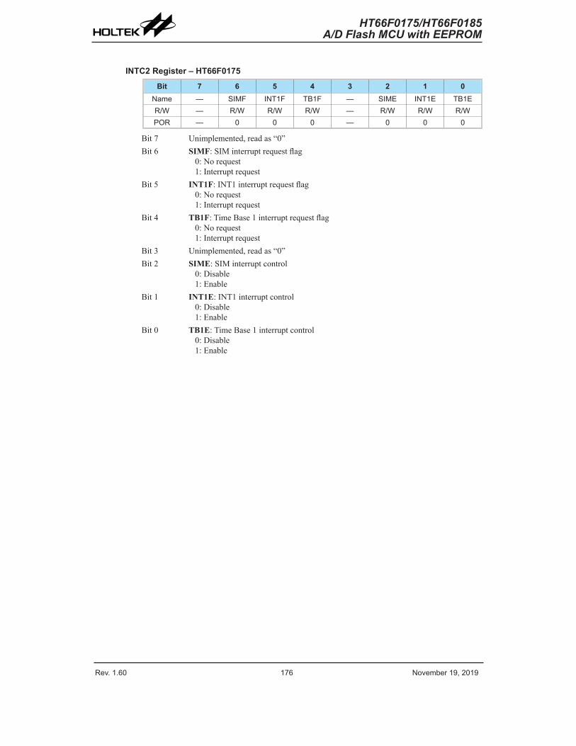
Rev. 1.60 176 November 19, 2019 Rev. 1.60 177 November 19, 2019
HT66F0175/HT66F0185A/D Flash MCU with EEPROM
HT66F0175/HT66F0185A/D Flash MCU with EEPROM
INTC2 Register – HT66F0175Bit 7 6 5 4 3 2 1 0
Name — SIMF INT1F TB1F — SIME INT1E TB1ER/W — R/W R/W R/W — R/W R/W R/WPOR — 0 0 0 — 0 0 0
Bit 7 Unimplemented, read as “0”Bit 6 SIMF: SIM interrupt request flag
0: No request1: Interrupt request
Bit 5 INT1F: INT1 interrupt request flag0: No request1: Interrupt request
Bit 4 TB1F: Time Base 1 interrupt request flag0: No request1: Interrupt request
Bit 3 Unimplemented, read as “0”Bit 2 SIME: SIM interrupt control
0: Disable1: Enable
Bit 1 INT1E: INT1 interrupt control0: Disable1: Enable
Bit 0 TB1E: Time Base 1 interrupt control0: Disable1: Enable
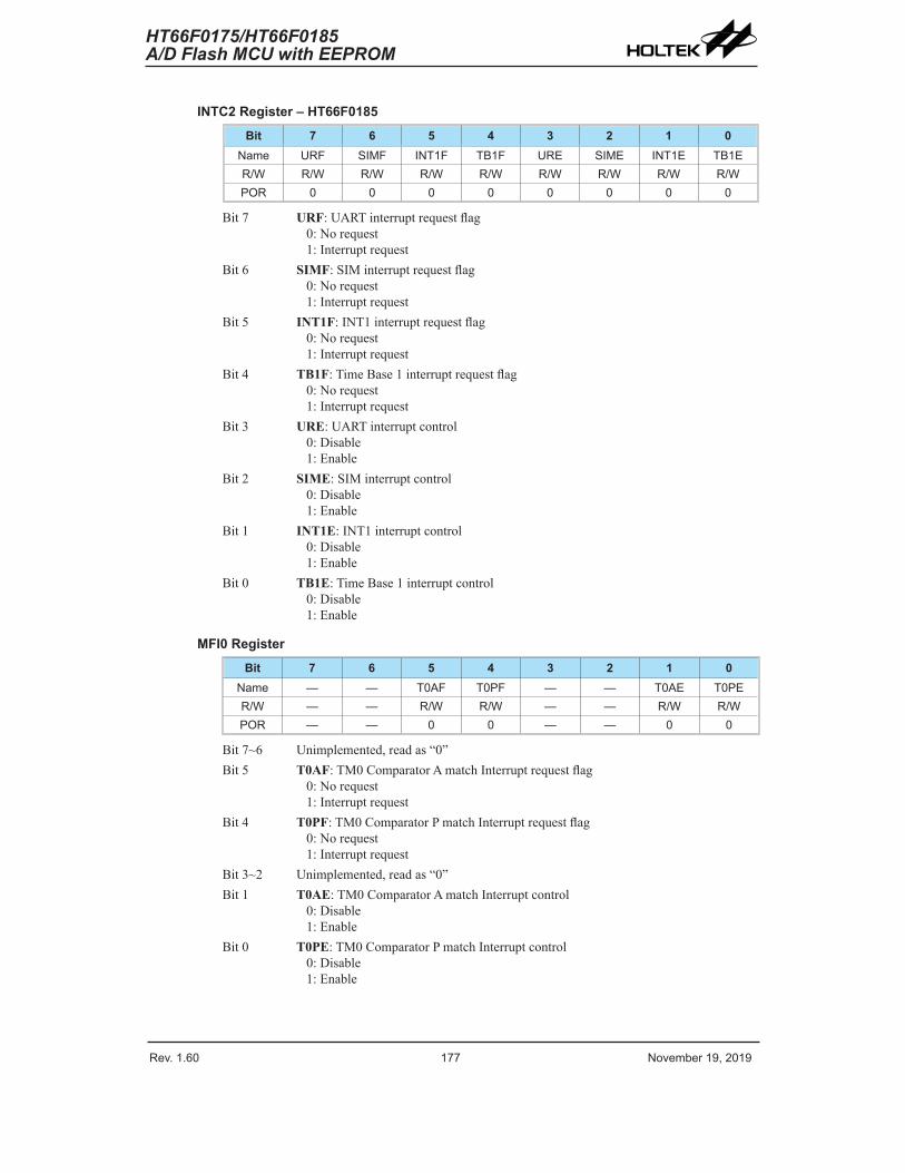
Rev. 1.60 176 November 19, 2019 Rev. 1.60 177 November 19, 2019
HT66F0175/HT66F0185A/D Flash MCU with EEPROM
HT66F0175/HT66F0185A/D Flash MCU with EEPROM
INTC2 Register – HT66F0185Bit 7 6 5 4 3 2 1 0
Name URF SIMF INT1F TB1F URE SIME INT1E TB1ER/W R/W R/W R/W R/W R/W R/W R/W R/WPOR 0 0 0 0 0 0 0 0
Bit 7 URF: UART interrupt request flag0: No request1: Interrupt request
Bit 6 SIMF: SIM interrupt request flag0: No request1: Interrupt request
Bit 5 INT1F: INT1 interrupt request flag0: No request1: Interrupt request
Bit 4 TB1F: Time Base 1 interrupt request flag0: No request1: Interrupt request
Bit 3 URE: UART interrupt control0: Disable1: Enable
Bit 2 SIME: SIM interrupt control0: Disable1: Enable
Bit 1 INT1E: INT1 interrupt control0: Disable1: Enable
Bit 0 TB1E: Time Base 1 interrupt control0: Disable1: Enable
MFI0 RegisterBit 7 6 5 4 3 2 1 0
Name — — T0AF T0PF — — T0AE T0PER/W — — R/W R/W — — R/W R/WPOR — — 0 0 — — 0 0
Bit 7~6 Unimplemented, read as “0”Bit 5 T0AF: TM0 Comparator A match Interrupt request flag
0: No request1: Interrupt request
Bit 4 T0PF: TM0 Comparator P match Interrupt request flag0: No request1: Interrupt request
Bit 3~2 Unimplemented, read as “0”Bit 1 T0AE: TM0 Comparator A match Interrupt control
0: Disable1: Enable
Bit 0 T0PE: TM0 Comparator P match Interrupt control0: Disable1: Enable
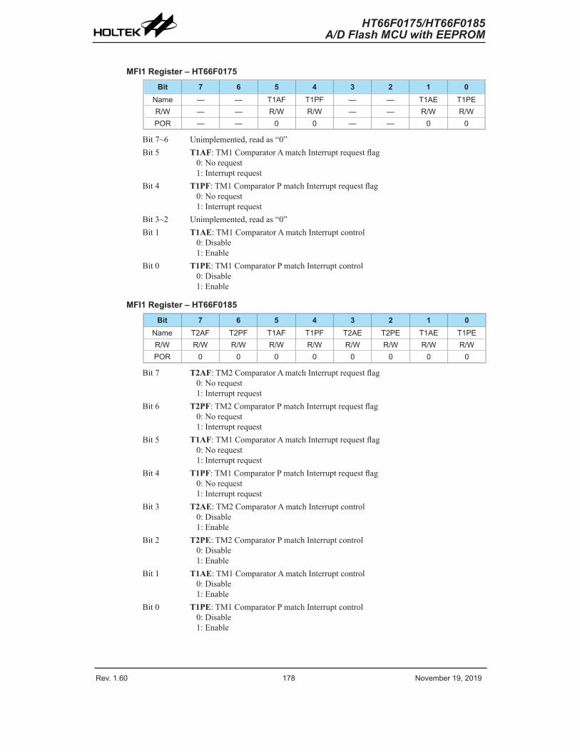
Rev. 1.60 178 November 19, 2019 Rev. 1.60 179 November 19, 2019
HT66F0175/HT66F0185A/D Flash MCU with EEPROM
HT66F0175/HT66F0185A/D Flash MCU with EEPROM
MFI1 Register – HT66F0175Bit 7 6 5 4 3 2 1 0
Name — — T1AF T1PF — — T1AE T1PER/W — — R/W R/W — — R/W R/WPOR — — 0 0 — — 0 0
Bit 7~6 Unimplemented, read as “0”Bit 5 T1AF: TM1 Comparator A match Interrupt request flag
0: No request1: Interrupt request
Bit 4 T1PF: TM1 Comparator P match Interrupt request flag0: No request1: Interrupt request
Bit 3~2 Unimplemented, read as “0”Bit 1 T1AE: TM1 Comparator A match Interrupt control
0: Disable1: Enable
Bit 0 T1PE: TM1 Comparator P match Interrupt control0: Disable1: Enable
MFI1 Register – HT66F0185Bit 7 6 5 4 3 2 1 0
Name T2AF T2PF T1AF T1PF T2AE T2PE T1AE T1PER/W R/W R/W R/W R/W R/W R/W R/W R/WPOR 0 0 0 0 0 0 0 0
Bit 7 T2AF: TM2 Comparator A match Interrupt request flag0: No request1: Interrupt request
Bit 6 T2PF: TM2 Comparator P match Interrupt request flag0: No request1: Interrupt request
Bit 5 T1AF: TM1 Comparator A match Interrupt request flag0: No request1: Interrupt request
Bit 4 T1PF: TM1 Comparator P match Interrupt request flag0: No request1: Interrupt request
Bit 3 T2AE: TM2 Comparator A match Interrupt control0: Disable1: Enable
Bit 2 T2PE: TM2 Comparator P match Interrupt control0: Disable1: Enable
Bit 1 T1AE: TM1 Comparator A match Interrupt control0: Disable1: Enable
Bit 0 T1PE: TM1 Comparator P match Interrupt control0: Disable1: Enable
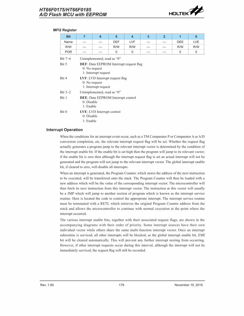
Rev. 1.60 178 November 19, 2019 Rev. 1.60 179 November 19, 2019
HT66F0175/HT66F0185A/D Flash MCU with EEPROM
HT66F0175/HT66F0185A/D Flash MCU with EEPROM
MFI2 RegisterBit 7 6 5 4 3 2 1 0
Name — — DEF LVF — — DEE LVER/W — — R/W R/W — — R/W R/WPOR — — 0 0 — — 0 0
Bit 7~6 Unimplemented, read as “0”Bit 5 DEF: Data EEPROM Interrupt request flag
0: No request1: Interrupt request
Bit 4 LVF: LVD Interrupt request flag0: No request1: Interrupt request
Bit 3~2 Unimplemented, read as “0”Bit 1 DEE: Data EEPROM Interrupt control
0: Disable1: Enable
Bit 0 LVE: LVD Interrupt control0: Disable1: Enable
Interrupt OperationWhen the conditions for an interrupt event occur, such as a TM Comparator P or Comparator A or A/D conversion completion, etc, the relevant interrupt request flag will be set. Whether the request flag actually generates a program jump to the relevant interrupt vector is determined by the condition of the interrupt enable bit. If the enable bit is set high then the program will jump to its relevant vector; if the enable bit is zero then although the interrupt request flag is set an actual interrupt will not be generated and the program will not jump to the relevant interrupt vector. The global interrupt enable bit, if cleared to zero, will disable all interrupts.
When an interrupt is generated, the Program Counter, which stores the address of the next instruction to be executed, will be transferred onto the stack. The Program Counter will then be loaded with a new address which will be the value of the corresponding interrupt vector. The microcontroller will then fetch its next instruction from this interrupt vector. The instruction at this vector will usually be a JMP which will jump to another section of program which is known as the interrupt service routine. Here is located the code to control the appropriate interrupt. The interrupt service routine must be terminated with a RETI, which retrieves the original Program Counter address from the stack and allows the microcontroller to continue with normal execution at the point where the interrupt occurred.
The various interrupt enable bits, together with their associated request flags, are shown in the accompanying diagrams with their order of priority. Some interrupt sources have their own individual vector while others share the same multi-function interrupt vector. Once an interrupt subroutine is serviced, all other interrupts will be blocked, as the global interrupt enable bit, EMI bit will be cleared automatically. This will prevent any further interrupt nesting from occurring. However, if other interrupt requests occur during this interval, although the interrupt will not be immediately serviced, the request flag will still be recorded.
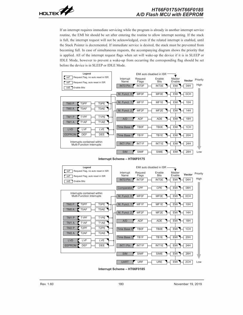
Rev. 1.60 180 November 19, 2019 Rev. 1.60 181 November 19, 2019
HT66F0175/HT66F0185A/D Flash MCU with EEPROM
HT66F0175/HT66F0185A/D Flash MCU with EEPROM
If an interrupt requires immediate servicing while the program is already in another interrupt service routine, the EMI bit should be set after entering the routine to allow interrupt nesting. If the stack is full, the interrupt request will not be acknowledged, even if the related interrupt is enabled, until the Stack Pointer is decremented. If immediate service is desired, the stack must be prevented from becoming full. In case of simultaneous requests, the accompanying diagram shows the priority that is applied. All of the interrupt request flags when set will wake-up the device if it is in SLEEP or IDLE Mode, however to prevent a wake-up from occurring the corresponding flag should be set before the device is in SLEEP or IDLE Mode.
INT0 Pin
INT1 Pin
INT0F
INT1F
INT0E
INT1E
EMI 04H
EMIM. Funct. 0 MF0F MF0E
EMI
0CH
EMI
10H
14H
Time Base 0 TB0F TB0E
EMI 18H
LVD LVF LVEEMI 1CH
Interrupt Name
Request Flags
Enable Bits
Master Enable Vector
EMI auto disabled in ISR
Priority
High
Low
M. Funct. 1 MF1F MF1ETM0 P T0PF T0PE
TM0 A T0AF T0AE
Interrupts contained within Multi-Function Interrupts
xxE Enable Bits
xxF Request Flag, auto reset in ISR
LegendxxF Request Flag, no auto reset in ISR
EMI 20H
A/D ADF ADE
EMI 24H
M. Funct. 2 MF2F MF2E
Time Base 1 TB1F TB1E
TM1 P T1PE
TM1 A T1AE
EEPROM DEF DEE
SIM SIMF SIME EMI 28H
T1PF
T1AF
Interrupt Scheme – HT66F0175
INT0 Pin
INT1 Pin
INT0F
INT1F
INT0E
INT1E
EMI 04H
EMI
08H
M. Funct. 0 MF0F MF0E
EMI
0CH
EMI
10H
14H
Time Base 0 TB0F TB0E
EMI 18H
LVD LVF LVE
EMI 1CH
Interrupt Name
Request Flags
Enable Bits
Master Enable Vector
EMI auto disabled in ISR
Priority
High
Low
M. Funct. 1 MF1F MF1ETM0 P T0PF T0PE
TM0 A T0AF T0AE
Interrupts contained within Multi-Function Interrupts
xxE Enable Bits
xxF Request Flag, auto reset in ISR
LegendxxF Request Flag, no auto reset in ISR
EMI 20H
A/D ADF ADE
EMI 24H
M. Funct. 2 MF2F MF2E
Time Base 1 TB1F TB1E
TM1 P T1PE
TM1 A T1AE
EEPROM DEF DEE
TM2 P T2PE
TM2 A T2AE
EMIComparator CPF CPE
SIM SIMF SIME EMI 28H
T1PF
T1AF
T2PF
T2AF
UART URF URE EMI 2CH
Interrupt Scheme – HT66F0185
Rev. 1.60 180 November 19, 2019 Rev. 1.60 181 November 19, 2019
HT66F0175/HT66F0185A/D Flash MCU with EEPROM
HT66F0175/HT66F0185A/D Flash MCU with EEPROM
External InterruptThe external interrupts are controlled by signal transitions on the pins INT0~INT1. An external interrupt request will take place when the external interrupt request flags, INT0F~INT1F, are set, which will occur when a transition, whose type is chosen by the edge select bits, appears on the external interrupt pins. To allow the program to branch to its respective interrupt vector address, the global interrupt enable bit, EMI, and respective external interrupt enable bit, INT0E~INT1E, must first be set. Additionally the correct interrupt edge type must be selected using the INTEG register to enable the external interrupt function and to choose the trigger edge type. As the external interrupt pins are pin-shared with I/O pins, they can only be configured as external interrupt pins if their external interrupt enable bit in the corresponding interrupt register has been set and the external interrupt pin is selected by the corresponding pin-shared function selection bits. The pin must also be setup as an input by setting the corresponding bit in the port control register. When the interrupt is enabled, the stack is not full and the correct transition type appears on the external interrupt pin, a subroutine call to the external interrupt vector, will take place. When the interrupt is serviced, the external interrupt request flags, INT0F~INT1F, will be automatically reset and the EMI bit will be automatically cleared to disable other interrupts. Note that any pull-high resistor selections on the external interrupt pins will remain valid even if the pin is used as an external interrupt input.
The INTEG register is used to select the type of active edge that will trigger the external interrupt. A choice of either rising or falling or both edge types can be chosen to trigger an external interrupt. Note that the INTEG register can also be used to disable the external interrupt function.
Comparator Interrupt – HT66F0185The comparator interrupt is controlled by the internal comparator. A comparator interrupt request will take place when the comparator interrupt request flag, CPF, is set, a situation that will occur when the comparator output changes state. To allow the program to branch to its respective interrupt vector address, the global interrupt enable bit, EMI, and comparator interrupt enable bit, CPE, must first be set. When the interrupt is enabled, the stack is not full and the comparator inputs generate a comparator output transition, a subroutine call to the comparator interrupt vector, will take place. When the interrupt is serviced, the comparator interrupt request flag, will be automatically reset and the EMI bit will be automatically cleared to disable other interrupts.
Multi-function InterruptWithin the device there are up to three Multi-function interrupts. Unlike the other independent interrupts, these interrupts have no independent source, but rather are formed from other existing interrupt sources, namely the TM interrupts, LVD interrupt and EEPROM write operation interrupt.
A Multi-function interrupt request will take place when any of the Multi-function interrupt request flags MFnF are set. The Multi-function interrupt flags will be set when any of their included functions generate an interrupt request flag. To allow the program to branch to its respective interrupt vector address, when the Multi-function interrupt is enabled and the stack is not full, and either one of the interrupts contained within each of Multi-function interrupt occurs, a subroutine call to one of the Multi-function interrupt vectors will take place. When the interrupt is serviced, the related Multi-Function request flag will be automatically reset and the EMI bit will be automatically cleared to disable other interrupts.
However, it must be noted that, although the Multi-function Interrupt request flags will be automatically reset when the interrupt is serviced, the request flags from the original source of the Multi-function interrupts will not be automatically reset and must be manually reset by the application program.
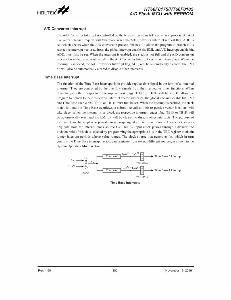
Rev. 1.60 182 November 19, 2019 Rev. 1.60 183 November 19, 2019
HT66F0175/HT66F0185A/D Flash MCU with EEPROM
HT66F0175/HT66F0185A/D Flash MCU with EEPROM
A/D Converter InterruptThe A/D Converter Interrupt is controlled by the termination of an A/D conversion process. An A/D Converter Interrupt request will take place when the A/D Converter Interrupt request flag, ADF, is set, which occurs when the A/D conversion process finishes. To allow the program to branch to its respective interrupt vector address, the global interrupt enable bit, EMI, and A/D Interrupt enable bit, ADE, must first be set. When the interrupt is enabled, the stack is not full and the A/D conversion process has ended, a subroutine call to the A/D Converter Interrupt vector, will take place. When the interrupt is serviced, the A/D Converter Interrupt flag, ADF, will be automatically cleared. The EMI bit will also be automatically cleared to disable other interrupts.
Time Base InterruptThe function of the Time Base Interrupts is to provide regular time signal in the form of an internal interrupt. They are controlled by the overflow signals from their respective timer functions. When these happens their respective interrupt request flags, TB0F or TB1F will be set. To allow the program to branch to their respective interrupt vector addresses, the global interrupt enable bit, EMI and Time Base enable bits, TB0E or TB1E, must first be set. When the interrupt is enabled, the stack is not full and the Time Base overflows, a subroutine call to their respective vector locations will take place. When the interrupt is serviced, the respective interrupt request flag, TB0F or TB1F, will be automatically reset and the EMI bit will be cleared to disable other interrupts. The purpose of the Time Base Interrupt is to provide an interrupt signal at fixed time periods. Their clock sources originate from the internal clock source fTB. This fTB input clock passes through a divider, the division ratio of which is selected by programming the appropriate bits in the TBC register to obtain longer interrupt periods whose value ranges. The clock source that generates fTB, which in turn controls the Time Base interrupt period, can originate from several different sources, as shown in the System Operating Mode section.
MUXfSYS/4
fTBC
Prescaler
TBCK
fTB
fTB/28 ~ fTB/215MUX
TB11~TB10
Time Base 0 Interrupt
Time Base 1 Interrupt
TB02~TB00
PrescalerMUX
fTB/212 ~ fTB/215
Time Base Interrupts
Rev. 1.60 182 November 19, 2019 Rev. 1.60 183 November 19, 2019
HT66F0175/HT66F0185A/D Flash MCU with EEPROM
HT66F0175/HT66F0185A/D Flash MCU with EEPROM
TBC RegisterBit 7 6 5 4 3 2 1 0
Name TBON TBCK TB11 TB10 LXTLP TB02 TB01 TB00R/W R/W R/W R/W R/W R/W R/W R/W R/WPOR 0 0 1 1 0 1 1 1
Bit 7 TBON: Time Base function enable control0: Disable1: Enable
Bit 6 TBCK: Time Base clock source select0: fTBC
1: fSYS/4Bit 5~4 TB11~TB10: Time Base 1 time-out period selection
00: 212/fTB
01: 213/fTB
10: 214/fTB
11: 215/fTB
Bit 3 LXTLP: LXT Low Power control0: Disable – LXT quick start-up1: Enable – LXT slow start-up
Bit 2~0 TB02~TB00: Time Base 0 time-out period selection000: 28/fTB
001: 29/fTB
010: 210/fTB
011: 211/fTB
100: 212/fTB
101: 213/fTB
110: 214/fTB
111: 215/fTB
Serial Interface Module InterruptThe Serial Interface Module Interrupt, also known as the SIM interrupt, is controlled by the SPI or I2C data transfer. A SIM Interrupt request will take place when the SIM Interrupt request flag, SIMF, is set, which occurs when a byte of data has been received or transmitted by the SIM interface, an I2C slave address match or I2C bus time-out occurrence. To allow the program to branch to its respective interrupt vector address, the global interrupt enable bit, EMI and the Serial Interface Interrupt enable bit, SIME, must first be set. When the interrupt is enabled, the stack is not full and any of the above described situations occurs, a subroutine call to the respective SIM Interrupt vector, will take place. When the Serial Interface Interrupt is serviced, the EMI bit will be automatically cleared to disable other interrupts. The SIMF flag will also be automatically cleared.
UART Transfer Interrupt – HT66F0185The UART Transfer Interrupt is controlled by several UART transfer conditions. When one of these conditions occurs, an interrupt pulse will be generated to get the attention of the microcontroller. These conditions are a transmitter data register empty, transmitter idle, receiver data available, receiver overrun, address detect and an RX pin wake-up. To allow the program to branch to its respective interrupt vector address, the global interrupt enable bit, EMI, and UART Interrupt enable bit, URE, must first be set. When the interrupt is enabled, the stack is not full and any of the conditions described above occurs, a subroutine call to the UART Interrupt vector, will take place. When the interrupt is serviced, the UART Interrupt flag, URF, will be automatically cleared. The EMI bit will also be automatically cleared to disable other interrupts.
Rev. 1.60 184 November 19, 2019 Rev. 1.60 185 November 19, 2019
HT66F0175/HT66F0185A/D Flash MCU with EEPROM
HT66F0175/HT66F0185A/D Flash MCU with EEPROM
LVD InterruptThe Low Voltage Detector Interrupt is contained within the Multi-function Interrupt. An LVD Interrupt request will take place when the LVD Interrupt request flag, LVF, is set, which occurs when the Low Voltage Detector function detects a low power supply voltage. To allow the program to branch to its respective interrupt vector address, the global interrupt enable bit, EMI, Low Voltage Interrupt enable bit, LVE, and associated Multi-function interrupt enable bit, must first be set. When the interrupt is enabled, the stack is not full and a low voltage condition occurs, a subroutine call to the Multi-function Interrupt vector, will take place. When the Low Voltage Interrupt is serviced, the EMI bit will be automatically cleared to disable other interrupts. However, only the Multi-function interrupt request flag will be also automatically cleared. As the LVF flag will not be automatically cleared, it has to be cleared by the application program.
EEPROM InterruptThe EEPROM Write Interrupt is contained within the Multi-function Interrupt. An EEPROM Write Interrupt request will take place when the EEPROM Write Interrupt request flag, DEF, is set, which occurs when an EEPROM Write cycle ends. To allow the program to branch to its respective interrupt vector address, the global interrupt enable bit, EMI, EEPROM Write Interrupt enable bit, DEE, and associated Multi-function interrupt enable bit must first be set. When the interrupt is enabled, the stack is not full and an EEPROM Write cycle ends, a subroutine call to the respective Multi-function Interrupt vector will take place. When the EEPROM Write Interrupt is serviced, the EMI bit will be automatically cleared to disable other interrupts. However, only the Multi-function interrupt request flag will be automatically cleared. As the DEF flag will not be automatically cleared, it has to be cleared by the application program.
TM InterruptThe Compact, Standard and Periodic TMs have two interrupts, one comes from the comparator A match situation and the other comes from the comparator P match situation. All of the TM interrupts are contained within the Multi-function Interrupts. For all of the TM types there are two interrupt request flags and two enable control bits. A TM interrupt request will take place when any of the TM request flags are set, a situation which occurs when a TM comparator P or A match situation happens.
To allow the program to branch to its respective interrupt vector address, the global interrupt enable bit, EMI, respective TM Interrupt enable bit, and relevant Multi-function Interrupt enable bit, MFnE, must first be set. When the interrupt is enabled, the stack is not full and a TM comparator match situation occurs, a subroutine call to the relevant Multi-function Interrupt vector locations, will take place. When the TM interrupt is serviced, the EMI bit will be automatically cleared to disable other interrupts. However, only the related MFnF flag will be automatically cleared. As the TM interrupt request flags will not be automatically cleared, they have to be cleared by the application program.
Rev. 1.60 184 November 19, 2019 Rev. 1.60 185 November 19, 2019
HT66F0175/HT66F0185A/D Flash MCU with EEPROM
HT66F0175/HT66F0185A/D Flash MCU with EEPROM
Interrupt Wake-up FunctionEach of the interrupt functions has the capability of waking up the microcontroller when in the SLEEP or IDLE Mode. A wake-up is generated when an interrupt request flag changes from low to high and is independent of whether the interrupt is enabled or not. Therefore, even though these devices are in the SLEEP or IDLE Mode and its system oscillator stopped, situations such as external edge transitions on the external interrupt pins, a low power supply voltage or comparator input change may cause their respective interrupt flag to be set high and consequently generate an interrupt. Care must therefore be taken if spurious wake-up situations are to be avoided. If an interrupt wake-up function is to be disabled then the corresponding interrupt request flag should be set high before the device enters the SLEEP or IDLE Mode. The interrupt enable bits have no effect on the interrupt wake-up function.
Programming ConsiderationsBy disabling the relevant interrupt enable bits, a requested interrupt can be prevented from being serviced, however, once an interrupt request flag is set, it will remain in this condition in the interrupt register until the corresponding interrupt is serviced or until the request flag is cleared by the application program.
Where a certain interrupt is contained within a Multi-function interrupt, then when the interrupt service routine is executed, as only the Multi-function interrupt request flags, MFnF, will be automatically cleared, the individual request flag for the function needs to be cleared by the application program.
It is recommended that programs do not use the “CALL” instruction within the interrupt service subroutine. Interrupts often occur in an unpredictable manner or need to be serviced immediately. If only one stack is left and the interrupt is not well controlled, the original control sequence will be damaged once a CALL subroutine is executed in the interrupt subroutine.
Every interrupt has the capability of waking up the microcontroller when it is in the SLEEP or IDLE Mode, the wake up being generated when the interrupt request flag changes from low to high. If it is required to prevent a certain interrupt from waking up the microcontroller then its respective request flag should be first set high before enter SLEEP or IDLE Mode.
As only the Program Counter is pushed onto the stack, then when the interrupt is serviced, if the contents of the accumulator, status register or other registers are altered by the interrupt service program, their contents should be saved to the memory at the beginning of the interrupt service routine.
To return from an interrupt subroutine, either a RET or RETI instruction may be executed. The RETI instruction in addition to executing a return to the main program also automatically sets the EMI bit high to allow further interrupts. The RET instruction however only executes a return to the main program leaving the EMI bit in its present zero state and therefore disabling the execution of further interrupts.
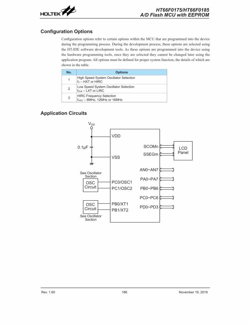
Rev. 1.60 186 November 19, 2019 Rev. 1.60 187 November 19, 2019
HT66F0175/HT66F0185A/D Flash MCU with EEPROM
HT66F0175/HT66F0185A/D Flash MCU with EEPROM
Configuration OptionsConfiguration options refer to certain options within the MCU that are programmed into the device during the programming process. During the development process, these options are selected using the HT-IDE software development tools. As these options are programmed into the device using the hardware programming tools, once they are selected they cannot be changed later using the application program. All options must be defined for proper system function, the details of which are shown in the table.
No. Options
1 High Speed System Oscillator SelectionfH – HXT or HIRC
2 Low Speed System Oscillator SelectionfSUB – LXT or LIRC
3 HIRC Frequency SelectionfHIRC – 8MHz, 12MHz or 16MHz
Application Circuits
VDD
VSS
VDD
PC0/OSC1PC1/OSC2
OSC Circuit
PB0/XT1PB1/XT2
OSC Circuit
See Oscillator Section
See Oscillator Section
AN0~AN7
SCOMn
SSEGmLCD
Panel
PA0~PA7
PB0~PB6
PC0~PC6
PD0~PD3
0.1µF
Rev. 1.60 186 November 19, 2019 Rev. 1.60 187 November 19, 2019
HT66F0175/HT66F0185A/D Flash MCU with EEPROM
HT66F0175/HT66F0185A/D Flash MCU with EEPROM
Instruction Set
IntroductionCentral to the successful operation of any microcontroller is its instruction set, which is a set of program instruction codes that directs the microcontroller to perform certain operations. In the case of Holtek microcontroller, a comprehensive and flexible set of over 60 instructions is provided to enable programmers to implement their application with the minimum of programming overheads.
For easier understanding of the various instruction codes, they have been subdivided into several functional groupings.
Instruction TimingMost instructions are implemented within one instruction cycle. The exceptions to this are branch, call, or table read instructions where two instruction cycles are required. One instruction cycle is equal to 4 system clock cycles, therefore in the case of an 8MHz system oscillator, most instructions would be implemented within 0.5μs and branch or call instructions would be implemented within 1μs. Although instructions which require one more cycle to implement are generally limited to the JMP, CALL, RET, RETI and table read instructions, it is important to realize that any other instructions which involve manipulation of the Program Counter Low register or PCL will also take one more cycle to implement. As instructions which change the contents of the PCL will imply a direct jump to that new address, one more cycle will be required. Examples of such instructions would be “CLR PCL” or “MOV PCL, A”. For the case of skip instructions, it must be noted that if the result of the comparison involves a skip operation then this will also take one more cycle, if no skip is involved then only one cycle is required.
Moving and Transferring DataThe transfer of data within the microcontroller program is one of the most frequently used operations. Making use of several kinds of MOV instructions, data can be transferred from registers to the Accumulator and vice-versa as well as being able to move specific immediate data directly into the Accumulator. One of the most important data transfer applications is to receive data from the input ports and transfer data to the output ports.
Arithmetic OperationsThe ability to perform certain arithmetic operations and data manipulation is a necessary feature of most microcontroller applications. Within the Holtek microcontroller instruction set are a range of add and subtract instruction mnemonics to enable the necessary arithmetic to be carried out. Care must be taken to ensure correct handling of carry and borrow data when results exceed 255 for addition and less than 0 for subtraction. The increment and decrement instructions such as INC, INCA, DEC and DECA provide a simple means of increasing or decreasing by a value of one of the values in the destination specified.
Rev. 1.60 188 November 19, 2019 Rev. 1.60 189 November 19, 2019
HT66F0175/HT66F0185A/D Flash MCU with EEPROM
HT66F0175/HT66F0185A/D Flash MCU with EEPROM
Logical and Rotate OperationThe standard logical operations such as AND, OR, XOR and CPL all have their own instruction within the Holtek microcontroller instruction set. As with the case of most instructions involving data manipulation, data must pass through the Accumulator which may involve additional programming steps. In all logical data operations, the zero flag may be set if the result of the operation is zero. Another form of logical data manipulation comes from the rotate instructions such as RR, RL, RRC and RLC which provide a simple means of rotating one bit right or left. Different rotate instructions exist depending on program requirements. Rotate instructions are useful for serial port programming applications where data can be rotated from an internal register into the Carry bit from where it can be examined and the necessary serial bit set high or low. Another application which rotate data operations are used is to implement multiplication and division calculations.
Branches and Control TransferProgram branching takes the form of either jumps to specified locations using the JMP instruction or to a subroutine using the CALL instruction. They differ in the sense that in the case of a subroutine call, the program must return to the instruction immediately when the subroutine has been carried out. This is done by placing a return instruction “RET” in the subroutine which will cause the program to jump back to the address right after the CALL instruction. In the case of a JMP instruction, the program simply jumps to the desired location. There is no requirement to jump back to the original jumping off point as in the case of the CALL instruction. One special and extremely useful set of branch instructions are the conditional branches. Here a decision is first made regarding the condition of a certain data memory or individual bits. Depending upon the conditions, the program will continue with the next instruction or skip over it and jump to the following instruction. These instructions are the key to decision making and branching within the program perhaps determined by the condition of certain input switches or by the condition of internal data bits.
Bit OperationsThe ability to provide single bit operations on Data Memory is an extremely flexible feature of all Holtek microcontrollers. This feature is especially useful for output port bit programming where individual bits or port pins can be directly set high or low using either the “SET [m].i” or “CLR [m].i” instructions respectively. The feature removes the need for programmers to first read the 8-bit output port, manipulate the input data to ensure that other bits are not changed and then output the port with the correct new data. This read-modify-write process is taken care of automatically when these bit operation instructions are used.
Table Read OperationsData storage is normally implemented by using registers. However, when working with large amounts of fixed data, the volume involved often makes it inconvenient to store the fixed data in the Data Memory. To overcome this problem, Holtek microcontrollers allow an area of Program Memory to be setup as a table where data can be directly stored. A set of easy to use instructions provides the means by which this fixed data can be referenced and retrieved from the Program Memory.
Other OperationsIn addition to the above functional instructions, a range of other instructions also exist such as the “HALT” instruction for Power-down operations and instructions to control the operation of the Watchdog Timer for reliable program operations under extreme electric or electromagnetic environments. For their relevant operations, refer to the functional related sections.
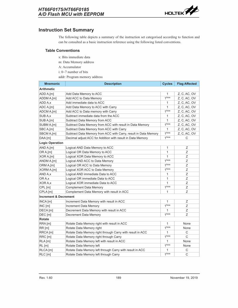
Rev. 1.60 188 November 19, 2019 Rev. 1.60 189 November 19, 2019
HT66F0175/HT66F0185A/D Flash MCU with EEPROM
HT66F0175/HT66F0185A/D Flash MCU with EEPROM
Instruction Set SummaryThe following table depicts a summary of the instruction set categorised according to function and can be consulted as a basic instruction reference using the following listed conventions.
Table Conventionsx: Bits immediate data m: Data Memory address A: Accumulator i: 0~7 number of bits addr: Program memory address
Mnemonic Description Cycles Flag AffectedArithmeticADD A,[m] Add Data Memory to ACC 1 Z, C, AC, OVADDM A,[m] Add ACC to Data Memory 1Note Z, C, AC, OVADD A,x Add immediate data to ACC 1 Z, C, AC, OVADC A,[m] Add Data Memory to ACC with Carry 1 Z, C, AC, OVADCM A,[m] Add ACC to Data memory with Carry 1Note Z, C, AC, OVSUB A,x Subtract immediate data from the ACC 1 Z, C, AC, OVSUB A,[m] Subtract Data Memory from ACC 1 Z, C, AC, OVSUBM A,[m] Subtract Data Memory from ACC with result in Data Memory 1Note Z, C, AC, OVSBC A,[m] Subtract Data Memory from ACC with Carry 1 Z, C, AC, OVSBCM A,[m] Subtract Data Memory from ACC with Carry, result in Data Memory 1Note Z, C, AC, OVDAA [m] Decimal adjust ACC for Addition with result in Data Memory 1Note CLogic OperationAND A,[m] Logical AND Data Memory to ACC 1 ZOR A,[m] Logical OR Data Memory to ACC 1 ZXOR A,[m] Logical XOR Data Memory to ACC 1 ZANDM A,[m] Logical AND ACC to Data Memory 1Note ZORM A,[m] Logical OR ACC to Data Memory 1Note ZXORM A,[m] Logical XOR ACC to Data Memory 1Note ZAND A,x Logical AND immediate Data to ACC 1 ZOR A,x Logical OR immediate Data to ACC 1 ZXOR A,x Logical XOR immediate Data to ACC 1 ZCPL [m] Complement Data Memory 1Note ZCPLA [m] Complement Data Memory with result in ACC 1 ZIncrement & DecrementINCA [m] Increment Data Memory with result in ACC 1 ZINC [m] Increment Data Memory 1Note ZDECA [m] Decrement Data Memory with result in ACC 1 ZDEC [m] Decrement Data Memory 1Note ZRotateRRA [m] Rotate Data Memory right with result in ACC 1 NoneRR [m] Rotate Data Memory right 1Note NoneRRCA [m] Rotate Data Memory right through Carry with result in ACC 1 CRRC [m] Rotate Data Memory right through Carry 1Note CRLA [m] Rotate Data Memory left with result in ACC 1 NoneRL [m] Rotate Data Memory left 1Note NoneRLCA [m] Rotate Data Memory left through Carry with result in ACC 1 CRLC [m] Rotate Data Memory left through Carry 1Note C
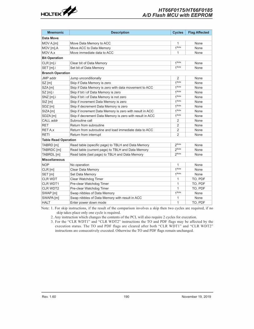
Rev. 1.60 190 November 19, 2019 Rev. 1.60 191 November 19, 2019
HT66F0175/HT66F0185A/D Flash MCU with EEPROM
HT66F0175/HT66F0185A/D Flash MCU with EEPROM
Mnemonic Description Cycles Flag AffectedData MoveMOV A,[m] Move Data Memory to ACC 1 NoneMOV [m],A Move ACC to Data Memory 1Note NoneMOV A,x Move immediate data to ACC 1 NoneBit OperationCLR [m].i Clear bit of Data Memory 1Note NoneSET [m].i Set bit of Data Memory 1Note NoneBranch OperationJMP addr Jump unconditionally 2 NoneSZ [m] Skip if Data Memory is zero 1Note NoneSZA [m] Skip if Data Memory is zero with data movement to ACC 1Note NoneSZ [m].i Skip if bit i of Data Memory is zero 1Note NoneSNZ [m].i Skip if bit i of Data Memory is not zero 1Note NoneSIZ [m] Skip if increment Data Memory is zero 1Note NoneSDZ [m] Skip if decrement Data Memory is zero 1Note NoneSIZA [m] Skip if increment Data Memory is zero with result in ACC 1Note NoneSDZA [m] Skip if decrement Data Memory is zero with result in ACC 1Note NoneCALL addr Subroutine call 2 NoneRET Return from subroutine 2 NoneRET A,x Return from subroutine and load immediate data to ACC 2 NoneRETI Return from interrupt 2 NoneTable Read OperationTABRD [m] Read table (specific page) to TBLH and Data Memory 2Note NoneTABRDC [m] Read table (current page) to TBLH and Data Memory 2Note NoneTABRDL [m] Read table (last page) to TBLH and Data Memory 2Note NoneMiscellaneousNOP No operation 1 NoneCLR [m] Clear Data Memory 1Note NoneSET [m] Set Data Memory 1Note NoneCLR WDT Clear Watchdog Timer 1 TO, PDFCLR WDT1 Pre-clear Watchdog Timer 1 TO, PDFCLR WDT2 Pre-clear Watchdog Timer 1 TO, PDFSWAP [m] Swap nibbles of Data Memory 1Note NoneSWAPA [m] Swap nibbles of Data Memory with result in ACC 1 NoneHALT Enter power down mode 1 TO, PDFNote: 1. For skip instructions, if the result of the comparison involves a skip then two cycles are required, if no
skip takes place only one cycle is required.2. Any instruction which changes the contents of the PCL will also require 2 cycles for execution.3. For the “CLR WDT1” and “CLR WDT2” instructions the TO and PDF flags may be affected by the
execution status. The TO and PDF flags are cleared after both “CLR WDT1” and “CLR WDT2” instructions are consecutively executed. Otherwise the TO and PDF flags remain unchanged.
Rev. 1.60 190 November 19, 2019 Rev. 1.60 191 November 19, 2019
HT66F0175/HT66F0185A/D Flash MCU with EEPROM
HT66F0175/HT66F0185A/D Flash MCU with EEPROM
Instruction Definition
ADC A,[m] Add Data Memory to ACC with CarryDescription The contents of the specified Data Memory, Accumulator and the carry flag are added. The result is stored in the Accumulator.Operation ACC ← ACC + [m] + CAffected flag(s) OV, Z, AC, C
ADCM A,[m] Add ACC to Data Memory with CarryDescription The contents of the specified Data Memory, Accumulator and the carry flag are added. The result is stored in the specified Data Memory.Operation [m] ← ACC + [m] + CAffected flag(s) OV, Z, AC, C
ADD A,[m] Add Data Memory to ACCDescription The contents of the specified Data Memory and the Accumulator are added. The result is stored in the Accumulator.Operation ACC ← ACC + [m]Affected flag(s) OV, Z, AC, C
ADD A,x Add immediate data to ACCDescription The contents of the Accumulator and the specified immediate data are added. The result is stored in the Accumulator.Operation ACC ← ACC + xAffected flag(s) OV, Z, AC, C
ADDM A,[m] Add ACC to Data MemoryDescription The contents of the specified Data Memory and the Accumulator are added. The result is stored in the specified Data Memory.Operation [m] ← ACC + [m]Affected flag(s) OV, Z, AC, C
AND A,[m] Logical AND Data Memory to ACCDescription Data in the Accumulator and the specified Data Memory perform a bitwise logical AND operation. The result is stored in the Accumulator.Operation ACC ← ACC ″AND″ [m]Affected flag(s) Z
AND A,x Logical AND immediate data to ACCDescription Data in the Accumulator and the specified immediate data perform a bit wise logical AND operation. The result is stored in the Accumulator.Operation ACC ← ACC ″AND″ xAffected flag(s) Z
ANDM A,[m] Logical AND ACC to Data MemoryDescription Data in the specified Data Memory and the Accumulator perform a bitwise logical AND operation. The result is stored in the Data Memory.Operation [m] ← ACC ″AND″ [m]Affected flag(s) Z
Rev. 1.60 192 November 19, 2019 Rev. 1.60 193 November 19, 2019
HT66F0175/HT66F0185A/D Flash MCU with EEPROM
HT66F0175/HT66F0185A/D Flash MCU with EEPROM
CALL addr Subroutine callDescription Unconditionally calls a subroutine at the specified address. The Program Counter then increments by 1 to obtain the address of the next instruction which is then pushed onto the stack. The specified address is then loaded and the program continues execution from this new address. As this instruction requires an additional operation, it is a two cycle instruction.Operation Stack ← Program Counter + 1 Program Counter ← addrAffected flag(s) None
CLR [m] Clear Data MemoryDescription Each bit of the specified Data Memory is cleared to 0.Operation [m] ← 00HAffected flag(s) None
CLR [m].i Clear bit of Data MemoryDescription Bit i of the specified Data Memory is cleared to 0.Operation [m].i ← 0Affected flag(s) None
CLR WDT Clear Watchdog TimerDescription The TO, PDF flags and the WDT are all cleared. Operation WDT cleared TO ← 0 PDF ← 0Affected flag(s) TO, PDF
CLR WDT1 Pre-clear Watchdog TimerDescription The TO, PDF flags and the WDT are all cleared. Note that this instruction works in conjunction with CLR WDT2 and must be executed alternately with CLR WDT2 to have effect. Repetitively executing this instruction without alternately executing CLR WDT2 will have no effect.Operation WDT cleared TO ← 0 PDF ← 0 Affected flag(s) TO, PDF
CLR WDT2 Pre-clear Watchdog TimerDescription The TO, PDF flags and the WDT are all cleared. Note that this instruction works in conjunction with CLR WDT1 and must be executed alternately with CLR WDT1 to have effect. Repetitively executing this instruction without alternately executing CLR WDT1 will have no effect.Operation WDT cleared TO ← 0 PDF ← 0Affected flag(s) TO, PDF
CPL [m] Complement Data MemoryDescription Each bit of the specified Data Memory is logically complemented (1′s complement). Bits which previously contained a 1 are changed to 0 and vice versa.Operation [m] ← [m]Affected flag(s) Z
Rev. 1.60 192 November 19, 2019 Rev. 1.60 193 November 19, 2019
HT66F0175/HT66F0185A/D Flash MCU with EEPROM
HT66F0175/HT66F0185A/D Flash MCU with EEPROM
CPLA [m] Complement Data Memory with result in ACCDescription Each bit of the specified Data Memory is logically complemented (1′s complement). Bits which previously contained a 1 are changed to 0 and vice versa. The complemented result is stored in the Accumulator and the contents of the Data Memory remain unchanged.Operation ACC ← [m]Affected flag(s) Z
DAA [m] Decimal-Adjust ACC for addition with result in Data MemoryDescription Convert the contents of the Accumulator value to a BCD (Binary Coded Decimal) value resulting from the previous addition of two BCD variables. If the low nibble is greater than 9 or if AC flag is set, then a value of 6 will be added to the low nibble. Otherwise the low nibble remains unchanged. If the high nibble is greater than 9 or if the C flag is set, then a value of 6 will be added to the high nibble. Essentially, the decimal conversion is performed by adding 00H, 06H, 60H or 66H depending on the Accumulator and flag conditions. Only the C flag may be affected by this instruction which indicates that if the original BCD sum is greater than 100, it allows multiple precision decimal addition.Operation [m] ← ACC + 00H or [m] ← ACC + 06H or [m] ← ACC + 60H or [m] ← ACC + 66HAffected flag(s) C
DEC [m] Decrement Data MemoryDescription Data in the specified Data Memory is decremented by 1.Operation [m] ← [m] − 1Affected flag(s) Z
DECA [m] Decrement Data Memory with result in ACCDescription Data in the specified Data Memory is decremented by 1. The result is stored in the Accumulator. The contents of the Data Memory remain unchanged.Operation ACC ← [m] − 1Affected flag(s) Z
HALT Enter power down modeDescription This instruction stops the program execution and turns off the system clock. The contents of the Data Memory and registers are retained. The WDT and prescaler are cleared. The power down flag PDF is set and the WDT time-out flag TO is cleared.Operation TO ← 0 PDF ← 1Affected flag(s) TO, PDF
INC [m] Increment Data Memory Description Data in the specified Data Memory is incremented by 1.Operation [m] ← [m] + 1Affected flag(s) Z
INCA [m] Increment Data Memory with result in ACCDescription Data in the specified Data Memory is incremented by 1. The result is stored in the Accumulator. The contents of the Data Memory remain unchanged.Operation ACC ← [m] + 1Affected flag(s) Z
Rev. 1.60 194 November 19, 2019 Rev. 1.60 195 November 19, 2019
HT66F0175/HT66F0185A/D Flash MCU with EEPROM
HT66F0175/HT66F0185A/D Flash MCU with EEPROM
JMP addr Jump unconditionallyDescription The contents of the Program Counter are replaced with the specified address. Program execution then continues from this new address. As this requires the insertion of a dummy instruction while the new address is loaded, it is a two cycle instruction.Operation Program Counter ← addrAffected flag(s) None
MOV A,[m] Move Data Memory to ACCDescription The contents of the specified Data Memory are copied to the Accumulator.Operation ACC ← [m]Affected flag(s) None
MOV A,x Move immediate data to ACCDescription The immediate data specified is loaded into the Accumulator.Operation ACC ← xAffected flag(s) None
MOV [m],A Move ACC to Data Memory Description The contents of the Accumulator are copied to the specified Data Memory.Operation [m] ← ACCAffected flag(s) None
NOP No operationDescription No operation is performed. Execution continues with the next instruction.Operation No operationAffected flag(s) None
OR A,[m] Logical OR Data Memory to ACCDescription Data in the Accumulator and the specified Data Memory perform a bitwise logical OR operation. The result is stored in the Accumulator.Operation ACC ← ACC ″OR″ [m]Affected flag(s) Z
OR A,x Logical OR immediate data to ACCDescription Data in the Accumulator and the specified immediate data perform a bitwise logical OR operation. The result is stored in the Accumulator.Operation ACC ← ACC ″OR″ xAffected flag(s) Z
ORM A,[m] Logical OR ACC to Data MemoryDescription Data in the specified Data Memory and the Accumulator perform a bitwise logical OR operation. The result is stored in the Data Memory.Operation [m] ← ACC ″OR″ [m]Affected flag(s) Z
RET Return from subroutineDescription The Program Counter is restored from the stack. Program execution continues at the restored address.Operation Program Counter ← StackAffected flag(s) None
Rev. 1.60 194 November 19, 2019 Rev. 1.60 195 November 19, 2019
HT66F0175/HT66F0185A/D Flash MCU with EEPROM
HT66F0175/HT66F0185A/D Flash MCU with EEPROM
RET A,x Return from subroutine and load immediate data to ACCDescription The Program Counter is restored from the stack and the Accumulator loaded with the specified immediate data. Program execution continues at the restored address.Operation Program Counter ← Stack ACC ← xAffected flag(s) None
RETI Return from interruptDescription The Program Counter is restored from the stack and the interrupts are re-enabled by setting the EMI bit. EMI is the master interrupt global enable bit. If an interrupt was pending when the RETI instruction is executed, the pending Interrupt routine will be processed before returning to the main program.Operation Program Counter ← Stack EMI ← 1Affected flag(s) None
RL [m] Rotate Data Memory leftDescription The contents of the specified Data Memory are rotated left by 1 bit with bit 7 rotated into bit 0.Operation [m].(i+1) ← [m].i; (i=0~6) [m].0 ← [m].7Affected flag(s) None
RLA [m] Rotate Data Memory left with result in ACCDescription The contents of the specified Data Memory are rotated left by 1 bit with bit 7 rotated into bit 0. The rotated result is stored in the Accumulator and the contents of the Data Memory remain unchanged.Operation ACC.(i+1) ← [m].i; (i=0~6) ACC.0 ← [m].7Affected flag(s) None
RLC [m] Rotate Data Memory left through CarryDescription The contents of the specified Data Memory and the carry flag are rotated left by 1 bit. Bit 7 replaces the Carry bit and the original carry flag is rotated into bit 0.Operation [m].(i+1) ← [m].i; (i=0~6) [m].0 ← C C ← [m].7Affected flag(s) C
RLCA [m] Rotate Data Memory left through Carry with result in ACCDescription Data in the specified Data Memory and the carry flag are rotated left by 1 bit. Bit 7 replaces the Carry bit and the original carry flag is rotated into the bit 0. The rotated result is stored in the Accumulator and the contents of the Data Memory remain unchanged.Operation ACC.(i+1) ← [m].i; (i=0~6) ACC.0 ← C C ← [m].7Affected flag(s) C
RR [m] Rotate Data Memory rightDescription The contents of the specified Data Memory are rotated right by 1 bit with bit 0 rotated into bit 7.Operation [m].i ← [m].(i+1); (i=0~6) [m].7 ← [m].0Affected flag(s) None
Rev. 1.60 196 November 19, 2019 Rev. 1.60 197 November 19, 2019
HT66F0175/HT66F0185A/D Flash MCU with EEPROM
HT66F0175/HT66F0185A/D Flash MCU with EEPROM
RRA [m] Rotate Data Memory right with result in ACCDescription Data in the specified Data Memory and the carry flag are rotated right by 1 bit with bit 0 rotated into bit 7. The rotated result is stored in the Accumulator and the contents of the Data Memory remain unchanged.Operation ACC.i ← [m].(i+1); (i=0~6) ACC.7 ← [m].0Affected flag(s) None
RRC [m] Rotate Data Memory right through CarryDescription The contents of the specified Data Memory and the carry flag are rotated right by 1 bit. Bit 0 replaces the Carry bit and the original carry flag is rotated into bit 7.Operation [m].i ← [m].(i+1); (i=0~6) [m].7 ← C C ← [m].0Affected flag(s) C
RRCA [m] Rotate Data Memory right through Carry with result in ACCDescription Data in the specified Data Memory and the carry flag are rotated right by 1 bit. Bit 0 replaces the Carry bit and the original carry flag is rotated into bit 7. The rotated result is stored in the Accumulator and the contents of the Data Memory remain unchanged.Operation ACC.i ← [m].(i+1); (i=0~6) ACC.7 ← C C ← [m].0Affected flag(s) C
SBC A,[m] Subtract Data Memory from ACC with CarryDescription The contents of the specified Data Memory and the complement of the carry flag are subtracted from the Accumulator. The result is stored in the Accumulator. Note that if the result of subtraction is negative, the C flag will be cleared to 0, otherwise if the result is positive or zero, the C flag will be set to 1.Operation ACC ← ACC − [m] − CAffected flag(s) OV, Z, AC, C
SBCM A,[m] Subtract Data Memory from ACC with Carry and result in Data MemoryDescription The contents of the specified Data Memory and the complement of the carry flag are subtracted from the Accumulator. The result is stored in the Data Memory. Note that if the result of subtraction is negative, the C flag will be cleared to 0, otherwise if the result is positive or zero, the C flag will be set to 1.Operation [m] ← ACC − [m] − CAffected flag(s) OV, Z, AC, C
SDZ [m] Skip if decrement Data Memory is 0Description The contents of the specified Data Memory are first decremented by 1. If the result is 0 the following instruction is skipped. As this requires the insertion of a dummy instruction while the next instruction is fetched, it is a two cycle instruction. If the result is not 0 the program proceeds with the following instruction.Operation [m] ← [m] − 1 Skip if [m]=0Affected flag(s) None
Rev. 1.60 196 November 19, 2019 Rev. 1.60 197 November 19, 2019
HT66F0175/HT66F0185A/D Flash MCU with EEPROM
HT66F0175/HT66F0185A/D Flash MCU with EEPROM
SDZA [m] Skip if decrement Data Memory is zero with result in ACCDescription The contents of the specified Data Memory are first decremented by 1. If the result is 0, the following instruction is skipped. The result is stored in the Accumulator but the specified Data Memory contents remain unchanged. As this requires the insertion of a dummy instruction while the next instruction is fetched, it is a two cycle instruction. If the result is not 0, the program proceeds with the following instruction.Operation ACC ← [m] − 1 Skip if ACC=0Affected flag(s) None
SET [m] Set Data MemoryDescription Each bit of the specified Data Memory is set to 1.Operation [m] ← FFHAffected flag(s) None
SET [m].i Set bit of Data MemoryDescription Bit i of the specified Data Memory is set to 1.Operation [m].i ← 1Affected flag(s) None
SIZ [m] Skip if increment Data Memory is 0Description The contents of the specified Data Memory are first incremented by 1. If the result is 0, the following instruction is skipped. As this requires the insertion of a dummy instruction while the next instruction is fetched, it is a two cycle instruction. If the result is not 0 the program proceeds with the following instruction.Operation [m] ← [m] + 1 Skip if [m]=0 Affected flag(s) None
SIZA [m] Skip if increment Data Memory is zero with result in ACCDescription The contents of the specified Data Memory are first incremented by 1. If the result is 0, the following instruction is skipped. The result is stored in the Accumulator but the specified Data Memory contents remain unchanged. As this requires the insertion of a dummy instruction while the next instruction is fetched, it is a two cycle instruction. If the result is not 0 the program proceeds with the following instruction.Operation ACC ← [m] + 1 Skip if ACC=0Affected flag(s) None
SNZ [m].i Skip if bit i of Data Memory is not 0Description If bit i of the specified Data Memory is not 0, the following instruction is skipped. As this requires the insertion of a dummy instruction while the next instruction is fetched, it is a two cycle instruction. If the result is 0 the program proceeds with the following instruction.Operation Skip if [m].i ≠ 0Affected flag(s) None
SUB A,[m] Subtract Data Memory from ACCDescription The specified Data Memory is subtracted from the contents of the Accumulator. The result is stored in the Accumulator. Note that if the result of subtraction is negative, the C flag will be cleared to 0, otherwise if the result is positive or zero, the C flag will be set to 1.Operation ACC ← ACC − [m]Affected flag(s) OV, Z, AC, C
Rev. 1.60 198 November 19, 2019 Rev. 1.60 199 November 19, 2019
HT66F0175/HT66F0185A/D Flash MCU with EEPROM
HT66F0175/HT66F0185A/D Flash MCU with EEPROM
SUBM A,[m] Subtract Data Memory from ACC with result in Data MemoryDescription The specified Data Memory is subtracted from the contents of the Accumulator. The result is stored in the Data Memory. Note that if the result of subtraction is negative, the C flag will be cleared to 0, otherwise if the result is positive or zero, the C flag will be set to 1.Operation [m] ← ACC − [m]Affected flag(s) OV, Z, AC, C
SUB A,x Subtract immediate data from ACCDescription The immediate data specified by the code is subtracted from the contents of the Accumulator. The result is stored in the Accumulator. Note that if the result of subtraction is negative, the C flag will be cleared to 0, otherwise if the result is positive or zero, the C flag will be set to 1.Operation ACC ← ACC − xAffected flag(s) OV, Z, AC, C
SWAP [m] Swap nibbles of Data MemoryDescription The low-order and high-order nibbles of the specified Data Memory are interchanged.Operation [m].3~[m].0 ↔ [m].7~[m].4Affected flag(s) None
SWAPA [m] Swap nibbles of Data Memory with result in ACCDescription The low-order and high-order nibbles of the specified Data Memory are interchanged. The result is stored in the Accumulator. The contents of the Data Memory remain unchanged.Operation ACC.3~ACC.0 ← [m].7~[m].4 ACC.7~ACC.4 ← [m].3~[m].0Affected flag(s) None
SZ [m] Skip if Data Memory is 0Description If the contents of the specified Data Memory is 0, the following instruction is skipped. As this requires the insertion of a dummy instruction while the next instruction is fetched, it is a two cycle instruction. If the result is not 0 the program proceeds with the following instruction.Operation Skip if [m]=0Affected flag(s) None
SZA [m] Skip if Data Memory is 0 with data movement to ACCDescription The contents of the specified Data Memory are copied to the Accumulator. If the value is zero, the following instruction is skipped. As this requires the insertion of a dummy instruction while the next instruction is fetched, it is a two cycle instruction. If the result is not 0 the program proceeds with the following instruction.Operation ACC ← [m] Skip if [m]=0Affected flag(s) None
SZ [m].i Skip if bit i of Data Memory is 0Description If bit i of the specified Data Memory is 0, the following instruction is skipped. As this requires the insertion of a dummy instruction while the next instruction is fetched, it is a two cycle instruction. If the result is not 0, the program proceeds with the following instruction.Operation Skip if [m].i=0Affected flag(s) None
Rev. 1.60 198 November 19, 2019 Rev. 1.60 199 November 19, 2019
HT66F0175/HT66F0185A/D Flash MCU with EEPROM
HT66F0175/HT66F0185A/D Flash MCU with EEPROM
TABRD [m] Read table (specific page) to TBLH and Data MemoryDescription The low byte of the program code (specific page) addressed by the table pointer pair (TBHP and TBLP) is moved to the specified Data Memory and the high byte moved to TBLH.Operation [m] ← program code (low byte) TBLH ← program code (high byte)Affected flag(s) None
TABRDC [m] Read table (current page) to TBLH and Data MemoryDescription The low byte of the program code (current page) addressed by the table pointer (TBLP) is moved to the specified Data Memory and the high byte moved to TBLH.Operation [m] ← program code (low byte) TBLH ← program code (high byte)Affected flag(s) None
TABRDL [m] Read table (last page) to TBLH and Data MemoryDescription The low byte of the program code (last page) addressed by the table pointer (TBLP) is moved to the specified Data Memory and the high byte moved to TBLH.Operation [m] ← program code (low byte) TBLH ← program code (high byte)Affected flag(s) None
XOR A,[m] Logical XOR Data Memory to ACCDescription Data in the Accumulator and the specified Data Memory perform a bitwise logical XOR operation. The result is stored in the Accumulator.Operation ACC ← ACC ″XOR″ [m]Affected flag(s) Z
XORM A,[m] Logical XOR ACC to Data MemoryDescription Data in the specified Data Memory and the Accumulator perform a bitwise logical XOR operation. The result is stored in the Data Memory.Operation [m] ← ACC ″XOR″ [m]Affected flag(s) Z
XOR A,x Logical XOR immediate data to ACCDescription Data in the Accumulator and the specified immediate data perform a bitwise logical XOR operation. The result is stored in the Accumulator.Operation ACC ← ACC ″XOR″ xAffected flag(s) Z
Rev. 1.60 200 November 19, 2019 Rev. 1.60 201 November 19, 2019
HT66F0175/HT66F0185A/D Flash MCU with EEPROM
HT66F0175/HT66F0185A/D Flash MCU with EEPROM
Package Information
Note that the package information provided here is for consultation purposes only. As this information may be updated at regular intervals users are reminded to consult the Holtek website for the latest version of the Package/Carton Information.
Additional supplementary information with regard to packaging is listed below. Click on the relevant section to be transferred to the relevant website page.
• Further Package Information (include Outline Dimensions, Product Tape and Reel Specifications)
• Packing Meterials Information
• Carton information
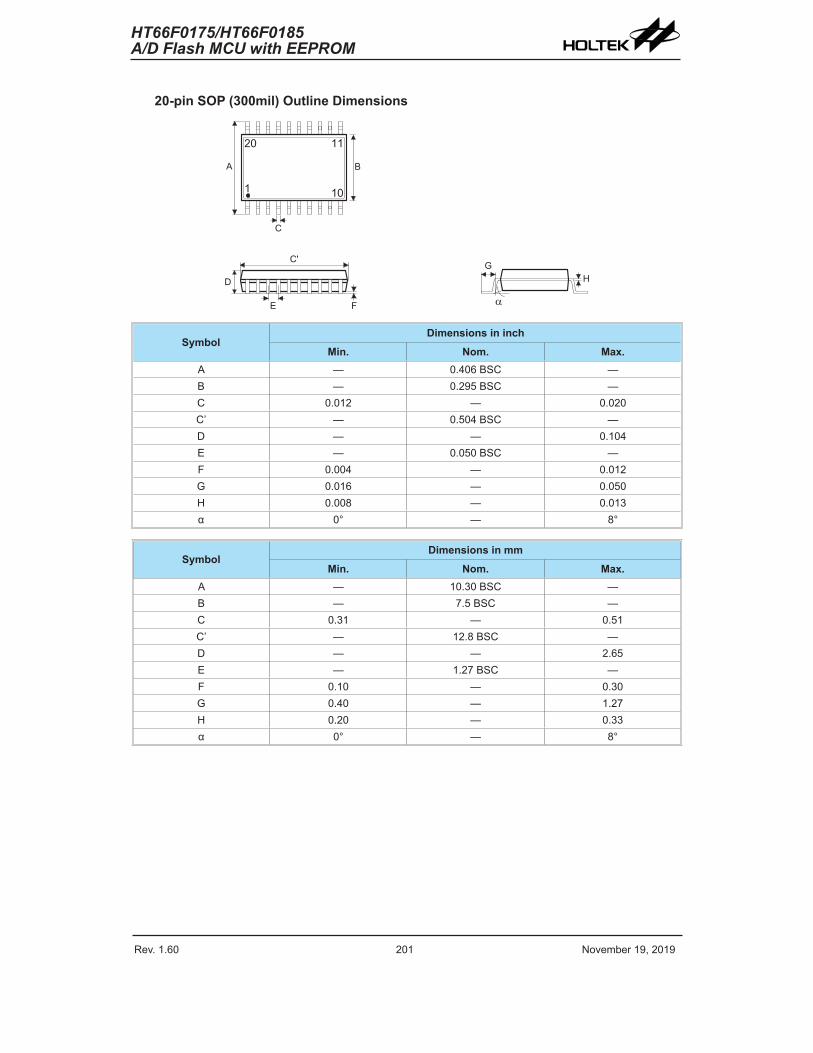
Rev. 1.60 200 November 19, 2019 Rev. 1.60 201 November 19, 2019
HT66F0175/HT66F0185A/D Flash MCU with EEPROM
HT66F0175/HT66F0185A/D Flash MCU with EEPROM
20-pin SOP (300mil) Outline Dimensions
� �
�
� �
� �
� �
�
�
� �
� ��
�
�
SymbolDimensions in inch
Min. Nom. Max.A — 0.406 BSC —B — 0.295 BSC —C 0.012 — 0.020 C’ — 0.504 BSC —D — — 0.104 E — 0.050 BSC —F 0.004 — 0.012 G 0.016 — 0.050 H 0.008 — 0.013 α 0° — 8°
SymbolDimensions in mm
Min. Nom. Max.A — 10.30 BSC —B — 7.5 BSC —C 0.31 — 0.51 C’ — 12.8 BSC —D — — 2.65 E — 1.27 BSC —F 0.10 — 0.30 G 0.40 — 1.27 H 0.20 — 0.33 α 0° — 8°

Rev. 1.60 202 November 19, 2019 Rev. 1.60 203 November 19, 2019
HT66F0175/HT66F0185A/D Flash MCU with EEPROM
HT66F0175/HT66F0185A/D Flash MCU with EEPROM
20-pin SSOP (150mil) Outline Dimensions
� �
�
� �
� �
� �
�
�
� �
� � ��
�
SymbolDimensions in inch
Min. Nom. Max.A — 0.236 BSC —B — 0.154 BSC —C 0.008 — 0.012 C’ — 0.341 BSC —D — — 0.069E — 0.025 BSC —F 0.004 — 0.010 G 0.016 — 0.050 H 0.004 — 0.010 α 0° — 8°
SymbolDimensions in mm
Min. Nom. Max.A — 6.0 BSC —B — 3.9 BSC —C 0.20 — 0.30 C’ — 8.66 BSC —D — — 1.75 E — 0.635 BSC —F 0.10 — 0.25 G 0.41 — 1.27 H 0.10 — 0.25 α 0° — 8°
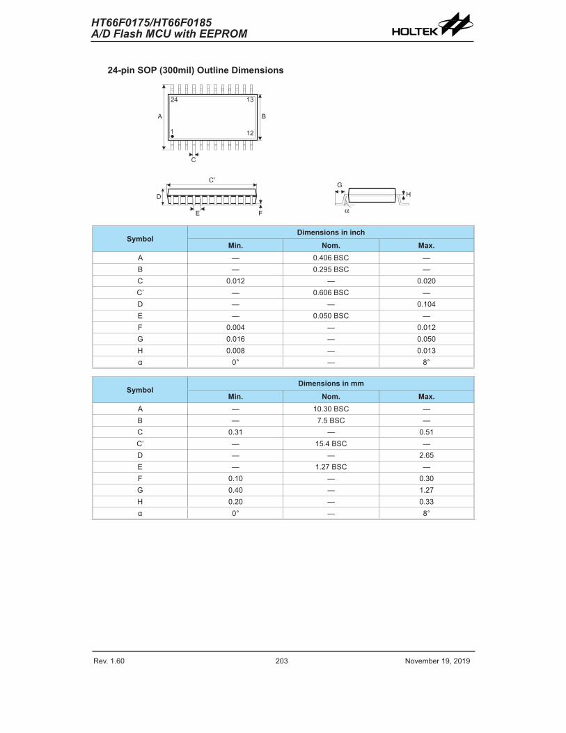
Rev. 1.60 202 November 19, 2019 Rev. 1.60 203 November 19, 2019
HT66F0175/HT66F0185A/D Flash MCU with EEPROM
HT66F0175/HT66F0185A/D Flash MCU with EEPROM
24-pin SOP (300mil) Outline Dimensions
� �
�
� �
� �
� �
�
�
� �
� ��
�
�
SymbolDimensions in inch
Min. Nom. Max.A — 0.406 BSC —B — 0.295 BSC —C 0.012 — 0.020C’ — 0.606 BSC —D — — 0.104E — 0.050 BSC —F 0.004 — 0.012G 0.016 — 0.050H 0.008 — 0.013α 0° — 8°
SymbolDimensions in mm
Min. Nom. Max.A — 10.30 BSC —B — 7.5 BSC —C 0.31 — 0.51C’ — 15.4 BSC —D — — 2.65E — 1.27 BSC —F 0.10 — 0.30G 0.40 — 1.27H 0.20 — 0.33α 0° — 8°
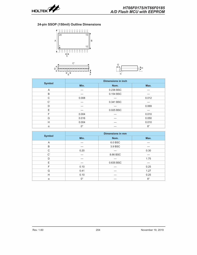
Rev. 1.60 204 November 19, 2019 Rev. 1.60 205 November 19, 2019
HT66F0175/HT66F0185A/D Flash MCU with EEPROM
HT66F0175/HT66F0185A/D Flash MCU with EEPROM
24-pin SSOP (150mil) Outline Dimensions
� �
�
� �
� �
� �
�
�
� �
� � ��
�
SymbolDimensions in inch
Min. Nom. Max.A — 0.236 BSC —B — 0.154 BSC —C 0.008 — 0.012C’ — 0.341 BSC —D — — 0.069E — 0.025 BSC —F 0.004 — 0.010G 0.016 — 0.050H 0.004 — 0.010α 0° — 8°
SymbolDimensions in mm
Min. Nom. Max.A — 6.0 BSC —B — 3.9 BSC —C 0.20 — 0.30C’ — 8.66 BSC —D — — 1.75E — 0.635 BSC —F 0.10 — 0.25G 0.41 — 1.27H 0.10 — 0.25α 0° — 8°
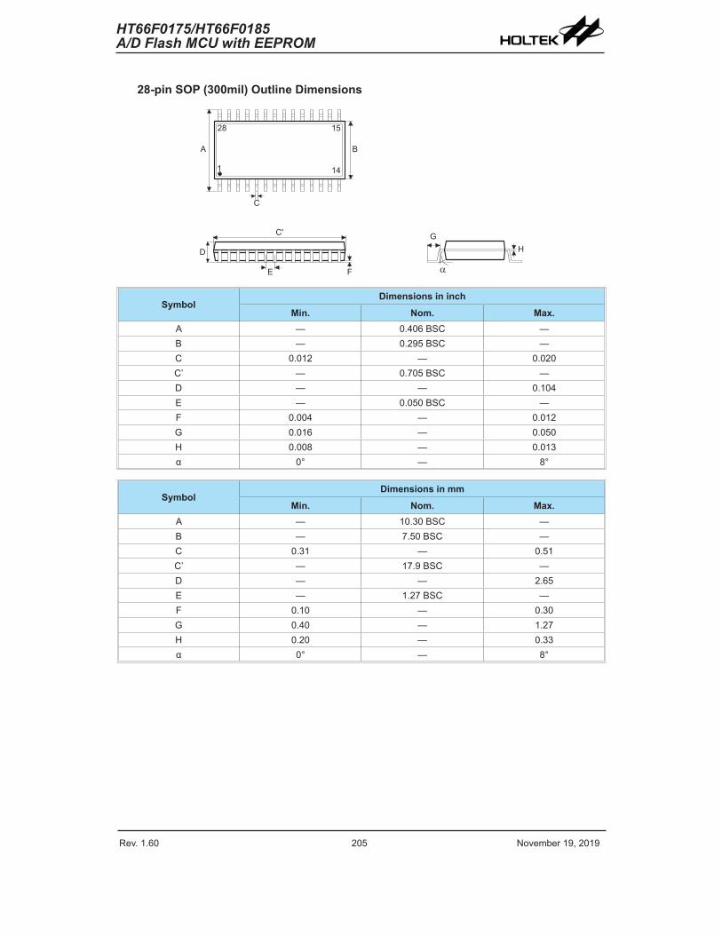
Rev. 1.60 204 November 19, 2019 Rev. 1.60 205 November 19, 2019
HT66F0175/HT66F0185A/D Flash MCU with EEPROM
HT66F0175/HT66F0185A/D Flash MCU with EEPROM
28-pin SOP (300mil) Outline Dimensions
� �
�
� �
� �
� �
�
�
�
� � ��
��
SymbolDimensions in inch
Min. Nom. Max.A — 0.406 BSC —B — 0.295 BSC —C 0.012 — 0.020C’ — 0.705 BSC —D — — 0.104E — 0.050 BSC —F 0.004 — 0.012G 0.016 — 0.050H 0.008 — 0.013α 0° — 8°
SymbolDimensions in mm
Min. Nom. Max.A — 10.30 BSC —B — 7.50 BSC —C 0.31 — 0.51C’ — 17.9 BSC —D — — 2.65E — 1.27 BSC —F 0.10 — 0.30G 0.40 — 1.27H 0.20 — 0.33α 0° — 8°
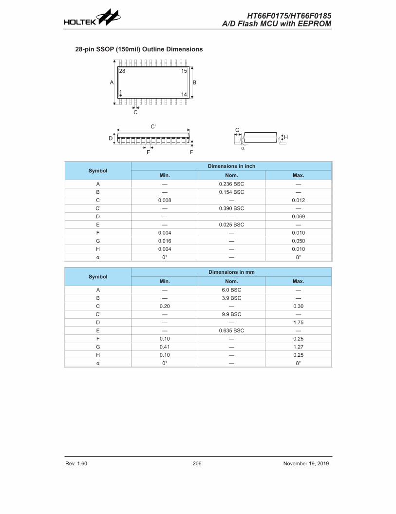
Rev. 1.60 206 November 19, 2019 Rev. 1.60 207 November 19, 2019
HT66F0175/HT66F0185A/D Flash MCU with EEPROM
HT66F0175/HT66F0185A/D Flash MCU with EEPROM
28-pin SSOP (150mil) Outline Dimensions
� �
�
� �
� �
� �
�
�
�
� � ��
��
SymbolDimensions in inch
Min. Nom. Max.A — 0.236 BSC —B — 0.154 BSC —C 0.008 — 0.012C’ — 0.390 BSC —D — — 0.069E — 0.025 BSC —F 0.004 — 0.010G 0.016 — 0.050H 0.004 — 0.010α 0° — 8°
SymbolDimensions in mm
Min. Nom. Max.A — 6.0 BSC —B — 3.9 BSC —C 0.20 — 0.30C’ — 9.9 BSC —D — — 1.75E — 0.635 BSC —F 0.10 — 0.25G 0.41 — 1.27H 0.10 — 0.25α 0° — 8°
Rev. 1.60 206 November 19, 2019 Rev. 1.60 207 November 19, 2019
HT66F0175/HT66F0185A/D Flash MCU with EEPROM
HT66F0175/HT66F0185A/D Flash MCU with EEPROM
Copyright© 2019 by HOLTEK SEMICONDUCTOR INC.
The information appearing in this Data Sheet is believed to be accurate at the time of publication. However, Holtek assumes no responsibility arising from the use of the specifications described. The applications mentioned herein are used solely for the purpose of illustration and Holtek makes no warranty or representation that such applications will be suitable without further modification, nor recommends the use of its products for application that may present a risk to human life due to malfunction or otherwise. Holtek's products are not authorized for use as critical components in life support devices or systems. Holtek reserves the right to alter its products without prior notification. For the most up-to-date information, please visit our web site at http://www.holtek.com.