microprocessor - nvchavan.files.wordpress.com fileinput for the microprocessor. when this signal is...
TRANSCRIPT

Microprocessor

Flags

• Carry flag: This flag is set when there is a carry out of MSB in case of addition or a borrow in case of subtraction.
• Parity flag: This flag is set, if the lower byte of the result contains even numbers of 1s
• Auxiliary carry flag : this is set if there is a carry from the lowest nibble, i.e. bit three during addition or borrow for the lowest nibble i.e. bit three during subtraction.
• Zero flag: This flag is set if the result of the computation or comparison performed by previous instruction is zero.

• Sign flag: this flag is set when the result of any computation is negative. For signed computations the sign flag equals the MSB of the result.
• Trap flag if this flag is set the processor enters the single step execution mode.
• Interrupt flag: If this flag is set the maskable interrupts are recognized by the cpu, otherwise they are ignored.
• Direction flag: This flag is used by string manipulation instructions. If this flag bit is 0 the string is processed beginning from the lowest address to the highest address, otherwise the string is processed from the highest address towards lowest address.
• Overflow flag: This flag is set if an overflow occurs.
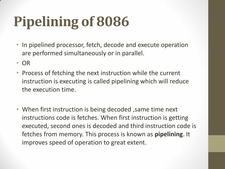
Pipelining of 8086
• In pipelined processor, fetch, decode and execute operation are performed simultaneously or in parallel.
• OR
• Process of fetching the next instruction while the current instruction is executing is called pipelining which will reduce the execution time.
• When first instruction is being decoded ,same time next instructions code is fetches. When first instruction is getting executed, second ones is decoded and third instruction code is fetches from memory. This process is known as pipelining. It improves speed of operation to great extent.

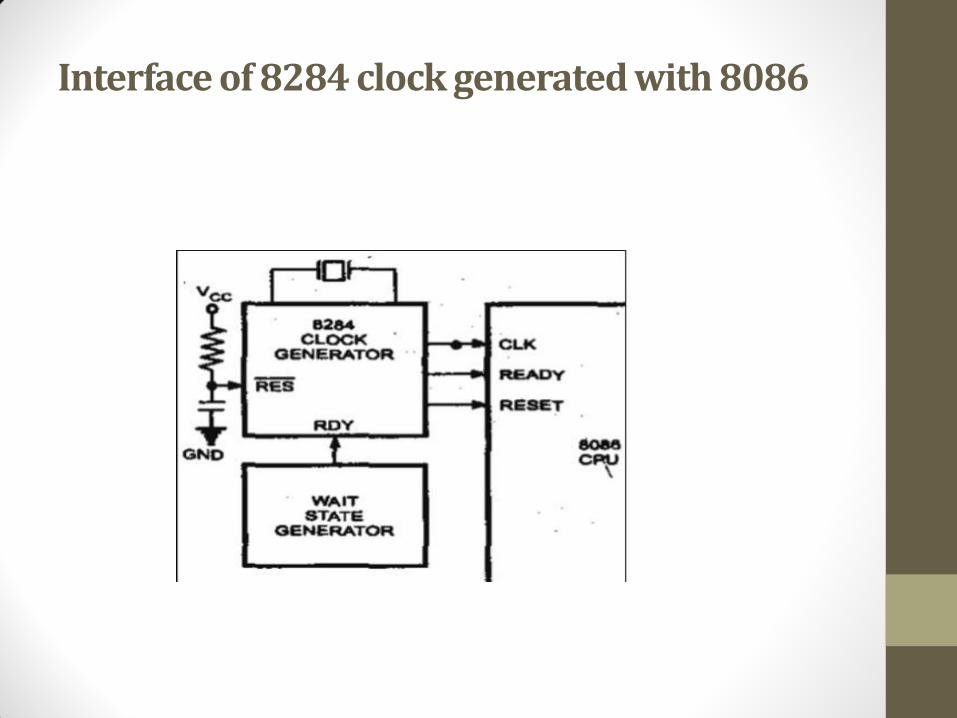
Interface of 8284 clock generated with 8086

• Generate system clock: The Clock logic results in three different frequencies required for the system. These outputs are CLOCK, READY, RESET.
• Generate READY signal: The Ready logic has a READY output which is connected to the processor. When this is low, wait states are added in the bus cycle.
• Generate RESET signal: The Reset logic generates a RESET input for the microprocessor. When this signal is High, processor performs reset sequence.

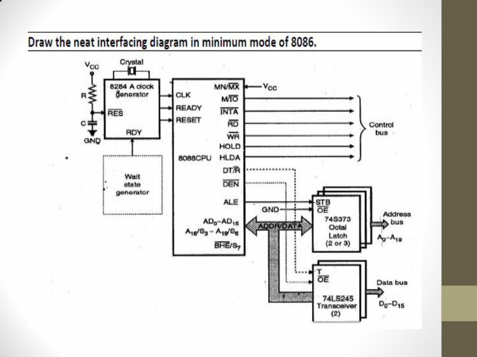


• The microprocessor 8086 is operated in minimum mode by strapping its MN/MX̅̅̅̅̅̅̅̅̅̅̅̅̅̅̅̅ pin to logic 1.
• The working of the minimum mode configuration system can be better described in terms of the timing diagrams.
• The op-code fetch and read cycles are similar. Hence the timing diagram can be categorized in two parts, the first is the timing diagram for read cycle and the second is the timing diagram for write cycle.
• The read cycle begins in T1 with the assertion of address latch enable (ALE) signal and also M / IO̅̅̅̅̅̅̅̅̅ signal. During the negative going edge of this signal, the valid address is latched on the local bus.

• The BHE and A0 signals address low, high or both bytes. From T1 to T4, the M/IO signal indicates a memory or I/O operation.
•
• At T2, the address is removed from the local bus and is sent to the output. The bus is then tristated. The read (RD̅̅̅̅̅̅̅̅̅̅̅̅̅̅̅̅) control signal is also activated in T2.
• The read (RD̅̅̅̅̅̅̅̅̅̅̅̅̅̅̅̅) signal causes the address device to enable its data bus drivers. After RD̅̅̅̅̅̅̅̅̅̅̅̅̅̅̅̅ goes low, the valid data is available on the data bus.
• The addressed device will drive the READY line high. When the processor returns the read signal to high level, the addressed device will again tri-state its bus drivers

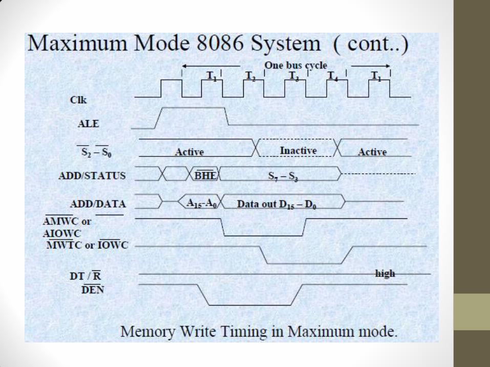
• A write cycle also begins with the assertion of ALE and the emission of the address. The M/IO̅̅̅̅̅̅̅̅̅̅̅̅ signal is again asserted to indicate a memory or I/O operation.
• In T 2, after sending the address in T1, the processor sends the data to be written to the addressed location.
• The data remains on the bus until middle of T 4 state. The WR becomes active at the beginning of T 2 (unlike RD̅̅̅̅̅̅̅̅̅̅̅̅̅̅̅̅ is somewhat delayed in T 2 to provide time for floating).
• The BHE̅̅̅̅̅̅̅̅̅̅̅̅̅̅̅̅̅̅̅̅̅̅̅̅ and A0 signals are used to select the proper byte or
bytes of memory or I/O word to be read or write.
• The M/IO̅̅̅̅̅̅̅̅̅̅̅̅ , RD̅̅̅̅̅̅̅̅̅̅̅̅̅̅̅̅ and WR̅̅̅̅̅̅̅̅̅̅̅̅̅̅̅̅̅̅̅̅ signals indicate the type of data transfer.


Maximum mode diagram of 8086.
• 8288 Bus Controller –
• Bus Command and Control
• Signals: 8086 does not directly provide all the signals that are required to control the memory, I/O and interrupt interfaces.
• Specially the WR, M/IO, DT/R, DEN, ALE and INTA,
• Signals are no longer produced by the 8086. Instead it outputs three status signals S0, S1, S2 prior to the initiation of each bus cycle. This 3- bit bus status code identifies which type of bus cycle is to follow.


• Local Bus Control Signal –
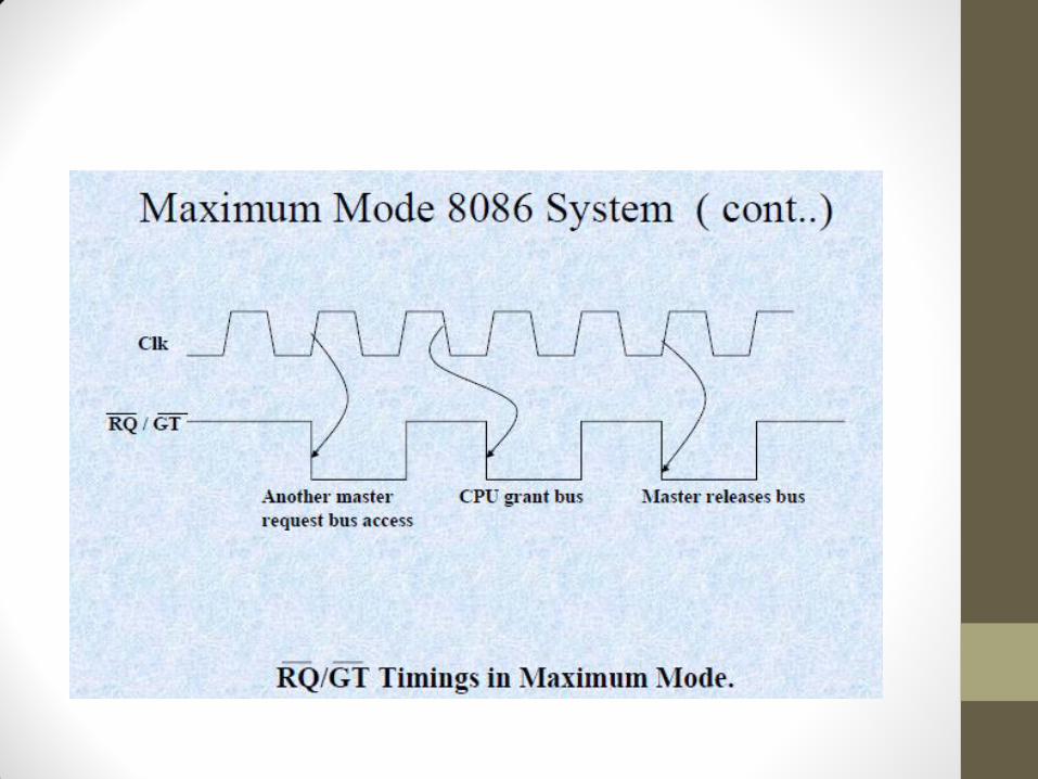
• Request / Grant Signals: In a maximum mode configuration, the minimum mode HOLD, HLDA interface is also changed. These two are replaced by request/grant lines RQ/ GT0 and RQ/ GT1, respectively.
• They provide a prioritized bus access mechanism for accessing the local bus.