microlight-emitting diode with integrated fresnel …...microlight-emitting diode with integrated...
TRANSCRIPT
Microlight-emitting diode withintegrated Fresnel zone plate for contactlens embedded display
Ramin MirjaliliBabak A. Parviz
Downloaded From: http://nanolithography.spiedigitallibrary.org/ on 03/11/2013 Terms of Use: http://spiedl.org/terms
Microlight-emitting diode with integrated Fresnel zoneplate for contact lens embedded display
Ramin MirjaliliBabak A. ParvizUniversity of WashingtonDepartment of Electrical Engineering185 Stevens Way, Paul Allen CenterCampus Box 352500Seattle, Washington 98195-2500E-mail: [email protected]
Abstract. We report the fabrication and testing of 30-μm radii circularInGaN blue light-emitting didode (LEDs) grown on sapphire wafers,with cointegrated Fresnel zone plates (FZP) with outermost ring radii of99.6 μm on the backside of the sapphire substrates to provide a collimatedoutput. After being embedded on a contact lens platform such LEDs withintegrated lenses can aid in producing in-focus images on the humanretina. We measured an image width of 50 μm created by a FZP f∕3 sub-sidiary focal point at 230 μm from the surface. We also demonstrate theconstruction and wireless operation of a contact lens with predeterminedembedded text. © 2012 Society of Photo-Optical Instrumentation Engineers (SPIE). [DOI:10.1117/1.JMM.11.3.033010]
Subject terms: contact lens; Fresnel zone plate; microlight-emitting diode; wearabledisplay.
Paper 12013 received Feb. 13, 2012; revised manuscript received Jul. 21, 2012;accepted for publication Jul. 31, 2012; published online Sep. 21, 2012.
1 IntroductionWearable devices, such as various health monitoring andentertainment systems, could soon alter our interactionswith the surrounding environment and the computingcloud. For example personal see-through displays could inprinciple overlay computer-generated visual informationon the real world, providing immediate, hands-free accessto information.1 Such displays may be realized in theform of devices resembling eyewear for vision correctionor even contact lenses that can be remotely powered andcontrolled to show information (Fig. 1). In a sample embodi-ment, the contact lens may integrate an array of microlight-emitting diode (LEDs) for producing images. We havepreviously reported the functionality of wirelessly controlledsingle pixel display on a contact lens platform.2,3 Such a sin-gle pixel system may be deployed for communicatingimmediate events to the user however it is of limited usefor conveying more information. Our custom designed wire-less system could deliver 12 μW of power to the display,harvested from a 0 dBm (1 mW) radio frequency (RF) broad-cast source and used 3% modulation for power manage-ment.2 In our prior demonstration, the nominal visibilitypoint for the InGaN LED (60 μA of current at 2.6 V fora 260-μm wide pixel),3 translated to approximately2.94 nW∕μm2, this in turn means the system as deployedcould support up to nearly 50 pixels made of 30-μm wideLEDs should the proper pixel design and optics becomesavailable.
A major challenge of constructing a display wearable inthe form of a contact lens with multiple pixels is producingin-focus images from components that are placed directly onthe cornea. As the nearest focus point of the human eye(closest point of accommodation) ranges from 7 to 40 cmfor teenagers to middle aged adults,4 the output light ofmicro-LED pixels on the contact lens will not be in-focuson the retina. Therefore, optical components are needed in
between the micro-LED pixels and the retina to bring theimage into focus. One approach is to use a micro lens foreach pixel or group of pixels to aid in focusing the lightemergent from them on the retina.
The simplest way to collimate the output light of a sourceis to position the source at the focal point of a lens. Integra-tion of micro lenses on micro-LEDs to enhance the extrac-tion of LED optical output has been previously reported.5–7
Micro lenses reported were based on either fabrication byreflow of transparent photoresist patterns acting as thelens,5–7 or followed by an extra etch step to pattern the sub-strate with the lens shape.8,9 Micro lenses fabricated in thismanner do not give sufficient variation of focal distance norcan their focal point and other optical properties be easilycontrolled. Additionally these approaches would not workwhen the lens is embedded in a material with a similar(or very close) index of refraction, which in the case forthe contact lens is the tear film next to the cornea. To mini-mize this effect and have a better control on focal distance,which is critical to collimate the output light, we use diffrac-tion-based Fresnel zone plate lenses (FZP).
We report how LEDs with integrated FZP acting as a lenscan be designed, fabricated, and tested. These devices pavethe way for constructing a contact lens display that is capableof producing in-focus images. The following sections outlinethe design parameters for the FZP, the fabrication process forbuilding the devices, and the characterization results. Finally,we briefly discuss the construction of a wirelessly poweredand controlled contact lens incorporating a predeterminedtext.
2 Design and Simulation
2.1 Fresnel Zone Plates
FZPs are used as x-ray optical components10 or lithographicpatterning elements.11 Their behavior is based on utilizingdiffraction from circular gratings to focus the incidentlight to a point. If we block or give a π phase change atboundary radiuses, Rn, given by Eq. (1),12 the zone plate0091-3286/2012/$25.00 © 2012 SPIE
J. Micro/Nanolith. MEMS MOEMS 033010-1 Jul–Sep 2012/Vol. 11(3)
J. Micro/Nanolith. MEMS MOEMS 11(3), 033010 (Jul–Sep 2012)
Downloaded From: http://nanolithography.spiedigitallibrary.org/ on 03/11/2013 Terms of Use: http://spiedl.org/terms

will act as a lens with first order focal point of f and sub-sidiary focal points at odd fractions of f12:
R2n ¼ ðnλf þ n2λ2∕4Þ: (1)
The less complicated way to fabricate a FZP is to elim-inate the destructive interference from the incident wavefrontwith an opaque material (amplitude-type zone plates). Here,50% of the incident light is blocked by the FZP surface initi-ally and only 10% of incident light is focused on the 1st orderfocal point. If the opaque rings are replaced with a transpar-ent material causing a π phase shift, thus making the inter-ference constructive at the focal point (phase-type zoneplates) more efficiency may be gained at the expense of addi-tional complexity of the fabrication process. As there is noabsorption in the optical path in this case, the amplitude atthe focal point could be doubled, so the diffraction efficiencyat 1st order focal point could be increased to 40%.12 As aninitial proof of concept, here we chose to fabricate ampli-tude-type zone plates to simplify the fabrication process.
2.2 Design
To collimate the LED light output, the source should be posi-tioned at the main focal point of the FZP. In our design, FZPswere integrated on the opposite side of sapphire wafers sup-porting the LED epitaxial layers on the surface; hence, thewafer thickness determined the required focal distance of the
lens. Our LED peak wavelength is 475 nm3, and the waferthickness (i.e., FZP focal distance) was approximately275 μm after lapping and polishing. Considering the wave-length and focal point in zone plate behavior, given byEq. (1), we calculated the respective zone radiuses upto 99.6 μm.
2.3 Simulation
We conducted two simulation approaches in ZEMAX-EE.First, we simulated the FZP and its focusing behavior,and second, we simulated the LED structure with integratedFZP. In the first approach, in order to model diffractiveeffects, we used physical optics propagation (POP) analysisof sequential mode ZEMAX. We implemented our opaquezones of FZP as concentric obscurations [Fig. 2(a)], andused a coherent Gaussian beam with 60-μm waist and475-nm wavelength as an illumination source. The zoneplate created a high intensity point at focal distance of275 μm as expected [Fig. 2(b)].
To model the InGaN LED structure, we used the nonse-quential mode of ZEMAX. Nonsequential mode is not cap-able of modeling amplitude FZP, while it can model phasetype FZP using Binary2 surfaces. As phase and amplitudetype FZPs are analogous in focal distance measures, weimplemented the FZP as a Binary2 surface to determinethe light distribution pattern. Considering the dimensionswe calculated for fabrication, we implemented the LEDp-metal contact, p-GaN region, n-GaN region, sapphire sub-strate, and FZP using a mirror layer, a GaN cylinder withembedded source volume, a GaN rectangular volume, a sap-phire rectangular volume, and a Binary2 surface, respec-tively. Positioning the LED active region at the FZP’s firstorder focal distance would collimate the largest fraction ofincident light, while subsidiary focal points would convergesmaller fractions.
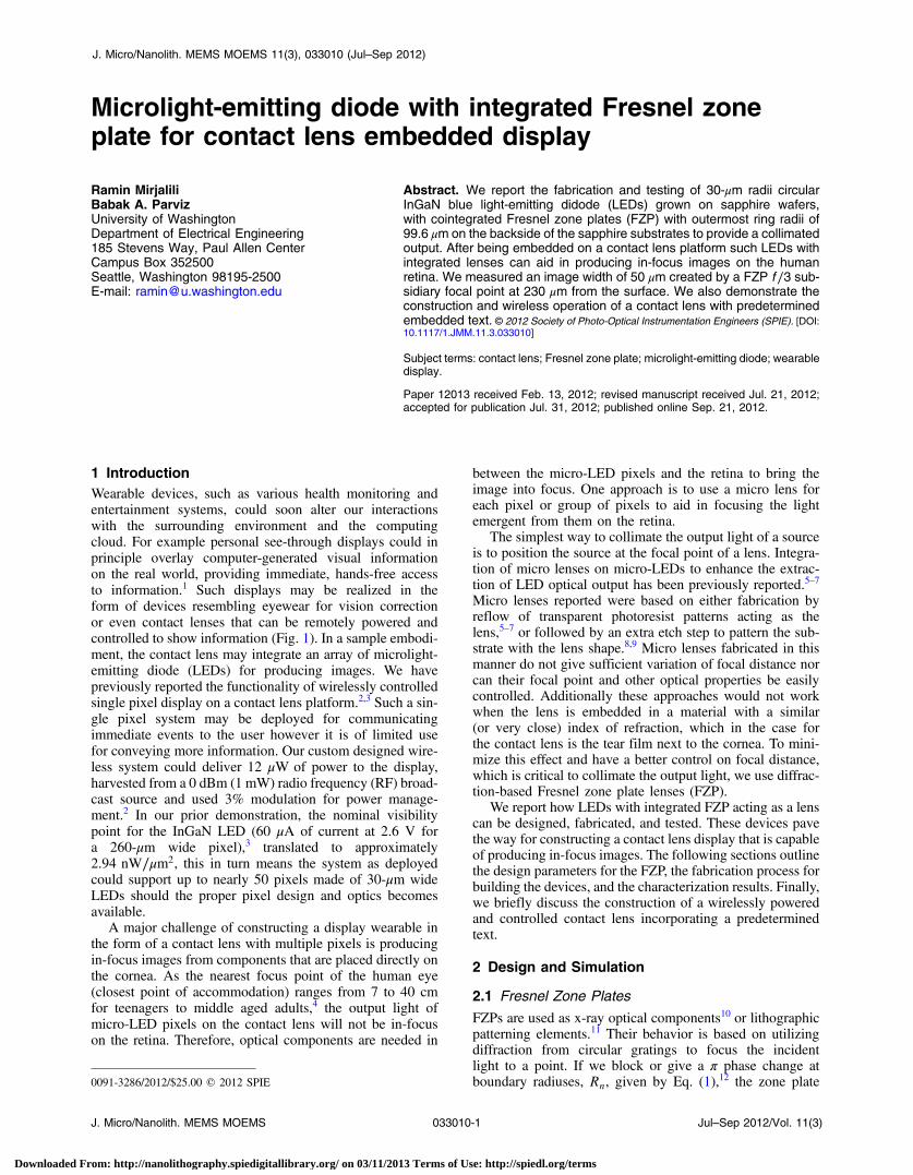
Having multiple focal points, the functionality of LED/FZP system can be tested by tracking the footprint of sub-sidiary focal points using regular optical microscopes, whilemeasuring the beam angle of collimated output caused bymain focal point requires more complex side-view micro-scopy. Hence, to simplify the required equipment for testingwe aimed for detecting the image created by the f∕3 subsidi-ary focal point. Following the same strategy in the simula-tion, the f∕3 subsidiary focal point creates a high intensityspot at distance of 250 μm from the surface [Fig. 3(a)] whilethe LED output without integrated FZP created a nonfocusedresult at the same distance [Fig. 3(b)].
Fig. 1 Conceptual drawing of a contact lens with embedded micro-LED display, antenna and RF circuit for powering and communication.
Fig. 2 A Fresnel zone plate (FZP) implemented as obscurations in ZEMAX, The scale bar is 20 μm (a), physical optic propagation (POP) analysisof FZP: 60-μm waist Gaussian beam, illuminated through the designed FZP focuses at the desired 275 μm; the scale bar is 10 μm (b)
J. Micro/Nanolith. MEMS MOEMS 033010-2 Jul–Sep 2012/Vol. 11(3)
Mirjalili and Parviz: Microlight-emitting diode with integrated Fresnel zone plate : : :
Downloaded From: http://nanolithography.spiedigitallibrary.org/ on 03/11/2013 Terms of Use: http://spiedl.org/terms
2.4 Fabrication
2.4.1 Blue micro-LED fabrication
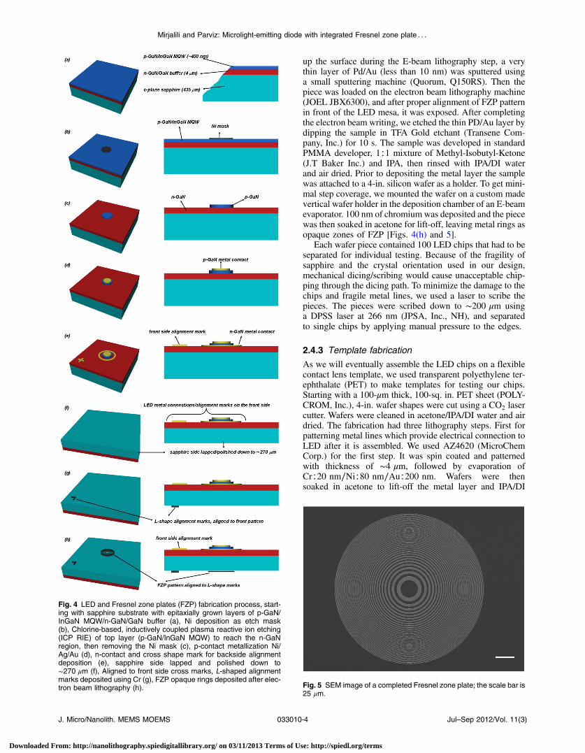
We started with epitaxial layers of InGaN/GaN grown onstandard 2-in., 435-μm thick c-plane sapphire wafers bymetal organic vapor phase epitaxy (MOVPE) [Fig. 4(a)].3
First, we defined the size and shape of each LED by evapor-ating a 120-nm thick layer of Ni to protect the p-GaN region(circular shape of 60-μm diameter in this case) during thechlorine-based, inductively coupled plasma reactive ionetching (ICP RIE). We used AZ5214E (MicroChemCorp., MA), an image reversal photoresist, to gain slopedsidewalls and good lift-off results. The photoresist wasspun coated, prebaked, exposed under a mask, hardbaked, and finally flood exposed and developed resultingin a ∼1.1-μm thick pattern. After development, the Nilayer was deposited by E-beam evaporation. The waferswere soaked in acetone for lift-off and then rinsed withiso propyl alcohol (IPA) and air dried [Fig. 4(b)]. Toreach the n-GaN region and make metal connections, weused a chlorine-based ICP RIE to remove about 800 nmof top surface-p-GaN/multi quantum well stacks/and par-tially the n-GaN layer. After etching, the Ni layer wasremoved by soaking the wafer in a mixture of 1∶3HC1∶HNO3 [Fig. 4(c)]. To make metal connections for p-GaN,we used patterned AZ5214E photoresist, E-beam evaporatedNi∶10 nm∕Ag∶70 nm∕Au∶150 nm layer, and performed alift-off [Fig. 4(d)]. P-GaN contacts then were annealed at500°C for 5 min. in nitrogen ambient. After a similarphotolithography step, the n-GaN metal connections weredeposited and lifted off as Ni∕Al∕Au∶20∕300∕200 nm[Fig. 4(e)].
After the completion of LED metallization, the waferswere lapped and polished (Valley Design Corp., CA) inorder to make the final LED chip thin enough to beembedded in a contact lens template, which resulted in anactual thickness of 273 to 276 μm [Fig. 4(f)]. As the FZPmust be fabricated on the lapped and polished side of thewafer, we needed to fabricate alignment marks for elec-tron-beam lithography. We need to fabricate the marksfrom a material that can be imaged by scanning electronmicrocopy (SEM) easily and has good adhesion to sapphire.Chromium was a good option as was reported in a process to
mask sapphire during anisotropic etching and for making thealignment marks.13 The alignment marks were designedlarge enough (∼10 μm) to allow photolithographic fabrica-tion. Negative photoresist, nr7-1000 (MicroChem Corp.,MA), was spun coated and patterned through a standardlithography process resulting in a 1.2-μm thin film. A100-nm thick layer of chromium was evaporated. Thenthe wafer was soaked in acetone for lift-off, rinsed withIPA and de-ionized (DI) water and air dried [Fig. 4(g)].The wafer contained more than 2000 LED chips. To mini-mize losses during different tests, the wafer was saw-diced into smaller pieces by the following process. The sap-phire wafer was mounted on a 4-in. silicon wafer as mechan-ical support by applying crystal bond. Using diamond resinblades (thermocarbon blades) mounted on a K&S dicingmachine, we cut small, 9-mm squares. Conducting fivepairs of perpendicular cuts, the wafer was soaked in acetoneto release the pieces from the handle wafer. Pieces were thenIPA/DI water rinsed, air dried and stored to be prepared forelectron beam lithography (EBL).
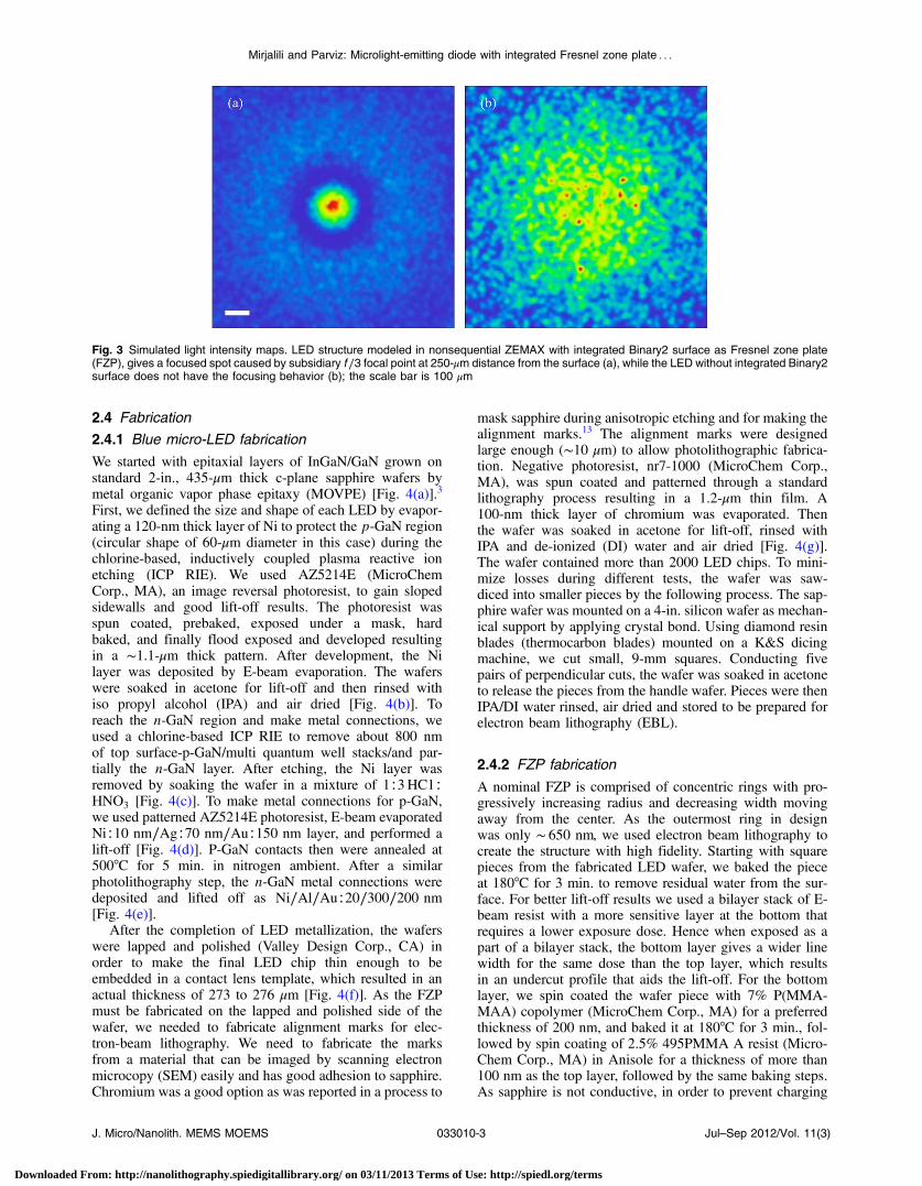
2.4.2 FZP fabrication
A nominal FZP is comprised of concentric rings with pro-gressively increasing radius and decreasing width movingaway from the center. As the outermost ring in designwas only ∼ 650 nm, we used electron beam lithography tocreate the structure with high fidelity. Starting with squarepieces from the fabricated LED wafer, we baked the pieceat 180°C for 3 min. to remove residual water from the sur-face. For better lift-off results we used a bilayer stack of E-beam resist with a more sensitive layer at the bottom thatrequires a lower exposure dose. Hence when exposed as apart of a bilayer stack, the bottom layer gives a wider linewidth for the same dose than the top layer, which resultsin an undercut profile that aids the lift-off. For the bottomlayer, we spin coated the wafer piece with 7% P(MMA-MAA) copolymer (MicroChem Corp., MA) for a preferredthickness of 200 nm, and baked it at 180°C for 3 min., fol-lowed by spin coating of 2.5% 495PMMA A resist (Micro-Chem Corp., MA) in Anisole for a thickness of more than100 nm as the top layer, followed by the same baking steps.As sapphire is not conductive, in order to prevent charging
Fig. 3 Simulated light intensity maps. LED structure modeled in nonsequential ZEMAX with integrated Binary2 surface as Fresnel zone plate(FZP), gives a focused spot caused by subsidiary f∕3 focal point at 250-μm distance from the surface (a), while the LED without integrated Binary2surface does not have the focusing behavior (b); the scale bar is 100 μm
J. Micro/Nanolith. MEMS MOEMS 033010-3 Jul–Sep 2012/Vol. 11(3)
Mirjalili and Parviz: Microlight-emitting diode with integrated Fresnel zone plate : : :
Downloaded From: http://nanolithography.spiedigitallibrary.org/ on 03/11/2013 Terms of Use: http://spiedl.org/terms
up the surface during the E-beam lithography step, a verythin layer of Pd/Au (less than 10 nm) was sputtered usinga small sputtering machine (Quorum, Q150RS). Then thepiece was loaded on the electron beam lithography machine(JOEL JBX6300), and after proper alignment of FZP patternin front of the LED mesa, it was exposed. After completingthe electron beam writing, we etched the thin PD/Au layer bydipping the sample in TFA Gold etchant (Transene Com-pany, Inc.) for 10 s. The sample was developed in standardPMMA developer, 1∶1 mixture of Methyl-Isobutyl-Ketone(J.T Baker Inc.) and IPA, then rinsed with IPA/DI waterand air dried. Prior to depositing the metal layer the samplewas attached to a 4-in. silicon wafer as a holder. To get mini-mal step coverage, we mounted the wafer on a custom madevertical wafer holder in the deposition chamber of an E-beamevaporator. 100 nm of chromium was deposited and the piecewas then soaked in acetone for lift-off, leaving metal rings asopaque zones of FZP [Figs. 4(h) and 5].
Each wafer piece contained 100 LED chips that had to beseparated for individual testing. Because of the fragility ofsapphire and the crystal orientation used in our design,mechanical dicing/scribing would cause unacceptable chip-ping through the dicing path. To minimize the damage to thechips and fragile metal lines, we used a laser to scribe thepieces. The pieces were scribed down to ∼200 μm usinga DPSS laser at 266 nm (JPSA, Inc., NH), and separatedto single chips by applying manual pressure to the edges.
2.4.3 Template fabrication
As we will eventually assemble the LED chips on a flexiblecontact lens template, we used transparent polyethylene ter-ephthalate (PET) to make templates for testing our chips.Starting with a 100-μm thick, 100-sq. in. PET sheet (POLY-CROM, Inc.), 4-in. wafer shapes were cut using a CO2 lasercutter. Wafers were cleaned in acetone/IPA/DI water and airdried. The fabrication had three lithography steps. First forpatterning metal lines which provide electrical connection toLED after it is assembled. We used AZ4620 (MicroChemCorp.) for the first step. It was spin coated and patternedwith thickness of ∼4 μm, followed by evaporation ofCr∶20 nm∕Ni∶80 nm∕Au∶200 nm. Wafers were thensoaked in acetone to lift-off the metal layer and IPA/DI
Fig. 4 LED and Fresnel zone plates (FZP) fabrication process, start-ing with sapphire substrate with epitaxially grown layers of p-GaN/InGaN MQW/n-GaN/GaN buffer (a), Ni deposition as etch mask(b), Chlorine-based, inductively coupled plasma reactive ion etching(ICP RIE) of top layer (p-GaN/InGaN MQW) to reach the n-GaNregion, then removing the Ni mask (c), p-contact metallization Ni/Ag/Au (d), n-contact and cross shape mark for backside alignmentdeposition (e), sapphire side lapped and polished down to∼270 μm (f), Aligned to front side cross marks, L-shaped alignmentmarks deposited using Cr (g), FZP opaque rings deposited after elec-tron beam lithography (h). Fig. 5 SEM image of a completed Fresnel zone plate; the scale bar is
25 μm.
J. Micro/Nanolith. MEMS MOEMS 033010-4 Jul–Sep 2012/Vol. 11(3)
Mirjalili and Parviz: Microlight-emitting diode with integrated Fresnel zone plate : : :
Downloaded From: http://nanolithography.spiedigitallibrary.org/ on 03/11/2013 Terms of Use: http://spiedl.org/terms
water rinsed and air dried. The second lithography step wasto passivate some of the metal interconnects that couldpotentially be shorted by LED metal pads after assembly.A ∼2-μm layer of SU8-2 was spin coated and patternedto make this insulation. Finally, for making a housing forthe LED chip, we spin coated and patterned a ∼25-μmlayer of SU8-25 with 900 × 900 μm2 openings for LEDchips.
2.4.4 LED assembly
The LED assembly was done using an aided self-assemblyprocess. Lead free, 60°C eutectic solder (Indalloy 19, IndiumCorp.) was melted in a 100-mL beaker while immersed inethylene glycol (EG). Templates were rinsed with acetone/IPA and air dried. Metal pads on the template were coatedwith solder using pipette flow. To minimize the surfaceoxidation of solder bumps and maintain clean surfaces,templates were immediately immersed in a glass Petridish containing 25 mL of EG and 10 μL of HCL. TheLED chips were then placed on corresponding spots onthe template manually using a tweezer. Afterwards thePetri dish was heated in order to melt the solder. As the
solder melted, the LED chip self-aligned and connected tothe template’s metal pads. After the solder was cooleddown, the template with assembled LED was rinsed withIPA and air dried to be ready for further testing.
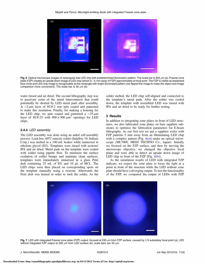
3 ResultsIn addition to integrating zone plates in front of LED struc-tures, we also fabricated zone plates on bare sapphire sub-strates to optimize the fabrication parameters for E-beamlithography. As our first test we put a sapphire wafer withFZP patterns 5 mm away from an illuminating LED chipwith a complex pattern [Fig. 6(a)] under an optical micro-scope (ML7000, MEIJI TECHNO Co., Japan). Initiallywe focused on the FZP surface, and then by moving themicroscope objective, we changed the objective focalplane and were able to detect an upside down image ofLED chip in front of the FZP [Fig. 6(b)].
As the simulation results of LED with integrated FZPindicate, we expect the zone plate to focus the light at apoint in front of the structure while the LED without zoneplate should have a diverging output. To test the functionalityof the FZP, we compared the output of LEDs with FZP
Fig. 6 Optical microscope images of rectangular test LED chip with predetermined illumination pattern. The scale bar is 200 μm (a), Fresnel zoneplate (FZP) creates an upside down image of LED chip (which is ∼5 mm away of FZP) approximately at focal point. The FZP is visible as shadowedblue circle and LED chip image is recognizable as the rectangle with bright illuminated pattern (we flipped the image to make the object and imagecomparison more convenient). The scale bar is 50 μm (b).
Fig. 7 LED with integrated Fresnel zone plate (FZP) output, focused at 230 μm from FZP surface, caused by f∕3 subsidiary focal point (a), LEDwithout integrated FZP output at 230 μm from LED surface (b); scale bars are 50 μm.
J. Micro/Nanolith. MEMS MOEMS 033010-5 Jul–Sep 2012/Vol. 11(3)
Mirjalili and Parviz: Microlight-emitting diode with integrated Fresnel zone plate : : :
Downloaded From: http://nanolithography.spiedigitallibrary.org/ on 03/11/2013 Terms of Use: http://spiedl.org/terms
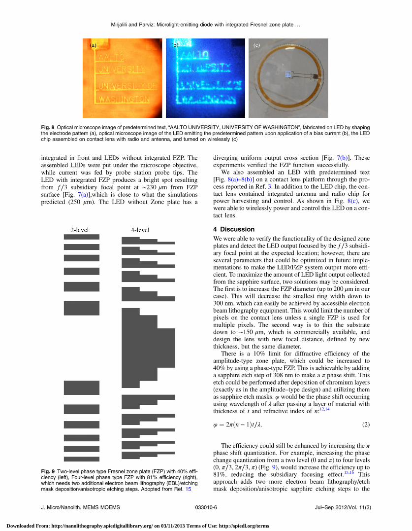
integrated in front and LEDs without integrated FZP. Theassembled LEDs were put under the microscope objective,while current was fed by probe station probe tips. TheLED with integrated FZP produces a bright spot resultingfrom f∕3 subsidiary focal point at ∼230 μm from FZPsurface [Fig. 7(a)],which is close to what the simulationspredicted (250 μm). The LED without Zone plate has a
diverging uniform output cross section [Fig. 7(b)]. Theseexperiments verified the FZP function successfully.
We also assembled an LED with predetermined text[Fig. 8(a)–8(b)] on a contact lens platform through the pro-cess reported in Ref. 3. In addition to the LED chip, the con-tact lens contained integrated antenna and radio chip forpower harvesting and control. As shown in Fig. 8(c), wewere able to wirelessly power and control this LED on a con-tact lens.
4 DiscussionWe were able to verify the functionality of the designed zoneplates and detect the LED output focused by the f∕3 subsidi-ary focal point at the expected location; however, there areseveral parameters that could be optimized in future imple-mentations to make the LED/FZP system output more effi-cient. To maximize the amount of LED light output collectedfrom the sapphire surface, two solutions may be considered.The first is to increase the FZP diameter (up to 200 μm in ourcase). This will decrease the smallest ring width down to300 nm, which can easily be achieved by accessible electronbeam lithography equipment. This would limit the number ofpixels on the contact lens unless a single FZP is used formultiple pixels. The second way is to thin the substratedown to ∼150 μm, which is commercially available, anddesign the lens with new focal distance, defined by newthickness, but the same diameter.
There is a 10% limit for diffractive efficiency of theamplitude-type zone plate, which could be increased to40% by using a phase-type FZP. This is achievable by addinga sapphire etch step of 308 nm to make a π phase shift. Thisetch could be performed after deposition of chromium layers(exactly as in the amplitude–type design) and utilizing themas sapphire etch masks. φ would be the phase shift occurringusing wavelength of λ after passing a layer of material withthickness of t and refractive index of n:12,14
φ ¼ 2πðn − 1Þt∕λ: (2)
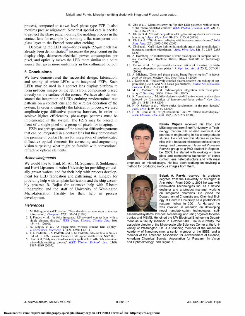
The efficiency could still be enhanced by increasing the πphase shift quantization. For example, increasing the phasechange quantization from a two level (0 and π) to four levels(0, π∕3, 2π∕3, π) (Fig. 9), would increase the efficiency up to81%, reducing the subsidiary focusing effect.15,16 Thisapproach adds two more electron beam lithography/etchmask deposition/anisotropic sapphire etching steps to the
Fig. 8 Optical microscope image of predetermined text, “AALTO UNIVERSITY, UNIVERSITY OF WASHINGTON”, fabricated on LED by shapingthe electrode pattern (a), optical microscope image of the LED emitting the predetermined pattern upon application of a bias current (b), the LEDchip assembled on contact lens with radio and antenna, and turned on wirelessly (c)
Fig. 9 Two-level phase type Fresnel zone plate (FZP) with 40% effi-ciency (left), Four-level phase type FZP with 81% efficiency (right),which needs two additional electron beam lithography (EBL)/etchingmask deposition/anisotropic etching steps. Adopted from Ref. 15
J. Micro/Nanolith. MEMS MOEMS 033010-6 Jul–Sep 2012/Vol. 11(3)
Mirjalili and Parviz: Microlight-emitting diode with integrated Fresnel zone plate : : :
Downloaded From: http://nanolithography.spiedigitallibrary.org/ on 03/11/2013 Terms of Use: http://spiedl.org/terms
process, compared to a two level phase type FZP. It alsorequires precise alignment. Note that special care is neededto protect the phase pattern during the molding process in thecontact lens for example by bonding a flat transparent thinglass layer to the Fresnel zone after etching.
Decreasing the LED size—for example 22-μm pitch hasalready been demonstrated17 increases the pixel count on thedisplay chip, decreases electrical power consumption perpixel, and optically makes the LED more similar to a pointsource that gives more uniformity in the collimated output.
5 ConclusionsWe have demonstrated the successful design, fabrication,and testing of micro-LEDs with integrated FZPs. SuchLEDs may be used in a contact lens display platform toform in-focus images on the retina from components placeddirectly on the surface of the cornea. We have also demon-strated the integration of LEDs emitting predetermined textpatterns on a contact lens and the wireless operation of thesystem. In order to simplify the fabrication process, we usedamplitude-type diffractive patterns; however, in order toachieve higher efficiencies, phase-type patterns must beimplemented in the system. The FZPs may be placed infront of a single pixel or a group of pixels for imaging.
FZPs are perhaps some of the simplest diffractive patternsthat can be integrated in a contact lens but they demonstratethe promise of contact lenses for integration of sophisticateddiffractive optical elements for correcting and augmentingvision surpassing what might be feasible with conventionalrefractive optical elements.
AcknowledgmentsWe would like to thank M. Ali, M. Sopanen, S. Suihkonen,and Harri Lipsanen of Aalto University for providing epitaxi-ally grown wafers, and for their help with process develop-ment for LED fabrication and patterning; A. Lingley forproviding help with template fabrication and the chip assem-bly process; R. Bojko for extensive help with E-beamlithography; and the staff of University of WashingtonMicrofabrication Facility for their help in processdevelopment.
References
1. M. Billinghurst and T. Starner, “Wearable devices: new ways to manageinformation,” Computer 32(1), 57–64 (1999).
2. J. Pandey et al., “A fully integrated RF-powered contact lens with asingle element display.” IEEE Trans. Biomed. Circuits Syst. 4(6),454–461 (2010).
3. A. Lingley et al., “A single-pixel wireless contact lens display,”J. Micromech. Microeng. 21(12), 125014 (2011).
4. F. L. Pedrotti, L. S. Pedrotti, and L. M. Pedrotti, Introduction to Optics,3rd ed., p. 426, Pearson Prentice Hall, upper saddle river, NJ(2007).
5. Jeon et al, “Polymer microlens arrays applicable to AlInGaN ultravioletmicro-light-emitting diodes,” IEEE Photon. Technol. Lett. 17(9),1887–1889 (2005).
6. Zhu et al., “Microlens array on flip-chip LED patterned with an ultra-violet micro-pixelated emitter,” IEEE Photon. Technol. Lett. 23(15),1067–1069 (2011).
7. Khizar et al., “Nitride deep-ultraviolet light-emitting diodes with micro-lens array,” Appl. Phys. Lett. 86(17), 173504 (2005).
8. Choi et al., “Nitride micro-display with integrated micro-lenses,” SolidState Phys. 2(7), 2903–2906 (2005).
9. Choi et al., “GaN micro-light-emitting diode arrays with monolithicallyintegrated sapphire microlenses,” Appl. Phys. Lett. 84(13), 2253–2255(2004)
10. A. Holmberg, “Nanofabrication of zone plate optics for compact soft x-ray microscopy,” Doctoral Thesis, (Royal Institute of Technology2006).
11. Menon et al., “Experimental characterization of focusing by high-numerical-aperture zone plates,” J. Opt. Soc. Am. A 23(3), 567–571(2006).
12. A. Michette, “Zone and phase plates, Bragg-Fresnel optics,” in Hand-book of Optics, McGraw-Hill, New York, 3 (2000)
13. J. Kang et al., “Inductively coupled plasma reactive ion etching of sap-phire using C2F6- and NF3-based gas mixtures,”Mater. Sci. Semicond.Process. 11(1), 16–19 (2008).
14. M. E. Motamedi et al., “Micro-optics integration with focal planearrays,” Opt. Eng. 36(5), 1374–1382 (1997).
15. K. Yamada et al., “Multilevel phase-type diffractive lenses in silica glassinduced by filamentation of femtosecond laser pulses,” Opt. Lett.29(16), 1846–1848 (2004).
16. H. O. Sankur et al., “Micro-optics development in the past decade,”Proc. SPIE 4179, 30–59 (2000).
17. H. W. Choi et al., “High-resolution 128 × 96 nitride microdisplay,”IEEE Electron. Dev. Lett. 25(5), 277–279 (2004).
Ramin Mirjalili received his BSc andMSc degrees from Sharif University of Tech-nology, Tehran. He studied electrical andpetroleum engineering in his undergraduatestudies. He continued his studies in electro-nics with a focus on microelectronics circuitrydesign and biosensors. He joined ProfessorParviz's group as a PhD student in Septem-ber 2009. He started with working on tem-plate and components fabrication of bioniccontact lens heterostructure and with main
emphasis on microdisplays. He has been working on devising amethod for producing in-focus images from them.
Babak A. Parviz received his graduatedegrees from the University of Michigan inAnn Arbor. From 2000 to 2001 he was withNanovation Technologies Inc. as a devicedesigner and a product manager workingon integrated photonics. He joined theDepartment of Chemistry and Chemical Biol-ogy at Harvard University as a postdoctoralresearch fellow in 2001. At Harvard, hewas involved in research on developingnovel nanofabrication technologies, self-
assembled systems, low-cost biosensing, and using organics for elec-tronics and MEMS. He joined the UW Electrical Engineering Depart-ment as a faculty member in October 2003. He is currently theassociate director of the Micro-scale Life Sciences Center at the Uni-versity of Washington. He is a founding member of the AmericanAcademy of Nanomedicine; a senior member of the IEEE; and amember of the American Association for Advancement of Science,American Chemical Society, Association for Research in Visionand Ophthalmology, and Sigma Xi.
J. Micro/Nanolith. MEMS MOEMS 033010-7 Jul–Sep 2012/Vol. 11(3)
Mirjalili and Parviz: Microlight-emitting diode with integrated Fresnel zone plate : : :
Downloaded From: http://nanolithography.spiedigitallibrary.org/ on 03/11/2013 Terms of Use: http://spiedl.org/terms