indian journal of science and technology, vol 12(1), doi
TRANSCRIPT

*Author for correspondence
Indian Journal of Science and Technology, Vol 12(1), DOI: 10.17485/ijst/2019/v12i1/139860, January 2019ISSN (Print) : 0974-6846
ISSN (Online) : 0974-5645
Modeling and Closed Loop Votlage Mode Control of a Forward Converter
Khandaker Sultan Mahmood1*, Iftekhar Hasan2 and Mirza Mursalin Iqbal1
1Department of Electrical and Electronic Engineering, University of Asia Pacific, Dhaka, Bangladesh; [email protected], [email protected]
2Department of Electrical and Electronic Engineering, Islamic University of Technology, Gazipur, Bangladesh; [email protected]
Keywords: Closed Loop, Forward Converter, Voltage Mode Control, PWM
AbstractObjectives: This study is to introduce the design and development of a closed loop voltage-controlled forward converter operating in continuous conduction mode. Methods: The open and closed loop simulation was done in PSIM and the four different compensators were designed. Experimental work was carried out for both open and closed loop converter incorporating a type-2 PI compensator. Findings: A PI compensated forward converterwas capable of stepping down voltage with low ripple content and improved steady state performance. Application: The forward converter was designed in a laboratory prototype to study its operation for open loop and closed loop feedback. PI compensated forward converter was found to reduce the steady state error of the converter.
1. IntroductionThe forward converter is a magnetically coupled DC-DC converter. Forward converters with only one transistor are generally used for off-line supplies with power ratings under 200W1. It is often a fitting substitute for Flyback converters which require circuits to be galvanically iso-lated and/or voltages step-down is necessary due to its simple structure and a smaller number of components. Forward converters are an ideal candidate for applica-tions requiring high current continuous operation. In2 the authors proposed a novel for high power applications using two forward converters with series input and par-allel output configuration. An intelligent PWM scheme along with a current doubler rectifier restricts the out-put current ripples whereas the energy of the leakage inductor is used to suppress the switching device voltage spikes using the active clamp circuit. In3 proposed pre-sented a research work on enhanced power quality in multiple output SMPS forward boost converter which
kept the power factor near to unity, brought down the input current THD and lowered output voltage ripples. In4 proposed suggested that the forward converter could be efficiently used to increase the DC voltage for DC microgrids based on various forward converter configu-rations. In5 proposed examined the EMI of the forward converter with symmetric topology through extraction of the EMI model considering the parasitic components of the circuits and verified the exactness of the forecasted EMI levels of forward converters with a single switch and symmetric topologies.
In6 proposed suggested the concept of a single stage forward-flyback converter combining the individual topologies of forward and flyback converters and gained high power factor with reduced core losses of the trans-former resulting in higher efficiency. In7 proposed designed a forward which possessed the characteristics of a buck type dc-dc converter and to keep the output volt-age fixed with the changes in load a sliding mode con-troller was introduced which made the control method

Indian Journal of Science and TechnologyVol 12 (1) | January 2019 | www.indjst.org 2
Modeling and Closed Loop Votlage Mode Control of a Forward Converter
of the converter simpler and also produced satisfactory results. In8 proposed constructed and investigated the small signal model of a double-ended forward converter and compared the roles of the circuit specifications on the small signal characteristics. The small signal performance of the converter acting as a DC-DC converter and as a PFC converter was also analyzed. In9 proposed designed and assembled a compact DC-DC converter for military applications. At 150 kHz switching frequency, residual current device (RCD) reset of forward converter main-tained a duty cycle of 55% at the low input end. Abrupt voltage changes across the switch were minimized achiev-ing an efficiency of over 75% and line and load voltage regulated within ±1%. In10 proposed studied the effects due to non-idealities in a boost converter such as the effect of equivalent series resistance (ESR) of a capacitor and found that the zeros in the right half plane must be translated in the frequency domain to minimize its effect on the dominant poles of the system. Limiting the fre-quency between its line and the cutoff value was adopted as a simple yet effective control methodology. Voltage peaks of the output were reduced by selecting a convenient sampling time. In11 proposed forward and fly-back con-verter in terms of efficiency and power factor and thereby proposed a flyback-forward converter with power factor improvement strategy. The proposed converter was able to achieve decreased core loss due to a reduced magnetiz-ing current and was able to scale down the transformer altogether. In12 developed a fast responding Proportional Integral (PI) controller to compensate for the right half plane zero of the boost converter as well as the LLC con-verter’s beat frequency aspect. Utilizing the small sig-nal analysis, the authors were able to derive a simplified transfer function with the ability to forecast the nature of the beat frequency. Moreover, a lead compensator was incorporated with the PI controller to widen the band-width. In13 proposed studied the strain on computation during simulation of closed loop control of voltage source converter (VSC) by using a three phase control system with sinusoidal pulse width modulation (SPWM) switch-ing techniques. A simulation system model was built with FPGA+DSP+PC structure where the VSC model was subdivided into the continuous and discontinuous mode of operations. Results were obtained to show that such structure was able to accomplish simulations with mul-tiple rates in converter with high frequency. In14 proposed
and his colleagues offered a novel closed loop control technique of buck-boost converter utilizing proportion-integral-derivative (PID) controller in 2017. Their anal-yses and comparisons were able to corroborate that the proposed control design was indeed simpler in design and assembly and provided better gain in voltage for tra-ditional step-up and step-down converter applications. In15 proposed and his colleagues simulated and analyzed the performance of a forward converter with the tertiary winding. Using a VSC, a 12V-12W forward converter was designed and was able to demonstrate that effectiveness of the tertiary winding in de-magnetizing the core of the transformer and showed an improvement of 6% efficiency over other related converters. In16 proposed devised a fly-back-forward converter where the leakage energy of the inductor is returned back to the source or clamped capac-itor in both step-up and step-down operation. In addition to the simple circuit structure of the flyback converter, the recycling of energy through the interleaved connection reduces the current ripple and conduction losses, thereby increasing the overall conversion efficiency upto 95.5% in step-up and 92.3% in step-down converters. The findings were validated using laboratory circuit model with 500 W power output.
In17 proposed and his fellow researchers introduced step down forward converter which is made up a pair of double high switch forward cells. It was shown that under zero-voltage switching (ZVS), the said converter provides high efficiency up to 95.6% and is suited for high input voltage and output current operations. The proposed design was tested and validated using a prototype con-verter with 100 kHz switching, 400 V at the input and 200 to 1000 W power at the output.
A18 two-transistor forward converter has been exam-ined and put forward to obtain high voltage input for several output operations. Here, the primary winding of the forward transformer is able to accomplish input voltage sharing (IVS) naturally and promptly by using synchronously operated switches with reduced leakage inductance. The design was proven to be feasible in a 96 W laboratory setup. The increase in difference of input voltage of different series modules could be augmented by increasing the value of filter capacitance at the input and resultant value of the excitation inductance. In19 pro-posed inspected and compared an active clamp forward converter (ACFC) controlled in current mode isolating it

Indian Journal of Science and Technology 3Vol 12 (1) | January 2019 | www.indjst.org
Khandaker Sultan Mahmood, Iftekhar Hasan and Mirza Mursalin Iqbal
using opto-coupler and Op-amp with PSPICE simulation. It was found that the system’s operating point is affected by the pole of the opto-coupler which is produced due to output capacitance of the transistor. Moreover, it was established from the results, that ACFC controlled in peak current mode had faster response compared to feedback with Op-Amp isolation. In20 proposed put forward a bat-tery charger with a 40V forward converter for Switching Mode Power Supply (SMPS) application. With the help of the closed-loop model, the authors were able to obtain a steady state voltage during the disturbance in the forward converter. With a minimized steady-state error and low noise content, the proposed circuit was simulated using Simulink blocks and was deemed suitable for SMPS appli-cation.
In this study, a closed loop voltage mode control of forward converter was developed for SMPS application. The subsequent sections describe the operating principle of the forward converter. The converter model and the closed-loop control developed for the forward converter has been presented. Thereafter, an analytical insight into the selection criteria for the converter components has been provided. In the results section, the simulation and experimental results have been presented for the forward converter. Finally, the paper concludes by providing the summary of the findings obtained through this research.
2. Materials and Methods
2.1 Statistical Analysis of the Forward Converter The mode of operations and the design equations required for a conventional off-line supply is elaborated. The forward converter is shown in Figure 11. For continu-ous conduction mode, the circuit operation can be sepa-rated into two stages. At Stage 1, the switch SW is turned on at t = tON shown in Figure 21. At Stage 2, the switch is turned off at t = tOFF shown in Figure 31. When the switch is closed, energy transfer occurs from the source to the load through the transformer. The secondary of the transformer produces a pulse waveform, and the output is evaluated similarly to that of the buck dc-dc converter. When the switch is open, the energy stored in the mag-netizing inductance during on-time of the switch can be returned to the input by means of the tertiary transformer winding. Therefore the output voltage Vo remains below the input voltage Vs, and is expressed as,
2
1o s
NV V D
N
=
(1)
Where D is the duty cycle, N2 and N1 is the number of turns in the primary and secondary winding. To maintain
Figure 1. Schematic of a forward converter.

Indian Journal of Science and TechnologyVol 12 (1) | January 2019 | www.indjst.org 4
Modeling and Closed Loop Votlage Mode Control of a Forward Converter
2.2 Large Signal ModelAssuming CCM operation, the state space average represen-tation is acquired by writing the state equations during inter-val DTs and D’Ts then averaging over one switching period.
( ) ( ) ( )dx t
Ax t Bu tdt
= + (3)
( ) ( ) ( )y t Cx t Eu t= + (4)
continuous conduction mode and to allow the magnetiz-ing inductance to reset, the duty ratio should be deter-mined by,
3
1
1 1N
DN
+ <
(2)
Where N3 is the number of turns on the tertiary winding of the transformer.
Figure 2. Circuit diagram during ton.
Figure 3. Circuit diagram during toff.

Indian Journal of Science and Technology 5Vol 12 (1) | January 2019 | www.indjst.org
Khandaker Sultan Mahmood, Iftekhar Hasan and Mirza Mursalin Iqbal
Where ( ) ( ) ( )( ),
l
l
c c
didx t i tdt x t
dv v tdtdt
= =
Using steady-state averaged model
1O
i
VCA B
V−= (5)
Where 2
1
0
... , ,
D NR rc RLx NB C
R rc R rc
= = + +
( )( )
( )( )
( )( )
( )( )( )
2 2
1
2 2
.
. . . . . .
. . . .
. . . . . .
Lx rc R R C R rc
R R rc R rlx rc rlx R R rc R rlx rc rlxA
R Lx R rc C rc R R rc R rlx rc rlx
R R rc R rlx rc rlx R R rc R rlx rc rlx
−
− + − +
+ + + + + + = − + − + + + + + + + + +
2.3 Small Signal ModelFrom the large-signal model, the following AC linearized model is obtained,
( ) ( ) ( ) ( ) ( ) ( )1 2 1 2. . .ˆ ˆˆ .ˆ
dx tA x t B u t A A X B B U d t
dt = + + − + − (6)
( ) ( ) ( ) ( )1 2ˆˆ .ˆ.T T Ty t C x t C C Xd t= + − (7)
Where A1, B1 and C1 and A2, B2 and C2 are the A, B and C matrices for the state-space representations during DTs and D’Ts respectively.
2.4 Open Loop Transfer FunctionsThe input voltage to output voltage transfer function,
( ) 2
1
vov
GG s
s sQwo Qwo
= + +
(8)
The duty ratio to output voltage transfer function,
( ) 2
1
dod
GG s
s sQwo Qwo
= + +
(9)
Where,
( ) 2 2
1 1
1. ., , , i
d vo
N V N D CG s G wo Q RN N LLC
= = = =√
(10)
For the purpose of this study, is considered as the control input while is a source of disturbance. For the control loop shown in Figure 4, the loop gain is,
( ) ( ) ( ) ( )c d
m
G s G s H sT s
V= (11)
Where ( )cG s is the transfer function of the compensator, ( )H s is the gain of the output sensor and the 1( / )mV fac-
tor is the transfer function of the PWM used to drive the MOSFET. For this system, ( ) 0 25.H s = and Vm = 2.7 V.
( ) 6 2
15
1 2 0 00025 1. .dG se s s−=
+ + (12)
Figure 4. Forward converter control loop.

Indian Journal of Science and TechnologyVol 12 (1) | January 2019 | www.indjst.org 6
Modeling and Closed Loop Votlage Mode Control of a Forward Converter
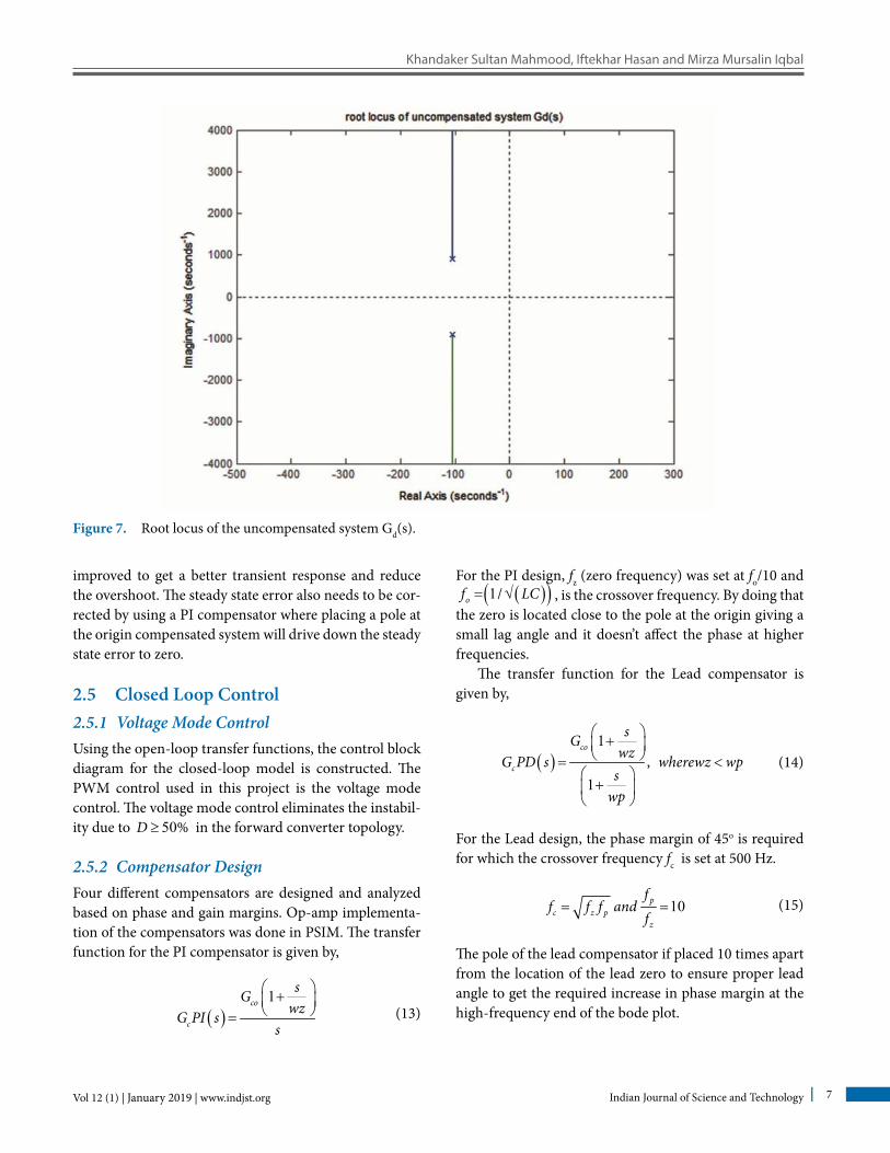
The Bode plot in Figure 5 shows an infinite gain mar-gin and a phase margin (PM) of 3.49°. The step response in Figure 6 shows 60.9% overshoot, a rise time of 0.00125 seconds and a settling time of 0.0355 seconds. The open
loop transfer function ( )dG s shows that there are two complex poles with constant damping ratio as shown in Figure 7. The PM of ( )dG s is very low and needs to be
Figure 5. Bode plot of the uncompensated system Gd(s)
Figure 6. Step response of the uncompensated system Gd(s).
Indian Journal of Science and Technology 7Vol 12 (1) | January 2019 | www.indjst.org
Khandaker Sultan Mahmood, Iftekhar Hasan and Mirza Mursalin Iqbal
improved to get a better transient response and reduce the overshoot. The steady state error also needs to be cor-rected by using a PI compensator where placing a pole at the origin compensated system will drive down the steady state error to zero.
2.5 Closed Loop Control2.5.1 Voltage Mode ControlUsing the open-loop transfer functions, the control block diagram for the closed-loop model is constructed. The PWM control used in this project is the voltage mode control. The voltage mode control eliminates the instabil-ity due to 50%D ≥ in the forward converter topology.
2.5.2 Compensator DesignFour different compensators are designed and analyzed based on phase and gain margins. Op-amp implementa-tion of the compensators was done in PSIM. The transfer function for the PI compensator is given by,
( )1co
c
sGwzG PI s
s
+ = (13)
For the PI design, fz (zero frequency) was set at fo/10 and ( )( )1 /of LC= √ , is the crossover frequency. By doing that
the zero is located close to the pole at the origin giving a small lag angle and it doesn’t affect the phase at higher frequencies.
The transfer function for the Lead compensator is given by,
( )1
1
, co
c
sGwzG PD s wherewz wp
swp
+ = <
+
(14)
For the Lead design, the phase margin of 45o is required for which the crossover frequency fc is set at 500 Hz.
10pc z p
z
ff f f and
f= = (15)
The pole of the lead compensator if placed 10 times apart from the location of the lead zero to ensure proper lead angle to get the required increase in phase margin at the high-frequency end of the bode plot.
Figure 7. Root locus of the uncompensated system Gd(s).

Indian Journal of Science and TechnologyVol 12 (1) | January 2019 | www.indjst.org 8
Modeling and Closed Loop Votlage Mode Control of a Forward Converter
The transfers function for the PID compensator:
( )1 1
1 21 2
1
, co
c
s sGwz wzG PID s where wz wz
sswp
+ + = <
+
(16)
The PID compensator was designed by cascading the PI and PD compensators. The PID compensator incorpo-rates both the advantages of the PI and Lead compensa-tor by improving both the steady state error and transient response of the response of the system while maintain-ing good stability margins. The compensator applied in the project was PI using a transconductance amplifier which came with the PWM chip SG1524. The location of the compensator pole and zero was determined by
2/po zo o sF F F f< < < where fs is the switching frequency and fo is the crossover frequency. The low frequency gain and the high frequency phase margin improve as required for the uncompensated forward converter.
2.6 Converter Component SelectionIn this study, a forward converter operated in continuous mode is designed to step down a constant dc input volt-age to a lower constant dc output voltage. The switching frequency is set at 40 kHz. The design specifications are given Table 1.
2.7 Selection of ComponentsTransformer Consideration: A convenient winding ratio between the primary (N1) and the reset winding (N3) is usually chosen as 1. However, in this paper, the ratio has been set to 3 so that the time required for the magnetising inductance current to return to zero is less. The winding ratio between primary winding (N1) and the secondary winding (N2) is set as 1.
Electronic Switch: The electronic switch has been cho-sen based on its voltage and current rating which must be higher than its maximum input voltage and current. A power MOSFET IRF150N is chosen as the switch to han-dle the 50W converter with an input dc voltage of 15-30V.
Inductor: To guarantee CCM, the inductor at the out-put must be sufficiently large. Although the value of the inductance has no defined upper limit, however, a large value signifies bulkier part and more number of turns which in turn increases the DCR and copper losses. The inductor selected is of a higher value than the calculated using equation (17)21 to avoid the problem of core satura-tion.
1
2 0
1 1 11 .O O
i L s
nL V
V n i f
> − ∆
(17)
Ferrite core inductor is used here.
Diode: The major concern for the selection of diode is its reverse voltage rating. Another important consideration is the peak and average current handling capability, fast switching characteristics, low reverse-recovery, and low forward voltage drop.
Output Capacitor: Equation (18)21 is used to determine the minimum value of capacitor required to meet the rip-ple voltage consideration.
2
1
8O
O x
V DV L Cf∆ −
= (18)
However, the capacitor value selected is much higher to obtain a nearly constant DC value.
The component specifications have been summarized in Table 2.
Table 1. Design SpecificationsMode Continuous conduction mode
Input Voltage ( )inV 15 35 inV V V≤ ≤
Output Voltage ( )outV 10 V
Switching Frequency 20 kHz
Output Power 50 W
Output Voltage Ripple 0 1.≤
Inductor Current Ripple 0 1.≤

Indian Journal of Science and Technology 9Vol 12 (1) | January 2019 | www.indjst.org
Khandaker Sultan Mahmood, Iftekhar Hasan and Mirza Mursalin Iqbal
2.8 Regulated Pulse Width ModulatorThe PWM chip selected for this project is SG1524. The entire control for a regulating power supply inverter or switching regulator is carried out by the circuit contained within this monolithic integrated circuit. The 16-pin dual-in-line package further includes the voltage refer-ence, error amplifier, oscillator, pulse width modulator, pulse steering flip-flop, dual alternating output switches, and current limiting and shut-down circuitry. Frequency of the oscillator ( )1 3 . / T TR C= .
Table 2. Component SpecificationsElectronic Switch IRF530N
Inductor 1 mH Diode MUR1560
Output Capacitor 1 2. mF
Load 4 Ω
Transformer 1 2 360 60 20, , N N N= = =
Figure 8. Open loop forward converter.
Figure 9. PID compensated-Output voltage response for input voltage step change.

Indian Journal of Science and TechnologyVol 12 (1) | January 2019 | www.indjst.org 10
Modeling and Closed Loop Votlage Mode Control of a Forward Converter
3. Results and DiscussionSimulations for the forward converter were done on PSIM and the results were used to identify which component rating will give a better performance thus selecting it for practical implementation. The output voltage and induc-tor current and the step response of the open and closed loop system were done.
3.1 Open Loop SimulationsAn open loop forward converter was designed as shown on Figure 8 and its PID-compensated output voltage for step
input and resulting inductor current has been recorded as depicted in Figure 9 and Figure 10 respectively.
3.2 Closed Loop SimulationsA closed loop forward converter with voltage mode control is illustrated in Figure 11 has and its output inductor current and PID-compensated output voltage for step input has been recorded as shown in Figure 12 and 13 respectively.
3.3 Experimental SetupUsing the setup shown in Figure 14, experimental mea-surements were recorded in order to corroborate the
Figure 10. Output inductor current.
Figure 11. Closed loop voltage mode controlled PID compensated Forward Converter.

Indian Journal of Science and Technology 11Vol 12 (1) | January 2019 | www.indjst.org
Khandaker Sultan Mahmood, Iftekhar Hasan and Mirza Mursalin Iqbal
performance of the designed forward converter. Figures 15 and 16 shows the open loop response of the system for inductor current, gate pulse and output voltage. Figures 17 and 18 show the closed loop response of the system for 20V and 30V input voltage respectively. Finally Figure 19, shows the response of the output inductor current due to step change in load. The experimental analysis revealed that the forward converter operated successfully in pro-viding a step-down the output of the input voltage as indicated in Table 3. The limitation observed during the
experiment was that as the input voltage is decreased, the duty ratio increases for the system. So the rising induc-tor current slope saturates the transformer core. So the input voltage cannot be decreased beyond 15V. However, the closed-loop feedback by voltage mode control allowed the converter to hold the output voltage constant when subjected to fluctuations in the input voltage. The losses in the forward converter are switching loss, conduction loss, inductor’s eddy current and hysteresis loss, ESR and electromagnetic interference.
Figure 12. Output inductor current (closed loop) with a step change in input voltage.
Figure 13. Output voltage (closed loop) with a step change in input voltage.

Indian Journal of Science and TechnologyVol 12 (1) | January 2019 | www.indjst.org 12
Modeling and Closed Loop Votlage Mode Control of a Forward Converter
Figure 14. Gate Drive and Experimental Setup.
Figure 15. Output inductor current.

Indian Journal of Science and Technology 13Vol 12 (1) | January 2019 | www.indjst.org
Khandaker Sultan Mahmood, Iftekhar Hasan and Mirza Mursalin Iqbal
4. ConclusionFrom the proposed design, it is understood that the for-ward converter was capable of stepping down the voltage at the output while maintaining low output voltage rip-ple. The output voltage was held constant by the voltage mode control and provided feedback and Tran’s conduc-tance amplifier based PI compensation. The experimen-
Table 3. Experimental results of the forward converterInput Voltage 30VDuty Cycle 0.40Frequency 39.69 kHzOutput Voltage 10.5VInductor current (average) 2.718AOutput voltage Ripple <0.01
Figure 16. A combined graph showing gate pulse, inductor current, and the output voltage.
Figure 17. Closed loop response showing output voltage, diode voltage, gate pulse and inductor current for an input voltage of 30V.

Indian Journal of Science and TechnologyVol 12 (1) | January 2019 | www.indjst.org 14
Modeling and Closed Loop Votlage Mode Control of a Forward Converter
Figure 18. Closed loop response showing output voltage, diode voltage, gate pulse and inductor current for an input voltage of 20V.
Figure 19. Effect of a step change in input voltage on inductor current and output voltage.
tal results were similar to the simulation results. The closed-loop experiment worked and PI compensation was implemented successfully to improve the steady state performance of the converter.
5. References1. Power electronics. Available from: https://www.abebooks.
com/9780073380674/Power-Electronics-Daniel-Hart-Professor-0073380679/plp. Date accessed: 2010.

Indian Journal of Science and Technology 15Vol 12 (1) | January 2019 | www.indjst.org
Khandaker Sultan Mahmood, Iftekhar Hasan and Mirza Mursalin Iqbal
2. Chen SJ, Huang CM, Yang SP. A new interleaved series input parallel output zero-voltage-switching forward con-verter. 6th IEEE Conference on Industrial Electronics and Applications. 2011; p. 1791-6. https://doi.org/10.1109/ICIEA.2011.5975883
3. Singh S, Bhuvaneswari B, Singh V. Power quality improve-ment in multi-output forward boost converter. India International Conference on Power Electronics 2010 (IICPE 2010). 2011; p. 1-5. https://doi.org/10.1109/IICPE.2011.5728105
4. A DC-DC interleaved forward converter to step - up DC voltage for DC Micro grid applications. Available from: https://ieeexplore.ieee.org/document/6672501. Date accessed: 25/11/2013.
5. EMI Examination of Symmetric Forward Converter.6. Choi Y, Keum MH, Han SK, Kang JI. High efficiency and
high power factor single-stage balanced forward-flyback converter. IECON 2013 - 39th Annual Conference of the IEEE Industrial Electronics Society. 2013; p. 822-7.
7. Baby A, Nithya M. Sliding mode controlled forward con-verter. IEEE 9th International Conference on Intelligent Systems and Control (ISCO). 2015; p. 1-4. https://doi.org/10.1109/ISCO.2015.7282270
8. Yang J, Faris AN, Zhang W. Small-signal model analysis and control design of a double-ended forward converter in discontinuous-capacitor-voltage mode. IET Power Electronics. 2015; 8(5):802-13. https://doi.org/10.1049/iet-pel.2014.0349
9. Sudeep E, Rachappa Singh BK, Chippalkatti VS, Rao KU. Design and implementation of current mode controlled 150W miniature forward converter for defence applica-tion. IEEE International Conference on Power Electronics, Drives and Energy Systems (PEDES). 2016; p. 1-6. https://doi.org/10.1109/PEDES.2016.7914231
10. Altintas G, Gulbahce MO, Kocabas DA. Non-ideal Analysis, Design and Voltage Mode Control of a Boost Converter. 57th International Scientific Conference on Power and Electrical Engineering of Riga Technical University (RTUCON). 2016; p. 1-6. PMCid:PMC5042924
11. Biabani MAKA. Simulation, Mathematical Calculation and Comparison of Power Factor and Efficiency for Forward, Fly back and Proposed Forward-Flyback Converter. International Conference on Electrical, Electronics, and Optimization Techniques (ICEEOT). 2016; p. 1583-9. https://doi.org/10.1109/ICEEOT.2016.7754952
12. Zhou G, Ruan X, Wang X. Input Voltage Feed-Forward Control Strategy for Cascaded DC/DC Converters With
Wide Input Voltage Range. IEEE 8th International Power Electronics and Motion Control Conference (IPEMC-ECCE Asia). 2016; p. 603-8.
13. Zhou Z, Zhang Q, Li S, Jin Q. A Real-time Co-Simulation Research Based on VSC Closed-Loop Control. IEEE International Conference on Power System Technology (POWERCON). 2016; p. 1-6. https://doi.org/10.1109/POWERCON.2016.7753961
14. Karuppiah M, Karthikumar K, Arunbalj A. A Transformerless Buck-Boost Converter with PID Controller (Closed Loop Controller). IEEE International Conference on Intelligent Techniques in Control, Optimization and Signal Processing (INCOS). 2017; p. 1-7. https://doi.org/10.1109/ITCOSP.2017.8303145
15. Loza B, Cherrez JP, Gonzalez LG. Design and analysis of performance of a forward converter with winding tertiary. IEEE International Autumn Meeting on Power, Electronics and Computing (ROPEC). 2017; p. 1-6. https://doi.org/10.1109/ROPEC.2017.8261632
16. Lu YJ, Liang TJ, Lin CH, Chen KH. Design and implemen-tation of a bidirectional dc-dc forward/flyback converter with leakage energy recycled. Asian Conference on Energy, Power and Transportation Electrification (ACEPT). 2017; p. 1-6. https://doi.org/10.1109/ACEPT.2017.8168572
17. Yang SP, Chen SJ, Huang CM, Chen CE. A Novel Soft-Switching High Step-Down Forward Converter. IEEE International Conference on Industrial Electronics for Sustainable Energy Systems (IESES). 2018; p. 82-7. https://doi.org/10.1109/IESES.2018.8349854
18. Meng T, Ben H, Song Y, Li C. Analysis and Design of an Input-Series Two-Transistor Forward Converter for High-Input Voltage Multiple-Output Applications. IEEE Transactions on Industrial Electronics. 2018; 65(1):270-9. https://doi.org/10.1109/TIE.2017.2716913
19. Krishnaja M, Samanta S. Effect of optocoupler feedback dynamics on peak current mode controlled active clamp forward converter. IEEMA Engineer Infinite Conference (eTechNxT). 2018; p. 1-6. https://doi.org/10.1109/ETECHNXT.2018.8385375
20. Vijayakumar AP, Devi R. Simulation and Experimental Results for the Closed Loop Controlled DC to DC Forward Converter. Acta Electrotechnica et Informatica. 2017; 17(2):23-9. https://doi.org/10.15546/aeei-2017-0012
21. Power electronics: converters, applications, and design. Available from: https://books.google.co.in/books/about/Power_electronics.html?id=ToYoAQAAMAAJ&redir_esc=y. Date accessed: 2003.