limits to non-fluorescent voltage sensitivity using surface and particle plasmons
TRANSCRIPT

Limits to non-fluorescent voltage sensitivity using surface and particle plasmons
Mark C. Pitter*, John Paul, Jing Zhang, Michael G. Somekh
IBIOS, University of Nottingham, UK NG9 2RD
ABSTRACT
Voltage sensitive fluorescent dyes have long been used to measure physiological voltages in live cell cultures. However dyes suffer from poor contrast and limited recording duration due to photobleaching. A photostable voltage sensitive cellular label, such as a noble metal nanoparticle, would potentially allow for indefinite recording from neural and other live cell cultures. Noble metals possess an inherent voltage sensitivity: their optical properties depend on their density of free electrons, which can be modulated in an aqueous environment by charging or discharging the double layer capacitance with an applied voltage. This manuscript contains a simple analysis of the expected voltage sensitivity using gold nanospheres and nanoshells in both darkfield and photothermal detection modalities and concludes that high bandwidth voltage measurement is fundamentally achievable.
Keywords: voltage sensitivity, gold, nanosphere, nanoshell, particle plasmon resonance, Drude, Lorentz, Mie
1. INTRODUCTION There are many applications where it is necessary to sense the voltage at sites on or within a cellular plasma membrane. Perhaps the greatest challenge is to sense neuron action potentials, which would require a voltage sensitivity of at least 100 mV (preferably 10 mV) in a bandwidth of 1 kHz (preferably 10 kHz). A possible candidate for this task is noble metal nanoparticles (NPs). Noble metal NPs exhibit the phenomenon of particle plasmon resonance (PPR) which confers upon them very large scattering and absorption cross-sections which are sensitive to the NP environment. When the membrane potential of a cell changes, there will be two main effects on PPR:
i) any alteration in the real part of the refractive index of the medium around the NP to higher or lower values will respectively red-shift or blue-shift the resonant peak. This can occur due to, for example, the opening and closing of ion channels in the cell membrane.
ii) any induced change in the electron density of the NP to higher or lower values will respectively blue-shift or red-shift the resonant peak. This occurs because the particle has a relatively large double-layer capacitance in an aqueous medium. When say, a negative voltage is applied to the NP, the double-layer capacitance will charge up with electrons. This will “stiffen” the resonant free electron “spring” and blue-shift it to higher frequencies. Application of a positive voltage will cause a red-shift as the NP is depleted of free electrons.
The following discussion considers only ii), the direct effect of applied voltage to PPR. The authors accept that this model cannot be directly applied to live cells due to neglecting the refractive index changes and the voltage coupling between the NP and the cell. However, the aim of this discussion is to attempt to establish fundamental limits for the detectability of voltage induced PPR changes in different optical arrangements (e.g. darkfield, photothermal) as a function of NP type, size and shape. This will help to establish the feasibility of voltage sensing with NPs and will eventually allow optimization of the particle and optics. Section 2 of this manuscript briefly describes a simple Drude-Mie model which qualitatively describes the relationship between applied voltage and the position of the PPR peak. Then in Sect. 3, a Drude-Lorentz model is introduced which, in combination with Mie theory, can be used to predict the detected signal in various microscopy modalities. Section 4 applies this model to darkfield detection of spherical gold nanospheres and gold/dielectric nanoshells. Section 5 briefly examines photothermal detection and concluding remarks are in Sect. 6.
*[email protected]; phone +44 115 951 3221; fax +44 115 951 5616; nottingham.ac.uk/ibios
Photons and Neurons, edited by Anita Mahadevan-Jansen, E. Duco Jansen, Proc. of SPIE Vol. 7180718006 · © 2009 SPIE · CCC code: 1605-7422/09/$18 · doi: 10.1117/12.809060
Proc. of SPIE Vol. 7180 718006-1

2. SIMPLE DRUDE-MIE MODEL Gold particles in an aqueous medium possess a double layer capacitance, dC , usually quoted as 40 μFcm-2. Hence the capacitance of an individual spherical NP is given by
dNP CrC 24π= (1)
where r is the radius of the NP [m]. For example, gold nanospheres of 10 and 100 nm diameter in water have capacitances of around 0.1 and 10 fF respectively.
Without an applied voltage, a gold NP has a free electron density en of approximately 5.6 x 1028 m-3. When a voltage
NPv [V] is applied to the NP, storage of charge by the double layer capacitance modulates this value and changes the optical properties of the NP.
By applying Drude and Mie theory, a simple relationship can be derived for the relative change in the position of the PPR peak in terms of the ratio of the number of free electrons, with and without the voltage applied [1],
v
v
NN 0
20
2
=λ
λ (2)
where 0λ and λλλ Δ+= 0v are the positions of the PPR peak , and 0N and vN are the number of free electrons, with and without an applied voltage respectively.
VnN e=0 ,
evC
NNNN NPNPv −=Δ+= 00 , (3)
where V is the NP volume [m3], e is the electronic charge [C] and NΔ is the voltage induced change to the number of electrons on the NP.
Since 3rVNo ∝∝ whereas 2rCN NP ∝∝Δ , it clear from Eqs. 2 and 3 that small spheres will produce a greater shift in the resonant wavelength than larger ones. For example, a 10 nm diameter gold nanospheres with an applied voltage of 100 mV exhibits a change in the resonant wavelength of around 0.7 nm, whereas for a 100 nm diameter sphere, the shift is about 0.07 nm. To summarize,
rv1
∝ΔΔλ . (4)
It may initially appear that the smaller the particle, the more sensitive the optical measurement. However, very small NPs are difficult or impossible to detect in practice because the amount of light scattering (and absorption) drops rapidly with NP size with 61 rI sca ∝ and 31 rI abs ∝ where scaI and absI are the scattered and absorbed intensities. In order to correctly optimize the particle size, we need to consider the optical detection technique and detection noise.
From the above, it is clear that NPs with large surface area to volume ratios should perform better than NPs with small surface area to volume ratios. In this respect, spheres are probably the least sensitive shape and rods, for example, could be expected to exhibit a larger shift for a given NP volume. However, spheres are readily available and an exact model exists for scattering and absorption. For these reasons, spheres will be analyzed first. Later sections will consider concentric core/shell nanospheres, for which an exact Mie model also exists. NPs with a dielectric core and a gold shell allow the volume of gold to be varied by changing the thickness of the shell layer, while maintaining the same surface area, and hence NP capacitance.
Proc. of SPIE Vol. 7180 718006-2

3. DRUDE-LORENTZ THEORY TO MODEL GOLD PERMITTIVITY IN PRESENCE OF AN APPLIED VOLTAGE
In order to apply Mie to the voltage sensitivity of gold nanospheres, we need a model of the permittivity of gold as a function of applied voltage. The Drude-Lorentz (DL) model is suitable for optical frequencies [2]. With no voltage applied,
( ) ( ) ( )ωω
εγωω
ωεωε
LL
L
D
DDL
ii Γ+Ω−
ΩΔ−
+−= ∞ 22
22
(5)
where ω is the optical angular frequency, ( )ωε DL is the frequency dependent relative permittivity and ∞ε is the high frequency limit, Dω is the plasma frequency [rad.s-1], Dγ is the damping coefficient [rad.s-1], LΩ and LΓ are the Lorentz oscillator strength and spectral width respectively [rad.s-1] and εΔ is a weighting factor.
The plasma frequency is affected by the free electron density and can be used to calculate the effect of an applied voltage on the optical properties of the nanospheres:
( ) ( )e
eD m
evnv
0
2
εω = (6)
where 0ε is the permittivity of vacuum [C2J-1m-1] and em is the resting mass of an electron [kg].
The DL model calculates the relative permittivity of bulk gold. When NP dimensions approach the mean free path for electrons in gold (~40 nm), damping is increased by additional electron collisions with the surface of the NP. This additional damping reduces the quality of the PPR, but if it is not taken into account, then the models can produce overly optimistic results, particularly in the case of the core/shell particles.
The additional damping caused by geometrical effects is modeled by corrected the permittivity to account for the additional surface collisions [3]. Briefly, if collγ is the collision frequency for bulk gold, then the collision frequency in a spherical particle can be estimated by
rvF
collcoll +=Γ γ (7)
where Fv is the Fermi velocity [ms-1]. The modified permittivity can then be calculated
. coll
D
coll
DbulkNP
ii Γ+−
++=
ωωω
ωγωω
εε2
2
2
2
. (8)
We can now apply the above equations to calculate signals and signal to noise ratios as a function of incident wavelength and nanosphere diameter for different microscopy modalities.
4. VOLTAGE SENSITIVITY WITH DARKFIELD DETECTION In darkfield detection (DF), only the scattered light is detected. The size of the signal in DF, that is, the intensity of scattered light, is determined by
i) the size, composition and shape of the NP,
ii) the numerical aperture of the detection optics,
iii) the efficiency of the detection optics and sensor,
iv) the incident light intensity,
v) the integration time.
Proc. of SPIE Vol. 7180 718006-3
It will be assumed that the NPs scatter in the Rayleigh limit, that is isotropically, therefore
intdet tII scaη= (9)
where intt is the integration time [s] and the overall efficiency η depends on the detection angle of the optics
( ( )coupnNA1sin − where NA is the numerical aperture and coupn is the refractive index of the objective lens coupling medium - air, water or oil) and the detection efficiency (the optical transmission of the detection optics T multiplied by the quantum efficiency of the sensor, QE ),
( )( )[ ]
( ) ( )λλπ
λη QETnNA coup
4sin2
21−
= (10)
Mie theory is used to calculate scaQ , the scattering efficiency, which is the ratio of the scattering cross-sectional area
scaX [m2] to the geometric cross-sectional area 2rX geo π= [m2].
2rQIXII scaincscaincsca π== (11)
incI is the incident light intensity per unit area [Wm-2]. This is limited by the illumination source and optics, but also by heating effects. Gold NPs are strong absorbers and can get very hot which can damage the sample under investigation. The temperature rise can be calculated and the results presented in Sect. 4.2 account for this by ensuring that the NP temperature change is limited to 1 K.
The fundamental limit to optical detection sensitivity is optical shot noise. Other noise sources such as readout noise and illumination intensity fluctuations will also be present, but can often be controlled to the extent that shot noise dominates. In terms of photon numbers, the shot noise ( SN ) is simply calculated
⎟⎠⎞
⎜⎝⎛==hc
INSN phλ
det (12)
where phN is the number of photons used in the measurement, h is Planck’s constant [Js], λ is the wavelength [m] and c is the speed of light [ms-1]. The signal to shot noise ratio ( SSNR ) is then given by
phph
ph NN
NSSNR == . (13)
The implications of this are that it is often possible in practice to detect a small change in a large signal with better SSNR than detecting a large change in a small signal. For example, to detect a 1% change in intensity with a SSNR of unity requires at least 104 photons whereas to detect an intensity change of 0.1% requires 106 photons. Clearly a more complete analysis is required to optimize the nanospheres radius for voltage sensing.
Proc. of SPIE Vol. 7180 718006-4

4.1 Darkfield voltage sensitivity for a fixed illumination intensity
The following subsection contains examples of SSNR calculations for gold nanospheres for a fixed illumination intensity of 1 mW/μm2. Table 1 contains the experimental parameters used for the simulations in this subsection.
Table 1: values of experimental parameters used in the simulations below
symbol comment value units
incI Incident intensity: the simulation calculates scattering over a range of discrete illumination wavelengths. 1 mWμm-2 incident at the sample is assumed for each wavelength.
1 mW/μm2
intt integration time. 1 ms or faster is usually required to record mammalian action potentials
1 ms
QET . detection efficiency – combined effect of transmission of detection optics and quantum efficiency of the sensor
0.5 .
NA a high NA, oil coupled fluar lens is assumed 1.3 .
coupn regular immersion oil 1.52 .
The values used in Table 1 were chosen to be realistic, but also to be easily scalable to other experimental conditions. The scaling relationships are given below in Table 2.
Table 2: scaling relationships for experimental factors listed in Table 1
parameter scaling
incident intensity incISSNR ∝
integration time inttSSNR ∝
detection efficiency QETSSNR .∝
detection angle, ( )coupnNA1sin −=θ ( )θsin∝SSNR
applied voltage NPvSSNR ∝
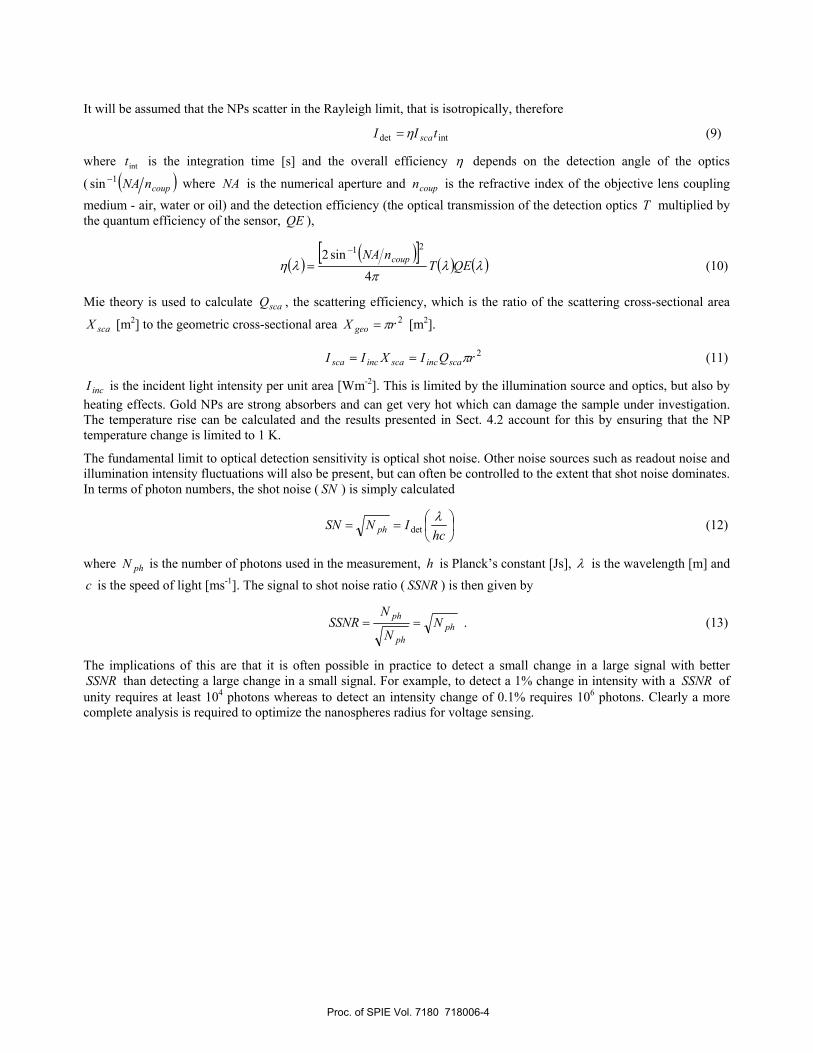
The voltage induced resonance shift for 1 V is easily visible for a 10 nm sphere (Fig. 1a). The applied voltage is positive so the scattering peak is red-shifted due to a depletion of conduction electrons. Note how the wavelength of peak contrast (Fig. 1b) is different to the wavelength of peak SSNR (Figs. 1c and 1d). This is because the higher light scattering near to resonance overcomes the decreased contrast.
Proc. of SPIE Vol. 7180 718006-5
500 510 520 530 540 550 560 570 580 590 6004000
5000
6000
7000
8000
9000
10000
lambda (nm)
Sca
ttere
d ph
oton
s
LD, V=0LD, V=1 V
500 510 520 530 540 550 560 570 580 590 600-8
-6
-4
-2
0
2
4
6
8
10
lambda (nm)
cont
rast
(%)
(a) (b)
500 510 520 530 540 550 560 570 580 590 6000
0.5
1
1.5
2
2.5
lambda (nm)
SS
NR
sca
tterin
g
500 510 520 530 540 550 560 570 580 590 600-25
-20
-15
-10
-5
0
5
lambda (nm)
SS
NR
sca
tterin
g (d
B)
(c) (d)
Fig.1. Voltage sensitivity simulation for a 10 nm diameter gold nanosphere, applied voltages of 0 V and 1 V, an incident intensity of 1 mW/μm2, an integration time of 1 ms, NA of 1.3 (oil immersion) and an overall detection efficiency of 50%. (a) scattering spectra in photons at 0 V (lighter, solid trace, green online) and 1 V (darker, dashed trace, red online), (b) percentage contrast, (c) SSNR as ratio and (d) in dB.
The SSNR is rather low for a 10 nm sphere, even when considering only shot noise. The result implies that voltage sensitivity is fundamentally limited to around 500 mV in these experimental conditions. In practice, achieving shot noise limited detection at these low light levels would require an electron multiplying charge couple device camera (EMCCD) or a photon counting photomultiplier tube (PMT). The incident intensity is quite high at 1 mW/μm2, so widefield detection would probably not be very practical, furthermore, a scanning approach would require the use of relatively low efficiency PMTs.
On the face of it, this is a discouraging result. Very small NPs are often favored by biologists as they are considered to be less invasive of the system under observation, but is well known that NPs of this size are extremely difficult to analyze using simple darkfield techniques. However, there are several approaches that could improve the SSNR. The simplest one is to increase the integration time, where possible, for example if observing invertebrate neurons or non-neuronal cells. Unfortunately, the voltage sensitivity is proportional to the square root of bandwidth, so quite large increases in integration time may be required. A more powerful strategy should be to increase the surface area volume ratio of the NP. One technique to achieve his will be investigated below. Another potentially powerful approach is to apply photothermal techniques (PT). Unlike darkfield, PT is sensitive to NP absorption which ‘only’ reduces with 3r , rather than 6r as is the case for scattering. PT methods will be analyzed in a future report.
The resonance shift is much less obvious for a 100 nm sphere (Fig. 2) and this translates to a greatly reduced contrast. However, the number of scattered photons is dramatically increased from the 10 nm sphere.
Proc. of SPIE Vol. 7180 718006-6

500 510 520 530 540 550 560 570 580 590 6000.5
1
1.5
2x 10¹⁰
lambda (nm)
Sca
ttere
d ph
oton
s
LD, V=0LD, V=1 V
500 510 520 530 540 550 560 570 580 590 600-1.5
-1
-0.5
0
0.5
1
1.5
lambda (nm)
cont
rast
(%)
(a) (b)
500 510 520 530 540 550 560 570 580 590 6000
50
100
150
200
250
300
350
400
450
500
lambda (nm)
SS
NR
sca
tterin
g
500 510 520 530 540 550 560 570 580 590 6000
5
10
15
20
25
30
lambda (nm)
SS
NR
sca
tterin
g (d
B)
(c) (d)
Fig. 2. Voltage sensitivity simulation for a 100 nm diameter gold nanosphere using the same parameters as in Fig. 1, i.e. applied voltage = 1 V, incident intensity = 1 mW/μm2, integration time = 1 ms, NA = 1.3 (oil immersion), detection efficiency = 50%. (a) scattering spectra for 0 V (light) and 1 V (dark trace), (b) percentage contrast, (c) and (d) SSNR as a ratio and in dB.
This high scattering intensity results in a greatly improved SSNR, despite the much lower contrast. The fundamental limit to voltage sensitivity is now potentially just over 2 mV in a 1 kHz bandwidth. This SSNR if achieved in practice would allow sensing action potentials in neurons to be feasible.
There are of course many simplifying assumptions in these models. The actual voltage sensitivity would be dependent on many factors, some of which are difficult to model. For example, although a 100 nm sphere appears to exhibit far greater voltage sensitivity than a 10 nm sphere, it may electrically couple less well to a cell membrane. These simulations should still be useful in identifying trends and attempting to optimize experimental conditions. They can be refined as we start to obtain experimental data.
4.2 Darkfield voltage sensitivity for a fixed nanosphere temperature rise
When the NPs absorb the illumination, it is converted to heat. If the incident light levels are too high, this heat can damage or even kill any adjacent cells, and while this effect shows promise as a potential cancer treatment, it is obviously to be avoided in most experiments.
It is possible to calculate the temperature rise of the particle by applying Mie theory to calculate the absorption and then applying the heat point source model for heat diffusion [4],
πκρ4absP
T =Δ (14)
where TΔ is the change in temperature caused by the heating effect of the illumination [K], absincabs XIP = is the power absorbed by the NP [W], κ is the thermal conductivity of the medium around the NP [Wm-1K-1] ( CD κ= where D is
Proc. of SPIE Vol. 7180 718006-7

the thermal diffusivity [m2s-1] and C is the heat capacity per unit volume [Jm-3K-1]) and ρ is the distance from the centre of the NP [m]. If the absorption cross section is calculated using Mie, the temperature change at the surface of the NP can be found by setting r=ρ in Eq. 14. Figure 3 shows a map of ( )TΔ10log in Kelvin for an illumination power of 1 mW/μm2, a detection efficiency of 50% and an oil immersion objective lens NA of 1.3.
lam
bda
(nm
)
nanosphere diameter (nm)10 20 30 40 50 60 70 80 90 100
450
500
550
600
650
-2
-1.5
-1
-0.5
0
0.5
1
1.5
2
Fig. 3. log10 of the temperature change induced in a nanosphere by illumination at 1 mW/μm2 as a function of nanosphere
diameter and incident wavelength. Very small nanospheres ( r < 10 nm) only heat by a fraction of 1 K, however the temperature of larger nanospheres may rise by over 100 K, which is clearly incompatible with live cell studies.
In Fig. 3 a temperature rise of 1 K is the mid grey band (green online) with all points to the right of the green band indicating temperature changes that may not be tolerated by the cell. The largest particles undergo temperature changes of over 100 K. This implies that if we wish to limit the maximum NP temperature rise to 1 K, we will have to reduce the illumination intensity accordingly.
The maximum allowable illumination intensity in mW/μm2 for a NP temperature rise of 1 K, a value easily tolerated by live cells, can be obtained by taking the reciprocal of the values in Fig. 3 and multiplying by 1 mW/μm2. It should be pointed out that the temperature rise is generally contained within a few tens or hundreds of nm of the NP surface, so somewhat higher temperatures may be allowed in practice, especially if the illumination is modulated. It can be seen from Fig. 3 that for very small nanospheres, intensities as high as 100 mW/μm2 can be tolerated. However for NPs of diameters approaching 100 nm, intensities of less than 10 μW/μm2 must be used. This will clearly affect the achievable SNR.
nanosphere diameter (nm)
inci
dent
wav
elen
gth
(nm
)
10 20 30 40 50 60 70 80 90 100
450
500
550
600
650
0.5
1
1.5
2
2.5
3
3.5
4
4.5
5
5.5
Fig. 4. SSNR for a gold nanosphere temperature rise of 1 K with an applied voltage of 100 mV as a function of incident
wavelength and nanosphere diameter. The best SSNR of around 5.5 is achieved for the largest nanospheres at an incident wavelength of about 580 nm.
Proc. of SPIE Vol. 7180 718006-8

If the incident intensity is controlled such that is sufficient to cause a rise in the surface temperature of the NP of just 1 K, the simulated SSNR achieved for a voltage change from 0 V to 100 mV is presented in Fig. 4. Clearly improved voltage sensitivity could be achieved with nanospheres of diameters above 100 nm, and NPs of this size will have some applications, but larger particles are generally considered by biologist to be too invasive for use as cellular labels and will possibly not couple very well to the voltage source.
It is clear from Fig. 4 that reasonable voltage sensitivity (of order 20 mV) is theoretically possible with gold nanospheres of around 90 nm diameter and above. Of course in practice, these values will never be achieved, only approached. A major factor that has not been considered in this discussion is the coupling between the voltage source of interest and the NP. It has simply been assumed that the charge stored on the nanosphere is the product of the voltage of interest and the double layer capacitance of the sphere. But these results do show that sensing voltage with gold nanospheres of diameters greater than around 100 nm is at least theoretically possible.
On the other hand, the results predict that sensing voltage by darkfield scattering with gold nanospheres less than say 30 or 40 nm in diameter is going to require prohibitively high incident intensities and/or long integration times, even if optical components, sensors and alignment are literally perfect. An encouraging fact is that it is possible that solid spheres are the worst possible NP configuration for sensing voltage. To a rough approximation, the PPR shift is proportional to the NP surface area to volume ratio, and of course, spheres are minimal in this respect. Another class of NP that can be precisely modeled using Mie theory is nanoshells - concentric core/shell nanospheres. The geometry of a dielectric/gold core/shell NP means it is possible to reduce the volume of gold while maintaining the surface area. Section 5 below examines the potential of dielectric/gold nanoshells for voltage sensing.
4.3 Darkfield voltage sensitivity for a fixed nanoshell temperature rise
Similar to nanorods, the PPR peak for nanoshells is red-shifted with respect to solid spheres and the NP volume can be varied while maintaining the surface area. In common with nanospheres, they are insensitive to incident polarization. The modeling procedure and experimental parameters used in the following results the same as in Table 1. The ratio of the overall nanoshell radius to the dielectric core radius is held constant at 80% (approximately optimal) while the overall nanoshell radius is varied.
nanosphere diameter (nm)
inci
dent
wav
elen
gth
(nm
)
10 20 30 40 50 60 70 80 90 100
500
550
600
650
700
750
800
2
4
6
8
10
12
14
16
18
Fig. 5. SSNR for a nanoshell temperature rise of 1 K and an applied voltage of 100 mV as a function of incident wavelength
and overall diameter. Dielectric core radius is 80% of the overall nanoshell radius
The results above indicate that nanoshells are capable of better voltage sensitivity as compared to nanospheres of the same diameter. The use of nanoshell also allows a tuning of the resonant wavelength, although only towards longer wavelengths relative to the equivalent sphere. The improvement in SSNR for the 100 nm diameter nanoshell with an 80 nm diameter core is a factor of around 3.2, which although quite low, still allows an increase in bandwidth of a factor of approximately 10 to achieve the same voltage sensitivity.
From these models, the best theoretical sensitivity that can be achieved with a spherical gold nanoparticle of diameter 100 nm or less is around 5 mV in a 1 kHz bandwidth using a temperature rise on 1 K in a 100 nm nanoshell with core
Proc. of SPIE Vol. 7180 718006-9
diameter of 80 nm. The incident intensities at the bandwidths required for action potentials mean that the DF technique is only really going to be suitable for scanning or point detection, rather than widefield imaging.
As stated earlier, theses theoretic values are the fundamental limit to sensitivity for a given set of experimental parameters. In practice, many other factor will act as noise sources, reducing the SNR. An obvious source of noise that is background scattering from the neurons or brain slices. The average value of this background can be subtracted from the measurements, but the shot noise carried by the background will remain and can easily dominate scattering from particles much under 100 nm diameter.
There is one factor that has been underestimated in the models here. An assumption of isotropic scattering has been used. This is certainly true for the smaller particles, but at the larger end of the simulation, the scattered light will be weighted towards the forward direction. So for transmission darkfield, there will be more light than modeled here, whereas in reflection darkfield there will be less. The error can be corrected by using an angle resolved Mie model. It has not yet been quantified as the smaller particles are of more interest and are accurately modeled in the Rayleigh limit used here.
The overall conclusion has to be that if these models translate to experiment, trying to sense action potentials of less than 100 mV by darkfield detection of nanospheres is going to be very difficult indeed. More general cell work, where higher intensities and/or longer integration times can be used, is much more tractable, but nanospheres are probably just about at the edge of what is useful.
Nanoshells are more promising, by about an order of magnitude in bandwidth or necessary intensity, but we could really do with a lot more if we are to sense action potentials. The best sensitivities (for single particle work) are achieved by rather large NPs of 100 nm diameter. These may be rather invasive in practice, and how well they couple to membrane potential is questionable.
5. VOLTAGE SENSITIVITY USING PHOTOTHERMAL DETECTION OF NANOPARTICLES
Section 4 of this manuscript analyzed the feasibility of applying darkfield detection to sensing voltage with nanospheres and nanoshells. The conclusions were that darkfield may be suitable at radii approaching 50 nm, but that it would be unlikely to succeed for smaller, less invasive NPs of radii less than 10 nm.
Thermal lens microscopy (TLM) [5] and photothermal interferometry (PHI) techniques [4] differ from darkfield in that they are sensitive to NP absorption, rather than scattering. As NP absorption is proportional to 31 r whereas NP
scattering is proportional to 61 r it is possible that photothermal methods may allow the use of smaller NPs for voltage sensing.
TLM and PHI are both pump/probe techniques where the pump beam, usually at a wavelength close to resonance, is used to heat the NP. This in turn heats the surrounding medium and slightly changes its refractive index,
dTdnTnn Δ+= 0 (15)
where n is the refractive index of the heated medium, 0n is the ambient medium index, TΔ is the change in temperature [K] and dTdn is the variation of refractive index with temperature [K-1]. The probe beam, usually at a wavelength well away from resonance, quantifies the amount of NP absorption by sensing the magnitude of the index change. The pump beam is modulated to allow low noise, phase sensitive detection of the probe.
As the NP is heated, the temperature in a sphere around the NP rises, creating a small region, or “virtual” particle (VP) of reduced refractive index. The size of this VP depends on the frequency of the pump beam modulation,
pump
thDt
Ω=
2 (16)
where thr is the characteristic length for heat diffusion [m], D is the thermal diffusivity and pumpΩ is the pump beam modulation frequency [rad.s-1].
Proc. of SPIE Vol. 7180 718006-10

PHI is used at high modulation frequencies (typically tens of MHz and above), where the diameter of the VP is smaller that the diameter of the probe beam. In this regime, the signal at the detector has two components. There is an undiffracted zero order component which passes around the VP and arrives at the detector unchanged and unmodulated. This can be regarded as a constant reference beam. The remaining light passes through the VP and has its optical path length modulated as the NP is heated and allowed to cool by the pump beam. By defocusing the probe beam, phase contrast can be enabled, and the diffracted light will efficiently interfere with the zero order beam at the detector. The interference converts the phase modulation to an intensity modulation which can be sensitively measured with a lock-in amplifier.
At lower modulation frequencies, the VP created by the heated NP is larger than the probe beam, and there is no zero order component. In this regime, it is useful to think of the VP as a weak lens. As the lens is modulated, refraction by the thermal lens causes a periodic divergence and convergence in the probe beam. In TLM, an aperture is placed in front of the detector, converting this effect to an intensity variation. Since dTdn is negative for liquids, the VP acts as a negative lens.
The temperature change due to the heating of a spherical NP can be calculated from heat diffusion and Mie theory. Using the heat point source model for heat diffusion [4]
( )⎥⎥⎦
⎤
⎢⎢⎣
⎡⎟⎟⎠
⎞⎜⎜⎝
⎛−Ω⎟⎟
⎠
⎞⎜⎜⎝
⎛−+=Δ
thpump
th
abs
rt
rP
tT ρρπκρ
ρ cosexp14
, (17)
where the symbols are the same as used previously and Mie theory is used to calculate absP .
Using the aberration approximation (Eq. 18) [5],
1
11
31tan11
−
−
⎥⎥⎦
⎤
⎢⎢⎣
⎡⎟⎟⎠
⎞⎜⎜⎝
⎛−+−=
Δ θII , where
λκθ absP303.2
1 = (18)
is a dimensionless variable which is related to the strength of the thermal lens and approximates the thermally induced phase shift of the beam wave front between the centre of the beam and the edge at steady state [5]. It is assumed in each case above that the probe beam defocus has been optimized.
Equation 18 was evaluated using Mie for a pump power of 1 mW/μm2. Figure 6 displays the imaging contrast obtained.
lam
bda
(nm
)
nanosphere diameter (nm)10 20 30 40 50 60 70 80 90 100
450
500
550
600
650
1
2
3
4
5
6
7
8
x 10-8
lam
bda
(nm
)
nanosphere diameter (nm)10 20 30 40 50 60 70 80 90 100
500
550
600
650
700
750
800
850
900
950
1000
1
2
3
4
5
6
7
8
x 10-8
(a) (b)
Fig. 6. the detection contrast using thermal lens microscopy for an applied voltage of 100 mV and a temperature rise of 1 K. (a) solid gold nanospheres, (b) gold/dielectric nanoshells. (Note the differing wavelength axis for the nanoshells)
Proc. of SPIE Vol. 7180 718006-11

The results in Fig. 6 demonstrate how TLM techniques allow the signal to be maintained at lower NP dimensions, however, the contrasts are very low and would require large (off-resonance) pump powers to measure in a high bandwidth.
6. CONCLUSIONS AND WORK IN PROGRESS The results presented in this manuscript demonstrate than noble metal NPs may have the potential to be used in all optical voltage sensing in live cells.
The experimental parameters simulated are conservative in some respects (spherical geometry, low temperatures), however, the simulations also contain many assumptions, the validity of which remain to be tested. Work is in progress to test the validity of these simulations in a model environment, and future work will attempt to apply the results to live cell imaging.
The authors would like to acknowledge the European Community 6th Framework for contributing to the funding of this work
REFERENCES
[1] Ung T., Giersig M., Dunstan D. and Mulvaney P., “Spectroelectro-chemistry of colloidal silver,” Langmuir 13, 1773-1782 (1997)
[2] Vial A., Grimault A.-S., Macías D., Barchiesi D. and Lamy de la Chapelle M., “Improved analytical fit of gold dispersion: Application to the modeling of extinction spectra with a finite-difference time-domain method,” Physical Review B 71, 085416 (2005)
[3] Scaffardi L. B., Pellegri N., de Sanctis O. and Tocho J. O., “Sizing gold nanoparticles by optical extinction spectroscopy,” Nanotechnology 16, 158–163 (2005)
[4] Berciaud S., Lasne D., Blab G. A., Cognet L. and Lounis B., “Photothermal heterodyne imaging of individual metallic nanoparticles: Theory versus experiment,” Physical Review B 73, 045424 (2006)
[5] Carter C. A. and Harris J. M., “Comparison of models describing the thermal lens effect,” Applied Optics 23(3), 476-481 (1984)
Proc. of SPIE Vol. 7180 718006-12