generation of surface plasmons at waveguide surfaces in the mid-infrared region
TRANSCRIPT

Generation of Surface Plasmons at Waveguide Surfacesin the Mid-Infrared Region
Óscar Esteban & Agustín González-Cano &
Boris Mizaikoff & Natalia Díaz-Herrera &
María-Cruz Navarrete
Received: 23 November 2011 /Accepted: 5 March 2012# Springer Science+Business Media, LLC 2012
Abstract A technique is proposed to extend the applicationof surface-plasmon-based spectroscopy into the mid-infrared spectral regime, which is of substantial interest inthe field of chemical analysis and biosensing. Surface plas-mons can be excited for wavelengths of the order of 6 μm atcorrugated waveguides for a given combination of materialsand thicknesses, and for refractive indices of the surround-ing medium corresponding to those of organic solvents.This approach can easily be extrapolated to other values ofany of these parameters. Based on these considerations, anew generation of mid-IR SPR sensors can be developedwith a diverse range of potential applications in chem/biosensing.
Keywords Surface plasmons . Corrugated waveguides .
Mid-infrared
Introduction
Surface plasmon resonance (SPR) is a well-studied physicalmechanism, commonly used in chemical and biologicalsensing, where it has repeatedly proven its versatility, accu-racy, and practical operativity [1]. Many methods have beenemployed to excite plasmons. Most of them are based onattenuated total reflection (ATR) in a refractive element, theso-called Kretschmann configuration [2, 3]. There alsoexists a tremendous variety of operative SPR fiber sensors,some of them based on so-called tapered fibers. [4, 5]
However, it is quite surprising to note that the effec-tive spectral range where SPR-based devices have beendeveloped is rather confined to date, roughly between thered limit of the visible spectrum to around 1.6 μm in thenear infrared (NIR). This fact is remarkable, becausemany other spectral regions are of substantial interest inthe field of chem/bio spectroscopy and sensing and havelargely been ignored with respect to designing novel SPRconfigurations.
In particular, it is well-known that spectroscopy in themid-infrared (mid-IR; 3–20 μm) is a most important spectralregime in terms of identification of constituents of chemicaland biological interest, e.g., in environmental analysis orbioanalytics. Mid-IR spectroscopy permits to detect thefingerprints of many compounds, and significant effortshave been made to develop more accurate techniques toprovide identification and precise measurement of particularsubstances. However, since the molecular information iscontained in weak vibrational modes, electric field enhance-ment techniques are frequently needed [6]. Consequently, itwould be a great opportunity to exploit the advantageouscharacteristics of SPR devices in the mid-IR thereby facili-tating the translation of mid-IR SPR into a valuable routinetechnique comparable to NIR-based devices.
Ó. Esteban (*)Departamento de Electrónica, Universidad de Alcalá,Escuela Politécnica,28871 Alcalá de Henares, Madrid, Spaine-mail: [email protected]
A. González-Cano :N. Díaz-HerreraSección Departamental de Óptica, Escuela Universitaria de Óptica,Universidad Complutense,Arcos de Jalón 118,28037 Madrid, Spain
B. MizaikoffInstitut für Analytische und Bioanalytische Chemie,Universität Ulm, Albert-Einstein Allee 11,89075 Ulm, Germany
M.-C. NavarreteDepartamento de Óptica, Facultad de Ciencias Físicas,Universidad Complutense, Ciudad Universitaria,28040 Madrid, Spain
PlasmonicsDOI 10.1007/s11468-012-9354-4
The number of papers in the literature that explore thepossibility of mid-IR SPR sensors is surprisingly small andquite often their claims are limited. In particular, to the bestof our knowledge, the existing references on SPR sensing inthe mid-IR range are mainly theoretical developments basedon gratings generated by doping of silicon substrates [7, 8],although some experimental work based on ATR configu-rations have been presented [6, 9]. However, all the pro-posed and tested setups reported in literature are angularlyinterrogated, which is a drawback for the development ofe.g., lab-on-a-chip devices.
To extend the SPR technology to the mid-IR, the authorspropose instead the design and fabrication of waveguidesthat enable waveguide-based SPR sensors operating at mid-IR frequencies. Such devices will offer several importantadvantages including compactness, ruggedness, and versa-tility in fabrication, along with the subsequent benefit ofintegration into complex optoelectronic circuits.
Mid-IR Waveguides for SPR Sensing
In order to get an integrated operative device based on thesurface plasmon resonance in the mid-IR, the first challengeis to find a waveguide transparent in the desired range 3–20 μm. Currently it is easy to find optical fibers based oneither sulfide or selenide glasses up to 9 μm and silverhalide fibers transparent on a wide bandwidth up to about15 μm. These later fibers have been used in fact as the basisof silver halide slab waveguides for measuring refractiveindices of outer media through evanescent wave interaction[10]. Also operative semiconductor waveguides in the mid-IR range up to 13 μm have been recently reported [11].
The use of silver halide slabs is quite cumbersome fromthe technical point of view, and although they could besuitable to design and fabricate a device based on thisprinciple, it is not so easy to get a single-mode waveguidewith the technique reported in [10]. Thus a fabrication basedon semiconductor techniques and facilities would be moreadequate.
Furthermore, the main feature of these waveguides is therelatively high effective propagation index of the fundamen-tal TM mode, above 2.4. For instance a slab waveguidemade from GaAs grown at an Al0.2Ga0.8As buffer [11]presents an effective refractive index of around 3.30 at awavelength of 6 μm, for an outer refractive index around1.56, which is in the range of some organic solvents such ase.g., aniline or benzyl-alcohol.
Indeed, in order to get a surface plasmon resonancesuitable for determining outer refractive indices, a metallicmedium should be added to the waveguide along withphase-matching between the effective refractive index ofthe structure and the surface plasmon. Since surface
plasmons (SP) can be understood as confined surface wavesin a multi-layered structure including metallic media, it isstraightforward to calculate the dispersion relations of theguided modes for a planar structure including a substrate[12] (which in this case must be the waveguide itself), ametallic layer, and an outer medium. The values that can becalculated for the SP effective refractive index are substan-tially below the value of the TM0 mode in the slab wave-guide, thereby no possibility of phase-matching exists.
The usual method to get the resonance of a surface plasmonin such conditions is based on the deposition of an additionaldielectric layer on top of the structure [5, 12] for modifying thereal part of the effective index of the supported surface plasmawave, whose value is mainly affected by the outer refractiveindex one. Although in the case of mid-IR waveguides thelarge difference between the effective refractive indices of thefundamental TM mode and the surface plasmon makes thisapproach unsuitable if a high sensitivity is required. Thus adifferent approach has to be made.
Generation of Surface Plasmon Resonancein Corrugated Waveguides
It is well-known that a grating can be used to modify theincident wavevector at the surface [13]; hence, in order toexcite a surface plasmon, the use of grating-assisted wave-guides appears to be a viable solution toward integratedsensors based on SPR. With this kind of waveguides, theguided mode is diffracted, and the phase matching with thesurface plasmon wavevector can be accomplished.
To get a plasmon resonance, the waveguide grating mustbe designed to couple radiation from the fundamental TMmode of the waveguide to an SP mode. The grating period Λcan then be calculated from the phase-matching condition[14, 15]
! ! lRe "neff ;W # $ Re"neff ; SP#
; "1#
where l is the desired resonance wavelength, neff,W is theeffective index of the fundamental TM mode for the wave-guide and neff,SP is the effective refractive index for thesurface plasmon mode. A variation in the outer refractiveindex of the structure then becomes a change in the neff,SP.
Following this approach, we have focused on corrugatedwaveguides made from state-of-the-art materials that can befabricated and structured rapidly and easily, thereby provid-ing a proof-of-principle for the feasibility of transferringSPR technology into the mid-IR region. The technical fea-sibility, simplicity, and versatility of the selected approachrender this concept a natural extension of the devices thathave been working quite successfully in other spectral
Plasmonics

regions. Consequently, rather than a specific sensor, a con-cept is proposed that can be easily applied also for othermaterials and measurement situations due to its scalabilityfor different frequency ranges.
A scheme of the proposed waveguide is shown in Fig. 1. Itconsists of a guiding layer of GaAs with a mean thickness h,and a superficial corrugation with a height ofΔh and a periodof Λ. Both the material and the dimensions are appropriate forstate-of-the-art fabrication facilities. On the top of the corru-gated waveguide a gold layer with a thickness of d is depos-ited. Gold is selected, as it is by far the most common materialfor SPR sensing due to the standardized techniques availablefor its deposition, structuring, and functionalization in order toobtain specific recognition of analytes dissolved in the outer(sample) medium. In this context, the inherent molecularselectivity of absorptions in the mid-IR is considered a majoradvantage for SPR devices operating in the 3–20μm range, asless specificity of the molecular recognition interface may becompensated with the SPR tuned to a selective absorptionband of the analyte to be determined, where the authors haveshown the variation of refractive index is enhanced [16]; inmoderately complex samples, the (bio)recognition interfacemay be omitted at all.
In any case, the presence of the metallic layer is the keyto achieving plasmon excitation, and the values of h, d, andΛ must be calculated to provide excitation of plasmons forthe desired ranges of operating wavelengths and outer re-fractive indices.
The transmittance of a corrugated waveguide with agrating period ! and length L such as depicted in Fig. 1,can be evaluated through the equation [15]
T ! cos zL" # $ j"zsin zL" #
! "ej k neff ;W$"" # L
####
####2
; "2#
where
" !k neff ;W $ neff ; SP$ %
2$ p
!; "3#
is the detuning parameter, k the wavenumber and
z ! "2 % kj j2& '1=2
; "4#
being # the coupling coefficient of the grating [14], which canbe analytically calculated for single-mode waveguides [17].
With the calculated values of the effective refractiveindices for the fundamental mode of the waveguide andthe surface plasmon, it is possible to calculate the value ofthe grating period !, thereby taking into account that forsmall corrugation, Δh<<h, the neff,SP can be considered asthe one obtained for pure planar layers.
Furthermore, the optimization of the transmittance, un-derstood as the contrast of the transmittance dip or figure-of-merit (FOM), can be achieved for #L0(2n+1)π/2, wheren00, 1, 2, …
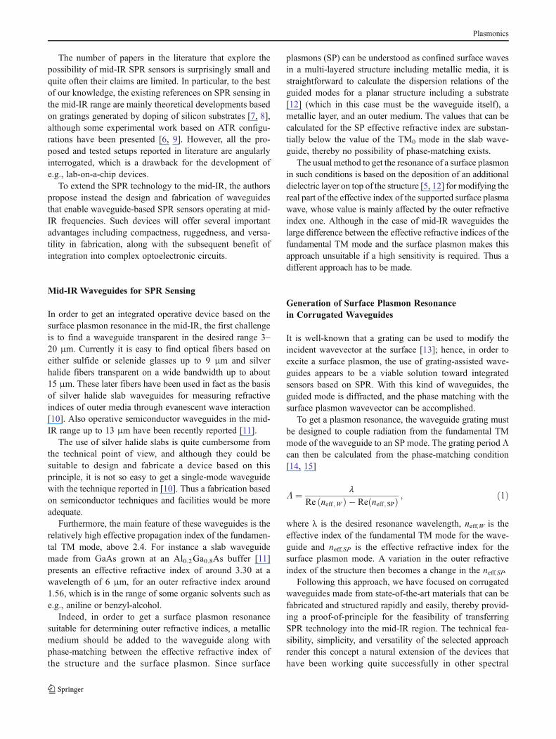
Following the procedure depicted above, it is quite easyto obtain the starting parameters for designing a corrugatedwaveguide based on a GaAs slab 10 μm height for SPRaround 6 μm wavelength. For a waveguide such as thedepicted, the effective index of the fundamental modeTM0 turn out to be like the shown in Fig. 2a in the rangebetween 5.9 and 6.5 μm. In this range, a planar slab withGaAs as substrate, a gold layer 15 nm thick and an outermedium with refractive index of 1.56, gives a real part of theeffective refractive index for the SP like the plotted inFig. 2b. As can be seen, these values are far apart one fromthe other so as to directly fulfill the phase-matching condi-tion. However, with both set of values, it is straightforwardto calculate the grating pitch needed to obtain a SPR arounda wavelength of 6 μm. This calculation renders a value ofabout 3.5 μm for the corrugation period.
Then, if one considers a corrugated waveguide such asthe one depicted in Fig. 1, with the calculated period of3.5 μm, 10 μm height and 5 mm length, and a gold layer of15 nm thickness deposited on top of the corrugated surface,an optimized value of #L05π/2 is obtainable from a corru-gation height of approximately 10 nm. The transmittance forthis structure, obtained from Eq. (1), for a range of outerrefractive indices between 1.54 and 1.57 is shown in Fig. 3a.Evidently, FOM is high enough to perform an accurateidentification of the resonance wavelength, for which thetransmittance is a minimum.
The slope of the curve obtained by tracking the displacementof the SPR wavelengths with the outer refractive index varia-tion (the commonly utilized analytical parameter evaluated in
waveguide (GaAs)
outer medium gold layer
d h!
h
z y
x"
Fig. 1 Scheme of the proposeddevice, consisting of acorrugated waveguide of GaAswith an Au layer deposited ontoit
Plasmonics

SPR sensors) gives an estimation of the potential device sensi-tivity, which is approximately !3,500 nm/RIU, as shown inFig. 3b. This value is comparable with those obtained with SPRdevices reported in literature operating in the NIR.
We have chosen to study the feasibility of SPR around6μmbecause the advances in technology havemade available
the required elements in terms of light sources (quantumcascade lasers, QCLs) and waveguides, so an experimentalverification of these calculations can be relatively easyand fast. Of course this analysis may easily be extendedto other interesting region inside the MIR where QCLsor CO2 lasers can be also used as sources. In that case, a
5.9 6 6.1 6.2 6.3 6.4 6.53.3
3.301
3.302
3.303
3.304
3.305
3.306
3.307
3.308
3.309
3.31
# (µm)
n eff
TM
5.9 6 6.1 6.2 6.3 6.4 6.5
1.5646
1.5647
1.5648
1.5649
1.565
1.5651
1.5652
1.5653
1.5654
1.5655
# (µm)
Re
(nef
fSP
)
a
b
Fig. 2 a Effective index of the fundamental TM0 supported mode by aGaAs slab 10 μm thick on an Al0.2Ga0.8As buffer and a cover with arefractive index of 1.560. b Real part of the effective index of the
supported mode by a multilayer structure GaAs-Au(15 nm)-outer me-dium (nout01.560)
Plasmonics
new selection of materials and a new calculation of theparameters would be needed, but the method depicted
here is fairly general and the modifications would bestraightforward.
6 6.02 6.04 6.06 6.08 6.1 6.12 6.14 6.16 6.18 6.2-30
-25
-20
-15
-10
-5
0
# (µm)
Tra
nsm
ittan
ce (d
B)
a
b
1.535 1.54 1.545 1.55 1.555 1.56 1.565 1.57 1.575 1.586.02
6.04
6.06
6.08
6.1
6.12
6.14
6.16
nouter medium
# SPR
Fig. 3 a Transmittance of the proposed device. From left to right, thevalues of outer refractive index are 1.57, 1.56, 1.55, and 1.54 respec-tively. b Displacement of the plasmon resonance wavelengths with the
variations of the refractive index of the outer medium. The estimatedsensitivity of the device is around !3,500 nm/RIU in the range of outerrefractive indices 1.54–1.57
Plasmonics
Conclusions
In this work, the concepts linked to generation of surfaceplasmons and their application to refractive index measure-ments have been extended to an unusual spectral range such isthe mid-infrared. The expected sensitivity is in the samemagnitude order than the currently available SPR transducersbased on waveguides. Thus, the procedure for developingoperative integrated SPR sensors based on semiconductortechnologies has been stated.
The availability of advanced light sources such as quan-tum cascade lasers emitting at 6 μm renders this approacheasy to implement. Furthermore, the proposed deviceparameters may readily be adapted for response at manyother wavelengths within the mid-IR spectral band providedthat appropriate light sources and detectors are available.With the proposed concept, the advantages of SPR-basedspectroscopy and sensing can be transferred to the probablymost relevant spectral regime in chemical and biologicalanalysis facilitating novel diagnostic platforms with appli-cations ranging from environmental monitoring to biomed-ical diagnostics and label-free assay technology. Given thatthe proposed technique takes advantage of conventionalmicrofabrication techniques, a wide range of sensing plat-forms with unsurpassed versatility, operativity, compact-ness, and sensitivity may be anticipated.
Acknowledgments This work has been partially supported withSpanish Research Ministry Project SPRINT, ref. CTQ2009-10550, byCommunity of Madrid project FACTOTEM II (reference S2009/ESP-1781) and by the European Social Fund and the European Fund forRegional Development.
References
1. Homola J (2008) Surface plasmon resonance sensors for detectionof chemical and biological species. Chem Rev 108:462–493
2. Leong HS, Guo J, Lindquist RG, Liu QH (2009) Surface plasmonresonance in nanostructured metal films under the Kretschmannconfiguration. J Appl Phys 106:124314
3. Sutapun B, Sombookaew A, Amrit R, Houngkamhang N, SrikhirinT (2011) A multichannel surface plasmon resonance sensor using anew spectral readout system without moving optics. Sens Act B156:312
4. Bueno FJ, Esteban Ó, Díaz-Herrera N, Navarrete MC, González-Cano A (2004) Sensing properties of asymmetric double-layercovered tapered fibers. Appl Opt 43:1615–1620
5. Díaz-Herrera N, González-Cano A, Viegas D, Santos JL, NavarreteMC (2010) Refractive index sensing of aqueous media based onplasmonic resonance in tapered optical fibres operating in the 1.5 μmregion. Sens and Act B 146:195–198
6. Neuner B III, Korobkin D, Fietz C, Carole D, Ferro G, Shvets G(2010) Mid-infrared index sensing of pL-scale analytes based onsurface phonon polaritons in silicon carbide. J Phys Chem C114:7489–7491
7. Yu-Bin Chen (2009) Development of mid-infrared surface plas-mon resonance-based sensors with highly-doped silicon for bio-medical and chemical applications. Opt Expr 17:3130–3140
8. DiPippo W, Lee BJ, Park K (2010) Design analysis of doped-silicon surface plasmon resonance immunosensors in mid-infrared range. Opt Expr 18:19396–19406
9. Herminjard S, Sirigu L, Herzig HP, Studemann E, Crottini A,Pellaux JP, Gresch T, Fischer M, Faist J (2009) Surface plasmonresonance sensor showing enhanced sensitivity for CO2 detectionin the mid-infrared range. Opt Expr 17:293–303
10. Charlton C, Katzir A, Mizaikoff B (2005) Infrared evanescent fieldsensing with quantum cascade lasers and planar silver halide wave-guides. Anal Chem 77:4398–4403
11. Charlton C, Giovannini M, Faist J, Mizaikoff B (2006) Fabricationand characterization of molecular beam epitaxy grown thin-filmCaAs waveguides for mid-infrared evanescent field chemical sens-ing. Anal Chem 78:4224
12. Esteban Ó, Navarrete MC, González-Cano A, Bernabéu E (2000)Simple model of compound waveguide structures used as fiber-optic sensors. Optics and Laser in Engineering 33:219–230
13. H. Raether, Surface Plasmons on Smooth and Rough Surfaces andon Gratings, Springer Tracts in Modern Physics vol. 111, Springer,Berlin, 1988.
14. Liu Q, Chiang KS, Rastogi V (2003) Analysis of corrugated long-period gratings in slab waveguides and their polarization depen-dence. IEEE J Light Technol 21:3399–3405
15. Liu Q, Chiang KS (2009) Refractive-index sensor based on long-range surface plasmon mode excitation with long period wave-guide grating. Opt Exp 17:7933–7942
16. Estéban Ó, González-Cano A, Díaz-Herrera N, Navarrete MC(2006) Absorption as a selective mechanism in surface plasmonresonance fiber optic sensors. Optics Letters 31:3089–3091
17. Hardy A (1984) Exact derivation of the coupling coefficient incorrugated waveguides with rectangular tooth shape. IEEE J QuantElect QE-20:1132–1139
Plasmonics