grating-coupled surface plasmons for
TRANSCRIPT

GRATING-COUPLED SURFACE PLASMONSFOR ENHANCED TERAHERTZ EMISSION
Proefschrift
ter verkrijging van de graad van doctoraan de Technische Universiteit Delft,
op gezag van de Rector Magnificus prof. ir. K. C. A. M. Luyben,voorzitter van het College voor Promoties,
in het openbaar te verdedigen op dinsdag 1 april 2014 om 12.30 uur
door
Gopika Ramanandan KOTTAYI PILAPPARA
Master of Science in PhotonicsCochin University of Science and Technology, Cochin, India
geboren te Kozhikode, India
Dit proefschrift is goedgekeurd door de promotor:prof. dr. P. C. M. Planken
Samenstelling promotiecommissie:
Rector Magnificus, voorzitterprof. dr. P. C. M. Planken, Technische Universiteit Delft, promotorprof. dr. L. Kuipers, Universiteit Twenteprof. dr. P. U. Jepsen, Technical University of Denmarkprof. dr. H. P. Urbach, Technische Universiteit Delftprof. dr. A. Neto, Technische Universiteit DelftDr. A. J. L. Adam, Technische Universiteit DelftDr. J. Caro, Technische Universiteit Delft
This work was funded by the Nederlandse Organisatie voorWetenschappelijk Onderzoek (NWO) and the Stichting voor TechnischeWetenschappen (STW)
Copyright c© 2014 by G. R. Kottayi Pilappara
All rights reserved. No part of this publication may be reproduced, storedin a retrieval system or transmitted in any form or by any means:electronic, mechanical, photocopying, recording or otherwise, withoutprior written permission of the author.
ISBN 978-94-6259-120-2
Printed in the Netherlands by Ipskamp Drukkers, Enschede.
A free electronic version of this thesis can be downloaded from:http://repository.tudelft.nl
Author email: [email protected]

To my parents.

Cover photo credit:Parvathi Ramanandan
Grating-coupled surface plasmons for enhanced
terahertz emission
Summary
The colors we see around us correspond to light of various wavelengths. Oureye is sensitive only to a small range of wavelengths which ‘light’ consistsof. Other kinds of ‘invisible’ light are also well known to people, like x-rays,which are used for imaging bones; micro-waves which heat up our food inthe kitchen, and radio waves which are used for wireless information trans-mission. Terahertz radiation is similarly a kind of light which is invisibleto our eyes. Its wavelengths lie in between that of the infrared and the mi-crowave region of the electromagnetic spectrum. Terahertz radiation canpass through a lot of materials like wood, paper, clothing, plastic etc. Manychemicals and biomolecules also have a signature absorption at terahertzfrequencies, which makes this light highly suitable for spectroscopy. Theseinteresting properties have lured people to think of several applications, likesecurity imaging, drug identification, etc., using terahertz radiation.
However, there are several aspects of terahertz technology, which could beimproved to suit these applications better. One of those is terahertz radi-ation sources. While thinking of a suitable source for terahertz radiation,one considers several aspects like the strength of the radiation emitted,the spectrum of the light emitted and also the cost factor. Consideringthe growth of on-chip optical sensors, it’s likely that the future terahertztechnology will incorporate miniaturized terahertz sources. One kind ofterahertz source, which has been studied in this thesis, is a junction formedbetween a thin gold film and a thin cuprous oxide film. Cuprous oxideis an oxide of the most abundant metal in nature, copper. When ultra-fast pulses of infrared light fall on such junctions between cuprous oxideand gold, pulses of terahertz radiation are emitted. The radiation fromthese emitters is broadband in nature and is sufficiently strong to performspectroscopy with. In this thesis, we have studied the properties of theseemitters, and investigated a technique to increase the strength of the tera-hertz emission from these emitters by nano-structuring them, allowing usto excite surface plasmons. The important aspects of the research described
v
vi
in this thesis are outlined below.
To form the cuprous oxide thin film, we have heated Cu thin films at el-evated temperatures in the ambient atmosphere of the lab. This is animportant step, since we wanted the copper film to completely oxidize intocuprous oxide, but wanted to avoid the formation of cupric oxide. Thismade us think about a method to characterize the oxidation of copper thinfilms. In fact we have shown that terahertz radiation itself could be usedto study the oxidation kinetics of thin films of copper, deposited on siliconsubstrates. By using a terahertz time-domain spectroscopy setup, we stud-ied in-situ the oxidation of Cu thin films. While trying to calibrate thetransmission of terahertz radiation through thin copper films deposited byevaporation techniques, we also found that percolation causes the terahertz-optical properties of these thin films to differ from that of bulk metal. Infact, thin films of metals like copper start to act as a metal only after de-positing a minimum thickness, which is known as the percolation thresholdthickness.
A logical explanation for the terahertz emission from gold-cuprous oxidejunctions requires them to behave as a diode. However, scientific literatureseems to suggest that junctions formed by depositing gold on cuprous ox-ide do not show characteristics of a diode. Through a part of the researchcarried out in this thesis, we show that heating copper on gold to form junc-tions with cuprous oxide, results in the inter-diffusion of gold and copperresulting in the formation of an alloy of these metals at the interface. Ourmeasurements suggest that this alloy forms a junction with cuprous oxide,which has diode-like behavior. We have studied the optical properties ofthis alloy, through techniques like ellipsometry, x-ray diffraction etc.
A considerable portion of this research is dedicated to the enhancement ofterahertz radiation emitted from metal/semiconductor junctions using sur-face plasmons. Vaguely resembling waves on the surface of water, surfaceplasmons are waves of electrons at the interface between a metal and adielectric. Surface plasmons have a very interesting property that their en-ergy is confined/localized to the interface. Excitation of surface plasmonsincreases the amount of pump laser light absorbed by the gold-cuprous ox-ide thin films, resulting in enhanced terahertz emission. To excite surfaceplasmons, we fabricated gold nano-gratings and then deposited cuprousoxide over it. We have shown that the important factor for enhanced ter-ahertz emission is to increase the absorption at a region where it mattersthe most for terahertz generation, which is the semiconductor region closeto the metal/semiconductor interface.

vii
Plasmon excitation can also result in terahertz emission from gold gratingswithout any extra-material deposited over it. We show that we can generateterahertz radiation from gold gratings, after the excitation of surface plas-mons. The mechanism by which terahertz radiation is generated from goldthin films has been a matter of debate, with several explanations found inthe literature. An important indicator of the terahertz emission mechanismis the dependence of the emitted terahertz radiation on the incident pumppower. The emitted terahertz power shows a second-order dependence onthe incident pump laser power, which is in contradiction with the higherorder pump-power dependence observed by other groups using similar grat-ings. We have explored the different possible mechanisms by also measuringthe azimuthal-angle dependence and by measuring the polarization of theterahertz radiation emitted from these gratings. An interesting aspect ofour study is that it hints at the possibility of a new generation mechanism,transient photon-drag currents, and could lead us to interesting revelationson the terahertz generation from metal surfaces in general.
In summary, we have studied the characteristics of metal/semiconductorthin film terahertz emitters formed using gold and cuprous oxide. Wehave explored the use of gratings for coupling surface plasmons and thusenhancing the strength of terahertz emitters made of metal/semiconductorthin films. This concept has also been extended to enhancing the terahertzemission from pure gold thin films to study a possibly new THz generationmechanism.
Gopika Ramanandan Kottayi Pilappara, March 2014

Traliegekoppelde oppervlakteplasmonen voor ver-
sterkte terahertz emissie
Samenvatting
De kleuren die we om ons heen zien corresponderen met licht van verschil-lende golflengtes. Ons oog is alleen gevoelig voor een smalle golflengtebandwaar licht uit bestaat. Andere vormen van onzichtbaar licht zijn ook be-kend: rontgen straling, gebruikt om botten af te beelden, microgolven omons eten op te warmen in de keuken, en ook radio golven die gebruiktworden voor informatie overdracht. Terahertz straling is een vergelijkbarevorm van licht die onzichtbaar is voor onze ogen. De golflengtes liggentussen dat van infrarood en microgolf straling in. Terahertz straling kanzich voortplanten door veel materialen, zoals hout, papier, kleren, plasticetc. Veel chemicalien en biomoleculen hebben absorptielijnen op terahertzfrequenties, wat terahertz licht geschikt maakt voor spectroscopie. Dezeinteressante eigenschappen hebben mensen laten denken aan verschillendetoepassingen, zoals veiligheidscameras, identificatie van medicijnen, etc.,voor het gebruik van terahertz straling.
Echter, er zijn verschillende aspecten van terahertz technologie die verbe-terd kunnen worden voor genoemde toepassingen. Een van deze is de bronvan terahertz straling. Wanneer er gedacht wordt aan een geschikte bronvan terahertz straling wordt naar verschillende aspecten gekeken, zoals deintensiteit, het spectrum en de kosten. Gezien de groei van on-chip optischesensoren is het waarschijnlijk dat toekomstige terahertz technologie gebruikgaat maken van geminiaturiseerde terahertz bronnen. Een soort terahertzbron die onderzocht is in dit proefschrift is een junctie gevormd tusseneen dunne goud laag en een dunne koper(I)oxide laag. Koper(I)oxide iseen oxide van het meest voorkomende metaal in de natuur, namelijk koper.Wanneer een femtoseconde puls van infrarood licht zon junctie van koper-oxide en goud belicht, wordt er een puls van terahertz straling uitgezonden.De straling van deze emitters is breedbandig en is sterk genoeg om te ge-bruiken voor spectroscopie. In dit proefschrift zijn de eigenschappen vandeze emitters bestudeerd en er is een techniek onderzocht om de sterktevan terahertz emissie te vergroten door het gebruik van nanostructuren,
ix

x
die de excitatie van oppervlakteplasmonen mogelijk maakt. De hoofdlijnenvan het onderzoek, zoals beschreven in het proefschrift, worden hierondergeschetst.
Om de dunne laag koperoxide te vormen wordt een dunne laag koper verhitin de lucht. Dit is een belangrijke stap omdat we de koperlaag helemaal wil-len omzetten in koper(I)oxide, terwijl de vorming van koper(I)oxide moetworden voorkomen. Dit heeft ons laten nadenken over een methode omde oxidatie van de koperoxide laag te karakteriseren. We laten zien datterahertz straling zelf gebruikt kan gebruikt worden om de oxidatiekineticavan dunne lagen koper, gedeponeerd op silicium substraten, te bestuderen.Door het gebruik van een terahertz tijd-domein spectroscopie opstelling,hebben we in-situ de oxidatiekinetica van dunne koperlagen bestudeerd.Toen we probeerden om de transmissie van terahertz straling door dunnelagen koper, gedeponeerd door het gebruik van verschillende opdamptech-nieken, te kalibreren, hebben we ook gevonden dat percolatie er voor zorgtdat de terahertz-optische eigenschappen van deze dunne oppervlakken ver-schilt van dat van bulkmetaal. Dunne oppervlakken van metalen zoals ko-per gedragen zich alleen als metaal indien er een bepaalde minimumdiktegedeponeerd wordt, bekend onder de term percolatiedrempeldikte.
Een logische verklaring voor de terahertz emissie van goud-koper(I)oxidejuncties is dat deze zich als diodes gedragen. Echter, wetenschappelijkeliteratuur lijkt te suggereren dat juncties die gevormd worden door deposi-tie van goud op koper(I)oxide niet te karakteriseren zijn als een diode. Ineen gedeelte van het onderzoek uitgevoerd in dit proefschrift laten we ziendat het verwarmen van koper op goud om juncties met koper(I)oxide tevormen, resulteert in de inter-diffusie van goud en koper resulterend in devorming van een legering van deze metalen bij het raakvlak. Onze metin-gen suggereren dat deze legering een junctie vormt met koper(I)oxide, diezich als een diode-achtige overgang gedraagt. We hebben de optische ei-genschappen van deze legering bestudeerd met technieken als ellipsometrie,rontgendiffractie etc.
Een aanzienlijk gedeelte van dit onderzoek is gewijd aan de versterkingvan terahertz straling, geemitteerd van metaal-halfgeleider juncties, doorhet gebruik van oppervlakteplasmonen. Oppervlakteplasmonen zijn gol-ven van elektronen op het grensvlak van een metaal en een dielektrischmateriaal. Deze golven hebben heel vaag wel iets weg van watergolven.Oppervlakteplasmonen hebben de interessante eigenschap dat hun energiebeperkt/gelokaliseerd is tot dichtbij het raakvlak. Excitatie van oppervlak-teplasmonen verhoogt de hoeveelheid geabsorbeerd pomp licht bij de goud-
xi
koper(I)oxide dunne lagen, resulterend in verhoogde terahertz emissie. Omoppervlakteplasmonen te exciteren hebben we gouden nanotralies gefabri-ceerd en daar koper(I)oxide op gedeponeerd. We hebben aangetoond dat debelangrijkste factor voor de versterkte emissie de verhoogde absorptie vlakbij het metaal/halfgeleider raakvlaak is, het gebeid dat het belangrijkste isvoor de terahertz generatie.
Plasmon excitatie kan ook resulteren in terahertz emissie van goudtralieszonder dat daar een ander materiaal op is gedeponeerd. We laten zien datwe terahertz straling kunnen genereren van goudtralies, na excitatie vanoppervlakteplasmonen. Het mechanisme waardoor terahertz straling wordtgegenereerd bij dunne goudoppervlaktes staat ter discussie, en er kunnerverschillende verklaringen in de literatuur worden gevonden. Een belang-rijke indicatie van het terahertzemissiemechanisme is de afhankelijkheid vanterahertz emissie van het invallende laser pompvermogen. De geemitteerdeterahertz straling heeft een kwadratische afhankelijkheid van het invallendelaser pompvermogen, wat tegenstrijdig is met de hogere-orde afhankelijk-heid gemeten door andere groepen met vergelijkbare tralies. We hebbenverschillende mechanismes onderzocht door ook de azimuthale hoekafhanke-lijkheid te meten en ook door de polarisatie van het geemitteerde terahertzlicht te meten. Een interessant aspect van onze studie is dat we hintshebben gevonden van de mogelijkheid van een nieuw excitatie mechanisme,photon-drag stromen, wat zou kunnen leiden naar interessante verklaringenvoor terahertz generatie van metalen.
Samenvattend, hebben we de karakteristieken bestudeerd van metaal/halfgeleider dunne laag terahertz emitters gevormd door het gebruik vangoud en koper(I)oxide. We hebben het gebruik van tralies om oppervlak-teplasmonen te genereren om aldus terahertz emitters, gemaakt van dunnelagen metaal/halfgeleider, te versterken onderzocht. Dit concept is ook uit-gebreid naar de versterkte terahertz emissie van pure dunne lagen goud omeen mogelijk nieuw terahertzgeneratiemechanisme te onderzoeken.
Gopika Ramanandan Kottayi Pilappara, March 2014

Contents
Summary v
Samenvatting ix
Contents xiii
1 Introduction 1
1.1 Introduction to THz radiation . . . . . . . . . . . . . . . . . 11.2 Applications of THz radiation . . . . . . . . . . . . . . . . . 31.3 THz generation using femtosecond laser pulses . . . . . . . 4
1.3.1 Photo-conducting antenna . . . . . . . . . . . . . . . 41.3.2 Optical rectification . . . . . . . . . . . . . . . . . . 51.3.3 Current surge on semiconductor surfaces . . . . . . . 6
1.4 Plasmonics . . . . . . . . . . . . . . . . . . . . . . . . . . . 71.5 This thesis . . . . . . . . . . . . . . . . . . . . . . . . . . . . 9
2 Plasmon facilitated THz emission from gold gratings 11
2.1 Introduction to plasmonics . . . . . . . . . . . . . . . . . . 112.1.1 Dispersion relation of surface plasmons . . . . . . . . 122.1.2 Properties of surface plasmons . . . . . . . . . . . . 13
2.2 Grating coupling of surface plasmons . . . . . . . . . . . . . 152.2.1 Plasmon excitation with a metal grating for non-zero
azimuthal angles . . . . . . . . . . . . . . . . . . . . 182.3 THz emission from gold thin films - a literature survey . . . 19
2.3.1 Optical rectification . . . . . . . . . . . . . . . . . . 192.3.2 Multiphoton excitation . . . . . . . . . . . . . . . . 202.3.3 Other mechanisms . . . . . . . . . . . . . . . . . . . 22
2.4 THz emission from gold gratings . . . . . . . . . . . . . . . 232.4.1 Azimuthal-angle dependence . . . . . . . . . . . . . 26
2.5 Etch depth dependence . . . . . . . . . . . . . . . . . . . . 272.6 Discussion . . . . . . . . . . . . . . . . . . . . . . . . . . . . 29
xiii
xiv
3 Oxidation kinetics of Cu thin films 33
3.1 Introduction . . . . . . . . . . . . . . . . . . . . . . . . . . . 33
3.2 THz transmission through oxidizing Cu thin films . . . . . . 34
3.2.1 Experiment . . . . . . . . . . . . . . . . . . . . . . . 35
3.2.2 Results . . . . . . . . . . . . . . . . . . . . . . . . . 36
3.3 Thickness-dependent THz transmission . . . . . . . . . . . . 39
3.3.1 Percolation . . . . . . . . . . . . . . . . . . . . . . . 41
3.3.2 Calibration of THz transmission . . . . . . . . . . . 42
3.4 Oxidation kinetics and Arrhenius equation . . . . . . . . . . 43
4 THz emission from Cuprous oxide thin films 47
4.1 Introduction . . . . . . . . . . . . . . . . . . . . . . . . . . . 47
4.2 Metal-Semiconductor (Schottky) junctions . . . . . . . . . . 48
4.3 Cuprous oxide as a semiconductor . . . . . . . . . . . . . . 51
4.4 THz generation from Au/Cu2O thin films . . . . . . . . . . 53
4.4.1 Sample preparation . . . . . . . . . . . . . . . . . . 53
4.4.2 Experimental set-up and results . . . . . . . . . . . 53
4.5 Interface between gold and thermally formed Cu2O . . . . . 56
4.6 Variable-Angle Spectroscopic Ellipsometry . . . . . . . . . . 59
4.7 Thickness dependence of pump power absorption and THzemission . . . . . . . . . . . . . . . . . . . . . . . . . . . . . 62
4.8 Multilayer reflection: Calculation and experiment . . . . . . 64
4.9 Application: Tapered waveguide . . . . . . . . . . . . . . . 66
5 Plasmon-enhanced THz emission from Schottky junctions 71
5.1 Introduction . . . . . . . . . . . . . . . . . . . . . . . . . . . 71
5.2 The concept of a plasmon-enhanced Schottky emitter . . . . 72
5.2.1 Plasmon excitation at the Au/Cu2O interface . . . . 73
5.3 Sample fabrication and characterization . . . . . . . . . . . 75
5.4 Experimental Setup . . . . . . . . . . . . . . . . . . . . . . 78
5.5 Plasmon-enhanced THz emission . . . . . . . . . . . . . . . 79
5.6 Reflection spectroscopy measurements . . . . . . . . . . . . 83
5.6.1 p-polarized incident light . . . . . . . . . . . . . . . 86
5.6.2 s-polarized incident light . . . . . . . . . . . . . . . . 90
5.7 THz emission as a function of the grating periodicity . . . . 94
5.8 Azimuthal angle dependence . . . . . . . . . . . . . . . . . . 99
5.8.1 Enhanced THz emission: significance of exciting plas-mon modes . . . . . . . . . . . . . . . . . . . . . . . 99
5.8.2 Reflection spectra vs azimuthal angle . . . . . . . . 101
5.8.3 Near-field analysis . . . . . . . . . . . . . . . . . . . 104
5.9 Conclusion . . . . . . . . . . . . . . . . . . . . . . . . . . . 106

xv
6 Conclusions and Outlook 111

xvi
A Surface plasmon dispersion relation on a planar interface 115
Bibliography 118
Acknowledgements 133
About the Author 137

Chapter
1Introduction
1.1 Introduction to THz radiation
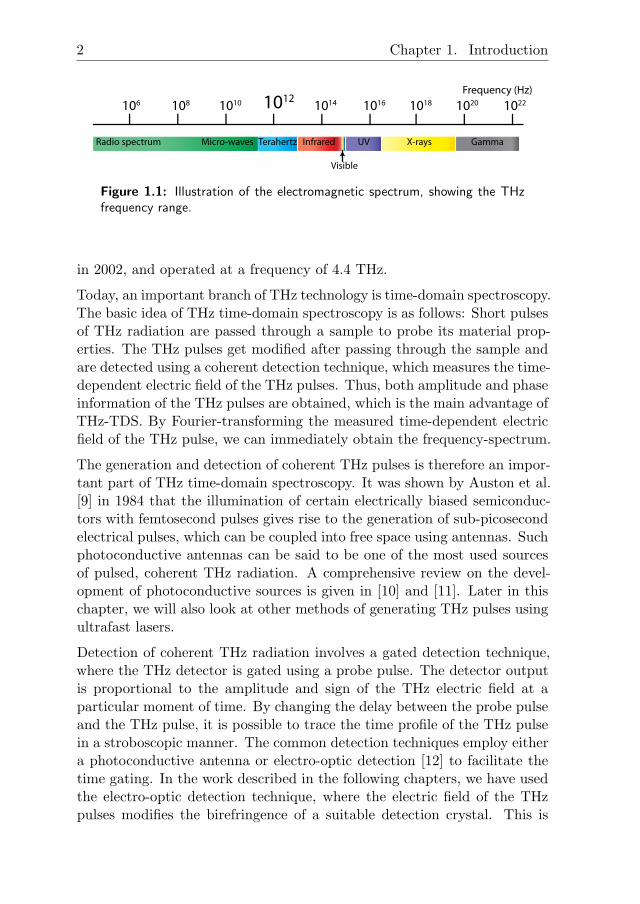
Terahertz radiation (THz) is the name used for electromagnetic radiationin a region of the electromagnetic spectrum which is positioned in-betweenthe microwave and the infrared domains. The THz range includes frequen-cies from 0.1-10 THz. To get an idea of the wavelengths involved, 1 THzcorresponds to a wavelength of 300 µm, a wavenumber of 33 cm−1, and aphoton energy of 4.14 meV.
Historically the THz frequency range has been known as the THz gap, dueto the lack of availability of suitable sources, detectors and other technolo-gies compared to that in the electronic and photonic domains. This locationof THz radiation in the electromagnetic spectrum has also given it a mul-tidisciplinary character, and attempts to fill the THz gap have come fromboth the optical and the electronic domains.
A good overview of the development of various THz sources can be foundin the articles [1, 2, 3]. The developments from the electronic side includeelectron-beam backward wave oscillators and recombination diode lasers,operating at sub-mm wavelengths [4]. High frequency Gunn and IMPATTdiodes have been demonstrated to work quite well for frequencies in thesub-THz range [5].
From the optics side, gas lasers were developed in the 1960s due to a desireto have coherent sources of far infrared radiation. Stimulated emission offar infrared wavelengths between 23 µm and 79 µm was demonstrated byCrocker et al. [6] in 1964 using pulsed electrical discharges in water vapor.An important recent development regarding continuous wave THz sources,is the invention of the quantum cascade laser (QCL) by Faist et al. [7] in1994. The first QCL in the THz range was fabricated by Kohler et al. [8]
1
2 Chapter 1. Introduction
106 108 1010 10121014 1016 1018 1020 1022
Radio spectrum Terahertz Infrared UV X-rays Gamma
Visible
Frequency (Hz)
Micro-waves
Figure 1.1: Illustration of the electromagnetic spectrum, showing the THzfrequency range.
in 2002, and operated at a frequency of 4.4 THz.
Today, an important branch of THz technology is time-domain spectroscopy.The basic idea of THz time-domain spectroscopy is as follows: Short pulsesof THz radiation are passed through a sample to probe its material prop-erties. The THz pulses get modified after passing through the sample andare detected using a coherent detection technique, which measures the time-dependent electric field of the THz pulses. Thus, both amplitude and phaseinformation of the THz pulses are obtained, which is the main advantage ofTHz-TDS. By Fourier-transforming the measured time-dependent electricfield of the THz pulse, we can immediately obtain the frequency-spectrum.
The generation and detection of coherent THz pulses is therefore an impor-tant part of THz time-domain spectroscopy. It was shown by Auston et al.[9] in 1984 that the illumination of certain electrically biased semiconduc-tors with femtosecond pulses gives rise to the generation of sub-picosecondelectrical pulses, which can be coupled into free space using antennas. Suchphotoconductive antennas can be said to be one of the most used sourcesof pulsed, coherent THz radiation. A comprehensive review on the devel-opment of photoconductive sources is given in [10] and [11]. Later in thischapter, we will also look at other methods of generating THz pulses usingultrafast lasers.
Detection of coherent THz radiation involves a gated detection technique,where the THz detector is gated using a probe pulse. The detector outputis proportional to the amplitude and sign of the THz electric field at aparticular moment of time. By changing the delay between the probe pulseand the THz pulse, it is possible to trace the time profile of the THz pulsein a stroboscopic manner. The common detection techniques employ eithera photoconductive antenna or electro-optic detection [12] to facilitate thetime gating. In the work described in the following chapters, we have usedthe electro-optic detection technique, where the electric field of the THzpulses modifies the birefringence of a suitable detection crystal. This is

1.2. Applications of THz radiation 3
measured as a change in the polarization state of the probe pulse. A THztime-domain spectroscopy system used for the study of oxidation of Cu thinfilms, is described in section 3.2.1.
1.2 Applications of THz radiation
Perhaps the most important feature of THz radiation is that it can bepartially transmitted by a number of materials, such as paper, cloth, leather,polymers, etc, which are opaque to visible light. This unique property ofTHz radiation, to look through materials, makes it suitable for applicationsin security and screening [13, 14], quality analysis [15] etc.
Another important aspect is that various crystalline vibrations and molec-ular rotational transitions of various materials and gases also lie in thisfrequency range. THz spectroscopy has become an important tool to un-derstand the interaction of biomolecular systems with water[16]. Anotherapplication of THz technology is the identification of materials using theirspectral signature in this frequency range. Kawase et al. [17] demonstrateda technique to identify drugs concealed in envelopes using terahertz imag-ing. THz spectroscopy can also differentiate between the polymorphs ofthe same material. For example, Chakkittakandy et al. [18] demonstratedthat THz spectroscopy can identify the different polymorphs of mannitol,a product used in the pharmaceutical industry. More pharmaceutical ap-plications of THz spectroscopy can be found in Refs. [15, 19].
Applications of THz imaging in the biomedical sciences, although still thesubject of discussion, should be mentioned as well. A good review of thistopic is provided by Pickwell andWallace [20], discussing applications whichrange from spectroscopy of crystalline drugs to imaging of skin cancer.
THz imaging has become a valuable tool for art historians, due to its capa-bility to see through the various layers in a painting [21], and to determinethe properties of the paint used by the artist [22].
A major hurdle for imaging with THz radiation is it’s large wavelength,which limits the resolution which can be achieved. This is a direct con-sequence of the laws of diffraction, which imply that with a conventionalmicroscope, its not possible to see “sharper” than about half of a wave-length. For THz light with a wavelength of 300 µm, this means that thesharpest features that can be observed would be about 150 µm. The con-cept of near-field scanning optical microscopy using apertures was used toovercome the diffraction limit and to image with sub-wavelength spatial res-

4 Chapter 1. Introduction
olution [23, 24]. In 2002, van der Valk and Planken [25] demonstrated anapertureless method to obtain sub-wavelength resolution in THz imagingby using a sharp copper tip and selective detection of THz light near thetip through electro-optic detection. A number of applications for THz nearfield imaging has come up, primarily in understanding and exploring thelaws of physics, which would be more difficult to do with visible light[26, 27].High resolution THz near-field imaging has been used as an effective toolto map mobile carriers in semiconductor nanodevices [28].
1.3 THz generation using femtosecond laserpulses
1.3.1 Photo-conducting antenna
In a photoconducting antenna, THz pulses are created by the acceleration ofphoto-excited charge carriers in a semiconductor in an electric field appliedby biasing two electrodes on the surface of the semiconductor. A pair ofmetal electrodes is deposited on a semiconductor, as shown in Fig. 1.2.A DC bias is applied between the electrodes. Laser pulses, with photonshaving an energy greater than the band-gap energy of the semiconductingmaterial, are focussed onto the area in between the electrodes, generatingelectron-hole pairs. These free charge carriers are accelerated by the DCelectric field and simultaneously decay due to recombination. The impulsecurrent generated due to this acceleration of the charge carriers, radiatespulses of THz electromagnetic waves [11].
The radiated electric field ETHz is proportional to the rate of change of theinduced current J(t) [29]:
ETHz ∝∂J(t)
∂t. (1.1)
The photo current density j(t) can be described as a convolution of theoptical intensity profile of the pulse incident on the sample I(t), and theimpulse response of the photoconductive antenna, n(t)qv(t), where n(t) isthe density, q is the electronic charge, and v(t) is the velocity of the chargecarriers:
j(t) ∝∫
I(t− t′)[n(t′)qv(t)]dt′. (1.2)

1.3. THz generation using femtosecond laser pulses 5
V
Electrodes
Figure 1.2: The basic idea of a photoconductive THz emitter. The chargecarriers generated by the laser pulses incident on the semiconductor, are accel-erated by the external applied DC field. This transient current radiates THzpulses.
The THz radiation properties like intensity and the bandwidth are deter-mined mainly by the charge carrier lifetime, band-gap energy and resistivityof the material. A model of THz generation based on the Drude-Lorentztheory of a photoconductive antenna can be found in Refs. [30] and [31].
1.3.2 Optical rectification
THz pulses can also be generated by optical rectification of fs laser pulsesin a medium with a strong second-order optical nonlinearity. Opticalrectification of femtosecond pulses can be described using the concept ofdifference-frequency generation, which is a second-order nonlinear-opticalphenomenon. The second-order nonlinear-optical polarization created inthis manner is, in a simplified manner, given by [32]:
P (2)(∆ω) = χ(2)
∫
E(ω1)E∗(ω1 −∆ω)dω1, (1.3)
where χ(2) is the second-order susceptibility assumed to be frequency in-dependent, and both frequencies ω1 and ω1 − ∆ω involved in the processare assumed to come from the same laser pulse. The spectral componentswithin the single femtosecond pulse spectrum are sufficiently apart suchthat the difference frequency of these components is in the THz domain.It can be shown that in the time domain and in the far field[33], the THzelectric field is proportional to the second time derivative of the second-order nonlinear polarization induced by the laser pulse: ETHz ∝ ∂2P
∂t2, with
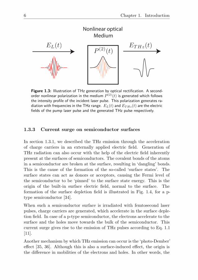
P (t) ∝ I(t), the intensity envelope of the laser pulse. This is illustrated inFig. 1.3.
6 Chapter 1. Introduction
Nonlinear optical
Medium
Figure 1.3: Illustration of THz generation by optical rectification. A second-order nonlinear polarization in the medium P (2)(t) is generated which followsthe intensity profile of the incident laser pulse. This polarization generates ra-diation with frequencies in the THz range. EL(t) and ETHz(t) are the electricfields of the pump laser pulse and the generated THz pulse respectively.
1.3.3 Current surge on semiconductor surfaces
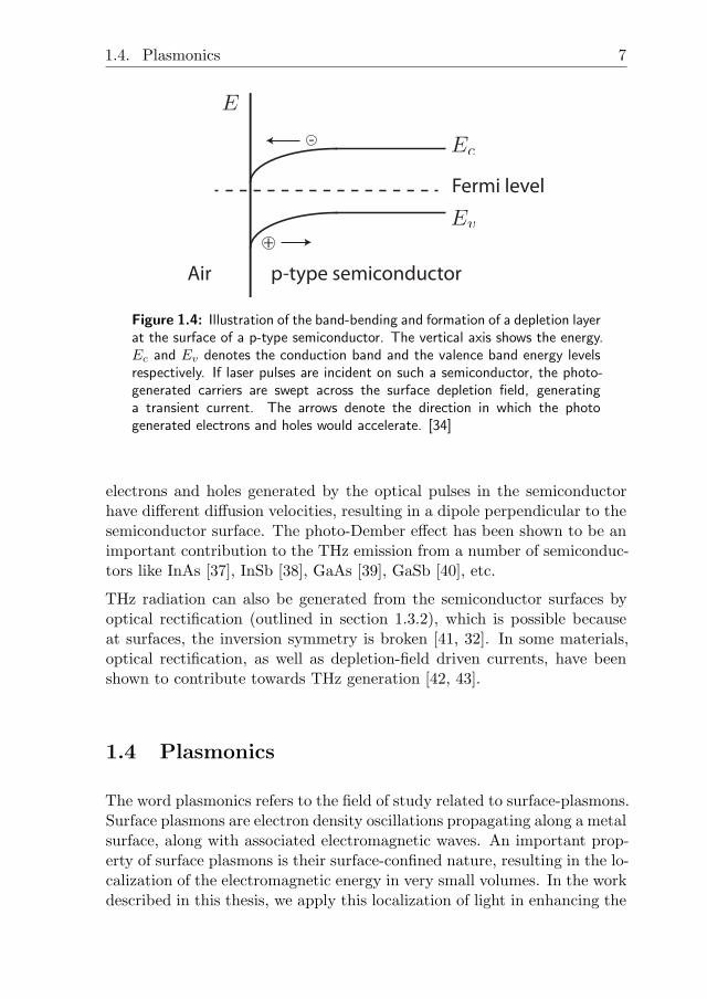
In section 1.3.1, we described the THz emission through the accelerationof charge carriers in an externally applied electric field. Generation ofTHz radiation can also occur with the help of the electric field inherentlypresent at the surfaces of semiconductors. The covalent bonds of the atomsin a semiconductor are broken at the surface, resulting in ‘dangling’ bonds.This is the cause of the formation of the so-called ‘surface states’. Thesurface states can act as donors or acceptors, causing the Fermi level ofthe semiconductor to be ‘pinned’ to the surface state energy. This is theorigin of the built-in surface electric field, normal to the surface. Theformation of the surface depletion field is illustrated in Fig. 1.4, for a p-type semiconductor [34].
When such a semiconductor surface is irradiated with femtosecond laserpulses, charge carriers are generated, which accelerate in the surface deple-tion field. In case of a p-type semiconductor, the electrons accelerate to thesurface and the holes move towards the bulk of the semiconductor. Thiscurrent surge gives rise to the emission of THz pulses according to Eq. 1.1[11].
Another mechanism by which THz emission can occur is the ‘photo-Dember’effect [35, 36]. Although this is also a surface-induced effect, the origin isthe difference in mobilities of the electrons and holes. In other words, the
1.4. Plasmonics 7
Air p-type semiconductor
Fermi level
+
-
Figure 1.4: Illustration of the band-bending and formation of a depletion layerat the surface of a p-type semiconductor. The vertical axis shows the energy.Ec and Ev denotes the conduction band and the valence band energy levelsrespectively. If laser pulses are incident on such a semiconductor, the photo-generated carriers are swept across the surface depletion field, generatinga transient current. The arrows denote the direction in which the photogenerated electrons and holes would accelerate. [34]
electrons and holes generated by the optical pulses in the semiconductorhave different diffusion velocities, resulting in a dipole perpendicular to thesemiconductor surface. The photo-Dember effect has been shown to be animportant contribution to the THz emission from a number of semiconduc-tors like InAs [37], InSb [38], GaAs [39], GaSb [40], etc.
THz radiation can also be generated from the semiconductor surfaces byoptical rectification (outlined in section 1.3.2), which is possible becauseat surfaces, the inversion symmetry is broken [41, 32]. In some materials,optical rectification, as well as depletion-field driven currents, have beenshown to contribute towards THz generation [42, 43].
1.4 Plasmonics
The word plasmonics refers to the field of study related to surface-plasmons.Surface plasmons are electron density oscillations propagating along a metalsurface, along with associated electromagnetic waves. An important prop-erty of surface plasmons is their surface-confined nature, resulting in the lo-calization of the electromagnetic energy in very small volumes. In the workdescribed in this thesis, we apply this localization of light in enhancing the
8 Chapter 1. Introduction
THz emission from metal surfaces (Chapter 2) and metal/semiconductorthin film interfaces (Chapter 5).
The first observation of surface plasmons was made in the year 1902, whenWood [44] reported an anomalous decrease of intensity at certain wave-lengths in the spectrum of light reflected by a metallic grating, although hecould not give an explanation for this phenomenon. He also noted that thesudden decrease in the reflection at certain wavelengths occurred only forp-polarized incident light, when the grating lines were oriented parallel tothe magnetic field of the incident light. Rayleigh noticed that the anoma-lies in the spectrum of light reflected from a metal grating occur at thewavelength for which a scattered wave emerges tangentially to the gratingsurface [45]. He called these orders as “passing-off orders”, to show thatan anomaly in the reflection spectrum occurs at a wavelength for which ahigher order (1st, 2nd etc.) disappears at an angle parallel to the gratingsurface. This results in the re-arrangement of the intensities in the lower-diffraction orders. Now it is understood that these anomalies occur dueto the excitation of surface plasmons by the periodic structure of the grat-ing1. The dispersion relation of surface plasmons on metallic films was firsttheoretically derived by Ritchie [47] in 1957. His theory was proven to bevalid through the experiments done by Powell and Swan [48], by measuringthe electron energy loss spectra of Al foils. In 1968, Otto [49], as well asKretschmann and Raether [50] demonstrated optical methods for excitingplasmons using prisms. In this technique, a glass prism is coated with ametal thin film. Light is incident on the metal coated surface through theglass side at a suitable angle, which excites surface plasmon resonances(SPR) at the metal/air interface. A review of the development of the fieldof plasmonics can be found in Ref. [51].
Nowadays, the field of plasmonics has expanded vastly, with applicationsspreading into chemical and biological sciences. Plasmon excitation usingprisms is extremely sensitive to various changes at the metal surfaces andis now used as an indispensable tool for sensing biomolecules, called theSPR sensor [52]. An important potential use of plasmons is in enablingsub-wavelength photonic circuits [53]. Research has been going on in thepast decade to study components of surface plasmon nano-photonics, suchas splitters [54], waveguides [55], resonators [56], interferometers [57] etc.The strong local electromagnetic fields associated with the surface plasmonscan also enhance various optical processes [58, 59]. This field enhancementproperty of surface plasmons has been exploited to improve the performance
1An interesting article about the Wood’s anomalies can be found in [46].
1.5. This thesis 9
of sensors [60], detectors [61, 62] and solar cells [63, 64], and several surfaceenhanced non-linear phenomena, like second harmonic generation, Ramanspectroscopy, etc. [65, 66, 67].
Welsh et al. [68] demonstrated in 2007 that exciting surface plasmons usingfemtosecond laser pulses on shallow metal gratings can cause THz emission.It has been shown that random, as well as ordered metal nano-structures ofgold can emit THz radiation due to the excitation of localized surface plas-mons [69, 70]. Emission of terahertz radiation is also observed when surfaceplasmons are excited on a thin film of gold, in the Kretschmann geometry[71]. The THz emission from known THz emitters can also be enhancedin this manner. Most recently, plasmonic photoconductive antennas havebeen shown to enhance the terahertz emission compared to conventionalphotoconductive antennas [72, 73]. In these papers, interleaved plasmonicelectrodes were used in order to reduce the transit time of the generatedcarriers to the electrodes.
1.5 This thesis
The goal of this thesis is to apply the field localization properties of sur-face plasmons to enhance the THz generation from metal/semiconductorSchottky-interfaces. In particular, the THz generation from Au/Cu2O in-terfaces upon illumination with fs laser pulses is studied. The fabricationof the Cu2O thin films used for the THz generation involves the oxidationof Cu thin films.
In Chapter 2, we introduce the concepts of surface plasmons and the ex-citation of surface plasmons on metal surfaces using gratings. The THzemission from thin gold films deposited on etched Si gratings, upon illumi-nation with femtosecond laser pulses, is discussed.
Chapter 3 discusses the use of THz time-domain spectroscopy to studythe oxidation of such ultra-thin Cu thin films deposited on Si substrates.The transmission of broadband THz pulses from 1 to 7 THz through thecopper film is measured while it gets oxidized at an elevated temperature inambient air. The change in the transmitted THz electric field is correlatedwith the growth of the cuprous oxide layer and the decrease in thickness ofthe copper layer.
In Chapter 4, we provide an overview of the THz generation experimentsperformed on Au/Cu2O thin films. In this chapter, techniques like ellipsom-etry, x-ray diffraction, etc. are used to characterize the Au/Cu2O interface.

10 Chapter 1. Introduction
In Chapter 5, we demonstrate the enhancement of THz generation fromAu/Cu2O interfaces using surface plasmon excitation. Gratings of suitableperiodicity are used for the excitation of the surface plasmons. A systematicstudy of the dependence of the THz emission on the grating periodicity,azimuthal angle, oxide thickness etc. is carried out, to understand the roleof surface plasmons in the emission enhancement. White light reflectionspectroscopy measurements are also discussed, to give more information onthe plasmon excitation.
Chapter
2Plasmon facilitated THz
emission from goldgratings
2.1 Introduction to plasmonics
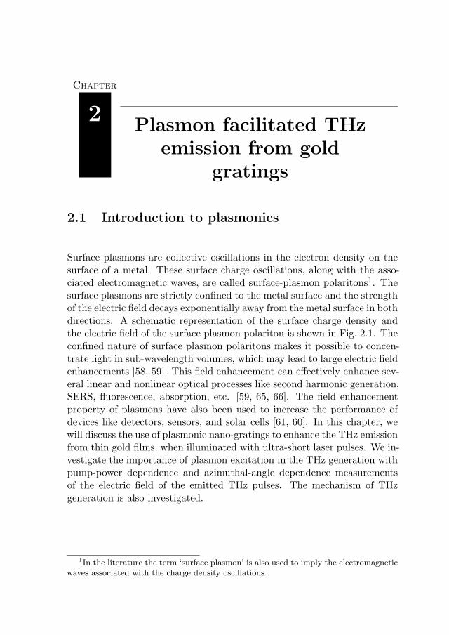
Surface plasmons are collective oscillations in the electron density on thesurface of a metal. These surface charge oscillations, along with the asso-ciated electromagnetic waves, are called surface-plasmon polaritons1. Thesurface plasmons are strictly confined to the metal surface and the strengthof the electric field decays exponentially away from the metal surface in bothdirections. A schematic representation of the surface charge density andthe electric field of the surface plasmon polariton is shown in Fig. 2.1. Theconfined nature of surface plasmon polaritons makes it possible to concen-trate light in sub-wavelength volumes, which may lead to large electric fieldenhancements [58, 59]. This field enhancement can effectively enhance sev-eral linear and nonlinear optical processes like second harmonic generation,SERS, fluorescence, absorption, etc. [59, 65, 66]. The field enhancementproperty of plasmons have also been used to increase the performance ofdevices like detectors, sensors, and solar cells [61, 60]. In this chapter, wewill discuss the use of plasmonic nano-gratings to enhance the THz emissionfrom thin gold films, when illuminated with ultra-short laser pulses. We in-vestigate the importance of plasmon excitation in the THz generation withpump-power dependence and azimuthal-angle dependence measurementsof the electric field of the emitted THz pulses. The mechanism of THzgeneration is also investigated.
1In the literature the term ‘surface plasmon’ is also used to imply the electromagneticwaves associated with the charge density oscillations.
12 Chapter 2. Plasmon facilitated THz emission from gold gratings
Metal
Dielectric
+ + + +-- - - - + + + + -- - - --- - - -
E
(a) (b)
Figure 2.1: (a) Schematic illustration of the surface charge density and theelectric field associated with a surface plasmon. (b) The strength of theelectric field decreases exponentially away from the interface, both in themetal and in the dielectric.
2.1.1 Dispersion relation of surface plasmons
Surface plasmons are characterized by the solutions of Maxwell’s equationsthat are localized at the interface of a metal and dielectric. If we considerthe waves that propagate in the x direction (see Fig. 2.1), it is possibleto solve the wave equation to get a propagating transverse magnetic (TM)mode (for the derivation see Appendix. A). The electric field of the surfaceplasmons can be described as
Ej = (Ej,x, 0, Ej,z)e+i(kxx±kj,zz−ωt) j = 1, 2, (2.1)
where j = 1, 2 represents the dielectric and the metal, respectively. Thez-component of the wave-vector, kj,z, is imaginary, which causes the electricfield to decay exponentially in the z-direction. kx is the x-component ofthe surface plasmon wave-vector, the component parallel to the interface.Solving Maxwell’s equations, with appropriate boundary conditions, it ispossible to derive the dispersion relation of surface-plasmons as [74, 75]:
kx =ω
c
√
ǫ1ǫ2ǫ1 + ǫ2
, (2.2)
where, ǫ1 and ǫ2 are the permittivities of the dielectric and the metal re-spectively, and ω is the angular frequency.
2.1. Introduction to plasmonics 13
Let us assume, for convenience, that the imaginary parts of ǫ1 and ǫ2 aresmall compared to their real parts and can hence be neglected. To havewaves which propagate along the interface, we need kx to be real. FromEq. 2.2, this condition is satisfied if the sum and product of the dielectricfunctions are either both positive or both negative.
Also, the normal component of the wave vector in both media is
kj,z =ω
c
√
ǫ2jǫ1 + ǫ2
, j = 1, 2. (2.3)
Since the wave is confined to the interface, kz has to be purely imaginaryin both media, such that the electric field is exponentially decaying awayfrom the interface. This requires the sum of the dielectric functions to benegative, as can be seen from Eq. 2.3. Hence, the condition to have wavesconfined to the interface becomes
ǫ1(ω)ǫ2(ω) < 0, (2.4)
and
ǫ1(ω) + ǫ2(ω) < 0. (2.5)
For the above two conditions to be satisfied simultaneously, only one ofthe dielectric functions has to be negative and its absolute value should begreater than that of the other. The real-part of the permittivity of metalsis usually negative with a large value compared to the absolute value of thepermittivity of dielectrics. This explains why surface plasmons are possibleat the interface between a metal and a dielectric.
In the above discussion, we considered the permittivities of the two mediato be real, which helps to understand why a metal/dielectric interface isnecessary for the excitation of surface plasmons. However, in reality, boththe materials forming the interface can also have an imaginary part ofthe dielectric function. This leads to kx having an imaginary part as well,leading to the damping of surface plasmons propagating along the interface,which is explained in the next section.
2.1.2 Properties of surface plasmons
The properties of surface plasmons are well known and are summarizedhere for convenience, following the derivation of Novotny and Hecht [75].
14 Chapter 2. Plasmon facilitated THz emission from gold gratings
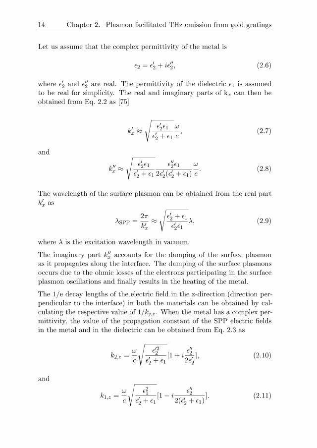
Let us assume that the complex permittivity of the metal is
ǫ2 = ǫ′2 + iǫ′′2, (2.6)
where ǫ′2 and ǫ′′2 are real. The permittivity of the dielectric ǫ1 is assumedto be real for simplicity. The real and imaginary parts of kx can then beobtained from Eq. 2.2 as [75]
k′x ≈√
ǫ′2ǫ1ǫ′2 + ǫ1
ω
c, (2.7)
and
k′′x ≈√
ǫ′2ǫ1ǫ′2 + ǫ1
ǫ′′2ǫ12ǫ′2(ǫ
′2 + ǫ1)
ω
c. (2.8)
The wavelength of the surface plasmon can be obtained from the real partk′x as
λSPP =2π
k′x≈
√
ǫ′2 + ǫ1ǫ′2ǫ1
λ, (2.9)
where λ is the excitation wavelength in vacuum.
The imaginary part k′′x accounts for the damping of the surface plasmonas it propagates along the interface. The damping of the surface plasmonsoccurs due to the ohmic losses of the electrons participating in the surfaceplasmon oscillations and finally results in the heating of the metal.
The 1/e decay lengths of the electric field in the z-direction (direction per-pendicular to the interface) in both the materials can be obtained by cal-culating the respective value of 1/kj,z. When the metal has a complex per-mittivity, the value of the propagation constant of the SPP electric fieldsin the metal and in the dielectric can be obtained from Eq. 2.3 as
k2,z =ω
c
√
ǫ′22ǫ′2 + ǫ1
[1 + iǫ′′22ǫ′2
], (2.10)
and
k1,z =ω
c
√
ǫ21ǫ′2 + ǫ1
[1− iǫ′′2
2(ǫ′2 + ǫ1)]. (2.11)
2.2. Grating coupling of surface plasmons 15
2.2 Grating coupling of surface plasmons
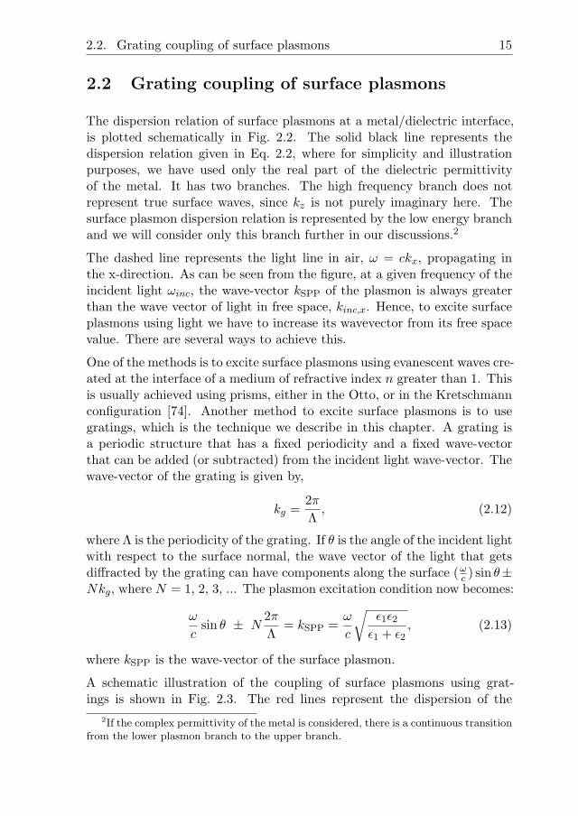
The dispersion relation of surface plasmons at a metal/dielectric interface,is plotted schematically in Fig. 2.2. The solid black line represents thedispersion relation given in Eq. 2.2, where for simplicity and illustrationpurposes, we have used only the real part of the dielectric permittivityof the metal. It has two branches. The high frequency branch does notrepresent true surface waves, since kz is not purely imaginary here. Thesurface plasmon dispersion relation is represented by the low energy branchand we will consider only this branch further in our discussions.2
The dashed line represents the light line in air, ω = ckx, propagating inthe x-direction. As can be seen from the figure, at a given frequency of theincident light ωinc, the wave-vector kSPP of the plasmon is always greaterthan the wave vector of light in free space, kinc,x. Hence, to excite surfaceplasmons using light we have to increase its wavevector from its free spacevalue. There are several ways to achieve this.
One of the methods is to excite surface plasmons using evanescent waves cre-ated at the interface of a medium of refractive index n greater than 1. Thisis usually achieved using prisms, either in the Otto, or in the Kretschmannconfiguration [74]. Another method to excite surface plasmons is to usegratings, which is the technique we describe in this chapter. A grating isa periodic structure that has a fixed periodicity and a fixed wave-vectorthat can be added (or subtracted) from the incident light wave-vector. Thewave-vector of the grating is given by,
kg =2π
Λ, (2.12)
where Λ is the periodicity of the grating. If θ is the angle of the incident lightwith respect to the surface normal, the wave vector of the light that getsdiffracted by the grating can have components along the surface (ω
c) sin θ±
Nkg, where N = 1, 2, 3, ... The plasmon excitation condition now becomes:
ω
csin θ ± N
2π
Λ= kSPP =
ω
c
√
ǫ1ǫ2ǫ1 + ǫ2
, (2.13)
where kSPP is the wave-vector of the surface plasmon.
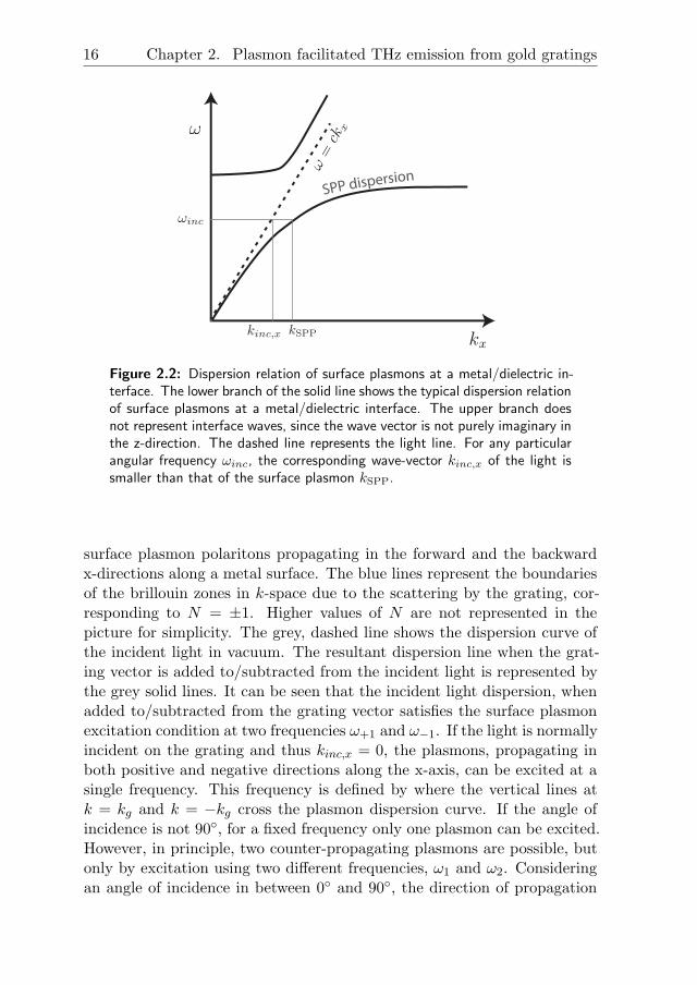
A schematic illustration of the coupling of surface plasmons using grat-ings is shown in Fig. 2.3. The red lines represent the dispersion of the
2If the complex permittivity of the metal is considered, there is a continuous transitionfrom the lower plasmon branch to the upper branch.
16 Chapter 2. Plasmon facilitated THz emission from gold gratings
SPP dispersion
Figure 2.2: Dispersion relation of surface plasmons at a metal/dielectric in-terface. The lower branch of the solid line shows the typical dispersion relationof surface plasmons at a metal/dielectric interface. The upper branch doesnot represent interface waves, since the wave vector is not purely imaginary inthe z-direction. The dashed line represents the light line. For any particularangular frequency ωinc, the corresponding wave-vector kinc,x of the light issmaller than that of the surface plasmon kSPP.
surface plasmon polaritons propagating in the forward and the backwardx-directions along a metal surface. The blue lines represent the boundariesof the brillouin zones in k-space due to the scattering by the grating, cor-responding to N = ±1. Higher values of N are not represented in thepicture for simplicity. The grey, dashed line shows the dispersion curve ofthe incident light in vacuum. The resultant dispersion line when the grat-ing vector is added to/subtracted from the incident light is represented bythe grey solid lines. It can be seen that the incident light dispersion, whenadded to/subtracted from the grating vector satisfies the surface plasmonexcitation condition at two frequencies ω+1 and ω−1. If the light is normallyincident on the grating and thus kinc,x = 0, the plasmons, propagating inboth positive and negative directions along the x-axis, can be excited at asingle frequency. This frequency is defined by where the vertical lines atk = kg and k = −kg cross the plasmon dispersion curve. If the angle ofincidence is not 90◦, for a fixed frequency only one plasmon can be excited.However, in principle, two counter-propagating plasmons are possible, butonly by excitation using two different frequencies, ω1 and ω2. Consideringan angle of incidence in between 0◦ and 90◦, the direction of propagation
2.2. Grating coupling of surface plasmons 17
incident light incident light
(b) (c)
(a)
Figure 2.3: (a) The grating coupling of surface plasmons is illustrated. The x-component of the incident light (kinc,x) is shown by the dashed grey line. Thescattering of the incident light by the grating results in the lines kinc,x+kg andkinc,x − kg. Only the first-order diffracted light is shown here, for simplicity.Plasmons are excited for the frequencies where these lines intersect with theplasmon dispersion lines kSPP and −kSPP. From the figure it can be seenthat surface plasmons can be excited for two frequencies ω+1 and ω−1. (b)and (c) show the direction of propagation of the surface plasmons for thetwo excitation light frequencies ω−1 and ω+1 respectively. θ is the angle ofincidence of the exciting light with respect to the normal to the metal surface.
of the surface plasmons for the two cases is schematically shown in Fig. 2.3(b) and (c).
18 Chapter 2. Plasmon facilitated THz emission from gold gratings
φ
Figure 2.4: Diagram, schematically showing excitation of plasmons by inci-dent light. For an angle of incidence θ and azimuthal angle φ, the arrowsshow that light can couple to a surface plasmon which propagates at an angleΨ with respect to the kx direction.
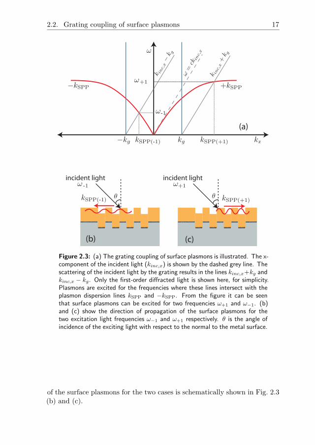
2.2.1 Plasmon excitation with a metal grating for non-zeroazimuthal angles
The azimuthal angle φ is defined as the angle between the grating vectorand the plane of incidence of the excitation laser beam, as shown in Fig. 2.4.The plasmon coupling condition given in Eq. 2.13 is valid only for the casewhen φ = 0. For non-zero azimuthal angles, the grating vector, the plasmonvector, and the k-vector component of the incident light in the plane of thegrating are not collinear. Hence, the surface plasmon coupling conditionbecomes [76]
k2SPP = k20sin2θ +N2k2g ± 2Nkgk0 sinθ cosφ, (2.14)
where θ is the angle of incidence of the light beam and φ is the azimuthalangle (see Fig. 2.4). Now, plasmon excitation is possible if the vector addi-tion of the grating vector and the incident light matches with the surfaceplasmon wave vector. A schematic diagram of the plasmon excitation con-dition is shown in the Fig. 2.4, where light incident at a polar angle θ andan azimuthal angle φ can couple to a grating of wave vector kg. The angleΨ between the direction of propagation of the resulting surface plasmon
2.3. THz emission from gold thin films - a literature survey 19
with respect to the in-plane component of the incident vector, is given as
Ψ = 90− arccos(kg sinφ
kSPP). (2.15)
2.3 THz emission from gold thin films - a litera-ture survey
In this section, we discuss the generation of THz radiation from gold-coatedgrating surfaces, upon fs pulse irradiation and subsequent surface plasmonexcitation. There have been several reports in the literature of THz emis-sion from Au thin films. There are various non-linear optical processeswhich may lead to the generation of THz light from these metal films, de-pending on the experimental conditions, like incident power density, mor-phology of the metal film, etc. Below, we describe briefly the various casesof THz generation from metal thin films, as reported previously in theliterature.
2.3.1 Optical rectification
Optical rectification on metal surfaces like gold and silver, was first reportedby Kadlec et al. [77] in 2004.3 This paper reported that when surfacesof gold and silver are irradiated with high energy laser pulses (1-mJ) of810 nm center wavelength and 50 fs pulse duration, optical rectification ofthe laser pulses occurs at the metal surface, resulting in the generation ofTHz pulses. They observed the THz fluence emitted by the gold surfacesto be proportional to the square of the pump laser fluence.
Second-order non-linear optical effects like optical rectification require ma-terials that lack inversion symmetry. Metals are mostly isotropic materialsand, hence, optical rectification cannot take place in the interior of metals.However, at the surface, the translational symmetry is broken, allowingχ(2) nonlinear effects like second harmonic generation [79, 80] to take place.Hence, it was concluded that optical rectification on the metal surface isthe terahertz emission mechanism. In another paper, Kadlec et al. [81] alsonoted that the THz emission depends on the thickness of the gold thin film,and no THz emission was observed for film thicknesses less than 100 nm.
3At the same time, Hilton et al. [78] also reported THz emission from single-crystalthin iron films by optical rectification. The THz emission was explained as arising froma magnetic nonlinearity in addition to the surface nonlinearity of the thin film sample.
20 Chapter 2. Plasmon facilitated THz emission from gold gratings
This was explained in the paper as follows: The nonlinear polarization atthe surface induces a current perpendicular to the metal surface and, forthin Au films, the charges can accumulate on the metal-glass interface, re-sulting in the rapid build up of a field opposing the initial current that isthe origin of the THz emission.
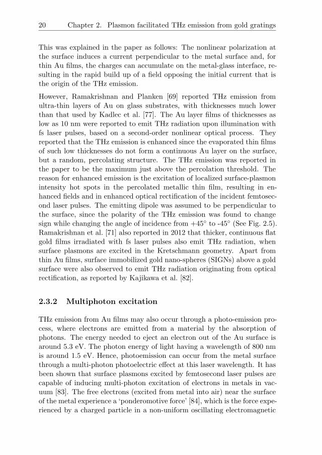
However, Ramakrishnan and Planken [69] reported THz emission fromultra-thin layers of Au on glass substrates, with thicknesses much lowerthan that used by Kadlec et al. [77]. The Au layer films of thicknesses aslow as 10 nm were reported to emit THz radiation upon illumination withfs laser pulses, based on a second-order nonlinear optical process. Theyreported that the THz emission is enhanced since the evaporated thin filmsof such low thicknesses do not form a continuous Au layer on the surface,but a random, percolating structure. The THz emission was reported inthe paper to be the maximum just above the percolation threshold. Thereason for enhanced emission is the excitation of localized surface-plasmonintensity hot spots in the percolated metallic thin film, resulting in en-hanced fields and in enhanced optical rectification of the incident femtosec-ond laser pulses. The emitting dipole was assumed to be perpendicular tothe surface, since the polarity of the THz emission was found to changesign while changing the angle of incidence from +45◦ to -45◦ (See Fig. 2.5).Ramakrishnan et al. [71] also reported in 2012 that thicker, continuous flatgold films irradiated with fs laser pulses also emit THz radiation, whensurface plasmons are excited in the Kretschmann geometry. Apart fromthin Au films, surface immobilized gold nano-spheres (SIGNs) above a goldsurface were also observed to emit THz radiation originating from opticalrectification, as reported by Kajikawa et al. [82].
2.3.2 Multiphoton excitation
THz emission from Au films may also occur through a photo-emission pro-cess, where electrons are emitted from a material by the absorption ofphotons. The energy needed to eject an electron out of the Au surface isaround 5.3 eV. The photon energy of light having a wavelength of 800 nmis around 1.5 eV. Hence, photoemission can occur from the metal surfacethrough a multi-photon photoelectric effect at this laser wavelength. It hasbeen shown that surface plasmons excited by femtosecond laser pulses arecapable of inducing multi-photon excitation of electrons in metals in vac-uum [83]. The free electrons (excited from metal into air) near the surfaceof the metal experience a ‘ponderomotive force’ [84], which is the force expe-rienced by a charged particle in a non-uniform oscillating electromagnetic
2.3. THz emission from gold thin films - a literature survey 21
Figure 2.5: The THz pulses emitted by a 8 nm percolating Au thin filmon a glass substrate, for angles of incidence +45◦ and -45◦, as reported byRamakrishnan and Planken [69]. The measurement was done in a transmissionconfiguration, with the pump light incident on the glass side of the sample.No THz emission was detected at normal incidence.
field. The free electrons near the metal are accelerated towards the regionof lower electric field strength, which, in the case of the evanescent field ofsurface plasmons, is away from the metal surface.
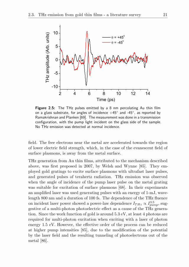
THz generation from Au thin films, attributed to the mechanism describedabove, was first proposed in 2007, by Welsh and Wynne [85]. They em-ployed gold gratings to excite surface plasmons with ultrafast laser pulses,and generated pulses of terahertz radiation. THz emission was observedwhen the angle of incidence of the pump laser pulse on the metal gratingwas suitable for excitation of surface plasmons [68]. In their experimentsan amplified laser was used generating pulses with an energy of 1-mJ, wave-length 800 nm and a duration of 100 fs. The dependence of the THz fluenceon incident laser power showed a power-law dependence ITHz ∝ I3.5pump, sug-gestive of a multi-photon photoelectric effect as a cause of the THz genera-tion. Since the work function of gold is around 5.3 eV, at least 4 photons arerequired for multi-photon excitation when exciting with a laser of photonenergy 1.5 eV. However, the effective order of the process can be reducedat higher pump intensities [85], due to the modification of the potentialby the laser field and the resulting tunneling of photoelectrons out of themetal [86].

22 Chapter 2. Plasmon facilitated THz emission from gold gratings
In 2009, Gao et al. [87] theoretically investigated the plasmon-based pho-toemission model from gold nanostructures. They showed that the electricfield inside the metal is an important factor on which the number of elec-trons emitted, and hence the strength of the THz electric field depends.Hence, the design of the nanostructure can play an important role in thegeneration of THz pulses. Polyushkin et al. [70] later demonstrated THzemission from arrays of silver nano-particles irradiated by strong femtosec-ond laser pulses. The THz emission intensity in their experiments dependson the pump intensity as I5pump, for incident power intensities less than 5GW/cm2 and drops to a 1.5 - 1.75 order power dependence for higher pumppower intensities. This bimodal power dependence is consistent with themodel based on ponderomotive acceleration of the photo-generated elec-trons, since ultrafast photo-emission measurements have also shown suchbimodal power dependencies [88]. The handwaving explanation given bythe authors is that at low incident power densities, the ponderomotivepotential is not completely converted into kinetic energy of the electronsbefore the lifetime of the plasmon pulse. If the incident power density ishigher, the electrons are pushed out of the field within the lifetime of theplasmons and the transfer of energy from ponderomotive potential to thekinetic energy of electrons is more significant [83].
2.3.3 Other mechanisms
It is interesting that various groups have reported THz emission from metalsurfaces and nano-structures, but that the reported dependence of the emit-ted THz electric field on pump power, varies. In addition to the second-order and higher-order pump power dependencies of the emitted THz elec-tric field explained briefly in the previous sections, Garwe et al. [89] reporteda linear dependence of emitted THz fluence on the pump laser fluence. Thiscontradicts the model assumed by Welsh and Wynne [85] and Polyushkinet al. [70], based on the ponderomotive acceleration of photo-emitted elec-trons, which can occur only through a higher-order process. To explaintheir observations, they (Garwe et al. [89]) consider a model where sur-face plasmon polaritons propagate perpendicular to the grooves of the goldgrating surface, constituting a transient current, which emits THz pulsesdirectly [90]. However, creation of photons of a different color requires atleast a second-order nonlinear process, which leads to at least a quadraticdependence of THz fluence on the laser power. This makes the linear powerdependence observed in their experiments a bit puzzling. An interestingaspect of the experimental setup used by Garwe et al. [89] is that they used

2.4. THz emission from gold gratings 23
an incoherent detection technique, a bolometer, which essentially detectsthermal radiation. The linear dependence of the THz emission suggeststhat the power detected by the bolometer is the thermal radiation emitteddue to the high power pump laser heating up the metal.
Suvorov et al. [91] also reported on the THz emission from metal surfacesusing high power fs laser pulses. THz emission from Cu surfaces was shownto have an exponential dependence on the energy of the input laser pulses.The energy of the laser pulses used by Suvorov et al. was around 2.5 mJ.It is possible that in their experiment the Cu surface could have partiallyoxidized, resulting in a Cu/Cu2O junction, which was recently reportedby Ramakrishnan et al. [92] to emit strong THz pulses on excitation withfemtosecond laser pulses.
2.4 THz emission from gold gratings
Inspired by the various mechanisms suggested in literature as being respon-sible for the emission of THz light from metal surfaces illuminated withfemtosecond laser pulses, we performed THz emission experiments withplasmonic metal gratings. Our goal is to determine the role played by sur-face plasmons in the THz generation. Initial experiments were performedusing a commercially obtained etched grating on quartz, similar to thatused by Welsh et al. [68]. The periodicity of the grating is 500 nm. We de-posited a thin layer of Cr (2 nm) with a Au layer of 40 nm thickness on top.The Cr layer is to promote the adhesion between the Au and the quartzsubstrate. From the plasmon-excitation condition given in Eq. 2.13, we cancalculate that for this periodicity, a plasmon resonance should appear atan angle of 36◦.
To confirm that we can excite plasmons on this grating, we have performedwhite-light transmission spectroscopy measurements. An Ocean Opticsfiber-coupled spectrometer was used to measure the spectral transmissionusing a Tungsten-Halogen lamp as a white-light source. The transmissionspectra of the light through the grating sample were measured for differentangles of incidence. The measurements are normalized to the transmissionthrough a flat gold film of equal thickness on the glass substrate. The ex-perimental transmission spectra thus obtained are shown in Fig. 2.6. Wesee peaks in the transmission through the Au grating compared to the flatgold film, with the peak wavelength depending on the angle of incidence.This increased transmission efficiency has been attributed to the excitationof surface plasmons [93, 94]. At an angle of incidence of 36◦, a resonance
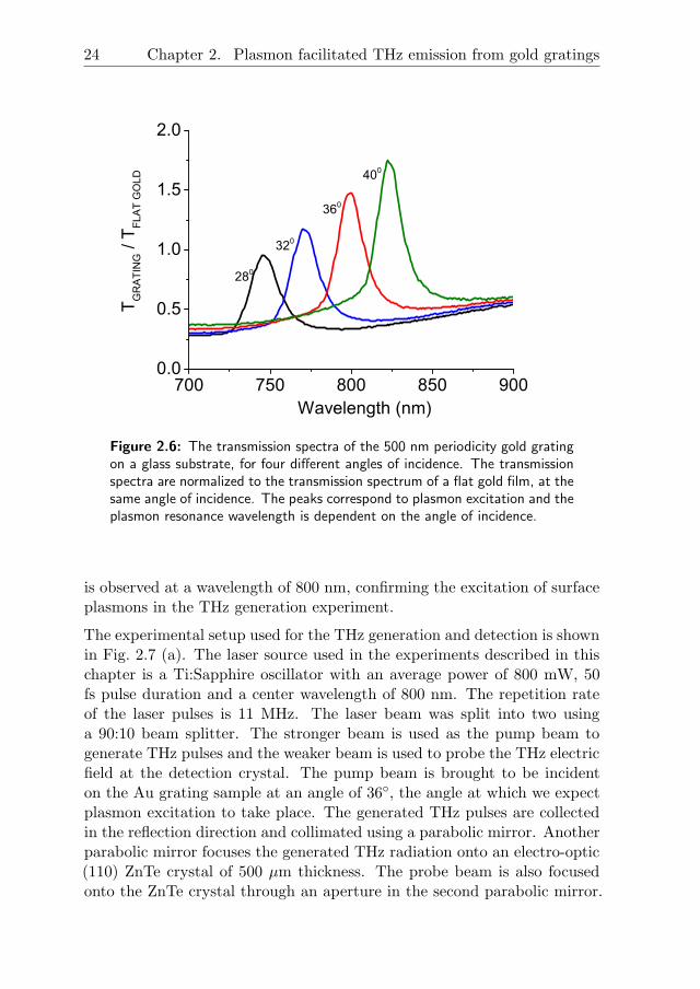
24 Chapter 2. Plasmon facilitated THz emission from gold gratings
700 750 800 850 9000.0
0.5
1.0
1.5
2.0
400
360
320
T GR
ATI
NG /
T FLA
T G
OLD
Wavelength (nm)
280
Figure 2.6: The transmission spectra of the 500 nm periodicity gold gratingon a glass substrate, for four different angles of incidence. The transmissionspectra are normalized to the transmission spectrum of a flat gold film, at thesame angle of incidence. The peaks correspond to plasmon excitation and theplasmon resonance wavelength is dependent on the angle of incidence.
is observed at a wavelength of 800 nm, confirming the excitation of surfaceplasmons in the THz generation experiment.
The experimental setup used for the THz generation and detection is shownin Fig. 2.7 (a). The laser source used in the experiments described in thischapter is a Ti:Sapphire oscillator with an average power of 800 mW, 50fs pulse duration and a center wavelength of 800 nm. The repetition rateof the laser pulses is 11 MHz. The laser beam was split into two usinga 90:10 beam splitter. The stronger beam is used as the pump beam togenerate THz pulses and the weaker beam is used to probe the THz electricfield at the detection crystal. The pump beam is brought to be incidenton the Au grating sample at an angle of 36◦, the angle at which we expectplasmon excitation to take place. The generated THz pulses are collectedin the reflection direction and collimated using a parabolic mirror. Anotherparabolic mirror focuses the generated THz radiation onto an electro-optic(110) ZnTe crystal of 500 µm thickness. The probe beam is also focusedonto the ZnTe crystal through an aperture in the second parabolic mirror.
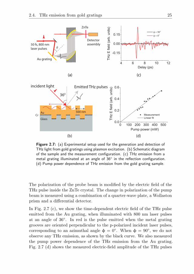
2.4. THz emission from gold gratings 25
(b)
50 fs, 800 nm
laser pulses
Au grating
Detector
assembly
ZnTe
(a) (c)
(d)
incident light
360
500 nmAu
Glass
Cr
Emitted THz pulses
Figure 2.7: (a) Experimental setup used for the generation and detection ofTHz light from gold gratings using plasmon excitation. (b) Schematic diagramof the sample and the measurement configuration. (c) THz emission from ametal grating illuminated at an angle of 36◦ in the reflection configuration.(d) Pump power dependence of THz emission from the gold grating sample.
The polarization of the probe beam is modified by the electric field of theTHz pulse inside the ZnTe crystal. The change in polarization of the pumpbeam is measured using a combination of a quarter-wave plate, a Wollastonprism and a differential detector.
In Fig. 2.7 (c), we show the time-dependent electric field of the THz pulseemitted from the Au grating, when illuminated with 800 nm laser pulsesat an angle of 36◦. In red is the pulse emitted when the metal gratinggrooves are oriented perpendicular to the p-polarized incident laser pulses,corresponding to an azimuthal angle φ = 0◦. When φ = 90◦, we do notobserve any THz emission, as shown by the black curve. We also measuredthe pump power dependence of the THz emission from the Au grating.Fig. 2.7 (d) shows the measured electric-field amplitude of the THz pulses
26 Chapter 2. Plasmon facilitated THz emission from gold gratings
(a)
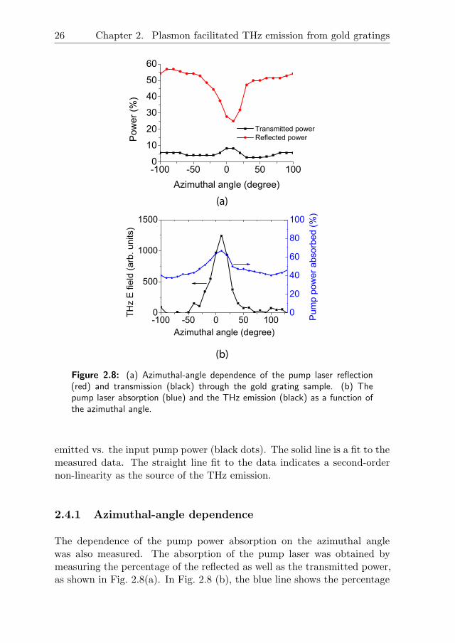
(b)
Figure 2.8: (a) Azimuthal-angle dependence of the pump laser reflection(red) and transmission (black) through the gold grating sample. (b) Thepump laser absorption (blue) and the THz emission (black) as a function ofthe azimuthal angle.
emitted vs. the input pump power (black dots). The solid line is a fit to themeasured data. The straight line fit to the data indicates a second-ordernon-linearity as the source of the THz emission.
2.4.1 Azimuthal-angle dependence
The dependence of the pump power absorption on the azimuthal anglewas also measured. The absorption of the pump laser was obtained bymeasuring the percentage of the reflected as well as the transmitted power,as shown in Fig. 2.8(a). In Fig. 2.8 (b), the blue line shows the percentage

2.5. Etch depth dependence 27
of the laser power absorbed as a function of the azimuthal angle. Forefficient plasmon excitation to take place, the grating grooves should beoriented perpendicular to the laser polarization and, hence, when φ = 0◦,we observe a peak in the absorption. The THz emission is correlated withthe absorbed laser power (see Fig. 2.8(b)): the amplitude of the emittedTHz pulse also sharply decreases as the azimuthal angle is changed from0◦, and at 90◦, there is no detectable THz emission.
Here we see that a relatively small increase in absorbed power leads to abig change in the THz amplitude. This demonstrates that it is not enoughto simply increase the absorption, but that plasmon excitation is very im-portant for the THz emission.
2.5 Etch depth dependence
Since it is easier to perform the experiment for an angle of incidence of45◦, we also fabricated gratings with a periodicity suitable for plasmonexcitation at 45◦. Such a grating should have a periodicity of ∼463 nm.We fabricated these gratings using electron-beam lithography and reactiveion etching. The gratings were first etched into silicon substrates and thencovered with Au by evaporation. The thickness of the Au layer is 100 nmand an adhesive Cr layer of 10 nm thickness was evaporated before Au.
Since these gratings are fabricated on Si, which does not transmit any lightbelow ∼1100 nm, and also because the Au layer is 100 nm thick, transmis-sion spectra could not be obtained for these samples. In Fig. 2.9 (a) weshow the visible light reflection spectra of the fabricated Au nano-gratingsof periodicity 463 nm. The gratings have etch-depths varying from 20 nm to60 nm. The spectra are normalized to the reflection spectrum of a bare Ausurface. It can be seen that around a wavelength of 800 nm, a plasmonicresonance appears. The strength of the resonance depends on the etchdepth and is largest for an etch depth of 60 nm. Around λ = 787 nm, thereis a discontinuity in the reflection spectrum, which correspond to Wood’sanomaly [46]. Below this wavelength, the diffracted order correspondingto N = -1 disappears and hence the energy is redistributed to the zerothorder. We see that the difference of intensity before and after the Wood’sanomaly discontinuity increases with the etch depth. This is because thediffraction intensity depends on the etch depth of the grating [74].
The THz emission from these gratings was recorded in a reflection config-uration with an angle of incidence of 45◦ of the pump laser pulses. The

28 Chapter 2. Plasmon facilitated THz emission from gold gratings
(a)
(b)
Figure 2.9: (a) Reflection spectra from gold-gratings of periodicity 463 nmfor four different etch depths at 45◦ angle of incidence. (b) THz pulsesemitted by the gold-gratings upon excitation with p-polarized femtosecondlaser pulses. No THz emission was observed from the grating with an etchdepth of 20 nm.
2.6. Discussion 29
measured electric field of the emitted THz pulses is plotted in Fig. 2.9 (b).The maximum THz emission is observed for a sample with an etch depthof 60 nm. The strongest plasmon resonance at the pump laser wavelengthwas also observed for this grating etch-depth, again providing support forthe idea that plasmon excitation is necessary for the THz emission.
2.6 Discussion
Mainly two types of explanations have been given in literature to explain theTHz emission from Au thin films and surfaces: one based on photoemissionfrom the Au surface [70, 68, 85] and the other based on a surface nonlinear-ity [77, 81, 82, 71, 69]. THz emission seen after plasmon excitation on grat-ings and nano-particles, was observed to have a higher-order pump-powerdependence and hence could be explained as originating from multi-photonexcitation of electrons and subsequent acceleration in the evanescent field ofthe surface plasmons [68, 70]. However, in our experiments, a second-orderdependence on the pump power is observed (Fig. 2.7(d)). As mentionedin section 2.3, a multi-photon excitation cannot be a second-order process,since the energy of the 800 nm photon is at least 4 times less than the workfunction of gold. Hence, multi-photon excitation can be ruled out as theTHz generation mechanism. It is interesting that Welsh et al. [68] observe ahigher-order dependence of the THz emission on incident laser power thanwe do, considering that we have used an identical grating. However, thelaser power incident on the sample in our case is much lower than thatused by Welsh et al. [68] and Polyushkin et al. [70]. Higher-order processesrequire a high pump power, which may be the reason why we do not ob-serve it in our case. At the same time, Welsh et al. and Polyushkin et al.use a low repetition rate amplified laser which is not suitable to detect theweaker emission associated with a possible χ(2) process. It is therefore pos-sible that our experiment and those of Welsh et al. and Polyushkin et al.simply probe two different power regimes and two different THz generationmechanisms.
The second-order dependence of the generated THz power on the incidentlaser power suggests optical-rectification by the surface non-linearity as thesource of the THz light. Using low power laser sources, a second-orderTHz generation process from gold thin films has been observed only for thecase of percolated-gold by Ramakrishnan and Planken [69] using similarpump powers. The emitting THz dipole, in the case of percolated gold wasassumed to be along the surface normal (see also Fig. 2.5). Moreover, the

30 Chapter 2. Plasmon facilitated THz emission from gold gratings
500 600 700 800 900 1000 1100
0.5
1.0
1.5
2.0
2.5
3.0102o
98o
94o
RGRATING/R
GOLD
Wavelength (nm)
90o
Figure 2.10: The white-light reflection spectra of the gold-grating with aperiodicity 1090 nm, for different azimuthal angles 90◦, 94◦, 98◦ and 102◦,and s-polarized incident light, at θ = 45◦.
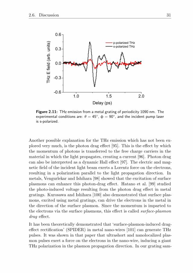
generated THz pulses were found to be p-polarized, irrespective of whetherthe incident laser polarization was s or p.
In order to check the effect of having s-polarized incident light, we fabri-cated another grating of periodicity 1090 nm, suitable for exciting surfaceplasmons at an angle of incidence of 45◦ and an azimuthal angle of 90◦. Thewhite-light reflection spectra of this grating for different azimuthal angles,and s-polarized incident light, are shown in Fig. 2.10. It can be seen thatthe plasmon resonance wavelength depends strongly on the azimuthal an-gle. When φ = 102◦, the plasmon resonances seen at ∼700 nm and ∼1 µmcorrespond to the plasmons excited through the grating vectors ±kg. Whenφ = 90◦, surface plasmons excited from both ±kg merge and both theseplasmon modes seem to have almost the same frequency.
The THz pulse emitted from this sample oriented at an azimuthal angle of90◦, when excited with s-polarized pump laser pulses, is shown in Fig. 2.11.We measured both s- and p-polarized components in the generated THzpulse. The presence of an s-polarized component in the THz light cannoteasily be explained on the basis of an emitting dipole along the surfacenormal. This would mean that the surface χ(2) of the sample is unlikely tobe the only contributing THz generation mechanism.
2.6. Discussion 31
1.0 1.5 2.0-0.6
-0.3
0.0
0.3
0.6
THz
E fie
ld (a
rb. u
nits
)
Delay (ps)
p-polarized THz s-polarized THz
Figure 2.11: THz emission from a metal grating of periodicity 1090 nm. Theexperimental conditions are: θ = 45◦, φ = 90◦, and the incident pump laseris s-polarized.
Another possible explanation for the THz emission which has not been ex-plored very much, is the photon drag effect [95]. This is the effect by whichthe momentum of photons is transferred to the free charge carriers in thematerial in which the light propagates, creating a current [96]. Photon dragcan also be interpreted as a dynamic Hall effect [97]. The electric and mag-netic field of the incident light beam exerts a Lorentz force on the electrons,resulting in a polarization parallel to the light propagation direction. Inmetals, Vengurlekar and Ishihara [98] showed that the excitation of surfaceplasmons can enhance this photon-drag effect. Hatano et al. [99] studiedthe photo-induced voltage resulting from the photon drag effect in metalgratings. Kurosawa and Ishihara [100] also demonstrated that surface plas-mons, excited using metal gratings, can drive the electrons in the metal inthe direction of the surface plasmon. Since the momentum is imparted tothe electrons via the surface plasmons, this effect is called surface-plasmon
drag effect.
It has been theoretically demonstrated that ‘surface-plasmon-induced drag-effect rectification’ (SPIDER) in metal nano-wires [101] can generate THzpulses. It was shown in that paper that ultrashort and nanolocalized plas-mon pulses exert a force on the electrons in the nano-wire, inducing a giantTHz polarization in the plasmon propagation direction. In our grating sam-
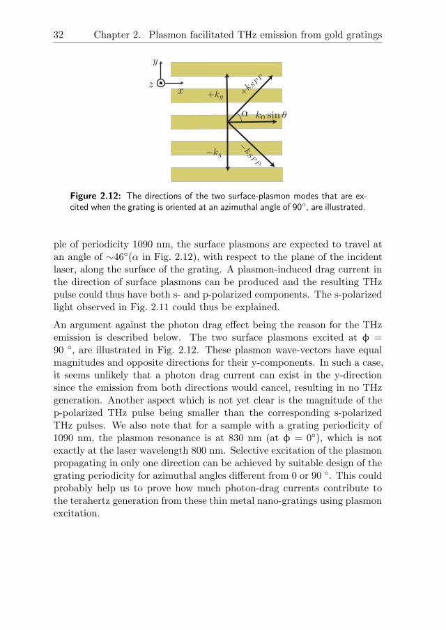
32 Chapter 2. Plasmon facilitated THz emission from gold gratings
Figure 2.12: The directions of the two surface-plasmon modes that are ex-cited when the grating is oriented at an azimuthal angle of 90◦, are illustrated.
ple of periodicity 1090 nm, the surface plasmons are expected to travel atan angle of ∼46◦(α in Fig. 2.12), with respect to the plane of the incidentlaser, along the surface of the grating. A plasmon-induced drag current inthe direction of surface plasmons can be produced and the resulting THzpulse could thus have both s- and p-polarized components. The s-polarizedlight observed in Fig. 2.11 could thus be explained.
An argument against the photon drag effect being the reason for the THzemission is described below. The two surface plasmons excited at φ =90 ◦, are illustrated in Fig. 2.12. These plasmon wave-vectors have equalmagnitudes and opposite directions for their y-components. In such a case,it seems unlikely that a photon drag current can exist in the y-directionsince the emission from both directions would cancel, resulting in no THzgeneration. Another aspect which is not yet clear is the magnitude of thep-polarized THz pulse being smaller than the corresponding s-polarizedTHz pulses. We also note that for a sample with a grating periodicity of1090 nm, the plasmon resonance is at 830 nm (at φ = 0◦), which is notexactly at the laser wavelength 800 nm. Selective excitation of the plasmonpropagating in only one direction can be achieved by suitable design of thegrating periodicity for azimuthal angles different from 0 or 90 ◦. This couldprobably help us to prove how much photon-drag currents contribute tothe terahertz generation from these thin metal nano-gratings using plasmonexcitation.
Chapter
3Oxidation kinetics of Cu
thin films
The work described in this chapter has been published in [102], and islargely reproduced here, with modifications.
3.1 Introduction
Copper and copper-based alloys are very popular for use in the electronicsand optoelectronics industry because of their low cost, high thermal andelectrical conductivity and ease of fabrication. For example, copper is pre-ferred over aluminium in ultra large scale integration devices for use as aninterconnect material because of its low electrical resistivity [103, 104]. Cop-per foils are also used as the conductive element in flexible circuits. How-ever, the surface of copper easily oxidizes and the oxide layer formed doesnot provide enough protection to prevent further oxidation [105]. Oxida-tion is an important factor which degrades the performance of copper-basedelectronic devices [106].
Copper is also an important material for terahertz(THz) applications. Dueto the high conductivity, copper can be used for metal wire and parallelplate THz waveguides [107, 108, 109] and for the production of sharp tipsin aperture-less near field scanning optical microscopy [25]. The presenceof even a thin oxide layer on a metal surface can, in principle, distort thepropagation of THz surface waves [110]. This occurs because the surfacewave propagates along the wire and interacts with this thin layer over along propagation distance of several cm or more. Another interesting ap-plication of copper and in particular, one of the oxides of copper, cuprousoxide, is that in combination with a metal, the oxide/metal interface consti-tutes a surprisingly good THz emitter [92]. Hence, it is interesting to studythe oxidation of copper and the effect it has on the THz optical properties
33

34 Chapter 3. Oxidation kinetics of Cu thin films
of copper surfaces. In chapter 4, we also discuss the THz generation fromAu/Cu2O interfaces. For this purpose, the Cu2O films are fabricated byoxidizing thin Cu films on Au substrates by heating in the ambient atmo-sphere. The study of oxidation of thin Cu films is important in this respectas well.
In the past, different techniques have been employed to measure the oxida-tion of copper and copper thin films [111, 112, 113, 114]. Njeh et al. [111]discuss the oxidation of copper thin films in air using x-ray reflectometryand x-ray diffraction at temperatures below 250 ◦C. Ellipsometry, using350 nm to 850 nm light, has also been employed successfully to character-ize the oxidation kinetics by Iijima et al. [112]. It was shown by Zhonget al. [113] that the measurement of the sheet resistance of copper layersduring oxidation can also give information about the oxidation kinetics. Inthe latter technique, the change in sheet resistance was correlated with thethinning of the copper metal layer due to oxidation. Transmission electronmicroscopy has also been used to obtain insight into the initial stages ofoxidation [114]. All these techniques, however, either provide little infor-mation on the optical properties of copper during the various stages ofoxidation of a copper surface, or require physical contact to be made withthe copper which may influence the measurement.
In this chapter, we explore a new method to study the oxidation of Cufilms at elevated temperatures in the range of 120 to 150 ◦C in air by non-contact, in-situ transmission measurements of broadband terahertz pulses.We attempt to calibrate the transmission of THz light through thin Cufilms, to extract the instantaneous thickness of the copper layer and thethickness of the Cu2O layer during oxidation from the instantaneous THztransmission. This can give us more information on the oxidation kineticsand activation energy for oxidation.
3.2 THz transmission through oxidizing Cu thinfilms
We used a THz time-domain spectroscopy setup to measure the instanta-neous transmission of the Cu thin films, while oxidizing them by heating inthe ambient atmosphere. The details of the sample and the experimentalsetup are described below.
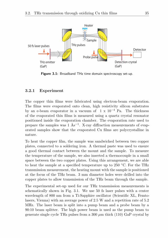
3.2. THz transmission through oxidizing Cu thin films 35
50 fs laser pulses THz pulses
Sample
Detection crystal
(GaP)THz emitter
(GaP)
Probe pulse
Detector
Heater
Figure 3.1: Broadband THz time domain spectroscopy set-up.
3.2.1 Experiment
The copper thin films were fabricated using electron-beam evaporation.The films were evaporated onto clean, high resistivity silicon substratesby an e-beam evaporator in a vacuum of 1 x 10⁻⁴ Pa. The thicknessof the evaporated thin films is measured using a quartz crystal resonatorpositioned inside the evaporation chamber. The evaporation rate used toprepare the samples was 1 As−1. X-ray diffraction measurements of evap-orated samples show that the evaporated Cu films are polycrystalline innature.
To heat the copper film, the sample was sandwiched between two copperplates, connected to a soldering iron. A thermal paste was used to ensurea good thermal contact between the mount and the sample. To measurethe temperature of the sample, we also inserted a thermocouple in a smallspace between the two copper plates. Using this arrangement, we are ableto heat the sample at a specified temperature up to 250 ◦C. For the THztransmission measurement, the heating mount with the sample is positionedat the focus of the THz beam. 3 mm diameter holes were drilled into thecopper plates to allow transmission of the THz beam through the sample.
The experimental set-up used for our THz transmission measurements isschematically shown in Fig. 3.1. We use 50 fs laser pulses with a centerwavelength of 800 nm from a Ti:Sapphire oscillator (Scientific XL, Femto-lasers, Vienna) with an average power of 2.5 W and a repetition rate of 5.2MHz. The laser beam is split into a pump beam and a probe beam by a90:10 beam splitter. The high power beam is used as the pump beam togenerate single cycle THz pulses from a 300 µm thick (110) GaP crystal by
36 Chapter 3. Oxidation kinetics of Cu thin films
optical rectification. Optical rectification can be interpreted as differencefrequency mixing of the frequencies within the bandwidth of the femtosec-ond laser pulses giving rise to the creation of THz photons. The generatedTHz pulses are collected, collimated and focussed onto the sample usingtwo parabolic mirrors. Another two parabolic mirrors collect and focus thebeam again onto another 300 µm GaP crystal which acts as electro-optic de-tection crystal [115, 116]. The probe beam is also focussed onto the electro-optic detection crystal through a hole in the last parabolic mirror. In theelectro-optic crystal, the instantaneous electric field of the THz pulse ellip-tically polarizes the probe beam. The ellipticity induced in the probe beamis measured using a system of a quarter wave plate, a Wollaston prism, anda differential detector and is proportional to the instantaneous THz electricfield. Since the detection efficiency also depends on the azimuthal angle ofthe crystal, the crystal is rotated around the surface normal to maximizethe signal. The strongest detected signals are obtained when the angle be-tween the 800 nm probe polarization and the THz polarization is either 90◦
or 0◦ [33]. The pump pulses and, hence, the THz pulses, are delayed usinga retro-reflecting mirror arrangement mounted on a loudspeaker oscillatingat 50 Hz. By varying the delay between the THz and probe pulses we canmeasure the THz electric field in a stroboscopic manner. In this way, weget a 25 ps long THz electric field time trace, every 20 ms [117].
3.2.2 Results
Fig. 3.2(a) shows the temporal waveform of a typical THz pulse detectedafter passing through a 9 nm thick copper film on a thick silicon wafer. Forreference, the THz pulse detected after passing through an uncoated siliconwafer is also shown. The detected THz electric field consists of almost asingle cycle. The rapidly oscillating tail following the main pulse is due tothe phase mismatch between the pump laser pulses and the THz pulses inthe generation crystal [115]. By performing a fast fourier transform of thetemporal data, we obtain the amplitude spectra of the pulses as shown inFig. 3.2(b). The ultrafast THz pulses are seen to contain usable spectralcomponents in a wide bandwidth from 0.5 to 7 THz.
Fig. 3.3 shows the normalized peak-to-peak value of the electric field of theTHz pulses transmitted through the copper films, as a function of time. Thefilms were heated at temperatures of 120, 130, 140, and 150 ◦C. The initialthickness of the copper films used for the oxidation measurement is 21 nm.The THz transmission through a freshly deposited 21 nm thick copper filmis very low. However, as the film is heated, the THz transmission increases
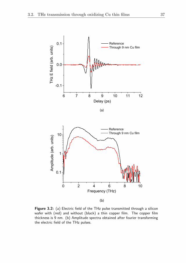
3.2. THz transmission through oxidizing Cu thin films 37
(a)
(b)
Figure 3.2: (a) Electric field of the THz pulse transmitted through a siliconwafer with (red) and without (black) a thin copper film. The copper filmthickness is 9 nm. (b) Amplitude spectra obtained after fourier transformingthe electric field of the THz pulses.

38 Chapter 3. Oxidation kinetics of Cu thin films
Figure 3.3: The peak-to-peak value of THz pulses transmitted through oxi-dizing copper films at different temperatures, as a function of time.
with time. The rate of increase is much higher at a temperature of 150 ◦Cthan at 120 ◦C, even though the temperature difference is only 30 ◦C. Forthe three highest temperatures used, the transmission reached its highest,final value within 3 hours, suggesting that the oxidation is complete. Forthe lowest temperature, the transmission continues to increase even afterthis time. Apparently, at this temperature, the oxidation is incompleteeven after 3 hours.
In order to study the oxidation kinetics, we need to extract the informationabout the instantaneous thickness of the oxide layer from the above data.Copper can oxidize to form two oxides, cuprous oxide (Cu2O) or cupricoxide (CuO). However, for heating temperatures below 225 ◦C, it is knownthat the oxide formed is predominantly cuprous oxide [118]. Hence, at anyparticular instant of time during oxidation, the sample consists of the sili-con substrate, a remaining copper layer and a cuprous oxide layer formeddue to heating. A thin layer of cuprous oxide fully transmits the THzpulses, as do most dielectric, nonabsorbing layers which are much thinnerthan the wavelength of the light used. In our case, the oxide film is a fewnanometers thick, whereas the THz wavelength is around 300 µm. For thesame reason, we can also neglect the reflection losses at the Cu2O-air in-terface. Therefore, the transmission through the oxidizing sample dependsonly on the thickness of the copper film. If we know which thickness of

3.3. Thickness-dependent THz transmission 39
the copper film corresponds to a particular value of the THz transmission,we can determine the instantaneous remaining copper film thickness dur-ing oxidation. It is tempting to calibrate our measurement by performingthe THz transmission experiments on un-oxidized copper films of varyingthickness, and to correlate this with the instantaneous transmission of theoriginally 21 nm thick film during oxidation. However, as we will show inthe next section, this leads to erroneous results.
3.3 Thickness-dependent THz transmission
First, we attempt to model the transmission of a copper thin film using thetransmission equation: [119, 120, 121, 122]
Etx
Eref
=1 + n
1 + n+ Z0σ(ω)d, (3.1)
where Etx is the amplitude of the THz electric field transmitted throughthe copper film, Eref is the transmitted electric field through the uncoatedhalf of the silicon wafer, and Z0 is the impedance of free space (see alsoFig.3.4(a)). d is the thickness of the copper film, and n3 = 3.418 [123] isthe frequency-independent refractive index of silicon at THz frequencies andσ(ω) is the complex conductivity of the film. If we know the conductivity ofthe thin film, we can calculate the THz transmission as a function of thick-ness from Eq. 3.1. For a thin film, the conductivity is expected to be lowerthan that of bulk metal, due to the large number of intrinsic defects createdduring physical vapor deposition [124, 125]. The electron-beam evaporatedfilms are polycrystalline, with distinct grain boundaries. Scattering fromthese grain boundaries considerably influences the properties of the film.This results in a lower conductivity of evaporated thin films compared tothat of bulk metal. Hence, we adjusted the value of the conductivity of cop-per, so as to match the measured value of the THz transmission througha thick copper film of 37 nm. This gives a conductivity value of σ = 1.8x 10⁷ Sm−1. This should be compared to the DC bulk conductivity valueof copper, σ = 5.6 x 10⁷ Sm−1. The conductivity is assumed to be realand frequency-independent for the low THz frequencies. Since the THztransmission seems to be frequency-independent, only a single frequencywas used in the calculation. The calculated THz transmission for copperfilms of different thickness is shown by the solid line in Fig. 3.4(b).
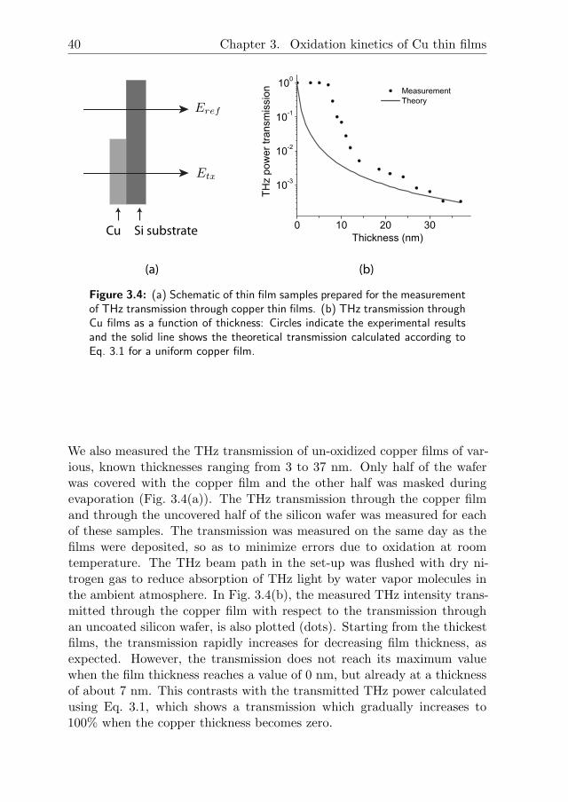
40 Chapter 3. Oxidation kinetics of Cu thin films
Cu Si substrate
(a) (b)
Figure 3.4: (a) Schematic of thin film samples prepared for the measurementof THz transmission through copper thin films. (b) THz transmission throughCu films as a function of thickness: Circles indicate the experimental resultsand the solid line shows the theoretical transmission calculated according toEq. 3.1 for a uniform copper film.
We also measured the THz transmission of un-oxidized copper films of var-ious, known thicknesses ranging from 3 to 37 nm. Only half of the waferwas covered with the copper film and the other half was masked duringevaporation (Fig. 3.4(a)). The THz transmission through the copper filmand through the uncovered half of the silicon wafer was measured for eachof these samples. The transmission was measured on the same day as thefilms were deposited, so as to minimize errors due to oxidation at roomtemperature. The THz beam path in the set-up was flushed with dry ni-trogen gas to reduce absorption of THz light by water vapor molecules inthe ambient atmosphere. In Fig. 3.4(b), the measured THz intensity trans-mitted through the copper film with respect to the transmission throughan uncoated silicon wafer, is also plotted (dots). Starting from the thickestfilms, the transmission rapidly increases for decreasing film thickness, asexpected. However, the transmission does not reach its maximum valuewhen the film thickness reaches a value of 0 nm, but already at a thicknessof about 7 nm. This contrasts with the transmitted THz power calculatedusing Eq. 3.1, which shows a transmission which gradually increases to100% when the copper thickness becomes zero.

3.3. Thickness-dependent THz transmission 41
(a) 5 nm thick (b) 8 nm thick
(c) 10 nm thick
Figure 3.5: Scanning electron micrographs of thin copper films on siliconsubstrates, with thickness around the percolation threshold.
3.3.1 Percolation
The discrepancy between the measured and the calculated thickness-depen-dent THz transmission can be understood, if we examine the SEM imagesof the Cu thin films. In Fig. 3.5 the SEM images of the copper films forthree different thicknesses; 5, 8, and 10 nm are shown. The images showthat these ultra thin films do not form a smooth uniform layer. Formationof thin films by physical vapor deposition is characterized by the forma-tion of nuclei and their subsequent growth. As the deposition continues,the nucleated metal islands grow until they coalesce to form a continuousmacroscopic network. The transition from isolated islands to a connectednetwork occurs at the so-called percolation threshold thickness, which is theeffective thickness at which the electrons can completely percolate throughthe random metal network. The unexpected increase in the THz transmis-sion for films of thickness < 8 nm can be explained on the basis of thisnon-uniform film morphology [124]. Below the percolation threshold, theelectrons cannot move out of the metal islands and hence the film behaves
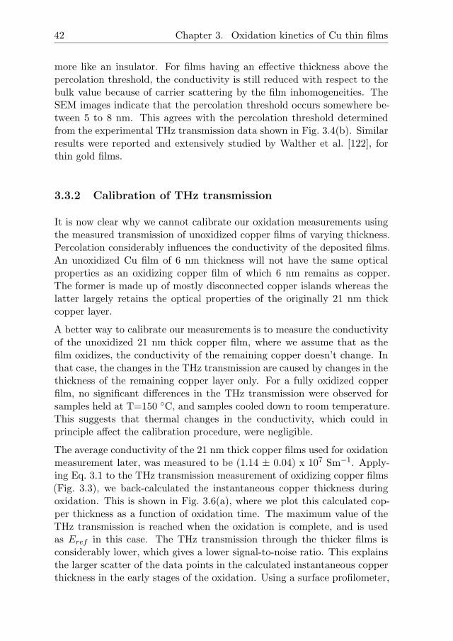
42 Chapter 3. Oxidation kinetics of Cu thin films
more like an insulator. For films having an effective thickness above thepercolation threshold, the conductivity is still reduced with respect to thebulk value because of carrier scattering by the film inhomogeneities. TheSEM images indicate that the percolation threshold occurs somewhere be-tween 5 to 8 nm. This agrees with the percolation threshold determinedfrom the experimental THz transmission data shown in Fig. 3.4(b). Similarresults were reported and extensively studied by Walther et al. [122], forthin gold films.
3.3.2 Calibration of THz transmission
It is now clear why we cannot calibrate our oxidation measurements usingthe measured transmission of unoxidized copper films of varying thickness.Percolation considerably influences the conductivity of the deposited films.An unoxidized Cu film of 6 nm thickness will not have the same opticalproperties as an oxidizing copper film of which 6 nm remains as copper.The former is made up of mostly disconnected copper islands whereas thelatter largely retains the optical properties of the originally 21 nm thickcopper layer.
A better way to calibrate our measurements is to measure the conductivityof the unoxidized 21 nm thick copper film, where we assume that as thefilm oxidizes, the conductivity of the remaining copper doesn’t change. Inthat case, the changes in the THz transmission are caused by changes in thethickness of the remaining copper layer only. For a fully oxidized copperfilm, no significant differences in the THz transmission were observed forsamples held at T=150 ◦C, and samples cooled down to room temperature.This suggests that thermal changes in the conductivity, which could inprinciple affect the calibration procedure, were negligible.
The average conductivity of the 21 nm thick copper films used for oxidationmeasurement later, was measured to be (1.14 ± 0.04) x 107 Sm−1. Apply-ing Eq. 3.1 to the THz transmission measurement of oxidizing copper films(Fig. 3.3), we back-calculated the instantaneous copper thickness duringoxidation. This is shown in Fig. 3.6(a), where we plot this calculated cop-per thickness as a function of oxidation time. The maximum value of theTHz transmission is reached when the oxidation is complete, and is usedas Eref in this case. The THz transmission through the thicker films isconsiderably lower, which gives a lower signal-to-noise ratio. This explainsthe larger scatter of the data points in the calculated instantaneous copperthickness in the early stages of the oxidation. Using a surface profilometer,

3.4. Oxidation kinetics and Arrhenius equation 43
we have measured the thickness of several copper films before and after com-plete oxidation. When completely oxidized, the thickness of the oxide layeris around 1.5 times that of the pure copper layer. To calculate the instanta-neous cuprous oxide thickness during oxidation, we multiplied the used-upcopper thickness by this experimentally determined factor 1.5, which givesus the instantaneous Cu2O thickness. The growth of the cuprous oxidelayer as a function of time is shown in Fig. 3.6(b). When the copper film iscompletely oxidized, the oxide layer does not grow further. This explainsthe saturation in the growth of the cuprous oxide thickness after a certaintime.
3.4 Oxidation kinetics and Arrhenius equation
We can further analyze the temperature dependence of the oxidation rate.In the temperature range we used, the oxidation of copper is expected tofollow a parabolic rate law: [126, 113]
doxide = d0 + k(T )t1
2 , (3.2)
where doxide is the thickness of the oxide layer at time t, and k(T ) is therate constant. d0 is the natural oxide layer on the copper film formed atroom temperature before heating the sample. Eq. 3.2 is fitted to the oxidegrowth curves shown in Fig. 3.6(b). A natural oxide layer of d0 = 1 nm wasassumed for all the films to obtain the best fit for the measurements. Whenoxidation is complete, the thickness of the cuprous oxide no longer increases.Hence the part of the curve where the thickness remains constant is not usedin the fitting procedure. Generally, a parabolic rate law for the oxidationof copper thin films implies a diffusion-dominated oxidation process [127].The activation energy for diffusion can be obtained from the temperaturedependence of the rate constant k, which follows the Arrhenius equation:[128]
k(T ) = k0e−EaR
1
T . (3.3)
Here k0 is a constant, Ea is the activation energy for diffusion, R = 8.314 Jmol−1K−1 is the universal gas constant and T is the heating temperature.If we plot ln(k) against 1
T, the slope of the straight line thus obtained is
−Ea
R. Hence, the value of the activation energy can be determined from
the slope of the Arrhenius curve. The Arrhenius relation for rate constantsobtained from fitting Eq. 3.2 to our oxidation data is plotted in Fig. 3.7.The activation energy for diffusion calculated from the slope of a straightline fit to this data is 0.55 ± 0.06 eV.

44 Chapter 3. Oxidation kinetics of Cu thin films
(a)
(b)
Figure 3.6: (a) The instantaneous copper film thickness during oxidationas a function of time after calibration. (b) The instantaneous cuprous oxidethickness as a function of time. The used-up copper thickness is multipliedby a factor of 1.5 to obtain the thickness of the oxide layer as a function oftime.
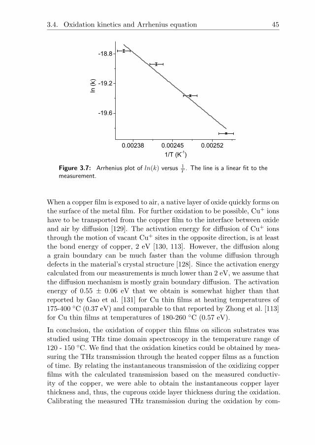
3.4. Oxidation kinetics and Arrhenius equation 45
Figure 3.7: Arrhenius plot of ln(k) versus 1T. The line is a linear fit to the
measurement.
When a copper film is exposed to air, a native layer of oxide quickly forms onthe surface of the metal film. For further oxidation to be possible, Cu+ ionshave to be transported from the copper film to the interface between oxideand air by diffusion [129]. The activation energy for diffusion of Cu+ ionsthrough the motion of vacant Cu+ sites in the opposite direction, is at leastthe bond energy of copper, 2 eV [130, 113]. However, the diffusion alonga grain boundary can be much faster than the volume diffusion throughdefects in the material’s crystal structure [128]. Since the activation energycalculated from our measurements is much lower than 2 eV, we assume thatthe diffusion mechanism is mostly grain boundary diffusion. The activationenergy of 0.55 ± 0.06 eV that we obtain is somewhat higher than thatreported by Gao et al. [131] for Cu thin films at heating temperatures of175-400 ◦C (0.37 eV) and comparable to that reported by Zhong et al. [113]for Cu thin films at temperatures of 180-260 ◦C (0.57 eV).
In conclusion, the oxidation of copper thin films on silicon substrates wasstudied using THz time domain spectroscopy in the temperature range of120 - 150 ◦C. We find that the oxidation kinetics could be obtained by mea-suring the THz transmission through the heated copper films as a functionof time. By relating the instantaneous transmission of the oxidizing copperfilms with the calculated transmission based on the measured conductiv-ity of the copper, we were able to obtain the instantaneous copper layerthickness and, thus, the cuprous oxide layer thickness during the oxidation.Calibrating the measured THz transmission during the oxidation by com-

46 Chapter 3. Oxidation kinetics of Cu thin films
parison with the measured THz transmission through unoxidized copperlayers of several thicknesses is not possible. We show that this is explainedby the percolation transition of copper that occurs for average copper layerthicknesses around 7 nm. Such a transition is absent in layers of the samethickness which result from the oxidation of a layer with a much largerstarting thickness. The oxidation follows a parabolic rate law from whichthe activation energy for diffusion is calculated to be 0.55 ± 0.06 eV. Thisvalue suggests a fast diffusion mechanism, such as diffusion of Cu atomsthrough the grain boundaries as the dominant diffusion mechanism.

Chapter
4THz emission from
Cuprous oxide thin films
4.1 Introduction
When a semiconductor is excited with ultrashort laser pulses with photonshaving sufficient energy, mobile charge carriers may be excited. On thesurface of a semiconductor this can produce a current surge which emitsTHz radiation. This current surge is generally caused by either the acceler-ation of the photoexcited carriers by the surface depletion field, or by thephoto-Dember effect arising from a difference in the mobilities of electronsand holes, in combination with a carrier concentration gradient [132, 36].
Laser-induced terahertz emission originating from a current surge at ametal/semiconductor interface has also been reported in the literature[133, 134]. A potential energy barrier for electrons can be formed at suchan interface, known as a Schottky barrier junction. An electric field and adepletion layer devoid of mobile charge carriers are present at these junc-tions, as explained in the following section. When these junctions are illu-minated with laser pulses, the semiconducting material absorbs the laserphotons creating electron-hole pairs. These free carriers at the interfaceare then swept across the depletion layer due to the electric field presentat the Schottky barrier and form a photocurrent normal to the interface.This transient photocurrent in the depletion layer radiates a sub-picosecondelectromagnetic pulse, which contains terahertz frequencies.
Recently, emission of THz pulses has been observed from semiconductingthin films like silicon, germanium and cuprous oxide deposited on metalsurfaces, when excited with femtosecond laser pulses [92, 135]. The THzemission from these thin films also results from the formation of a Schottkybarrier, which creates a static electric field in the depletion region of theSchottky barrier. The THz emission from Au/Cu2O junctions is especially
47
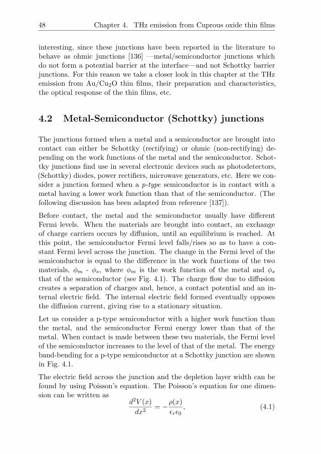
48 Chapter 4. THz emission from Cuprous oxide thin films
interesting, since these junctions have been reported in the literature tobehave as ohmic junctions [136] —metal/semiconductor junctions whichdo not form a potential barrier at the interface—and not Schottky barrierjunctions. For this reason we take a closer look in this chapter at the THzemission from Au/Cu2O thin films, their preparation and characteristics,the optical response of the thin films, etc.
4.2 Metal-Semiconductor (Schottky) junctions
The junctions formed when a metal and a semiconductor are brought intocontact can either be Schottky (rectifying) or ohmic (non-rectifying) de-pending on the work functions of the metal and the semiconductor. Schot-tky junctions find use in several electronic devices such as photodetectors,(Schottky) diodes, power rectifiers, microwave generators, etc. Here we con-sider a junction formed when a p-type semiconductor is in contact with ametal having a lower work function than that of the semiconductor. (Thefollowing discussion has been adapted from reference [137]).
Before contact, the metal and the semiconductor usually have differentFermi levels. When the materials are brought into contact, an exchangeof charge carriers occurs by diffusion, until an equilibrium is reached. Atthis point, the semiconductor Fermi level falls/rises so as to have a con-stant Fermi level across the junction. The change in the Fermi level of thesemiconductor is equal to the difference in the work functions of the twomaterials, φm - φs, where φm is the work function of the metal and φs
that of the semiconductor (see Fig. 4.1). The charge flow due to diffusioncreates a separation of charges and, hence, a contact potential and an in-ternal electric field. The internal electric field formed eventually opposesthe diffusion current, giving rise to a stationary situation.
Let us consider a p-type semiconductor with a higher work function thanthe metal, and the semiconductor Fermi energy lower than that of themetal. When contact is made between these two materials, the Fermi levelof the semiconductor increases to the level of that of the metal. The energyband-bending for a p-type semiconductor at a Schottky junction are shownin Fig. 4.1.
The electric field across the junction and the depletion layer width can befound by using Poisson’s equation. The Poisson’s equation for one dimen-sion can be written as
d2V (x)
dx2= −ρ(x)
ǫrǫ0, (4.1)
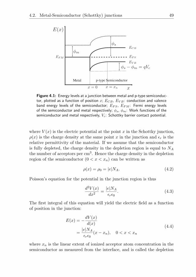
4.2. Metal-Semiconductor (Schottky) junctions 49
Metal p-type Semiconductor
Figure 4.1: Energy levels at a junction between metal and p-type semiconduc-tor, plotted as a function of position x; ECB , EV B : conduction and valenceband energy levels of the semiconductor; EFS , EFM : Fermi energy levelsof the semiconductor and metal respectively; φs, φm: Work functions of thesemiconductor and metal respectively, Vc: Schottky barrier contact potential.
where V (x) is the electric potential at the point x in the Schottky junction,ρ(x) is the charge density at the same point x in the junction and ǫr is therelative permittivity of the material. If we assume that the semiconductoris fully depleted, the charge density in the depletion region is equal to NA
the number of acceptors per cm3. Hence the charge density in the depletionregion of the semiconductor (0 < x < xn) can be written as
ρ(x) = ρ0 = |e|NA. (4.2)
Poisson’s equation for the potential in the junction region is thus
d2V (x)
dx2=
|e|NA
ǫrǫ0. (4.3)
The first integral of this equation will yield the electric field as a functionof position in the junction:
E(x) = −dV (x)
d(x)
=|e|NA
ǫrǫ0(x− xn), 0 < x < xn
(4.4)
where xn is the linear extent of ionized acceptor atom concentration in thesemiconductor as measured from the interface, and is called the depletion
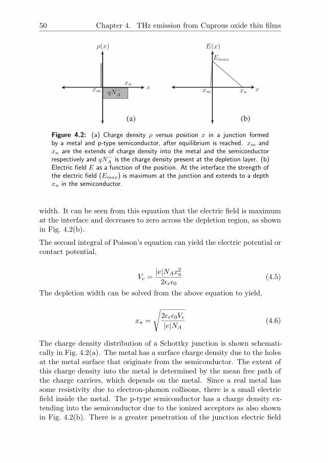
50 Chapter 4. THz emission from Cuprous oxide thin films
(a) (b)
Figure 4.2: (a) Charge density ρ versus position x in a junction formedby a metal and p-type semiconductor, after equilibrium is reached. xm andxn are the extends of charge density into the metal and the semiconductorrespectively and qN−
A is the charge density present at the depletion layer. (b)Electric field E as a function of the position. At the interface the strength ofthe electric field (Emax) is maximum at the junction and extends to a depthxn in the semiconductor.
width. It can be seen from this equation that the electric field is maximumat the interface and decreases to zero across the depletion region, as shownin Fig. 4.2(b).
The second integral of Poisson’s equation can yield the electric potential orcontact potential,
Vc =|e|NAx
2n
2ǫrǫ0(4.5)
The depletion width can be solved from the above equation to yield,
xn =
√
2ǫrǫ0Vc
|e|NA
(4.6)
The charge density distribution of a Schottky junction is shown schemati-cally in Fig. 4.2(a). The metal has a surface charge density due to the holesat the metal surface that originate from the semiconductor. The extent ofthis charge density into the metal is determined by the mean free path ofthe charge carriers, which depends on the metal. Since a real metal hassome resistivity due to electron-phonon collisons, there is a small electricfield inside the metal. The p-type semiconductor has a charge density ex-tending into the semiconductor due to the ionized acceptors as also shownin Fig. 4.2(b). There is a greater penetration of the junction electric field
4.3. Cuprous oxide as a semiconductor 51
Cu+
O2-
Figure 4.3: Cuprous oxide crystalizes in a simple cubic form. The dottedlines represent the cell edge [139].
into the semiconductor than into the metal, because the charge density isless in the semiconductor than in the metal. The electric field strength ismaximum at the interface and decreases as the distance from the junctionincreases. At the depletion region boundary, the electric field reduces tozero. This property is of importance in the THz generation from Schottkydevices, as we will see later.
4.3 Cuprous oxide as a semiconductor
Cuprous oxide (Cu2O) is one of the two stable phases of oxides of copper,the other one being cupric oxide (CuO). Cuprous oxide is reddish in colourwith a direct band gap of 2 eV, whereas cupric oxide has a dark graycolour with a band gap of 1.4 eV [138]. Cuprous oxide crystalizes in acubic structure as shown in the Fig. 4.3 [139]. The copper atoms formface-centered cubic lattices (fcc) and the oxygen atoms form body-centeredcubic lattices (bcc). Some of the properties of Cu2O are given in Table. 4.1.
From a historical point of view, it is interesting to note that cuprous oxide isthe oldest material in semiconductor electronics [142]. Before the discoveryof silicon, germanium, and other semiconductors, Cu2O was recognized asa potential semiconductor for the fabrication of solar cells. The advantagesoffered by Cu2O are that
• It is a non-toxic material• The starting material, Cu, is very abundant• The production process is simple
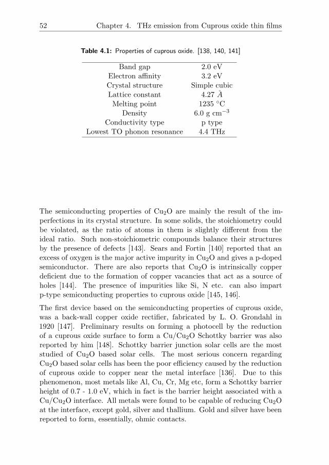
52 Chapter 4. THz emission from Cuprous oxide thin films
Table 4.1: Properties of cuprous oxide. [138, 140, 141]
Band gap 2.0 eVElectron affinity 3.2 eVCrystal structure Simple cubicLattice constant 4.27 AMelting point 1235 ◦C
Density 6.0 g cm−3
Conductivity type p typeLowest TO phonon resonance 4.4 THz
The semiconducting properties of Cu2O are mainly the result of the im-perfections in its crystal structure. In some solids, the stoichiometry couldbe violated, as the ratio of atoms in them is slightly different from theideal ratio. Such non-stoichiometric compounds balance their structuresby the presence of defects [143]. Sears and Fortin [140] reported that anexcess of oxygen is the major active impurity in Cu2O and gives a p-dopedsemiconductor. There are also reports that Cu2O is intrinsically copperdeficient due to the formation of copper vacancies that act as a source ofholes [144]. The presence of impurities like Si, N etc. can also impartp-type semiconducting properties to cuprous oxide [145, 146].
The first device based on the semiconducting properties of cuprous oxide,was a back-wall copper oxide rectifier, fabricated by L. O. Grondahl in1920 [147]. Preliminary results on forming a photocell by the reductionof a cuprous oxide surface to form a Cu/Cu2O Schottky barrier was alsoreported by him [148]. Schottky barrier junction solar cells are the moststudied of Cu2O based solar cells. The most serious concern regardingCu2O based solar cells has been the poor efficiency caused by the reductionof cuprous oxide to copper near the metal interface [136]. Due to thisphenomenon, most metals like Al, Cu, Cr, Mg etc, form a Schottky barrierheight of 0.7 - 1.0 eV, which in fact is the barrier height associated with aCu/Cu2O interface. All metals were found to be capable of reducing Cu2Oat the interface, except gold, silver and thallium. Gold and silver have beenreported to form, essentially, ohmic contacts.
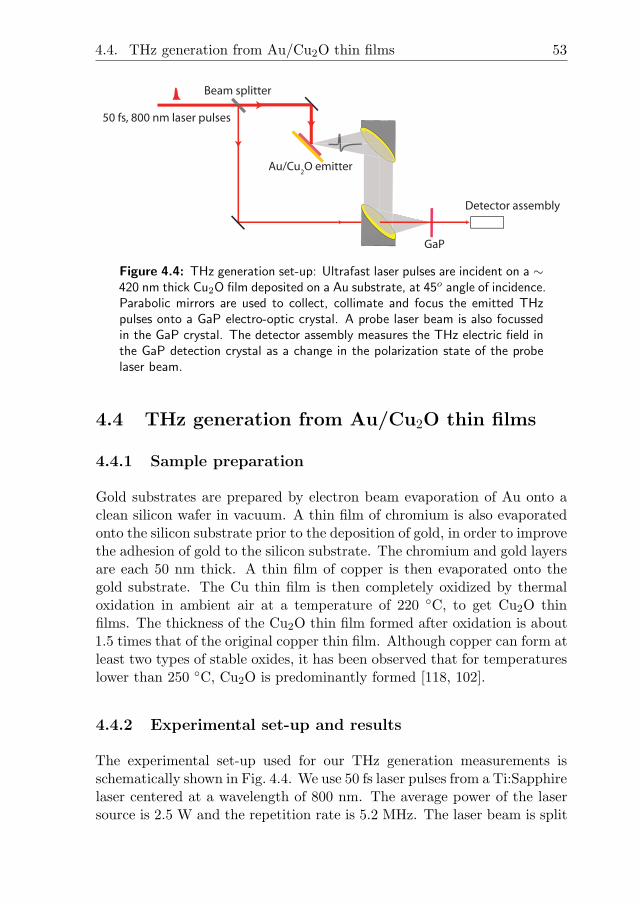
4.4. THz generation from Au/Cu2O thin films 53
50 fs, 800 nm laser pulses
Au/Cu2O emitter
Detector assembly
GaP
Beam splitter
Figure 4.4: THz generation set-up: Ultrafast laser pulses are incident on a ∼420 nm thick Cu2O film deposited on a Au substrate, at 45o angle of incidence.Parabolic mirrors are used to collect, collimate and focus the emitted THzpulses onto a GaP electro-optic crystal. A probe laser beam is also focussedin the GaP crystal. The detector assembly measures the THz electric field inthe GaP detection crystal as a change in the polarization state of the probelaser beam.
4.4 THz generation from Au/Cu2O thin films
4.4.1 Sample preparation
Gold substrates are prepared by electron beam evaporation of Au onto aclean silicon wafer in vacuum. A thin film of chromium is also evaporatedonto the silicon substrate prior to the deposition of gold, in order to improvethe adhesion of gold to the silicon substrate. The chromium and gold layersare each 50 nm thick. A thin film of copper is then evaporated onto thegold substrate. The Cu thin film is then completely oxidized by thermaloxidation in ambient air at a temperature of 220 ◦C, to get Cu2O thinfilms. The thickness of the Cu2O thin film formed after oxidation is about1.5 times that of the original copper thin film. Although copper can form atleast two types of stable oxides, it has been observed that for temperatureslower than 250 ◦C, Cu2O is predominantly formed [118, 102].
4.4.2 Experimental set-up and results
The experimental set-up used for our THz generation measurements isschematically shown in Fig. 4.4. We use 50 fs laser pulses from a Ti:Sapphirelaser centered at a wavelength of 800 nm. The average power of the lasersource is 2.5 W and the repetition rate is 5.2 MHz. The laser beam is split

54 Chapter 4. THz emission from Cuprous oxide thin films
into pump and probe beams by a 90:10 beam splitter. 90% of the laserpower is used for the generation of THz pulses from the Au/Cu2O thinfilms. The samples are mounted in a reflection-type configuration, and thelaser is incident on the sample at an angle of 45◦. The pump pulses are de-layed using a retro-reflecting mirror arrangement mounted on a translationstage. The generated THz pulses are collected, collimated and focussedonto a 300 µm GaP crystal which acts as an electro-optic detection crystal[33]. The probe beam is also focussed onto the detection crystal throughan aperture in the last parabolic mirror. The electric field of the THz pulsemodifies the polarization state of the 800 nm probe beam which is mea-sured using an arrangement of a quarter wave plate, a Wollaston prism,and a differential detector. The setup was purged with dry nitrogen gasin order to reduce the absorption by water vapor in the atmosphere. Thespectrum of the measured THz pulse is obtained by Fourier transformingthe time-dependent THz electric field.
The electric field as a function of time of the single-cycle THz pulse emit-ted from ∼420 nm thick Cu2O on gold and the corresponding Fourier-transformed amplitude spectrum are shown in Fig. 4.5. The bandwidth ofthe emitted THz pulse ranges from 0.1 to ∼7 THz. The dip seen around4.46 THz in the emission spectrum, is a transverse-optic (TO) phonon res-onance of Cu2O, indicating that the sample is polycrystalline in natureand not amorphous, which is also confirmed by x-ray diffraction measure-ments. In the THz frequency range, Cu2O has two TO phonon resonances,at 4.4 and 18.3 THz [141, 149]. The asymmetric shape of the THz emissionspectrum around the 4.46 THz resonance observed in our measurement isdue to the strong refractive index modulation in this region caused by thephonon resonance, which can be explained as follows. The variation of thereal and imaginary part of the refractive index of cuprous oxide around thephonon resonance has been studied by Dawson et al. [141] and is shownin Fig. 4.6. It can be seen that around the phonon resonance there is astrong asymmetry in the real part of the refractive index of cuprous oxide.Since the reflection/transmission at the Cu2O/air interface depends on thefrequency-dependent refractive index of Cu2O, we can see the asymmetryof the refractive index also reflected in the generation spectrum. Around4.5 THz a peak is seen in the recorded THz emission spectrum, which isdue to the fact that the real part of refractive index is ∼1 at this frequency.Thus at 4.5 THz, the radiation does not experience a reflection loss at theCu2O/air interface. This is seen as a peak at the same frequency in therecorded THz emission spectrum.
4.4. THz generation from Au/Cu2O thin films 55
0 1 2 3 4 5 6 7 8 91E-3
0.01
0.1
Ampl
itude
(arb
. uni
ts)
Frequency (THz)
(a) (b)
Figure 4.5: (a) Electric field of the THz pulses emitted from a 420 nmthick cuprous oxide film on gold substrate, and (b) the corresponding fouriertransformed spectrum
Figure 4.6: Frequency-dependent real (n) and imaginary (k) parts of thecomplex refractive index n = n + ik of Cu2O around the phonon resonanceat ∼4.4 THz [141].
56 Chapter 4. THz emission from Cuprous oxide thin films
4.5 Interface between gold and thermally formedCu2O
The most plausible explanation for THz generation from Au/Cu2O junc-tions is carrier acceleration by the Schottky barrier electric field near theAu/Cu2O interface. However, earlier reports indicate that the junctionsformed when Au is deposited on Cu2O, are essentially ohmic in nature[136]. In order to verify the formation of a Schottky junction when Cu2Othin films are fabricated on gold substrates, we measured the current volt-age (I-V) characteristics of one of the samples. The measured I-V char-acteristic of such a sample is shown by the solid red line in Fig. 4.7. Wecan see that the junction formed by the oxidation of a Cu film depositedon Au has a non-linear I-V curve. We also made a sample where, first,the Cu was deposited and oxidized to Cu2O, followed by the deposition ofAu. The junction formed by this sample is characterized by a linear I-Vcurve (dashed line in Fig. 4.7), typical of an ohmic junction. This inter-esting result can be explained as follows. The barrier height of a Schottkyinterface depends on the work function of the metal. The samples used forterahertz emission experiments are thermally formed Cu2O thin films ongold substrates. During the process of heating copper to get the oxide film,inter-metallic compounds, or alloys, of Au/Cu can be formed by diffusion[150]. In our experiments, this would mean that the interface we have is notan Au-Cu2O interface, but an AuCu-Cu2O interface. Since Cu and Cu2Ocan form a Schottky junction, it is likely that a AuCu/Cu2O actually doesgive rise to a Schottky-like junction. Note that although the non-linearityof the I-V curve is indicative of a barrier formation, a deviation from theideal behavior of a Schottky diode is observed. The nearly point symmetricnature of the observed I-V curve is currently under investigation.
In order to investigate the presence of the AuCu diffusion layer, we removedthe thermal oxide film from the gold substrate by treating it with dilutenitric acid. A color contrast enhanced photograph of a pure gold substrateand a gold substrate after removing the Cu2O film is shown in Fig. 4.8. Thesurface of the gold substrate, obtained after removal of the oxide layer, hasa rose-gold color, clearly indicating the presence of an interfacial diffusionlayer [151]. To confirm this, X-ray analysis of these substrates was alsoperformed.
X-ray diffraction patterns were recorded in a Bragg-Brentano geometryin a Bruker D5005 diffractometer equipped with a Huber incident-beammonochromator and Braun PSD detector. Data collection was carried out

4.5. Interface between gold and thermally formed Cu2O 57
Figure 4.7: Measured current-voltage (I-V) characteristics of the Au/Cu2Ojunctions. The solid line shows the non-ohmic junction characteristics of aCu2O thin film fabricated on a Au thin film substrate and the dashed lineshows the ohmic junction characteristics when the Au thin film is depositedon the Cu2O thin film. For the case of Cu2O formed on Au, it is now knownthat the Au and Cu form a AuCu alloy.
Figure 4.8: A photograph of the AuCu alloyed sample surface. The right sideof the sample was alloyed, and looks brownish. The left side of the sample is apure gold surface. The image was processed to obtain a better color contrast.
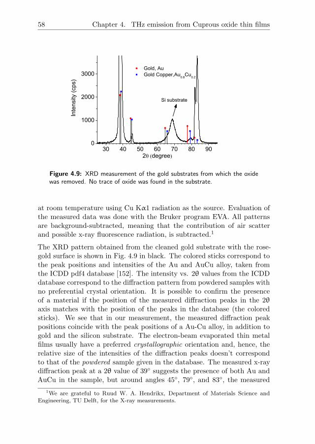
58 Chapter 4. THz emission from Cuprous oxide thin films
30 40 50 60 70 80 900
1000
2000
3000In
tens
ity (c
ps)
2 degree
Si substrate
Gold, Au Gold Copper,Au0.8Cu0.2
Figure 4.9: XRD measurement of the gold substrates from which the oxidewas removed. No trace of oxide was found in the substrate.
at room temperature using Cu Kα1 radiation as the source. Evaluation ofthe measured data was done with the Bruker program EVA. All patternsare background-subtracted, meaning that the contribution of air scatterand possible x-ray fluorescence radiation, is subtracted.1
The XRD pattern obtained from the cleaned gold substrate with the rose-gold surface is shown in Fig. 4.9 in black. The colored sticks correspond tothe peak positions and intensities of the Au and AuCu alloy, taken fromthe ICDD pdf4 database [152]. The intensity vs. 2θ values from the ICDDdatabase correspond to the diffraction pattern from powdered samples withno preferential crystal orientation. It is possible to confirm the presenceof a material if the position of the measured diffraction peaks in the 2θaxis matches with the position of the peaks in the database (the coloredsticks). We see that in our measurement, the measured diffraction peakpositions coincide with the peak positions of a Au-Cu alloy, in addition togold and the silicon substrate. The electron-beam evaporated thin metalfilms usually have a preferred crystallographic orientation and, hence, therelative size of the intensities of the diffraction peaks doesn’t correspondto that of the powdered sample given in the database. The measured x-raydiffraction peak at a 2θ value of 39◦ suggests the presence of both Au andAuCu in the sample, but around angles 45◦, 79◦, and 83◦, the measured
1We are grateful to Ruud W. A. Hendrikx, Department of Materials Science andEngineering, TU Delft, for the X-ray measurements.
4.6. Variable-Angle Spectroscopic Ellipsometry 59
peaks coincide better with the expected peak positions of the AuCu alloy.This proves that inter-diffusion compounds of Au and Cu are formed at theinterface. From the peaks around 38◦ and 82◦, it can be argued that someAu is also present in its pure form. From the XRD analysis, the alloy isestimated to have a composition of Au0.8Cu0.2. However, since nitric acidcan dissolve Cu, we note that the process of removing the Cu2O layer couldhave caused some changes in the actual composition of the alloy layer. Itcan also be argued that the composition of the alloy may also vary in depthand laterally due to inhomogeneities in the diffusion. However, we do notsee a proof for this from the XRD analysis, since the presence of severalcompositions would have given rise to more peaks in the XRD measurement.The main intention here is to show the presence of an inter-diffusion layer,and its importance in the THz generation process from our samples.
4.6 Variable-Angle Spectroscopic Ellipsometry
Spectroscopic ellipsometry allows for accurate measurements of the opticalproperties of thin films. In this technique, the change in polarization stateof the light reflected from the thin film-substrate system is measured andis expressed by two values (Ψ, ∆) which are defined by the ellipsometricequation [153]
ei∆ tan (Ψ) = ρ =rprs. (4.7)
Here rp and rs are the complex Fresnel reflection coefficients of the samplefor p- and s-polarized incident light. Ψ and ∆ represent the angles deter-mined from the amplitude ratio and phase difference between the reflectedp- and s-polarized components. A model is constructed to calculate thevalues of (Ψ, ∆) using various parameters such as optical constants, layerthicknesses, surface roughness, etc. The generated and the experimentallydetermined values of Ψ and ∆ are compared and one or more model param-eters are adjusted to fit the experimental data. This is done in an iterativemanner until a good fit is reached between the measured and the experi-mental spectra. In variable-angle spectroscopic ellipsometry, these valuesare measured over a wide range of wavelengths and angles of incidence,which helps to minimize errors in extracting the material properties.
We performed ellipsometric measurements using a Variable Angle Spectro-scopic Ellipsometer (VASE, J.A.WoollamCo.) in the wavelength regionfrom 600 nm to 1600 nm and at different angles of incidence varying from45◦ to 60◦. Initially, we fabricated individual thin films of Au and Cu2O
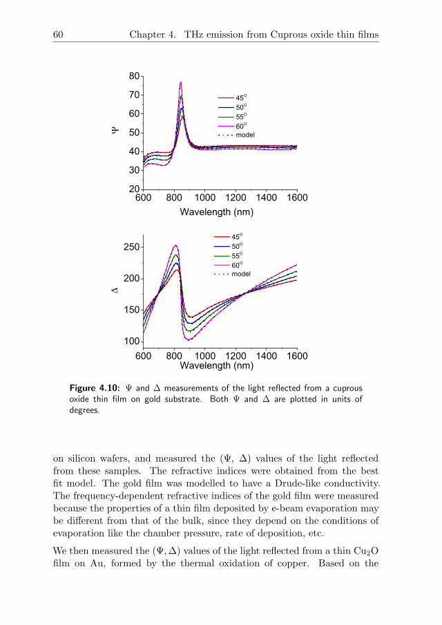
60 Chapter 4. THz emission from Cuprous oxide thin films
600 800 1000 1200 1400 160020
30
40
50
60
70
80
Wavelength (nm)
45O
50O
55O
60O
model
600 800 1000 1200 1400 1600100
150
200
250 45O
50O
55O
60O
model
Wavelength (nm)
Figure 4.10: Ψ and ∆ measurements of the light reflected from a cuprousoxide thin film on gold substrate. Both Ψ and ∆ are plotted in units ofdegrees.
on silicon wafers, and measured the (Ψ, ∆) values of the light reflectedfrom these samples. The refractive indices were obtained from the bestfit model. The gold film was modelled to have a Drude-like conductivity.The frequency-dependent refractive indices of the gold film were measuredbecause the properties of a thin film deposited by e-beam evaporation maybe different from that of the bulk, since they depend on the conditions ofevaporation like the chamber pressure, rate of deposition, etc.
We then measured the (Ψ,∆) values of the light reflected from a thin Cu2Ofilm on Au, formed by the thermal oxidation of copper. Based on the

4.6. Variable-Angle Spectroscopic Ellipsometry 61
(a) (b)
Figure 4.11: Frequency-dependent real (n) and imaginary (k) parts of therefractive index of (a) the AuCu alloy layer and (b) the Cu2O thin film, asobtained using the VASE software. The inset of (b) gives a closer look at theimaginary part of the refractive index of the Cu2O thin film.
assumption that there is an inter-diffusion layer of AuCu formed at theinterface, we included this layer in the model. Hence, the model consistsof the AuCu alloy film on gold (which was considered as the substrate),and the Cu2O layer with surface roughness. At the start of the fittingprocedure, the thickness of the pure gold film and the AuCu alloy was setto 50 nm and 0 nm, respectively, and was then allowed to vary duringthe iterations. The refractive index of AuCu was allowed to vary in themodel, and the frequency-dependent refractive indices of the material wereparametrized by means of B-splines, which provide a numerical tool for datafitting, without considering any physical model [154]. A B-spline consistsof an array of control or ‘knot’ points and a set of interpolating polynomialfunctions. The permittivity values of the material assumed by the modelat the knot points are so as to generate (Ψ,∆) values which match withthe experimentally measured ones. The imaginary part of the frequency-dependent dielectric permittivity of the material is modeled as the B-splinefunction and the real part is calculated from the Kramers-Kronig relations.The imaginary part of the refractive index, k is forced to be always positive,to make physical sense. Measured optical constants of the evaporated 50nm Au film were used as the starting values for fitting that of the AuCufilm. The frequency-dependent refractive indices of the Cu2O thin filmwere also parametrized by means of B-splines. For Cu2O, the initial valuesof the refractive index were taken from the measured values for a differentoxide film on a silicon substrate.
The values of Ψ and ∆ for the sample from the experiment and the best

62 Chapter 4. THz emission from Cuprous oxide thin films
(a) (b)
Figure 4.12: (a) AFM image of the surface of a cuprous oxide thin film (b)Height histogram of the cuprous oxide surface.
fit model are shown in Fig. 4.10. The colored solid lines correspond to themeasured Ψ and ∆ at different angles of incidence and the dashed blacklines show the values calculated using the model. A good fit is obtainedbetween the measurement and the model, as can be seen from the figure.The optical constants of the Au-Cu alloy and Cu2O from the best-fit modelare given in Fig. 4.11. The thickness of the Cu2O thin film was around232 nm with a roughness of 23 nm. This agrees well with the averageroughness (∼ 21 nm) measured using the AFM (see Fig. 4.12). Increasingthe thickness did not have any effect on the model generated values of(Ψ,∆), indicating that the thickness of the AuCu film is larger than thepenetration depth. The penetration depth of light of wavelength 700 nmin the AuCu thin film was calculated to be around 8 nm.
4.7 Thickness dependence of pump power absorp-tion and THz emission
As mentioned earlier, the band gap of Cu2O is ∼2 eV. The wavelength ofthe pump laser used for the THz emission experiments, is centered around800 nm, which corresponds to an energy of 1.5 eV. At this wavelength,the absorption coefficient α of bulk Cu2O has a small value of 9.42 x 10³
cm−1 [155]. In our THz generation model, charge carriers are generatedin the Cu2O film by absorbing the laser photons, which then accelerate inthe Schottky electric field to result in THz emission. The small absorption
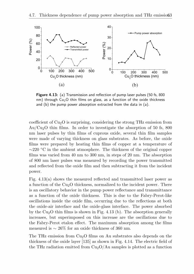
4.7. Thickness dependence of pump power absorption and THz emission63
(b)(a)
Figure 4.13: (a) Transmission and reflection of pump laser pulses (50 fs, 800nm) through Cu2O thin films on glass, as a function of the oxide thicknessand (b) the pump power absorption extracted from the data in (a).
coefficient of Cu2O is surprising, considering the strong THz emission fromAu/Cu2O thin films. In order to investigate the absorption of 50 fs, 800nm laser pulses by thin films of cuprous oxide, several thin film sampleswere made of varying thickness on glass substrates. As before, the oxidefilms were prepared by heating thin films of copper at a temperature of∼220 ◦C in the ambient atmosphere. The thickness of the original copperfilms was varied from 40 nm to 300 nm, in steps of 20 nm. The absorptionof 800 nm laser pulses was measured by recording the power transmittedand reflected from the oxide film and then subtracting it from the incidentpower.
Fig. 4.13(a) shows the measured reflected and transmitted laser power asa function of the Cu2O thickness, normalized to the incident power. Thereis an oscillatory behavior in the pump power reflectance and transmittanceas a function of the oxide thickness. This is due to the Fabry-Perot-likeoscillations inside the oxide film, occurring due to the reflections at boththe oxide-air interface and the oxide-glass interface. The power absorbedby the Cu2O thin films is shown in Fig. 4.13 (b). The absorption generallyincreases, but superimposed on this increase are the oscillations due tothe Fabry-Perot etalon effect. The maximum absorption among the filmsmeasured is ∼ 26% for an oxide thickness of 360 nm.
The THz emission from Cu2O films on Au substrates also depends on thethickness of the oxide layer [135] as shown in Fig. 4.14. The electric field ofthe THz radiation emitted from Cu2O/Au samples is plotted as a function

64 Chapter 4. THz emission from Cuprous oxide thin films
0 100 200 300 400 500 6000.0
0.5
1.0
Cu2O layer thickness (nm)
THz
ampl
itude
(Arb
. uni
ts)
0
20
40
60
80
Abso
rbed
pum
p po
wer
(%)
Figure 4.14: Amplitude of THz electric field emitted from Cu2O/Au samplesas a function of the oxide thickness (black). In blue is the corresponding pumppower absorption. (adapted from Ref. [135])
of the oxide thickness (dots). The squares correspond to the pump powerabsorption in these samples. A much stronger absorption of the pump laserpulses is seen in the case of Cu2O films deposited on Au. For example, for aCu2O thickness of 65 nm on Au, the absorption is already 55 %. This shouldbe compared with the 6 % absorption observed for the same Cu2O thicknesson glass. The absorption increases as a function of thickness and also showsetalon effects. The maximum pump power absorption seen is almost 75 %for a Cu2O film thickness of 420 nm. The THz emission also increases withthe pump power absorption, but faster. The maximum THz emission occursfor oxide thicknesses at which the reflection is minimized due to the etaloneffect. For the right thicknesses, multiple reflections occur at the Au/Cu2Oand Cu2O/air boundaries, which increases the optical path length of thelaser pulses inside Cu2O. This enhances the laser-light absorption insidethe material. This is also called the cavity-resonance effect.
4.8 Multilayer reflection: Calculation and experi-ment
As mentioned in the previous section, the THz emission from a Cu2O/Auinterface is proportional to the amount of laser power absorbed in the oxidefilm. At an optimum thickness, the Cu2O film can act as its own antire-flection coating and, hence, increase the absorption inside the sample at

4.8. Multilayer reflection: Calculation and experiment 65
(a) (b)
Figure 4.15: (a) Measured and (b) calculated reflection spectra of Cu2Olayers of different thicknesses on a gold substrate, normalized to the reflectionfrom a bare gold substrate.
a particular wavelength. Knowing the reflection spectra of the Cu2O thinfilms on oxide substrates we can find the thickness at which the reflectionminimum occurs at the pump laser wavelength, 800 nm. Since we have ex-tracted the frequency-dependent refractive indices of the Cu2O and AuCuthin films, we can calculate the reflection spectra of the oxide films on theAuCu substrate for various thicknesses. We also experimentally measuredthe broadband reflection spectra of samples of five different Cu2O thick-nesses on AuCu substrates, to validate the complex refractive indices ofthe materials obtained from the ellipsometer analysis (refer Section. 4.6).
To measure the reflection spectrum, a Tungsten halogen lamp (HL 2000,Ocean optics) was used as the broadband visible light source. The lightfrom the source was passed through a polarizer and was incident upon thesamples at 45◦ angle of incidence. The spectrum of the reflected light wasmeasured using an Ocean Optics spectrometer. The Cu2O layer thicknessesof the samples used in the experiment were measured using the variable an-gle spectroscopic ellipsometer. The intensity of the light reflected from theoxide film on the gold substrate was measured as a function of wavelengthand normalized to the reflection from a bare gold film. The reflectivityspectra thus obtained for five different Cu2O film thicknesses are plottedin Fig. 4.15(a). The calculation of the wavelength dependent reflectivity,also normalized to the reflection from a bare gold film, was done with ananalytical solution [156] which is suitable for multilayers containing strongabsorbing elements such as metals. The calculated reflection spectra areshown in Fig. 4.15 (b). The multilayer stack considered for the reflectioncoefficient calculation consists of the silicon substrate, a 50 nm thick Cr
66 Chapter 4. THz emission from Cuprous oxide thin films
film, 50 nm AuCu layer and the Cu2O film. To calculate the reflectionspectra, we used the frequency-dependent complex refractive-index of thematerials which was obtained from analyzing the ellipsometry measure-ments. We can see that there is a good agreement between the calculatedand the measured reflection spectra. The dashed blue curve in Fig. 4.15(b)shows the reflection spectrum of a sample with a 223 nm thick Cu2O film,calculated without considering the formation of AuCu layer, but consider-ing pure gold as the substrate. It can be seen that this does not matchwell with the experimentally measured spectrum for the same oxide thick-ness. In particular, the position of the calculated minimum at ∼855 nmis off compared to the measured one at ∼820 nm. The thickness of theoxide layer of this sample was also measured independently using a surfaceprofilometre to be ∼ 225 nm, which is very close to the value of 223 nmextracted from the ellipsometer measurement. The minimum in the calcu-lated reflection spectrum of this sample occurs at a different wavelength inthe case of AuCu alloy instead of Au as the substrate for the Cu2O layer,since the dielectric function of AuCu is different compared to Au. Hencethere is a difference in the phase change on reflection compared to that fromAu, leading to the shift in the calculated minimum in the reflection shownin Fig. 4.15(b). A good agreement between the measured and calculatedreflection spectra was obtained only when the AuCu thin film was consid-ered in the calculation, again supporting the presence of the inter-diffusionAuCu alloy layer and validating the optical constants derived from the el-lipsometer measurements. The small discrepancies between the calculatedand measured reflection spectra could be due to a combination of severalissues. The reflection calculation, for example, ignores the roughness of theoxide film in the calculation, the lateral inhomogeneities in the refractiveindex of the Cu2O layer, and experimental errors in determining the angleof incidence. It can also be seen from the calculated and reflected spectrathat an oxide film of ∼225 nm thickness is well suited for THz emissionapplications, since it has a very low reflection coefficient at 800 nm, whichis the pump laser wavelength used in THz generation experiments.
4.9 Application: Tapered waveguide
One of the main applications of optoelectronic THz transmitters and re-ceivers is terahertz absorption spectroscopy for the characterization ofmolecules and crystals. Often, there is a need to identify very small quan-tities of a material. A promising solution appears to be the use of THz

4.9. Application: Tapered waveguide 67
(a)
THz in
THz outPPWG
THz out
800 nm, 50 fs
(b)
1 mm
Figure 4.16: (a) Conventional configuration of a parallel plate waveguide(PPWG) [top] and a tapered PPWG, modified to have the THz source insidethe waveguide [bottom]. In the tapered waveguide, one of the waveguideplate is a copper plate with a cuprous oxide thin film on the surface and theother is Al. (b) A magnified image of the tapered end of the PPWG.
waveguides for frequency-dependent absorption measurements using THztime-domain spectroscopy [157]. THz spectroscopy using metal parallel-plate waveguides (PPWG) has also been demonstrated by Melinger et al.[158]. They used the transverse electromagnetic (TEM) mode of the metalPPWG to probe the properties of a thin polycrystalline film dropcast ontoone of the metal plates. The advantage of performing spectroscopy using aPPWG is that only micrograms of a sample are required due to the spatialconfinement. In addition, high spatial resolution THz absorption spectrameasurements are possible due to the 2D spatial confinement [159]. It wasreported that PPWG terahertz time domain spectroscopy can be sensitiveeven to nanometer-thick water layers on surfaces [160]. THz waveguideshave also been used for the characterization of Bragg and non-Bragg stopbands of metal slits [161], photonic crystals [162], terahertz band gap prop-erties [161, 163], etc.
However, an important issue limiting the use of THz-waveguides is reflec-tion losses due to the inefficient coupling between the guided and freelypropagating THz waves. An increase in the measurement sensitivity is ob-tained by decreasing the plate separation of the PPWG, but this comes atthe cost of reducing the energy coupled into the waveguide. To increasethe coupling of THz radiation to these narrow waveguides, silicon lensesare used. However, the refractive index of silicon is high and this results inthe loss of THz radiation by reflection from the silicon lenses. The reflec-tion losses at the silicon lenses essentially suppress the advantage of using a

68 Chapter 4. THz emission from Cuprous oxide thin films
(a) (b)
Figure 4.17: (a) The THz signal generated and guided out from a taperedparallel plate waveguide. One of the waveguide plates is made of Cu, with athin Cu2O film on the surface. (b) The corresponding frequency spectrum ofthe detected THz pulse.
waveguide for high sensitivity measurements. Recently, it was shown thatthe use of a tapered parallel plate waveguide can improve THz coupling tothe narrow gap of the waveguide [164, 165]. In the conventional quasi-opticapproach (shown in Fig. 4.16 (a) [top figure]), most of the THz light is re-flected by the silicon surfaces. By tapering the metal surface of the parallelplate waveguide, the changes in the waveguide gap are introduced gradually[166]. In other words, the width of the PPWG changes slowly with respectto the wavelength and hence the reflection losses can be minimized.
Utilizing the THz emission properties of Cu2O on metal substrates, weput forward a new method for achieving efficient coupling into the parallelplate waveguide. The tapered PPWG can be modified in such a way thatinstead of coupling THz radiation into the PPWG, we can generate theTHz radiation inside the waveguide itself. In this approach, one of themetal plates is a copper plate having a thin film of cuprous oxide on itssurface. An aluminium plate is used on the other side in the parallel plateconfiguration. The pump laser illuminates the copper plate with the oxidesurface at a grazing angle, as shown in Fig. 4.16(a) [bottom figure]. Theexperimental setup is the same as Fig. 4.4. A 500 µm ZnTe crystal is usedfor THz detection. A photograph of the waveguide is shown in Fig. 4.16(b).The THz signal generated and guided out from the waveguide is shownin Fig. 4.17(a). The Fourier-transformed spectrum of the THz signal isshown in Fig. 4.17(b). The spectrum consists of components from 0.5 THzto almost 4 THz. Apart from the spectroscopic applications, this kind ofwaveguide can also be used to concentrate THz radiation in subwavelength-

4.9. Application: Tapered waveguide 69
sized focal spots. The spot size of the THz beam at the end of the waveguideis determined by the plate separation at the out-coupling end. By reducingthis in the x- and y-directions, it is possible to achieve sub-wavelength THzspot sizes. This can also have important applications in sub-wavelengthimaging using THz frequencies.

Chapter
5Plasmon-enhanced THzemission from Schottky
junctions
5.1 Introduction
In the previous chapter we saw that Au/Cu2O Schottky junctions can emitbroadband THz radiation when excited with femtosecond laser pulses. Itwas observed that the bandwidth of the THz generation extends upto al-most 8 THz. The THz light generated from Au/Cu2O thin films with anoptimized Cu2O film thickness is almost half as powerful as the emissionfrom a 300 µm GaP crystal, which is another THz source capable of suchbroadband THz emission. Understanding the THz emission mechanism ofthese emitters could help us to further increase the emitted THz power,perhaps leading to a broadband and strong THz source. The possibleTHz emission mechanisms include: optical rectification occurring due toSchottky electric-field-induced second-order nonlinearities [167] in Cu2O,acceleration of photoexcited charge carriers in the Schottky field, or inter-nal photoemission of holes over the Schottky barrier [168]. In any case, theformation of a Schottky junction seems to be critical for the THz emission.In this respect it is logical to propose that localizing the pump light at theinterface — where the Schottky electric field is the maximum — can resultin an increase in the efficiency of these THz emitters. One way to achievethis is by exciting so-called surface plasmons at the metal/Cu2O interface.
It has been shown that the strong local electromagnetic fields associatedwith surface plasmons can give rise to stronger optical absorption [59] andstronger fluorescence [169], and can enhance nonlinear processes like second-harmonic generation [65], Raman scattering [170] etc. Recent attention hasalso focused on the use of surface plasmons to enhance the emission fromknown THz emitters in several ways. It has been demonstrated that surfaceplasmons, excited using random, as well as ordered nanostructures, can en-hance the terahertz emission from thin gold films [85, 69, 70]. Emission of

72 Chapter 5. Plasmon-enhanced THz emission from Schottky junctions
terahertz radiation is also observed when surface plasmons are excited ona thin unstructured film of gold deposited on a glass prism and excited inthe so-called Kretschmann geometry [71]. Most recently, plasmonic pho-toconductive antennas have been shown to enhance the terahertz emissioncompared to conventional photoconductive antennas [72, 73]. Interleavedplasmonic electrodes were used with the photoconductive antenna by Berryand Jarrahi [73], where the interleaved electrodes were used to reduce thetransit time of the generated carriers to the electrodes. It was illustrated,through simulations, that the plasmonic nature of the interleaved electrodesincreases the pump power absorption inside the photo-conducting material.However, the relation between the THz emission and the plasmonic natureof the electrodes was not experimentally demonstrated.
In this chapter, we demonstrate that Au/Cu2O Schottky interfaces capa-ble of emitting terahertz radiation can be nano-structured to support sur-face plasmon modes, and that this leads to enhanced THz generation. Thenanostructures we have shown are Cu2O covered gold gratings of various pe-riodicities. We argue that the efficiency of the THz generation is improvedbecause surface plasmon excitation leads to increased optical absorptionnear the interfaces where the Schottky electric field is the strongest. Cou-pling of light into plasmons at the laser excitation wavelength is confirmedusing white-light reflection spectroscopy. The THz emission, as well as thepump power absorption, show a dependence on both the azimuthal angle ofthe sample when rotated around the surface normal, and on the periodicityof the grating, clearly highlighting the role played by the grating in enhanc-ing the THz emission. It is shown that the plasmon mode is essential inenhancing the THz emission.
5.2 The concept of a plasmon-enhanced Schottkyemitter
A schematic diagram showcasing the idea of a nano-structured metal/semiconductor thin film THz emitter is shown in Fig. 5.1. A gold nanograting is fabricated and covered with a thin Cu2O film. Femtosecondlaser pulses centered around a wavelength of 800 nm are used to pumpa Au/Cu2O thin film THz emitter at an angle of incidence of 45◦, andsurface plasmons are optically excited at the interface. The optical fieldof the pump laser is thus localized near the interface between Au and theoxide thin film. The objective behind the work described in this chapter is
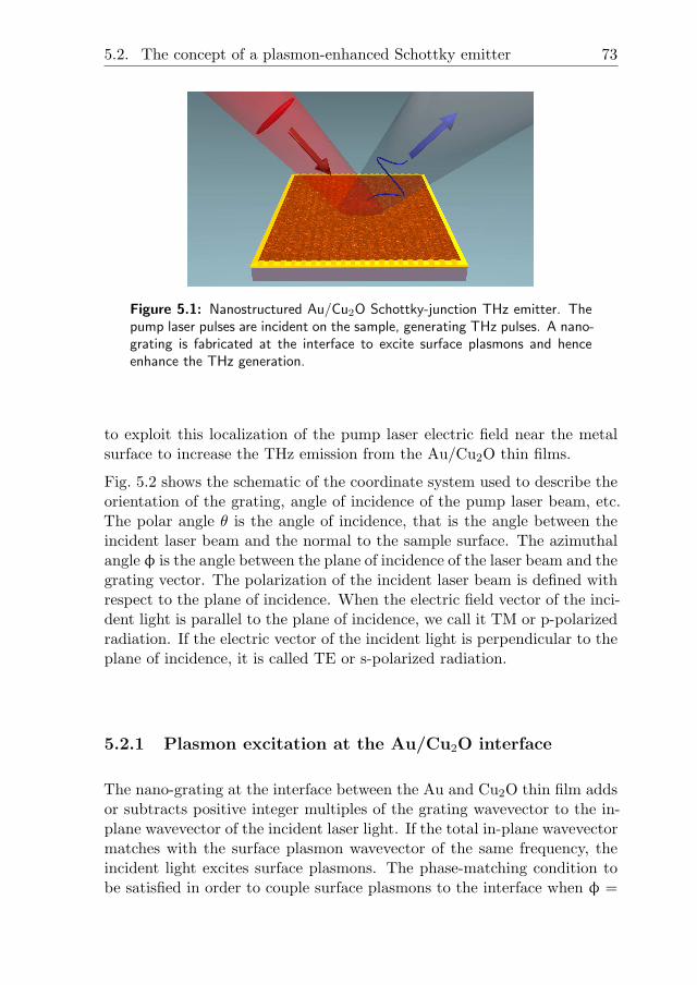
5.2. The concept of a plasmon-enhanced Schottky emitter 73
Figure 5.1: Nanostructured Au/Cu2O Schottky-junction THz emitter. Thepump laser pulses are incident on the sample, generating THz pulses. A nano-grating is fabricated at the interface to excite surface plasmons and henceenhance the THz generation.
to exploit this localization of the pump laser electric field near the metalsurface to increase the THz emission from the Au/Cu2O thin films.
Fig. 5.2 shows the schematic of the coordinate system used to describe theorientation of the grating, angle of incidence of the pump laser beam, etc.The polar angle θ is the angle of incidence, that is the angle between theincident laser beam and the normal to the sample surface. The azimuthalangle φ is the angle between the plane of incidence of the laser beam and thegrating vector. The polarization of the incident laser beam is defined withrespect to the plane of incidence. When the electric field vector of the inci-dent light is parallel to the plane of incidence, we call it TM or p-polarizedradiation. If the electric vector of the incident light is perpendicular to theplane of incidence, it is called TE or s-polarized radiation.
5.2.1 Plasmon excitation at the Au/Cu2O interface
The nano-grating at the interface between the Au and Cu2O thin film addsor subtracts positive integer multiples of the grating wavevector to the in-plane wavevector of the incident laser light. If the total in-plane wavevectormatches with the surface plasmon wavevector of the same frequency, theincident light excites surface plasmons. The phase-matching condition tobe satisfied in order to couple surface plasmons to the interface when φ =
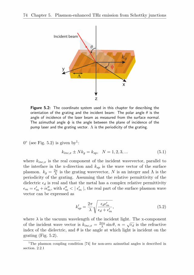
74 Chapter 5. Plasmon-enhanced THz emission from Schottky junctions
Incident beam
x
z
y
Λ
φ
Figure 5.2: The coordinate system used in this chapter for describing theorientation of the grating and the incident beam: The polar angle θ is theangle of incidence of the laser beam as measured from the surface normal.The azimuthal angle φ is the angle between the plane of incidence of thepump laser and the grating vector. Λ is the periodicity of the grating.
0◦ (see Fig. 5.2) is given by1:
kinc,x ±Nkg = ksp, N = 1, 2, 3, ... (5.1)
where kinc,x is the real component of the incident wavevector, parallel tothe interface in the x-direction and ksp is the wave vector of the surfaceplasmon. kg = 2π
Λ is the grating wavevector, N is an integer and Λ is theperiodicity of the grating. Assuming that the relative permittivity of thedielectric ǫd is real and that the metal has a complex relative permittivityǫm = ǫ′m + iǫ′′m, with ǫ′′m < | ǫ′m |, the real part of the surface plasmon wavevector can be expressed as
k′sp =2π
λ
√
ǫdǫ′mǫd + ǫ′m
, (5.2)
where λ is the vacuum wavelength of the incident light. The x-componentof the incident wave vector is kinc,x = 2πn
λsin θ, n =
√ǫd is the refractive
index of the dielectric, and θ is the angle at which light is incident on thegrating (Fig. 5.2).
1The plasmon coupling condition [74] for non-zero azimuthal angles is described insection. 2.2.1
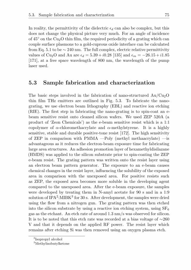
5.3. Sample fabrication and characterization 75
In reality, the permittivity of the dielectric ǫd can also be complex, but thisdoes not change the physical picture very much. For an angle of incidenceof 45◦ on the Cu2O thin film, the required periodicity of a grating which cancouple surface plasmons to a gold-cuprous oxide interface can be calculatedfrom Eq. 5.1 to be ∼ 240 nm. The full complex, electric relative permittivityvalues of Cu2O and Au are ǫd = 5.39+ i0.28 [135] and ǫm = −26.15+ i1.85[171], at a free space wavelength of 800 nm, the wavelength of the pumplaser used.
5.3 Sample fabrication and characterization
The basic steps involved in the fabrication of nano-structured Au/Cu2Othin film THz emitters are outlined in Fig. 5.3. To fabricate the nano-grating, we use electron beam lithography (EBL) and reactive ion etching(RIE). The first step in fabricating the nano-grating is to spin-coat an e-beam sensitive resist onto cleaned silicon wafers. We used ZEP 520A (aproduct of ‘Zeon Chemicals’) as the e-beam sensitive resist which is a 1:1copolymer of α-chloromethacrylate and α-methylstyrene. It is a highlysensitive, stable and durable positive-tone resist [172]. The high sensitivityof ZEP in comparison with PMMA —Poly (methyl methaacrylate) —isadvantageous as it reduces the electron-beam exposure time for fabricatinglarge area structures. An adhesion promotion layer of hexamethyldisilazane(HMDS) was applied to the silicon substrate prior to spin-coating the ZEPe-beam resist. The grating pattern was written onto the resist layer usingan electron beam pattern generator. The exposure to an e-beam causeschemical changes in the resist layer, influencing the solubility of the exposedarea in comparison with the unexposed area. For positive resists suchas ZEP, the exposed area becomes more soluble in the developing agentcompared to the unexposed area. After the e-beam exposure, the sampleswere developed by treating them in N-amyl acetate for 90 s and in a 1:9solution of IPA2:MIBK3 for 30 s. After development, the samples were driedusing the flow from a nitrogen gun. The grating pattern was then etchedinto the silicon substrate by using a reactive ion etching system, using SF6
gas as the etchant. An etch rate of around 1.3 nm/s was observed for silicon.It is to be noted that this etch rate was recorded at a bias voltage of ∼260V and that it depends on the applied RF power. The resist layer whichremains after etching Si was then removed using an oxygen plasma etch.
2Isopropyl alcohol3Methylisobutylketone
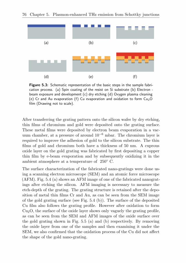
76 Chapter 5. Plasmon-enhanced THz emission from Schottky junctions
(a) (b) (c)
(d) (e) (f )
Figure 5.3: Schematic representation of the basic steps in the sample fabri-cation process. (a) Spin coating of the resist on Si substrate (b) Electron -beam exposure and development (c) dry etching (d) Oxygen plasma cleaning(e) Cr and Au evaporation (f) Cu evaporation and oxidation to form Cu2Ofilm (Drawing not to scale).
After transferring the grating pattern onto the silicon wafer by dry etching,thin films of chromium and gold were deposited onto the grating surface.These metal films were deposited by electron beam evaporation in a vac-uum chamber, at a pressure of around 10−6 mbar. The chromium layer isrequired to improve the adhesion of gold to the silicon substrate. The thinfilms of gold and chromium both have a thickness of 50 nm. A cuprousoxide layer on the gold grating was fabricated by first depositing a copperthin film by e-beam evaporation and by subsequently oxidizing it in theambient atmosphere at a temperature of 250◦ C.
The surface characterization of the fabricated nano-gratings were done us-ing a scanning electron microscope (SEM) and an atomic force microscope(AFM). Fig. 5.4 (a) shows an AFM image of one of the fabricated nanograt-ings after etching the silicon. AFM imaging is necessary to measure theetch-depth of the grating. The grating structure is retained after the depo-sition of metal thin films Cr and Au, as can be seen from the SEM imageof the gold grating surface (see Fig. 5.4 (b)). The surface of the depositedCu film also follows the grating profile. However after oxidation to formCu2O, the surface of the oxide layer shows only vaguely the grating profile,as can be seen from the SEM and AFM images of the oxide surface overthe gold grating shown in Fig. 5.5 (a) and (b) respectively. By removingthe oxide layer from one of the samples and then examining it under theSEM, we also confirmed that the oxidation process of the Cu did not affectthe shape of the gold nano-grating.
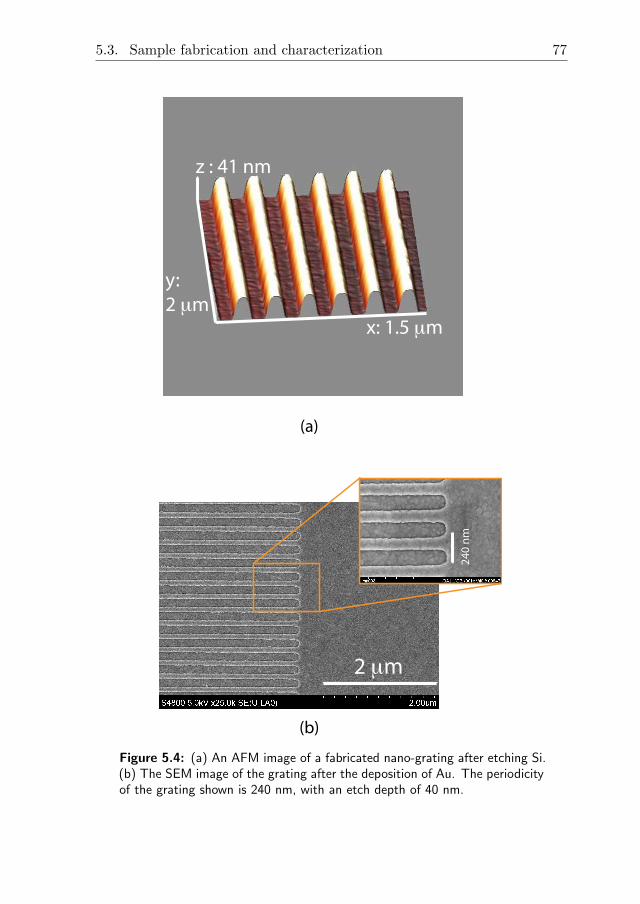
5.3. Sample fabrication and characterization 77
2 μm
24
0 n
m
(a)
(b)
z : 41 nm
y:
2 μm x: 1.5 μm
Figure 5.4: (a) An AFM image of a fabricated nano-grating after etching Si.(b) The SEM image of the grating after the deposition of Au. The periodicityof the grating shown is 240 nm, with an etch depth of 40 nm.
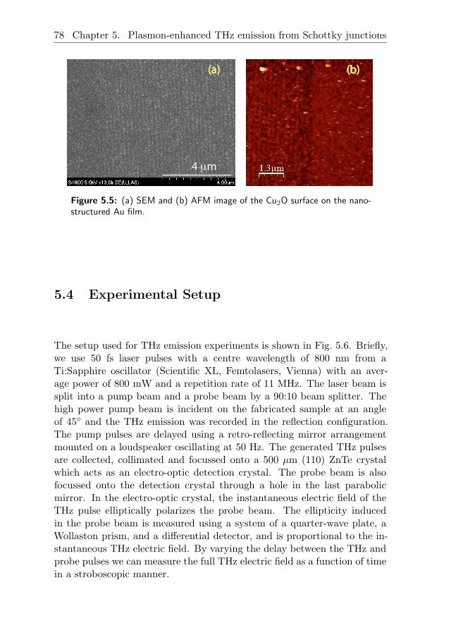
78 Chapter 5. Plasmon-enhanced THz emission from Schottky junctions
4 μm
(a) (b)
Figure 5.5: (a) SEM and (b) AFM image of the Cu2O surface on the nano-structured Au film.
5.4 Experimental Setup
The setup used for THz emission experiments is shown in Fig. 5.6. Briefly,we use 50 fs laser pulses with a centre wavelength of 800 nm from aTi:Sapphire oscillator (Scientific XL, Femtolasers, Vienna) with an aver-age power of 800 mW and a repetition rate of 11 MHz. The laser beam issplit into a pump beam and a probe beam by a 90:10 beam splitter. Thehigh power pump beam is incident on the fabricated sample at an angleof 45◦ and the THz emission was recorded in the reflection configuration.The pump pulses are delayed using a retro-reflecting mirror arrangementmounted on a loudspeaker oscillating at 50 Hz. The generated THz pulsesare collected, collimated and focussed onto a 500 µm (110) ZnTe crystalwhich acts as an electro-optic detection crystal. The probe beam is alsofocussed onto the detection crystal through a hole in the last parabolicmirror. In the electro-optic crystal, the instantaneous electric field of theTHz pulse elliptically polarizes the probe beam. The ellipticity inducedin the probe beam is measured using a system of a quarter-wave plate, aWollaston prism, and a differential detector, and is proportional to the in-stantaneous THz electric field. By varying the delay between the THz andprobe pulses we can measure the full THz electric field as a function of timein a stroboscopic manner.
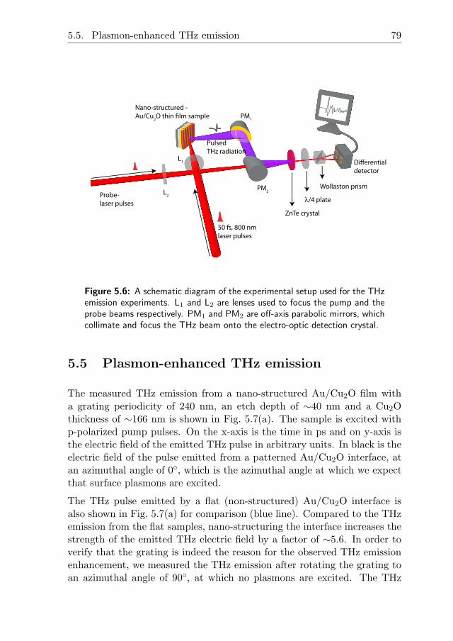
5.5. Plasmon-enhanced THz emission 79
L1
L2
Nano-structured -
Au/Cu2O thin �lm sample PM
1
PM2
ZnTe crystal
λ/4 plate
Wollaston prism
Di!erential
detector
Pulsed
THz radiation
50 fs, 800 nm
laser pulses
Probe-
laser pulses
Figure 5.6: A schematic diagram of the experimental setup used for the THzemission experiments. L1 and L2 are lenses used to focus the pump and theprobe beams respectively. PM1 and PM2 are off-axis parabolic mirrors, whichcollimate and focus the THz beam onto the electro-optic detection crystal.
5.5 Plasmon-enhanced THz emission
The measured THz emission from a nano-structured Au/Cu2O film witha grating periodicity of 240 nm, an etch depth of ∼40 nm and a Cu2Othickness of ∼166 nm is shown in Fig. 5.7(a). The sample is excited withp-polarized pump pulses. On the x-axis is the time in ps and on y-axis isthe electric field of the emitted THz pulse in arbitrary units. In black is theelectric field of the pulse emitted from a patterned Au/Cu2O interface, atan azimuthal angle of 0◦, which is the azimuthal angle at which we expectthat surface plasmons are excited.
The THz pulse emitted by a flat (non-structured) Au/Cu2O interface isalso shown in Fig. 5.7(a) for comparison (blue line). Compared to the THzemission from the flat samples, nano-structuring the interface increases thestrength of the emitted THz electric field by a factor of ∼5.6. In order toverify that the grating is indeed the reason for the observed THz emissionenhancement, we measured the THz emission after rotating the grating toan azimuthal angle of 90◦, at which no plasmons are excited. The THz
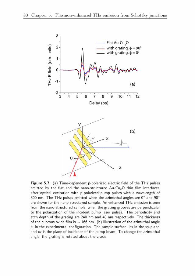
80 Chapter 5. Plasmon-enhanced THz emission from Schottky junctions
Flat Au-Cu2O
with grating, φ = 900 with grating, φ = 00
x
y
z
φ
θ
(a)
(b)
Figure 5.7: (a) Time-dependent p-polarized electric field of the THz pulsesemitted by the flat and the nano-structured Au-Cu2O thin film interfaces,after optical excitation with p-polarized pump pulses with a wavelength of800 nm. The THz pulses emitted when the azimuthal angles are 0◦ and 90◦
are shown for the nano-structured sample. An enhanced THz emission is seenfrom the nano-structured sample, when the grating grooves are perpendicularto the polarization of the incident pump laser pulses. The periodicity andetch depth of the grating are 240 nm and 40 nm respectively. The thicknessof the cuprous oxide film is ∼ 166 nm. (b) Illustration of the azimuthal angleφ in the experimental configuration. The sample surface lies in the xy-plane,and xz is the plane of incidence of the pump beam. To change the azimuthalangle, the grating is rotated about the z-axis.
5.5. Plasmon-enhanced THz emission 81
emission from the nano-structured sample at this orientation is shown inred in the Fig. 5.7(a). The THz emission is only weakly enhanced for thisgrating orientation. It can be seen that the orientation of the grating has asignificant effect on the THz emission from the nano-structured thin films.This substantiates the role played by the grating in enhancing the THzemission from Au/Cu2O thin film samples. In order to achieve the desiredazimuthal angle, the grating is rotated about an axis perpendicular to thesample surface, while the plane of incidence of the laser beam remains thesame. This is illustrated in Fig. 5.7 (b).
The dependence of the THz emission on the orientation of the grating canbe interpreted as an indication of the excitation of surface plasmons at theAu/Cu2O interface. In order to excite surface plasmons, a component ofthe electric field of the incident light perpendicular to the metal surfaceis necessary. For p-polarized laser light incident on the sample at φ =0◦, this condition is satisfied and, hence, surface plasmons can be excited.However, for s-polarized light, there is no component of the incident lightperpendicular to the metal surface at φ = 0◦ and hence no plasmon exci-tation is possible. We experimentally observe that an enhancement of theTHz emission occurs only when the configuration is favorable for plasmonexcitation.
The enhancement of the THz emission from the grating samples also showsa dependence on the etch depth of the grating. The THz emission fromthe nano-structured thin films was measured for three different grating etchdepths —23 nm, 33 nm, and 55 nm. Figure 5.8 shows the time dependentelectric field of the THz pulses emitted from these three samples, comparedto the THz emission from a non-structured sample. The Cu2O film thick-ness deposited on these nano-gratings was around 166 nm. The samplewith an etch depth d ∼ 55 nm shows the maximum THz emission enhance-ment. In this case, the emitted THz electric field is larger than the emissionfrom the flat sample by a factor of around 5.8. Note that this correspondsto a power enhancement factor of ∼33. The samples with a lower etchdepth also showed an enhanced emission, with electric field enhancementfactors of around 2.9 and 4.0, for etch depth values of 23 nm and 33 nmrespectively.
In order to better understand the role of surface plasmons in the enhancedTHz generation, we measured the azimuthal-angle dependence of the pumplaser absorption as well as the THz emission from these three grating sam-ples. Fig. 5.9 compares the variation of the electric-field amplitude of theemitted THz light with respect to the increase in the pump power absorp-

82 Chapter 5. Plasmon-enhanced THz emission from Schottky junctions
Figure 5.8: (a) Electric field of the THz pulses emitted by the flat and thenano-structured Au-Cu2O thin film interfaces with varying etch depths of thegrating. The grating etch depths of the samples shown are 23 nm (blackline), 33 nm(red line), and 55 nm(blue line). The THz pulse emitted by thenon-structured sample (green) is also shown for comparison.
tion resulting from surface plasmon excitation, for φ varying from -90◦ to90◦. The black points show the percentage of the incident light which isabsorbed inside the nano-structured Au/Cu2O thin film samples. In allthe three samples (d = 23, 33, and 55 nm), the maximum absorption isseen when φ = 0◦. The blue points show the electric field amplitude of theTHz pulses emitted from these samples. To make a comparison betweenthe emission from the three samples, the emission is normalized to the THzemission from the sample with an etch depth of 54 nm, at φ = 0◦. It can beseen that the maximum THz emission from each of the samples also occursat φ = 0◦.
When the azimuthal angle is varied from ±90◦ to 0◦, the increase in THzemission strength is faster than the increase in the pump power absorption.For example, for an etch depth of 33 nm, as we vary the azimuthal angleφ from -900 to 00, the optical absorption increases by a factor of about1.8, but the peak-to-peak electric field of the THz emission increases bya factor of 3.2. This faster increase in the THz emission is an indicationof the important role of plasmons in enhancing the THz emission. Whenplasmons are excited, the electric field of the pump laser is concentratedat the Au/Cu2O interface. This increases the absorption and charge car-
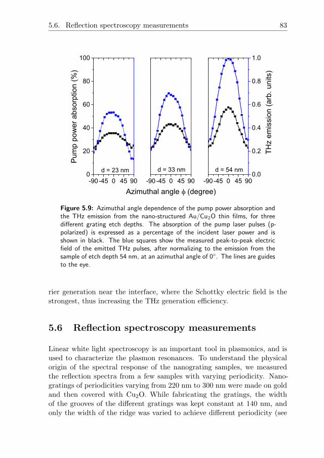
5.6. Reflection spectroscopy measurements 83
-90-45 0 45 900
20
40
60
80
100
THz
emis
sion
(arb
. uni
ts)
Pum
p po
wer
abs
orpt
ion
(%)
d = 23 nm
-90-45 0 45 90
d = 54 nmd = 33 nm
Azimuthal angle (degree)
-90-45 0 45 90
0.0
0.2
0.4
0.6
0.8
1.0
Figure 5.9: Azimuthal angle dependence of the pump power absorption andthe THz emission from the nano-structured Au/Cu2O thin films, for threedifferent grating etch depths. The absorption of the pump laser pulses (p-polarized) is expressed as a percentage of the incident laser power and isshown in black. The blue squares show the measured peak-to-peak electricfield of the emitted THz pulses, after normalizing to the emission from thesample of etch depth 54 nm, at an azimuthal angle of 0◦. The lines are guidesto the eye.
rier generation near the interface, where the Schottky electric field is thestrongest, thus increasing the THz generation efficiency.
5.6 Reflection spectroscopy measurements
Linear white light spectroscopy is an important tool in plasmonics, and isused to characterize the plasmon resonances. To understand the physicalorigin of the spectral response of the nanograting samples, we measuredthe reflection spectra from a few samples with varying periodicity. Nano-gratings of periodicities varying from 220 nm to 300 nm were made on goldand then covered with Cu2O. While fabricating the gratings, the widthof the grooves of the different gratings was kept constant at 140 nm, andonly the width of the ridge was varied to achieve different periodicity (see

84 Chapter 5. Plasmon-enhanced THz emission from Schottky junctions
= 220 nm
140 nm
= 300 nm
140 nm
Figure 5.10: While changing the periodicities of the gratings, only the widthof the ridges was varied and the width of the grooves was kept constant at140 nm.
Fig. 5.10). This was done to avoid a periodicity dependence for any reso-nance which depends on the groove width, and hence, propagating surfaceplasmons would be the only periodicity dependent feature in the reflectionspectra.
To measure the reflection spectrum of the grating samples we used a tung-sten halogen light source and an ‘Ocean Optics’ spectrometer. The mea-surements were made for the spectral range from 600 nm to 1000 nm. Theexperimental setup used for the reflection spectra measurements is shown inFig. 5.11. The light from the output of the light source is collimated usinga lens of focal length 5 cm, and then passed through a polarizer mountedon a rotation stage. The polarized light is then focussed by another lensof focal length 10 cm onto the nano-structured Au/Cu2O sample at a 45degree angle of incidence. The light reflected by the sample is collimatedand focused onto a fiber-optic receiver by a pair of lenses of focal length 10cm and 5 cm respectively. The optical fiber sends the collected light to aspectrometer and the spectrum is then analyzed with a computer.
To normalize the reflection spectra from the nano-structured Au/Cu2O thinfilms, we first obtain a reference spectrum by measuring the reflection froma bare gold surface. The reference spectrum thus obtained is shown inFig. 5.12. The reflection spectra measured from the nano-structured sam-ples RGRATING(Λ) were divided by the reference measurement RGOLD(Λ)(see Fig. 5.11 (b)). Hence the quantity plotted in the reflection spectroscopyanalysis of the nano-structured samples shown in this chapter can be de-

5.6. Reflection spectroscopy measurements 85
L3
L1
L2
L4
Lamp
Spectrometer
RGRATING
RGOLD
(a) (b)
Polarizer
Sample
Figure 5.11: (a) A schematic of the experimental setup for reflection spec-troscopy. The spectrum of the light reflected by the sample is measuredusing a spectrometer. (b) The reflection spectrum of a bare gold surfaceis used to normalize the spectral response of the nano-structured Au/Cu2Ofilms. RGRATING is the reflection from the nano-structured Au/Cu2O filmsand RGOLD is that from a bare gold surface. L1 and L2 lenses used to focusthe light onto the sample and L3, and L4 collect the reflected light to thespectrometer.
400 600 800 1000 12000
20
40
Inte
nsity
(arb
. uni
ts)
Wavelength (nm)
Figure 5.12: The spectrum of the light reflected by a bare gold surface. Thisis used as a reference for normalizing the reflection spectra of Au/Cu2O thinfilms.
86 Chapter 5. Plasmon-enhanced THz emission from Schottky junctions
fined as
R(λ) =RGRATING(λ)
RGOLD(λ). (5.3)
5.6.1 p-polarized incident light
First we measured the reflection spectra of the nano-structured Au/Cu2Osamples of varying periodicity when the incident light is p-polarized andthe azimuthal angle φ = 0◦. The Cu2O film thickness on all the samplesis around 166 nm. In Fig. 5.13, we plot the reflection spectra of the nano-structured Au/Cu2O thin films, normalized to the reflection spectrum ofa bare gold surface. The inset shows the orientation of the grating andthe laser polarization with respect to the plane of incidence. The reflectionspectra were measured for gratings with periodicities varying from 220 to300 nm. In all the reflection spectra, a dip is seen around a wavelengthof 660 nm. This occurs due to the destructive interference caused by themultiple reflections at the oxide boundaries [173, 92], as explained in theprevious chapter. This etalon dip in the reflection spectra is independentof the grating periodicity as it only depends on the average thickness of theCu2O film over the Au substrate.
In Fig. 5.13, another resonance is observed which does depend on the grat-ing periodicity, which is suggestive of a plasmonic character. This plasmonresonance is seen around a wavelength of 980 nm for a sample with gratingperiodicity of 300 nm. The plasmon resonance shifts to lower wavelengthswhen the periodicity is reduced. For a periodicity of 230 nm, the plasmonresonance is around a wavelength of 800 nm, corresponding to the excita-tion laser wavelength. The spectrum of the incident laser beam is indicatedby the red graph close to the x-axis, around a wavelength of 800 nm. Theplasmon resonances are quite broad, which could be attributed to the highabsorption coefficient in the surrounding medium, which increases the plas-mon bandwidth [174].
To confirm the plasmonic nature of the resonances we observe in the re-flection spectra, we also measured the reflection spectra of these samplesfor the case when the azimuthal angle of the grating is 90◦. The spectrameasured in this configuration are shown in Fig. 5.14. As mentioned be-fore, the plasmon resonances depend on the orientation of the grating withrespect to the incident laser polarization. Here, since the grating groovesare now parallel to the incident laser polarization, we do not observe anydips in the reflection spectra in the 800 - 1000 nm wavelength range.

5.6. Reflection spectroscopy measurements 87
600 700 800 900 10000.0
0.2
0.4
0.6
0.8
1.0
RGRATING/R
GOLD
Grating periodicity:
300 nm
280 nm
260 nm
250 nm
240 nm
230 nm
220 nm
Wavelength (nm)
Figure 5.13: White light reflection spectra of the nano-structured Au/Cu2Othin films, when φ = 0◦. The different colored lines correspond to the differentperiodicities of the nano-grating. The periodicity is varied from 220 nm to300 nm. The thickness of the Cu2O film is around 166 nm. The incident lightis p-polarized. This configuration is suitable for plasmon excitation. The inseton the lower right shows the orientation of the grating, and the polarization ofthe incident laser pulses during the measurement. Also shown (in red) is thespectrum of the pump laser pulses used in the THz generation experiment.
In the samples used in all the measurements till now, the interference min-ima, corresponding to absorption maxima, do not coincide with the laserexcitation wavelength, which is around 800 nm. This was done to movethe interference minimum to a different wavelength than the plasmon dipbut only for the purpose of proving that clear plasmon excitation occurs.However, the optimum thickness of Cu2O for a good emitter is when thereflection minimum coincides with the excitation laser wavelength, maxi-mizing the pump laser absorption. Hence we also prepared a set of nano-structured samples with a Cu2O film of approximately 232 nm thickness.The reflection spectra from these samples were measured and normalizedby dividing them with the bare gold reflection spectrum, and are shownin Fig. 5.15. It can be seen that the interference minima occur at a wave-length of ∼ 840 nm, which is closer to the pump laser wavelength of 800 nm.In Fig. 5.15, the dip in the reflection spectra caused by the interference ismarked by the red arrows. For a grating of periodicity 300 nm, the plasmonresonance is clearly visible around a wavelength of 1000 nm. For gratings
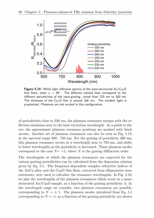
88 Chapter 5. Plasmon-enhanced THz emission from Schottky junctions
600 700 800 900 10000.0
0.2
0.4
0.6
0.8
1.0
Grating periodicity:
300 nm
280 nm
260 nm
250 nm
240 nm
230 nm
220 nm
RGRATING/R
GOLD
Wavelength (nm)
Figure 5.14: White light reflection spectra of the nano-structured Au/Cu2Othin films, when φ = 90◦. The different colored lines correspond to thedifferent periodicities of the nano-grating, varied from 220 nm to 300 nm.The thickness of the Cu2O film is around 166 nm. The incident light isp-polarized. Plasmons are not excited in this configuration.
of periodicities close to 230 nm, the plasmon resonance merges with the re-flection minimum near to the laser excitation wavelength. As a guide to theeye, the approximate plasmon resonance positions are marked with blackarrows. Another set of plasmon resonances can also be seen in Fig. 5.15,in the spectral range 600 - 750 nm. For the grating of periodicity 300 nm,this plasmon resonance occurs at a wavelength near to 750 nm, and shiftsto lower wavelengths as the periodicity is decreased. These plasmon modescorrespond to the case N= +1, where N is the grating diffraction order.
The wavelengths at which the plasmon resonances are expected for thevarious grating periodicities can be calculated from the dispersion relationgiven by Eq. 5.1. The frequency-dependent complex refractive indices ofthe AuCu alloy and the Cu2O thin films, extracted from ellipsometer mea-surements, were used to calculate the resonance wavelengths. In Fig. 5.16,we plot the wavelengths of the plasmon resonances which occur in a nano-structured Au/Cu2O sample, as a function of the grating periodicity Λ. Inthe wavelength range we consider, two plasmon resonances are possible,corresponding to N = ± 1. The plasmon modes calculated from Eq. 5.1corresponding to N = -1, as a function of the grating periodicity are shown
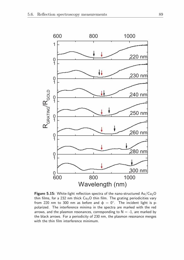
5.6. Reflection spectroscopy measurements 89
Figure 5.15: White-light reflection spectra of the nano-structured Au/Cu2Othin films, for a 232 nm thick Cu2O thin film. The grating periodicities varyfrom 220 nm to 300 nm as before and φ = 0◦. The incident light is p-polarized. The interference minima in the spectra are marked with the redarrows, and the plasmon resonances, corresponding to N = -1, are marked bythe black arrows. For a periodicity of 230 nm, the plasmon resonance mergeswith the thin film interference minimum.
90 Chapter 5. Plasmon-enhanced THz emission from Schottky junctions
as the solid black line and the ones corresponding to N = +1 are shown asthe dashed black line. The peak plasmon wavelengths observed experimen-tally through the reflection spectroscopy measurements are also plotted inthe same figure. The scattered points in red show the plasmon resonancewavelengths measured from the set of samples with an oxide film thicknessof 232 nm, and in blue are the measured resonances from the samples withan oxide film of thickness 166 nm. The plasmon resonance wavelengths cor-responding to N = +1 are not shown for the samples with a Cu2O thicknessof 166 nm, since these plasmon resonances occur near to the interferenceminimum around 650 nm, and were impossible to determine. The plasmonresonance wavelengths observed experimentally are close to the expectedvalues. The differences between the measurements and calculations maybe attributed to the error in the extracted refractive index values of theAuCu alloy and the Cu2O thin film. It can also be seen from Fig. 5.16 thatthe wavelengths at which plasmon resonances are experimentally observedmatch better with the analytically calculated resonance wavelengths for aCu2O thickness of 232 nm, compared to a thickness of 166 nm. This couldbe due to the fact that for the analytical calculation, the thickness of theCu2O layer is considered infinite. In other words, we ignore the effects ofhaving a finite Cu2O layer while determining the expected resonance wave-length for a particular grating periodicity. Perhaps in this case, the extentof the plasmon field in the z-direction is such that it“feels” the presence ofthe air and thus experiences a different refractive index.
5.6.2 s-polarized incident light
To couple electromagnetic waves to surface plasmons, an electric field com-ponent perpendicular to the interface is required to set up the necessarysurface charges. Hence, while using grating coupling at an azimuthal an-gle φ = 0◦, we require p-polarized incident light for the excitation of thesurface plasmons. However, when φ = 90◦, it is possible to excite surfaceplasmons using s-polarized incident light. In the case of a grating, the sur-face of the metal has been “folded”, which allows both s and p-polarizedincident light to have a component of the electric field vector normal tothe metal surface, depending on the orientation of the grating grooves withrespect to the plane of incidence. When the azimuthal angle φ = 90◦,s-polarized incident light has the electric field vector normal to the slopeof the ridges of the grating and can excite surface plasmon polaritons, asshown in Fig. 5.17 [175, 176].
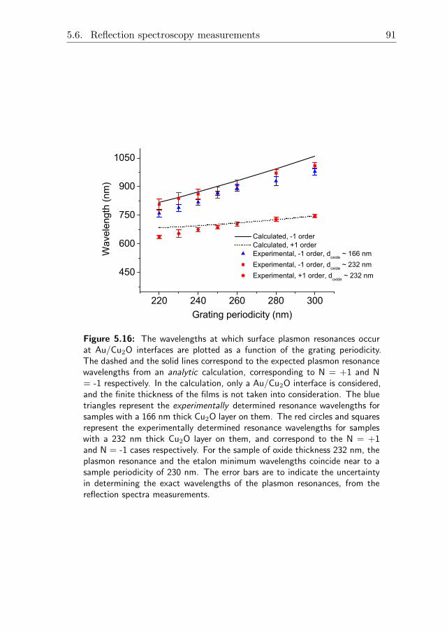
5.6. Reflection spectroscopy measurements 91
220 240 260 280 300
450
600
750
900
1050
Calculated, -1 order Calculated, +1 order Experimental, -1 order, d
oxide ~ 166 nm
Experimental, -1 order, doxide
~ 232 nm Experimental, +1 order, d
oxide ~ 232 nm
Wav
elen
gth
(nm
)
Grating periodicity (nm)
Figure 5.16: The wavelengths at which surface plasmon resonances occurat Au/Cu2O interfaces are plotted as a function of the grating periodicity.The dashed and the solid lines correspond to the expected plasmon resonancewavelengths from an analytic calculation, corresponding to N = +1 and N= -1 respectively. In the calculation, only a Au/Cu2O interface is considered,and the finite thickness of the films is not taken into consideration. The bluetriangles represent the experimentally determined resonance wavelengths forsamples with a 166 nm thick Cu2O layer on them. The red circles and squaresrepresent the experimentally determined resonance wavelengths for sampleswith a 232 nm thick Cu2O layer on them, and correspond to the N = +1and N = -1 cases respectively. For the sample of oxide thickness 232 nm, theplasmon resonance and the etalon minimum wavelengths coincide near to asample periodicity of 230 nm. The error bars are to indicate the uncertaintyin determining the exact wavelengths of the plasmon resonances, from thereflection spectra measurements.
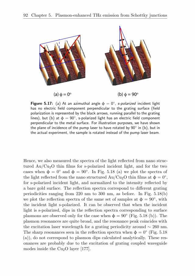
92 Chapter 5. Plasmon-enhanced THz emission from Schottky junctions
(a) φ = 0o (b) φ = 90o
Figure 5.17: (a) At an azimuthal angle φ = 0◦, s-polarized incident lighthas no electric field component perpendicular to the grating surface (fieldpolarization is represented by the black arrows, running parallel to the gratinglines), but (b) at φ = 90◦, s-polarized light has an electric field componentperpendicular to the metal surface. For illustration purposes, we have shownthe plane of incidence of the pump laser to have rotated by 90◦ in (b), but inthe actual experiment, the sample is rotated instead of the pump laser beam.
Hence, we also measured the spectra of the light reflected from nano struc-tured Au/Cu2O thin films for s-polarized incident light, and for the twocases when φ = 0◦ and φ = 90◦. In Fig. 5.18 (a) we plot the spectra ofthe light reflected from the nano structured Au/Cu2O thin films at φ = 0◦,for s-polarized incident light, and normalized to the intensity reflected bya bare gold surface. The reflection spectra correspond to different gratingperiodicities ranging from 220 nm to 300 nm, as before. In Fig. 5.18(b)we plot the reflection spectra of the same set of samples at φ = 90◦, withthe incident light s-polarized. It can be observed that when the incidentlight is s-polarized, dips in the reflection spectra corresponding to surfaceplasmons are observed only for the case when φ = 90◦ (Fig. 5.18 (b)). Theplasmon resonances are quite broad, and the resonance peak coincides withthe excitation laser wavelength for a grating periodicity around ∼ 260 nm.The sharp resonances seen in the reflection spectra when φ = 0◦ (Fig. 5.18(a)), do not correspond to plasmon dips calculated analytically. These res-onances are probably due to the excitation of grating coupled waveguidemodes inside the Cu2O layer [177].
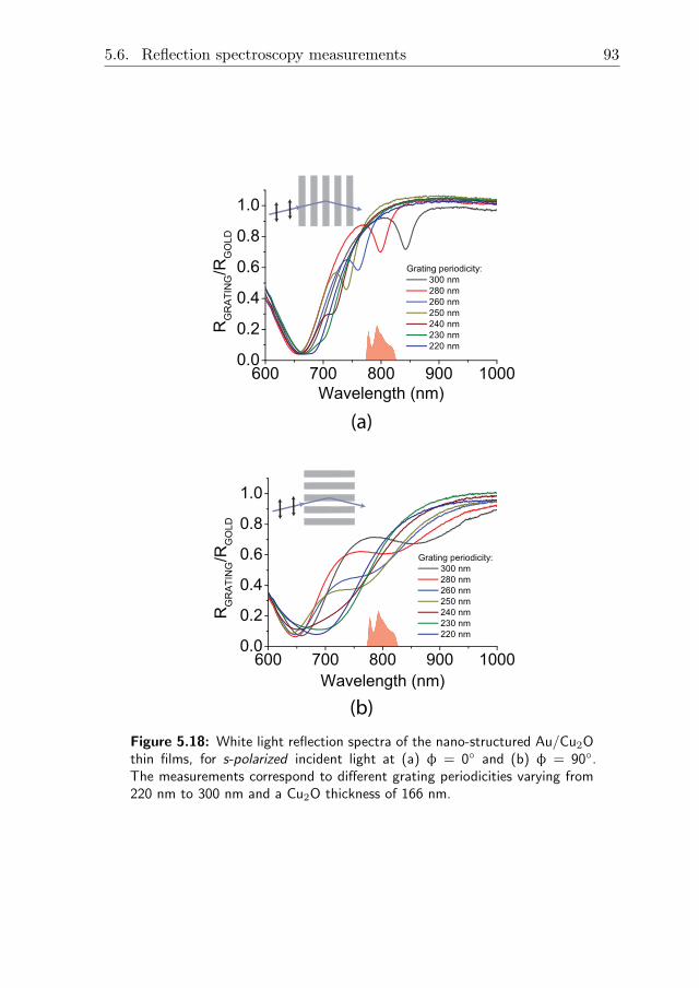
5.6. Reflection spectroscopy measurements 93
(a)
(b)
600 700 800 900 10000.0
0.2
0.4
0.6
0.8
1.0RGRATING/R
GOLD
Grating periodicity:
300 nm
280 nm
260 nm
250 nm
240 nm
230 nm
220 nm
Wavelength (nm)
600 700 800 900 10000.0
0.2
0.4
0.6
0.8
1.0
RGRATING/R
GOLD
Grating periodicity:
300 nm
280 nm
260 nm
250 nm
240 nm
230 nm
220 nm
Wavelength (nm)
Figure 5.18: White light reflection spectra of the nano-structured Au/Cu2Othin films, for s-polarized incident light at (a) φ = 0◦ and (b) φ = 90◦.The measurements correspond to different grating periodicities varying from220 nm to 300 nm and a Cu2O thickness of 166 nm.
94 Chapter 5. Plasmon-enhanced THz emission from Schottky junctions
5.7 THz emission as a function of the grating pe-riodicity
In order to provide more evidence that the plasmon resonances we ob-serve in the reflection spectroscopy are correlated with the enhancementof THz emission from the nano-structured samples, we also measured theTHz emission from the set of samples with varying grating periodicities.In Fig. 5.19(a) we plot the electric field of the THz pulses emitted by thenano structured Au/Cu2O samples, as a function of the grating periodic-ity. The Cu2O thin film thickness is around 166 nm. In Fig. 5.19(b) weplot the THz emission from the set of samples with a Cu2O thickness ofaround 232 nm. The azimuthal angle φ is 0◦ in both measurements. Inboth graphs, the black squares represent the peak-to-peak electric field ofthe THz pulses emitted by the nano-structured interfaces for p-polarizedincident light. Each of these samples also has a part where the Au/Cu2O in-terface is not nano-structured. The THz emission from these flat Au/Cu2Ointerfaces for p-polarized incident light are shown in Fig. 5.19(a) and (b)as red dots. Similarly, the THz light emitted by the nano-structured andthe flat samples for s-polarized incident light is represented by the blueand green triangles respectively. From Fig. 5.19(a) and (b), the followingobservations can be made:
1. For the two Cu2O thicknesses, 166 nm and 232 nm, when the in-cident light is p-polarized and φ = 0◦, the THz emission from thenano-structured samples (black squares) is enhanced compared to theemission from the flat samples (red dots), and the maximum enhance-ment occurs near to a grating periodicity of 230 nm.
2. When the incident light is s-polarized (and φ remaining 0◦), we do notobserve an enhancement in the emitted THz pulse amplitude (blueline), compared to the emission from the flat samples (green line).
3. In all samples, THz emission from plain Au/Cu2O samples using s-polarized incident light is lower than when using p-polarized incidentlight.
As both graphs have different arbitrary units along the vertical axes, theamplitudes between them may differ and should not be compared. However,experimentally it was observed that the THz emission from a sample withperiodicity 230 nm and Cu2O thickness 232 nm was about 1.4 times higher
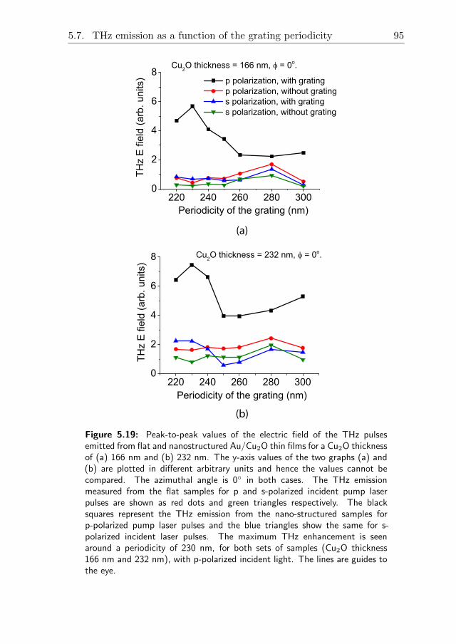
5.7. THz emission as a function of the grating periodicity 95
(a)
(b)
Figure 5.19: Peak-to-peak values of the electric field of the THz pulsesemitted from flat and nanostructured Au/Cu2O thin films for a Cu2O thicknessof (a) 166 nm and (b) 232 nm. The y-axis values of the two graphs (a) and(b) are plotted in different arbitrary units and hence the values cannot becompared. The azimuthal angle is 0◦ in both cases. The THz emissionmeasured from the flat samples for p and s-polarized incident pump laserpulses are shown as red dots and green triangles respectively. The blacksquares represent the THz emission from the nano-structured samples forp-polarized pump laser pulses and the blue triangles show the same for s-polarized incident laser pulses. The maximum THz enhancement is seenaround a periodicity of 230 nm, for both sets of samples (Cu2O thickness166 nm and 232 nm), with p-polarized incident light. The lines are guides tothe eye.
96 Chapter 5. Plasmon-enhanced THz emission from Schottky junctions
than that from a sample of the same periodicity and thickness 166 nm. Sur-face plasmon excitation occurs, as verified using the reflection spectroscopymeasurements, only for p-polarized incident pump light in the case of φ= 0◦. The maximum enhancement in the emitted electric field of the THzpulses occurs when the grating periodicity is near to 230 nm, which is alsoroughly the periodicity for which we observe the plasmon resonance at thelaser excitation wavelength in the reflection spectra measurements. Thismakes it very likely that the plasmon resonance we observe in the reflectionspectroscopy measurements is responsible for the enhanced THz emissionfrom the nano-structured samples. Assuming that the plasmons are in-volved in enhancing the THz emission, it is expected and observed thatthe THz amplitude emitted by the nano-structured samples for s-polarizedpump laser is not enhanced compared to the emission from the flat sam-ples. This is because surface plasmons cannot be excited at the Au/Cu2Ointerface in this configuration.
The strength of the THz emission from flat Au/Cu2O samples using s-polarized incident light is lower than when using p-polarized incident light,presumably because s-polarized light has a higher reflection coefficient atthe air/dielectric interface than p-polarized light. Hence, for s-polarizedlight, less power is coupled into the Cu2O thin film, resulting in lowerTHz emission. In principle, the THz emission from all the flat sampleswith the same thickness of Cu2O thin film, should be of equal strength.However, the small changes in the strength from these samples for the sameincident light polarization, probably occur due to the slight variations inrefractive index, thickness, etc. arising from unintentional variations in thefabrication procedure.
The THz emission measured for the grating samples at an azimuthal angleof φ = 90◦ is shown in Fig. 5.20 for p- and s-polarized incident light, for(a) 166 nm and (b) 232 nm thick Cu2O layer on the metal grating. Asexpected, the s-polarized incident light gives rise to enhanced THz emis-sion compared to the emission from a flat sample. From the reflectionspectroscopy measurements for samples covered with 166 nm of Cu2O, thegrating periodicity required for plasmon coupling at an azimuthal angle of90◦ is around 260 nm, with s-polarized incident light (Fig. 5.18(b)). This isclose to the grating periodicity of 250 nm, where the maximum emission isobserved in Fig. 5.20(a). Similarly, when s-polarized pump light is used, en-hanced THz emission is seen from the nano-structured Au/Cu2O samplesof oxide thickness 232 nm (Fig. 5.20(b)). The corresponding white-lightreflection spectra of these samples are shown in Fig. 5.21. The approxi-mate plasmon resonance wavelengths are marked by the arrows and appear

5.7. THz emission as a function of the grating periodicity 97
(a)
(b)
Figure 5.20: Peak-to-peak values of the electric field of the THz pulsesemitted from flat and nanostructured Au/Cu2O thin films for a Cu2O thicknessof (a) 166 nm and (b) 232 nm. The azimuthal angle is 90◦. The THzemission measured from the flat samples for p- and s-polarized incident pumplaser pulses are shown as red dots and green triangles respectively. The blacksquares represents the THz emission from the nano-structured samples forp-polarized pump laser pulses and the blue triangles shows the same for s-polarized incident laser pulses.
slightly shifted compared to those from samples of oxide thickness of 166 nm.However, it can be seen that the plasmon resonance is closer to the laserexcitation wavelength for a sample of periodicity 280 nm, which also showsthe strongest THz emission, compared to the other samples for s-polarizedincident laser light.
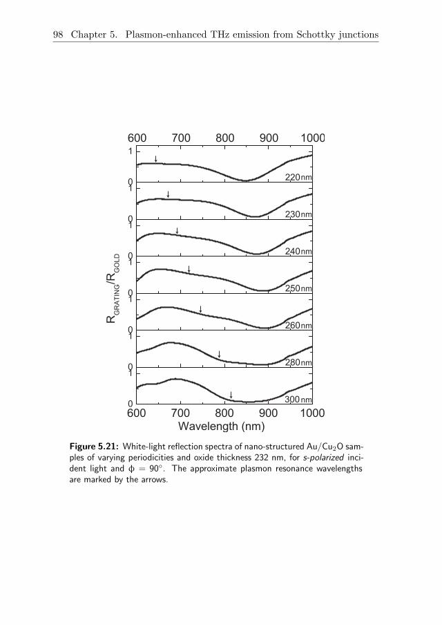
98 Chapter 5. Plasmon-enhanced THz emission from Schottky junctions
Figure 5.21: White-light reflection spectra of nano-structured Au/Cu2O sam-ples of varying periodicities and oxide thickness 232 nm, for s-polarized inci-dent light and φ = 90◦. The approximate plasmon resonance wavelengthsare marked by the arrows.

5.8. Azimuthal angle dependence 99
5.8 Azimuthal angle dependence
5.8.1 Enhanced THz emission: significance of exciting plas-mon modes
To understand the importance of plasmon excitation in enhancing the THzemission, we measured the variation of the pump power absorption and theTHz emission of a few nano-structured Au/Cu2O samples as a function ofthe azimuthal angle. These measurements are similar to those in Fig. 5.9,but here, the the Cu2O layer is 232 nm thick. In Fig. 5.22, we plot this forthe nano-structured Au/Cu2O thin films with (a) Λ = 280 nm and (b) Λ= 230 nm. The thickness of the Cu2O layer on both samples was around232 nm. Note that at this thickness, there is a maximum at a wavelengthof 800 nm in the thickness-dependent pump-power absorption due to theetalon effect. The percentage of the incident pump power absorbed bythe samples is represented by the black points in both graphs. The bluepoints show the peak-to-peak values of the electric field of the emitted THzpulses. The THz electric field amplitude is normalized to that emitted bythe sample with Λ = 230 nm, at φ = 0◦. In the first case (Λ = 280 nm), thegrating periodicity does not support the excitation of surface plasmons atthe Au/Cu2O interface (at the incident laser wavelength), whereas in thesecond case the grating periodicity, Λ = 230 nm, is suitable for plasmonexcitation. Stronger enhancement of the THz emission occurs when theperiodicity is suitable for plasmon excitation. For this sample, when theazimuthal angle is varied from -90◦ to 0◦, the percentage of absorbed pumppower increases from about 75% to 90%. However, for the same change inthe azimuthal angle, the electric field strength of the emitted THz pulsesincreases by a factor of ∼3 (shown as the blue line), which is a much moredramatic increase compared to the increase in the absorbed pump power.
A peculiar feature is that the pump power absorption of the sample withΛ = 280 nm (Fig. 5.22(a)) shows a peak at φ = ∼45◦. Surprisingly, thispeak in the laser absorption is accompanied by a reduction in the emittedTHz amplitude. We also see similar behaviour for the samples with a Cu2Ofilm thickness of ∼166 nm and Λ = 280 nm, which is shown in Fig 5.23(a).The peak in the absorption and the corresponding decrease in the THzemission are also observed but this time at an azimuthal angle of around30◦. These peaks in the absorption are also observed in the visible lightreflection spectra of these samples, as discussed in the next section.

100 Chapter 5. Plasmon-enhanced THz emission from Schottky junctions
(a) (b)
Figure 5.22: The percentage of the pump power absorbed by (black) andthe electric field amplitude of the THz pulses emitted (blue) from the nano-structured Au/Cu2O thin films, as a function of the azimuthal angle φ. (a)Λ = 280 nm, corresponding to the case of no plasmon excitation, and (b) Λ= 230 nm, corresponding to the plasmon excitation case. The thickness ofthe Cu2O thin film is ∼232 nm, and the incident light is p-polarized.
(a) (b)
Figure 5.23: The percentage of the pump power absorbed by (black), andthe electric field amplitude of the THz pulses emitted from (blue) the nano-structured Au/Cu2O thin films, as a function of the azimuthal angle φ: (a)grating periodicity Λ = 280 nm corresponding to the case of no plasmonexcitation, and (b) Λ = 230 nm corresponding to the plasmon excitationcase. The thickness of the Cu2O thin film is ∼166 nm and the incident lightis p-polarized.

5.8. Azimuthal angle dependence 101
5.8.2 Reflection spectra vs azimuthal angle
To understand the nature of the plasmon resonances further, we also mea-sured the visible light reflection spectra as a function of the azimuthal an-gle. Fig. 5.24(a) and (b) show the measured reflection spectra of the nano-structured Au/Cu2O thin films with Λ = 280 nm, for oxide thicknessesaround 166 nm and 232 nm respectively. The incident light is p-polarizedin all the cases. The color bar indicates the reflected intensity, normalizedto the reflection from a bare Au surface. The normalized reflected intensityis plotted as a function of the wavelength along the x-axis and as a functionof the azimuthal angle φ along the y-axis. The minimum in the reflectionspectrum occuring due to the multiple reflections at the interfaces of theCu2O thin film is seen at a wavelength of ∼650 nm in Fig. 5.24(a) and ismarked as ‘E’. The oxide thickness of this sample is ∼166 nm. The plasmonresonance is at a wavelength of ∼925 nm at φ = 0◦ and is marked as -1in the figure. When φ is changed from 0 to 90◦, the plasmon resonancedisappears, since the polarization of the pump laser pulses becomes parallelto the grating grooves at φ = 90◦. Fig. 5.24(b) shows the reflection spectraof the sample with doxide = ∼232 nm, in which the etalon dip occurs a littleabove our wavelength of interest, 800 nm. In this case, two resonances dueto plasmon excitation are visible at φ = 0◦, at wavelengths ∼730 nm and975 nm respectively, corresponding to the N = +1 and -1 diffracted orders.These are marked as +1 and -1.
We also simulated the reflection spectra using an in-house developed pro-gram called ‘Cyclops’, based on the finite element method. Refractive in-dices of the Cu2O and AuCu thin films used were obtained from the ellip-someter measurements described in chapter 4. In order to have a bettermatch with the experimental plasmon resonance wavelength, the real partof the frequency-dependent refractive index of the Cu2O film was decreasedby 7%. The thickness of the oxide was then adjusted accordingly so thatthe etalon resonance wavelength does not change. The simulated reflectionspectra of the samples with oxide thicknesses 171 nm (corresponding to166 nm with earlier refractive indices) and 250 nm (232 nm earlier) anda grating periodicity of 280 nm are shown in Fig. 5.24 (c) and (d) respec-tively. The simulated spectra show a good match with the measured spec-tra. It was observed from the calculations that the strength of the plasmonresonances depends critically on the etch depth of the grating. The etchdepth was assumed to be 17 nm in the simulations, which provided a bettermatch with the experimentally measured reflection spectra. However, themeasured etch depth is around 50 nm, and this discrepancy is assumed to
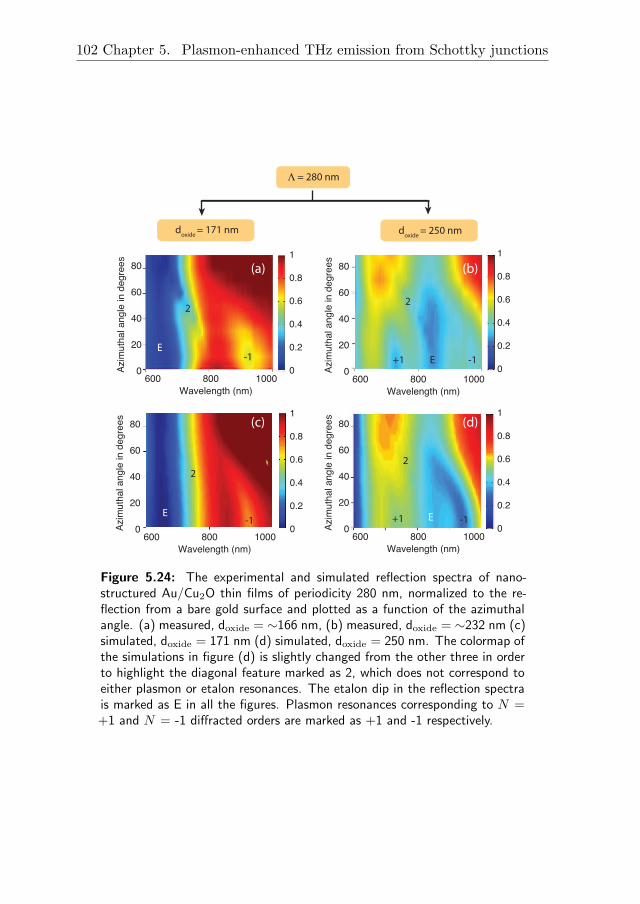
102 Chapter 5. Plasmon-enhanced THz emission from Schottky junctions
Wavelength (nm)
Azim
uth
al a
ng
le in
de
gre
es
600 800 10000
20
40
60
80
Wavelength (nm)
Azim
uth
al a
ng
le in
de
gre
es
600 800 10000
20
40
60
80
Wavelength (nm)
Azim
uth
al a
ng
le in
de
gre
es
600 800 10000
20
40
60
80
Wavelength (nm)
Azim
uth
al a
ng
le in
de
gre
es
600 800 10000
20
40
60
80
(a) (b)
(c) (d)
0
0.2
0.4
0.6
0.8
1
0
0.2
0.4
0.6
0.8
1
0
0.2
0.4
0.6
0.8
1
0
0.2
0.4
0.6
0.8
1
E
2
E -1
2
E
2
E
2
Λ = 280 nm
doxide
= 171 nm doxide
= 250 nm
+1
-1+1
-1
-1
Figure 5.24: The experimental and simulated reflection spectra of nano-structured Au/Cu2O thin films of periodicity 280 nm, normalized to the re-flection from a bare gold surface and plotted as a function of the azimuthalangle. (a) measured, doxide = ∼166 nm, (b) measured, doxide = ∼232 nm (c)simulated, doxide = 171 nm (d) simulated, doxide = 250 nm. The colormap ofthe simulations in figure (d) is slightly changed from the other three in orderto highlight the diagonal feature marked as 2, which does not correspond toeither plasmon or etalon resonances. The etalon dip in the reflection spectrais marked as E in all the figures. Plasmon resonances corresponding to N =+1 and N = -1 diffracted orders are marked as +1 and -1 respectively.
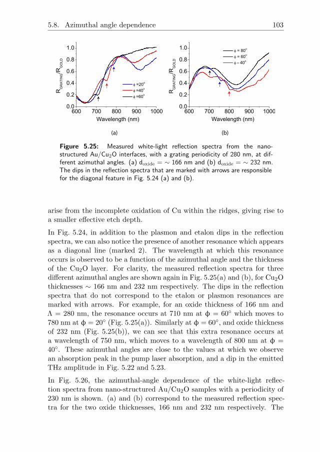
5.8. Azimuthal angle dependence 103
(a) (b)
Figure 5.25: Measured white-light reflection spectra from the nano-structured Au/Cu2O interfaces, with a grating periodicity of 280 nm, at dif-ferent azimuthal angles. (a) doxide = ∼ 166 nm and (b) doxide = ∼ 232 nm.The dips in the reflection spectra that are marked with arrows are responsiblefor the diagonal feature in Fig. 5.24 (a) and (b).
arise from the incomplete oxidation of Cu within the ridges, giving rise toa smaller effective etch depth.
In Fig. 5.24, in addition to the plasmon and etalon dips in the reflectionspectra, we can also notice the presence of another resonance which appearsas a diagonal line (marked 2). The wavelength at which this resonanceoccurs is observed to be a function of the azimuthal angle and the thicknessof the Cu2O layer. For clarity, the measured reflection spectra for threedifferent azimuthal angles are shown again in Fig. 5.25(a) and (b), for Cu2Othicknesses ∼ 166 nm and 232 nm respectively. The dips in the reflectionspectra that do not correspond to the etalon or plasmon resonances aremarked with arrows. For example, for an oxide thickness of 166 nm andΛ = 280 nm, the resonance occurs at 710 nm at φ = 60◦ which moves to780 nm at φ = 20◦ (Fig. 5.25(a)). Similarly at φ = 60◦, and oxide thicknessof 232 nm (Fig. 5.25(b)), we can see that this extra resonance occurs ata wavelength of 750 nm, which moves to a wavelength of 800 nm at φ =40◦. These azimuthal angles are close to the values at which we observean absorption peak in the pump laser absorption, and a dip in the emittedTHz amplitude in Fig. 5.22 and 5.23.
In Fig. 5.26, the azimuthal-angle dependence of the white-light reflec-tion spectra from nano-structured Au/Cu2O samples with a periodicity of230 nm is shown. (a) and (b) correspond to the measured reflection spec-tra for the two oxide thicknesses, 166 nm and 232 nm respectively. The
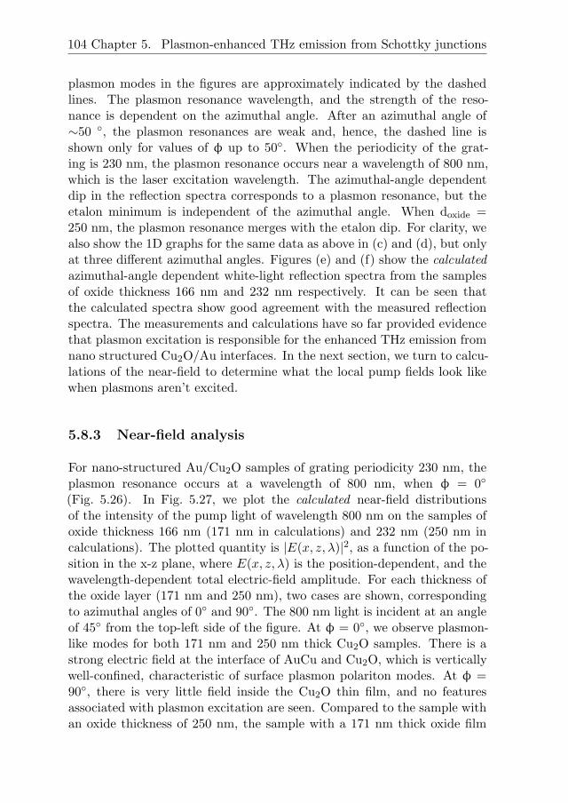
104 Chapter 5. Plasmon-enhanced THz emission from Schottky junctions
plasmon modes in the figures are approximately indicated by the dashedlines. The plasmon resonance wavelength, and the strength of the reso-nance is dependent on the azimuthal angle. After an azimuthal angle of∼50 ◦, the plasmon resonances are weak and, hence, the dashed line isshown only for values of φ up to 50◦. When the periodicity of the grat-ing is 230 nm, the plasmon resonance occurs near a wavelength of 800 nm,which is the laser excitation wavelength. The azimuthal-angle dependentdip in the reflection spectra corresponds to a plasmon resonance, but theetalon minimum is independent of the azimuthal angle. When doxide =250 nm, the plasmon resonance merges with the etalon dip. For clarity, wealso show the 1D graphs for the same data as above in (c) and (d), but onlyat three different azimuthal angles. Figures (e) and (f) show the calculated
azimuthal-angle dependent white-light reflection spectra from the samplesof oxide thickness 166 nm and 232 nm respectively. It can be seen thatthe calculated spectra show good agreement with the measured reflectionspectra. The measurements and calculations have so far provided evidencethat plasmon excitation is responsible for the enhanced THz emission fromnano structured Cu2O/Au interfaces. In the next section, we turn to calcu-lations of the near-field to determine what the local pump fields look likewhen plasmons aren’t excited.
5.8.3 Near-field analysis
For nano-structured Au/Cu2O samples of grating periodicity 230 nm, theplasmon resonance occurs at a wavelength of 800 nm, when φ = 0◦
(Fig. 5.26). In Fig. 5.27, we plot the calculated near-field distributionsof the intensity of the pump light of wavelength 800 nm on the samples ofoxide thickness 166 nm (171 nm in calculations) and 232 nm (250 nm incalculations). The plotted quantity is |E(x, z, λ)|2, as a function of the po-sition in the x-z plane, where E(x, z, λ) is the position-dependent, and thewavelength-dependent total electric-field amplitude. For each thickness ofthe oxide layer (171 nm and 250 nm), two cases are shown, correspondingto azimuthal angles of 0◦ and 90◦. The 800 nm light is incident at an angleof 45◦ from the top-left side of the figure. At φ = 0◦, we observe plasmon-like modes for both 171 nm and 250 nm thick Cu2O samples. There is astrong electric field at the interface of AuCu and Cu2O, which is verticallywell-confined, characteristic of surface plasmon polariton modes. At φ =90◦, there is very little field inside the Cu2O thin film, and no featuresassociated with plasmon excitation are seen. Compared to the sample withan oxide thickness of 250 nm, the sample with a 171 nm thick oxide film
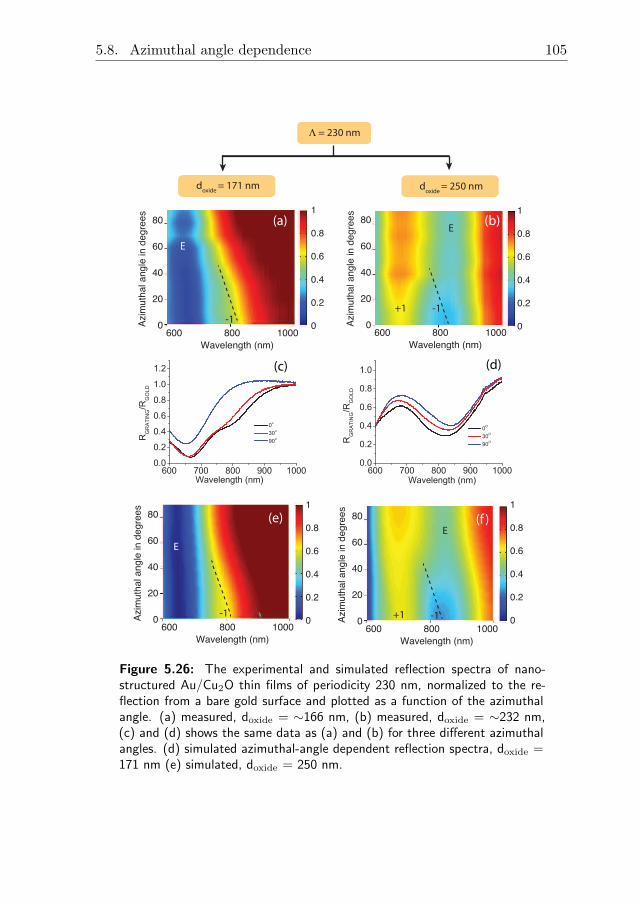
5.8. Azimuthal angle dependence 105
Wavelength (nm)
Azim
uth
al a
ng
le in
de
gre
es
600 800 10000
20
40
60
80 (a)
0
0.2
0.4
0.6
0.8
1
Wavelength (nm)A
zim
uth
al a
ng
le in
de
gre
es
600 800 10000
20
40
60
80 (b)
0
0.2
0.4
0.6
0.8
1
Wavelength (nm)
Azim
uth
al a
ng
le in
de
gre
es
600 800 10000
20
40
60
80 (f )
0
0.2
0.4
0.6
0.8
1
(c) (d)
Wavelength (nm)
Azim
uth
al a
ng
le in
de
gre
es
600 800 10000
20
40
60
80 (e)
0
0.2
0.4
0.6
0.8
1
Λ = 230 nm
doxide
= 171 nm doxide
= 250 nm
E
E
E
E
+1 -1
+1 -1-1
-1
E
Figure 5.26: The experimental and simulated reflection spectra of nano-structured Au/Cu2O thin films of periodicity 230 nm, normalized to the re-flection from a bare gold surface and plotted as a function of the azimuthalangle. (a) measured, doxide = ∼166 nm, (b) measured, doxide = ∼232 nm,(c) and (d) shows the same data as (a) and (b) for three different azimuthalangles. (d) simulated azimuthal-angle dependent reflection spectra, doxide =171 nm (e) simulated, doxide = 250 nm.

106 Chapter 5. Plasmon-enhanced THz emission from Schottky junctions
has more light reflected from the sample, due to etalon effects. The red boxsurrounding the azimuthal angle values in the figure denotes that plasmonexcitation is expected in this case.
The near-field distributions corresponding to a grating periodicity of280 nm, are shown in Fig. 5.28. For this sample periodicity, the plasmon res-onance occurs at a wavelength of 925 nm, and hence at 800 nm wavelength,no features of plasmon excitation are expected. Slight edge-enhancementeffects are observed at an azimuthal angle of 0◦, since the electric field ofthe incident light is oriented perpendicular to the ridges.
In Fig. 5.29, we show the near-field cross sections of |Hy| in the x-z plane forthe two grating periodicities 230 nm and 280 nm. The excitation of surfaceplasmons in the case of gratings of periodicity 230 nm, is more clearlyvisible here. It can be seen that in the case of samples with a periodicity230 nm, there is a strong localization of the magnetic field at the surface,for both the samples of thickness 171 nm and 250 nm. The asymmetryin the field distribution arises from the non-normal incidence of the pumplight. A movie showing the |Hy| distribution as a function of time, for thefour different cases shown in Fig. 5.29, is uploaded online and can be seenthrough this web-linkhttps://www.dropbox.com/sh/kc7xj2tt7dsg0zo/70SXtvJtKm?lst. Forthe samples with a periodicity of 230 nm, a surface-wave propagating tothe left is visible, whereas in the case of samples of periodicity 280 nm, nosuch surface-wave is observed. This reinforces the argument that plasmonsare excited when light of wavelength 800 nm is incident on nano-structuredAu/Cu2O samples of grating periodicity 230 nm. For a nano-structuredsample of periodicity 280 nm, there is a plasmon at a wavelength of 735 nm,corresponding to the diffracted order N = +1. We have also included amovie of the magnetic near-field corresponding to this case. It is to benoted that the the magnetic field shown in the movies is comprised ofthe incident and reflected light as well as the plasmon field, which makesit somewhat difficult to clearly recognize the plasmons, in the case theplasmons propagates in the same direction as the incident field componentalong the surface. For comparison, we have also included movies of flatAu/Cu2O interfaces, for two different oxide thicknesses, 171 and 250 nm.
5.9 Conclusion
THz emission from Au/Cu2O interfaces occurs in a region near to the Schot-tky interface, where the static electric field has a maximum. The absorption

5.9. Conclusion 107
late
ral p
ositio
n (
nm
)
−2
00
02
00
−2
000
20
0
40
0
late
ral p
ositio
n (
nm
)
−2
00
02
00
−2
000
20
0
40
0
late
ral p
ositio
n (
nm
)
−2
00
02
00
−2
000
20
0
40
0
00.5
11.5
2
late
ral p
ositio
n (
nm
)
Vertical position (nm)
−2
00
02
00
−2
000
20
0
40
0
Λ =
23
0 n
m
dC
u2
O =
17
1 n
m d
Cu
2O
= 2
50
nm
φ =
0o
φ =
90
oφ
= 0
oφ
= 9
0o
Figure 5.27: The calculated optical near-field cross-sections of nano-structured Au/Cu2O thin films with a grating periodicity 230 nm and thick-nesses 171 nm and 250 nm, at azimuthal angles 0◦ and 90◦. The plottedquantity is |E(x, z, λ)|2. The wavelength of the incident light is 800 nm inthe simulations. The cases where plasmon excitation is expected is denotedby the red box around the value of the azimuthal angle.
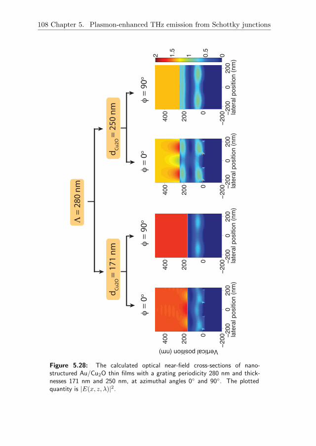
108 Chapter 5. Plasmon-enhanced THz emission from Schottky junctions
late
ral p
ositio
n (
nm
)
Vertical position (nm)
−2
00
02
00
−2
000
20
0
40
0
late
ral p
ositio
n (
nm
)
−2
00
02
00
−2
000
20
0
40
0
late
ral p
ositio
n (
nm
)
−2
00
02
00
−2
000
20
0
40
0
late
ral p
ositio
n (
nm
)
−2
00
02
00
−2
000
20
0
40
0
00.5
11.5
2
Λ =
28
0 n
m
dC
u2
O =
17
1 n
m d
Cu
2O
= 2
50
nm
φ =
0o
φ =
90
oφ
= 0
oφ
= 9
0o
Figure 5.28: The calculated optical near-field cross-sections of nano-structured Au/Cu2O thin films with a grating periodicity 280 nm and thick-nesses 171 nm and 250 nm, at azimuthal angles 0◦ and 90◦. The plottedquantity is |E(x, z, λ)|2.

5.9. Conclusion 109
lateral position (nm)
Ve
rtic
al p
ositio
n (
nm
)
−200 0 200−200
0
200
400
0
0.002
0.004
0.006
0.008
0.01
lateral position (nm)V
ert
ica
l p
ositio
n (
nm
)
−200 0 200−200
0
200
400
0
0.002
0.004
0.006
0.008
0.01
lateral position (nm)
Ve
rtic
al p
ositio
n (
nm
)
−200 0 200−200
0
200
400
0
0.002
0.004
0.006
0.008
0.01
lateral position (nm)
Ve
rtic
al p
ositio
n (
nm
)
−200 0 200−200
0
200
400
0
0.002
0.004
0.006
0.008
0.01
Figure 5.29: The calculated magnetic near-field cross-sections of nano-structured Au/Cu2O thin films for grating periodicities 230 and 280 nm andfor two oxide thicknesses 171 nm and 250 nm. φ = 0◦ in all the cases. Theplotted quantity is |Hy| as a function of the position in the x-z plane.
110 Chapter 5. Plasmon-enhanced THz emission from Schottky junctions
of the pump light further away from the interface does not contribute ef-ficiently to the THz emission. Hence for increasing the THz emission, itis important that the absorption of the laser light takes place near theinterface.
We have shown that by nano-structuring the interfaces between Au andCu2O, we can excite surface plasmons to concentrate pump laser energyat the interface. This leads to an enhanced THz emission compared to aflat Au/Cu2O sample. The evidences for surface-plasmon-enhanced THzemission can be summarized as follows:
• Periodicity dependence: The strongest THz emission was obtainedfrom a sample of grating periodicity 230 nm. We have seen from thewhite-light reflection spectra that the plasmon resonances depend onthe grating periodicity, and that a periodicity of 230 nm is suitable forexcitation of surface plasmons at 800 nm wavelength, as predicted.
• Azimuthal angle dependence: The maximum pump power absorp-tion and THz emission occur when the grating is oriented verticallyand the incident laser is p-polarized. This is the orientation suitablefor the excitation of the surface plasmons. The azimuthal angle de-pendence of the THz emission also indicates that concentrating theabsorption of the pump laser light at the interface leads to an increasein the efficiency of THz emission. In other words, it is not just theabsorption of the laser by the sample that is important, but where itis absorbed.
• No enhancement at other resonant modes: This is also seen fromthe azimuthal angle dependence of THz emission from the sample ofperiodicity 280 nm, where a peak in the absorption is observed at anazimuthal angle of 45◦. However, this does not result in an increasedTHz emission, but on the contrary, in a decreased THz emission. Onereason for this decrease in the THz emission is that a resonant modeis excited, for which the pump light is concentrated away from theinterface, thus contributing less to THz emission.
Thus the measurements and calculations clearly show that to maximizeTHz emission it matters more where the light is absorbed than how much isabsorbed. This understanding may lead to new and improved THz emitters.

Chapter
6Conclusions and Outlook
In this thesis, we have discussed the potential of plasmonics in enhancingthe THz emission from metal (Au) thin films, and metal/semiconductor(Au/Cu2O) junctions.
Several reports on THz emission from gold thin films, upon illuminationwith femtosecond laser pulses, can be found in the literature and are brieflyreviewed in Chapter 2. While plasmonics has been used to enhance theTHz emission from these films, the different processes which result in THzgeneration vary, depending on the incident pump laser power and morphol-ogy of the thin films used. We studied the THz emission from thin goldfilms deposited on etched Si gratings, in an attempt to determine the roleplayed by the surface plasmons in THz generation. The interesting resultfrom our experiments is that the THz emission follows a second-order de-pendence on the incident pump power, when excited by femtosecond laserpulses at the plasmon excitation angle. This is contrary to the higher-orderdependence of THz emission on the incident pump power observed by othergroups using similar samples, indicating a multi-photon photoelectric effect.Other processes which might be responsible for the THz emission, namelyoptical rectification by the surface non-linearity, and the photon-drag effectare also discussed in the chapter. It was seen from our experiments that,as the angle of propagation of surface plasmons on the metal surface varies,a small change in the polarization of the THz pulse emitted is observed.More research into this could lead us to an answer on the role of plasmonson the THz emission from bare gold gratings.
Another important part of this thesis covers the THz emission fromAu/Cu2O thin film interfaces, when illuminated with femtosecond laserpulses and the role of plasmonics in enhancing the THz emission fromthem. Cu2O thin films were fabricated by depositing a thin film of Cuon a suitable substrate and then oxidizing it in the ambient atmosphere.
111
112 Chapter 6. Conclusions and Outlook
To understand the oxidation process, we showed in chapter 3, that THztransmission spectroscopy can be used to measure the oxidation kineticsof copper thin films evaporated on silicon substrates. The transmissionof broadband THz pulses from 1 to 7 THz through the copper films wasmeasured during oxidation in the ambient atmosphere, at elevated tem-peratures ranging from 120 - 150 ◦C. The change in the transmitted THzelectric field was correlated with the growth of the cuprous oxide layer and adecrease in the thickness of the copper layer. We also showed that the THzconductivity of evaporated metal thin films depends on the film thickness,due to percolation effects.
Metal/semiconductor interfaces can form a Schottky barrier potential atthe interface, creating an electric field. Photo-excited charge carriers, gen-erated near the interface, are accelerated by this electric field and giverise to the emission of THz radiation. However, it has been reported inthe literature that Au films deposited on Cu2O form ohmic junctions, andnot Schottky junctions. In chapter 4, we show that our Au/Cu2O sam-ples which emit THz radiation, are in-fact AuCu/Cu2O interfaces, due tothe formation of a thermal diffusion alloy AuCu. The alloy enables theformation of a Schottky barrier electric field near the interface, which isvery important for THz emission from these samples. The formation ofthis AuCu alloy layer is confirmed by X-ray diffraction measurements, el-lipsometry and visual inspection. From the ellipsometry measurements, wealso determined the frequency-dependent complex refractive-indices of theCu2O and AuCu layers.
The capability of Au/Cu2O thin films as broad-band terahertz emitters,can be exploited further by enhancing the THz emission through plas-monics. In order to excite surface plasmons at the metal/semiconductorinterface, gold nano-gratings were fabricated and then covered by Cu2O.The evidence for surface-plasmon-enhanced THz emission is obtained fromTHz emission measurements, as a function of grating periodicity and az-imuthal angle. Visible-light reflection-spectroscopy was used to determinethe plasmon resonance wavelengths. The experimental results suggest thatfor increasing the THz emission, it is important that the absorption of thelaser light takes place near the interface. This makes sense, as the Schottkyelectric field is also maximum near the metal/semiconductor interface anddecreases as we move away from the interface. Excitation of other reso-nant, non-plasmonic modes may result in an increased absorption of thepump laser pulses, but not necessarily in increased THz emission, as thepump light may get concentrated away from the interface. Our results arepromising in that they give meaning to the motto ”more with less”: The ex-

113
citation of surface plasmons gives rise to strong THz emission even thoughthe total amount of material is small compared to other types of emitters.It is possible that this will lead to new applications in THz science andtechnology.

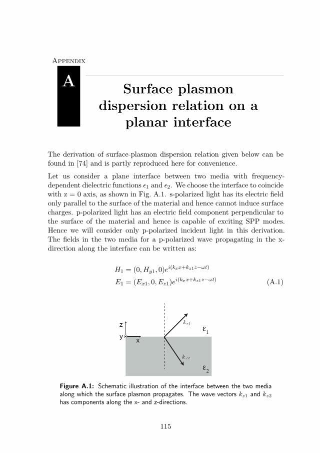
Appendix
ASurface plasmon
dispersion relation on aplanar interface
The derivation of surface-plasmon dispersion relation given below can befound in [74] and is partly reproduced here for convenience.
Let us consider a plane interface between two media with frequency-dependent dielectric functions ǫ1 and ǫ2. We choose the interface to coincidewith z = 0 axis, as shown in Fig. A.1. s-polarized light has its electric fieldonly parallel to the surface of the material and hence cannot induce surfacecharges. p-polarized light has an electric field component perpendicular tothe surface of the material and hence is capable of exciting SPP modes.Hence we will consider only p-polarized incident light in this derivation.The fields in the two media for a p-polarized wave propagating in the x-direction along the interface can be written as:
H1 = (0, Hy1, 0)ei(kxx+kz1z−ωt)
E1 = (Ex1, 0, Ez1)ei(kxx+kz1z−ωt) (A.1)
ε2
ε1
x
z
y
Figure A.1: Schematic illustration of the interface between the two mediaalong which the surface plasmon propagates. The wave vectors kz1 and kz2has components along the x- and z-directions.
115

116Appendix A. Surface plasmon dispersion relation on a planar interface
H2 = (0, Hy2, 0)ei(kxx−kz2z−ωt)
E2 = (Ex2, 0, Ez2)ei(kxx−kz2z−ωt) (A.2)
By applying Maxwells equation
∇× ~H = ǫ∂ ~E
∂t(A.3)
we obtain
Ex1 =kz1ǫ1ω
Hy1
Ex2 = − kz2ǫ2ω
Hy2 (A.4)
At the interface between the two materials, we can apply the boundaryconditions that the components of the electric and magnetic fields parallelto the interface must be continuous across the interface, when there is nofree current at the interface. Hence we can write,
Ex1 = Ex2
Hy1 = Hy2 (A.5)
From Eq. A.4 and A.5 we can obtain
Hy1 −Hy2 = 0
kz1ǫ1ω
Hy1 +kz2ǫ2ω
Hy2 = 0 (A.6)
In order to obtain a solution to the above equations, the determinant hasto be zero.
kz1ǫ1
+kz2ǫ2
= 0 (A.7)
Further, from Eq. A.4
k2x1 = ǫ1(ω
c)2 − k2z1
k2x2 = ǫ2(ω
c)2 − k2z2 (A.8)
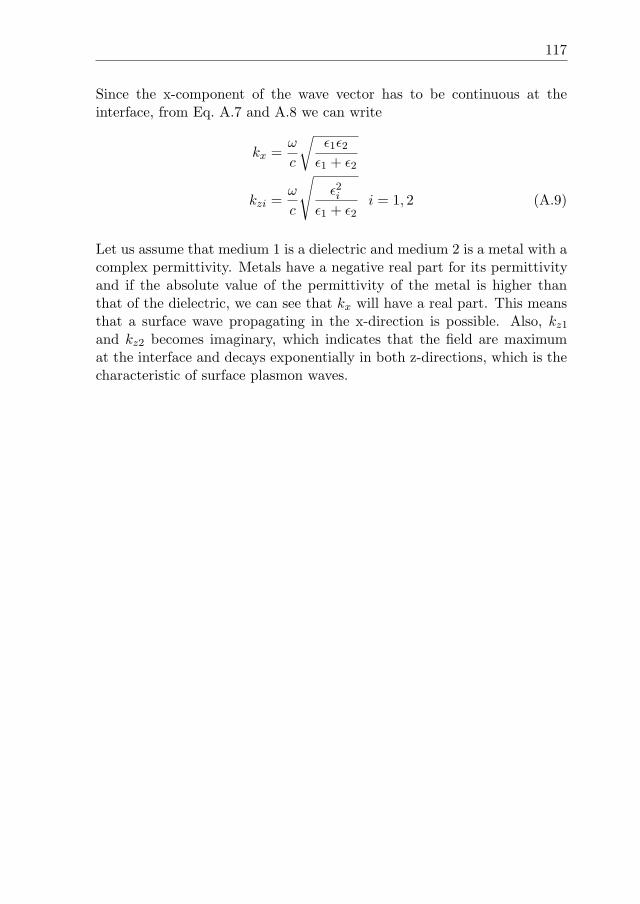
117
Since the x-component of the wave vector has to be continuous at theinterface, from Eq. A.7 and A.8 we can write
kx =ω
c
√
ǫ1ǫ2ǫ1 + ǫ2
kzi =ω
c
√
ǫ2iǫ1 + ǫ2
i = 1, 2 (A.9)
Let us assume that medium 1 is a dielectric and medium 2 is a metal with acomplex permittivity. Metals have a negative real part for its permittivityand if the absolute value of the permittivity of the metal is higher thanthat of the dielectric, we can see that kx will have a real part. This meansthat a surface wave propagating in the x-direction is possible. Also, kz1and kz2 becomes imaginary, which indicates that the field are maximumat the interface and decays exponentially in both z-directions, which is thecharacteristic of surface plasmon waves.


Bibliography
[1] G. P. Gallerano and S. Biedron. Overview of terahertz radiation sources. In 26thInternational Free Electron Laser Conference, pages 216–221, 2004.
[2] M. Tonouchi. Cutting-edge terahertz technology. Nat. Photonics, 1(2):97–105,2007. doi: 10.1038/nphoton.2007.3.
[3] D. Dragoman and M. Dragoman. Terahertz fields and applications. Prog. Quant.Electron., 28(1):1 – 66, 2004. doi: 10.1016/S0079-6727(03)00058-2.
[4] R. L. Ives, C. Kory, M. Read, J. Neilson, M. Caplan, N. Chubun, S. Schwartzkopf,and R. Witherspoon. Development of backward-wave oscillators for terahertz ap-plications. In Terahertz for Military and Security Applications, volume 5070, pages71–82. SPIE, 2003. doi: 10.1117/12.506905.
[5] D. H. Martin and K. Mizuno. The generation of coherent submillimetre waves.Adv. Phys., 25(3):211–246, 1976. doi: 10.1080/00018737600101382.
[6] A. Crocker, H. A. Gebbie, M. F. Kimmitt, and L. E. S. Mathias. Stimulatedemission in the far infra-red. Nature, 201:250–251, 1964. doi: 10.1038/201250a0.
[7] J. Faist, F. Capasso, D. L. Sivco, C. Sirtori, A. L. Hutchinson, and A. Y. Cho.Quantum cascade laser. Science, 264(5158):553–556, 1994. doi: 10.1126/science.264.5158.553.
[8] R. Kohler, A. Tredicucci, F. Beltram, H. E. Beere, E. H. Linfield, A. G. Davies,D. A. Ritchie, R. C. Iotti, and F. Rossi. Terahertz semiconductor-heterostructurelaser. Nature, 417:156–159, 2002. doi: 10.1038/417156a.
[9] D. H. Auston, K. P. Cheung, and P. R. Smith. Picosecond photoconductinghertzian dipoles. Appl. Phys. Lett., 45(3):284–286, 1984. doi: 10.1063/1.95174.
[10] P. R. Smith, D. H. Auston, and M. C. Nuss. Subpicosecond photoconducting dipoleantennas. IEEE J. Quantum Elect., 24(2):255–260, 1988. doi: 10.1109/3.121.
[11] K. Sakai and M. Tani. Terahertz Optoelectronics, Topics in Appl. Phys., chapterIntroduction to Terahertz Pulses, pages 1–30. Springer Berlin / Heidelberg, 2005.
[12] Z. G. Lu, P. Campbell, and X.-C. Zhang. Free-space electro-optic sampling with ahigh-repetition-rate regenerative amplified laser. Appl. Phys. Lett., 71(5):593–595,1997. doi: 10.1063/1.119803.
119
120 Bibliography
[13] J. F. Federici, B. Schulkin, F. Huang, D. Gary, R. Barat, F. Oliveira, and D. Zim-dars. THz imaging and sensing for security applications-explosives, weapons anddrugs. Semicond. Sci. Technol., 20(7):S266, 2005. doi: 10.1088/0268-1242/20/7/018.
[14] M. C. Kemp, P. F. Taday, B. E. Cole, J. A. Cluff, A. J. Fitzgerald, and W. R. Tribe.Security applications of terahertz technology. In Terahertz for Military and SecurityApplications, volume 5070, pages 44–52. Proc. SPIE, 2003. doi: 10.1117/12.500491.
[15] M. Niwa, Y. Hiraishi, N. Iwasaki, and K. Terada. Quantitative analysis of the layerseparation risk in bilayer tablets using terahertz pulsed imaging. Int. J. Pharm,452(1-2):249–256, 2013. doi: 10.1016/j.ijpharm.2013.05.010.
[16] K. J. Tielrooij, D. Paparo, L. Piatkowski, H. J. Bakker, and M. Bonn. Dielectric re-laxation dynamics of water in model membranes probed by terahertz spectroscopy.Biophys. J., 97(9):2484–2492, 2009. doi: 10.1016/j.bpj.2009.08.024.
[17] K. Kawase, Y. Ogawa, Y. Watanabe, and H. Inoue. Non-destructive terahertzimaging of illicit drugs using spectral fingerprints. Opt. Express, 11(20):2549–2554,2003. doi: 10.1364/OE.11.002549.
[18] R. Chakkittakandy, J. A. W. M. Corver, and P. C. M. Planken. Terahertz spec-troscopy to identify the polymorphs in freeze-dried mannitol. J. Pharm. Sci., 99(2):932–940, 2010. doi: 10.1002/jps.21870.
[19] H. Wu and M. Khan. THz spectroscopy: An emerging technology for pharmaceu-tical development and pharmaceutical process analytical technology (PAT) appli-cations. J. Mol. Struct., 1020:112–120, 2012.
[20] E. Pickwell and V. P. Wallace. Biomedical applications of terahertz technology.J. Phys. D: Appl. Phys., 39(17):R301–R310, 2006. doi: 10.1088/0022-3727/39/17/R01.
[21] A. J. L. Adam, P. C. M. Planken, S. Meloni, and J. Dik. Terahertz imaging ofhidden paint layers on canvas. Opt. Express, 17(5):3407–3416, 2009. doi: 10.1364/OE.17.003407.
[22] K. Fukunaga and M. Picollo. Terahertz spectroscopy applied to the analysis ofartists’ materials. Appl. Phys. A., 100(3):591–597, 2010. doi: 10.1007/s00339-010-5643-y.
[23] S. Hunsche, M. Koch, I. Brener, and M. C. Nuss. THz near-field imaging. Opt.Comm., 150(1-6):22 – 26, 1998. doi: 10.1016/S0030-4018(98)00044-3.
[24] O. Mitrofanov, I. Brener, R. Harel, J. D. Wynn, L. N. Pfeiffer, K. W. West, andJ. Federici. Terahertz near-field microscopy based on a collection mode detector.Appl. Phys. Lett., 77(22):3496–3498, 2000. doi: 10.1063/1.1328772.
[25] N. C. J. van der Valk and P. C. M. Planken. Electro-optic detection of subwave-length terahertz spot sizes in the near field of a metal tip. Appl. Phys. Lett., 81:1558–1560, 2002. doi: 10.1063/1.1503404.

121
[26] J. R. Knab, A. J. L. Adam, M. Nagel, E. Shaner, M. A. Seo, D. S. Kim, and P. C. M.Planken. Terahertz near-field vectorial imaging of subwavelength apertures andaperture arrays. Opt. Express, 17(17):15072–15086, 2009. doi: 10.1364/OE.17.015072.
[27] M. A. Seo, A. J. L. Adam, J. H. Kang, J. W. Lee, S. C. Jeoung, Q. H. Park,P. C. M. Planken, and D. S. Kim. Fourier-transform terahertz near-field imaging ofone-dimensional slit arrays: mapping of electric-field, magnetic-field, and Poyntingvectors. Opt. express, 15(19):11781–11789, 2007. doi: 10.1364/OE.15.011781.
[28] A. J. Huber, F. Keilmann, J. Wittborn, J. Aizpurua, and R. Hillenbrand. Terahertznear-field nanoscopy of mobile carriers in single semiconductor nanodevices. NanoLett., 8(11):3766–3770, 2008. doi: 10.1021/nl802086x.
[29] P. K. Benicewicz, J. P. Roberts, and A. J. Taylor. Scaling of terahertz radiationfrom large-aperture biased photoconductors. J. Opt. Soc. Am. B, 11(12):2533–2546,1994. doi: 10.1364/JOSAB.11.002533.
[30] Z. Piao, M. Tani, and K. Sakai. Carrier dynamics and terahertz radiation inphotoconductive antennas. Jpn. J. Appl. Phys., 39:96–100, 2000. doi: 10.1143/JJAP.39.96.
[31] F. Wahaia. Spectroscopic and imaging techniques using terahertz frequency bandfor biomedical applications. PhD thesis, University of Porto, 2011.
[32] A. Bonvalet, M. Joffre, J. L. Martin, and A. Migus. Generation of ultrabroadbandfemtosecond pulses in the midinfrared by optical rectification of 15 fs light pulsesat 100 mhz repetition rate. Appl. Phys. Lett., 67(20):2907–2909, 1995. doi: 10.1063/1.114838.
[33] N. C. J. van der Valk, T. Wenckebach, and P. C. M. Planken. Full mathematicaldescription of electro-optic detection in optically isotropic crystals. J. Opt. Soc.Am. B, 21(3):622–631, 2004. doi: 10.1364/JOSAB.21.000622.
[34] X. C. Zhang and D. H. Auston. Optoelectronic measurement of semiconductorsurfaces and interfaces with femtosecond optics. J. Appl. Phys., 71:326–338, 1992.doi: 10.1063/1.350710.
[35] H. Dember. Uber eine photoelektronische kraft in kupferoxydul-kristallen. Z. Phys.,32:554, 1931.
[36] M. B. Johnston, D. M. Whittaker, A. Corchia, A. G. Davies, and E. H. Linfield.Simulation of terahertz generation at semiconductor surfaces. Phys. Rev. B, 65:165301, 2002. doi: 10.1103/PhysRevB.65.165301.
[37] C. T. Que, T. Edamura, M. Nakajima, M. Tani, and M. Hangyo. Terahertz radia-tion from InAs films on silicon substrates excited by femtosecond laser pulses. Jpn.J. Appl. Phys., 48:010211, 2009. doi: 10.1143/JJAP.48.010211.
[38] P. Gu, M. Tani, S. Kono, K. Sakai, and X.-C. Zhang. Study of terahertz radiationfrom InAs and InSb. J. Appl. Phys., 91:5533–5537, 2002. doi: 10.1063/1.1465507.

122 Bibliography
[39] J. N. Heyman, N. Coates, A. Reinhardt, and G. Strasser. Diffusion and drift interahertz emission at GaAs surfaces. Appl. Phys. Lett., 83:5476–5478, 2003. doi:10.1063/1.1636821.
[40] R. Ascazubi, C. Shneider, I. Wilke, R. Pino, and P. S. Dutta. Enhanced terahertzemission from impurity compensated GaSb. Phys. Rev. B, 72:045328, 2005. doi:10.1103/PhysRevB.72.045328.
[41] S. L. Chuang, S. Schmitt-Rink, B. I. Greene, P. N. Saeta, and A. F. J. Levi. Opticalrectification at semiconductor surfaces. Phys. Rev. Lett., 68:102–105, Jan 1992. doi:10.1103/PhysRevLett.68.102.
[42] S. C. Howells and L. A. Schlie. Temperature dependence of terahertz pulses pro-duced by difference frequency mixing in InSb. Appl. Phys. Lett., 67:3688–3690,1995. doi: 10.1063/1.114928.
[43] M. Tonouchi T. Kondo, M. Sakamoto and M. Hangyo. Terahertz radiation from(111) InAs surface using 1.55 µm femtosecond laser pulses. Jpn. J. Appl. Phys., 38:L1035–L1037, 1999. doi: 10.1143/JJAP.38.L1035.
[44] R. W. Wood. On a remarkable case of uneven distribution of light in a diffractiongrating spectrum. The London, Edinburgh, and Dublin Philosophical Magazine andJournal of Science, 4(21):396–402, 1902. doi: 10.1088/1478-7814/18/1/325.
[45] L. Rayleigh. On the dynamical theory of gratings. Proc. R. Soc. Lond. A, 79, 1907.doi: 10.1098/rspa.1907.0051.
[46] D. Maystre. Plasmonics, volume 167, chapter Theory of Wood’s Anomalies, pages39–83. Springer Series in Optical Sciences, 2012.
[47] R. H. Ritchie. Plasma losses by fast electrons in thin films. Phys. Rev., 106:874–881,Jun 1957. doi: 10.1103/PhysRev.106.874.
[48] C. J. Powell and J. B. Swan. Origin of the characteristic electron energy losses inaluminum. Phys. Rev., 115:869–875, Aug 1959. doi: 10.1103/PhysRev.115.869.
[49] A. Otto. Excitation of nonradiative surface plasma waves in silver by the methodof frustrated total reflection. Zeitschrift fur Physik, 216(4):398–410, 1968. doi:10.1007/BF01391532.
[50] E. Kretschmann and H. Raether. Radiative decay of nonradiative surface plasmonsexcited by light. Z. Naturforsch. A, 23:2135, 1968.
[51] S. Hayashi and T. Okamoto. Plasmonics: visit the past to know the future. J. Phys.D: Appl. Phys., 45(43):433001, 2012. doi: 10.1088/0022-3727/45/43/433001.
[52] J. Homola and M. Piliarik. Surface plasmon resonance (spr) sensors. In Sur-face Plasmon Resonance Based Sensors, volume 4 of Springer Series on Chemi-cal Sensors and Biosensors, pages 45–67. Springer Berlin Heidelberg, 2006. doi:10.1007/5346 014.
[53] W. L. Barnes, A. Dereux, and T. W. Ebbesen. Surface plasmon subwavelengthoptics. Nature, 424:824–830, 2003. doi: 10.1038/nature01937.
123
[54] G. Veronis and S. Fan. Bends and splitters in metal-dielectric-metal subwavelengthplasmonic waveguides. Appl. Phys. Lett., 87:131102, 2005. doi: 10.1063/1.2056594.
[55] R. F. Oulton, V. J. Sorger, D. A. Genov, D. F. P. Pile, and X. TI Zhang. A hybridplasmonic waveguide for subwavelength confinement and long-range propagation.Nat. Photonics, 2(8):496–500, 2008. doi: 10.1038/nphoton.2008.131.
[56] A. Hosseini and Y. Massoud. Nanoscale surface plasmon based resonator usingrectangular geometry. Appl. Phys. Lett., 90:181102, 2007. doi: 10.1063/1.2734380.
[57] S. I. Bozhevolnyi, V. S. Volkov, E. Devaux, J.-Y. Laluet, and T. W. Ebbesen.Channel plasmon subwavelength waveguide components including interferometersand ring resonators. Nature, 440:508–511, 2006. doi: 10.1038/nature04594.
[58] A. V. Zayats, I. I. Smolyaninov, and A. A. Maradudin. Nano-optics of surfaceplasmon polaritons. Phys. Rep., 408(3-4):131–314, 2005. doi: 10.1016/j.physrep.2004.11.001.
[59] D. M. Schaadt, B. Feng, and E. T. Yu. Enhanced semiconductor optical absorptionvia surface plasmon excitation in metal nanoparticles. Appl. Phys. Lett., 86(6):063106, 2005. doi: 10.1063/1.1855423.
[60] J. Homola. Surface plasmon resonance sensors for detection of chemical and bio-logical species. Chem. Rev., 108(2):462–493, 2008. doi: 10.1021/cr068107d.
[61] M. W. Knight, H. Sobhani, P. Nordlander, and N. J. Halas. Photodetection withactive optical antennas. Science, 332(6030):702–704, 2011. doi: 10.1126/science.1203056.
[62] P. Senanayake, C.-H. Hung, J. Shapiro, A. Lin, B. Liang, B. S. Williams, and D. L.Huffaker. Surface plasmon-enhanced nanopillar photodetectors. Nano Lett., 11(12):5279–5283, 2011. doi: 10.1021/nl202732r.
[63] V. E. Ferry, M. A. Verschuuren, H. B. T. Li, E. Verhagen, R. J. Walters, R. E. I.Schropp, H. A. Atwater, and A. Polman. Light trapping in ultrathin plasmonic solarcells. Opt. Express, 18(S2):A237–A245, Jun 2010. doi: 10.1364/OE.18.00A237.
[64] Y. A. Akimov, W. S. Koh, and K. Ostrikov. Enhancement of optical absorptionin thin-film solar cells through the excitation of higher-order nanoparticle plasmonmodes. Opt. Express, 17(12):10195–10205, 2009. doi: 10.1364/OE.17.010195.
[65] H. J. Simon, D. E. Mitchell, and J. G. Watson. Optical second-harmonic generationwith surface plasmons in silver films. Phys. Rev. Lett., 33(26):1531–1534, 1974. doi:10.1103/PhysRevLett.33.1531.
[66] C. Steuwe, C. F. Kaminski, J. J. Baumberg, and S. Mahajan. Surface enhancedcoherent anti-stokes raman scattering on nanostructured gold surfaces. Nano Lett.,11(12):5339–5343, 2011. doi: 10.1021/nl202875w.
[67] M. Kauranen and A. V. Zayats. Nonlinear plasmonics. Nat. Phot., 6(11):737–748,2012. doi: 10.1038/nphoton.2012.244.

124 Bibliography
[68] G. H. Welsh, N. T. Hunt, and K. Wynne. Terahertz-pulse emission through laserexcitation of surface plasmons in a metal grating. Phys. Rev. Lett., 98(2):026803,2007. doi: 10.1103/PhysRevLett.98.026803.
[69] G. Ramakrishnan and P. C. M. Planken. Percolation-enhanced generation of ter-ahertz pulses by optical rectification on ultrathin gold films. Opt. Lett., 36(13):2572–2574, 2011.
[70] D. K. Polyushkin, E. Hendry, E. K. Stone, and W. L. Barnes. THz generationfrom plasmonic nanoparticle arrays. Nano Lett., 11(11):4718–4724, 2011. doi:10.1021/nl202428g.
[71] G. Ramakrishnan, N. Kumar, P. C. M. Planken, D. Tanaka, and K. Kajikawa.Surface plasmon-enhanced terahertz emission from a hemicyanine self-assembledmonolayer. Opt. Express, 20(4):4067–4073, 2012. doi: 10.1364/OE.20.004067.
[72] B. Heshmat, H. Pahlevaninezhad, P. Yuanjie, M. Masnadi-Shirazi, R. Burton Lewis,T. Tiedje, R. Gordon, and T. E. Darcie. Nanoplasmonic terahertz photoconductiveswitch on GaAs. Nano Lett., 12(12):6255–6259, 2012. doi: 10.1021/nl303314a.
[73] C. W. Berry and M. Jarrahi. Terahertz generation using plasmonic photoconduc-tive gratings. New J. Phys., 14(10):105029, 2012. doi: 10.1088/1367-2630/14/10/105029.
[74] H. Raether. Surface Plasmons on Smooth and Rough Surfaces and on Gratings,volume 111. Springer-Verlag, 1988.
[75] L. Novotny and B. Hecht. Principles of Nano-optics. Cambridge University Press,2006.
[76] Z. Chen. Grating coupled surface plasmons in metallic structures. PhD thesis,University of Exeter, 2007.
[77] F. Kadlec, P. Kuzel, and J.-L. Coutaz. Optical rectification at metal surfaces. Opt.Lett., 29(22):2674–2676, 2004. doi: 10.1364/OL.29.002674.
[78] D. J. Hilton, R. D. Averitt, C. A. Meserole, G. L. Fisher, D. J. Funk, J. D. Thomp-son, and A. J. Taylor. Terahertz emission via ultrashort-pulse excitation of mag-netic metalfilms. Opt. Lett., 29(15):1805–1807, 2004. doi: 10.1364/OL.29.001805.
[79] F. Brown, R. E. Parks, and A. M. Sleeper. Nonlinear optical reflection from a metal-lic boundary. Phys. Rev. Lett., 14:1029–1031, 1965. doi: 10.1103/PhysRevLett.14.1029.
[80] J. E. Sipe, V. C. Y. So, M. Fukui, and G. I. Stegeman. Analysis of second-harmonicgeneration at metal surfaces. Phys. Rev. B, 21(10):4389–4402, 1980.
[81] F. Kadlec, P. Kuzel, and J.-L. Coutaz. Study of terahertz radiation generated byoptical rectification on thin gold films. Opt. Lett., 30(11):1402–1404, 2005. doi:10.1364/OL.30.001402.
[82] K. Kajikawa, Y. Nagai, Y. Uchiho, G. Ramakrishnan, N. Kumar, G. K. P. Ra-manandan, and P. C. M. Planken. Terahertz emission from surface-immobilizedgold nanospheres. Opt. Lett., 37(19):4053–4055, 2012. doi: 10.1364/OL.37.004053.
125
[83] S. E. Irvine and A. Y. Elezzabi. Surface-plasmon-based electron acceleration. Phys.Rev. A, 73:013815, 2006. doi: 10.1103/PhysRevA.73.013815.
[84] H. A. H. Boot and R. B. R. S. Harvie. Charged particles in a non-uniform radio-frequency field. Nature, 180(4596):1187–1187, 1957. doi: 10.1038/1801187a0.
[85] G. H. Welsh and K. Wynne. Generation of ultrafast terahertz radiation pulseson metallic nanostructured surfaces. Opt. Express, 17(4):2470–2480, 2009. doi:10.1364/OE.17.002470.
[86] C. Toth, G. Farkas, and K. L. Vodopyanov. Laser-induced electron-emission froman Au surface irradiated by single picosecond pulses at λ=2.94 µm. The inter-mediate region between multiphoton and tunneling effects. Appl. Phys. B, 53(4):221–225, 1991. doi: 10.1007/BF00357140.
[87] Y. Gao, M.-K. Chen, C.-E Yang, Y.-C. Chang, S. Yin, R. Hui, P. Ruffin, C. Brant-ley, E. Edwards, and C. Luo. Analysis of terahertz generation via nanostruc-ture enhanced plasmonic excitations. J. Appl. Phys., 106(7):074302, 2009. doi:10.1063/1.3236629.
[88] A. Gloskovskii, D. A. Valdaitsev, M. Cinchetti, S. A. Nepijko, J. Lange, M. Aeschli-mann, M. Bauer, M. Klimenkov, L. V. Viduta, P. M. Tomchuk, and G. Schonhense.Electron emission from films of Ag and Au nanoparticles excited by a femtosecondpump-probe laser. Phys. Rev. B, 77:195427, 2008. doi: 10.1103/PhysRevB.77.195427.
[89] F. Garwe, A. Schmidt, G. Zieger, T. May, K. Wynne, U. Hubner, M. Zeisberger,W. Paa, H. Stafast, and H.-G. Meyer. Bi-directional terahertz emission from gold-coated nanogratings by excitation via femtosecond laser pulses. Appl. Phys. B, 102(3):551–554, 2011. doi: 10.1007/s00340-011-4377-7.
[90] A. Schmidt, F. Garwe, U. Hubner, T. May, W. Paa, M. Zeisberger, G. Zieger,and H. Stafast. Experimental characterization of bi-directional terahertz emissionfrom gold-coated nanogratings. Appl. Phys. B, 109(4):631–642, 2012. doi: 10.1007/s00340-012-5230-3.
[91] E. V. Suvorov, R. A. Akhmedzhanov, D. A. Fadeev, I. E. Ilyakov, V. A. Mironov,and B. V. Shishkin. Terahertz emission from a metallic surface induced by afemtosecond optic pulse. Opt. Lett., 37(13):2520–2522, 2012. doi: 10.1364/OL.37.002520.
[92] G. Ramakrishnan, G. K. P. Ramanandan, A. J. L. Adam, M. Xu, N. Kumar,R. W. A. Hendrikx, and P. C. M. Planken. Enhanced terahertz emission by coherentoptical absorption in ultrathin semiconductor films on metals. Opt. Express, 21(14):16784–16798, 2013. doi: 10.1364/OE.21.016784.
[93] T. W. Ebbesen, H. J. Lezec, H. F. Ghaemi, T. Thio, and P. A. Wolff. Extraordinaryoptical transmission through sub-wavelength hole arrays. Nature, 391(6668):667–669, 1998. doi: 10.1038/35570.
[94] H. F. Ghaemi, T. Thio, D. E. Grupp, T. W. Ebbesen, and H. J. Lezec. Surfaceplasmons enhance optical transmission through subwavelength holes. Phys. Rev.B, 58:6779–6782, 1998. doi: 10.1103/PhysRevB.58.6779.
126 Bibliography
[95] M. Wegener. Extreme nonlinear optics. Springer, 2004.
[96] A. F. Gibson, M. F. Kimmit, and A. C. Walker. Photon drag in germanium. Appl.Phys. Lett, 17(2):75–77, 1970. doi: 10.1063/1.1653315.
[97] H. M. Barlow. Application of the Hall effect in a semiconductor to the mea-surement of power in an electromagnetic field. Nature, 173:41–42, 1954. doi:10.1038/173041a0.
[98] A. S. Vengurlekar and T. Ishihara. Surface plasmon enhanced photon drag in metalfilms. Appl. Phys. Lett., 87(9):091118, 2005. doi: 10.1063/1.2037851.
[99] T. Hatano, B. Nishikawa, M. Iwanaga, and T. Ishihara. Optical rectification effectin 1D metallic photonic crystal slabs with asymmetric unit cell. Opt. Express, 16(11):8236–8241, 2008. doi: 10.1364/OE.16.008236.
[100] H. Kurosawa and T. Ishihara. Surface plasmon drag effect in a dielectrically mod-ulated metallic thin film. Opt. Express, 20(2):1561–1574, 2012. doi: 10.1364/OE.20.001561.
[101] M. Durach, A. Rusina, and M. I. Stockman. Giant surface-plasmon-induced drageffect in metal nanowires. Phys. Rev. Lett., 103(4):186801, 2009. doi: 10.1103/PhysRevLett.103.186801.
[102] G. K. P. Ramanandan, G. Ramakrishnan, and P. C. M. Planken. Oxidation kineticsof nanoscale copper films studied by terahertz transmission spectroscopy. J. Appl.Phys., 111(12):123517–6, 2012. doi: 10.1063/1.4729808.
[103] Y. Z. Hu, R. Sharangpani, and S.-P. Tay. In situ rapid thermal oxidation andreduction of copper thin films and their applications in ultralarge scale integration.J. Electrochem. Soc., 148(12):G669–G675, 2001. doi: 10.1149/1.1413480.
[104] T. Osborn, A. He, N. Galiba, and P. A. Kohl. All-copper chip-to-substrate in-terconnects part i. fabrication and characterization. J. Electrochem. Soc., 155(4):D308–D313, 2008. doi: 10.1149/1.2839007.
[105] S. Suzuki, Y. Ishikawa, M. Isshiki, and Y. Waseda. Native oxide layers formedon the surface of ultra high-purity iron and copper investigated by angle resolvedXPS. Mater. Trans., 38(11):1004–1009, 1997.
[106] J. Li, G. Vizkelethy, P. Revesz, J. W. Mayer, and K. N. Tu. Oxidation and reductionof copper oxide thin films. J. Appl. Phys., 69(2):1020–1029, 1991. doi: 10.1063/1.347417.
[107] T.-I. Jeon, J. Zhang, and D. Grischkowsky. THz Sommerfeld wave propagation ona single metal wire. Appl. Phys. Lett., 86:161904, 2005. doi: 10.1063/1.1904718.
[108] K. Wang and D. M. Mittleman. Metal wires for terahertz wave guiding. Nature,432(7015):376–379, 2004. doi: 10.1038/nature03040.
[109] R. Mendis and D. Grischkowsky. Undistorted guided-wave propagation of subpi-cosecond terahertz pulses. Opt. Lett., 26:846–848, Jun 2001. doi: 10.1364/OL.26.000846.
127
[110] N. C. J. van der Valk and P. C. M. Planken. Effect of a dielectric coating onterahertz surface plasmon polaritons on metal wires. Appl. Phys. Lett., 87(7):071106, 2005. doi: 10.1063/1.2011773.
[111] A. Njeh, T. Wieder, and H. Fuess. Reflectometry studies of the oxidation kinetics ofthin copper films. Surf. Interface Anal., 33(7):626–628, 2002. doi: 10.1002/sia.1421.
[112] J. Iijima, J.-W. Lim, S.-H. Hong, S. Suzuki, K. Mimura, and M. Isshiki. Nativeoxidation of ultra high purity Cu bulk and thin films. Appl. Surf. Sci, 253(5):2825– 2829, 2006. doi: 10.1016/j.apsusc.2006.05.063.
[113] C. Zhong, Y. M. Jiang, Y. F. Luo, B. Deng, L. Zhang, and J. Li. Kineticscharacterization of the oxidation of Cu thin films at low temperature by usingsheet resistance measurement. Appl. Phys. A:Mater., 90(2):263–266, 2008. doi:10.1007/s00339-007-4259-3.
[114] G. Zhou, J. A. Eastman, R. C. Birtcher, P. M. Baldo, J. E. Pearson, L. J. Thomp-son, L. Wang, and J. C. Yang. Composition effects on the early-stage oxida-tion kinetics of (001) Cu-Au alloys. J. Appl. Phys., 101(3):033521, 2007. doi:10.1063/1.2433714.
[115] R. Chakkittakandy, J. A. W. M. Corver, and P. C. M. Planken. Quasi-near fieldterahertz generation and detection. Opt. Express, 16(17):12794–12805, 2008. doi:10.1364/OE.16.012794.
[116] Q. Wu and X.-C. Zhang. 7 terahertz broadband gap electro-optic sensor. Appl.Phys. Lett., 70(14):1784–1786, 1997. doi: 10.1063/1.118691.
[117] G. Zhao, R. N. Schouten, N. Van Der Valk, W. T. Wenckebach, and P. C. M.Planken. Design and performance of a THz emission and detection setup basedon a semi-insulating GaAs emitter. Rev. Sci. Instrum., 73(4):1715, 2002. doi:10.1063/1.1459095.
[118] G. Papadimitropoulos, N. Vourdas, V. Em Vamvakas, and D. Davazoglou. Depo-sition and characterization of copper oxide thin films. J. Phys: Conf. Ser, 10(1):182, 2005. doi: 10.1088/1742-6596/10/1/045.
[119] J. J. Tu, C. C. Homes, and M. Strongin. Optical properties of ultrathin films:Evidence for a dielectric anomaly at the insulator-to-metal transition. Phys. Rev.Lett., 90:017402, Jan 2003. doi: 10.1103/PhysRevLett.90.017402.
[120] D. G. Cooke, F. A. Hegmann, E. C. Young, and T. Tiedje. Electron mobilityin dilute GaAs bismide and nitride alloys measured by time-resolved terahertzspectroscopy. Appl. Phys. Lett, 89(12):122103, 2006. doi: 10.1063/1.2349314.
[121] M. Tinkham. Energy gap interpretation of experiments on infrared transmissionthrough superconducting films. Phys. Rev., 104:845–846, Nov 1956. doi: 10.1103/PhysRev.104.845.
[122] M. Walther, D. G. Cooke, C. Sherstan, M. Hajar, M. R. Freeman, and F. A. Heg-mann. Terahertz conductivity of thin gold films at the metal-insulator percolationtransition. Phys. Rev. B, 76(12):125408, Sep 2007. doi: 10.1103/PhysRevB.76.125408.

128 Bibliography
[123] D. Grischkowsky, S. Keiding, M. van Exter, and Ch. Fattinger. Far-infrared time-domain spectroscopy with terahertz beams of dielectrics and semiconductors. J.Opt. Soc. Am. B, 7(10):2006–2015, 1990. doi: 10.1364/JOSAB.7.002006.
[124] N. Kaiser. Review of the fundamentals of thin-film growth. Appl. Opt., 41(16):3053–3060, 2002. doi: 10.1364/AO.41.003053.
[125] N. Laman and D. Grischkowsky. Terahertz conductivity of thin metal films. Appl.Phys. Lett., 93(5):051105, 2008. doi: 10.1063/1.2968308.
[126] N. F. Mott. Oxidation of metals and the formation of protective films. Nature, 145(3687):996–1000, 1940. doi: 10.1038/145996a0.
[127] N. Cabrera and N. F. Mott. Theory of the oxidation of metals. Rep. Prog. Phys,12(1):163–184, 1949. doi: 10.1088/0034-4885/12/1/308.
[128] J. F. Shackelford. Introduction to materials science for engineers. MacmillanPublishing Company, 3 edition, 1992.
[129] J. Bardeen, W. H. Brattain, and W. Shockley. Investigation of oxidation of copperby use of radioactive Cu tracer. J. Chem. Phys, 14(12):714–721, 1946. doi: 10.1063/1.1724091.
[130] C. Kittel. Introduction to Solid State Physics. Wiley, New York, 1996.
[131] W. Gao, H. Gong, J. He, A. Thomas, L. Chan, and S. Li. Oxidation behaviourof Cu thin films on Si wafer at 175-400◦C. Mater. Lett., 51(1):78 – 84, 2001. doi:10.1016/S0167-577X(01)00268-3.
[132] X.-C. Zhang, B. B. Hu, J. T. Darrow, and D. H. Auston. Generation of femtosecondelectromagnetic pulses from semiconductor surfaces. Appl. Phys. Lett., 56(11):1011–1013, 1990. doi: 10.1063/1.102601.
[133] Y. Jin, X. F. Ma, G. A. Wagoner, M. Alexander, and X. C. Zhang. Anomalousoptically generated THz beams from metal/GaAs interfaces. Appl. Phys. Lett., 65(6):682–684, 1994. doi: 10.1063/1.112267.
[134] X.-C. Zhang, J. T. Darrow, B. B. Hu, D. H. Auston, M. T. Schmidt, P. Tham,and E. S. Yang. Optically induced electromagnetic radiation from semiconductorsurfaces. Appl. Phys. Lett., 56(22):2228–2230, 1990. doi: 10.1063/1.102952.
[135] G. Ramakrishnan. Enhanced terahertz emission from thin film semiconduc-tor/metal interfaces. PhD thesis, Delft University of Technology, 2012.
[136] L. C. Olsen, R. C. Bohara, and M. W. Urie. Explanation for low-efficiency Cu2OSchottky-barrier solar cells. Appl. Phys. Lett., 34:47–49, 1979. doi: 10.1063/1.90593.
[137] C. C. Coleman. Modern physics for semiconductor science. Wiley-VCH, 2008.
[138] A. E. Rakhshani. Preparation, characteristics and photovoltaic properties ofcuprous oxide - a review. Solid State Electron., 29(1):7 – 17, 1986. doi:10.1016/0038-1101(86)90191-7.

129
[139] J. Xu and D. Xue. Five branching growth patterns in the cubic crystal system: Adirect observation of cuprous oxide microcrystals. Acta. Mater., 55(7):2397 – 2406,2007. doi: 10.1016/j.actamat.2006.11.032.
[140] W. M Sears and E Fortin. Preparation and properties of Cu2O/Cu photovoltaiccells. Sol. Energ. Mater., 10(1):93 – 103, 1984. doi: 10.1016/0165-1633(84)90011-X.
[141] P. Dawson, M. M. Hargreave, and G. R. Wilkinson. The dielectric and latticevibrational spectrum of cuprous oxide. J. Phys. Chem. Solids, 34(12):2201 – 2208,1973. doi: 10.1016/S0022-3697(73)80067-8.
[142] W. H. Brattain. The copper oxide rectifier. Rev. Mod. Phys., 23:203–212, 1951.doi: 10.1103/RevModPhys.23.203.
[143] M. O’Keeffe and W. J. Moore. Thermodynamics of the formation and migrationof defects in cuprous oxide. J. Chem. Phys., 36(11):3009–3013, 1962. doi: 10.1063/1.1732418.
[144] H. Raebiger, S. Lany, and A. Zunger. Origins of the p-type nature and cationdeficiency in Cu2O and related materials. Phys. Rev. B, 76:045209, 2007. doi:10.1103/PhysRevB.76.045209.
[145] Y. Nakano, S. Saeki, and T. Morikawa. Optical bandgap widening of p-type Cu2Ofilms by nitrogen doping. Appl. Phys. Lett., 94(2):022111, 2009. doi: 10.1063/1.3072804.
[146] S. Ishizuka, S. Kato, Y. Okamoto, and K. Akimoto. Control of hole carrier densityof polycrystalline Cu2O thin films by Si doping. Appl. Phys. Lett., 80(6):950–952,2002. doi: 10.1063/1.1448398.
[147] L. O. Grondahl. The copper-cuprous-oxide rectifier and photoelectric cell. Rev.Mod. Phys., 5(141), 1933.
[148] L. O. Grondahl and P. H. Geiger. A new electronic rectifier. A.I.E.E., 46:357–366,1927. doi: 10.1109/JAIEE.1927.6534186.
[149] Y. P. Yang, Wen. C. Wang, Z. W. Zhang, L. L. Zhang, and C. L. Zhang. Dielectricand lattice vibrational spectra of Cu2O hollow spheres in the range of 1-10 THz.J. Phys. Chem. C., 115(21):10333–10337, 2011. doi: 10.1021/jp1114256.
[150] R. Morrish, K. Dorame, and A. J. Muscat. Formation of nanoporous Au by deal-loying AuCu thin films in HNO3. Scripta Mater., 64(9):856 – 859, 2011. doi:10.1016/j.scriptamat.2011.01.021.
[151] C. Cretu and E. Lingen. Coloured gold alloys. Gold Bulletin, 32(4):115–126, 1999.doi: 10.1007/BF03214796.
[152] J. Faber and T. Fawcett. The powder diffraction file: present and future. ActaCrystall. B, 58(3 Part 1):325–332, 2002. doi: 10.1107/S0108768102003312.
[153] J. A. Woollam, B. D. Johs, C. M. Herzinger, J. N. Hilfiker, R. A. Synowicki, andC. L. Bungay. Overview of variable-angle spectroscopic ellipsometry (VASE): I.basic theory and typical applications. In Society of Photo-Optical InstrumentationEngineers (SPIE) Conference Series, pages 3–28, 1999. doi: 10.1117/12.351660.

130 Bibliography
[154] J. W. Weber, T. A. R Hansen, M. C. M Van de Sanden, and R. Engeln. B-splineparametrization of the dielectric function applied to spectroscopic ellipsometry onamorphous carbon. J. Appl. Phys., 106(12):123503, 2009. doi: 10.1063/1.3257237.
[155] Refractive index database, 2013. URL http://refractiveindex.info.
[156] O. El Gawhary, M. Dheur, S. Pereira, and J. Braat. Extension of the classicalFabry-Perot formula to 1D multilayered structures. Appl. Phys. B, 111(4):1–9,2013. doi: 10.1007/s00340-013-5390-9.
[157] V. Astley, K. S. Reichel, J. Jones, R. Mendis, and D. M. Mittleman. Terahertzmultichannel microfluidic sensor based on parallel-plate waveguide resonant cavi-ties. Appl. Phys. Lett., 100(23):231108, 2012. doi: 10.1063/1.4724204.
[158] J. S. Melinger, N. Laman, S. S. Harsha, S. Cheng, and D. Grischkowsky. High-resolution waveguide terahertz spectroscopy of partially oriented organic poly-crystalline films. J. Phys. Chem. A, 111(43):10977–10987, 2007. doi: 10.1021/jp074975i.
[159] H. Zhan, R. Mendis, and D. M. Mittleman. Characterization of the terahertz near-field output of parallel-plate waveguides. J. Opt. Soc. Am. B, 28(3):558–566, 2011.doi: 10.1364/JOSAB.28.000558.
[160] J. Zhang and D. Grischkowsky. Waveguide terahertz time-domain spectroscopy ofnanometer water layers. Opt. Lett., 29(14):1617–1619, 2004. doi: 10.1364/OL.29.001617.
[161] E. S. Lee, Y. B. Ji, and T-I Jeon. Terahertz band gap properties by using metalslits in tapered parallel-plate waveguides. Appl. Phys. Lett., 97(18):181112, 2010.doi: 10.1063/1.3514558.
[162] Z. Jian, J. Pearce, and D. M Mittleman. Two-dimensional photonic crystal slabs inparallel-plate metal waveguides studied with terahertz time-domain spectroscopy.Semiconductor Science and Technology, 20(7):S300, 2005. doi: 10.1088/0268-1242/20/7/022.
[163] E. S. Lee, J-K. So, G-S Park, D. S. Kim, C-S Kee, and T-I Jeon. Terahertz bandgaps induced by metal grooves inside parallel-plate waveguides. Opt. Express, 20(6):6116–6123, 2012. doi: 10.1364/OE.20.006116.
[164] S-H Kim, E. S. Lee, Y. B. Ji, and T-I Jeon. Improvement of THz coupling usinga tapered parallel-plate waveguide. Opt. Express, 18(2):1289–1295, 2010. doi:10.1364/OE.18.001289.
[165] J. Zhang and D. Grischkowsky. Adiabatic compression of parallel-plate metalwaveguides for sensitivity enhancement of waveguide THz time-domain spec-troscopy. Appl. Phys. Lett., 86(6):061109, 2005. doi: 10.1063/1.1863439.
[166] M. Theuer, S. S. Harsha, and D. Grischkowsky. Flare coupled metal parallel-platewaveguides for high resolution terahertz time-domain spectroscopy. J. Appl. Phys.,108(11):113105, 2010. doi: 10.1063/1.3516307.
131
[167] R. A. Myers, N. Mukherjee, and S. R. J. Brueck. Large second-order nonlinearityin poled fused silica. Opt. Lett., 16(22):1732–1734, 1991.
[168] J. A. Assimos and D. Trivich. Photovoltaic properties and barrier heights of single-crystal and polycrystalline Cu2O - Cu contacts. J. Appl. Phys., 44(4):1687–1693,1973.
[169] A. Ishida and T. Majima. Surface plasmon enhanced fluorescence measurementon flat and constructed gold surfaces. Analyst, 125:535–540, 2000. doi: 10.1039/A906318H.
[170] M. Fleischmann, P. J. Hendra, and A. J. McQuillan. Raman spectra of pyridineadsorbed at a silver electrode. Chem. Phys. Lett., 26(2):163 – 166, 1974. doi:10.1016/0009-2614(74)85388-1.
[171] E. D. Palik. Handbook of Optical Constants of Solids. Academic Press, Boston,1985.
[172] T. Nishida, M. Notomi, R. Iga, and T. Tamamura. Quantum wire fabricationby e-beam elithography using high-resolution and high-sensitivity e-beam resistZEP-520. Jpn. J. Appl. Phys., 31(Part 1, No. 12B):4508–4514, 1992.
[173] G. K. P. Ramanandan, A. J. L. Adam, G. Ramakrishnan, R. Hendrikx, and P. C. M.Planken. Optical characterization of gold-cuprous oxide interface for terahertzemission applications. submitted, 2013.
[174] J. Zhu. Local environment dependent linewidth of plasmon absorption in goldnanoshell: Effects of local field polarization. Appl. Phys. Lett., 92(24):241919,2008.
[175] R. A. Watts, T. W. Preist, and J. R. Sambles. Sharp surface-plasmon resonanceson deep diffraction gratings. Phys. Rev. Lett., 79(20):3978–3981, 1997. doi: 10.1103/PhysRevLett.79.3978.
[176] Z. Chen. Grating coupled surface plasmons in metallic structures. PhD thesis,University of Exeter, 2007.
[177] C. Tan, J. Simonen, and T. Niemi. Hybrid waveguide-surface plasmon polaritonmodes in a guided-mode resonance grating. Optics Comm., 285(21-22):4381 – 4386,2012.


Acknowledgements
My experience of doing a PhD can be compared to a rollercoaster ride: itwas exciting, adventurous and there were several ups and downs on the way.To reach the end of this journey successfully, I have been graciously helpedby a lot of people. It is my pleasure to remember those people and thankthem in these pages.
First and foremost I am grateful to Prof. Paul Planken for his guidancethroughout my PhD. I have learnt quite a lot from the scientific discussionswith him and also enjoyed plenty of freedom as a researcher. Many thanksto Paul for reading and correcting the thesis patiently and for having ori-ented and supported my research through uncertain moments.
I am also sincerely grateful to Dr. Aurele Adam, for his continuous helpduring my PhD. He often had clever solutions to technical problems in thelab, and I also gained a lot through discussing my research with him. Ialso thank Aurele for performing the simulations that complemented myexperimental work which gave the finishing touch to the work presented inmy thesis.
Let me also thank our head of the department Prof. Paul Urbach, for thesupport and encouragement he provided.
I would like to thank all the committee members for their time and effortin reading my thesis and providing suggestions.
I am grateful to Yvonne van Aalst for always expertly solving problems re-garding administrative stuff, she is of great help to students who have to gothrough residence permit and visa issues. I also thank Mandy Jungschlagerand Lucia Heijenga-Becht for their help with the paper work.
I sincerely thank Gopakumar Ramakrishnan for helping me get familiarizedwith the lab. I am also indebted to him for generously spending time intraining me at the nanofacility, and for all the constructive discussions wehad. It has been a pleasure to work with Nishant Kumar, and he was always
133
134 Bibliography
ready to help in the lab or in the nanofacility. I remember with gratitude thehelp of Joseph Knab in the initial stages of my PhD. Gerward Weppelmanwas a cheerful lab-mate during his master thesis period and I thank himfor the good times at the lab. I am also indebted to him for translating thesummary of this thesis and the propositions accompanying it.
Peter Petrik is an expert in the field of ellipsometry and my sincere thanksto Peter, for assisting me with the ellipsometry modeling involved in thisthesis and for suggesting changes to my thesis after reading it carefully. Ithank Ruud Hendrikx from the Department of Material Science and En-gineering, for the X-ray diffraction measurements of many samples, andhis readiness to answer my questions on the analysis. Thanks to PeterSwart from DIMES technology center for his valuable help with I-V curvemeasurements. I also thank Carel Heerkens from the Charged Particle Op-tics group, for his help in the nano-facility, whose suggestions and recipeshelped me considerably in the nanofabrication. He also helped a lot withwet etching of silicon, although that work is not mentioned in this thesis.My thanks to Lei Wei for listening enthusiastically about my stories relatedto research and for the discussions we had. I also thank Thim Zuidwijk,Rob Pols and Roland Horsten for the technical support they gave.
I am indebted to Marco van der Krogt, Marc Zuiddam, Roel Mattern,Anja van Langen, Hozanna Miro, Charles de Boer and Arnold van Run fortheir valuable help at the nanofacility. I would also like to thank Marcoand Charles specifically for training me to use the electron-beam patterngenerator and the reactive ion etcher respectively.
I thank Omar El Gawhary for being always ready to help academically andotherwise. Special thanks to Nandini Battacharya for being supportive atall times. I am also grateful to Silvania Pereira, Florian Bociort, AuraNugrowati, Prof. Joseph Braat and Jeffrey Meisner for their help. I thankPeter Somers and Willeke for being patient listeners whenever I wantedto try my expertise of Dutch language during Optica events. I also thankReshmi Chakkitakandy for her warm response whenever I approached herfor some help.
My colleagues in Optica have been a great source of support throughout.In an incredibly international group, thank you all for making me feel per-fectly at home. It was great to have office-mates like Pascal van Grol,Thomas Liebig, Olaf Janssen, Sarathi Roy, Daniel Asoubar, Edgar RojasGonzales, Peter Petrik and Sven van Haver. Let me thank (in no particularorder at all) Alberto da Costa Assafrao, Alessandro Polo, Man Xu, MounirZeitouny, Luca Cisotto, Andreas Hansel, Mahsa Nemati, Morris Cui, Axel
135
Wiegmann, Katsiaryna Ushakova, Adonis Reyes Reyes, and Wouter West-erveld for being wonderful colleagues and friends. Let me also thank thenew faces of Optica: Daniel Nascimento Duplat, Zhe Hou, Ying Tang,Matthias Strauch, Yifeng Shao and Hamed Ahmedpanahi for the goodtimes. It was also a pleasure to work with Wioletta Moskaluk, Rik Star-mans, and Hui-Shan Malisa Chan. I also thank the several students whodid their master/bachelor thesis in Optica for adding to the ‘gezelligheid’
of the group. Several of you have also participated in discussions relatedto my research, sat through my presentations and have given your valu-able opinions and ideas, for which also I thank you. I also thank EdaKuran, Elisabetta Iorfida, Emanuelle Prest, Manish Kumar, Jose-Luis Ala-torre Warren and Dinesh Lokanathan for your friendship and for makingmy stay in the Netherlands more interesting. I thank Venkatesh Sheshanfor keeping me informed about the bureaucratic procedure surrounding thePhD defense. Thanks to Wouter Westerveld and Olaf Janssen for givingme the latex template used for this thesis. I sincerely thank Andreas andNishant for accepting the role of paranymphs at my thesis defense.
Finally I acknowledge and thank the help of my family through their con-stant support in every possible way. I am immensely grateful to my fatherRamanandan Manhapra and mother Rajeswari Kottayi Pilappara. It’stheir hardwork and sacrifices, which gave me the foundation to do thisPhD. I will thank my sisters Parvathi, Oormila and Uthara for their loveand encouragement and the confidence they have in me. Everyday, I missterribly the fun we have when we are together. Lastly, I thank my hus-band Nitish for being there for me always. This thesis would not havebeen possible without your help in more than one way and thank you foreverything.
Gopika Ramanandan Kottayi Pilappara, March 2014

About the Author
Gopika Ramanandan Kottayi Pilappara was born in 1987 in Kozhikode,India. In 2009 she completed a five-year integrated MSc degree inPhotonics from the Cochin University of Science and Technology, India,with distinction. Her master thesis was on the behavior of carbon nan-otubes in an optical trap for which she worked at the Tata Institute ofFundamental Research, Mumbai, India. In September 2009, she movedto Delft, to do a PhD at the Optics Research Group of Delft Universityof Technology. Her PhD position was funded by the Nederlandse Organ-isatie voor Wetenschappelijk Onderzoek (NWO) and the Stichting voorTechnische Wetenschappen (STW). Her work has been presented at severalinternational conferences and published in refereed journals.
Refereed Journal Publications
G. K. P. Ramanandan, A. J. L. Adam, and P. C. M. Planken Plasmonic nano-gratingsfor enhanced THz emission from Schottky junction thin films (manuscript in preparation)
G. K. P. Ramanandan, G. Ramakrishnan, A. J. L. Adam and P. C. M. Planken Gen-eration of terahertz light from nano-structured metal surfaces (manuscript in preparation)
G. K. P. Ramanandan, A. J. L. Adam, G. Ramakrishnan, P. Petrik, R. Hendrikx, andP. C. M. Planken Optical characterization of gold-cuprous oxide interfaces for terahertzemission applications Appl. Optics 53, 8 (2014)
G. K. P. Ramanandan, G. Ramakrishnan, and P. C. M. Planken Oxidation kinetics ofnanoscale copper films studied by terahertz transmission spectroscopy J. Appl. Phys.111, 12 (2012)
N. Kumar, P. Petrik, G. K. P. Ramanandan, O. El Gawhary, S. F. Pereira, W. M. J.Coene, and H. P. Urbach, Experimental demonstration of coherent Fourier scatterometryfor sub-wavelength features reconstruction and nano-positioning of periodic structures(submitted)
G. Ramakrishnan, N. Kumar, G. K. P. Ramanandan, A. J. L. Adam, R. Hendrikx andP. C. M. Planken, Plasmon-enhanced terahertz emission from a semiconductor/metal
137
138 Bibliography
interface Appl. Phys. Lett. 104, 7 (2014)
G. Ramakrishnan, G. K. P. Ramanandan, A. J. L. Adam, M. Xu, N. Kumar, R.Hendrikx and P. C. M. Planken Enhanced terahertz emission by coherent opticalabsorption in semiconductor thin films Opt. Exp. 21, 14 (2013)
K. Kajikawa, Y. Nagai, Y. Uchiho, G. Ramakrishnan, N. Kumar, G. K. P. Ramanandanand P. C. M. Planken Terahertz emission from surface-immobilized gold nanospheresOpt. Lett. 37, 19 (2012)
Conference Contributions
G. K. P. Ramanandan, A. J. L. Adam and P. C. M. Planken, Plasmon enhanced terahertzemission using nano-gratings, Physics@FOM Veldhoven, Veldhoven 2014 (oral).
G. K. P. Ramanandan, A. J. L. Adam and P. C. M. Planken, Plasmonic gratings forenhanced terahertz emission from metal-semiconductor thin films, The 38th InternationalConference on Infrared, Millimeter and Terahertz waves (IRMMW-THz), Mainz, 2013(oral).
G. K. P. Ramanandan, A. J. L. Adam and P. C. M. Planken, Enhanced terahertzemission from Schottky junctions using plasmonic nanostructures, The 6th InternationalConference on Surface Plasmon Photonics (SPP6), Ottawa 2013 (oral).
G. K. P. Ramanandan and P. C. M. Planken, THz transmission spectroscopy to studythe oxidation kinetics of nanometer thick copper films, The 36th International Confer-ence on Infrared, Millimeter, and Terahertz waves (IRMMW-THz), Houston, 2011 (oral).
G. R. Kottayi Pilappara, G. Ramakrishnan and P. C. M. Planken, Oxidation kinetics ofnano-scale copper thin films using terahertz transmission spectroscopy, Physics@FOMVeldhoven, Veldhoven 2011 (oral).
G. Ramakrishnan, G. K. P. Ramanandan, A. J. L. Adam and P. C. M. Planken,Enhanced terahertz emission from ultra thin semiconductor films, The 38th InternationalConference on Infrared, Millimeter and Terahertz waves (IRMMW-THz), Mainz 2013(oral).
G. Ramakrishnan, N. Kumar, G. K. P. Ramanandan, A. J. L. Adam and P. C. M.Planken, Plasmon-enhanced terahertz emission from a Schottky interface, Internationalworkshop on optical terahertz science and technology (OTST), Kyoto Terrsa 2013(poster presented by G. Ramakrishnan).
G. Ramakrishnan, G. K. P. Ramanandan, A. J. L. Adam and P. C. M. Planken, Enhanced
THz generation from ultra thin semiconductor layers on metals, International workshop
on optical terahertz science and technology (OTST), Kyoto Terrsa 2013 (invited talk
given by P. C. M. Planken).