structural modification of solids by ultra-short x-ray laser pulses
TRANSCRIPT

Structural modification of solids by ultra-shortX-ray laser pulses
Dissertation zur Erlangung des Doktorgradesder Fakultat fur Physikder Universitat Hamburg
Shafagh Dastjani Farahani
Tehran, Iran
Hamburg2017

2
Erklarung
Diese Dissertation wurde im Sinne von §13 Abs. 3 der
Promotionsordnung vom 29. Jan 1998 von Prof. Dr. H. Chapman
betreut.
Ehrenwortliche Versicherung
Diese Dissertation wurde selbststandig, ohne unerlaubte Hilfe
erarbeitet.
Hamburg, am 01.04.2017 Shafagh Dastjani Farahani
3
Gutachter/innen Disseration:
Prof. Dr. Henry Chapman
Prof. Dr. Michael Alexander Rubhausen
Gutachter/innen Disputation:
Prof. Dr. Henry Chapman
Prof. Dr. Arwen Pearson
Vorsitzende/r Prufungskommission: Prof. Dr. Daniela Pfannkuche
Datum der Disputation: 21.09.2017
Vorsitzender des Fach-Promotionsausschusses PHYSIK: Prof. Dr. Wolfgang Hansen
Leiter des Fachbereichs PHYSIK: Prof. Dr. Michael Potthoff
Dekan der Fakultat MIN: Prof. Dr. Heinrich Graener

4
Contents
1 Die Zusammenfassung 9
2 Abstract 11
3 Introduction 13
4 Electromagnetic origin of radiation interaction with matter 17
5 Ultra-fast electrons and lattice dynamics 275.1 A general picture . . . . . . . . . . . . . . . . . . . . . . . . . . . 275.2 X-ray FEL light, matter interaction . . . . . . . . . . . . . . . . 305.3 Ablation . . . . . . . . . . . . . . . . . . . . . . . . . . . . . . . . 335.4 Time scale of X-ray light-matter interaction . . . . . . . . . . . . 355.5 Length scale of X-ray light, matter interaction . . . . . . . . . . . 365.6 Absorbed energy per volume . . . . . . . . . . . . . . . . . . . . 38
6 Low-Z materials 396.1 Properties of amorphous carbon . . . . . . . . . . . . . . . . . . . 406.2 Amorphous carbon preparation . . . . . . . . . . . . . . . . . . . 426.3 CVD single crystal diamond . . . . . . . . . . . . . . . . . . . . . 42
7 Experimental technique 457.1 FLASH Beamlines and baseline instrumentation . . . . . . . . . 45
7.1.1 BL2 . . . . . . . . . . . . . . . . . . . . . . . . . . . . . . 467.1.2 BL3 . . . . . . . . . . . . . . . . . . . . . . . . . . . . . . 467.1.3 Gas monitor detector . . . . . . . . . . . . . . . . . . . . 47
7.2 Dedicated set up for damage experiments . . . . . . . . . . . . . 487.2.1 Sample holder . . . . . . . . . . . . . . . . . . . . . . . . 497.2.2 Detectors . . . . . . . . . . . . . . . . . . . . . . . . . . . 51
7.3 Alignment and experimental protocol . . . . . . . . . . . . . . . . 537.3.1 Sample irradiation procedure . . . . . . . . . . . . . . . . 55
7.4 Setup at other FEL sources . . . . . . . . . . . . . . . . . . . . . 577.4.1 Soft X-ray setup at SCSS . . . . . . . . . . . . . . . . . . 577.4.2 LCLS Atomic, Molecular and Optical Science (AMO) . . 58
7.5 Damage characterization . . . . . . . . . . . . . . . . . . . . . . . 617.5.1 Nomarski Microscope . . . . . . . . . . . . . . . . . . . . 627.5.2 Atomic Force Microscopy . . . . . . . . . . . . . . . . . . 647.5.3 Raman scattering . . . . . . . . . . . . . . . . . . . . . . . 67
5
6 Contents
7.5.4 White light interferometer . . . . . . . . . . . . . . . . . . 68
7.5.5 Photoemission spectroscopy and Scanning Electron Mi-croscopy . . . . . . . . . . . . . . . . . . . . . . . . . . . . 69
8 Damage Investigations 75
8.1 Damage threshold . . . . . . . . . . . . . . . . . . . . . . . . . . 76
8.2 Experimental Results . . . . . . . . . . . . . . . . . . . . . . . . . 82
8.2.1 Below and around carbon K−edge . . . . . . . . . . . . . 82
8.2.2 Above carbon K−edge . . . . . . . . . . . . . . . . . . . 84
8.2.3 Below carbon K−edge and at grazing angle . . . . . . . . 85
8.2.4 Discussions . . . . . . . . . . . . . . . . . . . . . . . . . . 93
8.3 Photoemission spectroscopy results . . . . . . . . . . . . . . . . . 98
8.4 Atomic Force Microscopy results . . . . . . . . . . . . . . . . . . 100
8.5 Raman spectroscopy results . . . . . . . . . . . . . . . . . . . . . 109
9 Simulations 119
9.1 Hybrid code XTANT (Theoretical simulation) . . . . . . . . . . . 119
9.2 Heat diffusion simulation . . . . . . . . . . . . . . . . . . . . . . 128
9.2.1 Discussions . . . . . . . . . . . . . . . . . . . . . . . . . . 147
10 Damage on gratings 151
10.1 Grating’s parameters . . . . . . . . . . . . . . . . . . . . . . . . . 153
10.2 Results of damage experiment on gratings . . . . . . . . . . . . . 153
11 Discussions and summary 161
11.1 Discussions . . . . . . . . . . . . . . . . . . . . . . . . . . . . . . 161
11.2 Summary . . . . . . . . . . . . . . . . . . . . . . . . . . . . . . . 173
12 Appendix A 177
12.1 Damage threshold values summarized in Tables at different pho-ton energies for a-C and CVD diamond . . . . . . . . . . . . . . 177
12.2 Damage energy threshold and effective beam area at differentphoton energies on a-C and CVD diamond . . . . . . . . . . . . . 179
12.3 Damage energy threshold and effective beam area at differentgrazing angles on Nickel at 269 eV . . . . . . . . . . . . . . . . . 189
12.4 Damage energy threshold and effective beam area at differentgrazing angles on MoB4C at 269 eV . . . . . . . . . . . . . . . . 195
12.5 Raman plots . . . . . . . . . . . . . . . . . . . . . . . . . . . . . 201
12.6 Heat diffusion plots . . . . . . . . . . . . . . . . . . . . . . . . . . 205
List of Figures 209
List of Tables 227
Bibliography 229
13 Acknowledgement 241

Contents 7
Curriculum vitae – Lebenslauf 243
List of Publications 247

8 Contents
Chapter 1
Die Zusammenfassung
Die Motivation fur diese Doktorarbiet besteht darin, die strukturellen Anderun-gen von Festkorpern durch ultrakurze Rontgenstrahlpulse zu bestimmen.
Diese Doktorarbeit fokussiert sich auf die Analyse von amorphen Kohlen-stoff (a-C), das als potentielle Beschichtung fur Spiegel, insbesondere der Weich-Rontgenstrahlbeamline des Europaischen Freie Elektronenlasers ( European X-ray Free Electron Laser (XFEL)) in Hamburg in Frage kommt. Des weiterensoll chemische Gasphasenabscheidung (CVD) Diamant, das in Monochroma-toren fur Rotngenstrahlfuhrung des XFELs eingesetzt wird, untersucht wer-den. Von Materialien mit einer hohen Kernladungszahl wurden Nickel (Ni) undMoB4C (Multilayer) bei einer Energie von 269 eV untersucht. Im Fokus standdabei das Verhalten von a-C-beschichteten Spiegeln und den CVD-Diamant-Monochromatoren, die in den durchgefuhrten Experimenten das Hauptthemasind.
Freie−Elektronen Laser liefern fokussierte Pulse mit einer hohenspitzen−Brillianz, hoher Leistung und einer Pulsebereite in Femtosekunden-bereich. Optische Elemente in diesen Anlagen sind von entscheidender Bedeu-tung, da sie den Strahl mit hoher Qualitat weiterleiten sollen und zugleich dieintensiven Strahlbedingungen standhalten mussen. Daher ist es wichtig, dasZusammenspiel der Rontgenstrahlpulse des Freie-Elektronen Lasers mit denSpiegelbeschichtungen und den Einkristallen der Monochromatoren zu verste-hen. Mit Hilfe dieses Projekts wird offensichtlich, dass auf einer fundamen-talen Ebene verschiedene Mechanismen in einen Zerstorungsprozess auf unter-schiedlichen Zeitskalen involviert sind. Innerhalb der esrten Femtosekunden(fs) ist der Photoionisation der Hauptmechanismus des Zerstorungsprozesses.Wahrend dieser Zeit andert sich die Materialdichte und das System neigt dazueinen energetisch stabilen Status zu erreichen (a-C/ CVD Diamant wandelt sichin Graphit um). Auf der Pikosekunden−Zeitskala werden sekundare Prozesseinitiiert. Unter diesen sind zu nennen: Auger−Effekt, Stoßionisation, Tun-nelionisation, Leitungsdiffusion gefolgt von freien Ladungstragern, die Z.B.mit dem Gitter interagieren, Elektron−Phononen Wechselwirkung, etc. DieWarmediffusion beginnt nach einigen 100 ps und halt solange an bis das Sys-tem nach einigen Mikrosekunden (7 µs) wieder Raumtemperatur erreicht. DieAnalyse des Zerstorungsprozesses kann in drei Hauptphasen unterteilt werden,
9
10 Chapter 1. Die Zusammenfassung
die auf den oben genannten Zeitskalen basieren.Die Kombination von Warmediffusion und sekundaren Prozessen bewirkt
eine nichtlineare Erhohung der Grosse der Schadensflecken auf der loga-rithmischen Achse in Abhangigkeit von der Pulsenergie. Die Zerstorungss-chwelle der Photoioniastion (nicht thermisch) wird bestimmt durch Experi-mente, die an unterschiedlichen Freie−Elektronen Lasern bei unterschiedlichenPhotonen-energien durchgefuhrt wurden. Durch Simulation der Warmedif-fusion mit Hilfe von COMSOL (Software Paket basiert auf ’Advanced nu-merical methods’), kann die Schmelzenergieschwelle fur jedes Material beiverschiedenen Photon−Energien bestimmt werden. Um einen Teiferen Ein-blick in den Zerstorungsprozesses in Rahmen dieses Projektes zu erhal-ten, wurden zusatzliche Untersuchungen, wie Rasterkraftmikroskopie (AFM),Raman−Spektroskopie, Photoemission−Spektroskopie und theroretische Sim-ulationen mit dem Hybride XTANT Code durschgefuhrt.
Chapter 2
Abstract
The motivation behind this Ph.D. project is to determine the structural modifi-cation of solids by ultra-short X-ray laser pulses. This Ph.D. project focuses ondetermining the amorphous carbon (a-C) as a potential coating on the mirrorsof the soft X-ray beamline of the European X-ray Free Electron Laser (XFEL)in Hamburg, in particular. Furthermore, chemical vapor deposition (CVD) di-amond used in the monochromators for X-ray beamlines of European XFELneeds to be examined. Among high Z materials Nickel (Ni), MoB4C (multi-layer), are studied at 269 eV photon energy. The focus was on testing thebehavior of a-C coated mirrors and the CVD diamond monochromators whichare the main subject in the performed experiments.
XFEL deliver high peak brilliance, high power, femtosecond focused laserpulses. Optical elements in these facilities are of crucial importance as theyshould distribute the beam with high quality and survive the intense conditions.Hence, understanding the interplay between the X-ray FEL pulses with coatingson the mirrors as well as single crystal monochromators is important.
By means of this project it becomes evident that from the fundamentalaspect, different mechanisms are involved in the damage process at differenttime scales. In the early femtosecond (fs) time zone, the photo-ionization is themain mechanism governing the damage process. During this time the materialdensity changes. The system tends to reach its energetically stable potentialstate (a-C turns into graphite). In the picosecond (ps) time scale, secondaryprocesses initiate. Among those, one can mention Auger, impact ionization,tunnel ionization, carrier diffusion followed by free carriers interaction with thelattice e.g. electron-phonon coupling, etc. The heat diffusion process starts totake place after some 100 ps, which continues until the system returns to roomtemperature after some µs (7 µs). The analysis of the damage process can bedivided into three main phases; based on the different time zone named above.
The combination of heat diffusion and secondary processes cause a non-linear increase in the size of the damage spots on the logarithmic axis dependingon the pulse energy.
The photo-ionization (non-thermal) damage threshold is determined fromexperiments performed at different FEL facilities on different photon energies.From heat diffusion simulation via COMSOL (software package based on ad-vanced numerical methods), one can extract the melting energy threshold for
11
12 Chapter 2. Abstract
each material at different photon energies. To gain a deeper knowledge on thedamage process within the scope of this project, several investigations such asAtomic Force Microscopy (AFM), Raman spectroscopy, photoemission spec-troscopy, and theoretical simulation via Hybrid XTANT code were conductedbased on the subjected samples.
Chapter 3
Introduction
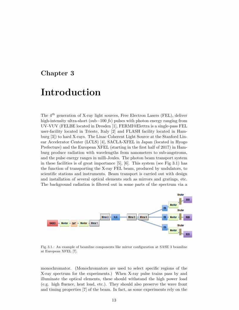
The 4th generation of X-ray light sources, Free Electron Lasers (FEL), deliverhigh-intensity ultra-short (sub−100 fs) pulses with photon energy ranging fromUV-VUV (FELBE located in Dresden [1], FERMI@Elettra is a single-pass FELuser-facility located in Trieste, Italy [2] and FLASH facility located in Ham-burg [3]) to hard X-rays. The Linac Coherent Light Source at the Stanford Lin-ear Accelerator Center (LCLS) [4], SACLA-XFEL in Japan (located in HyogoPrefecture) and the European XFEL (starting in the first half of 2017) in Ham-burg produce radiation with wavelengths from nanometers to sub-angstroms,and the pulse energy ranges in milli-Joules. The photon beam transport systemin these facilities is of great importance [5], [6]. This system (see Fig 3.1) hasthe function of transporting the X-ray FEL beam, produced by undulators, toscientific stations and instruments. Beam transport is carried out with designand installation of several optical elements such as mirrors and gratings, etc.The background radiation is filtered out in some parts of the spectrum via a
Fig. 3.1.: An example of beamline components like mirror configuration at SASE 3 beamlineat European XFEL [7].
monochromator. (Monochromators are used to select specific regions of theX-ray spectrum for the experiments.) When X-ray pulse trains pass by andilluminate the optical elements, these should withstand the high power load(e.g. high fluence, heat load, etc.). They should also preserve the wave frontand timing properties [7] of the beam. In fact, as some experiments rely on the
13
14 Chapter 3. Introduction
coherence and high quality of the wave front of the beam, any degradation ofthe optical components even on the nano scale will affect the performance ofthese experiments.
The high reflectivity of X-ray mirrors is another significant issue in FELs.Mirrors are used at very shallow grazing angles (lower than the critical an-gle). Since beam coherence should be conserved during the beam transport,understanding how degradation or deformation of the optical coating leads tochanges in the beam quality is important. These components should, therefore,be manufactured with certain specific characteristic parameters to let the FELrun for a sustained duration under reliable conditions.
For example, the effects of ionizing radiation on the coatings (e.g. amor-phous carbon (a-C) coatings in this case) in soft X-ray regime, and the energythresholds for surface damage/modifications had to be studied. The length ofmirrors at European-XFEL are around 1 m long. They will be installed ata grazing angle, as they work in X-ray regime with total external reflection.There is a compensation (relation) between the length of the mirrors and theangle at which they operate. This means using lower angles would necessitatemanufacturing longer mirrors; a difficult task for industry (to produce longsmooth coherent surfaces). These facts limit the production.
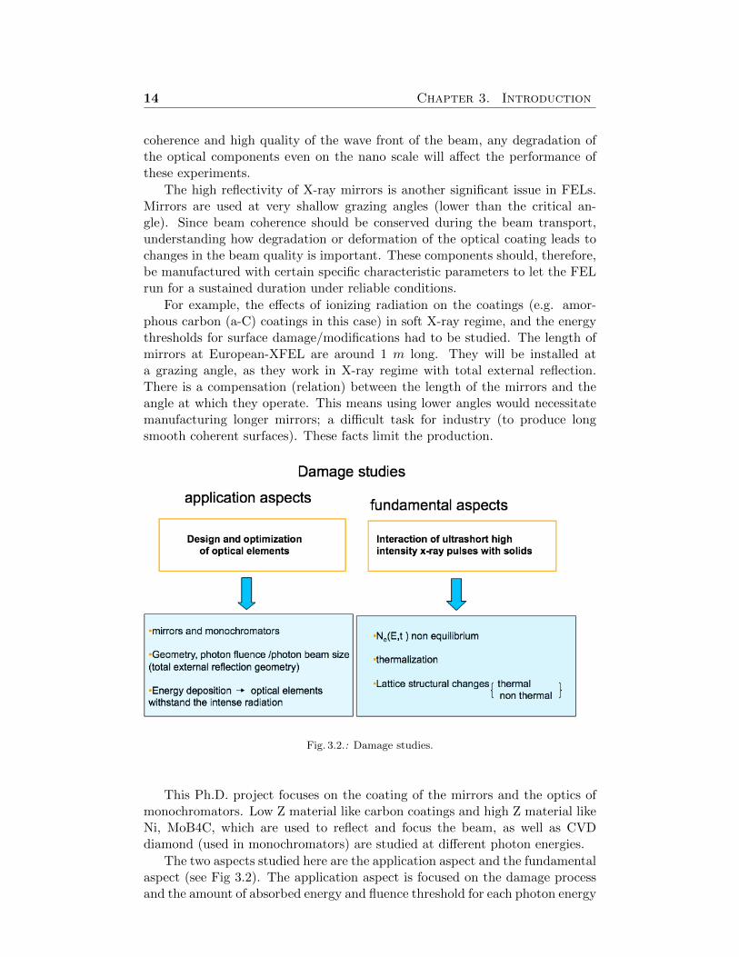
Fig. 3.2.: Damage studies.
This Ph.D. project focuses on the coating of the mirrors and the optics ofmonochromators. Low Z material like carbon coatings and high Z material likeNi, MoB4C, which are used to reflect and focus the beam, as well as CVDdiamond (used in monochromators) are studied at different photon energies.
The two aspects studied here are the application aspect and the fundamentalaspect (see Fig 3.2). The application aspect is focused on the damage processand the amount of absorbed energy and fluence threshold for each photon energy
15
at different incidence angles (grazing angles are the main focus in practical use).In the fundamental aspect, the focus is on the process of damage on mattercaused by FEL beam in femtosecond (fs) time scale. The fs is the time scaleduring which the semiclassical wave packet circulates the proton in an atom(Hydrogen atom), its corresponding wavelength being around 300 nm.
FEL beam pulses with a pulse duration in the fs timescale allow studyingthe interaction of X-rays with a matter with a very high time-resolution. Thisis important e.g. for the understanding of the vibration of chemical bondingsor the creation of plasmas.
After the system is being exposed to FEL pulse, the electronic system ofthe material gets highly excited. During and after the first 100 fs, the excitedelectrons decay back to low energy thermalized states. Where the electronsand lattice coupling is dominated by transferring kinetic and potential energyto the atoms of the lattice. At this point, the atoms experience a modifiedpotential energy surface and relax into the new phase. The purely solid to solidtransition occurs extremely fast (100 fs). The thermal process is assigned asa direct increase in the kinetic energy (temperature) of atoms in the lattice,and the non-thermal melting process is addressed as changes in the interatomicpotential which is caused due to the changes in the potential energy of thesystem [8].
Whether these interactions are thermal or non-thermal, and the possiblephases that the material undergoes from the moment of the beam illuminatingthe sample’s surface to the moment that the sample cools, are important tounderstanding the processes taking place. Any ablation, spallation or melt-ing and the physical reasons connected to such processes are, to some extent,addressed by this project.

16 Chapter 3. Introduction
Chapter 4
Electromagnetic origin ofradiation interaction withmatter
Light is a primary tool for perceiving the world and communicating within it.Its interaction with matter helped to structure the universe. Its transmissionof spatial and temporal information provides a window to the universe, fromcosmological to atomic scales. Light wave-particle nature, revealed in quantummechanics, isn’t exclusive to it but is shared by all of the primary constituentsof nature (electrons are another example of this duality). In classical electro-magnetism, light can be described by coupled electric and magnetic fields inform of waves propagating in the medium. Maxwell's equations are the fourfundamental equations describing the propagation of light in medium [9], [10](see Equations 4.1-4.4).
∇ · E = 4πρ (4.1)
∇ ·B = 0 (4.2)
∇× E = −1
c
∂B
∂t(4.3)
∇×B =1
c
∂E
∂t+
4π
cJ (4.4)
The speed of light (as a wave propagating) in each medium depends onthe properties of that medium, which is described using its phase and groupvelocity (see Eq 4.12).
In quantum mechanics, light is described as discrete packets of energy, calledphotons.
Regarding maxwell equations (see Equations 4.1-4.4), one can obtain a sim-ple electromagnetic wave equation, described by the Equation 4.5
∇2E − µ0ε0E = 0 (4.5)
17
18Chapter 4. Electromagnetic origin of radiation interaction
with matter
which can be simplified (time independent part of wave equation consideringseparation of variable methods) to a Helmholtz equation (plane wave equation)given by
∇2E + k2E = 0 (4.6)
Knowing that Magnetic and electric field are in phase and perpendicular toeach other, the solution to this equation is a plane wave of the following form(Gaussian wave Equation)
~E(r, t) = ~E0ei(k.r−ωt) (4.7)
Hence, the intensity of the Gaussian beam propagating inside the mediumwould be as follows
I ∝| (E0ei(k.r−ωt)) |2 (4.8)
I ∝| E0 |2e−α.r (4.9)
The α is the absorption coefficient, where
α = 1/σp (4.10)
and σp is the penetration depth.The wave vector k and the angular frequency ω obey the following relations
k =2π
λ,ω
k=
√1
ε0µ0(4.11)
vph =ω
k, vgr =
∂ω
∂k(4.12)
The phase velocity vph describes the speed of wave crest and the group velocityvgr, the speed of the center of mass of a wave packet with middle frequency w.In vacuum the phase and group velocity are the same and equal to the speedof light (see Eq 4.13). ε0 and µ0 are called dielectric constant and permeabilityof vacuum, respectively.
c =1
√µ0ε0
(4.13)
Understanding principles of the interaction of electromagnetic waves withmatter is a useful aid in developing methods of understanding the structure ofmatter and its different chemical, mechanical, electrical and thermal properties.
Chemical bonding (ionic, metallic, valence, van der Waals and hydrogenbonding) ascribes a potential which creates the interactions holding the atomsin molecules or crystal together. There are several theories, including Bloch the-ory, Tight-Binding model, etc., which describe the periodic potential in whichatoms (ions) are located and electrons move. Each atomic orbital correspondsto a particular energy level of the electron [11], [12]. The time independentSchrodinger equation (see Eq 4.14) explains the energy levels and bond struc-ture in a matter.
19
EΨ =−~2m∇2Ψ + V 2Ψ (4.14)
The electromagnetic force between electrons and protons is responsible forbuilding up atoms which requires an external source of energy for the electronto escape its atom. The closer an electron is to the nucleus, the greater theattractive force. Electrons bound near the center of the potential well (coreelectrons) therefore, need more energy to escape from the atom than those athigher shells (valence electrons). Valence electrons are those occupying the out-ermost shell or highest energy level of an atom and are responsible for buildingup atomic bondings [11], [9]. In contrast, the core electrons do not participatein bindings in that sense.
Electrons in solid insulators can be considered confined to each atom. Onecan treat them as a harmonic oscillator, where each can be described with
m(r + γr + ω02r) = eE(r(x, y, z), t) (4.15)
where the solution to this equation would be
~r =e ~E(r(x, y, z), t)
m((ω02 − ω2) + iγω)
(4.16)
Exposed by the electromagnetic wave, the atoms/molecules in matter getpolarized (because of the electromagnetic force acting on them (see Eq 4.17)).The electromagnetic wave acts on a charge particle via force F given by
~F = q( ~E +v
c× ~B) (4.17)
As v ≤ c, the electric filed is the dominant factor in this equation.The electric displacement is defined as
~D = ε0 ~E + ~P (4.18)
Proceeding with that equation (Eq 4.18) the wave equation (see Eq 4.5)turns to
∇2E − µ0ε0E = µ0P (4.19)
which states that each dipole, where its second derivative varying with time, isa source of electromagnetic wave propagating in a medium. Where ~E(t)= ~Eeiwt,
~r(t)=~reiwt and ~P=e ~r(t)=~peiwt.The dipole moment of the charge (as the electromagnetic wave acts on it)
changes with (involving results of Eq 4.15 for ~r)
~P = e~r =e2
m(ω2
0 − ω2 − iγω)−1 ~E (4.20)
If one assumes a linear relationship between P (polarization) and E (electricfield) such as
~P
ε0= χ~E (4.21)
20Chapter 4. Electromagnetic origin of radiation interaction
with matter
Then
χ =e2N
ε0m(ω20 − ω2 − iγω)
(4.22)
with χ called the susceptibility (ε = 4 πχ + 1) respectively, or in the formof
~D = ε0(1 + 4πχ) ~E = ε0ε ~E (4.23)
Where both ε and χ depend on (ω,k).Suppose there are N molecules inside the medium and each molecule has
Z electrons with a binding frequency of ωi and damping constant γi, where∑fi=Z. The dielectric constant gets the following form
ε(ω) = 1 +4πNe2
m
∑(fi(ω
2i − ω2 − iγiω)−1) (4.24)
where the damping constant is usually small compared to the binding orresonant frequency ωi. The εω for most frequencies is real and ω2
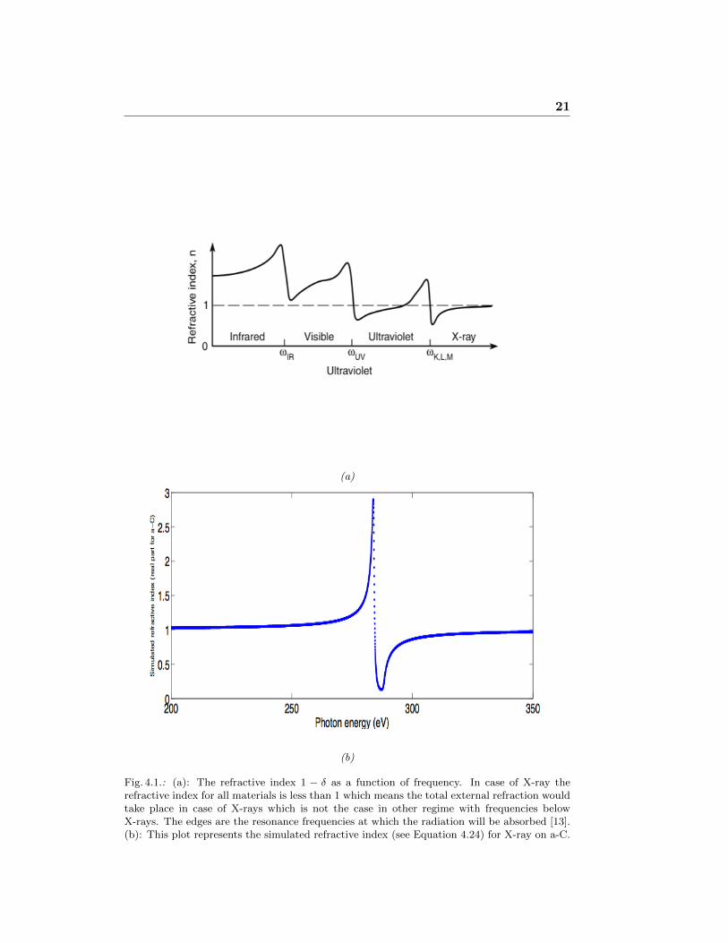
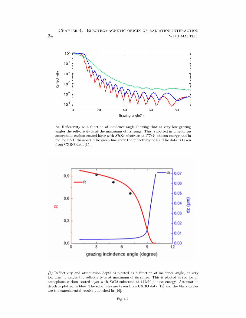
i −ω2 is positivefor ω ≤ ωi and negative for ω ≥ ωi. Below the smallest ωi , at low frequenciesthe ε(ω) is greater than unity. An interesting behavior is seen when the ε(ω)is negative. It occurs on passing the smallest values of ε(ω) and reaching highfrequencies as in the case of X-rays (see Figs 4.1). This means in that region,the phase velocity (velocity of wave crest) is faster than the speed of light.
In the neighborhood of any ωi one sees an extreme behavior (see Figs 4.1).The absorption is at maximum and the phase speed is very low. The resonancefrequencies are defined as frequencies at which the radiation will be absorbedto the maximum, and the imaginary part is large.
For a better understanding one can describe the wave vector of the propa-gating wave by
k2 = (1 + χ(ω))ω2/c2 (4.25)
Where the refractive index is introduced as n2 = (1 +χ(ω)). Since χ(ω) [9] is acomplex number, the refractive index can be presented in its real and imaginarycomponents
n = 1− δ(ω) + iβ(ω) (4.26)
The real part 1 − δ(ω) (see Figs 4.1 and 4.3) describes the phase velocity andβ(ω) is related to the absorption of radiation through the medium.
With Beer Lambert Law (is relevant mainly for linear optic [14]), it is possi-ble to calculate the changes in the intensity of the EM radiation as it enters andpropagates inside the medium. Starting with the Equation 4.7 and substitutingk with the
k = nω/c (4.27)
where n is described in the Equation 4.26 it appears that
I(z) = I0e(−4πβ(ω)/λ)r (4.28)
Here λ is the wavelength of radiation, r the distance the radiation willtravel to and β the absorption parameter in refractive index. The distance
21
(a)
(b)
Fig. 4.1.: (a): The refractive index 1 − δ as a function of frequency. In case of X-ray therefractive index for all materials is less than 1 which means the total external refraction wouldtake place in case of X-rays which is not the case in other regime with frequencies belowX-rays. The edges are the resonance frequencies at which the radiation will be absorbed [13].(b): This plot represents the simulated refractive index (see Equation 4.24) for X-ray on a-C.
22Chapter 4. Electromagnetic origin of radiation interaction
with matter
up to which the radiation decays is called the attenuation length (where theintensity becomes 1/e of its initial value, the α in the Equation 4.9 is exactly1/Latt which is named the absorption coefficient) and can be determined by
Latt = λ/(4πβ(ω)) (4.29)
This quantity depends on both the wavelength of the incident radiation andthe medium, in the latter case the imaginary part of the refractive index (seeFig 4.3) being the key factor. In general, the attenuation depth varies from nmto µm. Calculations show that X-ray attenuates deep inside the medium depth(at high photon energies up to few µm and at very low photon energies up tofew nm [15], [8]). If the medium is transparent to a sort of radiation, it denotesthat there are no available energy levels matching the radiation wavelength inthe matter and energy can not get absorbed. In the case of strong electric field,in non-linear medium, the induced polarization can be expressed by the Taylorexpression
P = ε0(χ1E + χ2E2 + χ3E3......) (4.30)
χ2, χ3, etc. described in nonlinear optics, are high-order terms which canbe obtained in this condition. The high-order-of-magnitude waves from theseterms are named as 2nd, 3rd harmonic waves, with a frequency of twice ortriple the incident waves. Electric displacement would therefore not have thesimple form as in Equation 4.18. Hence, the refractive index would have a morecomplicated form.
The reflectivity of a material depends on its reflective index and the inci-dence angle of the incoming beam. In the X-ray beam transport system, the aimis to maximize the reflected intensity. It is desired, to avoid normal incidencegeometry, which increases the absorption percentage of the beam. The goal isto maximize reflection at the surface of the coating material at a grazing inci-dence angle. The candidate material in the case of this project was amorphouscarbon.
According to Snell law (see Equation 4.31), it is possible to calculate themost appropriate geometry, at which the reflectivity, for a given material, ismaximized. The angle of incidence beyond which, rays of light passing througha denser medium to the surface of a less dense medium and are no longerrefracted but totally reflected is named as the critical angle. The total reflectionoccurs at an angle larger than a particular critical angle (with respect to thenormal to the surface).
One obtains the critical angle through following steps
n′sin(φ
′) = n sin(φ) (4.31)
(φ) is the incident angle of the EM radiation, n = 1 (in vacuum), as mentionedin Fig 4.1 in the X-ray regime n
′is smaller than 1, n
′= (1 − δ) and β (see
Fig 4.3) can be neglected in this regime. Equation 4.31 turns into
sin(φ′) = sin(φ)/1− δ (4.32)
23
In the case of critical angle
φ′ ⇒ π/2 (4.33)
1 = sin(φ)/1− δ (4.34)
and substitution of θ = 90− φ and considering the Taylor expansion of Cos(θ)results in
θc =√
2δ (4.35)
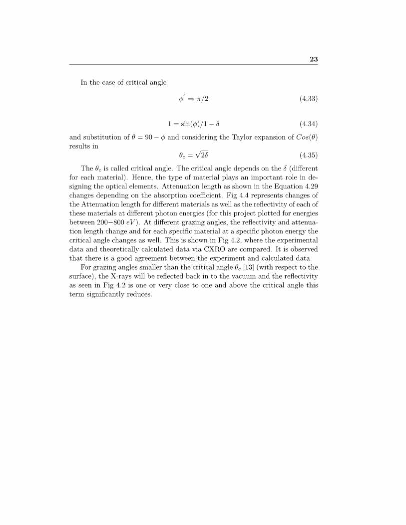
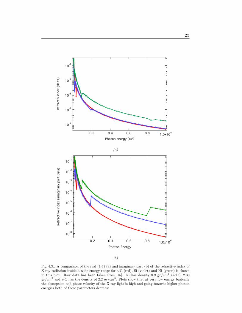
The θc is called critical angle. The critical angle depends on the δ (differentfor each material). Hence, the type of material plays an important role in de-signing the optical elements. Attenuation length as shown in the Equation 4.29changes depending on the absorption coefficient. Fig 4.4 represents changes ofthe Attenuation length for different materials as well as the reflectivity of each ofthese materials at different photon energies (for this project plotted for energiesbetween 200−800 eV ). At different grazing angles, the reflectivity and attenua-tion length change and for each specific material at a specific photon energy thecritical angle changes as well. This is shown in Fig 4.2, where the experimentaldata and theoretically calculated data via CXRO are compared. It is observedthat there is a good agreement between the experiment and calculated data.
For grazing angles smaller than the critical angle θc [13] (with respect to thesurface), the X-rays will be reflected back in to the vacuum and the reflectivityas seen in Fig 4.2 is one or very close to one and above the critical angle thisterm significantly reduces.
24Chapter 4. Electromagnetic origin of radiation interaction
with matter
10-5
10-4
10-3
10-2
10-1
100
Reflecti
vit
y
806040200
Grazing angle(¡)
(a) Reflectivity as a function of incidence angle showing that at very low grazingangles the reflectivity is at the maximum of its range. This is plotted in blue for anamorphous carbon coated layer with SiO2 substrate at 177eV photon energy and inred for CVD diamond. The green line show the reflectivity of Ni. The data is takenfrom CXRO data [15].
(b) Reflectivity and attenuation depth is plotted as a function of incidence angle, at verylow grazing angles the reflectivity is at maximum of its range. This is plotted in red for anamorphous carbon coated layer with SiO2 substrate at 177eV photon energy. Attenuationdepth is plotted in blue. The solid lines are taken from CXRO data [15] and the black circlesare the experimental results published in [16].
Fig. 4.2.
25
10-5
10-4
10-3
10-2
10-1
Refr
acti
v index (
delt
a)
1.0x1040.80.60.40.2
Photon energy (eV)
(a)
10-8
10-7
10-6
10-5
10-4
10-3
10-2
10-1
Refr
acti
ve index (
imagin
ary
part
Be
ta)
1.0x1040.80.60.40.2
Photon Energy
(b)
Fig. 4.3.: A comparison of the real (1-δ) (a) and imaginary part (b) of the refractive index ofX-ray radiation inside a wide energy range for a-C (red), Si (violet) and Ni (green) is shownin this plot. Raw data has been taken from [15]. Ni has density 8.9 gr/cm3 and Si 2.33gr/cm3 and a-C has the density of 2.2 gr/cm3. Plots show that at very low energy basicallythe absorption and phase velocity of the X-ray light is high and going towards higher photonenergies both of these parameters decrease.
26Chapter 4. Electromagnetic origin of radiation interaction
with matter
0.01
2
4
6
80.1
2
4
6
81
2
Att
enuati
on length
(um
)
1000800600400200
Photon energy (eV)
(a)
10-7
10-6
10-5
10-4
10-3
10-2
10-1
Reflecti
vit
y
1000800600400200
Photon energy(eV)
(b)
Fig. 4.4.: (a): Attenuation length at different photon energies are compared for differentmaterials. a-C (red), CVD (pink), Si (violet) and Ni (green). (b): Reflectivity of a-C (red),CVD (pink), Si (Violet), Ni (green) vs photon energies are compared here.
Chapter 5
Ultra-fast electrons and latticedynamics
5.1 A general picture
The X-ray FEL beam interacts directly with the electronic system of the ma-terial (see Figs 5.1 and 5.2). It excites the atoms, moving electrons from initialground state to the unoccupied levels, resulting in the creation of electron-holepairs. The time-dependent intensity of the laser pulse has an effect on the de-gree of damage. Since the laser pulses are FEL pulses with fs time scale, theexcitation process occurs very quickly. As a consequence, the non-equilibriumdistribution of electrons gets thermalized through electron-electron collisions.Hence, the system returns to a Fermi-like equilibrium state in a short time.This thermalization results in a single chemical potential. As the laser inten-sity is very high, a vast number of electrons and hole pairs are created. Atthe same time, this means that the recombination time becomes short and ionsalso get displaced to large distances compared to a low-intensity laser pulse.Displacements of ions (in large distances) on the other hand means that theelectronic band structure gets modified and valence and conduction bands cancross each other (in the case of insulators or semiconductors). During this time,the lattice undergoes some modifications such as bonds breaking, and the mate-rial gets restructured. This results in the possibility of the material undergoingcrystal phase changes, melting, ablation, etc. Besides, the laser pulse causesheat diffusion in the sample as well, a process which takes a long time (ps−ns)compared to the non-thermal structural changes of the matter. As the heatdiffuses inside the sample, it can cause a more significant amount of damage inthe sample. There are two processes, the heat that gets diffused into the origi-nal material through conduction, and the heat which passes through from thecenter of damaged area towards the rest of the sample. After some hundreds ofµs the sample cools down to the room temperature.
If a semiconductor gets excited with an ultrashort laser pulse, it undergoesseveral stages of relaxation before returning to the equilibrium state. Thesecan be categorized under
27
28 Chapter 5. Ultra-fast electrons and lattice dynamics
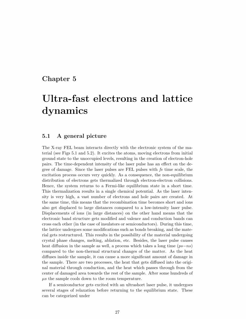
Fig. 5.1.: Very simple schematic of the matter and laser beam interaction [17]. The left sideshows the system in its ground state; the electrons cold state. The potential landscape showsminima at the crystal lattice sites. Therefore, no external forces are acting on them excepttight binding Coulomb potential induced by the lattice. On the right side, the laser light hasaffected the system and transported it to an excited state. Hot electrons and holes are createdhere. The potential landscape undergoes qualitative and quantitative changes, resulting indisappearance or shifting of the minima. This happens in very short time scale (shorter thanreaction time); as a result, forces act on the carriers/atoms and move them.
• Carrier excitation
• Thermalization
• Carrier removal
• Thermal and structural effects
5.1. A general picture 29
• Carrier excitation
If the photon energy is larger than the band gap, single photon absorp-tion process dominates in exciting the valence electrons to the conductionband. If the semiconductor has an indirect band gap such as Silicon(Si), the absorbed optical photon can still excite the valence electron,but here the assistance of a phonon would be necessary (for the momen-tum conservation). As the coherence between the electromagnetic fieldof the radiation and the excitation disappears (due to scattering), andbonds break, the carriers become free. The free carriers can be absorbedinto the conduction band. This results in an increase of energy in thefree carriers plasma. In the case of carriers with energies higher than thebandgap, it is possible to generate more free carriers through the impactionization.
The photo-absorption process could be linear or nonlinear. This issimply influenced by the duration of the pulse. In the case of longpulses, the linear photo-absorption process takes place. Where thephoton gets absorbed and the photo-absorption happens as a result ofthe Beer-Lamber-law. Whereas in the case of femtosecond optical laserpulses of the same fluence intensity, the absorption follows a nonlinearprocess. Main active processes in the case of the fs laser pulses are impactionization, tunnel ionization and multiphoton ionization [18], [19], [20],[21], [22], [23], [24], [25], [26], [27], [28].
• Thermalization
Carrier-carrier scattering or carrier-phonon scattering takes place assoon as the free carriers are generated. Carrier-carrier scattering doesn'tchange the total energy in the excited carrier system, but rather causesdephasing which can take place within a 10 fs timescale. Whereasapproaching the Fermi-Dirac distribution would take 100s of fs. Incontrast, carriers lose or absorb energy and momentum by scatteringwith phonons [29]. Through this interaction energy of carriers candecrease due to spontaneous phonon emission. Since phonons can carryvery little energy, it may take several picoseconds to achieve thermalequilibrium between lattice and carriers [30].
• Carrier removal
Before the thermal equilibrium is reached a state exists where carriersand lattice are in equilibrium at a defined temperature, but the densityof free carriers is more than at in thermal equilibrium. At this stage, theexcess free carriers disappear via electron-hole recombinations or escapefrom the excited region and defects. In the case of recombination, oneof two processes will occur; either the excess energy will be emitted inthe shape of a photon (Luminescence), or it will have enough energy tokick an electron out from an upper shell in the conduction band (Auger
30 Chapter 5. Ultra-fast electrons and lattice dynamics
process). Excess energy will be spent on the removal of carriers from thesurface when defects or surface recombinations occur. The increase offree carriers density will lower the band gap.
• Thermal and structural effects
At this stage, the lattice and free carriers are at the same temperature,and the excess free carriers are removed from the material. Reachingthis thermal equilibrium state may take some picoseconds, but the excesscarriers removal takes place over a longer time. If the lattice temperaturegoes above the melting or boiling point, the material can become meltedor vaporize away. This happens over longer timescales, more than few tensof picoseconds. In the case of evaporation or melting, the temperaturedrops down via resolidification. This, however, doesnt mean that thematerial turns back to the original structure or phase [29]. In the event ofno phase transition, the temperature drops down to ambient temperaturein microseconds.
5.2 X-ray FEL light, matter interaction
X-ray photons, exposing the matter, either get absorbed or scattered away. Itis possible that X-ray photons get elastically or inelastically scattered insteadof being absorbed. The elastically scattered photons have no energy change.This process is called Rayleigh scattering, which happens when the particlehas smaller dimensions than the radiation wavelength, and the scatterer hasenormous mass (infinite). This is when photons scatter off the bound electrons.The nucleus is heavy enough to act as the required large mass. In the case offree electrons, the elastic scattering can only occur if photons have low energyto let quasi-elastic scattering happen.
The inelastic scattering of photons off a free electron (charge particle) iscalled Compton scattering. In this process, the incoming photon interacts withthe charged particle and get scattered with a different wavelength and with theangle of θ. Hence, an electron with an energy difference of scattered and initialphoton energy gets scattered away.
Studies show that in damage process with fs FEL pulses, the photo-ionization has a maximum cross section compared to the scattering pro-cesses like Compton scattering, which play a minor role in the damage pro-cess [31], [32], [33], [34], [35].
Photo-ionization is the leading process in the interaction of fs laser pulseswith matter both in the case of the optical laser (depending on the photonenergy, the incoming energetic photon has enough energy to kick an electronout of the bond system) or in the case of the X-ray FEL. X-ray photons havehigh enough energy to ionize the atoms and kick electrons out of the boundstate. The X-ray photons, also, can attenuate deep (up to few µm) inside thematter.
5.2. X-ray FEL light, matter interaction 31
High energy (around or above core level energy state) X-ray photons inter-act with inner shell electrons of atoms. This could result in the ejection of acore level electron, which can be refilled with an electron from an upper-levelshell and the emission of another photon called fluorescence photon or anotherelectron from the atom, which is called the Auger electron. This process takesplace during the pulse. The ejected Auger electron (in the case of low Z mate-rials, this is the dominant process) or fluorescence photon will have a definedamount of energy and will interact with surrounding atoms inside the materialthrough different processes. In other words, the Auger electron, as an example,causes further electronic excitations, e.g., electron excitation from the valenceband into the conduction band, even from deep shell electronic state or throughimpact ionization. They also could get elastically scattered away or even skipout of the medium from the surface (see Fig: 5.2). On the other hand, theymight just excite an atom. In this case, the atom would get back to the normalinert state by emitting a photon or phonon, depending on the energy of thewhole system. All these processes can get categorized as secondary processes.The energy of the emitted photoelectrons depends on the photon energy of theinitial photon (of the incoming beam) and also the binding energy in the atomicsystem (see Equation 5.1). The number of photons, which are interacting withthe matter (a higher or lower flux of photons) in each pulse, the energy of eachphoton and the binding energy of the electrons have a significant impact onchanging the interaction intensity and the damage level.
KE = hν − φ−BE (5.1)
If the free electron absorbs high enough energy from a photon to ionizeanother electron from an atom, there will be two free electrons available in thesystem. These two can absorb energy from incoming photons (as free carriers)and undergo the same cycle. This process continues and produces a high rateof free carriers in what is called avalanche ionization.
Optical laser avalanche ionization is mainly an active process for the laserintensities below 1012 W/cm2. Avalanche ionization, in the sense of cascades viaelectron impact ionization, is the dominant channel for free-electron productionfor the case of X-rays [36].
The impact ionization occurs on the femtosecond time scale. In contrast,the elastic scattering of photons as an example takes place over a longer timescale (typically in picosecond time scale). In the case of Carbon for the impactionization as an example, the minimum amount of energy need is around theindirect bandgap (Ee>4.8 eV ) [36]. Another effect which can occur is theinverse-Bremsstrahlung, in which the free electron in the presence of an ioninteracts with the X-ray photon without ionizing another electron from thesystem. One can say that the electron absorbs energy from the beam duringthe collision with an ion. This collision result in an electron-positron pairproduction [37], [30], [36]. Inverse−Bremsstrahlung is a complicated process,more pronounced in lower X-ray energies and lower electron temperatures. ForX-ray, direct photo-absorption by free electrons (or inverse-Bremsstrahlung) isnegligible, as the deep-shell photo-ionization is the dominated processes in this
32 Chapter 5. Ultra-fast electrons and lattice dynamics
case.
If N photons strike a bound electron (each with an energy of hν ), it seemsthat the electron is facing a photon with Nhν energy and λ/N wavelength, inmultiphoton ionization. If the energy is high enough the electron will becomefree and the atom ionized. The intensity at which multiphoton ionization mainlytakes place is 1013 W/cm2 [38]. Photons should have a minimum amount ofenergy to be able to ionize the valence electrons to the conduction band.
Tunnel ionization (a process in which electrons in an atom (or a molecule)pass through the potential barrier and escape from the atom/molecule) mainlytakes place when the intensity is higher than 1015 W/cm2. The multiphotonionization and tunnel ionization are sometimes called strong electron field ion-ization. It is important to mention that the peak brightness in case of FEL isof the order of 1014 W/cm2 in general norm [38]. The temporal number of freeelectrons, ionized by the direct photo-ionization (photo-absorption), electronimpact ionization and Auger-like processes, increases during the fs FEL pulsevery fast. The impact ionization collision time can be estimated around 10−16
s. In comparison to visible light, the impact ionization is the first dominantprocess, and the Auger-like process is the second dominant processes in the freesecondary electron production process [36] (see Fig 9.7).
Bloembergen, Perry, and Du and co-workers conducted several studies onlaser-induced damage of alkali halides, fused silica, and some other dielectricmaterials by using nanosecond and picosecond laser pulses [40], [38], [25], [41].Investigations and studies show in the case of femtosecond laser pulses; sev-eral different processes are involved in the damage process. Among these areCoulomb explosion [42], thermal melting [42], [43], plasma formation [43] andmaterial cracking caused by thermoelastic stress [44], [45](see Fig 5.2). Whilethe underlying physics may be totally different, all cases have a critical energydensity (where free electron density saturates), at which damage occurs. Atthis stage, the reflectivity is at maximum state (see Eq 5.2).
The state at which matter is in the form of a mixture of positive ions andnegatively charged particles is called plasma. Since the invention of laser, cre-ation of plasma in matter has been studied [46], [47], [48], [49]. It is believedthat when the ionization is completed, the free electron density is comparableto the ion density of about 1023 cm−3 [50]. The critical density (see Eq 5.2) isthe free-electron density when the plasma oscillation frequency equals the laserfrequency
ncr =πmec
2
e2λ2(5.2)
Where me is the electron mass, c speed of light, e the electron charge andλ the laser wavelength. The importance of critical density in the interactionof electromagnetic waves with plasmas becomes apparent when considering thedielectric function of the plasma. This is given by
εw = 1−ω2pe
ω(ω + ivm)(5.3)
5.3. Ablation 33
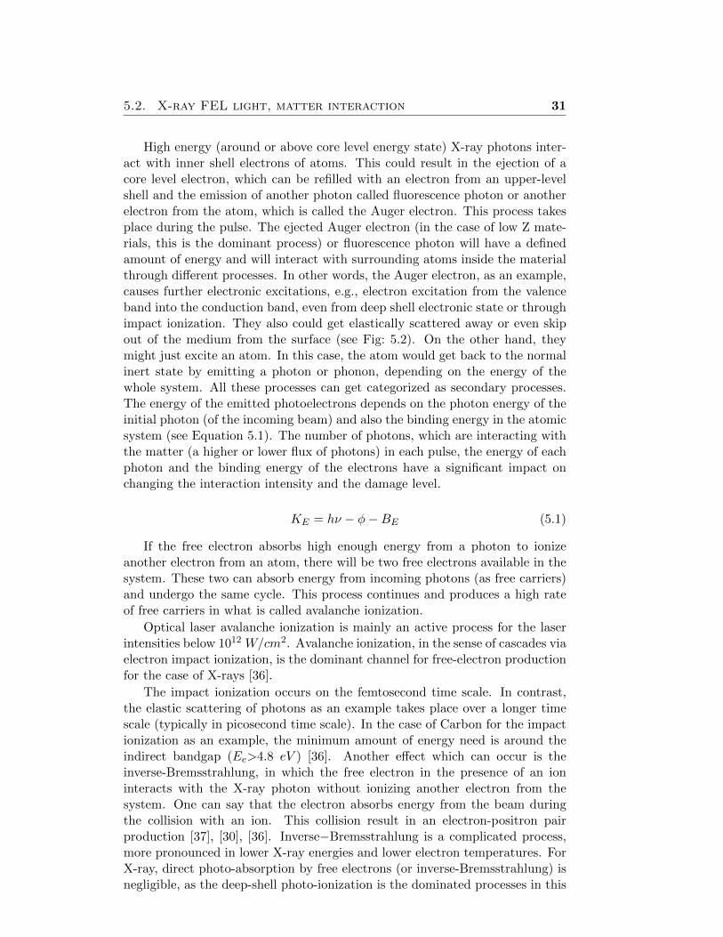
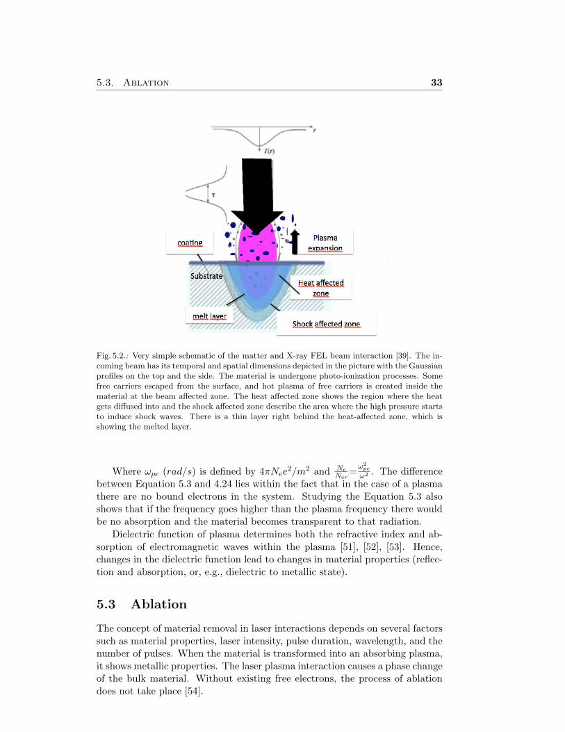
Fig. 5.2.: Very simple schematic of the matter and X-ray FEL beam interaction [39]. The in-coming beam has its temporal and spatial dimensions depicted in the picture with the Gaussianprofiles on the top and the side. The material is undergone photo-ionization processes. Somefree carriers escaped from the surface, and hot plasma of free carriers is created inside thematerial at the beam affected zone. The heat affected zone shows the region where the heatgets diffused into and the shock affected zone describe the area where the high pressure startsto induce shock waves. There is a thin layer right behind the heat-affected zone, which isshowing the melted layer.
Where ωpe (rad/s) is defined by 4πNee2/m2 and Ne
Ncr=ω2pe
ω2 . The differencebetween Equation 5.3 and 4.24 lies within the fact that in the case of a plasmathere are no bound electrons in the system. Studying the Equation 5.3 alsoshows that if the frequency goes higher than the plasma frequency there wouldbe no absorption and the material becomes transparent to that radiation.
Dielectric function of plasma determines both the refractive index and ab-sorption of electromagnetic waves within the plasma [51], [52], [53]. Hence,changes in the dielectric function lead to changes in material properties (reflec-tion and absorption, or, e.g., dielectric to metallic state).
5.3 Ablation
The concept of material removal in laser interactions depends on several factorssuch as material properties, laser intensity, pulse duration, wavelength, and thenumber of pulses. When the material is transformed into an absorbing plasma,it shows metallic properties. The laser plasma interaction causes a phase changeof the bulk material. Without existing free electrons, the process of ablationdoes not take place [54].
34 Chapter 5. Ultra-fast electrons and lattice dynamics
There exist two ablation mechanisms (regimes), distinguished by their pulsedurations. In the case of long pulses (longer than 100 ps), the ablation proceedsin equilibrium conditions. The damage fluence threshold, in this case, increaseswith pulse duration. The interaction of the pulse with matter is different de-pending on the type of matter. In the case of metals, ablation occurs at verylow intensities, whereas in the case of dielectrics this process is very weak at lowintensities. All possible processes like the electron-to-ion energy transfer, theelectron heat conduction, and therefore the hydrodynamic or expansion, appearto take place over a longer time scale (equilibrium conditions) compared to thecase of fs pulses.
In the case of fs pulses, the laser matter interaction appears to take placewith the matter with constant density.
Since energy transition from the electron to the lattice with regard tosub-picosecond pulses (fs or faster) takes place on a time scale of 1 − 10 ps(which is longer than the pulse duration itself), therefore the ablation pro-ceeds in non-equilibrium conditions and the conventional hydrodynamics mo-tion does not occur during the femtosecond interaction time. One can say theelectrons cool down without transferring energy to the lattice. Because theelectron heating rate is much greater than the rate of energy transfer to thelattice. Hence, in latter case the ablation doesn’t depend on the pulse dura-tion [52], [53], [51], [55], [56], [57].
The laser ablation is sometimes mentioned as laser induced breakdown [38].Among several existing theories [52], [53], one states that multiphoton ionizationsupplies seed electrons, while avalanche ionization is still responsible for theablation. For pulses shorter than 100 fs the ionization process is governed bythe multiphoton ionization. Some theories [52], [53], [58], [59], [60], [61] basedon analytic models and Boltzmann equations (distribution), given by nc =nee
(eφ/KBTe) with Te as electron temperature and nc as electron density (whileignoring ion motion) and experimental measurements, confirm that multiphotonionization dominates free electron generation at intensities on the order of 1014
W/cm2. After the critical density is created, Bremsstrahlung and resonanceabsorption play a significant role in absorbing energy.
If the intensity is much higher than the threshold fluence, then it is possiblethat the vaporization process occurs. Where the electron-phonon collisionsincrease the local temperature above the vaporization point.
Another parameter which plays a role in ablation in the case of the ultrafastpulses is the Coulomb explosion at intensities near the ablation threshold fluencein dielectrics [14], [62]. Since electron-to-ion energy exchange time, as well as theheat conduction time, is much longer than the pulse duration, the ions remaincold during that process. Hence, excited electrons escape from the surface ofthe bulk materials and form a strong electric field that pulls out the ions fromwithin the impact area.
In high-density plasmas, the electron-ion (e-i) interaction leads to ioniza-tion, excitation, and reduction of the electron temperature. However, elasticcollisions can also lead to absorption, where a photon is absorbed by a free elec-tron which is excited to a more energetic continuum state in the Coulomb fieldof an ion. This ”absorption through collisions” is often referred to as inverse
5.4. Time scale of X-ray light-matter interaction 35
Bremsstrahlung [49], [63], [64], [65], [66], [67], [68], [69], [70].
In general, one can say that energy transfer from electron to ions occursin ps time scale. Hence, it's mainly deposited in a small layer in electron-photon interaction process. Therefore, during the pulse, heat conduction andhydrodynamic motions are negligible and thermal damage (micro cracks orshock affected zone) and the heat affected zone are also reduced regarding shortfs pulses [71].
5.4 Time scale of X-ray light-matter interaction
The pulse duration declares how long the energy is deposited into the matter.The deposited energy gets absorbed mainly through photo-ionization.
The photo-ionization cross-section as a function of energy for different ma-terials is found in literature [15]. The ionized electrons and ions, as well asphonons, distribute the deposited energy inside the matter. This type of inter-action occurs in 1−10 ps and is categorized as thermal conduction. X-ray pho-ton absorption decreases the number of bound electrons, therefore the numberof free electrons increases, the system heats up, and the absorption capabilitiesof the matter decrease. With increasing X-ray intensity, ionization of boundelectrons increases and the material becomes more and more transparent to theX-ray absorption.
The whole X-ray absorption process including the photo-ionization and sec-ondary processes such as Auger electron ejection etc. happens in the very shorttime scale up to 100 fs. Phonons are also a result of the interaction of the emit-ted electrons with atoms inside the material. The recombination of electronsand ions is among all the processes which take place during the interaction pro-cess [72]. After a sufficient time in ps regime, the number of electrons and ionsand the temperature of the system is high enough to have a hot plasma consist-ing of electrons and ions. The system gets into a state that tries to reduce theheat and return to a thermodynamic stable state. Part of the hot plasma getsdepleted from the matter and part distributed inside the bulk. At this point,craters appear, which usually have a size bigger than the beam size. This isbecause of the secondary processes and the heat transfer inside a volume withinthe bulk.
Basically, for short pulses (sub-100 fs), the ionization processes are muchmore efficient during the pulse than the recombination processes such as Auger-like recombination of the valence-band hole or fluorescence. In contrast, if thepulse is very long, there is enough time for all those processes to happen, eventhe recombination process possibly taking place during the pulse. The excitedmatter transforms into a thermodynamic equilibrium state of materials. Aconsequence of X-ray interaction with matter is an increase in temperature,pressure and ionization, all inducing stress and stress gradients in the material.
To stabilize the system, theses can all lead to a phase transition in thematerial. Among different types of phase transitions, one can mention Solid-liquid, liquid-gas, solid-gas as well as solid to plasma transition.
36 Chapter 5. Ultra-fast electrons and lattice dynamics
5.5 Length scale of X-ray light, matter interaction
In optical fs laser, the depth to which radiation would drill was estimated to bevery close to skin depth. Since the incident electric field decreases exponentially,the skin depth increases logarithmically with fluence [53]
deV =ls2
lnF
Fth(5.4)
with ls = cwk (k taken as the imaginary part of refractive index) repre-
sented as skin depth (field penetration depth), Fth fluence threshold and deVas the crater depth. Another part of the studies shows that the heat wavepropagates inside the matter to a depth less than the skin depth during thepulse. This comes from the energy transfer between the electrons to ions insolid which occurs with a frequency almost matching the plasma frequency ofelectrons [53], [60]. The characteristic heat conduction time is given by
tth =l2sD
(5.5)
Where D is thermal diffusivity. Gamaly [50], [52], [53] demonstrated (inthe case of thermal melting) electrons have no time to transfer the energy tothe ions during the laser pulse τei > tp. The target density remains constantduring the laser pulse. Since the heat conductivity time is also much longerthan the pulse duration, its not possible for electrons to transfer the heat outof the skin layer (except X-ray excited electrons which are fast). With the helpof conventional thermal diffusion, one can get
tth ≈l2eκ
(5.6)
κ =leve3
(5.7)
where κ is the coefficient of thermal diffusion and le and ve are the electronmean free path and velocity, respectively. X-rays interact with matter in µmscale in normal incidence geometry. Therefore the interaction takes place ina large volume compared to other types of radiation. Worthy of note is theincidence angle which, alongside the optical properties of the material itself,plays a role in attenuation length. For instance, the attenuation length versusthe photon energy in the case of amorphous carbon is depicted in Fig 5.3. Thesudden drop is due to the ionization threshold of this element. The attenuationdepth is not the only important factor, but also the path that electrons travelafter they are ejected via the X-ray photons inside that material. The direc-tion where those electrons travel depends on the electric field of the incomingradiation (on the polarization of the radiation). In the total external reflectiongeometry and XUV radiation case (where σ (see section 5.1) is positive, andβ is nonzero for all materials), the electric field decays in exponential depen-dence on depth. As a result, the energy absorbed by the coating is deposited onthe layer, a few nanometers below the surface, characterized by the absorptiondepth dz
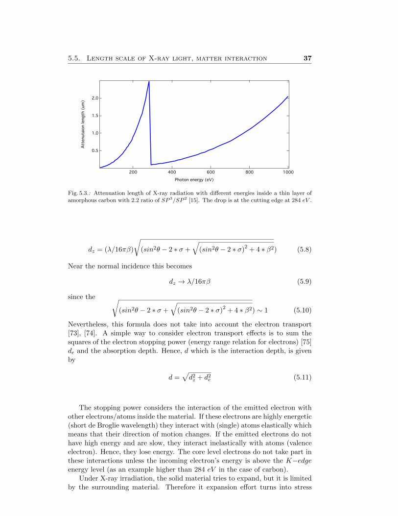
5.5. Length scale of X-ray light, matter interaction 37
2.0
1.5
1.0
0.5
Att
enuta
ion length
(um
)
1000800600400200
Photon energy (eV)
Fig. 5.3.: Attenuation length of X-ray radiation with different energies inside a thin layer ofamorphous carbon with 2.2 ratio of SP 3/SP 2 [15]. The drop is at the cutting edge at 284 eV .
dz = (λ/16πβ)
√(sin2θ − 2 ∗ σ +
√(sin2θ − 2 ∗ σ)2 + 4 ∗ β2) (5.8)
Near the normal incidence this becomes
dz → λ/16πβ (5.9)
since the √(sin2θ − 2 ∗ σ +
√(sin2θ − 2 ∗ σ)2 + 4 ∗ β2) ∼ 1 (5.10)
Nevertheless, this formula does not take into account the electron transport[73], [74]. A simple way to consider electron transport effects is to sum thesquares of the electron stopping power (energy range relation for electrons) [75]de and the absorption depth. Hence, d which is the interaction depth, is givenby
d =√d2z + d2e (5.11)
The stopping power considers the interaction of the emitted electron withother electrons/atoms inside the material. If these electrons are highly energetic(short de Broglie wavelength) they interact with (single) atoms elastically whichmeans that their direction of motion changes. If the emitted electrons do nothave high energy and are slow, they interact inelastically with atoms (valenceelectron). Hence, they lose energy. The core level electrons do not take part inthese interactions unless the incoming electron’s energy is above the K−edgeenergy level (as an example higher than 284 eV in the case of carbon).
Under X-ray irradiation, the solid material tries to expand, but it is limitedby the surrounding material. Therefore it expansion effort turns into stress
38 Chapter 5. Ultra-fast electrons and lattice dynamics
which is transported through the matter. The mechanical response is fasterthan the heat conduction inside the medium [76], [77], [62].
5.6 Absorbed energy per volume
The absorbed dose, sometimes also known as the physical dose, corresponds tothe amount of energy absorbed per unit mass, from the deposited energy inthe material at the time of exposure. Assuming that all the energy is absorbedwithin the volume limited by the attenuation length, dose is calculated withthe Equation 5.12
D = F ∗ (1−R)/d ∗ nae (5.12)
The fluence (F) is defined in SI units by W/m2. In damage studies, thefluence unit is usually defined by J/cm2. The e is the electric charge (1.602 ∗10−19C) and na the atomic density (1.10∗1023atom/cm3 in the case of a-C). Rrepresents the reflectivity and penetration (absorption) depth as explained inlast section is taken equal to the interaction (attenuation) depth d = dz (Thisformula does not take into account the electron transport).
The amount of absorbed energy with respect to the beam footprint areadecreases with a decrease in the incidence angle (from normal to lower thanthe critical angle). This happens because the cross section area of the beamirradiating the material increases when decreasing the incidence angle.
However, the dose is also affected by changes in reflectivity. Looking atreflectivity shows that, it decreases with decreasing angle from normal to grazingangles, which is an opposite effect compared to the absorption depth see Fig 4.2.
Chapter 6
Low-Z materials
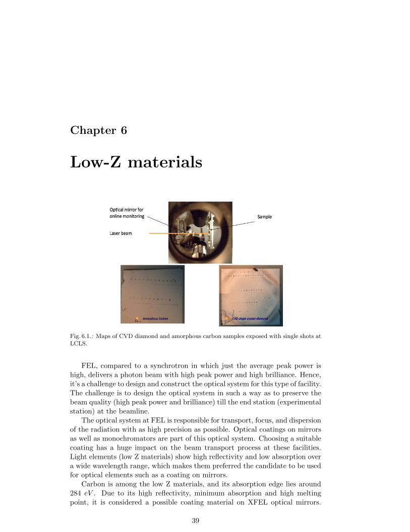
Fig. 6.1.: Maps of CVD diamond and amorphous carbon samples exposed with single shots atLCLS.
FEL, compared to a synchrotron in which just the average peak power ishigh, delivers a photon beam with high peak power and high brilliance. Hence,it’s a challenge to design and construct the optical system for this type of facility.The challenge is to design the optical system in such a way as to preserve thebeam quality (high peak power and brilliance) till the end station (experimentalstation) at the beamline.
The optical system at FEL is responsible for transport, focus, and dispersionof the radiation with as high precision as possible. Optical coatings on mirrorsas well as monochromators are part of this optical system. Choosing a suitablecoating has a huge impact on the beam transport process at these facilities.Light elements (low Z materials) show high reflectivity and low absorption overa wide wavelength range, which makes them preferred the candidate to be usedfor optical elements such as a coating on mirrors.
Carbon is among the low Z materials, and its absorption edge lies around284 eV . Due to its high reflectivity, minimum absorption and high meltingpoint, it is considered a possible coating material on XFEL optical mirrors.
39
40 Chapter 6. Low-Z materials
The pioneer FEL, FLASH based in Hamburg, has also used carbon as a coat-ing on its beamline mirrors. CVD Diamond has a high melting temperature,high breakdown electric field, a large band gap of 5.5 eV and high chemicalstability [78] and is considered to be a suitable candidate to be used as a singlecrystal monochromator’s component. Among metals, Nickel is the only possiblecandidate examined during this Ph.D. project. Among multilayers, MoB4C hasbeen considered as a possible coating and tested in the scope of this project.
The focus was on testing the behavior of a-C coated mirrors and the CVDdiamond monochromators which are the main subject in the performed exper-iments and this chapter.The study is divided in damage studies below and around carbon K−edge,higher than carbon K−edge energy regime, and at grazing and normal inci-dence angles
6.1 Properties of amorphous carbon
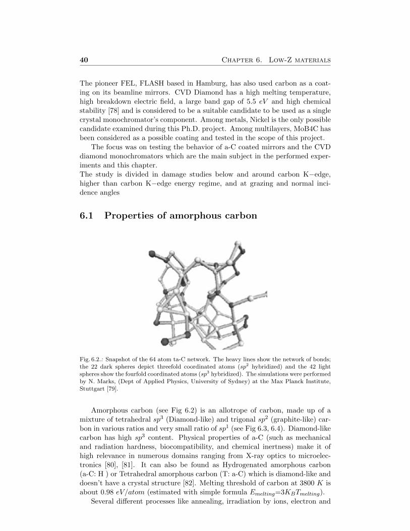
Fig. 6.2.: Snapshot of the 64 atom ta-C network. The heavy lines show the network of bonds;the 22 dark spheres depict threefold coordinated atoms (sp2 hybridized) and the 42 lightspheres show the fourfold coordinated atoms (sp3 hybridized). The simulations were performedby N. Marks, (Dept of Applied Physics, University of Sydney) at the Max Planck Institute,Stuttgart [79].
Amorphous carbon (see Fig 6.2) is an allotrope of carbon, made up of amixture of tetrahedral sp3 (Diamond-like) and trigonal sp2 (graphite-like) car-bon in various ratios and very small ratio of sp1 (see Fig 6.3, 6.4). Diamond-likecarbon has high sp3 content. Physical properties of a-C (such as mechanicaland radiation hardness, biocompatibility, and chemical inertness) make it ofhigh relevance in numerous domains ranging from X-ray optics to microelec-tronics [80], [81]. It can also be found as Hydrogenated amorphous carbon(a-C: H ) or Tetrahedral amorphous carbon (T: a-C) which is diamond-like anddoesn’t have a crystal structure [82]. Melting threshold of carbon at 3800 K isabout 0.98 eV/atom (estimated with simple formula Emelting=3KBTmelting).
Several different processes like annealing, irradiation by ions, electron and
6.1. Properties of amorphous carbon 41
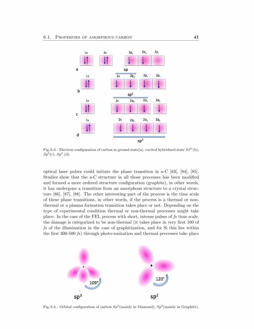
Fig. 6.3.: Electron configuration of carbon in ground state(a), excited hybridized state SP 1(b),Sp2(c), Sp3 (d).
optical laser pulses could initiate the phase transition in a-C [83], [84], [85].Studies show that the a-C structure in all those processes has been modifiedand formed a more ordered structure configuration (graphite), in other words,it has undergone a transition from an amorphous structure to a crystal struc-ture [86], [87], [88]. The other interesting part of the process is the time scaleof these phase transitions, in other words, if the process is a thermal or non-thermal or a plasma formation transition takes place or not. Depending on thetype of experimental condition thermal or non-thermal processes might takeplace. In the case of the FEL process with short, intense pulses of fs time scale,the damage is categorized to be non-thermal (it takes place in very first 100 offs of the illumination in the case of graphitization, and for Si this lies withinthe first 300-500 fs) through photo-ionization and thermal processes take place
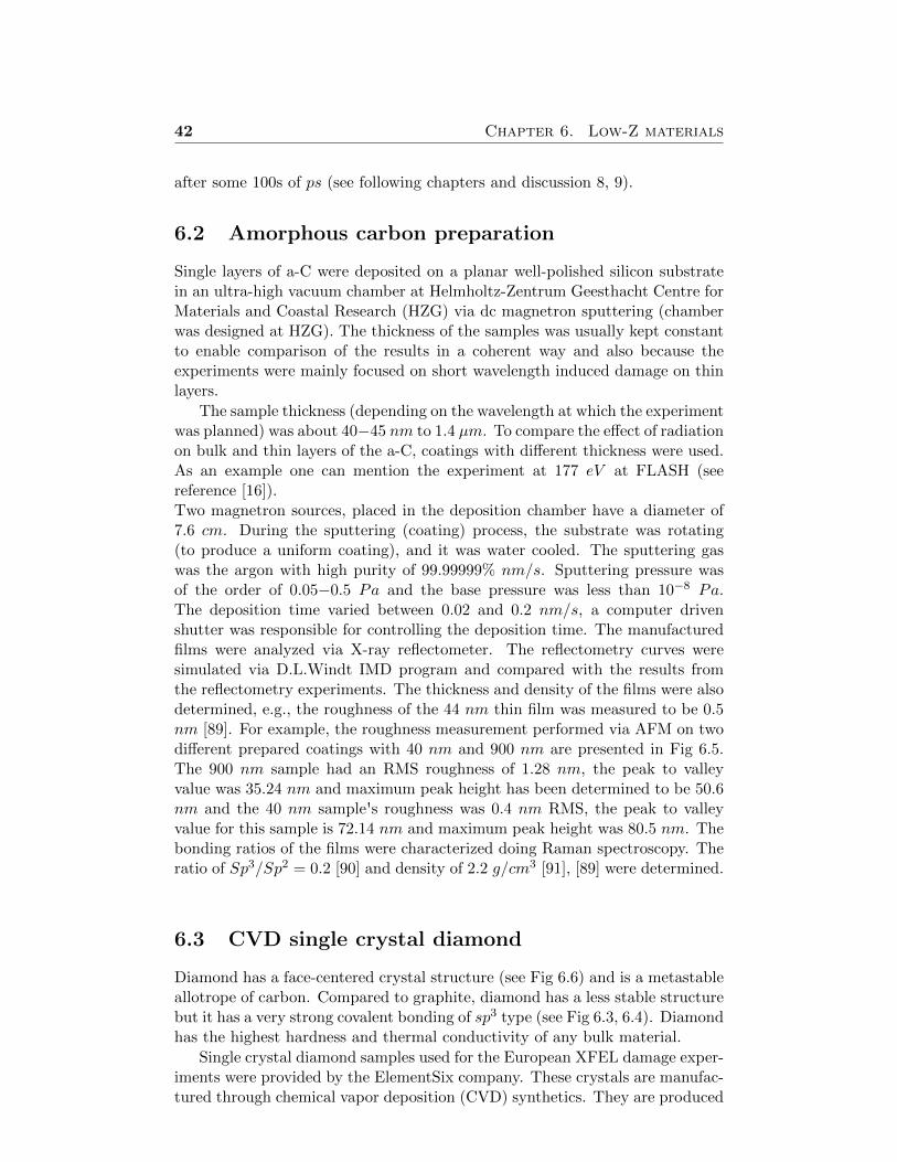
Fig. 6.4.: Orbital configuration of carbon Sp3(mainly in Diamond), Sp2(mainly in Graphite).
42 Chapter 6. Low-Z materials
after some 100s of ps (see following chapters and discussion 8, 9).
6.2 Amorphous carbon preparation
Single layers of a-C were deposited on a planar well-polished silicon substratein an ultra-high vacuum chamber at Helmholtz-Zentrum Geesthacht Centre forMaterials and Coastal Research (HZG) via dc magnetron sputtering (chamberwas designed at HZG). The thickness of the samples was usually kept constantto enable comparison of the results in a coherent way and also because theexperiments were mainly focused on short wavelength induced damage on thinlayers.
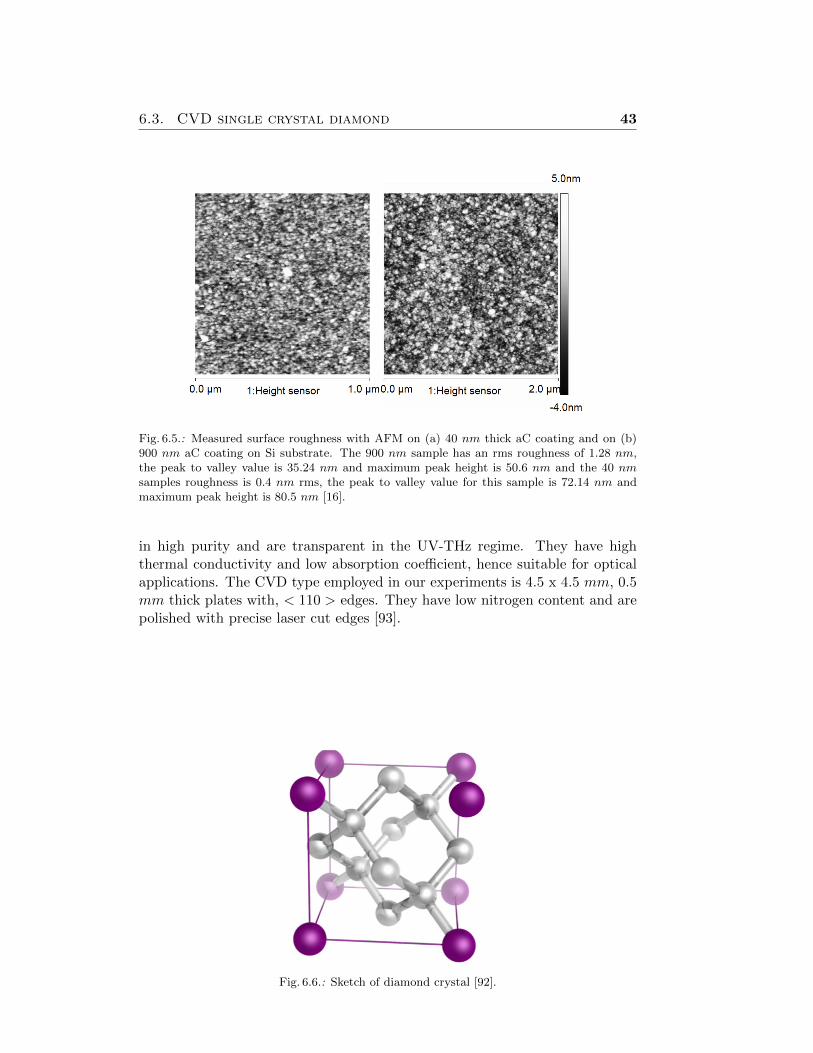
The sample thickness (depending on the wavelength at which the experimentwas planned) was about 40−45 nm to 1.4 µm. To compare the effect of radiationon bulk and thin layers of the a-C, coatings with different thickness were used.As an example one can mention the experiment at 177 eV at FLASH (seereference [16]).Two magnetron sources, placed in the deposition chamber have a diameter of7.6 cm. During the sputtering (coating) process, the substrate was rotating(to produce a uniform coating), and it was water cooled. The sputtering gaswas the argon with high purity of 99.99999% nm/s. Sputtering pressure wasof the order of 0.05−0.5 Pa and the base pressure was less than 10−8 Pa.The deposition time varied between 0.02 and 0.2 nm/s, a computer drivenshutter was responsible for controlling the deposition time. The manufacturedfilms were analyzed via X-ray reflectometer. The reflectometry curves weresimulated via D.L.Windt IMD program and compared with the results fromthe reflectometry experiments. The thickness and density of the films were alsodetermined, e.g., the roughness of the 44 nm thin film was measured to be 0.5nm [89]. For example, the roughness measurement performed via AFM on twodifferent prepared coatings with 40 nm and 900 nm are presented in Fig 6.5.The 900 nm sample had an RMS roughness of 1.28 nm, the peak to valleyvalue was 35.24 nm and maximum peak height has been determined to be 50.6nm and the 40 nm sample's roughness was 0.4 nm RMS, the peak to valleyvalue for this sample is 72.14 nm and maximum peak height was 80.5 nm. Thebonding ratios of the films were characterized doing Raman spectroscopy. Theratio of Sp3/Sp2 = 0.2 [90] and density of 2.2 g/cm3 [91], [89] were determined.
6.3 CVD single crystal diamond
Diamond has a face-centered crystal structure (see Fig 6.6) and is a metastableallotrope of carbon. Compared to graphite, diamond has a less stable structurebut it has a very strong covalent bonding of sp3 type (see Fig 6.3, 6.4). Diamondhas the highest hardness and thermal conductivity of any bulk material.
Single crystal diamond samples used for the European XFEL damage exper-iments were provided by the ElementSix company. These crystals are manufac-tured through chemical vapor deposition (CVD) synthetics. They are produced
6.3. CVD single crystal diamond 43
Fig. 6.5.: Measured surface roughness with AFM on (a) 40 nm thick aC coating and on (b)900 nm aC coating on Si substrate. The 900 nm sample has an rms roughness of 1.28 nm,the peak to valley value is 35.24 nm and maximum peak height is 50.6 nm and the 40 nmsamples roughness is 0.4 nm rms, the peak to valley value for this sample is 72.14 nm andmaximum peak height is 80.5 nm [16].
in high purity and are transparent in the UV-THz regime. They have highthermal conductivity and low absorption coefficient, hence suitable for opticalapplications. The CVD type employed in our experiments is 4.5 x 4.5 mm, 0.5mm thick plates with, < 110 > edges. They have low nitrogen content and arepolished with precise laser cut edges [93].
Fig. 6.6.: Sketch of diamond crystal [92].

44 Chapter 6. Low-Z materials
Chapter 7
Experimental technique
X-ray FELs are the source of short pulses, high-peak-power, and high-brilliancephoton beams. This fact makes it challenging to construct the optical systemfor such facilities. These properties can render an optical element useless in afraction of a second. Besides, it is possible to face new damage mechanisms thatdegrade optical components in the X-ray beamlines in comparison to storagerings/synchrotrons (at synchrotrons high average power load is the possiblesource of damage to optical elements). The characteristic properties of FELfacilities around the world differ from each other with regards to the wavelengthrange, peak brilliance and pulse parameters at which they operate. Therefore,the study of the damage mechanism at those different facilities is helpful to gaina vast knowledge of this process.
In this chapter, different characteristic parameters of various FEL facilitiesare briefly described. Special attention is dedicated to FLASH, where mostof the experiments of this work were performed at. The experimental set upwhich was developed at FLASH for the most recent experiment with 4.6 nmwavelength (the wavelength varied between 4.7 nm and 4.5 nm. This probablywas due to the two upstream carbon coated mirrors present in the beamline.Carbon mirrors are very sensitive around the carbon K−edge (at 4.37 nm).These mirrors absorb the radiation inside the water window and are thereforeunsuitable for use at these wavelengths.) is described in more details in thischapter. Later in the chapter, the experiment's parameters at other facilities(at those experiments were performed) will be given.
7.1 FLASH Beamlines and baseline instrumentation
FLASH source runs at a maximum repetition rate of 10 Hz with 800 pulses in800 µs long bunch trains [5], [94]. The beam can be distributed to the direct orthe monochromator branch. The branches leading to beamline 1 (BL1), BL2and BL3 utilizes the direct FEL beam. The three end-stations offer differentfocusing schemes leading to more or less intensely collimated FEL beams. Thebeam is distributed to the different BLs by switching one or two plane mirrors.An attenuation system based on gas absorption and a set of four gas monitorsare used for the beam intensity and beam position determination before it gets
45
46 Chapter 7. Experimental technique
branched into different BLs. A variable line spacing spectrograph available ateach BL could monitor the beam spectrum parallel to user experiments.
To provide high degrees of reflectivity, avoid the risk of damage due to thehigh peak powers and minimize deformation of the mirrors at long bunch trains,very shallow incidence angles of 2◦ and 3◦ were chosen [5]. Damage experiments(for this work) at FLASH were done at two of the existing beamlines: BL2 (seesection 7.1.1) and BL3 (see section 7.1.2). Each is equipped with ellipsoidalmirror with the focal point at 2 m focal distance.
The fast shutter available at the beamlines behind the ellipsoid mirror makesit possible to work with single pulses.
Each of the experimental stations can be combined with a synchronizedfemtosecond optical laser system in a laser hutch and a THz source generatedby an additional undulator through which the FLASH electron beam is passed.Both can be combined with FEL pulses for femtosecond time-resolved pump-and-probe experiments with a time resolution of 100 fs [5].
7.1.1 BL2
BL2 [5] is equipped with ellipsoidal mirrors which generate focal sizes of ∼ 20- 30 µm (FWHM). High-density carbon coated mirrors (0.5 m long) have a lowsurface roughness, less than 5 A over the full mirror length. The almost con-stant high reflectivity of these coatings was the reason for choosing them [5]. AtBL2 there are 3 carbon coated mirrors available with grazing incidence anglesof 2◦ and 3◦. At the experiment time (in 2008/2009) the transmission of thebeam-line was calculated via reflectivity calculations considering each of the 3plane amorphous carbon (a-C) coated mirrors in the beamline using the CXROwebsite [15]. During the experiment, samples were mainly placed in focus po-sition. The focus spot size (smallest) was found to be 5 µm corresponding tothe maximum achievable fluence of 50 J/cm2.
7.1.2 BL3
BL3 beam-line [5], which was used for our experiment in May 2011, is equippedwith 2 plane nickel mirrors and 3 plane a-C coated mirrors (1 focusing mirrorwith a 2 m focal point and 2 reflecting mirrors). The mirrors work underthe grazing angles of 2◦ and 3◦ respectively. To obtain a Gaussian-like beamshape, circular apertures of various diameters (1, 3, 5 and 10 mm ) were placedupstream to the focusing mirror and the gas monitor detector.
The focused beam FWHM is typically on the order of 20 µm, the unfocussedbeam size 5−10 mm (depending on wavelength). Users can install their ownoptics if needed. A back-reflecting multilayer mirror on this beamline makesit possible to vary the beam from a non-focused beam with ∼ 10 mm to ∼ 2µm radius (we didn’t use the multilayer mirror in our experiment). Hence, it ispossible to study a broad range of scientific fields (e.g. plasma physics, clusterscience or materials research) [95], [96]. In the experiment close to the carbonK-edge, the pulse duration was on the order of 125± 25 fs, where the electronbunch was 300 pC. The wavelength during this experiment had an absolute
7.2. Dedicated set up for damage experiments 47
uncertainty of 0.1 nm for the beam wavelength of 4.6 nm and the bandwidthshot-to-shot fluctuation was found to be negligible (see ref [94], [97]). Theaverage energy per pulse was typically in the range of 10–90 µJ with peakvalues up to 170 µJ . The maximum repetition rate was 10 Hz and the 800 µslong bunch train contained 800 pulses.
7.1.3 Gas monitor detector
One of the common elements in all the beamlines is the gas monitor detector,known as GMD, which allows one to measure the pulse energy. The GMDused in our experiments was developed at FLASH. It was optimized for thecurrent and future X-ray free electron laser facilities for shot-to-shot measure-ments. It has an online determination of the beam position and a temporalresolution better than 100 ns. The relative standard uncertainty of the photonpulse energy was measured to be better than 10 % (dominated by the inherentstatistical shot-to-shot fluctuations of an SASE-FEL like FLASH). The photonbeam position was measured to be below 20 µm. All these mentioned abovewere achieved at a quality checking test of this device [98]. An upgraded ver-sion of the device for the hard X-ray regime, X-GMD, was presented with asignal amplification up to 106 by means of an open electron multiplier for iondetection, which was tested at LCLS. There are four GMDs available at FLASHbeamline construction, which are also used to determine the beam position foreach pulse. Two of these are placed at the end of the accelerator tunnel andtwo others are in use at the beginning of the experimental hall. Between thesetwo sets, a 15 m long gas attenuator reduces the FEL intensity by many ordersof magnitude without changing the accelerator parameters
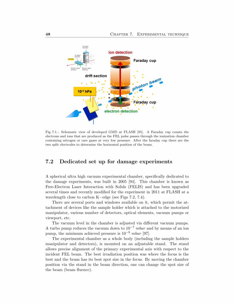
Since the GMD detector (at FLASH) is located before the optical elementsof the beamline, one should consider the beamline transmission after the opticalelement, in order to get the correct pulse energy values. The GMD is based onphoto-ionization of a low-density noble gas or N2, creating ions and electronswhich are detected by a Faraday cup [98], [99] (see Fig 7.1).
N = Nphnσl (7.1)
Where N is the number of electrons or ions and Nph is the number of photons.The n represents the target density, σ the photo-ionization cross-section and lis the length of interaction volume.
Typically the ion signal, calibrated at a synchrotron storage ring with anuncertainty of 4%, was averaged over 25 s.
The electron signal was used to get (measure) individual pulse energies.The electron signal was calibrated by comparing its average to the average ionsignal. Hence, the relative pulse fluctuations are dominated by the inherentstatistical fluctuations of the FEL pulse intensities during the calibration andless than 1% for pulses of more than 1010 photons.
48 Chapter 7. Experimental technique
Fig. 7.1.: Schematic view of developed GMD at FLASH [85]. A Faraday cup counts theelectrons and ions that are produced as the FEL pulse passes through the ionization chambercontaining nitrogen or rare gases at very low pressure. After the faraday cup there are thetwo split electrodes to determine the horizontal position of the beam.
7.2 Dedicated set up for damage experiments
A spherical ultra high vacuum experimental chamber, specifically dedicated tothe damage experiments, was built in 2005 [94]. This chamber is known asFree-Electron Laser Interaction with Solids (FELIS) and has been upgradedseveral times and recently modified for the experiment in 2011 at FLASH at awavelength close to carbon K−edge (see Figs 7.2, 7.4).
There are several ports and windows available on it, which permit the at-tachment of devices like the sample holder which is attached to the motorizedmanipulator, various number of detectors, optical elements, vacuum pumps orviewport, etc.
The vacuum level in the chamber is adjusted via different vacuum pumps.A turbo pump reduces the vacuum down to 10−7 mbar and by means of an ionpump, the minimum achieved pressure is 10−9 mbar [97].
The experimental chamber as a whole body (including the sample holdersmanipulator and detectors), is mounted on an adjustable stand. The standallows precise alignment of the primary experimental axis with respect to theincident FEL beam. The best irradiation position was where the focus is thebest and the beam has its best spot size in the focus. By moving the chamberposition via the stand in the beam direction, one can change the spot size ofthe beam (beam fluence).
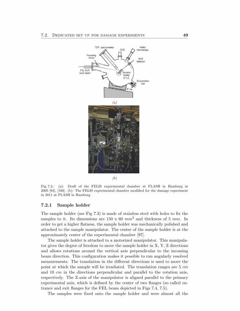
7.2. Dedicated set up for damage experiments 49
(a)
(b)
Fig. 7.2.: (a): Draft of the FELIS experimental chamber at FLASH in Hamburg in2005 [94], [100]. (b): The FELIS experimental chamber modified for the damage experimentin 2011 at FLASH in Hamburg
7.2.1 Sample holder
The sample holder (see Fig 7.3) is made of stainless steel with holes to fix thesamples to it. Its dimensions are 150 x 60 mm2 and thickness of 5 mm. Inorder to get a higher flatness, the sample holder was mechanically polished andattached to the sample manipulator. The center of the sample holder is at theapproximately center of the experimental chamber [97].
The sample holder is attached to a motorized manipulator. This manipula-tor gives the degree of freedom to move the sample holder in X, Y, Z directionsand allows rotations around the vertical axis perpendicular to the incomingbeam direction. This configuration makes it possible to run angularly resolvedmeasurements. The translation in the different directions is used to move thepoint at which the sample will be irradiated. The translation ranges are 5 cmand 10 cm in the directions perpendicular and parallel to the rotation axis,respectively. The Z-axis of the manipulator is aligned parallel to the primaryexperimental axis, which is defined by the center of two flanges (so called en-trance and exit flanges for the FEL beam depicted in Figs 7.4, 7.5).
The samples were fixed onto the sample holder and were almost all the
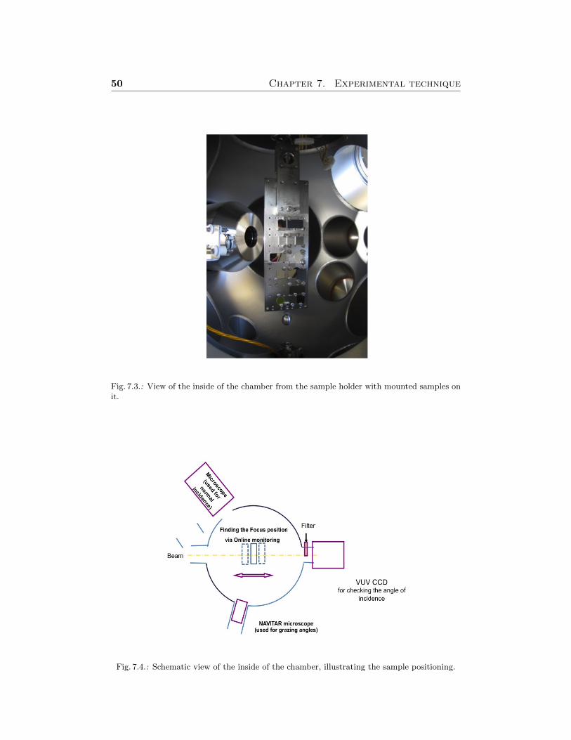
50 Chapter 7. Experimental technique
Fig. 7.3.: View of the inside of the chamber from the sample holder with mounted samples onit.
Fig. 7.4.: Schematic view of the inside of the chamber, illustrating the sample positioning.
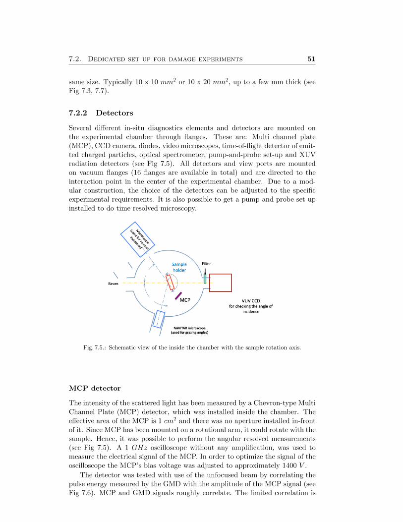
7.2. Dedicated set up for damage experiments 51
same size. Typically 10 x 10 mm2 or 10 x 20 mm2, up to a few mm thick (seeFig 7.3, 7.7).
7.2.2 Detectors
Several different in-situ diagnostics elements and detectors are mounted onthe experimental chamber through flanges. These are: Multi channel plate(MCP), CCD camera, diodes, video microscopes, time-of-flight detector of emit-ted charged particles, optical spectrometer, pump-and-probe set-up and XUVradiation detectors (see Fig 7.5). All detectors and view ports are mountedon vacuum flanges (16 flanges are available in total) and are directed to theinteraction point in the center of the experimental chamber. Due to a mod-ular construction, the choice of the detectors can be adjusted to the specificexperimental requirements. It is also possible to get a pump and probe set upinstalled to do time resolved microscopy.
Fig. 7.5.: Schematic view of the inside the chamber with the sample rotation axis.
MCP detector
The intensity of the scattered light has been measured by a Chevron-type MultiChannel Plate (MCP) detector, which was installed inside the chamber. Theeffective area of the MCP is 1 cm2 and there was no aperture installed in-frontof it. Since MCP has been mounted on a rotational arm, it could rotate with thesample. Hence, it was possible to perform the angular resolved measurements(see Fig 7.5). A 1 GHz oscilloscope without any amplification, was used tomeasure the electrical signal of the MCP. In order to optimize the signal of theoscilloscope the MCP’s bias voltage was adjusted to approximately 1400 V .
The detector was tested with use of the unfocused beam by correlating thepulse energy measured by the GMD with the amplitude of the MCP signal (seeFig 7.6). MCP and GMD signals roughly correlate. The limited correlation is
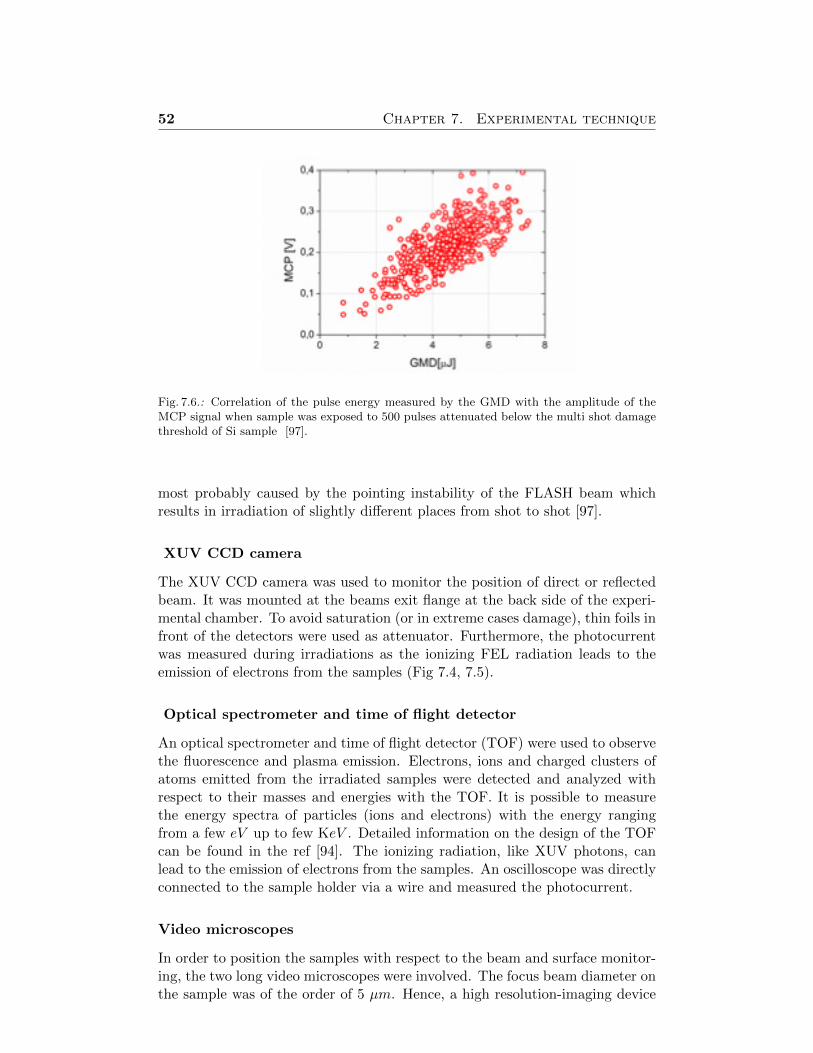
52 Chapter 7. Experimental technique
Fig. 7.6.: Correlation of the pulse energy measured by the GMD with the amplitude of theMCP signal when sample was exposed to 500 pulses attenuated below the multi shot damagethreshold of Si sample [97].
most probably caused by the pointing instability of the FLASH beam whichresults in irradiation of slightly different places from shot to shot [97].
XUV CCD camera
The XUV CCD camera was used to monitor the position of direct or reflectedbeam. It was mounted at the beams exit flange at the back side of the experi-mental chamber. To avoid saturation (or in extreme cases damage), thin foils infront of the detectors were used as attenuator. Furthermore, the photocurrentwas measured during irradiations as the ionizing FEL radiation leads to theemission of electrons from the samples (Fig 7.4, 7.5).
Optical spectrometer and time of flight detector
An optical spectrometer and time of flight detector (TOF) were used to observethe fluorescence and plasma emission. Electrons, ions and charged clusters ofatoms emitted from the irradiated samples were detected and analyzed withrespect to their masses and energies with the TOF. It is possible to measurethe energy spectra of particles (ions and electrons) with the energy rangingfrom a few eV up to few KeV . Detailed information on the design of the TOFcan be found in the ref [94]. The ionizing radiation, like XUV photons, canlead to the emission of electrons from the samples. An oscilloscope was directlyconnected to the sample holder via a wire and measured the photocurrent.
Video microscopes
In order to position the samples with respect to the beam and surface monitor-ing, the two long video microscopes were involved. The focus beam diameter onthe sample was of the order of 5 µm. Hence, a high resolution-imaging device
7.3. Alignment and experimental protocol 53
for microscopic imaging (1 − 2µm) was necessary. The inlet flanges were usedto minimize the working distance.
7.3 Alignment and experimental protocol
Starting the experiment needs precisely aligned experimental elements and com-ponents. These steps can be summarized as follows: Alignment of experimentalchamber, determination of the samples’ coordinates, finding the focus positionand the calibration of the grazing angle.
Alignment of the chamber axis means that the center of the chamber shouldapproximately be at the focus position. This procedure is done in two steps:pre-alignment, using optical laser light and final alignment. In our case, a He-Ne laser beam which is collinear with the FEL beam served this task. Duringthis process, the motors of the manipulator were kept in the middle of theirtravel ranges. At this point, the two online microscopes were used. In this way,the height and the horizontal position of the chamber were aligned. Here theposition of laser light on the sample holder was observed while the chamber wastransported on the stand. If the spot position was always seen unchanged andstatic, that point was the best alignment position.
Further, the offset angles for the rotational motor on both sides of thesample holder were calibrated (the read-out of the motors position while theHe-Ne laser beam was under normal incidence angle to the holder’s surface).Similar alignment procedures were repeated using the FEL beam and plasmaemission from metals or fluorescence from a Ce: YAG crystal.
The samples were mounted on the sample holder in the clean room. Eachsample was given a defined coordinate system with a horizontal and verticalaxis (see Fig 7.7), lying in the plane of the sample’s surface. This made itpossible to have a map, on which one can picture the movement of the FELbeam on the surface of the sample. The sample holder was then, mounted on themanipulator. The manipulator’s angular and height accuracy are respectivelybetter than 0.1◦ and 100 µm.
The focus of the beam on each sample was examined by studying the imprintof the beam on a PMMA sample (see Fig 7.8). At different positions withrespect to the chamber, imprints were made and observed by means of onlinemicroscopes. The focus shape changes due to astigmatism at different positions.The best focus position was where the imprints were most circular in shape.
As the samples have all a certain thickness, this could effect the best focusposition. Hence, their thickness was measured and taken into account whilepositioning them. An optical microscope with accuracy better than 50 µm wasused for this purpose, where the depth of focus was measured.
In order to control the angle of the incident beam on the sample, the offsetangle to rotate the motors had to be found. The angles normal to the sample’ssurface and the normal to the samples holder are collinear and the offset anglesfor a rotational motor were the same.
Finding the correct grazing angle is done via the following steps. In order tomeasure the direct beam position, a charge coupled device (CCD) was mounted
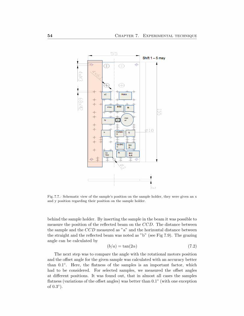
54 Chapter 7. Experimental technique
Fig. 7.7.: Schematic view of the sample’s position on the sample holder, they were given an xand y position regarding their position on the sample holder.
behind the sample holder. By inserting the sample in the beam it was possible tomeasure the position of the reflected beam on the CCD. The distance betweenthe sample and the CCD measured as ”a” and the horizontal distance betweenthe straight and the reflected beam was noted as ”b” (see Fig 7.9). The grazingangle can be calculated by
(b/a) = tan(2α) (7.2)
The next step was to compare the angle with the rotational motors positionand the offset angle for the given sample was calculated with an accuracy betterthan 0.1◦. Here, the flatness of the samples is an important factor, whichhad to be considered. For selected samples, we measured the offset anglesat different positions. It was found out, that in almost all cases the samplesflatness (variations of the offset angles) was better than 0.1◦ (with one exceptionof 0.3◦).
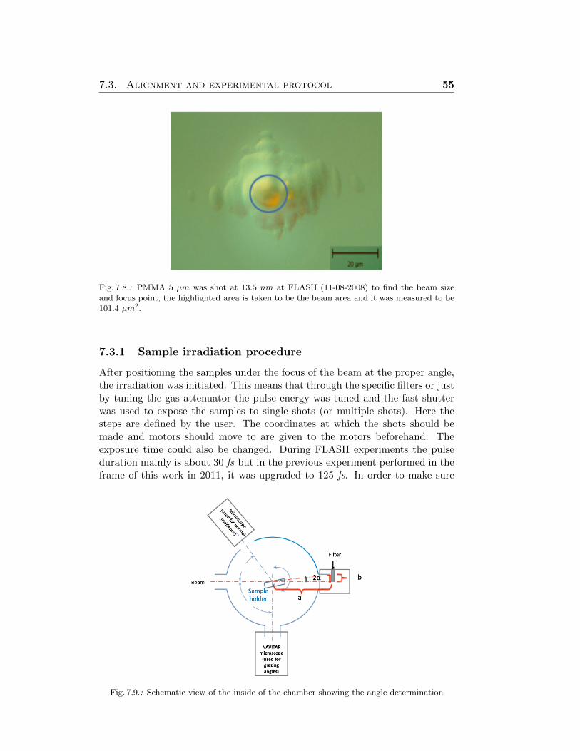
7.3. Alignment and experimental protocol 55
Fig. 7.8.: PMMA 5 µm was shot at 13.5 nm at FLASH (11-08-2008) to find the beam sizeand focus point, the highlighted area is taken to be the beam area and it was measured to be101.4 µm2.
7.3.1 Sample irradiation procedure
After positioning the samples under the focus of the beam at the proper angle,the irradiation was initiated. This means that through the specific filters or justby tuning the gas attenuator the pulse energy was tuned and the fast shutterwas used to expose the samples to single shots (or multiple shots). Here thesteps are defined by the user. The coordinates at which the shots should bemade and motors should move to are given to the motors beforehand. Theexposure time could also be changed. During FLASH experiments the pulseduration mainly is about 30 fs but in the previous experiment performed in theframe of this work in 2011, it was upgraded to 125 fs. In order to make sure
Fig. 7.9.: Schematic view of the inside of the chamber showing the angle determination
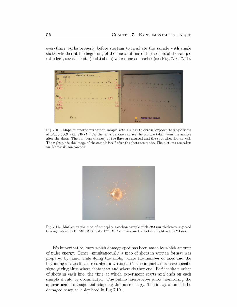
56 Chapter 7. Experimental technique
everything works properly before starting to irradiate the sample with singleshots, whether at the beginning of the line or at one of the corners of the sample(at edge), several shots (multi shots) were done as marker (see Figs 7.10, 7.11).
Fig. 7.10.: Maps of amorphous carbon sample with 1.4 µm thickness, exposed to single shotsat LCLS 2009 with 830 eV . On the left side, one can see the picture taken from the sampleafter the shots. The numbers (names) of the lines are marked and the shot direction as well.The right pic is the image of the sample itself after the shots are made. The pictures are takenvia Nomarski microscope.
Fig. 7.11.: Marker on the map of amorphous carbon sample with 890 nm thickness, exposedto single shots at FLASH 2008 with 177 eV . Scale size on the bottom right side is 20 µm.
It’s important to know which damage spot has been made by which amountof pulse energy. Hence, simultaneously, a map of shots in written format wasprepared by hand while doing the shots, where the number of lines and thebeginning of each line is recorded in writing. It’s also important to have specificsigns, giving hints where shots start and where do they end. Besides the numberof shots in each line, the time at which experiment starts and ends on eachsample should be documented. The online microscopes allow monitoring theappearance of damage and adapting the pulse energy. The image of one of thedamaged samples is depicted in Fig 7.10.
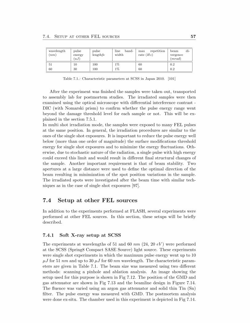
7.4. Setup at other FEL sources 57
wavelength(nm)
pulseenergy(uJ)
pulselengthfs
line band-width
max repetitionrate (Hz)
beam di-vergence(mrad)
51 10 100 1% 60 0.2
60 30 100 1% 60 0.2
Table 7.1.: Characteristic parameters at SCSS in Japan 2010. [101]
After the experiment was finished the samples were taken out, transportedto assembly lab for postmortem studies. The irradiated samples were thenexamined using the optical microscope with differential interference contrast -DIC (with Nomarski prism) to confirm whether the pulse energy range wentbeyond the damage threshold level for each sample or not. This will be ex-plained in the section 7.5.1.In multi shot irradiation mode, the samples were exposed to many FEL pulsesat the same position. In general, the irradiation procedures are similar to theones of the single shot exposures. It is important to reduce the pulse energy wellbelow (more than one order of magnitude) the surface modifications thresholdenergy for single shot exposures and to minimize the energy fluctuations. Oth-erwise, due to stochastic nature of the radiation, a single pulse with high energycould exceed this limit and would result in different final structural changes ofthe sample. Another important requirement is that of beam stability. Twoapertures at a large distance were used to define the optimal direction of thebeam resulting in minimization of the spot position variations in the sample.The irradiated spots were investigated after the beam time with similar tech-niques as in the case of single shot exposures [97].
7.4 Setup at other FEL sources
In addition to the experiments performed at FLASH, several experiments wereperformed at other FEL sources. In this section, these setups will be brieflydescribed.
7.4.1 Soft X-ray setup at SCSS
The experiments at wavelengths of 51 and 60 nm (24, 20 eV ) were performedat the SCSS (Spring8 Compact SASE Source) light source. These experimentswere single shot experiments in which the maximum pulse energy went up to 10µJ for 51 nm and up to 30 µJ for 60 nm wavelength. The characteristic param-eters are given in Table 7.1. The beam size was measured using two differentmethods: scanning a pinhole and ablation analysis. An image showing thesetup used for this purpose is shown in Fig 7.12. The position of the GMD andgas attenuator are shown in Fig 7.13 and the beamline design in Figure 7.14.The fluence was varied using an argon gas attenuator and solid thin Tin (Sn)filter. The pulse energy was measured with GMD. The postmortem analysiswere done ex-situ. The chamber used in this experiment is depicted in Fig 7.14.
58 Chapter 7. Experimental technique
Fig. 7.12.: Scanning pinhole structure designed for the SCSS in Japan in 2010 [101].
7.4.2 LCLS Atomic, Molecular and Optical Science (AMO)
This soft X-ray beamline at LCLS provides intense ultra-short soft X-ray pulses,generated by the free electron laser. AMO is designed to minimize losses anddeliver the maximum possible X-ray intensity to the interaction region. Inorder to maintain the high peak brightness of the LCLS X-ray pulse, a minimalset of optics is used to deliver the beam to the target in the AMO instrument.Figure 7.15 gives an overview of the design of the beamline and its parts. There
Fig. 7.13.: Gas attenuator and Photon intensity monitor at SCSS in Japan in2010 [102], [103], [101].
7.4. Setup at other FEL sources 59
(a)
(b)
(c)
Fig. 7.14.: (a): Design of the experimental beamline at SCSS in Japan [101]. (b): Theexperimental beamline and chamber. (c): The experimental chamber.
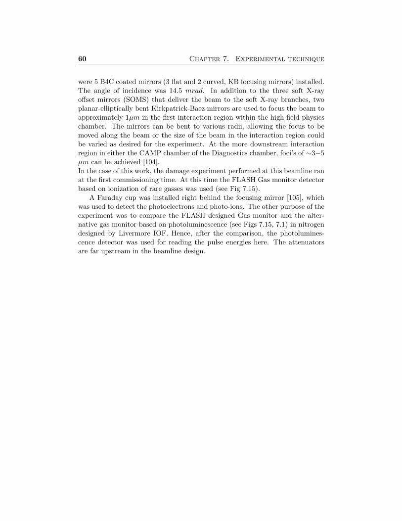
60 Chapter 7. Experimental technique
were 5 B4C coated mirrors (3 flat and 2 curved, KB focusing mirrors) installed.The angle of incidence was 14.5 mrad. In addition to the three soft X-rayoffset mirrors (SOMS) that deliver the beam to the soft X-ray branches, twoplanar-elliptically bent Kirkpatrick-Baez mirrors are used to focus the beam toapproximately 1µm in the first interaction region within the high-field physicschamber. The mirrors can be bent to various radii, allowing the focus to bemoved along the beam or the size of the beam in the interaction region couldbe varied as desired for the experiment. At the more downstream interactionregion in either the CAMP chamber of the Diagnostics chamber, foci’s of ∼3−5µm can be achieved [104].In the case of this work, the damage experiment performed at this beamline ranat the first commissioning time. At this time the FLASH Gas monitor detectorbased on ionization of rare gasses was used (see Fig 7.15).
A Faraday cup was installed right behind the focusing mirror [105], whichwas used to detect the photoelectrons and photo-ions. The other purpose of theexperiment was to compare the FLASH designed Gas monitor and the alter-native gas monitor based on photoluminescence (see Figs 7.15, 7.1) in nitrogendesigned by Livermore IOF. Hence, after the comparison, the photolumines-cence detector was used for reading the pulse energies here. The attenuatorsare far upstream in the beamline design.
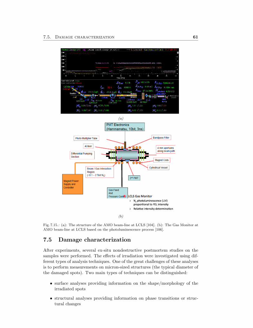
7.5. Damage characterization 61
(a)
(b)
Fig. 7.15.: (a): The structure of the AMO beam-line at LCLS [104]. (b): The Gas Monitor atAMO beam-line at LCLS based on the photoluminescence process [106].
7.5 Damage characterization
After experiments, several ex-situ nondestructive postmortem studies on thesamples were performed. The effects of irradiation were investigated using dif-ferent types of analysis techniques. One of the great challenges of these analysesis to perform measurements on micron-sized structures (the typical diameter ofthe damaged spots). Two main types of techniques can be distinguished:
• surface analyses providing information on the shape/morphology of theirradiated spots
• structural analyses providing information on phase transitions or struc-tural changes
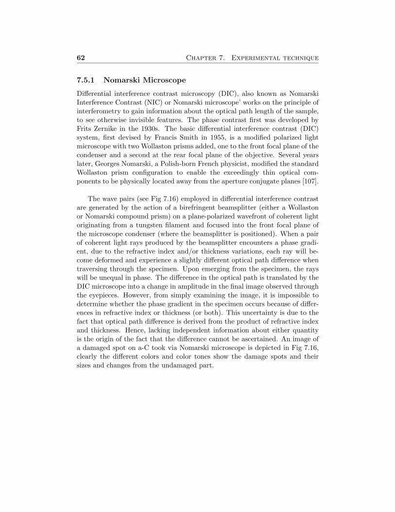
62 Chapter 7. Experimental technique
7.5.1 Nomarski Microscope
Differential interference contrast microscopy (DIC), also known as NomarskiInterference Contrast (NIC) or Nomarski microscope’ works on the principle ofinterferometry to gain information about the optical path length of the sample,to see otherwise invisible features. The phase contrast first was developed byFrits Zernike in the 1930s. The basic differential interference contrast (DIC)system, first devised by Francis Smith in 1955, is a modified polarized lightmicroscope with two Wollaston prisms added, one to the front focal plane of thecondenser and a second at the rear focal plane of the objective. Several yearslater, Georges Nomarski, a Polish-born French physicist, modified the standardWollaston prism configuration to enable the exceedingly thin optical com-ponents to be physically located away from the aperture conjugate planes [107].
The wave pairs (see Fig 7.16) employed in differential interference contrastare generated by the action of a birefringent beamsplitter (either a Wollastonor Nomarski compound prism) on a plane-polarized wavefront of coherent lightoriginating from a tungsten filament and focused into the front focal plane ofthe microscope condenser (where the beamsplitter is positioned). When a pairof coherent light rays produced by the beamsplitter encounters a phase gradi-ent, due to the refractive index and/or thickness variations, each ray will be-come deformed and experience a slightly different optical path difference whentraversing through the specimen. Upon emerging from the specimen, the rayswill be unequal in phase. The difference in the optical path is translated by theDIC microscope into a change in amplitude in the final image observed throughthe eyepieces. However, from simply examining the image, it is impossible todetermine whether the phase gradient in the specimen occurs because of differ-ences in refractive index or thickness (or both). This uncertainty is due to thefact that optical path difference is derived from the product of refractive indexand thickness. Hence, lacking independent information about either quantityis the origin of the fact that the difference cannot be ascertained. An image ofa damaged spot on a-C took via Nomarski microscope is depicted in Fig 7.16,clearly the different colors and color tones show the damage spots and theirsizes and changes from the undamaged part.
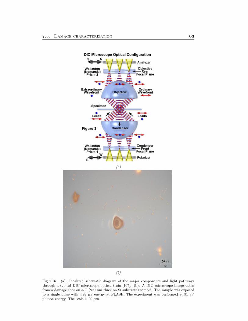
7.5. Damage characterization 63
(a)
(b)
Fig. 7.16.: (a): Idealized schematic diagram of the major components and light pathwaysthrough a typical DIC microscope optical train [107]. (b): A DIC microscope image takenfrom a damage spot on a-C (890 nm thick on Si substrate) sample. The sample was exposedto a single pulse with 4.83 µJ energy at FLASH. The experiment was performed at 91 eVphoton energy. The scale is 20 µm.
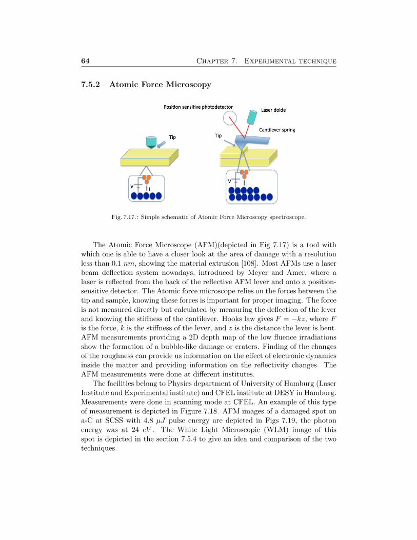
64 Chapter 7. Experimental technique
7.5.2 Atomic Force Microscopy
Fig. 7.17.: Simple schematic of Atomic Force Microscopy spectroscope.
The Atomic Force Microscope (AFM)(depicted in Fig 7.17) is a tool withwhich one is able to have a closer look at the area of damage with a resolutionless than 0.1 nm, showing the material extrusion [108]. Most AFMs use a laserbeam deflection system nowadays, introduced by Meyer and Amer, where alaser is reflected from the back of the reflective AFM lever and onto a position-sensitive detector. The Atomic force microscope relies on the forces between thetip and sample, knowing these forces is important for proper imaging. The forceis not measured directly but calculated by measuring the deflection of the leverand knowing the stiffness of the cantilever. Hooks law gives F = −kz, where Fis the force, k is the stiffness of the lever, and z is the distance the lever is bent.AFM measurements providing a 2D depth map of the low fluence irradiationsshow the formation of a bubble-like damage or craters. Finding of the changesof the roughness can provide us information on the effect of electronic dynamicsinside the matter and providing information on the reflectivity changes. TheAFM measurements were done at different institutes.
The facilities belong to Physics department of University of Hamburg (LaserInstitute and Experimental institute) and CFEL institute at DESY in Hamburg.Measurements were done in scanning mode at CFEL. An example of this typeof measurement is depicted in Figure 7.18. AFM images of a damaged spot ona-C at SCSS with 4.8 µJ pulse energy are depicted in Figs 7.19, the photonenergy was at 24 eV . The White Light Microscopic (WLM) image of thisspot is depicted in the section 7.5.4 to give an idea and comparison of the twotechniques.
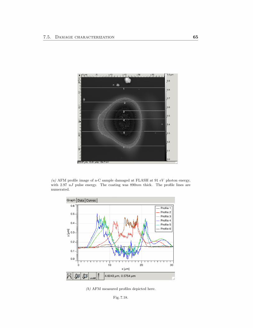
7.5. Damage characterization 65
(a) AFM profile image of a-C sample damaged at FLASH at 91 eV photon energy,with 2.97 uJ pulse energy. The coating was 890nm thick. The profile lines arenumerated.
(b) AFM measured profiles depicted here.
Fig. 7.18.
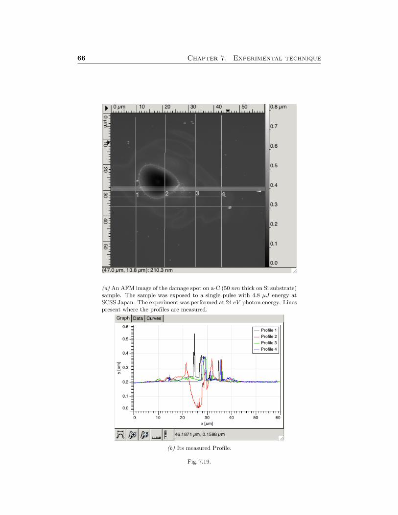
66 Chapter 7. Experimental technique
(a) An AFM image of the damage spot on a-C (50 nm thick on Si substrate)sample. The sample was exposed to a single pulse with 4.8 µJ energy atSCSS Japan. The experiment was performed at 24 eV photon energy. Linespresent where the profiles are measured.
(b) Its measured Profile.
Fig. 7.19.
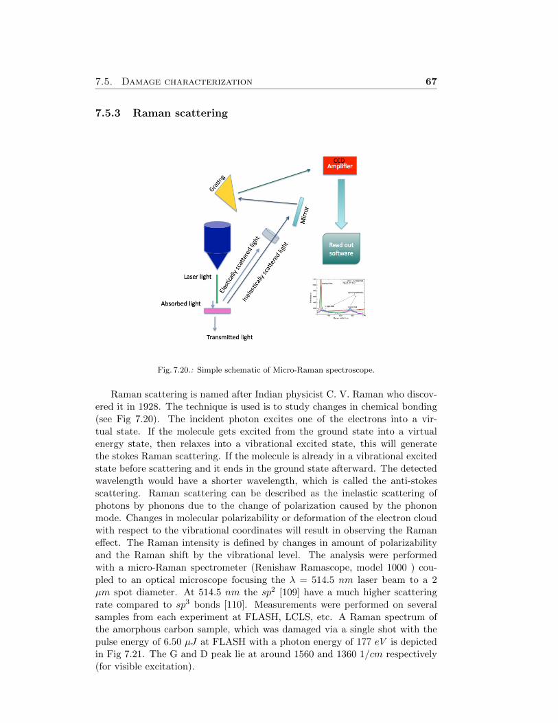
7.5. Damage characterization 67
7.5.3 Raman scattering
Fig. 7.20.: Simple schematic of Micro-Raman spectroscope.
Raman scattering is named after Indian physicist C. V. Raman who discov-ered it in 1928. The technique is used is to study changes in chemical bonding(see Fig 7.20). The incident photon excites one of the electrons into a vir-tual state. If the molecule gets excited from the ground state into a virtualenergy state, then relaxes into a vibrational excited state, this will generatethe stokes Raman scattering. If the molecule is already in a vibrational excitedstate before scattering and it ends in the ground state afterward. The detectedwavelength would have a shorter wavelength, which is called the anti-stokesscattering. Raman scattering can be described as the inelastic scattering ofphotons by phonons due to the change of polarization caused by the phononmode. Changes in molecular polarizability or deformation of the electron cloudwith respect to the vibrational coordinates will result in observing the Ramaneffect. The Raman intensity is defined by changes in amount of polarizabilityand the Raman shift by the vibrational level. The analysis were performedwith a micro-Raman spectrometer (Renishaw Ramascope, model 1000 ) cou-pled to an optical microscope focusing the λ = 514.5 nm laser beam to a 2µm spot diameter. At 514.5 nm the sp2 [109] have a much higher scatteringrate compared to sp3 bonds [110]. Measurements were performed on severalsamples from each experiment at FLASH, LCLS, etc. A Raman spectrum ofthe amorphous carbon sample, which was damaged via a single shot with thepulse energy of 6.50 µJ at FLASH with a photon energy of 177 eV is depictedin Fig 7.21. The G and D peak lie at around 1560 and 1360 1/cm respectively(for visible excitation).
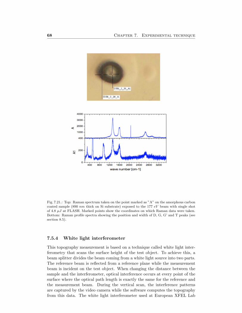
68 Chapter 7. Experimental technique
Fig. 7.21.: Top: Raman spectrum taken on the point marked as ”A” on the amorphous carboncoated sample (890 nm thick on Si substrate) exposed to the 177 eV beam with single shotof 4.8 µJ at FLASH. Marked points show the coordinates on which Raman data were taken.Bottom: Raman profile spectra showing the position and width of D, G, G’ and T peaks (seesection 8.5).
7.5.4 White light interferometer
This topography measurement is based on a technique called white light inter-ferometry that scans the surface height of the test object. To achieve this, abeam splitter divides the beam coming from a white light source into two parts.The reference beam is reflected from a reference plane while the measurementbeam is incident on the test object. When changing the distance between thesample and the interferometer, optical interference occurs at every point of thesurface where the optical path length is exactly the same for the reference andthe measurement beam. During the vertical scan, the interference patternsare captured by the video camera while the software computes the topographyfrom this data. The white light interferometer used at European XFEL Lab
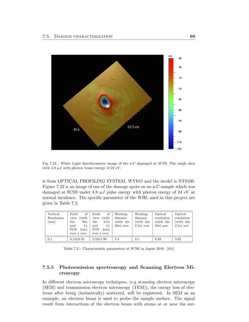
7.5. Damage characterization 69
Fig. 7.22.: White Light Interferometer image of the a-C damaged at SCSS. The single shotwith 4.8 µJ with photon beam energy of 24 eV .
is from OPTICAL PROFILING SYSTEM, WYKO and the model is NT9100.Figure 7.22 is an image of one of the damage spots on an a-C sample which wasdamaged at SCSS under 4.8 µJ pulse energy with photon energy of 24 eV atnormal incidence. The specific parameter of the WHL used in this project aregiven in Table 7.2.
VerticalResolution(nm)
Field ofview (withthe 50xand 1xFOV lens)mm x mm
Field ofview (withthe 2.5xand 1xFOV lens)mm x mm
Workingdistance(with the50x) mm
Workingdistance(with the2.5x) mm
Opticalresolution(with the50x) µm
Opticalresolution(with the2.5x) µm
0.1 0.13x0.10 2.53x1.90 3.4 3.5 0.49 3.82
Table 7.2.: Characteristic parameters at SCSS in Japan 2010 [101]
7.5.5 Photoemission spectroscopy and Scanning Electron Mi-croscopy
In different electron microscopy techniques, (e.g scanning electron microscopy(SEM) and transmission electron microscopy (TEM)), the energy loss of elec-trons after being (inelastically) scattered, will be registered. In SEM as anexample, an electron beam is used to probe the sample surface. The signalresult from interactions of the electron beam with atoms at or near the sur-
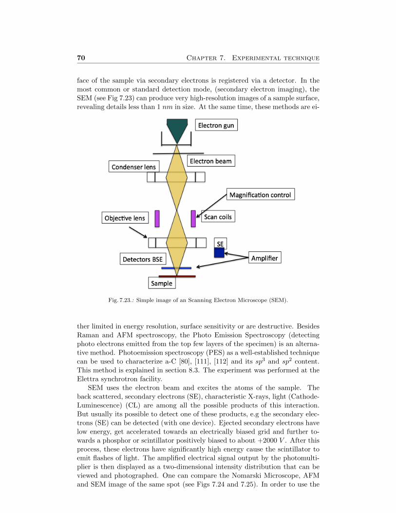
70 Chapter 7. Experimental technique
face of the sample via secondary electrons is registered via a detector. In themost common or standard detection mode, (secondary electron imaging), theSEM (see Fig 7.23) can produce very high-resolution images of a sample surface,revealing details less than 1 nm in size. At the same time, these methods are ei-
Fig. 7.23.: Simple image of an Scanning Electron Microscope (SEM).
ther limited in energy resolution, surface sensitivity or are destructive. BesidesRaman and AFM spectroscopy, the Photo Emission Spectroscopy (detectingphoto electrons emitted from the top few layers of the specimen) is an alterna-tive method. Photoemission spectroscopy (PES) as a well-established techniquecan be used to characterize a-C [80], [111], [112] and its sp3 and sp2 content.This method is explained in section 8.3. The experiment was performed at theElettra synchrotron facility.
SEM uses the electron beam and excites the atoms of the sample. Theback scattered, secondary electrons (SE), characteristic X-rays, light (Cathode-Luminescence) (CL) are among all the possible products of this interaction.But usually its possible to detect one of these products, e.g the secondary elec-trons (SE) can be detected (with one device). Ejected secondary electrons havelow energy, get accelerated towards an electrically biased grid and further to-wards a phosphor or scintillator positively biased to about +2000 V . After thisprocess, these electrons have significantly high energy cause the scintillator toemit flashes of light. The amplified electrical signal output by the photomulti-plier is then displayed as a two-dimensional intensity distribution that can beviewed and photographed. One can compare the Nomarski Microscope, AFMand SEM image of the same spot (see Figs 7.24 and 7.25). In order to use the

7.5. Damage characterization 71
SEM, the sample should get cut into small pieces, this can damage the wholesample (since samples are thin). The AFM or the white light interferometer areless destructive methods in order to get a clear vision of the surface topology.
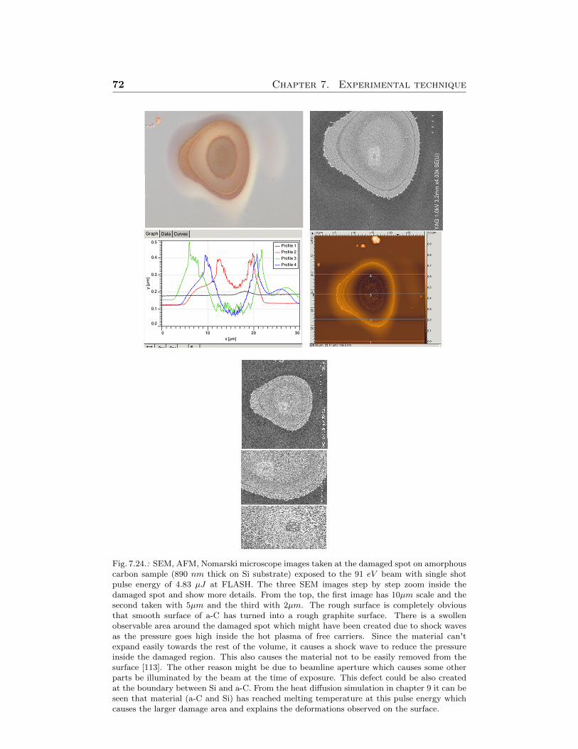
72 Chapter 7. Experimental technique
Fig. 7.24.: SEM, AFM, Nomarski microscope images taken at the damaged spot on amorphouscarbon sample (890 nm thick on Si substrate) exposed to the 91 eV beam with single shotpulse energy of 4.83 µJ at FLASH. The three SEM images step by step zoom inside thedamaged spot and show more details. From the top, the first image has 10µm scale and thesecond taken with 5µm and the third with 2µm. The rough surface is completely obviousthat smooth surface of a-C has turned into a rough graphite surface. There is a swollenobservable area around the damaged spot which might have been created due to shock wavesas the pressure goes high inside the hot plasma of free carriers. Since the material can'texpand easily towards the rest of the volume, it causes a shock wave to reduce the pressureinside the damaged region. This also causes the material not to be easily removed from thesurface [113]. The other reason might be due to beamline aperture which causes some otherparts be illuminated by the beam at the time of exposure. This defect could be also createdat the boundary between Si and a-C. From the heat diffusion simulation in chapter 9 it can beseen that material (a-C and Si) has reached melting temperature at this pulse energy whichcauses the larger damage area and explains the deformations observed on the surface.
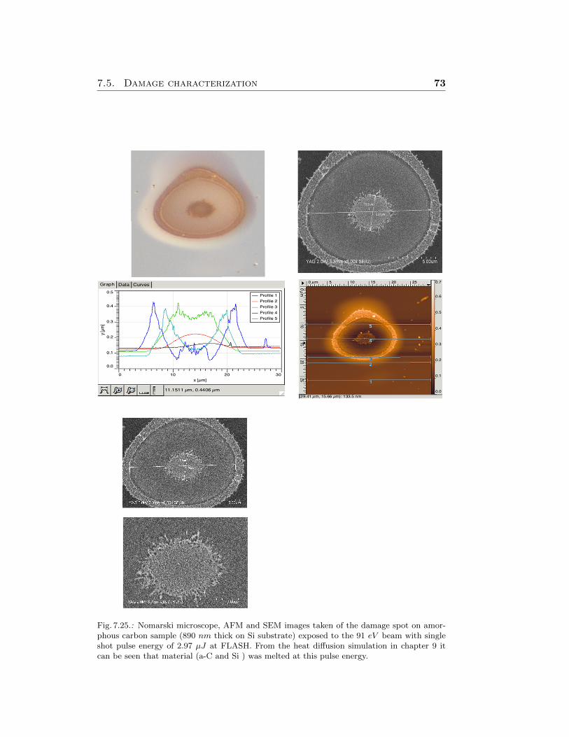
7.5. Damage characterization 73
Fig. 7.25.: Nomarski microscope, AFM and SEM images taken of the damage spot on amor-phous carbon sample (890 nm thick on Si substrate) exposed to the 91 eV beam with singleshot pulse energy of 2.97 µJ at FLASH. From the heat diffusion simulation in chapter 9 itcan be seen that material (a-C and Si ) was melted at this pulse energy.

74 Chapter 7. Experimental technique
Chapter 8
Damage Investigations
Damage experiments under the scope of this project were performed at differentFree Electron Laser (FEL) facilities around the world. The specific wavelengthdesired for further investigations of the damage process was among the criteriaof why a specific FEL facility was chosen over another.
Most of the experiments were performed at FLASH [114]. Each of thosewas focused on a different wavelength. The experiments were performed usingnormal and grazing angles (smaller than the critical angle) defined for eachwavelength. The performed experiments are listed here.
1. 20 eV at normal incidence angle at SCSS in Hyogo Prefecture (Japan) onCVD diamond and a-C samples
2. 24 eV at normal incidence angle at SCSS in Japan on CVD diamond anda-C samples
3. 91 eV at normal/grazing incidence angle at FLASH in Hamburg on CVDdiamond and a-C samples
4. 177 eV at normal/grazing incidence angle at FLASH in Hamburg on CVDdiamond and a-C samples
5. 269 eV at normal/grazing incidence angle at FLASH in Ham-burg/Germany on CVD diamond and a-C samples as well as on Ni andMoB4C
6. 830 eV at normal incidence angle at LCLS in California/USA on CVDdiamond and a-C samples
Table 8.1 represents parameters such as pulse duration at each experiment.The damage investigation procedure is divided into ”Surface analysis” and”Structural analysis”. The surface analysis provides information on the mor-phology of damaged spots. The Structural analysis provides information onstructural changes of the material under irradiation.
The surface analysis includes determining the size of damaged areas (this isabout µm2 in dimension), ’Nomarski microscopy’ was the best tool for makingthis type of measurement (see section 7.5.1). Example images of damage spots
75
76 Chapter 8. Damage Investigations
Photonenergy(eV )
angle(◦)
Pulse duration fs
890 90 100
269 90 125
177 90 30
91 90 30
24 90 100
20 90 100
Table 8.1.: Damage experiment parameter on CVD diamond/a-C at different photon energylevels.
on both single CVD diamond crystal and amorphous carbon are depicted inFigs 8.1, 8.2, 8.4. These images are the initial snapshots in determining thedamage threshold, explained in further detail in the next section. The Whitelight interferometer, AFM and Scanning Electron Microscopy (SEM) (all ex-plained in section 7.5) are other surface analysis methods which are used toobtain information on the morphological level. Micro-Raman spectroscopy [80]and SPEM [115] make it possible to gain information on the changes of the lo-cal atomic order and electronic properties of the damaged spots respectively. Itis also possible to apply Scanning Transmission Electron Microscopy (STEM)as an additional method for structural analysis. This destructive method isapplied when all other measurements are performed on the sample. To charac-terize the long-range order (crystalizing order) of the matter, X-ray diffractionwould provide the necessary information [100], [116].
8.1 Damage threshold
Damage threshold energy is defined as the minimum amount of energy depositedin the matter, by which the first sign of damage can be detected (this includeschanges of the reflectivity or roughness that when compared to the sample’sinitial state are considered as damage). This is measured postmortem in theframe of this work.
The procedure for damage threshold retrieval starts with taking imagesfrom each damage spot on each sample. The microscope used in the frame ofthis work had a resolution between 500 nm and 1 µm and was bought fromLesia company. Recognizing the damage spots is often not straightforward.Observation of any changes in color or removal or expansion of the material iskey to recognizing the damaged area. At very high fluence, the substrate mightbe affected by the beam (melted, ablated, etc.). This can be seen in Fig 8.2. Inthis case, the sample coating was not thick enough in comparison to the beampenetration depth. The beam has reached the substrate at high fluence, whereit melted the substrate and caused a larger beam imprint area on the spot.
After preparing the images, the next step is to measure the area of eachdamage spot and document them with regards to their position. This is a com-
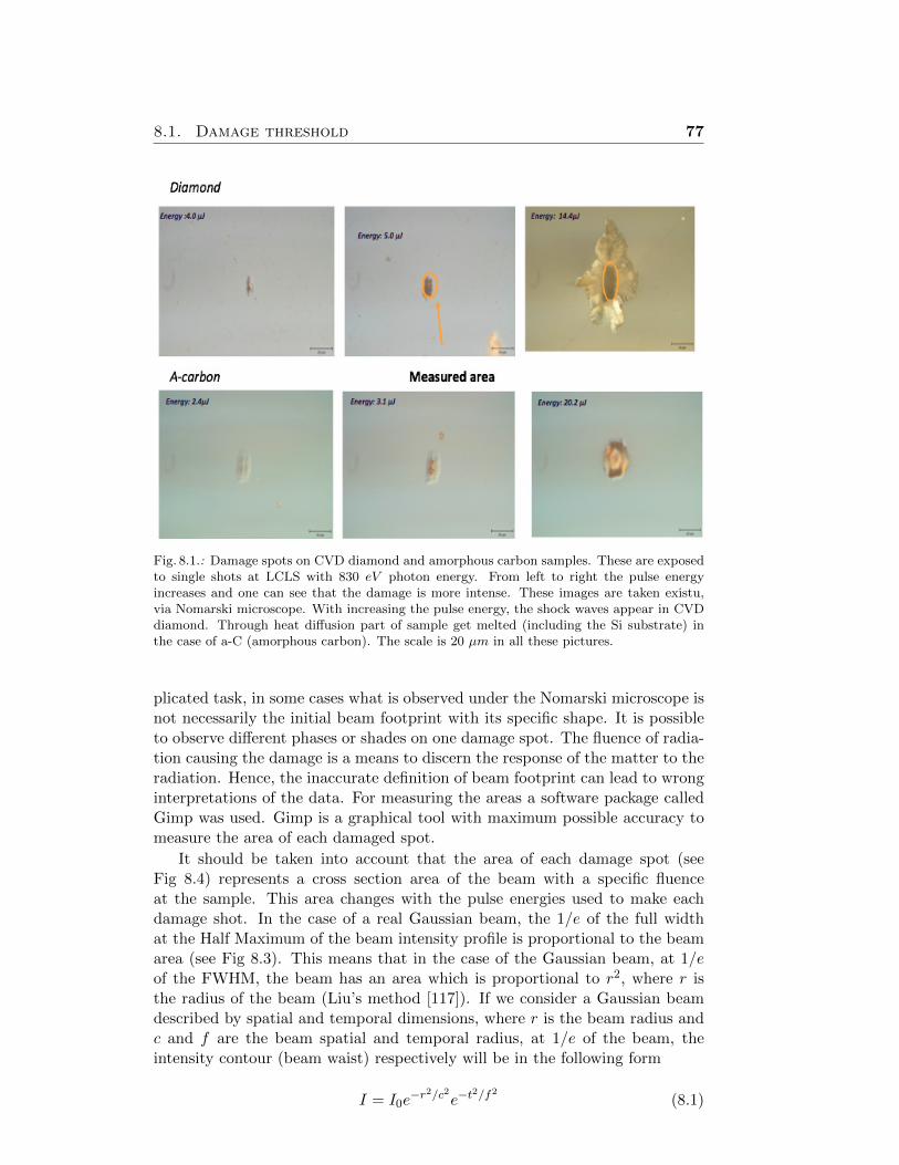
8.1. Damage threshold 77
Fig. 8.1.: Damage spots on CVD diamond and amorphous carbon samples. These are exposedto single shots at LCLS with 830 eV photon energy. From left to right the pulse energyincreases and one can see that the damage is more intense. These images are taken existu,via Nomarski microscope. With increasing the pulse energy, the shock waves appear in CVDdiamond. Through heat diffusion part of sample get melted (including the Si substrate) inthe case of a-C (amorphous carbon). The scale is 20 µm in all these pictures.
plicated task, in some cases what is observed under the Nomarski microscope isnot necessarily the initial beam footprint with its specific shape. It is possibleto observe different phases or shades on one damage spot. The fluence of radia-tion causing the damage is a means to discern the response of the matter to theradiation. Hence, the inaccurate definition of beam footprint can lead to wronginterpretations of the data. For measuring the areas a software package calledGimp was used. Gimp is a graphical tool with maximum possible accuracy tomeasure the area of each damaged spot.
It should be taken into account that the area of each damage spot (seeFig 8.4) represents a cross section area of the beam with a specific fluenceat the sample. This area changes with the pulse energies used to make eachdamage shot. In the case of a real Gaussian beam, the 1/e of the full widthat the Half Maximum of the beam intensity profile is proportional to the beamarea (see Fig 8.3). This means that in the case of the Gaussian beam, at 1/eof the FWHM, the beam has an area which is proportional to r2, where r isthe radius of the beam (Liu’s method [117]). If we consider a Gaussian beamdescribed by spatial and temporal dimensions, where r is the beam radius andc and f are the beam spatial and temporal radius, at 1/e of the beam, theintensity contour (beam waist) respectively will be in the following form
I = I0e−r2/c2e−t
2/f2 (8.1)
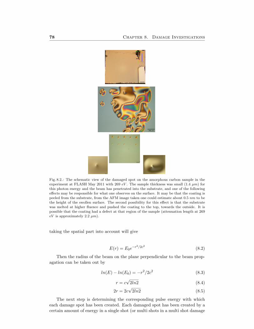
78 Chapter 8. Damage Investigations
Fig. 8.2.: The schematic view of the damaged spot on the amorphous carbon sample in theexperiment at FLASH May 2011 with 269 eV . The sample thickness was small (1.4 µm) forthis photon energy and the beam has penetrated into the substrate, and one of the followingeffects may be responsible for what one observes on the surface. It may be that the coating ispeeled from the substrate, from the AFM image taken one could estimate about 0.5 nm to bethe height of the swollen surface. The second possibility for this effect is that the substratewas melted at higher fluence and pushed the coating to the top, towards the outside. It ispossible that the coating had a defect at that region of the sample (attenuation length at 269eV is approximately 2.2 µm).
taking the spatial part into account will give
E(r) = E0e−r2/2c2 (8.2)
Then the radius of the beam on the plane perpendicular to the beam prop-agation can be taken out by
ln(E)− ln(E0) = −r2/2c2 (8.3)
r = c√
2ln2 (8.4)
2r = 2c√
2ln2 (8.5)
The next step is determining the corresponding pulse energy with whicheach damage spot has been created. Each damaged spot has been created by acertain amount of energy in a single shot (or multi shots in a multi shot damage
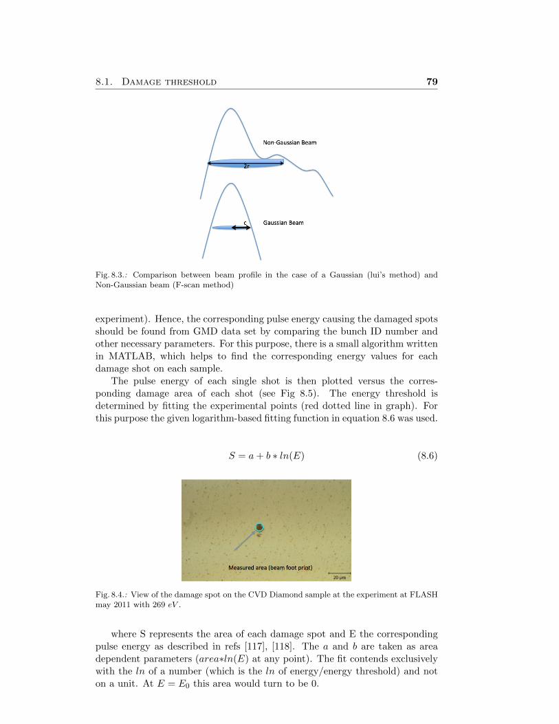
8.1. Damage threshold 79
Fig. 8.3.: Comparison between beam profile in the case of a Gaussian (lui’s method) andNon-Gaussian beam (F-scan method)
experiment). Hence, the corresponding pulse energy causing the damaged spotsshould be found from GMD data set by comparing the bunch ID number andother necessary parameters. For this purpose, there is a small algorithm writtenin MATLAB, which helps to find the corresponding energy values for eachdamage shot on each sample.
The pulse energy of each single shot is then plotted versus the corres-ponding damage area of each shot (see Fig 8.5). The energy threshold isdetermined by fitting the experimental points (red dotted line in graph). Forthis purpose the given logarithm-based fitting function in equation 8.6 was used.
S = a+ b ∗ ln(E) (8.6)
Fig. 8.4.: View of the damage spot on the CVD Diamond sample at the experiment at FLASHmay 2011 with 269 eV .
where S represents the area of each damage spot and E the correspondingpulse energy as described in refs [117], [118]. The a and b are taken as areadependent parameters (area∗ln(E) at any point). The fit contends exclusivelywith the ln of a number (which is the ln of energy/energy threshold) and noton a unit. At E = E0 this area would turn to be 0.
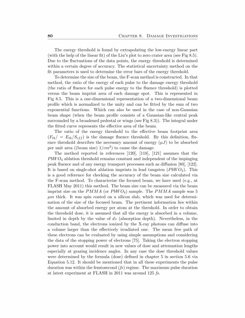
80 Chapter 8. Damage Investigations
The energy threshold is found by extrapolating the low-energy linear part(with the help of the linear fit) of the Liu's plot to zero crater area (see Fig 8.5).Due to the fluctuations of the data points, the energy threshold is determinedwithin a certain degree of accuracy. The statistical uncertainty method on thefit parameters is used to determine the error bars of the energy threshold.
To determine the size of the beam, the F-scan method is constructed. In thatmethod, the ratio of the energy of each pulse to the damage energy threshold(the ratio of fluence for each pulse energy to the fluence threshold) is plottedversus the beam imprint area of each damage spot. This is represented inFig 8.5. This is a one-dimensional representation of a two-dimensional beamprofile which is normalized to the unity and can be fitted by the sum of twoexponential functions. Which can also be used in the case of non-Gaussianbeam shape (when the beam profile consists of a Gaussian-like central peaksurrounded by a broadened pedestal or wings (see Fig 8.3)). The integral underthe fitted curve represents the effective area of the beam.
The ratio of the energy threshold to the effective beam footprint area(Fth/ = Eth/Seff ) is the damage fluence threshold. By this definition, flu-ence threshold describes the necessary amount of energy (µJ) to be absorbedper unit area ((beam size) 1/cm2) to cause the damage.
The method reported in references [120], [118], [121] assumes that thePbWO4 ablation threshold remains constant and independent of the impingingpeak fluence and of any energy transport processes such as diffusion [80], [122].It is based on single-shot ablation imprints in lead tungsten (PbWO4). Thisis a good reference for checking the accuracy of the beam size calculated viathe F-scan method. To characterize the focused beam, we have used (e.g., atFLASH May 2011) this method. The beam size can be measured via the beamimprint size on the PMMA (or PbWO4) sample. The PMMA sample was 5µm thick. It was spin coated on a silicon slab, which was used for determi-nation of the size of the focused beam. The pertinent information lies withinthe amount of absorbed energy per atom at the threshold. In order to obtainthe threshold dose, it is assumed that all the energy is absorbed in a volume,limited in depth by the value of dz (absorption depth). Nevertheless, in theconduction band, the electrons ionized by the X-ray photons can diffuse intoa volume larger than the effectively irradiated one. The mean free path ofthese electrons can be evaluated by using simple assumptions and consideringthe data of the stopping power of electrons [75]. Taking the electron stoppingpower into account would result in new values of dose and attenuation lengthsespecially at grazing incidence angles. In any case the dose threshold valueswere determined by the formula (dose) defined in chapter 5 in section 5.6 viaEquation 5.12. It should be mentioned that in all these experiments the pulseduration was within the femtosecond (fs) regime. The maximum pulse durationat latest experiment at FLASH in 2011 was around 125 fs.
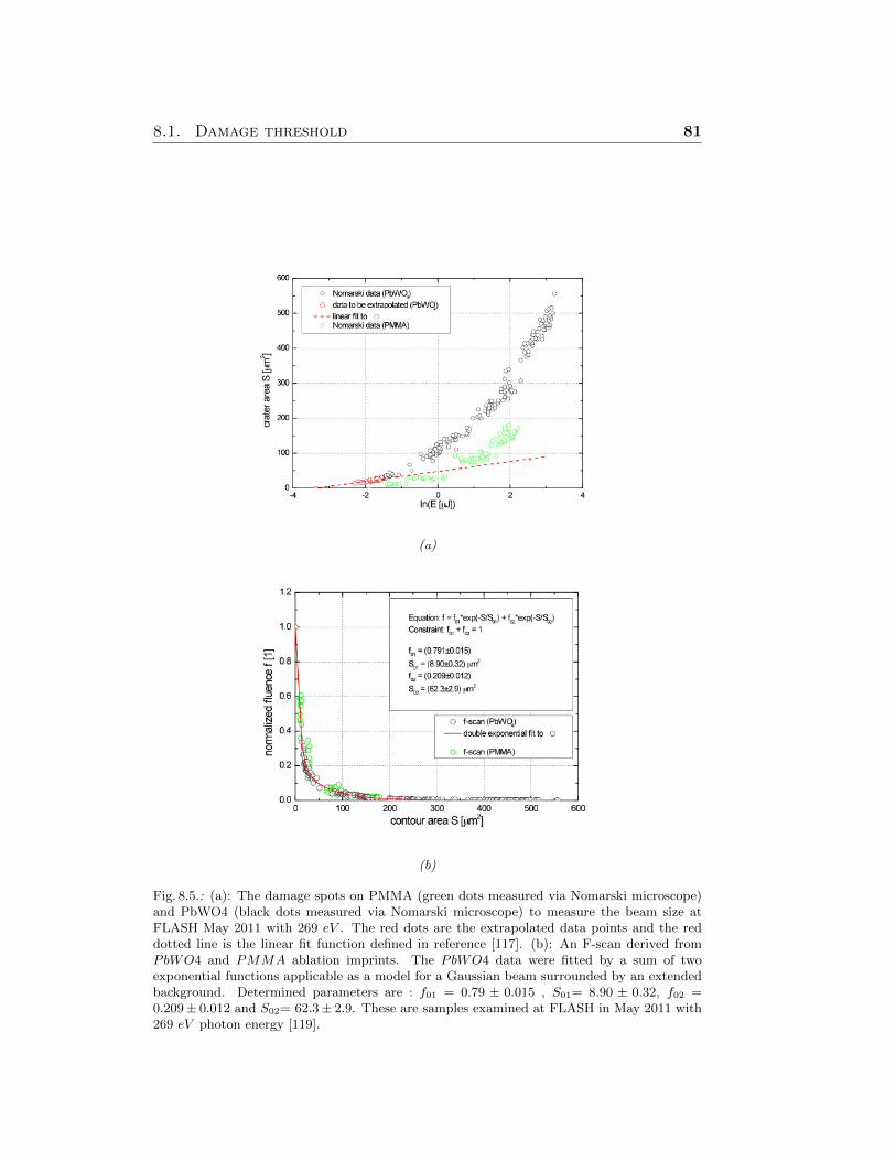
8.1. Damage threshold 81
(a)
(b)
Fig. 8.5.: (a): The damage spots on PMMA (green dots measured via Nomarski microscope)and PbWO4 (black dots measured via Nomarski microscope) to measure the beam size atFLASH May 2011 with 269 eV . The red dots are the extrapolated data points and the reddotted line is the linear fit function defined in reference [117]. (b): An F-scan derived fromPbWO4 and PMMA ablation imprints. The PbWO4 data were fitted by a sum of twoexponential functions applicable as a model for a Gaussian beam surrounded by an extendedbackground. Determined parameters are : f01 = 0.79 ± 0.015 , S01= 8.90 ± 0.32, f02 =0.209± 0.012 and S02= 62.3± 2.9. These are samples examined at FLASH in May 2011 with269 eV photon energy [119].
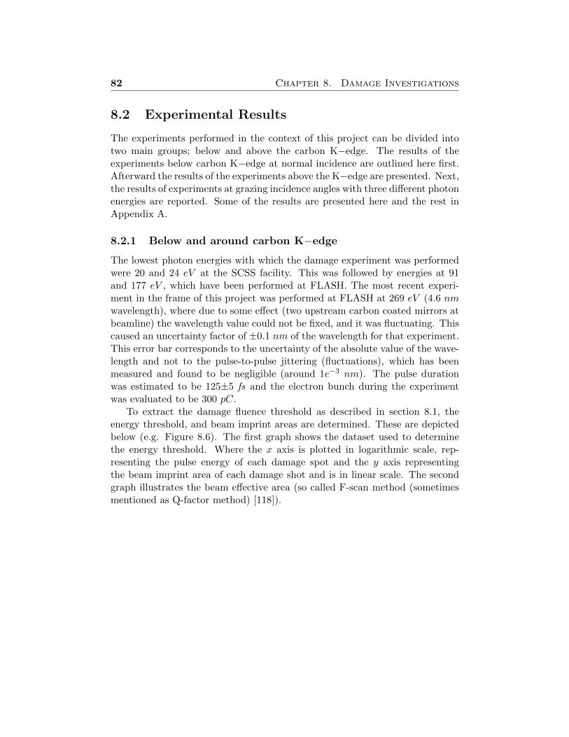
82 Chapter 8. Damage Investigations
8.2 Experimental Results
The experiments performed in the context of this project can be divided intotwo main groups; below and above the carbon K−edge. The results of theexperiments below carbon K−edge at normal incidence are outlined here first.Afterward the results of the experiments above the K−edge are presented. Next,the results of experiments at grazing incidence angles with three different photonenergies are reported. Some of the results are presented here and the rest inAppendix A.
8.2.1 Below and around carbon K−edge
The lowest photon energies with which the damage experiment was performedwere 20 and 24 eV at the SCSS facility. This was followed by energies at 91and 177 eV , which have been performed at FLASH. The most recent experi-ment in the frame of this project was performed at FLASH at 269 eV (4.6 nmwavelength), where due to some effect (two upstream carbon coated mirrors atbeamline) the wavelength value could not be fixed, and it was fluctuating. Thiscaused an uncertainty factor of ±0.1 nm of the wavelength for that experiment.This error bar corresponds to the uncertainty of the absolute value of the wave-length and not to the pulse-to-pulse jittering (fluctuations), which has beenmeasured and found to be negligible (around 1e−3 nm). The pulse durationwas estimated to be 125±5 fs and the electron bunch during the experimentwas evaluated to be 300 pC.
To extract the damage fluence threshold as described in section 8.1, theenergy threshold, and beam imprint areas are determined. These are depictedbelow (e.g. Figure 8.6). The first graph shows the dataset used to determinethe energy threshold. Where the x axis is plotted in logarithmic scale, rep-resenting the pulse energy of each damage spot and the y axis representingthe beam imprint area of each damage shot and is in linear scale. The secondgraph illustrates the beam effective area (so called F-scan method (sometimesmentioned as Q-factor method) [118]).
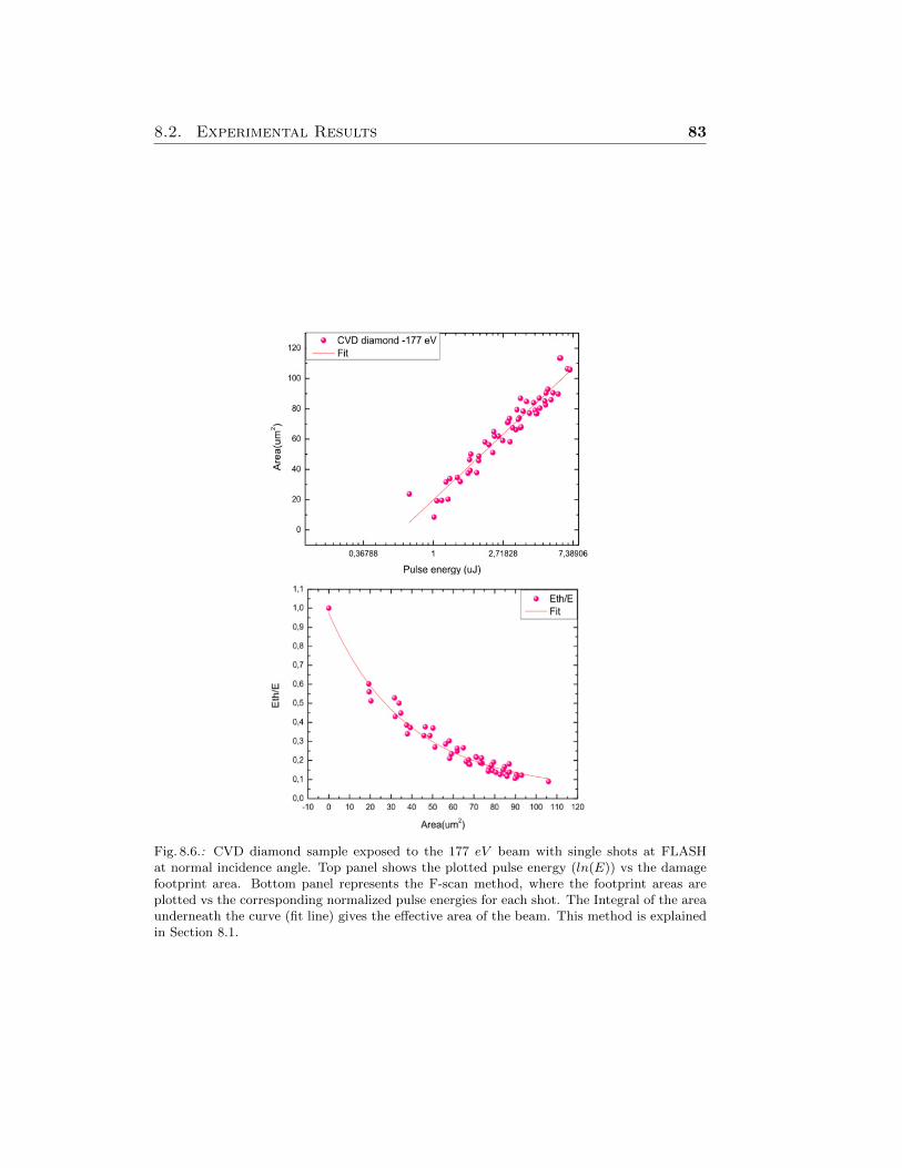
8.2. Experimental Results 83
Fig. 8.6.: CVD diamond sample exposed to the 177 eV beam with single shots at FLASHat normal incidence angle. Top panel shows the plotted pulse energy (ln(E)) vs the damagefootprint area. Bottom panel represents the F-scan method, where the footprint areas areplotted vs the corresponding normalized pulse energies for each shot. The Integral of the areaunderneath the curve (fit line) gives the effective area of the beam. This method is explainedin Section 8.1.
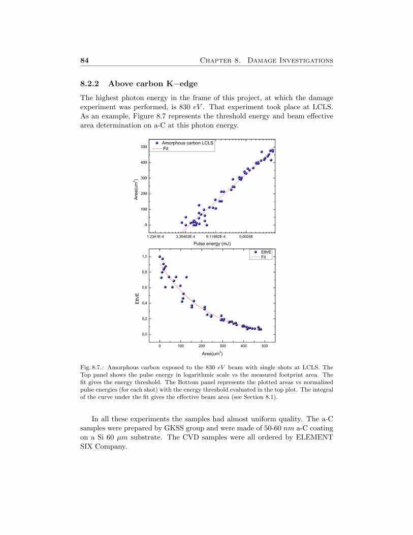
84 Chapter 8. Damage Investigations
8.2.2 Above carbon K−edge
The highest photon energy in the frame of this project, at which the damageexperiment was performed, is 830 eV . That experiment took place at LCLS.As an example, Figure 8.7 represents the threshold energy and beam effectivearea determination on a-C at this photon energy.
Fig. 8.7.: Amorphous carbon exposed to the 830 eV beam with single shots at LCLS. TheTop panel shows the pulse energy in logarithmic scale vs the measured footprint area. Thefit gives the energy threshold. The Bottom panel represents the plotted areas vs normalizedpulse energies (for each shot) with the energy threshold evaluated in the top plot. The integralof the curve under the fit gives the effective beam area (see Section 8.1).
In all these experiments the samples had almost uniform quality. The a-Csamples were prepared by GKSS group and were made of 50-60 nm a-C coatingon a Si 60 µm substrate. The CVD samples were all ordered by ELEMENTSIX Company.
8.2. Experimental Results 85
8.2.3 Below carbon K−edge and at grazing angle
It is critical in the design of any (safe) beamline to know the maximum fluencethat can impinge on the optical elements for a given photon energy withoutdamaging them. Since X-ray mirrors work under total external reflection ge-ometry (at the grazing angle which is smaller than the critical angle θc (seeEquation 4.35)), the energy deposits in the very few first nm layers of the coat-ing, which can be characterized by the absorption depth dz (see Equations 5.8and 5.11).
As a high flux of radiation is desired in any beamline, the reflectivity of thesemirrors (their coatings) at those certain photon energies and grazing angles isone of the critical parameters which should be considered while choosing theoptical coatings.
(a)
1.0 1.0
0.9 0.9
0.8 0.8
0.7 0.7
0.6 0.6
0.5 0.5
0.4 0.4
0.3 0.3
0.2 0.2
0.1 0.1
0.0 0.0
Reflecti
vit
y
9080706050403020100
Grazing angle(degrees)
Atte
nuatio
n le
ngth
(um
)
Blue- attenuation length at 177 ev on a-C (for both 40 nm and 900 nm)
Green-Reflectivity at 177 ev on a-C with 40 nm thickness
Red-Reflectivity at 177 ev on a-C with 900 nm thickness
(b)
Fig. 8.8.: (a): Damage on amorphous carbon at grazing angles of 4.3◦ and 7.7◦ at 177eV atFLASH. (b): Comparing changes of the attenuation length and reflectivity on the thin (40nm) and bulk (900 nm) a-C sample at 177 eV on a-C. The attenuation length doesn’t changebut the reflectivity slightly changes and on a thicker sample the drop happens at a slightlylower angle.
The attenuation depth, the area of the damaged spot and the reflectivityof the material, all change with tuning the grazing angle (see Fig 8.8). Theamount of the absorbed dose in the material also depends on the grazing angle.In the case of a-C, most of the X-ray photons get reflected away at low photonenergies. Increasing the photon energy results in reduction of reflectivity and
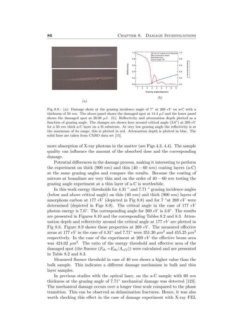
86 Chapter 8. Damage Investigations
(a)
1.0 1.0
0.8 0.8
0.6 0.6
0.4 0.4
0.2 0.2
0.0 0.0
Reflecti
vit
y
987654321
Grazing angle(degrees)
Atte
nuatio
n d
epth
(um
)50 nm a-C coation on Si substrate
Blue Attenuation depth
Red Reflectivity
critical angle 3.6¼
(b)
Fig. 8.9.: (a): Damage shots at the grazing incidence angle of 7◦ at 269 eV on a-C with athickness of 50 nm. The above panel shows the damaged spot at 14.4 µJ and the lower panelshows the damaged spot at 20.08 µJ . (b): Reflectivity and attenuation depth plotted as afunction of grazing angle. The changes are shown here around critical angle (3.6◦) at 269 eVfor a 50 nm thick a-C layer on a Si substrate. At very low grazing angle the reflectivity is atthe maximum of its range, this is plotted in red. Attenuation depth is plotted in blue. Thesolid lines are taken from CXRO data set [15].
more absorption of X-ray photons in the matter (see Figs 4.3, 4.4). The samplequality can influence the amount of the absorbed dose and the correspondingdamage.
Potential differences in the damage process, making it interesting to performthe experiment on thick (900 nm) and thin (40 − 60 nm) coating layers (a-C)at the same grazing angles and compare the results. Because the coating ofmirrors at beamlines are very thin and on the order of 40− 60 nm testing thegrazing angle experiment at a thin layer of a-C is worthwhile.
In this work energy thresholds for 4.31 ◦ and 7.71 ◦ grazing incidence angles(below and above critical angle) on thin (40 nm) and thick (900 nm) layers ofamorphous carbon at 177 eV (depicted in Fig 8.8) and for 7 ◦at 269 eV weredetermined (depicted in Figs 8.9). The critical angle in the case of 177 eVphoton energy is 7.6◦. The corresponding angle for 269 eV is 3.6◦. The resultsare presented in Figures 8.10 and the corresponding Tables 8.2 and 8.3. Atten-uation depth and reflectivity around the critical angle at 177 eV are plotted inFig 8.8. Figure 8.9 shows these properties at 269 eV . The measured effectiveareas at 177 eV in the case of 4.31◦ and 7.71◦ were 351.30 µm2 and 455.25 µm2
respectively. In the case of the experiment at 269 eV the effective beam areawas 424.02 µm2. The ratio of the energy threshold and effective area of thedamaged spot (the fluence (Fth =Eth/Aeff )) were calculated and are presentedin Table 8.2 and 8.3.
Measured fluence threshold in case of 40 nm shows a higher value than thebulk sample. This indicates a different damage mechanism in bulk and thinlayer samples.
In previous studies with the optical laser, on the a-C sample with 60 nmthickness at the grazing angle of 7.71◦ mechanical damage was detected [123].The mechanical damage occurs over a longer time scale compared to the phasetransition. This can be observed as delamination fractures. Hence, it was alsoworth checking this effect in the case of damage experiment with X-ray FEL
8.2. Experimental Results 87
single pulses. After doing so, under the Nomarski microscope, no sign of me-chanical damage was detected, ablation, however, was observed (see Figs 8.8).The ablation can be recognized by observing the removal of the coating materialas well as melting of the substrate [16].
An interesting observation is the changes of fluence threshold at the samegrazing angle for the thin and thick sample. The Fluence threshold (dose thresh-old as well) in the case of the thin layer is higher than of a bulk sample. Oneexplanation could be the sample quality. The fact that the deposition time fora bulk sample is longer than for a thin layer suggests that this can cause moredefect and changes of surface roughness and density. Defects or high roughnessincrease the damage possibilities. The roughness of both samples measured viaAFM shows that roughness of the bulk sample is higher (see Fig: 6.5). Also asa result of irradiation, free carriers can escape from the surface of the sampleand carry away some energy with them as leaving the sample. This means thehigher the grazing angle, the greater the number of the scattered away electronsfrom the surface of the sample will be. In the case of the thin coating layer,this effect could increase the fluence threshold more than in the case of the bulksample. Another fact is that free carriers can get scattered within a larger vol-ume inside a bulk sample, which increases the secondary ionization possibilitiesinside the coating. The volume which gets involved in the damage process isnot limited to the attenuation depth (see Chapter 5) but also depends on themean free path of these carriers, electron range (see Chapter 9) as well as onthe depth to which the heat can get diffused to. In a thin sample, heat can betransferred towards the substrate, much faster than in the bulk sample. At theexperiment with 269 eV photon energy, the attenuation depth (see Fig 8.9 andTables 8.3 and 8.2) was higher than the thickness of a-C coating. It means thesubstrate was affected by the pulse and this event had influenced the damagethreshold (coating thickness should have been larger).
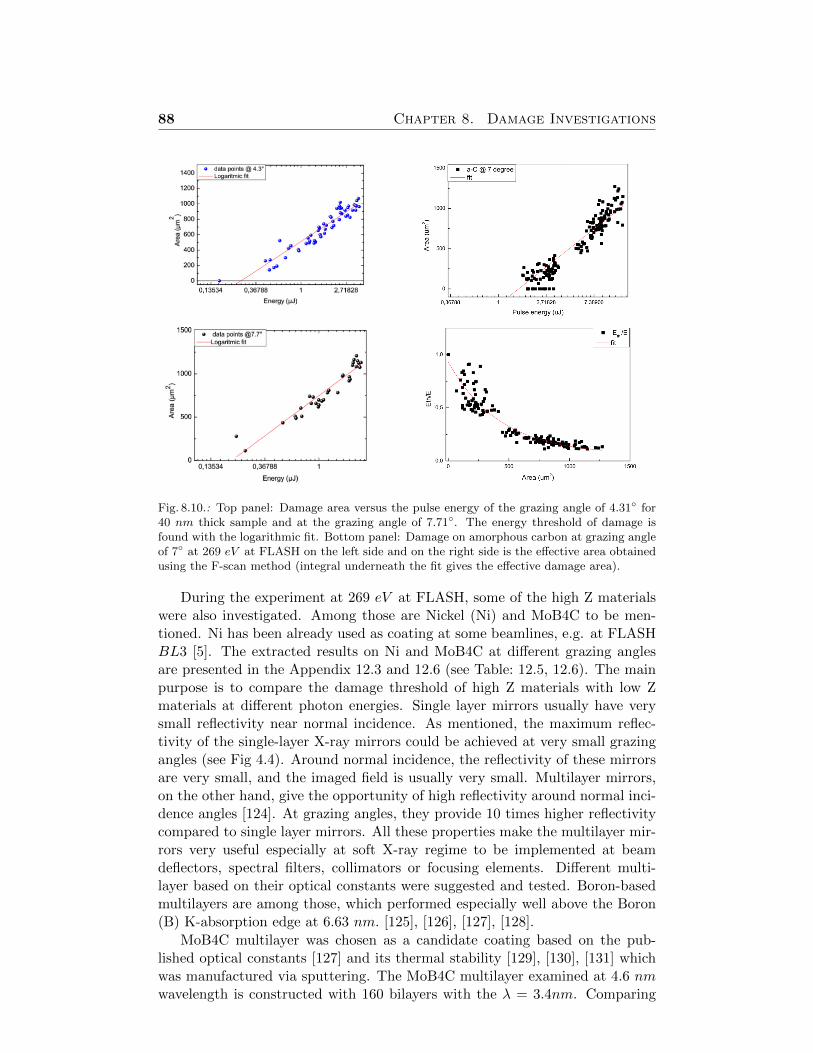
88 Chapter 8. Damage Investigations
Fig. 8.10.: Top panel: Damage area versus the pulse energy of the grazing angle of 4.31◦ for40 nm thick sample and at the grazing angle of 7.71◦. The energy threshold of damage isfound with the logarithmic fit. Bottom panel: Damage on amorphous carbon at grazing angleof 7◦ at 269 eV at FLASH on the left side and on the right side is the effective area obtainedusing the F-scan method (integral underneath the fit gives the effective damage area).
During the experiment at 269 eV at FLASH, some of the high Z materialswere also investigated. Among those are Nickel (Ni) and MoB4C to be men-tioned. Ni has been already used as coating at some beamlines, e.g. at FLASHBL3 [5]. The extracted results on Ni and MoB4C at different grazing anglesare presented in the Appendix 12.3 and 12.6 (see Table: 12.5, 12.6). The mainpurpose is to compare the damage threshold of high Z materials with low Zmaterials at different photon energies. Single layer mirrors usually have verysmall reflectivity near normal incidence. As mentioned, the maximum reflec-tivity of the single-layer X-ray mirrors could be achieved at very small grazingangles (see Fig 4.4). Around normal incidence, the reflectivity of these mirrorsare very small, and the imaged field is usually very small. Multilayer mirrors,on the other hand, give the opportunity of high reflectivity around normal inci-dence angles [124]. At grazing angles, they provide 10 times higher reflectivitycompared to single layer mirrors. All these properties make the multilayer mir-rors very useful especially at soft X-ray regime to be implemented at beamdeflectors, spectral filters, collimators or focusing elements. Different multi-layer based on their optical constants were suggested and tested. Boron-basedmultilayers are among those, which performed especially well above the Boron(B) K-absorption edge at 6.63 nm. [125], [126], [127], [128].
MoB4C multilayer was chosen as a candidate coating based on the pub-lished optical constants [127] and its thermal stability [129], [130], [131] whichwas manufactured via sputtering. The MoB4C multilayer examined at 4.6 nmwavelength is constructed with 160 bilayers with the λ = 3.4nm. Comparing
8.2. Experimental Results 89
the thickness of Mo layer to the B4C results in 0.33. The multilayers are fin-ished with the B4C. In the FLASH experiment at 4.6 nm wavelength, theywere exposed to the beam under normal and grazing angles, and in each caseone sample was annealed for about an hour at 500◦C, to compare the stabilityof the multilayer under this circumstance. Around carbon edge, the B4C incomparison to Ni has lower reflectivity, but at higher energies, up to 3 keV(interesting for XFEL in Hamburg), this value changes and Ni has lower reflec-tivity. That is why it is interesting to compare the damage threshold and toinvestigate the possibility of using it (Ni) as a coating on mirrors. Two stripes,one out of Ni and one out of B4C would be a great combination for coating onone mirror but due to cost reason it was decided to use B4C for mirrors with20 mm wide, reflecting area at XFEL beamline; which was more of practicaluse [132] [125], [133], [134]. Next important factor is the answer to the questionof if this coating could be good enough for vast energy range in comparison tolow Z material or multilayers like B4C. The energy threshold results and effec-tive areas are plotted in Appendix 12.3- 12.5. Further studies on Ni at differentphoton energies could be considered for future experiments.
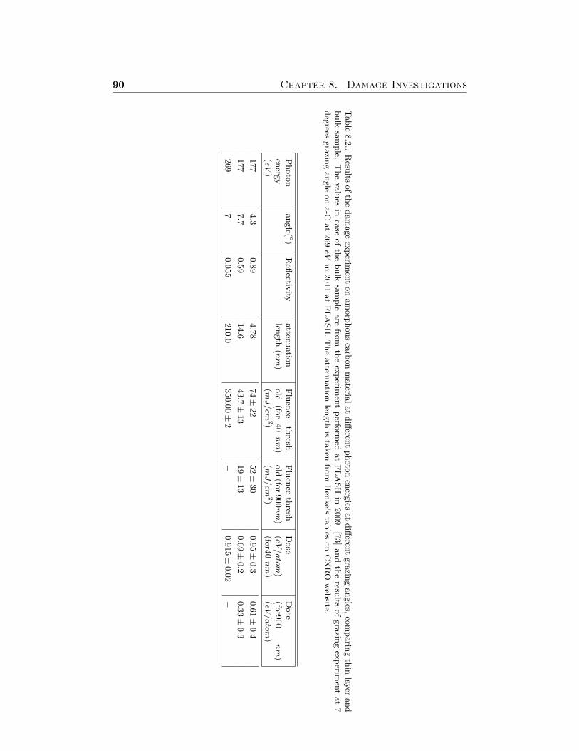
90 Chapter 8. Damage Investigations
Table
8.2
.:R
esults
of
the
dam
age
exp
erimen
ton
am
orp
hous
carb
on
materia
lat
diff
erent
photo
nen
ergies
at
diff
erent
gra
zing
angles,
com
parin
gth
inlay
erand
bulk
sam
ple.
The
valu
esin
case
of
the
bulk
sam
ple
are
from
the
exp
erimen
tp
erform
edat
FL
ASH
in2009
[73]
and
the
results
of
gra
zing
exp
erimen
tat
7deg
reesgra
zing
angle
on
a-C
at
269eV
in2011
at
FL
ASH
.T
he
atten
uatio
nlen
gth
ista
ken
from
Hen
ke’s
tables
on
CX
RO
web
site.
Photo
nen
ergy
(eV)
angle( ◦)
Refl
ectivity
atten
uatio
nlen
gth
(nm
)F
luen
ceth
resh-
old
(for
40nm
)(mJ/cm
2)
Flu
ence
thresh
-old
(for
900nm
)(mJ/cm
2)
Dose
(eV/atom
)(fo
r40nm
)
Dose
(for9
00
nm
)(eV
/atom
)
177
4.3
0.8
94.7
874±
22
52±
30
0.9
5±
0.3
0.6
1±
0.4
177
7.7
0.5
914.6
43.7±
13
19±
13
0.6
9±
0.2
0.3
3±
0.3
269
70.0
55
210.0
350.0
0±
2−
0.9
15±
0.0
2−
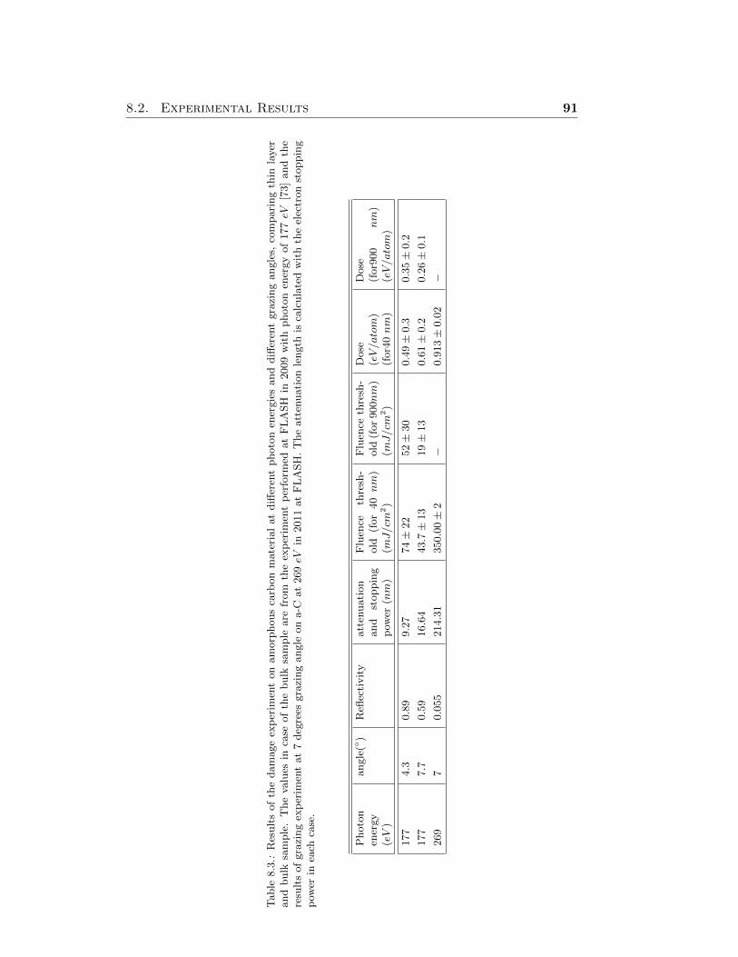
8.2. Experimental Results 91
Table
8.3
.:R
esult
sof
the
dam
age
exp
erim
ent
on
am
orp
hous
carb
on
mate
rial
at
diff
eren
tphoto
nen
ergie
sand
diff
eren
tgra
zing
angle
s,co
mpari
ng
thin
layer
and
bulk
sam
ple
.T
he
valu
esin
case
of
the
bulk
sam
ple
are
from
the
exp
erim
ent
per
form
edat
FL
ASH
in2009
wit
hphoto
nen
ergy
of
177eV
[73]
and
the
resu
lts
of
gra
zing
exp
erim
ent
at
7deg
rees
gra
zing
angle
on
a-C
at
269eV
in2011
at
FL
ASH
.T
he
att
enuati
on
length
isca
lcula
ted
wit
hth
eel
ectr
on
stoppin
gp
ower
inea
chca
se.
Photo
nen
ergy
(eV
)
angle
(◦)
Refl
ecti
vit
yatt
enuati
on
and
stoppin
gp
ower
(nm
)
Flu
ence
thre
sh-
old
(for
40nm
)(mJ/cm
2)
Flu
ence
thre
sh-
old
(for
900nm
)(mJ/cm
2)
Dose
(eV/atom
)(f
or4
0nm
)
Dose
(for9
00
nm
)(eV/atom
)
177
4.3
0.8
99.2
774±
22
52±
30
0.4
9±
0.3
0.3
5±
0.2
177
7.7
0.5
916.6
443.7±
13
19±
13
0.6
1±
0.2
0.2
6±
0.1
269
70.0
55
214.3
1350.0
0±
2−
0.9
13±
0.0
2−

92 Chapter 8. Damage Investigations
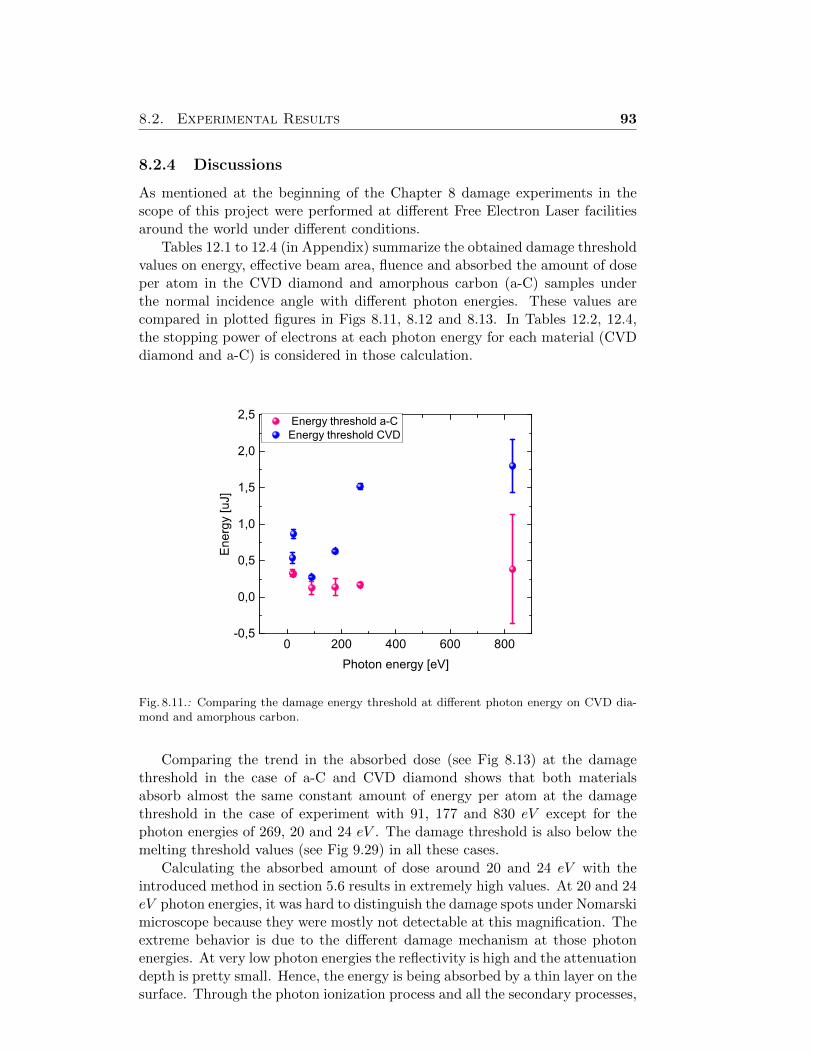
8.2. Experimental Results 93
8.2.4 Discussions
As mentioned at the beginning of the Chapter 8 damage experiments in thescope of this project were performed at different Free Electron Laser facilitiesaround the world under different conditions.
Tables 12.1 to 12.4 (in Appendix) summarize the obtained damage thresholdvalues on energy, effective beam area, fluence and absorbed the amount of doseper atom in the CVD diamond and amorphous carbon (a-C) samples underthe normal incidence angle with different photon energies. These values arecompared in plotted figures in Figs 8.11, 8.12 and 8.13. In Tables 12.2, 12.4,the stopping power of electrons at each photon energy for each material (CVDdiamond and a-C) is considered in those calculation.
0 200 400 600 800-0,5
0,0
0,5
1,0
1,5
2,0
2,5 Energy threshold a-CEnergy threshold CVD
Ene
rgy
[uJ]
Photon energy [eV]
Fig. 8.11.: Comparing the damage energy threshold at different photon energy on CVD dia-mond and amorphous carbon.
Comparing the trend in the absorbed dose (see Fig 8.13) at the damagethreshold in the case of a-C and CVD diamond shows that both materialsabsorb almost the same constant amount of energy per atom at the damagethreshold in the case of experiment with 91, 177 and 830 eV except for thephoton energies of 269, 20 and 24 eV . The damage threshold is also below themelting threshold values (see Fig 9.29) in all these cases.
Calculating the absorbed amount of dose around 20 and 24 eV with theintroduced method in section 5.6 results in extremely high values. At 20 and 24eV photon energies, it was hard to distinguish the damage spots under Nomarskimicroscope because they were mostly not detectable at this magnification. Theextreme behavior is due to the different damage mechanism at those photonenergies. At very low photon energies the reflectivity is high and the attenuationdepth is pretty small. Hence, the energy is being absorbed by a thin layer on thesurface. Through the photon ionization process and all the secondary processes,
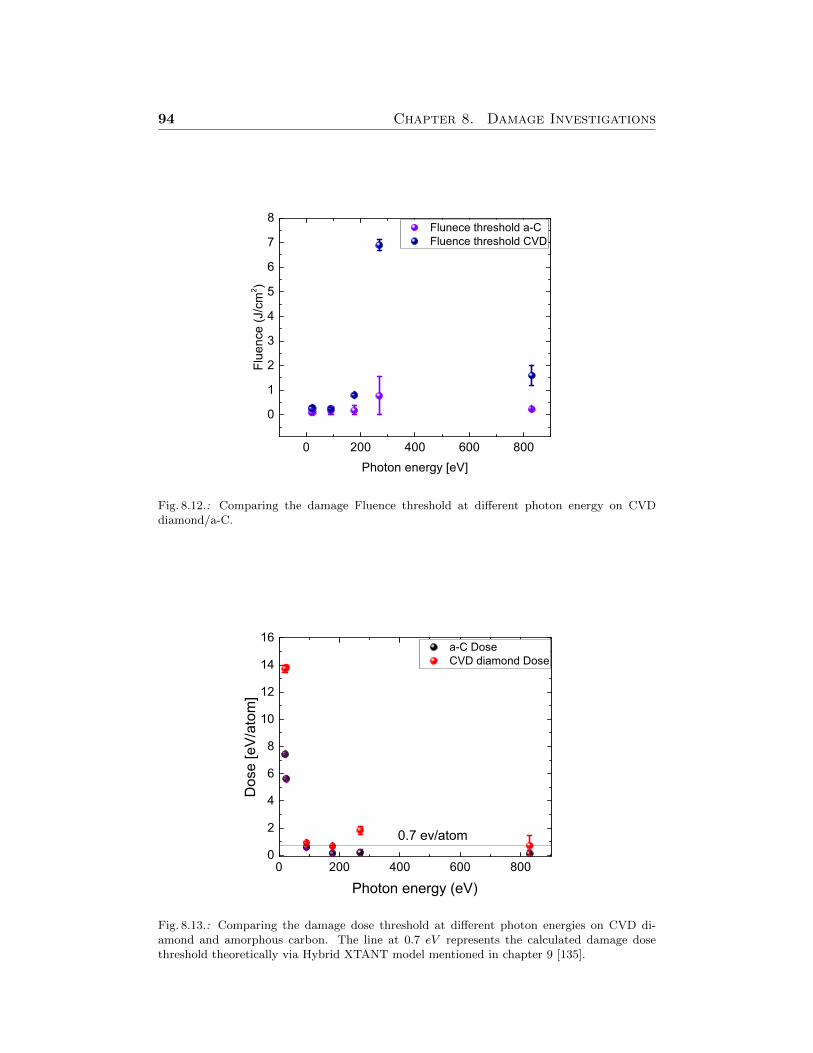
94 Chapter 8. Damage Investigations
0 200 400 600 800
0
1
2
3
4
5
6
7
8 Flunece threshold a-C Fluence threshold CVD
Flue
nce
(J/c
m2 )
Photon energy [eV]
Fig. 8.12.: Comparing the damage Fluence threshold at different photon energy on CVDdiamond/a-C.
0 200 400 600 8000
2
4
6
8
10
12
14
16 a-C Dose CVD diamond Dose
Dos
e [e
V/a
tom
]
Photon energy (eV)
0.7 ev/atom
Fig. 8.13.: Comparing the damage dose threshold at different photon energies on CVD di-amond and amorphous carbon. The line at 0.7 eV represents the calculated damage dosethreshold theoretically via Hybrid XTANT model mentioned in chapter 9 [135].
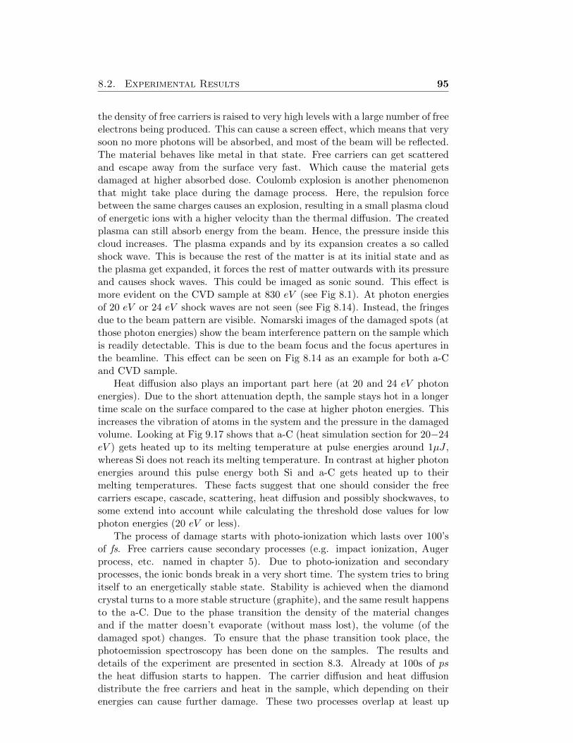
8.2. Experimental Results 95
the density of free carriers is raised to very high levels with a large number of freeelectrons being produced. This can cause a screen effect, which means that verysoon no more photons will be absorbed, and most of the beam will be reflected.The material behaves like metal in that state. Free carriers can get scatteredand escape away from the surface very fast. Which cause the material getsdamaged at higher absorbed dose. Coulomb explosion is another phenomenonthat might take place during the damage process. Here, the repulsion forcebetween the same charges causes an explosion, resulting in a small plasma cloudof energetic ions with a higher velocity than the thermal diffusion. The createdplasma can still absorb energy from the beam. Hence, the pressure inside thiscloud increases. The plasma expands and by its expansion creates a so calledshock wave. This is because the rest of the matter is at its initial state and asthe plasma get expanded, it forces the rest of matter outwards with its pressureand causes shock waves. This could be imaged as sonic sound. This effect ismore evident on the CVD sample at 830 eV (see Fig 8.1). At photon energiesof 20 eV or 24 eV shock waves are not seen (see Fig 8.14). Instead, the fringesdue to the beam pattern are visible. Nomarski images of the damaged spots (atthose photon energies) show the beam interference pattern on the sample whichis readily detectable. This is due to the beam focus and the focus apertures inthe beamline. This effect can be seen on Fig 8.14 as an example for both a-Cand CVD sample.
Heat diffusion also plays an important part here (at 20 and 24 eV photonenergies). Due to the short attenuation depth, the sample stays hot in a longertime scale on the surface compared to the case at higher photon energies. Thisincreases the vibration of atoms in the system and the pressure in the damagedvolume. Looking at Fig 9.17 shows that a-C (heat simulation section for 20−24eV ) gets heated up to its melting temperature at pulse energies around 1µJ ,whereas Si does not reach its melting temperature. In contrast at higher photonenergies around this pulse energy both Si and a-C gets heated up to theirmelting temperatures. These facts suggest that one should consider the freecarriers escape, cascade, scattering, heat diffusion and possibly shockwaves, tosome extend into account while calculating the threshold dose values for lowphoton energies (20 eV or less).
The process of damage starts with photo-ionization which lasts over 100’sof fs. Free carriers cause secondary processes (e.g. impact ionization, Augerprocess, etc. named in chapter 5). Due to photo-ionization and secondaryprocesses, the ionic bonds break in a very short time. The system tries to bringitself to an energetically stable state. Stability is achieved when the diamondcrystal turns to a more stable structure (graphite), and the same result happensto the a-C. Due to the phase transition the density of the material changesand if the matter doesn’t evaporate (without mass lost), the volume (of thedamaged spot) changes. To ensure that the phase transition took place, thephotoemission spectroscopy has been done on the samples. The results anddetails of the experiment are presented in section 8.3. Already at 100s of psthe heat diffusion starts to happen. The carrier diffusion and heat diffusiondistribute the free carriers and heat in the sample, which depending on theirenergies can cause further damage. These two processes overlap at least up
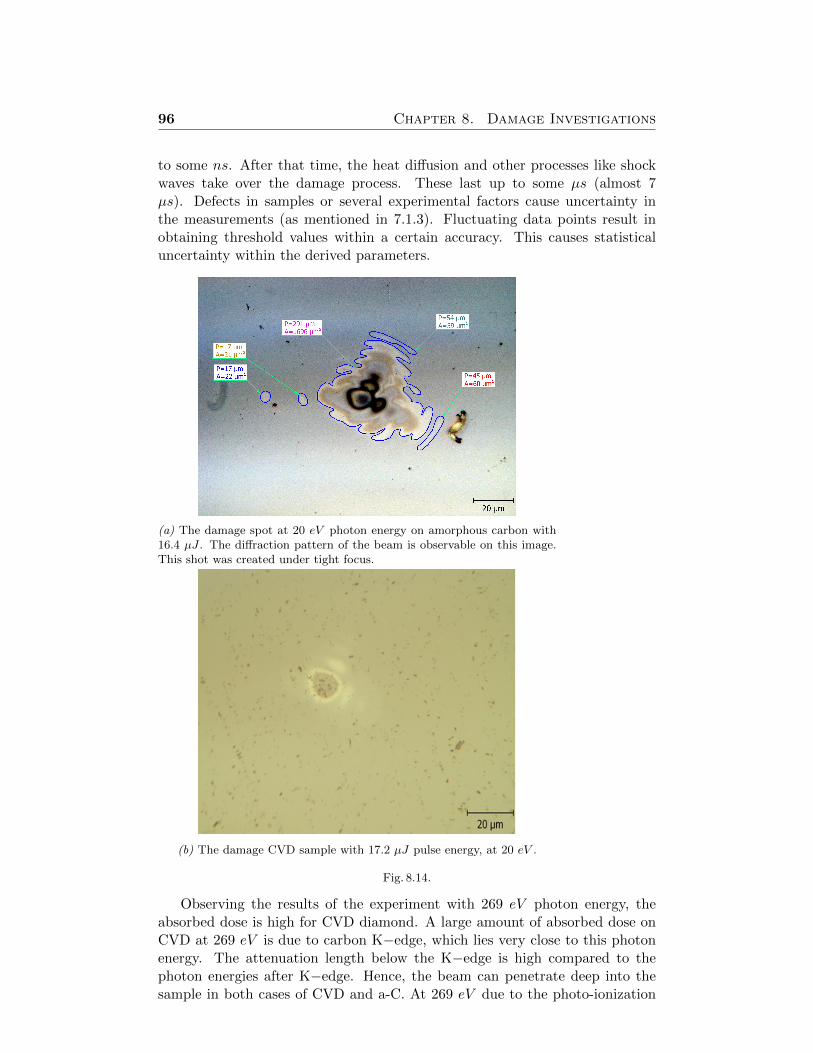
96 Chapter 8. Damage Investigations
to some ns. After that time, the heat diffusion and other processes like shockwaves take over the damage process. These last up to some µs (almost 7µs). Defects in samples or several experimental factors cause uncertainty inthe measurements (as mentioned in 7.1.3). Fluctuating data points result inobtaining threshold values within a certain accuracy. This causes statisticaluncertainty within the derived parameters.
(a) The damage spot at 20 eV photon energy on amorphous carbon with16.4 µJ . The diffraction pattern of the beam is observable on this image.This shot was created under tight focus.
(b) The damage CVD sample with 17.2 µJ pulse energy, at 20 eV .
Fig. 8.14.
Observing the results of the experiment with 269 eV photon energy, theabsorbed dose is high for CVD diamond. A large amount of absorbed dose onCVD at 269 eV is due to carbon K−edge, which lies very close to this photonenergy. The attenuation length below the K−edge is high compared to thephoton energies after K−edge. Hence, the beam can penetrate deep into thesample in both cases of CVD and a-C. At 269 eV due to the photo-ionization
8.2. Experimental Results 97
process, lots of electrons above the K−shell are ejected out of atoms in the CVDcrystal structure. The 2S−shell is being ionized first, and the ejected electronshave 160 eV rest energy that still can ionize the upper shell electrons. Augerprocess and other secondary process are running at the same time. These allcreate enormously high numbers of free carriers. Besides the fact that some ofthe free electrons can escape away from the surface. The free carriers can causescreening effect (metallic behavior of the electrically insulating solid material).This could also lead to a high absorbed dose at this photon energy. ThroughF−scan method calculation, the obtained beam imprint radius is much largerthan the beam radius given as a parameter at the time of the experiment.That’s why in the calculation of absorbed dose, the beam size is taken as givenfrom the facility (FLASH) at the time of the experiment.
At 269 eV photon energy the a-C sample was partly swollen, and it seemedthat the substrate was molten underneath the coating, or the coating was peeledoff. Unfortunately, at this experiment, the a-C coating thickness was madeshorter than the attenuation length of radiation. Hence, the substrate was alsoirradiated by the pulse, and part of the dose was absorbed into the substrate(Si). At higher pulse energies Si has been molten. This is also obvious in heatsimulation calculations in chapter 9 (see Fig 9.17).
Considering the sample was only made out of Si, the absorbed dose has beencalculated. The attenuation depth and reflectivity for Si wafer (substrate) at269 eV are 0.20 µm and 7.2 ∗ 10−6 respectively. The damage absorbed dose forSi was found to be 0.15 eV/atom. The threshold energy was taken the same asevaluated (0.17 µJ).
The melting threshold for Si was estimated to be 0.4 eV , by using thefollowing formula (see Eq 8.7)
Cv = 3 ∗KB ∗ Tmelting (8.7)
As mentioned before, the melting threshold dose was 1 eV (calculated in sec-tion 6.1 with the above-given formula) for Carbon. Hence, the sample reacheshigh temperatures close to melting temperature, at higher pulse energies, soonerat the substrate (in this case) compared to a-C. This causes an extra inducedpressure which forces the coating outwards. The free carriers also have highenergy and possibility to move around from a-C to Si or vise verse, and thiscauses secondary effects or ionization of further atoms on their path. Anothereffect is due to the shock waves, which increases the pressure inside the volume.This could happen in between the Si and a-C layer as well [113].
98 Chapter 8. Damage Investigations
8.3 Photoemission spectroscopy results
Photoemission Spectroscopy (PEM) is a well-established surface analysismethod to study the electronic structure of matter. PEM examines the samplewith a specific wavelength of photon beam (beam of UV or XUV light), and onegains information on the binding energies of the electrons (which also dependson their vibrational state and rotational level) through emitted photoelectrons.SPEM as an imaging technique allows the same type of analysis in a space-resolved way. For solids, photoelectrons can only escape from a depth on theorder of nanometers (that is the surface layer). The binding energies of themeasured electrons are characteristic of the chemical structure and molecularbonding of the material. With this technique, one can gain information onchanges in the bindings of the material. Hence, if the material is modified viadamage process, SPEM measurement determines the changes.
The SPEM experiment was performed at the ESCA microscopy beamlineat the Elettra synchrotron facility. The complete description of the beamline isgiven in ref [136]. In this experiment, the monochromatized X-ray photon beamwith 649 eV was focused on zone plate optic. As a result, a circular spot with adiameter of about 150 nm was determined, which scanned over the sample. Ahemispherical sector spectrometer collected the photo-emitted electrons, whichwere measured by a multi-channel (48-channel) detector. The data acquisitionfor each pixel was performed in a spectra-imaging mode.
Figure 8.15 shows the a-C 1s core level photoemission spectrum resultingfrom an average over 10 × 10 pixels for two different regions correspondinglydepicted. Black curve: Non-irradiated sample. Gray curve: Center of theirradiated sample corresponding to 1.4 J/cm2.
The SPEM spectra of the a-C show two energy regions. The first is (282.9 eVto 284.7 eV ) where the signal is mainly due to sp2 bonds and the second (284.9eV to 286.7 eV ) corresponds to sp3 bonds. Determining peak positions, theirintensities and width are a way to extract information on the chemical changesinside the sample [80] [137], [111]. In the irradiated area, the sp2 component ishigher, whereas the sp3 is reduced compared to the original material, indicatingthe conversion of the sp3 to the sp2 bonds, e.g., graphitization of the sample,similar to what has been observed from an annealed a-C sample. [137]. Sincethe two components of the C 1 s peak overlap, the SPEM images give only aqualitative indication and not an absolute measurement of the hybrid contents.
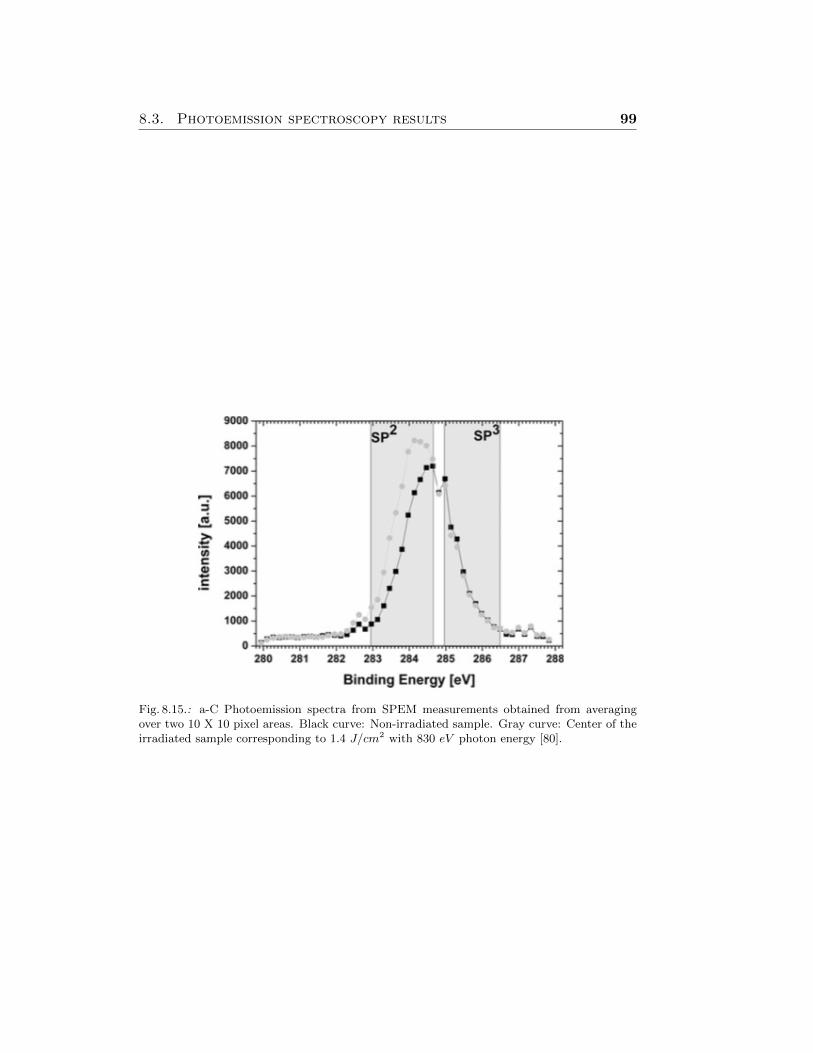
8.3. Photoemission spectroscopy results 99
Fig. 8.15.: a-C Photoemission spectra from SPEM measurements obtained from averagingover two 10 X 10 pixel areas. Black curve: Non-irradiated sample. Gray curve: Center of theirradiated sample corresponding to 1.4 J/cm2 with 830 eV photon energy [80].
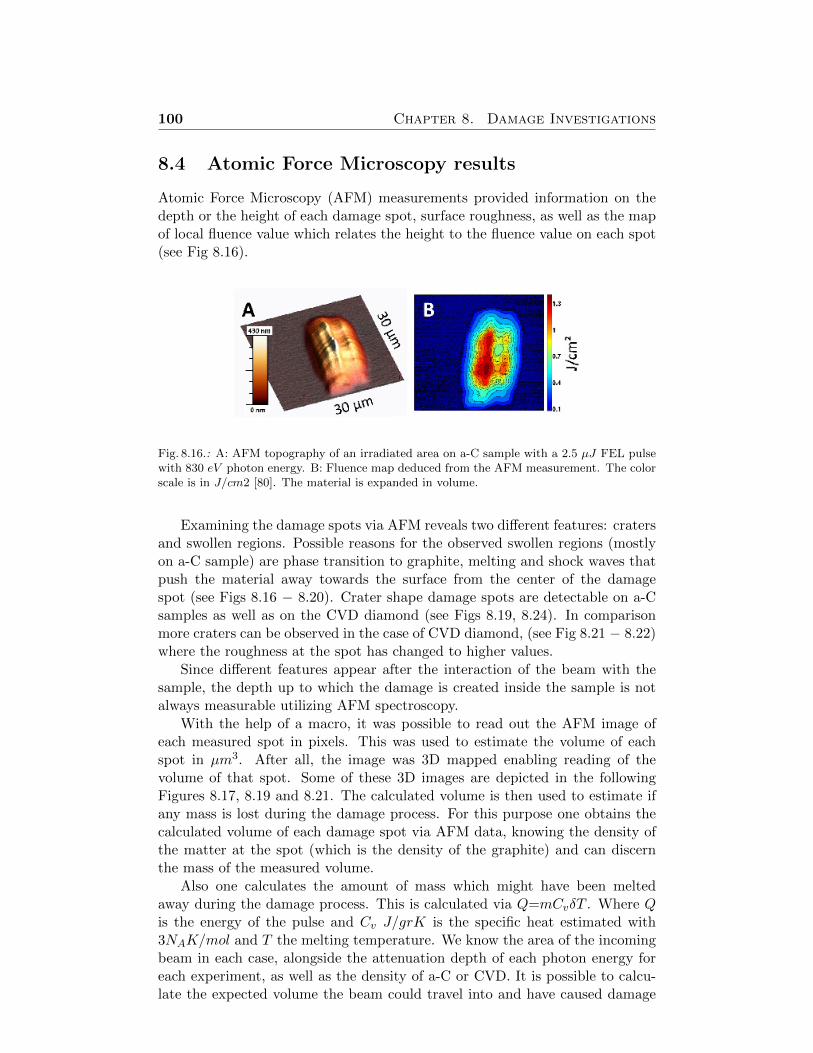
100 Chapter 8. Damage Investigations
8.4 Atomic Force Microscopy results
Atomic Force Microscopy (AFM) measurements provided information on thedepth or the height of each damage spot, surface roughness, as well as the mapof local fluence value which relates the height to the fluence value on each spot(see Fig 8.16).
Fig. 8.16.: A: AFM topography of an irradiated area on a-C sample with a 2.5 µJ FEL pulsewith 830 eV photon energy. B: Fluence map deduced from the AFM measurement. The colorscale is in J/cm2 [80]. The material is expanded in volume.
Examining the damage spots via AFM reveals two different features: cratersand swollen regions. Possible reasons for the observed swollen regions (mostlyon a-C sample) are phase transition to graphite, melting and shock waves thatpush the material away towards the surface from the center of the damagespot (see Figs 8.16 − 8.20). Crater shape damage spots are detectable on a-Csamples as well as on the CVD diamond (see Figs 8.19, 8.24). In comparisonmore craters can be observed in the case of CVD diamond, (see Fig 8.21 − 8.22)where the roughness at the spot has changed to higher values.
Since different features appear after the interaction of the beam with thesample, the depth up to which the damage is created inside the sample is notalways measurable utilizing AFM spectroscopy.
With the help of a macro, it was possible to read out the AFM image ofeach measured spot in pixels. This was used to estimate the volume of eachspot in µm3. After all, the image was 3D mapped enabling reading of thevolume of that spot. Some of these 3D images are depicted in the followingFigures 8.17, 8.19 and 8.21. The calculated volume is then used to estimate ifany mass is lost during the damage process. For this purpose one obtains thecalculated volume of each damage spot via AFM data, knowing the density ofthe matter at the spot (which is the density of the graphite) and can discernthe mass of the measured volume.
Also one calculates the amount of mass which might have been meltedaway during the damage process. This is calculated via Q=mCvδT . Where Qis the energy of the pulse and Cv J/grK is the specific heat estimated with3NAK/mol and T the melting temperature. We know the area of the incomingbeam in each case, alongside the attenuation depth of each photon energy foreach experiment, as well as the density of a-C or CVD. It is possible to calcu-late the expected volume the beam could travel into and have caused damage
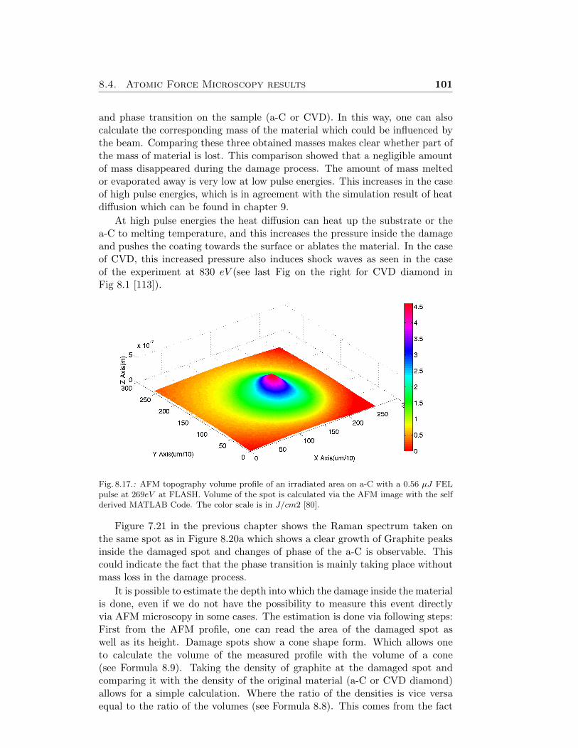
8.4. Atomic Force Microscopy results 101
and phase transition on the sample (a-C or CVD). In this way, one can alsocalculate the corresponding mass of the material which could be influenced bythe beam. Comparing these three obtained masses makes clear whether part ofthe mass of material is lost. This comparison showed that a negligible amountof mass disappeared during the damage process. The amount of mass meltedor evaporated away is very low at low pulse energies. This increases in the caseof high pulse energies, which is in agreement with the simulation result of heatdiffusion which can be found in chapter 9.
At high pulse energies the heat diffusion can heat up the substrate or thea-C to melting temperature, and this increases the pressure inside the damageand pushes the coating towards the surface or ablates the material. In the caseof CVD, this increased pressure also induces shock waves as seen in the caseof the experiment at 830 eV (see last Fig on the right for CVD diamond inFig 8.1 [113]).
Fig. 8.17.: AFM topography volume profile of an irradiated area on a-C with a 0.56 µJ FELpulse at 269eV at FLASH. Volume of the spot is calculated via the AFM image with the selfderived MATLAB Code. The color scale is in J/cm2 [80].
Figure 7.21 in the previous chapter shows the Raman spectrum taken onthe same spot as in Figure 8.20a which shows a clear growth of Graphite peaksinside the damaged spot and changes of phase of the a-C is observable. Thiscould indicate the fact that the phase transition is mainly taking place withoutmass loss in the damage process.
It is possible to estimate the depth into which the damage inside the materialis done, even if we do not have the possibility to measure this event directlyvia AFM microscopy in some cases. The estimation is done via following steps:First from the AFM profile, one can read the area of the damaged spot aswell as its height. Damage spots show a cone shape form. Which allows oneto calculate the volume of the measured profile with the volume of a cone(see Formula 8.9). Taking the density of graphite at the damaged spot andcomparing it with the density of the original material (a-C or CVD diamond)allows for a simple calculation. Where the ratio of the densities is vice versaequal to the ratio of the volumes (see Formula 8.8). This comes from the fact
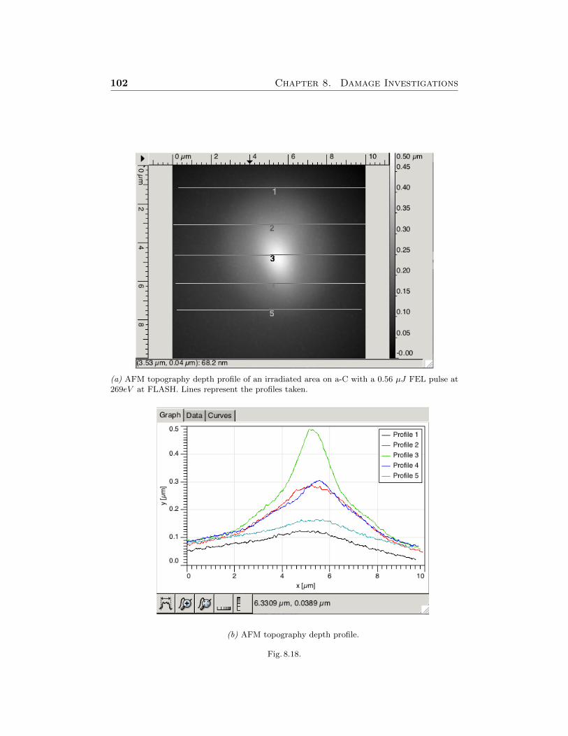
102 Chapter 8. Damage Investigations
(a) AFM topography depth profile of an irradiated area on a-C with a 0.56 µJ FEL pulse at269eV at FLASH. Lines represent the profiles taken.
(b) AFM topography depth profile.
Fig. 8.18.
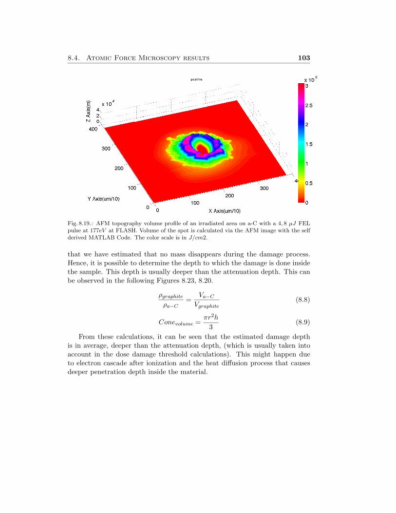
8.4. Atomic Force Microscopy results 103
Fig. 8.19.: AFM topography volume profile of an irradiated area on a-C with a 4, 8 µJ FELpulse at 177eV at FLASH. Volume of the spot is calculated via the AFM image with the selfderived MATLAB Code. The color scale is in J/cm2.
that we have estimated that no mass disappears during the damage process.Hence, it is possible to determine the depth to which the damage is done insidethe sample. This depth is usually deeper than the attenuation depth. This canbe observed in the following Figures 8.23, 8.20.
ρgraphiteρa−C
=Va−CVgraphite
(8.8)
Conevolume =πr2h
3(8.9)
From these calculations, it can be seen that the estimated damage depthis in average, deeper than the attenuation depth, (which is usually taken intoaccount in the dose damage threshold calculations). This might happen dueto electron cascade after ionization and the heat diffusion process that causesdeeper penetration depth inside the material.
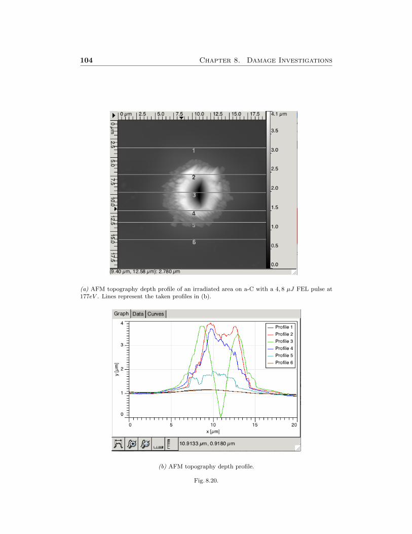
104 Chapter 8. Damage Investigations
(a) AFM topography depth profile of an irradiated area on a-C with a 4, 8 µJ FEL pulse at177eV . Lines represent the taken profiles in (b).
(b) AFM topography depth profile.
Fig. 8.20.
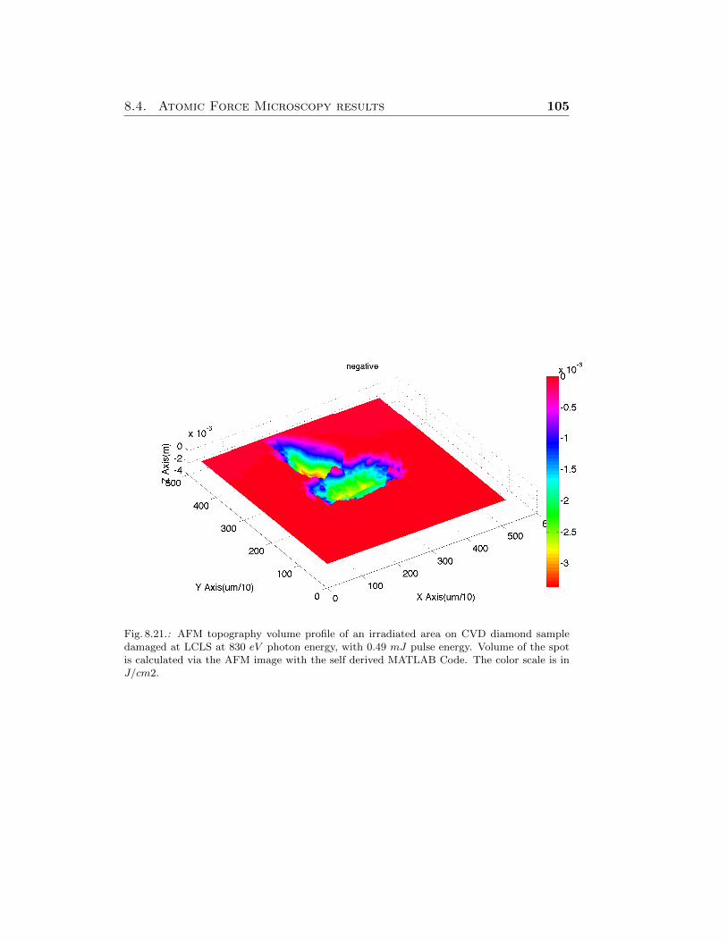
8.4. Atomic Force Microscopy results 105
Fig. 8.21.: AFM topography volume profile of an irradiated area on CVD diamond sampledamaged at LCLS at 830 eV photon energy, with 0.49 mJ pulse energy. Volume of the spotis calculated via the AFM image with the self derived MATLAB Code. The color scale is inJ/cm2.
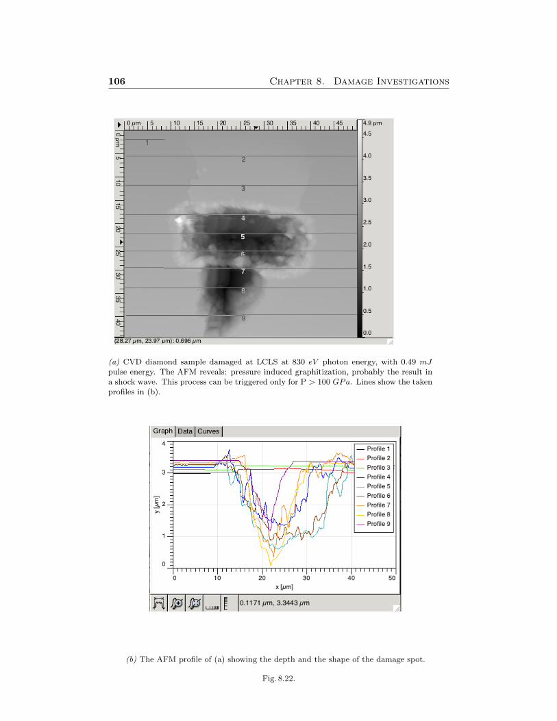
106 Chapter 8. Damage Investigations
(a) CVD diamond sample damaged at LCLS at 830 eV photon energy, with 0.49 mJpulse energy. The AFM reveals: pressure induced graphitization, probably the result ina shock wave. This process can be triggered only for P > 100 GPa. Lines show the takenprofiles in (b).
(b) The AFM profile of (a) showing the depth and the shape of the damage spot.
Fig. 8.22.
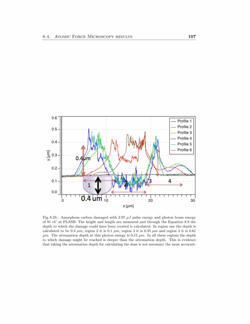
8.4. Atomic Force Microscopy results 107
Fig. 8.23.: Amorphous carbon damaged with 2.97 µJ pulse energy and photon beam energyof 91 eV at FLASH. The height and length are measured and through the Equation 8.8 thedepth to which the damage could have been created is calculated. In region one the depth iscalculated to be 0.4 µm, region 2 it is 0.1 µm, region 3 it is 0.35 µm and region 4 it is 0.61µm. The attenuation depth at this photon energy is 0.15 µm. In all these regions the depthto which damage might be reached is deeper than the attenuation depth. This is evidencethat taking the attenuation depth for calculating the dose is not necessary the most accurate.
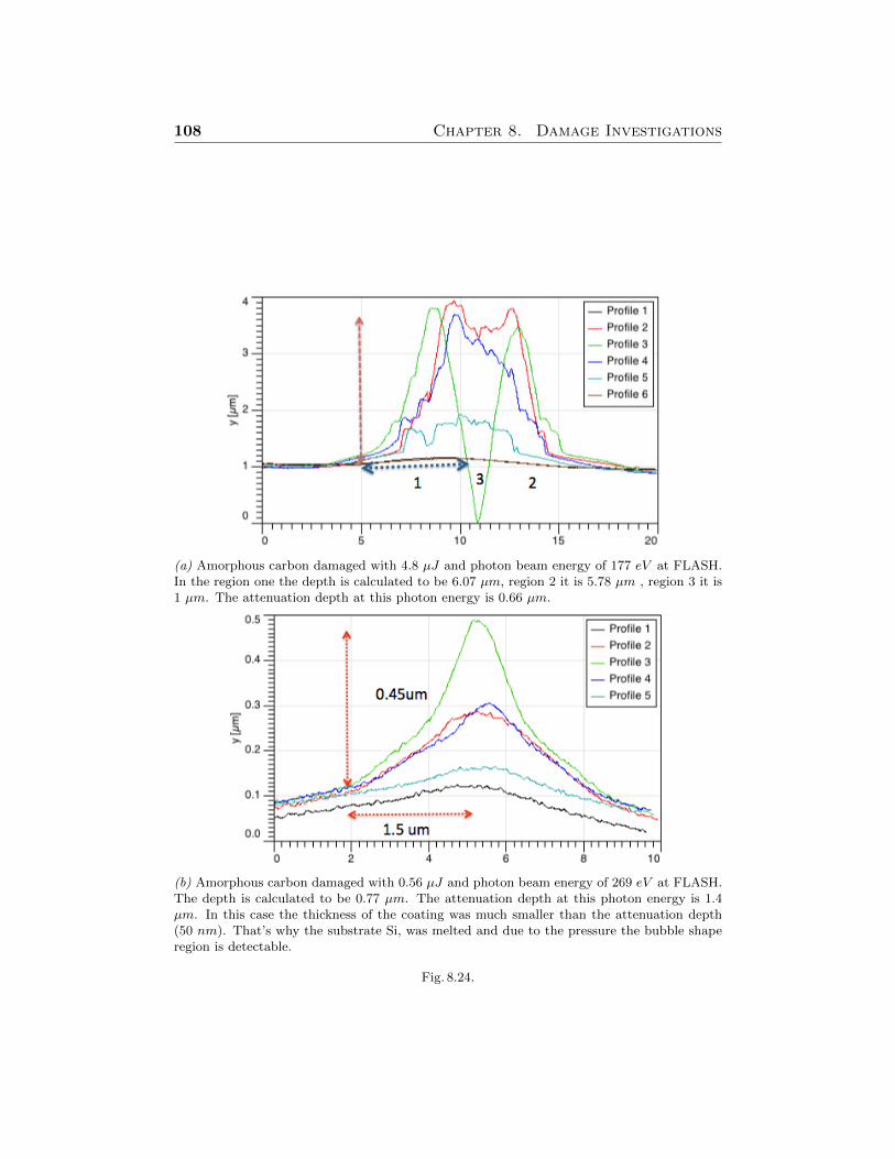
108 Chapter 8. Damage Investigations
(a) Amorphous carbon damaged with 4.8 µJ and photon beam energy of 177 eV at FLASH.In the region one the depth is calculated to be 6.07 µm, region 2 it is 5.78 µm , region 3 it is1 µm. The attenuation depth at this photon energy is 0.66 µm.
(b) Amorphous carbon damaged with 0.56 µJ and photon beam energy of 269 eV at FLASH.The depth is calculated to be 0.77 µm. The attenuation depth at this photon energy is 1.4µm. In this case the thickness of the coating was much smaller than the attenuation depth(50 nm). That’s why the substrate Si, was melted and due to the pressure the bubble shaperegion is detectable.
Fig. 8.24.
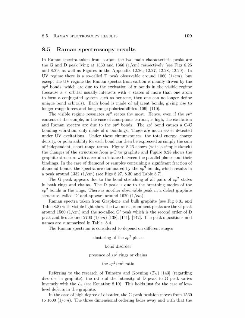
8.5. Raman spectroscopy results 109
8.5 Raman spectroscopy results
In Raman spectra taken from carbon the two main characteristic peaks arethe G and D peak lying at 1560 and 1360 (1/cm) respectively (see Figs 8.25and 8.29, as well as Figures in the Appendix 12.26, 12.27, 12.28, 12.29). InUV regime there is a so-called T peak observable around 1060 (1/cm), butexcept the UV regime the Raman spectra from carbon is mainly driven by thesp2 bonds, which are due to the excitation of π bonds in the visible regime(because a π orbital usually interacts with π states of more than one atomto form a conjugated system such as benzene, then one can no longer defineunique bond orbitals). Each bond is made of adjacent bonds, giving rise tolonger-range forces and long-range polarizabilities [109], [110].
The visible regime resonates sp2 states the most. Hence, even if the sp3
content of the sample, in the case of amorphous carbon, is high, the excitationand Raman spectra are due to the sp2 bonds. The sp3 bond causes a C-Cbonding vibration, only made of σ bondings. These are much easier detectedunder UV excitations. Under these circumstances, the total energy, chargedensity, or polarizability for each bond can then be expressed as simply the sumof independent, short-range terms. Figure 8.26 shows (with a simple sketch)the changes of the structures from a-C to graphite and Figure 8.28 shows thegraphite structure with a certain distance between the parallel planes and theirbindings. In the case of diamond or samples containing a significant fraction ofdiamond bonds, the spectra are dominated by the sp3 bonds, which results ina peak around 1332 (1/cm) (see Figs 8.27, 8.30 and Table 8.7).
The G peak appears due to the bond stretching of all pairs of sp2 statesin both rings and chains. The D peak is due to the breathing modes of thesp2 bonds in the rings. There is another observable peak in a defect graphitestructure, called D’ and appears around 1620 (1/cm).
Raman spectra taken from Graphene and bulk graphite (see Fig 8.31 andTable 8.8) with visible light show the two most prominent peaks are the G peakaround 1560 (1/cm) and the so-called G’ peak which is the second order of Dpeak and lies around 2700 (1/cm) [138], [141], [142]. The peak’s positions andnames are summarized in Table 8.4.
The Raman spectrum is considered to depend on different stages
clustering of the sp2 phase
bond disorder
presence of sp2 rings or chains
the sp2/sp3 ratio
Referring to the research of Tuinstra and Koening (TK) [143] (regardingdisorder in graphite), the ratio of the intensity of D peak to G peak variesinversely with the La (see Equation 8.10). This holds just for the case of low-level defects in the graphite.
In the case of high degree of disorder, the G peak position moves from 1560to 1600 (1/cm). The three dimensional ordering fades away and with that the
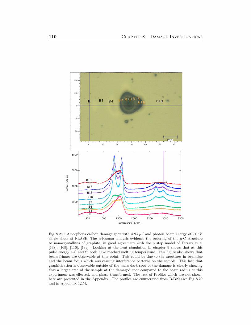
110 Chapter 8. Damage Investigations
Fig. 8.25.: Amorphous carbon damage spot with 4.83 µJ and photon beam energy of 91 eVsingle shots at FLASH. The µ-Raman analysis evidence the ordering of the a-C structureto nanocrystallites of graphite, in good agreement with the 3 step model of Ferrari et al[138], [109], [110], [139]. Looking at the heat simulation in chapter 9 shows that at thispulse energy a-C and Si both have reached melting temperature. This figure also shows thatbeam fringes are observable at this point. This could be due to the apertures in beamlineand the beam focus which was causing interference patterns on the sample. This fact thatgraphitization is observable outside of the main dark spot of the damage is clearly showingthat a larger area of the sample at the damaged spot compared to the beam radius at thisexperiment was effected, and phase transformed. The rest of Profiles which are not shownhere are presented in the Appendix. The profiles are enumerated from B-B20 (see Fig 8.29and in Appendix 12.5).
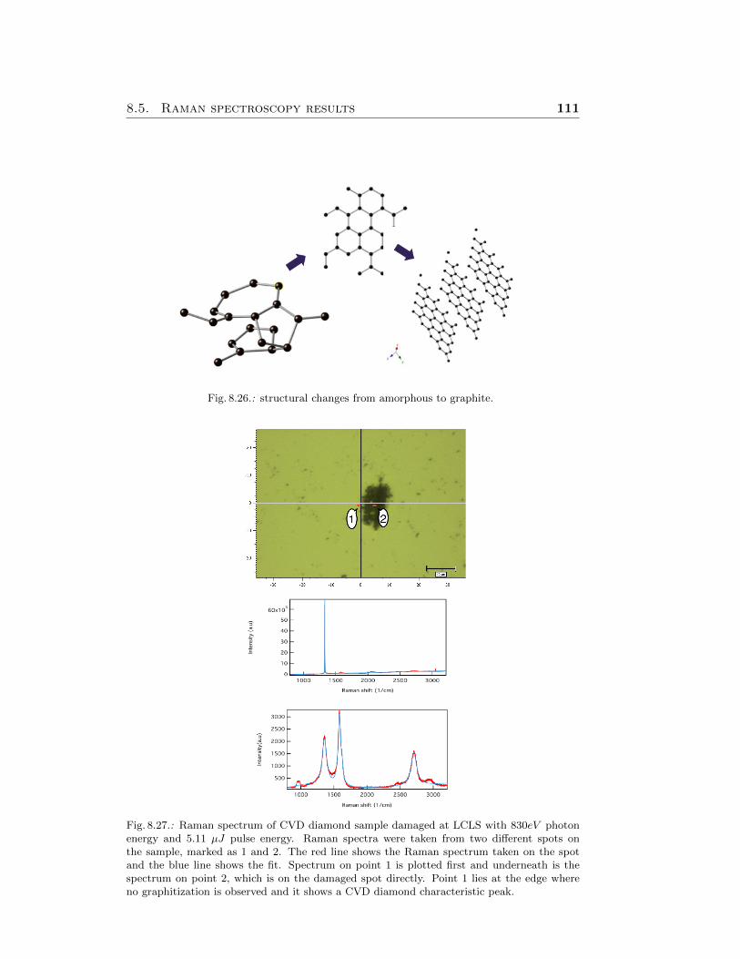
8.5. Raman spectroscopy results 111
Fig. 8.26.: structural changes from amorphous to graphite.
Fig. 8.27.: Raman spectrum of CVD diamond sample damaged at LCLS with 830eV photonenergy and 5.11 µJ pulse energy. Raman spectra were taken from two different spots onthe sample, marked as 1 and 2. The red line shows the Raman spectrum taken on the spotand the blue line shows the fit. Spectrum on point 1 is plotted first and underneath is thespectrum on point 2, which is on the damaged spot directly. Point 1 lies at the edge whereno graphitization is observed and it shows a CVD diamond characteristic peak.
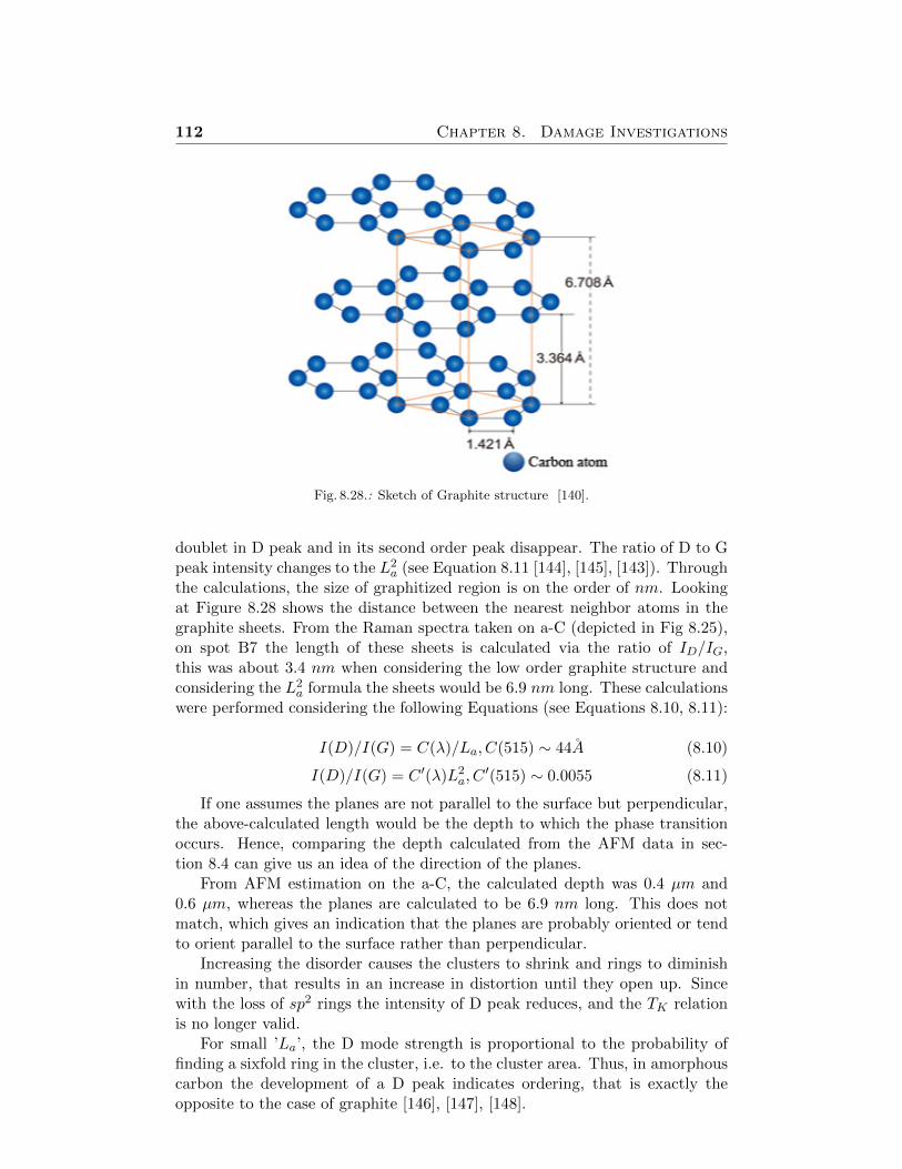
112 Chapter 8. Damage Investigations
Fig. 8.28.: Sketch of Graphite structure [140].
doublet in D peak and in its second order peak disappear. The ratio of D to Gpeak intensity changes to the L2
a (see Equation 8.11 [144], [145], [143]). Throughthe calculations, the size of graphitized region is on the order of nm. Lookingat Figure 8.28 shows the distance between the nearest neighbor atoms in thegraphite sheets. From the Raman spectra taken on a-C (depicted in Fig 8.25),on spot B7 the length of these sheets is calculated via the ratio of ID/IG,this was about 3.4 nm when considering the low order graphite structure andconsidering the L2
a formula the sheets would be 6.9 nm long. These calculationswere performed considering the following Equations (see Equations 8.10, 8.11):
I(D)/I(G) = C(λ)/La, C(515) ∼ 44A (8.10)
I(D)/I(G) = C ′(λ)L2a, C
′(515) ∼ 0.0055 (8.11)
If one assumes the planes are not parallel to the surface but perpendicular,the above-calculated length would be the depth to which the phase transitionoccurs. Hence, comparing the depth calculated from the AFM data in sec-tion 8.4 can give us an idea of the direction of the planes.
From AFM estimation on the a-C, the calculated depth was 0.4 µm and0.6 µm, whereas the planes are calculated to be 6.9 nm long. This does notmatch, which gives an indication that the planes are probably oriented or tendto orient parallel to the surface rather than perpendicular.
Increasing the disorder causes the clusters to shrink and rings to diminishin number, that results in an increase in distortion until they open up. Sincewith the loss of sp2 rings the intensity of D peak reduces, and the TK relationis no longer valid.
For small ’La’, the D mode strength is proportional to the probability offinding a sixfold ring in the cluster, i.e. to the cluster area. Thus, in amorphouscarbon the development of a D peak indicates ordering, that is exactly theopposite to the case of graphite [146], [147], [148].
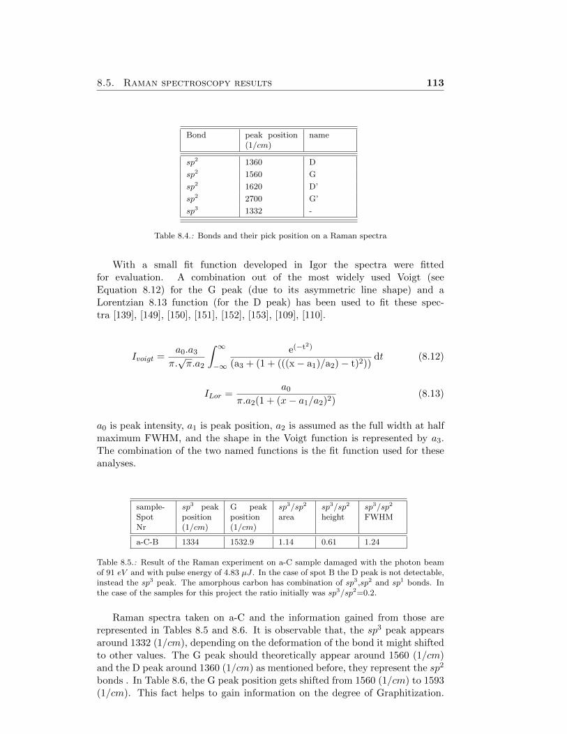
8.5. Raman spectroscopy results 113
Bond peak position(1/cm)
name
sp2 1360 D
sp2 1560 G
sp2 1620 D’
sp2 2700 G’
sp3 1332 -
Table 8.4.: Bonds and their pick position on a Raman spectra
With a small fit function developed in Igor the spectra were fittedfor evaluation. A combination out of the most widely used Voigt (seeEquation 8.12) for the G peak (due to its asymmetric line shape) and aLorentzian 8.13 function (for the D peak) has been used to fit these spec-tra [139], [149], [150], [151], [152], [153], [109], [110].
Ivoigt =a0.a3
π.√π.a2
∫ ∞−∞
e(−t2)
(a3 + (1 + (((x− a1)/a2)− t)2))dt (8.12)
ILor =a0
π.a2(1 + (x− a1/a2)2)(8.13)
a0 is peak intensity, a1 is peak position, a2 is assumed as the full width at halfmaximum FWHM, and the shape in the Voigt function is represented by a3.The combination of the two named functions is the fit function used for theseanalyses.
sample-SpotNr
sp3 peakposition(1/cm)
G peakposition(1/cm)
sp3/sp2
areasp3/sp2
heightsp3/sp2
FWHM
a-C-B 1334 1532.9 1.14 0.61 1.24
Table 8.5.: Result of the Raman experiment on a-C sample damaged with the photon beamof 91 eV and with pulse energy of 4.83 µJ . In the case of spot B the D peak is not detectable,instead the sp3 peak. The amorphous carbon has combination of sp3,sp2 and sp1 bonds. Inthe case of the samples for this project the ratio initially was sp3/sp2=0.2.
Raman spectra taken on a-C and the information gained from those arerepresented in Tables 8.5 and 8.6. It is observable that, the sp3 peak appearsaround 1332 (1/cm), depending on the deformation of the bond it might shiftedto other values. The G peak should theoretically appear around 1560 (1/cm)and the D peak around 1360 (1/cm) as mentioned before, they represent the sp2
bonds . In Table 8.6, the G peak position gets shifted from 1560 (1/cm) to 1593(1/cm). This fact helps to gain information on the degree of Graphitization.
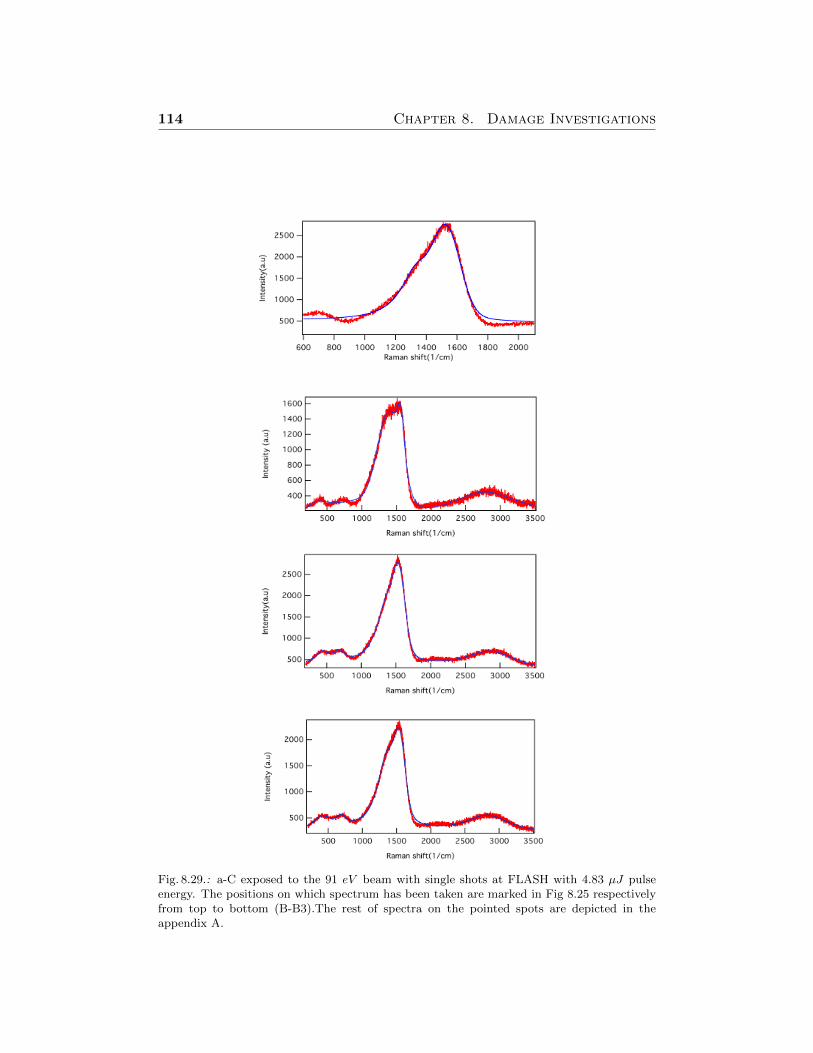
114 Chapter 8. Damage Investigations
Fig. 8.29.: a-C exposed to the 91 eV beam with single shots at FLASH with 4.83 µJ pulseenergy. The positions on which spectrum has been taken are marked in Fig 8.25 respectivelyfrom top to bottom (B-B3).The rest of spectra on the pointed spots are depicted in theappendix A.
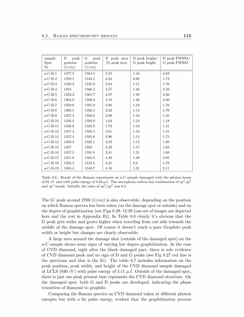
8.5. Raman spectroscopy results 115
sample-SpotNr
D peakposition(1/cm)
G peakposition(1/cm)
D peak area/G peak area
D peak height/G peak height
D peak FWHM/G peak FWHM
a-C-B-1 1377.5 1564.5 2.55 1.43 2.62
a-C-B-2 1359.1 1543.5 2.24 0.88 1.73
a-C-B-3 1356.2 1545.9 2.84 1.11 1.76
a-C-B-4 1354 1566.3 4.57 1.46 2.10
a-C-B-5 1352.3 1561.7 4.87 1.49 2.20
a-C-B-6 1364.9 1589.2 4.10 1.26 2.20
a-C-B-7 1359.6 1591.9 2.86 1.16 1.76
a-C-B-8 1360.5 1592.4 2.82 1.14 1.79
a-C-B-9 1357.4 1592.6 2.08 1.16 1.45
a-C-B-10 1356.2 1592.9 1.64 1.23 1.18
a-C-B-11 1356.6 1592.9 1.79 1.18 1.31
a-C-B-12 1357.4 1592.4 2.01 1.16 1.41
a-C-B-13 1357.4 1591.6 2.96 1.13 1.75
a-C-B-14 1359.3 1592.1 2.83 1.15 1.80
a-C-B-15 1357 1593 2.49 1.17 1.65
a-C-B-16 1357.5 1591.8 2.81 1.21 1.68
a-C-B-17 1351.6 1562.3 4.49 1.48 2.05
a-C-B-18 1356.5 1543.5 2.21 0.8 1.78
a-C-B-19 1364.4 1548.7 4.10 1.31 2.11
Table 8.6.: Result of the Raman experiment on a-C sample damaged with the photon beamof 91 eV and with pulse energy of 4.83 µJ . The amorphous carbon has combination of sp3,sp2
and sp1 bonds. Initially the ratio of sp3/sp2 was 0.2.
The G’ peak around 2700 (1/cm) is also observable, depending on the positionon which Raman spectra has been taken (on the damage spot or outside) and onthe degree of graphitization (see Figs 8.29- 12.29 (one set of images are depictedhere and the rest in Appendix B)). In Table 8.6 clearly it’s obvious that theG peak gets wider and grows higher when traveling from out side towards themiddle of the damage spot. Of course it doesn’t reach a pure Graphite peakwidth or height but changes are clearly observable.
A large area around the damage shot (outside of the damaged spot) on thea-C sample shows some signs of varying low degree graphitization. In the caseof CVD diamond, right after the black damaged part, there is sole evidenceof CVD diamond peak and no sign of D and G peaks (see Fig 8.27 red line isthe spectrum and blue is the fit). The table 8.7 includes information on thepeak position, peak width, and height of the CVD diamond sample damagedat LCLS (830 eV ) with pulse energy of 5.11 µJ . Outside of the damaged spot,there is just one peak present that represents the CVD diamond structure. Onthe damaged spot, both G and D peaks are developed, indicating the phasetransition of diamond to graphite.
Comparing the Raman spectra on CVD diamond taken at different photonenergies but with a fix pulse energy, evident that the graphitization process
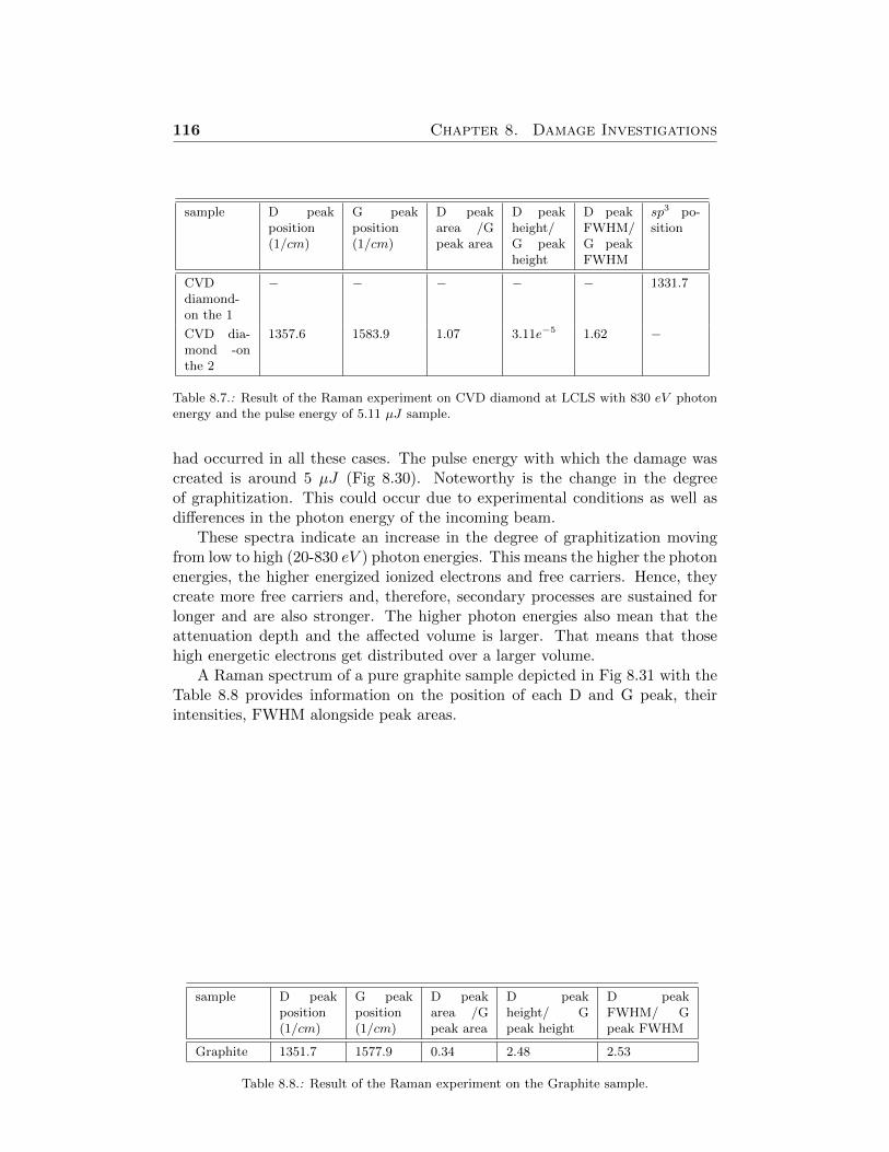
116 Chapter 8. Damage Investigations
sample D peakposition(1/cm)
G peakposition(1/cm)
D peakarea /Gpeak area
D peakheight/G peakheight
D peakFWHM/G peakFWHM
sp3 po-sition
CVDdiamond-on the 1
− − − − − 1331.7
CVD dia-mond -onthe 2
1357.6 1583.9 1.07 3.11e−5 1.62 −
Table 8.7.: Result of the Raman experiment on CVD diamond at LCLS with 830 eV photonenergy and the pulse energy of 5.11 µJ sample.
had occurred in all these cases. The pulse energy with which the damage wascreated is around 5 µJ (Fig 8.30). Noteworthy is the change in the degreeof graphitization. This could occur due to experimental conditions as well asdifferences in the photon energy of the incoming beam.
These spectra indicate an increase in the degree of graphitization movingfrom low to high (20-830 eV ) photon energies. This means the higher the photonenergies, the higher energized ionized electrons and free carriers. Hence, theycreate more free carriers and, therefore, secondary processes are sustained forlonger and are also stronger. The higher photon energies also mean that theattenuation depth and the affected volume is larger. That means that thosehigh energetic electrons get distributed over a larger volume.
A Raman spectrum of a pure graphite sample depicted in Fig 8.31 with theTable 8.8 provides information on the position of each D and G peak, theirintensities, FWHM alongside peak areas.
sample D peakposition(1/cm)
G peakposition(1/cm)
D peakarea /Gpeak area
D peakheight/ Gpeak height
D peakFWHM/ Gpeak FWHM
Graphite 1351.7 1577.9 0.34 2.48 2.53
Table 8.8.: Result of the Raman experiment on the Graphite sample.
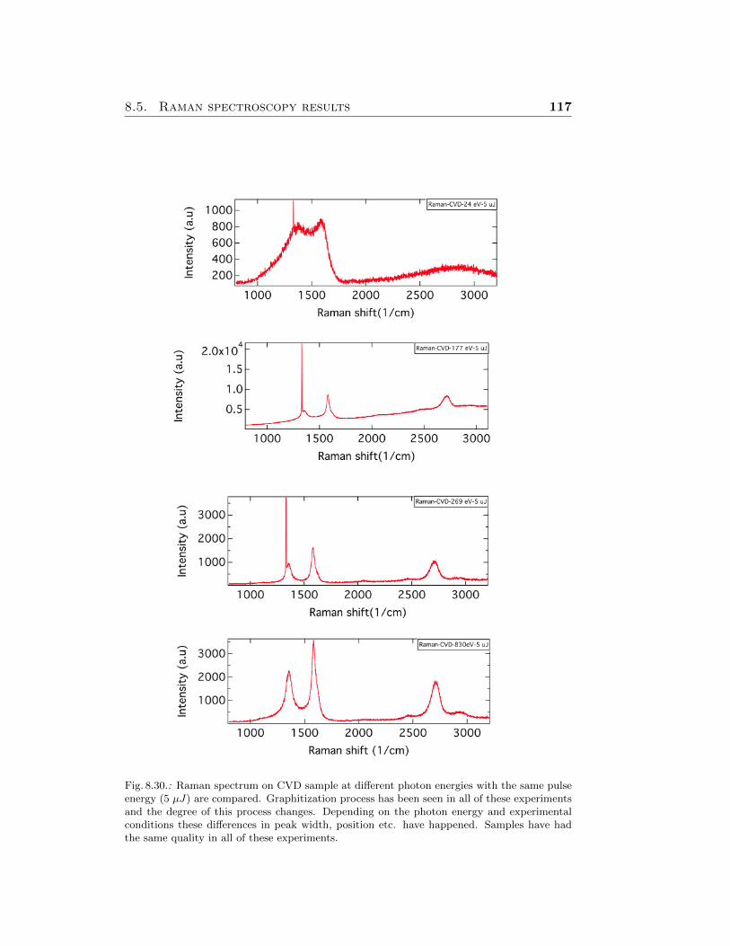
8.5. Raman spectroscopy results 117
Fig. 8.30.: Raman spectrum on CVD sample at different photon energies with the same pulseenergy (5 µJ) are compared. Graphitization process has been seen in all of these experimentsand the degree of this process changes. Depending on the photon energy and experimentalconditions these differences in peak width, position etc. have happened. Samples have hadthe same quality in all of these experiments.
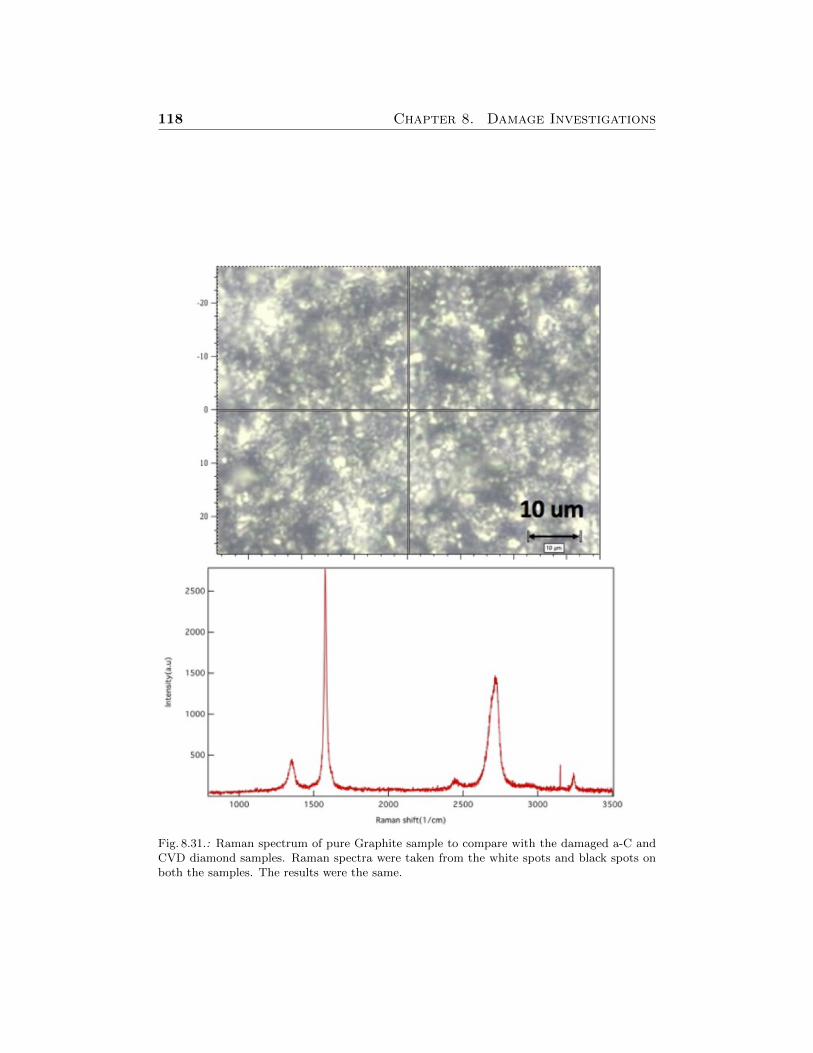
118 Chapter 8. Damage Investigations
Fig. 8.31.: Raman spectrum of pure Graphite sample to compare with the damaged a-C andCVD diamond samples. Raman spectra were taken from the white spots and black spots onboth the samples. The results were the same.
Chapter 9
Simulations
In the following two sections, the results of theoretical simulation via HybridXTANT model and the heat diffusion process (simulated via COMSOL) arepresented. With the help of Hybrid model, it is possible to follow the changesof the electronic states and its potential energy states, from the time that theFEL pulse irradiates the sample until some 100’s of fs after the irradiation. Thissection focuses on the ionization processes and consequences as bond breaking,secondary processes, etc. Heat diffusion, on the other hand, starts to take partin the damage process after some 100’s of ps after the irradiation and last upto some µs until sample gets back to the room temperature. Heat diffusionhelps to estimate if the sample could reach melting temperature during thedamage process and how far it could affect the size of imprints. After some100’s of ps one can not separate these processes from each other. There is anoverlap between them, where each process is active but with different intensitycompared to the other.
9.1 Hybrid code XTANT (Theoretical simulation)
Under femtosecond irradiation as mentioned in chapter 5, semiconductors un-dergo several sequences of processes. The photo-ionization process, which hap-pens within fs is followed by secondary processes like decay of Auger electrons orfluorescence photons. These decays lead to the production of further atomic ex-citation, bond breaking, and free carriers production e.g. via exciting electronsfrom the valence band into the conduction band. Elastic or inelastic scatter-ing of electrons or photons (for example through impact ionization) takes placewithin fs, while the scattering of electrons on atoms or phonons leads to signif-icant energy losses and occurs over significant longer time periods, typically inthe order of ps [154], [155].
This inter-particle interaction leads to changes of the inter-particle poten-tial energy. The electronic state of the system in covalently bonded materialinfluences the (inter) atomic bindings. Hence, any changes e.g. the number ofanti-bonding states will result in an ultra-fast rearrangement of atoms. This isbecause the system tries to balance and minimize the potential energy of theelectronic system. This happens in the form of phase transition, where in the
119
120 Chapter 9. Simulations
case of diamond, sp3 bonds change into sp2 bonds and the material turns intographite. A phase transition process can take place in a few hundred fs. Thephoto-ionization process is the leading process here. Besides, there is a greatpossibility that graphitization occurs due to the heat generated through freecarriers. Calculations show that around Tm= 1360 K diamond can undergographitization. This temperature is calculated with Lindemann’s formula (seeequation 9.1) and so-called intra-cell graphitization [156].
Tm =x2m9~2
MKθ2r2s (9.1)
The theoretical simulation attempts modeling the phase transition throughfs FEL pulses and is undertaken by a group of theoretical physicists. The groupcomprising Dr. H. Jeschke, Dr. N. Medvedev and Dr. B. Ziaja at FrankfurtUniversity and CFEL in DESY in Hamburg developed a Hybrid model, whichtraces non-equilibrium kinetics of electrons under ultrashort laser irradiationand follows the rearrangement of atoms.
The model is based on the following combined codes (Monte Carlo, Tracingthe temperature of valence and low energy conduction band electrons, Molecu-lar Dynamics, Tight Binding model) described in great detail in the followingreferences [17], [157], [158], [135], [30], [159], [36], [160], [161]. These modelsare briefly explained here:
• Monte Carlo (MC): treating the non-equilibrium kinetics of high energyelectrons after photo-absorption. Here, the photo-absorption and sec-ondary electron cascading have been modeled in a simulation box. Thephoton pulse temporal profile is taken to have a Gaussian shape with e.g.10fs FWHM. The penetration details are taken from photo-absorptionlength corresponding to the specific photon energy. Photo-absorption canoccur in valence band or K-shell depending on the energy of the photon.In the case of valence band photo-absorption in this model, an energylevel among all the valence band levels has been chosen randomly (ob-tained from tight-binding formalism). In this model, it is assumed thateach photon excites just one electron. The excited electron undergoesseveral secondary scattering processes. The inelastic mean free path ofthese electrons, which depends on their energy, has been calculated us-ing the complex dielectric function. The inelastic electron scattering crosssection is therefore calculated with the help of the complex dielectric func-tion within the first Born approximation. The mean free path of electronsfor diamond and graphite is then calculated and compared in this model.This shows that mean free paths are similar to each other for both graphiteand diamond. Due to the difference in the band gap of graphite and di-amond, a shift to a lower energy is present in the case of graphite. Theband gap of diamond is around 5.5 eV whereas this vanishes for graphitebecause it is a semimetal.
• Tracing the temperature of valence and low energy conduction band elec-trons, which are in thermal equilibrium:The low energy electrons are assumed to be in partial equilibrium. The
9.1. Hybrid code XTANT (Theoretical simulation) 121
number of electrons which get excited to high energy states or fall backinto low energy states is followed here. This distribution function for va-lence band and the low energy conduction band is calculated via Fermifunction. This is carried out because the electron distribution functionchanges due to the changes in the electronic states. This is defined in theMC step algorithm.
• Molecular Dynamics (MD), focuses on picturing the atomic motion of allatoms individually in the simulation box:The classical motion of all atoms are described by spatial coordinatesand velocities, and the collective potential energy surface is describedquantum mechanically. Two cases analyzed here are under two differentconditions, one with a constant volume of the simulation box and theother with constant pressure (see Fig 9.2). The potential energy surfaceis defined by the transient electron distribution function, the position ofall atoms in the supercell and by the transient band structure updatedwith the tight binding method at each time step. For constant volumesimulation, the MD model employs Parrinello-Rahman method [162].
• Tight Binding model for tracing the transient electron band structure andcollective interatomic forces:In this part of the model, the electronic energy levels are calculated ateach time step. This is used to determine the potential energy surface.The interatomic forces are being calculated here. The atomic Hamilto-nian considered here is two-fold: The attractive part depending on theelectron configuration and the repulsive part which illustrate the repulsionof atomic cores.
A simple schematic is depicted in Fig 9.1 which shows how these models arecombined and the structure of the simulation is built.
With this model, they have tried to reproduce the experimental parametersat different photon energies and for different fluences. Some of simulated resultsin the case of 830 eV are depicted below (these data sets are not published yet)in Figs 9.4a, 9.4b, 9.4c, 9.4d. From the previous calculations it was expectedthat at constant pressure the value of 1 eV/atom absorbed dose is above thedamage threshold. The damage threshold in the case of diamond in previousworks was reported to be 0.69 eV/atom for constant pressure. With the helpof this Hybrid model, the damage threshold for constant volume was calculatedas well and found to be 0.74 eV/atom (see ref [158], [159], [36]). A simple signfor recognizing the phase transition is the sudden strong drop in the atomicpotential energy. This can be seen in Figs 9.4a for fluence energy of 1.87J/cm2
at 830 eV photon energy. These graphs show that the total energy is constantexcept for the deposition time. In this period the energy is transferred from thepulse to the high energy electrons. Hence, the total energy of atoms is lowerthan the total energy of electrons and atoms. After some time this changes andsome part of the energy gets transferred to the potential energy, in other wordsto the low energy domain. Hence, both the total energy of atoms and electrons(blue) and total energy of atoms (green) curves meet (see Fig 9.4c). Around 90
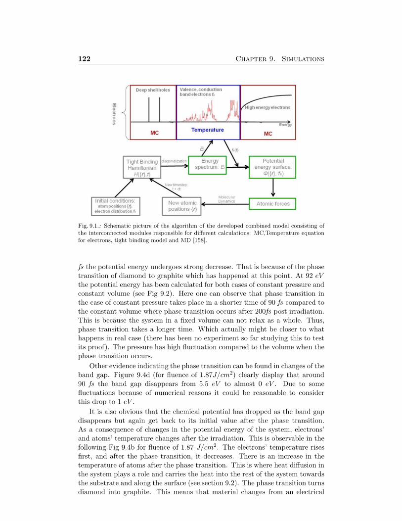
122 Chapter 9. Simulations
Fig. 9.1.: Schematic picture of the algorithm of the developed combined model consisting ofthe interconnected modules responsible for different calculations: MC,Temperature equationfor electrons, tight binding model and MD [158].
fs the potential energy undergoes strong decrease. That is because of the phasetransition of diamond to graphite which has happened at this point. At 92 eVthe potential energy has been calculated for both cases of constant pressure andconstant volume (see Fig 9.2). Here one can observe that phase transition inthe case of constant pressure takes place in a shorter time of 90 fs compared tothe constant volume where phase transition occurs after 200fs post irradiation.This is because the system in a fixed volume can not relax as a whole. Thus,phase transition takes a longer time. Which actually might be closer to whathappens in real case (there has been no experiment so far studying this to testits proof). The pressure has high fluctuation compared to the volume when thephase transition occurs.
Other evidence indicating the phase transition can be found in changes of theband gap. Figure 9.4d (for fluence of 1.87J/cm2) clearly display that around90 fs the band gap disappears from 5.5 eV to almost 0 eV . Due to somefluctuations because of numerical reasons it could be reasonable to considerthis drop to 1 eV .
It is also obvious that the chemical potential has dropped as the band gapdisappears but again get back to its initial value after the phase transition.As a consequence of changes in the potential energy of the system, electrons’and atoms’ temperature changes after the irradiation. This is observable in thefollowing Fig 9.4b for fluence of 1.87 J/cm2. The electrons’ temperature risesfirst, and after the phase transition, it decreases. There is an increase in thetemperature of atoms after the phase transition. This is where heat diffusion inthe system plays a role and carries the heat into the rest of the system towardsthe substrate and along the surface (see section 9.2). The phase transition turnsdiamond into graphite. This means that material changes from an electrical
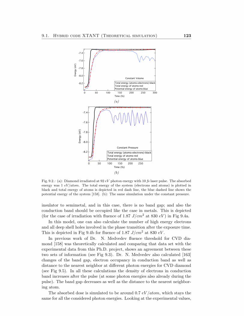
9.1. Hybrid code XTANT (Theoretical simulation) 123
-8.2
-8.0
-7.8
-7.6
-7.4
Energ
y (
eV
)
300250200150100500
Time (fs)
Constant Volume
Total energy (atoms+electrons)-black
Total energy of atoms-red
Potential energy of atoms-blue
(a)
-8.2
-8.0
-7.8
-7.6
-7.4
Energ
y (
eV
)
250200150100500
Time (fs)
Constant Pressure
Total energy (atoms+electrons)-black
Total energy of atoms-red
Potential energy of atoms-blue
(b)
Fig. 9.2.: (a): Diamond irradiated at 92 eV photon energy with 10 fs laser pulse. The absorbedenergy was 1 eV/atom. The total energy of the system (electrons and atoms) is plotted inblack and total energy of atoms is depicted in red dash line, the blue dashed line shows thepotential energy of the system [158]. (b): The same simulation under the constant pressure.
insulator to semimetal, and in this case, there is no band gap; and also theconduction band should be occupied like the case in metals. This is depicted(for the case of irradiation with fluence of 1.87 J/cm2 at 830 eV ) in Fig 9.4a.
In this model, one can also calculate the number of high energy electronsand all deep shell holes involved in the phase transition after the exposure time.This is depicted in Fig 9.4b for fluence of 1.87 J/cm2 at 830 eV .
In previous work of Dr. N. Medvedev fluence threshold for CVD dia-mond [158] was theoretically calculated and comparing that data set with theexperimental data from this Ph.D. project, shows an agreement between thesetwo sets of information (see Fig 9.3). Dr. N. Medvedev also calculated [163]changes of the band gap, electron occupancy in conduction band as well asdistance to the nearest neighbor at different photon energies for CVD diamond(see Fig 9.5). In all these calculations the density of electrons in conductionband increases after the pulse (at some photon energies also already during thepulse). The band gap decreases as well as the distance to the nearest neighbor-ing atom.
The absorbed dose is simulated to be around 0.7 eV /atom, which stays thesame for all the considered photon energies. Looking at the experimental values,
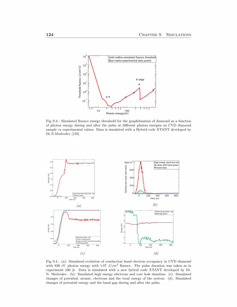
124 Chapter 9. Simulations
10-1
100
101
102
103
104
Thre
shold
flu
ence (
J/cm
^2)
5 6
102 3 4 5 6
1002 3 4 5 6
Photon energy(eV)
K-edge
Solid redline-simulated fluence threshold
Blue marks-experimental data points
Fig. 9.3.: Simulated fluence energy threshold for the graphitization of diamond as a functionof photon energy during and after the pulse at different photon energies on CVD diamondsample vs experimental values. Data is simulated with a Hybrid code XTANT developed byDr.N.Medvedev [158].
3.0
2.5
2.0
1.5
1.0
0.5
0.0
Ele
ctr
ons
(%)
8006004002000Time (fs)
Conduction band electrons -red
Photons-green
(a)
800x10-6
600
400
200
0
Part
ilces
per
ato
m (
arb
unit
s)
8006004002000
Time (fs)
High energy electrons-red
All deep shell holes-green
Photons-blue
(b)
-8.2
-8.0
-7.8
-7.6
Energ
y (
eV
)
8006004002000
Time (fs)
Potential energy -red
Atomic energy-green
Energy of atoms and electrons-blue
Total energy-pink
(c)
5
4
3
2
1
0
Energ
y (
eV
)
8006004002000
Time (fs)
Chemical potential -red
Band gap-green
(d)
Fig. 9.4.: (a): Simulated evolution of conduction band electron occupancy in CVD diamondwith 830 eV photon energy with 1.87 J/cm2 fluence. The pulse duration was taken as inexperiment 100 fs. Data is simulated with a new hybrid code XTANT developed by Dr.N. Medvedev. (b): Simulated high energy electrons and core hole densities. (c): Simulatedchanges of potential, atomic, electrons and the total energy of the system. (d): Simulatedchanges of potential energy and the band gap during and after the pulse.
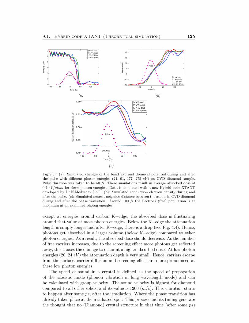
9.1. Hybrid code XTANT (Theoretical simulation) 125
6
5
4
3
2
1
0
Band g
ap (
eV
)
100500-50-100
Time (fs)
Pulse
24 eV -red
91 eV-violet
177 eV-blue
275 eV-green
(a)
3.0
2.5
2.0
1.5
1.0
0.5
0.0
Ele
ctr
ons
(%)
100500-50
time (fs)
Pulse
24 eV -red
91 eV-violet
177 eV-blue
275 eV-green
(b)
1.60
1.55
1.50
1.45
1.40
Neare
st n
eig
hbor
dis
tance (
A¡)
100500-50-100
Time (fs)
Pulse
Graphite
24 eV -red
91 eV-violet
177 eV-blue
275 eV-green
(c)
Fig. 9.5.: (a): Simulated changes of the band gap and chemical potential during and afterthe pulse with different photon energies (24, 91, 177, 275 eV ) on CVD diamond sample.Pulse duration was taken to be 50 fs. These simulations result in average absorbed dose of0.7 eV/atom for these photon energies. Data is simulated with a new Hybrid code XTANTdeveloped by Dr.N.Medvedev [163]. (b): Simulated conduction electron density during andafter the pulse. (c): Simulated nearest neighbor distance between the atoms in CVD diamondduring and after the phase transition. Around 100 fs the electrons (free) population is atmaximum at all examined photon energies.
except at energies around carbon K−edge, the absorbed dose is fluctuatingaround that value at most photon energies. Below the K−edge the attenuationlength is simply longer and after K−edge, there is a drop (see Fig: 4.4). Hence,photons get absorbed in a larger volume (below K−edge) compared to otherphoton energies. As a result, the absorbed dose should decrease. As the numberof free carriers increases, due to the screening effect more photons get reflectedaway, this causes the damage to occur at a higher absorbed dose. At low photonenergies (20, 24 eV ) the attenuation depth is very small. Hence, carriers escapefrom the surface, carrier diffusion and screening effect are more pronounced atthese low photon energies.
The speed of sound in a crystal is defined as the speed of propagationof the acoustic mode (phonon vibration in long wavelength mode) and canbe calculated with group velocity. The sound velocity is highest for diamondcompared to all other solids, and its value is 1200 (m/s). This vibration startsto happen after some ps, after the irradiation. Where the phase transition hasalready taken place at the irradiated spot. This process and its timing generatethe thought that no (Diamond) crystal structure in that time (after some ps)
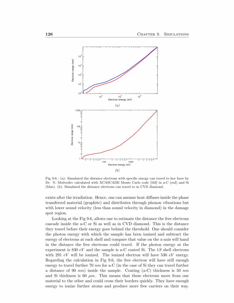
126 Chapter 9. Simulations
100
101
102
103
104
Ele
ctr
on r
ange (
nm
)
102
103
104
Electron energy (eV)
(a)
1
2
4
6
810
2
4
6
8100
2
4
6
81000
Ele
ctr
on r
ange (
nm
)
2 3 4 5 6 7
1002 3 4 5 6 7
10002 3 4 5 6 7
Electron energy (eV)
(b)
Fig. 9.6.: (a): Simulated the distance electrons with specific energy can travel to hey have byDr. N. Medvedev calculated with XCASCADE Monte Carlo code [163] in a-C (red) and Si(blue). (b): Simulated the distance electrons can travel to in CVD diamond.
exists after the irradiation. Hence, one can assume heat diffuses inside the phasetransferred material (graphite) and distributes through phonon vibrations butwith lower sound velocity (less than sound velocity in diamond) in the damagespot region.
Looking at the Fig 9.6, allows one to estimate the distance the free electronscascade inside the a-C or Si as well as in CVD diamond. This is the distancethey travel before their energy goes behind the threshold. One should considerthe photon energy with which the sample has been ionized and subtract theenergy of electrons at each shell and compare that value on the x-axis will handin the distance the free electrons could travel. If the photon energy at theexperiment is 830 eV and the sample is a-C coated Si. The 1S shell electronswith 291 eV will be ionized. The ionized electron will have 530 eV energy.Regarding the calculation in Fig 9.6, the free electron will have still enoughenergy to travel further 70 nm for a-C (in the case of Si they can travel furthera distance of 90 nm) inside the sample. Coating (a-C) thickness is 50 nmand Si thickness is 60 µm. This means that these electrons move from onematerial to the other and could cross their borders quickly. They have enoughenergy to ionize further atoms and produce more free carriers on their way.
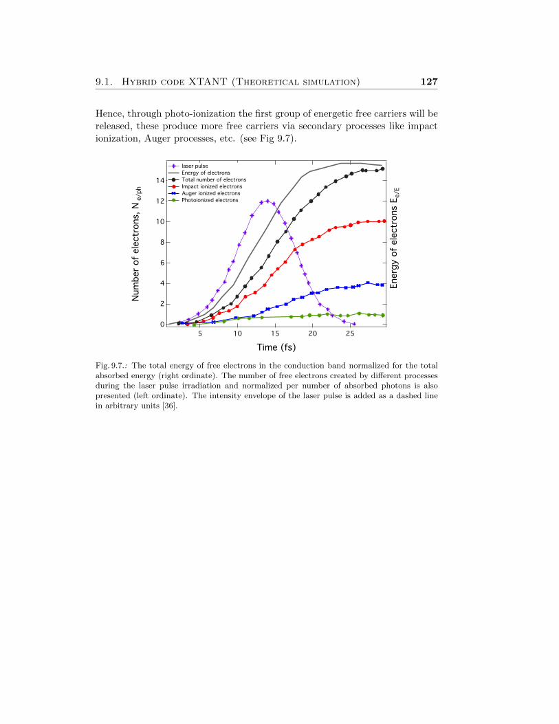
9.1. Hybrid code XTANT (Theoretical simulation) 127
Hence, through photo-ionization the first group of energetic free carriers will bereleased, these produce more free carriers via secondary processes like impactionization, Auger processes, etc. (see Fig 9.7).
14
12
10
8
6
4
2
0
Num
ber
of
ele
ctr
ons,
N e
/ph
252015105
Time (fs)
Energ
y o
f ele
ctr
ons
Ee/E
laser pulse
Energy of electrons
Total number of electrons
Impact ionized electrons
Auger ionized electrons
Photoionized electrons
Fig. 9.7.: The total energy of free electrons in the conduction band normalized for the totalabsorbed energy (right ordinate). The number of free electrons created by different processesduring the laser pulse irradiation and normalized per number of absorbed photons is alsopresented (left ordinate). The intensity envelope of the laser pulse is added as a dashed linein arbitrary units [36].
128 Chapter 9. Simulations
9.2 Heat diffusion simulation
In the early stages of damage process (very first 100fs after the irradiation),phase transition through ionization processes (see section 9.1) takes place.Hence, the density of a-C or CVD diamond, both changes to graphite (Gr).This part of the process is recognized as non-thermal. Later on, after some 100’sof ps due to a direct increase in the kinetic energy (temperature) of atoms, heatdiffusion process takes place and the melting temperature might be reached onthe coating, the substrate or both. In the non-thermal section of the damageprocess, the area of each damage spot is on the logarithmic axes linearly de-pendent on the pulse energy. This is under the assumption that the beam hasa Gaussian shape. If the beam shape changes or any other process like melting(heat diffusion) plays a role in the damage process, some changes regarding thisdependency will be detectable from the experimental results (see Figs 9.26, 9.27and 9.28).
Heat diffusion in this Ph.D. project is simulated via COMSOL. It is a soft-ware package based on advanced numerical methods, for modeling and simu-lating physics-based problems.
Benefits of use include COMSOL's graphical user interface and its optionsfor different predefined interfaces and corresponding modeling tools. Based onthe COMSOL simulation one can estimate if the melting temperature could bereached on the surface, in the volume, at the boundary between the coatingand the substrate or the substrate alone.
As a first approach, the heat is simulated inside the a-C or CVD diamondafter being illuminated by the pulse and without considering the phase transi-tion. One can check if the melting temperature is achieved on the sample. Thearea (on the surface) up to which the melting temperature is reached, is thenextracted and compared with the measured damaged areas on Nomarski imagesof each damaged spot at different pulse energies for various photon energies.In the more advanced approach, one can consider that phase transition has al-ready taken place and simulate the diffusion of the heat from the center of thephase transferred material (graphite instead of a-C or CVD) inside the primarymaterial (a-C or CVD diamond) further away.Different cases are studied here
• Phase transition has happened in the area as large as the beam size
• Phase transition has happened in the area smaller or larger than the beamsize
• The case where the created graphite is thinner in depth than the coatingthickness
• Considering different length (partial formation or grating shape like struc-ture) of created graphite on the surface with a thin or thick thickness
Fig 9.11 shows different studied models in this section. The last modelis more of a realistic option. Based on Raman spectroscopy measurements
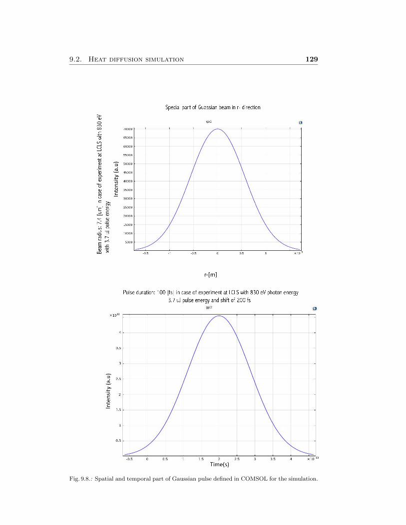
9.2. Heat diffusion simulation 129
Fig. 9.8.: Spatial and temporal part of Gaussian pulse defined in COMSOL for the simulation.
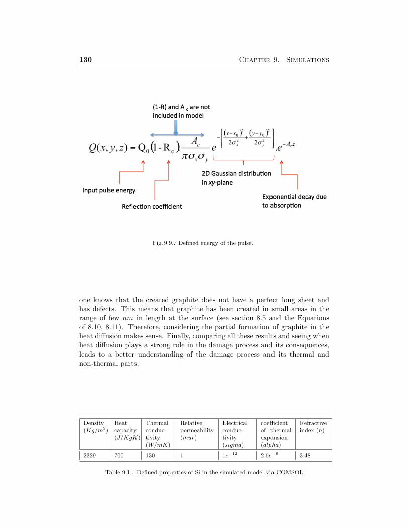
130 Chapter 9. Simulations
Fig. 9.9.: Defined energy of the pulse.
one knows that the created graphite does not have a perfect long sheet andhas defects. This means that graphite has been created in small areas in therange of few nm in length at the surface (see section 8.5 and the Equationsof 8.10, 8.11). Therefore, considering the partial formation of graphite in theheat diffusion makes sense. Finally, comparing all these results and seeing whenheat diffusion plays a strong role in the damage process and its consequences,leads to a better understanding of the damage process and its thermal andnon-thermal parts.
Density(Kg/m3)
Heatcapacity(J/KgK)
Thermalconduc-tivity(W/mK)
Relativepermeability(mur)
Electricalconduc-tivity(sigma)
coefficientof thermalexpansion(alpha)
Refractiveindex (n)
2329 700 130 1 1e−12 2.6e−6 3.48
Table 9.1.: Defined properties of Si in the simulated model via COMSOL
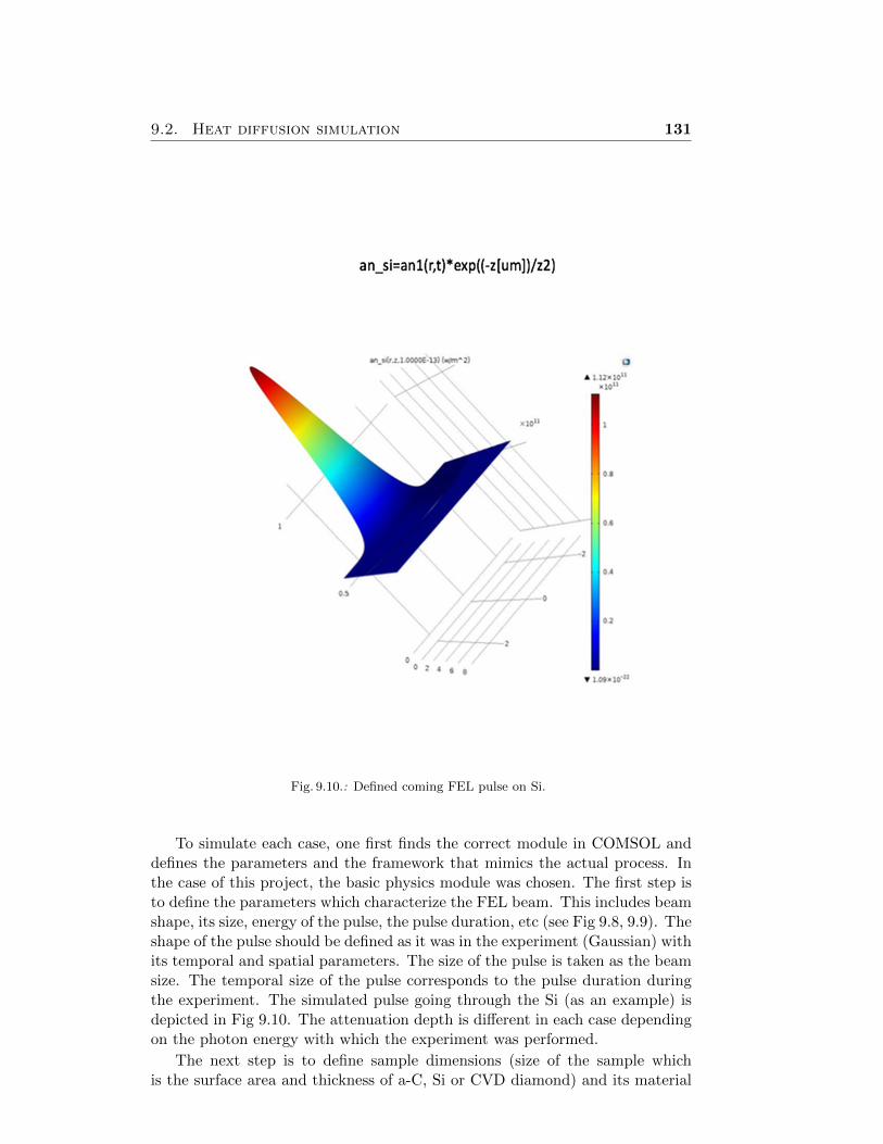
9.2. Heat diffusion simulation 131
Fig. 9.10.: Defined coming FEL pulse on Si.
To simulate each case, one first finds the correct module in COMSOL anddefines the parameters and the framework that mimics the actual process. Inthe case of this project, the basic physics module was chosen. The first step isto define the parameters which characterize the FEL beam. This includes beamshape, its size, energy of the pulse, the pulse duration, etc (see Fig 9.8, 9.9). Theshape of the pulse should be defined as it was in the experiment (Gaussian) withits temporal and spatial parameters. The size of the pulse is taken as the beamsize. The temporal size of the pulse corresponds to the pulse duration duringthe experiment. The simulated pulse going through the Si (as an example) isdepicted in Fig 9.10. The attenuation depth is different in each case dependingon the photon energy with which the experiment was performed.
The next step is to define sample dimensions (size of the sample whichis the surface area and thickness of a-C, Si or CVD diamond) and its material
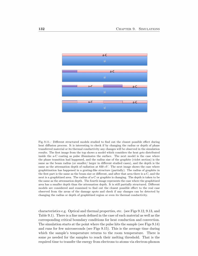
132 Chapter 9. Simulations
Fig. 9.11.: Different structured models studied to find out the closest possible effect duringheat diffusion process. It is interesting to check if by changing the radius or depth of phasetransferred material or its thermal conductivity any changes will be observed in the simulationresults. The first image from the top shows a model which considers the heat gets distributedinside the a-C coating as pulse illuminates the surface. The next model is the case wherethe phase transition had happened, and the radius size of the graphite (violet section) is thesame as the beam radius (or smaller/ larger in different studied cases), and the depth is thesame as the attenuation depth of radiation at 830 eV . The next image shows the case wheregraphitization has happened in a grating-like structure (partially). The radius of graphite inthe first part is the same as the beam size or different, and after that area there is a-C, and thenext is a graphitized area. The radius of a-C or graphite is changing. The depth is taken to bethe same as the attenuation depth. The fourth image represents the case where the graphitizedarea has a smaller depth than the attenuation depth. It is still partially structured. Differentmodels are considered and examined to find out the closest possible effect to the real caseobserved from the areas of the damage spots and check if any changes can be detected bychanging the radius or depth of graphitized region or even its thermal conductivity.
characteristics e.g. Optical and thermal properties, etc. (see Figs 9.12, 9.13, andTable 9.1). There is a fine mesh defined in the case of each material as well as thecorresponding critical boundary conditions for heat conduction and convection.The simulation starts at the point where the pulse hits the sample (see Figs 9.14)and runs for few microseconds (see Figs 9.15). This is the average time duringwhich the sample’s temperature returns to the room temperature. There issome ps needed for the samples to reach their melting threshold. That is therequired time to transfer the energy from electrons to atoms via electron-phonon
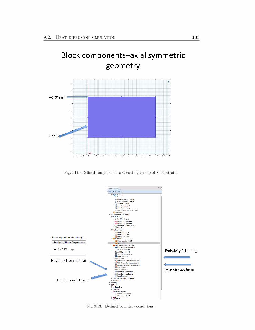
9.2. Heat diffusion simulation 133
Fig. 9.12.: Defined components. a-C coating on top of Si substrate.
Fig. 9.13.: Defined boundary conditions.
134 Chapter 9. Simulations
coupling [8], [157]. This indicates that before this time the damage process ismainly governed by photo-ionization, and one can name it non-thermal. Thiswas also proven by the Hybrid XTANT theoretical simulation in section 9.1.After some hundred’s of ps both non/thermal processes are involved in thedamage.
As an example are the pulses with 3.7 and 17.5 µJ depicted in Figs 9.15;as well as the temperature achieved on and in the sample. The correspondingradius up to which this temperature was reached is depicted in Fig 9.16. Onecan see how far the heat diffuses on the surface of a-C as well as in Si.
Simulations show that melting plays a role in the damage process startingwith pulse energies around 10 µJ (2.7 eV/atom) at 830 eV without consideringthe phase transition (see Fig 9.19). In the case of phase transition this valueschanges to 5 µJ (1.38 eV/atom)(see Fig 9.20).
As mentioned earlier different designed models are studied in this project,even the value of the thermal conductivity at 830 eV photon energy waschanged to lower values for comparison reasons. The thermal conductivity ofthe graphite was changed from 5.7 W/mK to 3 W/mK (see Fig: 9.21). Also thedamage structure was changed to grating like (partial formed graphite areas).Some of the results are depicted in Figures 9.22, 9.23 and some are depicted inAppendix 12.6.e.g in Fig 12.30.
Silicon has higher thermal conductivity than amorphous carbon andgraphite (see Table 9.1). It’s (Si) heat capacity is almost the same as graphitebut higher than amorphous carbon. Therefore, it can reach melting thresholdon lower pulse energies compared to amorphous carbon and graphite. From thetheoretical simulation, it can be seen that free electrons after photo-ionizationprocess have still enough energy to travel and escape from a-C to Si, whichcould generate secondary processes. Figure 9.6 shows that one can estimate ata specific energy how far electrons can travel inside the a-C, Si or CVD diamondand generate free carriers.
In Figures 9.17 - 9.19 simulated heat diffusion at different photon energiesof 20 eV , 177 eV , 296 eV and 830 eV on a-C sample at room temperature aredepicted.
At 20 eV , compared to the higher photon energies, the heating starts at verylow pulse energies and mainly is the a-C which reaches melting temperature.The attenuation depth of X-ray-FEL pulse at 20 eV is very small, and thephoto-ionization mostly takes place in an area very close to the surface. Hence,lots of free carriers can escape from the surface, or the screening effect createsa hot plasma of electrons on the surface of the sample. The generated highpressure could cause shock waves and distribute the carriers out of the beamregion (in size). All these processes lead to a high damage threshold value beingobtained which is presented in chapter 8.
Considering the theoretical calculation in Fig 9.4, sample reaches 2000 Ktemperature after the phase transition. Starting with the 2000 K base temper-ature in heat diffusion simulations shows that Si reaches the melting thresholdmuch faster and even before the a-C coating reaches its melting temperature.This means, after some few ns the Si melts.
Looking at the Figures 9.17- 9.19 shows that at very first low pulse energies
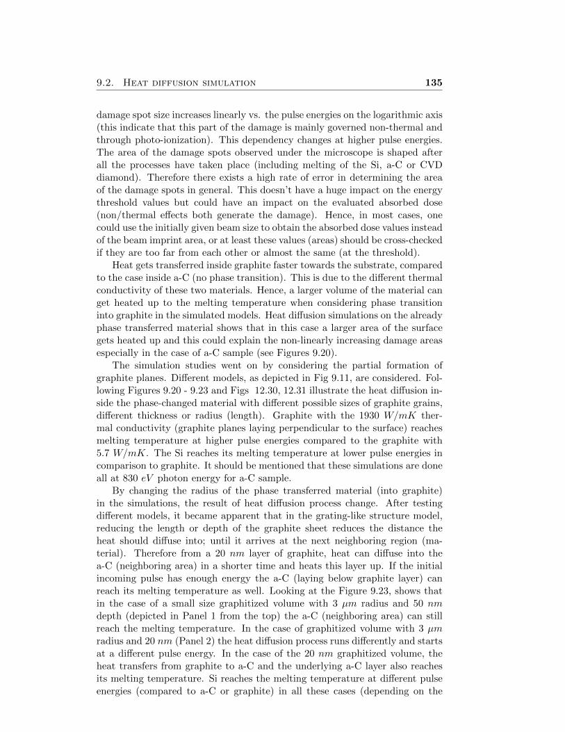
9.2. Heat diffusion simulation 135
damage spot size increases linearly vs. the pulse energies on the logarithmic axis(this indicate that this part of the damage is mainly governed non-thermal andthrough photo-ionization). This dependency changes at higher pulse energies.The area of the damage spots observed under the microscope is shaped afterall the processes have taken place (including melting of the Si, a-C or CVDdiamond). Therefore there exists a high rate of error in determining the areaof the damage spots in general. This doesn’t have a huge impact on the energythreshold values but could have an impact on the evaluated absorbed dose(non/thermal effects both generate the damage). Hence, in most cases, onecould use the initially given beam size to obtain the absorbed dose values insteadof the beam imprint area, or at least these values (areas) should be cross-checkedif they are too far from each other or almost the same (at the threshold).
Heat gets transferred inside graphite faster towards the substrate, comparedto the case inside a-C (no phase transition). This is due to the different thermalconductivity of these two materials. Hence, a larger volume of the material canget heated up to the melting temperature when considering phase transitioninto graphite in the simulated models. Heat diffusion simulations on the alreadyphase transferred material shows that in this case a larger area of the surfacegets heated up and this could explain the non-linearly increasing damage areasespecially in the case of a-C sample (see Figures 9.20).
The simulation studies went on by considering the partial formation ofgraphite planes. Different models, as depicted in Fig 9.11, are considered. Fol-lowing Figures 9.20 - 9.23 and Figs 12.30, 12.31 illustrate the heat diffusion in-side the phase-changed material with different possible sizes of graphite grains,different thickness or radius (length). Graphite with the 1930 W/mK ther-mal conductivity (graphite planes laying perpendicular to the surface) reachesmelting temperature at higher pulse energies compared to the graphite with5.7 W/mK. The Si reaches its melting temperature at lower pulse energies incomparison to graphite. It should be mentioned that these simulations are doneall at 830 eV photon energy for a-C sample.
By changing the radius of the phase transferred material (into graphite)in the simulations, the result of heat diffusion process change. After testingdifferent models, it became apparent that in the grating-like structure model,reducing the length or depth of the graphite sheet reduces the distance theheat should diffuse into; until it arrives at the next neighboring region (ma-terial). Therefore from a 20 nm layer of graphite, heat can diffuse into thea-C (neighboring area) in a shorter time and heats this layer up. If the initialincoming pulse has enough energy the a-C (laying below graphite layer) canreach its melting temperature as well. Looking at the Figure 9.23, shows thatin the case of a small size graphitized volume with 3 µm radius and 50 nmdepth (depicted in Panel 1 from the top) the a-C (neighboring area) can stillreach the melting temperature. In the case of graphitized volume with 3 µmradius and 20 nm (Panel 2) the heat diffusion process runs differently and startsat a different pulse energy. In the case of the 20 nm graphitized volume, theheat transfers from graphite to a-C and the underlying a-C layer also reachesits melting temperature. Si reaches the melting temperature at different pulseenergies (compared to a-C or graphite) in all these cases (depending on the
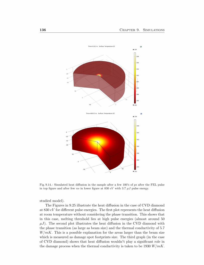
136 Chapter 9. Simulations
Fig. 9.14.: Simulated heat diffusion in the sample after a few 100’s of ps after the FEL pulsein top figure and after few ns in lower figure at 830 eV with 3.7 µJ pulse energy.
studied model).The Figures in 9.25 illustrate the heat diffusion in the case of CVD diamond
at 830 eV for different pulse energies. The first plot represents the heat diffusionat room temperature without considering the phase transition. This shows thatin this case, melting threshold lies at high pulse energies (almost around 50µJ). The second plot illustrates the heat diffusion in the CVD diamond withthe phase transition (as large as beam size) and the thermal conductivity of 5.7W/mK. This is a possible explanation for the areas larger than the beam sizewhich is measured as damage spot footprints size. The third graph (in the caseof CVD diamond) shows that heat diffusion wouldn't play a significant role inthe damage process when the thermal conductivity is taken to be 1930 W/mK.
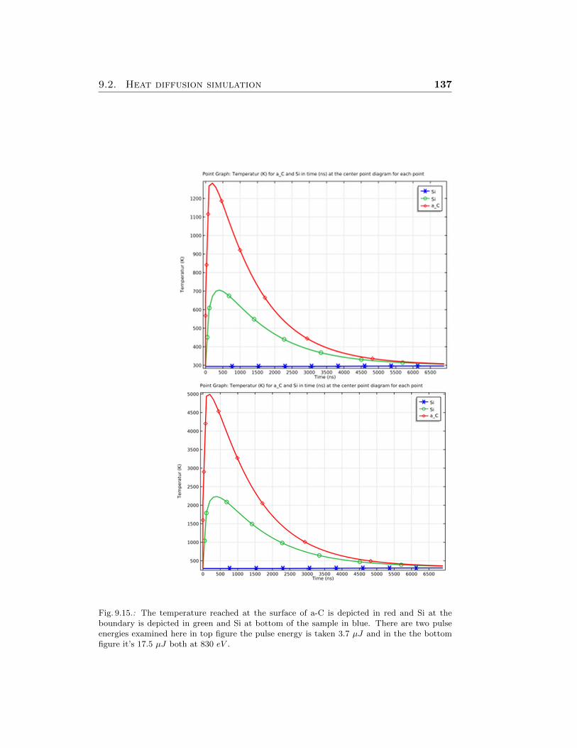
9.2. Heat diffusion simulation 137
Fig. 9.15.: The temperature reached at the surface of a-C is depicted in red and Si at theboundary is depicted in green and Si at bottom of the sample in blue. There are two pulseenergies examined here in top figure the pulse energy is taken 3.7 µJ and in the the bottomfigure it’s 17.5 µJ both at 830 eV .
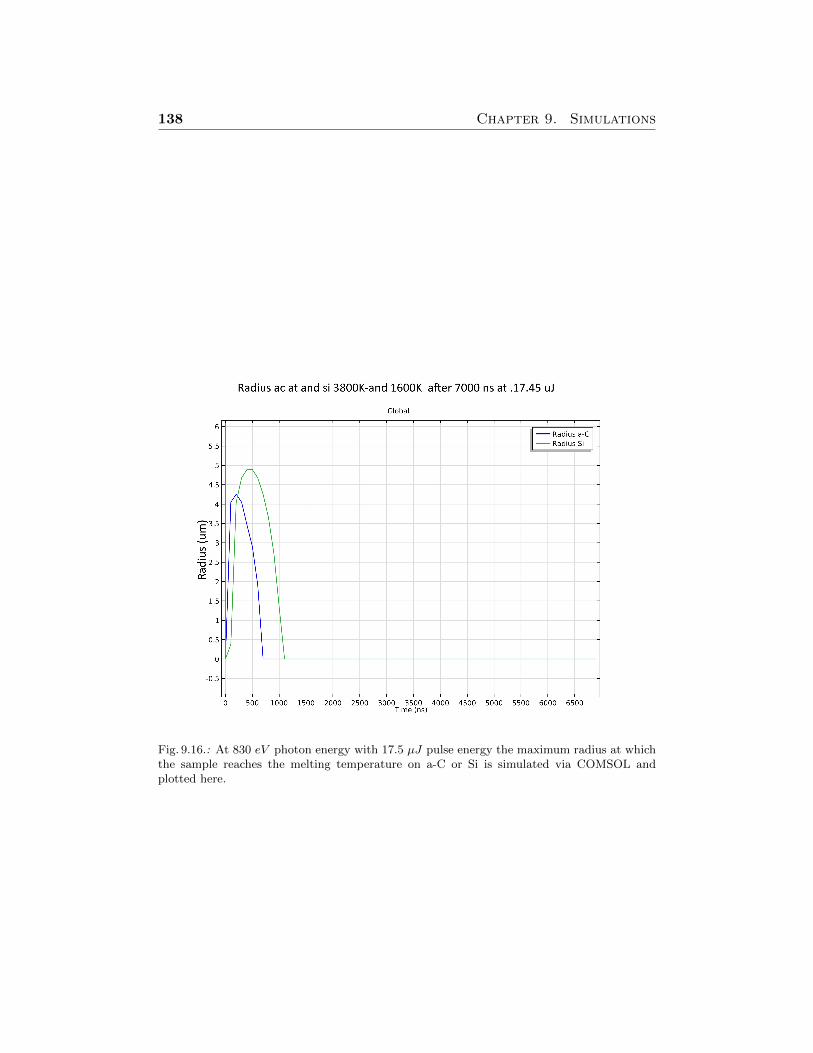
138 Chapter 9. Simulations
Fig. 9.16.: At 830 eV photon energy with 17.5 µJ pulse energy the maximum radius at whichthe sample reaches the melting temperature on a-C or Si is simulated via COMSOL andplotted here.
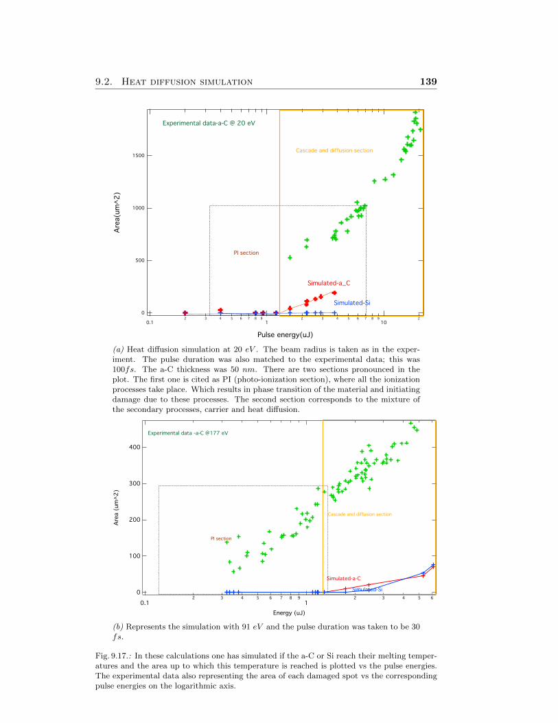
9.2. Heat diffusion simulation 139
1500
1000
500
0
Are
a(u
m^2)
0.12 3 4 5 6 7 8 9
12 3 4 5 6 7 8 9
102
Pulse energy(uJ)
Experimental data-a-C @ 20 eV
Simulated-a_C
Simulated-Si
PI section
Cascade and diffusion section
(a) Heat diffusion simulation at 20 eV . The beam radius is taken as in the exper-iment. The pulse duration was also matched to the experimental data; this was100fs. The a-C thickness was 50 nm. There are two sections pronounced in theplot. The first one is cited as PI (photo-ionization section), where all the ionizationprocesses take place. Which results in phase transition of the material and initiatingdamage due to these processes. The second section corresponds to the mixture ofthe secondary processes, carrier and heat diffusion.
400
300
200
100
0
Are
a (
um
^2)
0.12 3 4 5 6 7 8 9
12 3 4 5 6
Energy (uJ)
Experimental data -a-C @177 eV
Simulated-a-C
Simulated-Si
PI section
Cascade and diffusion section
(b) Represents the simulation with 91 eV and the pulse duration was taken to be 30fs.
Fig. 9.17.: In these calculations one has simulated if the a-C or Si reach their melting temper-atures and the area up to which this temperature is reached is plotted vs the pulse energies.The experimental data also representing the area of each damaged spot vs the correspondingpulse energies on the logarithmic axis.
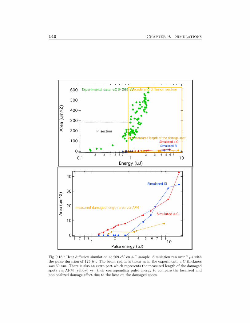
140 Chapter 9. Simulations
40
30
20
10
0
Are
a (
um
^2)
6 7 8 9
12 3 4 5 6 7 8 9
10Pulse energy (uJ)
Simulated a-C
Simulated Si
measured damaged length area via AFM
600
500
400
300
200
100
0
Are
a (
um
^2)
0.12 3 4 5 6 7
12 3 4 5 6 7
10
Energy (uJ)
Experimental data -aC @ 269 eV
PI section
Cascade and diffusion section
Simulated a-C
Simulated Si
AFM measured length of the damage spot
Fig. 9.18.: Heat diffusion simulation at 269 eV on a-C sample. Simulation ran over 7 µs withthe pulse duration of 125 fs . The beam radius is taken as in the experiment. a-C thicknesswas 50 nm. There is also an extra part which represents the measured length of the damagedspots via AFM (yellow) vs. their corresponding pulse energy to compare the localized andnonlocalized damage effect due to the heat on the damaged spots.
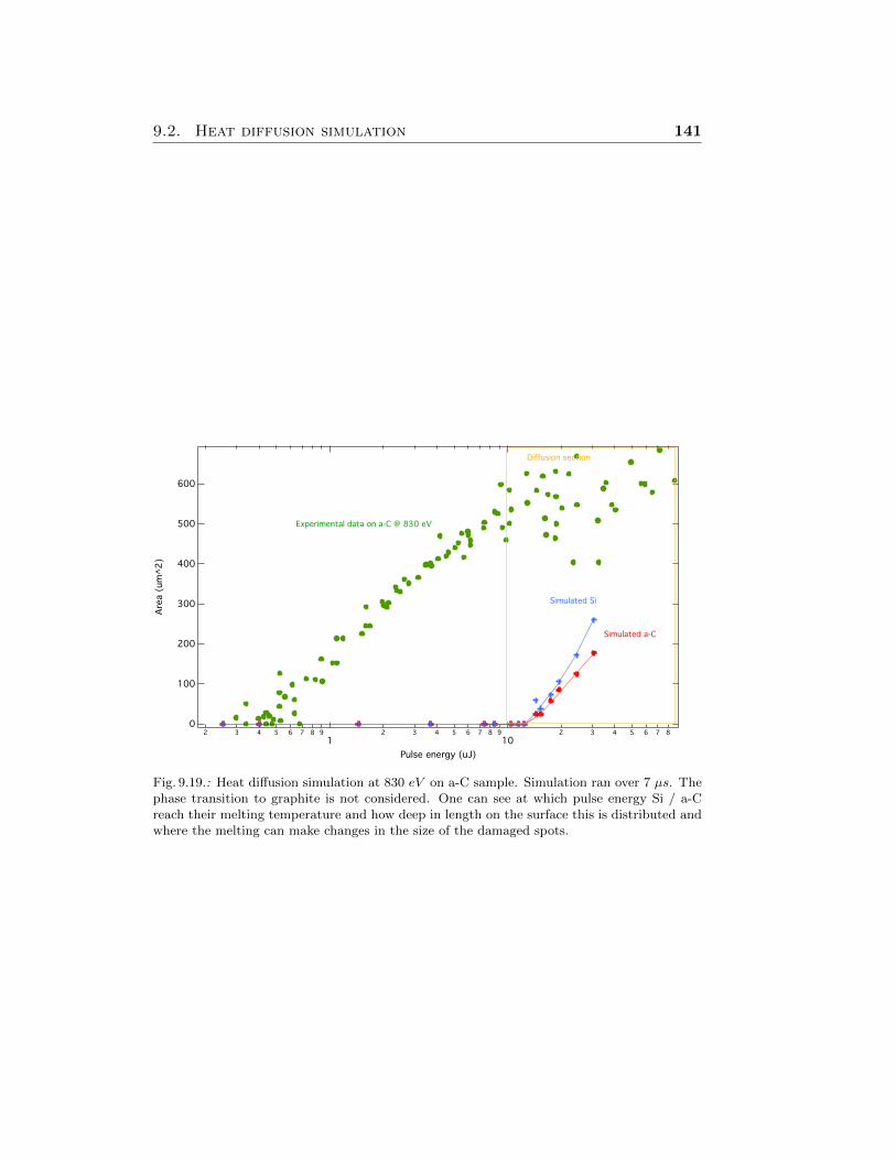
9.2. Heat diffusion simulation 141
600
500
400
300
200
100
0
Are
a (
um
^2)
2 3 4 5 6 7 8 9
12 3 4 5 6 7 8 9
102 3 4 5 6 7 8
Pulse energy (uJ)
Experimental data on a-C @ 830 eV
Simulated Si
Simulated a-C
Diffusion section
Fig. 9.19.: Heat diffusion simulation at 830 eV on a-C sample. Simulation ran over 7 µs. Thephase transition to graphite is not considered. One can see at which pulse energy Si / a-Creach their melting temperature and how deep in length on the surface this is distributed andwhere the melting can make changes in the size of the damaged spots.
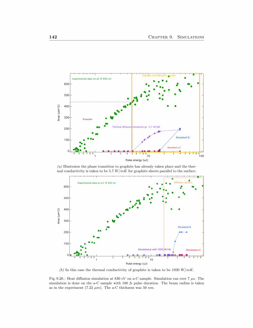
142 Chapter 9. Simulations
600
500
400
300
200
100
0
Ara
e (
um
^2)
4 5 6 7 8 9
12 3 4 5 6 7 8 9
102 3 4 5 6 7 8 9
100
Pulse energy (uJ)
Thermal diffusion simulation-gr- 5,7 W/mK
experimental data on aC @ 830 eV
PI section
Cascade and Diffusion section
Simulated Si
Simulated a-C
(a) Illustrates the phase transition to graphite has already taken place and the ther-mal conductivity is taken to be 5.7 W/mK for graphite sheets parallel to the surface.
600
500
400
300
200
100
0
Are
a (
um
^2)
4 5 6 7 8 9
12 3 4 5 6 7 8 9
102 3 4 5 6 7 8
Pulse energy (uJ)
Experimental data on a-C @ 830 eV
Simulated Si
Simulated a-CSimulated gr with 1930 W/mK
Diffusion section
(b) In this case the thermal conductivity of graphite is taken to be 1930 W/mK.
Fig. 9.20.: Heat diffusion simulation at 830 eV on a-C sample. Simulation ran over 7 µs. Thesimulation is done on the a-C sample with 100 fs pulse duration. The beam radius is takenas in the experiment (7.22 µm). The a-C thickness was 50 nm.
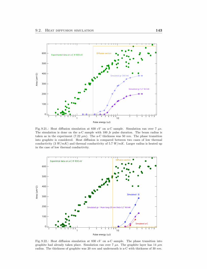
9.2. Heat diffusion simulation 143
600
500
400
300
200
100
0
Are
a (
um
^2)
2 3 4 5 6 7 8 9
12 3 4 5 6 7 8 9
102 3 4 5 6 7 8
Pulse energy (uJ)
Experimental data on a-C @ 830 eV
Simulated gr 3W/mK
Simulated gr 5,7 W/mK
Diffusion section
Fig. 9.21.: Heat diffusion simulation at 830 eV on a-C sample. Simulation ran over 7 µs.The simulation is done on the a-C sample with 100 fs pulse duration. The beam radius istaken as in the experiment (7.22 µm). The a-C thickness was 50 nm. The phase transitioninto graphite is considered. Heat diffusion is compared between two cases of low thermalconductivity (3 W/mK) and thermal conductivity of 5.7 W/mK. Larger radius is heated upin the case of low thermal conductivity.
600
500
400
300
200
100
0
Are
a (
um
^2)
2 3 4 5 6 7 8 9
12 3 4 5 6 7 8 9
102 3 4 5 6 7 8
Pulse energy (uJ)
Experimtal data on a-C @ 830 eV
Simulated Si
Simulated gr- 14um long-20 nm thick-5,7 W/mK
Simulated a-C
Diffusion section
Fig. 9.22.: Heat diffusion simulation at 830 eV on a-C sample. The phase transition intographite had already taken place. Simulation ran over 7 µs. The graphite layer has 14 µmradius. The thickness of graphite was 20 nm and underneath is a-C with thickness of 30 nm.
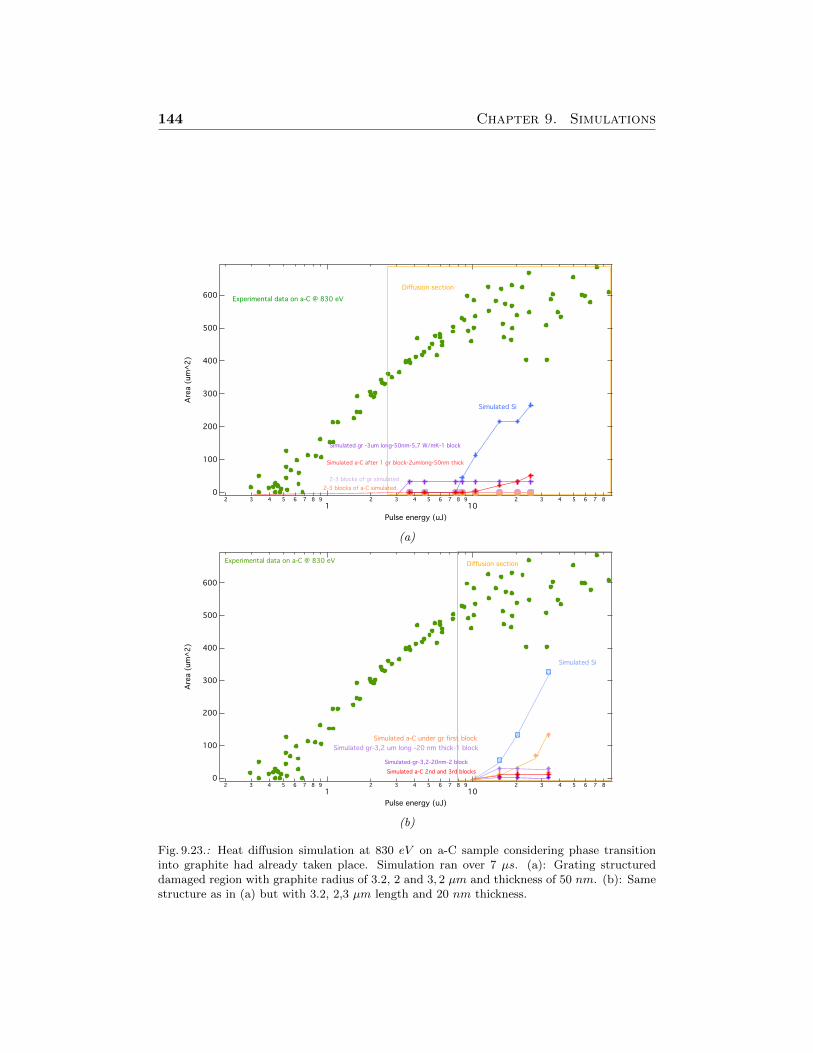
144 Chapter 9. Simulations
600
500
400
300
200
100
0
Are
a (
um
^2)
2 3 4 5 6 7 8 9
12 3 4 5 6 7 8 9
102 3 4 5 6 7 8
Pulse energy (uJ)
Experimental data on a-C @ 830 eV
Simulated Si
Simulated gr -3um long-50nm-5,7 W/mK-1 block
Simulated a-C after 1 gr block-2umlong-50nm thick
2-3 blocks of gr simulated
2-3 blocks of a-C simulated
Diffusion section
(a)
600
500
400
300
200
100
0
Are
a (
um
^2)
2 3 4 5 6 7 8 9
12 3 4 5 6 7 8 9
102 3 4 5 6 7 8
Pulse energy (uJ)
Experimental data on a-C @ 830 eV
Simulated Si
Simulated a-C under gr first block
Simulated a-C 2nd and 3rd blocks
Simulated gr-3,2 um long -20 nm thick-1 block
Simulated-gr-3,2-20nm-2 block
Diffusion section
(b)
Fig. 9.23.: Heat diffusion simulation at 830 eV on a-C sample considering phase transitioninto graphite had already taken place. Simulation ran over 7 µs. (a): Grating structureddamaged region with graphite radius of 3.2, 2 and 3, 2 µm and thickness of 50 nm. (b): Samestructure as in (a) but with 3.2, 2,3 µm length and 20 nm thickness.
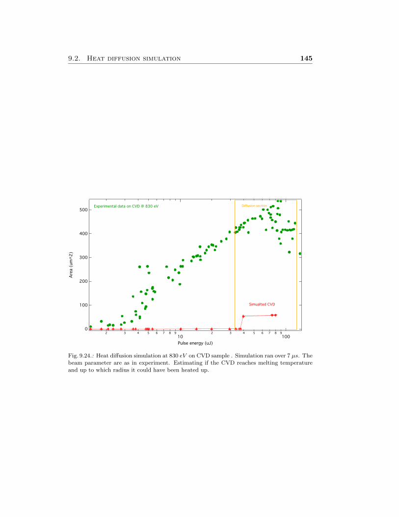
9.2. Heat diffusion simulation 145
500
400
300
200
100
0
Are
a (
um
^2)
2 3 4 5 6 7 8 9
102 3 4 5 6 7 8 9
100
Pulse energy (uJ)
Experimental data on CVD @ 830 eV
Simualted CVD
Diffusion section
Fig. 9.24.: Heat diffusion simulation at 830 eV on CVD sample . Simulation ran over 7 µs. Thebeam parameter are as in experiment. Estimating if the CVD reaches melting temperatureand up to which radius it could have been heated up.
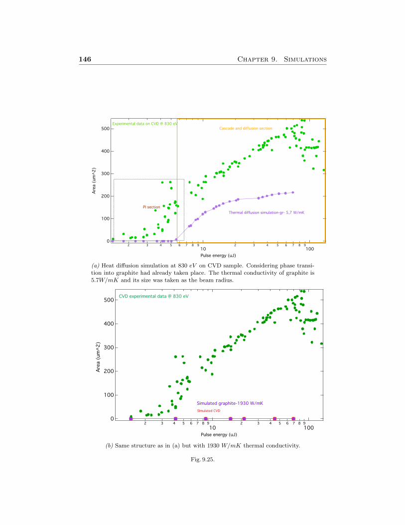
146 Chapter 9. Simulations
500
400
300
200
100
0
Are
a (
um
^2)
2 3 4 5 6 7 8 9
102 3 4 5 6 7 8 9
100
Pulse energy (uJ)
PI section
Experimental data on CVD @ 830 eVCascade and diffusion section
Thermal diffusion simulation-gr- 5,7 W/mK
(a) Heat diffusion simulation at 830 eV on CVD sample. Considering phase transi-tion into graphite had already taken place. The thermal conductivity of graphite is5.7W/mK and its size was taken as the beam radius.
500
400
300
200
100
0
Are
a (
um
^2)
2 3 4 5 6 7 8 9
102 3 4 5 6 7 8 9
100Pulse energy (uJ)
CVD experimental data @ 830 eV
Simulated graphite-1930 W/mK
SImulated CVD
(b) Same structure as in (a) but with 1930 W/mK thermal conductivity.
Fig. 9.25.
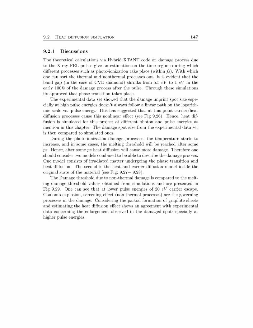
9.2. Heat diffusion simulation 147
9.2.1 Discussions
The theoretical calculations via Hybrid XTANT code on damage process dueto the X-ray FEL pulses give an estimation on the time regime during whichdifferent processes such as photo-ionization take place (within fs). With whichone can sort the thermal and nonthermal processes out. It is evident that theband gap (in the case of CVD diamond) shrinks from 5.5 eV to 1 eV in theearly 100fs of the damage process after the pulse. Through these simulationsits approved that phase transition takes place.
The experimental data set showed that the damage imprint spot size espe-cially at high pulse energies doesn’t always follow a linear path on the logarith-mic scale vs. pulse energy. This has suggested that at this point carrier/heatdiffusion processes cause this nonlinear effect (see Fig 9.26). Hence, heat dif-fusion is simulated for this project at different photon and pulse energies asmention in this chapter. The damage spot size from the experimental data setis then compared to simulated ones.
During the photo-ionization damage processes, the temperature starts toincrease, and in some cases, the melting threshold will be reached after someps. Hence, after some ps heat diffusion will cause more damage. Therefore oneshould consider two models combined to be able to describe the damage process.One model consists of irradiated matter undergoing the phase transition andheat diffusion. The second is the heat and carrier diffusion model inside theoriginal state of the material (see Fig: 9.27− 9.28).
The Damage threshold due to non-thermal damage is compared to the melt-ing damage threshold values obtained from simulations and are presented inFig 9.29. One can see that at lower pulse energies of 20 eV carrier escape,Coulomb explosion, screening effect (non-thermal processes) are the governingprocesses in the damage. Considering the partial formation of graphite sheetsand estimating the heat diffusion effect shows an agreement with experimentaldata concerning the enlargement observed in the damaged spots specially athigher pulse energies.
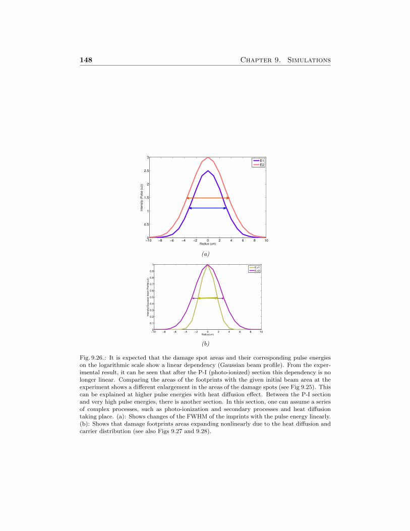
148 Chapter 9. Simulations
−10 −8 −6 −4 −2 0 2 4 6 8 100
0.5
1
1.5
2
2.5
3
Radius (um)
Inte
nsity (
Pu
lse
(u
J))
E1
E2
(a)
−10 −8 −6 −4 −2 0 2 4 6 8 100
0.1
0.2
0.3
0.4
0.5
0.6
0.7
0.8
0.9
1
Radius(um)
Inte
nsity(G
au
ssia
n b
ea
m P
rofile
(uJ))
E,r1
E,r2
(b)
Fig. 9.26.: It is expected that the damage spot areas and their corresponding pulse energieson the logarithmic scale show a linear dependency (Gaussian beam profile). From the exper-imental result, it can be seen that after the P-I (photo-ionized) section this dependency is nolonger linear. Comparing the areas of the footprints with the given initial beam area at theexperiment shows a different enlargement in the areas of the damage spots (see Fig 9.25). Thiscan be explained at higher pulse energies with heat diffusion effect. Between the P-I sectionand very high pulse energies, there is another section. In this section, one can assume a seriesof complex processes, such as photo-ionization and secondary processes and heat diffusiontaking place. (a): Shows changes of the FWHM of the imprints with the pulse energy linearly.(b): Shows that damage footprints areas expanding nonlinearly due to the heat diffusion andcarrier distribution (see also Figs 9.27 and 9.28).
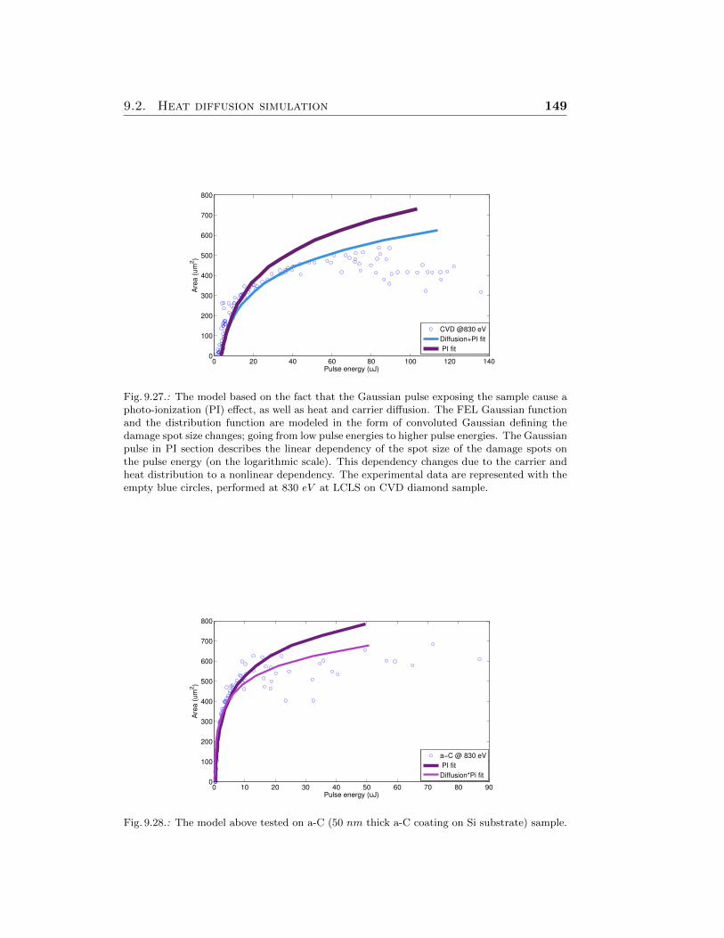
9.2. Heat diffusion simulation 149
0 20 40 60 80 100 120 1400
100
200
300
400
500
600
700
800
Pulse energy (uJ)
Are
a (
um
2)
CVD @830 eV
Diffusion+PI fit
PI fit
Fig. 9.27.: The model based on the fact that the Gaussian pulse exposing the sample cause aphoto-ionization (PI) effect, as well as heat and carrier diffusion. The FEL Gaussian functionand the distribution function are modeled in the form of convoluted Gaussian defining thedamage spot size changes; going from low pulse energies to higher pulse energies. The Gaussianpulse in PI section describes the linear dependency of the spot size of the damage spots onthe pulse energy (on the logarithmic scale). This dependency changes due to the carrier andheat distribution to a nonlinear dependency. The experimental data are represented with theempty blue circles, performed at 830 eV at LCLS on CVD diamond sample.
0 10 20 30 40 50 60 70 80 900
100
200
300
400
500
600
700
800
Pulse energy (uJ)
Are
a (
um
2)
a−C @ 830 eV
PI fit
Diffusion*Pi fit
Fig. 9.28.: The model above tested on a-C (50 nm thick a-C coating on Si substrate) sample.
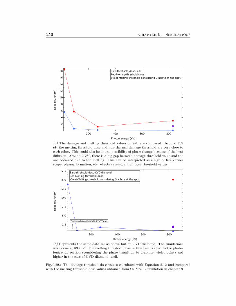
150 Chapter 9. Simulations
18
16
14
12
10
8
6
4
2
Dose
(eV
/ato
m)
800600400200
Photon energy (eV)
Blue-threhsold-dose- a-C
Red-Melting-threshold-dose
Violet-Melting-threshold considering Graphite at the spot
(a) The damage and melting threshold values on a-C are compared. Around 269eV the melting threshold dose and non-thermal damage threshold are very close toeach other. This could also be due to possibility of phase change because of the heatdiffusion. Around 20eV , there is a big gap between damage threshold value and theone obtained due to the melting. This can be interpreted as a sign of free carrierscape, plasma formation, etc. effects causing a high dose threshold values.
17.5
15.0
12.5
10.0
7.5
5.0
2.5
Dose
(eV
/ato
m)
800600400200
Photon energy (eV)
Blue-threhsold-dose-CVD diamond
Red-Melting-threshold-dose
Violet-Melting-threshold considering Graphite at the spot
Theoretical dose threshold 0.7 eV/atom
(b) Represents the same data set as above but on CVD diamond. The simulationswere done at 830 eV . The melting threshold dose in this case is close to the photo-ionization section (considering the phase transition to graphite; violet point) andhigher in the case of CVD diamond itself.
Fig. 9.29.: The damage threshold dose values calculated with Equation 5.12 and comparedwith the melting threshold dose values obtained from COMSOL simulation in chapter 9.
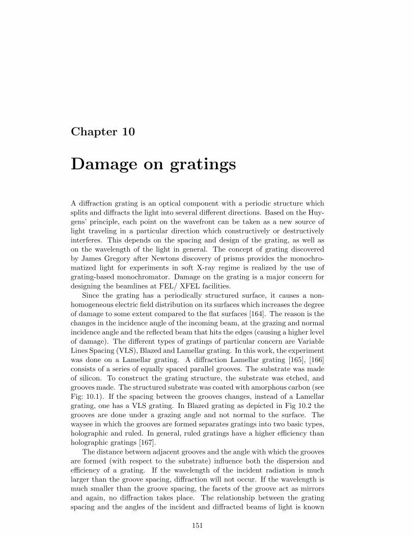
Chapter 10
Damage on gratings
A diffraction grating is an optical component with a periodic structure whichsplits and diffracts the light into several different directions. Based on the Huy-gens’ principle, each point on the wavefront can be taken as a new source oflight traveling in a particular direction which constructively or destructivelyinterferes. This depends on the spacing and design of the grating, as well ason the wavelength of the light in general. The concept of grating discoveredby James Gregory after Newtons discovery of prisms provides the monochro-matized light for experiments in soft X-ray regime is realized by the use ofgrating-based monochromator. Damage on the grating is a major concern fordesigning the beamlines at FEL/ XFEL facilities.
Since the grating has a periodically structured surface, it causes a non-homogeneous electric field distribution on its surfaces which increases the degreeof damage to some extent compared to the flat surfaces [164]. The reason is thechanges in the incidence angle of the incoming beam, at the grazing and normalincidence angle and the reflected beam that hits the edges (causing a higher levelof damage). The different types of gratings of particular concern are VariableLines Spacing (VLS), Blazed and Lamellar grating. In this work, the experimentwas done on a Lamellar grating. A diffraction Lamellar grating [165], [166]consists of a series of equally spaced parallel grooves. The substrate was madeof silicon. To construct the grating structure, the substrate was etched, andgrooves made. The structured substrate was coated with amorphous carbon (seeFig: 10.1). If the spacing between the grooves changes, instead of a Lamellargrating, one has a VLS grating. In Blazed grating as depicted in Fig 10.2 thegrooves are done under a grazing angle and not normal to the surface. Thewaysee in which the grooves are formed separates gratings into two basic types,holographic and ruled. In general, ruled gratings have a higher efficiency thanholographic gratings [167].
The distance between adjacent grooves and the angle with which the groovesare formed (with respect to the substrate) influence both the dispersion andefficiency of a grating. If the wavelength of the incident radiation is muchlarger than the groove spacing, diffraction will not occur. If the wavelength ismuch smaller than the groove spacing, the facets of the groove act as mirrorsand again, no diffraction takes place. The relationship between the gratingspacing and the angles of the incident and diffracted beams of light is known
151
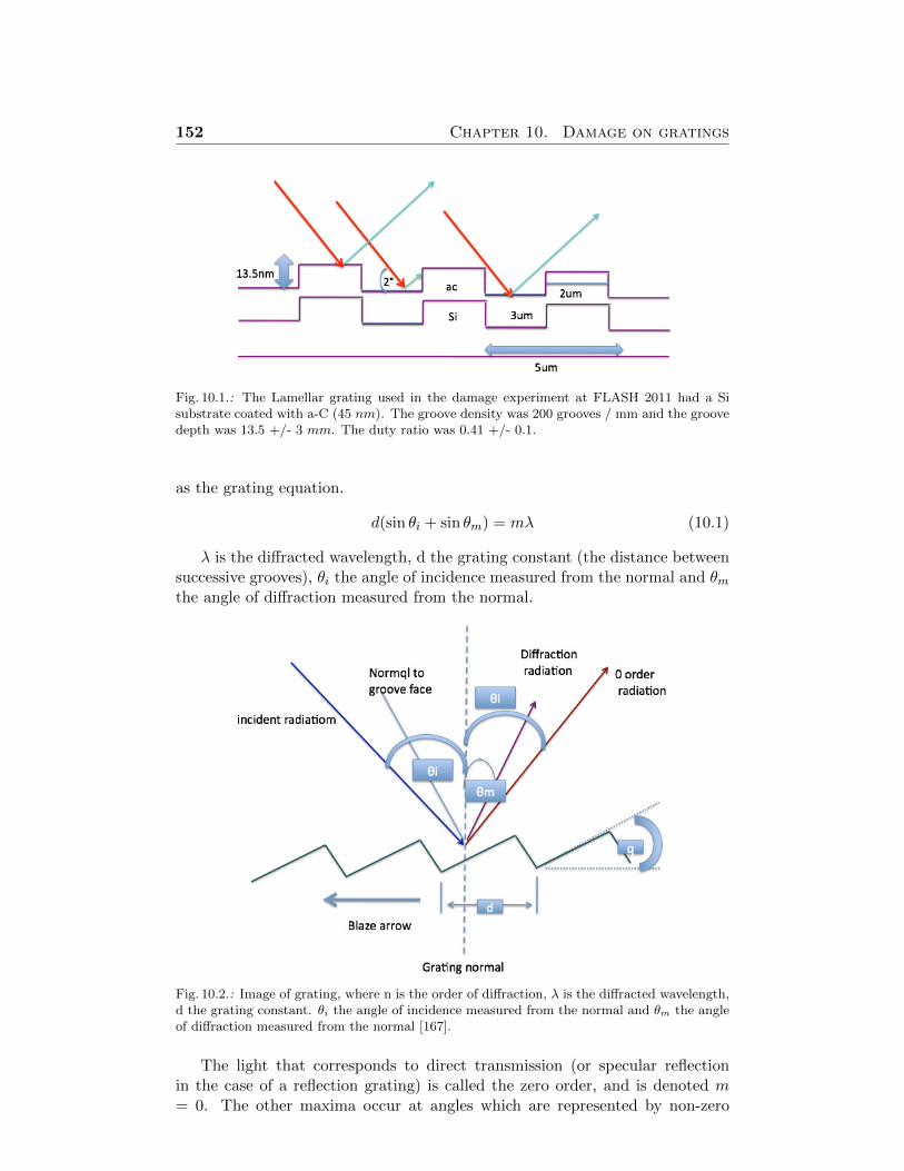
152 Chapter 10. Damage on gratings
Fig. 10.1.: The Lamellar grating used in the damage experiment at FLASH 2011 had a Sisubstrate coated with a-C (45 nm). The groove density was 200 grooves / mm and the groovedepth was 13.5 +/- 3 mm. The duty ratio was 0.41 +/- 0.1.
as the grating equation.
d(sin θi + sin θm) = mλ (10.1)
λ is the diffracted wavelength, d the grating constant (the distance betweensuccessive grooves), θi the angle of incidence measured from the normal and θmthe angle of diffraction measured from the normal.
Fig. 10.2.: Image of grating, where n is the order of diffraction, λ is the diffracted wavelength,d the grating constant. θi the angle of incidence measured from the normal and θm the angleof diffraction measured from the normal [167].
The light that corresponds to direct transmission (or specular reflectionin the case of a reflection grating) is called the zero order, and is denoted m= 0. The other maxima occur at angles which are represented by non-zero
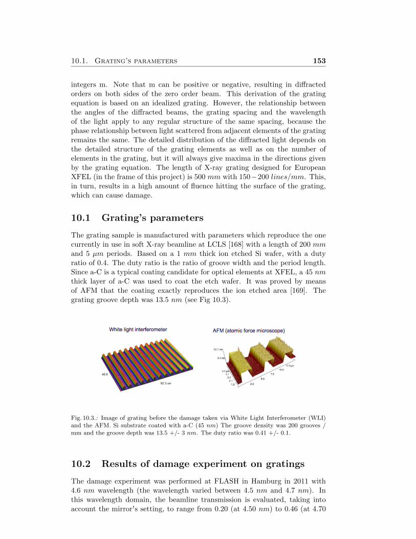
10.1. Grating’s parameters 153
integers m. Note that m can be positive or negative, resulting in diffractedorders on both sides of the zero order beam. This derivation of the gratingequation is based on an idealized grating. However, the relationship betweenthe angles of the diffracted beams, the grating spacing and the wavelengthof the light apply to any regular structure of the same spacing, because thephase relationship between light scattered from adjacent elements of the gratingremains the same. The detailed distribution of the diffracted light depends onthe detailed structure of the grating elements as well as on the number ofelements in the grating, but it will always give maxima in the directions givenby the grating equation. The length of X-ray grating designed for EuropeanXFEL (in the frame of this project) is 500 mm with 150−200 lines/mm. This,in turn, results in a high amount of fluence hitting the surface of the grating,which can cause damage.
10.1 Grating’s parameters
The grating sample is manufactured with parameters which reproduce the onecurrently in use in soft X-ray beamline at LCLS [168] with a length of 200 mmand 5 µm periods. Based on a 1 mm thick ion etched Si wafer, with a dutyratio of 0.4. The duty ratio is the ratio of groove width and the period length.Since a-C is a typical coating candidate for optical elements at XFEL, a 45 nmthick layer of a-C was used to coat the etch wafer. It was proved by meansof AFM that the coating exactly reproduces the ion etched area [169]. Thegrating groove depth was 13.5 nm (see Fig 10.3).
Fig. 10.3.: Image of grating before the damage taken via White Light Interferometer (WLI)and the AFM. Si substrate coated with a-C (45 nm) The groove density was 200 grooves /mm and the groove depth was 13.5 +/- 3 nm. The duty ratio was 0.41 +/- 0.1.
10.2 Results of damage experiment on gratings
The damage experiment was performed at FLASH in Hamburg in 2011 with4.6 nm wavelength (the wavelength varied between 4.5 nm and 4.7 nm). Inthis wavelength domain, the beamline transmission is evaluated, taking intoaccount the mirror's setting, to range from 0.20 (at 4.50 nm) to 0.46 (at 4.70
154 Chapter 10. Damage on gratings
nm). The experimental results that are presented below are based on thebeamline transmission of 0.39 corresponding to 4.6 nm. The single shot damageexperiment was done at a grazing angle, which was α = 2◦±0.1◦ and each shotwas made with a different pulse energy. Afterward, the experiment’s samplewas analyzed ex-situ with the same procedure as described in Chapter 8. Withthe difference that the damage areas were measured in this case for both flatmirror-like sample and grating sample to determine the damage threshold.
The energy threshold for grating was EGth= 0.40 ± 0.04 µJ and for the
flat sample was determined to be EMth= 1.17 ± 0.16 µJ . The error bars
correspond to the confidence on the fit, at the 4.60± 0.1 nm wavelength. Theratio EMth
/EGth= 2.92 ± 0.69 is independent of the beamline transmission
value and can be compared to the results of the suggested damage model ongratings (Beam Propagation Method (BPM)) in [170]. Considering effectivebeam area value (using imprints on the PMMA sample) to be Aeff = 22 ± 2µm2, the fluence threshold was determined to be FGth
= 63.7± 8.7 mJ / cm2
and FMth= 186.6± 29.9 mJ / cm2 [169].
Observing the grating under DIC microscope shows that damage mainlyoccurs at the edge of the grating structure. This was confirmed by taking AFMimages (see Fig 10.7). Since at the edges of the grooves the reflected beamfrom the sides and from the flat surface between the grooves hits the surface atthe edges and also at the sides the incidence beam interact with the surface at(close to) normal incidence, one can imagine that the damage and especially atthe top of the edges should be stronger than the flat parts.
Increasing the fluence of the shot causes different degrees of damage. Thedamage at low fluence starts from the top corner of the grooves (which face thebeam), and at very high fluences the bottom part of the grating (the lower flatarea) gets damaged as well. This behavior can be explained by the interplayof reflectivity and extinction depth under total reflection conditions and heatdiffusion.
Melting of the substrate (Si) or the removal of the a-C coating happens atextremely high fluence. Figures 10.6 to 10.8 show the increasing damage degreewith increasing fluence of the impinging shot on the grating. In Fig 10.4 theamount of absorbed dose for different grazing angles was estimated. This showsthat the best angles are grazing angles below 10 degrees and above 2 degrees.
With help of the Helmholtz equation in a paraxial approximation (see Equa-tion 10.2) Dr. Krzywinski had simulated the model behind the grating damage(see Fig 10.5). This model is called the Beam Propagation Method (BPM). Therefractive index of the medium is nearly equal to 1 (for the photon energy con-sidered here). Basically, the Paraxial approximation of the Helmholtz equationin inhomogeneous media is the Schrodinger equation (see Eq 10.4). Propagationof the scalar field ψ can be expressed as [170]
∂ψ(~r,~z)/∂~z = i/2[∂2ψ(~r,~z)/∂~r2 + δε(~r, ~z)ψ(~r, ~z)] (10.2)
where paraxial approximation is given by
(kx)2 + (ky)2 � (kz)
2 (10.3)
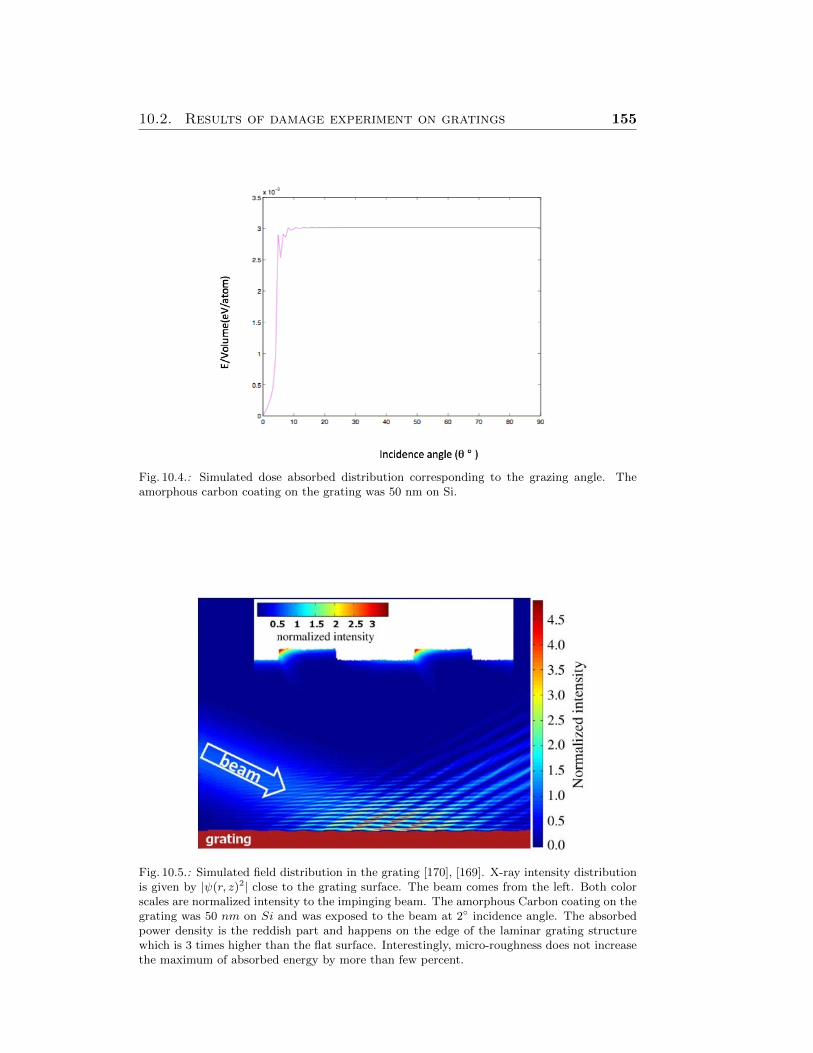
10.2. Results of damage experiment on gratings 155
Fig. 10.4.: Simulated dose absorbed distribution corresponding to the grazing angle. Theamorphous carbon coating on the grating was 50 nm on Si.
Fig. 10.5.: Simulated field distribution in the grating [170], [169]. X-ray intensity distributionis given by |ψ(r, z)2| close to the grating surface. The beam comes from the left. Both colorscales are normalized intensity to the impinging beam. The amorphous Carbon coating on thegrating was 50 nm on Si and was exposed to the beam at 2◦ incidence angle. The absorbedpower density is the reddish part and happens on the edge of the laminar grating structurewhich is 3 times higher than the flat surface. Interestingly, micro-roughness does not increasethe maximum of absorbed energy by more than few percent.
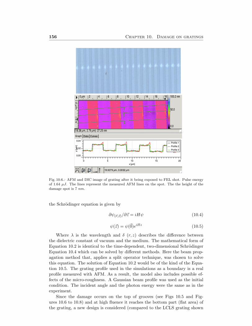
156 Chapter 10. Damage on gratings
Fig. 10.6.: AFM and DIC image of grating after it being exposed to FEL shot. Pulse energyof 1.64 µJ . The lines represent the measured AFM lines on the spot. The the height of thedamage spot is 7 nm.
the Schrodinger equation is given by
∂ψ(~r,~z)/∂~z = iHψ (10.4)
ψ(~z) = ψ(~0)eiHz (10.5)
Where λ is the wavelength and δ (r, z) describes the difference betweenthe dielectric constant of vacuum and the medium. The mathematical form ofEquation 10.2 is identical to the time-dependent, two-dimensional SchrodingerEquation 10.4 which can be solved by different methods. Here the beam prop-agation method that, applies a split operator technique, was chosen to solvethis equation. The solution of Equation 10.2 would be of the kind of the Equa-tion 10.5. The grating profile used in the simulations as a boundary is a realprofile measured with AFM. As a result, the model also includes possible ef-fects of the micro-roughness. A Gaussian beam profile was used as the initialcondition. The incident angle and the photon energy were the same as in theexperiment.
Since the damage occurs on the top of grooves (see Figs 10.5 and Fig-ures 10.6 to 10.8) and at high fluence it reaches the bottom part (flat area) ofthe grating, a new design is considered (compared to the LCLS grating shown
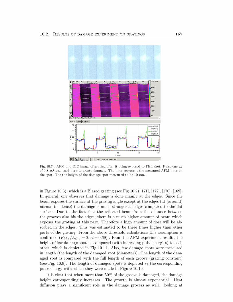
10.2. Results of damage experiment on gratings 157
Fig. 10.7.: AFM and DIC image of grating after it being exposed to FEL shot. Pulse energyof 1.8 µJ was used here to create damage. The lines represent the measured AFM lines onthe spot. The the height of the damage spot measured to be 10 nm.
in Figure 10.3), which is a Blazed grating (see Fig 10.2) [171], [172], [170], [169].In general, one observes that damage is done mainly at the edges. Since thebeam exposes the surface at the grazing angle except at the edges (at (around)normal incidence) the damage is much stronger at edges compared to the flatsurface. Due to the fact that the reflected beam from the distance betweenthe grooves also hit the edges, there is a much higher amount of beam whichexposes the grating at this part. Therefore a high amount of dose will be ab-sorbed in the edges. This was estimated to be three times higher than otherparts of the grating. From the above threshold calculations this assumption isconfirmed (EMth
/EGth= 2.92± 0.69) . From the AFM experiment results, the
height of few damage spots is compared (with increasing pulse energies) to eachother, which is depicted in Fig 10.11. Also, few damage spots were measuredin length (the length of the damaged spot (diameter)). The length of the dam-aged spot is compared with the full length of each groove (grating constant)(see Fig: 10.9). The length of damaged spots is depicted vs the correspondingpulse energy with which they were made in Figure 10.10.
It is clear that when more than 50% of the groove is damaged, the damageheight correspondingly increases. The growth is almost exponential. Heatdiffusion plays a significant role in the damage process as well. looking at
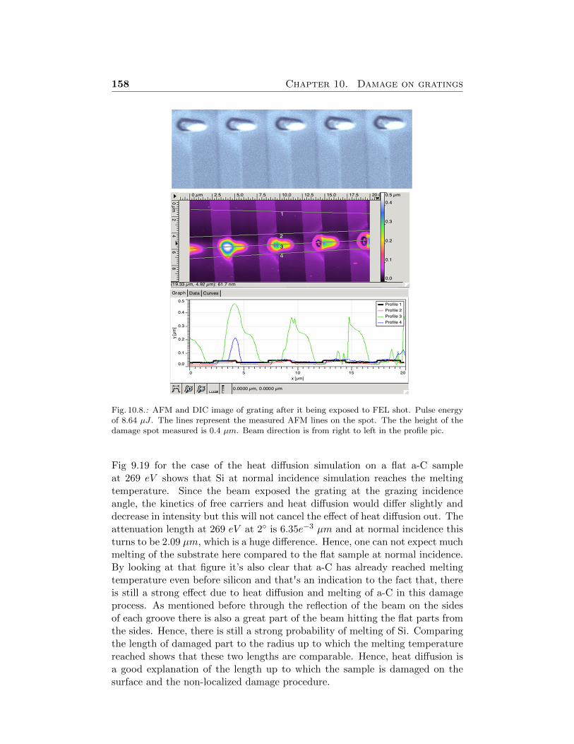
158 Chapter 10. Damage on gratings
Fig. 10.8.: AFM and DIC image of grating after it being exposed to FEL shot. Pulse energyof 8.64 µJ . The lines represent the measured AFM lines on the spot. The the height of thedamage spot measured is 0.4 µm. Beam direction is from right to left in the profile pic.
Fig 9.19 for the case of the heat diffusion simulation on a flat a-C sampleat 269 eV shows that Si at normal incidence simulation reaches the meltingtemperature. Since the beam exposed the grating at the grazing incidenceangle, the kinetics of free carriers and heat diffusion would differ slightly anddecrease in intensity but this will not cancel the effect of heat diffusion out. Theattenuation length at 269 eV at 2◦ is 6.35e−3 µm and at normal incidence thisturns to be 2.09 µm, which is a huge difference. Hence, one can not expect muchmelting of the substrate here compared to the flat sample at normal incidence.By looking at that figure it’s also clear that a-C has already reached meltingtemperature even before silicon and that's an indication to the fact that, thereis still a strong effect due to heat diffusion and melting of a-C in this damageprocess. As mentioned before through the reflection of the beam on the sidesof each groove there is also a great part of the beam hitting the flat parts fromthe sides. Hence, there is still a strong probability of melting of Si. Comparingthe length of damaged part to the radius up to which the melting temperaturereached shows that these two lengths are comparable. Hence, heat diffusion isa good explanation of the length up to which the sample is damaged on thesurface and the non-localized damage procedure.
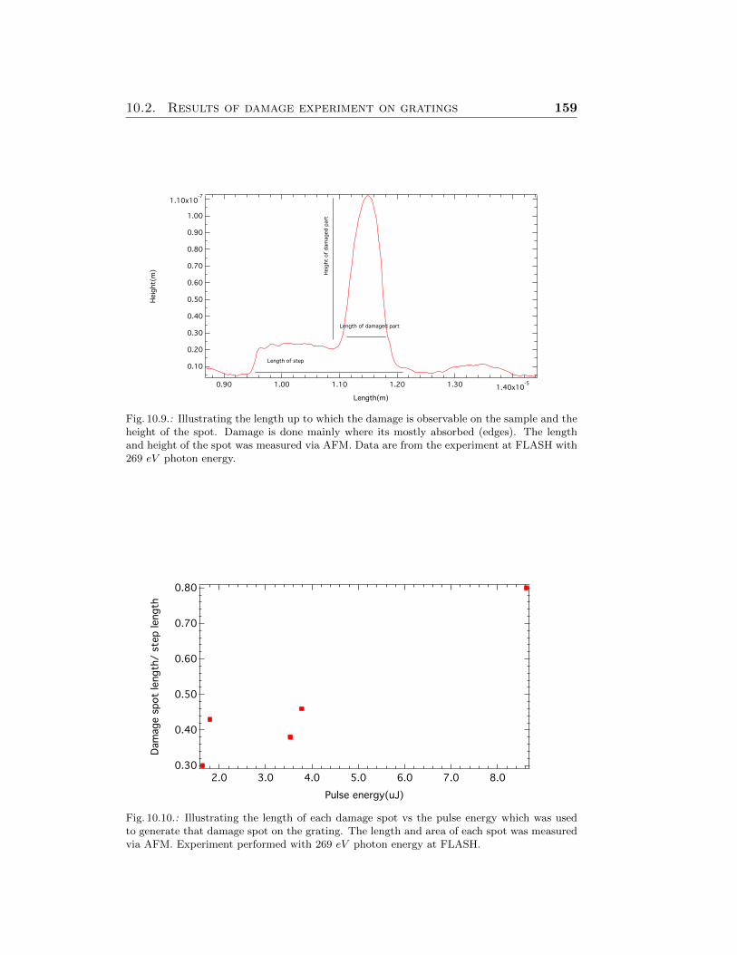
10.2. Results of damage experiment on gratings 159
1.10x10⁻⁷
1.00
0.90
0.80
0.70
0.60
0.50
0.40
0.30
0.20
0.10
Heig
ht(
m)
1.40x10-51.301.201.101.000.90
Length(m)
Heig
ht
of
dam
aged p
art
Length of damaged part
Length of step
Fig. 10.9.: Illustrating the length up to which the damage is observable on the sample and theheight of the spot. Damage is done mainly where its mostly absorbed (edges). The lengthand height of the spot was measured via AFM. Data are from the experiment at FLASH with269 eV photon energy.
0.80
0.70
0.60
0.50
0.40
0.30
Dam
age s
pot
length
/ s
tep length
8.07.06.05.04.03.02.0
Pulse energy(uJ)
Fig. 10.10.: Illustrating the length of each damage spot vs the pulse energy which was usedto generate that damage spot on the grating. The length and area of each spot was measuredvia AFM. Experiment performed with 269 eV photon energy at FLASH.
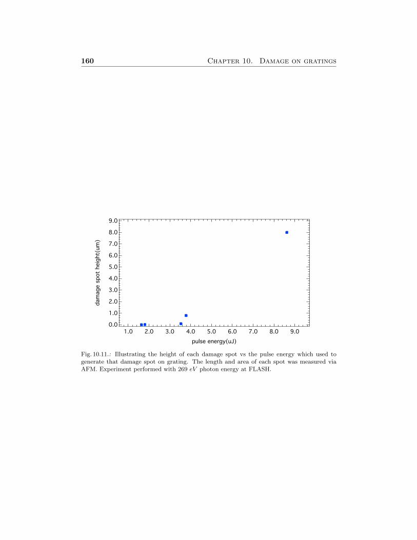
160 Chapter 10. Damage on gratings
9.0
8.0
7.0
6.0
5.0
4.0
3.0
2.0
1.0
0.0
dam
age s
pot
heig
ht(
um
)
9.08.07.06.05.04.03.02.01.0
pulse energy(uJ)
Fig. 10.11.: Illustrating the height of each damage spot vs the pulse energy which used togenerate that damage spot on grating. The length and area of each spot was measured viaAFM. Experiment performed with 269 eV photon energy at FLASH.
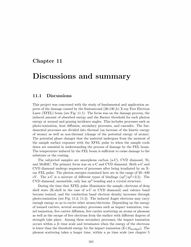
Chapter 11
Discussions and summary
11.1 Discussions
This project was concerned with the study of fundamental and application as-pects of the damage caused by the femtosecond (30-130 fs) X-ray Free ElectronLaser (XFEL) beam (see Fig: 11.1). The focus was on the damage process, theinduced amount of absorbed energy and the fluence threshold for each photonenergy at normal and grazing incidence angles. This includes processes such asphoto-ionization, heat diffusion, secondary processes, and cascades. The fun-damental processes are divided into thermal (an increase of the kinetic energyof atoms) as well as non-thermal (change of the potential energy of atoms).The potential phase changes that the material undergoes from the moment ofthe sample surface exposure with the XFEL pulse to when the sample coolsdown are essential in understanding the process of damage by the FEL beam.The temperature induced by the FEL beam is sufficient to cause damage to thesubstrate or the coating.
The subjected samples are amorphous carbon (a-C), CVD diamond, Ni,and MoB4C. The primary focus was on a-C and CVD diamond. Both a-C andCVD diamond undergo sequences of processes after being irradiated by an X-ray FEL pulse. The photon energies examined here are in the range of 20−830eV . The a-C is a mixture of different types of bindings (sp3/sp2=2.2). TheCVD diamond, meanwhile, only has sp3 bonding and a crystal structure.
During the time that XFEL pulse illuminates the sample, electrons of deepshell state (K-shell in the case of a-C or CVD diamond) and valence bandbecome ionized, and the conduction band electron density increases throughphoto-ionization (see Fig: 11.2, 11.3). The induced Auger electrons may carryenough energy so as to excite other atoms/electrons. Depending on the energyof ionized carriers, several secondary processes such as impact ionization, tun-nel ionization, free carrier diffusion, free carrier scattering on atoms or phononsas well as the escape of free electrons from the surface with different degrees ofstrength take place. Among these secondary processes, the impact ionizationoccurs within a fs time scale and terminates when the energy of the electronsis lower than the threshold energy for the impact ionization (E<Ebandgap). Thephonon scattering takes a longer time, within a ps time scale (see chapter 5
161
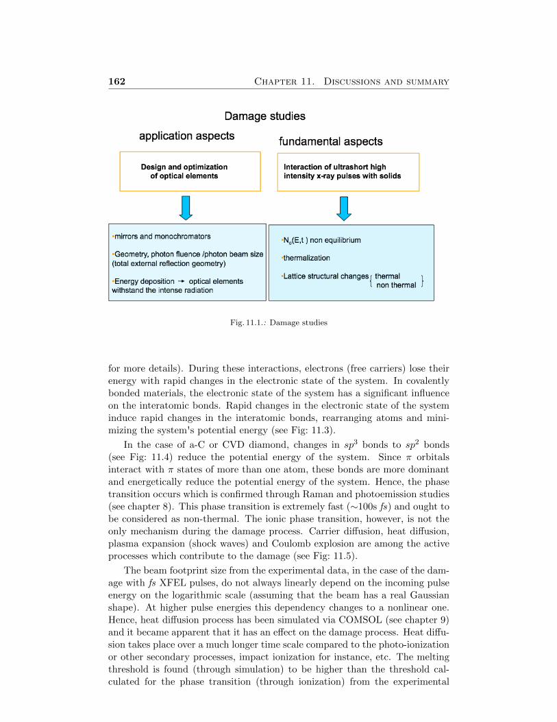
162 Chapter 11. Discussions and summary
Fig. 11.1.: Damage studies
for more details). During these interactions, electrons (free carriers) lose theirenergy with rapid changes in the electronic state of the system. In covalentlybonded materials, the electronic state of the system has a significant influenceon the interatomic bonds. Rapid changes in the electronic state of the systeminduce rapid changes in the interatomic bonds, rearranging atoms and mini-mizing the system's potential energy (see Fig: 11.3).
In the case of a-C or CVD diamond, changes in sp3 bonds to sp2 bonds(see Fig: 11.4) reduce the potential energy of the system. Since π orbitalsinteract with π states of more than one atom, these bonds are more dominantand energetically reduce the potential energy of the system. Hence, the phasetransition occurs which is confirmed through Raman and photoemission studies(see chapter 8). This phase transition is extremely fast (∼100s fs) and ought tobe considered as non-thermal. The ionic phase transition, however, is not theonly mechanism during the damage process. Carrier diffusion, heat diffusion,plasma expansion (shock waves) and Coulomb explosion are among the activeprocesses which contribute to the damage (see Fig: 11.5).
The beam footprint size from the experimental data, in the case of the dam-age with fs XFEL pulses, do not always linearly depend on the incoming pulseenergy on the logarithmic scale (assuming that the beam has a real Gaussianshape). At higher pulse energies this dependency changes to a nonlinear one.Hence, heat diffusion process has been simulated via COMSOL (see chapter 9)and it became apparent that it has an effect on the damage process. Heat diffu-sion takes place over a much longer time scale compared to the photo-ionizationor other secondary processes, impact ionization for instance, etc. The meltingthreshold is found (through simulation) to be higher than the threshold cal-culated for the phase transition (through ionization) from the experimental
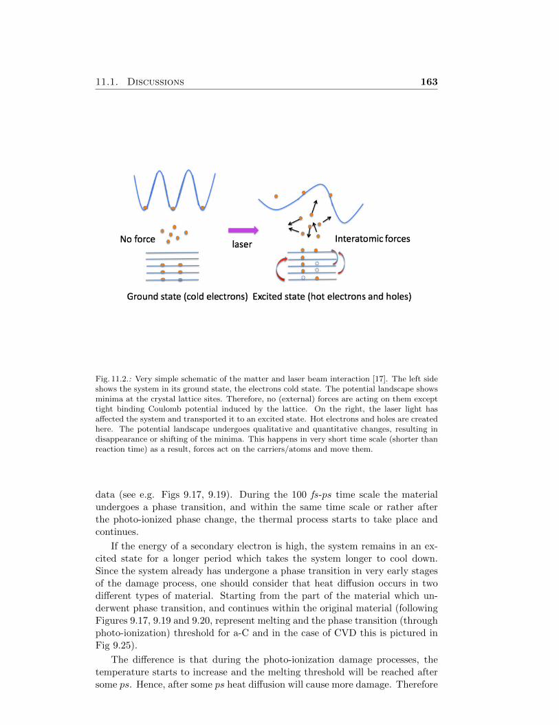
11.1. Discussions 163
Fig. 11.2.: Very simple schematic of the matter and laser beam interaction [17]. The left sideshows the system in its ground state, the electrons cold state. The potential landscape showsminima at the crystal lattice sites. Therefore, no (external) forces are acting on them excepttight binding Coulomb potential induced by the lattice. On the right, the laser light hasaffected the system and transported it to an excited state. Hot electrons and holes are createdhere. The potential landscape undergoes qualitative and quantitative changes, resulting indisappearance or shifting of the minima. This happens in very short time scale (shorter thanreaction time) as a result, forces act on the carriers/atoms and move them.
data (see e.g. Figs 9.17, 9.19). During the 100 fs-ps time scale the materialundergoes a phase transition, and within the same time scale or rather afterthe photo-ionized phase change, the thermal process starts to take place andcontinues.
If the energy of a secondary electron is high, the system remains in an ex-cited state for a longer period which takes the system longer to cool down.Since the system already has undergone a phase transition in very early stagesof the damage process, one should consider that heat diffusion occurs in twodifferent types of material. Starting from the part of the material which un-derwent phase transition, and continues within the original material (followingFigures 9.17, 9.19 and 9.20, represent melting and the phase transition (throughphoto-ionization) threshold for a-C and in the case of CVD this is pictured inFig 9.25).
The difference is that during the photo-ionization damage processes, thetemperature starts to increase and the melting threshold will be reached aftersome ps. Hence, after some ps heat diffusion will cause more damage. Therefore
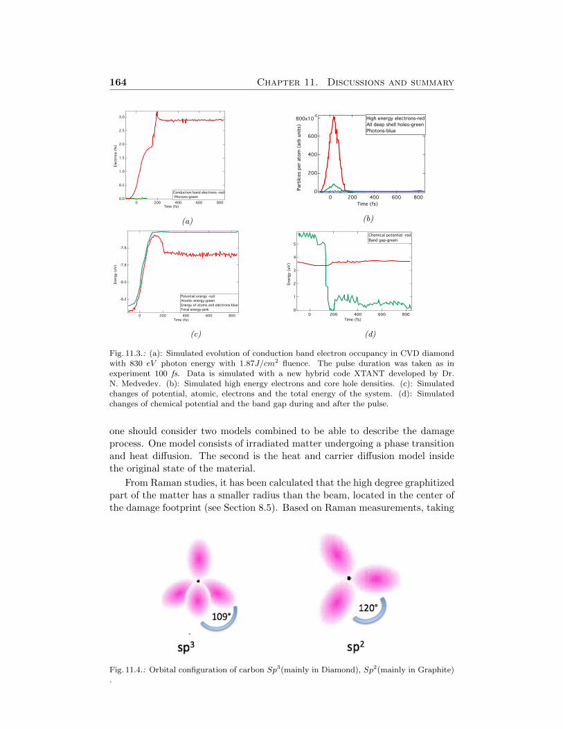
164 Chapter 11. Discussions and summary
3.0
2.5
2.0
1.5
1.0
0.5
0.0
Ele
ctr
ons
(%)
8006004002000Time (fs)
Conduction band electrons -red
Photons-green
(a)
800x10-6
600
400
200
0
Part
ilces
per
ato
m (
arb
unit
s)
8006004002000
Time (fs)
High energy electrons-red
All deep shell holes-green
Photons-blue
(b)
-8.2
-8.0
-7.8
-7.6
Energ
y (
eV
)
8006004002000
Time (fs)
Potential energy -red
Atomic energy-green
Energy of atoms and electrons-blue
Total energy-pink
(c)
5
4
3
2
1
0
Energ
y (
eV
)
8006004002000
Time (fs)
Chemical potential -red
Band gap-green
(d)
Fig. 11.3.: (a): Simulated evolution of conduction band electron occupancy in CVD diamondwith 830 eV photon energy with 1.87J/cm2 fluence. The pulse duration was taken as inexperiment 100 fs. Data is simulated with a new hybrid code XTANT developed by Dr.N. Medvedev. (b): Simulated high energy electrons and core hole densities. (c): Simulatedchanges of potential, atomic, electrons and the total energy of the system. (d): Simulatedchanges of chemical potential and the band gap during and after the pulse.
one should consider two models combined to be able to describe the damageprocess. One model consists of irradiated matter undergoing a phase transitionand heat diffusion. The second is the heat and carrier diffusion model insidethe original state of the material.
From Raman studies, it has been calculated that the high degree graphitizedpart of the matter has a smaller radius than the beam, located in the center ofthe damage footprint (see Section 8.5). Based on Raman measurements, taking
Fig. 11.4.: Orbital configuration of carbon Sp3(mainly in Diamond), Sp2(mainly in Graphite).
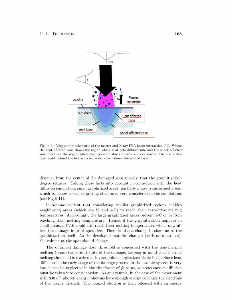
11.1. Discussions 165
Fig. 11.5.: Very simple schematic of the matter and X-ray FEL beam interaction [39]. Wherethe heat affected zone shows the region where heat gets diffused into and the shock affectedzone describes the region where high pressure starts to induce shock waves. There is a thinlayer right behind the heat-affected zone, which shows the melted layer.
distance from the center of the damaged spot reveals; that the graphitizationdegree reduces. Taking these facts into account in connection with the heatdiffusion simulation, small graphitized areas, partially phase transformed areas;which somehow look like grating structure, were considered in the simulations(see Fig 9.11).
It became evident that considering smaller graphitized regions enablesneighboring areas (which are Si and a-C) to reach their respective meltingtemperatures. Accordingly, the large graphitized areas prevent a-C or Si fromreaching their melting temperature. Hence, if the graphitization happens insmall areas, a-C/Si could still reach their melting temperatures which may af-fect the damage imprint spot size. There is also a change in size due to thegraphitization itself. As the density of material changes (with no mass loss),the volume at the spot should change.
The obtained damage dose threshold is concerned with the non-thermalmelting (phase transition) state of the damage; keeping in mind that thermalmelting threshold is reached at higher pulse energies (see Table 11.1). Since heatdiffusion in the early stage of the damage process in the atomic system is verylow, it can be neglected in the timeframe of fs to ps, whereas carrier diffusionmust be taken into consideration. As an example, in the case of the experimentwith 830 eV photon energy, photons have enough energy to ionize the electronsof the atoms’ K-shell. The ionized electron is then released with an energy
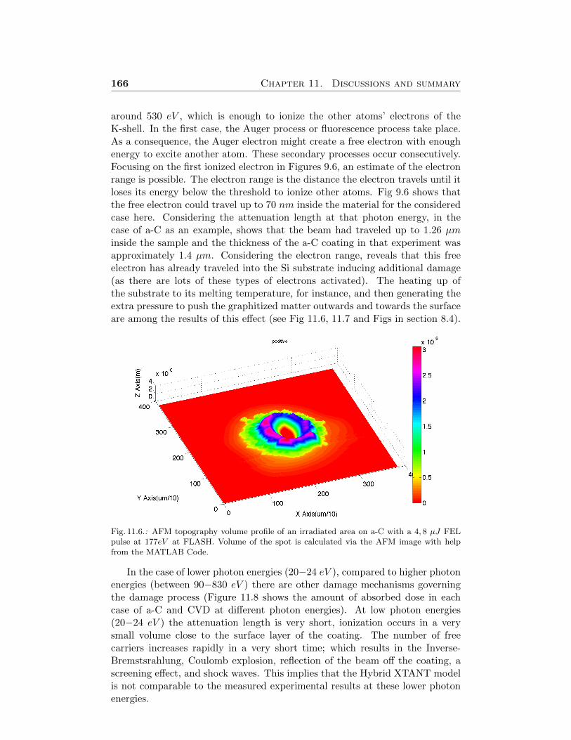
166 Chapter 11. Discussions and summary
around 530 eV , which is enough to ionize the other atoms’ electrons of theK-shell. In the first case, the Auger process or fluorescence process take place.As a consequence, the Auger electron might create a free electron with enoughenergy to excite another atom. These secondary processes occur consecutively.Focusing on the first ionized electron in Figures 9.6, an estimate of the electronrange is possible. The electron range is the distance the electron travels until itloses its energy below the threshold to ionize other atoms. Fig 9.6 shows thatthe free electron could travel up to 70 nm inside the material for the consideredcase here. Considering the attenuation length at that photon energy, in thecase of a-C as an example, shows that the beam had traveled up to 1.26 µminside the sample and the thickness of the a-C coating in that experiment wasapproximately 1.4 µm. Considering the electron range, reveals that this freeelectron has already traveled into the Si substrate inducing additional damage(as there are lots of these types of electrons activated). The heating up ofthe substrate to its melting temperature, for instance, and then generating theextra pressure to push the graphitized matter outwards and towards the surfaceare among the results of this effect (see Fig 11.6, 11.7 and Figs in section 8.4).
Fig. 11.6.: AFM topography volume profile of an irradiated area on a-C with a 4, 8 µJ FELpulse at 177eV at FLASH. Volume of the spot is calculated via the AFM image with helpfrom the MATLAB Code.
In the case of lower photon energies (20−24 eV ), compared to higher photonenergies (between 90−830 eV ) there are other damage mechanisms governingthe damage process (Figure 11.8 shows the amount of absorbed dose in eachcase of a-C and CVD at different photon energies). At low photon energies(20−24 eV ) the attenuation length is very short, ionization occurs in a verysmall volume close to the surface layer of the coating. The number of freecarriers increases rapidly in a very short time; which results in the Inverse-Bremstsrahlung, Coulomb explosion, reflection of the beam off the coating, ascreening effect, and shock waves. This implies that the Hybrid XTANT modelis not comparable to the measured experimental results at these lower photonenergies.
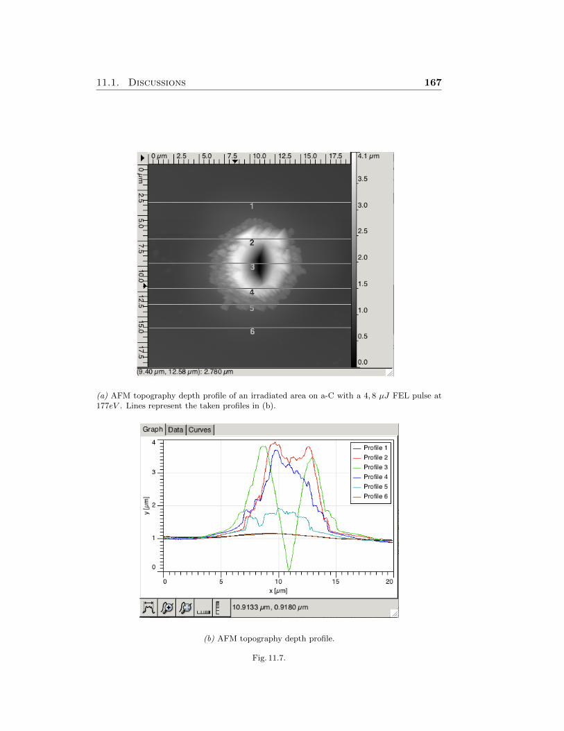
11.1. Discussions 167
(a) AFM topography depth profile of an irradiated area on a-C with a 4, 8 µJ FEL pulse at177eV . Lines represent the taken profiles in (b).
(b) AFM topography depth profile.
Fig. 11.7.
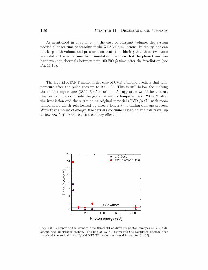
168 Chapter 11. Discussions and summary
As mentioned in chapter 9, in the case of constant volume, the systemneeded a longer time to stabilize in the XTANT simulations. In reality, one cannot keep both volume and pressure constant. Considering that these two casesare valid at the same time, from simulation it is clear that the phase transitionhappens (non-thermal) between first 100-200 fs time after the irradiation (seeFig 11.10).
The Hybrid XTANT model in the case of CVD diamond predicts that tem-perature after the pulse goes up to 2000 K. This is still below the meltingthreshold temperature (3800 K) for carbon. A suggestion would be to startthe heat simulation inside the graphite with a temperature of 2000 K afterthe irradiation and the surrounding original material (CVD /a-C ) with roomtemperature which gets heated up after a longer time during damage process.With that amount of energy, free carriers continue cascading and can travel upto few nm further and cause secondary effects.
0 200 400 600 8000
2
4
6
8
10
12
14
16 a-C Dose CVD diamond Dose
Dos
e [e
V/a
tom
]
Photon energy (eV)
0.7 ev/atom
Fig. 11.8.: Comparing the damage dose threshold at different photon energies on CVD di-amond and amorphous carbon. The line at 0.7 eV represents the calculated damage dosethreshold theoretically via Hybrid XTANT model mentioned in chapter 9 [135].
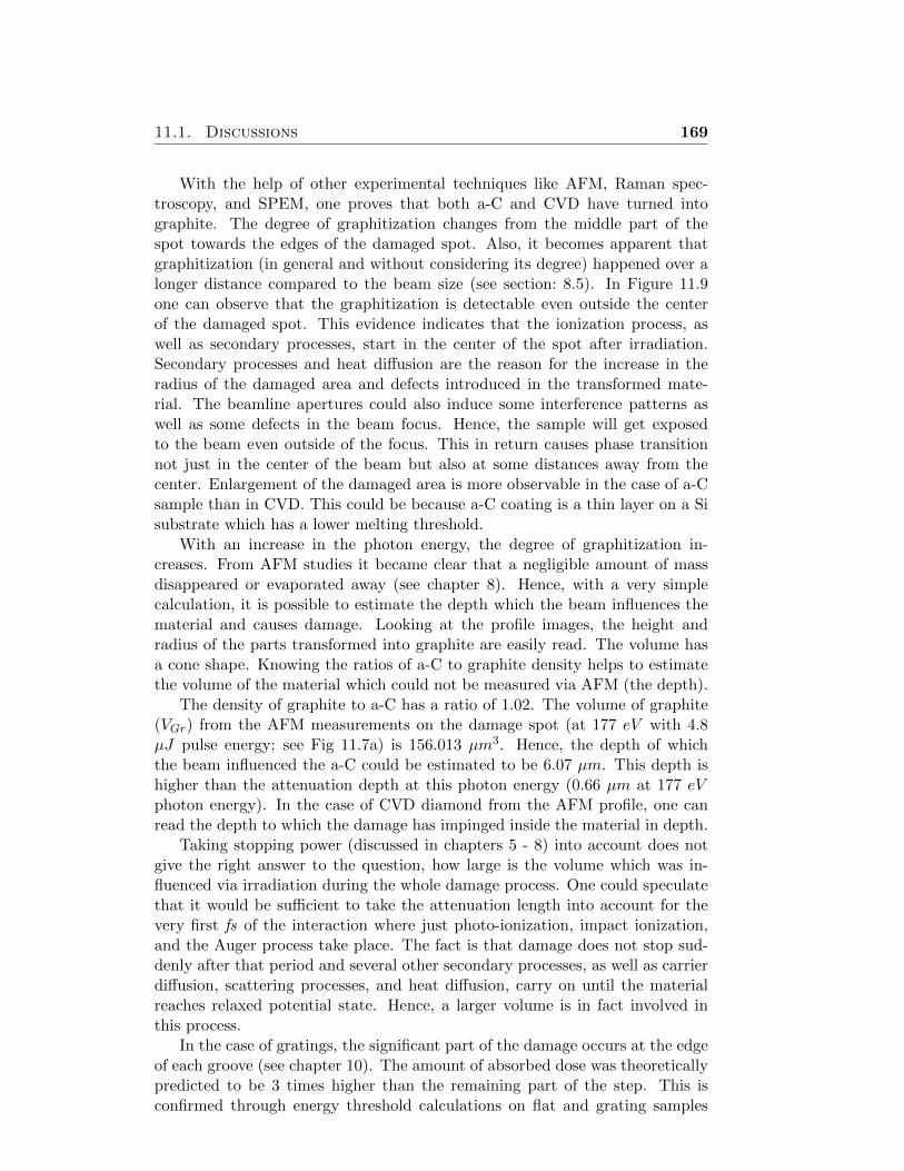
11.1. Discussions 169
With the help of other experimental techniques like AFM, Raman spec-troscopy, and SPEM, one proves that both a-C and CVD have turned intographite. The degree of graphitization changes from the middle part of thespot towards the edges of the damaged spot. Also, it becomes apparent thatgraphitization (in general and without considering its degree) happened over alonger distance compared to the beam size (see section: 8.5). In Figure 11.9one can observe that the graphitization is detectable even outside the centerof the damaged spot. This evidence indicates that the ionization process, aswell as secondary processes, start in the center of the spot after irradiation.Secondary processes and heat diffusion are the reason for the increase in theradius of the damaged area and defects introduced in the transformed mate-rial. The beamline apertures could also induce some interference patterns aswell as some defects in the beam focus. Hence, the sample will get exposedto the beam even outside of the focus. This in return causes phase transitionnot just in the center of the beam but also at some distances away from thecenter. Enlargement of the damaged area is more observable in the case of a-Csample than in CVD. This could be because a-C coating is a thin layer on a Sisubstrate which has a lower melting threshold.
With an increase in the photon energy, the degree of graphitization in-creases. From AFM studies it became clear that a negligible amount of massdisappeared or evaporated away (see chapter 8). Hence, with a very simplecalculation, it is possible to estimate the depth which the beam influences thematerial and causes damage. Looking at the profile images, the height andradius of the parts transformed into graphite are easily read. The volume hasa cone shape. Knowing the ratios of a-C to graphite density helps to estimatethe volume of the material which could not be measured via AFM (the depth).
The density of graphite to a-C has a ratio of 1.02. The volume of graphite(VGr) from the AFM measurements on the damage spot (at 177 eV with 4.8µJ pulse energy; see Fig 11.7a) is 156.013 µm3. Hence, the depth of whichthe beam influenced the a-C could be estimated to be 6.07 µm. This depth ishigher than the attenuation depth at this photon energy (0.66 µm at 177 eVphoton energy). In the case of CVD diamond from the AFM profile, one canread the depth to which the damage has impinged inside the material in depth.
Taking stopping power (discussed in chapters 5 - 8) into account does notgive the right answer to the question, how large is the volume which was in-fluenced via irradiation during the whole damage process. One could speculatethat it would be sufficient to take the attenuation length into account for thevery first fs of the interaction where just photo-ionization, impact ionization,and the Auger process take place. The fact is that damage does not stop sud-denly after that period and several other secondary processes, as well as carrierdiffusion, scattering processes, and heat diffusion, carry on until the materialreaches relaxed potential state. Hence, a larger volume is in fact involved inthis process.
In the case of gratings, the significant part of the damage occurs at the edgeof each groove (see chapter 10). The amount of absorbed dose was theoreticallypredicted to be 3 times higher than the remaining part of the step. This isconfirmed through energy threshold calculations on flat and grating samples
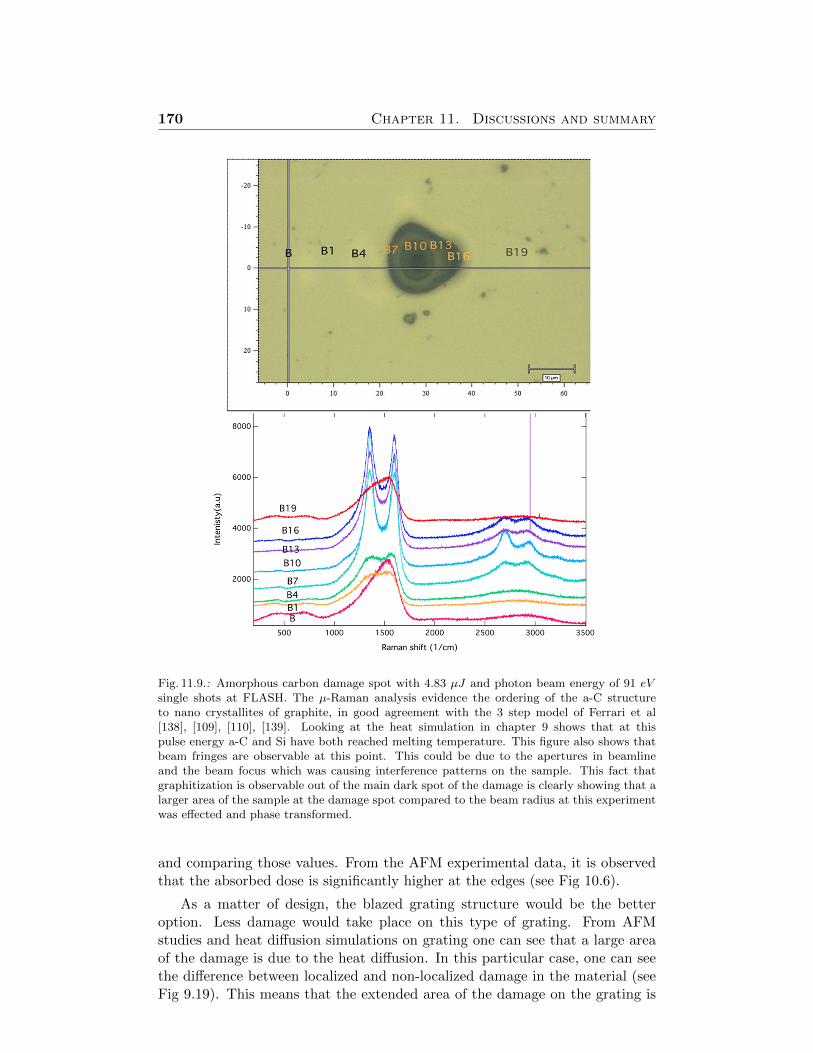
170 Chapter 11. Discussions and summary
Fig. 11.9.: Amorphous carbon damage spot with 4.83 µJ and photon beam energy of 91 eVsingle shots at FLASH. The µ-Raman analysis evidence the ordering of the a-C structureto nano crystallites of graphite, in good agreement with the 3 step model of Ferrari et al[138], [109], [110], [139]. Looking at the heat simulation in chapter 9 shows that at thispulse energy a-C and Si have both reached melting temperature. This figure also shows thatbeam fringes are observable at this point. This could be due to the apertures in beamlineand the beam focus which was causing interference patterns on the sample. This fact thatgraphitization is observable out of the main dark spot of the damage is clearly showing that alarger area of the sample at the damage spot compared to the beam radius at this experimentwas effected and phase transformed.
and comparing those values. From the AFM experimental data, it is observedthat the absorbed dose is significantly higher at the edges (see Fig 10.6).
As a matter of design, the blazed grating structure would be the betteroption. Less damage would take place on this type of grating. From AFMstudies and heat diffusion simulations on grating one can see that a large areaof the damage is due to the heat diffusion. In this particular case, one can seethe difference between localized and non-localized damage in the material (seeFig 9.19). This means that the extended area of the damage on the grating is
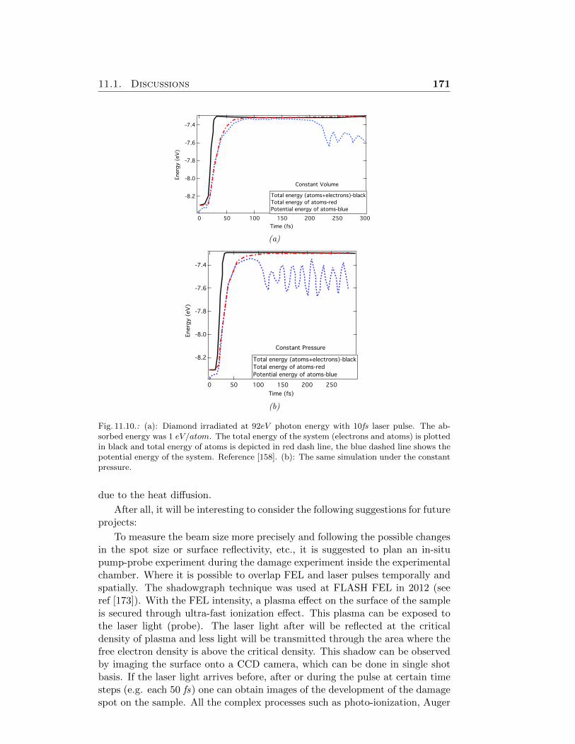
11.1. Discussions 171
-8.2
-8.0
-7.8
-7.6
-7.4
Energ
y (
eV
)
300250200150100500
Time (fs)
Constant Volume
Total energy (atoms+electrons)-black
Total energy of atoms-red
Potential energy of atoms-blue
(a)
-8.2
-8.0
-7.8
-7.6
-7.4
Energ
y (
eV
)
250200150100500
Time (fs)
Constant Pressure
Total energy (atoms+electrons)-black
Total energy of atoms-red
Potential energy of atoms-blue
(b)
Fig. 11.10.: (a): Diamond irradiated at 92eV photon energy with 10fs laser pulse. The ab-sorbed energy was 1 eV/atom. The total energy of the system (electrons and atoms) is plottedin black and total energy of atoms is depicted in red dash line, the blue dashed line shows thepotential energy of the system. Reference [158]. (b): The same simulation under the constantpressure.
due to the heat diffusion.
After all, it will be interesting to consider the following suggestions for futureprojects:
To measure the beam size more precisely and following the possible changesin the spot size or surface reflectivity, etc., it is suggested to plan an in-situpump-probe experiment during the damage experiment inside the experimentalchamber. Where it is possible to overlap FEL and laser pulses temporally andspatially. The shadowgraph technique was used at FLASH FEL in 2012 (seeref [173]). With the FEL intensity, a plasma effect on the surface of the sampleis secured through ultra-fast ionization effect. This plasma can be exposed tothe laser light (probe). The laser light after will be reflected at the criticaldensity of plasma and less light will be transmitted through the area where thefree electron density is above the critical density. This shadow can be observedby imaging the surface onto a CCD camera, which can be done in single shotbasis. If the laser light arrives before, after or during the pulse at certain timesteps (e.g. each 50 fs) one can obtain images of the development of the damagespot on the sample. All the complex processes such as photo-ionization, Auger
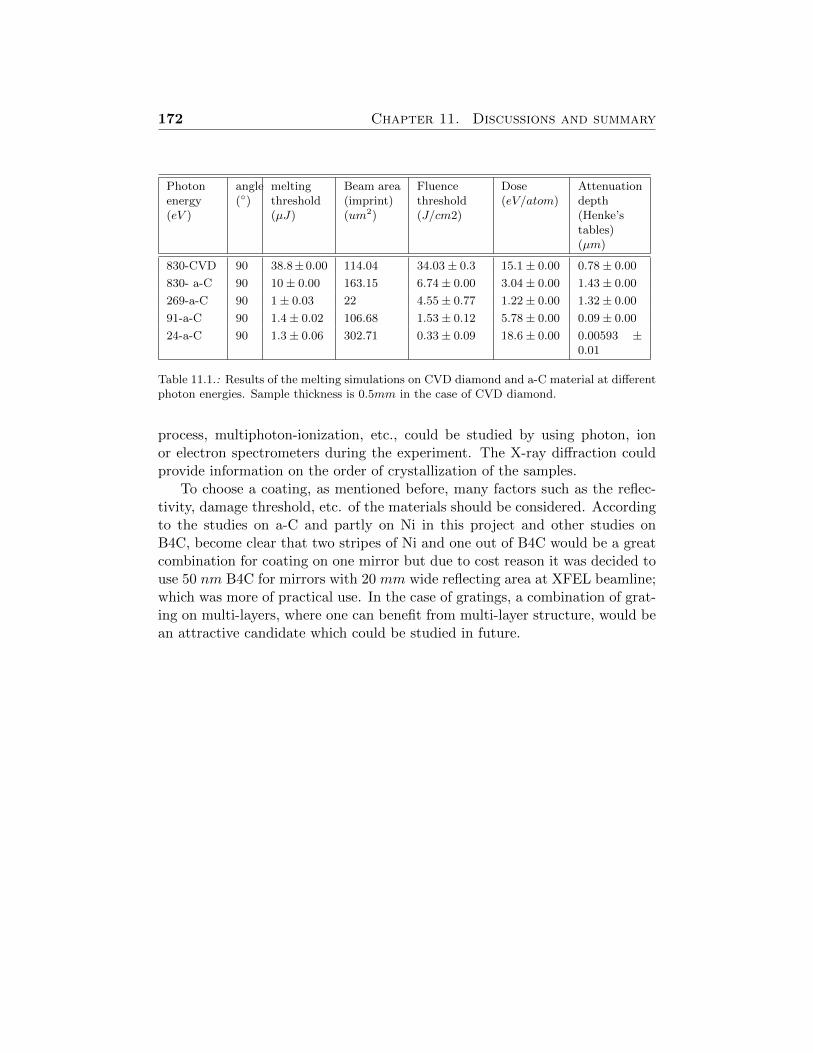
172 Chapter 11. Discussions and summary
Photonenergy(eV )
angle(◦)
meltingthreshold(µJ)
Beam area(imprint)(um2)
Fluencethreshold(J/cm2)
Dose(eV/atom)
Attenuationdepth(Henke’stables)(µm)
830-CVD 90 38.8±0.00 114.04 34.03± 0.3 15.1± 0.00 0.78± 0.00
830- a-C 90 10± 0.00 163.15 6.74± 0.00 3.04± 0.00 1.43± 0.00
269-a-C 90 1± 0.03 22 4.55± 0.77 1.22± 0.00 1.32± 0.00
91-a-C 90 1.4± 0.02 106.68 1.53± 0.12 5.78± 0.00 0.09± 0.00
24-a-C 90 1.3± 0.06 302.71 0.33± 0.09 18.6± 0.00 0.00593 ±0.01
Table 11.1.: Results of the melting simulations on CVD diamond and a-C material at differentphoton energies. Sample thickness is 0.5mm in the case of CVD diamond.
process, multiphoton-ionization, etc., could be studied by using photon, ionor electron spectrometers during the experiment. The X-ray diffraction couldprovide information on the order of crystallization of the samples.
To choose a coating, as mentioned before, many factors such as the reflec-tivity, damage threshold, etc. of the materials should be considered. Accordingto the studies on a-C and partly on Ni in this project and other studies onB4C, become clear that two stripes of Ni and one out of B4C would be a greatcombination for coating on one mirror but due to cost reason it was decided touse 50 nm B4C for mirrors with 20 mm wide reflecting area at XFEL beamline;which was more of practical use. In the case of gratings, a combination of grat-ing on multi-layers, where one can benefit from multi-layer structure, would bean attractive candidate which could be studied in future.
11.2. Summary 173
11.2 Summary
X-ray Free Electron Lasers (XFEL) contribute to several different scientificapplications reaching from physics, over chemistry, material and earth sciencesto biology. They deliver high peak brilliance, high power, femtosecond focusedlaser pulses. Optical elements in these facilities are of crucial importance asthey need to survive those severe conditions (high peak power, etc.) during thedistribution of a high-quality beam to the experimental stations.
The optical element such as the mirror or grating need to withstand thehigh peak power of the intense, focused fs pulses over a full spectral range ofphoton energies at FEL beamlines. Besides, the wavefront needs to stay undis-torted during the transport along the beamline until the experimental station.Choosing a suitable substrate and coating for mirrors or gratings (as opticalelements) in the beamline depends on many factors including high reflectivity,low roughness, high mechanical and thermal stability.
Many investigations have been done up to now on low and high Z materialsto find out the suitable coating for soft/ hard X-ray beamlines. Among allthese, one can mention B4C, B, SiC, C, SiN, Al, Al2O3, SiO2, Li, Cu, InSb,Mo, etc [174], [132], [175], [176].
This Ph.D. project is concerned with the structural modification of solidsunder ultra-short X-ray FEL laser pulses. These materials are chosen from thegroup of low Z materials (amorphous carbon (a-C), CVD diamond). Addition-ally, a-C is tested as a potential coating on mirrors and CVD diamond to be usedin monochromators for the soft X-ray beamline at the European XFEL facility.These two materials were studied at normal (to study the structural modifica-tion processes) and grazing incidence angles for the total external reflection. Atnormal incidence, the exposed material via FEL X-ray beam experiences a highpeak power and exhibit non-linear effects. Among those, are photo-ionization,secondary processes (e.g. Auger, impact ionization, carrier diffusion, etc. (seeChapters 5, 9)) and high amount of heat induced, which influence the damageprocess.
The time scale of events happening during the interaction of the XFELpulse with the material can be grouped in three different time zones. In early fstime, the photo-ionization is the ruling process; taking place. After some 100 fs,events like Auger, impact ionization, tunnel ionization, carrier diffusion start totake place. These are followed by free carriers interaction with the lattice (e.g.electron-phonon coupling, etc.), and heat diffusion is grouped in the third timezone, which starts after some 100 ps and continue till the system gets backto room temperature after some µs. Depending on the pulse energy at eachphoton energy, heat diffusion could play a substantial role in these interactionsand cause effects like melting (see this in Figure 11.11). The consequence ofcrossing the threshold values of structural modifications of materials is causingdamage to those coatings, gratings or monochromators used at the beamlines;which is not desirable.
One of the interesting points observed from the experimental results is thatthe damage footprint area on the logarithmic scale was not growing linearlywith pulse energy as expected. The results of the experiments show that the
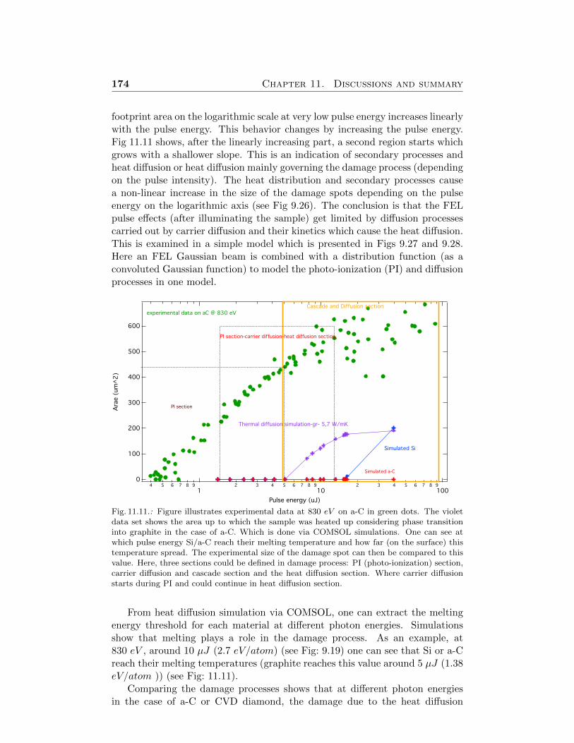
174 Chapter 11. Discussions and summary
footprint area on the logarithmic scale at very low pulse energy increases linearlywith the pulse energy. This behavior changes by increasing the pulse energy.Fig 11.11 shows, after the linearly increasing part, a second region starts whichgrows with a shallower slope. This is an indication of secondary processes andheat diffusion or heat diffusion mainly governing the damage process (dependingon the pulse intensity). The heat distribution and secondary processes causea non-linear increase in the size of the damage spots depending on the pulseenergy on the logarithmic axis (see Fig 9.26). The conclusion is that the FELpulse effects (after illuminating the sample) get limited by diffusion processescarried out by carrier diffusion and their kinetics which cause the heat diffusion.This is examined in a simple model which is presented in Figs 9.27 and 9.28.Here an FEL Gaussian beam is combined with a distribution function (as aconvoluted Gaussian function) to model the photo-ionization (PI) and diffusionprocesses in one model.
600
500
400
300
200
100
0
Ara
e (
um
^2)
4 5 6 7 8 9
12 3 4 5 6 7 8 9
102 3 4 5 6 7 8 9
100
Pulse energy (uJ)
Thermal diffusion simulation-gr- 5,7 W/mK
experimental data on aC @ 830 eV
PI section
Cascade and Diffusion section
Simulated Si
Simulated a-C
PI section-carrier diffusion-heat diffusion section
Fig. 11.11.: Figure illustrates experimental data at 830 eV on a-C in green dots. The violetdata set shows the area up to which the sample was heated up considering phase transitioninto graphite in the case of a-C. Which is done via COMSOL simulations. One can see atwhich pulse energy Si/a-C reach their melting temperature and how far (on the surface) thistemperature spread. The experimental size of the damage spot can then be compared to thisvalue. Here, three sections could be defined in damage process: PI (photo-ionization) section,carrier diffusion and cascade section and the heat diffusion section. Where carrier diffusionstarts during PI and could continue in heat diffusion section.
From heat diffusion simulation via COMSOL, one can extract the meltingenergy threshold for each material at different photon energies. Simulationsshow that melting plays a role in the damage process. As an example, at830 eV , around 10 µJ (2.7 eV/atom) (see Fig: 9.19) one can see that Si or a-Creach their melting temperatures (graphite reaches this value around 5 µJ (1.38eV/atom )) (see Fig: 11.11).
Comparing the damage processes shows that at different photon energiesin the case of a-C or CVD diamond, the damage due to the heat diffusion
11.2. Summary 175
(melting) in the system happens at high pulse energies compared to the non-thermal process. The next observation is that around K−edge these two values(non/thermal damage absorbed dose) get close to each other and at lower pho-ton energies (20 eV ) melting has a much weaker effect in the damage comparedto non-thermal processes. Which is a hint to the point that at lower photonenergies, effects like free carriers escape from the surface, secondary processes,plasma formation, Coulomb explosion, etc. are mainly the processes inducingthe damage on the material. In the case of CVD diamond at 830 eV (con-sidering the phase transition) the COMSOL simulation shows that the inducedgraphite can reach the melting temperature around 5 µJ which cause a thermaldamage (see Figs: 9.25 and 9.29).
The CVD diamond is a suitable material to be used in monochroma-tors [177], [4] and [178].
Based on the performed studies from other groups, the B4Cseems to be a better candidate to be used on mirrors (optical ele-ments) [174], [132], [175], [176]. Among multilayers, the MoB4C is an inter-esting candidate, and from the group of high Z material, Ni shows promisingvalues and is interesting to be studied with more details with different photonenergies. Results of the experiment on Ni at different grazing angles at 269 eVare presented in Table 12.5.
The result of the damage studies on MoB4C are presented in Table 12.6and Figs 12.18a − 12.25. Looking at those results shows that the thresholdfluence in the case of annealed MoB4C samples is higher than in the case of a-C(which is not annealed). This is due to the more stable structure of annealedsamples. Hence, further studies on annealed multi layers are interesting to becontinued.

176 Chapter 11. Discussions and summary
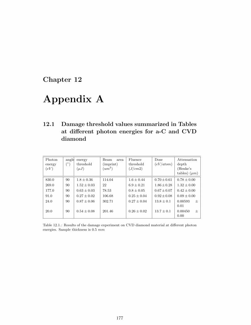
Chapter 12
Appendix A
12.1 Damage threshold values summarized in Tablesat different photon energies for a-C and CVDdiamond
Photonenergy(eV )
angle(◦)
energythreshold(µJ)
Beam area(imprint)(um2)
Fluencethreshold(J/cm2)
Dose(eV/atom)
Attenuationdepth(Henke’stables) (µm)
830.0 90 1.8± 0.36 114.04 1.6± 0.44 0.70±0.61 0.78± 0.00
269.0 90 1.52± 0.03 22 6.9± 0.21 1.86±0.28 1.32± 0.00
177.0 90 0.63± 0.03 78.53 0.8± 0.05 0.67±0.07 0.42± 0.00
91.0 90 0.27± 0.02 106.68 0.25± 0.04 0.92±0.08 0.09± 0.00
24.0 90 0.87± 0.06 302.71 0.27± 0.04 13.8± 0.1 0.00593 ±0.01
20.0 90 0.54± 0.08 201.46 0.26± 0.02 13.7± 0.1 0.00450 ±0.00
Table 12.1.: Results of the damage experiment on CVD diamond material at different photonenergies. Sample thickness is 0.5 mm
177
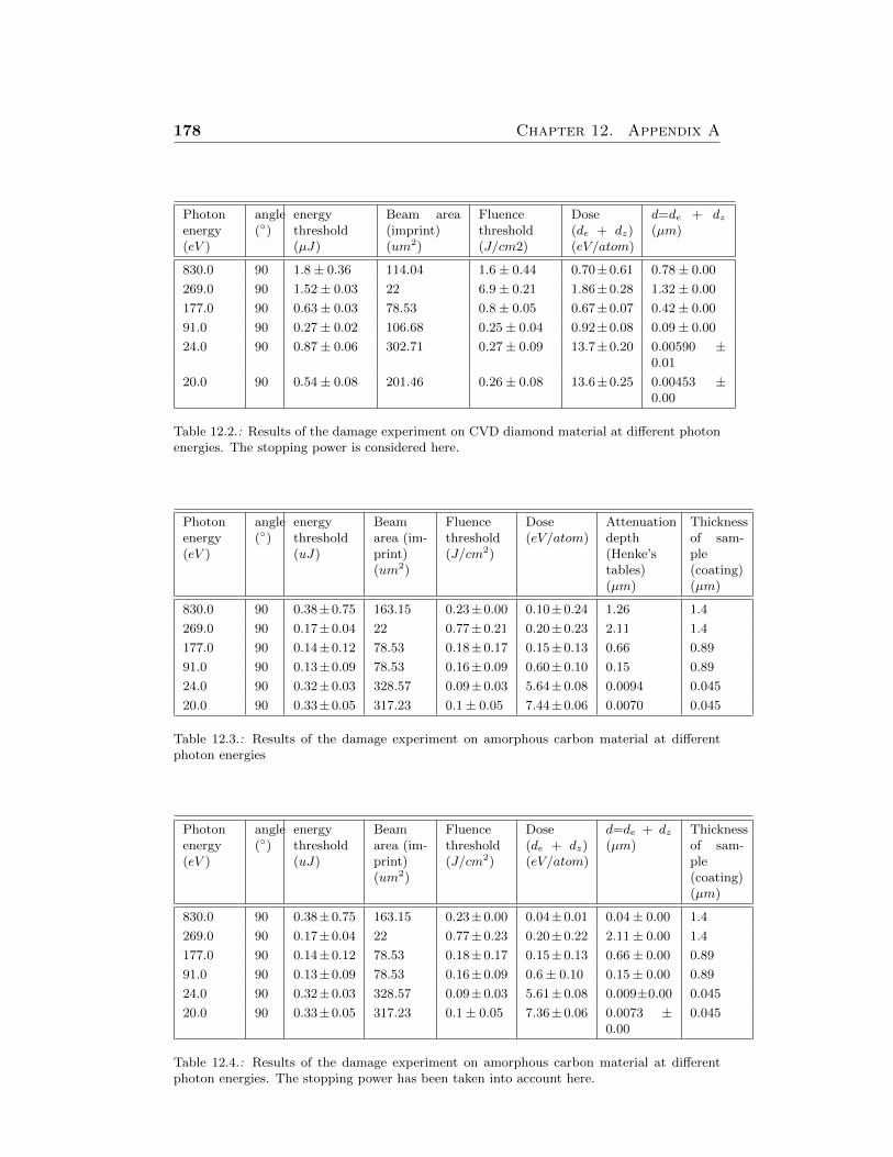
178 Chapter 12. Appendix A
Photonenergy(eV )
angle(◦)
energythreshold(µJ)
Beam area(imprint)(um2)
Fluencethreshold(J/cm2)
Dose(de + dz)(eV/atom)
d=de + dz(µm)
830.0 90 1.8± 0.36 114.04 1.6± 0.44 0.70±0.61 0.78± 0.00
269.0 90 1.52± 0.03 22 6.9± 0.21 1.86±0.28 1.32± 0.00
177.0 90 0.63± 0.03 78.53 0.8± 0.05 0.67±0.07 0.42± 0.00
91.0 90 0.27± 0.02 106.68 0.25± 0.04 0.92±0.08 0.09± 0.00
24.0 90 0.87± 0.06 302.71 0.27± 0.09 13.7±0.20 0.00590 ±0.01
20.0 90 0.54± 0.08 201.46 0.26± 0.08 13.6±0.25 0.00453 ±0.00
Table 12.2.: Results of the damage experiment on CVD diamond material at different photonenergies. The stopping power is considered here.
Photonenergy(eV )
angle(◦)
energythreshold(uJ)
Beamarea (im-print)(um2)
Fluencethreshold(J/cm2)
Dose(eV/atom)
Attenuationdepth(Henke’stables)(µm)
Thicknessof sam-ple(coating)(µm)
830.0 90 0.38±0.75 163.15 0.23±0.00 0.10±0.24 1.26 1.4
269.0 90 0.17±0.04 22 0.77±0.21 0.20±0.23 2.11 1.4
177.0 90 0.14±0.12 78.53 0.18±0.17 0.15±0.13 0.66 0.89
91.0 90 0.13±0.09 78.53 0.16±0.09 0.60±0.10 0.15 0.89
24.0 90 0.32±0.03 328.57 0.09±0.03 5.64±0.08 0.0094 0.045
20.0 90 0.33±0.05 317.23 0.1± 0.05 7.44±0.06 0.0070 0.045
Table 12.3.: Results of the damage experiment on amorphous carbon material at differentphoton energies
Photonenergy(eV )
angle(◦)
energythreshold(uJ)
Beamarea (im-print)(um2)
Fluencethreshold(J/cm2)
Dose(de + dz)(eV/atom)
d=de + dz(µm)
Thicknessof sam-ple(coating)(µm)
830.0 90 0.38±0.75 163.15 0.23±0.00 0.04±0.01 0.04± 0.00 1.4
269.0 90 0.17±0.04 22 0.77±0.23 0.20±0.22 2.11± 0.00 1.4
177.0 90 0.14±0.12 78.53 0.18±0.17 0.15±0.13 0.66± 0.00 0.89
91.0 90 0.13±0.09 78.53 0.16±0.09 0.6± 0.10 0.15± 0.00 0.89
24.0 90 0.32±0.03 328.57 0.09±0.03 5.61±0.08 0.009±0.00 0.045
20.0 90 0.33±0.05 317.23 0.1± 0.05 7.36±0.06 0.0073 ±0.00
0.045
Table 12.4.: Results of the damage experiment on amorphous carbon material at differentphoton energies. The stopping power has been taken into account here.
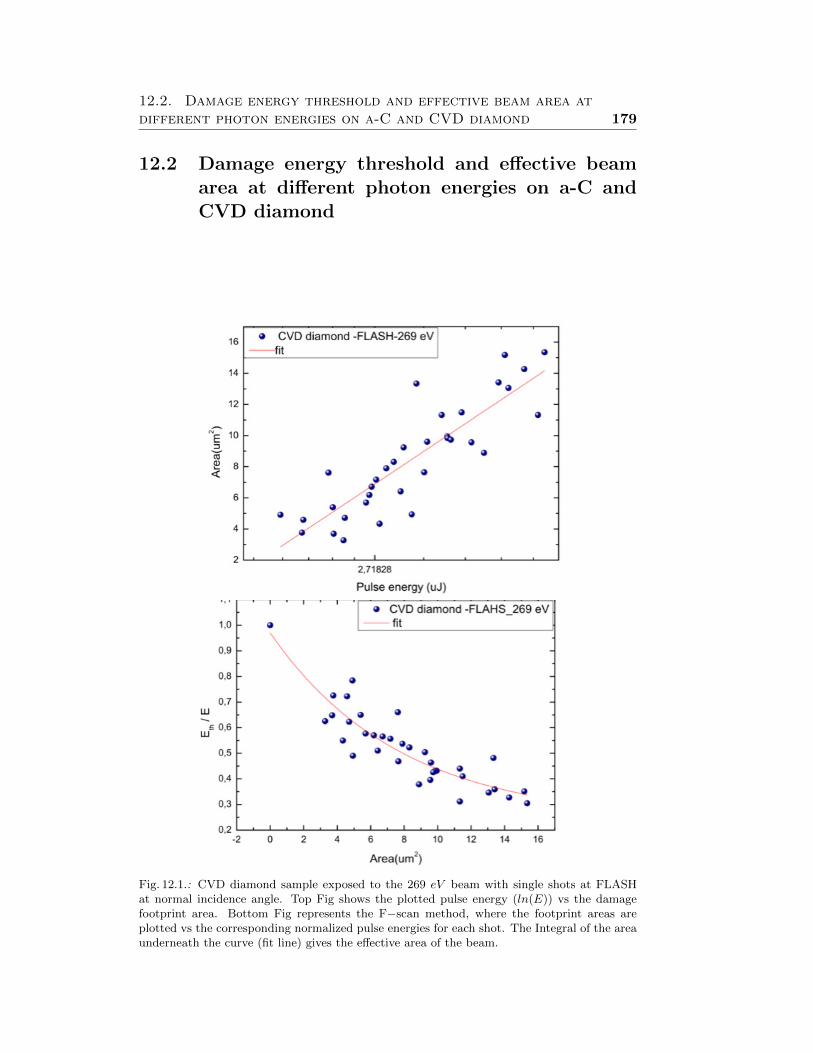
12.2. Damage energy threshold and effective beam area atdifferent photon energies on a-C and CVD diamond 179
12.2 Damage energy threshold and effective beamarea at different photon energies on a-C andCVD diamond
Fig. 12.1.: CVD diamond sample exposed to the 269 eV beam with single shots at FLASHat normal incidence angle. Top Fig shows the plotted pulse energy (ln(E)) vs the damagefootprint area. Bottom Fig represents the F−scan method, where the footprint areas areplotted vs the corresponding normalized pulse energies for each shot. The Integral of the areaunderneath the curve (fit line) gives the effective area of the beam.
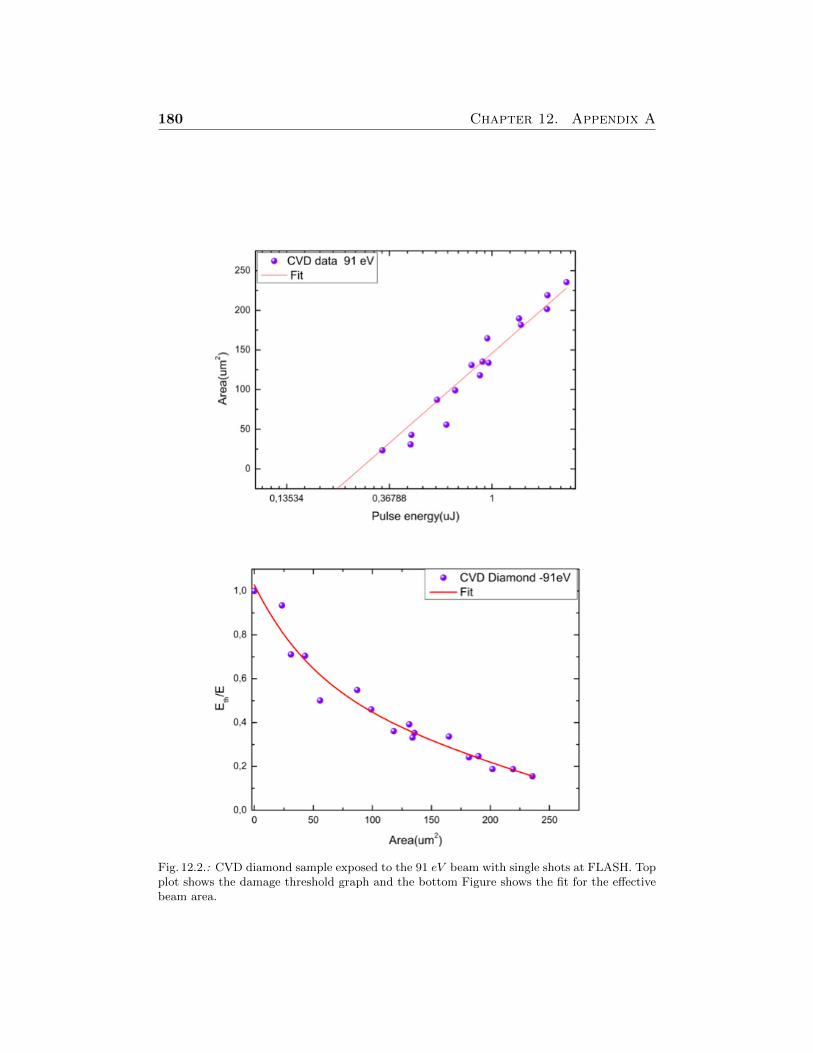
180 Chapter 12. Appendix A
Fig. 12.2.: CVD diamond sample exposed to the 91 eV beam with single shots at FLASH. Topplot shows the damage threshold graph and the bottom Figure shows the fit for the effectivebeam area.
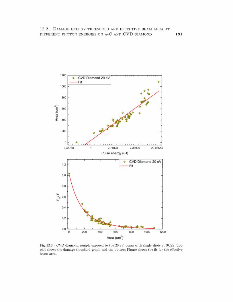
12.2. Damage energy threshold and effective beam area atdifferent photon energies on a-C and CVD diamond 181
Fig. 12.3.: CVD diamond sample exposed to the 20 eV beam with single shots at SCSS. Topplot shows the damage threshold graph and the bottom Figure shows the fit for the effectivebeam area.
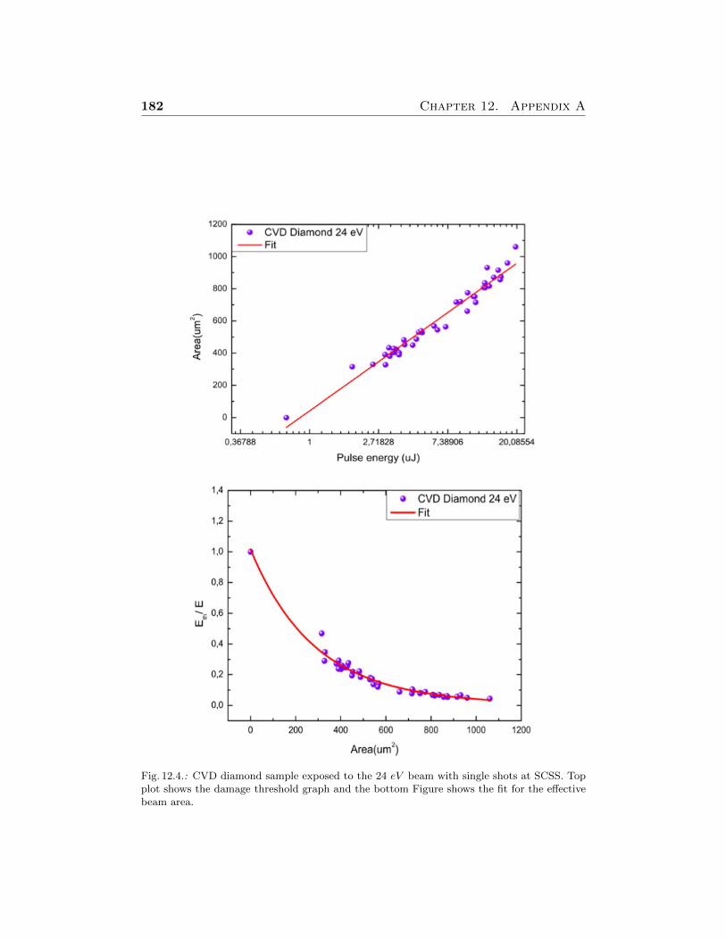
182 Chapter 12. Appendix A
Fig. 12.4.: CVD diamond sample exposed to the 24 eV beam with single shots at SCSS. Topplot shows the damage threshold graph and the bottom Figure shows the fit for the effectivebeam area.
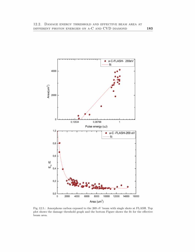
12.2. Damage energy threshold and effective beam area atdifferent photon energies on a-C and CVD diamond 183
Fig. 12.5.: Amorphous carbon exposed to the 269 eV beam with single shots at FLASH. Topplot shows the damage threshold graph and the bottom Figure shows the fit for the effectivebeam area.
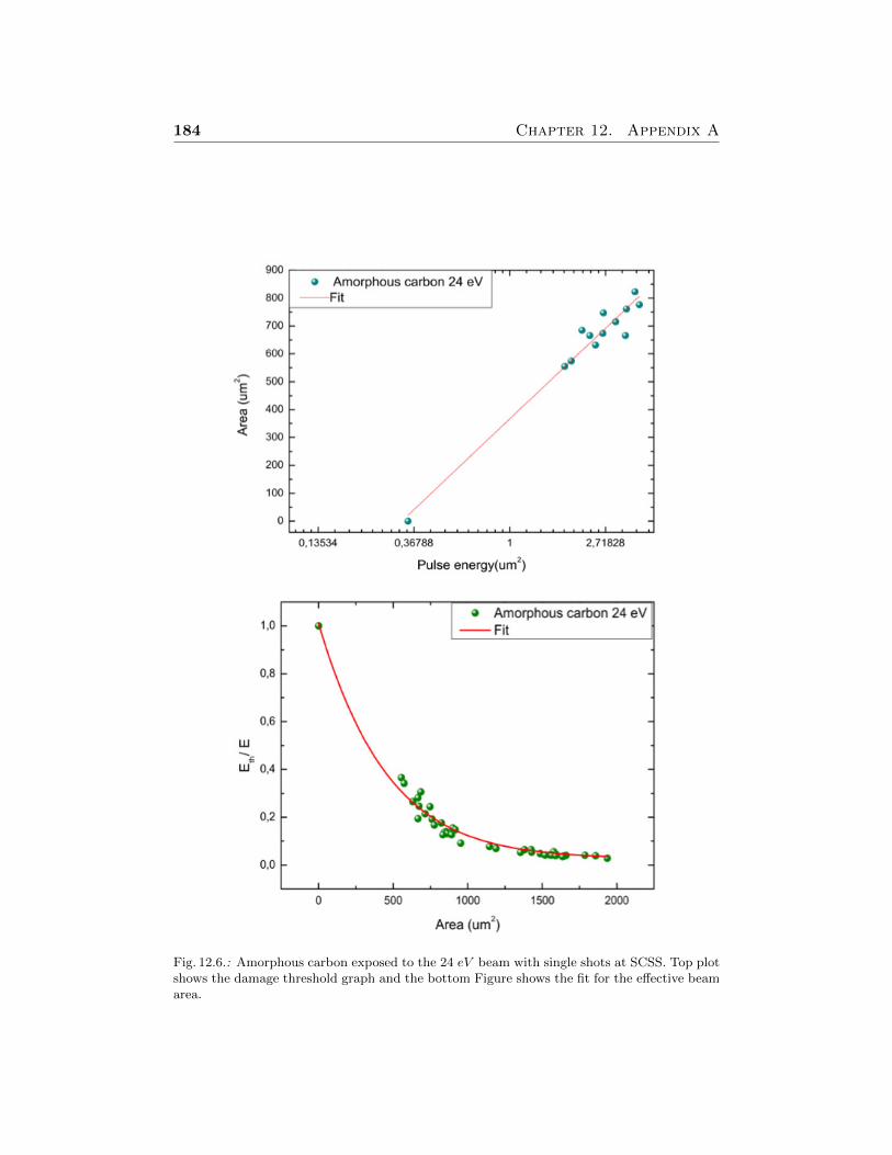
184 Chapter 12. Appendix A
Fig. 12.6.: Amorphous carbon exposed to the 24 eV beam with single shots at SCSS. Top plotshows the damage threshold graph and the bottom Figure shows the fit for the effective beamarea.
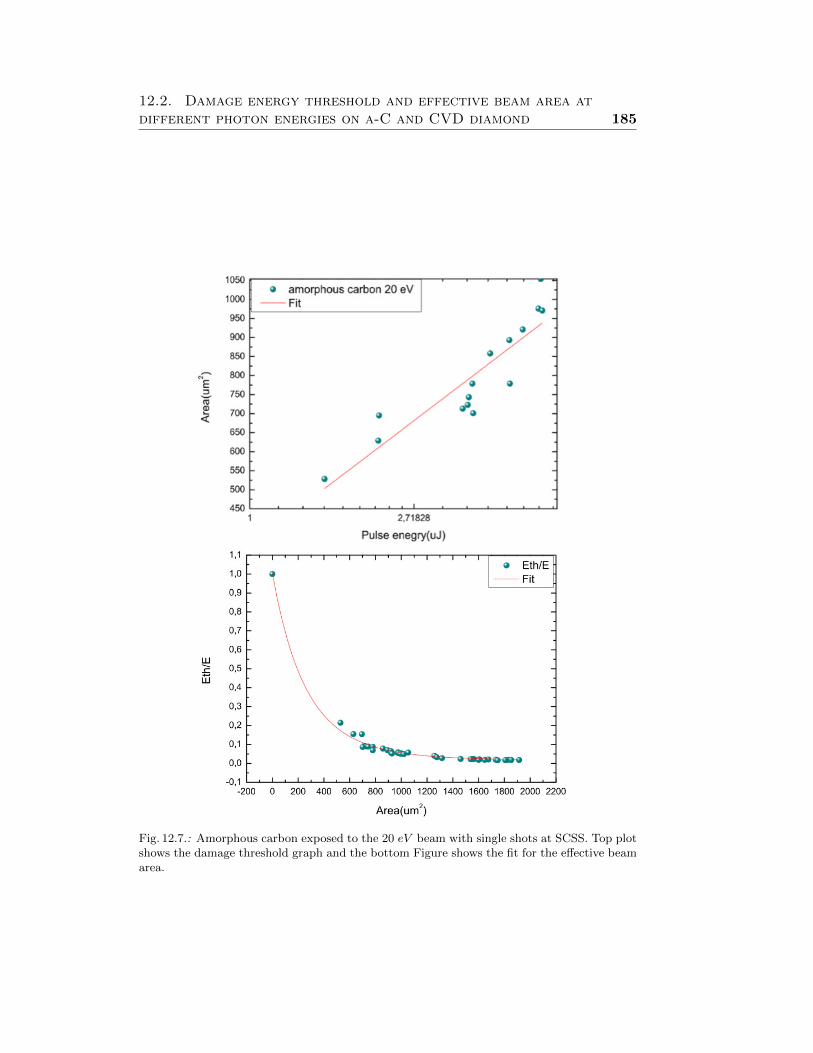
12.2. Damage energy threshold and effective beam area atdifferent photon energies on a-C and CVD diamond 185
Fig. 12.7.: Amorphous carbon exposed to the 20 eV beam with single shots at SCSS. Top plotshows the damage threshold graph and the bottom Figure shows the fit for the effective beamarea.
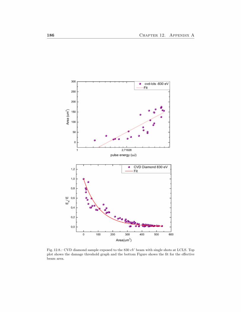
186 Chapter 12. Appendix A
Fig. 12.8.: CVD diamond sample exposed to the 830 eV beam with single shots at LCLS. Topplot shows the damage threshold graph and the bottom Figure shows the fit for the effectivebeam area.
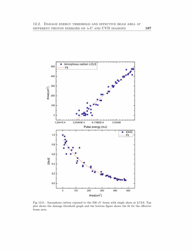
12.2. Damage energy threshold and effective beam area atdifferent photon energies on a-C and CVD diamond 187
Fig. 12.9.: Amorphous carbon exposed to the 830 eV beam with single shots at LCLS. Topplot shows the damage threshold graph and the bottom figure shows the fit for the effectivebeam area.

188 Chapter 12. Appendix A
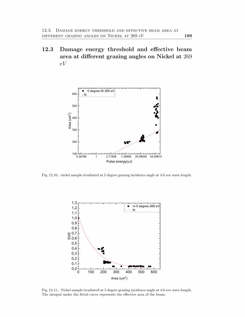
12.3. Damage energy threshold and effective beam area atdifferent grazing angles on Nickel at 269 eV 189
12.3 Damage energy threshold and effective beamarea at different grazing angles on Nickel at 269eV
0,36788 1 2,71828 7,38906 20,08554 54,59815100
200
300
400
500
600 5 degree Ni 269 eV
- fit
Are
a (u
m2 )
Pulse energy(uJ)
Fig. 12.10.: nickel sample irradiated at 5 degree grazing incidence angle at 4.6 nm wave length.
0 100 200 300 400 500 6000,00,10,20,30,40,50,60,70,80,91,01,11,21,3
ni-5 degree-269 eV fit
E0/E
Area (um2)
Fig. 12.11.: Nickel sample irradiated at 5 degree grazing incidence angle at 4.6 nm wave length.The integral under the fitted curve represents the effective area of the beam.
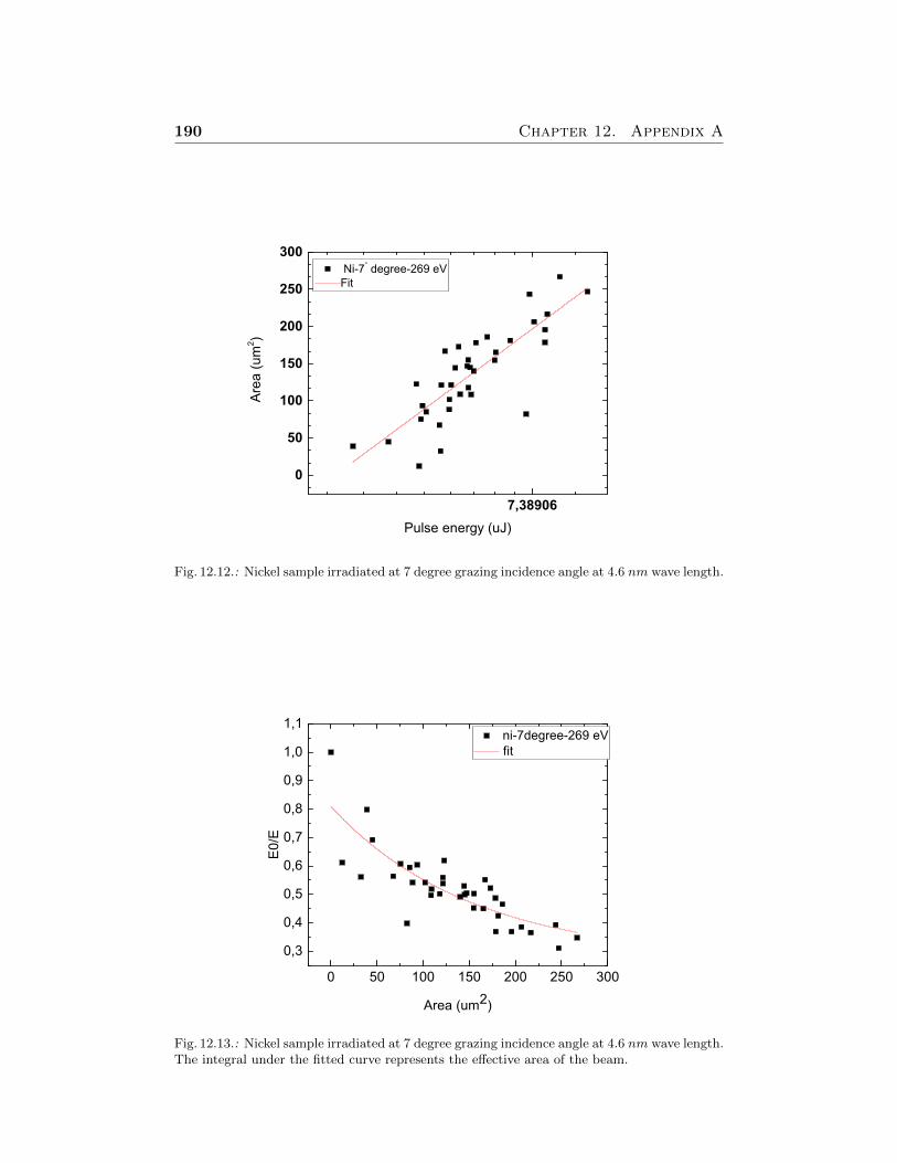
190 Chapter 12. Appendix A
7,38906
0
50
100
150
200
250
300 Ni-7° degree-269 eVFit
Are
a (u
m2 )
Pulse energy (uJ)
Fig. 12.12.: Nickel sample irradiated at 7 degree grazing incidence angle at 4.6 nm wave length.
0 50 100 150 200 250 300
0,3
0,4
0,5
0,6
0,7
0,8
0,9
1,0
1,1 ni-7degree-269 eV fit
E0/E
Area (um2)
Fig. 12.13.: Nickel sample irradiated at 7 degree grazing incidence angle at 4.6 nm wave length.The integral under the fitted curve represents the effective area of the beam.
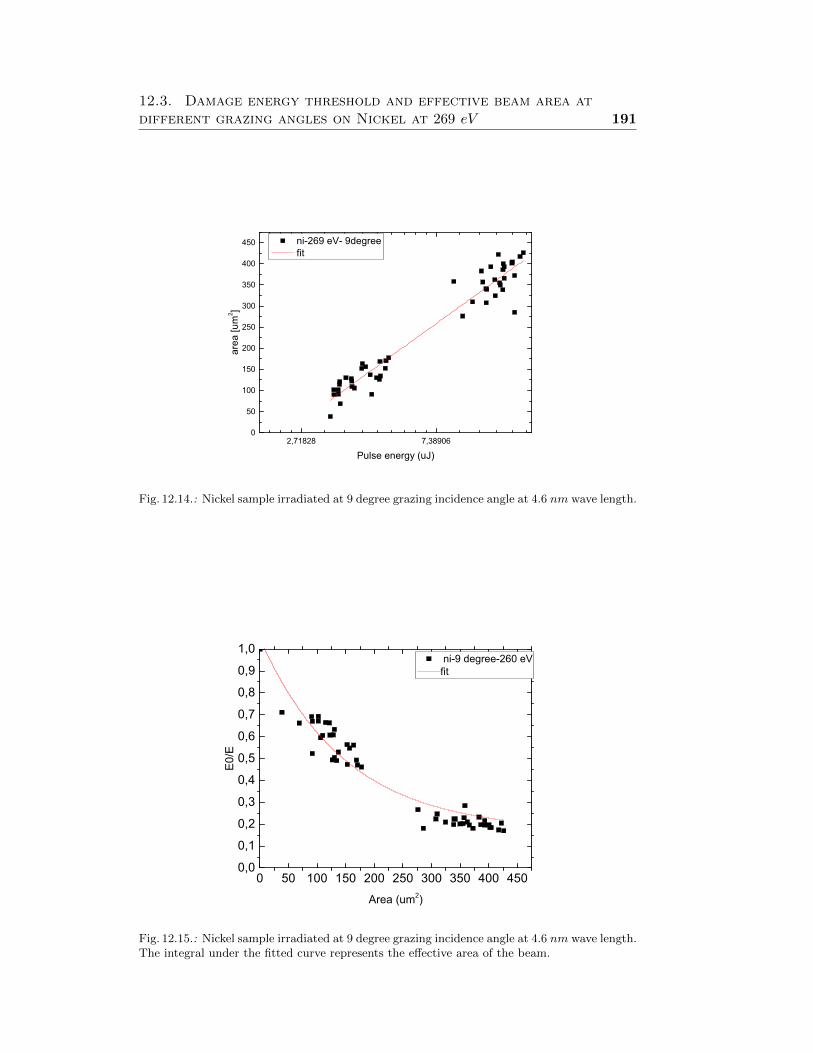
12.3. Damage energy threshold and effective beam area atdifferent grazing angles on Nickel at 269 eV 191
2,71828 7,389060
50
100
150
200
250
300
350
400
450 ni-269 eV- 9degree fit
area
[um
2 ]
Pulse energy (uJ)
Fig. 12.14.: Nickel sample irradiated at 9 degree grazing incidence angle at 4.6 nm wave length.
0 50 100 150 200 250 300 350 400 4500,0
0,1
0,2
0,3
0,4
0,5
0,6
0,7
0,8
0,9
1,0 ni-9 degree-260 eVfit
E0/E
Area (um2)
Fig. 12.15.: Nickel sample irradiated at 9 degree grazing incidence angle at 4.6 nm wave length.The integral under the fitted curve represents the effective area of the beam.
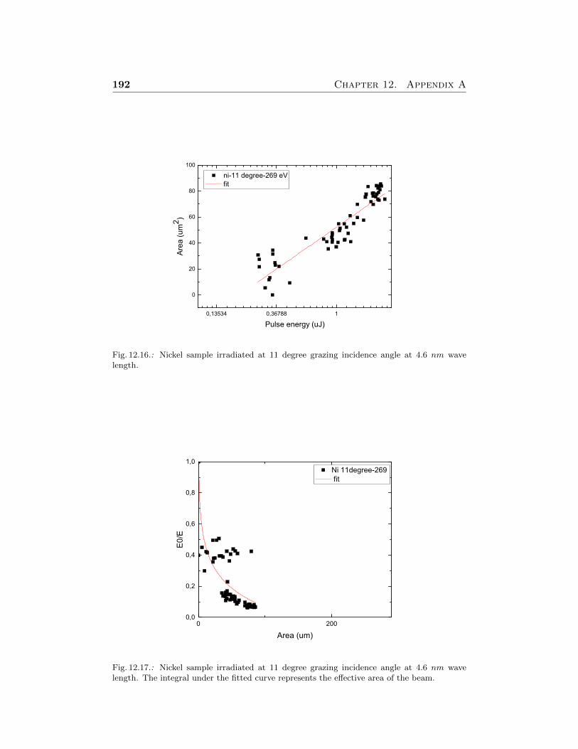
192 Chapter 12. Appendix A
0,13534 0,36788 1
0
20
40
60
80
100
ni-11 degree-269 eV fit
Area
(um
2 )
Pulse energy (uJ)
Fig. 12.16.: Nickel sample irradiated at 11 degree grazing incidence angle at 4.6 nm wavelength.
0 2000,0
0,2
0,4
0,6
0,8
1,0Ni 11degree-269 fit
E0/E
Area (um)
Fig. 12.17.: Nickel sample irradiated at 11 degree grazing incidence angle at 4.6 nm wavelength. The integral under the fitted curve represents the effective area of the beam.
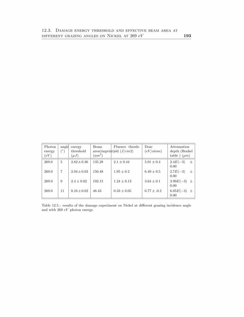
12.3. Damage energy threshold and effective beam area atdifferent grazing angles on Nickel at 269 eV 193
Photonenergy(eV )
angle(◦)
energythreshold(µJ)
Beamarea(imprint)(um2)
Fluence thresh-old (J/cm2)
Dose(eV/atom)
Attenuationdepth (Henkeltable ) (µm)
269.0 5 2.82±0.36 135.28 2.1± 0.44 5.01± 0.4 2.4E(−3) ±0.00
269.0 7 2.94±0.03 150.48 1.95± 0.2 6.49± 0.5 2.7E(−3) ±0.00
269.0 9 2.4± 0.02 192.15 1.24± 0.13 3.64± 0.1 3.99E(−3) ±0.00
269.0 11 0.16±0.02 48.43 0.33± 0.05 0.77± .0.2 6.05E(−3) ±0.00
Table 12.5.: results of the damage experiment on Nickel at different grazing incidence angleand with 269 eV photon energy.

194 Chapter 12. Appendix A
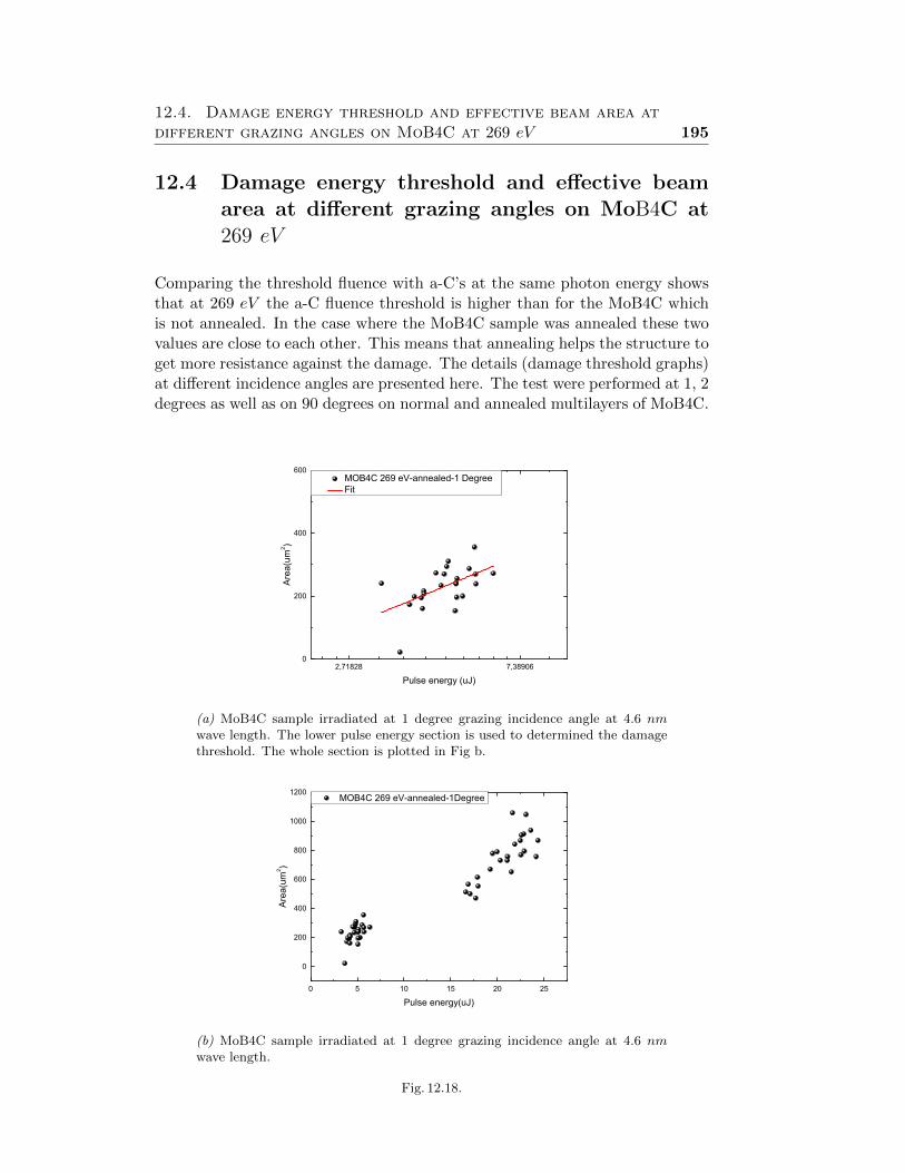
12.4. Damage energy threshold and effective beam area atdifferent grazing angles on MoB4C at 269 eV 195
12.4 Damage energy threshold and effective beamarea at different grazing angles on MoB4C at269 eV
Comparing the threshold fluence with a-C’s at the same photon energy showsthat at 269 eV the a-C fluence threshold is higher than for the MoB4C whichis not annealed. In the case where the MoB4C sample was annealed these twovalues are close to each other. This means that annealing helps the structure toget more resistance against the damage. The details (damage threshold graphs)at different incidence angles are presented here. The test were performed at 1, 2degrees as well as on 90 degrees on normal and annealed multilayers of MoB4C.
2,71828 7,389060
200
400
600
MOB4C 269 eV-annealed-1 Degree Fit
Are
a(um
2 )
Pulse energy (uJ)
(a) MoB4C sample irradiated at 1 degree grazing incidence angle at 4.6 nmwave length. The lower pulse energy section is used to determined the damagethreshold. The whole section is plotted in Fig b.
0 5 10 15 20 25
0
200
400
600
800
1000
1200
MOB4C 269 eV-annealed-1Degree
Are
a(um
2 )
Pulse energy(uJ)
(b) MoB4C sample irradiated at 1 degree grazing incidence angle at 4.6 nmwave length.
Fig. 12.18.
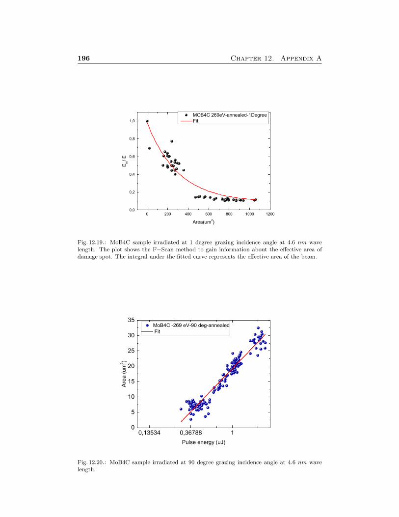
196 Chapter 12. Appendix A
0 200 400 600 800 1000 12000,0
0,2
0,4
0,6
0,8
1,0
MOB4C 269eV-annealed-1Degree Fit
Eth/ E
Area(um2)
Fig. 12.19.: MoB4C sample irradiated at 1 degree grazing incidence angle at 4.6 nm wavelength. The plot shows the F−Scan method to gain information about the effective area ofdamage spot. The integral under the fitted curve represents the effective area of the beam.
0,13534 0,36788 10
5
10
15
20
25
30
35MoB4C -269 eV-90 deg-annealed Fit
Are
a (u
m2 )
Pulse energy (uJ)
Fig. 12.20.: MoB4C sample irradiated at 90 degree grazing incidence angle at 4.6 nm wavelength.
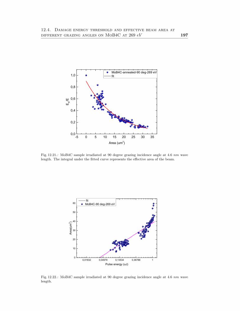
12.4. Damage energy threshold and effective beam area atdifferent grazing angles on MoB4C at 269 eV 197
-5 0 5 10 15 20 25 30 350,0
0,2
0,4
0,6
0,8
1,0 MoB4C-annealed-90 deg-269 eV fit
Eth/E
Area (um2)
Fig. 12.21.: MoB4C sample irradiated at 90 degree grazing incidence angle at 4.6 nm wavelength. The integral under the fitted curve represents the effective area of the beam.
0,01832 0,04979 0,13534 0,36788 10
10
20
30
40
50
60
fitMoB4C-90 deg-269 eV
Are
a(um
2 )
Pulse energy (uJ)
Fig. 12.22.: MoB4C sample irradiated at 90 degree grazing incidence angle at 4.6 nm wavelength.
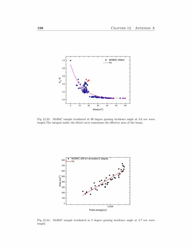
198 Chapter 12. Appendix A
0 10 20 30 40 50 60
0,0
0,2
0,4
0,6
0,8
1,0
MOB4C 269eV Fit
Eth/ E
Area(um2)
Fig. 12.23.: MoB4C sample irradiated at 90 degree grazing incidence angle at 4.6 nm wavelength.The integral under the fitted curve represents the effective area of the beam.
0,49260
100
200
300
400
500
600
700
800 MOB4C 269 eV-annealed-2 degree Fit
Are
a (u
m2 )
Pulse energy(uJ)
Fig. 12.24.: MoB4C sample irradiated at 2 degree grazing incidence angle at 4.7 nm wavelength.
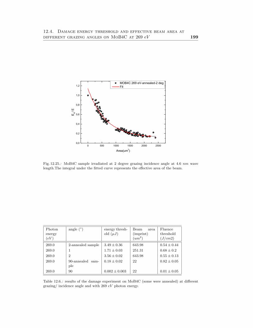
12.4. Damage energy threshold and effective beam area atdifferent grazing angles on MoB4C at 269 eV 199
0 500 1000 1500 2000 25000,0
0,2
0,4
0,6
0,8
1,0
1,2
MOB4C 269 eV-annealed-2 deg Fit
Eth/ E
Area(um2)
Fig. 12.25.: MoB4C sample irradiated at 2 degree grazing incidence angle at 4.6 nm wavelength.The integral under the fitted curve represents the effective area of the beam.
Photonenergy(eV )
angle (◦) energy thresh-old (µJ)
Beam area(imprint)(um2)
Fluencethreshold(J/cm2)
269.0 2-annealed sample 3.49± 0.36 643.98 0.54± 0.44
269.0 1 1.71± 0.03 251.31 0.68± 0.2
269.0 2 3.56± 0.02 643.98 0.55± 0.13
269.0 90-annealed sam-ple
0.18± 0.02 22 0.82± 0.05
269.0 90 0.002± 0.003 22 0.01± 0.05
Table 12.6.: results of the damage experiment on MoB4C (some were annealed) at differentgrazing/ incidence angle and with 269 eV photon energy.

200 Chapter 12. Appendix A
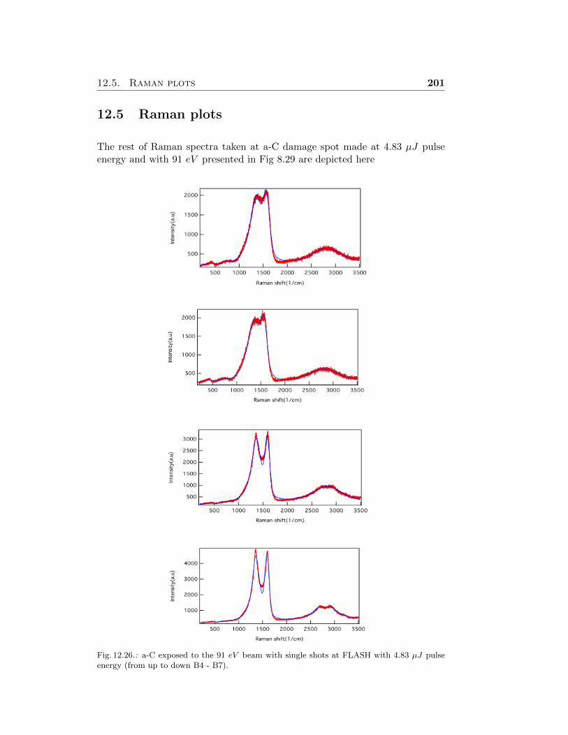
12.5. Raman plots 201
12.5 Raman plots
The rest of Raman spectra taken at a-C damage spot made at 4.83 µJ pulseenergy and with 91 eV presented in Fig 8.29 are depicted here
Fig. 12.26.: a-C exposed to the 91 eV beam with single shots at FLASH with 4.83 µJ pulseenergy (from up to down B4 - B7).
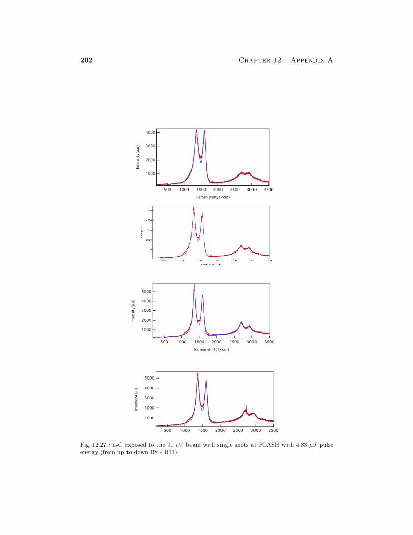
202 Chapter 12. Appendix A
Fig. 12.27.: a-C exposed to the 91 eV beam with single shots at FLASH with 4.83 µJ pulseenergy (from up to down B8 - B11).
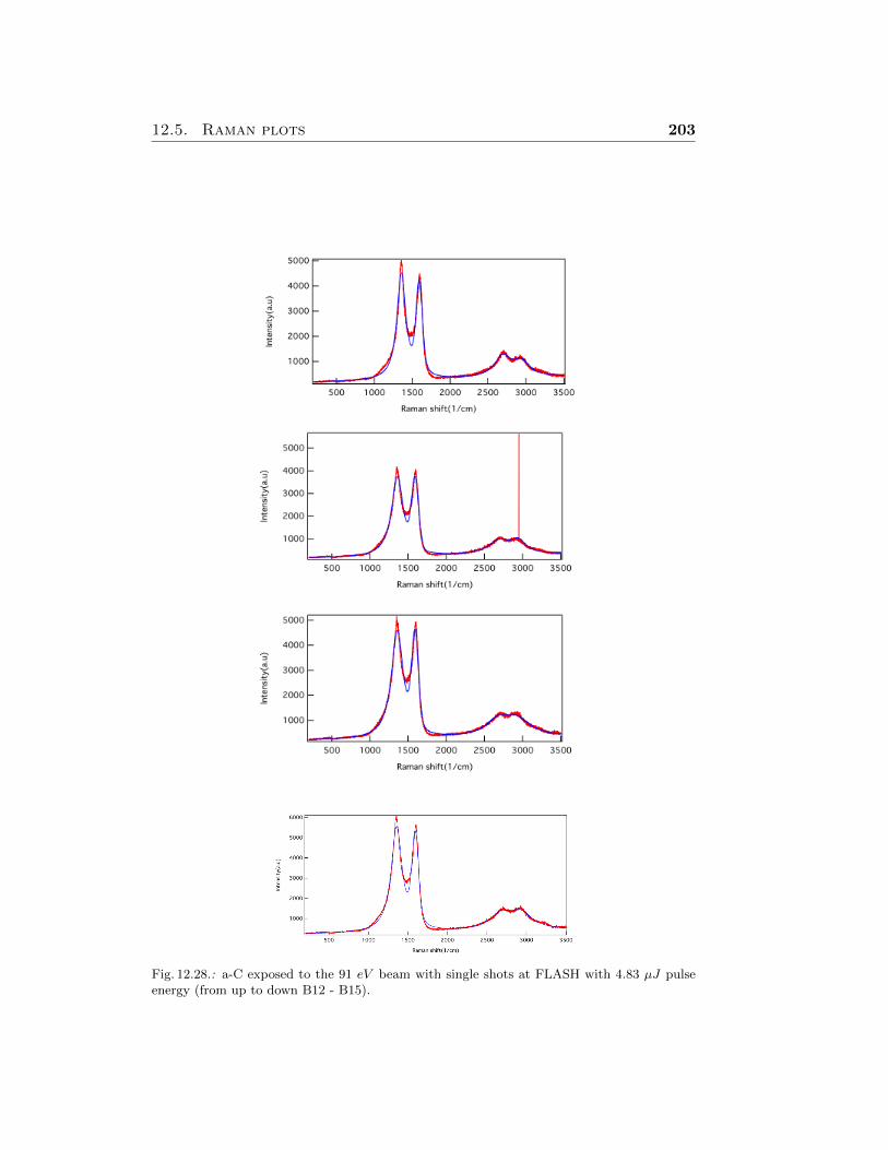
12.5. Raman plots 203
Fig. 12.28.: a-C exposed to the 91 eV beam with single shots at FLASH with 4.83 µJ pulseenergy (from up to down B12 - B15).
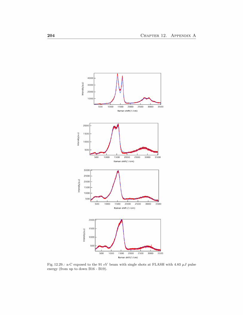
204 Chapter 12. Appendix A
Fig. 12.29.: a-C exposed to the 91 eV beam with single shots at FLASH with 4.83 µJ pulseenergy (from up to down B16 - B19).
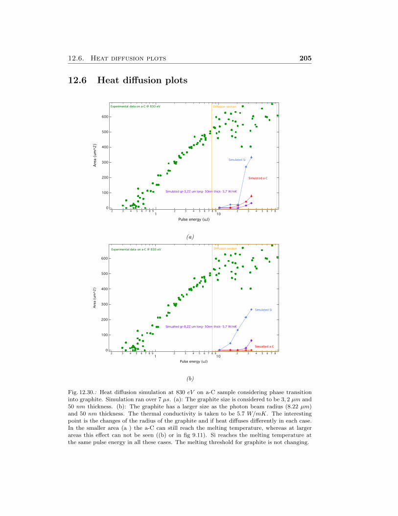
12.6. Heat diffusion plots 205
12.6 Heat diffusion plots
600
500
400
300
200
100
0
Are
a (
um
^2)
2 3 4 5 6 7 8 9
12 3 4 5 6 7 8 9
102 3 4 5 6 7 8
Pulse energy (uJ)
Experimental data on a-C @ 830 eV
Simulated Si
Simulated gr-3,22 um long- 50nm thick- 5,7 W/mK
Simulated a-C
Diffusion section
(a)
600
500
400
300
200
100
0
Are
a (
um
^2)
2 3 4 5 6 7 8 9
12 3 4 5 6 7 8 9
102 3 4 5 6 7 8
Pulse energy (uJ)
Experimental data on a-C @ 830 eV
Simulated Si
Simualted gr-8,22 um long- 50nm thick- 5,7 W/mK
Simualted a-C
Diffusion section
(b)
Fig. 12.30.: Heat diffusion simulation at 830 eV on a-C sample considering phase transitioninto graphite. Simulation ran over 7 µs. (a): The graphite size is considered to be 3, 2 µm and50 nm thickness. (b): The graphite has a larger size as the photon beam radius (8.22 µm)and 50 nm thickness. The thermal conductivity is taken to be 5.7 W/mK. The interestingpoint is the changes of the radius of the graphite and if heat diffuses differently in each case.In the smaller area (a ) the a-C can still reach the melting temperature, whereas at largerareas this effect can not be seen ((b) or in fig 9.11). Si reaches the melting temperature atthe same pulse energy in all these cases. The melting threshold for graphite is not changing.
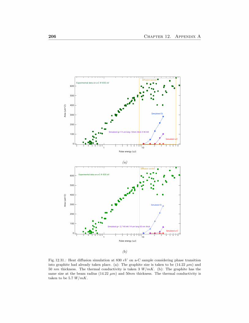
206 Chapter 12. Appendix A
600
500
400
300
200
100
0
Are
a (
um
^2)
2 3 4 5 6 7 8 9
12 3 4 5 6 7 8 9
102 3 4 5 6 7 8
Pulse energy (uJ)
Experimental data on a-C @ 830 eV
Simulated Si
Simulated gr-14 um long- 50nm thick-3 W/mK
Simulated a-C
Diffusion section
(a)
600
500
400
300
200
100
0
Are
a (
um
^2)
2 3 4 5 6 7 8 9
12 3 4 5 6 7 8 9
102 3 4 5 6 7 8
Pulse energy (uJ)
Experimental data on a-C @ 830 eV
Simulated Si
Simulated a-C
Simulated gr- 5,7 W/mK-14 um long-50 nm thick
Diffusion section
(b)
Fig. 12.31.: Heat diffusion simulation at 830 eV on a-C sample considering phase transitioninto graphite had already taken place. (a): The graphite size is taken to be (14.22 µm) and50 nm thickness. The thermal conductivity is taken 3 W/mK. (b): The graphite has thesame size at the beam radius (14.22 µm) and 50nm thickness. The thermal conductivity istaken to be 5.7 W/mK.
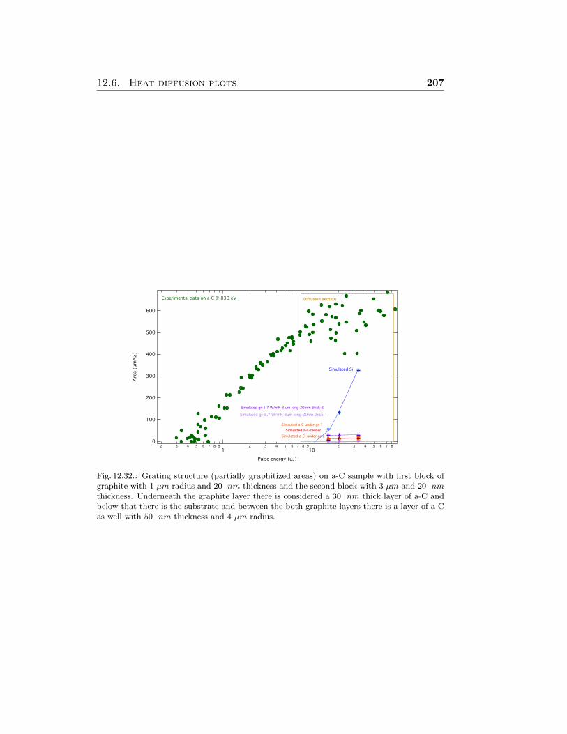
12.6. Heat diffusion plots 207
600
500
400
300
200
100
0
Are
a (
um
^2)
2 3 4 5 6 7 8 9
12 3 4 5 6 7 8 9
102 3 4 5 6 7 8
Pulse energy (uJ)
Experimental data on a-C @ 830 eV
Simulated Si
Simulated gr-5,7 W/mK-3 um long-20 nm thick-2
Simulated gr-5,7 W/mK-3um long-20nm thick-1
Simualted a-C-center
Simauted a-C-under gr-1
Simulated-a-C- under gr-2
Diffusion section
Fig. 12.32.: Grating structure (partially graphitized areas) on a-C sample with first block ofgraphite with 1 µm radius and 20 nm thickness and the second block with 3 µm and 20 nmthickness. Underneath the graphite layer there is considered a 30 nm thick layer of a-C andbelow that there is the substrate and between the both graphite layers there is a layer of a-Cas well with 50 nm thickness and 4 µm radius.

208 Chapter 12. Appendix A
List of Figures
3.1 An example of beamline components like mirror configuration atSASE 3 beamline at European XFEL [7]. . . . . . . . . . . . . . 13
3.2 Damage studies. . . . . . . . . . . . . . . . . . . . . . . . . . . . 14
4.1 (a): The refractive index 1−δ as a function of frequency. In caseof X-ray the refractive index for all materials is less than 1 whichmeans the total external refraction would take place in case ofX-rays which is not the case in other regime with frequenciesbelow X-rays. The edges are the resonance frequencies at whichthe radiation will be absorbed [13]. (b): This plot represents thesimulated refractive index (see Equation 4.24) for X-ray on a-C. . 21
4.2 . . . . . . . . . . . . . . . . . . . . . . . . . . . . . . . . . . . . . 24
4.3 A comparison of the real (1-δ) (a) and imaginary part (b) of therefractive index of X-ray radiation inside a wide energy range fora-C (red), Si (violet) and Ni (green) is shown in this plot. Rawdata has been taken from [15]. Ni has density 8.9 gr/cm3 and Si2.33 gr/cm3 and a-C has the density of 2.2 gr/cm3. Plots showthat at very low energy basically the absorption and phase ve-locity of the X-ray light is high and going towards higher photonenergies both of these parameters decrease. . . . . . . . . . . . . 25
4.4 (a): Attenuation length at different photon energies are com-pared for different materials. a-C (red), CVD (pink), Si (violet)and Ni (green). (b): Reflectivity of a-C (red), CVD (pink), Si(Violet), Ni (green) vs photon energies are compared here. . . . . 26
5.1 Very simple schematic of the matter and laser beam interac-tion [17]. The left side shows the system in its ground state; theelectrons cold state. The potential landscape shows minima atthe crystal lattice sites. Therefore, no external forces are actingon them except tight binding Coulomb potential induced by thelattice. On the right side, the laser light has affected the systemand transported it to an excited state. Hot electrons and holesare created here. The potential landscape undergoes qualitativeand quantitative changes, resulting in disappearance or shiftingof the minima. This happens in very short time scale (shorterthan reaction time); as a result, forces act on the carriers/atomsand move them. . . . . . . . . . . . . . . . . . . . . . . . . . . . . 28
209
210 List of Figures
5.2 Very simple schematic of the matter and X-ray FEL beam in-teraction [39]. The incoming beam has its temporal and spatialdimensions depicted in the picture with the Gaussian profiles onthe top and the side. The material is undergone photo-ionizationprocesses. Some free carriers escaped from the surface, and hotplasma of free carriers is created inside the material at the beamaffected zone. The heat affected zone shows the region wherethe heat gets diffused into and the shock affected zone describethe area where the high pressure starts to induce shock waves.There is a thin layer right behind the heat-affected zone, whichis showing the melted layer. . . . . . . . . . . . . . . . . . . . . . 33
5.3 Attenuation length of X-ray radiation with different energiesinside a thin layer of amorphous carbon with 2.2 ratio ofSP 3/SP 2 [15]. The drop is at the cutting edge at 284 eV . . . . . 37
6.1 Maps of CVD diamond and amorphous carbon samples exposedwith single shots at LCLS. . . . . . . . . . . . . . . . . . . . . . 39
6.2 Snapshot of the 64 atom ta-C network. The heavy lines showthe network of bonds; the 22 dark spheres depict threefold co-ordinated atoms (sp2 hybridized) and the 42 light spheres showthe fourfold coordinated atoms (sp3 hybridized). The simula-tions were performed by N. Marks, (Dept of Applied Physics,University of Sydney) at the Max Planck Institute, Stuttgart [79]. 40
6.3 Electron configuration of carbon in ground state(a), excited hy-bridized state SP 1(b), Sp2(c), Sp3 (d). . . . . . . . . . . . . . . . 41
6.4 Orbital configuration of carbon Sp3(mainly in Diamond),Sp2(mainly in Graphite). . . . . . . . . . . . . . . . . . . . . . . 41
6.5 Measured surface roughness with AFM on (a) 40 nm thick aCcoating and on (b) 900 nm aC coating on Si substrate. The 900nm sample has an rms roughness of 1.28 nm, the peak to valleyvalue is 35.24 nm and maximum peak height is 50.6 nm and the40 nm samples roughness is 0.4 nm rms, the peak to valley valuefor this sample is 72.14 nm and maximum peak height is 80.5nm [16]. . . . . . . . . . . . . . . . . . . . . . . . . . . . . . . . 43
6.6 Sketch of diamond crystal [92]. . . . . . . . . . . . . . . . . . . . 43
7.1 Schematic view of developed GMD at FLASH [85]. A Faradaycup counts the electrons and ions that are produced as the FELpulse passes through the ionization chamber containing nitrogenor rare gases at very low pressure. After the faraday cup thereare the two split electrodes to determine the horizontal positionof the beam. . . . . . . . . . . . . . . . . . . . . . . . . . . . . . . 48
7.2 (a): Draft of the FELIS experimental chamber at FLASH inHamburg in 2005 [94], [100]. (b): The FELIS experimental cham-ber modified for the damage experiment in 2011 at FLASH inHamburg . . . . . . . . . . . . . . . . . . . . . . . . . . . . . . . 49
List of Figures 211
7.3 View of the inside of the chamber from the sample holder withmounted samples on it. . . . . . . . . . . . . . . . . . . . . . . . 50
7.4 Schematic view of the inside of the chamber, illustrating thesample positioning. . . . . . . . . . . . . . . . . . . . . . . . . . . 50
7.5 Schematic view of the inside the chamber with the sample rota-tion axis. . . . . . . . . . . . . . . . . . . . . . . . . . . . . . . . 51
7.6 Correlation of the pulse energy measured by the GMD with theamplitude of the MCP signal when sample was exposed to 500pulses attenuated below the multi shot damage threshold of Sisample [97]. . . . . . . . . . . . . . . . . . . . . . . . . . . . . . 52
7.7 Schematic view of the sample’s position on the sample holder,they were given an x and y position regarding their position onthe sample holder. . . . . . . . . . . . . . . . . . . . . . . . . . . 54
7.8 PMMA 5 µm was shot at 13.5 nm at FLASH (11-08-2008) tofind the beam size and focus point, the highlighted area is takento be the beam area and it was measured to be 101.4 µm2. . . . 55
7.9 Schematic view of the inside of the chamber showing the angledetermination . . . . . . . . . . . . . . . . . . . . . . . . . . . . 55
7.10 Maps of amorphous carbon sample with 1.4 µm thickness, ex-posed to single shots at LCLS 2009 with 830 eV . On the leftside, one can see the picture taken from the sample after theshots. The numbers (names) of the lines are marked and theshot direction as well. The right pic is the image of the sam-ple itself after the shots are made. The pictures are taken viaNomarski microscope. . . . . . . . . . . . . . . . . . . . . . . . . 56
7.11 Marker on the map of amorphous carbon sample with 890 nmthickness, exposed to single shots at FLASH 2008 with 177 eV .Scale size on the bottom right side is 20 µm. . . . . . . . . . . . 56
7.12 Scanning pinhole structure designed for the SCSS in Japan in2010 [101]. . . . . . . . . . . . . . . . . . . . . . . . . . . . . . . . 58
7.13 Gas attenuator and Photon intensity monitor at SCSS in Japanin 2010 [102], [103], [101]. . . . . . . . . . . . . . . . . . . . . . . 58
7.14 (a): Design of the experimental beamline at SCSS in Japan [101].(b): The experimental beamline and chamber. (c): The experi-mental chamber. . . . . . . . . . . . . . . . . . . . . . . . . . . . 59
7.15 (a): The structure of the AMO beam-line at LCLS [104]. (b):The Gas Monitor at AMO beam-line at LCLS based on the pho-toluminescence process [106]. . . . . . . . . . . . . . . . . . . . . 61
7.16 (a): Idealized schematic diagram of the major componentsand light pathways through a typical DIC microscope opticaltrain [107]. (b): A DIC microscope image taken from a damagespot on a-C (890 nm thick on Si substrate) sample. The samplewas exposed to a single pulse with 4.83 µJ energy at FLASH.The experiment was performed at 91 eV photon energy. Thescale is 20 µm. . . . . . . . . . . . . . . . . . . . . . . . . . . . . 63
7.17 Simple schematic of Atomic Force Microscopy spectroscope. . . . 647.18 . . . . . . . . . . . . . . . . . . . . . . . . . . . . . . . . . . . . . 65
212 List of Figures
7.19 . . . . . . . . . . . . . . . . . . . . . . . . . . . . . . . . . . . . . 66
7.20 Simple schematic of Micro-Raman spectroscope. . . . . . . . . . 67
7.21 Top: Raman spectrum taken on the point marked as ”A” on theamorphous carbon coated sample (890 nm thick on Si substrate)exposed to the 177 eV beam with single shot of 4.8 µJ at FLASH.Marked points show the coordinates on which Raman data weretaken. Bottom: Raman profile spectra showing the position andwidth of D, G, G’ and T peaks (see section 8.5). . . . . . . . . . 68
7.22 White Light Interferometer image of the a-C damaged at SCSS.The single shot with 4.8 µJ with photon beam energy of 24 eV . . 69
7.23 Simple image of an Scanning Electron Microscope (SEM). . . . . 70
7.24 SEM, AFM, Nomarski microscope images taken at the damagedspot on amorphous carbon sample (890 nm thick on Si substrate)exposed to the 91 eV beam with single shot pulse energy of 4.83µJ at FLASH. The three SEM images step by step zoom insidethe damaged spot and show more details. From the top, thefirst image has 10µm scale and the second taken with 5µm andthe third with 2µm. The rough surface is completely obviousthat smooth surface of a-C has turned into a rough graphite sur-face. There is a swollen observable area around the damagedspot which might have been created due to shock waves as thepressure goes high inside the hot plasma of free carriers. Sincethe material can't expand easily towards the rest of the volume,it causes a shock wave to reduce the pressure inside the damagedregion. This also causes the material not to be easily removedfrom the surface [113]. The other reason might be due to beam-line aperture which causes some other parts be illuminated by thebeam at the time of exposure. This defect could be also createdat the boundary between Si and a-C. From the heat diffusion sim-ulation in chapter 9 it can be seen that material (a-C and Si) hasreached melting temperature at this pulse energy which causesthe larger damage area and explains the deformations observedon the surface. . . . . . . . . . . . . . . . . . . . . . . . . . . . . 72
7.25 Nomarski microscope, AFM and SEM images taken of the dam-age spot on amorphous carbon sample (890 nm thick on Si sub-strate) exposed to the 91 eV beam with single shot pulse energyof 2.97 µJ at FLASH. From the heat diffusion simulation in chap-ter 9 it can be seen that material (a-C and Si ) was melted atthis pulse energy. . . . . . . . . . . . . . . . . . . . . . . . . . . . 73
List of Figures 213
8.1 Damage spots on CVD diamond and amorphous carbon samples.These are exposed to single shots at LCLS with 830 eV photonenergy. From left to right the pulse energy increases and one cansee that the damage is more intense. These images are taken ex-istu, via Nomarski microscope. With increasing the pulse energy,the shock waves appear in CVD diamond. Through heat diffu-sion part of sample get melted (including the Si substrate) in thecase of a-C (amorphous carbon). The scale is 20 µm in all thesepictures. . . . . . . . . . . . . . . . . . . . . . . . . . . . . . . . 77
8.2 The schematic view of the damaged spot on the amorphous car-bon sample in the experiment at FLASH May 2011 with 269 eV .The sample thickness was small (1.4 µm) for this photon energyand the beam has penetrated into the substrate, and one of thefollowing effects may be responsible for what one observes on thesurface. It may be that the coating is peeled from the substrate,from the AFM image taken one could estimate about 0.5 nm tobe the height of the swollen surface. The second possibility forthis effect is that the substrate was melted at higher fluence andpushed the coating to the top, towards the outside. It is possi-ble that the coating had a defect at that region of the sample(attenuation length at 269 eV is approximately 2.2 µm). . . . . . 78
8.3 Comparison between beam profile in the case of a Gaussian (lui’smethod) and Non-Gaussian beam (F-scan method) . . . . . . . 79
8.4 View of the damage spot on the CVD Diamond sample at theexperiment at FLASH may 2011 with 269 eV . . . . . . . . . . . . 79
8.5 (a): The damage spots on PMMA (green dots measured via No-marski microscope) and PbWO4 (black dots measured via No-marski microscope) to measure the beam size at FLASH May2011 with 269 eV . The red dots are the extrapolated data pointsand the red dotted line is the linear fit function defined in refer-ence [117]. (b): An F-scan derived from PbWO4 and PMMAablation imprints. The PbWO4 data were fitted by a sum of twoexponential functions applicable as a model for a Gaussian beamsurrounded by an extended background. Determined parametersare : f01 = 0.79 ± 0.015 , S01= 8.90 ± 0.32, f02 = 0.209± 0.012and S02= 62.3± 2.9. These are samples examined at FLASH inMay 2011 with 269 eV photon energy [119]. . . . . . . . . . . . . 81
8.6 CVD diamond sample exposed to the 177 eV beam with singleshots at FLASH at normal incidence angle. Top panel showsthe plotted pulse energy (ln(E)) vs the damage footprint area.Bottom panel represents the F-scan method, where the footprintareas are plotted vs the corresponding normalized pulse energiesfor each shot. The Integral of the area underneath the curve(fit line) gives the effective area of the beam. This method isexplained in Section 8.1. . . . . . . . . . . . . . . . . . . . . . . 83
214 List of Figures
8.7 Amorphous carbon exposed to the 830 eV beam with single shotsat LCLS. The Top panel shows the pulse energy in logarithmicscale vs the measured footprint area. The fit gives the energythreshold. The Bottom panel represents the plotted areas vsnormalized pulse energies (for each shot) with the energy thresh-old evaluated in the top plot. The integral of the curve underthe fit gives the effective beam area (see Section 8.1). . . . . . . . 84
8.8 (a): Damage on amorphous carbon at grazing angles of 4.3◦ and7.7◦ at 177eV at FLASH. (b): Comparing changes of the at-tenuation length and reflectivity on the thin (40 nm) and bulk(900 nm) a-C sample at 177 eV on a-C. The attenuation lengthdoesn’t change but the reflectivity slightly changes and on athicker sample the drop happens at a slightly lower angle. . . . 85
8.9 (a): Damage shots at the grazing incidence angle of 7◦ at 269eV on a-C with a thickness of 50 nm. The above panel showsthe damaged spot at 14.4 µJ and the lower panel shows thedamaged spot at 20.08 µJ . (b): Reflectivity and attenuationdepth plotted as a function of grazing angle. The changes areshown here around critical angle (3.6◦) at 269 eV for a 50 nmthick a-C layer on a Si substrate. At very low grazing angle thereflectivity is at the maximum of its range, this is plotted in red.Attenuation depth is plotted in blue. The solid lines are takenfrom CXRO data set [15]. . . . . . . . . . . . . . . . . . . . . . . 86
8.10 Top panel: Damage area versus the pulse energy of the grazingangle of 4.31◦ for 40 nm thick sample and at the grazing angleof 7.71◦. The energy threshold of damage is found with thelogarithmic fit. Bottom panel: Damage on amorphous carbonat grazing angle of 7◦ at 269 eV at FLASH on the left side andon the right side is the effective area obtained using the F-scanmethod (integral underneath the fit gives the effective damagearea). . . . . . . . . . . . . . . . . . . . . . . . . . . . . . . . . . 88
8.11 Comparing the damage energy threshold at different photonenergy on CVD diamond and amorphous carbon. . . . . . . . . . 93
8.12 Comparing the damage Fluence threshold at different photonenergy on CVD diamond/a-C. . . . . . . . . . . . . . . . . . . . . 94
8.13 Comparing the damage dose threshold at different photon ener-gies on CVD diamond and amorphous carbon. The line at 0.7eV represents the calculated damage dose threshold theoreticallyvia Hybrid XTANT model mentioned in chapter 9 [135]. . . . . 94
8.14 . . . . . . . . . . . . . . . . . . . . . . . . . . . . . . . . . . . . . 96
8.15 a-C Photoemission spectra from SPEM measurements obtainedfrom averaging over two 10 X 10 pixel areas. Black curve: Non-irradiated sample. Gray curve: Center of the irradiated samplecorresponding to 1.4 J/cm2 with 830 eV photon energy [80]. . . 99
List of Figures 215
8.16 A: AFM topography of an irradiated area on a-C sample witha 2.5 µJ FEL pulse with 830 eV photon energy. B: Fluencemap deduced from the AFM measurement. The color scale is inJ/cm2 [80]. The material is expanded in volume. . . . . . . . . . 100
8.17 AFM topography volume profile of an irradiated area on a-C witha 0.56 µJ FEL pulse at 269eV at FLASH. Volume of the spotis calculated via the AFM image with the self derived MATLABCode. The color scale is in J/cm2 [80]. . . . . . . . . . . . . . . . 101
8.18 . . . . . . . . . . . . . . . . . . . . . . . . . . . . . . . . . . . . . 1028.19 AFM topography volume profile of an irradiated area on a-C with
a 4, 8 µJ FEL pulse at 177eV at FLASH. Volume of the spot iscalculated via the AFM image with the self derived MATLABCode. The color scale is in J/cm2. . . . . . . . . . . . . . . . . . 103
8.20 . . . . . . . . . . . . . . . . . . . . . . . . . . . . . . . . . . . . . 1048.21 AFM topography volume profile of an irradiated area on CVD
diamond sample damaged at LCLS at 830 eV photon energy,with 0.49 mJ pulse energy. Volume of the spot is calculated viathe AFM image with the self derived MATLAB Code. The colorscale is in J/cm2. . . . . . . . . . . . . . . . . . . . . . . . . . . . 105
8.22 . . . . . . . . . . . . . . . . . . . . . . . . . . . . . . . . . . . . . 1068.23 Amorphous carbon damaged with 2.97 µJ pulse energy and pho-
ton beam energy of 91 eV at FLASH. The height and length aremeasured and through the Equation 8.8 the depth to which thedamage could have been created is calculated. In region one thedepth is calculated to be 0.4 µm, region 2 it is 0.1 µm, region 3 itis 0.35 µm and region 4 it is 0.61 µm. The attenuation depth atthis photon energy is 0.15 µm. In all these regions the depth towhich damage might be reached is deeper than the attenuationdepth. This is evidence that taking the attenuation depth forcalculating the dose is not necessary the most accurate. . . . . . 107
8.24 . . . . . . . . . . . . . . . . . . . . . . . . . . . . . . . . . . . . . 1088.25 Amorphous carbon damage spot with 4.83 µJ and photon beam
energy of 91 eV single shots at FLASH. The µ-Raman analysisevidence the ordering of the a-C structure to nanocrystallites ofgraphite, in good agreement with the 3 step model of Ferrari etal [138], [109], [110], [139]. Looking at the heat simulation inchapter 9 shows that at this pulse energy a-C and Si both havereached melting temperature. This figure also shows that beamfringes are observable at this point. This could be due to theapertures in beamline and the beam focus which was causinginterference patterns on the sample. This fact that graphitiza-tion is observable outside of the main dark spot of the damageis clearly showing that a larger area of the sample at the dam-aged spot compared to the beam radius at this experiment waseffected, and phase transformed. The rest of Profiles which arenot shown here are presented in the Appendix. The profiles areenumerated from B-B20 (see Fig 8.29 and in Appendix 12.5). . 110
216 List of Figures
8.26 structural changes from amorphous to graphite. . . . . . . . . . 111
8.27 Raman spectrum of CVD diamond sample damaged at LCLSwith 830eV photon energy and 5.11 µJ pulse energy. Ra-man spectra were taken from two different spots on the sample,marked as 1 and 2. The red line shows the Raman spectrumtaken on the spot and the blue line shows the fit. Spectrum onpoint 1 is plotted first and underneath is the spectrum on point2, which is on the damaged spot directly. Point 1 lies at theedge where no graphitization is observed and it shows a CVDdiamond characteristic peak. . . . . . . . . . . . . . . . . . . . . 111
8.28 Sketch of Graphite structure [140]. . . . . . . . . . . . . . . . . . 112
8.29 a-C exposed to the 91 eV beam with single shots at FLASH with4.83 µJ pulse energy. The positions on which spectrum has beentaken are marked in Fig 8.25 respectively from top to bottom(B-B3).The rest of spectra on the pointed spots are depicted inthe appendix A. . . . . . . . . . . . . . . . . . . . . . . . . . . . . 114
8.30 Raman spectrum on CVD sample at different photon energieswith the same pulse energy (5 µJ) are compared. Graphitizationprocess has been seen in all of these experiments and the degreeof this process changes. Depending on the photon energy andexperimental conditions these differences in peak width, positionetc. have happened. Samples have had the same quality in all ofthese experiments. . . . . . . . . . . . . . . . . . . . . . . . . . . 117
8.31 Raman spectrum of pure Graphite sample to compare with thedamaged a-C and CVD diamond samples. Raman spectra weretaken from the white spots and black spots on both the samples.The results were the same. . . . . . . . . . . . . . . . . . . . . . . 118
9.1 Schematic picture of the algorithm of the developed combinedmodel consisting of the interconnected modules responsible fordifferent calculations: MC,Temperature equation for electrons,tight binding model and MD [158]. . . . . . . . . . . . . . . . . 122
9.2 (a): Diamond irradiated at 92 eV photon energy with 10 fs laserpulse. The absorbed energy was 1 eV/atom. The total energyof the system (electrons and atoms) is plotted in black and totalenergy of atoms is depicted in red dash line, the blue dashed lineshows the potential energy of the system [158]. (b): The samesimulation under the constant pressure. . . . . . . . . . . . . . . 123
9.3 Simulated fluence energy threshold for the graphitization of dia-mond as a function of photon energy during and after the pulseat different photon energies on CVD diamond sample vs exper-imental values. Data is simulated with a Hybrid code XTANTdeveloped by Dr.N.Medvedev [158]. . . . . . . . . . . . . . . . . . 124
List of Figures 217
9.4 (a): Simulated evolution of conduction band electron occupancyin CVD diamond with 830 eV photon energy with 1.87 J/cm2
fluence. The pulse duration was taken as in experiment 100 fs.Data is simulated with a new hybrid code XTANT developedby Dr. N. Medvedev. (b): Simulated high energy electrons andcore hole densities. (c): Simulated changes of potential, atomic,electrons and the total energy of the system. (d): Simulatedchanges of potential energy and the band gap during and afterthe pulse. . . . . . . . . . . . . . . . . . . . . . . . . . . . . . . . 124
9.5 (a): Simulated changes of the band gap and chemical potentialduring and after the pulse with different photon energies (24, 91,177, 275 eV ) on CVD diamond sample. Pulse duration was takento be 50 fs. These simulations result in average absorbed dose of0.7 eV/atom for these photon energies. Data is simulated witha new Hybrid code XTANT developed by Dr.N.Medvedev [163].(b): Simulated conduction electron density during and after thepulse. (c): Simulated nearest neighbor distance between theatoms in CVD diamond during and after the phase transition.Around 100 fs the electrons (free) population is at maximum atall examined photon energies. . . . . . . . . . . . . . . . . . . . 125
9.6 (a): Simulated the distance electrons with specific energy cantravel to hey have by Dr. N. Medvedev calculated with XCAS-CADE Monte Carlo code [163] in a-C (red) and Si (blue). (b):Simulated the distance electrons can travel to in CVD diamond. 126
9.7 The total energy of free electrons in the conduction band normal-ized for the total absorbed energy (right ordinate). The numberof free electrons created by different processes during the laserpulse irradiation and normalized per number of absorbed pho-tons is also presented (left ordinate). The intensity envelope ofthe laser pulse is added as a dashed line in arbitrary units [36]. . 127
9.8 Spatial and temporal part of Gaussian pulse defined in COMSOLfor the simulation. . . . . . . . . . . . . . . . . . . . . . . . . . . 129
9.9 Defined energy of the pulse. . . . . . . . . . . . . . . . . . . . . 130
9.10 Defined coming FEL pulse on Si. . . . . . . . . . . . . . . . . . 131
218 List of Figures
9.11 Different structured models studied to find out the closest possi-ble effect during heat diffusion process. It is interesting to checkif by changing the radius or depth of phase transferred materialor its thermal conductivity any changes will be observed in thesimulation results. The first image from the top shows a modelwhich considers the heat gets distributed inside the a-C coat-ing as pulse illuminates the surface. The next model is the casewhere the phase transition had happened, and the radius size ofthe graphite (violet section) is the same as the beam radius (orsmaller/ larger in different studied cases), and the depth is thesame as the attenuation depth of radiation at 830 eV . The nextimage shows the case where graphitization has happened in agrating-like structure (partially). The radius of graphite in thefirst part is the same as the beam size or different, and after thatarea there is a-C, and the next is a graphitized area. The radiusof a-C or graphite is changing. The depth is taken to be the sameas the attenuation depth. The fourth image represents the casewhere the graphitized area has a smaller depth than the attenu-ation depth. It is still partially structured. Different models areconsidered and examined to find out the closest possible effect tothe real case observed from the areas of the damage spots andcheck if any changes can be detected by changing the radius ordepth of graphitized region or even its thermal conductivity. . . 132
9.12 Defined components. a-C coating on top of Si substrate. . . . . 133
9.13 Defined boundary conditions. . . . . . . . . . . . . . . . . . . . 133
9.14 Simulated heat diffusion in the sample after a few 100’s of psafter the FEL pulse in top figure and after few ns in lower figureat 830 eV with 3.7 µJ pulse energy. . . . . . . . . . . . . . . . . 136
9.15 The temperature reached at the surface of a-C is depicted in redand Si at the boundary is depicted in green and Si at bottomof the sample in blue. There are two pulse energies examinedhere in top figure the pulse energy is taken 3.7 µJ and in the thebottom figure it’s 17.5 µJ both at 830 eV . . . . . . . . . . . . . 137
9.16 At 830 eV photon energy with 17.5 µJ pulse energy the maxi-mum radius at which the sample reaches the melting temperatureon a-C or Si is simulated via COMSOL and plotted here. . . . . 138
9.17 In these calculations one has simulated if the a-C or Si reach theirmelting temperatures and the area up to which this temperatureis reached is plotted vs the pulse energies. The experimental dataalso representing the area of each damaged spot vs the corres-ponding pulse energies on the logarithmic axis. . . . . . . . . . . 139
List of Figures 219
9.18 Heat diffusion simulation at 269 eV on a-C sample. Simulationran over 7 µs with the pulse duration of 125 fs . The beam radiusis taken as in the experiment. a-C thickness was 50 nm. Thereis also an extra part which represents the measured length of thedamaged spots via AFM (yellow) vs. their corresponding pulseenergy to compare the localized and nonlocalized damage effectdue to the heat on the damaged spots. . . . . . . . . . . . . . . 140
9.19 Heat diffusion simulation at 830 eV on a-C sample. Simulationran over 7 µs. The phase transition to graphite is not considered.One can see at which pulse energy Si / a-C reach their meltingtemperature and how deep in length on the surface this is dis-tributed and where the melting can make changes in the size ofthe damaged spots. . . . . . . . . . . . . . . . . . . . . . . . . . . 141
9.20 Heat diffusion simulation at 830 eV on a-C sample. Simulationran over 7 µs. The simulation is done on the a-C sample with 100fs pulse duration. The beam radius is taken as in the experiment(7.22 µm). The a-C thickness was 50 nm. . . . . . . . . . . . . . 142
9.21 Heat diffusion simulation at 830 eV on a-C sample. Simulationran over 7 µs. The simulation is done on the a-C sample with 100fs pulse duration. The beam radius is taken as in the experiment(7.22 µm). The a-C thickness was 50 nm. The phase transitioninto graphite is considered. Heat diffusion is compared betweentwo cases of low thermal conductivity (3 W/mK) and thermalconductivity of 5.7 W/mK. Larger radius is heated up in thecase of low thermal conductivity. . . . . . . . . . . . . . . . . . . 143
9.22 Heat diffusion simulation at 830 eV on a-C sample. The phasetransition into graphite had already taken place. Simulation ranover 7 µs. The graphite layer has 14 µm radius. The thicknessof graphite was 20 nm and underneath is a-C with thickness of30 nm. . . . . . . . . . . . . . . . . . . . . . . . . . . . . . . . . 143
9.23 Heat diffusion simulation at 830 eV on a-C sample consideringphase transition into graphite had already taken place. Simula-tion ran over 7 µs. (a): Grating structured damaged region withgraphite radius of 3.2, 2 and 3, 2 µm and thickness of 50 nm.(b): Same structure as in (a) but with 3.2, 2,3 µm length and 20nm thickness. . . . . . . . . . . . . . . . . . . . . . . . . . . . . 144
9.24 Heat diffusion simulation at 830 eV on CVD sample . Simula-tion ran over 7 µs. The beam parameter are as in experiment.Estimating if the CVD reaches melting temperature and up towhich radius it could have been heated up. . . . . . . . . . . . . 145
9.25 . . . . . . . . . . . . . . . . . . . . . . . . . . . . . . . . . . . . . 146
220 List of Figures
9.26 It is expected that the damage spot areas and their correspondingpulse energies on the logarithmic scale show a linear dependency(Gaussian beam profile). From the experimental result, it can beseen that after the P-I (photo-ionized) section this dependencyis no longer linear. Comparing the areas of the footprints withthe given initial beam area at the experiment shows a differentenlargement in the areas of the damage spots (see Fig 9.25). Thiscan be explained at higher pulse energies with heat diffusioneffect. Between the P-I section and very high pulse energies,there is another section. In this section, one can assume a seriesof complex processes, such as photo-ionization and secondaryprocesses and heat diffusion taking place. (a): Shows changes ofthe FWHM of the imprints with the pulse energy linearly. (b):Shows that damage footprints areas expanding nonlinearly dueto the heat diffusion and carrier distribution (see also Figs 9.27and 9.28). . . . . . . . . . . . . . . . . . . . . . . . . . . . . . . . 148
9.27 The model based on the fact that the Gaussian pulse exposingthe sample cause a photo-ionization (PI) effect, as well as heatand carrier diffusion. The FEL Gaussian function and the distri-bution function are modeled in the form of convoluted Gaussiandefining the damage spot size changes; going from low pulse ener-gies to higher pulse energies. The Gaussian pulse in PI sectiondescribes the linear dependency of the spot size of the damagespots on the pulse energy (on the logarithmic scale). This de-pendency changes due to the carrier and heat distribution to anonlinear dependency. The experimental data are representedwith the empty blue circles, performed at 830 eV at LCLS onCVD diamond sample. . . . . . . . . . . . . . . . . . . . . . . . . 149
9.28 The model above tested on a-C (50 nm thick a-C coating on Sisubstrate) sample. . . . . . . . . . . . . . . . . . . . . . . . . . . 149
9.29 The damage threshold dose values calculated with Equation 5.12and compared with the melting threshold dose values obtainedfrom COMSOL simulation in chapter 9. . . . . . . . . . . . . . . 150
10.1 The Lamellar grating used in the damage experiment at FLASH2011 had a Si substrate coated with a-C (45 nm). The groovedensity was 200 grooves / mm and the groove depth was 13.5+/- 3 mm. The duty ratio was 0.41 +/- 0.1. . . . . . . . . . . . 152
10.2 Image of grating, where n is the order of diffraction, λ is thediffracted wavelength, d the grating constant. θi the angle of in-cidence measured from the normal and θm the angle of diffractionmeasured from the normal [167]. . . . . . . . . . . . . . . . . . . 152
10.3 Image of grating before the damage taken via White Light Inter-ferometer (WLI) and the AFM. Si substrate coated with a-C (45nm) The groove density was 200 grooves / mm and the groovedepth was 13.5 +/- 3 nm. The duty ratio was 0.41 +/- 0.1. . . 153
List of Figures 221
10.4 Simulated dose absorbed distribution corresponding to the graz-ing angle. The amorphous carbon coating on the grating was 50nm on Si. . . . . . . . . . . . . . . . . . . . . . . . . . . . . . . . 155
10.5 Simulated field distribution in the grating [170], [169]. X-rayintensity distribution is given by |ψ(r, z)2| close to the gratingsurface. The beam comes from the left. Both color scales arenormalized intensity to the impinging beam. The amorphousCarbon coating on the grating was 50 nm on Si and was ex-posed to the beam at 2◦ incidence angle. The absorbed powerdensity is the reddish part and happens on the edge of the lami-nar grating structure which is 3 times higher than the flat surface.Interestingly, micro-roughness does not increase the maximum ofabsorbed energy by more than few percent. . . . . . . . . . . . . 155
10.6 AFM and DIC image of grating after it being exposed to FELshot. Pulse energy of 1.64 µJ . The lines represent the measuredAFM lines on the spot. The the height of the damage spot is 7nm. . . . . . . . . . . . . . . . . . . . . . . . . . . . . . . . . . . 156
10.7 AFM and DIC image of grating after it being exposed to FELshot. Pulse energy of 1.8 µJ was used here to create damage.The lines represent the measured AFM lines on the spot. Thethe height of the damage spot measured to be 10 nm. . . . . . . 157
10.8 AFM and DIC image of grating after it being exposed to FELshot. Pulse energy of 8.64 µJ . The lines represent the measuredAFM lines on the spot. The the height of the damage spotmeasured is 0.4 µm. Beam direction is from right to left in theprofile pic. . . . . . . . . . . . . . . . . . . . . . . . . . . . . . . . 158
10.9 Illustrating the length up to which the damage is observable onthe sample and the height of the spot. Damage is done mainlywhere its mostly absorbed (edges). The length and height of thespot was measured via AFM. Data are from the experiment atFLASH with 269 eV photon energy. . . . . . . . . . . . . . . . . 159
10.10Illustrating the length of each damage spot vs the pulse energywhich was used to generate that damage spot on the grating. Thelength and area of each spot was measured via AFM. Experimentperformed with 269 eV photon energy at FLASH. . . . . . . . . 159
10.11Illustrating the height of each damage spot vs the pulse energywhich used to generate that damage spot on grating. The lengthand area of each spot was measured via AFM. Experiment per-formed with 269 eV photon energy at FLASH. . . . . . . . . . . 160
11.1 Damage studies . . . . . . . . . . . . . . . . . . . . . . . . . . . . 162
222 List of Figures
11.2 Very simple schematic of the matter and laser beam interac-tion [17]. The left side shows the system in its ground state, theelectrons cold state. The potential landscape shows minima atthe crystal lattice sites. Therefore, no (external) forces are act-ing on them except tight binding Coulomb potential induced bythe lattice. On the right, the laser light has affected the systemand transported it to an excited state. Hot electrons and holesare created here. The potential landscape undergoes qualitativeand quantitative changes, resulting in disappearance or shiftingof the minima. This happens in very short time scale (shorterthan reaction time) as a result, forces act on the carriers/atomsand move them. . . . . . . . . . . . . . . . . . . . . . . . . . . . . 163
11.3 (a): Simulated evolution of conduction band electron occupancyin CVD diamond with 830 eV photon energy with 1.87J/cm2
fluence. The pulse duration was taken as in experiment 100 fs.Data is simulated with a new hybrid code XTANT developedby Dr. N. Medvedev. (b): Simulated high energy electrons andcore hole densities. (c): Simulated changes of potential, atomic,electrons and the total energy of the system. (d): Simulatedchanges of chemical potential and the band gap during and afterthe pulse. . . . . . . . . . . . . . . . . . . . . . . . . . . . . . . . 164
11.4 Orbital configuration of carbon Sp3(mainly in Diamond),Sp2(mainly in Graphite) . . . . . . . . . . . . . . . . . . . . . . . 164
11.5 Very simple schematic of the matter and X-ray FEL beam inter-action [39]. Where the heat affected zone shows the region whereheat gets diffused into and the shock affected zone describes theregion where high pressure starts to induce shock waves. Thereis a thin layer right behind the heat-affected zone, which showsthe melted layer. . . . . . . . . . . . . . . . . . . . . . . . . . . . 165
11.6 AFM topography volume profile of an irradiated area on a-C witha 4, 8 µJ FEL pulse at 177eV at FLASH. Volume of the spot iscalculated via the AFM image with help from the MATLAB Code.166
11.7 . . . . . . . . . . . . . . . . . . . . . . . . . . . . . . . . . . . . . 167
11.8 Comparing the damage dose threshold at different photon ener-gies on CVD diamond and amorphous carbon. The line at 0.7eV represents the calculated damage dose threshold theoreticallyvia Hybrid XTANT model mentioned in chapter 9 [135]. . . . . 168
List of Figures 223
11.9 Amorphous carbon damage spot with 4.83 µJ and photon beamenergy of 91 eV single shots at FLASH. The µ-Raman analysisevidence the ordering of the a-C structure to nano crystallitesof graphite, in good agreement with the 3 step model of Ferrariet al [138], [109], [110], [139]. Looking at the heat simulationin chapter 9 shows that at this pulse energy a-C and Si haveboth reached melting temperature. This figure also shows thatbeam fringes are observable at this point. This could be due tothe apertures in beamline and the beam focus which was causinginterference patterns on the sample. This fact that graphitizationis observable out of the main dark spot of the damage is clearlyshowing that a larger area of the sample at the damage spotcompared to the beam radius at this experiment was effectedand phase transformed. . . . . . . . . . . . . . . . . . . . . . . . 170
11.10(a): Diamond irradiated at 92eV photon energy with 10fs laserpulse. The absorbed energy was 1 eV/atom. The total energyof the system (electrons and atoms) is plotted in black and totalenergy of atoms is depicted in red dash line, the blue dashed lineshows the potential energy of the system. Reference [158]. (b):The same simulation under the constant pressure. . . . . . . . . 171
11.11Figure illustrates experimental data at 830 eV on a-C in greendots. The violet data set shows the area up to which the samplewas heated up considering phase transition into graphite in thecase of a-C. Which is done via COMSOL simulations. One cansee at which pulse energy Si/a-C reach their melting tempera-ture and how far (on the surface) this temperature spread. Theexperimental size of the damage spot can then be compared tothis value. Here, three sections could be defined in damage pro-cess: PI (photo-ionization) section, carrier diffusion and cascadesection and the heat diffusion section. Where carrier diffusionstarts during PI and could continue in heat diffusion section. . . 174
12.1 CVD diamond sample exposed to the 269 eV beam with sin-gle shots at FLASH at normal incidence angle. Top Fig showsthe plotted pulse energy (ln(E)) vs the damage footprint area.Bottom Fig represents the F−scan method, where the footprintareas are plotted vs the corresponding normalized pulse energiesfor each shot. The Integral of the area underneath the curve (fitline) gives the effective area of the beam. . . . . . . . . . . . . . 179
12.2 CVD diamond sample exposed to the 91 eV beam with singleshots at FLASH. Top plot shows the damage threshold graphand the bottom Figure shows the fit for the effective beam area. 180
12.3 CVD diamond sample exposed to the 20 eV beam with singleshots at SCSS. Top plot shows the damage threshold graph andthe bottom Figure shows the fit for the effective beam area. . . 181
224 List of Figures
12.4 CVD diamond sample exposed to the 24 eV beam with singleshots at SCSS. Top plot shows the damage threshold graph andthe bottom Figure shows the fit for the effective beam area. . . 182
12.5 Amorphous carbon exposed to the 269 eV beam with single shotsat FLASH. Top plot shows the damage threshold graph and thebottom Figure shows the fit for the effective beam area. . . . . . 183
12.6 Amorphous carbon exposed to the 24 eV beam with single shotsat SCSS. Top plot shows the damage threshold graph and thebottom Figure shows the fit for the effective beam area. . . . . . 184
12.7 Amorphous carbon exposed to the 20 eV beam with single shotsat SCSS. Top plot shows the damage threshold graph and thebottom Figure shows the fit for the effective beam area. . . . . . 185
12.8 CVD diamond sample exposed to the 830 eV beam with singleshots at LCLS. Top plot shows the damage threshold graph andthe bottom Figure shows the fit for the effective beam area. . . . 186
12.9 Amorphous carbon exposed to the 830 eV beam with single shotsat LCLS. Top plot shows the damage threshold graph and thebottom figure shows the fit for the effective beam area. . . . . . . 187
12.10nickel sample irradiated at 5 degree grazing incidence angle at4.6 nm wave length. . . . . . . . . . . . . . . . . . . . . . . . . . 189
12.11Nickel sample irradiated at 5 degree grazing incidence angle at 4.6nm wave length. The integral under the fitted curve representsthe effective area of the beam. . . . . . . . . . . . . . . . . . . . 189
12.12Nickel sample irradiated at 7 degree grazing incidence angle at4.6 nm wave length. . . . . . . . . . . . . . . . . . . . . . . . . . 190
12.13Nickel sample irradiated at 7 degree grazing incidence angle at 4.6nm wave length. The integral under the fitted curve representsthe effective area of the beam. . . . . . . . . . . . . . . . . . . . . 190
12.14Nickel sample irradiated at 9 degree grazing incidence angle at4.6 nm wave length. . . . . . . . . . . . . . . . . . . . . . . . . . 191
12.15Nickel sample irradiated at 9 degree grazing incidence angle at 4.6nm wave length. The integral under the fitted curve representsthe effective area of the beam. . . . . . . . . . . . . . . . . . . . 191
12.16Nickel sample irradiated at 11 degree grazing incidence angle at4.6 nm wave length. . . . . . . . . . . . . . . . . . . . . . . . . . 192
12.17Nickel sample irradiated at 11 degree grazing incidence angle at4.6 nm wave length. The integral under the fitted curve repre-sents the effective area of the beam. . . . . . . . . . . . . . . . . 192
12.18 . . . . . . . . . . . . . . . . . . . . . . . . . . . . . . . . . . . . . 195
12.19MoB4C sample irradiated at 1 degree grazing incidence angleat 4.6 nm wave length. The plot shows the F−Scan method togain information about the effective area of damage spot. Theintegral under the fitted curve represents the effective area of thebeam. . . . . . . . . . . . . . . . . . . . . . . . . . . . . . . . . . 196
12.20MoB4C sample irradiated at 90 degree grazing incidence angleat 4.6 nm wave length. . . . . . . . . . . . . . . . . . . . . . . . 196
List of Figures 225
12.21MoB4C sample irradiated at 90 degree grazing incidence angleat 4.6 nm wave length. The integral under the fitted curve rep-resents the effective area of the beam. . . . . . . . . . . . . . . . 197
12.22MoB4C sample irradiated at 90 degree grazing incidence angleat 4.6 nm wave length. . . . . . . . . . . . . . . . . . . . . . . . 197
12.23MoB4C sample irradiated at 90 degree grazing incidence angle at4.6 nm wave length.The integral under the fitted curve representsthe effective area of the beam. . . . . . . . . . . . . . . . . . . . 198
12.24MoB4C sample irradiated at 2 degree grazing incidence angle at4.7 nm wave length. . . . . . . . . . . . . . . . . . . . . . . . . . 198
12.25MoB4C sample irradiated at 2 degree grazing incidence angle at4.6 nm wave length.The integral under the fitted curve representsthe effective area of the beam. . . . . . . . . . . . . . . . . . . . 199
12.26a-C exposed to the 91 eV beam with single shots at FLASH with4.83 µJ pulse energy (from up to down B4 - B7). . . . . . . . . . 201
12.27a-C exposed to the 91 eV beam with single shots at FLASH with4.83 µJ pulse energy (from up to down B8 - B11). . . . . . . . . 202
12.28a-C exposed to the 91 eV beam with single shots at FLASH with4.83 µJ pulse energy (from up to down B12 - B15). . . . . . . . . 203
12.29a-C exposed to the 91 eV beam with single shots at FLASH with4.83 µJ pulse energy (from up to down B16 - B19). . . . . . . . . 204
12.30Heat diffusion simulation at 830 eV on a-C sample consideringphase transition into graphite. Simulation ran over 7 µs. (a):The graphite size is considered to be 3, 2 µm and 50 nm thickness.(b): The graphite has a larger size as the photon beam radius(8.22 µm) and 50 nm thickness. The thermal conductivity istaken to be 5.7 W/mK. The interesting point is the changes ofthe radius of the graphite and if heat diffuses differently in eachcase. In the smaller area (a ) the a-C can still reach the meltingtemperature, whereas at larger areas this effect can not be seen((b) or in fig 9.11). Si reaches the melting temperature at thesame pulse energy in all these cases. The melting threshold forgraphite is not changing. . . . . . . . . . . . . . . . . . . . . . . 205
12.31Heat diffusion simulation at 830 eV on a-C sample consideringphase transition into graphite had already taken place. (a): Thegraphite size is taken to be (14.22 µm) and 50 nm thickness. Thethermal conductivity is taken 3 W/mK. (b): The graphite hasthe same size at the beam radius (14.22 µm) and 50nm thickness.The thermal conductivity is taken to be 5.7 W/mK. . . . . . . 206
12.32Grating structure (partially graphitized areas) on a-C samplewith first block of graphite with 1 µm radius and 20 nm thick-ness and the second block with 3 µm and 20 nm thickness.Underneath the graphite layer there is considered a 30 nm thicklayer of a-C and below that there is the substrate and betweenthe both graphite layers there is a layer of a-C as well with 50nm thickness and 4 µm radius. . . . . . . . . . . . . . . . . . . . 207

226 List of Figures
List of Tables
7.1 Characteristic parameters at SCSS in Japan 2010. [101] . . . . . 57
7.2 Characteristic parameters at SCSS in Japan 2010 [101] . . . . . 69
8.1 Damage experiment parameter on CVD diamond/a-C at differ-ent photon energy levels. . . . . . . . . . . . . . . . . . . . . . . 76
8.2 Results of the damage experiment on amorphous carbon materialat different photon energies at different grazing angles, compar-ing thin layer and bulk sample. The values in case of the bulksample are from the experiment performed at FLASH in 2009[73] and the results of grazing experiment at 7 degrees grazingangle on a-C at 269 eV in 2011 at FLASH. The attenuationlength is taken from Henke’s tables on CXRO website. . . . . . 90
8.3 Results of the damage experiment on amorphous carbon materialat different photon energies and different grazing angles, compar-ing thin layer and bulk sample. The values in case of the bulksample are from the experiment performed at FLASH in 2009with photon energy of 177 eV [73] and the results of grazing ex-periment at 7 degrees grazing angle on a-C at 269 eV in 2011 atFLASH. The attenuation length is calculated with the electronstopping power in each case. . . . . . . . . . . . . . . . . . . . . . 91
8.4 Bonds and their pick position on a Raman spectra . . . . . . . . 113
8.5 Result of the Raman experiment on a-C sample damaged withthe photon beam of 91 eV and with pulse energy of 4.83 µJ . Inthe case of spot B the D peak is not detectable, instead the sp3
peak. The amorphous carbon has combination of sp3,sp2 andsp1 bonds. In the case of the samples for this project the ratioinitially was sp3/sp2=0.2. . . . . . . . . . . . . . . . . . . . . . . 113
8.6 Result of the Raman experiment on a-C sample damaged withthe photon beam of 91 eV and with pulse energy of 4.83 µJ . Theamorphous carbon has combination of sp3,sp2 and sp1 bonds.Initially the ratio of sp3/sp2 was 0.2. . . . . . . . . . . . . . . . 115
8.7 Result of the Raman experiment on CVD diamond at LCLS with830 eV photon energy and the pulse energy of 5.11 µJ sample. . 116
8.8 Result of the Raman experiment on the Graphite sample. . . . . 116
9.1 Defined properties of Si in the simulated model via COMSOL . . 130
227
228 List of Tables
11.1 Results of the melting simulations on CVD diamond and a-Cmaterial at different photon energies. Sample thickness is 0.5mmin the case of CVD diamond. . . . . . . . . . . . . . . . . . . . . 172
12.1 Results of the damage experiment on CVD diamond material atdifferent photon energies. Sample thickness is 0.5 mm . . . . . . 177
12.2 Results of the damage experiment on CVD diamond material atdifferent photon energies. The stopping power is considered here. 178
12.3 Results of the damage experiment on amorphous carbon materialat different photon energies . . . . . . . . . . . . . . . . . . . . . 178
12.4 Results of the damage experiment on amorphous carbon materialat different photon energies. The stopping power has been takeninto account here. . . . . . . . . . . . . . . . . . . . . . . . . . . . 178
12.5 results of the damage experiment on Nickel at different grazingincidence angle and with 269 eV photon energy. . . . . . . . . . . 193
12.6 results of the damage experiment on MoB4C (some were an-nealed) at different grazing/ incidence angle and with 269 eVphoton energy. . . . . . . . . . . . . . . . . . . . . . . . . . . . . 199
Bibliography
[1] Felbe free electron laser web page, http://www.hzdr.de/db/, accessedApril 2013.
[2] Fermi@eletra, URL https://www.elettra.trieste.it/FERMI/.
[3] W. Ackermann, G. Asova, V. Ayvazyan, A. Azima, N. Baboi, J. Baehr,V. Balandin, B. Beutner, A. Brandt, A. Bolzmann, R. Brinkmann, O. I.Brovko, et al., Nature Photonics 1, 336 (2007).
[4] P. Emma, R. Akre, J. Arthur, R. Bionta, C. Bostedt, J. Bozek, A. Brach-mann, P. Bucksbaum, R. Coffee, FJ, Decker, Y. Ding, et al., NaturePhotonics 4, 641 (2010).
[5] K. Tiedtke, A. Azima, N. von Bargen, L. Bittner, S. Bongt, S. Dsterer,B. Faatz, U. Frhling, M. Gensch, C. Gerth, N. Guerassimova, U. Hahn,et al., New Journal of Physics 11, 023029 (2009).
[6] S. Moeller, J. Arthur, A. Brachmann, R. Coffee, F.-J. Decker, Y. Ding,D. Dowell, S. Edstroma, P. Emma, Y. Feng, A. Fisher, J. Frisch, et al.,Nuclear Instrumental Methods A, 56 (2011).
[7] M. Altarelli, Nuclear Instruments and Methods A 269, 2845 (2011).
[8] N. Medvedev, A. E. Volkov, and B. Ziaja, Nuclear Instruments and Meth-ods in Physics Research B 365, 437 (2015).
[9] J. Jackson, Classical Electrodynamics (John Weily and sons, Universityof California Berkeley, 1962-1975).
[10] G. Fowles, Introduction to modern optics (Dover publications, Newyork,1968).
[11] C. Kittel, Introduction to solid state physics (John wiley and sons, Cali-fornia Berkely, 2005).
[12] S. H. Simon, Lecture notes for solid state physics (2012), URLhttp://www-thphys.physics.ox.ac.uk/people/SteveSimon/
condmat2012/LectureNotes2012.pdf.
[13] D. Attwood, soft x ray and ultraviolet radiation (University Press, Cam-bridge, 1999).
229
230 Bibliography
[14] X. Liu, D. Du, and G. Mourou, IEEE Applied Mechanics and TechnicalPhysics 33, 1706 (1997).
[15] X-ray interactions with matter, URL http://www.lbl.gov/security/.
[16] S. D. Farahani, J. Chalupsky, T. Burian, H. Chapman, A. J. Gleeson,V. Hajkoya, L. Juha, M. Jurek, D. Klinger, H. Sinn, R. Sobierajski,M. Stormer, et al., Nuclear Instruments and Methods in Physics 39, 635(2011).
[17] H. O. Jeschke, M. S. Diakhte, and M. E. Garcia, Applied Physics AJournal (2008).
[18] A. Tien, S. Backus, H. Kapteyn, M. Murnane, and G. Mourou, PhysicalReview Letter 82, 3883 (1999).
[19] S. S. Li, Semiconductor Physical Electronics (Kluwer Academic / PlenumPublishers, 1993).
[20] A. Kaiser, B. Rethfeld, M. Vicanek, and G. Simon .
[21] P. S. Banks, M. D. Feit, A. M. Rubenchik, B. C. Stuart, and M. D. Perry,Applied Physics A 69, 377 (1999).
[22] D. Arnold and E. Cartier, Physical Review B 82, 15102 (1992).
[23] M. V. Ammosov, N. B. Delone, and V. P. Krainov, Soviet Physical JournalJETP 64, 1191 (1986).
[24] X. Mao, S. S. Mao, and R. E. Russo, Physical Review Letter 82, 697(2003).
[25] M. D. Perry, B. C. Stuart, P. S. Banks, V. Y. M D Feit, and A. M.Rubenchik, Applied Physics 85, 6803 (1999).
[26] A. A. Manenkov, Laser Physics 6, 501 (1996).
[27] K. Wong, S. Vongehr, and V. V. Kresin, Physical Review B 67, 035406(2003).
[28] B. C. Stuart, M. D. Feit, S. Herman, A. M. Rubenchik, B. W. Shore, andM. D. Perry, Physical Review B 53, 1749 (1996).
[29] S. K. sundaram and E. Mazur, Nature-Nature Materials 1 1, 217 (2002).
[30] B. Ziaja and N. Medvedev, High Energy Density Physics 8 (2012).
[31] O. Klein and Y. lishina, Zeitschrift fuer Physik A Hadrons and Nuclei 52,853 (1928).
[32] D. V. Rao, R. Cesareo, and G. E. Gigante, Physica Scripta 50, 314 (1994).
[33] D. V. Rao, R. Cesareo, and G. E. Gigante, Journal of Physics 74, 10(1996).
Bibliography 231
[34] Y. Namito, S. Ban, H. Hirayama, N. Nariyama, H. Nakamshima,Y. Nakane, Y. Sakamoto, N. Sasamoto, Y. Asano, and S. Takana, PhysicalReview A 51, 3036 (1995).
[35] M. L. Garg, R. R. Garg, F. Hennrich, and D. Heimerman, Nuclear In-struments and Methods B 73, 109 (1993).
[36] N. Medvedev and B. Rethfeld, New Journal of Physics 12, 073037 (2010).
[37] J. F. Seely, H. J. Schwarz, and H. Hora, Laser Interaction and RelatedPlasma Phenomena, vol. 3B (New York, 1974).
[38] L. Jiang and H. L. Tsai, Proceeding of NSF Workshop on Research pp.1–13 (2003).
[39] J. Krger and W. Kautek, Laser Physics 9 No 1 (1999).
[40] N. Bloembergen, IEEE QE 10, 375 (1974).
[41] D. Du, X. Liu, J. Squier, and G. Mourou, Applied Physics Letter 64,3071 (1994).
[42] R. Stoian, D. Ashkenasi, A. Rosenfeld, and E. E. B. Campbell, PhysicalReview B 62, 13167 (2000).
[43] B. Rethfeld, V. V. Temnov, K. S. Tinten, P. Tsu, D. von der Linde, S. I.Anisimov, S. I. Ashitkov, and M. B. Agranat, Optical Technology 71, 348(2004).
[44] M. F. Koldunov, A. A. Manenkov, and I. L. Pokotilo, Quantum Electron-ics 32, 335 (2002).
[45] P. N. Saeta and B. I. Greene, Physical Review Letters 70, 3588 (1993).
[46] L. V. Keldysh, Soviet Physics JETP 20, 1307 (1965).
[47] D. von der Linde, K. S. Tinten, and J. Bialkowski, Applied Surface Science109r110, 1 (1996).
[48] K. S. Tinten, J. Bialkowski, A. Cavalleri, and D. von der Linde, PhysicalReview Letters 81 (1998).
[49] M. Bergh, Interaction of Ultrashort X-ray Pulses with Material, Ph.D.thesis, University Uppsala (2007).
[50] E. G. Gamaly, A. V. Rode, B. L. Davies, V. T. Tikhonchuk, M. Ju-rek, D. Klinger, R. Nietubye, J. B. Pelka, H. Reniewicz, M. Sikora, andW. Sobala, Physics of Plasmas 9, 949 (2002).
[51] M. D. Perry, B. C. Stuart, P. S. Banks, M. D. Feit, V. Yanovsky, andA. M. Rubenchik, Journal of Applied Physics 85, 6803 (1999).
[52] E. G. Gamaly, A. V. Rode, B. L. Davies, and V. T. Tikhonchuk, Physicsof Plasmas 9, 949 (2002).
232 Bibliography
[53] E. G. Gamaly, N. R. Madsen, M. Duering, A. V. Rode, V. Z. Kolev, andB. L. Davies, Physical Review B 71, 174405 (2005).
[54] C. Wang, L. Jiang, F. Wang, X. Li, Y. P. Yuan, and H. L. Tsai, PhysicsLetters A 375, 32003204 (2011).
[55] A. M. Malvezzi, N. Bloembergen, and C. Y. Huang, International Journalof Thermo Physics 13, 131 (1992).
[56] B. L. Davies, E. G. Gamaly, Y. Wang, A. V. Rode, and V. T. Tikhonchuk,Soviet Journal of Quantum Electron 22, 289 (1992).
[57] K. Eidmann, J. M. T. Vehn, T. Schlegel, and S. Huller, Physical ReviewE 62, 1202 (2000).
[58] W. Rozmus and V. T. Tikhonchuk, Physical Review A 42 number 12,7401 (1990).
[59] B. L. Davies, E. G. G. andY Wang, A. V. Rode, and V. T. Tikhonchuk,Soviet Journal of Quantum Electron 22, 289 (1992).
[60] E. M. Lifshitz and L. P. Pitaevskii, Physical kientics (Prgamon Press,Oxford, 1981).
[61] Y. P. Raizer, Laser Induced Discharge Phenomena (Plenum Publishing,New York, 1997).
[62] A. M. Molotvin, Applied Mechanics and Technical Physics 44, 135 (2003).
[63] D. Ashkenasi, A. Rosenfeld, H. Varel, M. Waehmer, and E. Campbell,Applied Surface Science 120, 65 (1997).
[64] A. C. Tam, H. K. Park, and C. P. Grigoropoulos, Applied Surface Science127, 721 (1998).
[65] V. P. Krainov and A. S. Roshchupkin, Physical Review A 64, 063204(2001).
[66] H. P. Cheng and J. D. Gillaspy, Physical Review B 55, 2628 (1997).
[67] C. Cornaggia, Molecules and Clusters in Intense Laser Fields (Cam-bridge, Cambridge University Press, 2001).
[68] X. Wang and X. Xu, Journal of Heat Transfer 124, 265 (2002).
[69] A. Miotello and R. Kelly, Physical Review A Supplemental 69, 67 (1999).
[70] E. N. Glezer, Y. Siegal, L. Huang, and E. Mazur, Physical Review B 51,9589 (1995).
[71] B. W. Rottke, J. Ihlemann, H. Schmidt, and A. Scholl, Physical ReviewA Supplemental 60, 13 (1995).
[72] H. A. Scott, Journal of Quantum Spectroscopy Radiation 71, 689 (2001).
Bibliography 233
[73] J. Chalupsky, V. H. jkova, V. Altapova, T. Burian, A. J. Gleeson, L. Juha,M. Jurek, H. Sinn, M. Stoermer, R. Sobierajski, K. Tiedtke, S. Toleikis,et al., Applied Physics letter 95, 031111 (2009).
[74] D. C. Joy, EM Facility University of Tennessee FAMS scanning 17, 270(1995).
[75] E. J. kobetich, Physical Review Letter 170, 391 (1968).
[76] D. D. Ryutov, Review of Scientific Instruments 74, 3722 (2003).
[77] A. R. B. de Castro, A. R. Vasconcellos, and R. Luzzi, Review of ScientificInstruments 81, 073102 (2010).
[78] Y. Iwakaji, M. Kanasugi, S. Iguchi, O. Maida, and T. Ito, Performanceof CVD Diamond Photon Detectors in the Soft X-ray Region (GraduateSchool of Engineering Osaka UniversityJapan, 2007).
[79] Amorphous carbon simulated structure, http://www.rcc.uq.edu.au/
gallery/diamond/, accessed Jan 2013.
[80] J. Gaudin, a Peyrusse, J. Chalupsky, M. Toufarova, L. Vysn, V. Hajkov,R. Sobierajsk, T. Burian, S. D. Farahani, A. Graf, M. Amati, L. Grego-ratti, et al., Physical Review B 86, 024103 (2012).
[81] J. Robertson, Materials Science and Engineering R Reports 37, 129(2002).
[82] J. Robertson, Material Science Engeeniering R 37, 129 (2002).
[83] A. C. Ferrari, B. Kleinsorge, N. A. Morrison, A. Hart, V. Stolojan, andJ. Robertson, Journal of Applied Physics 85, 7191 (1999).
[84] J. A. Robinson, M. LaBella, M. Zhu, M. Hollander, R. Kasarda,Z. Hughes, K. Trumbull, R. Cavalero, and D. Snyder, Applied PhysicsLetter 88, 163106 (2006).
[85] K. Takai, M. Oga, H. Sato, T. Enoki, Y. Ohki, A. Taomoto, K. Suenaga,and S. Iijima, Physical Review B 67, 214202 (2003).
[86] D. G. McCulloch, X. L. Xiao, J. L. Peng, P. C. T. Ha, D. R. McKenzie,M. M. M. Bilek, S. P. Lau, D. Sheeja, and B. K. Tay, Physical Review B52, 850 (1995).
[87] Y. Linang, Y. Mera, and K. Maeda, Diamond Related Matter 17, 137(2008).
[88] V. S. Kovivchak, T. V. Panova, O. V. Krivozubov, and N. A. Davletk-ildeev, Applied Physics A 79, 543 (2004).
[89] M. Stoermer, C. Horstmann, F. Siewert, F. Scholze, M. Krumrey, andF. Hertlein, Proceeding of SPIE p. 707705 1 (2008).
234 Bibliography
[90] J. Robertson, Materials Science and Engineering R 37, 129 (2002).
[91] M. Stoermer, C. Horstmann, F. Siewert, F. Scholze, M. Krumrey, andF. Hertlein, 10th International Conference on Synchrotron Radiation In-strumentation (Melbourn, Australia) pp. 756–759 (2010).
[92] Image of diamond crystal structure, http://en.wikipedia.org/, ac-cessed Jan 2013.
[93] Cvd single crytsal dimond-element6, URL http://www.e6.com/.
[94] R. Sobierajski, J. Krzywinski, A. Andrejczuk, U. Hahn, R. Treusch,M. Jurek, D. Klinger, R. Nietubyc, J. B. Pelka, H. Reniewicz, M. Sikora,and W. Sobala, Review Scientific Instruments 76, 013909 (2005).
[95] A. A. Sorokin, S. V. Bobashev, T. Feigl, K. Tiedtke, H. Wabnitz, andM. Richter, Physical Review Letter 99, 213002 (2008).
[96] S. P. H. Riege, R. A. London, R. M. Bionta, M. A. McKernan, S. L.Baker, J. Krzywinski, R. Sobierajski, R. Nietubyc, J. B. Pelka, , M. Jurek,L. Juha, et al., Applied Physics Letter 90, 173128 (2008).
[97] R. Sobierajski, M. Jurek, J. Chalupsky, J. Krzywinski, T. Burian, S. D.Farahani, V. Hajkova, M. Harmand, L. Juha, D. Klinger, R. A. Loch,C. Ozkan, et al., IOP 8, 02010 (2013).
[98] K. Tiedtke, J. Feldhaus, U. Hahn, U. Jastrow, T. Nunez, T. Tschentscher,S. V. Bobashev, A. A. Sorokin, J. B. Hastings, S. Moeller, L. Cibik,A. Gottwald, et al., Applied Physics 103, 094511 (2008).
[99] M. Richter, C. Blome, S. V. Bobashev, L. Cibic, J. B. Hastings, R. Is-chebeck, U. Jastrow, U. Kroth, M. Krumrey, S. Moeller, J. Schneider,H. Schoeppe, et al., Applied Physics Letter 83, 2970 (2003).
[100] J. B. Pelka, A. Andrejczuk, H. Reniewicz, N. Schell, J. Krzywinski, R. So-bierajskie, A. Wawro, Z. R. Zytkiewicz, D. Klinger, and L. Juha, Journalof Alloys and Compounds 382, 264 (2004).
[101] M. Nagasono, RIKEN XFEL Project Head Office 3-site FEL meeting(2010).
[102] N. Saito, P. N. Juranic, M. Kato, M. Richter, A. A. Sorokin, K. Tiedtke,U. Jastrow, U. Kroth, H. Schoppe, M. Nagasono, M. Yabashi, K. Tono,et al., IOP Publishing Metrologia 47, 21 (2010).
[103] M. Kato, N. Saito, T. Tanaka, Y. Morishita, H. Kimura, H. Ohashi,M. Nagasono, M. Yabashi, K. Tono, T. Togashi, A. Higashiya, andT. Ishikawa, Nuclear Instruments and Methods in Physics Research A612, 209 (2009).
[104] SLAC, Lcls machine real time status (2012), URL https://portal.
slac.stanford.edu/sites/lcls_public/Pages/status.aspx.
Bibliography 235
[105] K. Tiedtke, A. A. Sorokin, U. Jastrow, P. Juranic, S. Kreis, N. Gerken,M. Richter, U. Arp, Y. Feng, D. Nordlund, R. Soufli, M. F. Perea, et al.,Optics Express 22, 21214 (2014).
[106] P. Heimann, A. Busse, Y. Feng, N. Kelez, J. Krzywinski, S. Moeller,M. Rowen, P. Stefan, and J. Welch, School of Chemistry of University ofBristol (2012).
[107] Nomarski micrsocope (olympus), URL http://http://www.
olympusmicro.com/primer/techniques/dic/dicintro.html.
[108] A. Vilalta-Clemente and K. Gloystein, Physics of Advanced MaterialsWinter School pp. 1–10 (2008).
[109] A. C. Ferrari and J. Robertson, Physical Review B 61, 14095 (2000).
[110] A. C. Ferrari and J. Robertson, Philosophical Transactions of the RoyalSociety LondonA 362, 14095 (2004).
[111] R. H. andE Riedo, A. Pasquarello, and A. Baldereschi, Physical ReviewB 65, 045101 (2001).
[112] J. Diaz, G. Paolicelli, S. Ferrer, and F. Comin, Physical Review B 54,8064 (1996).
[113] H. S. Niehoff and F. Vollersten, MJOM Journal of Metallurgy p. 183(2012).
[114] R. Mitzner, Physical Review Letter A80, 025402 (2009).
[115] M. K. Abyaneh, L. Gregoratti, M. Amati, M. Dalmiglio, and M. Kiski-nova, Surface Science Nanotechnology 9, 158 (2011).
[116] W. Wierzchowski, K. Wieteska, T. Balcer, D. Klinger, R. Sobierajski,D. ymierska, J. Chalupsky, V. Hajkova, T. Burian, A. J. Gleeson, L. Juha,K. Tiedtke, et al., Radiation Physics and Chemistry 80, 1036 (2011).
[117] J. M. Liu, Optical physics letter 7, 196 (1982).
[118] J. Chalupsky, J. Krzywinski, L. Juha, V. H. jkova, J. Cihelka, T. Burian,L. Vysan, J. Gaudin, A. Gleeson, M. Jurek, A. R. Khorsand, D. Klinger,et al., Optical Express (2011).
[119] J. Chalupsky and V. Hajkova, IOP (2011).
[120] V. Hajkova, L. Juha, P. Bohacek, T. Burian, J. Chalupsky, L. Vysin,J. Gaudin, P. A. Heimann, S. P. H. Riege, M. Jurek, D. Klinger, J. Pelka,et al., Proceeding SPIE 8077, 807718 (2011).
[121] T. Burian, V. Hajkova, J. Chalupsky, L. Vysin, P. Bohacek, M. Precek,J. Wild, C. Ozkan, N. Coppola, S. D. Farahani, J. Schulz, H. Sinn, et al.,Optical Materials Express 254 5, 224407 (2015).
236 Bibliography
[122] T. Burian, V. Hajkova, J. Chalupsky, L. Juha, M. Toufarova, and V. Vor-licek, WDS 11 Proceedings of Contributed Papers 2, 247 (2011).
[123] K. S. Tinten, W. Ziegler, D. von der Linde, M. P. Siegal, and D. L.Overmyer, Applied Physics Letter 86, 121911 (2005).
[124] E. Spillers, Advances in X-ray Analysis 42, 297 (2011).
[125] A. F. Jankowski and P. L. Perry, Thin Solid Films 206, 365 (1991).
[126] S. S. Andreev, M. M. Barysheva, N. I. Chkhalo, S. A. Gusev, A. E. Pestov,V. N. Polkovnikov, D. N. Rogachev, N. N. Salashchenko, Y. A. Vainer,and S. Y. Zuev, Technical Physics 55, 1168 (2010).
[127] A. Thompson, D. Attwood, E. Gullikson, M. Howells, K. J. Kim, J. Kirz,J. Kortright, I. Lindau, Y. Liu, P. Pianetta, A. Robinson, J. Scofield,et al., Lawrence Berkeley National Laboratory 55, 1168 (2009).
[128] P. A. Kearney, J. M. Slaughter, and C. M. Falco, Optical Engineering 30,1076 (1991).
[129] I. A. Kopilets, V. V. Kondratenko, and A. I. Fedorenko, Metal Physicsand Advanced Technology 17, 717 (1998).
[130] A. Kopilets, V. V. Kondratenko, A. I. Fedorenko, E. N. Zubarev, O. V.Poltseva, A. G. Ponomarenko, and I. I. Lyakhovskaya, X-ray Science Tech-nology 6, 141 (1996).
[131] M. Niibe, H. Nii, and Y. Sugie, Journal of Applied Physics 41, 3069(2002).
[132] M. Stoermer, F. Siewert, and H. Sinn, Journal of Synchrotron radiation23, 50 (2015).
[133] M. Barthelmess and S. Bajt, Applied Optics 50, 1610 (2011).
[134] D. L. Civita, N. Gerasimova, H. Sinn, and M. Vannoni, Proceeding SPIE9210, 921002 (2014).
[135] N. Medvedev, H. O. Jeschke, and B. Ziaja, SPIE proceeding 8777-877709-1 (2013).
[136] M. A. Kazemian, L. G. M. Amati, M. Dalmiglio, and M. Kiskinova, eJour-nal of Surface Science and Nanotechnology 9, 13 (2011).
[137] J. Daz, G. Paolicelli, S. Ferrer, and F. Comin, Physical Review B 54,8064 (1996).
[138] J. Robertson and E. P. O. Reilly, Advance Physics 35, 317 (1986).
[139] A. C. Ferrari and J. Robertson, Physical Review B 64, 075414 (2001).
[140] Image of graphite structure, http://image.tutorvista.com/content/
chemical-bonding/, accessed Jan 2013.
Bibliography 237
[141] J. Schwan, S. Ulrich, V. Batori, H. Ehrhardt, and S. R. P. Silva, Journalof Applied Physics 80, 440 (1996).
[142] C. A. Coulson and H. C. L. Higgins, Proceeding of Royal Society of Lon-don Series A 39, 191 (1996).
[143] F. Tuinstra and J. L. Koenig, Journal of Chemical Physics 539, 1126(1970).
[144] M. J. Matthews, M. A. Pimenta, G. Dresselhaus, M. S. Dresselhaus, andM. Endo, Physical Review B 59, R6585 (1999).
[145] D. S. Knight and W. B. White, Journal of Material Research 4, 385(1989).
[146] W. A. Harrison, Physical Review B 8, 4487 (1973).
[147] Q. Wu, L. Yu, Y. Ma, Y. Liao, L. Zhang, X. Chen, and K. Wang, Journalof Applied Physics 93, 94 (1994).
[148] M. A. Tamor and W. C. Vassell, Journal of Applied Physics 76, 3823(1994).
[149] A. C. Ferrari and J. Robertson, Philosophical Transactions of the RoyalSociety London A 362, 14095 (2004).
[150] C. Casiraghi, A. C. Ferrari, and J. Robertson, Physical Review B 72,085401 (2005).
[151] D. G. McCulloch and S. Prawer, Applied Physics 78, 3040 (1995).
[152] S. Prawer, K. W. Nugent, Y. Lifshitz, G. D. Lempert, E. Grossman,J. Kulik, I. Avigal, and R. Kalish, Diamond Related Mater 5, 433 (1996).
[153] D. G. McCulloch, S. Prawer, and A. Hoffman, Physical Review B 50,5905 (1994).
[154] B. Ziaja, N. Medvedev, V. Tkachenko, T. Maltezopoulos, and W. Wurth,Nature Scientific Reports 5, 18068 (2015).
[155] B. Ziaja, , H. Wabnitz, E. Weckert, and T. Moller, New Journal of Physics(IOP) 10, 043003 (24 pages) (2008).
[156] V. Strekalov (2012), URL http://arxiv.org/pdf/1208.1535.
pdf.MoscowStateUniversityofTechnology.
[157] N. Medvedev, Applied Physics B journal Volume 118, 417 (2015).
[158] N. Medvedev, H. O. Jeschke, and B. Ziaja, Physical Review B 88 (2013).
[159] N. Medvedev, U. Zastrau, E. Forster, D. O. Gericke, and B. Rethfeld,Physical Review Letter 107 (2011).
238 Bibliography
[160] O. Osmani, N. Medvedev, and B. Rethfeld, Physical review B 84, 214105(2010).
[161] M. Parrinello and A. Rahman, Physical Review Letter 45, 1196 (1980).
[162] J. F. Lutsko, D. Wolf, S. Yip, S. R. phillpot, and T. Nguyen, Physicalreview B 38 Nr 16, 11572 (1988).
[163] J. Gaudin, N. Medvedev, J. Chalupsky, T. Burian, S. D. Farahani, V. Ha-jkova, M. H. H. O. Jeschke, L. Juha, D. Klinger, J. Krzywinski, R. A.Loch, S. Moeller, et al., Physical Review B 88, 060191 (2013).
[164] S. Hocquet, J. Neauport, and N. Bonod, Applied Physics Letter 99,061101 (2011).
[165] J. Strong and G. A. Vanasse, Journal of the Optical Society of America50, 113 (1960).
[166] G. Naumenko, B. Kalinin, G. Saruev, D. Karlovets, Y. Popov, A. Potyl-itsyn, L. Sukhikh, and V. Cha p. 481 (2009).
[167] Diffraction grating, URL http://www.optometrics.com/diffraction_
grating.html#GRATINGEQUATION.
[168] P. Heimann, O. Krupin, W. F. Schlotter, J. Turner, J. Krzywinski, F. Sor-genfrei, M. Messerschmidt, D. Bernstein, J. Chalupsky, V. Hajkova, S. H.Riege, M. Holmes, et al., Review Scientific Instruments 82, 093104 (2011).
[169] J. Gaudin, C. Ozkan, J. Chalupsky, S. Bajt, T. Burian, L. Vyein, N. Cop-pola, S. D. Farahani, H. N. Chapman, G. Galasso, V. Hajkova, M. Har-mand, et al., Optic Letters 37, 3033 (2012).
[170] J. Krzywinski, J. Gaudin, and A. Andrejczuk, SLAC Talk (2012).
[171] H. J. W. M. Hoekstra, Optical Quantum Electron 29, 157 (1997).
[172] O. K. Ersoy, Diffraction, Fourier Optics and Imaging (WILEY, Univer-sity College London, 2007).
[173] M. Harmand, C. D. Murphy, C. R. D. Brown, M. Cammarata, T. Dopp-ner, S. Dusterer, D. Fritz, E. Forster, E. Galtier, J. Gaudin, S. H. Glenzer,S. Gode, et al., IOP PUBLISHING FOR SISSA MEDIALAB 7, 1 (2012).
[174] SLAC, Lcls conceptual design report-x-ray beam transport and diagnos-tics (2016), URL http://www.slac.stanford.edu/cgi-wrap/getdoc/
slac-r-978.pdf.
[175] A. Aquila, R. Sobierajski, C. Ozkan, V. Hajkova, T. Burian, J. Chalupsky,L. J. ad M Stoermer, S. Bajt, M. T. K. abd P Dluzwski, K. Morawiec,H. Ohashi, T. Koyama, et al., Applied physics letter 106, 241905 (2015).
Bibliography 239
[176] L. Patthey, U. Flechsig, R. Follath, P. Juranic, B. Pedrini, B. Patterson,C. Milne, G. Ingold, M. Radovic, and R. Abela pp. 1–96 (2013), URLhttps://www.psi.ch/swissfel/CurrentSwissFELPublicationsEN/
CDR_ARAMIS_Beamline_V2_2013-06-21_VM16-S.pdf.
[177] M. Yabashi and T. Tanaka, Nature Photonics 6, 648 (2012).
[178] G. Gelonia, V. Kocharyanb, and E. Saldinb, Journal of Modern Optics 6,1391 (2011).

240 Bibliography
Chapter 13
Acknowledgement
To my life-coach, forever interested, encouraging and always concerned lovelymother Farah (Zeinab) Sotoudeh: because I owe it all to you. Many Thanks!To my supportive and encouraging Dad: Massoud Dastjani Farahani. Who isalways keen to know what I am doing and how I am proceeding. Supportive tothe very last moment and who helped me stand on my feet when I couldn’t doso.Dear Prof. Nader Shah Angha, I would have never decided to study physics asI was eight without you in my life. Thank you for inspiring me and teachingme so many life lessons.
I would like to express my sincere gratitude to my advisors Prof. Dr. HenryChapman and Prof. Dr. Michael Alexander Rubhausen for the continuoussupport of my Ph.D. study and related research, for their patience, motivation,and immense knowledge. Their guidance helped me in all the time of researchand writing of this thesis. I could not have imagined having better advisorsand mentors for my Ph.D. study. Besides my advisors, I would like to thankthe rest of my thesis committee: Prof. Arwen Pearson, Prof. Nils Huse, andDr. Harald Sinn, for their insightful comments and encouragement, but also forquestions which incensed me to widen my research from various perspectives.
My sincere thanks also go to Dr. Nikita Medvedev for the stimulatingdiscussions in the theory section and his collaboration to this thesis through hissimulations with XTANT Code. Many thanks to Dr.S. Bajt who provided mean opportunity and gave me access to her laboratory and research facilities forAFM measurements at CFEL Hamburg and Dr.G.Hoffman for the using theirAFM facility at the University of Hamburg. I Would to thank Prof. Dr. Juhafor allowing me using their Raman Spectroscope at Prague university.
In particular, I am grateful to Prof. Dr. L. Juha, Dr. J. Chalupsky, Dr.T. Burian, V. Hajkoya, Dr. R .Sobierajskie, Dr.M. Stormer, Dr. K. Tiedtkeg,Dr. S. Toleikisg for their collaboration during the experiments at different FELfacilities. I would like to thank Prof.Dr. H. O. Jeschke at Frankfurt University,Dr. S. Boutet, Dr. J. Bozek, Dr. C. Borstedt, Dr. J. Krzywinski at LCLS,also Dr. S. Hau-Riege, Dr. R. London, Dr. R. Bionta at Lawrence LivermoreNational Lab. I also thank my friend Dr.B.Dicke at CFEL for his support.
Special thanks to Prof. Dr. M. Altarelli, Dr. Th. Tschentscher Dr. JGaudin and European XFEL for offering me the chance to start my Ph.D. at
241
242 Chapter 13. Acknowledgement
European XFEL in Hamburg and coaching me on my way.Thank you so much for being in my life; Eddie Palmieri, Luques Curtis, and
Raul Valdez. Without you three I wouldn’t learn many different valuable lifelessons.
Curriculum vitae – Lebenslauf
Personliche Angaben
• Name: Shafagh Dastjani Farahani
• Date of Birth: 27.03.1980
• Place of Birth: Iran/Tehran
• Nationality: German
Education
• Jan.2003-Dec.2003
High school Diploma at the students college of Hamburg In Mathematicsand Physics. Grade: satisfactory
• Aug.1994- Jul.1998
High school diploma at the BU ALI SINA High school in Tehran,Iran.Grade: excellent
Major subject
• Oct.2009-Sep.2017
PhD Project at Hamburg University; physics department co-operationwith European XFEL
• 2008 Sept.2009
PhD Project at Gutenberg University of Mainz in inorganic chemistryand Physics
• 1.Feb.2008
Diploma degree from Hamburg University in Physics
• 2006-Aug.2007
Diploma Project at the institute of Applied Physics at the University ofHamburg. Topic: Studying thin magnetic Ni2MnIn Heusler alloys films
• Oct.2003-Feb.2008
Major in Physics at the University of Hamburg Nuclear Physics, NeutrinoPhysics, High energy Physics, Atom and Molecular Physics, Bio Physics,Solid states Physics and others
243
244 Curriculum vitae – Lebenslauf
• Aug.1998-Jul.2002
Studies in Physics at the Governmental University of AlZAHRA inTehran, Iran
Work experience
• 2013-present
Freelance
• Oct.2009-2013
Research fellow at European XFEL Hamburg, Optic department
• Oct.2008-2009
Research fellow at Gutenberg University of Mainz in Organic chemistrydepartment AK Felser
• Jun.2004-Feb.2008
Students assistant at the national library in Hamburg customer service
• Jan.2005-Jan.2006
Students assistant at the Optic and Nano structure, Department at theUniversity of Hamburg Simulation With ZEMAX and SHADOW
Teaching activities
• Dez.2004-May.2016
Private lessons in Physics, Mathematics and Persian and English in Ham-burg
Computer Skills
• MS Office
• LATEX
• ORIGIN
• CASA XPS
• ZEMAX
• MATLAB
• IGOR
• COMSOL simulation
• Python (basic knowledge)
Languages
• Farsi: mother tongue
• English: fluent
• German: fluent
Curriculum vitae – Lebenslauf 245
• Arabic: basic knowledge
• French: basic knowledge
Experimental experiences
• FLASH at DESY in Hamburg (damage experiment)
• Petra at DESY in Hamburg (White light and Nomarski spectroscopy)
• BESSY in Berlin (Photoemission spectroscopy)
• ESRF in Grenoble in France (Time resolved x-ray reflectometry)
• Prague University (Raman spectroscopy)
• CFEL at DESY in Hamburg(AFM)
• Hamburg University (AFM, Etching, Coating, Molecular beam epitaxy,Auger spectroscopy, cleanroom sample preparation)
• Gutenberg university of Mainz (Arc-melting, rare earth superconductorcompounds preparation, X-ray diffraction, SQUID measurement, Anneal-ing, Glovebox sample preparation, annealing under vacuum conditions,vacuum ampules preparation)

246 Curriculum vitae – Lebenslauf
List of Publications
1. Damage threshold of amorphous carbon mirror for 177 eV FELradiation
Sh. Dastjani Farahani, J. Chalupsky , T. Burian , H. Chapman , AJ.Gleeson, V. Hajkoya, L. Juha, M. Jurek, D. Klinger,H. Sinn, R. Sobiera-jski, M. Stormer, K. Tiedtke, S. Toleikis, Th. Tschentscher, H. Wabnitz,J. Gaudin, Nuclear Instruments and Methods in physics research. 635, 39(2011)
2. Soft x-ray free-electron laser induced damage to inorganic scin-tillators
T. Burian, V Hajkov, J. Chalupsky, L. Vysin, P. Bohacek, M. Precek,J. Wild, C. Ozkan, N. Coppola, Sh. Dastjani Faharani, J. Schulz, H.Sinn, Th. Tschentscher, J. Gaudin, S. Bajt, K. Tiedtke, S. Toleikis, H.N. Chapman, R. A. Loch, M. Jurek, R. Sobierajski, J. Krzywinski, S.Moeller, M. Harmand, G. Galasso, M. Nagasono, K. Saskl, P. Sovak, L.Juha , OSA. (2015). Optical Materials Express. 254
3. Photon energy dependence of graphitization threshold for dia-mond irradiated with an intense XUV FEL pulse
J. Gaudin, Sh. Dastjani Farahani, J. Chalupsky, T. Burian, L. Vysin,H. Wabnitz, V. Hajkova, M. Harmand, L. Juha, M. Jurek, R. A. Loch,S. Moeller, M. Nagasono, M. Stormer, H. Sinn, K. Saksl, R. Sobierajski,P. Sovak, S. Toleikis, K. Tiedtke, Th. Tschentscher, J. Krzywinski, B.Ziaja, M. Nagasono, K. Saksl, K. Tiedtke, M. Harmand,N. Medvedev,D. Klinger, J. Krzywinski, H. O. Jeschke, M. Toufarova, P. Sovak, C.Ozkan,V. Vorlcek, Physical Review. B 88, 060101(R) (2013)
4. Experimental set-up and procedures for the investigation ofXUV free electron laser interactions with solids R. Sobierajski, M.Jurek, J. Chalupsky, J. Krzywinski, T. Burian, Sh. Dastjani Faharani,V. Hajkova, M. Harmand, L. Juha, D. Klinger, R. A. Loch, C. Ozkan,J. B. Pelka, K. Sokolowski-Tinten , H. Sinn, S. Toleikis, K. Tiedtke, Th.Tschentscher, H. Wabnitz, J. Gaudin. Journal of Instrumentation. 8(2)February 2013
5. Investigating the interaction of X-ray free electron laser radia-tion with grating structure
247
248 List of Publications
J. Gaudin, C. Ozkan, J. Chalupsky, S. Bajt, T. Burian, L. Vysin, N.Coppola, Sh. Dastjani Farahani, H. N. Chapman, G. Galasso, V.Hajkova, M. Harmand, L. Juha, M. Jurek, R. A. Loch, S. Moeller, M.Nagasono, M. Stormer, H. Sinn, K. Saksl, R. Sobierajski, J. Schulz, P.Sovak, S. Toleikis, K. Tiedtke, Th. Tschentscher, J. Krzywinski, OpticsLetters. 37, Issue 15- 3033(2012)
6. Amorphous to crystalline phase transition in carbon induced byintense femtosecond X-ray free-electron laser pulses
J. Gaudin, O. Peyrusse, J. Chalupsky, M. Toufarova, L. Vysn, V. Hajkova,R. Sobierajski, T. Burian, Sh. Dastjani Farahani, A. Graf, M. Amati,L. Gregoratti, S. P. Hau-Riege, G. Hoffmann, L. Juha, J. Krzywinski, R.A. London, S. Moeller, H. Sinn, S. Schorb, M. Stormer, Th. Tschentscher,V. Vorlcek, H. Vu, J. Bozek, C. Bostedt , Physical Review. B, 86-2, 024103(2012)
7. Solid-to-solid phase transition from amorphous carbon tographite nanocrystal induced by intense femtosecond X-raypulses
J. Gaudin, J. Chalupsky, M. Toufarova, L. Vysin, V. Hajkova, R. So-bierajski, T. Burian, Sh. Dastjani Farahani, A. Graf, M. Amati, L.Gregoratti, S. P. Hau-Riege, G. Hoffmann, L. Juha, J. Krzywinski, R. A.London, S. Moeller, H. Sinn, S. Schorb, M. Stoermer, Th. Tschentscher,V. Vorlicek, H. Vu, J. Bozek, C. Bostedt, Physical Review. B 86, 0241103(2012)
8. Picosecond time-resolved X-ray reflectivity of a laser-heatedamorphous carbon film
R. Nueske, A. Jurgilaitis, H. Enquist, Sh. Dastjani Farahani, J.Gaudin, L. Guerin, M. Harb, C. v. Korff Schmising, M. Stoermer, M.Wulff, and J. Larsson, Applied Physics Letter. 98, 101909 (2011)
9. Ternary rare earth compounds
Sh. Dastjani Farahani, F. Casper, C. Felser, Research Report AKFelser. Moment Group, Material for Optical, Magnetic and Energy tech-nology (2008/2009)
10. Electronic structure studies of BaFe2As2 by angle-resolved pho-toemission spectroscopy
J. Fink, S. Thirupathaiah, R. Ovsyannikov, H. A. Duerr, R. Follath, Y.Huang, S. de Jong, M.S. Golden, Yu-Zhong Zhang, H. O. Jeschke, R.Valenti, C. Felser, Sh. Dastjani Farahani, M. Rotter, D. Johrendt,Physical Review Research. B 79, 155118 (2009)
11. Giant Magneto-resistance in Rare Earth Compounds
F. Casper, Sh. Dastjani Farahani, C. Felseret al, Zeitschrift fuer anor-ganische und allgemeine Chemie 634, 2033, September 2008
List of Publications 249
12. Dielectric properties of TbMnO3 and La(Sr,Ca)0:3MnO3evidence for spectral weight changes up to 20 eV S. Mueller,M. Ruebhausen, R. Rauer, A. Rusydi, M. Bastjan, G. Neuber, Sh.Dastjani Faharani, B. Schulz, S. Singer, A. Lichtenstein, D. Argyriou,and K. Doerr, American Physical Society (2006)
250 List of Publications
Talks:
1. Results of damage experiments at FLASH and LCLS, Frankfurt, 2011.University of Frankfurt
2. Results of damage experiments at FLASH, Hamburg, 2011. XFEL
3. First results of damage experiment done at LCLS, Hamburg, 2010. XFELDamage investigation on a-C and CVD, Hamburg, 2010. XFEL
4. Damage investigation on a-C and CVD, Hamburg, 2010. CFEL
List of Posters:
1. Damage investigations caused by femtosecond X-ray pulses, Hamburg2011
2. Ultrafast phase transition in Carbon based coatings. User meeting 2011
3. Damage of amorphous carbon induced by X-ray femtosecond Free Elec-tron Laser pulses, Prague, 2011
4. Investigation of damage induced on X-ray optics by femtosecond X-rayFEL pulses, Hamburg, 2010
5. Investigation of damage caused by femtosecond X-ray laser pulses. Usermeeting, Hamburg, 2010.

List of Publications 251
