defects in solids
TRANSCRIPT

DEFECTS IN SOLIDS
Richard J. D. TilleyEmeritus Professor, University of Cardiff, Wales

DEFECTS IN SOLIDS


DEFECTS IN SOLIDS
Richard J. D. TilleyEmeritus Professor, University of Cardiff, Wales
Copyright # 2008 by John Wiley & Sons, Inc. All rights reserved.
Published by John Wiley & Sons, Inc., Hoboken, New JerseyPublished simultaneously in Canada
No part of this publication may be reproduced, stored in a retrieval system, or transmitted in any form or byany means, electronic, mechanical, photocopying, recording, scanning, or otherwise, except as permittedunder Sections 107 or 108 of the 1976 United States Copyright Act, without either the prior written per-mission of the Publisher, or authorization through payment of the appropriate per-copy fee to the CopyrightClearance Center, Inc., 222 Rosewood Drive, Danvers, MA 01923, (978) 750-8400, fax (978) 750-4470, oron the web at www.copyright.com. Requests to the Publisher for permission should be addressed to thePermissions Department, John Wiley & Sons, Inc., 111 River Street, Hoboken, NJ 07030, (201)748-6011, fax (201) 748-6008, or online at http://www.wiley.com/go/permission.
Limit of Liability/Disclaimer of Warranty: While the publisher and author have used their best efforts inpreparing this book, they make no representations or warranties with respect to the accuracy or complete-ness of the contents of this book and specifically disclaim any implied warranties of merchantability orfitness for a particular purpose. No warranty may be created or extended by sales representatives orwritten sales materials. The advice and strategies contained herein may not be suitable for your situation.You should consult with a professional where appropriate. Neither the publisher nor author shall be liablefor any loss of profit or any other commercial damages, including but not limited to special, incidental,consequential, or other damages.
For general information on our other products and services or for technical support, please contact ourCustomer Care Department within the United States at (800) 762-2974, outside the United States at(317) 572-3993 or fax (317) 572-4002.
Wiley also publishes its books in variety of electronic formats. Some content that appears in print may notbe available in electronic format. For more information about Wiley products, visit our web site atwww.wiley.com.
Library of Congress Cataloging-in-Publication Data:
Tilley, R. J. D.Defects in solids/Richard J. D. Tilley.
p. cm.Includes indexes.ISBN 978-0-470-07794-8 (cloth)
1. Solids—Defects. 2. Solids—Electric properties. 3. Solids—Magnetic properties.4. Solids—Optical properties. I. Title.QC176.8.D44T55 2008620.101—dc22 2008001362
Printed in the United States of America
10 9 8 7 6 5 4 3 2 1

To Professor F. S. Stonewho engendered a unique research group spirit
and my contemporaries in the University of Bristol,who augmented it.

& CONTENTS
Preface xv
1. Point Defects 1
1.1 Introduction 1
1.2 Point and Electronic Defects in Crystalline Solids 4
1.3 Electronic Properties: Doped Silicon and Germanium as Examples 7
1.4 Optical Properties: F Centers and Ruby as Examples 10
1.5 Bulk Properties 12
1.5.1 Unit Cell Dimensions 131.5.2 Density 141.5.3 Volume 161.5.4 Young’s Modulus (the Elastic Modulus) 17
1.6 Thermoelectric Properties: The Seebeck Coefficient as an Example 18
1.7 Point Defect Notation 20
1.8 Charges on Defects 21
1.8.1 Electrons and Electron Holes 211.8.2 Atomic and Ionic Defects 22
1.9 Balanced Populations of Point Defects: Schottky and Frenkel Defects 25
1.9.1 Schottky Defects 251.9.2 Frenkel Defects 27
1.10 Antisite Defects 28
1.11 Defect Formation and Reaction Equations 31
1.11.1 Addition and Subtraction of Atoms 311.11.2 Equation Formalism 311.11.3 Formation of Antisite Defects 331.11.4 Nickel Oxide 331.11.5 Cadmium Oxide 351.11.6 Calcia-stabilized Zirconia 361.11.7 Ternary Oxides 37
1.12 Combinations of Point Defects in Pure Materials 38
1.13 Structural Consequences of Point Defect Populations 39
1.14 Answers to Introductory Questions 40
vii
Problems and Exercises 41
References 44
Further Reading 44
2. Intrinsic Point Defects in Stoichiometric Compounds 45
2.1 Equilibrium Population of Vacancies in a Monatomic Crystal 45
2.2 Equilibrium Population of Self-Interstitials in a Monatomic Crystal 50
2.3 Equilibrium Population of Schottky Defects in a Crystal 52
2.4 Lithium Iodide Battery 54
2.5 Equilibrium Population of Frenkel Defects in a Crystal 56
2.6 Photographic Film 58
2.7 Photochromic Glasses 62
2.8 Equilibrium Population of Antisite Defects in a Crystal 64
2.9 Intrinsic Defects: Trends and Further Considerations 65
2.10 Computation of Defect Energies 66
2.10.1 Defect Calculations 662.10.2 Point Defect Interactions 682.10.3 Atomistic Simulation 702.10.4 The Shell Model 722.10.5 Defect Formation Energy 752.10.6 Quantum Mechanical Calculations 76
2.11 Answers to Introductory Questions 77
Problems and Exercises 78
References 81
Further Reading 81
3. Extended Defects 83
3.1 Dislocations 83
3.2 Edge Dislocations 85
3.3 Screw Dislocations 90
3.4 Mixed Dislocations 93
3.5 Unit and Partial Dislocations 94
3.6 Multiplication of Dislocations 99
3.7 Interaction of Dislocations and Point Defects 99
3.7.1 Dislocation Loops 993.7.2 Dislocation Climb 1023.7.3 Decoration of Dislocations 103
3.8 Dislocations in Nonmetallic Crystals 103
3.9 Internal Boundaries 107
3.10 Low-Angle Grain Boundaries 108
3.11 Twin Boundaries 110
3.12 Antiphase Boundaries 114
viii CONTENTS
3.13 Domains and Ferroic Materials 116
3.13.1 Magnetic Structures 1163.13.2 Ferroelectric Structures 1183.13.3 Ferroic Structures 119
3.14 External Surfaces and Grain Boundaries 120
3.14.1 Optical Characteristics of Polycrystalline Solids 1223.14.2 Electronic Properties of Interfaces 1223.14.3 Varistors 1243.14.4 Positive Temperature Coefficient Thermistors 126
3.15 Volume Defects and Precipitates 128
3.16 Answers to Introductory Questions 129
Problems and Exercises 131
Further Reading 133
4. Structural Aspects of Composition Variation 135
4.1 Composition Variation and Nonstoichiometry 135
4.1.1 Phase Diagrams and the Coexistence of Solids 1354.1.2 Nonstoichiometric Compounds 1374.1.3 Phase Diagrams and Composition 137
4.2 Substitutional Solid Solutions 140
4.3 Point Defects and Departures from Stoichiometry 143
4.3.1 Substitution: Gallium Arsenide, GaAs 1434.3.2 Vacancies: Cobalt Oxide, CoO 1454.3.3 Interstitials: La2CuO4 and Sr2CuO2F2 1454.3.4 Interstitial Impurities: Alloys and Hydrides 1474.3.5 Defect Variation: Zinc Oxide, ZnO 1474.3.6 Defect Spinels, M2O3 148
4.4 Defect Clusters 149
4.4.1 Point Defect Aggregations 1494.4.2 Iron Oxide, Wustite 1504.4.3 Hyperstoichiometric Uranium Dioxide 1524.4.4 Anion-Excess Fluorite Structures 1554.4.5 Anion-Deficient Fluorite Structures 157
4.5 Interpolation 161
4.6 Intercalation 165
4.7 Linear Defects 167
4.8 Modular Structures 170
4.8.1 Crystallographic Shear Phases 1714.8.2 Twinning and Composition Variation 1764.8.3 Chemical Twinning 1774.8.4 Perovskite-Related Structures 1794.8.5 Misfit-Layer Compounds 1844.8.6 Niobium Pentoxide Block Structures 187
CONTENTS ix
4.9 Ordering and Assimilation 190
4.10 Modulated Structures 192
4.10.1 Structure Modulations 1924.10.2 Yttrium Oxyfluoride and Related Structures 1934.10.3 U3O8-Related Structures 1954.10.4 SrxTiS3 and Related Structures 196
4.11 Answers to Introductory Questions 198
Problems and Exercises 199
Further Reading 202
5. Defects and Diffusion 205
5.1 Diffusion 205
5.2 Diffusion in Solids 207
5.3 Random-Walk Diffusion in Crystals 213
5.4 Diffusion Mechanisms 216
5.4.1 Vacancy Diffusion 2165.4.2 Interstitial Diffusion 2175.4.3 Interstitialcy Diffusion 2175.4.4 Impurity and Cluster Diffusion Mechanisms 2195.4.5 Diffusion Paths 221
5.5 Point Defect Concentration and Diffusion 227
5.6 Correlation Factors 227
5.7 Temperature Variation of the Diffusion Coefficient 231
5.8 Temperature Variation and Intrinsic Diffusion 236
5.9 Diffusion Mechanisms and Impurities 240
5.10 Chemical and Ambipolar Diffusion 241
5.11 Dislocation and Grain Boundary Diffusion 243
5.12 Diffusion in Amorphous and Glassy Solids 245
5.13 Answers to Introductory Questions 245
Problems and Exercises 246
Further Reading 250
6. Intrinsic and Extrinsic Defects in Insulators: Ionic Conductivity 251
6.1 Ionic Conductivity 251
6.1.1 Ionic Conductivity in Solids 2516.1.2 Fundamental Concepts 252
6.2 Mechanisms of Ionic Conductivity 255
6.2.1 Random-Walk Model 2556.2.2 Relationship between Ionic Conductivity and Diffusion Coefficient 2596.2.3 Ionic Conductivity and Defects 261
6.3 Impedance Measurements 263
6.4 Electrochemical Cells and Batteries 265
x CONTENTS
6.5 Disordered Cation Compounds 268
6.6 b-Alumina Oxides 270
6.6.1 Idealized Structures of the b-Alumina-Related Phases 2706.6.2 Defects in b-Alumina 2726.6.3 Defects in b00-Alumina 2746.6.4 Ionic Conductivity 2746.6.5 Batteries Using b00-Alumina 276
6.7 Enhancement of Ionic Conductivity 278
6.8 Calcia-Stabilized Zirconia and Related Fast Oxygen Ion Conductors 280
6.8.1 Structure and Oxygen Diffusion in Fluorite Structure Oxides 2806.8.2 Free Energy and Stoichiometry of Oxides 2816.8.3 Oxygen Sensors 2826.8.4 Oxygen Pumps and Coulometric Titrations 284
6.9 Proton (Hþ Ion) Conductors 285
6.10 Solid Oxide Fuel Cells 287
6.11 Answers to Introductory Questions 288
Problems and Exercises 290
Further Reading 294
7. Nonstoichiometry and Intrinsic Electronic Conductivity 297
7.1 Nonstoichiometry and Electronic Defects in Oxides 297
7.1.1 Electronic and Ionic Compensation 2977.1.2 Metal-Excess Phases 2987.1.3 Oxygen-Excess Phases 299
7.2 Conductivity and Defects 3017.2.1 Conductivity and Defect Concentrations 301
7.2.2 Holes, Electrons, and Valence 3027.2.3 Localized Electrons and Polarons 3037.2.4 Defects and Hopping Conductivity 3047.2.5 Band versus Hopping Conduction 3067.2.6 Seebeck Coefficient and Stoichiometry 307
7.3 Stoichiometry, Defect Populations and Partial Pressures 309
7.3.1 Equilibrium Partial Pressures 3097.3.2 Phase Rule 312
7.4 Variation of Defect Populations with Partial Pressure 315
7.4.1 Metal-Excess Oxides 3157.4.2 Oxygen-Excess Oxides 3177.4.3 Ba2In2O5 318
7.5 Brouwer Diagrams 320
7.5.1 Initial Assumptions 3207.5.2 Defect Equilibria 3217.5.3 Stoichiometric Point: Ionic Defects 322
CONTENTS xi
7.5.4 Near Stoichiometry: Ionic Defects 3247.5.5 High X2 Partial Pressures: Ionic Defects 3267.5.6 Low X2 Partial Pressures: Ionic Defects 3277.5.7 Complete Diagram: Ionic Defects 328
7.6 Brouwer Diagrams: Electronic Defects 329
7.6.1 Electronic Defects 3297.6.2 Near Stoichiometry: Electronic Defects 3307.6.3 High X2 Partial Pressures: Electronic Defects 3337.6.4 Low X2 Partial Pressures: Electronic Defects 3347.6.5 Complete Diagram: Electronic Defects 335
7.7 Brouwer Diagrams: More Complex Examples 336
7.7.1 Cr2O3 3367.7.2 Ba2In2O5 338
7.8 Brouwer Diagrams: Effects of Temperature 339
7.9 Polynomial Forms for Brouwer Diagrams 340
7.9.1 Ionic Defects 3407.9.2 Electronic Defects 343
7.10 Answers to Introductory Questions 344
Problems and Exercises 345
References 349
Further Reading 349
8. Nonstoichiometry and Extrinsic Electronic Conductivity 351
8.1 Effect of Impurity Atoms 351
8.2 Impurities in Oxides 352
8.2.1 Donor Doping 3528.2.2 Donor Doping of Cr2O3 3528.2.3 Acceptor Doping 3538.2.4 Acceptor Doping of NiO 354
8.3 Negative Temperature Coefficient (NTC) Thermistors 355
8.4 Brouwer Diagrams for Doped Systems 358
8.4.1 Construction 3588.4.2 General Trends: MX 360
8.5 Metals and Insulators 363
8.5.1 Acceptor Doping into La2CuO4 3638.5.2 Donor Doping into Nd2CuO4 3658.5.3 Spinel System Li1þxTi22xO4 366
8.6 Cuprate High-Temperature Superconductors 367
8.6.1 Perovskite-Related Structures and Series 3678.6.2 Hole Doping 3708.6.3 Defect Structures 373
xii CONTENTS
8.7 Mixed Electronic/Ionic Conductors 378
8.7.1 Fluorite Structure Oxides: CeO22d 3788.7.2 Layered Structures: LixMX2 3808.7.3 Acceptor Doping in Perovskite Structure Oxides 381
8.8 Mixed Proton/Electronic Conductors 385
8.8.1 Proton Mixed Conductors 3858.8.2 Brouwer Diagram Representation of Mixed Proton Conductivity 3878.8.3 Charge Carrier Map Representation of Mixed Conductivity 389
8.9 Choice of Compensation Mechanism 391
8.10 Answers to Introductory Questions 392
Problems and Exercises 394
Further Reading 397
9. Magnetic and Optical Defects 399
9.1 Magnetic Defects 399
9.2 Magnetic Defects in Semiconductors 403
9.3 Magnetic Defects in Ferrites 405
9.4 Charge and Spin States in Cobaltites and Manganites 406
9.5 Extended Magnetic Defects 409
9.6 Optical Defects 412
9.6.1 Absorption and Scattering 4129.6.2 Energy Levels 4139.6.3 Energy Levels in Solids 416
9.7 Pigments, Minerals and Gemstones 417
9.7.1 Transition-Metal and Lanthanide Ion Colors 4179.7.2 Colors and Impurity Defects 418
9.8 Photoluminescence 420
9.8.1 Energy Degradation and Down-conversion 4209.8.2 Up-conversion 421
9.9 Solid-State Lasers 428
9.9.1 Emission of Radiation 4289.9.2 Ruby Laser: Three-Level Lasers 4299.9.3 Neodymium (Nd3þ) Laser: Four-Level Lasers 430
9.10 Color Centers 432
9.10.1 The F Center 4329.10.2 Electron and Hole Centers 4339.10.3 Surface Color Centers 4359.10.4 Complex Color Centers: Laser and Photonic Action 436
9.11 Electrochromic Films 438
9.12 Photoinduced Magnetism 440
9.13 Answers to Introductory Questions 441
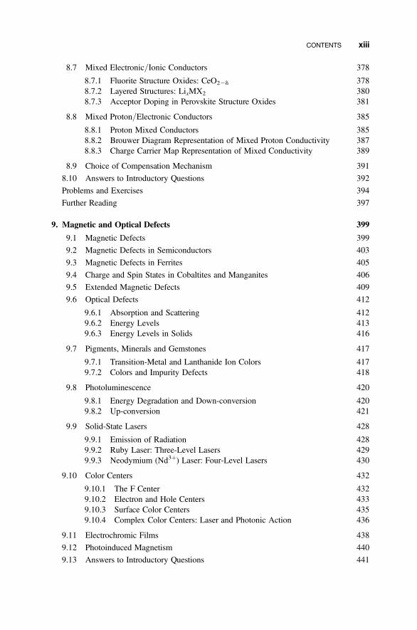
CONTENTS xiii
Problems and Exercises 443
Further Reading 446
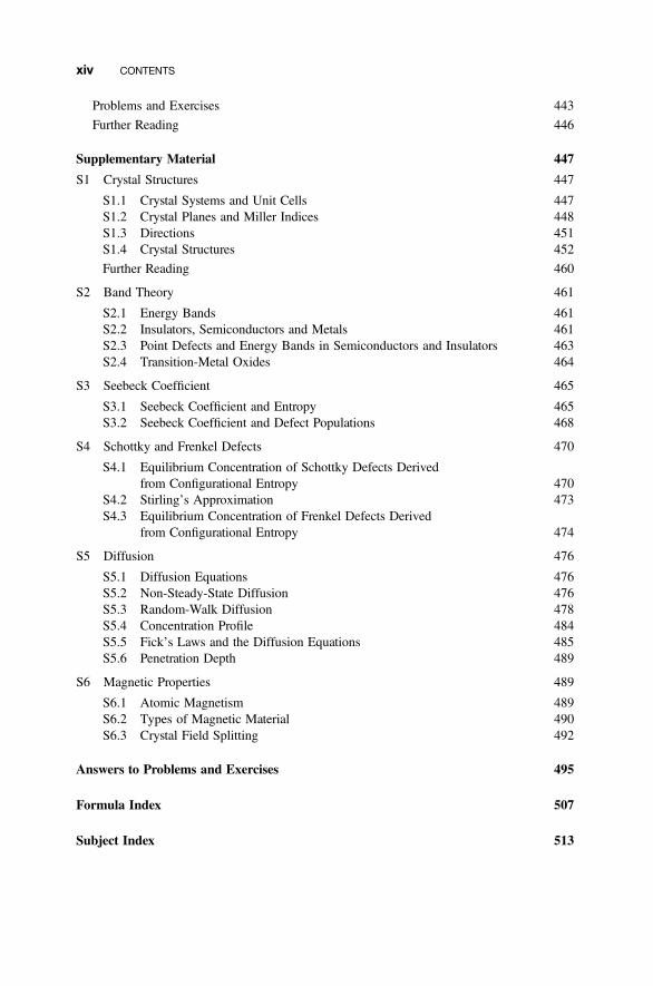
Supplementary Material 447
S1 Crystal Structures 447
S1.1 Crystal Systems and Unit Cells 447S1.2 Crystal Planes and Miller Indices 448S1.3 Directions 451S1.4 Crystal Structures 452
Further Reading 460
S2 Band Theory 461
S2.1 Energy Bands 461S2.2 Insulators, Semiconductors and Metals 461S2.3 Point Defects and Energy Bands in Semiconductors and Insulators 463S2.4 Transition-Metal Oxides 464
S3 Seebeck Coefficient 465
S3.1 Seebeck Coefficient and Entropy 465S3.2 Seebeck Coefficient and Defect Populations 468
S4 Schottky and Frenkel Defects 470
S4.1 Equilibrium Concentration of Schottky Defects Derivedfrom Configurational Entropy 470
S4.2 Stirling’s Approximation 473S4.3 Equilibrium Concentration of Frenkel Defects Derived
from Configurational Entropy 474
S5 Diffusion 476
S5.1 Diffusion Equations 476S5.2 Non-Steady-State Diffusion 476S5.3 Random-Walk Diffusion 478S5.4 Concentration Profile 484S5.5 Fick’s Laws and the Diffusion Equations 485S5.6 Penetration Depth 489
S6 Magnetic Properties 489
S6.1 Atomic Magnetism 489S6.2 Types of Magnetic Material 490S6.3 Crystal Field Splitting 492
Answers to Problems and Exercises 495
Formula Index 507
Subject Index 513
xiv CONTENTS

&PREFACE
During the course of the last century, it was realized that many properties of solids arecontrolled not so much by the chemical composition or the chemical bonds linkingthe constituent atoms in the crystal but by faults or defects in the structure. Overthe course of time the subject has, if anything, increased in importance. Indeed,there is no aspect of the physics and chemistry of solids that is not decisively influ-enced by the defects that occur in the material under consideration. The whole ofthe modern silicon-based computer industry is founded upon the introduction ofprecise amounts of specific impurities into extremely pure crystals. Solid-statelasers function because of the activity of impurity atoms. Battery science, solidoxide fuel cells, hydrogen storage, displays, all rest upon an understanding ofdefects in the solid matrix.
As the way in which defects modify the properties of a solid has been graduallyunderstood, the concept of a defect has undergone considerable evolution. The earli-est and perhaps simplest concept of a defect in a solid was that of a wrong atom, orimpurity, in place of a normal atom in a crystal—a so-called point defect. Not longafter the recognition of point defects, the concept of linear defects, dislocations,was invoked to explain a number of diverse features including the mechanical prop-erties of metals and the growth of crystals. In recent years it has become apparent thatdefect interactions, aggregation, or clustering is of vital importance.
The advance in understanding of defects has been made hand in hand with thespectacular development of sophisticated experimental techniques. The initial break-through was in X-ray diffraction—a technique that still remains as the foundation ofmost studies. A further change came with the development of transmission electronmicroscopy that was able, for the first time, to produce images of defects at an atomicscale of resolution. Since then, advances in computing techniques, together with theavailability of powerful graphics, have thrown quite new light on the defect structureof materials.
Besides the multiplicity of defects that can be envisaged, there is also a wide rangeof solid phases within which such defects can reside. The differences between analloy, a metallic sulfide, a crystalline fluoride, a silicate glass, or an amorphouspolymer are significant. Moreover, developments in crystal growth and the pro-duction of nanoparticles have changed the perspective of earlier studies, whichwere usually made on polycrystalline solids, sometimes with uncertain degrees ofimpurity present.
All of these changes have meant that the view of defects in solids has changedconsiderably over the last 20 years or so. This book is aimed at presenting an
xv
overview of this information. However, the topic encompasses a huge subject area,and selection has been inevitable. Moreover, courses about defects in solids,whether to undergraduate or postgraduate students in chemistry, physics, geology,materials science, or engineering, are usually constrained to a relatively small partof the curriculum. Nevertheless, the material included in this book has beenchosen so that not only basics are covered but also aspects of recent researchwhere exciting frontiers lie. Unfortunately, the influence of defects upon mechanicalproperties is mostly excluded, and the important area of surfaces and surface defectsis only mentioned in passing. Similarly, the area of studies prefixed by nano- has beenbypassed. This is because the literature here is growing at an enormous rate, and timewas not available to sift through this mountain of data. Although these omissionsare regrettable, they leave scope for future volumes in this series. Finally, it mustbe mentioned that most emphasis has been placed upon principles, leaving littlespace for description of important experimental details. This is a pity, but withinthe constraints of time and space, became inevitable. Again, a future volume couldcorrect this shortcoming.
The first four chapters introduce basic concepts that are developed to build up aframework for understanding defect chemistry and physics. Thereafter, chaptersfocus rather more on properties related to applications. Chapter 5 describes diffusionin solids; Chapter 6, ionic conductivity; Chapters 7 and 8 the important topics of elec-tronic conductivity, both intrinsic (Chapter 7) and extrinsic (Chapter 8). The finalchapter gives a selected account of magnetic and optical defects.
To assist in understanding, each chapter has been prefaced with three “introduc-tory questions” that focus the reader upon some of the important points to beraised in the following text. These are answered at the end of each chapter. Inaddition, end-of-chapter questions aid understanding of the preceding material. Thefirst set of these consists of multiple choice questions—a “quick quiz,” to test knowl-edge of terms and principles. This is followed by a number of more traditional prob-lems and calculations to build skills and understanding in more depth. In addition,supplementary material covering the fundamentals of relevant topics such as crystal-lography and band theory are included so that, in the first instance, a reader will nothave to look elsewhere for this information.
Each chapter contains a short list of additional sources that expand or give a differ-ent perspective on the material in the preceding chapter. Most of these are books ororiginal scientific literature, and only a few web sources are listed. The Internet pro-vides a data bank of considerable power but has two drawbacks: It is easy to becomeswamped by detail (often a simple search will throw up a million or more allegedlyrelevant pages), and much of the information located has an ephemeral nature. Ratherthan list a large number of sites, the reader is encouraged to use a search engine andkeywords such as “magnetic defects,” which will open an alternative perspective onthe subject to that presented in this book.
I have been particularly helped in the compilation of this book by family, friends,and colleagues. Professor R. B. King first suggested the project, and Drs. E. E. M.Tyler, G. J. Tilley, and R. D. Tilley made suggestions about contents and scope.Professor F. S. Stone offered encouragement and kindly offered to read sections in
xvi PREFACE
draft form, resulting in invaluable advice and comment that added substantially to theclarity and balance. Mr. A. Coughlin was constantly encouraging and gave assistancewhen mathematical discussions of topics such as polynomials or random walksbecame opaque and provided valued help into the proofs. The staff of theTrevithick Library, University of Cardiff, have been helpful at all times and continu-ally located obscure references. The staff at Wiley, gave constant advice, help, andencouragement. Dr. John Hutchison, University of Oxford, provided stunning micro-graphs for which I am greatly indebted. Finally, my gratitude to my wife Anne cannotbe understated. Her tolerance of my neglect and her continued encouragement hasallowed this project to reach a conclusion.
Comments and queries will be gratefully received and can be sent [email protected] or [email protected].
R. J. D. TILLEY
PREFACE xvii

&CHAPTER 1
Point Defects
What is a point defect?
What is the “effective charge” on a defect?
What is an antisite defect?
1.1 INTRODUCTION
Defects play an important part in both the chemical and physical behavior of solids,and much of modern science and technology centers upon the exploitation or sup-pression of the properties that defects confer upon a solid. Batteries, fuel cells, dis-plays, data storage, and computer memories all directly utilize, or have evolvedfrom, an understanding and manipulation of defects in inorganic materials. This tech-nology has been developed over some 80–100 years and started with the simplestconcepts. However, as the effect of defects upon the properties of the solid graduallybecame appreciated, the concept of a defect has undergone considerable evolution.The simplest notion of a defect in a solid was the idea of a mistake such as amissing atom or an impurity in place of a normal atom. These structurally simpledefects are called point defects. Not long after the recognition of point defects, theconcept of more complex structural defects, such as linear defects termed dislo-cations, was invoked to explain the mechanical properties of metals. In the sameperiod it became apparent that planar defects, including surfaces and grain bound-aries, and volume defects such as rods, tubes, or precipitates, have important rolesto play in influencing the physical and chemical properties of a solid.
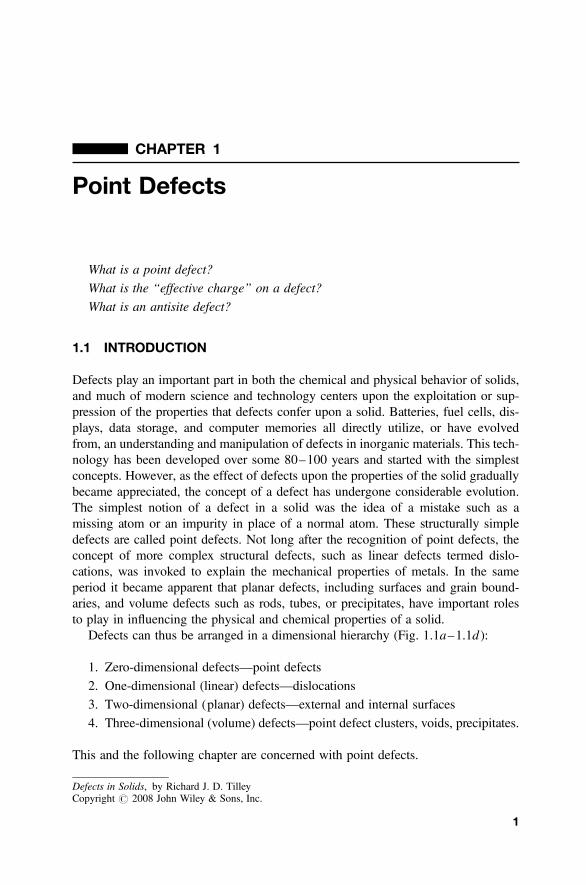
Defects can thus be arranged in a dimensional hierarchy (Fig. 1.1a–1.1d ):
1. Zero-dimensional defects—point defects
2. One-dimensional (linear) defects—dislocations
3. Two-dimensional (planar) defects—external and internal surfaces
4. Three-dimensional (volume) defects—point defect clusters, voids, precipitates.
This and the following chapter are concerned with point defects.
Defects in Solids, by Richard J. D. TilleyCopyright # 2008 John Wiley & Sons, Inc.
1
In addition to the defects listed above, which may be termed structural defects, thereare also electronic defects. The first of these are electrons that are in excess of thoserequired for chemical bonding and that, in certain circumstances, constitute chargeddefects that can carry current. In addition, current in somematerials is carried by particles
Figure 1.1 Defects in crystalline solids: (a) point defects (interstitials); (b) a linear defect(edge dislocation); (c) a planar defect (antiphase boundary); (d ) a volume defect (precipitate);(e) unit cell (filled) of a structure containing point defects (vacancies); and ( f ) unit cell (filled)of a defect-free structure containing “ordered vacancies.”
2 POINT DEFECTS
that behave rather like positive electrons, and these form the second type of electronicdefect.1 They are called electron holes, positive holes, or more often just holes.
Besides the multiplicity of defects that can be envisaged, there is a wide range ofhost solid phases within which such defects can reside. The differences between analloy, a metallic sulfide, a crystalline fluoride, or a silicate glass are significant from
Figure 1.1 (Continued).
1These are not the positive equivalent of an electron, a positron, because such a particle would be elimi-nated instantaneously by combination with an ordinary electron, but are virtual particles equivalent to theabsence of an electron. They can be considered to be analogs of a vacancy, which is the absence of an atom.
1.1 INTRODUCTION 3
both a chemical or physical viewpoint. By default, defects have come to be associatedwith crystalline solids because a crystal has a regular repetition of atoms throughout itsvolume.2 A disturbance of this regularity then constitutes the defect (Fig. 1.1a–1.1d ).In this sense, the nature of a defect in, for example, a glass or amorphous polymer, ismore difficult to picture.
When circumstances permit, defects can order. This may happen at low tempera-tures, for example, when defect interactions overcome the disordering effect due totemperature. From a diffraction point of view the ordered sample no longer containsdefects, as the characteristic signs disappear. For example, in X-ray analysis broad-ened diffraction spots and diffuse scattering, both characteristic of disordered crystals,disappear, to be replaced by additional sharp reflections. In such cases the defects areincorporated or assimilated into the crystal structure and so effectively vanish. Theoriginal unit cell of the defect-containing phase is replaced by a new unit cell inwhich the original “defects” are now integral components of the structure(Fig. 1.1e and 1.1f ).
1.2 POINT AND ELECTRONIC DEFECTS INCRYSTALLINE SOLIDS
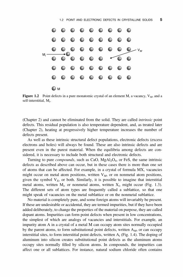
The simplest localized defect in a crystal is a mistake at a single atom site in a puremonatomic crystal, such as silicon or iron. Such a defect is called a point defect. Twodifferent types of simple point defect can occur in a pure crystal of an element, M. Anatom can be imagined to be absent from a normally occupied position, to leave avacancy, given the symbol VM (Fig. 1.2). This may occur, for instance, duringcrystal growth. A second defect can also be envisaged; namely an extra atomincorporated into the structure, again, say, during crystallization. This extra atom isforced to take up a position in the crystal that is not a normally occupied site: it iscalled an interstitial site, and the atom is called an interstitial atom (or more oftensimply an interstitial), given the symbol Mi, (Fig. 1.2). If it is necessary to stressthat the interstitial atom is the same as the normal atoms in the structure, it iscalled a self-interstitial atom.
The various point defects present in a crystal as grown, for example, vacancies,interstitials, excess electrons, holes, and other arrangements, are called nativedefects. These native defects can arise in several ways. They can be introducedduring crystal growth, as mentioned above, especially if this is rapid and crystalliza-tion is far removed from equilibrium. Defects can also form after the crystal is devel-oped if the crystal is subjected to irradiation by high-energy particles or other formsof radiation. Defects that result from such processes are called induced defects. Whena pure crystal is heated at a moderate temperature for a long period, a process calledannealing, the number of native defects will gradually change. However, no matterhow long the sample is annealed, a population of point defects will always remain,even in the purest crystal. These point defects are in thermodynamic equilibrium
2An introduction to crystal structures and nomenclature is given in the Supplementary Material Section S1.
4 POINT DEFECTS
(Chapter 2) and cannot be eliminated from the solid. They are called intrinsic pointdefects. This residual population is also temperature dependent, and, as treated later(Chapter 2), heating at progressively higher temperature increases the number ofdefects present.
As well as these intrinsic structural defect populations, electronic defects (excesselectrons and holes) will always be found. These are also intrinsic defects and arepresent even in the purest material. When the equilibria among defects are con-sidered, it is necessary to include both structural and electronic defects.
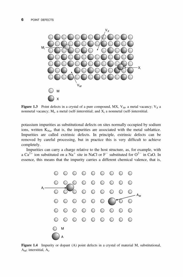
Turning to pure compounds, such as CaO, MgAl2O4, or FeS, the same intrinsicdefects as described above can occur, but in these cases there is more than one setof atoms that can be affected. For example, in a crystal of formula MX, vacanciesmight occur on metal atom positions, written VM, or on nonmetal atom positions,given the symbol VX, or both. Similarly, it is possible to imagine that interstitialmetal atoms, written Mi, or nonmetal atoms, written Xi, might occur (Fig. 1.3).The different sets of atom types are frequently called a sublattice, so that onemight speak of vacancies on the metal sublattice or on the nonmetal sublattice.
No material is completely pure, and some foreign atoms will invariably be present.If these are undesirable or accidental, they are termed impurities, but if they have beenadded deliberately, to change the properties of the material on purpose, they are calleddopant atoms. Impurities can form point defects when present in low concentrations,the simplest of which are analogs of vacancies and interstitials. For example, animpurity atom A in a crystal of a metal M can occupy atom sites normally occupiedby the parent atoms, to form substitutional point defects, written AM, or can occupyinterstitial sites, to form interstitial point defects, written Ai (Fig. 1.4). The doping ofaluminum into silicon creates substitutional point defects as the aluminum atomsoccupy sites normally filled by silicon atoms. In compounds, the impurities canaffect one or all sublattices. For instance, natural sodium chloride often contains
Figure 1.2 Point defects in a pure monatomic crystal of an element M, a vacancy, VM, and aself-interstitial, Mi.
1.2 POINT AND ELECTRONIC DEFECTS IN CRYSTALLINE SOLIDS 5
potassium impurities as substitutional defects on sites normally occupied by sodiumions, written KNa, that is, the impurities are associated with the metal sublattice.Impurities are called extrinsic defects. In principle, extrinsic defects can beremoved by careful processing, but in practice this is very difficult to achievecompletely.
Impurities can carry a charge relative to the host structure, as, for example, witha Ca2þ ion substituted on a Naþ site in NaCl or F2 substituted for O22 in CaO. Inessence, this means that the impurity carries a different chemical valence, that is,
Figure 1.3 Point defects in a crystal of a pure compound, MX, VM, a metal vacancy; VX anonmetal vacancy; Mi, a metal (self-)interstitial; and Xi a nonmetal (self-)interstitial.
Figure 1.4 Impurity or dopant (A) point defects in a crystal of material M, substitutional,AM; interstitial, Ai.
6 POINT DEFECTS
it comes from a different group of the periodic table than the host atoms. Deliberateintroduction of such impurities is called aliovalent or altervalent doping. The intro-duction of charged impurities will upset the charge neutrality of the solid, and thismust be balanced in some way so as to restore the electronic neutrality of thecrystal. One way in which this compensation can be achieved is by the incorporationof other vacancies or interstitial atoms that carry a balancing charge. The substitutionof a Ca2þ ion for Naþ in NaCl can be balanced, for example, by the introduction atthe same time, of a sodium ion vacancy, VNa, at the same time. This mechanism iscalled ionic compensation, structural compensation, or less often self-compensation.However, compensation can also take place electronically by the introduction ofappropriate numbers of electrons or holes. For example, the substitution of F2 forO22 in CaO could be balanced by the introduction of an equivalent number of elec-trons, one per added F2. Impurities that are compensated by excess electrons in thisway are called donors or donor impurities, while those that are compensated byaddition of holes are called acceptors or acceptor impurities. One consequence ofthese alternatives is that the electrons and holes present in the solid must be includedin the overall accounting system used for assessing the defects present in a solid.
The importance of point defects in a crystal cannot be overstated. They can changethe physical properties of a solid significantly. To introduce the range of changespossible, Sections 1.3–1.6 outline some of the physical properties that are influencedin this way.
1.3 ELECTRONIC PROPERTIES: DOPED SILICONAND GERMANIUM AS EXAMPLES
Silicon, Si, lies at the heart of most current electronic devices. Both silicon and thesimilar semiconductor element germanium, Ge, crystallize with the diamond structure(Fig. 1.5). In this structure each atom is surrounded by four others arranged at thecorners of a tetrahedron. Each atom has four outer electrons available for chemicalbonding, and these are completely taken up by creating a network of tetrahedrallyoriented sp3-hybrid bonds. Although pure silicon and germanium are intrinsic semi-conductors, these properties are inadequate for the creation of sophisticated electronicmaterials for which selected impurity doping is necessary. The resulting materials arecalled extrinsic semiconductors because of the extrinsic nature of the defects that giverise to the important conductivity changes.
Impurity atoms will upset the orderly arrangement of bonding electrons and thischanges the electronic properties. Doping with a very small amount of an impurityfrom the next higher neighboring group of the periodic table, phosphorus (P),arsenic (As), or antimony (Sb), results in the formation of substitutional pointdefects in which the impurities occupy normal sites, for example, a phosphorusatom on a site normally occupied by a silicon atom, PSi (Fig. 1.6a). Each of theseatoms has five valence electrons available for bonding, and after using four toform the four sp3-hybrid bonds, one electron per impurity atom is left over. Theseelectrons are easily liberated from the impurity atoms by thermal energy and are
1.3 ELECTRONIC PROPERTIES: DOPED SILICON AND GERMANIUM AS EXAMPLES 7
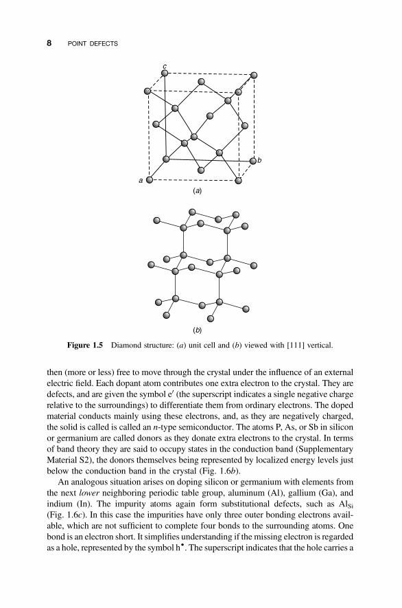
then (more or less) free to move through the crystal under the influence of an externalelectric field. Each dopant atom contributes one extra electron to the crystal. They aredefects, and are given the symbol e0 (the superscript indicates a single negative chargerelative to the surroundings) to differentiate them from ordinary electrons. The dopedmaterial conducts mainly using these electrons, and, as they are negatively charged,the solid is called is called an n-type semiconductor. The atoms P, As, or Sb in siliconor germanium are called donors as they donate extra electrons to the crystal. In termsof band theory they are said to occupy states in the conduction band (SupplementaryMaterial S2), the donors themselves being represented by localized energy levels justbelow the conduction band in the crystal (Fig. 1.6b).
An analogous situation arises on doping silicon or germanium with elements fromthe next lower neighboring periodic table group, aluminum (Al), gallium (Ga), andindium (In). The impurity atoms again form substitutional defects, such as AlSi(Fig. 1.6c). In this case the impurities have only three outer bonding electrons avail-able, which are not sufficient to complete four bonds to the surrounding atoms. Onebond is an electron short. It simplifies understanding if the missing electron is regardedas a hole, represented by the symbol h†. The superscript indicates that the hole carries a
Figure 1.5 Diamond structure: (a) unit cell and (b) viewed with [111] vertical.
8 POINT DEFECTS
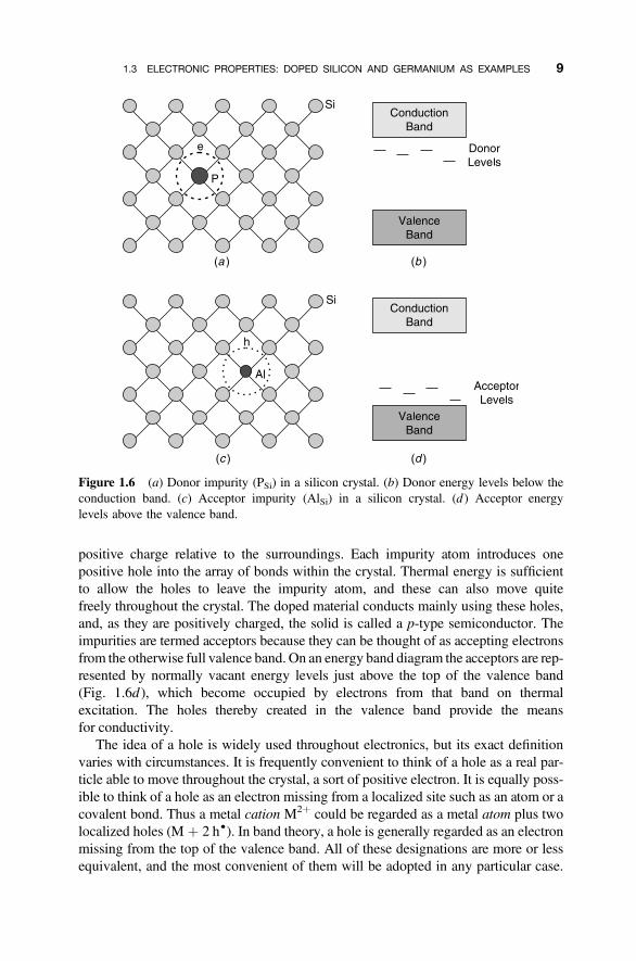
positive charge relative to the surroundings. Each impurity atom introduces onepositive hole into the array of bonds within the crystal. Thermal energy is sufficientto allow the holes to leave the impurity atom, and these can also move quitefreely throughout the crystal. The doped material conducts mainly using these holes,and, as they are positively charged, the solid is called a p-type semiconductor. Theimpurities are termed acceptors because they can be thought of as accepting electronsfrom the otherwise full valence band. On an energy band diagram the acceptors are rep-resented by normally vacant energy levels just above the top of the valence band(Fig. 1.6d), which become occupied by electrons from that band on thermalexcitation. The holes thereby created in the valence band provide the meansfor conductivity.
The idea of a hole is widely used throughout electronics, but its exact definitionvaries with circumstances. It is frequently convenient to think of a hole as a real par-ticle able to move throughout the crystal, a sort of positive electron. It is equally poss-ible to think of a hole as an electron missing from a localized site such as an atom or acovalent bond. Thus a metal cation M2þ could be regarded as a metal atom plus twolocalized holes (M þ 2 h†). In band theory, a hole is generally regarded as an electronmissing from the top of the valence band. All of these designations are more or lessequivalent, and the most convenient of them will be adopted in any particular case.
Figure 1.6 (a) Donor impurity (PSi) in a silicon crystal. (b) Donor energy levels below theconduction band. (c) Acceptor impurity (AlSi) in a silicon crystal. (d ) Acceptor energylevels above the valence band.
1.3 ELECTRONIC PROPERTIES: DOPED SILICON AND GERMANIUM AS EXAMPLES 9
The unique electronic properties of semiconductor devices arise at the regionswhere p-type and n-type materials are in close proximity, as in p–n junctions.Typical impurity levels are about 0.0001 at %, and their inclusion and distributionneed to be very strictly controlled during preparation. Without these deliberatelyintroduced point defects, semiconductor devices of the type now commonly availablewould not be possible.
1.4 OPTICAL PROPERTIES: F CENTERS ANDRUBY AS EXAMPLES
Point defects can have a profound effect upon the optical properties of solids. Themost important of these in everyday life is color,3 and the transformation of transpar-ent ionic solids into richly colored materials by F centers, described below, providedone of the first demonstrations of the existence of point defects in solids.
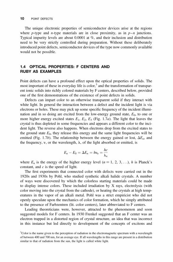
Defects can impart color to an otherwise transparent solid if they interact withwhite light. In general the interaction between a defect and the incident light is viaelectrons or holes. These may pick up some specific frequency of the incident illumi-nation and in so doing are excited from the low-energy ground state, E0, to one ormore higher energy excited states E1, E2, E3 (Fig. 1.7a). The light that leaves thecrystal is thus depleted in some frequencies and appears a different color to the inci-dent light. The reverse also happens. When electrons drop from the excited states tothe ground state E0, they release this energy and the same light frequencies will beemitted (Fig. 1.7b). The relationship between the energy gained or lost, DEn, andthe frequency, n, or the wavelength, l, of the light absorbed or emitted, is
En � E0 ¼ DEn ¼ hnn ¼ hc
ln
where En is the energy of the higher energy level (n ¼ 1, 2, 3, . . .), h is Planck’sconstant, and c is the speed of light.
The first experiments that connected color with defects were carried out in the1920s and 1930s by Pohl, who studied synthetic alkali halide crystals. A numberof ways were discovered by which the colorless starting materials could be madeto display intense colors. These included irradiation by X rays, electrolysis (withcolor moving into the crystal from the cathode), or heating the crystals at high temp-eratures in the vapor of an alkali metal. Pohl was a strict empiricist who did notopenly speculate upon the mechanics of color formation, which he simply attributedto the presence of Farbzentren (lit. color centers), later abbreviated to F centers.
Leading theoreticians were, however, attracted to the phenomenon and soonsuggested models for F centers. In 1930 Frenkel suggested that an F center was anelectron trapped in a distorted region of crystal structure, an idea that was incorrectin this instance but led directly to development of the concepts of excitons and
3Color is the name given to the perception of radiation in the electromagnetic spectrum with a wavelengthof between 400 and 700 nm, for an average eye. If all wavelengths in this range are present in a distributionsimilar to that of radiation from the sun, the light is called white light.
10 POINT DEFECTS
polarons (Section 7.2). In 1934 Schottky suggested that an F center was an anionvacancy together with a trapped electron, and this model was put onto a firmquantum mechanical footing by Gurney and Mott in 1937 and later by Seitz, whoextended the work to other types of color centers.
The origin of the color is as follows. The electron trapped at an anion vacancy inan alkali halide crystal is an analog of a hydrogen atom. The electron can occupy oneof a number of orbitals, and transitions between some of these levels absorb light andhence endow the solid with a characteristic color. F centers and related defects arediscussed further in Chapter 9.
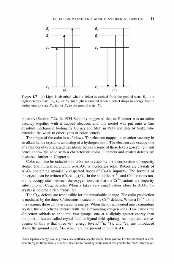
Color can also be induced into colorless crystals by the incorporation of impurityatoms. The mineral corundum, a-Al2O3, is a colorless solid. Rubies are crystals ofAl2O3 containing atomically dispersed traces of Cr2O3 impurity. The formula ofthe crystal can be written (CrxAl12x)2O3. In the solid the Al3þ and Cr3þ cations ran-domly occupy sites between the oxygen ions, so that the Cr3þ cations are impuritysubstitutional, CrAl, defects. When x takes very small values close to 0.005, thecrystal is colored a rich “ruby” red.
The CrAl defects are responsible for the remarkable change. The color productionis mediated by the three 3d electrons located on the Cr3þ defects. When a Cr3þ ion isin a vacuum, these all have the same energy. When the ion is inserted into a corundumcrystal, the d electrons interact with the surrounding oxygen ions. This causes thed-electron orbitals to split into two groups, one at a slightly greater energy thanthe other, a feature called crystal field or ligand field splitting. An important conse-quence of this is that three new energy levels,4 2E, 4T2, and
4T1, are introducedabove the ground state, 4A2, which are not present in pure Al2O3.
Figure 1.7 (a) Light is absorbed when a defect is excited from the ground state, E0, to ahigher energy state, E1, E2, or E3. (b) Light is emitted when a defect drops in energy from ahigher energy state E1, E2, or E3 to the ground state, E0.
4Each separate energy level is given a label called a (spectroscopic) term symbol. For the moment it is suffi-cient to regard these merely as labels. See Further Reading at the end of this chapter for more information.
1.4 OPTICAL PROPERTIES: F CENTERS AND RUBY AS EXAMPLES 11
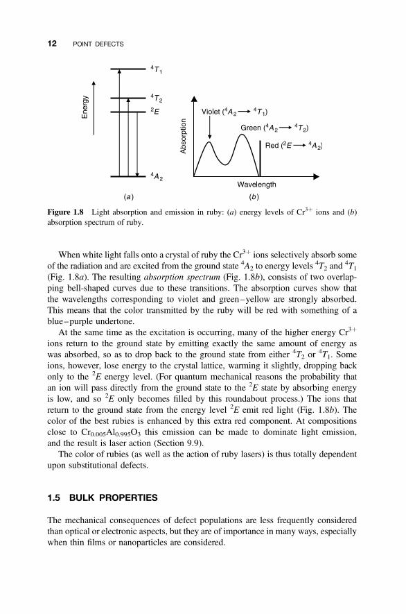
When white light falls onto a crystal of ruby the Cr3þ ions selectively absorb someof the radiation and are excited from the ground state 4A2 to energy levels
4T2 and4T1
(Fig. 1.8a). The resulting absorption spectrum (Fig. 1.8b), consists of two overlap-ping bell-shaped curves due to these transitions. The absorption curves show thatthe wavelengths corresponding to violet and green–yellow are strongly absorbed.This means that the color transmitted by the ruby will be red with something of ablue–purple undertone.
At the same time as the excitation is occurring, many of the higher energy Cr3þ
ions return to the ground state by emitting exactly the same amount of energy aswas absorbed, so as to drop back to the ground state from either 4T2 or 4T1. Someions, however, lose energy to the crystal lattice, warming it slightly, dropping backonly to the 2E energy level. (For quantum mechanical reasons the probability thatan ion will pass directly from the ground state to the 2E state by absorbing energyis low, and so 2E only becomes filled by this roundabout process.) The ions thatreturn to the ground state from the energy level 2E emit red light (Fig. 1.8b). Thecolor of the best rubies is enhanced by this extra red component. At compositionsclose to Cr0.005Al0.995O3 this emission can be made to dominate light emission,and the result is laser action (Section 9.9).
The color of rubies (as well as the action of ruby lasers) is thus totally dependentupon substitutional defects.
1.5 BULK PROPERTIES
The mechanical consequences of defect populations are less frequently consideredthan optical or electronic aspects, but they are of importance in many ways, especiallywhen thin films or nanoparticles are considered.
Figure 1.8 Light absorption and emission in ruby: (a) energy levels of Cr3þ ions and (b)absorption spectrum of ruby.
12 POINT DEFECTS
1.5.1 Unit Cell Dimensions
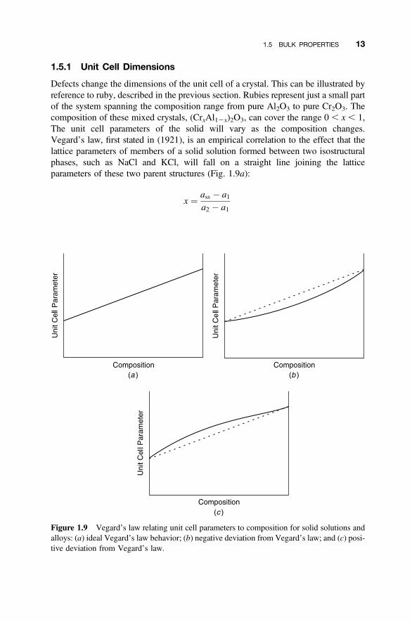
Defects change the dimensions of the unit cell of a crystal. This can be illustrated byreference to ruby, described in the previous section. Rubies represent just a small partof the system spanning the composition range from pure Al2O3 to pure Cr2O3. Thecomposition of these mixed crystals, (CrxAl12x)2O3, can cover the range 0 , x, 1,The unit cell parameters of the solid will vary as the composition changes.Vegard’s law, first stated in (1921), is an empirical correlation to the effect that thelattice parameters of members of a solid solution formed between two isostructuralphases, such as NaCl and KCl, will fall on a straight line joining the latticeparameters of these two parent structures (Fig. 1.9a):
x ¼ ass � a1a2 � a1
Figure 1.9 Vegard’s law relating unit cell parameters to composition for solid solutions andalloys: (a) ideal Vegard’s law behavior; (b) negative deviation from Vegard’s law; and (c) posi-tive deviation from Vegard’s law.
1.5 BULK PROPERTIES 13
that is,
ass ¼ a1 þ x(a2–a1)
where a1 and a2 are the lattice parameters of the parent phases, ass is the latticeparameter of the solid solution, and x is the mole fraction of the parent phase withlattice parameter a2. (The relationship holds for all unit cell parameters, a, b, and cand any interaxial angles.) This “law” is simply an expression of the idea that thecell parameters are a direct consequence of the sizes of the component atoms inthe solid solution. Vegard’s law, in its ideal form, is almost never obeyed exactly.A plot of cell parameters that lies below the ideal line (Fig. 1.9b) is said to show anegative deviation from Vegard’s law, and a plot that lies above the ideal line(Fig. 1.9c) is said to show a positive deviation from Vegard’s law. In these cases,atomic interactions, which modify the size effects, are responsible for the deviations.In all cases, a plot of composition versus cell parameters can be used to determine theformulas of intermediate structures in a solid solution.
1.5.2 Density
X-ray diffraction allows the dimensions of the unit cell to be accurately measured. Ifthe structure type of the material is known, the ideal cell contents are also known.Thus, the unit cell of a crystal of composition M2O3 that adopts the corundum struc-ture contains 12M atoms and 18 O atoms (Supplementary Material, S1). This readilyallows the theoretical density of a solid to be calculated. The weights of all of theatoms in the cell are added, and this is divided by the cell volume.
It was realized at an early stage that a comparison of the theoretical and measureddensity of a solid can be used to determine the notional species of point defectpresent. The general procedure is:
1. Measure the composition of the solid.
2. Measure the density.
3. Measure the unit cell parameters.
4. Calculate the theoretical density for alternative point defect populations.
5. Compare the theoretical and experimental densities to see which point defectmodel best fits the data.
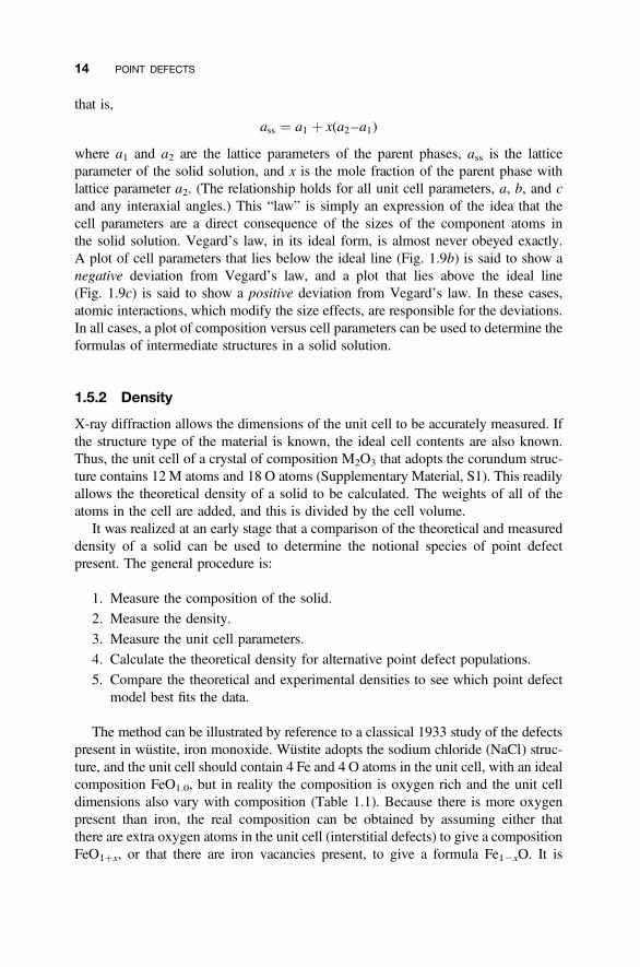
The method can be illustrated by reference to a classical 1933 study of the defectspresent in wustite, iron monoxide. Wustite adopts the sodium chloride (NaCl) struc-ture, and the unit cell should contain 4 Fe and 4 O atoms in the unit cell, with an idealcomposition FeO1.0, but in reality the composition is oxygen rich and the unit celldimensions also vary with composition (Table 1.1). Because there is more oxygenpresent than iron, the real composition can be obtained by assuming either thatthere are extra oxygen atoms in the unit cell (interstitial defects) to give a compositionFeO1þx, or that there are iron vacancies present, to give a formula Fe12xO. It is
14 POINT DEFECTS
possible to determine which of these suppositions is correct by comparing the realand theoretical density of the material.
For example, consider the sample specified in the top line of Table 1.1, with anoxygen : iron ratio of 1.058, a measured density of 5728 kg m23 and a cubic latticeparameter, a, of 0.4301 nm.
1. Assume that the iron atoms in the crystal are in a perfect array, identicalto the metal atoms in the sodium chloride structure, and that the 0.058excess of oxygen is due to interstitial oxygen atoms being present, over andabove those on the normal anion positions. The unit cell of the structurenow contains 4 Fe and (4 � 1.058) O. The density is calculated to be6076 kg m23.
2. Assume that the oxygen array is perfect and identical to the nonmetal atomarray in the sodium chloride structure and that the unit cell contains somevacancies on the iron positions. In this case, one unit cell will contain 4atoms of oxygen and (4/1.058) atoms of iron, that is, 4 Fe0.945O. Thedensity is calculated to 5741 kg m23.
The difference in the two values is surprisingly large and is well within the accu-racy of density determinations. The experimental value is in accord with a model thatassumes vacancies on the iron positions, as are all results in Table 1.1, indicating thata formula Fe12xO, in which there are vacancies at some of the Fe positions, betterreflects the structure.
Although this analysis is correct, it is a macroscopic method that does not give anytrue crystallographic information. The oxygen vacancies may be arranged in anynumber of ways. In fact, it is found that the vacancies form clusters that can beregarded as fragments of the next higher oxide, Fe3O4, with the spinel structureembedded in a sodium chloride structure matrix (Section 4.4.2).
Because of Vegard’s law, it is clear that the density of a solid solution will also beexpected to be a linear function of the densities of the parent phases that make up thelimits of a solid solution.
TABLE 1.1 Experimental Data for Wustite, FeOx
Density/kg m23
O/FeRatio
Fe/ORatio
LatticeParameter/nm Observed
Calculated forInterstitial Oxygen
Calculated forIron Vacancies
1.058 0.945 0.4301 5728 6076 57401.075 0.930 0.4292 5658 6136 57061.087 0.920 0.4285 5624 6181 56871.099 0.910 0.4282 5613 6210 5652
Source: Adapted from E. R. Jette and F. Foote, J. Chem. Phys., 1, 29 (1933).
1.5 BULK PROPERTIES 15
1.5.3 Volume
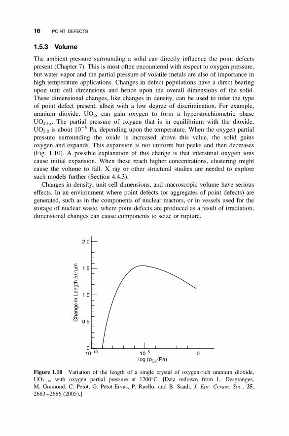
The ambient pressure surrounding a solid can directly influence the point defectspresent (Chapter 7). This is most often encountered with respect to oxygen pressure,but water vapor and the partial pressure of volatile metals are also of importance inhigh-temperature applications. Changes in defect populations have a direct bearingupon unit cell dimensions and hence upon the overall dimensions of the solid.These dimensional changes, like changes in density, can be used to infer the typeof point defect present, albeit with a low degree of discrimination. For example,uranium dioxide, UO2, can gain oxygen to form a hyperstoichiometric phaseUO2þx. The partial pressure of oxygen that is in equilibrium with the dioxide,UO2.0 is about 10
29 Pa, depending upon the temperature. When the oxygen partialpressure surrounding the oxide is increased above this value, the solid gainsoxygen and expands. This expansion is not uniform but peaks and then decreases(Fig. 1.10). A possible explanation of this change is that interstitial oxygen ionscause initial expansion. When these reach higher concentrations, clustering mightcause the volume to fall. X ray or other structural studies are needed to exploresuch models further (Section 4.4.3).
Changes in density, unit cell dimensions, and macroscopic volume have seriouseffects. In an environment where point defects (or aggregates of point defects) aregenerated, such as in the components of nuclear reactors, or in vessels used for thestorage of nuclear waste, where point defects are produced as a result of irradiation,dimensional changes can cause components to seize or rupture.
Figure 1.10 Variation of the length of a single crystal of oxygen-rich uranium dioxide,UO2þx, with oxygen partial pressure at 12008C. [Data redrawn from L. Desgranges,M. Gramond, C. Petot, G. Petot-Ervas, P. Ruello, and B. Saadi, J. Eur. Ceram. Soc., 25,2683–2686 (2005).]
16 POINT DEFECTS
Such changes in the defect population can be critical in device manufacture andoperation. For example, a thin film of an oxide such as SiO laid down in a vacuummay have a large population of anion vacancy point defects present. Similarly, afilm deposited by sputtering in an inert atmosphere may incorporate both vacanciesand inert gas interstitial atoms into the structure. When these films are subsequentlyexposed to different conditions, for example, moist air at high temperatures, changesin the point defect population will result in dimensional changes that can cause thefilm to buckle or tear.
Ionic conductors, used in electrochemical cells and batteries (Chapter 6), havehigh point defect populations. Slabs of solid ceramic electrolytes in fuel cells, forinstance, often operate under conditions in which one side of the electrolyte is heldin oxidizing conditions and the other side in reducing conditions. A significantchange in the point defect population over the ceramic can be anticipated in theseconditions, which may cause the electrolyte to bow or fracture.
These effects can all be enhanced if the point defects interact to form defect clus-ters or similar structures, as in Fe12xO above or UO2þx (Section 4.4). Such clusterscan suppress phase changes at low temperatures. Under circumstances in which theclusters dissociate, such as those found in solid oxide fuel cells, the volumechange can be considerable, leading to failure of the component.
1.5.4 Young’s Modulus (the Elastic Modulus)
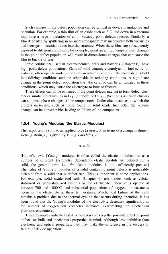
The response of a solid to an applied force (a stress, s) in terms of a change in dimen-sions (a strain, 1) is given by Young’s modulus, E:
s ¼ E1
(Hooke’s law). [Young’s modulus is often called the elastic modulus, but as anumber of different (symmetry dependent) elastic moduli are defined for asolid, the generic term, i.e., the elastic modulus, is not sufficiently precise.]The value of Young’s modulus of a solid containing point defects is noticeablydifferent from a solid that is defect free. This is important is some applications.For example, solid oxide fuel cells (Chapter 6) use oxides such as calcia-stabilized or yttria-stabilized zirconia as the electrolyte. These cells operate atbetween 700 and 10008C, and substantial populations of oxygen ion vacanciesoccur in the electrolyte at these temperatures. Mechanical failure of the cellsremains a problem due to the thermal cycling that occurs during operation. It hasbeen found that the Young’s modulus of the electrolyte decreases significantly asthe number of oxygen ion vacancies increases, exacerbating the mechanicalproblems encountered.
These examples indicate that it is necessary to keep the possible effect of pointdefects on bulk and mechanical properties in mind. Although less definitive thanelectronic and optical properties, they may make the difference in the success orfailure of device operation.
1.5 BULK PROPERTIES 17
1.6 THERMOELECTRIC PROPERTIES: THE SEEBECKCOEFFICIENT AS AN EXAMPLE
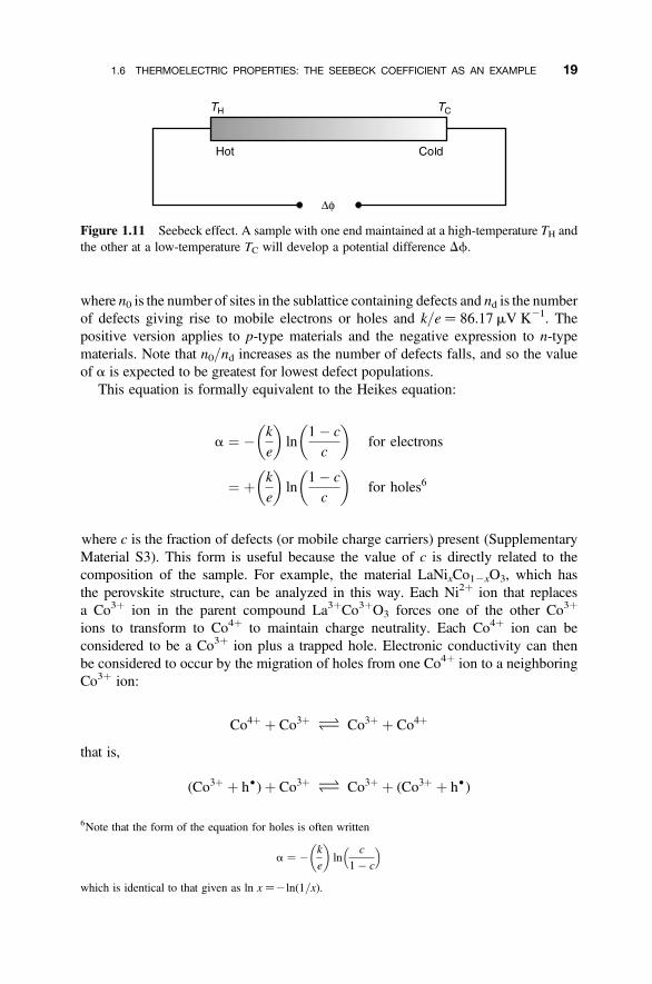
When the two ends of a material containing mobile charge carriers, holes or electrons,are held at different temperatures, a voltage is produced, a phenomenon called theSeebeck effect (Fig. 1.11). The Seebeck coefficient of a material, a, is defined asthe ratio of the electric potential produced when no current flows to the temperaturedifference present across a material:5
a ¼ +fH � fC
TH � TC¼ +
Df
DT
where fH and fC are the potentials and TH and TC are the temperatures at the hot endand the cold end of the sample, respectively. The main virtue of the Seebeck coeffi-cient in the context of this book is that its sign and magnitude can provide a measureof the concentration of charge carriers, the nature of the charge carriers, and, withsome simple assumptions, the number of defects present that give rise to thecharge carriers.
In the case of materials that have mobile electrons, that is, n-type semiconductors,the colder end of the rod will be negative with respect to the hotter end and the signof the Seebeck coefficient is negative. In the case where the mobile charge carriers arepositive holes, that is, p-type semiconductors, the colder end of the rod will bepositive with respect to the hotter end, making the Seebeck coefficient positive.For example, the nonstoichiometric forms of NiO, CoO, and FeO all show positivevalues for a, indicating that conductivity is by way of holes, whereas nonstoichio-metric ZnO has a negative value of a, indicating conductivity by way of electrons.In the case of materials with both types of charge carrier present, the one that ispresent in greatest numbers dominates the measurement.
The magnitude of the Seebeck coefficient is related to the concentration of mobilecharge carriers present and is greatest at low defect concentrations, when othermethods of analyzing defect populations give least precision. The relationshipbetween the number of defects and the Seebeck coefficient is obtained by estimatingthe configurational entropy of the defect-containing material. A number of formsfor this estimate are found, each depending upon slightly different approximations(Supplementary Material S3). The most direct is
a ¼ +k
e
� �ln
n0nd
� �� �
5The Seebeck coefficient is frequently called the thermoelectric power or thermopower, and labeled Q or S.Neither of these alternatives is a good choice. The units of the Seebeck coefficient are not those of power.The symbol Q is most often used to signify heat transfer in materials. The designation S can easily be con-fused with the entropy of the mobile charge carriers, which is important because the Seebeck coefficient isequivalent to the entropy per mobile charge carrier (see Supplementary Material S3).
18 POINT DEFECTS
where n0 is the number of sites in the sublattice containing defects and nd is the numberof defects giving rise to mobile electrons or holes and k/e ¼ 86.17mV K21. Thepositive version applies to p-type materials and the negative expression to n-typematerials. Note that n0/nd increases as the number of defects falls, and so the valueof a is expected to be greatest for lowest defect populations.
This equation is formally equivalent to the Heikes equation:
a ¼ � k
e
� �ln
1� c
c
� �for electrons
¼ þ k
e
� �ln
1� c
c
� �for holes6
where c is the fraction of defects (or mobile charge carriers) present (SupplementaryMaterial S3). This form is useful because the value of c is directly related to thecomposition of the sample. For example, the material LaNixCo12xO3, which hasthe perovskite structure, can be analyzed in this way. Each Ni2þ ion that replacesa Co3þ ion in the parent compound La3þCo3þO3 forces one of the other Co3þ
ions to transform to Co4þ to maintain charge neutrality. Each Co4þ ion can beconsidered to be a Co3þ ion plus a trapped hole. Electronic conductivity can thenbe considered to occur by the migration of holes from one Co4þ ion to a neighboringCo3þ ion:
Co4þ þ Co3þ O Co3þ þ Co4þ
that is,
(Co3þ þ h†)þ Co3þ O Co3þ þ (Co3þ þ h†)
Figure 1.11 Seebeck effect. A sample with one end maintained at a high-temperature TH andthe other at a low-temperature TC will develop a potential difference Df.
6Note that the form of the equation for holes is often written
a ¼ � k
e
� �ln
c
1� c
� �which is identical to that given as ln x ¼2ln(1/x).
1.6 THERMOELECTRIC PROPERTIES: THE SEEBECK COEFFICIENT AS AN EXAMPLE 19
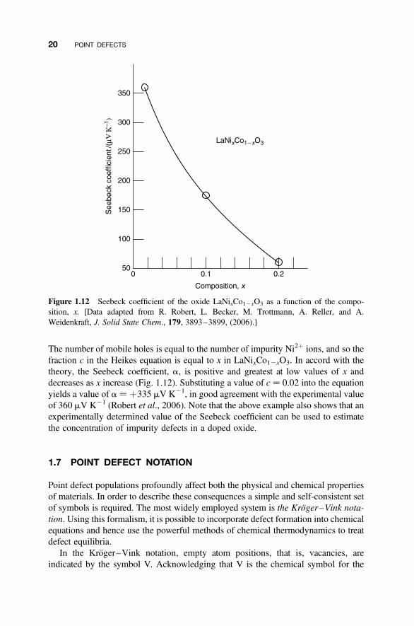
The number of mobile holes is equal to the number of impurity Ni2þ ions, and so thefraction c in the Heikes equation is equal to x in LaNixCo12xO3. In accord with thetheory, the Seebeck coefficient, a, is positive and greatest at low values of x anddecreases as x increase (Fig. 1.12). Substituting a value of c ¼ 0.02 into the equationyields a value of a ¼ þ335 mV K21, in good agreement with the experimental valueof 360 mV K21 (Robert et al., 2006). Note that the above example also shows that anexperimentally determined value of the Seebeck coefficient can be used to estimatethe concentration of impurity defects in a doped oxide.
1.7 POINT DEFECT NOTATION
Point defect populations profoundly affect both the physical and chemical propertiesof materials. In order to describe these consequences a simple and self-consistent setof symbols is required. The most widely employed system is the Kroger–Vink nota-tion. Using this formalism, it is possible to incorporate defect formation into chemicalequations and hence use the powerful methods of chemical thermodynamics to treatdefect equilibria.
In the Kroger–Vink notation, empty atom positions, that is, vacancies, areindicated by the symbol V. Acknowledging that V is the chemical symbol for the
Figure 1.12 Seebeck coefficient of the oxide LaNixCo12xO3 as a function of the compo-sition, x. [Data adapted from R. Robert, L. Becker, M. Trottmann, A. Reller, and A.Weidenkraft, J. Solid State Chem., 179, 3893–3899, (2006).]
20 POINT DEFECTS
element vanadium, it is necessary to add that, where confusion may occur, the symbolfor a vacancy is written Va. The atom that is absent from a normally occupied site isspecified by the normal chemical symbol for the element, written as a subscript. Thusin NiO, for example, the symbol VO would represent an oxygen atom vacancy andVNi a nickel atom vacancy.
The position of a defect that has been substituted for another atom in the structureis represented by a subscript that is the chemical symbol of the atom normally foundat the site occupied by the defect impurity atom. The impurity is given its normalchemical symbol, and the site occupied is written as a subscript, using the chemicalsymbol for the atom that normally occupies the site. Thus, an Mg atom on a Ni site inNiO would be written as MgNi. The same nomenclature is used if an atom in a crystaloccupies the wrong site. For example, antisite defects in GaN would be written asGaN and NGa.
Interstitial positions, positions in a crystal not normally occupied by an atom, aredenoted by the subscript i. For example, Fi would represent an interstitial fluorineatom in, say, a crystal of fluorite, CaF2.
It is possible for one or more lattice defects to associate with one another, that is, tocluster together. These are indicated by enclosing the components of such a cluster inparentheses. As an example, (VMVX) would represent a defect in which a vacancyon a metal site and a vacancy on a nonmetal site are associated as a vacancy pair.
1.8 CHARGES ON DEFECTS
One of the most difficult problems when working with defects, especially in ioniccrystals, is to decide on the charge on the ions and atoms of importance. TheKroger–Vink notation bypasses the problem of deciding on the real charges ondefects (zd), by considering only effective charges (qe). The effective charge on adefect is the charge that the defect has with respect to the charge that would bepresent at the same site in a perfect crystal. Thus, the effective charge is a relativecharge. For atomic or ionic species, this is equal to the difference between the realcharges on the defect species, zd, minus the real charge at the site occupied in aperfect crystal, zs:
qe ¼ zd � zs (1:1)
To distinguish effective charges from real charges, the superscript 0 is used for eachunit of effective negative charge and the superscript † is used for each unit of effec-tive positive charge. The real charges on a defect are still given the superscriptsymbols 2 and þ .
1.8.1 Electrons and Electron Holes
The charged defects that most readily come to mind are electrons. In a crystal contain-ing defects, some fraction of the electrons may be free to move through the matrix.These are denoted by the symbol e0. The superscript 0 represents the effective negative
1.8 CHARGES ON DEFECTS 21
charge on the electron (qe), and it is written in this way to emphasize that it isconsidered relative to the surroundings rather than as an isolated real point charge.The concentration of electrons that are free to carry current through a crystal isfrequently given the symbol n in semiconductor physics.
The counterparts to electrons in semiconducting solids are holes, represented bythe symbol h†. Each hole will bear an effective positive charge, qe, of þ1, whichis represented by the superscript † to emphasize that it is considered relative to thesurrounding structure. The concentration of holes that are free to carry currentthrough a crystal is often given the symbol p in semiconductor physics.
1.8.2 Atomic and Ionic Defects
Point defects can carry a charge. In ionic crystals, this may be considered to be thenormal state of affairs. The effective charge on these defects is the charge thatthe defect has with respect to the charge present or expected at the same point inthe perfect crystal structure. To illustrate this concept, consider the situation in anionic material such as NaCl, which it is convenient to consider as made up of thecharged ions Naþ and Cl2. What is the effective charge on a sodium vacancy,VNa, in the NaCl structure? The result is easily obtained using Eq. (1.1). The realcharge on the vacancy, zd, is 0. The real charge at the site in a perfect crystal, zs, isdue to the presence of Naþ, that is, þ1, hence:
qe ¼ zd � zs ¼ (0� 1) ¼ �1
Relative to the normal situation at the site, the vacancy appears to bear an effectivenegative charge equivalent to 21. Hence, a vacancy at a sodium ion (Naþ) site inNaCl would be written as V0
Na.In general, the absence of a positive ion will leave a vacancy with a negative effec-
tive charge relative to the normally occupied site. Multiple effective negative chargescan exist and are written using superscript n 0. A Ca2þ ion vacancy in a crystal of CaOwill bear an effective negative charge of 2 0, and the vacancy has the symbol V20
Ca ascan be seen from Eq. (1.1):
qe ¼ zd � zs ¼ (0� 2) ¼ �2
The same reasoning indicates that the absence of a negative ion will leave a posi-tive effective charge relative to a normal site occupied by a negative ion. A vacancy ata chloride ion (Cl2) site is positively charged relative to the normal situation prevail-ing at an anion site in the crystal. Using Eq. (1.1):
qe ¼ zd � zs ¼ (0� (�1)) ¼ þ1
Hence, the vacancy has an effective charge of þ1, which would be written VCl† .
22 POINT DEFECTS
In general, the absence of a negative ion will endow a site with a positiveeffective charge. Multiple effective positive charges can exist and are written usingsuperscript n†. An oxide ion (O22) vacancy in a crystal of CaO will bear an effectivepositive charge of
qe ¼ zd � zs ¼ (0� (�2)) ¼ þ2
and the vacancy has the symbol VO2†.
An effective charge relative to the host lattice is possible with any defect. These areadded as superscripts to the appropriate symbol: VM, VX, Mi, MX and associateddefects such as (VMVX).
Interstitial sites, which are normally unoccupied in a crystal, will have nopreexisting charge. When an atom or an ion occupies an interstitial site, its realcharge is the same as the effective charge. Thus, for a Zn2þ ion at an interstitialsite, from Eq. (1.1):
qe ¼ zd � zs ¼ (2� 0) ¼ 2
The defect is given the symbol Zni2†.
Substitution of an ion with one valence by another with a different valence,aliovalent substitution, will create a charged defect. For example, a divalent ionsuch as Ca2þ substituted for a monovalent Naþ on a sodium site in NaCl gives alocal electronic charge augmented by one extra positive charge:
qe ¼ zd � zs ¼ (2� 1) ¼ 1
The defect has an effective charge of 1 and it is represented by the symbol CaNa† .
Not all defects carry effective charges. Frequently, this need not be noted. Forinstance, suppose that a sodium ion in NaCl, represented by NaNa, is substitutedby a potassium ion, represented by KNa. Clearly, the defect will have no effectivecharge:
qe ¼ zd � zs ¼ (1� 1) ¼ 0
This defect is therefore neutral in terms of effective charge. The same could be said ofa neutral lithium atom introduced into an interstitial site in titanium disulfide, TiS2,which would be written Lii. However, it is sometimes important to emphasize thatthe defect is neutral in terms of effective charge. This is made clear by the useof a superscript x. Thus a Kþ ion substituted for a Naþ ion could be writtenKNax when the effective charge situation needs to be specified. Similarly, an interstitial
Li atom could be represented as Liix to emphasize the lack of an effective charge on
the defect when it is essential to do so.Some defects are termed amphoteric7 defects. These are defects that can take on
either a positive or negative effective charge, depending upon circumstances. For
7Amphoteric is a chemical term used to describe (mainly) oxides or hydroxides that are able to react bothwith acids and alkalis. In the present use, it is not related to acid–base properties.
1.8 CHARGES ON DEFECTS 23
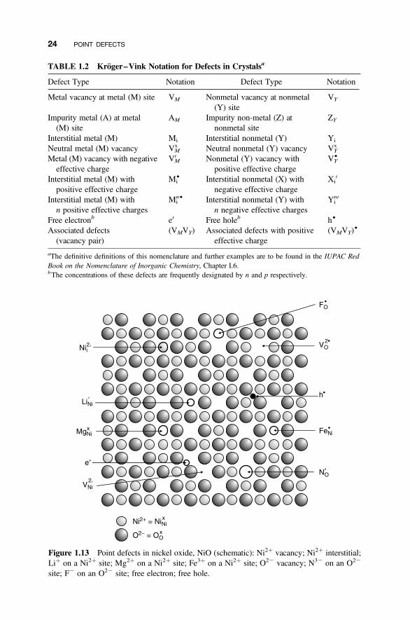
TABLE 1.2 Kroger–Vink Notation for Defects in Crystalsa
Defect Type Notation Defect Type Notation
Metal vacancy at metal (M) site VM Nonmetal vacancy at nonmetal(Y) site
VY
Impurity metal (A) at metal(M) site
AM Impurity non-metal (Z) atnonmetal site
ZY
Interstitial metal (M) Mi Interstitial nonmetal (Y) Yi
Neutral metal (M) vacancy VMx Neutral nonmetal (Y) vacancy VY
x
Metal (M) vacancy with negativeeffective charge
V0M Nonmetal (Y) vacancy with
positive effective chargeVY†
Interstitial metal (M) withpositive effective charge
Mi† Interstitial nonmetal (X) with
negative effective chargeXi
0
Interstitial metal (M) withn positive effective charges
Min† Interstitial nonmetal (Y) with
n negative effective chargesYin0
Free electronb e0 Free holeb h†
Associated defects(vacancy pair)
(VMVY) Associated defects with positiveeffective charge
(VMVY)†
aThe definitive definitions of this nomenclature and further examples are to be found in the IUPAC RedBook on the Nomenclature of Inorganic Chemistry, Chapter I.6.bThe concentrations of these defects are frequently designated by n and p respectively.
Figure 1.13 Point defects in nickel oxide, NiO (schematic): Ni2þ vacancy; Ni2þ interstitial;Liþ on a Ni2þ site; Mg2þ on a Ni2þ site; Fe3þ on a Ni2þ site; O22 vacancy; N32 on an O22
site; F2 on an O22 site; free electron; free hole.
24 POINT DEFECTS
example, the incorporation of lithium ions, Liþ, into zinc selenide, ZnSe, can lead tolithium interstitials, Lii
†, in which the real charge and the effective charge are identi-cal, as stated above. Alternatively, the ions can form substitution defects in which theLiþ ions occupy Zn2þ sites, in which case the designation is Li0Zn. As the populationsof these two alternatives changes, for instance, with lithium concentration, so does theelectronic character of the defect population.
The effective charges on an ionic defect can be considered to be linked to thedefect by an imaginary bond. If the bond is weak, the effective charge can be liber-ated, say by thermal energy, so that it becomes free to move in an applied electric fieldand so contribute to the electronic conductivity of the material. Whether the effectivecharge on a defect is considered to be strongly associated with the defect or freedepends upon the results obtained when the physical properties of the solid aremeasured.
The main features of the Kroger–Vink notation are summarized in Table 1.2 andare illustrated with respect to point defects in a crystal containing Ni2þ and O22 ionsin Figure 1.13.
1.9 BALANCED POPULATIONS OF POINT DEFECTS: SCHOTTKYAND FRENKEL DEFECTS
1.9.1 Schottky Defects
Compounds are made up of atoms of more than one chemical element. The pointdefects that can occur in pure compounds parallel those that occur in monatomicmaterials, but there is an added complication in this case concerning the compositionof the material. In this chapter discussion is confined to the situation in which thecomposition of the crystal is (virtually) fixed. Such solids are called stoichiometriccompounds. (The situations that arise when the composition is allowed to vary areconsidered in Chapter 4 and throughout much of the rest of this book. This lattertype of solid is called a nonstoichiometric compound.) The composition problemcan be illustrated with respect to a simple compound such as sodium chloride.
Sodium chloride, also known as rock salt or halite, is composed of equal numbersof sodium (Na) and chlorine (Cl) atoms, has a chemical formula NaCl and a simplestructure (Fig. 1.14). It is a good first approximation to regard this material as beingcomposed of ions. The introduction of vacancies on the cation sublattice will upsetboth the composition and the charge balance. If x such vacancies occur, theformula of the crystal will now be Na12xCl, and the overall material will have anexcess negative charge of x2 because the number of chloride ions is greater thanthe number of sodium ions by this amount. The compound should be written[Na12xCl]
x2. The same will be true for the anion sublattice. If x vacancies areplaced on the anion sublattice, the material will take on an overall positive chargebecause the number of sodium ions now outnumbers the chlorine ions, and theformula becomes [NaCl12x]
xþ. Ordinary crystals of sodium chloride do not showan overall negative or positive charge or have a formula different to NaCl. Thus, ifvacancy defects occur in these crystals, the numbers on the anion and cation
1.9 BALANCED POPULATIONS OF POINT DEFECTS 25
sublattices must be balanced to maintain the correct formula and preserve electricalneutrality. This means that we must introduce equal numbers of vacancies ontoboth sublattices.
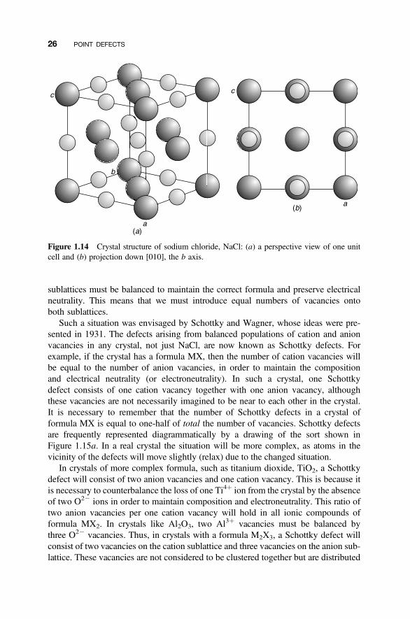
Such a situation was envisaged by Schottky and Wagner, whose ideas were pre-sented in 1931. The defects arising from balanced populations of cation and anionvacancies in any crystal, not just NaCl, are now known as Schottky defects. Forexample, if the crystal has a formula MX, then the number of cation vacancies willbe equal to the number of anion vacancies, in order to maintain the compositionand electrical neutrality (or electroneutrality). In such a crystal, one Schottkydefect consists of one cation vacancy together with one anion vacancy, althoughthese vacancies are not necessarily imagined to be near to each other in the crystal.It is necessary to remember that the number of Schottky defects in a crystal offormula MX is equal to one-half of total the number of vacancies. Schottky defectsare frequently represented diagrammatically by a drawing of the sort shown inFigure 1.15a. In a real crystal the situation will be more complex, as atoms in thevicinity of the defects will move slightly (relax) due to the changed situation.
In crystals of more complex formula, such as titanium dioxide, TiO2, a Schottkydefect will consist of two anion vacancies and one cation vacancy. This is because itis necessary to counterbalance the loss of one Ti4þ ion from the crystal by the absenceof two O22 ions in order to maintain composition and electroneutrality. This ratio oftwo anion vacancies per one cation vacancy will hold in all ionic compounds offormula MX2. In crystals like Al2O3, two Al3þ vacancies must be balanced bythree O22 vacancies. Thus, in crystals with a formula M2X3, a Schottky defect willconsist of two vacancies on the cation sublattice and three vacancies on the anion sub-lattice. These vacancies are not considered to be clustered together but are distributed
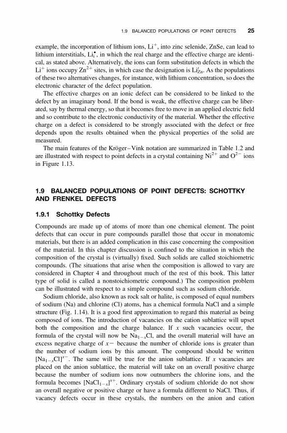
Figure 1.14 Crystal structure of sodium chloride, NaCl: (a) a perspective view of one unitcell and (b) projection down [010], the b axis.
26 POINT DEFECTS
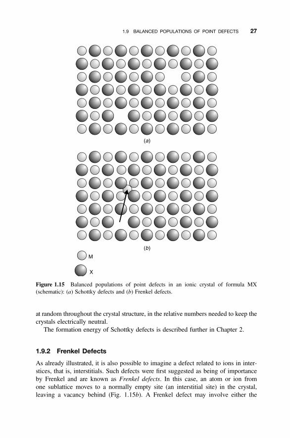
at random throughout the crystal structure, in the relative numbers needed to keep thecrystals electrically neutral.
The formation energy of Schottky defects is described further in Chapter 2.
1.9.2 Frenkel Defects
As already illustrated, it is also possible to imagine a defect related to ions in inter-stices, that is, interstitials. Such defects were first suggested as being of importanceby Frenkel and are known as Frenkel defects. In this case, an atom or ion fromone sublattice moves to a normally empty site (an interstitial site) in the crystal,leaving a vacancy behind (Fig. 1.15b). A Frenkel defect may involve either the
Figure 1.15 Balanced populations of point defects in an ionic crystal of formula MX(schematic): (a) Schottky defects and (b) Frenkel defects.
1.9 BALANCED POPULATIONS OF POINT DEFECTS 27
cation or the anion sublattice. Thus, in any crystal of formula MX, a Frenkel defectconsists of one interstitial ion plus one vacant site in the sublattice where that ionwould normally be found. Because ions are being moved internally, no problem ofelectronic charge balance occurs. This means that the number of interstitials andvacancies forming a Frenkel defect population is not connected to the formula ofthe compound. For example, if we have Frenkel defects on the anion sublattice inCaF2, we can think of just one F2 ion being displaced; it is not necessary to displacetwo F2 ions to form the Frenkel defect.
The formation energy of Frenkel defects is described further in Chapter 2.
1.10 ANTISITE DEFECTS
An antisite defect is an atom on a site normally occupied by a different chemicalspecies that exists in the compound. Antisite defects are a feature of a numberof important materials, especially weakly ionic or covalently bonded ones. In acompound of formula AB the antisite defects that can occur are an A atom on asite normally occupied by a B atom (Fig. 1.16a), or a B atom on a site normally occu-pied by an A atom (Fig. 1.16b).
Antisite defects are not important in binary ionic compounds, as the resultantincrease in electrostatic energy is generally prohibitive. For example, if an Naþ
ion were to replace a Cl2 ion in NaCl (Fig. 1.16c), it would be surrounded by anoctahedron of Naþ cations, leading to strong electrostatic repulsion. Similarly, aCl2 anion on an Naþ site would be surrounded by an octahedron of Cl2 anions(Fig. 1.16d ) again, leading to strong electrostatic repulsion. This is not true whencations of different elements are present together in an ionic compound, as antistitedefects can then be accommodated without the electrostatic penalty. An example isthe oxide spinel, MgAl2O4. Notionally all of the Mg2þ ions occupy tetrahedrallycoordinated sites in the structure, written (Mg), and Al3þ ions occupy octahedrallycoordinated sites, written [Al2], so that the structure can be represented as(Mg)[Al2]O4. In most such crystals it is found that a small number of Mg2þ andAl3þ cations exchange sites to form antisite defects (Mg12xAlx)[Al22xMgx]O4:
MgMg þ AlAl �! Mg0Al þ Al†Mg
where the effective charges are derived assuming the compound is ionic. Thisexchange of cations between octahedral and tetrahedral sites is generally designatedin terms of normal and inverse spinel structures (Supplementary Material S1).Similarly, in Er2Ti2O7, which has the pyrochlore structure, antisite defects occurbetween the two metal atoms. In this structure, in the absence of defects, the largeratom (Er) is coordinated by eight oxygen atoms in an approximately cubic arrange-ment, while the smaller atom (Ti) is in distorted octahedral coordination. The antisitedefects can be represented as forming by the reaction:
ErEr þ TiTi �! Er0Ti þ Ti†Er
28 POINT DEFECTS
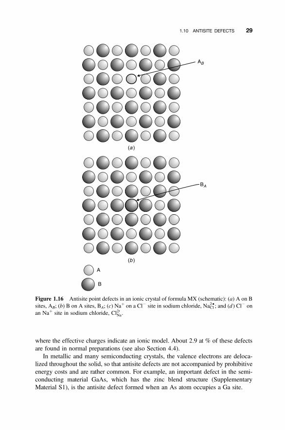
where the effective charges indicate an ionic model. About 2.9 at % of these defectsare found in normal preparations (see also Section 4.4).
In metallic and many semiconducting crystals, the valence electrons are deloca-lized throughout the solid, so that antisite defects are not accompanied by prohibitiveenergy costs and are rather common. For example, an important defect in the semi-conducting material GaAs, which has the zinc blend structure (SupplementaryMaterial S1), is the antisite defect formed when an As atom occupies a Ga site.
Figure 1.16 Antisite point defects in an ionic crystal of formula MX (schematic): (a) A on Bsites, AB; (b) B on A sites, BA; (c) Na
þ on a Cl2 site in sodium chloride, NaCl2†; and (d ) Cl2 on
an Naþ site in sodium chloride, Cl20Na.
1.10 ANTISITE DEFECTS 29
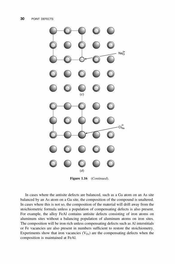
In cases where the antisite defects are balanced, such as a Ga atom on an As sitebalanced by an As atom on a Ga site, the composition of the compound is unaltered.In cases where this is not so, the composition of the material will drift away from thestoichiometric formula unless a population of compensating defects is also present.For example, the alloy FeAl contains antisite defects consisting of iron atoms onaluminum sites without a balancing population of aluminum atoms on iron sites.The composition will be iron rich unless compensating defects such as Al interstitialsor Fe vacancies are also present in numbers sufficient to restore the stoichiometry.Experiments show that iron vacancies (VFe) are the compensating defects when thecomposition is maintained at FeAl.
Figure 1.16 (Continued).
30 POINT DEFECTS
The creation of antisite defects can occur during crystal growth, when atoms aremisplaced on the surface of the growing crystal. Alternatively, they can be createdby internal mechanisms once the crystal is formed, provided that sufficient energyis applied to allow for atom movement.
1.11 DEFECT FORMATION AND REACTION EQUATIONS
Defects are often deliberately introduced into a solid in order to modify physical orchemical properties. However, defects do not occur in the balance of reactantsexpressed in traditional chemical equations, and so these important components arelost to the chemical accounting system that the equations represent. Fortunately,traditional chemical equations can be easily modified so as to include defectformation. The incorporation of defects into normal chemical equations allows astrict account of these important entities to be kept and at the same time facilitatesthe application of chemical thermodynamics to the system. In this sense it ispossible to build up a defect chemistry in which the defects play a role analogousto that of the chemical atoms themselves. The Kroger–Vink notation allows this tobe done provided the normal rules that apply to balanced chemical equationsare preserved.
1.11.1 Addition and Subtraction of Atoms
When writing defect formation equations, the strategy involved is always to add orsubtract elements to or from a crystal via electrically neutral atoms. When ionic crys-tals are involved, this requires that electrons are considered separately. Thus, if oneconsiders NiO to be ionic, formation of a VNi would imply the removal of aneutral Ni atom, that is, removal of a Ni2þ ion together with two electrons.Similarly, formation of a VO would imply removal of a neutral oxygen atom, thatis, removal of an O22 ion, followed by the addition of two electrons to the crystal.An alternative way to express this is to say the removal of an O22 ion togetherwith 2h†. Similarly, only neutral atoms are added to interstitial positions. If ionsare considered to be present, the requisite number of electrons must be added or sub-tracted as well. Thus, the formation of an interstitial Zn2þ defect would involve theaddition of a neutral Zn atom and the removal of two electrons.
1.11.2 Equation Formalism
The formation of defects can be considered as the reaction of a nominally perfectcrystal with dopant. The rules for writing equations including defects are similar tothose of elementary chemistry, but as the matrix is a crystal structure, quantities mustbe specified with respect to crystallographic sites rather than molecules or moles.
1. The number of metal atom sites must always be in the correct proportion to thenumber of nonmetal atom sites in the crystal. This is in essence a crystal structure
1.11 DEFECT FORMATION AND REACTION EQUATIONS 31
constraint. In a crystal structure there are a certain number of atoms that occupyspecified positions within the space group of the solid. Provided that the crystal struc-ture is (even only loosely) specified, the number of atom sites must remain fixed.Thus, in CaS, which adopts the sodium chloride structure, formula MX, there mustalways be equal numbers of metal and nonmetal atom positions in the equation.For an oxide such as TiO2, with the rutile structure, there must always be twice asmany anion sites as cation sites, or, in general, for a compound MaXb, there mustbe an a metal atom sites for every b nonmetal atom sites. As long as this proportionis maintained, the total number of sites can vary, as this simply corresponds to moreor less substance present. If the crystal contains vacancies, these must be counted aspart of the total number of sites, as each vacancy can be considered to occupy a sitejust as legally as an atom. Interstitial atoms do not occupy normal sites and so do notcount when this rule is being applied.
2. The total number of atoms on one side of the equation must balance the totalnumber of atoms on the other side. This rule is simply an expression of the well-known chemical fact that atoms are neither created nor destroyed during a chemicalreaction. Remember that subscripts and superscripts are labels describing charges andsites and are not counted in evaluating the atom balance.
3. The crystal must always be electrically neutral. This means not only that thetotal charge on one side of the equation must be equal to the total charge on theother side, but also that the sum of the charges on each side of the equation mustequal zero. In this assessment, both effective and real charges must be counted ifboth sorts are present.
Recall that only neutral atoms are involved in reactions. After reaction, neutralatoms can dissociate into charged species if this is thought to represent the real situ-ation in the crystal, provided that electroneutrality, as described, is maintained.
Reactions involving the creation, destruction, and elimination of defects canappear mysterious. In such cases it is useful to break the reaction down into hypothe-tical steps that can be represented by partial equations, rather akin to the half-reactionsused to simplify redox reactions in chemistry. The complete defect formationequation is found by adding the partial equations together. The rules describedabove can be interpreted more flexibly in these partial equations but must be rigor-ously obeyed in the final equation. Finally, it is necessary to mention that a defectformation equation can often be written in terms of just structural (i.e., ionic)defects such as interstitials and vacancies or in terms of just electronic defects,electrons, and holes. Which of these alternatives is preferred will depend upon thephysical properties of the solid. An insulator such as MgO is likely to utilize structuraldefects to compensate for the changes taking place, whereas a semiconductingtransition-metal oxide with several easily accessible valence states is likely toprefer electronic compensation.
To illustrate exactly how these rules work, a number of examples follow. In thefirst, the formation of antisite defects, a simple example that does not involvechanges in atom numbers or charges on defects, is described. Secondly, two reactionsinvolving oxides, nickel oxide and cadmium oxide, both of which are nonstoichio-metric, but for opposite reasons, indicate how to deal with a solid–gas interaction
32 POINT DEFECTS
in terms of electronic compensation. Thirdly, the formation of calcia-stabilizedzirconia, ZrO2
. xCaO, where x is of the order of 10–15 mol % outlines the methodfor a reaction between two solids utilizing structural compensation. Finally, defectformation in more complex oxides containing two cation species is outlined. Noneof these reactions can be represented by conventional chemical equations.
1.11.3 Formation of Antisite Defects
The creation of a complementary pair of antisite defects consisting of an A atom on aB atom site, AB, and a B atom on an A atom site, BA, can be written in terms of achemical equation:
AA þ BB �! AB þ BA
Antisite defects can be created via the intermediate formation of a Frenkel defect bythe following rules:
1. Frenkel defect formation on the A sublattice:
AA �! Ai þ VA
2. Exchange of the interstitial Ai atom with a B atom on its correct site:
Ai þ BB �! AB þ Bi
3. The interstitial Bi atom can eliminate the vacancy to form a B atom antisitedefect:
Bi þ VA �! BA
4. If these three equations are added, the result is
AA þ BB �! AB þ BA
The same equations can also be written in terms of interstitial B atom formation andexchange of the interstitial Bi with an AA atom, and so forth.
1.11.4 Nickel Oxide
Nickel oxide, NiO, which adopts the sodium chloride structure (Fig. 1.14), canreadily be made slightly oxygen rich, and, because the solid then contains moreoxygen than nickel, the crystal must also contain a population of point defects.This situation can formally be considered as a reaction of oxygen gas with stoichio-metric NiO, and the simplest assumption is to suppose that the extra oxygen extendsthe crystal by adding extra oxygen sites. Atoms are added as neutral atoms, and
1.11 DEFECT FORMATION AND REACTION EQUATIONS 33
initially it is reasonable to suppose that NiO is built of neutral atoms. Because of rule1 above, each oxygen added must be balanced by the creation of a correspondingnickel site, so that the reaction equation is
x2 O2(NiO) �! x OO þ x VNi (1:2)
The reactant, oxygen gas, is written as in a normal equation. Strictly speaking theentry (NiO) to specify the host crystal is superfluous, but its inclusion avoids con-fusion (see later examples). The host crystal is written in parentheses to emphasizethat it is not really part of the equation.8 It might be considered to be more realisticif NiO is supposed to be ionic, containing Ni2þ and O22 ions. In an ionic crystal eachNi vacancy must carry two effective negative charges, written V20
Ni, because a normalNi2þ ion has been removed. The neutral oxygen atom introduced onto the oxygen ionsite will be missing two electrons compared to O22, so that it carries two effectivepositive charges, written OO
2†. This transformation can be designated by extendingEq. (1.2) in the following way:
x OO þ x VNi �! x O2†O þ x V20
Ni (1:3)
The charges balance, in accordance with rule 3 above. Finally, it may be regarded asreasonable to assume that the added oxygen ends up as O22. In this case each addedatom of oxygen must gain two electrons. These will be taken from another source inthe crystal, thereby generating two positive holes, h†:
x O2†O �! x OO þ 2x h† (1:4)
The complete equation is derived by adding Eqs. (1.2), (1.3), and (1.4):
x2 O2(NiO) �! x OO þ x V20
Ni þ 2x h† (1:5)
The creation of each vacancy is accompanied by the creation of a hole. If the ionicassumption is correct, the solid would therefore be expected to behave as a p-typesemiconductor. This is, in fact, the case for NiO. However, if for some analogouscase this is not confirmed experimentally, the equation is not valid.
Chemically, it might be preferable to specify exactly the source of the electronsdonated to form O22 ions in NiO. The physical properties of the solid suggest thatthe two electrons actually come from separate Ni2þ ions, converting each ofthem to the ion Ni3þ. The defect is then a Ni3þ ion located on a Ni2þ site. Thisdefect has an effective positive charge of one unit compared to the Ni2þ ion, so itwould be written NiNi
† . Taking this into account, the reaction Eq. (1.4) needs to be
8Frequently, in defect formation equations the host crystal is written above the reaction arrows. Throughoutthis book the convention of placing the host crystal in parentheses on the left side of the equation will befollowed.
34 POINT DEFECTS
written as
x O2†O þ 2x NiNi �! x OO þ 2x Ni†Ni (1:6)
Adding Eqs. (1.2), (1.3), and (1.6) gives
x2 O2(NiO)þ 2x NiNi �! x OO þ x V20
Ni þ 2x Ni†Ni (1:7)
This reveals that two alternative defect structures can be imagined, one with free holesand one with Ni3þ defects. A further possibility is that the hole may be lightly boundto an Ni2þ ion to give a defect complex that could be written (NiNi þ h†). All of thesedescriptions are valid. The one adopted would be the one most consistent with themeasured properties of the solid.
1.11.5 Cadmium Oxide
Cadmium oxide, CdO, like nickel oxide, also adopts the sodium chloride structure(Fig. 1.14). However, unlike nickel oxide, this compound can be made to containmore metal than oxygen. The defects that cause this metal excess are usually con-sidered to be interstitial Cd atoms or ions. In this case the reaction is one in whichthe solid formally loses oxygen. Because of the rules of equation writing, thismust involve the removal of neutral oxygen atoms. Each oxygen lost results in theloss of a nonmetal site. In order to keep the site ratio correct, a metal site mustalso be lost, forcing the metal into interstitial sites:
x CdO �! x2 O2 þ x Cdi
If CdO is considered to be ionic, and built of Cd2þ and O22 ions, the cadmium inter-stitial will show two effective positive charges, written Cdi
2†. At the same time,removal of an oxygen atom will require that the two electrons that are part of theO22 ion are left in the crystal:
x CdO �! x2 O2 þ xCd2†i þ 2x e0
The presence of free electrons means that metal-rich CdO should be an n-type semi-conductor. It is possible to imagine that the divalent cadmium interstitials can take upan electron to form monovalent interstitials:
x CdO �! x2 O2 þ x Cd†i þ x e0
As in the case of nickel oxide, the equation that best represents the real situation canonly be determined experimentally. In this case one possible method would be to
1.11 DEFECT FORMATION AND REACTION EQUATIONS 35
measure the way in which the electronic conductivity varies with the partial pressureof the surrounding oxygen atmosphere (Chapter 7).
1.11.6 Calcia-stabilized Zirconia
The same principles apply when two solids react, as can be illustrated by the reactionof a crystal of zirconia, ZrO2, with a small amount of calcia, CaO, to produce acrystal of calcia-stabilized zirconia. There are two principal ways that this reactioncan be imagined to occur: either the Ca atoms occupy Zr sites or they occupyinterstitial sites.
Suppose that on reaction Ca atoms are located on normal metal sites in ZrO2. Inorder to comply with rule 1 in Section 1.11.2, it is necessary to create two anionsites per Ca atom introduced. Initially, these are vacant. However, as an oxygenatom from the CaO must also be accommodated in the crystal, it is reasonable toplace it in one of these sites. The other site remains vacant. If we take the ZrO2 tobe ionic and composed of Zr4þ and O22 ions, the added (neutral) atoms willacquire effective charges. The neutral Ca atom at the Zr4þ displays an effectivecharge of 4 with respect to the charge experienced when a normal Zr4þ ion ispresent, so it is written as Ca40Zr. Similarly, for ionic (Zr4þO2
22) a neutral oxygenatom at an occupied oxygen site acquires an effective charge of 2†, and is hencewritten OO
2†. The same is true of the oxygen vacancy. Compared to a site occupiedby an O22 ion, the site has an effective positive charge of 2†, so the vacancy iswritten VO
2†. Formally, one can therefore write
CaO(ZrO2) �! Ca40Zr þ V2†O þ O2†
O (1:8)
The host crystal, ZrO2, is written in parentheses (ZrO2). Note that the equation con-serves mass balance, electrical charge balance, and site numbers in accordance withthe rules given in Section 1.11.2. Now CaO is normally regarded as an ionic com-pound, as implied by the foregoing allocation of charges, so that ions shouldoccupy the sites, not neutral atoms. To achieve this, two electrons are transferredfrom the neutral Ca atom to create Ca2þ and lodged upon the neutral O atom tocreate O22. The effective charge on the Ca ion will now be just two negative unitsinstead of four, and there will be no effective charge on the oxygen ion as allnormal oxygen sites contain O22. To stress this electroneutrality, it is given thesymbol OO
x . There is no change in the status of the oxygen vacancy. The processis summarized by
Ca40Zr þ V2†O þ O2†
O �! Ca20Zr þ V2†O þ Ox
O (1:9)
The final outcome for the reaction between the two ionic crystals is obtained byadding Eqs. (1.8) and (1.9) to give
CaO(ZrO2) �! Ca20Zr þ V2†O þ Ox
O
36 POINT DEFECTS
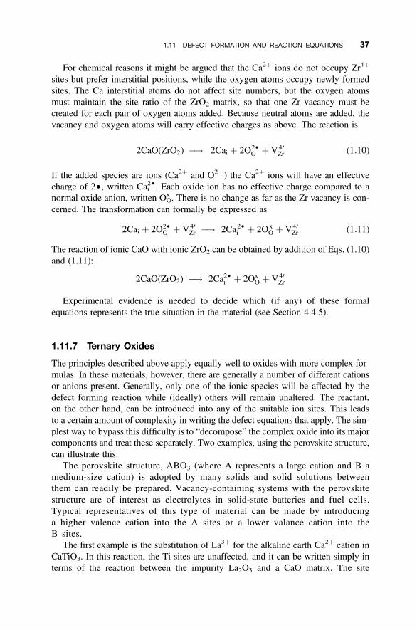
For chemical reasons it might be argued that the Ca2þ ions do not occupy Zr4þ
sites but prefer interstitial positions, while the oxygen atoms occupy newly formedsites. The Ca interstitial atoms do not affect site numbers, but the oxygen atomsmust maintain the site ratio of the ZrO2 matrix, so that one Zr vacancy must becreated for each pair of oxygen atoms added. Because neutral atoms are added, thevacancy and oxygen atoms will carry effective charges as above. The reaction is
2CaO(ZrO2) �! 2Cai þ 2O2†O þ V40
Zr (1:10)
If the added species are ions (Ca2þ and O22) the Ca2þ ions will have an effectivecharge of 2†, written Cai
2†. Each oxide ion has no effective charge compared to anormal oxide anion, written OO
x . There is no change as far as the Zr vacancy is con-cerned. The transformation can formally be expressed as
2Cai þ 2O2†O þ V40
Zr �! 2Ca2†i þ 2OxO þ V40
Zr (1:11)
The reaction of ionic CaO with ionic ZrO2 can be obtained by addition of Eqs. (1.10)and (1.11):
2CaO(ZrO2) �! 2Ca2†i þ 2OxO þ V40
Zr
Experimental evidence is needed to decide which (if any) of these formalequations represents the true situation in the material (see Section 4.4.5).
1.11.7 Ternary Oxides
The principles described above apply equally well to oxides with more complex for-mulas. In these materials, however, there are generally a number of different cationsor anions present. Generally, only one of the ionic species will be affected by thedefect forming reaction while (ideally) others will remain unaltered. The reactant,on the other hand, can be introduced into any of the suitable ion sites. This leadsto a certain amount of complexity in writing the defect equations that apply. The sim-plest way to bypass this difficulty is to “decompose” the complex oxide into its majorcomponents and treat these separately. Two examples, using the perovskite structure,can illustrate this.
The perovskite structure, ABO3 (where A represents a large cation and B amedium-size cation) is adopted by many solids and solid solutions betweenthem can readily be prepared. Vacancy-containing systems with the perovskitestructure are of interest as electrolytes in solid-state batteries and fuel cells.Typical representatives of this type of material can be made by introducinga higher valence cation into the A sites or a lower valance cation into theB sites.
The first example is the substitution of La3þ for the alkaline earth Ca2þ cation inCaTiO3. In this reaction, the Ti sites are unaffected, and it can be written simply interms of the reaction between the impurity La2O3 and a CaO matrix. The site
1.11 DEFECT FORMATION AND REACTION EQUATIONS 37
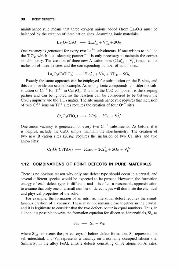
maintenance rule means that three oxygen anions added (from La2O3) must bebalanced by the creation of three cation sites. Assuming ionic materials:
La2O3(CaO) �! 2La†Ca þ V20Ca þ 3OO
One vacancy is generated for every two La3þ substituents. If one wishes to includethe TiO2, which is a “sleeping partner,” it is only necessary to maintain the correctstoichiometry. The creation of three new A cation sites (2LaCa
† þ V20Ca) requires the
inclusion of three Ti sites and the corresponding number of anion sites:
La2O3(CaTiO3) �! 2La†Ca þ V20Ca þ 3TiTi þ 9OO
Exactly the same approach can be employed for substitution on the B sites, andthis can provide our second example. Assuming ionic compounds, consider the sub-stitution of Cr3þ for Ti4þ in CaTiO3. This time the CaO component is the sleepingpartner and can be ignored so the reaction can be considered to be between theCr2O3 impurity and the TiO2 matrix. The site maintenance rule requires that inclusionof two Cr3þ ions on Ti4þ sites requires the creation of four O22 sites:
Cr2O3(TiO2) �! 2Cr 0Ti þ 3OO þ V2†O
One anion vacancy is generated for every two Cr3þ substituents. As before, if itis helpful, include the CaO, simply maintain the stoichiometry. The creation oftwo new B cation sites (2Cr0Ti) requires the inclusion of two Ca sites and twoanion sites:
Cr2O3(CaTiO3) �! 2CaCa þ 2Cr 0Ti þ 5OO þ V2†O
1.12 COMBINATIONS OF POINT DEFECTS IN PURE MATERIALS
There is no obvious reason why only one defect type should occur in a crystal, andseveral different species would be expected to be present. However, the formationenergy of each defect type is different, and it is often a reasonable approximationto assume that only one or a small number of defect types will dominate the chemicaland physical properties of the solid.
For example, the formation of an intrinsic interstitial defect requires the simul-taneous creation of a vacancy. These may not remain close together in the crystal,and it is legitimate to consider that the two defects occur in equal numbers. Thus, insilicon it is possible to write the formation equation for silicon self-interstitials, Sii, as
SiSi �! Sii þ VSi
where SiSi represents the perfect crystal before defect formation, Sii represents theself-interstitial, and VSi represents a vacancy on a normally occupied silicon site.Similarly, in the alloy FeAl, antisite defects consisting of Fe atoms on Al sites,
38 POINT DEFECTS
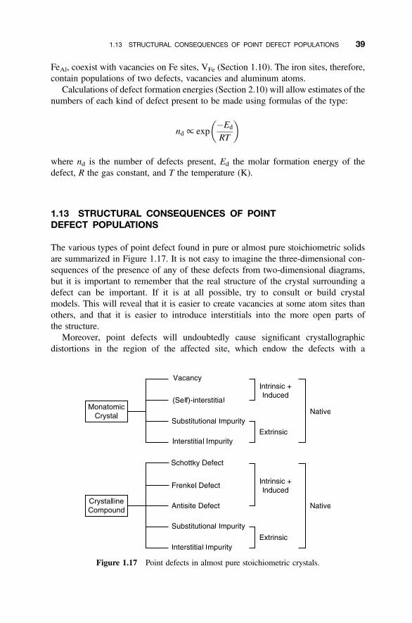
FeAl, coexist with vacancies on Fe sites, VFe (Section 1.10). The iron sites, therefore,contain populations of two defects, vacancies and aluminum atoms.
Calculations of defect formation energies (Section 2.10) will allow estimates of thenumbers of each kind of defect present to be made using formulas of the type:
nd / exp�Ed
RT
� �
where nd is the number of defects present, Ed the molar formation energy of thedefect, R the gas constant, and T the temperature (K).
1.13 STRUCTURAL CONSEQUENCES OF POINTDEFECT POPULATIONS
The various types of point defect found in pure or almost pure stoichiometric solidsare summarized in Figure 1.17. It is not easy to imagine the three-dimensional con-sequences of the presence of any of these defects from two-dimensional diagrams,but it is important to remember that the real structure of the crystal surrounding adefect can be important. If it is at all possible, try to consult or build crystalmodels. This will reveal that it is easier to create vacancies at some atom sites thanothers, and that it is easier to introduce interstitials into the more open parts ofthe structure.
Moreover, point defects will undoubtedly cause significant crystallographicdistortions in the region of the affected site, which endow the defects with a
Figure 1.17 Point defects in almost pure stoichiometric crystals.
1.13 STRUCTURAL CONSEQUENCES OF POINT DEFECT POPULATIONS 39
spatial extension greater than that implied in the term point defect. The resulting strainfield plays an important part in the aggregation of point defects into clusters and otherextended defects. The fraction of point defects that aggregate will depend upon therelative energy gain when a cluster forms, as well as the mobility of the defects inthe crystal. The electronic and other interactions between defects can be calculatedusing approaches analogous to the Debye–Huckel treatment used for electrolytesor the Lorentz theory of the polarizability of insulating solids. In fact, simulationsand quantum mechanical calculations (Chapter 2) suggest that defect association isthe rule rather than the exception.
1.14 ANSWERS TO INTRODUCTORY QUESTIONS
What is a point defect?
A point defect is a localized defect that consists of a mistake at a single atom site ina solid. The simplest point defects that can occur in pure crystals are missingatoms, called vacancies, or atoms displaced from the correct site into positionsnot normally occupied in the crystal, called self-interstitials. Additionally atomsof an impurity can occupy a normal atom site to form substitutional defects orcan occupy a normally vacant position in the crystal structure to form an intersti-tial. Other point defects can be characterized in pure compounds that contain morethan one atom. The best known of these are Frenkel defects, Schottky defects, andantisite defects.
What is the effective charge on a defect?
The effective charge on a defect is the chargewith respect to that normally occurringat the same site in a perfect crystal. Interstitial sites are normally unoccupied, so anatom or ion at an interstitial site will have an effective charge equal to its real charge.For example, interstitial Ti4þ ions will have an effective charge of 4†. Any neutralatom, Zn, for example, will have no effective charge at an interstitial site. When animpurity atom or an impurity ion occupies a site that normally contains an ion, theeffective charge will be the difference between the real charge on the impurity atomor ion and the real charge on the normal ion. Thus, aCa2þ ion located on aNaþ site ina crystal will carry an effective charge of 2 2 1 ¼ 1, that is, it will be written CaNa
† .Similarly, a neutral atom such as Li located at the same site would carry an effectivecharge of 02 1 ¼ 21, that is, it will be written Li0Na.
What is an antisite defect?
An antisite defect is an atom on an inappropriate site in a crystal, that is, a site nor-mally occupied by a different chemical species. In a compound of formula AB theantisite defects that can occur are an A atom on a site normally occupied by a Batom, or a B atom on a site normally occupied by an A atom. Antisite defects arenot very important in binary ionic compounds, as the misplacement of an ion isenergetically costly, and so unfavorable. In ternary ionic compounds, however,such as spinels, AB2O4, the transfer of A ions to B sites and vice versa, is not
40 POINT DEFECTS

expensive on energy and can occur. In metallic and many semiconducting crystals,the valence electrons are delocalized throughout the solid, so that also in thesecases antisite defects are not accompanied by prohibitive energy costs.For example, most important defect in the semiconducting material GaAs is theantisite defect formed when an As atom occupies a Ga site.
PROBLEMS AND EXERCISES
Quick Quiz
1. Point defects that form in a crystal exposed to radioactivity are called:
(a) Intrinsic defects
(b) Induced defects
(c) Native defects
2. Intrinsic defects in crystals:
(a) Are always present
(b) Only form if two or more different atom species occur
(c) Only form in the presence of impurities
3. Impurity atoms are:
(a) Intrinsic defects
(b) Extrinsic defects
(c) Native defects
4. An impurity P atom on a Si site in a crystal of silicon is a:
(a) Interstitial defect
(b) Antisite defect
(c) Substitutional defect
5. The number of Schottky defects in a crystal of formula MX is equal to:
(a) Half the total number of vacancies present
(b) The total number of vacancies present
(c) Double the total number of vacancies present
6. A single anion Frenkel defect in an ionic crystal of formula MX2 needs to bebalanced by:
(a) A cation Frenkel defect
(b) Two cation Frenkel defects
(c) Nothing
7. A metal atom N on an M site in a crystal MX would be written:
(a) NM
(b) MN
(c) NMX
PROBLEMS AND EXERCISES 41
8. An anion vacancy in an ionic oxide has the symbol:
(a) VOx
(b) V20O
(c) VO2†
9. A Ca2þ ion on a Naþ site in a crystal is written:
(a) CaCax
(b) CaNa†
(c) Ca0Na
10. The equation representing doping of La2O3 into CaO is:
(a) La2O3 (CaO) �! 2LaCa† þ V20
Ca þ 3OO
(b) La2O3 (CaO) �! 2LaCa3† þ V20
Ca þ 3OO
(c) La2O3 (CaO) �! 2La30Ca þ V20Ca þ 3OO
Calculations and Questions
1. (a) A ruby crystal has a composition (Al0.99Cr0.01)2O3. How many Cr3þ ions arethere in a ruby of dimensions 1 cm3? (The unit cell dimensions are a ¼0.4763 nm, c ¼ 1.3009 nm; Z (the unit cell contents) ¼ 6Al2O3; thevolume of the unit cell can be taken as 0.966a2c.)
(b) A solid solution between the spinel structure phases MgGa2O4 (a ¼0.82780 nm) and MgGaMnO4 (a ¼ 0.83645 nm) obeys Vegard’slaw. What is the composition of the phase with a lattice parameter of0.83000 nm?
2. (a) Theunit cell of zirconium sulfide, ZrS, is sodiumchloride type, a ¼ 0.514 nm.The measured density is 4800 kg m23. Suggest a possible defect structureand formula for the solid. There are four ZrS units per unit cell, relativemolar mass: Zr, 91.22 g mol21; S, 32.07 g mol21.
(b) A sample of a cubic calcia-stabilized zirconia ceramic has a density of5720 kg m23 and a lattice parameter of 0.5130 nm. Assuming VO
2† arethe dominant point defects, suggest a composition for the solid. Thereare four MO2 units in the unit cell. Molar mass: Zr, 91.22 g mol21; Ca,40.08 g mol21; O, 16.00 g mol21.
3. The Seebeck coefficient for pure LaCoO3 is þ600 mVK21. (a) What are themobile charge carriers? (b) Suppose these occur because the crystal contains atrace of an impurity, Co4þ, calculate the defect concentration and the formulaof the material (data from Robert et al., 2006).
4. Estimate the Seebeck coefficient for the reduced oxide TiO1.94, assuming that thedefects are Ti3þ ions and the parent phase is TiO2.
5. Plot a graph of the expected Seebeck coefficient of La12xSrxMnO3 for x ¼ 0–0.2.
42 POINT DEFECTS
6. A complex Hg-Sr-Ca-Co containing oxide has a Seebeck coefficient of115 mV K21, due to the presence of both Co3þ and Co4þ. If the defects arethe Co4þ ions, what is the average valence of the Co ions (data from Pelloquinet al., 2003).
7. Write defect equations for the following reactions:
(a) MgO doped with Li2O
(b) Slight reduction of PrO2
(c) TiO2 doped with Ga2O3
(d) LaCoO3 doped with CaO
(e) MgAl2O4 doped with V2O3 to form Mg(Al22xVx)2O4
8. Nickel oxide, NiO, is doped with lithium oxide, Li2O, to form LixNi1– xO withthe sodium chloride structure. (a) Derive the form of the Heikes equationfor the variation of Seebeck coefficient, a, with the degree of doping, x.The following table gives values of a versus log[(1–x)/x] for this material.(b) Are the current carriers holes or electrons? (c) Estimate the value of theconstant term k/e.
a/mV K21 log [(1–x)/x]
0.12 0.20.18 0.50.28 1.00.39 1.50.48 2.00.59 2.50.69 3.0
Data adapted from E. Antolini, Mater. Chem.Phys., 82, 937–948 (2003).
9. The oxides with general formulas A2O, AO, A2O3, AO2, and A2O5 are dopedinto MgO so that the cation substitutes for Mg. Write general defect equationsfor the reactions, assuming cation vacancies rather than electronic compensationoccurs.
10. The crystallographic data for Al2O3 are a ¼ 0.47628 nm, c ¼ 13.0032 nm, andfor V2O3 are a ¼ 0.4955 nm, c ¼ 14.003 nm. The structure of both oxides isthe corundum type, the volume of the hexagonal unit cell can be taken as0.966a2c and Z (the unit cell contents) ¼ 6 formula units. (a) Calculate thedensity of Al2O3. (b) Calculate the density of V2O3. (c) Provided Vegard’slaw is obeyed, estimate the density of V0.6Al1.4O3. (d) The measured densityis 3620 kg m23. What does this suggest about Vegard’s law dependence?
PROBLEMS AND EXERCISES 43
REFERENCES
D. Pelloguin, A. Maignan, S. Hebert, C. Michel, and B. Raveau, J. Solid State Chem., 170,374–381 (2003).
R. Robert, L. Becker, M. Trottman, A. Reller, and A. Weidenkraft, J. Solid State Chem., 179,3893–3899 (2006).
FURTHER READING
Much of the material in this chapter is introductory. Background information on solids isgiven in:
R. J. D. Tilley, Understanding Solids, Wiley, Chichester, 2004.
R. J. D. Tilley, Crystals and Crystal Structures, Wiley, Chichester, 2006.
A. F. Wells, Structural Inorganic Chemistry, 5th ed., Oxford University Press, Oxford, UnitedKingdom, 1984.
A. R. West, Solid State Chemistry, Wiley, Chichester, 1984.
Expansion and further explanation with respect to defects and defect chemistry and physicswill be found in:
F. Agullo-Lopez, C. R. A. Catlow, and P. D. Townsend Point Defects in Materials, Academic,New York, 1988.
D. M. Smyth The Defect Chemistry of Metal Oxides, Oxford University Press, Oxford, UnitedKingdom, 2000.
A. M. Stoneham, The Theory of Defects in Solids, Oxford University Press, Oxford, UnitedKingdom, 1985.
Various authors Mat. Res. Soc. Bull., XVI, November (1991) and December (1991).
Many aspects of the study and importance of defects in solids presented from a historical andmaterials perspective are to be found in:
R. W. Cahn, The Coming of Materials Science, Pergamon/Elsevier, Oxford, United Kingdom,2001.
Details about the Heikes formula is found in:
R. R. Heikes and R. W. Ure, Jr., Thermoelectricity; Science and Engineering, Wiley/Interscience, New York, 1961, p. 40.
44 POINT DEFECTS

&CHAPTER 2
Intrinsic Point Defects inStoichiometric Compounds
What is an intrinsic defect?
What point defects are vital for the operation of LiI pacemaker batteries?
What is the basis of “atomistic simulation” calculations of point defect formationenergies?
Intrinsic point defects are always present in a crystal as an inescapable property ofthe solid. For this to be so the intrinsic defect must be stable from a thermodynamicpoint of view. In this chapter the consequences of this thermodynamic aspect will beconsidered in more detail.
2.1 EQUILIBRIUM POPULATION OF VACANCIESIN A MONATOMIC CRYSTAL
In order to estimate the likelihood that vacancies are present in a crystal, it is necess-ary to determine the energy needed to form the defects in an otherwise perfectsolid. Thermodynamics, which gives information about systems when they are atequilibrium, is able to provide guidance on this problem. In general, the first lawof thermodynamics indicates that there will be an energy cost in introducing thedefects, which can loosely be equated with changes in the chemical bonds aroundthe defect. The second law of thermodynamics says that this energy cost may berecouped via the disorder introduced into the crystal. These imprecise concepts canbe quantified by considering the Gibbs energy of a crystal, G:
G ¼ H � TS
where H is the enthalpy, S is the entropy, and T the temperature (K) of the crystal.If vacancies exist in the crystal under equilibrium, the Gibbs energy must be less
than it is in a perfect crystal. However, if the introduction of more and more defectscauses the Gibbs energy to continually fall, then ultimately no crystal will remain.
Defects in Solids, by Richard J. D. TilleyCopyright # 2008 John Wiley & Sons, Inc.
45
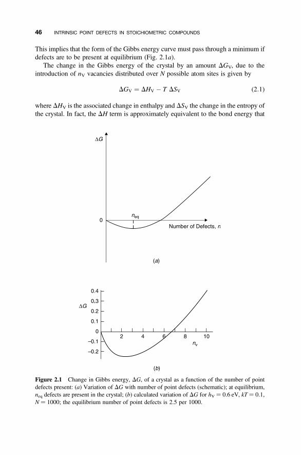
This implies that the form of the Gibbs energy curve must pass through a minimum ifdefects are to be present at equilibrium (Fig. 2.1a).
The change in the Gibbs energy of the crystal by an amount DGV, due to theintroduction of nV vacancies distributed over N possible atom sites is given by
DGV ¼ DHV � T DSV (2:1)
where DHV is the associated change in enthalpy and DSV the change in the entropy ofthe crystal. In fact, the DH term is approximately equivalent to the bond energy that
Figure 2.1 Change in Gibbs energy, DG, of a crystal as a function of the number of pointdefects present: (a) Variation of DG with number of point defects (schematic); at equilibrium,neq defects are present in the crystal; (b) calculated variation of DG for hV ¼ 0.6 eV, kT ¼ 0.1,N ¼ 1000; the equilibrium number of point defects is 2.5 per 1000.
46 INTRINSIC POINT DEFECTS IN STOICHIOMETRIC COMPOUNDS
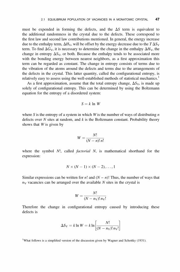
must be expended in forming the defects, and the DS term is equivalent tothe additional randomness in the crystal due to the defects. These correspond tothe first law and second law contributions mentioned. In general, the energy increasedue to the enthalpy term, DHV, will be offset by the energy decrease due to the T DSVterm. To find DGV, it is necessary to determine the change in the enthalpy DHV, thechange in entropy DSV, or both. Because the enthalpy tends to be associated morewith the bonding energy between nearest neighbors, as a first approximation thisterm can be regarded as constant. The change in entropy consists of terms due tothe vibration of the atoms around the defects and terms due to the arrangements ofthe defects in the crystal. This latter quantity, called the configurational entropy, isrelatively easy to assess using the well-established methods of statistical mechanics.1
As a first approximation, assume that the total entropy change, DSV, is made upsolely of configurational entropy. This can be determined by using the Boltzmannequation for the entropy of a disordered system:
S ¼ k ln W
where S is the entropy of a system in whichW is the number of ways of distributing ndefects over N sites at random, and k is the Boltzmann constant. Probability theoryshows that W is given by
W ¼ N!
(N � n)! n!
where the symbol N!, called factorial N, is mathematical shorthand for theexpression:
N � (N � 1)� (N � 2), . . . , 1
Similar expressions can be written for n! and (N – n)! Thus, the number of ways thatnV vacancies can be arranged over the available N sites in the crystal is
W ¼ N!
(N � nV)! nV!
Therefore the change in configurational entropy caused by introducing thesedefects is
DSV ¼ k lnW ¼ k lnN!
(N � nV)! nV!
� �
1What follows is a simplified version of the discussion given by Wagner and Schottky (1931).
2.1 EQUILIBRIUM POPULATION OF VACANCIES IN A MONATOMIC CRYSTAL 47
To proceed, it is necessary to eliminate the factorials. This is usually done byemploying the approximation:
lnN! � N lnN � N (2:2)
which is referred to as Stirling’s approximation.2
Substituting from Eq. (2.2):
DSV ¼ k{N lnN � (N � nV) ln (N � nV)� nV ln nV} (2:3)
The enthalpy change involved, DHV, is not explicitly calculated. It is assumed thatthe enthalpy to form one vacancy, DhV, is constant over the temperature range ofinterest, so that the total enthalpy change, DHV, is given by
DHV ¼ nVDhV
Substituting this, and the value of DSV from Eq. (2.3) into Eq. (2.1), gives
DGV ¼ nVDhV � kT{N lnN � (N � nV)ln(N � nV)� nV ln nV}
A plot of this equation (Fig. 2.1b) closely resembles Figure 2.1a. The minimum in thecurve gives the equilibrium number of vacancies present and confirms that vacanciesexist in all crystals at temperatures above 0 K. For this reason these defects cannot beremoved by thermal treatment but are always present in a crystal. Such defects arethus intrinsic defects. At equilibrium, DGV will be equal to zero and the minimumin the DGV versus nV curve is given by
dDGV
dnV
� �T
¼ 0
that is,
dDGV
dnV
� �T
¼ d
dnV{nVDhV � kT[N lnN � (N � nV)ln(N � nV)� nVln nV]}
¼ 0
DhV � kTd
dnV[N lnN � (N � nV)ln(N � nV)� nV ln nV]
� ¼ 0
2In fact this last approximation is not very accurate and is several percent in error even for values of N aslarge as 1010. The correct expression for Stirling’s approximation is
lnN! � N lnN � N þ 12 ln (2pN)
(Supplementary Material S4).
48 INTRINSIC POINT DEFECTS IN STOICHIOMETRIC COMPOUNDS
Remembering that (N ln N ) is constant, so its differential is zero, the differential of(ln x) is (l/x) and of (x ln x) is (1 þ ln x), on differentiating:
DhV � kT ln (N � nV)þ (N � nV)(N � nV)
� ln nV � nVnV
� �¼ 0
hence:
DhV ¼ kT ln(N � nV)
nV
� �Rearranging:
nV ¼ (N � nV)e�DhV=kT
If N is considered to be very much greater than nV:
nV � Ne�DhV=kT (2:4)
In the knowledge that the Gibbs energy of a crystal containing a small number ofintrinsic defects is lower than that of a perfect crystal, the defect population can betreated as a chemical equilibrium. In the case of vacancies we can write
null O vacancy
0 O VM
where null represents a normal occupied site in a crystal and VM represents a vacancyon the position normally occupied by an atom M. Chemically, the reaction can beimagined as the migration of an atom within a crystal to the surface to extend thevolume of the solid or to evaporate, while leaving a vacancy in its place. The lawof mass action in its simplest form, with concentrations instead of activities, can beapplied if there is no interaction between the defects to give an expression for theequilibrium constant for vacancy generation, KV:
KV ¼ nVN
¼ exp�DGV
RT
� �
where nV is the number of vacant sites, N is the total number of normally occupiedatom sites, and the term nV/N, the fraction of vacancies in the crystal thus representsconcentration (defects per atom site), DGV is the molar Gibbs energy of formationof the vacancies, R is the gas constant, and T the temperature (K). This equation isoften written
nV ¼ N exp�DGV
RT
� �(2:5a)
2.1 EQUILIBRIUM POPULATION OF VACANCIES IN A MONATOMIC CRYSTAL 49
where nV is taken as the number of vacant sites per unit volume, and N is the totalnumber of normally occupied atom sites per unit volume. When the Gibbs energyfor the formation of a single defect is used, Eq. (2.5a) is written in the form:
nV ¼ N exp�DgVkT
� �(2:5b)
where the Gibbs energy 2DgV is often given the units joules or electronvolts,3 (per defect), and is paired with the Bolzmann constant, k with units J K21
or eV K21.The fraction of vacancies in the crystal, nV/N, is given by
nVN
¼ exp�DGV
RT
� �(2:6)
The Gibbs energy, DGV, is often split into two terms using Eq. (2.1) to give
nVN
¼ exp�DHV
RT
� �þ exp
DSVT
� �
and the entropy term neglected, so that:
nVN
� exp�DHV
RT
� �(2:7)
When written in terms of energy per defect, Eqs. (2.6) and (2.7) become
nVN
¼ exp�DgVkT
� �
� exp�DhVkT
� �
2.2 EQUILIBRIUM POPULATION OF SELF-INTERSTITIALSIN A MONATOMIC CRYSTAL
Because the configurational entropy of interstitial defects has the same form as that ofvacancies, a population of self-interstitial atoms is also thermodynamically stable.The creation of these defects can then also be treated as a pseudochemical equili-brium, and an equation for the relationship between the number of self-interstitialsand the appropriate equilibrium constant for interstitial generation, Ki, is readily
3In the literature, the calculations are almost always expressed in units of electron volt (eV), where 1 eV isequivalent to 96.485 kJ mol21 or 1.60218 � 10219 J.
50 INTRINSIC POINT DEFECTS IN STOICHIOMETRIC COMPOUNDS
obtained. The creation of a self-interstitial on one of Ni possible interstitial sites leavesa vacancy on one of the N normal lattice sites:
null O interstitialþ vacancy
0 O Mi þ VM
where Mi represents an interstitial M atom and VM a vacancy on a normally occupiedatom site in the crystal. The law of mass action in its simplest form, with concen-trations instead of activities, can be applied if there is no interaction betweenthe defects to give an expression for the equilibrium constant for self-interstitialgeneration, Ki:
Ki ¼ niNi
� �nVN
� �¼ exp
�DGi
RT
� �
where ni is the number of interstitials, nV the number of vacancies, Ni the number ofsuitable interstitial sites, N the number of normally occupied sites, DGi is the molarGibbs energy of formation of the self-interstitials, R is the gas constant, and T theabsolute temperature. As the number of interstitials and vacancies is the same in amonatomic crystal, ni ¼ nV:
ni ¼ffiffiffiffiffiffiffiffiNNi
pexp
�DGi
2RT
� �(2:8)
where ni is the number of interstitials per unit volume, nV the number of vacancies perunit volume, Ni the number of suitable interstitial sites per unit volume, and N thenumber of normally occupied sites per unit volume. The fraction of interstitialdefects is given by
niffiffiffiffiffiffiffiffiNNi
p ¼ exp�DGi
2RT
� �
In the case where the number of normal and interstitial sites is the same, that is,N ¼ Ni:
ni ¼ N exp�DGi
2RT
� �
which is identical to the equation for vacancies, as is the fraction of interstitials in thecrystal, ni/N:
niN
¼ exp�DGi
2RT
� �
The Gibbs energy, DGi, is often split into two terms and the entropy termneglected, as in the previous section, to give
ni �ffiffiffiffiffiffiffiffiNNi
pexp
�DHi
2RT
� �(2:9)
2.2 EQUILIBRIUM POPULATION OF SELF-INTERSTITIALS IN A MONATOMIC CRYSTAL 51
Similar relationships hold if the Gibbs energy of formation per defect, Dgi, and theenthalpy of formation per defect, Dhi, is used and R is replaced by k, theBoltzmann constant:
ni ¼ffiffiffiffiffiffiffiffiNNi
pexp
�Dgi2kT
� �
� ffiffiffiffiffiffiffiffiNNi
pexp
�Dhi2kT
� �
2.3 EQUILIBRIUM POPULATION OF SCHOTTKYDEFECTS IN A CRYSTAL
A Schottky defect in a crystal consists of a cation and anion vacancy combination thatensures overall electroneutrality in the crystal (Section 1.9). The estimation of theconfigurational entropy change in creating a population of Schottky defects in acrystal can be obtained in the same way as that of a population of vacancies in amonatomic crystal. The method follows that given in Section 2.1 for the equilibriumconcentration of vacancies in a monatomic crystal and is set out in detail inSupplementary Material S4.
Because Schottky defects are present as equilibrium species, the defect populationcan be treated as a chemical equilibrium. For a crystal of composition MX:
null O cation vacancyþ anion vacancy
0 O VM þ VX
where VM represents a vacancy on a cation site and VX a vacancy on an anion site.If there is no interaction between the defects, the law of mass action in its simplestform, with concentrations instead of activities, yields an expression for the equili-brium constant for the formation of Schottky defects, KS:
KS ¼ ncvN
� � navN
� �¼ exp
�DGS
RT
� �
where ncv is the number of cation vacancies, nav the number of anion vacancies, N thenumber of cation sites, equal to the number of anion sites in the crystal, DGS is themolar Gibbs energy of formation of the Schottky defects, R is the gas constant,and T the absolute temperature. Because ncv is equal to nav, it is possible to writethe number of Schottky defects, nS, as
ncv ¼ nav ¼ nS ¼ Ne�DGS=2RT (2:10)
where nS is the number of Schottky defects per unit volume distributed over the Ncation or anion sites per unit volume. The fraction of defects present is given by
ncvN
¼ navN
¼ nSN
¼ e�DGS=2RT (2:11)
52 INTRINSIC POINT DEFECTS IN STOICHIOMETRIC COMPOUNDS
The Gibbs energy, DGS, is often replaced by the enthalpy of Schottky defectformation, DHS, as in previous sections, to give
nS � Ne�DHS=2RT (2:12)
where DHS is in joules per mole and is the energy required to form 1 mol of Schottkydefects, and R is the gas constant. Similar relationships hold if the Gibbs energy offormation per defect, DgS, or the enthalpy of formation per defect, DhS, is used, thus:
nS ¼ Ne�DgS=2kT
� Ne�DhS=2kT
where the units of DgS and DhS are joules or electron volts per defect, and k is theBoltzmann constant.
Remember that these formulas only apply to materials with a composition MX.Some values for the enthalpy of formation of Schottky defects in alkali halides of
formula MX that adopt the sodium chloride structure are given in Table 2.1. Theexperimental determination of these values (obtained mostly from diffusion orionic conductivity data (Chapters 5 and 6) is not easy, and there is a large scatterof values in the literature. The most reliable data are for the easily purified alkalihalides. Currently, values for defect formation energies are more often obtainedfrom calculations (Section 2.10).
Despite the uncertainty in the experimental values given in Table 2.1, they revealthat more energy is required to form defects as the systems are traversed in the direc-tion LiX to KX and that the energy falls on passing from MF toward MI (Fig. 2.2).
TABLE 2.1 Formation Enthalpy of Schottky Defects in SomeAlkali Halide Compounds of Formula MXa
Compound DHS/kJ mol21 DhS/eV
LiF 225.2 2.33LiCl 204.1 2.12LiBr 173.4 1.80LiI 102.4 1.06NaF 233.1 2.42NaCl 225.8 2.34NaBr 203.0 2.10NaI 140.9 1.46KF 262.0 2.72KCl 244.5 2.53KBr 224.6 2.33KI 153.0 1.59
aAll compounds have the sodium chloride structure.
2.3 EQUILIBRIUM POPULATION OF SCHOTTKY DEFECTS IN A CRYSTAL 53
2.4 LITHIUM IODIDE BATTERY
Batteries, almost indispensable in the modern world, are discussed in more detail inChapter 6. In essence, a battery consists of an electrode (the anode), where electronsare moved out of the cell, and an electrode (the cathode), where electrons move intothe cell. The electrons are generated in the region of the anode and then move aroundan external circuit, carrying out a useful function, before entering the cathode. Theanode and cathode are separated inside the battery by an electrolyte, and the circuitis completed inside the battery by ions moving across it. A key component inbattery construction is an electrolyte that can support ionic conduction but notelectronic conduction.
Lithium iodide is the electrolyte in a number of specialist batteries, especially inimplanted cardiac pacemakers. In this battery the anode is made of lithium metal.A conducting polymer of iodine and poly-2-vinyl pyridine (P2VP) is employedas cathode because iodine itself is not a good enough electronic conductor(Fig. 2.3a). The cell is fabricated by placing the Li anode in contact with the poly-vinyl pyridine–iodine polymer. The lithium, being a reactive metal, immediatelycombines with the iodine in the polymer to form a thin layer of lithium iodide,LiI, which acts as the electrolyte:
Li(s)þ 12 I2(s) �! LiI(s)
In order for the battery to function, the lithium iodide must be able to transfer ions.LiI adopts the sodium chloride structure, and there are no open channels for ions touse. In fact, the cell operation is sustained by the Schottky defect population in the
Figure 2.2 Variation of Schottky formation energy of the sodium chloride structurehalides MX; M ¼ Li, Na, K; X ¼ F, Cl, Br, I.
54 INTRINSIC POINT DEFECTS IN STOICHIOMETRIC COMPOUNDS
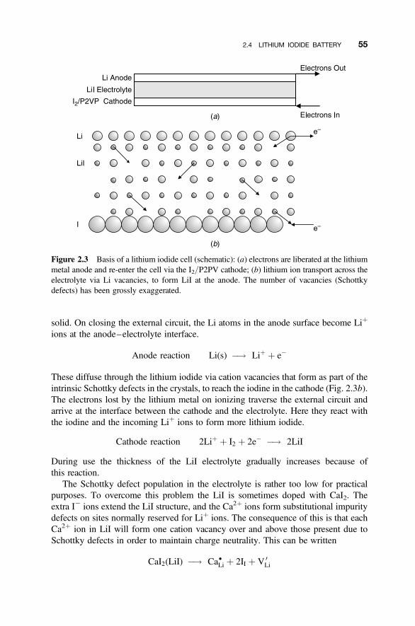
solid. On closing the external circuit, the Li atoms in the anode surface become Liþ
ions at the anode–electrolyte interface.
Anode reaction Li(s) �! Liþ þ e�
These diffuse through the lithium iodide via cation vacancies that form as part of theintrinsic Schottky defects in the crystals, to reach the iodine in the cathode (Fig. 2.3b).The electrons lost by the lithium metal on ionizing traverse the external circuit andarrive at the interface between the cathode and the electrolyte. Here they react withthe iodine and the incoming Liþ ions to form more lithium iodide.
Cathode reaction 2Liþ þ I2 þ 2e� �! 2LiI
During use the thickness of the LiI electrolyte gradually increases because ofthis reaction.
The Schottky defect population in the electrolyte is rather too low for practicalpurposes. To overcome this problem the LiI is sometimes doped with CaI2. Theextra I2 ions extend the LiI structure, and the Ca2þ ions form substitutional impuritydefects on sites normally reserved for Liþ ions. The consequence of this is that eachCa2þ ion in LiI will form one cation vacancy over and above those present due toSchottky defects in order to maintain charge neutrality. This can be written
CaI2(LiI) �! Ca†Li þ 2II þ V 0Li
Figure 2.3 Basis of a lithium iodide cell (schematic): (a) electrons are liberated at the lithiummetal anode and re-enter the cell via the I2/P2PV cathode; (b) lithium ion transport across theelectrolyte via Li vacancies, to form LiI at the anode. The number of vacancies (Schottkydefects) has been grossly exaggerated.
2.4 LITHIUM IODIDE BATTERY 55
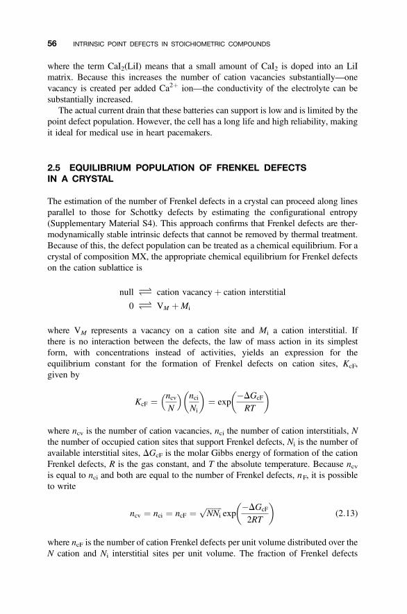
where the term CaI2(LiI) means that a small amount of CaI2 is doped into an LiImatrix. Because this increases the number of cation vacancies substantially—onevacancy is created per added Ca2þ ion—the conductivity of the electrolyte can besubstantially increased.
The actual current drain that these batteries can support is low and is limited by thepoint defect population. However, the cell has a long life and high reliability, makingit ideal for medical use in heart pacemakers.
2.5 EQUILIBRIUM POPULATION OF FRENKEL DEFECTSIN A CRYSTAL
The estimation of the number of Frenkel defects in a crystal can proceed along linesparallel to those for Schottky defects by estimating the configurational entropy(Supplementary Material S4). This approach confirms that Frenkel defects are ther-modynamically stable intrinsic defects that cannot be removed by thermal treatment.Because of this, the defect population can be treated as a chemical equilibrium. For acrystal of composition MX, the appropriate chemical equilibrium for Frenkel defectson the cation sublattice is
null O cation vacancyþ cation interstitial
0 O VM þMi
where VM represents a vacancy on a cation site and Mi a cation interstitial. Ifthere is no interaction between the defects, the law of mass action in its simplestform, with concentrations instead of activities, yields an expression for theequilibrium constant for the formation of Frenkel defects on cation sites, KcF,given by
KcF ¼ ncvN
� � nciNi
� �¼ exp
�DGcF
RT
� �
where ncv is the number of cation vacancies, nci the number of cation interstitials, Nthe number of occupied cation sites that support Frenkel defects, Ni is the number ofavailable interstitial sites, DGcF is the molar Gibbs energy of formation of the cationFrenkel defects, R is the gas constant, and T the absolute temperature. Because ncvis equal to nci and both are equal to the number of Frenkel defects, nF, it is possibleto write
ncv ¼ nci ¼ ncF ¼ ffiffiffiffiffiffiffiffiNNi
pexp
�DGcF
2RT
� �(2:13)
where ncF is the number of cation Frenkel defects per unit volume distributed over theN cation and Ni interstitial sites per unit volume. The fraction of Frenkel defects
56 INTRINSIC POINT DEFECTS IN STOICHIOMETRIC COMPOUNDS
present is given by
ncvffiffiffiffiffiffiffiffiNNi
p ¼ nciffiffiffiffiffiffiffiffiNNi
p ¼ ncFffiffiffiffiffiffiffiffiNNi
p ¼ exp�DGcF
2RT
� �(2:14a)
In the case where the number of normal and interstitial sites is the same, that is,N ¼ Ni:
ncF ¼ N exp�DGi
2RT
� �
which is identical to the equation for Schottky defects, as is the fraction of Frenkeldefects, ncF/N:
ncFN
¼ exp�DGi
2RT
� �
The Gibbs energy, DGcF, is often replaced by the enthalpy of Frenkel defectformation, DHcF, as described above, to give
ncF � ffiffiffiffiffiffiffiffiNNi
pexp
�DHcF
2RT
� �(2:15a)
where DHcF is in joules per mole and is the energy required to form 1 mol of Frenkeldefects, and R is the gas constant. Similar relationships hold if the Gibbs energyof formation per defect, DgcF, or the enthalpy of formation per defect, DhcF, isused, thus:
ncF ¼ ffiffiffiffiffiffiffiffiNNi
pexp
�DgcF2kT
� �
� ffiffiffiffiffiffiffiffiNNi
pexp
�DhcF2kT
� �
where the units of DgcF and DhcF are Joules or electron volts per defect, and k is theBoltzmann constant.
A similar equation can be written for Frenkel defects on the anion positions:
null O anion vacancyþ anion interstitial
0 O VX þ Xi
where VX represents a vacancy on an anion site and Xi an anion interstitial. Followingthe same procedure as before:
nav ¼ nai ¼ naF ¼ ffiffiffiffiffiffiffiffiNNi
pexp
�DGaF
2RT
� �(2:14b)
2.5 EQUILIBRIUM POPULATION OF FRENKEL DEFECTS IN A CRYSTAL 57
naF � ffiffiffiffiffiffiffiffiNNi
pexp
�DHaF
2RT
� �(2:15b)
¼ ffiffiffiffiffiffiffiffiNNi
pexp
�DgaF2kT
� �
� ffiffiffiffiffiffiffiffiNNi
pexp
�DhaF2kT
� �
where DGaF is the molar Gibbs energy of formation of the anion defects, DHaF is themolar enthalpy of formation of the anion defects, DgaF is the Gibbs energy required toform one defect, DhaF is the enthalpy of formation of one defect, R is the gas constant,and k is the Boltzmann constant. In the case where the number of interstitial positionsused, Ni, is equal to the number of normally occupied cation sites, N, the equationsare identical to those for Schottky defects.
Some experimental values for the formation enthalpy of Frenkel defects are givenin Table 2.2. As with Schottky defects, it is not easy to determine these values exper-imentally and there is a large scatter in the values found in the literature. (Calculatedvalues of the defect formation energies for AgCl and AgBr, which differ a little fromthose in Table 2.2, can be found in Fig. 2.5.)
2.6 PHOTOGRAPHIC FILM
Photographic film was the most widely used storage method for images throughoutthe twentieth century and still has an important part to play in image capture andstorage, although digital data recording is now widely used. Both black-and-whiteand color photography using film are possible because of the presence of pointdefects in the crystals used. The light-sensitive materials employed are silverhalides, notably AgBr, which are dispersed in gelatine to form the photographicemulsion. To ensure that the crystals are free of macroscopic defects such as dislo-cations, which degrade the perfection of the photographic images produced, thesilver halide crystals are carefully grown within the gelatine matrix itself. The crystalsso formed are usually thin triangular or hexagonal plates, varying between 0.01 and10mm in size, and in photographic parlance are known as grains.
TABLE 2.2 Formation Enthalpy of Frenkel Defects in Some Compounds ofFormula MX and MX2
Compound DHF/kJ mol21 DhF/eV Compound DHF/kJ mol21 DhF/eV
AgCla 139.7 1.45 CaF2b 261.4 2.71
AgBra 109.0 1.13 SrF2b 167.4 1.74
b-AgIa 57.8 0.60 BaF2b 184.3 1.91
aFrenkel defects on the cation sublattice of a sodium chloride structure compound.bFrenkel defects on the anion sublattice of a fluorite structure compound.
58 INTRINSIC POINT DEFECTS IN STOICHIOMETRIC COMPOUNDS
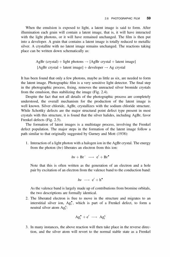
When the emulsion is exposed to light, a latent image is said to form. Afterillumination each grain will contain a latent image, that is, it will have interactedwith the light photons, or it will have remained unchanged. The film is then putinto a developer. A grain that contains a latent image is totally reduced to metallicsilver. A crystallite with no latent image remains unchanged. The reactions takingplace can be written down schematically as:
AgBr (crystal)þ light photons ! [AgBr crystalþ latent image]
[AgBr crystalþ latent image]þ developer ! Ag crystal
It has been found that only a few photons, maybe as little as six, are needed to formthe latent image. Photographic film is a very sensitive light detector. The final stepin the photographic process, fixing, removes the unreacted silver bromide crystalsfrom the emulsion, thus stabilizing the image (Fig. 2.4).
Despite the fact that not all details of the photographic process are completelyunderstood, the overall mechanism for the production of the latent image iswell known. Silver chloride, AgBr, crystallizes with the sodium chloride structure.While Schottky defects are the major structural point defect type present in mostcrystals with this structure, it is found that the silver halides, including AgBr, favorFrenkel defects (Fig. 2.5).
The formation of latent images is a multistage process, involving the Frenkeldefect population. The major steps in the formation of the latent image follow apath similar to that originally suggested by Gurney and Mott (1938):
1. Interaction of a light photon with a halogen ion in the AgBr crystal. The energyfrom the photon (hn) liberates an electron from this ion:
hnþ Br� �! e0 þ Br†
Note that this is often written as the generation of an electron and a holepair by excitation of an electron from the valence band to the conduction band:
hn �! e0 þ h†
As the valence band is largely made up of contributions from bromine orbitals,the two descriptions are formally identical.
2. The liberated electron is free to move in the structure and migrates to aninterstitial silver ion, Agi
†, which is part of a Frenkel defect, to form aneutral silver atom Agi
x:
Ag†i þ e0 �! Agxi
3. In many instances, the above reaction will then take place in the reverse direc-tion, and the silver atom will revert to the normal stable state as a Frenkel
2.6 PHOTOGRAPHIC FILM 59
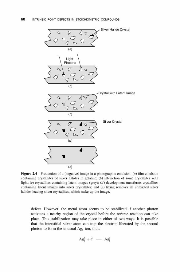
defect. However, the metal atom seems to be stabilized if another photonactivates a nearby region of the crystal before the reverse reaction can takeplace. This stabilization may take place in either of two ways. It is possiblethat the interstitial silver atom can trap the electron liberated by the secondphoton to form the unusual Agi0 ion, thus:
Agxi þ e0 �! Ag0i
Figure 2.4 Production of a (negative) image in a photographic emulsion: (a) film emulsioncontaining crystallites of silver halides in gelatine; (b) interaction of some crystallites withlight; (c) crystallites containing latent images (gray); (d ) development transforms crystallitescontaining latent images into silver crystallites; and (e) fixing removes all unreacted silverhalides leaving silver crystallites, which make up the image.
60 INTRINSIC POINT DEFECTS IN STOICHIOMETRIC COMPOUNDS
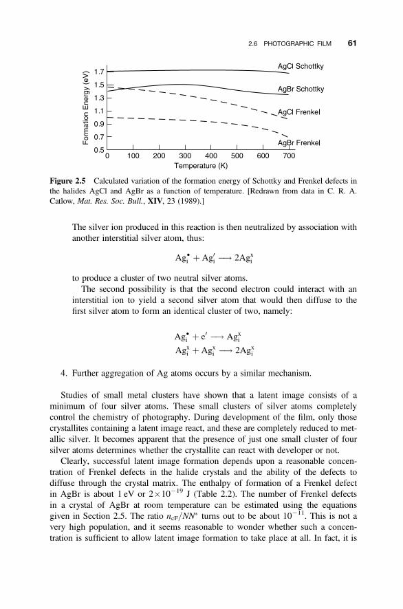
The silver ion produced in this reaction is then neutralized by association withanother interstitial silver atom, thus:
Ag†i þ Ag0i �! 2Agxi
to produce a cluster of two neutral silver atoms.The second possibility is that the second electron could interact with an
interstitial ion to yield a second silver atom that would then diffuse to thefirst silver atom to form an identical cluster of two, namely:
Ag†i þ e0 �! AgxiAgxi þ Agxi �! 2Agxi
4. Further aggregation of Ag atoms occurs by a similar mechanism.
Studies of small metal clusters have shown that a latent image consists of aminimum of four silver atoms. These small clusters of silver atoms completelycontrol the chemistry of photography. During development of the film, only thosecrystallites containing a latent image react, and these are completely reduced to met-allic silver. It becomes apparent that the presence of just one small cluster of foursilver atoms determines whether the crystallite can react with developer or not.
Clearly, successful latent image formation depends upon a reasonable concen-tration of Frenkel defects in the halide crystals and the ability of the defects todiffuse through the crystal matrix. The enthalpy of formation of a Frenkel defectin AgBr is about 1 eV or 2�10219 J (Table 2.2). The number of Frenkel defectsin a crystal of AgBr at room temperature can be estimated using the equationsgiven in Section 2.5. The ratio ncF/NN� turns out to be about 10211. This is not avery high population, and it seems reasonable to wonder whether such a concen-tration is sufficient to allow latent image formation to take place at all. In fact, it is
Figure 2.5 Calculated variation of the formation energy of Schottky and Frenkel defects inthe halides AgCl and AgBr as a function of temperature. [Redrawn from data in C. R. A.Catlow, Mat. Res. Soc. Bull., XIV, 23 (1989).]
2.6 PHOTOGRAPHIC FILM 61
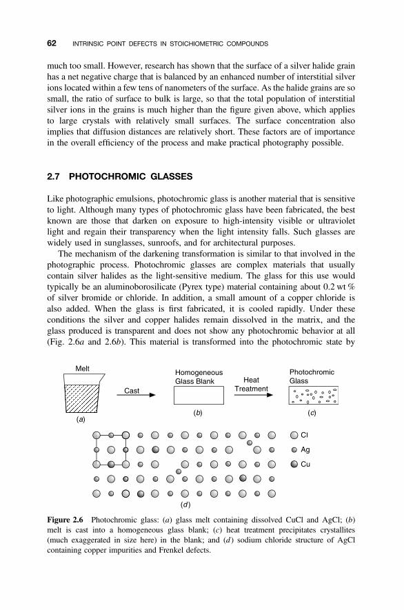
much too small. However, research has shown that the surface of a silver halide grainhas a net negative charge that is balanced by an enhanced number of interstitial silverions located within a few tens of nanometers of the surface. As the halide grains are sosmall, the ratio of surface to bulk is large, so that the total population of interstitialsilver ions in the grains is much higher than the figure given above, which appliesto large crystals with relatively small surfaces. The surface concentration alsoimplies that diffusion distances are relatively short. These factors are of importancein the overall efficiency of the process and make practical photography possible.
2.7 PHOTOCHROMIC GLASSES
Like photographic emulsions, photochromic glass is another material that is sensitiveto light. Although many types of photochromic glass have been fabricated, the bestknown are those that darken on exposure to high-intensity visible or ultravioletlight and regain their transparency when the light intensity falls. Such glasses arewidely used in sunglasses, sunroofs, and for architectural purposes.
The mechanism of the darkening transformation is similar to that involved in thephotographic process. Photochromic glasses are complex materials that usuallycontain silver halides as the light-sensitive medium. The glass for this use wouldtypically be an aluminoborosilicate (Pyrex type) material containing about 0.2 wt %of silver bromide or chloride. In addition, a small amount of a copper chloride isalso added. When the glass is first fabricated, it is cooled rapidly. Under theseconditions the silver and copper halides remain dissolved in the matrix, and theglass produced is transparent and does not show any photochromic behavior at all(Fig. 2.6a and 2.6b). This material is transformed into the photochromic state by
Figure 2.6 Photochromic glass: (a) glass melt containing dissolved CuCl and AgCl; (b)melt is cast into a homogeneous glass blank; (c) heat treatment precipitates crystallites(much exaggerated in size here) in the blank; and (d ) sodium chloride structure of AgClcontaining copper impurities and Frenkel defects.
62 INTRINSIC POINT DEFECTS IN STOICHIOMETRIC COMPOUNDS
heating under carefully controlled conditions of temperature and time, which mightbe, for example, 5508C for 30 min. followed by 6508C for 30 min. The heat treatmentis chosen so that the halides crystallize in the glass matrix (Fig. 2.6c). Care mustbe taken to ensure that the crystals do not become too large and that they do notaggregate. A desirable size is about 10 nm diameter, and the individual crystallitesshould be about 100 nm apart. These crystals form volume defects throughout thehomogeneous glass matrix.
It is important that the copper is in the monovalent state and incorporated into thesilver halide crystals as an impurity. Because the Cuþ has the same valence as theAgþ, some Cuþ will replace Agþ in the AgX crystal, to form a dilute solid solutionCuxAg12xX (Fig. 2.6d). The defects in this material are substitutional CuAg pointdefects and cation Frenkel defects. These crystallites are precipitated in the completeabsence of light, after which a finished glass blank will look clear because the silverhalide grains are so small that they do not scatter light.
The influence of light causes changes similar to that occurring in a photographicemulsion. The photons liberate electrons and these are trapped by interstitial silverions, which exist as Frenkel defects, to form neutral silver atoms. Unlike the photo-graphic process, the electrons are liberated by the Cuþ ions, which are converted toCu2þ ions (CuAg
† ) in the process:
hnþ CuAg �! Cu†Ag þ e0
e0 þ Ag†i �! AgxiAgxi þ Agxi �! 2Agi
This process continues until a small speck of silver is created. It is these clusters ofsilver that absorb the light falling on the glass. The absorption characteristics ofthe silver specks depend quite critically upon their size and shape. Photochromicglass production is carefully controlled so as to produce a wide variety of shapesand sizes of the silver specks, ensuring that the glass darkens uniformly.
In a photographic emulsion the halide atoms produced when electrons are releasedunder the influence of light can diffuse away from the silver or react with the emul-sion, and the process becomes irreversible. In the photochromic material the copperions remain trapped near to the silver particles. This means that the silver particles canrelease electrons to the Cu2þ ions when the light is turned off, reforming Cuþ ionsand making the whole process reversible. This bleaching process is the reverse ofthe darkening process. In fact the darkening and bleaching reactions are takingplace simultaneously under normal circumstances, in dynamic equilibrium. Whenthe amount of incident light is high, a large number of silver specks are present inthe glass, leading to hence a high degree of darkening. At low light intensity thenumber of silver particles present decreases and the glass becomes clear again.
Photochromic behavior depends critically upon the interaction of two point defecttypes with light: Frenkel defects in the silver halide together with substitutional Cuþ
impurity point defects in the silver halide matrix. It is these two defects together thatconstitute the photochromic phase.
2.7 PHOTOCHROMIC GLASSES 63
Commercially useful materials require that the rate of the combined reaction israpid. If the darkening takes place too slowly, or if the subsequent fading of thecolor is too slow, the materials will not be useful. The presence of the copperhalide is essential in ensuring that the kinetics of the reaction are appropriate andthat the process is reversible.
2.8 EQUILIBRIUM POPULATION OF ANTISITE DEFECTSIN A CRYSTAL
Antisite defect equilibria can be treated in the same way as the other point defectequilibria. The creation of a complementary pair of antisite defects consisting of anA atom on a B atom site, AB, and a B atom on an A atom site, BA, can then be written:
nul O AB þ BA
The relationship between defect number and free energy of formation can then bederived as in the examples above.
The creation of antisite defects can occur during crystal growth, when wrongatoms are misplaced on the growing surface. Alternatively, they can be created byinternal mechanisms once the crystal is formed, provided that sufficient energy isapplied to allow for atom movement. For example, antisite defects can be createdvia the intermediate formation of a Frenkel defect in the following way:
1. Frenkel defect formation on the A sublattice:
nul O Ai þ VA
2. Exchange of the interstitial Ai atom with a B atom on its correct site, BB:
Ai þ BB O AB þ Bi
3. The interstitial Bi atom can eliminate the vacancy to form a B atomantisite defect:
Bi þ VA O BA
4. If these three equations are added, the result is
nul O AB þ BA
The same equations can also be written in terms of interstitial B atom formation:
1. Frenkel defect formation on the B sublattice:
nul O Bi þ VB
64 INTRINSIC POINT DEFECTS IN STOICHIOMETRIC COMPOUNDS
2. Exchange of the interstitial Bi atom with an A atom on its correct site, AA:
Bi þ AA O BA þ Ai
3. The interstitial Ai atom can eliminate the vacancy to form an A atom antisitedefect:
Ai þ VB O AB
4. If these three equations are added, the result is again
nul O AB þ BA
These indirect mechanisms may be energetically preferable to a direct exchangeof atoms.
2.9 INTRINSIC DEFECTS: TRENDS AND FURTHERCONSIDERATIONS
At all temperatures above 08K Schottky, Frenkel, and antisite point defects arepresent in thermodynamic equilibrium, and it will not be possible to remove themby annealing or other thermal treatments. Unfortunately, it is not possible topredict, from knowledge of crystal structure alone, which defect type will bepresent in any crystal. However, it is possible to say that rather close-packed com-pounds, such as those with the NaCl structure, tend to contain Schottky defects.The important exceptions are the silver halides. More open structures, on the otherhand, will be more receptive to the presence of Frenkel defects. Semiconductorcrystals are more amenable to antisite defects.
Despite the utility of the formulas given in Eqs. (2.4)–(2.15), they suffer from anumber of limitations which it is useful to collect together here.
1. First of all, the formulas apply to materials of composition MX. In order todiscuss crystals of different composition, such as M2X3, MX2, and so on,different, though similar, formulas will result.
2. Only one sort of defect is supposed to be found in a crystal. Broadly speaking,this assumption is based upon the fact that the number of defects, nd, is relatedto the Gibbs energy of formation, DG, by an equation of the form:
nd ¼ Ns exp�DG
RT
� �
where Ns is the number of sites affected by the defect in question, DG the defectformation energy, R the gas constant, and T the temperature (K). One wouldanticipate that only the defect with the lower value of DG would be presentin important quantities. However, this assumption is often poor, and minority
2.9 INTRINSIC DEFECTS: TRENDS AND FURTHER CONSIDERATIONS 65
defects may have an important role to play when properties are considered,especially for semiconductor crystals. In fact, calculations show (Section2.10) that significant populations of many defects are invariably present ina crystal.
3. The treatment assumes that the point defects do not interact with each other.This is not a very good assumption because point defect interactions areimportant, and it is possible to take such interactions into account in moregeneral formulas. For example, high-purity silicon carbide, SiC, appears tohave important populations of carbon and silicon vacancies, VC
† and VSix ,
which are equivalent to Schottky defects, together with a large population ofdivacancy pairs.
4. The important quantities DH and DS are assumed to be temperature indepen-dent. This is often quite a good approximation, but the vibrational componentof the entropy, which has been neglected altogether, will become increasinglyimportant at high temperatures. The effects of these factors can cause the majordefect type present to change as the temperature increases. Near to the tran-sition temperature a complex equilibrium between both defect types will bepresent.
These limitations are largely eliminated in sophisticated defect calculationsdescribed in the following section. This approach can also include more sophisticatedsite exclusion rules, which allow defects to either cluster or keep apart from eachother. Nevertheless, the formulas quoted are a very good starting point for an explo-ration of the role of defects in solids and do apply well when defect concentrationsare small and at temperatures that are not too high.
2.10 COMPUTATION OF DEFECT ENERGIES
2.10.1 Defect Calculations
It is difficult to measure the formation and migration energy of point defects experi-mentally. Moreover, questions such as which mechanism is favored for the formationof, for example, antisite defects, are not easily resolved via experiment. The increas-ing application of computers during the second half of the twentieth century has beenvitally important in the resolution of such questions. This approach was first deve-loped as part of the Los Alamos work concerning nuclear fission. It was appreciatedthat experiments to ascertain neutron diffusion were too difficult to carry out, and themathematical equations describing the process could not be solved analytically togive meaningful results. The answer was the development of the so-called MonteCarlo method of computation of neutron diffusion by Metropolis and Ulam inwhich the movement of the particles was essentially decided by random numbergeneration. This method, in which an initial configuration is decided by a series ofrandom choices, is still a widely used computational tool. The second developmentof relevance to defect studies was the inception of the study of the defects produced
66 INTRINSIC POINT DEFECTS IN STOICHIOMETRIC COMPOUNDS
when an energetic particle collides with a solid. The initial impact displaces an atomthat in turn displaces other atoms in a cascade. These computer studies, published in1960, eventually evolved into molecular dynamics studies.
From these early beginnings, computer studies have developed into sophisticatedtools for the understanding of defects in solids. There are two principal methods usedin routine investigations: atomistic simulation and quantum mechanics. In simulation,the properties of a solid are calculated using theories such as classical electrostatics,which are applied to arrays of atoms. On the other hand, the calculation of the pro-perties of a solid via quantum mechanics essentially involves solving theSchrodinger equation for the electrons in the material.
In simulation methods, the key requisite is a function to express the interactionbetween the atoms. These interatomic potentials are either empirical or else calcu-lated by quantum mechanics. Having formulated the necessary interatomic poten-tials, the process to be explored, say vacancy formation, is set out in terms that areconsidered reasonable from a chemical and physical view. Finally, the method ofattack on the problem is chosen. The simplest, in principle, is to minimize theenergy of a static structure containing the defects of interest. A more complexapproach uses equations of motion for all of the atoms in the solid that arecombined with the interatomic forces to calculate how a solid evolves with timeand temperature. This molecular dynamics technique is widely used to studydiffusion in ionic conductors. A third way in which the simulation can be impli-cated is by starting from a random configuration—the Monte Carlo approach, andthen to compute the effects of small displacements of the atoms. Those newconfigurations that are energetically unfavorable are eliminated until a finalconfiguration remains that is considered to be optimal with respect to the con-ditions being investigated.
Quantum mechanical methods follow a similar path, except that the starting pointis the solution of the Schrodinger equation for the system under investigation. Themost successful and widely used method is that of Density Functional Theory.Once again, a key point is the development of a realistic model that can serve asthe input to the computer investigation. Energy minimization, molecular dynamics,and Monte Carlo methods can all be employed in this process.
There are two other methods in which computers can be used to give informationabout defects in solids, often setting out from atomistic simulations or quantummechanical foundations. Statistical methods, which can be applied to the generationof random walks, of relevance to diffusion of defects in solids or over surfaces, arewell suited to a small computer. Similarly, the generation of patterns, such as theaggregation of atoms by diffusion, or superlattice arrays of defects, or defectsformed by radiation damage, can be depicted visually, which leads to a better under-standing of atomic processes.
Calculations are now carried out routinely using a wide variety of programs, manyof which are freely available. In particular, the charge on a defect can be included sothat the formation energies, interactions, and relative importance of two defects suchas a charged interstitial as against a neutral interstitial are now accessible. Similarly,computation is not restricted to intrinsic defects, and the energy of formation of
2.10 COMPUTATION OF DEFECT ENERGIES 67
defects in doped or impure solids is equally available. Indeed, these two latter aspectsare among the most valuable assets of defect computation.
The purpose of the following sections is not to describe the calculations but to givean idea of the basics of the methods, particularly that of atomistic simulation, becausequantum mechanical calculations remain largely mathematical in nature and oftencannot be described in visual terms. The starting point is a simple estimation ofdefect interaction energy.
2.10.2 Point Defect Interactions
Defects in a crystal can carry effective charges and, because of this, it is to beexpected that the defects would interact with each other quite strongly. It is easy tomake a simple estimate of the approximate magnitude of these energy terms.
Classical electrostatic theory gives the energy of interaction of two charges, Ee
(sometimes expressed as the work needed to separate them or the Coulombenergy) as
Ee ¼ (�e)(þe)4p10r
¼ �e2
4p10r
where the charges have a magnitude of +e and so attract each other, r is theseparation of the charges, and 10 is the permittivity of vacuum. In this formulation,the energy of the pair is zero at infinite separation and decreases as the separationbetween them falls, so that a negative energy indicates a stable pair. In a vacuum,of course, the charges would come together and be annihilated, unless a counterforcebecomes important at low charge separation.
If we apply this formula to defects in a crystal, and again assume that the defectsare oppositely charged, so that they attract each other, the energy term will be roughlyequivalent to the enthalpy of formation of a defect pair, DHp. The closest separationof the defects will normally be equivalent to the spacing between two adjacentlattice sites.
In order to allow for the crystal structure itself, which will modify the interactionenergy, it is possible, as a first approximation, to assume that the force of attraction is“diluted” in the crystal by an amount equal to its relative permittivity. The modifiedformula is then
Ee � DHp � (Z1e)(�Z2e)4p1r10r
(2:16)
where DHp is the enthalpy of interaction, Z1 and 2Z2 are the effective charges on thedefects, 1r is the static relative permittivity of the crystal, and the other symbols havethe same meaning as above.
Simple as this theory is, it is good enough to give an indication of whether asso-ciation of defects is likely to occur. Consider, as an example, a Schottky defect,
68 INTRINSIC POINT DEFECTS IN STOICHIOMETRIC COMPOUNDS
consisting of a cation vacancy and an anion vacancy, in a crystal of a monovalentmetal MX with the sodium chloride structure. These vacancies will have effectivecharges of þe and 2e. Their interaction will be greatest when they are closest toeach other, that is, when they occupy neighboring sites in the crystal. The separationof these sites is about 3�10210 m. An approximate value for the relative permittivityof a sodium chloride structure crystal is 10. Substituting these values gives a valuefor the interaction energy, which is attractive:
DHp � �7:69� 10�20 J
This value is for one pair of vacancies. To obtain the molar quantity, we multiply DHp
above by NA, the Avogadro constant, to yield
DHp � �46:3 kJ mol�1
This is similar in magnitude to the energy of formation of Schottky defects, and so itcould be anticipated that a reasonable proportion of the vacancies would be asso-ciated into pairs.
It is possible to assess the fraction of defects in a crystal that is associated usingthe approximate interaction energy calculated above using the Boltzmann law. Thisgives the information about the distribution of a population of defects between twoenergy states. The fraction f of the population in the upper energy state, when theenergy difference between the states is DE, is
f ¼ exp�DE
kT
� �
where k is the Boltzmann constant and T the temperature (K). Using the exampleabove, the energy separation of the associated and unassociated states is7.69�10220 J, the value of f at a temperature of 1000 K will be 0.0038. Now inthis example the upper energy state corresponds to the separated vacancies. That is,the vast majority of the defects will be associated into pairs at 1000 K.
Although this estimate of the interaction energy between defects is simplistic, itdemonstrates that a fair number of defects may cluster together rather than remainas isolated “point defects,” provided, of course, that they can diffuse through thecrystal. It is difficult, experimentally, to determine the absolute numbers of pointdefects present in a crystal, and doubly so to determine the percentage that mightbe associated rather than separate. It is in both of these areas that theoretical calcu-lations are able to bear fruit.
As the above illustration shows, calculations using classical theories, especiallyelectrostatics, are relatively easy to picture. However, matter at an atomic scale isbest described by quantum mechanics. Quantum theory calculations are moredifficult and are preferred when electronic properties are of prime importance.Both techniques are described in the following sections.
2.10 COMPUTATION OF DEFECT ENERGIES 69
2.10.3 Atomistic Simulation
Atomistic simulation is the rigorous application of the simplistic method sketched inthe previous section. The properties of a solid are calculated using theories such asclassical electrostatics, which are applied to arrays of atoms, (rather than electrons,which form the focus of quantum mechanical approaches). Moreover, the atoms arefrequently represented as point charges. At the outset, the positions of the atoms inthe solid are defined. The more atoms specified, the closer the solid will approach amacroscopic crystal, but the greater will be the computer time needed to obtain theanswers. In practice, a balance is struck between atom numbers and computerresources. The energy of interaction between the atoms is then expressed algebraically,generally as a function of the position of the atoms. Broadly speaking, these pieces ofinformation allow the total energy of the collection to be determined. The atoms arethen displaced and a new energy is calculated. The preferred state of the system isthat with the lowest energy. A comparison of the energy of a perfect crystalwith that of a crystal containing a defect allows the formation energy of the defect tobe estimated. The calculations are referred to two nominal thermodynamic states, con-stant volume, in which the unit cell of the crystal is fixed, and constant pressure, inwhich the unit cell dimensions are allowed to vary during the course of the calculation.
These calculations require less computer time than quantum mechanical calcu-lations, and, more importantly, they can be applied to much larger collections ofatoms. This means that many problems can be tackled using atomistic simulationsthat remain impossible to approach (at the time of this writing) using quantumtheory. Although the method is simple in principle, the development of themodern programs that are used for atomistic simulation studies required great skillfrom the authors and contain ingenious algorithms to make the computations feasible.However, the ultimate accuracy of atomistic simulations depends upon how well theinteratomic potentials chosen represent the real atomic interactions.
The most critical aspect of atomistic simulations is thus the representation of theinteractions between atoms by an algebraic function. If covalency is important, apart of the expression should contain details of how the interaction changes withangle, to mimic directional covalent bonds. In cases where a simulation is used topredict the location of a cluster of atoms within or at the surface of a solid, interactionsbetween the atoms in the cluster, interactions between the atoms in the solid, andinteractions between the atoms in the cluster and those in the solid must all beincluded.
Results have shown that the properties of solids can usually be modeled effectivelyif the interactions are expressed in terms of those between just pairs of atoms. Theresulting potential expressions are termed pair potentials. The number and form ofthe pair potentials varies with the system chosen, and metals require a different setof potentials than semiconductors or molecules bound by van der Waals forces. Toillustrate this consider the method employed with nominally ionic compounds, typi-cally used to calculate the properties of perfect crystals and defect formation energiesin these materials.
In an ionic material, the ions interact via long-range electrostatic (Coulombic)forces, as set out in the previous section. Instead of the simple expression used
70 INTRINSIC POINT DEFECTS IN STOICHIOMETRIC COMPOUNDS
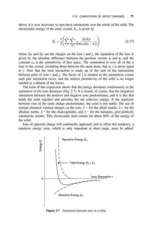
above, it is now necessary to sum these interactions over the whole of the solid. Theelectrostatic energy of the ionic crystal, Ee, is given by
Ee ¼ 12
Xni
Xnj=i
ZieZje
(4p10)(jri � rjj)
!(2:17)
where Zie and Zje are the charges on the ions i and j, the separation of the ions isgiven by the absolute difference between the position vectors ri and rj, and theconstant 10 is the permittivity of free space. The summation is over all of the nions in the crystal, excluding those between the same atom, that is, i is never equalto j. Note that the total interaction is made up of the sum of the interactionsbetween pairs of ions i and j. The factor of 1
2 is needed as the summation countseach pair interaction twice, and the relative permittivity of the solid is no longerneeded as a diluent of the forces.
The form of this expression shows that the energy decreases continuously as theseparation of the ions decreases (Fig. 2.7). It is found, of course, that the (negative)interaction between the positive and negative ions predominates, and it is this thatholds the solid together and provides the net cohesive energy. If the repulsionbetween ions of the same charge predominates, the solid is not stable. The use ofnormal chemical valence charges on the ions, 1þ for the alkali metals, 2þ for thealkaline earths, 22 for the chalcogenides, and 12 for the halogens, give perfectlysatisfactory results. This electrostatic term counts for about 80% of the energy ofthe solid.
Ions of opposite charge will continually approach, and to offset this tendency, arepulsive energy term, which is only important at short range, must be added.
Figure 2.7 Interaction between ions in a solid.
2.10 COMPUTATION OF DEFECT ENERGIES 71
Another short-range force that occurs in a solid is the weak van der Waals attractionbetween electron orbitals. There are a number of expressions for the short-rangepotential that takes both these factors into account. One commonly used expressionis the Buckingham potential:
Es ¼ 12
Xni
Xni=j
A exp�jri � rjj
r
� �� C
jri � rjj6 !
(2:18)
where A, r, and C are adjustable parameters, and the separation of the ions is given bythe absolute difference between the position vectors ri and rj. The summation is overall of the n ions in the crystal, excluding those between the same atom, that is, i isnever equal to j. Note that the total interaction is again made up of the sum of theinteractions between pairs of ions i and j. The factor of 1
2 is needed as the summationcounts each pair interaction twice. The short-range forces act so as to oppose thelong-range interactions (Fig. 2.7).
The first (exponential) term represents repulsion between electron orbitals on theatoms. The second term can be seen to be opposite in sign to the first and sorepresents an attraction—the weak van der Waals interaction between the electronorbitals on approaching atoms. The adjustable parameters can sometimes be calcu-lated using quantum mechanics, but in other systems they are derived empiricallyby comparing the measured physical properties of a crystal, relative permittivity,elastic constants, and so on, with those calculated with varying parameters untilthe best fit is obtained. Some parameters obtained in this way, relevant to the calcu-lation of the stability of phases in the system SrO–SrTiO3, are given in Table 2.3.
The total energy of the solid is given by
Etotal ¼ Ee þ Es
The balance between the long-range and short-range forces will result in a relativelyshallow minimum, the lowest point of which gives the energy of the stable solid(Fig. 2.7).
2.10.4 The Shell Model
Calculations using just the terms Ee and Es described above have been found to be toofar from agreement with experiment to be considered satisfactory. The disagreementwith experimental observations can often be attributed to the fact that the electronicpolarizability of the ions in the solid has been ignored. The electronic polarizability ofan ion is a measure of the amount by which the electron cloud around an atomicnucleus is distorted in an electric field.
The electronic polarizability can be included in the simulation procedure by use ofthe shell model. In this formalism, the core of an ion is considered to be massive, andto take a charge zjej. This is surrounded by a massless shell, with a charge zjej, where
72 INTRINSIC POINT DEFECTS IN STOICHIOMETRIC COMPOUNDS
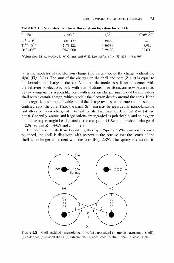
jej is the modulus of the electron charge (the magnitude of the charge without thesign) (Fig. 2.8a). The sum of the charges on the shell and core (Z þ z) is equal tothe formal ionic charge of the ion. Note that the model is still not concerned withthe behavior of electrons, only with that of atoms. The atoms are now representedby two components, a pointlike core, with a certain charge, surrounded by a masslessshell with a certain charge, which models the electron density around the cores. If theion is regarded as nonpolarizable, all of the charge resides on the core and the shell iscentered upon the core. Thus, the small Si4þ ion may be regarded as nonpolarizableand allocated a core charge of þ4e and the shell a charge of 0, so that Z ¼ þ4 andz ¼ 0. Generally, anions and large cations are regarded as polarizable, and an oxygenion, for example, might be allocated a core charge of þ0.9e and the shell a charge of22.9e, so that Z ¼ þ0.9 and z ¼ 22.9.
The core and the shell are bound together by a “spring.” When an ion becomespolarized, the shell is displaced with respect to the core so that the center of theshell is no longer coincident with the core (Fig. 2.8b). The spring is assumed to
TABLE 2.3 Parameters for Use in Buckingham Equation for SrTiO3
Ion Pair A/eVa r/A C/eV A26
Sr2þ–O22 682.172 0.39450 —Ti4þ–O22 2179.122 0.30384 8.986O22–O22 9547.960 0.29120 32.00
aValues from M. A. McCoy, R. W. Grimes, and W. E. Lee, Philos. Mag., 75, 833–846 (1997).
Figure 2.8 Shell model of ionic polarizability: (a) unpolarized ion (no displacement of shell);(b) polarized (displaced shell); (c) interactions: 1, core–core; 2, shell–shell; 3, core–shell.
2.10 COMPUTATION OF DEFECT ENERGIES 73
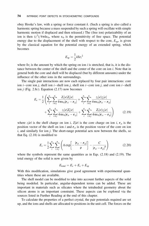
obey Hooke’s law, with a spring or force constant k. (Such a spring is also called aharmonic spring because a mass suspended by such a spring will oscillate with simpleharmonic motion if displaced and then released.) The (free ion) polarizability of anion is then (z2)/4pk10, where 10 is the permittivity of free space. The potentialenergy due to the displacement of the shell with respect to the core, Esp, is givenby the classical equation for the potential energy of an extended spring, whichbecomes
Esp ¼ 12kdri
2
where dri is the amount by which the spring on ion i is stretched, that is, it is the dis-tance between the center of the shell and the center of the core on ion i. Note that ingeneral both the core and shell will be displaced (but by different amounts) under theinfluence of the other ions in the surroundings.
The single pair interactions are now each replaced by four pair interactions: coreion i–core ion j, shell ion i–shell ion j, shell ion i–core ion j, and core ion i–shellion j (Fig. 2.8c). Equation (2.17) now becomes
Ee ¼ 12
Xni
Xni=j
ZijejZjjej4p10jrci � rcjj þ
Xni
Xni=j
zijejzjjej4p10jrsi � rsjj
þXni
Xni=j
zijejZjjej4p10jrsi � rcjj þ
Xni
Xni=j
Zijejzjjej4p10jrci � rsjj
!(2:19)
where zi|e| is the shell charge on ion i, Zi|e| is the core charge on ion i, rsi is theposition vector of the shell on ion i and rci is the position vector of the core on ioni, and similarly for ion j. The short-range potential acts now between the shells, sothat Eq. (2.18) is modified to
Es ¼ 12
Xni
Xni=j
A exp � jrsi � rsjjr
� �� C
jrsi � rsjj6 !
(2:20)
where the symbols represent the same quantities as in Eqs. (2.18) and (2.19). Thetotal energy of the solid is now given by
Etotal ¼ Ee þ Es þ Esp
With this modification, simulations give good agreement with experimental quan-tities where these are available.
The shell model can be modified to take into account further aspects of the solidbeing modeled. In particular, angular-dependent terms can be added. These areimportant in materials such as silicates where the tetrahedral geometry about thesilicon atoms is an important constraint. These aspects can be explored via thesources listed in Further Reading at the end of this chapter.
To calculate the properties of a perfect crystal, the pair potentials required are setup, and the ions and shells are allocated to positions in the unit cell. The forces on the
74 INTRINSIC POINT DEFECTS IN STOICHIOMETRIC COMPOUNDS
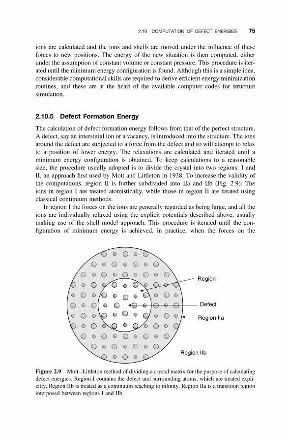
ions are calculated and the ions and shells are moved under the influence of theseforces to new positions. The energy of the new situation is then computed, eitherunder the assumption of constant volume or constant pressure. This procedure is iter-ated until the minimum energy configuration is found. Although this is a simple idea,considerable computational skills are required to derive efficient energy minimizationroutines, and these are at the heart of the available computer codes for structuresimulation.
2.10.5 Defect Formation Energy
The calculation of defect formation energy follows from that of the perfect structure.A defect, say an interstitial ion or a vacancy, is introduced into the structure. The ionsaround the defect are subjected to a force from the defect and so will attempt to relaxto a position of lower energy. The relaxations are calculated and iterated until aminimum energy configuration is obtained. To keep calculations to a reasonablesize, the procedure usually adopted is to divide the crystal into two regions: I andII, an approach first used by Mott and Littleton in 1938. To increase the validity ofthe computations, region II is further subdivided into IIa and IIb (Fig. 2.9). Theions in region I are treated atomistically, while those in region II are treated usingclassical continuum methods.
In region I the forces on the ions are generally regarded as being large, and all theions are individually relaxed using the explicit potentials described above, usuallymaking use of the shell model approach. This procedure is iterated until the con-figuration of minimum energy is achieved, in practice, when the forces on the
Figure 2.9 Mott–Littleton method of dividing a crystal matrix for the purpose of calculatingdefect energies. Region I contains the defect and surrounding atoms, which are treated expli-citly. Region IIb is treated as a continuum reaching to infinity. Region IIa is a transition regioninterposed between regions I and IIb.
2.10 COMPUTATION OF DEFECT ENERGIES 75
ions are zero. The computation is expensive and the region is chosen to be as small aspossible, while still giving reliable results. Usually, a volume with a radius of 1–2 nmor so around the defect is considered to be sufficient, containing a few hundred ions.
The forces from the defect are regarded as being weaker in region II, which allowsthe region to be treated as a continuous dielectric medium without too much loss ofprecision. The consequence of the presence of the defect is that this region becomespolarized in the same way as a classical slab of insulator becomes polarized in thepresence of an electric charge. The energy is evaluated using classical continuumtheories. The displacement of an ion, at a position defined by vector r, is assumedto be due to the presence of a charge q on the defect. The displacement of eachion is expressed in terms of the bulk polarization of the structure, P:
P ¼ 1� 11
� �q
4pr
� �
where 1 is the permittivity of the material, given by (1r 10), in which 1r is the relativepermittivity of the solid and 10 the permittivity of free space. For ease of computation,the energy of this region is supposed to be a harmonic function of the displacement ofthe ions present, which arise due to the total charge q on the defect in region I. Tosmooth out the rather abrupt change from region I to region II, region IIa is takenas the inner part of region II. In this volume, the displacements are calculated viathe Mott–Littleton (1938) approach, but the interactions with the ions in region Iare summed explicitly. This region is usually of the order of 3 nm in radius andcontains several thousand ions. The remainder of region II, called region IIb,extends to infinity.
The energy of the solid containing the defect is minimized with respect to thevarious relaxations possible. The result is compared to that of the perfect defect-free structure to give a value for the defect formation energy.
2.10.6 Quantum Mechanical Calculations
The calculation of the properties of a solid via quantum mechanics essentiallyinvolves solving the Schrodinger equation for the collection of atoms that makesup the material. The Schrodinger equation operates upon electron wave functions,and so in quantum mechanical theories it is the electron that is the subject of thecalculations. Unfortunately, it is not possible to solve this equation exactly for realsolids, and various approximations have to be employed. Moreover, the calculationsare very demanding, and so quantum evaluations in the past have been restricted tosystems with rather few atoms, so as to limit the extent of the approximationsmade and the computation time. As computers increase in capacity, these limitationsare becoming superseded.
The use of quantum mechanical calculations of solid properties was initially theprovince of solid-state physics, and the calculation of electron energy levels inmetals and semiconductors is well established. Chemical quantum mechanical
76 INTRINSIC POINT DEFECTS IN STOICHIOMETRIC COMPOUNDS
calculations have tended, for computational reasons, to center upon molecules.However, as theory has advanced, the sizes of the “molecules” have increased, andclusters of several hundred atoms can now be handled. For chemical work, theSchrodinger equation is often recast in the Hartree–Fock formalism. The Hartree–Fock equations can be solved using no input except the fundamental constants, tech-niques referred to as ab initio methods. The computationally expensive ab initio pro-cedure is often replaced by using a semi-empirical Hartree–Fock formalism. Theequations are solved using methods that introduce approximations based uponobserved properties. Both these techniques are used to compute interatomic potentialsfor use in simulations. Similarly, the techniques are sometimes applied to anembedded cluster. This is a combination of quantum mechanics and classicaltheory. The properties of a cluster of atoms are computed using Hartree–Fockequations. The cluster is imagined to be embedded in a surrounding solid, whichis treated in more approximate terms, often in terms of pair potentials.
The inherent problems associated with the computation of the properties of solidshave been reduced by a computational technique called Density Functional Theory.This approach to the calculation of the properties of solids again stems from solid-state physics. In Hartree–Fock equations the N electrons need to be specified by3N variables, indicating the position of each electron in space. The density functionaltheory replaces these with just the electron density at a point, specified by just threevariables. In the commonest formalism of the theory, due to Kohn and Sham, calledthe local density approximation (LDA), noninteracting electrons move in an effectivepotential that is described in terms of a uniform electron gas. Density functionaltheory is now widely used for many chemical calculations, including the stabilitiesand bulk properties of solids, as well as defect formation energies and configurationsin materials such as silicon, GaN, and AgI. At present, the excited states of solids arenot well treated in this way.
Quantum mechanical calculations are essentially mathematical, and further discus-sion is not merited here. More information can be gained from the sources cited inFurther Reading at the end of this chapter.
2.11 ANSWERS TO INTRODUCTORY QUESTIONS
What is an intrinsic defect?
An intrinsic defect is one that is in thermodynamic equilibrium in the crystal.This means that a population of these defects cannot be removed by any forms ofphysical or chemical processing. Schottky, Frenkel, and antisite defects are thebest characterized intrinsic defects. A totally defect-free crystal, if warmed to atemperature that allows a certain degree of atom movement, will adjust to allowfor the generation of intrinsic defects. The type of intrinsic defects that formwill depend upon the relative formation energies of all of the possibilities. Thedefect with the lowest formation energy will be present in the greatest numbers.This can change with temperature.
2.11 ANSWERS TO INTRODUCTORY QUESTIONS 77
What point defects are vital for the operation of LiI pacemaker batteries?
Lithium iodide pacemaker batteries use lithum iodide as the electrolyte, separatingthe lithium anode and the iodine anode. The function of the electrolyte is to transportions but not electrons. Lithium iodide achieves this by the transport of Liþ ions fromthe anode to the cathode. This transport is made possible by the presence of Livacancies that are generated by the intrinsic Schottky defect population present inthe solid. Lithium ions jump from vacancy to vacancy during battery operation.
What is the basis of “atomistic simulation” calculations of point defect formationenergies?
Atomistic simulation is a computational technique to assess the properties of asolid. The solid is considered to be constructed of atoms (or ions) and electrons arenot involved. At the simplest level, solids may be modeled by considering that thecomponent species are ions represented by point charges. The interaction betweenthe ions can then be represented by the formulas of classical electrostatics. Thedifference between the calculations when the solid is perfect compared with thatwhen the solid contains one or more point defects then provides informationabout the defect formation energy. Rapidly increasing sophistication in terms ofboth hardware and software, such as using the shell model to include polarization,result in atomistic simulation calculations that give excellent agreement withexperimental results when these are available. Such calculations are frequentlyrelied upon for the accurate assessment of the formation energies of defects in awide variety of solids when experimental data is not available.
PROBLEMS AND EXERCISES
Quick Quiz
1. The number of different types of point defects found in a pure monatomic crystal is:
(a) Three
(b) Two
(c) One
2. The number of vacancies in a metal crystal is proportional to:
(a) exp(2DH/RT)
(b) exp(DH/RT)
(c) exp(2DH/2RT)
3. The formation energies of point defects in a pure metal are 1.0 eV (vacancies)and 1.1 eV (interstitials). The number of vacancies is:
(a) Less than the number of interstitials
(b) More than the number of interstitials
(c) Equal to the number of interstitials
78 INTRINSIC POINT DEFECTS IN STOICHIOMETRIC COMPOUNDS
4. The number of Schottky defects in a crystal of formula MX is equal to:
(a) The total number of vacancies present
(b) Double the total number of vacancies present
(c) Half the total number of vacancies present
5. The ratio of cation to anion vacancies due to Schottky defects in a crystal offormula M2X3 is equal to:
(a) 1 : 1
(b) 3 : 2
(c) 2 : 3
6. The formation of a Frenkel defect in CaF2 is represented by:
(a) 0! VF† þ Fi0
(b) 0! 2VF† þ Fi0
(c) 0! 2VF† þ Cai
2†
7. The enthalpy of formation of Frenkel defects (kJ mol21) is AgCl,140, AgBr, 109, AgI, 58. The compound with the greatest number of Agþ inter-stitials is:
(a) AgI
(b) AgBr
(c) AgCl
8. The darkening of photochromic sunglasses is due to the formation of:
(a) Copper crystallites
(b) Silver crystallites
(c) (Ag, Cu) crystallites
9. Calculations described as simulations generally deal with:
(a) Atoms
(b) Electrons
(c) Atoms and electrons
10. The shell model is used to take into account:
(a) Atomic displacement
(b) Atomic vibration
(c) Atomic polarization
Calculations and Questions
1. Plot DG vs. nV using the equation:
DGV ¼ nVDhV � kT{N ln N � (N � nV)ln(N � nV)� nV ln nV}
PROBLEMS AND EXERCISES 79
for values of hV ¼ 1, 0.5, 0.1 eV, kT ¼ 0.1 (k ¼ 8.61739 � 1025 eV K21, T ¼1160 K), N ¼ 104.
2. The energy of formation of a defect in a typical metal varies from approximately1�10219 J to 6�10219 J. (a) Calculate the variation in the fraction of defectspresent, nd/N, in a crystal as a function of the defect formation energy. (b)Calculate the variation in the fraction of defects present as a function of tempera-ture if the defect formation energy is 3.5�10219 J.
3. The enthalpy of formation of vacancies DHV, in pure silver is 105.2 kJ mol21.(a) Estimate the fraction of vacancies, nV/N, at 9508C (approximately 128Cbelow the melting point of silver). (b) Calculate the number of vacancies percubic meter of silver at 9508C temperature using the crystallographic data:cubic unit cell with edge length a ¼ 0.4086 nm, containing four atoms ofsilver. (c) Repeat the calculation using the density of silver, 10,500 kg m23,and molar mass, 107.87 g mol21.
4. Following the method set out in Supplementary Material S4, derive a formula forthe number of Schottky defects in a crystal of formula MX2.
5. The energy of formation of defects in PbF2 are: anion Frenkel defect, 0.69 eV;cation Frenkel defect, 4.53 eV; Schottky defect, 1.96 eV. (a) What pointdefects do these consist of? (b) What are (approximately) the relative numbersof these defects in a crystal at 300 K? (Data from H. Jiang et al., 2000).
6. Pure potassium bromide, KBr, which adopts the sodium chloride structure, hasthe fraction of empty cation sites due to Schottky defects, ncv/Nc, equal to9.159�10221 at 208C. (a) Estimate the enthalpy of formation of a Schottkydefect, DhS. (b) Calculate the number of anion vacancies per cubic meter ofKBr at 7308C ( just below the melting point of KBr). The unit cell of KBr iscubic with edge length a ¼ 0.6600 nm and contains four formula units of KBr.
7. The favored defect type in strontium fluoride, which adopts the fluorite struc-ture, are Frenkel defects on the anion sublattice. The enthalpy of formation ofan anion Frenkel defect is estimated to be 167.88 kJ mol21. Calculate thenumber of F2 interstitials and vacancies due to anion Frenkel defects percubic meter in SrF2 at 10008C. The unit cell is cubic, with a cell edge of0.57996 nm and contains four formula units of SrF2. It is reasonable toassume that the number of suitable interstitial sites is half that of the numberof anion sites.
8. Write out the explicit form of Eq. (2.17) for three atoms at r1, r2, r3, with chargesq1, q2, q3.
9. The formation energy of Schottky defects in NiO has been estimated at198 kJ mol21. The lattice parameter of the sodium chloride structure unit cell is0.417 nm. (a) Calculate the number of Schottky defects per cubic meter in NiOat 10008C. (b) How many vacancies are there at this temperature? (c) Estimatethe density of NiO and hence the number of Schottky defects per gram of NiO.
80 INTRINSIC POINT DEFECTS IN STOICHIOMETRIC COMPOUNDS
10. (a) Calculate the relative number of interstitial Agþ ions that exist in a crystal ofAgCl at 300 K, assuming that all are derived from Frenkel defects, formationenthalpy 2.69 � 10219 J. (b) Knowing that AgCl adopts the sodium chloridestructure, with lattice parameter a ¼ 0.5550 nm, calculate the absolute numberof interstitials present per cubic meter at 300 K.
11. The following table gives the values of the fraction of Schottky defects, nS/N, ina crystal of NaBr, with the sodium chloride structure, as a function of tempera-ture. Estimate the formation enthalpy of the defects.
Temperature/8C Fraction of Defects
300 7.66 � 10210
400 1.73 � 1028
500 1.75 � 1027
600 1.04 � 1026
700 4.28 � 1026
REFERENCES
R. W. Gurney and N. F. Mott, Proc. Roy. Soc. Lond., 164A, 151 (1938).
H. Jiang, A. Costales, M. A. Blanes, M. Gu, R. Pandy, and J. D. Gale, Phys. Rev. B, 62,803–809 (2000).
N. F. Mott and M. J. Littleton, Trans. Farad. Soc., 34, 485–499 (1938).
C. Wagner and W. Schottky, Zeit. Phys. Chem., 11B, 163–210 (1931).
FURTHER READING
Information on point defect equilibria are given in:
D. M. Smyth, The Defect Chemistry of Metal Oxides, Oxford University Press, Oxford, UnitedKingdom, 2000.
A. M. Stoneham, The Theory of Defects in Solids, Oxford University Press, Oxford, UnitedKingdom, 1985.
F. Agullo-Lopez, C. R. Catlow, and P. D. Townsend Point Defects in Materials, Academic,New York, 1988.
The photographic process is described by:
F. C. Brown, The Photographic Process, in Treatise on Solid State Chemistry, Vol. 4, Reactivityof Solids, N. B. Hannay, Ed., Plenum, New York, 1976, Chapter 7.
Photochromic glass from the inventor’s point of view is described in:
S. D. Stookey, Explorations in Glass, American Ceramic Society, Westerville, Ohio, 2000.
The Monte Carlo method is described by:
C. P. Robert and G. Casella, Monte Carlo Statistical Methods, Springer, New York, 2004.
FURTHER READING 81
N. Metropolis and S. Ulam, Amer. Statistic Assoc. 44, 335 (1949).
The history of the Monte Carlo method and molecular dynamics simulations is given in:
R. W. Cahn, The Coming of Materials Science, Pergamon/Elsevier, Oxford, United Kingdom,2001, 465–471.
The development of computer modeling can be seen by comparing:
C. R. A. Catlow, Computational Techniques and Simulation of Crystal Structures, in SolidState Chemistry Techniques, A. K. Cheetham and P. Day, Eds., Oxford University Press,Oxford, United Kingdom, 1987.
C. R. A. Catlow, Computer Modelling of Solids, in Encyclopedia of Inorganic Chemistry, 2nded., R. B. King, Ed., Wiley, Hoboken, NJ, 2006.
C. R. A. Catlow, J. D. Gale, and R. W. Grimes, J. Solid State Chem., 106, 13–26 (1993).
Information about computational methods can be found in:
Atomistic simulations: Various authors Mat. Res. Soc. Bull., 21, February (1996).
Density functional theory: Various authors Mat. Res. Soc. Bull., 31, September (2006).
Applications of density functional theory to surface studies is given by:
N. D. Lang, Surf. Sci., 299/300, 284–297 (1994).
A good starting place for information about Monte Carlo and density functional methods is:
Wikipedia: http://en.wikipedia.org/wiki/Monte_Carlo_method.
http://en.wikipedia.org/wiki/Density_functional_theory.
A widely used progam for atomistic simulation (GULP) is at:
http://gulp.curtin.edu.au.
Four classic papers are:
Y. I. Frenkel, Z. Physik, 35, 652–669 (1926).
R. W. Gurney and N. F. Mott, Proc. Roy. Soc. Lond., 164A, 151 (1938).
N. F. Mott, M. J. Littleton Trans. Farad. Soc., 34, 485–499 (1938).
C. Wagner and W. Schottky Z. Phys., Chem. 11B, 163–211 (1931).
82 INTRINSIC POINT DEFECTS IN STOICHIOMETRIC COMPOUNDS
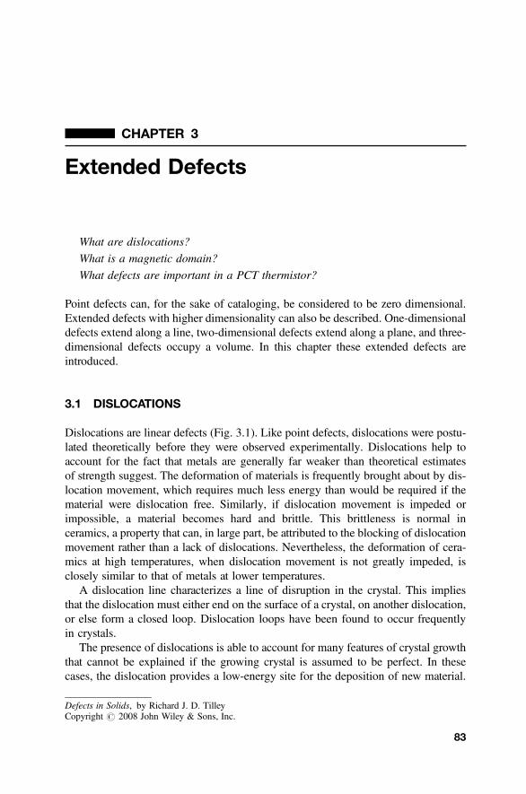
&CHAPTER 3
Extended Defects
What are dislocations?
What is a magnetic domain?
What defects are important in a PCT thermistor?
Point defects can, for the sake of cataloging, be considered to be zero dimensional.Extended defects with higher dimensionality can also be described. One-dimensionaldefects extend along a line, two-dimensional defects extend along a plane, and three-dimensional defects occupy a volume. In this chapter these extended defects areintroduced.
3.1 DISLOCATIONS
Dislocations are linear defects (Fig. 3.1). Like point defects, dislocations were postu-lated theoretically before they were observed experimentally. Dislocations help toaccount for the fact that metals are generally far weaker than theoretical estimatesof strength suggest. The deformation of materials is frequently brought about by dis-location movement, which requires much less energy than would be required if thematerial were dislocation free. Similarly, if dislocation movement is impeded orimpossible, a material becomes hard and brittle. This brittleness is normal inceramics, a property that can, in large part, be attributed to the blocking of dislocationmovement rather than a lack of dislocations. Nevertheless, the deformation of cera-mics at high temperatures, when dislocation movement is not greatly impeded, isclosely similar to that of metals at lower temperatures.
A dislocation line characterizes a line of disruption in the crystal. This impliesthat the dislocation must either end on the surface of a crystal, on another dislocation,or else form a closed loop. Dislocation loops have been found to occur frequentlyin crystals.
The presence of dislocations is able to account for many features of crystal growththat cannot be explained if the growing crystal is assumed to be perfect. In thesecases, the dislocation provides a low-energy site for the deposition of new material.
Defects in Solids, by Richard J. D. TilleyCopyright # 2008 John Wiley & Sons, Inc.
83
The vast subject of dislocations, particularly with respect to mechanical properties,will not be considered in this book, and only a few aspects of dislocations, especiallyinteractions with point defects, will be explored.
The disruption to the crystal introduced by a dislocation is characterized by theBurgers vector, b (see Supplementary Material S1 for information on directions incrystals). During dislocation motion individual atoms move in a direction parallelto b, and the dislocation itself moves in a direction perpendicular to the dislocationline. As the energy of a dislocation is proportional to b2, dislocations with smallBurgers vectors form more readily.
A dislocation represents a disruption of the perfect crystal structure. In the case ofFrenkel and Schottky defects the energy to form the defect, the enthalpy, is offset bythe entropy of the disordered state. Dislocations also introduce an entropy increaseinto the system, but the dislocation formation energy is much higher than that of apoint defect, and the entropy term is never able to completely balance the enthalpyterm, meaning that dislocations are never in thermodynamic equilibrium with theirsurroundings. They are thus extrinsic defects and, in principle, careful preparationor annealing can result in dislocation-free materials. In practice, this is extremelydifficult to achieve, although materials that crystallize in whisker habit, or siliconsingle crystals prepared under extremely careful conditions, contain few dislocations.
Figure 3.1 Electron micrograph showing a dislocation in silver, imaged as a dark line. Thesmall triangular features that decorate the dislocation are stacking faults formed by the aggrega-tion of point defects. [From W. Sigle, M. L. Jenkins, and J. L. Hutchison, Phil. Mag. Lett., 57267 (1988). Reproduced by permission of Taylor and Francis, http://www.informaworld.com.]
84 EXTENDED DEFECTS
A dislocation is surrounded by displaced atoms and the shifts give rise to a sur-rounding strain field. The strain field contributes to enhanced chemical reactivity,and crystals react at increased rates near to dislocations. For this reason, dislocationsthat intersect the surface of a crystal can be revealed by placing the crystal in asolvent. The regions where the dislocations emerge dissolve preferentially toproduce small pits called etch figures on the surface. Similarly, precipitates orother defects often aggregate near to dislocations, called dislocation decoration(Fig. 3.1) (see also Section 3.7.3). The disruption that occurs near to a dislocationline also facilitates atomic movement, and diffusion of atoms along a dislocation isnormally much higher than diffusion through the bulk solid (Section 5.11).
The strain field around a dislocation means that it will interact strongly with otherdislocations as well as other structural defects. The strain field will depend upon thetype of dislocation, its width, and its Burgers vector. In fact, the width of a dislo-cation, w, is defined in terms of the Burgers vector. The width is equated to thedistance from the dislocation line over which the atom displacements are greaterthan b/4, where b is the length of the dislocation’s Burgers vector, b. Metals areusually found to have rather wide dislocations, with w equal to three or fouratomic spacings, whereas ceramic materials tend to contain narrow dislocations inwhich the atomic displacements are only greater than b/4 over one or two atomicspacings surrounding the dislocation core.
The Burgers vector of a dislocation can lie at any angle to the dislocation line.Although there are many different types of dislocations, they can all be thought ofas combinations of two fundamental types, edge dislocations, which have Burgersvectors perpendicular to the dislocation line, and screw dislocations, with Burgersvectors parallel to the dislocation line.
3.2 EDGE DISLOCATIONS
Edge dislocations, which are primarily linked to mechanical properties, are the sim-plest to portray on a planar figure. They consist of an extra half plane of atomsinserted into the crystal (Fig. 3.2). The dislocation itself is described by the line,running perpendicular to the plane of the figure, localized at the tip of the insertedatom plane; marked by ? on diagrams. The Burgers vector of the dislocation canbe determined by drawing a closed circuit in the crystal, called a Burgers circuit,from atom to atom, in a region of crystal surrounding the dislocation core, proceedingin a clockwise or right-hand direction (Fig. 3.3a). An identical circuit is then mappedin a perfect crystal (Fig. 3.3b). The circuit will not close in this case. The vectorrequired to close the loop, running from the last atom, the finish atom of thecircuit, to the start atom, is the Burgers vector, b, of the dislocation. This is calledthe FS/RH (perfect crystal) convention. (Note that this procedure can be reversed.A clockwise circuit is first drawn in a perfect crystal. This is then repeated exactly,in the same direction and the same number of steps, around the dislocation. Asbefore, the circuit will not close. The Burgers vector is now the vector joining the
3.2 EDGE DISLOCATIONS 85
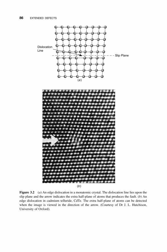
Figure 3.2 (a) An edge dislocation in a monatomic crystal. The dislocation line lies upon theslip plane and the arrow indicates the extra half-plane of atoms that produces the fault. (b) Anedge dislocation in cadmium telluride, CdTe. The extra half-plane of atoms can be detectedwhen the image is viewed in the direction of the arrow. (Courtesy of Dr J. L. Hutchison,University of Oxford).
86 EXTENDED DEFECTS
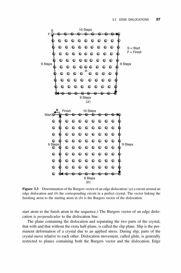
start atom to the finish atom in the sequence.) The Burgers vector of an edge dislo-cation is perpendicular to the dislocation line.
The plane containing the dislocation and separating the two parts of the crystal,that with and that without the extra half-plane, is called the slip plane. Slip is the per-manent deformation of a crystal due to an applied stress. During slip, parts of thecrystal move relative to each other. Dislocation movement, called glide, is generallyrestricted to planes containing both the Burgers vector and the dislocation. Edge
Figure 3.3 Determination of the Burgers vector of an edge dislocation: (a) a circuit around anedge dislocation and (b) the corresponding circuit in a perfect crystal. The vector linking thefinishing atom to the starting atom in (b) is the Burgers vector of the dislocation.
3.2 EDGE DISLOCATIONS 87
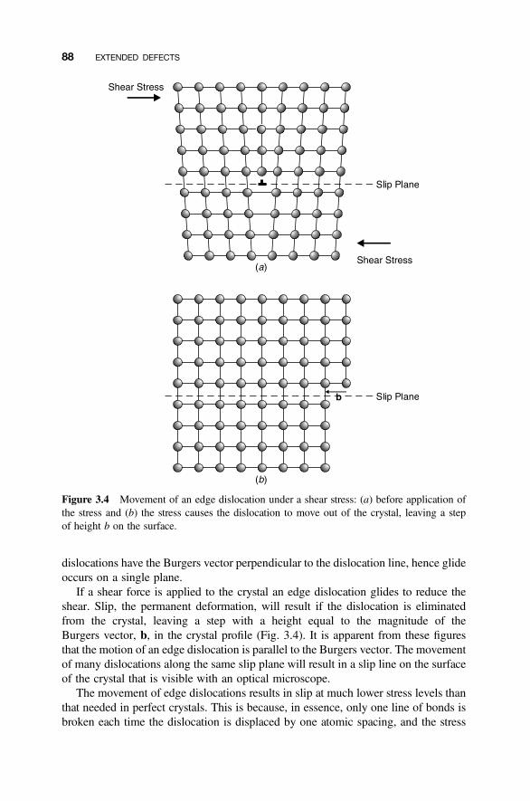
dislocations have the Burgers vector perpendicular to the dislocation line, hence glideoccurs on a single plane.
If a shear force is applied to the crystal an edge dislocation glides to reduce theshear. Slip, the permanent deformation, will result if the dislocation is eliminatedfrom the crystal, leaving a step with a height equal to the magnitude of theBurgers vector, b, in the crystal profile (Fig. 3.4). It is apparent from these figuresthat the motion of an edge dislocation is parallel to the Burgers vector. The movementof many dislocations along the same slip plane will result in a slip line on the surfaceof the crystal that is visible with an optical microscope.
The movement of edge dislocations results in slip at much lower stress levels thanthat needed in perfect crystals. This is because, in essence, only one line of bonds isbroken each time the dislocation is displaced by one atomic spacing, and the stress
Figure 3.4 Movement of an edge dislocation under a shear stress: (a) before application ofthe stress and (b) the stress causes the dislocation to move out of the crystal, leaving a stepof height b on the surface.
88 EXTENDED DEFECTS
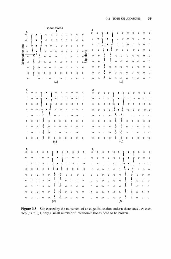
Figure 3.5 Slip caused by the movement of an edge dislocation under a shear stress. At eachstep (a) to ( j), only a small number of interatomic bonds need to be broken.
3.2 EDGE DISLOCATIONS 89
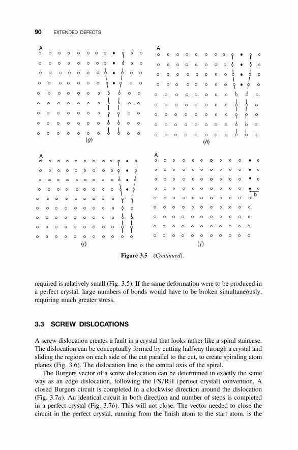
required is relatively small (Fig. 3.5). If the same deformation were to be produced ina perfect crystal, large numbers of bonds would have to be broken simultaneously,requiring much greater stress.
3.3 SCREW DISLOCATIONS
A screw dislocation creates a fault in a crystal that looks rather like a spiral staircase.The dislocation can be conceptually formed by cutting halfway through a crystal andsliding the regions on each side of the cut parallel to the cut, to create spiraling atomplanes (Fig. 3.6). The dislocation line is the central axis of the spiral.
The Burgers vector of a screw dislocation can be determined in exactly the sameway as an edge dislocation, following the FS/RH (perfect crystal) convention. Aclosed Burgers circuit is completed in a clockwise direction around the dislocation(Fig. 3.7a). An identical circuit in both direction and number of steps is completedin a perfect crystal (Fig. 3.7b). This will not close. The vector needed to close thecircuit in the perfect crystal, running from the finish atom to the start atom, is the
Figure 3.5 (Continued).
90 EXTENDED DEFECTS
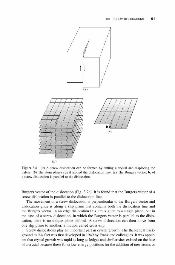
Burgers vector of the dislocation (Fig. 3.7c). It is found that the Burgers vector of ascrew dislocation is parallel to the dislocation line.
The movement of a screw dislocation is perpendicular to the Burgers vector anddislocation glide is along a slip plane that contains both the dislocation line andthe Burgers vector. In an edge dislocation this limits glide to a single plane, but inthe case of a screw dislocation, in which the Burgers vector is parallel to the dislo-cation, there is no unique plane defined. A screw dislocation can then move fromone slip plane to another, a motion called cross-slip.
Screw dislocations play an important part in crystal growth. The theoretical back-ground to this fact was first developed in 1949 by Frank and colleagues. It was appar-ent that crystal growth was rapid as long as ledges and similar sites existed on the faceof a crystal because these form low-energy positions for the addition of new atoms or
Figure 3.6 (a) A screw dislocation can be formed by cutting a crystal and displacing thehalves. (b) The atom planes spiral around the dislocation line. (c) The Burgers vector, b, ofa screw dislocation is parallel to the dislocation.
3.3 SCREW DISLOCATIONS 91
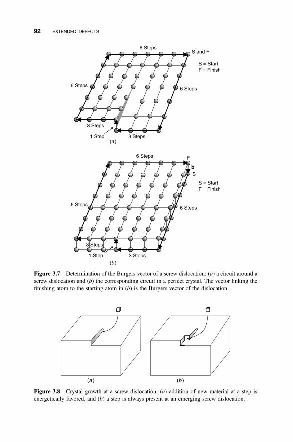
Figure 3.7 Determination of the Burgers vector of a screw dislocation: (a) a circuit around ascrew dislocation and (b) the corresponding circuit in a perfect crystal. The vector linking thefinishing atom to the starting atom in (b) is the Burgers vector of the dislocation.
Figure 3.8 Crystal growth at a screw dislocation: (a) addition of new material at a step isenergetically favored, and (b) a step is always present at an emerging screw dislocation.
92 EXTENDED DEFECTS
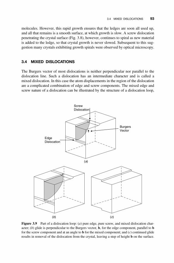
molecules. However, this rapid growth ensures that the ledges are soon all used up,and all that remains is a smooth surface, at which growth is slow. A screw dislocationpenetrating the crystal surface (Fig. 3.8), however, continues to spiral as new materialis added to the ledge, so that crystal growth is never slowed. Subsequent to this sug-gestion many crystals exhibiting growth spirals were observed by optical microscopy.
3.4 MIXED DISLOCATIONS
The Burgers vector of most dislocations is neither perpendicular nor parallel to thedislocation line. Such a dislocation has an intermediate character and is called amixed dislocation. In this case the atom displacements in the region of the dislocationare a complicated combination of edge and screw components. The mixed edge andscrew nature of a dislocation can be illustrated by the structure of a dislocation loop,
Figure 3.9 Part of a dislocation loop: (a) pure edge, pure screw, and mixed dislocation char-acter; (b) glide is perpendicular to the Burgers vector, b, for the edge component, parallel to bfor the screw component and at an angle to b for the mixed component; and (c) continued glideresults in removal of the dislocation from the crystal, leaving a step of height b on the surface.
3.4 MIXED DISLOCATIONS 93
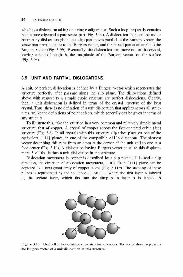
which is a dislocation taking on a ring configuration. Such a loop frequently containsboth a pure edge and a pure screw part (Fig. 3.9a). A dislocation loop can expand orcontract by dislocation glide, the edge part moves parallel to the Burgers vector, thescrew part perpendicular to the Burgers vector, and the mixed part at an angle to theBurgers vector (Fig. 3.9b). Eventually, the dislocation can move out of the crystal,leaving a step of height b, the magnitude of the Burgers vector, on the surface(Fig. 3.9c).
3.5 UNIT AND PARTIAL DISLOCATIONS
A unit, or perfect, dislocation is defined by a Burgers vector which regenerates thestructure perfectly after passage along the slip plane. The dislocations definedabove with respect to a simple cubic structure are perfect dislocations. Clearly,then, a unit dislocation is defined in terms of the crystal structure of the hostcrystal. Thus, there is no definition of a unit dislocation that applies across all struc-tures, unlike the definitions of point defects, which generally can be given in terms ofany structure.
To illustrate this, take the situation in a very common and relatively simple metalstructure, that of copper. A crystal of copper adopts the face-centered cubic (fcc)structure (Fig. 2.8). In all crystals with this structure slip takes place on one of theequivalent f111g planes, in one of the compatible <110> directions. The shortestvector describing this runs from an atom at the corner of the unit cell to one at aface center (Fig. 3.10). A dislocation having Burgers vector equal to this displace-ment, 1
2 <110>, is thus a unit dislocation in the structure.Dislocation movement in copper is described by a slip plane f111g and a slip
direction, the direction of dislocation movement, [110]. Each f111g plane can bedepicted as a hexagonal array of copper atoms (Fig. 3.11a). The stacking of theseplanes is represented by the sequence . . . ABC . . . where the first layer is labeledA, the second layer, which fits into the dimples in layer A is labeled B
Figure 3.10 Unit cell of face-centered cubic structure of copper. The vector shown representsthe Burgers vector of a unit dislocation in this structure.
94 EXTENDED DEFECTS
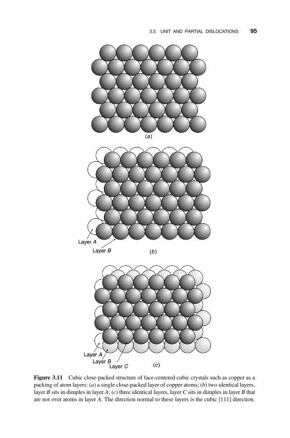
Figure 3.11 Cubic close-packed structure of face-centered cubic crystals such as copper as apacking of atom layers: (a) a single close-packed layer of copper atoms; (b) two identical layers,layer B sits in dimples in layer A; (c) three identical layers, layer C sits in dimples in layer B thatare not over atoms in layer A. The direction normal to these layers is the cubic [111] direction.
3.5 UNIT AND PARTIAL DISLOCATIONS 95
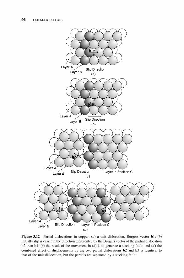
Figure 3.12 Partial dislocations in copper: (a) a unit dislocation, Burgers vector b1; (b)initially slip is easier in the direction represented by the Burgers vector of the partial dislocationb2 than b1; (c) the result of the movement in (b) is to generate a stacking fault; and (d ) thecombined effect of displacements by the two partial dislocations b2 and b3 is identical tothat of the unit dislocation, but the partials are separated by a stacking fault.
96 EXTENDED DEFECTS
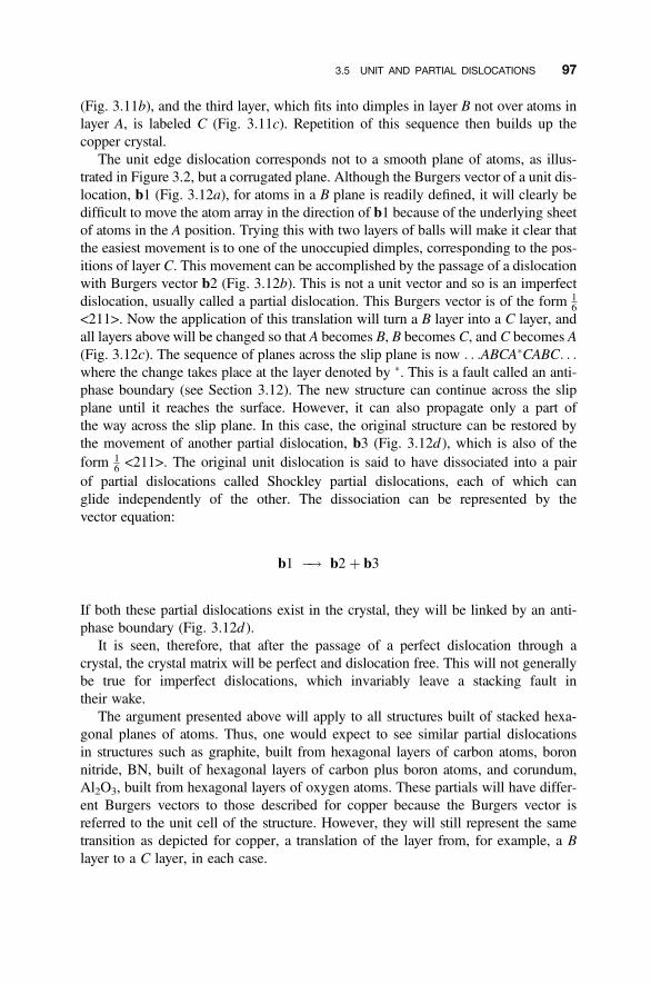
(Fig. 3.11b), and the third layer, which fits into dimples in layer B not over atoms inlayer A, is labeled C (Fig. 3.11c). Repetition of this sequence then builds up thecopper crystal.
The unit edge dislocation corresponds not to a smooth plane of atoms, as illus-trated in Figure 3.2, but a corrugated plane. Although the Burgers vector of a unit dis-location, b1 (Fig. 3.12a), for atoms in a B plane is readily defined, it will clearly bedifficult to move the atom array in the direction of b1 because of the underlying sheetof atoms in the A position. Trying this with two layers of balls will make it clear thatthe easiest movement is to one of the unoccupied dimples, corresponding to the pos-itions of layer C. This movement can be accomplished by the passage of a dislocationwith Burgers vector b2 (Fig. 3.12b). This is not a unit vector and so is an imperfectdislocation, usually called a partial dislocation. This Burgers vector is of the form 1
6<211>. Now the application of this translation will turn a B layer into a C layer, andall layers above will be changed so that A becomes B, B becomes C, and C becomes A(Fig. 3.12c). The sequence of planes across the slip plane is now . . .ABCA�CABC. . .where the change takes place at the layer denoted by �. This is a fault called an anti-phase boundary (see Section 3.12). The new structure can continue across the slipplane until it reaches the surface. However, it can also propagate only a part ofthe way across the slip plane. In this case, the original structure can be restored bythe movement of another partial dislocation, b3 (Fig. 3.12d ), which is also of theform 1
6 <211>. The original unit dislocation is said to have dissociated into a pairof partial dislocations called Shockley partial dislocations, each of which canglide independently of the other. The dissociation can be represented by thevector equation:
b1 �! b2þ b3
If both these partial dislocations exist in the crystal, they will be linked by an anti-phase boundary (Fig. 3.12d ).
It is seen, therefore, that after the passage of a perfect dislocation through acrystal, the crystal matrix will be perfect and dislocation free. This will not generallybe true for imperfect dislocations, which invariably leave a stacking fault intheir wake.
The argument presented above will apply to all structures built of stacked hexa-gonal planes of atoms. Thus, one would expect to see similar partial dislocationsin structures such as graphite, built from hexagonal layers of carbon atoms, boronnitride, BN, built of hexagonal layers of carbon plus boron atoms, and corundum,Al2O3, built from hexagonal layers of oxygen atoms. These partials will have differ-ent Burgers vectors to those described for copper because the Burgers vector isreferred to the unit cell of the structure. However, they will still represent the sametransition as depicted for copper, a translation of the layer from, for example, a Blayer to a C layer, in each case.
3.5 UNIT AND PARTIAL DISLOCATIONS 97
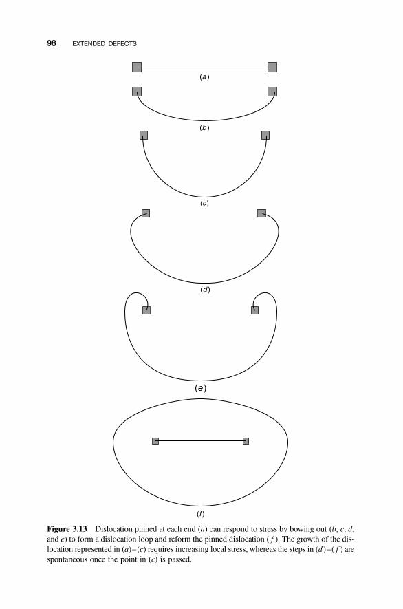
Figure 3.13 Dislocation pinned at each end (a) can respond to stress by bowing out (b, c, d,and e) to form a dislocation loop and reform the pinned dislocation ( f ). The growth of the dis-location represented in (a)–(c) requires increasing local stress, whereas the steps in (d )–( f ) arespontaneous once the point in (c) is passed.
98 EXTENDED DEFECTS
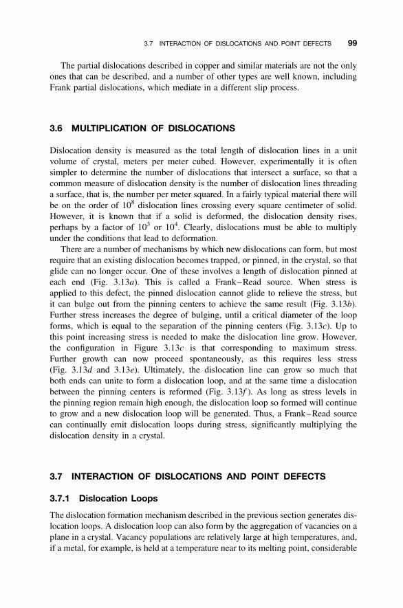
The partial dislocations described in copper and similar materials are not the onlyones that can be described, and a number of other types are well known, includingFrank partial dislocations, which mediate in a different slip process.
3.6 MULTIPLICATION OF DISLOCATIONS
Dislocation density is measured as the total length of dislocation lines in a unitvolume of crystal, meters per meter cubed. However, experimentally it is oftensimpler to determine the number of dislocations that intersect a surface, so that acommon measure of dislocation density is the number of dislocation lines threadinga surface, that is, the number per meter squared. In a fairly typical material there willbe on the order of 108 dislocation lines crossing every square centimeter of solid.However, it is known that if a solid is deformed, the dislocation density rises,perhaps by a factor of 103 or 104. Clearly, dislocations must be able to multiplyunder the conditions that lead to deformation.
There are a number of mechanisms by which new dislocations can form, but mostrequire that an existing dislocation becomes trapped, or pinned, in the crystal, so thatglide can no longer occur. One of these involves a length of dislocation pinned ateach end (Fig. 3.13a). This is called a Frank–Read source. When stress isapplied to this defect, the pinned dislocation cannot glide to relieve the stress, butit can bulge out from the pinning centers to achieve the same result (Fig. 3.13b).Further stress increases the degree of bulging, until a critical diameter of the loopforms, which is equal to the separation of the pinning centers (Fig. 3.13c). Up tothis point increasing stress is needed to make the dislocation line grow. However,the configuration in Figure 3.13c is that corresponding to maximum stress.Further growth can now proceed spontaneously, as this requires less stress(Fig. 3.13d and 3.13e). Ultimately, the dislocation line can grow so much thatboth ends can unite to form a dislocation loop, and at the same time a dislocationbetween the pinning centers is reformed (Fig. 3.13f ). As long as stress levels inthe pinning region remain high enough, the dislocation loop so formed will continueto grow and a new dislocation loop will be generated. Thus, a Frank–Read sourcecan continually emit dislocation loops during stress, significantly multiplying thedislocation density in a crystal.
3.7 INTERACTION OF DISLOCATIONS AND POINT DEFECTS
3.7.1 Dislocation Loops
The dislocation formation mechanism described in the previous section generates dis-location loops. A dislocation loop can also form by the aggregation of vacancies on aplane in a crystal. Vacancy populations are relatively large at high temperatures, and,if a metal, for example, is held at a temperature near to its melting point, considerable
3.7 INTERACTION OF DISLOCATIONS AND POINT DEFECTS 99
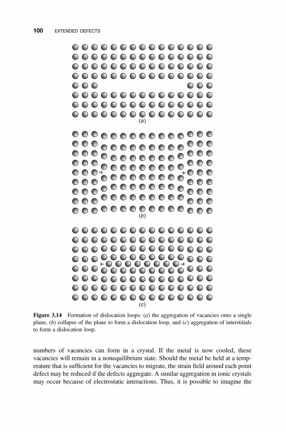
numbers of vacancies can form in a crystal. If the metal is now cooled, thesevacancies will remain in a nonequilibrium state. Should the metal be held at a temp-erature that is sufficient for the vacancies to migrate, the strain field around each pointdefect may be reduced if the defects aggregate. A similar aggregation in ionic crystalsmay occur because of electrostatic interactions. Thus, it is possible to imagine the
Figure 3.14 Formation of dislocation loops: (a) the aggregation of vacancies onto a singleplane, (b) collapse of the plane to form a dislocation loop, and (c) aggregation of interstitialsto form a dislocation loop.
100 EXTENDED DEFECTS
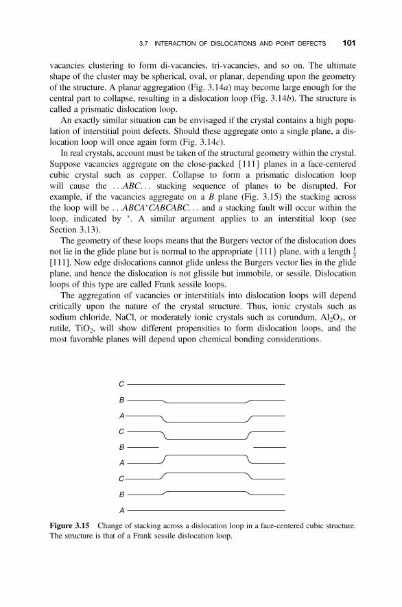
vacancies clustering to form di-vacancies, tri-vacancies, and so on. The ultimateshape of the cluster may be spherical, oval, or planar, depending upon the geometryof the structure. A planar aggregation (Fig. 3.14a) may become large enough for thecentral part to collapse, resulting in a dislocation loop (Fig. 3.14b). The structure iscalled a prismatic dislocation loop.
An exactly similar situation can be envisaged if the crystal contains a high popu-lation of interstitial point defects. Should these aggregate onto a single plane, a dis-location loop will once again form (Fig. 3.14c).
In real crystals, account must be taken of the structural geometry within the crystal.Suppose vacancies aggregate on the close-packed f111g planes in a face-centeredcubic crystal such as copper. Collapse to form a prismatic dislocation loopwill cause the . . .ABC. . . stacking sequence of planes to be disrupted. Forexample, if the vacancies aggregate on a B plane (Fig. 3.15) the stacking acrossthe loop will be . . .ABCA�CABCABC. . . and a stacking fault will occur within theloop, indicated by �. A similar argument applies to an interstitial loop (seeSection 3.13).
The geometry of these loops means that the Burgers vector of the dislocation doesnot lie in the glide plane but is normal to the appropriate f111g plane, with a length 1
3[111]. Now edge dislocations cannot glide unless the Burgers vector lies in the glideplane, and hence the dislocation is not glissile but immobile, or sessile. Dislocationloops of this type are called Frank sessile loops.
The aggregation of vacancies or interstitials into dislocation loops will dependcritically upon the nature of the crystal structure. Thus, ionic crystals such assodium chloride, NaCl, or moderately ionic crystals such as corundum, Al2O3, orrutile, TiO2, will show different propensities to form dislocation loops, and themost favorable planes will depend upon chemical bonding considerations.
Figure 3.15 Change of stacking across a dislocation loop in a face-centered cubic structure.The structure is that of a Frank sessile dislocation loop.
3.7 INTERACTION OF DISLOCATIONS AND POINT DEFECTS 101
3.7.2 Dislocation Climb
The edge dislocations bounding the dislocation loops just described cannot glide, butnevertheless the loop can grow by the continued collection of vacancies or intersti-tials. This method of movement of an edge dislocation, which allows edge
Figure 3.16 Edge dislocation climb: (a) an edge dislocation before climb, (b) the start ofclimb by vacancy aggregation on the dislocation, and (c) the start of climb by interstitial aggre-gation on the dislocation.
102 EXTENDED DEFECTS
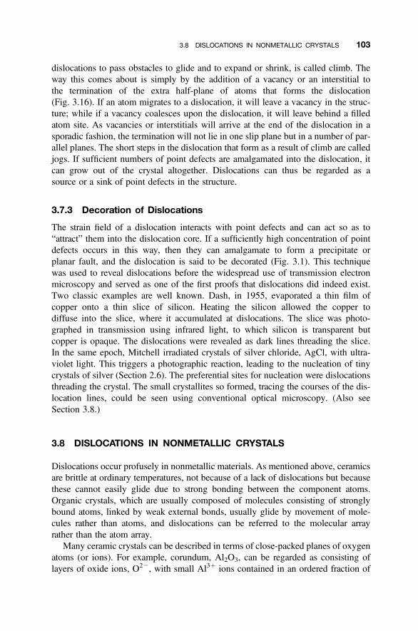
dislocations to pass obstacles to glide and to expand or shrink, is called climb. Theway this comes about is simply by the addition of a vacancy or an interstitial tothe termination of the extra half-plane of atoms that forms the dislocation(Fig. 3.16). If an atom migrates to a dislocation, it will leave a vacancy in the struc-ture; while if a vacancy coalesces upon the dislocation, it will leave behind a filledatom site. As vacancies or interstitials will arrive at the end of the dislocation in asporadic fashion, the termination will not lie in one slip plane but in a number of par-allel planes. The short steps in the dislocation that form as a result of climb are calledjogs. If sufficient numbers of point defects are amalgamated into the dislocation, itcan grow out of the crystal altogether. Dislocations can thus be regarded as asource or a sink of point defects in the structure.
3.7.3 Decoration of Dislocations
The strain field of a dislocation interacts with point defects and can act so as to“attract” them into the dislocation core. If a sufficiently high concentration of pointdefects occurs in this way, then they can amalgamate to form a precipitate orplanar fault, and the dislocation is said to be decorated (Fig. 3.1). This techniquewas used to reveal dislocations before the widespread use of transmission electronmicroscopy and served as one of the first proofs that dislocations did indeed exist.Two classic examples are well known. Dash, in 1955, evaporated a thin film ofcopper onto a thin slice of silicon. Heating the silicon allowed the copper todiffuse into the slice, where it accumulated at dislocations. The slice was photo-graphed in transmission using infrared light, to which silicon is transparent butcopper is opaque. The dislocations were revealed as dark lines threading the slice.In the same epoch, Mitchell irradiated crystals of silver chloride, AgCl, with ultra-violet light. This triggers a photographic reaction, leading to the nucleation of tinycrystals of silver (Section 2.6). The preferential sites for nucleation were dislocationsthreading the crystal. The small crystallites so formed, tracing the courses of the dis-location lines, could be seen using conventional optical microscopy. (Also seeSection 3.8.)
3.8 DISLOCATIONS IN NONMETALLIC CRYSTALS
Dislocations occur profusely in nonmetallic materials. As mentioned above, ceramicsare brittle at ordinary temperatures, not because of a lack of dislocations but becausethese cannot easily glide due to strong bonding between the component atoms.Organic crystals, which are usually composed of molecules consisting of stronglybound atoms, linked by weak external bonds, usually glide by movement of mole-cules rather than atoms, and dislocations can be referred to the molecular arrayrather than the atom array.
Many ceramic crystals can be described in terms of close-packed planes of oxygenatoms (or ions). For example, corundum, Al2O3, can be regarded as consisting oflayers of oxide ions, O22, with small Al3þ ions contained in an ordered fraction of
3.8 DISLOCATIONS IN NONMETALLIC CRYSTALS 103
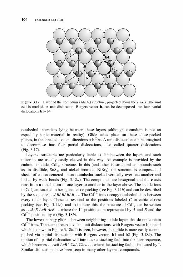
octahedral interstices lying between these layers (although corundum is not anespecially ionic material in reality). Glide takes place on these close-packedplanes, in the three equivalent directions <10l0>. A unit dislocation can be imaginedto decompose into four partial dislocations, also called quarter dislocations(Fig. 3.17).
Layered structures are particularly liable to slip between the layers, and suchmaterials are usually easily cleaved in this way. An example is provided by thecadmium iodide, CdI2, structure. In this (and other isostructural compounds suchas tin disulfide, SnS2, and nickel bromide, NiBr2), the structure is composed ofsheets of cation centered anion ocatahedra stacked vertically over one another andlinked by weak bonds (Fig. 3.18a). The compounds are hexagonal and the c axisruns from a metal atom in one layer to another in the layer above. The iodide ionsin CdI2 are stacked in hexagonal close packing (see Fig. 3.11b) and can be describedby the sequence . . .ABABABAB. . .. The Cd2þ ions occupy octahedral sites betweenevery other layer. These correspond to the positions labeled C in cubic closestpacking (see Fig. 3.11c), and to indicate this, the structure of CdI2 can be writtenas . . .AcB AcB AcB. . . where the I2 positions are represented by A and B and theCd2þ positions by c (Fig. 3.18b).
The lowest energy glide is between neighboring iodide layers that do not containCd2þ ions. There are three equivalent unit dislocations, with Burgers vector b, one ofwhich is drawn in Figure 3.18b. It is seen, however, that glide is more easily accom-plished via partial dislocations with Burgers vectors b1 and b2 (Fig. 3.18b). Themotion of a partial dislocation will introduce a stacking fault into the later sequence,which becomes . . .AcB AcB � CbACbA. . . , where the stacking fault is indicated by �.Similar dislocations have been seen in many other layered compounds.
Figure 3.17 Layer of the corundum (Al2O3) structure, projected down the c axis. The unitcell is marked. A unit dislocation, Burgers vector b, can be decomposed into four partialdislocations b1–b4.
104 EXTENDED DEFECTS
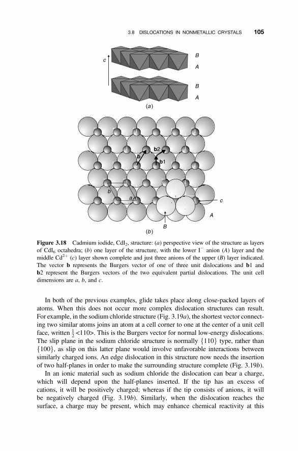
In both of the previous examples, glide takes place along close-packed layers ofatoms. When this does not occur more complex dislocation structures can result.For example, in the sodium chloride structure (Fig. 3.19a), the shortest vector connect-ing two similar atoms joins an atom at a cell corner to one at the center of a unit cellface, written 1
2 <110>. This is the Burgers vector for normal low-energy dislocations.The slip plane in the sodium chloride structure is normally f110g type, rather thanf100g, as slip on this latter plane would involve unfavorable interactions betweensimilarly charged ions. An edge dislocation in this structure now needs the insertionof two half-planes in order to make the surrounding structure complete (Fig. 3.19b).
In an ionic material such as sodium chloride the dislocation can bear a charge,which will depend upon the half-planes inserted. If the tip has an excess ofcations, it will be positively charged; whereas if the tip consists of anions, it willbe negatively charged (Fig. 3.19b). Similarly, when the dislocation reaches thesurface, a charge may be present, which may enhance chemical reactivity at this
Figure 3.18 Cadmium iodide, CdI2, structure: (a) perspective view of the structure as layersof CdI6 octahedra; (b) one layer of the structure, with the lower I2 anion (A) layer and themiddle Cd2þ (c) layer shown complete and just three anions of the upper (B) layer indicated.The vector b represents the Burgers vector of one of three unit dislocations and b1 andb2 represent the Burgers vectors of the two equivalent partial dislocations. The unit celldimensions are a, b, and c.
3.8 DISLOCATIONS IN NONMETALLIC CRYSTALS 105
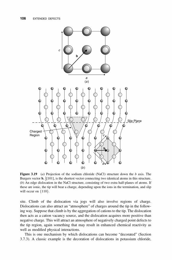
site. Climb of the dislocation via jogs will also involve regions of charge.Dislocations can also attract an “atmosphere” of charges around the tip in the follow-ing way. Suppose that climb is by the aggregation of cations to the tip. The dislocationthen acts as a cation vacancy source, and the dislocation acquires more positive thannegative charge. This will attract an atmosphere of negatively charged point defects tothe tip region, again something that may result in enhanced chemical reactivity aswell as modified physical interactions.
This is one mechanism by which dislocations can become “decorated” (Section3.7.3). A classic example is the decoration of dislocations in potassium chloride,
Figure 3.19 (a) Projection of the sodium chloride (NaCl) structure down the b axis. TheBurgers vector b, 12[101], is the shortest vector connecting two identical atoms in this structure.(b) An edge dislocation in the NaCl structure, consisting of two extra half-planes of atoms. Ifthese are ionic, the tip will bear a charge, depending upon the ions in the termination, and slipwill occur on f110g.
106 EXTENDED DEFECTS
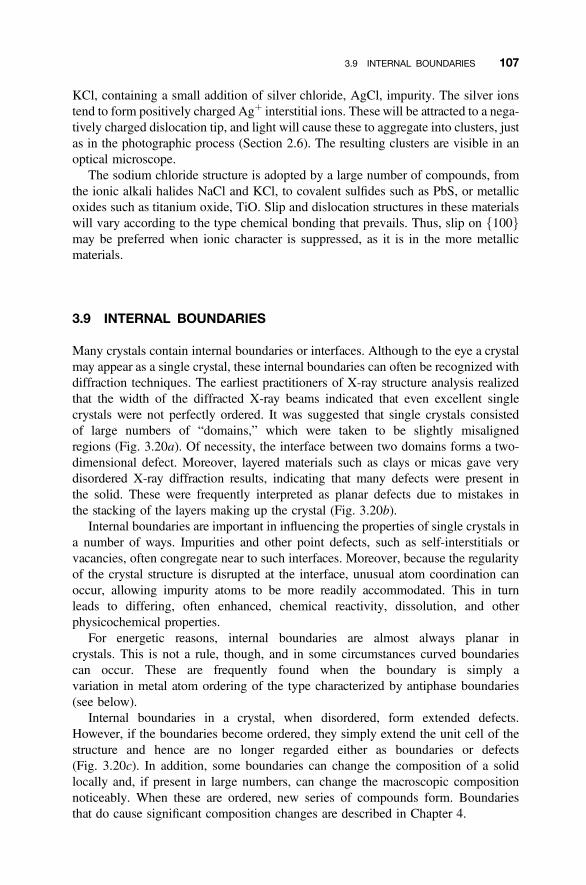
KCl, containing a small addition of silver chloride, AgCl, impurity. The silver ionstend to form positively charged Agþ interstitial ions. These will be attracted to a nega-tively charged dislocation tip, and light will cause these to aggregate into clusters, justas in the photographic process (Section 2.6). The resulting clusters are visible in anoptical microscope.
The sodium chloride structure is adopted by a large number of compounds, fromthe ionic alkali halides NaCl and KCl, to covalent sulfides such as PbS, or metallicoxides such as titanium oxide, TiO. Slip and dislocation structures in these materialswill vary according to the type chemical bonding that prevails. Thus, slip on f100gmay be preferred when ionic character is suppressed, as it is in the more metallicmaterials.
3.9 INTERNAL BOUNDARIES
Many crystals contain internal boundaries or interfaces. Although to the eye a crystalmay appear as a single crystal, these internal boundaries can often be recognized withdiffraction techniques. The earliest practitioners of X-ray structure analysis realizedthat the width of the diffracted X-ray beams indicated that even excellent singlecrystals were not perfectly ordered. It was suggested that single crystals consistedof large numbers of “domains,” which were taken to be slightly misalignedregions (Fig. 3.20a). Of necessity, the interface between two domains forms a two-dimensional defect. Moreover, layered materials such as clays or micas gave verydisordered X-ray diffraction results, indicating that many defects were present inthe solid. These were frequently interpreted as planar defects due to mistakes inthe stacking of the layers making up the crystal (Fig. 3.20b).
Internal boundaries are important in influencing the properties of single crystals ina number of ways. Impurities and other point defects, such as self-interstitials orvacancies, often congregate near to such interfaces. Moreover, because the regularityof the crystal structure is disrupted at the interface, unusual atom coordination canoccur, allowing impurity atoms to be more readily accommodated. This in turnleads to differing, often enhanced, chemical reactivity, dissolution, and otherphysicochemical properties.
For energetic reasons, internal boundaries are almost always planar incrystals. This is not a rule, though, and in some circumstances curved boundariescan occur. These are frequently found when the boundary is simply avariation in metal atom ordering of the type characterized by antiphase boundaries(see below).
Internal boundaries in a crystal, when disordered, form extended defects.However, if the boundaries become ordered, they simply extend the unit cell of thestructure and hence are no longer regarded either as boundaries or defects(Fig. 3.20c). In addition, some boundaries can change the composition of a solidlocally and, if present in large numbers, can change the macroscopic compositionnoticeably. When these are ordered, new series of compounds form. Boundariesthat do cause significant composition changes are described in Chapter 4.
3.9 INTERNAL BOUNDARIES 107

3.10 LOW-ANGLE GRAIN BOUNDARIES
As remarked in the previous section, single crystals are not perfect but are built ofdomains of material that are slightly mismatched. The interfaces between theseregions are called low-angle or small-angle grain boundaries. These boundariesconsist of an array of dislocations arranged so as to remove the misfit between the
Figure 3.20 Planar defects in solids: (a) boundaries between slightly misaligned regions ordomains; (b) stacking mistakes in solids built of layers, such as the micas or clays; (c) “orderedplanar faults” assimilated into a crystal to give a new structure and unit cell (shaded).
108 EXTENDED DEFECTS
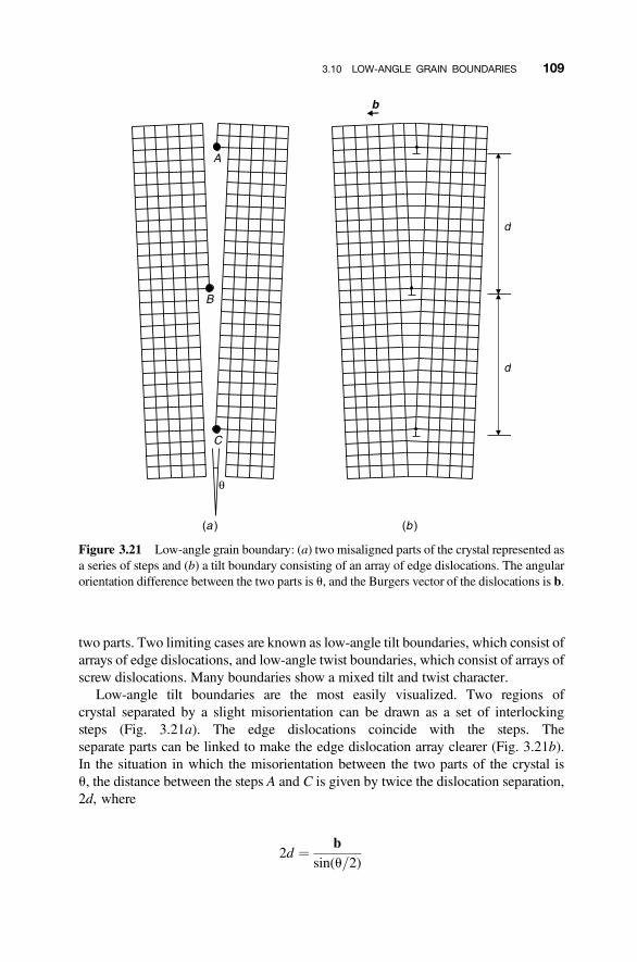
two parts. Two limiting cases are known as low-angle tilt boundaries, which consist ofarrays of edge dislocations, and low-angle twist boundaries, which consist of arrays ofscrew dislocations. Many boundaries show a mixed tilt and twist character.
Low-angle tilt boundaries are the most easily visualized. Two regions ofcrystal separated by a slight misorientation can be drawn as a set of interlockingsteps (Fig. 3.21a). The edge dislocations coincide with the steps. Theseparate parts can be linked to make the edge dislocation array clearer (Fig. 3.21b).In the situation in which the misorientation between the two parts of the crystal isu, the distance between the steps A and C is given by twice the dislocation separation,2d, where
2d ¼ bsin(u=2)
Figure 3.21 Low-angle grain boundary: (a) two misaligned parts of the crystal represented asa series of steps and (b) a tilt boundary consisting of an array of edge dislocations. The angularorientation difference between the two parts is u, and the Burgers vector of the dislocations is b.
3.10 LOW-ANGLE GRAIN BOUNDARIES 109
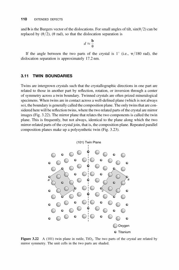
and b is the Burgers vector of the dislocations. For small angles of tilt, sin(u/2) can bereplaced by (u/2), (u rad), so that the dislocation separation is
d � bu
If the angle between the two parts of the crystal is 18 (i.e., p/180 rad), thedislocation separation is approximately 17.2 nm.
3.11 TWIN BOUNDARIES
Twins are intergrown crystals such that the crystallographic directions in one part arerelated to those in another part by reflection, rotation, or inversion through a centerof symmetry across a twin boundary. Twinned crystals are often prized mineralogicalspecimens. When twins are in contact across a well-defined plane (which is not alwaysso), the boundary is generally called the composition plane. The only twins that are con-sidered herewill be reflection twins, where the two related parts of the crystal are mirrorimages (Fig. 3.22). The mirror plane that relates the two components is called the twinplane. This is frequently, but not always, identical to the plane along which the twomirror-related parts of the crystal join, that is, the composition plane. Repeated parallelcomposition planes make up a polysynthetic twin (Fig. 3.23).
Figure 3.22 A (101) twin plane in rutile, TiO2. The two parts of the crystal are related bymirror symmetry. The unit cells in the two parts are shaded.
110 EXTENDED DEFECTS
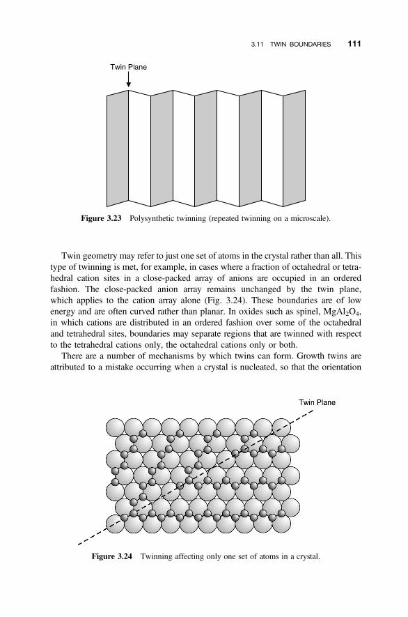
Twin geometry may refer to just one set of atoms in the crystal rather than all. Thistype of twinning is met, for example, in cases where a fraction of octahedral or tetra-hedral cation sites in a close-packed array of anions are occupied in an orderedfashion. The close-packed anion array remains unchanged by the twin plane,which applies to the cation array alone (Fig. 3.24). These boundaries are of lowenergy and are often curved rather than planar. In oxides such as spinel, MgAl2O4,in which cations are distributed in an ordered fashion over some of the octahedraland tetrahedral sites, boundaries may separate regions that are twinned with respectto the tetrahedral cations only, the octahedral cations only or both.
There are a number of mechanisms by which twins can form. Growth twins areattributed to a mistake occurring when a crystal is nucleated, so that the orientation
Figure 3.23 Polysynthetic twinning (repeated twinning on a microscale).
Figure 3.24 Twinning affecting only one set of atoms in a crystal.
3.11 TWIN BOUNDARIES 111
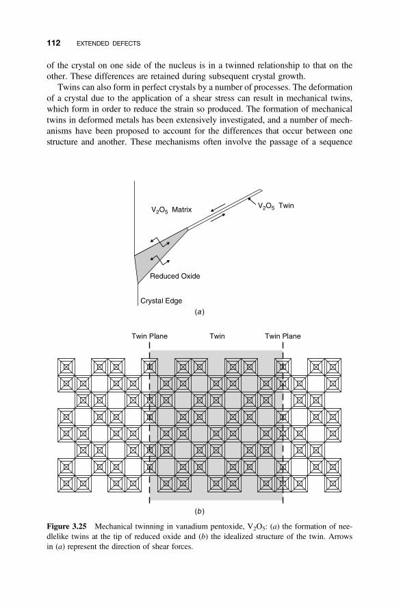
of the crystal on one side of the nucleus is in a twinned relationship to that on theother. These differences are retained during subsequent crystal growth.
Twins can also form in perfect crystals by a number of processes. The deformationof a crystal due to the application of a shear stress can result in mechanical twins,which form in order to reduce the strain so produced. The formation of mechanicaltwins in deformed metals has been extensively investigated, and a number of mech-anisms have been proposed to account for the differences that occur between onestructure and another. These mechanisms often involve the passage of a sequence
Figure 3.25 Mechanical twinning in vanadium pentoxide, V2O5: (a) the formation of nee-dlelike twins at the tip of reduced oxide and (b) the idealized structure of the twin. Arrowsin (a) represent the direction of shear forces.
112 EXTENDED DEFECTS
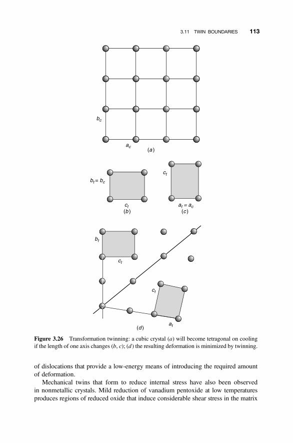
of dislocations that provide a low-energy means of introducing the required amountof deformation.
Mechanical twins that form to reduce internal stress have also been observedin nonmetallic crystals. Mild reduction of vanadium pentoxide at low temperaturesproduces regions of reduced oxide that induce considerable shear stress in the matrix
Figure 3.26 Transformation twinning: a cubic crystal (a) will become tetragonal on coolingif the length of one axis changes (b, c); (d ) the resulting deformation is minimized by twinning.
3.11 TWIN BOUNDARIES 113
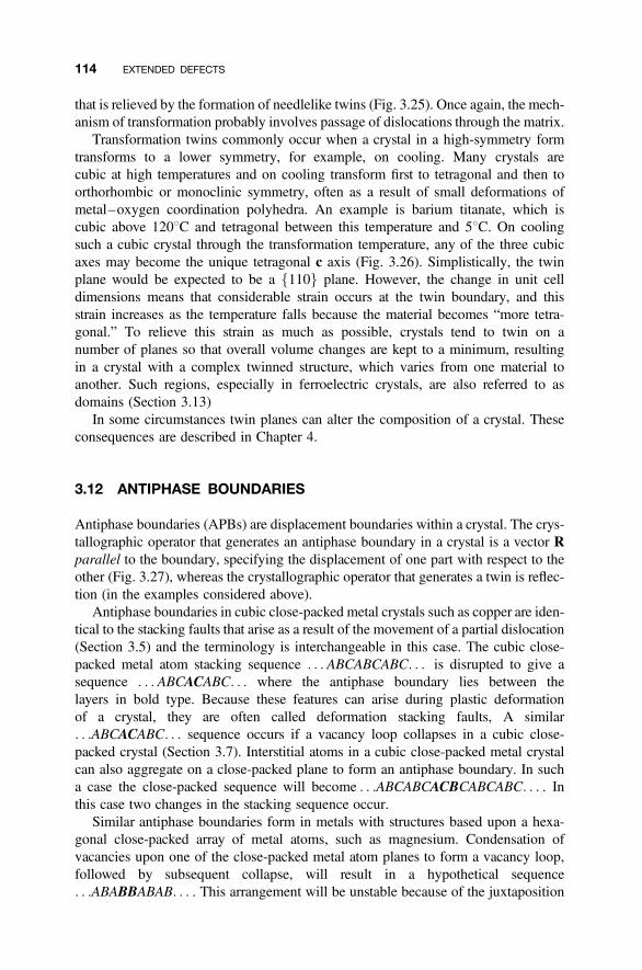
that is relieved by the formation of needlelike twins (Fig. 3.25). Once again, the mech-anism of transformation probably involves passage of dislocations through the matrix.
Transformation twins commonly occur when a crystal in a high-symmetry formtransforms to a lower symmetry, for example, on cooling. Many crystals arecubic at high temperatures and on cooling transform first to tetragonal and then toorthorhombic or monoclinic symmetry, often as a result of small deformations ofmetal–oxygen coordination polyhedra. An example is barium titanate, which iscubic above 1208C and tetragonal between this temperature and 58C. On coolingsuch a cubic crystal through the transformation temperature, any of the three cubicaxes may become the unique tetragonal c axis (Fig. 3.26). Simplistically, the twinplane would be expected to be a f110g plane. However, the change in unit celldimensions means that considerable strain occurs at the twin boundary, and thisstrain increases as the temperature falls because the material becomes “more tetra-gonal.” To relieve this strain as much as possible, crystals tend to twin on anumber of planes so that overall volume changes are kept to a minimum, resultingin a crystal with a complex twinned structure, which varies from one material toanother. Such regions, especially in ferroelectric crystals, are also referred to asdomains (Section 3.13)
In some circumstances twin planes can alter the composition of a crystal. Theseconsequences are described in Chapter 4.
3.12 ANTIPHASE BOUNDARIES
Antiphase boundaries (APBs) are displacement boundaries within a crystal. The crys-tallographic operator that generates an antiphase boundary in a crystal is a vector Rparallel to the boundary, specifying the displacement of one part with respect to theother (Fig. 3.27), whereas the crystallographic operator that generates a twin is reflec-tion (in the examples considered above).
Antiphase boundaries in cubic close-packed metal crystals such as copper are iden-tical to the stacking faults that arise as a result of the movement of a partial dislocation(Section 3.5) and the terminology is interchangeable in this case. The cubic close-packed metal atom stacking sequence . . . ABCABCABC. . . is disrupted to give asequence . . . ABCACABC. . . where the antiphase boundary lies between thelayers in bold type. Because these features can arise during plastic deformationof a crystal, they are often called deformation stacking faults, A similar. . .ABCACABC. . . sequence occurs if a vacancy loop collapses in a cubic close-packed crystal (Section 3.7). Interstitial atoms in a cubic close-packed metal crystalcan also aggregate on a close-packed plane to form an antiphase boundary. In sucha case the close-packed sequence will become . . .ABCABCACBCABCABC. . . . Inthis case two changes in the stacking sequence occur.
Similar antiphase boundaries form in metals with structures based upon a hexa-gonal close-packed array of metal atoms, such as magnesium. Condensation ofvacancies upon one of the close-packed metal atom planes to form a vacancy loop,followed by subsequent collapse, will result in a hypothetical sequence. . .ABABBABAB. . . . This arrangement will be unstable because of the juxtaposition
114 EXTENDED DEFECTS
of the two B layers. Translation of one part of the crystal by a vector parallel to thefault plane will create an antiphase boundary with the stacking sequence. . .ABABCBCB. . . . The condensation of an interstitial population on a close-packed plane will result in an initial sequence . . .ABABAABABAB. . . , which willbe unstable for a similar reason. Translation of part of the crystal by a vector parallelto the fault can give an antiphase boundary sequence . . .ABABABCBCBC. . . .
As in the case of twin planes, the antiphase relationship may affect only one part ofthe structure, for example, the cation substructure, while leaving the anion substruc-ture unchanged. This is particularly common when the anion array can be consideredto consist of a close-packed array of ions, which remains unchanged by the antiphaseboundary (Fig. 3.28).
Figure 3.27 Antiphase boundaries: (a, b) antiphase boundaries are formed when one part ofa crystal is displaced with respect to the other part by a vector parallel to the boundary.
3.12 ANTIPHASE BOUNDARIES 115
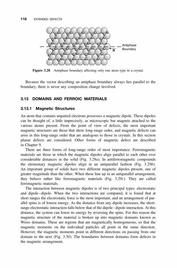
Because the vector describing an antiphase boundary always lies parallel to theboundary, there is never any composition change involved.
3.13 DOMAINS AND FERROIC MATERIALS
3.13.1 Magnetic Structures
An atom that contains unpaired electrons possesses a magnetic dipole. These dipolescan be thought of, a little imprecisely, as microscopic bar magnets attached to thevarious atoms present. From the point of view of defects, the most importantmagnetic structures are those that show long-range order, and magnetic defects canarise in this long-range order that are analogous to those in crystals. In this sectionplanar defects are considered. Other forms of magnetic defect are describedin Chapter 9.
There are three forms of long-range order of most importance. Ferromagneticmaterials are those in which the magnetic dipoles align parallel to each other overconsiderable distances in the solid (Fig. 3.29a). In antiferromagnetic compoundsthe elementary magnetic dipoles align in an antiparallel fashion (Fig. 3.29b).An important group of solids have two different magnetic dipoles present, one ofgreater magnitude than the other. When these line up in an antiparallel arrangement,they behave rather like ferromagnetic materials (Fig. 3.29c). They are calledferrimagnetic materials.
The interaction between magnetic dipoles is of two principal types: electrostaticand dipole–dipole. When the two interactions are compared, it is found that atshort ranges the electrostatic force is the most important, and an arrangement of par-allel spins is of lowest energy. As the distance from any dipole increases, the short-range electrostatic interaction falls below that of the dipole–dipole interaction. At thisdistance, the system can lower its energy by reversing the spins. For this reason themagnetic structure of the material is broken up into magnetic domains known asWeiss domains. These are regions that are magnetically homogeneous, so that themagnetic moments on the individual particles all point in the same direction.However, the magnetic moments point in different directions on passing from onedomain to the next (Fig. 3.30). The boundaries between domains form defects inthe magnetic arrangement.
Figure 3.28 Antiphase boundary affecting only one atom type in a crystal.
116 EXTENDED DEFECTS
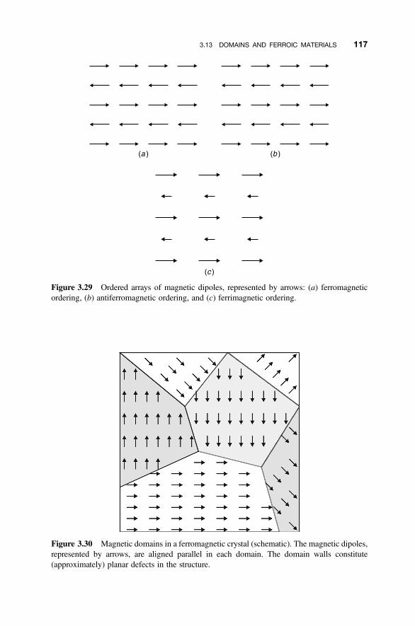
Figure 3.30 Magnetic domains in a ferromagnetic crystal (schematic). The magnetic dipoles,represented by arrows, are aligned parallel in each domain. The domain walls constitute(approximately) planar defects in the structure.
Figure 3.29 Ordered arrays of magnetic dipoles, represented by arrows: (a) ferromagneticordering, (b) antiferromagnetic ordering, and (c) ferrimagnetic ordering.
3.13 DOMAINS AND FERROIC MATERIALS 117
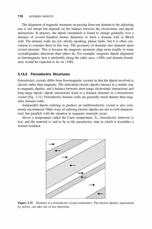
The alignment of magnetic moments on passing from one domain to the adjoiningone is not abrupt but depends on the balance between the electrostatic and dipoleinteractions. In practice, the dipole orientation is found to change gradually over adistance of several hundred atomic diameters to form a domain wall or Blochwall. The domain walls are not, strictly speaking, planar faults, but it is often con-venient to consider them in this way. The geometry of domains also depends uponcrystal structure. This is because the magnetic moments align more readily in somecrystallographic directions than others do. For example, magnetic dipole alignmentin ferromagnetic iron is preferably along the cubic axes, <100> and domain bound-aries would be expected to lie on f100g.
3.13.2 Ferroelectric Structures
Ferroelectric crystals differ from ferromagnetic crystals in that the dipole involved iselectric rather than magnetic. The individual electric dipoles interact in a similar wayto magnetic dipoles, and a balance between short-range electrostatic interactions andlong-range dipole–dipole interactions leads to a domain structure in a ferroelectriccrystal (Fig. 3.31). Ferroelectric domain walls are generally much thinner than mag-netic domain walls.
Antiparallel dipole ordering to produce an antiferroelectric crystal is also com-monly encountered. Other ways of ordering electric dipoles are not so well character-ized, but parallels with the situation in magnetic materials occur.
Above a temperature called the Curie temperature, TC, ferroelectric behavior islost, and the material is said to be in the paraelectric state in which it resembles anormal insulator.
Figure 3.31 Domains in a ferroelectric crystal (schematic). The electric dipoles, representedby arrows, can take one of two directions.
118 EXTENDED DEFECTS

3.13.3 Ferroic Structures
In general, a ferroelectric or ferromagnetic crystal will be composed of an equalnumber of domains oriented in all the equivalent directions allowed by thecrystal symmetry. A defining characteristic of both ferromagnetic and ferroelectric(and related) materials is that the direction of the dipoles can be changed, orswitched, by an external field so that the overall magnetization or electric polariz-ation of the sample can be changed by the application of the appropriate magneticor electric field. In either case, the form that the magnetization or polarizationcurves take as a function of applied field is that of a hysteresis loop (Fig. 3.32).At the extremes of the loop all dipoles point in the same direction. The practicalusefulness of many magnetic and ferroelectric materials is centered upon thisswitching ability.
Ferromagnetic and ferroelectric materials are only two examples of a wider groupthat contains domains built up from switchable units. Such solids, which are calledferroic materials, exhibit domain boundaries in the normal state. These includeferroelastic crystals whose domain structure can be switched by the application ofmechanical stress. In all such materials, domain walls act as planar defects runningthroughout the solid.
Figure 3.32 Hysteresis behavior of the magnetization of a ferromagnetic crystal orpolarization of a ferroelectric crystal with respect to the applied magnetic or electricswitching field.
3.13 DOMAINS AND FERROIC MATERIALS 119
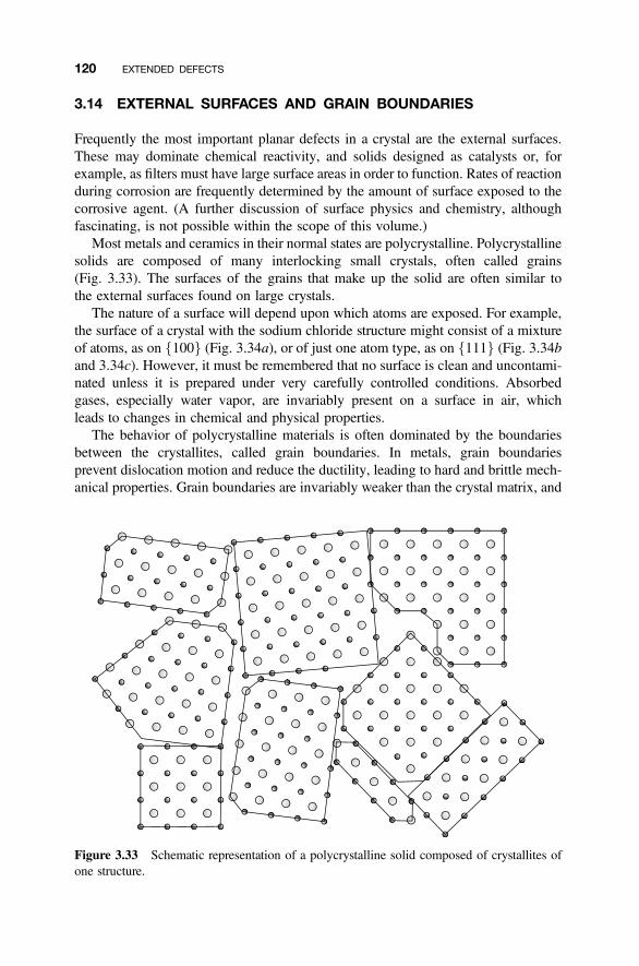
3.14 EXTERNAL SURFACES AND GRAIN BOUNDARIES
Frequently the most important planar defects in a crystal are the external surfaces.These may dominate chemical reactivity, and solids designed as catalysts or, forexample, as filters must have large surface areas in order to function. Rates of reactionduring corrosion are frequently determined by the amount of surface exposed to thecorrosive agent. (A further discussion of surface physics and chemistry, althoughfascinating, is not possible within the scope of this volume.)
Most metals and ceramics in their normal states are polycrystalline. Polycrystallinesolids are composed of many interlocking small crystals, often called grains(Fig. 3.33). The surfaces of the grains that make up the solid are often similar tothe external surfaces found on large crystals.
The nature of a surface will depend upon which atoms are exposed. For example,the surface of a crystal with the sodium chloride structure might consist of a mixtureof atoms, as on f100g (Fig. 3.34a), or of just one atom type, as on f111g (Fig. 3.34band 3.34c). However, it must be remembered that no surface is clean and uncontami-nated unless it is prepared under very carefully controlled conditions. Absorbedgases, especially water vapor, are invariably present on a surface in air, whichleads to changes in chemical and physical properties.
The behavior of polycrystalline materials is often dominated by the boundariesbetween the crystallites, called grain boundaries. In metals, grain boundariesprevent dislocation motion and reduce the ductility, leading to hard and brittle mech-anical properties. Grain boundaries are invariably weaker than the crystal matrix, and
Figure 3.33 Schematic representation of a polycrystalline solid composed of crystallites ofone structure.
120 EXTENDED DEFECTS
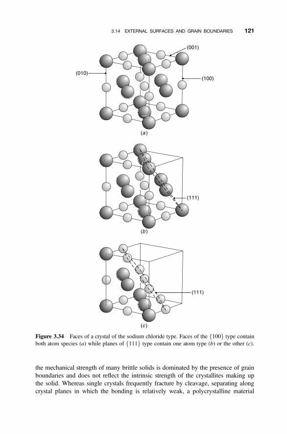
the mechanical strength of many brittle solids is dominated by the presence of grainboundaries and does not reflect the intrinsic strength of the crystallites making upthe solid. Whereas single crystals frequently fracture by cleavage, separating alongcrystal planes in which the bonding is relatively weak, a polycrystalline material
Figure 3.34 Faces of a crystal of the sodium chloride type. Faces of the f100g type containboth atom species (a) while planes of f111g type contain one atom type (b) or the other (c).
3.14 EXTERNAL SURFACES AND GRAIN BOUNDARIES 121
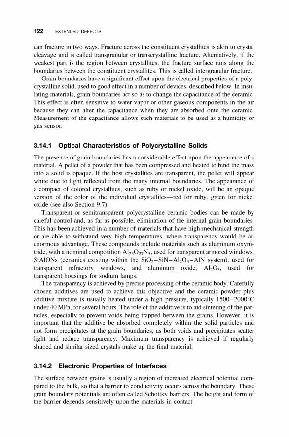
can fracture in two ways. Fracture across the constituent crystallites is akin to crystalcleavage and is called transgranular or transcrystalline fracture. Alternatively, if theweakest part is the region between crystallites, the fracture surface runs along theboundaries between the constituent crystallites. This is called intergranular fracture.
Grain boundaries have a significant effect upon the electrical properties of a poly-crystalline solid, used to good effect in a number of devices, described below. In insu-lating materials, grain boundaries act so as to change the capacitance of the ceramic.This effect is often sensitive to water vapor or other gaseous components in the airbecause they can alter the capacitance when they are absorbed onto the ceramic.Measurement of the capacitance allows such materials to be used as a humidity orgas sensor.
3.14.1 Optical Characteristics of Polycrystalline Solids
The presence of grain boundaries has a considerable effect upon the appearance of amaterial. A pellet of a powder that has been compressed and heated to bind the massinto a solid is opaque. If the host crystallites are transparent, the pellet will appearwhite due to light reflected from the many internal boundaries. The appearance ofa compact of colored crystallites, such as ruby or nickel oxide, will be an opaqueversion of the color of the individual crystallites—red for ruby, green for nickeloxide (see also Section 9.7).
Transparent or semitransparent polycrystalline ceramic bodies can be made bycareful control and, as far as possible, elimination of the internal grain boundaries.This has been achieved in a number of materials that have high mechanical strengthor are able to withstand very high temperatures, where transparency would be anenormous advantage. These compounds include materials such as aluminum oxyni-tride, with a nominal composition Al23O27N5, used for transparent armored windows,SiAlONs (ceramics existing within the SiO2–SiN–Al2O3–AlN system), used fortransparent refractory windows, and aluminum oxide, Al2O3, used fortransparent housings for sodium lamps.
The transparency is achieved by precise processing of the ceramic body. Carefullychosen additives are used to achieve this objective and the ceramic powder plusadditive mixture is usually heated under a high pressure, typically 1500–20008Cunder 40MPa, for several hours. The role of the additive is to aid sintering of the par-ticles, especially to prevent voids being trapped between the grains. However, it isimportant that the additive be absorbed completely within the solid particles andnot form precipitates at the grain boundaries, as both voids and precipitates scatterlight and reduce transparency. Maximum transparency is achieved if regularlyshaped and similar sized crystals make up the final material.
3.14.2 Electronic Properties of Interfaces
The surface between grains is usually a region of increased electrical potential com-pared to the bulk, so that a barrier to conductivity occurs across the boundary. Thesegrain boundary potentials are often called Schottky barriers. The height and form ofthe barrier depends sensitively upon the materials in contact.
122 EXTENDED DEFECTS
The best understood barriers are formed between a semiconductor and a metal.When a metal and a semiconductor are brought into contact, electrons will flowfrom the metal to the semiconductor or vice versa, depending upon the relativeenergy levels across the boundary. Suppose, for example, that the Fermi level of
Figure 3.35 Formation of a Schottky (potential) barrier: (a) isolated semiconductor andmetal, (b) on contact a Schottky barrier is formed at the interface, and (c) Schottky barrierscan also form between semiconducting grains separated by insulating layers.
3.14 EXTERNAL SURFACES AND GRAIN BOUNDARIES 123
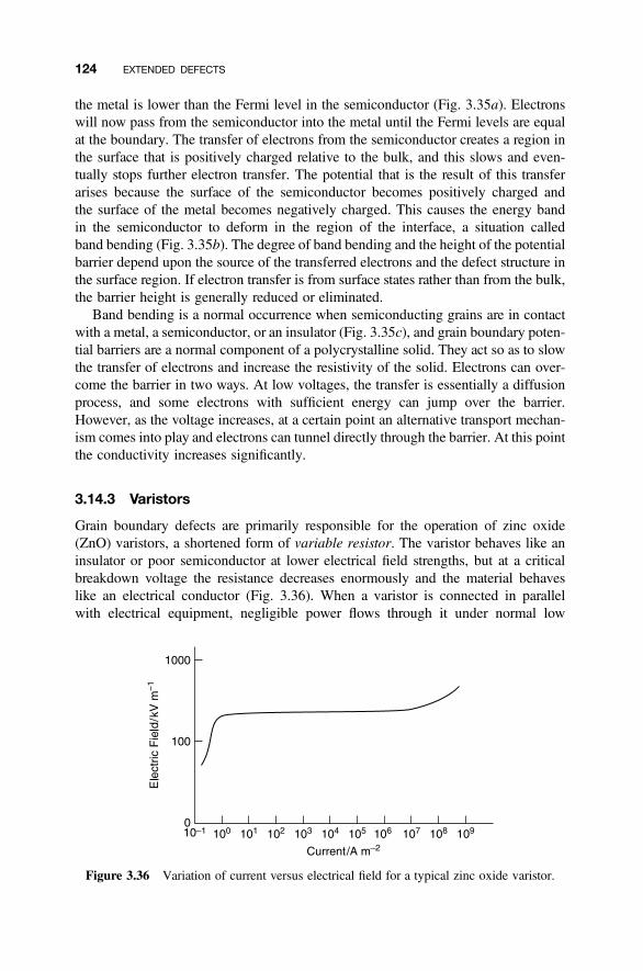
the metal is lower than the Fermi level in the semiconductor (Fig. 3.35a). Electronswill now pass from the semiconductor into the metal until the Fermi levels are equalat the boundary. The transfer of electrons from the semiconductor creates a region inthe surface that is positively charged relative to the bulk, and this slows and even-tually stops further electron transfer. The potential that is the result of this transferarises because the surface of the semiconductor becomes positively charged andthe surface of the metal becomes negatively charged. This causes the energy bandin the semiconductor to deform in the region of the interface, a situation calledband bending (Fig. 3.35b). The degree of band bending and the height of the potentialbarrier depend upon the source of the transferred electrons and the defect structure inthe surface region. If electron transfer is from surface states rather than from the bulk,the barrier height is generally reduced or eliminated.
Band bending is a normal occurrence when semiconducting grains are in contactwith a metal, a semiconductor, or an insulator (Fig. 3.35c), and grain boundary poten-tial barriers are a normal component of a polycrystalline solid. They act so as to slowthe transfer of electrons and increase the resistivity of the solid. Electrons can over-come the barrier in two ways. At low voltages, the transfer is essentially a diffusionprocess, and some electrons with sufficient energy can jump over the barrier.However, as the voltage increases, at a certain point an alternative transport mechan-ism comes into play and electrons can tunnel directly through the barrier. At this pointthe conductivity increases significantly.
3.14.3 Varistors
Grain boundary defects are primarily responsible for the operation of zinc oxide(ZnO) varistors, a shortened form of variable resistor. The varistor behaves like aninsulator or poor semiconductor at lower electrical field strengths, but at a criticalbreakdown voltage the resistance decreases enormously and the material behaveslike an electrical conductor (Fig. 3.36). When a varistor is connected in parallelwith electrical equipment, negligible power flows through it under normal low
Figure 3.36 Variation of current versus electrical field for a typical zinc oxide varistor.
124 EXTENDED DEFECTS

field conditions and power is provided to the equipment. In the event of a voltagesurge, the varistor becomes a good electrical conductor and current is divertedacross it, thus protecting the sensitive equipment. This behavior (called nonohmic)is reversible and is controlled by the microstructure of the zinc oxide body. The non-ohmic behavior results from the contacts between the zinc oxide grains at the grainboundaries.
Chemically, varistors are principally composed of small grains of zinc oxide thathave been doped with 1 or 2% bismuth oxide, Bi2O3. The bismuth oxide impuritiesmodify the grain boundary regions. These ions, which can take a valence of 3þ or5þ , do not substitute readily into the ZnO matrix. They congregate near to thesurface, where relaxation is easier and these large ions can be accommodatedwith less strain. The bismuth-enriched surface layer has a depth of between3 and 10 nm and is called the depletion layer, a term borrowed from semiconductorphysics. As the name suggests, the surface layer is depleted in mobile charge carriersand is highly insulating, with a resistivity of approximately 1010Vm. The structure ofa varistor can then be described in terms of n-type semiconducting ZnO grains sur-rounded by a thin insulating shell of Bi2O3 structure (Fig. 3.37). In this situation, elec-trons in the semiconductor near to the insulating layer are trapped in the bismuth-richsurface, leaving a bilayer of ionized donors in the semiconductor. This creates asymmetrical Schottky barrier (see Fig. 3.35c).
When a low voltage is applied to the varistor, the current is due to the thermaltransfer of electrons across the barrier by a diffusion process. However, at a certaincritical voltage the thin insulating barrier breaks down, and current effectivelyflows across the insulating layer from the grain interiors, which have a high conduc-tivity. The point at which breakdown occurs is modified by changing the amounts andnature of the chemical dopants used so that protection can be achieved over a widerange of voltages.
The microstructure of commercial varistors is extremely complex, and commercialpreparations also contain other dopants, mainly oxides of cobalt, manganese,chromium, and antimony, that are used to fine tune the varistor characteristics. Thetransition-metal dopants are chemically similar to Zn2þ and mainly form substitu-tional defects within the ZnO grains, such as CoZn, that modify the n-type behaviorof the grain interior. (See also Chapter 8 for further discussion of the electronic
Figure 3.37 Microstructure of a zinc oxide varistor (schematic).
3.14 EXTERNAL SURFACES AND GRAIN BOUNDARIES 125
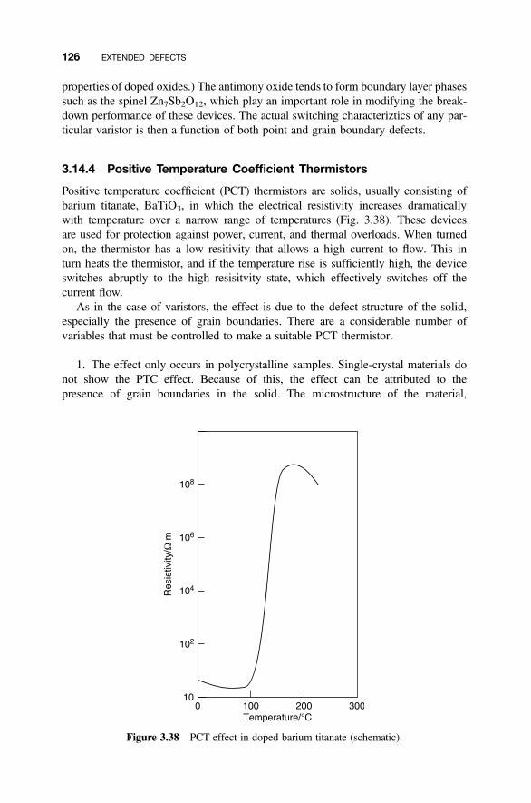
properties of doped oxides.) The antimony oxide tends to form boundary layer phasessuch as the spinel Zn7Sb2O12, which play an important role in modifying the break-down performance of these devices. The actual switching characteriztics of any par-ticular varistor is then a function of both point and grain boundary defects.
3.14.4 Positive Temperature Coefficient Thermistors
Positive temperature coefficient (PCT) thermistors are solids, usually consisting ofbarium titanate, BaTiO3, in which the electrical resistivity increases dramaticallywith temperature over a narrow range of temperatures (Fig. 3.38). These devicesare used for protection against power, current, and thermal overloads. When turnedon, the thermistor has a low resitivity that allows a high current to flow. This inturn heats the thermistor, and if the temperature rise is sufficiently high, the deviceswitches abruptly to the high resisitvity state, which effectively switches off thecurrent flow.
As in the case of varistors, the effect is due to the defect structure of the solid,especially the presence of grain boundaries. There are a considerable number ofvariables that must be controlled to make a suitable PCT thermistor.
1. The effect only occurs in polycrystalline samples. Single-crystal materials donot show the PTC effect. Because of this, the effect can be attributed to thepresence of grain boundaries in the solid. The microstructure of the material,
Figure 3.38 PCT effect in doped barium titanate (schematic).
126 EXTENDED DEFECTS
especially the size of the grains in the sample, has a marked effect upon the magni-tude of the PTC effect.
2. The BaTiO3 must be doped with higher valence impurities such as La3þ, Ce3þ,Y3þ in place of Ba2þ or Nb5þ in place of Ti4þ and then only in a narrow range ofconcentrations in the region of 0.2–0.5 mol %. The effect of these impurities is totransform the insulting BaTiO3 into an n-type semiconductor. (These impurities actas donors; see Chapter 8.)
3. The temperature range over which the effect occurs is quite narrow andcoincides with the Curie temperature, TC, of ferroelectric barium titanate (Section3.13.2). Moreover, the temperature at which the resistivity changes, the switchingtemperature, is markedly dependent upon the impurities present. The switching temp-erature is particularly sensitive to replacement of Ba2þ by Pb2þ and Sr2þ, and dopingwith these ions can then allow switching to occur anywhere in the range of 0–1408C.
4. Barium titanate can be made into an n-type semiconductor by heating in avacuum. Such materials do not exhibit the PTC effect. [Materials heated invacuum show negative temperature coefficient (NTC) thermistor behavior; seeChapter 8]. Samples for use in PCT thermistors are heated in oxygen to preventany chance of reduction.
5. The magnitude of the PTC effect is greatly affected by the way in which thepolycrystalline sample is cooled (in oxygen) after preparation.
As this list reveals, the complexity of the phenomenon is considerable, and there isstill a degree of uncertainty about the exact roles of the various defect species involved.However, the basic cause of the effect is believed to involve the following steps:
1. Assume for simplicity that the dopant ion is La3þ. The La3þ ions substitute forBa2þ forming LaBa
† defects. The positive charge on these defects must be compensatedto maintain charge neutrality. This can be achieved either by ionic or electronic com-pensation (Section 1.2). As doping with La3þ creates n-type material, electronic com-pensation is believed to occur. The simplest way that this can be achieved is to considerthat the counter defects are Ti3þ ions. To obtain charge neutrality, one Ti3þ ion iscreated for each La3þ ion in the crystal so that the doped material can be written inchemical terms as Ba12x
2þ Lax3þTi12x
4þ Tix3þO3. The point defects present are LaBa
† andTi0Ti. Electron conductivity than can take place by electron transfer between Ti
4þ ions:
TiTi þ e0 �! Ti0Ti [Ti4þ þ e0 �! Ti3þ]
This leads to the formation of grains of BaTiO3, which are n-type semiconductors.
2. Heating the sample in oxygen will oxidize any Ti3þ ions in the grain surfaces toTi4þ, thus causing the material to revert to an insulator. This can be written as
xTi0Ti þ x4 O2 �! xTiTi þ x
2 OO
or
Ba2þ1�x La3þx Ti4þ1�x Ti
3þx O3 þ x
4 O2 �! Ba2þ1�x La3þx Ti4þO3þx=2
3.14 EXTERNAL SURFACES AND GRAIN BOUNDARIES 127
The extra oxygen can be accommodated in the surface layers but not in the bulk, thusrestricting oxidation to the grain boundary region. This accounts for the fact that grainsize and cooling rate have an effect on the PCT effect, as both of these factors willinfluence the amount of insulating layer that is formed on the grains. The insulatinglayer creates a Schottky barrier, as described above (Fig. 3.35c).
3. Under normal circumstances the Schottky barrier would be expected to reducethe current flow across the sample and hence create a high-resisivity device. However,barium titanate is a ferroelectric below a temperature of approximately 1358C, theCurie temperature, TC (see Section 3.13.2). It is believed that the action of the ferro-electric domain walls is to reduce the height of the Schottky barrier between certaingrains and increase it between others. The overall effect of this is to create low-resistivity pathways through the solid so that the overall measured resisitivity islow. At the Curie temperature the ferroelectric state reverts to a normal insulator.At this point none of the Schottky barriers are reduced, as ferroelectric domainsare no longer present, and a high-resistivity state is produced. Thus, the linkbetween the Curie point and the PTC switching temperature is established.
4. The role of dopants such as Sr2þ and Pb2þ is to alter the Curie temperature ofthe barium titanate so that devices that switch at a desired temperature can befabricated.
3.15 VOLUME DEFECTS AND PRECIPITATES
Point defects are only notionally zero dimensional. It is apparent that the atomsaround a point defect must relax (move) in response to the defect, and as such thedefect occupies a volume of crystal. Atomistic simulations have shown that suchvolumes of disturbed matrix can be considerable. Moreover, these calculationsshow that the clustering of point defects is of equal importance. These defect clusterscan be small, amounting to a few defects only, or extended over many atoms in non-stoichiometric materials (Section 4.4).
In a similar fashion, the line and planar defects described above are all, strictlyspeaking, volume defects. For the sake of convenience it is often easiest to ignorethis point of view, but it is of importance in real structures, and dislocationtangles, for instance, which certainly affect the mechanical properties of crystals,should be viewed in terms of volume defects.
Apart from these, there are volume defects that cannot conveniently be describedin any other terms. The most important of these consist of regions of an impurityphase—precipitates—in the matrix of a material (Fig. 3.39). Precipitates form in avariety of circumstances. Phases that are stable at high temperatures may not bestable at low temperatures, and decreasing the temperature slowly will frequentlylead to the formation of precipitates of a new crystal structure within the matrix ofthe old. Glasses, for example, are inherently unstable, and a glass may slowlyrecrystallize. In this case precipitates of crystalline material will appear in the non-crystalline matrix.
128 EXTENDED DEFECTS
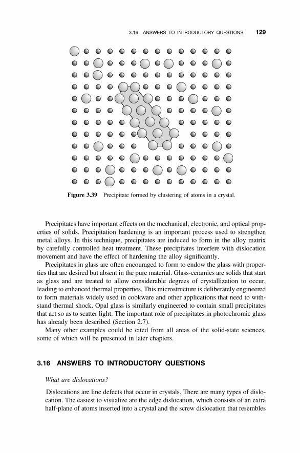
Precipitates have important effects on the mechanical, electronic, and optical prop-erties of solids. Precipitation hardening is an important process used to strengthenmetal alloys. In this technique, precipitates are induced to form in the alloy matrixby carefully controlled heat treatment. These precipitates interfere with dislocationmovement and have the effect of hardening the alloy significantly.
Precipitates in glass are often encouraged to form to endow the glass with proper-ties that are desired but absent in the pure material. Glass-ceramics are solids that startas glass and are treated to allow considerable degrees of crystallization to occur,leading to enhanced thermal properties. This microstructure is deliberately engineeredto form materials widely used in cookware and other applications that need to with-stand thermal shock. Opal glass is similarly engineered to contain small precipitatesthat act so as to scatter light. The important role of precipitates in photochromic glasshas already been described (Section 2.7).
Many other examples could be cited from all areas of the solid-state sciences,some of which will be presented in later chapters.
3.16 ANSWERS TO INTRODUCTORY QUESTIONS
What are dislocations?
Dislocations are line defects that occur in crystals. There are many types of dislo-cation. The easiest to visualize are the edge dislocation, which consists of an extrahalf-plane of atoms inserted into a crystal and the screw dislocation that resembles
Figure 3.39 Precipitate formed by clustering of atoms in a crystal.
3.16 ANSWERS TO INTRODUCTORY QUESTIONS 129
a spiral staircase. The line that describes the dislocation is drawn at the center ofthe disturbed crystal caused by the presence of the dislocation. That is, the dislo-cation line lies along the termination of the extra half-plane of atoms for an edgedislocation and along the center of the spiral of atom planes for a screwdislocation.
Edge dislocations play an important role in the strength of a metal, and screwdislocations are important in crystal growth. Dislocations also interact stronglywith other defects in the crystal and can act as sources and sinks of point defects.
What is a magnetic domain?
Magnetism arises when atoms or ions contain unpaired electrons. Such atomsbehave as if they were magnetic, that is, they can be treated as microscopicmagnets, each possessing a magnetic dipole. A magnetic domain is a region ofa crystal containing magnetic atoms or ions over which all of the atomic magneticdipoles are aligned. The alignment is brought about by two interactions, a short-range electrostatic interaction that produces a parallel alignment of magneticdipoles and long-range dipole–dipole interactions that favors an antiparallel align-ment. The size of magnetic domains in a crystal is determined by the relativestrengths of these interactions.
What defects are important in a PCT thermistor?
A PCT thermistor is an electrical ceramic component that has a low resistivity atthe normal operating temperature of the equipment. Under these circumstancescurrent is allowed to flow to the machinery. The current passing through the ther-mistor heats it. If an unusually high current passes, the temperature rise causes theresistivity of the thermistor to increase manyfold, and the device switches abruptlyto a high-resistivity state. This effectively switches off the current flow and so pro-tects the equipment from damage.
The PCT effect is produced by a combination of point defects, grain bound-aries, and ferroelectric domains in ceramic blocks of polycrystalline barium tita-nate. The point defects arise when barium titanate is doped with higher valencecations such as La3þ, which replaces Ba2þ. These point defects induce compen-sating defects to maintain charge neutrality and cause the normally insulatingbarium titanate to become an n-type semiconductor. The ceramic is heated inoxygen, and this oxidizes the surface of each grain to form a thin insulatingshell. The combination of a thin insulating shell surrounding an n-type core pro-duces Schottky barriers between the resulting grains. These are partly removed byinteraction with ferroelectric domains to provide a low-resistance pathway throughthe ceramic. The ceramic switches to a high-resistance state when the ferroelectricbehavior is lost. This occurs at the Curie temperature of the doped barium titanateused in the device.
130 EXTENDED DEFECTS

PROBLEMS AND EXERCISES
Quick Quiz
1. Dislocations are:
(a) Planar defects
(b) Line defects
(c) Point defects
2. The Burgers vector and dislocation line are normal to each other in:
(a) A screw dislocation
(b) A partial dislocation
(c) An edge dislocation
3. Dislocation movement occurs by:
(a) Motion in the slip plane
(b) Motion perpendicular to the slip plane
(c) Motion of the slip plane
4. Ceramic materials are brittle compared to metals because:
(a) They contain no dislocations
(b) The dislocations cannot move easily
(c) The dislocations only move on certain planes
5. Transformation twins arise on cooling a crystal because of:
(a) A decrease in crystallographic symmetry
(b) An increase in mechanical strain
(c) A change of chemical composition
6. A stacking sequence of metal atom planes ABCABCCBACBA represents:
(a) An antiphase boundary
(b) A twin boundary
(c) A domain boundary
7. A Schottky barrier forms close to:
(a) Dislocations
(b) Grain boundaries
(c) Schottky defects
8. Varistor behavior is principally attributed to:
(a) Grain boundries
(b) Dislocations
(c) Point defects
PROBLEMS AND EXERCISES 131
9. The active material in PTC thermistor is:
(a) Titanium dioxide
(b) Zinc oxide
(c) Barium titanate
10. A precipitate is a:
(a) Line defect
(b) Planar defect
(c) Volume defect
Calculations and Questions
1. The Burgers vector of unit dislocations in copper is equal to the line joining theclosest atoms, written a/2[110]. (a) What is the length of this vector innanometers? This dislocation is often replaced by partial dislocations a
6[211].(b) What is the length of this vector in nanometers? (The copper structure isgiven in Supplementary Material S1 and drawn in Fig. 3.10. a ¼ 0.3610 nm.)
2. The unit Burgers vector in the diamond structure joins two atoms in the f100gplane. (a) What is the Burgers vector? This can be split into partial dislocations,which are vectors joining two nearest-neighbor carbon atoms. (b) What is thedirection of the vector corresponding to this link? (The diamond structure isgiven in Supplementary Material S1 and drawn in Figs. 1.5 and 9.27.)
3. Sketch an edge dislocation formed by the insertion of extra material parallel to acube edge in fluorite, CaF2, and use the FS/RH convention to determine theBurgers vector. (The fluorite structure is given in Supplementary Material S1and drawn in Fig. 4.7a.)
4. What are the Burgers vectors of the dislocations shown in Figure 3.17?
5. What are the Burgers vectors of the dislocations shown in Figure 3.18b?
6. A low-angle grain boundary in a single crystal is revealed by a line of dislo-cations with a separation of 7 nm. The angle between the grains is estimated tobe 48. What is the Burgers vector of the dislocations?
7. What are the following boundary types?
(a) ABCABC* BACBAC in fcc metal (Fig. 3.11)
(b) ABCABCC* BACBA in fcc metal (Fig. 3.11)
(c) TiOOTiO * TiOOTiOOTi Ti and O planes parallel to (110) in rutile(Fig. 3.22)
(d) AcB AcB* AcB AcB in CdI2 (Fig. 3.18)
(e) AcB AcB* CbA CbA in CdI2 (Fig. 3.18)
(f) AcB AcB* BcA BcA in CdI2 (Fig. 3.18)
132 EXTENDED DEFECTS

8. What is the atomic composition of the (100), (200), (400), (110), and (220)planes in fluorite, CaF2? (The fluorite structure is given in SupplementaryMaterial S1 and drawn in Fig. 4.7a).
9. (a) What is the sequence of planes (in terms of V, VO, VO2, etc.) across the twinboundaries in Figure 3.25b, V2O5? (b) Is there a composition change across theboundary?
10. Write the defect equations and the ionic formula of the phases producedby doping of BaTiO3 PCT material with (a) Y3þ as a Ba2þ substituent and(b) Nb5þ as a Ti4þ substituent.
FURTHER READING
Background material on the defects described here is found in:
R. W. Cahn, The Coming of Materials Science, Pergamon/Elsevier, Oxford, United Kingdom,2001.
W. D. Callister, Materials Science and Engineering, an Introduction, 5th ed., Wiley,New York, 2000.
M. Catti, Physical Properties of Crystals in Elements of Crystallography, 2nd ed.,C. Giacovazzo, H. L. Monaco, A. Artioli, D. Viterbo, G. Ferraris, G. Gilli. G. Zanotti,and M. Catti, Eds., Oxford University Press, Oxford, United Kingdom, 2002, Chapter 10.
W. D. Kingery, H. K. Bowen, and D. R. Uhlmann, Introduction to Ceramics, 2nd ed., Wiley,New York, 1976.
R. E. Newnham Structure–Property Relations, Springer, Berlin, 1975.
R. J. D. Tilley Understanding Solids, Wiley, Chichester, 2004.
J. B. Wachtman, Ed. Ceramic Innovations in the 20th Century, American Ceramic Society,Westerville, Ohio, 2001.
The history of the development of dislocation theory is given by:
E. Braun, Chapter 5 in Out of the Crystal Maze, ed. L. Hoddeson, E. Braun, J. Teichmann,S. Weart, Oxford University Press, New York, 1992.
R. W. Cahn, as above, esp pp. 110–117.
J. W. Dash, J. Appl. Phys., 27, 1193–1195 (1956).
The early work on dislocation decoration in silver halides is described in:
J. W. Mitchell, The Beginnings of Solid State Physics, Royal Society, London, 1980,pp. 140–159.
Information expanding specific areas is in:
D. Cohen and C. B. Carter, J. Microscopy, 208, 84–99 (2002) and references therein.
J. Eckert, G. D. Stucky, and A. K. Cheetham, Mat. Res. Soc. Bull. 24 (May), 31–41 (1999).
J. Li, The Mechanics and Physics of Defect Nucleation, Mat. Res. Soc. Bull. 32, 151 (2007).
FURTHER READING 133

&CHAPTER 4
Structural Aspects of CompositionVariation
What are solid solutions?
What are modular structures?
What are incommensurately modulated structures?
4.1 COMPOSITION VARIATION AND NONSTOICHIOMETRY
During the latter part of the nineteenth century and the early years of the twentiethcentury, there was considerable controversy over the composition of chemicalcompounds—were compounds strictly stoichiometric, with an immutable compo-sition, or could the composition vary. Indeed, at the turn of the twentieth century,even the existence of atoms was a subject of debate. The principal techniquesinvolved at this epoch were accurate quantitative chemical analysis and metallo-graphic studies of phase equilibria. The advent of X-ray diffraction studies effectivelyresolved the problem, and the experimental evidence for composition ranges of manysolids became incontestable.
4.1.1 Phase Diagrams and the Coexistence of Solids
Probably the most widely employed technique now used in phase studies is powderX-ray diffraction. The X-ray powder pattern of a compound can be used as a finger-print, and data for many compounds are available. This can be illustrated with refer-ence to the sodium fluoride (NaF)–zinc fluoride (ZnF2) system. Suppose that pureNaF is mixed with a few percent of pure ZnF2 and the mixture heated at about6008C until reaction is complete. An X-ray powder photograph will show the pre-sence of two compounds (or phases), NaF, which will be the major component,and a small amount of a new compound (point A, Fig. 4.1a). A repetition of theexperiment, with gradually increasing amounts of ZnF2 will yield a similar result,but the amount of the new phase will increase relative to the amount of NaF until
Defects in Solids, by Richard J. D. TilleyCopyright # 2008 John Wiley & Sons, Inc.
135
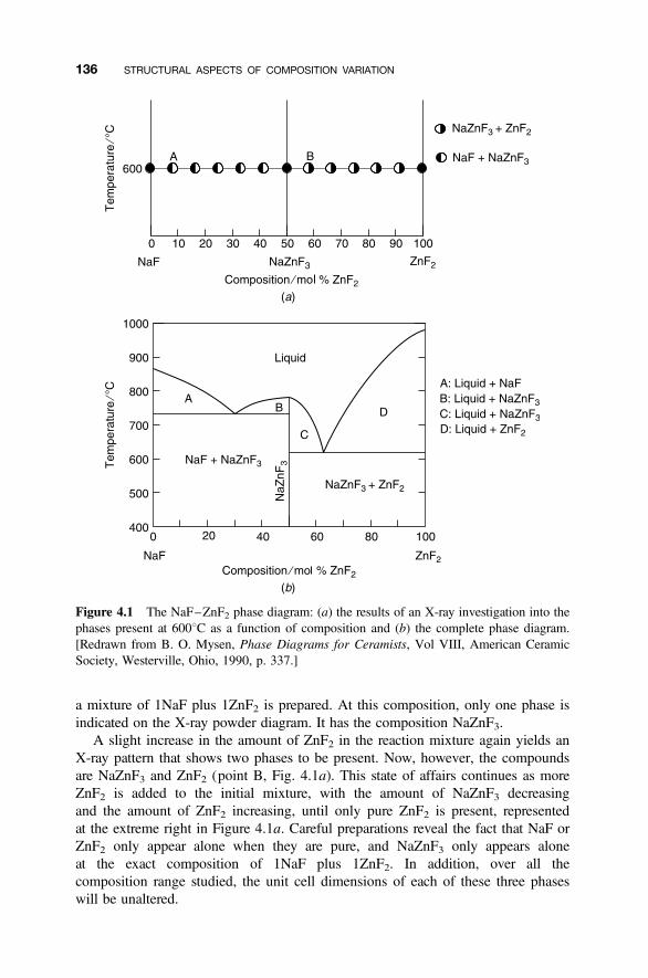
a mixture of 1NaF plus 1ZnF2 is prepared. At this composition, only one phase isindicated on the X-ray powder diagram. It has the composition NaZnF3.
A slight increase in the amount of ZnF2 in the reaction mixture again yields anX-ray pattern that shows two phases to be present. Now, however, the compoundsare NaZnF3 and ZnF2 (point B, Fig. 4.1a). This state of affairs continues as moreZnF2 is added to the initial mixture, with the amount of NaZnF3 decreasingand the amount of ZnF2 increasing, until only pure ZnF2 is present, representedat the extreme right in Figure 4.1a. Careful preparations reveal the fact that NaF orZnF2 only appear alone when they are pure, and NaZnF3 only appears aloneat the exact composition of 1NaF plus 1ZnF2. In addition, over all thecomposition range studied, the unit cell dimensions of each of these three phaseswill be unaltered.
Figure 4.1 The NaF–ZnF2 phase diagram: (a) the results of an X-ray investigation into thephases present at 6008C as a function of composition and (b) the complete phase diagram.[Redrawn from B. O. Mysen, Phase Diagrams for Ceramists, Vol VIII, American CeramicSociety, Westerville, Ohio, 1990, p. 337.]
136 STRUCTURAL ASPECTS OF COMPOSITION VARIATION
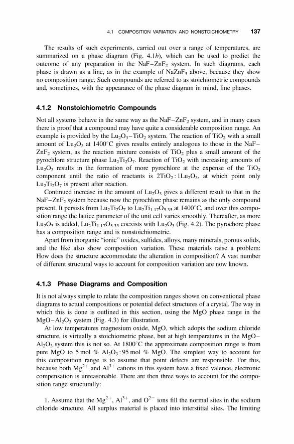
The results of such experiments, carried out over a range of temperatures, aresummarized on a phase diagram (Fig. 4.1b), which can be used to predict theoutcome of any preparation in the NaF–ZnF2 system. In such diagrams, eachphase is drawn as a line, as in the example of NaZnF3 above, because they showno composition range. Such compounds are referred to as stoichiometric compoundsand, sometimes, with the appearance of the phase diagram in mind, line phases.
4.1.2 Nonstoichiometric Compounds
Not all systems behave in the same way as the NaF–ZnF2 system, and in many casesthere is proof that a compound may have quite a considerable composition range. Anexample is provided by the Lu2O3–TiO2 system. The reaction of TiO2 with a smallamount of Lu2O3 at 14008C gives results entirely analogous to those in the NaF–ZnF2 system, as the reaction mixture consists of TiO2 plus a small amount of thepyrochlore structure phase Lu2Ti2O7. Reaction of TiO2 with increasing amounts ofLu2O3 results in the formation of more pyrochlore at the expense of the TiO2
component until the ratio of reactants is 2TiO2 : 1Lu2O3, at which point onlyLu2Ti2O7 is present after reaction.
Continued increase in the amount of Lu2O3 gives a different result to that in theNaF–ZnF2 system because now the pyrochlore phase remains as the only compoundpresent. It persists from Lu2Ti2O7 to Lu2Ti1.17O5.35 at 14008C, and over this compo-sition range the lattice parameter of the unit cell varies smoothly. Thereafter, as moreLu2O3 is added, Lu2Ti1.17O5.35 coexists with Lu2O3 (Fig. 4.2). The pyrochore phasehas a composition range and is nonstoichiometric.
Apart from inorganic “ionic” oxides, sulfides, alloys, manyminerals, porous solids,and the like also show composition variation. These materials raise a problem:How does the structure accommodate the alteration in composition? A vast numberof different structural ways to account for composition variation are now known.
4.1.3 Phase Diagrams and Composition
It is not always simple to relate the composition ranges shown on conventional phasediagrams to actual compositions or potential defect structures of a crystal. The way inwhich this is done is outlined in this section, using the MgO phase range in theMgO–Al2O3 system (Fig. 4.3) for illustration.
At low temperatures magnesium oxide, MgO, which adopts the sodium chloridestructure, is virtually a stoichiometric phase, but at high temperatures in the MgO–Al2O3 system this is not so. At 18008C the approximate composition range is frompure MgO to 5 mol % Al2O3 : 95 mol % MgO. The simplest way to account forthis composition range is to assume that point defects are responsible. For this,because both Mg2þ and Al3þ cations in this system have a fixed valence, electroniccompensation is unreasonable. There are then three ways to account for the compo-sition range structurally:
1. Assume that the Mg2þ, Al3þ, and O22 ions fill the normal sites in the sodiumchloride structure. All surplus material is placed into interstitial sites. The limiting
4.1 COMPOSITION VARIATION AND NONSTOICHIOMETRY 137
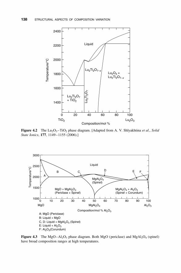
Figure 4.2 The Lu2O3–TiO2 phase diagram. [Adapted from A. V. Shlyakhtina et al., SolidState Ionics, 177, 1149–1155 (2006).]
Figure 4.3 The MgO–Al2O3 phase diagram. Both MgO (periclase) and MgAl2O4 (spinel)have broad composition ranges at high temperatures.
138 STRUCTURAL ASPECTS OF COMPOSITION VARIATION
composition is approximately 0.95MgO plus 0.05Al2O3 or Mg0.95Al0.1O1.10. Fillingthe cation and anion sites requires Mg0.95Al0.05O. The surplus ions present(Al0.05O0.10) are allocated to interstitial sites.
To generalize this, the composition is given by adding (1 2 x) MgO and x (Al2O3)to give Mg12xAl2xO1þ2x (M1þxO1þ2x, where M is the total Mg plus Al).
The defect reaction is
xAl2O3 (MgO) �! xAl†Mg þ xAl3†i þ xOO þ 2xO20i
where the limiting composition is represented by x ¼ 0.05. The point defectspresent are Al3þ substitutional defects, AlMg
† , Al3þ interstitials, Ali3†, and O22 inter-
stitials, Oi20.
2. Assume that the anions build up a perfect sodium chloride structure matrix.In this case the formula of the nonstoichiometric phase must be expressed as(Mg, Al)zO1.0. To make sure that this is in agreement with the measured ratio ofMgO and Al2O3, use the following procedure:
a. Starting formula: Mg0.95Al0.1O1.10 ¼ (Mg, Al)1.05O1.10
b. Desired formula: (Mg,Al)zO1.0 ¼Mg0.95/1.10Al0.1/1.10O1.10/1.10 � Mg0.864Al0.091O1.0 ¼ (Mg, Al)0.955O
This formula means that there are 0.045 too few cations present compared to thoserequired to build the sodium chloride crystal, which must create an equivalentnumber of cation vacancies.
The general composition (1 2 x) MgO : x (Al2O3) ¼ Mg12xAl2xO1þ2x is nowrepresented by the formula Mg(12x)/(1þ2x)Al(2x/(1þ2x)O1.0 ([M(1þx)/(1þ2x)O1.0],where M is the total Mg plus Al). The defect reaction is
xAl2O3 (MgO) �! 2x Al†Mg þ 3xOO þ xV20Mg
The point defects present are Al3þ cations substituted on Mg2þ sites, AlMg† and Mg2þ
vacancies, V20Mg.
3. Assume that the cations build up a perfect sodium chloride structure matrix. Theformula must be expressed as (Mg, Al)1.0Oy. To make sure that this formula is inagreement with the measured ratio of MgO and Al2O3 represented on the phasediagram use the following procedure:
a. Starting formula: Mg0.95Al0.1O1.10 ¼ (Mg, Al)1.05O1.10
b. Desired formula: (Mg,Al)1.0Oy ¼ Mg0.95/1.05Al0.1/1.05O1.10/1.05 � Mg0.905Al0.095O1.048 ¼ (Mg, Al)O1.048
4.1 COMPOSITION VARIATION AND NONSTOICHIOMETRY 139
This formula means that there are 0.48 additional oxygen ions over those required tobuild the sodium chloride crystal, which must be placed into the structure asinterstitials.
The general composition (12 x)MgO : x(Al2O3) ¼ Mg12xAl2xO1þ2x ¼ (Mg,Al)1þxO1þ2x is now best represented by the formula Mg(12x)/(1þx) Al(2x)/(1þx)
O(1þ2x)/(1þx)(M1.0O(1þ2x)/(1þx), where M is the total Mg plus Al). Thedefect reaction is:
xAl2O3 (MgO) �! 2xAl†Mg þ 2x OO þ x O20i
The point defects present are Al3þ cations substituted on Mg2þ sites, AlMg† and O22
interstitials, Oi20.
These alternatives are summarized in Table 4.1. To discover which model turnsout to be correct, it is necessary to turn to experiment or calculation, as describedin other chapters of this book.
4.2 SUBSTITUTIONAL SOLID SOLUTIONS
Many alloys are substitutional solid solutions, well-studied examples being copper–gold and copper–nickel. In both of these examples, the alloy has the same crystalstructure as both parent phases, and the metal atoms simply substitute at randomover the available metal atom sites (Fig. 4.4a). The species considered to be thedefect is clearly dependent upon which atoms are in the minority.
The likelihood of forming a substitutional solid solution between two metalsdepends upon a variety of chemical and physical properties. A large number ofalloy systems were investigated by Hume-Rothery, in the first part of the lastcentury, with the aim of understanding the principles that controlled alloy formation.His findings with respect to substitutional solid solution formation are summarized in
TABLE 4.1 Composition Range of MgO in the MgO–Al2O3 System
Composition Defect Structure Formula Defects
(12 x)MgO :x(Al2O3)
Additional material asinterstitials
M1þxO1þ2x ¼Mg12xAl2xO1þ2x
AlMg† , Ali
3†, Oi20
(12 x)MgO :x(Al2O3)
Anion sublatticeperfect, cationdeficiency asvacancies
M(1þx)/(1þ2x)O1.0 ¼Mg(12x)/(1þ2x)
Al(2x)/(1þ2x)O1.0
Al†Mg, VMg20
(12 x)MgO :x(Al2O3)
Cation sublatticeperfect, additionaloxygen asinterstitials
M1.0O(1þ2x)/(1þx) ¼Mg(12x)/(1þx)
Al(2x)/(1þx)O(1þ2x)/(1þx)
AlMg† , Oi
20
140 STRUCTURAL ASPECTS OF COMPOSITION VARIATION
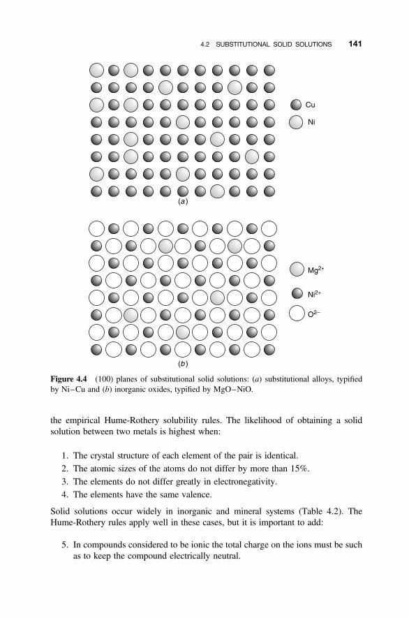
the empirical Hume-Rothery solubility rules. The likelihood of obtaining a solidsolution between two metals is highest when:
1. The crystal structure of each element of the pair is identical.
2. The atomic sizes of the atoms do not differ by more than 15%.
3. The elements do not differ greatly in electronegativity.
4. The elements have the same valence.
Solid solutions occur widely in inorganic and mineral systems (Table 4.2). TheHume-Rothery rules apply well in these cases, but it is important to add:
5. In compounds considered to be ionic the total charge on the ions must be suchas to keep the compound electrically neutral.
Figure 4.4 (100) planes of substitutional solid solutions: (a) substitutional alloys, typifiedby Ni–Cu and (b) inorganic oxides, typified by MgO–NiO.
4.2 SUBSTITUTIONAL SOLID SOLUTIONS 141
The extent of solid solution formation is well predicted qualitatively by the Hume-Rothery rules. When the “rules” are obeyed well, complete solid solution is likely.When the rules are only poorly obeyed, only small amounts of solid solution(partial solid solution) are observed. For example, isovalent substitution betweenions of similar sizes leads to complete solid solution, typified by that formed bythe sodium chloride structure oxides magnesium oxide, MgO, and nickel oxide,NiO (Fig. 4.4b). The MgO–CaO system would be expected to be very similar tothe MgO–NiO system, as both parent phases adopt the sodium chloride structure.However, only partial solid solutions occur because of the difference in ionic size(Mg2þ, 0.086 nm; Ca2þ, 0.114 nm). At 22008C the solid solution range in thecrystal CaxMg12xO extends over the composition range 0, x, 0.05 near to MgOand 0.88 , x, 1.0 near to CaO. Note that the extent of these ranges is in goodaccord with the relative ionic sizes. It is energetically more costly to insert largeCa2þ ions into Mg2þ sites to form CaMg defects than to insert small Mg2þ ionsinto Ca2þ sites to form MgCa defects.
These days the variables in the Hume-Rothery rules can be made quantitativeby making use of computer simulation or quantum mechanical calculations(Section 2.10).
In solids with several atomic constituents, solid solution formation may berestricted to one of the component atoms, as in the pyrochlore structure oxidesBi2Pb2O7 and Tl2Pb2O7, which form a continuous solid solution with a formulaBi22xTlxPb2O7 from x ¼ 0 to x ¼ 2. In some materials only partial replacementis possible. For example, Ca2þ can replace Sr2þ in SrCuO2 over the rangeCaxSr12xCuO2 from x ¼ 0 to x ¼ 0.6, that is, from SrCuO2 to Ca0.6Sr0.4CuO2. Inothers a double substitution is necessary. For example, mineral samples of pyrochlorehave a general formula (Na, Ca)2(Nb, Ta)2O6(O, OH, F). The nominal parent phasehas a formula Na2(Nb,Ta)2O7. Complete solid solution is possible between the Nband Ta species, as they are similarly sized M5þ cations. The same is not true forthe substitution of Naþ by Ca2þ because this will cause charge imbalance. Theadditional positive charge on the Ca2þ ions is compensated for by a variable popu-lation of O22, OH2, and F2. Each time an Naþ is substituted by Ca2þ in theparent phase Na2(Nb,Ta)2O7, an O22 anion is substituted by either F2 or OH2.
TABLE 4.2 Some Mineral Systems Showing Broad Solid Solution Ranges
System Structure Examples
AO–BO Sodiumchloride
MgO–NiO, complete solid solution often possible
A2O3–B2O3 Corundum Al2O3–Cr2O3, Al1.995Cr0.005O3 rubyAB2O4–A�B2
�O4
Spinel MgAl2O4–MgCr2O4, Mg(Al0.99Cr0.01)2O4 ruby spinel,ferrites (A,B)Fe2O4
A2SiO4–B2SiO4 Olivine Mg2SiO4–Fe2SiO4, end members forsterite andfayalite, solid solution is olivine
AAlSi3O8–BAlSi3O8
Feldspar KAlSi3O8–NaAlSi3O8, high temperature
142 STRUCTURAL ASPECTS OF COMPOSITION VARIATION
Interesting effects are found in systems that nominally show point defect popu-lations. The perovskite structure, ABO3 (where A represents a large cation and B amedium-size cation) is adopted by many oxides, and solid solutions between themcan readily be fabricated. Perovskite structure materials containing a high populationof vacancies are of interest as electrolytes in solid-state batteries and fuel cells.Typical representatives of this type of material are found in the solid solutionsbetween the perovskite structure phases CaTiO3–La2/3TiO3 and SrTiO3–La2/3TiO3. In both of these, La3þ substitutes for the alkaline earth A2þ cation, generatingone vacancy for every two La3þ substituents (Section 1.11.7). For example:
La2O3 þ 3TiO2 (SrTiO3) �! 2La†Sr þ V20Sr þ 3TiTi þ 9OO
This last equation is equivalent to the reaction of La2Ti3O9 (i.e., La2/3TiO3) withSrTiO3.
At low concentrations of the lanthanum dopant, the vacancies appear to be distrib-uted at random over the available anion sites. However, as the concentration of La3þ
and hence of vacancies increases, both tend to order in the crystal.
4.3 POINT DEFECTS AND DEPARTURES FROM STOICHIOMETRY
Many binary inorganic phases with a significant composition range can be listed1
(Table 4.3). Apart from binary compounds, ternary and other more complex materialsmay show nonstoichiometry in one or all atom components.
The simplest way to account for composition variation is to include point defectpopulations into the crystal. This can involve substitution, the incorporation of unba-lanced populations of vacancies or by the addition of extra interstitial atoms. Thisapproach has a great advantage in that it allows a crystallographic model to beeasily constructed and the formalism of defect reaction equations employed toanalyze the situation (Section 1.11). The following sections give examples of thisbehavior.
4.3.1 Substitution: Gallium Arsenide, GaAs
At 8008C gallium arsenide, GaAs, has a small composition range to the As-rich sideof the exact composition GaAs, so that the composition can vary between GaAs andGa0.9998As1.0002. This composition imbalance is believed to be due to unbalancedantisite defects in which the As atoms occupy Ga sites to give a formulaGa12xAs1þx. The population of unbalanced antisite defects is a function of tempera-ture, thus generating a temperature-sensitive composition range. The additional Asatoms form substitutional point defects, AsGa, distributed throughout the solid.
1When it is necessary to emphasize the variable composition aspects of a phase, the formula will bepreceded by �.
4.3 POINT DEFECTS AND DEPARTURES FROM STOICHIOMETRY 143
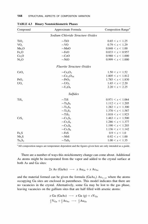
There are a number of ways this stoichiometry change can come about. AdditionalAs atoms might be incorporated from the vapor and added to the crystal surface atboth As and Ga sites:
2x As (GaAs) �! x AsGa þ x AsAs
and the material formed can be given the formula (GaAsx) As1þx, where the atomsoccupying Ga sites are enclosed in parentheses. This model indicates that there areno vacancies in the crystal. Alternatively, some Ga may be lost to the gas phase,leaving vacancies on the gallium sites that are half filled with arsenic atoms:
x Ga (GaAs) �! x Ga (g)þ xVGa
x2 VGa þ x
2 AsAs �! x2 AsGa
TABLE 4.3 Binary Nonstoichiometric Phases
Compound Approximate Formula Composition Rangea
Sodium Chloride Structure Oxides
TiOx �TiO 0.65, x, 1.25VOx �VO 0.79, x, 1.29MnxO �MnO 0.848 , x, 1.00FexO �FeO 0.833 , x, 0.957CoxO �CoO 0.988 , x, 1.000NixO �NiO 0.999 , x, 1.000
Fluorite Structure Oxides
CeOx �Ce2O3 1.50, x, 1.52�Ce32O58 1.805 , x, 1.812
PrOx �PrO2 1.785 , x, 1.830UOx �UO2 1.65, x, 2.20
�U4O9 2.20, x, 2.25
Sulfides
TiSx �TiS 0.971 , x, 1.064�Ti8S9 1.112 , x, 1.205�Ti3S4 1.282 , x, 1.300�Ti2S3 1.370 , x, 1.587�TiS2 1.818 , x, 1.923
CrSx �Cr2S3 1.463 , x, 1.500�Cr3S4 1.286 , x, 1.377�Cr5S6 1.190 , x, 1.203�Cr7S8 1.136 , x, 1.142
FexS �FeS 0.9 , x, 1.0NbxS �NbS 0.92, x, 1.00TaxS2 �TaS2 1.00, x, 1.35
aAll composition ranges are temperature dependent and the figures given here are only intended as a guide.
144 STRUCTURAL ASPECTS OF COMPOSITION VARIATION

This would produce a crystal with a formula (Ga12xAsx/2)As12x/2, where the atomsoccupying Ga sites are enclosed in parentheses. This model indicates that there arevacancies on both the Ga and As sublattices in the crystal.
These point defect models need to be regarded as a first approximation.Calculations for stoichiometric GaAs suggest that balanced populations of vacancieson both gallium and arsenic sites, VGa and VAs, exist, as well as defect complexes.Calculation for nonstoichiometric materials would undoubtedly throw further lighton the most probable defect populations present.
4.3.2 Vacancies: Cobalt Oxide, CoO
The best known inorganic compounds that show small composition variations due toa population of vacancies are probably the transition-metal monoxides, but a largenumber of other oxides also fall into this class. Cobalt oxide, CoO, which adoptsthe sodium chloride structure, is a representative example. The oxide is oftenoxygen rich and is considered to accommodate the composition change by way ofa population of vacancies on the normally occupied metal positions, to give trueformula Co12xO. In the stoichiometric crystal, the nominal charges on the speciesare Co2þ and O22. In the crystal containing metal vacancies, these will bear an effec-tive negative charge, V20
Co. Charge compensation is achieved by the production ofholes, which are generally considered to be sited on Co2þ ions to generate Co3þ
defects. The formation of metal ion vacancies can be written in terms of theformal equations:
x2 O2(CoO) O xOO þ x V20
Co þ 2x h†
2x h† þ 2x CoCo O 2x Co†Co
The crystal now contains two-point defect species, Co2þ vacancies, and double thenumber of Co3þ ions. The electronic implications of these changes are dealt within Chapters 7 and 8.
4.3.3 Interstitials: La2CuO4 and Sr2CuO2F2
The phase La2CuO4 contains trivalent La and divalent Cu and adopts a slightly dis-torted version of the K2NiF4 structure in which the CuO6 octahedra are lengthenedalong the c axis due to the Jahn–Teller effect.2 (In the superconductor literaturethis structure is often called the T or T/O structure.) The La2CuO4 structure containssheets of the perovskite type 1 CuO6 octahedron in thickness stacked up one on top ofthe other (Fig. 4.5).
2Transition-metal ions Cr2þ, Mn3þ Co2þ, Ni3þ, and Cu2þ in regular MO6 octahedral coordination can gainstability by allowing the octahedron to distort so that there are two long and four short bonds, or vice versa.This is called the Jahn–Teller effect.
4.3 POINT DEFECTS AND DEPARTURES FROM STOICHIOMETRY 145
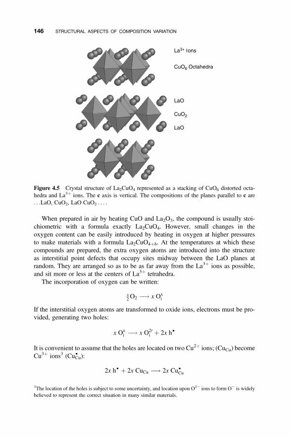
When prepared in air by heating CuO and La2O3, the compound is usually stoi-chiometric with a formula exactly La2CuO4. However, small changes in theoxygen content can be easily introduced by heating in oxygen at higher pressuresto make materials with a formula La2CuO4þd. At the temperatures at which thesecompounds are prepared, the extra oxygen atoms are introduced into the structureas interstitial point defects that occupy sites midway between the LaO planes atrandom. They are arranged so as to be as far away from the La3þ ions as possible,and sit more or less at the centers of La3þ tetrahedra.
The incorporation of oxygen can be written:
x2 O2 �! x Ox
i
If the interstitial oxygen atoms are transformed to oxide ions, electrons must be pro-vided, generating two holes:
x Oxi �! x O20
i þ 2x h†
It is convenient to assume that the holes are located on two Cu2þ ions; (CuCu) becomeCu3þ ions3 (CuCu
† ):
2x h† þ 2x CuCu �! 2x Cu†Cu
Figure 4.5 Crystal structure of La2CuO4 represented as a stacking of CuO6 distorted octa-hedra and La3þ ions. The c axis is vertical. The compositions of the planes parallel to c are. . .LaO, CuO2, LaO CuO2 . . . .
3The location of the holes is subject to some uncertainty, and location upon O22 ions to form O2 is widelybelieved to represent the correct situation in many similar materials.
146 STRUCTURAL ASPECTS OF COMPOSITION VARIATION
This is the same as saying that two Cu3þ ions are created per oxygen interstitial:
x2 O2 þ 2x CuCu(La2CuO4) �! x Ox
i þ 2x Cu†Cu
The electronic properties of these oxygen-rich solids change drastically from that ofthe typically insulating ceramic La2CuO4. The material becomes first a metal andthen a superconductor (Section 8.5).
The compound Sr2CuO2F2 also adopts the K2NiF4 structure and in its normal stateis a poor conductor. In a similar way to La2CuO4, extra F2 ions can be added into(more or less) the same interstitial sites to give an overall composition ofSr2CuO2F2þx. Once again the change in stoichiometry results in the transformationof the solid into a metal and a superconductor, due to the generation of holes:
12 F2 �! F0i þ h†
These may be located on the Cu2þ ions to form Cu3þ.The interaction between these interstitials is considerable, and when either of these
phases is heated at temperatures at which diffusion can occur, they order, thus gen-erating new structures.
4.3.4 Interstitial Impurities: Alloys and Hydrides
There are many metal alloys that contain interstitial atoms embedded in the metalstructure. Traditionally, the interstitial alloys most studied are those of the transitionmetals with carbon and nitrogen, as the addition of these atoms to the crystal structureincreases the hardness of the metal considerably. Steel remains the most importanttraditional interstitial alloy from a world perspective. It consists of carbon atoms dis-tributed at random in interstitial sites within the face-centered cubic structure of ironto form the phase austenite, which exists over the composition range from pure iron toapproximately 7 at % carbon.
More recently, hydrogen storage has become important, and interstitial alloysformed by incorporation of hydrogen into metals are of considerable interest.Niobium is typical of these. This metal is able to incorporate interstitial hydrogenup to a limiting composition of approximately NbH0.1.
4.3.5 Defect Variation: Zinc Oxide, ZnO
Zinc oxide is normally an n-type semiconductor with a narrow stoichiometry range.For many years it was believed that this electronic behavior was due to the presence ofZn†i (Znþ) interstitials, but it is now apparent that the defect structure of this simpleoxide is more complicated. The main point defects that can be considered to exist arevacancies, VO and VZn, interstitials, Oi and Zni, and antisite defects, OZn and ZnO.Each of these can show various charge states and can occupy several different
4.3 POINT DEFECTS AND DEPARTURES FROM STOICHIOMETRY 147
interstitial sites in the crystal. Combining these, the order of 20 or more defect speciescan be designated.
Calculations can provide information on the formation energy of these alterna-tives. Broadly speaking, the number of defects nd is related to the formationenergy by an equation of the sort described in Chapter 2:
nd ¼ Ns exp�E
kT
� �
where Ns is the number of sites affected by the defect in question, E the defect for-mation energy, k the Boltzmann constant, and T the temperature (K). Using calculateddefect formation energies, the general result is that in Zn-rich conditions oxygenvacancies, VO
2†, prevail, whereas in the O-rich regime neutral zinc vacancies, VZn,are preferred. The defect type thus changes as the crystal swings from Zn rich toO rich.
Chemically, this can be expressed in terms of defect formation equations. Takingthe partial pressure of the zinc as dominant, zinc-rich material can be formulated bythe capture of zinc atoms from the gas phase:
Zn (ZnO) �! ZnZn þ VO2†
where ZnZn represents a Zn2þ ion on a normal cation site and VO
2† an oxygen vacancyon a normal anion site. Similarly, the oxygen-rich material can be generated by lossof zinc atoms to the gas phase:
ZnZn �! Zn(g)þ V20Zn þ 2h†
In this equation, the zinc is lost as atoms, not ions, and two electrons have to bedonated to the Zn2þ for this to be possible, leaving two holes in the crystal. Theseholes can sit at the vacancy to create a neutral defect, VZn:
V20Zn þ 2h† �! Vx
Zn
4.3.6 Defect Spinels, M2O3
The normal spinel structure has a formula AB2O4, where A2þ ions occupy tetrahedral
sites and B3þ ions octahedral sites in a matrix composed of cubic close-packedoxygen ions (Supplementary Material S1). A number of oxides, generally preparedat moderate temperatures, adopt this structure while maintaining a compositionM2O3. The best known of these are g-Al2O3, g -Cr2O3, g-Fe2O3, and g-Ga2O3. Ofthese the aluminum oxide is an important surface-active material, and the ironoxide is widely used in magnetic data recording.
148 STRUCTURAL ASPECTS OF COMPOSITION VARIATION
Because the phases are prepared at low temperatures, they are poorly crystallineand may contain variable amounts of water, with a consequence that the structureshave been inadequately characterized by X-ray diffraction. Nevertheless, thesestudies have suggested that these compounds have cation vacancies distributedover both octahedral and tetrahedral sites. Thus, the compounds are given a spinel-like formula VMM8O12. This may not hold for all materials. Density functionaltheory calculations suggest that in g-Al2O3, all of the vacancies are located on theoctahedral sites so that the structure can be formulated (Al)[Al1.67V0.33]O4, wherethe tetrahedrally coordinated Al is written in parentheses ( ) and the octahedrallycoordinated Al in square brackets [ ]. Similarly, there is evidence that morecomplex ordering patterns of defects may occur in magnetic g-Fe2O3, perhaps as aresult of magnetic interactions.
4.4 DEFECT CLUSTERS
4.4.1 Point Defect Aggregations
Even when the composition range of a nonstoichiometric phase remains small,complex defect structures can occur. Both atomistic simulations and quantum mech-anical calculations suggest that point defects tend to cluster. In many systems isolatedpoint defects have been replaced by aggregates of point defects with a well-definedstructure. These materials therefore contain a population of volume defects.
At low concentrations, defect clusters can be arranged at random, mimicking pointdefects but on a larger scale. This seems to be the case in zinc oxide, ZnO, doped withphosphorus, P. The favored defects appear to be phosphorus substituted for Zn, PZn
† ,and vacancies on zinc sites, VZn
20 . These defects are not isolated but preferentially formclusters consisting of (PZn
† þ 2V20Zn).
Defect clusters are similarly prominent in hydrated phases. For example, anatasenanocrystals prepared by sol-gel methods contain high numbers of vacancies ontitanium sites, counterbalanced by four protons surrounding the vacancy, making a(V40
Ti 4H†) cluster. In effect the protons are associated with oxygen ions to form
OH2 ions, and a vacancy–hydroxyl cluster is an equally valid description. Similarclusters are known in other hydrated systems, the best characterized being Mn4þ
vacancies plus 4H† in g-MnO2, known as Reutschi defects.Antisite defects in the pyrochore structure Er2Ti2O7 were mentioned previously
(Section 1.10). These defects also occur in the nonstoichiometric compoundEr2.09Ti1.94O6.952, which is slightly Er2O3-rich compared to the stoichiometricparent phase. The formation of the antisite pair is now accompanied by the parallelformation of oxygen vacancies:
ErEr þ TiTi �! Er0Ti þ Ti†Er
OO �! V2†O þ O20
i
4.4 DEFECT CLUSTERS 149
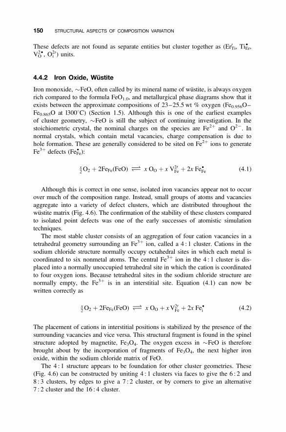
These defects are not found as separate entities but cluster together as (Er0Ti, TiEr† ,
VO2†, O20
i ) units.
4.4.2 Iron Oxide, Wustite
Iron monoxide, �FeO, often called by its mineral name of wustite, is always oxygenrich compared to the formula FeO1.0, and metallurgical phase diagrams show that itexists between the approximate compositions of 23–25.5 wt % oxygen (Fe0.956O–Fe0.865O at l3008C) (Section 1.5). Although this is one of the earliest examplesof cluster geometry, �FeO is still the subject of continuing investigation. In thestoichiometric crystal, the nominal charges on the species are Fe2þ and O22. Innormal crystals, which contain metal vacancies, charge compensation is due tohole formation. These are generally considered to be sited on Fe2þ ions to generateFe3þ defects (FeFe
† ):
x2 O2 þ 2FeFe(FeO) O x OO þ x V20
Fe þ 2x Fe†Fe (4:1)
Although this is correct in one sense, isolated iron vacancies appear not to occurover much of the composition range. Instead, small groups of atoms and vacanciesaggregate into a variety of defect clusters, which are distributed throughout thewustite matrix (Fig. 4.6). The confirmation of the stability of these clusters comparedto isolated point defects was one of the early successes of atomistic simulationtechniques.
The most stable cluster consists of an aggregation of four cation vacancies in atetrahedral geometry surrounding an Fe3þ ion, called a 4 : 1 cluster. Cations in thesodium chloride structure normally occupy octahedral sites in which each metal iscoordinated to six nonmetal atoms. The central Fe3þ ion in the 4 : 1 cluster is dis-placed into a normally unoccupied tetrahedral site in which the cation is coordinatedto four oxygen ions. Because tetrahedral sites in the sodium chloride structure arenormally empty, the Fe3þ is in an interstitial site. Equation (4.1) can now bewritten correctly as
x2 O2 þ 2FeFe(FeO) O x OO þ xV20
Fe þ 2x Fe†i (4:2)
The placement of cations in interstitial positions is stabilized by the presence of thesurrounding vacancies and vice versa. This structural fragment is found in the spinelstructure adopted by magnetite, Fe3O4. The oxygen excess in �FeO is thereforebrought about by the incorporation of fragments of Fe3O4, the next higher ironoxide, within the sodium chloride matrix of FeO.
The 4 : 1 structure appears to be foundation for other cluster geometries. These(Fig. 4.6) can be constructed by uniting 4 : 1 clusters via faces to give the 6 : 2 and8 : 3 clusters, by edges to give a 7 : 2 cluster, or by corners to give an alternative7 : 2 cluster and the 16 : 4 cluster.
150 STRUCTURAL ASPECTS OF COMPOSITION VARIATION
The forces uniting these clusters seem to be relatively weak, as the overall clustergeometry appears to vary both with temperature, composition, and oxygen partialpressure. Broadly speaking, relatively isolated 4 : 1 clusters are found at the highesttemperatures and in iron-rich compositions. As the temperature and relative amountof iron falls, more complex clusters are found. To some extent it is as if the 4 : 1clusters aggregate at lower temperatures and dissociate at higher temperatures.
Despite the numerous studies made on this material, the defect structures found inthis system are still not completely clarified. For example, it has been shown that in
Figure 4.6 Point defect clusters in Fe12xO: (a) 4 : 1, (b) 6 : 2, (c) 8 : 3, (d ) 7 : 2, (e) 7 : 2, and( f ) 16 : 4. The open circles represent O22 ions on normal sites, the shaded circles Fe3þ inter-stitials in tetrahedral sites, and the small filled circles Fe2þ vacancies. In ( f ), four 4 : 1 clustersare arranged tetrahedrally around a central cluster, drawn with heavy outline.
4.4 DEFECT CLUSTERS 151
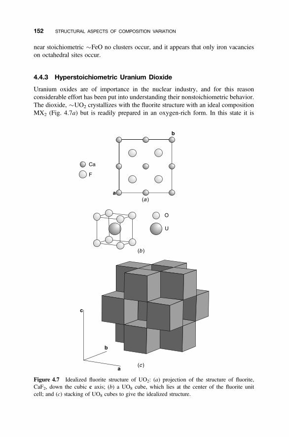
near stoichiometric �FeO no clusters occur, and it appears that only iron vacancieson octahedral sites occur.
4.4.3 Hyperstoichiometric Uranium Dioxide
Uranium oxides are of importance in the nuclear industry, and for this reasonconsiderable effort has been put into understanding their nonstoichiometric behavior.The dioxide, �UO2 crystallizes with the fluorite structure with an ideal compositionMX2 (Fig. 4.7a) but is readily prepared in an oxygen-rich form. In this state it is
Figure 4.7 Idealized fluorite structure of UO2: (a) projection of the structure of fluorite,CaF2, down the cubic c axis; (b) a UO8 cube, which lies at the center of the fluorite unitcell; and (c) stacking of UO8 cubes to give the idealized structure.
152 STRUCTURAL ASPECTS OF COMPOSITION VARIATION
an example of a large class of nonstoichiometric compounds grouped under theheading of anion-excess fluorite structure phases. As with iron monoxide,hyperstoichiometric uranium dioxide, UO2þx, was one of the earliest materials con-taining clusters to be studied structurally and is still the subject of continuinginvestigation.
At temperatures above 11008C uranium dioxide can exist between the compositionlimits of UO2 and approximately UO2.25. The fluorite structure of the parent UO2 canbe imagined to be constructed of edge-shared UO8 cubes (Fig. 4.7b and 4.7c). At thesimplest level, the composition variation can be considered to be due to the presenceof interstitial anions. Each cube containing a U ion is adjacent to an empty cube. Theincorporation of anions, O22, within these empty cubes is therefore possible, and it isthese interstitial positions that are occupied in oxygen-rich UO2þx.
As in the case of the oxides described above, the incorporation of additionaloxygen ions in the solid will upset the charge balance by introducing extra negativecharge. This can be corrected by increasing the charge on the parent cations, so thatsome of the U4þ ions must become either U5þ or U6þ. This can be written as
x2 O2 O x O20
i þ 2x U†U
x2 O2 O x O20
i þ x U2†U
Initial crystallographic studies of oxygen-rich material made it clear that a modelfor the defect structure consisting of random interstitial point defects was too simpleand that point defect clusters were present. One of the earliest cluster geometries to besuggested was that of the so-called Willis or 2 : 2 : 2 cluster in UO2þx. The cluster isconstructed from four “empty” oxygen cubes, joined in the normal fluorite arrange-ment (Fig. 4.8a and 4.8b). The four cubes each contain an internal interstitial oxygenion. These do not sit at the cube centers but are displaced either along a cube bodydiagonal ,111. direction in two of the cubes (Fig. 4.8c) or along a diagonal parallelto ,110. in the other two (Fig. 4.8d). The cluster is formed by uniting two periph-eral cubes of ,111. type with two central cubes of ,110. type (Fig. 4.8e). Twoof the oxygen ions at the centers of the cubes are derived from the extra oxygencontent of the crystal, and two are from normally occupied positions. These twooxygen ions, which should be found at the junctions of three cubes, move into inter-stitial sites in the middle of the two central cubes (Fig. 4.8e) and in so doing createtwo oxygen vacancies at these corner junctions. The cluster name comes from the factthat there are two interstitials created by moving normal anions (called ,110. inter-stitials), two normal interstitials (called ,111. interstitials), and two vacancies inthe grouping. [In some literature, these defects are labeled as O0 (,110.) and O00
(,111.). The same nomenclature is found with clusters in anion excess fluorides(Section 4.4.3), where these are labeled as F0 (,110.) and F00 (,111.). The con-fusion with the Kroger–Vink notation for effective charge is obvious, and thisnomenclature will not be used here. Where necessary these sites will be referred toas O1 or F1 (,110.) and O2 or F2 (,111.)].
4.4 DEFECT CLUSTERS 153
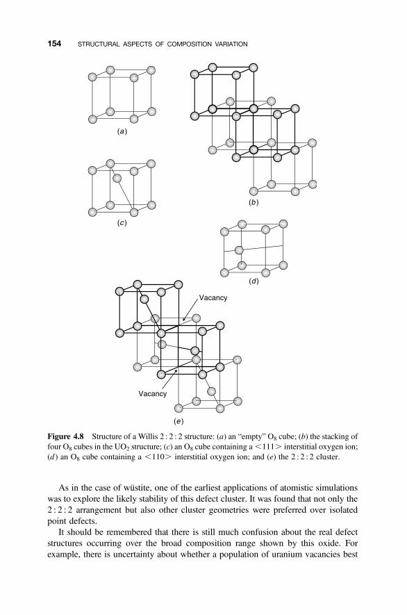
As in the case of wustite, one of the earliest applications of atomistic simulationswas to explore the likely stability of this defect cluster. It was found that not only the2 : 2 : 2 arrangement but also other cluster geometries were preferred over isolatedpoint defects.
It should be remembered that there is still much confusion about the real defectstructures occurring over the broad composition range shown by this oxide. Forexample, there is uncertainty about whether a population of uranium vacancies best
Figure 4.8 Structure of a Willis 2 : 2 : 2 structure: (a) an “empty” O8 cube; (b) the stacking offour O8 cubes in the UO2 structure; (c) an O8 cube containing a ,111. interstitial oxygen ion;(d ) an O8 cube containing a ,110. interstitial oxygen ion; and (e) the 2 : 2 : 2 cluster.
154 STRUCTURAL ASPECTS OF COMPOSITION VARIATION
explains the data or whether both uranium vacancies and oxygen interstitials arepresent, at least in some composition regions.
4.4.4 Anion-Excess Fluorite Structures
Anion-excess fluorite structure materials can be typified by the products of the reac-tion of fluorite, CaF2, with fluorides of higher valance atoms, such as LaF3, YF3,ThF4, and UF4. In all cases nonstoichiometric phases form that have considerablecomposition ranges, and the parent structure can accommodate up to approximately50 mol% of the added fluoride to form anion-rich fluorite structures. For example, thelimiting composition of the nonstoichiometric fluorite structure phase in the CaF2–YF3 system is approximately 0.6CaF2 : 0.4YF3 at 11008C. The formula can bewritten as CaxY12xF2þx, where x takes values between 0 and 0.4.
Across the phase range of all of these systems themetal atoms La, Y, and the like sub-stitute for calciumon the cation sublattice.Charge balance is ensured by the incorporationof additional F2 ions into the crystals, which, to a first approximation, can be regardedas F2 interstitials that occupy the unoccupied (F8) coordination polyhedra (Fig. 4.7):
LaF3(CaF2) �! La†Ca þ 2FF þ F0i
ThF4(CaF2) �! Th2†Ca þ 2FF þ 2F0i
One interstitial ion needs to be accommodated for each M3þ incorporated and two foreach M4þ cation.
There are large numbers of anion excess fluorite-related structures known, a smallnumber of which are listed in Table 4.4. The defect chemistry of these phases is enor-mously complex, deserving of far more space than can be allocated here. The defectstructures can be roughly divided into three categories: random interstitials, which in
TABLE 4.4 Some Anion-Excess Fluorite-Related Phases
System Approximate Composition Range
Zr(N, O, F)x 2.12, x, 2.25Nb2Zrx22O2xþ1 7.1, x, 12Ln oxyfluorides (Ln ¼ Y, Sm–Lu) Typically MX2.12–MX2.20
ZrO2 þ ZrF4 Typically MX2.12–MX2.20
ZrO2 þ UO2F Typically MX2.12–MX2.20
AF2–BiF3 (A ¼ Sr, Ba) MX2.45–MX2.5
(12 x)KF þ xBiF3 (K12xBixF1þ2x) 0.50, x, 0.70(12 x)RbF þ xBiF3 (Rb12xBixF1þ2x) 0.50, x, 0.60U4O92y UO2.235–UO2.245
(12 x)PbF2 þ xInF3 (Pb12xInxF2þx) 0, x, 0.25LnF3–2xOx (Ln ¼ La–Nd) 0.58, x, 1Ca12xMxF2þ2x (M ¼ Th, U) 0, x, 0.18Ba12xBixOzF2þx22z 0, x, 0.4; 0 , z , 0.25
4.4 DEFECT CLUSTERS 155
reality almost never exist, defect clusters, which may be ordered or disordered, andmodulated structures. These latter are described in Section 4.10, while here someof the cluster geometries are described.
As in the case of UO2þx, crystallographic studies of the anion-excess fluoritephases indicated that there were complex arrangements of interstitials and vacancies,arranged in clusters, present. Some of these clusters are relatively simple to envisage,such as the 2 : 2 : 2 cluster described above, but many are of greater complexity.Indeed, there is still uncertainty of the true defect structure of many of thesephases over all composition ranges and temperature regimes, even the moststudied, Ca12xYxF2þx in the CaF2–YF3 system. The following descriptions musttherefore be read in the light that further revisions may be likely.
The foundation of many of the clusters found in the anion-excess fluorites is asquare antiprism of anions. A square antiprism can be constructed from a cube bythe rotation of one face of anions by 458 with respect to the opposite face (Fig. 4.9aand 4.9b). The other principal cluster geometry is that of the cuboctahedron. Thiscan be constructed from a cube by truncating (i.e., removing) the corners until eightequilateral triangles are formed (Fig. 4.9c and 4.9d). In terms of the MF2 fluorite struc-ture, an MF8 cube can be transformed into an MF8 square antiprism by moving fouranions from normal positions into the appropriate F1 ,110. defect positions, leavingfour vacancies at the cube corners (Fig. 4.9e). This operation leaves the cation pos-itions unchanged, but the structure now contains four ,110. interstitials and fouranion vacancies. If six such operations are performed on a group of six cubes arrangedaround the faces of a central empty cube, the resulting central polyhedron so formed isa cuboctahedron with a composition of M6F36 (Fig. 4.9f ). If a central anion is includedin the cluster, the composition becomes M6F37.
There are many ways in which these square antiprism and cuboctahedral defectclusters can be arranged. A nonstoichiometric composition can be achieved by arandom distribution of varying numbers of clusters throughout the crystal matrix.This appears to occur in Ca0.94Y0.06F2.06, which contains statistically distributedcuboctahedral clusters.
Alternatively, the clusters can order, in which case new structures that are essen-tially defect free, are produced. In the PbF2–ZrF4 phases Pb12xZrxF2þ2x, in which xcan take the range 0–0.18, pairs of square antiprisms are found. As well as disorderedarrangements of the antiprisms, ordering of the clusters is frequent, giving rise to aseries of phases PbnZr2F2nþ8, which includes Pb3ZrF10 (n ¼ 6) and Pb5ZrF14 (n ¼10) (Fig. 4.10). Other members of this series of ordered structures can be constructedby varying the spacing between the rows of square antiprisms.
Ordered cuboctahedra appear in a number of structures, for example, inNa7Zr6F31, a number of M7U6F31 and MTh6F31 phases, and in Ba4Bi3F17, anordered structure in the anion-excess fluorite range that is found in the BaF2–BiF3system. However, the most important of these ordered structures is that adopted bythe oxide U4O92d. This is the next higher oxide to the UO2þx phase describedabove (Section 4.4.3). The composition is never exactly U4O9, a fact accounted forby the structure, which consists of an ordered array of U6O36 cuboctahedra in afluorite structure matrix.
156 STRUCTURAL ASPECTS OF COMPOSITION VARIATION
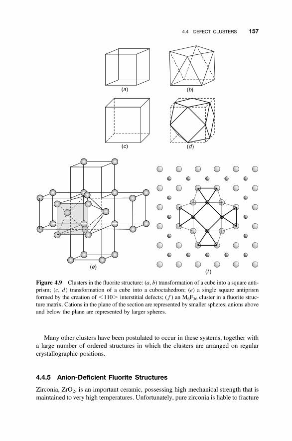
Many other clusters have been postulated to occur in these systems, together witha large number of ordered structures in which the clusters are arranged on regularcrystallographic positions.
4.4.5 Anion-Deficient Fluorite Structures
Zirconia, ZrO2, is an important ceramic, possessing high mechanical strength that ismaintained to very high temperatures. Unfortunately, pure zirconia is liable to fracture
Figure 4.9 Clusters in the fluorite structure: (a, b) transformation of a cube into a square anti-prism; (c, d ) transformation of a cube into a cuboctahedron; (e) a single square antiprismformed by the creation of ,110. interstitial defects; ( f ) an M6F36 cluster in a fluorite struc-ture matrix. Cations in the plane of the section are represented by smaller spheres; anions aboveand below the plane are represented by larger spheres.
4.4 DEFECT CLUSTERS 157
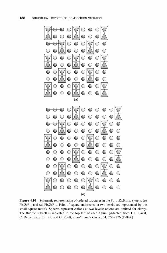
Figure 4.10 Schematic representation of ordered structures in the Pb12xZrxK2þ2x system: (a)Pb3ZrF10 and (b) Pb5ZrF14. Pairs of square antiprisms, at two levels, are represented by thesmall square motifs. Spheres represent cations at two levels; anions are omitted for clarity.The fluorite subcell is indicated in the top left of each figure. [Adapted from J. P. Laval,C. Depierrefixe, B. Frit, and G. Roult, J. Solid State Chem., 54, 260–276 (1984).]
158 STRUCTURAL ASPECTS OF COMPOSITION VARIATION
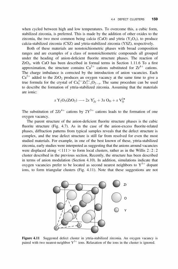
when cycled between high and low temperatures. To overcome this, a cubic form,stabilized zirconia, is preferred. This is made by the addition of other oxides to thezirconia, the two most common being calcia (CaO) and yttria (Y2O3), to producecalcia-stabilized zirconia (CSZ) and yttria-stabilized zirconia (YSZ), respectively.
Both of these materials are nonstoichiometric phases with broad compositionranges and are examples of a class of nonstoichiometric compounds all groupedunder the heading of anion-deficient fluorite structure phases. The reaction ofZrO2, with CaO has been described in formal terms in Section 1.11.6 To a firstapproximation, the structure contains Ca2þ cations substituted for Zr4þ cations.The charge imbalance is corrected by the introduction of anion vacancies. EachCa2þ added to the ZrO2 produces an oxygen vacancy at the same time to give atrue formula for the crystal of Ca2þx Zr4þ12xO22x. The same procedure can be usedto describe the formation of yttria-stabilized zirconia. Assuming that the materialsare ionic:
x Y2O3(ZrO2) �! 2x Y0Zr þ 3x OO þ x V2†
O
The substitution of 2Zr4þ cations by 2Y3þ cations leads to the formation of oneoxygen vacancy.
The parent structure of the anion-deficient fluorite structure phases is the cubicfluorite structure (Fig. 4.7). As in the case of the anion-excess fluorite-relatedphases, diffraction patterns from typical samples reveals that the defect structure iscomplex, and the true defect structure is still far from resolved for even the moststudied materials. For example, in one of the best known of these, yttria-stabilizedzirconia, early studies were interpreted as suggesting that the anions around vacancieswere displaced along ,111. to form local clusters, rather as in the Willis 2 : 2 : 2cluster described in the previous section, Recently, the structure has been describedin terms of anion modulation (Section 4.10). In addition, simulations indicate thatoxygen vacancies prefer to be located as second nearest neighbors to Y3þ dopantions, to form triangular clusters (Fig. 4.11). Note that these suggestions are not
Figure 4.11 Suggested defect cluster in yttria-stabilized zirconia. An oxygen vacancy ispaired with two nearest-neighbor Y3þ ions. Relaxation of the ions in the cluster is ignored.
4.4 DEFECT CLUSTERS 159
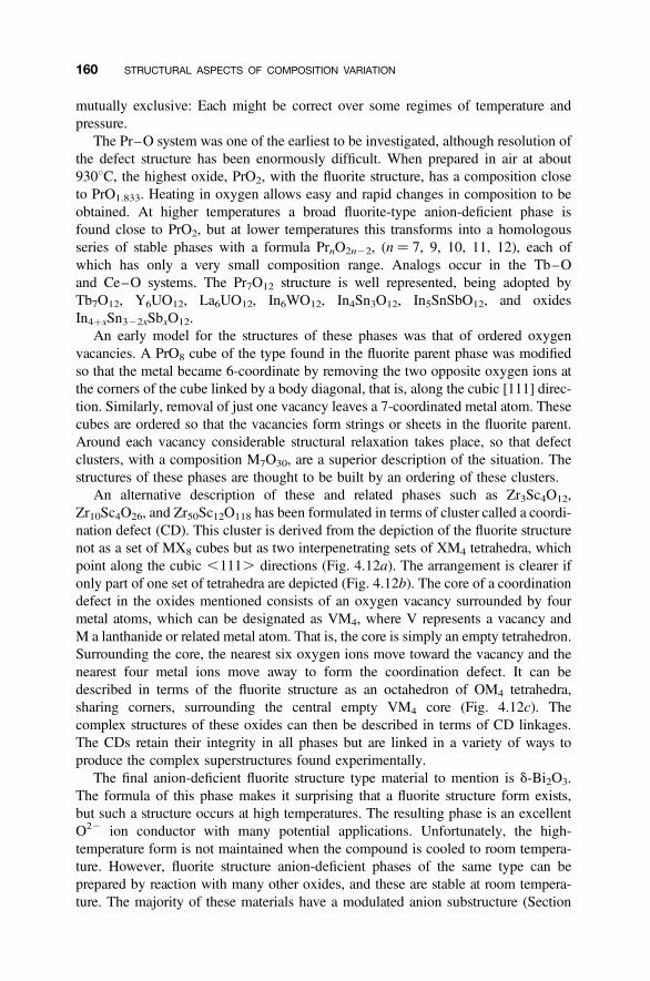
mutually exclusive: Each might be correct over some regimes of temperature andpressure.
The Pr–O system was one of the earliest to be investigated, although resolution ofthe defect structure has been enormously difficult. When prepared in air at about9308C, the highest oxide, PrO2, with the fluorite structure, has a composition closeto PrO1.833. Heating in oxygen allows easy and rapid changes in composition to beobtained. At higher temperatures a broad fluorite-type anion-deficient phase isfound close to PrO2, but at lower temperatures this transforms into a homologousseries of stable phases with a formula PrnO2n22, (n ¼ 7, 9, 10, 11, 12), each ofwhich has only a very small composition range. Analogs occur in the Tb–Oand Ce–O systems. The Pr7O12 structure is well represented, being adopted byTb7O12, Y6UO12, La6UO12, In6WO12, In4Sn3O12, In5SnSbO12, and oxidesIn4þxSn322xSbxO12.
An early model for the structures of these phases was that of ordered oxygenvacancies. A PrO8 cube of the type found in the fluorite parent phase was modifiedso that the metal became 6-coordinate by removing the two opposite oxygen ions atthe corners of the cube linked by a body diagonal, that is, along the cubic [111] direc-tion. Similarly, removal of just one vacancy leaves a 7-coordinated metal atom. Thesecubes are ordered so that the vacancies form strings or sheets in the fluorite parent.Around each vacancy considerable structural relaxation takes place, so that defectclusters, with a composition M7O30, are a superior description of the situation. Thestructures of these phases are thought to be built by an ordering of these clusters.
An alternative description of these and related phases such as Zr3Sc4O12,Zr10Sc4O26, and Zr50Sc12O118 has been formulated in terms of cluster called a coordi-nation defect (CD). This cluster is derived from the depiction of the fluorite structurenot as a set of MX8 cubes but as two interpenetrating sets of XM4 tetrahedra, whichpoint along the cubic ,111. directions (Fig. 4.12a). The arrangement is clearer ifonly part of one set of tetrahedra are depicted (Fig. 4.12b). The core of a coordinationdefect in the oxides mentioned consists of an oxygen vacancy surrounded by fourmetal atoms, which can be designated as VM4, where V represents a vacancy andM a lanthanide or related metal atom. That is, the core is simply an empty tetrahedron.Surrounding the core, the nearest six oxygen ions move toward the vacancy and thenearest four metal ions move away to form the coordination defect. It can bedescribed in terms of the fluorite structure as an octahedron of OM4 tetrahedra,sharing corners, surrounding the central empty VM4 core (Fig. 4.12c). Thecomplex structures of these oxides can then be described in terms of CD linkages.The CDs retain their integrity in all phases but are linked in a variety of ways toproduce the complex superstructures found experimentally.
The final anion-deficient fluorite structure type material to mention is d-Bi2O3.The formula of this phase makes it surprising that a fluorite structure form exists,but such a structure occurs at high temperatures. The resulting phase is an excellentO22 ion conductor with many potential applications. Unfortunately, the high-temperature form is not maintained when the compound is cooled to room tempera-ture. However, fluorite structure anion-deficient phases of the same type can beprepared by reaction with many other oxides, and these are stable at room tempera-ture. The majority of these materials have a modulated anion substructure (Section
160 STRUCTURAL ASPECTS OF COMPOSITION VARIATION
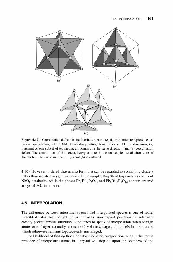
4.10). However, ordered phases also form that can be regarded as containing clustersrather than isolated oxygen vacancies. For example, Bi94Nb32O221 contains chains ofNbO6 octahedra, while the phases Pb5Bi17P5O43 and Pb5Bi18P4O42 contain orderedarrays of PO4 tetrahedra.
4.5 INTERPOLATION
The difference between interstitial species and interpolated species is one of scale.Interstitial sites are thought of as normally unoccupied positions in relativelyclosely packed crystal structures. One tends to speak of interpolation when foreignatoms enter larger normally unoccupied volumes, cages, or tunnels in a structure,which otherwise remains topotactically unchanged.
The likelihood of finding that a nonstoichiometric composition range is due to thepresence of interpolated atoms in a crystal will depend upon the openness of the
Figure 4.12 Coordination defects in the fluorite structure: (a) fluorite structure represented astwo interpenetrating sets of XM4 tetrahedra pointing along the cube ,111. directions; (b)fragment of one subset of tetrahedra, all pointing in the same direction; and (c) coordinationdefect. The central part of the defect, heavy outline, is the unoccupied tetrahedron core ofthe cluster. The cubic unit cell in (a) and (b) is outlined.
4.5 INTERPOLATION 161
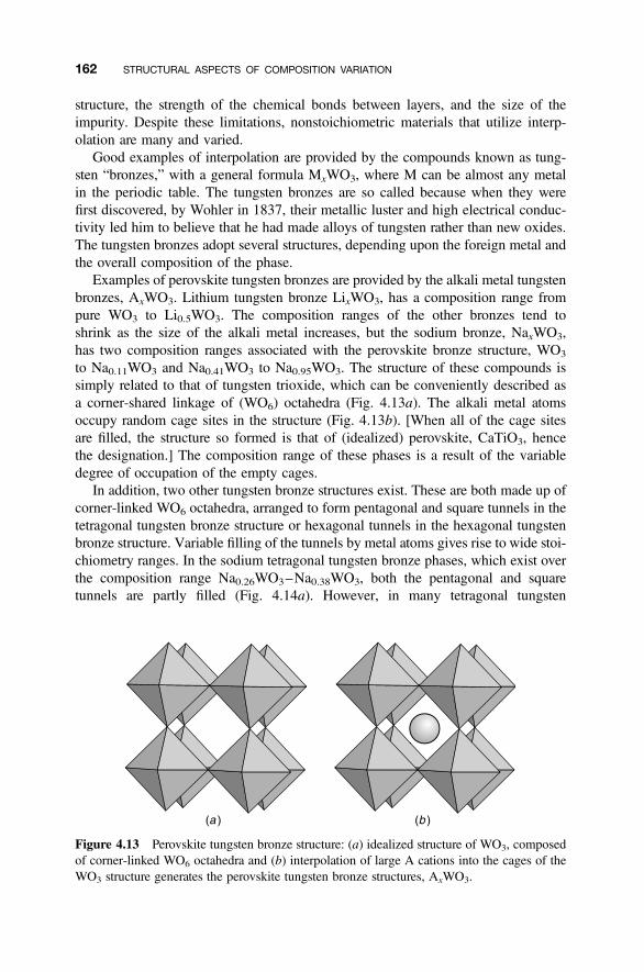
structure, the strength of the chemical bonds between layers, and the size of theimpurity. Despite these limitations, nonstoichiometric materials that utilize interp-olation are many and varied.
Good examples of interpolation are provided by the compounds known as tung-sten “bronzes,” with a general formula MxWO3, where M can be almost any metalin the periodic table. The tungsten bronzes are so called because when they werefirst discovered, by Wohler in 1837, their metallic luster and high electrical conduc-tivity led him to believe that he had made alloys of tungsten rather than new oxides.The tungsten bronzes adopt several structures, depending upon the foreign metal andthe overall composition of the phase.
Examples of perovskite tungsten bronzes are provided by the alkali metal tungstenbronzes, AxWO3. Lithium tungsten bronze LixWO3, has a composition range frompure WO3 to Li0.5WO3. The composition ranges of the other bronzes tend toshrink as the size of the alkali metal increases, but the sodium bronze, NaxWO3,has two composition ranges associated with the perovskite bronze structure, WO3
to Na0.11WO3 and Na0.41WO3 to Na0.95WO3. The structure of these compounds issimply related to that of tungsten trioxide, which can be conveniently described asa corner-shared linkage of (WO6) octahedra (Fig. 4.13a). The alkali metal atomsoccupy random cage sites in the structure (Fig. 4.13b). [When all of the cage sitesare filled, the structure so formed is that of (idealized) perovskite, CaTiO3, hencethe designation.] The composition range of these phases is a result of the variabledegree of occupation of the empty cages.
In addition, two other tungsten bronze structures exist. These are both made up ofcorner-linked WO6 octahedra, arranged to form pentagonal and square tunnels in thetetragonal tungsten bronze structure or hexagonal tunnels in the hexagonal tungstenbronze structure. Variable filling of the tunnels by metal atoms gives rise to wide stoi-chiometry ranges. In the sodium tetragonal tungsten bronze phases, which exist overthe composition range Na0.26WO3–Na0.38WO3, both the pentagonal and squaretunnels are partly filled (Fig. 4.14a). However, in many tetragonal tungsten
Figure 4.13 Perovskite tungsten bronze structure: (a) idealized structure of WO3, composedof corner-linked WO6 octahedra and (b) interpolation of large A cations into the cages of theWO3 structure generates the perovskite tungsten bronze structures, AxWO3.
162 STRUCTURAL ASPECTS OF COMPOSITION VARIATION
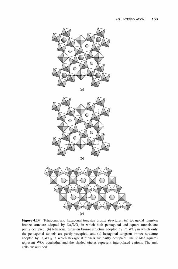
Figure 4.14 Tetragonal and hexagonal tungsten bronze structures: (a) tetragonal tungstenbronze structure adopted by NaxWO3 in which both pentagonal and square tunnels arepartly occupied; (b) tetragonal tungsten bronze structure adopted by PbxWO3 in which onlythe pentagonal tunnels are partly occupied; and (c) hexagonal tungsten bronze structureadopted by InxWO3 in which hexagonal tunnels are partly occupied. The shaded squaresrepresent WO6 octahedra, and the shaded circles represent interpolated cations. The unitcells are outlined.
4.5 INTERPOLATION 163
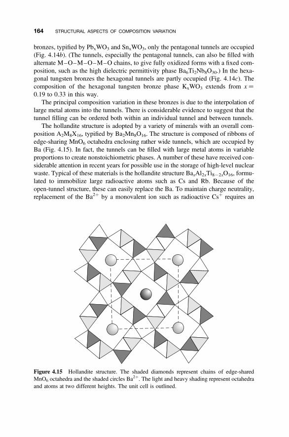
bronzes, typified by PbxWO3 and SnxWO3, only the pentagonal tunnels are occupied(Fig. 4.14b). (The tunnels, especially the pentagonal tunnels, can also be filled withalternate M–O–M–O–M–O chains, to give fully oxidized forms with a fixed com-position, such as the high dielectric permittivity phase Ba6Ti2Nb8O30.) In the hexa-gonal tungsten bronzes the hexagonal tunnels are partly occupied (Fig. 4.14c). Thecomposition of the hexagonal tungsten bronze phase KxWO3 extends from x ¼0.19 to 0.33 in this way.
The principal composition variation in these bronzes is due to the interpolation oflarge metal atoms into the tunnels. There is considerable evidence to suggest that thetunnel filling can be ordered both within an individual tunnel and between tunnels.
The hollandite structure is adopted by a variety of minerals with an overall com-position A2M8X16, typified by Ba2Mn8O16. The structure is composed of ribbons ofedge-sharing MnO6 octahedra enclosing rather wide tunnels, which are occupied byBa (Fig. 4.15). In fact, the tunnels can be filled with large metal atoms in variableproportions to create nonstoichiometric phases. A number of these have received con-siderable attention in recent years for possible use in the storage of high-level nuclearwaste. Typical of these materials is the hollandite structure BaxAl2xTi822xO16, formu-lated to immobilize large radioactive atoms such as Cs and Rb. Because of theopen-tunnel structure, these can easily replace the Ba. To maintain charge neutrality,replacement of the Ba2þ by a monovalent ion such as radioactive Csþ requires an
Figure 4.15 Hollandite structure. The shaded diamonds represent chains of edge-sharedMnO6 octahedra and the shaded circles Ba
2þ. The light and heavy shading represent octahedraand atoms at two different heights. The unit cell is outlined.
164 STRUCTURAL ASPECTS OF COMPOSITION VARIATION
adjustment in the Al : Ti ratio, so that a fabricated composition might typically beBaCs0.28Al2.28Ti5.72O16.
4.6 INTERCALATION
Intercalation is mainly associated with the insertion of atoms or molecules betweenthe layers of a structure in such a way that the layers maintain their integrity. Thefirst material to be studied extensively, and which is still the subject of enquiry, isgraphite.
Intrinsically, intercalation compounds are characterized by strong chemicalbonding within the layers (intralayer bonding) and weak chemical bondingbetween the layers (interlayer bonding). There are many examples, ranging fromclays and hydroxides to sulfides and oxides. Such compounds are of increasingimportance in many applications, particularly in battery technology.
The prototypes for this latter application are derived from layer structure disulfides,such as TiS2 and NbS2. Take TiS2 as an example. The structure of TiS2 is of the CdI2type (Fig. 4.16a) and can be thought of as a hexagonal packing of sulfur layers inwhich the octahedral positions between every alternate pair of layers is occupiedby titanium to form layers of composition TiS2. The layers can also be visualizedas a stacking of sheets of edge-sharing TiS6 octahedra. These are held together byweak van der Waals bonds.
A series of nonstoichiometric phases can be generated by gradually filling thevacant octahedral sites in TiS2 with Ti itself. Ultimately, all of the available octa-hedral sites are filled and the material has a composition TiS, with the nickel arsenideNiAs, structure (Fig. 4.16b). The formula of this nonstoichiometric phase range canbe written Ti1þxS2, with x taking all values from 0 to 1.0. Similar phases can be gen-erated with the use of other transition metals, such as Cr.
One of the most widely explored systems is derived from the interpolation of Libetween the TiS2 layers in varying amounts to form nonstoichiometric phases witha general formula LixTiS2. Because the bonding between the layers is weak, thisprocess is easily reversible. The open nature of the structure allows the Li atoms tomove readily in and out of the crystals, and these compounds can act as convenientalkali metal reservoirs in batteries and other devices. A battery using lithium interca-lated into TiS2 as the cathode was initially developed some 30 years ago.
For a number of reasons the TiS2 battery was not widely exploited commercially,but similar batteries based upon intercalation into transition-metal oxides LixTO2,where T is a 3d transition metal such as Ni, Co, or Mn (or a solid solution ofthese metals, LixT12yT0
yO2) are widely available. The first of these, the “Sonycell,” introduced in 1991, employs LixCoO2 as the cathode and the intercalation ofLi into graphite as the anode, to form LixC6.
The structure of the parent phase CoO2 is similar to that of TiS2 in that it iscomposed of layers of composition CoO2 in which the Co4þ ions are in octahedralcoordination. The stacking of the oxygen ion layers is in a . . . ABAB . . . hexagonal
4.6 INTERCALATION 165
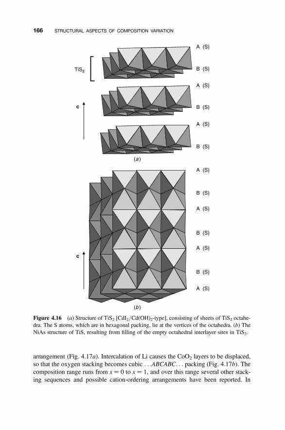
arrangement (Fig. 4.17a). Intercalation of Li causes the CoO2 layers to be displaced,so that the oxygen stacking becomes cubic . . .ABCABC. . . packing (Fig. 4.17b). Thecomposition range runs from x ¼ 0 to x ¼ 1, and over this range several other stack-ing sequences and possible cation-ordering arrangements have been reported. In
Figure 4.16 (a) Structure of TiS2 [CdI2/Cd(OH)2-type], consisting of sheets of TiS2 octahe-dra. The S atoms, which are in hexagonal packing, lie at the vertices of the octahedra. (b) TheNiAs structure of TiS, resulting from filling of the empty octahedral interlayer sites in TiS2.
166 STRUCTURAL ASPECTS OF COMPOSITION VARIATION
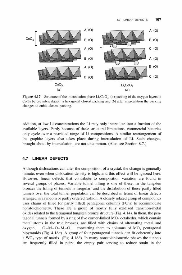
addition, at low Li concentrations the Li may only intercalate into a fraction of theavailable layers. Partly because of these structural limitations, commercial batteriesonly cycle over a restricted range of Li compositions. A similar rearrangement ofthe graphite layers also takes place during intercalation of Li. Such changes,brought about by intercalation, are not uncommon. (Also see Section 8.7.)
4.7 LINEAR DEFECTS
Although dislocations can alter the composition of a crystal, the change is generallyminute, even when dislocation density is high, and this effect will be ignored here.However, linear defects that contribute to composition variation are found inseveral groups of phases. Variable tunnel filling is one of these. In the tungstenbronzes the filling of tunnels is irregular, and the distribution of these partly filledtunnels over the total tunnel population can be described in terms of linear defectsarranged in a random or partly ordered fashion. A closely related group of compoundsuses chains of filled (or partly filled) pentagonal columns (PC’s) to accommodatenonstoichiometry. These are a group of mostly fully oxidized transition-metaloxides related to the tetragonal tungsten bronze structure (Fig. 4.14). In them, the pen-tagonal tunnels formed by a ring of five corner-linked MO6 octahedra, which containmetal atoms in the true bronzes, are filled with chains of alternating metal andoxygen, . . .O–M–O–M–O. . . converting them to columns of MO7 pentagonalbipyramids (Fig. 4.18a). A group of four pentagonal tunnels can fit coherently intoa WO3 type of matrix, (Fig. 4.18b). In many nonstoichiometric phases the tunnelsare frequently filled in pairs; the empty pair serving to reduce strain in the
Figure 4.17 Structure of the intercalation phase LixCoO2: (a) packing of the oxygen layers inCoO2 before intercalation is hexagonal closest packing and (b) after intercalation the packingchanges to cubic closest packing.
4.7 LINEAR DEFECTS 167
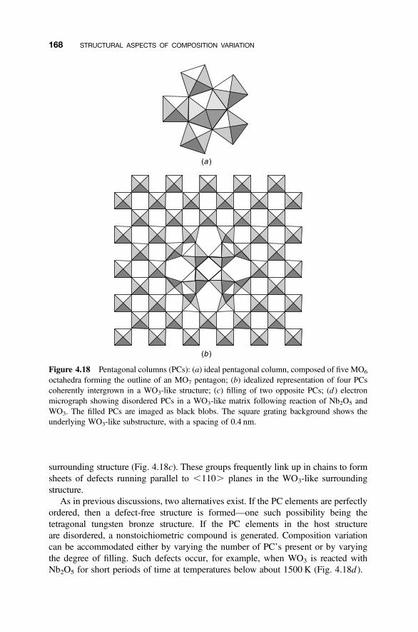
surrounding structure (Fig. 4.18c). These groups frequently link up in chains to formsheets of defects running parallel to ,110. planes in the WO3-like surroundingstructure.
As in previous discussions, two alternatives exist. If the PC elements are perfectlyordered, then a defect-free structure is formed—one such possibility being thetetragonal tungsten bronze structure. If the PC elements in the host structureare disordered, a nonstoichiometric compound is generated. Composition variationcan be accommodated either by varying the number of PC’s present or by varyingthe degree of filling. Such defects occur, for example, when WO3 is reacted withNb2O5 for short periods of time at temperatures below about 1500 K (Fig. 4.18d ).
Figure 4.18 Pentagonal columns (PCs): (a) ideal pentagonal column, composed of five MO6
octahedra forming the outline of an MO7 pentagon; (b) idealized representation of four PCscoherently intergrown in a WO3-like structure; (c) filling of two opposite PCs; (d ) electronmicrograph showing disordered PCs in a WO3-like matrix following reaction of Nb2O5 andWO3. The filled PCs are imaged as black blobs. The square grating background shows theunderlying WO3-like substructure, with a spacing of 0.4 nm.
168 STRUCTURAL ASPECTS OF COMPOSITION VARIATION
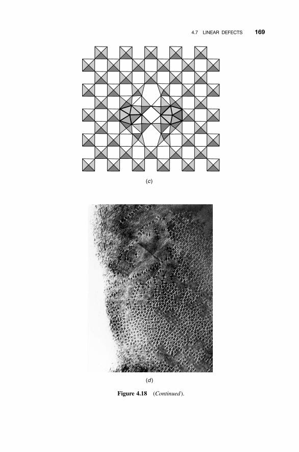
Figure 4.18 (Continued).
4.7 LINEAR DEFECTS 169
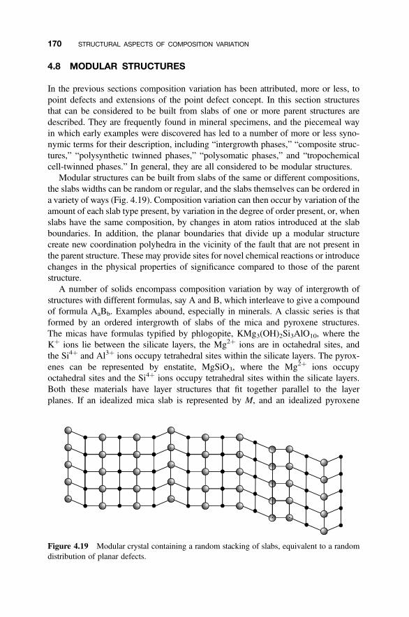
4.8 MODULAR STRUCTURES
In the previous sections composition variation has been attributed, more or less, topoint defects and extensions of the point defect concept. In this section structuresthat can be considered to be built from slabs of one or more parent structures aredescribed. They are frequently found in mineral specimens, and the piecemeal wayin which early examples were discovered has led to a number of more or less syno-nymic terms for their description, including “intergrowth phases,” “composite struc-tures,” “polysynthetic twinned phases,” “polysomatic phases,” and “tropochemicalcell-twinned phases.” In general, they are all considered to be modular structures.
Modular structures can be built from slabs of the same or different compositions,the slabs widths can be random or regular, and the slabs themselves can be ordered ina variety of ways (Fig. 4.19). Composition variation can then occur by variation of theamount of each slab type present, by variation in the degree of order present, or, whenslabs have the same composition, by changes in atom ratios introduced at the slabboundaries. In addition, the planar boundaries that divide up a modular structurecreate new coordination polyhedra in the vicinity of the fault that are not present inthe parent structure. These may provide sites for novel chemical reactions or introducechanges in the physical properties of significance compared to those of the parentstructure.
A number of solids encompass composition variation by way of intergrowth ofstructures with different formulas, say A and B, which interleave to give a compoundof formula AaBb. Examples abound, especially in minerals. A classic series is thatformed by an ordered intergrowth of slabs of the mica and pyroxene structures.The micas have formulas typified by phlogopite, KMg3(OH)2Si3AlO10, where theKþ ions lie between the silicate layers, the Mg2þ ions are in octahedral sites, andthe Si4þ and Al3þ ions occupy tetrahedral sites within the silicate layers. The pyrox-enes can be represented by enstatite, MgSiO3, where the Mg2þ ions occupyoctahedral sites and the Si4þ ions occupy tetrahedral sites within the silicate layers.Both these materials have layer structures that fit together parallel to the layerplanes. If an idealized mica slab is represented by M, and an idealized pyroxene
Figure 4.19 Modular crystal containing a random stacking of slabs, equivalent to a randomdistribution of planar defects.
170 STRUCTURAL ASPECTS OF COMPOSITION VARIATION
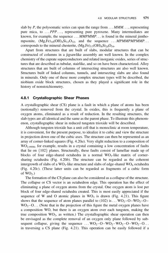
slab by P, the polysomatic series can span the range from . . .MMM. . . , representingpure mica, to . . . PPP. . . , representing pure pyroxene. Many intermediates areknown, for example, the sequence . . .MMPMMP. . . is found in the mineral jimtho-mpsonite, (Mg,Fe)10(OH)4Si12O32, and the sequence . . .MPMMPMPMMP. . .corresponds to the mineral chesterite, (Mg,Fe)17(OH)6Si20O54.
Apart from structures that are built of slabs, modular structures that can beconstructed of columns in a jigsawlike assembly are well known. In the complexchemistry of the cuprate superconductors and related inorganic oxides, series of struc-tures that are described as tubular, stairlike, and so on have been characterized. Alloystructures that are built of columns of intersecting structures are also well known.Structures built of linked columns, tunnels, and intersecting slabs are also foundin minerals. Only one of these more complex structure types will be described, theniobium oxide block structures, chosen as they played a significant role in thehistory of nonstoichiometry.
4.8.1 Crystallographic Shear Phases
A crystallographic shear (CS) plane is a fault in which a plane of atoms has been(notionally) removed from the crystal. In oxides, this is frequently a plane ofoxygen atoms, eliminated as a result of reduction. In the resulting structures, theslab types are all identical and the same as the parent phase. To illustrate this phenom-enon, crystallographic shear in reduced tungsten trioxide will be described.
Although tungsten trioxide has a unit cell that is monoclinic at room temperature,it is convenient, for the present purpose, to idealize it to cubic and view the structurein projection down one of the cubic axes. The structure can then be represented as anarray of corner-linked squares (Fig. 4.20a). Very slight reduction to a composition ofWO2.9998, for example, results in a crystal containing a low concentration of faultsthat lie on f102g planes. Structurally, these faults consist of lamellae made up ofblocks of four edge-shared octahedra in a normal WO3-like matrix of corner-sharing octahedra (Fig. 4.20b). The structure can be regarded as the coherentintergrowth of slabs of a WO3-like structure and slabs of edge-shared WO6 octahedra(Fig. 4.20c). (These latter units can be regarded as fragments of a cubic formof WO2.)
The formation of the CS plane can also be considered as a collapse of the structure.The collapse or CS vector is an octahedron edge. This operation has the effect ofeliminating a plane of oxygen atoms from the crystal. One oxygen atom is lost perblock of four edge-shared octahedra created. This is most easily appreciated if thesequence of W and O atomic planes in WO3 is drawn (Fig. 4.21). This figureshows that the sequence of atom planes parallel to (102) is . . .WO2–O–WO2–O–WO2–O. . . (Note that in the projection of this figure the metal oxygen planes havea composition WO, but there is an oxygen atom over each tungsten, making thetrue composition WO2, as written.) The crystallographic shear operation can thenbe envisaged as the complete removal of an oxygen only plane followed by sub-sequent collapse, giving the sequence . . .WO2–O–WO2–WO2–O–WO2–O. . .in traversing a CS plane (Fig. 4.21). This operation can be easily followed if a
4.8 MODULAR STRUCTURES 171
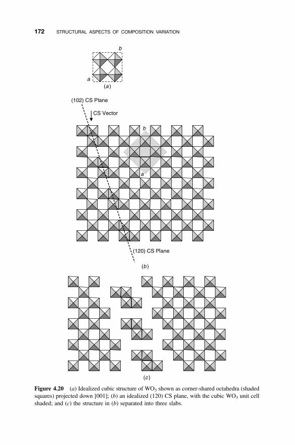
Figure 4.20 (a) Idealized cubic structure of WO3 shown as corner-shared octahedra (shadedsquares) projected down [001]; (b) an idealized (120) CS plane, with the cubic WO3 unit cellshaded; and (c) the structure in (b) separated into three slabs.
172 STRUCTURAL ASPECTS OF COMPOSITION VARIATION
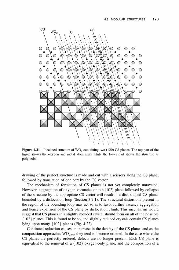
drawing of the perfect structure is made and cut with a scissors along the CS plane,followed by translation of one part by the CS vector.
The mechanism of formation of CS planes is not yet completely unraveled.However, aggregation of oxygen vacancies onto a (102) plane followed by collapseof the structure by the appropriate CS vector will result in a disk-shaped CS plane,bounded by a dislocation loop (Section 3.7.1). The structural distortions present inthe region of the bounding loop may act so as to favor further vacancy aggregationand hence expansion of the CS plane by dislocation climb. This mechanism wouldsuggest that CS planes in a slightly reduced crystal should form on all of the possiblef102g planes. This is found to be so, and slightly reduced crystals contain CS planeslying upon many f102g planes (Fig. 4.22).
Continued reduction causes an increase in the density of the CS planes and as thecomposition approaches WO2.97, they tend to become ordered. In the case where theCS planes are perfectly ordered, defects are no longer present. Each CS plane isequivalent to the removal of a f102g oxygen-only plane, and the composition of a
Figure 4.21 Idealized structure of WO3 containing two (120) CS planes. The top part of thefigure shows the oxygen and metal atom array while the lower part shows the structure aspolyhedra.
4.8 MODULAR STRUCTURES 173
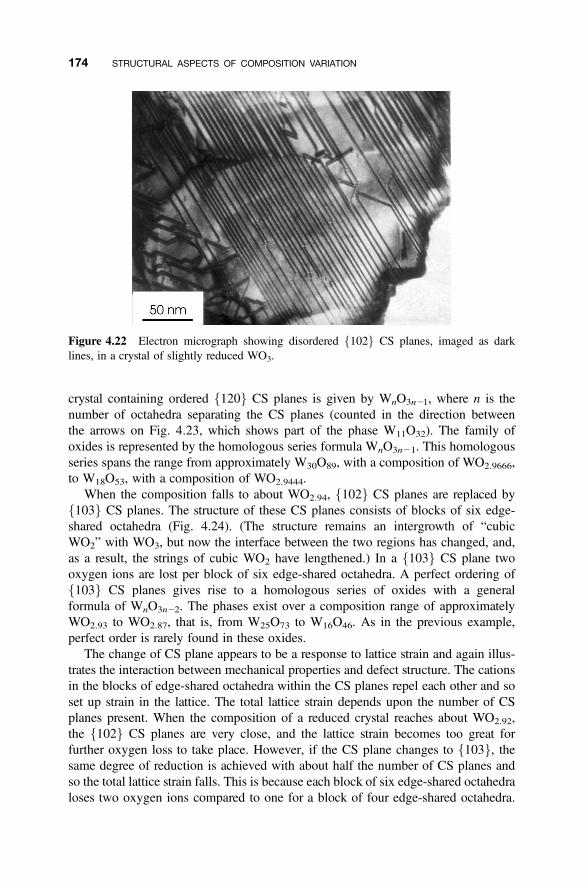
crystal containing ordered f120g CS planes is given by WnO3n21, where n is thenumber of octahedra separating the CS planes (counted in the direction betweenthe arrows on Fig. 4.23, which shows part of the phase W11O32). The family ofoxides is represented by the homologous series formula WnO3n21. This homologousseries spans the range from approximately W30O89, with a composition of WO2.9666,to W18O53, with a composition of WO2.9444.
When the composition falls to about WO2.94, f102g CS planes are replaced byf103g CS planes. The structure of these CS planes consists of blocks of six edge-shared octahedra (Fig. 4.24). (The structure remains an intergrowth of “cubicWO2” with WO3, but now the interface between the two regions has changed, and,as a result, the strings of cubic WO2 have lengthened.) In a f103g CS plane twooxygen ions are lost per block of six edge-shared octahedra. A perfect ordering off103g CS planes gives rise to a homologous series of oxides with a generalformula of WnO3n22. The phases exist over a composition range of approximatelyWO2.93 to WO2.87, that is, from W25O73 to W16O46. As in the previous example,perfect order is rarely found in these oxides.
The change of CS plane appears to be a response to lattice strain and again illus-trates the interaction between mechanical properties and defect structure. The cationsin the blocks of edge-shared octahedra within the CS planes repel each other and soset up strain in the lattice. The total lattice strain depends upon the number of CSplanes present. When the composition of a reduced crystal reaches about WO2.92,the f102g CS planes are very close, and the lattice strain becomes too great forfurther oxygen loss to take place. However, if the CS plane changes to f103g, thesame degree of reduction is achieved with about half the number of CS planes andso the total lattice strain falls. This is because each block of six edge-shared octahedraloses two oxygen ions compared to one for a block of four edge-shared octahedra.
Figure 4.22 Electron micrograph showing disordered f102g CS planes, imaged as darklines, in a crystal of slightly reduced WO3.
174 STRUCTURAL ASPECTS OF COMPOSITION VARIATION
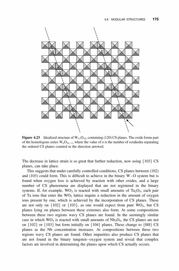
The decrease in lattice strain is so great that further reduction, now using f103g CSplanes, can take place.
This suggests that under carefully controlled conditions, CS planes between (102)and (103) could form. This is difficult to achieve in the binary W–O system but isfound when oxygen loss is achieved by reaction with other oxides, and a largenumber of CS phenomena are displayed that are not registered in the binarysystems. If, for example, WO3 is reacted with small amounts of Ta2O5, each pairof Ta ions that enter the WO3 lattice require a reduction in the amount of oxygenions present by one, which is achieved by the incorporation of CS planes. Theseare not only on f102g or f103g, as one would expect from pure WO3, but CSplanes lying on planes between these extremes also form. At some compositionsbetween these two regions wavy CS planes are found. In the seemingly similarcase in which WO3 is reacted with small amounts of Nb2O5, the CS planes are noton f102g or f103g but form initially on f104g planes. These change to f00lg CSplanes as the Nb concentration increases. At compositions between these tworegions wavy CS planes are found. Other impurities also produce CS planes thatare not found in the binary tungsten–oxygen system and reveal that complexfactors are involved in determining the planes upon which CS actually occurs.
Figure 4.23 Idealized structure of W11O32, containing (120) CS planes. The oxide forms partof the homologous series WnO3n21, where the value of n is the number of octahedra separatingthe ordered CS planes counted in the direction arrowed.
4.8 MODULAR STRUCTURES 175
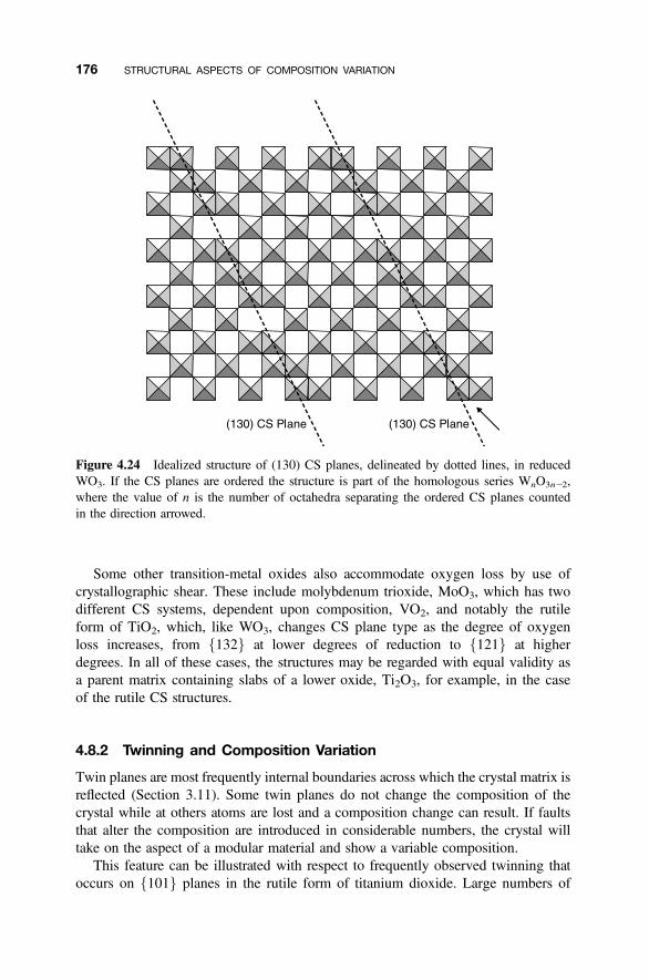
Some other transition-metal oxides also accommodate oxygen loss by use ofcrystallographic shear. These include molybdenum trioxide, MoO3, which has twodifferent CS systems, dependent upon composition, VO2, and notably the rutileform of TiO2, which, like WO3, changes CS plane type as the degree of oxygenloss increases, from f132g at lower degrees of reduction to f121g at higherdegrees. In all of these cases, the structures may be regarded with equal validity asa parent matrix containing slabs of a lower oxide, Ti2O3, for example, in the caseof the rutile CS structures.
4.8.2 Twinning and Composition Variation
Twin planes are most frequently internal boundaries across which the crystal matrix isreflected (Section 3.11). Some twin planes do not change the composition of thecrystal while at others atoms are lost and a composition change can result. If faultsthat alter the composition are introduced in considerable numbers, the crystal willtake on the aspect of a modular material and show a variable composition.
This feature can be illustrated with respect to frequently observed twinning thatoccurs on f101g planes in the rutile form of titanium dioxide. Large numbers of
Figure 4.24 Idealized structure of (130) CS planes, delineated by dotted lines, in reducedWO3. If the CS planes are ordered the structure is part of the homologous series WnO3n22,where the value of n is the number of octahedra separating the ordered CS planes countedin the direction arrowed.
176 STRUCTURAL ASPECTS OF COMPOSITION VARIATION
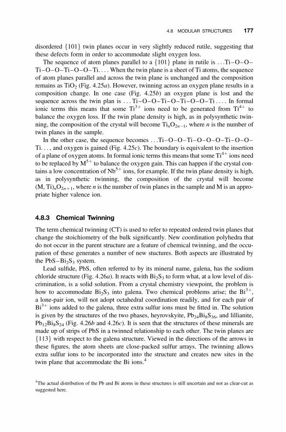
disordered f101g twin planes occur in very slightly reduced rutile, suggesting thatthese defects form in order to accommodate slight oxygen loss.
The sequence of atom planes parallel to a f101g plane in rutile is . . .Ti–O–O–Ti–O–O–Ti–O–O–Ti. . . . When the twin plane is a sheet of Ti atoms, the sequenceof atom planes parallel and across the twin plane is unchanged and the compositionremains as TiO2 (Fig. 4.25a). However, twinning across an oxygen plane results in acomposition change. In one case (Fig. 4.25b) an oxygen plane is lost and thesequence across the twin plan is . . . Ti–O–O–Ti–O–Ti–O–O–Ti . . . . In formalionic terms this means that some Ti3þ ions need to be generated from Ti4þ tobalance the oxygen loss. If the twin plane density is high, as in polysynthetic twin-ning, the composition of the crystal will become TinO2n21, where n is the number oftwin planes in the sample.
In the other case, the sequence becomes . . .Ti–O–O–Ti–O–O–O–Ti–O–O–Ti. . . , and oxygen is gained (Fig. 4.25c). The boundary is equivalent to the insertionof a plane of oxygen atoms. In formal ionic terms this means that some Ti4þ ions needto be replaced by M5þ to balance the oxygen gain. This can happen if the crystal con-tains a low concentration of Nb5þ ions, for example. If the twin plane density is high,as in polysynthetic twinning, the composition of the crystal will become(M, Ti)nO2nþ1, where n is the number of twin planes in the sample and M is an appro-priate higher valence ion.
4.8.3 Chemical Twinning
The term chemical twinning (CT) is used to refer to repeated ordered twin planes thatchange the stoichiometry of the bulk significantly. New coordination polyhedra thatdo not occur in the parent structure are a feature of chemical twinning, and the occu-pation of these generates a number of new stuctures. Both aspects are illustrated bythe PbS–Bi2S3 system.
Lead sulfide, PbS, often referred to by its mineral name, galena, has the sodiumchloride structure (Fig. 4.26a). It reacts with Bi2S3 to form what, at a low level of dis-crimination, is a solid solution. From a crystal chemistry viewpoint, the problem ishow to accommodate Bi2S3 into galena. Two chemical problems arise; the Bi3þ,a lone-pair ion, will not adopt octahedral coordination readily, and for each pair ofBi3þ ions added to the galena, three extra sulfur ions must be fitted in. The solutionis given by the structures of the two phases, heyrovskyite, Pb24Bi8S36, and lillianite,Pb12Bi8S24 (Fig. 4.26b and 4.26c). It is seen that the structures of these minerals aremade up of strips of PbS in a twinned relationship to each other. The twin planes aref113g with respect to the galena structure. Viewed in the directions of the arrows inthese figures, the atom sheets are close-packed sulfur arrays. The twinning allowsextra sulfur ions to be incorporated into the structure and creates new sites in thetwin plane that accommodate the Bi ions.4
4The actual distribution of the Pb and Bi atoms in these structures is still uncertain and not as clear-cut assuggested here.
4.8 MODULAR STRUCTURES 177
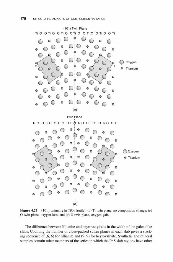
The difference between lillianite and heyrovskyite is in the width of the galenalikeslabs. Counting the number of close-packed sulfur planes in each slab gives a stack-ing sequence of (6, 6) for lillianite and (9, 9) for heyrovskyite. Synthetic and mineralsamples contain other members of the series in which the PbS slab regions have other
Figure 4.25 f101g twinning in TiO2 (rutile): (a) Ti twin plane, no composition change; (b)O twin plane, oxygen loss; and (c) O twin plane, oxygen gain.
178 STRUCTURAL ASPECTS OF COMPOSITION VARIATION
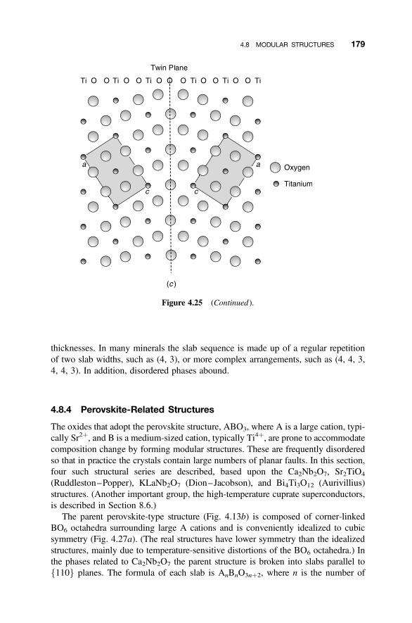
thicknesses. In many minerals the slab sequence is made up of a regular repetitionof two slab widths, such as (4, 3), or more complex arrangements, such as (4, 4, 3,4, 4, 3). In addition, disordered phases abound.
4.8.4 Perovskite-Related Structures
The oxides that adopt the perovskite structure, ABO3, where A is a large cation, typi-cally Sr2þ, and B is a medium-sized cation, typically Ti4þ, are prone to accommodatecomposition change by forming modular structures. These are frequently disorderedso that in practice the crystals contain large numbers of planar faults. In this section,four such structural series are described, based upon the Ca2Nb2O7, Sr2TiO4
(Ruddleston–Popper), KLaNb2O7 (Dion–Jacobson), and Bi4Ti3O12 (Aurivillius)structures. (Another important group, the high-temperature cuprate superconductors,is described in Section 8.6.)
The parent perovskite-type structure (Fig. 4.13b) is composed of corner-linkedBO6 octahedra surrounding large A cations and is conveniently idealized to cubicsymmetry (Fig. 4.27a). (The real structures have lower symmetry than the idealizedstructures, mainly due to temperature-sensitive distortions of the BO6 octahedra.) Inthe phases related to Ca2Nb2O7 the parent structure is broken into slabs parallel tof110g planes. The formula of each slab is AnBnO3nþ2, where n is the number of
Figure 4.25 (Continued).
4.8 MODULAR STRUCTURES 179
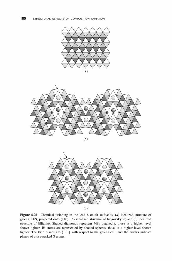
Figure 4.26 Chemical twinning in the lead bismuth sulfosalts: (a) idealized structure ofgalena, PbS, projected onto (110); (b) idealized structure of heyrovskyite; and (c) idealizedstructure of lillianite. Shaded diamonds represent MS6 octahedra, those at a higher levelshown lighter. Bi atoms are represented by shaded spheres, those at a higher level shownlighter. The twin planes are f113g with respect to the galena cell, and the arrows indicateplanes of close-packed S atoms.
180 STRUCTURAL ASPECTS OF COMPOSITION VARIATION
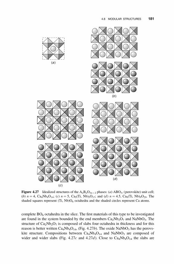
complete BO6 octahedra in the slice. The first materials of this type to be investigatedare found in the system bounded by the end members Ca2Nb2O7 and NaNbO3. Thestructure of Ca2Nb2O7 is composed of slabs four octahedra in thickness and for thisreason is better written Ca4Nb4O14, (Fig. 4.27b). The oxide NaNbO3 has the perovs-kite structure. Compositions between Ca4Nb4O14 and NaNbO3 are composed ofwider and wider slabs (Fig. 4.27c and 4.27d ). Close to Ca4Nb4O14 the slabs are
Figure 4.27 Idealized structures of the AnBnO3nþ2 phases: (a) ABO3, (perovskite) unit cell;(b) n ¼ 4, Ca4Nb4O14; (c) n ¼ 5, Ca5(Ti, Nb)5O17; and (d ) n ¼ 4.5, Ca9(Ti, Nb)9O29. Theshaded squares represent (Ti, Nb)O6 octahedra and the shaded circles represent Ca atoms.
4.8 MODULAR STRUCTURES 181
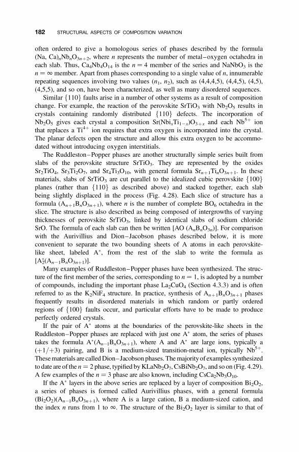
often ordered to give a homologous series of phases described by the formula(Na, Ca)nNbnO3nþ2, where n represents the number of metal–oxygen octahedra ineach slab. Thus, Ca4Nb4O14 is the n ¼ 4 member of the series and NaNbO3 is then ¼ 1 member. Apart from phases corresponding to a single value of n, innumerablerepeating sequences involving two values (n1, n2), such as (4,4,4,5), (4,4,5), (4,5),(4,5,5), and so on, have been characterized, as well as many disordered sequences.
Similar f110g faults arise in a number of other systems as a result of compositionchange. For example, the reaction of the perovskite SrTiO3 with Nb2O5 results incrystals containing randomly distributed f110g defects. The incorporation ofNb2O5 gives each crystal a composition Sr(NbixTi12x)O3þx and each Nb5þ ionthat replaces a Ti4þ ion requires that extra oxygen is incorporated into the crystal.The planar defects open the structure and allow this extra oxygen to be accommo-dated without introducing oxygen interstitials.
The Ruddleston–Popper phases are another structurally simple series built fromslabs of the perovskite structure SrTiO3. They are represented by the oxidesSr2TiO4, Sr3Ti2O7, and Sr4Ti3O10, with general formula Srnþ1TinO3nþ1. In thesematerials, slabs of SrTiO3 are cut parallel to the idealized cubic perovskite f100gplanes (rather than f110g as described above) and stacked together, each slabbeing slightly displaced in the process (Fig. 4.28). Each slice of structure has aformula (Anþ1BnO3nþ1), where n is the number of complete BO6 octahedra in theslice. The structure is also described as being composed of intergrowths of varyingthicknesses of perovskite SrTiO3, linked by identical slabs of sodium chlorideSrO. The formula of each slab can then be written [AO (AnBnO3n)]. For comparisonwith the Aurivillius and Dion–Jacobson phases described below, it is moreconvenient to separate the two bounding sheets of A atoms in each perovskite-like sheet, labeled A�, from the rest of the slab to write the formula as[A2
�(An21BnO3nþ1)].Many examples of Ruddleston–Popper phases have been synthesized. The struc-
ture of the first member of the series, corresponding to n ¼ 1, is adopted by a numberof compounds, including the important phase La2CuO4 (Section 4.3.3) and is oftenreferred to as the K2NiF4 structure. In practice, synthesis of Anþ1BnO3nþ1 phasesfrequently results in disordered materials in which random or partly orderedregions of f100g faults occur, and particular efforts have to be made to produceperfectly ordered crystals.
If the pair of A� atoms at the boundaries of the perovskite-like sheets in theRuddleston–Popper phases are replaced with just one A� atom, the series of phasestakes the formula A�(An21BnO3nþ1), where A and A� are large ions, typically a(þ1/þ3) pairing, and B is a medium-sized transition-metal ion, typically Nb5þ.Thesematerials are calledDion–Jacobsonphases. Themajorityof examples synthesizedto date are of the n ¼ 2 phase, typified byKLaNb2O7, CsBiNb2O7, and so on (Fig. 4.29).A few examples of the n ¼ 3 phase are also known, including CsCa2Nb3O10.
If the A� layers in the above series are replaced by a layer of composition Bi2O2,a series of phases is formed called Aurivillius phases, with a general formula(Bi2O2)(An21BnO3nþ1), where A is a large cation, B a medium-sized cation, andthe index n runs from 1 to 1. The structure of the Bi2O2 layer is similar to that of
182 STRUCTURAL ASPECTS OF COMPOSITION VARIATION
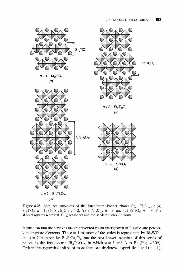
fluorite, so that the series is also represented by an intergrowth of fluorite and perovs-kite structure elements. The n ¼ 1 member of the series is represented by Bi2WO6,the n ¼ 2 member by Bi2SrTa2O9, but the best-known member of this series ofphases is the ferroelectric Bi4Ti3O12, in which n ¼ 3 and A is Bi (Fig. 4.30a).Ordered intergrowth of slabs of more than one thickness, especially n and (n þ 1),
Figure 4.28 Idealized structures of the Ruddleston–Popper phases Srnþ1TinO3nþ1: (a)Sr2TiO4, n ¼ 1; (b) Sr3Ti2O7, n ¼ 2; (c) Sr4Ti3O10, n ¼ 3; and (d ) SrTiO3, n ¼ 1. Theshaded squares represent TiO6 octahedra and the shaded circles Sr atoms.
4.8 MODULAR STRUCTURES 183
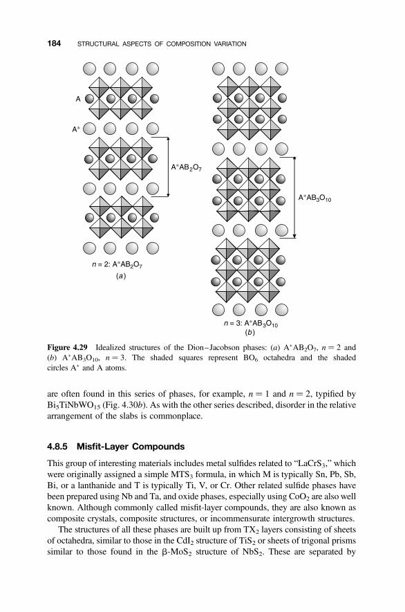
are often found in this series of phases, for example, n ¼ 1 and n ¼ 2, typified byBi5TiNbWO15 (Fig. 4.30b). As with the other series described, disorder in the relativearrangement of the slabs is commonplace.
4.8.5 Misfit-Layer Compounds
This group of interesting materials includes metal sulfides related to “LaCrS3,” whichwere originally assigned a simple MTS3 formula, in which M is typically Sn, Pb, Sb,Bi, or a lanthanide and T is typically Ti, V, or Cr. Other related sulfide phases havebeen prepared using Nb and Ta, and oxide phases, especially using CoO2 are also wellknown. Although commonly called misfit-layer compounds, they are also known ascomposite crystals, composite structures, or incommensurate intergrowth structures.
The structures of all these phases are built up from TX2 layers consisting of sheetsof octahedra, similar to those in the CdI2 structure of TiS2 or sheets of trigonal prismssimilar to those found in the b-MoS2 structure of NbS2. These are separated by
Figure 4.29 Idealized structures of the Dion–Jacobson phases: (a) A�AB2O7, n ¼ 2 and(b) A�AB3O10, n ¼ 3. The shaded squares represent BO6 octahedra and the shadedcircles A� and A atoms.
184 STRUCTURAL ASPECTS OF COMPOSITION VARIATION
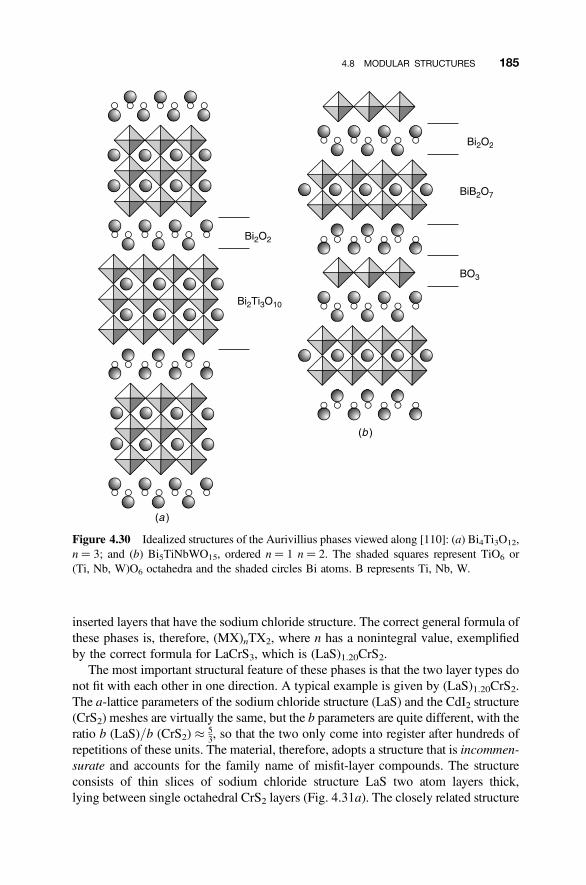
inserted layers that have the sodium chloride structure. The correct general formula ofthese phases is, therefore, (MX)nTX2, where n has a nonintegral value, exemplifiedby the correct formula for LaCrS3, which is (LaS)1.20CrS2.
The most important structural feature of these phases is that the two layer types donot fit with each other in one direction. A typical example is given by (LaS)1.20CrS2.The a-lattice parameters of the sodium chloride structure (LaS) and the CdI2 structure(CrS2) meshes are virtually the same, but the b parameters are quite different, with theratio b (LaS)/b (CrS2) � 5
3, so that the two only come into register after hundreds ofrepetitions of these units. The material, therefore, adopts a structure that is incommen-surate and accounts for the family name of misfit-layer compounds. The structureconsists of thin slices of sodium chloride structure LaS two atom layers thick,lying between single octahedral CrS2 layers (Fig. 4.31a). The closely related structure
Figure 4.30 Idealized structures of the Aurivillius phases viewed along [110]: (a) Bi4Ti3O12,n ¼ 3; and (b) Bi5TiNbWO15, ordered n ¼ 1 n ¼ 2. The shaded squares represent TiO6 or(Ti, Nb, W)O6 octahedra and the shaded circles Bi atoms. B represents Ti, Nb, W.
4.8 MODULAR STRUCTURES 185
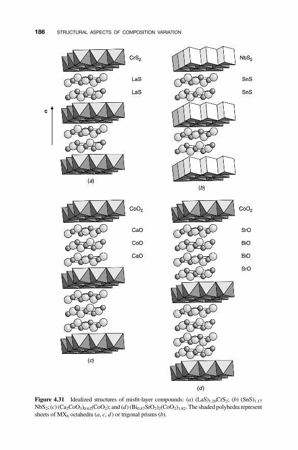
Figure 4.31 Idealized structures of misfit-layer compounds: (a) (LaS)1.20CrS2; (b) (SnS)1.17NbS2; (c) (Ca2CoO3)0.62(CoO2); and (d) (Bi0.87SrO2)2(CoO2)1.82. The shaded polyhedra representsheets of MX6 octahedra (a, c, d) or trigonal prisms (b).
186 STRUCTURAL ASPECTS OF COMPOSITION VARIATION
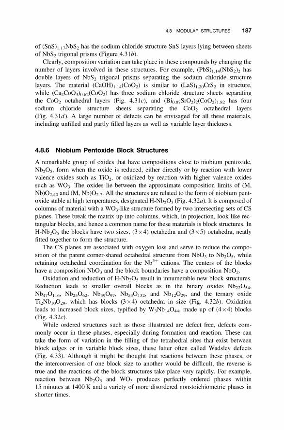
of (SnS)1.17NbS2 has the sodium chloride structure SnS layers lying between sheetsof NbS2 trigonal prisms (Figure 4.31b).
Clearly, composition variation can take place in these compounds by changing thenumber of layers involved in these structures. For example, (PbS)1.14(NbS2)2 hasdouble layers of NbS2 trigonal prisms separating the sodium chloride structurelayers. The material (CaOH)1.14(CoO2) is similar to (LaS)1.20CrS2 in structure,while (Ca2CoO3)0.62(CoO2) has three sodium chloride structure sheets separatingthe CoO2 octahedral layers (Fig. 4.31c), and (Bi0.87SrO2)2(CoO2)1.82 has foursodium chloride structure sheets separating the CoO2 octahedral layers(Fig. 4.31d ). A large number of defects can be envisaged for all these materials,including unfilled and partly filled layers as well as variable layer thickness.
4.8.6 Niobium Pentoxide Block Structures
A remarkable group of oxides that have compositions close to niobium pentoxide,Nb2O5, form when the oxide is reduced, either directly or by reaction with lowervalence oxides such as TiO2, or oxidized by reaction with higher valence oxidessuch as WO3. The oxides lie between the approximate composition limits of (M,Nb)O2.40 and (M, Nb)O2.7. All the structures are related to the form of niobium pent-oxide stable at high temperatures, designated H-Nb2O5 (Fig. 4.32a). It is composed ofcolumns of material with a WO3-like structure formed by two intersecting sets of CSplanes. These break the matrix up into columns, which, in projection, look like rec-tangular blocks, and hence a common name for these materials is block structures. InH-Nb2O5 the blocks have two sizes, (3�4) octahedra and (3�5) octahedra, neatlyfitted together to form the structure.
The CS planes are associated with oxygen loss and serve to reduce the compo-sition of the parent corner-shared octahedral structure from NbO3 to Nb2O5, whileretaining octahedral coordination for the Nb5þ cations. The centers of the blockshave a composition NbO3 and the block boundaries have a composition NbO2.
Oxidation and reduction of H-Nb2O5 result in innumerable new block structures.Reduction leads to smaller overall blocks as in the binary oxides Nb22O54,Nb47O116, Nb25O62, Nb39O97, Nb53O132, and Nb12O29, and the ternary oxideTi2Nb10O29, which has blocks (3�4) octahedra in size (Fig. 4.32b). Oxidationleads to increased block sizes, typified by W3Nb14O44, made up of (4�4) blocks(Fig. 4.32c).
While ordered structures such as those illustrated are defect free, defects com-monly occur in these phases, especially during formation and reaction. These cantake the form of variation in the filling of the tetrahedral sites that exist betweenblock edges or in variable block sizes, these latter often called Wadsley defects(Fig. 4.33). Although it might be thought that reactions between these phases, orthe interconversion of one block size to another would be difficult, the reverse istrue and the reactions of the block structures take place very rapidly. For example,reaction between Nb2O5 and WO3 produces perfectly ordered phases within15 minutes at 1400 K and a variety of more disordered nonstoichiometric phases inshorter times.
4.8 MODULAR STRUCTURES 187
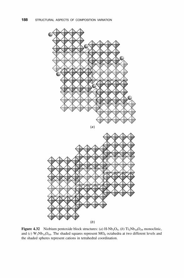
Figure 4.32 Niobium pentoxide block structures: (a) H-Nb2O5, (b) Ti2Nb10O29 monoclinic,and (c) W3Nb14O44. The shaded squares represent MO6 octahedra at two different levels andthe shaded spheres represent cations in tetrahedral coordination.
188 STRUCTURAL ASPECTS OF COMPOSITION VARIATION
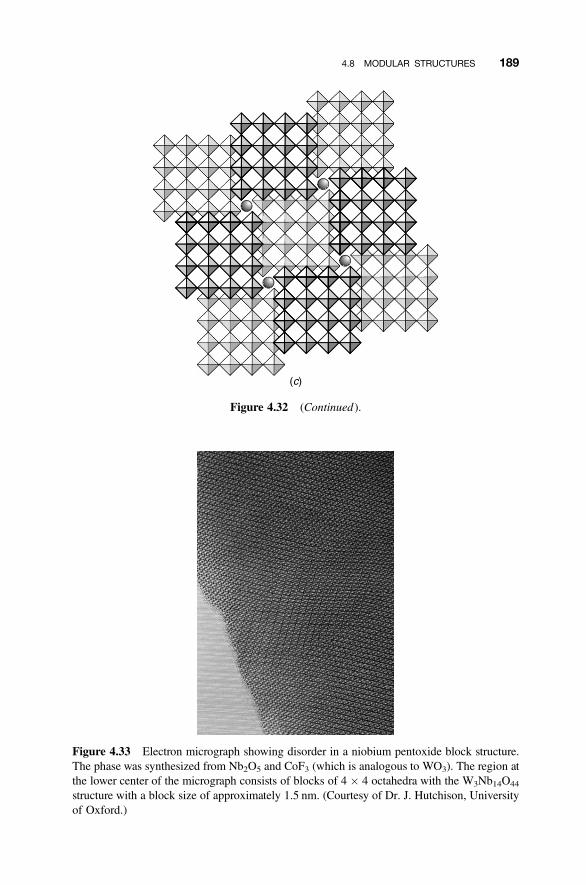
Figure 4.33 Electron micrograph showing disorder in a niobium pentoxide block structure.The phase was synthesized from Nb2O5 and CoF3 (which is analogous to WO3). The region atthe lower center of the micrograph consists of blocks of 4 � 4 octahedra with the W3Nb14O44
structure with a block size of approximately 1.5 nm. (Courtesy of Dr. J. Hutchison, Universityof Oxford.)
Figure 4.32 (Continued).
4.8 MODULAR STRUCTURES 189
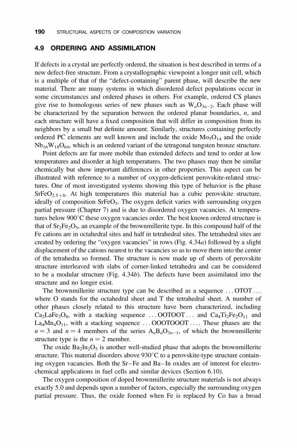
4.9 ORDERING AND ASSIMILATION
If defects in a crystal are perfectly ordered, the situation is best described in terms of anew defect-free structure. From a crystallographic viewpoint a longer unit cell, whichis a multiple of that of the “defect-containing” parent phase, will describe the newmaterial. There are many systems in which disordered defect populations occur insome circumstances and ordered phases in others. For example, ordered CS planesgive rise to homologous series of new phases such as WnO3n22. Each phase willbe characterized by the separation between the ordered planar boundaries, n, andeach structure will have a fixed composition that will differ in composition from itsneighbors by a small but definite amount. Similarly, structures containing perfectlyordered PC elements are well known and include the oxide Mo5O14 and the oxideNb16W18O64, which is an ordered variant of the tetragonal tungsten bronze structure.
Point defects are far more mobile than extended defects and tend to order at lowtemperatures and disorder at high temperatures. The two phases may then be similarchemically but show important differences in other properties. This aspect can beillustrated with reference to a number of oxygen-deficient perovskite-related struc-tures. One of most investigated systems showing this type of behavior is the phaseSrFeO2.5þd. At high temperatures this material has a cubic perovskite structure,ideally of composition SrFeO3. The oxygen deficit varies with surrounding oxygenpartial pressure (Chapter 7) and is due to disordered oxygen vacancies. At tempera-tures below 9008C these oxygen vacancies order. The best known ordered structure isthat of Sr2Fe2O5, an example of the brownmillerite type. In this compound half of theFe cations are in octahedral sites and half in tetrahedral sites. The tetrahedral sites arecreated by ordering the “oxygen vacancies” in rows (Fig. 4.34a) followed by a slightdisplacement of the cations nearest to the vacancies so as to move them into the centerof the tetrahedra so formed. The structure is now made up of sheets of perovskitestructure interleaved with slabs of corner-linked tetrahedra and can be consideredto be a modular structure (Fig. 4.34b). The defects have been assimilated into thestructure and no longer exist.
The brownmillerite structure type can be described as a sequence . . .OTOT . . .where O stands for the octahedral sheet and T the tetrahedral sheet. A number ofother phases closely related to this structure have been characterized, includingCa2LaFe3O8, with a stacking sequence . . .OOTOOT . . . and Ca4Ti2Fe2O11 andLa4Mn4O11, with a stacking sequence . . .OOOTOOOT . . . . These phases are then ¼ 3 and n ¼ 4 members of the series AnBnO3n21, of which the brownmilleritestructure type is the n ¼ 2 member.
The oxide Ba2In2O5 is another well-studied phase that adopts the brownmilleritestructure. This material disorders above 9308C to a perovskite-type structure contain-ing oxygen vacancies. Both the Sr–Fe and Ba–In oxides are of interest for electro-chemical applications in fuel cells and similar devices (Section 6.10).
The oxygen composition of doped brownmillerite structure materials is not alwaysexactly 5.0 and depends upon a number of factors, especially the surrounding oxygenpartial pressure. Thus, the oxide formed when Fe is replaced by Co has a broad
190 STRUCTURAL ASPECTS OF COMPOSITION VARIATION
oxygen stoichiometry range SrCo0.8Fe0.2O2.582–SrCo0.8Fe0.2O2.332, depending uponthe surrounding oxygen partial pressure.
In general, an ordered brownmillerite phase transforms to the disordered state via atwo-phase region in which the ordered and disordered forms coexist. However, themetal atoms are unchanged on passing from the brownmillerite structure to the dis-ordered perovskite structure, and the transformation can be viewed as the creationof defect clusters that gradually expand to form a recognizable unit of a new structurecoherently embedded in the surrounding matrix. These small units are referred to asmicrodomains. The defect solid then consists of microdomains randomly distributedthroughout a defect-free matrix.
There is, naturally, no real distinction between a large defect cluster and a smallmicrodomain. However, microdomains are generally regarded as larger, 10–20 nmin diameter, and showing a sufficiently different structure to the surroundingmatrix so as to be readily discerned. Thus, for example, when CeO2 is reacted withan oxide such as Y2O3 to form the series (12 x)CeO22xY2O3, the mixturesconsist of a defect-free fluorite structure matrix and a defective fluorite phase that con-tains a random array of microdomains consisting of regions in which oxygenvacancies have ordered.
Figure 4.34 Brownmillerite structure: (a) ideal perovskite structure (circles indicate oxygenatoms that need to be removed to convert octahedra to tetrahedra in brownmillerite) and(b) idealized brownmillerite structure consisting of sheets of octahedra and tetrahedra.
4.9 ORDERING AND ASSIMILATION 191
Another example of microdomain formation is given by the oxide La2CuO4þd
(Section 4.3.3). At room temperature the oxygen interstitials that cause the oxygenexcess are not distributed at random. Instead they segregate onto a limited numberof the LaO layers. These defect-containing layers can stack up in several differentways to give several different crystallographic repeat lengths along the c axis of thebasic La2CuO4 unit cell. The actual configurations observed vary with oxygencontent and with temperature. On cooling a typical preparation the microstructureof the sample consists of microdomains of material with no interstitial oxygenatoms together with ordered interstitial oxygen atom layers.
Clustering and ordering of defects is a response of the crystal to composition vari-ation in which the defects are effectively assimilated into a new structure and so nolonger exist as defects per se. Another way in which solids can respond to an inap-propriate composition is via spinodal decomposition. In this process, small fluctu-ations in composition occur so that a roughly sinusoidal composition variation isset up. As time proceeds the sinusoidal curve deepens and can end in a series oflamellae of the resulting two phases. As pointed out earlier (Section 1.5), the vari-ation in composition will have a direct bearing upon the lattice parameter of thematerial, and this will in turn give rise to internal strain in the matrix. The directionof the composition fluctuations will be such as to minimize this strain. In a crystalthese directions will follow readily apparent crystallographic symmetry axes, and,when this results in a modulation in two more or less perpendicular directions, theresultant defect structure is called a “tweed” microstructure.
These and similar transformations are best documented in mineralogical studies(see Further Reading section at the end of this chapter).
4.10 MODULATED STRUCTURES
4.10.1 Structure Modulations
The continuous sinusoidal composition change that occurs during spinodal decompo-sition can be considered to be a modulation of the solid structure. It is now known thatmany structures employ modulation in response to compositional or crystallographicvariations, and in such cases the material flexibly accommodates changes withoutrecourse to defect populations. (Other modulations, in, for example, magneticmoments or electron spins, although important, will not be discussed here.)
In general, these defect-free modulated structures can, to a first approximation, bedivided into two parts. One part is a conventional structure that behaves like a normalcrystal, but a second part exists that is modulated5 in one, two, or three dimensions.The fixed part of the structure might be, for example, the metal atoms, while theanions might be modulated in some fashion. The primary modulation might be inthe position of the atoms, called a displacive modulation (Fig. 4.35a). Displacivemodulations sometimes occur when a crystal structure is transforming from one
5Take care to note that a modulated structure is not the same as a modular structure.
192 STRUCTURAL ASPECTS OF COMPOSITION VARIATION
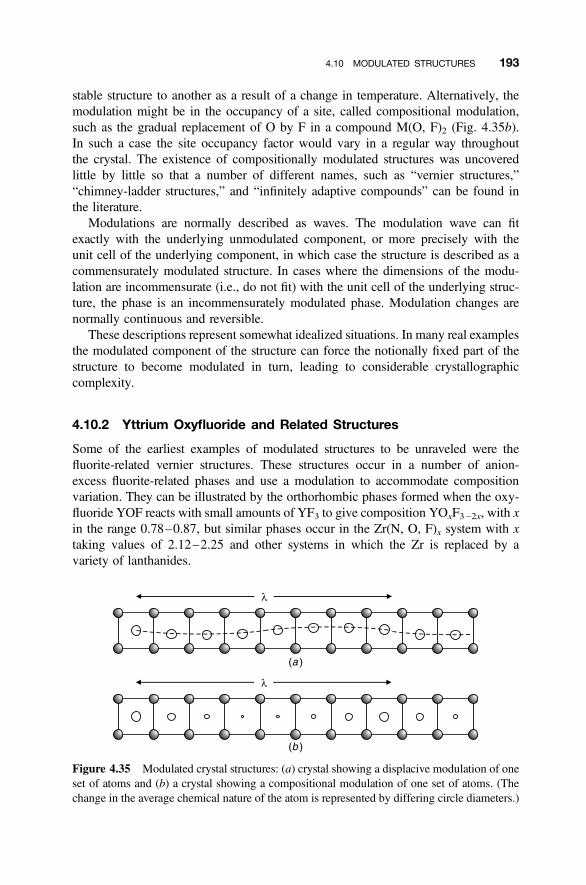
stable structure to another as a result of a change in temperature. Alternatively, themodulation might be in the occupancy of a site, called compositional modulation,such as the gradual replacement of O by F in a compound M(O, F)2 (Fig. 4.35b).In such a case the site occupancy factor would vary in a regular way throughoutthe crystal. The existence of compositionally modulated structures was uncoveredlittle by little so that a number of different names, such as “vernier structures,”“chimney-ladder structures,” and “infinitely adaptive compounds” can be found inthe literature.
Modulations are normally described as waves. The modulation wave can fitexactly with the underlying unmodulated component, or more precisely with theunit cell of the underlying component, in which case the structure is described as acommensurately modulated structure. In cases where the dimensions of the modu-lation are incommensurate (i.e., do not fit) with the unit cell of the underlying struc-ture, the phase is an incommensurately modulated phase. Modulation changes arenormally continuous and reversible.
These descriptions represent somewhat idealized situations. In many real examplesthe modulated component of the structure can force the notionally fixed part of thestructure to become modulated in turn, leading to considerable crystallographiccomplexity.
4.10.2 Yttrium Oxyfluoride and Related Structures
Some of the earliest examples of modulated structures to be unraveled were thefluorite-related vernier structures. These structures occur in a number of anion-excess fluorite-related phases and use a modulation to accommodate compositionvariation. They can be illustrated by the orthorhombic phases formed when the oxy-fluoride YOF reacts with small amounts of YF3 to give composition YOxF322x, with xin the range 0.78–0.87, but similar phases occur in the Zr(N, O, F)x system with xtaking values of 2.12–2.25 and other systems in which the Zr is replaced by avariety of lanthanides.
Figure 4.35 Modulated crystal structures: (a) crystal showing a displacive modulation of oneset of atoms and (b) a crystal showing a compositional modulation of one set of atoms. (Thechange in the average chemical nature of the atom is represented by differing circle diameters.)
4.10 MODULATED STRUCTURES 193
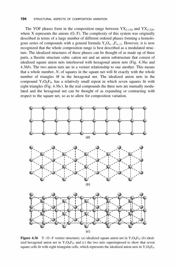
The YOF phases form in the composition range between YX2.130 and YX2.220.where X represents the anions (O, F). The complexity of this system was originallydescribed in terms of a large number of different ordered phases forming a homolo-gous series of compounds with a general formula YnOn21Fnþ2. However, it is nowrecognized that the whole composition range is best described as a modulated struc-ture. The idealized structures of these phases can be thought of as made up of threeparts, a fluorite structure cubic cation net and an anion substructure that consist ofidealized square anion nets interleaved with hexagonal anion nets (Fig. 4.36a and4.36b). The two anion nets are in a vernier relationship to one another. This meansthat a whole number, N, of squares in the square net will fit exactly with the wholenumber of triangles M in the hexagonal net. The idealized anion nets in thecompound Y7O6F9, has a relatively small repeat in which seven squares fit witheight triangles (Fig. 4.36c). In the real compounds the three nets are mutually modu-lated and the hexagonal net can be thought of as expanding or contracting withrespect to the square net, so as to allow for composition variation.
Figure 4.36 Y–O–F vernier structures: (a) idealized square anion net in Y7O6F9; (b) ideal-ized hexagonal anion net in Y7O6F9; and (c) the two nets superimposed to show that sevensquare cells fit with eight triangular cells, which represents the idealized anion nets in Y7O6F9.
194 STRUCTURAL ASPECTS OF COMPOSITION VARIATION
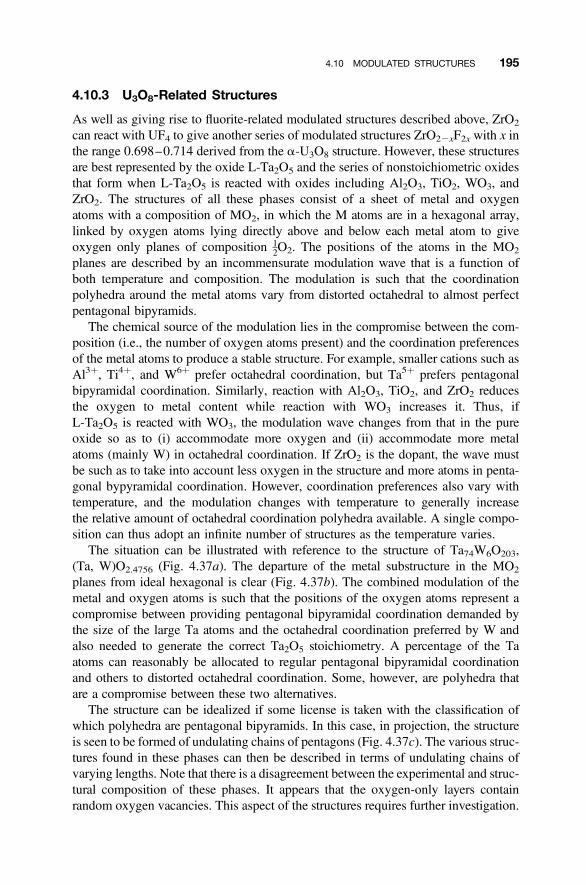
4.10.3 U3O8-Related Structures
As well as giving rise to fluorite-related modulated structures described above, ZrO2
can react with UF4 to give another series of modulated structures ZrO22xF2x with x inthe range 0.698–0.714 derived from the a-U3O8 structure. However, these structuresare best represented by the oxide L-Ta2O5 and the series of nonstoichiometric oxidesthat form when L-Ta2O5 is reacted with oxides including Al2O3, TiO2, WO3, andZrO2. The structures of all these phases consist of a sheet of metal and oxygenatoms with a composition of MO2, in which the M atoms are in a hexagonal array,linked by oxygen atoms lying directly above and below each metal atom to giveoxygen only planes of composition 1
2O2. The positions of the atoms in the MO2
planes are described by an incommensurate modulation wave that is a function ofboth temperature and composition. The modulation is such that the coordinationpolyhedra around the metal atoms vary from distorted octahedral to almost perfectpentagonal bipyramids.
The chemical source of the modulation lies in the compromise between the com-position (i.e., the number of oxygen atoms present) and the coordination preferencesof the metal atoms to produce a stable structure. For example, smaller cations such asAl3þ, Ti4þ, and W6þ prefer octahedral coordination, but Ta5þ prefers pentagonalbipyramidal coordination. Similarly, reaction with Al2O3, TiO2, and ZrO2 reducesthe oxygen to metal content while reaction with WO3 increases it. Thus, ifL-Ta2O5 is reacted with WO3, the modulation wave changes from that in the pureoxide so as to (i) accommodate more oxygen and (ii) accommodate more metalatoms (mainly W) in octahedral coordination. If ZrO2 is the dopant, the wave mustbe such as to take into account less oxygen in the structure and more atoms in penta-gonal bypyramidal coordination. However, coordination preferences also vary withtemperature, and the modulation changes with temperature to generally increasethe relative amount of octahedral coordination polyhedra available. A single compo-sition can thus adopt an infinite number of structures as the temperature varies.
The situation can be illustrated with reference to the structure of Ta74W6O203,(Ta, W)O2.4756 (Fig. 4.37a). The departure of the metal substructure in the MO2
planes from ideal hexagonal is clear (Fig. 4.37b). The combined modulation of themetal and oxygen atoms is such that the positions of the oxygen atoms represent acompromise between providing pentagonal bipyramidal coordination demanded bythe size of the large Ta atoms and the octahedral coordination preferred by W andalso needed to generate the correct Ta2O5 stoichiometry. A percentage of the Taatoms can reasonably be allocated to regular pentagonal bipyramidal coordinationand others to distorted octahedral coordination. Some, however, are polyhedra thatare a compromise between these two alternatives.
The structure can be idealized if some license is taken with the classification ofwhich polyhedra are pentagonal bipyramids. In this case, in projection, the structureis seen to be formed of undulating chains of pentagons (Fig. 4.37c). The various struc-tures found in these phases can then be described in terms of undulating chains ofvarying lengths. Note that there is a disagreement between the experimental and struc-tural composition of these phases. It appears that the oxygen-only layers containrandom oxygen vacancies. This aspect of the structures requires further investigation.
4.10 MODULATED STRUCTURES 195
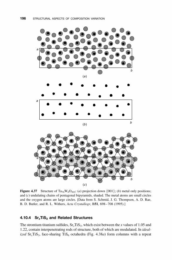
4.10.4 SrxTiS3 and Related Structures
The strontium titanium sulfides, SrxTiS3, which exist between the x values of 1.05 and1.22, contain interpenetrating rods of structure, both of which are modulated. In ideal-ized SrxTiS3, face-sharing TiS6 octahedra (Fig. 4.38a) form columns with a repeat
Figure 4.37 Structure of Ta76W6O203: (a) projection down f001g; (b) metal only positions;and (c) undulating chains of pentagonal bipyramids, shaded. The metal atoms are small circlesand the oxygen atoms are large circles. [Data from S. Schmid, J. G. Thompson, A. D. Rae,B. D. Butler, and R. L. Withers, Acta Crystallogr, B51, 698–708 (1995).]
196 STRUCTURAL ASPECTS OF COMPOSITION VARIATION

composition of TiS6/2 or TiS3, arranged to give a hexagonal unit cell (Fig. 4.38b).Chains of Sr atoms lie between these columns to complete the idealized structure(Fig. 4.38c). The a parameters of the TiS3 and Sr arrays are equal. The Sr chainsare flexible and expand or contract along the c axis, as a smooth function of the com-position x in SrxTiS3. One of the simpler commensurately modulated structuresreported is Sr8(TiS3)7, the idealized structure of which is drawn in Figure 4.38d.
The real structures of these phases are more complex. The coordination of the Tiatoms is always six, but the coordination polyhedron of sulfur atoms around the metalatoms is in turn modulated by the modulations of the Sr chains. The result of this isthat some of the TiS6 polyhedra vary between octahedra and a form some waybetween an octahedron and a trigonal prism. The vast majority of compositionsgive incommensurately modulated structures with enormous unit cells. As in thecase of the other modulated phases, and the many more not mentioned, compositionvariation is accommodated without recourse to “defects.”
Figure 4.38 Idealized structure of SrxTiS3 modulated phases: (a) an idealized TiS6 octa-hedron (the shaded faces are shared to form columns); (b) idealized hexagonal unit cellformed by columns of face-shared TiS6 octahedra; (c) idealized unit cell formed by columnsof face-sharing octahedra and Sr atoms (shaded); and (d ) idealized structure of Sr8(TiS3)7.
4.10 MODULATED STRUCTURES 197
4.11 ANSWERS TO INTRODUCTORY QUESTIONS
What are solid solutions?
A solid solution is a crystal structure in which two (or more) atom types arearranged at random over the sites normally occupied by one atom type alone.For example, in the corundum structure solid solution formed by Cr2O3 andAl2O3, a random mixture of Cr3þ and Al3þ ions occupy the cation sites that areonly occupied by one of these in the parent phases. The formula of the solid sol-ution materials is written (Al12xCrx)2O3. In this example, x can vary continuouslybetween 0 and 1.0. In some cases, especially when the atoms involved have differ-ent sizes, only partial solid solutions are found, characterized by a compositionrange in which the span of x is smaller than 1.0. Solid solutions are widelyexploited as both the chemical and physical properties of the solid can bevaried sensitively by changing the relative amounts of the components of thesolid solution.
What are modular structures?
Modular structures are those that can be considered to be built from slabs of one ormore parent structures. Slabs can be sections from just one parent phase, as inmany perovskite-related structures and CS phases, or they can come from twoor more parent structures, as in the mica–pyroxene intergrowths. Some of thesecrystals possess enormous unit cells, of some hundreds of nanometers in length.In many materials the slab thicknesses may vary widely, in which case the slabboundaries will not fall on a regular lattice and form planar defects.
What are incommensurately modulated structures?
Ideally, incommensurately modulated structures have two fairly distinct parts.One part of the crystal structure is conventional and behaves like a normalcrystal. An additional, more or less independent part, exists that is modulated inone, two, or three dimensions. For example, the fixed part of the structuremight be the metal atom array, while the modulated part might be the anionarray. The modulation might be in the position of the atoms, called a displacivemodulation or the occupancy of a site, for example, the gradual replacementof O by F in a compound M(O, F)2, to give a compositional modulation.In some more complex crystals modulation in one part of the structure inducesa corresponding modulation in the “fixed” part.
In cases where the wavelength of the modulation fits exactly with the dimen-sions of the underlying structure, a commensurately modulated crystallographicphase forms. In cases where the dimensions of the modulation are incommensurate(i.e., do not fit) with the underlying (generally small) unit cell of the parent struc-ture, the phase is an incommensurately modulated phase.
198 STRUCTURAL ASPECTS OF COMPOSITION VARIATION
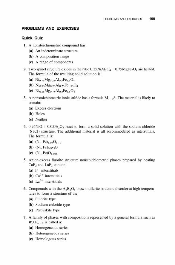
PROBLEMS AND EXERCISES
Quick Quiz
1. A nonstoichiometric compound has:
(a) An indeterminate structure
(b) A composition range
(c) A range of components
2. Two spinel structure oxides in the ratio 0.25NiAl2O4 : 0.75MgFe2O4 are heated.The formula of the resulting solid solution is:
(a) Ni0.75Mg0.25Al0.5Fe1.5O4
(b) Ni0.75Mg0.25Al0.25Fe1.75O4
(c) Ni0.25Mg0.75Al0.5Fe1.5O4
3. A nonstoichiometric ionic sulfide has a formula M12xS. The material is likely tocontain:
(a) Excess electrons
(b) Holes
(c) Neither
4. 0.95NiO þ 0.05Fe2O3 react to form a solid solution with the sodium chloride(NaCl) structure. The additional material is all accommodated as interstitials.The formula is:
(a) (Ni, Fe)1.05O1.10
(b) (Ni, Fe)0.955O
(c) (Ni, Fe)O1.048
5. Anion-excess fluorite structure nonstoichiometric phases prepared by heatingCaF2 and LaF3 contain:
(a) F2 interstitials
(b) Ca2þ interstitials
(c) La3þ interstitials
6. Compounds with the A2B2O5 brownmillerite structure disorder at high tempera-tures to form a structure of the:
(a) Fluorite type
(b) Sodium chloride type
(c) Perovskite type
7. A family of phases with compositions represented by a general formula such asWnO3n22 is called a:
(a) Homogeneous series
(b) Heterogeneous series
(c) Homologous series
PROBLEMS AND EXERCISES 199
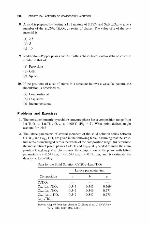
8. A solid is prepared by heating a 1 : 1 mixture of SrTiO3 and Sr4Nb4O14 to give amember of the Srn(Nb, Ti)nO3nþ2 series of phases. The value of n of the newmaterial is:
(a) 2.5
(b) 5
(c) 10
9. Ruddleston–Popper phases and Aurivillius phases both contain slabs of structuresimilar to that of:
(a) Perovskite
(b) CdI2(c) Spinel
10. If the positions of a set of atoms in a structure follows a wavelike pattern, themodulation is described as:
(a) Compositional
(b) Displacive
(c) Incommensurate
Problems and Exercises
1. The nonstoichiometric pyrochlore structure phase has a composition range fromLu2Ti2O7 to Lu2Ti1.17O5.35 at 14008C (Fig. 4.2). What point defects mightaccount for this?
2. The lattice parameters of several members of the solid solution series betweenCaTiO3 and La2/3TiO3 are given in the following table. Assuming that the struc-ture remains unchanged across the whole of the composition range: (a) determinethe molar ratio of parent phases CaTiO3 and La2/3TiO3 needed to make the com-position Ca0.4La0.4TiO3; (b) estimate the composition of the phase with latticeparameters a � 0.545 nm, b � 0.545 nm, c � 0.771 nm; and (c) estimate thedensity of La2/3TiO3.
Data for the Solid Solution CaTiO3–La2/3TiO3
Composition
Lattice parameter/nm
a b c
CaTiO3 — — —Ca0.7La0.2TiO3 0.543 0.545 0.769Ca0.4La0.4TiO3 0.547 0.546 0.771Ca0.2La0.53TiO3 0.547 0.547 0.775La2/3TiO3 — — —
Source: Adapted from data given by Z. Zhang et al., J. Solid StateChem., 180, 1083–1092 (2007).
200 STRUCTURAL ASPECTS OF COMPOSITION VARIATION
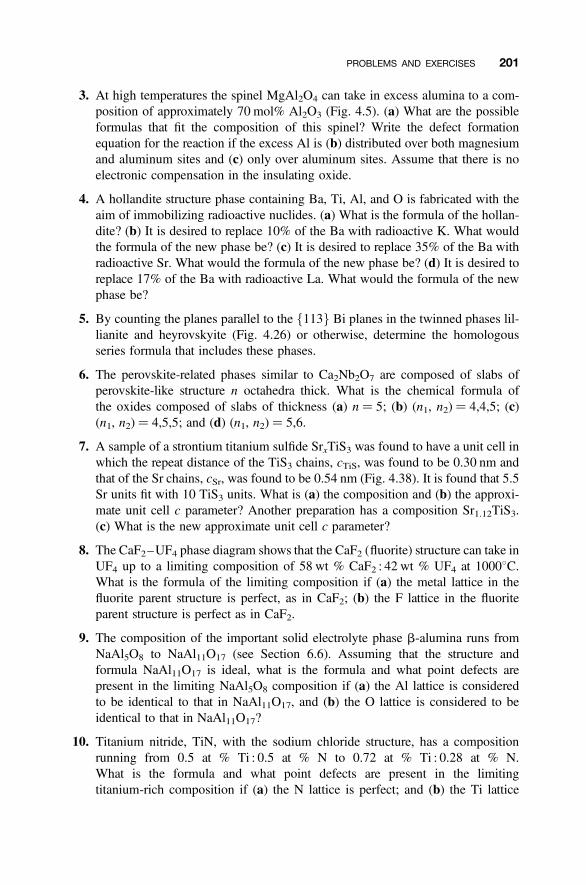
3. At high temperatures the spinel MgAl2O4 can take in excess alumina to a com-position of approximately 70 mol% Al2O3 (Fig. 4.5). (a) What are the possibleformulas that fit the composition of this spinel? Write the defect formationequation for the reaction if the excess Al is (b) distributed over both magnesiumand aluminum sites and (c) only over aluminum sites. Assume that there is noelectronic compensation in the insulating oxide.
4. A hollandite structure phase containing Ba, Ti, Al, and O is fabricated with theaim of immobilizing radioactive nuclides. (a) What is the formula of the hollan-dite? (b) It is desired to replace 10% of the Ba with radioactive K. What wouldthe formula of the new phase be? (c) It is desired to replace 35% of the Ba withradioactive Sr. What would the formula of the new phase be? (d) It is desired toreplace 17% of the Ba with radioactive La. What would the formula of the newphase be?
5. By counting the planes parallel to the f113g Bi planes in the twinned phases lil-lianite and heyrovskyite (Fig. 4.26) or otherwise, determine the homologousseries formula that includes these phases.
6. The perovskite-related phases similar to Ca2Nb2O7 are composed of slabs ofperovskite-like structure n octahedra thick. What is the chemical formula ofthe oxides composed of slabs of thickness (a) n ¼ 5; (b) (n1, n2) ¼ 4,4,5; (c)(n1, n2) ¼ 4,5,5; and (d) (n1, n2) ¼ 5,6.
7. A sample of a strontium titanium sulfide SrxTiS3 was found to have a unit cell inwhich the repeat distance of the TiS3 chains, cTiS, was found to be 0.30 nm andthat of the Sr chains, cSr, was found to be 0.54 nm (Fig. 4.38). It is found that 5.5Sr units fit with 10 TiS3 units. What is (a) the composition and (b) the approxi-mate unit cell c parameter? Another preparation has a composition Sr1.12TiS3.(c) What is the new approximate unit cell c parameter?
8. The CaF2–UF4 phase diagram shows that the CaF2 (fluorite) structure can take inUF4 up to a limiting composition of 58 wt % CaF2 : 42 wt % UF4 at 10008C.What is the formula of the limiting composition if (a) the metal lattice in thefluorite parent structure is perfect, as in CaF2; (b) the F lattice in the fluoriteparent structure is perfect as in CaF2.
9. The composition of the important solid electrolyte phase b-alumina runs fromNaAl5O8 to NaAl11O17 (see Section 6.6). Assuming that the structure andformula NaAl11O17 is ideal, what is the formula and what point defects arepresent in the limiting NaAl5O8 composition if (a) the Al lattice is consideredto be identical to that in NaAl11O17, and (b) the O lattice is considered to beidentical to that in NaAl11O17?
10. Titanium nitride, TiN, with the sodium chloride structure, has a compositionrunning from 0.5 at % Ti : 0.5 at % N to 0.72 at % Ti : 0.28 at % N.What is the formula and what point defects are present in the limitingtitanium-rich composition if (a) the N lattice is perfect; and (b) the Ti lattice
PROBLEMS AND EXERCISES 201
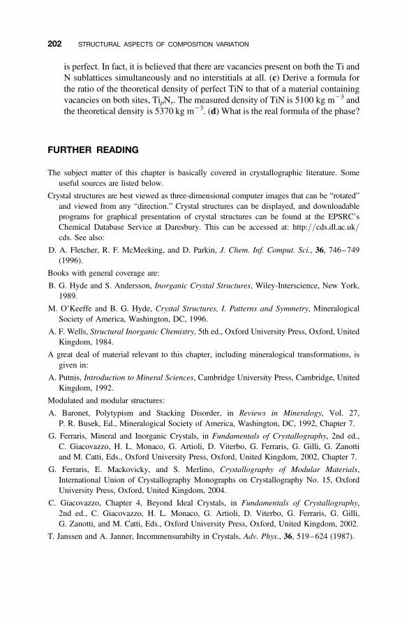
is perfect. In fact, it is believed that there are vacancies present on both the Ti andN sublattices simultaneously and no interstitials at all. (c) Derive a formula forthe ratio of the theoretical density of perfect TiN to that of a material containingvacancies on both sites, TipNr. The measured density of TiN is 5100 kg m23 andthe theoretical density is 5370 kg m23. (d) What is the real formula of the phase?
FURTHER READING
The subject matter of this chapter is basically covered in crystallographic literature. Someuseful sources are listed below.
Crystal structures are best viewed as three-dimensional computer images that can be “rotated”and viewed from any “direction.” Crystal structures can be displayed, and downloadableprograms for graphical presentation of crystal structures can be found at the EPSRC’sChemical Database Service at Daresbury. This can be accessed at: http://cds.dl.ac.uk/cds. See also:
D. A. Fletcher, R. F. McMeeking, and D. Parkin, J. Chem. Inf. Comput. Sci., 36, 746–749(1996).
Books with general coverage are:
B. G. Hyde and S. Andersson, Inorganic Crystal Structures, Wiley-Interscience, New York,1989.
M. O’Keeffe and B. G. Hyde, Crystal Structures, I. Patterns and Symmetry, MineralogicalSociety of America, Washington, DC, 1996.
A. F. Wells, Structural Inorganic Chemistry, 5th ed., Oxford University Press, Oxford, UnitedKingdom, 1984.
A great deal of material relevant to this chapter, including mineralogical transformations, isgiven in:
A. Putnis, Introduction to Mineral Sciences, Cambridge University Press, Cambridge, UnitedKingdom, 1992.
Modulated and modular structures:
A. Baronet, Polytypism and Stacking Disorder, in Reviews in Mineralogy, Vol. 27,P. R. Busek, Ed., Mineralogical Society of America, Washington, DC, 1992, Chapter 7.
G. Ferraris, Mineral and Inorganic Crystals, in Fundamentals of Crystallography, 2nd ed.,C. Giacovazzo, H. L. Monaco, G. Artioli, D. Viterbo, G. Ferraris, G. Gilli, G. Zanottiand M. Catti, Eds., Oxford University Press, Oxford, United Kingdom, 2002, Chapter 7.
G. Ferraris, E. Mackovicky, and S. Merlino, Crystallography of Modular Materials,International Union of Crystallography Monographs on Crystallography No. 15, OxfordUniversity Press, Oxford, United Kingdom, 2004.
C. Giacovazzo, Chapter 4, Beyond Ideal Crystals, in Fundamentals of Crystallography,2nd ed., C. Giacovazzo, H. L. Monaco, G. Artioli, D. Viterbo, G. Ferraris, G. Gilli,G. Zanotti, and M. Catti, Eds., Oxford University Press, Oxford, United Kingdom, 2002.
T. Janssen and A. Janner, Incommensurabilty in Crystals, Adv. Phys., 36, 519–624 (1987).
202 STRUCTURAL ASPECTS OF COMPOSITION VARIATION
E. Makovicky and B. G. Hyde, Incommensurate, Two-Layer Structures with Complex CrystalChemistry: Minerals and Related Synthetics, Mat. Sci. Forum, 100 & 101, 1–100 (1992).
S. van Smaalen, Incommenurate Crystal Structures, Crystal. Rev., 4, 79–202 (1995).
D. R. Veblen, Electron Microscopy Applied to Nonstoichiometry, Polysomatism andReplacement Reactions in Minerals, in Reviews in Mineralogy, Vol. 27, P. R. Busek,Ed., Mineralogical Society of America, Washington, DC, 1992, Chapter 6.
D. R. Veblen, Polysomatism and Polysomatic Series: A Review and Applications, Am.Mineral., 76, 801–826 (1991).
G. A. Wiegers, Misfit Layer Compounds: Structures and Physical Properties, Prog. Solid StateChem., 24, 1–139 (1996).
R. L. Withers, S. Schmid, and J. G. Thompson, Compositionally and/or Displacively FlexibleSystems and Their Underlying Crystal Chemistry, Prog. Solid State Chem., 26, 1–96(1998).
References to �FeO:
H. Fjellvag, H. Grønvold, S. Stølen, and Bjørn Hauback, J. Solid State Chem., 124, 52–57(1992).
M. J. Radler, J. B. Cohen, and J. B. Faber, J. Phys. Chem. Solids, 51, 217–228 (1990).
References to calcia-stabilized zirconia:
R. Devanathan, W. J. Weber, S. C. Singhal, and J. D. Gale, Solid State Ionics, 177, 1251–1258(2006).
T. R. Welberry, R. L. Withers, J. G. Thompson, and R. D. Butler, J. Solid State Chem., 100,71–89 (1992).
References to anion-excess fluorite structures:
D. J. M. Bevan, I. E. Grey, and B. T. M. Willis (b-U4O92y) J. Solid State Chem., 61, 1–7(1986).
J. P. Laval, C. Depierefixe, B. Frit, and G. Roult (Pb12xZrxF2þ2x: 0, x, 0.18) J. Solid StateChem., 54, 260–276 (1984).
C. Rocaniere, J. P. Laval, P. Dehaudt, B. Gaudreau, A. Chotard, and E. Suard,((U0.9Ce0.1)4O92d), J. Solid State Chem., 177, 1758–1767 (2004).
K. Wurst, E. Schweda, D. J. M. Bevan, C. Mohyla, K. S. Wallwork, and M. Hofmann,(Zr50Sc12O118), Solid State Sci., 5, 1491–1497 (2003).
A description of L-Ta2O5 as a modulated structure:
S. Schmid, J. G. Thompson, A. D. Rae, B. D. Butler, and R. L. Withers, Acta Crystallogr.,B51, 698 (1995); A. D. Rae, S. Schmid, J. G. Thompson, and R. Withers, ActaCrystallogr., B51, 709 (1995).
S. Schmid, R. L. Withers, and J. G. Thompson, J. Solid State Chem., 99, 226 (1992).
A description of SrxTiS3 as a modulated structure:
O. Gourdon, V. Petricek, and M. Evain, Acta Crystallogr., B56, 409–418 (2000).
M. Saeki, M. Ohta, K. Kurashima, and M. Onoda, Mat. Res. Bull., 37, 1519–1529 (2002).
FURTHER READING 203

&CHAPTER 5
Defects and Diffusion
What is volume diffusion?
How does temperature effect diffusion in solids?
How do defects influence diffusion in solids?
5.1 DIFFUSION
Diffusion is a description of the way in which atoms, ions, or molecules flow througha surrounding medium. For example, when two different atom types (which can bedifferent elements or merely different isotopes of the same element) are unitedalong a planar boundary, diffusion leads to the gradual mixing of the species andblurring of the initially sharp interface (Fig. 5.1). It is apparent that diffusion willbe an important factor when considering the reaction of solids with other solids,liquids, or gases.
Diffusion is quantified by measuring the concentration of the diffusing speciesat different distances from the release point after a given time has elapsed at aprecise temperature. Raw experimental data thus consists of concentration anddistance values. The degree of diffusion is represented by a diffusion coefficient,which is extracted from the concentration–distance results by solution of one oftwo diffusion equations. For one-dimensional diffusion, along x, they are Fick’sfirst law of diffusion:
J ¼ �Ddc
dx(5:1)
and Fick’s second law of diffusion, known more commonly as the diffusionequation:
dc
dt¼ D
d2c
dx2(5:2)
Defects in Solids, by Richard J. D. TilleyCopyright # 2008 John Wiley & Sons, Inc.
205
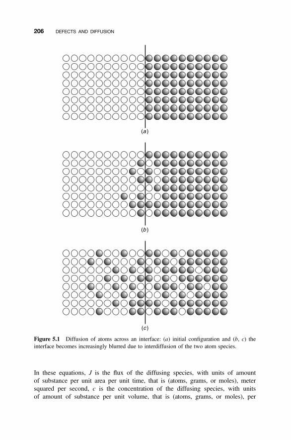
In these equations, J is the flux of the diffusing species, with units of amountof substance per unit area per unit time, that is (atoms, grams, or moles), metersquared per second, c is the concentration of the diffusing species, with unitsof amount of substance per unit volume, that is (atoms, grams, or moles), per
Figure 5.1 Diffusion of atoms across an interface: (a) initial configuration and (b, c) theinterface becomes increasingly blurred due to interdiffusion of the two atom species.
206 DEFECTS AND DIFFUSION
cubic meter, at position x, units in meter, after time t, units in seconds, and D is thediffusion coefficient or diffusivity, with units1 of square meter per second.
There are two overriding considerations to keep in mind when discussing diffusionin solids: the structure of the matrix across which diffusion occurs and thedefects present. In a normal crystalline solid, diffusion is mediated by the defectspresent, and the speed of diffusion will vary significantly if the predominant defecttype changes. This is because diffusion involves the movement of a species from astable position, through some sort of less stable position or bottleneck, to anotherstable position. Any disorder in the solid due to defects will make this process easier.
Movement through the body of a solid is called volume, lattice, or bulk diffusion.In a gas or liquid, bulk diffusion is usually the same in all directions and the materialis described as isotropic. This is also true in amorphous or glassy solids and in cubiccrystals. In all other crystals, the rate of bulk diffusion depends upon the directiontaken and is anisotropic. Bulk diffusion through a perfect single crystal is dominatedby point defects, with both impurity and intrinsic defect populations playing a part.
Diffusion along two- and three-dimensional imperfections in the material is muchfaster than bulk diffusion, especially at lower temperatures. This process is referred toas short-circuit diffusion. The main imperfections that are of importance for short-circuit diffusion are dislocations and grain boundaries. Dislocations can be thoughtof as tubes of disordered structure that thread through a crystal, and diffusionalong a dislocation core is sometimes called pipe diffusion. Low-angle grain bound-aries in crystals are comprised of arrays of dislocations, and diffusion along thesedislocations will result in enhanced atom transport compared to the bulk. Grainboundaries are ordinarily regions between individual crystallites in a polycrystallinesolid, and diffusion making use of these surfaces is called grain boundary diffusion.Diffusion at external surfaces, surface diffusion, is also important and plays a vitalrole in many chemical reactions, notably those in heterogeneous catalysis.
In this chapter, to keep the material compact, only the relationship between diffu-sion and defects in solids will be discussed. Moreover, the diffusion coefficient willbe considered as a constant at a fixed temperature, and attention is focused upon themovement of atoms and ions rather than the equally important diffusion of gasesor liquids through a solid. Discussion of diffusion per se, the extensive literatureon classical theories of diffusion, and diffusion when the diffusion coefficient isnot a constant will be found in the Further Reading section at the end of this chapter.
5.2 DIFFUSION IN SOLIDS
Diffusion is followed by tracking the movements of tracer species through the solid toobtain the tracer diffusion coefficient, written as D� when the tracer is identical to oneof the components of the crystal, and D�
A when an impurity or foreign atom A is thetracer. Earlier studies made extensive use of radioactive isotopes because the progress
1The values of diffusion coefficients in (especially) the older literature are frequently given in square centi-meter per second. To convert to square meters per second, multiply by 1024, that is, D (cm2 s21) � 1024 !D (m2 s21).
5.2 DIFFUSION IN SOLIDS 207
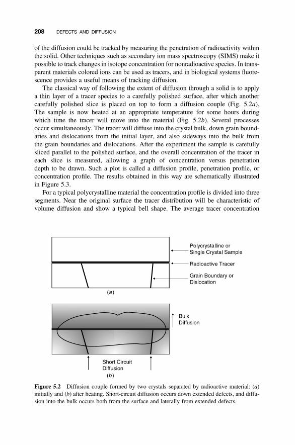
of the diffusion could be tracked by measuring the penetration of radioactivity withinthe solid. Other techniques such as secondary ion mass spectroscopy (SIMS) make itpossible to track changes in isotope concentration for nonradioactive species. In trans-parent materials colored ions can be used as tracers, and in biological systems fluore-scence provides a useful means of tracking diffusion.
The classical way of following the extent of diffusion through a solid is to applya thin layer of a tracer species to a carefully polished surface, after which anothercarefully polished slice is placed on top to form a diffusion couple (Fig. 5.2a).The sample is now heated at an appropriate temperature for some hours duringwhich time the tracer will move into the material (Fig. 5.2b). Several processesoccur simultaneously. The tracer will diffuse into the crystal bulk, down grain bound-aries and dislocations from the initial layer, and also sideways into the bulk fromthe grain boundaries and dislocations. After the experiment the sample is carefullysliced parallel to the polished surface, and the overall concentration of the tracer ineach slice is measured, allowing a graph of concentration versus penetrationdepth to be drawn. Such a plot is called a diffusion profile, penetration profile, orconcentration profile. The results obtained in this way are schematically illustratedin Figure 5.3.
For a typical polycrystalline material the concentration profile is divided into threesegments. Near the original surface the tracer distribution will be characteristic ofvolume diffusion and show a typical bell shape. The average tracer concentration
Figure 5.2 Diffusion couple formed by two crystals separated by radioactive material: (a)initially and (b) after heating. Short-circuit diffusion occurs down extended defects, and diffu-sion into the bulk occurs both from the surface and laterally from extended defects.
208 DEFECTS AND DIFFUSION
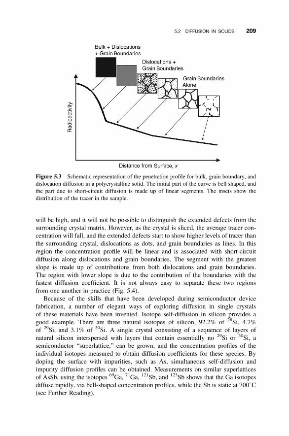
will be high, and it will not be possible to distinguish the extended defects from thesurrounding crystal matrix. However, as the crystal is sliced, the average tracer con-centration will fall, and the extended defects start to show higher levels of tracer thanthe surrounding crystal, dislocations as dots, and grain boundaries as lines. In thisregion the concentration profile will be linear and is associated with short-circuitdiffusion along dislocations and grain boundaries. The segment with the greatestslope is made up of contributions from both dislocations and grain boundaries.The region with lower slope is due to the contribution of the boundaries with thefastest diffusion coefficient. It is not always easy to separate these two regionsfrom one another in practice (Fig. 5.4).
Because of the skills that have been developed during semiconductor devicefabrication, a number of elegant ways of exploring diffusion in single crystalsof these materials have been invented. Isotope self-diffusion in silicon provides agood example. There are three natural isotopes of silicon, 92.2% of 28Si, 4.7%of 29Si, and 3.1% of 30Si. A single crystal consisting of a sequence of layers ofnatural silicon interspersed with layers that contain essentially no 29Si or 30Si, asemiconductor “superlattice,” can be grown, and the concentration profiles of theindividual isotopes measured to obtain diffusion coefficients for these species. Bydoping the surface with impurities, such as As, simultaneous self-diffusion andimpurity diffusion profiles can be obtained. Measurements on similar superlatticesof AsSb, using the isotopes 69Ga, 71Ga, 121Sb, and 123Sb shows that the Ga isotopesdiffuse rapidly, via bell-shaped concentration profiles, while the Sb is static at 7008C(see Further Reading).
Figure 5.3 Schematic representation of the penetration profile for bulk, grain boundary, anddislocation diffusion in a polycrystalline solid. The initial part of the curve is bell shaped, andthe part due to short-circuit diffusion is made up of linear segments. The insets show thedistribution of the tracer in the sample.
5.2 DIFFUSION IN SOLIDS 209
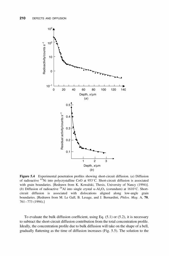
To evaluate the bulk diffusion coefficient, using Eq. (5.1) or (5.2), it is necessaryto subtract the short-circuit diffusion contribution from the total concentration profile.Ideally, the concentration profile due to bulk diffusion will take on the shape of a bell,gradually flattening as the time of diffusion increases (Fig. 5.5). The solution to the
Figure 5.4 Experimental penetration profiles showing short-circuit diffusion. (a) Diffusionof radioactive 63Ni into polycrystalline CoO at 9538C. Short-circuit diffusion is associatedwith grain boundaries. [Redrawn from K. Kowalski, Thesis, University of Nancy (1994)].(b) Diffusion of radioactive 26Al into single crystal a-Al2O3 (corundum) at 16108C. Short-circuit diffusion is associated with dislocations aligned along low-angle grainboundaries. [Redrawn from M. Le Gall, B. Lesage, and J. Bernardini, Philos. Mag. A, 70,761–773 (1994).]
210 DEFECTS AND DIFFUSION
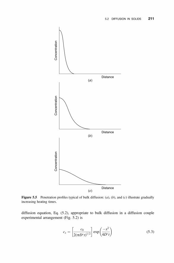
diffusion equation, Eq. (5.2), appropriate to bulk diffusion in a diffusion coupleexperimental arrangement (Fig. 5.2) is
cx ¼ c02(pD�t)1=2
� �exp
�x2
4D�t
� �(5:3)
Figure 5.5 Penetration profiles typical of bulk diffusion: (a), (b), and (c) illustrate graduallyincreasing heating times.
5.2 DIFFUSION IN SOLIDS 211
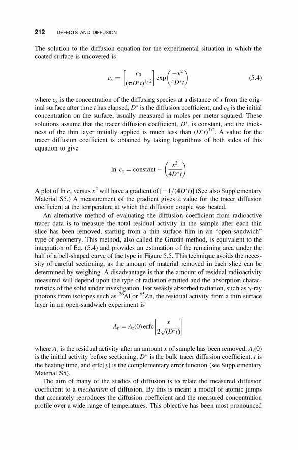
The solution to the diffusion equation for the experimental situation in which thecoated surface is uncovered is
cx ¼ c0(pD�t)1=2
� �exp
�x2
4D�t
� �(5:4)
where cx is the concentration of the diffusing species at a distance of x from the orig-inal surface after time t has elapsed, D� is the diffusion coefficient, and c0 is the initialconcentration on the surface, usually measured in moles per meter squared. Thesesolutions assume that the tracer diffusion coefficient, D�, is constant, and the thick-ness of the thin layer initially applied is much less than (D�t)1/2. A value for thetracer diffusion coefficient is obtained by taking logarithms of both sides of thisequation to give
ln cx ¼ constant� x2
4D�t
� �
A plot of ln cx versus x2 will have a gradient of [21/(4D�t)] (See also Supplementary
Material S5.) A measurement of the gradient gives a value for the tracer diffusioncoefficient at the temperature at which the diffusion couple was heated.
An alternative method of evaluating the diffusion coefficient from radioactivetracer data is to measure the total residual activity in the sample after each thinslice has been removed, starting from a thin surface film in an “open-sandwich”type of geometry. This method, also called the Gruzin method, is equivalent to theintegration of Eq. (5.4) and provides an estimation of the remaining area under thehalf of a bell-shaped curve of the type in Figure 5.5. This technique avoids the neces-sity of careful sectioning, as the amount of material removed in each slice can bedetermined by weighing. A disadvantage is that the amount of residual radioactivitymeasured will depend upon the type of radiation emitted and the absorption charac-teristics of the solid under investigation. For weakly absorbed radiation, such as g-rayphotons from isotopes such as 26Al or 65Zn, the residual activity from a thin surfacelayer in an open-sandwich experiment is
Ar ¼ Ar(0) erfcx
2ffiffiffiffiffiffiffiffiffiffi(D�t)
p� �
where Ar is the residual activity after an amount x of sample has been removed, Ar(0)is the initial activity before sectioning, D� is the bulk tracer diffusion coefficient, t isthe heating time, and erfc[ y] is the complementary error function (see SupplementaryMaterial S5).
The aim of many of the studies of diffusion is to relate the measured diffusioncoefficient to a mechanism of diffusion. By this is meant a model of atomic jumpsthat accurately reproduces the diffusion coefficient and the measured concentrationprofile over a wide range of temperatures. This objective has been most pronounced
212 DEFECTS AND DIFFUSION
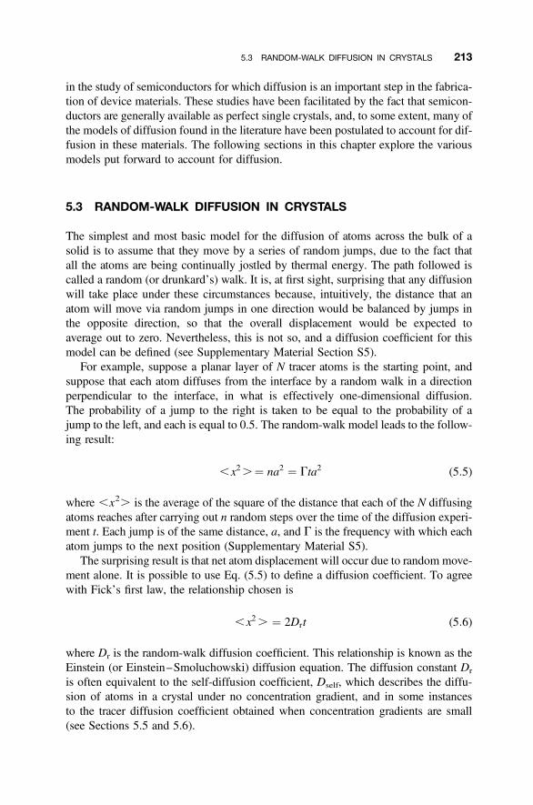
in the study of semiconductors for which diffusion is an important step in the fabrica-tion of device materials. These studies have been facilitated by the fact that semicon-ductors are generally available as perfect single crystals, and, to some extent, many ofthe models of diffusion found in the literature have been postulated to account for dif-fusion in these materials. The following sections in this chapter explore the variousmodels put forward to account for diffusion.
5.3 RANDOM-WALK DIFFUSION IN CRYSTALS
The simplest and most basic model for the diffusion of atoms across the bulk of asolid is to assume that they move by a series of random jumps, due to the fact thatall the atoms are being continually jostled by thermal energy. The path followed iscalled a random (or drunkard’s) walk. It is, at first sight, surprising that any diffusionwill take place under these circumstances because, intuitively, the distance that anatom will move via random jumps in one direction would be balanced by jumps inthe opposite direction, so that the overall displacement would be expected toaverage out to zero. Nevertheless, this is not so, and a diffusion coefficient for thismodel can be defined (see Supplementary Material Section S5).
For example, suppose a planar layer of N tracer atoms is the starting point, andsuppose that each atom diffuses from the interface by a random walk in a directionperpendicular to the interface, in what is effectively one-dimensional diffusion.The probability of a jump to the right is taken to be equal to the probability of ajump to the left, and each is equal to 0.5. The random-walk model leads to the follow-ing result:
,x2.¼ na2 ¼ Gta2 (5:5)
where ,x2. is the average of the square of the distance that each of the N diffusingatoms reaches after carrying out n random steps over the time of the diffusion experi-ment t. Each jump is of the same distance, a, and G is the frequency with which eachatom jumps to the next position (Supplementary Material S5).
The surprising result is that net atom displacement will occur due to random move-ment alone. It is possible to use Eq. (5.5) to define a diffusion coefficient. To agreewith Fick’s first law, the relationship chosen is
,x2. ¼ 2Drt (5:6)
where Dr is the random-walk diffusion coefficient. This relationship is known as theEinstein (or Einstein–Smoluchowski) diffusion equation. The diffusion constant Dr
is often equivalent to the self-diffusion coefficient, Dself, which describes the diffu-sion of atoms in a crystal under no concentration gradient, and in some instancesto the tracer diffusion coefficient obtained when concentration gradients are small(see Sections 5.5 and 5.6).
5.3 RANDOM-WALK DIFFUSION IN CRYSTALS 213
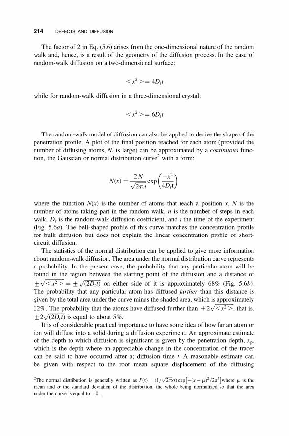
The factor of 2 in Eq. (5.6) arises from the one-dimensional nature of the randomwalk and, hence, is a result of the geometry of the diffusion process. In the case ofrandom-walk diffusion on a two-dimensional surface:
,x2.¼ 4Drt
while for random-walk diffusion in a three-dimensional crystal:
,x2.¼ 6Drt
The random-walk model of diffusion can also be applied to derive the shape of thepenetration profile. A plot of the final position reached for each atom (provided thenumber of diffusing atoms, N, is large) can be approximated by a continuous func-tion, the Gaussian or normal distribution curve2 with a form:
N(x) ¼ 2Nffiffiffiffiffiffiffiffiffi2pn
p exp�x2
4Drt
� �
where the function N(x) is the number of atoms that reach a position x, N is thenumber of atoms taking part in the random walk, n is the number of steps in eachwalk, Dr is the random-walk diffusion coefficient, and t the time of the experiment(Fig. 5.6a). The bell-shaped profile of this curve matches the concentration profilefor bulk diffusion but does not explain the linear concentration profile of short-circuit diffusion.
The statistics of the normal distribution can be applied to give more informationabout random-walk diffusion. The area under the normal distribution curve representsa probability. In the present case, the probability that any particular atom will befound in the region between the starting point of the diffusion and a distance of
+ffiffiffiffiffiffiffiffiffiffiffiffiffiffi,x2.
p¼ +
ffiffiffiffiffiffiffiffiffiffiffiffi(2Drt)
pon either side of it is approximately 68% (Fig. 5.6b).
The probability that any particular atom has diffused further than this distance isgiven by the total area under the curve minus the shaded area, which is approximately
32%. The probability that the atoms have diffused further than +2ffiffiffiffiffiffiffiffiffiffiffiffiffiffi,x2.
p, that is,
+2ffiffiffiffiffiffiffiffiffiffiffiffi(2Drt)
pis equal to about 5%.
It is of considerable practical importance to have some idea of how far an atom orion will diffuse into a solid during a diffusion experiment. An approximate estimateof the depth to which diffusion is significant is given by the penetration depth, xp,which is the depth where an appreciable change in the concentration of the tracercan be said to have occurred after a; diffusion time t. A reasonable estimate canbe given with respect to the root mean square displacement of the diffusing
2The normal distribution is generally written as P(x) ¼ (1=ffiffiffiffiffiffi2p
ps) exp �(x� m)2=2s2
� �where m is the
mean and s the standard deviation of the distribution, the whole being normalized so that the areaunder the curve is equal to 1.0.
214 DEFECTS AND DIFFUSION
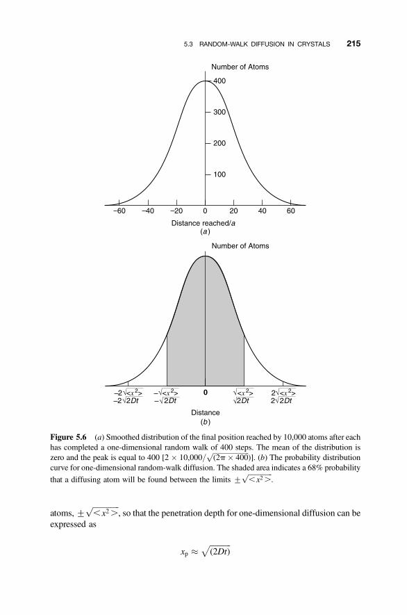
atoms,+ffiffiffiffiffiffiffiffiffiffiffiffiffiffi,x2.
p, so that the penetration depth for one-dimensional diffusion can be
expressed as
xp �ffiffiffiffiffiffiffiffiffiffiffi(2Dt)
p
Figure 5.6 (a) Smoothed distribution of the final position reached by 10,000 atoms after eachhas completed a one-dimensional random walk of 400 steps. The mean of the distribution iszero and the peak is equal to 400 [2 � 10,000/
ffiffiffiffiffiffiffiffiffiffiffiffiffiffiffiffiffiffiffiffiffi(2p� 400
p)]. (b) The probability distribution
curve for one-dimensional random-walk diffusion. The shaded area indicates a 68% probability
that a diffusing atom will be found between the limits +ffiffiffiffiffiffiffiffiffiffiffiffiffiffi,x2.
p.
5.3 RANDOM-WALK DIFFUSION IN CRYSTALS 215
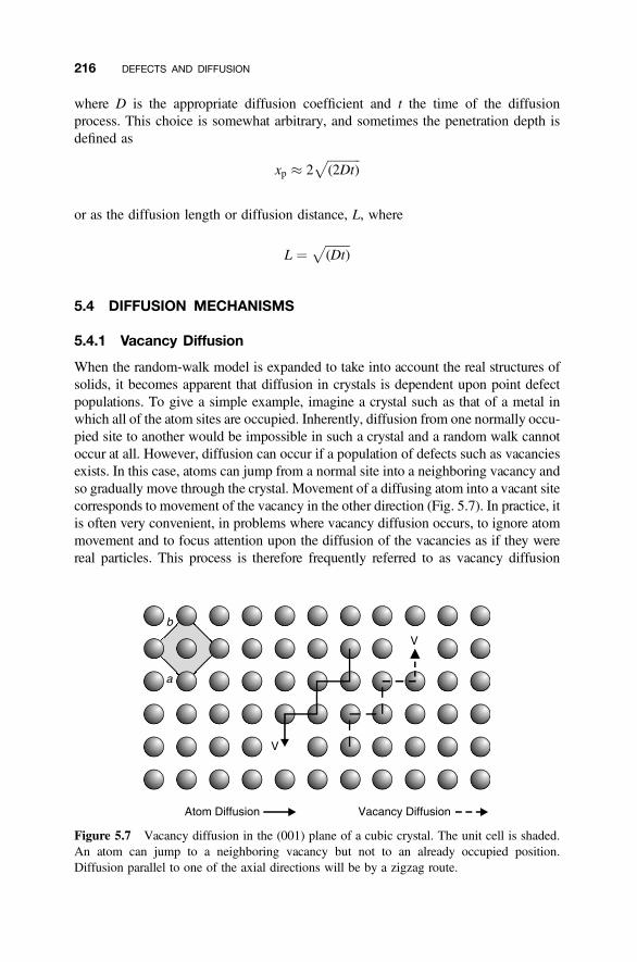
where D is the appropriate diffusion coefficient and t the time of the diffusionprocess. This choice is somewhat arbitrary, and sometimes the penetration depth isdefined as
xp � 2ffiffiffiffiffiffiffiffiffiffiffi(2Dt)
p
or as the diffusion length or diffusion distance, L, where
L ¼ffiffiffiffiffiffiffiffi(Dt)
p
5.4 DIFFUSION MECHANISMS
5.4.1 Vacancy Diffusion
When the random-walk model is expanded to take into account the real structures ofsolids, it becomes apparent that diffusion in crystals is dependent upon point defectpopulations. To give a simple example, imagine a crystal such as that of a metal inwhich all of the atom sites are occupied. Inherently, diffusion from one normally occu-pied site to another would be impossible in such a crystal and a random walk cannotoccur at all. However, diffusion can occur if a population of defects such as vacanciesexists. In this case, atoms can jump from a normal site into a neighboring vacancy andso gradually move through the crystal. Movement of a diffusing atom into a vacant sitecorresponds to movement of the vacancy in the other direction (Fig. 5.7). In practice, itis often very convenient, in problems where vacancy diffusion occurs, to ignore atommovement and to focus attention upon the diffusion of the vacancies as if they werereal particles. This process is therefore frequently referred to as vacancy diffusion
Figure 5.7 Vacancy diffusion in the (001) plane of a cubic crystal. The unit cell is shaded.An atom can jump to a neighboring vacancy but not to an already occupied position.Diffusion parallel to one of the axial directions will be by a zigzag route.
216 DEFECTS AND DIFFUSION
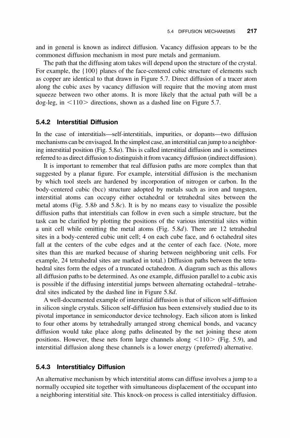
and in general is known as indirect diffusion. Vacancy diffusion appears to be thecommonest diffusion mechanism in most pure metals and germanium.
The path that the diffusing atom takes will depend upon the structure of the crystal.For example, the {100} planes of the face-centered cubic structure of elements suchas copper are identical to that drawn in Figure 5.7. Direct diffusion of a tracer atomalong the cubic axes by vacancy diffusion will require that the moving atom mustsqueeze between two other atoms. It is more likely that the actual path will be adog-leg, in ,110. directions, shown as a dashed line on Figure 5.7.
5.4.2 Interstitial Diffusion
In the case of interstitials—self-interstitials, impurities, or dopants—two diffusionmechanisms canbe envisaged. In the simplest case, an interstitial can jump to a neighbor-ing interstitial position (Fig. 5.8a). This is called interstitial diffusion and is sometimesreferred to as direct diffusion to distinguish it fromvacancy diffusion (indirect diffusion).
It is important to remember that real diffusion paths are more complex than thatsuggested by a planar figure. For example, interstitial diffusion is the mechanismby which tool steels are hardened by incorporation of nitrogen or carbon. In thebody-centered cubic (bcc) structure adopted by metals such as iron and tungsten,interstitial atoms can occupy either octahedral or tetrahedral sites between themetal atoms (Fig. 5.8b and 5.8c). It is by no means easy to visualize the possiblediffusion paths that interstitials can follow in even such a simple structure, but thetask can be clarified by plotting the positions of the various interstitial sites withina unit cell while omitting the metal atoms (Fig. 5.8d ). There are 12 tetrahedralsites in a body-centered cubic unit cell; 4 on each cube face, and 6 octahedral sitesfall at the centers of the cube edges and at the center of each face. (Note, moresites than this are marked because of sharing between neighboring unit cells. Forexample, 24 tetrahedral sites are marked in total.) Diffusion paths between the tetra-hedral sites form the edges of a truncated octahedron. A diagram such as this allowsall diffusion paths to be determined. As one example, diffusion parallel to a cubic axisis possible if the diffusing interstitial jumps between alternating octahedral–tetrahe-dral sites indicated by the dashed line in Figure 5.8d.
A well-documented example of interstitial diffusion is that of silicon self-diffusionin silicon single crystals. Silicon self-diffusion has been extensively studied due to itspivotal importance in semiconductor device technology. Each silicon atom is linkedto four other atoms by tetrahedrally arranged strong chemical bonds, and vacancydiffusion would take place along paths delineated by the net joining these atompositions. However, these nets form large channels along ,110. (Fig. 5.9), andinterstitial diffusion along these channels is a lower energy (preferred) alternative.
5.4.3 Interstitialcy Diffusion
An alternative mechanism by which interstitial atoms can diffuse involves a jump to anormally occupied site together with simultaneous displacement of the occupant intoa neighboring interstitial site. This knock-on process is called interstitialcy diffusion.
5.4 DIFFUSION MECHANISMS 217
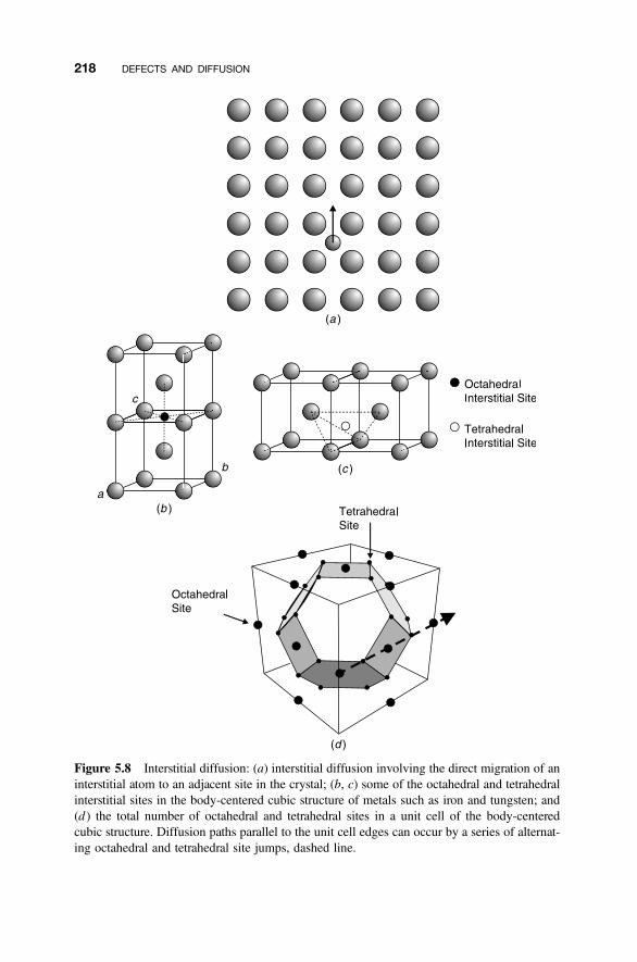
Figure 5.8 Interstitial diffusion: (a) interstitial diffusion involving the direct migration of aninterstitial atom to an adjacent site in the crystal; (b, c) some of the octahedral and tetrahedralinterstitial sites in the body-centered cubic structure of metals such as iron and tungsten; and(d ) the total number of octahedral and tetrahedral sites in a unit cell of the body-centeredcubic structure. Diffusion paths parallel to the unit cell edges can occur by a series of alternat-ing octahedral and tetrahedral site jumps, dashed line.
218 DEFECTS AND DIFFUSION
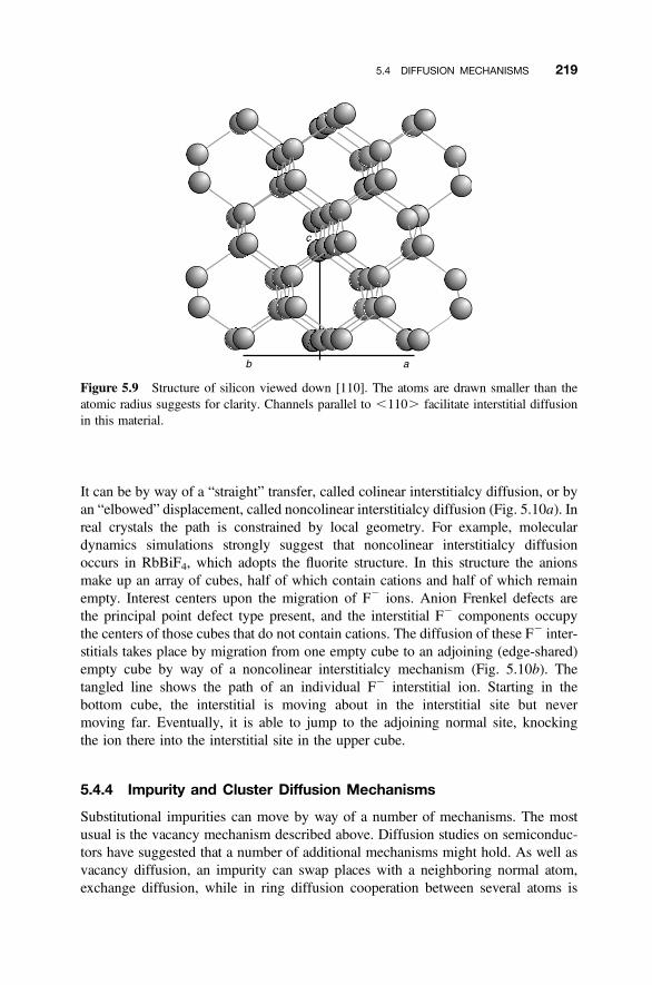
It can be by way of a “straight” transfer, called colinear interstitialcy diffusion, or byan “elbowed” displacement, called noncolinear interstitialcy diffusion (Fig. 5.10a). Inreal crystals the path is constrained by local geometry. For example, moleculardynamics simulations strongly suggest that noncolinear interstitialcy diffusionoccurs in RbBiF4, which adopts the fluorite structure. In this structure the anionsmake up an array of cubes, half of which contain cations and half of which remainempty. Interest centers upon the migration of F2 ions. Anion Frenkel defects arethe principal point defect type present, and the interstitial F2 components occupythe centers of those cubes that do not contain cations. The diffusion of these F2 inter-stitials takes place by migration from one empty cube to an adjoining (edge-shared)empty cube by way of a noncolinear interstitialcy mechanism (Fig. 5.10b). Thetangled line shows the path of an individual F2 interstitial ion. Starting in thebottom cube, the interstitial is moving about in the interstitial site but nevermoving far. Eventually, it is able to jump to the adjoining normal site, knockingthe ion there into the interstitial site in the upper cube.
5.4.4 Impurity and Cluster Diffusion Mechanisms
Substitutional impurities can move by way of a number of mechanisms. The mostusual is the vacancy mechanism described above. Diffusion studies on semiconduc-tors have suggested that a number of additional mechanisms might hold. As well asvacancy diffusion, an impurity can swap places with a neighboring normal atom,exchange diffusion, while in ring diffusion cooperation between several atoms is
Figure 5.9 Structure of silicon viewed down [110]. The atoms are drawn smaller than theatomic radius suggests for clarity. Channels parallel to ,110. facilitate interstitial diffusionin this material.
5.4 DIFFUSION MECHANISMS 219
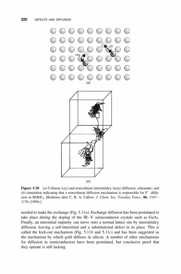
needed to make the exchange (Fig. 5.11a). Exchange diffusion has been postulated totake place during the doping of the III–V semiconductor crystals such as GaAs.Finally, an interstitial impurity can move onto a normal lattice site by interstitialcydiffusion, leaving a self-interstitial and a substitutional defect in its place. This iscalled the kick-out mechanism (Fig. 5.11b and 5.11c) and has been suggested asthe mechanism by which gold diffuses in silicon. A number of other mechanismsfor diffusion in semiconductors have been postulated, but conclusive proof thatthey operate is still lacking.
Figure 5.10 (a) Colinear (ciy) and noncolinear interstitialcy (nciy) diffusion, schematic; and(b) simulation indicating that a noncolinear diffusion mechanism is responsible for F2 diffu-sion in RbBiF4. [Redrawn after C. R. A. Catlow, J. Chem. Soc. Faraday Trans., 86, 1167–1176 (1990).]
220 DEFECTS AND DIFFUSION
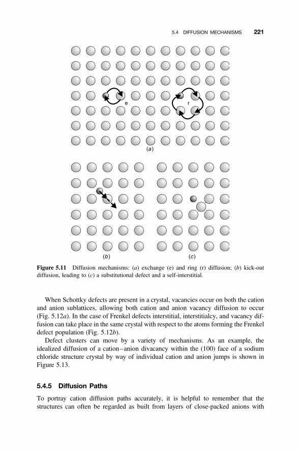
When Schottky defects are present in a crystal, vacancies occur on both the cationand anion sublattices, allowing both cation and anion vacancy diffusion to occur(Fig. 5.12a). In the case of Frenkel defects interstitial, interstitialcy, and vacancy dif-fusion can take place in the same crystal with respect to the atoms forming the Frenkeldefect population (Fig. 5.12b).
Defect clusters can move by a variety of mechanisms. As an example, theidealized diffusion of a cation–anion divacancy within the (100) face of a sodiumchloride structure crystal by way of individual cation and anion jumps is shown inFigure 5.13.
5.4.5 Diffusion Paths
To portray cation diffusion paths accurately, it is helpful to remember that thestructures can often be regarded as built from layers of close-packed anions with
Figure 5.11 Diffusion mechanisms: (a) exchange (e) and ring (r) diffusion; (b) kick-outdiffusion, leading to (c) a substitutional defect and a self-interstitial.
5.4 DIFFUSION MECHANISMS 221
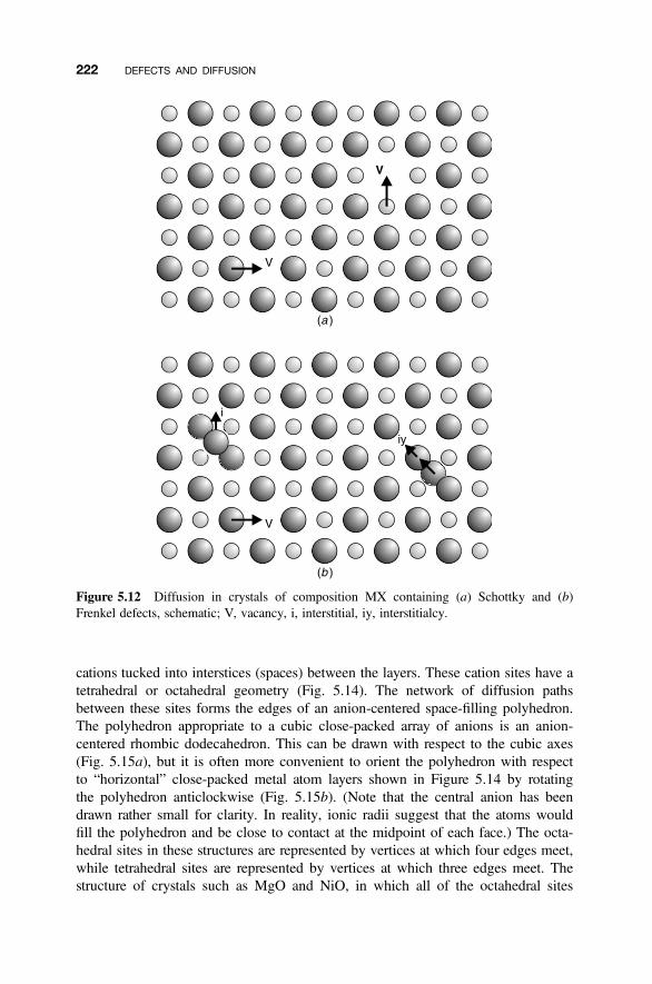
cations tucked into interstices (spaces) between the layers. These cation sites have atetrahedral or octahedral geometry (Fig. 5.14). The network of diffusion pathsbetween these sites forms the edges of an anion-centered space-filling polyhedron.The polyhedron appropriate to a cubic close-packed array of anions is an anion-centered rhombic dodecahedron. This can be drawn with respect to the cubic axes(Fig. 5.15a), but it is often more convenient to orient the polyhedron with respectto “horizontal” close-packed metal atom layers shown in Figure 5.14 by rotatingthe polyhedron anticlockwise (Fig. 5.15b). (Note that the central anion has beendrawn rather small for clarity. In reality, ionic radii suggest that the atoms wouldfill the polyhedron and be close to contact at the midpoint of each face.) The octa-hedral sites in these structures are represented by vertices at which four edges meet,while tetrahedral sites are represented by vertices at which three edges meet. Thestructure of crystals such as MgO and NiO, in which all of the octahedral sites
Figure 5.12 Diffusion in crystals of composition MX containing (a) Schottky and (b)Frenkel defects, schematic; V, vacancy, i, interstitial, iy, interstitialcy.
222 DEFECTS AND DIFFUSION
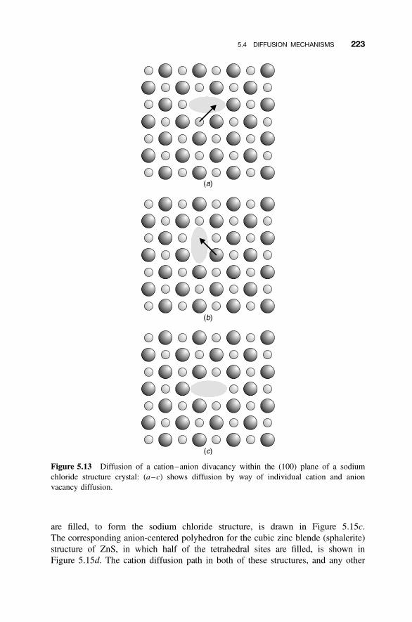
are filled, to form the sodium chloride structure, is drawn in Figure 5.15c.The corresponding anion-centered polyhedron for the cubic zinc blende (sphalerite)structure of ZnS, in which half of the tetrahedral sites are filled, is shown inFigure 5.15d. The cation diffusion path in both of these structures, and any other
Figure 5.13 Diffusion of a cation–anion divacancy within the (100) plane of a sodiumchloride structure crystal: (a–c) shows diffusion by way of individual cation and anionvacancy diffusion.
5.4 DIFFUSION MECHANISMS 223
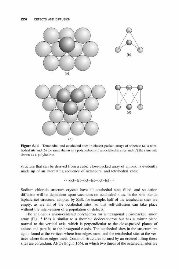
structure that can be derived from a cubic close-packed array of anions, is evidentlymade up of an alternating sequence of octahedral and tetrahedral sites:
� � � oct–tet–oct–tet–oct–tet � � �
Sodium chloride structure crystals have all octahedral sites filled, and so cationdiffusion will be dependent upon vacancies on octahedral sites. In the zinc blende(sphalerite) structure, adopted by ZnS, for example, half of the tetrahedral sites areempty, as are all of the octahedral sites, so that self-diffusion can take placewithout the intervention of a population of defects.
The analogous anion-centered polyhedron for a hexagonal close-packed anionarray (Fig. 5.16a) is similar to a rhombic dodecahedron but has a mirror planenormal to the vertical axis, which is perpendicular to the close-packed planes ofanions and parallel to the hexagonal c axis. The octahedral sites in the structure areagain found at the vertices where four edges meet, and the tetrahedral sites at the ver-tices where three edges meet. Common structures formed by an ordered filling thesesites are corundum, Al2O3 (Fig. 5.16b), in which two thirds of the octahedral sites are
Figure 5.14 Tetrahedral and octahedral sites in closest-packed arrays of spheres: (a) a tetra-hedral site and (b) the same drawn as a polyhedron; (c) an octahedral sites and (d ) the same sitedrawn as a polyhedron.
224 DEFECTS AND DIFFUSION
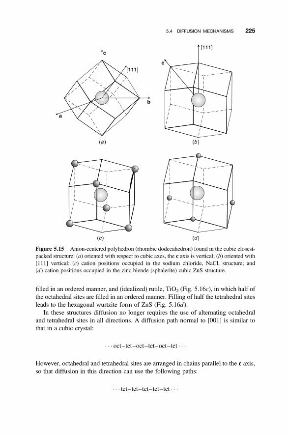
filled in an ordered manner, and (idealized) rutile, TiO2 (Fig. 5.16c), in which half ofthe octahedral sites are filled in an ordered manner. Filling of half the tetrahedral sitesleads to the hexagonal wurtzite form of ZnS (Fig. 5.16d ).
In these structures diffusion no longer requires the use of alternating octahedraland tetrahedral sites in all directions. A diffusion path normal to [001] is similar tothat in a cubic crystal:
� � � oct–tet–oct–tet–oct–tet � � �
However, octahedral and tetrahedral sites are arranged in chains parallel to the c axis,so that diffusion in this direction can use the following paths:
� � � tet–tet–tet–tet–tet � � �
Figure 5.15 Anion-centered polyhedron (rhombic dodecahedron) found in the cubic closest-packed structure: (a) oriented with respect to cubic axes, the c axis is vertical; (b) oriented with[111] vertical; (c) cation positions occupied in the sodium chloride, NaCl, structure; and(d ) cation positions occupied in the zinc blende (sphalerite) cubic ZnS structure.
5.4 DIFFUSION MECHANISMS 225
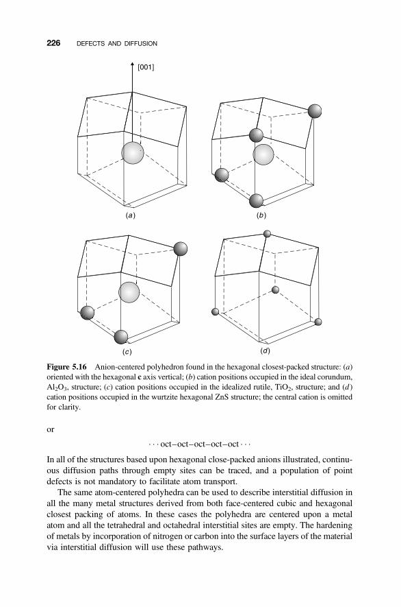
or
� � � oct–oct–oct–oct–oct � � �In all of the structures based upon hexagonal close-packed anions illustrated, continu-ous diffusion paths through empty sites can be traced, and a population of pointdefects is not mandatory to facilitate atom transport.
The same atom-centered polyhedra can be used to describe interstitial diffusion inall the many metal structures derived from both face-centered cubic and hexagonalclosest packing of atoms. In these cases the polyhedra are centered upon a metalatom and all the tetrahedral and octahedral interstitial sites are empty. The hardeningof metals by incorporation of nitrogen or carbon into the surface layers of the materialvia interstitial diffusion will use these pathways.
Figure 5.16 Anion-centered polyhedron found in the hexagonal closest-packed structure: (a)oriented with the hexagonal c axis vertical; (b) cation positions occupied in the ideal corundum,Al2O3, structure; (c) cation positions occupied in the idealized rutile, TiO2, structure; and (d )cation positions occupied in the wurtzite hexagonal ZnS structure; the central cation is omittedfor clarity.
226 DEFECTS AND DIFFUSION
5.5 POINT DEFECT CONCENTRATION AND DIFFUSION
The random-walk model of diffusion needs to be modified if it is to accuratelyrepresent the mechanism of the diffusion. One important change regards thenumber of point defects present. It has already been pointed out that vacancy diffu-sion in, for example, a metal crystal cannot occur without an existing population ofvacancies. Because of this the random-walk jump probability must be modified totake vacancy numbers into account. In this case, the probability that a vacancy isavailable to a diffusing atom can be approximated by the number of vacant sitespresent in the crystal, [d ], expressed as a fraction, that is
[d] ¼ nVN
where nV is the number of vacancies per unit volume and N the number of normalsites per unit volume, both with respect to the relevant diffusion sublattice. Themeasured diffusion coefficient, D, which may be a self-diffusion coefficient or atracer diffusion coefficient, will be related to the random-walk coefficient, Dr, by
D ¼ [d]Dr ¼ 12[d]Ga
2
via Eq. (5.5) and (5.6), where [d ] is the concentration of appropriate defects per unitvolume expressed as a fraction of the number of normal sites per unit volume and isunitless. (It is possible to introduce more detailed expressions for [d ] if specificcrystal geometry and diffusion paths are taken into account.)
More than one point defect species may be present in a crystal at any temperature,and the amount of matter transported by diffusion will depend upon the number ofeach defect type present. In general, therefore, the overall apparent diffusion coeffi-cient, D, will be the sum of the individual contributions, for example:
D ¼ [d1]D1 þ [d2]D2 þ [d3]D3 þ � � � (5:7)
where the terms [d1] and so forth represent the concentrations of defects present asdefect fractions, and the Dn terms refer to the differing random-walk diffusion coeffi-cient contributions relevant to vacancy diffusion, interstitial diffusion, and so on.
Just as one point defect type may dominate the defect population in a crystal, soone diffusion coefficient may be dominant, but the other diffusion coefficients cansometimes make an important contribution to the overall transport of atomsthrough a solid. It is by no means easy to separate these contributions to a measuredvalue of D, and, as well as theoretical assessments, the way in which the diffusioncoefficient varies with temperature can help.
5.6 CORRELATION FACTORS
A second modification to the random-walk model of diffusion is required if motion isnot random but correlated in some way with preceding passage through the crystal
5.6 CORRELATION FACTORS 227
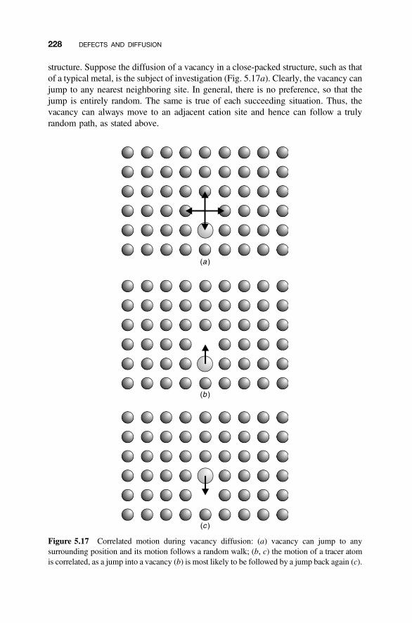
structure. Suppose the diffusion of a vacancy in a close-packed structure, such as thatof a typical metal, is the subject of investigation (Fig. 5.17a). Clearly, the vacancy canjump to any nearest neighboring site. In general, there is no preference, so that thejump is entirely random. The same is true of each succeeding situation. Thus, thevacancy can always move to an adjacent cation site and hence can follow a trulyrandom path, as stated above.
Figure 5.17 Correlated motion during vacancy diffusion: (a) vacancy can jump to anysurrounding position and its motion follows a random walk; (b, c) the motion of a tracer atomis correlated, as a jump into a vacancy (b) is most likely to be followed by a jump back again (c).
228 DEFECTS AND DIFFUSION
However, the diffusion of a tracer atom by the mechanism of vacancy diffusion isdifferent. A tracer can only move if it is next to a vacancy, and in this case, the tracercan only jump to the vacancy (Fig. 5.17b). The possibility of any other jump isexcluded. Similarly, when the tracer has made the jump, then it is equally clearthat the most likely jump for the tracer is back to the vacancy (Fig. 5.17c). Thetracer can only jump to a new position after the vacancy has diffused to an alternativeneighboring position.
The vacancy will follow a random-walk diffusion route, while the diffusion of thetracer by a vacancy diffusion mechanism will be constrained. When these processesare considered over many jumps, the mean square displacement of the tracer will beless than that of the vacancy, even though both have taken the same number of jumps.Therefore, it is expected that the observed diffusion coefficient of the tracer will beless than that of the vacancy. In these circumstances, the random-walk diffusionequations need to be modified for the tracer. This is done by ascribing a differentprobability to each of the various jumps that the tracer may make. The result isthat the random-walk diffusion expression must be multiplied by a correlationfactor, f, which takes the diffusion mechanism into account.
In the case of interstitial diffusion in which we have only a few diffusing interstitialatoms and many available empty interstitial sites, random-walk equations would beaccurate, and a correlation factor of 1.0 would be expected. This will be sowhether the interstitial is a native atom or a tracer atom. When tracer diffusion bya colinear intersticialcy mechanism is considered, this will not be true and the situ-ation is analogous to that of vacancy diffusion. Consider a tracer atom in an interstitialposition (Fig. 5.18a). An initial jump can be in any random direction in the structure.Suppose that the jump shown in Figure 5.18b occurs, leading to the situation inFigure 5.18c. The most likely next jump of the tracer, which must be back to aninterstitial site, will be a return jump (Fig. 5.18d ). Once again the diffusion of theinterstitial is different from that of a completely random walk, and once again a cor-relation factor, f, is needed to compare the two situations.
The correlation factor, for any mechanism, is given by the ratio of the values of themean square displacement of the atom (often the tracer) moving in a correlatedmotion to that of the atom (or vacancy) moving by a random-walk process. If thenumber of jumps considered is large, the correlation factor f can be written as
f ¼ ,x2. corr,x2. random
¼ D�
Dr
that is,
D� ¼ fDr
where ,x2.corr represents the mean square displacement of the correlated (nonran-dom) walk by the diffusing atom and ,x2. random the mean square displacementfor a truly random diffusion process with the same number of jumps, and Dr and D�
are the random-walk and tracer diffusion coefficients.
5.6 CORRELATION FACTORS 229
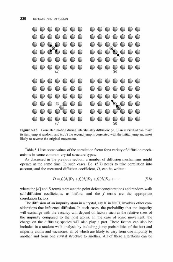
Table 5.1 lists some values of the correlation factor for a variety of diffusion mech-anisms in some common crystal structure types.
As discussed in the previous section, a number of diffusion mechanisms mightoperate at the same time. In such cases, Eq. (5.7) needs to take correlation intoaccount, and the measured diffusion coefficient, D, can be written:
D ¼ f1[d1]D1 þ f2[d2]D2 þ f3[d3]D3 þ � � � (5:8)
where the [d] and D terms represent the point defect concentrations and random-walkself-diffusion coefficients, as before, and the f terms are the appropriatecorrelation factors.
The diffusion of an impurity atom in a crystal, say K in NaCl, involves other con-siderations that influence diffusion. In such cases, the probability that the impuritywill exchange with the vacancy will depend on factors such as the relative sizes ofthe impurity compared to the host atoms. In the case of ionic movement, thecharge on the diffusing species will also play a part. These factors can also beincluded in a random-walk analysis by including jump probabilities of the host andimpurity atoms and vacancies, all of which are likely to vary from one impurity toanother and from one crystal structure to another. All of these alterations can be
Figure 5.18 Correlated motion during intersticialcy diffusion: (a, b) an interstitial can makeits first jump at random; and (c, d ) the second jump is correlated with the initial jump and mostlikely to reverse the original movement.
230 DEFECTS AND DIFFUSION
assimilated into a multiplying constant appropriate to the diffusion mechanismpostulated.
5.7 TEMPERATURE VARIATION OF THE DIFFUSION COEFFICIENT
Diffusion coefficients vary considerably with temperature. This variation is generallyexpressed in terms of the Arrhenius equation:
D ¼ D0 exp � Ea
RT
� �(5:9)
where R is the gas constant, T is the temperature (K), and D0 is a constant termreferred to as the pre-exponential factor, frequency factor, or (occasionally) as the dif-fusion coefficient. The term Ea is called the activation energy of diffusion, and D isthe measured diffusion coefficient, often the tracer diffusion coefficient. Taking log-arithms of both sides of this equation gives
ln D ¼ ln D0 � Ea
RT
The activation energy can be determined from the gradient of a plot of ln D versus 1/T(Fig. 5.19). Such graphs are known as Arrhenius plots. Diffusion coefficients foundin the literature are usually expressed in terms of the Arrhenius equation D0 and Ea
values. Some representative values for self-diffusion coefficients are given inTable 5.2.
TABLE 5.1 Correlation Factors for Self-diffusion
Crystal Structure Correlation Factor ( f )
Vacancy diffusionDiamond 0.50Tungsten (A2, body-centered cubic) 0.73Copper (A1, face-centered cubic) 0.78Magnesium (A3, hexagonal close packed), all axes 0.78Corundum (a-Al2O3) (cations); k a axis 0.50Corundum (a-Al2O3) (cations); k c axis 0.65
Colinear interstitialcy diffusionDiamond 0.73Sodium chloride (NaCl) (cations or anions) 0.33CsCl (cations or anions) 0.33Fluorite (CaF2) cations 0.40Fluorite (CaF2) anions 0.74
All data from K. Compaan and Y. Haven, Trans. Faraday Soc., 52, 786–801 (1956); 54, 1498–1508(1958).
5.7 TEMPERATURE VARIATION OF THE DIFFUSION COEFFICIENT 231
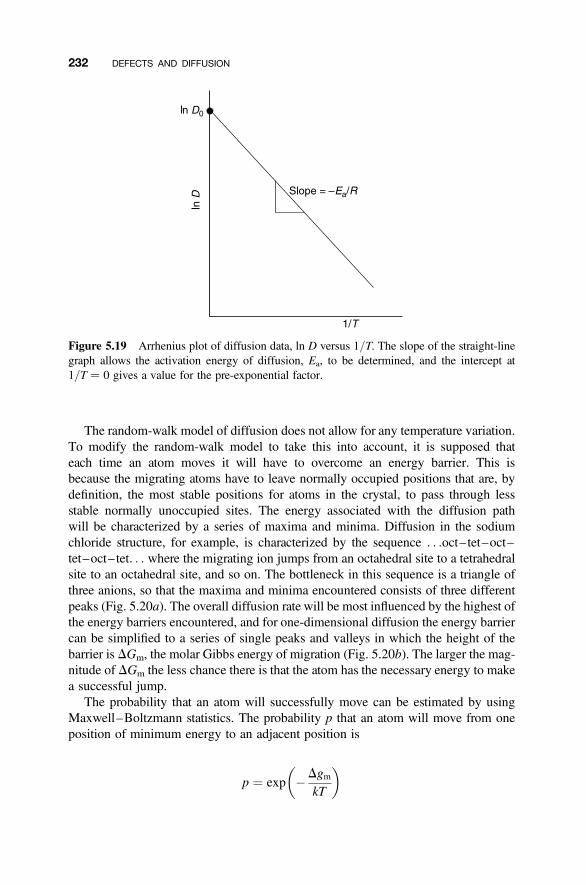
The random-walk model of diffusion does not allow for any temperature variation.To modify the random-walk model to take this into account, it is supposed thateach time an atom moves it will have to overcome an energy barrier. This isbecause the migrating atoms have to leave normally occupied positions that are, bydefinition, the most stable positions for atoms in the crystal, to pass through lessstable normally unoccupied sites. The energy associated with the diffusion pathwill be characterized by a series of maxima and minima. Diffusion in the sodiumchloride structure, for example, is characterized by the sequence . . .oct–tet–oct–tet–oct–tet. . . where the migrating ion jumps from an octahedral site to a tetrahedralsite to an octahedral site, and so on. The bottleneck in this sequence is a triangle ofthree anions, so that the maxima and minima encountered consists of three differentpeaks (Fig. 5.20a). The overall diffusion rate will be most influenced by the highest ofthe energy barriers encountered, and for one-dimensional diffusion the energy barriercan be simplified to a series of single peaks and valleys in which the height of thebarrier is DGm, the molar Gibbs energy of migration (Fig. 5.20b). The larger the mag-nitude of DGm the less chance there is that the atom has the necessary energy to makea successful jump.
The probability that an atom will successfully move can be estimated by usingMaxwell–Boltzmann statistics. The probability p that an atom will move from oneposition of minimum energy to an adjacent position is
p ¼ exp �DgmkT
� �
Figure 5.19 Arrhenius plot of diffusion data, ln D versus 1/T. The slope of the straight-linegraph allows the activation energy of diffusion, Ea, to be determined, and the intercept at1/T ¼ 0 gives a value for the pre-exponential factor.
232 DEFECTS AND DIFFUSION
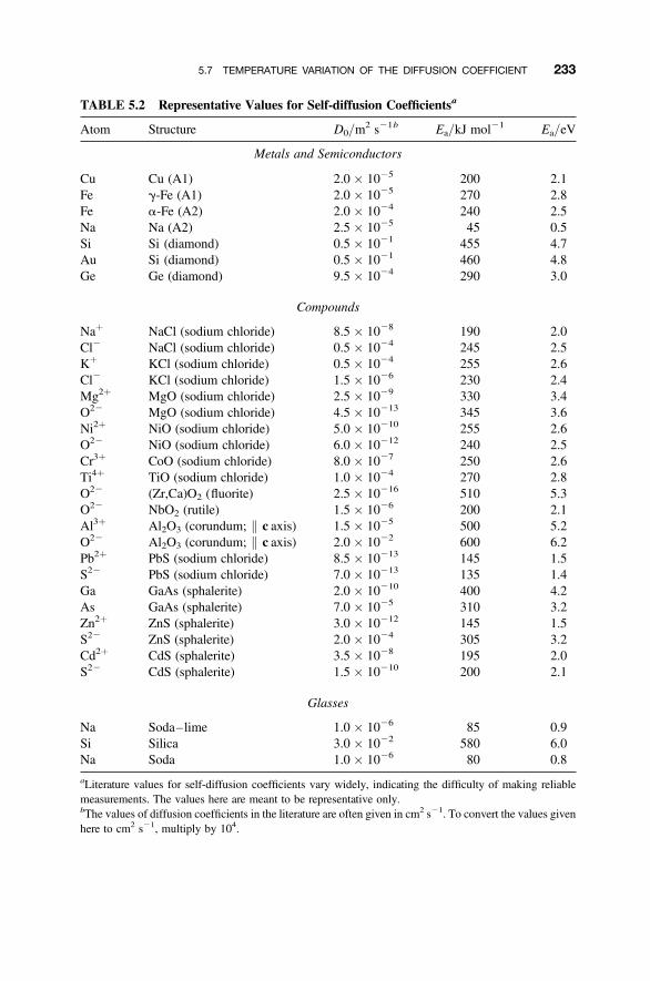
TABLE 5.2 Representative Values for Self-diffusion Coefficientsa
Atom Structure D0/m2 s21b Ea/kJ mol21 Ea/eV
Metals and Semiconductors
Cu Cu (A1) 2.0 � 1025 200 2.1Fe g-Fe (A1) 2.0 � 1025 270 2.8Fe a-Fe (A2) 2.0 � 1024 240 2.5Na Na (A2) 2.5 � 1025 45 0.5Si Si (diamond) 0.5 � 1021 455 4.7Au Si (diamond) 0.5 � 1021 460 4.8Ge Ge (diamond) 9.5 � 1024 290 3.0
Compounds
Naþ NaCl (sodium chloride) 8.5 � 1028 190 2.0Cl2 NaCl (sodium chloride) 0.5 � 1024 245 2.5Kþ KCl (sodium chloride) 0.5 � 1024 255 2.6Cl2 KCl (sodium chloride) 1.5 � 1026 230 2.4Mg2þ MgO (sodium chloride) 2.5 � 1029 330 3.4O22 MgO (sodium chloride) 4.5 � 10213 345 3.6Ni2þ NiO (sodium chloride) 5.0 � 10210 255 2.6O22 NiO (sodium chloride) 6.0 � 10212 240 2.5Cr3þ CoO (sodium chloride) 8.0 � 1027 250 2.6Ti4þ TiO (sodium chloride) 1.0 � 1024 270 2.8O22 (Zr,Ca)O2 (fluorite) 2.5 � 10216 510 5.3O22 NbO2 (rutile) 1.5 � 1026 200 2.1Al3þ Al2O3 (corundum; k c axis) 1.5 � 1025 500 5.2O22 Al2O3 (corundum; k c axis) 2.0 � 1022 600 6.2Pb2þ PbS (sodium chloride) 8.5 � 10213 145 1.5S22 PbS (sodium chloride) 7.0 � 10213 135 1.4Ga GaAs (sphalerite) 2.0 � 10210 400 4.2As GaAs (sphalerite) 7.0 � 1025 310 3.2Zn2þ ZnS (sphalerite) 3.0 � 10212 145 1.5S22 ZnS (sphalerite) 2.0 � 1024 305 3.2Cd2þ CdS (sphalerite) 3.5 � 1028 195 2.0S22 CdS (sphalerite) 1.5 � 10210 200 2.1
Glasses
Na Soda–lime 1.0 � 1026 85 0.9Si Silica 3.0 � 1022 580 6.0Na Soda 1.0 � 1026 80 0.8
aLiterature values for self-diffusion coefficients vary widely, indicating the difficulty of making reliablemeasurements. The values here are meant to be representative only.bThe values of diffusion coefficients in the literature are often given in cm2 s21. To convert the values givenhere to cm2 s21, multiply by 104.
5.7 TEMPERATURE VARIATION OF THE DIFFUSION COEFFICIENT 233
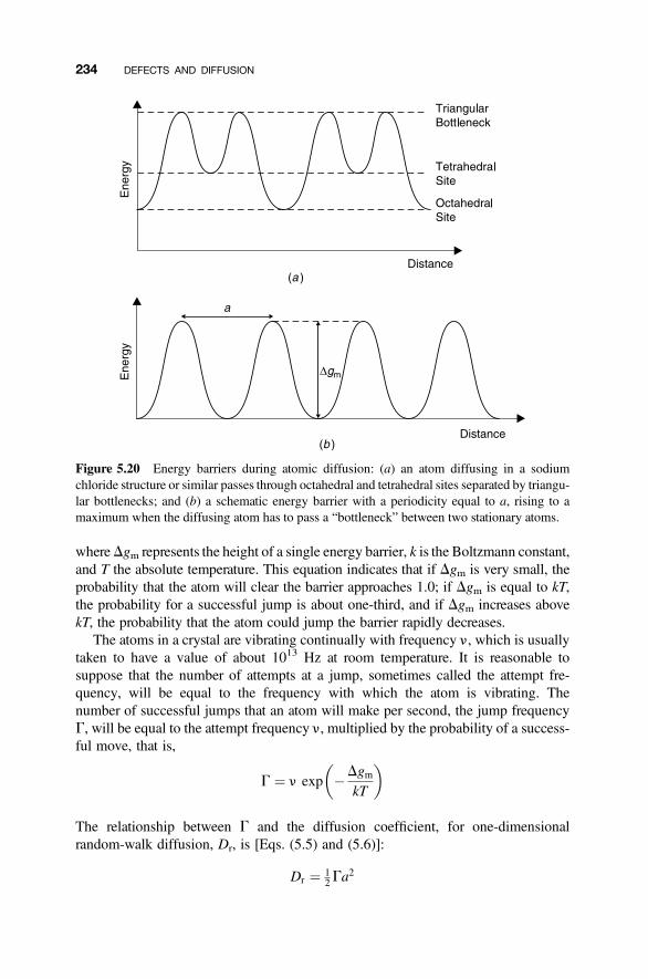
whereDgm represents the height of a single energy barrier, k is the Boltzmann constant,and T the absolute temperature. This equation indicates that if Dgm is very small, theprobability that the atom will clear the barrier approaches 1.0; if Dgm is equal to kT,the probability for a successful jump is about one-third, and if Dgm increases abovekT, the probability that the atom could jump the barrier rapidly decreases.
The atoms in a crystal are vibrating continually with frequency n, which is usuallytaken to have a value of about 1013 Hz at room temperature. It is reasonable tosuppose that the number of attempts at a jump, sometimes called the attempt fre-quency, will be equal to the frequency with which the atom is vibrating. Thenumber of successful jumps that an atom will make per second, the jump frequencyG, will be equal to the attempt frequency n, multiplied by the probability of a success-ful move, that is,
G ¼ n exp �DgmkT
� �
The relationship between G and the diffusion coefficient, for one-dimensionalrandom-walk diffusion, Dr, is [Eqs. (5.5) and (5.6)]:
Dr ¼ 12Ga
2
Figure 5.20 Energy barriers during atomic diffusion: (a) an atom diffusing in a sodiumchloride structure or similar passes through octahedral and tetrahedral sites separated by triangu-lar bottlenecks; and (b) a schematic energy barrier with a periodicity equal to a, rising to amaximum when the diffusing atom has to pass a “bottleneck” between two stationary atoms.
234 DEFECTS AND DIFFUSION
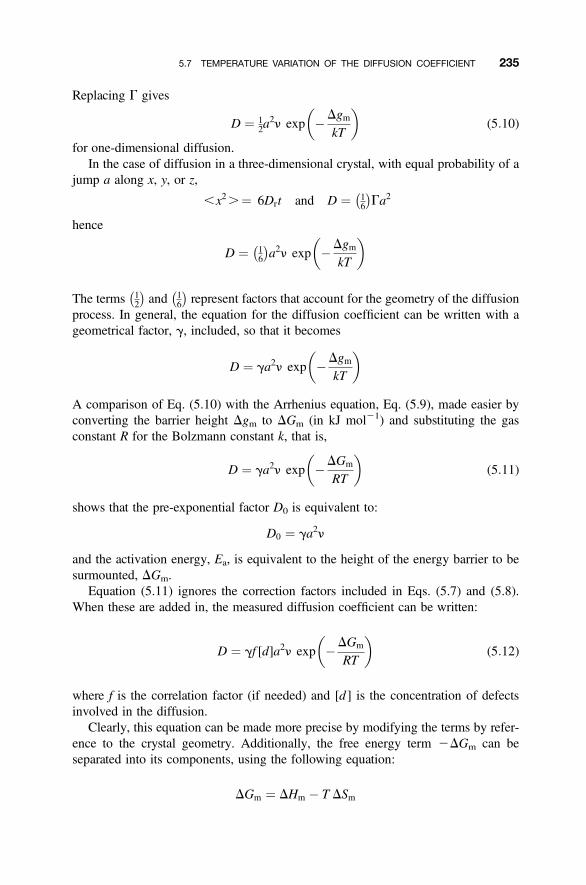
Replacing G gives
D ¼ 12a
2n exp �DgmkT
� �(5:10)
for one-dimensional diffusion.In the case of diffusion in a three-dimensional crystal, with equal probability of a
jump a along x, y, or z,
,x2.¼ 6Drt and D ¼ 16
�Ga2
hence
D ¼ 16
�a2n exp �Dgm
kT
� �
The terms 12
�and 1
6
�represent factors that account for the geometry of the diffusion
process. In general, the equation for the diffusion coefficient can be written with ageometrical factor, g, included, so that it becomes
D ¼ ga2n exp �DgmkT
� �
A comparison of Eq. (5.10) with the Arrhenius equation, Eq. (5.9), made easier byconverting the barrier height Dgm to DGm (in kJ mol21) and substituting the gasconstant R for the Bolzmann constant k, that is,
D ¼ ga2n exp �DGm
RT
� �(5:11)
shows that the pre-exponential factor D0 is equivalent to:
D0 ¼ ga2n
and the activation energy, Ea, is equivalent to the height of the energy barrier to besurmounted, DGm.
Equation (5.11) ignores the correction factors included in Eqs. (5.7) and (5.8).When these are added in, the measured diffusion coefficient can be written:
D ¼ gf [d]a2n exp �DGm
RT
� �(5:12)
where f is the correlation factor (if needed) and [d ] is the concentration of defectsinvolved in the diffusion.
Clearly, this equation can be made more precise by modifying the terms by refer-ence to the crystal geometry. Additionally, the free energy term 2DGm can beseparated into its components, using the following equation:
DGm ¼ DHm � T DSm
5.7 TEMPERATURE VARIATION OF THE DIFFUSION COEFFICIENT 235
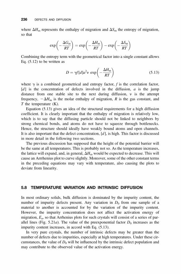
where DHm represents the enthalpy of migration and DSm the entropy of migration,so that
exp �DGm
RT
� �¼ exp �DHm
RT
� �� exp �DSm
RT
� �
Combining the entropy term with the geometrical factor into a single constant allowsEq. (5.12) to be written as
D ¼ gf [d]a2n exp �DHm
RT
� �(5:13)
where g is a combined geometrical and entropy factor, f is the correlation factor,[d ] is the concentration of defects involved in the diffusion, a is the jumpdistance from one stable site to the next during diffusion, n is the attemptfrequency, 2DHm is the molar enthalpy of migration, R is the gas constant, andT the temperature (K).
Equation (5.13) gives an idea of the structural requirements for a high diffusioncoefficient. It is clearly important that the enthalpy of migration is relatively low,which is to say that the diffusing particle should not be linked to neighbors bystrong chemical bonds, and atoms do not have to squeeze through bottlenecks.Hence, the structure should ideally have weakly bound atoms and open channels.It is also important that the defect concentration, [d ], is high. This factor is discussedin more detail in the following two sections.
The previous discussion has supposed that the height of the potential barrier willbe the same at all temperatures. This is probably not so. As the temperature increases,the lattice will expand, and, in general, DHm would be expected to decrease. This willcause an Arrrhenius plot to curve slightly. Moreover, some of the other constant termsin the preceding equations may vary with temperature, also causing the plots todeviate from linearity.
5.8 TEMPERATURE VARIATION AND INTRINSIC DIFFUSION
In most ordinary solids, bulk diffusion is dominated by the impurity content, thenumber of impurity defects present. Any variation in D0 from one sample of amaterial to another is accounted for by the variation of the impurity content.However, the impurity concentration does not affect the activation energy ofmigration, Ea, so that Arrhenius plots for such crystals will consist of a series of par-allel lines (Fig. 5.21a). The value of the preexponential factor D0 increases as theimpurity content increases, in accord with Eq. (5.13).
In very pure crystals, the number of intrinsic defects may be greater than thenumber of defects due to impurities, especially at high temperatures. Under these cir-cumstances, the value of D0 will be influenced by the intrinsic defect population andmay contribute to the observed value of the activation energy.
236 DEFECTS AND DIFFUSION
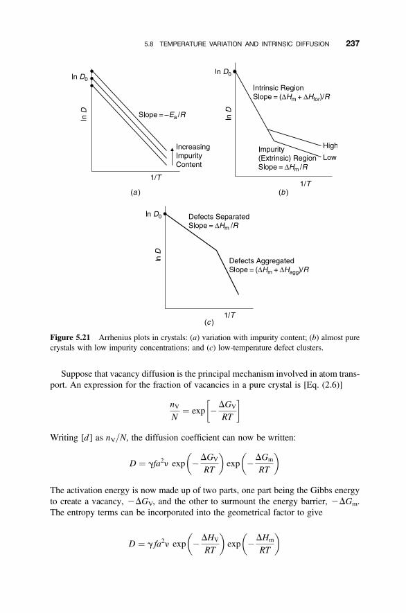
Suppose that vacancy diffusion is the principal mechanism involved in atom trans-port. An expression for the fraction of vacancies in a pure crystal is [Eq. (2.6)]
nVN
¼ exp �DGV
RT
� �
Writing [d ] as nV/N, the diffusion coefficient can now be written:
D ¼ gfa2n exp �DGV
RT
� �exp �DGm
RT
� �
The activation energy is now made up of two parts, one part being the Gibbs energyto create a vacancy, 2DGV, and the other to surmount the energy barrier, 2DGm.The entropy terms can be incorporated into the geometrical factor to give
D ¼ g fa2n exp �DHV
RT
� �exp �DHm
RT
� �
Figure 5.21 Arrhenius plots in crystals: (a) variation with impurity content; (b) almost purecrystals with low impurity concentrations; and (c) low-temperature defect clusters.
5.8 TEMPERATURE VARIATION AND INTRINSIC DIFFUSION 237
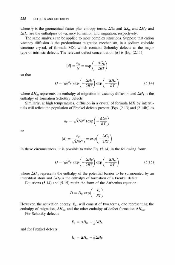
where g is the geometrical factor plus entropy terms, DSV and DSm and DHV andDHm are the enthalpies of vacancy formation and migration, respectively.
The same analysis can be applied to more complex situations. Suppose that cationvacancy diffusion is the predominant migration mechanism, in a sodium chloridestructure crystal, of formula MX, which contains Schottky defects as the majortype of intrinsic defects. The relevant defect concentration [d ] is [Eq. (2.11)]
[d] ¼ nSN
¼ exp �DGS
2RT
� �so that
D ¼ gfa2n exp �DHS
2RT
� �exp �DHm
RT
� �(5:14)
where DHm represents the enthalpy of migration in vacancy diffusion and DHS is theenthalpy of formation Schottky defects.
Similarly, at high temperatures, diffusion in a crystal of formula MX by intersti-tials will reflect the population of Frenkel defects present [Eqs. (2.13) and (2.14b)] as
nF ¼ffiffi(
pNN�) exp �DGF
RT
� �so
[d] ¼ nFffiffi(
pNN�)
¼ exp �DGF
2RT
� �
In these circumstances, it is possible to write Eq. (5.14) in the following form:
D ¼ gfa2n exp �DHF
2RT
� �exp �DHm
RT
� �(5:15)
where DHm represents the enthalpy of the potential barrier to be surmounted by aninterstitial atom and DHF is the enthalpy of formation of a Frenkel defect.
Equations (5.14) and (5.15) retain the form of the Arrhenius equation:
D ¼ D0 exp � Ea
RT
� �
However, the activation energy, Ea, will consist of two terms, one representing theenthalpy of migration, DHm, and the other enthalpy of defect formation DHfor.
For Schottky defects:
Ea ¼ DHm þ 12DHS
and for Frenkel defects:
Ea ¼ DHm þ 12DHF
238 DEFECTS AND DIFFUSION
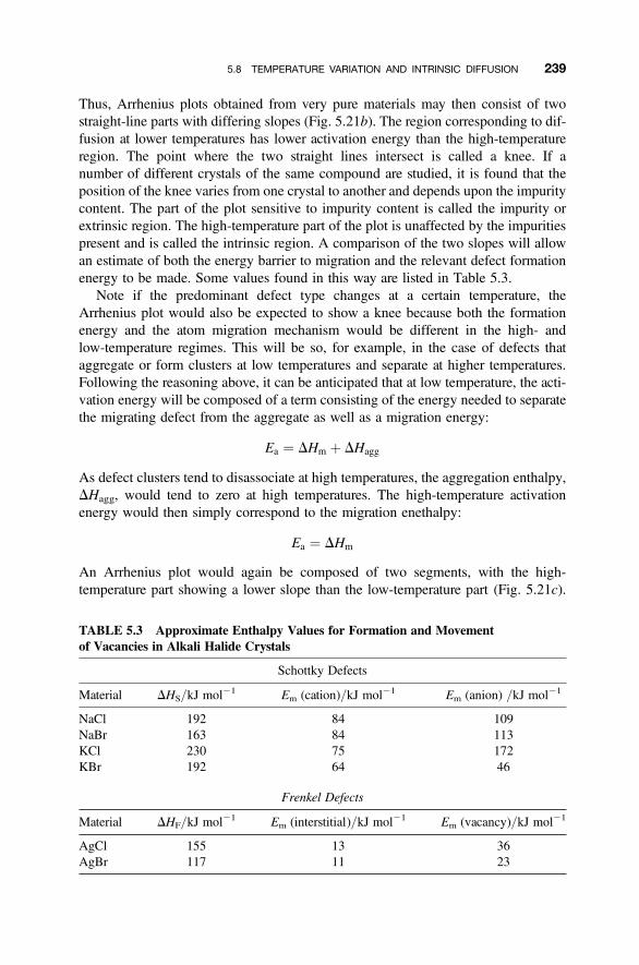
Thus, Arrhenius plots obtained from very pure materials may then consist of twostraight-line parts with differing slopes (Fig. 5.21b). The region corresponding to dif-fusion at lower temperatures has lower activation energy than the high-temperatureregion. The point where the two straight lines intersect is called a knee. If anumber of different crystals of the same compound are studied, it is found that theposition of the knee varies from one crystal to another and depends upon the impuritycontent. The part of the plot sensitive to impurity content is called the impurity orextrinsic region. The high-temperature part of the plot is unaffected by the impuritiespresent and is called the intrinsic region. A comparison of the two slopes will allowan estimate of both the energy barrier to migration and the relevant defect formationenergy to be made. Some values found in this way are listed in Table 5.3.
Note if the predominant defect type changes at a certain temperature, theArrhenius plot would also be expected to show a knee because both the formationenergy and the atom migration mechanism would be different in the high- andlow-temperature regimes. This will be so, for example, in the case of defects thataggregate or form clusters at low temperatures and separate at higher temperatures.Following the reasoning above, it can be anticipated that at low temperature, the acti-vation energy will be composed of a term consisting of the energy needed to separatethe migrating defect from the aggregate as well as a migration energy:
Ea ¼ DHm þ DHagg
As defect clusters tend to disassociate at high temperatures, the aggregation enthalpy,DHagg, would tend to zero at high temperatures. The high-temperature activationenergy would then simply correspond to the migration enethalpy:
Ea ¼ DHm
An Arrhenius plot would again be composed of two segments, with the high-temperature part showing a lower slope than the low-temperature part (Fig. 5.21c).
TABLE 5.3 Approximate Enthalpy Values for Formation and Movementof Vacancies in Alkali Halide Crystals
Schottky Defects
Material DHS/kJ mol21 Em (cation)/kJ mol21 Em (anion) /kJ mol21
NaCl 192 84 109NaBr 163 84 113KCl 230 75 172KBr 192 64 46
Frenkel Defects
Material DHF/kJ mol21 Em (interstitial)/kJ mol21 Em (vacancy)/kJ mol21
AgCl 155 13 36AgBr 117 11 23
5.8 TEMPERATURE VARIATION AND INTRINSIC DIFFUSION 239

In practice, there is often not a sharp change from one state to another, and the plotsare frequently curved over the temperature range in which aggregation becomesimportant.
5.9 DIFFUSION MECHANISMS AND IMPURITIES
Diffusion in the extrinsic region can readily be modified by doping, although knowl-edge of the mechanism by which the diffusion takes place is important if this is to beimmediately successful. For example, sodium chloride structure materials thatconduct by a vacancy mechanism can have the cation conductivity enhanced bydoping with divalent cations, as these generate compensating cation vacancies. Theinclusion of cadmium chloride into sodium chloride can be written:
CdCl2(NaCl) �! Cd†Na þ V0Na þ 2ClCl
Each added Cd2þ ion generates one cation vacancy. Similarly, each added Ca2þ ioninto ZrO2, as in calcia-stabilized zirconia (Section 1.11.6), generates a compensatinganion vacancy:
CaO(ZrO2) �! Ca20Zr þ V2†O þ OO
In both cases the diffusion coefficient of the ions using the vacancy population will beenhanced considerably.
Diffusion studies coupled with doping data can also yield information about thelikely defect types present in a solid. For example, silica, SiO2, is a common impurityin alumina, Al2O3. The Si
4þ cations are accommodated on Al3þ sites as substitutionaldefects with an effective positive charge, SiAl
† . As SiO2 is oxygen rich compared toalumina, the extra oxygen can either be accommodated as oxygen interstitials, O20
i :
2SiO2(Al2O3) �! 2Si†Al þ 3OO þ O20i
or balanced by Al3þ vacancies, V30Al:
3SiO2(Al2O3) �! 3Si†Al þ 6OO þ V30Al
Suppose that it is known that Al diffusion is by a vacancy mechanism. As the SiO2
impurity content increases, the Al diffusion coefficient should increase if V30Al defects
form. If it does not, the evidence is in favor of the assumption that the incorporation ofSiO2 generates oxygen interstitials. This can be substantiated by measuring theoxygen diffusion coefficient. Oxygen diffusion in Al2O3 is believed to be by wayof an interstitial mechanism. Clearly, therefore, an increase in oxygen diffusioncoefficient with impurity SiO2 concentration would be expected.
240 DEFECTS AND DIFFUSION
Possible diffusion mechanisms can also be investigated by doping with impuritieswith greater or smaller ionic charge and comparing the results. For example, ZnO canbe doped with Li2O or Al2O3. From the point of view of oxygen diffusion, theseshould give quite distinctive results. If the impurity atoms are supposed to form sub-stitutional defects, in one case (Li2O) a deficit of oxygen will lead to oxygenvacancies:
Li2O(ZnO) �! 2Li0Zn þ OO þ V2†O
while in the other (Al2O3) the additional oxygen may lead to oxygen interstitials oraluminum vacancies:
Al2O3(ZnO) �! 2Al†Zn þ 2OO þ O20i
Al2O3(ZnO) �! 2Al†Zn þ 3OO þ V20Zn
A comparison of O diffusion in pure ZnO and ZnO doped with varying amountsof Al2O3 and Li2O would indicate whether O diffusion is more likely to be byway of a vacancy or an interstitial mechanism. In fact, oxygen diffusion is similarin pure and Li2O-doped materials and is much faster in Al2O3-doped materials,strongly suggesting that oxygen diffusion is by way of an interstitial mechanism.
Of course, it is possible to write other and more complex defect reactions, whichmay be equally compatible with the results. In all of these examples, therefore, directevidence is desirable before the mechanisms can be regarded as proven.
5.10 CHEMICAL AND AMBIPOLAR DIFFUSION
The above sections have focused upon homogeneous systems with a constantcomposition in which tracer diffusion coefficients give a close approximation to self-diffusion coefficients. However, a diffusion coefficient can be defined for any transportof material across a solid, whether or not such limitations hold. For example, the diffu-sion processes taking place when a metal A is in contact with a metal B is usuallycharacterized by the interdiffusion coefficient, which provides a measure of the totalmixing that has taken place. The mixing that occurs when two chemical compounds,say oxide AO is in contact with oxide BO, is characterized by the chemical diffusioncoefficient (see the Further Reading section for more information).
Ambipolar diffusion involves the transport of charged species, and in such casesoverall electric charge neutrality must be maintained during diffusion. Moreover,during ambipolar diffusion the difference in the mobilities of the diffusing speciessets up a field, the Nernst field, that influences the rates of motion of the particles.
Corrosion reactions of a metal with gaseous species such as oxygen, chlorine,sulfur containing molecules or water vapor to produce a thin layer of productphase are typical of ambipolar diffusion reactions. For example, metal oxidation
5.10 CHEMICAL AND AMBIPOLAR DIFFUSION 241

involves the formation of a metal oxide, the simplest example of which is a monoxideformed by a divalent metal M, such as Mg:
Mþ 12 O2 �! MO
After initial attack, further reaction can only proceed if ions can diffuse across theproduct, either from the outside gaseous phase into the inner metal layer or elsefrom the metal out to meet the gas.
The reaction can proceed by diffusion of M2þ cations outward from the metaltoward the gas atmosphere, allowing the film to grow at the oxide–gas interface.In this case, a large negative charge would be left behind at the metal–metal oxideinterface, which would soon slow down the moving cations and bring the reactionto a halt. To maintain electrical neutrality in the system and to allow the reactionto continue, this diffusion must be accompanied by a parallel diffusion of electrons(Fig. 5.22a) or a counterdiffusion of holes (Fig. 5.22b). This disparity of mobilitiesbetween the cations and the electrons or holes creates a Nernst field that acts so asto slow down the faster diffusing species and speed up the slower diffusing species
Figure 5.22 Formation of metal oxide films: (a) parallel diffusion of cations and electrons;(b) counterdiffusion of cations and holes; (c) counterdiffusion of anions and electrons; (d ) par-allel diffusion of anions and holes; and (e) counterdiffusion of anions and cations.
242 DEFECTS AND DIFFUSION
until charge neutrality is maintained across the oxide layer. It is clear that the processoccurring depends on the intrinsic semiconductivity of the oxide film. Electrontransport is expected if the oxide is an n-type semiconductor such as ZnO and holetransport if the film consists of a naturally p-type semiconductor, such as NiO.
The diffusion of oxide ions may also dominate an oxidation reaction. In a similarfashion to that described for cations, the anions can be accompanied by a flow ofholes or a counterflow of electrons (Fig. 5.22c and 5.22d ). The arriving O22
anions extend the oxide film at the metal–metal oxide boundary. Once again,which of these mechanisms is theoretically possible will depend upon whether theoxide is naturally n-type or p-type.
Many metal oxides are insulators. In these cases oxidation can only occur if chargeneutrality is maintained by way of a significant counterdiffusion of cations and anions(Fig. 5.22e). Once again, mobilities will be equalized by the Nernst field set up whenone species moves faster than the other. When counterdiffusion of ions is involved,the oxide film grows at both the inner and outer surfaces.
5.11 DISLOCATION AND GRAIN BOUNDARY DIFFUSION
The concentration of diffusing material at a depth x from the initial interface in a solidcontaining dislocations and grain boundaries will be composed of contributions frombulk diffusion in from the initial interface, fast diffusion down the dislocations andgrain boundaries, and diffusion into the bulk laterally from the dislocations andgrain boundaries. In the part of the crystal corresponding to the linear “tail” of theconcentration profile (Fig. 5.3), diffusion from the surface can be ignored and onlylateral diffusion from the defect is important. The concentration of the diffusingspecies in the solid will then depend upon both the bulk diffusion coefficient, forthe lateral spread, and the diffusion coefficient along the defect. The form of anyequation relating concentration will then involve the relative magnitudes of the diffu-sion coefficients and the spacing of the defects. It is thus not simple to produce ageneralized equation that will fit all circumstances.
The likelihood that Fick’s laws will be obeyed in a crystal containing dislocationsis dependent upon the spacing between the defects. Provided that this spacing is muchgreater than the diffusion length (Dt)1/2, where D is the bulk diffusion coefficient,Fick’s laws are obeyed, with an effective (measured) diffusion coefficient, Deff,given by
Deff ¼ D(1� fs)þ Dd fs
where Dd is the diffusion coefficient along the dislocations and fs is the fraction ofsites that are considered to be involved in dislocation diffusion. (The factor fs is some-times written as the fraction of time that a diffusing atom spends in the neighborhoodof the dislocation, ft.) In a normal solid, fs is of the order of 10
28, and so Dd will onlycontribute significantly to the measured value of the (effective) diffusion coefficient
5.11 DISLOCATION AND GRAIN BOUNDARY DIFFUSION 243
at low temperatures where volume diffusion is low, even if the value of Dd is 103 or
104 that of the bulk diffusion coefficient, that is,
Deff ¼ D(1� 10�8)þ (D� 104)10�8
� (1þ 10�4)D
Dislocations can attract a population of impurities, vacancies, or self-interstitialsthat are bound to the dislocation core by a binding energy Dgb. These will be liberatedand become free to contribute to the overall diffusion at higher temperatures, so that itis possible to write
Deff ¼ D(1� fs)þ Dd fs exp �DgbkT
� �
The situation with respect to grain boundary diffusion is similar. The contributionof the grain boundaries to the effective diffusion coefficient can be written as follows:
Deff ¼ D(1� fs)þ Dgb fs
where Dgb is the grain boundary diffusion coefficient, assuming that the diffusionlength (Dt)1/2, is much greater than the grain size. The solution to the diffusionequation must now take into account bulk diffusion from the surface, diffusiondown the grain boundaries, and bulk diffusion from the grain boundaries intothe bulk. In this situation, the one-dimensional solution appropriate to a thin layerof diffusant, Eq. (5.4), becomes
Dgbd ¼ 1:322�d ln c
dx6=5
� ��5=3 D
t
� �1=2
where Dgb is the grain boundary diffusion coefficient, d is the grain boundary width,D the bulk diffusion coefficient, c is the concentration of diffusant in a layer at depth xafter time t, when volume diffusion is perpendicular to the grain boundary. The term(d ln c/dx6/5) is the slope of a plot of log c versus x6/5, and therefore such a plot allowsthe value of Dgbd to be obtained. Note that the grain boundary diffusion coefficientcannot be derived directly, only the product of the diffusion coefficient and the grainboundary width. Moreover, the bulk diffusion coefficient must also be known inorder to determine Dgb.
Other solutions for the determination of grain boundary diffusion coefficients,using differing assumptions, have also been derived. Further complexity is addedwhen the grain boundary separates two different phases. These specialist topics lieoutside the scope of this introduction. (See the Further Reading section for moreinformation.)
244 DEFECTS AND DIFFUSION
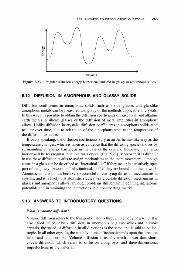
5.12 DIFFUSION IN AMORPHOUS AND GLASSY SOLIDS
Diffusion coefficients in amorphous solids such as oxide glasses and glasslikeamorphous metals can be measured using any of the methods applicable to crystals.In this way it is possible to obtain the diffusion coefficients of, say, alkali and alkalineearth metals in silicate glasses or the diffusion of metal impurities in amorphousalloys. Unlike diffusion in crystals, diffusion coefficients in amorphous solids tendto alter over time, due to relaxation of the amorphous state at the temperature ofthe diffusion experiment.
Broadly speaking, the diffusion coefficients vary in an Arrhenius-like way as thetemperature changes, which is taken as evidence that the diffusing species moves bysurmounting an energy barrier, as in the case of the crystals. However, the energybarrier will be less regular than that for a crystal (Fig. 5.23). Moreover, it is difficultto use these diffusion results to assign mechanisms to the atom movement, althoughatoms in a glass can be described as “interstitial-like” if they occur in a relatively openpart of the glassy network or “substitutional-like” if they are bound into the network.Atomistic simulation has been very successful in clarifying diffusion mechanisms incrystals, and it is likely that atomistic studies will elucidate diffusion mechanisms inglasses and amorphous alloys, although problems still remain in defining interatomicpotentials and in summing the interactions in a nonrepeating matrix.
5.13 ANSWERS TO INTRODUCTORY QUESTIONS
What is volume diffusion?
Volume diffusion refers to the transport of atoms through the body of a solid. It isalso called lattice or bulk diffusion. In amorphous or glassy solids and in cubiccrystals, the speed of diffusion in all directions is the same and is said to be iso-tropic. In all other crystals, the rate of volume diffusion depends upon the directiontaken and is anisotropic. Volume diffusion is usually much slower than short-circuit diffusion, which refers to diffusion along two- and three-dimensionalimperfections in the material.
Figure 5.23 Irregular diffusion energy barrier encountered in glassy or amorphous solids.
5.13 ANSWERS TO INTRODUCTORY QUESTIONS 245
How do defects influence diffusion in solids?
The ability of an atom to diffuse through a solid frequently depends upon thenumber of defects present. For geometrical reasons an atom may be able tojump between sites readily but will be unable to make the move if the target pos-ition is occupied by an atom. This means that a population of vacancies is neededfor normal atom diffusion to occur at all. (An exception to this is the mechanism ofring diffusion, which appears to operate in some solids.) The diffusion of intersti-tial atoms clearly requires the presence of defects in the form of interstitials.Impurities, either substitutional or interstitial, are governed by the same con-straints. In general, it is reasonable to say that bulk diffusion through a perfectsingle crystal is dominated by point defects, with both impurity and intrinsicdefect populations playing a part. It is also true that the rates of diffusion increasein proportion to the number of defects present.
How does temperature effect diffusion in solids?
Diffusion coefficients invariably increase as the temperature rises. This variation isgenerally expressed in terms of the Arrhenius equation:
D ¼ D0 exp � Ea
RT
� �
where R is the gas constant, T is the temperature (K), and D0 is a constant termreferred to as the pre-exponential factor, frequency factor, or (occasionally) asthe diffusion coefficient. The magnitude of this term is a function of the defectconcentrations present. The term Ea is called the activation energy of diffusionand D is the measured diffusion coefficient. A plot of ln D versus 1/T will be astraight line if the Arrhenius law is obeyed. Curved plots indicate that complexinteractions are taking place between the diffusing species and the surroundingsand that diffusion is not a random process.
PROBLEMS AND EXERCISES
Quick Quiz
1. Diffusion through a crystalline structure is called:
(a) Tracer diffusion
(b) Volume diffusion
(c) Self-diffusion
2. Short-circuit diffusion refers to diffusion along:
(a) Defects
(b) Tunnels
(c) Planes
246 DEFECTS AND DIFFUSION
3. A diffusion profile is a graph of:
(a) Concentration versus time
(b) Concentration versus distance
(c) Distance versus time
4. To obtain the diffusion coefficient from a diffusion profile, use:
(a) Fick’s first law
(b) The Gruzin equation
(c) The diffusion equation
5. Vacancy diffusion refers to:
(a) Diffusion of atoms via vacant sites
(b) Diffusion not involving atoms
(c) Diffusion of defects
6. Correlation factors compensate for:
(a) Nonrandom diffusion
(b) Impurity content
(c) Defect concentrations
7. The activation energy for diffusion can be determined by a plot of:
(a) ln c versus 1/T
(b) ln D versus T
(c) ln D versus 1/T
8. The geometrical factor in diffusion equations compensates for:
(a) The types of defects present
(b) The size of the diffusing atoms
(c) The crystal structure
9. Ti impurities substitute for Mg on doping MgO with a small amount of TiO2.Will the diffusion coefficient of Mg be expected to:
(a) Decrease
(b) Increase
(c) Stay the same
10. Ambipolar diffusion refers to diffusion involving:
(a) Polar crystals
(b) Amorphous solids
(c) Charged particles
PROBLEMS AND EXERCISES 247
Calculations and Questions
1. Radioactive 22Na was coated onto a glass sample that was made into a diffusioncouple (Fig. 5.2) and heated for 4 h at 4118C. The radioactivity perpendicular tothe surface is given in the following table. Calculate the tracer diffusion coeffi-cient, D�, of 22Na in the glass.
Activity/counts s21 Distance/mm
2.239 � 105 801.122 � 105 903.311 � 104 1001.549�104 1103.981�103 1201.479�103 1303.020�102 140
Source: Data adapted from E. M. Tanguep Njiokop and H. Mehrer,Solid State Ionics, 177, 2839–2844 (2006).
2. The list below shows the last position reached, in units of the jump step a, duringa random walk for 100 atoms, each of which makes 200 jumps. If the jump timeis 1023 s and the jump distance, a, is 0.3 nm, estimate the diffusion coefficient (a)in units of a2 s21 and (b) in units of m2 s21:
f0g,f12g,f�14g,f4g,f4g,f8g,f8g,f�12g,f�24g,f16g,f�8g,f�12g,f�6g,f14g,f14g,f18g,f�4g,f10g,f6g,f4g,f�30g,f�8g,f16g,f�14g,f12g,f0g,f�6g,f0g,f�6g,f14g,f8g,f�6g,f6g,f�22g,f6g,f�2g,f�18g,f�10g,f18g,f�6g,f2g,f4g,f�4g,f�6g,f0g,f�10g,f20g,f�2g,f12g,f�10g,f�4g,f�12g,f8g,f�8g,f�6g,f�18g,f8g,f30g,f6g,f0g,f�12g,f10g,f�2g,f�16g,f30g,f�14g,f�12g,f8g,f0g,f�26g,f4g,f8g,f26g,f14g,f�18g,f�4g,f�4g,f�12g,f�16g,f10g,f14g,f2g,f12g,f0g,f6g,f8g,f20g,f12g,f10g,f�16g,f14g,f10g,f22g,f10g,f6g,f12g,f0g,f4g,f0g,f20g
3. Using the data in Question 2, estimate the activation energy for diffusion if thevibration frequency is 1 � 1013 Hz and the temperature of the diffusion is1200 K.
4. The fraction of vacancies in a crystal of NaCl, nV/N due to a population ofSchottky defects, is 5 � 1025 at 1000 K. In a diffusion experiment at this temp-erature, the activation energy for self-diffusion of Na was found to be 173.2 kJmol21. Determine the potential barrier that the diffusing ions have to surmount.
5. The radioactive tracer diffusion coefficient of 22Na in glass is given in thefollowing table. Estimate the activation energy for diffusion.
248 DEFECTS AND DIFFUSION
T/K D�/m2 s21
400 1.16 � 10219
450 2.08 � 10218
500 3.63 � 10217
550 2.81 � 10216
600 2.10 � 10215
650 1.03 � 10214
700 3.19 � 10214
Source: Data adapted from E. M. Tanguep Njiokop and H. Mehrer,Solid State Ionics, 177, 2839–2844 (2006).
6. Using the data in Question 5, at what temperature (8C) will the penetration depthbe 5mm after 2 h of heating?
7. Derive the equation for interstitial diffusion in a pure material equivalent to thatfor vacancy diffusion:
D ¼ ga2n exp �DHV
RT
� �exp �DHm
RT
� �
8. Radioactive 18O was diffused into a polycrystalline pellet of ZnO at 9008C for48 h. The diffusion profile had a marked tail showing that extensive grainboundary diffusion had occurred. The variation of the concentration of theradioactive isotope with depth for the tail of the penetration profile isgiven in the following table. Calculate the grain boundary diffusion coefficient,Dgb, of
18O if the bulk diffusion coefficient at 9008C is 5.53 � 10221 m2 s21
and the grain boundary width is taken as 1 nm.
18O Concentration/% Distance/mm
1.850 0.212.118 0.1752.387 0.152.656 0.1252.925 0.10
Source: Data adapted from A. C. S. Sabioni et al., MaterialsResearch, 6, 173–178 (2003).
9. Plot the concentration profile over the range 0 to 1 � 1026 m for Al diffusion intoAl2O3 (corundum) in a planar sandwich type of diffusion couple using the data:c0 ¼ 10, t ¼ 100 h, D ¼ 8 � 10220 m2 s21 at 16108C.
10. Plot the residual activity over the range 0 to 1 � 1023 m for 65Zn diffusion intoZnO in a planar sandwich type of diffusion couple using the data: Ar(0) ¼10,000, t ¼ 29 h, D ¼ 2.7 � 10212 m2 s21 at 13008C.
PROBLEMS AND EXERCISES 249
11. Plot the concentration profile over the range 0 to 2 � 1023 m for Fe diffusioninto TiO2 (rutile) in a planar sandwich type of diffusion couple using the data:c0 ¼ 600, t ¼ 300 s, D ¼ 2 � 10210 m2 s21 at 8008C.
12. Plot the residual activity over the range 0 to 1 � 1025 m for 63Ni diffusion intoCoO in a planar sandwich type of diffusion couple using the data: Ar(0) ¼ 100,t ¼ 30 min, D ¼ 1.56 � 10214 m2 s21 at 9538C.
FURTHER READING
The classical theory of diffusion is covered in:
J. Crank The Mathematics of Diffusion, 2nd ed., Oxford University Press, Oxford, UnitedKingdom, 1975.
J. S. Kirkaldy and D. J. Young Diffusion in the Condensed State, Institute of Metals London,1987.
A. D. Le Claire, Diffusion, in Treatise on Solid State Chemistry, Vol. 4, N. B. Hannay, Ed.,Plenum, New York, 1976, Chapter 1.
J. Philibert, Atom Movements: Diffusion and Mass Transport, translated by S. J. Rothman, LesEditions de Physique, F-91944 Les Ulis, 1991.
Short-circuit diffusion is described in:
A. Atkinson J. Chem. Soc. Faraday Trans., 86, 1307–1310 (1990).
I. Kaur and W. Gust Fundamentals of Grain and Interphase Boundary Diffusion, Ziegler,Stuttgart, 1988.
A discussion of the relation between random walks and diffusion, together with examples ofcomputations, is found in:
S. Wolfram, A New Kind of Science, Wolfram Media Inc., Champaign, IL 61820, 2002,Chapter 7.
Diffusion in glass and amorphous materials:
R. S. Averback, Mat. Res. Soc. Bull., XX(11), 47–52 (1991).
E. M. Tanguep Njiokep and H. Mehrer, Solid State Ionics, 177, 2839–2844 (2006).
Diffusion in semiconductors, including AsSb, is described by:
H. Bracht, Mat. Res. Soc. Bull., 25(6), 22–27 (2000).
H. Bracht, E. E. Haller, and R. Clark-Phelps Phys. Rev. Lett., 81, 393–396 (1998).
H. Bracht, S. P. Nicols, W. Walukiewicz, J. P. Silveira, F. Briones, and E. E. Haller, Nature,408, 69–72 (2000).
250 DEFECTS AND DIFFUSION
&CHAPTER 6
Intrinsic and Extrinsic Defects inInsulators: Ionic Conductivity
Why are ionic conductors vital for battery operation?
How does an oxygen sensor work?
What is a fuel cell?
This chapter mostly discusses defects in insulating crystals. These compounds arecharacterized by ions with a strong and single predominant valence. They are noteasily oxidized or reduced and are typified by the normal group metals [group 1(Na, K, etc.), group 2, (Mg, Ca, etc.), group 3, (Al, Sc, etc.)]. The compounds ofthese metals are generally fully stoichiometric. In pure compounds, point defectsare limited to populations of vacancies, interstitials, or substituents and, except inexceptional cases, the defect populations are low. Such solids are used in a varietyof applications, but in this chapter the focus will be upon ionic conductivity andapplications stemming from ionic transport.
6.1 IONIC CONDUCTIVITY
6.1.1 Ionic Conductivity in Solids
Ionic conductivity, in the context of solids, refers to the passage of ions across a solidunder the influence of an externally applied electric field. High ionic conductivity isvital to the operation of batteries and related devices. As outlined earlier (Section 2.4),in essence a battery consists of an electrode (the anode), where electrons are movedout of the cell, and an electrode (the cathode), where electrons move into the cell. Theelectrons are thus generated in the region of the anode and then move around an exter-nal circuit, carrying out a useful function, before entering the cathode. The anode andcathode are separated inside the battery by an electrolyte. The circuit is completedinside the battery by ions moving across an electrolyte. A key component inbattery construction is an electrolyte that can support ionic conduction but notelectronic conduction.
Defects in Solids, by Richard J. D. TilleyCopyright # 2008 John Wiley & Sons, Inc.
251
The output of a battery depends upon the concentrations and Gibbs energy of thecomponents at the anode and cathode. Because of this, battery technology also under-pins the operation of many sensors.
For a battery to give a reasonable power output, the ionic conductivity of theelectrolyte must be substantial. Historically, this was achieved by the use of liquidelectrolytes. However, over the last quarter of a century there has been increasingemphasis on the production of batteries and related devices employing solid electro-lytes. These are sturdy and ideal for applications where liquid electrolytes pose pro-blems. The primary technical problem to overcome is that of achieving high ionicconductivity across the solid.
There are three broad categories of materials that have been utilized in this endea-vor. In the first, even in fully stoichiometric compounds, the ionic conductivity ishigh enough to be useful in devices because the cation or anion substructure ismobile and behaves rather like a liquid phase trapped in the solid matrix. A secondgroup have structural features such as open channels that allow easy ion transport.In the third group the ionic conductivity is low and must be increased by the additionof defects, typically impurities. These defects are responsible for the enhancement ofionic transport.
Optimization of all of these categories of materials has produced solids in whichthe ionic conductivity is as large as that normally found in solutions (Fig. 6.1). Suchmaterials are sometimes called super-ionic conductors, but the terms fast ionconductors or solid electrolytes are to be preferred to avoid confusion with metallicsuperconductors, which transport electrons and holes, not ions, and by a quite differ-ent mechanism.
6.1.2 Fundamental Concepts
The electrical conductivity of a material is made up by the movement of charged par-ticles: cations, anions, electrons, or holes. The conductivity due to charged particlesof type i moving through a solid is given by
si ¼ ciqimi
where si is the conductivity (V21 m21 ¼ S m21),1 ci is the number of charged par-ticles per unit volume (particles m23), qi is the charge on the particles (C), and mi isthe mobility of the particles (m2 V21 s21). When several different species contributeto the overall conductivity, the total conductivity, s, is simply the sum of the variouscontributions:
s ¼X
si
1Note: many published studies use centimeters rather than meters when reporting results. To convert con-ductivity in V21 cm21 to V21 m21, multiply the value by 100. To convert conductivity in V21 m21 toV21 cm21, divide the value by 100.
252 INTRINSIC AND EXTRINSIC DEFECTS IN INSULATORS: IONIC CONDUCTIVITY
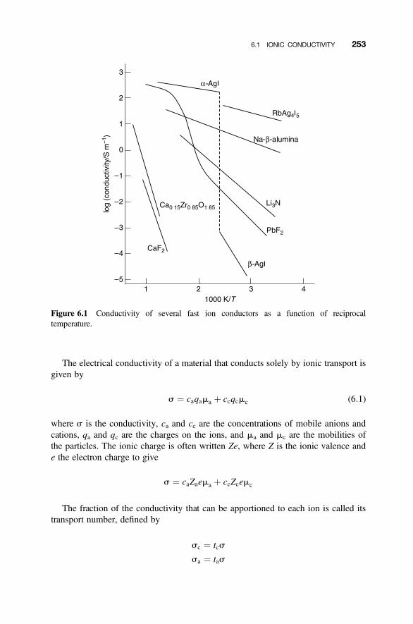
The electrical conductivity of a material that conducts solely by ionic transport isgiven by
s ¼ caqama þ ccqcmc (6:1)
where s is the conductivity, ca and cc are the concentrations of mobile anions andcations, qa and qc are the charges on the ions, and ma and mc are the mobilities ofthe particles. The ionic charge is often written Ze, where Z is the ionic valence ande the electron charge to give
s ¼ caZaema þ ccZcemc
The fraction of the conductivity that can be apportioned to each ion is called itstransport number, defined by
sc ¼ tcs
sa ¼ tas
Figure 6.1 Conductivity of several fast ion conductors as a function of reciprocaltemperature.
6.1 IONIC CONDUCTIVITY 253
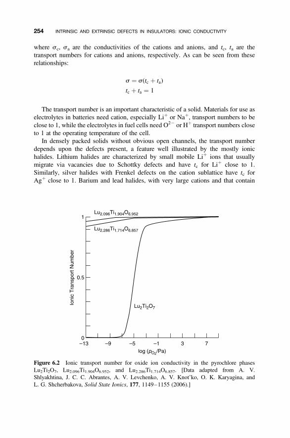
where sc, sa are the conductivities of the cations and anions, and tc, ta are thetransport numbers for cations and anions, respectively. As can be seen from theserelationships:
s ¼ s(tc þ ta)
tc þ ta ¼ 1
The transport number is an important characteristic of a solid. Materials for use aselectrolytes in batteries need cation, especially Liþ or Naþ, transport numbers to beclose to 1, while the electrolytes in fuel cells need O22 or Hþ transport numbers closeto 1 at the operating temperature of the cell.
In densely packed solids without obvious open channels, the transport numberdepends upon the defects present, a feature well illustrated by the mostly ionichalides. Lithium halides are characterized by small mobile Liþ ions that usuallymigrate via vacancies due to Schottky defects and have tc for Liþ close to 1.Similarly, silver halides with Frenkel defects on the cation sublattice have tc forAgþ close to 1. Barium and lead halides, with very large cations and that contain
Figure 6.2 Ionic transport number for oxide ion conductivity in the pyrochlore phasesLu2Ti2O7, Lu2.096Ti1.904O6.952, and Lu2.286Ti1.714O6.857. [Data adapted from A. V.Shlyakhtina, J. C. C. Abrantes, A. V. Levchenko, A. V. Knot’ko, O. K. Karyagina, andL. G. Shcherbakova, Solid State Ionics, 177, 1149–1155 (2006).]
254 INTRINSIC AND EXTRINSIC DEFECTS IN INSULATORS: IONIC CONDUCTIVITY
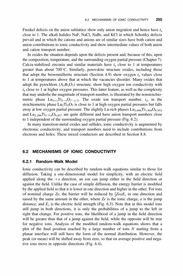
Frenkel defects on the anion sublattice show only anion migration and hence have taclose to 1. The alkali halides NaF, NaCl, NaBr, and KCl in which Schottky defectsprevail and in which the cations and anions are of similar sizes have both cation andanion contributions to ionic conductivity and show intermediate values of both anionand cation transport number.
In oxides the situation depends upon the defects present and, because of this, uponthe composition, temperature, and the surrounding oxygen partial pressure (Chapter 7).Calcia-stabilized zirconia and similar materials have ta close to 1 at temperaturesgreater than about 7008C. Similarly, perovskite structure oxides, including thosethat adopt the brownmillerite structure (Section 4.9) show oxygen ta values closeto 1 at temperatures above that at which the vacancies disorder. Many oxides thatadopt the pyrochlore (A2B2O7) structure, show high oxygen ion conductivity withta close to 1 at higher oxygen pressures. This latter feature, as well as the complexitythat may underlie the magnitude of transport number, is illustrated by the nonstoichio-metric phase Lu2þxTi22xO72x/2. The oxide ion transport number, ta, in thestoichiometric phase Lu2Ti2O7 is close to 1 at high oxygen partial pressures but fallsaway at low oxygen partial pressure. The slightly Lu-rich phases Lu2.096Ti1.904O6.952
and Lu2.286Ti1.714O6.857 are quite different and have anion transport numbers closeto 1 independent of the surrounding oxygen partial pressure (Fig. 6.2).
In many transition-metal oxides and sulfides, ionic conductivity is augmented byelectronic conductivity, and transport numbers need to include contributions fromelectrons and holes. These mixed conductors are described in Section 8.8.
6.2 MECHANISMS OF IONIC CONDUCTIVITY
6.2.1 Random-Walk Model
Ionic conductivity can be described by random-walk equations similar to those fordiffusion. Taking a one-dimensional model for simplicity, with an electric fieldapplied along the þx direction, an ion can jump either in the field direction oragainst the field. Unlike the case of simple diffusion, the energy barrier is modifiedby the applied field so that it is lower in one direction and higher in the other. For ionsof nominal charge Ze, the barrier will be reduced by 1
2ZeaEv in one direction andraised by the same amount in the other, where Ze is the ionic charge, a is the jumpdistance, and Ev is the electric field strength (Fig. 6.3). Note that in this model ionsstill jump in both directions, it is only the probabilities of a jump to the left orright that change. For positive ions, the likelihood of a jump in the field directionwill be greater than that of a jump against the field, while the opposite will be truefor negative ions. Analysis of the modified random-walk equations shows that aplot of the final position reached by a large number of ions N starting from aplanar interface will still have the form of the normal distribution. However, thepeak (or mean) will be shifted away from zero, so that on average positive and nega-tive ions move in opposite directions (Fig. 6.4).
6.2 MECHANISMS OF IONIC CONDUCTIVITY 255
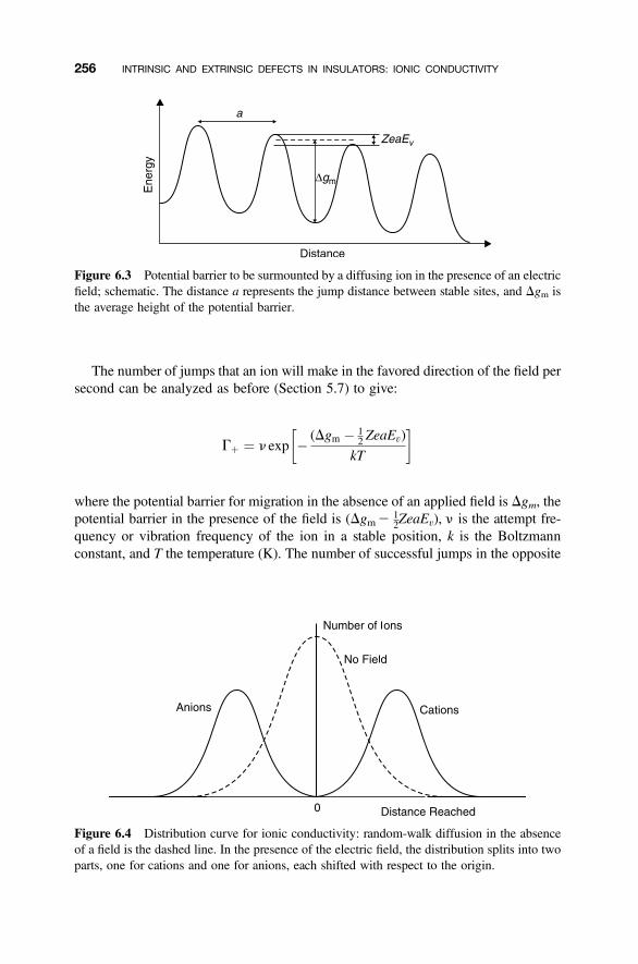
The number of jumps that an ion will make in the favored direction of the field persecond can be analyzed as before (Section 5.7) to give:
Gþ ¼ n exp � (Dgm � 12 ZeaEv)
kT
� �
where the potential barrier for migration in the absence of an applied field is Dgm, thepotential barrier in the presence of the field is (Dgm2 1
2ZeaEv), n is the attempt fre-quency or vibration frequency of the ion in a stable position, k is the Boltzmannconstant, and T the temperature (K). The number of successful jumps in the opposite
Figure 6.4 Distribution curve for ionic conductivity: random-walk diffusion in the absenceof a field is the dashed line. In the presence of the electric field, the distribution splits into twoparts, one for cations and one for anions, each shifted with respect to the origin.
Figure 6.3 Potential barrier to be surmounted by a diffusing ion in the presence of an electricfield; schematic. The distance a represents the jump distance between stable sites, and Dgm isthe average height of the potential barrier.
256 INTRINSIC AND EXTRINSIC DEFECTS IN INSULATORS: IONIC CONDUCTIVITY
direction will be given by
G� ¼ n exp � (Dgm þ 12 ZeaEv)
kT
� �
where the potential barrier for migration is now (Dgm þ 12ZeaEv).
The overall jump rate in the direction of the field is (Gþ 2 G2), and as the netvelocity of the ions in the direction of the field, v, is given by the net jump rate mul-tiplied by the distance moved at each jump, we can write
v ¼ na exp � (Dgm � 12 ZeaEv)
kT
� �� exp � (Dgm þ 1
2 ZeaEv
kT
� �
¼ na exp �DgmkT
� �exp
ZeaEv
2kT
� �� exp �ZeaEv
2kT
� �� �
For the field strengths used in conductivity experiments, ZeaEv is less than kT, so
expZeaEv
2kT
� �� exp
�ZeaEv
2kT
� �� �� ZeaEv
kT
and v can be written as:
v ¼ nZea2Ev
kT
� �exp �Dgm
kT
� �
The mobility, m, of the ion is defined as the velocity when the value of Ev isunity, so:
m ¼ nZea2
kT
� �exp �Dgm
kT
� �
Often a geometrical factor g is included to take into account different crystal struc-tures to give
m ¼ gnZea2
kT
� �exp �Dgm
kT
� �
6.2 MECHANISMS OF IONIC CONDUCTIVITY 257
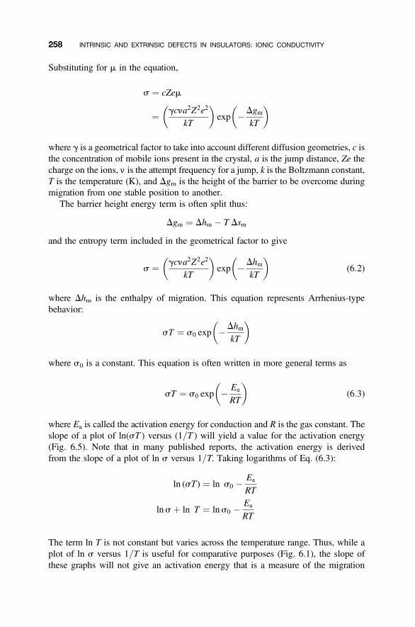
Substituting for m in the equation,
s ¼ cZem
¼ gcna2Z2e2
kT
� �exp �Dgm
kT
� �
where g is a geometrical factor to take into account different diffusion geometries, c isthe concentration of mobile ions present in the crystal, a is the jump distance, Ze thecharge on the ions, n is the attempt frequency for a jump, k is the Boltzmann constant,T is the temperature (K), and Dgm is the height of the barrier to be overcome duringmigration from one stable position to another.
The barrier height energy term is often split thus:
Dgm ¼ Dhm � T Dsm
and the entropy term included in the geometrical factor to give
s ¼ gcna2Z2e2
kT
� �exp �Dhm
kT
� �(6:2)
where Dhm is the enthalpy of migration. This equation represents Arrhenius-typebehavior:
sT ¼ s0 exp �DhmkT
� �
where s0 is a constant. This equation is often written in more general terms as
sT ¼ s0 exp � Ea
RT
� �(6:3)
where Ea is called the activation energy for conduction and R is the gas constant. Theslope of a plot of ln(sT ) versus (1/T ) will yield a value for the activation energy(Fig. 6.5). Note that in many published reports, the activation energy is derivedfrom the slope of a plot of ln s versus 1/T. Taking logarithms of Eq. (6.3):
ln (sT) ¼ ln s0 � Ea
RT
lnsþ ln T ¼ lns0 � Ea
RT
The term ln T is not constant but varies across the temperature range. Thus, while aplot of ln s versus 1/T is useful for comparative purposes (Fig. 6.1), the slope ofthese graphs will not give an activation energy that is a measure of the migration
258 INTRINSIC AND EXTRINSIC DEFECTS IN INSULATORS: IONIC CONDUCTIVITY
barrier height, or equivalent to that determined from diffusion studies, as described inthe following section.
6.2.2 Relationship between Ionic Conductivityand Diffusion Coefficient
If both ionic conductivity and ionic diffusion occur by the same random-walk mech-anism, a relationship between the self-diffusion coefficient, D, and the ionic
Figure 6.5 Arrhenius plots of ln(sT ) versus 1/T for ionic conductivity in a crystal: (a)straight-line plot used to obtain the activation energy of migration; (b) experimental resultsfor the pyrochlore phases Lu2Ti2O7, Lu2.096Ti1.904O6.952, and Lu2.286Ti1.714O6.857. [Dataadapted from A. V. Shlyakhtina, J. C. C. Abrantes, A. V. Levchenko, A. V. Knot’ko, O. K.Karyagina, and L. G. Shcherbakova, Solid State Ionics, 177, 1149–1155 (2006).]
6.2 MECHANISMS OF IONIC CONDUCTIVITY 259
conductivity, s, can be derived. In the simplest case, assume one-dimensional diffu-sion along x and that both processes involve the same energy barrier, Dgm, and jumpdistance, a (Figs. 5.20b and 6.3). For this case the diffusion coefficient is
D ¼ gna2 exp �DgmkT
� �
and the mobility is given by
m ¼ gnZea2
kT
� �exp �Dgm
kT
� �
leading to the Nernst–Einstein equation:
D ¼ mkT
Ze
where Ze is the charge on the mobile ions. The ionic conductivity of an ion is
s ¼ gcna2Z2e2
kT
� �exp �Dgm
kT
� �
so that an alternative formulation of the Nernst–Einstein equation is
D ¼ kTs
cZ2e2
where c is the number of mobile ions per unit volume, Ze is the ionic charge, k is theBoltzmann constant, and T the temperature (K). Values of the diffusion coefficientcalculated from the conductivity are usually written Ds, so that
Ds ¼ kTs
cZ2e2
This equation shows that it is possible to determine the diffusion coefficient fromthe easier measurement of ionic conductivity. However, Ds is derived by assumingthat the conductivity mechanism utilizes a random-walk mechanism, which maynot true.
The Haven ratio, HR, is defined as
HR ¼ tracer diffusion coefficientconductivity diffusion coefficient
¼ D�
Ds
260 INTRINSIC AND EXTRINSIC DEFECTS IN INSULATORS: IONIC CONDUCTIVITY
The correlation factor, f, is defined by the ratio of the tracer diffusion coefficient to therandom-walk diffusion coefficient (Section 5.6):
f ¼ D�
Dr
Taking Ds to be equal to Dr (which may not always be correct) allows HR to beequated with the correlation factor:
HR ¼ f ¼ D�
Ds
When ionic conductivity is by way of interstitials, both conductivity and diffusioncan occur by random motion, so that the correlation factor and HR are both equalto 1. In general, the correlation factor for a diffusion mechanism will differ from 1,and in such a case Ds can be described by the following relationship:
Ds ¼ fkTs
cZ2e2
where f is the correlation factor appropriate to the diffusion mechanism. For vacancydiffusion in a cubic structure,
Ds ¼ fvkTs
cZ2e2
where fv is the correlation factor for vacancy self-diffusion, and
Ds ¼ fiykTs
cZ2e2
for interstitialcy diffusion, where fiy is the appropriate intersticialcy correlation factor.
6.2.3 Ionic Conductivity and Defects
To obtain a solid with a high conductivity, it is clearly important that a large concen-tration, c, of mobile ions is present in the crystal [Eq. (6.1)]. This entails that a largenumber of empty sites are available, so that an ion jump is always possible. Inaddition, a low enthalpy of migration is required, which is to say that there is alow-energy barrier between sites and ions do not have to squeeze through bottle-necks. Hence the structure should ideally have open channels and a high populationof vacancy defects.
The close connection between ionic conductivity and diffusion means that the roleof defect concentrations will be similar to that discussed in the previous chapter(Sections 5.8 and 5.9). For crystals such as oxides and halides with close-packed
6.2 MECHANISMS OF IONIC CONDUCTIVITY 261
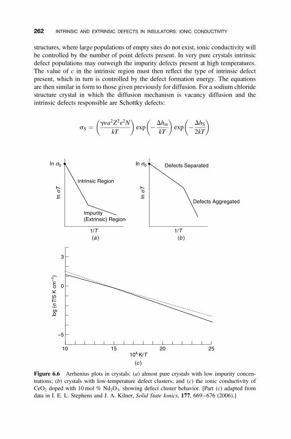
structures, where large populations of empty sites do not exist, ionic conductivity willbe controlled by the number of point defects present. In very pure crystals intrinsicdefect populations may outweigh the impurity defects present at high temperatures.The value of c in the intrinsic region must then reflect the type of intrinsic defectpresent, which in turn is controlled by the defect formation energy. The equationsare then similar in form to those given previously for diffusion. For a sodium chloridestructure crystal in which the diffusion mechanism is vacancy diffusion and theintrinsic defects responsible are Schottky defects:
sS ¼ gna2Z2e2N
kT
� �exp �Dhm
kT
� �exp �DhS
2kT
� �
Figure 6.6 Arrhenius plots in crystals: (a) almost pure crystals with low impurity concen-trations; (b) crystals with low-temperature defect clusters; and (c) the ionic conductivity ofCeO2 doped with 10 mol % Nd2O3, showing defect cluster behavior. [Part (c) adapted fromdata in I. E. L. Stephens and J. A. Kilner, Solid State Ionics, 177, 669–676 (2006).]
262 INTRINSIC AND EXTRINSIC DEFECTS IN INSULATORS: IONIC CONDUCTIVITY
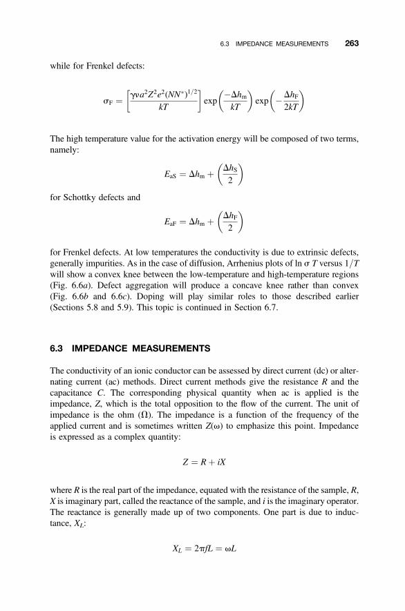
while for Frenkel defects:
sF ¼ gna2Z2e2(NN�)1=2
kT
� �exp
�DhmkT
� �exp �DhF
2kT
� �
The high temperature value for the activation energy will be composed of two terms,namely:
EaS ¼ Dhm þ DhS2
� �
for Schottky defects and
EaF ¼ Dhm þ DhF2
� �
for Frenkel defects. At low temperatures the conductivity is due to extrinsic defects,generally impurities. As in the case of diffusion, Arrhenius plots of ln s T versus 1/Twill show a convex knee between the low-temperature and high-temperature regions(Fig. 6.6a). Defect aggregation will produce a concave knee rather than convex(Fig. 6.6b and 6.6c). Doping will play similar roles to those described earlier(Sections 5.8 and 5.9). This topic is continued in Section 6.7.
6.3 IMPEDANCE MEASUREMENTS
The conductivity of an ionic conductor can be assessed by direct current (dc) or alter-nating current (ac) methods. Direct current methods give the resistance R and thecapacitance C. The corresponding physical quantity when ac is applied is theimpedance, Z, which is the total opposition to the flow of the current. The unit ofimpedance is the ohm (V). The impedance is a function of the frequency of theapplied current and is sometimes written Z(v) to emphasize this point. Impedanceis expressed as a complex quantity:
Z ¼ Rþ iX
where R is the real part of the impedance, equated with the resistance of the sample, R,X is imaginary part, called the reactance of the sample, and i is the imaginary operator.The reactance is generally made up of two components. One part is due to induc-tance, XL:
XL ¼ 2pfL ¼ vL
6.3 IMPEDANCE MEASUREMENTS 263
where the frequency of the ac is f, the angular frequency is v, and L is the inductanceof the sample. The second part is due to capacitance, XC:
XC ¼ 12pfC
¼ 1vC
where C is the capacitance of the sample.The impedance of a ceramic material such as an oxide is often considered to be
made up of a resistive part in parallel with a reactive part (Fig. 6.7a). The impedanceof this combination is
Z ¼ RX2
R2 þ X2þ iR2X
R2 þ X2
Ideally, the reactance is made up only of a capacitive component in which case theimpedance can be written:
Z ¼ R
1þ R2C2v2� i(R2Cv)1þ R2C2v2
Figure 6.7 Complex impedance of a polycrystalline ceramic sample: (a) representation of theequivalent circuit of a component; (b) the impedance spectrum of the equivalent circuit in (a);(c) the impedance spectrum of a typical ceramic sample. Each semicircular arc represents onecomponent with an equivalent circuit as in (a); that at the highest frequency corresponds to therepose of the bulk, that at middle frequencies to the grain boundary response, and that at lowestfrequencies to the electrodes.
264 INTRINSIC AND EXTRINSIC DEFECTS IN INSULATORS: IONIC CONDUCTIVITY
If the real part of the impedance is written Z0 and the imaginary part as Z00, where
Z 0 ¼ R
1þ R2C2v2
�Z 00 ¼ R2Cv
1þ R2C2v2
a plot of Z0 versus Z00 forms a semicircular arc. The arc passes through the origin forv ¼ 1, through the point (12R,
12R) at RCv ¼ 1, and cuts the Z00 axis at R. The
maximum of the arc is given by RCv ¼ 1 (Fig. 6.7b). The measurement of impe-dance across a frequency range is called impedance spectroscopy, and the displayof the plots in terms of Z0 and Z00 are often called complex plane representations,Nyquist plots, or Cole–Cole plots (although these two latter designations are notstrictly accurate terminologies).
A typical ceramic sample contains contributions from the bulk, the grain bound-aries, and the electrode. Each of these is characterized by a semicircular arc with amaximum at RCv ¼ 1, where the values of resistance, capacitance, and frequencyrefer directly to the bulk, grain boundaries, or electrodes (Fig. 6.7c). The separationof resistance due to the bulk from that of the grain boundaries is thus easily achievedusing impedance spectroscopy.
6.4 ELECTROCHEMICAL CELLS AND BATTERIES
One of the major applications of ionic conductors is as an electrolyte in an electro-chemical cell. An electrochemical cell is a device for the conversion of electricalto chemical energy and vice versa by way of redox reactions. Electrochemical cellsconsist of two electrodes that are good electron conductors (an anode and acathode) in contact with an electrolyte that is a good ionic conductor but is notable to conduct electrons. A galvanic cell uses a spontaneous chemical reaction toproduce an external electric current. Galvanic cells are called batteries in colloquialspeech, reflecting the fact that historically several (i.e., a battery of) galvanic cellswere generally connected together so as to increase the output power; the phrase“a battery of galvanic cells” became shortened to “a battery.”
Batteries are self-contained units in which the chemical reactants and the means oftransforming the chemical energy to electrical energy are present (Fig. 6.8a). In abattery, electrons generated as a result of the internal chemical reaction leavevia the anode, cross an external circuit, doing useful work, such as powering a com-puter, and then re-enter the battery via the cathode. The reaction is completed by atransfer of ions across the electrolyte from the anode region to the cathode regionor vice versa.
As against this, fuel cells contain only the means for energy conversion. Thechemical reactants, or fuel (principally hydrogen or hydrocarbons and oxygen), aresupplied from an external source (Fig. 6.8b).
6.4 ELECTROCHEMICAL CELLS AND BATTERIES 265
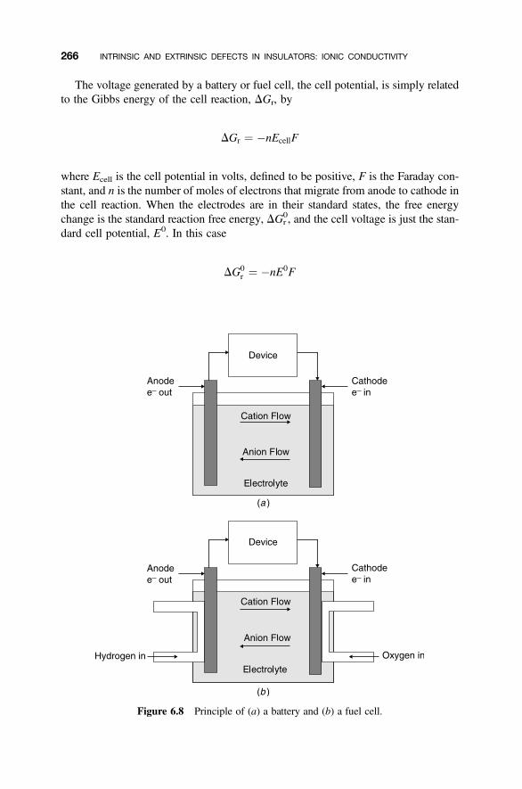
The voltage generated by a battery or fuel cell, the cell potential, is simply relatedto the Gibbs energy of the cell reaction, DGr, by
DGr ¼ �nEcellF
where Ecell is the cell potential in volts, defined to be positive, F is the Faraday con-stant, and n is the number of moles of electrons that migrate from anode to cathode inthe cell reaction. When the electrodes are in their standard states, the free energychange is the standard reaction free energy, DGr
0, and the cell voltage is just the stan-dard cell potential, E0. In this case
DG0r ¼ �nE0F
Figure 6.8 Principle of (a) a battery and (b) a fuel cell.
266 INTRINSIC AND EXTRINSIC DEFECTS IN INSULATORS: IONIC CONDUCTIVITY

The potential generated by a cell is dependent upon the concentration of the com-ponents present. The relationship is given by the following equation:
DGr ¼ �nEcellF ¼ RT lnQ
K
� �
where R is the gas constant, T the temperature (K), Q is the reaction quotient, and K isthe equilibrium constant for the reaction.2
The cell voltage is thus given by
�nEcellF ¼ RT lnQ
K
� �
Ecell ¼ � RT
nF
� �ln
Q
K
� �
It is convenient to separate the term due to the equilibrium constant and write theequation for the cell voltage as
Ecell ¼ RT
nF
� �ln K–
RT
nF
� �lnQ
When all species are in the standard state, Q ¼ 1, ln Q ¼ 0, and the cell voltage is E0,hence:
Ecell ¼ E0 ¼ RT
nF
� �lnK
and in general
Ecell ¼ E0 � RT
nF
� �lnQ (6:4)
where Ecell is the cell voltage, E0 is the standard cell voltage, R is the gas constant, T
the temperature (K), n is the number of electrons transferred in the cell reaction, F is
2The reaction quotient, Qc, of a reaction
aAþ bB ! xX þ yY
is given by
Qc ¼ [X]x[Y]y
[A]a[B]b
where [A] denotes the concentration of component A at any time. Note that the quantity of importance is theactivity rather than concentration and for precise work activity must be used. For reactions involving gases,the concentration term can be replaced by the partial pressure of the gaseous reactants to give
Qp ¼ pxXpyY
paApbB.
6.4 ELECTROCHEMICAL CELLS AND BATTERIES 267
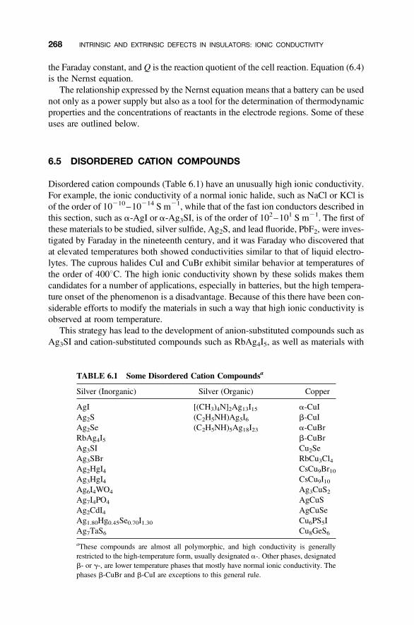
the Faraday constant, and Q is the reaction quotient of the cell reaction. Equation (6.4)is the Nernst equation.
The relationship expressed by the Nernst equation means that a battery can be usednot only as a power supply but also as a tool for the determination of thermodynamicproperties and the concentrations of reactants in the electrode regions. Some of theseuses are outlined below.
6.5 DISORDERED CATION COMPOUNDS
Disordered cation compounds (Table 6.1) have an unusually high ionic conductivity.For example, the ionic conductivity of a normal ionic halide, such as NaCl or KCl isof the order of 10210–10214 S m21, while that of the fast ion conductors described inthis section, such as a-AgI or a-Ag3SI, is of the order of 10
2–101 S m21. The first ofthese materials to be studied, silver sulfide, Ag2S, and lead fluoride, PbF2, were inves-tigated by Faraday in the nineteenth century, and it was Faraday who discovered thatat elevated temperatures both showed conductivities similar to that of liquid electro-lytes. The cuprous halides CuI and CuBr exhibit similar behavior at temperatures ofthe order of 4008C. The high ionic conductivity shown by these solids makes themcandidates for a number of applications, especially in batteries, but the high tempera-ture onset of the phenomenon is a disadvantage. Because of this there have been con-siderable efforts to modify the materials in such a way that high ionic conductivity isobserved at room temperature.
This strategy has lead to the development of anion-substituted compounds such asAg3SI and cation-substituted compounds such as RbAg4I5, as well as materials with
TABLE 6.1 Some Disordered Cation Compoundsa
Silver (Inorganic) Silver (Organic) Copper
AgI [(CH3)4N]2Ag13I15 a-CuIAg2S (C2H5NH)Ag5I6 b-CuIAg2Se (C2H5NH)5Ag18I23 a-CuBrRbAg4I5 b-CuBrAg3SI Cu2SeAg3SBr RbCu3Cl4Ag2HgI4 CsCu9Br10Ag3HgI4 CsCu9I10Ag6I4WO4 Ag3CuS2Ag7I4PO4 AgCuSAg2CdI4 AgCuSeAg1.80Hg0.45Se0.70I1.30 Cu6PS5IAg7TaS6 Cu8GeS6aThese compounds are almost all polymorphic, and high conductivity is generallyrestricted to the high-temperature form, usually designated a-. Other phases, designatedb- or g-, are lower temperature phases that mostly have normal ionic conductivity. Thephases b-CuBr and b-CuI are exceptions to this general rule.
268 INTRINSIC AND EXTRINSIC DEFECTS IN INSULATORS: IONIC CONDUCTIVITY
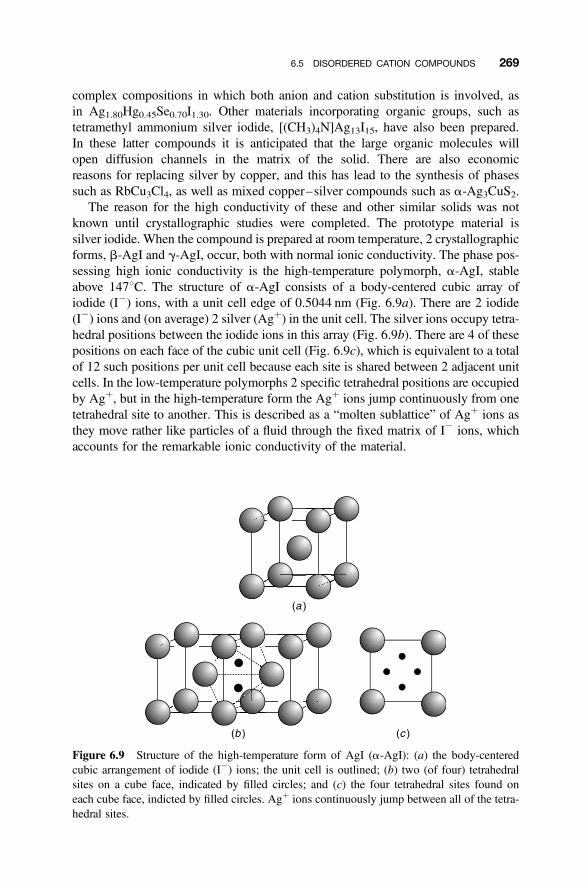
complex compositions in which both anion and cation substitution is involved, asin Ag1.80Hg0.45Se0.70I1.30. Other materials incorporating organic groups, such astetramethyl ammonium silver iodide, [(CH3)4N]Ag13I15, have also been prepared.In these latter compounds it is anticipated that the large organic molecules willopen diffusion channels in the matrix of the solid. There are also economicreasons for replacing silver by copper, and this has lead to the synthesis of phasessuch as RbCu3Cl4, as well as mixed copper–silver compounds such as a-Ag3CuS2.
The reason for the high conductivity of these and other similar solids was notknown until crystallographic studies were completed. The prototype material issilver iodide. When the compound is prepared at room temperature, 2 crystallographicforms, b-AgI and g-AgI, occur, both with normal ionic conductivity. The phase pos-sessing high ionic conductivity is the high-temperature polymorph, a-AgI, stableabove 1478C. The structure of a-AgI consists of a body-centered cubic array ofiodide (I2) ions, with a unit cell edge of 0.5044 nm (Fig. 6.9a). There are 2 iodide(I2) ions and (on average) 2 silver (Agþ) in the unit cell. The silver ions occupy tetra-hedral positions between the iodide ions in this array (Fig. 6.9b). There are 4 of thesepositions on each face of the cubic unit cell (Fig. 6.9c), which is equivalent to a totalof 12 such positions per unit cell because each site is shared between 2 adjacent unitcells. In the low-temperature polymorphs 2 specific tetrahedral positions are occupiedby Agþ, but in the high-temperature form the Agþ ions jump continuously from onetetrahedral site to another. This is described as a “molten sublattice” of Agþ ions asthey move rather like particles of a fluid through the fixed matrix of I2 ions, whichaccounts for the remarkable ionic conductivity of the material.
Figure 6.9 Structure of the high-temperature form of AgI (a-AgI): (a) the body-centeredcubic arrangement of iodide (I2) ions; the unit cell is outlined; (b) two (of four) tetrahedralsites on a cube face, indicated by filled circles; and (c) the four tetrahedral sites found oneach cube face, indicted by filled circles. Agþ ions continuously jump between all of the tetra-hedral sites.
6.5 DISORDERED CATION COMPOUNDS 269
In the main, all of the disordered cation compounds in Table 6.1 behave similarlyand have low-temperature structures that do not show high conductivity and containonly a low population of point defects. At some higher temperature all or part of themetal atom array becomes mobile with cations able to freely move over some or all ofthe various allowed cation sites in the unit cell. This is manifested as increasingamplitude of vibration of the cations as the temperature rises. At the transition temp-erature this vibration is so great that the ions become effectively free. At the same timethe anion array, or this and some of the large cations, remains relatively immobile. Forexample, the compound Ag3CuS2 has a distorted body-centered cubic packing ofsulfur atoms analogous to the body-centered cubic packing of I2 ions in a-AgI.The Agþ ions occupy distorted octahedral or tetrahedral sites and Cuþ ions are inlinear coordination at room temperature. The cation structure disorders at 1178C,giving rise to high conductivity. In this material, although it seems that both Agþ
and Cuþ are mobile, the conductivity is dominated by Agþ movement.In the closely related compound AgCuS, the sulfur atoms form a slightly distorted
hexagonal close-packed array. The Cuþ ions are located in positions within this fra-mework to form layers, while the Agþ ions lie between the sulfur–copper layers.These Agþ ions show a progressively greater anisotropic thermal motion as the temp-erature rises, until, above 938C, they are essentially completely mobile, leading toextremely high silver ion conductivity.
In terms of formal point defect terminology, it is possible to think of each silver orcopper ion creating an instantaneous interstitial defect and a vacancy, Ag†i and V0
Ag,or Cui
† and V0Cu as it jumps between two tetrahedral sites. This is equivalent to a high
and dynamic concentration of cation Frenkel defects that continuously form and areeliminated. For this to occur, the formation energy of these notional defects must beclose to zero.
6.6 b-ALUMINA OXIDES
6.6.1 Idealized Structures of the b-Alumina-Related Phases
The name b-alumina is misleading. When this material was first prepared, it wasthought to be a polymorph of alumina, but later it was discovered that the compoundwas a sodium aluminum oxide. Despite this fact, the name b-alumina was retainedand is now firmly entrenched. b-alumina is the prototype for a family of nonstoichio-metric compounds with compositions lying somewhere between the limitsA2O.nM2O3 with n taking values of between 5 and 11 (i.e., between AM5O8 andAM11O17), where M represents a large cation, typically Na and A represents atrivalent ion, usually Al. The parent phase, b-alumina itself, has a nominal compo-sition of NaAl11O17. These solids have high ionic conductivities, with transportnumbers for the A cations close to 1.0 over a wide range of temperatures.
The unit cell of b-alumina is hexagonal, with lattice parameters a ¼ 0.595 nm,c ¼ 2.249 nm. The dominant features of the idealized structure of b-alumina, withcomposition NaAl11O17, are layers called spinel blocks stacked perpendicular tothe c axis (Fig. 6.10a). These blocks are composed of four oxygen layers in a
270 INTRINSIC AND EXTRINSIC DEFECTS IN INSULATORS: IONIC CONDUCTIVITY
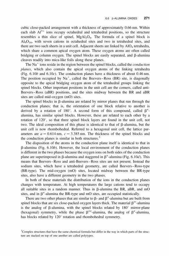
cubic close-packed arrangement with a thickness of approximately 0.66 nm. Withineach slab Al3þ ions occupy octahedral and tetrahedral positions, so the structureresembles a thin slice of spinel, MgAl2O4. The formula of a spinel block isAl9O16, with seven cations in octahedral sites and two in tetrahedral sites, andthere are two such sheets in a unit cell. Adjacent sheets are linked by AlO4 tetrahedra,which share a common apical oxygen atom. These oxygen atoms are often calledbridging or column oxygen. The spinel blocks are easily separated, and b-aluminacleaves readily into mica-like foils along these planes.
The Naþ ions reside in the region between the spinel blocks, called the conductionplanes, which also contain the apical oxygen atoms of the linking tetrahedra(Fig. 6.10b and 6.10c). The conduction planes have a thickness of about 0.46 nm.The position occupied by Naþ, called the Beevers–Ross (BR) site, is diagonallyopposite to the apical bridging oxygen atom of the tetrahedral groups linking thespinel blocks. Other important positions in the unit cell are the corners, called anti-Beevers–Ross (aBR) positions, and the sites midway between the BR and aBRsites are called mid-oxygen (mO) sites.
The spinel blocks in b-alumina are related by mirror planes that run through theconduction planes; that is, the orientation of one block relative to another isderived by a rotation of 1808. A second form of this compound, called b00-alumina, has similar spinel blocks. However, these are related to each other by arotation of 1208, so that three spinel block layers are found in the unit cell, nottwo. The ideal composition of this phase is identical to that of b-alumina, but theunit cell is now rhombohedral. Referred to a hexagonal unit cell, the lattice par-ameters are a ¼ 0.614 nm, c ¼ 3.385 nm. The thickness of the spinel blocks andthe conduction planes is similar in both structures.3
The disposition of the atoms in the conduction plane itself is identical to that inb-alumina (Fig. 6.10b). However, the local environment of the conduction planesis different in the two phases because the oxygen ions on both sides of the conductionplane are superimposed in b-alumina and staggered in b00-alumina (Fig. 6.10d ). Thismeans that Beevers–Ross and anti-Beevers–Ross sites are not present. Instead thesodium sites, which have a tetrahedral geometry, are called Beevers–Ross-type(BR-type). The mid-oxygen (mO) sites, located midway between the BR-typesites, also have a different geometry in the two phases.
In both of these materials the distribution of the ions in the conduction planeschanges with temperature. At high temperatures the large cations tend to occupyall suitable sites in a random manner. Thus in b-alumina the BR, aBR, and mOsites, and in b00-alumina the BR-type and mO sites, are occupied statistically.
There are two other phases that are similar to b- and b00-alumina but are built fromspinel blocks that are six close-packed oxygen layers thick. The material b000-aluminais the analog of b-alumina, with the spinel blocks related by 1808 mirror-plane(hexagonal) symmetry, while the phase b0000-alumina, the analog of b00-alumina,has blocks related by 1208 rotation and rhombohedral symmetry.
3Complex structures that have the same chemical formula but differ in the way in which parts of the struc-ture are stacked on top of one another are called polytypes.
6.6 b-ALUMINA OXIDES 271
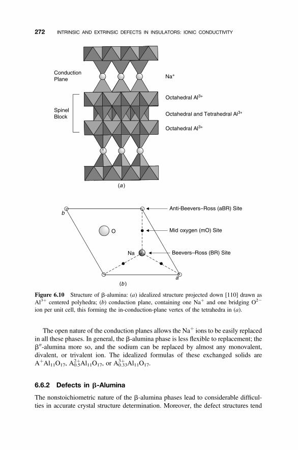
The open nature of the conduction planes allows the Naþ ions to be easily replacedin all these phases. In general, the b-alumina phase is less flexible to replacement; theb00-alumina more so, and the sodium can be replaced by almost any monovalent,divalent, or trivalent ion. The idealized formulas of these exchanged solids areAþAl11O17, A0.5
2þAl11O17, or A0.333þ Al11O17.
6.6.2 Defects in b-Alumina
The nonstoichiometric nature of the b-alumina phases lead to considerable difficul-ties in accurate crystal structure determination. Moreover, the defect structures tend
Figure 6.10 Structure of b-alumina: (a) idealized structure projected down [110] drawn asAl3þ centered polyhedra; (b) conduction plane, containing one Naþ and one bridging O22
ion per unit cell, this forming the in-conduction-plane vertex of the tetrahedra in (a).
272 INTRINSIC AND EXTRINSIC DEFECTS IN INSULATORS: IONIC CONDUCTIVITY
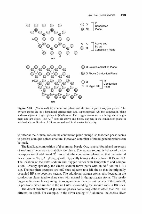
to differ as the A metal ions in the conduction plane change, so that each phase seemsto possess a unique defect structure. However, a number of broad generalizations canbe made.
The idealized composition of b-alumina, NaAl11O17, is never found and an excessof sodium is necessary to stabilize the phase. The excess sodium is balanced by theincorporation of additional O22 ions into the conduction planes, so that the materialhas a formula Na1þxAl11O17þx/2 with x typically taking values between 0.15 and 0.3.The location of the extra sodium and oxygen varies with temperature and compo-sition. Broadly speaking, the excess sodium forms pairs with an Naþ ion on a BRsite. The pair then occupies two mO sites adjacent to a BR site so that the originallyoccupied BR site becomes vacant. The additional oxygen atoms, also located in theconduction plane, tend to share sites with normal bridging oxygen atoms. The result-ing pairs lie along lines joining the oxygen site to the adjacent corners of the unit cell,in positions rather similar to the mO sites surrounding the sodium ions in BR sites.
The defect structures of b-alumina phases containing cations other than Naþ aredifferent in detail. For example, in the silver analog of b-alumina, the excess silver
Figure 6.10 (Continued) (c) conduction plane and the two adjacent oxygen planes. Theoxygen atoms are in a hexagonal arrangement and superimposed; (d ) the conduction planeand two adjacent oxygen planes in b00-alumina. The oxygen atoms are in a hexagonal arrange-ment and are offset. The Al3þ ions lie above and below oxygen in the conduction plane intetrahedral coordination. All ions are reduced in diameter for clarity.
6.6 b-ALUMINA OXIDES 273

occupies aBR sites. When higher valence ions replace the sodium, the BR sites aregenerally occupied, but charge balance means that a considerable number of thesesites are empty, creating a population of vacancies. Ideally, half are unoccupied forA2þ cations and two-thirds are unoccupied for A3þ cations. The higher charge onthese cations can also create other defect structures. In the phase Ba0.75Al11O17.25,Ba2þ occupies BR sites, and Ba vacancies are surrounded by Roth–Reidingerdefects. These are linear groups consisting of Ali
3†–Oi20 –Ali
3† units, which are iden-tical to the bridging units linking the spinel blocks. These defects are distributed atrandom throughout the conduction plane, balancing the Ba2þ deficit and providingextra links between the spinel blocks. In some phases the additional oxygen isbelieved to occupy the Ba vacancy to form Ali
3†–OBa40 –Ali
3† units.The situation is more complex when several ions replace the sodium. In
Ba0.75Al11O17.25 containing 10 mol % Eu2þ, the lanthanide ions occupy both BRand anti-BR sites.
The defect structures found in the b-alumina family of oxides require furtherstudy.
6.6.3 Defects in b00-Alumina
The b00-alumina structure is stabilized by the addition of several monovalent ordivalent cations, notably Liþ or Mg2þ. The general formula for these phases isNa1þxLix/2 Al112x/2O17 and Na1þxMgxAl112xO17 with x taking a value of approxi-mately 0.67. Additional oxygen is not needed to maintain charge neutrality, whichis taken care of by substitution impurity defects LiAl
20 and Mg0Al within the spinelblocks. The lack of interstitial oxygen in the conduction planes has a considerableeffect, and generally the b00-alumina phases are better ionic conductors than theirb-alumina counterparts.
There are two identical BR-type sites in the unit cell to accommodate the 1 þ xNaþ ions, and there are always vacant BR-type sites in proximity to occupiedsites. When cations of higher valence replace sodium, the number of vacant BR-type sites increase in proportion. Although there is no geometrical reason whylarge cations should occupy other sites, in many compounds, the large cations arelocated in both BR-type sites and mO sites. As in the case of b-alumina, thedefect structure of each compound is uniquely related to the chemical nature of thecations in the conduction layer.
6.6.4 Ionic Conductivity
Both the oxides b- and b00-alumina show extremely high Naþ ion conductivity. Asthe structure suggests, the conductivity is anisotropic, and rapid sodium ion transportis limited to the two-dimensional conduction plane. There is almost unimpededmotion in the Naþ layers, especially in b00-alumina, which lacks interstitial oxygenion defects in the conduction plane, and the conductivity is of the same order of mag-nitude as in a strong solution of a sodium salt in water. The conductivity is a
274 INTRINSIC AND EXTRINSIC DEFECTS IN INSULATORS: IONIC CONDUCTIVITY
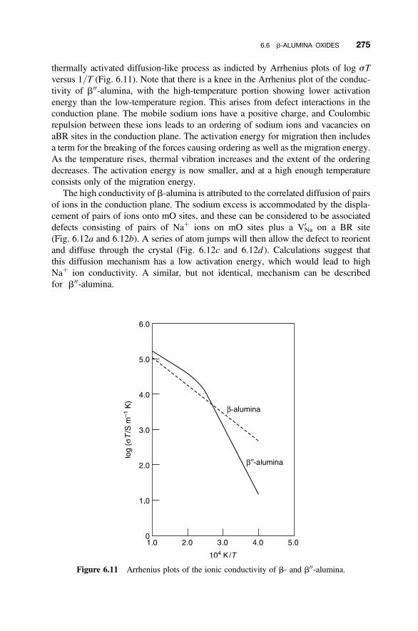
thermally activated diffusion-like process as indicted by Arrhenius plots of log sTversus 1/T (Fig. 6.11). Note that there is a knee in the Arrhenius plot of the conduc-tivity of b00-alumina, with the high-temperature portion showing lower activationenergy than the low-temperature region. This arises from defect interactions in theconduction plane. The mobile sodium ions have a positive charge, and Coulombicrepulsion between these ions leads to an ordering of sodium ions and vacancies onaBR sites in the conduction plane. The activation energy for migration then includesa term for the breaking of the forces causing ordering as well as the migration energy.As the temperature rises, thermal vibration increases and the extent of the orderingdecreases. The activation energy is now smaller, and at a high enough temperatureconsists only of the migration energy.
The high conductivity of b-alumina is attributed to the correlated diffusion of pairsof ions in the conduction plane. The sodium excess is accommodated by the displa-cement of pairs of ions onto mO sites, and these can be considered to be associateddefects consisting of pairs of Naþ ions on mO sites plus a V0
Na on a BR site(Fig. 6.12a and 6.12b). A series of atom jumps will then allow the defect to reorientand diffuse through the crystal (Fig. 6.12c and 6.12d ). Calculations suggest thatthis diffusion mechanism has a low activation energy, which would lead to highNaþ ion conductivity. A similar, but not identical, mechanism can be describedfor b00-alumina.
Figure 6.11 Arrhenius plots of the ionic conductivity of b- and b00-alumina.
6.6 b-ALUMINA OXIDES 275
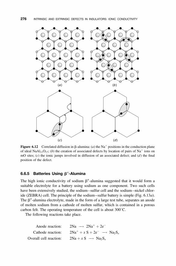
6.6.5 Batteries Using b00-Alumina
The high ionic conductivity of sodium b00-alumina suggested that it would form asuitable electrolyte for a battery using sodium as one component. Two such cellshave been extensively studied, the sodium–sulfur cell and the sodium–nickel chlor-ide (ZEBRA) cell. The principle of the sodium–sulfur battery is simple (Fig. 6.13a).The b00-alumina electrolyte, made in the form of a large test tube, separates an anodeof molten sodium from a cathode of molten sulfur, which is contained in a porouscarbon felt. The operating temperature of the cell is about 3008C.
The following reactions take place.
Anode reaction: 2Na �! 2Naþ þ 2e�
Cathode reaction: 2Naþ þ x Sþ 2e� �! Na2SxOverall cell reaction: 2Naþ x S �! Na2Sx
Figure 6.12 Correlated diffusion in b-alumina: (a) the Naþ positions in the conduction planeof ideal NaAl11O17; (b) the creation of associated defects by location of pairs of Naþ ions onmO sites; (c) the ionic jumps involved in diffusion of an associated defect; and (d ) the finalposition of the defect.
276 INTRINSIC AND EXTRINSIC DEFECTS IN INSULATORS: IONIC CONDUCTIVITY

The phase Na2Sx is sodium polysulfide, a material with a sulfur content of between 3and 5. The anode reaction takes place at the liquid sodium–b00-alumina interface.Here sodium atoms lose an electron and the Naþ ions formed enter the conductionplanes in the electrolyte. The cathode reaction, which occurs at the interfacebetween the b00-alumina and the liquid sulfur forms sodium polysulfides. Despitethe desirable properties of the cell, technical and economic considerations haveacted so as to curtail large-scale commercial production.
The sodium–nickel chloride cell also employs b00-alumina as an electrolyte. As inthe sodium–sulfur cell, the negative electrode is molten sodium metal. The cathode isa porous mixture of Ni metal and the chloride NiCl2. Because the connection betweenthe solid cathode and the solid electrolyte is generally unsatisfactory, a second elec-trolyte, NaAlCl4, with a melting point of 1578C, is also included in the battery. Thecell is operated at a temperature of approximately 3008C. The design concept of thecell is similar to that of the sodium–sulfur battery, but the arrangement of the com-ponents is reversed, with the cathode taking the central position and the liquid sodiumsurrounding the outer face of the b00-alumina electrolyte (Fig. 6.13b).
The following reactions take place:
Anode reaction: 2Na �! 2Naþ þ 2e�
Cathode reaction: 2Naþ þ NiCl2 þ 2e� �! 2NaClþ Ni
Overall cell reaction: 2Naþ NiCl2 �! 2NaClþ Ni
Figure 6.13 Batteries using b00-alumina electrolyte, schematic: (a) the sodium–sulfur celland (b) the sodium–nickel chloride (ZEBRA) cell.
6.6 b-ALUMINA OXIDES 277
As with the sodium–sulfur battery, the extraordinary conductivity of the b00-aluminaelectrolyte, due to the defect structure of the conduction layer, is key to this device.
6.7 ENHANCEMENT OF IONIC CONDUCTIVITY
The features described above that lead to high ionic conductivity are uncommon andmost solids have low ionic conductivity. However, it is possible to enhance ionic con-ductivity if a substantial population of defects can be introduced into the crystal.There are a number of strategies that can be employed to achieve this.
A straightforward method is to incorporate aliovalent impurity ions into thecrystal. These impurities can, in principle, be compensated structurally, by the incor-poration of interstitials or vacancies, or by electronic defects, holes, or electrons. Thepossibility of electronic compensation can be excluded by working with insulatingsolids that contain ions with a fixed valence.
As an example, consider the reaction of a solid with no significant compositionrange, such as CaF2, SrF2, or BaF2, all of which adopt the fluorite structure-type,with a similar aliovalent compound. Doping with an ion of lower valence will fre-quently induce charge compensation via anion vacancies. Reaction of CaF2 withNaF can be written:
NaF (CaF2) �! Na0Ca þ FF þ V†F
The reaction introduces one vacancy into the F2 positions for every Naþ substitutedonto a Ca2þ position. The fluoride ion conductivity is substantially increased fromthat of the parent CaF2. Reaction with an ion of higher valence can also introducesubstantial defect populations and lead to an increase in fluoride ion conductivity.For instance, doping CaF2 with GdF3 yields a stable phase with a stoichiometry span-ning the range CaF2 to (Ca, Gd)F2.4. This range is due to a significant population ofinterstitials:
GdF3(CaF2) �! Gd†Ca þ 2FF þ F 0i
The fluoride ion interstitials again lead to an increase in ionic conductivity. At lowertemperatures this increase is modest because the interstitials aggregate into clusters,thus impeding ionic diffusion. At higher temperatures the clusters tend to dissociate,resulting in a substantial increase in conductivity.
The stabilized zirconia family of oxides, especially calcia-stabilized zirconia, aresolids in which oxide ion conductivity has been increased to the extent that theyare widely used solid electrolytes (Section 1.11.6, Section 4.4.5, and Section 6.8).
In many nonstoichiometric solids high-temperature structures contain disordereddefects, but, as in the previous example, these order or form aggregates at lower temp-eratures. If this aggregation could be suppressed, low-temperature ionic conductivitywould be enhanced. An example of this strategy is provided by compounds with the
278 INTRINSIC AND EXTRINSIC DEFECTS IN INSULATORS: IONIC CONDUCTIVITY
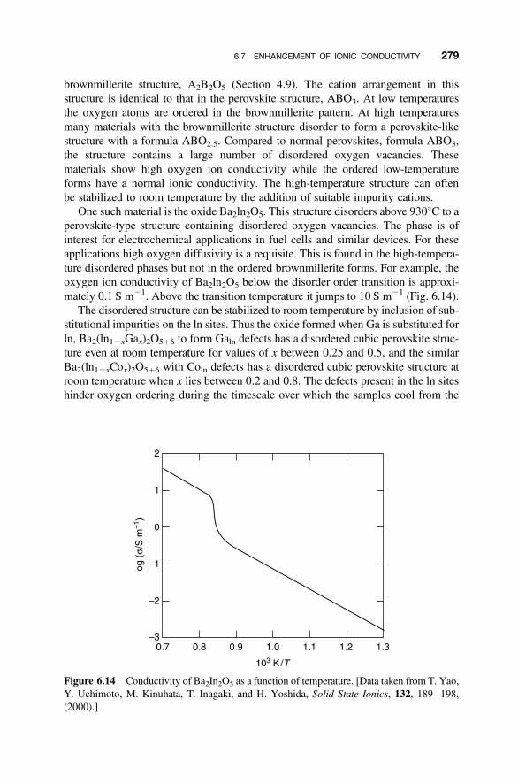
brownmillerite structure, A2B2O5 (Section 4.9). The cation arrangement in thisstructure is identical to that in the perovskite structure, ABO3. At low temperaturesthe oxygen atoms are ordered in the brownmillerite pattern. At high temperaturesmany materials with the brownmillerite structure disorder to form a perovskite-likestructure with a formula ABO2.5. Compared to normal perovskites, formula ABO3,the structure contains a large number of disordered oxygen vacancies. Thesematerials show high oxygen ion conductivity while the ordered low-temperatureforms have a normal ionic conductivity. The high-temperature structure can oftenbe stabilized to room temperature by the addition of suitable impurity cations.
One such material is the oxide Ba2ln2O5. This structure disorders above 9308C to aperovskite-type structure containing disordered oxygen vacancies. The phase is ofinterest for electrochemical applications in fuel cells and similar devices. For theseapplications high oxygen diffusivity is a requisite. This is found in the high-tempera-ture disordered phases but not in the ordered brownmillerite forms. For example, theoxygen ion conductivity of Ba2ln2O5 below the disorder order transition is approxi-mately 0.1 S m21. Above the transition temperature it jumps to 10 S m21 (Fig. 6.14).
The disordered structure can be stabilized to room temperature by inclusion of sub-stitutional impurities on the ln sites. Thus the oxide formed when Ga is substituted forln, Ba2(ln12xGax)2O5þd to form Galn defects has a disordered cubic perovskite struc-ture even at room temperature for values of x between 0.25 and 0.5, and the similarBa2(ln12xCox)2O5þd with Coln defects has a disordered cubic perovskite structure atroom temperature when x lies between 0.2 and 0.8. The defects present in the ln siteshinder oxygen ordering during the timescale over which the samples cool from the
Figure 6.14 Conductivity of Ba2In2O5 as a function of temperature. [Data taken from T. Yao,Y. Uchimoto, M. Kinuhata, T. Inagaki, and H. Yoshida, Solid State Ionics, 132, 189–198,(2000).]
6.7 ENHANCEMENT OF IONIC CONDUCTIVITY 279
preparation temperature. Note that the oxygen composition of these doped materialsis not always exactly 5.0 and depends upon a number of factors, especially the sur-rounding oxygen partial pressure (Chapters 7 and 8).
These two examples illustrate how desirable properties of a solid can be enhancedby selective doping. One of the most important examples follows.
6.8 CALCIA-STABILIZED ZIRCONIA AND RELATED FASTOXYGEN ION CONDUCTORS
6.8.1 Structure and Oxygen Diffusion in Fluorite Structure Oxides
A number of oxides with the fluorite structure are used in solid-state electrochemicalsystems. They have formulas AO2
. xCaO or AO2. xM2O3, where A is typically Zr,
Hf, and Th, and M is usually La, Sm, Y, Yb, or Sc. Calcia-stabilized zirconia,ZrO2.xCaO, typifies the group. The technological importance of thesematerials lies in the fact that they are fast ion conductors for oxygen ions at moderatetemperatures and are stable to high temperatures. This property is enhanced by thefact that there is negligible cation diffusion or electronic conductivity in thesematerials, which makes them ideal for use in a diverse variety of batteries andsensors.
The parent phase is a stoichiometric oxide MO2 with the fluorite structure.Substitution of a lower valence cation for Zr4þ is compensated by oxygen vacancies(Section 1.11.6 and Section 4.4.5). Taking calcia-stabilized zirconia as an example,addition of CaO drops the metal to oxygen ratio to below 2.0, and the formula ofthe oxide becomes CaxZr12xO22x.
CaO (ZrO2) �! Ca20Zr þ V2†O þ Ox
O
Each Ca2þ ion substituent inserted into the structure is balanced by one anionvacancy. Hence, an oxide containing 20 mol % CaO will have 20 mol % oxygenvacancies in the structure. Exactly the same situation holds when zirconia isreacted with the M2O3 oxides. In these cases one oxygen vacancy will form forevery two M3þ cations incorporated, leading to a generalized formula ofM3þ
x Zr12xO22x/2. For example, the reaction between Y2O3 and ZrO2 to formyttria-stabilized zirconia, Y3þ
x Zr12xO22x/2, can be represented as:
x Y2O3(ZrO2) �! 2x Y0Zr þ 3x OO þ xV2†
O
Every two Y3þ substituents inserted into the crystal is balanced by one oxygenvacancy.
The result of the oxygen vacancy population is that the diffusion coefficient ofoxygen ions is increased by many orders of magnitude compared to a normal oxide.
280 INTRINSIC AND EXTRINSIC DEFECTS IN INSULATORS: IONIC CONDUCTIVITY
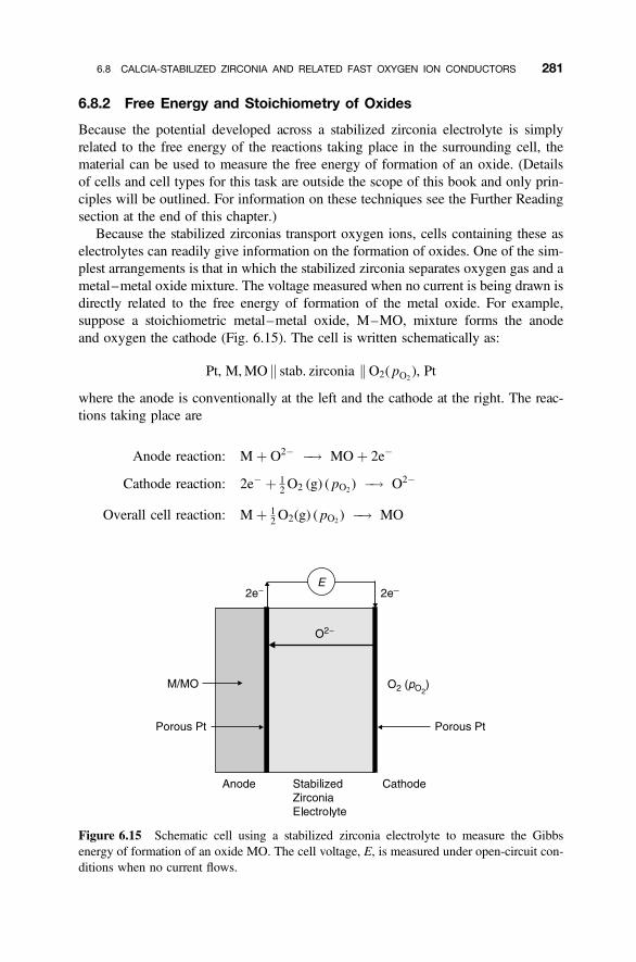
6.8.2 Free Energy and Stoichiometry of Oxides
Because the potential developed across a stabilized zirconia electrolyte is simplyrelated to the free energy of the reactions taking place in the surrounding cell, thematerial can be used to measure the free energy of formation of an oxide. (Detailsof cells and cell types for this task are outside the scope of this book and only prin-ciples will be outlined. For information on these techniques see the Further Readingsection at the end of this chapter.)
Because the stabilized zirconias transport oxygen ions, cells containing these aselectrolytes can readily give information on the formation of oxides. One of the sim-plest arrangements is that in which the stabilized zirconia separates oxygen gas and ametal–metal oxide mixture. The voltage measured when no current is being drawn isdirectly related to the free energy of formation of the metal oxide. For example,suppose a stoichiometric metal–metal oxide, M–MO, mixture forms the anodeand oxygen the cathode (Fig. 6.15). The cell is written schematically as:
Pt, M,MO k stab. zirconia kO2( pO2), Pt
where the anode is conventionally at the left and the cathode at the right. The reac-tions taking place are
Anode reaction: Mþ O2� �! MOþ 2e�
Cathode reaction: 2e� þ 12 O2 (g) ( pO2) �! O2�
Overall cell reaction: Mþ 12 O2(g) ( pO2) �! MO
Figure 6.15 Schematic cell using a stabilized zirconia electrolyte to measure the Gibbsenergy of formation of an oxide MO. The cell voltage, E, is measured under open-circuit con-ditions when no current flows.
6.8 CALCIA-STABILIZED ZIRCONIA AND RELATED FAST OXYGEN ION CONDUCTORS 281
Oxygen is transferred from the high-pressure side (pO2) to the low-pressure (M, MO)side of the cell. Two electrons are transferred via the external circuit from the anode tothe cathode. The Gibbs energy change of the cell reaction, DGr, which is equal to theGibbs energy of formation of MO, is given by:
DGr ¼ �2EF
where E is the cell voltage and F is the Faraday constant. Note that the cell voltage ismeasured when the circuit is open and no current is actually flowing. If the reactantsare in their standard states, the standard Gibbs energy of reaction, DGr
0, is measured.When the cell is set up, the voltage will be constant provided that there is always anadequate amount of M and MO present.
If the oxide is a nonstoichiometric phase MOx, it will still be able to gain oxygen.The cell will be
Pt, MOx k stab. zirconia kO2( pO2), Pt
The reactions taking place are
Anode reaction: MOx þ dO2� �! MOxþd þ 2de�
Cathode reaction: 2de� þ (d=2)O2(g) ( pO2) �! dO2�
Overall cell reaction: MOx þ (d=2)O2(g) ( pO2) �! MOxþd
The voltage measured will now appear to drift as the composition range of the non-stoichiometric oxide is crossed. The voltage will become constant above and belowthe composition range of the oxide. Note that this is closely related to the variation ofoxygen partial pressure over a nonstoichiometric oxide (see Sections 7.3, 7.4).
6.8.3 Oxygen Sensors
One of the most important applications of calcia-stabilized zirconia is as an oxygensensor. In its simplest form, the sensor is just a membrane of stabilized zirconia sep-arating oxygen gas at two different pressures. The high oxygen ion diffusion coeffi-cient will allow ions to move from the high-pressure side to the low-pressure side toeven out the pressure differential. Connecting both sides of the stabilized zirconia viaporous platinum electrodes sets up an electrochemical cell in which the voltage isproportional to the difference between the oxygen pressures. The cell can berepresented as:
Pt, O2( p0O2) k stab. zirconia kO2( p
00O2), Pt
282 INTRINSIC AND EXTRINSIC DEFECTS IN INSULATORS: IONIC CONDUCTIVITY
The reactions taking place are
Anode reaction: 2O2� �! O2(g) ( p0O2)þ 4e�
Cathode reaction: 4e� þ O2(g) ( p00O2) �! 2O2�
Overall cell reaction: O2(g) ( p00O2) �! O2(g) ( p
0O2)
Oxygen is transferred from the high-pressure side (p00O2) to the low-pressure ( p0O2
) sideof the cell. The cell voltage is related to the oxygen pressures by the Nernst equation,Eq. (6.4):
Ecell ¼ E0 � RT
nF
� �ln Q
In this case, the number of electrons transferred, n, is 4 and the appropriate reactionquotient is
Q ¼ p0O2
p00O2
Noting that E0 for this cell reaction is zero:
E ¼ � RT
4F
� �ln
p0O2
p00O2
!
¼ � RT
4F
� �ln
anode pressure (low)cathode pressure (high)
� �
Solving this equation for the oxygen partial pressure gives
p0O2¼ p00O2
exp�4ERT
� �
The high-pressure p00O2is taken as a reference pressure so that the unknown pressure
p0O2is readily determined. These equations are often seen in the form:
E ¼ þ RT
4F
� �ln
p 00O2
p0O2
!
E ¼ þ RT
4F
� �ln
cathode pressure (high)anode pressure (low)
� �
where R is the gas constant, T the temperature (K), and the oxygen pressures aremeasured in atmospheres.
6.8 CALCIA-STABILIZED ZIRCONIA AND RELATED FAST OXYGEN ION CONDUCTORS 283
The same principles apply for oxygen in solutions as diverse as liquid metals orblood. Because the oxygen is dissolved, the voltage measured depends upon theactivity of the oxygen in the solution. For low concentrations, the activity can beapproximated to the concentration, hence:
E ¼ � RT
4F
� �ln
[O2(solution)]pO2(reference)
�
where [O2 (solution)] is the concentration of the oxygen molecules, which is assumedto be lower than the reference pressure. If pO2 is taken as 1 atm, the equation becomes
E ¼ � RT
4F
� �ln [O2(solution)]
These equations consider the oxygen present as molecules in solution. If theoxygen exists as atoms in solution, only two electrons are needed in the cell equationand the potential is given by:
E ¼ � RT
2F
� �ln [O (solution)]
The design of the sensor depends upon its ultimate use. For high-temperatureapplications a stabilized zirconia tube coated inside and outside with porous plati-num forms a suitable design. The tube can be used directly as an oxygen meter ifp 00O2
is a standard pressure, such as 1 atm of oxygen or else the pressure ofoxygen in air, which is approximately 0.21 atm. Such a system is utilized tomonitor the exhaust oxygen content, and thus fuel efficiency, of a car engine.The coated zirconia tube is arranged to project into the exhaust stream of theengine (Fig. 6.16). Using air as the standard oxygen pressure, the output voltageof the sensor is directly related to the stoichiometry of the air–fuel mixture. Thecell voltage may be used to alter the engine input fuel–air mix automatically to opti-mize engine efficiency.
6.8.4 Oxygen Pumps and Coulometric Titrations
If a current is passed through a cell using a stabilized zirconia electrolyte, oxygen istransferred from one side of the electrolyte to the other. Thus, these cells can be usedas electrochemical pumps capable of delivering or removing very precisely monitoredamounts of oxygen. The amount of oxygen transferred can be calculated by an appli-cation of Faraday’s law of electrolysis. The number of moles of O22 transferredduring cell operation, dO, is
dO ¼ It
2F
284 INTRINSIC AND EXTRINSIC DEFECTS IN INSULATORS: IONIC CONDUCTIVITY
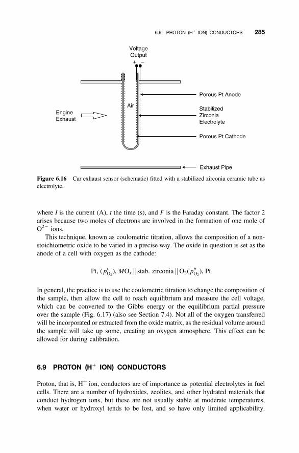
where I is the current (A), t the time (s), and F is the Faraday constant. The factor 2arises because two moles of electrons are involved in the formation of one mole ofO22 ions.
This technique, known as coulometric titration, allows the composition of a non-stoichiometric oxide to be varied in a precise way. The oxide in question is set as theanode of a cell with oxygen as the cathode:
Pt, ( p0O2), MOx k stab. zirconia kO2( p
00O2), Pt
In general, the practice is to use the coulometric titration to change the composition ofthe sample, then allow the cell to reach equilibrium and measure the cell voltage,which can be converted to the Gibbs energy or the equilibrium partial pressureover the sample (Fig. 6.17) (also see Section 7.4). Not all of the oxygen transferredwill be incorporated or extracted from the oxide matrix, as the residual volume aroundthe sample will take up some, creating an oxygen atmosphere. This effect can beallowed for during calibration.
6.9 PROTON (H1 ION) CONDUCTORS
Proton, that is, Hþ ion, conductors are of importance as potential electrolytes in fuelcells. There are a number of hydroxides, zeolites, and other hydrated materials thatconduct hydrogen ions, but these are not usually stable at moderate temperatures,when water or hydroxyl tends to be lost, and so have only limited applicability.
Figure 6.16 Car exhaust sensor (schematic) fitted with a stabilized zirconia ceramic tube aselectrolyte.
6.9 PROTON (Hþ ION) CONDUCTORS 285
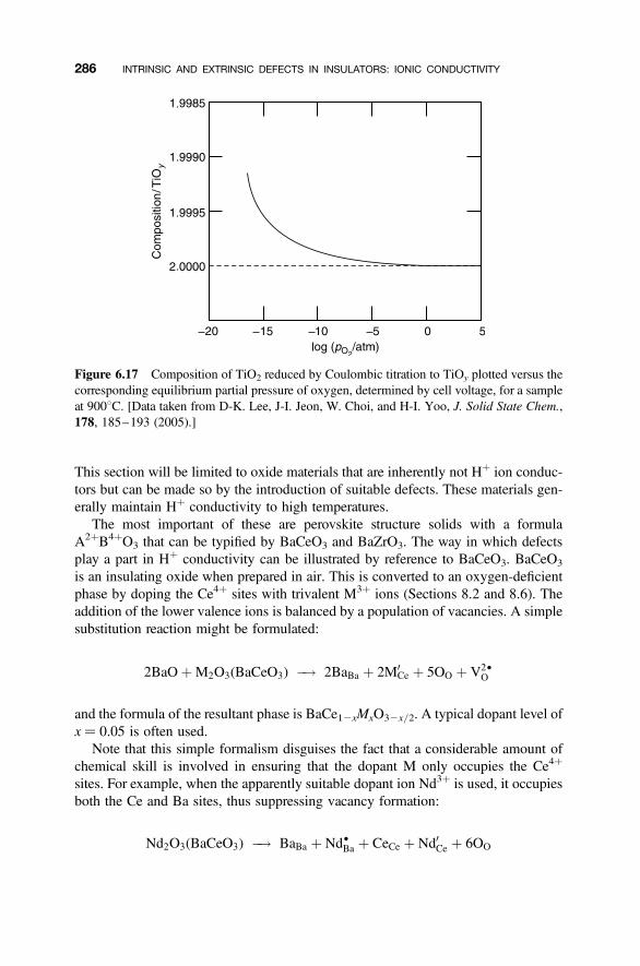
This section will be limited to oxide materials that are inherently not Hþ ion conduc-tors but can be made so by the introduction of suitable defects. These materials gen-erally maintain Hþ conductivity to high temperatures.
The most important of these are perovskite structure solids with a formulaA2þB4þO3 that can be typified by BaCeO3 and BaZrO3. The way in which defectsplay a part in Hþ conductivity can be illustrated by reference to BaCeO3. BaCeO3
is an insulating oxide when prepared in air. This is converted to an oxygen-deficientphase by doping the Ce4þ sites with trivalent M3þ ions (Sections 8.2 and 8.6). Theaddition of the lower valence ions is balanced by a population of vacancies. A simplesubstitution reaction might be formulated:
2BaOþM2O3(BaCeO3) �! 2BaBa þ 2M0Ce þ 5OO þ V2†
O
and the formula of the resultant phase is BaCe12xMxO32x/2. A typical dopant level ofx ¼ 0.05 is often used.
Note that this simple formalism disguises the fact that a considerable amount ofchemical skill is involved in ensuring that the dopant M only occupies the Ce4þ
sites. For example, when the apparently suitable dopant ion Nd3þ is used, it occupiesboth the Ce and Ba sites, thus suppressing vacancy formation:
Nd2O3(BaCeO3) �! BaBa þ Nd†Ba þ CeCe þ Nd0Ce þ 6OO
Figure 6.17 Composition of TiO2 reduced by Coulombic titration to TiOy plotted versus thecorresponding equilibrium partial pressure of oxygen, determined by cell voltage, for a sampleat 9008C. [Data taken from D-K. Lee, J-I. Jeon, W. Choi, and H-I. Yoo, J. Solid State Chem.,178, 185–193 (2005).]
286 INTRINSIC AND EXTRINSIC DEFECTS IN INSULATORS: IONIC CONDUCTIVITY
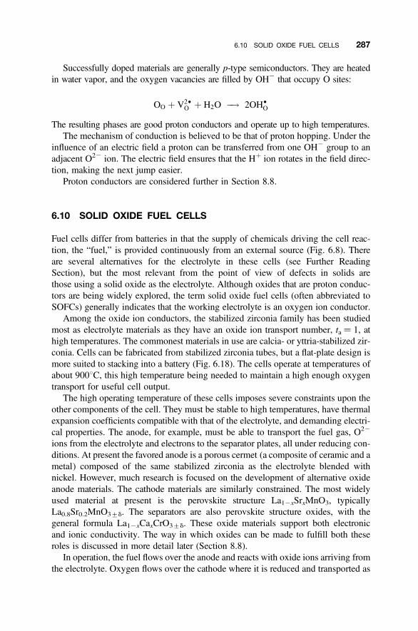
Successfully doped materials are generally p-type semiconductors. They are heatedin water vapor, and the oxygen vacancies are filled by OH2 that occupy O sites:
OO þ V2†O þ H2O �! 2OH†
O
The resulting phases are good proton conductors and operate up to high temperatures.The mechanism of conduction is believed to be that of proton hopping. Under the
influence of an electric field a proton can be transferred from one OH2 group to anadjacent O22 ion. The electric field ensures that the Hþ ion rotates in the field direc-tion, making the next jump easier.
Proton conductors are considered further in Section 8.8.
6.10 SOLID OXIDE FUEL CELLS
Fuel cells differ from batteries in that the supply of chemicals driving the cell reac-tion, the “fuel,” is provided continuously from an external source (Fig. 6.8). Thereare several alternatives for the electrolyte in these cells (see Further ReadingSection), but the most relevant from the point of view of defects in solids arethose using a solid oxide as the electrolyte. Although oxides that are proton conduc-tors are being widely explored, the term solid oxide fuel cells (often abbreviated toSOFCs) generally indicates that the working electrolyte is an oxygen ion conductor.
Among the oxide ion conductors, the stabilized zirconia family has been studiedmost as electrolyte materials as they have an oxide ion transport number, ta ¼ 1, athigh temperatures. The commonest materials in use are calcia- or yttria-stabilized zir-conia. Cells can be fabricated from stabilized zirconia tubes, but a flat-plate design ismore suited to stacking into a battery (Fig. 6.18). The cells operate at temperatures ofabout 9008C, this high temperature being needed to maintain a high enough oxygentransport for useful cell output.
The high operating temperature of these cells imposes severe constraints upon theother components of the cell. They must be stable to high temperatures, have thermalexpansion coefficients compatible with that of the electrolyte, and demanding electri-cal properties. The anode, for example, must be able to transport the fuel gas, O22
ions from the electrolyte and electrons to the separator plates, all under reducing con-ditions. At present the favored anode is a porous cermet (a composite of ceramic and ametal) composed of the same stabilized zirconia as the electrolyte blended withnickel. However, much research is focused on the development of alternative oxideanode materials. The cathode materials are similarly constrained. The most widelyused material at present is the perovskite structure La12xSrxMnO3, typicallyLa0.8Sr0.2MnO3+d. The separators are also perovskite structure oxides, with thegeneral formula La12xCaxCrO3+d. These oxide materials support both electronicand ionic conductivity. The way in which oxides can be made to fulfill both theseroles is discussed in more detail later (Section 8.8).
In operation, the fuel flows over the anode and reacts with oxide ions arriving fromthe electrolyte. Oxygen flows over the cathode where it is reduced and transported as
6.10 SOLID OXIDE FUEL CELLS 287
ions from the high oxygen pressure cathode region to the low oxygen pressure anoderegion. The cell reactions depend upon the fuel. Typically these are
Anode reaction: H2(g)þ O2� �! H2O(g)þ 2e�
CO(g)þ O2� �! CO2(g)þ 2e�
CH4(g)þ 4O2� �! 2H2O(g)þ CO2(g)þ 8e�
Cathode reaction: O2(g)þ 4e� �! 2O2�
Typical cell reaction: 2H2(g)þ O2(g) �! 2H2O(g)
The fact that these cells can operate with many different fuels is one advantage ofhigh-temperature operation. However, there is at present much research directedtoward lowering the operating temperature for cost reasons.
6.11 ANSWERS TO INTRODUCTORY QUESTIONS
Why are ionic conductors vital for battery operation?
A battery is a self-contained unit in which chemical reactants undergo a spon-taneous chemical reaction and the resulting chemical energy is transformed into
Figure 6.18 Schematic diagram of a fuel cell stack using a stabilized zirconia electrolyte.
288 INTRINSIC AND EXTRINSIC DEFECTS IN INSULATORS: IONIC CONDUCTIVITY
an external electric current. (Technically, a battery is a single galvanic cell orseveral connected together so as to increase power output.) In a battery, electronsgenerated as a result of the internal cell chemical reaction leave via the anode,cross an external circuit, doing useful work, such as powering a computer, andthen reenter the battery via the cathode. The reaction is completed by a transferof ions across the electrolyte from the anode region to the cathode region orvice versa.
In order for the transformation of chemical energy to external electrical energyto occur, it is essential that the electrons cannot traverse the battery internally. Forthis reason the electrolyte must be an insulator. However, for the reaction to con-tinue, charge transport is needed, and for this to occur the electrolyte must be ableto transfer ions. Thus, the electrolyte must consist of an insulating material with ahigh ionic conductivity for one ion taking part in the cell reaction.
How does an oxygen sensor work?
The principle of an oxygen sensor is similar to that of a battery. A battery uses aspontaneous chemical reaction to produce an external electric current. In anoxygen sensor the voltage generated by the reaction is used as a measure ofoxygen concentration compared to a standard oxygen pressure, such as pureoxygen or oxygen in air. The sensor consists of an inert metal anode andcathode separated by a solid electrolyte that is a good O22 ion conductor. Forthis calcia- or yttria-stabilized zirconia is generally used.
The voltage generated by a battery or fuel cell, the cell potential, is simplyrelated to the Gibbs energy of the cell reaction, DGr, by:
DGr ¼ �nEcellF
where Ecell is the cell potential, F is the Faraday constant, and n is the number ofmoles of electrons that migrate from anode to cathode in the cell reaction. Thepotential generated by a cell is dependent upon the concentration of the com-ponents present at the anode and cathode. For an oxygen sensor, this is
Ecell ¼ � RT
4F
� �ln
p0O2
p00O2
" #
¼ � RT
4F
� �ln
anode pressure (low)cathode pressure (high)
� �
where Ecell is the cell voltage, R is the gas constant, T the temperature (K), and F isthe Faraday constant. Solving this equation for the oxygen partial pressure gives
p0O2¼ p00O2
exp�4ERT
� �
6.11 ANSWERS TO INTRODUCTORY QUESTIONS 289
The high pressure p00O2is taken as a reference pressure, such as the oxygen partial
pressure in air. A measurement of the cell voltage, together with knowledge of thetemperature allows the unknown pressure p0O2
to be determined.
What is a fuel cell?
A fuel cell is a form of battery. An ordinary battery consists of internal reactants thatare converted into electrical energy, whereas in a fuel cell the chemical reactants aresupplied from an external source. There are several designs of fuel cell, one of whichis the solid oxide fuel cell (SOFC). These employ calcia- or yttria-stabilized zirco-nia. The cells operate at temperatures of about 9008C, this high temperature beingneeded to maintain a high enough oxygen transport for useful cell output.
In operation, the fuel flows over the anode and reacts with oxide ions arrivingfrom the electrolyte. Oxygen flows over the cathode where it is reduced and trans-ported as ions from the high oxygen pressure cathode region to the low oxygenpressure anode region. The cell reactions depend upon the fuel. Typically these are
Anode reaction: H2(g)þ O2� �! H2O(g)þ 2e�
CO(g)þ O2� �! CO2(g)þ 2e�
CH4(g)þ 4O2� �! 2H2O(g)þ CO2(g)þ 8e�
Cathode reaction: O2(g)þ 4e� �! 2O2�
Typical cell reaction: 2H2(g)þ O2(g) �! 2H2O(g)
The fact that these cells can operate with many different fuels is one advantage ofhigh-temperature operation. However, there is at present much research directedtoward lowering the operating temperature as much as possible.
PROBLEMS AND EXERCISES
Quick Quiz
1. Assuming identical conductivity mechanisms, the conductivity of a solid will begreatest if the cation charge carriers are:
(a) Monovalent
(b) Divalent
(c) Trivalent
2. One-fourth of the current is carried by anions across a solid conducting by way ofboth anions and cations. The transport number for anions is:
(a) 0.25
(b) 20.25
(c) 20.75
290 INTRINSIC AND EXTRINSIC DEFECTS IN INSULATORS: IONIC CONDUCTIVITY
3. The activation energy for ionic conductivity is derived from a plot of:
(a) log s vs. 1/T
(b) log(sT ) vs. 1/T
(c) log s vs. 1/(sT )
4. The ratio of the tracer diffusion coefficient to the diffusion coefficient obtainedfrom ionic conductivity measurements is called:
(a) The Nernst–Einstein ratio
(b) The Haven ratio
(c) The correlation ratio
5. The bulk and grain boundary conductivities of a ceramic sample can be separatedusing the impedance, Z, by plotting:
(a) Z0 versus Z00
(b) Z0 versus v(c) Z00 versus v
6. A fast ion conductor with a molten sublattice contains:
(a) A liquid layer of cations
(b) A molten layer of metal atoms
(c) Rapidly diffusing cations
7. The electrolyte b-alumina conducts using:
(a) Al3þ ions
(b) O22 ions
(c) Naþ ions
8. The ZEBRA cell uses the reaction between:
(a) Liquid sodium and sulfur
(b) Liquid sodium and nickel chloride
(c) Liquid sodium and b00-alumina
9. The electrolyte in an oxygen sensor is:
(a) Stabilized zirconia
(b) b-alumina
(c) Doped BaCeO3
10. A perovskite structure oxide such as BaZrO4 can be made into a protonconductor by doping so as to introduce:
(a) Cation vacancies
(b) Anion vacancies
(c) Hþ interstitials
PROBLEMS AND EXERCISES 291
Calculations and Questions
1. Estimate the activation energy for ionic conductivity in the Lu2Ti2O7 phaseillustrated in Figure 6.5b.
2. Estimate (a) the energy of migration and (b) the energy of aggregation of VO
defects in CeO2 doped with 10 mol % Nd2O3 using the data in Figure 6.6.
3. The phase EuNbO4 can be made nonstoichiometric by doping with Nb2O5. Theionic conductivity, tO � 1, increases with dopant content, but the slope of the sTversus 1/T plots does not change. (a) Write a defect equation for the reactionof Nb2O5 with EuNbO4, assuming that Nb does not occupy interstitial positions.(b) Explain why the conductivity increases with dopant concentration. (c)Estimate the activation energy for O22 ion conductivity using the followingdata for Eu0.77NbO3.655.
log sT Temperature/8C
23.25 56023.62 50023.98 45724.3 41224.63 36025.19 315
Data adapted from K. Toda et al., Solid State Ionics, 136–137,25–30 (2000).
4. The values of the conductivity due to Naþ ions in a glass are given in the follow-ing table. (a) Estimate the activation energy for conductivity. The conductivity at700 K is 0.00316 S m21. (b) Estimate the value of the diffusion coefficient Ds atthis temperature if the concentration of Naþ ions is 7.2 � 1027 m23. (c) Using thedata in Chapter 5, Question 5, calculate the Haven ratio at this temperature.
Conductivity/S m21 Temperature/K
0.0316 8030.0071 7370.0011 6530.00013 5720.0000079 490
Data adapted from E. M. Tanguep Njiokop and H. Mehrer,Solid State Ionics, 177, 2839–2844 (2006).
5. Why is it only possible to replace 50% of the Na ions in b-alumina by M2þ ionsand by 33% M3þ ions? If more than these quantities were introduced, whatwould be the consequences for the defect structure of the phases?
292 INTRINSIC AND EXTRINSIC DEFECTS IN INSULATORS: IONIC CONDUCTIVITY
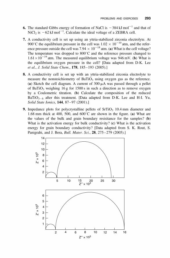
6. The standard Gibbs energy of formation of NaCl is 2384 kJ mol21 and that ofNiCl2 is 262 kJ mol21. Calculate the ideal voltage of a ZEBRA cell.
7. A conductivity cell is set up using an yttria-stabilized zirconia electrolyte. At9008C the equilibrium pressure in the cell was 1.02 � 10210 atm, and the refer-ence pressure outside the cell was 7.94 � 10218 atm. (a) What is the cell voltage?The temperature was dropped to 8008C and the reference pressure changed to1.61�10219 atm. The measured equilibrium voltage was 946 mV. (b) What isthe equilibrium oxygen pressure in the cell? [Data adapted from D-K. Leeet al., J. Solid State Chem., 178, 185–193 (2005).]
8. A conductivity cell is set up with an yttria-stabilized zirconia electrolyte tomeasure the nonstoichiometry of BaTiO3 using oxygen gas as the reference.(a) Sketch the cell diagram. A current of 300 mA was passed through a pelletof BaTiO3 weighing 16 g for 1500 s in such a direction as to remove oxygenby a Coulometric titration. (b) Calculate the composition of the reducedBaTiO32d after this treatment. [Data adapted from D-K. Lee and H-I. Yu,Solid State Ionics, 144, 87–97 (2001).]
9. Impedance plots for polycrystalline pellets of SrTiO3 10.4 mm diameter and1.68 mm thick at 400, 500, and 6008C are shown in the figure. (a) What arethe values of the bulk and grain boundary resisitance for the samples? (b)What is the activation energy for bulk conductivity? (c) What is the activationenergy for grain boundary conductivity? [Data adapted from S. K. Rout, S.Panigrahi, and J. Bera, Bull. Mater. Sci., 28, 275–279 (2005).]
PROBLEMS AND EXERCISES 293
10. (a) Calculate the diffusion coefficient of Cuþ ions in Cu2O at 10008C fromthe conductivity: 0.19 S m21. The measured Cuþ tracer diffusion coefficientin Cu2O at this temperature is 2.8 � 10212 m2 s21. (b) What is the Havenratio? The unit cell of Cu2O is cubic, a ¼ 0.4267 nm, the unit cell contents,Z ¼ 2Cu2O.
11. The diffusion coefficient of Ca2þ in CaO is 3 � 10215 m2 s21 at 10008C. (a)Estimate the conductivity due to Ca2þ at this temperature. The total conductivityis measured as 8�1024 S m21. (b) What does a comparison of these valuessuggest? The density of CaO is 3300 kg m23.
FURTHER READING
General sources covering selected parts of the chapter are:
R. M. Dell and D. A. J. Rand, Understanding Batteries, Royal Society of ChemistryCambridge, United Kingodm, 2001.
N. E. W. de Reca and J. I. Franco, Crystallographic Aspects of Solid Electrolytes Cryst. Rev., 2,241 (1992).
M. Greenblatt, Ionic Conductors, in Encyclopedia of Inorganic Chemistry, 2nd ed., Wiley,Hoboken, NJ, 2006.
R. E. Newnham Structure-Property Relationships in Sensors Cryst. Rev., 1, 253 (1988).
F. W. Poulsen, N. H. Andersen, K. Clausen, S. Skaarup, and O. T. Sørensen Eds., Fast Ion andMixed Conductors, Risø international Symposium on Metallurgy and Materials Science,Risø National Laboratory, Denmark, 1985.
H. Rickert, Solid State Electrochemistry, in Treatise on Solid State Chemistry Vol. 4,N. B. Hannay, Ed., Plenum, New York, 1976, Chapter 6.
Measurement of Impedance:
Argilent Technologies Impedance Measurement Handbook, at www.argilent.com (2006).
Fuel cells:
M. Winter and R. J. Brodd Chem. Rev., 104, 4245–4269 (2004).
294 INTRINSIC AND EXTRINSIC DEFECTS IN INSULATORS: IONIC CONDUCTIVITY

The first paper describing electrochemical use of b0-alumina is:
Y. F. Y. Yao and J. T. Kummer, J. Inorg. Nucl. Chem., 29, 2453 (1967).
For interesting sidelights on the Cole–Cole plot, see:
A. B. Pippard Response and Stability, Cambridge University Press, Cambridge, UnitedKingdom, 1985, Chapter 3, especially, pp. 57–60.
Fuel cells and batteries are surveyed by:
M. Winter and M. J. Brodd Chem. Rev., 104, 4245–4269 (2004).
FURTHER READING 295

&CHAPTER 7
Nonstoichiometry and IntrinsicElectronic Conductivity
How does composition variation change the electronic properties of a solid?
Why does the electronic conductivity of a nonstoichiometric solid change as thesurrounding partial pressure changes?
What information does a Brouwer diagram display?
7.1 NONSTOICHIOMETRY AND ELECTRONIC DEFECTS IN OXIDES
7.1.1 Electronic and Ionic Compensation
Significant changes in electronic properties of a solid can result from compositionvariation. The examples chosen to illustrate this will mainly be drawn from oxidesas these have been studied in most detail. In this chapter, pure (single-phase)solids will be described—intrinsic conductivity—while in the following chapterimpurities and doping—that is, extrinsic conductivity—will be considered. Notethat the principles described below apply equally well to doped crystals—the divisioninto two chapters is a matter of convenience.
Chemical intuition can provide good guidance as to the electronic changes thatnonstoichiometry brings about in oxides. Broadly speaking, materials in which allof the atoms have a fixed valence show little variation of composition at ordinarytemperatures and are electrical insulators. These solids are typified by the oxidesMgO, Al2O3, and MgAl2O4, which are stable to high temperatures in air. Anysmall variation in composition in these solids is compensated by the introductionof vacancies or interstitials. On the other hand, oxides in which the valence canchange tend to show composition variation and associated electronic conductivity.For example, nickel oxide, NiO, a green insulating powder, or strontium titanate,SrTiO3, a colorless ferroelectric solid, can be changed into electronic conductorsby increasing or decreasing the amount of oxygen relative to the amount of metalpresent, to form a nonstoichiometric compound. Indeed, strontium titanate caneven be made superconducting. The difference between the transition-metal
Defects in Solids, by Richard J. D. TilleyCopyright # 2008 John Wiley & Sons, Inc.
297
compounds and oxides such as MgO is that the composition change is offset at a rela-tively low energy cost by a change of valence, that is, by electronic compensation.The change in composition can be conveniently divided into two types, compositionchange that results in metal excess solids and composition change that results in metaldeficit phases.
7.1.2 Metal-Excess Phases
Taking as an example an ionic oxide MO, this material can be made into a metal-excess nonstoichiometric material by the loss of oxygen. As only neutral oxygenatoms are removed from the crystal, each anion removed will leave two electronsbehind, which leads to electronic conductivity. The oxygen loss can be incorporatedas oxygen vacancies to give a nonstoichiometric oxide with a formula MO12x, or thestructure can assimilate the loss and compensate by the introduction of cation inter-stitials to give a formula M1þxO.
The introduction of anion vacancies can be written:
x OO(MO) O x2 O2 þ x V2†
O þ 2e0
The electrons might be free or else may be associated with variable valence cations,chemically transforming M2þ ions (MM) to Mþ ions (M0
M):
x MO O x2 O2 þ x V2†
O þ xM0M
The introduction of interstitial metal can be written:
x MO O x2 O2 þ xM2†
i þ 2 x e0
where the interstitial cation has two effective positive charges, Mi2†. As before, if the
cations can accept a lower valence, interstitial Mþ ions can form:
2x MO O xO2 þ 2xM†i þ 2x e0
In both these materials, nonstoichiometry results in the introduction of electrons.The electronic properties will depend upon how strongly the additional electrons arebound to other species. Generally, though, if sufficient energy is supplied to makethem move from one cation to another, the crystal will be able to conduct electricity.Often light will provide the energy needed to allow the electrons to migrate and thematerial shows photoconductivity. When thermal energy is sufficient to free the elec-trons, the electronic conductivity will increase with increasing temperature and thesolids are n-type semiconductors. Both ZnO and CdO are believed to becomemetal excess via the introduction of metal interstitials, although the defect speciespresent in both these oxides is more complex than the simple scheme presentedabove (Sections 1.11.5 and 4.3.5).
Exactly the same principles apply to oxides that are more complex from a compo-sitional point of view. In these materials, however, there is a greater degree of
298 NONSTOICHIOMETRY AND INTRINSIC ELECTRONIC CONDUCTIVITY
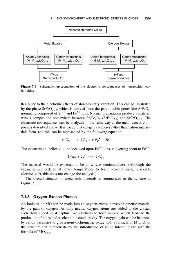
flexibility to the electronic effects of stoichiometry variation. This can be illustratedby the phase SrFeO2.75, which is derived from the parent cubic perovskite SrFeO3,nominally composed of Sr2þ and Fe4þ ions. Normal preparations produce a materialwith a composition somewhere between Sr2Fe2O5 (SrFeO2.5) and SrFeO2.75. Theelectronic consequences can be analyzed in the same way as the metal excess com-pounds described above. It is found that oxygen vacancies rather than cation intersti-tials form, and this can be represented by the following equation:
x OO �! x2 O2 þ x V2†
o þ 2e0
The electrons are believed to be localized upon Fe4þ ions, converting them to Fe3þ:
2FeFe þ 2e0 �! 2Fe0Fe
The material would be expected to be an n-type semiconductor. (Although thevacancies are ordered at lower temperatures to form brownmillerite, Sr2Fe2O5
(Section 4.9), this does not change the analysis.)The overall situation in metal-rich materials is summarized in the scheme in
Figure 7.1.
7.1.3 Oxygen-Excess Phases
An ionic oxide MO can be made into an oxygen-excess nonstoichiometric materialby the gain of oxygen. As only neutral oxygen atoms are added to the crystal,each atom added must capture two electrons to form anions, which leads to theproduction of holes and to electronic conductivity. The oxygen gain can be balancedby cation vacancies to give a nonstoichiometric oxide with a formula of M12xO, orthe structure can compensate by the introduction of anion interstitials to give theformula of MO1þx.
Figure 7.1 Schematic representation of the electronic consequences of nonstoichiometryin oxides.
7.1 NONSTOICHIOMETRY AND ELECTRONIC DEFECTS IN OXIDES 299
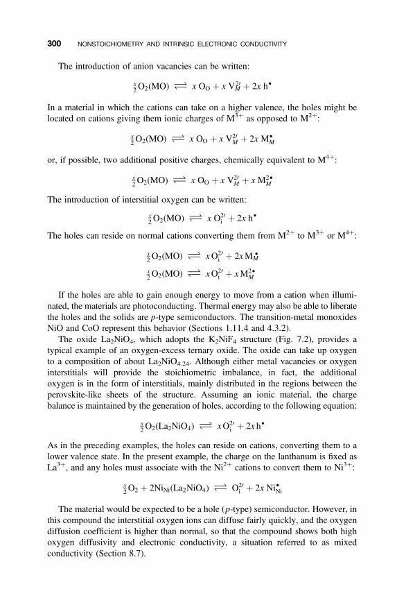
The introduction of anion vacancies can be written:
x2 O2(MO) O x OO þ x VM
20 þ 2x h†
In a material in which the cations can take on a higher valence, the holes might belocated on cations giving them ionic charges of M3þ as opposed to M2þ:
x2 O2(MO) O x OO þ x V20
M þ 2x M†M
or, if possible, two additional positive charges, chemically equivalent to M4þ:
x2 O2(MO) O x OO þ x V20
M þ x M2†M
The introduction of interstitial oxygen can be written:
x2 O2(MO) O x O20
i þ 2x h†
The holes can reside on normal cations converting them from M2þ to M3þ or M4þ:
x2 O2(MO) O xO20
i þ 2xMM†
x2 O2(MO) O xO20
i þ xM2†M
If the holes are able to gain enough energy to move from a cation when illumi-nated, the materials are photoconducting. Thermal energy may also be able to liberatethe holes and the solids are p-type semiconductors. The transition-metal monoxidesNiO and CoO represent this behavior (Sections 1.11.4 and 4.3.2).
The oxide La2NiO4, which adopts the K2NiF4 structure (Fig. 7.2), provides atypical example of an oxygen-excess ternary oxide. The oxide can take up oxygento a composition of about La2NiO4.24. Although either metal vacancies or oxygeninterstitials will provide the stoichiometric imbalance, in fact, the additionaloxygen is in the form of interstitials, mainly distributed in the regions between theperovskite-like sheets of the structure. Assuming an ionic material, the chargebalance is maintained by the generation of holes, according to the following equation:
x2 O2(La2NiO4) O xO20
i þ 2x h†
As in the preceding examples, the holes can reside on cations, converting them to alower valence state. In the present example, the charge on the lanthanum is fixed asLa3þ, and any holes must associate with the Ni2þ cations to convert them to Ni3þ:
x2 O2 þ 2NiNi(La2NiO4) O O20
i þ 2x Ni†Ni
The material would be expected to be a hole (p-type) semiconductor. However, inthis compound the interstitial oxygen ions can diffuse fairly quickly, and the oxygendiffusion coefficient is higher than normal, so that the compound shows both highoxygen diffusivity and electronic conductivity, a situation referred to as mixedconductivity (Section 8.7).
300 NONSTOICHIOMETRY AND INTRINSIC ELECTRONIC CONDUCTIVITY
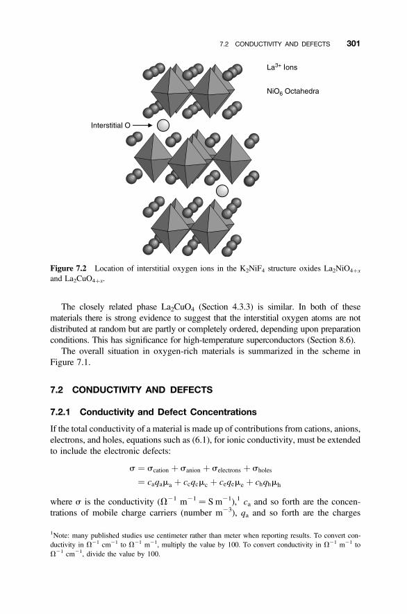
The closely related phase La2CuO4 (Section 4.3.3) is similar. In both of thesematerials there is strong evidence to suggest that the interstitial oxygen atoms are notdistributed at random but are partly or completely ordered, depending upon preparationconditions. This has significance for high-temperature superconductors (Section 8.6).
The overall situation in oxygen-rich materials is summarized in the scheme inFigure 7.1.
7.2 CONDUCTIVITY AND DEFECTS
7.2.1 Conductivity and Defect Concentrations
If the total conductivity of a material is made up of contributions from cations, anions,electrons, and holes, equations such as (6.1), for ionic conductivity, must be extendedto include the electronic defects:
s ¼ scation þ sanion þ selectrons þ sholes
¼ caqama þ ccqcmc þ ceqeme þ chqhmh
where s is the conductivity (V21 m21 ¼ S m21),1 ca and so forth are the concen-trations of mobile charge carriers (number m23), qa and so forth are the charges
Figure 7.2 Location of interstitial oxygen ions in the K2NiF4 structure oxides La2NiO4þx
and La2CuO4þx.
1Note: many published studies use centimeter rather than meter when reporting results. To convert con-ductivity in V21 cm21 to V21 m21, multiply the value by 100. To convert conductivity in V21 m21 toV21 cm21, divide the value by 100.
7.2 CONDUCTIVITY AND DEFECTS 301
on the particles (C), and ma and so forth are the mobilities of the particles (m2 V21
s21). The conductivity, therefore, is directly proportional to the number of defectspresent. (Electrical behavior of semiconductor devices is manipulated in this way.)
The fraction of the conductivity that can be apportioned to each charge carrier, itstransport number, is defined by
sc ¼ tcs
sa ¼ tas
se ¼ tes
sh ¼ ths
where sc, sa, se, and sh are the conductivities of the cations, anions, electrons, andholes, and tc, ta, te, and th are the transport numbers for cations, anions, electrons, andholes, respectively. As can be seen from these relationships:
s ¼ s(tc þ ta þ te þ th)
tc þ ta þ te þ th ¼ 1
7.2.2 Holes, Electrons, and Valence
The viewpoint presented above suggests that electrons and holes in oxide semicon-ductors are located (usually) on cations that can take a variable valence, Ni2þ/Ni3þ or Cu2þ/Cu3þ, for instance. In such a model the electronic conductivity cantake place by way of a hopping mechanism in which the charges jump from onesite to another in a process akin to that of diffusion2 (Chapters 5 and 6). However,it is by no means easy to state categorically whether such localization of chargestates fits the experimental observations. Currently, the favored method of investi-gating this problem is via calculation, frequently using quantum mechanicalmethods. To illustrate the situation, two examples follow, the apparently simpleoxides nickel oxide, NiO, and zinc oxide, ZnO.
Nickel oxide is a classical nonstoichiometric oxide that has been studied intensivelyover the last 30–40 years. Despite this, there is still uncertainty about the electronicnature of the defects present. It is well accepted that the material is an oxygen-excessphase, and the structural defects present are vacancies on cation sites. Although it iscertain that the electronic conductivity is by way of holes, there is still hesitancyabout the best description of the location of these charge carriers.
2There are a number of ways in which hopping conductivity can be treated theoretically. In semiconductorphysics, the best known approach is Mott’s variable range hopping model. This applies to disorderedsystems that have localized states within the band gap. The low-temperature conductivity in such asystem is proportional to exp[-(T0/T )
1/4], where T is the temperature and T0 a constant. The Mott lawhas been found to account well for the conductivity of doped semiconductors at low temperatures. Thesame approach is not usually applicable when hopping involves valence state alternation, as this tendsto occur at higher temperatures. In such cases considering the conductivity to be identical to atomic diffu-sion offers an alternative approach.
302 NONSTOICHIOMETRY AND INTRINSIC ELECTRONIC CONDUCTIVITY
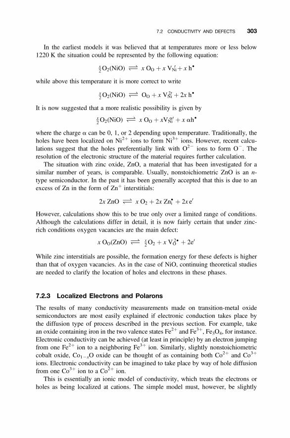
In the earliest models it was believed that at temperatures more or less below1220 K the situation could be represented by the following equation:
x2 O2(NiO) O x OO þ x VNi
0 þ x h†
while above this temperature it is more correct to write
x2 O2(NiO) O OO þ x VNi
20 þ 2x h†
It is now suggested that a more realistic possibility is given by
x2 O2(NiO) O x OO þ xVNi
a0 þ x ah†
where the charge a can be 0, 1, or 2 depending upon temperature. Traditionally, theholes have been localized on Ni2þ ions to form Ni3þ ions. However, recent calcu-lations suggest that the holes preferentially link with O22 ions to form O2. Theresolution of the electronic structure of the material requires further calculation.
The situation with zinc oxide, ZnO, a material that has been investigated for asimilar number of years, is comparable. Usually, nonstoichiometric ZnO is an n-type semiconductor. In the past it has been generally accepted that this is due to anexcess of Zn in the form of Znþ interstitials:
2x ZnO O x O2 þ 2x Zni† þ 2x e0
However, calculations show this to be true only over a limited range of conditions.Although the calculations differ in detail, it is now fairly certain that under zinc-rich conditions oxygen vacancies are the main defect:
x OO(ZnO) O x2 O2 þ x VO
2† þ 2e0
While zinc interstitials are possible, the formation energy for these defects is higherthan that of oxygen vacancies. As in the case of NiO, continuing theoretical studiesare needed to clarify the location of holes and electrons in these phases.
7.2.3 Localized Electrons and Polarons
The results of many conductivity measurements made on transition-metal oxidesemiconductors are most easily explained if electronic conduction takes place bythe diffusion type of process described in the previous section. For example, takean oxide containing iron in the two valence states Fe2þ and Fe3þ, Fe3O4, for instance.Electronic conductivity can be achieved (at least in principle) by an electron jumpingfrom one Fe2þ ion to a neighboring Fe3þ ion. Similarly, slightly nonstoichiometriccobalt oxide, Co12xO oxide can be thought of as containing both Co2þ and Co3þ
ions. Electronic conductivity can be imagined to take place by way of hole diffusionfrom one Co3þ ion to a Co2þ ion.
This is essentially an ionic model of conductivity, which treats the electrons orholes as being localized at cations. The simple model must, however, be slightly
7.2 CONDUCTIVITY AND DEFECTS 303
modified to take into account other interactions. For example, an electron will attractpositive ions and repel negative ions while a hole will have the opposite effect. Thisresulting polarization (distortion) of the structure is localized around the charged par-ticle, and it is convenient to consider the particle and the deformation to jumptogether as a quasi-particle called a polaron.
When the interaction is weak, the polaron is called a large polaron. Large polaronshave properties very similar to free particles and are considered to move in an energyband. Band theory equations are appropriate, with small modification, particularly inthe effective mass of the electron or hole. When the interaction is strong, considerabledeformation of the surrounding structure occurs and the term small polaron is appro-priate. In such cases, the charged particle is more strongly trapped and movement ofthe charged particle is by a hopping mechanism. The two mechanisms can be separ-ated (in ideal cases) by comparing the temperature variation of conductivity andmobility of the conducting entities (see below).
There are a number of ways in which an electron can become trapped by a struc-tural distortion. Transition-metal ions Cr2þ, Mn3þ, Co2þ, Ni3þ, and Cu2þ in regularMO6 octahedral coordination can gain stability by allowing the octahedron to flexso that there are two long and four short bonds or vice versa. This is known as theJahn–Teller effect. These distortions can effectively trap either an electron or ahole at the cation position. In solids such as BaBiO3, trapping can also resultbecause of structural deformations. In this case the Bi ions are in two differentcharge states, Bi3þ, with a lone pair of electrons, and Bi5þ with no lone pair. Thelone pair causes considerable local asymmetry in the structure, thus preventingeasy charge migration.
7.2.4 Defects and Hopping Conductivity
Electron movement by way of discrete jumps is identical to that of atomic diffusion(Chapter 5) and ionic conductivity (Chapter 6), and Eq. (6.2) for the conductivitywould be expected to hold provided that two simple changes are incorporated (alsosee footnote 2). The charge on the migrating particles is +e rather than +Ze, ofcourse. In addition, the geometrical factor that relates to crystal structure in ionic con-ductivity can be replaced by a factor that takes into account the composition of thenonstoichiometric phase. This is because a mobile particle can only jump to a siteif it is occupied by a suitable ion. Thus, a hole on a Co2þ ion (Co3þ) can onlyjump if there is a neighboring Co2þ ion available. In general, it is possible to writethe fraction of total sites that are occupied by mobile charges, either e0 or h†, as w,and the fraction of available unoccupied sites that the charge can jump to is (12 w).The term (1 2 w) now replaces the geometrical factor so that the form that Eq.(6.2) now adopts is
s ¼ (1� w)c n a2e2
kT
� �exp
�DhmkT
� �(7:1)
304 NONSTOICHIOMETRY AND INTRINSIC ELECTRONIC CONDUCTIVITY
where (1 2 w) is the fraction of available unoccupied sites to which the charge canjump, c is the concentration of mobile electrons or holes present in the crystal, a isthe jump distance, e the charge on the electrons or holes, n is the attempt frequencyfor a jump, k is the Boltzmann constant, T is the temperature (K), and Dhm isthe height of the barrier to be overcome during migration from one stable positionto another.
Unlike a geometrical factor, the value of the factor w will vary with composition ina predictable way. To illustrate this, suppose that stoichiometric MO2 is heated in avacuum so that it loses oxygen. Initially, all cations are in the M4þ state, and weexpect the material to be an insulator. Removal of O22 to the gas phase as oxygencauses electrons to be left in the crystal, which will be localized on cation sites toproduce some M3þ cations. The oxide now has a few M3þ cations in the M4þ
matrix, and thermal energy should allow electrons to hop from M3þ to M4þ. Thus,the oxide should be an n-type semiconductor. The conductivity increases untilw ¼ 0.5 or x ¼ 1.75, when there are equal numbers of M3þ and M4þ cationspresent. As reduction continues, eventually almost all the ions will be in the M3þ
state and only a few M4þ cations will remain. In this condition it is convenientto imagine holes hopping from site to site and the material will be a p-type semicon-ductor. Eventually at x ¼ 1.5, all cations will be in the M3þ state and M2O3 is aninsulator (Fig. 7.3).
This argument can be repeated over the composition range from M2O3 to MO.Slight reduction of M2O3 will produce a few M2þ cations in the M3þ matrix,leading to n-type semiconductivity. This would persist in the composition rangeMOx between x ¼ 1.5 and x ¼ 1.25, the conductivity passing through a maximumat the composition MO1.25. Further reduction would lead to the situation wherethere are fewer M3þ cations than M2þ and p-type behavior is anticipated in the com-position range between x ¼ 1.25 and x ¼ 1.0. The stoichiometric composition MOshould be an insulator.
Figure 7.3 Theoretical variation of the conductivity as a function of composition for ahopping semiconducting oxide MOx, where x can take values of between 1.0 and 2.0.
7.2 CONDUCTIVITY AND DEFECTS 305
7.2.5 Band versus Hopping Conduction
The differentiation between whether delocalized (band theory) conductivity or diffu-sionlike hopping conductivity best explains experimental conductivity results is notalways easy in practice but can be made by a comparison of the theoreticalexpressions for electrical conductivity and mobility of the charge carriers in a solid.
For a metal that obeys band theory well, and conducts by electrons, the conduc-tivity can be written:
s ¼ neme
where n is the number of mobile electrons in the metal, which is more or less constantover small temperature ranges, e is the charge on the electron, and me is the mobilityof the electrons. The mobility of the electrons depends upon their mass and thenumber of times an electron collides with another electron or some other obstaclein the crystal. It can be expressed as
me ¼et
m�
where m� is the effective mass of the electron in the crystal and t is the mean lifetimebetween electron collisions. At normal temperatures me is inversely proportional to alow power of temperature, typically:
me /1
T3=2
For a metal, therefore, s decreases with temperature, thus:
s/ ne
T3=2
In the case of elemental semiconductors such as Si, which are also well describedin band theory terms, the equation for the conductivity is composed of an electronand hole component so that:
s ¼ neme þ pemh
where n is the number of mobile electrons and p is the number of mobile holes, e isthe charge on the electrons or holes and me and mh are the respective electron and holemobilities. The number of charge carriers, n or p, is not constant but increases withtemperature because electrons can be transferred to the conduction band by thermalexcitation. This is described by
n ¼ p ¼ n0T3=2 exp
�Eg
2kT
� �
306 NONSTOICHIOMETRY AND INTRINSIC ELECTRONIC CONDUCTIVITY
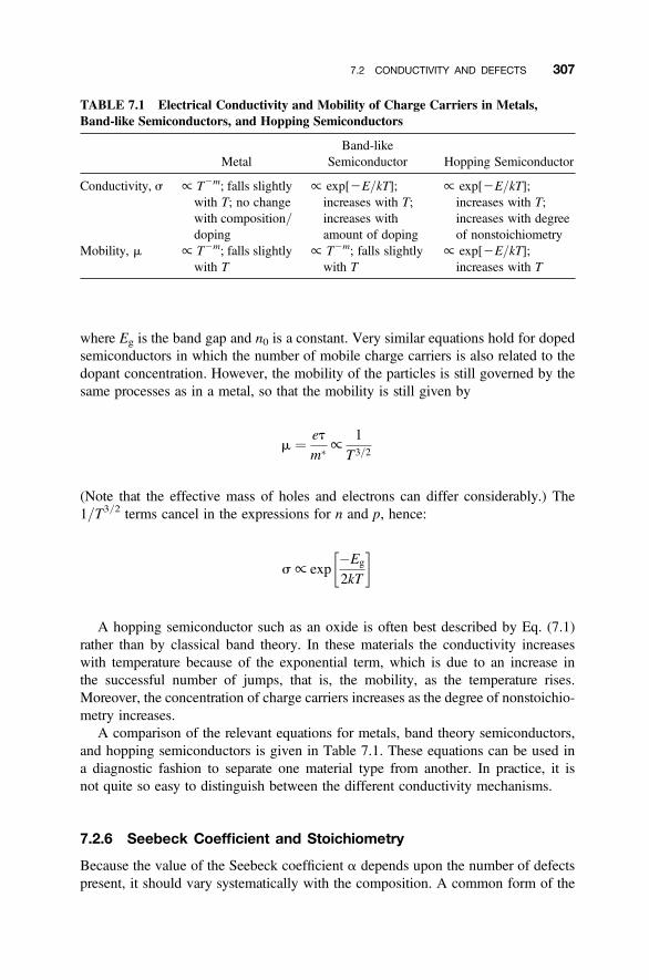
where Eg is the band gap and n0 is a constant. Very similar equations hold for dopedsemiconductors in which the number of mobile charge carriers is also related to thedopant concentration. However, the mobility of the particles is still governed by thesame processes as in a metal, so that the mobility is still given by
m ¼ et
m� /1
T3=2
(Note that the effective mass of holes and electrons can differ considerably.) The1/T3/2 terms cancel in the expressions for n and p, hence:
s/ exp�Eg
2kT
� �
A hopping semiconductor such as an oxide is often best described by Eq. (7.1)rather than by classical band theory. In these materials the conductivity increaseswith temperature because of the exponential term, which is due to an increase inthe successful number of jumps, that is, the mobility, as the temperature rises.Moreover, the concentration of charge carriers increases as the degree of nonstoichio-metry increases.
A comparison of the relevant equations for metals, band theory semiconductors,and hopping semiconductors is given in Table 7.1. These equations can be used ina diagnostic fashion to separate one material type from another. In practice, it isnot quite so easy to distinguish between the different conductivity mechanisms.
7.2.6 Seebeck Coefficient and Stoichiometry
Because the value of the Seebeck coefficient a depends upon the number of defectspresent, it should vary systematically with the composition. A common form of the
TABLE 7.1 Electrical Conductivity and Mobility of Charge Carriers in Metals,Band-like Semiconductors, and Hopping Semiconductors
MetalBand-like
Semiconductor Hopping Semiconductor
Conductivity, s / T2m; falls slightlywith T; no changewith composition/doping
/ exp[2E/kT];increases with T;increases withamount of doping
/ exp[2E/kT];increases with T;increases with degreeof nonstoichiometry
Mobility, m / T2m; falls slightlywith T
/ T2m; falls slightlywith T
/ exp[2E/kT];increases with T
7.2 CONDUCTIVITY AND DEFECTS 307
dependence is
a ¼ +k
e
� �ln
n0nd
� �� �(7:2)
where n0 is the number of sites in the sublattice containing defects and nd is thenumber of defects giving rise to mobile electrons or holes (Section 1.6 andSupplementary Material S3). To consider how this relates to stoichiometric variation,consider a oxide MO2, which is fairly readily reduced to form MO22x and that passesthrough the phases M2O3 and MO during the course of this reduction.
The sequence of events that occurs during the reduction has been described whenthe electrical conductivity of a nonstoichiometric oxide was discussed. Initialreduction will populate our MO22x crystal with a few M3þ ions, which will giverise to n-type semiconductivity. The value of a will therefore be large and negative.This value will fall as the number of defects increases. Turning to M2O3, a slightdegree of oxidation will introduce into the M2O3þx phase a small number of M4þ
ions in a matrix of M3þ ions. This will lead to p-type semiconductivity and a largepositive value of a. Continued oxidation will cause this value to fall as the numberof M4þ centers increases. Most significantly, there is a change from n-type to p-type behavior as the composition passes through a composition of MO1.75 (Fig. 7.4).
A similar situation will hold as the composition range between M2O3 and MO iscrossed, with a changing from positive to negative at a composition of MO1.25. Thevalue of a will change drastically from large and positive to large and negative as wepass through the stoichiometric position at M2O3 (Fig. 7.4).
Figure 7.4 Theoretical variation of the Seebeck coefficient as a function of composition for ahopping semiconducting oxide MOx, where x can take values of between 1.0 and 2.0.
308 NONSTOICHIOMETRY AND INTRINSIC ELECTRONIC CONDUCTIVITY
The same analysis can be applied to compounds with a more complex formula.For example, the oxide LaCoO3, which adopts the cubic perovskite structure,usually shows a large positive Seebeck coefficient, of the order of þ700 mV K21,when prepared in air (Hebert et al., 2007). This indicates that there are holespresent in the material. The La ions have a fixed valence, La3þ, hence the presenceof holes must be associated with the transition-metal ion present. Previous discussionsuggests that LaCoO3 has become slightly oxidized to LaCoO3þd and contains apopulation of Co4þ ions (Co3þ þ h† or CoCo
† ). Each added oxygen ion will generatetwo holes, equivalent to two Co4þ:
12 O2 �! OO þ 2 h† or 1
2 O2 �! OO þ 2CoCo†
Using Eq. (7.2), the value of nd, the number of holes (or Co4þ ions) present, is3 � 1024 of the total population, n0, of Co3þ. The approximate formula of theoxide can be written LaCoO3þx/2, where x is the number of holes. With x ¼ 3 �1024, the material has a formula LaCoO3.00015.
7.3 STOICHIOMETRY, DEFECT POPULATIONS ANDPARTIAL PRESSURES
7.3.1 Equilibrium Partial Pressures
Nonstoichiometric phases can gain or loose components by reaction with the sur-rounding gaseous atmosphere. Broadly speaking, the composition of any purephase will depend upon the equilibrium partial pressure of each of the componentsof the solid in the surrounding vapor. This implies that physical properties such aselectronic conductivity will also vary as a function of the surrounding partial pressureof the components of the solid. To illustrate this, the relationship between the stabilityof an oxide and the surrounding oxygen partial pressure is described.
Silver oxide is a stoichiometric phase that decomposes at about 2308C to silvermetal and oxygen gas when heated in air.
2Ag2O �! 4Agþ O2
The change in the Gibbs free energy for this reaction, DGr, can be related to the partialpressure of the oxygen gas, pO2 , using the equation:
DGr ¼ �RT ln Kp
where Kp is the equilibrium constant of the reaction. In this example,
Kp ¼ pO2 DGr ¼ �RT ln pO2
7.3 STOICHIOMETRY, DEFECT POPULATIONS AND PARTIAL PRESSURES 309
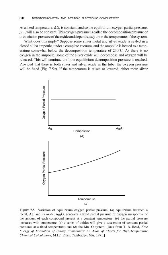
At a fixed temperature,DGr is constant, and so the equilibrium oxygen partial pressure,pO2 , will also be constant. This oxygen pressure is called the decomposition pressure ordissociation pressure of the oxide and depends only upon the temperature of the system.
What does this imply? Suppose some silver metal and silver oxide is sealed in aclosed silica ampoule, under a complete vacuum, and the ampoule is heated to a temp-erature somewhat below the decomposition temperature of 2308C. As there is nooxygen in the ampoule, some of the silver oxide will decompose and oxygen will bereleased. This will continue until the equilibrium decomposition pressure is reached.Provided that there is both silver and silver oxide in the tube, the oxygen pressurewill be fixed (Fig. 7.5a). If the temperature is raised or lowered, either more silver
Figure 7.5 Variation of equilibrium oxygen partial pressure: (a) equilibrium between ametal, Ag, and its oxide, Ag2O, generates a fixed partial pressure of oxygen irrespective ofthe amount of each compound present at a constant temperature; (b) the partial pressureincreases with temperature; (c) a series of oxides will give a succession of constant partialpressures at a fixed temperature; and (d) the Mn–O system. [Data from T. B. Reed, FreeEnergy of Formation of Binary Compounds: An Atlas of Charts for High-TemperatureChemical Calculations, M.I.T. Press, Cambridge, MA, 1971.]
310 NONSTOICHIOMETRY AND INTRINSIC ELECTRONIC CONDUCTIVITY

oxide will decompose or some silver will oxidize until a new equilibrium decompo-sition pressure is reached, which is appropriate to the new temperature (Fig. 7.5b).
The same analysis will hold for any metal in contact with its single oxide. In orderto determine the oxygen partial pressure over the pair, it is only necessary to know thevalue of the free energy of the reaction at the temperature required and insert the valueinto the following equation:
DGr ¼ �RT ln pO2
A multivalent metal M, will form several oxides, for example, MO2, M2O3, M3O4,and MO. In this case the same analysis holds good for the metal M in contact with the
Figure 7.5 (Continued).
7.3 STOICHIOMETRY, DEFECT POPULATIONS AND PARTIAL PRESSURES 311
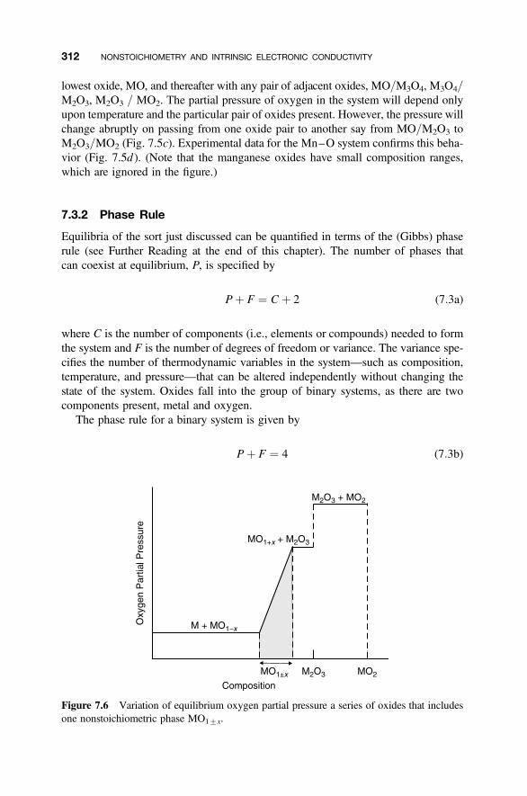
lowest oxide, MO, and thereafter with any pair of adjacent oxides, MO/M3O4, M3O4/M2O3, M2O3 / MO2. The partial pressure of oxygen in the system will depend onlyupon temperature and the particular pair of oxides present. However, the pressure willchange abruptly on passing from one oxide pair to another say from MO/M2O3 toM2O3/MO2 (Fig. 7.5c). Experimental data for the Mn–O system confirms this beha-vior (Fig. 7.5d ). (Note that the manganese oxides have small composition ranges,which are ignored in the figure.)
7.3.2 Phase Rule
Equilibria of the sort just discussed can be quantified in terms of the (Gibbs) phaserule (see Further Reading at the end of this chapter). The number of phases thatcan coexist at equilibrium, P, is specified by
Pþ F ¼ C þ 2 (7:3a)
where C is the number of components (i.e., elements or compounds) needed to formthe system and F is the number of degrees of freedom or variance. The variance spe-cifies the number of thermodynamic variables in the system—such as composition,temperature, and pressure—that can be altered independently without changing thestate of the system. Oxides fall into the group of binary systems, as there are twocomponents present, metal and oxygen.
The phase rule for a binary system is given by
Pþ F ¼ 4 (7:3b)
Figure 7.6 Variation of equilibrium oxygen partial pressure a series of oxides that includesone nonstoichiometric phase MO1+x.
312 NONSTOICHIOMETRY AND INTRINSIC ELECTRONIC CONDUCTIVITY

When the system (e.g., a sealed ampoule containing Ag, Ag2O, and O2 gas) containsthree phases, P ¼ 3 and Eq. (7.3b) gives
F ¼ 1
The system is said to have a variance of one; it is univariant. This means that underconditions in which three phases are in equilibrium, just one thermodynamicparameter needs to be given in order to specify the state of the system. In this casethe most important parameters are temperature and oxygen partial pressure becausein the Ag–O system the phases all have fixed compositions. Thus, knowledge of
Figure 7.7 Equilibrium oxygen partial pressure for a nonstoichiometric oxide; YBa2Cu3Ox:(a) composition, x, versus temperature under an oxygen partial pressure of 1 bar; (b) oxygenpartial pressure versus temperature for a composition of YBa2Cu3O6.5; and (c) oxygenpartial pressure versus composition, x, for a temperature of 6008C. [Adapted from data inP. Karen, J. Solid State Chem., 179, 3167–3183 (2006).]
7.3 STOICHIOMETRY, DEFECT POPULATIONS AND PARTIAL PRESSURES 313
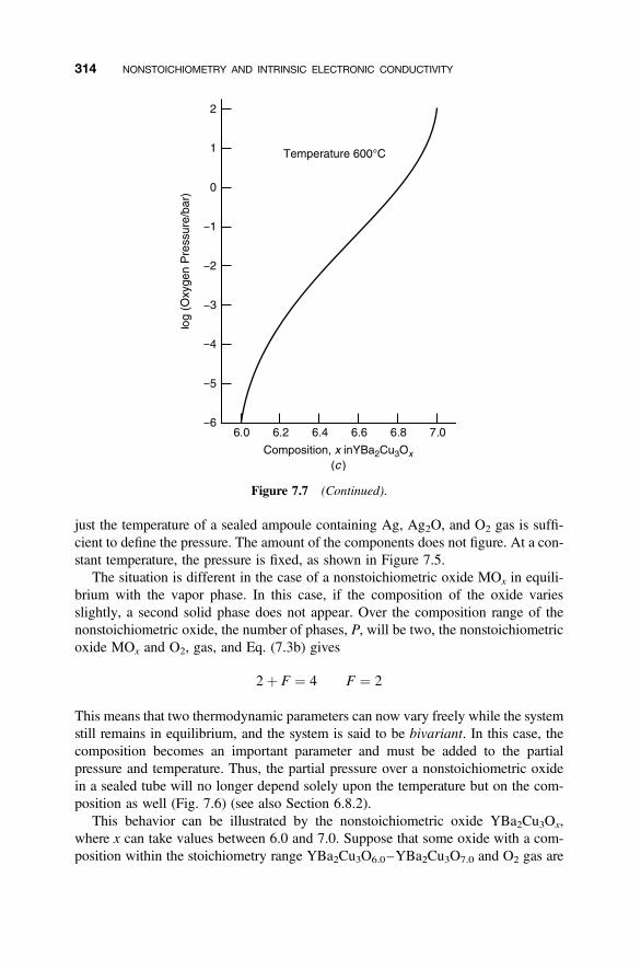
just the temperature of a sealed ampoule containing Ag, Ag2O, and O2 gas is suffi-cient to define the pressure. The amount of the components does not figure. At a con-stant temperature, the pressure is fixed, as shown in Figure 7.5.
The situation is different in the case of a nonstoichiometric oxide MOx in equili-brium with the vapor phase. In this case, if the composition of the oxide variesslightly, a second solid phase does not appear. Over the composition range of thenonstoichiometric oxide, the number of phases, P, will be two, the nonstoichiometricoxide MOx and O2, gas, and Eq. (7.3b) gives
2þ F ¼ 4 F ¼ 2
This means that two thermodynamic parameters can now vary freely while the systemstill remains in equilibrium, and the system is said to be bivariant. In this case, thecomposition becomes an important parameter and must be added to the partialpressure and temperature. Thus, the partial pressure over a nonstoichiometric oxidein a sealed tube will no longer depend solely upon the temperature but on the com-position as well (Fig. 7.6) (see also Section 6.8.2).
This behavior can be illustrated by the nonstoichiometric oxide YBa2Cu3Ox,where x can take values between 6.0 and 7.0. Suppose that some oxide with a com-position within the stoichiometry range YBa2Cu3O6.0–YBa2Cu3O7.0 and O2 gas are
Figure 7.7 (Continued).
314 NONSTOICHIOMETRY AND INTRINSIC ELECTRONIC CONDUCTIVITY
present in a sealed tube. Two out of the three parameters—temperature, composition,and oxygen partial pressure—are now required to specify equilibrium. For instance, ifthe temperature is 5008C and the pressure is 1 bar of oxygen, at equilibrium the com-position is YBa2Cu3O6.88 (Fig. 7.7a). Similarly, if the composition is YBa2Cu3O6.5
and the temperature is 6508C, the equilibrium oxygen partial pressure will beapproximately 0.78 bar (log pO2 � 21.1 � 1021) (Fig. 7.7b). Finally, the oxygenpartial pressure will not be fixed at a definite temperature but will vary with thecomposition of the oxide (Fig. 7.7c).
7.4 VARIATION OF DEFECT POPULATIONSWITH PARTIAL PRESSURE
The previous sections imply that in the case of nonstoichiometric oxides that favorelectronic compensation of composition change a relationship exists between thevariation in partial pressure and the electronic conductivity. The form that thisrelationship takes depends upon the way in which the oxide accommodates compo-sition variation.
7.4.1 Metal-Excess Oxides
Metal-excess oxides can change composition by way of metal interstitials or oxygenvacancies. The formation of cation interstitials in a nonstoichiometric oxide MO canbe represented by
MO O 12 O2 þMi
2† þ 2e0 (7:4)
The assumption that the defects are noninteracting allows the law of mass action in itssimplest form, with concentrations instead of activities, to be used for this purpose. Inthis case, the equilibrium constant K for this reaction is
K ¼ [Mi2†][e0]2pO2
1=2
[MO]
where the brackets [ ] denote concentrations. The concentration of the parentoxide, MO, can be taken as more or less static and can be included in a new constantK1, giving
K1 ¼ [Mi2†][e0]2pO2
1=2
Equation (7.4) shows that the concentrations of interstitials and electrons arerelated thus:
2[M2†i ] ¼ [e0]
7.4 VARIATION OF DEFECT POPULATIONS WITH PARTIAL PRESSURE 315
hence
K1 ¼ 12 [e
0]3pO21=2
so that the concentration of electrons [e0] is given by:
[e0� ¼ 2K1=31 pO2
�1=6
The conductivity of the solid, s, will be proportional to the electron concentrationso that
s/ [e0]/ pO2�1=6
The electronic conductivity will fall as the oxygen pressure increases.A similar analysis can be carried out for the case of oxygen vacancies:
OO(MO) O 12 O2 þ VO
2† þ 2e0
Repeating the steps above gives exactly the same pressure dependence, namely
s/ [e0]/ pO2�1=6
The variation of conductivity with partial pressure is found to be sensitive to thenumber of electrons present. To illustrate this, suppose that the interstitial cation losesonly one electron to form Mi
† defects:
MO O 12 O2 þM†
i þ e0 (7:5)
The equilibrium constant K for this reaction is
K ¼ [M†i ][e
0]pO21=2
[MO]
including the term [MO] in a revised constant K1 gives
K1 ¼ [M†i ][e
0]pO21=2
Equation (7.5) shows that the concentration of interstitials and electrons arerelated; thus,
[M†i ] ¼ [e0]
Hence:
K1 ¼ [e0]2pO21=2
so that the concentration of electrons [e0] is given by:
[e0] ¼ K1=21 pO2
�1=4
316 NONSTOICHIOMETRY AND INTRINSIC ELECTRONIC CONDUCTIVITY

that is,
s/ [e0]/ pO2�1=4
The electronic conductivity is now proportional to the � 14 power of the oxygen
partial pressure. In all cases described the conductivity falls as the partial pressureof oxygen rises, but the exact power relationship, � 1
4 or � 16, depends upon the
charge state of the interstitial cation.
7.4.2 Oxygen-Excess Oxides
The analysis of oxygen-excess oxides is similar to that for metal-rich phases justgiven. For example, the creation of oxygen excess by cation vacancies can be written:
12 O2(MO) O OO þ V20
M þ 2h† (7:6)
The equilibrium constant, K, of Eq. (7.6) is
K ¼ [h†]2[V20M][OO]
pO21=2
where [ ] represent concentrations and pO2 the oxygen partial pressure. Now the valueof [OO] is essentially constant, as the change in stoichiometry is small. Hence we canassimilate it into a new constant, K1, and write
K1 ¼ [h†]2[V20M]
pO21=2
For every vacancy in the crystal there are two holes generated [Eq. (7.6)]: thus:
[V20M] ¼ 1
2 [h†]
and substituting:
K1 ¼ [h†]3
2pO21=2
so that the concentration of holes is given by
[h†] ¼ (2K1)1=3pO2
1=6
That is, the concentration of holes, [h†], and the electronic conductivity is pro-portional to the 1
6 power of the oxygen partial pressure:
s/ [h†]/ pO21=6
7.4 VARIATION OF DEFECT POPULATIONS WITH PARTIAL PRESSURE 317
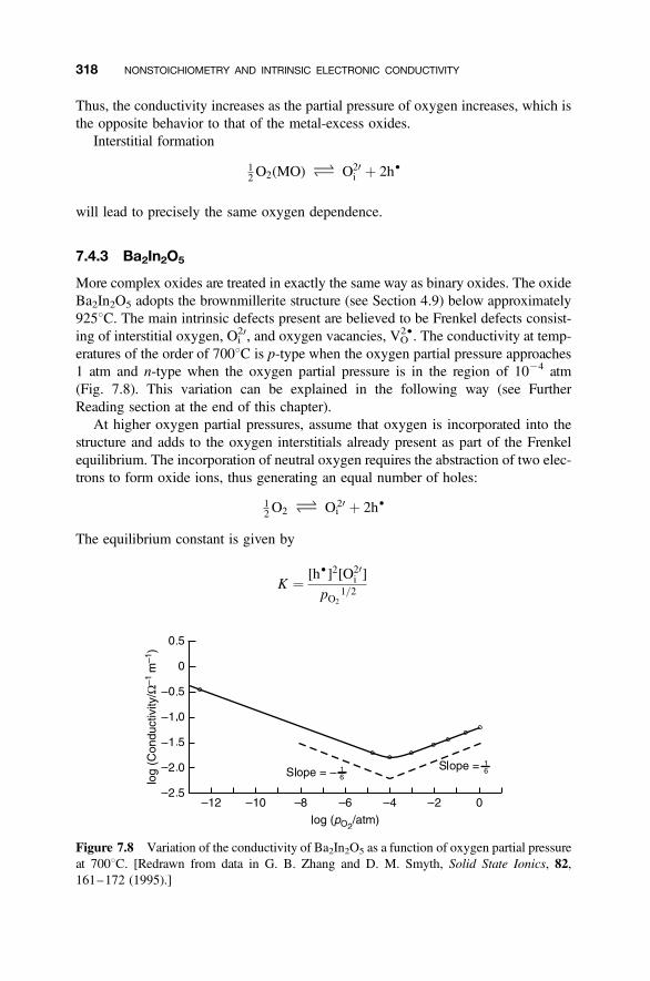
Thus, the conductivity increases as the partial pressure of oxygen increases, which isthe opposite behavior to that of the metal-excess oxides.
Interstitial formation
12 O2(MO) O O20
i þ 2h†
will lead to precisely the same oxygen dependence.
7.4.3 Ba2In2O5
More complex oxides are treated in exactly the same way as binary oxides. The oxideBa2In2O5 adopts the brownmillerite structure (see Section 4.9) below approximately9258C. The main intrinsic defects present are believed to be Frenkel defects consist-ing of interstitial oxygen, Oi
20, and oxygen vacancies, VO2†. The conductivity at temp-
eratures of the order of 7008C is p-type when the oxygen partial pressure approaches1 atm and n-type when the oxygen partial pressure is in the region of 1024 atm(Fig. 7.8). This variation can be explained in the following way (see FurtherReading section at the end of this chapter).
At higher oxygen partial pressures, assume that oxygen is incorporated into thestructure and adds to the oxygen interstitials already present as part of the Frenkelequilibrium. The incorporation of neutral oxygen requires the abstraction of two elec-trons to form oxide ions, thus generating an equal number of holes:
12 O2 O Oi
20 þ 2h†
The equilibrium constant is given by
K ¼ [h†]2[O20i ]
pO21=2
Figure 7.8 Variation of the conductivity of Ba2In2O5 as a function of oxygen partial pressureat 7008C. [Redrawn from data in G. B. Zhang and D. M. Smyth, Solid State Ionics, 82,161–172 (1995).]
318 NONSTOICHIOMETRY AND INTRINSIC ELECTRONIC CONDUCTIVITY
For every interstitial introduced into the crystal, two holes are generated:
[Oi20] ¼ 1
2 [h†]
that is,
K ¼ [h†]3
2 pO21=2
Rearrangement gives
[h†] ¼ (2K)1=3pO21=6
The conductivity is proportional to the hole concentration:
s/ [h†]/ pO21=6
Under oxidizing conditions the conductivity increases with oxygen partial pressure tothe power þ 1
6, in agreement with the experimental results (Fig. 7.8).At low oxygen partial pressures, that is, reducing conditions, assume that oxygen
is lost to the surrounding atmosphere to create oxygen vacancies to add to thosepresent due to the Frenkel defects. The charged oxide ion is extracted as a neutralatom, leaving behind two electrons:
OO O 12 O2 þ VO
2† þ 2e0
The equilibrium constant is given by
K ¼ [e0]2[V2†O ] pO2
1=2
[OO]
For every vacancy introduced into the crystal, two electrons are generated:
[VO2†] ¼ 1
2 [e0]
that is,
K ¼ [e0]3
2[OO]pO2
1=2
Regarding the amount of structural oxygen, [OO], as constant and incorporating itinto a constant K1, followed by rearrangement gives
[e0] ¼ (2K1)1=3pO2
�1=6
7.4 VARIATION OF DEFECT POPULATIONS WITH PARTIAL PRESSURE 319
The conductivity is proportional to the electron concentration:
s/ [e0]/ pO2�1=6
Under reducing conditions the conductivity is n type and decreases with oxygenpartial pressure, in agreement with the experimental results (Fig. 7.8).
7.5 BROUWER DIAGRAMS
Defect populations and physical properties such as electronic conductivity can bealtered and controlled by manipulation of the surrounding atmosphere. To specifythe exact electronic conductivity of such a material, it is necessary to specify itschemical composition, the defect types and populations present, the temperature ofthe crystal, and the surrounding partial pressures of all the constituents. In thiscomplex situation it is extremely helpful if the defect concentrations (and indirectlythe associated electrical conductivity) can be displayed graphically as a function ofsome variable such as partial pressure of one of the components. A procedure intro-duced by Brouwer (1954) allows such figures to be compiled. These diagrams,Brouwer or Kroger–Vink diagrams, are widely used, especially for solids withnarrow composition ranges.
To construct such a diagram, a set of defect reaction equations is formulated andexpressions for the equilibrium constants of each are obtained. The assumption thatthe defects are noninteracting allows the law of mass action in its simplest form, withconcentrations instead of activities, to be used for this purpose. To simplify matters,only one defect reaction is considered to be dominant in any particular compositionregion, this being chosen from knowledge of the chemical attributes of the systemunder consideration. The simplified equilibrium expressions are then used to con-struct plots of the logarithm of defect concentration against an experimental variablesuch as the log (partial pressure) of the components. The procedure is best illustratedby an example.
7.5.1 Initial Assumptions
The first step is to set out the assumptions concerning the defects that are likely tooccur, using physical and chemical intuition about the system in mind. For illustrativepurposes, take a nonstoichiometric phase of composition MX, nominally containingM2þ and X22 ions, with a stoichiometric composition, MX1.0. In this example thefollowing is assumed:
1. The only ionic defects of importance are vacancies on metal sites, V20M , and
vacancies on anion sites, VX2†; interstitial defects are ignored. The stoichio-
metric composition MX1.0 will occur when the number of vacancies on thecation sublattice is exactly equal to the number of vacancies on the anionsublattice, which is, therefore, a population of Schottky defects.
320 NONSTOICHIOMETRY AND INTRINSIC ELECTRONIC CONDUCTIVITY
2. MX can have an existence range that spans both sides of the stoichiometriccomposition, MX1.0, which is due to an imbalance in the population ofvacancies.
3. As well as vacancies, MX contains a varying population of electrons e0, orholes, h†, which can act to maintain electroneutrality when the solidbecomes nonstoichiometric. At the stoichiometric composition of MX1.0, thenumber of electrons is equal to the number of holes, which are simply the nor-mally present intrinsic electrons and holes.
4. The most important gaseous component is X2, as is the case in most oxides,halides, and sulfides. The stoichiometric variation will be linked to thepartial pressure of the surrounding nonmetal atmosphere. The nonmetal com-ponent will be gained at high pressures and lost at low pressures. Theseoptions correspond to oxidation and reduction.
These assumptions mean that there are only four defects to consider, electrons, e0,holes, h†, vacancies on metal sites V20
M and vacancies on anion sites, VX2†.
7.5.2 Defect Equilibria
The equilibrium between the defects present can be described in terms of chemicalequations:
1. Creation and Elimination of Schottky Defects These defects can form at thecrystal surface or vanish by diffusing to the surface. The equation describing this andthe associated equilibrium constant is
nul O V20M þ V2†
X KS ¼ [V20M][V
2†X ] (7:7)
2. Creation and Elimination of Electronic Defects These are the normal intrin-sic electrons and holes present in a semiconductor. Electrons can combine with holesto be eliminated from the crystal thus:
nul O e0 þ h† Ke ¼ [e0][h†] ¼ np (7:8)
(Electron and hole concentrations are often written as n and p, but this alternative willnot be followed here to avoid confusion with pressure, also denoted as p.)
3. Composition Change This comes about by interaction with the gas phase toproduce cation or anion vacancies. For oxidation the equation is
12 X2 O XX þ V20
M þ 2h† Ko ¼ [V20M][h
†]2pX2�1=2 (7:9)
7.5 BROUWER DIAGRAMS 321
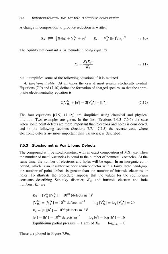
A change in composition to produce reduction is written:
XX O 12 X2(g)þ V2†
X þ 2e0 Kr ¼ [V2†X ][e0]2pX2
1=2 (7:10)
The equilibrium constant Kr is redundant, being equal to
Kr ¼ KSKe2
Ko(7:11)
but it simplifies some of the following equations if it is retained.
4. Electroneutrality At all times the crystal must remain electrically neutral.Equations (7.9) and (7.10) define the formation of charged species, so that the appro-priate electroneutrality equation is
2[V20M]þ [e0] ¼ 2[V2†
X ]þ [h†] (7:12)
The four equations [(7.9)–(7.12)] are simplified using chemical and physicalintuition. Two examples are given. In the first (Sections 7.6.3–7.6.6) the casewhere ionic point defects are more important than electrons and holes is considered,and in the following sections (Sections 7.7.1–7.7.5) the reverse case, whereelectronic defects are more important than vacancies, is described.
7.5.3 Stoichiometric Point: Ionic Defects
The compound will be stoichiometric, with an exact composition of MX1.0000 whenthe number of metal vacancies is equal to the number of nonmetal vacancies. At thesame time, the number of electrons and holes will be equal. In an inorganic com-pound, which is an insulator or poor semiconductor with a fairly large band-gap,the number of point defects is greater than the number of intrinsic electrons orholes. To illustrate the procedure, suppose that the values for the equilibriumconstants describing Schottky disorder, KS, and intrinsic electron and holenumbers, Ke, are
KS ¼ [V20M][V
2†X ] ¼ 1040 (defects m�3)2
[V20M] ¼ [V2†
X ] ¼ 1020 defects m�3 log [V20M] ¼ log [V2†
X ] ¼ 20
Ke ¼ [e0][h†] ¼ 1032 (defects m�3)2
[e0] ¼ [h†] ¼ 1016 defects m�3 log [e0] ¼ log [h†] ¼ 16
Equilibrium partial pressure ¼ 1 atm of X2 log pX2 ¼ 0
These are plotted in Figure 7.9a.
322 NONSTOICHIOMETRY AND INTRINSIC ELECTRONIC CONDUCTIVITY
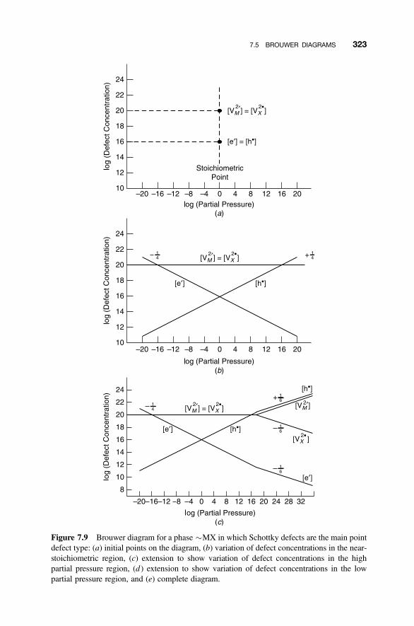
Figure 7.9 Brouwer diagram for a phase �MX in which Schottky defects are the main pointdefect type: (a) initial points on the diagram, (b) variation of defect concentrations in the near-stoichiometric region, (c) extension to show variation of defect concentrations in the highpartial pressure region, (d ) extension to show variation of defect concentrations in the lowpartial pressure region, and (e) complete diagram.
7.5 BROUWER DIAGRAMS 323
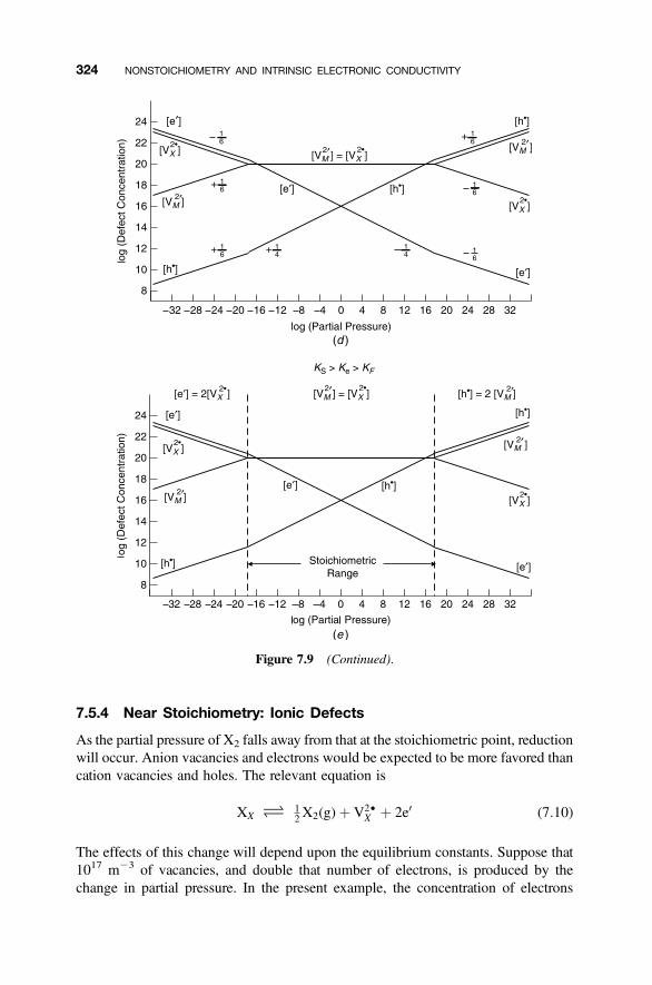
7.5.4 Near Stoichiometry: Ionic Defects
As the partial pressure of X2 falls away from that at the stoichiometric point, reductionwill occur. Anion vacancies and electrons would be expected to be more favored thancation vacancies and holes. The relevant equation is
XX O 12 X2(g)þ V2†
X þ 2e0 (7:10)
The effects of this change will depend upon the equilibrium constants. Suppose that1017 m23 of vacancies, and double that number of electrons, is produced by thechange in partial pressure. In the present example, the concentration of electrons
Figure 7.9 (Continued).
324 NONSTOICHIOMETRY AND INTRINSIC ELECTRONIC CONDUCTIVITY
will change considerably, from 1 � 1016 m23 to 20 � 1016 m23. However, theconcentration of vacancies will change only slightly, from 1 � 1020 m23 to1.001 � 1020 m23.
As the partial pressure of X2 increases beyond that at the stoichiometric point, oxi-dation will occur. Cation vacancies would be expected to be more favored than anionvacancies. The relevant equation is
12 X2 O XX þ V20
M þ 2h† (7:9)
Under these conditions, cation vacancies and holes will be formed. As before, theeffect of this change will depend upon the equilibrium constants. Suppose1017 m23 of vacancies, and double that number of holes, is produced by thechange in partial pressure. The concentration of holes will change considerably,from 1 � 1016 m23 to 20 � 1016 m23. The concentration of vacancies will changeonly slightly, from 1 � 1020 m23 to 1.001 � 1020 m23.
Because it is assumed that KS is a lot greater than Ke it is reasonable to ignorethe minority electronic defects and approximate the electroneutrality Eq. (7.12) bythe relation:
[V20M] ¼ [V2†
X ] (7:13)
This equation is now substituted into Eqs. (7.7), (7.9), and (7.10) to obtain a new setof equations describing the appropriate defect concentrations:From Eq. (7.7):
[V20M] ¼ [V2†
X ] ¼ KS1=2
log [V20M] ¼ log [V2†
X ] ¼ 12 log KS
(7:7)
From Eq. (7.9):
[h†]2 ¼ Ko
[V20M]
� �pX2
1=2 ¼ Ko
KS1=2
� �pX2
1=2
[h†] ¼ K1=2o K�1=4
S pX21=4 (7:14)
log [h†] ¼ 12 log Ko � 1
4 logKS þ 14 log pX2
From Eq. (7.10):
[e0]2 ¼ Kr
[V2†X ]pX2
1=2¼ Kr
KS1=2pX2
1=2
[e0] ¼ Kr1=2KS
�1=4pX2�1=4 (7:15)
log [e0] ¼ 12 log Kr � 1
4 logKS � 14 log pX2
7.5 BROUWER DIAGRAMS 325
These equations apply to both sides of the stoichiometric composition. They can beplotted as log(defect concentration) versus log pX2 . A plot of log [h†] versus log pX2
has a slope of 14 and passes through the (electronic) stoichiometric point. A plot
of log [e0] versus log pX2 has a slope of 214 and passes through the (electronic) stoi-
chiometric point (Fig. 7.9b).
7.5.5 High X2 Partial Pressures: Ionic Defects
At ever higher partial pressures the number of nonmetal vacancies will diminish moreand more. In addition, Figure 7.9b suggests that the number of holes will eventuallyexceed the number of vacancies in this regime. Thus, the approximate electroneutral-ity Eq. (7.13) will no longer be representative. A more appropriate form of theelectroneutrality equation for the high-pressure region is obtained by ignoring theminority species, nonmetal vacancies and electrons, to give
2[V20M] ¼ [h†] (7:16)
This can now be substituted into Eqs. (7.7)–(7.10) to obtain relationships betweenthe partial pressure of X2 and the defect concentrations present in the material relevantto the high partial pressure region.
From Eq. (7.9):
[V20M] ¼
KopX21=2
[h†]2¼ KopX2
1=2
(2[V20M])
2
4[V20M]
3 ¼ KopX21=2
8[V20M]
3 ¼ 2KopX21=2
[V20M] ¼ 1
2 (2Ko)1=3pX21=6 (7:17)
log [V20M] ¼ log 1
2 þ 13 log (2Ko)þ 1
6 log pX2
From Eq. (7.16):
[h†] ¼ (2Ko)1=3pX2
1=6 (7:18)
log [h†] ¼ 13 log (2Ko)þ 1
6 log pX2
From Eq. (7.7):
[VX2†] ¼ KS
[V20M]
¼ 2KS(2Ko)�1=3pX2
�1=6 (7:19)
log [VX2†] ¼ log 2þ logKS � 1
3 log (2Ko)� 16 log pX2
326 NONSTOICHIOMETRY AND INTRINSIC ELECTRONIC CONDUCTIVITY
From Eq. (7.8):
[e0] ¼ Ke
[h†]¼ Ke(2Ko)
�1=3pX2�1=6 (7:20)
log [e0] ¼ logKe � 13 log (2Ko)� 1
6 log pX2
A plot of log[h†] versus log pX2 has a slope of16, a plot of log[e
0] versus log pX2 hasa slope of � 1
6, a plot of log [V20M] versus log pX2 has a slope of 1
6, and a plot of log[VX
2†] versus log pX2 has a slope of � 16.
The point at which the slopes change is chosen to coincide with the point at whichthe region obeying the electroneutrality condition given by Eq. (7.13) is replacedby Eq. (7.16). Thus, the change of slope occurs when 2[V20
M] ¼ [h†], and using thevalues of [V20
M] as 1020 defects m23, the slope of the line displaying theconcentration of holes changes slope at a value of [h†] ¼ 2 � 1020 defects m23.This is close to the intersection of the line representing the concentration of holeswith the line representing the concentration of vacancies. The results can be usedto continue Figure 7.9b to the right (Fig. 7.9c).
7.5.6 Low X2 Partial Pressures: Ionic Defects
As the pressure diminishes far below that of the stoichiometric point, the number ofmetal vacancies and holes will continue to fall and the electroneutrality equationchosen, Eq. (7.16), will no longer be representative. A more appropriate form ofthe electroneutrality equation for the low-pressure region ignores the minoritydefects, which are now metal vacancies and holes, to give
[e0] ¼ 2[V2†X ] (7:21)
This is substituted into Eqs. (7.7)–(7.10) to derive the defect concentrations relevantto the low partial pressure region.
From Eq. (7.10):
[V2†X ] ¼ Kr
[e0]2pX21=2
¼ Kr
(2[V2†X ])2pX2
1=2
4[V2†X ]3 ¼ Kr
pX21=2
8[V2†X ]3 ¼ 2Kr
pX21=2
[V2†X ] ¼ 1
2 (2Kr)1=3pX2�1=6 (7:22)
log [V2†X ] ¼ log 1
2 þ 13 log (2Kr)� 1
6 log pX2
7.5 BROUWER DIAGRAMS 327
From Eq. (7.21):
[e0] ¼ (2Kr)1=3pX2
�1=6 (7:23)
log [e0] ¼ 13 log (2Kr)� 1
6 log pX2
From Eq. (7.7):
[V20M] ¼
KS
[V2†X ]
¼ 2KS (2Kr)�1=3pX2
1=6 (7:24)
log [VM20] ¼ log 2þ logKS � 1
3 log (2Kr)þ 16 log pX2
From Eq. (7.8):
[h†] ¼ Ke
[e0]¼ Ke(2Kr)
�1=3pX21=6 (7:25)
log [h†] ¼ logKe � 13 log (2Kr)þ log pX2
1=6
A plot of log [h†] versus log pX2 has a slope of 16, a plot of log [e0] versus log pX2
has a slope of � 16, a plot of log [V20
M] versus log pX2 has a slope of 16, and a plot of
log [VX2†] versus log pX2 has a slope of � 1
6, exactly as in the high-pressure region.The point at which the slopes change is chosen to coincide with the point at which
the region obeying the electroneutrality condition given by Eq. (7.13) is replaced byEq. (7.21). Thus, the change of slope occurs when [e0] ¼ 2[VX
2†], and using the valuesof [VX
2†] as 1020 defects m23, the slope of the line displaying the concentration ofholes changes slope at a value of [e0] ¼ 2 � 1020 defects m23. This is close to theintersection of the line representing the concentration of holes with the line represent-ing the concentration of vacancies. The results can be used to continue Figure 7.9b tothe left (Fig. 7.9d ).
7.5.7 Complete Diagram: Ionic Defects
It is important that the complete diagram displays prominently information about theassumptions made. Thus, the assumption that Schottky defect formation was pre-ferred to the formation of electronic defects is explicitly stated in the form KS .Ke (Fig. 7.9e). As Frenkel defect formation has been ignored altogether, it is alsopossible to write KS . Ke .. KF, where KF represents the equilibrium constantfor the formation of Frenkel defects in MX.
This central, medium pressure, region of the diagram displays the electroneutralityequation approximation [V20
M] ¼ [VX2†] at the top. In this region the compound
328 NONSTOICHIOMETRY AND INTRINSIC ELECTRONIC CONDUCTIVITY
remains stoichiometric across this range, as the number of cation and anion vacanciesremains the same. The number of holes and electrons will be below the number ofcation and anion vacancies for most of this region, and the material will be a stoichio-metric insulator with a composition MX1.000 containing Schottky defects.
The high partial pressure region displays the electroneutrality equation approxi-mation [h†] ¼ 2[V20
M]. The defects with the highest concentration are holes, so thatthe material is a p-type semiconductor in this regime. In addition, the conductivitywill increase as the partial pressure of the gaseous X2 component increases. Thenumber of metal vacancies will increase as the partial pressure of the gaseous X2
component increases and, because of the corresponding fall in the concentration ofanion vacancies, the phase will be nonstoichiometric and rich in nonmetal. In thisregion the high concentration of cation vacancies would be expected to enhancecation diffusion.
The low-pressure region displays the electroneutrality equation approximation[e0] ¼ 2[VX
2†]. Electrons predominate so that the material is an n-type semiconductorin this regime. In addition, the conductivity will increase as the partial pressure of thegaseous X2 component decreases. The number of nonmetal vacancies will increase asthe partial pressure of the gaseous X2 component decreases, and the phase willdisplay a metal-rich nonstoichiometry opposite to that in the high-pressure domain.Because there is a high concentration of anion vacancies, easy diffusion of anionsis to be expected.
The form of this diagram in which abrupt changes occur between the three regionsis clearly too extreme. The diagram can easily be modified to smooth out these dis-continuities by inserting additional segments, employing additional electroneutralityequations. For example, between the low-pressure and medium-pressure regions theelectroneutrality equation
2[V20M] ¼ 2[V2†
X ]þ [h†]
is appropriate. Between the medium-pressure and high-pressure regions
2[V20M]þ [e0] ¼ [V2†
X ]
can be used. The value of these extensions depends upon the precision of availableexperimental data and the intended use of the diagram.
7.6 BROUWER DIAGRAMS: ELECTRONIC DEFECTS
7.6.1 Electronic Defects
In many compound semiconductors the band gap is rather small, leading to a signifi-cant concentration of intrinsic electrons and holes while the population of interstitial
7.6 BROUWER DIAGRAMS: ELECTRONIC DEFECTS 329
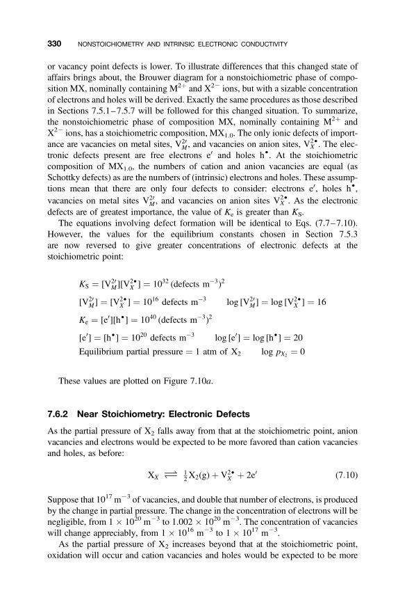
or vacancy point defects is lower. To illustrate differences that this changed state ofaffairs brings about, the Brouwer diagram for a nonstoichiometric phase of compo-sition MX, nominally containing M2þ and X22 ions, but with a sizable concentrationof electrons and holes will be derived. Exactly the same procedures as those describedin Sections 7.5.1–7.5.7 will be followed for this changed situation. To summarize,the nonstoichiometric phase of composition MX, nominally containing M2þ andX22 ions, has a stoichiometric composition, MX1.0. The only ionic defects of import-ance are vacancies on metal sites, V20
M , and vacancies on anion sites, VX2†. The elec-
tronic defects present are free electrons e0 and holes h†. At the stoichiometriccomposition of MX1.0, the numbers of cation and anion vacancies are equal (asSchottky defects) as are the numbers of (intrinsic) electrons and holes. These assump-tions mean that there are only four defects to consider: electrons e0, holes h†,vacancies on metal sites V20
M , and vacancies on anion sites VX2†. As the electronic
defects are of greatest importance, the value of Ke is greater than KS.The equations involving defect formation will be identical to Eqs. (7.7–7.10).
However, the values for the equilibrium constants chosen in Section 7.5.3are now reversed to give greater concentrations of electronic defects at thestoichiometric point:
KS ¼ [V20M][V
2†X ] ¼ 1032 (defects m�3)2
[V20M] ¼ [V2†
X ] ¼ 1016 defects m�3 log [V20M] ¼ log [V2†
X ] ¼ 16
Ke ¼ [e0][h†] ¼ 1040 (defects m�3)2
[e0] ¼ [h†] ¼ 1020 defects m�3 log [e0] ¼ log [h†] ¼ 20
Equilibrium partial pressure ¼ 1 atm of X2 log pX2 ¼ 0
These values are plotted on Figure 7.10a.
7.6.2 Near Stoichiometry: Electronic Defects
As the partial pressure of X2 falls away from that at the stoichiometric point, anionvacancies and electrons would be expected to be more favored than cation vacanciesand holes, as before:
XX O 12 X2(g)þ V2†
X þ 2e0 (7:10)
Suppose that 1017 m23 of vacancies, and double that number of electrons, is producedby the change in partial pressure. The change in the concentration of electrons will benegligible, from 1 � 1020 m23 to 1.002 � 1020 m23. The concentration of vacancieswill change appreciably, from 1 � 1016 m23 to 1 � 1017 m23.
As the partial pressure of X2 increases beyond that at the stoichiometric point,oxidation will occur and cation vacancies and holes would be expected to be more
330 NONSTOICHIOMETRY AND INTRINSIC ELECTRONIC CONDUCTIVITY
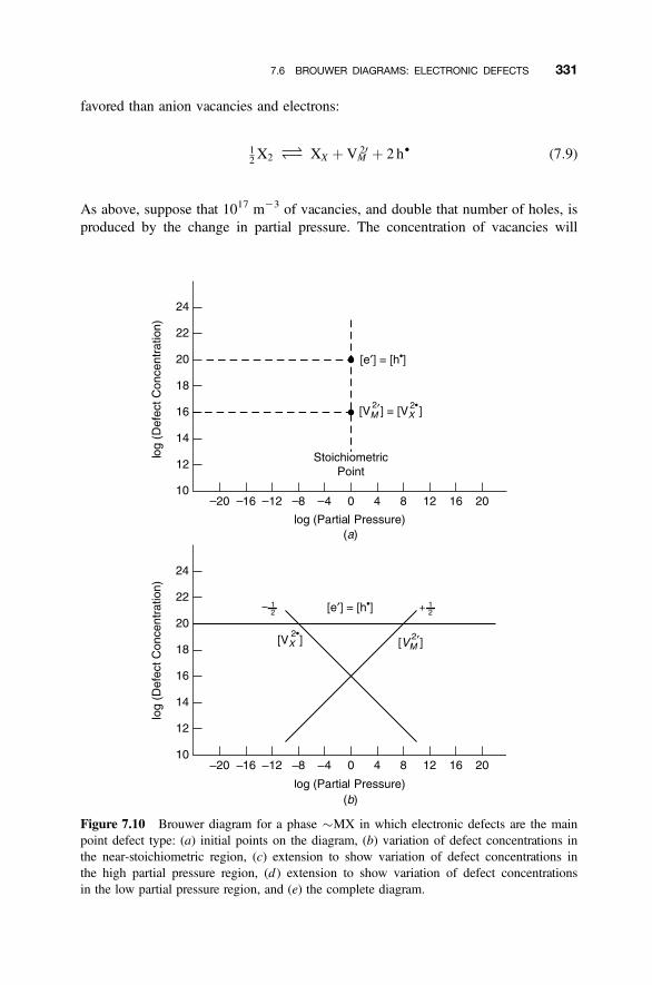
favored than anion vacancies and electrons:
12 X2 O XX þ VM
20 þ 2 h† (7:9)
As above, suppose that 1017 m23 of vacancies, and double that number of holes, isproduced by the change in partial pressure. The concentration of vacancies will
Figure 7.10 Brouwer diagram for a phase �MX in which electronic defects are the mainpoint defect type: (a) initial points on the diagram, (b) variation of defect concentrations inthe near-stoichiometric region, (c) extension to show variation of defect concentrations inthe high partial pressure region, (d ) extension to show variation of defect concentrationsin the low partial pressure region, and (e) the complete diagram.
7.6 BROUWER DIAGRAMS: ELECTRONIC DEFECTS 331
Figure 7.10 (Continued).
332 NONSTOICHIOMETRY AND INTRINSIC ELECTRONIC CONDUCTIVITY
change considerably, from 1 � 1016 m23 to 1 � 1017 m23. The concentration ofholes will change only slightly, from 1 � 1020 m23 to 1.002 � 1020 m23.
In both of these regimes it is more reasonable to approximate the electroneutralityEq. (7.12) by
[e0] ¼ [h†] (7:26)
This is equivalent to the assumption that Ke is a lot greater than KS, as stated.This equation is now substituted into Eqs. (7.8) and (7.9) to obtain a new set of
equations for the defect concentrations:
[h†] ¼ [e0] ¼ Ke1=2 (7:27)
log [h†] ¼ log [e0] ¼ 12 log Ke
[V2†X ] ¼ Kr
Ke
� �pX2
�1=2 (7:28)
log [V2†X ] ¼ logKr � logKe � 1
2 log pX2
[VM20] ¼ Ko
Ke
� �pX2
1=2 (7:29)
log [VM20] ¼ logKo � logKe þ 1
2 log pX2
As expected, these equations are similar in form to Eqs. (7.13)–(7.15) and apply toboth sides of the stoichiometric composition. They can be plotted as log(defectconcentration) versus log pX2 graph. A plot of log[VX
2†] versus log pX2 has a slopeof 21
2 and passes through the (ionic) stoichiometric point. A plot of log [V20M]
versus log pX2 has a slope of þ 12 and passes through the (ionic) stoichiometric
point (Fig. 7.10b).
7.6.3 High X2 Partial Pressures: Electronic Defects
At ever higher partial pressures the number of nonmetal vacancies will diminish moreand more and the number of holes will exceed the number of vacancies in this regime.Thus the approximate electroneutrality Eq. (7.13) will no longer be representative.A more appropriate form of the electroneutrality equation for the high-pressureregion is obtained by ignoring the minority species, nonmetal vacancies and elec-trons, to give
[h†] ¼ 2[VM20] (7:16)
This can now be substituted into Eqs. (7.7)–(7.10) to obtain relationships betweenthe partial pressure of X2 and the defect concentrations present in the material relevant
7.6 BROUWER DIAGRAMS: ELECTRONIC DEFECTS 333
to the high partial pressure region. This is identical to the situation described for ionicdefects, and so some detail will be condensed in the following.
From Eq. (7.9):
[V20M] ¼ 1
2 (2Ko)1=3pX21=6 (7:17)
log [V20M] ¼ log 1
2 þ 13 log (2Ko)þ 1
6 log pX2
From Eq. (7.16):
[h†] ¼ (2Ko)1=3pX2
1=6 (7:18)
log [h†] ¼ 13 log (2Ko)þ 1
6 log pX2
From Eq. (7.7):
[VX2†] ¼ 2KS(2Ko)
�1=3pX2�1=6 (7:19)
log [VX2†] ¼ log 2þ logKS � log (2Ko)� 1
6 log pX2
From Eq. (7.8):
[e0] ¼ Ke(2Ko)�1=3pX2
�1=6
log [e0] ¼ logKe � 13 log (2Ko)� 1
6 log pX2
(7:20)
A plot of log [h†] versus log pX2 has a slope of16, a plot of log [e
0] versus log pX2 has aslope of � 1
6, a plot of log [V20M] versus log pX2 has a slope of
16, and a plot of log [VX
2†]versus log pX2 has a slope of � 1
6.The point at which the slopes change is chosen to coincide with the point at which
the region obeying the electroneutrality condition given by Eq. (7.13) is replaced byEq. (7.16). Thus the change of slope occurs when 2[V20
M] ¼ [h†], and using the valueof [h†] as 1020 defects m23, the slope of the line displaying the concentration of metalvacancies changes slope at a value of [V20
M] ¼ 5 � 1019 defects m23. The results canbe used to continue Figure 7.10b to the right (Fig. 7.10c).
7.6.4 Low X2 Partial Pressures: Electronic Defects
As the pressure diminishes far below that of the stoichiometric point, the number ofmetal vacancies and holes will continue to fall, and, as before, the electroneutralityequation chosen, Eq. (7.16), will no longer be representative. A more appropriateform of the electroneutrality equation for the low-pressure region ignores the minoritydefects, which are now metal vacancies and holes, to give
[e0] ¼ 2[V2†X ] (7:21)
334 NONSTOICHIOMETRY AND INTRINSIC ELECTRONIC CONDUCTIVITY
This equation is substituted into Eqs. (7.7)–(7.10) to derive the defect concentrationsrelevant to the low partial pressure region. Once again these will be similar to thosederived for ionic defects.
From Eq. (7.10):
[V2†X ] ¼ 1
2 (2Kr)1=3pX2�1=6 (7:22)
log [V2†X ] ¼ log 1
2 þ 13 log (2Kr)� 1
6 log pX2
From Eq. (7.21):
[e0] ¼ (2Kr)1=3pX2
�1=6 (7:23)
log [e0] ¼ 13 log (2Kr)� 1
6 log pX2
From Eq. (7.7):
[VM20] ¼ 2KS(2Kr)
�1=3pX21=6 (7:24)
log [VM20] ¼ log 2þ logKS � 1
3 log (2Kr)þ 16 log pX2
From Eq. (7.8):
[h†] ¼ Ke(2Kr)�1=3pX2
1=6 (7:25)
log [h†] ¼ logKe � 13 log (2Kr)þ log pX2
1=6
A plot of log [h†] versus log pX2 has a slope of16, a plot of log [e
0] versus log pX2 has aslope of � 1
6, a plot of log [V20M] versus log pX2 has a slope of
16, and a plot of log [VX
2†]versus log pX2 has a slope of � 1
6, exactly as in the high-pressure region.The point at which the slopes change is chosen to coincide with the point at which
the region obeying the electroneutrality condition given by Eq. (7.13) is replaced byEq. (7.21). Thus the change of slope occurs when [e0] ¼ 2[VX
2†], and using the valuesof [e0] as 1020 defects m23, the slope of the line displaying the concentration of non-metal vacancies changes slope at a value of [VX
2†] ¼ 5 � 1019 defects m23. Theresults can be used to continue Figure 7.10b to the left (Fig. 7.10d ).
7.6.5 Complete Diagram: Electronic Defects
The original assumption that electronic defect formation was preferred to the for-mation of Schottky defects is explicitly stated at the top of Figure 7.10e. AsFrenkel defect formation has been ignored altogether, it is also possible to writeKe . KS KF, where KF represents the equilibrium constant for the formation ofFrenkel defects in MX.
Although Fig. 7.10e is similar to that for ionic defects (Fig. 7.9e), there are anumber of significant differences. In particular, the stoichiometric range is now far
7.6 BROUWER DIAGRAMS: ELECTRONIC DEFECTS 335
narrower. This central region of the diagram displays the electroneutrality equationchosen, [e0] ¼ [h†], prominently. In this region the compound remains an intrinsicsemiconductor. However, the number of anion and cation vacancies change unsym-metrically away from the stoichiometric point and the composition will vary fromMX1.000. However, this variation will be extremely small. For example, at the highpartial pressure limit (log pX2 ¼ þ7) side the metal vacancy concentration is 5 �1019 metal vacancies m23; then from Figure 7.10e it is found that there are 5 �1013 nonmetal vacancies m23. Taking a NaCl crystal as typical, there are of theorder of 1028 cations and anions m23, so that the composition change is minute.
The high-pressure region is associated with the electroneutrality equation [h†] ¼2[V20
M]. Holes predominate, so that the material is a p-type semiconductor in thisregime. In addition, the conductivity will increase as the 1
6 power of the partialpressure of the gaseous X2 component increases. The number of metal vacancies(and nonmetal excess) will increase as the partial pressure of the gaseous X2 com-ponent increases and the phase will be distinctly nonstoichiometric. There is a highconcentration of cation vacancies that would be expected to enhance cation diffusion.
The low-pressure region is associated with the electroneutrality equation [e0] ¼2[VX
2†]. Electrons predominate so that the material is an n-type semiconductor inthis regime. In addition, the conductivity will increase as the � 1
6 power of thepartial pressure of the gaseous X2 component increases. The number of nonmetalvacancies (and metal excess) will increase as the partial pressure of the gaseous X2
component decreases and the phase will display a nonstoichiometry opposite tothat in region III. Because there is high concentration of anion vacancies, easy diffu-sion of anions is to be expected.
As in the case of ionic defects, the form of this diagram can easily be modified tosmooth out the abrupt changes between the three regions by including intermediateelectroneutrality equations.
7.7 BROUWER DIAGRAMS: MORE COMPLEX EXAMPLES
In general, there is little problem in extending the concepts just outlined to morecomplex materials. The procedure is to write down the equations specifying thevarious equilibria: point defect formation, electronic defect formation, the oxidationreaction, and the reduction reaction. These four equations, only three of which areindependent, are augmented by the electroneutrality equation. Two examples willbe sketched for the oxides Cr2O3 and Ba2In2O5.
7.7.1 Cr2O3
The presence of relatively small Cr3þ cations and the close-packed corundum struc-ture anions suggest that Schottky defects will be preferred. Oxidation will add anionsand reduction will remove anions. The four equilibria can now be written.
336 NONSTOICHIOMETRY AND INTRINSIC ELECTRONIC CONDUCTIVITY
Point defect formation; Schottky defects:
nul O 2V30Cr þ 3V2†
O KS ¼ [V30Cr]
2[V2†O ]3
Electronic defect formation:
nul O e0 þ h† Ke ¼ [e0][h†]
Oxidation:
32 O2 O 3OO þ 2V30
Cr þ 6 h† Ko ¼ [V30Cr]
2[h†]
p3=2O2
Reduction:
OO O V2†O þ 2e0 þ 1
2 O2 Kr ¼ [V2†O ][e0]2p1=2O2
Electroneutrality:
3[V30Cr]þ [e0] ¼ [h†]þ 2[V2†
O ]
These equations can now be simplified in the manner described above. The elec-troneutrality point is given by
[e0] ¼ [h†]
and the point at which the compound is strictly stoichiometric by
3[V30Cr] ¼ 2[V2†
O ]
The approximations to use depend upon the pressure regime and the values of theequilibrium constants. This oxide is an insulator under normal conditions, and so,in the middle region of the diagram, Schottky equilibrium is dominant, that is,KS . Ke and the electroneutrality equation is approximated by
3[V30Cr] ¼ 2[V2†
O ]
In the oxidized region, holes and cation vacancies are preferred, so the electroneutral-ity equation is approximated by
3[V30Cr] ¼ [h†]
7.7 BROUWER DIAGRAMS: MORE COMPLEX EXAMPLES 337
In the reduced region, electrons and anion vacancies are to be preferred, and the elec-troneutrality equation is approximated by
[e0] ¼ 2[V2†O ]
Insertion of the relevant equilibrium constants allows the diagram to be drawn.
7.7.2 Ba2In2O5
Although the formula of this phase is more complex than the binary compoundsdescribed above, the procedure is exactly the same. It is only necessary to identifythe likely defect equilibria that pertain to the experimental situation.
The structure of the oxide Ba2In2O5 suggests that anion Frenkel defects will bepreferred. Oxidation will add anions and reduction will remove anions. The fourequilibria can now be written.
Point defect formation; Frenkel defects:
nul O O20i þ V2†
O KF ¼ [O20i ][V
2†O ]
Electronic defect formation:
nul O e0 þ h† Ke ¼ [e0][h†]
Oxidation:
12 O2 O Oi
20 þ 2 h† Ko ¼ [Oi20][h†]2
p1=2O2
Reduction:
OO O V2†O þ 2e0 þ 1
2 O2 Kr ¼ [V2†O ][e0]2p1=2O2
Electroneutrality:
2[O20i ]þ [e0] ¼ [h†]þ 2[V2†
O ]
These equations can now be simplified in the manner described above. The elec-troneutrality point is given by
[e0] ¼ [h†]
338 NONSTOICHIOMETRY AND INTRINSIC ELECTRONIC CONDUCTIVITY
and the point at which the compound is strictly stoichiometric by
[Oi20] ¼ [VO
2†]
The approximations to use depend upon the pressure regime and the values of theequilibrium constants. This oxide is an insulator under normal conditions, and so,in the middle region of the diagram, Frenkel equilibrium is dominant, that is,KF . Ke and the electroneutrality equation is approximated by
[Oi20] ¼ [VO
2†]
In the oxidized region, holes and anion interstitials are preferred, so the electroneu-trality equation is approximated by
2[Oi20] ¼ [h†]
In the reduced region, electrons and anion vacancies are to be preferred, and the elec-troneutrality equation is approximated by
[e0] ¼ 2[VO2†]
The diagram can now be constructed.For a fuller discussion of this material, see the Further Reading section at the end
of this chapter.
7.8 BROUWER DIAGRAMS: EFFECTS OF TEMPERATURE
A Brouwer diagram is drawn up for one temperature and is an isothermal represen-tation of the situation in the phase. A number of parameters determine the way inwhich any diagram changes with temperature.
Frenkel and Schottky defect equilibria are temperature sensitive and at highertemperatures defect concentrations rise, so that values ofKS andKF increasewith temp-erature. The same is true of the intrinsic electrons and holes present, and Ke alsoincreases with temperature. This implies that the defect concentrations in the centralpart of a Brouwer diagram will move upward at higher temperatures with respect tothat at lower temperatures, and the whole diagram will be shifted vertically.
The temperature dependence of the other equilibrium constants is more difficult togeneralize. The partial pressure of a gaseous component will increase with tempera-ture, and so equilibrium constants with partial pressure in the numerator will be likelyto increase with temperature. Similarly, equilibrium constants with the partialpressure in the denominator may well decrease with temperature.
If a species tends to move from an oxidized to a reduced form at higher tempera-tures, say A2þ moving toward Aþ, the overall diagram will tend to shift toward thelow pressure (left hand) side of the diagram. Thus the diagram will tend to shiftupward and to the left at high temperatures for reducible ions. The stoichiometricpoint will tend to move to the left at the same time. The reverse is true if the main
7.8 BROUWER DIAGRAMS: EFFECTS OF TEMPERATURE 339
species tends to be oxidized at higher temperatures, such as A3þ changing to A4þ.Here the diagram will tend to move upward and to the right at higher temperatures,and the stoichiometric point will tend to move to the right.
Finally, it is apparent that the principal defect type may change as the temperatureincreases, so that, for example, electronic defects may become more important thanionic defects. In such cases the diagram will change appreciably.
These rule-of-thumb generalizations must be treated cautiously. For precise workit is necessary to recalculate values of the equilibrium constants at the new tempera-ture and then replot the diagram. The equilibrium constants have a general form(Chapter 2):
K ¼ exp�DH
RT
� �
where DH is the enthalpy of the defect formation reaction (often substitutedfor DG), R is the gas constant, and T the temperature (K). Thus, knowing avalue of the enthalpy change allows the value of K to be calculated at othertemperatures.
7.9 POLYNOMIAL FORMS FOR BROUWER DIAGRAMS
The approximations inherent in Brouwer diagrams can be bypassed by writing theappropriate electroneutrality equation as a polynomial equation and then solvingthis numerically using a computer. (This is not always a computationally trivialtask.) To illustrate this method, the examples given in Sections 7.5 and 7.6, theMX system, will be rewritten in this form.
7.9.1 Ionic Defects
The five important equilibrium equations are:Point defect formation:
KS ¼ [VM20][VX
2†] ¼ 1040 (defects m�3)2 (7:30)
Electronic defect formation:
Ke ¼ [e0][h†] ¼ 1032 (defects m�3)2 (7:31)
Oxidation:
Ko ¼ [VM20][h†]2pX2
�1=2 ¼ 1052pX2�1=2 (defects m�3)3 (7:32)
340 NONSTOICHIOMETRY AND INTRINSIC ELECTRONIC CONDUCTIVITY
Reduction:
Kr ¼ [V2†X ][e0]2pX2
1=2 ¼ 1052pX21=2 (defects m�3)3 (7:33)
Electroneutrality:
2[V20M]þ [e0] ¼ 2[V2†
X ]þ [h†] (7:34)
Equilibrium partial pressure ¼ 1 atm of X2; log pX2 ¼ 0:Note that the values for Ko and Kr are obtained by using:
[V20M] ¼ [V2†
X ] ¼ 1020 (defects m�3)
[e0] ¼ [h†] ¼ 1016 (defects m�3)
derived from Eqs. (7.30) and (7.31).It is necessary to write the electroneutrality equation in terms of just two variables,
a defect type and the partial pressure, to obtain a polynomial capable of solution. Forexample, the equation for the concentration of holes, [h†], is obtained thus:
Electroneutrality:
2[V20M]þ [e0] ¼ 2[V2†
X ]þ [h†]
From Eq. (7.31):
[e0] ¼ Ke
[h†]
From Eq. (7.32):
[VM20] ¼ Ko pX2
1=2
[h†]2
From Eq. (7.33):
[VX2†] ¼ Kr
[e0]2pX21=2
¼ Kr[h†]2
Ke2pX2
1=2
Substituting:
2Ko pX21=2
[h†]2þ Ke
[h†]¼ 2Kr[h
†]2
Ke2pX2
1=2þ [h†]
Simplifying:
2Ko Ke2pX2 þ Ke
3[h†]pX21=2 � 2Kr [h
†]4 � Ke2 [h†]3pX2
1=2 ¼ 0 (7:35)
7.9 POLYNOMIAL FORMS FOR BROUWER DIAGRAMS 341
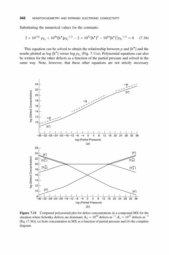
Substituting the numerical values for the constants:
2� 10116 pX2 þ 1096[h†]pX21=2 � 2� 1052[h†]4 � 1064[h†]3pX2
1=2 ¼ 0 (7:36)
This equation can be solved to obtain the relationship between p and [h†] and theresults plotted as log [h†] versus log pX2 (Fig. 7.11a). Polynomial equations can alsobe written for the other defects as a function of the partial pressure and solved in thesame way. Note, however, that these other equations are not strictly necessary
Figure 7.11 Computed polynomial plot for defect concentrations in a compound MX for thesituation where Schottky defects are dominant, KS ¼ 1040 defects m23, Ke ¼ 1032 defects m23
[Eq. (7.36)]: (a) hole concentration in MX as a function of partial pressure and (b) the completediagram.
342 NONSTOICHIOMETRY AND INTRINSIC ELECTRONIC CONDUCTIVITY
because of the relations between the constants, as set out above:
[e0] ¼ Ke
[h†]
[V20M] ¼
Ko pX21=2
[h†]2
[V2†X ] ¼ KS
[V20M]
The results, plotted as log (defect concentration) versus log pX2, give the complete
diagram (Fig. 7.11b). It is seen that the Brouwer approximation bears a goodcorrespondence to this diagram and indicates that the simplification procedure maybe adequate in most cases.
7.9.2 Electronic Defects
Exactly the same equations apply for cases in which the electronic defects dominatethe equilibrium, so that Eq. (7.35) still represents the relationship between the holeconcentration and partial pressure. The values of the equilibrium constants,however, are now changed. The revised values are:
KS ¼ 1032 (defects m�3)2
Ke ¼ 1040 (defects m�3)2
Ko ¼ 1056pX2�1=2 (defects m�3)3
Kr ¼ 1056pX2�1=2 (defects m�3)3
Substituting these values into Eq. (7.35) gives
2� 10136pX2 þ 10120[h†]pX21=2 � 2� 1056[h†]4 � 1080[h†]3pX2
1=2 ¼ 0 (7:37)
This equation can be solved to obtain the relationship between p and [h†]. Similarly,other equations can be set up, but, as mentioned, these other polynomials are notstrictly necessary because of the relations between the constants, as set out above:
[e0] ¼ Ke
[h†]
[V20M] ¼
Ko pX21=2
[h†]2
[V2†X ] ¼ KS
[V20M]
7.9 POLYNOMIAL FORMS FOR BROUWER DIAGRAMS 343
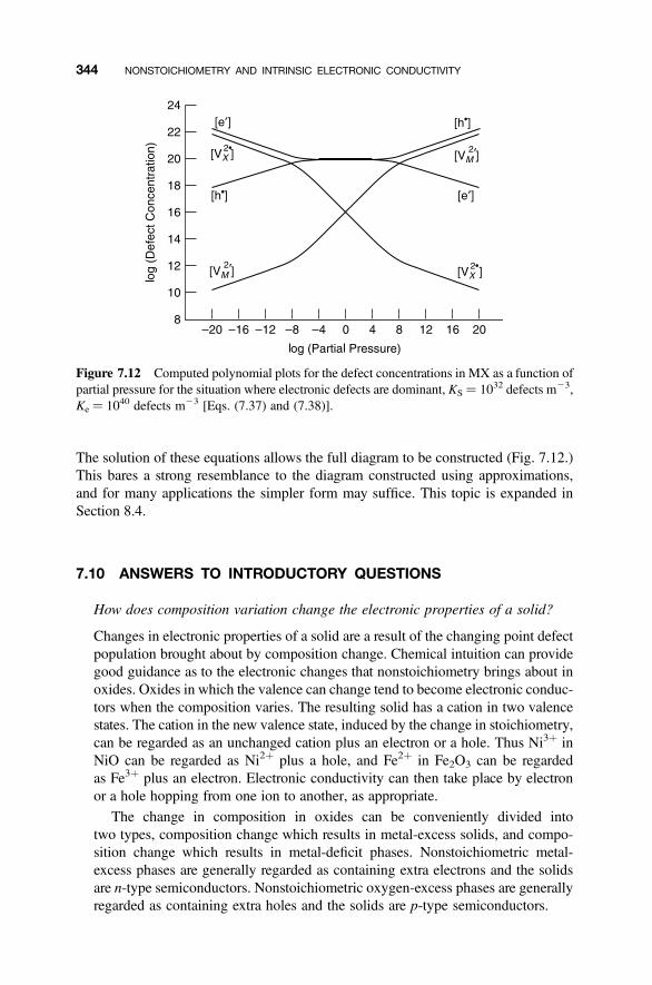
The solution of these equations allows the full diagram to be constructed (Fig. 7.12.)This bares a strong resemblance to the diagram constructed using approximations,and for many applications the simpler form may suffice. This topic is expanded inSection 8.4.
7.10 ANSWERS TO INTRODUCTORY QUESTIONS
How does composition variation change the electronic properties of a solid?
Changes in electronic properties of a solid are a result of the changing point defectpopulation brought about by composition change. Chemical intuition can providegood guidance as to the electronic changes that nonstoichiometry brings about inoxides. Oxides in which the valence can change tend to become electronic conduc-tors when the composition varies. The resulting solid has a cation in two valencestates. The cation in the new valence state, induced by the change in stoichiometry,can be regarded as an unchanged cation plus an electron or a hole. Thus Ni3þ inNiO can be regarded as Ni2þ plus a hole, and Fe2þ in Fe2O3 can be regardedas Fe3þ plus an electron. Electronic conductivity can then take place by electronor a hole hopping from one ion to another, as appropriate.
The change in composition in oxides can be conveniently divided intotwo types, composition change which results in metal-excess solids, and compo-sition change which results in metal-deficit phases. Nonstoichiometric metal-excess phases are generally regarded as containing extra electrons and the solidsare n-type semiconductors. Nonstoichiometric oxygen-excess phases are generallyregarded as containing extra holes and the solids are p-type semiconductors.
Figure 7.12 Computed polynomial plots for the defect concentrations in MX as a function ofpartial pressure for the situation where electronic defects are dominant, KS ¼ 1032 defects m23,Ke ¼ 1040 defects m23 [Eqs. (7.37) and (7.38)].
344 NONSTOICHIOMETRY AND INTRINSIC ELECTRONIC CONDUCTIVITY
Why does the electronic conductivity of a nonstoichiometric solid change as thesurrounding partial pressure changes?
A solid in a perfect vacuumwill loose material to the vapor phase until equilibrium isreached. In the case of a solidwith no composition range, this results in the productionof a new phase. In a nonstoichiometric solid it results in a change of composition.When a nonstoichiometric solid is surrounded by an atmosphere with a greaterpressure of these components than the equilibrium pressure, then the solid will tendto gainmaterial, andwhen surrounded by an atmospherewith a lower partial pressure,then it will tend to loose material. In either case the change in composition isaccomplished by a change in the defect structure of the material. The change indefect structure is responsible for the change in electronic properties. Because thecomposition change is a function of the surrounding partial pressure, the electronicproperties are a function of the surrounding partial pressure.
Models describing the point defect population can be used to determine howthe electronic conductivity will vary with changes in the surrounding partialpressure.
What information does a Brouwer diagram display?
Defect populations and physical properties such as electronic conductivity can bealtered and controlled by manipulation of the surrounding atmosphere. To specifythe exact electronic conductivity of such a material, it is necessary to specify itschemical composition, the defect types and populations present, the temperatureof the crystal, and the surrounding partial pressures of all the constituents.Brouwer diagrams display the defect concentrations present in a solid as a functionof the partial pressure of one of the components. Because the defect populationscontrol such properties as electronic and ionic conductivity, it is generally easy todetermine how these vary as the partial pressure varies.
To construct such a diagram, a set of defect reaction equations is written down,and expressions for the number of defects present as a function of the partialpressure are derived. The diagram can then be drawn, either by using the simpli-fication that only one defect reaction is considered to be dominant in any particularcomposition region, or else the polynomial describing the reaction can be solvedacross the whole partial pressure range using a computer.
PROBLEMS AND EXERCISES
Quick Quiz
1. Which of the following oxides, (a), (b), or (c), is likely to employ electronic com-pensation to balance oxygen loss:
(a) BaO
(b) WO3
(c) SrAl2O4
PROBLEMS AND EXERCISES 345
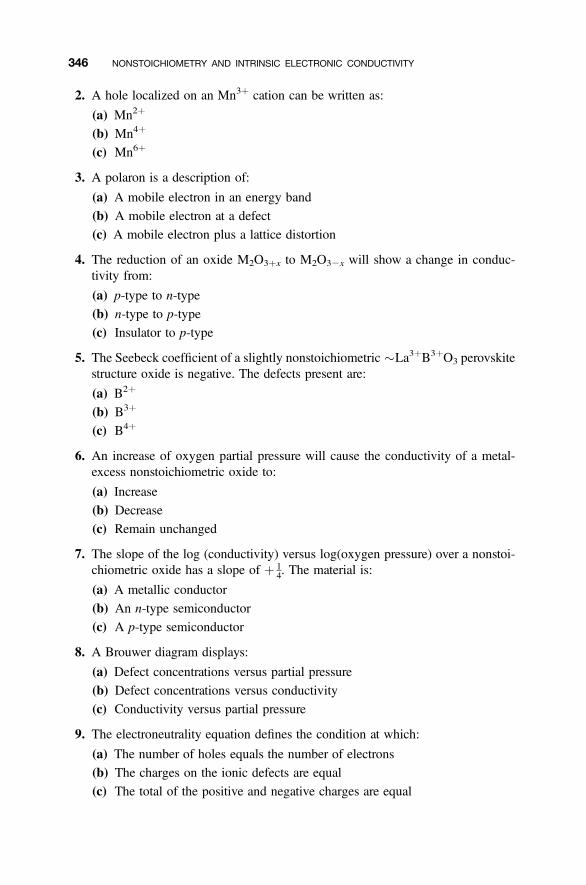
2. A hole localized on an Mn3þ cation can be written as:
(a) Mn2þ
(b) Mn4þ
(c) Mn6þ
3. A polaron is a description of:
(a) A mobile electron in an energy band
(b) A mobile electron at a defect
(c) A mobile electron plus a lattice distortion
4. The reduction of an oxide M2O3þx to M2O32x will show a change in conduc-tivity from:
(a) p-type to n-type
(b) n-type to p-type
(c) Insulator to p-type
5. The Seebeck coefficient of a slightly nonstoichiometric �La3þB3þO3 perovskitestructure oxide is negative. The defects present are:
(a) B2þ
(b) B3þ
(c) B4þ
6. An increase of oxygen partial pressure will cause the conductivity of a metal-excess nonstoichiometric oxide to:
(a) Increase
(b) Decrease
(c) Remain unchanged
7. The slope of the log (conductivity) versus log(oxygen pressure) over a nonstoi-chiometric oxide has a slope of þ 1
4. The material is:
(a) A metallic conductor
(b) An n-type semiconductor
(c) A p-type semiconductor
8. A Brouwer diagram displays:
(a) Defect concentrations versus partial pressure
(b) Defect concentrations versus conductivity
(c) Conductivity versus partial pressure
9. The electroneutrality equation defines the condition at which:
(a) The number of holes equals the number of electrons
(b) The charges on the ionic defects are equal
(c) The total of the positive and negative charges are equal
346 NONSTOICHIOMETRY AND INTRINSIC ELECTRONIC CONDUCTIVITY
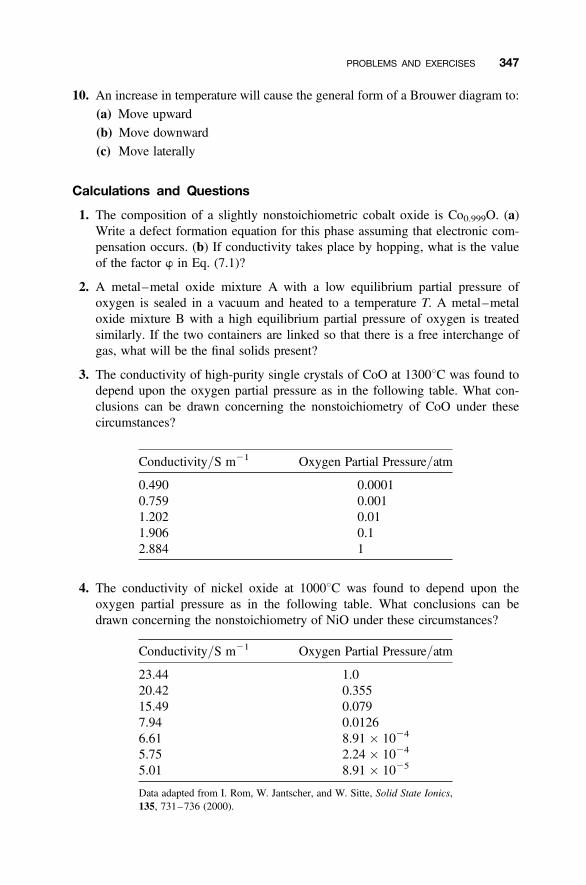
10. An increase in temperature will cause the general form of a Brouwer diagram to:
(a) Move upward
(b) Move downward
(c) Move laterally
Calculations and Questions
1. The composition of a slightly nonstoichiometric cobalt oxide is Co0.999O. (a)Write a defect formation equation for this phase assuming that electronic com-pensation occurs. (b) If conductivity takes place by hopping, what is the valueof the factor w in Eq. (7.1)?
2. A metal–metal oxide mixture A with a low equilibrium partial pressure ofoxygen is sealed in a vacuum and heated to a temperature T. A metal–metaloxide mixture B with a high equilibrium partial pressure of oxygen is treatedsimilarly. If the two containers are linked so that there is a free interchange ofgas, what will be the final solids present?
3. The conductivity of high-purity single crystals of CoO at 13008C was found todepend upon the oxygen partial pressure as in the following table. What con-clusions can be drawn concerning the nonstoichiometry of CoO under thesecircumstances?
Conductivity/S m21 Oxygen Partial Pressure/atm
0.490 0.00010.759 0.0011.202 0.011.906 0.12.884 1
4. The conductivity of nickel oxide at 10008C was found to depend upon theoxygen partial pressure as in the following table. What conclusions can bedrawn concerning the nonstoichiometry of NiO under these circumstances?
Conductivity/S m21 Oxygen Partial Pressure/atm
23.44 1.020.42 0.35515.49 0.0797.94 0.01266.61 8.91 � 1024
5.75 2.24 � 1024
5.01 8.91 � 1025
Data adapted from I. Rom, W. Jantscher, and W. Sitte, Solid State Ionics,135, 731–736 (2000).
PROBLEMS AND EXERCISES 347
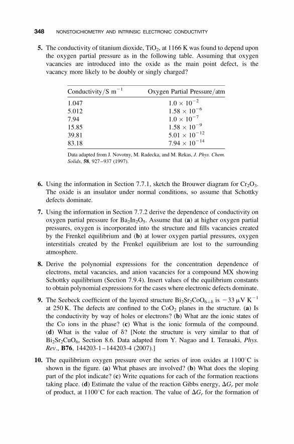
5. The conductivity of titanium dioxide, TiO2, at 1166 K was found to depend uponthe oxygen partial pressure as in the following table. Assuming that oxygenvacancies are introduced into the oxide as the main point defect, is thevacancy more likely to be doubly or singly charged?
Conductivity/S m21 Oxygen Partial Pressure/atm
1.047 1.0 � 1022
5.012 1.58 � 1026
7.94 1.0 � 1027
15.85 1.58 � 1029
39.81 5.01 � 10212
83.18 7.94 � 10214
Data adapted from J. Novotny, M. Radecka, and M. Rekas, J. Phys. Chem.Solids, 58, 927–937 (1997).
6. Using the information in Section 7.7.1, sketch the Brouwer diagram for Cr2O3.The oxide is an insulator under normal conditions, so assume that Schottkydefects dominate.
7. Using the information in Section 7.7.2 derive the dependence of conductivity onoxygen partial pressure for Ba2In2O5. Assume that (a) at higher oxygen partialpressures, oxygen is incorporated into the structure and fills vacancies createdby the Frenkel equilibrium and (b) at lower oxygen partial pressures, oxygeninterstitials created by the Frenkel equilibrium are lost to the surroundingatmosphere.
8. Derive the polynomial expressions for the concentration dependence ofelectrons, metal vacancies, and anion vacancies for a compound MX showingSchottky equilibrium (Section 7.9.4). Insert values of the equilibrium constantsto obtain polynomial expressions for the cases where electronic defects dominate.
9. The Seebeck coefficient of the layered structure Bi2Sr2CoO6þd is 233mV K21
at 250 K. The defects are confined to the CoO2 planes in the structure. (a) Isthe conductivity by way of holes or electrons? (b) What are the ionic states ofthe Co ions in the phase? (c) What is the ionic formula of the compound.(d) What is the value of d? [Note the structure is very similar to that ofBi2Sr2CuO6, Section 8.6. Data adapted from Y. Nagao and I. Terasaki, Phys.Rev., B76, 144203-1–144203-4 (2007).]
10. The equilibrium oxygen pressure over the series of iron oxides at 11008C isshown in the figure. (a) What phases are involved? (b) What does the slopingpart of the plot indicate? (c) Write equations for each of the formation reactionstaking place. (d) Estimate the value of the reaction Gibbs energy, DGr per moleof product, at 11008C for each reaction. The value of DGr for the formation of
348 NONSTOICHIOMETRY AND INTRINSIC ELECTRONIC CONDUCTIVITY
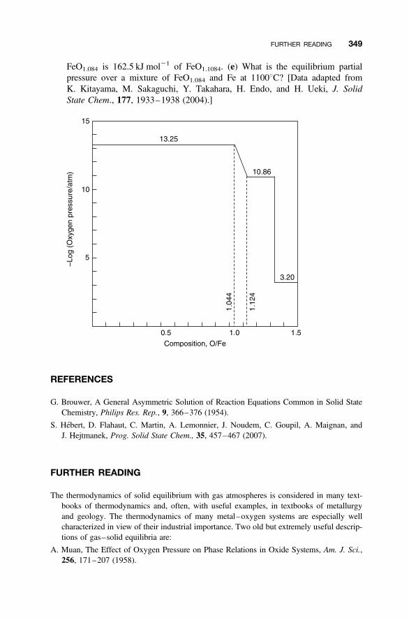
FeO1.084 is 162.5 kJ mol21 of FeO1.1084. (e) What is the equilibrium partialpressure over a mixture of FeO1.084 and Fe at 11008C? [Data adapted fromK. Kitayama, M. Sakaguchi, Y. Takahara, H. Endo, and H. Ueki, J. SolidState Chem., 177, 1933–1938 (2004).]
REFERENCES
G. Brouwer, A General Asymmetric Solution of Reaction Equations Common in Solid StateChemistry, Philips Res. Rep., 9, 366–376 (1954).
S. Hebert, D. Flahaut, C. Martin, A. Lemonnier, J. Noudem, C. Goupil, A. Maignan, andJ. Hejtmanek, Prog. Solid State Chem., 35, 457–467 (2007).
FURTHER READING
The thermodynamics of solid equilibrium with gas atmospheres is considered in many text-books of thermodynamics and, often, with useful examples, in textbooks of metallurgyand geology. The thermodynamics of many metal–oxygen systems are especially wellcharacterized in view of their industrial importance. Two old but extremely useful descrip-tions of gas–solid equilibria are:
A. Muan, The Effect of Oxygen Pressure on Phase Relations in Oxide Systems, Am. J. Sci.,256, 171–207 (1958).
FURTHER READING 349

T. B. Reed, Free Energy of Formation of Binary Compounds: An Atlas of Charts for High-Temperature Chemical Calculations, M.I.T. Press, Cambridge, MA, 1971.
Much of the material covered here is discussed in:
D. M. Smyth, The Defect Chemistry of Metal Oxides, Oxford University Press, Oxford, UnitedKingdom, 2000.
Expansion and further explanation with respect to defects and defect chemistry and physics willbe found in:
F. Agullo-Lopez, C. R. Catlow, and P. D. Townsend, Point Defects in Materials, Academic,New York, 1988.
A. M. Stoneham, The Theory of Defects in Solids, Oxford University Press, Oxford, UnitedKingdom, 1985.
The Mott variable-range hopping law is derived in:
N. F. Mott, Metal–Insulator Transitions, Taylor and Francis, London, 1974, p. 35 ff.
The phase rule is clearly explained in:
E. G. Ehlers, The Interpretation of Geological Phase Diagrams, Freeman,San Francisco, 1972.
The original description of Brouwer diagrams is well worth consulting. It is:
G. Brouwer, A General Asymmetric Solution of Reaction Equations Common in Solid StateChemistry, Philips Res. Rept., 9, 366–376 (1954).
Details of point defect equilibria in Ba2In2O5 are in:
G. B. Zhang and D. M. Smyth, Solid State Ionics, 82, 161–172 (1995).
Information on polynomial forms of Brouwer diagrams for Cr2O3 is in:
P. Karen, J. Solid State Chem., 179, 3167–3183 (2006).
350 NONSTOICHIOMETRY AND INTRINSIC ELECTRONIC CONDUCTIVITY
&CHAPTER 8
Nonstoichiometry and ExtrinsicElectronic Conductivity
What are donor and acceptor dopants?
How do negative temperature coefficient (NTC) thermistors respond totemperature changes?
What are mixed conductors?
8.1 EFFECT OF IMPURITY ATOMS
The composition variation described in the previous chapter has a considerable impactupon the electronic properties of the solid. However, it is often difficult to alter thecomposition of a phase to order, and stoichiometry ranges are frequently too narrow toallow desired electronic properties to be achieved. Traditionally, the problem has beencircumvented by using selective doping by aliovalent impurities, that is, impuritieswith a different nominal valence to those present in the parent material. However, it isimportant to remember that all the effects described in the previous chapter still applyto the materials below. The division into two chapters is a matter of convenience only.
Depending upon the electronic consequences of the doping, aliovalent additivesare often called donor impurities or donor dopants when they tend to provide elec-trons and enhance intrinsic n-type semiconducting behavior, or acceptor impuritiesor acceptor dopants when they tend to give a population of mobile holes andenhance p-type semiconducting behavior. Alternatively, the process is simplyreferred to as electron doping or hole doping. The process of creating electronicdefects in a crystal in this way is called valence induction. Extreme changes in prop-erties can be brought about by use of this technique. Examples given below includecases where insulating oxides can be made metallic, representing examples of metal–insulator transitions. In the case of some oxides, especially well represented by thecuprates, insulating parent phases can be made superconducting. Moreover, thesetransformations can often be controlled with great precision, as the introduction ofsmall amounts of impurity poses no inherent problems.
Defects in Solids, by Richard J. D. TilleyCopyright # 2008 John Wiley & Sons, Inc.
351
As in the previous chapter, most work has been carried out on oxides, and thesefigure prominently here. As the literature on oxides alone is not only vast but is alsorapidly increasing, this chapter focuses upon a number of representative structuretypes to explain the broad principles upon which the defect chemistry depends.However, despite considerable research, the defect chemistry and physics of dopedcrystals is still open to considerable uncertainty, and even well-investigated“simple” oxides such as lithium-doped nickel oxide, LixNi12xO, appear to havemore complex defect structures than thought some years ago.
8.2 IMPURITIES IN OXIDES
8.2.1 Donor Doping
Donor dopants are impurity ions of a higher valence than that of the parent ions, aswhen small amounts of Nb2O5 are incorporated into TiO2, so that Nb5þ substitutesfor Ti4þ. The donor species has an effective positive charge, NbTi
† , in this example,and the introduction of donor species tends to introduce counterbalancing electronsinto the structure. The inclusion of higher valence impurities will have an effectupon the stoichiometry of the phase and the charge balance of the host, whichneed to be compensated by a set of balancing defects. There are three ways inwhich this can be achieved for donor doping:
1. Cation vacancies
2. Anion interstitials
3. Electrons
8.2.2 Donor Doping of Cr2O3
The doping of chromium(III) oxide, Cr2O3, doped with titanium dioxide, TiO2, givesa material that is of use in sensors that detect reducing gases. The general principleunderlying the operation of this and similar sensors is that atmospheric oxygen ischemisorbed onto the surface. This process removes electrons from the bulk, enhan-cing bulk p-type semiconductivity or reducing bulk n-type semiconductivity. A redu-cing gas, such as carbon monoxide, CO, will remove chemisorbed oxygen, liberatingelectrons back to the bulk, so that n-type conductivity increases and p-type semicon-ductivity decreases. For successful operation, a low concentration of bulk carriers isneeded, so that the weak absorption effects make a measurable difference in elec-tronic properties.
Pure Cr2O3 is an intrinsic semiconductor with a band-gap of approximately 3.3 eV.Generally, Cr2O3 shows little stoichiometric variation. On doping with TiO2, Ti
4þ
ions substitute on Cr3þ sites in the structure. The conductivity of the doped solidis n-type and has a � 1
8 dependence upon oxygen partial pressure. The three
352 NONSTOICHIOMETRY AND EXTRINSIC ELECTRONIC CONDUCTIVITY
alternative compensation mechanisms can be written as follows:
Cation vacancies: 3TiO2(Cr2O3) O 3Ti†Cr þ V30Cr þ 6OO (8:1a)
Anion interstitials: 2TiO2(Cr2O3) O 2Ti†Cr þ 3OO þ O2 0i (8:1b)
Electrons: 2TiO2(Cr2O3) O 2Ti†Cr þ 2e0 þ 3OO þ 12 O2 (8:1c)
Equation (8.1c) is derived from Eq. (8.1b) by supposing that the oxygen interstitialsare lost to the atmosphere:
O20i O 1
2 O2 þ 2e0
The partial pressure dependence is readily explained using Eq. (8.1c). The equili-brium constant, K, is
K ¼ [Ti†Cr]2 [e0]2 [OO]
3 p 1=2O2
As the incorporation of one substitutional cation results in the production of one electron:
[Ti†Cr] ¼ [e0]
and including the term [OO] into a new constant, K1,
K1 ¼ [e0]4 p 1=2O2
[e0]4 ¼ K1 p�1=2
O2
s/ [e0]/ p �1=8O2
However, density measurements suggest that the formation of chromiumvacancies occurs, and atomistic simulations indicate that the vacancies are likely tocluster near to titanium substituents to form neutral entities:
3TiO2(Cr2O3) O (3Ti†Cr þ V30Cr)
x þ 6OO
This indicates that the defect structure is complex and may vary with degree ofdoping. Further studies are needed to clarify the defect structure of this notionallysimple solid.
8.2.3 Acceptor Doping
Acceptor dopants are impurity ions of a lower valence than that of the parent ions, aswhen small amounts of Al2O3 are incorporated into TiO2, so that the Al3þ ion sub-stitutes for Ti4þ. The acceptor species has an effective negative charge, Al0Ti in thisexample, and the introduction of acceptor species tends to introduce counterbalancing
8.2 IMPURITIES IN OXIDES 353
holes into the structure. The inclusion of lower valence impurities will have an effectupon the stoichiometry of the phase and the charge balance of the host, which need tobe compensated by a set of balancing defects. There are three ways in which this canbe achieved for acceptor doping:
1. Cation interstitials
2. Anion vacancies
3. Holes
8.2.4 Acceptor Doping of NiO
Lithium-doped nickel oxide provides a good example of acceptor doping. This is anextremely well-studied system but (as in the case of TiO2 doped Cr2O3), there is stilluncertainty about the real defect structure of the material. Nonstoichiometry in nickeloxide has been mentioned previously (Sections 1.11.4 and 7.2.2). Although the elec-tronic properties of the pure oxide are greatly influenced by degree of composition vari-ation, this is too small to be exploited for device application. The limitation instoichiometric variation can be overcome by aliovalent acceptor doping, most oftenby the incorporation of lithium oxide, Li2O. The process is accomplished by heatingcolorless Li2O and green NiO together at high temperatures. The resulting compoundis black in color with a formula LixNi12xO. At the same time, the electronic conduc-tivity changes from approximately 10214 to approximately 1021V21 cm21, dependingupon dopant concentration and oxygen partial pressure. The material is a p-type semi-conductor, and shows high (quasi-metallic) conductivity, which is still the subject ofinvestigation. The electronic conductivity is also very temperature dependent,and lithium-doped nickel oxide and related materials are widely used in thermistortemperature sensors (Section 8.3).
Assuming that the material is ionic and the ions have their normal charges, Liþ,Ni2þ, O22, the three compensation mechanisms possible for donor doping are:
Cation interstitials: Li2O(NiO) O Li0Ni þ Li†i þ OO (8:2a)
Anion vacancies: Li2O(NiO) O 2Li0Ni þ V2†O þ OO (8:2b)
Holes: Li2O(NiO) þ 12 O2 O 2Li0Ni þ 2OO þ 2h† (8:2c)
Equation (8.2c) is derived from Eq. (8.2b) by assuming that the anion vacancy isfilled by reaction with atmospheric oxygen:
12 O2 Li2O=NiOð Þ þ V2†
O O OO þ 2h†
The variation expected in the electronic conductivity is readily derived fromEq. (8.2c):
K ¼ [Li0Ni]2 [OO]2 [h
†]2
p 1=2O2
354 NONSTOICHIOMETRY AND EXTRINSIC ELECTRONIC CONDUCTIVITY
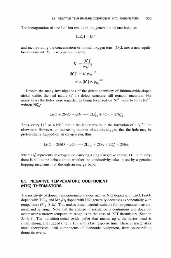
The incorporation of one Liþ ion results in the generation of one hole, so:
[Li 0Ni] ¼ [h†]
and incorporating the concentration of normal oxygen ions, [OO], into a new equili-brium constant, K1, it is possible to write:
K1 ¼ [h†]4
pO21=2
[h†]4 ¼ K1pO21=2
s/ [h†]/ p 1=8O2
Despite the many investigations of the defect chemistry of lithium-oxide-dopednickel oxide, the real nature of the defect structure still remains uncertain. Formany years the holes were regarded as being localized on Ni2þ ions to form Ni3þ,written NiNi
† :
Li2Oþ 2NiOþ 12 O2 �! 2Li0Ni þ 4OO þ 2Ni†Ni
Thus, every Liþ on a Ni2þ site in the lattice results in the formation of a Ni3þ ionelsewhere. However, an increasing number of studies suggest that the hole may bepreferentially trapped on an oxygen ion, thus:
Li2Oþ 2NiOþ 12 O2 �! 2Li 0Ni þ 2OO þ 2O†
O þ 2NiNi
where OO† represents an oxygen ion carrying a single negative charge, O2. Similarly,
there is still some debate about whether the conductivity takes place by a genuinehopping mechanism or through an energy band.
8.3 NEGATIVE TEMPERATURE COEFFICIENT(NTC) THERMISTORS
The resistivity of doped transition-metal oxides such as NiO doped with Li2O, Fe2O3
doped with TiO2, and Mn3O4 doped with NiO generally decreases exponentially withtemperature (Fig. 8.1a). This makes these materials suitable for temperature measure-ment and sensing. [Note that the change in resistance is continuous and does notoccur over a narrow temperature range as in the case of PCT thermistors (Section3.14.4)]. The transition-metal oxide pellet that makes up a thermistor bead issmall, strong, and rugged (Fig. 8.1b), with a fast response time. These characteristicsmake thermistors ideal components of electronic equipment, from spacecraft todomestic ovens.
8.3 NEGATIVE TEMPERATURE COEFFICIENT (NTC) THERMISTORS 355
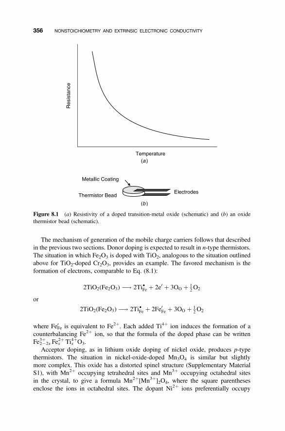
The mechanism of generation of the mobile charge carriers follows that describedin the previous two sections. Donor doping is expected to result in n-type thermistors.The situation in which Fe2O3 is doped with TiO2, analogous to the situation outlinedabove for TiO2-doped Cr2O3, provides an example. The favored mechanism is theformation of electrons, comparable to Eq. (8.1):
2TiO2(Fe2O3) �! 2Ti†Fe þ 2e0 þ 3OO þ 12 O2
or
2TiO2(Fe2O3) �! 2Ti†Fe þ 2Fe0Fe þ 3OO þ 12 O2
where Fe0Fe is equivalent to Fe2þ. Each added Ti4þ ion induces the formation of acounterbalancing Fe2þ ion, so that the formula of the doped phase can be writtenFe222x
3þ Fex2þ Tix
4þO3.Acceptor doping, as in lithium oxide doping of nickel oxide, produces p-type
thermistors. The situation in nickel-oxide-doped Mn3O4 is similar but slightlymore complex. This oxide has a distorted spinel structure (Supplementary MaterialS1), with Mn2þ occupying tetrahedral sites and Mn3þ occupying octahedral sitesin the crystal, to give a formula Mn2þ[Mn3þ]2O4, where the square parenthesesenclose the ions in octahedral sites. The dopant Ni2þ ions preferentially occupy
Figure 8.1 (a) Resistivity of a doped transition-metal oxide (schematic) and (b) an oxidethermistor bead (schematic).
356 NONSTOICHIOMETRY AND EXTRINSIC ELECTRONIC CONDUCTIVITY
octahedral sites. Because the tetrahedral sites and the Mn2þ ions do not figure in thereaction, the spinel can be written MnO . Mn2O3 and the MnO part ignored. Thus,the defect chemistry can be written in terms of NiO doping into Mn2O3. Thedefect equations are then equivalent to acceptor doping into Mn2O3:
2NiO(Mn2O3) �! 2Ni0Mn þ 2OO þ V2†O
2NiO(Mn2O3)þ 12 O2 �! 2Ni0Mn þ 3OO þ 2h†
The holes can be regarded a localized on Mn3þ ions to give Mn4þ, and the dopedoxide has a nominal formula Mn2þ[Mn22x
3þ Mnx4þ Nix
2þ]O4. The material is ap-type semiconductor.
Impurity substitution that is effectively neutral, that is, neither donor nor acceptor,can also lead to significant changes in properties that are utilized in NTC thermistors.For example, the replacement of Ga3þ in the spinel MgGa2O4 by Mn3þ involves noapparent donor or acceptor action. The conductivity in the system MgGa22xMnxO4
evolves from insulating (conductivity about 1029 V21 m21) for the parent phasewith x ¼ 0, to a conductivity approximately equal to that of germanium (1021V21
m21) in the compound MgGaMnO4, in which x ¼ 1. The resistivity decreases mark-edly with temperature and the compounds display typical NCT behavior.
The parent phases for this series can be regarded as MgGa2O4 and MgMn2O4.Both are mixed spinels, but it is convenient to regard them as normal spinels initially.The replacement of Ga3þ by Mn3þ then only concerns the octahedral sites in thestructure. Ignoring the MgO component, this is written:
Mn2O3(Ga2O3) �! 2MnGa þ 3OO
The conductivity comes about because of electron hopping between a pair of Mn3þ
ions. This is equivalent to disproportionation:
MnGa þMnGa �! Mn†Ga þMn0Ga
or in ionic terms:
Mn3þ þMn3þ �! Mn4þ þMn2þ
In mixed spinels, electron transfer between tetrahedral and octahedral Mn3þ ionsis hampered. As the cation distribution is temperature sensitive, preparation ofmaterials for NTC use must optimize the amount of Mn in octahedral sites.
Although these materials are often best described as hopping semiconductors inwhich the mobility is proportional to the exponential of the energy required to liberatethe charge carriers, the conduction mechanism in devices is often complex. Forapplication, mechanisms are sometimes neglected in favor of empirical relationships.
8.3 NEGATIVE TEMPERATURE COEFFICIENT (NTC) THERMISTORS 357
Thus, the thermistor resistance R is frequently written as:
RT ¼ RT0 expb(T0 � T)
T0T
� �
where RT is the resistance at a temperature T (K), b is the thermistor constant, andRT0 is the resistance at a specified reference temperature T0. The thermistor constant,b, is given by
b ¼ Ea
k
where Ea is the activation energy associated with electron movement, usually con-sidered to be by a hopping mechanism, and k is the Boltzmann constant.Thermistors are also frequently characterized by the temperature coefficient ofresistance, a, which is the percentage change in R with temperature. The parameterb generally lies in the range 2000–6000 and devices have values of a of the orderof 4% per degree.
8.4 BROUWER DIAGRAMS FOR DOPED SYSTEMS
8.4.1 Construction
Brouwer diagrams plot the defect concentrations in a solid as a function of the partialpressure of the components of the material and are a convenient way of displayingelectronic properties (Sections 7.6–7.9). These can be readily extended to includethe effects of doping by acceptors or donors.
It is important to know that the defect equilibria that apply to the pure material, andthe associated equilibrium constants, also apply to the doped material. The onlyadditional information required is the nature and concentration of the dopant. To illus-trate the construction of a diagram, an example similar to that given in Chapter 7 willbe presented, for a nonstoichiometric phase of composition MX, nominally contain-ing M2þ and X22 ions, with a stoichiometric composition MX1.0. In this example, itis assumed that the relevant defect formation equations are the same as those given inChapter 7:
1. The creation and elimination of Schottky defects:
nul O V20M þ V2†
X KS ¼ [V20M] [V
2†X ] (8:3)
2. The creation and elimination of electronic defects:
nul O e0 þ h† Ke ¼ [e0] [h†] (8:4)
358 NONSTOICHIOMETRY AND EXTRINSIC ELECTRONIC CONDUCTIVITY
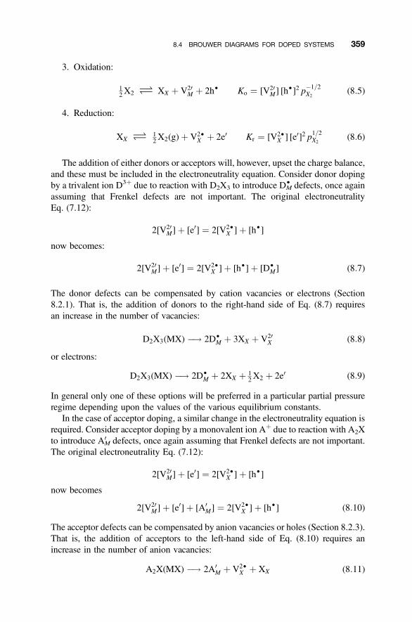
3. Oxidation:
12 X2 O XX þ V20
M þ 2h† Ko ¼ [V20M] [h
†]2 p�1=2X2
(8:5)
4. Reduction:
XX O 12 X2(g)þ V2†
X þ 2e0 Kr ¼ [V2†X ] [e0]2 p1=2X2
(8:6)
The addition of either donors or acceptors will, however, upset the charge balance,and these must be included in the electroneutrality equation. Consider donor dopingby a trivalent ion D3þ due to reaction with D2X3 to introduce DM
† defects, once againassuming that Frenkel defects are not important. The original electroneutralityEq. (7.12):
2[V20M]þ [e0] ¼ 2[V2†
X ]þ [h†]
now becomes:
2[V20M]þ [e0] ¼ 2[V2†
X ]þ [h†]þ [D†M] (8:7)
The donor defects can be compensated by cation vacancies or electrons (Section8.2.1). That is, the addition of donors to the right-hand side of Eq. (8.7) requiresan increase in the number of vacancies:
D2X3(MX) �! 2D†M þ 3XX þ V20
X (8:8)
or electrons:
D2X3(MX) �! 2D†M þ 2XX þ 1
2 X2 þ 2e0 (8:9)
In general only one of these options will be preferred in a particular partial pressureregime depending upon the values of the various equilibrium constants.
In the case of acceptor doping, a similar change in the electroneutrality equation isrequired. Consider acceptor doping by a monovalent ion Aþ due to reaction with A2Xto introduce A0
M defects, once again assuming that Frenkel defects are not important.The original electroneutrality Eq. (7.12):
2[V20M]þ [e0] ¼ 2[V2†
X ]þ [h†]
now becomes
2[V20M]þ [e0]þ [A0
M] ¼ 2[V2†X ]þ [h†] (8:10)
The acceptor defects can be compensated by anion vacancies or holes (Section 8.2.3).That is, the addition of acceptors to the left-hand side of Eq. (8.10) requires anincrease in the number of anion vacancies:
A2X(MX) �! 2A0M þ V2†
X þ XX (8:11)
8.4 BROUWER DIAGRAMS FOR DOPED SYSTEMS 359
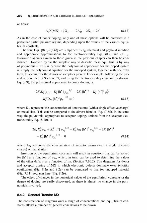
or holes:
A2X(MX)þ 12 X2 �! 2A0
M þ 2XX þ 2h† (8:12)
As in the case of donor doping, only one of these options will be preferred in aparticular partial pressure regime, depending upon the values of the various equili-brium constants.
The four Eqs. [(8.3)–(8.6)] are simplified using chemical and physical intuitionand appropriate approximations to the electroneutrality Eqs. (8.7) and (8.10).Brouwer diagrams similar to those given in the previous chapter can then be con-structed. However, by far the simplest way to describe these equilibria is by wayof polynomials. This is because the polynomial appropriate for the doped systemis simply the polynomial equation for the undoped system, together with one extraterm, to account for the donors or acceptors present. For example, following the pro-cedure described in Section 7.9, and using the electroneutrality equation for donors,Eq. (8.9), the polynomial appropriate to donor doping is:
2KoK2e pX2 þ K3
e [h†] p 1=2
X2� 2Kr [h
†]4 � K2e [h†]3 p1=2X2
� K2e DM [h†]2 p 1=2
X2¼ 0 (8:13)
where DM represents the concentration of donor atoms (with a single effective charge)on metal sites. This can be compared to the almost identical Eq. (7.35). In the sameway, the polynomial appropriate to acceptor doping, derived from the acceptor elec-troneutrality Eq. (8.10), is
2KoK2e pX2 þ K3
e [h†] p 1=2
X2þ K2
e AM [h†]2 p 1=2X2
� 2Kr [h†]4
� K2e [h
†]3 p 1=2X2 ¼ 0 (8:14)
where AM represents the concentration of acceptor atoms (with a single effectivecharge) on metal sites.
Insertion of the equilibrium constants will result in equations that can be solvedfor [h†] as a function of pX2 , which, in turn, can be used to determine the valuesof the other defects as a function of pX2 (Section 7.10.2). The diagrams for donorand acceptor doping of MX in which electronic defects dominate over Schottkyequilibrium (Fig. 8.2a and 8.2c) can be compared to that for undoped material(Fig. 7.11), redrawn here (Fig. 8.2b).
The effect of changes in the numerical values of the equilibrium constants or thedegree of doping are easily discovered, as there is almost no change in the poly-nomials involved.
8.4.2 General Trends: MX
The construction of diagrams over a range of concentrations and equilibrium con-stants allows a number of general conclusions to be drawn.
360 NONSTOICHIOMETRY AND EXTRINSIC ELECTRONIC CONDUCTIVITY
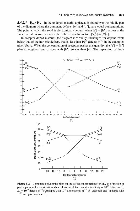
8.4.2.1 Ke > KS In the undoped material a plateau is found over the middle partof the diagram where the dominant defects, [e0] and [h†], have equal concentrations.The point at which the solid is electronically neutral, when [e0] ¼ [h†], occurs at thesame partial pressure as when the solid is stoichiometric, [VM
2 0] ¼ [VX2†].
In acceptor-doped material, the diagram is virtually unchanged for dopant levelsbelow that of the intrinsic defects, that is, less than 1020 defects m23 in the examplesgiven above. When the concentration of acceptors passes this quantity, the [e0] ¼ [h†]plateau lengthens and divides with [h†] greater than [e0]. The separation of these
Figure 8.2 Computed polynomial plots for the defect concentrations for MX as a function ofpartial pressure for the situation where electronic defects are dominant, KS ¼ 1032 defects m23,Ke ¼ 1040 defects m23: (a) doped with 1025 donor atoms m23, (b) undoped, and (c) doped with1025 acceptor atoms m23.
8.4 BROUWER DIAGRAMS FOR DOPED SYSTEMS 361
components increases as the amount of dopant increases. The acceptors are compen-sated by the upper component of the plateau, holes. The point at which the solid iselectronically neutral, when [e0] ¼ [h†], moves to lower pressures, while the pointat which the solid is stoichiometric, when [VM
2 0] ¼ [VX2†], moves to higher pressures.
Electronic neutrality and the stoichiometric composition no longer occur at the samepartial pressure of X. However, the values at which [e0] ¼ [h†] and [VM
20] ¼ [VX2†]
remain the same as in the undoped solid, as these points are governed by the equili-brium constants Ke and KS, which are unchanged upon doping.
In donor-doped material, similar considerations apply. The diagram is virtuallyunchanged when dopant levels are below that of the intrinsic defects, that is, lessthan 1020 defects m23 in the examples given above. When the concentration ofdonors passes this quantity, the [e0] ¼ [h†] plateau lengthens and divides with [e0]greater than [h†]. The separation of these components increases as the amount ofdopant increases. The donors are compensated by the upper component of theplateau, electrons. The point at which the solid is electronically neutral, when[e0] ¼ [h†], moves to higher pressures, while the point at which the solid is stoichio-metric, when [VM
2 0] ¼ [VX2†], moves to lower pressures. Electronic neutrality and the
stoichiometric composition no longer occur at the same partial pressure of X.However, the values at which [e0] ¼ [h†] and [VM
2 0] ¼ [VX2†] remain the same as in
the undoped solid, as these points are governed by the equilibrium constants Ke
and KS, which are unchanged upon doping.
8.4.2.2 KS > Ke In the undoped material a plateau is found over the middlepart of the diagram where the dominant defects, [VM
2 0] and [VX2†], have equal
Figure 8.2 (Continued).
362 NONSTOICHIOMETRY AND EXTRINSIC ELECTRONIC CONDUCTIVITY
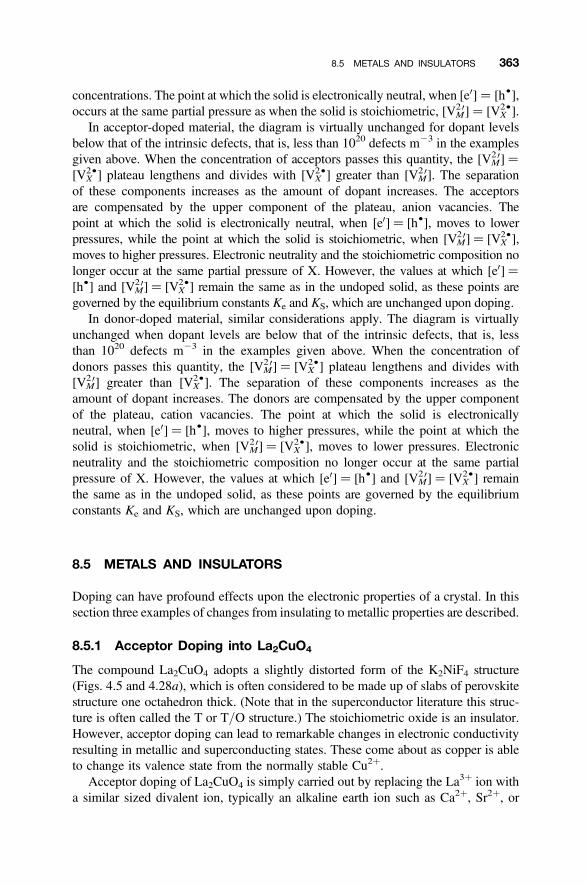
concentrations. The point at which the solid is electronically neutral, when [e0] ¼ [h†],occurs at the same partial pressure as when the solid is stoichiometric, [VM
2 0] ¼ [VX2†].
In acceptor-doped material, the diagram is virtually unchanged for dopant levelsbelow that of the intrinsic defects, that is, less than 1020 defects m23 in the examplesgiven above. When the concentration of acceptors passes this quantity, the [VM
2 0] ¼[VX
2†] plateau lengthens and divides with [VX2†] greater than [VM
2 0]. The separationof these components increases as the amount of dopant increases. The acceptorsare compensated by the upper component of the plateau, anion vacancies. Thepoint at which the solid is electronically neutral, when [e0] ¼ [h†], moves to lowerpressures, while the point at which the solid is stoichiometric, when [VM
2 0] ¼ [VX2†],
moves to higher pressures. Electronic neutrality and the stoichiometric composition nolonger occur at the same partial pressure of X. However, the values at which [e0] ¼[h†] and [VM
2 0] ¼ [VX2†] remain the same as in the undoped solid, as these points are
governed by the equilibrium constants Ke and KS, which are unchanged upon doping.In donor-doped material, similar considerations apply. The diagram is virtually
unchanged when dopant levels are below that of the intrinsic defects, that is, lessthan 1020 defects m23 in the examples given above. When the concentration ofdonors passes this quantity, the [VM
2 0] ¼ [VX2†] plateau lengthens and divides with
[VM2 0] greater than [VX
2†]. The separation of these components increases as theamount of dopant increases. The donors are compensated by the upper componentof the plateau, cation vacancies. The point at which the solid is electronicallyneutral, when [e0] ¼ [h†], moves to higher pressures, while the point at which thesolid is stoichiometric, when [VM
2 0] ¼ [VX2†], moves to lower pressures. Electronic
neutrality and the stoichiometric composition no longer occur at the same partialpressure of X. However, the values at which [e0] ¼ [h†] and [VM
2 0] ¼ [VX2†] remain
the same as in the undoped solid, as these points are governed by the equilibriumconstants Ke and KS, which are unchanged upon doping.
8.5 METALS AND INSULATORS
Doping can have profound effects upon the electronic properties of a crystal. In thissection three examples of changes from insulating to metallic properties are described.
8.5.1 Acceptor Doping into La2CuO4
The compound La2CuO4 adopts a slightly distorted form of the K2NiF4 structure(Figs. 4.5 and 4.28a), which is often considered to be made up of slabs of perovskitestructure one octahedron thick. (Note that in the superconductor literature this struc-ture is often called the T or T/O structure.) The stoichiometric oxide is an insulator.However, acceptor doping can lead to remarkable changes in electronic conductivityresulting in metallic and superconducting states. These come about as copper is ableto change its valence state from the normally stable Cu2þ.
Acceptor doping of La2CuO4 is simply carried out by replacing the La3þ ion witha similar sized divalent ion, typically an alkaline earth ion such as Ca2þ, Sr2þ, or
8.5 METALS AND INSULATORS 363
Ba2þ. In this process, small changes in the oxygen content also occur, which will beignored in the following discussion.
Following substitution, charge neutrality can be maintained in one of the threeways, as described above, that is, by the introduction of cation interstitials, anionvacancies, or holes. Replacement of some of the La3þ by Sr2þ can be written interms of La2O3 alone (Section 1.11.7):
Cation interstitials: 3SrO(La2O3) �! 2Sr0La þ 3OO þ Sr2†i (a)
Anion vacancies: 2SrO(La2O3) �! 2Sr0La þ 2OO þ V2†O (b)
Holes: 2SrO(La2O3)þ 12 O2 �! 2Sr0La þ 3OO þ 2 h† (c)
This last equation is equivalent to filling of the anion vacancies by atmosphericoxygen:
V2†O þ 1
2 O2 O OO þ 2h†
Including the component, CuO gives:
Cation interstitials: 3SrO(La2CuO4) �! 2Sr0La þ 4OO þ Sr2†i þ CuCu (a)
Anion vacancies: 2SrO(La2CuO4) �! 2Sr0La þ 3OO þ V2†O þ CuCu (b)
Holes: 2SrO(La2CuO4)þ 12 O2 �! 2Sr0La þ 4OO þ CuCu þ 2h† (c)
The defect structure that occurs on acceptor doping is a function of dopantconcentration. At low concentrations, hole generation is preferred—Eq. (c). Theincorporation of one acceptor ion generates one hole in the structure. In terms ofsuperconductivity, these are regarded as being generated in the LaO layers beforemigrating into the CuO sheets. Within the CuO layers the holes are generally regardedas located on some of the Cu2þ ions to form Cu3þ defects, although there is evidencethat holes may also reside on O22 ions to generate O2 species. Insulating La2CuO4
becomes a semiconductor when the hole concentration reaches about 0.05 holes perCu2þ. As each Sr2þ dopant ion generates 1 hole, the composition is approximatelyLa1.95Sr0.05Cu0.95
2þ Cu0.053þ O4. Continued doping continues the transformation, and the
solid shows superconductivity when the hole concentration reaches about 0.1holes per Cu2þ, that is, at a composition La1.9Sr0.1Cu0.9
2þCu0.13þO4. Further doping
transforms the phase into a metallic conductor. The material that has a maximumsuperconducting transition temperature of 37 K has a composition ofLa1.85Sr0.15CuO4 and is referred to as a “hole” superconductor. As doping increasespast this amount, the compensation mechanism changes from hole generation tovacancy generation—Eq. (b). One oxygen vacancy is generated for every two Sr2þ
dopant ions to give a formula La22xSrxCu2þO42x/2. Holes are no longer generated
and superconductivity is lost. Preparations made under high oxygen pressures canreverse this trend, and vacancy-free materials can be prepared with higher dopantconcentrations. Under these conditions the material loses superconductor properties
364 NONSTOICHIOMETRY AND EXTRINSIC ELECTRONIC CONDUCTIVITY
when the concentration of Sr2þ reaches approximately 0.32, although it remains ametal.
Although the superconducting state of this material has attracted considerableattention, the metallic state is also of interest. For instance, metallic samples arebeing explored for use as cathode materials in solid oxide fuel cells (Section 6.10).
8.5.2 Donor Doping into Nd2CuO4
The structure of Nd2CuO4 is very similar to La2CuO4, the principal difference lies inthe disposition of the oxygen atoms, as the cations in the two structures are in almostidentical positions (Fig. 8.3). However, in Nd2CuO4 the Nd
3þ ions are in the centersof oxygen cubes, and so this region of the structure can be likened to slabs of thefluorite type, and the structure may be described as an intergrowth of perovskiteand fluorite structures. The Cu atoms lie at the centers of square coordinationgroups between these fluorite slabs rather than octahedra, as in La2CuO4. (Notethat in the superconductor literature this structure is often called the T0 structure.)
The structural and chemical similarity of La2CuO4 and Nd2CuO4 suggest thatNd2CuO4 should become metallic following acceptor (hole) doping. This turns outnot to occur, and hole superconductivity does not arise in this phase when Nd3þ issubstituted by Ca2þ, Sr2þ, or Ba2þ. However, Nd2CuO4 can be made metallic andsuperconducting by donor doping involving the substitution of the lanthanide bya higher valence cation such as Ce4þ to form, for example, Nd22xCexCuO4. As inthe case of La2CuO4, doping is usually accompanied by small changes in oxygencontent, which will be ignored in the present discussion.
Figure 8.3 Comparison of the unit cells of the idealized La2CuO4 and Nd2CuO4 structures.
8.5 METALS AND INSULATORS 365

Using the same formalism as above, and writing Nd2CuO4 as Nd2O3 þ CuO,and focusing upon donor doping into Nd2O3, charge compensation can be by thefollowing:
Cation vacancies: 3CeO2(Nd2O3) �! 3Ce†Nd þ V30Nd þ 6OO (a)
Anion interstitials: 2CeO2(Nd2O3) �! 2Ce†Nd þ 3OO þ O20i (b)
Electrons: 2CeO2(Nd2O3) �! 2Ce†Nd þ 2e0 þ 3OO þ 12 O2 (c)
The oxygen interstitials in Eq. (b) are regarded as lost to the atmosphere:
O20i O 1
2 O2 þ 2e0
to give Eq. (c). The component CuO as CuCu and OO can be added to each of theseequations to make them represent stoichiometric Nd2CuO4.
As in the case of La2CuO4, initial doping turns the insulator into a metal.Further doping creates the superconducting state. Chemically, the donor dopingcan be written in terms of the generation of Cuþ in place of Cu2þ. The Cuþ ion isequivalent to a Cu2þ ion together with a trapped electron, and the formula isNd22xCexCu12x
2þ CuxþO4 where one Cuþ ion is created for every donor Ce4þ in
the crystal. The compounds are considered to be electron superconductors ratherthan hole superconductors as in the La2CuO4-related phases. The superconductingstate occurs over a rather narrow range of substitutions with x taking values ofapproximately 0.12–0.18. The maximum value of the superconducting transitiontemperature, Tc, is approximately 24 K, reached in the compound Nd1.85Ce0.15CuO4.
8.5.3 Spinel System Li11xTi22xO4
The spinel family of oxides with composition AB2O4 has the A and B cations distri-buted in octahedral and tetrahedral sites in a close-packed oxygen structure(Supplementary Material S1). Impurity doping can take place by the addition of adopant to octahedral or tetrahedral sites. In this, the spinel family of compounds isquite different from the A2BO4 perovskite-related phases of the previous section inthat both cation sites are similar in size and can take the same cations.
The normal spinel Li[Ti2]O4 is a metallic oxide with a superconducting transitiontemperature of 13.7 K. The nominal formula is Liþ[Ti3þTi4þ]O4, in which the Liþ
ions occupy the tetrahedral sites while the octahedral sites contain titanium with anaverage charge Ti3.5þ, although as the material is metallic at room temperature theelectrons are delocalized in a partly filled 3d band.
The average valance of the Ti component can be pushed toward 4.0 by valenceinduction, simply by increasing the amount of Li present relative to that of titanium,to give a formula Li1þxTi22xO4. This is equivalent to acceptor doping of the phase.The additional Liþ ions enter the octahedral sites, as the tetrahedral sites are alreadyoccupied, to a maximum of Liþ[Li1/3
þ Ti5/34þ ]O4 and the acceptor doping is balanced
by holes. In order to write formal defect equations for this situation, it is convenient
366 NONSTOICHIOMETRY AND EXTRINSIC ELECTRONIC CONDUCTIVITY
to regard the doping as affecting only the Ti3þ component. Writing the spinel asLi2O þ Ti2O3 þ 2TiO2 (to give 2LiTi2O4), the defect reaction of importanceapplies only to the Ti2O3 component:
Li2O(Ti2O3)þ O2 �! 2Li20Ti3 þ 3OO þ 4h†
where only the Ti3þ sites are involved and are written as Ti3. Clearly a Ti3þ ion on itsnormal site shows no effective charge. The other components can be added to theseequations to give
Li2O(2LiTi2O4) �! 2LiLi þ 2Li20Ti3 þ 2TiTi4 þ 8OO þ 4h†
where the Ti4þ sites involved are written as Ti4.The holes can be regarded as transferred to Ti3þ ions converting them to Ti4þ by
adding in the requisite number of extra ions:
Li2O(6LiTi2O4)þ O2 �! 6LiLi þ 2Li20Ti3 þ 4Ti†Ti3 þ 6TiTi4 þ 24OO
where TiTi3† represents a Ti3þ ion plus a hole on a Ti3þ site. In terms of an ionic
picture each extra Liþ present forces a Ti3þ ion to become Ti4þ. The limit occurswhen x ¼ 1
3, to give Li4/3Ti5/3O4. The 3d band is now completely empty. Aswould be expected, this material is a colorless insulator.
The conductivity changes in a discontinuous fashion at a composition of approxi-mately x ¼ 0.12 at which composition the metal becomes a poor semiconductor. Theformula is now Liþ[Li0.12
þ Ti0.643þ Ti1.24
4þ ]O4. This transition is reversible. Donor dopingof insulating Li4/3Ti5/3O4 will return the compound to the metallic state.
8.6 CUPRATE HIGH-TEMPERATURE SUPERCONDUCTORS
8.6.1 Perovskite-Related Structures and Series
The important and widely studied copper-oxide-derived high-temperature super-conductors, known as cuprate superconductors, are basically insulators. Dopingconverts these into metallic materials, many of which are superconductors overrather more restricted composition ranges. Several of these materials have alreadybeen discussed: La2CuO4 and Sr2CuO2F2 (Section 4.3.3), La22xSrxCuO4 (Section8.5.1), and Nd22xCexCuO4 (Section 8.5.2).
In the materials that follow, the structures are all layered. This structural featurehas lead to a description of the doping in terms of charge reservoirs, a differentapproach to that described previously, and which is detailed below. Structurally thephases are all related to the perovskite-layered structures (Figs. 4.27, 4.28,4.29, and 4.30). The similarity can be appreciated by comparison ofthe idealized structures and formulas of some of these materials, Bi2Sr2CuO6
8.6 CUPRATE HIGH-TEMPERATURE SUPERCONDUCTORS 367
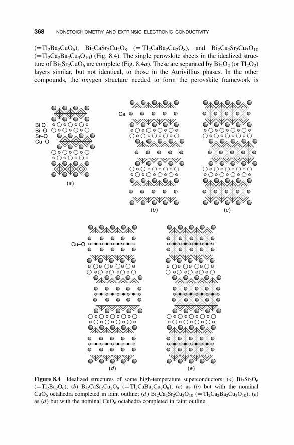
(¼Tl2Ba2CuO6), Bi2CaSr2Cu2O8 (¼ Tl2CaBa2Cu2O8), and Bi2Ca2Sr2Cu3O10
(¼Tl2Ca2Ba2Cu3O10) (Fig. 8.4). The single perovskite sheets in the idealized struc-ture of Bi2Sr2CuO6 are complete (Fig. 8.4a). These are separated by Bi2O2 (or Tl2O2)layers similar, but not identical, to those in the Aurivillius phases. In the othercompounds, the oxygen structure needed to form the perovskite framework is
Figure 8.4 Idealized structures of some high-temperature superconductors: (a) Bi2Sr2O6
(¼Tl2Ba2O6); (b) Bi2CaSr2Cu2O8 (¼Tl2CaBa2Cu2O8); (c) as (b) but with the nominalCuO6 octahedra completed in faint outline; (d ) Bi2Ca2Sr2Cu3O10 (¼Tl2Ca2Ba2Cu3O10); (e)as (d ) but with the nominal CuO6 octahedra completed in faint outline.
368 NONSTOICHIOMETRY AND EXTRINSIC ELECTRONIC CONDUCTIVITY

incomplete. The nominal double layer of CuO6 octahedra needed to form a sheet ofthe idealized perovskite structure is replaced by square pyramids in Bi2CaSr2Cu2O8
(Fig. 8.4b). To make the relationship clearer, the octahedra are completed in faintoutline in Figure 8.4c. In the case of Ba2Ca2Sr2Cu3O10 the three CuO6 octahedralperovskite layers have been replaced by two sheets of square pyramids and middlelayer by a sheet of CuO4 squares (Fig. 8.4d ). The octahedra are completed in faintoutline in Figure 8.4e.
In these and the other cuprate superconductors, the part of the structure that leadsto superconductivity is the slab of CuO2 sheets. When more than one sheet is present,they are separated by cation layers, Q (usually Ca or Y) to give a sequence CuO2–(Q–CuO2)n21, which forms the superconducting layer in the material. The index nis the total number of CuO2 layers in the phase, which is equal to the formulanumber of Cu atoms present (Fig. 8.5).
The CuO2 layers themselves are not, as such, superconducting and have to bedoped with (usually) holes. These are provided by the charge reservoir layers thatseparate each CuO2–(Q–CuO2)n21 slab. The general structure of a charge reservoirsheet is AO–[MOx]m–AO, where A is a lanthanide such as La, or alkaline earth, typi-cally Sr or Ba, M is a metal, typically Bi, Pb, Tl, or Hg, present as a nonstoichiometricoxide layer with x usually close to 0 or 1.0, and m takes values of 0, 1, 2, and so on.Doping the charge reservoir layer with acceptors, mainly oxygen, favors the creationof holes, which are subsequently transferred to the CuO2 slab for metallic behaviorand superconductivity to occur (Fig. 8.6).
Figure 8.5 Superconducting planes found in cuprate superconductors: (a) a single CuO2
sheet and (b) a CuO2 (Q2CuO2)n21 superconducting layer.
8.6 CUPRATE HIGH-TEMPERATURE SUPERCONDUCTORS 369
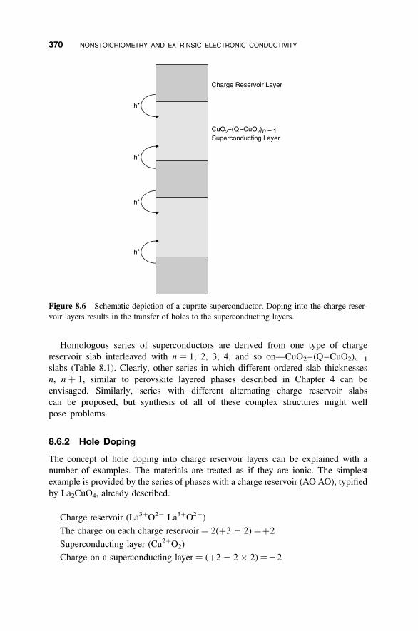
Homologous series of superconductors are derived from one type of chargereservoir slab interleaved with n ¼ 1, 2, 3, 4, and so on—CuO2–(Q–CuO2)n21
slabs (Table 8.1). Clearly, other series in which different ordered slab thicknessesn, n þ 1, similar to perovskite layered phases described in Chapter 4 can beenvisaged. Similarly, series with different alternating charge reservoir slabscan be proposed, but synthesis of all of these complex structures might wellpose problems.
8.6.2 Hole Doping
The concept of hole doping into charge reservoir layers can be explained with anumber of examples. The materials are treated as if they are ionic. The simplestexample is provided by the series of phases with a charge reservoir (AO AO), typifiedby La2CuO4, already described.
Charge reservoir (La3þO22 La3þO22)
The charge on each charge reservoir ¼ 2(þ32 2) ¼þ2
Superconducting layer (Cu2þO2)
Charge on a superconducting layer ¼ (þ2 2 2 � 2) ¼22
Figure 8.6 Schematic depiction of a cuprate superconductor. Doping into the charge reser-voir layers results in the transfer of holes to the superconducting layers.
370 NONSTOICHIOMETRY AND EXTRINSIC ELECTRONIC CONDUCTIVITY
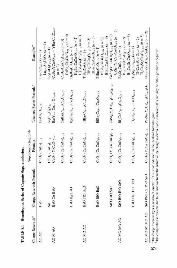
TABLE8.1
Hom
ologou
sSeries
ofCup
rate
Supercon
ductors
ChargeReservoira
ChargeReservoirFo
rmula
Superconductin
gSlab
Form
ula
Idealized
SeriesFo
rmulaa
Examples
b
AOAO
LaO
CuO
2(CuO
2) n21
La 2Cu nO2nþ2
La 2CuO
4þd(n
¼1)
La 2
2xSr xCuO
4(n
¼1)
SrF
CuO
2(CuO
2) n21
Sr 2Cu nO2nF2
Sr 2CuO
2F2þd(n
¼1)
AO
MAO
BaO
CuBaO
CuO
2(Y
CuO
2) n21
Ba 2Yn21Cu n
þ1O2nþd
CuB
a 2YCu 2O6þd¼
YBa 2Cu 3O6þd
(n¼
2)CuO
2(CaCuO
2) n21
CuB
a 2Ca n
21Cu nO2nþ2
CuB
a 2Ca 2Cu 3O8þd(n
¼3)
CuB
a 2Ca 3Cu 4O10þd(n
¼4)
BaO
HgBaO
CuO
2(CaCuO
2) n21
HgB
a 2Ca n
21Cu nO2nþ2
HgB
a 2CuO
4þd(n
¼1)
HgB
a 2CaC
u 2O6þd(n
¼2)
HgB
a 2Ca 2Cu 3O8þd(n
¼3)
AO
MOAO
BaO
TlO
BaO
CuO
2(CaCuO
2) n21
TlBa 2Ca n
21Cu nO2nþ3
TlBa 2CuO
5(n
¼1)
TlBa 2CaC
u 2O7þd(n
¼2)
TlBa 2Ca 2Cu 3O9þd(n
¼3)
BaO
BiO
BaO
CuO
2(CaCuO
2) n21
BiBa 2Ca n
21Cu nO2nþ3
BiBa 2CuO
5þd(n
¼1)
BiBa 2CaC
u 2O7þd(n
¼2)
BiBa 2Ca 2Cu 3O9þd(n
¼3)
SrO
GaO
SrO
CuO
2(Y
,CaCuO
2) n21
GaSr 2(Y,C
a)n21Cu nO2nþ3
GaSr 2(Y
,Ca)Cu 2O7þd(n
¼2)
GaSr 2(Y,Ca)
2Cu 3O9þd(n
¼3)
AO
MO
MOAO
SrO
BiO
BiO
SrO
CuO
2(CaCuO
2) n21
Bi 2CaSr 2n21Cu nO2nþ4
Bi 2Sr 2CuO
6þd(n
¼1)
Bi 2CaSr 2Cu 2O8þd(n
¼2)
Bi 2Ca 2Sr 2Cu 3O10þd(n
¼3)
BaO
TlO
TlO
BaO
CuO
2(CaCuO
2) n21
Tl 2Ba 2Ca n
21Cu nO2nþ4
Tl 2Sr 2CuO
6þd(n
¼1)
Tl 2CaSr 2Cu 2O8þd(n
¼2)
Tl 2Ca 2Sr 2Cu 3O10þd(n
¼3)
AO
MO
M0 M
OAO
SrO
PbO
CuPbO
SrO
CuO
2(Y
,CaCuO
2) n21
Pb 2Sr 2(Y,Ca)
n21Cu n
þ1O8
Pb 2Sr 2Y0.5Ca 0
.5Cu 3O8þd(n
¼2)
aThe
charge
reservoirlayerisnonstoichiom
etric.
Thisisnotindicatedin
theidealized
form
ulas
given.
bThe
compositio
nisvariable
dueto
thenonstoichiom
etricnature
ofthecharge
reservoirslabs;dindicatesthisandmay
beeither
positiv
eor
negativ
e.
371
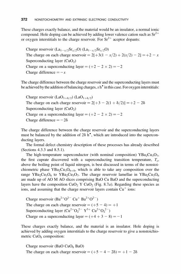
These charges exactly balance, and the material would be an insulator, a normal ioniccompound. Hole doping can be achieved by adding lower valence cation such as Sr2þ
or oxygen interstitials to the charge reservoir. For Sr2þ aceptor dopants:
Charge reservoir (La12x/2Srx/2O) (La12x/2Srx/2O)
The charge on each charge reservoir ¼ 2[þ3(1 2 x/2) þ 2(x/2)2 2] ¼þ2 2 x
Superconducting layer (CuO2)
Charge on a superconducting layer ¼ (þ22 2 � 2) ¼22
Charge difference ¼2x
The charge difference between the charge reservoir and the superconducting layers mustbe achieved by the addition of balancing charges, xh† in this case. Foroxygen interstitials:
Charge reservoir (LaO1þd/2) (LaO1þd/2)
The charge on each charge reservoir ¼ 2[þ32 2(1 þ d/2)] ¼þ22 2d
Superconducting layer (CuO2)
Charge on a superconducting layer ¼ (þ22 2 � 2) ¼22
Charge difference ¼22d
The charge difference between the charge reservoir and the superconducting layersmust be balanced by the addition of 2d h†, which are introduced into the supercon-ducting layers.
The formal defect chemistry description of these processes has already described(Sections 4.3.3 and 8.5.1).
The high-temperature superconductor (with nominal composition) YBa2Cu3O7,the first cuprate discovered with a superconducting transition temperature, Tc,above the boiling point of liquid nitrogen, is best discussed in terms of the nonstoi-chiometric phase YBa2Cu3O6þd, which is able to take any composition over therange YBa2Cu3O6 to YBa2Cu3O7. The charge reservoir lamellae in YBa2Cu3O6
are made up of AO M AO slices comprising BaO Cu BaO and the superconductinglayers have the composition CuO2 Y CuO2 (Fig. 8.7a). Regarding these species asions, and assuming that the charge reservoir layers contain Cuþ ions:
Charge reservoir (Ba2þO22 Cuþ Ba2þO22)
The charge on each charge reservoir ¼ (þ52 4) ¼ þ1
Superconducting layer (Cu2þO222 Y3þ Cu2þO2
22)
Charge on a superconducting layer ¼ (þ4 þ 3 2 8) ¼21
These charges exactly balance, and the material is an insulator. Hole doping isachieved by adding oxygen interstitials to the charge reservoir to give a nonstoichio-metric CuOd composition:
Charge reservoir (BaO CuOd BaO)
The charge on each charge reservoir ¼ (þ52 4 2 2d) ¼ þ1 2 2d
372 NONSTOICHIOMETRY AND EXTRINSIC ELECTRONIC CONDUCTIVITY
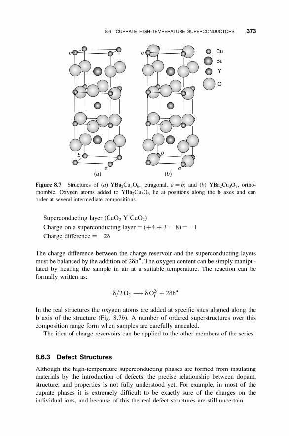
Superconducting layer (CuO2 Y CuO2)
Charge on a superconducting layer ¼ (þ4 þ 32 8) ¼21
Charge difference ¼22d
The charge difference between the charge reservoir and the superconducting layersmust be balanced by the addition of 2dh†. The oxygen content can be simply manipu-lated by heating the sample in air at a suitable temperature. The reaction can beformally written as:
d=2O2 �! dO20i þ 2dh†
In the real structures the oxygen atoms are added at specific sites aligned along theb axis of the structure (Fig. 8.7b). A number of ordered superstructures over thiscomposition range form when samples are carefully annealed.
The idea of charge reservoirs can be applied to the other members of the series.
8.6.3 Defect Structures
Although the high-temperature superconducting phases are formed from insulatingmaterials by the introduction of defects, the precise relationship between dopant,structure, and properties is not fully understood yet. For example, in most of thecuprate phases it is extremely difficult to be exactly sure of the charges on theindividual ions, and because of this the real defect structures are still uncertain.
Figure 8.7 Structures of (a) YBa2Cu3O6, tetragonal, a ¼ b; and (b) YBa2Cu3O7, ortho-rhombic. Oxygen atoms added to YBa2Cu3O6 lie at positions along the b axes and canorder at several intermediate compositions.
8.6 CUPRATE HIGH-TEMPERATURE SUPERCONDUCTORS 373
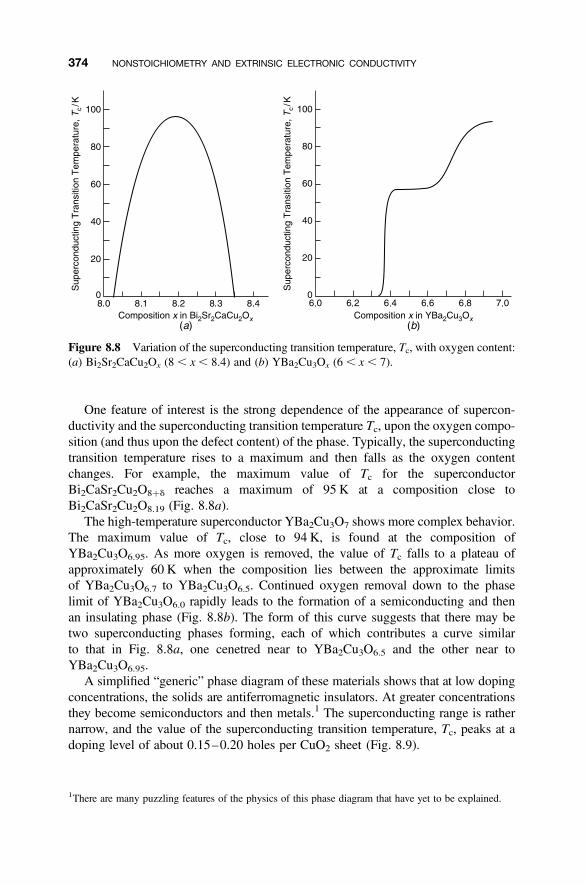
One feature of interest is the strong dependence of the appearance of supercon-ductivity and the superconducting transition temperature Tc, upon the oxygen compo-sition (and thus upon the defect content) of the phase. Typically, the superconductingtransition temperature rises to a maximum and then falls as the oxygen contentchanges. For example, the maximum value of Tc for the superconductorBi2CaSr2Cu2O8þd reaches a maximum of 95 K at a composition close toBi2CaSr2Cu2O8.19 (Fig. 8.8a).
The high-temperature superconductor YBa2Cu3O7 shows more complex behavior.The maximum value of Tc, close to 94 K, is found at the composition ofYBa2Cu3O6.95. As more oxygen is removed, the value of Tc falls to a plateau ofapproximately 60 K when the composition lies between the approximate limitsof YBa2Cu3O6.7 to YBa2Cu3O6.5. Continued oxygen removal down to the phaselimit of YBa2Cu3O6.0 rapidly leads to the formation of a semiconducting and thenan insulating phase (Fig. 8.8b). The form of this curve suggests that there may betwo superconducting phases forming, each of which contributes a curve similarto that in Fig. 8.8a, one cenetred near to YBa2Cu3O6.5 and the other near toYBa2Cu3O6.95.
A simplified “generic” phase diagram of these materials shows that at low dopingconcentrations, the solids are antiferromagnetic insulators. At greater concentrationsthey become semiconductors and then metals.1 The superconducting range is rathernarrow, and the value of the superconducting transition temperature, Tc, peaks at adoping level of about 0.15–0.20 holes per CuO2 sheet (Fig. 8.9).
Figure 8.8 Variation of the superconducting transition temperature, Tc, with oxygen content:(a) Bi2Sr2CaCu2Ox (8, x, 8.4) and (b) YBa2Cu3Ox (6 , x , 7).
1There are many puzzling features of the physics of this phase diagram that have yet to be explained.
374 NONSTOICHIOMETRY AND EXTRINSIC ELECTRONIC CONDUCTIVITY
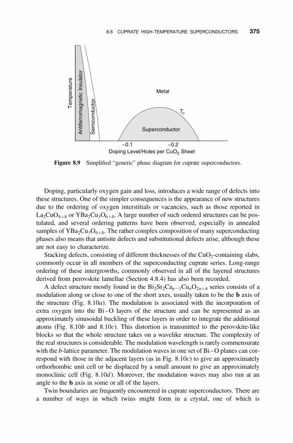
Doping, particularly oxygen gain and loss, introduces a wide range of defects intothese structures. One of the simpler consequences is the appearance of new structuresdue to the ordering of oxygen interstitials or vacancies, such as those reported inLa2CuO4þd or YBa2Cu3O6þd. A large number of such ordered structures can be pos-tulated, and several ordering patterns have been observed, especially in annealedsamples of YBa2Cu3O6þd. The rather complex composition of many superconductingphases also means that antisite defects and substitutional defects arise, although theseare not easy to characterize.
Stacking defects, consisting of different thicknesses of the CuO2-containing slabs,commonly occur in all members of the superconducting cuprate series. Long-rangeordering of these intergrowths, commonly observed in all of the layered structuresderived from perovskite lamellae (Section 4.8.4) has also been recorded.
A defect structure mostly found in the Bi2Sr2Can21CunO2nþ4 series consists of amodulation along or close to one of the short axes, usually taken to be the b axis ofthe structure (Fig. 8.10a). The modulation is associated with the incorporation ofextra oxygen into the Bi–O layers of the structure and can be represented as anapproximately sinusoidal buckling of these layers in order to integrate the additionalatoms (Fig. 8.10b and 8.10c). This distortion is transmitted to the perovskite-likeblocks so that the whole structure takes on a wavelike structure. The complexity ofthe real structures is considerable. The modulation wavelength is rarely commensuratewith the b-lattice parameter. The modulation waves in one set of Bi–O planes can cor-respond with those in the adjacent layers (as in Fig. 8.10c) to give an approximatelyorthorhombic unit cell or be displaced by a small amount to give an approximatelymonoclinic cell (Fig. 8.10d ). Moreover, the modulation waves may also run at anangle to the b axis in some or all of the layers.
Twin boundaries are frequently encountered in cuprate superconductors. There area number of ways in which twins might form in a crystal, one of which is
Figure 8.9 Simplified “generic” phase diagram for cuprate superconductors.
8.6 CUPRATE HIGH-TEMPERATURE SUPERCONDUCTORS 375

Figure 8.10 Idealized structures of Bi2Ca2Sr2Cu3O10þd: (a) atomic structure projected down[100]; (b) structure as Bi–O and perovskite lamellae; (c) incommensurate modulation (exag-gerated) along the b axis with a period b0 � 5.8 b (orthorhombic); and (d ) incommensuratemodulation (exaggerated) along the b axis with a period b0 � 5.8 b (monoclinic).
376 NONSTOICHIOMETRY AND EXTRINSIC ELECTRONIC CONDUCTIVITY
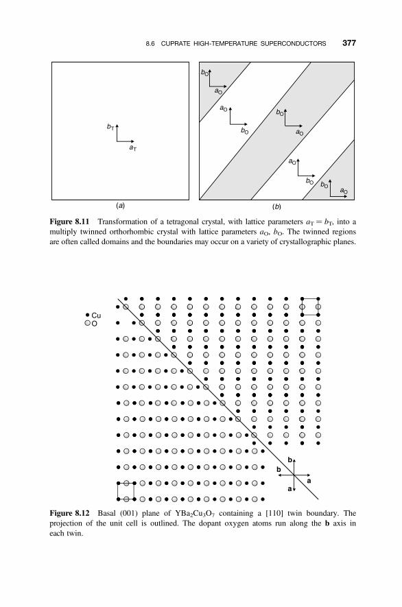
Figure 8.11 Transformation of a tetragonal crystal, with lattice parameters aT ¼ bT, into amultiply twinned orthorhombic crystal with lattice parameters aO, bO. The twinned regionsare often called domains and the boundaries may occur on a variety of crystallographic planes.
Figure 8.12 Basal (001) plane of YBa2Cu3O7 containing a [110] twin boundary. Theprojection of the unit cell is outlined. The dopant oxygen atoms run along the b axis ineach twin.
8.6 CUPRATE HIGH-TEMPERATURE SUPERCONDUCTORS 377
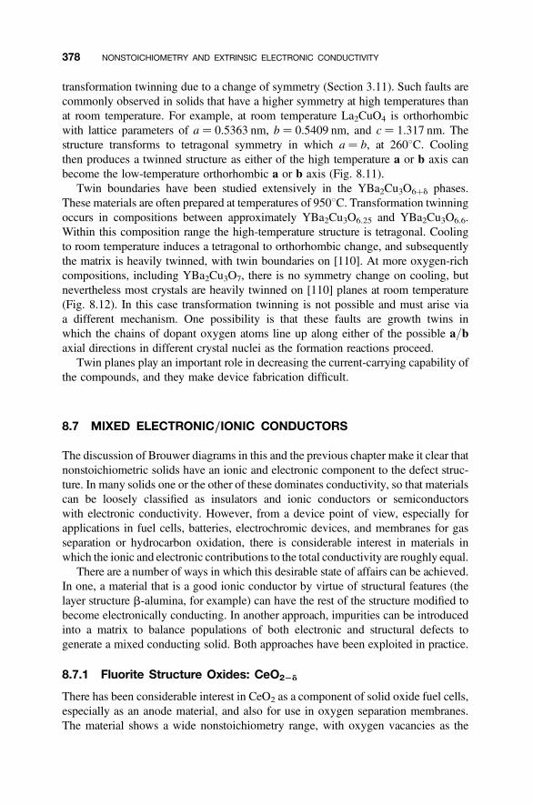
transformation twinning due to a change of symmetry (Section 3.11). Such faults arecommonly observed in solids that have a higher symmetry at high temperatures thanat room temperature. For example, at room temperature La2CuO4 is orthorhombicwith lattice parameters of a ¼ 0.5363 nm, b ¼ 0.5409 nm, and c ¼ 1.317 nm. Thestructure transforms to tetragonal symmetry in which a ¼ b, at 2608C. Coolingthen produces a twinned structure as either of the high temperature a or b axis canbecome the low-temperature orthorhombic a or b axis (Fig. 8.11).
Twin boundaries have been studied extensively in the YBa2Cu3O6þd phases.These materials are often prepared at temperatures of 9508C. Transformation twinningoccurs in compositions between approximately YBa2Cu3O6.25 and YBa2Cu3O6.6.Within this composition range the high-temperature structure is tetragonal. Coolingto room temperature induces a tetragonal to orthorhombic change, and subsequentlythe matrix is heavily twinned, with twin boundaries on [110]. At more oxygen-richcompositions, including YBa2Cu3O7, there is no symmetry change on cooling, butnevertheless most crystals are heavily twinned on [110] planes at room temperature(Fig. 8.12). In this case transformation twinning is not possible and must arise viaa different mechanism. One possibility is that these faults are growth twins inwhich the chains of dopant oxygen atoms line up along either of the possible a/baxial directions in different crystal nuclei as the formation reactions proceed.
Twin planes play an important role in decreasing the current-carrying capability ofthe compounds, and they make device fabrication difficult.
8.7 MIXED ELECTRONIC/IONIC CONDUCTORS
The discussion of Brouwer diagrams in this and the previous chapter make it clear thatnonstoichiometric solids have an ionic and electronic component to the defect struc-ture. In many solids one or the other of these dominates conductivity, so that materialscan be loosely classified as insulators and ionic conductors or semiconductorswith electronic conductivity. However, from a device point of view, especially forapplications in fuel cells, batteries, electrochromic devices, and membranes for gasseparation or hydrocarbon oxidation, there is considerable interest in materials inwhich the ionic and electronic contributions to the total conductivity are roughly equal.
There are a number of ways in which this desirable state of affairs can be achieved.In one, a material that is a good ionic conductor by virtue of structural features (thelayer structure b-alumina, for example) can have the rest of the structure modified tobecome electronically conducting. In another approach, impurities can be introducedinto a matrix to balance populations of both electronic and structural defects togenerate a mixed conducting solid. Both approaches have been exploited in practice.
8.7.1 Fluorite Structure Oxides: CeO22d
There has been considerable interest in CeO2 as a component of solid oxide fuel cells,especially as an anode material, and also for use in oxygen separation membranes.The material shows a wide nonstoichiometry range, with oxygen vacancies as the
378 NONSTOICHIOMETRY AND EXTRINSIC ELECTRONIC CONDUCTIVITY
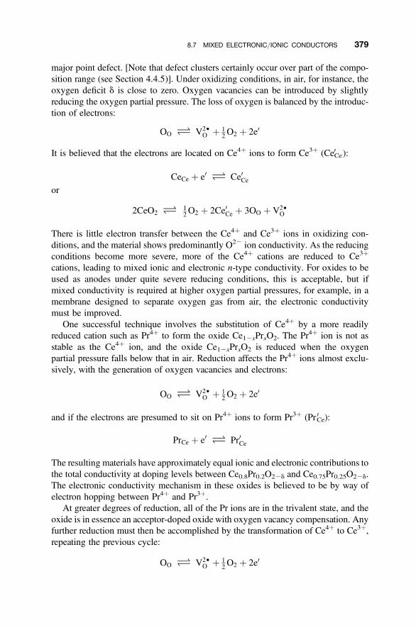
major point defect. [Note that defect clusters certainly occur over part of the compo-sition range (see Section 4.4.5)]. Under oxidizing conditions, in air, for instance, theoxygen deficit d is close to zero. Oxygen vacancies can be introduced by slightlyreducing the oxygen partial pressure. The loss of oxygen is balanced by the introduc-tion of electrons:
OO O V2†O þ 1
2 O2 þ 2e0
It is believed that the electrons are located on Ce4þ ions to form Ce3þ (CeCe0 ):
CeCe þ e0 O Ce0Ceor
2CeO2 O 12 O2 þ 2Ce0Ce þ 3OO þ V2†
O
There is little electron transfer between the Ce4þ and Ce3þ ions in oxidizing con-ditions, and the material shows predominantly O22 ion conductivity. As the reducingconditions become more severe, more of the Ce4þ cations are reduced to Ce3þ
cations, leading to mixed ionic and electronic n-type conductivity. For oxides to beused as anodes under quite severe reducing conditions, this is acceptable, but ifmixed conductivity is required at higher oxygen partial pressures, for example, in amembrane designed to separate oxygen gas from air, the electronic conductivitymust be improved.
One successful technique involves the substitution of Ce4þ by a more readilyreduced cation such as Pr4þ to form the oxide Ce12xPrxO2. The Pr4þ ion is not asstable as the Ce4þ ion, and the oxide Ce12xPrxO2 is reduced when the oxygenpartial pressure falls below that in air. Reduction affects the Pr4þ ions almost exclu-sively, with the generation of oxygen vacancies and electrons:
OO O V2†O þ 1
2 O2 þ 2e0
and if the electrons are presumed to sit on Pr4þ ions to form Pr3þ (Pr 0Ce):
PrCe þ e0 O Pr0Ce
The resulting materials have approximately equal ionic and electronic contributions tothe total conductivity at doping levels between Ce0.8Pr0.2O22d and Ce0.75Pr0.25O22d.The electronic conductivity mechanism in these oxides is believed to be by way ofelectron hopping between Pr4þ and Pr3þ.
At greater degrees of reduction, all of the Pr ions are in the trivalent state, and theoxide is in essence an acceptor-doped oxide with oxygen vacancy compensation. Anyfurther reduction must then be accomplished by the transformation of Ce4þ to Ce3þ,repeating the previous cycle:
OO O V2†O þ 1
2 O2 þ 2e0
8.7 MIXED ELECTRONIC/IONIC CONDUCTORS 379
and if the electrons are presumed to sit on Ce4þ ions to form Ce3þ (Ce0Ce):
CeCe þ e0 O Ce0Ce
8.7.2 Layered Structures: LixMX2
The cathode of a battery or fuel cell must allow good ionic conductivity for the ionsarriving from the electrolyte and allow for electron conduction to any interconnectsbetween cells and to external leads. In addition these properties must persist underoxidizing conditions. An important strategy has been to employ layered structuresolids in which rapid ionic motion occurs between the layers while electronic conduc-tivity is mainly a function of the layers themselves.
One of the first mixed conductors to be utilized as a battery cathode was lithiumintercalated LixTiS2. This material is composed of TiS2 sheets (Section 4.7). Lithiumcan be inserted between the layers reversibly, making LixTiS2 suitable for use as acathode material in batteries that employ Liþ ion transport from the anode acrossthe electrolyte (Fig. 8.13). The parent phase, TiS2, is a semiconductor. As Lienters the structure, the electrons on the Li atoms delocalize to give a significantelectronic conductivity. The reactions that take place when the battery is used(discharged) or recharged are:
Discharge: xLiþ TiS2 �! LixTiS2Recharge: LixTiS2 �! xLiþ TiS2
and the cell reaction is
xLiþ TiS2 �! LixTiS2
Figure 8.13 Structure of TiS2 and LixTiS2. The packing of the sulfur atoms remains inhexagonal . . . ABAB . . . sequence across the composition range from TiS2 to Li1.0TiS2.
380 NONSTOICHIOMETRY AND EXTRINSIC ELECTRONIC CONDUCTIVITY
The Li–TiS2 battery was superceded by the “Sony cell,” which uses a cathodeLixCoO2. This has a similar structure to TiS2 and intercalation of Li takes placein a similar fashion (Section 4.6). The potential cathode material LixNiO2
behaves in a similar way. Under normal preparation conditions the material isalways nickel rich, with a formula Li12yNi1þyO2. In this phase the extranickel ions are located as defects in the Li layer. The nominal ionic charges are(Li12yNiy
2þ)(Niy2þNi12y
3þ )O2 and the defect species are nominally NiLi† and NiNi0 .
The close to stoichiometric Ni1.02O2 has the same CdI2 structure as TiS2 andCoO2, (Fig. 8.14a), although preparations usually produce a material in which the. . . ABAB . . . packing of the anions is interrupted by stacking faults to give occasionallamellae with an . . . ABC . . . packing. The stacking of the NiO2 layers changescompletely to . . . ABCABC . . . packing for compositions in the range Li0.07NiO2–Li1.0NiO2 (Fig. 8.14b). Ionic conductivity is due to the easy movement of Liþ ionsbetween the close-packed NiO2 layers. Electronic conductivity appears to bemainly due to electron hopping from Ni2þ to Ni3þ within the layers.
In practice, the defect structure of the materials Lix(Co, M)O2 and Lix(Ni, M)O2
under oxidizing conditions found at cathodes, is complex. For example, oxidationof Fe3þ substituted lithium nickelate, Lix(Ni, Fe)O2, under cathodic conditionsleads to the formation of Fe4þ and Ni4þ. Conductivity can then take place bymeans of rapid charge hopping between Fe3þ, Ni3þ, Fe4þ, and Ni4þ, givingaverage charges of Fe3þd and Ni3þd. These solids are the subject of ongoing research.
8.7.3 Acceptor Doping in Perovskite Structure Oxides
The introduction of an impurity cation onto one sublattice of perovskite structureoxides can change the defects on the other cation sublattice, on the oxygen sublattice,
Figure 8.14 Layer structure of oxides with composition Li12yNi1þyO2: (a) Ni1.02O2, with theoxygen atoms in hexagonal . . . ABAB . . . sequence; and (b) nominal compositions betweenLi0.07NiO2–Li1.0NiO2 have the oxygen atoms in cubic . . . ABCABC . . . sequence.
8.7 MIXED ELECTRONIC/IONIC CONDUCTORS 381
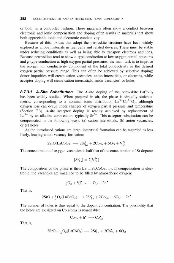
or both, in a controlled fashion. These materials often show a conflict betweenelectronic and ionic compensation and doping often results in materials that showboth appreciable ionic and electronic conductivity.
Because of this, oxides that adopt the perovskite structure have been widelyexplored as anode materials in fuel cells and related devices. These must be stableunder reducing conditions as well as being able to transport electrons and ions.Because perovskites tend to show n-type conduction at low oxygen partial pressuresand p-type conduction at high oxygen partial pressures, the main task is to improvethe oxygen ion conductivity component of the total conductivity in the desiredoxygen partial pressure range. This can often be achieved by selective doping;donor impurities will create cation vacancies, anion interstitials, or electrons, whileacceptor doping will create cation interstitials, anion vacancies, or holes.
8.7.3.1 A-Site Substitution The A-site doping of the perovskite LaCoO3
has been widely studied. When prepared in air, the phase is virtually stoichio-metric, corresponding to a nominal ionic distribution La3þCo3þO3, althoughoxygen loss can occur under changes of oxygen partial pressure and temperature(Section 7.3). A-site acceptor doping is readily achieved by replacement ofLa3þ by an alkaline earth cation, typically Sr2þ. This acceptor substitution can becompensated in the following ways: (a) cation interstitials, (b) anion vacancies,or (c) holes.
As the introduced cations are large, interstitial formation can be regarded as lesslikely, leaving anion vacancy formation:
2SrO(LaCoO3) �! 2Sr0La þ 2CoCo þ 5OO þ V2†O
The concentration of oxygen vacancies is half that of the concentration of Sr dopant:
[Sr0La] ¼ 2[V2†O ]
The composition of the phase is then La12xSrxCoO32x/2. If compensation is elec-tronic, the vacancies are imagined to be filled by atmospheric oxygen:
12 O2 þ V2†
O O OO þ 2h†
That is,
2SrOþ 12 O2(LaCoO3) �! 2Sr0La þ 2CoCo þ 6OO þ 2h†
The number of holes is thus equal to the dopant concentration. The possibility thatthe holes are localized on Co atoms is reasonable:
CoCo þ h† �! Co†CoThat is,
2SrOþ 12 O2(LaCoO3) �! 2Sr0La þ 2Co†Co þ 6OO
382 NONSTOICHIOMETRY AND EXTRINSIC ELECTRONIC CONDUCTIVITY
The ion Co† corresponds to Co4þ and the number of Co4þ ions is then equal to thenumber of dopant Sr2þ ions. The reaction can be formally considered to be the for-mation of a solid solution between the perovskite structure phases LaCoO3 (Co3þ)and SrCoO3 (Co
4þ). The formula is formally La12xSrxCo12x3þ Cox
4þO3.Note that other equilibria could be written, including the disproportionation:
2CoCo O Co0Co þ Co†Co
That is,
Co3þ þ Co3þ O Co2þ þ Co4þ
Which of these possibilities is preferred can be answered by experiment. A plot ofthe strontium content, x, in La12xSrxCoO32d, versus the oxygen content, 32d, for thetwo possibilities, VO
2† or CoCo† , can be drawn and compared with experimental
measurements, which show that both defect types are present with vacanciesdominating (Fig. 8.15). The material is a mixed conductor.
Preparations under higher oxygen partial pressure would be expected toincrease hole concentrations (CoCo
†) and under lower partial pressures to increasethe concentration of vacancies (VO
2†). The exact defect population in a sample willdepend upon temperature, oxygen partial pressure, and the rate at which samplesare cooled.
Figure 8.15 Calculated composition versus oxygen stoichiometry curves forLa12xSrxCoO32d. [The two experimental points are taken from data in A. N. Petrov, V. A.Cherepanov, and A. Y. Zuev, Thermodynamics, Defect Structure and Charge Transfer inDoped Lanthanum Cobaltites: An Overview, J. Solid State Electrochem., 10, 517–537 (2006).]
8.7 MIXED ELECTRONIC/IONIC CONDUCTORS 383
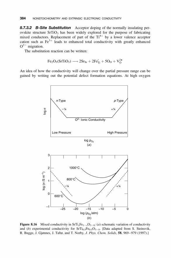
8.7.3.2 B-Site Substitution Acceptor doping of the normally insulating per-ovskite structure SrTiO3 has been widely explored for the purpose of fabricatingmixed conductors. Replacement of part of the Ti4þ by a lower valence acceptorcation such as Fe3þ leads to enhanced total conductivity with greatly enhancedO22 migration.
The substitution reaction can be written:
Fe2O3(SrTiO3) �! 2SrSr þ 2Fe0Ti þ 5OO þ V2†O
An idea of how the conductivity will change over the partial pressure range can begained by writing out the potential defect formation equations. At high oxygen
Figure 8.16 Mixed conductivity in SrTixFe12xO32d: (a) schematic variation of conductivityand (b) experimental conductivity for SrTi0.5Fe0.5O32d. [Data adapted from S. Steinsvik,R. Bugge, J. Gjønnes, J. Taftø, and T. Norby, J. Phys. Chem. Solids, 58, 969–979 (1997).]
384 NONSTOICHIOMETRY AND EXTRINSIC ELECTRONIC CONDUCTIVITY
pressure the oxygen vacancies will tend to fill:
V2†O þ 1
2 O2 O OO þ 2h†
Ko ¼ [h†]2
[V2†O ] p1=2O2
The conductivity will be proportional to the concentration of holes, so that:
s/ [h†]/ p1=4O2
At low oxygen pressure more vacancies will tend to be created:
OO O 12 O2 þ V2†
O þ 2e0
Kr ¼ [e0]2[V2†O ] p1=2O2
The conductivity will be proportional to the concentration of electrons so that:
s/ [e0]/ p�1=4O2
The way in which the conductivity will change with oxygen partial pressure can thenbe estimated (Fig. 8.16a). Experimental data (Fig. 8.16b) are in fair agreement withthese ideas.
8.8 MIXED PROTON/ELECTRONIC CONDUCTORS
8.8.1 Proton Mixed Conductors
Acceptor doping in perovskite oxides gives materials with a vacancy population thatcan act as proton conductors in moist atmospheres (Section 6.9). In addition, thedoped materials are generally p-type semiconductors. This means that in moist atmos-pheres there is the possibility of mixed conductivity involving three charge carriers(Hþ, O22, and h†) or four if electrons, e0, are included.
The situation can be illustrated with respect to the acceptor-doped perovskitestructure SrZrO3, with Y3þ substituted for Zr4þ to give compositionsSrZr12xYxO320.5x. The doping reaction can be written:
2SrOþ Y2O3(SrZrO3) �! 2SrSr þ 2Y0Zr þ 5OO þ V2†
O
Dopant levels of x ¼ 0.05–0.2 are common.The successfully doped materials are generally p-type semiconductors. This arises
from a combination of atmospheric oxygen with the vacancies, thus:
V2†O þ 1
2 O2 O OO þ 2h†
8.8 MIXED PROTON/ELECTRONIC CONDUCTORS 385
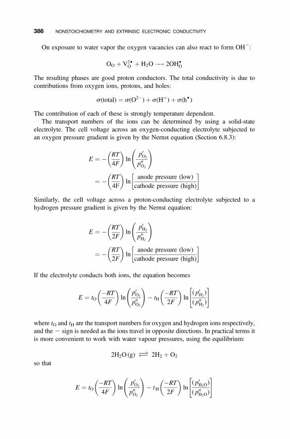
On exposure to water vapor the oxygen vacancies can also react to form OH2:
OO þ V2†O þ H2O �! 2OH†
O
The resulting phases are good proton conductors. The total conductivity is due tocontributions from oxygen ions, protons, and holes:
s(total) ¼ s(O2�)þ s(Hþ)þ s(h†)
The contribution of each of these is strongly temperature dependent.The transport numbers of the ions can be determined by using a solid-state
electrolyte. The cell voltage across an oxygen-conducting electrolyte subjected toan oxygen pressure gradient is given by the Nernst equation (Section 6.8.3):
E ¼ � RT
4F
� �ln
p0O2
p00O2
!
¼ � RT
4F
� �ln
anode pressure (low)cathode pressure (high)
� �
Similarly, the cell voltage across a proton-conducting electrolyte subjected to ahydrogen pressure gradient is given by the Nernst equation:
E ¼ � RT
2F
� �ln
p0H2
p00H2
!
¼ � RT
2F
� �ln
anode pressure (low)cathode pressure (high)
� �
If the electrolyte conducts both ions, the equation becomes
E ¼ tO�RT
4F
� �ln
p0O2
p00O2
!� tH
�RT
2F
� �ln
( p0H2)
( p00H2)
" #
where tO and tH are the transport numbers for oxygen and hydrogen ions respectively,and the 2 sign is needed as the ions travel in opposite directions. In practical terms itis more convenient to work with water vapour pressures, using the equilibrium:
2H2O (g) O 2H2 þ O2
so that
E ¼ tO�RT
4F
� �ln
p0O2
p00O2
!� tH
�RT
2F
� �ln
( p0H2O)
( p00H2O)
" #
386 NONSTOICHIOMETRY AND EXTRINSIC ELECTRONIC CONDUCTIVITY
Thus, measurement of the total conductivity together with the cell voltage allowsthe transport numbers of the ions to be determined (Fig. 8.17). The results show thatat lower temperatures proton conductivity is of greatest importance, at middle temp-eratures oxygen ion conductivity becomes dominant, and at high temperatures thematerial is predominantly a hole conductor. Between these temperatures, at approxi-mately 3508C the solid is a mixed Hþ and O22 conductor while at approximately6508C it is a mixed hole and O22 conductor.
8.8.2 Brouwer Diagram Representation of MixedProton Conductivity
A number of factors must be taken into account when the diagrammatic repre-sentation of mixed proton conductivity is attempted. The behavior of the soliddepends upon the temperature, the dopant concentration, the partial pressureof oxygen, and the partial pressure of hydrogen or water vapor. Schematicrepresentation of defect concentrations in mixed proton conductors on a Brouwerdiagram therefore requires a four-dimensional depiction. A three-dimensional plotcan be constructed if two variables, often temperature and dopant concentration,are fixed (Fig. 8.18a). It is often clearer to use two-dimensional sections of such aplot, constructed with three variables fixed (Fig. 8.18b–8.18d ).
The Brouwer diagram approach can be illustrated with reference to theperovskite structure oxide system BaYbxPr12xO3, which has been explored as apotential cathode material for use in solid oxide fuel cells. The parent phase
Figure 8.17 Schematic representation of the variation of the transport numbers for Hþ, O22.and h† in SrZr12xYxO32d. [Data adapted from P. Huang and A. Petric, J. Mater. Chem., 5,53–56 (1995).]
8.8 MIXED PROTON/ELECTRONIC CONDUCTORS 387
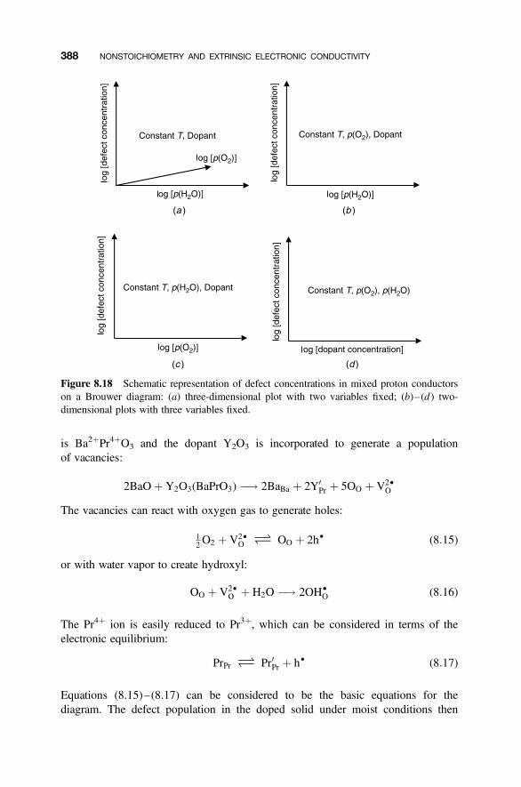
is Ba2þPr4þO3 and the dopant Y2O3 is incorporated to generate a populationof vacancies:
2BaOþ Y2O3(BaPrO3) �! 2BaBa þ 2Y0Pr þ 5OO þ V2†
O
The vacancies can react with oxygen gas to generate holes:
12 O2 þ V2†
O O OO þ 2h† (8:15)
or with water vapor to create hydroxyl:
OO þ V2†o þ H2O �! 2OH†
O (8:16)
The Pr4þ ion is easily reduced to Pr3þ, which can be considered in terms of theelectronic equilibrium:
PrPr O Pr0Pr þ h† (8:17)
Equations (8.15)–(8.17) can be considered to be the basic equations for thediagram. The defect population in the doped solid under moist conditions then
Figure 8.18 Schematic representation of defect concentrations in mixed proton conductorson a Brouwer diagram: (a) three-dimensional plot with two variables fixed; (b)–(d ) two-dimensional plots with three variables fixed.
388 NONSTOICHIOMETRY AND EXTRINSIC ELECTRONIC CONDUCTIVITY
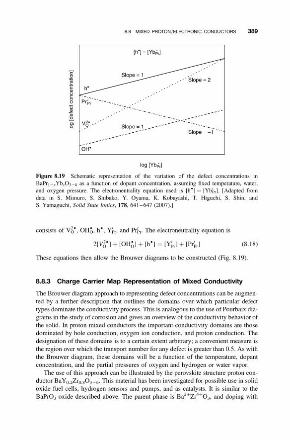
consists of VO2†, OHO
†, h†, Y0Pr, and Pr0Pr. The electroneutrality equation is
2[V2†O ]þ [OH†
O]þ [h†] ¼ [Y0Pr]þ [Pr0Pr] (8:18)
These equations then allow the Brouwer diagrams to be constructed (Fig. 8.19).
8.8.3 Charge Carrier Map Representation of Mixed Conductivity
The Brouwer diagram approach to representing defect concentrations can be augmen-ted by a further description that outlines the domains over which particular defecttypes dominate the conductivity process. This is analogous to the use of Pourbaix dia-grams in the study of corrosion and gives an overview of the conductivity behavior ofthe solid. In proton mixed conductors the important conductivity domains are thosedominated by hole conduction, oxygen ion conduction, and proton conduction. Thedesignation of these domains is to a certain extent arbitrary; a convenient measure isthe region over which the transport number for any defect is greater than 0.5. As withthe Brouwer diagram, these domains will be a function of the temperature, dopantconcentration, and the partial pressures of oxygen and hydrogen or water vapor.
The use of this approach can be illustrated by the perovskite structure proton con-ductor BaY0.2Zr0.8O32d. This material has been investigated for possible use in solidoxide fuel cells, hydrogen sensors and pumps, and as catalysts. It is similar to theBaPrO3 oxide described above. The parent phase is Ba2þZr4þO3, and doping with
Figure 8.19 Schematic representation of the variation of the defect concentrations inBaPr12xYbxO32d as a function of dopant concentration, assuming fixed temperature, water,and oxygen pressure. The electroneutrality equation used is [h†] ¼ [Yb0Pr]. [Adapted fromdata in S. Mimuro, S. Shibako, Y. Oyama, K. Kobayashi, T. Higuchi, S. Shin, andS. Yamaguchi, Solid State Ionics, 178, 641–647 (2007).]
8.8 MIXED PROTON/ELECTRONIC CONDUCTORS 389
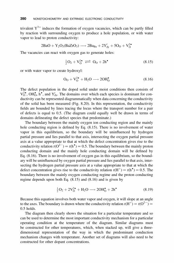
trivalent Y3þ induces the formation of oxygen vacancies, which can be partly filledby reaction with surrounding oxygen to produce a hole population, or with watervapor to lead to proton conductivity:
2BaOþ Y2O3(BaZrO3) �! 2BaBa þ 2Y0Zr þ 5OO þ V2†
O
The vacancies can react with oxygen gas to generate holes:
12 O2 þ V2†
O O OO þ 2h† (8:15)
or with water vapor to create hydroxyl:
OO þ V2†O þ H2O �! 2OH†
O (8:16)
The defect population in the doped solid under moist conditions then consists ofVO2†, OHO
†, h†, and Y0Zr. The domains over which each species is dominant for con-
ductivity can be represented diagrammatically when data concerning the conductivityof the solid has been measured (Fig. 8.20). In this representation, the conductivityfields are bounded by lines tracing the locus where the transport number for a pairof defects is equal to 0.5. (The diagram could equally well be drawn in terms ofdomains delineating the defect species that predominate.)
The boundary between the mainly oxygen ion conducting region and the mainlyhole conducting region is defined by Eq. (8.15). There is no involvement of watervapor in this equilibrium, so the boundary will be uninfluenced by hydrogenpartial pressure and lies parallel to that axis, intersecting the oxygen partial pressureaxis at a value appropriate to that at which the defect concentration gives rise to theconductivity relation t(O22) ¼ t(h†) ¼ 0.5. The boundary between the mainly protonconducting domain and the mainly hole conducting domain will be defined byEq. (8.16). There is no involvement of oxygen gas in this equilibrium, so the bound-ary will be uninfluenced by oxygen partial pressure and lies parallel to that axis, inter-secting the hydrogen partial pressure axis at a value appropriate to that at which thedefect concentration gives rise to the conductivity relation t(Hþ) ¼ t(h†) ¼ 0.5. Theboundary between the mainly oxygen conducting regime and the proton conductingregime depends upon both Eq. (8.15) and (8.16) and is given by
12 O2 þ 2V2†
O þ H2O �! 2OH†O þ 2h† (8:19)
Because this equation involves both water vapor and oxygen, it will slope at an angleto the axes. The boundary is drawn where the conductivity relation t(Hþ) ¼ t(O22) ¼0.5 holds.
The diagram then clearly shows the situation for a particular temperature and socan be used to determine the most important conductivity mechanism for a particularoperating condition at the temperature of the diagram. Similar diagrams mustbe constructed for other temperatures, which, when stacked up, will give a three-dimensional representation of the way in which the predominant conductionmechanism changes with temperature. Another set of diagrams will also need to beconstructed for other dopant concentrations.
390 NONSTOICHIOMETRY AND EXTRINSIC ELECTRONIC CONDUCTIVITY
8.9 CHOICE OF COMPENSATION MECHANISM
There are several ways in which a solid doped with an aliovalent impurity can main-tain charge balance. It is by no means simple to be sure which compensation mech-anism will hold, or even if one mechanism will hold over all of the doping range.However, there are some quantitative guidelines that apply, especially for oxides.The principal mechanism will depend upon how easily the host cation that is beingreplaced is oxidized or reduced.
1. Host cations are neither easily oxidized or reduced [group 1 metals(Na2O, etc.), group 2 metals (MgO, etc.), and group 3 metals (Al2O3,Sc2O3, etc.)]. In this case both donor (higher valence) and acceptor (lowervalence) doping will be compensated structurally, that is, by interstitialsor vacancies.
Figure 8.20 Charge carrier map representation of conductivity in the mixed conductorBaZr0.8Y0.2O32d at 773 K. The domains are areas within which conductivity of one species,Hþ, O22, or h†, predominate. Boundaries represent the locus of t(species) ¼ 0.5. [Adaptedfrom data in K. Nomura and H. Kageyama, Solid State Ionics, 178, 661–665 (2007).]
8.9 CHOICE OF COMPENSATION MECHANISM 391
2. Host cations are easily oxidized and reduced [transition metals (Fe2O3, Mn2O3,etc.)]. In both donor (higher valence) and acceptor (lower valence) dopingelectronic compensation (donors by electrons and acceptors by holes) will bepreferred to structural (vacancies and interstitials) compensation.
3. Host cations are easily oxidized but not reduced [transition metals (Cr2O3, NiO,etc.)]. In this case donor (higher valence) doping will be compensated structu-rally. Acceptor doping is most likely to lead to hole compensation. Thus therewill be considerable asymmetry in doping. Donor doping a colorless insulatingphase will yield a colorless insulating phase, while acceptor doping will yield ablack semiconductor or metallic phase.
4. Host cations are not readily oxidized but can be reduced [transition metals(TiO2, Nb2O5, etc.)]. In this case donor (higher valence) doping will lead toelectron compensation, while acceptor (lower valence) doping will be compen-sated structurally. Thus there will be considerable asymmetry in doping in theopposite direction to that in guideline (3). Acceptor doping a colorless insulat-ing phase will yield a colorless insulating phase, while donor doping will yielda black semiconductor or metallic phase.
These “rules” are not foolproof but should serve as a first approximation. A morerigorous approach must be used for more quantitative assessments. One possibility isto compute defect formation energies for the compound in question using atomisticsimulations or quantum mechanical theory. These formation energies can be insertedinto formulas similar to those described for simple defect populations (Chapter 2):
nd ¼ N exp�DgdkT
� �
where nd is the number of defects, N is the number of atom sites supporting the defectpopulation, and Dgd is the (Gibbs) energy of formation of the defect. In this way, therelative numbers of the various defects may be ranked.
The variation of the defect species present as a function of dopant concentration,oxygen partial pressure, or temperature can then be determined by solution of thepolynomial equations that connect the various defect populations. The Brouwerapproximation may be satisfactory in many cases. As always, comparison withexperimental data is essential.
8.10 ANSWERS TO INTRODUCTORY QUESTIONS
What are donor and acceptor dopants?
Aliovalent additives are often called donor dopants, when they tend to provideelectrons and enhance intrinsic n-type semiconducting behavior, or acceptordopants, when they tend to give a population of mobile holes and enhancep-type semiconducting behavior. The process of creating electronic defects in acrystal in this way is called valence induction.
392 NONSTOICHIOMETRY AND EXTRINSIC ELECTRONIC CONDUCTIVITY
Donor dopants are impurity ions of a higher valence than that of the parentions, as when small amounts of Nb2O5 are incorporated into TiO2, so that Nb5þ
substitutes for Ti4þ. The donor species has an effective positive charge, NbTi† , in
this example.
Acceptor dopants are impurity ions of a lower valence than that of the parentions, as when small amounts of Al2O3 incorporated into TiO2, so that the Al3þ
ion substitutes for Ti4þ. The acceptor species has an effective negative charge,AlTi0 , in this example.
How do negative temperature coefficient (NTC) thermistors respond totemperature changes?
Negative temperature coefficient thermistors are made from impurity-doped tran-sition-metal oxides. Donor doping, for example, Fe2O3 doped with TiO2, producesn-type thermistors. The favored mechanism is the formation of electrons:
2TiO2(Fe2O3) �! 2Ti†Fe þ 2e0 þ 3OO þ 12 O2
Acceptor doping, as in lithium oxide doping of nickel oxide, leads to theproduction of holes and produces p-type thermistors:
Li2O(NiO) þ 12 O2 �! 2Li0Ni þ 2OO þ 2h†
These materials are often described as hopping semiconductors in which the mobi-lity is proportional to the exponential of the energy required to liberate the chargecarriers so that the resistance decreases exponentially with temperature.Thermistor resistance R is frequently written as
RT ¼ RT0 expb(T0 � T)
T0T
� �
where RT is the resistance at a temperature T (K), b is the thermistor constant,which is the slope of the RT versus T curve, and RT0 is the resistance at a specifiedreference temperature T0.
What are mixed conductors?
Mixed conductors are solids in which the total conductivity is made up of bothelectronic and ionic components, each of which makes an appreciable contributionto the overall conductivity. There is considerable interest in mixed conductors forapplications such as fuel cells, batteries, electrochromic devices, and membranesfor gas separation or hydrocarbon oxidation.
There are a number of ways in which mixed conductors can be obtained. In one,a material that is a good ionic conductor by virtue of structural features, typified bylayer structures, can have the rest of the structure modified to become electronically
8.10 ANSWERS TO INTRODUCTORY QUESTIONS 393
conducting. In another approach, impurities can be introduced into a matrix toinduce both electronic or ionic defects, so as to generate a mixed conducting matrix.
An example of a layer structure mixed conductor is provided by the cathodematerial LixCoO2 used in lithium batteries. In this solid the ionic conductivitycomponent is due to the migration of Liþ ions between sheets of electronicallyconducting CoO2. The production of a successful mixed conductor by dopingcan be illustrated by the oxide Ce12xPrxO2. Reduction of this solid producesoxygen vacancies and Pr3þ ions. The electronic conductivity mechanism inthese oxides is believed to be by way of electron hopping between Pr4þ andPr3þ, and the ionic conductivity is essentially vacancy diffusion of O22 ions.
PROBLEMS AND EXERCISES
Quick Quiz
1. Acceptor dopants are NOT compensated by one of:
(a) Interstitial cations
(b) Anion vacancies
(c) Electrons
2. The substitution of Mn3þ by Al3þ in MgMn2O4 is:
(a) Donor doping
(b) Acceptor doping
(c) Neither donor or acceptor doping
3. When a donor or acceptor is doped into an oxide, changes must be made to:
(a) The electroneutrality equation
(b) The electronic equilibrium equation
(c) The point defect equilibrium equation
4. Each Sr2þ ion incorporated into La2CuO4 generates:
(a) One electron
(b) One hole
(c) One Cu2þ vacancy
5. To make the metallic oxide LiTi2O4 insulating, dope with:
(a) Liþ
(b) Mg2þ
(c) Mn3þ
6. The charge reservoir layer in the cuprate superconductor HgBa2CaCu2O6þd is:
(a) BaO Ca BaO
(b) BaO Hg BaO
(c) BaO Cu BaO
394 NONSTOICHIOMETRY AND EXTRINSIC ELECTRONIC CONDUCTIVITY
7. The main defects responsible for mixed conductivity in Ce0.8Pr0.2O22d are:
(a) Pr0Ce þ Ce0Ce(b) VO
2† þ Ce0Ce(c) VO
2† þ Pr0Ce
8. The layered material LixNiO2 is of use in a battery as the:
(a) Anode
(b) Cathode
(c) Electrolyte
9. In dry air the proton mixed conductor SrZr12xYxO3 is a:
(a) p-type semiconductor
(b) n-type semiconductor
(c) Insulator
10. Which of the following dopants will change colorless insulating TiO2 into ablue-black semiconductor?
(a) Nb5þ
(b) Hf 4þ
(c) Liþ
Calculations and Questions
1. Write defect equations for (a) TiO2 doped with Al2O3; (b) TiO2 doped withNb2O5; (c) Mn3O4 doped with NiO; (d) MgO doped with Cr2O3; and (e)Nb2O5 doped with Fe2O3.
2. A plot of the conductivity of the thermistor material MgGaMnO4 is given in thefollowing table. Estimate the value of the thermistor constant b.
Conductivity/S m21 Temperature/1000 K
8.21 10.674 1.350.0184 2.03.04 � 1023 2.231.12 � 1023 2.53.06 � 1025 3.25
Data adapted from A. Veres et al., Solid State Ionics, 178,423–428 (2007).
3. Write down the explicit polynomial form of Eqs. (8.13) and (8.14) for the casewhere Schottky defects are more important than electronic defects, KS ¼ 1040
defects m23, Ke ¼ 1032 defects m23, DM ¼ 1025 donors m23, AM ¼ 1025
accceptors m23. (Determine values of Ko and Kr from Section 7.5.2.)
PROBLEMS AND EXERCISES 395
4. The normal spinel MgTi2O4 is a black semiconductor with a high conductivity.(a) Write defect equations to express the results of doping with Mg2þ into Tisites. (b) What is the limiting composition? (c) Is the final spinel a metal or aninsulator?
5. Determine the charge on the charge reservoir and the superconductinglayers for (a) Bi2Sr2CaCu2O8, (b) HgBa2Ca2Cu3O8, (c) TlBa2Ca2Cu3O9,(d) Tl2Sr2CaCu2O8, and (e) Pb2Sr2Y0.5Ca0.5Cu3O8.
6. LaCoO3 can be donor doped with CeO2 to give a mixed conductor. (a) Writedefect equations for the reaction. A sample of nominal compositionLa0.99Ce0.01CoO3 has a Seebeck coefficient of approximately 2300 mVK21.(b)What are the charge carriers? (c)What is the ratio of defects to normal Co sites?
7. The dependence of the conductivity of the mixed conductor La2Ni0.8Cu0.2O4þd
at 7508C is given in the following table. Explain the oxygen dependence anddetermine the nature of the charge carriers.
Conductivity/S m21 Oxygen Pressure/Pa
83.18 3.16 � 10210
104.71 1.41 � 1029
144.54 7.94 � 1029
190.55 2.82 � 1028
263.03 1.26 � 1027
331.13 0.56 � 1026
Data adapted from V. V. Kharton et al., J. Solid State Chem.,177, 26–37 (2004).
8. Write out the specific equations needed to draw Figure 8.19, using the approxi-mation that [h†] ¼ [Yb0Pr] (see Section 8.8.2).
9. V2O3 is doped with NiO to give NixV22xO3, which is a hopping semiconductor.Assuming that Ni2þ substitutes for V3þ and is compensated by V4þ; (a) writeequations for the doping of V2O3 by NiO and the overall equation showingcompensation of Ni2þ by V4þ. (b) Calculate the activation energy for hoppingfrom the data in the following table. (c) At what composition will the conduc-tivity be a maximum, if hopping is between V3þ and V4þ?
Temperature/K Conductivity/S m21
300 70.92350 94.31400 116.41450 134.41500 149.93
Data adapted from P. Rozier, A. Ratuszna, and J. Galy, Z. Anorg.Allgem. Chem., 628, 1236–1242 (2002).
396 NONSTOICHIOMETRY AND EXTRINSIC ELECTRONIC CONDUCTIVITY
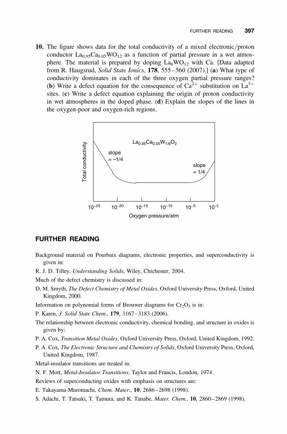
10. The figure shows data for the total conductivity of a mixed electronic/protonconductor La0.95Ca0.05WO12 as a function of partial pressure in a wet atmos-phere. The material is prepared by doping La6WO12 with Ca. [Data adaptedfrom R. Haugsrud, Solid State Ionics, 178, 555–560 (2007).] (a) What type ofconductivity dominates in each of the three oxygen partial pressure ranges?(b) Write a defect equation for the consequence of Ca2þ substitution on La3þ
sites. (c) Write a defect equation explaining the origin of proton conductivityin wet atmospheres in the doped phase. (d) Explain the slopes of the lines inthe oxygen-poor and oxygen-rich regions.
FURTHER READING
Background material on Pourbaix diagrams, electronic properties, and superconductivity isgiven in:
R. J. D. Tilley, Understanding Solids, Wiley, Chichester, 2004.
Much of the defect chemistry is discussed in:
D. M. Smyth, The Defect Chemistry of Metal Oxides, Oxford University Press, Oxford, UnitedKingdom, 2000.
Information on polynomial forms of Brouwer diagrams for Cr2O3 is in:
P. Karen, J. Solid State Chem., 179, 3167–3183 (2006).
The relationship between electronic conductivity, chemical bonding, and structure in oxides isgiven by:
P. A. Cox, Transition Metal Oxides, Oxford University Press, Oxford, United Kingdom, 1992.
P. A. Cox, The Electronic Structure and Chemistry of Solids, Oxford University Press, Oxford,United Kingdom, 1987.
Metal-insulator transitions are treated in:
N. F. Mott, Metal-Insulator Transitions, Taylor and Francis, London, 1974.
Reviews of superconducting oxides with emphasis on structures are:
E. Takayama-Muromachi, Chem. Mater., 10, 2686–2698 (1998).
S. Adachi, T. Tatsuki, T. Tamura, and K. Tanabe, Mater. Chem., 10, 2860–2869 (1998).
FURTHER READING 397

P. Majewski, J. Mater. Res., 15, 854–870 (2000).
Mixed conductivity is discussed by:
J. W. Fergus, Solid State Ionics, 177, 1529–1541 (2006).
M. S. Whittingham, Mat. Res. Bull., XIV, September, 31–38 (1989).
Lanthanum colbaltes are reviewed in:
A. N. Petrov, V. A. Cherapanov, and A. Yu. Zuev, J. Solid State Electrochem., 10, 517–537(2000).
398 NONSTOICHIOMETRY AND EXTRINSIC ELECTRONIC CONDUCTIVITY
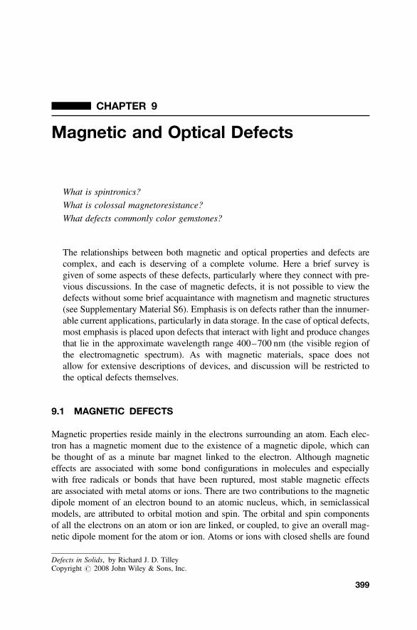
&CHAPTER 9
Magnetic and Optical Defects
What is spintronics?
What is colossal magnetoresistance?
What defects commonly color gemstones?
The relationships between both magnetic and optical properties and defects arecomplex, and each is deserving of a complete volume. Here a brief survey isgiven of some aspects of these defects, particularly where they connect with pre-vious discussions. In the case of magnetic defects, it is not possible to view thedefects without some brief acquaintance with magnetism and magnetic structures(see Supplementary Material S6). Emphasis is on defects rather than the innumer-able current applications, particularly in data storage. In the case of optical defects,most emphasis is placed upon defects that interact with light and produce changesthat lie in the approximate wavelength range 400–700 nm (the visible region ofthe electromagnetic spectrum). As with magnetic materials, space does notallow for extensive descriptions of devices, and discussion will be restricted tothe optical defects themselves.
9.1 MAGNETIC DEFECTS
Magnetic properties reside mainly in the electrons surrounding an atom. Each elec-tron has a magnetic moment due to the existence of a magnetic dipole, which canbe thought of as a minute bar magnet linked to the electron. Although magneticeffects are associated with some bond configurations in molecules and especiallywith free radicals or bonds that have been ruptured, most stable magnetic effectsare associated with metal atoms or ions. There are two contributions to the magneticdipole moment of an electron bound to an atomic nucleus, which, in semiclassicalmodels, are attributed to orbital motion and spin. The orbital and spin componentsof all the electrons on an atom or ion are linked, or coupled, to give an overall mag-netic dipole moment for the atom or ion. Atoms or ions with closed shells are found
Defects in Solids, by Richard J. D. TilleyCopyright # 2008 John Wiley & Sons, Inc.
399
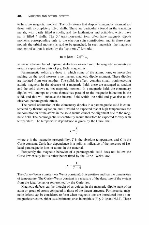
to have no magnetic moment. The only atoms that display a magnetic moment arethose with incompletely filled shells. These are particularly found in the transitionmetals, with partly filled d shells, and the lanthanides and actinides, which havepartly filled f shells. The 3d transition-metal ions often have magnetic dipolemoments corresponding only to the electron spin contribution, and in these com-pounds the orbital moment is said to be quenched. In such materials, the magneticmoment of an ion is given by the “spin-only” formula:
m ¼ [n(nþ 2)]1=2mB
where n is the number of unpaired d electrons on each ion. The magnetic moments areusually expressed in units of mB, Bohr magnetons.
Paramagnetic solids are those in which some of the atoms, ions, or moleculesmaking up the solid possess a permanent magnetic dipole moment. These dipolesare isolated from one another. The solid, in effect, contains small, noninteractingatomic magnets. In the absence of a magnetic field, these are arranged at randomand the solid shows no net magnetic moment. In a magnetic field, the elementarydipoles will attempt to orient themselves parallel to the magnetic induction in thesolid, and this will enhance the internal field within the solid and give rise to theobserved paramagnetic effect.
The partial orientation of the elementary dipoles in a paramagnetic solid is coun-teracted by thermal agitation, and it would be expected that at high temperatures therandom motion of the atoms in the solid would cancel the alignment due to the mag-netic field. The paramagnetic susceptibility would therefore be expected to vary withtemperature. The temperature dependence is given by the Curie law:
x ¼ C
T
where x is the magnetic susceptibility, T is the absolute temperature, and C is theCurie constant. Curie law dependence in a solid is indicative of the presence of iso-lated paramagnetic ions or atoms in the material.
Frequently the magnetic behavior of a paramagnetic solid does not follow theCurie law exactly but is rather better fitted by the Curie–Weiss law:
x ¼ C
T � u
The Curie–Weiss constant (or Weiss constant), u, is positive and has the dimensionsof temperature. The Curie–Weiss constant is a measure of the departure of the systemfrom the ideal behavior represented by the Curie law.
Magnetic defects can be thought of as defects in the magnetic dipole state of anatom or group of atoms compared to those of the parent structure. For instance, mag-netic defects can be considered to form when magnetic ions are introduced into a non-magnetic structure, either as substituents or as interstitials (Fig. 9.1a and 9.1b). These
400 MAGNETIC AND OPTICAL DEFECTS
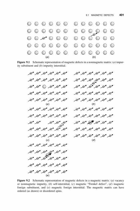
Figure 9.1 Schematic representation of magnetic defects in a nonmagnetic matrix: (a) impur-ity substituent and (b) impurity interstitial.
Figure 9.2 Schematic representation of magnetic defects in a magnetic matrix: (a) vacancyor nonmagnetic impurity, (b) self-interstitial, (c) magnetic “Frenkel defect”, (d ) magneticforeign substituent, and (e) magnetic foreign interstitial. The magnetic matrix can haveordered (as drawn) or disordered spins.
9.1 MAGNETIC DEFECTS 401
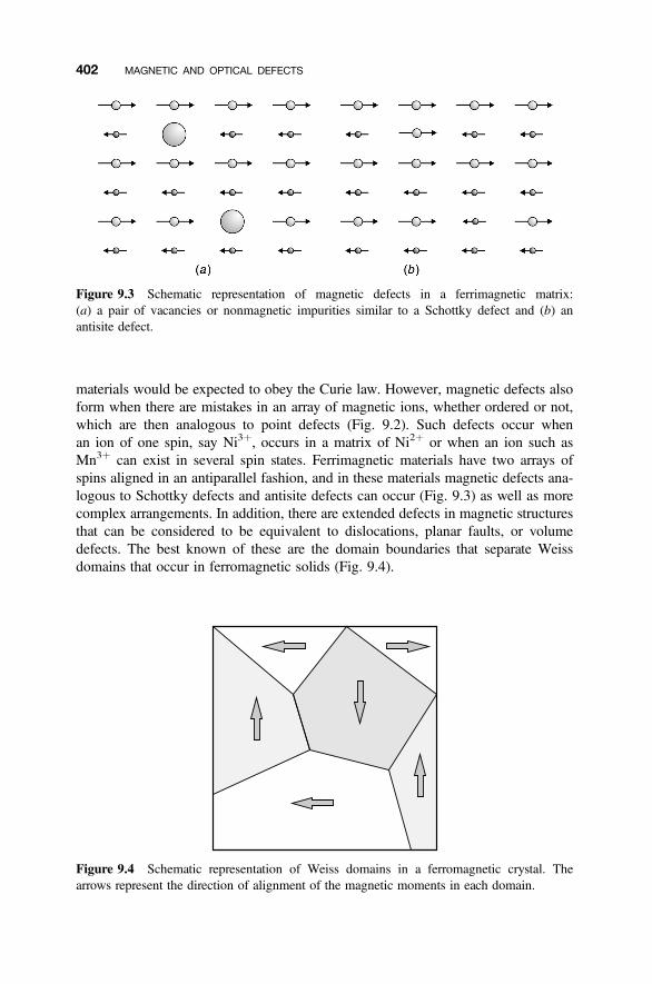
materials would be expected to obey the Curie law. However, magnetic defects alsoform when there are mistakes in an array of magnetic ions, whether ordered or not,which are then analogous to point defects (Fig. 9.2). Such defects occur whenan ion of one spin, say Ni3þ, occurs in a matrix of Ni2þ or when an ion such asMn3þ can exist in several spin states. Ferrimagnetic materials have two arrays ofspins aligned in an antiparallel fashion, and in these materials magnetic defects ana-logous to Schottky defects and antisite defects can occur (Fig. 9.3) as well as morecomplex arrangements. In addition, there are extended defects in magnetic structuresthat can be considered to be equivalent to dislocations, planar faults, or volumedefects. The best known of these are the domain boundaries that separate Weissdomains that occur in ferromagnetic solids (Fig. 9.4).
Figure 9.3 Schematic representation of magnetic defects in a ferrimagnetic matrix:(a) a pair of vacancies or nonmagnetic impurities similar to a Schottky defect and (b) anantisite defect.
Figure 9.4 Schematic representation of Weiss domains in a ferromagnetic crystal. Thearrows represent the direction of alignment of the magnetic moments in each domain.
402 MAGNETIC AND OPTICAL DEFECTS
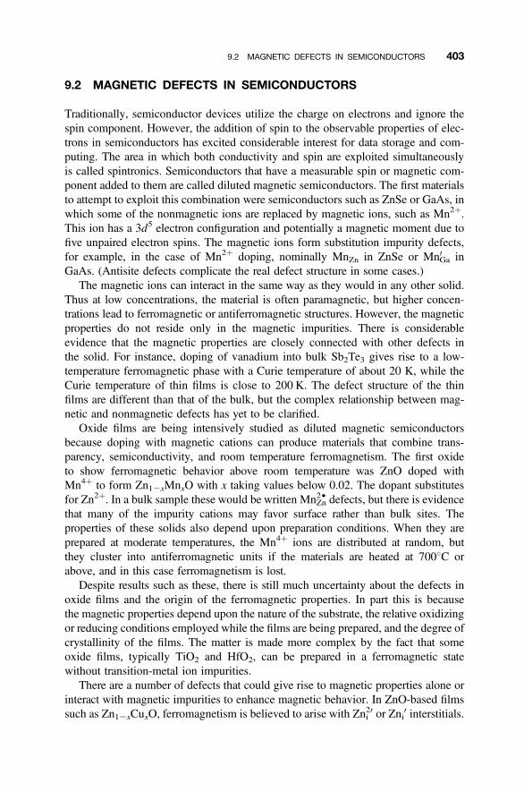
9.2 MAGNETIC DEFECTS IN SEMICONDUCTORS
Traditionally, semiconductor devices utilize the charge on electrons and ignore thespin component. However, the addition of spin to the observable properties of elec-trons in semiconductors has excited considerable interest for data storage and com-puting. The area in which both conductivity and spin are exploited simultaneouslyis called spintronics. Semiconductors that have a measurable spin or magnetic com-ponent added to them are called diluted magnetic semiconductors. The first materialsto attempt to exploit this combination were semiconductors such as ZnSe or GaAs, inwhich some of the nonmagnetic ions are replaced by magnetic ions, such as Mn2þ.This ion has a 3d5 electron configuration and potentially a magnetic moment due tofive unpaired electron spins. The magnetic ions form substitution impurity defects,for example, in the case of Mn2þ doping, nominally MnZn in ZnSe or Mn0Ga inGaAs. (Antisite defects complicate the real defect structure in some cases.)
The magnetic ions can interact in the same way as they would in any other solid.Thus at low concentrations, the material is often paramagnetic, but higher concen-trations lead to ferromagnetic or antiferromagnetic structures. However, the magneticproperties do not reside only in the magnetic impurities. There is considerableevidence that the magnetic properties are closely connected with other defects inthe solid. For instance, doping of vanadium into bulk Sb2Te3 gives rise to a low-temperature ferromagnetic phase with a Curie temperature of about 20 K, while theCurie temperature of thin films is close to 200 K. The defect structure of the thinfilms are different than that of the bulk, but the complex relationship between mag-netic and nonmagnetic defects has yet to be clarified.
Oxide films are being intensively studied as diluted magnetic semiconductorsbecause doping with magnetic cations can produce materials that combine trans-parency, semiconductivity, and room temperature ferromagnetism. The first oxideto show ferromagnetic behavior above room temperature was ZnO doped withMn4þ to form Zn12xMnxO with x taking values below 0.02. The dopant substitutesfor Zn2þ. In a bulk sample these would be written MnZn
2† defects, but there is evidencethat many of the impurity cations may favor surface rather than bulk sites. Theproperties of these solids also depend upon preparation conditions. When they areprepared at moderate temperatures, the Mn4þ ions are distributed at random, butthey cluster into antiferromagnetic units if the materials are heated at 7008C orabove, and in this case ferromagnetism is lost.
Despite results such as these, there is still much uncertainty about the defects inoxide films and the origin of the ferromagnetic properties. In part this is becausethe magnetic properties depend upon the nature of the substrate, the relative oxidizingor reducing conditions employed while the films are being prepared, and the degree ofcrystallinity of the films. The matter is made more complex by the fact that someoxide films, typically TiO2 and HfO2, can be prepared in a ferromagnetic statewithout transition-metal ion impurities.
There are a number of defects that could give rise to magnetic properties alone orinteract with magnetic impurities to enhance magnetic behavior. In ZnO-based filmssuch as Zn12xCuxO, ferromagnetism is believed to arise with Zni
20 or Zni0 interstitials.
9.2 MAGNETIC DEFECTS IN SEMICONDUCTORS 403
In films such as SnO2, oxygen vacancies together with liberated electrons are impli-cated in the ferromagnetic properties.
The interaction between a charged point defect and neighboring magnetic ions inmagnetically doped thin films has been described in terms of a defect cluster called abound magnetic polaron (Fig. 9.5a). The radius of a bound magnetic polaron due toan electron located on the defect, r, is given by
r ¼ 1rm
meff
� �
where 1r is the relative permittivity (dielectric constant) of the solid,m is the electronmass,meff the effective mass of the electron and the units are Bohr radius (0.0529 nm). The
Figure 9.5 Schematic representation of a bound magnetic polaron: (a) one bound magneticpolaron located on a charged defect; and (b) overlapping bound magnetic polarons leading toferromagnetic alignment of magnetic ions.
404 MAGNETIC AND OPTICAL DEFECTS
boundmagnetic polaron then has avolumeof r3. The charged point defect acts to align thespins on magnetic ions that lie within the polaron volume. If there is an overlap of boundmagnetic polarons, then ferromagnetic order can occur throughout the sample (Fig. 9.5b).
9.3 MAGNETIC DEFECTS IN FERRITES
The magnetically important ferrites are oxides that adopt the spinel structure and havea general formula A2þFe3þ2 O4. The cations are distributed between two types of site,tetrahedral and octahedral (Supplementary Material S1). The ferrite ZnFe2O4, anormal spinel in which the Zn2þ ions occupy the tetrahedral sites and the Fe3þ
ions the octahedral sites, is written Zn2þ[Fe3þ]2O4, where the ions in octahedralsites are enclosed in square brackets. The magnetic moments of the individualFe3þ are ions opposed even though they both occupy the octahedral sites, and theformula can be written Zn2þ[Fe3þ"Fe3þ#]O4 where the arrows symbolize the direc-tions of the magnetic moments on the ions. Because the magnetic moments areopposed, the material is effectively nonmagnetic. In reality, the normal spinel struc-ture is not perfect and the cation distribution between the tetrahedral and octahedralsites is temperature dependent, leading to magnetic defects in which some Fe3þ
replaces the Zn2þ.Many important ferrites crystallize with the inverse spinel structure, written as
Fe3þ[A2þFe3þ]O4, where the octahedrally coordinated ions are in square brackets.In these materials, the magnetic moment of the Fe3þ ions in the tetrahedral sites isopposed to that of the Fe3þ ions in the octahedral sites, so that the net magneticmoment due to Fe3þ is zero. The first magnetic material known, and for many cen-turies the only magnetic material known, was the magnetic oxide Fe3O4, which is alsocalled lodestone1 or magnetite. The oxide Fe3O4 is an inverse spinel, although thisfact is obscured in the formula by the fact that the A and B cations are both Fe.The magnetic arrangement is given by the formula Fe3þ" [Fe3þ#Fe2þ#]O4, whichshows that the overall magnetic moment is solely due to the Fe2þ contribution.Similarly, nickel ferrite can be written as Fe3þ"[Fe3þ#Ni2þ"]O4, and, becausethe magnetic moments on the Fe3þ ions cancel, the net magnetic moment is dueto the Ni2þ ions alone.
By forming solid solutions between two ferrites, it is possible to tune the proper-ties magnetically. An example is provided by the solid solution ZnxNi12xFe2O4,which is between the normal spinel ZnFe2O4 and the inverse spinel NiFe2O4.Reaction to form a solid solution with NiFe2O4:
(1� x)NiFe2O4 þ xZnFe2O4 �! ZnxNi1�xFe2O4
introduces substitutional defects. However, although the Ni2þ ions substitute forZn2þ, they do not occupy the tetrahedral sites but the octahedral sites. This has
1The name lodestone is a corruption of the expression leading stone, which reflects on the fact that one ofits earliest and most important uses was as a compass pointer.
9.3 MAGNETIC DEFECTS IN FERRITES 405
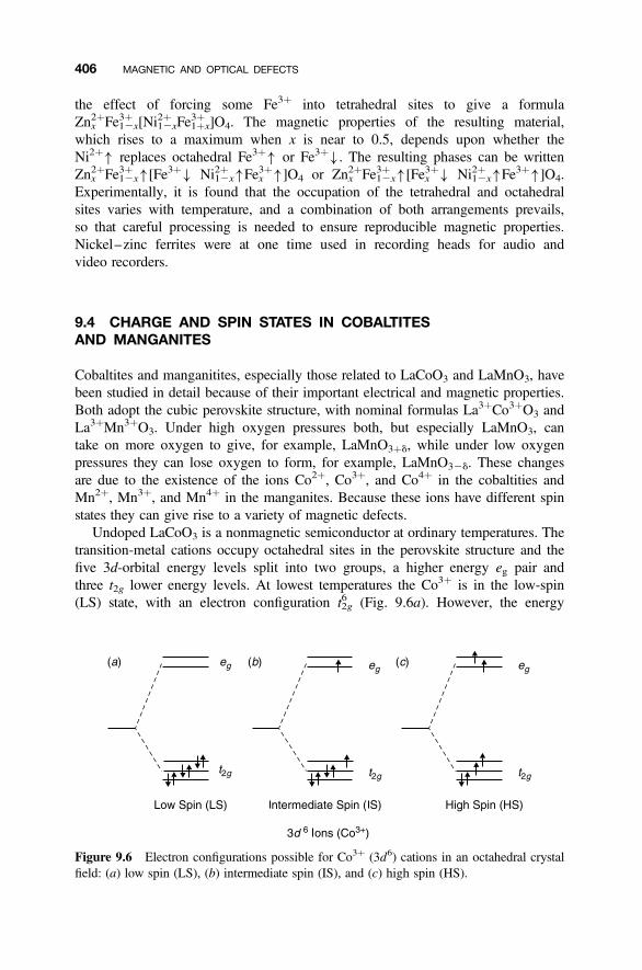
the effect of forcing some Fe3þ into tetrahedral sites to give a formulaZn2þx Fe3þ12x[Ni
2þ12xFe
3þ1þx]O4. The magnetic properties of the resulting material,
which rises to a maximum when x is near to 0.5, depends upon whether theNi2þ" replaces octahedral Fe3þ" or Fe3þ#. The resulting phases can be writtenZn2þx Fe3þ12x"[Fe3þ# Ni2þ12x"Fe3þx "]O4 or Zn2þx Fe3þ12x"[Fe3þx # Ni2þ12x"Fe3þ"]O4.Experimentally, it is found that the occupation of the tetrahedral and octahedralsites varies with temperature, and a combination of both arrangements prevails,so that careful processing is needed to ensure reproducible magnetic properties.Nickel–zinc ferrites were at one time used in recording heads for audio andvideo recorders.
9.4 CHARGE AND SPIN STATES IN COBALTITESAND MANGANITES
Cobaltites and manganitites, especially those related to LaCoO3 and LaMnO3, havebeen studied in detail because of their important electrical and magnetic properties.Both adopt the cubic perovskite structure, with nominal formulas La3þCo3þO3 andLa3þMn3þO3. Under high oxygen pressures both, but especially LaMnO3, cantake on more oxygen to give, for example, LaMnO3þd, while under low oxygenpressures they can lose oxygen to form, for example, LaMnO32d. These changesare due to the existence of the ions Co2þ, Co3þ, and Co4þ in the cobaltities andMn2þ, Mn3þ, and Mn4þ in the manganites. Because these ions have different spinstates they can give rise to a variety of magnetic defects.
Undoped LaCoO3 is a nonmagnetic semiconductor at ordinary temperatures. Thetransition-metal cations occupy octahedral sites in the perovskite structure and thefive 3d-orbital energy levels split into two groups, a higher energy eg pair andthree t2g lower energy levels. At lowest temperatures the Co3þ is in the low-spin(LS) state, with an electron configuration t2g
6 (Fig. 9.6a). However, the energy
Figure 9.6 Electron configurations possible for Co3þ (3d6) cations in an octahedral crystalfield: (a) low spin (LS), (b) intermediate spin (IS), and (c) high spin (HS).
406 MAGNETIC AND OPTICAL DEFECTS
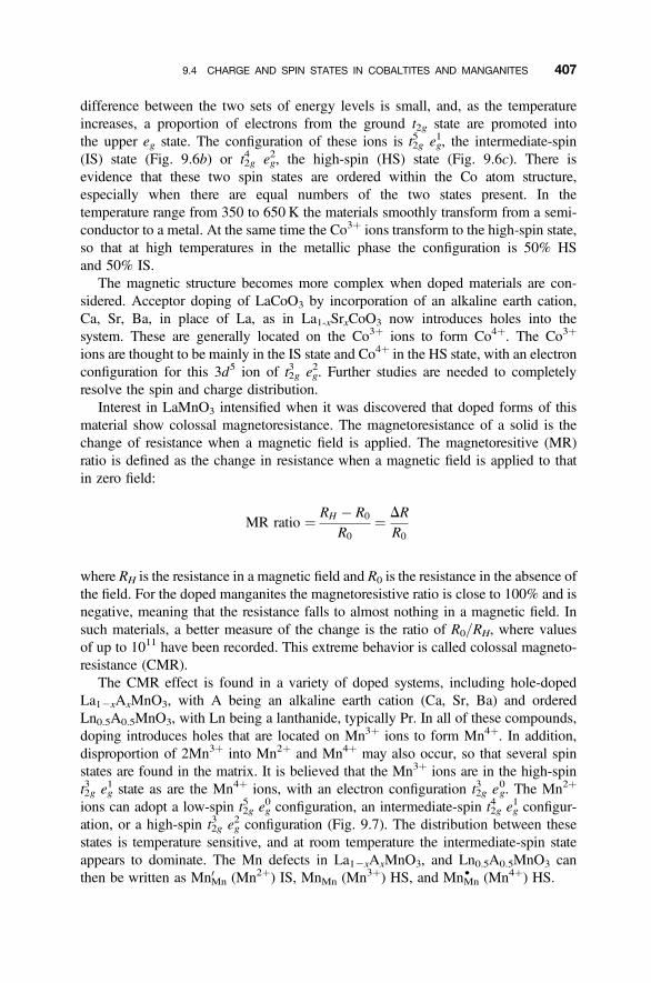
difference between the two sets of energy levels is small, and, as the temperatureincreases, a proportion of electrons from the ground t2g state are promoted intothe upper eg state. The configuration of these ions is t2g
5 eg1, the intermediate-spin
(IS) state (Fig. 9.6b) or t2g4 eg
2, the high-spin (HS) state (Fig. 9.6c). There isevidence that these two spin states are ordered within the Co atom structure,especially when there are equal numbers of the two states present. In thetemperature range from 350 to 650 K the materials smoothly transform from a semi-conductor to a metal. At the same time the Co3þ ions transform to the high-spin state,so that at high temperatures in the metallic phase the configuration is 50% HSand 50% IS.
The magnetic structure becomes more complex when doped materials are con-sidered. Acceptor doping of LaCoO3 by incorporation of an alkaline earth cation,Ca, Sr, Ba, in place of La, as in La1-xSrxCoO3 now introduces holes into thesystem. These are generally located on the Co3þ ions to form Co4þ. The Co3þ
ions are thought to be mainly in the IS state and Co4þ in the HS state, with an electronconfiguration for this 3d5 ion of t2g
3 eg2. Further studies are needed to completely
resolve the spin and charge distribution.Interest in LaMnO3 intensified when it was discovered that doped forms of this
material show colossal magnetoresistance. The magnetoresistance of a solid is thechange of resistance when a magnetic field is applied. The magnetoresitive (MR)ratio is defined as the change in resistance when a magnetic field is applied to thatin zero field:
MR ratio ¼ RH � R0
R0¼ DR
R0
where RH is the resistance in a magnetic field and R0 is the resistance in the absence ofthe field. For the doped manganites the magnetoresistive ratio is close to 100% and isnegative, meaning that the resistance falls to almost nothing in a magnetic field. Insuch materials, a better measure of the change is the ratio of R0/RH, where valuesof up to 1011 have been recorded. This extreme behavior is called colossal magneto-resistance (CMR).
The CMR effect is found in a variety of doped systems, including hole-dopedLa12xAxMnO3, with A being an alkaline earth cation (Ca, Sr, Ba) and orderedLn0.5A0.5MnO3, with Ln being a lanthanide, typically Pr. In all of these compounds,doping introduces holes that are located on Mn3þ ions to form Mn4þ. In addition,disproportion of 2Mn3þ into Mn2þ and Mn4þ may also occur, so that several spinstates are found in the matrix. It is believed that the Mn3þ ions are in the high-spint2g3 eg
1 state as are the Mn4þ ions, with an electron configuration t2g3 e0g. The Mn2þ
ions can adopt a low-spin t2g5 eg
0 configuration, an intermediate-spin t2g4 eg
1 configur-ation, or a high-spin t2g
3 eg2 configuration (Fig. 9.7). The distribution between these
states is temperature sensitive, and at room temperature the intermediate-spin stateappears to dominate. The Mn defects in La12xAxMnO3, and Ln0.5A0.5MnO3 canthen be written as Mn0Mn (Mn2þ) IS, MnMn (Mn3þ) HS, and MnMn
† (Mn4þ) HS.
9.4 CHARGE AND SPIN STATES IN COBALTITES AND MANGANITES 407
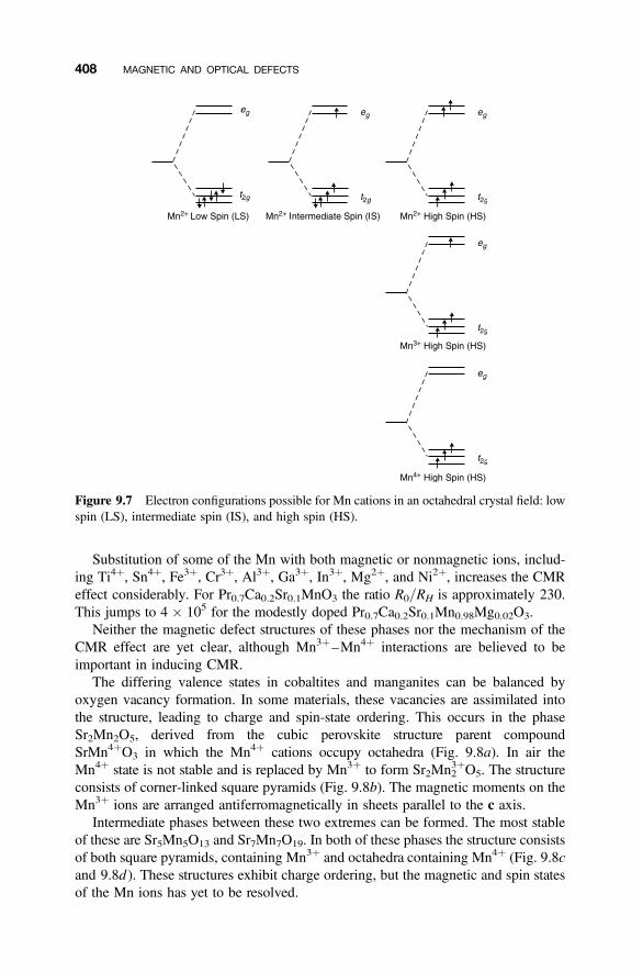
Substitution of some of the Mn with both magnetic or nonmagnetic ions, includ-ing Ti4þ, Sn4þ, Fe3þ, Cr3þ, Al3þ, Ga3þ, In3þ, Mg2þ, and Ni2þ, increases the CMReffect considerably. For Pr0.7Ca0.2Sr0.1MnO3 the ratio R0/RH is approximately 230.This jumps to 4 � 105 for the modestly doped Pr0.7Ca0.2Sr0.1Mn0.98Mg0.02O3.
Neither the magnetic defect structures of these phases nor the mechanism of theCMR effect are yet clear, although Mn3þ–Mn4þ interactions are believed to beimportant in inducing CMR.
The differing valence states in cobaltites and manganites can be balanced byoxygen vacancy formation. In some materials, these vacancies are assimilated intothe structure, leading to charge and spin-state ordering. This occurs in the phaseSr2Mn2O5, derived from the cubic perovskite structure parent compoundSrMn4þO3 in which the Mn4þ cations occupy octahedra (Fig. 9.8a). In air theMn4þ state is not stable and is replaced by Mn3þ to form Sr2Mn2
3þO5. The structureconsists of corner-linked square pyramids (Fig. 9.8b). The magnetic moments on theMn3þ ions are arranged antiferromagnetically in sheets parallel to the c axis.
Intermediate phases between these two extremes can be formed. The most stableof these are Sr5Mn5O13 and Sr7Mn7O19. In both of these phases the structure consistsof both square pyramids, containing Mn3þ and octahedra containing Mn4þ (Fig. 9.8cand 9.8d ). These structures exhibit charge ordering, but the magnetic and spin statesof the Mn ions has yet to be resolved.
Figure 9.7 Electron configurations possible for Mn cations in an octahedral crystal field: lowspin (LS), intermediate spin (IS), and high spin (HS).
408 MAGNETIC AND OPTICAL DEFECTS
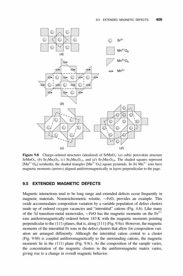
9.5 EXTENDED MAGNETIC DEFECTS
Magnetic interactions tend to be long range and extended defects occur frequently inmagnetic materials. Nonstoichiometric wustite, �FeO, provides an example. Thisoxide accommodates composition variation by a variable population of defect clustersmade up of ordered oxygen vacancies and “interstitial” cations (Fig. 4.6). Like manyof the 3d transition-metal monoxides, �FeO has the magnetic moments on the Fe2þ
ions antiferromagnetically ordered below 183 K with the magnetic moments pointingperpendicular to the (111) planes, that is, along [111] (Fig. 9.9a). However, the magneticmoments of the interstitial Fe ions in the defect clusters that allow for composition vari-ation are arranged differently. Although the interstitial cation central to a cluster(Fig. 9.9b) is coupled antiferromagnetically to the surrounding cations, the magneticmoments lie in the (111) plane (Fig. 9.9c). As the composition of the sample varies,the concentration of the magnetic clusters in the antiferromagnetic matrix varies,giving rise to a change in overall magnetic behavior.
Figure 9.8 Charge-ordered structures (idealized) of SrMnOx: (a) cubic perovskite structureSrMnO3, (b) Sr2Mn2O5, (c) Sr5Mn5O13, and (d ) Sr7Mn7O19. The shaded squares represent[Mn4þO6] octahedra, the shaded triangles [Mn3þO5] square pyramids. In (b) Mn3þ ions havemagnetic moments (arrows) aligned antiferromagnetically in layers perpendicular to the page.
9.5 EXTENDED MAGNETIC DEFECTS 409
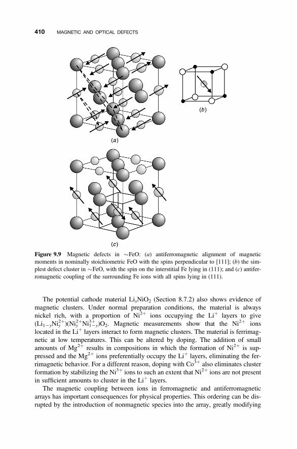
The potential cathode material LixNiO2 (Section 8.7.2) also shows evidence ofmagnetic clusters. Under normal preparation conditions, the material is alwaysnickel rich, with a proportion of Ni2þ ions occupying the Liþ layers to give(Li12yNiy
2þ)(Niy2þNi12y
3þ )O2. Magnetic measurements show that the Ni2þ ionslocated in the Liþ layers interact to form magnetic clusters. The material is ferrimag-netic at low temperatures. This can be altered by doping. The addition of smallamounts of Mg2þ results in compositions in which the formation of Ni2þ is sup-pressed and the Mg2þ ions preferentially occupy the Liþ layers, eliminating the fer-rimagnetic behavior. For a different reason, doping with Co3þ also eliminates clusterformation by stabilizing the Ni3þ ions to such an extent that Ni2þ ions are not presentin sufficient amounts to cluster in the Liþ layers.
The magnetic coupling between ions in ferromagnetic and antiferromagneticarrays has important consequences for physical properties. This ordering can be dis-rupted by the introduction of nonmagnetic species into the array, greatly modifying
Figure 9.9 Magnetic defects in �FeO: (a) antiferromagnetic alignment of magneticmoments in nominally stoichiometric FeO with the spins perpendicular to [111]; (b) the sim-plest defect cluster in �FeO, with the spin on the interstitial Fe lying in (111); and (c) antifer-romagnetic coupling of the surrounding Fe ions with all spins lying in (111).
410 MAGNETIC AND OPTICAL DEFECTS
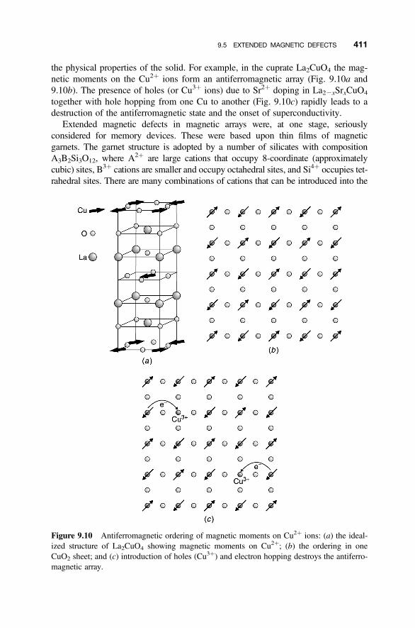
the physical properties of the solid. For example, in the cuprate La2CuO4 the mag-netic moments on the Cu2þ ions form an antiferromagnetic array (Fig. 9.10a and9.10b). The presence of holes (or Cu3þ ions) due to Sr2þ doping in La22xSrxCuO4
together with hole hopping from one Cu to another (Fig. 9.10c) rapidly leads to adestruction of the antiferromagnetic state and the onset of superconductivity.
Extended magnetic defects in magnetic arrays were, at one stage, seriouslyconsidered for memory devices. These were based upon thin films of magneticgarnets. The garnet structure is adopted by a number of silicates with compositionA3B2Si3O12, where A2þ are large cations that occupy 8-coordinate (approximatelycubic) sites, B3þ cations are smaller and occupy octahedral sites, and Si4þ occupies tet-rahedral sites. There are many combinations of cations that can be introduced into the
Figure 9.10 Antiferromagnetic ordering of magnetic moments on Cu2þ ions: (a) the ideal-ized structure of La2CuO4 showing magnetic moments on Cu2þ; (b) the ordering in oneCuO2 sheet; and (c) introduction of holes (Cu3þ) and electron hopping destroys the antiferro-magnetic array.
9.5 EXTENDED MAGNETIC DEFECTS 411
garnet structure; the one chosen for magnetic memories being Ln3Fe5O12, where Lnrepresents a lanthanide, typically Y, Er, or Eu. These materials are ferromagneticdue to alignment of the magnetic moments on the lanthanide with those on the Fe.
The principle behind magnetic data storage was the creation of magnetic domainsof cylindrical form (called bubbles), with an opposite polarity to that of the rest of athin ferromagnetic film (Fig. 9.11). These magnetic bubble memories stored data bythe creation, movement, and annihilation of the small cylinders of opposite polarity.As with the ferrites, doping of the lanthanide and iron sites could be used to modifythe magnetic properties so that fine-tuning of the response of the film to input signalswas possible and compositions such as EuEr2Ga0.7Fe4.3O12 were investigated indetail. Data storage by other means rendered magnetic bubble memories redundantbefore they came into widespread use.
9.6 OPTICAL DEFECTS
9.6.1 Absorption and Scattering
The color and appearance of nonluminous solids depends upon the interaction of theincident light with the solid (Fig. 9.12) and defects can color a solid by absorption oremission of light. In this respect, surfaces are of considerable importance (Section3.14.1). An insulating solid that has no internal surfaces (planar defects) thatreflect or otherwise scatter the light will appear to be transparent. The same transpar-ent material in powder form will appear white. This is because the surface of eachgranule of the powder scatters light of all wavelengths. Crystallites of transparentmaterial deposited inside a glass act as scattering centers and scatter light by reflectionif large and by diffraction if small. If there are sufficient numbers of scatteringcenters, the glass will appear milky white. Opal glass contains large concentrationsof internal surfaces and appears uniformly white.
In the absence of scattering centers, the appearance and color of a solid are influ-enced by the presence of defects known as absorption centers. Of these, the bestknown are those that absorb radiation of one wavelength and release radiation ofanother wavelength. Fluorescence refers to the instantaneous emission of radiationafter excitation by some external radiation. The radiation emitted has a longer wave-length (lower energy) than the exciting radiation. The “missing energy” is lost vianonradiative transitions (also called photon-assisted transitions or, loosely speaking,
Figure 9.11 Magnetic bubble memory schematic: domains of reversed polarity (bubbles) areinduced in the thin ferromagnetic garnet film.
412 MAGNETIC AND OPTICAL DEFECTS
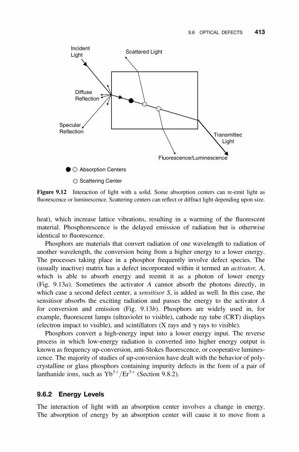
heat), which increase lattice vibrations, resulting in a warming of the fluorescentmaterial. Phosphorescence is the delayed emission of radiation but is otherwiseidentical to fluorescence.
Phosphors are materials that convert radiation of one wavelength to radiation ofanother wavelength, the conversion being from a higher energy to a lower energy.The processes taking place in a phosphor frequently involve defect species. The(usually inactive) matrix has a defect incorporated within it termed an activator, A,which is able to absorb energy and reemit it as a photon of lower energy(Fig. 9.13a). Sometimes the activator A cannot absorb the photons directly, inwhich case a second defect center, a sensitisor S, is added as well. In this case, thesensitisor absorbs the exciting radiation and passes the energy to the activator Afor conversion and emission (Fig. 9.13b). Phosphors are widely used in, forexample, fluorescent lamps (ultraviolet to visible), cathode ray tube (CRT) displays(electron impact to visible), and scintillators (X rays and g rays to visible).
Phosphors convert a high-energy input into a lower energy input. The reverseprocess in which low-energy radiation is converted into higher energy output isknown as frequency up-conversion, anti-Stokes fluorescence, or cooperative lumines-cence. The majority of studies of up-conversion have dealt with the behavior of poly-crystalline or glass phosphors containing impurity defects in the form of a pair oflanthanide ions, such as Yb3þ/Er3þ (Section 9.8.2).
9.6.2 Energy Levels
The interaction of light with an absorption center involves a change in energy.The absorption of energy by an absorption center will cause it to move from a
Figure 9.12 Interaction of light with a solid. Some absorption centers can re-emit light asfluorescence or luminescence. Scattering centers can reflect or diffract light depending upon size.
9.6 OPTICAL DEFECTS 413
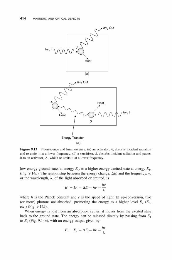
low-energy ground state, at energy E0, to a higher energy excited state at energy E1,(Fig. 9.14a). The relationship between the energy change, DE, and the frequency, n,or the wavelength, l, of the light absorbed or emitted, is
E1 � E0 ¼ DE ¼ hn ¼ hc
l
where h is the Planck constant and c is the speed of light. In up-conversion, two(or more) photons are absorbed, promoting the energy to a higher level E2 (E3,etc.) (Fig. 9.14b).
When energy is lost from an absorption center, it moves from the excited stateback to the ground state. The energy can be released directly by passing from E1
to E0 (Fig. 9.14a), with an energy output given by
E1 � E0 ¼ DE ¼ hn ¼ hc
l
Figure 9.13 Fluorescence and luminescence: (a) an activator, A, absorbs incident radiationand re-emits it at a lower frequency; (b) a sensitisor, S, absorbs incident radiation and passesit to an activator, A, which re-emits it at a lower frequency.
414 MAGNETIC AND OPTICAL DEFECTS
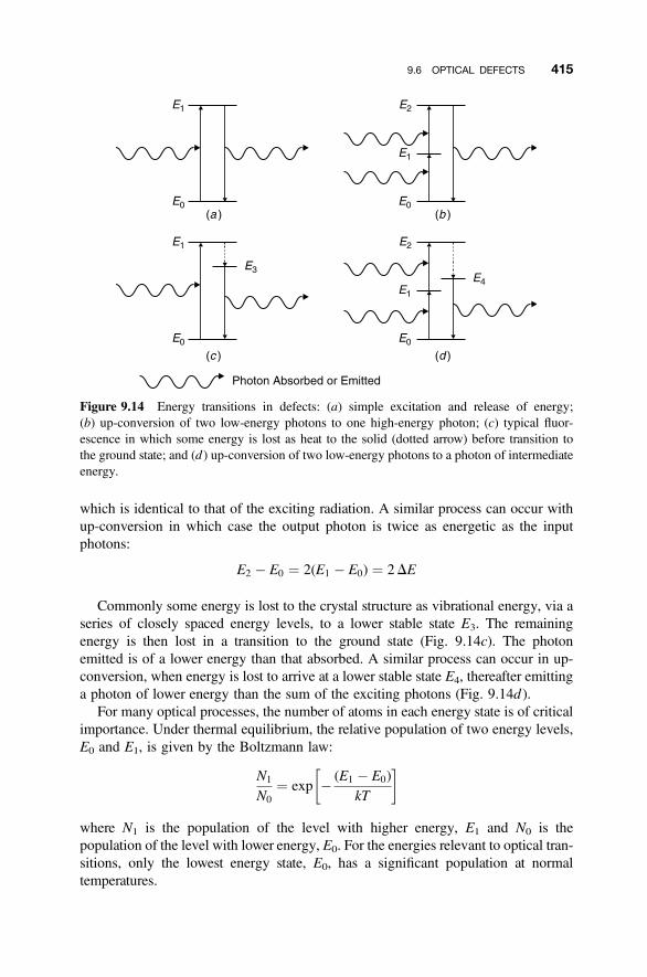
which is identical to that of the exciting radiation. A similar process can occur withup-conversion in which case the output photon is twice as energetic as the inputphotons:
E2 � E0 ¼ 2(E1 � E0) ¼ 2DE
Commonly some energy is lost to the crystal structure as vibrational energy, via aseries of closely spaced energy levels, to a lower stable state E3. The remainingenergy is then lost in a transition to the ground state (Fig. 9.14c). The photonemitted is of a lower energy than that absorbed. A similar process can occur in up-conversion, when energy is lost to arrive at a lower stable state E4, thereafter emittinga photon of lower energy than the sum of the exciting photons (Fig. 9.14d ).
For many optical processes, the number of atoms in each energy state is of criticalimportance. Under thermal equilibrium, the relative population of two energy levels,E0 and E1, is given by the Boltzmann law:
N1
N0¼ exp � (E1 � E0)
kT
� �
where N1 is the population of the level with higher energy, E1 and N0 is thepopulation of the level with lower energy, E0. For the energies relevant to optical tran-sitions, only the lowest energy state, E0, has a significant population at normaltemperatures.
Figure 9.14 Energy transitions in defects: (a) simple excitation and release of energy;(b) up-conversion of two low-energy photons to one high-energy photon; (c) typical fluor-escence in which some energy is lost as heat to the solid (dotted arrow) before transition tothe ground state; and (d ) up-conversion of two low-energy photons to a photon of intermediateenergy.
9.6 OPTICAL DEFECTS 415
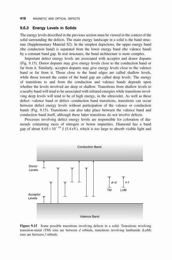
9.6.3 Energy Levels in Solids
The energy levels described in the previous section must be viewed in the context of thesolid surrounding the defects. The main energy landscape in a solid is the band struc-ture (Supplementary Material S2). In the simplest depictions, the upper energy band(the conduction band) is separated from the lower energy band (the valence band)by a constant band gap. In real structures, the band architecture is more complex.
Important defect energy levels are associated with acceptor and donor dopants(Fig. 9.15). Donor dopants may give energy levels close to the conduction band orfar from it. Similarly, acceptor dopants may give energy levels close to the valenceband or far from it. Those close to the band edges are called shallow levels,while those toward the center of the band gap are called deep levels. The energyof transitions to and from the conduction and valence bands depends uponwhether the levels involved are deep or shallow. Transitions from shallow levels toa nearby band will tend to be associated with infrared energies while transitions invol-ving deep levels will tend to be of high energy, in the ultraviolet. As well as thesedefect–valence band or defect–conduction band transitions, transitions can occurbetween defect energy levels without participation of the valence or conductionbands (Fig. 9.15). Transitions can also take place between the valence band andconduction band itself, although these latter transitions do not involve defects.
Processes involving defect energy levels are responsible for coloration of dia-monds containing races of nitrogen or boron impurities. Diamond has a bandgap of about 8.65�10219 J (5.4 eV), which is too large to absorb visible light and
Figure 9.15 Some possible transitions involving defects in a solid. Transitions involvingtransition-metal (TM) ions are between d orbitals, transitions involving lanthanide (LnM)ions are between f orbitals.
416 MAGNETIC AND OPTICAL DEFECTS
diamonds are therefore clear. Nitrogen impurities occupy normal carbon atompositions to form N0
C defects. Nitrogen has five bonding electrons, one more thancarbon. Four of the electrons around each impurity nitrogen atom are used to fulfillthe local bonding requirements of the crystal structure and one electron remainsunused. The extra electron, one per nitrogen atom impurity, sits in the energy gapto form a donor level at 6.41�10219 J (4 eV) below the conduction band. Thisenergy is in the ultraviolet and corresponds to a wavelength of 310 nm, but theabsorption spectrum is broad enough for the low-energy tail to creep into theviolet beyond 400 nm. Thus, diamond containing a few atoms of nitrogen absorbsslightly in the violet region, giving the stones a faint yellow aspect. As the nitrogenconcentration increases, the color intensifies.
In the case of boron impurities a complementary situation occurs. Boron has onlythree outer bonding electrons instead of the four found on carbon. Each boron impur-ity atom occupies a carbon position, forming BC
†, which results in the creation of a setof new acceptor energy levels just 0.64 � 10219 J (0.4 eV) above the valence band.The transition of an electron from the valence band to this acceptor level has anabsorption peak in the infrared, but the high-energy tail of the absorption bandspills into the red at 700 nm. The boron-doped diamonds therefore absorb somered light and leave the gemstone with an overall blue color.
Optical transitions are of interest for a number of device applications, but the exactmechanism of light production is often hard to pin down. For example, thin films ofzinc oxide, ZnO, reduced in an atmosphere of N2/H2 show a bright green lumines-cence after irradiation with ultraviolet light. The active defect is believed to be asingly ionized oxygen vacancy, VO
†, which exists as a deep level in the band gap.However, two mechanisms have been proposed for light production, involvingeither the transition of an electron from the conduction band to form a neutraldefect VO or interaction of the VO
† defect with a hole in the valence band to form aVO2† defect. Doping with Mg broadens the band gap of the ZnO moving the green
luminescence toward blue.Electron transitions in transition-metal ions usually involve electron movement
between the d orbitals (d–d transitions) and in lanthanides between the f orbitals( f– f transitions). The band structure of the solid plays only a small part in theenergy of these transitions, and, when these atoms are introduced into crystals, theycan be represented as a set of levels within the wide band gap of the oxide (Fig. 9.15).
9.7 PIGMENTS, MINERALS AND GEMSTONES
9.7.1 Transition-Metal and Lanthanide Ion Colors
Pigments, minerals, gemstones, glasses, and many related materials are colored byimpurity defects that absorb some of the incident white light, leaving a depleted spec-trum to color the solid. Colors in these materials are thus characterized by the absorp-tion spectrum of the solid. Common inorganic colorants are the transition-metal andlanthanide metal ions. The colors are characteristic of the ions themselves and are due
9.7 PIGMENTS, MINERALS AND GEMSTONES 417
to transitions between the partly filled d orbitals of transition-metals (d–d transitions)or the partly filled f orbitals of lanthanides ( f– f transitions).
In the 3d transition-metal ions, the 3d orbitals contain one or more electrons.When these ions are introduced into a solid, the d-orbital energies are split by inter-actions with the surrounding anions. The commonest coordination for these ions isoctahedral, and in this geometry the five d-orbital energy levels split into twogroups, a higher energy eg pair and three t2g lower energy levels (SupplementaryMaterial S6 and Figs. 9.6 and 9.7). The energy gap between the lower and upperset is written D(oct) or 10 Dq(oct). This rearrangement in the energies of thed orbitals is called crystal field splitting or ligand field splitting.
Although the way in which the d-orbital energy levels are split depends solelyupon the geometry of surrounding atoms, the degree of splitting is dependent uponthe interatomic distances between the ion and its neighbors. Short interionic distanceslead to a large splitting, that is, large values of D, due to a strong crystal field. Longinterionic distances produce a smaller splitting, that is, small values of D, due to aweak crystal field. The color produced by an ion is due to d electrons movingbetween the energy levels created by the crystal field splitting. The actual colorperceived will therefore be a function of both the geometry of the surroundingcoordination polyhedron and its size.
There is an important difference between the interaction of electromagnetic radi-ation with isolated transition-metal ions and with ions in a solid. In the case of iso-lated ions, the electrons move between sharp energy levels, E0, E1, and so on(Fig. 9.14). This means that light given out corresponds to a sharply definedenergy difference and will ideally consist of only one (or a very small range) of fre-quencies. In solids, the interaction of the d orbitals with the surrounding structure,especially lattice vibrations, mean that the spacing between the energy levels willvary slightly from atom to atom in the crystal. This leads to a spread of energylevels in the crystal, and the absorption or emission spectrum of a solid due to elec-tron transitions will consist of a series of bell-shaped curves rather than sharp lines.
The lanthanides have electrons in partly filled 4f orbitals. Many lanthanides showcolors due to electron transitions involving the 4f orbitals. However, there is a con-siderable difference between the lanthanides and the 3d transition-metal ions. The4f electrons in the lanthanides are well shielded beneath an outer electron configur-ation, (5s2 5p6 6s2) and are little influenced by the crystal surroundings. Hence theimportant optical and magnetic properties attributed to the 4f electrons on any par-ticular lanthanide ion are rather unvarying and do not depend significantly uponthe host structure. Moreover, the energy levels are sharper than those of transition-metal ions and the spectra resemble those of free ions.
9.7.2 Colors and Impurity Defects
Glasses are frequently colored with transition-metal ions such as Mn2þ, Ni2þ, Co2þ,lanthanides, or actinides.2 The addition of Co2þ impurities to silica glass leads to a
2The major use for uranium before the advent of the nuclear energy industry was as an additive to glass, toproduce a yellow-green coloration.
418 MAGNETIC AND OPTICAL DEFECTS
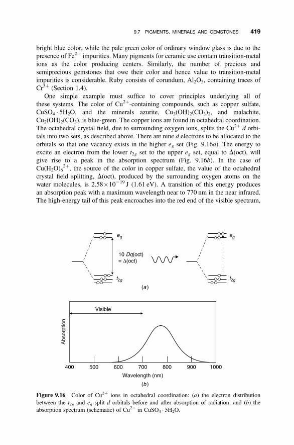
bright blue color, while the pale green color of ordinary window glass is due to thepresence of Fe2þ impurities. Many pigments for ceramic use contain transition-metalions as the color producing centers. Similarly, the number of precious andsemiprecious gemstones that owe their color and hence value to transition-metalimpurities is considerable. Ruby consists of corundum, Al2O3, containing traces ofCr3þ (Section 1.4).
One simple example must suffice to cover principles underlying all ofthese systems. The color of Cu2þ-containing compounds, such as copper sulfate,CuSO4 . 5H2O, and the minerals azurite, Cu3(OH)2(CO3)2, and malachite,Cu2(OH)2(CO3), is blue-green. The copper ions are found in octahedral coordination.The octahedral crystal field, due to surrounding oxygen ions, splits the Cu2þ d orbi-tals into two sets, as described above. There are nine d electrons to be allocated to theorbitals so that one vacancy exists in the higher eg set (Fig. 9.16a). The energy toexcite an electron from the lower t2g set to the upper eg set, equal to D(oct), willgive rise to a peak in the absorption spectrum (Fig. 9.16b). In the case ofCu(H2O)6
2þ, the source of the color in copper sulfate, the value of the octahedralcrystal field splitting, D(oct), produced by the surrounding oxygen atoms on thewater molecules, is 2.58�10219 J (1.61 eV). A transition of this energy producesan absorption peak with a maximum wavelength near to 770 nm in the near infrared.The high-energy tail of this peak encroaches into the red end of the visible spectrum,
Figure 9.16 Color of Cu2þ ions in octahedral coordination: (a) the electron distributionbetween the t2g and eg split d orbitals before and after absorption of radiation; and (b) theabsorption spectrum (schematic) of Cu2þ in CuSO4 . 5H2O.
9.7 PIGMENTS, MINERALS AND GEMSTONES 419
preferentially absorbing red, and leaving the observer to perceive a blue color.The coordination polyhedra in azurite and malachite are of slightly different sizes.Although this only alters the values of D(oct) in these compounds by a smallamount, the position of the absorption band is changed enough for the color ofthese minerals to be easily differentiated from each other and from copper sulfate.
The effect of the strength of the crystal field on transition-metal ion color can bedemonstrated by comparing ruby with emerald. Both minerals are colored by Cr3þ
ions in octahedral sites. Emeralds possess the beryl (Be3Al2Si6O18) structure, witha color derived from traces of Cr3þ substituted for Al3þ in octahedral sites Inberyl, the octahedra surrounding the Cr3þ ions are slightly larger than in corundum,and so the crystal field experienced by the Cr3þ in emerald is weaker than in ruby andD(oct) is smaller. Thus, although the energy level diagram remains essentially thesame, the shift in the energy levels due to a change in the crystal field changes theperceived color enormously from red to green. Note that the colors of solids dopedwith lanthanides do not vary so much, as the f-electron energy levels are well shieldedfrom the external surroundings.
In all of these examples, the agent causing the color is a defect in the form of(usually) a substituted transition-metal or lanthanide ion. The degree of colorationcan be adjusted by changing the amount of dopant or by adjusting co-dopants tochange the dimensions of the surrounding crystal structure. Thus, a colorlesscrystal can be made to appear black by doping with two substituents, one of whichabsorbs radiation in the low-energy yellow part of the visible spectrum andanother that absorbs in the high-energy blue region. The black color of thepigment Zn72xCoxSb2O12 is attributed to such double absorption. In this material,which adopts the inverse spinel structure, Co2þ ions occupy both octahedral andtetrahedral sites. The color is due to the Co2þ, which replaces Zn2þ to form substitu-tional defects. The absorption of Co2þ in octahedral sites centers on red-yellow, andof Co2þ in tetrahedral sites on blue, giving an overall black material.
9.8 PHOTOLUMINESCENCE
9.8.1 Energy Degradation and Down-conversion
While pigments and related materials are colored by defects that absorb radiation,luminescent materials are colored by the emission of radiation from defects. Colorsin these materials are characterized by their emission spectra. Transition-metal andlanthanide metal impurity ions are still the main defects responsible for the effect,and the energy levels described in the previous section are relevant. In order forthe impurity centers to emit radiation, they must gain energy and be promoted to ahigher energy state. In photoluminescence, including fluorescent lamps, this is bythe absorption of ultraviolet radiation. For an efficient device, this absorption mustbe rapid and correspond to a quantum mechanically allowed transition from theground state. Frequently, these transitions are to a broad band of energies formedby the interaction of metal orbitals with nearby anion orbitals to create a wide
420 MAGNETIC AND OPTICAL DEFECTS
energy band. In order for the ultraviolet (UV) exciting radiation to be converted intovisible light, some of the energy must be lost. This comes about by the transfer ofenergy into crystal structure vibrations, that is, heat energy, due to transitionsthrough a series of closely spaced energy levels that do not produce externallyemitted photons, until a lower level is reached, only after which optical emission ispossible. Because of the change from high-energy input to lower energy output,photoluminescence is sometimes called down-conversion.
The general principles of photoluminescence can be illustrated with respect to tri-chromatic fluorescent lamps. These use a phosphor mixture that emits equal amountsof the colors red, blue, and green, all of which generate color emission from impurityatoms in an oxide matrix. The favored red emitter is Eu3þ doped into a Y2O3 matrixforming EuY defects. Ultraviolet radiation is readily absorbed due to charge transferbetween Eu3þ and O22 ions. Energy is then lost to the surrounding matrix as non-radiative transitions until the Eu3þ ion reaches the upper f-electron energy levels.At this point photons at a wavelength of 612 nm, corresponding to a transitionbetween the energy levels 5D0–
7F2, are emitted, allowing the return of the ionto the ground state. The green emission is from Tb3þ coupled with a sensitisor,usually Ce3þ, and occurs at wavelength close to 550 nm, mainly from a 5D4–
7F5transition. Typical host matrices are La(Ce)PO4, LaMg(Ce)Al11O19, andLa(Ce)MgB5O10. In each case the Tb3þ and Ce3þ ions replace La3þ ions to formTbLa and CeLa defects. The blue emission is produced by Eu2þ ions. Among themost widely used host lattices for Eu2þ ions are BaMgAl11O19 and Sr4Al14O25.However, the introduction of Eu2þ into b-alumina structures has also been widelyinvestigated as an alternative. In these latter materials, the Eu2þ occupies theBeevers–Ross and anti-Beevers–Ross sites normally occupied by Naþ, to formEuNa
† defects (Section 6.6).The emission spectra of all defect centers depend upon the degree of doping and
the host structure. Because of the sensitivity of normal color vision, the color per-ceived can change appreciably with even small changes of dopant concentration orhost structure. Thus, although the principles of color production using defects areunderstood, great skill is required to produce a satisfactory working phosphor.
9.8.2 Up-conversion
Up-conversion is the opposite of photoluminescence. In this latter process, high-energy ultraviolet radiation is transformed into visible light. In up-conversionlow-energy infrared radiation is transformed into visible light. The majority ofstudies of up-conversion have dealt with the behavior of polycrystalline or glassmatrices containing lanthanide ions, especially Er3þ, Tm3þ, Ho3þ, and Yb3þ, asdefect absorption centers. The Er3þ ion has an appeal because the up-conversioncan be achieved with low-cost diode lasers operating at wavelengths near to 800and 900 nm. A number of host structures have been used for these ions, includingbinary oxides Y2O3, Gd2O3, and ZrO2, perovskite structure BaTiO3, SrTiO3, andPbTiO3, fluorides such as NaYF4 and oxide and oxyfluoride glasses. The up-conver-sion efficiency is strongly dependent upon the nature of the host and dopant levels.
9.8 PHOTOLUMINESCENCE 421
In general, low concentrations of the active ion, of the order of 1%, are used. At theseconcentrations, the ions form point defects well isolated from each other. At higherconcentrations, dopant ions tend to cluster and other energy loss mechanismsinterfere with up-conversion.
The energy for up-conversion can be gained by the active ion in two principalways. In the first, the ion itself can pick up more than one photon. The first photonexcites the ion from the ground state to an excited energy level, a process referredto as ground-state absorption (GSA). A subsequent photon is absorbed to excitethe ion to a higher energy level again, referred to as excited state absorption(ESA). In the second mechanism, energy is picked up by another ion and transferredto the emitter, a mechanism called energy transfer (ET). In either case, the intensity ofthe up-converted output, Iup, is related to the intensity of the exciting radiation, Iex,by the formula:
Iup / Inex
where n is the number of photons absorbed per up-converted photon emitted.A graph of log Iup versus log Iex will give information on the mechanism ofthe process.
The oxide CeO2 doped with approximately 1% Er3þ exhibits up-conversion invol-ving only one active ion. The Er3þ ions substitute for Ce4þ to form a low concen-tration of Er0Ce defects randomly distributed within the oxide matrix. Irradiationwith near-infrared photons with a wavelength of 785 nm excites the Er3þ ions fromthe 4I15/2 ground state to the 4I9/2 level, that is, a GSA mechanism:
4I15=2 (Er)þ hn (785 nm) �! 4I9=2 (Er)
These ions loose energy internally to phonons (lattice vibrations), a process calleddecay or relaxation, to reach the 4I11/2 and
4I13/2 energy levels:
4I9=2 (Er) �! 4I11=2 (Er)þ 4I13=2 (Er)þ phonons
(Fig. 9.17a). Ions in both these levels are further excited by an ESA mechanism togain energy from the irradiating 785-nm radiation. Those in the 4I11/2 energy levelare excited to the 4F3/2, 5/2 doublet:
4I11=2 (Er)þ hn (785 nm) �! 4F3=2,5=2 (Er)
These states subsequently decay by internal energy loss to the 2H11/2,4S3/2, and
4F9/2energy levels:
4F3=2,5=2 (Er) �! 2H11=2 (Er)þ 4S3=2 (Er)þ 4F9=2 (Er)þ phonons
422 MAGNETIC AND OPTICAL DEFECTS
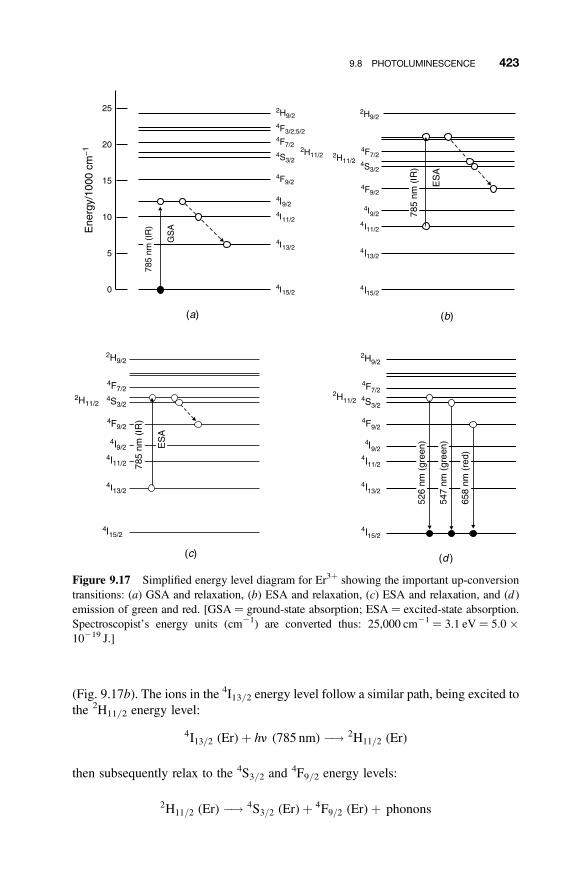
(Fig. 9.17b). The ions in the 4I13/2 energy level follow a similar path, being excited tothe 2H11/2 energy level:
4I13=2 (Er)þ hn (785 nm) �! 2H11=2 (Er)
then subsequently relax to the 4S3/2 and4F9/2 energy levels:
2H11=2 (Er) �! 4S3=2 (Er)þ 4F9=2 (Er)þ phonons
Figure 9.17 Simplified energy level diagram for Er3þ showing the important up-conversiontransitions: (a) GSA and relaxation, (b) ESA and relaxation, (c) ESA and relaxation, and (d )emission of green and red. [GSA ¼ ground-state absorption; ESA ¼ excited-state absorption.Spectroscopist’s energy units (cm21) are converted thus: 25,000 cm21 ¼ 3.1 eV ¼ 5.0 �10219 J.]
9.8 PHOTOLUMINESCENCE 423
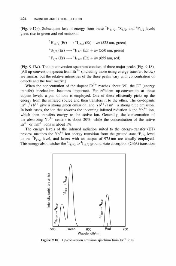
(Fig. 9.17c). Subsequent loss of energy from these 2H11/2,4S3/2, and
4F9/2 levelsgives rise to green and red emission:
2H11=2 (Er) �! 4I15=2 (Er)þ hn (525 nm, green)
4S3=2 (Er) �! 4I15=2 (Er)þ hn (550 nm, green)
4F9=2 (Er) �! 4I15=2 (Er)þ hn (655 nm, red)
(Fig. 9.17d ). The up-conversion spectrum consists of three major peaks (Fig. 9.18).[All up-conversion spectra from Er3þ (including those using energy transfer, below)are similar, but the relative intensities of the three peaks vary with concentration ofdefects and the host matrix.]
When the concentration of the dopant Er3þ reaches about 3%, the ET (energytransfer) mechanism becomes important. For efficient up-conversion at thesedopant levels, a pair of ions is employed. One of these efficiently picks up theenergy from the infrared source and then transfers it to the other. The co-dopantsEr3þ/Yb3þ give a strong green emission, and Yb3þ/Tm3þ a strong blue emission.In both cases, the ion that absorbs the incoming infrared radiation is the Yb3þ ion,which then transfers energy to the active ion. Generally, the concentration ofthe absorbing Yb3þ centers is about 20%, while the concentration of the activeEr3þ or Tm3þ ions is about 1%.
The energy levels of the infrared radiation suited to the energy-transfer (ET)process matches the Yb3þ ion energy transition from the ground-state 2F7/2 levelto the 2F5/2 level, and lasers with an output of 975 nm are usually employed.This energy also matches the 4I15/2 to
4I11/2 ground-state absorption (GSA) transition
Figure 9.18 Up-conversion emission spectrum from Er3þ ions.
424 MAGNETIC AND OPTICAL DEFECTS
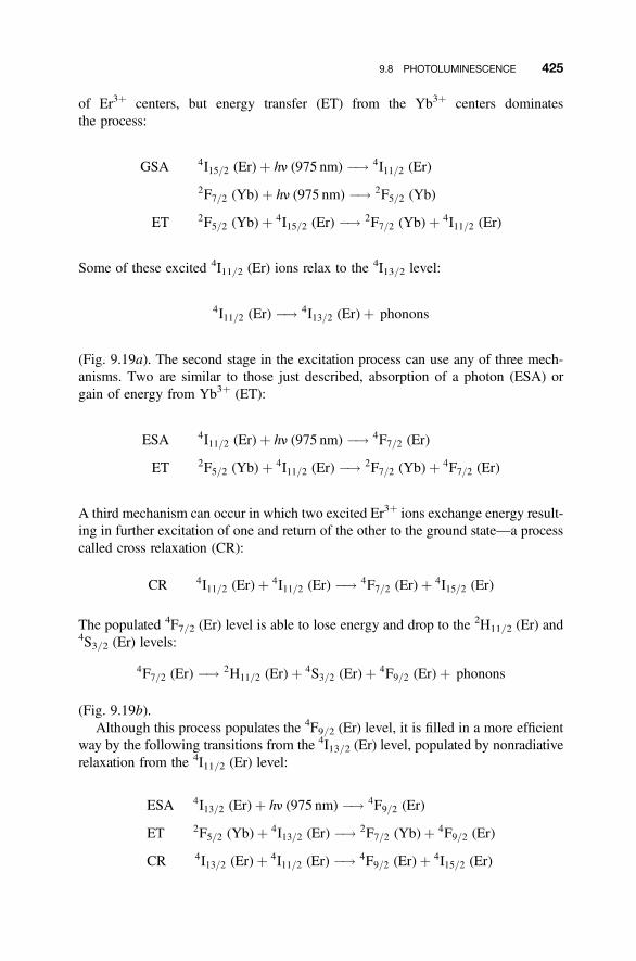
of Er3þ centers, but energy transfer (ET) from the Yb3þ centers dominatesthe process:
GSA 4I15=2 (Er)þ hn (975 nm) �! 4I11=2 (Er)
2F7=2 (Yb)þ hn (975 nm) �! 2F5=2 (Yb)
ET 2F5=2 (Yb)þ 4I15=2 (Er) �! 2F7=2 (Yb)þ 4I11=2 (Er)
Some of these excited 4I11/2 (Er) ions relax to the 4I13/2 level:
4I11=2 (Er) �! 4I13=2 (Er)þ phonons
(Fig. 9.19a). The second stage in the excitation process can use any of three mech-anisms. Two are similar to those just described, absorption of a photon (ESA) orgain of energy from Yb3þ (ET):
ESA 4I11=2 (Er)þ hn (975 nm) �! 4F7=2 (Er)
ET 2F5=2 (Yb)þ 4I11=2 (Er) �! 2F7=2 (Yb)þ 4F7=2 (Er)
A third mechanism can occur in which two excited Er3þ ions exchange energy result-ing in further excitation of one and return of the other to the ground state—a processcalled cross relaxation (CR):
CR 4I11=2 (Er)þ 4I11=2 (Er) �! 4F7=2 (Er)þ 4I15=2 (Er)
The populated 4F7/2 (Er) level is able to lose energy and drop to the 2H11/2 (Er) and4S3/2 (Er) levels:
4F7=2 (Er) �! 2H11=2 (Er)þ 4S3=2 (Er)þ 4F9=2 (Er)þ phonons
(Fig. 9.19b).Although this process populates the 4F9/2 (Er) level, it is filled in a more efficient
way by the following transitions from the 4I13/2 (Er) level, populated by nonradiativerelaxation from the 4I11/2 (Er) level:
ESA 4I13=2 (Er)þ hn (975 nm) �! 4F9=2 (Er)
ET 2F5=2 (Yb)þ 4I13=2 (Er) �! 2F7=2 (Yb)þ 4F9=2 (Er)
CR 4I13=2 (Er)þ 4I11=2 (Er) �! 4F9=2 (Er)þ 4I15=2 (Er)
9.8 PHOTOLUMINESCENCE 425
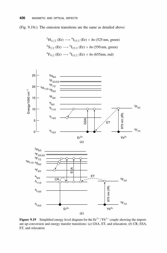
(Fig. 9.19c). The emission transitions are the same as detailed above:
2H11=2 (Er) �! 4I15=2 (Er)þ hn (525 nm, green)
4S3=2 (Er) �! 4I15=2 (Er)þ hn (550 nm, green)
4F9=2 (Er) �! 4I15=2 (Er)þ hn (655nm, red)
Figure 9.19 Simplified energy level diagram for the Er3þ/Yb3þ couple showing the import-ant up-conversion and energy transfer transitions: (a) GSA, ET, and relaxation; (b) CR, ESA,ET, and relaxation
426 MAGNETIC AND OPTICAL DEFECTS
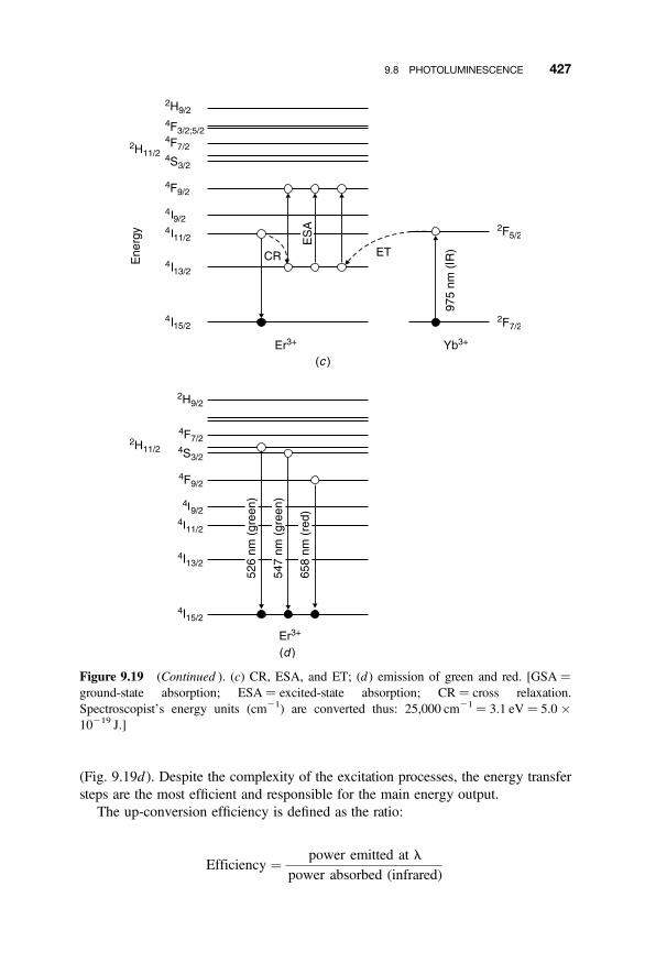
(Fig. 9.19d ). Despite the complexity of the excitation processes, the energy transfersteps are the most efficient and responsible for the main energy output.
The up-conversion efficiency is defined as the ratio:
Efficiency ¼ power emitted at lpower absorbed (infrared)
Figure 9.19 (Continued ). (c) CR, ESA, and ET; (d ) emission of green and red. [GSA ¼ground-state absorption; ESA ¼ excited-state absorption; CR ¼ cross relaxation.Spectroscopist’s energy units (cm21) are converted thus: 25,000 cm21 ¼ 3.1 eV ¼ 5.0 �10219 J.]
9.8 PHOTOLUMINESCENCE 427
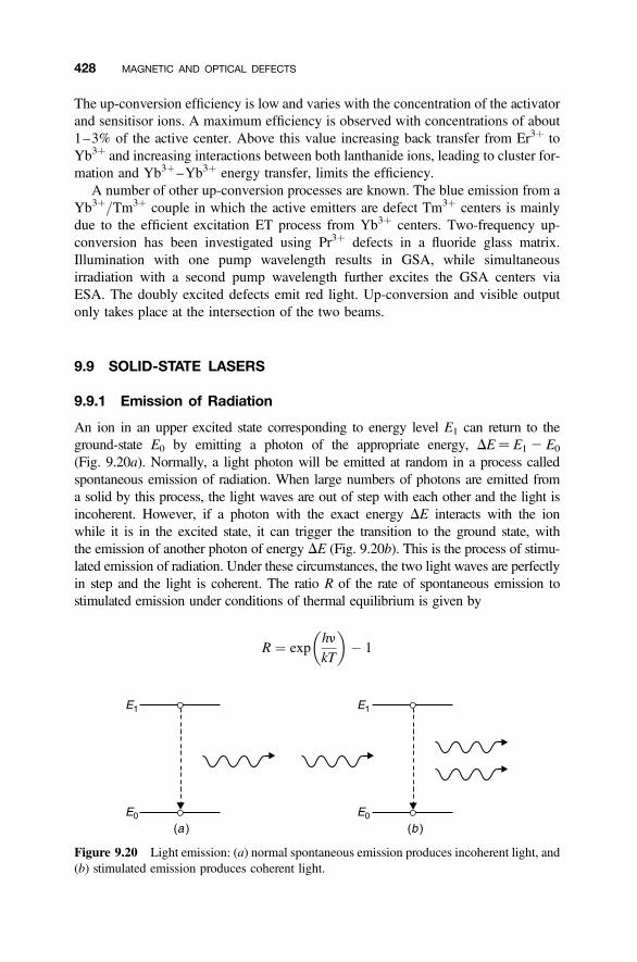
The up-conversion efficiency is low and varies with the concentration of the activatorand sensitisor ions. A maximum efficiency is observed with concentrations of about1–3% of the active center. Above this value increasing back transfer from Er3þ toYb3þ and increasing interactions between both lanthanide ions, leading to cluster for-mation and Yb3þ–Yb3þ energy transfer, limits the efficiency.
A number of other up-conversion processes are known. The blue emission from aYb3þ/Tm3þ couple in which the active emitters are defect Tm3þ centers is mainlydue to the efficient excitation ET process from Yb3þ centers. Two-frequency up-conversion has been investigated using Pr3þ defects in a fluoride glass matrix.Illumination with one pump wavelength results in GSA, while simultaneousirradiation with a second pump wavelength further excites the GSA centers viaESA. The doubly excited defects emit red light. Up-conversion and visible outputonly takes place at the intersection of the two beams.
9.9 SOLID-STATE LASERS
9.9.1 Emission of Radiation
An ion in an upper excited state corresponding to energy level E1 can return to theground-state E0 by emitting a photon of the appropriate energy, DE ¼ E1 2 E0(Fig. 9.20a). Normally, a light photon will be emitted at random in a process calledspontaneous emission of radiation. When large numbers of photons are emitted froma solid by this process, the light waves are out of step with each other and the light isincoherent. However, if a photon with the exact energy DE interacts with the ionwhile it is in the excited state, it can trigger the transition to the ground state, withthe emission of another photon of energy DE (Fig. 9.20b). This is the process of stimu-lated emission of radiation. Under these circumstances, the two light waves are perfectlyin step and the light is coherent. The ratio R of the rate of spontaneous emission tostimulated emission under conditions of thermal equilibrium is given by
R ¼ exphn
kT
� �� 1
Figure 9.20 Light emission: (a) normal spontaneous emission produces incoherent light, and(b) stimulated emission produces coherent light.
428 MAGNETIC AND OPTICAL DEFECTS
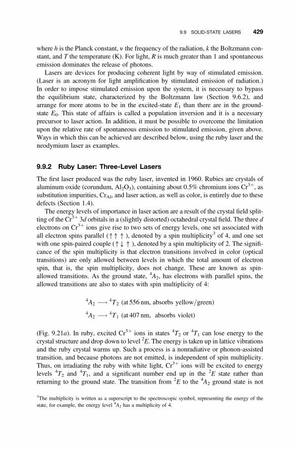
where h is the Planck constant, n the frequency of the radiation, k the Boltzmann con-stant, and T the temperature (K). For light, R is much greater than 1 and spontaneousemission dominates the release of photons.
Lasers are devices for producing coherent light by way of stimulated emission.(Laser is an acronym for light amplification by stimulated emission of radiation.)In order to impose stimulated emission upon the system, it is necessary to bypassthe equilibrium state, characterized by the Boltzmann law (Section 9.6.2), andarrange for more atoms to be in the excited-state E1 than there are in the ground-state E0. This state of affairs is called a population inversion and it is a necessaryprecursor to laser action. In addition, it must be possible to overcome the limitationupon the relative rate of spontaneous emission to stimulated emission, given above.Ways in which this can be achieved are described below, using the ruby laser and theneodymium laser as examples.
9.9.2 Ruby Laser: Three-Level Lasers
The first laser produced was the ruby laser, invented in 1960. Rubies are crystals ofaluminum oxide (corundum, Al2O3), containing about 0.5% chromium ions Cr3þ, assubstitution impurities, CrAl, and laser action, as well as color, is entirely due to thesedefects (Section 1.4).
The energy levels of importance in laser action are a result of the crystal field split-ting of the Cr3þ 3d orbitals in a (slightly distorted) octahedral crystal field. The three delectrons on Cr3þ ions give rise to two sets of energy levels, one set associated withall electron spins parallel ("" " ), denoted by a spin multiplicity3 of 4, and one setwith one spin-paired couple ("# " ), denoted by a spin multiplicity of 2. The signifi-cance of the spin multiplicity is that electron transitions involved in color (opticaltransitions) are only allowed between levels in which the total amount of electronspin, that is, the spin multiplicity, does not change. These are known as spin-allowed transitions. As the ground state, 4A2, has electrons with parallel spins, theallowed transitions are also to states with spin multiplicity of 4:
4A2 �! 4T2 (at 556 nm, absorbs yellow=green)
4A2 �! 4T1 (at 407 nm, absorbs violet)
(Fig. 9.21a). In ruby, excited Cr3þ ions in states 4T2 or 4T1 can lose energy to thecrystal structure and drop down to level 2E. The energy is taken up in lattice vibrationsand the ruby crystal warms up. Such a process is a nonradiative or phonon-assistedtransition, and because photons are not emitted, is independent of spin multiplicity.Thus, on irradiating the ruby with white light, Cr3þ ions will be excited to energylevels 4T2 and 4T1, and a significant number end up in the 2E state rather thanreturning to the ground state. The transition from 2E to the 4A2 ground state is not
3The multiplicity is written as a superscript to the spectroscopic symbol, representing the energy of thestate, for example, the energy level 4A2 has a multiplicity of 4.
9.9 SOLID-STATE LASERS 429
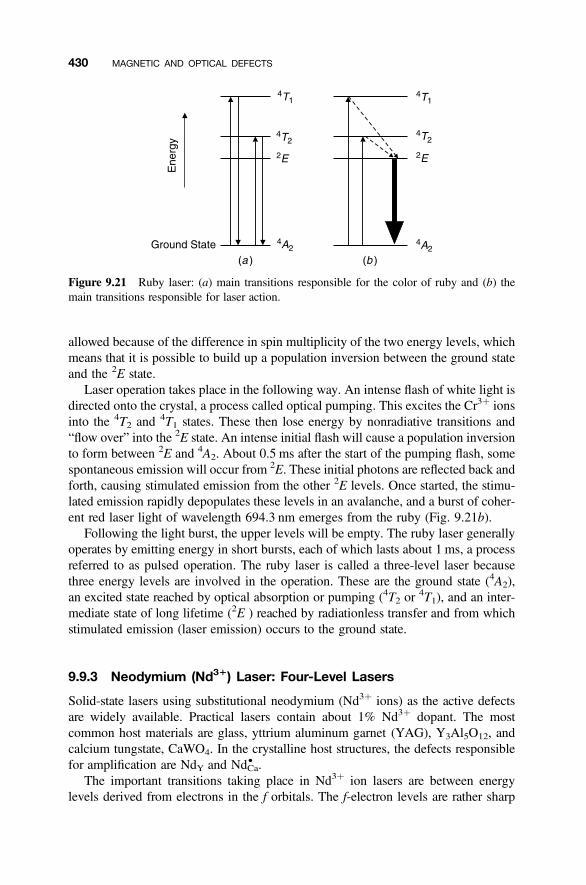
allowed because of the difference in spin multiplicity of the two energy levels, whichmeans that it is possible to build up a population inversion between the ground stateand the 2E state.
Laser operation takes place in the following way. An intense flash of white light isdirected onto the crystal, a process called optical pumping. This excites the Cr3þ ionsinto the 4T2 and 4T1 states. These then lose energy by nonradiative transitions and“flow over” into the 2E state. An intense initial flash will cause a population inversionto form between 2E and 4A2. About 0.5 ms after the start of the pumping flash, somespontaneous emission will occur from 2E. These initial photons are reflected back andforth, causing stimulated emission from the other 2E levels. Once started, the stimu-lated emission rapidly depopulates these levels in an avalanche, and a burst of coher-ent red laser light of wavelength 694.3 nm emerges from the ruby (Fig. 9.21b).
Following the light burst, the upper levels will be empty. The ruby laser generallyoperates by emitting energy in short bursts, each of which lasts about 1 ms, a processreferred to as pulsed operation. The ruby laser is called a three-level laser becausethree energy levels are involved in the operation. These are the ground state (4A2),an excited state reached by optical absorption or pumping (4T2 or
4T1), and an inter-mediate state of long lifetime (2E ) reached by radiationless transfer and from whichstimulated emission (laser emission) occurs to the ground state.
9.9.3 Neodymium (Nd31) Laser: Four-Level Lasers
Solid-state lasers using substitutional neodymium (Nd3þ ions) as the active defectsare widely available. Practical lasers contain about 1% Nd3þ dopant. The mostcommon host materials are glass, yttrium aluminum garnet (YAG), Y3Al5O12, andcalcium tungstate, CaWO4. In the crystalline host structures, the defects responsiblefor amplification are NdY and NdCa
† .The important transitions taking place in Nd3þ ion lasers are between energy
levels derived from electrons in the f orbitals. The f-electron levels are rather sharp
Figure 9.21 Ruby laser: (a) main transitions responsible for the color of ruby and (b) themain transitions responsible for laser action.
430 MAGNETIC AND OPTICAL DEFECTS
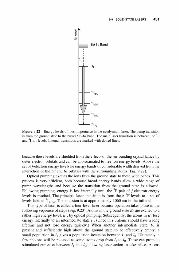
because these levels are shielded from the effects of the surrounding crystal lattice byouter electron orbitals and can be approximated to free ion energy levels. Above theset of f-electron energy levels lie energy bands of considerable width derived from theinteraction of the 5d and 6s orbitals with the surrounding atoms (Fig. 9.22).
Optical pumping excites the ions from the ground state to these wide bands. Thisprocess is very efficient, both because broad energy bands allow a wide range ofpump wavelengths and because the transition from the ground state is allowed.Following pumping, energy is lost internally until the 4F pair of f electron energylevels is reached. The principal laser transition is from these 4F levels to a set oflevels labeled 4I11/2. The emission is at approximately 1060 nm in the infrared.
This type of laser is called a four-level laser because operation takes place in thefollowing sequence of steps (Fig. 9.23). Atoms in the ground state E0 are excited to arather high energy level, E1, by optical pumping. Subsequently, the atoms in E1 loseenergy internally to an intermediate state I1. (Once in I1, atoms should have a longlifetime and not lose energy quickly.) When another intermediate state, I0, ispresent and sufficiently high above the ground state to be effectively empty, asmall population in I1 gives a population inversion between I1 and I0. Ultimately, afew photons will be released as some atoms drop from I1 to I0. These can promotestimulated emission between I1 and I0, allowing laser action to take place. Atoms
Figure 9.22 Energy levels of most importance in the neodymium laser. The pump transitionis from the ground state to the broad 5d–6s band. The main laser transition is between the 4Fand 4I11/2 levels. Internal transitions are marked with dotted lines.
9.9 SOLID-STATE LASERS 431
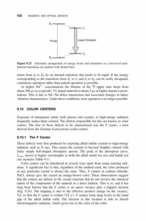
return from I0 to E0 by an internal transition that needs to be rapid. If the energycorresponding to the transitions from E1 to I1 and I0 to E0 can be easily dissipated,continuous operation rather than pulsed operation is possible.
At higher Nd3þ concentrations the lifetime of the 4F upper state drops fromabout 200 ms in a typically 1% doped material to about 5 ms at higher dopant concen-trations. This is due to Nd–Nd defect interactions and associated changes in latticevibration characteristics. Under these conditions, laser operation is no longer possible.
9.10 COLOR CENTERS
Exposure of transparent solids, both glasses and crystals, to high-energy radiationfrequently makes them colored. The defects responsible for this are known as colorcenters. The first of these defects to be characterized was the F center, a termderived from the German Farbzentrum (color center).
9.10.1 The F Center
These defects were first produced by exposing alkali halide crystals to high-energyradiation such as X rays. This causes the crystals to become brightly colored withfairly simple bell-shaped absorption spectra. The peak of the absorption curve,lmax, moves to higher wavelengths as both the alkali metal ion size and halide ionsize increase (Table 9.1).
Color centers can be introduced in several ways apart from using ionizing radi-ation. A significant fact is that, regardless of the method used, the color producedin any particular crystal is always the same. Thus, F centers in sodium chloride,NaCl, always give the crystal an orange-brown color. These observations suggestthat the centers are defects in the crystal structure that do not involve the chemicalnature of the components of the material in a direct fashion. This is so, and it haslong been known that the F center is an anion vacancy plus a trapped electron(Fig. 9.24). The trapping is due to the effective positive charge on the vacancy,VX†, so that the F center is written (VX
† e0). F centers form deep levels in the bandgap of the alkali halide solid. The electron in this location is able to absorbelectromagnetic radiation, which gives rise to the color of the solid.
Figure 9.23 Schematic arrangement of energy levels and transitions in a four-level laser.Internal transitions are marked with dotted lines.
432 MAGNETIC AND OPTICAL DEFECTS
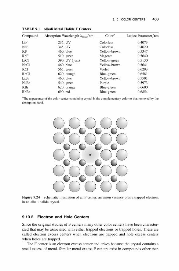
9.10.2 Electron and Hole Centers
Since the original studies of F centers many other color centers have been character-ized that may be associated with either trapped electrons or trapped holes. These arecalled electron excess centers when electrons are trapped and hole excess centerswhen holes are trapped.
The F center is an electron excess center and arises because the crystal contains asmall excess of metal. Similar metal excess F centers exist in compounds other than
TABLE 9.1 Alkali Metal Halide F Centers
Compound Absorption Wavelength lmax/nm Colora Lattice Parameter/nm
LiF 235, UV Colorless 0.4073NaF 345, UV Colorless 0.4620KF 460, blue Yellow-brown 0.5347RbF 510, green Magenta 0.5640LiCl 390, UV ( just) Yellow-green 0.5130NaCl 460, blue Yellow-brown 0.5641KCl 565, green Violet 0.6293RbCl 620, orange Blue-green 0.6581LiBr 460, blue Yellow-brown 0.5501NaBr 540, green Purple 0.5973KBr 620, orange Blue-green 0.6600RbBr 690, red Blue-green 0.6854
aThe appearance of the color-center-containing crystal is the complementary color to that removed by theabsorption band.
Figure 9.24 Schematic illustration of an F center, an anion vacancy plus a trapped electron,in an alkali halide crystal.
9.10 COLOR CENTERS 433
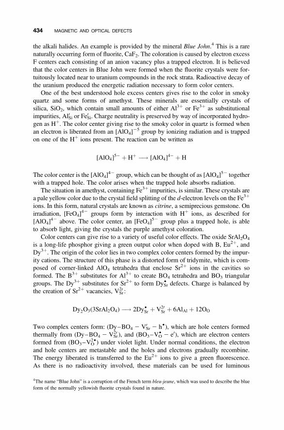
the alkali halides. An example is provided by the mineral Blue John.4 This is a rarenaturally occurring form of fluorite, CaF2. The coloration is caused by electron excessF centers each consisting of an anion vacancy plus a trapped electron. It is believedthat the color centers in Blue John were formed when the fluorite crystals were for-tuitously located near to uranium compounds in the rock strata. Radioactive decay ofthe uranium produced the energetic radiation necessary to form color centers.
One of the best understood hole excess centers gives rise to the color in smokyquartz and some forms of amethyst. These minerals are essentially crystals ofsilica, SiO2, which contain small amounts of either Al3þ or Fe3þ as substitutionalimpurities, Al0Si or Fe0Si. Charge neutrality is preserved by way of incorporated hydro-gen as Hþ. The color center giving rise to the smoky color in quartz is formed whenan electron is liberated from an [AlO4]
25 group by ionizing radiation and is trappedon one of the Hþ ions present. The reaction can be written as
[AlO4]5� þ Hþ �! [AlO4]
4� þ H
The color center is the [AlO4]42 group, which can be thought of as [AlO4]
52 togetherwith a trapped hole. The color arises when the trapped hole absorbs radiation.
The situation in amethyst, containing Fe3þ impurities, is similar. These crystals area pale yellow color due to the crystal field splitting of the d-electron levels on the Fe3þ
ions. In this form, natural crystals are known as citrine, a semiprecious gemstone. Onirradiation, [FeO4]
42 groups form by interaction with Hþ ions, as described for[AlO4]
42 above. The color center, an [FeO4]52 group plus a trapped hole, is able
to absorb light, giving the crystals the purple amethyst coloration.Color centers can give rise to a variety of useful color effects. The oxide SrAl2O4
is a long-life phosphor giving a green output color when doped with B, Eu2þ, andDy3þ. The origin of the color lies in two complex color centers formed by the impur-ity cations. The structure of this phase is a distorted form of tridymite, which is com-posed of corner-linked AlO4 tetrahedra that enclose Sr2þ ions in the cavities soformed. The B3þ substitutes for Al3þ to create BO4 tetrahedra and BO3 triangulargroups. The Dy3þ substitutes for Sr2þ to form DySr
† defects. Charge is balanced bythe creation of Sr2þ vacancies, VSr
20 :
Dy2O3(3SrAl2O4) �! 2Dy†Sr þ V20Sr þ 6AlAl þ 12OO
Two complex centers form: (Dy–BO4 2 V0Sr 2 h†), which are hole centers formed
thermally from (Dy–BO4 2 VSr20 ), and (BO3–VO
† 2 e0), which are electron centersformed from (BO3–VO
2†) under violet light. Under normal conditions, the electronand hole centers are metastable and the holes and electrons gradually recombine.The energy liberated is transferred to the Eu2þ ions to give a green fluorescence.As there is no radioactivity involved, these materials can be used for luminous
4The name “Blue John” is a corruption of the French term bleu-jeune, which was used to describe the blueform of the normally yellowish fluorite crystals found in nature.
434 MAGNETIC AND OPTICAL DEFECTS
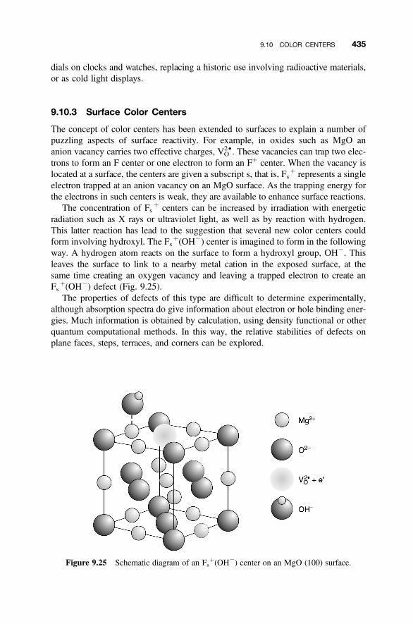
dials on clocks and watches, replacing a historic use involving radioactive materials,or as cold light displays.
9.10.3 Surface Color Centers
The concept of color centers has been extended to surfaces to explain a number ofpuzzling aspects of surface reactivity. For example, in oxides such as MgO ananion vacancy carries two effective charges, VO
2†. These vacancies can trap two elec-trons to form an F center or one electron to form an Fþ center. When the vacancy islocated at a surface, the centers are given a subscript s, that is, Fs
þ represents a singleelectron trapped at an anion vacancy on an MgO surface. As the trapping energy forthe electrons in such centers is weak, they are available to enhance surface reactions.
The concentration of Fsþ centers can be increased by irradiation with energetic
radiation such as X rays or ultraviolet light, as well as by reaction with hydrogen.This latter reaction has lead to the suggestion that several new color centers couldform involving hydroxyl. The Fs
þ(OH2) center is imagined to form in the followingway. A hydrogen atom reacts on the surface to form a hydroxyl group, OH2. Thisleaves the surface to link to a nearby metal cation in the exposed surface, at thesame time creating an oxygen vacancy and leaving a trapped electron to create anFs
þ(OH2) defect (Fig. 9.25).The properties of defects of this type are difficult to determine experimentally,
although absorption spectra do give information about electron or hole binding ener-gies. Much information is obtained by calculation, using density functional or otherquantum computational methods. In this way, the relative stabilities of defects onplane faces, steps, terraces, and corners can be explored.
Figure 9.25 Schematic diagram of an Fsþ(OH2) center on an MgO (100) surface.
9.10 COLOR CENTERS 435
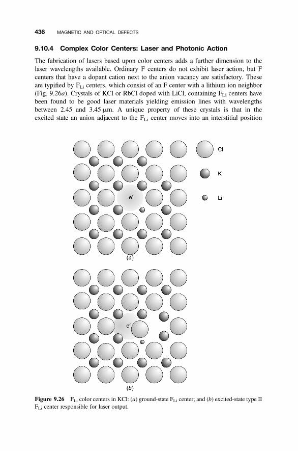
9.10.4 Complex Color Centers: Laser and Photonic Action
The fabrication of lasers based upon color centers adds a further dimension to thelaser wavelengths available. Ordinary F centers do not exhibit laser action, but Fcenters that have a dopant cation next to the anion vacancy are satisfactory. Theseare typified by FLi centers, which consist of an F center with a lithium ion neighbor(Fig. 9.26a). Crystals of KCl or RbCl doped with LiCl, containing FLi centers havebeen found to be good laser materials yielding emission lines with wavelengthsbetween 2.45 and 3.45 mm. A unique property of these crystals is that in theexcited state an anion adjacent to the FLi center moves into an interstitial position
Figure 9.26 FLi color centers in KCl: (a) ground-state FLi center; and (b) excited-state type IIFLi center responsible for laser output.
436 MAGNETIC AND OPTICAL DEFECTS

(Fig. 9.26b). This is “type II” laser behavior, and the active centers are calledFLi (II) centers.
These complex defects are introduced in a series of steps. Take KCl doped withLiþ as an example. Initially KCl crystals are grown from a solution containingLiCl as an impurity. The Liþ cations form substitutional LiK impurity defects distrib-uted at random throughout the crystal. F centers are introduced by irradiation using Xrays. These are not usually located next to a dopant Liþ cation. To convert the Fcenters into FLi (II) centers the crystal is subjected to a process called aggregation.In this step, the crystals are cooled to about 2108C and then exposed to whitelight. This releases the electrons trapped at the F centers, leaving ordinary anionvacancies, which are then able to diffuse through the crystal before recombiningwith the electrons once more to reform the F center. Ultimately, each vacancycenter ends up next to a Liþ ion. At this position it is strongly trapped and furtherdiffusion is not possible. Recombination with an electron forms the FLi centerrequired. This process of aggregation is permanent if the crystal is kept at 2108Cand in this state the crystals are laser active.
The color of diamond due to nitrogen impurities has been described in Section9.6.3 It has been found that nitrogen impurities that are located next to a carbonvacancy in diamond thin films endow the solid with quite new properties, somewhatsimilar to the properties of a solid containing FLi centers compared with ordinary Fcenters. The diamond structure is built up of carbon atoms each surrounded by four
Figure 9.27 A (N–V) center in diamond, consisting of a carbon atom vacancy and aneighboring nitrogen atom impurity.
9.10 COLOR CENTERS 437
carbon atom neighbors in a tetrahedron. In these centers, called nitrogen–vacancy(N–V) centers, the central carbon atom is missing, forming the vacancy, and a nitro-gen atom replaces one of the neighboring carbon atoms, so that the tetrahedron sur-rounding the vacancy is composed of three carbon atoms and one nitrogen atom(Fig. 9.27). The electron trapped at the color center has an orbital that extends overthe cavity, so that it encompasses not only the nitrogen impurity but also the threecarbon atoms that also surround the vacancy.
Within its orbit, which has some of the characteristics of a molecular orbitalbecause it is shared with electrons on the surrounding atoms, the electron has twopossible spin multiplicity states. These have different energies, and because of thespin-multiplicity rule, when an (N–V) center emits a photon, the transition isallowed from one of these and forbidden from the other. Moreover, the electroncan be flipped from one state to another by using low-energy radio-frequencyirradiation. Irradiation with an appropriate laser wavelength will excite the electronand as it returns to the ground state will emit fluorescent radiation. The intensity ofthe emitted photon beam will depend upon the spin state, which can be changed atwill by radio-frequency input. These color centers are under active exploration foruse as components for the realization of quantum computers.
9.11 ELECTROCHROMIC FILMS
Electrochromic materials, which change color when subjected to an electric field, arewidely explored for application as “smart windows” that control the amount of lightreflected or transmitted. Color production is linked to defect formation in an other-wise colorless matrix.
The material most widely explored for such devices is tungsten trioxide, WO3,which ordinarily is pale yellow and an insulator. Thin films are transparent.Electrochromic films rely on the formation of tungsten bronzes, MxWO3, as areduced phase (Section 4.5). There are a number of tungsten bronze structures, butthe ones utilized for electrochromic purposes are the perovskite bronzes in whichcations such as Li, Na, or K occupy cage sites between the corner-linked WO6 octa-hedra of the parent phase. The phase range over which the perovskite bronze structureis stable is greatest for the Li phases and smallest for the K phases. The hydrogenbronzes, HxWO3 are also deeply colored, although these are rather different fromthe alkali metal phases and are probably best regarded as a nonstoichiometric hydrox-ide, WO3-x(OH)x.
Although the color of the tungsten bronzes has not been explained fully over all ofthe composition range, it is believed that at high metal M concentrations the color ismetallic, due to electrons in the conduction band. At low concentrations, the colorinduced is so similar to that of reduced tungsten trioxide that it is presumed thatcharge transfer between two valence states of tungsten is occurring. If so, colormay then be attributed to W5þ–W6þ or W4þ–W6þ couples, formally equivalentto W20
W or W0W defects.
438 MAGNETIC AND OPTICAL DEFECTS
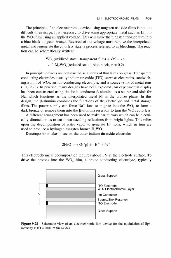
The principle of an electrochromic device using tungsten trioxide films is not toodifficult to envisage. It is necessary to drive some appropriate metal such as Li intothe WO3 film using an applied voltage. This will make the tungsten trioxide turn intoa blue-black tungsten bronze. Reversal of the voltage must remove the interpolatedmetal and regenerate the colorless state, a process referred to as bleaching. The reac-tion can be schematically written:
WO3(oxidized state, transparent film)þ xMþ x e�
O MxWO3(reduced state, blue-black, x � 0:2)
In principle, devices are constructed as a series of thin films on glass. Transparentconducting electrodes, usually indium tin oxide (ITO), serve as electrodes, sandwich-ing a film of WO3, an ion-conducting electrolyte, and a source–sink of metal ions(Fig. 9.28). In practice, many designs have been explored. An experimental displayhas been constructed using the ionic conductor b-alumina as a source and sink forNa, which functions as the interpolated metal M in the bronze phase. In thisdesign, the b-alumina combines the functions of the electrolyte and metal storagefilms. The power supply can force Naþ ions to migrate into the WO3 to form adark bronze or remove them into the b-alumina reservoir to turn the WO3 colorless.
A different arrangement has been used to make car mirrors which can be electri-cally dimmed so as to cut down dazzling reflections from bright lights. This reliesupon the decomposition of water vapor to generate Hþ ions, which in turn areused to produce a hydrogen tungsten bronze HxWO3.
Decomposition takes place on the outer indium tin oxide electrode:
2H2O �! O2(g)þ 4Hþ þ 4e�
This electrochemical decomposition requires about 1 V at the electrode surface. Todrive the protons into the WO3 film, a proton-conducting electrolyte, typically
Figure 9.28 Schematic view of an electrochromic film device for the modulation of lightintensity (ITO ¼ indium tin oxide).
9.11 ELECTROCHROMIC FILMS 439
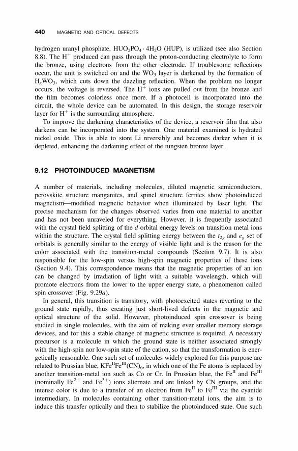
hydrogen uranyl phosphate, HUO2PO4. 4H2O (HUP), is utilized (see also Section
8.8). The Hþ produced can pass through the proton-conducting electrolyte to formthe bronze, using electrons from the other electrode. If troublesome reflectionsoccur, the unit is switched on and the WO3 layer is darkened by the formation ofHxWO3, which cuts down the dazzling reflection. When the problem no longeroccurs, the voltage is reversed. The Hþ ions are pulled out from the bronze andthe film becomes colorless once more. If a photocell is incorporated into thecircuit, the whole device can be automated. In this design, the storage reservoirlayer for Hþ is the surrounding atmosphere.
To improve the darkening characteristics of the device, a reservoir film that alsodarkens can be incorporated into the system. One material examined is hydratednickel oxide. This is able to store Li reversibly and becomes darker when it isdepleted, enhancing the darkening effect of the tungsten bronze layer.
9.12 PHOTOINDUCED MAGNETISM
A number of materials, including molecules, diluted magnetic semiconductors,perovskite structure manganites, and spinel structure ferrites show photoinducedmagnetism—modified magnetic behavior when illuminated by laser light. Theprecise mechanism for the changes observed varies from one material to anotherand has not been unraveled for everything. However, it is frequently associatedwith the crystal field splitting of the d-orbital energy levels on transition-metal ionswithin the structure. The crystal field splitting energy between the t2g and eg set oforbitals is generally similar to the energy of visible light and is the reason for thecolor associated with the transition-metal compounds (Section 9.7). It is alsoresponsible for the low-spin versus high-spin magnetic properties of these ions(Section 9.4). This correspondence means that the magnetic properties of an ioncan be changed by irradiation of light with a suitable wavelength, which willpromote electrons from the lower to the upper energy state, a phenomenon calledspin crossover (Fig. 9.29a).
In general, this transition is transitory, with photoexcited states reverting to theground state rapidly, thus creating just short-lived defects in the magnetic andoptical structure of the solid. However, photoinduced spin crossover is beingstudied in single molecules, with the aim of making ever smaller memory storagedevices, and for this a stable change of magnetic structure is required. A necessaryprecursor is a molecule in which the ground state is neither associated stronglywith the high-spin nor low-spin state of the cation, so that the transformation is ener-getically reasonable. One such set of molecules widely explored for this purpose arerelated to Prussian blue, KFeIIFeIII(CN)6, in which one of the Fe atoms is replaced byanother transition-metal ion such as Co or Cr. In Prussian blue, the FeII and FeIII
(nominally Fe2þ and Fe3þ) ions alternate and are linked by CN groups, and theintense color is due to a transfer of an electron from FeII to FeIII via the cyanideintermediary. In molecules containing other transition-metal ions, the aim is toinduce this transfer optically and then to stabilize the photoinduced state. One such
440 MAGNETIC AND OPTICAL DEFECTS
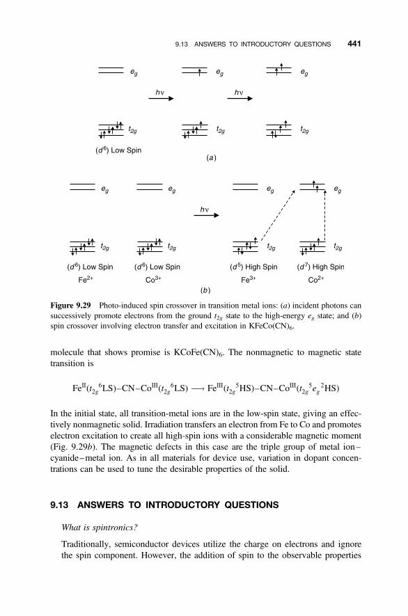
molecule that shows promise is KCoFe(CN)6. The nonmagnetic to magnetic statetransition is
FeII(t 62g LS)–CN–CoIII(t 6
2g LS) �! FeIII(t 52g HS)–CN–CoIII(t 5
2g e 2g HS)
In the initial state, all transition-metal ions are in the low-spin state, giving an effec-tively nonmagnetic solid. Irradiation transfers an electron from Fe to Co and promoteselectron excitation to create all high-spin ions with a considerable magnetic moment(Fig. 9.29b). The magnetic defects in this case are the triple group of metal ion–cyanide–metal ion. As in all materials for device use, variation in dopant concen-trations can be used to tune the desirable properties of the solid.
9.13 ANSWERS TO INTRODUCTORY QUESTIONS
What is spintronics?
Traditionally, semiconductor devices utilize the charge on electrons and ignorethe spin component. However, the addition of spin to the observable properties
Figure 9.29 Photo-induced spin crossover in transition metal ions: (a) incident photons cansuccessively promote electrons from the ground t2g state to the high-energy eg state; and (b)spin crossover involving electron transfer and excitation in KFeCo(CN)6.
9.13 ANSWERS TO INTRODUCTORY QUESTIONS 441
of electrons in semiconductors has excited considerable interest for datastorage and computing. The area in which both conductivity and spin areexploited simultaneously is called spintronics. Semiconductors that have ameasurable spin or magnetic component added to them, called diluted magneticsemiconductors, are being studied extensively with respect to their use inspintronic devices.
What is colossal magnetoresistance?
The magnetoresistance of a solid is the change of resistance when a magnetic fieldis applied. The magnetoresitive (MR) ratio is defined as the change in resistancewhen a magnetic field is applied to that in zero field:
MR ratio ¼ RH � R0
R0¼ DR
R0
where RH is the resistance in a magnetic field and R0 is the resistance in theabsence of the field. For the doped manganites the magnetoresistive ratio isclose to 100% and is negative, meaning that the resistance falls to almostnothing in a magnetic field. In such materials, a better measure of the change isthe ratio of R0/RH, where values of up to 1011 have been recorded. Thisextreme behavior has been called colossal magnetoresistance (CMR).
The CMR effect is found in a variety of doped systems, including hole dopedLa1-xAxMnO3, with A being an alkaline earth cation (Ca, Sr, Ba), orderedLn0.5A0.5MnO3, with Ln being a lanthanide, typically Pr. In all of these com-pounds, doping introduces holes that are located on Mn3þ ions to form Mn4þ.Substitution of some of the Mn with both magnetic or nonmagnetic ions, includ-ing Ti4þ, Sn4þ, Fe3þ, Cr3þ, Al3þ, Ga3þ, In3þ, Mg2þ, and Ni2þ, has been found toincrease the CMR effect considerably.
What defects commonly color glass and gemstones?
These materials are normally colored by low concentrations of 3d transition-metalions or more rarely by lanthanide ions. The pale green color of ordinary windowglass is due to the presence of Fe2þ impurities and small amounts of doping ofCr3þ into Al2O3 (corundum) creates ruby.
The colors are characteristic of the ions themselves and are due to transitionsbetween the partly filled d orbitals of transition metals (d-d transitions) or thepartly filled f orbitals of lanthanides ( f-f transitions). In the 3d transition-metalions, the 3d orbitals contain one or more electrons. When these ions are introducedinto a solid, the d-orbital energies are split by interactions with the surroundinganions. The color observed is due to transitions between these split energy levels.The color observed varies considerably as the interactions are dependent upon the
442 MAGNETIC AND OPTICAL DEFECTS
closeness of the surrounding anions and their chemical nature. The colors of solidsdoped with lanthanides do not vary asmuch as those dopedwith 3d transition-metalions, because, unlike the d orbitals, the f electron energy levels are well shieldedfrom the external surroundings. Thus, lanthanide ions in both glasses and crystalstend to exhibit very similar colors.
PROBLEMS AND EXERCISES
Quick Quiz
1. Magnetism is associated with partly filled electron:
(a) s shells
(b) p shells
(c) d shells
2. Magnetic semiconductors are doped with:
(a) Transition-metal ions
(b) Alkaline earth metal ions
(c) Donor ions
3. The high-spin (HS) state of the d6 ion Co3þ has the configuration:
(a) t2g6 eg
0
(b) t2g5 eg
1
(c) t2g4 eg
2
4. Colossal magnetoresistance is associated with:
(a) Ferrites
(b) Manganites
(c) Cobaltites
5. Data storage via magnetic bubble memories used thin films of:
(a) Garnet
(b) Perovskite
(c) Spinel
6. The color of a glass containing transition-metal ion impurities is due to:
(a) Emission of radiation
(b) Absorption of radiation
(c) Scattering of radiation
7. Up-conversion is the name of the process in which:
(a) Ultraviolet absorption gives visible light output
(b) Visible light absorption gives infrared output
(c) Infrared absorption gives visible output
PROBLEMS AND EXERCISES 443
8. Laser light is distinguished by being:
(a) Coherent
(b) Incoherent
(c) Partly coherent
9. An F center is an electron trapped at:
(a) A cation vacancy
(b) An impurity
(c) An anion vacancy
10. The Fsþ color center in the surface of an MgO crystal is an oxygen vacancy plus:
(a) A trapped hole
(b) A trapped electron
(c) A trapped Hþ
Calculations and Questions
1. A magnetic semiconductor thin film is made by doping ZnO with the 3d7 ionCo2þ. The crystal filed splitting of the d orbitals in a tetrahedral site is oppositeto that in an octahedral site, with the lower pair of levels labeled e and three upperorbitals labeled t2. (a) What is the spin state of the Co2þ ion in ZnO? (b) What isthe expected magnetic moment on the Co2þ ions? (c) The spectrum has anabsorption peak at 660 nm. What is the crystal field splitting of the Co2þ ionin the tetrahedral crystal field of ZnO?
2. A plot of the variation of the magnetic moment of Mn ions in the thermistormaterial MgGa22xMnxO4 is given in the following table. What can be concludedabout the spin state of the Mn ions?
x m/mB
0.10 5.20.25 4.920.5 4.610.75 4.211.0 4.29�Data adapted from A. Veres et al., Solid State Ionics, 178, 423–428(2007). See also Question 8.2.
3. Zinc oxide, ZnO, band gap 3.2 eV, gives green (l ¼ 498 nm) photoluminescentemission that changes to blue (l ¼ 468 nm) for a ZnO film doped with MgO.The photoluminescence is associated with a transition from the valence bandto a deep level due to a VO
† defect. (a) Confirm that the photoluminescencedoes not correspond to a transition from the valance band to the conductionband. (b) What is the energy of the VO
† level compared to the valence band for
444 MAGNETIC AND OPTICAL DEFECTS
both of these cases? (c) If the displacement of the valence band and conductionband is the same, what is the band gap of the MgO-doped film compared to thatof pure ZnO? [Data adapted from S. Fujihara, Y. Ogawa, and A. Kasai, Chem.Mater., 16, 2965–2968 (2004).]
4. An Eu3þ containing phosphor is excited by radiation with a wavelength of 400nm and emits radiation at either 592 or 611 nm with equal intensities. Whatpercentage of the exciting radiation is lost as heat to the solid?
5. The intensity of the upconverted beam as a function of the intensity of the excit-ing radiation for Er3þ doped into CeO2 is given in the following table. Determinewhether the up-conversion is likely to be a two- or three-photon absorptionprocess.
Input Intensity, Iex(arbitrary units)
Upconverted Intensity, Iup(arbitrary units)
10.0 50.07.50 30.05.00 15.03.75 9.502.50 5.00�Data adapted from H. Guo, J. Solid State Chem., 180, 127–131(2007).
6. The F center absorption maximum for KCl is at 565 nm and that for KF is460 nm (Table 9.1). (a) What is the composition of a natural crystal with colorcenters showing an absorption peak at 500 nm? (b) If the absorption peak forKF corresponds to the promotion of an electron from the F center to the conduc-tion band, determine the energy of the color center with respect to the conductionband. (The band gap in KF is 10.7 eV.) If the relative position of the color centerenergy level remains the same throughout the KF–KCl solid solution range,estimate (c) the band gap of KCl and (d) the band gap for the natural crystal.
7. (a) Calculate the magnetic moments on the Mn ion states in Figure 9.7. (b) If thecrystal field splitting for Mn2þ is 0.97 eV (1.54 � 10219 J), estimate the relativenumber of ions in the LS and IS states. (c) What wavelength of light will changethe magnetic moment of the Mn2þ ions in the ground state?
8. Mn0.01Ga0.99As is a ferromagnetic semiconductor prepared by doping the parentsemiconductor GaAs with Mn2þ. (a) What is the magnetic moment of the Mn2þ
ions if the spin-only formula applies to this material? (b) If ferromagnetismis due to the overlap of bound magnetic polarons, estimate the minimumradius of these defects. The unit cell of GaAs is cubic, a ¼ 0.56533 nm, Z ¼ 4GaAs.
9. Co0.04Zn0.96O is a ferromagnetic semiconductor. (a) Estimate the radius of abound magnetic polaron in this material. (b) If the Co2þ ions are uniformly
PROBLEMS AND EXERCISES 445
distributed, calculate the volume associated with each ion. (c) Will bound mag-netic polarons located on these ions overlap? The relative permittivity of ZnO ¼9.8 (average), the effective mass of an electron ¼ 0.28m, the unit cell is hexago-nal, a ¼ 0.3250 nm, c ¼ 0.5206 nm, the volume of the unit cell can be taken as0.866a2c.
10. The band gap of the semiconductor HgTe is 0.06 eV. (a) What is the ratioof spontaneous to stimulated emission from this semiconductor at 300 K, fortransitions from the valence band to the conduction band? (b) If the band gapis constant, at what temperature does the rate of spontaneous emission equalthe rate of stimulated emission?
FURTHER READING
Introductory material concerning the magnetic and optical properties of solids is given in:
R. J. D. Tilley, Understanding Solids, Wiley, Chichester, 2004.
Magnetic materials are covered in:
N. Spaldin, Magnetic Materials, Cambridge University Press Cambridge, United Kingdom,2003.
Specific topics of relevance are in:
Various authors, Mat. Res. Soc. Bull., 28(10) (2003) (magnetic semiconductors).
J. E. Greedan, Magnetic Oxides, in Encyclopedia of Inorganic Chemistry, 2nd ed., Wiley,Hoboken, NJ, 2006.
W. E. Hatfield, Magnetic Transition Metal Ions, in Encyclopedia of Inorganic Chemistry, 2nded., Wiley, Hoboken, NJ, 2006.
More information on color and optical properties in general is in:
P. Bamfield, Chromic Phenomena, The Royal Society of Chemistry Cambridge, UnitedKingdom, 2001.
K. Nassau, The Physics and Chemistry of Color, 2nd ed., Wiley, New York, 2001.
R. J. D. Tilley, Colour and the Optical Properties of Materials, Wiley, Chichester, 2000.
Information on specific topics is in:
G. Blasse and B. C. Grabmeier, Luminescent Materials, Springer, Berlin, 1994.
C. G. Granquist, Handbook of Inorganic Electrochromic Materials, Elsevier, Amsterdam,1995.
C. Fouassier, Luminescence, in Encyclopedia of Inorganic Chemistry, 2nd ed., Wiley,Hoboken, NJ, 2006.
M. Greenblatt, Ionic Conductors, in Encyclopedia of Inorganic Chemistry, 2nd ed., Wiley,Hoboken, NJ, 2006.
D. R. Smith, Ligand Field Theory and Spectra, in Encyclopedia of Inorganic Chemistry, 2nded., Wiley, Hoboken, NJ, 2006.
M. S. Whittingham, Mat. Res. Bull., XIV, September, 31–38 (1989).
An introduction to (N–V) centers is in:
D. A. Awschalom, R. Epstein, and R. Hanson, Sci. Am., 297(4), 58–65 (2007).
446 MAGNETIC AND OPTICAL DEFECTS
Supplementary Material
S1 CRYSTAL STRUCTURES
S1.1 Crystal Systems and Unit Cells
In crystals of any material, the atoms present are always arranged in exactly the sameway, over the whole extent of the solid, and exhibit long-range translational order. Acrystal is conventionally described by its crystal structure, which comprises theunit cell, the symmetry of the unit cell, and a list of the positions of the atoms thatlie in the unit cell.
Crystal structures and crystal lattices are different, although these terms arefrequently (and incorrectly) used as synonyms. A crystal structure is built ofatoms. A crystal lattice is an infinite pattern of points, each of which must have thesame surroundings in the same orientation. A lattice is a mathematical concept.
The external form of crystals, the internal crystal structures, and the three-dimensional lattices need to be defined unambiguously. For this purpose, a set ofvectors, a, b, and c are chosen to define the structure. The vectors a, b, and c canbe selected in any number of ways, and crystallographic convention is to choosevectors that are small and reveal the underlying symmetry of the lattice. The parallele-piped formed by the three vectors a, b, and c defines the unit cell of the crystal, withedges of length a, b, and c. The numerical values of the unit cell edges and the anglesbetween them are collectively called the lattice parameters or unit cell parameters.Conventionally, the axes are drawn so that the a axis points out from the page, theb axis points to the right, and the c axis is vertical. The angles between the axesare chosen to be equal to or greater than 908 whenever possible. These are labeleda, b, and g, where a lies between b and c, b lies between a and c, and g liesbetween a and b. Just seven different arrangements of axes, called crystal systems,and hence of unit cells, are needed in order to specify all three-dimensional structuresand lattices (Table S1.1).
The unique axis in the monoclinic unit cell is mostly taken as the b axis.Rhombohedral unit cells are often specified in terms of a bigger hexagonal unit cell.
Different compounds that crystallize with the same crystal structure, forexample, the two alums, NaAl(SO4)2 . 12H2O and NaFe(SO4)2 . 12H2O, are said to
Defects in Solids, by Richard J. D. TilleyCopyright # 2008 John Wiley & Sons, Inc.
447
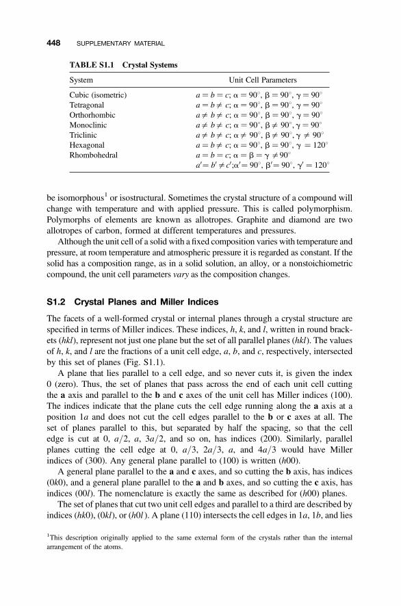
be isomorphous1 or isostructural. Sometimes the crystal structure of a compound willchange with temperature and with applied pressure. This is called polymorphism.Polymorphs of elements are known as allotropes. Graphite and diamond are twoallotropes of carbon, formed at different temperatures and pressures.
Although the unit cell of a solid with a fixed composition varies with temperature andpressure, at room temperature and atmospheric pressure it is regarded as constant. If thesolid has a composition range, as in a solid solution, an alloy, or a nonstoichiometriccompound, the unit cell parameters vary as the composition changes.
S1.2 Crystal Planes and Miller Indices
The facets of a well-formed crystal or internal planes through a crystal structure arespecified in terms of Miller indices. These indices, h, k, and l, written in round brack-ets (hkl), represent not just one plane but the set of all parallel planes (hkl). The valuesof h, k, and l are the fractions of a unit cell edge, a, b, and c, respectively, intersectedby this set of planes (Fig. S1.1).
A plane that lies parallel to a cell edge, and so never cuts it, is given the index0 (zero). Thus, the set of planes that pass across the end of each unit cell cuttingthe a axis and parallel to the b and c axes of the unit cell has Miller indices (100).The indices indicate that the plane cuts the cell edge running along the a axis at aposition 1a and does not cut the cell edges parallel to the b or c axes at all. Theset of planes parallel to this, but separated by half the spacing, so that the celledge is cut at 0, a/2, a, 3a/2, and so on, has indices (200). Similarly, parallelplanes cutting the cell edge at 0, a/3, 2a/3, a, and 4a/3 would have Millerindices of (300). Any general plane parallel to (100) is written (h00).
A general plane parallel to the a and c axes, and so cutting the b axis, has indices(0k0), and a general plane parallel to the a and b axes, and so cutting the c axis, hasindices (00l). The nomenclature is exactly the same as described for (h00) planes.
The set of planes that cut two unit cell edges and parallel to a third are described byindices (hk0), (0kl), or (h0l ). A plane (110) intersects the cell edges in 1a, 1b, and lies
TABLE S1.1 Crystal Systems
System Unit Cell Parameters
Cubic (isometric) a ¼ b ¼ c; a ¼ 908, b ¼ 908, g ¼ 908Tetragonal a ¼ b= c; a ¼ 908, b ¼ 908, g ¼ 908Orthorhombic a= b= c; a ¼ 908, b ¼ 908, g ¼ 908Monoclinic a= b= c; a ¼ 908, b= 908, g ¼ 908Triclinic a= b= c; a= 908, b= 908, g= 908Hexagonal a ¼ b= c; a ¼ 908, b ¼ 908, g ¼ 1208Rhombohedral a ¼ b ¼ c; a ¼ b ¼ g=908
a0¼ b0=c0;a0¼ 908, b0¼ 908, g0 ¼ 1208
1This description originally applied to the same external form of the crystals rather than the internalarrangement of the atoms.
448 SUPPLEMENTARY MATERIAL
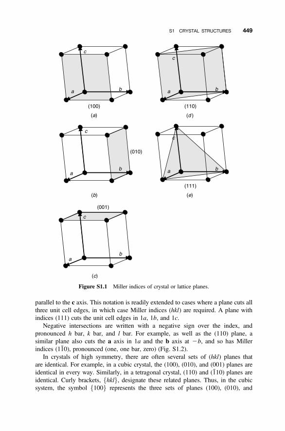
parallel to the c axis. This notation is readily extended to cases where a plane cuts allthree unit cell edges, in which case Miller indices (hkl) are required. A plane withindices (111) cuts the unit cell edges in 1a, 1b, and 1c.
Negative intersections are written with a negative sign over the index, andpronounced h bar, k bar, and l bar. For example, as well as the (110) plane, asimilar plane also cuts the a axis in 1a and the b axis at 2b, and so has Millerindices (110), pronounced (one, one bar, zero) (Fig. S1.2).
In crystals of high symmetry, there are often several sets of (hkl) planes thatare identical. For example, in a cubic crystal, the (100), (010), and (001) planes areidentical in every way. Similarly, in a tetragonal crystal, (110) and (110) planes areidentical. Curly brackets, fhklg, designate these related planes. Thus, in the cubicsystem, the symbol f100g represents the three sets of planes (100), (010), and
Figure S1.1 Miller indices of crystal or lattice planes.
S1 CRYSTAL STRUCTURES 449
Figure S1.2 Negative Miller indices.
450 SUPPLEMENTARY MATERIAL
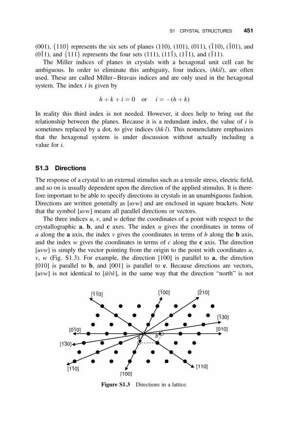
(001), f110g represents the six sets of planes (110), (101), (011), (110), (101), and(011), and f111g represents the four sets (111), (111), (111), and (111).
The Miller indices of planes in crystals with a hexagonal unit cell can beambiguous. In order to eliminate this ambiguity, four indices, (hkil), are oftenused. These are called Miller–Bravais indices and are only used in the hexagonalsystem. The index i is given by
hþ k þ i ¼ 0 or i ¼ �(hþ k)
In reality this third index is not needed. However, it does help to bring out therelationship between the planes. Because it is a redundant index, the value of i issometimes replaced by a dot, to give indices (hk.l). This nomenclature emphasizesthat the hexagonal system is under discussion without actually including avalue for i.
S1.3 Directions
The response of a crystal to an external stimulus such as a tensile stress, electric field,and so on is usually dependent upon the direction of the applied stimulus. It is there-fore important to be able to specify directions in crystals in an unambiguous fashion.Directions are written generally as [uvw] and are enclosed in square brackets. Notethat the symbol [uvw] means all parallel directions or vectors.
The three indices u, v, and w define the coordinates of a point with respect to thecrystallographic a, b, and c axes. The index u gives the coordinates in terms ofa along the a axis, the index v gives the coordinates in terms of b along the b axis,and the index w gives the coordinates in terms of c along the c axis. The direction[uvw] is simply the vector pointing from the origin to the point with coordinates u,v, w (Fig. S1.3). For example, the direction [100] is parallel to a, the direction[010] is parallel to b, and [001] is parallel to c. Because directions are vectors,[uvw] is not identical to [uvw], in the same way that the direction “north” is not
Figure S1.3 Directions in a lattice.
S1 CRYSTAL STRUCTURES 451
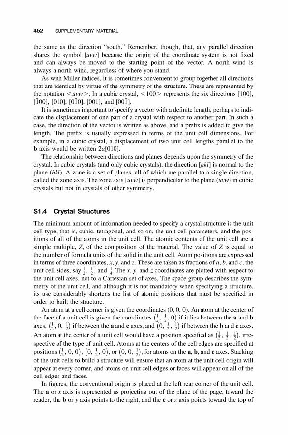
the same as the direction “south.” Remember, though, that, any parallel directionshares the symbol [uvw] because the origin of the coordinate system is not fixedand can always be moved to the starting point of the vector. A north wind isalways a north wind, regardless of where you stand.
As with Miller indices, it is sometimes convenient to group together all directionsthat are identical by virtue of the symmetry of the structure. These are represented bythe notation ,uvw.. In a cubic crystal, ,100. represents the six directions [100],[100], [010], [010], [001], and [001].
It is sometimes important to specify a vector with a definite length, perhaps to indi-cate the displacement of one part of a crystal with respect to another part. In such acase, the direction of the vector is written as above, and a prefix is added to give thelength. The prefix is usually expressed in terms of the unit cell dimensions. Forexample, in a cubic crystal, a displacement of two unit cell lengths parallel to theb axis would be written 2a[010].
The relationship between directions and planes depends upon the symmetry of thecrystal. In cubic crystals (and only cubic crystals), the direction [hkl] is normal to theplane (hkl). A zone is a set of planes, all of which are parallel to a single direction,called the zone axis. The zone axis [uvw] is perpendicular to the plane (uvw) in cubiccrystals but not in crystals of other symmetry.
S1.4 Crystal Structures
The minimum amount of information needed to specify a crystal structure is the unitcell type, that is, cubic, tetragonal, and so on, the unit cell parameters, and the pos-itions of all of the atoms in the unit cell. The atomic contents of the unit cell are asimple multiple, Z, of the composition of the material. The value of Z is equal tothe number of formula units of the solid in the unit cell. Atom positions are expressedin terms of three coordinates, x, y, and z. These are taken as fractions of a, b, and c, theunit cell sides, say 1
2 ,12 , and
14. The x, y, and z coordinates are plotted with respect to
the unit cell axes, not to a Cartesian set of axes. The space group describes the sym-metry of the unit cell, and although it is not mandatory when specifying a structure,its use considerably shortens the list of atomic positions that must be specified inorder to built the structure.
An atom at a cell corner is given the coordinates (0, 0, 0). An atom at the center ofthe face of a unit cell is given the coordinates 1
2 ,12 , 0
�if it lies between the a and b
axes, 12 , 0,
12
�if between the a and c axes, and 0, 1
2 ,12
�if between the b and c axes.
An atom at the center of a unit cell would have a position specified as 12 ,
12 ,
12
�, irre-
spective of the type of unit cell. Atoms at the centers of the cell edges are specified atpositions 1
2 , 0, 0 �
, 0, 12 , 0
�, or 0, 0, 1
2
�, for atoms on the a, b, and c axes. Stacking
of the unit cells to build a structure will ensure that an atom at the unit cell origin willappear at every corner, and atoms on unit cell edges or faces will appear on all of thecell edges and faces.
In figures, the conventional origin is placed at the left rear corner of the unit cell.The a or x axis is represented as projecting out of the plane of the page, toward thereader, the b or y axis points to the right, and the c or z axis points toward the top of
452 SUPPLEMENTARY MATERIAL
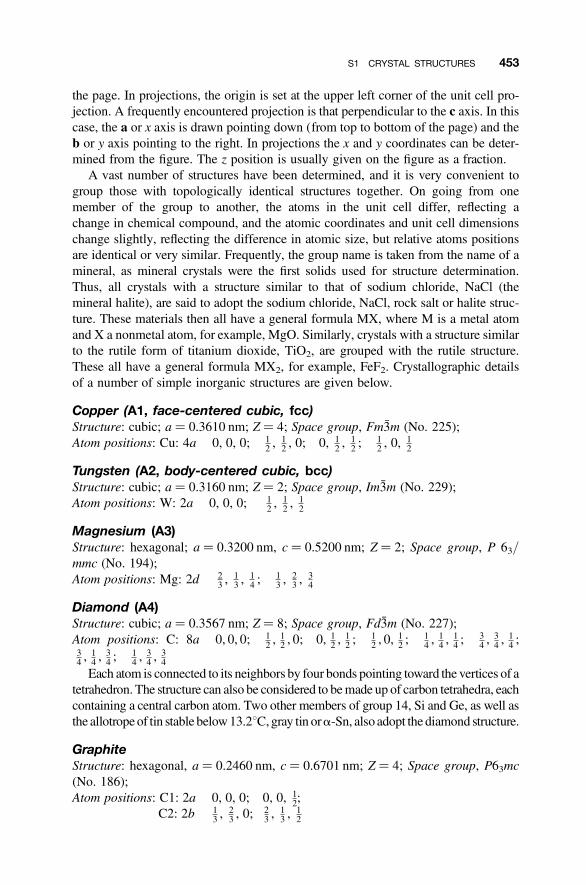
the page. In projections, the origin is set at the upper left corner of the unit cell pro-jection. A frequently encountered projection is that perpendicular to the c axis. In thiscase, the a or x axis is drawn pointing down (from top to bottom of the page) and theb or y axis pointing to the right. In projections the x and y coordinates can be deter-mined from the figure. The z position is usually given on the figure as a fraction.
A vast number of structures have been determined, and it is very convenient togroup those with topologically identical structures together. On going from onemember of the group to another, the atoms in the unit cell differ, reflecting achange in chemical compound, and the atomic coordinates and unit cell dimensionschange slightly, reflecting the difference in atomic size, but relative atoms positionsare identical or very similar. Frequently, the group name is taken from the name of amineral, as mineral crystals were the first solids used for structure determination.Thus, all crystals with a structure similar to that of sodium chloride, NaCl (themineral halite), are said to adopt the sodium chloride, NaCl, rock salt or halite struc-ture. These materials then all have a general formula MX, where M is a metal atomand X a nonmetal atom, for example, MgO. Similarly, crystals with a structure similarto the rutile form of titanium dioxide, TiO2, are grouped with the rutile structure.These all have a general formula MX2, for example, FeF2. Crystallographic detailsof a number of simple inorganic structures are given below.
Copper (A1, face-centered cubic, fcc)Structure: cubic; a ¼ 0.3610 nm; Z ¼ 4; Space group, Fm3m (No. 225);Atom positions: Cu: 4a 0, 0, 0; 1
2 ,12 , 0; 0, 1
2 ,12 ;
12 , 0,
12
Tungsten (A2, body-centered cubic, bcc)Structure: cubic; a ¼ 0.3160 nm; Z ¼ 2; Space group, Im3m (No. 229);Atom positions: W: 2a 0, 0, 0; 1
2 ,12 ,
12
Magnesium (A3)Structure: hexagonal; a ¼ 0.3200 nm, c ¼ 0.5200 nm; Z ¼ 2; Space group, P 63/mmc (No. 194);Atom positions: Mg: 2d 2
3 ,13 ,
14 ;
13 ,
23 ,
34
Diamond (A4)Structure: cubic; a ¼ 0.3567 nm; Z ¼ 8; Space group, Fd3m (No. 227);Atom positions: C: 8a 0, 0, 0; 1
2 ,12 , 0; 0, 1
2 ,12 ;
12 , 0,
12 ;
14 ,
14 ,
14 ;
34 ,
34 ,
14 ;
34 ,
14 ,
34 ;
14 ,
34 ,
34
Each atom is connected to its neighbors by four bonds pointing toward the vertices of atetrahedron. The structure can also be considered to bemade up of carbon tetrahedra, eachcontaining a central carbon atom. Two other members of group 14, Si and Ge, as well asthe allotrope of tin stable below13.28C,gray tin ora-Sn, also adopt the diamond structure.
GraphiteStructure: hexagonal, a ¼ 0.2460 nm, c ¼ 0.6701 nm; Z ¼ 4; Space group, P63mc(No. 186);Atom positions: C1: 2a 0, 0, 0; 0, 0, 1
2;C2: 2b 1
3 ,23 , 0;
23 ,
13 ,
12
S1 CRYSTAL STRUCTURES 453
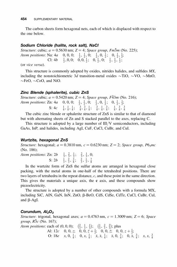
The carbon sheets form hexagonal nets, each of which is displaced with respect tothe one below.
Sodium Chloride (halite, rock salt), NaClStructure: cubic; a ¼ 0.5630 nm; Z ¼ 4; Space group, Fm3m (No. 225);Atom positions: Na: 4a 0, 0, 0; 1
2 ,12 , 0;
12 , 0,
12 ; 0, 1
2 ,12;
Cl: 4b 12 , 0, 0; 0, 0, 1
2 ; 0, 12 , 0;
12 ,
12 ,
12 ;
(or vice versa).
This structure is commonly adopted by oxides, nitrides halides, and sulfides MX,including the nonstoichiometric 3d transition-metal oxides �TiO, �VO, �MnO,�FeO, �CoO, and NiO.
Zinc Blende (sphalerite), cubic ZnSStructure: cubic; a ¼ 0.5420 nm; Z ¼ 4; Space group, F43m (No. 216);Atom positions: Zn: 4a 0, 0, 0; 1
2 ,12 , 0;
12 , 0,
12 ; 0, 1
2 ,12;
S: 4c 14 ,
14 ,
14 ;
34 ,
34 ,
14 ;
34 ,
14 ,
34 ;
14 ,
34 ,
34
The cubic zinc blende or sphalerite structure of ZnS is similar to that of diamondbut with alternating sheets of Zn and S stacked parallel to the axes, replacing C.
This structure is adopted by a large number of III/V semiconductors, includingGaAs, InP, and halides, including AgI, CuF, CuCl, CuBr, and CuI.
Wurtzite, hexagonal ZnSStructure: hexagonal; a ¼ 0.3810 nm, c ¼ 0.6230 nm; Z ¼ 2; Space group, P63mc(No. 186);Atom positions: Zn: 2b 1
3 ,23 ,
12 ;
23 ,
13 , 0;
S: 2b 13 ,
23 ,
38 ;
23 ,
13 ,
78
In the wurtzite form of ZnS the sulfur atoms are arranged in hexagonal closepacking, with the metal atoms in one-half of the tetrahedral positions. There aretwo layers of tetrahedra in the repeat distance, c, and these point in the same direction.This gives the materials a unique axis, the c axis, and these compounds showpiezoelectricity.
The structure is adopted by a number of other compounds with a formula MX,including SiC, AlN, GaN, InN, ZnO, b-BeO, CdS, CdSe, CdTe, CuCl, CuBr, Cul,and b-AgI.
Corundum, Al2O3
Structure: trigonal, hexagonal axes; a ¼ 0.4763 nm, c ¼ 1.3009 nm; Z ¼ 6; Spacegroup, R3c (No. 167);Atom positions: each of (0, 0, 0); 2
3 ,13 ,
13
�; 1
3 ,23 ,
23
�; plus
Al: 12c 0, 0, z; 0, 0, z þ 12; 0, 0, z; 0, 0, z þ 1
2;O: 18e x, 0, 1
4 ; 0, x, 14 ; �x, �x, 1
4 ; �x, 0, 34 ; 0, �x, 3
4 ; x, x, 34
454 SUPPLEMENTARY MATERIAL

The x coordinate (O) and the z coordinate (Al) can be approximated to 13. In
general, these can be written x ¼ 13 þ u and z ¼ 1
3 þ w, where u and w are bothsmall. Taking typical values of x ¼ 0.306, and z ¼ 0.352, the positions are:
Al: 12c 0, 0, 0.352; 0, 0, 0.148; 0, 0, 0.648; 0, 0, 0.852
O: 18e 0:306, 0, 14 ; 0, 0:306, 1
4 ; 0:694, 0:694, 14 ; 0:694, 0, 3
4 ;0, 0:694, 3
4 ; 0:306, 0:306, 34
The unit cell of corundum is rhombohedral, but the structure is usually describedwith respect to hexagonal axes. Each of the cations is surrounded by six oxygenions in a slightly distorted octahedral coordination. The anions are close to ahexagonal close-packed array and the cations occupy two-thirds of the available octa-hedral positions in this array in an ordered fashion. The structure is also adopted bya-Fe2O3 and Cr2O3.
Fluorite, CaF2Structure: cubic; a ¼ 0.5450 nm; Z ¼ 4; Space group, Fm3m (No. 225);Atom positions: Ca: 4a 0, 0, 0; 1
2 ,12 , 0;
12 , 0,
12 ; 0, 1
2 ,12;
F: 8c 14 ,
14 ,
14 ;
14 ,
34 ,
34 ;
34 ,
14 ,
34 ;
34 ,
34 ,
14 ;
14 ,
14 ,
34 ;
14 ,
34 ,
14 ;
34 ,
14 ,
14 ;
34 ,
34 ,
34
Rutile, TiO2
Structure: tetragonal; a ¼ 0.4594 nm, c ¼ 0.2959 nm; Z ¼ 2; Space group, P42/mnm(No. 136);Atom positions: Ti: 2a 0, 0, 0; 1
2 ,12 ,
12;
O: 4f x, x, 0; �x, �x, 0; �xþ 12 , xþ 1
2 ,12 ; xþ 1
2 , �xþ 12 ,
12
The x coordinate for O is close to 13. Taking a typical value of x ¼ 0.305, the
positions are:
O: 4f 0.305, 0.305, 0; 0.695, 0.695, 0; 0.195, 0.805, 12; 0.805, 0.195, 12
Titanium dioxide crystallizes in several forms. The most important is the rutileform. This structure is also adopted by SnO2, MgF2, and ZnF2. A number ofoxides that show metallic or metal–insulator transitions, for example, VO2, NbO2,and CrO2, have a slightly distorted form of the structure.
Cadmium Iodide (ideal), CdI2, Cadmium Hydroxide, Cd(OH)2Structure: hexagonal; a ¼ 0.424 nm, c ¼ 0.684 nm; Z ¼ 2; Space group, P3m1(No. 164);Atom positions: Cd: 1a 0, 0, 0;
I: 2d 13 ,
23 ,
14 ;
23 ,
13 , �1
4
S1 CRYSTAL STRUCTURES 455
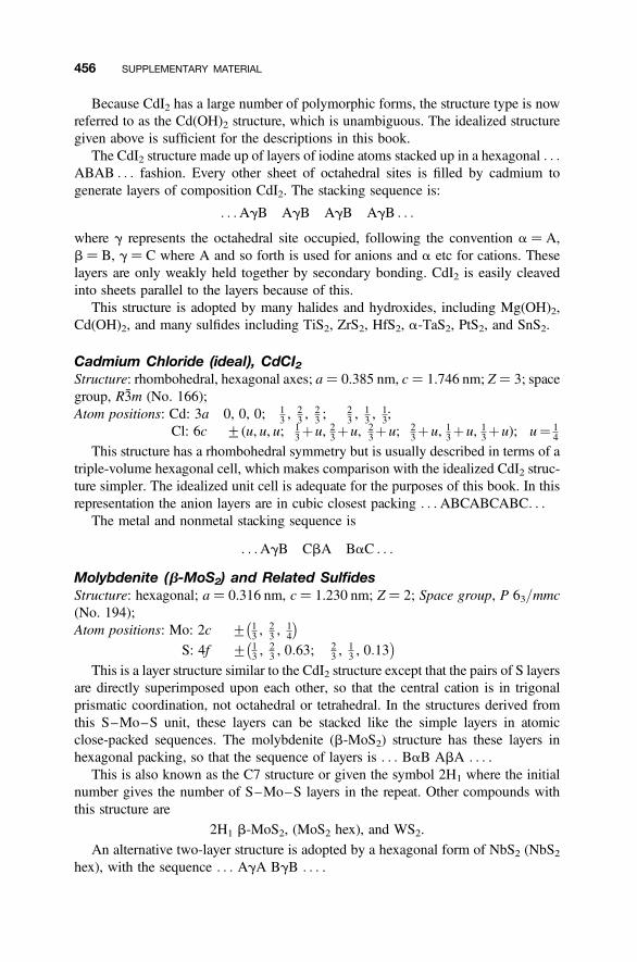
Because CdI2 has a large number of polymorphic forms, the structure type is nowreferred to as the Cd(OH)2 structure, which is unambiguous. The idealized structuregiven above is sufficient for the descriptions in this book.
The CdI2 structure made up of layers of iodine atoms stacked up in a hexagonal . . .ABAB . . . fashion. Every other sheet of octahedral sites is filled by cadmium togenerate layers of composition CdI2. The stacking sequence is:
. . .AgB AgB AgB AgB . . .
where g represents the octahedral site occupied, following the convention a ¼ A,b ¼ B, g ¼ C where A and so forth is used for anions and a etc for cations. Theselayers are only weakly held together by secondary bonding. CdI2 is easily cleavedinto sheets parallel to the layers because of this.
This structure is adopted by many halides and hydroxides, including Mg(OH)2,Cd(OH)2, and many sulfides including TiS2, ZrS2, HfS2, a-TaS2, PtS2, and SnS2.
Cadmium Chloride (ideal), CdCI2Structure: rhombohedral, hexagonal axes; a ¼ 0.385 nm, c ¼ 1.746 nm; Z ¼ 3; spacegroup, R3m (No. 166);Atom positions: Cd: 3a 0, 0, 0; 1
3 ,23 ,
23 ;
23 ,
13 ,
13;
Cl: 6c +(u, u, u; 13þu, 23þu, 2
3þu; 23þu, 13þu, 13þu); u¼ 1
4
This structure has a rhombohedral symmetry but is usually described in terms of atriple-volume hexagonal cell, which makes comparison with the idealized CdI2 struc-ture simpler. The idealized unit cell is adequate for the purposes of this book. In thisrepresentation the anion layers are in cubic closest packing . . .ABCABCABC. . .
The metal and nonmetal stacking sequence is
. . .AgB CbA BaC . . .
Molybdenite (b-MoS2) and Related SulfidesStructure: hexagonal; a ¼ 0.316 nm, c ¼ 1.230 nm; Z ¼ 2; Space group, P 63/mmc(No. 194);Atom positions: Mo: 2c + 1
3 ,23 ,
14
�S: 4f + 1
3 ,23 , 0:63;
23 ,
13 , 0:13
�This is a layer structure similar to the CdI2 structure except that the pairs of S layers
are directly superimposed upon each other, so that the central cation is in trigonalprismatic coordination, not octahedral or tetrahedral. In the structures derived fromthis S–Mo–S unit, these layers can be stacked like the simple layers in atomicclose-packed sequences. The molybdenite (b-MoS2) structure has these layers inhexagonal packing, so that the sequence of layers is . . . BaB AbA . . . .
This is also known as the C7 structure or given the symbol 2H1 where the initialnumber gives the number of S–Mo–S layers in the repeat. Other compounds withthis structure are
2H1 b-MoS2, (MoS2 hex), and WS2.
An alternative two-layer structure is adopted by a hexagonal form of NbS2 (NbS2hex), with the sequence . . . AgA BgB . . . .
456 SUPPLEMENTARY MATERIAL
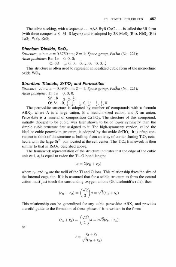
The cubic stacking, with a sequence . . . AbA BgB CaC . . . . is called the 3R form(with three composite S–M–S layers) and is adopted by 3R-MoS2 (Rh), NbS2 (Rh)TaS2, WS2, ReS2.
Rhenium Trioxide, ReO3
Structure: cubic; a ¼ 0.3750 nm; Z ¼ 1; Space group, Pm3m (No. 221);Atom positions: Re: 1a 0, 0, 0;
O: 3d 12 , 0, 0; 0, 1
2 , 0; 0, 0, 12
This structure is often used to represent an idealized cubic form of the monoclinicoxide WO3.
Strontium Titanate, SrTiO3 and PerovskitesStructure: cubic; a ¼ 0.3905 nm; Z ¼ 1; Space group, Pm3m (No. 221);Atom positions: Ti: 1a 0, 0, 0;
Sr: 1b 12 ,
12 ,
12;
O: 3c 0, 12 ,
12 ;
12 , 0,
12 ;
12 ,
12 , 0
The perovskite structure is adopted by number of compounds with a formulaABX3, where A is a large cation, B a medium-sized cation, and X an anion.Perovskite is a mineral of composition CaTiO3. The structure of this compound,initially thought to be cubic, was later shown to be of lower symmetry than thesimple cubic structure first assigned to it. The high-symmetry version, called theideal or cubic perovskite structure, is adopted by the oxide SrTiO3. It is often con-venient to think of the structure as built up from an array of corner sharing TiO6 octa-hedra with the large Sr2þ ion located at the cell center. The TiO6 framework is thensimilar to that in ReO3, described above.
The framework representation of the structure indicates that the edge of the cubicunit cell, a, is equal to twice the Ti–O bond length:
a ¼ 2(rTi þ rO)
where rTi and rO are the radii of the Ti and O ions. This relationship fixes the size ofthe internal cage site. If it is assumed that for a stable structure to form the centralcation must just touch the surrounding oxygen anions (Goldschmidt’s rule), then
(rSr þ rO) ¼ffiffiffi2
p
2
� �a ¼
ffiffiffi2
p(rTi þ rO)
This relationship can be generalized for any cubic perovskite ABX3 and providesa useful guide to the formation of these phases if it is written in the form:
(rA þ rX) ¼ffiffiffi2
p
2
� �a ¼ t
ffiffiffi2
p(rB þ rX)
or
t ¼ rA þ rXffiffiffi2
p(rB þ rX)
S1 CRYSTAL STRUCTURES 457
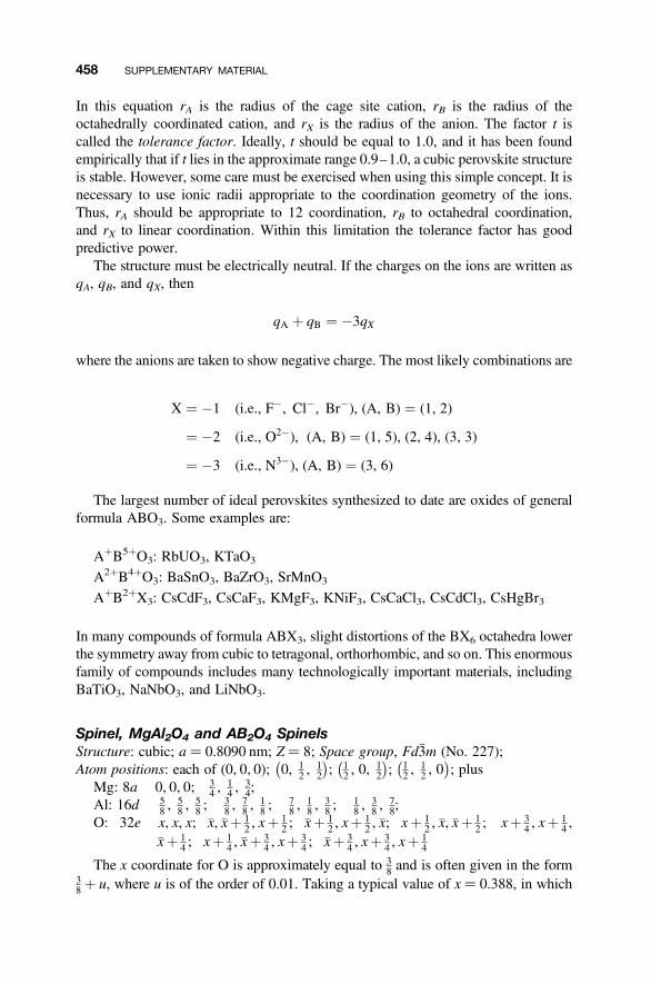
In this equation rA is the radius of the cage site cation, rB is the radius of theoctahedrally coordinated cation, and rX is the radius of the anion. The factor t iscalled the tolerance factor. Ideally, t should be equal to 1.0, and it has been foundempirically that if t lies in the approximate range 0.9–1.0, a cubic perovskite structureis stable. However, some care must be exercised when using this simple concept. It isnecessary to use ionic radii appropriate to the coordination geometry of the ions.Thus, rA should be appropriate to 12 coordination, rB to octahedral coordination,and rX to linear coordination. Within this limitation the tolerance factor has goodpredictive power.
The structure must be electrically neutral. If the charges on the ions are written asqA, qB, and qX, then
qA þ qB ¼ �3qX
where the anions are taken to show negative charge. The most likely combinations are
X ¼ �1 (i.e., F�, Cl�, Br�), (A, B) ¼ (1, 2)
¼ �2 (i.e., O2�), (A, B) ¼ (1, 5), (2, 4), (3, 3)
¼ �3 (i.e., N3�), (A, B) ¼ (3, 6)
The largest number of ideal perovskites synthesized to date are oxides of generalformula ABO3. Some examples are:
AþB5þO3: RbUO3, KTaO3
A2þB4þO3: BaSnO3, BaZrO3, SrMnO3
AþB2þX3: CsCdF3, CsCaF3, KMgF3, KNiF3, CsCaCl3, CsCdCl3, CsHgBr3
In many compounds of formula ABX3, slight distortions of the BX6 octahedra lowerthe symmetry away from cubic to tetragonal, orthorhombic, and so on. This enormousfamily of compounds includes many technologically important materials, includingBaTiO3, NaNbO3, and LiNbO3.
Spinel, MgAl2O4 and AB2O4 SpinelsStructure: cubic; a ¼ 0.8090 nm; Z ¼ 8; Space group, Fd3m (No. 227);Atom positions: each of (0, 0, 0); 0, 1
2 ,12
�; 1
2 , 0,12
�; 1
2 ,12 , 0
�; plus
Mg: 8a 0, 0, 0; 34 ,
14 ,
34;
Al: 16d 58 ,
58 ,
58 ;
38 ,
78 ,
18 ;
78 ,
18 ,
38 ;
18 ,
38 ,
78;
O: 32e x, x, x; �x, �xþ 12 , xþ 1
2 ; �xþ 12 , xþ 1
2 , �x; xþ 12 , �x, �xþ 1
2 ; xþ 34 , xþ 1
4 ,�xþ 1
4 ; xþ 14 , �xþ 3
4 , xþ 34 ; �xþ 3
4 , xþ 34 , xþ 1
4
The x coordinate for O is approximately equal to 38 and is often given in the form
38 þ u, where u is of the order of 0.01. Taking a typical value of x ¼ 0.388, in which
458 SUPPLEMENTARY MATERIAL
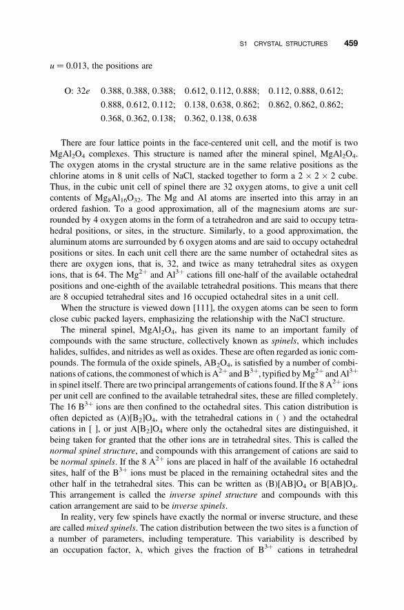
u ¼ 0.013, the positions are
O: 32e 0:388, 0:388, 0:388; 0:612, 0:112, 0:888; 0:112, 0:888, 0:612;
0:888, 0:612, 0:112; 0:138, 0:638, 0:862; 0:862, 0:862, 0:862;
0:368, 0:362, 0:138; 0:362, 0:138, 0:638
There are four lattice points in the face-centered unit cell, and the motif is twoMgAl2O4 complexes. This structure is named after the mineral spinel, MgAl2O4.The oxygen atoms in the crystal structure are in the same relative positions as thechlorine atoms in 8 unit cells of NaCl, stacked together to form a 2 � 2 � 2 cube.Thus, in the cubic unit cell of spinel there are 32 oxygen atoms, to give a unit cellcontents of Mg8Al16O32. The Mg and Al atoms are inserted into this array in anordered fashion. To a good approximation, all of the magnesium atoms are sur-rounded by 4 oxygen atoms in the form of a tetrahedron and are said to occupy tetra-hedral positions, or sites, in the structure. Similarly, to a good approximation, thealuminum atoms are surrounded by 6 oxygen atoms and are said to occupy octahedralpositions or sites. In each unit cell there are the same number of octahedral sites asthere are oxygen ions, that is, 32, and twice as many tetrahedral sites as oxygenions, that is 64. The Mg2þ and Al3þ cations fill one-half of the available octahedralpositions and one-eighth of the available tetrahedral positions. This means that thereare 8 occupied tetrahedral sites and 16 occupied octahedral sites in a unit cell.
When the structure is viewed down [111], the oxygen atoms can be seen to formclose cubic packed layers, emphasizing the relationship with the NaCl structure.
The mineral spinel, MgAl2O4, has given its name to an important family ofcompounds with the same structure, collectively known as spinels, which includeshalides, sulfides, and nitrides as well as oxides. These are often regarded as ionic com-pounds. The formula of the oxide spinels, AB2O4, is satisfied by a number of combi-nations of cations, the commonest of which is A2þ andB3þ, typified byMg2þ andAl3þ
in spinel itself. There are two principal arrangements of cations found. If the 8A2þ ionsper unit cell are confined to the available tetrahedral sites, these are filled completely.The 16 B3þ ions are then confined to the octahedral sites. This cation distribution isoften depicted as (A)[B2]O4, with the tetrahedral cations in ( ) and the octahedralcations in [ ], or just A[B2]O4 where only the octahedral sites are distinguished, itbeing taken for granted that the other ions are in tetrahedral sites. This is called thenormal spinel structure, and compounds with this arrangement of cations are said tobe normal spinels. If the 8 A2þ ions are placed in half of the available 16 octahedralsites, half of the B3þ ions must be placed in the remaining octahedral sites and theother half in the tetrahedral sites. This can be written as (B)[AB]O4 or B[AB]O4.This arrangement is called the inverse spinel structure and compounds with thiscation arrangement are said to be inverse spinels.
In reality, very few spinels have exactly the normal or inverse structure, and theseare called mixed spinels. The cation distribution between the two sites is a function ofa number of parameters, including temperature. This variability is described byan occupation factor, l, which gives the fraction of B3þ cations in tetrahedral
S1 CRYSTAL STRUCTURES 459
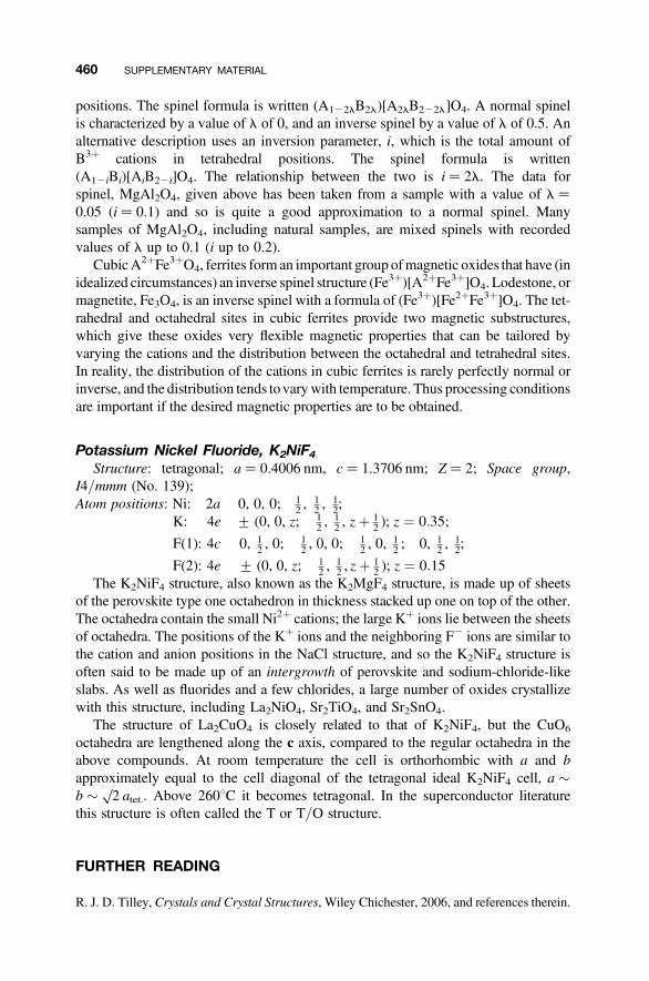
positions. The spinel formula is written (A122lB2l)[A2lB222l]O4. A normal spinelis characterized by a value of l of 0, and an inverse spinel by a value of l of 0.5. Analternative description uses an inversion parameter, i, which is the total amount ofB3þ cations in tetrahedral positions. The spinel formula is written(A12iBi)[AiB22i]O4. The relationship between the two is i ¼ 2l. The data forspinel, MgAl2O4, given above has been taken from a sample with a value of l ¼0.05 (i ¼ 0.1) and so is quite a good approximation to a normal spinel. Manysamples of MgAl2O4, including natural samples, are mixed spinels with recordedvalues of l up to 0.1 (i up to 0.2).
CubicA2þFe3þO4, ferrites form an important group ofmagnetic oxides that have (inidealized circumstances) an inverse spinel structure (Fe3þ)[A2þFe3þ]O4. Lodestone, ormagnetite, Fe3O4, is an inverse spinel with a formula of (Fe3þ)[Fe2þFe3þ]O4. The tet-rahedral and octahedral sites in cubic ferrites provide two magnetic substructures,which give these oxides very flexible magnetic properties that can be tailored byvarying the cations and the distribution between the octahedral and tetrahedral sites.In reality, the distribution of the cations in cubic ferrites is rarely perfectly normal orinverse, and the distribution tends tovarywith temperature. Thus processing conditionsare important if the desired magnetic properties are to be obtained.
Potassium Nickel Fluoride, K2NiF4Structure: tetragonal; a ¼ 0.4006 nm, c ¼ 1.3706 nm; Z ¼ 2; Space group,
I4/mmm (No. 139);Atom positions: Ni: 2a 0, 0, 0; 1
2 ,12 ,
12;
K: 4e + (0, 0, z; 12 ,
12 , zþ 1
2 ); z ¼ 0:35;
F(1): 4c 0, 12 , 0;
12 , 0, 0;
12 , 0,
12 ; 0, 1
2 ,12;
F(2): 4e + (0, 0, z; 12 ,
12 , zþ 1
2 ); z ¼ 0:15The K2NiF4 structure, also known as the K2MgF4 structure, is made up of sheets
of the perovskite type one octahedron in thickness stacked up one on top of the other.The octahedra contain the small Ni2þ cations; the large Kþ ions lie between the sheetsof octahedra. The positions of the Kþ ions and the neighboring F2 ions are similar tothe cation and anion positions in the NaCl structure, and so the K2NiF4 structure isoften said to be made up of an intergrowth of perovskite and sodium-chloride-likeslabs. As well as fluorides and a few chlorides, a large number of oxides crystallizewith this structure, including La2NiO4, Sr2TiO4, and Sr2SnO4.
The structure of La2CuO4 is closely related to that of K2NiF4, but the CuO6
octahedra are lengthened along the c axis, compared to the regular octahedra in theabove compounds. At room temperature the cell is orthorhombic with a and bapproximately equal to the cell diagonal of the tetragonal ideal K2NiF4 cell, a �b � p
2 atet.. Above 2608C it becomes tetragonal. In the superconductor literaturethis structure is often called the T or T/O structure.
FURTHER READING
R. J. D. Tilley, Crystals and Crystal Structures, Wiley Chichester, 2006, and references therein.
460 SUPPLEMENTARY MATERIAL
S2 BAND THEORY
S2.1 Energy Bands
At the beginning of the twentieth century explanations of the electrical properties ofsolids were hazy. The best that could be said was that metals could be supposed tocontain a gas of free electrons, with properties derived from an approach that mirroredthe kinetic theory of gases. The theory of the electron pair bond and the notion ofvalence were not as obviously applicable to solids as to molecules. In fact progressin understanding the nature of the electrical properties in solids came from thedirect application of the wave equation to the free electron theory. This was firstattempted by Sommerfeld in 1928, rapidly followed by Bloch in 1929, who tookinto account the periodic nature of the atom array in a crystal, and Wilson, in1931, who distinguished between metals, semiconductors, and insulators on thebasis of Bloch’s calculations. It was soon realized that the breakdown into thesethree classes was incomplete. Some solids, especially transition-metal oxides suchas CoO or NiO should be metals in terms of the simple theory but were, in fact,insulators. The dilemma was resolved by Mott in the years between 1937 and1949, and the possibility of transforming insulating solids into metals was appreci-ated. In the years between 1946 and 1950 the semiconductor industry was foundedon the practical and theoretical studies of Bardeen, Brattain, and Shockley into theconstruction and operation of the transistor. By the middle of the twentiethcentury, the mystery surrounding the electronic behavior of solids was erased. Thetheory as a whole is generally called band theory.
In band theory the electrons responsible for conduction are not linked to anyparticular atom. They can move easily throughout the crystal and are said to befree or very nearly so. The wave functions of these electrons are considered toextend throughout the whole of the crystal and are delocalized. The outer electronsin a solid, that is, the electrons that are of greatest importance from the point ofview of both chemical and electronic properties, occupy bands of allowed energies.Between these bands are regions that cannot be occupied, called band gaps.
The energy bands are derived from the overlap of the outer electron energy levels onthe atoms making up the solid. The respective bands are then given names describingthe principal contributing orbitals. Thus bands may be described as mainly of s, p, or dcharacter. The band structure of a crystal is quite complex, and energy bands canoverlap in certain crystallographic directions while being well separated in others.Fortunately, the complex three-dimensional nature of the bands in a solid can beignored for many purposes and a “flat-band” picture is then adequate.
S2.2 Insulators, Semiconductors and Metals
The fundamental division of materials when electrical properties are considered isinto metals, insulators, and semiconductors. An insulator is a material that normallyshows no electrical conductivity. Metals and semiconductors were originally classi-fied more or less in terms of the magnitude of the measured electrical conductivity.However, a better definition is to include in metals those materials for which the
S2 BAND THEORY 461
electrical conductivity falls as the temperature increases. Semiconductors show anincrease in electrical conductivity as the temperature increases.
Metals are defined as materials in which the uppermost energy band is only partlyfilled. The uppermost energy level filled is called the Fermi energy or the Fermi level.Conduction can take place because of the easy availability of empty energy levels justabove the Fermi energy. In a crystalline metal the Fermi level possesses a complexshape and is called the Fermi surface. Traditionally, typical metals are those of thealkalimetals, Li,Na,K, and the like.However, the criterion is not restricted to elements,but some oxides, and many sulfides, are metallic in their electronic properties.
Insulators have the upper band completelyemptyand the lower band completelyfilledby electrons. The energy gap between the top of the filled band and the bottom ofempty band is quite large. The filled band of energies is called the valence band, andthe empty band is called the conduction band. The energy difference between the topof the valence band and the bottom of the conduction band is called the band gap.When a material conducts electricity the electrons pick up some energy and are trans-ferred to slightly higher energy levels. If the electron-containing band is full, conduc-tivity cannot occur because there are no slightly higher energy levels available.2
Intrinsic semiconductors have a similar band picture to insulators except that theseparation of the empty and filled bands is small. The band gap must be such thatsome electrons will be transferred from the top of the valence band to the bottomof the conduction band at room temperature. The electrons in the conduction bandwill have plenty of slightly higher energy levels available, and, when a voltage isimposed upon the material, they can take up some energy, and this leads to somedegree of conductivity. At 0 K these materials will be insulators because no electronswill cross from the valence band to the conduction band. The magnitude of theirelectrical conductivity will increase as the temperature increases because more elec-trons will gain sufficient energy to cross the band gap. The Fermi level for an intrinsicsemiconductor lies at the midpoint of the band gap.
Rather surprisingly, an equal contribution to the conductivity will come frompositive charge carriers equal in number to the electrons promoted into the conduc-tion band. These are “vacancies” in the valence band and are called positive holes ormore generally holes. Each time an electron is removed from the full valence bandto the conduction band, two mobile charge carriers are therefore created, an electronand a hole.
The magnitude of the band gap can be estimated by measuring the variation of theconductivity of a semiconductor with temperature, to give the thermal band gap.Alternatively, the energy of light photons that are just sufficient to excite an electronacross the band gap can be determined to give an estimate of the optical band gap.Optical band gap measurements show more transitions than just a single energypeak corresponding to the valence band–conduction band energy gap. Theseadditional peaks in the absorption spectra of intrinsic semiconductors were
2Naturally, if an enormous voltage is applied, as in a thunderstorm, the electrons are given so much energythat they are ripped from the valence band and can transfer to the conduction band. In these conditions theinsulator is said to break down.
462 SUPPLEMENTARY MATERIAL
interpreted in terms of bound hole–electron pairs, called excitons, during the yearsbetween 1938 and 1948 by Peierls, Frenkel, and Davydov.
Extrinsic semiconductors contain an appreciable number of foreign atoms thatmay have been added intentionally as dopants or occur unintentionally as impurities.At very low temperatures these may have no effect on the electronic properties of thematerial, but, as the temperature rises, they can influence the behavior in two verydifferent ways. They can act as donors, donating electrons to the conduction band,or as acceptors, accepting electrons from the valence band, which is equivalent todonating holes to the valence band. Donors and acceptors are often represented byenergy levels within the band gap. Large number of impurities can give rise tonarrow energy bands in place of localized energy levels. When donors are themain impurities present in the crystals, the conduction is mainly by way of electronsand the material is called an n-type semiconductor. Similarly, if acceptors are themajor impurities present, conduction is mainly by way of holes and the material iscalled a p-type semiconductor. In intrinsic semiconductors electrons and holesare present in roughly equal numbers. In extrinsic conduction the conductivity isdominated by either one or the other.
The position of the Fermi level in an extrinsic semiconductor depends upon thedopant concentrations and the temperature. As a rough guide the Fermi level canbe taken as half way between the donor levels and the bottom of the valence bandfor n-type materials or half way between the top of the valence band and the acceptorlevels for p-type semiconductor, both referred to 0 K. As the temperature rises theFermi level in both cases moves toward the center of the band gap.
If the donors and acceptors are present in equal numbers, the material is said to bea compensated semiconductor. At 0 K these materials are insulators, and it is difficultin practice to distinguish between compensated and intrinsic semiconductors. Whenall of the impurities are fully ionized so that either all the donor levels have lost anelectron or all the acceptor levels have gained an electron, the exhaustion rangehas been reached.
Degenerate semiconductors can be intrinsic or extrinsic semiconductors, but inthese materials the band gap is similar to or less than the thermal energy. In suchcases the number of charge carriers in each band becomes very high, as does theelectronic conductivity. The compounds are said to show quasi-metallic behavior.
Semimetals show metallic conductivity due to the overlap of a filled and an emptyband. In this case electrons spill over from the filled band into the bottom of theempty band until the Fermi surface intersects both sets of bands. In semimetalsholes and electrons coexist even at 0 K.
S2.3 Point Defects and Energy Bands in Semiconductorsand Insulators
A point defect in an insulator or semiconductor is represented on band diagrams as anenergy level. These energy levels can lie within the conduction or valence bands, butthose of most consequence for electronic and optical properties are those that lie in theband gap. The effects of these impurities on the electronic properties of the solid will
S2 BAND THEORY 463

depend upon how close the energy levels lie to either the bottom of the conductionband or the top of the valence band. Those that are close to these edges are calledshallow levels, while those nearer to the center of the band gap are called deep levels.
The most fundamental transition that can take place is the transfer of an electronfrom the valence band to the conduction band. This creates a mobile electron and amobile hole, both of which can often be treated as defects. Transitions of this type,and the reverse, when an electron in the conduction band drops to the valenceband, eliminating a hole in the process and liberating energy, are called interbandtransitions. Apart from the electrons and holes themselves, interband transitions donot involve defects. All other transitions do.
Shallow levels play an important part in electronic conductivity. Shallow donorlevels lie close to the conduction band in energy and liberate electrons to it toproduce n-type semiconductors. Interstitial metal atoms added to an insulatingionic oxide often act in this way because metal atoms tend to ionize by losing elec-trons. When a donor level looses one or more electrons to the conduction band, it issaid to be ionized. The energy level representing an ionized donor will be lower thanthat of the un-ionized (neutral) donor by the same amount as required to move theelectron into the conduction band. The presence of shallow donor levels causes thematerial to become an n-type semiconductor.
Shallow acceptor levels lie close to the valence band and take up electrons from itto create holes in the valence band and produce p-type semiconductors. Interstitialnonmetal atoms often generate shallow acceptor levels because anion formationinvolves taking up extra electrons. Acceptor levels are said to be ionized whenthey take electrons from the valence band, creating holes in the process.The energy of a neutral acceptor atom is different to that of an ionized acceptor.The electrons on the ionized anions are often “trapped” and do not contributeto the conductivity.
The same sort of considerations will apply to vacancies. For instance, an anionvacancy may give rise to a set of shallow donor levels just below the lower edgeof the conduction band. If the vacancy is created by removing a neutral nonmetalatom from the crystal, the electrons that were on the anion are transferred to theconduction band to produce an n-type semiconductor. The energies of neutral andionized vacancies are slightly different.
A cation vacancy will be opposite to this in behavior. Removal of a neutral metalatom from a material will involve removal of a cation plus the correct number ofelectrons, which are taken from the valence band. Cation vacancies will thereforebe represented as acceptor levels situated near to the valence band together with anequivalent number of holes in the band. These materials are p-type semiconductors.
Deep levels generally have less effect on electronic conductivity but are importantin other ways, and especially influence optical properties.
S2.4 Transition-Metal Oxides
Shallow levels are often found in transition-metal compounds in which the cationscan exist in several valence states. The most familiar of these are the transition
464 SUPPLEMENTARY MATERIAL
metal oxides. In these compounds, the valence band is mainly derived from oxygen porbitals. The conduction band is made up mainly from the metal atom d orbitals butcan also contain considerable mixing in of metal s orbitals as well. The situation canbe illustrated with respect to two transition-metal oxides, titanium dioxide, TiO2, andnickel oxide, NiO.
Titanium dioxide, nominally Ti4þ and O22, has a band structure with a filledvalence band mainly derived from oxygen 2p orbitals and an empty conductionband derived from the titanium d orbitals. The oxide is an insulator. The oxideTi2O3, nominally Ti3þ and O22, has an extra electron on each cation, located inthe 3d orbitals. In the band picture, these electrons are distributed in the d band,which is only partly filled so that the material behaves as a metal. The situationthat is found when TiO2 is slightly reduced to TiO22x is a step toward this lattersituation. The charge imbalance resulting from oxygen loss is restored by the creationof Ti3þ ions; nominally two Ti3þ form for each O22 lost. Each Ti3þ can be rep-resented as an impurity level close to the bottom of the conduction band. Thermalenergy is generally sufficient to ionize these centers, and the electrons are liberatedinto the conduction band. Slightly reduced TiO2 would then be expected to shown-type semiconductivity.
In nickel oxide the d band should be partly full, as Ni2þ has 8d electrons and theband can hold 10. However, in this material the d band is split into a completely filledpart and an empty part, this latter probably overlapping with the 4s band. This meansthat NiO will be an insulator. Nickel oxide can be made nonstoichiometric, and theresulting material has an excess of oxygen, due to Ni2þ vacancies, so that the formulais Ni12xO. The charge imbalance is corrected by transforming some Ni2þ ions intoNi3þ ions, which are equivalent to a normal Ni2þ ion together with a hole. Each Ni3þ
ion can be represented as a shallow acceptor level just above the filled portion of the dband. Thermal energy is generally sufficient to ionize these centers. In this case theholes are transferred from the Ni3þ ions into the valence band. Slightly metal-deficientNi12xO would then be expected to show p-type semiconductivity.
S3 SEEBECK COEFFICIENT
S3.1 Seebeck Coefficient and Entropy
The origin of the Seebeck effect can be qualitatively understood by assuming that theelectrons or holes in the material are defects that behave rather like gas atoms. Thecharge carriers in the hot region will have a higher kinetic energy, and hence ahigher velocity, than those in the cold region. This means that the net velocity ofthe charge carriers at the hot end moving toward the cold end will be higher thanthe net velocity of the charge carriers at the cold end moving toward the hot end.In this situation more carriers will flow from the hot end toward the cold end thanvice versa, which will cause a voltage to build up between the hot and cold endsof the sample. Eventually equilibrium will be established and the potential so setup is the Seebeck voltage. This simple model, the classical or Drude model, gives
S3 SEEBECK COEFFICIENT 465
a formula for the Seebeck coefficient:
a ¼ � k
2efor electrons
¼ þ k
2efor holes
where k is the Boltzmann constant and e the charge on the electron.Electrons, holes, or other mobile charge carriers can be considered as chemically
reactive species that can be allotted a thermodynamic chemical potential—theelectrochemical potential, m, defined as
�m ¼ mþ Zef
where m is the chemical potential of a mobile charge carrier in the absence of an elec-trical potential, Ze is the charge on the mobile species, and f is the electric potentialin the neighborhood of the carrier. In the case of electrons or holes, Z will be equal to21 or þ1; hence:
�m ¼ mþ ef (holes)
¼ m� ef (electrons)
In the case of a p-type material subjected to a temperature gradient, at equilibriumthe electrochemical potential of the holes at the hot end of the rod must be equal tothat of the holes at the cold end of the rod. Hence:
�mH ¼ �mC
�mH þ efH ¼ �mC þ efC
e(fH � fC) ¼ �mC � �mH
The chemical potential of a substance can be equated to the Gibbs energy, and in thiscase we can write this as g per hole3 so that:
�m ¼ g ¼ h� Ts
where h and s represent the enthalpy and entropy of a mobile hole and T is thetemperature (K). Using this equation to substitute for m:
e(fH � fC) ¼ (hC � TCsC)� (hH � THsH)
¼ hC � hH þ THsH � TCsC
If the enthalpy and entropy of the holes at the hot and cold ends of the material can,to a reasonable approximation, be taken as equal over the small temperature ranges
3The use of lower case letters, g, h, and s, indicates that the free energy per particle is being discussed.
466 SUPPLEMENTARY MATERIAL
that are normal in experiments:
hC ¼ hH ¼ h sC ¼ sH ¼ s
thus:
e(fH � fC) ¼ (TH � TC)s
fH � fC
TH � TC¼ s
e
The Seebeck coefficient, a, is defined as
a ¼ fH � fC
TH � TC
so that, for holes:
a ¼ s
e
The analysis can be repeated for electrons, using:
�m ¼ m� ef
to give
a ¼ � s
e
This result is frequently generalized as the entropy per carrier:
a ¼ � 1e
� �@S
@N
� �
where N is the number of particles and S the total entropy.The units of Seebeck coefficient are given by:
Entropy (J K�1) per particleElectron charge (C) per particle
which is (J K21 C21) per particle. Using the conversion J C21 ¼ V, this becomesvolts per degree (V K21).
S3 SEEBECK COEFFICIENT 467
S3.2 Seebeck Coefficient and Defect Populations
The Seebeck coefficient can be related to the number of defects present in a crystal fora material in which the mobile charges are located on a particular sublattice andmigrate by jumping from one ion to another. The defects are the ions together withthe (momentarily localized) charge carrier. For example, slightly reduced titaniumdioxide can be written as Ti122x
4þ Ti2x3þO22x. The defects present are Ti3þ ions,
which, in this context, can be thought of as point defects consisting of a Ti4þ ionplus an electron. The electronic conductivity and thermoelectric effects arisebecause of the ability of electrons to hop from one Ti3þ ion to an adjacent Ti4þ ion.
The entropy of the defects, which can be related to the Seebeck coefficient, canbe broken down into several components. The arrangement of the defects over theavailable sites gives rise to the configurational entropy. Displacements of thecharge carriers due to thermal energy gives rise to the vibrational entropy. Finally,it is necessary to consider the possible arrangements of spin states on the ions, thespin degeneracy.
It is easiest to start with the configurational entropy, SC. Suppose that the numberof defects, which is equal to the number of mobile (localized) holes or electrons, is ndand moreover that only one type of mobile carrier, either holes or electrons, is present.The configurational entropy SC is given by using the Boltzmann formula:
SC ¼ k lnn0!
(n0 � nd)! nd!
� �
where SC is the configurational entropy of nd electrons or holes arranged on n0available sites, k is the Boltzmann constant, and ! represents the factorial of thenumber. This can be simplified using Stirling’s approximation:
ln n! ¼ n ln(n� n)
(see also Supplementary Material Section S4). The configurational entropy can thenbe written:
SC ¼ k[n0 ln n0 � nd ln nd � (n0 � nd) ln (n0 � nd)]
The configurational entropy per particle, sC, is given by dSC/dnd, which is
sC ¼ k lnn0 � nd
nd
� �(S5:1)
¼ k lnn0nd
� �� 1
� �
468 SUPPLEMENTARY MATERIAL
In general, n0 is of the order of 1028 cation sites m23 and nd is of the order of 10
20
defects m23, so that n0/nd 1, hence:
a ¼ � k
e
� �ln
n0nd
� �� �for electrons (S5:2a)
¼ þ k
e
� �ln
n0nd
� �� �for holes (S5:2b)
The positive version applies to p-type materials and the negative expression to n-typematerials. Note that n0/nd increases as the number of defects falls, so that largestvalues of a are to be found in materials with the smallest defect populations.
Equation (S5.1) can be written in an alternative form. Write:
Number of sites occupied by a charge carrier ¼ cn0 ¼ ndNumber of available sites ¼ (1� c)n0 ¼ (n0 � nd)
Substitution into Eq. (S5.1) gives
sC ¼ k lnn0 � nd
nd
� �¼ k ln
(1� c)n0cn0
� �¼ k ln
1� c
c
� �
where c is the fraction of defects present. This leads directly to the Heikes equation:
a ¼ � k
e
� �ln
1� c
c
� �for electrons
¼ þ k
e
� �ln
1� c
c
� �for holes
This form is useful because the value of c is related in a simple way to thecomposition of the sample.
A vibrational entropy term, SV, can be added to Eq. (S5.2a) or (S5.2b) to give
a ¼ � k
e
� �ln
n0nd
� �þ SV
k
� for electrons
¼ þ k
e
� �ln
n0nd
� �þ SV
k
� for holes
In general SV/k is much smaller than ln[(n0/nd)] and as the only temperature variationwill come into this equation from the SV term, a will be approximately independentof temperature in this approximation. These equations are of the form:
a ¼ +k
e
� �ln
n0nd
� �þ A
� �
S3 SEEBECK COEFFICIENT 469
where A is a constant, n0 is the number of cation sites, and nd is the number of defectsgiving rise to mobile electrons or holes. In the Heikes equation the term A is omitted.
The configurational entropy evaluated above omits all mention of electron spin.Because there are two spin directions, a spin degeneracy of 2, these must be includedin the possible configurations. When this term is included, the Heikes equationbecomes the Chaikin–Beni equation:
a ¼ � k
e
� �ln 2
1� c
c
� �� �
In general, the spin degeneracy can be specified by a parameter b, to give
a ¼ � k
e
� �ln b
1� c
c
� �� �
This equation is sometimes called the extended Heikes equation.If cations in the material can take two valence states, as occurs in many transition-
metal compounds, Ti3þ/Ti4þ or Co3þ/Co4þ, for example, then the value of thespin degeneracy, b, must take into account these configurations and can takevalues greater than 2.
Note that the above model is for a simple system in which there is only one defectand one type of mobile charge carrier. In semiconductors both holes and electronscontribute to the conductivity. In materials where this analysis applies, both holesand electrons contribute to the value of the Seebeck coefficient. If there are equalnumbers of mobile electrons and holes, the value of the Seebeck coefficient willbe zero (or close to it). Derivation of formulas for the Seebeck coefficient for bandtheory semiconductors such as Si and Ge, or metals, takes us beyond the scope ofthis book.
S4 SCHOTTKY AND FRENKEL DEFECTS
S4.1 Equilibrium Concentration of Schottky Defects Derivedfrom Configurational Entropy
The introduction of Schottky defects causes the Gibbs energy of the crystal to changeby an amount DGS:
DGS ¼ DHS � T DSS
where DHS is the associated change in enthalpy, and DSS is the change in the entropyof the crystal. In general, the energy increase due to the DHS term will be offset by theenergy decrease due to the T DSS term.
In a crystal of overall composition MX, suppose that nS is the number of Schottkydefects in the crystal at a temperature T (K), that is, there are nS vacant cation sites andnS vacant anion sites present, distributed over N possible cation sites and N possibleanion sites. The configurational entropy change, DSS, due to the distribution of the
470 SUPPLEMENTARY MATERIAL
vacancies over the available cation and anion positions can be determined by usingthe Boltzmann equation:
S ¼ k lnW
where S is the entropy of a system in whichW is the number of ways of distributing ndefects over N sites at random and k is the Boltzmann constant. The value of W isgiven by the formula:
W ¼ N!
(N � n)! n!
where the symbol ! represents the factorial of the number. The number of ways thatthe nS cation and anion vacancies can be distributed over the N available sites in thecrystal is given by
wc ¼ N!
(N � nS)! nS!
for vacancies on cation sites, and
wa ¼ N!
(N � nS)! nS!
for vacancies on anion sites. For a crystal of stoichiometry MX,
wc ¼ wa
The total number of ways of distributing these defects, W, is given by the product ofwc and wa, hence:
W ¼ wc � wa ¼ w2
Therefore, the change in configurational entropy caused by introducing thesedefects is
DSS ¼ k ln (w2) ¼ 2k ln w
that is,
DSS ¼ 2k lnN!
(N � nS)! nS!
� �
This expression is simplified by employing the approximation:
ln N! � N ln N � N
(known as Stirling’s approximation, but see Section S.4.2). Substituting andsimplifying yields
DSS ¼ 2k{N lnN � (N � nS) ln(N � nS)� nS ln nS}
S4 SCHOTTKY AND FRENKEL DEFECTS 471
It is assumed that the entropy change is solely made up of this contribution.The enthalpy change involved, DHS, is not explicitly calculated. It is assumed
that the enthalpy to form one defect, DhS, is constant over the temperature range ofinterest, so that the total enthalpy change, DHS, is given by
DHS ¼ nS DhS
The values for DSS and DHS are substituted into the Gibbs equation to give
DGS ¼ nS DhS � 2kT{N ln N � (N � nS) ln(N � nS)� nS ln nS}
At equilibrium, DG will be equal to zero and the minimum in the DG versus nS curveoccurs when
dDG
dnS
� �T
¼ 0
that is,
dDG
dnS
� �T
¼ d
dnS{nS DhS � 2kT[N lnN � (N � nS) ln(N � nS)� nS ln nS]} ¼ 0
Remembering that (N ln N ) is constant, so its differential is zero, the differential of(ln x) is (l/x) and of (x ln x) is (1 þ ln x), on differentiating:
DhS � 2kTd
dnS[N ln N � (N � nS) ln(N � nS)� nS ln nS]
� ¼ 0
that is,
DhS � 2kT ln (N � nS)þ N � nSN � nS
� ln nS � nSnS
� �¼ 0
hence:
DhS ¼ 2kT lnN � nSnS
� �
Rearranging:
nS ¼ (N � nS)e�DhS=2kT
This expression can be further simplified if we make yet another approximationand suppose the number of Schottky defects, nS, is a lot less than the number ofnormally occupied sites N. In this case
nS � Ne�DhS=2kT
472 SUPPLEMENTARY MATERIAL
S4.2 Stirling’s Approximation
The approximation described as Stirling’s approximation above and in Section S3.2is not very accurate. It is several percent in error even for values of N as large as 1010.The correct expression for Stirling’s approximation is
lnN! � N ln N � N þ 12 ln (2pN) (S4:1)
which is accurate even for very low values of N.It is of interest to derive the relationship between defect numbers and configura-
tional entropy using the correct form of Stirling’s approximation. The principle canbest be illustrated with respect to the population of vacancies in a monatomiccrystal (Section 2.1). Substituting from the more accurate Eq. (S4.1):
DSV ¼ k[{N lnN � (N � nV) ln(N � nV)� nV ln nV}
� 12 ln 2pN þ 1
2 ln 2p(N � nV)þ 12 ln 2pnV]
Proceeding as before:
DGV ¼ nVDhV � kT[{N lnN � (N � nV) ln (N � nV)� nV ln nV}
� 12 ln 2pN þ 1
2 ln 2p(N � nV)þ 12 ln 2pnV]
and setting (d DGV/dnV)T ¼ 0:
DhV � kT
�d
dnV[{N lnN � (N � nV) ln (N � nV)� nV ln nV}
� 12 ln 2pN þ 1
2 ln 2p(N � nV)þ 12 ln 2pnV]
¼ 0
On differentiating:
DhV � kT{[ln(N � nV)� ln nV]þ 12[ ln 2p(N � nV)þ ln 2pnV]} ¼ 0
Hence:
DhV ¼ kT lnN � nVnV
� �þ 1
2 ln [4p2(N � n2V)]
Assuming that N is much greater than nV, this can be solved to give
nV ¼ e�DhV=kTN1þ1=2kT (2p)1=kT
S4 SCHOTTKY AND FRENKEL DEFECTS 473
S4.3 Equilibrium Concentration of Frenkel Defects Derivedfrom Configurational Entropy
The calculation of the number of Frenkel defects in a crystal proceeds along linesparallel to those above. The introduction of Frenkel defects causes the Gibbsenergy of the crystal to change by an amount DGF:
DGF ¼ DHF � T DSF
where DHF is the associated change in enthalpy and DSF the change in the entropy ofthe crystal. In general, the energy increase due to the DHF term will be offset by theenergy decrease due to the T DSF term.
In a crystal of overall composition MX, suppose that nF is the number of Frenkeldefects in the crystal at a temperature T (K), that is, there are nF interstitials distributedover Ni interstitial sites and nF vacant atom sites present, distributed over N possibleatom sites.
The configurational entropy change, DSF, due to the distribution of the defectsover the available positions, can be determined by using the Boltzmann equation.The number of ways of distributing the nF vacancies that have been created overthe N available positions in the atom array affected by Frenkel defects is
wv ¼ N!
(N � nF)! nF!
Similarly, the number of ways of distributing the nF interstitial atoms over the Ni
available interstitial positions in the crystal is
wi ¼ Ni!
(Ni � nF)! nF!
The total number of ways of distributing these defects, W, is given by the product ofwv and wi, hence:
W ¼ wvwi
The change in configurational entropy, DSF, due to this distribution is
DSF ¼ k lnW ¼ k lnwvwi
Hence:
DSF ¼ k lnN!
(N � nF)! nF!
� �þ ln
Ni!
(Ni � nF)! nF!
� ��
474 SUPPLEMENTARY MATERIAL
This expression is simplified by employing Stirling’s approximation:
ln N! � N ln N � N
ln Ni! � Ni ln Ni � Ni
Substituting and simplifying yields the cumbersome expression:
DSF ¼ k[N lnN þ Ni ln Ni
� (N � nF) ln (N � nF)� (Ni � nF) ln (Ni � nF)� 2nF ln nF]
(Note that if we make Ni and N equal to each other we arrive at the expression forSchottky defects.)
The enthalpy change involved, DHF, is not explicitly calculated. It is assumedthat the enthalpy to form one defect, DhF, is constant over the temperature range ofinterest, so that the total enthalpy change, DHF, is given by
DHF ¼ nF DhF
The values for DSF and DHF are substituted into the Gibbs equation to give:
DGF ¼ nF DhF � kT[N ln N � Ni ln Ni � (N � nF)
ln(N � nF)� (Ni � nF) ln(Ni � nF)� 2nF ln nF]
Setting (dDGF/dnF)T ¼ 0 at equilibrium and differentiating, remembering that(N ln N ) and (Ni ln Ni) are constant, so their differentials are zero, and the differentialof (ln x) is (l/x) and of (x ln x) is (1 þ ln x), yields
DhF ¼ kT ln(N � nF)(Ni � nF)
n 2F
� �that is,
n2F ¼ (N � nF)(Ni � nF)e�DhF=kT
This expression can be further simplified if we make yet another approximation,and suppose the number of Frenkel defects, nF, is a lot less than either the numberof normal positions N or the number of interstitial positions available Ni. In this case:
nF � (NNi)1=2e�DhF=2kT
A more extended expression, using the correct formulation of Stirling’sapproximation, can be derived as in Section S4.2.
S4 SCHOTTKY AND FRENKEL DEFECTS 475
S5 DIFFUSION
S5.1 Diffusion Equations
Measurement of the diffusion of an atom through a perfect crystal will give a concen-tration profile. The diffusion coefficient is extracted from the concentration profileby solution of one of two diffusion equations. For one-dimensional diffusion,along x, they are
J ¼ �Ddc
dx(S5:1)
Fick’s first law of diffusion, and
dc
dt¼ D
d2c
dx2(S5:2)
This is known as Fick’s second law of diffusion or more commonly as the diffusionequation. In these equations, J is called the flux of the diffusing species, with units of[amount of substance (atoms or equivalent units) m2 s21], c is the concentration of thediffusing species, with units of [amount of substance (atoms or equivalent units) m23]at position x (m) after time t (s); D is the diffusion coefficient, units (m2 s21).
S5.2 Non-Steady-State Diffusion
The normal state of affairs during a diffusion experiment is one in which the concen-tration at any point in the solid changes over time. This situation is called non-steady-state diffusion, and diffusion coefficients are found by solving the diffusion equation[Eq. (S5.2)]:
dcxdt
¼ Dd2cxdx2
� �
Provided the diffusion coefficient, D, is not dependent upon composition andposition, analytical solutions can be found to give an expression for c in termsof x. (The symbol D generally stands for Dself, D�, or D�
A, depending upon theexperimental details.)
For the diffusion couple experimental arrangement (Fig. 5.2), (ignoring all short-circuit diffusion), the solution is
cx ¼ c02(pDt)1=2
� �exp
�x2
4Dt
� �
where c0 is the initial concentration on the surface, usually measured in moles persquare meter. A value for the diffusion coefficient is obtained by taking logarithms
476 SUPPLEMENTARY MATERIAL
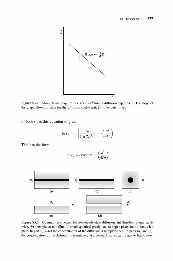
of both sides this equation to give:
ln cx ¼ lnc0
2(pDt)1=2
� �� x2
4Dt
� �
This has the form
ln cx ¼ constant� x2
4Dt
� �
Figure S5.1 Straight-line graph of ln c versus x2 from a diffusion experiment: The slope ofthe graph allows a value for the diffusion coefficient, D, to be determined.
Figure S5.2 Common geometries for non-steady-state diffusion: (a) thin-film planar sand-wich, (b) open planar thin film, (c) small spherical precipitate, (d ) open plate, and (e) sandwichplate. In parts (a)–(c) the concentration of the diffusant is unreplenished; in parts (d ) and (e),the concentration of the diffusant is maintained at a constant value, c0, by gas or liquid flow.
S5 DIFFUSION 477
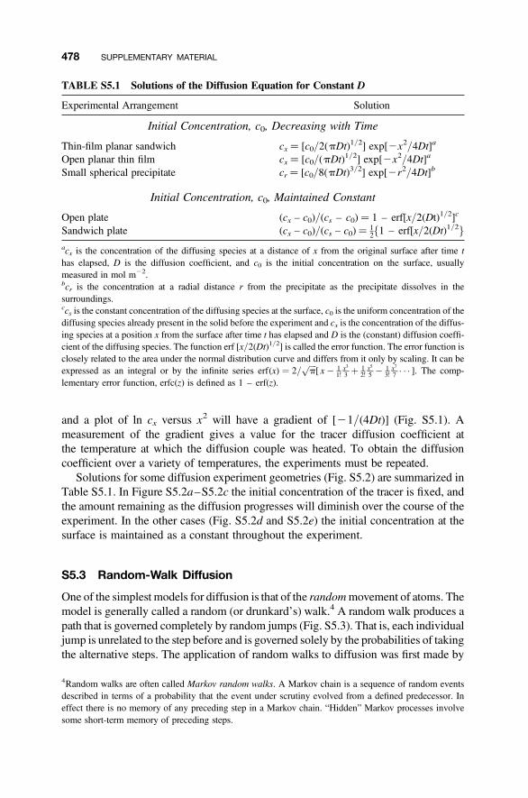
and a plot of ln cx versus x2 will have a gradient of [21/(4Dt)] (Fig. S5.1). Ameasurement of the gradient gives a value for the tracer diffusion coefficient atthe temperature at which the diffusion couple was heated. To obtain the diffusioncoefficient over a variety of temperatures, the experiments must be repeated.
Solutions for some diffusion experiment geometries (Fig. S5.2) are summarized inTable S5.1. In Figure S5.2a–S5.2c the initial concentration of the tracer is fixed, andthe amount remaining as the diffusion progresses will diminish over the course of theexperiment. In the other cases (Fig. S5.2d and S5.2e) the initial concentration at thesurface is maintained as a constant throughout the experiment.
S5.3 Random-Walk Diffusion
One of the simplest models for diffusion is that of the randommovement of atoms. Themodel is generally called a random (or drunkard’s) walk.4 A random walk produces apath that is governed completely by random jumps (Fig. S5.3). That is, each individualjump is unrelated to the step before and is governed solely by the probabilities of takingthe alternative steps. The application of random walks to diffusion was first made by
TABLE S5.1 Solutions of the Diffusion Equation for Constant D
Experimental Arrangement Solution
Initial Concentration, c0, Decreasing with Time
Thin-film planar sandwich cx ¼ [c0/2(pDt)1/2] exp[2x2/4Dt]a
Open planar thin film cx ¼ [c0/(pDt)1/2] exp[2x2/4Dt]a
Small spherical precipitate cr ¼ [c0/8(pDt)3/2] exp[2r2/4Dt]b
Initial Concentration, c0, Maintained Constant
Open plate (cx – c0)/(cs – c0) ¼ 1 – erf[x/2(Dt)1/2]c
Sandwich plate (cx – c0)/(cs – c0) ¼ 12f1 – erf[x/2(Dt)1/2g
acx is the concentration of the diffusing species at a distance of x from the original surface after time thas elapsed, D is the diffusion coefficient, and c0 is the initial concentration on the surface, usuallymeasured in mol m22.bcr is the concentration at a radial distance r from the precipitate as the precipitate dissolves in thesurroundings.ccs is the constant concentration of the diffusing species at the surface, c0 is the uniform concentration of thediffusing species already present in the solid before the experiment and cx is the concentration of the diffus-ing species at a position x from the surface after time t has elapsed and D is the (constant) diffusion coeffi-cient of the diffusing species. The function erf [x/2(Dt)1/2] is called the error function. The error function isclosely related to the area under the normal distribution curve and differs from it only by scaling. It can beexpressed as an integral or by the infinite series erf(x) ¼ 2=
ffiffiffiffip
p[ x� 1
1!x3
3 þ 12!
x5
5 � 13!
x7
7 � � � ]. The comp-lementary error function, erfc(z) is defined as 1 – erf(z).
4Random walks are often called Markov random walks. A Markov chain is a sequence of random eventsdescribed in terms of a probability that the event under scrutiny evolved from a defined predecessor. Ineffect there is no memory of any preceding step in a Markov chain. “Hidden” Markov processes involvesome short-term memory of preceding steps.
478 SUPPLEMENTARY MATERIAL
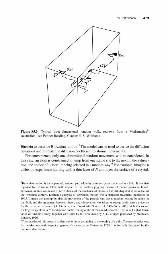
Einstein to describe Brownian motion.5 The model can be used to derive the diffusionequations and to relate the diffusion coefficient to atomic movements.
For convenience, only one-dimensional random movement will be considered. Inthis case, an atom is constrained to jump from one stable site to the next in the x direc-tion, the choice of þx or –x being selected in a random way.6 For example, imagine adiffusion experiment starting with a thin layer of N atoms on the surface of a crystal.
Figure S5.3 Typical three-dimensional random walk, redrawn from a Mathematicaw
calculation (see Further Reading, Chapter 5, S. Wolfram).
5Brownian motion is the apparently random path taken by a minute grain immersed in a fluid. It was firstreported by Brown in 1828, with respect to the endless joggling motion of pollen grains in liquid.Brownian motion was taken to be evidence of the existence of atoms, a fact still disputed at the outset ofthe twentieth century. Einstein’s analysis of Brownian motion was a statistical treatment, published in1905. It made the assumption that the movement of the particle was due to random jostling by atoms inthe fluid, and the agreement between theory and observation was taken as strong confirmatory evidencefor the existence of atoms. [A. Einstein, Ann. Physik (4th Series), 17, 549–560 (1905)]. A better sourcefor English speakers is: “Investigation on the Theory of the Brownian Movement.” This is an English trans-lation of Einstein’s study, together with notes by R. Furth, made by A. D. Couper, published by Melthuen,London, 1926.6The statistics of this process is identical to those pertaining to the tossing of a coin. The mathematics wasfirst worked out with respect to games of chance by de Moivre, in 1733. It is formally described by thebinomial distribution.
S5 DIFFUSION 479

After a time t, each atom will have carried out a random walk of n steps, to yield aconcentration profile. Three such walks, each of 100 jumps, are shown inFigure S5.4. The net displacement of a diffusing atom after n jumps will be the alge-braic sum of the individual jumps. If xi is the distance moved along the x axis in the ith jump, the distance moved after a total of n jumps, x, will simply be the sum of all
Figure S5.4 Three one-dimensional random walks: each individual walk, (a)–(c), gives theposition of the diffusing atom, x after the Nth jump. The final positions reached are: (a) x ¼ 0,(b), x ¼ 22a, and (c) x ¼ 28a.
480 SUPPLEMENTARY MATERIAL
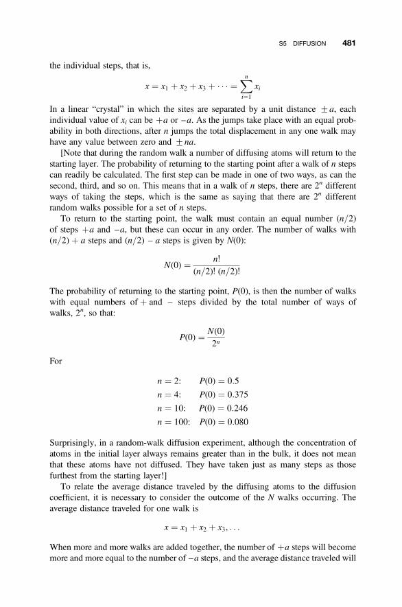
the individual steps, that is,
x ¼ x1 þ x2 þ x3 þ � � � ¼Xni¼1
xi
In a linear “crystal” in which the sites are separated by a unit distance +a, eachindividual value of xi can be þa or –a. As the jumps take place with an equal prob-ability in both directions, after n jumps the total displacement in any one walk mayhave any value between zero and +na.
[Note that during the random walk a number of diffusing atoms will return to thestarting layer. The probability of returning to the starting point after a walk of n stepscan readily be calculated. The first step can be made in one of two ways, as can thesecond, third, and so on. This means that in a walk of n steps, there are 2n differentways of taking the steps, which is the same as saying that there are 2n differentrandom walks possible for a set of n steps.
To return to the starting point, the walk must contain an equal number (n/2)of steps þa and –a, but these can occur in any order. The number of walks with(n/2) þ a steps and (n/2) – a steps is given by N(0):
N(0) ¼ n!
(n=2)! (n=2)!
The probability of returning to the starting point, P(0), is then the number of walkswith equal numbers of þ and – steps divided by the total number of ways ofwalks, 2n, so that:
P(0) ¼ N(0)2n
For
n ¼ 2: P(0) ¼ 0:5
n ¼ 4: P(0) ¼ 0:375
n ¼ 10: P(0) ¼ 0:246
n ¼ 100: P(0) ¼ 0:080
Surprisingly, in a random-walk diffusion experiment, although the concentration ofatoms in the initial layer always remains greater than in the bulk, it does not meanthat these atoms have not diffused. They have taken just as many steps as thosefurthest from the starting layer!]
To relate the average distance traveled by the diffusing atoms to the diffusioncoefficient, it is necessary to consider the outcome of the N walks occurring. Theaverage distance traveled for one walk is
x ¼ x1 þ x2 þ x3, . . .
When more and more walks are added together, the number of þa steps will becomemore and more equal to the number of –a steps, and the average distance traveled will
S5 DIFFUSION 481
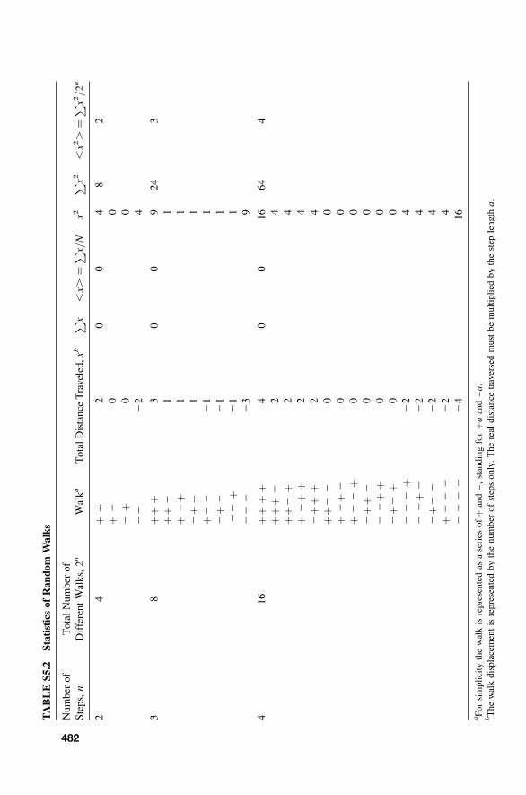
TABLES5
.2Statistics
ofRan
dom
Walks
Num
berof
Steps,n
Total
Num
berof
Different
Walks,2
nWalka
TotalDistanceTraveled,xb
P x,x.
¼P x/
Nx2
P x2
,x2.
¼P x
2/2
n
24
þþ
20
04
82
þ2
00
2þ
00
22
22
4
38
þþ
þ3
00
924
3þþ
21
1þ
2þ
11
2þ
þ1
1þ2
221
12þ
221
122
þ21
122
223
9
416
þþ
þþ
40
016
644
þþþ
22
4þþ2
þ2
4þ
2þ
þ2
42þþ
þ2
4þþ2
20
0þ
2þ
20
0þ
22
þ0
02þþ
20
02
2þ
þ0
02þ2
þ0
02
22
þ22
42
2þ
222
42þ2
222
4þ
22
222
42
22
224
16
aFo
rsimplicity
thewalkisrepresentedas
aseries
ofþ
and–,standing
forþa
and–a.
bThe
walkdisplacementisrepresentedby
thenumberof
stepsonly.The
real
distance
traversedmustbe
multip
liedby
thestep
length
a.
482
approach zero. If all different 2n walks are included, then the average works out to beexactly zero (Table S5.2).
To get an idea of the probable displacement distribution of the atoms, the jumpdistances are squared, and the mean of these squares, over the n steps, is computed.Thus, for a single walk:
x2 ¼ (x1 þ x2 þ x3, . . . , xn)(x1 þ x2 þ x3, . . . , xn)
¼ (x1x1 þ x1x2 þ x1x3 þ � � � þ x1xn)
þ (x2x1 þ x2x2 þ x2x3 þ � � � þ x2xn)
þ � � �þ xnx1 þ xnx2 þ xnx3 þ � � � þ xnxn)
This can be written:
x2 ¼Xni¼1
x 2i þ 2
Xni¼1
xixiþ1 þ 2Xni¼1
xixiþ2 þ � � �
¼Xni¼1
x 2i þ 2
Xni¼1
Xnj¼iþ1
xixiþj
In the limit of a large number of jumps, knowing that each jump may be eitherpositive or negative, all terms except the first average to zero. As each jump, xi,can be equal to þa or 2a,
x2 ¼ x 21 þ x 2
2 þ x 23 þ � � � þ x 2
n
¼ a2 þ a2 þ a2 þ � � � þ a2
¼ na2
where n is the number of steps in the walk. Adding the x2 terms for all of the Ndifferent walks and dividing by the number of walks, N, gives the mean squaredisplacement ,x2.:
,x2. ¼ N(na2)N
¼ na2
Statistics for three simple walks, with n ¼ 2, 3, and 4 are set out in Table S5.2.If the time that has elapsed from the beginning of the random walk is t, and the
time for each step is t, the number of jumps, n is given by
n ¼ t
t
and writing G as the jump frequency, 1/t:
,x2. ¼ Gta2
S5 DIFFUSION 483
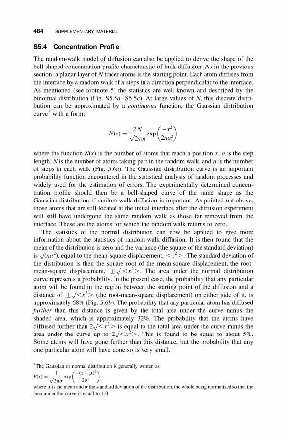
S5.4 Concentration Profile
The random-walk model of diffusion can also be applied to derive the shape of thebell-shaped concentration profile characteristic of bulk diffusion. As in the previoussection, a planar layer of N tracer atoms is the starting point. Each atom diffuses fromthe interface by a random walk of n steps in a direction perpendicular to the interface.As mentioned (see footnote 5) the statistics are well known and described by thebinomial distribution (Fig. S5.5a–S5.5c). At large values of N, this discrete distri-bution can be approximated by a continuous function, the Gaussian distributioncurve7 with a form:
N(x) ¼ 2Nffiffiffiffiffiffiffiffiffi2pn
p exp�x2
2na2
� �
where the function N(x) is the number of atoms that reach a position x, a is the steplength, N is the number of atoms taking part in the random walk, and n is the numberof steps in each walk (Fig. 5.6a). The Gaussian distribution curve is an importantprobability function encountered in the statistical analysis of random processes andwidely used for the estimation of errors. The experimentally determined concen-tration profile should then be a bell-shaped curve of the same shape as theGaussian distribution if random-walk diffusion is important. As pointed out above,those atoms that are still located at the initial interface after the diffusion experimentwill still have undergone the same random walk as those far removed from theinterface. These are the atoms for which the random walk returns to zero.
The statistics of the normal distribution can now be applied to give moreinformation about the statistics of random-walk diffusion. It is then found that themean of the distribution is zero and the variance (the square of the standard deviation)isp(na2), equal to the mean-square displacement, ,x2.. The standard deviation of
the distribution is then the square root of the mean-square displacement, the root-mean-square displacement, +
p,x2.. The area under the normal distribution
curve represents a probability. In the present case, the probability that any particularatom will be found in the region between the starting point of the diffusion and adistance of +
p,x2. (the root-mean-square displacement) on either side of it, is
approximately 68% (Fig. 5.6b). The probability that any particular atom has diffusedfurther than this distance is given by the total area under the curve minus theshaded area, which is approximately 32%. The probability that the atoms havediffused further than 2
p,x2. is equal to the total area under the curve minus the
area under the curve up to 2p,x2.. This is found to be equal to about 5%.
Some atoms will have gone further than this distance, but the probability that anyone particular atom will have done so is very small.
7The Gaussian or normal distribution is generally written as
P(x) ¼ 1ffiffiffiffiffiffi2p
psexp
�(x� m)2
2s2
� �where m is the mean and s the standard deviation of the distribution, the whole being normalized so that thearea under the curve is equal to 1.0.
484 SUPPLEMENTARY MATERIAL
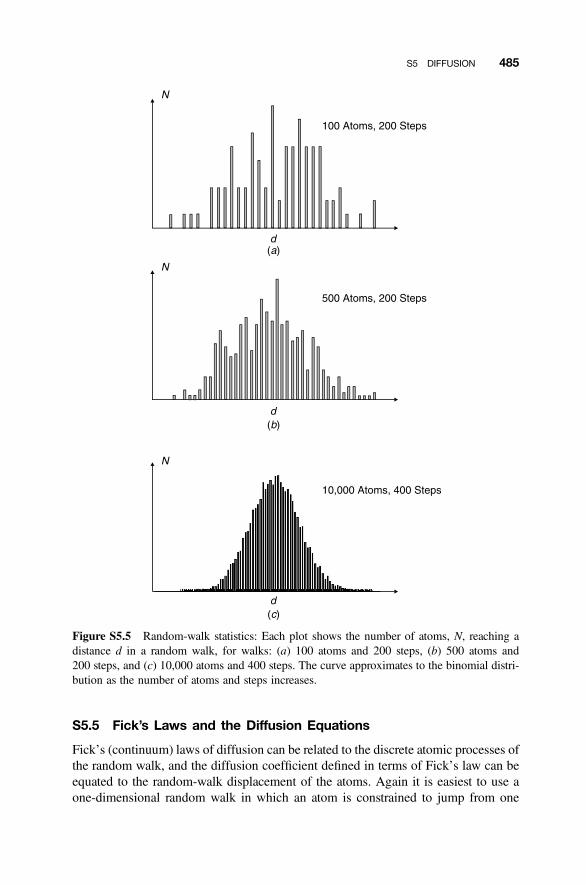
S5.5 Fick’s Laws and the Diffusion Equations
Fick’s (continuum) laws of diffusion can be related to the discrete atomic processes ofthe random walk, and the diffusion coefficient defined in terms of Fick’s law can beequated to the random-walk displacement of the atoms. Again it is easiest to use aone-dimensional random walk in which an atom is constrained to jump from one
Figure S5.5 Random-walk statistics: Each plot shows the number of atoms, N, reaching adistance d in a random walk, for walks: (a) 100 atoms and 200 steps, (b) 500 atoms and200 steps, and (c) 10,000 atoms and 400 steps. The curve approximates to the binomial distri-bution as the number of atoms and steps increases.
S5 DIFFUSION 485
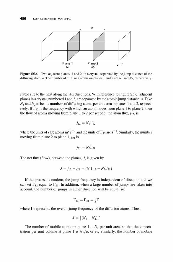
stable site to the next along the +x directions. With reference to Figure S5.6, adjacentplanes in a crystal, numbered 1 and 2, are separated by the atomic jumpdistance, a. TakeN1 andN2 to be the numbers of diffusing atoms per unit area in planes 1 and 2, respect-ively. If G12 is the frequency with which an atom moves from plane 1 to plane 2, thenthe flow of atoms moving from plane 1 to 2 per second, the atom flux, j12, is
j12 ¼ N1G12
where the units of j are atomsm2 s21 and the units ofG12 are s21. Similarly, the number
moving from plane 2 to plane 1, j21 is
j21 ¼ N2G21
The net flux (flow), between the planes, J, is given by
J ¼ j12 � j21 ¼ (N1G12 � N2G21)
If the process is random, the jump frequency is independent of direction and wecan set G12 equal to G21. In addition, when a large number of jumps are taken intoaccount, the number of jumps in either direction will be equal, so:
G12 ¼ G21 ¼ 12G
where G represents the overall jump frequency of the diffusion atoms. Thus:
J ¼ 12 (N1 � N2)G
The number of mobile atoms on plane 1 is N1 per unit area, so that the concen-tration per unit volume at plane 1 is N1/a, or c1. Similarly, the number of mobile
Figure S5.6 Two adjacent planes, 1 and 2, in a crystal, separated by the jump distance of thediffusing atom, a. The number of diffusing atoms on planes 1 and 2 are N1 and N2, respectively.
486 SUPPLEMENTARY MATERIAL
atoms per unit area on plane 2 is N2, so that the concentration per unit volume atplane 2 is N2/a or c2. Thus:
(N1 � N2) ¼ a(c1 � c2)
Hence:
J ¼ 12 a(c1 � c2)G
The concentration gradient, dc/dx, is given by the change in concentrationbetween planes 1 and 2 divided by the distance between planes 1 and 2, that is
�dc
dx¼ c1 � c2
a
where a minus sign is introduced as the concentration falls as we move from plane 1to plane 2. Hence:
c1 � c2 ¼ �adc
dx
so that:
J ¼ �12G a2
dc
dx
The units of the term 12Ga
2 are m2 s21, the units of the diffusion coefficient, andwriting:
12G a2 ¼ D
where D is defined as the diffusion coefficient, one obtains Fick’s first lawof diffusion:
J ¼ �Ddc
dx
In addition, the random-walk statistics show that
,x2.¼ 12G a2
so that
,x2.¼ 2Dt D ¼ ,x2.
2t
S5 DIFFUSION 487
where D is the diffusion coefficient, t is the time over which diffusion occurs, and,x2. is the mean-square displacement of the diffusing atoms. This is the Einsteindiffusion equation.
The overall flow of atoms into the volume between the two planes 1 and 2 fromplane 1 is the flux, j1, multiplied by the total area of plane 1, A, and so the increasein concentration of atoms in the volume between planes 1 and 2, dc(þ), is:
dc(þ)dt
¼ j1A
(Aa)¼ j1
a
where a is the separation of planes 1 and 2 and the volume of the region betweenplanes 1 and 2 is Aa. Similarly, the decrease in concentration of the atoms in thisregion due to the flow of atoms out of the volume at plane 2, dc(2) is
dc(�)dt
¼ j2A
(Aa)¼ j2
a
The net change in concentration, dc/dt is then
dc
dt¼ dc(þ)
dt
� �� dc(�)
dt
� �¼ j1 � j2
a¼ J
a
Now this last term is the flux gradient, that is,
j1 � j2a
¼ J
a¼ �dJ
dx
Hence:
dc
dt¼ �dJ
dx
¼ �d
dx� 12Ga2
dc
dx
� �
¼ �d
dx�D
dc
dx
� �
that is,
dc
dt¼ D
d2c
dx2
This is Fick’s second law of diffusion, the diffusion equation.
488 SUPPLEMENTARY MATERIAL
S5.6 Penetration Depth
The distribution of diffusing atoms represented by the Gaussian distribution curve:
N(x) ¼ 2Nffiffiffiffiffiffiffiffiffi2pn
p exp�x2
2na2
� �
can now be written in terms of the diffusion coefficient because na2 can be replacedby 2Dt. Hence:
N(x) ¼ 2Nffiffiffiffiffiffiffiffiffi2pn
p exp�x2
4Dt
� �
It is of considerable practical importance to have some idea of how far an atom orion will diffuse into a solid during a diffusion experiment. For example, the electronicproperties of integrated circuits are created by the careful diffusion of selecteddopants into single crystals of very pure silicon, and metallic machine componentsare hardened by the diffusion of carbon or nitrogen from the surface into the bulk.An approximate estimate of the depth to which diffusion is significant is given bythe penetration depth or diffusion length, xp, which is the depth where an appreciablechange in the concentration of the tracer can be said to have occurred after a diffusiontime t. The statistics of the Gaussian function indicates that the probability of adiffusing atom being found within the region between zero and +
p,x2. from
original interface is 68%, and within a of region +2p,x2. is 95%. Using the
information
,x2.¼ na2 ¼ 2Dt
the penetration depth can be expressed as
xp �ffiffi(
p2Dt) or xp � 2
ffiffi(
p2Dt)
depending upon the precision required.
S6 MAGNETIC PROPERTIES
S6.1 Atomic Magnetism
Magnetic properties reside in the subatomic particles that make up atoms. Of these,electrons make the biggest contribution, and only these will be considered here.Each electron has a magnetic moment due to the existence of a magnetic dipole,which can be thought of as a minute bar magnet linked to the electron.
S6 MAGNETIC PROPERTIES 489
There are two contributions to the magnetic dipole moment of an electron boundto an atomic nucleus, which, in semiclassical models, are attributed to orbital motion,represented by quantum number l, and spin, represented by quantum number s. Theorbital and spin components are linked, or coupled, on isolated atoms or ions to givean overall magnetic dipole moment for the atom. The total magnetic dipole momentof the atom is given by
matom ¼ gJ mB[J(J þ 1)]1=2 (S6:1)
where gJ is the Lande g-factor, and J is the total quantum angular momentum.Atoms or ions with completely filled orbitals have J equal to zero, which means
that atoms with closed shells have no magnetic moment. The only atoms that displaya magnetic moment are those with incompletely filled shells. These are particularlyfound in the transition metals, with incompletely filled d shells, and the lanthanidesand actinides, which have incompletely filled f shells.
Equation (S6.1) is applicable to the salts of lanthanide ions. These have a partlyfilled 4f shell, and the 4f orbitals are well shielded from any interaction with the sur-rounding atoms by filled 5s, 5p, and 6s orbitals, so that, with the notable exceptions,Eu3þ and Sm3þ, they behave like isolated ions. For the transition metals, especiallythose of the 3d series, interaction with the surroundings is considerable. Because ofthis, the 3d transition-metal ions often have magnetic dipole moments correspondingonly to the electron spin contribution. The orbital moment is said to be quenched. Insuch materials Eq. (S6.1) can then be replaced by a “spin-only” formula:
m ¼ [n(nþ 2)]1=2mB
where n is the number of unpaired d electrons on each ion.
S6.2 Types of Magnetic Material
Magnetic materials can be classified in terms of the arrangements of magnetic dipolesin the solid. These dipoles can be thought of, a little imprecisely, as microscopicbar magnets attached to the various atoms present. Materials with no elementarymagnetic dipoles at all are diamagnetic.
Paramagnetic solids are those in which some of the atoms, ions, or moleculesmaking up the solid possess a permanent magnetic dipole moment. These dipolesare isolated from one another. The solid, in effect, contains small, noninteractingatomic magnets. In the absence of a magnetic field, these are arranged at randomand the solid shows no net magnetic moment. In a magnetic field, the elementarydipoles will attempt to orient themselves parallel to the magnetic induction in thesolid, and this will enhance the internal field within the solid and give rise to theobserved paramagnetic effect (Fig. S6.1a).
The partial orientation of the elementary dipoles in a paramagnetic solid iscounteracted by thermal agitation, and it would be expected that at high temperatures
490 SUPPLEMENTARY MATERIAL
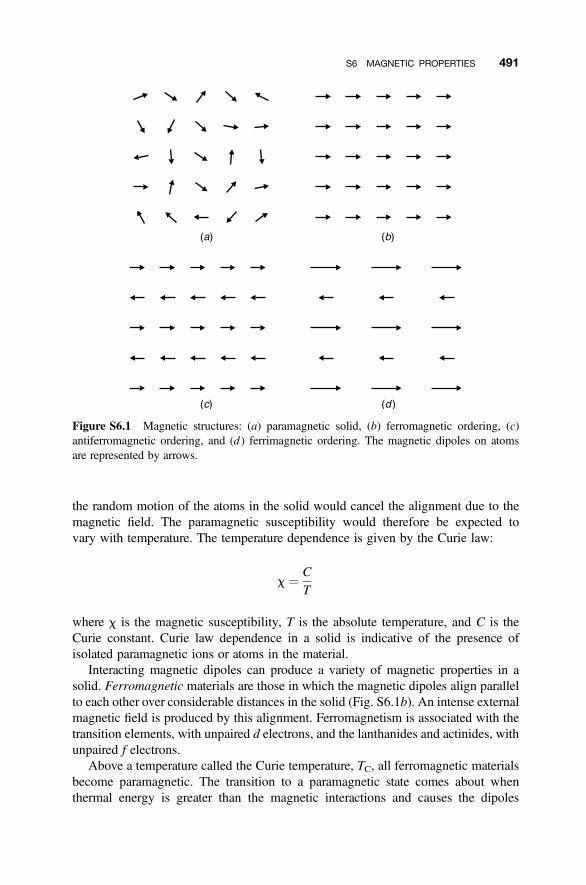
the random motion of the atoms in the solid would cancel the alignment due to themagnetic field. The paramagnetic susceptibility would therefore be expected tovary with temperature. The temperature dependence is given by the Curie law:
x ¼ C
T
where x is the magnetic susceptibility, T is the absolute temperature, and C is theCurie constant. Curie law dependence in a solid is indicative of the presence ofisolated paramagnetic ions or atoms in the material.
Interacting magnetic dipoles can produce a variety of magnetic properties in asolid. Ferromagnetic materials are those in which the magnetic dipoles align parallelto each other over considerable distances in the solid (Fig. S6.1b). An intense externalmagnetic field is produced by this alignment. Ferromagnetism is associated with thetransition elements, with unpaired d electrons, and the lanthanides and actinides, withunpaired f electrons.
Above a temperature called the Curie temperature, TC, all ferromagnetic materialsbecome paramagnetic. The transition to a paramagnetic state comes about whenthermal energy is greater than the magnetic interactions and causes the dipoles
Figure S6.1 Magnetic structures: (a) paramagnetic solid, (b) ferromagnetic ordering, (c)antiferromagnetic ordering, and (d ) ferrimagnetic ordering. The magnetic dipoles on atomsare represented by arrows.
S6 MAGNETIC PROPERTIES 491
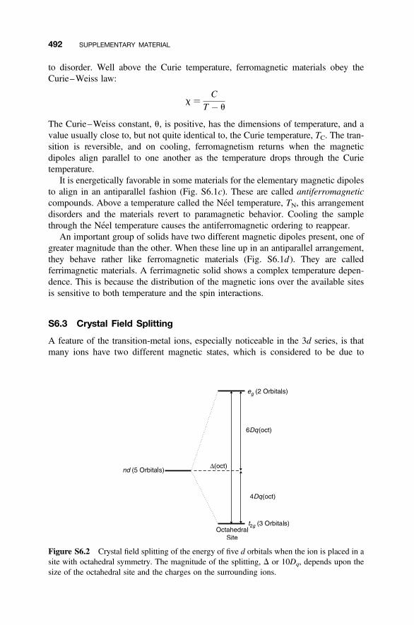
to disorder. Well above the Curie temperature, ferromagnetic materials obey theCurie–Weiss law:
x ¼ C
T � u
The Curie–Weiss constant, u, is positive, has the dimensions of temperature, and avalue usually close to, but not quite identical to, the Curie temperature, TC. The tran-sition is reversible, and on cooling, ferromagnetism returns when the magneticdipoles align parallel to one another as the temperature drops through the Curietemperature.
It is energetically favorable in some materials for the elementary magnetic dipolesto align in an antiparallel fashion (Fig. S6.1c). These are called antiferromagneticcompounds. Above a temperature called the Neel temperature, TN, this arrangementdisorders and the materials revert to paramagnetic behavior. Cooling the samplethrough the Neel temperature causes the antiferromagnetic ordering to reappear.
An important group of solids have two different magnetic dipoles present, one ofgreater magnitude than the other. When these line up in an antiparallel arrangement,they behave rather like ferromagnetic materials (Fig. S6.1d). They are calledferrimagnetic materials. A ferrimagnetic solid shows a complex temperature depen-dence. This is because the distribution of the magnetic ions over the available sitesis sensitive to both temperature and the spin interactions.
S6.3 Crystal Field Splitting
A feature of the transition-metal ions, especially noticeable in the 3d series, is thatmany ions have two different magnetic states, which is considered to be due to
Figure S6.2 Crystal field splitting of the energy of five d orbitals when the ion is placed in asite with octahedral symmetry. The magnitude of the splitting, D or 10Dq, depends upon thesize of the octahedral site and the charges on the surrounding ions.
492 SUPPLEMENTARY MATERIAL
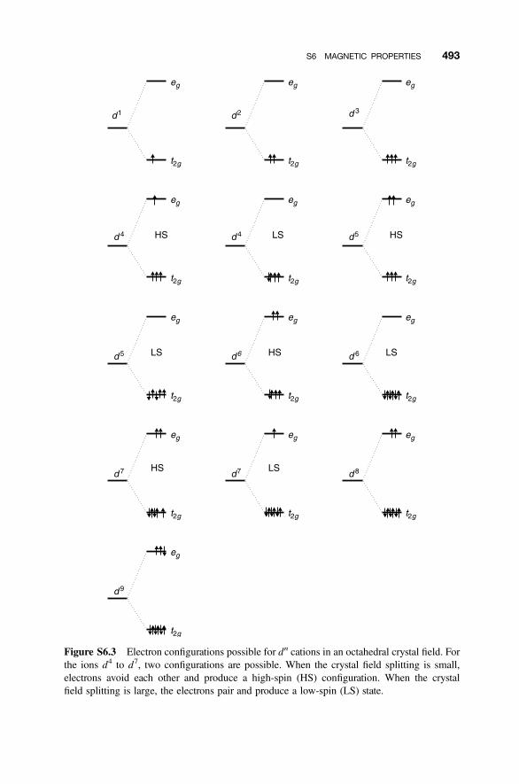
Figure S6.3 Electron configurations possible for dn cations in an octahedral crystal field. Forthe ions d4 to d7, two configurations are possible. When the crystal field splitting is small,electrons avoid each other and produce a high-spin (HS) configuration. When the crystalfield splitting is large, the electrons pair and produce a low-spin (LS) state.
S6 MAGNETIC PROPERTIES 493
two different amounts of unpaired electron spin, giving rise to high-spin and low-spinstates. For example, Fe3þ, with a 3d5 electron configuration, sometimes appears tohave five unpaired spins and sometimes only one. This behavior is found for 3dions with configurations between 3d4 and 3d7. The explanation of this phenomenonlies with crystal field splitting of the d-electron energy levels. When the ions are inoctahedral surroundings, the d-electron levels are split into two groups, one oflower energy, containing three levels, labeled t2g, and one of higher energy, contain-ing two levels, called eg (Fig. S6.2). If the splitting is large, the d electrons preferen-tially occupy the lower, t2g, group. Spin pairing occurs for more than three delectrons, giving rise to a low-spin state. In the alternative case, when the splittingis small, the electrons occupy all of the d orbitals, avoiding double occupation of orbi-tals as far as possible. Spin pairing is avoided, and the ion has a high-spin state.The crystal field alternatives only arise for ions with a configuration betweend4 and d7 (Fig. S6.3).
494 SUPPLEMENTARY MATERIAL
Answers to Problems and Exercises
Chapter 1
Quick Quiz
1. (b) 6. (c)
2. (a) 7. (a)
3. (b) 8. (b)
4. (c) 9. (b)
5. (a) 10. (a)
Calculations and Questions
1. (a) 4.21 � 1020 cm23; (b) MgGa1.75Mn0.25O4
2. (a) VZr most likely, Zr0.796 S; (b) Ca0.1Zr0.9O1.9
3. (a) Holes; (b) concentration, 0.00095; LaCoO3.00095
4. 182.7 mV K21
5. Representative points are: La0.9Sr0.1MnO3, a ¼ 189 mV K21; La0.8Sr0.2MnO3,a ¼ 119 mV K21
6. 3.26
7. (a) Li2O (MgO) �! 2Li0Mg þ OO þ VO2†
(b) PrO2 212O2 �! VO
2† þ 2e0
(c) Ga2O3 (TiO2) �! 2Ga0Ti þ 3OO þ VO2†
(d) 2CaO (La2O3) �! 2Ca0La þ 2OO þ VO2†
or 2CaO (LaCoO3) �! 2Ca0La þ 2CoCo þ 5OO þ VO2†
(e) V2O3 (Al2O3) �! 2VAl þ 3OO
or V2O3 (MgAl2O4) �! MgMg þ 2VAl þ 4OO
8. (a) a ¼ þk/e ln [(1 2 2x)/x]; (b) holes; (c) 0.0884 mV K21
9. M2þO (MgO) �! 2M0
Mg þ OO þ VO2†
Defects in Solids, by Richard J. D. TilleyCopyright # 2008 John Wiley & Sons, Inc.
495
MO (MgO) �! MMg þ OO
M2O3 (MgO) �! 2MMg† þ V20
Mg þ 3OO
MO2 (MgO) �! MMg2† þ V20
Mg þ 2OO
M2O5 (MgO) �! 2MMg3† þ 3V20
Mg þ 5OO
10. (a) 3565 kg m23; (b) 4502 kg m23; (c) 3840 kg m23; positive deviation fromVegard’s law
Chapter 2
Quick Quiz
1. (b) 6. (a)
2. (a) 7. (a)
3. (b) 8. (b)
4. (c) 9. (a)
5. (c) 10. (c)
Calculations and Questions
1.
496 ANSWERS TO PROBLEMS AND EXERCISES
2.
3. (a) 3.2 � 1025; (b) 1.88 � 1024 m23; (c) 1.88 � 1024 m23
4. nS � N exp(2DHS/3RT)
5. (a) anion Frenkel: VF† þ F0i; cation Frenkel, V20
Pb þ Pbi2†; Schottky, V20
Pb þ 2F0i(b) aF : S : cF � 1 : 2.6 � 1026 : 1.3 � 10217
6. (a) 3.7 � 10219 J ¼ 2.3 eV; (b) 1.95 � 1022 m23
7. 1.04 � 10225 m23 (for both)
8. E ¼ (2/4 p 10) f[q1 q2/(r1 2 r2)] þ [q1 q3/(r1 2r3)] þ [q2 q3/(r2 2 r3)]g9. (a) 4.78 � 1024 m23; (b) 9.56 � 1024 m23; 6.99 � 1017 g21
10. (a) 7.90 � 10215; (b) 2.61 � 1014 m23
11. 200 kJ mol21
ANSWERS TO PROBLEMS AND EXERCISES 497

Chapter 3
Quick Quiz
1. (b) 6. (b)
2. (c) 7. (b)
3. (a) 8. (a)
4. (b) 9. (c)
5. (a) 10. (c)
Calculations and Questions
1. (a) 0.255 nm; (b) 0.147 nm
2. (a) a/2[110]; (b) [111]
3.
498 ANSWERS TO PROBLEMS AND EXERCISES
4. b ¼ [010]; b1 ¼ 13[100]; b2 ¼ 1
3[010]; b3 ¼ 13[110]; b4 ¼ 1
3[010]
5. b ¼ [110]; b1 ¼ 13[120]; b2 ¼ 1
3[210]
6. 0.49 nm
7. (a) Antiphase boundary; (b) twin; (c) twin; (d) no boundary; (e) antiphaseboundary; (f) twin
8. (100), Ca; (200) Ca; (400), F; (110), CaF; (220), CaF
9. (a) VO2 O3 VO2 O3 VO2 O3 VO2 O3 VO2 O3 VO2 O3 VO2 (twin plane bold);
(b) no composition change
10. (a) Y2O3 (BaO) ! 2YBa† þ 2OO þ O20
i
[Ti2O3 (TiO2) ! 2Ti0Ti4 þ 3OO þ VO2†]
Adding: Y2O3 (BaTiO3) ! 2YBa† þ 2Ti0Ti4 þ 6OO
(b) Nb2O5 (TiO2) ! 2NbTi4† þ 4OO þ O20
i
[Ti2O3 (TiO2) ! 2Ti0Ti4 þ 3OO þ VO2†]
Adding: Nb2O5 (TiO2) ! 2NbTi4† þ 2Ti0Ti4 þ 8OO
Chapter 4
Quick Quiz
1. (b) 6. (c)
2. (c) 7. (c)
3. (b) 8. (b)
4. (a) 9. (a)
5. (a) 10. (b)
Calculations and Questions
1. VTi40 þ VO
2†; Lu0Ti þ VO2†; Lu0Ti, Tii
4†
2. (a) 0.4CaTiO3 þ 0.6La2/3TiO3; (b) 0.5CaTiO3 þ 0.5 La2/3TiO3; 1339.7 kg m23
3. (a) Mg0.3Al1.4O2.4, Mg0.5Al2.333O4, Mg0.429Al2O3.43
(b) 4Al2O3 (MgAl2O4) ! V20Mg þ 2AlMg
† þ 6AlAl þ 12OO
(c) Al2O3 (MgAl2O4) ! V20Mg þ 2AlAl þ 3OO þ VO
2†
4. (a) BaTi2Al2O8; (b) Ba0.9Cs0.1Ti2.2Al1.8O8; (c) Ba0.65Sr0.35Ti2Al2O8;(d) Ba0.83La0.17Ti1.83Al2.17O8
5. Bi8Pb4nS4nþ12 or (Bi2S3)4(PbS)N, N ¼ 4n
ANSWERS TO PROBLEMS AND EXERCISES 499
6. (a) (Ca, Na)5Nb5O17; (b) (Ca, Na)13Nb13O45; (c) (Ca, Na)14Nb14O48;(d) (Ca, Na)11Nb11O37
7. (a) Sr1.1TiS3; 3.0 nm; (c) 3024 nm
8. (a) Ca0.847U0.153F2.306 (MF2.306); (b) Ca0.644U0.116F2 (M0.76F2)
9. (a) Na2.2Al11O17.6, Na and O interstitials; (b) Na2.125Al10.625O17, Na interstitialsand Al vacancies
10. (a) Ti2.57N, Ti interstitials; (b) TiN0.36, N vacancies; (c) r (vacancies)/r(perfect) ¼ p; (d) Ti0.95N0.95
Chapter 5
Quick Quiz
1. (b) 6. (a)
2. (a) 7. (c)
3. (b) 8. (c)
4. (c) 9. (b)
5. (a) 10. (c)
Calculations and Questions
1. 3.6 � 10214 m2 s21
2. (a) 386.4 a2 s21; 3.48 � 10217 m2 s21
3. 232 kJ mol21 ¼ 2.41 eV
4. 87.9 kJ mol21
5. 99.0 kJ mol21
6. 3228C
7. D ¼ ga2n exp(2DHi/RT) exp(2DHm/RT)
8. 1.854 � 10217 m2 s21
9. Bell-shaped curve, representative points: x¼ 0, cx ¼ 1.66 � 107; x¼ 2.0 � 1027 m,cx ¼ 1.17 � 107; x ¼ 4.0 � 1027 m, cx ¼ 4.35 � 106
10. Almost linear, representative points: Ar(0) ¼ 10000; x ¼ 2.3 � 1024 m, Ar ¼7 � 103; x ¼ 5.6 � 1024 m, Ar ¼ 4.6 � 103
11. Bell-shaped curve, representative points: x¼ 0, cx ¼ 7.0 � 105; x¼ 2.0 � 1024 m,cx ¼ 5.84 � 105; x¼ 4.8� 1024 m, cx ¼ 2.72 � 105
12. Almost linear, representative points: Ar(0) ¼ 100; x ¼ 1.95 � 1026 m, Ar ¼ 80;x ¼ 6.0 � 1026 m, Ar ¼ 42.6
500 ANSWERS TO PROBLEMS AND EXERCISES
Chapter 6
Quick Quiz
1. (c) 6. (c)
2. (a) 7. (c)
3. (b) 8. (b)
4. (b) 9. (a)
5. (a) 10. (b)
Calculations and Questions
1. 181 kJ mol21 ¼ 1.88 eV
2. (a) 52.1 kJ mol21 ¼ 0.54 eV; (b) 15.4 kJ mol21 ¼ 0.16 eV
3. (a) Nb2O5 (EuNbO4) ! 2V30Eu þ 2NbNb þ 5OO þ 3VO
2†; (b) an increase in[VO
2†] increases the O ion conductivity; (c) 72.6 kJ mol21
4. (a) 87.9 kJ mol21; (b) 1.63 � 10213 m2 s21; (c) 0.20
5. This is due to charge neutrality, 1 Na þ ¼ 12M
2þ ¼ 13M
3þ. If more is added, theremust either be more O20
i in the interlayers or V30Al in the spinel blocks. Interstitial
O in the spinel blocks is unlikely.
6. 3.66 V
7. (a) þ414 mV; 0.0954 atm
8. (a) Pt, p0O2, BaTiO3kZrO2kp00O2
, Pt; (b) BaTiO2.99997
9. (a) 4008C: R(bulk) 5 kV, R(grain boundary) 29 kV; 5008C: R(bulk) 2 kV,R(grain boundary) 16 kV; 6008C: R(bulk) 1 kV, R(grain boundary) 9 kV;(b) 46 kJ mol21; (c) 35 kJ mol21
10. (a) 2.53 � 10212 m2 s21; (b) �1
11. (a) 6.20 � 1024 S m21; (b) the values are similar so that both diffusion andconductivity are likely to take place by the same mechanism.
Chapter 7
Quick Quiz
1. (b) 6. (b)
2. (b) 7. (c)
3. (c) 8. (a)
ANSWERS TO PROBLEMS AND EXERCISES 501
4. (a) 9. (c)
5. (a) 10. (a)
Calculations and Questions
1. (a) x2 O2 (CoO) ! x OO þ x V20
Co þ 2 x CoCo† or x
2 O2 (CoO) ! x OO þx V20
Co þ 2x h†; (b) 0.002/0.999
2. A oxide þ B oxide þ B metal
3. The slope of the log s versus log pO2 graph is 1/5.2. A slope of 16 corresponds to
Co3þ in Co12xO, a slope of 14 corresponds to Co4þ, so the defects are almost all
Co3þ, but there may be some Co4þ present.
4. The slope of the log s versus log pO2 graph is16, corresponding to Ni
3þ in Ni12xO
5. Doubly charged vacancies fit best.
6.
7. At high pressure: s/ [h†]/ pO21=4; at low pressure: s/ [e0]/ pO2
�1=4
8. [e0]: 2Kop[e0]4 þ Ke
2p1/2 [e0]3 2 2KrKe2 2 Ke
2p1/2 [e0] ¼ 0
[e0]: 2 � 1056p[e0]4 þ 1 � 1080p1/2 [e0]3 2 2�10136 2 1 � 10120p1/2 [e0] ¼ 0
[V20M]: 2KS
1/2p1/4[V20M]
2 þ Kr1/2[V20
M]3/2 2 2KS
3/2p1/4 2 Ko1/2KS
1/2 p1/2[V20M]
1/2 ¼ 0
[V20M]: 2 � 1016p1/4[V20
M]2 þ 1 � 1028[V20
M]3/2 2 2 � 1048p1/42
1 � 1044p1/2[V20M]
1/2 ¼ 0
[VX2†]: 2KS
3/2p1/4 þ Kr1/2KS
1/2[VX2†]1/2 2 2Kr
1/2p1/4[VX2†]2 þ Ko
1/2p1/2 [VX2†]3/2 ¼ 0
502 ANSWERS TO PROBLEMS AND EXERCISES
[VX2†]: 2 � 1048p1/4 þ 1 � 1044[VX
2†]1/2 2 2 � 1016p1/4[VX2†]2 þ
1 � 1028p1/2[VX2†]3/2 ¼ 0
9. (a) Electrons; (b) Co2þ, Co3þ; (c) Co3þ; (d) Bi23þSr2
2þCo0.3202þ Co0.680
3þ O6þd;(e) 0.340
10. (a) Fe, �FeO, Fe3O4, Fe2O3; (b) �FeO is nonstoichiometric; (c) Fe þ 12O2 !
FeO, 3FeO þ 12O2 ! Fe3O4, 2
3Fe3O4 þ 16O2 ! Fe2O3; (d) 2174.2 kJ
mol21, 2142.8 kJ mol21, 214.0 kJ mol21; (e) 4.37 � 10213 atm
Chapter 8
Quick Quiz
1. (c) 6. (b)
2. (c) 7. (c)
3. (a) 8. (b)
4. (b) 9. (a)
5. (a) 10. (c)
Calculations and Questions
1. (a) Al2O3 (TiO2) ! 2Al0Ti þ 3OO þ VO2†
Al2O3 (TiO2) þ 12O2 ! 2Al0Ti þ 4OO þ 2 h†
2Al2O3 (TiO2) ! 3Al0Ti þ 6OO þ Ali3†
(b) 2Nb2O5 (TiO2) ! 4NbTi† þ 10OO þ V40
TiNb2O5 (TiO2) ! 2NbTi
† þ 4OO þ O20i
Nb2O5 (TiO2) ! 2NbTi† þ 4OO þ 1
2O2 þ 2e0
(c) NiO (Mn3O4) ! NiMn2 þ 2MnMn3 þ 4OO
2NiO (Mn3O4) ! 2Ni0Mn3 þ MnMn2 þ 3OO þ VO2†
(d) Cr2O3 (MgO) ! 2CrMg† þ 2OO þ O20
i
Cr2O3 (MgO) ! 2CrMg† þ 3OO þ V20
Mg
Cr2O3 (MgO) ! 2CrMg† þ 2OO þ 1
2O2 þ 2e0
(e) 5Fe2O3 (Nb2O5) ! 6Fe20Nb þ 15OO þ 4Fei3†
Fe2O3 (Nb2O5) ! 2Fe20Nb þ 3OO þ 2VO2†
Fe2O3 (Nb2O5) ! 2Fe20Nb þ 3OO þ 4h†
2. 5560 K
3. Donors: 2� 10116p þ 1� 1096[h†] p1/2 2 2 � 1052 [h†]4 2 1� 1064 [h†]3p1/2 21 � 1089[h†]2p1/2 ¼ 0
ANSWERS TO PROBLEMS AND EXERCISES 503
Acceptors: 2 � 10116p þ 1 � 1096[h†]p1/2 þ 1 � 1089 [h†]2p1/2 22 � 1052[h†]4 2 1 � 1064[h†]3p1/2 ¼ 0
4. (a) 2MgO (Ti2O3) þ 12O2 ! 2Mg0Ti þ 3OO þ 2h†
or 2MgO (MgTi2O3) þ 12O2 !MgMg þ 2Mg0Ti þ 4OO þ 2h†
or 2MgO (MgTi2O3) þ 12O2 ! 2MgMg þ 2Mg0Ti þ 2TiTi
† þ 4OO
(b) Mg2TiO4, that is, (Mg2þ)[Mg2þTi4þ]O4
(c) Insulator
5. (a) Charge reservoir: þ2; superconducting layer: 22
(b) Charge reservoir: þ2; superconducting layer: 22
(c) Charge reservoir: þ1; superconducting layer: 22
(d) Charge reservoir: þ2; superconducting layer: 22
(e) Charge reservoir: þ1; superconducting layer: 21.5
6. (a) 3CeO2 (LaCoO3) ! 3CeLa† þ V30
La þ4CoCo þ 12OO
or 2CeO2 (LaCuO3) ! 2CeLa† þ 2CoCo þ 6OO þ O20
i
or 2CeO2 (LaCoO3) ! 2CeLa† þ 2CoCo þ 6OO þ 1
2O2 þ 2e0
or 2CeO2 (LaCoO3) ! 2CeLa† þ 2Co0Co þ 6OO þ 1
2O2
(b) Electrons(c) 0.03
7. Slope ¼ 1/5.5. The equation is in agreement with holes plus oxygen interstitials:12O2 ! O20
i þ 2h†
8. [Pr0] ¼ Ke/[h†] ¼ Ke/[Yb0Pr]; slope ¼ 21
[VO2†] ¼ [h†]2/Kop
1=2O2
¼ [Yb0Pr]2/Kop
1=2O2
; slope ¼ þ2
[OHO†] ¼ Kw
1/2[Yb0Pr]p1=2H2O/Ko
1/2p1=2O2; slope ¼ þ1
9. (a) 2NiO (V2O3) ! 2Ni0V þ 2OO þ VaO2†
VaO2† þ 1
2O2 ! OO þ 2h†
Adding: 2NiO (V2O3) ! 2Ni0V þ 2OO þ 2h†
(b) 7.85 kJ mol21; (c) Ni 2/3V2/33þV2/3
4þO3
10. (a) Low O2 pressure: negative slope, n-type electronic conductivity; high O2
pressure: positive slope, p-type electronic conductivity; middle O2 pressure:no pressure dependence, proton conductivity
(b) Taking WO3 as the “sleeping partner”: 2CaO (La2O3) ! 2Ca0La þ 2OO þVO2† or: 6CaO (La6WO12) ! 6Ca0La þ WW þ 9OO þ 3VO
2†
(c) H2O þ OO þ VO2† ! 2OHO
†
(d) At low O2 pressure reduction occurs: OO ! VO2† þ 2e0 þ 1
2O2 This leads to
s/ ½e0�/ p�1=4O2
; at high O2 pressure oxidation occurs: VO2† þ 1
2O2 !OO þ 2 h†. This leads to s/ [h†]/ p 1=4
O2.
504 ANSWERS TO PROBLEMS AND EXERCISES
Chapter 9
Quick Quiz
1. (c) 6. (b)
2. (a) 7. (c)
3. (c) 8. (a)
4. (b) 9. (c)
5. (a) 10. (b)
Calculations and Questions
1. (a) e4 t3: #" #" """(b) 3.87 mB
(c) 1.88 eV ¼ 3.01 � 10219 J
2. The material is mainly Mn3þ. At x ¼ 0.1 there might be some Mn2þ present, andat x ¼ 1.0 there might be some Mn4þ present.
3. (a) The band gap transition is at a wavelength of 387.5 nm (ultraviolet).
(b) 2.49 eV ¼ 3.99 � 10219 J; 2.65 eV ¼ 4.24 � 10219 J(c) 3.52 eV
4. 33.5%
5. The slope is approximately 1.7, so the process is likely to be a two-photonexcitation.
6. (a) KF0.63Cl0.37(b) 2.7 eV ¼ 4.3 � 10219 J
(c) 8.8 eV ¼ 14.1 � 10219 J
(d) 9.9 eV ¼ 15.9 � 10219 J
7. (a) Mn2þ LS, 1.73 mB; Mn2þ IS, 3.87 mB; Mn2þ HS, 5.92 mB; Mn3þ HS, 4.90mB; Mn4þ HS, 3.87 mB
(b) Ratio is 5.08 � 10217; none in the upper states
(c) 1278 nm (infrared)
8. (a) 5.92 mB; (b) 1.03 nm
9. (a) 1.85 nm; (b) 0.52 nm; (c) yes, they would overlap
10. (a) 9.18; (b) 1004.5 K
ANSWERS TO PROBLEMS AND EXERCISES 505

&FORMULA INDEX
Nonstoichiometric compounds such as �FeO, Ni12xO, LaCoO3þd, LaCoO3þ x/2 etc. areindexed under the notionally stoichiometric phase, i.e. FeO, NiO, LaCoO3.
Doped phases such as Al1.995Cr0.005O3, LaNixCo12xO3 etc. are classed as subset of theparent compound, i.e. Al2O3, LaCoO3.
Phases given ionic charges, such as Ba2þZr4þO3, are mostly indexed under the parentphase without ionic charges, i.e. BaZrO3.
Ag, 310, 313, 314AgBr, 58, 59, 61, 239Ag2CdI4, 268AgCl, 58, 61, 103, 107, 239AgCuS, 268, 270a-Ag3CuS2, 268, 269, 270AgCuSe, 268Ag2HgI4, 268Ag3HgI4, 268Ag1.80Hg0.45Se0.70I1.30, 268, 269AgI, a-AgI, 268, 269, 270b-AgI, 58, 269, 454, 454g-AgI, 269Ag6I4WO4, 268Ag2O, 310, 313, 314Ag2S, 268Ag3SBr, 268Ag3SI, 268Ag2Se, 268Ag7I4PO4, 268Ag7TaS6, 268Al, 826Al, 210AlN, 454Al2O3, a-Al2O3, 11, 13, 26, 101, 103,
122, 137–140, 142, 195, 198, 210,224, 226, 231, 233, 240, 241, 297,353, 391, 393, 419, 429, 442, 454
Al1.995 Cr0.005O3, 12, 142
(Al12xCrx)2O3, 198g-Al2O3, 148, 149Al23O27N5, 122As, 7, 8, 209AsSb, 209Au, 233
Ba0.75Al11O17.25, 274BaCeO3, 286BaBiO3, 304Ba4Bi3F17, 156BaCs0.28Al2.28Ti5.72O16, 165Ba2Ca2Cu4O8, 371Ba2Ca3Cu5O10, 371BaF2, 58, 156, 278Ba2In2O5, 190, 279, 318, 336, 338–339Ba2(In12xCox)2O5, 279Ba2(In12xGax)2O5, 279
BaMgAl11O19, 421Ba2Mn8O16, 164BaPrO3, 388, 389BaYbxPr12xO3, 387
BaSnO3, 458BaTiO3, 126, 127, 421, 458Ba12x
2þ Lax3þTi12x
4þ Tix3þO3, 127
Ba6Ti2Nb8O30, 164BaZrO3, 286, 389, 458BaY0.2Zr0.8O3, 389
Be3Al2Si6O18, 420
Defects in Solids, by Richard J. D. TilleyCopyright # 2008 John Wiley & Sons, Inc.
507
b-BeO, 454BiBa2CuO5, 371BiBa2CaCu2O7, 371BiBa2Ca2Cu3O9, 371Bi2CaSr2Cu2O8, 368, 369, 371, 374Bi2CaSr2Cu2O8.19, 374Bi2Ca2Sr2Cu3O10, 368, 369, 371, 376BiF3, 155, 156Bi2O3, 125d-Bi2O3, 160Bi2Pb2O7, 142Bi94Nb32O221
Bi2S3(Bi0.87SrO2)2(CoO2)1.82, 186, 187Bi2Sr2CuO6, 367, 368, 371Bi2SrTa2O9, 183Bi4Ti3O12, 179, 183Bi5TiNbWO15, 184Bi2WO6, 183Bi94Nb32O221, 161
[(CH3)4N]Ag13I15, 268, 269(C2H5NH)Ag5I6, 268(C2H5NH)5Ag18I23, 268CO, 252(Ca2CoO3)0.62(CoO2), 186, 187CaF2, 21, 28, 58, 155, 156, 231, 278,
434, 455(Ca, Gd)F2.4, 278Ca0.94Y0.06F2.06, 156
CaI2, 55Ca2LaFe3O8, 190Ca2Nb2O7, 179, 181Ca4Nb4O14, 181, 182CaO, 5, 6, 7, 22, 37, 38, 142,
159, 280CaxMg12xO, 142
(CaOH)1.14(CoO2), 187Ca0.6Sr0.4CuO2, 142CaS, 32CaTiO3, 37–38, 143, 162, 457Ca5(Ti, Nb)5O17, 181Ca9(Ti, Nb)9O29, 181Ca4Ti2Fe2O11, 190CaWO4, 430CdCl2, 456CdI2, 104, 455CdO, 35–36, 298Cd(OH)2, 455, 456CdS, 233, 454
CdSe, 454CdTe, 454Ce2O3, 144Ce32O58, 144CeO2, 191, 378, 422Ce0.8Pr0.2O2, 379Ce0.75Pr0.25O2, 379Ce12xPrxO2, 379, 394
CoF3, 189CoO, 18, 144, 145, 210, 233, 300,
303, 454, 461CoO2, 165, 166, 184, 394LixCoO2, 165, 381, 394
Cr2O3, 11, 13, 38, 142, 198, 336–338,352–353, 354, 356, 392, 455
(CrxAl12x)2O3, 11, 13g-Cr2O3, 148CrO2, 455Cr2S3, 144Cr3S4, 144Cr5S6, 144Cr7S8, 144CsBiNb2O7, 182CsCaF3, 458CsCaCl3, 458CsCa2Nb3O10, 182CsCdCl3, 458CsCdF3, 458CsCu9Br10, 268CsCu9I10, 268CsHgBr3, 458Cu, 233a-CuBr, 268b-CuBr, 268CuBr, 268, 454CuCl, 454Cu8GeS6, 268a-CuI, 268b-CuI, 268CuI, 268, 454CuO, 366Cu2(OH)2(CO3), 419Cu3(OH)2(CO3)2, 419Cu6PS5I, 268CuSO4.5H2O, 419Cu2Se, 268
Er2Ti2O7, 28, 149Er2.09Ti1.94O6.952, 149EuEr2Ga0.7Fe4.3O12, 412
508 FORMULA INDEX
a-Fe, 233g-Fe, 233FeAl, 30, 38FeF2, 453FeO, 14–15, 17, 18, 144, 150–152,
409–410, 454Fe0.956O, 150Fe0.865O, 150
Fe2O3, 344g-Fe2O3, 148, 149Fe2O3, 353, 355, 392, 393, 455Fe2–2xFexTixO3, 356
Fe3O4, 15, 150, 303, 405, 460Fe3þ " [Fe3þ# Fe2þ#]O4, 405Fe3þ " [Fe3þ# Ni2þ"]O4, 405
FeS, 5Fe2SiO4, 142
Ga, 869Ga, 20971Ga, 209GaAs, 29, 41, 143, 403, 454Ga0.9998As1.0002, 143
GaN, 21, 454g-Ga2O3, 148GaSr2(Y, Ca)Cu2O7, 371GaSr2(Y, Ca)2Cu3O9, 371GdF3, 278Gd2O3, 421Ge, 7, 233, 453, 470
HUO2PO4.4H2O, 440HfO2, 403HfS2, 456HgBa2CuO4, 371HgBa2CaCu2O6, 371HgBa2Ca2Cu3O8, 371
In, 8InF3, 155InN, 454InP, 454In4Sn3O12, 160In5SnSbO12, 160In6WO12, 160
K, 462KAlSi3O8, 142KBr, 53, 54, 239, 433KCl, 13, 53, 54, 107, 233, 239,
255, 268, 433, 436, 437
KCoFe(CN)6, 441KF, 53, 54, 155, 433KFeIIFeIII(CN)6, 440KI, 53, 54KLaNb2O7, 179, 182KMgF3, 458K2MgF4, 460KMg3(OH)2Si3AlO10, 170KNiF3, 458K2NiF4, 145, 182, 460KTaO3, 458
La12xCaxCrO3, 287La(Ce)PO4, 421La(Ce)MgB5O10, 421LaCoO3, 19, 309, 382, 383,
406, 407LaNixCo12xO3, 19, 20La12xSrxCoO32x/2, 382, 383La12xSrxCoO3, 383, 407
LaCrS3, 184, 185La2CuO4, 145, 182, 192, 301, 363, 364,
365, 366, 367, 370, 371, 375, 378,411, 460
La1.95Sr0.05Cu0.952þ Cu0.05
3þ O4, 364La1.9Sr0.1Cu0.9
2þCu0.13þO4, 364
La1.85Sr0.15CuO4, 364La22xSrxCuO4, 367, 411La22xSrxCuO42x/2, 364, 367
LaF3, 155LaMg(Ce)Al11O19, 421LaMnO3, 406, 407La0.8Sr0.2MnO3, 287La12xSrxMnO3, 287
La4Mn4O11, 190La2NiO4, 300, 460La2NiO4.24, 300
La2O3, 37, 38(LaS)1.20CrS2, 185, 186, 187La2Ti3O9, 143La2/3TiO3, 143La6UO12, 160Li, 462LiBr, 53, 54, 433LixC6, 165LiCl, 53, 54, 433, 436, 437LiF, 53, 54, 433LiI, 53, 54–56LiNbO3, 458Li2O, 241, 354, 355
FORMULA INDEX 509
LiTi2O4, 366Li1þxTi22xO4, 366Li4/3 Ti5/3 O4, 367Liþ[Li1/3
þ Ti5/34þ ]O4, 366
Liþ[Li0.12þ Ti0.64
3þ Ti1.244þ ]O4, 367
Liþ[Li1/3þ Ti5/3
4þ ]O4, 366Lu2O3, 137Lu2Ti2O7, 137, 255Lu2Ti1.17O5.35, 137Lu2.096Ti1.904O6.952, 255Lu2.286Ti1.714O6.857, 255Lu2þxTi22xO72x/2, 255
MgAl2O4, 5, 28, 111, 142, 271,297, 458, 459, 460
Mg(Al0.99Cr0.01)2O4, 142MgCr2O4, 142MgF2, 455(Mg, Fe)10[(OH)4Si12O32], 171(Mg, Fe)17[(OH)6Si20O54], 171MgGa2O4, 357MgGa22xMnxO4, 357MgGaMnO4, 357
MgMn2O4, 357MgO, 32, 137–140, 142, 222, 233, 297,
298, 391, 435, 453Mg0.95Al0.1O1.10, 139–140
Mg(OH)2, 456MgSiO3, 170Mg2SiO4, 142MnO, 144, 454Mn2O3, 392Mn3O4, 355, 356Mn2þ [Mn22x
3þ Mnx4þ Nix
2þ]O4, 357g-MnO2, 149MoO3, 176Mo5O14, 190b-MoS2, 4563R-MoS2, 457
Na, 233, 462NaAlCl4, 277NaAl11O17, 270, 273Na1þxAl11O17þx/2, 273Na1þx Lix/2Al112x/2 O17, 274Na1þxMgxAl112xO17, 274
NaAl(SO4)2.12H2O, 447NaAlSi3O8, 142(Na, Ca)2(Nb, Ta)2O6(O, OH, F), 142
NaFe(SO4)2.12H2O, 447NaNbO3, 181, 182, 458Na2(Nb, Ta)2O7, 142NaBr, 53, 54, 239, 255, 433NaCl, 6, 7, 13, 22, 23, 25, 26, 28, 53, 54,
101, 107, 225, 230, 231, 233, 239,255, 268, 432, 433, 453, 454
NaF, 53, 54, 135–137, 255, 278, 433NaI, 53, 54Na2O, 391Na2Sx, 277NaYF4, 421NaZnF3, 136, 137Na7Zr6F31, 156NbH0.1, 147NbO2, 233, 455Nb2O5, 168, 175, 182, 187, 189,
352, 392, 393H-Nb2O5, 187, 188Nb12O29, 187Nb22O54, 187Nb25O62, 187Nb39O97, 187Nb47O116, 187Nb53O132, 187Nb16W18O64, 190NbS2, 165, 184, 456, 457Nb2Zrx22O2xþ1, 155Nd2CuO4, 365, 366Nd22xCexCuO4, 365Nd22xCexCu12x
2þ CuxþO4, 366
Nd1.85Ce0.15CuO4, 366Nd2O3, 36563Ni, 210Ni, 277NiBr2, 104NiFe2O4, 405Ni12xZnxFe2O4, 405
NiO, 18, 21, 24, 31, 33–35, 142, 144, 222,233, 297, 300, 344, 354–355, 355,392, 454, 461, 465
Ni12xLixO, 352, 354NiO2, Ni1.02O2, 381Li0.07NiO2, 381Li1.0NiO2, 381LixNiO2, 381, 410Li12yNi1þyO2, 381(Li12yNiy
2þ)(Niy2þNi12y
3þ )O2, 381, 410Lix(Ni, Fe)O2, 381
510 FORMULA INDEX
P, 7, 8Pb12Bi8S24, 177Pb24Bi8S36, 177Pb5Bi17P5O43, 161Pb5Bi18P4O42, 161PbF2, 155, 156, 268PbS, 107, 177, 233(PbS)1.14(NbS2)2, 187Pb2Sr2Y0.5Ca0.5Cu3O8, 371PbTiO3, 421Pb3ZrF10, 156, 158Pb5ZrF14, 156, 158Pr0.7Ca0.2Sr0.1MnO3, 408Pr0.7Ca0.2Sr0.1Mn0.98Mg0.02O3, 408PrO2, 144, 160PrO1.833, 160Pr7O12, 160PtS2, 456
RbAg4I5, 268RbBiF4, 219RbBr, 433RbCl, 433, 436RbCu3Cl4, 268, 269RbF, 155, 433RbUO3, 458ReO3, 457ReS2, 457
Sb, 7, 8121Sb, 209123Sb, 209Sb2Te3, 403Sc2O3, 391Si, 7, 233, 453, 47028Si, 20929Si, 20930Si, 209SiC, 66, 454SiO, 17SiO2, 240, 434a-Sn, 453SnO2, 404, 455SnS2, 104, 456(SnS)1.17NbS2, 186, 187SrAl2O4, 434Sr4Al14O25, 421SrCoO3, 383SrCo0.8Fe0.2O2.582, 191
SrCo0.8Fe0.2O2.332, 192SrCuO2, 142Sr2CuO2F2, 147, 367, 371SrF2, 58, 278Sr2Fe2O5, 190, 299SrFeO2.5, 190, 299SrFeO2.75, 299
SrFeO3, 190, 299SrMnO3, 408, 458Sr2Mn2O5, 408, 409Sr5Mn5O13, 408, 409Sr7Mn7O19, 408, 409SrO, 72Sr2SnO4, 460SrTiO3, 72, 182, 297, 384, 421, 457Sr2TiO4, 179, 182, 183, 460Sr3Ti2O7, 182, 183Sr4Ti3O10, 182, 183SrxTiS3, 196, 197Sr8(TiS3)7, 197SrZrO3, 385SrZr12xYxO3–0.5x, 385, 387
Ta2O5, 175L-Ta2O5, 195(Ta,W)O2.4756, 195
TaS2, 456, 457Ta74W6O203, 195, 196Tb7O12, 160ThF4, 144Ti2Nb10O29, 187, 188TiO, 107, 144, 233, 454TiO2, 26, 32, 38, 101, 176, 177, 178, 179,
187, 195, 225, 226, 352, 353, 354,355, 356, 392, 393, 403, 453, 455, 465
Ti1–2x4þ Ti2x
3þO22x, 468Ti2O3, 176TiS, 144, 165Ti8S9, 144Ti3S4, 144Ti2S3, 144TiS2, 144, 165, 184, 381, 456LixTiS2, 165, 380Li1.0TiS2, 380
TlBa2CuO5, 371TlBa2CaCu2O7, 371TlBa2Ca2Cu3O9, 371Tl2Ba2CuO6, 368Tl2CaBa2Cu2O8, 368
FORMULA INDEX 511
Tl2CaSr2Cu2O8, 371Tl2Ca2Ba2Cu3O10, 368Tl2Sr2Ca2Cu3O10, 371Tl2Pb2O7, 140Tl2Sr2CuO6, 371
UF4, 155, 195UO2, 16, 17, 144, 152–154U4O9, UO2.25, 144, 153,
155, 156UO2F, 155a-U3O8, 195
VO, 144, 454VO2, 176, 455V2O5, 112
W3Nb14O44, 187, 188, 189WO3, 168, 172, 175, 176, 187, 195, 438,
439, 440, 457WO2.9998, 171WO2.9666
WO2.9444, 174WO2.97, 173WO2.94, 174WO2.93, 174WO2.92, 174WO2.87, 174HxWO3, 438, 439, 440InxWO3, 163KxWO3, 164Li0.5WO3, 162LixWO3, 162Na0.11WO3, 162Na0.95WO3, 162Na0.41WO3, 162Na0.38WO3, 162Na0.26WO3, 162NaxWO3, 162, 163PbxWO3, 163, 164SnxWO3, 164
W11O32, 174W16O46, 174W18O53, 174W25O73, 174W30O89, 179
WO32x(OH)x, 438, 439WS2, 456, 457
Y3Al5O12, 430YBa2Cu3O6.0, 314, 371, 372, 373, 374,
375, 376YBa2Cu3O6.25, 378YBa2Cu3O6.5, 313, 315, 374YBa2Cu3O6.6, 378YBa2Cu3O6.7, 374YBa2Cu3O6.88, 315YBa2Cu3O6.95, 374
YBa2Cu3O7.0, 314, 372, 373, 374, 377, 378YF3, 155, 193YOF, 193, 194Y2O3, 159, 191, 388, 421Y6UO12, 160Y7O6F9, 194
ZnF2, 135–137, 455ZnFe2O4, 405Zn2þ[Fe3þ" Fe3þ#]O4, 405Zn2þx Fe3þ12x[Ni
2þ12xFe
3þ1þx]O4, 406
Zn2þx Fe3þ12x"[Fe3þ#Ni2þ12x"Fe3þx "]O4,406
Zn2þx Fe3þ12x"[Fe3þx #Ni2þ12x"Fe3þ"]O4,406
ZnO, 18, 124, 125, 147, 149, 241,298, 403, 417, 454
Zn12xCuxO, 403Zn12xMnxO, 403
Zn72xCoxSb2O12, 420ZnS, 223, 224, 225, 226,
233, 454ZnSe, 25, 403Zn7Sb2O12, 126ZrF4, 155, 156Zr(N, O, F)x, 155ZrO2, 36–37, 155, 157, 159, 195, 421ZrO2.xCaO, (Zr, Ca)O2, 32, 36–37,
159, 233, 280Zr12xY
3þx O22x/2, 280
ZrS2Zr3Sc4O12, 160Zr10Sc4O26, 160Zr50Sc12O118, 160
512 FORMULA INDEX
&SUBJECT INDEX
ab initio methods, 77Absorption, 412center, 412, 413, 421excited state (ESA), 422–427ground state (GSA), 422–428
Acceptor: see DopantActivator, 413Aggregation: see Point defect aggregationAlkali metals, 462Allotrope, 448Alumina: also see Aluminium oxide,
corundum, 240Alums, 447b-alumina, 270–278, 421, 439composition range, 270, 273correlated diffusion in, 275, 276crystal structure, 272, 273defects in, 272–274ionic conductivity in, 274–276silver analogue, 273unit cell, 270
b00-alumina, 271batteries, 276–278crystal structure, 271, 273defects in, 274as an electrolyte, 276ionic conductivity in, 274–276unit cell, 271
b0 00-alumina, 271b0000-alumina, 271Alloyinterstitial, 147substitutional, 140
Aluminium oxide:also see Corundum, 122
g-aluminium oxide, 147
Aluminium oxynitride, 122Amethyst, 434Anatase, 149Anode, 54, 251, 265, 287, 289, 378Anti-Beevers-Ross (aBR) site, 271, 421Antiferroelectric material, 118, 492Antiferrromagnetic material, 116, 374,
403, 410–411Antiphase boundary, 97, 107, 114–116in copper, 97, 114in cubic close-packed metal
crystals, 114in a hexagonal close-packed
array, 114in magnesium, 114
Antisite defect, 21, 28–31, 40, 77, 143equilibrium population, 64–65formation via Frenkel defects, 33
Anti-Stokes fluorescence, 413Arrhenius behaviour, 258Arrhenius equation, 231, 235Arrhenius plot, 231, 236, 259, 263, 275enthalpy of formation of point defects
from, 237, 238enthalpy of migation from, 237,
238, 259extrinsic region, 237, 239impurity region, 237, 239intrinsic region, 237, 239knee in, 237, 239, 263
Atomistic simulation, 67, 70–76,78, 353
Attempt frequency, 234, 256Aurivillius phase, 179,182–184, 368Austenite, 147Azurite, 419
Defects in Solids, by Richard J. D. TilleyCopyright # 2008 John Wiley & Sons, Inc.
513

Bandbending, 124conduction, 8, 416, 462energy, 461gap, 416, 461
thermal, 462optical, 462
valence, 9, 416, 462Band theory, 461–465comparison with hopping conduction,
306–307definition of major types of electrical
materials, 461–463point defects in terms of, 463–464transition metal oxides in terms of,
464–463Barium titanate, 114, 126, 127, 128, 130Battery, 54, 251, 252, 265, 266, 288lithium iodide, 54–56, 78sodium–sulphur, 276–278ZEBRA, 276–278
Beevers–Ross (BR) site, 271, 273,274, 421
Beevers–Ross type (BR-type) site, 271,274
Beryl, 420Bismuth oxide, 125Bivariant system, 314Bleaching, 63Bloch wall, 118Block structures, 187–189Blue John, 434Boltzmannequation, 47law, 69, 415, 429
Boron nitride, 97Boundarygrain: see Grain boundarytwin: see Twin boundaryinternal, 107
Bound magnetic polaron, 404–405Bridging oxygen, 271, 272Bronzes: see Tungsten bronzesBrouwer diagram, 320–344, 345,
387–389assumptions, 320for Ba2In2O5, 338–339for Cr2O3, 336–338defect equilibria for MX, 321–322
for doped systems, 358–363construction, 358trends, 360–363
effects of temperature, 339–320for electronic defects in MX, 329–336for ionic defects in MX, 322–329polynomial form, 340–344
for electronic defects in MX, 343–344for ionic defects in MX, 340–343
Brownmillerite structure, 190, 255, 297,318
Buckinghamequation, 73potential, 72
Bulk properties, 12–17Burgerscircuit, 85, 87, 90, 92vector, 84, 85, 90, 93, 94, 96, 97,
104, 105
CMR, 407–408, 442CR, 425–427CRT display, 413Cadmium chloride structure, 456Cadmium hydroxide structure, 455Cadmium iodide structure, 104, 106, 455Cadmium oxide, 35–36Calcia, 36Calcia-stabilised zirconia: see ZirconiaCalcium fluoride: see FluoriteCalcium oxide: see CalciaCalcium tungstate, 430Capacitance, 263–265Car mirror, 439Cathode, 54, 251, 265, 287, 289,
380, 381Cathode ray tube (CRT) display, 413Cell: see fuel cellGalvanic, 265, 289potential, 265
and Gibbs energy, 265voltage, 267, 387
Chaikin–Beni equation, 470Chargeeffective, 21–25
Charge reservoir, 367, 369Chemical twinningin the PbS-Bi2S3 system, 177in lead-bismuth sulphosalts, 177
514 SUBJECT INDEX
Chesterite, 171Chimney-ladder structure, 193Chromium oxidedoped with TiO2, 352–353
Clay, 107Cleavage, 121Cobaltites, 407–409Cobalt oxide, 145Cole–Cole plot, 265Colossal magnetoresistance (CMR),
407–408, 442Colordue to impurity defects, 418–420of gemstones, 417, 419, 420, 442of glasses, 417–418, 419, 442of lanthanides, 417–418of pigments, 417–418, 420of minerals, 417–418of transition metal ions, 417–418
Color center: also see F center,432–438
in alkali metal halides, 432–433in amythyst, 434in CaF2, 434complex, 434electron centers, 434hole centers, 434laser, 436–437in smoky quartz, 434surface, 435
Column oxygen, 271Compensation, 352, 353choice of mechanism, 297, 298,
391–392electronic, 7, 297, 298ionic, 7, 297self-, 7structural, 7
Composite crystals, 184Composite structures, 170, 184Compositionand equilibrium partial pressure,
309–315and phase diagrams, 137–140plane, 110variation, 135–140, 143
Compoundisomorphous, 448isostructural, 448
stoichiometric, 25, 137nonstoichiometric, 25, 137
Concentration profile, 484–485Conduction: see ConductivityConduction plane, 271Conductivityactivation energy for, 258of anion-deficient oxides, 298–299of BaIn2O5, 318–320of cation-deficient oxides, 299–301and defect concentrations, 261–263,
301–307,effect of O2 pressure upon, 315–320,
353electrical, 252electronic, 297hopping, 302, 304, 357, 379, 381
and defects, 304–305compared to band theory, 306–307
and impurities, 262and intrinsic defects, 262–263, 297ionic, 251–255, 304
enhancement of, 278–280and ionic model, 303–307of metal-excess phases, 298–299mixed electronic/ionic, 300, 378–385mixed proton/electronic, 385–391
representation by Brouwer diagram,387–389
representation by charge carrier map,389–391
of oxygen-excess phases, 299–301and polarisation, 304random-walk mechanism, 255–259and self-diffusion, 259–261total, 301, 387variation with composition, 304–305
Conductorelectronic/ionic, 378–385fast ion, 252Hþ ion, 285–287metallic, 363mixed, 300, 378–391, 393–394proton, 285–287, 385–391proton/electronic, 385–391super-ionic, 252
Copper, 94, 101structure, 94, 95, 96, 231, 453
Copper halides, 62–64
SUBJECT INDEX 515
Copper sulphate, 419Concentration profile, 208Cooperative luminescence, 413Coordination defect, 160–161Correlation factor, 227–231, 235, 236, 261for interstitial diffusion, 229for interstitialcy diffusion, 229,
230, 231for vacancy diffusion, 228, 231values, 231
Correlated diffusion, 275–276Corrosion reactions, 241–243Corundum, 11, 97, 101, 103, 142, 224,
419, 429Corundum structure, 226, 231, 233, 454Coulometric titration, 284–285Cross relaxation (CR), 425–427Cross-slip, 91Crystalatom positions in, 452directions in, 451–452growth and screw dislocations, 91–93isomorphous, 448isostructural, 448lattice, 447planes in, 448system, 448unit cell, 447
Crystal field splitting, 417, 420, 440,441, 492–494
of Cr3þ 3d-orbitals, 11, 429–430of Cu2þ 3d-orbitals, 419
Crystal structure, 447, 452body-centered cubic, 453diamond, 7, 453cadmium chloride, 456cadmium hydroxide, 455cadmium iodide, 455copper, 94, 453corundum, 454face-centered cubic, 453fluorite, 455graphite, 453halite, 454magnesium, 453molybdenite, 456potassium nickel fluoride, 460rhenium trioxide, 457rock salt, 454rutile, 455
sodium chloride, 453sphalerite, 454spinel, 458–460
inverse, 459–460mixed, 459–460normal, 459–460
strontium titanate, 457tungsten, 453wurtzite, 454zinc blende, 454
Crystal system, 448cubic (isometric), 448tetragonal, 448orthorhombic, 448monoclinic, 448triclinic, 448hexagonal, 448rhombohedral, 448
Crystallographic shear, 171–176, 179formation via dislocation loop, 173operation, 171f102g planes, 171–174f103g planes, 174–175f104g planes, 175f001g planes, 175in reduced tungsten trioxide, 171–176vector, 171wavy, 175
Cubic close packing, 94–95, 101Cuboctahedral cluster, 156–157Cuprate superconductors, 367–378Cuprous halides, 62–64, 268Curie law, 400, 491Curie temperature, 118, 127, 128, 130,
491, 492Curie–Weiss law, 400, 492
Decoration: see Dislocation decorationDefect: Also seeAntisite defect, Point defect,
Dislocation, Antiphase boundary, Twinboundary, Interstitial, Vacancy
amphoteric, 23cluster, 128, 221, 223charges on, 21–25, 40chemistry, 31coordination, 160, 161effective charge on, 21–25, 40electronic, 2, 4–7, 278, 358
creation and elimination of, 321, 337,340, 358
516 SUBJECT INDEX
energy, computation, 66–77extended, 107extrinsic, 6, 84formation energy, 75–76, 148, 262formation equations, 31–38impurity, 417induced, 4intergrowth, 375intrinsic, 45, 49, 65–66, 77linear, 167–169magnetic, 399–406
in semiconductors, 403–406native, 4neutral, 23planar, 1, 107stacking, 375structural, 2in superconductors, 373–378volume, 1, 128–129Wadsley, 187
Defect clusters: see Point defect clustersDefect interactions, 68–69Defect populations and partial pressure,
315–320Density, 14–15and point defect type, 14–15, 353of wustite, �FeO, 14–15
Density functional theory, 67, 77local density approximation
(LDA), 77Depletion layer, 125Diamond, 448boron impurities in, 416, 417coloration, 416–417crystal structure, 8nitrogen impurities in, 417nitrogen–vacancy (N–V) center in,
437–438Diamond structure, 231, 233, 453Diffusion, 205activation energy of, 231ambipolar, 241–243in amorphous solids, 245anisotropic, 207and point defects, 236–240, 246in semiconductor superlattices, 209bulk, 207, 208, 209chemical, 241correlated, 275, 276couple, 208
distance, 216dislocation, 243–244effect of temperature on,
231–236, 246in glassy solids, 245grain boundary, 244interstitial, 101, 217, 226interstitial-like, 241intrinsic
temperature variation, 236–240and Frenkel defects, 238and Schottky defects, 238
isotropic, 207lattice, 207length, 216mechanism: see Diffusion mechanismnon-steady state, 476–478pipe, 207and point defect concentration, 227in potential gradient, 255–257profile, 208random walk analysis, 213–216,
478–483self-
in silicon, 209, 217in semiconductor superlattice, 209
short-circuit, 207, 208, 209substitutional-like, 241tracer, 207–208volume, 207, 208, 241
Diffusion coefficient, 205, 260chemical, 241and ionic conductivity, 259–261effective, 243, 244evaluation, 210–212interdiffusion, 241self-, 209tracer, 207determination by Gruzin
method, 212determination by residual activity, 212numerical values of, 233temperature variation, 231–236
Diffusion equation, 205, 476Einstein, 213, 488Einstein–Smoluchowski, 213solutions of, 211, 212, 476–478
Diffusion mechanism, 212, 216–227divacancy, 221, 223direct, 217
SUBJECT INDEX 517
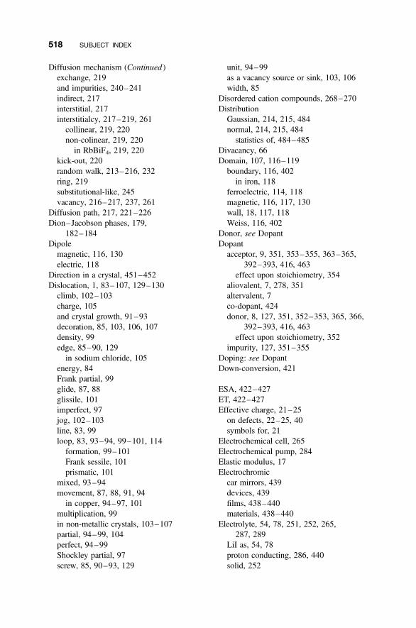
Diffusion mechanism (Continued )exchange, 219and impurities, 240–241indirect, 217interstitial, 217interstitialcy, 217–219, 261
collinear, 219, 220non-colinear, 219, 220
in RbBiF4, 219, 220kick-out, 220random walk, 213–216, 232ring, 219substitutional-like, 245vacancy, 216–217, 237, 261
Diffusion path, 217, 221–226Dion–Jacobson phases, 179,
182–184Dipolemagnetic, 116, 130electric, 118
Direction in a crystal, 451–452Dislocation, 1, 83–107, 129–130climb, 102–103charge, 105and crystal growth, 91–93decoration, 85, 103, 106, 107density, 99edge, 85–90, 129
in sodium chloride, 105energy, 84Frank partial, 99glide, 87, 88glissile, 101imperfect, 97jog, 102–103line, 83, 99loop, 83, 93–94, 99–101, 114
formation, 99–101Frank sessile, 101prismatic, 101
mixed, 93–94movement, 87, 88, 91, 94
in copper, 94–97, 101multiplication, 99in non-metallic crystals, 103–107partial, 94–99, 104perfect, 94–99Shockley partial, 97screw, 85, 90–93, 129
unit, 94–99as a vacancy source or sink, 103, 106width, 85
Disordered cation compounds, 268–270DistributionGaussian, 214, 215, 484normal, 214, 215, 484
statistics of, 484–485Divacancy, 66Domain, 107, 116–119boundary, 116, 402
in iron, 118ferroelectric, 114, 118magnetic, 116, 117, 130wall, 18, 117, 118Weiss, 116, 402
Donor, see DopantDopantacceptor, 9, 351, 353–355, 363–365,
392–393, 416, 463effect upon stoichiometry, 354
aliovalent, 7, 278, 351altervalent, 7co-dopant, 424donor, 8, 127, 351, 352–353, 365, 366,
392–393, 416, 463effect upon stoichiometry, 352
impurity, 127, 351–355Doping: see DopantDown-conversion, 421
ESA, 422–427ET, 422–427Effective charge, 21–25on defects, 22–25, 40symbols for, 21
Electrochemical cell, 265Electrochemical pump, 284Elastic modulus, 17Electrochromiccar mirrors, 439devices, 439films, 438–440materials, 438–440
Electrolyte, 54, 78, 251, 252, 265,287, 289
LiI as, 54, 78proton conducting, 286, 440solid, 252
518 SUBJECT INDEX
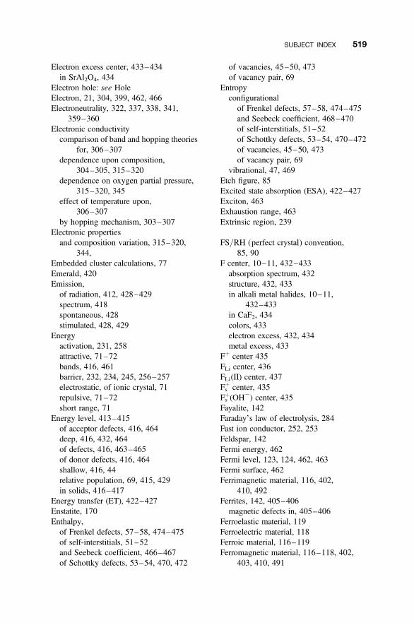
Electron excess center, 433–434in SrAl2O4, 434
Electron hole: see HoleElectron, 21, 304, 399, 462, 466Electroneutrality, 322, 337, 338, 341,
359–360Electronic conductivitycomparison of band and hopping theories
for, 306–307dependence upon composition,
304–305, 315–320dependence on oxygen partial pressure,
315–320, 345effect of temperature upon,
306–307by hopping mechanism, 303–307
Electronic propertiesand composition variation, 315–320,
344,Embedded cluster calculations, 77Emerald, 420Emission,of radiation, 412, 428–429spectrum, 418spontaneous, 428stimulated, 428, 429
Energyactivation, 231, 258attractive, 71–72bands, 416, 461barrier, 232, 234, 245, 256–257electrostatic, of ionic crystal, 71repulsive, 71–72short range, 71
Energy level, 413–415of acceptor defects, 416, 464deep, 416, 432, 464of defects, 416, 463–465of donor defects, 416, 464shallow, 416, 44relative population, 69, 415, 429in solids, 416–417
Energy transfer (ET), 422–427Enstatite, 170Enthalpy,of Frenkel defects, 57–58, 474–475of self-interstitials, 51–52and Seebeck coefficient, 466–467of Schottky defects, 53–54, 470, 472
of vacancies, 45–50, 473of vacancy pair, 69
Entropyconfigurational
of Frenkel defects, 57–58, 474–475and Seebeck coefficient, 468–470of self-interstitials, 51–52of Schottky defects, 53–54, 470–472of vacancies, 45–50, 473of vacancy pair, 69
vibrational, 47, 469Etch figure, 85Excited state absorption (ESA), 422–427Exciton, 463Exhaustion range, 463Extrinsic region, 239
FS/RH (perfect crystal) convention,85, 90
F center, 10–11, 432–433absorption spectrum, 432structure, 432, 433in alkali metal halides, 10–11,
432–433in CaF2, 434colors, 433electron excess, 432, 434metal excess, 433
Fþ center 435FLi center, 436FLi(II) center, 437Fsþ center, 435
Fsþ(OH2) center, 435
Fayalite, 142Faraday’s law of electrolysis, 284Fast ion conductor, 252, 253Feldspar, 142Fermi energy, 462Fermi level, 123, 124, 462, 463Fermi surface, 462Ferrimagnetic material, 116, 402,
410, 492Ferrites, 142, 405–406magnetic defects in, 405–406
Ferroelastic material, 119Ferroelectric material, 118Ferroic material, 116–119Ferromagnetic material, 116–118, 402,
403, 410, 491
SUBJECT INDEX 519
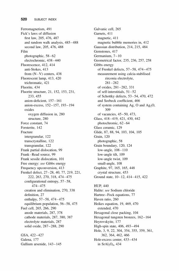
Ferromagnetism, 491Fick’s laws of diffusionfirst law, 205, 476, 487and random walk analysis, 485–488second law, 205, 476, 488
Filmphotographic, 58–62electochromic, 438–440
Fluorescence, 412, 414anti-Stokes, 413from (N–V) centers, 438
Fluorescent lamp, 413, 420trichromatic, 421
Fluorite, 434Fluorite structure, 21, 152, 153, 231,
233, 455anion-deficient, 157–161anion-excess, 152–157, 193–194oxides
oxygen diffusion in, 280structure, 280
Force constant, 74Forsterite, 142Fractureintergranular, 122transcrystalline, 122transgranular, 122
Frank partial dislocation, 99Frank–Read source, 99Frank sessile dislocation, 101Free energy: see Gibbs energyFrequency upconversion, 413Frenkel defect, 27–28, 40, 77, 219, 221,
222, 263, 270, 318, 474–475configurational entropy, 57–58,
474–475creation and elimination, 270, 338definition, 27enthalpy, 57–58, 474–475equilibrium population, 56–58, 475
Fuel cell, 265, 266, 290anode materials, 287, 378cathode materials, 287, 380, 387electrolyte materials, 287solid oxide, 287–288, 290
GSA, 422–427Galena, 177Gallium arsenide, 143–145
Galvanic cell, 265Garnets, 411magnetic, 411magnetic bubble memories in, 412
Gaussian distribution, 214, 215, 484Gemstones, 417Germanium, 7–10Geometrical factor, 235, 236, 257, 258Gibbs energyof Frenkel defects, 57–58, 474–475measurement using calcia-stabilised
zirconia electrolyte,281–282
of oxides, 281–282, 331of self-interstitials, 51–52of Schottky defects, 53–54, 470, 472and Seebeck coefficient, 466of system containing Ag, O and Ag2O,
309of vacancies, 45–50, 473,
Glass, 418–419, 421, 430, 442photochromic, 62–64
Glass ceramic, 129Glide, 87, 88, 94, 103, 104, 105Grain, 120photographic, 58
Grain boundary, 120, 124low-angle, 108–110low-angle tilt, 109low-angle twist, 109small-angle, 108
Graphite, 97, 165, 165, 448crystal structure, 453
Ground state, 10–12, 414–415, 422
HUP, 440Halite: see Sodium chlorideHartree–Fock equations, 77Haven ratio, 260Heikes equation, 19, 469, 470extended, 470
Hexagonal close packing, 104Hexagonal tungsten bronzes, 162–164Heyrovskyite, 177High-spin state, 406, 493–494Hole, 3, 9, 22, 304, 354, 355, 359, 361,
362, 364, 462, 466Hole-excess center, 433–434in SrAl2O4, 434
520 SUBJECT INDEX
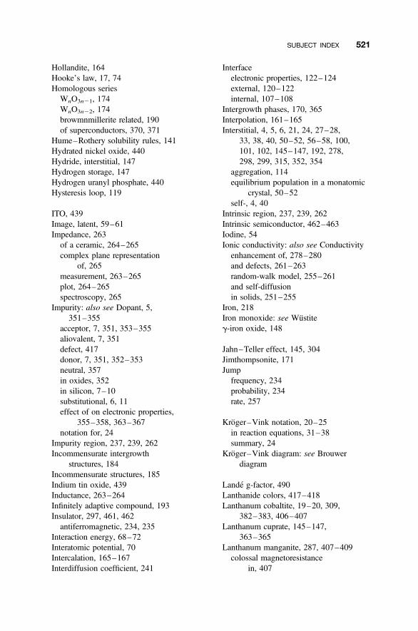
Hollandite, 164Hooke’s law, 17, 74Homologous seriesWnO3n21, 174WnO3n22, 174browmnmillerite related, 190of superconductors, 370, 371
Hume–Rothery solubility rules, 141Hydrated nickel oxide, 440Hydride, interstitial, 147Hydrogen storage, 147Hydrogen uranyl phosphate, 440Hysteresis loop, 119
ITO, 439Image, latent, 59–61Impedance, 263of a ceramic, 264–265complex plane representation
of, 265measurement, 263–265plot, 264–265spectroscopy, 265
Impurity: also see Dopant, 5,351–355
acceptor, 7, 351, 353–355aliovalent, 7, 351defect, 417donor, 7, 351, 352–353neutral, 357in oxides, 352in silicon, 7–10substitutional, 6, 11effect of on electronic properties,
355–358, 363–367notation for, 24
Impurity region, 237, 239, 262Incommensurate intergrowth
structures, 184Incommensurate structures, 185Indium tin oxide, 439Inductance, 263–264Infinitely adaptive compound, 193Insulator, 297, 461, 462antiferromagnetic, 234, 235
Interaction energy, 68–72Interatomic potential, 70Intercalation, 165–167Interdiffusion coefficient, 241
Interfaceelectronic properties, 122–124external, 120–122internal, 107–108
Intergrowth phases, 170, 365Interpolation, 161–165Interstitial, 4, 5, 6, 21, 24, 27–28,
33, 38, 40, 50–52, 56–58, 100,101, 102, 145–147, 192, 278,298, 299, 315, 352, 354
aggregation, 114equilibrium population in a monatomic
crystal, 50–52self-, 4, 40
Intrinsic region, 237, 239, 262Intrinsic semiconductor, 462–463Iodine, 54Ionic conductivity: also see Conductivityenhancement of, 278–280and defects, 261–263random-walk model, 255–261and self-diffusionin solids, 251–255
Iron, 218Iron monoxide: see Wustiteg-iron oxide, 148
Jahn–Teller effect, 145, 304Jimthompsonite, 171Jumpfrequency, 234probability, 234rate, 257
Kroger–Vink notation, 20–25in reaction equations, 31–38summary, 24
Kroger–Vink diagram: see Brouwerdiagram
Lande g-factor, 490Lanthanide colors, 417–418Lanthanum cobaltite, 19–20, 309,
382–383, 406–407Lanthanum cuprate, 145–147,
363–365Lanthanum manganite, 287, 407–409colossal magnetoresistance
in, 407
SUBJECT INDEX 521
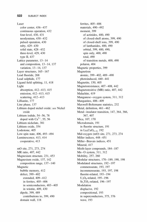
Lasercolor center, 436–437continuous operation, 432four-level, 430, 431neodymium, 430–432pulsed operation, 430ruby, 429–430solid state, 428–432three-level, 429, 430type II, 437
Lattice parameter, 13–14and composition, 13–14, 137variation, 13–14, 137
Layer structures, 165–167Lead fluoride, 268Lead sulphide, 177Ligand field splitting, 11, 418Lightabsorption, 412–413, 415emission, 412–413, 415scattering, 412–413
Lillianite, 177Line phase, 137Lithium doped nickel oxide: see Nickel
oxideLithium iodide, 54–56, 78doped with Ca2þ, 55, 56
Lithium nickelate, 381Lithium oxide, 354Lodestone, 405Low-spin state, 406, 493–494Luminescence, 413, 414cooperative, 413
mO site, 271, 273, 274MR ratio, 407, 442Magnesium structure, 231, 453Magnesium oxide, 137, 142composition range, 137–140
Magneticbubble memory, 412defect, 399–402
extended, 409–412in ferrites, 405–406in semiconductors, 403–405in wustite, 409, 430
dipole, 399, 489contributions to, 399, 490
domain wall, 118
ferrites, 405–406materials, 490–492moment, 399
of actinides, 400, 490of closed-shell atoms, 399, 490of closed-shell ions, 399, 490of lanthanides, 400, 490orbital, 399, 400, 490,spin only, 400, 490total, 490of transition metals, 400, 490
polaron, 404Magnetic properties, 399Magnetismatomic, 399–402, 489–490photoinduced, 440–441
Magnetite, 150, 405Magnetoresistance, 407–408, 442Magnetoresitive (MR) ratio, 407, 442Malachite, 419Manganese–oxygen system, 311, 312Manganites, 406–409Maxwell-Boltzmann statistics, 232Metal, definition, 461–462Metal–insulator transition, 147, 364, 366,
367, 407Mica, 107, 170Microdomain, 191in fluorite structure, 191in La2CuO4þd, 192
Mid-oxygen (mO) site, 271, 273, 274Miller indices, 448–451Miller–Bravais indices, 451Mineral, 417Misfit-layer compounds, 184–187Mn–O system, 311, 312Mobility, 257, 260Modular structures, 170–189, 190, 198Modulated structures, 192–197commensurate, 193, 197incommensurate, 193, 197, 198fluorite-related, 193–194U3O8-related, 195–196SrxTiS3-related, 196–197
Modulationdisplacive, 192compositional, 193in superconductors, 375, 376wave, 193
522 SUBJECT INDEX
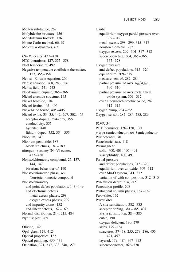
Molten sub-lattice, 269Molybdenite structure, 456Molybdenum trioxide, 176Monte Carlo method, 66, 67Molecular dynamics, 67
(N–V) center, 437–438NTC thermistor, 127, 355–358Neel temperature, 492Negative temperature coefficient thermistor,
127, 355–358Nernst–Einstein equation, 260Nernst equation, 268, 283, 386Nernst field, 241–243Neodymium cuprate, 365–366Nickel arsenide structure, 165Nickel bromide, 104Nickel ferrite, 405–406Nickel-zinc ferrite, 405–406Nickel oxide, 33–35, 142, 297, 302, 465acceptor doping, 354–355, 356conductivity, 355hydrated, 440lithium doped, 352, 354–355
Niobium, 147Niobium pentoxide, 187block structures, 187–189
nitrogen–vacancy (N–V) center,437–438
Nonstoichiometric compound, 25, 137,144, 147
bivariant behaviour of, 190Nonstoichiometric phase: see
Nonstoichiometric compoundNonstoichiometryand point defect populations, 143–149and electronic defects
metal excess phases, 298oxygen excess phases, 299
and impurity atoms, 132and linear defects, 167–169
Normal distribution, 214, 215, 484Nyquist plot, 265
Olivine, 142Opal glass, 129, 412Optical properties, 122Optical pumping, 430, 431Oxidation, 321, 337, 338, 340, 359
Oxideequilibrium oxygen partial pressure over,
309–312metal excess, 298–299, 315–317nonstoichiometric, 282oxygen excess, 299–301, 317–318superconducting, 364, 365–366,
367–378Oxygen pressureand defect populations, 315–320equilibrium, 309–315measurement of, 282–284partial pressure of over Ag/Ag2O,
309–310partial pressure of over metal/metal
oxide system, 309–312over a nonstoichiometric oxide, 282,
312–315Oxygen pump, 284–285Oxygen sensor, 282–284, 285, 289
P2VP, 54PCT thermistor, 126–128, 130p-type semiconductor: see SemiconductorPair potential, 70Paraelectric state, 118Paramagneticsolid, 400, 403, 490–491susceptibility, 400, 491
Partial pressureand defect populations, 315–320equilibrium over an oxide, 309–312over Mn-O system, 311, 312variation of with composition, 312–315
Penetration depth, 214, 215Penetration profile, 208Pentagonal column phases, 167–169Perovskite, 162PerovskitesA-site substitution, 382–383acceptor doping, 381–385, 407B-site substitution, 384–385cubic, 190oxygen deficient, 190, 279slabs, 179–184structures, 37–38, 255, 279, 286, 406,
421, 457layered, 179–184, 367–373superconductors, 367–378
SUBJECT INDEX 523
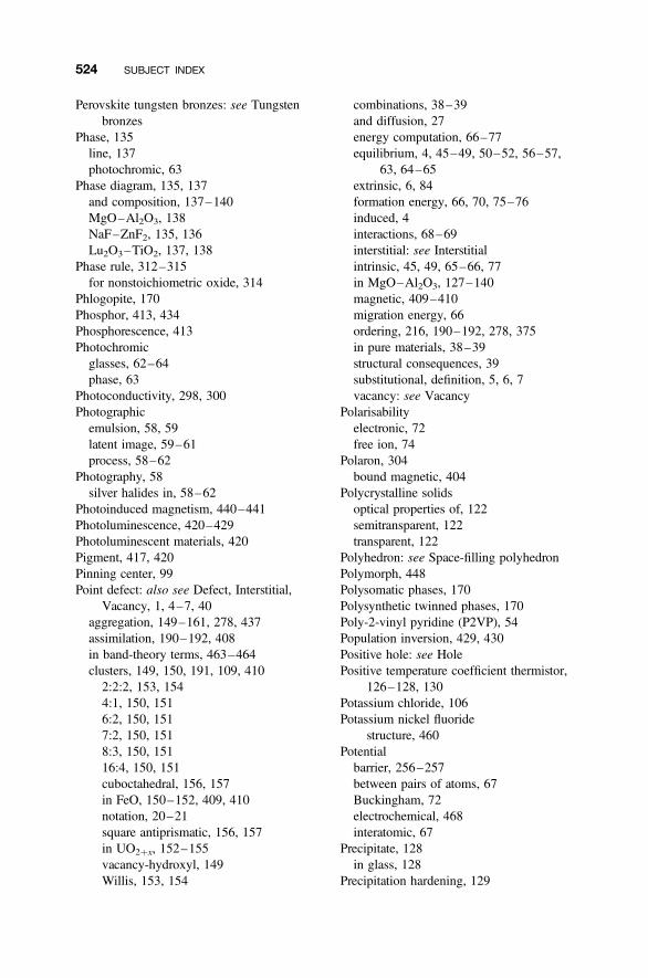
Perovskite tungsten bronzes: see Tungstenbronzes
Phase, 135line, 137photochromic, 63
Phase diagram, 135, 137and composition, 137–140MgO–Al2O3, 138NaF–ZnF2, 135, 136Lu2O3–TiO2, 137, 138
Phase rule, 312–315for nonstoichiometric oxide, 314
Phlogopite, 170Phosphor, 413, 434Phosphorescence, 413Photochromicglasses, 62–64phase, 63
Photoconductivity, 298, 300Photographicemulsion, 58, 59latent image, 59–61process, 58–62
Photography, 58silver halides in, 58–62
Photoinduced magnetism, 440–441Photoluminescence, 420–429Photoluminescent materials, 420Pigment, 417, 420Pinning center, 99Point defect: also see Defect, Interstitial,
Vacancy, 1, 4–7, 40aggregation, 149–161, 278, 437assimilation, 190–192, 408in band-theory terms, 463–464clusters, 149, 150, 191, 109, 410
2:2:2, 153, 1544:1, 150, 1516:2, 150, 1517:2, 150, 1518:3, 150, 15116:4, 150, 151cuboctahedral, 156, 157in FeO, 150–152, 409, 410notation, 20–21square antiprismatic, 156, 157in UO2þx, 152–155vacancy-hydroxyl, 149Willis, 153, 154
combinations, 38–39and diffusion, 27energy computation, 66–77equilibrium, 4, 45–49, 50–52, 56–57,
63, 64–65extrinsic, 6, 84formation energy, 66, 70, 75–76induced, 4interactions, 68–69interstitial: see Interstitialintrinsic, 45, 49, 65–66, 77in MgO–Al2O3, 127–140magnetic, 409–410migration energy, 66ordering, 216, 190–192, 278, 375in pure materials, 38–39structural consequences, 39substitutional, definition, 5, 6, 7vacancy: see Vacancy
Polarisabilityelectronic, 72free ion, 74
Polaron, 304bound magnetic, 404
Polycrystalline solidsoptical properties of, 122semitransparent, 122transparent, 122
Polyhedron: see Space-filling polyhedronPolymorph, 448Polysomatic phases, 170Polysynthetic twinned phases, 170Poly-2-vinyl pyridine (P2VP), 54Population inversion, 429, 430Positive hole: see HolePositive temperature coefficient thermistor,
126–128, 130Potassium chloride, 106Potassium nickel fluoride
structure, 460Potentialbarrier, 256–257between pairs of atoms, 67Buckingham, 72electrochemical, 468interatomic, 67
Precipitate, 128in glass, 128
Precipitation hardening, 129
524 SUBJECT INDEX
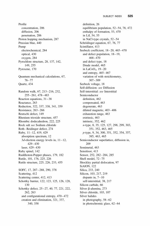
Profileconcentration, 206diffusion, 206penetration, 206
Proton hopping mechanism, 287Prussian blue, 440Pumpelectrochemical, 284optical, 430oxygen, 284
Pyrochlore structure, 28, 137, 142,149, 255
Pyroxene, 170
Quantum mechanical calculations, 67,76–77
Quartz, 434
Random walk, 67, 213–216, 232,255–261, 478–483
Reaction equations, 31–38Reactance, 263Reduction, 322, 337, 338, 341, 359Resistance, 263–266Reutschi defect, 149Rhenium trioxide structure, 457Rhombic dodecahedron, 222, 225Rock salt see Sodium chlorideRoth–Reidinger defect, 274Ruby, 11–12, 419, 429absorption spectrum, 123d-electron energy levels in, 11–12,
429–430laser, 429–430
Ruby spinel, 142Ruddleston-Popper phases, 179, 182Rutile, 101, 176, 225, 226Rutile structure, 225, 226, 233, 455
SOFC, 17, 287–288, 290, 378Scattering, 412Scattering center, 412, 413Schottky barrier, 122, 123, 125, 126, 128,
130Schottky defect, 25–27, 40, 77, 221, 222,
262, 263and configurational entropy, 470–472creation and elimination, 321, 337,
340, 358
definition, 26equilibrium population, 52–54, 78, 472enthalpy of formation, 53, 470in LiI, 54, 55in NaCl-type crystals, 52–54
Schrodinger equation, 67, 76, 77Scintillator, 413Seebeck coefficient, 18–20, 465–470and defect population, 18–19,
468–470and defect type, 18Drude model, 465in LaCoO3, 19–20and entropy, 465–467variation of with stoichiometry,
307–309Seebeck voltage, 18Self-diffusion: see DiffusionSelf-interstitial: see InterstitialSemiconductordefinition, 462compensated, 463degenerate, 463diluted magnetic, 403–406exhaustion range, 463extrinsic, 463intrinsic, 352, 462n-type, 8, 35, 125, 127, 298, 299, 303,
351, 352, 463, 465p-type, 9, 34, 300, 351, 352, 354, 357,
385, 463, 465Semiconductor superlattice, diffusion in,
209Semimetal, 463Sensitisor, 413Sensor, 252, 282–284, 285Shell model, 72–75Shockley partial dislocation, 97SiAlON, 122Silica, 233, 240Silicon, 103, 217, 219dopants in, 7–10self-interstitial, 38, 217
Silicon carbide, 66Silver b-alumina, 273Silver chloride, 103, 107Silver halidesin photography, 58–62in photochromic glass, 62–64
SUBJECT INDEX 525
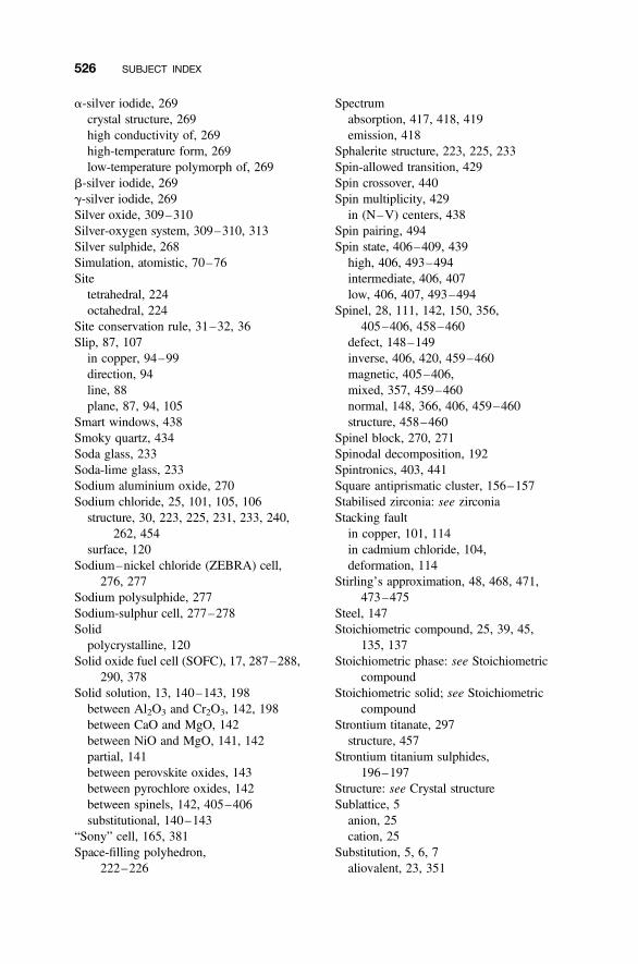
a-silver iodide, 269crystal structure, 269high conductivity of, 269high-temperature form, 269low-temperature polymorph of, 269
b-silver iodide, 269g-silver iodide, 269Silver oxide, 309–310Silver-oxygen system, 309–310, 313Silver sulphide, 268Simulation, atomistic, 70–76Sitetetrahedral, 224octahedral, 224
Site conservation rule, 31–32, 36Slip, 87, 107in copper, 94–99direction, 94line, 88plane, 87, 94, 105
Smart windows, 438Smoky quartz, 434Soda glass, 233Soda-lime glass, 233Sodium aluminium oxide, 270Sodium chloride, 25, 101, 105, 106structure, 30, 223, 225, 231, 233, 240,
262, 454surface, 120
Sodium–nickel chloride (ZEBRA) cell,276, 277
Sodium polysulphide, 277Sodium-sulphur cell, 277–278Solidpolycrystalline, 120
Solid oxide fuel cell (SOFC), 17, 287–288,290, 378
Solid solution, 13, 140–143, 198between Al2O3 and Cr2O3, 142, 198between CaO and MgO, 142between NiO and MgO, 141, 142partial, 141between perovskite oxides, 143between pyrochlore oxides, 142between spinels, 142, 405–406substitutional, 140–143
“Sony” cell, 165, 381Space-filling polyhedron,
222–226
Spectrumabsorption, 417, 418, 419emission, 418
Sphalerite structure, 223, 225, 233Spin-allowed transition, 429Spin crossover, 440Spin multiplicity, 429in (N–V) centers, 438
Spin pairing, 494Spin state, 406–409, 439high, 406, 493–494intermediate, 406, 407low, 406, 407, 493–494
Spinel, 28, 111, 142, 150, 356,405–406, 458–460
defect, 148–149inverse, 406, 420, 459–460magnetic, 405–406,mixed, 357, 459–460normal, 148, 366, 406, 459–460structure, 458–460
Spinel block, 270, 271Spinodal decomposition, 192Spintronics, 403, 441Square antiprismatic cluster, 156–157Stabilised zirconia: see zirconiaStacking faultin copper, 101, 114in cadmium chloride, 104,deformation, 114
Stirling’s approximation, 48, 468, 471,473–475
Steel, 147Stoichiometric compound, 25, 39, 45,
135, 137Stoichiometric phase: see Stoichiometric
compoundStoichiometric solid; see Stoichiometric
compoundStrontium titanate, 297structure, 457
Strontium titanium sulphides,196–197
Structure: see Crystal structureSublattice, 5anion, 25cation, 25
Substitution, 5, 6, 7aliovalent, 23, 351
526 SUBJECT INDEX
Superconductor, 147, 364, 366, 411antiferromagnetic, 374charge reservoir, 367, 369crystal structures, 367–370, 373cuprate, 367–378defect structures, 373–378electron, 366high temperature, 367–378hole, 364hole doping, 370–373, 411homologous series, 370, 371perovskite-structure related, 367–370phase diagram, 374, 375transition temperature, 364, 366
Super-ionic conductor, 352Surface, 412electronic properties, 122–124external, 120–122internal, 107–116, 412structure, 120
Systembivariant, 314lead sulphide–bismuth sulphide
(PbS–Bi2S3), 177, 180lutetium oxide–titanium dioxide
(Lu2O3–TiO2), 137, 138magnesium oxide–aluminium oxide
(MgO–Al2O3), 137, 138magnesium oxide–calcium oxide
(MgO–CaO), 142magnesium oxide–nickel oxide
(MgO–NiO), 142manganese–oxygen (Mn–O), 311, 312silver–oxygen (Ag–O), 309–310sodium fluoride–zinc fluoride
(NaF–ZnF2), 135–137tantanlum pentoxide–tungsten trioxide
(Ta2O5–WO3), 195–196univariant, 313yttrium oxyfluoride–yttrium fluoride
(YOF-YF3), 193–194
T structure, 363T/O structure, 363T0 structure, 365Tetragonal tungsten bronze structure,
162–164Tetramethyl ammonium silver
iodide, 269
Thermistor, 355–358bead, 355, 356constant, 358n-type, 356negative temperature coefficient,
355–358NCT, 355–358, 393,p-type, 356positive temperature coefficient,
126–128, 130PCT, 126–128, 130
defect structure, 126–128dopant in, 127, 128point defects in, 127
resistance, 358, 393temperature coefficient of
resistance, 358Thermoelectric properties, 18Tin disulphide, 104Titanium dioxide, 26, 453, 465rutile form, 453
Titanium sulphides, 144, 165Tracer diffusion coefficient, 207–208Tracer species, 207–208Transitioninterband, 416, 464non-magnetic to magnetic,
440–441non-radiative, 412, 429phonon assisted, 412, 429spin-allowed, 420
Transition metalions, 492–494
colors, 417–420oxides in terms of band theory, 461,
464–465Transport number, 253–255, 302,
390–391determination using a solid state
electrolyte, 386–387of halides, 254, 255of oxides, 255of sulphides, 255
Trapping center: see Color centerTridymite, 434Tropochemical cell-twinned
phases, 170Tungsten, 217Tungsten structure, 231, 453
SUBJECT INDEX 527
Tungsten bronzes, 162–164, 438color of, 438cubic, 162, 438hexagonal, 162, 163hydrogen, 439lithium, 162tetragonal, 162, 163, 167sodium, 162perovskite, 162, 438
Tungsten trioxide, 171–176, 438–439Tweed microstructure, 192Twinboundary, 110–114growth, 111mechanical, 112
in V2O5, 112plane, 110, 176polysynthetic, 110reflection, 110transformation, 114
Twinningand composition variation, 176–179chemical: see Chemical twinningin PbS-Bi2S3 sulphosalts,
177–179, 180in superconductors, 375, 377–378in YBa2Cu3O7, 377–378f101g planes in rutile, 110, 177
Unit cell, 13–14, 447cubic (isometric), 448tetragonal, 448orthorhombic, 448monoclinic, 448triclinic, 448hexagonal, 448rhombohedral, 448
Unit cell parameters: see Latticeparameters
Univariant system, 313Up-conversion, 413, 415, 421–428in CeO2, 422–427efficiency, 421, 427–428energy, 422intensity of output, 422two-frequency, 428
Uranium dioxide, 14, 152–155hyperstoichiometric, 14,
152–155
Vacancy, 4, 5, 21, 40, 99–101, 145,278, 298, 299, 316, 361, 362, 363,364, 408
anion, 25, 26, 278, 298, 352creation and elimination of, 358definition of, 4cation, 25, 26, 299, 302, 352equilibrium population in a monatomic
crystal, 45–50notation, 4, 5, 20–21, 24ordered, 160, 190–192
Vacancy diffusion, 216–217, 237, 261Vacancy pair, 21, 66diffusion of, 221, 223, 275–276
Valence induction, 351, 366Valence band, 9, 416, 462Vanadium, 403Vanadium pentoxide, 112, 113van der Waals attraction, 72Variance, 312Varistor, 124–126microstructure, 125
Vegard’s law, 13–14Vernier structures, 193fluorite related, 193–194
Vibration frequency, 256Vibrational entropy, 47, 469Volume, 16–17Volume defect, 1, 3, 128–129
Wadsley defect, 187Weiss domain, 116, 402Willis 2:2:2 cluster, 153Wurtzite structure, 225, 226, 454Wustiteantiferromagnetic structure, 409, 410,composition range, 14–15, 150experimental and theoretical
densities of, 14–15magnetic defect clusters, 409, 410point defects in, 14–15point defect clusters in, 150–152,
409
X-ray diffraction, 135
Young’s modulus, 17Yttria-stabilised zirconia:
see Zirconia
528 SUBJECT INDEX

Yttrium aluminium garnet, 430Yttrium barium copper oxide
(YBa2Cu3O6þx), 371, 372–373,374–377, 378
ZEBRA cell, 276, 277Zinc blende structure, 223, 225, 454Zinc oxide, 124, 149, 303defect structure, 147–148
luminescence of thin films, 417Zinc selenide, 25Zirconia, 157calcia-stabilised, 17, 36–37,
159, 255, 278, 280–285,287, 289
yttria-stabilised, 17, 159, 280,287, 289
Zirconium dioxide: see Zirconia
SUBJECT INDEX 529