native defects and complexes in sic
TRANSCRIPT

INSTITUTE OF PHYSICS PUBLISHING JOURNAL OF PHYSICS: CONDENSED MATTER
J. Phys.: Condens. Matter 13 (2001) 9027–9037 PII: S0953-8984(01)24507-X
Native defects and complexes in SiC
F Bechstedt, A Fissel, J Furthmuller, U Grossner and A Zywietz
Institut fur Festkorpertheorie und Theoretische Optik, Friedrich-Schiller-Universitat, 07743 Jena,Germany
Received 2 May 2001Published 20 September 2001Online at stacks.iop.org/JPhysCM/13/9027
AbstractPrototypical native defects, in particular monovacancies, are studied usingab initio density functional theory and the local spin-density approximation.Several properties such as the energetics, geometry, electronic structure, andspin states are discussed regarding their dependence on the chemical nature,the preparation conditions, and the polytype of the SiC crystal. Consequencesof the defects are derived for the doping behaviour, electrical properties, andphotoluminescence spectra.
1. Introduction
The physical properties of silicon carbide (SiC) make this wide-band-gap semiconductor wellsuited for high-temperature, high-power, and high-frequency applications. A striking propertyof SiC is its polytypism. The compound exists in more than 200 different polytypes of whichthe 3C, 4H, 6H, and 15R structures are the most common [1]. The accompanying variationof the indirect fundamental gap between 2.39 eV (3C) and 3.26 eV (4H) [2] makes SiC alsointeresting for application in heterostructure devices, e.g. in twinning superlattices [3].
Defects and their complexes play an important role. To a great extent the electrical andoptical properties of SiC are governed by native defects, which also exhibit interesting physicsof their own. They are observed in as-grown crystals and layers as well as in irradiatedsamples. The monovacancies are prototypical examples in this respect. In SiC the situationis markedly different from that encountered in common semiconductors like silicon. Becauseof the stronger chemical bonding in this hard compound, the mobility of such point defects isreduced. They are thermally stable at room temperature, and far above [4]. In contrast to thecase of silicon, antisites also occur in the compound semiconductor SiC. These native pointdefects can give rise to energy levels in the fundamental gap and, hence, exist in differentcharge states [5, 6]. Consequently, they may influence the doping efficiency [7].
Strong indications for certain defects or defect complexes come from characteristic sharplines in photoluminescence (PL) spectra. One prototypical defect responsible for such emissionlines in the low-temperature PL spectra is the so-called D1 centre [8]. Its fingerprint is anefficient luminescence at a photon energy 0.35–0.45 eV below the excitonic gap independentof the polytype. The most important L1 line is followed by characteristic phonon-assisted
0953-8984/01/409027+11$30.00 © 2001 IOP Publishing Ltd Printed in the UK 9027
9028 F Bechstedt et al
structures [9]. It has been observed for different polytypes after irradiation [9–13], but also foras-grown material after quenching from the growth temperature and epitaxial layers grown bychemical vapour deposition (CVD) or solid-source molecular beam epitaxy (MBE) [14–16].For 4H-SiC the L1 line appears at about 2.901 eV [11, 12], whereas 3C-SiC shows thisline at about 1.972 eV [17]. Other strong indications for a native defect, perhaps a siliconvacancy [18], are the characteristic PL bands with no-phonon lines at 1.121 eV for 3C-SiC [19], 1.438 and 1.352 eV for 4H-SiC [20, 21], or 1.433, 1.398, and 1.368 eV for 6H-SiC [20, 21]. In contrast to the positions of the L1 lines, these PL bands depend only weaklyon the polytype.
Besides the direct influence on the doping efficiency [7] of e.g. donating electrons [5],native defects may influence the effect of dopants by forming complexes. One exampleconcerns the interpretation of the deep boron acceptor as a boron (B) on a silicon positionwith an adjacent vacancy [22, 23]. There is also a shallow boron acceptor, the geometry andthe sublattice site, BSi or BC, of which are under discussion [24,25]. There are indications thatthe preferential occupation of a Si or C site depends on the preparation conditions, i.e. C-richor Si-rich conditions [24, 26]. These findings seem to be in agreement with results of C/Bcoimplantation experiments [27].
In the present paper we discuss the relationship between energetics, geometry, andelectronic states for native defects in 3C- and 4H-SiC. Monovacancies are considered asprototypical defects, but antisites are also studied. B atoms adsorbed at a surface are consideredas defect complexes. The computational method is described in section 2. The followingsections 3 and 4 discuss the formation of native defects and the resulting electronic states.This is completed by studies of boron at surfaces in section 5. Finally, a brief summaryis given.
2. Computational method
The calculations are based on density functional theory (DFT) [28] in the local spin-densityapproximation (LSDA) [29]. Explicitly we use the Vienna Ab initio Simulation Package(VASP) [30]. The interaction of the valence electrons with the atomic cores is treated usingnon-norm-conserving Vanderbilt pseudopotentials [31]. Their supersoftened form is especiallyimportant for the treatment of first-row elements such as C and B. It allows the restriction ofthe plane-wave expansion of the single-particle eigenfunctions to a cut-off energy of 13.4 Ryd.This corresponds to about 55 plane waves per atom. Exchange and correlation are described inthe parametrization of Perdew and Zunger [32]. In order to avoid partial errors due to the useof frozen cores, non-linear core corrections are included. For arbitrary spin polarization thecorrelation energy is interpolated between the non-polarized and fully polarized case as for theexchange energy [33]. The method described gives for the defect-free polytypes 3C and 4Hlattice constants slightly smaller than the experimental ones. The cubic lattice constant of thezinc-blende polytype with T2
d symmetry amounts to a0 = 4.332 Å, whereas the two hexagonallattice constants of 4H-SiC (C4
6v) are a = 3.061 Å and c = 10.013 Å. The internal deform-ations of the bonding tetrahedra are small (see [34]). Without quasiparticle corrections [35]DFT-LDA gives the values 1.33 eV (3C-SiC) and 2.23 eV (4H-SiC) for the energy gaps whichare about 1 eV smaller than the experimental energies [2].
Extremely large supercells with 216 atoms (3C) or 128 atoms (4H) are treated to avoidtoo strong defect–defect interactions and electrostatic effects. The total-energy minimizationwith respect to the atomic coordinates is performed by a conjugate-gradient technique [30].Within the structural optimization a 2 × 2 × 2 special-point mesh [36] is used for the k-space
Native defects and complexes in SiC 9029
sampling. In order to describe excited defect states we take into account the constraint of ahole in the lowest a1-derived single-particle defect state. However, the effects of the excitationas well as of the spin polarization are described restricting the sampling to the � point. Theinfluence of unphysical k-induced splittings and dispersions is suppressed in this way. Detailsof the computational method can be found in reference [5]. In the case of B adsorption theSi-terminated SiC(111) surfaces are modelled by repeated slabs containing six Si–C bilayersand a vacuum region of the same thickness. The C-terminated bottom layers of the slabs aresaturated with atomic hydrogen [37]. In the case of a two-dimensional
√3 × √
3 translationalsymmetry, supercells with effectively 72 atoms are taken into account.
3. Formation of charged native defects
First, we consider monovacancies Vq
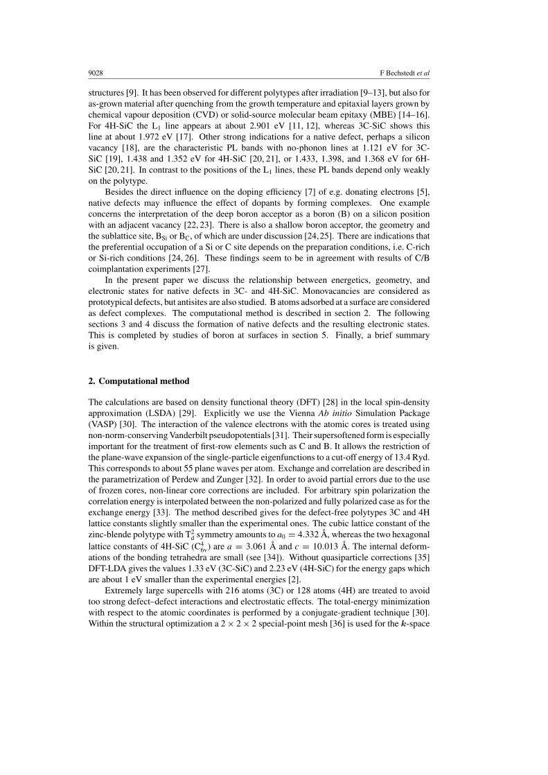
X in the charge states q = 2+, +, 0, −, 2−. Independentof the polytype, 3C or 4H, the ground state of a C-site vacancy generally exhibits a remarkableJahn–Teller distortion apart from the double positively charged one. This can be easilyexplained for the cubic polytype. However, disregarding the small deformations of the bondingtetrahedra, locally the same happens also in the 4H case. There is a tendency for relaxationtowards D2d symmetry as a consequence of a pairing mode. The Si dangling bonds of the Cvacancy overlap partially. In addition to an inward (positively charged) or outward (negativelycharged) breathing relaxation, the defect systems gain energy by formation of bonded pairs offirst-nearest-neighbour atoms. This is demonstrated in figure 1. Lowering the local symmetryfrom Td to D2d, the threefold-degenerate t2 defect level (without spin) splits into a lowerb2 state and a higher twofold-degenerate e state. This mechanism occurs for V+
C, V0C, and
V−C . Further local symmetry reductions do not occur for V2−
C . In 3C the additional electronsoccupy conduction band states. Hence, negatively charged carbon vacancies do not exist in
� �
Figure 1. Contour plots of the square of the wave function of the highest occupied defect state ofV0
C in 3C-SiC in a plane perpendicular to a cubic direction. Two local symmetries Td and D2d areallowed.
(This figure is in colour only in the electronic version)

9030 F Bechstedt et al
3C. However, they occur in the 4H case with a wider energy gap. Additionally, the crystal-fieldsplitting acts in the hexagonal polytype.
V2+C exhibits a huge inward breathing mode, whereas V0
C shows the above-mentionedpronounced pairing mechanism. The large geometrical changes in the V0
C and V2+C cases in
comparison to the intermediate charge state q = + result in a negative-U behaviour [38]. Wecalculate a Hubbard U = Etot (V2+
C )+Etot (V0C)−2Etot (V+
C) = −0.35 eV [39]. Consequently,the single positively charged C vacancy should be unstable in thermodynamic equilibrium.For 4H-SiC we calculate similar values, U = −0.29 and −0.24 eV, depending on the cubic(k) or hexagonal (h) lattice site [5]. However, because of the larger energy gap, the doublenegatively charged vacancy can also occur as a stable defect. As a consequence one observesa negative-U behaviour with U = −0.29 eV independent of the lattice site also for the defectswith additional electrons.
The situation is quite different for the Si-site vacancies [5, 40]. Because of the stronglocalization of the C dangling bonds and the SiC lattice constant, only an outward breathingrelaxation may occur [41]. The defect system can gain additional energy by a spin splittingof the t2 levels. In the case of the single positively charged, neutral, and negatively chargedSi-site vacancies, high-spin states are predicted independent of the polytype in agreement withHund’s rule. The total spins S = 0 (V2+
Si ), 1/2 (V+Si), 1 (V0
Si), 3/2 (V−Si), and 1 (V2−
Si ) are obtainedfor the ground states [5, 40]. Meanwhile, there is reason to doubt the DFT-LSDA result ofa 3T1 ground state for the neutral Si vacancy, at least in the 3C-SiC case [42]. More carefulLSDA studies end up with a mixed-spin state, 1E + 3T1 [43]. However, because of principallimitations of the DFT-LSDA a pure-spin multiplet 1E cannot be derived. Fortunately, despitethe spin problem the results for the atomic geometry and the energetics do not change verymuch. We estimate an energy difference between 1E and 3T1 of about 0.04 eV, which slightlyincreases upon inclusion of gradient corrections in the exchange–correlation energy.
In thermal equilibrium the concentrations of the defects are mainly determined by theirformation energies. We adapt the formalism of Zhang and Northrup [44]. All chemicalpotentials and heats of formation are taken from ab initio calculations as described in section 2.The Fermi level EF is allowed to vary in an interval defined by the experimental gap energyEg [2]. Results for 3C-SiC are presented in figure 2. The results for 4H-SiC are rather similar.There is only a small difference in vacancy formation on cubic and hexagonal sites. In general,
0 1
EF/E
g
0
5
10
15
For
mat
ion
ener
gy (
eV)
C-rich
++
+
0
-
--
++
+
0
---
0 1
EF/E
g
0
5
10
15
For
mat
ion
ener
gy (
eV)
Si-rich
++
+
0
-
--
++
+
0
-
--
Figure 2. Formation energies of C (solid lines) and Si (dashed lines) vacancies in 3C-SiC versusthe Fermi level position in the fundamental energy gap. The most extreme preparation conditionsare considered.

Native defects and complexes in SiC 9031
the cubic sites are preferred for carbon vacancies. The most important change happens dueto the increase of the energy gap by about 1 eV. The slopes in figure 2 indicate that in highlyn-doped 4H the negatively charged C vacancies should possess the lowest formation energies.The lowest formation energies (and, hence, highest defect concentrations) are found for V2+
Cunder p-type doping and both Si-rich and C-rich preparation conditions. That means, underequilibrium conditions, that in the p-type limit the carbon vacancy is a double donor, regardlessof stoichiometry [5,7]. These findings may explain why as-grown cubic SiC is always weaklyn-type as well as the lowered doping efficiency of acceptors [45–47]. It seems that 40–60%of Al acceptors are compensated in p-type epilayers [47].
The formation energies of carbon antisite defects in 3C-SiC are shown in figure 3. Theunderlying local symmetry is Td. Test calculations employing starting configurations withD2d or C3v symmetry showed that the defect system relaxes into a Td configuration. Incontrast to these findings we expected a planar C3v configuration of four carbon atoms withsp2 hybridization and an empty p dangling-bond orbital. It turns out that the negativelycharged carbon antisites C−
Si have the lowest formation energy of all native defects studied inn-type 3C-SiC grown under C-rich conditions, in agreement with other published theoreticalstudies [6, 7]. However, the carbon antisite is not electrically active. It does not induce anystate in the fundamental gap.
� �
��� �
�
�
�
�
����
����
�����������
�
�
�
�
Figure 3. Formation energies of Cq
Si antisites in 3C-SiC versus the Fermi level position for twodifferent preparation conditions. Solid lines: C-rich; dashed lines: Si-rich.
4. Ionization levels and intravacancy transitions
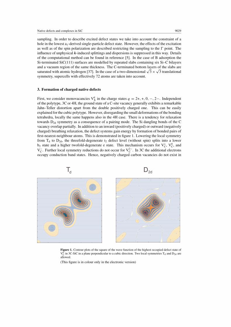
The (donor-like) ionization levels (q − 1/q) of a defect are independent of the preparationconditions, i.e. the actual values of the chemical potentials of the species involved. They aredefined as the positions of the Fermi level EF at which the charge states of the defects changefrom q − 1 to q. Results are presented in figure 4. They indicate similarities of the levelschemes of 3C and 4H with respect to the valence band maximum. The main variation is dueto the wider energy gap in 4H. Deep mid-gap defect levels can more or less be used to alignthe band structures of 3C- and 4H-SiC according to the Langer–Heinrich rule [48].
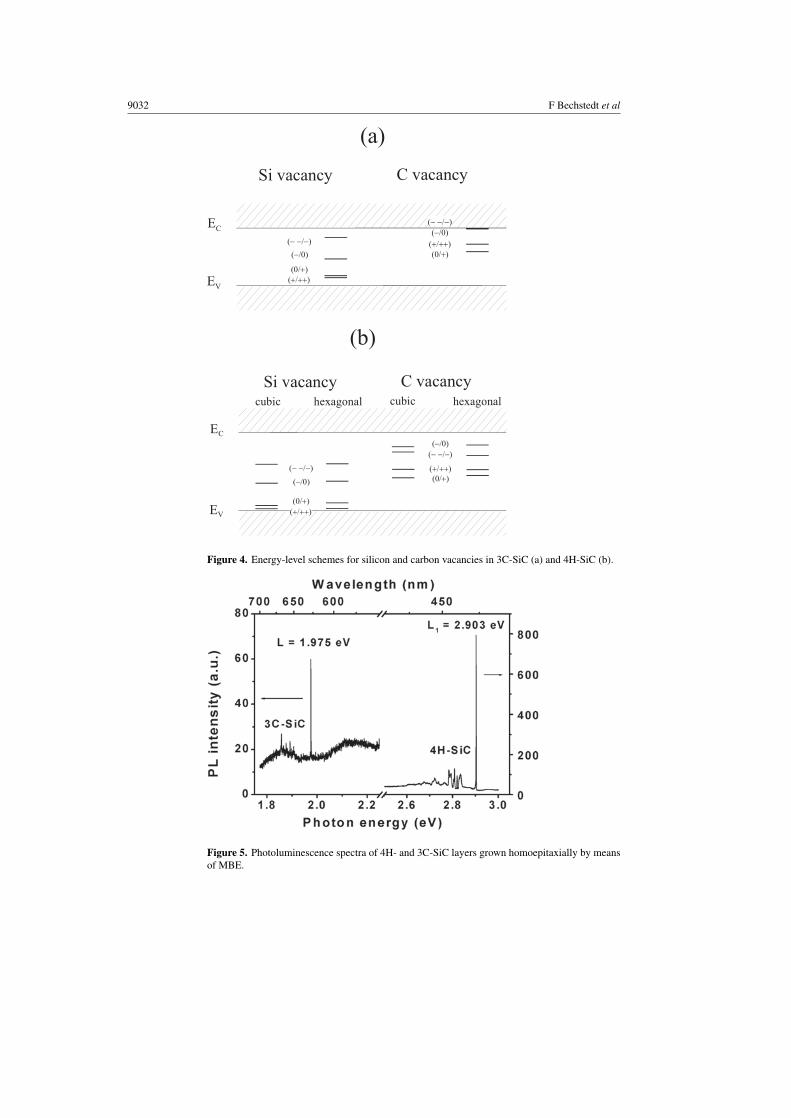
Figure 5 presents the low-temperature PL spectra of 4H- and 3C-SiC layers grown bymeans of solid-source MBE [16]. They show the well-known emission lines of the D1
defect centre, both the zero-phonon L1 line and the phonon replica. In table 1 we compare
9032 F Bechstedt et al
� � � � � � � � � � �
��
��
� � � � � � �
� � � � �
� � � � � �
� � � � �
� � � � � � �
� � � � �
� � � � �
� � � � � �
� �
� � � � � � � � � � �
� �
� �
� � � � � � �
� � � � �
� � � � �
� � � � � � � � � � � � � � � � � � � � � � � � � �
� � � � � � �
� � � � �
� � � � �
� � � � � �
� � � � � �
� � �
Figure 4. Energy-level schemes for silicon and carbon vacancies in 3C-SiC (a) and 4H-SiC (b).
Figure 5. Photoluminescence spectra of 4H- and 3C-SiC layers grown homoepitaxially by meansof MBE.

Native defects and complexes in SiC 9033
Table 1. Ionization energies (in eV) of Si (C) vacancies in 3C- and 4H-SiC with respect to theconduction band minimum. Cubic (k) and hexagonal (h) sites are indicated. For comparison theL1 emission line positions are also given.
k (3C) h (4H) k (4H)
(+/2+) 2.05 (0.67) 3.18 (1.58) 3.20 (1.58)
(0/+) 1.96 (0.98) 2.95 (1.82) 3.06 (1.89)
(−/0) 1.28 (—) 1.98 (0.65) 2.07 (0.52)
(2−/−) 0.41 (—) 1.31 (0.84) 1.32 (0.81)
L1 1.97 2.90
the line positions with calculated donor ionization energies. The comparison shows thatthe donor ionization levels (0/+) of silicon vacancies in 3C and 4H (hexagonal site) nearlygive the positions of the luminescence lines. Thereby, the binding energy of about 0.03–0.06 eV [11–13] of the bound exciton is neglected and an inaccuracy of about 0.1 eV of thetheoretical level positions is taken into account. The advantage of this identification is theexplanation of the polytype dependence of the L1 line and of the non-occurrence of a secondline for 4H. The splitting of the two (0/+) energies of cubic and hexagonal sites is rather large,so electron–hole pairs recombine via the lower-energy transition.
These results suggest the conclusion that a Si vacancy, or more strictly speaking a Cdangling bond, is involved in the D1 centre. There are also arguments against this interpretation.The Si vacancy formation energies are generally larger than those of C vacancies (cf. figure 2).However, the MBE growth of SiC [16] happens under conditions where the concentration of Siadatoms is nearly given by its equilibrium value. No accumulation of Si occurs on the growingSiC surface. On the other hand, desorption of carbon or carbon-bearing species, such as Si2Cand SiC2, can be neglected.
In addition, it has been suggested that Si vacancies are unstable in thermodynamic equil-ibrium against a transformation into a defect complex according to V0
Si → V0C + C0
Si, becauseof their larger formation energy in comparison to that of C vacancies [49]. However, thereexists an energy barrier for this process of about 1.8 eV which is much higher than the thermalenergy at the growth temperature of 1500 K (3C) or 1600 K (4H).
The question arises of whether other PL lines, e.g. that at 1.35 and 1.44 eV for 4H [20,21]or 1.12 eV for 3C [19], can be related to native defects such as vacancies or not. To answerthis question, we study the lowest intravacancy transition energies of Si vacancies in 3C- and4H-SiC as total-energy differences hω = Etot (V
q
Si, excited) − Etot (Vq
Si, ground). Thereby,the excited state is described using the constraint of a hole in the low-energy a1 defect state.Results are listed in table 2. In the 3C case we also give transition energies that are correctedby about 0.15 or 0.35 eV, in order to account for the strong dispersion of the lowest a1 defectband [41]. Despite the large supercells of 216 atoms, such a strong dispersion occurs due tothe vacancy–vacancy interaction and the mixing with bulk-like contributions.
Interestingly all of the intravacancy transition energies considered in table 2 vary littlewith the charge state of the vacancy Vq
Si and the polytype of the host, in particular consideringonly cubic lattice sites. The reason is that the charge state q shifts both participating single-particle levels a1 and t2 in the same manner. The participating orbitals are combined by thesame C hybrids in more or less the same distance. The large difference in the V2−
Si case is aconsequence of the fact that in 3C the t↑2 level lies above the conduction band minimum. For4H-SiC the site dependence has to be taken into consideration. The transitions at hexagonal
9034 F Bechstedt et al
Table 2. Lowest intradefect transition energies (in eV) for Vq
Si in 3C- and 4H-SiC. The inequivalentlattice sites, k and h, are distinguished in 4H. In the 3C case the energies corrected by the strongk-dispersion of the a1 defect band are given in parentheses.
Charge state q Transition 3C (k) 4H (k) 4H (h)
+ a21t↑2 → a↓
1 t↑↑2 1.41 (1.06) 1.42 1.77
0 a21t↑↑
2 → a↓1 t↑↑↑
2 1.42 (1.07) 1.44 1.82
− a21t↑↑↑
2 → a→1 t↑↑↑
2 t↓2 1.60 (1.40) 1.57 1.40
2− a21t↑↑↑
2 t↓2 → a↑1 t↑↑↑
2 t↓↓2 1.43 (1.23) 1.73 1.68
sites possess larger (smaller) energies for positively charged or neutral (negatively charged) Sivacancies than those at cubic sites.
The values in table 2 approach the experimental findings [19–21]. Son et al [19] relate thePL line at 1.12 eV for 3C to a S = 1/2 centre, probably V+
Si. We follow this interpretation, inparticular because of the spin state. From the point of view of the energy, one cannot excludeV0
Si. However, neither the spin S = 1 nor the spin S = 0 fits the PL experiments, in contrastto the corresponding vacancy in diamond [50]. The conclusions from the comparison aremore vague in the case of 4H, despite the reduced dispersion of the lowest defect band as aconsequence of the hexagonal crystal field. The transition energies 1.44 and 1.82 eV calculatedwithout dispersion corrections for V0
Si approach the positions of the two zero-phonon PL linesat 1.35 and 1.44 eV accompanied by an S = 1 signal measured with optically detected magneticresonance (ODMR) [20, 21]. However, such an interpretation is doubtful because of the spinstate and the larger computed line splitting. Another possible explanation of the occurrence oftwo lines for 4H may be related to the crystal-field splitting of the t↑2 level into a↑
1 and e↑ onesand not to the two inequivalent sites. Taking into account a dispersion correction of 0.31 eV,the transition in V2−
Si can also be considered for the interpretation. Spin state and line splittingagree with the measurements.
5. Complexes with boron
There is usually no direct access to the atomic and electronic structures of defects, in particularnot to those of defect complexes. On the other hand more direct studies, especially of thegeometry, are possible near surfaces. In order to contribute to a clarification of the problemof doping with boron, we therefore study the adsorption of B atoms on SiC surfaces. Thevacuum region may be considered to simulate the presence of vacancies near to the B atoms.Since the bilayer stacking is less important for the surface structure [34], the Si-terminatedSiC(111)
√3 × √
3R30◦ adatom surface of 3C-SiC is investigated as a model surface. Elevenadsorption geometries and stoichiometries are investigated. We find the two surface geometriesin figure 6 to be stable. Both conserve the Si adatom in a T4 position.
Under more C-rich preparation conditions, B substitutes for a Si basis atom of the Siadatom (figure 6(a)). This is in agreement with bulk experiments. A coimplantation of C andB atoms leads to a competition for the occupation of a site in the C sublattice, so boron occupiesa Si site [27]. Similar results are observed for layers grown by CVD with low Si/C ratio [51]or by solid-source MBE [52]. Since the B adatom appears in the first atomic layer below thevacuum region, the resulting configuration may be related to a boron–vacancy complex in thebulk, e.g. BSi–VC. Under Si-rich conditions the B adatom replaces a C atom in the subsurfaceregion (see figure 6(b)). The result may be interpreted as a substitutional impurity, BC.

Native defects and complexes in SiC 9035
� � � � � � � � � � � � � � � �
Figure 6. Electron density near a SiC(111)√
3 × √3 surface projected onto a (110) plane. Shaded
(open, full) circle: B (Si, C) atom. Results for the two most favourable configurations (a) and (b)are plotted.
The two B-induced geometries give rise to completely different electronic structures asindicated by the surface band structures in figure 7. In the case (a) of substituting a Si atom,no filled surface states appear in the fundamental gap of 3C-SiC. There is only a pronouncedempty mid-gap band that is related to Si dangling bonds and combinations of B–C antibondingorbitals which could also occur in a BSi–VC complex. Electrons are transferred from the Sidangling bonds (of the C vacancy in the bulk) into B–C bonds. In the case (b), replacing acarbon atom in the second atomic layer, boron induces surface bands that are energetically notvery different from bulk SiC states. Filled B-related bands occur slightly below the valenceband maximum. Besides those of B–Si bonding orbitals there are also strong contributionsfrom the Si dangling bonds to the underlying wave functions. We suggest experimental studies
� � �
� � � �
� � �
� � �
� �
� � �
� �
� �
�
����������
� � � �
� � � �� � �
� � � �
� � �
� � �
� �
� � �
� �
� �
�
����������
� � � �
� � � �
� � � � � � � � � � � � � � � �
Figure 7. Band structures of the two most stable B adsorbates (a) and (b) on SiC(111)√
3 × √3.
The projected bulk band structure is indicated by shaded regions.

9036 F Bechstedt et al
of the geometrical and electronic structure of the boron adsorbates in order to clarify the natureof bulk B-related acceptors.
6. Summary
In the case of wide-band-gap semiconductors such as SiC, first-principles calculations alsoallow the description of geometrical, thermodynamic, and electronic properties of defects ordefect complexes. In the paper this is mainly demonstrated for native defects. Monovacancieshave been considered as prototypical defects. However, to a certain extent antisites and vacancycomplexes have also been discussed. We have shown that in thermodynamic equilibriumthe carbon vacancy should have the lowest formation energies in bulk SiC independent ofthe polytype. It forms a double donor which dramatically reduces the doping efficiency ofacceptors as Al atoms. The theory also allows the calculation of energies of optical transitionsbetween bulk and vacancy states or excited and ground states of vacancies. We discussed theirpossible relationship to recent photoluminescence measurements. The preparation-dependentbehaviour of boron with respect to occupation of Si or C lattice sites and the possible formationof complexes with vacancies is demonstrated by studying the B adsorption on a SiC surface.
Acknowledgments
The authors acknowledge financial support from the Deutsche Forschungsgemeinschaft(Sonderforschungsbereich 196, projects A3 and A8). Some of the computations were done atthe J von Neumann Institute for Computing in Julich.
References
[1] Jepps N W and Page T F 1983 Prog. Cryst. Growth Charact. 7 259[2] Choyke W J, Hamilton D R and Patrick L 1964 Phys. Rev. 133 A1163[3] Bechstedt F and Kackell P 1995 Phys. Rev. Lett. 75 2180[4] Itoh H, Hayakawa N, Nashiyama I and Sakuma E 1989 J. Appl. Phys. 66 4529[5] Zywietz A, Furthmuller J and Bechstedt F 1999 Phys. Rev. B 59 15 166[6] Torpo L, Poykko S and Nieminen R 1998 Phys. Rev. B 57 6243[7] Wang C, Bernholc J and Davis R F 1988 Phys. Rev. B 38 12 752[8] Schneider J and Maier K 1993 Physica B 185 199[9] Choyke W J 1990 The Physics and Chemistry of Carbides, Nitrides and Borides (NATO Advanced Study Institute
Series E, vol 185: Applied Sciences) ed R Freer (Dordrecht: Kluwer Academic) p 563[10] Makarov V V 1972 Sov. Phys.–Solid State 13 1974[11] Haberstroh Ch, Helbig R and Stein R A 1994 J. Appl. Phys. 76 509[12] Egilsson T, Bergmann J P, Ivanov I G, Henry A and Janzen E 1999 Phys. Rev. B 59 1956[13] Egilsson T, Henry A, Ivanov I G, Lindstrom J L and Janzen E 1999 Phys. Rev. B 59 8008[14] Kennedy T A, Freitas J A and Bishop S G 1990 J. Appl. Phys. 68 6170[15] Nishino K, Kimoto T and Matsunami H 1995 Japan. J. Appl. Phys. 34 L1110[16] Fissel A, Richter W, Furthmuller J and Bechstedt F 2001 Appl. Phys. Lett. 78 2512[17] Choyke W J, Fenc Z C and Powell J A 1988 J. Appl. Phys. 64 3163[18] Zywietz A, Furthmuller J and Bechstedt F 2000 Phys. Rev. B 61 13 655[19] Son N T, Sorman E, Chen W M, Singh M, Hallin C, Kordina O, Monemar B and Janzen E 1996 J. Appl. Phys.
79 3784[20] Sorman E, Son N T, Chen W M, Kordina O, Hallin C and Janzen E 2000 Phys. Rev. B 61 2613[21] Wagner M, Magnusson B, Chen W M, Janzen E, Sorman E, Hallin C and Lindstrom J L 2000 Phys. Rev. B 62
16 555[22] Van Duijn-Arnold A, Ikoma T, Poluektov O G, Baranov P G, Mokhov E N and Schmidt J 1998 Phys. Rev. B 57
1607[23] Gali A, Deak P, Devaty R P and Choyke W J 1999 Phys. Rev. B 60 10 620

Native defects and complexes in SiC 9037
[24] Fukumoto A 1996 Phys. Rev. B 53 4458[25] Van Duijn-Arnold A, Mol J, Verberk R, Schmidt J, Mokhov E N and Baranov P G 1999 Phys. Rev. B 60 15 829[26] Bockstedte M, Mattausch A and Pankratov O 2001 Mater. Sci. Forum 353–356 447[27] Frank T, Troffer T, Pensl G, Nordell N, Karlsson S and Schoner A 1998 Mater. Sci. Forum 264–268 681[28] Hohenberg P and Kohn W 1964 Phys. Rev. 136 B864[29] Kohn W and Sham L J 1965 Phys. Rev. 140 A1133[30] Kresse G and Furthmuller J 1996 Comput. Mater. Sci. 6 15
Kresse G and Furthmuller J 1996 Phys. Rev. B 54 11 169[31] Furthmuller J, Kackell P, Bechstedt F and Kresse G 2000 Phys. Rev. B 61 4576[32] Perdew J P and Zunger A 1981 Phys. Rev. B 23 5048[33] von Barth U and Hedin L 1972 J. Phys. C: Solid State Phys. 5 1629[34] Bechstedt F, Zywietz A, Karch K, Adolph B, Tenelsen K and Furthmuller J 1997 Phys. Status Solidi b 202 35[35] Wenzien B, Kackell P, Bechstedt F and Cappellini G 1995 Phys. Rev. B 52 10 897[36] Monkhorst H J and Pack J D 1976 Phys. Rev. B 13 5188[37] Grossner U, Furthmuller J and Bechstedt F 2001 Phys. Rev. B submitted[38] Baraff G A, Kane E O and Schluter M 1980 Phys. Rev. B 21 5662[39] Bechstedt F, Zywietz A and Furthmuller J 1998 Europhys. Lett. 44 309[40] Torpo L, Nieminen R M, Laasonen K E and Poykko S 1999 Appl. Phys. Lett. 74 221[41] Zywietz A, Furthmuller J and Bechstedt F 1998 Phys. Status Solidi b 210 13[42] Deak P, Miro J, Gali A, Udvardi L and Overhof H 1999 Appl. Phys. Lett. 75 2103[43] Zywietz A, Furthmuller J and Bechstedt F 2000 Phys. Rev. B 62 6854[44] Zhang S B and Northrup J E 1991 Phys. Rev. Lett. 67 2339[45] Itoh H, Kawasuro A, Ohshima T, Yoshikawa M, Nashiyama I, Tanigawa S, Misawa S, Okumura H and Yoshida
S 1997 Phys. Status Solidi a 162 173[46] Kim H J and Davis R F 1986 J. Electrochem. Soc. 133 2350[47] Yamanaka M, Daimon H, Sakuma E, Misawa S and Yoshida S 1987 J. Appl. Phys. 61 599[48] Langer J M and Heinrich H 1985 Phys. Rev. Lett. 55 1414[49] Rauls E, Lingner T, Hajnal Z, Greulich-Weber S, Fraunheim T and Spaeth J-M 2000 Phys. Status Solidi b 217
R1[50] Davies G, Lawson S C, Collins A T, Mainwood A and Sharp S J 1992 Phys. Rev. B 46 13 157[51] Sridhara S G, Clemen L L, Devaty R P, Choyke W J, Larkin D J, Kong H S, Troffer T and Pensl G 1998 J. Appl.
Phys. 83 7909[52] Fissel A 2001 J. Cryst. Growth 805 227