polytypism and surface structure of sic
TRANSCRIPT

Vol. 6, No. 10, August 1997 ISSN 0925-9635
" ) /
r
j
\ \ \ \ \
\ /
\ \ \
■• /
/ /
\ \ \ \ \
r i / /
\ \ \
A A iA _r-\\ .
i /
- N\ I | \ i i s\
INTERNATIONAL JOURNAL ON THE SCIENCE AND TECHNOLOGY OF DIAMOND AND RELATED MATERIALS
Editor-in-Chief R. Messier
Proceedings of ECSCRM 1996,
the 1st European Conference on
Silicon Carbide and
Related Materials, 6-9 October 1996,
Heraklion, Greece
Associate Editors J. C. Angus T. R. Anthony P. K. Bachmann A. M. Bonnot I. Buckley-Golder A. T. Collins R. F. Davis K. Y. Eun O. Fukunaga J. T. Glass A. Grill S.-T. Lee H. Matsunami Y. Sato M. N. Yoder
Guest Editor K. Zekentes
MTO QUALITY QIü?E(W:SD ®
ELSEVIER 19971121 100
DIAMOND AND RELATED MATERIALS Editor-in-Chief R. Messier, 265 Materials Research Laboratory, Pennsylvania State University, University Park, PA 16802-4801, USA. Tel: (1-814) 865-3704 or 865-3423. Fax: (1-814) 863-7039. e-mail: [email protected]
Associate Editors J. C. Angus, Chemical Engineering Department, Case Western Reserve University, Cleveland, OH 44106, USA. Tel: (1-216) 368-4133. Fax: (1-216) 368-3016. e-mail: [email protected]. T. R. Anthony, GE Corporate R&D, One Research Circle, Bldg. K-1, Room 1C30, Schenectady, NY 12309, USA. Tel: (1-518) 387-6160. Fax: (1-518) 387-7563. e-mail: [email protected] P. K. Bachmann, Philips GmbH, Research Laboratories Aachen, Postfach 1980, Weisshausstrasse, 52066 Aachen, Germany. Tel and fax: (49) 241 6003314. e-mail: [email protected] A. M. Bonnot, Centre National de la Recherche Scientifique/LEPES, BP 166X, 38042 Grenoble Cedex 9, France. Tel: (33) 76 88 79 93. Fax: (33) 76 88 79 88. e-mail: [email protected] I. Buckley-Golder, AEA Technology, Surface Science & Technology, Harwell Laboratory, Bldg. 552, Didcot, Oxon. OX11 ORA, UK. Tel: (44) 1235 434 574. Fax: (44) 1235 432 697. e-mail: [email protected] A. T. Collins, Wheatstone Physics Laboratory, King's College London, Strand, London WC2R 2LS, UK. Tel: (44) 171 873 2584. Fax: (44) 171 873 2160. e-mail: [email protected] R. F. Davis, North Carolina State University, Materials Research Center, Campus Box 7919, Raleigh, NC 27695-7919, USA. Tel: (1-919) 515-2377. Fax: (1-919) 515-7724. e-mail: [email protected] K. Y. Eun, Division of Ceramics, Korea Institute of Science and Technology (KIST), PO Box 131, Cheongryang, Seoul 130-650, South Korea. Tel: (82) 2-958-5491. Fax: (82) 2-958-5509. e-mail: [email protected] O. Fukunaga, Ace-Tech Co. Ltd., 1-167-1, Higashi Ome, Ome 198, Japan. Tel: (81) 428 21 1225. Fax: (81) 428 20 7341. e-mail: [email protected] J. T. Glass, Materials Science and Engineering (NCSU), Kobe Steel USA, Inc., 79 Alexander Drive, P.O. 13608, 4401 Bldg.- Suite 101, Research Triangle Park, NC 27709, USA. Tel: (1-919) 549-9823. Fax: (1-919) 549-8460. e-mail: [email protected] A. Grill, IBM, Thomas J. Watson Research Center, P.O. Box 218, Yorktown Heights, NY 10598 Tel: 914 945 1492. Fax: 914 945 2141. e-mail: [email protected] S.-T. Lee, Department of Physics, City University of Hong Kong, 83 Tat Chee Avenue, Kowloon, Hong Kong. Tel: (852) 2788 9606. Fax: (852) 2788 7830. e-mail: [email protected] H. Matsunami, Kyoto University, Department of Electrical Engineering, Yoshida Honmachi, Sakyp-ku, Kyoto 606-01, Japan. Tel: (81) 75-753 5340. Fax: (81) 75-75 1576. e-mail: [email protected] Y. Sato, National Institute for Research in Inorganic Materials, 1-1 Namiki, Tsukuba, Ibaraki 305, Japan. Tel: (81) 298-51-3351. Fax: (81) 298-52-7449 M. N. Yoder, Electronics Division, Office of Naval Research, 800 N Quincy Street, Arlington, VA 22217-5660, USA. Tel: (1-703) 696-4216. Fax: (1-703) 696-2611. e-mail: [email protected]
Types of Contributions - original papers - invited or contributed reviews on specific topics - Letters on topics requiring rapid publication. These should
be no longer than 2000 words (allowing approximately 350 words per figure or table).
- notices of meetings, symposia and short courses
Scope Diamond and Related Materials is an international, interdisciplinary journal which publishes articles covering both basic and applied research on diamond materials and related materials. These include cubic boron nitride and materials with characteristics and properties approaching or possibly exceeding those of diamond. The primary emphasis is on vapour-deposited materials; also important are high-temperature/high-pressure synthetic materials, as well as relevant natural diamond research and characterization. Papers published cover all fundamental and technological aspects of synthesis, characterization, properties, devices and generic applications of these materials.
Frequency One volume per year, in 12 issues.
Abstracting/Indexing Services This journal is cited by the following services: ASM International (Non-Ferrous Metals Alerts), Cambridge Scientific Abstracts, Chemical Abstracts, Engineering Information Inc., FIZ Karlsruhe, Geo Abstracts, GEOBASE, INSPEC, Institute for Scientific Information (Current Contents/Engineering, Technology and Applied Science, Research Alert, Materials Science Citation Index, Science Citation Index, SciSearch), Materials Information (Metals Abstracts, Engineered Materials Abstracts), PASCAL/Centre National de Recherche Scientifique, Surface Treatment Technology Abstracts, Tribology and Corrosion Abstracts. Pre-publication abstracts of articles in Diamond and Related Materials and other related journals are now available weekly in electronic form via CoDAS, a new direct alerting service in condensed matter and materials science run jointly by Elsevier Science and Institute of Physics Publishing. For details on a free one-month subscription contact Paul Bancroft on fax +44 1179 294318 or e-mail [email protected].
Advertising Information Advertising orders and enquiries may be sent to: International: Elsevier Science, Advertising Department, The Boulevard, Langford Lane, Kidlington, Oxford OX5 1GB, UK. Tel.: +44 (1865) 843 565. Fax: +44 (1865) 843 952. USA and Canada: Weston Media Associates; Dan Lipner, P.O. Box 1110, Greens Farms, CT 06436-1110, USA. Tel.: +1 (203) 261 2500. Fax: +1 (203) 261 0101. Japan: Elsevier Science Japan, 9-15 Higashi-Azabu 1-chome, Minato-ku, Tokyo 106; Tel: +81-3- 5561-5032; Fax: +81-5561-5045.
Subscription Information 1997 Volume 6, containing 12 issues, is scheduled for publication. Prices are available from the publishers upon request. Subscriptions are accepted on a prepaid basis only. Issues are sent by SAL (Surface Air Lifted) mail wherever this service is available. Airmail rates are available upon request. Please address all requests regarding orders and subscription queriesto:
ELSEVIER SCIENCE S.A., P.O. Box 564, 1001 Lausanne, Switzerland. Telephone: +41 21 320 73 81; Telex: 450 620 ELSA CH; Telefax: +41 21 323 54 44.
Customers in Japan may obtain information from: Elsevier Science Japan Customer Support DTP, 9-15, Higashi-Azabu l-chrome, Minato-ku, Tokyo 106, Japan. Telephone: 81 35561 5033; Fax: 81 35561 5047; E-mail: [email protected]
US and Canadian customers may obtain information from: ELSEVIER SCIENCE INC., Attn: Journal Information Center, 655 Avenue of the Americas, New York, NY 10010, USA. Telephone: (212) 633-3750; Telex: 420-643 AEP Ul; Telefax: (212) 633-3764.
US mailing notice — Diamond and Related Materials (ISSN 0925-9635) is published monthly by Elsevier Science S.A. (PO Box 564, 1001 Lausanne). Annual subscription price in the USA is US$1303 (valid in North, Central and South America), including air speed delivery. Second class postage rate is paid at Jamaica, NY 11431. USA POSTMASTER: Send address changes to Diamond and Related Materials Publications Expediting, Inc., 200 Meacham Avenue, Elmot, NY 11003. AIRFREIGHT AND MAILING in the USA by Publications Expediting Inc., 200 Meacham Avenue, Elmont, NY 11003.

*■■■ DIAMOND AND
RELATED MATERIALS
ELSEVIER Volume 6, Number 10, August 1997 ^^=^===
Contents
Proceedings of the 1st European Conference on Silicon Carbide and Related Materials (ECSCRM 1996)
Guest Editor: K. Zekentes
Preface xxxix
Organizers and Sponsors xxxxi
Progress in the study of optical and related properties of SiC since 1992 1243 W.J. Choyke and R.P. Devaty
SiC bulk growth
Defects formation in sublimation grown 6H-SiC single crystal boules* 1249 R. Madar, M. Anikin, K. Chourou, M. Labeau, M. Pons, E. Blanquet, J.M. Dedulle, C. Bernard, S. Milita and J. Baruchel
Sublimation growth of 4H- and 6H-SiC boule crystals 1262 V.D. Heydemann, N. Schulze, D.L. Barrett and G. Pensl
Growth of SiC from the liquid phase: wetting and dissolution of SiC 1266 M. Syväjärvi, R. Yakimova and E. Janzen
The kinetic growth model applied to micropipes in 6H-SiC 1269 J. Heindl, W. Dorsch, R. Eckstein, D. Hofmann, T. Marek, S. Müller, H.P. Strunk and A. Winnacker
Growth-related structural defects in seeded sublimation-grown SiC 1272 M. Tuominen, R. Yakimova, E. Prieur, A. Ellison, T. Tuomi, A. Vehanen and E. Janzen
SiC epitaxial growth
Surface polarity dependence in step-controlled epitaxy: progress in SiC epitaxy* 1276 H. Matsunami and T. Kimoto
Growth and doping via gas-source molecular beam epitaxy of SiC and SiC/AIN heterostructures and their microstructural and electrical characterization* 1282 R.S. Kern, K. Järrendahl, S. Tanaka and R.F. Davis
High quality 4H-SiC grown on various substrate orientations 1289 A. Henry, I.G. Ivanov, T. Egilsson, C. Hallin, A. Ellison, O. Kordina, U. Lindefelt and E. Janzen
Hydrogen incorporation in epitaxial layers of 4H- and 6H-silicon carbide grown by vapor phase epitaxy 1293 A. Schöner, K. Rottner, N. Nordell, M. Linnarsson, C. Peppermüller and R. Helbig
The origin of 3C polytype inclusions in epitaxial layers of silicon carbide grown by chemical vapour deposition 1297 C. Hallin, A.O. Konstantinov, B. Pecz, O. Kordina and E. Janzen
SiC and group III nitride growth in MOVPE production reactors 1301 R. Beccard, D. Schmitz, E.G. Woelk, G. Strauch and H. Jürgensen
Growth of SiC films obtained by LPCVD 1306 M.T. Clavaguera-Mora, J. Rodriguez-Viejo, Z. El Felk, E. Hurtös, S. Berberich, J. Stoemenos and N. Clavaguera
Chemical conversion of Si to SiC by solid source MBE and RTCVD 1311 J. Pezoldt, V. Cimalla, T. Stauden, G. Ecke, G. Eichhorn, F. Scharmann and D. Schipanski
•Invited papers. pTIC QUALITY IHSPEÜilD W
Elsevier Science S.A.

xxxviii Contents
Hexagonal and cubic SiC thin films on SiC deposited by solid source MBE 1316 A. Fissel, K. Pfennighaus, U. Kaiser, B. Schröter and W. Richter
Hydrogen-, boron-, and hydrogen-boron-related low temperature photoluminescence of 6H-SiC 1321 C. Peppermüller, A. Schöner, K. Rottner and R. Helbig
SiC characterization: Crystal structure and defects: Optical and electrical properties
Carrier lifetimes in SiC, studied by time resolved photoluminescence spectroscopy* 1324 J.P. Bergman
Analysis of transport properties of ß-SiC films: determination of donor density and compensation ratio 1329 S. Contreras, C. Dezauzier, P. Thomas and J.L. Robert
Radiation-induced defect centers in 4H silicon carbide 1333 T. Dalibor, G. Pensl, T. Kimoto, H. Matsunami, S. Sridhara, R.P. Devaty and W.J. Choyke
Thermal properties of ß-SiC epitaxial layers between 150 °C and 500 °C measured by using microstructures 1338 C. Wagner and G. Krötz
Valence band dispersion of hexagonal SiC 1342 G. Wellenhofer and U. Rössler
Polytypism and surface structure of SiC 1346 P. Käckell, J. Furthmüller and F. Bechstedt
Structure and morphology of SiC surfaces studied by LEED, AES, HREELS and STM 1349 U. Starke, J. Bernhardt, M. Franke, J. Schardt and K. Heinz
Investigation of modified 3C SiC( 100) surfaces by surface-sensitive techniques 1353 T. Balster, F.S. Tautz, H. Ibach and J.A. Schaefer
Angle resolved photoemission and the band structure of 6H-SiC 1358 M. Hollering, A. Ziegler, R. Graupner, B. Mattern, L. Ley, A.P.J. Stampfl, J.D. Riley and R.C.G. Leckey
Topology of twin junctions in epitaxial jS-SiC 1362 V. Papaioannou, P. Komninou, G.P. Dimitrakopulos, K. Zekentes, B. Pecz, T. Karakostas and J. Stoemenos
Micropipe defects and voids at /?-SiC/Si( 100) interfaces 1365 R. Scholz, U. Gösele, E. Niemann, D. Leidich and F. Wischmeyer
Wafer warpage, crystal bending and interface properties of 4H-SiC epi-wafers 1369 A. Ellison, H. Radamson, M. Tuominen, S. Milita, C. Hallin, A. Henry, O. Kordina, T. Tuomi, R. Yakimova, R. Madar and E. Janzen
Nonlinear optical mapping of 3C-inclusions in 6H-SiC-epilayers 1374 C. Meyer, G. Lilpke, E. Stein von Kamienski, A. Gölz and H. Kurz
Deep luminescent centres in electron-irradiated 6H SiC 1378 N.T. Son, E. Sörman, M. Singh, W.M. Chen, C. Hallin, O. Kordina, B. Monemar, J.L. Lindström and E. Janzen
Optically detected magnetic resonance studies of defects in 3C SiC epitaxial layers 1381 N.T. Son, E. Sörman, W.M. Chen, C. Hallin, O. Kordina, B. Monemar and E. Janzen
Optical investigation of thick 3C-SiC layers deposited on bulk silicon by CVD 1385 J.M. Bluet, J. Camassel, L.A. Falkovsky and A. Leycuras
Characterization of electrically active deep level defects in 4H and 6H SiC 1388 J.P. Doyle, M.O. Aboelfotoh, B.G. Svensson, A. Schöner and N. Nordell
High field/high temperature performance of semi-insulating silicon carbide 1392 T.S. Sudarshan, G. Gradinaru, G. Korony, S.A. Gradinaru and W. Mitchel
OBIC studies on 6H-SiC Schottky rectifiers with different surface pretreatments 1396 M. Frischholz, K. Rottner, A. Schöner, T. Dalibor and G. Pensl
SiC processing: Oxidation, metallization, ion implantation and etching
SiC device technology: remaining issues* 1400 J.W. Palmour, L.A. Lipkin, R. Singh, D.B. Slater, Jr, A.V. Suvorov and C.H. Carter, Jr
* Invited papers.

Contents xxxix
Silicon carbide for microwave power applications* 1405 C. Brylinski
Aluminium implantation of p-SiC for ohmic contacts 1414 L. Spie, O. Nennewitz, H. Weishart, J. Lindner, W. Skorupa, H. Romanus, F. Erler and J. Pezoldt
Fabrication of high-quality oxides on SiC by remote PECVD 1420 A. Gölz, S. Groß, R. Janssen, E. Stein von Kamienski and H. Kurz
An interface study of vapor-deposited rhenium with the two (0001) polar faces of single crystal 6H-SiC 1424 S. Kennou, A. Siokou, I. Dontas and S. Ladas
TEM study ofNi and Ni2Si ohmic contacts to SiC 1428 B. Pecz, G. Radnoczi, S. Cassette, C. Brylinski, C. Arnodo and O. Noblanc
Ion beam assisted deposition of a tungsten compound layer on 6H-silicon carbide 1432 H. Weishart, V. Heera, W. Matz and W. Skorupa
Hafnium, cadmium and indium impurities in 4H-SiC observed by perturbed angular correlation spectroscopy 1436 T. Licht, N. Achtziger, D. Forkel-Wirth, K. Freitag, J. Grillenberger, M. Kaltenhäuser, U. Reislöhner, M. Rüb, M. Uhrmacher, W. Witthuhn and ISOLDE Collaboration
Nuclear transmutation doping of 6H-silicon carbide with phosphorous 1440 H. Heissenstein, C. Peppermüller and R. Helbig
Investigation of the effects of high temperature implantation and post implantation annealing on the electrical behavior of nitrogen implanted ß-SiC films 1445 W. Reichert, R. Lossy, M. Gonzalez Sirgo, E. Obermeier and W. Skorupa
ß-SiC films on SOI substrates for high temperature applications 1448 W. Reichert, E. Obermeier and J. Stoemenos
Surface chemistry of 6H-SiC(0001) after reactive ion etching 1451 N. Sieber, M. Hollering and L. Ley
Preferential etching of SiC crystals 1456 R. Yakimova, A.-L. Hylen, M. Tuominen, M. Syväjärvi and E. Janzen
Schottky contact investigation on reactive ion etched 6H a-SiC 1459 G. Constantinidis, J. Kuzmik and K. Michelakis
Comparative investigation of ECR-RIE patterns on Si and C faces of 6H-SiC using a CF4/02 gas mixture 1463 R. Bonnot, A.L. Syrkin, G. Leveque, J.M. Bluet and J. Camassel
Anisotropie oxidation of silicon carbide 1467 K. Christiansen, S. Christiansen, M. Albrecht, H.P. Strunk and R. Helbig
"Carbon cluster model" for electronic states at SiC/Si02 interfaces 1472 M. Bassler, G. Pensl and V. Afanas'ev
SiC-based devices and applications
Investigation of walk-out phenomena in SiC mesa diodes with Si02/Si3N4 passivation 1476 Z. Ovuka and M. Bakowski
Overview of SiC power electronics* 1480 V.E. Chelnokov, A.L. Syrkin and V.A. Dmitriev
2.5 kV ion-implantedp+n diodes in 6H-SiC 1485 K.H. Rottner, A. Schöner, S.M. Savage, M. Frischholz, C. Hallin, O. Kordina and E. Janzen
High field and high temperature stress ofn-SiCMOS capacitors 1489 E. Bano, T. Ouisse, C. Leonhard, A. Gölz and E.G. Stein Von Kamienski
Low frequency noise in silicon carbide Schottky diodes 1494 L. Anghel, T. Ouisse, T. Billon, P. Lassagne and C. Jaussaud
Passivation of interface traps in MOS-Devices on«- and />-type 6H-SiC 1497 E.G. Stein von Kamienski, C. Leonhard, S. Scharnholz, A. Gölz and H. Kurz
* Invited papers.

xl Contents
Numerical study of avalanche breakdown of 6H-SiC planar p-n junctions 1500 E. Stefanov, L. Bailon and J. Barbolla
Temperature dependence of electrical properties of 6H-SiC buried gate JFET 1504 C. Raynaud, C. Richier and G. Guillot
Microwave Power MESFET on 4H-SiC 1508 O. Noblanc, E. Chartier, C. Arnodo and C. Brylinski
The potential of SiC and GaN for application in high speed devices 1512 F. Schwierz, M. Kittler, H. Förster and D. Schipanski
Nitrides growth and characterization
Thermodynamics and high-Pressure growth of (Al, Ga, In)N single crystals* 1515 S. Krukowski
Residual strains in GaN grown on 6H-SiC 1524 LP. Nikitina, M.P. Sheglov, Y. Melnik, K.G Irvine and V.A. Dmitriev
Structural and electrical properties of Schottky barriers on n-GaN 1528 E.V. Kalinina, N.I. Kuznetsov, A.I. Babanin, V.A. Dmitriev and A.V. Shchukarev
Structural properties of GaN grown on SiC substrates by hydride vapor phase epitaxy 1532 Y. Melnik, LP. Nikitina, A.E. Nikolaev and V.A. Dmitriev
Contactless characterisation of 2D-electrons in GaN/AlGaN HFETs 1536 H. Alause, C. Skierbiszewski, M. Dyakonov, W. Knap, M.L. Sadowski, S. Huant, J. Young, M. Asif Khan and Q. Chen
Identification of the cubic and hexagonal polytypes of GaN with X-ray absorption measurements 1539 M. Katsikini, E.C. Paloura, T.S. Cheng and C.T. Foxon
Amorphorous SiC and other SiC-related materials
Colour sensing applications of hydrogenated amorphous silicon carbide* 1542 G. Müller
Surface and bulk effects in ex-situ hydrogenated a-SiC thin films 1547 J. Kalomiros, E.C. Paloura, C. Janowitz, B. Theys and A. Anagnostopoulos
Optical study of boron nitride thin films prepared by plasma-enhanced chemical vapor deposition 1550 M.C. Polo, M. Ben el Mekki, J.L. Andüjar, N. Mestres and J. Pascual
Electrical properties of PECVD amorphous silicon-carbon alloys from amorphous-crystalline heterojunctions 1555 L.F. Marsal, J. Pallares, X. Correig, M. Dominguez, D. Bardes, J. Calderer and R. Alcubilla
Effects of thermal and laser annealing on silicon carbide nanopowder produced in radio frequency glow discharge 1559 G. Viera, S.N. Sharma, J. Costa, R.Q. Zhang, J.L. Andüjar and E. Bertran
Emission and excitation spectra of silicon-related luminescent centers in CVD-grown diamond films 1564 M.C. Rossi, S. Salvatori, F. Galluzzi, R.M. Montereali and F. Somma
Amorphous GaAsj ^XNX thin films on crystalline Si substrates: growth and characterizations 1568 D. Lollman, K. Aguir, B. Roumiguieres and H. Carchano
Conference Calendar 1573
Author Index 1575
Subject Index 1581
* Invited papers.

DIAMOND AND
RELATED UT CCUTCD IVIAI fcKIALD ELdÜVifcK Diamond and Related Materials 6 (1997) xxxxi —
Preface
The first European Conference on Silicon Carbide and Related Materials (ECSCRM 96) was held in Heraklion, Crete, Greece from October 6 to October 9, 1996. This was the first event of a series of biannual conferences addressing wide band gap semiconductors research field and supported by the European Union through the "Euroconferences" action. The next conference will be held in Montpellier, France in 1998.
The conference was attended by 140 scientists from 13 countries representing most of the European research groups active in the subject. Thirteen invited talks, 18 oral and 61 poster contributions were presented in 8 oral and 2 poster sessions. These 92 contributions demonstrated the rapid development of wide band gap semiconductor research. Moreover, two panel discussions on European effort on SiC wafer production & SiC bulk and epitaxial growth apparatus and on SiC-based devices and applications were organized.
Two main research areas were covered by the majority of presentations namely the SiC material aspect and the device-oriented aspect as well as balancing academic and industrial participation. The topics covered by the oral sessions were:
1. SiC bulk growth. 2. SiC epitaxial growth. 3. SiC characterization: Crystal structure & defects; Optical and electrical properties. 4. SiC processing: Oxidation, metallization, ion implantation and etching. 5. SiC-based devices and applications. 6. Nitrides growth and characterization. 7. Amorphous SiC and other SiC-related materials.
The above topical structure is followed in this volume. The contributions were reviewed according to the "Diamond & Related Materials" Journal refereeing procedure and 75 manuscripts were accepted and published in this volume. The Editor wishes to thank the referees who conscientiously reported on manuscripts.
Konstantinos Zekentes

SA warn
H DIAMOND AND
^*ffii RELATED ~MJS3L* MATERIALS ELSEVIER Diamond and Related Materials 6 (1997) xxxxiii
Organizers and Sponsors of ECSCRM 1996
Conference Chairman
J. Stoemenos (Arist. Univ. Thessaloniki)
Scientific Program Committee
A. Christou (University of Maryland, USA)
E. Janzen (Linköping University, SWEDEN)
C. Jaussaud (CENG/LETI/DMEL, FRANCE)
M. T. Mora (Univ. Autonoma Barcelona, SPAIN)
E. Obermeier (Techn. Univ. Berlin, GERMANY)
G. Pensi (Erlangen Univ., GERMANY)
J. L. Robert (Universite de Montpellier II, FRANCE)
Y. M. Tairov (St. Peterbourg University, RUSSIA)
Local Committee
G. Constantinidis (FORTH/IESL)
P. Panayotatos (FORTH/IESL, Univ. of Crete, Rutgers Univ.)
K. Zekentes (FORTH/IESL)
Sponsored By:
- Training and Mobility of Researchers Programme
(EuroConferences). Commission of the European Union
- Foundation for Research and Technology-Hellas
- Greek Ministry of Culture
- General Secretariat of Research and Technology (Greece)
- Aristotle University of Thessaloniki (Greece)
- US Army/European Research Office

DIAMOND AND
RELATED MATERIALS
ELSEVIER Diamond and Related Materials 6 (1997) 1243-1248
Progress in the study of optical and related properties ofSiC since 1992
W.J. Choyke *, R.P. Devaty Department of Physics and Astronomy, University of Pittsburgh, Pittsburgh, PA 15260, USA
Abstract
A selected review is given of some of the advances made in the understanding of the optical and related properties of SiC during the years 1992-1996. Areas which are briefly covered are ultraviolet reflectivity and band structure, phonon replicas and the positions in A-space of the conduction band minima, cyclotron resonance and effective masses, pressure dependence of the electronic energy gap, electronic Raman scattering in heavily doped SiC, acceptors and donors, transition metals, thermolumines- cence, porous SiC, and erbium-implanted 3C, 4H, 6H and 15R SiC. © 1997 Elsevier Science S.A.
Keywords: Band structure; Effective masses; Experiments; Review; Silicon carbide
1. Introduction
As the field of SiC grows, the task of reviewing in a very limited space becomes harder and harder. We have chosen to start where our last review stopped [1]. Only a few selected topics have been chosen with the full knowledge that other equally interesting contribu- tions have been left unmentioned. We apologize for having had to pick and choose, and fully recognize that our selection was biased by our own interests.
2. VUV reflectivity and band structure of SiC
It has been recognized for a long time that the occurrence of as many as 170 polytypes of SiC leads to strong differences in many of the properties of these polytypes. A striking example is the variation of the minimum indirect band gap from 2.42 eV in 3C SiC to 3.33 eV in 2H SiC, as well as the notable changes in the locations of the conduction-band minima. In recent years there has been substantial progress in SiC boule growth for substrates which are subsequently used for epitaxial growth of relatively thick and perfect layers of single-crystal material. This development enables one to obtain sufficiently large samples for absolute reflectivity
' Corresponding author. Fax: +1 412 6241479.
measurements in the vacuum ultraviolet. More impor- tantly, the epitaxial layers have flat specular surfaces in "as-grown" form. This is critical, since polishing intro- duces surface damage which can seriously perturb the reflectivity results in the ultraviolet due to the very small penetration depth of the light into the surface. With good "as-grown" surfaces in hand, a systematic VUV- reflectivity (4-10 eV) investigation of the polytypes 3C, 4H, 6H and 15R SiC was conducted [2-4]. In parallel with the experimental study, a series of band-structure and optical response function calculations was carried out and used to interpret the data. The reflectivities of 3C, 4H, 6H and 15R SiC were found to have significant differences. The positions of all major features are in good agreement with those obtained from density func- tional theory (DFT) calculations in the local density approximation (LDA) using the scalar-relativistic linear muffin-tin orbital (LMTO) method in the atomic sphere approximation (ASA) modified by a polytype- and energy-independent upward shift of the conduction bands, which at the same time provides good agreement for the minimum band gaps. The major peaks in the reflectivity are associated with relatively extended areas of nearly parallel bands at general k points, and not with critical point transitions at symmetry points. The trend of minimum and specific A-point band gaps of five polytypes of SiC with hexagonality has been discussed.
0925-9635/97/S17.00 © 1997 Elsevier Science S.A. All rights reserved. PII S0925-9635(97)00063-0

1244 W.J. Choyke, R.P. Devaty / Diamond and Related Materials 6 (1997) 1243-1248
3. Phonon replicas and conduction band minima
For more than 30 years band-structure calculations have been carried out on the polytypes of SiC, with most emphasis being placed on the 3C SiC or zincblende structure. In the last few years, it has become possible to perform first-principles calculations, making much higher precision available [5-7]. An important question which these modern calculations are being used to answer is where in the Brillouin zone are the conduction- band minima of the various polytypes located? For the zincblende structure (3C SiC) there is universal agreement that the minima are at the X point, but for some of the other common polytypes there is still a certain measure of uncertainty. There appears to be agreement amongst all the current band-structure calcu- lations of 4H SiC that the minima are at the M points, and that the minima for 6H SiC are at a point U which is located somewhere on the line between L and M. Fortunately, the recent theoretical progress has made it possible to calculate phonon energies associated with the M, U and L points in the hexagonal zone [8], making it possible to undertake a comparison between theory and experiment [9,10]. New higher-resolution measurements of phonon energies have been obtained from the phonon replicas in the recombination radiation of an exciton in a nitrogen four-particle complex in the spectra of 4H and 6H SiC epitaxial films oriented in the (1120) planes. In the case of 4H SiC, the experimen- tal phonon replica energies and the calculated phonon energies at the M point are in fair alignment, whereas the calculated L-point energies are definitely not in contention. If the minimum in 4H SiC is at the M point, we have three conduction band minima. However, if it were at the U point we would have six minima and at some interior point, as previously conjectured, we would have 12 minima. In the case of 4H SiC it was possible to make careful new Hall measurements on lightly doped n-type 4H SiC samples, and a careful fit was able to deduce that for the deeper nitrogen donor, consistency with the optical data could only be obtained if one assumed three minima. One concludes that the conduc- tion band minimum in 4H SiC is at the M point. The latest high-resolution phonon replica spectrum of 6H SiC is somewhat more complicated than that of 4H SiC, but there are many sharp lines which can be compared with the theoretically calculated phonon energies. The fit to either the M or the U point is not absolutely satisfactory, but the L point is again out of contention. We think the fit to the U point (calculated location of the conduction band minimum) is somewhat better, and this is also in line with band structure calculations. Unfortunately, the deep nitrogen-donor levels in 6H SiC are considerably deeper than the deep nitrogen-donor level in 4H SiC, and Hall measurements are unable to break the tie between M and U. Nevertheless, the
consensus of present opinion is that the minimum in 6H SiC is located at a U point.
4. Cyclotron resonance and effective masses of 4H and 6HSiC
In 3C SiC, effective masses obtained from two electron transition luminescence [ 11 ], far infrared cyclotron reso- nance [12] and infrared optical absorption [13] gave very good agreement. These results were based on an analysis using a simplified effective mass model by Faulkner [14]. This success prompted the same use of the Faulkner model for infrared optical absorption in 6H, 4H and 15R SiC [15-17] to obtain effective masses in these polytypes. Shortly thereafter, new first-principles band calculations [7] and the finding that 4H SiC has a much smaller and opposite anisotropy of the electron mobility with respect to the c axis than does 6H or 15R SiC [18] cast doubts on these results. The situation has been clarified considerably recently in a number of papers on optically detected cyclotron resonance (ODCR) [19-21] and the theoretical analysis given by Lambrecht and Segall [7].
The data on the electron effective mass tensor in 4H SiC and the theory are now in good agreement. However, the agreement in 6H SiC is still somewhat unsatisfactory. One obtains the correct sign of the anisotropy, but the magnitude of the heavy mass still varies by almost a factor of two between theory and experiment.
5. Pressure dependence of the bandgap of 6H SiC
A number of theoretical studies have appeared in the last two years addressing the pressure-dependent proper- ties of SiC [22-26]. An interesting experimental and theoretical study of the pressure dependence of the electronic energy band gap of 6H SiC was reported this summer [27]. In this contribution, low-temperature photoluminescence experiments were carried out with nitrogen-doped 6H SiC under hydrostatic pressures up to 5 GPa. By measuring the energy shifts of the sharp exciton no-phonon emission lines as a function of hydrostatic pressure, the authors determined the pressure coefficient of the indirect gap of 6H SiC (2.0 meV GPa-1). Theoretical ab-initio calculations of the band structure of polytypes 6H, 4H and 3C SiC under hydrostatic pressure were carried out and compared with the available experimental data.

W.J. Choyke, R.P. Devaty / Diamond and Related Materials 6 (1997) 1243-1248 1245
6. Electronic Raman scattering
In a recent series of papers [28-32] there is a wealth of new information on electronic Raman scattering from heavily doped n-type 4H and 6H SiC. In Ref. [28], Raman scattering measurements at room temperature have been made of the LO-phonon plasmon-coupled (LOPC) modes in n-type 4H and 6H SiC with doping concentrations ranging from 5 x 10¹⁶ to 1.3 x 1018 cm"3. The axial type mode and the planar type mode have been observed separately. A line-shape analysis of these spectra yields values for the plasmon frequency, carrier damping and phonon damping. For 6H SiC, it is found that there is a large difference between the axial and planar type modes, which is consistent with the Hall mobility anisot- ropy in 6H SiC. For 4H SiC a small anisotropy is found, again in agreement with Hall mobility measurements. "Fano interference" was first observed by Colwell and Klein [33] in Raman spectra taken on n-type 6H SiC. Now, Harima and Nakashima [30,32] compare the Fano interference in n-type 4H and 6H SiC. Data is presented on the spectral line-shape variation when the carrier density is varied from n=\ x 1018 to 2x 1019cm~3. In 4H SiC, single-particle excitations of free carriers give a relatively large contribution to the Fano interference. In 6H SiC, excitations of bound electrons principally take part in the interference. Finally, in Ref. [32] a systematic Raman study is made of heavily doped n-type 4H and 6H SiC in order to determine at which carrier concen- tration 4H and 6H undergo the semiconductor-to-metal transition. It is found that down to 35 K at a doping value of 1.8 x 1019 cm-3 there is only a very slight freeze out as well as no sharpening of the LOPC peak at 960-980 cm"1. One concludes that for 6H SiC a metallic transition takes place in the neighborhood of this level of doping. In 4H SiC, delocalization is observed earlier, at about 6 x 1018 cm-3 carriers. This is consistent with the fact that the ionization energy of the shallow donor in 4H is about 50 meV, whereas it is about 80 meV for 6H SiC.
7. Dopants in SiC
For over 40 years, shallow impurity levels have been studied in SiC. Nevertheless, we still have many ques- tions regarding the nature of even the best known n- and p-type dopants, nitrogen and aluminum. CVD technology is currently producing SiC single-crystal films with net carrier concentrations as low as 1013cm~3. This poses a difficult problem for C-Fand Hall measure- ments. Clemen et al. [34] showed how to determine the nitrogen impurity concentration of 6H SiC for concen- trations from 1016 to 1013cm~3 by means of low- temperature photoluminescence. Henry et al. [35] improved on these measurements by showing the addi-
tional correction one has to make for donor compensa- tion and making a special point of the fact that these calibrations are valid for a specific excitation intensity. Ivanov et al. [36] have extended this work to 4H SiC. Phosphorus is also a shallow donor in SiC, and it has been introduced into the SiC lattice by means of neutron transmutation of 30Si [37,38], ion implantation [39-42], chemical vapor deposition [43-45] and by diffusion into a bulk sample [46]. In 6H SiC, from EPR and ENDOR [46] experiments one deduces that the phosphorus is on a Si lattice site, as well as forming a phosphorus-related complex. From transport measurements in 6H SiC one obtains two ionization energies [42], one of about 80meV and the other of approximately HOmeV. Substantial progress has been made since 1992 on the study of the acceptors boron, aluminum and gallium. Reinke et al. [47], using EPR and ODEPR, suggested that the shallow acceptor site of boron is associated with the Si lattice site. Fukomoto [48], from a first- principles calculation of p-type impurities in 3C SiC, concluded that both Al and B form shallow acceptor levels on a Si site and a deep level on a C site. For Al, a Si site has a lower formation energy than a C site, regardless of the composition, while for B the lower formation energy site depends on the composition. A C site is favorable for B under Si-rich conditions, and a Si site under C-rich conditions. These predictions are in good accord with results from low-temperature photo- luminescence and Hall measurements on boron-doped CVD samples [49]. In these experiments, a very clear photoluminescence neutral four-particle complex signa- ture has been established for the shallow boron level in 4H SiC. For the deep boron center, at low temperature, N-B donor-acceptor pairs are observed, and as the temperature is raised sufficiently one observes free-to- bound transitions. Finally, in a splendid combination of crystal growth and spectroscopy, the Linköping group has investigated bound excitons in gallium-doped 3C, 4H and 6H SiC [50]. Several no-phonon lines are observed, which are unfortunately superimposed on the nitrogen no-phonon lines in 4H and 6H SiC. A compari- son is made with the no-phonon lines observed in p-type Al-doped SiC. It is shown that Haynes' rule applies for the acceptors Al and Ga in SiC.
8. Transition metals in SiC
In the words of the authors of Ref. [51], transition metals in semiconductors are known and feared as omnipresent and practically unavoidable contamin- ations. In SiC, Ti and V have been thoroughly studied by resonance techniques [52-56], and for 6H SiC there have also been publications on Mn [57], Cr [58] and Sc [59]. In two very recent publications [51,60], Mo impuri- ties have been identified by electron spin resonance,

1246 W.J. Choyke, R.P. Devaty / Diamond and Related Materials 6 (1997) 1243-1248
optically detected magnetic resonance (ESR, ODMR) and magnetic circular dichroism (MCD) in 6H and 15R SiC. In both polytypes, two charge states are found: Mo4+(4d2) and Mo3+(4d3). Crystal field absorption lines of Mo4+(4d2) in the range 1.0-1.25 eV are attrib- uted to 3A2-to-3T2 transitions. Mo impurities on different inequivalent lattice sites are resolved.
9. Thermoluminescence
Thermoluminescence has been observed in SiC for over 40 years, and very crude empirical correlations with polytypism and doping have been used to great advantage. However, there are few early reports [61,62] where thermoluminescence was used to try to obtain ionization energies or other quantitative results associ- ated with deep levels in 6H SiC. This interesting phenom- enon has recently been revisited by Stiasny and Helbig in an extensive set of investigations, primarily on n- and p-type 6H SiC [63-65]. They measured thermal lumines- cence (TL) and thermally stimulated conductivity (TSC) in the temperature range 12-300 K. A model consisting of one species of trap and recombination center was used to describe the processes. This analysis applied to the main glow-curve peaks leads to the thermal activa- tion energy of the emptied traps. TL as a function of excitation wavelength was used to deduce the energy required for the charge transfer of an impurity. Such experiments yield a range of energies between 1.65 and 1.9 eV to recharge a given recombination center. In Ref. [66] Stiasny has further enlarged these investiga- tions to encompass single-crystal CVD films of 6H SiC, 2 MeV electron irradiations with a fluence of 1 x 1018 cm-2 and fast neutron bombardments to fluences of 5 x 1017 cm-2.
3.7 eV, but it was not certain whether this peak came from the SiC crystallites or from an oxide coating the crystallites. Matsumoto et al. [68] observed a lumines- cence peak at 460 nm from porous 6H SiC excited at 300 K with a 3250 nm He-Cd laser and did not report any luminescence in the UV. The intensity of the visible luminescence from porous SiC is estimated to be about 100 times stronger than that from the substrate. Konstantinov et al. [69] gave a detailed description of their material preparation and discussed a number of electrical characteristics of porous SiC. They obtained room-temperature photoluminescence spectra of 6H, 4H and 3C porous SiC under UV laser excitation, but also did not observe any peak in the UV. Strangely, the luminescence peak response of porous 6H, 4H and 3C SiC is almost the same and does not follow the normal polytype dependence. A detailed study of the infrared reflectance at near-normal incidence of thick p-type porous SiC layers was performed by MacMillan et al. [70]. Striking differences are observed in the restrahl region room-temperature reflectance of thick porous 6H SiC layers compared to that of bulk single-crystal 6H SiC. Several effective medium models, based on different morphologies of the component materials, 6H SiC and air, are used to obtain the frequency-dependent dielectric function of porous 6H SiC, from which calculated reflectance spectra are generated. The best match between measured and calculated spectra is obtained for the Maxwell-Garnett model with SiC acting as the host material and air cavities acting as the inclusion material. These experiments also indicate that the crystallites in the porous medium are at most lightly oxidized. This infrared technique may provide a simple non-destructive method by which the porosity of a layer may be deter- mined by the location of a specific feature in the reflectivity.
10. Porous SiC
In the early 1990s it was shown that porous Si exhibited bright room-temperature photoluminescence above the normal band-edge of Si. This created a great deal of interest, since many researchers felt that this phenomenon had to be due to quantum confinement of the carriers within the microcrystallites in the porous network. In addition, there was the great lure that this enhanced quantum efficiency would make Si an inexpen- sive optoelectronic material. Naturally, one hoped that if this worked in Si, for whatever reason, it would also work for such a large indirect band-gap semiconductor as SiC, promising efficient LEDs in the ultraviolet. In Ref. [67] it was shown that porous SiC can be fabricated by anodization in HF. Nanocrystals of 1.5 nm were studied by TEM. Cathodoluminescence spectra at 300 K of 6H SiC porous material did show a small peak at
11. Erbium-implanted crystals of 3C, 6H, 4H and 15R SiC
For the past 14 years there has been an intense interest in the intra-4f shell, 1.54 urn luminescence of Er3+(4fn) in numerous semiconductors. One is looking for an ideal semiconductor system in which stable, room-temperature 1.54 urn light-emitting diodes or diode lasers may be fabricated, since 1.54 um lies in the region of minimum light attenuation for silica-based optical fibers. In 1994, Choyke et al. [71] started to investigate the optical properties of implanted erbium in various polytypes of SiC. An intense line spectrum in the neighborhood of 1.54 um was observed in annealed (1700 °C) 3C, 6H, 4H and 15R SiC. No major differ- ences were found for the spectra of the hexagonal and rhombohedral polytypes, but a considerable difference was found for cubic (3C) SiC. Luminescence data were
W.J. Choyke, R.P. Devaty / Diamond and Related Materials 6 (1997) 1243-1248 1247
obtained from 2 to 525 K, and in all polytypes the luminescence drop-off occurred well above room temper- ature, in stark contrast to most other semiconductors. A more detailed study of the post-implantation annealing temperature on the 1.54 um emission in Er-implanted 6H SiC was reported by Steckl et al. [72]. The 4f n Er3+ free ion spectrum is split by the spin-orbit and Coulomb interactions into many multiplets. One might therefore expect that when the erbium is embed- ded in the SiC matrix a whole series of spectra should be observed. Indeed this is so, and has been reported together with details of the fine structure in several very recent publications [73-75]. Finally, the issue whether 1.54 um Er-doped LEDs can be made in SiC has also been resolved [76]. Saturation effects in the diodes have been studied and the integrated electroluminescence intensity was found to increase with donor concentration of the samples up to mid-1017 cm-3.
12. Conclusions
Very considerable progress has been made in the last few years in our understanding of the band structure of the SiC polytypes. More modest progress has been made in the understanding of shallow and deep centers. New phenomena have been unearthed, and better diagnostic techniques are coming along every day. However, the large knowledge base so necessary for the full industrial exploitation of SiC is still mostly empty. We have much to do in the coming years!
References
[1] G. Pensl, W.J. Choyke, Physica B 185 (1993) 264-283. [2] W.R.L. Lambrecht, B. Segall, W. Suttrop, M. Yoganathan, R.P.
Devaty, W.J. Choyke, J.A. Edmond, J.A. Powell, M. Alouani, Appl. Phys. Lett. 63 (1993) 2747-2749.
[3] W. Suttrop, M. Yoganathan, R.P. Devaty, W.J. Choyke, J.A. Edmond, J.A. Powell, W.R.L. Lambrecht, B. Segall, M. Alouani, Inst. Phys. Conf. Ser. 137 (1993) 169-172.
[4] W.R.L. Lambrecht, B. Segall, M. Yoganathan, W. Suttrop, R.P. Devaty, W.J. Choyke, J.A. Edmond, J.A. Powell, M. Alouani, Phys. Rev. B 50 (1994) 10722-10726.
[5] P. Käckell, B. Wenzian, F. Bechstedt, Phys. Rev. B 50 (1994) 10761.
[6] W.R.L. Lambrecht, Mater. Res. Soc. Symp. Proc. 339 (1994) 565. [7] W.R.L. Lambrecht, B. Segall, Phys. Rev. B 52 (1995) R2249. [8] M. Hoffman, A. Zywietz, K. Karch, F. Bechstedt, Phys. Rev. B
50(1994) 13401. [9] W.R.L. Lambrecht, S. Limpijumnong, B. Segall, Inst. Phys. Conf.
Ser. 142(1996)263-268. [10] W.J. Choyke, R.P. Devaty, L.L. Clemen, M.F. MacMillan, M.
Yoganathan, G. Pensl, Inst. Phys. Conf. Ser. 142 (1996) 257-262. [11] P.J. Dean, W.J. Choyke, L. Patrick, J. Luminescence 15 (1977)
299-314. [12] R. Kaplan, R.J. Wagner, HJ. Kim, R.F. Davis, Solid State
Commun. 55(1985)67.
[13] W.J. Moore, P.J. Lin-Chung, FreitasJ.A., Jr., Y.M. Altaisky, V.L. Zuev, L.M. Ivanova, Phys. Rev. B 48 (1993) 12289-12291.
[14] R.A. Faulkner, Phys. Rev. 184 (1969) 713. [15] W. Suttrop, G. Pensl, W.J. Choyke, R. Stein, S. Leibenzeder,
J. Appl. Phys. 73(1992)3708. [16] W. Götz, A. Schöner, G. Pensl, W. Suttrop, W.J. Choyke,
R. Stein, S. Leibenzeder, J. Appl. Phys. 73 (1993) 3332. [17] Th. Troffer, W. Götz, A. Schöner, W. Suttrop, G. Pensl, R.P.
Devaty, W.J. Choyke, Inst. Phys. Conf. Ser. 137 (1994) 173-176. [18] M. Schadt, G. Pensl, R.P. Devaty, W.J. Choyke, R. Stein, D.
Stephani, Appl. Phys. Lett. 63 (1994) 3120. [19] N.T. Son, O. Kordina, A.O. Konstantinov, W.M. Chen, E.
Sörman, B. Monemar, E. Janzen, Appl. Phys. Lett. 65 (1994) 3209.
[20] N.T. Son, W.M. Chen, O. Kordina, A.O. Konstantinov, B. Monemar, E. Janzen, D.M. Hofmann, D. Volm, M. Drechsler, B.K. Meyer, Appl. Phys. Lett. 66 (1995) 1074.
[21] D. Volm, B.K. Meyer, D.M. Hofmann, W.M. Chen, N.T. Son, C. Persson, U. Lindefelt, O. Kordina, E. Sörman, A.O. Konstanti- nov, B. Monemar, E. Janzen, Phys. Rev. B 53 (1996) 15409-15412.
[22] P. Käckell, B. Wenzien, F. Bechstedt, Phys. Rev. B 50 (1994) 17037-17046.
[23] K. Karch, A. Zywietz, F. Bechstedt, P. Pavone, D. Strauch, Inst. Phys. Conf. Ser. 142 (1996) 337-340.
[24] K. Karch, F. Bechstedt, P. Pavone, D. Strauch, Phys. Rev. B 53 (1996) 13400.
[25] K. Karch, F. Bechstedt, Phys. Rev. Lett. 77 (1996) 1660-1661. [26] K. Karch, F. Bechstedt, Europhys. Lett. 35 (1996) 195-200. [27] F. Engelbrecht, J. Zeman, G. Wellenhofer, C. Peppermüller,
R. Helbig, G. Martinez, U. Rössler, Phys. Status Solidi, (b) 198, 81 (1996).
[28] H. Harima, S. Nakashima, T. Uemura, J. Appl. Phys. 78 (1995) 1996-2005.
[29] S. Nakashima, H. Harima, Inst. Phys. Conf. Ser. 142 (1996) 269-274.
[30] H. Harima, S. Nakashima, Inst. Phys. Conf. Ser. 142 (1996) 365-368.
[31] S. Nakashima, H. Harima, ICORS XV, 1996, pp. 932-933. [32] H. Harima, S. Nakashima, T. Hamamoto, ICORS XV, 1996,
pp. 952-953. [33] P.J. Colwell, M.V. Klein, Phys. Rev. B 6 (1972) 498. [34] L.L. Clemen, M. Yoganathan, W.J. Choyke, R.P. Devaty, H.S.
Kong, J.A. Edmond, D.J. Larkin, J.A. Powell, BurkAA., Jr., Inst. Phys. Conf. Ser. 137 (1994) 251.
[35] A. Henry, O. Kordina, C. Hallin, C. Hemmingsson, E. Janzen, Appl. Phys. Lett. 65 (1994) 2457-2459.
[36] I.G. Ivanov, C. Hallin, A. Henry, O. Kordina, E. Janzen, J. Appl. Phys. 80(1996) 3504.
[37] A.I. Veinger, A.G. Zabrodskii, GA. Lomakina, E.N. Mokhov, Sov. Phys. Solid State 28 (1986) 917.
[38] E.N. Kalabukhova, S.N. Lukin, E.N. Mokhov, Phys. Solid State 35 (1993) 361.
[39] T. Sugii, T. Ito, J. Electrochem. Soc. 134 (1987) 2545. [40] K. Shibahara, T. Takeuchi, S. Nishino, H. Matsunami, Jpn.
J. Appl. Phys. 28 (1989) 1341. [41] H. Sonntag, S. Kalbitzer, Appl. Phys. A 61 (1995) 363. [42] T. Troffer, C. Peppermüller, G Pensl, K. Rottner, A. Schöner,
J. Appl. Phys. 80(1996)3739. [43] H.J. Kim, R.F. Davis, J. Electrochem. Soc. 133 (1986) 2350. [44] S. Hasegawa, N. Furuta, T. Takeshita, T. Inikuma, Y. Kurata,
J. Appl. Phys. 72(1992) 1374. [45] D.J. Larkin, private communication. [46] S. Greulich-Weber, M. Feege, J.-M. Spaeth, E.N. Kalabukhova,
S.N. Lukin, E.N. Mokhov, Solid State Commun. 93 (1995) 393.

1248 W.J. Choyke, R.P. Devaty / Diamond and Related Materials 6 (1997) 1243-1248
[47] J. Reinke, S. Greulich-Weber, J.-M. Spaeth, E.N. Kalabukhova, S.N. Lukin, E.N. Mokhov, Inst. Phys. Conf. Ser. 137 (1994) 211-214.
[48] A. Fukomoto, Phys. Rev. B 53 (1996) 4458-4461. [49] S.G. Sridhara, L.L. Clemen, R.P. Devaty, W.J. Choyke,
D.J. Larkin, T. Troffer, G. Pensl, to be published. [50] A. Henry, C. Hallin, I.G. Ivanov, J.P. Bergman, O. Kordina, U.
Lindefelt, E. Janzen, Phys. Rev. B 53 (1996) 13503-13506. [51] K.F. Dombrowski, M. Kunzer, U. Kaufmann, J. Schneider, P.G.
Baranov, E.N. Mokhov, Phys. Rev. B 54 (1996) 7323-7327. [52] K. Maier, H.D. Müller, J. Schneider, Mater. Sei. Forum 83-87
(1992) 1183. [53] M. Kunzer, H.D. Müller, U. Kaufmann, Phys. Rev. B 48
(1993) 10846. [54] M. Kunzer, U. Kaufmann, K. Maier, J. Schneider, Mater. Sei.
Eng. B 29 (1995) 118. [55] K.F. Dombrowski, U. Kaufmann, M. Kunzer, K. Maier, J.
Schneider, V.B. Shields, M.G. Spencer, Appl. Phys. Lett. 65 (1994) 1811.
[56] K.F. Dombrowski, U. Kaufmann, M. Kunzer, K. Maier, J. Schneider, V.B. Shields, M.G. Spencer, Phys. Rev. B 50 (1994) 18034.
[57] M. Feege, S. Greulich-Weber, J.M. Spaeth, Semicond. Sei. Technol. 8 (1993) 1620.
[58] P.G. Baranov, V.A. Khramstov, E.N. Mokhov, Semicond. Sei. Technol. 9(1994) 1340.
[59] P.G. Baranov, N.G. Romanov, Mater. Sei. Forum 83-87 (1992) 1207.
[60] J. Baur, M. Kunzer, K.F. Domrowski, U. Kaufmann, J. Schnei- der, P.G. Baranov, E.N. Mokhov, Mater. Sei. Engng. B, 46 (1997) 313-316.
[61] A. Halparin, E. Zacks, E. Silberg, J. Luminescence 6 (1973) 304. [62] M.P. Lisita, O.V. Vakulenk, Y.S. Krasnov, V.N. Solodov, Sov.
Phys. Semicond. 5 (1972) 1785. [63] Th. Stiasny, R. Helbig, Inst. Phys. Conf. Ser. 137 (1994) 151-154. [64] Th. Stiasny, R. Helbig, Inst. Phys. Conf. Ser. 142 (1996) 389-392. [65] Th. Stiasny, R. Helbig, J. Appl. Phys. 79 (1996) 4152-4156. [66] Th. Stiasny, PhD dissertation, University of Erlangen-
Nürnberg, 1996. [67] J.S. Shor, L. Bemis, A.D. Kurtz, M. MacMillan, W.J. Choyke,
I. Grimberg, B.Z. Weiss, Inst. Phys. Conf. Ser. 137 (1994) 193-196.
[68] T. Matsumoto, J. Takahashi, T. Tamaki, T. Futagi, H. Mimura, Y. Kanemitsu, Appl. Phys. Lett. 64 (1994) 226-228.
[69] A.O. Konstantinov, C.I. Harris, A. Henry, E. Janzen, Inst. Phys. Conf. Ser. 142 (1996) 1079-1082.
[70] M.F. MacMillan, R.P. Devaty, W.J. Choyke, D.R. Goldstein, J.E. Spanier, A.D. Kurtz, J. Appl. Phys. 80 (1996) 2412-2419.
[71] W.J. Choyke, R.P. Devaty, L.L. Clemen, M. Yoganathan, G. Pensl, Ch. Hässler, Appl. Phys. Lett. 65 (1994) 1668-1670.
[72] A.J. Steckl, J. Devrajan, W.J. Choyke, R.P. Devaty, M. Yogana- than, S.W. Novak, J. Electron. Mater. 25 (1996) 869-873.
[73] W.J. Choyke, R.P. Devaty, L.L. Clemen, M.F. MacMillan, M. Yoganathan, G. Pensl, Inst. Phys. Conf. Ser. 142 (1996) 257-262.
[74] M. Yoganathan, W.J. Choyke, R.P. Devaty, G. Pensl, JA. Edmond, Mat. Res. Soc. Symp. Proc. Vol 422 (1996) 339.
[75] W.J. Choyke, R.P. Devaty, M. Yoganathan, G. Pensl, J.A. Edmond, Shallow-Level Centres in Semiconductors (Amsterdam, 17-19 July 1996). Eds: C.A.J. Ammerlaan and B. Pajot, World Scientific Publishing Company 1997, pp. 297-302.
[76] M. Yoganathan, W.J. Choyke, R.P. Devaty, G. Pensl, JA. Edmond, Inst. Phys. Conf. Ser. 142 (1996) 377-380.

ELSEVIER
DIAMOND AND
RELATED MATERIALS
Diamond and Related Materials 6 (1997) 1249-1261
Defects formation in sublimation grown 6H-SiC single crystal boules
R. Madara-*, M. Anikina, K. Chourou a, M. Labeaua, M. Pons b, E. Blanquetb, J.M. Dedullea, C. Bernard b, S. Militac, J. Baruchelc
a LMGP- UMR 5628 CNRS, ENSPG, BP 46-38402 St Martin d'Heres, France b LTPCM, UMR 5614 CNRS, ENSEEG, BP 75, 38402 St Martin d'Heres, France
°ESRF, BP 220-38043 Grenoble, France
Abstract
A perfect understanding of the origin of defects in connection with crystal growth conditions is of prime importance for the future of SiC based electronic. In the generally used modified Lely method (M-Lely), the growth takes place by incongruent sublimation from SiC powder on a monocrystalline SiC seed at low pressure and high temperature. We have recently proposed beginning the growth process at the inversed sign of temperature gradient and low argon pressure. In these conditions, nucleation at low temperature is suppressed and sublimation polishing etching takes place. Then the sign of the temperature gradient is slowly inversed to start the growth.
The influence of this nucleation step on the nature and density of defects has been studied by structural analysis using X-ray diffraction, optical and electronic microscopy, atomic force microscopy and synchrotron white beam X-ray topography. The results are discussed in the light of our present understanding of the sublimation process. © 1997 Elsevier Science S.A.
Keywords: Silicon carbide; Defects; Synchrotron radiation
1. Introduction
In view of the increasing importance of silicon carbide as a material for high temperature, high power and high frequency electronic device applications [1-3], it may seem quite surprising that a good understanding of the nature of the defects and formation during the crystal growth of this material has not yet been achieved. This situation results in part from the fact that the material itself is quite complex, crystallizing into several modifi- cations known as polytypes whose c parameters vary with the stacking sequence [4]. More than 250 different polytypes have already been reported, the 3C, 4H, 6H and 15R being the more familiar. Moreover, the fact that SiC decomposes before melting makes its crystal growth process much more difficult than for other industrial semiconductors, that is, silicon or gallium arsenide which both melt congruently.
All silicon carbide single crystals are presently pro- duced from the vapour phase by the sublimation of silicon carbide powder according to the technique first
* Corresponding author. Fax: 33 768 26394; e-mail: [email protected]
proposed by Lely in 1955 [5]. Since this date, several modifications of this original process have been pro- posed and used for the growth of large silicon carbide boules [6-20]. The most important one is the introduc- tion of the so-called modified Lely method (M-Lely) by Tairov and Tsvetkov [6] who proposed to grow on SiC single crystalline seed which are placed in the holes of a graphite crystallization cylinder. In this original pro- cess, the temperature of the source was always main- tained higher than that of the seed. In these conditions, the only way to avoid nucleation during the heating step is to maintain a high pressure of argon (ca 1 atm) in the crucible and to start the growth by a controlled decrease of this pressure. As a result, a lot of defects due mainly to damages and contaminations on the seed surface are usually generated in the initial stage of growth and penetrate the growing ingot.
With some modifications of the geometrical arrange- ment of the experimental set-up, this procedure has been used by most of the research teams working on this subject. The best results obtained so far have been reported by Cree Research [17].
We have recently proposed a modification of this original process by starting the growth process at the
0925-9635/97/S17.00 © 1997 Elsevier Science S.A. All rights reserved. PII S0925-9635(97)00068-X
1250 R. Madaretal. / Diamond and Related Materials 6 (1997) 1249-1261
nl«■„^■f■XH^,X^^r^!K^^^^frX^^^^t^y^^^'^^^^"'^"^r^
*/'_* :->r.}
«««- i>u* rf» i!» HoutHtfBbUfCh* ■ 0«rwft» UW^flMJKO. W -1«. Sä« S»lMT.MAnTIH D'"^S CEDE*. FH&SJCF
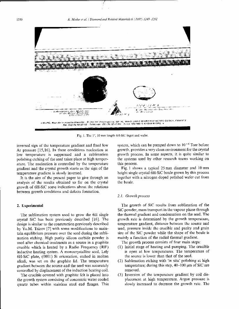
Fig. 1. The 1", 10 mm length 6H-SiC ingot and wafer.
inversed sign of the temperature gradient and fixed low Ar pressure [15,16]. In these conditions nucleation at low temperature is suppressed and a sublimation polishing etching of the seed takes place at high temper- ature. The nucleation is controlled by the temperature gradient and the crystal growth starts as the sign of the temperature gradient is slowly inversed.
It is the aim of the present paper to give through an analysis of the results obtained so far on the crystal growth of 6H-SiC some indications about the relations between growth conditions and defects formation.
2. Experimental
The sublimation system used to grow the 6H single crystal SiC has been previously described [16]. The design is similar to the construction previously described by Yu.M. Tairov [7] with some modifications to main- tain equilibrium pressure over the seed during the subli- mation etching. High purity silicon carbide powder is used after chemical treatments as a source in a graphite crucible which is heated by a Radio Frequency (RF) inductive heating system. A monocrystalline seed, Lely 6H-SiC plate, (0001) Si orientation, etched in molten alkali, was set on the graphite lid. The temperature gradient between the source and the seed was accurately controlled by displacement of the induction heating coil.
The crucible covered with graphite felt is placed into the growth system consisting of concentric water cooled quartz tubes within stainless steel end flanges. This
system, which can be pumped down to 10 ~6 Torr before growth, provides a very clean environment for the crystal growth process. In some aspects, it is quite similar to the systems used by other research teams working on this process.
Fig. 1 shows a typical 25 mm diameter and 10 mm height single crystal 6H-SiC boule grown by this process together with a nitrogen doped polished wafer cut from the boule.
2.1. Growth process
The growth of SiC results from sublimation of the SiC powder, mass transport in the vapour phase through the thermal gradient and condensation on the seed. The growth rate is determined by the growth temperature, temperature gradient, distance between the source and seed, pressure inside the crucible and purity and grain size of the SiC powder while the shape of the boule is mainly a function of the radial thermal gradient.
The growth process consists of four main steps: (1) Initial stage of heating and pumping. The crucible
is open at low temperatures. The temperature of the source is lower than that of the seed.
(2) Sublimation etching with 'in situ' polishing at high temperature; during this step, 40-100 |a.m of SiC are removed.
(3) Inversion of the temperature gradient by coil dis- placement at high temperature. Argon pressure is slowly increased to decrease the growth rate. The
R. Madaretal. / Diamond and Related Materials 6 (1997) 1249-1261 1251
k'i
■M
:fe».., ^akJ
kV %."^k .>&-"-^-- '^H»
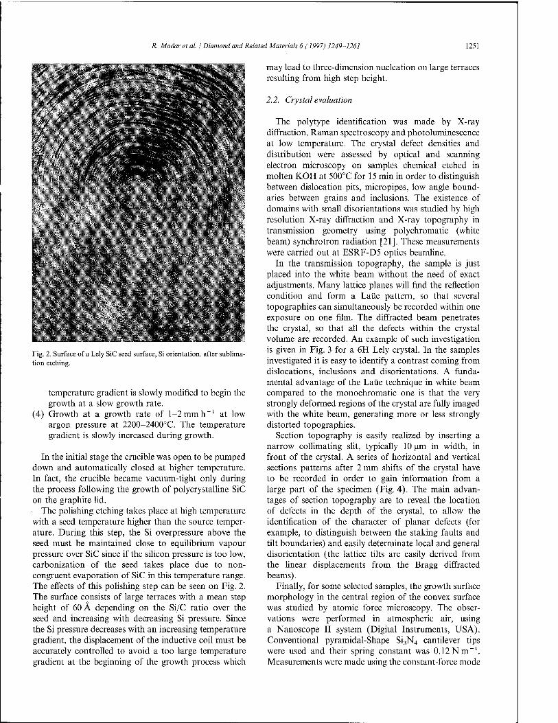
Fig. 2. Surface of a Lely SiC seed surface, Si orientation, after sublima- tion etching.
temperature gradient is slowly modified to begin the growth at a slow growth rate.
(4) Growth at a growth rate of 1-2 mm h"1 at low argon pressure at 2200-2400°C. The temperature gradient is slowly increased during growth.
In the initial stage the crucible was open to be pumped down and automatically closed at higher temperature. In fact, the crucible became vacuum-tight only during the process following the growth of polycrystalline SiC on the graphite lid.
The polishing etching takes place at high temperature with a seed temperature higher than the source temper- ature. During this step, the Si overpressure above the seed must be maintained close to equilibrium vapour pressure over SiC since if the silicon pressure is too low, carbonization of the seed takes place due to non- congruent evaporation of SiC in this temperature range. The effects of this polishing step can be seen on Fig. 2. The surface consists of large terraces with a mean step height of 60 A depending on the Si/C ratio over the seed and increasing with decreasing Si pressure. Since the Si pressure decreases with an increasing temperature gradient, the displacement of the inductive coil must be accurately controlled to avoid a too large temperature gradient at the beginning of the growth process which
may lead to three-dimension nucleation on large terraces resulting from high step height.
2.2. Crystal evaluation
The polytype identification was made by X-ray diffraction, Raman spectroscopy and photoluminescence at low temperature. The crystal defect densities and distribution were assessed by optical and scanning electron microscopy on samples chemical etched in molten KOH at 500°C for 15 min in order to distinguish between dislocation pits, micropipes, low angle bound- aries between grains and inclusions. The existence of domains with small disorientations was studied by high resolution X-ray diffraction and X-ray topography in transmission geometry using polychromatic (white beam) synchrotron radiation [21]. These measurements were carried out at ESRF-D5 optics beamline.
In the transmission topography, the sample is just placed into the white beam without the need of exact adjustments. Many lattice planes will find the reflection condition and form a Laue pattern, so that several topographies can simultaneously be recorded within one exposure on one film. The diffracted beam penetrates the crystal, so that all the defects within the crystal volume are recorded. An example of such investigation is given in Fig. 3 for a 6H Lely crystal. In the samples investigated it is easy to identify a contrast coming from dislocations, inclusions and disorientations. A funda- mental advantage of the Laue technique in white beam compared to the monochromatic one is that the very strongly deformed regions of the crystal are fully imaged with the white beam, generating more or less strongly distorted topographies.
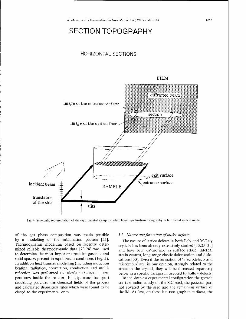
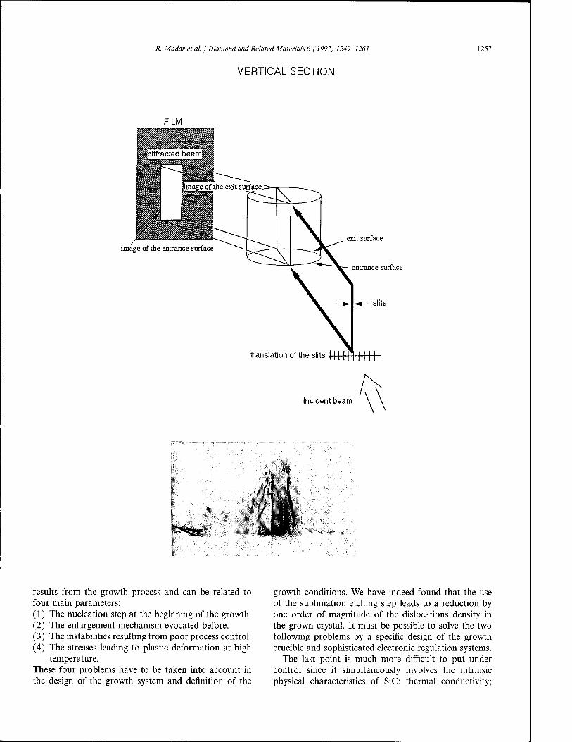
Section topography is easily realized by inserting a narrow collimating slit, typically 10 um in width, in front of the crystal. A series of horizontal and vertical sections patterns after 2 mm shifts of the crystal have to be recorded in order to gain information from a large part of the specimen (Fig. 4). The main advan- tages of section topography are to reveal the location of defects in the depth of the crystal, to allow the identification of the character of planar defects (for example, to distinguish between the staking faults and tilt boundaries) and easily determinate local and general disorientation (the lattice tilts are easily derived from the linear displacements from the Bragg diffracted beams).
Finally, for some selected samples, the growth surface morphology in the central region of the convex surface was studied by atomic force microscopy. The obser- vations were performed in atmospheric air, using a Nanoscope II system (Digital Instruments, USA). Conventional pyramidal-Shape Si3N4 cantilever tips were used and their spring constant was 0.12 Nm_1. Measurements were made using the constant-force mode

1252 R. Madaretal. / Diamond and Related Materials 6 (1997) 1249-1261
TRANSMISSION GEOMETRY
Incident beam
Crystal
hM
h2k2l2
Film
Fig. 3. Schematic representation of the experimental set-up for white beam synchrotron topography in transmission mode; topograph of a Lely 6H-SiC crystal.
of the atomic force microscope, where the force was of 1(T8M.
3. Results and discussion
3.1. Control ofthe poly type structure
Crystals having the same polytype structure as the seed can be grown if the growth occurs in step flow mode at low supersaturation or if the growth conditions correspond 'thermodynamically' to those required for the formation of this polytype, that is, 6H at high temperature and 3C at low temperature. It is well known that the polytype structure of the grown ingots
depends also on the composition of the vapour phase at a given temperature. It was shown, for example, that an excess of silicon, obtained using an additional Si source, may lead to the formation of ingots with 3C-SiC inclusions and in the case of high supersat- uration, if the growth rate is too high at a given temperature the polytype may be modified. SiC-6H crystals grown at 2200°C at a growth rate >2 mm h_1
had inclusions of 3C-SiC while the crystals grown at 2400°C at a growth rate of 2.5 mm h-1 did not have inclusions of other polytypes.
So, by a careful control of the gas phase composition, we have achieved the reproducible growth of pure 6H-SiC boules of 1" diameter starting from 1 cm2
6H-SiC Lely substrates used as seed. The knowledge
R Madaretal. j Diamond and Related Materials 6 (1997) 1249-1261
SECTION TOPOGRAPHY
1253
HORIZONTAL SECTIONS
FILM
image of the entrance surface
image of the exit surface
diffracted beam j
incident beam ::
translation of the slits T
exit surface
\entrance surface
Fig. 4. Schematic representation of the experimental set-up for white beam synchrotron topography in horizontal section mode.
of the gas phase composition was made possible by a modelling of the sublimation process [22]. Thermodynamic modelling based on recently deter- mined reliable thermodynamic data [23,24] was used to determine the most important reactive gaseous and solid species present in equilibrium conditions (Fig. 5). In addition heat transfer modelling (including induction heating, radiation, convection, conduction and multi- reflection was performed to calculate the actual tem- peratures inside the reactor. Finally, mass transport modelling provided the chemical fields of the process and calculated deposition rates which were found to be closed to the experimental ones.
3.2. Nature and formation of lattice defects
The nature of lattice defects in both Lely and M-Lely crystals has been already extensively studied [13,25-31] and have been categorized as surface strain, internal strain centres, long range elastic deformation and dislo- cations [30]. Even if the formation of 'macrodefects and micropipes' are, in our opinion, strongly related to the stress in the crystal, they will be discussed separately below in a specific paragraph devoted to hollow defects.
In the simplest experimental configuration the growth starts simultaneously on the SiC seed, the pedestal part not covered by the seed and the remaining surface of the lid. At first, on these last two graphite surfaces, the

1254 R. Madaretal. / Diamond and Related Materials 6 (1997) 1249-1261
3500 3000 2500 T(K)
\ l
f *
Fig. 5. Partial pressures of gaseous species over SiC as a function of temperature at equilibrium.
SiC deposit is essentially polycrystalline. Hence, the achievement of a cylindrical single crystal boule needs the enlargement or the original single crystal surface of growth at the expense of adjacent polycrystalline ilots.
This enlargement process has been studied by white beam synchrotron topography. We will just give in this paper some indications on the main information obtained to date. Fig. 6 shows the results of the analysis of a 6H wafer by both transmission and section topogra- phy. In the transmission mode, two different positions of the sample were investigated, one at the bottom of the sample [Fig. 6(a)] and the second one at the centre [Fig. 6(b)]. In both cases, the main contrast comes from disoriented regions. All the borders of the sample show highly deformed regions but the centre of the sample also presents localized regions with slight lattice planes disorientation (up to 0.42°). Despite the presence of these disoriented domains, which can be seen also on the section topographs [Fig. 6(c)], the sample is not bent, in fact from one to the other side of the crystal there is no disorientation.
The investigation of a SiC boule by horizontal and vertical topography sections (Fig. 7) reveals that the enlargement process results from a progressive alignment of adjacent to the seed and initially disoriented domains by a continuous deformation of the boundary zones during the growth. A complete description and analysis of the results obtained so far by this technique will be published elsewhere together with a comparison with the work already published on this subject [32-34].
The modelling provides a good understanding of this enlargement phenomenon based on the radial gradient along the growth surface. Due to this radial gradient, ingot diameter increases with an increase in length if the growth of polycrystalline SiC on the graphite lid follows the ingot growth. An increase in radial gradient increased the lateral growth rate. If the distance between the ingot and polycrystal increased, resublimation of the
^
Fig. 6. White beam synchrotron topography analyses of a 6H-SiC sub- strate: (a) transmission topograph of the bottom; (b) transmission topograph at the centre; (c) corresponding sections (displacement between two sections: 2 mm).
ingot on polycrystal leads to a decrease in diameter with increasing crystal length.
X-ray topographies and chemical etching reveal the presence of domains with a high density of dislocation at the boundaries. Defect revelation is mainly done by

R. Madaretal. / Diamond and Related Materials 6 (1997) 1249-1261 1255
Incident beam
growth J ETZTT^
SECTION 1
^^^s^h ■*
FILM
Fig. 7. Horizontal and vertical sections topography analysis of a SiC ingot.
etching in molten alkali, which reveals in addition to pinholes, dislocations and low-angle boundaries between the different domains. The dislocations seen in topogra- phies or revealed as pits on the etched surface are screw dislocations along the growth axis, mixed dislocations with a screw component and pure edge dislocations lying in the basal plane.
It must be kept in mind that chemical etching only allows the determination of the density of dislocations intersecting the surface. According to the classification of Koga et al. [10] they correspond to the medium size and small hexagonal pits appearing on the (0001) Si-side
face after etching. Each of these pits has six sidewalls corresponding to the traces of the six [1100] planes intersecting the surface and a pointed bottom (Fig. 8). The total dislocations density is in general higher than the mean value determined by this technique (ca 104 cm"2) since the diffraction micrograph show a high density of dislocations lines lying parallel with (0001) planes.
Since the Lely 6H-SiC seed is characterized by a low density of dislocations lying mainly in the basal plane, we may consider that the high density generally reported for the SiC boules grown by the sublimation technique

1256 R. Madaretal. I Diamond and Related Materials 6 (1997) 1249-1261
SECTION 2
SECTION 3
SECTION 4
FILM
A
Incident beam
A°
/Jh FILM
A //B
/ Ji Incident beam /// »■ _X ^^'l/l
0 ^^
R. Madar et al. / Diamond and Related Materials 6 (1997) 1249-1261
VERTICAL SECTION
1257
FILM
/■ ■y
image of the entrance surface exit surface
entrance surface
slits
translation of the slits
Incident beam
results from the growth process and can be related to four main parameters: (1) The nucleation step at the beginning of the growth. (2) The enlargement mechanism evocated before. (3) The instabilities resulting from poor process control. (4) The stresses leading to plastic deformation at high
temperature. These four problems have to be taken into account in the design of the growth system and definition of the
growth conditions. We have indeed found that the use of the sublimation etching step leads to a reduction by one order of magnitude of the dislocations density in the grown crystal. It must be possible to solve the two following problems by a specific design of the growth crucible and sophisticated electronic regulation systems.
The last point is much more difficult to put under control since it simultaneously involves the intrinsic physical characteristics of SiC: thermal conductivity;

1258 R. Madaretal. / Diamond and Related Materials 6 (1997) 1249-1261
m
c.V Spot Magn Dot WD !l5.0kV5.0 241x . SE 13.6 VJMA-B5.lmminlKOII.500C.l5mn
Fig. 8. SiC wafer surface, (0001) Si-side, after chemical etching which reveals etch pits and micropipes.
thermal expansion coefficient; emissivity at high temper- ature; and the specific characteristics of the growth system: source and seed temperatures; vertical and radial thermal gradient; shape of the crucible...; all parameters which determine the thermoelastic field in the growing crystal.
3.3. Hollow defects
We will classify in this common denomination the already reported formation of 'macrodefects' and micro- pipes in addition to pyramidal holes (Fig. 9), which have been observed in some of our crystals. They were found at the interface in non-optimal conditions of
ft*!"*;--*.---'»!?.
Fig. 9. SEM micrograph of a 'pyramidal' hole at the surface seed-ingot.
sublimation etching. As a result, the crystals starts to growth in the islands growth mode in place of the desired steps flow mechanism. The resulting nuclei formed on the surface may coalesce leading to the formation of pyramidal holes if, like for the growing ingot, their diameters increase with the increase of ingot height. The contamination of the seed surface may come from local carbonization if the Si overpressure is too low or deposition of impurities evaporated from the SiC powder.
Macrodefects are large vertical holes with horizontal enlargement at the end (Fig. 10). They start at the interface holder-seed and may penetrate deep into the growing crystal. The formation of these defects has been explained [12] by local sublimation of the seed and then the growing ingot. High temperature and large temper- ature gradient between the seed and graphite holder lead to local sublimation of the seed at the beginning of the growth and then to the macrodefect formation. These macrodefects can be eliminated by a specific design of the seed-holder attachment technique, which determines the local gradient at the interface between the seed and the holder. Another practical solution may consist in a modification of the thermoelastic field into the growing ingot in order to stop the progression of these macrodefects into the single crystal boule. Both solutions are presently under investigation.
A major problem in the growth of SiC single crystals is the appearance of hollow pipes, so-called pinholes or micropipes, growing along the c axis through the whole crystal. Their diameter may vary from a few nanometers to several ten micrometers from pipe to pipe and also along the same pipe. Facets have been recently observed by transmission electron microscopy in the walls of pipes having a typical diameter of 15 \im [35]. Typical density of these pipes ranges between 50 cm-2 to several 1000 cm"2 measured on basal plane while better results
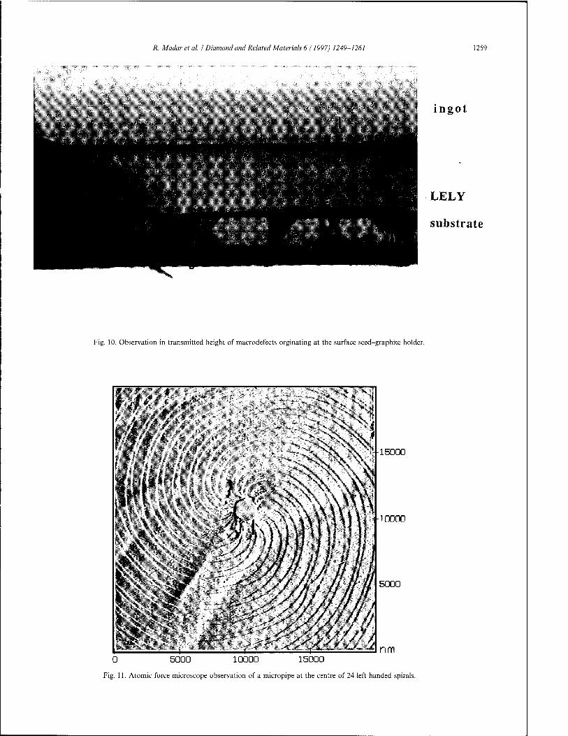
R Madar et al. / Diamond and Related Materials 6 (1997) 1249-1261 1259
ingot
LELY
substrate
Fig. 10. Observation in transmitted height of macrodefects orginating at the surface seed-graphite holder.
1 ""*" ~~ All4
.^i-4^r^!
1-15000
?-10000
5000
nm 0 5000 10000 15000
Fig. 11. Atomic force microscope observation of a micropipe at the centre of 24 left handed spirals.

1260 R. Madaretal. / Diamond and Related Materials 6 (1997) 1249-1261
have been reported recently by Cree Research without indications on the technical solutions used to achieve this goal [17]. The sublimation etch technique described above has permitted the reproducible growth of 6H-SiC crystals with < 100 cm"2 pinholes density.
It has been reported that the concentration of pinholes varied over the surface of the wafers, (0001) orientation, in a similar manner to the concentration of misoriented domains [30]. Since in M-Lely crystals these domains are bordered by boundaries of high dislocations density, it is quite natural that the more often proposed explana- tions for the formation of micropipes are based on the original mechanisms proposed first by Franck [36] and then developed theoretically by different groups [37- 44]. In its original work, Franck points out that a dislocation whose Burgers vector exceeds a critical value is only in equilibrium with an empty tube at its core of radius r such as:
r = \ib2 in2y
where y is the specific surface energy of the material, u its rigidity modulus and b is the modulus of the Burgers vector. The values generally accepted for y and \i are 400 erg cm-2 and 16.6 x 10u erg cm-3, respectively, leading to a value of 42 A-1 for u/y [30]. Quite different values have also been reported for this ratio [45-47] but the ones given above seem to be the more reliable. According to this model, a perfect screw dislocation in 6H-SiC whose Burgers vector in equal to the unit cell dimension along the c-axis should lead to a hole of 12.0 nm radius. To find values closer to what it is generally observed, one must consider the general case of a perfect screw dislocation in the 6H structure whose the Burgers vectors b = 6mh [30], m being an integer and h the length of an unit monomolecular layer parallel to the basal plane: 0.2518 nm. The 6m unit step could be distributed in any manner between the limits of complete bunching into a single macrostep of height h. Fig. 11 obtained by atomic force microscopy on the flat top surface of an as grown ingot illustrates this point by showing a micropipe surrounded by 24 left handed spirals with step height of 3h originated from a screw dislocation of Burgers vector 6x 12/*:18.129nm with a calculated r=1.72 nm quite close to the value deduced from Fig. 11.
A detailed analysis of step flow, step bunching and periodic delineation on the surface of 6H-SiC crystal is out of the scope of this paper and will be published elsewhere. However, based on these results, we may confirm that SiC can grow in a step flow mode from a spiral originated at an emerging screw dislocation: due to the stress a hollow core could develop and from this hollow core, a spiral step emerges. The bases of terrace risers are source of atomic steps and the lateral move- ment of these atomic steps on the treads causes the vertical growth of the crystal [48,49]. The growth will
depend on supersaturation and deposition temperature which will defined the surface mobility of reactive chemi- cal species on the terrace. However, in some conditions [48] macrosteps should be able to develop from the natural nucleation of monoatomic step rather than from dislocations. It must be pointed out that in the case of pure edge dislocation with Burgers vector parallel to the free surface, no spiral can be formed but under stress a hollow core will still develop.
In summary, the occurrence and characteristics of the micropipes depend on the dislocation network in the crystal, the supersaturation in reactive gaseous species and the stress field in the crystal during the growth. Hence, the production of SiC 6H single crystals with a low density of micropipes need at least two conditions: (1) The growth must occur in the step flow mode on
well prepared surface and at low supersaturation. (2) The enlargement step must be strictly controlled to
avoid the formation of a high density of screw dislocations along the c-axis.
References
[1] R.F. Davis, Physica B 185 (1993) 1. [2] B.J. Baliga, IEEE Electron Device Letters EDL- 10 (1989) 455. [3] B.J. Baliga, Inst. Phys. Conf. Sei. 142 (1) (1996) 1. [4] G.R. Fisher, P. Barnes, Phil. Mag. B 61 (2) (1990) 217. [5] J.A. Lely, Ber. Dent. Keram-Ges, 32 (1955). [6] Yu.M. Tairov, V.F. Tsvetkov, J. Cryst. Growth 43 (1978) 209. [7] Yu.M. Tairov, Mater. Sei. Engng B29 (1995) 83. [8] D.L. Barrett, R.G. Seidensticker, W. Gaida, R.H. Hopkins, W.S.
Choyke, J. Cryst. Growth 109 (1991) 17. [9] G. Ziegler, P. Lanig, D. Theis, C. Weyrich, IEEE. Trans. Electron
Devices ED-30 (1983) 277. [10] K. Koga, Y. Ueda, T. Nakata, T. Yamagnchi, T. Niina, Vacuum
30(1987)886. [11] D.L. Barrett, J.P. McHugh, H.M. Hobgood, R.H. Hopkins,
P.G McMullin, R.C. Clarke, W.J. Choyke, J. Cryst. Growth 128 (1993) 358.
[12] R.A. Stein, Physica B 185 (1993) 211. [13] J. Takahashi, M. Kanaya, Y. Fujiwara, J. Cryst. Growth 135
(1994)61. [14] S. Nishino, T. Higashino, T. Tanaka, J. Saraie, J. Cryst. Growth
147 (1995) 339. [15] M.M. Anikin, R. Madar, A. Rouault, I. Garcon, L. Di Coccio,
J.L. Robert, J. Camassel, J.M. Bluet, Inst. Phys. Conf. Sei. 142 (1) (1996) 33.
[16] M. Anikin, R. Madar, Proc. E-MRS Spring Meeting (1996). [17] V.F. Tsvetkov, S.T. Allen, H.S. Kong, C.H. Carter Jr, Inst. Phys.
Conf. Sei. 142(1) (1996) 17. [18] Yu.M. Tairov, Inst. Phys. Conf. Sei. 142 (1) (1996) 11. [19] K. Onoue, T. Nishikawa, M. Katsuno, N. Ohtani, H. Yashiro,
M. Kanaya, Inst. Phys. Conf. Serv. 142 (1) (1996) 65. [20] N. Takanaka, S. Nishino, J. Saraie, Inst. Phys. Conf. Serv. 142
(1)(1996) 49. [21] J. Baruchel, Phys. Stat. Sol. (a) 141 (1994) 59. [22] M. Pons, E. Blanquet, J.M. Dedulle, R. Madar, C. Bernard,
J. Electrochem. Soc, 143, 11 (1996) 3727. [23] P. Rocabois, C. Chatillon, C. Bernard, High Temp.-High Press.
27/28 (1995-1996) 3.
R Madaretal. / Diamond and Related Materials 6 (1997) 1249-1261 1261
[24] P. Rocabois, C. Chatillon, C. Bernard, F. Genet, High Tem- p.-High Press. 27/28 (1995-1996) 25.
[25] S. Amelinckx, G. Strumane, J. Appl. Phys. 31 (8) (1960) 1359. [26] I. Sunagawa, K. Narita, P. Bennema, B. van der Hoek, J. Cryst.
Growth 42 (1977) 121. [27] R.S. Rai, G. Siwgh, S.P. Sen Gupta, J. Cryst. Growth 61
(1983)170. [28] P. Bennema, J. Cryst. Growth 69 (1984) 182. [29] A.N. Pilyankevich, V.F. Britun, Phys. Stat. Sol. (a) 82 (1984) 449. [30] P. Krishna, S.S. Jiang, A.R. Lang, J. Cryst. Growth 71 (1985) 41. [31]R.C. Glass, L.O. Kjellberg, V.F. Tsvetkov, J.E. Sundgren, E.
Janzen, J. Cryst. Growth 132 (1993) 504. [32] M. Tuominen, R. Yakimova, R.C. Glass, T. Tuomi, E. Janzen,
J. Cryst. Growth 144 (1994) 267. [33] M. Dudley, S. Wang, W. Huang, C.H. Carter Jr, V. Tsvetkov,
C. Fazi, J. Phys. D: Appl. Phys. 28 (1995) A63. [34] M. Tuominen, E. Prieur, R. Yakimova, R.C. Glass, T. Tuomi,
E. Janzen, J. Cryst. Growth 165 (1996) 233. [35] J. Heindl, M.P. Strunk, Phys. Stat. Sol. (b) (1996) Kl. [36] F.C. Franck, Acta. Cryst. 4 (1951) 497. [37] N. Cabrera, M.M. Levine, Phil. Mag. 1 (1956) 450.
[38] F.C. Franck, Dis. Faraday Soc. 5 (1949) 5. [39] W.K. Burton, N. Cabrera, F.C. Franck, Phil. Trans. Roy. Soc.
243(1951)299. [40] I. Sunagawa, B. Bennema, J. Cryst. Growth 46 (1979) 451. [41] I. Sunagawa, B. Bennema, J. Cryst. Growth 53 (1981) 490. [42] B. van der Hoek, J.P. Van der Eerden, P. Bennema, J. Cryst.
Growth 56 (1982) 108. [43] B. van der Hoek, J.P. van der Eerden, P. Bennema, I. Sunagawa,
J. Cryst. Growth 58 (1982) 365. [44] B. van der Hoek, J.P. van der Eerden, P. Bennema, J. Cryst.
Growth 56 (1982) 621. [45] H. Tanaka, Y. Uemura, Y. Inomata, J. Cryst. Growth 53
(1981) 630. [46] J.P. Golightly, Z. Krist. 130 (1969) 310. [47] E. Pearson, T. Takai, T. Halicioglu, W.A. Tiller, J. Cryst. Growth
70(1984)33. [48] P. Heuell, M.A. Kulakov, B. Bullemer, Silicon Carbide and
Related Materials, Institute of Physics, London, 1994, p. 353. [49] Z. Zhang, M.A. Kulakov, B. Bullemer, Silicon Carbide and
Related Materials, Institute of Physics, London, 1994, p. 349.

DIAMOND AND
RELATED MATERIALS
ELSEVIER Diamond and Related Materials 6 (1997) 1262-1265
Sublimation growth of 4H- and 6H-S1C boule crystals
V.D. Heydemann *, N. Schulze, D.L. Barrett1, G. Pensl Institut für Angewandte Physik, Universität Erlangen-Nürnberg, Staudtstrasse 7, D-91058 Erlangen, Germany
Abstract
The dual-seed-crystal method is developed and used to study the growth of 4H- and 6H-SiC boule crystals by varying particular growth parameters, e.g. the distance between the growth front and the source material and the face polarity of the seeds. A range of values is elaborated for a series of growth parameters, which leads to the growth of single crystals. The grown SiC crystals are electrically and optically characterized. © 1997 Elsevier Science S.A.
Keywords: Sublimation growth; SiC polytypes; Nitrogen donors; Extended crystalline defects
1. Introduction
High quality silicon carbide (SiC) substrates of large diameter (0 > 5 cm) are the basis for a commercial production of SiC-based electronic devices. During the last 3 years, a continuous progress has been achieved in extending the size and improving the quality of 4H- and 6H-SiC boule crystals. However, a series of physical problems, e.g. the control of growing a particular poly- type (4H, 6H) or the avoidance of micropipes, are still not understood. We have started a SiC growth project in order to study the growth mechanism of the sublima- tion physical vapor transport and to provide SiC wafers for our optical and electrical characterization methods.
2. Experimental details
2.1. Dual-seed-crystal method
The modified Lely growth technique was first intro- duced by Tairov et al. [ 1 ] and Ziegler et al. [2]; variations of the growth arrangements are given by several authors [3-6]. The growth system we have used is described in Ref. [7].
In this system, two seed crystals with different proper- ties can be fixed on the lid of the crucible (see Fig. 1). This dual-seed-crystal technique enables the simulta- neous study of SiC growth on two seed crystals with
* Corresponding author. 1 Present address: 6141 Sanctuary Gardens Blvd., Port Orange, FL 32124, USA.
Si-face (0001)
C-face (0001)
graphite lid Fig. 1. Schematic demonstrating the dual seed crystal method for an example of two seeds with opposite face polarity.
different surface properties under identical growth condi- tions. The seeds may differ in face polarity (Si-face or C-face), orientation (on-axis or off-axis), surface treat- ment or polytype (4H or 6H).
2.2. Gro wth parameters
The growth of a particular SiC polytype depends not only on the properties of the seed crystal, but also on a variety of process parameters, which can be adjusted during the growth procedure. The diagrams in Fig. 2 show the dependence of the source temperature TmuTce, the seed temperature Tseed, their difference AT=
seed and the argon pressure pAl in the crucible during a growth run.
0925-9635/97/317.00 © 1997 Elsevier Science S.A. All rights reserved. PII S0925-9635(97)00080-0

V.D. Heydemann etal. I Diamond and Related Materials 6 (1997) 1262-1265 1263
O o
2500
2000
1500
120
~ 90
r 60
30
0 750
t 500
£250 Q.
■WA
• ' '- ■
\ temperature / T T 1 Source » ' Seed
■ ■ ■ ■ i i i i i—i—i i i.,.,
(b) ; i i i i
T ' tempe
/ i temperature difference
AT = T source - T Seed
-i—i—i—i—i i i i i i i_
\y\ ~
"(c) : Ar pressure b
V • % -
■ ■ :—1—•—•—i*--1 » i i i i i i ■■ i i i • ■
-100 0 100 200 tGrowth(min)
300
Fig. 2. Diagrams of (a) the source temperature rsource/seed temper- ature Tseed, (b) the temperature difference ^T=Tsoarcc—TxxA, and (c) the argon pressure pAv as a function of the growth time «Growth during a typical growth run.
The most essential growth parameters and ranges in which these parameters have been varied in our experi- ments are listed in Table 1.
3. Results and discussion
3.1. SiC boule crystal grown by sequential runs
We succeeded in growing 6H- and 4H-SiC boule crystals of about 2.5 cm in diameter and typically 1-2 cm
Table 1 Ranges of values of essential growth parameters typically employed during growth experiments
Growth parameter Range of used values/orientations
Source temperature Temperature gradient Argon pressure Growth duration Distance between growth
front and source material Seed face Seed orientation Additional Si powder
(related to the SiC source material)
2200-2400°C 10-40 K/cm 1-38 torr 1-15 h 6-30 mm
(0001)/(0001) On-axis/f 0-100%
' off-axis
in length. Fig. 3 shows a central cross-sectional cut parallel to the c-axis of a 6H-SiC boule crystal, which is grown sequentially during four growth runs. In this case, we have used only one seed crystal (diameter 0»lOmm). The interfaces between successive growth runs visualize the growth front, demonstrating that the growth rate has been slightly higher in the right half of the figure. The edge regions show a high density of agglomerated micropipes, which arise from the graphite bottom. It seems that the micropipes grow from the interface lid-seed crystal through the seed crystal and continue into the SiC boule. Great care has, therefore, to be exercised in the selection of a suitable lid material and the method of fixing the seed crystal to the lid. The SiC part grown centrally above the seed crystal provides a low density of micropipes. We counted 12 micropipes cm"2 in an area of 4 x 4 mm2 in the bulk of the second run, and we could find no micropipe in an equivalent area of the third run. During the fourth growth run, the growth rate increased considerably owing to the shrinking distance between the growth front and the source material such that the growth resulted in polycrystalline SiC material.
3.2. Effect of the seed face polarity on the grown SiC crystal
The dual seed crystal method is a useful tool to study the effect of the seed face polarity on the polytype, morphology and impurity incorporation of SiC boules.
The growth of the 4H and 6H polytype strongly depends on the face polarity [Si-face (0001), C-face (0001), which is offered for the sublimation growth. 4H-SiC growth is observed exclusively on C-faces, which is in agreement with findings reported [8]. We have observed in more detail 4H growth on on-axis aligned C-faces of 6H- or 4H-SiC seeds when the adjusted growth rates were greater than 1.1 g h1-, and seed temperatures of 2150-2190°C were used. For 8°off-axis aligned C-faces of 6H seed crystals, the para- meter range for 4H growth is slightly extended: Amlid/A?growth>0.5 glr1 and 2060°C< rSeed<2190°C.
The incorporation of nitrogen (N) atoms as the dominating donor species in SiC also depends on the face polarity of the seed crystal, which is presented for the sublimation growth. As is demonstrated by the Hall effect results displayed in Fig. 4a (for an evaluation of the Hall effect data, see Ref. [9]), the incorporation of nitrogen donors in SiC crystals grown on the C-face of seed crystals is higher than in those grown on Si-faces. The ratio of the total concentration of nitrogen donors incorporated in crystals grown on C-faces to those grown on Si-faces increases with the nitrogen concen- tration ([N]N= 1017 cm"3-1019 cm-3) itself:
[NN](C-face)
[NN](Si-face) = 2.2 to 5

1264 V.D. Heydemann et al. / Diamond and Related Materials 6 (1997) 1262-1265
6H-SiC boule central slice parallel to c-axis
5mm
Fig. 3. Cross-sectional view parallel to the c-axis of a 6H-SiC crystal grown sequentially with four growth runs.
| 1018
c 1017 o
(a) (b)
16 - £ 10 c CD o 10
15
!io- o
S io12
■ —Su^u 6H-SiC seed
^%v Vp-face
Si-face ijTv
: NN(C-face) _ *\
] NN(Si-face) ' ^
| 400
1200 T
.2« 100 a o 2 re X
Ü a ill
60
40
20
10
C-face
■; f Si,ace ^
o
6H-SiC seed I 1 1 1 1 T" " f 1 1—I 1 1 1
0 2 4 6 8 10 12 Rez. Temperature 1000/T (1/K)
100 Temperature T (K)
1000
• 6H-SiC grown on C-face o 6H-SiC grown on Si-face
Fig. 4. Hall effect results taken on a pair of 6H-SiC crystals grown by the dual-seed-crystal method with opposite face orientation, (a) Free electron concentration, n, as a function of the reciprocal temperature, T'1. (b) Electron Hall mobility, /%, as a function of the temperature, T.
This observation is independent of the SiC polytype (4H or 6H). Similar trends have also been reported in publications, where the corresponding SiC crystals were grown sequentially and not by the dual-seed method [10,11].
Fig. 4b reveals the electron Hall mobility of the samples investigated in Fig. 4a. Although the nitrogen concentration and the compensation (not shown here) in the 'C-face sample' are higher by approximately a factor of two, which results in a stronger electron scattering by impurities, the overall electron mobility in this sample is higher compared to that grown on the Si-face. This behavior is observed in all corresponding
pairs of SiC samples investigated. We believe that the lower electron mobility in 'Si-face samples' is caused by a degradation of the crystalline quality, as demonstrated in the micrographs of Fig. 5. Whereas the 'C-face sample' shows just eight micropipes, the 'Si-face sample' provides a high density of different extended defects.
4. Summary
We have demonstrated that the dual-seed-crystal method is a powerful tool to study the sublimation

V. D. Heydemann et al. / Diamond and Related Materials 6 (1997) 1262-1265 1265
C-face Si-face
8 micropipes a: hexagonal platelets b: stripe defects c: hollow core defects
(approx. 50um in diam.)
Fig. 5. Optical micrographs of the surface of the C-/Si-face sample characterized in Fig. 4 demonstrating the difference in crystalline defects.
growth of SiC. We succeeded in the growth of high-quality 4H- and 6H-SiC boules and determined ranges of suitable values for the different growth parameters.
Acknowledgement
The support of this work by the German Science Foundation (Sonderforschungsbereich 292) is gratefully acknowledged.
References
[1] Yu.M. Tairov, V.F. Tsvetkov, J. Crystal Growth 43 (1978) 209. [2] G. Ziegler, P. Lanig, D. Theis, D. Weyrich, IEEE Trans. Electron
Devices ED30 (1983) 277. [3] D.L. Barrett, R.G. Seidensticker, W. Gaida, R.H. Hopkins, W.J.
Choyke, J. Crystal Growth 109 (1991) 17. [4] D.L. Barrett, J.P. McHugh, H.M. Hobgood, R.H. Hopkins, P.G.
McMullin, R.C. Clarke, J. Crystal Growth 128 (1993) 358. [5] K. Furukawa, Y. Tajima, H. Saito, Y. Fujii, A. Suzuki, S. Nakaj-
ima, Jpn. J. Appl. Phys. 32 (1993) L645. [6] M. Kanaya, J. Takahashi, Y. Fujiwara, A. Moritani, Appl. Phys.
Lett. 58 (1991) 56. [7] Heydemann, V.D., Schulze, N., Barrett D.L. and Pensl, G Appl.
Phys. Lett. 69 (1996) 3728. [8] R.A. Stein, P. Lanig, S. Leibenzeder, Mat. Sei. Eng. Bll (1992)
69. [9] G Pensl, W.J. Choyke, Physica B185 (1993) 264.
[10] J. Takahashi, N. Ohtani, M. Kanaya, Jpn. J. Appl. Phys. 34 (1995)4694.
[11] K. Onoue, T. Nishikawa, M. Katsuno, N. Ohtani, H. Yashiro, M. Kanaya in, Silicon carbide and related materials, Inst. Phys. Conf. Ser. 142(1995)65.
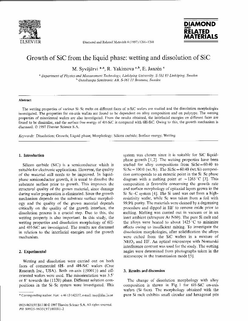
t»v'»-v',;«'.!
DIAMOND AND
RELATED MATERIALS
ELSEVIER Diamond and Related Materials 6 (1997) 1266-1268
Growth of SiC from the liquid phase: wetting and dissolution of SiC
M. Syväjärvi *'a, R. Yakimova a'b, E. Janzena
* Department of Physics and Measurement Technology, Linköping University, S-581 83 Linköping, Sweden b Outokumpu Semitronic AB, S-161 11 Bromma, Sweden
Abstract
The wetting properties of various Si-Sc melts on different faces of a-SiC wafers are studied and the dissolution morphologies investigated. The properties for on-axis wafers are found to be dependent on alloy composition and on polytype. The wetting properties of misoriented wafers are also investigated. From the results obtained, the interfacial energies on different faces are found to be dissimilar, and the surface free energy of 4H-SiC is compared with 6H-SiC. Owing to this, the growth mechanism is discussed. © 1997 Elsevier Science S.A.
Keywords: Dissolution; Growth; Liquid phase; Morphology; Silicon carbide; Surface energy; Wetting
1. Introduction
Silicon carbide (SiC) is a semiconductor which is suitable for electronic applications. However, the quality of the material still needs to be improved. In liquid- phase semiconductor growth, it is usual to dissolve the substrate surface prior to growth. This improves the structural quality of the grown material, since damage during wafer preparation is eliminated. Since the growth mechanism depends on the substrate surface morphol- ogy and the quality of the grown material depends critically on the quality of the growth interface, the dissolution process is a crucial step. Due to this, the wetting property is also important. In this study, the wetting properties and dissolution morphology of 6H- and 4H-SiC are investigated. The results are discussed in relation to the interfacial energies and the growth mechanism.
2. Experimental
Wetting and dissolution were carried out on both faces of commercial 6H- and 4H-SiC wafers (Cree Research Inc., USA). Both on-axis «0001» and off- oriented wafers were used. The misorientation was 3.5° or 8° towards the (1120) plane. Different solution com- positions in the Si-Sc system were investigated. This
: Corresponding author. Fax: +46 13 142337; e-mail: [email protected]
system was chosen since it is suitable for SiC liquid- phase growth [1,2]. The wetting properties have been studied for alloy compositions from Si:Sc = 60:40 to Si:Sc = 100:0 (wt.%). The Si:Sc = 60:40 (wt.%) composi- tion corresponds to an eutectic point in the Si-Sc phase diagram with a melting point at ~1265°C [3]. This composition is favorable concerning the growth rate and surface morphology of epitaxial layers grown in the Si-Sc-C system [4]. The Si used was cut from a high- resistivity wafer, while Sc was taken from a foil with 99.9% purity. The materials were cleaned by a degreasing procedure and dipped in HF to remove oxide prior to melting. Melting was carried out in vacuum or in an inert ambient (ultrapure Ar N60). The pure Si melt and the alloys were heated to about 1425 °C to minimize effects owing to insufficient mixing. To investigate the dissolution morphologies, after solidification the alloys were etched from the SiC wafers in a mixture of NH03 and HF. An optical microscope with Nomarski interference contrast was used for the study. The wetting angles were determined from photographs taken in the microscope in the transmission mode [5].
3. Results and discussion
The change of dissolution morphology with alloy composition is shown in Fig. 1 for 6H-SiC on-axis wafers (Si face). The morphology obtained with the pure Si melt exhibits small circular and hexagonal pits
0925-9635/97/S17.00 © 1997 Elsevier Science S.A. All rights reserved. PII S0925-9635(97)00081-2

M. Syväjärvi et at. / Diamond and Related Materials 6 (1997) 1266-1268
4 ..rSTSSSk^wcHHI
1267
"*,*.®asa
Fig. 1. Dissolution morphology of the 6H-SiC Si-face with different solvent compositions (wt.%): (a) Si:Sc = 100:0, (b) Si:Sc = 85:15, (c) Si:Sc = 60:40 (wafer orientation on-axis).
(Fig. 1(a)). For small amounts of Sc, the dissolved surface has triangular-shaped features (Fig. 1 (b)). When the solvent is more Sc-rich, larger triangular pits are developed (Fig. 1(c)). When the Sc content is above 40 wt.%, the morphology roughens severely, and no clear dissolution patterns are observed. For pure Sc, the dissolution morphology is rough. These observations are explained by an increasing dissolution rate with increasing Sc content in the melt, and by the dissolution mechanism, which obviously has a reactive character. The dissolution morphology of the C face of 6H-SiC was smoother, most probably due to a lower surface energy.
The dissolution morphology of 4H-SiC on-axis wafers (Si face) shows a difference as compared to 6H-SiC under similar conditions. The surface has a rather smooth appearance, with a spiral dissolution being observed occasionally. Most commonly, the dissolution spiral appears where a micropipe is located.
The wetting angles measured for different alloy com- positions are shown in Fig. 2(a). All angles are average values from 4-10 measurements. The wafer orientation was on-axis in order to reduce effects due to misorienta-
tion. The angle on the Si face decreases with increasing Sc content in the melt, due to the increasing solubility of SiC in the melt. A similar dependence is also seen at higher temperature [6] which is used when growing SiC from the liquid phase in the Si-Sc-C system. Measurement of the wetting angle on the C face was difficult when Sc was introduced into the Si melt. For a pure Si melt on on-axis wafers, the wetting angle is lower on the C face than on the Si face of 6H-SiC (Fig. 2(b)). With increasing misorientation the wetting angles approach similar values for different faces and polytypes. The wetting properties were not observed to depend on the wetting ambient, but the mixing of the alloy seems to improve in vacuum.
From the experimental values of the wetting angles, the interfacial energy of the melt/SiC system can be estimated using Young's equation, i.e. ö'6H = ö'int + °meitcos 0, where am is the surface free energy of 6H-SiC, ffmelt is the surface tension of the melt, ffint
is the interfacial energy of the melt/SiC system, and 9 is the wetting angle. There is no reliable data on the surface free energy of a-SiC. However, since the surface atomic configuration of the 6H(0001) face is
1268 M. Syväjärvi et al. / Diamond and Related Materials 6 (1997) 1266-1268
0 ^^ 40 o> OX) C 30 < Ml e 20
■** *•> 10
01 "3D c <
a '£ 0)
0
1 1 1 1 . 1 1 1 . 1 1 1 1 1
:(a)
A A
| i i i i | . i_
A ■
■
A 6H; Si ; A A 6H;Si* :
- T 6H;C - ; ■ 4H; Si :
i i 1 i i . i 1 i . i i 1 i i ■ • 1 i i ■ i 1 . 7"
60 70 80 90 Si [wt%]
100
44 42 40 38 36 34 32 30
. ' 1 ' ' '
r(b) '- A
1 ' ' ' 1 ' 11,1,1, , _
A 6H;Si : ▼ 6H;C ':
1 i . . 1
. .
i 1 i i
11 i .
i I i i
i I t
▼
A
■ 1 , , , 1 ,
m 4H;Si -j
■
.ill,,!,'
0 4 8 Misorientation [°]
Fig. 2. (a) Dependence of the wetting angle of the faces of 4H- and 6H-SiC on alloy composition. Asterisked data are from Ref. [6] and were obtained at a higher temperature (1750 °C). Wafer orientation on-axis. (b) Dependence of the wetting angle on wafer misorienta- tion for 6H- and 4H-SiC on different faces. Alloy composition: Si:Sc = 100:0 (wt.%).
istics have been used to obtain some indications of the possible growth mechanism. Basically, two-dimensional nucleation is considered as a possible growth mechanism when growing from the liquid phase on on-axis oriented substrates [11]. Using the relation between the interfacial energy and the supercooling [11], two-dimensional nucleation on 6H-SiC on-axis wafers may be excluded as a possible growth mechanism on the Si face, but it is likely to occur on the C face. This result is an interesting subject for further experimental study.
4. Conclusion
The wetting properties of Si-Sc melts on SiC improve with increasing Sc content in the melt. However, the dissolution morphology roughens and the reactive dis- solution process is uncontrolled when using Sc-rich solvent compositions. The wetting and dissolution prop- erties are different for the different faces of 6H-SiC and different a-SiC polytypes. From the experimental results, the surface free energy for 4H-SiC is estimated to be ~ 1860 erg cm"2 on the Si face, and this is higher as compared to 6H-SiC. The interfacial energy is lower on the C face than on the Si face for 6H-SiC. The results suggest different growth mechanisms on the different faces.
Acknowledgement
The Swedish National Space Board and the Swedish Board for Industrial and Technological Development (NUTEK) are acknowledged for financial support. We also thank Dr. T. Kimoto for providing information about the surface free energy of SiC.
similar to the 3C-SiC(l 11) face, the calculated data for the cubic polytype [7] are used. Consequently, the surface free energy for 6H-SiC is assumed to be <r6H= 1767 ergcmT2 for the Si face and <r6H = 718 ergcnT2 for the C face. Knowing the surface tension of molten Si (o-Si = 819 ergcnT2) [8] and molten Sc ((TSc=1153 erg cm-2) [9], and estimating the surface tension of the alloy [10], the interfacial energies of the pure Si melt and Si:Sc = 60:40 (wt.%) on the Si and C faces of SiC can be obtained. From Young's equation, the surface free energy for 4H-SiC (Si face) is thus deduced to be about <74H= 1860 ergcnT2, which is higher than that for 6H SiC (Si face). It is worth noting that the interfacial energy of the C face is much lower than that of the Si face of 6H-SiC, and that the interfacial energy is lower when using an alloy as com- pared to a pure Si melt. This result shows that growth in the Si-Sc-C system is energetically more favorable than growth in the Si-C system. Quantitative character-
References
[1] R. Yakimova, T. Tuominen, A.S. Bakin, J.-O. Fornell, A. Veha- nen, E. Janzen, Inst. Phys. Conf. Ser. 142 (1996) 101.
[2] M. Syväjärvi, R. Yakimova, I.G. Ivanov, E. Janzen, Mat. Sei. Eng. B 46 (1997) 329-332.
[3] V. Kotroczo, I.J. McColm, J. Alloys Comp. 203 (1994) 259. [4] R.T. Yakimova, A.A. Kalnin, Phys. Status Solidi (a) 32 (1975)
297. [5] A.W. Adamson, Physical Chemistry of Surfaces, Wiley, New
York, 1990, p. 389. [6] R. Yakimova, PhD thesis, Leningrad, 1974 (in Russian). [7] T. Takai, T. Halicioglu, W.A. Tiller, Surf. Sei. 164 (1985) 341. [8] S-I. Chung, K. Izunome, A. Yokotani, S. Kimura, Jpn. J. Appl.
Phys. 34(1995) L631. [9] C.T. Horowitz (Ed.), Scandium, Academic Press, London,
1975, p. 105. [ 10] V.K. Semenchenko, Surface phenomena in metals and alloys, Per-
gamon Press, Oxford (1961). [11] L.N. Alexandrov, Kinetica obrazovanya i structury tverdyh sloev,
Nauka, Moscow, 1972, p. 145 (in Russian).

DIAMOND AND
RELATED MATERIALS
ELSEVIER Diamond and Related Materials 6 (1997) 1269-1271
The kinetic growth model applied to micropipes in 6H-SiC
J. Heindla'*, W. Dorscha, R. Eckstein b, D. Hofmann b, T. Mareka, St.G. Müller b, H.P. Strunka, A. Winnacker b
a Institut für Werkstoffwissenschaften, Mikro Charakterisierung Universität Erlangen-Nürnberg, Cauerstraße 6, 91058 Erlangen, Germany
b Institut für Werkstoffwissenschaften, Werkstoffe der Elektrotechnik Universität Erlangen-Nürnberg, Martensstraße 7, 91058 Erlangen, Germany
Abstract
In this study we investigated the as-grown {0001} Si surface of modified Lely-grown 6H-SiC using atomic force microscopy. We found micropipes that lie in the center of growth spirals whose radii ranged between 25 and 6000 nm. The screw component of the Burgers vector of the micropipe, which is synonymous with the total step height of the growth spiral, ranged from 1 to 25 unit-cells (1.5-37.5 nm). We fitted Frank's theory of hollow core dislocations, as modified by Cabrera and Levine concerning kinetic effects, to these experimental results and obtained values for surface energy and supersaturation at the inner side of the micropipe. © 1997 Elsevier Science S.A.
Keywords: Micropipes; Growth model; Scanning force microscopy
1. Introduction
Micropipes in silicon carbide (SiC) are known to be hollow defects aligned along the direction of growth of the crystal. As they can penetrate the whole crystal they are a significant problem in growing high grade SiC single crystals. Their radii range from a few nanometers to several tens of micrometers [1]. One proposal for the growth mechanism was given by Frank [2] who consid- ered the hollow core dislocation model. If the Burgers vector of a screw dislocation exceeds a critical value (approximately 1 nm) then it is, due to the very high strain energy, energetically more favorable to remove the crystal material near the dislocation line and to create an additional surface in the form of a micropipe. In this paper we measure total step heights and radii of micropipes and compare this data with the model pro- posed by Cabrera and Levine [3] who extended Frank's model with respect to kinetic aspects.
2. Experimental
We investigated the as-grown 6H-SiC {0001} Si-terminated surfaces of two single crystals grown by
* Corresponding author.
physical vapor transport according to the m-Lely tech- nique. The crystals were grown at a pressure of 30 mbar and at temperatures of 2350<T<2450 K as described in Ref. [4]. The radii and total step heights of the micropipes were measured with an atomic force micro- scope (AFM) in contact mode with pyramidal and high aspect ratio cantilevers. The total step height of a spiral was measured during one revolution around the accom- panying micropipe (Fig. 1). Therefore upward and downward steps were considered to be of opposite sign and the absolute value of the sum represented the total step height.
3. Results and discussion
We found 14 micropipes all surrounded by spirals with step heights ranging from 1.5 (elementary Burgers vector) to 37.5 nm. Their radii ranged from 25 to 6000 nm, respectively. No difference between the two crystals could be observed. Fig. 2 shows the values as a plot suitable for discussion.
According to Frank [2] screw dislocations can mini- mize their total energy by removing material around the dislocation line and forming a hollow core. The relation- ship between the equilibrium radius of the hollow core
0925-9635/97/S17.00 © 1997 Elsevier Science S.A. All rights reserved. PII S0925-9635(97)00082-4

1270 /. Heindl et al. / Diamond and Related Materials 6 (1997) 1269-1271
^
10 pm
10|jm
Fig. 1. Micropipe in 6H-SiC surrounded by spirals: the growth step and the edge of the micropipe are clearly visible. Atomic force microscopy.
Burgers vector, b2, is represented in Fig. 2 with a dashed line. Our measured data do not fit this relationship (Fig. 2a) except for those concerning the micropipes with elementary Burgers vector (Fig. 2b). From these micropipes we obtain a value of \ijy between 93 and 155 A"1. This is in sufficiently good agreement with the value of n/y between 63 and 91 A"1 found by Dudley [5]. Using the room temperature value of ju = 1.9 x 10¹¹ J/m3 we can derive an average sur- face energy for the inner surface of the micropipe of y = 0.14J/m2. This is a rather low value, but not too low to appear unphysical.
An overall fit can be obtained using Cabrera and Levine's [4] kinetic extension (solid line in Fig. 2). This approach considers the fact that the transition from the solid to the gaseous state involves a Gibbs free energy. This energy has to be spent on evaporating the material which would exist inside the volume of the micropipe with radius r0. Again, the equilibrium radius is obtained by minimizing the total energy, which leads to the Cabrera-Levine radius, rcl, of the micropipe:
4000
3
(a)
E c
3
m a.
(b)
1 1 ■rc + .
400 800 1200
Square of total step height / nm2
50
0 2 4
Square of total step height / nm2
Fig. 2. (a) Total step heights versus radii of micropipes in 6H-SiC. The dashed line corresponds to the energetic approach of Frank [2], the solid line corresponds to the best fit obtained by including Cabrera and Levines kinetic extension [4]. (b) Magnified view of the dependen- cies at small pipe radii. The six micropipes have unit cell Burgers vectors. At these small micropipes there is no significant difference between energetic and kinetic theory.
(1)
In our case we identify the Burgers vector b with the total step height of the growth spiral. \i and y denote the shear modulus and the surface energy, respectively. This linear dependence of radius r0 on the square of the
0 and the Burgers vector b is given by:
lib2
° 87i2y
ri+rQrc (2)
Here rc = yQ/Ao is the critical radius of a nucleus on an unstrained surface where Aa denotes the difference of the chemical potential between the solid and the gaseous state and Q denotes the atomic volume. Using the surface energy value obtained above we can fit Eq. (2) to all our data in Fig. 2a and obtain rc = yQ/ Aa = 1.4 nm, yielding Aa=l.l x 10"24 J. This rather low supersaturation is reasonable if we assume that the growth process is stopped by scarcity of SiC-powder in the growth chamber.
4. Summary and conclusion
In this study we measured radii and total step heights of micropipes in m-Lely 6H-SiC. The micropipes can be interpreted as hollow core dislocations. The relationship between micropipe radius and the total step height of the accompanying growth spirals can be understood by using the kinetic theory of Cabrera and Levine. Good agreement between the measured data and the theory yields a micropipe surface energy of 0.14 J/m2 and a supersaturation of 1.1 x 10 ~24 J.
Acknowledgement
This work was supported by the Deutsche Forsch- ungsgemeinschaft (SFB 292 B3), the Bundesministerium

/. Heindl et al. j Diamond and Related Materials 6 (1997) 1269-1271 1271
für Bildung und Forschung (BMBF), and Siemens AG, [3] N. Cabrera, M.M. Levine, Phil. Mag. l (1956) 450. Erlangen (contract # 03 M 2746 B(J) ^ ^' Hofmann, M. Heinze, A. Winnacker, F. Durst, L. Kadinski, P.
Kaufmann, Y. Makarov, M. Schäfer, J. Cryst. Growth 146 (1995)214.
References [5] M. Dudley, W. Si, S. Wang, C. Carter, Jr., R. Glass, V. Tsvetkov, Proceedings of the Third European Symposium on X-ray Topogra-
[1] J. Heindl, H.P. Strunk, Phys. State Sol. 193 (1996) Kl. phy and High Resolution Diffraction, 1996, to be published in II [2] F.C. Frank, Acta Crystal. 4 (1951) 497. Nuovo Cimento D.
DIAMOND AND
RELATED MATERIALS
ELSEVIER Diamond and Related Materials 6 (1997) 1272-1275
Growth-related structural defects in seeded sublimation-grown SiC
M. Tuominen a'b'*, R. Yakimova a'b, E. Prieur c'e, A. Ellison a, T. Tuomi d, A. Vehanen b'e, E. Janzen a'e
a Department for Physics and Measurement Technology, IFM, Linköping University, S-581 83 Linköping, Sweden b Outokumpu Semitronic AB, P. O. Box 111 92, S-161 HBromma, Sweden
c European Synchrotron Radiation Facility, BP 220, F-38043 Grenoble, Cedex, France d Optoelectronics Laboratory, Helsinki University of Technology, FIN-02150 Espoo, Finland
c OkmeticLtd., P.O. Box44, FIN-02631 Espoo, Finland
Abstract
Structural defects in 4H and 6H SiC wafers have been studied by means of synchrotron X-ray topography and optical microscopy. The effect of seed crystal attachment, orientation, growth face shape, reloading and continued growth are discussed. A comparison between 4H and 6H material is made also. The results relate the origin of different defects to the mentioned growth conditions. © 1997 Elsevier Science S.A.
Keywords: 4H SiC; 6H SiC; Sublimation; Synchrotron X-ray photography
1. Introduction
The main problem faced by the commercial applica- tions of SiC is the quality of the substrates. The sub- strates are usually grown by sublimation methods, which causes inherent structural defects. In the seeded sublima- tion method the seed crystal attachment, reloading and continued growth, the growth front shape, the seed type and also the spiral growth mechanism have a crucial effect on the defect formation and appearance. Understanding of defect formation process is important to be able to eliminate defects. As long as the growth mechanism remains unchanged, defects due to the spiral growth mechanism are difficult to totally avoid, but the influence of the other factors can be studied and thus, minimized.
SiC material can normally be studied by optical microscopy obtaining a general picture of the wafer and its imperfections, like macro-defects and doping inhomo- geneities. In order to gain more information about the misorientation, the types of defect and strain fields, synchrotron X-ray topography is needed [1]. In this work different kinds of sublimation-grown samples are studied to clarify the origin of defects and the ways of eliminating them.
' Corresponding author.
2. Growth technique and characterization methods
The material studied was grown using the seeded sublimation technique at Linköping University. The experimental setup is described in [2]. The growth temperature was about 2300 °C and the growth took place at a reduced argon pressure of 5 mbar. Growing either on the C- or the Si-face of the SiC seed resulted normally in 4H or 6H polytypes, respectively, indepen- dent of the seed poly type.
Optical microscopy studies were performed under reflected and transmitted light utilizing Nomarski inter- ference contrast and polarized light. Synchrotron white beam projection and section topographs as well as grazing incidence reflection topographs [3,4] were made at D5 Optics beamline at ESRF in Grenoble, France. Reflected intensities (Laue patterns) were recorded on a Kodak Industrex SR film.
3. Results and discussion
3.1. Seed attachment and start of the growth
The rigid seed crystal attachment to the graphite lid can bend the seed crystal during the heating due to different thermal expansion coefficients of graphite and
0925-9635/97/S17.00 © 1997 Elsevier Science S.A. All rights reserved. PII S0925-9635(97)00096-4

M. Tuominen et al. / Diamond and Related Materials 6 (1997) 1272-1275 1273
Fig. 1. A section topograph of an a-cut 4H SiC sample showing uniform bending.
SiC. This also causes bending of the lattice planes. Such a uniform bending is seen in the section topograph (Fig. 1) taken from a sample cut perpendicularly to the c-axis. The Laue pattern also shows bending effects. The bending may lead to formation of domains with low angle boundaries and polygonization in the growing crystal. Micropipes can be formed at these boundaries [5].
In addition, non-uniformities in the seed attachment may lead to variations in the temperature distribution. Voids can be formed between the substrate and the graphite lid. These voids may hinder the heat dissipation from the crystal. The disturbances cause an uneven surface with depressions corresponding to these voids. This leads to an inhomogeneous defect distribution and doping. Fig. 2 shows a projection topograph of a 4H wafer with one vertical line (L) corresponding probably to a series of dislocations. The line position corresponds to the bottom of the depression on the crystal surface. The dislocations are gathered there owing to the energy minimization. The measurement geometry and the dislo- cation visibility in different reflections suggest that their Burgers vectors are perpendicular to the surface. They might be the same kind of screw dislocations as reported in [6]. Along the line white spots are observed showing
the deformed core. There are also white curved bound- aries (WB) in the picture. Because these boundaries can also be seen as color changes in the optical micrographs, they can be due to changes in defect and doping densities.
In the optical microscopy studies of the initially grown material, micropipes are found corresponding to some black inclusions at the seed-crystal interface. Often there is a defect in the substrate under the inclusion. Sometimes micropipes can change direction at the inter- face. At later stages of the growth these kind of micro- pipes are seen to unite or close up. The micropipes are observed in the vicinity of the voids on the reverse side of the seed.
At the initial stages of the growth the effect of the seed-crystal edges is enhanced. This can lead to a higher growth rate at the edges which results in an uneven surface. On the edges there are flat areas. Between these areas and the center of the crystal there are domain boundaries (DB) with defects (Fig. 3).
3.2. Defects due to interfaces and reloading
The cooling and heating procedures which are inevita- ble for the reloading can cause reformation in the structure. After reloading and the subsequent growth run the heavily bent sample shown in Fig. 1 started to create grain boundaries (GB) with polycrystalline
k,.h
Fig. 2. A projection topograph (g = 021, A = 0.2363A) of a 4H SiC crystal showing a dark line (L) of dislocations and white domain boundaries (WB).
X".
<DB
Fig. 3. A reflection topograph of a 6H SiC wafer with domain bound- aries (DB) between the center and the edges. Also micropipes (M) are observed in the center.
lmm

1274 M. Tuominen et al. / Diamond and Related Materials 6 (1997) 1272-1275
Fig. 4. A section topograph (g = 4310, A = 0.3357 Ä) of a 4H SiC wafer showing an interface (I) between two different growth runs. Also images of voids (V) in the interface and cracks (C) are seen.
growth. It is believed that due to a recrystallization large angle grain boundaries are produced and the grain growth can cause the polycrystal boundaries.
The interfaces between different growth runs are also sources of macro-defects, especially micropipes. Fig. 4 shows a section topograph of a sample cut from an interface between two growth runs. The interface (I) is seen as a black line slightly above the center of the image. One can see several images of voids (V) at the interface as well as a large crack (C). The voids can act as a starting point for dislocations and micropipes. After reloading the new growth starts on a non-flat as-grown surface and voids can be formed. Sometimes there are pits on the surface, which can be formed under C rich conditions. In this case the voids are more frequent. Thus, the quality of the grown material degrades with increasing number of reloadings.
3.3. Defects due to different orientations of the growth face
Off-axis growth seems to generally improve the quality of the material. Domain formation and micropipe sizes are diminished. It is observed that instead of a large micropipe, many smaller ones or even several screw dislocation replace them. Basically the material looks the same as on-axis grown one, but in addition line defects lying parallel to the steps appear. They are usually near the central facet and are due to a terraced growth [7].
The misorientation between different domains seems to be small in off-axis grown wafers. The section topo- graphs from such samples are not as bent as the ones taken from the highly misoriented samples [5].
The growth face orientation affects the doping homo- geneity. In the topographs one can see darker and lighter areas due to different amounts of defects related to the growth face orientation. The best quality material is grown in the middle of the crystal where the growth front is perpendicular to the growth direction. Depending on the angle between the flat and the adjacent surface the doping difference changes as well as the amount of defects at the interface. The steeper the adjacent surface the more defects are generated. In the case of very steep adjacent surfaces formation of grooves is observed. In these grooves the nucleation is disturbed and other polytypes are found.
3.4. Comparison between 4H and 6H material
The comparison between 4H and 6H crystals reveals a difference in the micropipe and domain appearance. The micropipes seem to be larger and the domain misorientation greater in the 6H wafers. Their section topographs are distorted whereas those of the 4H wafers are almost straight. Though, some bending-like effect is observed owing to polygonization. This may be expected when applying the same growth conditions, since the Burgers vector for 6H polytype is longer than for 4H SiC. According to the topographs the regions between micropipes in 6H have less defects. The reason for this can be that the defects are gathered into the micropipes which are bigger.
Sometimes there is a tendency of formation of 6H instead of 4H on the C-face. If this happens it usually results in a very poor quality 6H material with a high density of micropipes. There are also inclusions of 15R polytype which create a lot of strain and twist in the material and even higher micropipe density.
4. Conclusion
The crystal quality depends on several factors. Among them the most important appears to be the seed quality and the seed attachment. The formation of macro- defects happens very easily and factors such as well- polished substrate surface and stress-free attachment should be taken good care of to avoid defect formation and polygonization. It is also essential to keep the growth face as flat as possible.
Acknowledgement
The synchrotron topographic measurements were car- ried out under experiment HC 544 at ESRF. The authors would like to thank Dr. Jose Baruchel and Dr. Jürgen Hartwig for the beam time and for the assistance. Special thanks to M.Syväjärvi for technical assistance during the growth experiments. This work was financially sup- ported by the Swedish Board for Industrial and Technical Development (NUTEK).

M. Tuominen et al. j Diamond and Related Materials 6 (1997) 1272-1275 1275
References \M J. Baruchel, Y. Epelboin, J. Gastaldi, J. Hartwig, J. Kulda, P. Rejmankova, M. Schlenkev, F. Zontone, Phys. Status Solidi (a) 141 (1994) 59.
[1] M. Tuominen, E. Prieur, R. Yakimova, R.C. Glass, T. Tuomi, E. [5] M Tuominelli R yakimova, R.C. Glass, T. Tuomi, E. Janzen, Janzen, J. Crystal Growth 165 (1996) 233-244. ; Crysta] GrQwth m {mA) 261^276
[2] R. Yakimova, M. Tuominen, E. Janzen, Epigress Application Bui- [6] M Dud,ey; s Wan& w Huang; c H Carter Jr _ y Tsvetkov> c
letin, 1995 Epigress AB, S-223 70 Lund, Sweden. Fazi> ; phys D. App, phys 2g (1995) A63_A68
[3] T. Tuomi, K. Naukkannen, P. Rabe, Phys. Status Solidi (a) 25 [y] £ Bau Rp Stnmk ; c , Growth 69 (19g4) 561_580. (1974)93.

DIAMOND AND
ELSEVIER
RELATED MATERIALS
Diamond and Related Materials 6 (1997) 1276-1281
Surface polarity dependence in step-controlled epitaxy: progress in SiC epitaxy
Hiroyuki Matsunami *, Tsunenobu Kimoto Department of Electronic Science and Engineering, Kyoto University, Yoshidahonmachi, Sakyo, Kyoto 606-01, Japan
Abstract
The dependence of surface polarity in step-controlled epitaxy of 6H- and 4H-SiC polytypes on off-oriented {0001} substrates was examined. Dominant step heights correspond to half (6H-) or a full (4H-) unit cells of the SiC polytypes. The background doping level can be reduced to less than 1 x 10¹⁴ per cm3 by growth under C-rich conditions. High electron mobilities of 431 cm2 Vs_1 for 6H-SiC and 851 cm2 Vs_1 for 4H-SiC were obtained. The high quality of the epilayers was also elucidated, since the deep trap concentration detected by deep level analysis was in the order of 1012 per cm3. The surface polarity dependence and polytype dependence of impurity doping were demonstrated. © 1997 Elsevier Science S.A.
Keywords: Step-controlled epitaxy; Surface polarity dependance; Step bunching; C/Si ratio dependance
1. Introduction
Wide bandgap semiconductor silicon carbide (SiC) has been strongly anticipated as a candidate for high-temperature, high-power, and high-frequency/high- power electronic devices. Owing to the remarkable progress in homoepitaxy, various active semiconductor devices for the above purposes have been demon- strated [1].
In SiC epitaxial growth by chemical vapor deposition (CVD), step-flow growth on off-oriented SiC {0001} substrates ensures the polytype replication even at rela- tively low temperatures below 1600 °C (step-controlled epitaxy) [2]. Several reports on epitaxial growth on SiC vicinal substrates have been published to clarify the step-flow growth [3-8]. There exist two competitive processes on a growing surface, step-flow growth from atomic steps and two-dimensional nucleation on a terrace. The supersaturation of chemical species con- tributing to crystal growth on substrate terraces, which determines the growth mode, strongly depends on growth temperature, C/Si ratio, and step structures. In addition, the nucleation rate and surface migration rate are different for substrate surface polarity (Si or C faces). It is, therefore, more important to control the supersaturation on a surface to get high-quality epilayers
' Corresponding author.
without other polytype inclusions. In this paper, surface morphology, step bunching, and impurity doping in 6H-SiC and 4H-SiC epitaxial growth, especially surface polarity dependence, are discussed in detail.
2. Step-controlled epitaxy
Crystal growth was carried out by atmospheric-pres- sure CVD in a horizontal reaction tube. SiH4 (1% in H2) and C3H8 (1% in H2) were used as source gases with H2 carrier gas. The flow rates of SiH4 and C3H8
were 0.05-0.60 seem (typically 0.30 seem) and 0.03-0.80 seem (typically 0.20 seem), respectively. The H2 flow rate was fixed at 3.0 slm, which provides a linear gas velocity of 6-10 cm s_1. N2 was used for n-type doping, and trimethyl-aluminium (TMA), triethyl-aluminium (TEA) and B2H6 for p-type doping. Hydrogen chloride (HC1) gas was used for etching of a substrate surface before CVD growth.
Both (0001) Si and (000f)C faces were used to investigate the surface polarity dependence. Substrates were heated by radio-frequency induction. Before CVD growth, in-situ HC1 etching was carried out to remove surface damage. The growth temperature was varied in the range of 1100-1600 °C (typically 1500 °C).
Through various fundamental studies [9-11],
0925-9635/97/S17.00 © 1997 Elsevier Science S.A. All rights reserved. PII S0925-9635(97)00104-0

H. Matsunami, Tsunenobu Kimoto j Diamond and Related Materials 6 (1997) 1276-1281 mi
the following features have been made clear in step- controlled epitaxy. (1) The rate-determining step is given by the supply of
SiH4. (2) Surface morphology depends on the C/Si ratio. (3) Step-flow growth is obtained for off-angles of more
than 1°. (4) A small activation energy of 2.8 kcalmol"1 in the
temperature dependence of growth rate can be explained by a stagnant layer model [12].
(5) From a surface diffusion model [13], the critical growth conditions for step-flow are predicted.
The nucleation and lateral growth of steps in SiC growth were studied through short-time growth [14,15]. The nucleus density increases significantly at low temper- atures, which is attributed to the higher supersaturation caused by the reduced equilibrium vapor pressure and the suppressed surface diffusion of adsorbed species. The nucleus density is higher on (0001)C faces than on (OOOl)Si faces by more than one order of magnitude probably owing to its lower surface free energy [16]. There exists anisotropy in lateral growth: the faster growth is obtained for the <1120> direction, and the lower for <1100> [14].
3. Surface morphology and step bunching
The step structure of 6H- and 4H-SiC epilayers was investigated [17]. As-grown samples without any surface treatments were examined using atomic force micro- scopy (AFM) and transmission electron microscopy (TEM) observations. Cross-sectional TEM observation was done using 400 keV, and each sample was examined along the <U00> or <1120> zone axis.
In AFM images of 6H-SiC epilayers grown on (0001) Si and (0001) C faces, a distinctive difference in surface structure exists. An epitaxial layer on a (0001) Si face yields "apparent macrosteps" with a terrace width of 220-280 nm and a step height of 3-6 nm. High-reso- lution observation revealed that each macrostep on a (0001) Si face is not a single multiple-height step but composed of a number of "microsteps" [17]. On a (0001) C face, the surface becomes rather flat and no macrosteps are observed. Although 4H-SiC epilayers had similar step structures, the 4H-SiC (0001) Si faces exhibited real macrosteps with 110-160 nm width and 10-15 nm height.
The mechanism for the formation of "apparent macrostep" on 6H- and 4H-SiC (0001) Si faces is not clear at present. However, the surface seems quite similar to "hill-and-valley (or faceted)" structure, which often appears on a surface grown with off-orientation from a low-index plane [18,19]. The off-oriented surfaces may spontaneously rearrange to minimize their total surface
energy, even if this involves an increase in the surface area. The surface free energy of SiC was calculated as 2220 erg cm"2 for a (0001) Si face and 300 erg cm-2 for a (0001) C face [20]. The surface energy may be reduced by the formation of "hill-and-valley" structure on an off-oriented (0001) Si face, which has much higher surface energy.
Fig. 1 shows typical cross-sectional TEM images for 4H-SiC surfaces grown on (a) (0001) Si and (b) (000f) C faces. The samples were examined along the <1120> zone axis to obtain clear lattice images. No island growth on the (0001) terraces are observed. On a (0001) Si face (Fig. 1(a)), the number of Si-C bilayers at bunched steps is four: the bunched steps correspond to exactly the unit cell of_4H-SiC, ABCB steps in the ABC notation. On a (0001) C face (Fig. 1(b)), however, single bilayer-height steps dominate, and the number of bunched steps is relatively small.
Fig. 2 shows the histograms of step height for the surfaces of (a) 6H-SiC and (b) 4H-SiC epilayers grown on a (0001) Si face through observation of more than 200 steps. In 6H-SiC, 88% of steps have three Si-C bilayers (half of a unit cell), and 7% of steps have six Si-C bilayer height (unit cell). However, on 4H-SiC, four bilayer-height (unit cell) steps are the most domi- nant (66%) and two bilayer-height steps show the second highest probability (19%). Single Si-C bilayer-height steps are relatively few (5% or less) on both 6H- and 4H-SiC.
In Fig. 3, the histograms of step height for the surfaces of (a) 6H-SiC and (b) 4H-SiC epilayers on a (0001) C face are shown. In contrast to the bunched steps on a (0001) Si face, single Si-C bilayer-height steps are domi- nant on a (0001) C face for both polytypes, showing probability of 70-80%. A small number of bunched steps have a three or six bilayer-height in 6H-SiC, and a two or four bilayer-height in 4H-SiC. The origin of this striking surface polarity dependence is not known. The migrating species, surface coverage, and exact bond configuration at step edges should be analyzed to reveal the mechanism.
On a (0001) Si face with a 3.5° off-angle, the average terrace width experimentally obtained was 12.4 nm for 6H-SiC and 16.8 nm for 4H-SiC In spite of the same off-angle, the different average terrace width between 6H-SiC and 4H-SiC originates from the different height of multiple steps. From the point of view of step-flow growth, narrow terraces are preferable. This is crucial in SiC growth, because supersaturation of chemical species (Si species [10]) increases on wider terraces, leading to 3C-SiC nucleation on the terraces. In this sense, 4H-SiC, which shows wider terrace widths, may have a relatively higher probability for 3C-SiC nucle- ation on the terraces. To overcome this problem, a slightly higher growth temperature would be helpful, since the longer surface diffusion length of adsorbed

1278 H. Matsunami, Tsunenobu Kimoto / Diamond and Related Materials 6 (1997) 1276-1281
IW ;(b)IÜ
[0001] 1
™.\\1 kiA\o;\v^-_.^i ■.!. ■.'i'' I',.,i-'\i,\i,'i'i».0'l»-
i^iiwwuwMtriiuVAWMÜVASttY«^
äfö ft| step ^Ä\f|s|f,i||%SSa
SÄ!
P*rU^tWti jgtimm
[0001] iiSHSuHfttnifth
[1120]
— [1100]
w-immmiL
&Wjjjji ~Sä=?a£ **<t**tfi* xtCStKtvttv jMj&ii
sUgjltt wR/Wt WjpjßiliL
man iitiliwü! •fflSÜtflfilW!!
50Ä [1120]
[lioo] 50Ä
Fig. 1. Typical cross-sectional TEM images for 4H-SiC surfaces grown on: (a) Si and, (b) C faces. Substrates are (0001) Si 3.5° off-oriented toward [1120]. Samples are examined along the [1210] zone axis.
1.0
0.8
5 0.6 5 < CD O 0.4 rr a.
0.2
0.0 ~I
i 1 1 r i i i | i
6H-SiC Si face, 3.5° off - C/Si = 2.0
, 1 1 , , , . . ~ 1 2 3 4 5 6 7 8 9 10 11 12
NUMBER OF Si-C BILAYER AT STEP
1.0
0.8
5 0.6 m < CO O 0.4 ÜC D-
0.2
0.0
1 I— I ' i 1 r i I i | i
4H-SiC Si face, 3.5° off - C/Si = 2.0
I I I I i i i . .. 1 2 3 4 5 6 7 8 9 10 11 12
NUMBER OF Si-C BILAYER AT STEP
(a) (b)
Fig. 2. Histograms of step height for surfaces of: (a) 6H-SiC and (b) 4H-SiC epilayers. Substrates are (0001) Si 3.5° off-oriented toward <1120>.
1.0
0.8
§ 0.6 CD < CD O 0.4 rr Q.
0.2 h
0.0
—I ■ 1 1 1 r
6H-SiC C face, 3.5° off - C / Si = 2.0
, r 1 i , i 1 i
1 2 3 4 5 6 7 8 9 10 11 12 NUMBER OF Si-C BILAYER AT STEP
I.U i i i i i i i i i i i
4H-SiC -
0.8 —, C face, 3.5° off - C/ Si = 2.0
PR
OB
AB
ILIT
Y
o
o
*■
CO
-
0.2
- i—i i j i i i i i
-
■ 1 2 3 4 5 6 7 8 9 10 11 12 NUMBER OF Si-C BILAYER AT STEP
(a) (b)
Fig. 3. Histograms of step height for surfaces of: (a) 6H-SiC and (b) 4H-SiC epilayers. Substrates are (0001)C 3.5° off-oriented toward <1120>.

H. Matsunami, Tsunenobu Kimoto / Diamond and Related Materials 6 (1997) 1276-1281 1279
species and lower supersaturation on terraces are expected. Larger off-angles of substrates are also effec- tive in 4H-SiC growth [21]. However, a (0001) C face showed much narrower average terrace width, owing to fewer bunched steps: epilayers grown on a (OOOf) C face exhibit a very flat surface even for 4H-SiC.
As shown in Figs. 2 and 3, the formation of three or six bilayer-height steps seems to be inherent in 6H-SiC growth, and two or four bilayer-height steps in 4H-SiC growth. Similar results have been reported on 6H-SiC surfaces grown by the Lely method [22] and MBE [23]. The step bunching in SiC, therefore, may be correlated with the surface equilibrium process. Since the surface energy is different for each SiC bilayer plane owing to the peculiar stacking sequence [24], it may lead to a different step velocity between each Si-C bilayer, and causes "structurally induced macrostep formation" [25].
4. In-situ doping of impurities
4.1. Polarity dependence in doping
Fig. 4 shows the C/Si ratio dependence of background doping level in unintentionally doped epilayers. For a C/Si ratio of 2, no significant difference was observed between epilayers on (0001) Si and (0001) C faces. On a (0001) Si face, the donor concentration estimated from capacitance-voltage (C-V) characteristics can be drastically reduced by increasing the C/Si ratio, the lowest value is in the range of 5 x 10¹³—2 x 10¹⁴ per cm3. On a (0001) C face, however, the donor concen- tration is not sensitive to the C/Si ratio.
In-situ n-type doping can be easily achieved by the introduction of N2 during epitaxial growth. The donor concentration increased proportionally with the increase of Nj flow rate in the wide range on both (0001) Si and (0001) C faces. The doping efficiency of N strongly depends on the C/Si ratio during CVD growth (site- competition epitaxy) [26]. The higher C/Si ratio leads to the lower N concentration. This can be explained by that the higher coverage with C atoms on a growing surface prevents the incorporation of N atoms into epilayers, which substitute at the C site and work as donors.
However, the incorporation of Al and B atoms, which substitute at the Si site, is enhanced under C-rich condi- tions on a (0001) Si face [26,27]. The addition of trimethyl-aluminum (TMA:A1(CH3)3) is effective for in-situ p-type doping. Although most Al-doped epilayers showed very smooth surfaces, pits and hillocks were observed in heavily doped (Al concentration: 1019 per cm3) samples grown on (0001) C faces. The supply of TMA causes the shift of growth conditions toward C-rich ambience owing to the release of CH3 species from the mother molecules. The surface migration is suppressed and the two-dimensional nucleation is enhanced under C-rich conditions [15]. Besides, (0001) C faces easily suffer from two-dimensional nucleation, owing to its low critical supersaturation ratio. This may cause the surface roughening of heavily doped epilayers grown on (0001) C faces. The Al acceptor concentration versus the TMA flow rate for a C/Si ratio of 2 is shown in Fig. 5. The acceptor concentration estimated from C-V measurement agreed well with the Al concentration determined by secondary ion mass spectroscopy meas- urement. The doping efficiency is much higher on a
7 1017
o
16
15
10
< rr h- S 10 ü z o o §10" z o Q
\
I O
O : Si face • : C face
I I
"1 1 1 1— undoped 4H-SiC : SiK : 0.30sccm
!
J I 23456789
C/Si RATIO
CO
CM
E ü
£ CD O
o rr 1- ü LU _J LU
1000
900
800
700
600
500
400
300
200
100
1 llllll| 1 1 1 lllll| 1 1 llllll| 1 1 1 lllll| 1 1 1 lllll| 1 1 1 Mill
N-Doped Epilayer - •--^
- ^ 4H-S1C \ - . :
• \ \ • \
_ \
0--. «\
"^ - O Co°^ Q 6H-SIC OCD^
L
% .
1 ' ' 1 null ' 1 ' Mini 1 1 1 inn! 1 1 1 mill 11
Fig. 4. C/Si ratio dependence of donor concentration for unintention- ally doped 4H-SiC epilayers.
Fig. OH-
IO13 1014 1015 1016 1017 1018 1019
ELECTRON CONCENTRATION (err)-3)
5. Electron mobility versus carrier concentration of n-type and 4H-SiC epilayers at room temperature.

1280 H. Matsunami, Tsunenobu Kimoto / Diamond and Related Materials 6 (1997) 1276-1281
(0001) Si face than that on a (0001) C face by a factor of 10-80. On a (0001) Si face, the acceptor concentration increases superlinearly with the TMA supply, which may be caused by the increased effective C/Si ratio under high TMA flow conditions.
4.2. Polytype dependence in doping
4.2.1. n- type doping Relatively high values of ionization energy for N
donors in SiC (80-144 meV in 6H-SiC [28]) cause incomplete activation at room temperature. The activa- tion ratio n/Nd (where n is electron concentration; and Nd is donor concentration) is theoretically estimated as 0.4-0.7 at room temperature, which was confirmed experimentally. Fig. 6 shows the electron mobility at room temperature versus the carrier concentration of 6H- and 4H-SiC epilayers. As is well known, 4H-SiC exhibits electron mobility two times higher than that of 6H-SiC. However, the difference seems to be small for heavily doped layers, as in a previous report [29]. As shown in Fig. 4, very low doped epilayers can be grown on (0001) Si faces under C-rich conditions. For very low doped epilayers grown with a C/Si ratio of 4-5, high electron mobilities of 431 cm2 Vs"1 (n = 2 x 10¹⁴
per cm3) for 6H-SiC and 851 cm2 Vs"1 (» = 6 x 10¹³ per cm3) for 4H-SiC were obtained at room temperature, the highest values ever reported, to our knowledge. For device applications, 4F£-SiC is much more attractive than 6H-SiC owing to its higher electron mobility and smaller anisotropy in mobility [29,30].
4.2.2. p-type doping Because of a high value of ionization energy for Al
acceptors (250 meV) [31], the activation ratio p/NA
(where p is hole concentration; and N& is acceptor concentration) was as low as 10_2-10_1 at room tem- perature. However, a very high hole concentration of 4-6 x 10¹⁹ per cm3 could be achieved for heavily doped epilayers (Al concentration is in the mid 1020 per cm3), which might arise from the decreased ionization energy in heavily doped samples, or from the formation of an impurity band. The lowest p-type resistivity was 0.042 Qcm for 6H-SiC and 0.025 Qcm for 4H-SiC, obtained on (0001) Si faces.
Fig. 7 shows the hole mobility at room temperature versus the carrier concentration of Al-doped 6H- and 4H-SiC epilayers. The hole mobility is 67cm2Vs_1 at 2 x 10¹⁶ per cm3, and 6 cm2 Vs-1 at 1 x 10¹⁹ per cm3 for 6H-SiC. The hole mobility of 4H-SiC seems to be higher than that of 6H-SiC for the same hole concentration.
Another hopeful acceptor is boron (B), which can be easily doped using B2H6 gas. Although B doping did not affect surface morphology, the growth rate was reduced by 20-30% in epitaxial growth. The plot of B acceptor concentration versus the B2H6 flow rate yields a slope of unity. B-doped samples exhibited high resistiv- ity, which brought difficulties in forming ohmic contacts. This may be ascribed to the high ionization energy of the B acceptor (300-390 meV) [32,33]. The resistivity at room temperature was as high as 520 Qcm for a 6H-SiC layer with a boron concentration of 1 x 10¹⁷
per cm3. B-doped layers are known to contain so-called "D-centers", which are located at üV + O.öeV, and act as donor-like hole traps [33]. From deep level transient
m -|021p 1—i i i i 1111 1—I I i i M11 [~~J—I I I I Hi
o
6 io: 20^
< rr
10 19
UJ O
O 10 Ü
18
cr Rio17
Q_ UJ Ü O -in16
< 1010
D : Si face ■ : C face
ft
rrP' J3"'
.i" 6H-SiC
i i i 111111 1111 i i i 11111
10" 10 -1 10L
TMA FLOW RATE (seem)
Fig. 6. Al acceptor concentration versus TMA flow rate in Al-doped 6H-SiC epilayers.
100
90
80
70
60
£ 50
40
30
E
Q.
=1
GO o
UJ 20
10 O X
1°0
Al-Doped Epilayer
O 4H-SiC
° on 6H-S1C °^y
Q»
O
16 10 17 QO
101 10 19 io2o 10 ,21
HOLE CONCENTRATION (cnrT3)
Fig. 7. Hole mobility versus carrier concentration of Al-doped 6H- and 4H-SiC epilayers at room temperature.

H. Matsunami, Tsunenobu Kimoto j Diamond and Related Materials 6 (1997) 1276-1281 1281
spectroscopy measurement for B-doped 6H-SiC epi- layers, the D center concentration is lower by two orders of magnitude than the B acceptor concentration (S. Jang, T. Kimoto, H. Matsunami, unpublished data).
5. Conclusions
The dependence of surface polarity in step-controlled epitaxy of 6H- and 4H-SiC on off-oriented {0001} substrates was examined. Step-flow growth is essential to realize polytype replication in epilayers without 3C-SiC inclusions. The step structures of the epilayer surfaces strongly depended on the surface polarity as well as polytypes. Dominant step heights correspond to half (6H-) or a full unit (4H-) cells of the SiC polytypes. The background doping level of epilayers could be reduced to less than 1 x 10¹⁴ per cm3 by the growth under C-rich conditions, by which very high elec- tron mobilities of 431cm2Vs_1 for 6H-SiC and 851cm2Vs_1 for 4H-SiC were obtained. Deep level analyses revealed that the trap concentration was in the 1012 per cm3 range, indicating very high quality of epilayers. Excellent doping control has been obtained by in-situ doping of a nitrogen donor and aluminum/boron acceptors. The surface polarity depen- dence and polytype dependence of impurity doping were discussed.
Acknowledgement
The authors wish to express gratitude to Mr. T. Nakata of Ion Engineering Research Institute and Mr. T. Okano of Matsushita Technoresearch, Inc. for TEM analyses. Special thanks are due to Dr. A. Itoh (now Tokyo Institute of Technology) for his contribution to this work. This work was supported by the Ministry of Education, Science and Culture of Japan.
References
[1] S. Nakashima, H. Matsunami, S. Yoshida, H. Hasima (Eds.) Sili- con Carbide and Related Materials 1995, Proceedings of the Sixth International Conference, Kyoto, Japan, 18-21 September, Insti- tute of Physics, Bristol, 1996.
[2] N. Kuroda, K. Shibahara, W.S. Yoo, S. Nishino, H. Matsunami, Extended Abstracts of the 19th Conference on Solid State Devices and Materials, Tokyo, The Japan Society of Applied Physics, Business Center for Academic Societies, Japan, 1987, p. 227.
[3] H.S. Kong, J.T. Glass, R.F. Davis, J. Appl. Phys. 64 (1988) 2672. [4] J.A. Powell, D.J. Larkin, L.G. Matus, W.J. Choyke, J.L. Brads-
haw, L. Henderson, M. Yoganathan, J. Yang, P. Pirouz, Appl. Phys. Lett. 56(1990) 1442.
[5] S. Karmann, W. Suttrop, A. Schöner, M. Schadt, C. Haberstroh,
F. Engelbrecht, R. Helbig, G. Pensl, R.A. Stein, S. Leibenzeder, J. Appl. Phys. 72 (1992) 5437.
[6] O. Kordina, A. Henry, C. Hallin, R.C. Glass, A.O. Konstantinov, C. Hemmingsson, N.T. Son, E. Janzen, Mater. Res. Soc. Symp. Proc. 339(1994)405.
[7] A.A. Burk, Jr, D.L. Barrett, H.M. Hobgood, R.R. Siergiej, TT. Braggins, R.C. Clarke, G.W. Eldridge, CD. Brandt, D.J. Larkin, J.A. Powell, W.J. Choyke, Silicon Carbide and Related Materials, Proceedings of the Fifth Conference, 1-3 November, 1993, Wash- ington DC, USA, Eds: M.G. Spencer, R.P. Devaty, J.A. Edmond, M. Asif Khan, R. Kaplan and M. Rahman, Institute of Physics, Bristol, 1994, p. 29.
[8] R. Rupp, P. Lanig, J. Volkel, D. Stephani, J. Cryst. Growth 146 (1995) 37.
[9] T. Ueda, H. Nishino, H. Matsunami, J. Cryst. Growth 104 (1990) 695.
[10] T. Kimoto, H. Nishino, W.S. Yoo, H. Matsunami, J. Appl. Phys. 73(1993)726.
[11] T. Kimoto, H. Matsunami, J. Appl. Phys. 75 (1994) 850. [12] F.C. Eversteyn, P.J.W. Severin, C.H.J.v.d. Brekel, H.L. Peek,
J. Electrochem. Soc. 117 (1970) 925. [13] W.K. Burton, N. Cabrera, F.C. Frank, Phil. Trans. Roy. Soc.
London A243 (1951)299. [14] T. Kimoto, H. Matsunami, J. Appl. Phys. 76 (1994) 7322. [15] T. Kimoto, H. Matsunami, J. Appl. Phys. 78 (1995) 3132. [16] J.P. Hirth, G.M. Pound, Condensation and Evaporation, Nucle-
ation and Growth Kinetics, Pergamon Press, Oxford, 1963, Chap- ter D.
[17] T. Kimoto, A. Itoh, H. Matsunami, Appl. Phys. Lett. 66 (1995) 3645.
[18] C. Herring, Phys. Rev. 82 (1951) 87. [19] W.A. Tiller, The Science of Crystallization: Microscopic Inter-
facial Phenomena, Cambridge University Press, Cambridge, 1991, Chapter 2.
[20] E. Pearson, T. Takai, T. Halicioglu, W.A. Tiller, J. Cryst. Growth 70(1984) 33.
[21] V.F. Tsvetkov, ST. Allen, H.S. Kong, C.H. Carter, Jr., Silicon Carbide and Related Materials 1995, Institute of Physics, Bristol, 1996, p. 17.
[22] S. Tyc, Silicon Carbide and Related Materials, Proceedings of the Fifth Conference, 1-3 November, 1993, Washington DC, USA, Eds: M.G. Spencer, R.P. Devaty, J.A. Edmond, M. Asif Khan, R. Kaplan and M. Rahman, Institute of Physics, Bristol, 1994, p. 333.
[23] S. Tanaka, R.S. Kern, R.F. Davis, Appl. Phys. Lett. 65 (1994) 2851.
[24] V. Heine, C. Cheng, R.J. Needs, J. Am. Ceramic Soc. 74 (1991) 2630.
[25] T. Kimoto, Ph.D. dissertation, Step controlled epitaxial growth of alpha-SiC and device application, Kyoto University, 1995.
[26] D.J. Larkin, P.G. Neudeck, J.A. Powell, L.G. Matus, Appl. Phys. Lett. 65 (1994) 1659.
[27] T. Kimoto, A. Itoh, H. Matsunami, Appl. Phys. Lett. 67 (1995) 2385.
[28] W. Suttrop, G. Pensl, W.J. Choyke, R. Stein, S. Leibenzeder, J. Appl. Phys. 72(1992)3708.
[29] W.J. Schaffer, GH. Negley, K.G Irvine, J.W. Palmour, Mater. Res. Soc. Symp. Proc. 339 (1994) 595.
[30] M. Schadt, G. Pensl, R.P. Devaty, W.J. Choyke, R. Stein, D. Stephani, Appl. Phys. Lett. 65 (1994) 3120.
[31] M. Ikeda, H. Matsunami, T. Tanaka, Phys. Rev. B 22 (1980) 2842.
[32] Yu.A. Vodakov, N. Zhumaev, B.P. Zverev, GA. Lomakina, E.N. Mokhov, V.G. Oding, V.V. Semenov, Yu.F. Simakhin, Soviet Physics—Semiconductors 11 (1977) 214.
[33] W. Suttrop, G. Pensl, P. Lanig, Appl. Phys. A51 (1990) 231.

DIAMOND AND
RELATED MATERIALS
ELSEVIER Diamond and Related Materials 6 (1997) 1282-1288
Growth and doping via gas-source molecular beam epitaxy of SiC and SiC/AIN heterostructures and their microstructural
and electrical characterization
R.S. Kern \ K. Järrendahl, S. Tanaka 2, R.F. Davis * North Carolina State University, Box 7907, Raleigh, NC27695-7907, USA
Abstract
Gas-source molecular beam epitaxy has been employed to grown thin films of SiC and A1N on vicinal and on-axis 6H-SiC(0001). Growth using the SiH4-C2H4 system resulted in 3C-SiC(lll) epilayers under all conditions of reactant gas flow and temperatures. Films of 6H-SiC(0001) were deposited on vicinal 6H-SiC(0001) substrates using the SiH4-C2H4-H2 system at deposition temperatures > 1350 °C. In situ doping was achieved by intentional introduction of nitrogen and aluminum into the growing crystal.
Monocrystalline A1N was deposited using evaporated Al and ECR plasma derived N or NH3. Films < 50 A grown on the vicinal substrates had higher defect densities compared to those on the on-axis substrates due to the higher density of inversion boundaries forming at most SiC steps in the former material. Metal/AlN/6H-SiC(0001) thin film heterostructures which had a density of trapped charges as low as of 1 x 10n cm"2 at room temperature were prepared without post growth treatment. Superior single crystal AIN/SiC heterostructures were achieved when very thin A1N was deposited on the on-axis substrates. Single phase monocrystalline solid solutions of (AlN)x(SiC)1_I were deposited between 0.2<x<0.8. A transition from the zincblende to the wurtzite structure was observed at x«0.25. © 1997 Elsevier Science S.A.
Keywords: Silicon carbide; Aluminum nitride; Molecular beam epitaxy; Kinetics
1. Introduction
Molecular beam epitaxy (MBE) has attracted interest for epitaxial SiC [1-5] and A1N [6-12] growth mainly due to the possibilities of a cleaner ambient and lower deposition temperatures.
Several SiC [13,14] and A1N [15-17] deposition studies by gas-source molecular beam epitaxy (GSMBE) have previously been performed in our group. Rowland et al. [13] reported the deposition of monocrystalline 3C-SiC on vicinal 6H-SiC(0001) by GSMBE using a simultaneous supply of C2H4 and Si2H6 and a growth rate of approx. 100 A h"1. The films contained double positioning boundaries (DPBs) which formed as a result of 3C-SiC nucleation on terrace sites rather than step sites. Tanaka et al. [14] achieved the first growth of 6H-SiC epilayers on 6H-SiC substrates by stabilizing
* Corresponding author. 1 Present address: Hewlett-Packard Optoelectronics Division, San Jose, CA 95131, USA. 2 Present address: The Institute of Physical and Chemical Research (RIKEN), Saitama 351-01, Japan.
step flow growth using low C2H4-to-Si2H6 gas flow ratios.
Rowland et al. [15,16] and Tanaka et al. [17] used plasma-assisted GSMBE to grow and characterize A1N and the first AIN/SiC heterostructures on vicinal 6H-SiC(0001). High-resolution transmission electron microscopy (HRTEM) images indicated very abrupt interfaces and excellent microstructural quality. Layer- by-layer growth was observed on the on-axis 6H-SiC substrates and DPB formation on vicinal substrates due to island coalescence in the vicinity of the steps on the vicinal SiC surface.
In the following sections, recent research concerned with the growth of SiC [18-21] and A1N [18,22-24] thin films via GSMBE in the authors' laboratory are described.
2. Experimental procedures
A previously described [18,25] GSMBE system was used to deposit SIC and A1N thin films on 6H-SiC(0001)
0925-9635/97/S17.00 © 1997 Elsevier Science S.A. All rights reserved. PH S0925-9635(97)00066-6
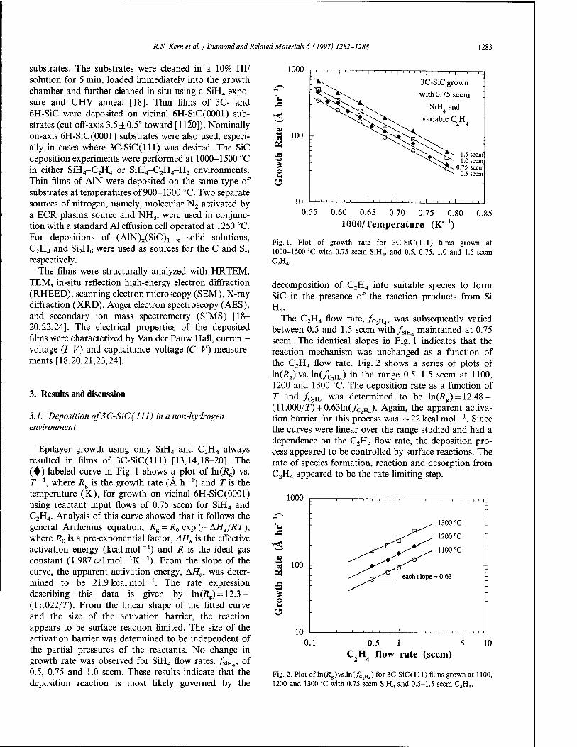
RS. Kernetal. / Diamond and Related Materials 6 (1997) 1282-1288 1283
substrates. The substrates were cleaned in a 10% HF solution for 5 min, loaded immediately into the growth chamber and further cleaned in situ using a SiH4 expo- sure and UHV anneal [18]. Thin films of 3C- and 6H-SiC were deposited on vicinal 6H-SiC(0001) sub- strates (cut off-axis 3.5 + 0.5° toward [1120]). Nominally on-axis 6H-SiC(0001) substrates were also used, especi- ally in cases where 3C-SiC(lll) was desired. The SiC deposition experiments were performed at 1000-1500 °C in either SiH4-C2H4 or SiH4-C2H4-H2 environments. Thin films of A1N were deposited on the same type of substrates at temperatures of 900-1300 °C. Two separate sources of nitrogen, namely, molecular N2 activated by a ECR plasma source and NH3, were used in conjunc- tion with a standard Al effusion cell operated at 1250 °C. For depositions of (AlN)x(SiC)1_x solid solutions, C2H4 and Si2H6 were used as sources for the C and Si, respectively.
The films were structurally analyzed with HRTEM, TEM, in-situ reflection high-energy electron diffraction (RHEED), scanning electron microscopy (SEM), X-ray diffraction (XRD), Auger electron spectroscopy (AES), and secondary ion mass spectrometry (SIMS) [18- 20,22,24]. The electrical properties of the deposited films were characterized by Van der Pauw Hall, current- voltage (I-V) and capacitance-voltage (C-V) measure- ments [18,20,21,23,24].
3. Results and discussion
3.1. Deposition of 3C-SiC(111) in a non-hydrogen environment
Epilayer growth using only SiH4 and C2H4 always resulted in films of 3C-SiC(lll) [13,14,18-20]. The (♦)-labeled curve in Fig. 1 shows a plot of ln(i?g) vs. T~l, where R% is the growth rate (Ah-1) and Tis the temperature (K), for growth on vicinal 6H-SiC(0001) using reactant input flows of 0.75 seem for SiH4 and C2H4. Analysis of this curve showed that it follows the general Arrhenius equation, Rg=R0exp(—AHei/RT), where R0 is a pre-exponential factor, AH^ is the effective activation energy (kcal mol ~l) and R is the ideal gas constant (1.987calmol_1K~1). From the slope of the curve, the apparent activation energy, Ai7a, was deter- mined to be 21.9 kcal mol-1. The rate expression describing this data is given by ln(i?g) = 12.3 — (11.022/77). From the linear shape of the fitted curve and the size of the activation barrier, the reaction appears to be surface reaction limited. The size of the activation barrier was determined to be independent of the partial pressures of the reactants. No change in growth rate was observed for SiH4 flow rates, /SiH4> of 0.5, 0.75 and 1.0 seem. These results indicate that the deposition reaction is most likely governed by the
1000
0)
JS
o u O
100
10 0.55 0.60 0.65 0.70 0.75 0.80
1000/Temperature (K- *) 0.85
Fig. 1. Plot of growth rate for 3C-SiC(lll) films grown at 1000-1500 °C with 0.75 seem SiH4, and 0.5, 0.75, 1.0 and 1.5 seem C2H4.
decomposition of C2H4 into suitable species to form SiC in the presence of the reaction products from Si H4.
The C2H4 flow rate, /C2H4, was subsequently varied between 0.5 and 1.5 seem with/siH4 maintained at 0.75 seem. The identical slopes in Fig. 1 indicates that the reaction mechanism was unchanged as a function of the C2H4 flow rate. Fig. 2 shows a series of plots of ln(i?g) vs. ln(/C2H4) in the range 0.5-1.5 seem at 1100, 1200 and 1300 °C. The deposition rate as a function of T and /C2H4 was determined to be ln(Rg) = 12.48 — (11.000/T) + 0.631n(/C2H4). Again, the apparent activa- tion barrier for this process was ~22 kcal mol-1. Since the curves were linear over the range studied and had a dependence on the C2H4 flow rate, the deposition pro- cess appeared to be controlled by surface reactions. The rate of species formation, reaction and desorption from C2H4 appeared to be the rate limiting step.
1000
u
«
o O
100 -
10 0.1 0.5 1 5
C2H4 flow rate (seem) 10
Fig. 2. Plot of ln(i?ir)vs.ln(/C2„4) for 3C-SiC(l 11) films grown at 1100, 1200 and 1300 °C with 0.75 seem SiH4 and 0.5-1.5 seem C2H4.

1284 R.S. Kern et al. / Diamond and Related Materials 6 (1997) 1282-1288
3.2. Deposition of3C-SiC(111) in a hydrogen ambient
Additions of H2 (5 seem flow rate) during the growth of SiC produced several advantageous changes in the resulting films [18-20]. At deposition temperatures < 1350 °C, the benefits were increased surface smooth- ness and a greatly enhanced growth rate of the 3C-SiC films. The activation energy for the films grown with 0.75 seem SiH4, 0.75 seem C2H4 and 5 seem H2 at 1000-1300 °C was 21.6 kcal mol"1. Thus, the presence of H2 did not change the magnitude of the barrier over this temperature range. Since the slopes of the curves shown in Fig. 1 and that from this latter study were nearly identical, the reaction mechanism was both appa- rently unchanged and independent on the input flow of C2H4.
The observations are attributed to the presence of H2 which apparently provided the impetus for at least one of the following processes: (i) adsorption of C2H4
onto the surface of the growing film, (ii) sweeping of the unreacted source gas species or unwanted product species from the growth surface and/or (iii) formation of a suitable reactant species in tandem with the decom- position or reaction of C2H4 in the presence of H2.
3.3. Deposition of6H-SiC(0001) in a hydrogen ambient
Further increases of the deposition temperature 01350 °C) in a H2 ambient, resulted in the stabilization of the step flow growth mode, the consequent deposition of 6H-SiC(0001) epilayers, a marked increase in growth rate and an apparent decrease in the activation energy [18-20]. The temperature dependence of the growth rate appeared to be linear on the Arrhenius plot shown in Fig. 3. The activation barrier was determined to be 12.6 kcal mol-1, which is in excellent agreement with values calculated from CVD research (13.0 kcal mol-1) using the same reactant sources, sub-
o s- O
3000 1 ' ' ' ' i 1 1 1 I 1 t 1 1 !
6H-SiC grown with
0.75 seem SiH,
0.75 seem CH,
2000
•^^«
and 5 seem H 2
slope =
i .1 i
-6.357 kcal mol'1 [_
mm ! 0.55 0.60 0.65
1000/Temperature (K- !)
strate orientation and crystallographic face [26]. Although the growth rate was still strongly dependent on the deposition temperature, the decrease in the value of this activation barrier was an excellent indicator of the effect of the H2 gas on the gas chemistry, growth kinetics and gas flow dynamics. Limited studies showed that varying the C2H4 input from 0.375 to 1.0 seem did not result in a change in the growth rate. This indicated that the rate controlling factor at these temperatures in the presence in H2 had most likely changed. It is important to note that growth on both vicinal and on-axis substrates proceeded at approximately the same rate (within 5%) under similar growth conditions. However, 3C-SiC was always produced on the on-axis substrates regardless of growth conditions, because the smaller atomic diffusion distance relative to the distance between steps.
3.4. Doping of3C- and 6H-SiCfilms
The presence of the N in SiC grown from the vapor phase is particularly significant, because it is the most shallow donor impurity. Consequently, it was the agent responsible for the n-type character of unintentionally doped SiC films [18,21,20]. Considerable differences in the background atomic nitrogen and electron concen- trations in the SiC films was measured when the C2H4
flow rate was modulated in the range 0.375-0.75 seem. Similar to the "site-competition epitaxy" arguments of Larkin et al. [27,28], the N contamination level was significantly decreased by increasing the amount of C2H4 delivered in the gas phase. Fig. 4 shows a SIMS profile from a 6H-SiC(0001) film grown at 1400 °C using 0.75 seem SiH4, 5 seem H2 and a variable C2H4
flow. The change in N content with C source supply is very apparent from the abrupt changes that occur in
« 10'
6H-SiC substrate
I , l
0.00 0.25 0.50 0.75 1.00 Depth (um)
1.25 1.50
Fig. 3. Plot of growth rate for 6H-SiC(0001) films grown at 1350-1500 °C with 0.75 seem SiH4, 0.75 seem C2H4 and 5 seem H2.
Fig. 4. SIMS profile of a 6H-SiC(0001) film grown at 1400 °C using 0.75 seem SiH4, 5 seem H2 and a variable C2H4 flow (0.375 seem in Region I, 0.5 seem in Region II, and 0.75 seem in Region III).

R.S. Kern etal. j Diamond and Related Materials 6 (1997) 1282-1288 1285
the N depth profile. A flow of 0.75 seem C2H4 resulted in the incorporation of N at the detection limit for N («5 x 1015 cm-3) in the SIMS system. Hall measure- ments of undoped 6H-SiC films with the lowest atomic nitrogen and electron concentration showed a mobility of 434 cm2 V_1s_1.
To study n-type doping of the reactant mixture with the lowest total input of source gases, 0.75 seem SiH4, 0.375 seem C2H4, and 5 seem H2 (for 6H-SiC), was chosen. Donor doping was performed in situ at 1400 °C on monocrystalline 6H- and 3C-SiC using both NH3
(diluted to 300 ppm in H2) and pure N2. Doping in the range 5 x 10¹⁵—8 x 1017 cm~3 was achieved using the NH3/H2 mixture and 1 x 10¹⁸-4x 1019cm"3 with the N2 additions. Figs. 5(a) and (b) show the electron mobility as a function of electron concentration in the close packed plane for 3C-SiC(lll) and 6H-SiC(0001) at room temperature.
Epilayers of 3C- and 6H-SiC were also doped p-type by evaporating Al from a standard MBE effusion cell
during the growth of SiC epilayers. All growth experi- ments were performed at 1450 °C using 0.75 seem SiH4, 0.75 seem C2H4, and 5 seem H2 (for 6H-SiC). The higher C2H4 flow rate was used to take advantage of the site-competition process which resulted in a decrease in the concentration of background N, a compensating impurity in p-type SiC. The higher temperature was used in an attempt to aid in dopant activation. Acceptor doping of 2x 10¹⁵—8 x 1018cm"3 was achieved. Figs. 6(a) and (b) show the hole mobility as a function of hole concentration in the close packed plane for 3C-SiC(lll) and 6H-SiC(0001) at room temperature.
3.5. Deposition ofAIN thin films and Al/AlN/SiC MIS-structures
Thin films of wurtzite structure (2H) A1N were depos- ited on 6H-SiC substrates [18]. The primary problem encountered using an ECR source as a nitrogen source was the unintentional incorporation of impurity atoms
■* 700 {«
> 600
s 500
>> +* 13 400 X! o S 300
c © 1- ?no
■w CJ V
m too
7
1 i ' '
n-type 3C-SiC(111) """1 ' ' '""!
epilayer
'- X* -j
- \»
-
'-
1 1 i > . . . «1 < ft„„T
10" 101 10,! 10" 1021
Carrier Concentration (cm" ) Carrier Concentration (cm" 3)
o
o u
W
Carrier Concentration (cm' ) Carrier Concentration (cm" 3)
Fig. 5. Room temperature measurements of electron mobility vs. car- rier concentration for n-type (a) 3C-( 111) epilayers and (b) 6H-SiC(0001) epilayers.
Fig. 6. Room temperature measurements of hole mobility vs. carrier concentration for p-type (a) 3C-( 111) epilayers and (b) 6H-SiC(0001) epilayers.

1286 R.S. Kernetal. / Diamond and Related Materials 6 (1997) 1282-1288
UPM
l6H-SiCfe
g, , ■■. ■ j =-—*^:.-~^..., _ ,..,., .
fctiü,«;:....ii,',k.:..'.. - ■ - :":?" ,-.,•«*■••...■'.<>; , ....,..,
(b)
Fig. 7. HRTEM micrographs of (a) a (111 )-oriented zincblende (AlN)0.2(SiC)_0.8 film and (b) an (0001 )-oriented wurtzite (AlN)a3(SiC)0.7 film. The RHEED patterns of the cubic and hexagonal films are taken along the [110] and [1120] azimuth, respectively.
from the material that made up the liner crucible. Substitution to NH3 improved film quality and growth rate. Growth rates of about 825 A h_1 were achieved for films grown at 1050 °C using the ECR, whereas, growth rates of about 1000Ah"1 were obtained for films deposited using NH3 at 1100 °C. With the addition of H2, higher growth rates and smoother surfaces were achieved. A comparison of thin (0001) oriented A1N films (<50A) grown simultaneously on vicinal and
on-axis 6H-SiC(0001) substrates were made. Films of A1N grown on the vicinal surface exhibited a rough surface, whereas, the films grown on the on-axis sub- strate possessed a very smooth surface and excellent thickness uniformity, indicative of two-dimensional growth. The achievement of higher quality A1N films in the latter case were due to the low density of surface irregularities (i.e. steps and kinks) on the on-axis sub- strates. Because of the very low critical thickness of the
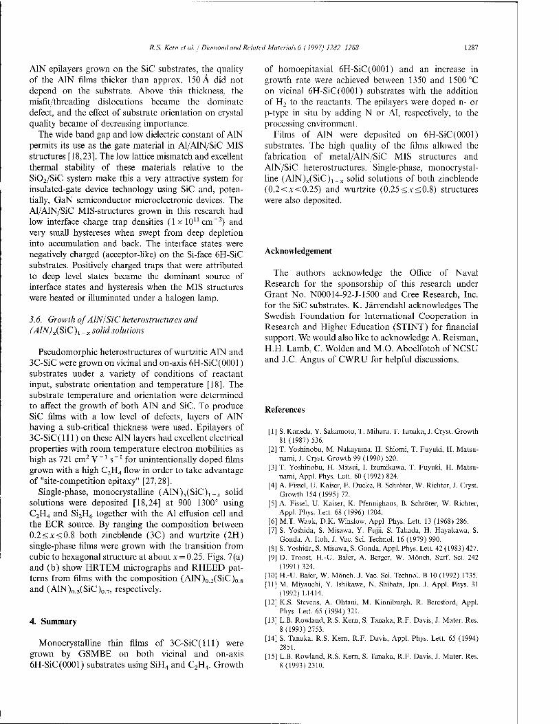
R.S. Kernetal. / Diamond and Related Materials 6 (1997) 1282-1288 1287
A1N epilayers grown on the SiC substrates, the quality of the A1N films thicker than approx. 150 A did not depend on the substrate. Above this thickness, the misfit/threading dislocations became the dominate defect, and the effect of substrate orientation on crystal quality became of decreasing importance.
The wide band gap and low dielectric constant of A1N permits its use as the gate material in Al/AlN/SiC MIS structures [18,23]. The low lattice mismatch and excellent thermal stability of these materials relative to the Si02/SiC system make this a very attractive system for insulated-gate device technology using SiC and, poten- tially, GaN semiconductor microelectronic devices. The Al/AlN/SiC MIS-structures grown in this research had low interface charge trap densities (1 x 10ncm~2) and very small hystereses when swept from deep depletion into accumulation and back. The interface states were negatively charged (acceptor-like) on the Si-face 6H-SiC substrates. Positively charged traps that were attributed to deep level states became the dominant source of interface states and hysteresis when the MIS structures were heated or illuminated under a halogen lamp.
3.6. Growth ofAlN/SiC heterostructures and (AIN) x(SiC)t _x solid solutions
Pseudomorphic heterostructures of wurtzitic A1N and 3C-SiC were grown on vicinal and on-axis 6H-SiC(0001) substrates under a variety of conditions of reactant input, substrate orientation and temperature [18]. The substrate temperature and orientation were determined to affect the growth of both A1N and SiC. To produce SiC films with a low level of defects, layers of A1N having a sub-critical thickness were used. Epilayers of 3C-SiC( 111) on these A1N layers had excellent electrical properties with room temperature electron mobilities as high as 721 cm2 V"1 s_1 for unintentionally doped films grown with a high C2H4 flow in order to take advantage of "site-competition epitaxy" [27,28].
Single-phase, monocrystalline (AlN)x(SiC)1_x solid solutions were deposited [18,24] at 900-1300° using C2H4 and Si2H6 together with the Al effusion cell and the ECR source. By ranging the composition between 0.2<x<0.8 both zincblende (3C) and wurtzite (2H) single-phase films were grown with the transition from cubic to hexagonal structure at about x = 0.25. Figs. 7(a) and (b) show HRTEM micrographs and RHEED pat- terns from films with the composition (A1N)0 2(SiC)0 8
and (A1N)0 3(SiC)0 7, respectively.
4. Summary
Monocrystalline thin films of 3C-SiC(lll) were grown by GSMBE on both vicinal and on-axis 6H-SiC(0001) substrates using SiH4 and C2H4. Growth
of homoepitaxial 6H-SiC(0001) and an increase in growth rate were achieved between 1350 and 1500 °C on vicinal 6H-SiC(0001) substrates with the addition of H2 to the reactants. The epilayers were doped n- or p-type in situ by adding N or Al, respectively, to the processing environment.
Films of A1N were deposited on 6H-SiC(0001) substrates. The high quality of the films allowed the fabrication of metal/AlN/SiC MIS structures and AIN/SiC heterostructures. Single-phase, monocrystal- line (AlN^SiC)!-^ solid solutions of both zincblende (0.2 <x< 0.25) and wurtzite (0.25<x<0.8) structures were also deposited.
Acknowledgement
The authors acknowledge the Office of Naval Research for the sponsorship of this research under Grant No. N00014-92-J-1500 and Cree Research, Inc. for the SiC substrates. K. Järrendahl acknowledges The Swedish Foundation for International Cooperation in Research and Higher Education (STINT) for financial support. We would also like to acknowledge A. Reisman, H.H. Lamb, C. Wolden and M.O. Aboelfotoh of NCSU and J.C. Angus of CWRU for helpful discussions.
References
[1] S. Kaneda, Y. Sakamoto, T. Mihara, T. Tanaka, J. Cryst. Growth 81 (1987) 536.
[2] T. Yoshinobu, M. Nakayama, H. Shiomi, T. Fuyuki, H. Matsu- nami, J. Cryst. Growth 99 (1990) 520.
[3] T. Yoshinobu, H. Mitsui, I. Izumikawa, T. Fuyuki, H. Matsu- nami, Appl. Phys. Lett. 60 (1992) 824.
[4] A. Fissel, U. Kaiser, E. Ducke, B. Schröter, W. Richter, J. Cryst. Growth 154(1995)72.
[5] A. Fissel, U. Kaiser, K. Pfennighaus, B. Schröter, W. Richter, Appl. Phys. Lett. 68 (1996) 1204.
[6] M.T. Wauk, D.K. Winslow, Appl. Phys. Lett. 13 (1968) 286. [7] S. Yoshida, S. Misawa, Y. Fujii, S. Takada, H. Hayakawa, S.
Gonda, A. Itoh, J. Vac. Sei. Technol. 16 (1979) 990. [8] S. Yoshida, S. Misawa, S. Gonda, Appl. Phys. Lett. 42 (1983) 427. [9] D. Troost, H.-U. Baier, A. Berger, W. Mönch, Surf. Sei. 242
(1991) 324. [10] H.-U. Baier, W. Mönch, J. Vac. Sei. Technol. B 10 (1992) 1735. [11] M. Miyauchi, Y. Ishikawa, N. Shibata, Jpn. J. Appl. Phys. 31
(1992) L1414. [12] K.S. Stevens, A. Ohtani, M. Kinniburgh, R. Beresford, Appl.
Phys. Lett. 65 (1994)321. [13] L.B. Rowland, R.S. Kern, S. Tanaka, R.F. Davis, J. Mater. Res.
8 (1993) 2753. [14] S. Tanaka, R.S. Kern, R.F. Davis, Appl. Phys. Lett. 65 (1994)
2851. [15] L.B. Rowland, R.S. Kern, S. Tanaka, R.F. Davis, J. Mater. Res.
8 (1993) 2310.

1288 R.S. Kern etal. / Diamond and Related Materials 6 (1997) 1282-1288
[16] L.B. Rowland, R.S. Kern, S. Tanaka, R.F. Davis, Appl. Phys. Lett. 62 (1993) 3333.
[17] S. Tanaka, R.S. Kern, R.F. Davis, Appl. Phys. Lett. 66 (1995) 37. [18] R.S. Kern, Ph.D. Thesis, North Carolina State University,
Raleigh, NC, 1996. [19] R.S. Kern, S. Tanaka, L.B. Rowland, R.F. Davis, J. Cryst.
Growth., submitted. [20] R.S. Kern, K. Järrendahl, S. Tanaka, R.F. Davis, Phys. Stat. Sol.
A., accepted. [21] R.S. Kern, R.F. Davis, Appl. Phys. Lett., accepted. [22] R.S. Kern, L.B. Rowland, S. Tanaka, R.F. Davis, J. Mater. Res.
8 (1993) 1477.
[23] M.O. Aboelfotoh, R.S. Kern, S. Tanaka, R.F. Davis, C.I. Harris, Appl. Phys. Lett. 69 (1996) 2873.
[24] R.S. Kern, L.B. Rowland, S. Tanaka, R.F. Davis, J. Mater. Res., submitted.
[25] L.B. Rowland, S. Tanaka, R.S. Kern, R.F. Davis, in Amorphous and Crystalline Silicon Carbide IV, C.Y. Yang, M.M. Rahman, G.L. Harris (Eds.), Springer, Berlin, 1992, p. 84.
[26] Y.C. Yang, R.F. Davis, J. Electron. Mater. 20 (1991) 869. [27] D.J. Larkin, P.G. Neudeck, JA. Powell, L.G. Matus, Appl. Phys.
Lett. 65 (1994) 1659. [28] D.J. Larkin, S.G. Sridhara, R.P. Devaty, W.J. Choyke,
J. Electron. Mater. 24 (1995) 289.

DIAMOND AND
RELATED MATERIALS
ELSEVIER Diamond and Related Materials 6 (1997) 1289-1292
High quality 4H-SiC grown on various substrate orientations
A. Henry a,b-*, I.G. Ivanova, T. Egilssona, C. Hallina, A. Ellison a, O. Kordina a'b, U. Lindefelt a'b, E. Janzen a
a Linköping University, Department of Physics and Measurement Technology, 581 83 Linköping, Sweden
b ABB Corporate Research, 721 78 Västeräs, Sweden
Abstract
Growth of 4H epilayers has been achieved by chemical vapour deposition on various substrate orientations which were on-(OOOl) oriented, off axis (3.5°- and 8°-off towards the (1120) direction) and a-cut, both (1120) and (lOlO)-oriented material. Various characterisation techniques have been used to assess the epilayer quality such as optical microscopy, X-ray diffraction, and mainly photoluminescence spectroscopy. © 1997 Elsevier Science S.A.
Keywords: 4H-SiC; c-Axis; a-Axis; Photoluminescence
1. Introduction
SiC currently attracts a growing interest owing to its large potential as a power device material. High-voltage bipolar devices require thick low-doped epitaxial layers with long carrier lifetimes, and are most conveniently grown by chemical vapour deposition (CVD) [1-4]. The study of epitaxy on various crystal orientations of SiC helps the understanding of the growth mechanisms and facilitates device development. Certain material proper- ties differ for the distinct crystal faces and one face could be more or less desirable for a special device application. Previous works on 6H-SiC report [5,6] a lower quality on the (lOlO)-oriented material compared with the (1120). We present a study on 4H-SiC, since this polytype has shown to be more suited as power device material than 6H. Various characterisation tech- niques are used such as a optical microscopy, X-ray diffraction and mainly photoluminescence (PL) spectroscopy.
2. Experiment
The samples used in this study are CVD epitaxial films grown in a hot-wall reactor with a SiC coated graphite susceptor [1,2]. The following substrate orien-
* Corresponding author. Fax: 46 13 14 23 37; e-mail: [email protected]
tations of the n-type 4H polytype were used: (1) (0001) oriented c-cut (a) on-axis, (b) 3.5°- and (c) 8°-off from the c-axis towards the (1120), direction; and (2) a-cut material (a) (1120); and (b) (lOlO)-oriented substrates grown by the modified Lely method. The growths were performed by passing reactive gases (silane and propane diluted to 5% in H2) through the susceptor inside which the substrates were placed. Hydrogen was used as the carrier gas. The growth temperature (Tg) was varied from 1450 to 1650 °C, the C/Si ratio from 1.5 to 3 and the growth rate (Rg) from 1.5 to 3 tun/h. A hydrogen etch prior to growth was performed at the growth temperature for a long time (15-30 min) in order to improve the substrate surface as much as possible [7]. It should be noted that some of the samples used in this study were intentionally doped n-type in the 1016cm~3
range and thus, no free exciton (FE or I) related line could be observed in the PL spectra. However, the background doping concentration in our reactor is read- ily low: samples with doping levels less than 5 x 1014 cm-3 are grown reproducibly.
To control the morphology of the epilayers, optical microscopy with Normaski optics was used. X-ray diffraction (XRD) measurements were performed on a Philips MRD 1880/HR diffractometer [8].
Low-temperature photoluminescence spectra were recorded at about 2 K, using the 275 nm or the double- frequency line of the 488 nm (thus 244 nm) of an Ar+-ion laser as the excitation source. The luminescence
0925-9635/97/S17.00 © 1997 Elsevier Science S.A. All rights reserved. PIT S0925-9635(97)00105-2

1290 A. Henry et al. / Diamond and Related Materials 6 (1997) 1289-1292
was dispersed by a SPEX 1404 0.85-m double monochro- mator, fitted with two 1200 grooves/mm gratings blazed at 5000 A and detected by a UV-sensitive Hamamatsu photomultiplier tube operating in a photon-counting mode. The usual geometry used to record the PL spectra is very close to the so-called backscattering geometry (see Fig. 1) and only photons with Elc polarisation can be detected, where E denotes the polarisation vector of the photon. However, with a rectangular geometry (Fig. lb) photons with both EJ_c or E//c can be detected and selected by means of a polariser. The emission from the surface was blocked with a mass of Ag paste, as indicated in Fig. lb.
3. Results
W
£io4
103 a H
£ 102
u
10u
4H(0004)
a in1 IMWW.W*' ■~ IU '''.''tfV'V
'MEM
8* Off 3.5' Off On-axis
35.50 35.55 35.60 35.65 28/cjo (degrees)
35.70
Fig. 2. X-ray diffraction rocking curves recorded for on-axis, 3.5°- and 8°-off 10 um thick n-type 4H-epilayers grown on c-cut substrates.
Three 4H-SiC, 10 tun thick, epilayers were grown on three different c-cut substrate orientations: on-axis, 3.5°- and 8°-off, at the same time, thus with the same growth conditions (Tg = 1600°C, C/Si = 2 and Rg approx. 2 nm/h). Mosaic patterns and boundaries of 3C-inclusions and 4H material were observed with opti- cal microscopy on the on-axis sample, whereas few triangles were seen from the 3.5°-offepilayer. The 8°-off grown material showed a specular good surface with very few defects.
Fig. 2 shows typical XRD spectra of these three samples. The present rocking curves are recorded in triple-axis mode, and thus allow polytype identification from the related lattice parameter change [9]. A very intense 4H-SiC (0004) peak could be observed from all three samples. However, 3C inclusions could be detected through the 3C-SiC (111) peak for the on-axis sample, and more weakly for the 3.5°-off sample.
These observations are confirmed by the PL results obtained on these samples. For the on-axis epilayer, strong 3C-related PL lines could be observed on some
a) Near backscattering geometry Epi-layer
Excitation
Detection
> c-axis b) Rectangular geometry
Excitation
Ag paste
] Polariser
r Detection
Fig. 1. Schematic representation of the experimental PL conditions.
parts of the samples (Fig. 3(a)), whereas 4H-related PL lines were observed on the other parts. The purity of the 3C-inclusions, which were in a very small proportion compared with the 4H, was extremely high, showing
a, U
e
OH
►J
N,
n IUJI^ ik 3C
5200 5300 5400 5500 5600 Photon Wavelength (Ä)
4H __>*— 1\J
a) 4H-SiC On-axis
b) 4H-SiC Off-Axis _ Qo
Or
'3
I
0, Po __JUU~-JJAJWV^_
3800 3850 3900 3950 Photon Wavelength (Ä)
4000 4500 5000 5500 Photon Wavelength (Ä)
6000
Fig. 3. PL spectra showing: (a) 3C related luminescence from the on-axis epilayer; and (b) 4H luminescence from the off-axis material. The insert in the both cases shows the near band gap emission. The multi-bound excitons (MBEC) are marked in the zero-phonon and TA phonon regions of the 3C nitrogen BE. The PL spectrum (a) was observed only from a few parts of the on-axis material, whereas the majority of the material shows PL spectra as the spectrum (b) which was recorded for 3.5°-off material.

A. Henry et al. / Diamond and Related Materials 6 (1997) 1289-1292 1291
multi-bound exciton (MBEC) lines of the N donor- bound exciton (BE) (see insert of Fig. 3(a)). No donor- acceptor pair or other deep emissions were observed, were only intense near band gap emission without the contribution of the Al-acceptor BE, as can be seen in Fig. 3. For the spectra recorded on the off-axis materials, as well as those showing 4H-related luminescence from the on-axis material, very intense nitrogen BE are detected with very sharp lines (less than our spectral resolution of 0.4 A) without broadening. These samples were doped in the 1016cm~3 range, and thus no FE lines could be observed.
By varying the growth conditions, samples showing either strong FE or BE related lines in the PL spectra, can be grown. For instance, if Tg = 1550°C, Rg = 3 um/h, and the C/Si is >3, the samples may be compensated n-type or even p-type. To be able to obtain samples showing only N donor BE, N2 gas needs to be added during growth in combination with a very low C/Si ratio.
Fig. 4(a) and (b) show the polarised PL spectra of FE replicas and the BE replicas, respectively, for the two possible polarisations. By comparing very carefully these spectra we found 11 phonon replicas with the E_Lc polarisation and 11 phonon replicas with the E//c polari- sation. It should be noted here that the zero-phonon
lines P0 and Q0 of the BE are observed to be polarised perpendicular to c (Elc). We would also like to point out that for the Elc polarisation, the 76.4 meV phonon replica is the dominating one, as it is often observed for the near backscattering geometry, whereas for the E//c polarisation, it is the 94.7 meV phonon replica which is the most intense. For 6H-SiC, the most intense phonon replica for Elc is the 77 meV, whereas for E//c it is the 95 meV from the TO region. The results for the phonon replica energies of FE and BE in the case of 4H are summarised and compared with values from the litera- ture, where only BE lines were considered [10,11] in Table 1. These results are in agreement with theoretical polarisation selection rules if the conduction band mini- mum in 4H-SiC is at the M-point of the Brillouin zone (BZ). At this point the 24 phonons can be classified by the irreductible representations of the so-called vibra- tional representation:
rM = 8Mt + 4M2 + 4M3 + 8M4, (1)
where M^ M2, M3 and M4 are the irreducible representa- tions of the group C2v of the wavevector at the M-point [12]. A group-theoretical analysis was carried out to find the polarisation selection rules leading to the results: (i) the polarisation selection rules are the same for the FE and BE described within the effective mass approxi- mation; (ii) 12 phonon replicas are polarised lc,
4H - SiC, T = 2K
a)FE 76.4
T 106.7 ^^ 3
46.15
95.9 1 03
ri \ E J-c
S C 94.7
si I
A
78.15
/I « J 1 i E//c
. . . 1 . . I . . . I . . . 1 . . .
3240 3200 3160 Photon Energy (meV)
3120
Fig. 4. PL spectra recorded at 2 K from 30 urn-thick 4H epilayers with dominant (a) FE phonon replicas; and (b) BE-related lines for the two possible polarisations.
Table 1 Phonon replicas energies as determined from the PL data
Ref. [12]
33.5 (TA1) 11 37.2 (TA1) 41.4 (TA2) 42.4 (TA2) 46.7 (TA1) 51.4 (TA2) 53.4 (TA2)
68.7 (LA) 69.7 (LA) 76.9 (LA) 78.8 (LA)
95 (TO)
96.1 96.7 (TO)
104 (LO) 104.3 (LO)
107 (LO)
107.4 (LO)
Ref. [11]
33.0 36.5 40.6 41.0 41.7 46.1 50.8 52.7 67.8 68.7 76.6 78.5
96.1 97.3
97.8 99.1
100.3 101.6
105.6 106.3 108.2 108.7
Our data
33.05 (Elc) 36.7 (E//c) 40.8 (E//c) 41.0 (Elc) 41.9 (E//c) 46.15 (Elc) 50.75 (Elc) 52.7 (E//c) 68.1 (Elc) 68.7 (E//c) 76.4 (Elc) 78.15 (E//c) 94.45 (Elc) 94.7 (E//c) 95.9 (Elc) 96.6 (E//c)
98.8 (Elc)
103.5 (E//c) 103.9 (Elc) 106.2 (E//c) 106.7 (Elc)
109.0 (E//c)

1292 A. Henry et al. / Diamond and Related Materials 6 (1997) 1289-1292
whereas 12 are //c; and (iii) the neutral donor state has a T4 symmetry in the double-group C3V.
The understanding of the polarisation study of c-axis material is very important for the characterisation of a-cut material. We expect to observe both E//c and Elc phonon replicas in a PL spectrum from an a-cut sample recorded in the near backscattering geometry.
Growth on a-cut material was thus attempted. The first grown epilayers showed very bad morphology mainly due to the poor quality of the substrate, and no XRD signal could be observed from these samples. The PL spectra showed, however, near band gap emission but with very low intensity compared with c-axis samples. For the (1010) oriented samples the observed lines were not only weak in intensity but also broad, underlining the poor quality of this layer. By increasing the time of the hydrogen etch prior the growth, better layers with significantly better morphology were grown with observation of the (1120) XRD peak. Very sharp lines could be observed in the PL spectra. As expected, the 94.7 meV phonon replica for both FE and BE are the most intense phonon replicas observed in the PL spectrum of the (1120) (Fig. 5(a)). This epilayer was found to have a net carrier concentration of 3x 1014cm~3, as determined from capacitance-voltage (C-V) measurements. The morphology of the (10l0)- oriented sample was observed to be of worse quality with more imperfections and defects. The growth of 4H on (lOlO)-oriented substrates appears to be more diffi- cult and sensitive to substrate imperfections, as is nor- mally observed also when 6H-SiC is grown on this substrate orientation [5]. These facts are confirmed by the PL spectrum where the 94.7 meV replica is still the most intense and where the 76.4 meV replica is also observed with a high intensity.
a
OH
3800 3850 3900
Photon Wavelength (Ä)
3950
Fig. 5. PL spectra of 18 um thick a-cut (a) (1120)-; and (b) (1010)- oriented materials.
4. Summary
High-quality growth for 4H thick epilayers is reported and characterised with various techniques. The quality on (1120) and (lOlO)-oriented substrates is confirmed by PL. Line widths of the PL lines from the (1120) grown epilayers are comparable with those of (0001)- oriented CVD material. The PL spectra of the a-cut samples show both Elc and E//c phonon replicas, whereas in the (OOOl)-orientated 4H, only the E_Lc replicas are observed.
Acknowledgement
Financial support of this work was provided by the Swedish Natural Science Research Council (NFR), the Swedish Council for Engineering Sciences (TFR), the Swedish Board for Industrial and Technical Development (NUTEK), the NUTEK/NFR Material Consortium on Thin Film Growth, and the NUTEK/Asea Brown Boveri (ABB) Power Device Program.
References
[1] E. Janzen, O. Kordina, Inst. Phys. Conf. Ser. No. 142 (1996) 653. [2] O. Kordina, C. Hallin, R.C. Glass, A. Henry, E. Janzen, Inst.
Phys. Conf. Ser. 137(1994)41. [3] A.A. Burke Jr., L.B. Rowland, A.K. Agarwal, S. Sriram,
R.C. Glass, CD. Brandt, Inst. Phys. Conf. Ser. 142 (1996) 201. [4] T. Kimoto, A. Itoh, H. Matsunami, S. Sridhara, L.L. Clemen,
R.P. Devaty, W.J. Choyke, T. Dalibor, C. Peppermfller, G. Pensl, Inst. Phys. Conf. Ser. 142 (1996) 393.
[5] A.A. Burke Jr., D.L. Barrett, H.M. Hobgood, R.R. Siergiej, T.T. Braggins, R.C. Clarke, G.W. Eldridge, CD. Brandt, D.J. Larkin, J.A. Powell, W.J. Choyke, Inst. Phys. Conf. Ser. 137 (1994) 29.
[6] L.L. Clemen, R.P. Devaty, M.F. MacMillan, W.J. Choyke, A.A. Burke Jr., D.L. Barrett, H.M. Hobgood, D.J. Larkin, J.A. Powell, Inst. Phys. Conf. Ser. 137 (1994) 147.
[7] C. Hallin, A.S. Bakin, F. Owman, P. Märtensson, O. Kordina, E. Janzen, Inst. Phys. Conf. Ser. 142 (1996) 613.
[8] P.F. Fewster, N.L. Andrew, J. Appl. Cryst. 28 (1995) 451. [9] Gmelin Handbook of Inorganic Chemistry, (Springer-Verlag,
Berlin), Si Suppl. Vol.B2—Silicon Carbide, 1984, p. 8. [10] W.J. Choyke, R.P. Devaty, L.L. Clemen, M.F. MacMillan,
M. Yoganathan, G. Pensl, Inst. Phys. Conf. Ser. No 142 (1996) 257.
[11] L. Patrick, W.J. Choyke, D.R. Hamilton, Phys. Rev 137 (1965) A1515.
[12] G. Koster et al., Proprieties of the Thirty-point Groups, MIT Press, Cambridge, Massachusetts, 1969.

DIAMOND AND
RELATED MATERIALS
ELSEVIER Diamond and Related Materials 6 (1997) 1293-1296
Hydrogen incorporation in epitaxial layers of 4H- and 6H-silicon carbide grown by vapor phase epitaxy
Adolf Schöner a'*, Kurt Rottnera, Nils Nordella, Margareta Linnarsson b, Christian Peppermüllerc, Reinhard Helbigc
a IMC, P.O. Box 1084, S-16421 Kista, Sweden b Royal Institute ofTechnology, Department of Solid State Electronics, Kista, Sweden
0 Lehrstuhl für Angewandte Physik, Universität Erlangen-Nürnberg, Nürnberg, Germany
Abstract
The incorporation of hydrogen during vapor phase epitaxy was investigated using secondary ion mass spectroscopy, low temperature photoluminescence, and capacitance-voltage measurements. It was found that hydrogen incorporation is strongly dependent on the concentration of the acceptor dopants aluminum and boron, regardless of changes in the doping concentration caused by varying the concentration ratio between carbon and silicon or the dopant precursor flow. An electrical passivation of the acceptor dopants was found and could be reduced by annealing at temperatures above 1000 °C. At the same anneal temperature hydrogen-related photoluminescence was considerably reduced and the diffusion of hydrogen was detected. © 1997 Elsevier Science S.A.
Keywords: Hydrogen incorporation; 6H-, 4H-SiC; SiC vapor phase epitaxy; Al-, B-doping
1. Introduction
The intrinsic material properties of silicon carbide (SiC) motivate the development of a new generation of high power and high frequency devices, and new devices that operate at high temperatures and in aggressive environments. To fabricate these next generation devices reproducible control of the dopant and impurity incorporation is crucial.
Hydrogen (H) passivation of electrically active shal- low and deep impurities is known from Si and III-V- compound semiconductors [1]. For SiC the passivation mechanisms are less well known, although H is present in epitaxial growth processes. Here H2 is the most commonly used carrier gas and growth precursors like silane (SiH4) and propane (C3H8) contain H. Therefore, the dissociation of the precursor and the carrier gas molecules leads to the presence of highly reactive atomic H at growth temperatures of around 1500 °C.
Recently the electrical passivation of impurities by H has been confirmed for SiC [2,3]. Hence the incorpora- tion and annealing behavior of H needs to be studied
' Corresponding author.
carefully, in order to understand the electrical properties and the thermal stability of epitaxially grown device material.
We investigated the incorporation and electrical pas- sivation effects of H in 4H- and 6H-SiC epilayers grown by vapor phase epitaxy (VPE). The layers were charac- terized by secondary ion mass spectroscopy (SIMS), low temperature photoluminescence (LTPL), and capacitance-voltage (C-V) measurements.
2. Experimental
The growth of the epitaxial films was carried out in a horizontal reactor for vapor phase epitaxy (VPE), for details see Ref. [4]. Besides the standard precursors silane (SiH4) and propane (C3H8), trimetylaluminum (TMA1) for aluminum (Al) and diborane (B2H6) for boron (B) doping were used to achieve p-type conductiv- ity. For n-type layers nitrogen gas (N2) was the dopant precursor. Palladium purified H2 was the carrier gas and the SiH4 flow was fixed to 2.2 seem, giving a growth rate of around 2.5 (xm h_1. The growth temperature was
0925-9635/97/S17.00 © 1997 Elsevier Science S.A. All rights reserved. PIT S0925-9635(97)00106-4
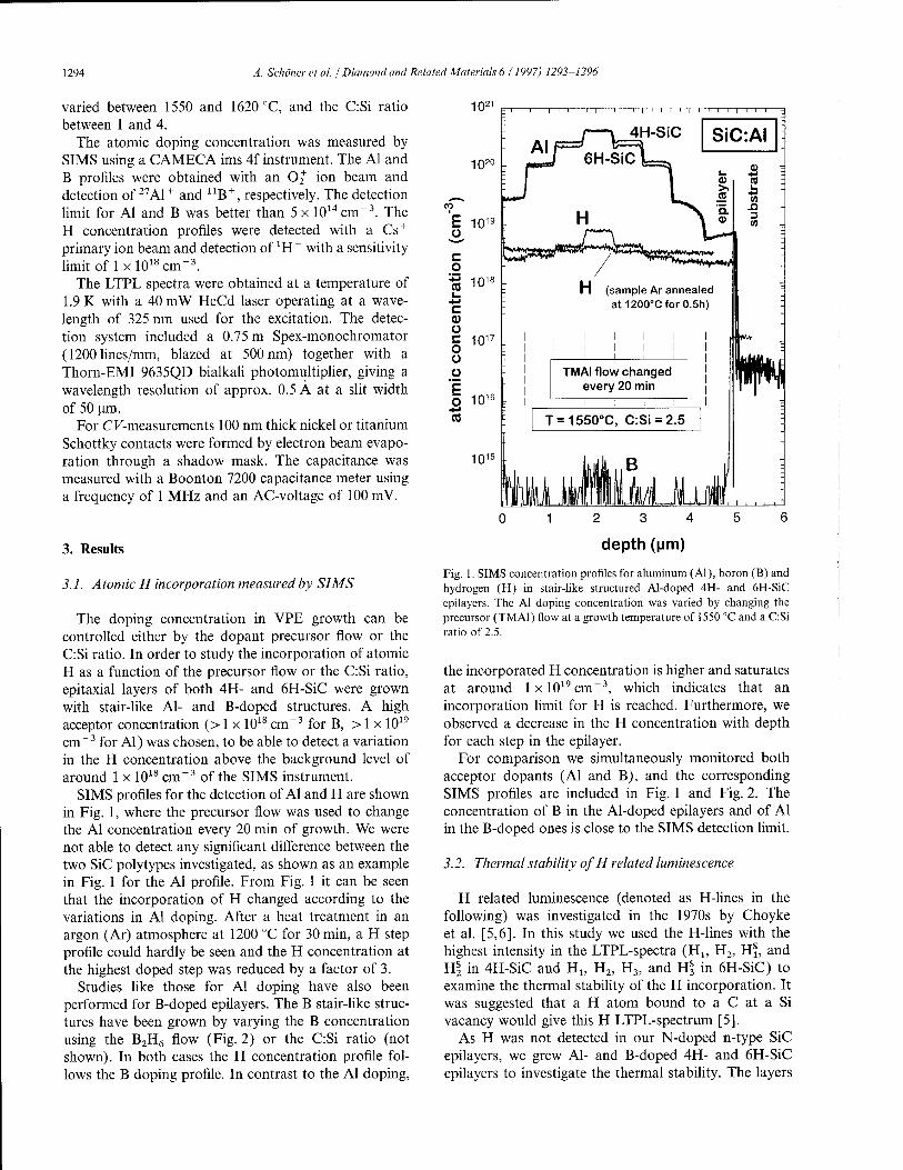
1294 A. Schöner et al. / Diamond and Related Materials 6 (1997) 1293-1296
varied between 1550 and 1620 °C, and the C:Si ratio between 1 and 4.
The atomic doping concentration was measured by SIMS using a CAMECA ims 4f instrument. The Al and B profiles were obtained with an O^ ion beam and detection of 27A1+ and UB + , respectively. The detection limit for Al and B was better than 5 x 1014 cm"3. The H concentration profiles were detected with a Cs +
primary ion beam and detection of 1H~ with a sensitivity limit of lxl018cm"3.
The LTPL spectra were obtained at a temperature of 1.9 K with a 40 mW HeCd laser operating at a wave- length of 325 nm used for the excitation. The detec- tion system included a 0.75 m Spex-monochromator (1200 lines/mm, blazed at 500 nm) together with a Thorn-EMI 963 5QD bialkali photomultiplier, giving a wavelength resolution of approx. 0.5 A at a slit width of 50 um.
For CF-measurements 100 nm thick nickel or titanium Schottky contacts were formed by electron beam evapo- ration through a shadow mask. The capacitance was measured with a Boonton 7200 capacitance meter using a frequency of 1 MHz and an AC-voltage of 100 mV.
3. Results
3.1. Atomic H incorporation measured by SIMS
The doping concentration in VPE growth can be controlled either by the dopant precursor flow or the C:Si ratio. In order to study the incorporation of atomic H as a function of the precursor flow or the C:Si ratio, epitaxial layers of both 4H- and 6H-SiC were grown with stair-like Al- and B-doped structures. A high acceptor concentration (> 1 x 1018 cm"3 for B, > 1 x 10¹⁹
cm"3 for Al) was chosen, to be able to detect a variation in the H concentration above the background level of around 1 x 1018 cm"3 of the SIMS instrument.
SIMS profiles for the detection of Al and H are shown in Fig. 1, where the precursor flow was used to change the Al concentration every 20 min of growth. We were not able to detect any significant difference between the two SiC polytypes investigated, as shown as an example in Fig. 1 for the Al profile. From Fig. 1 it can be seen that the incorporation of H changed according to the variations in Al doping. After a heat treatment in an argon (Ar) atmosphere at 1200 °C for 30 min, a H step profile could hardly be seen and the H concentration at the highest doped step was reduced by a factor of 3.
Studies like those for Al doping have also been performed for B-doped epilayers. The B stair-like struc- tures have been grown by varying the B concentration using the B2H6 flow (Fig. 2) or the C:Si ratio (not shown). In both cases the H concentration profile fol- lows the B doping profile. In contrast to the Al doping,
1021
1020
E 1019
ü
c o CO
4H-SiC SiC:AI
bspap,^
1018
c CD Ü | 10" o o
o 1016
*■>
CO
1015
&
.Q 3 CO
H (sample Ar annealed at1200°Cfor0.5h)
TMAI flow changed every 20 min
T = 1550°C, C:Si = 2.5
WfH
2 3 4
depth (|jm)
Fig. 1. SIMS concentration profiles for aluminum (Al), boron (B) and hydrogen (H) in stair-like structured Al-doped 4H- and 6H-SiC epilayers. The Al doping concentration was varied by changing the precursor (TMAI) flow at a growth temperature of 1550 °C and a C:Si ratio of 2.5.
the incorporated H concentration is higher and saturates at around lxl019cm"3, which indicates that an incorporation limit for H is reached. Furthermore, we observed a decrease in the H concentration with depth for each step in the epilayer.
For comparison we simultaneously monitored both acceptor dopants (Al and B), and the corresponding SIMS profiles are included in Fig. 1 and Fig. 2. The concentration of B in the Al-doped epilayers and of Al in the B-doped ones is close to the SIMS detection limit.
3.2. Thermal stability ofH related luminescence
H related luminescence (denoted as H-lines in the following) was investigated in the 1970s by Choyke et al. [5,6]. In this study we used the H-lines with the highest intensity in the LTPL-spectra (H1; H2, Hi, and Hi in 4H-SiC and Hl5 H2, H3, and Hi in 6H-SiC) to examine the thermal stability of the H incorporation. It was suggested that a H atom bound to a C at a Si vacancy would give this H LTPL-spectrum [5].
As H was not detected in our N-doped n-type SiC epilayers, we grew Al- and B-doped 4H- and 6H-SiC epilayers to investigate the thermal stability. The layers

A. Schöner et al. / Diamond and Related Materials 6 (1997) 1293-1296 1295
1020
CO
8io17
c o ü o
o1016
+■> CO
I I I I I I I ' I I I I M i i i I
j/r
6H-SiC:B
0) L. +J CD CO
es L.
a
I I l I I i i i i i
Diborane (B2H6) flow changed every 20 min
i i i i i
T = 1620°C, C:Si = 2.5
ll I I I I I I II
2 3 4 5 6
depth (pm)
Fig. 2. SIMS concentration profiles for aluminum (Al), boron (B) and hydrogen (H) in a stair-like structured B-doped 6H-SiC epilayer. The B doping concentration was varied by changing the precursor (dibor- ane B2H6) flow at a growth temperature of 1620 °C and a C:Si ratio of 2.5.
were devided into six pieces, one piece was kept as a reference and the other five were annealed in an argon atmosphere for 20 min at temperatures of 600, 800, 1000, 1200 and 1600 °C, respectively. LTPL-spectra of the grown B-doped and annealed 6H-SiC samples are shown in Fig. 3 for the wavelength range where the
Wave,^m(nm)
Fig. 3. Low temperature photoluminescence spectra of as-grown and (at different temperatures) annealed samples of a B-doped 6H-SiC epilayer.
H-lines appear. No difference in anneal behavior between Al- and B-doping or between the polytypes was observed and no new luminescence lines of for example B-H- or Al-H complexes were detected. In all cases, a drastic decrease in the intensity of the H-lines was seen at an anneal temperature of 1000 °C. For higher anneal temperatures the intensity of the H-lines remains stable at this low level.
3.3. Hydrogen passivation of the aluminum acceptor
To investigate electrical passivation effects in SiC we used the same Al-doped samples as for the LTPL studies. In order to obtain the net doping concentration as a function of the anneal temperature CF-measurements on Schottky diodes were performed. As seen in Fig. 4 the net doping concentration increased by 30% in this particu- lar sample series when the samples were annealed at temperatures above 1000 °C. This increase is monotonous and larger than the inaccuracy of around 10% for the CF-measurements, which indicates that it is a true effect.
4. Discussion
In our investigation we found a strong dependence between the incorporation of H and the number of acceptors in the epitaxially grown layer. We were able
*1017
2.2
c 2 1 3, c .2 2.0 -4-J CO
£ 1.9 Q) Ü
O 1-8 ü u> c 1.7
'£L o
"O 1.6 -M CD C
1.5
6H-SiC : Al
1.4 0 500 1000 1500
anneal temperature (°C)
Fig. 4. Net doping concentration in dependence of the anneal temper- ature of an Al-doped 6H-SiC epilayer obtained by capacitance-voltage measurements for three different depths in the layer.

1296 A. Schöner et al / Diamond and Related Materials 6 (1997) 1293-1296
to reproduce the results of Larkin et al. [2], where the incorporation of H into B-doped 6H-SiC epilayers using the C:Si ratio to change the doping concentration was studied. In addition we have shown, that the incorpora- tion of H was independent of the acceptor dopant (Al or B) and the same qualitative dependency occurs when either the precursor flow or the C:Si ratio was used to vary the acceptor doping concentration. As no H signa- ture could be detected in our N-doped epilayers, Figs. 1 and 2 lead to the conclusion that a high H incorporation is preferentially seen when acceptor impurities are pre- sent. The reason for this is most probably that H is incorporated with the acceptor dopant by Al-H and B-H complexes which remain from the used acceptor dopant precursors.
After heat treatment at a temperature of 1200 °C for 30 min in Ar the atomic concentration of H equalized at an intermediate level, when compared to the non annealed sample and a stair-like structure was evened out. This is most probably due to H diffusion in the crystal as recently demonstrated on implanted samples annealed at various temperatures [7].
We found a strong decrease in the intensity of the H-lines at anneal temperatures over 1000 °C. This find- ing is in agreement with infra-red absorption measure- ments [8], where C-H bond-related absorption lines observed in as-grown epilayers disappeared after heat treatment at 950 °C.
The presence of H in the p-type epilayers results in electrical passivation of impurities, as observed in other semiconductors [1] and for SiC [3]. As the concentration of compensating donors in our layers was found to be in the order of 1 x 1014cm~3 [4], the increase in net doping concentration after annealling at 1000 °C is most likely due to electrical passivation of the acceptors by H. For n-type SiC we did not observe a similar increase in net doping concentration during Ar anneal. Together with the fact that no H incorporation was found in the n-type epilayers, this indicates that H is not influencing the donor concentration in epitaxially grown material. This is in contrary to results given in Ref. [3], where after annealing in H2 atmosphere at a temperature
between 1500 and 1700 °C, and a H pressure of 10 bar a passivation of N donors was observed.
5. Conclusion
The incorporation of H into SiC during epitaxial growth seems to be mainly related to the presence of acceptor impurities. Independent of the actual shallow acceptor dopant (Al or B) used, the H concentration increased with increase of the acceptor concentration, where both a change in precursor flow and in the C:Si ratio at constant precursor flow gave similar results. H passivates electrically active acceptors to some extent, whereas a passivation of donors was not observed. The H concentration in the epilayers and the electrical passiv- ation of acceptors can be reduced by heat treatments in Ar atmosphere at temperatures above 1000 °C.
Acknowledgement
The authors gratefully acknowledge financial support by Asea Brown Boveri and the Swedish National Board for Industrial and Technical Development (NUTEK).
References
[1] R.K. Willardsen, A.C. Beer, in: J.I. Pankove, N.M. Johnson (Eds.), Hydrogen in Semiconductors, vol. 34, Academic Press, San Diego, 1991.
[2] D.J. Larkin, S.G. Sridhara, R.P. Devaty, W.J. Choyke, J. Electrochem. Mater. 24 (4) (1995) 289-294.
[3] F. Gendron, L.M. Porter, C. Porte, A. Bringuir, Appl. Phys. Lett. 67 (9) (1995) 1253-1255.
[4] N. Nordell, A. Schöner, S.G. Andersson, J. Electrochem. Soc. 143 (9) (1996) 2910-2919.
[5] L. Patrick, W.J. Choyke, Phys. Rev. B 8 (4) (1973) 1660-1669. [6] W.J. Choyke, L. Patrick, Phys. Rev. B 9 (8) (1974) 3214-3219. [7] M.K. Linnarsson, J.P. Doyle, B.G Svensson, MRS Spring Meet-
ing, San Francisco, 1996, MRS Symposium Proceedings Series, No.423.
[8] K. Rottner, R. Helbig, Appl. Phys. A 59 (1994) 427-429.

DIAMOND AND
RELATED MATERIALS
ELSEVIER Diamond and Related Materials 6 (1997) 1297-1300
The origin of 3C poly type inclusions in epitaxial layers of silicon carbide grown by chemical vapour deposition
C. Hallina, A.O. Konstantinova, B. Pecz b'*, O. Kordina a'c, E. Janzena
a Department of Physics and Measurement Technology, Linköping University, S-581 83 Linköping, Sweden b Research Institute for Physics of the Hungarian Academy of Sciences, P. O.Box 76, H-1325 Budapest, Hungary
c ABB Corporate Research, S-721 78 Västeräs, Sweden
Abstract
Formation of 3C silicon carbide (SiC) inclusions in 4H SiC epitaxial layers has been investigated using defect revealing techniques and transmission electron microscopy. The nucleation mechanism of 3C is shown to relate to the formation of triangular stacking faults (TSFs) induced by substrate imperfections and surface defects. The TSFs modify the surface morphology by forming large (0001) surface terraces. A high local supersaturation at the TSF regions results in the spontaneous nucleation of 3C, in a manner similar to that which occurs on on-axis SiC substrates. Depending on the defect that gives rise to the TSF, the 3C inclusions may be completely overgrown by 4H polytype only leaving a striation at the edge. © 1997 Elsevier Science S.A.
Keywords: SiC; Epitaxy; Stacking fault; Transmission electron microscopy (TEM)
1. Introduction
Recent advances in epitaxial growth of SiC using chemical vapour deposition (CVD) have brought down the background doping to within the 1014cm~3 range, and the minority carrier lifetimes up to several micro- seconds [1,2]. Such a material could ensure fabrication of high power high temperature devices. However, the substrate quality leaves much to be desired resulting in a high defect density in the device structures. In the present paper we study triangular defects, a common type of imperfection in epitaxial layers of 4H SiC. We show that these defects are related to the formation of 3C, the cubic polytype of SiC.
2. Experimental
Epitaxial growth was carried out in an atmospheric pressure hot-wall CVD reactor with a SiC-coated suscep- tor [3]. Silane and propane were used as precursor gases. The growth temperature was in the range 1450-1600 °C The substrates were (0001) Si-face off- axis (3.5° towards <1120» wafers grown using the
' Corresponding author.
modified-Lely technique [4]. They were cleaned by organic solvents and hydrogen-etched at the growth temperature prior to growth. The structure of the imper- fections was investigated by optical and scanning electron microscopy using defect revealing techniques, and by cross-section transmission microscopy (XTEM).
3. Results and discussion
When compared to 6H epitaxial layers of 4H-SiC appear to be more given to 3C formation, a simultaneous epitaxial growth onto 4H and 6H substrates usually results in a much higher 3C inclusion density on 4H. Both the substrate imperfections and the growth regimes are important for the nucleation of 3C. The 3C inclusion density is much more pronounced at low growth temper- atures and at high growth rates. Those observations are in agreement with the results reported by Kong et al. [5] and Kimoto and Matsunami [6] for 3C inclusions in 6H-SiC. The semi-quantitative model of Kimoto and Matsunami [6] explains the effect in terms of competi- tion between the step-flow growth due to adatom accom- modation on surface step ledges and the spontaneous two-dimensional (2D) nucleation of 3C at the surface terraces. The 2D nuclei of SiC spontaneously nucleated
0925-9635/97/S17.00 © 1997 Elsevier Science S.A. All rights reserved. PII S0925-9635(97)00083-6

1298 C. Hallin et al. j Diamond and Related Materials 6 (1997) 1297-1300
on low-index {0001} crystal planes typically do not follow the polytype structure of the substrate, rather they crystallise in the structure of 3C instead. If growth occurs via flow of the surface steps due to the off- orientation angle, the layer reproduces the substrate polytype. The material transport along the surface requires a certain supersaturation, and follows a para- bolic dependence on surface step period for a simple model of surface adatom transport [6,7]. If either the growth temperature is too low or the growth rate too high the maximum supersaturation will exceed the 2D nucleation threshold and 3C-SiC will be formed.
We found that the growth temperature and growth rate are not the only process parameters which affect the 3C inclusion density, the C/Si ratio also appears to be very important. A combination of a high growth rate, i.e. high silane flow, and a high C/Si ratio results in a dramatic increase of 3C inclusion densities, particu- larly at low growth temperatures.
Thin epi-layers were grown at 1500 and 1550 °C with a growth rate of 3 \m\/h and C/Si ~ 2. A high density of large triangular pits appeared on the 4H SiC epi-layer grown at 1500 °C, see Fig. 1. However, the epi-layer grown at 1550 °C showed a much lower concen- tration. The triangular regions expand in the close- packed directions [2lT0] and [1210], but the [1120], [1010], and [0110] directions also occur. The 6H SiC epi-layer grown at 1500 °C shows very few triangular defects and those that do occur have a slightly different character compared to those on the 4H surface. They do not grow beyond a certain size, instead, the triangular region is displaced laterally in the growth direction of the advancing steps. Behind the triangular region ter- raced growth appears. Investigation of thicker 6H epi- layers showed that the triangular regions may vary in size during the displacement, though, not too abruptly.
Fig. 1. Photomicrograph of the morphology of a 1 um epitaxial layer grown at 1500 °C on a 4H-SiC substrate. The epi-layer was oxidised after growth to reveal 3C inclusions, 3C appears as dark areas in the photograph.
To reveal the inclusion structure inside the triangular region as viewed from the top the samples were oxidised. Many of the triangles appeared to be completely filled with 3C while many other have mixed growth of 3C and 4H inside the region, see Fig. 1. However, no 3C was revealed in the 6H epi-layer.
The interface between 4H and 3C was investigated by removing the 3C using polytype-selective photo-electro- chemical etching. Because of the difference in bandgap energy the low-bandgap 3C polytype can be selectively etched in solutions of fluorides with a blue light (in this case the 458 nm line of an Ar-laser) photo excitation. The interface surface was flat and the inclination-angle was settled at ~3.5° from the epi-layer surface by investigation of a sample cross-section. Thus, the initial triangle surface was on-axis.
We investigated the effect of mechanical damage on 3C formation in 4H epitaxial layers following the experi- ments performed by Powell et al. on 6H [8]. The marks of a diamond scriber appear to be preferential sites of 3C nucleation on 4H-SiC. Damage-induced and self- nucleated inclusions of 3C are of the same size and of nearly the same shape. That suggests a common forma- tion mechanism, therefore, the self-nucleated 3C regions most probably originate from some highly strained regions in the substrate.
Potassium hydroxide (KOH) is an etchant with a high selectivity for defects [9,10], and it was used here to obtain more information about the triangular defects. The 4H epi-layers grown at 1500 and 1550 °C were etched for 2 min at approximately 500 °C. Four different kinds of etch-pits appeared, hexagonal with a pointed bottom, hexagonally shaped holes, 'shell-like', and pits with round or irregular shape. It was deduced that hexagonally shaped holes relate to micropipes (screw with hollow core), etch-pits with pointed bottoms to screw and edge dislocation, and shell-like pits to slip dislocation in the basal plane [9,10]. The round or irregular etch-pits are due to surface damage caused by for example, cutting and lapping. An etch-pit appeared at the top of all indented triangular regions, some with a hexagonal pit with a pointed bottom and the others with a rounded triangular or a more irregular shape. It could also be concluded that triangles with only 3C growth inside the area most often had an etch-pit related to a dislocation at the top, while most of the triangles with mixed growth inside had an etch-pit related to a shallow defect. Most of the triangular defects in the epi- layer surface grown at 1550 °C were related to a disloca- tion and showed only 3C inside the region.
The above results suggest that the triangular shaped morphology defects, which may result in 3C formation, are actually induced by a crystal imperfection within the hexagonal SiC material, which either appears in the epitaxial layers or is already present in the substrate.
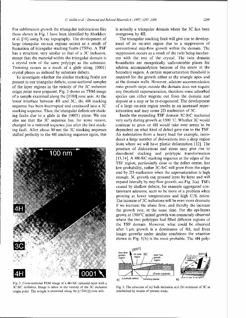
C. Hallin et al. j Diamond and Related Materials 6 (1997) 1297-1300 1299
For Sublimation growth the triangular indentations like those shown in Fig. 1 have been identified by Morkhov et al. [11] using X-ray topography. The development of large triangular on-axis regions occurs as a result of formation of triangular stacking faults (TSFs). A TSF has a structure, very similar to that of a 3C inclusion, except that the material within the triangular domain is a crystal twin of the same polytype as the substrate. Twinning occurs as a result of a glide along {0001} crystal planes as induced by substrate defects.
To investigate whether the similar stacking faults are present in our triangular defects, cross-sectional samples of the layer regions in the vicinity of the 3C inclusion origin point were prepared. Fig. 2 shows an TEM-image of a sample examined along the [ 1100] zone axis. At the lower interface between 4H and 3C, the 4H stacking sequence has been interrupted and continued into a 3C stacking sequence. Thus, the triangular defects are stack- ing faults due to a glide in the (0001) plane. We can also see that the 3C sequence has, for some reason, changed to a twinned sequence just after the first stack- ing fault. After about 80 nm the 3C stacking sequence shifted perfectly to the 4H stacking sequence again, this
0001 \
is actually a triangular domain where the 3C has been overgrown by 4H.
The triangular stacking fault will give rise to develop- ment of an on-axis region due to a suppression of conventional step-flow growth within the domain. The suppression occurs as a result of the twin being incoher- ent with the rest of the crystal. The twin domain boundaries are energetically unfavourable places for adatom accommodation because of the strain at the boundary region. A certain supersaturation threshold is required for the growth either at the triangle apex and at the domain walls. However, adatom accommodation onto growth steps outside the domain does not require any threshold supersaturation, therefore some adsorbed species can either migrate out from the domain and deposit at a step or be re-evaporated. The development of a large on-axis region results in an increased super- saturation and may cause 2D nucleation of 3C.
Inside the expanding TSF domain 3C-SiC nucleated very early during growth at 1500 °C. Whether 3C would continue to grow or 4H would take over seems to be dependent on what kind of defect gave rise to the TSF. An indentation from a heavy load for example, intro- duces a large number of dislocations into a deep region from where we will have plastic deformation [12]. The presence of dislocations and stress may give rise to disordered stacking and polytypic transformation [13,14]. A 4H-SiC stacking sequence at the edges of the TSF region, particularly close to the defect centre, has low probability, rather 3C-SiC will grow from the edges and by 2D nucleation when the supersaturation is high enough. 3C growth can proceed layer by layer and will expand laterally by step flow growth, see Fig. 3(a). TSFs caused by shallow defects, for example aggregated con- taminant adatoms, seem to be more of a problem when growing at lower temperatures and high C/Si ratios. The increase of 3C inclusions will be even more dramatic if we increase the silane flow, and thereby the increase the growth rate, at the same time. For the epi-layers grown at 1500°C mixed growth was commonly observed where the two polytypes had filled different regions of the TSF domain. However, what could be observed after 1 um growth is a dominance of 4H, and from longer growths under similar conditions the situation shown in Fig. 3(b) is the most probable. The 4H poly-
step-flow growth region
^oooA^
Fig. 2. Cross-sectional TEM image of a 4H-SiC epitaxial layer with a 3C-SiC inclusion. Image is taken in the vicinity of the 3C inclusion origin point. The sample is examined along the [<1100>]] zone axis.
Fig. 3. The structure of (a) bulk inclusion and (b) striations of 3C as established by results of present study.
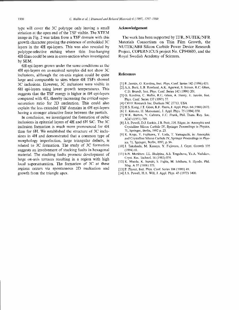
1300 C. Hallin et al. / Diamond and Related Materials 6 (1997) 1297-1300
type will cover the 3C polytype only leaving a small striation at the open end of the TSF visible. The XTEM image in Fig. 2 was taken from a TSF domain with this growth character proving the existence of embedded 3C layers in the 4H epi-layers. This was also revealed by polytype-selective etching where thin free-hanging 4H-films could be seen in cross-section when investigated by SEM.
6H epi-layers grown under the same conditions as the 4H epi-layers on as-received samples did not show 3C inclusions, although the on-axis region could be quite large and comparable to sizes where 4H TSFs showed 3C inclusions. However, 3C inclusions were visible in 6H epi-layers using lower growth temperatures. This suggests that the TSF energy is higher in 6H epi-layers compared with 4H, thereby increasing the critical super- saturation ratio for 2D nucleation. This could also explain the less extended TSF domains in 6H epi-layers having a stronger attractive force between the partials.
In conclusion, we investigated the formation of cubic inclusions in epitaxial layers of 4H and 6H SiC. The 3C inclusion formation is much more pronounced for 4H than for 6H. We established the structure of 3C inclu- sions in 4H and demonstrated that a common type of morphology imperfection, large triangular defects, is related to 3C formation. The study of 3C formation suggests an involvement of stacking faults in hexagonal material. The stacking faults promote development of large on-axis terraces resulting in a region with high local supersaturation. The formation of 3C at these regions occurs via spontaneous 2D nucleation and growth from the triangle apex.
Acknowledgement
The work has been supported by TFR, NUTEK/NFR Materials Consortium on Thin Film Growth, the NUTEK/ABB Silicon Carbide Power Device Research Project, COPERNICUS project No. CP940603, and the Royal Swedish Academy of Sciences.
References
[1] E. Janzen, O. Kordina, Inst. Phys. Conf. Series 142 (1996) 653. [2] A.A. Burk, L.B. Rowland, A.K. Agarwal, S. Sriram, R.C. Glass,
CD. Brandt, Inst. Phys. Conf. Series 142 (1996) 201. [3] O. Kordina, C. Hallin, R.C. Glass, A. Henry, E. Janzen, Inst.
Phys. Conf. Series 137 (1993) 37. [4] CREE Research Inc, Durham NC 27713, USA [5] H.S. Kong, J.T. Glass, R.F. Davis, J. Appl. Phys. 64 (1988) 2672. [6] T. Kimoto, H. Matsunami, J. Appl. Phys. 75 (1994) 850. [7] W.K. Burton, N. Cabrera, F.C. Frank, Phil. Trans. Roy. Soc.
A243 (1951) 299. [8] J.A. Powell, D.J. Larkin, J.B. Petit, J.H. Edgar, in: Amorphic and
Crystalline Silicon Carbide IV, Springer Proceedings in Physics, 71, Springer, Berlin, 1992 p. 23.
[9] K. Koga, Y. Fujikawa, Y. Ueda, T. Yamaguchi, in: Amorphic and Crystalline Silicon Carbide IV, Springer Proceedings in Phys- ics, 71, Springer, Berlin, 1992, p. 96.
[10] J. Takahashi, M. Kanaya, Y. Fujiwara, J. Cryst. Growth 135 (1994)61.
[11] E.N. Morkhov, I.L. Shulpina, A.S. Tregubova, Yu.A. Vodakov, Cryst. Res. Technol. 16 (1981) 879.
[12] K. Maeda, K. Suzuki, S. Fujita, M. Ichihara, S. Hyodo, Phil. Mag. A 57 (1988) 573.
[13] P. Pirouz, Inst. Phys. Conf. Series 104 (1989) 49. [14] J.A. Powell, H.A. Will, J. Appl. Phys. 43 (1972) 1400.
DIAMOND AND
RELATED MATERIALS
Diamond and Related Materials 6 (1997) 1301-1305
SiC and group III nitride growth in MOVPE production reactors
R. Beccard a'*, D. Schmitza, E.G. Woelk b, G. Straucha, H. Jürgensena
a AIXTRON GmbH, Kackertstr. 15-17, D-52072 Aachen, Germany
b AIXTRON Inc., 1569 Barclay Blvd, Buffalo Grove, IL 60089, USA
Abstract
In this study a range of MOVPE systems for high temperature epitaxial growth processes, such as SiC and group III nitrides, is presented. It is shown that extensive modelling of the heat transfer, gas flow and reactant depletion has led to highly efficient reactors that provide the capability for uniform growth of binary and ternary material systems at temperatures up to 1600 °C in single- and multi wafer configurations. Experimental results of various layers are presented to prove the availability of state-of- the-art process technology in production-scale systems. © 1997 Elsevier Science S.A.
Keywords: MOCVD; Nitride; SiC; Modelling
1. Introduction
Silicon carbide is currently gaining much attention as a material for high temperature, high speed and high power devices. However, fabricating epitaxial SiC films is still a challenge since very high growth temperatures (up to 1600 °C) have to be used. These require carefully adapted reactor design to ensure laminar flow conditions and controlled depletion of the reactants inside the reactor.
Similar considerations are valid for the group III nitrides (A1N, GaN, InN and their alloys). These materi- als are also grown at high deposition temperatures (up to 1300 °C). Furthermore, the heterostructures of these materials typically require abrupt changes in growth temperature. In general, both nitrides and SiC are similar in their challenges to growth equipment.
This study uses a family of high temperature reactors to grow SiC and nitrides. Extensive modelling was used in order to find the optimum reactor geometry. Thus an optimization of uniformity and efficiency, and a minimi- zation of undesired parasitic reactions was obtained.
2. Experimental
Growth experiments performed in an AIX 200/4 series two-flow horizontal laminar flow CVD reactor provided
: Corresponding author.
the basis for the numerical calculations of the optimiza- tion of this reactor type, as well as the reactor and process design for the high temperature Planetary Reactor®.
The reactor consists of a double-walled, water-cooled outer quartz reactor and a rectangular inner quartz liner tube in which the gas reaction takes place. The reactor is designed to sustain CVD processes in the pressure range 10-1000 mbar. The susceptor which is inductively heated can handle one wafer of up to 4 in. diameter rotated using the Gas Foil Rotation® technique.
Fig. 1 shows a cross-section of the Multiwafer Planetary Reactor® chamber. To obtain the required uniformity of material film each individual substrate is rotated around its centre axis similar to in the linear flow channel reactor described above [1]. The seven satellite disks, each with one 2 in. wafer, are also rotated around the inlet to provide total symmetry in the growth chamber for all wafers.
The reactor is able to sustain a susceptor temperature of 1600 °C by inductive heating which makes it suitable for the growth of SiC where temperatures in the range of 1400-1600 °C are required [2]. The susceptor temper- ature is measured by means of a pyrometer.
In MOVPE having control over the temperature of the reactor's inner walls has been found to be crucial. In the case of the Planetary Reactor®, this is simply the ceiling of the reactor chamber, a plate of fused quartz above the susceptor. The temperature can be controlled by adjusting the gas composition between the ceiling
0925-9635/97/S17.00 © 1997 Elsevier Science S.A. All rights reserved. PII S0925-9635(97)00110-6
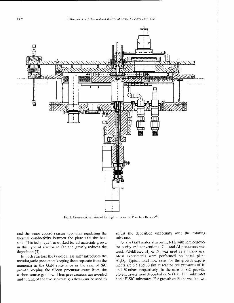
1302 R Beccardetal. / Diamond and Related Materials 6 (1997) 1301-1305
NWNWI
Fig. 1. Cross-sectional view of the high temperature Planetary Reactor11
and the water cooled reactor top, thus regulating the thermal conductivity between the plate and the heat sink. This technique has worked for all materials grown in this type of reactor so far and greatly reduces the deposition [3].
In both reactors the two-flow gas inlet introduces the metalorganic precursors keeping them separate from the ammonia in the GaN system, or in the case of SiC growth keeping the silicon precursor away from the carbon source gas flow. Thus pre-reactions are avoided and tuning of the two separate gas flows can be used to
adjust the deposition uniformity over the rotating substrate.
For the GaN material growth, NH3 with semiconduc- tor purity and conventional Ga- and Al-precursors was used. Pd-diffused H2 or N2 was used as a carrier gas. Most experiments were performed on basal plane A1203. Typical total flow rates for the growth experi- ments are 6.5 and 13 slm at reactor cell pressures of 10 and 50 mbar, respectively. In the case of SiC growth, 3C-SiC layers were deposited on Si (100, 111) substrates and 6H-SiC substrates. For growth on Si the well known

R. Beccardetal. / Diamond and Related Materials 6 (1997) 1301-1305
Growth rate of GaN vs 1/Td
1303
0,82
1/Td [1000/K]
Fig. 2. Growth rate of GaN versus 1/Td (AIX 200/4).
carbonization techniques were used. SiH2Cl4 and C2H4
were used as process gases. The substrate temperature was varied between 1200 and 1390 °C; when using SiH4 and C3H8 temperatures up to 1700 °C were employed.
3. Modelling
Extensive modelling was performed to study the dependence of the growth rate on key process parame- ters, such as temperature, pressure, input partial pressure of TMG and ammonia, and the total flow rate. A two- dimensional model was used as described in Ref. [4]. The results for the linear channel reactor are shown first. It can be seen that homogeneous decomposition of TMG near the growing surface is almost completed under the conditions used.
Fig. 2 shows the growth rate versus the deposition temperature of GaN in the linear channel reactor. The excellent agreement between the calculated and experi- mental growth rate distribution along the flow direction in the reactor has been published elsewhere [5]. Initial data with wafer rotation gave a growth rate uniformity of +4%. By further optimization a uniformity of + 1.5% is achievable.
All considerations concerning the linear horizontal two-flow reactor can be transferred to the mass pro- duction Planetary Reactor® family. Thus several pieces of information are obtained from the simulations, the most important being that the gas phase in the reactor with the susceptor at 1100 °C is laminar and stable. Fig. 3 shows the concentration of trimethylgallium (TMGa), monomethylgallium (MMGa), and Ga vapour as a function of the radius. The flux of MMGa
originating from the TMGa decomposition is assumed to govern the growth rate. As seen in Fig. 3(b), the MMGa gradient decreases linearly along the radius. Similar results were also found in the simulations of a smaller horizontal reactor which were in good agreement with the actual growth runs [5].
Both the modelling and the experiments show that the thermal management of heat transfer can be handled by the predicted Planetary Reactor® design. The temper- ature of the reactor ceiling can be adjusted to allow optimum and reproducible deposition conditions. Temperature uniformities at 1600 °C on 2 in. substrates that are better than + 5 °C have been measured. The calculated streamlines at 1000 mbar and 50mbar are free from any vortices from the centre toward the outer radius. Further, the model clearly points out the advan- tage of this geometrical concept in the Planetary Reactor® which, even at high-temperature growth, lin- earizes the depletion behaviour rather than compensat- ing depletion effects while giving the best achievable efficiency on wafers, as often seen in the conventional III-V material system.
4. Results
Trimethylgallium and trimethylindium in a purified nitrogen carrier gas were used for the growth of Ga(In)N together with purified ammonia. The growth temperature for the 500 A buffer layer was 600 °C, the temperatures for the GaN layer were 1050-1100 °C. By using growth initiation and buffer layer growth, excellent layer properties of GaN were obtained. Using optimized conditions, GaN with an X-ray 0002 peak FWHM of

1304 R. Beccard et al. I Diamond and Related Materials 6 (1997) 1301-1305
concentration = 1 a.)
trimethylgallium concentration
Ijsusceptor at 1100'Ci
concentration = 0 b.)
monomethylgallium concentration cencentration = max
Ijsusceptor at 110O'Cf
concentration = 0
---;""-'-" '-"" susceptor at 1100°C ::"" :-"-"'':: "/:"z; ~-::"c"---:
Fig. 3. Concentrations of TMGa (a), MMGa (b), and gallium vapour (c) in the reactor.
approximately 30 arcs was obtained. PL results show values of 50 meV FWHM.
In order to grow the p-doped layers necessary for LED and laser production, Mg-doping has been used employing Cp2Mg [6].
Growth of SiC on Si also shows excellent layer properties. The X-ray analysis reveals a strong texture. Beside the main high-intensity peak, reflexes with lower intensities have been registered. X-ray diffraction clearly shows the existence of additional 3C-SiC modifications, SEM analysis shows a smooth surface.
In the Planetary Reactor® the following growth parameters were used: pressure 100 mbar, total flow 14.1 slm, ammonia flow 4 slm and TMGa 267 nmol min*1. At these conditions a growth rate of 1.3 urn h-1 was observed. Higher TMGa flows yield higher growth rates. The simulated growth rate is shown
in Fig. 4 along with the actual growth rate. The total flow consumption of 2 1 min ~x per wafer is minimal compared to any other multiwafer MOCVD reactor described in the literature so far.
The material films were characterized by Hall, X-ray and photoluminescence (PL) measurements. The map- ping of the full width at half maximum (FWHM) of the X-ray peak of a GalnN film with an indium content of ~5% and a thickness of 0.3 urn shows a variation of less than +150 arc s. PL mappings reveal similar results; GalnN PL uniformities across a 2 in. wafer are better than 3 nm.
5. Summary
In this paper it is shown that material systems like GaN and SiC which require high temperature MOVPE

R. Beccard et al. / Diamond and Related Materials 6 (1997) 1301-1305 1305
2.0
1.5
E •a 1.0 £
I 2 0.5
0.0
/
' 1 ' I
o O 0 o D ^
. , growth rate on rotated wafer
o experimental value
0.04 0.12 0.06 0.08 0.10
distance from center (m)
Fig. 4. Simulated and observed growth rates in the reactor
reactors can be grown successfully. A two-flow reactor concept is required to separate the precursors until shortly before the growth area on the susceptor. Simulation has shown how to optimize the reactor geometry to guarantee high quality deposition. Using the Planetary Reactor® concept, multiwafer mass pro- duction of SiC and GaN is possible and available on the market. Modelling has shown that high quality and high efficiency layers can be deposited across large areas. Temperature uniformities at 1600 °C on 2 in. substrates of better than + 5 °C have been obtained. Currently a number of these 7 x 2 in. reactors are used to scale-up production quantities for both material systems.
Acknowledgement
The authors would like to acknowledge Prof. Razeghi's group, Center of Quantum Devices, Northwestern University; Dr Makarov, Institut für Strömungsmechanik, Erlangen; and also E. Niemann, D. Leidich, Daimler Benz AG, Frankfurt, for providing their modelling and experimental growth results for this paper.
References
[1] P.M. Frijlink, A new versatile, large size MOVPE reactor, J. Cryst. Growth 93 (1988) 207-215.
[2] BurkA.A., Jr., L.B. Rowland, Reduction of unintentional alumi- num spikes at SiC vapor phase epitaxial layer/substrate interfaces, Appl. Phys. Lett. 68 (1996) 382-384.
[3] P.M. Frijlink, Epitaxial Reactor having a wall which is protected from deposits, United States Patent No 5,027,746 July 2, 1991.
[4] T. Bergunde. M. Dauelsberg, Yu. Egorov, L. Kadinski, Yu.N. Makarov, M. Schäfer, G. Strauch, M. Weyers, Algorithms and models for simulation of MOCVD of III-V layers in the planetary reactor, in: H. Ryssel, P. Pichler (Eds.), Simulation of Semiconduc- tor Devices and Processes, vol. 6, Springer Wien, New York, 1995.
[5] M. Dauelsberg, L. Kadinski, Yu. N. Makarov, E. Woelk, G. Strauch, D. Schmitz, H. Juergensen, GaN-MOVPE: Correlation between computer modeling and experimental data, Proceedings of the 6th International Conference on Silicon Carbide and Related Materials, Kyoto, September 18-21, 1995 (in press).
[6] P. Kung, X. Zhang, E. Bigan, M. Razeghi, A. Saxler, Low pressure metalorganic chemical vapor deposition of high quality A1N and GaN thin films on sapphire and silicon substrates, Proceedings of SPIE Photonics West, San Jose, February 4-10, 1995 (in press).

ELSEVIER Diamond and Related Materials 6 (1997) 1306-1310
DIAMOND AND
RELATED MATERIALS
Growth of SiC films obtained by LPCVD
M.T. Clavaguera-Mora a'*, J. Rodriguez-Viejo a, Z. El Felka, E. Hurtösa, S. Berberich a, J. Stoemenosb, N. Clavaguerac
* Grup de Fisica de Materials I, Departament de Fisica, Universität Autönoma de Barcelona, 08193-Bellaterra, Spain b Physics Department, Aristotle University of Thessaloniki, 54006 Thessaloniki, Greece
'■ Grup de Fisica de l'Estat Solid, Departament ECM, Facultat de Fisica, Universität de Barcelona, Diagonal 647, 08028-Barcelona, Spain
Abstract
This paper reports the results of a systematic study of the influence of deposition conditions on the morphology of films grown using a tetramethylsilane Si(CH3)4 precursor in a hot-wall, low pressure, chemical vapor deposition system at the temperature range 900-1150 °C. Most of the SiC films were deposited on a thin a-Si02 layer, thermally grown on Si(001) wafers. Characterization of the SiC films was performed by X-ray diffraction, scanning and transmission electron microscopy, ellipsometry, profilometry, electron microprobe analysis with a wavelength dispersive spectrometry detection system, and X-ray photoelectron spectroscopy. The results obtained on the kinetics of growth concern the change in the growth rate and the evolution of the preferential [111] orientation of the polycrystalline films with the deposition conditions. The general characteristics of the polycrystalline films are their columnar structure, which is related with the very strong [111] preferred orientation, and the formation of microtwins, having the twin planes perpendicular to the direction of growth. © 1997 Elsevier Science S.A.
Keywords: Poly-SiC; LPCVD; Metal-organic precursors; Microtwins development
1. Introduction
SiC is a good candidate for electronic application at high temperatures because it combines excellent semi- conducting properties and high thermal conductivity with intrinsic resistance to oxidation and creep [1,2]. The growth of poly-SiC by metalorganic low pressure chemical vapor deposition (LPCVD) in a hot-wall reac- tor is of considerable interest due to the reduction of impurities inside grain boundaries and the deposition over large distances [3,4]. In the present study we concentrate on the influence of deposition conditions on the morphology of films deposited on (001) Si wafers, prepared from a mixture of tetramethylsilane (TMS), Si(CH3)4, in H2. A thin a-Si02 layer was thermally grown on the Si substrate prior to deposition to avoid strain development due to the 20% mismatch lattice and the 8% difference in thermal expansion coefficients of the substrate and the overgrown layer.
2. Experimental details
The deposition system, is shown schematically in Fig. 1. The furnace consists of a hot-wall tubular quartz reactor with a large («60 cm) isothermal (±5 °C) zone. The gas handling system uses pneumatically operated valves and electronic mass flow meters, every gas line
Baratron gauge o Furnace
Mass flow | ] f-
meters '# * ^
Valve Samples M-
w Pump
TMS H2N2
* Corresponding author. Fig. 1. Experimental set-up of the hot-wall LPCVD reactor.
O925-9635/97/S17.0O © 1997 Elsevier Science S.A. All rights reserved. PII S0925-9635(97)00084-8

M.T. Clavaguera-Mora et al. I Diamond and Related Materials 6 (1997) 1306-1310 1307
being connected in a run/vent configuration. The sub- strates used were 2 in. Si(100) wafers p-type with a resistivity of 1Q cm. Prior to the deposition the wafers were treated by a H2S04 + H202 mixture followed by HF etching, thoroughly rinsed with deionized water and then dried with N2. The Si02 thickness of the thermally grown interlayer film ranges between 60 and 3000 A. The growth parameters used during the process were: total pressure: 0.5-1.5 Torr, TMS flow: 0.5-15 seem, H2 flow: 1-2 slm, deposition time: 30-240 min and temperature 900-1150 °C. After deposition, samples were cooled to room temperature at a rate of 5 °C/min in a N2 atmosphere.
3. Results and discussion
Characterization of SiC films was performed by X-ray diffraction (XRD) using Cu K„ radiation, scanning electron microscopy (SEM), transmission electron microscopy (TEM), ellipsometry, profilometry, electron microprobe analysis with a wavelength dispersive spec- trometry detection system (EPMA/WDS) and X-ray photoelectron spectroscopy (XPS). Fig. 2 shows some details of the microstructures obtained by TEM. Films grown at 900-980 °C are amorphous with nanocrystals of mean grain size 10 nm and have smooth surfaces. Surface profilometry measurements give a root mean square roughness (RMS) of «6nm. At 1000-1150 °C
polycrystalline ß-SiC is formed, the growth being mostly columnar after an induction period where crystallites nucleate on the substrate forming equiaxed grains. The diameter of the cylindrical crystallites, arranged parallel to the growth direction, increases with deposition tem- perature and film thickness. They form rounded hillocks at the film surface. Consequently, the surface RMS increases with the development of preferred orientation along the [111] direction of ß-SiC. It is quite high, ranging from 70 to 100 nm depending on the temper- ature and film thickness. The crystallites show micro- twins having their twin planes perpendicular to the direction of growth even at the deposition temperature of 1000 °C [5]. This is attributed to the very low adatom mobility in conjunction with the high number of atoms which may be incorporated per unit area on the [111] planes at low energy sites.
Amorphous films are defective in Si. When they are deposited at 900 °C their Si content is 40 at% and this increases up to the stoichiometric value with deposition temperature, as shown by EPMA/WDS. Differences between polycrystalline and amorphous films are clearly seen in the XPS spectra. The C Is and Si 2p peaks of two samples deposited at similar total pressure, TMS and H2 flows, but different temperature are shown in Fig. 3. The most striking difference is the disappearance of the graphite peak [6] in the C Is spectrum at 283.9 eV (FWHM = 1.9 eV) in the poly-SiC films. The main peak has been identified as an Si-C bond. The FWHM are
4* ' -, \
91I1
\
20nm
(b)
Fig. 2. Cross-section TEM micrographs, (a) Dark-field image focalized on [111] reflection of a film deposited at 915 °C, showing the Si/Si02
interface (between arrows) and nanocrystals. (b) Bright-field image of a film deposited at 1130 °C; arrows show cavities between grains.

1308 M.T. Clavaguera-Mora et al. I Diamond and Related Materials 6 (1997) 1306-1310
4000
3000
2000
"~r- iooo
>, 0
0) 4000
3000
2000 -
1000 -
"I—'—'—' Cls ~i r 1 r-
C-Si
(a)
+ Exp Fit
C-Si 54% C-C 39% C-0 7%
C - 0 i/^h'W^nHn^
Cls (b)
+ Exp Fit
C-Si 88% C-0 12%
290
Binding Energy (eV)
4000
3000
2000
1000 3 to
to §5 4000
3000
2000
1000
Si2p
Si-C
Si-0 ^H-H*H| 11H11 |pt*'
Si-C Si-0
(d) -
Exp Fit 89.0% H 11.0%
**r*Wiii
-J L
95 100 105
Binding Energy (eV) 110
u
u
o
a a
•a c
Ü o
Ü
s
o
U
On X
a <
PH

M.T. Clavaguera-Mora et al I Diamond and Related Materials 6 (1997) 1306-1310 1309
2644.0 - 2832.2
2832,3 - 3020.4
3020.5 - 3208.7
3288.B - 3397.8
l«ii»j*j's
Fig. 4. Ellipsometric mapping of an SiC film.
4 -
3 3
CO
1 2 o Ü
_
1
H2
1 1
flow =
I I , I
= 1.5s!m
I I I I I I
/
PT = 0.7 Torr
,«> / '
T = =1130°C / /
/ / K —
/ /
/
- / / 1
s /
s —
/ /
_ 0 . / ' A at
— /\' ' 'U' O 80 cm from the ~~ TL ' s reactor entrance
1 I I
A 85 cm D 90 cm
I , , , i i i i
5 10
TMS flow (seem) 15
Fig. 5. Growth rate versus TMS flow at several wafer positions from the reactor entrance.
«10% higher for the amorphous films than for the poly- SiC ones due to the disordered network. In some of the samples peaks arising from C or Si bonded to oxygen are seen due to native oxidation or contamination.
The film thickness increases linearly with the depos- ition time, independently of the growth conditions. The thickness uniformity of the wafers is fairly good. Fig. 4 shows an ellipsometric mapping obtained with 50 points when measuring a SiC film whose mean thickness is about 15 um from edge to edge. Fringes are produced by the interference of the free SiC surface with the interface. Thickness differences between consecutive fringes correspond to about 0.1 (am.
Fig. 5 shows the dependence of the growth rate, /, on the wafer location in the reactor for a fixed H2 flow and
different values of TMS flow. As expected, there is a linear increase of J with the TMS flow. In addition, / decreases on successive wafers located at increasing distance from the reactor entrance. This decrease is due to an important TMS depletion along the reactor pro- duced by the deposition on the previous wafers and on the hot reactor walls.
The apparent activation energy of growth is (1.4 + 0.1) eV. This value of the activation energy remains constant irrespective of: the H2 to TMS flow ratio, the crystallinity of the film and the thickness of the Si02 interlayer. The linearity of the film thickness with both deposition time and TMS flow, as well as the film thickness uniformity and the high activation energy value support the finding that growth is controlled by some surface mechanism. Also, / increases with the TMS to H2 flow ratio, for a fixed total pressure. Since the strong preferred orientation of the crystalline growth is related to the generation of microtwins, it permits a fast incorporation of the atoms in the crystal lattice resulting in a reduction of the free energy of the system and creating large twined grains.
4. Conclusions
The main conclusions with respect to the growth of films from TMS/H2 by LPCVD process deduced from the experimental study are: (1) Amorphous (with nanocrystalline inclusions dis-
persed in the matrix) films incorporate an excess of C with respect to stoichiometry. Nanocrystals exhibit no preferred orientation.
(2) Polycrystalline films have the ß-type structure and develop [111] orientation.
(3) Planar defects are generated perpendicular to the direction of growth. They are microtwins which facilitate growth.
(4) The surface reaction-controlled growth rate has an activation energy of 1.4 + 0.1 eV.
(5) The surface roughness and preferential orientation increase with film thickness, deposition temperature and TMS versus H2 flow ratio.
Acknowledgement
Authors are indebted to the 'Serveis Cientifico-Tecnics' of the University of Barcelona for the XRD, EPMA/ WDS and XPS analysis. Financial support from CEE BRITE/EURAM by Contract No BRE-CT92-0211, from CIRIT by Project No GRQ-2.048 and from CICYT by Project No MAT95-0875 is acknowledged.

1310 M.T. Clavaguera-Mora et al. / Diamond and Related Materials 6 (1997) 1306-1310
References [3] K.K. Schuegraf (Ed.), Handbook of Thin Film Deposition, Noyes Publishers, Park Ridge, 1988.
[1] R.F. David, G. Keiner, J.W. Palmour, J.A. Edmond, Proc. IEEE [4] I- Golecki, F. Reidinger, J. Marti, Appl. Phys. Lett. 60 (1992) 1703. 79 (1991) 677. [5] J. Rodriguez Viejo, J. Soemenos, N. Clavaguera, M.T. Clavaguera-
[2] J. Rodriguez, N. Clavaguera, Z. El Felk, M.T. Clavaguera-Mora, Mora> J- Cryst. Growth 155 (1995) 214. G. Arnaud, J. Camasel, J. Pascual, S. Berberich, J. Millan, Mater. [6] A- Tabata, S. Fujii, Y. Suzuoki, T. Mizutani, M. Leda, J. Appl. Sei. Technol. 12 (1996) 98-101. Physics 23 (1990) 316.

^§n DIAMOND AND
ELSEVIER
RELATED MATERIALS
Diamond and Related Materials 6 (1997) 1311-1315
Chemical conversion of Si to SiC by solid source MBE and RTCVD
J. Pezoldt *, V. Cimalla, Th. Stauden, G. Ecke, G. Eichhorn, F. Scharmann, D. Schipanski TU Ilmenau, Institut für Festkörperelektronik, Postfach 100565, 98684 Ilmenau, Germany
Abstract
The carbonization of (lll)Si surfaces exposed to a sublimed carbon molecular beam with carbon fluxes varying ca two orders of magnitude at substrate temperatures between 700 and 1050°C was studied. The structural and morphological evolution was investigated in comparison to the growth under RTCVD conditions. Two different polytype structures, 3C- and 2H-SiC, were grown on 4" (lll)Si wafers. Generally in the investigated parameter range carbonized layers formed by RTCVD have a better crystallinity and a smoother surface. © 1997 Elsevier Science S.A.
Keywords: Molecular beam epitaxy; Polytypism; Reflection high energy electron diffraction; Silicon carbide
1. Introduction
Carbonization is a classical process to form silicon carbide on silicon. It is commonly used to form the buffer layer in different growth techniques [chemical vapour deposition (CVD) [1], rapid thermal chemical vapour deposition (RTCVD) [2], molecular beam epi- taxy (MBE) [3,4] etc.], acting as a pseudo-substrate for the further growth process. Up to now for carbonization by solid sources only few attempts have been reported and only one systematic investigation about the nucle- ation and growth process on (100) Si has been carried out [5].
The aim of this work was the comparative study of the carbonization process in a wide range of carbon fluxes, substrate temperatures and growth times using two different growth techniques RTCVD and solid source MBE. These two methods were compared regard- ing morphological and structural evolution on (lll)Si.
2. Experimental
In the case of RTCVD the substrates were cleaned wet chemically and by in situ H2 annealing. The carbon- ization in propane diluted in hydrogen at atmospheric pressure is as described in Refs [6,7].
1100
* Corresponding author. Tel.: 49 3677 691669; Fax: 49 3677 691674; e-mail: [email protected]
1000 o
900 r
& 800
en X) 3
C/3
700
600 r
500
1 1 1
: ©
i
©
i ! L
© j
\ 3C-SiC ©
© \
r P- ----'" Z-
: ® /
A \
\ © / ' A 2H-SiC \ / :
: no SiC formation [5,11] :
10 1 10 10
Carbon flux (a.u.) 10
Fig. 1. Kinetic phase diagram for solid source MBE carbonization at 10 min processing time: O, twinned (11 l)3C-SiC; D, (110)3C-SiC; *, (311)3C-SiC; A, 2H-SiC.
The carbonization of (lll)Si 4" wafers by carbon molecular beams was carried out in a UMS 500 Balzers MBE system with base pressure of 8xl0^nmbar during the deposition process the pressure was in the range of 10 ~9 mbar. The cleaning and deposition process were monitored by in situ reflection high energy electron diffraction (RHEED). Pyrolytic graphite was used as the C source. The carbon was evaporated using an electron beam evaporator. The flux (CF) was controlled
0925-9635/97/S17.00 © 1997 Elsevier Science S.A. All rights reserved. PII S0925-9635(97)00087-3
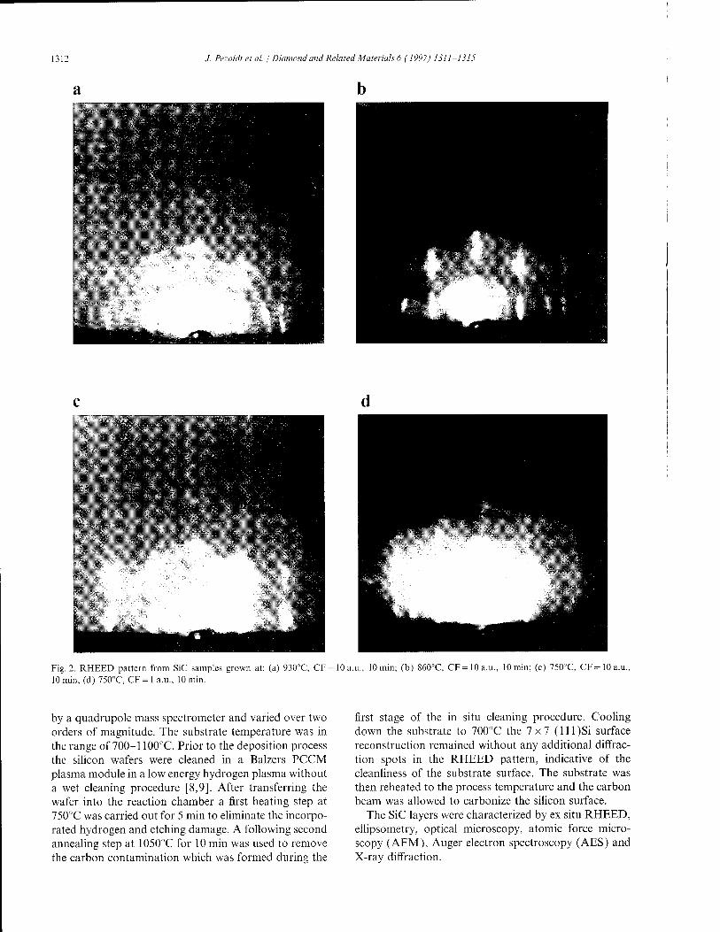
1312 J. Pezoldtetal. / Diamond and Related Materials 6 (1997) 1311-1315
a
Fig. 2. RHEED pattern from SiC samples grown at: (a) 930°C, CF = 10 min, (d) 750°C, CF = 1 a.u., 10 min.
= 10a.u., 10 min; (b) 860°C, CF=10a.u., 10 min; (c) 750°C, CF = 10a.u.,
by a quadrupole mass spectrometer and varied over two orders of magnitude. The substrate temperature was in the range of 700-1100°C. Prior to the deposition process the silicon wafers were cleaned in a Balzers PCCM plasma module in a low energy hydrogen plasma without a wet cleaning procedure [8,9]. After transferring the wafer into the reaction chamber a first heating step at 750°C was carried out for 5 min to eliminate the incorpo- rated hydrogen and etching damage. A following second annealing step at 1050°C for 10 min was used to remove the carbon contamination which was formed during the
first stage of the in situ cleaning procedure. Cooling down the substrate to 700°C the 7x7 (lll)Si surface reconstruction remained without any additional diffrac- tion spots in the RHEED pattern, indicative of the cleanliness of the substrate surface. The substrate was then reheated to the process temperature and the carbon beam was allowed to carbonize the silicon surface.
The SiC layers were characterized by ex situ RHEED, ellipsometry, optical microscopy, atomic force micro- scopy (AFM), Auger electron spectroscopy (AES) and X-ray diffraction.
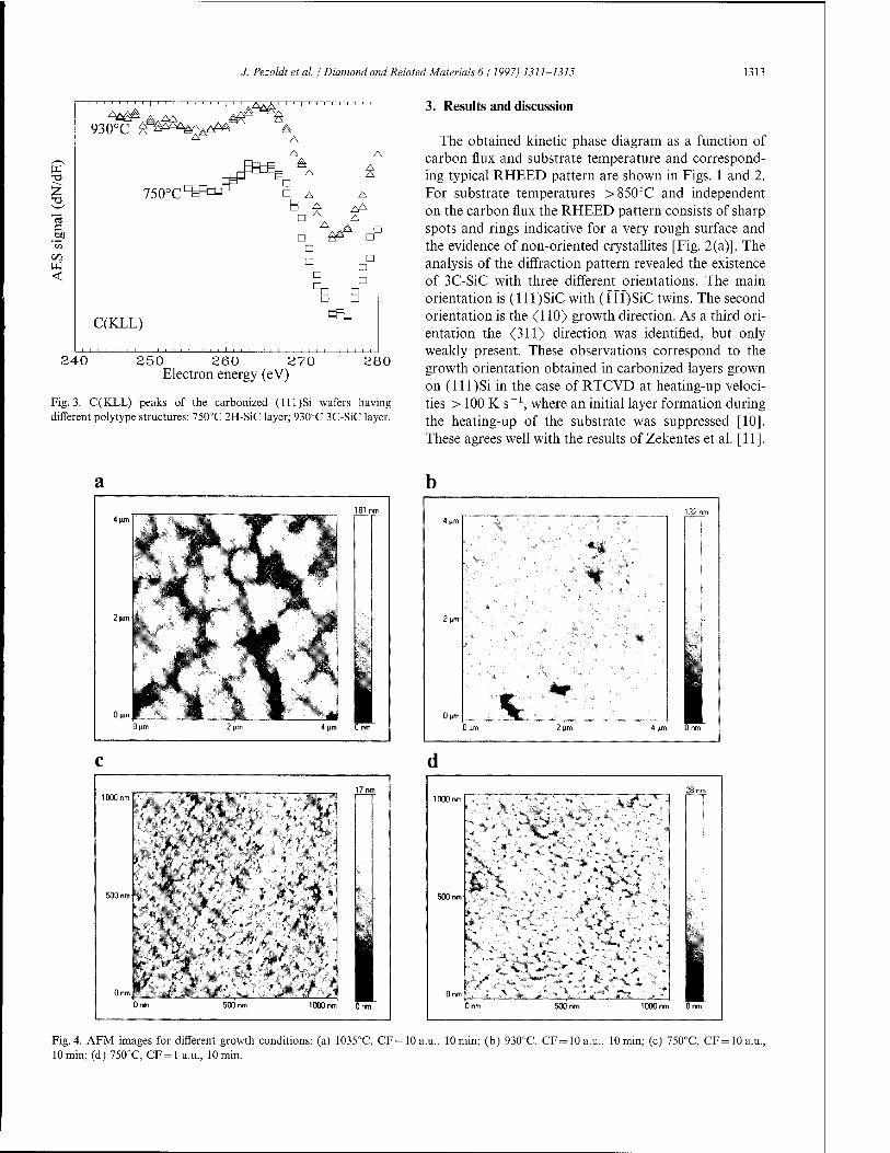
/. Pezoldtetal. / Diamond and Related Materials 6 (1997) 1311-1315 1313
1
c/3
<
AA£^ A„AA £& 930°C g^^^fiM
^ A A A
FPr-R ^ H" j=t±^ A A
750°CcS=™r^ □ A A
n A AA A
Ä .A n
n n n n □ % □
D a ffi-i
C(KLL)
240 250 260 270 Electron energy (eV)
280
Fig. 3. C(KLL) peaks of the carbonized (lll)Si wafers having different polytype structures: 750°C 2H-SiC layer; 930°C 3C-SiC layer.
3. Results and discussion
The obtained kinetic phase diagram as a function of carbon flux and substrate temperature and correspond- ing typical RHEED pattern are shown in Figs. 1 and 2. For substrate temperatures >850°C and independent on the carbon flux the RHEED pattern consists of sharp spots and rings indicative for a very rough surface and the evidence of non-oriented crystallites [Fig. 2(a)]. The analysis of the diffraction pattern revealed the existence of 3C-SiC with three different orientations. The main orientation is (111 )SiC with (1 H)SiC twins. The second orientation is the <110> growth direction. As a third ori- entation the <311> direction was identified, but only weakly present. These observations correspond to the growth orientation obtained in carbonized layers grown on (lll)Si in the case of RTCVD at heating-up veloci- ties > 100 Ks"1, where an initial layer formation during the heating-up of the substrate was suppressed [10]. These agrees well with the results of Zekentes et al. [11].
m I
v <%m i.-*•'};- -.• 7 •*' v W~ f."k '*■' •'*.■*' ■*" "' '* r 'J
'L »V.. ~ ..: ' ßp\' .". 'K'.it. -
1000 rm
r.
Orm
28 «n 1000rm
v*- \ -*'~:^ ****-t"C*^* ,,"i^ "^ *£.. ■ -*-*.i
500 nm
l^s
* v ^"t^tv *' > <-"" -A^ "" V ^ ^ 1 Orm '• • • * . % :; • •'" . st. -A Vf^ . >^iS; . !^%Blt " ""' ■
0 nm 500 nm 1000 nm Onm
Fig. 4. AFM images for different growth conditions: (a) 1035°C, CF = 10a.u., 10min; (b) 930°C, CF = 10a.u., 10min; (c) 750°C, CF = 10a.u., 10 min; (d) 750°C, CF = 1 a.u., 10 min.

1314 /. Pezoldtetal. / Diamond and Related Materials 6 (1997) 1311-1315
With decreasing substrate temperature the 3C-SiC diffraction spots elongates perpendicular to the RHEED pattern horizon, caused by the smoother growing surface [Fig. 2(b)]. In the temperature range between 800 and 900°C the <311> growth orientation could not be detected. At carbonization temperatures <800°C and high carbon fluxes the RHEED pictures indicate the growth of 2H-SiC silicon carbide [Figs. 1 and 2(c)]. The evidence of this structure was confirmed by additional X-ray diffraction measurements using the thin film ana- lyser of the SIEMENS D 500 TF diffractometer. In the case of carbon fluxes <10a.u.(see Fig. 1) between 700 and 800°C only the growth of 3C-SiC was observed [Fig. 2(d)]. In all cases the AES spectra revealed a clear carbidic peak (Fig. 3). This corresponds to the critical temperture (650°C) necessary for the formation of SiC by solid source MBE [11]. Under RTCVD conditions using propane we observed a SiC formation only at temperatures > 1050°C. This is caused by the necessary decomposition of the hydrocarbons and is in agreement with the observations by Steckl and Li [12]. The critical temperature can be lowered using higher reactive hydro- carbons and lower pressures [12].
The island density and the mean grain size as well as the morphological evolution were investigated by AFM. At high growth temperatures the AFM observations revealed isolated islands with irregular shapes [Fig. 4(a)]. With an increasing deposition time the coalescence of these islands occurs, forming a discontin- uous rough SiC film with a high density of diffusion channels for further material transport. With decreasing substrate temperature the island density increases and the mean grain size decreases [Figs. 4(a-c) and 5]. A similar behaviour was observed increasing the carbon flux [Fig. 4(c and d)]. Increasing island density results in more regular shaped islands. These dependencies are
in agreement with the common theories of crystal growth [13,14] and similar to the growth behaviour observed on (100)Si [5]. At the lowest investigated temperature no grains could be separated. The typical increasing of the grain density with the carbon impingement was also found for the carbonization under RTCVD conditions [15]. Here the nucleation density have shown a linear dependence on the propane concentration in the flowing hydrogen. The grain size increases slightly with the processing time by lateral overgrowth. However, both values, grain size and density, have not shown such a distinct temperature behaviour in the investigated tem- perature range (1100-1300°C).
The surface roughness decreases drastically with decreasing substrate temperature (Fig. 6) leading to the formation of smooth films which was also confirmed by RHEED analysis. This morphology was similar to the RTCVD carbonized silicon at very high propane concen- trations (>0.15%) despite different crystal structures. On the contrary, however, over the whole parameter range we found no carbon accumulation at the SiC surface, neither for the highest carbon flux which corres- ponds to an effective carbon pressure, where a saturation in the growth was observed in the case of acetylene (> 10-5 Torr, see Mogab and Leamy [16]).
This behaviour results in clear differences in the growth kinetics. This is similar to the increase of the initial growth rate with an increasing carbon supply. This rate is much higher in the case of RTCVD, which is simply caused by the higher temperatures and effective carbon fluxes. For the RTCVD carbonization a satura- tion was always found, differing only in the saturation thickness and time [7]. As earlier the saturation set in the better the crystal structure of the SiC film. On the contrary the growth rate under MBE conditions has shown only a weakly decreasing progressing growth
10 "
£ 10 ,0 r
c o T3 XI 5 10
10 0.7
10
0.8 0.9 1.
Inverse substrate temperature (107K)
E c
p c p <u kH
N tn
<u C C
JZ bO fcfl 3
c O
Fig. 5. Nucleation density and mean grain size versus inverse substrate temperature at carbon flux rates 10 a.u.: D, island density; A, mean grain size.
10
h. 7 0.8 0.9 1.0 1.1 Inverse substrate temperature (107K)
Fig. 6. Surface roughness versus inverse substrate temperature at carbon flux rates 10 a.u.
J. Pezoldt et al. / Diamond and Related Materials 6 (1997) 1311-1315 1315
rate. A similar behaviour was observed by Rimai et al. [17] using laser ablation for the carbon supply. This indicates the existence of open diffusion paths for further silicon transport to the growing SiC surface and conse- quently differences in the growth mechanism. The pre- ferred Si out-diffusion led to the void formation and non-epitaxial SiC grain growth. An important factor for this behaviour should be the different carbon supersat- uration at the growing surface, and consequently the nucleation density. However, the existing deviations to the carbonization using hydrocarbons as carbon sources [16] show the role of hydrogen to the lateral growth and coalescence behaviour during SiC growth.
4. Conclusion
In the investigated parameter range carbonized layers formed by RTCVD have a better crystallinity and a smoother surface. However, solid source MBE is suitable for the formation of large area thin silicon carbide layers having different polytypes structures (3C- and 2H-SiC). To use this silicon carbide layer as a buffer layer for the following epitaxial growth the development of methods for sealing-off the open diffusion paths to prevent void formation beneath the epitaxial layer is necessary.
Acknowledgement
The authors would like to thank O. Nennewitz and
H. Romanus for X-ray diffraction measurements and Dr L. Spieß for providing AFM, XRD facilities.
References
[1] H. Matsunami, S. Nishino, H. Ono, IEEE Trans. Electron Dev. 28 (1981) 1235.
[2] A.I. Steckl, J.P. Li, IEEE Trans. Electron Dev. 39 (1992) 64. [3] T. Yoshinobu, H. Mitsui, Y. Tarui, T. Fuyuki, H. Matsunami,
J. Appl. Phys. 72(1992)2006. [4] G.L. Zhou, Z. Ma, M.E. Lin, T.C. Shen, L.H. Allen, H. Morkoc,
J. Cryst. Growth 134 (1993) 167. [5] K. Zekentes, V. Papaioannou, B. Pecz, J. Stoemenos, J. Cryst.
Growth 157(1995)392. [6] V. Cimalla, J. Pezoldt, G. Ecke, H. Rößler, G. Eichhorn, J. Phys.
IV, Colloq. C5 (suppl.) J. Phys. II 5 (1995) C5-863. [7] V. Cimalla, K.V. Karagodina, J. Pezoldt, G. Eichhorn, Mater.
Sei. Eng. B29(1995) 170. [8] J. Ramm, E. Beck and A. Zueger, Mater. Res. Soc. Symp. Proa,
220(1991) 15. [9] J. Ramm, E. Beck, A. Zueger, A. Domman and R.E. Pixley, Thin
Solid Films, 228(1993)23. [10] V. Cimalla, J. Pezoldt, Mater. Res. Soc. Symp. Proc. 355
(1995) 332. [11] K. Zekentes, R. Callec, K. Tsagaraki, B. Sagnes, G. Arnaud,
J. Pascual, J. Camassel, Mater. Sei. Eng. B29 (1995) 138. [12] A.J. Steckl, J.P. Li, Mater. Res. Soc. Symp. Proc. 242 (1992) 537. [13] J.P. Hirth, G.M. Pound, Condensation and Evaporation, Perga-
mon Press, Oxford, 1963. [14] A van der Drift, Philips Res. Rep. 2 (1967) 269. [15] H. Romanus, V. Cimalla, A. Kromka, L. Spieß, J. Pezoldt, Mater.
Sei. Eng. B (1997) to be published. [16] C.J. Mogab, H.J. Leamy, J. Appl. Phys. 45 (3) (1974) 1075. [17] L. Rimai, R. Ager, W.H. Weber, J. Hangas, A. Samman, W. Zhu,
J. Appl. Phys. 77(1995)6601.

DIAMOND AND
RELATED MATERIALS
ELSEVIER Diamond and Related Materials 6 (1997) 1316-1320
Hexagonal and cubic SiC thin films on SiC deposited by solid source MBE
Andreas Fissel, Kay Pfennighaus, Ute Kaiser, Bernd Schröter, Wolfgang Richter * Friedrich-Schiller-Universität Jena, Institut für Festkörperphysik, Max-Wien-Platz 1, D-07743 Jena, Germany
Abstract
Epitaxial growth of SiC on SiC was realized between 900 and 1100 °C by means of solid-source molecular beam epitaxy. In general, our results show that the growth mode is strongly influenced on the surface stoichiometry. In case of Si-stabilized surfaces, showing 3-fold superstructures, films grow layer-by-layer via two-dimensional nucleation even at relatively low temperatures (<1000 °C). RHEED investigations of the epitaxial growth on 3C-SiC(100) show that a layer by layer growth is achieved at T>925 °C and R< 100 nm h_1. The activation energy of nucleation was determined to be 5.3 eV. The film structure was found to be dependent on the deposition mode. In the case of continuous deposition the films consist of a mixture of the cubic and hexagonal polytypes. The films grown by an alternating flux supply controlled to an atomic level using (\/3 x V3)- and (lxl)- surface superstructures were dominantly of 6H-SiC. In case of the Si-rich (3 x 3)-superstructure actually the cubic polytype has been grown. Therefore, we assume that the formation of a certain superstructure stabilizes the nucleation of a special polytype. © 1997 Elsevier Science S.A.
Keywords: Silicon carbide; Molecular beam epitaxy
1. Introduction
SiC is an interesting wide-band-gap semiconductor material. One of the most promising properties of SiC is the occurrence of different structures (polytypes) in this material with different physical properties, such as the band gap and carrier mobilities. Therefore, it may be possible to build devices consisting of one semicon- ducting material only with confined electrons in a two dimensional gas [ 1 ] by different stacking of atomic SiC layers. Because of changing stacking sequences along the c-axis, the growth of such structures is possible in the <0001> direction, however it demands definite nucleation conditions. In this context, epitaxial films of SiC in the [0001] orientation with a definite layer structure are of interest. Molecular beam epitaxy (MBE) is an attractive method to prepare such structures because of the controlled deposition process within an atomic layer range.
In general, different SiC-polytypes have been grown at high growth temperatures (T>1800°C) near the thermodynamical equilibrium in dependence of the
: Corresponding author.
growth rate and the temperature by means of CVD and sublimation growth (see e.g. [2]).
In a medium temperature range (r<1800°C) the growth is performed under non-equilibrium conditions. Growth by nucleation in this case results preferentially in the growth of the cubic polytype. However, a repro- duction of substrate polytype has been realized by a "step-controlled epitaxy" under selected conditions by an advantageous selection of growth rate and temper- ature as well as the off-orientation of the substrate [3].
Recently we found by MBE growth of SiC that at low temperatures (r<1000°C) different polytypes can be grown as well [4,5]. The reason for that may be the occurrence of thermodynamically stable surface phases, so called superstructures, on the SiC surface which are dependent on the coverage and substrate temperature.
In our studies surface superstructures on SiC (0001) have been investigated and, moreover, SiC films have been grown under surface-stabilized conditions using different superstructures. The surface-stabilized condi- tions were realized by an alternating deposition of silicon and carbon.
RHEED investigations have been performed to select the optimum growth conditions and to investigate the influence of increasing Si adlayer thicknesses in depen- dence on the temperature.
0925-9635/97/S17.00 © 1997 Elsevier Science S.A. All rights reserved. PII S0925-9635(97)00085-X

A. Fissel et al. I Diamond and Related Materials 6 (1997) 1316-1320 1317
1450 1400 1350
temperature(K)
1300 1250 1200 1150
120
100
3 80 CO
& to BO c <D ** c 40
20
0) c <D TJ C g
'•4-» CO
O 3 C I
0 «V. 0,001 r
® 0.01
0 20 40 60 80100120140
Time (s)
- 0.1
■ 0.01
0,001
0.70 0.75 0.80
103/T(K"1)
0.85 0.90
Fig. 1. RHEED measurements of the SiC MBE-growth on CVD-grown 3C-SiC(100): (a) intensity oscillations of the specular beam (upper curve) and the diffuse background (lower curve) at 900 °C (growth rate: about 60 nm h_1); (b) dependence of the specular beam intensity in the capture range 0.1 <0<O.35 monolayers between 1100 and 1400 K. The ascent corresponds to an activation energy of 5.3 eV between 1200 and 1400 K. (I0 RHEED intensity before growth, /RHEED intensity during growth, 0 monolayer coverage, T temperature).
2. Experimental conditions
The SiC films were grown between 900 and 1100 °C in a RIBER-EVA 32 MBE system. The source materials of high-purity Si and high-purity C were evaporated separately by means of electron beam guns. Substrates used were on-axis and 3-4° off-axis SiC(OOOl) wafers from Cree Research Inc., samples prepared from on-axis and 2-5° off-axis (0001) Acheson-grown crystals, and 3C-SiC films CVD-grown on Si(100).
The MBE growth mode, the surface morphology, and the structure were investigated by in situ reflection high- energy electron diffraction (RHEED) and ex situ by transmission electron microscopy (TEM) at 200 kV and 400 kV acceleration voltage and atomic force micro- scopy (AFM). Low-energy electron diffraction (LEED) experiments have been performed to investigate surface superstructures. Ex situ Auger electron spectroscopy (AES) measurements were done to clarify the stoichiom- etry, the impurities, and the depth profile of the film.
3. Results
3.1. RHEED intensity investigations of MBE growth of SiCon3C-SiC(100)
The RHEED intensity is very sensitive to morphologi- cal changes of the surface, such as changes of nucleation
density [6]. Therefore, investigations of RHEED inten- sities especially of the specular beam can give informa- tion concerning the nucleation or adatom mobility. Such investigations have been performed for the growth of SiC on SiC(lOO), where, in the onset of growth, RHEED intensity oscillations were found (Fig. 1(a)) correspond- ing to a SiC monolayer growth in each oscillation period. This indicates a layer-by-layer growth via two- dimensional nucleation. Additionally, we investigated the drop of the RHEED intensity just after the growth started, where the growth is mainly determined by nucleation. The drop of the intensity has been analysed using a simple scattering theory [7]. From the results presented in Fig. 1(b), it is clearly seen that at temper- atures <1200K the drop of the RHEED intensity is nearly temperature independent likely due to a non- thermally activated motion of adatoms. Growth at this temperatures results in the development of rough and highly defective films. At r>1200K the nucleation is strongly activated and an energy barrier of 5.3 eV was found from the slope of the curve in Fig. 1(b). This value corresponds to the diffusion barrier of carbon on SiC [8]. In this temperature range films can grow layer- by-layer [4].
3.2. LEED investigations of surface phases on 6H-SiC(0001)
During our investigation of surface superstructures on SiC(0001) we found the (3 x 3), a (1 x 1), a Si-rich

1318 A. Fisseletal / Diamond and Related Materials 6 (1997) 1316-1320
(00)-streak
1/3-order streak
Fig. 2. Sequence of source supply (upper part) and the corresponding RHEED intensity oscillations (lower part) of the (00) streak and the l/3-order streak during MEE-growth of SiC on vicinal 6H-SiC(000l).
(V3 x V3)R30°, a (1 x 1) again, a C-rich(V3 x \/3)R30c- and a C-rich (6\/3 x6V3)R30°-superstructure. (The order corresponds to the decreasing amount of Si on the surface.) We have concentrated our investigations on the Si-rich (V3 x V3)R30°- an(j (3 x 3^superstruc- tures, which are formed by an ordered 1/3 Si-monolayer and 2 Si-monolayers coverage, respectively.
3.3. Surface-stabilized growth on SiC (0001)
Recently, growth of SiC on 3C-SiC(100) by atomic layer epitaxy using different surface structures has attracted considerable attention [9,10]. In our experi- ments alternating deposition of Si and C has been performed on the Si-rich SiC(0001 )-(V3 x V3)R30° and on the (3 x 3)-surface by switching the flux supply by computer controlled automatic valve operation. Shutter sequences were adjusted to deposit approximately one monolayer per supply. Between each deposition step the sample was annealed for a certain time (up to an almost constant RHEED intensity) to improve the adatom ordering at the surface. The atomic level control of the surface stabilization was realized by recording the RHEED intensities of both the (00) streak and an 1/3-order streak resulting from superstructures on the SiC-surfaces. Exposing the (V3 x V3)R30°-surface to Si, the surface transforms to a (lxl) structure and the ( "\/3 x V3)R30o-superstructure recurs during deposition of one ML carbon. As seen in Fig. 2, oscillations of the RHEED intensities were measured during alternating deposition. In continuous deposition of SiC on SiC(0001) no RHEED oscillations occur [4]. This indi- cates an accurate layer-by-layer growth in case of alternating deposition.
A comparison of cross-sectional TEM investigations of layers grown by continuous and alternate deposition shows the difference in the structure. Whereas there is a high amount of different polytypes in continuously grown SiC layers [4,5], the alternately grown epilayers are predominantly of 6H polytype, as seen in Fig. 3. From the image examined in the <ll-20> direction for
the edge-on foils it is seen that to a small extent 3C is embedded within the 6H-phases as well. Additionally, microtwins appear inclined at approx. 70° to the (0001)- surface. These microtwins extending into the growing 6H-film were found to be formed within the cubic inclusions. Furthermore, the occurrence of 3C-SiC within the film corresponds to deviations from regular monolayer growth as indicated by a damping of the RHEED 1/3-order streak intensity.
The controlled deposition on the (OOOl)-surface using the (3 x 3 ^superstructure is much more difficult than on the (V3 x V3)R30°-surface because of the higher Si coverage. Only a few additional Si atoms can lead to a very rapid clustering of Si on the surface as it was investigated by RHEED. The Si-bulk pattern occurs already after the deposition of a submonolayer Si on the Si-rich (3 x 3)-superstructure at r>700°C indicat- ing the growth of large Si-clusters on the surface. During further growth these clusters carbonize and the result is a rough surface. Therefore, any Si clustering has to be avoided by a very accurate monolayer deposition. Further work is, however, required to get the process stable for many deposition cycles. In first successful experiments [11] on the Si-rich (3 x 3)-surface only 3C-SiC has been grown.
4. Summary and conclusions
For SiC MBE growth we found that the substrate temperature has to be higher than 925 °C and the growth rate lower than 0.1 umhT1. An activation barrier for the SiC nucleation of 5.3 eV was determined. Moreover, deposition under surface-stabilized conditions using the (V3 xV3)R30°- and the (1 x l)-surface superstructures results in the growth of preferentially the 6H polytype, whereas in case of the (3 x 3^superstructure 3C-SiC has been grown. However, the cubic structure also appears at any deviation from the surface stabilized layer-by- layer growth.
Because the superstructures are stable only up to temperatures of about 1000 °C, for the growth of special SiC-polytypes via nucleation there exists only a small window between 925 and 1000 °C. The variety of poly- type formation mechanisms at this low temperature may be wide and discussed elsewhere [12]. Up to now the question of mechanisms which are really responsible for the occurrence and the change of polytypes at low temperature MBE growth cannot be fully answered.
More accurate measurements recently performed [A. Fissel, H. Oehme, K. Pfennighaus, W. Richter, Surf. Sei. (in press) [13] yield nucleation activation energies of 0.77 eV for T < 1200 K and 3.9 eV for T > 1200 K.
Recent investigations suggest ordered Si-coverage for the (3 x 3^superstructure in the range between 11/9 and
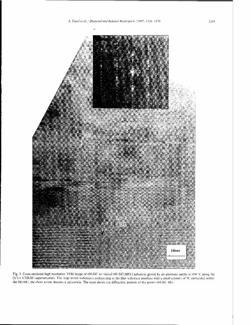
A. Fisseletal. j Diamond and Related Materials 6 (1997) 1316-1320 1319
■■ty
lOnm
Fig. 3. Cross-sectional high resolution TEM image of 6H-SiC on vicinal 6H-SiC(0001) substrate grown by an alternate supply at 930 °C using the (V3 x V3)R30°-superstructure. The large arrow indicates a surface step at the film-substrate interface with a small amount of 3C embedded within the 6H-SiC, the short arrow denotes a microtwin. The inset shows the diffraction pattern of the grown 6H-SiC film.
1320 A. Fissel et al. I Diamond and Related Materials 6 (1997) 1316-1320
13/9 ML [see H.A. Kulakov, G. Henn, B. Bullemer, Surf. Sei. 346 (1996) 49 [14]; J. Furthmüller, F. Bechstedt, A. Fissel, P. Käckell, K. Pfennighaus, W. Richter, B. Schröter, Ext. Abstract Int. Conf. Silicon Carbide, Ill-nitrides and Related Materials, 1997, Stockholm [15]].
Acknowledgement
The work was supported by the Sonder- forschungsbereich 196 (project A03) of the Deutsche Forschungsgemeinschaft and the British-German ARC (project 313-ARC-VII). The authors gratefully acknowledge P. Brown (Cambridge University) for the high resolution TEM work.
References
[1] F. Bechstedt, P. Käckell, Phys. Rev. Lett. 75 (1995) 2180. [2] Yu.M. Tairov, V.F. Tsvetkov, Prog. Cryst. Growth Character. 7
(1983) 111.
[3] T. Kimoto, H. Nishino, W.S. Yoo, H. Matsunami, J. Appl. Phys. 73 (1993) 726.
[4] A. Fissel, U. Kaiser, E. Ducke, B. Schröter, W. Richter, J. Cryst. Growth 154(1995)72.
[5] A. Fissel, U. Kaiser, K. Pfennighaus, E. Ducke, B. Schröter, W. Richter, Inst. Phys. Conf. Ser. 142 (1996) 121.
[6] T. Shitara, D.D. Vvedensky, M.R. Wilby, J. Zhang, J.H. Neave, B.A. Joyce, Phys. Rev. B 46 (1992) 6815.
[7] G Rosenfeld, N.N. Lipkin, W. Wulfhekel, J. Kliewer, K. Morgen- stern, B. Poelsema, G. Comsa, Appl. Phys. A. 61 (1995) 455.
[8] T. Takai, T. Halicioglu, W.A. Tiller, Surf. Sei. 164 (1985) 327. [9] T. Fuyuki, T. Yoshinobu, H. Matsunami, Thin Solid Films 225
(1993)225. [10] S. Hara, T. Meguro, Y. Aoyagi, M. Kawai, S. Misawa, E.
Sakuma, M. Yoshida, Thin Solid Films 225 (1993) 240. [11] A. Fissel, K. Pfennighaus, U. Kaiser, B. Schröter, W. Richter,
unpublished. [12] A. Fissel, K. Pfennighaus, U. Kaiser, B. Schröter, W. Richter,
Proc. E-MRS 1996 Spring Meeting, Strasbourg, Mater. Sei Eng. B, 46 (1997) 324-328.
[13] A. Fissel, H. Oehme, K. Pfennighaus, W. Richter, Surf. Sei. (in press).
[14] H.A. Kulakov, G. Henn, B. Bullemer, Surf. Sei. 346 (1996) 49. [15] J. Furthmüller, F. Bechstedt, A. Fissel, P. Käckell, K. Pfennig-
haus, W. Richter, B. Schröter, Ext. Abstract Int. Conf. Silicon Carbide, Hi-nitrides and Related Materials, 1997, Stockholm.

DIAMOND AND
RELATED MATERIALS
ELSEVIER Diamond and Related Materials 6 (1997) 1321-1323
Hydrogen-, boron-, and hydrogen-boron-related low temperature photoluminescence of 6H-SiC
C. Peppermüllera'*, Adolf Schöner b, Kurt Rottner b, R. Helbiga
a Institute ofApplied Physics, University of Erlangen-Nürnberg, Staudtstr. 7 A3, D-91058 Erlangen, Germany b Industrial Microelectronics Center (IMC), P.O. Box 1084, Isafjordsgatan 22, S-16421 Kista, Sweden
Received 21 March 1997 accepted 24 April 1997
Abstract
An investigation of the low temperature (T<2 K) photoluminescence (LTPL) of boron-, hydrogen-, and boron together with hydrogen-doped SiC was done. We used n-type samples of the polytype 6H. After the implantation of boron and annealing at 1700 °C, we detected three new LTPL emission lines close to a wavelength of 4205 Ä. After the implantation of hydrogen into the boron-implanted samples, we detected another single line at 4183 A, while the lines at 4205 A disappeared. In samples with a higher dose of boron, phonon replica of the 4183 A emission line were detected and two vibrational modes affiliated to the defect were identified (86 and 118 meV). The investigation of boron-doped CVD layers revealed intense hydrogen correlated LTPL emission. © 1997 Elsevier Science S.A.
Keywords: SiC; Photoluminescence; Boron; Hydrogen
1. Introduction
The development of electronic devices based on SiC requires a better knowledge of impurities and defects in this material. The influence of hydrogen on the electrical and optical properties of SiC is an important issue, because hydrogen is present at high concentrations during the CVD growth of epilayers. Furthermore, as described in Ref. [1], hydrogen is expected to be an efficient passivator for impurities, as in many other semiconductors. To obtain planar structures for devices, up to now only ion implantation has been used because of the low diffusion coefficients of dopants in SiC. For p-type doping, aluminium and boron are widely used as acceptor impurities; for MOS structures, boron is pre- ferred (to avoid possible problems with aluminium at the SiC-Si02 interface). We used low temperature photoluminescence (LTPL) to detect the presence of hydrogen, the behaviour of implanted boron after annealing, and the interaction between boron and hydrogen in 6H-SiC. To obtain well-defined concen- tration profiles of boron and hydrogen, ion implantation was used conducted by the computer simulation pro-
* Corresponding author. Fax: 49 9131 858423; e-mail: [email protected]
gram TRIM to calculate the implantation profiles and to maximize the overlap of the boron- and the hydrogen concentration profiles.
2. Sample preparation
Different samples (all n-type 6H-SiC) were prepared both from commercially available material (n-type 6H-SiC wafers from Cree Research, net doping concen- tration ND — NA«5.1017cm-3) and from epitaxial layers grown at IMC using the CVD technique (ND—NA «1016cm~3) on similar substrates. Each of these samples was divided into four parts (a)-(d), some into five (a)-(e). Part (a) was used as reference. Parts (b) and (d) were implanted with boron at an energy of 350 keV, a dose of HO14 cm"2, leading to a concen- tration maximum of nB = lT018 cm-3 at a depth of 0.6 um and annealed at 1700 °C for 30 min in argon atmosphere. Parts (c) and (d) were then implanted with hydrogen (HO14 cm-2, 80 keV, leading to 5-1018 cm"3
at 0.6 um); no annealing was done after the hydrogen implantation. Part (e) was first implanted with a higher dose of boron (5T014cm~2), annealed at 1700 °C for 30 min, implanted with hydrogen (lT014cm^2) and afterwards annealed at 600 °C for 5 min.
0925-9635/97/517.00 © 1997 Elsevier Science S.A. All rights reserved. PII S0925-9635(97)00100-3

1322 C. Peppermüller et al. / Diamond and Related Materials 6 (1997) 1321-1323
3. Experimental set-up
LTPL measurements were done using a He-Cd laser operating at a wavelength of 325 nm and 40 mW power for excitation. The samples were immersed in superfluid helium in a bath cryostat at a temperature of 1.9 K. Two filters were used to avoid the detection of laser plasma emission lines (Schott, UGH) and to suppress the scattered UV light (Schott, GG13). Wavelength selection was done using a Czerny-Turner-monochroma- tor (Spex 1700-III) with a 1200/mm grating blazed at 5000 A and slit widths of 50 )j,m, giving a resolution of 0.55 A. A S20 type photomultiplier and photon counting electronics were used for detection. Spectral intensity corrections were neither done nor were necessary, because of the limited wavelength interval investigated.
4. Experimental results
Fig. 1 shows the LPTL spectra of parts (a)-(c) of a Cree substrate. Part (a) shows the usual LTPL spectrum of n-type 6H-SiC consisting of the emission lines of excitons recombining at a neutral nitrogen donor. This spectrum is described in detail in Ref. [2]. Fig. 1(b) shows the LTPL spectrum of the boron-implanted and
2.7
Energy (eV) 2.8 _2,a_
(c) H-implanted
(b) B-implanted
I
4205Ä
So
Ro
4800
(a) not implanted
4600 4400
Wavelength (A)
_Phonon_ replica
4200
Fig. 1. LTPL spectra at a temperature of 1.9 K of a sample: (a) as grown; the lines marked as "P0","R0","S0" and "Phonon replica" are due to excitons recombining at neutral nitrogen, (b) Spectrum of the part that was boron-implanted and annealed at 1700 °C. Boron- implantation defect lines are marked by "4205 A". The "L" lines are the Dt defect emission lines, the "I" line originates from radiative recombination at another defect, (c) Spectrum of the hydrogen- implanted part. The lines H3 and H| are known as hydrogen-related LTPL emission lines.
annealed part of this sample. The LTPL emission lines L1; L2, and L3 are due to the Di-defect that appears usually after annealing of ion-implanted samples [3-5]. A Line labelled "I" was observed in former experiments after aluminium and chromium implantations and is probably the low temperature form of a line described in Ref. [6]. Additionally, we detected a shorter-wave- length emission located at 4205 A (three lines). These emission lines seem to be specific for the implantation of boron, because we did not detect these lines in samples implanted with different elements (e.g. Al, He, Ti). Fig. 1(c) shows the LTPL emission of part (c). The lines H3 and H| are attributed to a defect in which hydrogen is bound to carbon [7-10], because the energy difference of the emission lines of 369 meV corresponds to the energy of the C-H stretch mode in SiC detected by IR absorption spectroscopy [11]. The H-correlated luminescence was detected only in some of the samples, while all the other LTPL emission lines described in this paper were found to be sample-independent. Fig. 2 finally shows the spectrum of part (e) that was both implanted with boron and hydrogen and showed the same emission lines as part (d) (not shown here), but with much higher intensity. The boron-related emission at 4205 A was not detected but another single emission line at 4183 A was detected, together with its phonon replica and vibrational modes.
Further LTPL measurements were done on CVD grown layers that were doped with boron during the growth (a detailed description is given elsewhere by Schöner et al.). The spectrum of one of those samples is shown in Fig. 3. As described in Ref. [12], we detected
Energy (eV) 2.9 3
LO TO
6 " V118 \
I x \ / V86
LA
IHn
35 c
c 1 ÜW IW 1 .,
*1/5
Q.
i i i i 1,,,,
1 l
l l 1 I
4400 4300 4200
Wavelength (Ä)
4100
Fig. 2. LTPL spectrum at 1.9 K of a sample implanted with a high dose of boron, annealed at 1700 °C, implanted with hydrogen and annealed at 600 °C. The spectrum shows one emission line BH0 (inten- sity reduced 5 times) and its phonon replica together with two vibra- tional modes (called V with their energy as index). Lines not labelled originate from excitons recombining at a neutral nitrogen donor.
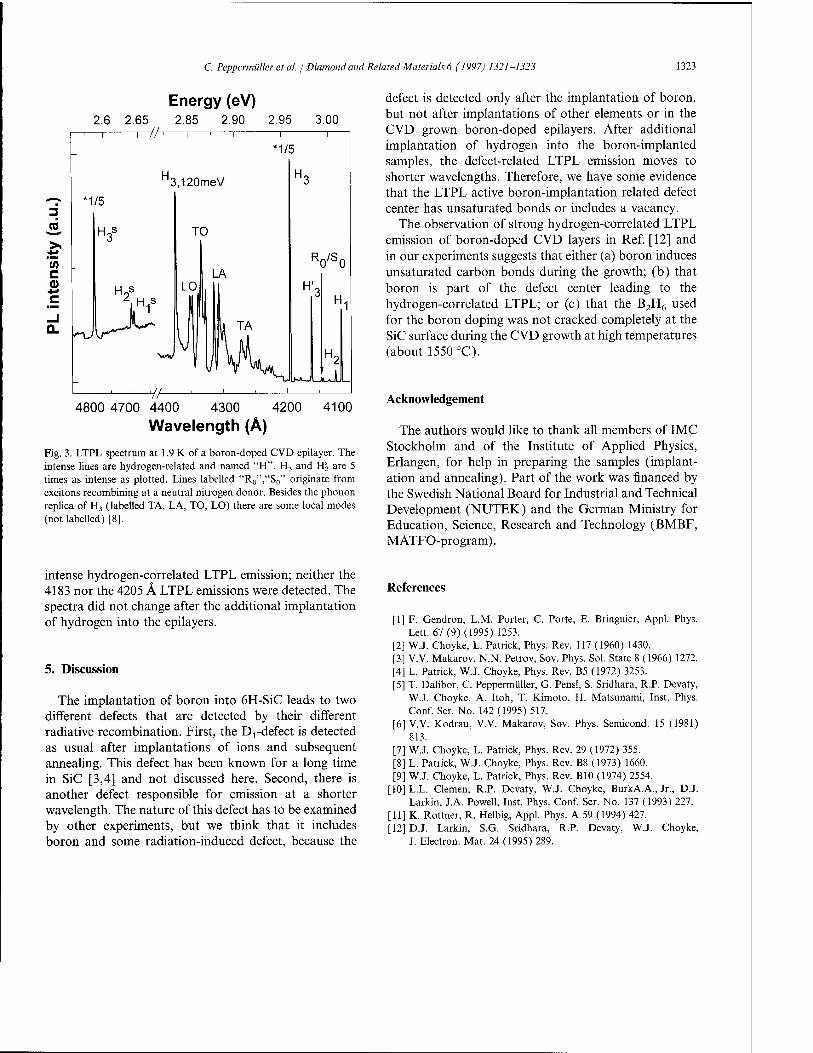
C. Peppermütter et al. / Diamond and Related Materials 6 (1997) 1321-1323 1323
2.6 2.65
Energy (eV) 2.85 2.90 2.95 3.00
3
CO
C
1 ' 1 //< \ ' 1 ' i ' i
- *1/5
H3,120meV H3
*1/5
H3S TO
A-L,
H2s 2LH1S
LO LA
M,
F
H',
0/S0
H? ' yi Y vv^ AJ
>*A- JLJUL ''■■'// ' ' -
I
4800 4700 4400 4300 4200 4100
Wavelength (A)
Fig. 3. LTPL spectrum at 1.9 K of a boron-doped CVD epilayer. The intense lines are hydrogen-related and named "H". H3 and H| are 5 times as intense as plotted. Lines labelled "R0","S0" originate from excitons recombining at a neutral nitrogen donor. Besides the phonon replica of H3 (labelled TA, LA, TO, LO) there are some local modes (not labelled) [8].
defect is detected only after the implantation of boron, but not after implantations of other elements or in the CVD grown boron-doped epilayers. After additional implantation of hydrogen into the boron-implanted samples, the defect-related LTPL emission moves to shorter wavelengths. Therefore, we have some evidence that the LTPL active boron-implantation related defect center has unsaturated bonds or includes a vacancy.
The observation of strong hydrogen-correlated LTPL emission of boron-doped CVD layers in Ref. [12] and in our experiments suggests that either (a) boron induces unsaturated carbon bonds during the growth; (b) that boron is part of the defect center leading to the hydrogen-correlated LTPL; or (c) that the B2H6 used for the boron doping was not cracked completely at the SiC surface during the CVD growth at high temperatures (about 1550 °C).
Acknowledgement
The authors would like to thank all members of IMC Stockholm and of the Institute of Applied Physics, Erlangen, for help in preparing the samples (implant- ation and annealing). Part of the work was financed by the Swedish National Board for Industrial and Technical Development (NUTEK) and the German Ministry for Education, Science, Research and Technology (BMBF, MATFO-program).
intense hydrogen-correlated LTPL emission; neither the 4183 nor the 4205 A LTPL emissions were detected. The spectra did not change after the additional implantation of hydrogen into the epilayers.
5. Discussion
The implantation of boron into 6H-SiC leads to two different defects that are detected by their different radiative recombination. First, the Drdefect is detected as usual after implantations of ions and subsequent annealing. This defect has been known for a long time in SiC [3,4] and not discussed here. Second, there is another defect responsible for emission at a shorter wavelength. The nature of this defect has to be examined by other experiments, but we think that it includes boron and some radiation-induced defect, because the
References
[1] F. Gendron, L.M. Porter, C. Porte, E. Bringuier, Appl. Phys. Lett. 67 (9) (1995) 1253.
[2] W.J. Choyke, L. Patrick, Phys. Rev. 117 (1960) 1430. [3] V.V. Makarov, N.N. Petrov, Sov. Phys. Sol. State 8 (1966) 1272. [4] L. Patrick, W.J. Choyke, Phys. Rev. B5 (1972) 3253. [5] T. Dalibor, C. Peppermüller, G. Pensl, S. Sridhara, R.P. Devaty,
W.J. Choyke, A. Itoh, T. Kimoto, H. Matsunami, Inst. Phys. Conf. Ser. No. 142 (1995) 517.
[6] V.V. Kodrau, V.V. Makarov, Sov. Phys. Semicond. 15 (1981) 813.
[7] W.J. Choyke, L. Patrick, Phys. Rev. 29 (1972) 355. [8] L. Patrick, W.J. Choyke, Phys. Rev. B8 (1973) 1660. [9] W.J. Choyke, L. Patrick, Phys. Rev. BIO (1974) 2554.
[10] L.L. Clemen, R.P. Devaty, W.J. Choyke, BurkA.A., Jr., D.J. Larkin, J.A. Powell, Inst. Phys. Conf. Ser. No. 137 (1993) 227.
[11] K. Rottner, R. Helbig, Appl. Phys. A 59 (1994) 427. [12] D.J. Larkin, S.G Sridhara, R.P. Devaty, W.J. Choyke,
J. Electron. Mat. 24 (1995) 289.

■ft :l -' . '4 DIAMOND AND
ELSEVIER
RELATED MATERIALS
Diamond and Related Materials 6 (1997) 1324-1328
Carrier lifetimes in SiC, studied by time resolved photoluminescence spectroscopy
J.P. Bergman a,b
1 Department of Physics and Measurement Technology, Linköping University, 581 83 Linköping, Sweden b Corporate Research, 721 78 Västeräs, Sweden
Abstract
Recent results regarding the time decay of carrier and exciton recombination in different SiC polytypes are presented. The recombination of bound excitons, bound both at the nitrogen donor and at the Al acceptor, is extremely fast in 4H- and 6H-SiC. These are therefore dominated by efficient non-radiative recombinations, assumed to be a phonon-less Auger process. In high quality epitaxial layers where the free exciton is present, all decay times are determined by the free exciton lifetime. Typically the free exciton also dominates recombination at intermediate temperatures, while the measured time decay at high temperatures is determined by the minority carrier lifetime.
A significant improvement in the minority carrier lifetime of 4H-SiC in particular has been obtained over the past two years, with values as high as 2 us. The minority carrier lifetime is probably determined by capture at unidentified deep levels. © 1997 Elsevier Science S.A.
Keywords: SiC; Bound excitation; Time resolved; Minority carrier lifetime
1. Introduction
For many years photoluminescence (PL) has been an important experimental technique for the study of SiC [1]. Photoluminescence has been used mainly to study the presence and properties of excitons bound at different defects. In recent years PL has also been used to determine the doping levels in high quality n-type epitaxial layers by comparison of the relative intensities between free and bound exciton PL emissions at low temperatures [2].
Time resolved PL measurements (TRPL) complement normal PL studies. By exciting with a pulsed laser and observing the luminescence decay which occurs after excitation further information about the recombination process is obtained. This can be used at low temperatures (as in normal PL) to study the recombination properties of the different bound exciton (BE) emissions, and also at high temperatures to observe the PL decay related to the lifetime of the minority carriers. This is an important material parameter for SiC, a semiconductor intended for power device applications.
A few years ago only a few studies of time resolved PL on SiC had been published [3-5]. But in recent years improvements in epitaxial crystal growth have meant
that better samples are available, and more detailed studies can be performed. This is especially true for the minority carrier lifetime observed at room temperature [6,7].
In this paper we present a compilation of the results obtained over recent years using time resolved PL. We will specifically describe the time decay of the domina- ting BE recombination observed at low temperatures in the 4H- and 6H-polytype. We will also show results indicating the recent increase in the room temperature minority carrier lifetime in high quality epitaxial layers.
2. Experimental
The samples used in this study were grown in a hot-wall chemical vapor deposition (CVD) type reactor, previously described in Ref. [8], using the silane- propane-hydrogen system on n+ 6H-SiC or 4H-SiC (0001) oriented substrates with an off-axis cut of 3.5° towards the [11-20] direction. The reactive gases silane and propane are initially diluted to 5% in hydrogen in the gas bottle and further diluted prior to entry into the cell by a massive flow of purified hydrogen.
0925-9635/97/S17.00 © 1997 Elsevier Science S.A. All rights reserved. PII S0925-9635(97)00107-6

J.P. Bergman / Diamond and Related Materials 6 (1997) 1324-1328 1325
The samples were excited using pulsed excitation from a dye laser synchronously pumped by a mode locked Ar-ion laser. The light pulses, with a duration of less than 10 ps and a wavelength of ~ 680 nm were frequency doubled by a LiI03 crystal to a wavelength of ~ 340 nm (3.65 eV). The frequency-doubled average power was below 1 mW and the repetition rate of the pulses was varied between 10 and 0.15 MHz, using a cavity dumper attached to the dye laser (Fig. 1).
Low temperature (2-300 K) measurements were per- formed in a combined bath and flow He cryostat. The luminescence from the sample was dispersed by a 0.6 m double monochromator. The high temperature measure- ments (300-600 K) were performed in normal atmo- sphere with the sample placed on a heater element. In this case the luminescence was dispersed by a 0.25 m single monochromator. In both cases, the luminescence was detected by a photon counting photomultiplier tube. Using a time-correlated photon counting technique, the luminescence decay could be measured with a time resolution of better than 200 ps (Fig. 2).
10
6H 5iC T = 2.0 K
10 20 30 40
3. Experimental results
In typical samples of all studied poly types (4H and 6H) the bound excitons (BE) at the neutral nitrogen donor dominate the spectrum at low temperatures. The nitrogen donors have, depending on the polytype, sev- eral different equivalent sites which together with the phonon coupling give a characteristic set of sharp emission lines. The measured values for the decay time
Time (ns)
as
in
■p
&_
6H SiC
T = 2.0 K.
4100 4150 4200 4250 4500 4350 Photon Wavelength (Ä)
Fig. 1. Photoluminescence at low temperatures from SiC:6H. The spectrum is dominated by the recombination of the exciton bound at the neutral nitrogen donor.
Fig. 2. Decay curves of the three different nitrogen-bound excitons in 6H-SiC.
of these nitrogen BE are 1.5 + 0.1 ns, 1.8 + 0.1 ns and 8.0 + 0.5 ns for the three different BEs in 6H, and 9.5 +1.0 ns and 48.5 + 4 ns for the two different excitons observed in 4H. These decay times are relatively fast for a material with an indirect band gap such as SiC, and it is clear that the radiative transition is not the domi- natant recombination process. A clear dependence between the observed decay times and the binding energy of the corresponding donor level has been reported previously [9]. This dependence has also been observed for similar BE in Si [10] and is consistent with a recombination dominated by a phonon-less Auger pro- cess. We believe that this is also the dominatant process in SiC [9].
This dependence between the decay time and the donor binding energy is a consequence of the overlap of the wavefunctions in momentum space between the three different particles in the neutral BE. A faster decay time is observed for the exciton bound to the Al acceptor observed in p-type 6H-SiC (Fig. 3). In 4H-SiC the corresponding decay time is even faster and is below the time resolution of 200 ps for the measurement. Similar behaviour is observed for the Ga acceptor in both 6H- and 4H-SiC, with a decay faster than 250 ps, at 2 K [11]. This was also observed previously in Si [10] for acceptor BEs and further demonstrates the effective non-radiative Auger process.
In high quality epitaxial samples the FE is also
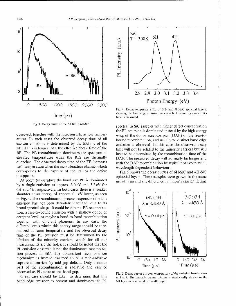
1326 J.P. Bergman / Diamond and Related Materials 6 (1997) 1324-1328
io3 1 1 1 1 1
io2
i \ «k
io1 r
Al BE ^Will |
IRS iiyji r i 10°
1 1 i i i
11 0 500 1000 1500 2000 2500
Time (ps)
Fig. 3. Decay curve of the Al BE in 6H-SiC.
observed, together with the nitrogen BE, at low temper- atures. In such cases the observed decay time of all exciton emissions is determined by the lifetime of the FE, if this is longer than the effective decay time of the BE. The FE recombination dominates the spectrum at elevated temperatures when the BEs are thermally quenched. The observed decay time of the FE increases with temperature when the recombination channel which corresponds to the capture of the FE to the defect disappears.
At room temperature the band gap PL is dominated by a single emission at approx. 3.0 eV and 3.2 eV for 6H and 4H, respectively. In both cases there is a weaker shoulder at an energy of approx. 0.1 eV lower, as seen in Fig. 4. The recombination process responsible for this emission has not been definitely identified, due to its broad spectral shape. It could be either a FE recombina- tion, a free-to-bound emission with a shallow donor or acceptor level, or maybe a band-to-band recombination together with different phonons. In any case, the different levels within this energy range should be ther- malized at room temperature and the observed decay time of the PL emission must be determined by the lifetime of the minority carriers, which for all our measurements are the holes. It should be noted that the PL emission observed is not the dominatant recombina- tion process in SiC. The dominatant recombination mechanism is instead assumed to be a non-radiative capture of carriers by mid-gap defects. Only a minor part of the recombination is radiative and can be observed as PL close to the band gap.
Great care should be taken to determine that this band edge emission is present and dominates the PL
2 d
' m Ö
CM
2.8 2.9 3.0 3.1 3.2 3.3 3.4
Photon Energy (eV)
Fig. 4. Room temperature PL of 6H- and 4H-SiC epitaxial layers, showing the band edge emission over which the minority carrier life- time is measured.
spectra. In SiC samples with higher defect concentration the PL emission is dominated instead by the high energy wing of the donor acceptor pair (DAP) or the free-to- bound recombination, and usually no distinct band edge emission is observed. In this case the observed decay time will not be related to the minority carriers but will instead be determined by the recombination time of the DAP. The measured decay will normally be longer and with the DAP recombination be typical nonexponential, wavelength dependent behaviour.
Fig. 5 shows the decay curves of 6H-SiC and 4H-SiC epitaxial layers. These samples were grown in the same growth run and any difference in minority carrier lifetime
■^ 10
- 10
SiC : 6H X = 4160 /
0.11 U.S
0 0.5 1.0 1.5
Time ((is)
0 5.0 1.0 1.5 Time (|o,s)
Fig. 5. Decay curves at room temperature of the emission band shown in Fig. 4. The minority carrier lifetime is significantly shorter in the 6H layer as compared to the 4H layer.

J.P. Bergman / Diamond and Related Materials 6 (1997) 1324-1328 1327
cannot be explained by differences in growth conditions. As can be seen, the lifetime is significantly shorter for the 6H layer than for the 4H layer. This is in no way a unique result of this growth run but is the normal outcome of an experiment such as this.
Previously we observed a weak correlation between the decay time and the nitrogen doping concentration in the sample [6]. This dependence is probably not related directly to the doping or carrier concentration, but to the general quality of the epitaxial layer.
Another strong correlation between observed minority carrier lifetime and epitaxial layer thickness has also been observed, as shown in Fig. 6. There may be two different explanations for this dependence; firstly, the quality of the epitaxial layer increases continuously with increasing thickness; secondly, the deep levels, that are assumed to be responsible for the non-radiative recombi- nation, which limits the minority carrier lifetime, are present with a higher concentration close to the interface between the epitaxial layer and the substrate. The highest observed value for the minority carrier lifetime is 2.1 us, in a sample that was approximately 60 |un thick.
The temperature dependence of the minority carrier lifetime in this sample is shown in Fig. 7, measured at two different spots on a 4H wafer. The increase in the measured decay time is expected for a process deter- mined by the lifetime of the minority carrier. A lack of such temperature dependence, or an inverse dependence, has previously been reported [4] and is most likely due to thermal emission of holes from deep levels, which have trapped the photoexcited minority carriers. The minority carrier lifetime at 500 K, which is a tentative
1600
10 20 30 40 50
Epi Thickness (|j,m)
Fig. 6. Observed minority carrier lifetime in epitaxial samples with different thickness. The different values for each sample originate from measurements on different places on the wafer.
300 400 500
Temperature (K)
Fig. 7. Temperature dependence of the minority carrier lifetime, from two different points at a wafer.
operating temperature for a SiC power device, is close to 5 (is.
To investigate this measured the PL decay time using different photon energies of the excitation light. By varying the wavelength of the laser between 310 and 350 nm, we were able to change the absorption length and hence create carriers at different concentrations and at different depths in the epitaxial layer. We also pre- pared samples with different doping profiles at the interface or at the surface to inhibit the diffusion of minority carriers to the interface or surface, respectively. In none of these cases did we observe any difference in measured minority carrier lifetime from the normal fluctuation between each sample. This indicates that the dominant non-radiative recombination channel is evenly distributed in the epi layer, and is not dominated by recombinations at the interface or surface.
4. Summary
We have shown that time resolved PL is an effective technique for the study of optical recombinations in SiC. We measured the PL decay time for nitrogen- and aluminium-bound excitons in different polytypes. The fast decay observed is attributed to an efficient non- radiative Auger process. The minority carrier lifetimes were also measured at room temperature using time resolved PL. An increase in the lifetime, specially in the 4H polytype, has been observed during recent years. The maximum observed minority carrier lifetime was longer than 2 us. The single most important factor that determines the observed lifetime is the thickness of the epitaxial layers.

1328 J.P. Bergman / Diamond and Related Materials 6 (1997) 1324-1328
References
[1] W.J. Choyke, Diamond and Related Materials (this proceedings). [2] A. Henry, O. Kordina, C. Hallin, C. Hemmingsson, E. Janzen,
Appl. Phys. Lett. 65 (1994) 2457. [3] A.V. Naumov, V.l. Sankin, Sov. Phys. Semicond. 23 (1989) 630. [4] M.M. Anikin, A.S. Zubrilov, A.A. Lebedev, A.P. Strelchuk,
A.E. Cherenkov, Sov. Phys. Semicond. 25 (1991) 289. [5] A.M. Danishevskii, A.Yu. Rogachev, Semiconductors 30 (9)
(1996).
[6] O. Kordina, J.P. Bergman, A. Henry, E. Janzen, Appl. Phys. Lett. 66(1995) 189.
[7] O. Kordina, J.P. Bergman, C. Hallin, E. Janzen, Appl. Phys. Lett. 69(1996)679.
[8] O. Kordina, A. Henry, J.P. Bergman, N.T. Son, W.M. Chen, C. Hallin, E. Janzen, Appl. Phys. Lett. 66 (1995) 1373.
[9] J.P. Bergman, C.I. Harris, O. Kordina, A. Henry, E. Janzen, Phys. Rev. B 50 (1994) 8305.
[10] N.T. Son, E. Sörman, W.M. Chen, O. Kordina, B. Monemar, E. Janzen, Appl. Phys. Lett. 65 (1994) 2687.
[11] W. Schmid, Phys. Stat. Solids 84 (1977) 529.

DIAMOND AND
ELSEVIER
RELATED MATERIALS
Diamond and Related Materials 6 (1997) 1329-1332
Analysis of transport properties of ß-SiC films: determination of donor density and compensation ratio
S. Contreras *, C. Dezauzier, P. Thomas, J.L. Robert G.E.S, cc074, UM2-CNRS, 34095 Montpellier, cedex5, France
Abstract
In this paper we present an interpretation of the electrical behavior of n-type ß-silicon carbide films deposited on silicon. The Hall effect and mobility behaviors were consistently analysed as a function of temperature in order to determine the donor concentration, the compensation ratio and the ionization energy of impurities in the SiC films. The model takes into account the parallel conduction at the interface and the role of the substrate. The role of the compensation ratio on the electrical properties is clearly demonstrated — for the more weakly doped sample, we found a value of ED which compares well to the one determined by optical spectroscopy. © 1997 Elsevier Science S.A.
Keywords: ß-SiC; Hall effect; High temperature
1. Introduction
Many authors have been interested in the analysis of the temperature dependence of the Hall coefficient in ß-SiC [1,2] and from the results, have deduced the activation energy of the main dopants (N, Al). However, fewer papers have been devoted to a full understanding of the Hall coefficient and mobility changes versus temperature. Susuki et al. [3] investigated both undoped and n-doped films within the temperature range 70-1000 K. They deduced the values of the donor and acceptor concentrations (ND, NA) from the temperature dependence of the carrier concentration. However, the results seem to be questionable since the impurity com- pensation ratio NA/ND is significantly different to the one estimated in the same series of samples using the mobility temperature dependence [4]. Tachibana et al. also performed measurements up to 1000 K [5] but the method they used to determine the compensation ratio is again doubtful, since it is based only on carrier concentration analysis.
In this work, we present measurements of the resistiv- ity and Hall effect performed on various CVD-grown, undoped and nitrogen-doped n-type ß-SiC films depos- ited on on-axis silicon substrates. Taking into account both the measured carrier concentration and the mobil-
* Corresponding author.
ity, the impurity density and the compensation ratio of the deposited films have been deduced.
2. Experimental details
The ß-SiC films were deposited on Si (100) substrates (Table 1). Sample B was non-intentionally doped. Samples A and C were n-type. Two of the samples (B and C) were grown using off-axis orientations of Si (100) with inclinations of 4° towards the <011) direction for sample B and 3.5° for sample C.
The electrical properties of the epitaxial layers were investigated for the temperature range 4.2-1000 K, using the standard four contacts Van der Pauw technique, without removal of the substrate. When analysing the data, we took into account the magnetoconductivity correction factor, CH, which depends on the sample geometry and the probe positions [6]. In our case CH
was about 0.75.
3. Results
The Hall carrier concentration versus temperature is shown in Fig. 1. Three different regions are clearly visible. At low temperatures (region 1), the material behaves like a degenerate semiconductor. In this tempe-
0925-9635/97/S17.00 © 1997 Elsevier Science S.A. All rights reserved. PII S0925-9635(97)00117-9

1330 S. Contreras et al. / Diamond and Related Materials 6 (1997) 1329-1332
Table 1 Samples' characteristics, donor concentrations ND, compensating acceptor concentrations NA, donor ionization energies ED and interface layer parameters (e2, n2, u2) obtained by the fitting procedure
Sample Thickness Nominal value of net density ED ND NA NA/ND e2 (A) u2 n2
(um) of donors* (x 10" cm"3) (meV) (xl017cnr3) (xl017cm-3) (cm2/Vs) (xl018cm~3)
A 5.35 1.8 B 6.1 NID C 2.8 0.35
45 1.8 33 3 28 3.3
0.1 1.5 3.13
0.05 50 25 15 0.5 50 70 3.5 0.94 50 3 2
"This value is given by the sample's supplier.
1021
1Q20 ,e
-2- 1019
en c
■B 1018 CO
CD -lfm ü c
§ 1016 CD
3 1015
CO X 1Q14
1013
? 103 .« . o * a r *
. 10' 4 >• 4^*MM > ' V.
m io-1
CD Region 1 Region 2 \ DC ■
10-3 . ■ ■ ■ \ I
a
10 1P0 ,!•, Temperature (K)
Region 1 Region 2 Region 3
10 100
Temperature (K)
1000
Fig. 1. Temperature dependences of the Hall carrier concentrations for sample A (■), sample B (♦) and sample C (A). The inset shows the temperature dependence of the resistivity for sample C.
rature range, the Hall coefficient remains constant. In the temperature range 40-400 K (region 2), the carrier concentration first increases, and then saturates. Above 400 K (region 3), it increases drastically.
This situation is very similar to the one encountered on SOS (silicon on sapphire) films [7] and, taking into account the full series of results, it is impossible to explain those observed if only the conduction mechanism which occurs in the SiC film is considered. There is obviously a highly doped transition layer, with a very low mobility, located at the Si/SiC interface. This is clearly shown in Fig. 1 (inset) in which the resistivity shows metallic behavior at low temperature. In this region, the Hall carrier concentration, determined with the total thickness of the layer, is much lower than that existing at the interface layer. To account for this metallic behavior, the carrier concentration must be larger than the critical concentration determined at the metal-non metal transition (i.e. »1018 cm-3). The cor- responding transition layer thickness must be much less
than 100 A and be comparable to the carbonization layer measured by TEM (20-50 A) [8].
In the high temperature range (region 3), a parallel conduction appears due to the existence of a strong leakage current, inducing an apparent increase of the carrier concentration. In other words, in this temper- ature range, the conduction is governed by the intrinsic carriers present in the silicon substrate and not in the SiC layer (the measured activation energy being strictly equal to half the Si energy gap).
The electrical properties of the 3C-SiC films only appear in the intermediate temperature range (40-450 K: region 2) in which the parallel conduction process is negligible. In this region we are not able to make any correlation between the electrical behavior and the substrate orientation.
The Hall mobility versus temperature, is plotted in Fig. 2. It increases below 50 K, passes through a maxi- mum and then decreases around room temperature. It is worth noticing that the mobility of sample C, which

S. Contreras et al / Diamond and Related Materials 6 (1997) 1329-1332 1331
1000
(/3
,100
o
10
_. ^-H
E 1E17
o TO
^^^^0W^ ^-**^"'"
rrie
r co
ncen
m
■■4 L *Ji S^
ö 1E15 ■ ■
TO . , , 100 200 300
Temperature (K)
100
Temperature (K)
Fig. 2. Temperature dependences of the Hall mobilities for sample A (■), sample B (♦) and sample C (A). The inset shows the variation of the Hall carrier concentrations versus temperature. The solid lines are theoretical calculations.
has the lowest carrier concentration, is always lower than that of samples A and B. This can only be explained by a large difference in the compensation ratio.
4. Discussion
In order to account for the experimental data collected in the range 40-400 K, we have only to concentrate on two parallel conducting layers: (i) the SiC film (e1; n1;
Hi) and (ii) the interface layer (e2, n2, \i2)- Concerning the SiC/Si transition layer, we used the thickness e2 as determined by TEM. The value of the mobility in this layer is deduced from the ratio RH/p and depends on the value of e2.
In the case of the SiC film, the carrier concentration nj in the non-degenerate material, obeys the following relation:
«i(»i+iVA) Ne -ED = — exp ND-NA-ni g KT
where g is the degeneracy factor, Nc the density of states in the conduction band and ED the activation energy of the impurity states.
When all impurities have been ionized, the carrier density is equal to ND—NA. This value is deduced from the Hall carrier concentration in the exhaustion regime (i.e. at the transition between regions 2 and 3, see Fig. 1).
Because of the uncertainty in the experimental Hall coefficients, several pairs of ED and ND—NA values can be used to fit the Hall carrier concentration. For a given pair, the fit of nn leads to a single value of NA/ND:
consequently, ND and NA must be chosen in order to obtain the best agreement between experimental and theoretical mobility values.
To compute the mobility, we consider the following scattering processes [9-11] (1) deformation potential and acoustic phonons
scattering, (2) piezoelectric, non polar and polar optical phonons
scattering, (3) neutral impurities scattering, and (4) ionized impurities scattering.
Each process is characterized by a relaxation time T;;
the final mobility is deduced from the mean value of 1 1
the relaxation time <x> using: - = £— • In the temper-
ature range 40-400 K, our results show that the acoustic phonon scattering and ionized impurity scattering are the most important. The ionized impurity scattering mode is usually described by the Brooks-Herring for- mula:
lAimp=( )xe4 xMxe-2x(2w)-1/2 xE~3/2 xf(b)
J67t,
where:
f(b) = \n(l+b)-b/(\+b)
with
'128TT2^
b = m*EL2

1332 S. Contreras et al. / Diamond and Related Materials 6 (1997) 1329-1332
L being the mean free path and
N{=n + 2NA
The Brooks-Herring formula is only valid in the frame- work of the first Born approximation when the electron wavelength (K¥) is shorter than the screening length. This leads to the condition b»1. In the case of SiC the electron mobility is not very high and, as the temperature is lowered, when ionized impurity scattering plays a dominant role, the condition ft» 1 is not satisfied. Moore [12] considered this problem in detail and obtained a general formula:
Hi, fJ-BH
1+ÖG
which includes the quantum corrections 8a to the Brooks-Herring expression. These corrections have been experimentally determined for b> 10 [13], in agreement with the theory. The fit of our experimental results has been made in the framework of this model, in the temperature range 100-400 K which corresponds to such values of b.
The procedure consists of self-consistent analysis of the electrical properties of the samples. The donor concentrations, compensating acceptor concentrations, donor ionization energies and interface layer parameters (e2, n2, u.2) obtained from the fitting procedure are given in Table 1. In Fig. 2, the solid lines correspond to theoretical calculations of the Hall concentration and Hall mobility.
Two important results can be noticed. First, as expected from the Pearson and Bardeen model for hydrogenic donors [14], we observe a decrease in the activation energy of the donor level when the total density of the impurities increases. For the purest sample, this activation energy is close to that determined by PL measurements [15]. As a result, the ambiguity already mentioned between the transport and optical measurements fails. Second, as expected, the compensa- tion ratio is much higher in sample C than the values found for the other samples.
Moreover, the compensation ratio is very low for sample A. This indicates that it is difficult to consider
an other mechanism which could play a role in the scattering processes in this temperature range. This allows us to consider that scattering by dislocation is not efficient in the present case.
5. Conclusion
We have shown that careful analysis of both the Hall effect and mobility in 3C-SiC films is necessary to fully understand their electrical behavior. The compensation ratio plays an important role and its determination is an absolute necessity if conclusions about the quality of the material are to be made. The activation energy ED
of the donor decreases as the impurity density increases and, for the first time, we obtain an agreement with the electrical and optical values of ED for the less heavily doped sample.
References
[1] K. Sasaki, E. Sakuma, S. Misawa, S. Yoshida, S. Gonda, Appl. Phys. Lett. 45(1) (1984) 72.
[2] B. Segall, S.A. Alterovitz, E.J. Haugland, L.G. Matus, Appl. Phys. Lett. 50 (21) (1987) 1533.
[3] A. Suzuki, A. Uemoto, M. Shigeta, K. Furukawa, S. Nakajima, Appl. Phys. Lett. 49 (1986) 450.
[4] A. Suzuki, A. Ogura, K. Furukawa, Y. Fuji, M. Shigeta, S. Nakaj- ima, J. Appl. Phys. 64 (5) (1988) 2818.
[5] T. Tachibana, H.S. Kong, Y.C. Chong, R.F. Davis, J. Appl. Phys. 67 (1990) 6375-6381.
[6] M.A. Green, M.W. Gun, Solid State Electr. 15 (1972) 577. [7] J.L. Robert, J.M. Dusseau, P. Girard, J. Sicart, J. Appl. Phys. 54
(4) (1983) 1903. [8] N. Becourt, J.L. Ponthenier, A.M. Papon, C. Jaussaud, Physica
B 185 (1993) 79-83. [9] H.J. van Daal, Mobility of charge carriers in silicon carbide, Phil-
ips Research Report, Suppl. 3, 1965, p. 48. [10] R. Kapln, R.J. Wagner, Solid State Commun. 55 (1985) 55. [11] R.C. Marshall, J.W. Faust, C.E. Ryan (Eds.), Silicon Carbide —
1973, University of South Carolina, Columbia, SC, 1974, p. 668. [12] E.J. Moore, Phys. Rev. 160 (1967) 607. [13] W. Zawadzki, Mechanisms of electron scattering in semiconduc-
tors, in: T.S. Moss (Ed.), Handbook on semiconductors, vol. 1, 1982, p. 713.
[14] W. Schokley, Electrons and holes in semiconductors, D. Van Nostrand Company, Inc., Princeton, New Jersey, 1950, p. 228.
[15] P.J. Dean, W.J. Choyke, L. Patrick, J. Lumin. 15 (1977) 299.

DIAMOND AND
ELSEVIER
RELATED MATERIALS
Diamond and Related Materials 6 (1997) 1333-1337
Radiation-induced defect centers in 4H silicon carbide
Thomas Dalibora'*, Gerhard Pensla, Tsunenobu Kimoto b, Hiroyuki Matsunamib, Shankar Sridharac, Robert P. Devatyc, Wolfgang J. Choykec
a Institute ofApplied Physics, University of Erlangen-Nümberg, Staudtstraße 7, D-91058 Erlangen, Germany
b Department of Electrical Engineering, Kyoto University, Kyoto 606-01, Japan c Department of Physics and Astronomy, University of Pittsburgh, Pittsburgh, PA 15260, USA
Abstract
Deep level transient spectroscopy (DLTS) and low temperature photoluminescence (LTPL) were applied to investigate radiation- induced defect centers and their thermal stability in 4H silicon carbide (SiC) epilayers grown by chemical vapor deposition (CVD). The epilayers were implanted with He+ ions and annealed at different temperatures. Several deep defect levels were monitored with DLTS in the 4H polytype. The correlation of these centers with photoluminescence lines is discussed with respect to appropriate annealing steps. © 1997 Elsevier Science S.A.
Keywords: Deep level transient spectroscopy; Low temperature photoluminescence; Radiation-induced deep defect centers; Thermal stability; 4H silicon carbide
1. Introduction
The fabrication of electronic devices based on the wide-bandgap semiconductor silicon carbide (SiC) requires the control of various processing techniques from epilayer growth to etching, oxidation, contact preparation and doping. Owing to very small diffusion coefficients leading to undesirably high temperatures for doping by diffusion [ 1 ], ion implantation and subsequent annealing are the favored techniques for n- and p-type doping of SiC. Recent progress in implantation of nitrogen (N) [2], phosphorus (P) [3], aluminum (Al) [4] and boron (B) [5] shows the feasibility of achieving n- or p-type conductivity in SiC epilayers grown by chemical vapor deposition (CVD). However, these reports mainly focus on the electrical activation of the dopants and the structural characterization of the implanted layer, rather than on electrically active radia- tion-induced defect centers and their thermal stability. Deep level transient spectroscopy (DLTS) investigations have been carried out by Doyle et al. [6] on electron- irradiated n-type 4H SiC and by Dalibor et al. [7] on ion-implanted n-type 4H SiC. The optical properties of radiation-induced defects were characterized by Choyke
* Corresponding author. Tel: +(49)-9131-858426; Fax: +(49)-9131-858423.
with low temperature photoluminescence (LTPL) (see e.g. [8]).
It is the purpose of this paper to present a detailed study of radiation-induced defect centers and their ther- mal stability in 4H SiC monitored by DLTS and LTPL.
2. Experimental
The 4H SiC epilayers used were grown by atmospheric pressure CVD in a silane (SiH4)-propane (C3H8)- hydrogen (H2) system on n-type 4H SiC {0001} sub- strates 4° off toward < 1120> [9] . The thickness of the epilayers was ~8um; growth temperature and C:Si ratio in the source gas flow were 1500 °C and 3.0, respectively. Nickel (Ni) Schottky contacts with a diam- eter of 0.7 mm were prepared on top of the epilayers for C-V and DLTS measurements. Large-area ohmic contacts were fabricated on the backside of the sub- strates by evaporating Ni and subsequent annealing at 1050 °C. The net doping concentration of unintention- ally n-type doped as-grown epilayers was about (1-2)-1016cm~3. To achieve a rectangular damage profile to a depth of 1.6 urn, we conducted a six- fold He+-implantation with an integral fluence of 9* 1010 cm~2 resulting in a mean vacancy concentration of 4.5-1016cm"3 as calculated by the TRIM cascade
0925-9635/97/$ 17.00 © 1997 Elsevier Science S.A. All rights reserved. PII S0925-9635(97)00108-8

1334 Thomas Dalibor et al. / Diamond and Related Materials 6 (1997) 1333-1337
program. The anneals were performed either in a rapid isothermal annealing system (1000 °C anneal) under vacuum (5-10~5mbar) or in a furnace with a closed SiC crucible (1400 °C anneal) under argon atmosphere. DLTS measurements were carried out in a temperature range from 80 to 700 K with a reverse bias of — 8 V, a filling pulse bias of -0.5 V and a filling pulse width of 20 ms using a fast computer-controlled system described in Ref. [10]. For LTPL measurements at T=2K, the samples were excited either with a He-Cd laser (X = 325 nm) or a frequency doubled Ar+ laser (FRED, A = 244nm). The spectra were recorded with a liquid nitrogen cooled CCD array on a Fast-Fastie spectrometer with an 18001/mm grating blazed at 4000 Ä.
3. Experimental results and discussion
Figs, la and b show DLTS and LTPL spectra of an n-type 4H SiC CVD epilayer subsequent to different processing steps. The trap parameters of the observed defect centers are summarized in Table 1. In the DLTS spectrum of the as-grown sample (solid curve, magnified by a factor of 10), we only observed one level at £c-(0.63-0.68) eV (the energy range is caused by assum- ing ff = const, and aozT~2 for the temperature depen- dence of the capture cross-section, respectively) attributed to the Zrcenter [7] at a concentration of 2-1013cm~3. A small Lt line due to the Drdefect is observed in the LTPL spectrum of the as-grown sample (magnified by a factor of 20).
After implantation of the epilayer with He+ ions and an anneal at 430 °C occurring during the DLTS measure- ment up to this temperature, several new peaks arise in the DLTS spectrum (dashed curve in Fig. 1(a)). The concentration of the Zrcenter increases to about 4-1015 cm"3, which has to be considered only as a rough estimate since the Zj peak is obviously overlapped by a second peak not resolved by our measurement. Furthermore, it is possible that the long tail to the low temperature edge of this double peak contains another two peaks at 7^210 K and 7^135 K. At higher tem- peratures, three additional features can be detected: a double peak around Tä;450K at a concentration of about 2-1015cm~3 termed RD1/2, which could not be resolved by our measurement and two peaks at r»560K (concentration equal to 2-1015cm~3) and 7» 660 K (concentration equal to 4-1015 cm"3) labeled as RD3 and RD4, respectively. An Arrhenius plot eval- uation results in ionization energies of (0.89-0.97), (0.98-1.08) and (1.49-1.60) eV for RD1/2 (treated as a single peak in the evaluation), RD3 and RD4, respectively; the capture cross sections for elec- trons are (7-10"16-5* 10"15), (5-10"17-3-10"16) and
(l-9)-10"14cm2. The LTPL spectrum (see Fig. lb) taken after He +-implantation and anneal at 430 °C is dominated by two lines at 4310.5 and 4347.7 Ä. In addition, the Lt line is increased compared with the as-grown spectrum and several further lines appear in the wavelength ranges 4270-4310 A, 4325-4375 A and 4410-4450Ä.
Annealing at 1000 °C for 10 min causes significant changes in the DLTS and LTPL spectra. The Zrcenter is now the dominating feature in the DLTS spectrum (dot-dashed curve in Fig. 1 (a)) with a concentration of 4-1015cm~3. The peak, which has overlapped the Z1
peak in the as-implanted and annealed at 430 °C state, disappeared, as can be seen from the reduced width of the Zi peak. Moreover, two new features are resolved on the low temperature side of the Zx peak: a double peak at T« 110/135 K at a concentration of about 1 • 1014 cm"3 and a single peak at 7^210 K at a concen- tration of 3-1014cm"3. Ionization energies of (0.19-0.21) eV (for the peak at Txl35 K; the shoulder at TäIIOK could not be evaluated) and of (0.31-0.35) eV and capture cross-sections for elec- trons of (l-10"17-l-10"16)cm2 and of (2-10"17- 1 • 10"16) cm2 are obtained from an Arrhenius plot eval- uation for these peaks. RD1/2, RD3 and RD4 are reduced with respect to their concentrations by about one order of magnitude by the anneal at 1000 °C. The L: line (reduced by a factor of 10 in Fig. 1 (b)) and its phonon- replica (4340-4470 A) with the local mode at 4400 A are dominating the LTPL spectrum after the anneal at 1000 °C for 10 min. However, several smaller lines in the wavelength range between 4275 and 4350 A are still observable, especially the lines at 4310.7 apd 4346.0 A. In addition, a new feature around 4250 A appears in the spectrum after the 1000 °C-anneal.
A further anneal at 1400 °C for 10 min leads to a reduction of deep levels observable in the DLTS spectrum (dot-dot-dashed curve in Fig. 1(a)). RD3 and RD4 disappeared as well as the peak at T'«210 K. The concentration of the Zrcenter is decreased to about 3-1014cm"3; the peak at 7^135 K and RD1/2 are detected at concentrations of ~4-1013cm~3. The number of lines in the LTPL spectrum (Fig. 1(b)) is also reduced. Although with a lower intensity compared with the 1000 °C-anneal spectrum, the Lt line and its phonon-replica still dominate after the anneal at 1400 °C. The lines in the wavelength range between 4275 and 4350 A, especially those at 4310.7 and 4346.0 A, disappeared. Besides Li only the feature at 4250 A survived the anneal; its line shape looks different com- pared with the 1000 °C-anneal spectrum.
The implantation of n-type 4H SiC CVD epilayers with He+ ions introduces several energetically deep levels in the bandgap of this poly type. Only one defect center, the Zrcenter, is present at a rather low con- centration in the epilayers prior to implantation. The

Thomas Dalibor el al. I Diamond and Related Materials 6 (1997) 1333-1337 1335
E
c
"to <0
a) N
75
o c
(a)
3
to c o
CD U c o u to CD c E
_3 O o x: a CD >
"■5 m CD
(b)
2.0
1.8
1.6
1.4
1.2
1.0
0.8
0.6
0.4
0.2
0.0
-0.2
+ anneal 1000°C/10min
4H SiC : N CVD epilayer
DLTS: t., = 16ms RD4 t2 = 32ms /\
1400°C/10min/; ll He+-implantation / \ ' " + anneal 430°C \/
RD3/ RD1/2 x«-
mT^^ i'ii'.-ni> ""'| **'/^r •-'■*-■■ 1 ijjBif (
as-grown (xio) _J I I I I L_
100 200 300 400 500
temperature T (K)
600 700
3.25 -//-
photon energy (eV)
2.9 2.85 2.8 2.75
*11 + anneal 1400°C / 10min
■M0
. -J
4310.7Ä + anneal 1000°C/10min
4346.0Ä.
Qr
\
^4310.5Ä 4H SiC : N CVD epilayer
|^4347.7Ä T = 2K
V^_ x20 J—^-//Z—L
He+-implantation + anneal 430°C
Q as-grown "
3800 4250 4300 4350 4400 4450 4500
wavelength (Ä)
Fig. 1. (a) Normalized DLTS spectra (time window tjt2= 16/32 ms) taken on an n-type 4H SiC as-grown CVD epilayer (solid curve, magnified by a factor of 10) and subsequent to He +-implantation and anneals at 430 °C (dashed curve), 1000 °C for 10 min (dot-dashed curve) and 1400 °C for 10 min (dot-dot-dashed curve), respectively, (b) LTPL spectra taken at T=2K on an n-type 4H SiC as-grown CVD epilayer (excited with a He-Cd laser) and subsequent to He+-implantation and anneals at 430 °C, 1000 °C for 10 min and 1400 °C for 10 min (excited with a frequency doubled Ar+ laser), respectively.
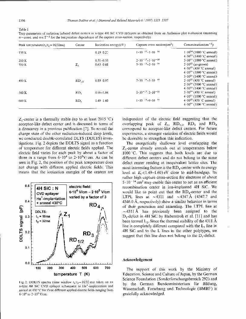
1336 Thomas Dalibor et al. / Diamond and Related Materials 6 (1997) 1333-1337
Table 1 Trap parameters of radiation-induced defect centers in n-type 4H SiC CVD epilayers as obtained from an Arrhenius plot evaluation (assuming 0 = const, and accT~2 for the temperature dependence of the capture cross-section, respectively)
Peak temperature^,/f2 = 16/32ms) Center Ionization energy (eV) Capture cross section(cm2) Concentration (cm 3)
135 K
210 K 310 K
450 K
560 K
660 K
0.19-0.21 1-10"17 1 • 10 16 1 4
1014 (1000 °C anneal) 10" (1400 °C anneal)
0.31-0.35 2-10-'7-M0-16 3 1014 (1000 °C anneal)
1 0.63-0.68 3-10-"-2-10-14 2 4 4 3
10" (as-grown) 10" (430 °C anneal) 10" (1000 °C anneal) 1014 (1400 °C anneal)
Dl,2 0.89-0.97 7-10-16-5-10~" 2 2 4
10" (430 °C anneal) 1014 (1000 °C anneal) 10" (1400 °C anneal)
D3 0.98-1.08 5-10~17-3-10-16 2 4
10" (430 °C anneal) 1014 (1000 °C anneal)
D4 1.49-1.60 l-10-14-9-10-14 4 4
10" (430 °C anneal) 1014 (1000 °C anneal)
ZjL-center is a thermally stable (up to at least 2015 °C) acceptor-like defect center and is discussed in terms of a divacancy in a previous publication [7]. To reveal the charge state of the other radiation-induced deep levels, we conducted double-correlated DLTS (DDLTS) inves- tigations. Fig. 2 depicts the DDLTS signal as a function of temperature for different electric fields applied. The electric field varies for each peak by about a factor of three in a range from 6-104 to 2-105V/cm. As can be seen in Fig. 2, the position of the peak temperature does not change with different applied electric fields. This means that the ionization energies of the centers are
0.5 -
0.4
Li. Q.
75 0.3 c O) "S W h-
Q D
0.2
0.1
0.0 b.
4H SiC : N CVD epilayer He+-implantation + anneal 430°C
electric field:
6-104V/cm-2-105V/cm varied by a factor of 3
RD4
DDLTS: t, - 16ms
100 200 300 400 500
temperature T (K)
600 700
Fig. 2. DDLTS spectra (time window tjt2= 16/32ms) taken on an n-type 4H SiC CVD epilayer subsequent to He+-implantation and anneal at 430 °C for three different applied electric fields ranging from 6-104to2-105V/cm.
independent of the electric field suggesting that the overlapping peak of Z1( RD1/2, RD3 and RD4
correspond to acceptor-like defect centers. For future experiments, a stronger variation of electric fields would be desirable to strengthen this indication.
The energetically shallower level overlapping the Zrcenter already anneals out at temperatures below 1000 °C. This suggests that both levels are due to different defect centers and do not belong to the same defect center residing at inequivalent lattice sites. The most interesting feature is the RD4-center with its energy level at Ec-{ 1.49-1.60) eV close to mid-bandgap. Its rather high capture cross-section for electrons of about 5 • 10"14 cm2 may enable this center to act as an efficient recombination center in ion-implanted 4H SiC. We would like to point out that the RD4-center and the LTPL lines at -4311 and -4347 Ä (4347.7 and 4346.0 A, respectively) show a similar behavior in terms of their generation and annealing. The LTPL line at ~ 4311A has previously been assigned to the Drdefect in 4H SiC by Haberstroh et al. [11] and has been termed L2. Since the thermal stability of the 4311 A line is completely different compared with the Lx line in 4H SiC and to the L lines in the other polytypes, we suggest that this line does not belong to the Drdefect.
Acknowledgement
The support of this work by the Ministry of Education, Science and Culture of Japan, by the German Science Foundation (Sonderforschungsbereich 292) and by the German Bundesministerium für Bildung, Wissenschaft, Forschung und Technologie (BMBF) is gratefully acknowledged.

Thomas Dalibor et al. / Diamond and Related Materials 6 (1997) 1333-1337 1337
References
[1] Yu.A. Vodakov, E.N. Mokhov, in: R.C. Marshall, J.W. Faust Jr., C.E. Ryan (Eds.), Silicon Carbide—1973, University of South Carolina Press, South Carolina, 1974, p. 508.
[2] T. Kimoto, A. Itoh, H. Matsunami, T. Nakata, M. Watanabe, J. Electron. Mat. 24 (1995) 235.
[3] T. Troffer, C. Peppermüller, G. Pensl, K. Rottner, A. Schöner, J. Appl. Phys. 80(1996)3739.
[4] T. Kimoto, A. Itoh, H. Matsunami, T. Nakata, M. Watanabe, J. Electron. Mat. 25 (1996) 879.
[5] T. Troffer, Ch. Häßler, G. Pensl, K. Hölzlein, H. Mitlehner, J. Völkl, Inst. Phys. Conf. Ser. No. 142 (1996) 281.
[6] J.P. Doyle, M.O. Aboelfotoh, M.K. Linnarsson, B.G. Svensson, A. Schöner, N. Nordeil, C. Harris, J.L. Lindström, E. Janzen, C. Hemmingsson, MRS Symp. Proc. Ser. Vol. 423 (1996) 519.
[7] T. Dalibor, C. Peppermüller, G. Pensl, S. Sridhara, R.P. Devaty, W.J. Choyke, A. Itoh, T. Kimoto, H. Matsunami, Inst. Phys. Conf. Ser. No. 142(1996) 517.
[8] W.J. Choyke, NATO ASI Series Vol. 185 (1989) 563. [9] T. Kimoto, A. Itoh, H. Matsunami, S. Sridhara, L.L. Clemen,
R.P. Devaty, W.J. Choyke, T. Dalibor, C. Peppermüller, G. Pensl, Appl. Phys. Lett. 67 (1995) 2833.
[10] K. Hölzlein, G. Pensl, M. Schulz, P. Stolz, Rev. Sei. Instrum. 57 (1986) 1373.
[11] Ch. Haberstroh, R. Heibig, R.A. Stein, J. Appl. Phys. 76 (1994) 509.

ELSEVIER
DIAMOND AND
RELATED MATERIALS
Diamond and Related Materials 6 (1997) 1338-1341
Thermal properties of ß-SiC epitaxial layers between 150 °C and 500 °C measured by using microstructures
C. Wagner *, G. Krötz Forschung und Technik, Daimler-Benz AG, Postfach 80 04 65, 81663 München, Germany
Abstract
The heat conductivity and the thermal diffusion velocity of LPCVD grown, nominally undoped epitaxial SiC layers on silicon were determined from 150 °C to 500 °C. A novel arrangement of micromachined SiC bridges was used to measure these quantities with little calculation effort. The thermal conductivity was derived from the temperature difference and the heat flow over a SiC micro bridge. The heat diffusion velocity was obtained from the phase shift between the temperature modulation induced at one side of the SiC micro bridge and detected at the other, respectively. The temperature distribution of the SiC microstructure was measured by a thermal imaging system. © 1997 Elsevier Science S.A.
Keywords: Heat diffusion; Thermal conductivity; High temperature; SiC
1. Introduction
SiC is usually known as an attractive wide bandgap material for high temperature and high power electron- ics. The chemical inertness and good elastic behaviour even at high temperatures also make it a good candidate for microsensor applications in harsh environments [1]. In particular, microsensor concepts based on silicon substrates can be improved by using epitaxial SiC. For thermal simulations of those sensors reliable data on the thermal properties are necessary. These partly exist for poly-crystalline bulk SiC [2] but are not available for thin layers of epitaxial SiC. For the latter the thermal data are not expected to be the same as for bulk material, as for example the influence of surfaces could increase with decreasing sample size or crystal quality decrease because of lattice mismatch and interface defects.
2. Sample design and preparation
In the case of macroscopic samples sticks are the standard structures for determining thermal quantities [3]. For microstructures an imitation very similar to those sticks are bridges [4]. Fig. 1 shows a photograph
* Corresponding author.
and a schematic sectional view of the novel sample design used in this work. It consists of four identical bridges namely heater, reference heater, heat sink and symmetrical heat sink. Each of these four bridges can be heated by evaporated conductors which are isolated electrically by an underlying oxide. The heater and the heat sink are connected by a SiC bridge without any add-on layer, called the transfer bridge. The thermal properties of the latter have been determined.
The arrangement has some advantages especially com- pared to heated membranes [5,6]: (1) A thin, narrow microbridge can be treated as one-
dimensional. The calculation then becomes less effort.
(2) The heat Q which flows across the transfer bridge and defines the thermal conductivity (see Eq. (1)) can be measured easily and with high accuracy. By comparing the heater bridge with an almost identical reference bridge several uncertainties can be elimi- nated: e.g. the unknown heat transfer between met- allization and SiC layer, thermal losses across the frame to the substrate as well as at the electric contacts or radiation losses along the metallizations.
(3) The hot parts of the microstructure are localized. They do not influence the temperature sensitive areas of the chip like wire bonds or chip fixation. Thus measurements up to very high temperatures can be realized.
0925-9635/97/S17.00 © 1997 Elsevier Science S.A. All rights reserved. PIT S0925-9635(97)00109-X

C. Wagner, G. Krötz / Diamond and Related Materials 6 (1997) 1338-1341 1339
reference heater, Pref.\
, — symmetrical heat sink, T0 sectional view A-B:
heater, Pheat, T, ^ heat sink, T0
Fig. 1. SiC microstructure for measurements of thermal conductivity heat diffusion velocity: (a) photograph, (b) schematic sectional view.
(4) Heater and heat sink can be heated seperately. If the difference between the temperatures is small the thermal properties can be treated as constants.
Most of the SiC microstructure preparation steps are standard micromachining processes [7] and only specific features will be described in detail:
Nominally undoped ß-SiC was grown at 1100 °C on both sides of the substrate up to a thickness of 2.5 ^m. Details of the applied low temperature LPCVD process working with methyl-silane as a precursor are described elsewhere [8]. The SiC epitaxial layers were thermally oxidized by a standard wet oxidation process to obtain an electrical isolation against the subsequent metalliza- tion. To structure the SiC epitaxial layers a PECVD etching process was developed [9]. As metallization for the heaters' molybdenum was used because of its high melting point, a similar thermal expansion coefficient as SiC O5.5xl0_6K at 500 K compared to «4.3xlO"6K respectively [10]) and because it exhibits a good adhesion to the underlying oxide. In a final process step free standing bridges were realized by anisotropic etching of the Si-substrate in KOH. Special substrate holders were used to protect the metallized side of the sample during the etching process.
3. Experimental setup
For all measurement procedures described below it is mandatory to measure the exact temperature at multiple points of the SiC microstructure. To avoid disturbances by convection the sample was placed in a vacuum chamber. An IR imaging system was used to record the temperature distribution on top of the microstructure with an optical and interpolated resolution of 100 and 25 urn, respectively. The emissivity of each structure was determined in a separate vacuum chamber where the
chip was mounted on a heating chuck. A comparison of the temperature of the chuck and the temperature measured by the IR system yielded the emissivity.
The heating power of the different heater bridges and heat sinks were determined by measuring the voltage drop U at a resistor R0 connected in series to the resistors of the bridges itself. The heating power was calculated from P=UxI where /= U/R0.
For measuring phase shifts in the case of diffusivity measurements the time resolving measurement mode of the IR imaging system was used.
4. Measurement procedures
4.1. Heat conductivity
To measure the heat conductivity the heater and the reference heater were heated to T\ and the heat sink and the symmetrical heat sink to T0. As the heater has thermal losses over the transfer bridge, the heating power Pheat is higher than that of the reference heater PTe{. All other losses, except for radiation losses of the transfer bridge, are eliminated by comparison of the heater and reference heater: AP = Pheat — Pref. This difference is used to calculate the heat conductivity K
from [11]:
AP Q = — = —KgradT
A (1)
where A is the cross-section of the transfer bridge. For temperatures higher than 400 °C it is necessary to con- sider radiation losses of the transfer bridge. For small temperature differences the temperature profile along the bridge can be assumed to be linear. The resulting radiation loss can be calculated according to the radia-

1340 C. Wagner, G. Krötz / Diamond and Related Materials 6 (1997) 1338-1341
tion law of Stefan-Boltzmann [12] and added as a simple correction term: Q' = Q — Pnd-
4.2. Heat diffusion velocity
To measure the heat diffusion velocity a sinusoidally modulated heating power was applied to the heater (Fig. 3). The heat flow across the transfer bridge causes a phase shifted temperature variation between two observation points. The phase shift (j> depends on their distance /, the wave period t and the thermal diffusion velocity a [3]. From this relation a can be derived:
a = %-l2
T<2>2
(2)
5.2. Heat diffusion velocity
Fig. 3 shows the temperature variation of the transfer bridge taken by the IR imaging system when a sinusoi- dally modulated heating power is applied to the heater. In the main figure each horizontal line indicates the temperature gradient across the transfer bridge within the scanning time per line of 4.1 ms. The lower curve in Fig. 3 shows the gradient in x-j-notation for the indi- cated line. The sine wave depicted on the left-hand side shows the temperature variation near the heat sink, the right curve near the heater. Evaluation of these two sine waves yields a phase shift. From Eq. (2) the thermal diffusion can be derived. As related temperature the time averaged temperature of the heater was taken. Fig. 4(b) shows the heat diffusion velocity determined for various temperatures.
5. Results
5.1. Heat conductivity
Fig. 2 shows an IR image of the temperature distribu- tion of the SiC microstructure given in Fig. lb. The sample is in thermal equilibrium and a constant temper- ature gradient is applied over the transfer bridge (600 run long, 2.5 urn thick, 200 |un wide). From Fig. 2 and similar results for other temperatures the temperature gradient along the transfer bridge was extracted. Together with the electrically measured heat transfer Q the thermal conductivity was determined according to Eq. (1) and assigned to the related average temperature across the transfer bridge. As a result Fig. 4(a) shows the thermal conductivity in dependence of the temperature.
6. Discussion
Thermal conductivity and heat diffusivity data of LPCVD grown SiC layers on silicon were measured up to temperatures of 500 °C. In comparison to data mea- sured with macroscopic samples [2] the heat conductivity is found to be 1.2 times smaller than expected. This may be due to varying crystal quality (doping and impurity effects, interface defects because of lattice mismatch of epitaxial ß-SiC on [100]-Si-substrate) as well as to increasing surface to bulk ratios. In order to distinguish and to quantify these surface and material influences additional samples with bridges of different surface to volume ratios must be investigated. The thermal diffu- sivity shows the expected 1/T dependence because for high temperatures the number of phonons, and therefore
2.1 mW "C c:\bilder\chris\wl'il881\c2_20004.tmp 200% max Emis:0.20 Lev:50.0 Sens:20.0 Zoom:5.0/5.0 Date:19.0
■10 • ' Al i | _j 100 •
90 80 ■ 70 60
™| " _3> • SO • %^|lIfl^^^^^%||Mp|UJ
7\ ' 40 •
?n •
I *■
ff '■<\ [ i I >l 15.0 - 97.5'C
Fig. 2. Thermographic image of the heated microstructure shown in Fig. 1.
jKWataOOQe.tmp .110%
gmis!0.53 Lev;200,0 *Sens;?,Q 2oom:5.D/5.0 Bate:G2.10.I
Fig. 3. Time resolved thermographic image of the transfer bridge heated by a sinusoidally modulated current.

C. Wagner, G. Krötz / Diamond and Related Materials 6 (1997) 1338-1341 1341
(b)
220
200
180
|l60
£.140
120
100
80
100 150 200 250 300 350 400 450 500
(a) T[°C]
1.00
0.80
5» E 0.60
"a ( , 0.40
0.20
I I I I
200 300 T[°C]
Fig. 4. Results: (a) Heat conductivity and (b) heat diffusion velocity of LPCVD grown ß-SiC on silicon in dependence on the temperature.
the phonon collision rate, increases proportionally with T[ll].
Acknowledgement
Part of this work has been supported by the BMBF within the project named HOMSIC.
References
[1] G. Krötz, Ch. Wagner, W. Legner, H. Sonntag, H. Müller, G. Müller, Institute of Physics Conference Series No. 142, Chap. 4, 1996, p. 829.
[2] Morton International, Woburn, MA, Technical Bulletin # 107. [3] Y.S. Touloukian, C.Y. Ho, Thermophysical Properties of Matter,
The TPRC Data Series, IFI Plenum Data Corp., New York, Ther- mal Diffusivity, vol. 10, 1973.
[4] CH. Mastrangelo, Yu-Chong Tai, R.S. Müller, Sensors and Actu- ators, A21-A23 (1990) 856-860
[5] C. Wagner, G. Krötz, H. Sonntag, H. Müller, W. Hellmich, G. Müller, Transducers '95, Eurosensors IX, Stockholm, Digest of Technical Papers, vol. 2, 280-A11, p. 194.
[6] E. Jansen, O. Dorsch, E. Obermeier, W. Kulisch, Diamond Relat. Mater. 5 (6-8) (1996) 644.
[7] S.M. Sze (Ed.), VLSI Technology, McGraw-Hill, Singapore, 1985.
[8] G. Krötz, W. Legner, G. Müller, H.W. Grueninger, L. Smith, B. Leese, A. Jones, S. Rushworth, Material Science and Engineer- ing B29( 1995) 154.
[9] C. Richter, K. Espertshuber, C. Wagner, M. Eickhoff, G. Krötz, E-MRS Spring Meeting, Strasbourg, 1996.
[10] G.A. Slack, S.F.Bartram, J. Appl. Phys. 46 (1) (1975) 89. [11] C. Kittel, Introduction to Solid State Physics, 3rd edition, New
York, 1967. [12] N.W. Ashcroft, N.D. Mermin, Solid State Physics, International
Edition, Japan, 1981.
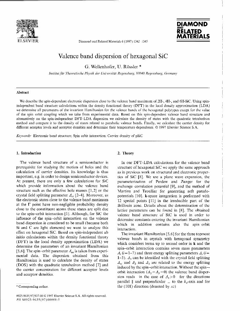
ELSEVIER
DIAMOND AND
RELATED MATERIALS
Diamond and Related Materials 6 (1997) 1342-1345
Valence band dispersion of hexagonal SiC
G. Wellenhofer, U. Rössler * Institut für Theoretische Physik der Universität Regensburg, 93040 Regensburg, Germany
Abstract
We describe the spin-dependent electronic dispersion close to the valence band maximum of 2H-, 4H-, and 6H-SiC. Using spin- independent band structure calculations within the density functional theory (DFT) in the local density approximation (LDA) we determine all parameters of the invariant Hamiltonian for the valence bands of the hexagonal polytypes except for the value of the spin-orbit coupling which we take from experimental data. Based on this spin-dependent valence band structure and alternatively on the spin-independent DFT-LDA dispersion we calculate the density of states with the quadratic tetrahedron method and compare it to the density of states related to parabolic valence bands. Finally, we calculate the carrier density for different acceptor levels and acceptor densities and determine their temperature dependence. © 1997 Elsevier Science S.A.
Keywords: Electronic band structure; Spin orbit interaction; Carvier density of pSiC
1. Introduction
The valence band structure of a semiconductor is prerequisite for studying the motion of holes and the calculation of carrier densities. Its knowledge is thus important, e.g. in order to design semiconductor devices. At present, there are only a few calculations for SiC which provide information about the valence band structure such as the effective hole masses [1,2] or the crystal field splitting parameter ACT [2-4]. Moreover, as the electronic states close to the valence band maximum at the T point have non-negligible probability density close to the constituent atoms these states are split due to the spin-orbit interaction [1]. Although, for SiC the influence of the spin-orbit interaction on the valence band dispersion is considered to be small (because both Si and C are light elements) we want to analyze this effect on hexagonal SiC. Based on spin-independent ab initio calculations within the density functional theory (DFT) in the local density approximation (LDA) we determine the parameters of an invariant Hamiltonian [5,6]. The spin-orbit parameter Aso is taken from experi- mental data. The dispersion obtained from this Hamiltonian is used to calculate the density of states (DOS) with the quadratic tetrahedron method [7] and the carrier concentration for different acceptor levels and acceptor densities.
: Corresponding author.
2. Theory
In our DFT-LDA calculations for the valence band structure of hexagonal SiC we apply the same approach as in previous work on structural and electronic proper- ties of SiC [8]. We use a plane wave expansion, the parameterization of Perdew and Zunger for the exchange-correlation potential [9], and the method of Martins and Troullier for generating soft pseudo- potentials [10]. k-space integration is performed with 12 special points [11] in the irreducible part of the Brillouin zone. Details about the determination of the lattice parameters can be found in [8]. The obtained valence band structure of SiC is used in order to determine constants entering the invariant Hamiltonian which in addition contains also the spin-orbit interaction.
The invariant Hamiltonian [5,6] for the three topmost valence bands in crystals with hexagonal symmetry which considers terms up to second order in k and the spin-orbit interaction contains seven mass parameters A{ (i= 1-7) and three energy splitting parameters At (i = 1-3). At can be identified with the crystal field splitting ACT and A2 and A3 are related to the energy splitting induced by the spin-orbit interaction. Without the spin- orbit interaction (A2=A3=0) the valence band disper- sion reads—in the case of A1>0—for the directions parallel || and perpendicular _L to the &z-axis and for the (101) direction (denoted by xz)
O925-9635/97/S17.0O © 1997 Elsevier Science S.A. All rights reserved. PII S0925-9635(97)00088-5

G. Wettenhof er, U. Rässler / Diamond and Related Materials 6 (1997) 1342-1345 1343
Ehh(k±) = A1+k2±(A2+A4-A5)
E±(k±)=UA1+kl(2A2+A4+A5)
(1)
± \IA\ +kl(8A21 + 2A4A, + 2A5A1) + k4
±(A4+A5)2
£hh(lh)(^||) = ^l+^(^l+^3)
-^split C^H ) = ^|| ^41
Ehh(kxz) = A1 +\klMi +A2+A3 +A4-A5)
E±(kxz)=HAi+^k2xz(2A1+2A2+A3+A4+A5)
/A21+kiz(4A2
1+A1(A3+A4+A5)) -\l +k4J4((A3+A4+A5)
2+8A2)
The subscripts hh, lh and split refer to the heavy hole, light hole and crystal field split-off bands, the subscript + means lh (+) and split (—), respectively. Including the spin-orbit interaction, these bands are denoted with decreasing order of energy by A, B, and C, respectively.
Including spin-orbit interaction (A2=A3=£Q) the energy differences EA— EB andisA — Ec at k = 0 only depend on the energy splitting parameters A{. Identifying A1 with Acr and using the cubic approxima- tion A2=A3 = l/3zfso [5,6] we can expand these differ- ences in second order of Aso/ACI
EA-EB=lAS0-l(A20)/(A
2T)ACI,
EA -EC=ACT +Ho +l(A2so)/(A2
r)ACI
because Aso is much smaller than ACI. Experimental values for Aso in hexagonal and rhombohedral SiC of about 7 meV [12-15] are used as the value of the spin-orbit interaction in the invariant Hamiltonian. Thus, all constants of this Hamiltonian are determined and the valence band dispersion and the DOS including the spin-orbit interaction can be studied.
Concerning the calculation of carrier densities for p- SiC we assume that the number of holes is determined by thermal equilibrium between the density of ionized acceptors N~ and the density of holes p in the valence bands, N~ =p. Both carrier densities are ruled by the Fermi function/
N; =NaJ*(E„T)-,P =
with
ff(E,T)- l+ge' (E-nWBT)
D{E){\-f,{E,T))
and/„(i?,7>
(2)
l+e< ,(E-n)IWT)
fied by the factor g = 4 which takes a four-fold degener- acy of the acceptor level (EAxEB) into account [16]. Here, /i is the chemical potential. Na is the acceptor density, Ey the valence band maximum, and E& the acceptor level. It turns out that for g = 2 (assuming a two-fold degeneracy of the acceptor level because EA > EB) the carrier concentrations is increased by most a factor of V2 at a given temperature.
3. Results
By fitting the expressions of Eq. (1) to our DFT-LDA band structure (an example is shown for 6H-SiC in Fig. 1(c), dotted lines) we obtain the parameters At...A7 and A1 = Acr of Table 1. The mass parameters At...A6 of the hexagonal poly types are very close to each other. The mass parameter An (which was not set to zero as in a similar study for A1N and GaN [6])
Fig. 1. Valence band dispersion of 6H-SiC. (a) Invariant theory, (b) parabolic approximation, (c) DFT-LDA.
> CD
O CNJ
o
The Fermi distribution of the acceptor level is modi-
0.0 -0.02 -0.04 -0.06 -0.0B
E [eV]
Fig. 2. Density of states of 6H-SiC. Solid lines: invariant theory, dotted lines: DFT-LDA, dashed lines: parabolic approximation.

1344 G. Wellenhofer, U. Rössler / Diamond and Related Materials 6 (1997) 1342-1345
Table 1 1-Dimensionless mass parameters A{ and crystal field splitting ACI in meV of 2H-, 4H-, and 6H-SiC
Ai A2 A3 A4 A5 A6 Al Aa
2H-SiC -4.83 -0.576 4.18 -1.24 -1.41 -1.49 0.0232 144 4H-SiC -4.76 -0.628 4.14 -1.11 -1.45 -1.49 0.0127 74 6H-SiC -4.76 -0.590 4.14 -1.15 -1.50 -1.34 0.0119 44
increases with the hexagonality parameter h. The value for the crystal field splitting Acr scales almost linearly with h.
The dashed lines in Fig. 1 show the parabolic approxi- mation to the expressions of Eq. (1) which allow to define band masses in terms of A1...A1 and Av These masses which are sometimes quoted in the literature [2,6] are shown in Table 2 (the masses of Ref. [2], however, do not reflect the hexagonal symmetry, e.g. different masses are given for the directions TM and FK). They should not be mixed with effective hole masses representing the curvature of the real valence bands close to the valence band maximum as they are obtained without considering the spin-orbit interaction [17]. As can be seen in Fig. 1 the parabolic dispersion (dashed lines (b)), however, is pretty close to case (c) (DFT-LDA calculations without spin-orbit interaction) and case (a) (solid lines, obtained by diagonalizing the invariant Hamiltonian including the spin-orbit inter- action) except for the anticrossing and the topmost part close to the valence band maximum. The solid lines in
10
io-!
,-, 10~'
'B IO-
% io-
p. H 10
10"'
10H
Fig. 1 show the removal of spin degeneracy in the second and third valence band along TM.
The DOS of 6H-SiC for the valence bands A, B, and C calculated with the quadratic tetrahedron method is depicted in Fig. 2. The spin degeneracy due to time reversal symmetry is considered. Solid (dotted) lines are obtained from calculations based on the invariant theory (DFT-LDA) and dashed lines from effective mass approximation. Except for energies near the band edges the DFT-LDA densities of states are close to the densities including the spin-orbit interaction. While the DOS of the A band follows a square-root dependence (dashed and dotted lines coincide) we find for the B and C bands deviations of the DOS in the parabolic approxi- mation (dashed lines) from DFT-LDA results and invariant theory due to the neglect of the anticrossing effect. Taking the sum of the DOS of band B and C, however, this deviation is less significant. Beyond the k- and energy range presented in Fig. 1 we continue the DOS with a slope, given by the mean curvature of the DFT-LDA valence bands. The parabolic approxima-
l
1 ' 1
/' ^ / / „--
///V" /' / / /
- \ \ 1
\
///// N. [10"em"s]
!// --io-1
■7/7/ -2 l\l 10 iiil , , i ,
-10-S ...._. io"4!
-io"s] i
400 T [K]
600 800 0 800
Fig. 3. Carrier density for acceptor levels 250 meV (left part of the figure) and 400 meV (right part of the figure) above the valence band maximum for different acceptor densities.
Table 2 Spin-independent effective hole masses and their relation to the mass parameters A{
2H-SiC 4H-SiC 6H-SiC
">hmt/m0 = (-A1-A3)~X 1.5 1.6 1.6
"isp,it"/'"o = (-AI)_1 0.20 0.21 0.21
mhh±/m0 = (-A2-A4 + A5y
1 2.4 3.6 4.1 mlh
1/m0 = (-A2~A4~A5-2A12/A1)-
1 0.32 0.33 0.32
'",pi,,1M = (-^2 + 2^72/^i)"1 1.5 1.6 1.4
tion, i.e. the effective masses (Table 2) are in excellent agreement with this mean curvature for bands B and C. However, the slope of band A for the direction perpen- dicular to the kz-axis becomes smaller with decreasing energy. Therefore, the carrier densities using the para- bolic approximation overestimate the carrier densities given by the DOS described above. Between 200 and 800 K, the differences are smaller than 4%, 6% and 9% for acceptor densities IO16, 1018 and IO20 cm-3, respectively.In Fig. 3 we show the temperature depen- dent carrier density of 6H-SiC for acceptor levels 250

G. Wellenhof er, U. Rössler / Diamond and Related Materials 6 (1997) 1342-1345 1345
and 400 meV above the valence band maximum calcu- lated from the DOS including spin-orbit interaction (solid lines of Fig. 2). In order to analyze the temper- ature dependence of the carrier concentration we define the temperature T1/2 at which half of the acceptors is excited. The closer the acceptor level is to the valence band maximum and the smaller the acceptor density the lower is this temperature T1/2- For isa = 250 meV it increases for densities 1016, 1017, 1018, 1019, and 1020
cm"3 from 320, 410, 555, 825, to 1410 K and for Ea = 400 meV for the same densities from 325, 610, 800, 1150 to 1875 K. These numbers are changed by less than 5 K if the DFT-LDA density of states or the DOS referring to parabolic approximated bands are used. This accounts for the reliability of both approximations.
References
[1] M. Willatzen, M. Cardona, N.E. Christensen, Phys. Rev. B 51 (1995) 13150.
[2] P. Käckell, B. Wenzien, F. Bechstedt, Phys. Rev. B 50 (1994) 10761.
[3] C.H. Park, B.-H. Cheong, K.-H. Lee, K.J. Chang, Phys. Rev. B 49(1994)4485.
[4] A. Qteish, V. Heine, R.J. Needs, Phys. Rev. B 45 (1992) 6534. [5] G.L. Bir, G.E. Pikus, Symmetry and Strain-induced Effects in
Semiconductors, Wiley, New York, 1974.
[6] M. Suzuki, T. Uenoyama, A. Yanase, Phys. Rev. B 52 (1995) 8132.
[7] M.H. Boon, M.S. Methfessel, F.M. Müller, J. Phys. C 19 (1986)5337.
[8] K. Karch, G. Wellenhofer, P. Pavone U. Rössler, D Strauch, in Proceedings of International Conference on Physics os Semicon- ductors, DJ. Lockwood (Ed.), World Scientific, Singapore, 1995, p. 401. G. Wellenhofer, U. Rössler, Solid Sate Commun., 96 (1995) 887. G. Wellenhofer, K. Karch, P. Pavone, U. Rössler, D. Strauch, Phys. Rev. B 53 (1996) 6071. G Wellenhofer, U. Rössler, in SiC and Related Materials 1995, S. Nakashima, H. Matsunami, S. Yoshida, H. Harima (Eds.), IOPP, Bristol, Philadelphia, 1996, p. 297 and 301.
[9] J.P. Perdew, A. Zunger, Phys. Rev. B 23 (1981) 5048. [10] N. Martins, J.L. Troullier, Phys. Rev. B 43 (1991) 1993. [11] D.J. Chadi, M.L. Cohen, Phys. Rev. B 8 (1973) 5747. [12] G.B. Dubrovskii, V.l. Sankin, Fizika Tverdogo Tela 14 (1972)
1200. [13] R.G. Humphreys, D. Bimberg, W.J. Choyke, Proc. 15th Int. Conf.
Physics of Semiconductors, Kyoto, in J. Phys. Soc. Japan Suppl. A 49 (1980) 519.
[14] R.G. Humphreys, D. Bimberg, W.J. Choyke, Solid State Commun. 39 (1981) 163.
[15] F. Engelbrecht, J. Zeman, G. Wellenhofer, C. Peppermueller, R. Helbig, G. Martinez, U. Rössler, Phys. Rev. B, in press.
[16] S.M. Sze, Physics of Semiconductor Devices, Wiley, New York, Chichester, Brisbone, Toronto, Singapore, 1981.
[17] We would like to emphasize that the mass obtained from the slope along k differs from the cyclotron mass observed for a magnetic field B || k due to the anisotropy of the valence band dispersion (e.g. U.Rössler, Solid State Commun., 65 (1988) 1279).

ELSEVIER
DIAMOND AND
RELATED MATERIALS
Diamond and Related Materials 6 (1997) 1346-1348
Polytypism and surface structure of SiC
P. Käckell *, J. Furthmüller, F. Bechstedt Friedrich-Schiller-Universität Jena, Institut für Festkörpertheorie und Theoretische Optik, Max-Wien-Platz 1,
D-07743 Jena, Germany
Abstract
Within the framework of density functional theory (DFT) in the local density approximation (LDA) using ultrasoft Vanderbilt pseudopotentials in a plane wave basis we investigate the atomic and electronic structure of 3C SiC(lll) and «H SiC(OOOl) surfaces (lxl and V3 x V3 reconstructions) and of 3C SiC(OOl) surfaces (2x2 reconstructions). Since (111)/(0001) is the natural growth direction, the 3C SiC(lll)/nH SiC(0001) surfaces are of special interest. Atomic geometries of various reconstructions, their relative stability and their electronic structure (surface band structure) are discussed. The theoretical results are compared with available experiments. © 1997 Elsevier Science S.A.
Keywords: Silicon carbide; Surface structure; Theory; First principles calculations
1. Introduction
The understanding of the atomic structure and the electronic (chemical) properties of SiC surfaces is one key ingredient for understanding crystal growth pro- cesses. A controlled growth of high quality SiC layers of a defined polytype by homo- and heteroepitaxy is of fundamental interest for many special electronic or optoelectronic applications of SiC (e.g. growth of hetero- structures, integrated optical/optoelectronic devices). The interpretation of experimental data is often compli- cated and ambiguous. Hence there is a need for supple- mentary theoretical investigations. Parameter-free DFT-LDA calculations serve as a powerful high-quality tool to investigate the atomic and electronic structure of SiC surfaces. In this paper we like to give a short overview of recent results obtained for V3 x A/3 (and lxl) reconstructions of Si-terminated 3C SiC( 111) and «H SiC (0001) surfaces with additional Si overlayers as well as for 2x2 reconstructions of clean and hydro- genated C-terminated 3C SiC(OOl) surfaces.
2. Theoretical framework
The theoretical framework of our investigations was the density functional theory in the local density approxi- mation. Explicitly we used the Vienna Ab initio Simulation Package (VASP) [1-4] developed at the TU Wien. For our calculations we used (two different)
: Corresponding author.
ultrasoft Vanderbilt pseudopotentials [5] in a plane wave basis corresponding to a cutoff energy of about 20 Ry for the 3C SiC(OOl) surfaces and about 13.2 Ry for the 3C SiC(lll)/«H SiC(0001) surfaces. Our surfaces were modelled by repeated slab geometries using the primitive surface unit cell. For the 3C SiC(OOl) surface we used slabs consisting of 8 layers of atoms and a vacuum region between the slabs being about 6 atomic layers thick (for clean surfaces). For the 3C SiC(lll) surfaces we used slabs with 6 double layers of atoms and a vacuum of about the same thickness in the case of a clean surface (less for adsorbate structure). In all cases the atoms of the one half of the slab (which is of no interest) were kept fixed in their ideal bulk positions and all dangling bonds of the corresponding surface were always saturated with hydrogen in order to mini- mize spurious interactions or charge transfers between the two slab surfaces. For the Brillouin zone sampling we used 16 Appoints in the half of the Brillouin zone for the 3C SiC(001)(2x2) surfaces and 8 it-points in the half of the Brillouin zone for the 3C SiC(lll)/«H SiC (0001) (V3 x V3) surfaces. Tests with more fc-points have been performed and we obtained no significant changes in our results.
3. Results and discussion
3.1. C-terminated 3C SiC(OOl) c(2 x 2) surfaces
The main results for this surface have already been published elsewhere [6], the aim of the investigation
0925-9635/97/S17.00 © 1997 Elsevier Science S.A. All rights reserved. PII S0925-9635(97)00089-7

P. Käckelletal. / Diamond and Related Materials 6 (1997) 1346-1348 1347
was to clarify the nature and bonding of the c(2x2) reconstruction of C-terminated 3C SiC(OOl) surfaces. Two possible models were suggested: a staggered C-dimer arrangement with C-C double bonds and C2
groups with C-C triple bonds in Si bridge sites. By comparing photoelectron spectroscopy data with the calculated surface band structures it could be shown that the triple bonded C2 groups in the Si-bridges should be the experimentally observed structure. The calculated total energies also favor this model (though the energy differences are very small). Counting the number of C-C, Si-C and Si-Si bonds of these two structures one would expect the opposite result (C-C bonds stronger than C-Si bonds stronger than Si-Si bonds). However, elastic effects might also play a significant role (the C2
groups fit very well into the Si-bridges whereas the staggered C-dimers introduce a relatively large surface stress). It seems that the C2 group structure is also kept if one hydrogenizes the surface though after hydrogeni- zation the staggered dimer model should become ener- getically more favorable. Our suspicion is that (maybe due to large barriers) the primarily formed hydro- genated C2 groups remain in a metastable state.
3.2. Si-terminated3CSiC(lll) (\ßx\ßR30°) surfaces
In many experimental studies a typical finding is that one observes a 3 x 3 reconstruction for very Si-rich surfaces [7-11]. After depletion of some few Si one observes sometimes a structure exhibiting a diffuse 1 x 1 LEED pattern [8-11]. The origin of this "unre- constructed" surface is yet absolutely unclear. After depletion of further Si one finally ends up with a V3xV3 reconstruction [7-11] which is commonly attributed to a T4-site Si-adatom structure [12,13].
We have investigated the atomic structure and the stability of Si- and C-covered Si-terminated 3C SiC( 111) surfaces of varying stoichiometry. In order to investigate possible polytypism effects we performed also, calcula- tions for 2H SiC(OOOl) surfaces. The general outcome was that the qualitative picture does not change at all when changing the underlying poly type (therefore we will focus only on the 3C SiC( 111) surfaces here). There are small quantitative changes (of maximum order 0.1 eV) in the relative surface energies.
A cubic termination is always favorable over a hexag- onal termination. The energy differences between the surfaces with cubic and hexagonal termination become as a crude rule of thumb the smaller the larger the adsorbate coverage. However, there remains always an energy difference of larger about 0.1 eV in favor of a cubic termination. From this we suspect that the selec- tion mechanism determining which polytype is finally grown might be quite complicated. Our calculations
performed at T= 0 K alone can surely not provide any final information. Inclusion of finite temperature effects is essential for the real understanding of SiC growth and especially of the polytype selection mechanism. Hence we cannot yet discuss such subtle details here. Anyway, we like to demonstrate that a first crude understanding of SiC growth can already be achieved.
Fig. 1 shows the phase diagram for a small selection of possible models for the V3 x V3 reconstruction of 3C SiC/«H SiC(OOOl) surfaces. Over a wide range of Si chemical potentials a T4-site Si-adatom structure is clearly favored (in full agreement with previous theoreti- cal work [12]). Only for very Si-rich environments one finds more stable Si-rich structures which can be charac- terized as Si-adatoms adsorbed on an additional Si-overlay er covering a Si-terminated surface. Though the work on these higher Si-coverages is still in progress the preliminary results point towards a certain "ener- getical flatness" of the surface, i.e. it seems that there exists no such clear preference for a special adsorption site as in the case of clean surfaces (energy differences of order 0.1 eV between different structures to be com- pared with 0.5 eV energy difference between the T4- and the H3-site Si-adatom on the clean surface). So we expect (at least at higher temperatures) some strong structural fluctuations destroying any long-range order, i.e. we suspect that these Si-rich surfaces are related to the sometimes observed "lxl" structure (the diffuse
-a^x
C-rich Hsi-i^c
AH = 0.56 eV Si-rich
Fig. 1. Phase diagram of possible models of V3 x V3 surface structures as a function of the Si (C) chemical potential.
1348 P. Käckell et al. I Diamond and Related Materials 6 (1997) 1346-1348
LEED pattern [11] clearly supports the picture of a "disordered" or strongly fluctuating surface).
Furthermore this phase diagram clearly shows that in general the adsorption of Si is clearly favored over the adsorption of C on less Si-rich surfaces. Only for Si-rich surfaces the adsorption of C becomes more and more favorable (at least for more C-rich environments— compare the energetical positions of the Si-rich surface with 4/3 Si-overlayers and of the Si-adatom structure corresponding to 1/3 Si overlayers on a clean Si-terminated surface which would be obtained after adsorbing one monolayer of C on the surface with 4/3 Si overlayers—there is now a substantial energy gain when adsorbing C). So generally some "two-step" growth mechanism for SiC can be expected (at least if no contaminants of surfactants are present). First one has to expect that some Si overlayers grow on a clean/Si- poor surface and it is very hard or even impossible to adsorb C (first step). After reaching a Si-rich surface the adsorption of C becomes then very easy (at least for more C-rich environments) so that finally a Si-overlayer can be transformed into a Si-C bilayer, i.e. finally SiC has been grown (second step). This is consistent with a recent experimental finding of an experimental group [8-11] that very good MBE growth can be achieved if one first grows a very Si-rich surface out of a Si-poor surface (detected by the development ofa3x3orlxl LEED pattern) and then switching (as a second step) to more C-rich conditions finally growing SiC by carbon- ization of the Si-rich surface (ending up with an again Si-poor surface detected by the observation of a V3 x V3 LEED pattern). The incorporation of C seems to be easiest for 3 x 3 reconstructed surfaces. The very details (on which paths can C reach its final "sub- surface" adsorption site, which barriers have to be overcome, how does all precisely depend on the stoichi- ometry etc?) have still to be clarified by future work. However, a first qualitative understanding of possible growth scenarios is already possible.
It should be noted that (contrary to the findings described above) one cannot rule out a possible scenario where first C-rich surfaces can be grown which are then enriched with Si. Of course we have only discussed "clean" conditions here (without any presence of surfactants/contaminants). It might be possible that for example the presence of large amounts of H (CVD growth) could change the picture (i.e. stabilisation of C-rich surfaces over Si-rich surfaces due to the higher strength of the C-H bond compared to the Si-H bond). Some future work shall also be dedicated to this impor- tant question. Furthermore, one should also note that extremely C-rich surfaces have not been included in this
work (i.e. we do not know where they would appear in the phase diagram).
4. Conclusions
We have shown that triple bonded C2 groups in Si-bridges are the favorite model for the c(2 x 2) recon- struction of C-terminated 3C SiC(OOl) surfaces. Our results for the 3C SiC(lll) surface clearly confirm recent findings that a T4-site Si-adatom model is the favorite model for the V3 x V3 reconstruction of Si-terminated (111) surfaces. For very Si-rich conditions one finds more stable structures (order 4/3 to 5/3 over- layers of additional Si adsorbed) which might be related to a sometimes observed "lxl" structure (randomly distributed adatoms on a Si overlayer). Some first crude understanding of SiC growth can be achieved ("two- step" mechanism) though the very details have still to be clarified.
Acknowledgement
This work was supported by the "Deutsche Forschungsgemeinschaft" within the framework of the "Sonderforschungsbereich 196" (project A8). We thank Bernd Schröter and Andreas Fissel for many helpful discussions. We also gratefully acknowledge the collabo- ration with Georg Kresse and Jürgen Hafner at the University of Technology in Vienna.
References
[1] G. Kresse, J. Hafner, Phys. Rev. B 47 (1993) RC558. [2] G. Kresse, PhD Thesis, TU Wien 1993. [3] G. Kresse, J. Furthmüller, Comput. Mat. Sei. 6 (1996) 15. [4] G. Kresse, J. Furthmüller, Phys. Rev. B 54 (1996) in press. [5] D. Vanderbilt, Phys. Rev. B 41 (1990) 7892. [6] P. Käckell, J. Furthmüller, F. Bechstedt, G. Kresse, J. Hafner,
Phys. Rev. B 54 (1996) in press. [7] R. Kaplan, Surf. Sei. 215 (1989) 111. [8] A. Fissel, U. Kaiser, E. Ducke, B. Schröter, W. Richter, J. Crystal
Growth 154 (1995) 72. [9] A. Fissel, U. Kaiser, K. Pfennighaus, B. Schröter, W. Richter,
Appl. Phys. Lett. 68 (1996) 1204. [10] A. Fissel, U. Kaiser, K. Pfennighaus, E. Ducke, B. Schröter, W.
Richter, Proc. of Silicon Carbide and Related Materials 1995 Con- ference, Kyoto, Japan, Inst. of Phys. Conf. Ser. No. 142, IOP, 1996, Chapter 1, p. 121.
[11] B. Schröter, A. Fissel, private communication. [12] J.E. Northrup, J. Neugebauer, Phys. Rev. B 52 (1995) 17001. [13] F. Owman, P. Martensson, Surf. Sei. 330 (1995) L639.

ELSEVIER
DIAMOND AND
RELATED MATERIALS
Diamond and Related Materials 6 (1997) 1349-1352
Structure and morphology of SiC surfaces studied by LEED, AES, HREELS and STM
U. Starke *, J. Bernhardt, M. Franke, J. Schardt, K. Heinz Lehrstuhl für Festkörperphysik, Universität Erlangen-Nürnberg, Staudtstraße 7, 91058 Erlangen, Germany
Abstract
Low energy electron diffraction, Auger electron spectroscopy, high resolution electron energy loss spectroscopy and scanning tunnelling microscopy investigations used for structure and morphology determinations of different hexagonal SiC surfaces are presented. The analyses include sample orientation, layer stacking, step morphology, layer spacings as well as the species and coordination of surface terminating adatoms. The samples were prepared ex situ and investigated without further treatment. Predominant ABCACB stacking is found for 6H-SiC(0001) corresponding to a triple step morphology. The surface is covered by hydroxyl species bound to the topmost Si atoms. The surface of a 3C-SiC(lll) sample was found to be covered by oxygen on only 50% ofthe available Si sites. On both surfaces the first bilayer is slightly compressed on an otherwise bulk-like geometry. 6H-SiC(0001) exhibits a single step morphology in agreement with the mixed stacking found on the surface. All three possible surface stacking sequences are present in equal amounts. © 1997 Elsevier Science S.A.
Keywords: Low-energy electron diffraction; Morphology; Silicon carbide; Surface structure
1. Introduction
The physical properties of silicon carbide make it a promising semiconductor material for new applications such as high power and high frequency devices or electronics in high temperature environments. Still the difficulties in growing SiC material of sufficient crystal- line and electronic quality have so far prevented a vast commercial development. It is apparent that the surface structure of the substrate plays an important role for the crystallization process. The natural growth plane of SiC is a hexagonal bilayer consisting of alternating Si and C atoms in tetrahedral bond coordination which is the (0001) plane in hexagonal SiC crystals and the (111) plane of the cubic modification. The different polytypes are distinguished by the sequence of linearly stacked and mutually rotated hexagonal bilayers. For a specific polytype surface, different termination domains are fea- sible distinguished by the topmost stacking sequence. In Fig. 1 the different stacking sequences for 6H and 3C polytypes and the termination possibilities for a 6H surface are shown. The analysis of the surface stacking is a major part of the present study. In addition we
* Corresponding author. Fax 49 9131 858400; e-mail: [email protected]
address the distinction between the two possible crystal orientations as well as the determination of surface layer geometries and the identification of possible adatoms and their sites applying scanning tunnelling microscopy (STM), high resolution electron energy loss spectro- scopy (HREELS), Auger electron spectroscopy (AES) and quantitative low energy electron diffraction (LEED). In a previous study of 6H-SiC(0001) we found large steps of multiple triple bilayer height, equivalent to odd or even numbers of half 6H unit cells, and the layer stacking sequence could be determined to be ABCACB [1,2]. In the present study we present a refined analysis of this 6H-SiC(0001) allowing for mix- tures of domains with different surface termination. Additionally, new results of the hexagonal surfaces of other samples of different polytype and different polar- ity, that is, 6H-SiC(000i), 4H-SiC(0001) and 3C-SiC(lll) are given.
2. Experimental
Samples of either bulk grown Lely material or CVD grown homoepitaxial films were prepared involving dry oxidation, chemical cleaning steps and HF treatment
0925-9635/97/S17.00 © 1997 Elsevier Science S.A. All rights reserved. PII S0925-9635(97)00090-3

1350 U. Starke et al. I Diamond and Related Materials 6 (1997) 1349-1352
3C-SiC(lll)
Si-Termination
6H-SiC(0001)
Si-Termination
C-Termination C-Termination
SI S2 S3
Fig. 1. Cross-sectional view of the linear stacking present in the cubic (3C) polytype (/?-SiC) and three different stacking sequences possible at the surface of the 6H polytype. The different surface terminations are labelled according to the depth of the orientation change (S1,CACBABC; S2, BCACBAB; and S3, ABCACBA).
[3]. The 3C-SiC sample used was an epitaxial film grown in (111) orientation on Si(lll). By a fast transfer into vacuum recontamination and oxidation of the sample surfaces could be kept to a minimum. In ultra-high vacuum we used different techniques to investigate the surface structure. AES was used to determine the stoichi- ometry of the surface as well as the presence of adatoms. The complete atomic surface structure was analysed using quantitative LEED. The lateral surface periodicity is immediately related to the periodicity of the diffraction pattern. Atomic positions can be accurately determined by analysing the spot intensities by means of fitting experimental intensity spectra to spectra obtained from model calculations [4,5]. The best-fit model was iden- tified by minimizing the Pendry ^-factor [6] calculated between the experimental and theoretical data. Additional information about the nature of dangling bond saturating ad-species was gathered using HREELS to detect their vibrational modes. Finally, STM was used to monitor the step morphology of the surfaces in real space.
3. Surface structure analysis
Immediately after the chemical treatment all samples showed a well ordered LEED pattern. This was found with and without oxidation included in the preparation treatment and was regardless whether 50% HF or buffered NH4F (pH 7.8) was used. The surface periodic- ity as judged from the diffraction angles corresponds to the SiC bilayer structure for all polytypes and prepara- tion procedures. Hexagonal and cubic samples can easily
be distinguished by the symmetry of their LEED pattern when the primary electron beam is aligned normal to the surface. A single domain of a specific layer stacking always exhibits three-fold surface symmetry. This gives rise to a three-fold diffraction pattern, where for exam- ple, within first order diffraction two groups of three spots, that is, the (10), (fl) and (01) and the (01), (10) and (11) have different intensities. This is indeed the case for the cubic modification which contains only linearly stacked bilayers. However, on surfaces of hexag- onal polytype we expect equally weighted domains rotated by 60° with respect to each other illuminated simultaneously by the electron beam. Their intensities add giving rise to the observed six-fold rotational sym- metry. Fig. 2 demonstrates this symmetry difference between a 3C-SiC(lll) and a 6H-SiC(0001) LEED pattern.
Information about the chemical composition of the surfaces was obtained from AES. We observe oxygen for all ex situ prepared samples. Unfortunately, the Si and C signal does not accurately reflect the SiC-stoichi- ometry due to contamination before the sample transfer. Therefore, the surface polarity, that is, whether (0001) or (0001) orientation applies, cannot be determined by AES. Yet, LEED intensity versus energy spectra are very different for the two crystal sides as demonstrated in Fig. 3 (a) and therefore can be used as an experimental fingerprint.
As mentioned above, the surface of a 6H-sample may be terminated by three different topmost layer stacking sequences (see Fig. 1), equivalent to different cuts in the ABCACBA... stacking of the crystal. From a new, detailed intensity analysis of LEED diffraction spots of
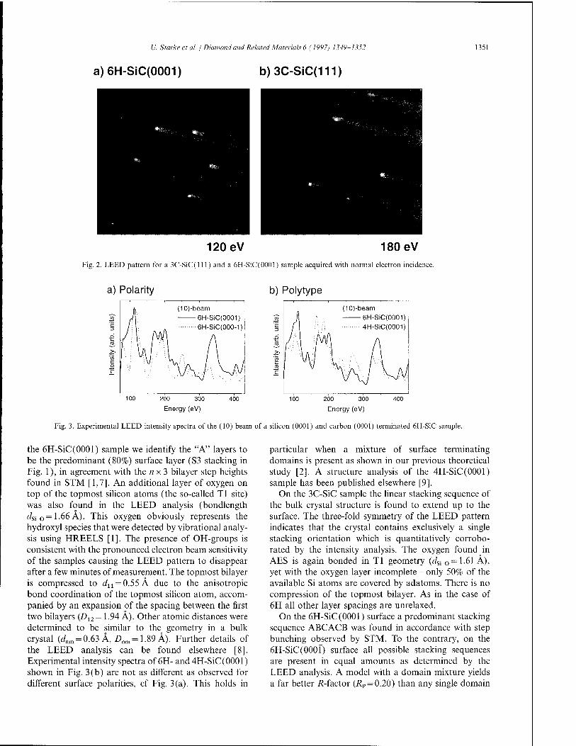
U. Starke et ah l Diamond and Related Materials 6 (1997) 1349-1352 1351
a)6H-SiC(0001) b)3C-SiC(111)
120 eV 180 eV Fig. 2. LEED pattern for a 3C-SiC(l 11) and a 6H-SiC(0001) sample acquired with normal electron incidence.
a) Polarity b) Polytype
(10)-beam 6H-SiC(0001
6H-SiC(000-1)
(10)-beam 6H-SiC(0001)
4H-SiC(0001)
200 300
Energy (eV) 200 300
Energy (eV)
400
Fig. 3. Experimental LEED intensity spectra of the (10) beam of a silicon (0001) and carbon (0001) terminated 6H-SiC sample.
the 6H-SiC(0001) sample we identify the "A" layers to be the predominant (80%) surface layer (S3 stacking in Fig. 1), in agreement with the n x 3 bilayer step heights found in STM [1,7]. An additional layer of oxygen on top of the topmost silicon atoms (the so-called Tl site) was also found in the LEED analysis (bondlength rfsi_0 = 1.66 A). This oxygen obviously represents the hydroxyl species that were detected by vibrational analy- sis using HREELS [ 1 ]. The presence of OH-groups is consistent with the pronounced electron beam sensitivity of the samples causing the LEED pattern to disappear after a few minutes of measurement. The topmost bilayer is compressed to d11 = 0.55 A due to the anisotropic bond coordination of the topmost silicon atom, accom- panied by an expansion of the spacing between the first two bilayers (D12= 1.94 A). Other atomic distances were determined to be similar to the geometry in a bulk crystal (<inm = 0.63 A, £>nm=1.89 A). Further details of the LEED analysis can be found elsewhere [8]. Experimental intensity spectra of 6H- and 4H-SiC(0001) shown in Fig. 3(b) are not as different as observed for different surface polarities, cf Fig. 3(a). This holds in
particular when a mixture of surface terminating domains is present as shown in our previous theoretical study [2]. A structure analysis of the 4H-SiC(0001) sample has been published elsewhere [9].
On the 3C-SiC sample the linear stacking sequence of the bulk crystal structure is found to extend up to the surface. The three-fold symmetry of the LEED pattern indicates that the crystal contains exclusively a single stacking orientation which is quantitatively corrobo- rated by the intensity analysis. The oxygen found in AES is again bonded in Tl geometry (<isi_0=1.61 A), yet with the oxygen layer incomplete - only 50% of the available Si atoms are covered by adatoms. There is no compression of the topmost bilayer. As in the case of 6H all other layer spacings are unrelaxed.
On the 6H-SiC(0001) surface a predominant stacking sequence ABCACB was found in accordance with step bunching observed by STM. To the contrary, on the 6H-SiC(000f) surface all possible stacking sequences are present in equal amounts as determined by the LEED analysis. A model with a domain mixture yields a far better 7?-factor (RP = 0.20) than any single domain

1352 U. Starke et al. / Diamond and Related Materials 6 (1997) 1349-1352
6H-SiC(0001)
Oxygen on T, (100 %)
S3 ä
S2
6H-SiC(0001)
S3
3C-SiC(111)
Oxygen on T1 (50 %)
-i
80% 20% 45% 30% 25% Linear stacking
Fig. 4. Surface stacking sequence and adatom coordination obtained from the analyses of 6H-SiC(0001), 6H-SiC(0001) and 3C-SiC(lll).
model (i?P>0.35). This result indicates a single step morphology for the carbon rich orientation. Different from the other surfaces investigated in this study, on SiC (0001) no oxygen could be found in the diffraction analysis. Possibly, the oxygen detected by AES is disor- dered or confined to step sites. The topmost bilayer is compressed for all three stacking domains by values between 0.10 and 0.16 Ä, while deeper layers are again unrelaxed.
4. Discussion
Using quantitative LEED in combination with AES, HREELS and STM the atomic structures of hexagonal 6H- and 3C-SiC surfaces were analysed. Work for 4H-SiC has been completed recently [9]. In agreement with recent transmission electron microscopy work [10,11], different step morphologies were found for the two orientations of 6H-SiC, that is, triple steps on the (0001) and single steps on the (0001) surface. Oxygen is present on all samples after the ex situ preparation. However, it seems that only on the Si orientation the adatoms are positioned in well defined and ordered sites. A summary of the three surface structures with respect to stacking sequences and adatom sites is given in Fig. 4.
LEED can be used as a fingerprinting technique to determine certain aspects of the SiC surface geometry. In particular, the distinction between hexagonal and cubic modifications is possible from the pattern symme- try, while spot intensity spectra can clearly identify the orientation of the sample. The surface stacking sequence can be determined in a full LEED analysis. However,
the intensity differences between different hexagonal polytypes are small and may not allow for an experimen- tal fingerprint distinction.
Acknowledgement
We would like to thank R. Helbig (University of Erlangen), and A. Schöner and N. Nordell (IMC, Kista, Sweden) for providing the different SiC film samples. The work carried out was supported by Deutsche Forschungsgemeinschaft (DFG) through SFB 292. U.S. gratefully acknowledges additional support by DFG (Sta 315/4-2).
References
[1] U. Starke, C. Bram, P.-R. Steiner, W. Hartner, L. Hammer, K. Heinz, K. Müller, Appl. Surf. Sei. 89 (1995) 175.
[2] J. Schardt, C. Bram, S. Müller, U. Starke, K. Heinz, K. Müller, Surf. Sei. 337(1995)232.
[3] W. Kern, D.A. Puotinen, RCA Review 31 (1970) 187. [4] J.B. Pendry, Low Energy Electron Diffraction, Academic Press,
London, 1974. [5] K. Heinz, Prog. Surf. Sei. 27 (1988) 239. [6] J.B. Pendry, J. Phys. C 13 (1980) 937. [7] U. Starke, J. Schardt, P.-R. Steiner, W. Hartner, S. Müller, L.
Hammer, K. Heinz, K. Müller, in: P. Varga, F. Aumayr (Eds.), Proceedings: Symposium on Surface Science 3S'95, Institut für Allg. Physik, TU Wien, Wien, 1995, p. 11.
[8] J. Schardt, U. Starke, J. Bernhardt, K. Heinz, Surf. Rev. Lett. accepted.
[9] U. Starke, J. Schardt, M. Franke, Appl. Phys. A, accepted. [10] T. Kimoto, H. Matsunami, J. Appl. Phys. 76 (1994) 7322. [11] H. Matsunami, private communication.
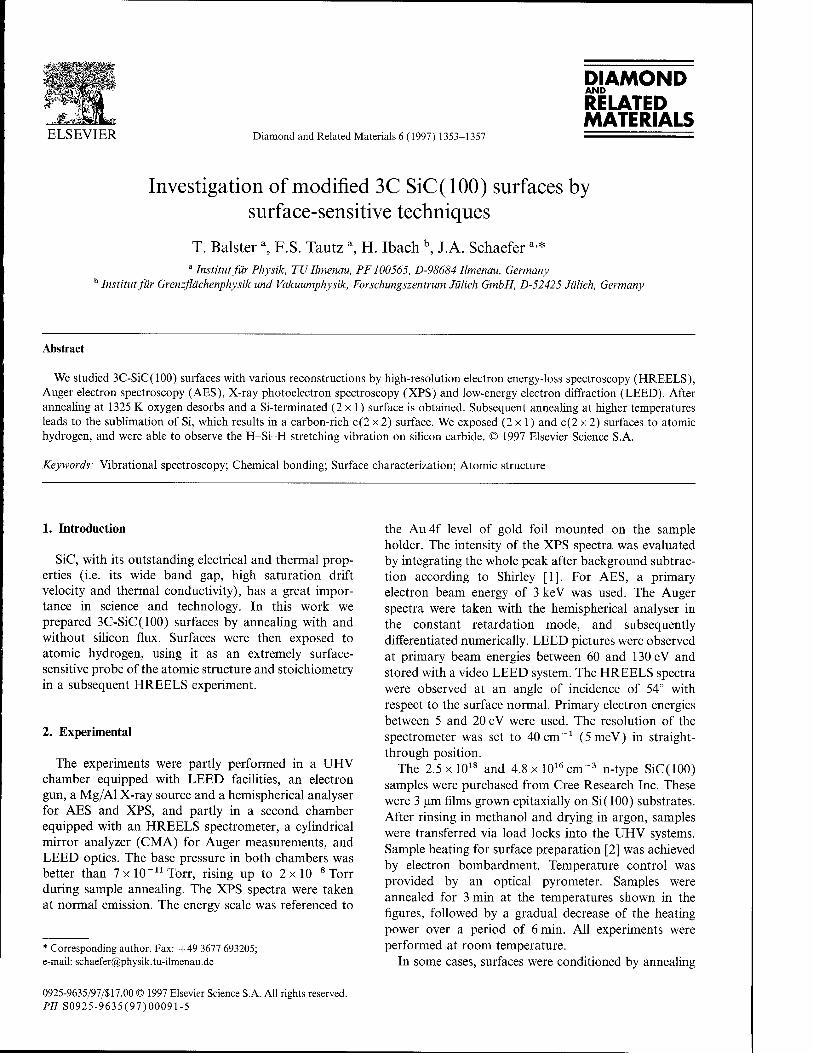
DIAMOND AND
ELSEVIER
RELATED MATERIALS
Diamond and Related Materials 6 (1997) 1353-1357
Investigation of modified 3C SiC(lOO) surfaces by surface-sensitive techniques
T. Balstera, F.S. Tautza, H. Ibach b, J.A. Schaefera>* a Institut für Physik, TU Ilmenau, PF 100565, D-98684 Ilmenau, Germany
b Institut für Grenzflächenphysik und Vakuumphysik, Forschungszentrum Jülich GmbH, D-52425 Jülich, Germany
Abstract
We studied 3C-SiC(100) surfaces with various reconstructions by high-resolution electron energy-loss spectroscopy (HREELS), Auger electron spectroscopy (AES), X-ray photoelectron spectroscopy (XPS) and low-energy electron diffraction (LEED). After annealing at 1325 K oxygen desorbs and a Si-terminated (2x1) surface is obtained. Subsequent annealing at higher temperatures leads to the sublimation of Si, which results in a carbon-rich c(2 x 2) surface. We exposed (2x1) and c(2 x 2) surfaces to atomic hydrogen, and were able to observe the H-Si-H stretching vibration on silicon carbide. © 1997 Elsevier Science S.A.
Keywords: Vibrational spectroscopy; Chemical bonding; Surface characterization; Atomic structure
1. Introduction
SiC, with its outstanding electrical and thermal prop- erties (i.e. its wide band gap, high saturation drift velocity and thermal conductivity), has a great impor- tance in science and technology. In this work we prepared 3C-SiC(100) surfaces by annealing with and without silicon flux. Surfaces were then exposed to atomic hydrogen, using it as an extremely surface- sensitive probe of the atomic structure and stoichiometry in a subsequent HREELS experiment.
2. Experimental
The experiments were partly performed in a UHV chamber equipped with LEED facilities, an electron gun, a Mg/Al X-ray source and a hemispherical analyser for AES and XPS, and partly in a second chamber equipped with an HREELS spectrometer, a cylindrical mirror analyzer (CMA) for Auger measurements, and LEED optics. The base pressure in both chambers was better than 7xlO~uTorr, rising up to 2xlO~8Torr during sample annealing. The XPS spectra were taken at normal emission. The energy scale was referenced to
* Corresponding author. Fax: +49 3677 693205; e-mail: [email protected]
the Au4f level of gold foil mounted on the sample holder. The intensity of the XPS spectra was evaluated by integrating the whole peak after background subtrac- tion according to Shirley [1]. For AES, a primary electron beam energy of 3 keV was used. The Auger spectra were taken with the hemispherical analyser in the constant retardation mode, and subsequently differentiated numerically. LEED pictures were observed at primary beam energies between 60 and 130 eV and stored with a video LEED system. The HREELS spectra were observed at an angle of incidence of 54° with respect to the surface normal. Primary electron energies between 5 and 20 eV were used. The resolution of the spectrometer was set to 40 cm"1 (5meV) in straight- through position.
The 2.5 xlO18 and 4.8xl016cm~3 n-type SiC(100) samples were purchased from Cree Research Inc. These were 3 irm films grown epitaxially on Si(100) substrates. After rinsing in methanol and drying in argon, samples were transferred via load locks into the UHV systems. Sample heating for surface preparation [2] was achieved by electron bombardment. Temperature control was provided by an optical pyrometer. Samples were annealed for 3 min at the temperatures shown in the figures, followed by a gradual decrease of the heating power over a period of 6 min. All experiments were performed at room temperature.
In some cases, surfaces were conditioned by annealing
0925-9635/97/S17.00 © 1997 Elsevier Science S.A. All rights reserved. PII S0925-9635(97)00091-5
1354 T. Bolster et al. / Diamond and Related Materials 6 (1997) 1353-1357
in a Si flux [3]. For this purpose, a Si wafer (0.6x1.8 cm2) was resistively heated to 1475 K. The deposition rate at a distance of approximately 4 cm from the sample was measured as one monolayer per minute. The sample was heated to 1275 K and kept in the Si flux for 3 min. After this exposure the sample was annealed for a further 3 min and cooled over a period of 6 min. Additional annealing cycles at higher temperatures were performed without the Si flux, as described above.
We exposed c(2x2)- and (2 x 1 ^reconstructed SiC(lOO) surfaces to atomic hydrogen. For this purpose, molecular hydrogen was introduced into the chamber via a leak valve. The molecules dissociated at a hot tungsten filament (T=2300K) placed at a distance of 4 cm in line of sight of the sample.
3. Results and discussion
3.1. Annealing without Si flux
As built in, samples show a (lxl) structure with satellites at the first l/5th order position. Given the shape of the Si L2 3W signal, we can deduce that this surface is covered by a silicon suboxide (SiOJ. Also, the Si L23W transition is shifted to lower kinetic ener- gies (as compared to Si in a SiC environment), which is characteristic for this oxidation stage of silicon [4]. After annealing at 1275 K the satellites in the LEED structure have vanished, but no significant changes in the O KLL/C KVV or the Si L2;3W/C KW intensity ratio occur (not shown here). This can be interpreted as thermal disordering of the oxide layer. The intensity ratio of O KLL/C KW is reduced after annealing at 1325 K. At the same time, the reconstruction changes to (2 x 1) in two domains with diffuse half-order spots. The Si L23VV/C KVV ratio increases and reaches its maximum of 3.8 at an annealing temperature of 1400 K. This supports the notion that oxygen bonds to silicon, because after the desorption of oxygen the uppermost Si layer contributes to the intensity of the unshifted Si L2 3VV transition in the SiC environment. At still higher temperatures the reconstruction changes to c(2x2), the SiL2i3VV/CKW ratio simultaneously decreasing to a minimal value of around 1.6 at 1475 K. The higher-order spots become more distinct with higher annealing temperatures. The reduction of the Si/C Auger ratio can be explained by sublimation of Si from the surface. The c(2x2) reconstruction is known to be terminated with a monolayer of carbon [5]. This is borne out by the observation of a second C Is peak at a shifted binding energy of 284.6 eV which is characteris- tic of carbon-carbon bonds, in addition to the peak at a binding energy of 283.1 eV which is characteristic of C in SiC (not shown here).
We now turn to our HREELS results. We measured
loss features at 945 cm"1 (118 meV), 1890 cm"1
(236 meV) and 2835 cm"1 (354 meV), which can be assigned to the optical surface phonon (Fuchs-Kliewer phonon) and its multiple losses. These frequencies are in good agreement with values at the 3C-Si(l 11) and 4H/6H-Si(0001) surfaces reported in Ref. [6], 6H-SiC(0001) in Ref. [7], and 3C-SiC(001) reported in Refs. [2,8]. Additionally, at 430cm"1 (54meV) and 1175 cm"1 (147 meV) two different modes of Si-O-Si stretching vibrations occur (not shown here). The fre- quency of 1175 cm"1 can be identified with the asymmet- ric Si-O-Si stretching mode [9,10]. The peak at 430 cm "J corresponds to a second type of stretching vibration [9,10] which is degenerate with the Si-O-Si wagging mode. The current results on SiC(lOO) are thus in good agreement with earlier observations on Si (100). It should be mentioned that both Si-O-Si peaks have disappeared after annealing at 1325 K, the temperature around which the intensity ratio O KLL/C KVV is also reduced. The FWHM of the elastically reflected beam increases and reaches its maximum of 190cm"1
(24meV) after annealing at 1275 K. This is in good agreement with LEED data, implying a disordering of the oxide at this temperature, as mentioned above. At higher annealing temperatures, the FWHM decreases again to 156 cm"1. The intensity of the Fuchs-Kliewer phonon increases relative to the oxygen-covered surface.
3.2. Annealing after deposition of silicon
Starting from the c(2 x 2^reconstructed surface, annealing in Si flux at 1275 K makes the C-C bonded peak in the C Is spectrum disappear. The sample exhibits a (3 x 2) LEED structure in two domains, the intensity ratio Si L2?3W/C KVV being at its maximum value of 10.8 (Fig. 1). This structure is known to correspond to a 1.33 monolayer Si-terminated surface [11]. Indeed, the Si 2p peak shows an additional shoulder due to Si in a Si environment. After successive annealing steps the intensity ratio Si L23W/C KW is reduced again, and reaches a minimum value of 2.3 at 1475 K. In LEED, several surface reconstructions can be observed with rising annealing temperatures (see Fig. 1 for details). Both the c(4x2) and the (2x1) structures are commonly interpreted as representing 1 ML Si-terminated surfaces [11,12]. However, in our investi- gations all samples show differing surface stoichiometries for these two reconstructions. We note that in a recent theoretical investigation by Sabisch et al. [13] it is claimed that a C-terminated (2x1) reconstruction is energetically favoured over a Si-terminated (2x1) reconstruction.
3.3. Exposure of a (2 x 1)-reconstructed surface to atomic hydrogen
Fig. 2 shows HREELS spectra for the clean and 40 L hydrogen-exposed SiC (2x1) surfaces. As compared to

12
10
1
c
T. Bolster et al. / Diamond and Related Materials 6 (1997) 1353-1357
-//■ , 1 1 1 . 1 1 1 1 1-
1355
Si-L2 3VV /C-KVV
before after Si-deposition
c(2x2) c(2x2)
300 1200 1250 1400 1450 1300 1350
Temperature (K)
Fig. 1. AES Si L2i3VV/C KW intensity ratio after Si deposition and annealing.
1500
1 ' 1 ' 1 SiC(100)-(2xl)
clean (a)
40 L (b) (lxl) weak half order spots
(c) off specular (8°)
3000
Energy loss (cm" )
Fig. 2. HREELS spectra (£0 = 7 eV) of the SiC(100)-(2 x 1) surface (a) before and (b, c) after 40 L hydrogen exposure. FK 1-FK 3 are Fuchs-Kliewer phonons. The shoulders on the high energy side of FK 2 in (b) and (c) correspond to the Si-H vibration.
the oxygen-free (lxl) surface, one notices a sharper elastic peak (135 versus 156 cm"1) and lower-intensity Fuchs-Kliewer phonons for the (2 x 1 )-reconstructed surface in Fig. 2(a). Turning to the hydrogen-covered specimens in Figs. 2(b) and (c), one notices a drastic increase of the FWHM of the elastic peak and a simultaneous loss of surface reconstruction in the LEED pattern, which reverts to (lxl). The most notable change, however, is the appearance of a shoulder on the high energy side of the peak denoted FK2. Fitting FK2 and the new structure yields peak positions at 1875 and 2120 cm-1, respectively, in the case of off-specular detec- tion (Fig. 3). The fitting in Fig. 3 was accomplished using two folded Gaussian-Lorentzian peaks, the FWHM of which was determined by the width of the elastically reflected intensity. The frequency of 2120cm"1 is in good agreement with the well-known H-Si-H dihydride stretching mode on Si (100) substrates [14-16], and is therefore assigned to the corresponding dihydride mode on H/SiC(100)-(l x 1). To the best of our knowledge, this vibrational mode has been observed for the first time in HREELS on SiC substrates. It confirms that the clean (2 x 1 )-reconstructed surface is indeed Si-terminated. Further results will be published elsewhere.
3.4. Exposure of a c(2 x2) -reconstructed surface to atomic hydrogen
The c(2 x 2) reconstruction was described above. After exposure to
prepared as 103 Langmuir

1356 T. Bolster et al. I Diamond and Related Materials 6 (1997) 1353-1357
3 cd
fr -
1 1 1 1 1 ' l 1 1 1 1 I 1 ' ' ■ 1 '
' 10-7C -1 H/SiC(100)-(2xl)
- -
- -
- '\ 2120 cm-1
~"
* 1 ■ .
'/■ s
/'■ / •
/ /
1 1 1 1 1 1 .
\ \.
[ i ' i
1500 1750 2000 2250 2500
Energy loss (cm" )
Fig. 3. Results of peak fitting procedure as described in the text for the spectrum of Fig. 2c (8° off-specular detection on 40 L hydrogen-covered surface). The peaks at 1875 and 2120 cm-1 correspond to FK 2 and the Si-H stretching vibration, respectively.
2.4
2.0
03 l-i
i
1.6
1.2
y/r H/SiC(100)-c(2x2)
after preparation c(2x2)
(lxl)
y/1
c(2x2) diffuse
Si-L23VV/C-KVV
0.0 102 W 104
Hydrogen-Exposure (L)
Fig. 4. AES Si L2,3W/C KW intensity ratio with increasing hydrogen exposure.
hydrogen the intensity ratio Si L2>3W/C KW has risen to 2.0 (Fig. 4), the c(2x2) LEED pattern simulta- neously becoming increasingly diffuse. At an exposure of 4 x 10³ L, the surface reverts to (1 x 1). This behavi- our can be interpreted by the conjecture that up to approximately 103 L exposure a monohydride forms, thus retaining the surface reconstruction. Beyond this threshold, hydrogen breaks up the bonds responsible
for the reconstruction, and a dihydride with its charac- terictic (lxl) pattern ensues. For higher exposures, the intensity ratio Si L2i3W/C KW increases to a value of 2.2, then remains constant within the error limits. This rise could be interpreted as the removal of carbon due to some etching reaction. However, more work on this point is needed, and will be undertaken in the future.

T. Bolster et al. / Diamond and Related Materials 6 (1997) 1353-1357 1357
4. Summary References
In this paper we have presented new results pertaining to the adsorption of hydrogen on the 3C-SiC(100) surface. Various reconstructions of the 3C-SiC(100) surface have been obtained by annealing SiC(lOO) sur- faces with or without Si flux. After exposing a (2x1) surface to 40 L hydrogen, we have observed the H-Si-H stretching mode of a (lxl) dihydride phase on 3C-SiC(100). Furthermore, exposing a C-terminated c(2 x 2) surface to atomic hydrogen, we observed a reduction of the carbon content of the surface in Auger electron spectrocopy, possibly indicating etching reactions.
Acknowledgement
This work was supported by the Deutsche Forschungsgemeinschaft and the Landesgraduierten- förderung Thüringen. We also wish to acknowledge helpful discussions with Dr. S. Lehwald and D. Bruchmann.
[1] D.A. Shirley, Phys. Rev. B 5 (1972) 4709. [2] M. Dayan, J. Vac. Sei. Technol. A 4 (1986) 38. [3] R. Kaplan, Surf. Sei. 215 (1989) 111. [4] B. Carriere, J.P. Deville, Surf. Sei. 80 (1979) 278. [5] J.M. Powers, A. Wander, M.A. Van Hove, G.A. Somorjai, Phys.
Rev. B 44 (1991) 11159. [6] H. Nienhaus, T.U. Kampen, W. Mönch, Surf. Sei. 324 (1995)
L328. [7] U. Starke, Ch. Bram, P.-R. Steiner, W. Hartner, L. Hammer,
K. Heinz, K. Müller, Appl. Surf. Sei. 89 (1995) 175. [8] M. Dayan, Surf. Sei. 149 (1985) L33. [9] J.A. Schaefer, W. Göpel, Surf. Sei. 155 (1985) 535.
[10] J.A. Schaefer, J. Electron Spectrosc. Relat. Phenom. 44 (1987) 163.
[11] S. Hara, W.F. Slijkerman, J.F. van der Veen, I. Ohdomari, S. Misawa, E. Sakuda, S. Yoshida, Surf. Sei. 260 (1992) L196.
[12] J.M. Powers, A. Wander, M.A. Van Hove, G.A. Somorjai, Surf. Sei. 260 (1992) L7.
[13] M. Sabisch, P. Krüger, A. Mazur, M. Rohlfing, J. Pollmann, Phys. Rev. B 53 (1996) 1.
[14] F. Stucki, J.A. Schaefer, J. Anderson, G.J. Lapeyre, W. Göpel, Solid State Commun. 47 (1983) 795.
[15] J.A. Schaefer, F. Stucki, J. Anderson, G.J. Lapeyre, W. Göpel, Surf. Sei. 140(1984)207.
[16] J.A. Schaefer, Trends Vacuum Sei. Technol. 1 (1993) 417.

DIAMOND AND
RELATED MATERIALS
ELSEVIER Diamond and Related Materials 6 (1997) 1358-1361
Angle resolved photoemission and the band structure of 6H-S1C
M. Hollering a'*, A. Ziegler a, R. Graupnera, B. Matterna, L. Leya, A.P.J. Stampflb, J.D. Riley b, R.C.G. Leckey b
1 Institut für Technische Physik, Universität Erlangen-Nürnberg, 91058 Erlangen, Germany
b Department of Physics, La Probe University, Victoria 3083, Australia
Abstract
Well ordered, unreconstructed, C-terminated surfaces of 6H-SiC(0001) were obtained after treatment with a hydrogen microwave plasma. From angle resolved photoemission spectra (ARPES) measured at normal emission for photon energies between 40 and 60 eV valence band energies at the F and A critical points of the hexagonal Brillouin zone of 6H-SiC are derived. Fhe boundaries of the ionic gap (9.3 and 10.5 eV) and the total valence band width of 15.5 eV are determined using X-ray excited photoemission spectra. The results are compared with pertinent band structure calculations. © 1997 Elsevier Science S.A.
Keywords: 6H-SiC; Electronic states; Photoelectron spectroscopy
1. Introduction
Silicon carbide (SiC) belongs to a class of materials that emerges on account of their unique properties as a new breed of semiconductors for high power applica- tions which can be operated under adverse environmen- tal conditions such as at high temperature or under high levels of radiation. The 6H polytype of SiC is a well suited candidate in this respect since it displays a thermal conductivity of 3.6Wcm"'K [1], a high breakdown field of 10 640x/V£142Vcm-1 [2], where ND is the donor concentration, and has an indirect gap of 3.0 eV [3]. A number of investigations dealing with the surface properties of this material have recently been reported. Little experimental work, however, has been published concerning the electronic band structure. The exception appears to be the recent work of Johansson et al. [4]. In the present paper the results of angle resolved photo- emission measurements on the C-terminated unre- constructed surface of 6H-SiC(00Ol) are reported and critical points of the bulk band structure are derived.
2. Experimental
Angle resolved photoemission measurements were performed at the Berlin synchrotron radiation source
* Corresponding author.
(BESSY) in the photon energy range 40-60 eV. The overall energy resolution was 0.25 eV and the angular resolution ±1°. Angle integrated core and valence band spectra were also performed with a resolution of 0.5 eV using monochromatized Al Ka. X-rays (XPS, hv = 1486.6 eV). In ultra-high vacuum (UHV) sample tem- peratures were determined by measuring the temperature of the Ta sample holder with an infra-red pyrometer. The 6x6 mm2 sample was cut from a 6H-SiC boule (Cree Research Inc.) such that the [0001] direction was perpendicular to the surface. After mechanical polishing, the C-terminated surface was plasma etched in a hydrogen microwave plasma (power 500 W, H2 pressure 5 x 10³ Pa, H2 mass flow 100 seem, sample temperature ~800°C) for ca 30 min, dipped in diluted HF (5% in deionized water), and transferred into the spectrometer which had a base pressure of 5 x 10"8 Pa. After a 5 min annealing at 700°C a stoichiometric and well ordered (lxl) surface was obtained as judged by XPS. Low energy electron diffraction (LEED) gave a sharp (lxl) pattern with a low background down to electron energies of 30 eV thus confirming the ordered, bulk truncated nature of the sample surface. C Is, Si2p and Ols core level spectra essentially reveal a contamination free stoichiometric surface. An oxygen contamination amounting approximately to an equivalent coverage of one monolayer is ascribed to oxidized areas localized in deep scratches that remained after mechanical polishing
0925-9635/97/S17.00 © 1997 Elsevier Science S.A. All rights reserved. PII S0925-9635(97)00092-7

M. Hollering et al. / Diamond and Related Materials 6 (1997) 1358-1361 1359
and could not be removed in the course of the plasma treatment.
3. Results and discussion
Fig. 1 shows the angle integrated XPS valence band spectrum of the 6H-SiC crystal. In SiC both Si and C are tetrahedrally coordinated by atoms of the opposite kind, and the structure of the 6H-polytype differs from the corresponding zincblende (ZB) structure only with respect to the stacking order of the SiC double layers along [ 111 ] or the equivalent [0001 ] direction. Therefore, due to their close structural similarity it is expected that the density of states (DOS) corresponds to the canonical three peaked DOS of III-V and II-VI compounds [5]. States in the topmost 7 eV are essentially due to the C 2p orbital; the peak at 8 eV can be identified as being of mixed C 2p-Si 3s bonding character, and the broader maximum III around 13 eV is of mixed Si 3s-C 2s character having more weight on the C 2s level [6]. Of course, the spectral features as measured differ from the DOS on account of varying photoemission cross- sections and a lifetime broadening that increases approximately quadratically with binding energy [7]. It is nevertheless possible to derive some salient energies from this spectrum.
Regions I and II are separated from III by the so-called ionic gap. Taking the finite resolution of our measurements and the lifetime broadening into account we place the boundaries of this gap at 9.3 and 10.5 eV, respectively. The uncertainty in these values is estimated to be no more than +0.1 eV. The total band width is estimated as 15.5 + 0.2 eV when the valence band maxi- mum is defined via the extrapolation of the leading edge of the spectrum to the base line.
Fig. 2 shows a series of angle resolved valence band
1 ' 1 ' 1 ' 1 ' ' ' 6H-SiC(000T) ■
normal emission ,'.„
'_ hv = 60eV t
• V^-, •v. -
y V A "i V \ \ " ,' \ A / \ / \ ,'\ V \\
'' . / ■'' y v x v \ / v. \^_ 1 . 1 . [
>- H So z DJ H
14 12 10 8 6 4
BINDING ENERGY (eV)
0=VBM
Fig. 2. Normal emission valence band spectra for different photon energies hv. For the normal emission spectrum at /iv = 60eV there is shown a least squares fit with Gaussian curves. Not shown is an also fitted cubic background.
>■
6H-SiC(0001)
XPS-VALENCE BAND
12 10 8 6 4
BINDING ENERGY (cV)
0=VBM
Fig. 1. XPS valence band spectrum. The binding energy is referred to the valence band maximum. The labels I, II and III indicate states with different atomic character as explained in the text.
spectra recorded at normal emission for photon energies between 44 and 60 eV. The structures in these spectra are much sharper than those in the angle integrated data and furthermore vary in intensity with photon energy as expected for direct transitions from different regions in k-space; in fact, all direct transitions are restricted to wave vectors with components (k|| = 0, k±) with kx lying along the crystallographic [0001 ] direction. The k± component for a particular peak and photon energy in Fig. 2 can be calculated if one makes the usual assumptions of direct, that is, ^-conserving, transitions and of free electron final states: k± = \j2m(Ekin — V0)/fi, where Ekin = hv — E{ — fl>0 is the kinetic energy of photo- electrons from a transition with initial energy E„ ®0 is the photoemission threshold, m is the free electron mass, and V0 is the so-called inner potential which here is defined with respect to the vacuum level. From this kind of analysis the band dispersion along [0001], that is,

1360 M. Holkringetal. / Diamond and Related Materials 6 (1997) 1358-1361
between the high symmetry points T and A of the hexagonal Brillouin zone can in principle be determined for the occupied valence states.
To this end we have determined the peak positions in the spectra of Fig. 2 either via minima in the their second derivatives or through least squares fits. The result was always the same: there is no dispersion of peak positions with photon energies and thus with k±.
Lack of dispersion may occur when the unit cell is small and contains many bands as is the case for SiC. Peaks in the spectra would generally reflect an average over many transitions and therefore may reasonably be approximated by the DOS. In Fig. 3 we have plotted the average peak positions as derived from our measure- ments together with the results of two band structure calculations for 6H-SiC along T-A [8,9]. According to both calculations parts of the band structure along T-A can be understood simply by folding the corresponding ZB bands along T-L, the [111] direction, back into the T-^4 [0001] direction. This holds in particular for the strongly dispersing split-off band which is twofold degenerate and spans the range from the valence band maximum to the upper boundary of the ionic gap at T (equivalent to L in the ZB structure) and again for the s-like band from T to T (equivalent to T->L in ZB) below the ionic gap. These are the only bands which can contribute to the measured spectra for binding energies beyond ~1.5eV. Between VBM and 1.5 eV a
multitude of p-like bands are present which are not shown in Fig. 3.
Both calculations were performed using the Kohn-Sham density functional formalism within the local density approximation (LDA). The one on the left of Fig. 3 is a quasiparticle calculation (QP) and should thus in principle be more appropriate for the interpreta- tion of photoemission data. Indeed, a better agreement with experiment is found as far as the width of the upper half (p and s-p bands) of the band structure is concerned: 9.4 eV for QP versus 8.8 eV for LDA and 9.3 eV from experiment. However, the width of the ionic gap is with 2.4 eV grossly overestimated in the QP calculation whereas the LDA calculation reproduces this quantity reasonably well: 1.3 eV versus the experimental value of 1.2 + 0.1 eV. For the remainder of the experi- mental structure a match between peak positions and critical point energies at T and A appears to be the most reasonable interpretation with the exception of the peak at 5.6 eV, which is ascribed to emission from the O 2p lone pair orbital. This is more clearly shown in Fig. 4 where we have plotted the experimental peak positions in an extended zone scheme along k± superimposed on the two band structures. The extension was chosen so as to correspond to the equivalent ZB structure along that direction. The peak energies are plotted at positions of k± which correspond alternately to the T and A points in the original hexagonal BZ. It is obvious that
>
O Pi
w Ü
PQ
XPS ARPES LDA
> 0.8eV
2.6eV
4.8eV
6.8eV
8.6eV 9.4eV
13.4eV .9eV
0.21
9.3eV
ionic gap
10.5eV
0.84 ±0.17
2.25 ±0.11
4.06 ±0.07
5.56 ±0.11
6.83 ±0.20
8.26±0.15
9.31 ±0.09
12,41+0.15
13.94 ±0.12 13.6
0.00 0.21
>
Ü oi
o
10 «
Fig. 3. Comparison of binding energies at the critical points T and A as determined by a quasiparticle calculation (QP) [9], by a calculation using the Kohn-Sham formalism in the LDA [8], and by photoelectron spectroscopy in normal emission (ARPES, this work). The width of the lines in the ARPES column indicates the statistical fluctuations of the fitted binding energy values. Also included in this figure are the boundaries of the ionic gap as determined by XPS.

M. Holleringetal. / Diamond and Related Materials 6 (1997) 1358-1361 1361
>< ü w z w Ü z 5 z
0
2 A^ r 6H-SiC(0001) |
4 X«A :
6 ' X\T i -
8 - ;
0 ! -
2 _ ! — LDA A__J
4 : QP T^^^^ \
^-~~~~* .■■'" :
0.00 kj.(A-')
1.26
Fig. 4. Experimental peak positions of normal emission spectra plotted in an extended zone scheme. Also shown are calculated band structures (LDA, [8]; QP, [9]). T and A denote critical points of the volume Brillouin zone (BZ) of 6H-SiC.
in this way all critical points are covered experimentally with the exception of the VBM and the topmost point of the s-like band starting at ~ 12 eV. Both are expected to have vanishing k-space volume. Moreover, the agreement with the LDA calculation is seen to be overall very good with the exception of states near the bottom of the upper band as mentioned earlier. Note that the ionic gap does not correspond to the band gap at T (Ä:± = 1.26A-1 in the extended zone scheme) as might be construed from Fig. 3. The lower edge of the ionic gap is rather defined by states with k-vector ca 70% of the way from T to K.
4. Summary
We succeeded in preparing well ordered 6H-SiC (0001) surfaces by a hydrogen plasma treatment in a microwave discharge with only small amounts of oxygen located in scratches left over from mechanical polishing and therefore not disturbing the smooth crystalline parts
of the surface. From angle integrated XPS valence band spectra we derived the boundaries of the ionic gap as 9.3 and 10.5 eV, and the total bandwidth as 15.5 + 0.2 eV, respectively. Binding energies of the bulk valence band at the critical points T and A of the BZ could be derived from UPS valence band spectra taken along normal emission. These values are in good agreement with theoretical computations (QP [9], LDA [8]).
Acknowledgement
This work was supported by the Deutsche Forschungsgemeinschaft through SFB 292 and the Bundesministerium für Bildung, Forschung, Wissenschaft und Technologie, Contract No. 05 622 WEA 7. We would like to thank the staff of BESSY, especially Dr Walter Braun, for their help during the experiments, and Magdalena Sabisch for her band struc- ture calculations. We also acknowledge the help of Reinhard Stöckel and Klemens Janischowsky who performed the hydrogen plasma preparation.
References
[1] E.A. Burgemeister, W. von Munch, E. Pettenpaul, J. Appl. Phys. 50(1979)5790.
[2] B.J. Baliga, Springer Proc. Phys. (Germany) 71 (1992) 305. [3] W. Choyke, D.R. Hamilton, L. Patrick, Phys. Rev. A 133 (1964)
1163. [4] L.I. Johansson, F. Owman, P. Märtensson, Surf. Sei. 360 (1996)
L478. [5] L. Ley, R.A. Pollack, F.R. McFeely, S.P. Kowalczyk, D.A. Shirley,
Phys. Rev. B9 (1974) 600. [6] L.I. Johansson, F. Owman, P. Märtensson, C. Persson, U. Linde-
felt, Phys. Rev. B 53 (1996) 13803. [7] J. Schäfer, J. Ristein, R. Graupner, L. Ley, U. Stephan,
T. Frauenheim, V.S. Veerasamy, G.A.J. Amaratunga, M. Weiler, H. Ehrhardt, Phys. Rev. B 53 (1996) 7762.
[8] M. Sabisch, Ph.D thesis, Münster, Germany, 1996. [9] B. Wenzien, P. Käckell, F. Bechstedt, Phys. Rev. B 52 (1995) 10897.
mmm
ELSEVIER
DIAMOND AND
RELATED MATERIALS
Diamond and Related Materials 6 (1997) 1362-1364
Topology of twin junctions in epitaxial /?-SiC
V. Papaioannou a, Ph. Komninoua, G.P. Dimitrakopulosa, K. Zekentes b, B. Peczc, Th. Karakostas a, J. Stoemenosa'*
a Aristotle University of Thessaloniki, Department of Physics, Solid State Section, 540 06 Thessaloniki, Greece b Foundation of Research and Technology, Heraclio, Crete, Greece
' Research Institute for Technical Physics, Hungarian Academy of Sciences, P. O. Box 76, H-1325 Budapest, Hungary
Abstract
The island growth of /?-SiC on vicinal (001) Si is studied by HREM and AFM. The initial nuclei have the morphology of tetragonal pyramids. Growth proceeds by a dendritic mechanism resulting in a large density of primary twins and stacking faults. The density of planar defects is reduced dramatically with increasing distance from the substrate. Mutual twin annihilation was studied taking into account interfacial connectivity principles developed recently. The secondary defects that are geometrically necessary for such a mechanism were identified. It has been shown that, for the formation of closed defect topologies, junction lines of planar defects are introduced. This has been verified using computer simulation of HREM images. © 1997 Elsevier Science S.A.
Keywords: Planar defects; Interfacial connectivity; Epitaxial /J-SiC
1. Introduction
Material behaviour depends strongly on the internal interfaces such as grain and twin boundaries. The spatial distribution and coexistence of these are subject to the interfacial connectivity principles [1,2]. In this paper the topology of twins in /?-SiC grown epitaxially on (001) Si by MBE is investigated. A possible mechanism of twin annihilation, based on experimental observations is proposed. The films were characterised by HREM and AFM.
island coalescence. As a consequence, a large density of stacking faults and micro-twins emerging from the Si/SiC interface are observed (Fig. 2(a)). These relieve some of the lattice mismatch (20%) by locally destroying the epitaxic orientation; the rest of the relaxation is introduced by misfit dislocations. However, at greater thickness, the planar defects seem to terminate and the film becomes almost monocrystalline [4].
3. Crystallographic analysis and discussion
2. Experimental observations
ß-SiC films were grown on (001) Si by MBE. A detailed description of the process is given elsewhere [3]. At early island growth, SiC islands having the morphology of tetragonal pyramids form, with their bases along the in-plane <110> directions (Fig. 1). Their surfaces are {111} close-packed planes in order to reduce surface energy; at their facet junctions, ledges are often observed which act as sites of preferential adsorption [4]. Growth proceeds by a dendritic mechanism until
' Corresponding author.
/J-SiC crystallises with the sphalerite structure. In accordance with its symmetry, {111} pyramids are polar with alternating polarity in each facet; the change of polarity is accompanied by the introduction of demisteps at the facet junctions, which promote the dendritic growth by acting as nucleation sites for ledges [4]. The primary (P) twins observed near the Si/SiC interface grow during epitaxial deposition until stopped by another interface or an array of line defects. Therefore, a {111} twin can meet with another of same type but different orientation. In this case, a strain field is formed for which relaxation is only possible via the introduction of a secondary (S) twin segment or the equivalent array of line defects. The junction line of the three twins is a
0925-9635/97/517.00 © 1997 Elsevier Science S.A. All rights reserved. PII S0925-9635(97)00093-9

V. Papaioannou et al. I Diamond and Related Materials 6 (1997) 1362-1364 1363
190 nm
. 95 nn
0 1500 nn
v y " 750 nn
750 nn
■/ /
¥-0 1500 nn
Fig. 1. AFM image of pyramidal SiC islands.
■|p:
''wjf- lip ..yli
HP"
jH.i§k
#
JÜPL
• Mk % * - i ••
..«► Itkk
*• **
lip '♦
41 pi. ^
|
:iÜÜi
!#
H # m m % # # § * i
#•*,# + *
**
*H!!
%*
•
•%
Fig. 2. (a) Cross-sectional HREM image of the epitaxic SiC along <110>. The micrograph exhibits pyramidal twin arrangements and triple junctions, (b) HREM image simulation of one junction line.
triple junction and two such lines are illustrated schemat- ically in Fig. 3. The P twins form initially on the faces of the pyramidal islands, while the S one propagates outwards. In Fig. 3, distinct atomic species are not
Fig. 3. Triple junctions each composed of two primary (P) and one secondary (S) twin boundary (numbers denote distinct crystals). The junction lines (LI, L2) are along the projection direction, i.e. along a <110> direction in the epitaxic interface. Colouring denotes distinct crystal orientations.
indicated; instead colouring has been used to show distinct orientation relationships of the crystals. Consideration of the interaction with Inversion Domain Boundaries leads to a number of feasible configurations, given elsewhere [4]. Both junction lines in Fig. 3 can be obtained from the same trichromatic complex and hence are symmetry related as explained elsewhere [2]. Such a crystallographic analysis can be used to predict the possible configurations that permit twin annihilation via mutual interaction, as explained below.
According to the observations, twin annihilation occurs for both P and S twins; this can be achieved by nested twin topologies comprising arrangements such as illustrated in Fig. 3, whereby two junction lines are involved. This configuration achieves twin annihilation for the case of the P twins being located on opposite faces of the initial pyramid (i.e. P twins intersecting at acute angle). As shown, a small segment of S twin connects the two junction lines. Fig. 2(a) is the experi- mental image corresponding to this configuration and similar observations have been made in other diamond- based deposited materials (e.g. [5]). In order to clarify the existence of junction lines, HREM image simulations of an unrelaxed model of one junction line were carried out using the multislice program of the EMS package [6]. The image is shown in Fig. 2(b). Good qualitative agreement is obtained as can be seen by comparing the experimental and simulated images of Figs. 2(a) and (b) respectively.
In the more general case, twinning is expected on all surfaces of the initial nuclei, so that twins may impinge

1364 V. Papaioannou et al. / Diamond and Related Materials 6 (1997) 1362-1364
at obtuse angles, i.e. corresponding to adjacent pyramid faces. For this case, the nested topology corresponds to a hyperpolyhedron [7] as shown in Fig. 4(a) whereby the outer and inner pyramids are made of P twin boundaries and they are interconnected by segments of S twins. Such configurations may be found complete or
[001]
(a)
partial. In accordance with the above topology is also an elongated prismatic arrangement (Fig. 4(b)) where the two pairs of P twins form an acute angle. The existence of prismatic nuclei is possible due to the difference in energy between {111} surfaces of different polarity [8]. It should be noted that configurations as in Fig. 4 cannot give clear HREM images due to the complexity of their structure. Thus only slices as the one of Fig. 2 can be observed.
4. Conclusions
In this paper nuclei and twins of jS-SiC are crystallo- graphically studied. It has been discussed that the tetra- gonal pyramids exhibit demisteps that can play an important role in film growth. The decrease of twins via mutual annihilation can contribute to the formation of an almost monocrystalline film. Using interfacial con- nectivity principles, it has been shown that closed twin topologies near the Si/SiC interface can be due to junctions lines. This mechanism can contribute to the reduction of the density of the twins. The secondary defects which result from these topologies are analysed. HREM observations support the existence of these models.
(b) Fig. 4. (a) Nested pyramidal topology. The primary twin boundaries are the faces of the pyramids, while the secondary twin boundaries are shaded, (b) Nested prismatic topology.
Acknowledgement
The authors gratefully acknowledge support by: EU mobility contract no. ERBCHRX-CT94-0467 (G.P.D., Ph.K. and Th.K.), and EU BRITE EURAM no. BRE2-CT92-0211 (K.Z., V.P. and J.S.).
References
[1] V. Rändle, Acta Metall. Mater. 42 (1994) 1769. [2] G.P. Dimitrakopulos, Th. Karakostas, Acta Cryst. A 52 (1996) 62. [3] K. Zekentes, V. Papaioannou, B. Pecz, J. Stoemenos, J. Cryst.
Growth 157 (1995) 392. [4] G.P. Dimitrakopulos, Ph. Komninou, K. Zekentes, V. Papaioan-
nou, J. Stoemenos, Th. Karakostas, J. Mech. Beh. Mater. 7 (1996) 51.
[5] D. Shechtman, J.L. Hutchison, L.H. Robins, E.N. Farabaugh, A. Feldman, J. Mater. Res. 8 (1993) 473.
[6] P. Stadelmann, Ultramicroscopy 21 (1987) 131. [7] M.A. Fortes, Acta Metall. 34 (1986) 33. [8] F. Ernst, P. Pirouz, J. Mater. Res. 4 (1989) 834.

DIAMOND AND
RELATED MATERIALS
ELSEVIER Diamond and Related Materials 6 (1997) 1365-1368
Micropipe defects and voids at ß-SiC/Si(100) interfaces
R. Scholza-*, U. Göselea, E. Niemann b, D. Leidich b, F. Wischmeyer b
a Max-Planck-Institut für Mikrostrukturphysik, Weinberg 2, D-06120 Halle, Germany b Daimler-Benz Forschungsinstitut, D-60528 Frankfurt/Main, Germany
Abstract
The application of an uncommon silicon substrate pretreatment and a carbonization procedure without temperature ramp in a CVD reactor was found to create a new kind of defect besides the usual voids at /?-SiC/Si(100) interfaces. SiC-covered micropipes of minute size and of high area densities evolve into the substrate by Si outdiffusion and simultaneous ingrowth of SiC. Results of our systematic investigations of micropipes and voids, obtained mainly by transmission electron microscopy (TEM), are summarized. The micropipe formation is obviously determined by very specific conditions such as, e.g., a high density of SiC nuclei at high carbonization temperatures. Recent new results demonstrate that micropipes together with voids can also develop in carbonization experiments during a relatively slow temperature rise at very low hydrocarbon concentrations. © 1997 Elsevier Science S.A.
Keywords: Carbonization; Silicon carbide; Micropipes; Electron microscopy
1. Introduction
Various deposition methods and numerous variations of experimental parameters have been applied over the last 30 years in order to grow epitaxial /?-SiC layers on silicon substrates or to improve layer and interface qualities. Disturbing defects at interfaces SiC/Si well known but difficult to prevent are planar defects of high density in the grown SiC layer arising from the large lattice mismatch, and pyramidal voids within the sub- strate created by silicon outdiffusion. The formation of voids in CVD carbonization processes seemed to be widely understood in relation to SiC nucleation and layer growth, depending on the hydrocarbon concen- tration in the reaction gas [1]. Voids described in the literature were directly observed mainly by light or scanning electron microscopy (SEM) [1-4]. Recently [5], using TEM as a method of higher local resolution, in addition to the usual voids a new kind of silicon outdiffusion defect was identified at ß-SiC/Si interfaces: micropipes which form by Si outdiffusion and simulta- neous ingrowth of SiC. In order to elucidate the reasons for their formation, and of the coexistence of micropipes and voids, short-time carbonization experiments were
* Corresponding author. Fax: 49 345 5511 223; e-mail: roscholz@mpi- halle.mpg.de
carried out. Details of the results and discussions will be given in a forthcoming paper [6]. Here, the essential statements of our observations and interpretations are summarized and discussed in conjunction with the results from some additional experiments.
2. Experiments
On a SiC-coated graphite susceptor within a CVD reactor, (100) Si substrates, 2-4° off-axis, were treated in the following sequence: (i) pretreatment with a H2
flow of 3.5 slm at 1300 °C for 1 h and subsequent cleaning by H2 and HC1. (ii) Carbonization with 20 seem C2H4 in 3.5 slm H2 for 1 min, or less, after the substrate was at high temperatures (1220 °C and 1300 °C, respectively). Total gas pressures of 20 and 80mbar, resp., were chosen, (iii) In most cases, layer growth followed with C2H4 and SiCl2H2 in H2.
In a recent new series of experiments the hydrogen pretreatment was drastically reduced to 5 min at 1000 °C without additional HC1 cleaning. Carbonization was initiated during a temperature rise of 200 °C/min. C3H8 was used instead of C2H4 with very low concen- trations in H2.
TEM investigations were carried out on different kinds of cross-section and planar specimens using
0925-9635/97/S17.00 © 1997 Elsevier Science S.A. All rights reserved. PII S0925-9635(97)00095-2

1366 R Scholz et cd. / Diamond and Related Materials 6 (1997) 1365-1368
JEM-4000EX and JEM-100C electron microscopes at 400 and 100 kV, respectively. Complementary SEM investigations on wafer surfaces were made, especially after short-time carbonization experiments.
3. Results
The new micropipes were first detected under SiC layers formed by carbonization and subsequent layer growth. Studying cross-sections under different imaging conditions revealed the pipe nature and a certain nanocrystalline SiC content within the pipes along their walls. Within the substrate, often pipes were detected with bubble-like bulges at their ends. Pipes of different diameters between about 10 and 30 nm were observed after temperature and total gas pressure as carbonization parameters had been varied. The area densities of micro- pipes were much higher than those of voids, which were occasionally detected in cross-sections. Micropipes were also found protruding from the inner {111} walls of pyramidal voids. The pipes there were always longer and of larger diameter than those under the SiC layer in the respective sample.
The SiC skeleton of micropipes below SiC layers could be imaged in different ways after the surrounding silicon was etched off. In thin cross-section specimens the pipe SiC was then freely hanging down from the SiC layer. Fig. 1 shows a respective example with a high density of pipes partly superimposed near the interface. The figure also shows a pyramidal void with longer pipes connected at the walls. It is obvious also that the inner void walls are coated with a thin SiC layer. Etching free the micropipes under thin SiC layers of planar specimens allowed one to image the lateral distribution of pipes and to determine their area density. Fig. 2 is a plan view image taken at relatively large overfocus. It shows micropipes of high density (about 2xl010cm"2) and, at the top, a group of entangled micropipes at a void. The voids of our samples were relatively small with edge lengths between about 60 and 250 nm.
Air" -d&
!»rtert<»
y&v %
.-■n-
iJfk''t
o .A K5f.
>o ';.V '•'"'"•
-Ji;'.«Ä"i\
'■■**$£§& :i. -Zens; .«*»;;•-
. >*v"* -.;-r*j-' rt-t* '-~?^
I:"
M¥* ."■' ••'.«■75 -'Si
sfeH 200 nm I
Fig. 2. Plan view (at overfocus) of a thin SiC layer with SiC micropipes interconnected. Above, there is a group of entangled micropipes located at a void.
Short-time carbonization experiments were carried out without further layer growth to elucidate the reasons for micropipe and void formation. After 10 s of carbon- ization, the initial shapes of micropipes with open SiC- covered craters at the top were found, in addition to voids smaller than before. The voids were already widely bridged by the thin SiC layer grown. Neither SiC growth nor pipe development was detected at the inner void walls. Fig. 3 indicates these structural features. SEM
200 nm
Fig. 1. SiC material of micropipes and of a pyramidal void under a continuous SiC layer after the chemical removal of the surrounding silicon of a cross-section specimen.
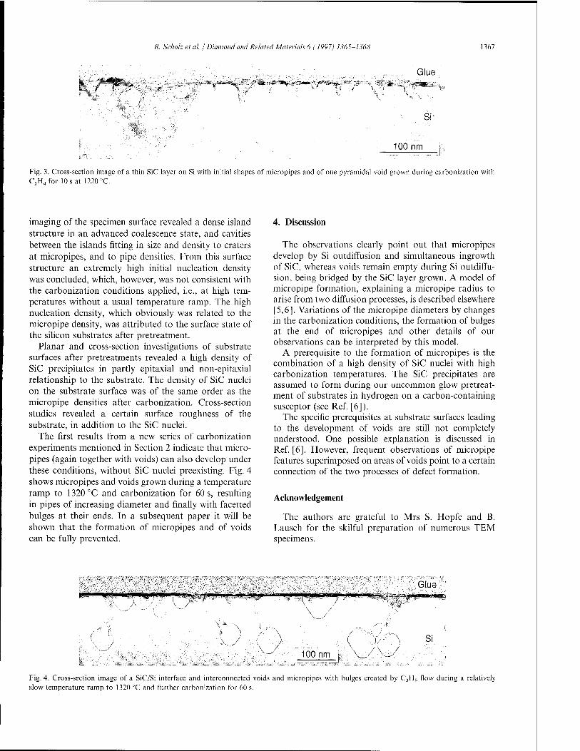
R. Scholz et al. / Diamond and Related Materials 6 (1997) 1365-1368 1367
K' «ife-IS ;»****•«*?
Glue
si-
100 nm
Fig. 3. Cross-section image of a thin SiC layer on Si with initial shapes of micropipes and of one pyramidal void grown during carbonization with C2H4for 10 sat 1220 °C.
imaging of the specimen surface revealed a dense island structure in an advanced coalescence state, and cavities between the islands fitting in size and density to craters at micropipes, and to pipe densities. From this surface structure an extremely high initial nucleation density was concluded, which, however, was not consistent with the carbonization conditions applied, i.e., at high tem- peratures without a usual temperature ramp. The high nucleation density, which obviously was related to the micropipe density, was attributed to the surface state of the silicon substrates after pretreatment.
Planar and cross-section investigations of substrate surfaces after pretreatments revealed a high density of SiC precipitates in partly epitaxial and non-epitaxial relationship to the substrate. The density of SiC nuclei on the substrate surface was of the same order as the micropipe densities after carbonization. Cross-section studies revealed a certain surface roughness of the substrate, in addition to the SiC nuclei.
The first results from a new series of carbonization experiments mentioned in Section 2 indicate that micro- pipes (again together with voids) can also develop under these conditions, without SiC nuclei preexisting. Fig. 4 shows micropipes and voids grown during a temperature ramp to 1320 °C and carbonization for 60 s, resulting in pipes of increasing diameter and finally with facetted bulges at their ends. In a subsequent paper it will be shown that the formation of micropipes and of voids can be fully prevented.
4. Discussion
The observations clearly point out that micropipes develop by Si outdiffusion and simultaneous ingrowth of SiC, whereas voids remain empty during Si outdiffu- sion, being bridged by the SiC layer grown. A model of micropipe formation, explaining a micropipe radius to arise from two diffusion processes, is described elsewhere [5,6]. Variations of the micropipe diameters by changes in the carbonization conditions, the formation of bulges at the end of micropipes and other details of our observations can be interpreted by this model.
A prerequisite to the formation of micropipes is the combination of a high density of SiC nuclei with high carbonization temperatures. The SiC precipitates are assumed to form during our uncommon glow pretreat- ment of substrates in hydrogen on a carbon-containing susceptor (see Ref. [6]).
The specific prerequisites at substrate surfaces leading to the development of voids are still not completely understood. One possible explanation is discussed in Ref. [6]. However, frequent observations of micropipe features superimposed on areas of voids point to a certain connection of the two processes of defect formation.
Acknowledgement
The authors are grateful to Mrs S. Hopfe and B. Tausch for the skilful preparation of numerous TEM specimens.
mm "-' *J
Glue, ■*•-•-?*■ ■ . i»j|i« l Jllll.ll.ljll-V«
■\ ) Si
100 nm .\ ■:.-/
Fig. 4. Cross-section image of a SiC/Si interface and interconnected voids and micropipes with bulges created by C3H8 flow during a relatively slow temperature ramp to 1320 °C and further carbonization for 60 s.

1368 R. Schöbet al. I Diamond and Related Materials 6 (1997) 1365-1368
References
[1] J.P. Li, A.J. Steckl, J. Electrochem. Soc. 142 (1995) 634. [2] A.J. Steckl, J.P. Li, IEEE Trans. Electron Devices 39 (1992) 64. [3] A. Addamiano, J.A. Sprague, Appl. Phys. Lett. 44 (1984) 525.
[4] H.J. Kim, R.F. Davis, X.B. Cox, R.W. Linton, J. Electrochem. Soc. 134(1987)2269.
[5] R. Scholz, U. Gösele, E. Niemann, D. Leidich, Appl. Phys. Lett. 67 (1995) 1453.
[6] R. Scholz, U. Gösele, E. Niemann, F. Wischmeyer, Appl. Phys. A. 64(1997) 115.
DIAMOND AND
RELATED MATERIALS
ELSEVIER Diamond and Related Materials 6 (1997) 1369-1373
Wafer warpage, crystal bending and interface properties of 4H-SiC epi-wafers
A. Ellisona'*, H. Radamsona, M. Tuominena,b, S. Militac, C. Hallina, A. Henry a'd, O. Kordinabd, T. Tuomie, R. Yakimovaa'b, R. Madarf, E. Janzena
a Department of Physics and Measurement Technology, Linköping University, S-581 83 Linköping, Sweden
b Okmetic Ltd, P.O. Box 44, FIN-02631 Espoo, Finland c European Synchrotron Radiation Facility, BP 220, F-38 043 Grenoble, France
d ABB Corporate Research, S-721 78 Västeras, Sweden " Optoelectronics Laboratory, Helsinki University of Technology, FIN-02150 Espoo, Finland
'LMGP (CNRS-INPG) ENSPG, BP 46, F-38 402 St-Martin-d'Heres, France
Abstract
The relationship between the warpage of 4H-SiC CVD grown epi-wafers with crystal bending and substrate properties is investigated. The wafer surface preparation before and after epitaxy is found to affect both long range properties such as the wafer flatness and to some extent local properties such as the epi-substrate interface. Structural characterisation is carried out using X-ray diffraction techniques and KOH etching. © 1997 Elsevier Science S.A.
Keywords: X-ray diffraction; Topography; Bending; Interface
1. Introduction
The high figures of merit of silicon carbide are cur- rently driving increased developments in device process- ing. Even during the development stage on 1.3 in. substrates, the processing of full wafers demands a wafer flatness which can tolerate micron or sub-micron optical lithography patterning. This is especially true for high- frequency and high-power transistor applications. Also, the final quality of the SiC epilayers is expected to be influenced, to a certain extent, by substrate defects and surface preparation before epitaxy. Structural proper- ties, such as the bending and interface quality, of epitax- ial layers grown by chemical vapour deposition (CVD) therefore need to be addressed.
2. Experimental procedure
Investigations were carried out on commercial (Cree Research Inc.) 4H (0001) wafers, 350-450 urn thick,
: Corresponding author.
either single (Si-face) or double-side polished, with n-type doping in the high 1018cm~3 range. The sub- strates used for epitaxy of low-doped (1015 cm"3 range) layers were Si-face, off-axis, the growth being performed in a hot-wall CVD reactor at 1550 °C, using propane and silane precursors diluted in a hydrogen carrier gas flow[l].
Substrate and epilayer crystalline defects were imaged by white beam synchrotron X-ray projection topogra- phy, combining transmission and section geometries. Measurements allowing high spatial resolution were carried out at the European Synchrotron Radiation Facility using HR Kodak film. The wafer flatness was measured with either a Dektak profilometer or with a micro-interferometer from Fisba Optik using a HeNe (633 nm) laser. X-ray diffraction (XRD) rocking curves of symmetrical (0004) reflections were measured with a Philips MRD 1880/HR diffractometer (Cu anode) using the triple-axis geometry [2]. The crystal curvature was measured by the shift of the peak centroid of ro rocking curves (sensitive to lattice plane tilts and bending) with the position of the incident beam along an in situ oriented <1120> diameter of the wafer.
0925-9635/97/S17.00 © 1997 Elsevier Science S.A. All rights reserved. PII S0925-9635(97)00086-l

1370 A. Ellison et al. / Diamond and Related Materials 6 (1997) 1369-1373
3. Results
3.1. Long range properties: crystal bending and wafer warpage
The warpage of 1.3 in. epi-wafers (low doped 15-30 um thick epilayer, ground backside) typically ranges from 5 to 12 um (Fig. 1) and depends on the backside preparation before CVD growth (concave towards Si-face for polished backside before epitaxy, convex or "horse-saddle" for ground backside). XRD mapping reveals a strong, non-uniform, crystal bending with a curvature radius, measured in the center of the wafer, of typically 5-15 m (Fig. 2). Unlike their direc- tion (towards Si-face), the magnitude of the crystal bending and the wafer warpage are found to be not simply correlated (see Figs. 1 and 2), which suggests that the substrate structural properties and preparation prior to, and after, CVD growth play an important role. Epilayer thickness variation as a cause of warpage is excluded, being typically one order of magnitude less than the observed epi-surface flatness variation. In par- ticular, XRD rocking curves mapped out before and after epitaxy show that, in as-grown epi-wafers, the crystal bending and the mosaicity are inherited from the substrate. The quality of the substrate prior to epitaxy therefore requires more attention.
3.1.1. Crystal bending Investigations carried out on several samples show
that crystal bending and warpage depend strongly on the origin of the substrate, together with its preparation. For commercial n-type 4H wafers from Cree Research Inc., the mean basal crystallographic plane bending is found to be oriented systematically towards the Si-face,
14 12 10
c %-» '3
>
c
(a) 11.4 urn warpage Surface curvature
<u i-
3 u
_>
-20 -15 -10 0 10 15 20
Position along a wafer diameter (mm)
-15 -10 -5 0 5 10 15
Position along <11.0> wafer diameter (mm)
Fig. 2. Bending of lattice planes measured on the Si-face of the same wafer as Fig. 1. The centroid of XRD co rocking curves from the (0004) reflection are plotted versus the position of the incident beam along a <1120> wafer diameter. The curvature radius Rc is determined in the linear region of the curve. The bending of the as-grown epilayer (1) is similar to the one of the as-received substrate, and is oriented towards the Si-face. It is increased after backside grinding (2), whereas re-polishing of the backside (3) allows to regain the initial bending.
whether measured on the Si- or C-face. The magnitude of the bending varies from substrate to substrate, but exhibits the same shape on substrates cut from the same boule.
X-ray transmission topographs taken from such 4H-SiC wafers revealed domain boundaries similar to the ones recently reported by Takahashi et al. [3], the domain walls containing a high density of edge disloca- tions with Burger vector mainly in <1120) directions. As mosaicity effects and crystal bending, the size of domain walls was observed to increase from the center to the periphery of the substrate. We relate the crystal bending and the domain structure to a polygonization of the crystal, the stresses introduced by the growth process, or its environment, relaxing into polygonized low-angle domains linked to the non-uniform crystal bending. Since polygonization requires glide and climb of dislocations, it is a temperature activated process, most probably occurring during bulk growth, the mosaic structure, together with a non-uniform bending, being inherited by the sliced substrate.
Owing to these results, together with the fact that the ductile-brittle transition is reported to occur between 800 and 1000 °C [4], it can be assumed that the level of intrinsic stresses present in the substrates will increase their sensitivity to warp during epitaxy and other processing steps.
Fig. 1. Wafer flatness measured by profilometer on a 15 um thick 4H CVD epilayer grown on the Si-face of a double side polished substrate: (a) as-grown, after backside grinding, (b) after backside re-polishing. The uniformity of the flatness was in both cases confirmed by micro-interferometry measurements.
3.1.2. Wafer warpage In particular, the magnitude of wafer warpage and
crystal bending is found to be strongly affected by the wafer's backside preparation. Fine polishing of the
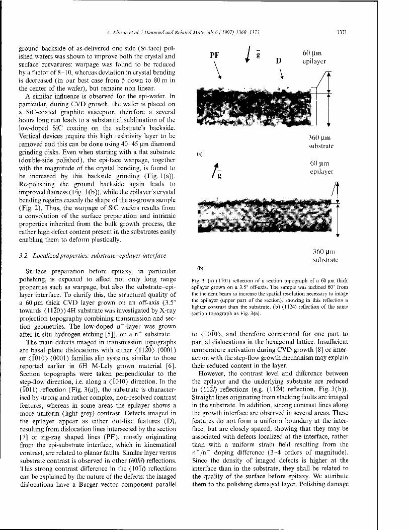
A. Ellison et al. / Diamond and Related Materials 6 (1997) 1369-1373 1371
ground backside of as-delivered one side (Si-face) pol- ished wafers was shown to improve both the crystal and surface curvatures: warpage was found to be reduced by a factor of 8-10, whereas deviation in crystal bending is decreased (in our best case from 5 down to 80 m in the center of the wafer), but remains non linear.
A similar influence is observed for the epi-wafer. In particular, during CVD growth, the wafer is placed on a SiC-coated graphite susceptor, therefore a several hours long run leads to a substantial sublimation of the low-doped SiC coating on the substrate's backside. Vertical devices require this high resistivity layer to be removed and this can be done using 40-45 um diamond grinding disks. Even when starting with a flat substrate (double-side polished), the epi-face warpage, together with the magnitude of the crystal bending, is found to be increased by this backside grinding (Fig. 1(a)). Re-polishing the ground backside again leads to improved flatness (Fig. 1 (b)), while the epilayer's crystal bending regains exactly the shape of the as-grown sample (Fig. 2). Thus, the warpage of SiC wafers results from a convolution of the surface preparation and intrinsic properties inherited from the bulk growth process, the rather high defect content present in the substrates easily enabling them to deform plastically.
3.2. Localized properties: substrate-epilayer interface
Surface preparation before epitaxy, in particular polishing, is expected to affect not only long range properties such as warpage, but also the substrate-epi- layer interface. To clarify this, the structural quality of a 60 um thick CVD layer grown on an off-axis (3.5° towards <1120» 4H substrate was investigated by X-ray projection topography combining transmission and sec- tion geometries. The low-doped n-layer was grown after in situ hydrogen etching [5]], on a n+ substrate.
The main defects imaged in transmission topographs are basal plane dislocations with either <1120> (0001) or <f010> (0001) families slip systems, similar to those reported earlier in 6H M-Lely grown material [6]. Section topographs were taken perpendicular to the step-flow direction, i.e. along a <1010> direction. In the (fOll) reflection (Fig. 3(a)), the substrate is character- ised by strong and rather complex, non-resolved contrast features, whereas in some areas the epilayer shows a more uniform (light grey) contrast. Defects imaged in the epilayer appear as either dot-like features (D), resulting from dislocation lines intersected by the section [7] or zig-zag shaped lines (PF), mostly originating from the epi-substrate interface, which in kinematical contrast, are related to planar faults. Similar layer versus substrate contrast is observed in other (hOhl) reflections. This strong contrast difference in the (101/) reflections can be explained by the nature of the defects: the imaged dislocations have a Burger vector component parallel
PF / D
60 fim epilayer
V
(a)
h
360 urn substrate
60 |im epilayer
- - ■ <*■■ "•■.. ' .
360 jim substrate
(b)
Fig. 3. (a) (1101) reflection of a section topograph of a 60 urn thick epilayer grown on a 3.5° off-axis. The sample was inclined 60° from the incident beam to increase the spatial resolution necessary to image the epilayer (upper part of the section), showing in this reflection a lighter contrast than the substrate, (b) (1124) reflection of the same section topograph as Fig. 3(a).
to <1010>, and therefore correspond for one part to partial dislocations in the hexagonal lattice. Insufficient temperature activation during CVD growth [8] or inter- action with the step-flow growth mechanism may explain their reduced content in the layer.
However, the contrast level and difference between the epilayer and the underlying substrate are reduced in (1120 reflections (e.g. (1124) reflection, Fig. 3(b)). Straight lines originating from stacking faults are imaged in the substrate. In addition, strong contrast lines along the growth interface are observed in several areas. These features do not form a uniform boundary at the inter- face, but are closely spaced, showing that they may be associated with defects localized at the interface, rather than with a uniform strain field resulting from the n + /n" doping difference (3-4 orders of magnitude). Since the density of imaged defects is higher at the interface than in the substrate, they shall be related to the quality of the surface before epitaxy. We attribute them to the polishing damaged layer. Polishing damage
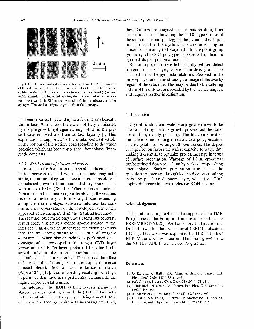
1372 A. Ellison et al. I Diamond and Related Materials 6 (1997) 1369-1373
*i
t 25 (im
I 1
Fig. 4. Interference contrast micrograph of a cleaved n /n+ epi-wafer (10i"0)-like surface etched for 3 min in KOH (480 °C). The selective etching at the interface leads to a horizontal contrast band (I) whose width extends with increased etching time. Pyramidal etch pits (P) pointing towards the Si face are revealed both in the substrate and the epilayer. The vertical stripes originate from the cleavage.
these features are assigned to etch pits resulting from dislocations lines intersecting the {1100} type surface of the section. The morphology of the pyramidal etch pits can be related to the crystal's structure: as etching on c-faces leads mainly to hexagonal pits, the point group symmetry of a-SiC polytypes is expected to lead to pyramid shaped pits on a-faces [11].
Section topographs revealed a slightly reduced defect content in the epilayer; whereas the density and size distribution of the pyramidal etch pits observed in the same epilayer are, in most cases, the image of the nearby region of the substrate. This may be due to the differing nature of the dislocations revealed by the two techniques, and requires further investigation.
has been reported to extend up to a few microns beneath the surface [9] and was therefore not fully eliminated by the pre-growth hydrogen etching (which in the pre- sent case removed a 0.1 um surface layer [6]). This explanation is supported by the similar contrast visible in the bottom of the section, corresponding to the wafer backside, which has been re-polished after epitaxy (kine- matic contrast).
3.2.1. KOH etching of cleaved epi-wafers In order to further assess the crystalline defect distri-
bution between the epilayer and the underlying sub- strate, the surface of epiwafers sections, either as-cleaved or polished down to 1 urn diamond slurry, were etched with molten KOH (480 °C). When observed under a Nomarski contrast microscope after etching, the sections revealed an extremely uniform straight band extending along the entire epilayer-substrate interface (as con- firmed from observation of the low-doped layer which appeared semi-transparent in the transmission mode). This feature, observable only under Nomarski contrast, results from a selectively etched groove located at the interface (Fig. 4), which under repeated etching extends into the underlying substrate at a rate of roughly 4 um min _1. When similar etching is performed on a cleavage of a low-doped (1015 range) CVD layer grown on a n+ buffer layer, preferential etching is ob- served only at the n~/n+ interface, not at the n+-buffer/n+-substrate interface. The observed interface etching can thus be assigned to the doping-difference induced electric field or to the lattice mismatch (Aa/a~l0~4) [10], weaker bonding resulting from high impurity content favoring a preferential etching into the higher doped crystal regions.
In addition, the KOH etching reveals pyramidal shaped features pointing towards the (0001) Si face both in the substrate and in the epilayer. Being absent before etching and extending in size with increasing etch time,
4. Conclusion
Crystal bending and wafer warpage are shown to be affected both by the bulk growth process and the wafer preparation, mainly polishing. The tilt component of the lattice plane bending is related to a polygonization of the crystal into low-angle tilt boundaries. This degree of imperfection favors the wafers capacity to warp, thus making it essential to optimize processing steps in terms of surface preparation. Warpage of 1.3 in. epi-wafers can be reduced down to 1-3 um by backside re-polishing after epitaxy. Surface preparation also affects the epi/substrate interface through localized defects resulting from the polishing damaged layer, while the n+/n~ doping difference induces a selective KOH etching.
Acknowledgement
The authors are grateful to the support of the TMR Programme of the European Commission (contract no ERBFMBICT960728). We thank Drs J. Baruchel and Dr J. Hartwig for the beam time at ESRF (application HC544). This work was supported by TFR, NUTEK/ NFR Material Consortium on Thin Film growth and the NUTEK/ABB Power Device Programme.
References
[1] O. Kordina, C. Hallin, R.C. Glass, A. Henry, E. Janzen, Inst. Phys. Conf. Series 137 (1994) 41-44.
[2] P.F. Fewster, J. Appl. Crystallogr. 24 (1991) 178-183. [3] J. Takahashi, N. Ohtani, M. Kanaya, Inst. Phys. Conf. Series 142
(1996)445-448. [4] K. Maeda et al., Phil. Mag. A, 57 (4) (1988) 573-592. [5] C. Hallin, A.S. Bakin, F. Owman, P. Märtensson, O. Kordina,
E. Janzen, Inst. Phys. Conf. Series 142 (1996) 613-616.

A. Ellison et al. / Diamond and Related Materials 6 (1997) 1369-1373 1373
[6] M. Dudley et al., J. Phys., D 28 (1995) A63-A68. Hobgood, R.H. Hopkins, J. Electrochem. Soc. 142 (12) (1995) [7] H. Klapper, Diffraction and Imaging Techniques in Material 4290-4294.
Science, vol. 2, Springer, Berlin, 1991, pp. 109-162. [10] Gmelin Handbook of Inorganic Chemistry, Si Suppl., vol. B2 [8] S. Wang, M. Dudley, C.H. Carter, H.S. Song, Mater. Res. Soc. (Silicon Carbide), 1984, p. 18.
Symp. Proc. 339 (1994) 735-740. [ 11 ] K. Sangwal, Etching of Crystals, North-Holland Physics Publish- [9] W. Qian, M. Skowronski, G. Augustine, R.C. Glass, H.McD. ing, Amsterdam, 1987 p. 303.

ELSEVIER
DIAMOND AND
RELATED MATERIALS
Diamond and Related Materials 6 (1997) 1374-1377
Nonlinear optical mapping of 3C-inclusions in 6H-SiC-epilayers
C. Meyer *, G. Lüpke, E. Stein von Kamienski, A. Gölz, H. Kurz Institute für Halbleitertechnik II, RWTH Aachen, 52056 Aachen, Germany
Abstract
Optical second-harmonic generation (SHG) is shown to be a powerful technique for identifying different polytypes of SiC-films deposited on 6H-SiC substrates. The rotational anisotropy of the SHG radiation reflected from homo-epitaxially grown 6H-SiC epilayers provides a clear fingerprint of microcrystalline inclusions of 3C-SiC. The large dynamic range of the SHG response of more than one order of magnitude between different SiC polytypes allows a fast nondestructive mapping of SiC wafer surfaces with a lateral resolution in the um-regime. © 1997 Elsevier Science S.A.
Keywords: Nondestructive testing; Second harmonic generation; Thin films
1. Introduction
Implementing high-temperature, high-frequency, and high-power electronic devices, as well as GaN blue lasers on SiC substrates depends critically on the quality of the material available. Although active and passive devices have been fabricated on homo-epitaxially grown 6H-SiC films [1,2], their performance is limited by defects, such as micropipes, microfacets, and crystalline inclusions of different polytypes. 6H-SiC epilayers grown at a high growth temperature reveal a high density of stacking faults and antiphase boundaries [3]. On the other hand, a low growth temperature favors the inclu- sion of 3C-SiC islands in the 6H-SiC film [4]. Experimental approaches to detect inclusions of different SiC polytypes include the growth of oxides on the epilayer making use of different growth rates of the polytypes [5] and white beam synchotron topographic analysis methods [6]. However, the development of new epitaxial growth processes requires fast and reliable in situ measurement techniques.
In this paper, we demonstrate the capability of optical second-harmonic generation (SHG) for detecting different SiC-polytypes. SHG is a known powerful tool for probing surfaces and interfaces of centrosymmetric media [7,8], and has been used for studying the forma- tion of antiphase domains in epitaxial layers of com- pound semiconductors, such as GaP [9], and GaSe films
[10], and SimGe„ superlattices [11], all grown on Si substrates. Recently, Galeckas et al. investigated the SHG rotational anisotropy (RA-SHG) from 3C-SiC films on Si (001) to probe the crystalline order, and detected the presence of (111 )-oriented 3C-SiC micro- areas [12]. RA-SHG which is defined by the nonlinear susceptibility tensor %(2) and its relation to structural symmetry is the key feature for identifying various SiC- polytypes. In this work, RA-SHG measurements from different polytypes, such as 4H-, 6H-, and 3C-SiC are presented, and the method is applied for spatially resolved mapping of 3C-SiC inclusions in 6H-SiC epilayers.
2. Theoretical background and experiments
The tensorial characteristic of x(2) gives rise to a RA-SHG response from SiC wafers rotated about its surface normal. The RA-SHG Intensity, 7(2<B,(^), as a function of the sample azimuthal angle <j> can be written in the electric dipole approximation as a truncated Fourier expansion:
I2a(4>)oc\x<2)Eia)E(™)\2=\ X c,„cosK^ + <0|2/(' ■<oY
(1)
* Corresponding author. Tel: +49 241 807895; Fax: +49 241 e-mail: [email protected]
where the complex cm are given by the appropriate elements of y}2) multiplied by Fresnel coefficients. The phase angles (j>m denote the relative phases of the aniso-
0925-9635/97/S17.00 © 1997 Elsevier Science S.A. All rights reserved. PII S0925-9635(97)00097-6
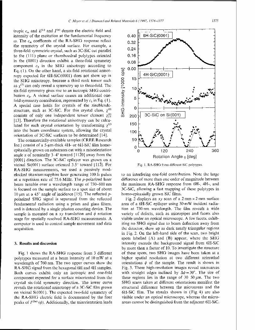
C. Meyer et al. / Diamond and Related Materials 6 (1997) 1374-1377 1375
tropic cm and £<t0) and 7(ro) denote the electric field and intensity of the excitation at the fundamental frequency co. The cm coefficents of the RA-SHG response reflect the symmetry of the crystal surface. For example, a three-fold symmetric crystal, such as 3C-SiC cut parallel to the (111) plane or rhomboedral polytypes oriented in the (0001) direction exhibit a three-fold symmetry component c3 in the SHG anisotropy according to Eq. (1). On the other hand, a six-fold rotational anisot- ropy expected for 6H-SiC(0001) does not show up in the SHG anisotropy, because a third rank tensor such as x(2) can only reveal a symmetry up to three-fold. The six-fold symmetry gives rise to an isotropic SHG contri- bution c0. A vicinal surface causes an additional one- fold symmetry contribution, represented by c1 in Eq. (1). A special case holds for crystals of the zincblende- structure, such as 3C-SiC. For this crystal class, xm
consists of only one independent tensor element xu [13]. Therefore the rotational anisotropy can be calcu- lated for each crystal orientation by transforming y}2)
into the beam coordinate system, allowing the crystal orientation of 3C-SiC surfaces to be determined [14].
The commercially-available samples (CREE Research Inc.) consist of a 5-[im-thick 4H- or 6H-SiC film homo- epitaxially grown on substrates cut with a misorientation angle a of nominally 3-4° toward [1120] away from the [0001] direction. The 3C-SiC epilayer was grown on a vicinal Si(001) surface oriented 3.5° toward [112]. For RA-SHG measurements, we used a passively mod- elocked titaniumrsapphire laser generating 100 fs pulses at a repetition rate of 75.6 MHz. The /^-polarized laser beam tunable over a wavelength range of 730-810 nm is focused on the sample surface to a spot size of about 10 urn at a 45° angle of incidence [15]. The reflected p- polarized SHG signal is separated from the reflected fundamental radiation using a prism and glass filters, and is detected by a single photon counting device. The sample is mounted on a xy translation and <j> rotation stage for spatially resolved RA-SHG measurements. A computer is used to control sample movement and data acquisition.
3. Results and discussion
Fig. 1 shows the RA-SHG response from 3 different polytypes measured at a beam intensity of 10 mW at a wavelength of 760 nm. The two upper curves show the RA-SHG signal from the hexagonal 6H and 4H samples. Both curves exhibit only an isotropic and one-fold component expected for a surface misoriented from the crystal six-fold symmetry direction. The lower curve reveals the rotational anisotropy of a 3C-SiC film grown on vicinal Si(001). The expected two-fold symmetry of the RA-SHG electric field is documented by the four peaks of 7(2co) (</>). Additionally, the misorientation leads
w a. o o o o
05 c 0)
I C/)
0 120 240 360 Rotation Angle (j> [deg]
Fig. 1. RA-SHG from different SiC polytypes.
to an interfering one-fold contribution. Note the large difference of more than one order of magnitude between the maximum RA-SHG response from 6H-, 4H-, and 3C-SiC, allowing a fast mapping of these polytypes in homo-epitaxially grown SiC films.
Fig. 2 displays an xy scan of a 2 mm x 2 mm surface area of a 6H-SiC epilayer using 30 mW incident radia- tion at 730 nm wavelength. The film reveals a wide variety of defects, such as micropipes and facets also visible under an optical microscope. A few facets, exhib- iting no SHG signal due to beam deflection away from the detector, show up as dark nearly triangular regions in Fig. 2. On the left-hand side of the scan, two bright spots labelled (A) and (B) appear, where the SHG intensity exceeds the background signal from 6H-SiC by more than a factor of 10. To investigate the structure of these spots, two SHG images have been taken at a higher spatial resolution at two different azimuthal orientations (j) of the sample. The result is shown in Fig. 3. These high-resolution images reveal microareas with straight edges inclined by A^> = 30°. The size of these regions lies in the range of 30-50 urn. The two SHG scans taken at different orientations manifest the structural difference between the microareas and the 6H-SiC film. The streaks shown in (Fig. 4) are also visible under an optical microscope, whereas the micro- areas cannot be distinguished from the adjacent 6H-SiC.

1376 C. Meyer et al. / Diamond and Related Materials 6 (1997) 1374-1377
0.5 1 x-position [mm]
20000 40000 60000
SHG-lntensity [cps]
80000
Fig. 2. Scan of a ~ 2 mm x 2 mm surface area. The scanning time was about 40 min for 200 x 200 points.
To determine the RA-SHG of the microareas, addi- tional xy scans were performed at a variety of different sample orientations ^ and the data were averaged over the regions labelled I and II in Fig. 3, respectively. The rotational anisotropy shows a clear three-fold symmetry, as displayed in Fig. 5(b) and (c). This excludes a hexagonal poly type for the inclusions. To identify the polytype in the regions I and II, we calculated the RA-SHG from 3C-SiC, which is determined by the Fourier coefficients cm as defined in Eq. (1). Therefore the only nonvanishing x<2) tensor element, %fl is trans- formed into the beam coordinate system as outlined by Bottomley et al. [14].
The solid lines in Fig. 5(a) and (b) represent theoreti- cal predictions of Ii2a\<f>) from zincblende-type micro- crystallites for polar and azimuthal misorientation angles a = 3.5°, and yS=-25.61° and +34.37° with respect to the cubic [111]- and [112]-direction, respec- tively. Refractive indices of n(a>) = 2.616 and n(2co) = 2.817 for the fundamental and second harmonic light where used for the calculation [16]. The agreement between theoretical curve and experimental data is excel- lent using only a scaling factor which is identical within <1% for both microareas. This clearly identifies the inclusions as 3C-SiC microcrystallites of different azi- muthal misorientation. The difference between ß values of the two areas is exactly 60° as one would expect for
150
1100
=*> 50
Im. tP®M
m$ msmn^*
100 x-position [urn]
200
100 x-position [urn]
0 10000 20000 30000 40000 50000 60000
SHG-lntensity [cps]
Fig. 3. Scans of area (A) in Fig. 2 taken at two different azimuthal angles. The scanning time for each image is approximately 8 min.
a lattice-matched cubic crystal with three-fold symmetry on a six-fold-symmetric substrate. The [112] direction of the cubic crystal corresponds to either the [1120] or the [1210] direction of the 6H substrate. From the ß values of the inclusions the azimuthal misorientation of the substrate can be determined to be 4.4° away from the [1120] direction.
Because of the large difference of more than one order of magnitude in the SHG response from different poly- types, sampling times of only 20 ms per data point are required. The image shown in Fig. 2 consisting of a 200 x 200 data array with a spacing of 9.375 um has been taken in about 40 min. Positioning required 12 min, which can be reduced further by using a faster position- ing system. The use of an optical imaging tool for monitoring the SHG reflection from a larger surface area will also reduce measurement time [17].
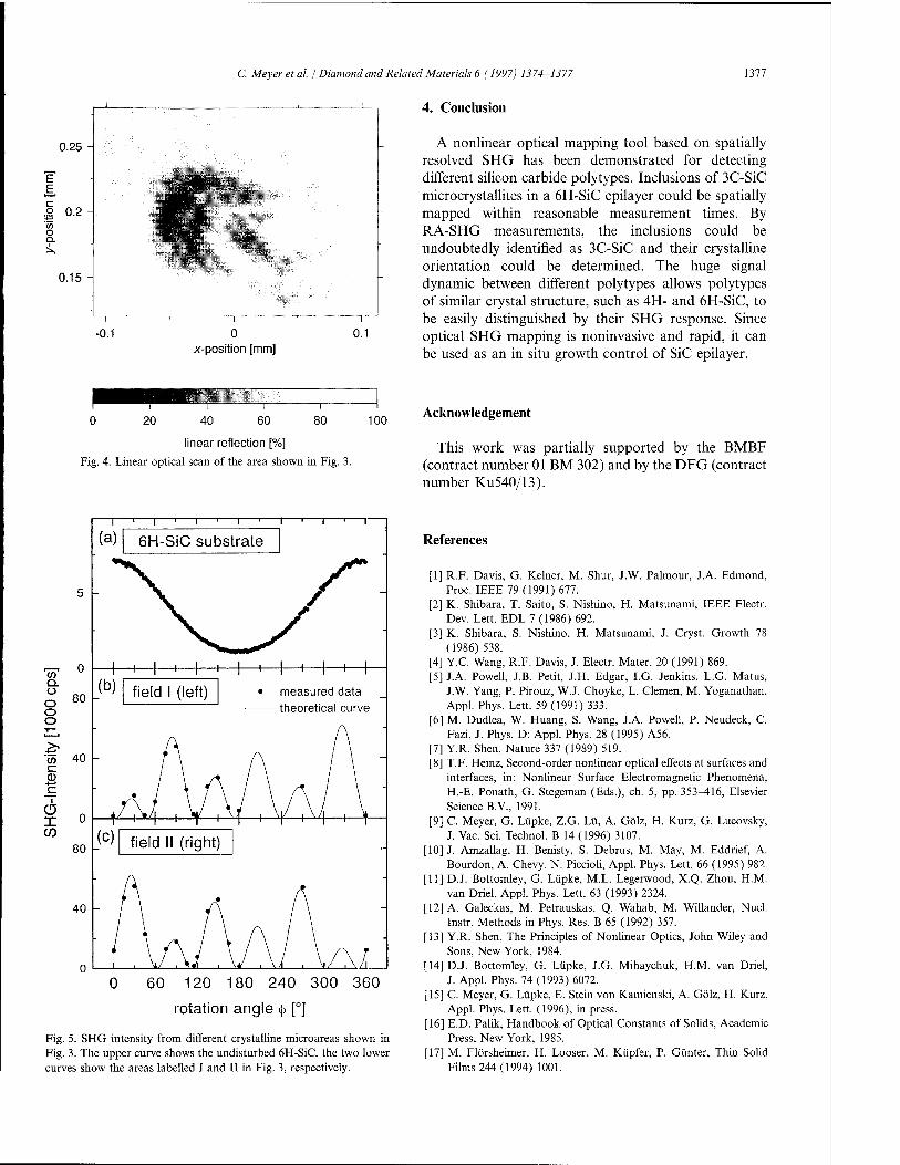
0.25 -
E E
C. Meyer et al. / Diamond and Related Materials 6 (1997) 1374-1377
4. Conclusion
1377
0.15
-0.1 0 x-position [mm]
0.1
A nonlinear optical mapping tool based on spatially resolved SHG has been demonstrated for detecting different silicon carbide polytypes. Inclusions of 3C-SiC microcrystallites in a 6H-SiC epilayer could be spatially mapped within reasonable measurement times. By RA-SHG measurements, the inclusions could be undoubtedly identified as 3C-SiC and their crystalline orientation could be determined. The huge signal dynamic between different polytypes allows polytypes of similar crystal structure, such as 4H- and 6H-SiC, to be easily distinguished by their SHG response. Since optical SHG mapping is noninvasive and rapid, it can be used as an in situ growth control of SiC epilayer.
0 20 40 60 80 100
linear reflection [%] Fig. 4. Linear optical scan of the area shown in Fig. 3.
Acknowledgement
This work was partially supported by the BMBF (contract number 01 BM 302) and by the DFG (contract number Ku540/13).
-i—i—|—.—|—i—|—i—|—i—|—i—r
6H-SiC substrate
60 120 180 240 300 360
rotation angle q> [°]
Fig. 5. SHG intensity from different crystalline microareas shown in Fig. 3. The upper curve shows the undisturbed 6H-SiC, the two lower curves show the areas labelled I and II in Fig. 3, respectively.
References
[1] R.F. Davis, G. Keiner, M. Shur, J.W. Palmour, J.A. Edmond, Proc. IEEE 79 (1991) 677.
[2] K. Shibara, T. Saito, S. Nishino, H. Matsunami, IEEE Electr. Dev. Lett. EDL 7 (1986) 692.
[3] K. Shibara, S. Nishino, H. Matsunami, J. Cryst. Growth 78 (1986)538.
[4] Y.C. Wang, R.F. Davis, J. Electr. Mater. 20 (1991) 869. [5] J.A. Powell, J.B. Petit, J.H. Edgar, I.G Jenkins, L.G. Matus,
J.W. Yang, P. Pirouz, W.J. Choyke, L. Clemen, M. Yoganathan, Appl. Phys. Lett. 59 (1991) 333.
[6] M. Dudlea, W. Huang, S. Wang, J.A. Powell, P. Neudeck, C. Fazi, J. Phys. D: Appl. Phys. 28 (1995) A56.
[7] Y.R. Shen, Nature 337 (1989) 519. [8] T.F. Heinz, Second-order nonlinear optical effects at surfaces and
interfaces, in: Nonlinear Surface Electromagnetic Phenomena, H.-E. Ponath, G. Stegeman (Eds.), ch. 5, pp. 353-416, Elsevier Science B.V., 1991.
[9] C. Meyer, G. Lüpke, Z.G. Lü, A. Götz, H. Kurz, G. Lucovsky, J. Vac. Sei. Technol. B 14 (1996) 3107.
[10] J. Amzallag, H. Benisty, S. Debrus, M. May, M. Eddrief, A. Bourdon, A. Chevy, N. Piccioli, Appl. Phys. Lett. 66 (1995) 982.
[11] D.J. Bottomley, G. Lüpke, M.L. Legerwood, X.Q. Zhou, H.M. van Driel, Appl. Phys. Lett. 63 (1993) 2324.
[12] A. Galeckas, M. Petrauskas, Q. Wahab, M. Willander, Nucl. Instr. Methods in Phys. Res. B 65 (1992) 357.
[13] Y.R. Shen, The Principles of Nonlinear Optics, John Wiley and Sons, New York, 1984.
[14] D.J. Bottomley, G. Lüpke, J.G. Mihaychuk, H.M. van Driel, J. Appl. Phys. 74(1993)6072.
[15] C. Meyer, G. Lüpke, E. Stein von Kamienski, A. Götz, H. Kurz, Appl. Phys. Lett. (1996), in press.
[16] E.D. Palik, Handbook of Optical Constants of Solids, Academic Press, New York, 1985.
[17] M. Flörsheimer, H. Looser, M. Kupfer, P. Günter, Thin Solid Films 244 (1994) 1001.

ELSEVIER
DIAMOND AND
RELATED MATERIALS
Diamond and Related Materials 6 (1997) 1378-1380
Deep luminescent centres in electron-irradiated 6H SiC
N.T. Son *, E. Sörman, M. Singh, W.M. Chen, C. Hallin, O. Kordina, B. Monemar, J.L. Lindström, E. Janzen
Department of Physics and Measurement Technology, Linköping University, S-581 83, Linköping, Sweden
Abstract
We report on our observation of several new photoluminescence (PL) spectra in electron-irradiated 6H SiC. In addition to the vacancy-related PL spectrum ranging from 1.36 to 1.44 eV, four other spectra with no-phonon lines in the regions of 0.9983-1.0738 eV, 1.0878-1.1342 eV and 1.3563-1.3711 eV were detected in 6H SiC. These luminescent centres are rather thermally stable. From the formation and annealing behaviour, these centres were suggested to be complexes, of which some involve a silicon vacancy. © 1997 Elsevier Science S.A.
Keywords: SiC; Electron irradiation; Defects; Photoluminescence; Deep levels; Vacancy complexes
1. Introduction
In semiconductors, vacancies and interstitials are cre- ated during high-energy particle bombardment. In a binary compound semiconductor such as SiC, anti-sites defects can also be formed. Under high temperature annealing, these primary defects become mobile and interact with other intrinsic defects or impurities to form complexes. Radiation-induced defects are often found to be associated with deep level states in the energy gap of semiconductors. Some of these are carrier traps, while others act as recombination centres, and both have a strong influence on the electrical and optical properties of the material. The creation of these recombination centres, either non-radiative or radiative, will lead to a considerable reduction of the carrier lifetime in the semiconductors. Such radiation defects, therefore, have been used for lifetime control in semiconductor bipolar devices. In some semiconductors, such as silicon, the vacancy and interstitial are mobile at temperatures well below room temperature, and hence, the properties of the material are mainly influenced by the secondary defects, i.e. their associated complex defects. In SiC, however, primary defects are stable at room temperature and will also be important for device applications. In some common polytypes such as 3C and 6H SiC, the negatively charged silicon vacancy had been detected by
' Corresponding author. Fax: 46-13-142337; e-mail: [email protected]
electron spin resonance (ESR) as early as 1970 [1], but was identified only recently [2,3], when high quality crystals became available. Secondary defects in SiC are thermally stable, and in some cases, also luminescent active. In the past, photoluminescence (PL) was extens- ively used to study radiation-induced luminescent centres, but mainly in the visible region [4]. Recently, several vacancy-related defects were detected by PL and optically detected magnetic resonance (ODMR) in the near-infrared region of irradiated 3C [5] and 6H [6] polytypes. In this paper, we report our observation of several new PL spectra in the region of 0.98-1.45 eV in electron-irradiated 6H SiC.
2. Samples and equipment
Samples used in this work are 6H SiC epitaxial films grown by chemical vapour deposition (CVD), including low-doped n-type and aluminium compensated p-type [7] material. The net donor concentration is in the mid 1014 to 1016cm~3 range. The typical thickness of the films is about 10-15 um. Samples were irradiated by 2.5 MeV electrons at room temperature with doses rang- ing from 5 x 10¹³ to 1018 cm-2. PL measurements were performed on a BOMEM DA3 Fourier transform spectrometer optimised for the region 0.7-1.6 eV. Luminescence emissions were detected using a cooled North-Coast germanium photo-diode. The sample tem-
0925-9635/97/S17.00 © 1997 Elsevier Science S.A. All rights reserved. PII S0925-9635(97)00098-8

N.T. Sonetal. / Diamond and Related Materials 6 (1997) 1378-1380 1379
perature could be varied from 5 K to room temperature using a He gas flow cryostat. The annealing time of the samples in nitrogen gas flow is typically 10 min at each temperature.
3. Results
In as-grown 6H SiC samples, through the range 0.7 to 1.6 eV, only the PL spectrum of vanadium was observed, as can be seen in Fig. 1(a). Irradiation with doses below 1015cm~2 does not change the picture of near-infrared PL, but introduces the well-known Dx
and D2 luminescence bands [4] in the visible region. With higher doses of irradiation, several PL bands can be detected in the region of 0.98-1.45 eV, while the PL from vanadium is almost quenched (Fig. 1(b)). The intensity of these PL bands increases rapidly with increasing the dose of irradiation from 1016 to 1017 cm-2. Higher doses lead to a creation of a number of PL lines in the regions 0.998-1.135 eV and 1.356-1.372 eV (Fig. 1(b)). The PL band with three NPLs at 1.368, 1.398 and 1.434 eV is related to the spin triplet states of the silicon vacancy, as identified by ODMR [6]. As can be seen from Fig. 1 (b), in the region 0.998-1.135 eV, several sharp lines were observed. These
cs W
■- et u C
e
6HSiC T=6K
(a) as-grown
kx (b) e"-irradiated
(lO'W3)
(c) annealed TWI x 10 at 750 °C
4 111111' 11 , 11.,, i
0.88 0.96 1.04 1.12 1.2 1.28 1.36 1.44
Photon Energy (eV)
Fig. 1. PL spectra observed at 6 K in 6H SiC epitaxial layers: (a) as-grown; (b) irradiated by 2.5 MeV electrons with a dose of 1017 cirT2, and (c) annealing at 750°C. The resolution is 0.25 meV.
lines appear differently in different samples, indicating that they are not all from the same defect. After annea- ling at 750 °C, the silicon vacancy-related PL band disappears together with its broad phonon band (Figs. 1(c) and 2). In the region 0.98-1.14 eV, some lines are also annealed out at this temperature, while the others become much stronger and a new group of four lines appears at 0.98-1.05 eV (Figs. 1(c) and 2). In annealed, p-type samples, only a PL band with five NPLs at the region 1.0878-1.1342 eV was detected, while in the n-type samples a deeper band with six NPLs (0.9983-1.0783 eV) was also observed (Fig. 2(a)). The energy position for these lines is indicated in Fig. 2(a). In the n-type samples, several new NPLs are also observed between 1.3563 and 1.3711 eV (the inset in Fig. 1(c)). After a short anneal at 960 °C, three lines can still be detected. Two of these are shown to be a doublet (Fig. 3(a)).
4. Discussion
Before annealing, three NPLs at 1.1031, 1.1195 and 1.1342 eV are dominating in this region, while the other two lines at 1.0878 and 1.0923 eV can hardly be seen (Fig. 1(b)). After annealing, these two lines appeared and the intensity ratios between the other three lines (1.1031-1.1342eV) changed. It seems that these five NPLs belong to two similar defects. The behaviour of these five NPLs with annealing (above 750 °C) is very
"a u
u V S
e
PLl
6H SiC T=6 K
-| 1 1 r
1.1342 eV
-+JJ
U (a)
Jl -—LJJL J
(b)
1.00 1.04 1.08 1.12
Photon Energy (eV) 1.16
Fig. 2. (a) High resolution (0.06 meV) PL spectra of the same sample as shown in Fig. 1(c); (b) the same PL spectra after annealing at 960 °C. The numbers indicate the energy positions of the lines in eV.

1380 N.T. Sonet al. / Diamond and Related Materials 6 (1997) 1378-1380
4>
-T—r-1—r-
6H SiC
1.3711
1.355 1.360 1.365 1.370 1.375
Photon Energy (eV) Fig. 3. Details of the PL band at 1.3563-1.3711 eV in n-type, electron- irradiated 6H SiC after annealing at 960 °C: (a) measured at 2 K; and (b) at 10 K. The energy positions of the lines are indicated in eV.
similar. This PL band only becomes clear in the structure and gets stronger when the silicon vacancy-related PL band at 1.434 eV [6] starts annealing out (700-750 °C). Annealing with temperatures above 750 °C leads to a decrease in intensity of this band. The spectrum still survives at temperatures closed to 1200 °C. This annea- ling behaviour indicates that this PL band is probably related to complex defects involving a silicon vacancy. These NPLs are very sharp and show no broadening effect or decreasing in intensity when increasing the temperature from 6 to 77 K. For such a deep centre, sharp PL lines are usually due to either excitonic trans- itions or internal transitions of the defect. In the case of a bound exciton, the NPLs are often shown to be split under a magnetic field. However, our preliminary data from the Zeeman effect experiments showed no splitting of any line, except a small energy shift of the 1.1342 eV line. The available data seem to indicate that these lines may be due to the transitions between the excited states and the ground state of a defect. For a substitutional impurity or a vacancy in 6H SiC, the PL spectrum usually consists of three NPLs (or three groups of NPLs in the case of the energy states are split by low-symmetry crystal field) corresponding to three different inequivalent sites of the lattice. It is possible that three NPLs at 1.1031, 1.1195 and 1.1342 eV belong to one defect. The other also gives rise to two NPLs,
overlapping with the 1.1195 and 1.1342 eV lines, and two other lines at 1.0878 and 1.0923 eV, corresponding to the third inequivalent site of the 6H SiC lattice. No optically detected magnetic resonance (ODMR) signal was detected via this PL band. The defects giving rise to this PL band may not be paramagnetic centres.
With increasing annealing temperature above 750 °C, the PL band at 0.9983-1.0738 eV is increased. From the intensity ratios between these NPLs from different samples and at different annealing temperatures, it seems that these lines belong to two different centres. A tentative assignment of these NPLs is indicated in Fig. 2(b). The formation and annealing behaviour of these centres suggest that they are complex defects. This PL band appears to be extremely weak in high purity n-type epilayers and is not observed in p-type samples. The involvement of the impurities (e.g. nitrogen) in these defects, therefore, may be considered.
Temperature dependence studies of the near-midgap PL band (1.3563-1.3711 eV) were carried out in the range 2-130 K. Figs. 3(a) and 3(b) show the spectrum recorded at 2 and 10 K. At temperatures above 2 K, a new doublet appears (1.3708 and 1.3711 eV). With increasing temperature, this new line increases in inten- sity while the 1.3699 eV line decreases. The temperature dependence of these two doublets is very similar to that of a triplet-singlet structure. At temperatures above 100 K, only the line at 1.3563 eV survives. Since this PL band can only be observed after annealing and is stable at high temperatures, it is probably related to a complex defect. These three lines/group of lines may be attributed to the same defect at three inequivalent sites of the 6H SiC lattice.
In summary, we have observed several new near- infrared PL spectra in electron-irradiated 6H SiC after annealing. From the formation and their annealing behaviour, these spectra are suggested to be related to complex centres. All the spectra are shown to be very complicated in structure, and therefore, at this stage the assignment of the lines and the electronic structure of these centres are preliminary.
References
[1] L.A.S. de Balona, J.H.N. Loubser, J. Phys. C 3 (1970) 2344. [2] H. Itoh, M. Yoshikawa, I. Nashiyama, S. Misawa, H. Okumura,
S. Yoshida, IEEE Trans. Nucl. Sei. 37 (1990) 1732. [3] J. Schneider, K. Maier, Physica B 185 (1993) 199. [4] W.J. Choyke, Inst. Phys. Conf. Ser. 31 (1977) 58. [5] N.T. Son, E. Sörman, W.M. Chen, M. Singh, C. Hallin, O. Kor-
dina, B. Monemar, E. Janzen, J.L. Lindström, J. Appl. Phys. 79 (1996) 3784.
[6] E. Sörman, N.T. Son, W.M. Chen, J.L. Lindström, O. Kordina, E. Janzen, in M. Scheffier and R. Zimmermann (Eds.), The physics of semiconductors Word Scientific, Singapore, 1996) p. 2649.
[7] O. Kordina, PhD thesis, Linköping 1994.

ELSEVIER
DIAMOND AND
RELATED MATERIALS
Diamond and Related Materials 6 (1997) 1381-1384
Optically detected magnetic resonance studies of defects in 3C SiC epitaxial layers
N.T. Son *, E. Sörman, W.M. Chen, C. Hallin, O. Kordina, B Monemar, E. Janzen Department of Physics and Measurement Technology, Linköping University, S-581 83 Linköping, Sweden
Abstract
Optically detected magnetic resonance (ODMR) was used to study defects in 3C SiC epitaxial layers grown at high temperatures (1550 °C) by chemical vapour deposition on a free-standing 3C SiC film substrate. An isotropic, very broad and asymmetric ODMR line was observed under ultraviolet light excitation. This line is shown to be due to the overlapping of two different isotropic spectra, as revealed by magnetic field modulation measurements. Both spectra can be described by an effective electron spin S = 1/2. The higher field line with a g-value of 2.006 may be related to a silicon vacancy. Using below bandgap excitation, the lower field spectrum (g = 2.012) was found to have a triplet structure which could be due to the hyperfine of 14N. This defect is related to a new photoluminescence band in the region of 1.1-1.58 eV. © 1997 Elsevier Science S.A.
Keywords: SiC thin films; Defects; ODMR; Photoluminescence
1. Introduction
Single crystals of 3C SiC are often grown epitaxially by chemical vapour deposition (CVD) on Si substrates. However, owing to the large mismatch of about 20% in lattice constants between Si and 3C SiC, a high density of dislocations and other structural defects are usually present in such films. The mismatch-induced strain may be partly relieved by dislocations and defects but will still affect the quality of the film during the growth. Therefore, for growing high quality films, free-standing 3C SiC film substrates would be desirable. Using 3C SiC substrates, one can grow at higher temperatures which helps to increase the mobility and surface diffusion of atoms during growth, and hence, to reduce structural defects. A higher growth rate is assured while achieving the same quality. The possible introduction of electronic defects during growth at high temperatures with high growth rates has not, however, been studied.
Photoluminescence (PL) is one of the most common techniques being used for characterisation of semicon- ductors, especially 3C SiC epitaxial films. The quality of 3C SiC films is often evaluated based on information obtained from the PL spectra of the nitrogen-bound exciton and other intrinsic defects in the visible region,
' Corresponding author. Fax: 46-13-142337; e-mail: [email protected]
e.g. the DJL and G centres [1]. In the past, defects in as-grown 3C SiC were extensively studied by PL, but only in the visible region. Very little is known about defects associated with PL in the near-infrared region. Such deep level defects often play an important role in carrier recombination and strongly influence the optical and electrical properties of the material. The carrier recombination processes are sometimes spin-dependent and can be studied by optically detected magnetic reso- nance (ODMR). In this work, we used ODMR and PL to investigate deep level defects introduced into 3C SiC epitaxial layers during growth at high temperatures (1550 °C) by CVD on free-standing 3C SiC film sub- strates. The PL and ODMR results of two defects observed in such a film are presented.
2. Experimental details
The 3C SiC film was first grown on a Si(100) substrate at 1250 °C by CVD up to a thickness of about 15 urn [2], then the silicon substrate was removed by chemical etching. Pieces of free-standing films with a size of about 5x5 mm2 were used as substrates for CVD growth of 3C SiC layers at 1550 °C. The ODMR meas- urements were performed on a modified Bruker
0925-9635/97/S17.00 © 1997 Elsevier Science S.A. All rights reserved. PII S0925-9635(97)00099-X
1382 N.T. Sonetal. I Diamond and Related Materials 6 (1997) 1381-1384
ER-200D X-band (approx. 9.22 GHz) electron spin reso- nance spectrometer using a TE011 cylindrical microwave cavity with optical access. The sample temperature can be varied from 5 K to room temperature using a helium gas flow cryostat. The film was glued directly on a quartz exchangeable sample holder with one of the <011> directions along the vertical axis. The rotation of the magnetic field in the (Oil) plane could be achieved by rotating the sample holder. The ultraviolet (UV) light (351.1-363.8 nm) or the 514 nm line of an ion argon laser was used for above-bandgap excitation. For below-bandgap excitation, a tuneable Ti-doped sapphire laser was used. In the ODMR experiments, different emissions were selected using optical filters and were collected by a North Coast cooled Ge detector. The PL measurements were carried out at temperatures below 2 K using a He bath cryostat and a SPEX-1404 double grating monochromator.
3. Results and discussion
In the 3C SiC films grown on Si substrates at 1250 °C, the PL emission from the nitrogen-bound exciton is dominating in the visible region [2]. In such films, no signal was observed in ODMR by monitoring different PL emissions. After regrowth by CVD at 1550 °C, the PL spectrum of the nitrogen-bound exciton showed very sharp lines (approx. 1.3 meV full width at half-maxi- mum) at the expected energy positions [2]. These are indications of strain-free layers with a low density of structural defects [ 1 ]. In addition, two new near-infrared PL bands were observed. One of these consisted of several sharp no-phonon lines at 1.453, 1.484 and 1.578 eV and their lattice phonon replicas (Fig. 1). The other ranged from 0.8 eV to 1.1 eV. This deep PL band is not related to the defects described in this paper and hence will not be discussed here. The PL spectrum shown in Fig. 1 was recorded with below-bandgap light excitation (760 nm). The same structure of this band was also observed under UV excitation, but the signals were weaker owing to a smaller excitation depth of the UV light.
In this regrown film, an isotropic and broad ODMR line was detected. As can be seen from Fig. 2(a), the asymmetric and broad (approx. 2.3 mT at half-maxi- mum) line, as observed under UV excitation seems to be due to the overlapping of several ODMR lines. However, the line shape remains unchanged with varying temperature or modulation frequency. At X-band fre- quency the spectrum is isotropic. The g-value at the peak position is g = 2.006. The observed PL spectrum of the nitrogen bound exciton with very sharp lines indicates that the broad line width of the ODMR spectrum is clearly not due to the strain in the film. The
1 1 1 1 | 1 1 1 1 | ITITf I 1 1 1 | 1 1 1 1
3C SiC 1.484 eV / s T=2K «5 ,. N
■+-» > G 3 E
-O ^
CJ IT) s—^ J ^f >>
__, ^^ +■> fW. ^ & — OH a 0> 2LO ,J «^Z oo
r- •^ '—' w IM IT>
G 3LO /
\ n J j A \ -Jy N 1 v J
— Cu Qu ~l 1 | 1 \ * 1
■ • ■ ■■••< i i i i i i i i i i i l , , , ,
1.1 1.2 1.3 1.4 1.5 1.6
Photon Energy (eV) Fig. 1. The PL band recorded at 2 K, under near-infrared excitation (760 nm) in a 3C SiC layer grown on a free-standing 3C SiC film substrate by CVD at 1550 °C.
u 03
C
G
Q O
T 1 I ' ' ■ I ' ' ' I ' ' ' I (b) (a)
exc.514 nm- *- exc.360 nm
3CSIC T=6 K
9.2239 GHz
X I
(c) exc.360 nm mag. field modulation
■ ■ i ■■■ i
324 326 328 330 332 Magnetic Field (mT)
Fig. 2. The ODMR spectrum observed in the same sample as shown in Fig. 1 with different excitation: (a) 360 nm; and (b) 514 nm; and (c) with magnetic field modulation (10 G).
spectral dependence studies using different bandpass filters show that the ODMR spectrum can be observed
N. T. Son et al. / Diamond and Related Materials 6 (1997) 1381-1384 1383
as a positive signal when detecting different PL emissions in the near-infrared region (780-1700 nm).
Fig. 2(b) shows the ODMR spectrum observed under green light excitation (514 nm). The line shape now becomes symmetric and the ODMR peak moves to a lower magnetic field, corresponding to a g-value of 2.012. This experimental fact indicates that there are probably two different defects giving rise to two isotropic ODMR spectra, which are overlapping owing to a small difference in g-value. The defect related to the high field part of the spectrum in Fig. 2(a) is more efficiently excited by the UV light than the 514 nm laser line, while both excitation sources are equally sufficient for the defect associated with the low field part. Moreover, the green light (514 nm) can penetrate deeper into the film and excite a larger volume of the sample. As a result, under the 514 nm line excitation, the high field side of the spectrum, which is favoured by the UV excitation, decreases, while the low field component increases and becomes dominant. This explains the shift of the ODMR peak towards the lower field and the change of the line shape (Fig. 2(b)). In this case, the spectrum seems to be attributed mainly to one defect. However, the line width of about 2.3 mT is unusually broad, which is probably due to an unresolved structure.
The ODMR measurements with magnetic field modu- lation, which often provides a higher resolution than the conventional MW modulated experiments, have been performed. As shown in Fig. 2(c), the broad line now decomposes into several components with the strongest one at the same magnetic field position as the ODMR peak in Fig. 2(a). Some weak structures were observed at lower magnetic fields. Thus, the high field side of the broad ODMR line in Fig. 2(a) is due to a defect which has an isotropic g-value of 2.006, while the low field part arises from a different ODMR centre. However, a part of this structure is still overlapping with the strong peak and it is therefore not possible to draw any further conclusion.
As shown above, one of these defects is favoured by UV excitation, so in order to selectively excite only one defect, ODMR experiments with near-infrared excita- tion (760 nm) were carried out. As can be seen in Fig. 3, the ODMR peak with g = 2.006 is not detected. The signal in this case is rather weak, but a structure of three lines with an estimated separation of about 9-10 G can be recognised (Fig. 3). The structure is not well resolved, even with such separation. It may partly be due to the broadening by high MW power (200 mW) which was required to observe the ODMR signal. In 3C SiC, a triplet structure of a nitrogen-related ODMR spectrum would have three lines of equal intensity. In this case, the observed structure, where the middle line is much stronger, does not fit to the hyperfine interaction of nitrogen, unless there is another isotropic ODMR line with the same g-value also present. This seems
S
9.22334 GHz exc.760 nm
T=6K
3C SiC
324 326 328 330 Magnetic Field (mT)
Fig. 3. The ODMR spectrum observed under near-infrared excita- tion (760 nm).
possible since under near-infrared excitation, several PL lines which are from different defects were observed (Fig. 1). A positive ODMR signal observed in this case must be related to this PL band. Unfortunately, the ODMR signal is too weak for a spectral dependence study using a monochromator, so the assignment of particular lines of that PL band being related to this ODMR defect was not possible.
The defect giving rise to the strong ODMR line with g = 2.006 is probably an intrinsic defect. Within experi- mental errors, its g-value is identical to that of the L2 centre (2.0061), which is observed in electron-irradiated 3C SiC and is suggested to be related to a silicon vacancy [3]. It is possible that the no-phonon line related to the L2 centre (1.121 eV) [3] is present but is obscured by the two new strong PL bands in this region.
In summary, we have revealed two different ODMR defects in 3C SiC layers grown by CVD at 1550 °C on free-standing 3C SiC film substrates. Nitrogen is proba- bly involved in one of these defects, which has an isotropic g-value of 2.012 and gives rise to the PL band in the region of 1.45-1.58 eV, while the other defect may be related to a silicon vacancy. These two deep level defects are introduced or enhanced during growth at moderately high temperatures.
Acknowledgement
Financial support for this work was provided by the Wenner-Gren Center Foundation for Scientific Research, the Swedish Board for Industrial and

1384 N. T. Son et al. / Diamond and Related Materials 6 (1997) 1381-1384
Technical Development (NUTEK), the Swedish Council References for Engineering Sciences (TFR), the Swedish National Science Research Council (NFR), the NUTEK/NFR M1„, r _, . __ _ T . „ „ T . . n, ,. /inoo.
1 >> ' [1]W.J. Choyke, Z.C. Feng, J.A. Powell, J. Appl. Phys. 64(1988) Materials Consortium on Thin Film Growth and the 3163
NUTEK/Asea Brown Boveri (ABB) Power Device [2] O. Kordina et al, J. Crystal Growth 154 (1995) 303. Research Project. [3] N.T. Son et al, J. Appl. Phys. 79 (1996) 3784.

ELSEVIER
DIAMOND AND
RELATED MATERIALS
Diamond and Related Materials 6 (1997) 1385-1387
Optical investigation of thick 3C-SiC layers deposited on bulk silicon by CVD
J.M. Bluet a>*, J. Camassela, L.A. Falkovsky a'b, A. Leycurasc
a Groupe d'Etudes des Semiconducteurs, cc074 UM2-CNRS, 34095 Montpellier, cedex 5, France
b L.D. Landau Institute for Theoretical Physics, Russian Academy of Sciences, Kosygina 2, Moscow 117 334, Russia c Centre de Recherche sur l'Heteroepitaxie et ses Applications, CNRS, Rue Bernard Gregory, 06560 Valbonne, France
Abstract
Thick (up to 25 urn) SiC layers deposited on silicon have been probed by micro-Raman spectroscopy and infrared reflectivity measurement. The Raman spectra collected on the edge of the sample show a large strain relaxation when moving from the interface region to the free surface of the sample. The IR reflectivity measurements evidence a finite roughness of the Si/SiC interface and about 10% dispersion in the layer thickness homogeneity. © 1997 Elsevier Science S.A.
Keywords: 3C-SiC heteroepitaxy; Roughness; Epitaxial layer uniformity; Strain relaxation
1. Introduction
The fabrication of thick (~ 20 um or more) epitaxial layers of 3C-SiC deposited on SOI (Silicon On Insulator) is a goal for micro-sensor applications work- ing in harsh (high temperature, space, radioactive and/or chemically corrosive) environments [1,2]. Considering the cost of available 6H-SiC (or the lack of reproducible 3C-SiC) substrates, this appears interesting also for producing large area-compliant substrate which could be used in the hetero-epitaxial deposition of GaN on silicon [3].
The main characteristic of SiC on SOI is to allow at the same time a better strain relaxation within the complete SiC/silicon wafer system [4] and, versus tem- perature, improved electrical properties [5,6]. The pur- pose now is to produce device quality films at the industrial level [7,8]. To this end, the growth technology has still to be optimized and fast, non-destructive, optical techniques are required. Of course, in order to compare with 3C-SiC deposited on bulk silicon wafers, a prere- quisite is to investigate the corresponding material. This is done in this work. Using only Raman scattering and infrared (IR) reflectivity measurements, we show that the relaxation of the residual stress, the roughness of
! Corresponding author. Fax: 04 67 14 37 60.
the interfaces and the homogeneity of the as-grown layers can be easily probed.
2. Experimental results and discussion
Four different samples have been considered. All consisted of thick 3C-SiC layers deposited by CVD on silicon, at 1400 °C. We have used propane and silane as active species and changed slightly the carbonization conditions from sample A to samples B, C and D. For additional information, see Ref. [9].
We first started by using a confocal micro-Raman spectrometer (Jobin-Yvon) equipped with a CCD camera. The excitation was provided by the 514 nm line of an argon-krypton laser. The sample was oriented in such a way that, focusing in the backscattering configu- ration on a {110} cleaved face with ~1 Lrm laser spot, we could easily probe the SiC layers at various distances from the interface. We display in Fig. 1 the results collected on sample A (18 urn thick).
We have found the following: (1) near the interface (Fig. 1(a)), a sizeable splitting of
the two transverse TO(X') and TO(Z) modes resolves clearly. The frequency splitting reduces significantly when moving 1 (im away from the interface (Fig. 1(b)) and, then, decreases more
0925-9635/97/S17.00 © 1997 Elsevier Science S.A. All rights reserved. PII S0925-9635(97)00101-5
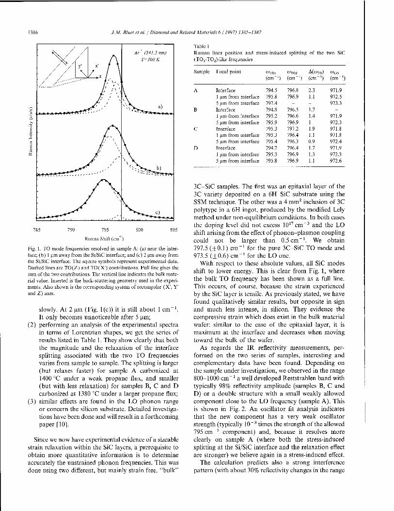
1386 J.M. Bluet et al. / Diamond and Related Materials 6 (1997) 1385-1387
Ar (541.5 nm) T=300K
Table 1 Raman lines position and stress-induced splitting of the two SiC (T01-T02)-like frequencies
785 790 795
Raman Shift (cm )
800 805
Fig. 1. TO mode frequencies resolved in sample A: (a) near the inter- face; (b) 1 um away from the Si/SiC interface; and (c) 2 urn away from the Si/SiC interface. The square symbols represent experimental data. Dashed lines are TO(Z) and TO(X') contributions. Full line gives the sum of the two contributions. The vertical line indicates the bulk mate- rial value. Inserted is the back-scattering geometry used in the experi- ments. Also shown is the corresponding system of rectangular (X', Y' and Z) axes.
slowly. At 2 \xm (Fig. 1(c)) it is still about 1 cm-1. It only becomes unnoticeable after 5 urn;
(2) performing an analysis of the experimental spectra in terms of Lorentzian shapes, we get the series of results listed in Table 1. They show clearly that both the magnitude and the relaxation of the interface splitting associated with the two TO frequencies varies from sample to sample. The splitting is larger (but relaxes faster) for sample A carbonized at 1400 °C under a weak propane flux, and smaller (but with less relaxation) for samples B, C and D carbonized at 1380 °C under a larger propane flux;
(3) similar effects are found in the LO phonon range or concern the silicon substrate. Detailed investiga- tions have been done and will result in a forthcoming paper [10].
Since we now have experimental evidence of a sizeable strain relaxation within the SiC layers, a prerequisite to obtain more quantitative information is to determine accurately the unstrained phonon frequencies. This was done using two different, but mainly strain free, "bulk"
Sample Focal point «TOl «"T02 A(coTO) «LO
(cm"1) (cm"1) (cm"1) (cm-1)
A Interface 794.5 796.8 2.3 971.9 1 urn from interface 795.8 796.9 1.1 972.5 5 urn from interface 797.4 - - 973.3
B Interface 794.8 796.5 1.7 - 1 um from interface 795.2 796.6 1.4 971.9 5 um from interface 795.9 796.9 1 972.3
C Interface 795.3 797.2 1.9 971.8 1 um from interface 795.3 796.4 1.1 971.8 5 urn from interface 795.4 796.3 0.9 972.4
D Interface 794.7 796.4 1.7 971.9 1 um from interface 795.3 796.9 1.3 972.3 5 urn from interface 795.8 796.9 1.1 972.6
3C-SiC samples. The first was an epitaxial layer of the 3C variety deposited on a 6H-SiC substrate using the SSM technique. The other was a 4 mm2 inclusion of 3C polytype in a 6H ingot, produced by the modified Lely method under non-equilibrium conditions. In both cases the doping level did not excess 1017cm~3 and the LO shift arising from the effect of phonon-plasmon coupling could not be larger than 0.5 cm"1. We obtain 797.5 (+0.1) cm-1 for the pure 3C-SiC TO mode and 973.5 (±0.6) cm-1 for the LO one.
With respect to these absolute values, all SiC modes shift to lower energy. This is clear from Fig. 1, where the bulk TO frequency has been shown as a full line. This occurs, of course, because the strain experienced by the SiC layer is tensile. As previously stated, we have found qualitatively similar results, but opposite in sign and much less intense, in silicon. They evidence the compressive strain which does exist in the bulk material wafer: similar to the case of the epitaxial layer, it is maximum at the interface and decreases when moving toward the bulk of the wafer.
As regards the IR reflectivity measurements, per- formed on the two series of samples, interesting and complementary data have been found. Depending on the sample under investigation, we observed in the range 800-1000 cm"1 a well developed Reststrahlen band with typically 98% reflectivity amplitude (samples B, C and D) or a double structure with a small weakly allowed component close to the LO frequency (sample A). This is shown in Fig. 2. An oscillator fit analysis indicates that the new component has a very weak oscillator strength (typically 10 "3 times the strength of the allowed 795 cm"1 component) and, because it resolves more clearly on sample A (where both the stress-induced splitting at the Si/SiC interface and the relaxation effect are stronger) we believe again in a stress-induced effect.
The calculation predicts also a strong interference pattern (with about 30% reflectivity changes in the range
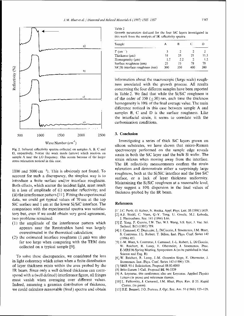
J. M. Bluet et al. / Diamond and Related Materials 6 (1997) 1385-1387 1387
SS
at
J] <
a)
b)
J] <=)
J" d)
500 1000 1500 2000
Wave Number (cm )
2500
Fig. 2. Infrared reflectivity spectra collected on samples A, B, C and D, respectively. Notice the weak mode (arrow) which resolves on sample A near the LO frequency. This occurs because of the larger stress relaxation noticed in this case.
1100 and 5000 cm ~l). This is obviously not found. To account for such a discrepancy, the simplest way is to introduce a finite surface and/or interface roughness. Both effects, which scatter the incident light, must result in a loss of amplitude of (i) specular reflectivity; and (ii) the interference pattern [11]. Fitting the experimental data, we could get typical values of 70 nm at the top SiC surface and 1 \xm at the lower Si/SiC interface. The comparison with the experimental spectra was satisfac- tory but, even if we could obtain very good agreement, two problems remained: (1) the amplitude of the interference pattern which
appears near the Reststrahlen band was largely overestimated in the theoretical calculation;
(2) the estimated interface roughness (1 |im) was also far too large when comparing with the TEM data collected on a typical sample [9].
To solve these discrepancies, we considered the loss in light coherency which arises when a finite distribution of layer thickness exists within the area probed by the IR beam. Since only a well defined thickness can corre- spond with a (well defined) interference figure, all fringes must vanish when averaging over different values. Indeed, assuming a gaussian distribution of thickness, we could calculate reasonable (final) spectra and obtain
Table 2 Growth parameters deduced for the four SiC layers investigated in this work from the analysis of IR reflectivity spectra
Sample B D
r(cm_1) Thickness (um) Homogeneity (um) Surface roughness (nm) SiC/Si interface roughness (nm) 300
3 2 2 2 18 25 21 11.3
1.5 2.2 2 1.2 25 75 78 70
350 400 300
information about the macroscopic (large scale) rough- ness associated with the growth process. All results concerning the four different samples have been reported in Table 2. We find that while the Si/SiC roughness is of the order of 350 (+ 50) nm, each time the thickness homogeneity is 10% of the final average value. The main difference noticed in this case between sample A and samples B, C and D is the surface roughness. Like the interfacial strain, it seems to correlate with the carbonization conditions.
3. Conclusion
Investigating a series of thick SiC layers grown on silicon substrates, we have shown that micro-Raman spectroscopy performed on the sample edge reveals strain in both the SiC layer and the bulk Si wafer. The strain relaxes when moving away from the interface. The IR reflectivity measurements confirm the strain relaxation and demonstrate either a surprisingly large roughness, both at the Si/SiC interface and the free SiC surface, or a lack of layer thickness uniformity. Maintaining the Si/SiC roughness at a reasonable level, they suggest a 10% dispersion in the final values of thickness probed by the IR beam.
References
[I] J.C. Pazik, G. Keiner, N. Bottka, Appl. Phys. Lett. 58 (1991) 1419. [2]A.J. Steckl, C. Yuan, Q.-Y. Tong, U. Gosele, M.J. Loboda,
J. Electrochem. Soc. 141 (1994) L66. [3] Z. Yang, F. Guarin, I.W. Tao, W.I. Wang, S.S. Iyer, J. Vac. Sei.
Technol. B13 (1995) 789. [4] J. Camassel, C. Dezauzier, L. DiCioccio, J. Stoemenos, J.M. Bluet,
S. Contreras, J.L. Robert, T. Billon, Inst. Phys. Conf. Series 142 (1996)453.
[5] J.-M. Bluet, S. Contreras, J. Camassel, J.-L. Robert, L. Di Cioccio, W. Reichert, R. Lossy, E. Obermeier, J. Stoemenos, Proc. E-MRS'96 Spring Meeting, Symposium A (to be published in Mat. Science and Eng. B)
[6] W. Reichert, R. Lossy, J.-M. Gonzales Sirgo, E. Obermeier, J. Stoemenos, Inst. Phys. Conf. Series 142 (1996) 129.
[7] SBIR 95-1 Solicitation, Proposal 08.02-6000 [8] Brite-Euram 3 Call, Proposal BE 96-3339 [9] A. Leycuras, this conference; also see: Leycuras, Applied Physics
Letters (in press) and references therein. [10] L. Falkovsky, J. Camassel, J.M. Bluet, Phys. Rev. B 55, Rapid
Comm. (in press). [II] H.E. Bennett, J.O. Porteus, J. Opt. Soc. Am. 51 (1960) 123-129.

ELSEVIER
DIAMOND AND
RELATED MATERIALS
Diamond and Related Materials 6 (1997) 1388-1391
Characterization of electrically active deep level defects in 4H and 6H SiC
J.P. Doylea'*, M.O. Aboelfotoh a, B.G. Svenssona, A. Schöner b, N. Nordeilb
* Royal Institute of Technology, Solid State Electronics, P.O. Box E229, S-164 40 Kista-Stockholm, Sweden b Industrial Microelectronics Center, P. O. Box 1084, S-164 21 Kista-Stockholm, Sweden
Abstract
Electrically active deep level defects have been characterized in n-type 6H- and 4H-SiC utilizing deep level transient spectroscopy (DLTS). In both polytypes, defects are observed in the as-grown state. In 6H-SiC two levels in the energy gap at 0.34 and 0.41 eV below the conduction band edge (Ec) are suggested as being intrinsic in nature as their concentration increases after 2 MeV electron irradiation. Additionally, a level 0.51 eV below Ec observed after electron or deuterium irradiation anneals out completely below 300 °C. In as-grown epitaxial layers of the 4H-SiC polytype, a level 0.70 eV below Ec is found with a capture cross-section of 4 x 10 "14 cm2 and a concentration at or below 1 x 10 13 cm ~3 exhibits acceptor-like behavior. Secondary ion mass spectrometry (SIMS) profiling reveals no evidence for Ti, V, or Cr incorporation into the epitaxial layers above «1013cm~3. © 1997 Elsevier Science S.A.
Keywords: Defects; SIMS; DLTS; Deep levels
1. Introduction
Defects and impurities in semiconducting materials can result in efficient recombination centers or carrier traps leading to a reduction in, for example, the carrier lifetime. The identification and control of as-grown defects becomes important as the elimination or control of these levels is required for device technology to progress. In this work, as-grown layers of both 6H and 4H polytypes were characterized through the use of deep level transient spectroscopy (DLTS), secondary ion mass spectrometry (SIMS), electron and ion beam irradiation, and thermal annealing in order to shed some light on the origin of these levels.
2. Experimental
Vapor phase epitaxy (VPE) was used to grow both 4H and 6H n-type epitaxial layers with doping concen- trations ranging from 1 x 10¹⁵ to 2 x 1016cm~3. In all cases the dopant was nitrogen. Characterization was performed on layers either grown by a previously described process [1,2] or on samples obtained from Cree Research Inc [3].
" Corresponding author.
Deep level transient spectroscopy measurements were conducted using rate windows ranging from (100ms)-1 to (3.2s)-1 in the temperature range 77-365 K. The experimental set-up has been previously described [4]. In the determination of the capture cross- section of the levels we assume a T2-correction to account for the temperature dependence of the effective density of states in the conduction band and the electron velocity.
Secondary ion mass spectroscopy measurements were performed using a Cameca IMS 4f microanalyzer utiliz- ing an O^ ion beam. Through the aid of ion implanted standards, we obtained sensitivities of <1014cm"3 for V and Ti and < 1013 cm"3 for Cr.
Electron irradiation was performed at room temper- ature with the samples held against a water-cooled block which kept them at a temperature below 30 °C The electron energy was 2 MeV with the dose in the range 1 x 10¹⁵ to 1 x 1016 cm"2. Annealing of the samples was conducted in a furnace continuously flushed with nitro- gen in the temperature range between 300 and 1000 °C
3. Results
As shown in Fig. 1, electron irradiation results in a number of electrically active deep levels which have been
0925-9635/97/S17.00 © 1997 Elsevier Science S.A. All rights reserved. PII S0925-9635(97)00102-7

J.P. Doyle et al. j Diamond and Related Materials 6 (1997) 1388-1391 1389
0.002
H Q
o
0.001
SiC-6H n-type Electron irradiated
— — -No anneal 800 C 1000 C
Ec-0.62 cV/ Ec-0.64 eV
2 10"
120 160 200 240 280
Temperature (K)
320 360
Fig. 1. DLTS spectra of electron irradiated SiC-6H n-type epitaxial layer. The doping concentration and electron dose were approximately 2 x 1016 cm"3 and 1 x 1016 cm-2, respectively, although in the case of the 1000 °C annealed sample the electron beam dose was somewhat higher. Maximum defect concentrations: 0.34 eV and 0.41 eV levels: 2.2xl014cm-3;0.51eV: 1.5 x 1014 cm-3; 0.62/0.64 eV: 8xl0I3cnr3.
reported previously [5,6]. However, after an 800 °C anneal for 30 min, a significant reduction in the levels at 0.62 eV (capture cross-section: lxl0~16cm2) and 0.64 eV (1 x 10~17 cm2) below the conduction band edge (Ec) is observed along with the complete removal of the Ec -0.51 eV (2xl0"14cm2) level. In addition, the Ec -0.34 eV (6xl0_16cm2) and Ec -0.41 eV (3 x 10 ~14 cm2) levels are also found to be reduced with the Ec — 0.34 eV level annealing at a faster rate. After a 1000 °C anneal we observe that the Ec —0.62 eV and Ec — 0.64 eV levels are completely annealed while the Ec — 0.34 eV and Ec —0.41 eV levels remain, with the Ec — 0.34eV level just visible as a kink on the low temperature side of the Ec —0.41 eV level. Note that the higher signal from these two levels is due to the slightly higher electron dose when compared with the as-grown and 800 °C conditions which were taken from the same sample. The result is consistent with that observed in as-grown material where only these lower energy levels remain as plotted in Fig. 2. Note that the spectra are identical except for the intensity of the peaks, a sign of the higher defect concentration in the electron beam irradiated sample even after the 1000 °C anneal.
As transition metals are ubiquitous to bulk grown samples especially Ti, Cr and V a SIMS analysis of a 6H-SiC epilayer is shown in Fig. 3. We find that the concentration of V and Ti is less than the detection limit which has been determined to be less than 1 x 1014 cm-3 while that for Cr is below lxlO13 cm-3.
The results of deuterium implantation shown in the DLTS spectra of Fig. 4 reveal the same basic trend as discussed earlier for electron irradiated samples. It should be noted that the damage introduced by the relatively moderate dose causes a significant amount of donor compensation which complicates the observability
H Q
o
1 10"
0 10"
/«
1 ' 1 ' i
SiC-6H n-type
'■\
-0.34 eV 1 \ / 1 E
1 c 0.41 eV --e-beam + 1000 C
\ 1 1
- \l
1 1
1 1 1
-
i : i : i :
1 -. 1 .1 -
t
i: A . ,-,v in — r~ r-0"J1","_". \t* ,
100 150 200 250 300 Temperature (K)
350
Fig. 2. A comparison of the as-grown (1.6 x 10¹³ cirT3) deep level defects and after a 1 x 1015 cm~2 electron irradiation dose and thermal annnealing (4xl013CffT3).
~ 1018 ,
s u 10 Fi 1016 o -J-» rt ■^-^
Ö 1014 o J-l rt u 4-) ri 1012 <u u C o u lOiu
6H-SiC n-type • Ti ■ V ♦ Cr
h^YSE25ffiäu£n*> i
0 2 4 6 8 10 12 Depth (microns)
Fig. 3. SIMS analyis for Ti, V, and Cr using 02+ ion sputtering.
H -J Q
SiC-6H n-type 300 keV Deuterium
0.12 _ lxl0"cm"2
E -0.41 eV / : ■ : 1 E -0.51 eV As-irradiated 1
^ E -0.34 eV / : | 300 C f c \ ' i 500 C i
\ Ml : / m u A
800 C J 0.08 -
E -0.62 eV/E -0.64 eV c c - *r \\ / \ /'~VK.
0.04 - ' *\ \ 1 l\ / '."-r.r.A :
- i /v--^,'/ . \ ; h»*~~J^<^ .,.""■-
100 150 200 250 300 Temperature (K)
350
Fig. 4. DLTS spectra after deuterium ion implantation and thermal annealing. Maximum defect concentrations: 0.34 eV: 1.7 x 1014cm-3; 0.41 eV: 2.5 x 1014cm"3; 1.6 x lO^cnT3; 0.62/0.64 eV: 1.4x 10I4crrT3.
of deep level traps especially at lower temperatures. Additionally, an accurate determination of the maxi- mum trap concentration is not possible as the compensa- tion does not allow us to fully probe the implantation end-of-range region where the highest concentration of defects are located. However, annealing at 300 °C results

1390 J.P. Doyle et al. / Diamond and Related Materials 6 (1997) 1388-1391
in a partial restoration of the lattice structure as reflected by the observability of all defect levels except for the level at Ec —0.51 eV which is completely eliminated. Additionally we observe a large decrease in the Ec
—0.62 eV and Ec —0.64eV levels. It should be noted that the increasing signal strength for the Ec — 0.34eV and Ec —0.41 eV levels is the result of a decreasing compensation of the donor levels as the crystal is annealed. Interestingly the compensation of the donor by deuterium implantation damage is found to be much greater in SiC than in Si for an equivalent dose and energy.
In 4H-SiC only a single level is observed at Ec
— 0.70 eV (4xl0_14cm2) in as-grown material with a concentration of «1 x 1013 cm-3. The level is observed to be acceptor-like from the lack of a Poole-Frenkel shift as the electric field is varied as shown in Fig. 5. Secondary ion mass spectrometry analysis was identical to that for the 6H epitaxial layer with Ti, V, and Cr below the detection limit shown in Fig. 3.
4. Discussion
The DLTS data on as-grown and irradiated SiC coupled with the SIMS analysis for the common bulk grown contaminants, provided strong evidence that the as-grown defects are not the result of metallic impurities but are intrinsic in nature (i.e. vacancies and/or Si and C interstitials and combinations thereof). Additionally, the annealing of 6H-SiC irradiated samples with the resulting decrease in the Ec — 0.51 eV, Ec — 0.62 eV, and Ec — 0.64eV levels is consistent with that usually observed in as-grown samples, that is only the Ec
—0.34eV and Ec —0.41 eV levels are present although the concentrations are typically in the low 1013cm~3
range. Early DLTS 6H-SiC studies of Lely grown bulk samples and epitaxial layers grown by LPE (liquid phase
epitaxy) reported the Ec — 0.62 eV and Ec —0.64eV levels (so-called XJZ2 centers) with the epitaxial layers requiring electron or ion irradiation in order to observe the level [5,7]. Unfortunately, there was no mention of a chemical characterization of these samples. The levels were also reported to have a thermal stability up to 1700 °C. The same levels observed in this work, however, are annealed out after a 1000 °C anneal for 30 min. One possible explanation is the presence of impurities in the sample with a position in the electronic bandgap near to the Zj/Z2 center. Recent work has shown that V incorporated into bulk grown samples introduces a level in the bandgap at Ec —0.66 eV, very near to the Zx/Z2
center [8]. In the case of 4H-SiC, our initial speculation for the
single level observed in as-grown material centered upon impurities. These are likely to be transition metals particularly in the recent work on the identification of a Cr deep level at Ec — 0.74eV through the use of radioactive ion implantation [9]. However, SIMS analy- sis revealed that the concentration of Cr in the epitaxial layers was below 1 x 1013cm~3, which is near to the measured defect concentration.
Additionally, after electron irradiation where two levels at Ec -0.62 eV (4 x 10"14 cm2) and Ec -0.68 eV (5xl0~15cm2) are produced [6], we find that the Ec
— 0.70 eV level evolves from these levels after low tem- perature thermal treatment. In contrast, Kimoto et al. [10] observed the levels at 0.62 and 0.68 eV in as-grown epitaxial layers. The transformation can occur at room temperature as well as after long periods of time. After the transformation, the Ec — 0.70 eV level is found to be stable. Although the origin of this effect is currently under more detailed study, it appears that carbon may be involved. In silicon, the high mobility of interstitial carbon can result in the formation of unstable electrically active defects at room temperature. The initial position of a deep level in the electronic bandgap associated with
0.0004
I SiC-4H n-type " as-grown E -0.70 eV c
/ \
- --5 V; 3V 15 V
Ö bO
c/5
H 1-1 Q
N 0.0002 : "c3 S i-i o
0 - «"T
i i *
—1-4 *-
240 260 280 300 320 Temperature (K)
Fig. 5. As-grown SiC-4H sample under differing electric fields. Concentration of the level was measured to be 1 x 1013 cm

J.P. Doyle et al. I Diamond and Related Materials 6 (1997) 1388-1391 1391
carbon is observed to decrease with the increasing concentration of a new level correlated to the decreasing level [11]. The new level produced in this transformation is also found to be stable.
5. Conclusion
In both 6H and 4H epitaxial layers in this study, the observed deep levels are found to be intrinsic defects (i.e. vacancies and/or interstitials and combinations thereof) and not the result of transition metal impurities of Ti, V, or Cr. The most stable defects are located in the electronic bandgap at Ec -0.34 eV and Ec -0.41 eV consistent with that observed in the as-grown state. The level at Ec —0.51 eV is found to anneal out completely at or below 300 °C while the defects at Ec -0.62 eV and Ec — 0.64eV are found to anneal out at or below 1000 °C. In 4H-SiC, the level at Ec -0.70 eV is found to be the most stable consistent with the as-grown case. The unstable nature of the Ec -0.62 eV and Ec -0.68 eV levels at room temperature may be related to carbon.
References
[1] N. Nordell, S.G. Andersson, A. Schöner, Inst. Phys. Conf. Series 142(1996)81.
[2] O. Kordina, C. Hallin, R.C. Glass, A. Henry, E. Janzen, Inst. Phys. Conf. Series 137 (1993) 41.
[3] Cree Research Inc. Meridian Parkway, Durham, N.C., USA [4] B.G. Svensson, K.H. Ryden, B.M.S. Lewerentz, J. Appl. Phys.
66(1989) 1699. [5] G. Pensl, W.J. Choyke, Phys. B 185 (1993) 264. [6] J.P. Doyle, M.O. Aboelfotoh, M.K. Linnarsson, B.G. Svensson,
A. Schöner, N. Nordell, C. Harris, J.L. Lindström, E. Janzen, C. Hemmingsson, Proceedings of the 1996 Spring MRS Meeting, San Francisco, CA (in press).
[7] H. Zhang, Ph.D. Thesis, Erlangen University, Germany, 1990. [8] J. Jenny, M. Skowronski, W.C. Mitchel, H.M. Hobgood, R.C.
Glass, G. Augustine, R.H. Hopkins, Appl. Phys. Lett. 68 (1996) 1963.
[9] N. Achtziger, W. Witthuhn, Proceedings of the E-MRS 1996 Spring Meeting, Session A (in press)
[10] T. Kimoto, A. Itoh, H. Matsunami, S. Sridhara, L.L. Clemen, R.P. Devaty, W.J. Choyke, T. Dalibor, C. Peppermuller, G. Pensl, Appl. Phys. Lett. 67 (1995) 2833.
[11] A.K. Tipping, R.C. Newman, Semicond. Sei. Technol. 2 (1987) 315.

ELSEVIER
DIAMOND AMD
RELATED MATERIALS
Diamond and Related Materials 6 (1997) 1392-1395
High field/high temperature performance of semi-insulating silicon carbide
T.S. Sudarshana-*, G. Gradinarua, G. Korony a, S.A. Gradinaru b, W. Mitchelc
"■ Department of Electrical and Computer Engineering, University of South Carolina, Columbia, SC 29208, USA b SC Governor's School for Science and Mathematics, Hartsville, SC 29550, USA
c WL/MLPO Bldg. 651, 3005 P St. Ste6, Wright-Patterson AFB, OH45433-7707, USA
Abstract
The influence of ambient temperature (295-730 K) and pulsed electric fields (0.5-80 kV/cm) on the electrical properties of high resistivity single-crystal 6H-SiC is reported. It is shown that the resistivity of the undoped 6H-SiC varies strongly, with the ambient temperature following a temperature/field function dominated by an exponential factor containing the activation (ionization) energy of residual boron of 0.35 eV. The dominant activation energy of semi-insulating Vanadium-compensated material (6H-SiC:V) varies with the ambient temperature, increasing from approx. 0 eV at 295-320 K to approx. 0.8 eV at T>600 K. This result can explain the viability of insulating 6H-SiC as a substrate for next-generation high temperature power microwave integrated circuits based on large bandgap semiconductors. © 1997 Elsevier Science S.A.
Keywords: Silicon carbide; Resistivity; Temperature; Electronic field
1. Introduction
Silicon carbide is a highly promising semiconductor material for high temperature (600-900 K) electronic applications [1-3]. Along with various electronic active devices, SiC is a serious contender as a semi-insulating or insulating substrate for next-generation high temperature/high power/high density microwave integ- rated circuits, based on large bandgap semiconductors (GaN and SiC). In the past few years high resistivity undoped and V-compensated single crystal 6H-SiC have been produced [4]. A severe limitation of these materials is the significant decrease of their electrical resistivity (p) with an increase in the ambient temperature (T) [4,5]. In the present work the electrical resistivity of 6H-SiC in measured directly in a pulsed regime in function of the applied field and ambient temperature.
2. Experimental
Three types of undoped 6H-SiC having the room temperature and low field resistivity (p0) of 1.1, 4.5, and
* Corresponding author. Fax: 1 803 777 8045; e-mail: [email protected]
27.5 kficm, and two types of 6H-SiC:V (p0= 165 kQcm and p0=10n-1012Qcm) were investigated using lateral MSM structures with a 0.64 mm gap and rounded NiCr/Au contacts (Fig. la). A resistive heater (Fig. lb) and a thermocouple control the device temperature. All tests were performed in vacuum (approx. 5x 10~4Pa). Simultaneous time-voltage [V(t)], current [I(t)], and light emission signal [VIS(t)] characteristics were obtained at different temperatures, starting with room temperature (T0 = 295K) with relatively small steps (10-20 K) up to approx. 730 K. The pulsed electric field was applied also in small steps (0.5-1 kV/cm) starting at approx. 0.5 kV/cm up to approx. 80 kV/cm, depending on the ambient temperature and maximum current density. Rectangular voltage pulses of approx. 2 jus duration were applied for semi-insulating and insulating 6H-SiC in order to separate the displacement current component from the total current.
3. Results
The I-V (peak-to-peak) and corresponding J-E char- acteristics at T=constant are fairly linear up to large fields for all undoped types of 6H-SiC and for the
0925-9635/97/S17.00 © 1997 Published by Elsevier Science S.A. All rights reserved. PII S0925-9635(97)00103-9
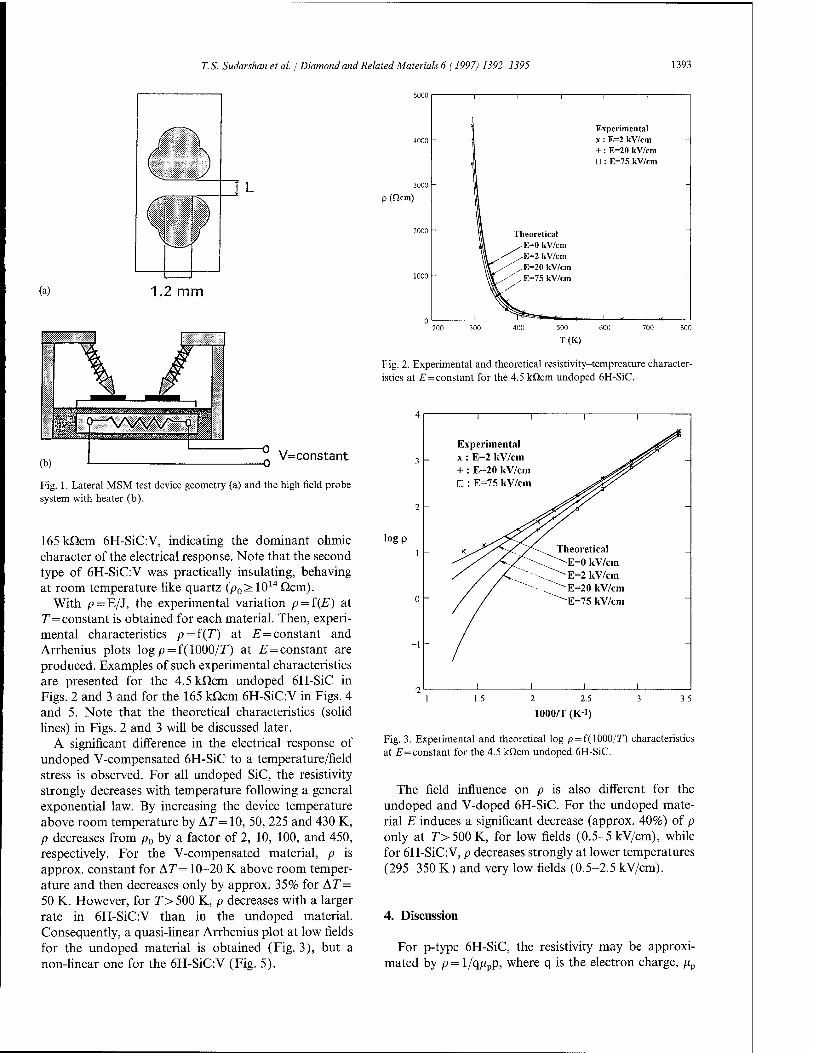
T. S. Sudarshan et al. / Diamond and Related Materials 6 (1997) 1392-1395 1393
(a) 1.2 mm
V=constant
Fig. 1. Lateral MSM test device geometry (a) and the high field probe system with heater (b).
165 kQcm 6H-SiC:V, indicating the dominant ohmic character of the electrical response. Note that the second type of 6H-SiC:V was practically insulating, behaving at room temperature like quartz (p0> 1014 Qcm).
With p = E/J, the experimental variation p = f(E) at T= constant is obtained for each material. Then, experi- mental characteristics p = i(T) at E=constant and Arrhenius plots logp = f(1000/T) at E=constant are produced. Examples of such experimental characteristics are presented for the 4.5 kQcm undoped 6H-SiC in Figs. 2 and 3 and for the 165 kQcm 6H-SiC:V in Figs. 4 and 5. Note that the theoretical characteristics (solid lines) in Figs. 2 and 3 will be discussed later.
A significant difference in the electrical response of undoped V-compensated 6H-SiC to a temperature/field stress is observed. For all undoped SiC, the resistivity strongly decreases with temperature following a general exponential law. By increasing the device temperature above room temperature by AT= 10, 50, 225 and 430 K, p decreases from p0 by a factor of 2, 10, 100, and 450, respectively. For the V-compensated material, p is approx. constant for AT= 10-20 K above room temper- ature and then decreases only by approx. 35% for AT= 50 K. However, for T> 500 K, p decreases with a larger rate in 6H-SiC:V than in the undoped material. Consequently, a quasi-linear Arrhenius plot at low fields for the undoped material is obtained (Fig. 3), but a non-linear one for the 6H-SiC:V (Fig. 5).
p (Hem)
Experimental x : E=2 kV/cm + : E=20 kV/cm D : E=75 kV/cm
Theoretical E=0 kV/cm E=2 kV/cm E=20 kV/cm E=75 kV/cm
500
T(K)
Fig. 2. Experimental and theoretical resistivity-tempreature character- istics at £=constant for the 4.5 kficm undoped 6H-SiC.
logp
1 1
Experimental
1 1
- x : E=2 kV/cm + : E=20 kV/cm
-
.
D : E=75 kV/cm
<^y^y^ /~~^- Theoretical ^~^E=0 kV/cm
/ /""^ ^-E=2 kV/cm ^^E=20 kV/cm ^^E=7S kV/cm
-
1 1 i i
-
1.5 2 2.5
1000/T (K-i)
3.5
Fig. 3. Experimental and theoretical log p = f(1000/r) characteristics at £=constant for the 4.5 kficm undoped 6H-SiC.
The field influence on p is also different for the undoped and V-doped 6H-SiC. For the undoped mate- rial E induces a significant decrease (approx. 40%) of p only at T>500K, for low fields (0.5-5 kV/cm), while for 6H-SiC:V, p decreases strongly at lower temperatures (295-350 K) and very low fields (0.5-2.5 kV/cm).
4. Discussion
For p-type 6H-SiC, the resistivity may be approxi- mated by p = 1/q/ipP, where q is the electron charge, ^p
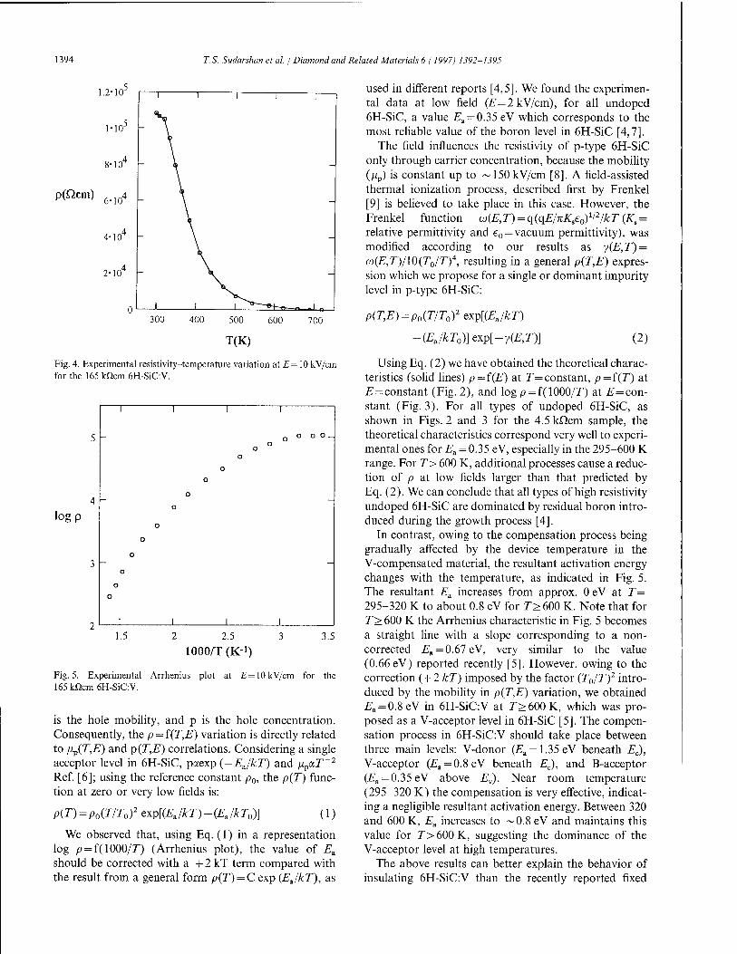
1394 T.S. Sudarshan et al. / Diamond and Related Materials 6 (1997) 1392-1395
1.2-10
p(ficm) 6-104
4-10 -
300 400 500
T(K)
600 700
Fig. 4. Experimental resistivity-temperature variation at E = 10 kV/cm for the 165kncm6H-SiC:V.
5 -
logp
2 2.5 3
1000/T (K-i)
Fig. 5. Experimental Arrhenius plot at £=10 kV/cm for the 165 kncm 6H-SiC:V.
is the hole mobility, and p is the hole concentration. Consequently, the p = f(T,E) variation is directly related to /ip(T,E) and p(T,E) correlations. Considering a single acceptor level in 6H-SiC, paexp (—EJkT) and npaT~2
Ref. [6]; using the reference constant p0, the p(T) func- tion at zero or very low fields is:
p(T) = Po(T/T0)2 cxp[(EJkT) -(EJkT0)] (1)
We observed that, using Eq. (1) in a representation log p = f(1000/r) (Arrhenius plot), the value of Et
should be corrected with a + 2 kT term compared with the result from a general form p(T) = C exp (EJkT), as
used in different reports [4,5]. We found the experimen- tal data at low field (ZT=2 kV/cm), for all undoped 6H-SiC, a value i?a = 0.35 eV which corresponds to the most reliable value of the boron level in 6H-SiC [4,7].
The field influences the resistivity of p-type 6H-SiC only through carrier concentration, because the mobility (/Up) is constant up to ~ 150 kV/cm [8]. A field-assisted thermal ionization process, described first by Frenkel [9] is believed to take place in this case. However, the Frenkel function oj(E,T) = q(qE/nKse0)ll2/kT (K,= relative permittivity and e0 = vacuum permittivity), was modified according to our results as y(E,T) = (ti(E,T)/\0(T0/T)4, resulting in a general p(T,E) expres- sion which we propose for a single or dominant impurity level in p-type 6H-SiC:
p(T,E) = p0(T/T0)2exp[(EJkT)
-(EJkT0)]exp[-y(E,T)] (2)
Using Eq. (2) we have obtained the theoretical charac- teristics (solid lines) p = f(E) at T= constant, p = f(T) at E=constant (Fig. 2), and log p = f(1000/T) at E=con- stant (Fig. 3). For all types of undoped 6H-SiC, as shown in Figs. 2 and 3 for the 4.5 kQcm sample, the theoretical characteristics correspond very well to experi- mental ones for 2sa = 0.35 eV, especially in the 295-600 K range. For T> 600 K, additional processes cause a reduc- tion of p at low fields larger than that predicted by Eq. (2). We can conclude that all types of high resistivity undoped 6H-SiC are dominated by residual boron intro- duced during the growth process [4].
In contrast, owing to the compensation process being gradually affected by the device temperature in the V-compensated material, the resultant activation energy changes with the temperature, as indicated in Fig. 5. The resultant Et increases from approx. 0 eV at T= 295-320 K to about 0.8 eV for 7>600 K. Note that for T> 600 K the Arrhenius characteristic in Fig. 5 becomes a straight line with a slope corresponding to a non- corrected £"a = 0.67eV, very similar to the value (0.66 eV) reported recently [5]. However, owing to the correction (+2 kT) imposed by the factor (TJT)2 intro- duced by the mobility in p(T,E) variation, we obtained £, = 0.8 eV in 6H-SiC:V at T>600K, which was pro- posed as a V-acceptor level in 6H-SiC [5]. The compen- sation process in 6H-SiC:V should take place between three main levels: V-donor (£'a = 1.35eV beneath Ec), V-acceptor (isa = 0.8eV beneath Ec), and B-acceptor (i?a = 0.35eV above Ey). Near room temperature (295-320 K) the compensation is very effective, indicat- ing a negligible resultant activation energy. Between 320 and 600 K, £a increases to ~0.8 eV and maintains this value for T> 600 K, suggesting the dominance of the V-acceptor level at high temperatures.
The above results can better explain the behavior of insulating 6H-SiC:V than the recently reported fixed
T.S. Sudarshan et al. / Diamond and Related Materials 6 (1997) 1392-1395 1395
£a values (1.48 or 0.66eV) [4,5]. In lateral MSM structures, considering our current sensitivity (~20 (iA), the material resistivity exceeds 108 Qcm for large ambi- ent temperatures (r=700K) and applied fields (E= 80 kV/cm). As shown in Fig. 5, a variable £a may result in a reduction of p by only about 103 between 295 and 700 K, leading to a p0 = 10n-1012 Qcm of the insulating material, more acceptable than p>1015Qcm required by a fixed Ea [4]. However, in vertical 6H-SiC:V MSM devices, at room temperature and moderate fields (20-50 kV/cm), p decreases to ~ 107 Qcm, indicating a large increase in the current density. We believe that this process is due to the presence of micropipes in the material, which activate easily in parallel fields (vertical devices), but are insensitive to perpendicular fields (lat- eral devices) [10].
resistivity at high ambient temperatures. The results of lateral MSM devices, with no micropipe activation at high temperatures and high fields, prove the viability of insulating 6H-SiC:V for high temperature power micro- wave integrated circuits based on large bandgap semiconductors.
Acknowledgement
We are grateful to Dr Dwight Duston and Dr Kepi Wu of BMDO/TRI for their encouragement and support of this research.
References
5. Conclusions
The strong influence of the ambient temperature and the applied electric field on the electrical resistivity of undoped and V-compensated 6H-SiC was demonstrated by direct measurements of the resistivity in lateral MSM devices in pulsed regime. The resistivity variation of the undoped 6H-SiC with ambient temperature is mainly dominated by the boron acceptor level, with £■3 = 0.35 eV making it impractical for high temperature microwave integrated circuits. The field influence was well described for the undoped material by a modified Frenkel function. A clear variation of the activation energy with the ambient temperature was observed in the V-compensated material, resulting in very large
[1] R.F. Davis, G. Keiner, M. Shur, J.M. Palmour, J.A. Edmond, Proceedings IEEE 79 (1991) 677.
[2] M. Bhatnagar, B.J. Baliga, IEEE Trans. Electron Devices 40 (1993)645.
[3] M. Shur, B. Gelmont, C. Saavedra-Munoz, G. Keiner, Inst. Phys. Conf. Ser. No. 137 (1993) 465-470.
[4] H.M. Hobgood, R.C. Glass, G. Augustine, R.H. Hopkins, J.R. Jenny, M. Skowronski, W.C. Mitchel, M. Roth, Appl. Phys. Lett. 66(1995) 1364.
[5] J.R. Jenny, J. Skowronski, W.C. Mitchel, H.M. Hobgood, R.C. Glass, G. Augustine, R.H. Hopkins, Appl. Phys. Lett. 68 (1996) 1963.
[6] M. Yamanaka, H. Daimon, E. Sakuma, S. Mishawa, S. Yoshida, J. Appl. Phys. 61 (1987) 599.
[7] W. Suttrop, G. Pensl, P. Lanig, Appl. Phys. A 51 (1990) 231. [8] R.J. Trew, J.-B. Yan, P. Mock, Proceedings IEEE 79 (1991) 598. [9] J. Frenkel, Tech. Phys. (USSR) 5, 685 (1938) and Phys. Rev. 54
(1938) 647. [10] T.S. Sudarshan, G. Gradinaru, G. Korony, W.C. Mitchel, R.H.
Hopkins, J. Electr. Mat. 25 (1996) 893.
1: ■' >' _■■■ DIAMOND AND
RELATED MATERIALS
ELSEVIER Diamond and Related Materials 6 (1997) 1396-1399
OBIC studies on 6H-SiC Schottky rectifiers with different surface pretreatments
Manfred Frischholz a'*, Kurt Rottner a, Adolf Schöner a, Thomas Dalibor b, Gerhard Pensl 1 IMC, P.O. Box 1084, S-16425 Stockholm-Kista, Sweden
b Lehrstuhl für Angewandte Physik, Universität Erlangen-Nürnberg, D-91058 Erlangen, Germary
Abstract
The influence of different surface treatments on the device characteristics of Schottky rectifiers was investigated. Prior to the formation of Schottky barrier contacts the SiC surface was either thermally annealed in hydrogen, etched using 02 or CF4/Ar/H2 as reactive gases or Ar sputtered. Differences in reverse current densities of several orders of magnitude for different surface treatments were observed. The effective device area was determined by the optical beam induced current (OBIC) technique. The results confirm that the effective device area is given by the area of the metal contact and the additional area of the surface charge induced depletion layer. Our results indicate the importance of an optimized surface treatment in order to control the quality and the area of the surface region for achieving optimum device performance. © 1997 Elsevier Science S.A.
Keywords: OBIC; Schottky contacts; Surface pretreatment; 6H-SiC
1. Introduction
The high breakdown electric field strength of SiC makes it one of the most promising candidates to replace silicon in power semiconductor applications. However, in order to utilize the advantage in electric field strength over other materials a proper design of the junction termination is crucial to reduce the surface electric field to prevent premature breakdown at the surface and to be able to use established passivation schemes developed for silicon power devices.
Experimentally observed breakdown voltage of SiC rectifiers exceed the value predicted by 2-D numerical device simulations and approach the value of the parallel plane case for both, SiC p-n mesa diodes [1] and Schottky diodes [2]. In these previous studies the authors found evidence for negative surface charge on n-type and positive surface charge on p-type 6H-SiC, respec- tively. The surface charge led to a significantly increased lateral depletion layer width which was mapped using optical beam induced current (OBIC: the abbreviation will be used throughout the text for both the method and the photocurrent as long as it is clear from the context). The increase of the surface depletion layer
' Corresponding author. Tel: +46 8 752 1061; Fax: +46 8 750 5430.
width causes a reduction in the surface electric field thus increasing the breakdown voltage. This was observed on as-grown and processed surfaces as well, however, differently pronounced. The presence of surface charge has a large impact on the design of any junction termination. Therefore it is important to obtain a com- prehensive understanding of the mechanism by which the surface charge is formed and its process dependence. Using Schottky contacts instead of p-n mesa diodes for the present study made it possible to study as-grown SiC surfaces and to study the influence of typical pro- cesses used in device processing. In this work we concen- trated on studying the influence of different surface treatments on the device characteristics of Schottky rectifiers in order to be able to control the surface charge density.
2. Experimental procedures
Commercially available n-type 6H SiC substrates (3.5° off-oriented) with a doping concentration of 7xl017cm~3 from Cree Inc. were used. CVD layers (n-type, 5 x 1015 cm"3, 10 urn) were grown on the Si face.
The SiC surface was then exposed to four different processes: (1) thermally annealed in hydrogen at atmo-
0925-9635/97/S17.00 © 1997 Elsevier Science S.A. All rights reserved. PII S0925-9635(97)00111-8

M. Frischholz et al. / Diamond and Related Materials 6 (1997) 1396-1399 1397
spheric pressure at 1500 °C; (2) plasma etched, using 02 (50 seem, 700 mTorr, 200 W); (3) RIE etched using a CF4/Ar/H2 (50/5/5 seem, 15 mTorr, 100 W); (4) sput- tered with Ar (ion current density: 0.5 mA cm"2, ion energy: 100 eV). The process time was 15 min for all processes (in the following the samples will be referred to as H, O, RIE and Ar sample, respectively).
Prior to the formation of Schottky contacts the samples were cleaned and residual oxide was removed by an HF etch. Schottky contacts were formed by thermal evaporation of Au using a shadow mask (0 = 0.2 mm) at a background pressure of 2xl0~7mbar. For the large area ohmic backside contact Al was deposited by electron-beam evaporation. The devices were characterized by current-voltage measurements and OBIC.
The OBIC technique is a method to study surface electric fields in power devices, as first demonstrated by Lindsay [3] in 1979. The technique involves measuring the current caused by a light beam focused onto the sample. If the energy of the light used for illumination is larger than the bandgap of the material electron-hole pairs are generated within the sample. In the presence of an electric field electrons and holes are separated before they can recombine and result in a current flow through the device. By measuring the spatial variation of the photocurrent a mapping of the depletion layer can be accomplished. A schematic view of the set-up is shown in Fig. 1. Because of the band gap of SiC we used monochromatic light from a 100 W mercury arc lamp in combination with interference filters (bandwidth 5 nm) for the UV mercury spectral lines. The plasma arc spot of the mercury lamp is imaged onto a pinhole aperture. The aperture acts as a well defined point light
source which is then reimaged onto the sample surface using a microscope with a long working distance objec- tive. The spot size achieved with our set-up is approxi- mately 15 um in diameter. The penetration depth (1/a, with the absorption coefficient a) in 6H-SiC is about 14 |xm for 3.4 eV photons [4]. A lock-in technique was used in order to separate the photocurrent from the dark current and for increased sensitivity. The light beam was mechanically chopped (/=70Hz). A more detailed description of the set-up can be found in [5].
3. Experimental results
3.1. Electrical measurements
The current-voltage characteristics of the Schottky diodes for different surface treatments are shown in Fig. 2. Differences in reverse current densities of several orders of magnitude are observed for different surface treatments indicating a large influence of surface treat- ment on the electrical characteristics of devices. The lowest current is observed for the O sample. Uniformity of current-voltage characteristics over as-grown samples is poor (two contacts denoted as #1 and #4 in Fig. 2). A similar non-uniform behavior is found for the hydrogen annealed sample, while the characteristics of the O, RIE and the Ar samples are uniform over the samples.
3.2. Optical beam induced current (OBIC) measurements
Using the OBIC technique for spatially resolved meas- urements of the photocurrent we determined the effective
mercury arc lamp
interference filter
A
aperture
ocular
reference
x-y stage
OBIC signal current-voltage-converter
Fig. 1. Schematic view of the OBIC set-up.

1398 M. Frischholz et cd. I Diamond and Related Materials 6 (1997) 1396-1399
10"
10":
< E
■g 10-3
CD L. i. 3 Ü
CD > CD a.
10"!
10(
- — ■—__
as-grown #1 ~ ̂ \
as-grown "~~- - \^ / #4
==:^u=^--T-<r Ar
RIE^
7\ H2
\ \ \ \ I \ \
V \
r^-_
: ^^-< /02 Ax
r ^\^ \
: T = 300K "^x
d = 0.2mm \ - ,,,,!., , , i , , ,
-100 -80 -60 -40
Voltage (V)
-20
Fig. 2. Reverse current as a function of voltage for different surface treatments. The as-grown sample shows a non-uniform behavior of the contacts over the sample area (indicated by the two contacts #1 and #4), also the H2 annealed sample (not shown here), while for the other samples all the contacts showed the same behavior.
area contributing to the electrical characteristics of the device. To account for non-symmetric behavior four line scans per contact in different directions (as shown in Fig. 3(a)) were used for the evaluation. The slope of the OBIC was extrapolated to the noise level on each side of the contact to determine the diameter of the surface depletion layer. Fig. 3 illustrates this procedure: a gray- scale encoded OBIC map for the RIE sample is shown in Fig. 3(a); the contact area and dashed lines represent-
ing the line scans are superimposed. Fig. 3(b) shows the corresponding OBIC profiles. The decrease of the OBIC in the center of the diode is due to the opaque metal contact. Current suppression there is incomplete owing to light reflected from the microscope objective reaching the surface field region at the contact edge. For each of the samples several contacts were evaluated except for the H sample, where high leakage currents prevented OBIC measurements on most of the contacts. Diameters obtained from these profiles are summarized in Table 1. For all surface treatments we observe a very large depletion layer width along the surface. The as-grown sample shows the largest spread of the diameter as can be seen from the larger standard deviation. As it has already been in the case in the reverse characteristic of the Schottky diodes (Fig. 2) Ar and RIE samples show little difference. The O sample has approximately the same surface depletion layer width as the RIE and Ar samples.
The behavior of the surface depletion layer width for different surface treatments is also reflected in the maxi- mum photocurrent observed on the samples, as seen in Table 1. Remarkably the O sample lies closer to the as-grown and H sample than to the RIE or Ar samples. If grouped in the two groups as suggested by this finding, the surface depletion width and maximum photocurrent show the same general trend.
4. Discussion
The results of our measurements show a large influ- ence of the surface preparation on the reverse character- istics of Schottky contacts where the currents vary over three orders of magnitude for different surface prepara-
line scan 10-1
max.
< O 10"11
CQ O
mm.
io-12
-400 -200 0 200
Distance from Center
400
Fig. 3. Illustration of the procedure to extract the diameter of the surface depletion region from the OBIC measurement, (a) OBIC image of RIE- etched sample (wavelength 365 nm, bias voltage 1 V), superimposed is the contact area and the four line scans used for the extraction procedure, (b) OBIC as a function of the distance from the center of the contact.

M. Frischholzetal. / Diamond and Related Materials 6 (1997) 1396-1399 1399
Table 1 Summary of OBIC results: diameters of the surface depletion region—the division in groups I and II is explained in the text—and the maximum optical beam induced current for the different processes
I II
as-grown 02 etched H2 annealed Ar sputtered RIE etched
Diameter (um) Max. OBIC (pA)
632 ±41 0.92
505 ±22 0.37
450 ±4 0.17
503 ±18 102
490+13 51
tion processes. Samples with lower reverse currents show also a higher OBIC.
On all samples large surface depletion layer widths were observed. Without assuming the presence of surface charge depletion layer widths calculated for a Schottky contact at the corresponding voltage are considerably smaller than those observed experimentally. The diffu- sion length in SiC (typically less than a few um) is too small to account for the observed depletion layer widths and its influence can be neglected for this consideration.
These data are, however, in agreement with previous results on Schottky diodes and mesa p-n junction diodes [1,2], where it was concluded that surface charges are responsible for the observed enlarged depletion layer width. From the value of the breakdown voltage we estimated a surface charge density in the range of 3 x 10¹²-1 x 1013 cm"2 [2]. For the present study we have chosen a relatively high doping concentration in order to minimize the influence of the increased depletion layer area on the reverse current of Schottky diodes, since a previous study has shown that for samples with low doping concentrations the lateral increase in deple- tion layer width was so pronounced that it caused an interconnection of several Schottky diodes on the sample and thus made it impossible to characterize individual devices without significant contributions from neighbor- ing devices [1].
The observed difference in surface depletion width implies that the effective device area is given by the area of the metal contact alone and by the additional deple- tion layer area its size strongly depending on the surface treatment. As is evident from our data the quality of
the surface region determines the reverse characteristic of the Schottky diodes. Considering the additional con- tribution from the adjacent surface region to the device characteristic it is even more fundamental to find an appropriate surface treatment for optimum device per- formance. Using plasma assisted etch processes, e.g. RIE, 02 or Ar-sputter etching, the reverse current of Schottky diodes is reduced by 1-2 orders of magnitude as compared to diodes prepared on as-grown and hydrogen-annealed surfaces, respectively.
Acknowledgement
The authors gratefully acknowledge financial support by Asea Brown Boveri and the Swedish National Board for Industrial and Technical Development (NUTEK).
References
[1] K. Rottner, A. Schöner, M. Frischholz, R. Helbig, MRS Spring Meeting, San Francisco, 1996, MRS Symp. Proc. Series., Vol. 423, in press.
[2] K. Rottner, S. Savage, J. Andre, L. Ramberg, M. Frischholz, R. Helbig, in Silicon Carbide and Related Materials 1995, Proc. 6th Int. Conf. on Silicon Carbide and Related Materials 1995, Kyoto, Japan, S. Nakashima, H. Matsunami, S. Yoshida, H. Harima (Eds.), Inst. Phys. Conf. Ser. No. 142, Bristol and Philadel- phia, 1996, p. 721.
[3] S.M. Lindsay, Phys. Stat. Sol. A 53 (1979) 311. [4] W.J. Choyke, L. Patrick, Phys. Rev. 172 (1968) 769. [5] M. Frischholz, Th. Mandel, R. Helbig, A. Hammerschmidt,
G. Schmidt, Appl. Surf. Sei. 65-66 (1993) 784.
ELSEVIER Diamond and Related Materials 6 (1997) 1400-1404
DIAMOND AND
RELATED MATERIALS
SiC device technology: remaining issues
J.W. Palmour *, L.A. Lipkin, R. Singh, D.B. Slater, Jr, A.V. Suvorov, C.H. Carter, Jr Cree Research, Inc., 4022 Stirrup Creek Drive, Suite 322, Durham, NC27703, USA
Abstract
Some of the key remaining issues facing SiC device technology for power devices and high temperature devices are discussed. Research on improving the oxide/SiC interface quality has shown that a low temperature re-oxidation step yields interface trap densities of 1 x 1011 cm~2eV_1, resulting in a high SiC MOSFET channel mobility of 72 cm2/V-sec. Device lifetimes for SiC n-channel MOSFETs have been increased to as much as 5 years at 350 °C, and time-dependent dielectric breakdown of oxides on p-type SiC have lifetimes >700 years at 2 MV/cm and 350 °C. Sheet resistivities for p+ of <10kfl/sq. and p-type contact resistivities less than 10~5ß-cm2 have been obtained using high temperature Al+ ion implantation processes. These processes have been used to fabricate the first SiC CMOS circuits, with an operational amplifier having a gain >105. High voltage termination techniques have improved Schottky diode yield, as well as that of mesa devices such as 4.2 kW, 700 V thyristors. The defect densities of SiC substrates has also been improved, with recent 4H-SiC wafers having a micropipe density of 1.8 cm"2. © 1997 Elsevier Science S.A.
Keywords: Oxide interface; SiC; Micropipes; Schottky diodes; Ion implantation; Thyristors; CMOS
1. Introduction
Silicon carbide technology has made tremendous strides in the last 5-7 years, with a variety of encouraging device and circuit demonstrations. The commercial availability of relatively large, high quality wafers of the 6H and 4H polytypes of SiC for device development has facilitated these exciting breakthroughs in laborato- ries throughout the world. These have occurred in numerous application areas, including high power devices, high temperature devices, and high power/high frequency devices. However, there are still a number of factors that are limiting the commercialization of devices in these areas. Some of the areas receiving the most attention currently are insulator/SiC interface quality, high temperature reliability, high voltage terminations, and ion implantation. Another area of major concern is the micropipe defect density in the SiC wafers, particu- larly for those interested in making high power vertical devices. This paper discusses efforts in these areas and the impact of the processes on the devices of interest.
* Corresponding author. Tel: 1 (919) 361-4770; Fax: 1 (919) 361-2266; e-mail: [email protected]
2. Oxide quality and reliability
One of the biggest advantages of SiC over other wide bandgap materials is the ability to grow a thermal oxide, as in the case of silicon. However, there is still much improvement required in the interface quality of thermal oxides grown on SiC before its full potential can be exploited. In particular, high interface trap densities (Dit) on p-type SiC, result in low channel mobilities for SiC n-channel MOSFETs. However, it has recently been demonstrated that thermal oxides grown on p-type 6H-SiC were significantly improved with a combination of low oxidation temperature (1050 °C) followed by a 950 °C re-oxidation anneal. Experimental results have shown that the interface state densities decreased with decreasing wet oxidation temperature, as shown in Fig. 1. By growing the bulk of the oxide at low temper- ature, and then finishing the growth in wet 02 at a still lower temperature, even further improvement can be made. Fig. 2 shows the effect of this "re-oxidation" annealing on oxide layers grown at 1050 °C in wet 02. Using this process, interface state densities of 1.0 x 1011 cm~2eV-1 have been achieved [1]. This improved process produced the highest SiC surface channel mobility, 72 cm2/V-s, reported to date for 6H-SiC MOSFETs. It is believed that further reductions
0925-9635/97/S17.00 © 1997 Elsevier Science S.A. All rights reserved. PII S0925-9635(97)00118-0

/. W. Palmour et cd. / Diamond and Related Materials 6 (1997) 1400-1404 1401
10 13
C
Q
10 12 .
10 '
-D- -D
Qox (cm-2)
Dit (cm-2/eV)
1000 1100 1200
Oxidation (°C) 1300
Fig. 1. Net oxide charge and interface state densities for samples oxi- dized in wet 02 across the usable temperature range.
4.0e+ll
!p 3.5e+ll
o 3.0e+ll
No Anneal o 1.5 hour ■ 3 hour
- A 5 hour
- 2 ■ - ■
< ■
■55 2.5e+ll a
^ 2.0e+ll
&> 1.5e+ll u ^ 1.0e+ll s c
M 5.0e+10 900 950 1000
Re-Oxidation Temperature (°C)
Fig. 2. Comparison of the interface state densities on oxides grown in wet 02 at 1050 °C then re-oxidized in wet 02 at 900, 950 or 1000 °C.
in Dit as well as the oxide charge (Qox) by about a factor of 5 must be achieved to make these devices commer- cially viable.
Oxide reliability is another area of concern for SiC devices. At high fields and high temperatures, Si02
layers have been reported to have poor lifetimes [2]. However, recent work has begun to show some promise. As oxide quality and device processing techniques improve, the lifetimes have been significantly increased. Time-dependent dielectric breakdown (TDDB) results indicate that thermal oxides grown on p-type SiC have lifetimes as high as 700 years at 2 MV/cm and 350 °C, as shown in Fig. 3 [3]. However, samples fabricated on heavily doped material demonstrate a reduced high temperature lifetime. Additionally, TDDB data on Si02 on n-type SiC show much worse lifetimes, indicat- ing an area of concern to be studied more thoroughly [2]. Device lifetimes measured on n-channel MOSFETs
o H
10
10 10
10
10
10 10
10
10 10
10 10
10
350°CSlope=1.2 250°C Slope =1.0
i i i i i_
0123456789 10 11 Field (MV/cm)
Fig. 3. TDDB data on MOS capacitors on p-type 6H-SiC oxidized in wet O, at 1150 °C.
have also shown a large increase, with devices operating in air at 350 °C for >70 h without failure. The projected lifetime for these n-channel MOSFETs is about 5 years at 350 °C, and is projected to be even longer for p-channel MOSFETs.
3. Ion implantation processes
The area of ion implantation of dopants into SiC has also begun to receive increased attention because of its importance to power devices and high temperature circuits. Reliable, low resistance N+ implants seem to be relatively easily attained through the use of high temperature implantation (500-800 °C) followed by high temperature annealing (1500 °C) [4]. While the N+ results have been encouraging, reliable processes for Al+ for p-type ion implantation have been more difficult to obtain. The best results reported to date have followed the same high temperature trends as was seen for N+ implantation, although it appears that even higher implantation and annealing temperatures are required [5]. Implantation temperatures in the range of 500-1000 °C and annealing temperatures in the range of 1000-1650 °C have been successfully used [6,7]. Recent efforts at Cree with similar conditions have resulted in significant increases in the dopant activation and reduction of sheet resistivities of Al+ implanted layers. Sheet resistivities less than 10 kQ/sq. and p-type contact resistivities less than 10~5 Q-cm2 have been obtained for Al implants into n-type 6H-SiC.
As a demonstration of the benefit of ion implantation processes in SiC, we have fabricated the first CMOS circuits reported in SiC [8], using 6H-SiC enhancement- mode MOSFETs. The n-channel MOSFET devices were fabricated in a lightly doped p-type epitaxial layer,
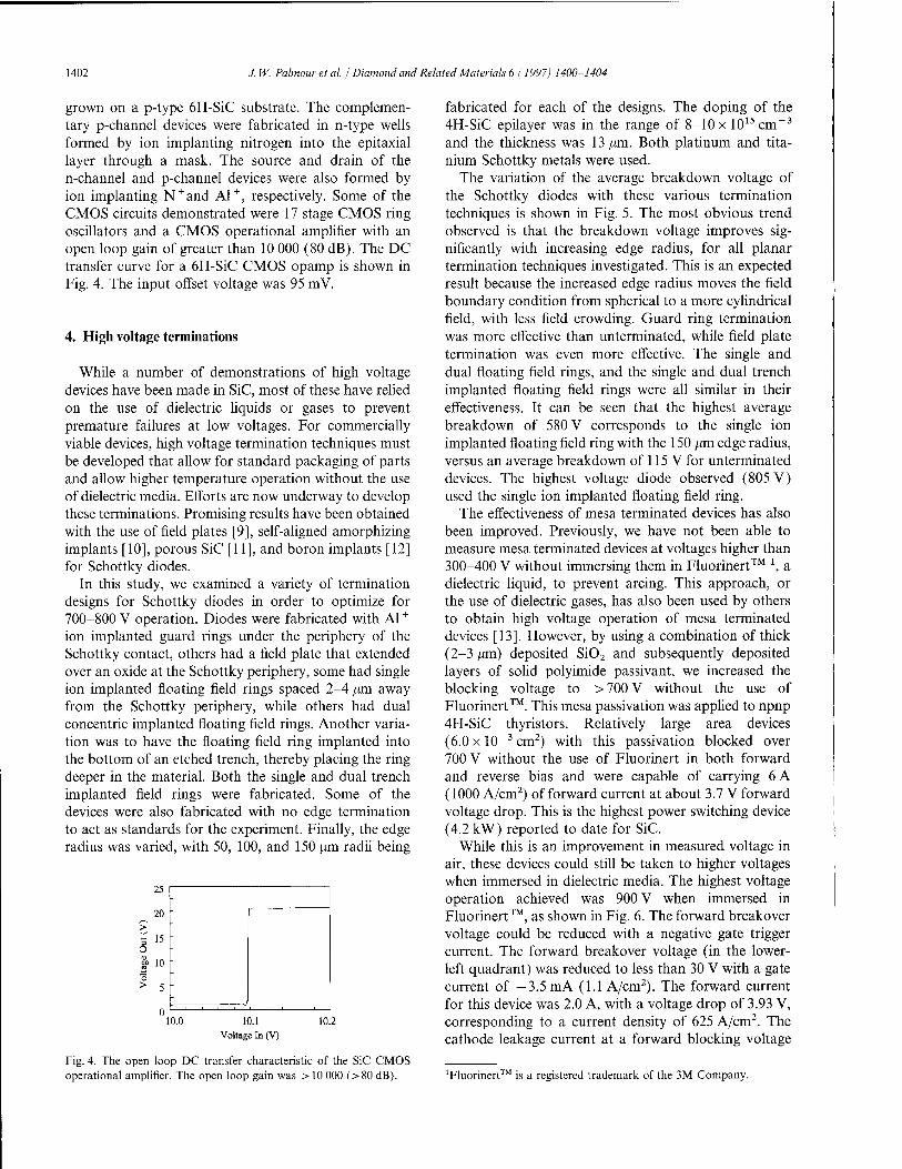
1402 J. W. Palmour el al. / Diamond and Related Materials 6 (1997) 1400-1404
grown on a p-type 6H-SiC substrate. The complemen- tary p-channel devices were fabricated in n-type wells formed by ion implanting nitrogen into the epitaxial layer through a mask. The source and drain of the n-channel and p-channel devices were also formed by ion implanting N+and Al + , respectively. Some of the CMOS circuits demonstrated were 17 stage CMOS ring oscillators and a CMOS operational amplifier with an open loop gain of greater than 10 000 (80 dB). The DC transfer curve for a 6H-SiC CMOS opamp is shown in Fig. 4. The input offset voltage was 95 mV.
4. High voltage terminations
While a number of demonstrations of high voltage devices have been made in SiC, most of these have relied on the use of dielectric liquids or gases to prevent premature failures at low voltages. For commercially viable devices, high voltage termination techniques must be developed that allow for standard packaging of parts and allow higher temperature operation without the use of dielectric media. Efforts are now underway to develop these terminations. Promising results have been obtained with the use of field plates [9], self-aligned amorphizing implants [10], porous SiC [11], and boron implants [12] for Schottky diodes.
In this study, we examined a variety of termination designs for Schottky diodes in order to optimize for 700-800 V operation. Diodes were fabricated with Al+
ion implanted guard rings under the periphery of the Schottky contact, others had a field plate that extended over an oxide at the Schottky periphery, some had single ion implanted floating field rings spaced 2-4 /mi away from the Schottky periphery, while others had dual concentric implanted floating field rings. Another varia- tion was to have the floating field ring implanted into the bottom of an etched trench, thereby placing the ring deeper in the material. Both the single and dual trench implanted field rings were fabricated. Some of the devices were also fabricated with no edge termination to act as standards for the experiment. Finally, the edge radius was varied, with 50, 100, and 150 |im radii being
25
20
> ¥ 15 O g> 10
10.0
J
10.1 Voltage In (V)
10.2
fabricated for each of the designs. The doping of the 4H-SiC epilayer was in the range of 8-10 x 1015 cm~3
and the thickness was 13 /mi. Both platinum and tita- nium Schottky metals were used.
The variation of the average breakdown voltage of the Schottky diodes with these various termination techniques is shown in Fig. 5. The most obvious trend observed is that the breakdown voltage improves sig- nificantly with increasing edge radius, for all planar termination techniques investigated. This is an expected result because the increased edge radius moves the field boundary condition from spherical to a more cylindrical field, with less field crowding. Guard ring termination was more effective than unterminated, while field plate termination was even more effective. The single and dual floating field rings, and the single and dual trench implanted floating field rings were all similar in their effectiveness. It can be seen that the highest average breakdown of 580 V corresponds to the single ion implanted floating field ring with the 150 /mi edge radius, versus an average breakdown of 115 V for unterminated devices. The highest voltage diode observed (805 V) used the single ion implanted floating field ring.
The effectiveness of mesa terminated devices has also been improved. Previously, we have not been able to measure mesa terminated devices at voltages higher than 300-400 V without immersing them in Fluorinert™ 1, a dielectric liquid, to prevent arcing. This approach, or the use of dielectric gases, has also been used by others to obtain high voltage operation of mesa terminated devices [13]. However, by using a combination of thick (2-3 jj.ro) deposited Si02 and subsequently deposited layers of solid polyimide passivant, we increased the blocking voltage to > 700 V without the use of Fluorinert™. This mesa passivation was applied to npnp 4H-SiC thyristors. Relatively large area devices (6.0 x 10~3 cm2) with this passivation blocked over 700 V without the use of Fluorinert in both forward and reverse bias and were capable of carrying 6 A (1000 A/cm2) of forward current at about 3.7 V forward voltage drop. This is the highest power switching device (4.2 kW) reported to date for SiC.
While this is an improvement in measured voltage in air, these devices could still be taken to higher voltages when immersed in dielectric media. The highest voltage operation achieved was 900 V when immersed in Fluorinert™, as shown in Fig. 6. The forward breakover voltage could be reduced with a negative gate trigger current. The forward breakover voltage (in the lower- left quadrant) was reduced to less than 30 V with a gate current of —3.5 mA (1.1 A/cm2). The forward current for this device was 2.0 A, with a voltage drop of 3.93 V, corresponding to a current density of 625 A/cm2. The cathode leakage current at a forward blocking voltage
Fig. 4. The open loop DC transfer characteristic of the SiC CMOS operational amplifier. The open loop gain was > 10 000 (>80 dB). 'Fluorinert™ is a registered trademark of the 3M Company.

/. W. Palmour et al. / Diamond and Related Materials 6 (1997) 1400-1404 1403
700
Fig. 5. The variation of average breakdown voltage of 4H-SiC Schottky barrier diodes with various termination techniques and diode edge radii.
of -800 V was only 22 nA at 27 °C, yielding an on-off ratio of about 108.
5. SiC material quality
Finally, one of the most important areas for SiC power devices still depends on material quality issues. High power devices (1-100 A) have large active areas
2.5
2.0
1.5
E 1.0
§ 0 u O -0.5
< -1.0
-1.5 h
-2.0
-2.5
i i i r~
A = 3.21xl0-3cm2
T% M
j_
i—r
4H-SiC npnp Thyristor at 300 K
_|_ J L
-1000 -800 -600 -400 -200 0 200 400 600 800 1000
CATHODE VOLTAGE (V)
Fig. 6. Forward and reverse bias I-V characteristics of a 900 V 4H-SiC npnp thyristor, immersed in Fluorinert™.
that must withstand high electric fields, so the wafer size and defect density of SiC is a key factor to the commer- cial success of this technology. One of the most impor- tant defects currently limiting the production of large area power devices in SiC is the "micropipe" defect, which causes device failures at high fields [14]. The diameters of the micropipes can vary depending on the growth conditions and formation mechanism but are typically 0.5-10 pxa in diameter [15]. These defects are fatal for many kinds of devices, and especially for high voltage power devices. Silicon carbide wafers have tradi- tionally had rather high densities (100-500 cm-2) of micropipes but recent 4H-SiC wafers at Cree have micropipe densities as low as 3.5 cm-2 [15]. A digitized image of an etched 30 mm 4H SiC wafer which has 13 micropipes or 1.8 cm-2 is shown in Fig. 7. It is important to note that the micropipes are not evenly distributed throughout the wafer. Some rather large areas which are free from micropipes can be found. In fact, the center 25 mm of the wafer in Fig. 7 only has two micropipes, a density of only 0.4 cm"2. These levels must be reduced to <1 cm~2in production quantities for viable power devices. We believe that micropipe densities can be rapidly decreased over the next few years and possibly eliminated in 3-4 years.
6. Conclusions
Four of the major issues remaining for the successful commercialization of SiC have been discussed. These issues concern SiC/Si02 interface quality and high tem-

1404 /. W. Palmour et al. / Diamond and Related Materials 6 (1997) 1400-1404
Fig. 7. Digitized micrograph of an etched 30 mm 4H-SiC wafer which has 13 micropipes, or 1.8 cm ~2. The darkness in the center is due to doping variation across the wafer.
perature reliability, ion implantation (particularly for the formation of p+ regions), high voltage termination techniques, and material quality. The interface quality of Si02 on SiC can be improved to 1 x 1011 cm"2 eV"1
using a low temperature "re-oxidation" anneal. This process has resulted in 6H-SiC MOSFET channel mobi- lities as high as 72 cm2/V-s. The high temperature reli- ability of n-channel MOSFETs has been improved to as much as 5 years at 350 °C, and the upper bound on what is achievable is the range of 700 years, based on high temperature TDDB data. The use of high temper- ature ion implantation, followed by higher temperature annealing has allowed the first demonstration of a viable SiC CMOS technology, with an operational amplifier having a gain of 105. However, further work on reducing the p + sheet resistivities, and improving the repeatability of the process is required. Using ion implantation tech- nology, high voltage termination techniques are begin- ning to show promise for SiC, with single floating field rings giving good results for 4H-SiC Schottky diodes in
the 500-800 V range. Mesa terminated devices have also been improved, with a 700 V, 6 A thyristor being demon- strated in air without the use of dielectric media. Finally, major strides have been made in reducing the micropipe density in SiC wafers, with a density as low as 1.8 cm~2 being demonstrated. While great progress has been demonstrated, much more work remains in each of these areas to enable the commercial success of SiC high temperature and high power devices.
References
[1] L.A. Lipkin, J.W. Palmour, J. Electronic Mater. 25 (1996) 909. [2] D.M. Brown, M. Ghezzo, J. Kretchmer, V. Krishnamurthy, G.
Michon, G. Gati, in: D.B. King, F.V. Thome (Eds), Trans. Second High Temp. Electronics Conf, Sandia National Labs, Albuquerque, NM, 1996, pp. XI-17.
[3] L.A. Lipkin, J.W. Palmour, J.S. Suehle, in: D.B. King, F.V. Thome (Eds), Trans. Third High Temp. Electronics Conf., Sandia National Labs, Albuquerque, NM, 1996, p. XIV-15.
[4] N. Inoue, A. Itoh, T. Kimoto, H. Matsunami, T. Nakata, M. Watanabe, Inst. Phys. Conf. Ser. 142 (1996) 525.
[5] A.V. Suvorov, P.A. Ivanov, Y.V. Morozenko, V.N. Makarov, Abstracts of Third Ail-Union Conference on Wide-Gap Semicon- ductors, (in Russian), Mahachkala, USSR, 10-12 September 1986, pp. 28
[6] M.V. Rao, P. Griffiths, J. Gardner, O.W. Holland, M. Ghezzo, J. Kretchmer, G. Keiner, J.A. Freitas, Jr., J. Electronic Mater. 25(1996)75.
[7] J.R. Flemish, K. Xie, H. Du, S.P. Withrow, J. Electrochem. Soc. 142 (1995) L144.
[8] D.B. Slater, Jr., G.M. Johnson, L.A. Lipkin, A.V. Suvorov, J.W. Palmour, Abstracts of 54th Device Research Conf, IEEE, Pisca- taway, NJ, 1996, p. 162.
[9] M. Bhatnagar, H. Nakanishi, S. Bothra, P.K. McLarty, B.J. Baliga, 5th Intl. Symp. on Power Semicond. Devices and ICs, IEEE, Piscataway, NJ, 1993, p. 89.
[10] D. Alok, B.J. Baliga, M. Kothandaraman, P.K. McLarty, Inst. Phys. Conf. Ser. 142 (1996) 565.
[11] C.I. Harris, A.O. Konstaninov, C. Hallin, E. Janzen, Appl. Phys. Lett. 66(1995) 1501.
[12] A. Itoh, T. Kimoto, H. Matsunami, Proc. of 1995 7th Intl. Symp. on Power Semicond. Devices and ICs, IEEE, Piscataway, NJ, 1995, p. 101.
[13] P.G. Neudeck, DJ. Larkin, J.A. Powell, L.G. Matus, Appl. Phys. Lett. 64(1994) 1386.
[14] P.G. Neudeck, J.A. Powell, IEEE Electron Device Lett. 15 (1994)63.
[15] V.F. Tsvetkov, S.T. Allen, H.S. Kong, C.H. Carter, Jr, Inst. Phys. Conf. Ser. 142(1996) 17.

DIAMOND AND
RELATED MATERIALS
ELSEVIER Diamond and Related Materials 6 (1997) 1405-1413
Silicon carbide for microwave power applications
Christian Brylinski * Thomson CSFLCR, Domaine de Corbeville, 91404 Orsay, Cedex, France
Abstract
Microwave power emission has entered into the citizen's daily life, pushing towards ever increasing availability and decreasing prices for both personal terminal and base station equipment. By lifting threshold limits in operating temperatures, power density and impedance matching capabilities, SiC is expected to bring a technological breakthrough in the RF and microwave high power amplification area.
Competitors to SiC could be diamond or III-N materials. However, diamond or BN technologies are far from maturity. III-N materials deposited on sapphire have shown promising small signal results but a thermally conductive substrate will be needed for high power devices and the most obvious candidate is SiC.
Preferred device structures on SiC will probably be MOSFET and HBT. Presently, the MOS interface still suffers from very poor channel mobility and HBT is only emerging. Therefore, the only published results today refer to Static Induction Transistors (SIT), JFETs or MESFETs. Westinghouse SIT microwave amplification results in the UHF (more than 1 kW at 600 MHz) and in the S-band (36 W pulse at 3 GHz) are impressive.
On the MESFET side, encouraging power results in the (2-4 W) range have been obtained at Westinghouse, Cree/Motorola, and Thomson, although only Westinghouse has been successful yet in using semi-insulating substrates. © 1997 Elsevier Science S.A.
Keywords: Silicon carbide; Microwave power
1. Introduction: microwave power amplification
Electromagnetic power emission applications now expand into customers' daily lives with the following areas of applications: (1) information transmission in free space, including
radio and TV broadcast, satellite transmissions, classical and cellular telephone;
(2) remote imaging, object detection (and jamming), including all kinds of radars for air traffic control, aeroplane and missile detection, meteorology, collision avoidance;
(3) heating for industrial processes and home micro- wave ovens.
In all cases, the core function is amplification the basic principle of which is energy conversion from a DC supply source into a high field electromagnetic signal with controlled frequency spectrum. The main evolution trends are frequency increase, owing to spectrum crowd-
* Corresponding author. Tel: +33 1 69339251; Fax: +33 1 69330866.
ing, power emission increase, and most crucially, volume, weight and cost decrease.
Convenient cost analysis of the related industrial activity must refer to the whole equipment or system which is split primarily into amplification unit, small signal information processing and infrastructure. The amplification unit of free-space communication or detec- tion equipment and systems today represents 30-50% of the overall fabrication cost.
Tubes and solid-state devices still compete as active devices. There exists an extremely wide variety of vacuum tube devices covering the whole electromagnetic spectrum with very high efficiency but rather low life- times owing to incompletely solved cathode limitations. Also, tube amplifiers need high-voltage supply, high vacuum atmosphere and individual precise mechanical adjustment.
However, solid-state chip prices can be made very low for large series but solid-state circuit prices increase fast with output power, owing to the necessary adapta- tion networks associated with the low output impedance of existing devices.
Indeed, vacuum is an excellent medium for
0925-9635/97/S17.00 © 1997 Elsevier Science S.A. All rights reserved. PII S0925-9635(97)00119-2

1406 C. Brylinski I Diamond and Related Materials 6 (1997) 1405-1413
electromagnetic energy conversion at high power levels. Semiconductors exhibit intrinsic power density limita- tions. The two main ones are the electrical breakdown and the electron velocity saturation. The ultimate figure of merit related to those physical properties is the Johnson figure of merit (JFM) as detailed in Section 2.
Small power applications, i.e. cellular telephone per- sonal terminals, are perfectly covered by the present solid-state devices. Only the technology complexity and the available lithography resolution decide whether sili- con or GaAs is the best choice. When power increases, the number of elementary solid state devices needed increases. Coupling of those elementary devices requires expensive passive networks and, for high power levels, the tube cost is inferior to the solid-state solution one. A typical case is that of today's microwave oven magnet- ron tube source.
Additionally, silicon existing microwave power devices (bipolar or MOS) do not work over a 200-250 °C active layer temperature. Their use in large power amplifiers implies the building of a heavy cooling infrastructure. The availability of devices based on wide band-gap semiconductors is expected to result in a displacement of the solid-state/tube applications border and a dra- matic reduction (30-50%) of the costs for the present solid-state high power systems (base stations) by cumu- lative cost reductions on design, passive circuitry and infrastructure.
2. Solid state ultimate performance: frequency/power/output impedance compromise: the Johnson limit
The JFM applies to comparisons of the ultimate possibilities of semiconducting materials used in electron transit devices. This device family covers all kinds of transistors and transit-time diodes (Gunn) but excludes avalanche mode devices such as IMPATT diodes. JFM gives a link between the basic significant physical proper- ties of the material and the main operational parameters of the ultimate elementary device: frequency, power and output impedance.
The mechanism under this limitation lies in the prin- ciple of operation of the elementary high-frequency amplifier stage whose usual basic circuit is shown on Fig. 1. Such an amplifier stage works as a cycling converter.
In a first phase of the cycle, power supply energy is converted into electrostatic energy stored inside the gate/anode capacitor.
Then, in a second phase, this energy is transferred by electrical conduction to the load by performing a con- trolled discharge of the capacitor.
Two kinds of limitations restrict the converted power flow. Firstly, since the storage capacitor dielectric is the
KTHT ANODE
G G
CHARGE
LOAD
DISCHARGE
Fig. 1. Basic microwave amplifier circuit.
semiconducting medium, the electrostatic energy density is expressed as 1/2 • e • E2 and the maximum energy density is obtained when E equals the breakdown field Eb in some area of the device. So, the maximum converted power is proportional to El.
As a second limitation, the discharge time cannot exceed roughly half of the cycle period, leaving enough time to properly charge the capacitor. This discharge time corresponds to the delay necessary for carriers to reach the anode after they get out of the gate influence zone.
In a semiconductor, for such a carrier transit, the saturation velocity limit vs cannot be exceeded, with some velocity overshoot (a factor of 2 is a maximum) possible for very short distances in direct band-gap semiconductors. Therefore, for operation at a given frequency, the carrier transit length, which is also the dielectric thickness of the storage capacitor, cannot exceed a maximum value. As a consequence of the breakdown field limit, maximum voltage swing is also limited which induces a subsequent limitation of the doping level. Therefore, there is only one free parameter left to adjust the optimum device (device giving maxi- mum power) global size: its transverse section area.
Increasing this section area gives greater volume to store and convert energy, hence higher converted power but it also increases the average electric charge current flowing through the device. Since the maximum voltage is fixed, an increase of the converted power gives a subsequent decrease of the output impedance.
In summary, JFM states that, for any transit electron device (excluding avalanche modes), the power x (frequency)2 x output impedance (real part) product is proportional the product of (Ebvs)
2 which is purely a material related factor.
For a given application, the frequency is imposed, and impedance of an elementary device must stay in a range compatible with the load one (typically an antenna) or the transmission lines characteristic imped- ance. Classical antennae and lines characteristic imped- ances stay within the 20-300 ohm range. Devices able to deliver power directly to the load impedance can be naturally operated with simple one- or two-element
C. Brylinski/Diamond and Related Materials 6 (1997) 1405-1413 1407
adaptation cells. Presently, owing to the relatively low breakdown field value of all actually available semicon- ductors (germanium, silicon, GaAs and InP exhibit £b<0.5 MV cm"1), most solid-state high power devices exhibit natural output impedance levels well below that of the lines and antennas. An example, output imped- ance real part of a typical 100 W silicon device at 1 GHz lays around 1 ohm. Therefore its adaptation requires a complex passive reactive network. Complexity, losses and band-narrowness increase dramatically with the impedance mismatch. This results in expensive, heavy, voluminous circuits and systems.
of copper, substrate thinning will probably not be neces- sary or even useful.
However, thermal resistance improvement for a given geometry, expected to lie around a factor of 5-8, will be lower than the electrical improvement. For CW applications, it is expected that optimizing device geome- try will require respect of a thermally driven compromise inducing larger spacing between fingers and/or elemen- tary finger size reduction, especially for the high power density structures such as HBT.
4. Semiconducting material choice
3. Thermal issues
Higher power density is the key to more compact and cheaper circuits and electronic functions. In the way towards higher power density, only in the case of short pulses mode applications JFM limit becomes the main limitation.
This mode essentially covers specific professional electronics needs (mainly radars). For devices working in a CW mode, which cover nearly all consumer electronics applications, thermal limitations arise before electric ones.
The thermal limitation is particularly stringent in semiconducting materials, because of the non-linear behavior of their thermal conduction. Thermal conduc- tivity decreases rapidly with temperature and so the heat dissipation is a self-impeding process. The use of a substrate with better thermal conductivity (K) raises the possible power density (P) with a P improvement much greater than the K one.
In standard bipolar transistors, emitter current injec- tion is a temperature activated process and thermal runaway naturally occurs. The threshold of this runaway process depends heavily on the device thermal resistance. Two ways to prevent those phenomena are substrate thinning and emitter ballasting.
In HBT transistors, the situation is slightly better owing to current gain thermal deactivation, but there exists a spatial thermal runaway effect (also called "crunch" effect) which tends to concentrate all the current in the hotter part of the transistor.
This is one reason why field effect transistors, which do not exhibit any thermal runaway problem, are often preferred.
In the far future, the most probable evolution will be towards the use of polycrystalline (or maybe monocrys- talline) diamond substrate and the bonding of wafers or chips on it.
At present, SiC substrates, with K values much over those of classical materials such as Si or GaAs, will represent a clear progress in the thermal behavior of devices. With SiC RT thermal conductivity nearing that
Regardless of any other parasitic limitation factors which we will describe later, materials with highest possible JFM would be preferred. As a natural trend, materials made out of lighter chemical elements (low atomic number) exhibit much higher breakdown fields, thermal conductivity and slightly higher saturation velocities.
At a first glance, "extra-light" semiconductors such as diamond or boron nitrides may be considered as the ultimate choice for making high-frequency power devices. However, as yet, diamond monocrystals are only available in very small wafers within a few square millimeters size, at very high prices.
Moreover, no effective n-type dopant has been iden- tified and the only p-type dopant, boron, gives a deep acceptor level with i?* = 0.36eV which means that electrical activity of B dopants is less than 1% at room temperature. Dopant electrical activity also varies a lot with increasing temperature which means that the tem- perature range for optimum operation of a given device will be narrow. This is expected to bring a severe limitation of the interest of such a technology. Little is known today on monocrystalline BN but on the one hand, its crystal growth remains very difficult, and on the other hand, problems with depth of doping impuri- ties levels are expected to be similar to the diamond case.
Just a step lower in the scale of "lightness" come materials such as SiC and GaN. SiC substrates and epitaxial layers are now commercially available, although wafer prices are very high and quality has still to be improved for large volume production of power devices. GaN and related compounds (III-Ns) are pres- ently thoroughly investigated, mainly for visible-UV light emission and detection, but also for microwave amplification purposes.
One of the main problems remaining with III-N is the absence of matched substrate [1]. Although sapphire does not exhibit exactly the same crystal lattice as GaN and presents a lattice parameter mismatch of around 15%, GaN epitaxy on sapphire is still the most successful today with high volumes of LEDs commercialized and impressive small signal microwave performances

1408 C. Brylinski I Diamond and Related Materials 6 (1997) 1405-1413
published for MESFETs [2], HEMTs or MISFETs [3-5]. However, on the one hand, sapphire has a low thermal conductivity, even lower than that of GaAs, which makes it unusable for making real power devices and moreover, GaN layers on it still exhibit a very high density of crystal defects (typically more than 107 per cm2) which reduces the usable breakdown field. Published GaN devices exhibit very limited breakdown voltage and no high power emission results are available on GaN-based devices today.
Wafer bonding technologies may be a long-term solu- tion to this kind of thermal problem, but much more promising appears to be the use of a SiC substrate with a much closer similarity to crystal lattice, lower lattice parameter mismatch, high thermal conductivity, and now commercially available as conductive or prototype semi-insulating 30-35 mm diameter wafers. GaN epitaxy on SiC is still tricky and GaN/SiC device results are still inferior to GaN/sapphire ones, but one can hope that this is only a technical problem which will be solved soon.
From this point of view, these are good reasons to say that the two best candidates (GaN and SiC) as semiconducting materials for the next generation of microwave power devices will both preferably be made on a SiC substrate.
This first choice stage related only to criteria referring to the basic intrinsic device ultimate possibilities and regardless of technology. In real devices, many parasitic passive elements embed the core characteristics. Technology refinement is the way to reduce those para- sitic influences. Lithography resolution choice results from a compromise between acceptable cost/yield and parasitic element values. Capacitance is one kind of ubiquitous parasite. Series resistance and inductance are the main other ones. Miller capacitance between device anode and gate electrodes and cathode series inductance are generally the most deleterious to microwave performances.
Connection capacitances can be very significantly reduced by the use of semi-insulating substrates. This has accounted for a large part of the success of GaAs compared to silicon in higher frequency microwave applications.
Access resistances depend on lithography resolution but also on carrier mobility. Regarding electron mobil- ity, standard III-V behaves better than SiC or III-N, which are roughly similar to silicon. Regarding holes, III-N seems to be the worst, followed by SiC and III-V far inferior to silicon or diamond (see Table 1). As a conclusion on the material choice, it is expected that SiC or GaN will allow much higher emitted power than Si or classical III-V compounds at a given frequency but they will also require a more refined technology in order not to let parasitic terms degrade the power gain, conversion efficiency and impedance levels.
Table 1 Measured or expected properties of semiconducting material relative to the silicon reference
Si GaAs SiC GaN C
Eh 1.2 10 10 20 vs 0.8 2 2 2 JFM 1.5 400 400 >2000 ue 6 0.8 1 1,5 |xh 0.5 0.1 0.02 3 Thermal conductivity (K) 0.3 3 1-2 15
5. Device structure choice for SIC microwave power technology
The choice of optimum device structure and geometry is crucial in several ways. In a first approach, it is a way to maximize amplifier performances, minimize energy losses and allow the best possible tuning according to the signal source and the load. All this has to be performed in a wide range of temperature and under the pressure of many other practical operating con- straints. In a second stage, it is a way to minimize fabrication costs and allow delivery of devices with adequate life-time.
Very restricted in the early years of solid state technol- ogy, the panel of potentially feasible devices is now rather extended. In the coming paragraph, we will review existing structures and discuss issues related to their adaptation to SiC.
5.1. Vertical versus horizontal
Transistor device structures divide primarily into "ver- tical" ones with current flowing perpendicular to the substrate plane and "horizontal" ones with current flowing parallel (see Fig. 2 and Fig. 3). Generally, for vertical devices such as bipolar junction transistors, U, V or D-MOS, static induction transistors (SIT), the substrate is conductive (as conductive as possible). Current flows through the whole substrate thickness and anode contact is taken on its back side.
For horizontal devices (see Fig. 3), such as laterally depleted MOSFETs (LD-MOS), MESFETs, JFETs, HEMTs, the cathode and anode are set as an alternate interdigital finger array. Each must be isolated (DC and RF) from its neighbours and so, insulating substrate is highly preferred.
Advantages of vertical structures compared to hori- zontal ones are: (1) Possibility of a back side contact which implies only
a two electrode connectic topology on the upper side of the substrate. There is no necessary crossing between the upper side electrodes. Getting a compa- rable situation for horizontal devices requires both insulating substrate and via-holes technology.
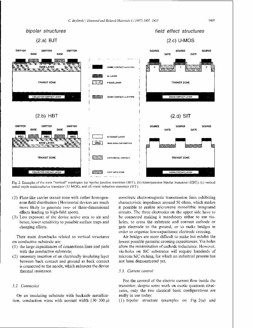
C. Brylinski / Diamond and Related Materials 6 (1997) 1405-1413 1409
bipolar structures field effect structures
(2.a) BJT (2.c) U-MOS
EMITTER EMITTER EMnTER BASE BASE
mm fffffff mz?> BASE LAYER OHMIC CONTACT on N-TYPE
P BASE LAYER
OHMIC CONTACT on P-TYPE
(2.b) HBT
EMITTER EMITTER EMITTER BASE BASE
WBG 1 B%%%| I WBG
BASE LAYER
TRANSIT ZONE
(2.d) SIT
N THANStT LAYER
WBG WIDE BAND GAP EMPTTER
GATE METAL CONTACT
GATE INSULATOR
SOURCE SOURCE SOURCE GATE GATE
■MB ■■■ ■■■
TRANSIT ZONE
Fig. 2. Examples of the main "vertical" topologies: (a) bipolar junction transistor (BJT); (b) heterojunction bipolar transistor (HBT); (c) vertical metal oxyde semiconductor transistor (U MOS); and (d) static induction transistor (SIT).
(2) Plate-like carrier transit zone with rather homogen- eous field distribution (Horizontal devices are much more likely to generate two- or three-dimensional effects leading to high-field spots).
(3) Less exposure of the device active area to air and hence, lower sensitivity to possible surface traps and charging effects.
Their main drawbacks related to vertical structures on conductive substrate are: (1) the large capacitances of connections lines and pads
with the conductive substrate; (2) necessary insertion of an electrically insulating layer
between back contact and ground as back contact is connected to the anode, which enhances the device thermal resistance.
constitute electromagnetic transmission lines exhibiting characteristic impedance around 50 ohms, which makes it possible to realize microwave monolithic integrated circuits. The three electrodes on the upper side have to be connected making it mandatory either to use via- holes, to cross the substrate and connect cathode or gate electrode to the ground, or to make bridges in order to organize low-capacitance electrode crossing.
Air bridges are more difficult to make but exhibit the lowest possible parasitic crossing capacitances. Via-holes allow the minimization of cathode inductance. However, via-holes on SiC substrates will require hundreds of microns SiC etching, for which an industrial process has not been demonstrated yet.
5.3. Current control
5.2. Connectics
On an insulating substrate with backside metalliza- tion, conduction wires with normal width (30-300 \x)
For the control of the electric current flow inside the transistor, despite some work on exotic quantum struc- tures, only the two classical basic configurations are really in use today: (1) bipolar structure (examples on Fig. 2(a) and

1410 C. Brylinski I Diamond and Related Materials 6 (1997) 1405-1413
DRAIN
(3.a) LD-MOS
SOURCE GATE GATE
DRAIN
JBBBSB I r BEZtl
'mySm%$$^^^m§mm
INSULATING SUBSTRATE h\ >
___
OHMIC
CONTACT
on N-TYPE
N+ LAYER
___— „.
f 1 INSULATOR
I I
GATE
METAL
CONTACT
N
TRANSIT
UYER \ i
PLAYER
DRAIN
(3.b) MES
SOURCE GATE GATE
DRAIN
Fig. 3. Examples of "horizontal" topologies: (a) laterally depleted metal oxyde semiconductor transistor (LD-MOS); and (b) metal semiconductor transistor (MESFET).
Fig. 2(b) in which minority carriers are injected from the emitter into the conductive base layer that they have to cross before entering the transit zone;
(2) field effect structure in which the gate is placed along side the current flow channel (its electrostatic potential controls the channel width and/or the mobile carriers density).
5.4. Bipolar structures
Bipolar transistors have long been the only solid-state devices available for high-frequency power operation.
The bipolar current control is the most efficient that can be obtained in any device, since carriers migrate through the gate conductive layer to reach the transit zone.
So, the transistor intrinsic transconductance is the highest possible, although it is current and temperature dependent and generally limited by the parasitic access resistance in all power amplifier configurations.
However, input impedance levels are very low, typi- cally far under the 1 ohm level, which makes it manda- tory to use complex input adaptation cell networks. The carrier transit zone topology is nearly plate-like making electric field distribution very homogeneous, giving max- imum possible voltage handling capability, often close to the theoretical limit in real devices.
5.5. Bipolar junction transistor
The classical silicon bipolar junction transistor (BJT) (Fig. 2(a)) without heterojunction is a vertical structure made on conductive substrate with alternate base and emitter fingers on the upper side (schematic view on Fig. 2(a)). Practical realisation have been available from 0 to 3 GHz. Emitter and base doped zones layers are generally made by diffusion into the collector epitaxial layer and so, this technology cannot be translated today to SiC. Anyway, this is not a high performance structure since it exhibits additional limitations owing to carrier injection from the base into the emitter. Doping levels have to be adjusted far from the optimum to conserve reasonable current gain.
Therefore, global intrinsic device performance com- promise is blocked at a level far inferior to the JFM limit and further from it as the operating frequency goes higher. Moreover, unavoidable losses happen in relation with to the use of conductive substrates. Although explored in the early days of SiC devices research, SiC BJT is certainly no longer considered to be one of the best routes to microwave power devices.
5.6. Heterojunction bipolar transistors
In heterojunction bipolar transistors (HBTs: Fig. 2(b)), the emitter hetero-interface blocks carrier diffusion from the base and allows much higher base doping levels only limited by the base material restric- tions (dopant solubility limit, recombination centers density, hence allowing an extreme reduction of the series base access resistance. Global level of performance can come very close to the JFM limit. HBT is the technology which gives the highest operation frequency for a given lithography resolution.
As an example, comparable performance at 10 GHz can be obtained using 0.5 um gate length MESFETs or HEMTs, or 2 um emitter HBT transistors. The highest difficulty is in the material structure. Present realisations include essentially the following assemblies: Si emitter/SiGe strained base technology on silicon, AlGaAs/GaAs or GalnP/GaAs matched emitter on GaAs substrate, and InP/GalnAs or InAlAs/GalnAs on InP substrate. The availability of semi-insulating III-V substrates makes it easier to realise low loss matching
C. Brylinski I Diamond and Related Materials 6 (1997) 1405-1413 1411
circuits. This is a rare example of a vertical structure on a semi-insulating substrate. However, its technology is much less mature than for BJT and the reliability of the present devices is still questionable.
HBT is certainly a favored direction for the future SiC-based microwave power devices. Emitter hetero- junction could be either established between different polytypes or between SiC and a III-N material such as GaN. Polytype transition control and GaN/SiC direct epitaxy of defect-free material with controlled doping profiles are still challenging goals for the next few years without predictable issue. Although GaN/SiC HBT with good static current gain has been published two years ago [13], published voltage handling capabilities were low and no microwave data have been made available since. In case of failure of the two already mentioned types of heterojunction, structures with AlGaAN emitter on GaN base, collector and contact sub-collector layers will certainly be tried because they are potentially less sensitive to hetero-interface problems.
5.7. MOS
The most popular device for silicon microwave power technology today is the n-channel inversion MOS tran- sistor; until recently, most silicon power MOS used vertical structure with inversion MOS channels on p-type localised either on edges of NPN ridges (V or U MOS, see Fig. 2(c)), or on the surface of localised double diffused/implanted NPN islands (DMOS). The recently developed horizontal laterally depleted silicon LD-MOS, (Fig. 3(a)) seems to exhibit better global characteristics. Translation to SiC would require good MOS or MIS interfaces on SiC and especially on p-type SiC, which has always been a problem so far. The best n-channel mobilities stay around 50cm2V_1s_1 [14], instead of approximately 500 for silicon. Recent progress has been made in improving SiC MOS interfaces but has not yet resulted in published microwave power transistors.
In the case of success in finding a good process to make SiC MOS, SiC LD-MOS devices would be one of the most favored devices owing to an isolated gate allowing large negative excursion for class B or C amplifiers and positive DC bias. However, even silicon MOS devices suffer from oxide degradation owing to high-energy carrier injection from the semiconductor. This effect is predicted to be even more stringent in SiC MOS owing to higher electric fields in operation and lower potential barriers at the insulator/semiconductor interface.
So the two silicon champions do not allow any simple and direct translation to silicon carbide and early SiC device research's only choice has been between "exotic" Si-like and GaAs-like structures such as static induction transistors, JFET and MESFET.
6. Static induction transistor
One "exotic" structure presently in use is the so-called static induction transistor, also known as the permeable base transistor, which has periodically appeared and disappeared during the past thirty years of silicon tech- nology. It is a majority carrier vertical field effect structure (see Fig. 2(d)). A network of trenches is etched into an epitaxial or implanted structure with a highly doped top layer. The resulting ribbons define the channel fingers. The sources' ohmic contacts are made on the top of the ribbons. Schottky metal/semiconductor con- trol gates are put at the bottom of the trenches, some- times extending on the lower parts of their edges. As mentioned before, the vertical structure allows plate-like transit zone topology with quite homogeneous field distribution and reduced surface effects.
However the gate control with reasonable lithography dimensions is highly bi-dimensional and its full optimiza- tion looks like a technological nightmare.
To get good control of carrier flow by the gate electrostatic influence, fingers have to be thin. To reduce parasitic Miller capacitance, trenches have also to be as thin as possible. Only devices with very fine lithography can approach JFM limit. With controllable lithography resolution (1 jun trenches), high efficiency (approaching the JFM limit) operation of SIT will be limited to a fraction of a GHz.
An optimized more than 3 GHz operation would require a submicronic (around 0.2 |un) lithography reso- lution and the associated manufacturing process.
If the dimensions are not fine enough, two deleterious effects will appear. Because of the gate-carriers' distance, channel depletion requires strong gate applied voltage and will impose a doping level reduction, leading to reduced current density and transconductance. The resulting improved linearity is little compensation for these basic drawbacks.
As a second effect, large channel opening (low channel length/height ratio) opens the way to the control of the injected current by the drain potential (dramatic short channel effects) resulting in high output static conduc- tance with "triode-like" characteristics [12], decreasing power gain capabilities in amplifier operation.
Examples of additional problems related to ultimate device optimization are source/gate isolation, edge passivation, gate resistance minimization, and gate positioning in the trench.
As an early SiC RF power device, even a non- optimized SIT/BPT has certainly been a good choice [12]. As the SiC technology gets more mature, it will only stay competitive by going to the most sophisticated lithography and technology. At low frequencies (less than 3 GHz), if passivation problems do not dominate the device performances, we believe that horizontal FETs will exhibit better global performances. At high

1412 C. Brylinski I Diamond and Related Materials 6 (1997) 1405-1413
frequencies, HBT will probably be preferred, because it allows relaxed lithography dimensions.
However today, it must be emphasized that the SIT/TBP structure is the only one for which true high- power (over 1 kW) amplification has been demonstrated at the laboratory level.
7. MESFET and JFET devices
The other existing early SiC power device structures are field effect ones: mainly horizontal MESFETs and JFETs.
7.1. MESFETs
ducibility and reliability often encountered in past silicon MESFET technology trials.
As for other kinds of horizontal devices, interconnec- tions are much easier and less lossy on semi-insulating substrates. Via-holes or air bridges interconnections are a necessity for power multi-finger since three electrodes have to be dispatched. Following GaAs MESFET evolu- tion, planar, implanted and self-aligned technologies are expected to emerge in case of success, in order to lower fabrication costs. Possible variants would be GaN active layer MESFETs and AlGaN/GaN HEMTs most proba- bly on SiC substrates, as mentioned in Section 1. For all these MESFET devices, passivation and reliability issues have still to be clarified and may determine the final choice.
MESFET experience comes from the III-V world. It is the simplest FET structure which needs only an n-type active layer (Fig. 3(b)) but for which outstanding per- formances have been predicted [11]. For power devices, the gate has to be placed as near as possible to the source to reduce source access resistance.
The simplest MESFET technology makes use of epi- taxial N+/N layers. Mesa and recess are first etched and then ohmic contacts and gate Schottky contacts are aligned relatively to the recess edges. Depending on the targeted operation frequency, devices with gate lengths of 2 urn (less than 1 GHz) down to 0.5 um (greater than 3 GHz) have already been studied [7-10].
7.2. JFETs
JFET topology is very similar to MESFET with the specificity that the gate barrier is a p/n junction. It requires the same technology background together with additional know-how on gate P+ layer, related P + ohmic contact and N+ ion implantation for making source and drain contacts. This explains why power MESFET technology and results are more advanced than the JFET ones. Following the silicon experience, optimized JFETs may turn out to be more reliable than MESFETs, although the possibility of making Schottky refractory contacts on SiC may make it possible to overcome possible problems related with Schottky repro-
8. SIC power amplification state of the art
Simply, today, all solid state applications over 3 GHz today are GaAs substrate-based and all those below 1 GHz are silicon based. In between, tough competition takes place. At the low frequency end, the "good old" silicon bipolar transistor is progressively replaced by MOS devices giving easier input impedance adaptation.
Inside the MOS category, laterally depleted "hori- zontal" structures (LD-MOS) are taking over "vertical" structures such as U, V and D-MOS. In the present SiC first approach period, SiC devices are expected to chal- lenge both Si and GaAs microwave power technologies in the RF to S-band spectrum (10 MHz-3 GHz).
At present the best published results for SiC are by Westinghouse/Northrop-Grumann and related to SIT and MESFET transistor (see Table 2). The most impres- sive is a prototype over 1 kW amplifier [6] made out of many-hundred-watts packaged SIT transistors which are assemblies of selected tens-of-watts cells on several chips. Global performances seem superior to those of silicon- based amplifiers roughly by a factor of three.
JFET results are encouraging, with 1.3 W mm-1 at 0.85 GHz [15] but despite significant early Russian works, only very few teams in the world are still active today in this area.
The other publications are related to MESFETs. The
Table 2 Summary of published SiC microwave power results
What Who Substrate type Power (W) Frequency (GHz) Size (mm) Power added efficiency (%)
SIT Westinghouse N + > 1000 0.6 350 SIT Westinghouse N + 36 pulse 3 30 42 MESFET Westinghouse S.I. 3.5 6 2 46 MESFET Cree/Motorola N + 0.7 1.8 0.33 50 MESFET Cree/Motorola N + 0.7 0.85 0.33 60 MESFET Thomson N + 1.6 2 1 38 MESFET Thomson N + 2 1 4.8 43
C. Brylinski I Diamond and Related Materials 6 (1997) 1405-1413 1413
highest frequency operation (6 GHz) was demonstrated in 1995, again by Westinghouse/Northrop-Grumann with 3.5 W output power and over 40% power added efficiency [15]. This is on 6H semi-insulating substrates; 4H results are expected soon. Other results are from Cree/Motorola [8,9] and Thomson [10] with devices on conductive substrates. For both, a similar trend is observed: owing to adaptation problems in relation with the conductive substrate, the power density decreases rapidly with the device size. Impressive improvements are expected with the arrival of semi-insulating substrates.
9. Trends for the future
Discrete MESFETs (and possibly JFETs) on SiC substrates should reach soon the 100 W level around 1 GHz and will progressively give competitive perfor- mances up to 10 GHz with reasonable gate length (0.3-0.5 um). MMICs will follow later, when substrate price will go down.
For higher-frequency or low-cost/narrow-band opera- tion, there is a chance that HBT will make a better industrial product. In both cases, choice will be made between purely SiC and mixed SiC/III-N solutions, mainly depending on reliability and fabrication cost issues.
Large-scale commercialisation of SiC based micro- wave power devices is expected by 2000-2002 when better semi-insulating wafers, at least 2 inches in diameter, will be commercially available.
References
[1] H. Morkoc, S. Strite, G.B. Gao, M.E. Lin, B. Sverdlov, M. Burns, Large-band-gap SiC, III-V nitride, and II-VI ZnSe-based semi-
conductor device technologies, Journal of Applied Physics 76 (3) (1994).
[2] S.C. Binari, L.B. Rowland, W. Kruppa, G. Keiner, K. Doverspike, D.K. Gaskill, Microwave performance of GaN MES- FETS, Electron. Lett. 30 (15) (1994).
[3] Microwave performance of a 0.25 um gate AlGaN/GaN hetero- structure field-effect transistor, Appl. Phys. Lett. 65 (9) (1994).
[4] A. Özgür, W. Kim, Z. Fan, A. Botchkarev, A. Salvador, S.N. Mohammad, B. Sverdlov, H. Morkoc, High transconductance- normally-off GaN MODFETs, Electron. Lett. 31 (16) (1995).
[5] Q. Chen, M. Asif Khan, J.W. Yang, C.J. Sun, M.S. Shur, H. Park, High transconductance heterostructure field-effect transis- tors based on AlGaN/GaN, Appl. Phys. Lett. 69 (6) (1996).
[6] A. Morse, P.M. Esker, R.C. Clarke, CD. Brandt, R.R. Siergiej, A.K. Agarwal, Applications of high power silicon carbide transis- tors at radar frequencies, IEEE MTT-S Conference Digest, 1996, pp. 677-680.
[7] CD. Brandt, A.K. Agarwal, G. Augustine, R.R. Baron, A.A. Burk, R.C. Clarke, R.C. Glass, H.M. Hobgood, A.W. Morse, L.B. Rowland, S. Seshadri, R.R. Siergiej, T.J. Smith, S. Sriram, M.C. Driver, R.H. Hopkins, Advances in SiC materials and devices for high frequency applications, Proceedings of the ICSCRM 95 Conference, 1995, p. 659.
[8] C.E. Weitzel, J.W. Palmour, C.H. Carter, K.J. Nordquist, 4H-SiC Mesfets with 2.8 W/mm power density at 1.8 GHz, IEEE Electron Devices Lett. 15 (10) (1994).
[9] S.T. Allen, J.W. Palmour, C.H. Carter C.E. Weitzel, K.E. Moore, K.J. Nordquist, L.L. Pond III, Silicon Carbide Mesfets with 2 W/ mm and 50% P.A.E. at 1.8 GHz, IEEE MTT-S Conference Digest, 1996, pp. 677-680.
[10] O. Noblanc, E. Chartier, C. Arnodo, C. Brylinski, Microwave Power Mesfet on 4H-SiC, ECSCRM 96 Conference, Diamond Relat. Mater. 6 (1997) 1510-1513.
[ 11 ] C. Weitzel, Comparison of SiC, GaAs and Si RF MESFET power densities, IEEE Electron Devices Lett. 16 (10) (1995) 451.
[12] R.R. Siergiej, R.C. Clarke, A.K. Agarwal, CD. Brandt, A.A. Burk Jr., A. Morse, P.A. Orphanos, High power 4H-SiC static induction transistors, Proceedings of IEDM 95 Conference, 1995, pp. 353-356.
[13] High temperature GaN/SiC heterojunction bipolar transistor with high gain, IEDM Technical Digest (1994) 389-394.
[14] S.C. Binari, L.B. Rowland, W. Kruppa, G. Keiner, DoverspikeK., D.K., D.K. Gaskill, Critical nature of oxide/inter- face quality for SiC power devices, Microelectron. Engng. 28 (1995) 177-184.
[15] K. Moore, DC, RF and power performance of 6H-SiC JFETs presented at WOCSEMMAD '95 Conference, New Orleans, 1995.

ELSEVIER
DIAMOND AND
RELATED MATERIALS
Diamond and Related Materials 6 (1997) 1414-1419
Aluminium implantation of p-SiC for ohmic contacts
L. Spieß a'*, O. Nennewitz a, H. Weishart b, J. Lindnerc, W. Skorupa b, H. Romanus F. Erler a, J. Pezoldt d
a TU Ilmenau, Institut für Werkstoffe, PF 100565, D-98684 Ilmenau, Germany b Forschungszentrum Rossendorf eV, PF510119, D-01314 Dresden, Germany
0 Universität Augsburg, Institut für Physik, Memminger Str. 6, D-86135 Augsburg, Germany d TU Ilmenau, Institut für Festkörperelektronik, PF 100565, D-98684 Ilmenau, Germany
Abstract
An important problem is the formation of low-resistance ohmic contacts, especially for p-lype SiC. The deposition of all known metals onto />type SiC will always result in a depletion p-type contact. To obtain an ohmic contact, the depletion zone has to be smaller. This may be achieved by very shallow p-dopant implantation. Another aim of this research was to study the structural and chemical changes of the surface, as well as the interface and bulk after implantation, annealing and contact formation. Specific contact resistance of 5 x 10"4 A cm2 was achieved on /^-implanted 6H-SiC with Al/Ti metallization. © 1997 Elsevier Science S.A.
Keywords: Atomic force microscopy; Metallization; Ohmic contact; Transmission electron microscopy
1. Introduction
SiC is a promising wide bandgap semiconductor mate- rial for active electronic devices. The great potential of SiC as a semiconductor, however, is challenged by the difficulty of controlling the metal contact properties. An important problem lies in creating low-resistance ohmic contacts, especially for/»-type SiC [1].
It is impossible to fabricate an enhancement p-type SiC contact. There is no metal or metal-like material known with a workfunction of about 6 eV. The theoreti- cal band bending that occurs at a metal-semiconductor contact is shown in Fig. 1. This gives rise to the Schottky barrier (f>Bp. If there are no other effects influencing the metal-semiconductor contact, then <f>Bp may be written as0Bp = 0s-(Pm.
The application of all known metals to /»-type SiC will always result in a depletion /»-type contact. The barrier height depends on the difference between the metal work function and the electron affinity plus the Fermi level of the semiconductor. A depletion zone of holes is observed at the interface. To obtain an ohmic contact, the depletion zone has to be smaller. This may be achieved by very shallows-dopant implantation. This additional doping, however, increases the barrier height
as shown in Fig. 1. A smaller depletion region allows thermionic-field or field emission. Fig. 2 shows the dependence of contact resistance on the hole concen- tration, using Eq. (1):
x tanh (1)
' Corresponding author.
To obtain a specific contact resistance below l<r3Qcm2 (r=300K; <£Bp = 0.4eV) a hole concen- tration of more than 1019cm-3 is necessary. Another problem occurs in SiC because of the high acceptor activation energy (more than 0.2 eV). Only about 1% of the acceptors are ionized at room temperature [2]. One possible way to increase the amount of acceptors is ion implantation.
Another aim of this research was to study the struc- tural and chemical changes of the surface, as well as the interface and bulk after implantation, annealing and contact formation. We performed complex solid state analysis involving atomic force microscopy (AFM), reflection of high energy electron diffraction (RHEED), transmission electron microscopy (TEM) and ruther- ford backscattering (RBS).
0925-9635/97/S17.00 © 1997 Elsevier Science S.A. All rights reserved. PII S0925-9635(97)00047-2

L. Spießetal. j Diamond and Related Materials 6 (1997) 1414-1419 1415
metal vacuu
semiconductor m
. i
/electron
O ^s workfunction ft 4,52 eV $
affinity ^ 6H SiC 3,37 eV
Ti 4,1 eV m i.
WSi9 4,62 eV ' band gap E„ 6H SiC 3 eV
'■ i.i.
if
s~>s {
depletion region
-c
semiconductor with higher p do- ping level
<D, Bp O -<t> ] Fig. 1. Theoretical band bending model at a metal-/j-semiconductor interface.
p [cm 10203*1019I019 3*1018 1018 7*101
10"1
10''
10--
a 10«
10";
10"'
10"'
*B = 0. 45 e V
0.4C eV
/
U.3t eV
0.3C eV
; 1 0.2! eV
| 1 0.2C eV
11 V 0.1! ieV
1 0.K eV
T =300«, A* =96A/K2cm2, m* =0.8 |
■ / .i.i.i.i.i.i.i.i.i.i.i 10"° £
01 23456789 10 11 12
1/Sqrt(p)[10"10cm2/3]
Fig. 2. Calculated contact resistance versus hole concentration.
2. Experimental
In order to increase the acceptor concentration near the surface, an Al implantation with different doses of an implantation energy of 50 keV and room temperature was performed. The theoretical implantation profiles are
shown in Fig. 3. After implantation, the activation of acceptors and the recrystallization of SiC were achieved by annealing at 1650 °C for 20 min in an Argon atmosphere.
RHEED investigations of the near-surface regions were carried out after implantation and after annealing in order to analyse the phase formation resulting from the fabrication process. The damage of the implants was investigated using RBS channeling techniques with 1.6 MeV He+ ion energy. The roughness after annealing process was estimated using atomic force microscopy at air and TEM was used to study the microstructure of deeper regions.
Metallization was performed using sputtered Al/Ti. The layer thicknesses were 20 nm Al and 250 nm Ti. A second set of samples was metallized with Tungsten disilicide. WSi2 layers with a thickness of 400 nm were cosputtered with a stochiometric ratio Si:W of approxi- mately 2.1:1. In order to form the ohmic contacts, a post implantation annealing was performed at temper- atures ranging from 200 to 1100 °C in an Argon atmo- sphere. The contact resistance was measured at rectangular and circular structures using the transmis- sion line method.
3. Results
The RHEED investigations indicated that the surface damage at implantation is negligible for an implantation dose smaller than 5xl014cm~2; see Fig. 4(a and d). The unannealed sample showed weak 6H-SiC patterns, the annealed sample showed a perfect 6H-SiC pattern including Kikuchi lines. The highest implantation dose resulted in an amorphous region near the surface [Fig. 4(c)]. After annealing, a twinned 3C-SiC RHEED pattern was observed [Fig. 4(f)]. Analysis of the RHEED pattern revealed that a set (111) 3C-SiC twin with a twin plane (111) was formed (Fig. 5).
A smooth surface morphology was observed at the
g 101e
O
101'
101'
y
i#
^ ,^— ^"-v
",# implanted dose
[atoms/cm2]
3,3 1013
-— 1,0 1014
5,0 1014
— 1,0 1015
• 5,0 1015
■ f / ■ „*****
^o '■I/,
** (+ *x ^
^\\
.1—- - x c4
-V\ - 1
, \ V, i 1200 1400
depth [A]
Fig. 3. Implantation profiles calculated using TRIM.

1416 L. Spießetal / Diamondand Related Materials 6 (1997) 1414-1419
b C
ND=5*10 cm' as implanted <1120> ND=1*10 cm' as implanted <1120>
d e
ND=5*1015cm"2 as implanted
Nn=5*10 cm" annealed <1120> Nn=1*10 cm" annealed <1010> 'D' ND=5*10 cm" annealed
Fig. 4. RHEED patterns: (a) as-implanted Nimp = 5 x 10" cm 2; (b) as-implanted Nimp= 1 x 1015 cm 2; (c) as-implanted Nimv = 5 x 1015 cm 2; (d) annealed N,„ ,lmp-5 x lO^cm"2; (e) annealed iVimp = 1 x 1015 cm"2; (f) annealed Nimp = 5 x 1015 cm"2.
<in>,<nT>tw
(lll)SiC twin reflection
V ■ V ■
■ V ■ V
□
V
■
■
V
1 1
V
■ 331
■
V
□
□
V ■ 113 1 l 222
V ■
□
■ 004 V ■ 220 V
D
V ■ 002 1 i 111
V ■ 222 □
224 Q
■ 113 V
—i > "111
V
—a <112>
Fig. 5. Theoretical RHEED pattern for (111) 3C SiC twin with plan (111).
as-implanted samples. AFM investigations of the annealed samples showed a smoothing in decrase of the surface roughness with increasing implantation dose; see Table 1. A step structure is observed after annealing;
see Fig. 6. The TEM images showed a perfect surface, but some damage was found in the region of 30 nm under the surface. Two defect regions were found in the sample implantated with a dose of 1 x 1015 cm~2. The

L. Spießetal. / Diamond and Related Materials 6 (1997) 1414-1419 1417
10.7 rm
8.02-
C
«3 5.35- -I—I ro Q N
2.67
¥._!
yJ i
# Distance Height 1 46.08 nm 0.77 nm 2 73.73 nm 0.96 nm 3 227.3 nm 0.26 nm 4 46.08 nm 0.77 nm
-T
,-_j
LJ
,s\ fA
400 800 1200
Distance (nm) 1600 2000 nm
2000 nm
6.81 nm
1000nm
0 nm
0 nm Onm "lOOOnm 2000 nm
Fig. 6. Surface morphology and step profiles measured using AFM.
shallower of these was observed at the maximum impu- rity concentration, as calculated by the TRIM program (50 nm), the deeper one at the end of the implantation region (100 nm). Both TEM and AFM investigations
indicated a step formation process during the annealing procedure. The step height ranged from approximately 0.2 to 0.85 nm. Micro beam diffraction in TEM did not indicate the existence of large 3C-SiC particles in the

1418 L. Spießetal. I Diamond and Related Materials 6 (1997) 1414-1419
1.07 8.85 0.85 10.4 0.49 4.4 0.46 4.0
Table 1 Estimated roughness of implanted and annealed samples using atomic force microscopy
Sample implant dose (cm"2) Ä, (nm) Maximal Height (nm)
Not implanted 3.3 xlO13
3.3 xlO14
l.OxlO15
case of samples with an implantation dose below 2xl015cmT2.
The implanted samples show a lower specific resis- tance than the non-implanted samples. The specific resistance of SiC is more temperature dependent than that of Si because of the high impurity activation energies. A comparison of the theoretically calculated /»-concentrations and the ^-concentrations obtained from resistance measurements versus temperature is shown in Fig. 7. The RBS channelling measurements
show that the sample with an implantation dose larger than 1 x 1015 cm"2 is damaged; see Fig. 8.
4. Discussion
The TEM images indicate that some damage is still present. This damage could be dislocations and disloca- tion loops. With an Al implantation dose of 5.0 x 1015cm~2, which corresponds to a 1021cm~3 Al concentration, an amorphization of the SiC can occur. 3C-SiC is formed during annealing: see the RHEED pattern in Fig. 5. This caused an increase of the surface roughness and a different set of fabrication parameters is required. It was not possible to obtain a good contact measurement in this case. On non-implanted contacts, the lowest specific contact resistance was achieved after annealing at 1100 °C (1.2 x 10⁻² ft cm2).
The obtained specific contact resistance for the
19
5. 10
19
1. 10
18
5. 10
P [cm3]
18
1. 10
17
5. 10
17
1. 10
implantation dosis NA(AI)=6*10 cm - implantation dosis NA(AI)=6*10l5cm2
Up = 27 cm2/Vs
250 300 350 400 T[K]
450
Fig. 7. Calculated /»-concentration and /»-concentration obtained from resistance measurements versus temperature.
Table 2 Estimated specific contact resistance of Al implanted 6H-SiC samples
Al Doping EPI layer Contact annealing conditions
Metallization Al implantation dose (At cm 2)
3.3 xlO13 lxlO14 3.3 xlO14 5xl014 1 x 10¹⁵ 5x10'
NA lxl015cm"3 Not annealed Al/Ti 225 °C Al/Ti 500 °C Al/Ti
NA5xl016cm-3 Not annealed WSi2
1050 °C WSi?
NA7xl016cm"3 Not annealed WSi2
1050 °C WSi, NA3xlOI8cm"3 Not annealed WSi,
1050 °C WSi,
4.5X10"1
7.9xl0"2
2.5 xlO"2
1.7x10" 3.1 xlO" 1.8x10"
3.3 xlO"2
3.6xl0"2
2.0 xlO"2
X X
X X X
9.7 xlO"3
5.6xl0"3
5.6 xlO"4
X 0.2 at 650 K
X X
X X 2.0xl0"2at650K
X = non-ohmic contact behaviour at room temperature.
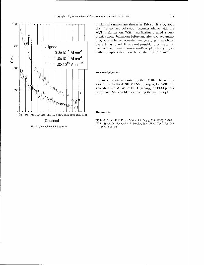
L. Spießetal. / Diamond and Related Materials 6 (1997) 1414-1419 1419
1000
750
0
500
250
I aligned
3.3x10¹³Alcm"2
1,0x10¹⁴Alcm"2
1,0X10¹⁵Alcm"2
N%vM o 125 150 175 200 225 250 275 300 325 350 375 400
Channel Fig. 8. Channelling RBS spectra.
implanted samples are shown in Table 2. It is obvious that the contact behaviour becomes ohmic with the Al/Ti metallization. WSi2 metallization created a non- ohmic contact behaviour before and after contact annea- ling, only at higher operating temperatures is an ohmic character is found. It was not possible to estimate the barrier height using current-voltage plots for samples with an implantation dose larger than 1 x 1014 cm~2.
Acknowledgement
This work was supported by the BMBF. The authors would like to thank SIEMENS Erlangen, Dr Völkl for annealing and Mr W. Reibe, Augsburg, for TEM prepa- ration and Mr Röschke for reading the manuscript.
References
[1] L.M. Porter, R.F. Davis, Mater. Sei. Engng B34 (1995) 83-105. [2] L. Spieß, O. Nennewitz, J. Pezoldt, Inst. Phys. Conf. Ser. 142
(1996)585-588.

ELSEVIER
DIAMOND AND
RELATED MATERIALS
Diamond and Related Materials 6 (1997) 1420-1423
Fabrication of high-quality oxides on SiC by remote PECVD
A. Gölz *, S. Groß, R. Janssen, E. Stein von Kamienski, H. Kurz Institut für Halbleitertechnik, Lehrstuhl II, RWTH Aachen, Sommer-feldstr. 24, D-52074 Aachen, Germany
Abstract
The interface trap density in oxides grown on 6H silicon carbide by remote plasma-enhanced chemical vapor deposition as well as by thermal oxidation is studied. This trap density is found to be drastically reduced by a plasma-assisted PDP (pre-deposition process) in hydrogen. The reduction is stable if a high-temperature annealing step is carried out which excludes a simple passivation by hydrogen. © 1997 Elsevier Science S.A.
Keywords: Pre-deposition processing; Silicon carbide; Thermal oxidation; Remote PECVD
1. Introduction
The high saturation drift velocity and thermal conduc- tivity, and the chemical inertness in harsh environments, makes the wide band-gap semiconductor silicon carbide a promising material for high-power, high-frequency and high-temperature electronics [1]. For MOS-related devices, a high-quality gate insulator is essential. Thermally grown silicon dioxide on 6H silicon carbide reveals electrical properties attractive for gate insulators in SiC-based MOSFETs (metal-oxide-semiconductor field-effect transistor). For some technical applications, e.g. thick field oxides, oxide fabrication by a noncon- sumptive method is desirable. Furthermore, surface engi- neering is expected to have more drastic effects on oxide qualities. For this purpose, we use a two-step remote plasma enhanced chemical vapor deposition (RPECVD) process. The first step consists of a so-called plasma- enhanced PDP (pre-deposition process), where surface engineering is carried out in oxygen or hydrogen plasma. In the second step, an oxide layer is deposited. The two- step RPECVD process has been already used success- fully for high-quality oxide deposition on silicon [2,3]. In this study, we describe the results obtained by HFCV (high-frequency capacitance-voltage) measurements on oxides fabricated by RPECVD on 6H silicon carbide, n- and p-type. The obtained HFCV-data emphasize the crucial role of a PDP. These results are compared with those on thermally grown oxides, where a PDP improves the oxide quality as well.
* Corresponding author.
0925-9635/97/S17.00 © 1997 Elsevier Science S.A. All rights reserved. PII S0925-9635(97)00048-4
2. Experimental
The RPECVD method is based on the plasma- enhanced chemical vapor deposition (PECVD) method, but includes technical improvements to reduce the amount of Si-H and Si-OH groups in the oxide layer and to prevent ion damage. This is realized by spatial separation of different reaction steps, especially the fact that the substrate holder is separated from the plasma generation region. For this, an RPECVD-chamber with a 1" substrate holder described elsewhere [3] has been constructed.
For sample preparation, commercially available (Cree Research, Inc.) Si-faced n- and /J-type 6H-SiC epilayers (d oping «1 x 1016cm"3) on 6H-SiC substrates are cleaned in acetone and by a standard RCA-clean. The samples are subsequently dipped for 10 s in buffered HF solution, rinsed in distilled water and placed in the chamber at a base pressure of 2 x 10~6 Pa. Before oxida- tion is carried out, a plasma-assisted pre-deposition processing (PDP) (30 s-20 min) in hydrogen or oxygen is performed. Oxide growth is realized either by the deposition of an oxide layer of about «25-30 nm by RPECVD or by thermal oxidation. As shown below, the low-temperature surface engineering step by the PDP plays an important role to reduce the interface trap density. The PDP and the RPECVD process are run at 200 °C and at a pressure of 33 Pa. The gas flows are 100 seem Ar, 10 seem 02 or H2, and 10 seem 1% SiH4 in Ar. Thermal oxidation is carried out in a quartz furnace in dry or wet oxygen at 1150 °C. Some samples
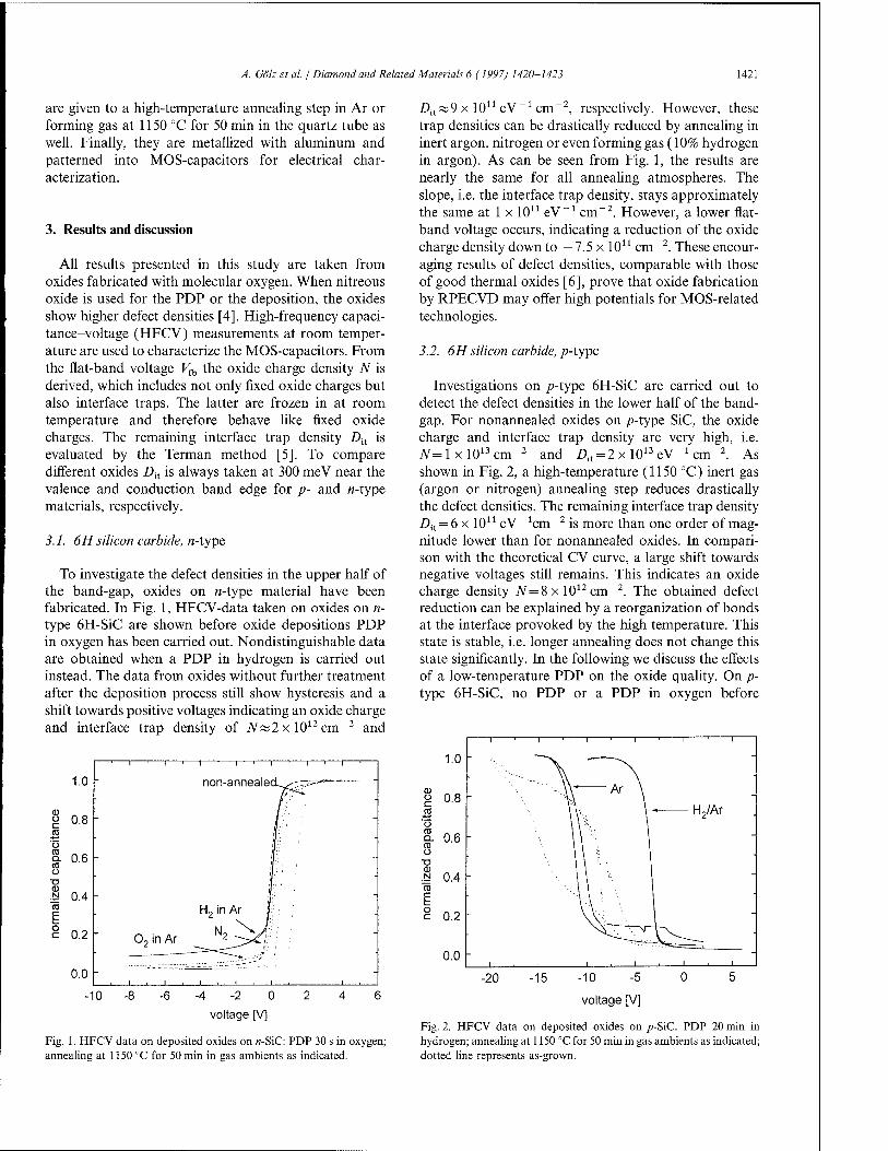
A. Gäbet al. j Diamond and Related Materials 6 (1997) 1420-1423 1421
are given to a high-temperature annealing step in Ar or forming gas at 1150 °C for 50 min in the quartz tube as well. Finally, they are metallized with aluminum and patterned into MOS-capacitors for electrical char- acterization.
3. Results and discussion
All results presented in this study are taken from oxides fabricated with molecular oxygen. When nitreous oxide is used for the PDP or the deposition, the oxides show higher defect densities [4]. High-frequency capaci- tance-voltage (HFCV) measurements at room temper- ature are used to characterize the MOS-capacitors. From the flat-band voltage Va the oxide charge density N is derived, which includes not only fixed oxide charges but also interface traps. The latter are frozen in at room temperature and therefore behave like fixed oxide charges. The remaining interface trap density Dit is evaluated by the Terman method [5]. To compare different oxides Dü is always taken at 300 meV near the valence and conduction band edge for p- and «-type materials, respectively.
3.1. 6H silicon carbide, «-type
To investigate the defect densities in the upper half of the band-gap, oxides on «-type material have been fabricated. In Fig. 1, HFCV-data taken on oxides on «- type 6H-SiC are shown before oxide depositions PDP in oxygen has been carried out. Nondistinguishable data are obtained when a PDP in hydrogen is carried out instead. The data from oxides without further treatment after the deposition process still show hysteresis and a shift towards positive voltages indicating an oxide charge and interface trap density of ./VÄ2xl012cm"2 and
1.0
' i ' i '
non-
i ' i ' i ' i '
am lealetL^-c^-—■-■
0) o c ro ü TO Q. TO O
0.8
0.6
1:::
t: ': n !r ' N 0.4 h ' TO £ o c 0.2 " 02 in Ar
H2 in
N2
Ar 1; ;
0.0 i
.....~.r.--~ --"„"-"'"''
i i . \ , i . I . I
-10 -4 -2 0
voltage [V]
At~9 x 10¹¹ eV"1 cm"2, respectively. However, these trap densities can be drastically reduced by annealing in inert argon, nitrogen or even forming gas (10% hydrogen in argon). As can be seen from Fig. 1, the results are nearly the same for all annealing atmospheres. The slope, i.e. the interface trap density, stays approximately the same at 1 x 10¹¹ eV"1 cm-2. However, a lower flat- band voltage occurs, indicating a reduction of the oxide charge density down to —7.5 x 1011 cm"2. These encour- aging results of defect densities, comparable with those of good thermal oxides [6], prove that oxide fabrication by RPECVD may offer high potentials for MOS-related technologies.
3.2. 6H silicon carbide, p-typs
Investigations on p-type 6H-SiC are carried out to detect the defect densities in the lower half of the band- gap. For nonannealed oxides on p-type SiC, the oxide charge and interface trap density are very high, i.e. 7V=lxl013cm"2 and Dit = 2 x 10¹³ eV"1 cm"2. As shown in Fig. 2, a high-temperature (1150 °C) inert gas (argon or nitrogen) annealing step reduces drastically the defect densities. The remaining interface trap density £>it = 6x 10u eV~1cm"2 is more than one order of mag- nitude lower than for nonannealed oxides. In compari- son with the theoretical CV curve, a large shift towards negative voltages still remains. This indicates an oxide charge density JV = 8 x 1012cm"2. The obtained defect reduction can be explained by a reorganization of bonds at the interface provoked by the high temperature. This state is stable, i.e. longer annealing does not change this state significantly. In the following we discuss the effects of a low-temperature PDP on the oxide quality. On p- type 6H-SiC, no PDP or a PDP in oxygen before
0) o c TO 'Ö TO Q. TO Ü ■o (D N "S E
Fig. 1. HFCV data on deposited oxides on n-SiC: PDP 30 s in oxygen; annealing at 1150 °C for 50 min in gas ambients as indicated.
-10 -5
voltage [V]
Fig. 2. HFCV data on deposited oxides on p-SiC: PDP 20 min in hydrogen; annealing at 1150 °C for 50 min in gas ambients as indicated; dotted line represents as-grown.
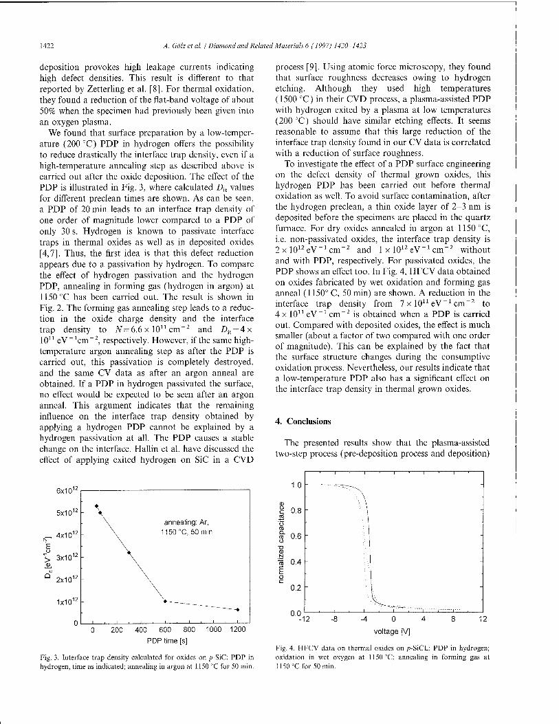
1422 A. Gölzetal. / Diamond and Related Materials 6 (1997) 1420-1423
deposition provokes high leakage currents indicating high defect densities. This result is different to that reported by Zetterling et al. [8]. For thermal oxidation, they found a reduction of the flat-band voltage of about 50% when the specimen had previously been given into an oxygen plasma.
We found that surface preparation by a low-temper- ature (200 °C) PDP in hydrogen offers the possibility to reduce drastically the interface trap density, even if a high-temperature annealing step as described above is carried out after the oxide deposition. The effect of the PDP is illustrated in Fig. 3, where calculated Dit values for different preclean times are shown. As can be seen, a PDP of 20 min leads to an interface trap density of one order of magnitude lower compared to a PDP of only 30 s. Hydrogen is known to passivate interface traps in thermal oxides as well as in deposited oxides [4,7]. Thus, the first idea is that this defect reduction appears due to a passivation by hydrogen. To compare the effect of hydrogen passivation and the hydrogen PDP, annealing in forming gas (hydrogen in argon) at 1150 °C has been carried out. The result is shown in Fig. 2. The forming gas annealing step leads to a reduc- tion in the oxide charge density and the interface trap density to JV=6.6 x 1011 cm"2 and Z>it = 4x 10u eV _1cm~2, respectively. However, if the same high- temperature argon annealing step as after the PDP is carried out, this passivation is completely destroyed, and the same CV data as after an argon anneal are obtained. If a PDP in hydrogen passivated the surface, no effect would be expected to be seen after an argon anneal. This argument indicates that the remaining influence on the interface trap density obtained by applying a hydrogen PDP cannot be explained by a hydrogen passivation at all. The PDP causes a stable change on the interface. Hallin et al. have discussed the effect of applying exited hydrogen on SiC in a CVD
6x101
5x101
4x101
\, 3x101
2x10T
1x1CT
0 200 400 600 800 1000 1200
PDP time [s]
Fig. 3. Interface trap density calculated for oxides on p-SiC: PDP in hydrogen, time as indicated; annealing in argon at 1150 °C for 50 min.
- \ \ annealing: Ar,
- 1150 °C, 50 min
- ♦
1 1 . 1
"~—-♦ * . t
process [9]. Using atomic force microscopy, they found that surface roughness decreases owing to hydrogen etching. Although they used high temperatures (1500 °C) in their CVD process, a plasma-assisted PDP with hydrogen exited by a plasma at low temperatures (200 °C) should have similar etching effects. It seems reasonable to assume that this large reduction of the interface trap density found in our CV data is correlated with a reduction of surface roughness.
To investigate the effect of a PDP surface engineering on the defect density of thermal grown oxides, this hydrogen PDP has been carried out before thermal oxidation as well. To avoid surface contamination, after the hydrogen preclean, a thin oxide layer of 2-3 nm is deposited before the specimens are placed in the quartz furnace. For dry oxides annealed in argon at 1150 °C, i.e. non-passivated oxides, the interface trap density is 2x 10¹²eV_1cm"2 and 1 x lO^eV"1 cm"2 without and with PDP, respectively. For passivated oxides, the PDP shows an effect too. In Fig. 4, HFCV data obtained on oxides fabricated by wet oxidation and forming gas anneal (1150° C, 50 min) are shown. A reduction in the interface trap density from 7 x 10¹¹ eV"1 cm"2 to 4x 10¹¹ eV"1 cm"2 is obtained when a PDP is carried out. Compared with deposited oxides, the effect is much smaller (about a factor of two compared with one order of magnitude). This can be explained by the fact that the surface structure changes during the consumptive oxidation process. Nevertheless, our results indicate that a low-temperature PDP also has a significant effect on the interface trap density in thermal grown oxides.
4. Conclusions
The presented results show that the plasma-assisted two-step process (pre-deposition process and deposition)
o CO Q. ra o
■o 0) N
15 £
1.0
i < i . i i i i i *
0.8
M 0.6 i 0.4
\ 0.2 -
-12 0 4
voltage [V]
Fig. 4. HFCV data on thermal oxides on />-SiCL: PDP in hydrogen; oxidation in wet oxygen at 1150°C; annealing in forming gas at 1150 °C for 50 min.

A. Götz el al. I Diamond and Related Materials 6 (1997) 1420-1423 1423
in a remote plasma has promising potentials for high- quality oxides on SiC. Oxides can be fabricated by RPECVD with defect densities comparable with thermal oxides, but at much higher growth rates. The surface engineering by a low-temperature PDP particularly improves oxide quality. For deposited as well as for thermal oxides, a reduction in interface traps in the lower half of the band-gap is achieved. For deposited oxides, the effect is more drastic because the well-prepared surface becomes the interface. In addition, this surface prepara- tion is stable against a high-temperature annealing step in an ambient inert gas, which excludes hydrogen passiv- ation to be the reason for the quality improvement.
Acknowledgement
The support by G. Lucovsky, North Carolina State University, USA, to build the Remote PECVD system is gratefully acknowledged. We thank the Bundesministerium für Bildung, Wissenschaft, Forschung und Technologie for financial support.
References
[1] M. Bhatanagar, B.J. Baliga, IEEE Trans. Elec. Devices 40 (1993) 645.
[2] G. Lucovsky, Y. Ma, T. Yasuda, C. Silvestre, J.R. Häuser, Jap. J. Appl. Phys. 31 (1992)4387.
[3] A. Gölz, R. Janssen, E. Stein von Kamienski, H. Kurz, in: H.Z. Massoud, E.H. Pointdexter, C.R. Helms (Eds.), The Physics and Chemistry of the Si02 and the Si-Si02 Interface, The Electrochemi- cal Society, Inc. Proceedings, 96 (1) 753.
[4] A. Gölz, S. Groß, R. Janssen, E. Stein von Kamienski, H. Kurz, Mater Sei. Engng B 00 (1997) 00-00.
[5] E.H. Nicollian, J.R. Brews, MOS (Metal Oxide Semiconductor) Physics and Technology, Wiley, New York, 1982.
[6] E. Stein von Kamienski, F. Portheine, A. Gölz, H. Kurz, Proceed- ings of the Sixth International Conference on Silicon Carbide and Related Materials, Kyoto, 1995, p. 641.
[7] E.G. Stein von Kamienski, C. Leonhard, S. Scharnholz, A. Gölz, H. Kurz, Mater. Sei. Engng B 00 (1997) 00-00.
[8] C.-M. Zetterling, C.I. Harris, M. Östling, V.V. Afanas'ev, Proceed- ings of the Sixth International Conference on Silicon Carbide and Related Materials, Kyoto, 1995, p. 605.
[9] C. Hallin, A.S. Bakin, F. Owman, P. Märtensson, O. Kordina, E. Janzen, Proceedings of the Sixth International Conference on Sili- con Carbide and Related Materials, Kyoto, 1995, p. 613
;*•'. '!:■•«'■: DIAMOND AND
RELATED MATERIALS
ELSEVIER Diamond and Related Materials 6 (1997) 1424-1427
An interface study of vapor-deposited rhenium with the two (0001) polar faces of single crystal 6H-SiC
S. Kennou 1, A. Siokou, I. Dontas, S. Ladas * Department of Chemical Engineering, University of Patras, and FORTH-ICE/HT, P.O.B. 1414, GR-26500 Rion, Patras, Greece
Abstract
The interfaces formed on the two (0001) polar faces of single crystal n-type 6H-SiC by Re evaporation and subsequent annealing were investigated by X-ray photoelectron spectroscopy (XPS), low energy electron diffraction (LEED) and work function (WF) measurements. Rhenium was deposited from submonolayer up to 2 nm thickness and gradually annealed up to 1100 K. Deposition led to a weakening and eventual disappearance of the 1 x 1 LEED pattern of the clean surface, an increase of the WF up to the value of metallic Re and the formation of a Schottky barrier with a height of 0.7 ±0.2 eV for both faces. The Re 4f7/2 peak binding energy decreased during deposition from approx. 41.1 eV below monolayer coverage, to 40.5 eV for a 2 nm film indicating an island growth of the film. Annealing of the Re films up to 1100 K on both faces led to Re particle coalescence without affecting the low Schottky barrier at the interface, however, there are indications of chemical changes at the interface which could affect the electrical characteristics of the contact. © 1997 Elsevier Science S.A.
Keywords: Silicon carbide; Rhenium; X-ray photoelectron spectroscopy; Work function
1. Introduction
Single-crystal silicon carbide devices are potential candidates for high-temperature applications [1]. In particular, metal/SiC contacts and the resulting Schottky barriers are important for such SiC-based devices. Although the metal/SiC Schottky contact formation at room temperature has been studied in recent years for a large number of metals [2-9], the effect of annealing at higher temperatures on the stability of the metal/SiC contact has been studied for rather few metals, namely Pt, Au, Co, Mo and Ni [3,6-9]. Rhenium is a good candidate for such stability at high temperature because it does not react with SiC at temperatures up to 1400 K, as shown by recent studies of Re films, at thicknesses of up to 300 nm, on n-type ß-SiC(OOl) [10]. On the basis of this thermodynamic inertness one would expect that the electrical behaviour of the Re contact on SiC would be stable with heat treatment, however changes are observed above 750 K which are attributed to minute changes at the interface [11]. In this study, we examined
«Corresponding author. Tel: +3061 997631/997856; Fax: +3061 993255; e-mail: [email protected] Permanent adress: Department of Physics, University of Ioannina, P.O.B.1186, GR-45110 Ioannina, Greece
the early stages of Re/SiC interface formation at room temperature and the influence of annealing up to 1100 K on the interface stability on the two (0001) polar faces of single crystal n-type 6H-SiC, the (0001) (Si-face) and the (0001) (C-face), by using X-ray photoelectron spectroscopy (XPS), work function (WF) measure- ments and low energy electron diffraction (LEED).
2. Experimental
All measurements were performed in a conventional ultra high vacuum system equipped with XPS, LEED and WF measurement facilities which have been described previously [12]. Single crystal 6H-silicon car- bide wafers, both Si-face and C-face, from Cree Research Inc. [13] were used as substrates. The wafers were n-type, nitrogen-doped (3 x 10¹⁷—3 x 1018 cm"3 net doping density) and oriented 3-4° off-axis with respect to the ideal (0001) plane towards the [11-20] direction. Before the samples were mounted into the ultra high vacuum system they were cleaned using the procedure described elsewhere [14]. In the vacuum the cystals were heated up to 900 K to remove volatile compounds. Both clean substrates exhibited a 1 x 1 hexagonal LEED
0925-9635/97/S17.00 © 1997 Elsevier Science S.A. All rights reserved. PII S0925-9635(97)00067-8

S. Kennou et al. I Diamond and Related Materials 6 (1997) 1424-1427 1425
pattern which was more intense for the C-face. The latter exhibited a Si 2p/C Is XPS intensity ratio of 0.8 compared with 1.1 for the Si-face. Both faces exhibited a small O Is peak in the XP spectrum and the Si 2p photopeak showed only traces of an oxidized compo- nent. The WF of the clean suface was found 4.5 + 0.1 eV for both the Si-face and the C-face in agreement with previous measurements [12]. Rhenium was e-beam evap- orated from a thoroughly degassed tip at a pressure of 5 x 10~10mbar and at a deposition rate of 0.2 nm per min. Rhenium was deposited at room temperature at successively increasing amounts up to 2 nm. After each deposition step XPS, LEED and WF measurements were taken. When the surface was covered with 2 nm of Re the crystal was heated for 2 min at successively increasing temperatures up to 1100 K. After each annea- ling step XPS, LEED and WF measurements were taken again.
3. Results and discussion
Upon Re deposition on both the Si-face and the C-face at room temperature the LEED pattern of the clean surface weakens continously with increasing back- ground intensity and no new spots are observed. Fig. 1 shows the work function change upon deposition which is the same for the two faces. This similarity between
> tu
' l<J
Re/SiC RT
% - 0,8- . o
i r >°. .■ o
500 K
0,6- o
0,4- rA k
Q : ■
700 K
0,2- a Si-face
o C-face
Annealing
0,0< > ' 1 r— 1 ' i ■ i '
0,0 0,5 1,0 1,5 2,0
Re THICKNESS / nm 2,5
Si- and C-faces extends over practically the whole range of measurements reported here, therefore in the following only the results for the Si-face will be shown and minor differences will be pointed out when they occur. The WF increases continuously and after ~ 1 nm or 3-4 monolayers of Re evaporation reaches a final value of ~5.2 eV, that is close to the value for polycrys- talline Re (5.1 eV) [15]. The relatively large amount of Re required to reach WF saturation indicates film growth with cluster formation. This is confirmed with XPS by the binding energy shift of the Re 4f7/2 core level peak from 41.1 eV at submonolayer deposition to 40.5 eV after 2 nm of Re as shown in Fig. 2. Such a shift is expected for metal cluster formation on a rela- tively inert substrate [16].
Upon Re deposition at room temperature the C Is and Si 2p core level peaks from the SiC substrate are attenuated but their shape does not change indicating negligible chemical interaction with deposited Re. The C Is and Si 2p peaks for the clean substrate and after 2 nm of Re are shown in Figs. 3 and 4 normalized to the same maximum height. The binding energy at the peak maximum shifts slightly and saturates after ~ 1 nm of Re to a value lower by ~0.1 eV for both peaks. The Schottky barrier height, OB, for the Re/SiC interface was calculated from the above XPS data using the
13
CO
>-
W z LU I- z w Q_ X
Fig. 1. The variation of the work function with Re deposition on the two polar faces of 6H-SiC at room temperature. The triangles indicate the WF decrease upon annealing a 2 nm Re deposit.
-46 -44 -42 -40 -38
BINDING ENERGY / eV Fig. 2. The Re 4f XPS peaks at successive stages of Re deposition on the Si-face of 6H-SiC. The arrow corresponds to a binding energy of

1426 S. Kennouetal. / Diamond and Related Materials 6 (1997) 1424-1427
Z3 CO
>-
w z LU
c/) Q_ X
-288 -286 -284 -282 -280
BINDING ENERGY / eV Fig. 3. The C Is XPS peak at various stages of Re deposition and annealing on the Si-face of 6H-SiC. The arrow indicates increased intensity near 285 eV on the annealed surface arising from free carbon.
method described by Waldrop and co-workers [5]. In brief, <t>B = Eg-Efi, where £g = 3.03eV is the 6H-S1C band gap [13] and Eti is the interface Fermi level measured by XPS with respect to the top of the SiC valence band; that is, En = Ec U — (EC U — Ev)0, where the quantity in parentheses is the C Is to valence-band maximum binding energy difference for the clean SiC. The latter was measured at 280.5+0.1 eV by using valence band data from the clean surface. From the measured C Is binding energy of 282.8 eV after 2 nm Re deposition (Fig. 3) a Schottky barrier height of 0.7 + 0.2 eV is obtained for both the Si- and C-faces. This value is lower than that expected if the simple Schottky-Mott model were valid, that is ®B = ®m-% where <J>m is the WF of the metal and % the semiconduc- tor electron affinity which is ~4eV for 6H-SiC [5]. Furthermore, the Schottky barrier for Re is about the same for the Si- and C-faces (less than ~0.2eV differ- ence), whereas for metals which are close to the Schottky-Mott model, like Pd and Au, the Schottky barrier is different on the two faces. On the C-face, it is, respectively, 0.4 eV higher for Pd and 0.2 eV lower for Au than on the Si-face [5]. Pd and Au have similar WF with Re, therefore the lower OB on Re could be due either to a lower % for our SiC specimens compared with those in Ref. [5], or to a sheer inadequacy of the simple Schottky-Mott model to describe the complex
13
CO
>
CX) z LU H Z
CO Q_ X
Re/SiC(Si-face)
-106 -104 -102 -100
BINDING ENERGY / eV Fig. 4. The Si 2p XPS peak at various stages of Re deposition and annealing on the Si-face of 6H-SiC. The arrow indicates increased intensity near 99.7 eV on the annealed surface arising from elemental Si or ReSi,.
electronic structure of the metal/6H-SiC interface, as pointed out in Ref. [5]. The former case seems less likely since the cleaning procedures were similar and the composition of the substrate surface before metal evapo- ration was about the same in this work and in Ref. [5].
Upon annealing of the samples up to 1100 K following 2 nm Re deposition the binding energies of the C Is and Si 2p peaks do not change (Figs. 3 and 4) hence the Schottky barrier is not affected. This suggests the absence of an extended chemical reaction at the inter- face, as for example, in the case of Er/SiC [12] where erbium suicide was formed at 900 K and the Schottky barrier increased by 0.4 eV. However, above 700 K there are small changes in the shape of the C Is and Si 2p peaks, namely the appearance of additional intensity near 99.7 eV for the Si 2p (Fig. 4) and near 285 eV for the C Is (Fig. 3). The former could be due to elemental Si or traces of ReSi2 [17] and the latter to free carbon arising from a limited interaction at the interface which is not enough to affect the Schottky barrier but could be related to the changes in the electrical characterisics of Re/SiC contacts alluded to in the Introduction [11]. Annealing up to 600 K does not affect the interface, however it does cause a significant decrease of the WF above 500 K (Fig. 1), which can be attributed to coalesc-

S. Kennou et al. / Diamond and Related Materials 6 (1997) 1424-1427 1427
ence of the Re film into larger particles leading to partial exposure of the substrate surface. This is supported by the LEED pattern, which after annealing again exhibits the 1 x 1 symmetry of the substrate.
References
[1] R.F. Davis, G. Keiner, M. Shur, J.W. Palmour, J.A. Edmond, Proc. IEEE 79 (1991) 677.
[2] V.M. Bermudez, J. Appl. Phys. 63 (10) (1988) 4951. [3] N.A. Papanicolaou, A. Christou, M.L. Gipe, J. Appl. Phys. 65
(9) (1989) 3526. [4] N. Lundberg, M. Oestling, Appl. Phys. Lett. 63 (22) (1993) 3069. [5] J.R. Waldrop, R.W. Grant, Y.C. Wang, R.F. Davis, J. Appl.
Phys. 72 (10) (1992) 4757. [6] D.E. Ioannou, N.A. Papanicolaou, NordquistP.E., Jr., IEEE
Trans., Elect. Devices 34 (1987) 1694.
[7] N. Lundberg, CM. Zetterling, M. Oestling, Appl. Surf. Sei. 73 (1993)316.
[8] S. Hara, K. Suzuki, A. Furuya, Y. Matsui, Japan. J. Appl. Phys. 29 (1990) L394.
[9] J. Crofton, P.G. McMulin, J.R. Williams, M.J. Bozack, J. Appl. Phys. 77(1995) 1317.
[10] J.S. Chen, E. Kolawa, M.-A. Nicolet, J. Appl. Phys. 75 (2) (1994)897.
[11] J.S. Chen, A. Bächli, M.-A. Nicolet, L. Baud, C. Jaussaud, R. Madar, Mater. Sei. Eng. B29 (1995) 185.
[12] S. Kennou, J. Appl. Phys. 78 (1) (1995) 587. [13] Cree Res. Inc., 2810 Meridian Parkway, Suite 176, Durham,
NC 27713. [14] M.E. Lin, S. Strite, A. Agarwal, A. Salvador, G.L. Zhou, N.
Teraguchi, A. Rockett, H. Morkoc, Appl. Phys. Lett. 62 (7) (1993) 702.
[15] H.B. Michalson, J. Appl. Phys. 48 (1977) 4729. [16] W.F. Egelhof, Surf. Sei. Rep. 6 (1987) 253. [17] A. Siokou, S. Kennou, S. Ladas, T.A. Nguyen Tan, J.-Y. Veuillen,
Surface Science 352-354 (1996) 628.

ELSEVIER
DIAMOND AND
RELATED MATERIALS
Diamond and Related Materials 6 (1997) 1428-1431
TEM study of Ni and Ni2Si ohmic contacts to SiC
B. Pecza'*, G. Radnöczia, S. Cassette b, C. Brylinski b, C. Arnodo b, O. Noblanc b
a Research Institute for Technical Physics PO Box 76, H-1325 Budapest, Hungary b THOMSON-CSF/Laboratoire Central de Recherches, Domaine de Corbeville, 91404 Orsay, Cedex, France
Abstract
The structure of Ni and Si/Ni contacts to SiC was studied by transmission electron microscopy. Annealed Ni/SiC contacts showed ohmic behaviour, but Ni proved to be reactive with SiC resulting in the formation of nickel suicide together with the formation of a high number of voids. Deposition and annealing of Si/Ni multilayer contacts resulted in a void free Ni2Si contact layer on SiC, while also exhibiting low contact resistivity. © 1997 Elsevier Science S.A.
Keywords: Silicon carbide; Ohmic contacts; Electron microscopy
1. Introduction
Wide-gap SiC is one of the most promising materials for manufacturing high temperature and high power electronic devices. Recently 4H-SiC substrates have become available which are expected to be an excellent alternative to 6H-SiC, due to the former's higher electron mobility. The efficient application of SiC to microwave power devices requires ohmic contacts with low specific contact resistance which are able to withstand high operating temperatures.
2. Experimental details
A 4H-SiC wafer with a heavily doped, 2 um thick n+ epitaxial layer (1019cm~3) was used as a substrate for the Ni contact layer to ensure low contact resistance. Prior to deposition, the sample was cleaned in HF (1 %) for 3 min and subsequently etched in situ by Ar+ ions at 200 eV for 8 min. A Ni layer with a thickness of 150 nm was deposited onto the substrate by high vacuum electron beam evaporation. Annealing was performed in a pure nitrogen ambient at 950 °C for 10 min.
Another set of samples was prepared by deposit- ing Ni and Si multilayers onto n+ 6H- SiC (1-1.8 x 1018 cm-3) by electron beam evaporation at a deposition rate of 0.25 nm s_1. The substrate was
* Corresponding author. Tel: 36-1-1698-961; Fax: 36-1-1698-037; e-mail: [email protected]
cleaned as above. Si(15 nm)/Ni(16.4 nm)/Si(30nm)/ Ni(32.8 nm)/Si(30nm)/Ni(32.8 nm) layers were depos- ited to obtain the overall composition of N2Si. Samples with the reversed sequence of the Ni/Si layers (e.g. starting with Ni) were also prepared. The Si/Ni contacts on SiC were annealed under the same conditions as the Ni/SiC samples (e.g. at 950 °C in nitrogen).
Cross sectional samples were prepared by ion beam milling. Preparation details of the present samples are given elsewhere [ 1 ]. The thinned samples were examined using a Philips CM20 transmission electron microscope operating at 200 kV. EDS (Energy Dispersive System) X-ray analysis was performed by a Ge detector NORAN system attached to the TEM.
3. Results and discussion
3.1. Ni/SiC
As shown in Fig. 1, the as-deposited Ni layer is homogeneous in thickness and exhibits a smooth surface. The Ni layer is of a polycrystalline structure with a typical grain length of ~ 400 nm. The thickness of the grains is determined by the thickness of the Ni layer. Selected area electron diffraction pattern (SAED) of the Ni layer revealed that the Ni layer possesses a (111) type texture.
The cross-section micrograph of the annealed speci- men is shown in Fig. 2. The contact layer substantially increased in thickness and contained a large number of voids (Kirkendall voids). Voids are shown to be present
0925-9635/97/S17.0O © 1997 Elsevier Science S.A. All rights reserved. PII S0925-9635(97)00069-l

B. Peczetal. / Diamond and Related Materials 6 (1997) 1428-1431 1429
Fig. 1. Cross-section of as-deposited Ni/SiC sample.
£"V
Fig. 2. Cross-section of Ni/SiC sample annealed at 950 °C.
at the original Ni/SiC interface, which corresponds to the white stripe in Fig. 2. The typical length of the grains showed no change and therefore, it was again measured to be ~400nm. The EDS spectrum of the layer (Fig. 3) showed a high silicon content. When the layer was EDS analysed, quantitative measurements showed a 2:1 Ni:Si ratio which indicates that the Ni layer reacted with SiC during the annealing and this resulted in the formation of a poly crystalline Ni2Si layer.
The Ni2Si phase was identified by Pai et al. [2] as the only reaction product in the temperature range 700-900 °C, and its formation was also reported [3] later. It is known from Auger depth profiling measure- ments [4] that carbon is approximately uniformly dis- tributed in the reacted layer and there is no carbon compound present. Our Auger measurements showed the same results with the only difference being that some carbon atoms were segregated to the surface of the specimen from the top region. This agrees well with the results given in Ref. [3].
The presence of large number of voids within the layer suggests that carbon is segregated to the surface
of the voids which is also confirmed by high resolution electron microscopy observations of the authors.
The investigated Ni/4H-SiC contact shows ohmic char- acteristic after annealing at 950 °C. When the contact resistivity of the annealed specimen is measured by linear TLM (transmission line method) the resulting specific contact resistivity is given [5] to be 3xl0"6Qcm2. The test structure consisted of a mesa of active material prepared with CHF3/SF6 RIE (reactive ion etching), over which identical contacts stripes were patterned. These contacts were 100 um wide and the distances between them varied from 2 to 32 um. The electrical performance of these contacts appeared unaffected after aging at 500 °C for 100 h in nitrogen gas.
Our present results show that the total proportion of Ni reacted with SiC resulting in the formation of a polycrystalline Ni2Si layer. We have also shown that annealed Ni/SiC contacts contain a large number of voids.
3.2. M2Si/SiC
Further work was performed to improve the interface morphology by introducing silicon into the deposited
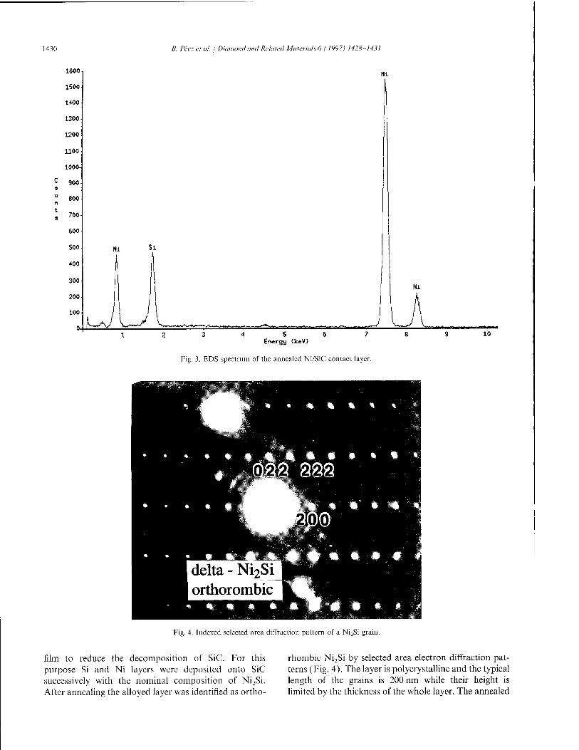
Fig. 3. EDS spectrum of the annealed Ni/SiC contact layer.
Fig. 4. Indexed selected area diffraction pattern of a Ni2Si grain.
film to reduce the decomposition of SiC. For this purpose Si and Ni layers were deposited onto SiC successively with the nominal composition of Ni2Si. After annealing the alloyed layer was identified as ortho-
rhombic Ni2Si by selected area electron diffraction pat- terns (Fig. 4). The layer is polycrystalline and the typical length of the grains is 200 nm while their height is limited by the thickness of the whole layer. The annealed

B. Peczetal. / Diamond and Related Materials 6 (1997) 1428-1431 1431
500 nm
Fig. 5. Cross-section of Ni2Si/SiC sample annealed at 950 °C.
contacts proved to be ohmic and their structure was improved as the contact layer itself did not contain voids (Fig. 5). There are still voids present at the layer/substrate interface even when Si was deposited at first (Fig. 5) during the preparation of Si/Ni multilayers. As expected the number of voids was higher when Ni was deposited at first. The measured specific contact resistivity was an order of magnitude higher than in the case of the annealed Ni/SiC contacts, but the lower doping level of SiC could be responsible for the difference.
are still present at the interface. The formation of those voids could be avoided by the deposition of a thicker Si layer onto the SiC substrate or by the co-deposition of Si and Ni.
Acknowledgement
This work was supported by the COPERNICUS project No. CP940603. G. Vincze is acknowledged for the TEM sample preparation.
4. Conclusion
Ni is very reactive with SiC and in Ni/SiC contacts the annealing leads to the formation of nickel suicide and the contact layer contains many voids while an extremely high number of voids are present at the contact layer-substrate interface. In the present study the Ni2Si layer was prepared and formation of voids avoided in the contact layer itself although a few voids
References
[1] A. Barna, Materials Research Society Symposia and Proceedings Series 254, (1992) 3.
[2] C.S. Pai, CM. Hanson, S.S. Lau, J. Appl. Phys. 57 (1985) 618. [3] W.F.J. Slijkerman, A.E.M.J. Fischer, J.F. van der Veen, I. Ohdo-
mari, S. Yoshida, S. Misawa, J. Appl. Phys. 66 (1989) 666. [4] I. Ohdomari, S. Sha, H. Aochi, T. Chikyow, S. Suzuki, J. Appl.
Phys. 62(1987)3747. [5] C. Arnodo, S. Tyc, F. Wyczisk, C. Brilinsky, 6th International
Conference on Silicon Carbide and Related Materials, Kyoto, 1995.

DIAMOND AND
ELSEVIER
RELATED MATERIALS
Diamond and Related Materials 6 (1997) 1432-1435
Ion beam assisted deposition of a tungsten compound layer on 6H-silicon carbide
H. Weishart *, V. Heera, W. Matz, W. Skorupa Forschungszentrum Rossendorf eV, Institut für Ionenstrahlphysik und Materialforschung, Postfach 510119, D-01314 Dresden,
Germany
Abstract
Ion beam assisted deposition (IBAD) as a means of synthesizing a tungsten carbide layer on top of SiC is investigated by Rutherford backscattering (RBS), X-ray diffraction (XRD) and four point probe measurements. Evaporation of tungsten and subsequent implantation of carbon leads to a crystalline layer of tungsten carbide whose resistivity is 1554uficm. At an implantation dose of 5 x 10¹⁷ C+ cm-2, enhanced surface erosion occurs. Simultaneous evaporation of tungsten and implantation of carbon produces a layer of crystalline W2C mixed with tungsten. The resistivity of this layer is 400 ixQ cm, i.e. only a factor of five higher than that of single crystal W2C. © 1997 Elsevier Science S.A.
Keywords: Implantation; Silicon Carbide; Tungsten Carbide
1. Introduction
Silicon carbide is an advantageous material for high- temperature semiconductor devices because of its supe- rior properties such as high thermal conductivity, high saturated drift velocity of electrons and wide bandgap [1,2]. High-temperature devices, however, are in need of reliable metallization, which should maintain a low resistivity, good adhesion to the underlying SiC and a high chemical stability at elevated temperatures. Several attempts have been made to achieve such metallization on 6H-SiC [3-10]. Promising contact materials that could meet the above-mentioned requirements are the carbides. In this work, we will investigate the synthesis of tungsten carbide on SiC using ion beam assisted deposition (IBAD).
Fabrication of pure W-carbide contact layers has not yet been reported. Baud et al. have prepared tungsten based contact layers by deposition of pure tungsten on SiC and subsequent annealing [11]. However, these layers have proven to be an inhomogeneous mixture of polycrystalline tungsten silicide, tungsten carbide and tungsten. Earlier investigations of the reaction of a deposited W layer with crystalline SiC [12,13] using Auger electron spectroscopy have shown that the forma-
* Corresponding author.
tion of tungsten carbide and silicide occurs without annealing only at defects within the W-SiC-interfacial region. A complete reaction between SiC and W takes place during annealing above 950 °C [11]. We have previously shown that synthesis of tungsten carbide and silicide in SiC at low temperatures is possible by implanting W into the SiC [14,15]. However, this tech- nique still requires high temperatures in order to anneal the implantation-induced damage and to crystallize the new phases.
In this work, we present first results on the synthesis of tungsten carbide by evaporation of tungsten onto a SiC substrate and implantation of C. We investigate the influence of the C dose on the structure of the synthe- sized layer and determine the crystallinity of the phases so formed. Four point probe measurements give a first elucidation of the electrical properties of the layer.
2. Experimental details
Single crystal «-type 6H-SiC from Cree Research, Inc., Durham, NC. served as substrate. Two samples were prepared by evaporation of tungsten onto the substrate and subsequent implantation with C + . The first sample had a 50 nm W layer and was implanted to a dose of 2.5 x 10¹⁷ cnT2. A dose of 5 x 1017 cm-2 was
0925-9635/97/$17.O0 © 1997 Elsevier Science S.A. All rights reserved. PII S0925-9635(97)00070-8
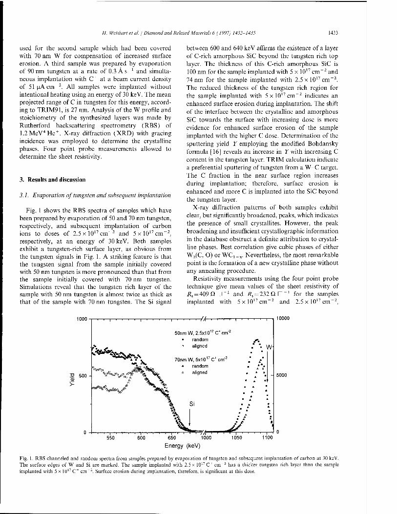
H. Weishart et al. / Diamond and Related Matehals 6 (1997) 1432-1435 1433
used for the second sample which had been covered with 70 nm W for compensation of increased surface erosion. A third sample was prepared by evaporation of 90 nm tungsten at a rate of 0.3 A s_1 and simulta- neous implantation with C+ at a beam current density of 51 uAcmT2. All samples were implanted without intentional heating using an energy of 30 keV. The mean projected range of C in tungsten for this energy, accord- ing to TRIM91, is 27 nm. Analysis of the W profile and stoichiometry of the synthesized layers was made by Rutherford backscattering spectrometry (RBS) of 1.2MeV4He+. X-ray diffraction (XRD) with gracing incidence was employed to determine the crystalline phases. Four point probe measurements allowed to determine the sheet resistivity.
3. Results and discussion
3.1. Evaporation of tungsten and subsequent implantation
Fig. 1 shows the RBS spectra of samples which have been prepared by evaporation of 50 and 70 nm tungsten, respectively, and subsequent implantation of carbon ions to doses of 2.5xl017cm-2 and 5xl017cm"2, respectively, at an energy of 30 keV. Both samples exhibit a tungsten-rich surface layer, as obvious from the tungsten signals in Fig. 1. A striking feature is that the tungsten signal from the sample initially covered with 50 nm tungsten is more pronounced than that from the sample initially covered with 70 nm tungsten. Simulations reveal that the tungsten rich layer of the sample with 50 nm tungsten is almost twice as thick as that of the sample with 70 nm tungsten. The Si signal
between 600 and 640 keV affirms the existence of a layer of C-rich amorphous SiC beyond the tungsten rich top layer. The thickness of this C-rich amorphous SiC is 100 nm for the sample implanted with 5 x 1017 cm-2 and 74 nm for the sample implanted with 2.5 x 1017 cm-2. The reduced thickness of the tungsten rich region for the sample implanted with 5xl017cm"2 indicates an enhanced surface erosion during implantation. The shift of the interface between the crystalline and amorphous SiC towards the surface with increasing dose is more evidence for enhanced surface erosion of the sample implanted with the higher C dose. Determination of the sputtering yield Y employing the modified Bohdansky formula [16] reveals an increase in Fwith increasing C content in the tungsten layer. TRIM calculation indicate a preferential sputtering of tungsten from a W-C target. The C fraction in the near surface region increases during implantation; therefore, surface erosion is enhanced and more C is implanted into the SiC beyond the tungsten layer.
X-ray diffraction patterns of both samples exhibit clear, but significantly broadened, peaks, which indicates the presence of small crystallites. However, the peak broadening and insufficient crystallographic information in the database obstruct a definite attribution to crystal- line phases. Best correlation give cubic phases of either W2(C, O) or WC1_X. Nevertheless, the most remarkable point is the formation of a new crystalline phase without any annealing procedure.
Resistivity measurements using the four point probe technique give mean values of the sheet resistivity of i?s = 409QD_1 and /?S = 232QD_1 for the samples implanted with 5xl017cm~2 and 2.5 x 1017 cm~2,
1000
S**%^.A
-ffr
■**» A»
50nmW, 2.5x10¹⁷C+cm"2
■ random ° aligned
70nmW, 5x10¹⁷C+crn2
* random a aligned
W
550 600 650 1000
Energy (keV) 1050
-i—i—i—i
1100
10000
5000
Fig. 1. RBS channeled and random spectra from samples prepared by evaporation of tungsten and subsequent implantation of carbon at 30 keV. The surface edges of W and Si are marked. The sample implanted with 2.5 x 10¹⁷ C+ cm~2 has a thicker tungsten rich layer than the sample implanted with 5 x 10¹⁷ C+ cm~2. Surface erosion during implantation, therefore, is significant at this dose.

1434 H. Weishart et al. / Diamond and Related Materials 6 (1997) 1432-1435
respectively. A resistivity of obtained for both samples.
p = 1554 |^Q cm is then
3.2. Evaporation of tungsten and simultaneous implantation
40 nm. A resistivity of p = 400 )iQ cm was then obtained. This low value compared with the resistivity obtained from the other samples may be due to the presence of pure tungsten within the tungsten carbide, as revealed by XRD.
Fig. 2 shows RBS random and channeled spectra from the sample which has been prepared by evaporation of tungsten at a rate of 0.3 As"1 and simultaneous implantation with carbon at a dose rate of 3 x 1014cm~2 s_1. The spectra reveal a tungsten-rich layer at the sample surface. The spectrum unambigu- ously shows a lack of Si in the near surface region. Under this region, a layer consisting of only a small fraction of Si, indicated by the plateau between 590 and 640 keV in Fig. 2, is detected. This layer is produced by the implanted C atoms which have penetrated through the W layer into the SiC because of their high energy. Depth calibration of the RBS spectra gives an average value of 130 nm for the thickness of this C-rich SiC. A comparison of random and aligned RBS signals reveals amorphization of the implanted layer. The slow increase in the Si signal around 660 keV is evidence for implant- ation induced intermixing of Si, C and W at the initial SiC-W interface.
The X-ray pattern from this sample indicates that crystallites of both pure tungsten and a-W2C are present in the tungsten-rich layer. The sharp and clear diffraction peaks give evidence of the formation of a crystalline W2C phase without annealing.
Resistivity measurements using the four point probe technique revealed a mean value for the sheet resistivity of .R,= 100fi D"1. From RBS data, we estimated the thickness of the W containing layer to be approximately
4. Summary
Synthesis of tungsten carbide by ion beam assisted deposition is feasible. However, an implantation energy of 30 keV is too high for this purpose since at this energy most C atoms penetrate through the evaporated tungsten layer. An implantation dose of more than 2.5 x 1017cm"2 leads to increased surface erosion, thus resulting in removal of the tungsten. Ion beam mixing occurs at the interface between SiC and the tungsten layer. Crystalline tungsten carbide develops without any annealing process after implantation. The best results with regard to the formation of W2C and electric resistivity are achieved by simultaneous evaporation of W and implantation of C. The resistivity of such a layer is by only a factor of five higher than that of single crystal W2C [17].
Acknowledgement
The authors wish to thank Dr R. Yankov for helping remarks, Mr U. Strauch for the support during sample preparation, Dr M. Voelskow for the RBS and Dr D. Panknin for the electric measurements. Our special thanks go to Mrs A. Scholz for her kind help with the XRD analysis.
1000
2 500
>-
—i 1 1 1—//f—i 1 r-
0.3/VsW, 51nA/crrfC • random » aligned W
p%
550 600
10000
5000
1100
Energy (keV)
Fig. 2. RBS channeled and random spectra from a sample prepared by evaporation of tungsten at a rate of 0.3 A s"1 and simultaneous implantation with carbon at a dose rate of 3 x 1014cm~2 s_1. The implantation energy of 30keV causes most of the carbon ions to penetrate through the tungsten layer, thus leading to a broad region of C rich amorphous SiC beyond the tungsten rich layer.

H. Weishart et al / Diamond and Related Materials 6 (1997) 1432-1435 1435
References
[1]W.E. Nelson, F.A. Halden, A. Rosengreen, J. Appl. Phys. 37 (1966) 333.
[2] G. Pensl, R. Heibig, Festkörperprobleme/Adv. Solid State Phys. 30(1990) 133.
[3] J.B. Petit, M.V. Zeller, in: T.D. Moustaka, J.I. Pankove, Y. Hamakawa (Eds.), Wide Band Gap Semiconductors, MRS Proc. 242, Pittsburgh, PA, 1992, pp. 567-572.
[4] R.C. Glass, L.M. Spellman, R.F. Davis, Appl. Phys. Lett. 59 (1991)2868.
[5] M.M. Anikin, M.R. Rastegaeva, A.L. Syrkin, I.V. Chuiko, in: G.L. Harris, M.G. Spencer and C.Y. Yang (Eds.), Amorphous and Crystalline Silicon Carbide III, and Other Group IV-VI Materials, Springer Proc. Phys. 56 (1992) 183.
[6] J. Crofton, J.M. Ferrero, P.A. Barnes, J.R. Williams, M.J. Bozack, C.C. Tin, CD. Ellis, J.A. Spitznagel, P.G McMullin, in: C.Y. Yang, M.M. Rahman, G.L. Harris (Eds.), Amorphous and Crystalline Silicon Carbide IV, Springer Proc. Phys. 71 (1992) 176.
[7] V.A. Dmitriev, K. Irvine, M. Spencer, G. Keiner, Appl. Phys. Lett. 64(1994)318.
[8] A.K. Chaddha, J.D. Parsons, G.B. Kruaval, Appl. Phys. Lett. 66 (1995)760.
[9] T. Uemoto, Jap. J. Appl. Phys. 34 (1995) L7. [10] J. Crofton, P.G. McMullin, J.R. Williams, M.J. Bozack, J. Appl.
Phys. 77(1995) 1317. [11] L. Baud, C. Jaussaud, R. Madar, C. Bernard, J.S. Chen, M.A.
Nicolet, Mater. Sei. Engng B29 (1995) 126. [12] K.M. Geib, C. Wilson, R.G Long, C.W. Wilmsen, J. Appl. Phys.
68 (1990) 2796. [13] C. Jacob, S. Nishino, M. Mehregany, P. Pirouz, in: Silicon Car-
bide and Related Materials, Institute of Physics Publishing, Bris- tol, 1994, p. 247.
[14] H. Weishart, J. Schöneich, H.-J. Steffen, W. Matz, W. Skorupa, in: D.E. Luzzi, T.F. Heinz, M. Iwaki, D.C. Jacobson (Eds.), Beam-Solid Interactions for Materials Synthesis and Character- ization, MRS Proc. 354, Pittsburgh, PA, 1995, pp. 177-182.
[15] H. Weishart, H.-J. Steffen, W. Matz, M. Voelskow, W. Skorupa, Nucl. Instr. Meth. B112 (1996) 338.
[16] C. Garcia-Rosales, W. Eckstein, J. Roth, J. Nucl. Mater. 218 (1994)8.
[17] H.J. Goldschmidt (Ed.), Interstitial Alloys, Plenum Press, New York, 1967, p. 88.
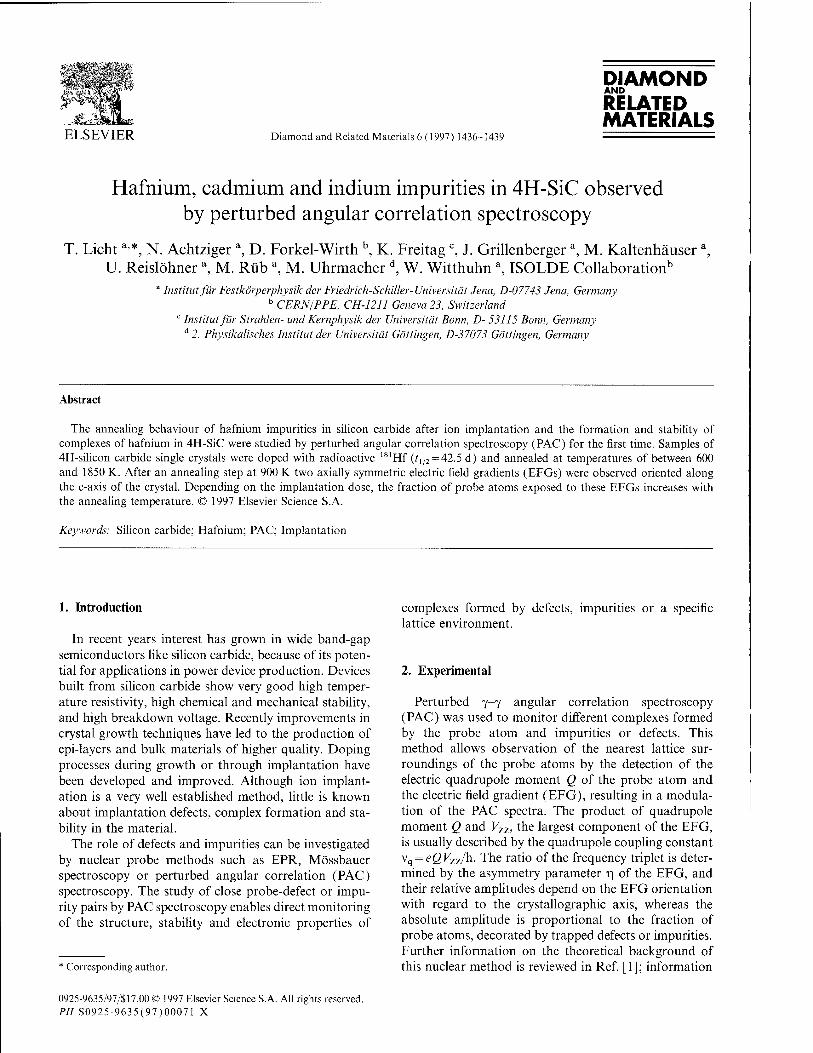
ELSEVIER
DIAMOND AND
RELATED MATERIALS
Diamond and Related Materials 6 (1997) 1436-1439
Hafnium, cadmium and indium impurities in 4H-SiC observed by perturbed angular correlation spectroscopy
T. Lichta'*, N. Achtziger a, D. Forkel-Wirth b, K. Freitagc, J. Grillenberger a, M. Kaltenhäuser a, U. Reislöhner a, M. Rüb a, M. Uhrmacher d, W. Witthuhn a, ISOLDE Collaboration15
1 Institut für Festkörperphysik der Friedrich-Schiller-Universität Jena, D-07743 Jena, Germany b CERN/PPE, CH-1211 Geneva 23, Switzerland
c Institut für Strahlen- und Kernphysik der Universität Bonn, D- 53115 Bonn, Germany d2. Physikalisches Institut der Universität Göttingen, D-37073 Göttingen, Germany
Abstract
The annealing behaviour of hafnium impurities in silicon carbide after ion implantation and the formation and stability of complexes of hafnium in 4H-SiC were studied by perturbed angular correlation spectroscopy (PAC) for the first time. Samples of 4H-silicon carbide single crystals were doped with radioactive 181Hf (;1/2=42.5 d) and annealed at temperatures of between 600 and 1850 K. After an annealing step at 900 K two axially symmetric electric field gradients (EFGs) were observed oriented along the c-axis of the crystal. Depending on the implantation dose, the fraction of probe atoms exposed to these EFGs increases with the annealing temperature. © 1997 Elsevier Science S.A.
Keywords: Silicon carbide; Hafnium; PAC; Implantation
1. Introduction
In recent years interest has grown in wide band-gap semiconductors like silicon carbide, because of its poten- tial for applications in power device production. Devices built from silicon carbide show very good high temper- ature resistivity, high chemical and mechanical stability, and high breakdown voltage. Recently improvements in crystal growth techniques have led to the production of epi-layers and bulk materials of higher quality. Doping processes during growth or through implantation have been developed and improved. Although ion implant- ation is a very well established method, little is known about implantation defects, complex formation and sta- bility in the material.
The role of defects and impurities can be investigated by nuclear probe methods such as EPR, Mössbauer spectroscopy or perturbed angular correlation (PAC) spectroscopy. The study of close probe-defect or impu- rity pairs by PAC spectroscopy enables direct monitoring of the structure, stability and electronic properties of
' Corresponding author.
complexes formed by defects, impurities or a specific lattice environment.
2. Experimental
Perturbed y-y angular correlation spectroscopy (PAC) was used to monitor different complexes formed by the probe atom and impurities or defects. This method allows observation of the nearest lattice sur- roundings of the probe atoms by the detection of the electric quadrupole moment Q of the probe atom and the electric field gradient (EFG), resulting in a modula- tion of the PAC spectra. The product of quadrupole moment Q and Vzz, the largest component of the EFG, is usually described by the quadrupole coupling constant vq = e2^zz/h- The ratio of the frequency triplet is deter- mined by the asymmetry parameter r| of the EFG, and their relative amplitudes depend on the EFG orientation with regard to the crystallographic axis, whereas the absolute amplitude is proportional to the fraction of probe atoms, decorated by trapped defects or impurities. Further information on the theoretical background of this nuclear method is reviewed in Ref. [1]; information
0925-9635/97/S17.00 © 1997 Elsevier Science S.A. All rights reserved. PII S0925-9635(97)00071-X

T. Lichtetal. j Diamond and Related Materials 6 (1997) 1436-1439 1437
concerning its application to semiconductor research is reviewed in Ref. [2].
In this work we present PAC measurements performed at the 181Ta (?1/2 = 10.5 ns), which is populated by the 7/2+ level of 181Hf (f1/2 = 42.5 d). These results are compared with measurements performed at the 5/2+
level of the niCd (fi/2 = 84 ns), which is populated either by electron capture of U1ln (?1/2 = 2.83 d) or by the isomeric transition of lllmCd (tlß = 49 min).
Samples of 4H- (n-type) silicon carbide single crystals were doped with radioactive 181Hf by ion implantation (E{ = 160 keV) at the ion separator of the University of Bonn. TRIM calculations for these implantation param- eters yield a projected range of 43 nm and a straggling of 9 nm [3]. During the first implantation the ratio of active to inactive ions was about 10%. Parallel to the 181Hf implantation, 180Hf and 182Wf are implanted unintentionally. The total number of implanted ions was about 2 x 1013 cm"2. For the second implantation the ratio of active to inactive ions was only about 2-3% resulting in a higher concentration of inactive ions in the sample. Here the implantation dose rises to l-2xl014cm"2.
After implantation the annealing behaviour of the 4H-SiC samples was investigated by encapsulating the samples in a quartz ampoule in an argon atmosphere and subsequent heating in a furnace. Varying the annea- ling temperature from 600 to 1850 K and annealing times from some minutes to 1 h lead to no significant loss of radioactive probe atoms. Only at the annealing step at 1850 K was a loss of about 10% of the probe atoms observed. After each step a PAC measurement was taken, to observe the change in the PAC parameters according to the annealing temperature. All these PAC-spectra were taken at room temperature. In the second series the measuring temperature was varied between 30 and 1200 K.
Comparable measurements were performed after implantation of mIn or lllmCd. Both isotopes decay via the same isomeric 5/2+ level of ulCd. The implantation of the U1ln ion into the silicon carbide was performed at the Göttingen IONAS facility using an implantation energy of 400 keV. The lllmCd isotope was produced at the on line mass separator ISOLDE at CERN. The implantation energy was 60 keV resulting in a cadmium distribution centered at 25 nm beneath the surface [3].
30.
25.
fraction /%
20-
15
10-
low impl. dose:
* EFG:Hf1 A EFG:Hf2
high impl. dose
o EFG:Hf1 A EFG:Hf2
op.o
800 1000 1200 1400 800 2000
annealing temperature /Kelvin
Fig. 1. Dependence of the fraction of decorated probe atoms in 4H-SiC on the annealing temperature and implantation dose after hafnium implantation.
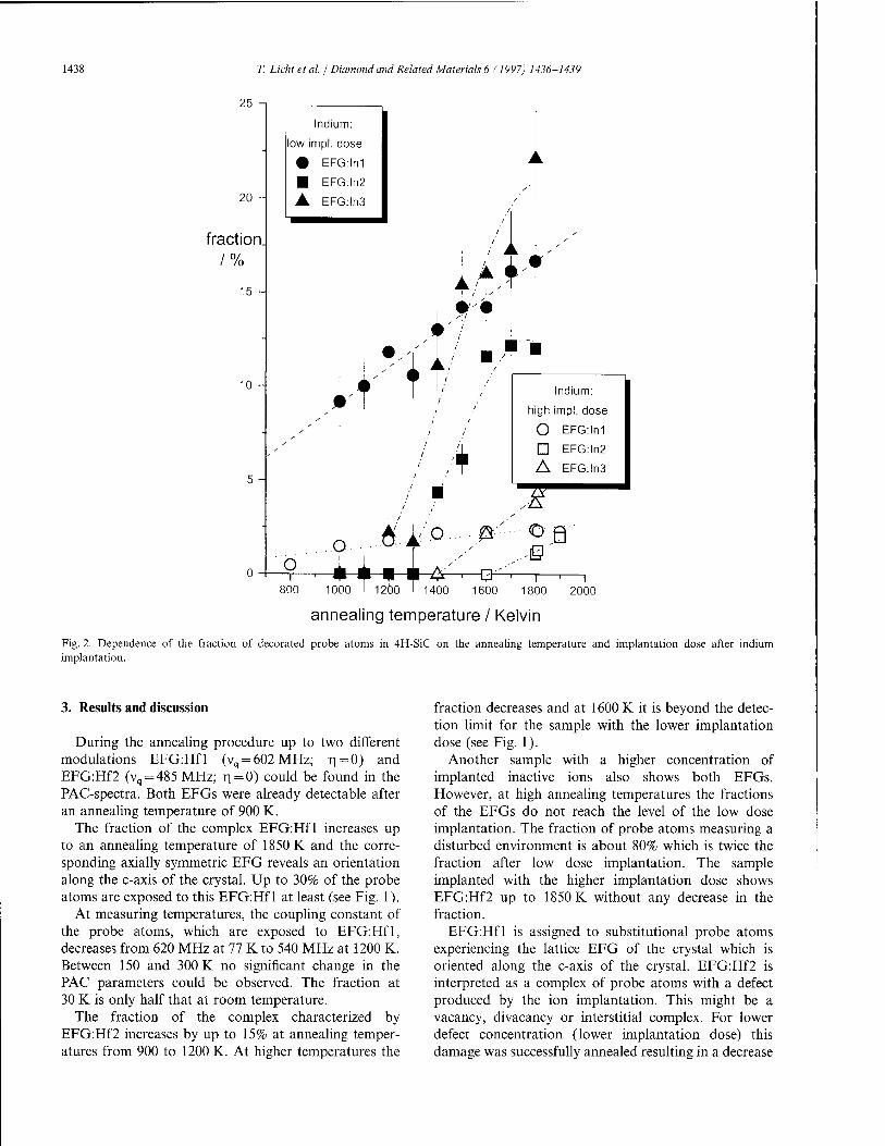
1438 T. Lichtetal. / Diamond and Related Materials 6 (1997) 1436-1439
25
20 -
fraction. /%
15 H
10 -
Indium:
low impl. dose
• EFG:ln1
■ EFG:ln2
A EFG:ln3
t T
*-T'f
;XfT A / I A
I ^
■ / t ■ +
+
o
ndium:
high mpl. dose
o EFG:ln1
D EFG:ln2
A EFG:ln3
-1—I—I—I
800 10Ö0 I 1200 I 1400 1600 1800 2000
annealing temperature / Kelvin
Fig. 2. Dependence of the fraction of decorated probe atoms in 4H-SiC on the annealing temperature and implantation dose after indium implantation.
3. Results and discussion
During the annealing procedure up to two different modulations EFG:Hfl (vq = 602MHz; r|=0) and EFG:Hf2 (vq = 485 MHz; r|=0) could be found in the PAC-spectra. Both EFGs were already detectable after an annealing temperature of 900 K.
The fraction of the complex EFG:Hf 1 increases up to an annealing temperature of 1850 K and the corre- sponding axially symmetric EFG reveals an orientation along the c-axis of the crystal. Up to 30% of the probe atoms are exposed to this EFG:Hfl at least (see Fig. 1).
At measuring temperatures, the coupling constant of the probe atoms, which are exposed to EFG:Hfl, decreases from 620 MHz at 77 K to 540 MHz at 1200 K. Between 150 and 300 K no significant change in the PAC parameters could be observed. The fraction at 30 K is only half that at room temperature.
The fraction of the complex characterized by EFG:Hf2 increases by up to 15% at annealing temper- atures from 900 to 1200 K. At higher temperatures the
fraction decreases and at 1600 K it is beyond the detec- tion limit for the sample with the lower implantation dose (see Fig. 1).
Another sample with a higher concentration of implanted inactive ions also shows both EFGs. However, at high annealing temperatures the fractions of the EFGs do not reach the level of the low dose implantation. The fraction of probe atoms measuring a disturbed environment is about 80% which is twice the fraction after low dose implantation. The sample implanted with the higher implantation dose shows EFG:Hf2 up to 1850 K without any decrease in the fraction.
EFG:Hfl is assigned to substitutional probe atoms experiencing the lattice EFG of the crystal which is oriented along the c-axis of the crystal. EFG:Hf2 is interpreted as a complex of probe atoms with a defect produced by the ion implantation. This might be a vacancy, divacancy or interstitial complex. For lower defect concentration (lower implantation dose) this damage was successfully annealed resulting in a decrease
T. Lichtetal. / Diamond and Related Materials 6 (1997) 1436-1439 1439
in the fraction of EFG:Hf2. This decrease in EFG:Hf2 is of the same magnitude as the increase in the fraction of EFG:Hfl. This result supports the interpretation of EFG:Hf2 as a defect complex, whereas EFG:Hfl is a lattice-induced EFG. The higher implantation dose caused lattice damage which was not completely annealed at this temperature. The dominance of EFG:Hf 1 supports its interpretation as a defect complex.
PAC investigations of the Hf probe atom are now compared to PAC measurements using the probe atom Cd or In, both measured at the same isomeric level of Cd. Here one EFG is detectable showing a behaviour very similar to EFG:Hf 1. This EFG:1 is already detecta- ble after an annealing temperature of 800 K. The frac- tion of this complex increases up to an annealing temperature of 1800 K showing an axial symmetry tensor oriented along the c-axis of the crystal (see Fig. 2). The coupling constant of this EFG:1 does not change significantly during the whole measuring temper- ature range. EFG:1 is assigned to substitutional probe atoms experiencing the lattice EFG of the crystal ori- ented along the c-axis of the crystal.
The two other EFGs are interpreted as complexes of probe atoms with a defect produced by ion implantation. The two different EFGs can be understood because of the two different silicon lattice sites of the probe atoms in 4H-SiC. At high implantation concentrations the annealing behavior of the indium-implanted samples is
very similar to the results for hafnium implantation (see Fig. 1 and Fig. 2). Contrary to the annealing behavior of the of EFG:HF2 observed after low-concentration HF implantation nothing comparable could be mea- sured after In or Cd implantation. The fraction increases up to an annealing temperature of 1600 K and remains constant up to 1900 K. A decrease of the observed fractions could not be observed. This leads to the interpretation of the EFG:2 and 3 as an indium-vacancy complex, which is much more stable up to higher annealing temperatures. A detailed description of the results of the indium and cadmium investigation depend- ing on the nitrogen concentration is given in Ref. [4].
References
[1] H. Frauenfelder, H.M. Steffen, in: K. Siegbaum (Ed.) Angular Distribution of Nuclear Radiation in Alpha-, Beta-, and Gamma-ray Spectroscopy, vol. 2, North Holland, Amsterdam, 1965, p. 997.
[2] Th. Wiehert, N. Achtziger, H. Metzner, R. Sielemann, in: G. Lan- gouche (Ed.) Hyperfine Interactions in Semiconductors, North Holland, Amsterdam, 1992.
[3] J.F. Ziegler, J.P. Biersack, U. Littmark, The Stopping and Ranges of Ions in Solids, Pergamon, New York, 1985.
[4] T. Licht, N. Achtziger, D. Forkel-Wirth, U. Reislöhner, M. Rüb, M. Uhrmacher, W. Witthuhn and ISOLDE Collaboration, Insti- tute of Physics Conference Series No. 142, Chapter 2, 1996. 461-464
ELSEVIER
DIAMOND AND
RELATED MATERIALS
Diamond and Related Materials 6 (1997) 1440-1444
Nuclear transmutation doping of 6H-silicon carbide with phosphorous
Hans Heissenstein *, Christian Peppermüller, Reinhard Heibig Institute of Applied Physics, University of Erlangen-Nürnberg, D-91058 Erlangen, Germany
Abstract
Aluminium doped 6H-SiC epilayers on a p+ doped 6H-SiC substrate were irradiated with total neutron doses of 9.4 x 1019 cm"2, 3.5 x 1020 cm"2, and 6.4 x 1020 cm"2 respectively. A donor species is produced by a nuclear reaction involving the decay of 31Si to 31P. The ß" activity after irradiation was measured. The samples were subsequently annealed at a temperature range of between 800 and 1800 °C. The annealing behaviour was studied by Low Temperature Photoluminescence (LTPL), Fourier Transform Infrared Spectroscopy (FTIR), Hall-effect, /-Fand C-Vmeasurements. The p type 6H-SiC epilayer was transmuted to n-type by an annealing process which resulted in a p-n junction to the p+ substrate. © 1997 Elsevier Science S.A.
Keywords: SiC; pn-junction; Phosphorous; Photoluminescence
1. Introduction
Silicon carbide as a wide band-gap semiconductor material with high thermal conductivity and chemical resistance, is suitable for high power, high frequency electronic devices with high radiation resistance. Until now the commonly used dopants in SiC have been nitrogen as a donor and aluminium as an acceptor. However, in situ doping during crystal growth or epitaxy is difficult to control and not very homogeneous.
Up to now silicon is still the best semiconductor material for high power devices. For this purpose it is homogenously doped by neutron transmutation doping using phosphorous to get a n-type material (e.g. Refs [1,2]). The implementation of this doping process was a real breakthrough in the development of Si power devices [3]. Phosphorous is also a donor in SiC. Therefore we need to test whether doping SiC by neutron transmutation with phosphorous is useful in obtaining homogeneously doped substrates or layers for new appli- cations. The high nitrogen concentration which is incor- porated unintentionally during growth makes the provision of high neutron doses necessary if higher phosphorous concentrations are to be achieved. Since the thermal neutron flux cannot be raised, one has to come along with high portions of fast neutrons, which cause severe damage in the SiC-lattice. It should be
* Corresponding author.
noted that the radiation damage caused by the fast neutrons is the reason for applying an annealing process. The radiation damage due to the nuclear reaction Si->P is very low.
2. Experimental
2.1. Preparation
We used a commercially available wafer (CREE Research Inc.) 3 pm (0001) 6H-SiC epitaxial layer (p-type, (NA-ND) = 5.2x 1015 cm"3 on a 300 pm thick 6H substrate (p-type, (NA-ND) = \018 cm"3) (Fig. 1). This wafer was cut into six pieces of approx. 5x5 mm. The different pieces were then irradiated within a moder- ated reactor spectrum (Table 1) in the RISÖ-nuclear reactor in Roskilde, Denmark. We irradiated two samples for each of three different periods (Table 1) to obtain three different doping concentrations.
Samples LI, Ml, H2 were successively annealed in several steps from 800 to 1800 °C and sample L2 was annealed at 1600 and 1700 °C, each for 30 min. The anneals were carried out in a vacuum for temperatures up to 1000 °C and in an argon atmosphere for higher temperatures. For annealing from 1500 to 1800 °C the samples were mounted in a closed SiC-coated graphite crucible.
0925-9635/97/S17.00 © 1997 Elsevier Science S.A. All rights reserved. PII S0925-9635(97)00072-l
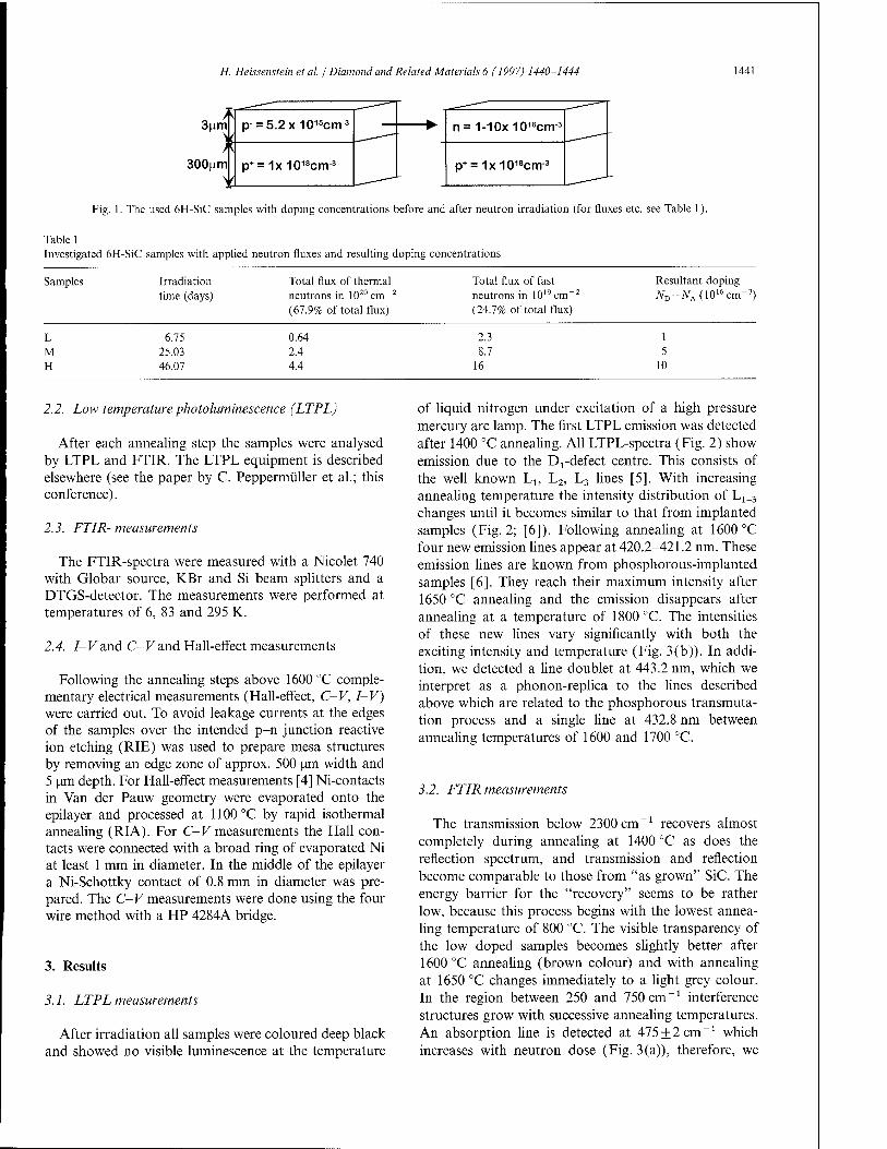
H. Heissenstein et al. / Diamond and Related Materials 6 (1997) 1440-1444 1441
3 urn
> 30(Vm
M
p=5.2x1015cm;
p+ = 1x1018cm;
^~—~— ^^~—-~~
n = 1-10x1016cnr3
■—-
p+ = 1x10¹⁸cnr3
Fig. 1. The used 6H-SiC samples with doping concentrations before and after neutron irradiation (for fluxes etc. see Table 1).
Table 1 Investigated 6H-SiC samples with applied neutron fluxes and resulting doping concentrations
Samples Irradiation time (days)
Total flux of thermal neutrons in 102Ocm~2
(67.9% of total flux)
Total flux of fast neutrons in 10'9cmT2
(24.7% of total flux)
Resultant doping WD-ArA(1016cm"3)
L M H
6.75 25.03 46.07
0.64 2.4 4.4
2.3 8.7
16
1 5
10
2.2. Low temperature photoluminescence (LTPL)
After each annealing step the samples were analysed by LTPL and FTIR. The LTPL equipment is described elsewhere (see the paper by C. Peppermüller et al.; this conference).
2.3. FTIR-measurements
The FTIR-spectra were measured with a Nicolet 740 with Globar source, KBr and Si beam splitters and a DTGS-detector. The measurements were performed at temperatures of 6, 83 and 295 K.
2.4. I- V and C- V and Hall-effect measurements
Following the annealing steps above 1600 °C comple- mentary electrical measurements (Hall-effect, C-V, I-V) were carried out. To avoid leakage currents at the edges of the samples over the intended p-n junction reactive ion etching (RIE) was used to prepare mesa structures by removing an edge zone of approx. 500 pm width and 5 um depth. For Hall-effect measurements [4] Ni-contacts in Van der Pauw geometry were evaporated onto the epilayer and processed at 1100 °C by rapid isothermal annealing (RIA). For C-V measurements the Hall con- tacts were connected with a broad ring of evaporated Ni at least 1 mm in diameter. In the middle of the epilayer a Ni-Schottky contact of 0.8 mm in diameter was pre- pared. The C-V measurements were done using the four wire method with a HP 4284A bridge.
3. Results
3.1. LTPL measuremen ts
After irradiation all samples were coloured deep black and showed no visible luminescence at the temperature
of liquid nitrogen under excitation of a high pressure mercury arc lamp. The first LTPL emission was detected after 1400 °C annealing. All LTPL-spectra (Fig. 2) show emission due to the D^defect centre. This consists of the well known L1; L2, L3 lines [5]. With increasing annealing temperature the intensity distribution of L^3
changes until it becomes similar to that from implanted samples (Fig. 2; [6]). Following annealing at 1600 °C four new emission lines appear at 420.2-421.2 nm. These emission lines are known from phosphorous-implanted samples [6]. They reach their maximum intensity after 1650 °C annealing and the emission disappears after annealing at a temperature of 1800 °C. The intensities of these new lines vary significantly with both the exciting intensity and temperature (Fig. 3(b)). In addi- tion, we detected a line doublet at 443.2 nm, which we interpret as a phonon-replica to the lines described above which are related to the phosphorous transmuta- tion process and a single line at 432.8 nm between annealing temperatures of 1600 and 1700 °C.
3.2. FTIR measurements
The transmission below 2300 cm"1 recovers almost completely during annealing at 1400 °C as does the reflection spectrum, and transmission and reflection become comparable to those from "as grown" SiC. The energy barrier for the "recovery" seems to be rather low, because this process begins with the lowest annea- ling temperature of 800 °C. The visible transparency of the low doped samples becomes slightly better after 1600 °C annealing (brown colour) and with annealing at 1650 °C changes immediately to a light grey colour. In the region between 250 and 750 cm"1 interference structures grow with successive annealing temperatures. An absorption line is detected at 475 + 2 cm"1 which increases with neutron dose (Fig. 3(a)), therefore, we
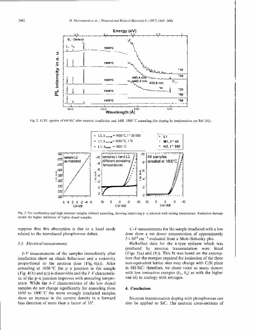
1442 H. Heissenstein et al. / Diamond and Related Materials 6 (1997) 1440-1444
tB C
c 0)
2.6 1 . f-
D, - Defect
Energy (eV) 2.7 2S_ I 1 II
11 1650°C
1600X
1500-C
1400°C *50
4800 4600 4400 Wavelength (A)
4200
Fig. 2. LTPL spectra of 6H-SiC after neutron irradiation and 1400-1800 °C annealing (for doping by implantation see Ref. [6]).
• L2,8lnnMl = 1600°C, * 20 000
■ L1, 8 „,„.„= 1650 °C, *5
• Ll.a^rt =1800°C
♦ L1
° M1, I* 40
• H2, 1*300
-023'
-Q15'
-0.D1
.-005" < EQCD"
-003'
QB"
Q15'
Q2T
l"l|Mlt|l
sample L2, as irradiated
rmrp
-10"
-8
-61
•I1"1!1"1!""!""!1
6 4 2 0-24-6 UinVdt
samples Hand L2, different annealing temperatures
1 -10' 1 "'I . All samples ; (l anealedat1800°C;;?
o U in Volt
0 U in Volt
Fig. 3. No rectification and high resistant samples without annealing, showing improving p-n junction with raising temperature. Radiation damage causes the higher resistance of higher dosed samples.
suppose that this absorption is due to a local mode related to the introduced phosphorous defect.
3.3. Electrical measurements
I-V measurements of the samples immediately after irradiation show an ohmic behaviour and a resistivity proportional to the neutron dose (Fig. 4(a)). After annealing at 1650 °C the p-n junction in the sample (Fig. 4(b) and (c)) is discernible and the I-V characteris- tic of the p-n junction improves with annealing temper- ature. While the I-V characteristics of the low doped samples do not change significantly for annealing from 1650 to 1800 °C the more strongly irradiated samples show an increase in the current density in a forward bias direction of more than a factor of 103.
C-V measurements for the sample irradiated with a low dose show a net donor concentration of approximately 5 x 1015 cm-3 evaluated from a Mott-Schottky plot.
Hall-effect data for the n-type epilayer which was produced by neutron transmutation were fitted (Figs. 5(a) and (b)). This fit was based on the assump- tion that the energies required for ionisation of the three non-equivalent lattice sites may change with C/Si place in 6H-SiC: therefore, we chose twice as many donors with low ionisation energies (äT1; k2) as with the higher one (h) in analogy with nitrogen.
4. Conclusions
Neutron transmutation doping with phosphorous can also be applied to SiC. The neutron cross-sections of
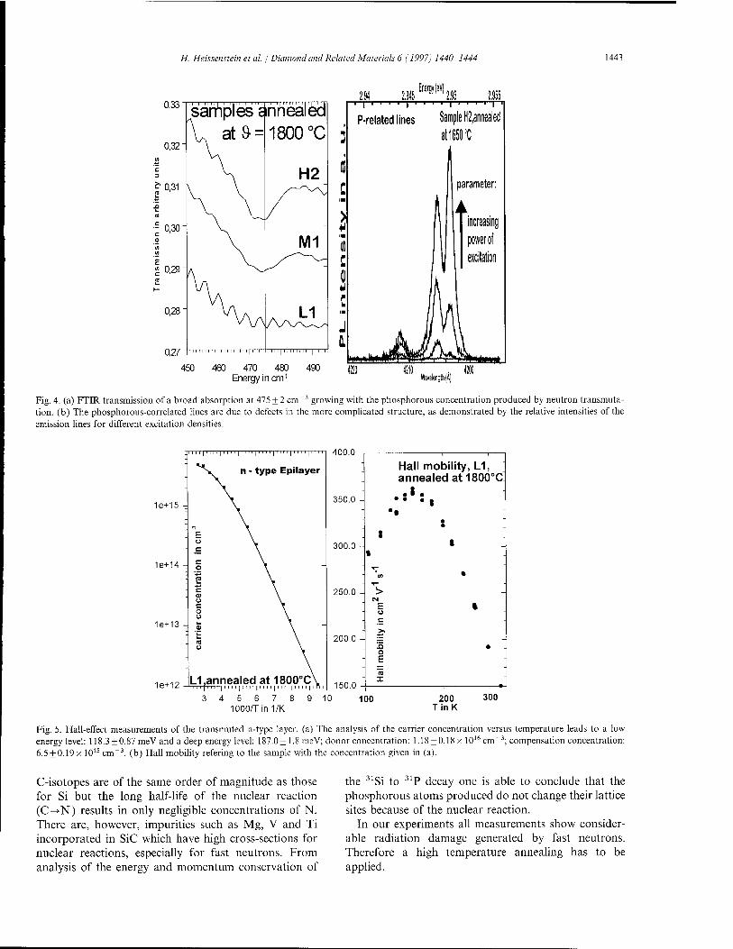
H. Heissenstein et al. / Diamond and Related Materials 6 (1997) 1440-1444 1443
EM
0,33" sariipleS's h'h'ealöd
0,32- V ata = 1800 °C
C 3
- 0,31 - H2
ra E 0,30- C o (/) (A
M1
» 0,29-
2
,-/
0,28"
0.27
IL1 - J D.
450 460 470 480 490 Energy in crrr1
■ I ■ ' ■ ■ I ■ ■ ■ ■ I ■ ' ' ■ I '
P-related lines Sample H2,annealed atWC
I
****** wto»«+
Wavelength (A|
Fig. 4. (a) FTIR transmission of a broad absorption at 475 + 2 cm-3 growing with the phosphorous concentration produced by neutron transmuta- tion, (b) The phosphorous-correlated lines are due to defects in the more complicated structure, as demonstrated by the relative intensities of the emission lines for different excitation densities.
; '"i ''«1'' ■' 1' ■ •' 1 ■''' 1 ■'«■ 1 ■''' 1''' ■
- •* n - type Epilayer
1e+15 - \ :
■?
- fc u ■ c
1e+14 - n o \
-j g c
- o " c
o u 1e+13 - <S) \
re u
1e+12 - Uf annealed at 1800°C\ i. i 11 i i i i u i i 11 i i i 1 i i i i ! i i i J ! i n i
- Hall mobility, L1, . annealed at 1800°C
350.0 - ..■:, : - »• - - - • . t .
300.0 - 1 _ ■
• - J ,_ -
m • - T- -
250.0 - !> _ 04
E % o c - >. -
200.0 - ■= - O
• iz ■
15 X
150.0 - 1 —i—»-i
3456789 1C 1000/Tin 1/K
200 300 Tin K
Fig. 5. Hall-effect measurements of the transmuted n-type layer, (a) The analysis of the carrier concentration versus temperature leads to a low energy level: 118.3 ±0.87 meV and a deep energy level: 187.0+1.8 meV; donor concentration: 1.18 + 0.18 x 1016 cm~3; compensation concentration: 6.5 + 0.19 x 1015 cm-3, (b) Hall mobility refering to the sample with the concentration given in (a).
C-isotopes are of the same order of magnitude as those for Si but the long half-life of the nuclear reaction (C-+N) results in only negligible concentrations of N. There are, however, impurities such as Mg, V and Ti incorporated in SiC which have high cross-sections for nuclear reactions, especially for fast neutrons. From analysis of the energy and momentum conservation of
the 31Si to 31P decay one is able to conclude that the phosphorous atoms produced do not change their lattice sites because of the nuclear reaction.
In our experiments all measurements show consider- able radiation damage generated by fast neutrons. Therefore a high temperature annealing has to be applied.

1444 H. Heissenstein et al. / Diamond and Related Materials 6 (1997) 1440-1444
References [3] E. Spenke, p-n Übergänge, Publisher: Springer, Berlin 1979, p. 138. [4] R. Schaub, G. Pensl, M. Schulz, C. Holm, Appl. Phys. A34
(1984)215. [1] M.S. Schneller, IEEE Trans. Elect. Dev. ED 21 (5) (1974) 313. [5] W.J. Choyke, L. Patrick, Phys. Rev. B5 (1972) 3253. [2] E.V. Haas, M.S. Schnöller, IEEE Trans. Elect. Dev. ED 23 (8) [6] T. Troffer, C. Peppermüller, G. Pensl, K. Rottner, A. Schöner,
(1976) 803. J. Appl. Phys. 80 (7) (1996) 3739-3743.
mm
ELSEVIER
DIAMOND AND
RELATED MATERIALS
Diamond and Related Materials 6 (1997) 1445-1447
Investigation of the effects of high temperature implantation and post implantation annealing on the electrical behavior of
nitrogen implanted ß-SiC films
W. Reichert a,H\ R. Lossy a, M. Gonzalez Sirgo a, E. Obermeier a, W. Skorupa b
Technical University of Berlin, Department of Electrical Engineering, Microsensor and Actuator Technology Center, Sehr. TIB 3.1, Gustav-Meyer-Allee 25, D-13355 Berlin, Germany
h FZ Rossendorf, FOB 510119, 01314 Dresden, Germany
Abstract
Nitrogen was implanted into p-type ß-SiC at implantation temperatures between 300 K and 1473 K. The implanted samples were characterized by Secondary Ion Mass Spectroscopy (SIMS) and electrically by resistivity and Hall measurements. The analysis was done with as-implanted samples and with samples that were annealed at 1473 K in a nitrogen atmosphere or in a vacuum. The implantation profiles did not show a significant dependence on the implantation temperature whereas the number of active dopants increased when the implantation temperature was raised. The electron mobility was also higher for high implantation temperatures, indicating a decrease in the implantation damage with increasing rimpl. As expected for the samples with Timpl<Tajineilh the annealing step caused a further rise in the number of electrically active dopants. The trend of electrical activation and the electron mobilities increasing with a higher implantation temperature remained unchanged also after the annealing step. © 1997 Elsevier Science S.A.
Keywords: ß-SiC; High temperature nitrogen implantation; Post implantation annealing; Electrical activation
1. Introduction
The material properties that characterize silicon car- bide are the wide bandgap, high breakdown electric field, high electron saturation velocity, and high chemical and physical stability. These properties make it a suitable material for high temperature, high power, and high frequency applications as well as for devices to be operated in chemically and radiation harsh environ- ments [1]. For micromechanical applications, e.g. sen- sors, the cubic polytype is of special interest. Since ß-SiC is deposited on Si or SOI (Silicon On Insulator) sub- strates, the micromachining of the substrate can be done with conventional silicon technology whereas the sensing elements are made of SiC.
Owing to the low diffusion coefficients of the dopants, ion implantation is the only possible technique for area selective doping of SiC. A major problem with ion implantation is the electrical activation of the implanted
* Corresponding author. Tel: +49 30 314 72 539; Fax: +49 30 314 72 603.
dopants in SiC. To achieve high activation the implanted wafers have to be annealed at very high temperatures (1773-1873 K), which is possible with bulk material such as 6H-SiC [2,3]. However, with ß-SiC annealing temperatures below the melting point of the Si substrate are necessary. To obtain high electrical activation with- out annealing at too higher temperatures, the implant- ation at elevated temperatures is a common method. During this work high temperature implantation of nitrogen in ß-SiC and post implantation annealing were analyzed with respect to the electrical behavior of the implanted films.
2. Experimental
Nitrogen was implanted into p-type (7YA = 2x 1018cm~3) ß-SiC obtained from CREE Inc., USA. For all samples the implantation energy was 50keV, the dose was 5xl014cm"2, and the implant- ation angle was 7° off axis. The implantation temper- atures were varied between room temperature (RT)
0925-9635/97/S17.00 © 1997 Elsevier Science S.A. All rights reserved. PII S0925-9635(97)00073-3

1446 W. Reichert et al. / Diamond and Related Materials 6 (1997) 1445-1447
and Timp\= 1473 K. The implantation parameters are listed in Table 1. After the implantation the wafers were diced. The first set of samples was analyzed without post implantation annealing while the second set was annealed at T= 1473 K (same as highest implantation temperature) for 60 minutes in a nitrogen atmosphere. Two samples, implanted at room temperature and at ^impi = 1473K, were also annealed in a vacuum at ^a, vac =1473 K for 30 min with a residual pressure Pres<10~6mbar.
The doping profiles were measured by secondary ion mass spectroscopy (SIMS) using negatively charged SiN ions while the electrical characterization was done by resistivity and Hall measurements.
3. Results and Discussion
3.1. Analysis of the Imp Ian ted Profiles
The dependence of the doping profile on the implant- ation temperature was obtained from SIMS measure- ments. The results of the as-implanted samples showed that the implantation profile is almost independent of the implantation temperature (Fig. 1). Only the tail of the profile implanted at rimpl = 1473K is larger than that of the samples implanted at lower temperatures which indicates diffusion of nitrogen at the highest temperature.
The profile implanted at T= 673 K was also analyzed by SIMS after the annealing step in nitrogen at ranneal= 1473 K. The profile broadened, i.e. the nitrogen concentration increased towards the surface and the tail became larger. The peak concentration was reduced when compared with the as-implanted sample (Fig. 1). The reason for the broadening of the profile is nitrogen diffusion due to the damage induced into the ß-SiC film during the implantation step. This effect is discussed in greater detail in [4].
^ 102° -
T «1473K
T = 1073K
T in
T -673K+ T = 1473K(N ) impl anneal 2
T - 300K
100 150 200 250 300
Depth [nm]
350 400
Fig. 1. Implantation (SIMS) profiles of nitrogen implanted in ß-SiC at four different temperatures without post implantation annealing compared with a sample annealed at T= 1473 K in nitrogen after the implantation process. The implantation energy and dose were 50 keV and 5 x 10" cm"2, respectively.
3.2. Electrical Characterization
From electrical measurements the resistivity, electrical activation and electron mobilities were determined (Hall method). The electrical characterization of the as-implanted samples showed no n-type doping for implantation temperatures below 1073 K. This is due to the high background p-type doping concentration (NA = 2 x 1018 cm~3) of the substrate. Nitrogen implant- ation into lower doped p-type ß-SiC using the same implantation energy and dose showed electrical activ-
for By
T, impl " = RT and increasing the
electrical activation T073K to 52% at
ations of 0.43% and 1.35% ^impi = 673 K, respectively [ 5 ]. implantation temperature the increased from 12% at rimpl = rimpl = 1473K.
In Fig. 2 the electrical activation is presented in terms of the activated dose. The electrical characterization of the samples after annealing in nitrogen and vacuum showed a significantly higher number of electrically
Table 1 Implantation conditions
Implantation Implantation Implantation Implantation Total time at implantation temperature (K) energy (keV) dose (cm 2) time (min) temperature (min)
RT 50 5x10" 2.1 _ 473 50 5x10" 2.1 17 673 50 5x10" 2.1 12 873 50 5x10" 2.2 7 1073 50 5x10" 6.5 14 1173 50 5x10" 6 13 1273 50 5x10" 6 13 1373 50 5x10" 6 14 1473 50 5x10" 7 15

W. Reichertet al. I Diamond and Related Materials 6 (1997) 1445-1447 1447
3,0x10«
2,5x10"
FT
E 2,0x10«
03 O 1,5x10« "D "D £ 1,0x10« CO >
< 5,0x10"
^ A
- r T -o— .^
JO-~. V / ■
1
- —■— annealed in N
2 —o— as-implanted
A annealed in vacuum
■" v 0,0 200 400 600 800 1000 1200 1400 1600
Implantation Temperature [K]
Fig. 2. Activated dose as a function of the implantation temperature for as-implanted and annealed (!Taimeal=1473K) ß-SiC samples. The implanted nitrogen dose was 5 x 1014 cm"2.
o 40
^Q / A
CO
> F
30 __—o o—
■GT
o
/ ■
u. 20 ■ 3. / >*
10 / /
5 - —o— annealed in N 2
2 —■— as-implanted /■ 0
A annealed in vacuum
1 ■
200 400 600 800 1000 1200 1400 1600
Implantation Temperature [K]
Fig. 3. Electron mobility vs. implantation temperature for as-implanted and annealed (ranneaI = 1473 K), nitrogen doped ß-SiC samples. The implantation energy and dose were 50 keV and 5 x 1014 cm"2, respectively.
active dopants as compared to the as-implanted case. However, the activation still showed a dependence on the temperature Timpi of the previous implantation step (Fig. 2) and the activation of the sample with Thnpi = ^anneal remained essentially the same even though the annealing time after the implantation step (60 min in nitrogen or 30 min in vacuum) was much longer than the annealing time during the implantation process (15 min).
Since most of the annealing was done in a nitrogen atmosphere it cannot be clearly distinguished between an increase in the electrical activation of the implanted dopants owing to the thermal treatment after the implantation, and an increase in the number of dopants due to damage-enhanced diffusion. However, since the two samples annealed in a vacuum show similar results to those annealed in nitrogen it appears likely that most of the increase in electrical activation results from the thermal treatment and not the in-diffusion of nitrogen atoms into the damaged crystal from outside. To clarify this point further annealing experiments are currently being performed.
The electron mobility of the as-implanted samples is in general very low (max. 30cm2V_1s_1) owing to high compensation. But it increases with increasing implantation temperature (Fig. 3) and therefore with an increasing number of free carriers. Normally the mobil- ity would decrease with increasing carrier concentration. However, if the damage is reduced when the implant- ation temperature is raised less scattering occurs and therefore the electron mobility is higher. And by raising the implantation temperature, the recrystallization during implantation can be increased as was also shown by Rutherford back scattering (RBS) [5]. However, the implantation damage is also reduced in an annealing step. Therefore the electron mobility is higher when the implanted samples are annealed.
4. Conclusions
The work shows that up to 50% electrical activation of the implanted nitrogen in ß-SiC can be obtained without post implantation annealing when the implant- ation is carried out at 1473 K. Annealing at the same temperature for a longer period of time did not cause a further increase in the electrical activation. However, the mobility values are improved.
The overall trend is that the electrical activation of the implanted nitrogen and the electron mobility increase with increasing implantation temperature for both sets of samples: the as-implanted and the annealed samples. The best results were obtained when the samples were implanted at high temperatures and annealed after the implantation.
Acknowledgement
The work was supported by the Commission of European Communities under the contract number BRE2-CT92-0211. The authors would also like to thank Ch. Wagner from the Daimler-Benz AG for technical assistance.
References
[1] P.G. Neudeck, J. Electron. Mat. 24 (4) (1995) 283. [2] J.A. Freitas, Jr., J. Gardner, M.V. Rao, Inst. Phys. Conf. Ser. No
142, Proceedings of the Sixth Intern. Conf. on Silicon Carbide and Related Materials, Kyoto Japan, 1996, p. 529.
[3] N. Inoue, A. Itoh, T. Komoto, H. Matsunami, T. Nakata, M. Wanatabe, Inst. Phys. Conf. Ser. No 142, Proceedings of the Sixth Intern. Conf. on Silicon Carbide and Related Materials, Kyoto Japan, 1996, p. 525.
[4] R. Lossy, W. Reichert, E. Obermeier, W. Skorupa, J. Electron. Mat. 26 (3) (1997) 123.
[5] R. Lossy, W. Reichert, E. Obermeier, J. Stoemenos, Inst. Phys. Conf. Ser. No 142, Proceedings of the Sixth Intern. Conf. on Silicon Carbide and Related Materials, Kyoto Japan, 1996 p. 553.
ELSEVIER
DIAMOND AND
RELATED MATERIALS
Diamond and Related Materials 6 (1997) 1448-1450
ß-SiC films on SOI substrates for high temperature applications
W. Reichert a,*5 E. Obermeiera, J. Stoemenos b
Technical University of Berlin, Department of Electrical Engineering, Microsensor and Actuator Technology Center, Sekr. TIB 3.1, Gustav-Meyer-Allee 25, D-13355 Berlin, Germany
h Aristotle University of Thessaloniki, Physics Department, 54006 Thessaloniki, Greece
Abstract
Single crystalline, cubic ß-SiC films were deposited by CREE Inc., USA on bonded SOI wafers. The SiC deposition took place under standard conditions used at CREE for deposition on Si wafers, and at deposition temperatures 25 °C and 50 °C below standard deposition conditions to investigate the influence of the deposition temperature on the damage of the buried oxide layer and therefore the insulating capability of that layer.
Transmission electron microscopy (TEM), atomic force microscopy (AFM) and optical microscopy were used for structural analysis of the Silicon Carbide On Insulator (SiCOI) structure. The deposited ß-SiC films, the buried Si02 layer, and the SiC/Si interface were investigated. First measurements showed similar results for all three deposition temperatures indicating that the deposition temperature is not the only parameter defining the structural and therefore also the electrical quality of the SiCOI wafers. The electrical measurements were performed up to T= 723 K (current limit of the equipment) and the results showed good electrical insulation of the SiC layer from the Si substrate in the whole temperature range. © 1997 Elsevier Science S.A.
Keywords: ß-SiC on SOI; SiCOI; Bonded SOI; High temperature
1. Introduction
Cubic silicon carbide, heteroepitaxially grown on sili- con, gives a material system that combines the high temperature capabilities of SiC with the micromachining possibilities of Si. Therefore this material system appears especially interesting for the development of micro- mechanical devices such as microsensors based on mem- branes, e.g. pressure, gas, and acceleration sensors for operation at high temperatures [1]. However, next to its advantages the SiC/Si system has a major problem. At temperatures greater than approximately 150-200 °C the SiC/Si heterojunction becomes leaky, which results in a current flow through the Si substrate [2]. One approach to minimize or remove this effect is the depos- ition of thin SiC films on SOI (Silicon On Insulator) substrates. Experiments with SiCOI structures, where ß-SiC was grown on SIMOX (Separation by Implanted Oxygen) substrates were very promising since that system allowed higher operating temperatures than the SiC/Si system. However, during the carbonization pro- cess cavities were formed in the Si-overlayer that extended to the buried oxide. This damage and the Si
: Corresponding author. Tel: +30 31 998 191; Fax: +30 31 214 276.
islands in the buried oxide limited the applicability of the SiC/SIMOX system to approximately 300 °C [3]. To obtain electrical insulation of the SiC film from the Si substrate for temperatures higher than 300 °C a better quality SOI substrate with a thermal oxide was used during this work.
2. Experimental
Bonded, (lOO)-oriented SOI wafers (UNIBOND), obtained from SOITEC, France, have been used for ß-SiC deposition since the thermal oxide with its higher density is expected to be a better insulator at high temperatures than an implanted oxide as in the case of SIMOX wafers. The UNIBOND wafers were fabricated using the Smart-Cut® process. The thicknesses of the Si-overlayer and the buried, thermal oxide layer (Box) were 200 nm and 400 nm, respectively (Fig. 1). The substrates used for ß-SiC deposition were (lOO)-oriented and had a size of 20 x 20 mm. The deposited ß-SiC films were 2.2 inn thick with an n-type doping concentration of 7VD = 3 x 10¹⁸ cmT3 at room temperature.
After deposition structural characterization of the ß-SiC films, the Si-overlayer, the buried Si02 layer, and the SiC/Si interface was done by optical microscopy,
0925-9635/97/$ 17.00 © 1997 Elsevier Science S.A. All rights reserved. PII S0925-9635(97)00078-2
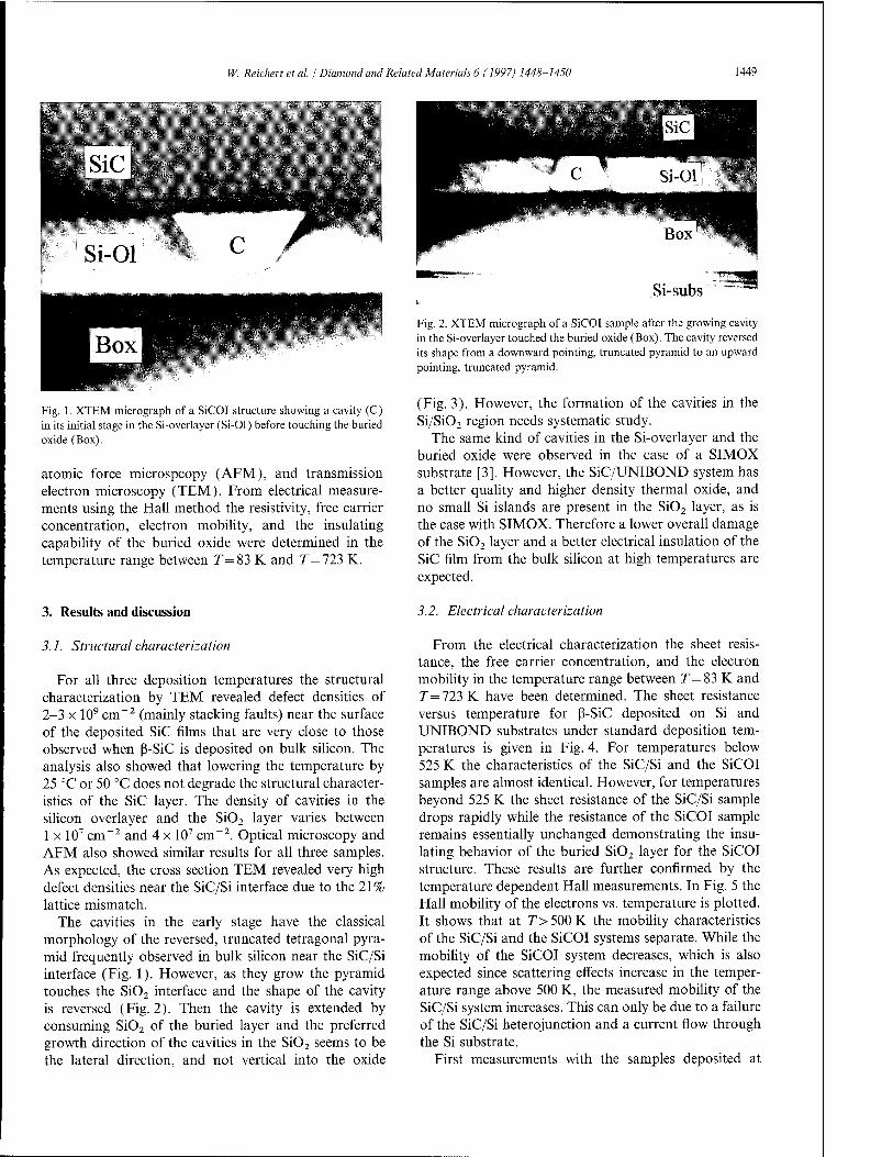
W. Reichert et al I Diamond and Related Materials 6 (1997) 1448-1450 1449
Si-01
Fig. 1. XTEM micrograph of a SiCOI structure showing a cavity (C) in its initial stage in the Si-overlayer (Si-Ol) before touching the buried oxide (Box).
atomic force microspcopy (AFM), and transmission electron microscopy (TEM). From electrical measure- ments using the Hall method the resistivity, free carrier concentration, electron mobility, and the insulating capability of the buried oxide were determined in the temperature range between T=83 K and 7"= 723 K.
3. Results and discussion
3.1. Structural characterization
For all three deposition temperatures the structural characterization by TEM revealed defect densities of 2-3 x 109 cm-2 (mainly stacking faults) near the surface of the deposited SiC films that are very close to those observed when ß-SiC is deposited on bulk silicon. The analysis also showed that lowering the temperature by 25 °C or 50 °C does not degrade the structural character- istics of the SiC layer. The density of cavities in the silicon overlayer and the Si02 layer varies between 1 x 107 cm"2 and 4 x 107 cm-2. Optical microscopy and AFM also showed similar results for all three samples. As expected, the cross section TEM revealed very high defect densities near the SiC/Si interface due to the 21% lattice mismatch.
The cavities in the early stage have the classical morphology of the reversed, truncated tetragonal pyra- mid frequently observed in bulk silicon near the SiC/Si interface (Fig. 1). However, as they grow the pyramid touches the Si02 interface and the shape of the cavity is reversed (Fig. 2). Then the cavity is extended by consuming SiOz of the buried layer and the preferred growth direction of the cavities in the Si02 seems to be the lateral direction, and not vertical into the oxide
Si-subs
Fig. 2. XTEM micrograph of a SiCOI sample after the growing cavity in the Si-overlayer touched the buried oxide (Box). The cavity reversed its shape from a downward pointing, truncated pyramid to an upward pointing, truncated pyramid.
(Fig. 3). However, the formation of the cavities in the Si/Si02 region needs systematic study.
The same kind of cavities in the Si-overlayer and the buried oxide were observed in the case of a SIMOX substrate [3]. However, the SiC/UNIBOND system has a better quality and higher density thermal oxide, and no small Si islands are present in the Si02 layer, as is the case with SIMOX. Therefore a lower overall damage of the Si02 layer and a better electrical insulation of the SiC film from the bulk silicon at high temperatures are expected.
3.2. Electrical characterization
From the electrical characterization the sheet resis- tance, the free carrier concentration, and the electron mobility in the temperature range between T= 83 K and T=723K have been determined. The sheet resistance versus temperature for ß-SiC deposited on Si and UNIBOND substrates under standard deposition tem- peratures is given in Fig. 4. For temperatures below 525 K the characteristics of the SiC/Si and the SiCOI samples are almost identical. However, for temperatures beyond 525 K the sheet resistance of the SiC/Si sample drops rapidly while the resistance of the SiCOI sample remains essentially unchanged demonstrating the insu- lating behavior of the buried Si02 layer for the SiCOI structure. These results are further confirmed by the temperature dependent Hall measurements. In Fig. 5 the Hall mobility of the electrons vs. temperature is plotted. It shows that at 7V500K the mobility characteristics of the SiC/Si and the SiCOI systems separate. While the mobility of the SiCOI system decreases, which is also expected since scattering effects increase in the temper- ature range above 500 K, the measured mobility of the SiC/Si system increases. This can only be due to a failure of the SiC/Si heterojunction and a current flow through the Si substrate.
First measurements with the samples deposited at
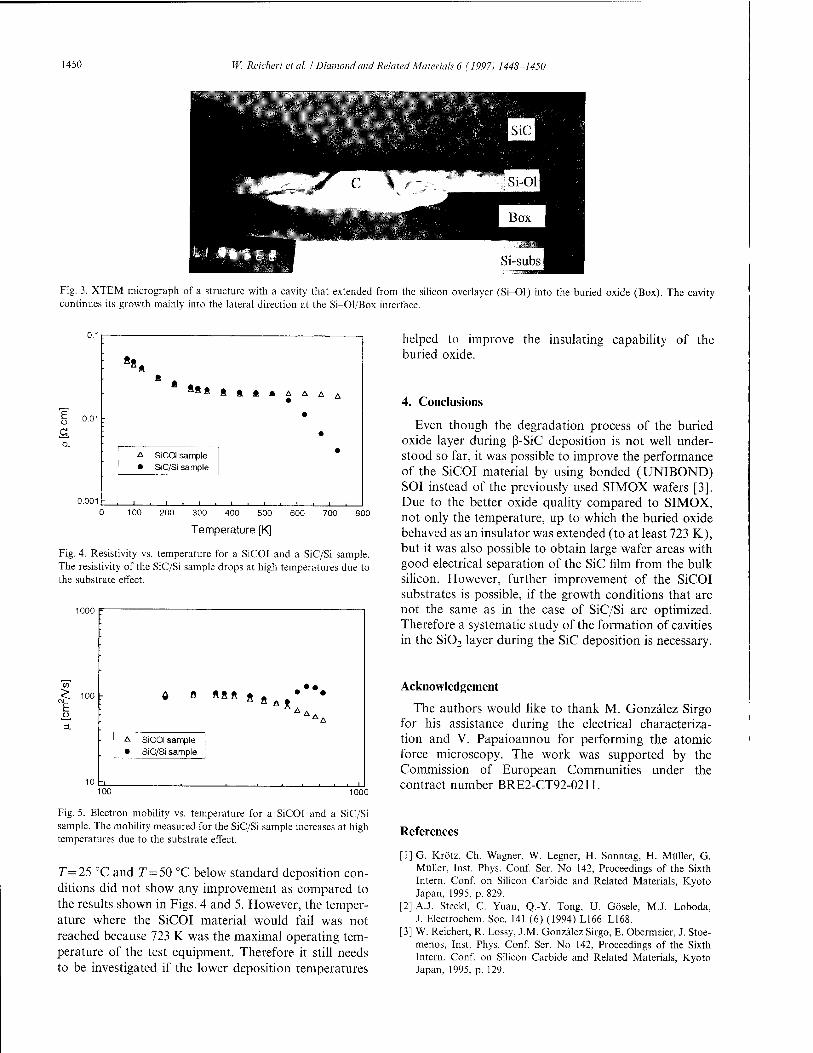
1450 W. Reichert et al. I Diamond and Related Materiah 6 (1997) 1448-1450
Fig. 3. XTEM micrograph of a structure with a cavity that extended from the silicon overlayer (Si-Ol) into the buried oxide (Box). The cavity continues its growth mainly into the lateral direction at the Si-Ol/Box interface.
0.01
8«
• «is ÄlftaAAAA
• •
A Sica sample • SiC/Si sample
•
.001 i.i.i. 1
100 500 600 700
Temperature [K]
Fig. 4. Resistivity vs. temperature for a SiCOI and a SiC/Si sample. The resistivity of the SiC/Si sample drops at high temperatures due to the substrate effect.
1000
^ 10° E
r A a
A*AA
A SiCOI sample • SiC/Si sample
100 1000
Fig. 5. Electron mobility vs. temperature for a SiCOI and a SiC/Si sample. The mobility measured for the SiC/Si sample increases at high temperatures due to the substrate effect.
7=25 °C and T=50 °C below standard deposition con- ditions did not show any improvement as compared to the results shown in Figs. 4 and 5. However, the temper- ature where the SiCOI material would fail was not reached because 723 K was the maximal operating tem- perature of the test equipment. Therefore it still needs to be investigated if the lower deposition temperatures
helped to improve the insulating capability of the buried oxide.
4. Conclusions
Even though the degradation process of the buried oxide layer during ß-SiC deposition is not well under- stood so far, it was possible to improve the performance of the SiCOI material by using bonded (UNIBOND) SOI instead of the previously used SIMOX wafers [3]. Due to the better oxide quality compared to SIMOX, not only the temperature, up to which the buried oxide behaved as an insulator was extended (to at least 723 K), but it was also possible to obtain large wafer areas with good electrical separation of the SiC film from the bulk silicon. However, further improvement of the SiCOI substrates is possible, if the growth conditions that are not the same as in the case of SiC/Si are optimized. Therefore a systematic study of the formation of cavities in the Si02 layer during the SiC deposition is necessary.
Acknowledgement
The authors would like to thank M. Gonzalez Sirgo for his assistance during the electrical characteriza- tion and V. Papaioannou for performing the atomic force microscopy. The work was supported by the Commission of European Communities under the contract number BRE2-CT92-0211.
References
[1] G. Krötz, Ch. Wagner, W. Legner, H. Sonntag, H. Müller, G. Müller, Inst. Phys. Conf. Ser. No 142, Proceedings of the Sixth Intern. Conf. on Silicon Carbide and Related Materials, Kyoto Japan, 1995, p. 829.
[2] A.J. Steckl, C. Yuan, Q.-Y. Tong, U. Gösele, MJ. Loboda, J. Electrochem. Soc. 141 (6) (1994) L166-L168.
[3] W. Reichert, R. Lossy, J.M. Gonzalez Sirgo, E. Obermeier, J. Stoe- menos, Inst. Phys. Conf. Ser. No 142, Proceedings of the Sixth Intern. Conf. on Silicon Carbide and Related Materials, Kyoto Japan, 1995, p. 129.
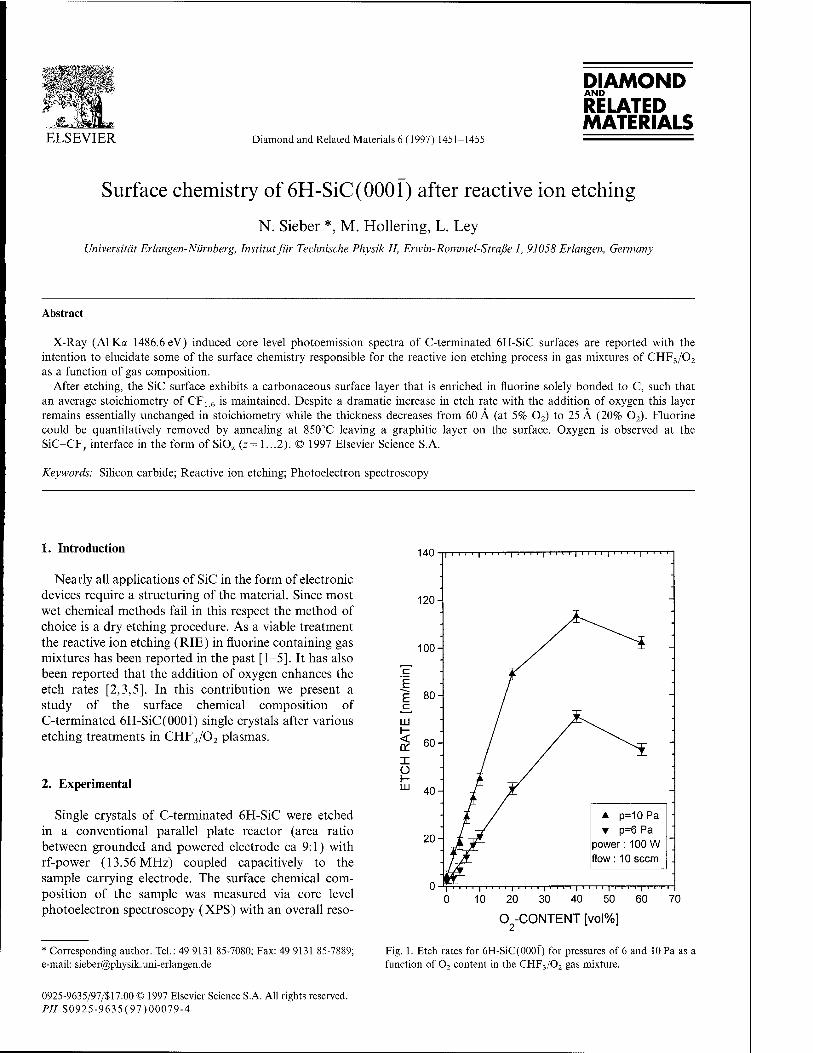
ELSEVIER
DIAMOND AND
RELATED MATERIALS
Diamond and Related Materials 6 (1997) 1451-1455
Surface chemistry of 6H-SiC(0001) after reactive ion etching
N. Sieber *, M. Hollering, L. Ley Universität Erlangen-Nürnberg, Institut für Technische Physik II, Erwin-Rommel-Straße 1, 91058 Erlangen, Germany
Abstract
X-Ray (Al Ka 1486.6 eV) induced core level photoemission spectra of C-terminated 6H-SiC surfaces are reported with the intention to elucidate some of the surface chemistry responsible for the reactive ion etching process in gas mixtures of CHF3/02
as a function of gas composition. After etching, the SiC surface exhibits a carbonaceous surface layer that is enriched in fluorine solely bonded to C, such that
an average stoichiometry of C¥1 6 is maintained. Despite a dramatic increase in etch rate with the addition of oxygen this layer remains essentially unchanged in stoichiometry while the thickness decreases from 60 A (at 5% 02) to 25 A (20% 02). Fluorine could be quantitatively removed by annealing at 850°C leaving a graphitic layer on the surface. Oxygen is observed at the SiC-CF,, interface in the form of SiOz (z= 1...2). © 1997 Elsevier Science S.A.
Keywords: Silicon carbide; Reactive ion etching; Photoelectron spectroscopy
1. Introduction
Nearly all applications of SiC in the form of electronic devices require a structuring of the material. Since most wet chemical methods fail in this respect the method of choice is a dry etching procedure. As a viable treatment the reactive ion etching (RIE) in fluorine containing gas mixtures has been reported in the past [1-5]. It has also been reported that the addition of oxygen enhances the etch rates [2,3,5]. In this contribution we present a study of the surface chemical composition of C-terminated 6H-SiC(000l) single crystals after various etching treatments in CHF3/02 plasmas.
2. Experimental
Single crystals of C-terminated 6H-SiC were etched in a conventional parallel plate reactor (area ratio between grounded and powered electrode ca 9:1) with rf-power (13.56 MHz) coupled capacitively to the sample carrying electrode. The surface chemical com- position of the sample was measured via core level photoelectron spectroscopy (XPS) with an overall reso-
* Corresponding author. Tel.: 49 9131 85-7080; Fax: 49 9131 85-7889; e-mail: [email protected]
0 'j i i i i | i i i i ] i i i i | i i i i [ i i i i | i i i i [ i i i i
0 10 20 30 40 50 60 70
O -CONTENT [vol%]
Fig. 1. Etch rates for 6H-SiC(000f) for pressures of 6 and 10 Pa as < function of 02 content in the CHF3/02 gas mixture.
0925-9635/97/S17.00 © 1997 Elsevier Science S.A. All rights reserved. PII S0925-9635(97)00079-4

1452 N. Sieber et al. I Diamond and Related Materials 6 (1997) 1451-1455
z D cd
<
U) Z LU
C1s
CIll -
cm \/ C IV
ci 1 TU cv \j ft il\ K/KA CVI 1 l\
JJl w vU cvn■
280 285 290 295
528 532 536 540 680 685 690 695
BINDING ENERGY REL. TO Ep [eV]
Fig. 2. High resolution core level spectra of all relevant elements after etching 6H-SiC in a CHF3/02 gas mixture with 20 vol% of 02 for 10 min and at a pressure of 50 Pa. Also shown are the line components used to fit the spectra. The Sill and Silll peak positions in the Si 2p spectrum are confirmed by other measurements where ca 15 at% of Si is bonded to oxygen.
lution of 0.6 eV using monochromatized Al Ka radiation (hv= 1486.6 eV). The relative concentration of a chemi- cal species within the sampling volume was determined from the area under the corresponding XPS line compo- nents after appropriate corrections for photoemission cross-sections according to Scofield [6] and for spec- trometer sensitivity have been made.
3. Results and discussion
All etch treatments were performed with the sample nominally at room temperature, an rf-power of 100 W, a gas flow of 10 seem, and pressures of 6 and 10 Pa, respectively, which results in bias voltages on the sample carrying electrode between —625 and —775 V. Fig. 1 shows the etch rate in a gas mixture of CHF3 and 02. Initially the etch rate increases linearly with 02 content, reaches a maximum of 70 nm min ~1 at 6 Pa and 110 nm min-1 at 10 Pa at an oxygen content of 40 vol%, and drops with higher 02 content. Without oxygen we
measure etch rates of only about 4nmmin_1. These results agree qualitatively with most previous reports about the beneficial effect of oxygen on the etch rate of SiC using CHF3 or CF4 as the main etching agent [2,3,5] despite one report to the contrary [1].
Two sets of core level spectra and their fits which are representative for the ones used to derive the surface chemical composition of the samples after different treatments are shown in Fig. 2 (as etched) and Fig. 3 (after an additional annealing step at 850°C for 10 min). The fits were performed with the constraint that a minimum number of components compatible with the experimental conditions was required to fit all the spectra. The Si 2p lines were fitted using a spin-orbit doublet with a splitting of 0.6 eV and a branching ratio of 2 [7,8].
Most of the line positions and their assignments to a chemical species agree with those given in the literature [9-12]. The Sil and CI components at binding energies of 101.0 + 0.1 and 283.5 + 0.1 eV, respectively, are due to SiC. Two further Si components at 102.3 + 0.1 and
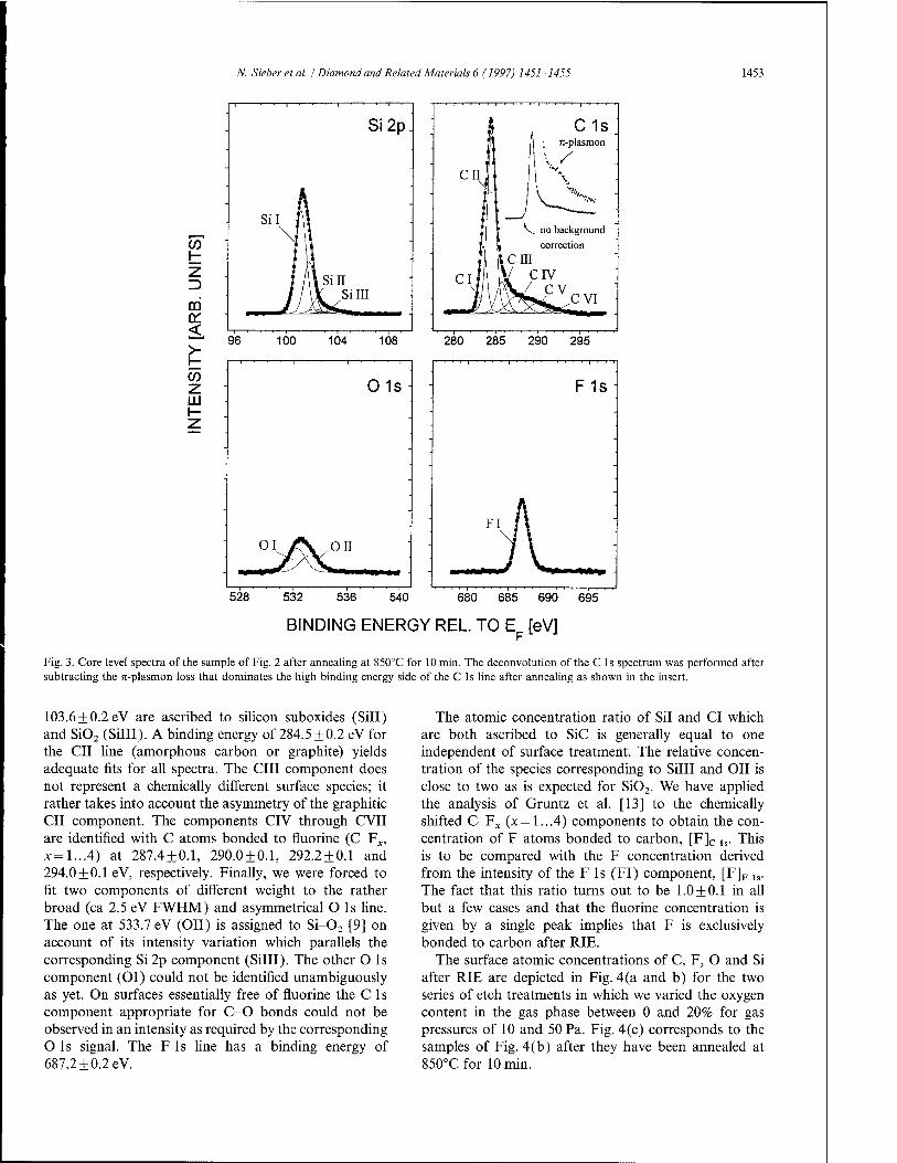
N. Sieber et al. / Diamond and Related Materials 6 (1997) 1451-1455 1453
C/)
m a: <^
w z LU
1 C1s |t Jl ■_ Jt-plasmon
CII l l ;-v
1 1 V f;°^,i-
1 V. no background I correction item
eil IV civ
280 285 290 295
528 532 536 540 680 685 690 695
BINDING ENERGY REL. TO Ep [eV]
Fig. 3. Core level spectra of the sample of Fig. 2 after annealing at 850°C for 10 min. The deconvolution of the C Is spectrum was performed after subtracting the 71-plasmon loss that dominates the high binding energy side of the C 1 s line after annealing as shown in the insert.
103.6 + 0.2 eV are ascribed to silicon suboxides (Sill) and Si02 (Silll). A binding energy of 284.5±0.2 eV for the CII line (amorphous carbon or graphite) yields adequate fits for all spectra. The CIII component does not represent a chemically different surface species; it rather takes into account the asymmetry of the graphitic CII component. The components CIV through CVII are identified with C atoms bonded to fluorine (C-Fx, x=1...4) at 287.4 + 0.1, 290.0 + 0.1, 292.2 + 0.1 and 294.0 + 0.1 eV, respectively. Finally, we were forced to fit two components of different weight to the rather broad (ca 2.5 eV FWHM) and asymmetrical O Is line. The one at 533.7 eV (Oil) is assigned to Si-02 [9] on account of its intensity variation which parallels the corresponding Si 2p component (Silll). The other O Is component (OI) could not be identified unambiguously as yet. On surfaces essentially free of fluorine the C Is component appropriate for C-O bonds could not be observed in an intensity as required by the corresponding O Is signal. The F Is line has a binding energy of 687.2 + 0.2 eV.
The atomic concentration ratio of Sil and CI which are both ascribed to SiC is generally equal to one independent of surface treatment. The relative concen- tration of the species corresponding to Silll and Oil is close to two as is expected for Si02. We have applied the analysis of Gruntz et al. [13] to the chemically shifted C-Fx (x = l..A) components to obtain the con- centration of F atoms bonded to carbon, [F]c ls. This is to be compared with the F concentration derived from the intensity of the F ls (FI) component, [F]F ls. The fact that this ratio turns out to be 1.0 + 0.1 in all but a few cases and that the fluorine concentration is given by a single peak implies that F is exclusively bonded to carbon after RIE.
The surface atomic concentrations of C, F, O and Si after RIE are depicted in Fig. 4(a and b) for the two series of etch treatments in which we varied the oxygen content in the gas phase between 0 and 20% for gas pressures of 10 and 50 Pa. Fig. 4(c) corresponds to the samples of Fig. 4(b) after they have been annealed at 850°Cfor 10 min.
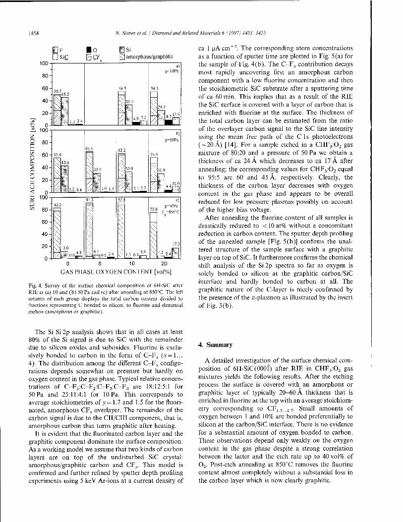
1454 N. Sieber et al. / Diamond and Related Materials 6 (1997) 1451-1455
ISi [\\] amorphous/graphitic
t: 0 Ä 100
o H &o O
S o u w o < 0 S 10° 1/3 80
60-
40-
20
0
-
55.4
\v
1
43.C
12 0.4
65.5
33.' »
1-6 1.5
62.2
1 33.C
2.1 2.7
55.6
30.C
b)
p=50Pa
91.3 92.4 c) 83.2 ^ ~ p=50Pa
75 8
SS > \ ^ T -850°C
■ Ä A
■
^ ^ ^
^ 12.0
1 17.3
~>A 61 Of. ^;' 5.4
1.3 0.9p;—, \ 4A"U 0 5 10 20
GAS PHASE OXYGEN CONTENT [vol%]
Fig. 4. Survey of the surface chemical composition of 6H-SiC after RIE at (a) 10 and (b) 50 Pa and (c) after annealing at 850°C. The left column of each group displays the total carbon content divided to fractions representing C bonded to silicon, to fluorine and elemental carbon (amorphous or graphitic).
ca 1 uAcm-2. The corresponding atom concentrations as a function of sputter time are plotted in Fig. 5 (a) for the sample of Fig. 4(b). The C-Fx contribution decays most rapidly uncovering first an amorphous carbon component with a low fluorine concentration and then the stoichiometric SiC substrate after a sputtering time of ca 60 min. This implies that as a result of the RIE the SiC surface is covered with a layer of carbon that is enriched with fluorine at the surface. The thickness of the total carbon layer can be estimated from the ratio of the overlayer carbon signal to the SiC line intensity using the mean free path of the C Is photoelectrons (~20Ä) [14]. For a sample etched in a CHF3:02 gas mixture of 80:20 and a pressure of 50 Pa we obtain a thickness of ca 24 A which decreases to ca 17 A after annealing; the corresponding values for CHF3:02 equal to 95:5 are 60 and 45 A, respectively. Clearly, the thickness of the carbon layer decreases with oxygen content in the gas phase and appears to be overall reduced for low pressure plasmas possibly on account of the higher bias voltage.
After annealing the fluorine content of all samples is drastically reduced to < 10 at% without a concomitant reduction in carbon content. The sputter depth profiling of the annealed sample [Fig. 5(b)] confirms the unal- tered structure of the sample surface with a graphitic layer on top of SiC. It furthermore confirms the chemical shift analysis of the Si 2p spectra so far as oxygen is solely bonded to silicon at the graphitic carbon/SiC interface and hardly bonded to carbon at all. The graphitic nature of the C-layer is nicely confirmed by the presence of the n-plasmon as illustrated by the insert of Fig. 3(b).
The Si Si 2p analysis shows that in all cases at least 80% of the Si signal is due to SiC with the remainder due to silicon oxides and suboxides. Fluorine is exclu- sively bonded to carbon in the form of C-Fx (x = 1... 4). The distribution among the different C-Fx configu- rations depends somewhat on pressure but hardly on oxygen content in the gas phase. Typical relative concen- trations of C-Fi:C-F2:C-F3:C-F4 are 18:12:5:1 for 50 Pa and 25:11:4:1 for 10 Pa. This corresponds to average stoichiometries of y—1.7 and 1.5 for the fluori- nated, amorphous CFj, overlayer. The remainder of the carbon signal is due to the CII/CIII component, that is, amorphous carbon that turns graphitic after heating.
It is evident that the fluorinated carbon layer and the graphitic component dominate the surface composition. As a working model we assume that two kinds of carbon layers are on top of the undisturbed SiC crystal: amorphous/graphitic carbon and CFr This model is confirmed and further refined by sputter depth profiling experiments using 5 keV Ar-ions at a current density of
4. Summary
A detailed investigation of the surface chemical com- position of 6H-SiC(000i) after RIE in CHF3:02 gas mixtures yields the following results. After the etching process the surface is covered with an amorphous or graphitic layer of typically 20-60 A thickness that is enriched in fluorine at the top with an average stoichiom- etry corresponding to CF15 A1. Small amounts of oxygen between 1 and 10% are bonded preferentially to silicon at the carbon/SiC interface. There is no evidence for a substantial amount of oxygen bonded to carbon. These observations depend only weakly on the oxygen content in the gas phase despite a strong correlation between the latter and the etch rate up to 40 vol% of 02. Post-etch annealing at 850°C removes the fluorine content almost completely without a substantial loss in the carbon layer which is now clearly graphitic.

N. Sieber et al. / Diamond and Related Materials 6 (1997) 1451-1455 1455
O
C/5 o
o u w <
«3
Fig. 5. Surface composition as a function of the Ar-ion sputter time for a sample etched in a pure CHF3 plasma for 10 min at pressure of 50 Pa (a) before and (b) after annealing at 850°C.
Acknowledgement
This work was supported by the Deutsche Forschungsgemeinschaft through SFB 292 and the Bundesministerium für Bildung, Forschung, Wissen- schaft und Technologie, Contract No. 05 622 WEA7. We thank Dr Jürgen Ristein, Anja Ziegler and Ralf Graupner for helpful discussions and Professor Dr. Heibig (Institut für Angewandte Physik) for the permis- sion to use the profilometer for etch step measurements.
References
[1] J.W. Palmour, R.F. Davis, T.M. Wallett, K.B. Bhasin, J. Vac. Sei. Technol. A 4 (1986) 590.
[2] J. Sugiura, W.-J. Lu, K.C. Cadien, A.J. Steckl, J. Vac. Sei. Tech- nol. B 4 (1986) 349.
[3] R. Padiyath, R.L. Wright, M.I. Chaudhry, S.V. Babu, Appl. Phys. Lett. 58(1991) 1053.
[4] A.J. Steckl, P.H. Yiu, Appl. Phys. Lett. 60 (1992) 1966. [5] P.H. Yiu, A.J. Steckl, Inst. Phys. Conf. Ser. No. 137, Chap. 3
(1993)321. [6] J.H. Scofield, J. Electron Spectrosc. Relat. Phenom. 8 (1976) 129. [7] M.L. Shek, Surf. Sei. 349 (1996) 317. [8] K.L. Häkansson, L.I. Johansson, Phys. Rev. B. 47 (1993) 10769. [9] L.I. Johansson, F. Owman, P. Märtensson, Phys. Rev. B. 53
(1996) 1. [10] V.M. Bermudez, J.P. Long, Appl. Phys. Lett. 66 (1995) 475. [11] A.T.S. Wee, Z.C. Feng, H.H. Hng, K.L. Tan, C.C. Tin, R. Hu,
R. Coston, Appl. Surf. Sei. 81 (1994) 377. [12] G. Beamson, D. Briggs, High Resolution XPS of Organic Poly-
mers, Wiley, Chichester, 1992. [13] K.L. Gruntz, L. Ley, R.L. Johnson, Phys. Rev. B. 24(1981) 2069. [14] H. Ibach, Electron Spectroscopy for Surface Analysis, Springer,
Berlin, 1977, p. 1.

ELSEVIER Diamond and Related Materials 6 (1997) 1456-1458
DIAMOND AND
RELATED MATERIALS
Preferential etching of SiC crystals
R. Yakimova a'b'*, A.-L. Hylen a, M. Tuominen a'b, M. Syväjärvia, E. Janzen a
1 Department of Physics and Measurement Technology, Linköping University, 58183 Linköping, Sweden
b Outokumpu Semitronic AB, 16111 Bromma, Sweden
Abstract
Preferential etching of 6H and 4H SiC in molten KOH is studied at different temperatures as to the etching rate and defect appearance. The effect of etching time on micropipe related etch-pit size is revealed. Optimal etching conditions are suggested in order to gain information on defect type and distribution. © 1997 Elsevier Science S.A.
Keywords: Chemical; Defects; Etching; Preferential; SiC
1. Introduction
Silicon carbide (SiC) is a very attractive material for semiconductor devices working at extreme conditions. High interatomic bonding energy makes it temperature stable and chemically inert. However, difficulties arise when processing SiC because of its outstanding stability. For instance, SiC cannot be etched in chemical solutions that are commonly used to attack preferentially the conventional semiconductors, for example, Si, GaAs, etc. Etching is especially important for revealing struc- tural imperfections in SiC crystals obtained via the sublimation growth method which is known to result in a rather high density of structural defects. Molten KOH (r>450°C) is most frequently applied to achieve preferential etching of SiC crystals. A limited number of studies have, however, been reported on the etching process and the effect of the etching conditions on the etch patterns produced. In this work we investigate the etch rate and etch pit appearance of SiC treated by molten KOH at different temperatures.
2. Experimental results and discussion
The SiC samples studied were grown with the seeded sublimation technique at Linköping University, but also some commercially available material grown with a
»Corresponding author. Tel.: +46 13 282528; Fax: +46 13 142337; e-mail: [email protected]
similar technique was investigated (Cree Research, Durham, NC, USA). Both the Si and C terminated faces of 6H and 4H polytype crystals were examined. The samples were on- or slightly off-axis oriented. Since revealing of structural defects via preferential chemical etching demands flat and smooth surfaces, prior to etching, the samples were mechanically polished suffi- ciently with 1 um diamond slurry. The etching was carried out in a conventional high-temperature etching set up with KOH in a temperature range of 480-570°C for 1-20 min. The temperature was measured in the vicinity of the crucible placed in the furnace. The samples were initially examined in an optical microscope with Nomarski-interference contrast in order to acquaint with defect appearance on as-polished surfaces and within the volume of the samples. Most attention was focused on micropipes and other defects exhibiting a hexagonal symmetry of the etch patterns. The former can be followed through the wafer in transmission mode while the latter terminate at different depths from the surface. After KOH-etching, the hexagonal symmetry of the defect shape becomes pronounced on the Si-face, where also a lot of dislocation etch pits were revealed. They appear as small hexagonal (sometimes rounded) and shell-like pits that are believed to be screw disloca- tions running parallel to the c-axis and slip dislocations in the basal plane intersecting vicinal (OOOl)Si surface, respectively [1]. Very often these defects are gathered around micropipes, Fig. l(a and b). It was observed that molten KOH attacks the Si-face and the C-face in different ways, the first one being etched preferentially,
0925-9635/97/S17.00 © 1997 Elsevier Science S.A. All rights reserved. PII S0925-9635(97)00076-9
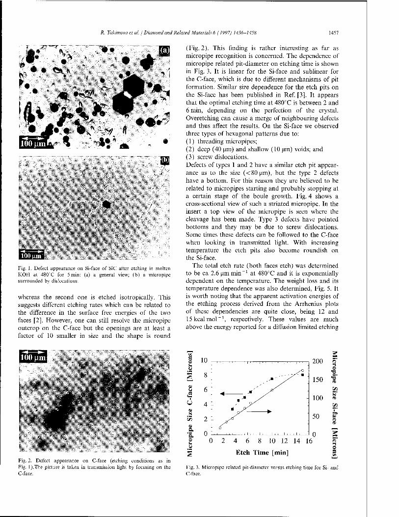
R. Yakimova et al. / Diamond and Related Materials 6 (1997) 1456-1458 1457
I '.*' ♦' ""JO
■<\>
C3f- -^
♦ ♦•^
Fig. 1. Defect appearance on Si-face of SiC after etching in molten KOH at 480°C for 5 min: (a) a general view; (b) a micropipe surrounded by dislocations.
whereas the second one is etched isotropically. This suggests different etching rates which can be related to the difference in the surface free energies of the two faces [2]. However, one can still resolve the micropipe outcrop on the C-face but the openings are at least a factor of 10 smaller in size and the shape is round
(Fig. 2). This finding is rather interesting as far as micropipe recognition is concerned. The dependence of micropipe related pit-diameter on etching time is shown in Fig. 3. It is linear for the Si-face and sublinear for the C-face, which is due to different mechanisms of pit formation. Similar size dependence for the etch pits on the Si-face has been published in Ref. [3]. It appears that the optimal etching time at 480°C is between 2 and 6 min, depending on the perfection of the crystal. Overetching can cause a merge of neighbouring defects and thus affect the results. On the Si-face we observed three types of hexagonal patterns due to: (1) threading micropipes; (2) deep (40 urn) and shallow (10 um) voids; and (3) screw dislocations. Defects of types 1 and 2 have a similar etch pit appear- ance as to the size (<80um), but the type 2 defects have a bottom. For this reason they are believed to be related to micropipes starting and probably stopping at a certain stage of the boule growth. Fig. 4 shows a cross-sectional view of such a striated micropipe. In the insert a top view of the micropipe is seen where the cleavage has been made. Type 3 defects have pointed bottoms and they may be due to screw dislocations. Some times these defects can be followed to the C-face when looking in transmitted light. With increasing temperature the etch pits also become roundish on the Si-face.
The total etch rate (both faces etch) was determined to be ca 2.6 um min"1 at 480°C and it is exponentially dependent on the temperature. The weight loss and its temperature dependence was also determined, Fig. 5. It is worth noting that the apparent activation energies of the etching process derived from the Arrhenius plots of these dependencies are quite close, being 12 and 15kcalmol_1, respectively. These values are much above the energy reported for a diffusion limited etching
Mar!
j#-
Fig. 2. Defect appearance on C-face (etching conditions as in Fig. l).The picture is taken in transmission light by focusing on the C-face.
e o s- u
01 u cd
53 <U a 'a o u u
0 2 4 6 8 10 12 14 16
Etch Time [min]
o ■Ö •5' n Vi 5' n Vi
M o n
o "I o s
Fig. 3. Micropipe related pit-diameter versus etching time for Si- and C-face.

1458 R Yakimova et al. / Diamond and Related Materials 6 (1997) 1456-1458
20|im Fig. 4. Cross-sectional view of a striated micropipe; the cleavage is perpendicular to the surface, shown in the insert. The sample is 6H SiC 3.5° off with an epilayer on top.
10
Furnace Temperature [°C] 480 510 540 570
0J
u
1
"i 1 r
Thickness [|LLm/min]
Weight [mg/min»cm ] I i i ' I i ■ » I t i ■ I i i i I i i i I i i i .1 i i .i I i i i .1
1.18 1.22 1.26 1.3 1.34 103/T [K1]
Fig. 5. Temperature dependence of the etch rate evaluated by thickness measurements and weight losses.
on the temperature and etching time. We did not observe etch spirals or hillocks [4]. The etching rate was deter- mined to be ca 2.6 pm min"1 at 480°C for both cases of side etching. The apparent activation energy of the etching process is suggesting a surface kinetics limited mechanism rather than a diffusion one.
Acknowledgement
This work was financially supported by the Swedish Board for Industrial and Technological Development (NUTEK).
of compound semiconductors [4], but they are smaller compared to the case of etching SiC in molten salts [5]. No difference was observed when comparing the etching behaviour of 6H and 4H SiC.
3. Conclusion
Preferential etching of SiC in molten KOH can pro- vide information on the type of strain field associated defects. The etch pit size and appearance strongly depend
References
[1]J. Takahashi, M. Kanaya, Y. Fujiwara, J. Crystal Growth 135 (1994)61.
[2] M. Syväjärvi, R. Yakimova, E. Janzen, Growth of SiC from liquid phase: wetting and dissolution of SiC, Diamond Relat. Mater. 6 (1997) 1266-1268.
[3] K. Koga, Y. Fujikawa, Y. Ueda, T. Yamaguchi, Springer Proc. Phys. 71 (1992)96.
[4] K. Sangwal, Etching of Crystals: Theory, Experiment and Applica- tion, Elsevier Science B.V., Amsterdam, 1987, p. 260.
[5] V.J. Jennings, Mater. Res. Bull. 4 (1969) 199.

DIAMOND AND
RELATED MATERIALS
ELSEVIER Diamond and Related Materials 6 (1997) 1459-1462
Schottky contact investigation on reactive ion etched 6H a-SiC
G. Constantinidis a*, J. Kuzmik b, K. Michelakis a
a Foundation for Research and Technology Hellas, P.O. Box 1527, 711 10 Heraklion, Crete, Greece b Institute of Electrical Engineering, Slovak Academy of Sciences, Dubravska cesta 9, 842 39 Bratislava, Slovakia
Abstract
Reactive Ion Etching (RIE) was performed on monocrystalline 6H a-SiC samples with CF4/H2-based gas mixtures. Schottky contacts on RIE etched a-SiC were compared with reference Schottky contacts on non-etched a-SiC. © 1997 Elsevier Science S.A.
Keywords: Silicon carbide; Reactive ion etching; Schottky contacts
1. Introduction
Silicon carbide has been attracting considerable atten- tion [1-5] because of its high electron saturation velocity (2.5 x 107cm/s) and its thermal and chemical stability. These unique physical and electrical properties make SiC a viable material for high power, high frequency and high temperature device applications. Schottky contacts on both a- and /?-SiC [2-5] play a key role in devices such as MESFETS and diodes. In the present investigation we report the investigation of Schottky barrier contacts to reactive ion etched (rIE) 6H a-SiC. Schottky contacts on RIE-etched a-SiC were compared with reference Schottky contacts on non-etched a-SiC. The effect of temperature annealing on the properties of the contacts was also investigated.
2. Experimental, results, discussion
The chemical stability of SiC makes device structure patterning difficult. Dry etching remains the main practi- cal technique for SiC removal for device fabrication using conventional photoresist techniques. Reactive Ion Etching (RIE) of SiC is performed with either fluorine- based gases such as CF4/02, SF6, CHF3/02, CBrF3 and CC12F2 or chlorine-based gases such as CCl4/02. RIE of SiC involves both physical and chemical removal processes. It has been shown that residue formation during the etching process can be minimized by
* Corresponding author. Fax: 00 30 81 239735.
introducing an additive gas such as H2 to the fluorinated plasmas [6].
In this investigation the RIE experiment was per- formed on half the surface (glass mask) of a 10 /m\ thick n-type a-SiC sample in a commercial VPS-1523 dual PECVD/RIE system from Vacutec. The conditions of RIE were: 50 mTorr pressure, 0.29 W/cm2 plasma power density, 20 seem of CF4 and 2 seem of H2 flow, respec- tively. The etching was performed for 10 min and resulted in a very smooth surface and a total etch depth of 150 nm. Then Schottky and ohmic contacts were fabricated on both the RIE-etched, as well as on the non-etched surfaces. The Schottky diode geometry was circular dots, 0.13 mm2 in area, separated from the ohmic region by an annulus. Pt (50nm)/Au (200 nm) was the metallization scheme employed for the diodes, while the ohmic contact was Cr (200 nm)/Au (200 nm) (both previously optimized). Both metallizations were fabricated by standard contact photolithography, e-gun evaporation (2xlO~7Torr) and lift-off process. Prior to the metallizations, the surface was treated in diluted HF. Rapid thermal annealing (RTA) in argon between 200 and 1000 °C (at 200 °C increments, 10 min duration) was then employed to investigate the behaviour of the diodes. Current-voltage and capacitance-voltage meas- urements were used for Schottky contact characteriza- tion and free carrier density determination. Averages over 5 diodes were taken in each case. Table 1 summa- rizes the results for the barrier height analysis. Parameters of diodes were calculated according to Ref. [7]. The I-V characteristics of the as-prepared diodes are shown in Fig. 1. Using C-V measurements,
0925-9635/97/S17.00 © 1997 Elsevier Science S.A. All rights reserved. PII S0925-9635(97)00112-X

1460 G. Constantinidis et al. / Diamond and Related Materials 6 (1997) 1459-1462
Table 1 Barrier height values from I-V and C-V measurements for RIE and non-RIE samples (eV) at various annealing temperatures
RTA Temperature (°C)
Non RIE Ob
(I-V) RIE<Db
(I-V)
Non RIE <Db
(C-V) RIE4>b
(C-V)
0 200 400 600 800 1000
0.96 0.94 0.98 0.92 1.1 1.04
0.84 0.97 1.06 0.94 1.04 1.14
1.45 1.55 1.20
1.60
1.10 1.45 1.75
2.5
10JT
^aA■
1CT
o 4„-
1D8
10M
-i—T—r—i—r-
-2
- RIE - Non RIE
~i—I—i—i—I—r- I ' ' ■1
-l—i—i—r—i—r-
\Mage (V)
Fig. 1. I-V characteristics of as-prepared Schottky contacts to RIE and non-etched 6H a-SiC.
a free carrier concentration of 7 x 1017 cm-3 and compa- rable capacitances on both etched and non-etched regions were determined. RIE-related damage due to radiation during the process and plasma-originated species diffusion into SiC is expected to alter the electri- cal parameters of the material. Zero-biased capacitance (C0) reflects directly changes in the free carrier concen- tration near the surface. However, in our investigation there was no substantial difference observed between the C0 of etched and non-etched samples. Thus, no RIE- related free carrier compensation or passivation effects were observed. The influence of subsequent RTA treat- ments on the parameters of the diodes is shown in (Fig. 2 and Fig. 3). From the I-V measurements, barrier height <^b(/_F) dependence on annealing temperature (Fig. 2) exhibits a local maximum at 400 °C with an ideality factor close to the minimum for both etched and non-etched regions. A further increase of ^b(/_F) was observed for higher annealing temperatures (800, 1000 °C). However, ideality factor evaluation shows contact degradation due to these annealings. This trend correlates with measurement of zero-biased capacitance C0 dependence shown in Fig. 3. Considerable decrease
of C0 at 1000 °C RTA was observed, especially for the RIE-treated region. Consequently, the C-V barrier height determination (Fig. 3) led to disagreement with the results of the I-V measurements. This may be explained using a hypothesis similar to Ioannou et al. [4], where from Auger-electron spectroscopy (AES) observations of Schottky contacts on /?-SiC, the presence of a thin interfacial layer between the metal and the semiconductor was suggested. Then the ideality factor n and the intercept <j)b(C-v) of the C2=f(V) plot can be expressed as follows [7]:
n=\+eJ{w{qoDi+e1), (1)
where a is the thickness of the interfacial layer £i is the dielectric constant of the interfacial layer e2 is the dielectric constant of the semiconductor w is the depletion layer width q is the electronic charge Ds is the density of the surface statesand
$ b(C-V) ^b+^i, (2)

G. Constantinidis et al. I Diamond and Related Materials 6 (1997) 1459-1462 1461
1,2 Barrier height RIE - D- Barrier height NonRlE—■-
0,5
ideality factor RIE - Q- Ideality factor Non RIE —»—
' ' ' I I , i i i I , il, I ■ ■ ■ i
0
3,0
2,5
2,0
1,5
1,0 1000 200 400 600 800
Annealing Temperature (C)
Fig. 2. Ideality factor and barrier height dependence on temperature of annealing, determined from I-V measurements.
Q. a>
0) o ft- o
Q0- 200
I 400
—A— Capacitance Non RIE —A— Capacitance RIE
I 630
I 800 1000
Temperature of Annealing (C)
700
600
53} o a>
400 D m o i-*- CD
300 O (0 ,^-v r>
'AD ~n
100
Fig. 3. Zero-biased capacitance and barrier height dependence on temperature of annealing, determined from C-V measurements.
where
01=2«2^D/es (3)
a = aeJ{ei+qaDs), (4)
where <Pt represents the error of the C-V method in the
determination of <Ph
ND is the free carrier concentration Ioannou et al. [4] have observed a strong interdiffusion
of species at the metal/ß-SiC interface and an increase
of the interface state density upon RTA annealing. Assuming that similar structural changes occurred in our experiments, an increase of the interface state density could account for the decrease of the ideality factor after RTA at 400 °C (Eq. (1)). On the other hand, this trend may be opposed by the accelerated species interdiffusion and the increase of the interfacial layer after RTA at 1000 °C and can explain the observed changes in n, <Ph(C-v) and Co (Eqs. (l)-(4)). Our previous AES obser- vation of the RIE-etched surface of /?-SiC has revealed the presence of RIE-originated fluorine species. This may

1462
account for the more profound degradation after high temperature RTA for RIE-based samples.
G. Constantinidis et al. j Diamond and Related Materials 6 (1997) 1459-1462
Acknowledgement
This work was supported by the CEC Brite-Euram project TECSICA No. 5416.
3. Conclusions
Schottky barrier contacts on RIE-etched 6H a-SiC were investigated. Pt-based diodes after 400°C/10min RTA led to the best parameters ($b(7_F) = 0.98 eV, n = 1.3) which were comparable to those obtained on refer- ence, non-etched samples. The room temperature barrier height ^b(i-F) value of 0.94 eV compares favourably with barrier height values for some other metals [8]. No signs of free carrier compensation or passivation were detected. After high-temperature RTA (1000 °C), degra- dation of contacts was observed, which was more evident for RIE-treated diodes. The presence of RIE-originated fluorine species on the SiC surface, which may enhance the formation of the thicker metal/semiconductor interfacial layer, could account for it.
References
[1] P.A. Ivanov, V.E. Chelnokov, Semicond. Sei. Technol. 7 (1992) 863-880.
[2] J.R. Waldrop, R.W. Grant, Y.C. Wang, R.F. Davis, J. Appl. Phys. 72(1992)4757-4760.
[3] M. Bhatanagar, P.K. McLarty, D.J. Baliga, IEEE Electron Device Letters 13(1992)501-503.
[4] D.E. Ioannou, N.A. Papanicolaou, P.E. Norquist, IEEE Trans. Electron Dev. ED 34 (1987) 1694-1699.
[5] N.A. Papanicolaou, A. Christou, L.M. Gipe, J. Appl. Phys 65 (1989)3526-3530.
[6] P.H. Yih, V. Saxena, A.J. Steckl, Inst. Phys. Conf. Ser. No 142, Chapter 3 (1996)621-624.
[7] E.H. Rhoderick, Metal-Semiconductor Contacts, Clarendon, Oxford, 1978.
[8] Y.G. Zhang, X.L. Li, A.Z. Li, A.G. Milnes, Inst. Phys. Conf. Ser. No 142, Chapter 4 (1996) 665-668.

DIAMOND AND
RELATED MATERIALS
ELSEVIER Diamond and Related Materials 6 (1997) 1463-1466
Comparative investigation of ECR-RIE patterns on Si and C faces of 6H-SiC using a CF4/02 gas mixture
R. Bonnota, A.L. Syrkin b-*, G. Levequec, J.M. Bluetb, J. Camasselb
a Atelier de Technologie Microelectronique, UM2 'Sciences et Techniques du Languedoc', 34095 Montpellier, Cedex 5, France
h Groupe d'Etude des Semiconducteurs, UM2 'Sciences et Techniques du Languedoc' et CNRS, cc074, 34095 Montpellier, Cedex 5, France
' Laboratoire d'Analyse des Interfaces et de Nanophysique, UM2 'Sciences et Techniques du Languedoc' et CNRS, 34095 Montpellier, Cedex 5, France
Abstract
We report on the relative results of dry etching <0001> Si-like or <000l"> C-like oriented faces of bulk natural 6H-SiC Lely crystals. For comparison, a 6H epilayer from Cree Research Inc. was also investigated. In all three cases, the initial and resulting surface morphology has been studied by means of scanning electron and atomic force microscopy. © 1997 Elsevier Science S.A.
Keywords: SiC; RIE; Surface morphology
1. Introduction
Prototype 6H-SiC device technology constantly involves the formation of patterned (mesa) structures on SiC crystal surfaces. To satisfy this requirement, dry etching in a plasma of fluorinated gas species is more appealing. As a consequence, for the last 10 years, many experimental set-up and gas mixtures have been pro- posed [1-10]. However, in many cases specific problems related to the rough surface of the etched sample have been encountered and no clear technological route has been evidenced.
Recently, we reported on the reactive ion etching (RIE) of 6H-SiC using an electron cyclotron resonance (ECR) plasma and a CF4/02 gas mixture [11]. Good anisotropy and reasonable etch-rate conditions could be found but no detailed investigation of the final (or even initial) surface morphology was done. In this work, we report on the relative results of dry etching either <0001> Si-like or <0001> C-like oriented faces of bulk, natural, 6H-SiC Lely crystals. For comparison, a 6H epilayer from Cree Research Inc. was also investigated. In all three cases, both the initial and resulting surface states have been studied using scanning electron microscopy (SEM) and atomic force microscopy (AFM).
* Corresponding author.
2. Experimental details
We have used a prototype GYGAX 50 reactor, designed by SEMCO Engineering S.A. [12]. The plasma is produced by a 250 W ASTeX compact electron cyclotron resonance (CECR) source operated at 2.45 GHz and diffused downstream into the reactor to the place where the sample has been loaded. The CECR source-sample distance can be adjusted between 10 and 21 cm. A 13.56 MHz r.f. bias is applied to the sample holder.
As already known [13], all 'natural' Lely crystals are thin pieces of material already sliced from large single crystals. They have been polished and normally, by naked eye, nothing allows to distinguish the Si from the C face. In this work, such an identification was per- formed using the following technique. Before processing, the polished crystals were immersed in a molten KOH bath at 550 °C for 30 s. Rinsing in boiling de-ionized water resulted in two different aspects: a uniform polish- ing-etching of the C face, while small polishing marks still remain on the Si side. Since in both cases similar defects originated from the mechanical polishing treat- ment, the difference in efficiency and anisotropy of the KOH etching illustrates the difference in chemistry which characterizes the two <0001> faces. This is the reason why not all defects could be eliminated from the Si side [14].
0925-9635/97/S17.00 © 1997 Elsevier Science S.A. All rights reserved. PII S0925-9635(97)00116-7
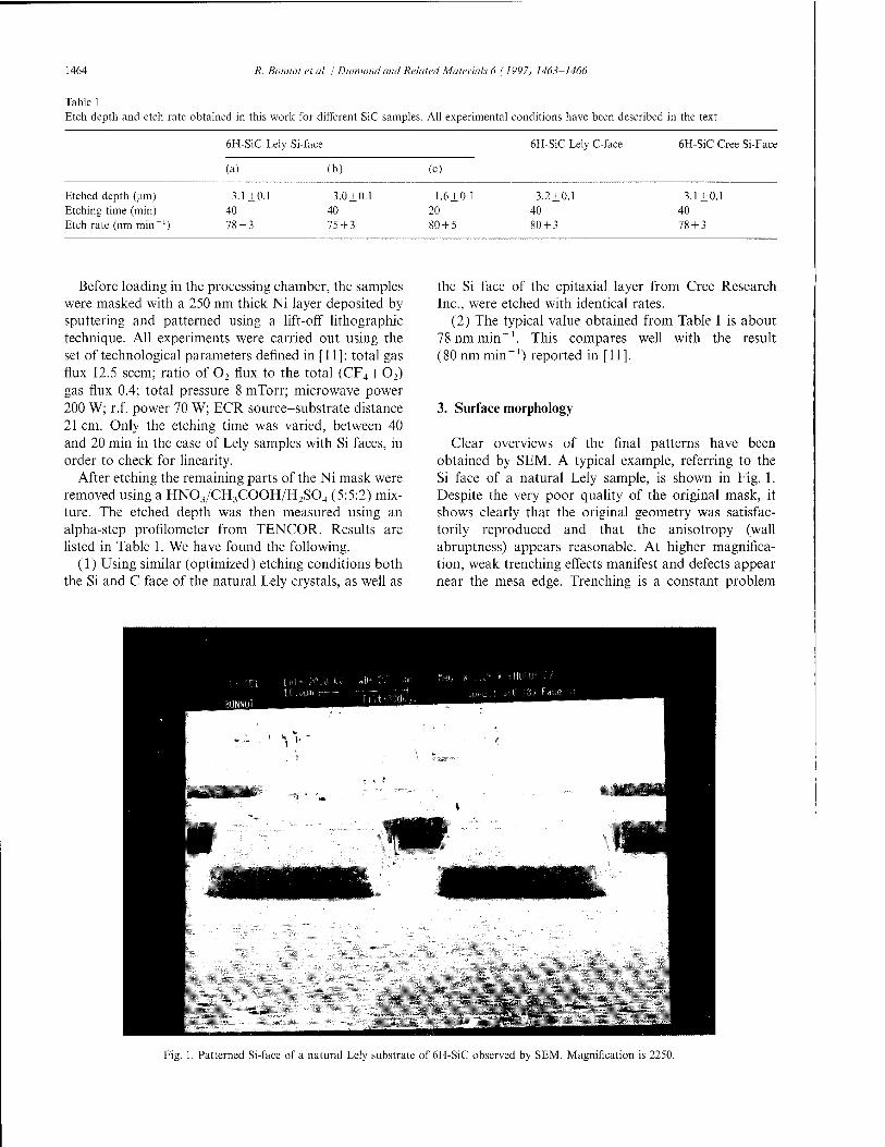
1464 R Bonnotetal j Diamond and Related Materials 6 (1997) 1463-1466
Table 1 Etch depth and etch rate obtained in this work for different SiC samples. All experimental conditions have been described in the text
6H-SiC Lely Si-face 6H-SiC Lely C-face 6H-SiC Cree Si-Face
(a) (b) (c)
Etched depth (um) Etching time (min) Etch rate (nm min-1)
3.1+0.1 40 78 + 3
3.0 + 0.1 40 75±3
1.6 + 0.1 20 80 + 5
3.2 + 0.1 40 80±3
3.1 ±0.1 40 78 + 3
Before loading in the processing chamber, the samples were masked with a 250 nm thick Ni layer deposited by sputtering and patterned using a lift-off lithographic technique. All experiments were carried out using the set of technological parameters defined in [11]: total gas flux 12.5 seem; ratio of 02 flux to the total (CF4 + 02) gas flux 0.4; total pressure 8 mTorr; microwave power 200 W; r.f. power 70 W; ECR source-substrate distance 21 cm. Only the etching time was varied, between 40 and 20 min in the case of Lely samples with Si faces, in order to check for linearity.
After etching the remaining parts of the Ni mask were removed using a HN03/CH3COOH/H2S04 (5:5:2) mix- ture. The etched depth was then measured using an alpha-step profilometer from TENCOR. Results are listed in Table 1. We have found the following.
(1) Using similar (optimized) etching conditions both the Si and C face of the natural Lely crystals, as well as
the Si face of the epitaxial layer from Cree Research Inc., were etched with identical rates.
(2) The typical value obtained from Table 1 is about 78nmmin_1. This compares well with the result (80nmmin_1) reported in [11].
3. Surface morphology
Clear overviews of the final patterns have been obtained by SEM. A typical example, referring to the Si face of a natural Lely sample, is shown in Fig. 1. Despite the very poor quality of the original mask, it shows clearly that the original geometry was satisfac- torily reproduced and that the anisotropy (wall abruptness) appears reasonable. At higher magnifica- tion, weak trenching effects manifest and defects appear near the mesa edge. Trenching is a constant problem
Fig. 1. Patterned Si-face of a natural Lely substrate of 6H-SiC observed by SEM. Magnification is 2250.

R. Bonnotetal. / Diamond and Related Materials 6 (1997) 1463-1466 1465
Table 2 Summary of RMS roughness obtained in this work by AFM for three different 6H-SiC samples
Sample Lely C-face Lely Si-face CREE Si-face
Surface 25 (im2
0.5 um2
Unetched 2±0.5nm 1.7 + 0.2 nm
Etched 2 + 0.5 nm 1.8 + 0.2 nmO
Unetched 7 + 3 nm 0.3 + 0.1 nm
Etched 7 + 3nm 0.2 + 0.1 nm
Unetched 0.5 + 0.2 nm 0.3 + 0.1 nm
Etched 0.5 + 0.2 nm 0.3 + 0.1nm
with SiC which could not be eliminated up to now. All other effects, which come from mask imperfections and/or defective 'lift off' process, will not be consid- ered further.
One of the most noticeable points is that, in the case of the Lely crystals, the structural difference which separated the initial Si- and C-like faces was well retained
after dry-etching. This is clear from Fig. 1. Because of the difference in surface chemistry already evidenced by the KOH etching, we believe that this evidences (more clearly) a chemical etching mechanism rather than a physical one. This is in very good agreement with the compositional dependence already observed in [11], where changing the 02 to CF4 gas ratio from zero to
(a)
i-6
0.4 urn
«I* «pi
m A •< ■#
0.6
0.4
0.2
(b) 0 ' 0
Fig. 2. AFM pictures of a patterned 6H-SiC epitaxial layer from Cree Research Inc: (a) before etching; (b) after dry etching for 40 min. Note that no degradation of the initial surface morphology results from the etching process.
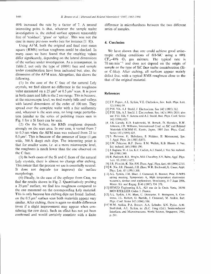
1466 R. Bonnot et at. / Diamond and Related Materiah 6 (1997) 1463-1466
40% increased the rate by a factor of 7. A second interesting point is that, whatever the sample under investigation is, the etched surface appears reasonably free of 'residues', 'grass' or 'spikes'. This was not the case in many previous works (see for instance [1-8]).
Using AFM, both the original and final root mean square (RMS) surface roughness could be checked. In many cases we have found that the resulting values differ significantly, depending on the lateral dimensions of the surface under investigation. As a consequence, in Table 2, not only the type of {0001} face and sample under consideration have been indicated but, also, the dimension of the AFM scan. Altogether, this shows the following.
(1) In the case of the C face of the natural Lely crystals, we find almost no difference in the roughness value measured on a 25 urn2 or 0.5 urn2 scan. It is poor in both cases and falls in the 2 nm range. This is because, at the microscopic level, we find mainly hills and valleys with lateral dimensions of the order of 100 nm. They spread over the complete wafer with a fair uniformity and, whatever is the scan area, no long range perturba- tion (similar to the series of polishing traces seen in Fig. 1 for a Si face) can be seen.
(2) On the Si-face, the RMS roughness depends strongly on the scan area. In our case, it varied from 7 to 0.3 nm when the AFM scan was reduced from 25 to 0.5 um2. This is because of the presence of large (1 urn wide, 300 A deep) etch dips. The interesting point is that for smaller scans, i.e. at a more microscopic level, the roughness is much lower than the one observed on the C face.
(3) In both cases of the Si and C faces of the natural Lely crystals, there is almost no change after etching. This means that the process we use is essentially neutral. It does not degrade (or improve) the surface morphology.
(4) Finally, in the case of the epilayer from Cree, we find the results shown in Fig. 2. Quantitatively probing a 25 um2 surface, we find less roughness compared to the one measured on the corresponding Lely material. This is only because less etching dips are found. Indeed, on the 0.5 um2 surface scan both materials appear very similar. After etching, there is again no sizable difference (even if a slight improvement may appear when con- sidering the raw data). Such an effect has not yet been confirmed and would certainly correlate with a finite
difference in microhardness between the two different series of samples.
4. Conclusion
We have shown that one could achieve good aniso- tropic etching conditions of 6H-SiC using a 60% CF4-40% 02 gas mixture. The typical rate is 78nmmin~1 and does not depend on the origin of sample or the type of SiC face under consideration (Si- or C-like). After etching, all surfaces appear mainly defect free, with a typical RMS roughness close to the that of the original material.
References
[1] I.V. Popov, A.L. Syrkin, V.E. Chelnokov, Sov. Tech. Phys. Lett. 12(1986)99.
[2] P.H. Yih, A.J. Steckl, J. Electrochem. Soc 142 (1995) 312. [3] P.H. Yih, A.J. Steckl, J. Electrochem. Soc. 142 (1995) 2853; also
see: P.H. Yih, V. Saxena and A.J. Steckl, Inst. Phys. Conf. Series 142(1996)621.
[4] J.B. Casady, E.D. Luckowski, M. Bozack, D. Sheridan, R.W. Johnson, J.R. Williams, International Conf. on SiC and Related Materials-ICSCRM-95, Kyoto, Japan, 1995 Just. Phys. Conf. Series 142(1995) 625.
[5] S. Dohmae, K. Shibahara, S. Nishino, H. Matsunami, Jpn. J. Appl. Phys. 24(1985)L873.
[6] J.W. Palmour, R.F. Davis, T.M. Wallett, K.B. Bhasin, J. Vac. Sei. technol. A4 (1986) 590.
[7] J. Sugiura, W.-J. Lu, K.C. Cadien, A.J. Steckl, J. Vac. Sei. technol. B4(1986) 349.
[8] R. Padiyath, R.L. Wright, M.I. Chaudhry, S.V. Babu, Appl. Phys. Lett. 58 (1991) 1053.
[9] J.R. Flemish, K. Xie, J.H. Zhao, Appl. Phys. Lett. 64 (1994) 2315. [10] K. Xie, J.R. Flemish, J.H. Zhao, W.R. Buchwald, L. Casas, Appl.
Phys. Lett. 67(1995)368. [11] A.L. Syrkin, J.M. Bluet, J. Camassel, R. Bonnot, Proc. E-MRS
spring meeting, Symposium A, High temperature electronics: materials, devices and applications, Strasbourg, 4-7 June 1996, Mater. Sei. and Engng. B 46 (1997) 374-378.
[12] SEMCO Engineering S.A., 625 rue de la Croix Verte, 34196 MONTPELLIER Cedex 5, France.
[13] A.L. Syrkin, J.M. Bluet, C. Dezauzier, T. Bretagnon, S. Con- treras, J.L. Robert, G. Bastide, J. Camassel, M. Anikin, Inst. Phys. Conf. Series 142 (1996) 189.
[14] M.M. Anikin, P.A. Ivanov, A.A. Lebedev, S.N. Pytko, A.M. Strel'chuk, A.L. Syrkin, in: Zh.C. Feng (Ed.), Semiconductor Interfaces and Microstructures, World Science, Singapore, 1992, p. 281.
DIAMOND AND
RELATED MATERIALS
ELSEVIER Diamond and Related Materials 6 (1997) 1467-1471
Anisotropie oxidation of silicon carbide
Kai Christiansena>*, Silke Christiansen b, Martin Albrechtb, Horst P. Strunk b, Reinhard Helbig' a Institute of Applied Physics, University Erlangen-Nürnberg, Staudtstraße 7, A3, D-91058 Erlangen, Germany
b Institute of Microcharacterization, University Erlangen-Nürnberg, Cauerstraße 6, D-91058 Erlangen, Germany
Abstract
The anisotropy of the thermal oxidation of Silicon Carbide has been investigated. Wet oxidation of a sphere of 6H SiC and dry oxidation of homoepitaxial CVD layers of 4H and 6H SiC were carried out. Afterwards, the oxide thickness and the interfacial structure was analyzed by Rutherford backscattering spectrometry, cross-sectional transmission electron microscopy and high- resolution transmission electron microscopy. After oxidation the sphere showed an impressive image of interference colors in different crystallographic orientations due to different oxide thicknesses. Additional microscopic studies of the oxidized epitaxial layers show a rough interface between SiC and Si02. Continuous oxidation of bilayers on a large scale is not observed. © 1997 Elsevier Science S.A.
Keywords: Rutherford backscattering spectrometry; Silicon carbide; Thermal oxidation; Transmission electron microscopy
1. Introduction
Progress in SiC research in recent years has allowed the realization of power electronic devices on SiC. Thermal oxidation is one of the key techniques in processing SiC-metal oxide semiconductor (MOS) structures. A typical class of these devices are U- and V-groove MOS structures. These three-dimensional devices require insulating oxides on faces with crystallo- graphic orientations other than the well investigated Si(0001) and C(0001) faces. Therefore a precise knowl- edge of the oxidation behavior of SiC for different crystallographic planes is necessary, because the break- down of a MOS device occurs, for example, at the thinnest point of the oxide layer for a study which includes electrical properties (c.f. Ref. [1]). Another important property of an MOS device is the channel mobility. In SiC devices the channel thickness is not more than 50 A. Thus the interface roughness on the nanometer scale is an important aspect of the oxidation of SiC. In this paper we report oxide thicknesses for various crystallographic orientations as well as transmis- sion electron microscopy (TEM) investigations of the interfacial SiC/Si02 structure.
* Corresponding author. Fax: +49 91 31858423; e-mail: [email protected]
2. Experimental
We used single-crystal material obtained from the modified Lely process for the sphere, and CVD epitaxial layers on Si (0001) and C(0001) faces on commercially available (CREE Research Inc.) 4H and 6H substrates. The samples were cleaned by acetone, methanol and a subsequent RCA cleaning process. The sphere was oxi- dized under wet conditions for 12 h at a temperature of 1100 °C in a gas flow of 02 saturated with H20 at 90 °C. The epitaxial layers on the Si face were oxidized under dry conditions for 24 h at a temperature of 1120 °C in a gas flow of 02, and those on the C face were oxidized for 8 h under the same conditions.
The oxide thicknesses of any orientation of the sphere was determined by Rutherford backscattering spectrom- etry (RBS). This method allows analysis of the oxide thickness even for curved surfaces, in contrast to other frequently used methods such as ellipsometry or C-V measurements. The RBS measurements were carried out with 2 MeV He+ ions on a 2 MV van der Graaff accelerator. The sphere was mounted on a three-axis goniometer and the detector was adjusted under a backscattering angle of <P = 170°. A detailed description of the experiments has been published elsewhere [2].
The interfacial SiC/Si02 structure of the Si(0001) and C(000f) faces at 4H and 6H SiC were investigated by cross-sectional transmission electron microscopy
0925-9635/97/517.00 © 1997 Elsevier Science S.A. All rights reserved. PII S0925-9635(97)00077-0

1468 K. Christiansen et al. / Diamond and Related Materials 6 (1997) 1467-1471
O 0 © © © 0 © © O 550
© o -A azimuthal angle 1 / equator minimum ^ - azimuthal angle 2 / equator maximum
C-Hemisphere Equator Region
Si-Hemisphere
150 0 10 20 30 40 50 60 70 80 90 100 110 120 130 140 150 160 170 180
polar angle <P in °
Fig. 1. Oxide thickness versus polar angle for two different azimuthal angles. The different points of the RBS measurement are marked on the optical micrographs of the C hemisphere (with the equatorial region) and the Si hemisphere.
(XTEM) and high-resolution transmission electron microscopy (HRTEM). We used a Philips CM 20 microscope operating at 200 kV for the XTEM studies and a Philips CM 300 UT microscope operating at 300 kV (spherical aberration Cs = 0.65mm, point-to- point resolution 1.72 A) for the HRTEM studies. The cross-sectional specimens were prepared by conventional mechanical grinding and dimpling, followed by ion milling with Ar+ to electron transparency in a Gatan Duomill (operating at 4kV, 1 mA, 13° angle of inci- dence, nitrogen cooling stage).
3. Results and discussion
After oxidation the sphere showed a remarkably anisotropic coating with Si02. In analogy to a globe, it is possible to distinguish three different areas on the sphere, i.e. two polar regions and one equatorial zone. From Laue diffraction patterns we could determine the crystallographic orientation of the exposed points of the sphere. The pole with the star-shaped structure can be assigned to the Si (0001) face and the pole with the concentric contrast rings to the C(000l) face. The equa- torial zone shows six maxima and six minima in the oxide thickness due to the six-fold symmetry of hexago- nal SiC. The maxima correspond to an orientation of
the (1100) type, and the minima correspond to an orientation of the (1120) type. We measured the oxide thickness on several spots of the sphere as a function of the polar angle <p for two different azimuthal angles related to an equatorial maximum and minimum, respec- tively. The sphere shows decreasing oxide thickness from ?> = 0o(C(000i) pole) to <? = 180° (Si(0001) pole) with an intermediate maximum around ^ = 90° (c.f. Fig. 1). On the C hemisphere the oxide thickness is independent of the azimuthal angle, while in the equatorial region and on the Si hemisphere a slight difference is observed, dependent on the azimuthal angle. The reason for the different oxidation kinetics are the different activation energies of the oxidation process for the various crystal- lographic orientations. More detailed discussions of this point have been published elsewhere [2,3].
The interfacial SiC/Si02 structure of the 6H samples shows a different behavior for the different crystal faces (c.f. Fig. 2; the undulating oxide surface on both faces is an effect of ion milling). The C(000f) face shows a rough interface on the nanometer scale. The roughness can be described as being quasiperiodic, having ripples with an amplitude of about one unit cell of 6H SiC (15 A) and a wavelength of about 20-60 A. A con- tinuous oxidation process takes place simultaneously on the whole interface, i.e. the oxidation of Si-C bilayers or in half or full unit-cell steps is not observed. The

K. Christiansen et al. / Diamond and Related Materials 6 (1997) 1467-1471 1469
.'..'.' .'-'•'.-'.'i.'.'1 "■' 7* :■■-■•• \* •'•:'•■•:'*'"-'":-' ;•■''■■"■.=•; -• ^-'-^'li^'---■::'•.^^~-- * W"^*. \
20 nm
(a)
«|lpi««!i|Ä$
Fig. 2. XTEM micrographs of the interfacial SiC/Si02 structure of a 6H epitaxial layer (3.5° off axis), (a) Si(0001) face, (b) C(0001) face.
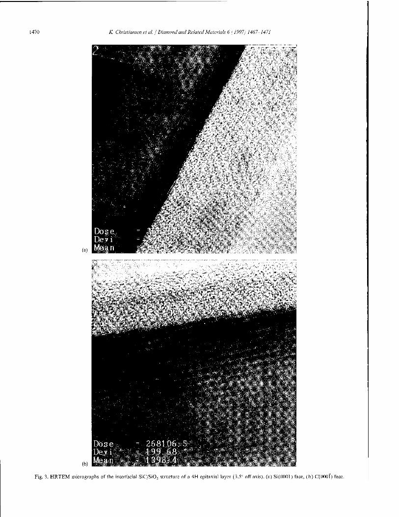
1470 K. Christiansen et al. I Diamond and Related Materials 6 (1997) 1467-1471
wmm Fig. 3. HRTEM micrographs of the interfacial SiC/SiQ2 structure of a 4H epitaxial layer (3.5° off axis), (a) Si(0001) face, (b) C(0001) face.
K. Christiansen et cd. / Diamond and Related Materials 6 (1997) 1467-1471 1471
interface of the Si(0001) face is much smoother, with only a few ripples being visible. However, long-range undulations with a wavelength of some hundred A and an amplitude of about 10 nm are visible. This property is less distinct on the C(0001) face.
In contrast to the 6H samples, the 4H samples exhibit long-range undulation equally on the C and Si faces. The amplitudes and wavelengths of the undulating struc- tures are comparable to those observed on the 6H samples. HRTEM investigations of the SiC/Si02 inter- face (Fig. 3) show distinct interfacial steps on the C and Si faces. A statistical investigation of the step height reveals that essentially half and full unit-cell steps occur and that these are equally represented. The statistic is carried out on an interfacial length of 0.5 um for each type of specimen.
The occurrence of steps on the surface is a well known and expected process during the growth of epitaxial layers, because of the off-axis orientation of the sub- strates used in order to avoid defects during epitaxial growth. For the 4H and 6H polytypes it has been reported [4-6] that on the Si face mainly half and full unit-cell steps occur. On the C face single Si-C bilayer steps are observed. In the case of thermal oxidation the reaction on half and full unit-cell steps (i.e. on the hexagonal sites of the unit cell) seems to be most favorable for energetic reasons.
4. Conclusion
The anisotropic oxidation of Silicon Carbide has been investigated. We studied the different oxide thicknesses
on a sphere of 6H SiC. The oxidation rates show an extreme dependence on the crystallographic orientation. The maximum oxidation rate is observed on the C(000i) face and the minimum rate on the Si(0001) face. In crystallographic orientations perpendicular to the c-axis we observe a structure with six maxima and six minima corresponding to orientations of the (lfOO) and (1120) types, respectively.
Additionally, the interfacial SiC/Si02 structure of 4H and 6H CVD epitaxial layers on the C and Si faces is investigated. The samples of both polytypes exhibit undulating interfaces on the Si and C faces. On the 4H samples, we observe oxidation in half or full unit-cell steps and on the 6H samples we see ripples with an amplitude of about 15 A, with a higher density on the C face than on the Si face.
References
[1] N. Tokura, K. Hara, T. Miyajima, H. Fuma, K. Hara, Jpn. J. Appl. Phys. 34(1995) 5567.
[2] K. Christiansen, R. Helbig, J. Appl. Phys. 79 (1996) 3276. [3] K. Ueno, Y. Seki, Inst. Phys. Conf. Ser. 142 (1996) 629. [4] J. Schardt, C. Bram, S. Müller, U. Starke, K. Heinz, K. Müller,
Surf. Sei. 89 (1995) 175. [5] T. Kimoto, A. Itoh, H. Matsunami, Inst. Phys. Conf. Ser. 142
(1996) 241. [6] T. Kimoto, A. Itoh, H. Matsunami, Appl. Phys. Lett. 66 (1995)
3645.
DIAMOND AND
ELSEVIER
RELATED MATERIALS
Diamond and Related Materials 6 (1997) 1472-1475
'Carbon cluster model" for electronic states at SiC/Si02 interfaces
M. Bassler a'*, G. Pensl a, V. Afanas'ev b
a Institute ofApplied Physics, University of Erlangen-Niimberg, Staudtstrasse 7, D-91058 Erlangen, Germany b KU Lernen, Lab. voor Halfgeleiderfysica, Celestijnenlaan 200D, B-3001 Leinen, Belgium
Abstract
The electronic properties of the SiC/Si02 interface are studied for a series of SiC poly types (3C, 4H, 6H) using various electrical methods and internal photoemission spectroscopy. The energy distribution of states at SiC/SiO, interfaces is found to be similar for all the investigated polytypes. The lowest density of states measured at SiC/SiO, interfaces is at least one order of magnitude higher than the density of states at Si/SiO, interfaces. We have strong indications that this enhancement is caused by residual carbon (graphite-like films, carbon clusters) bonded at the SiC/Si02 interface. We propose a "carbon cluster model", which qualitatively describes the electrical properties of (3C, 4H, 6H)-SiC MOS structures. © 1997 Elsevier Science S.A.
Keywords: SiC/Si02-interface; MOS-structure; Density of interface states; Carbon cluster model
1. Introduction
The possibility of growing thermal silicon dioxide (Si02) layers on silicon carbide (SiC) is of particular importance in the fabrication of SiC-based MOS devices. However, several groups have recently demonstrated that the density of states at the SiC/Si02 interface is higher compared to Si/Si02 interfaces [1-5], although the dielec- tric quality of the Si02 layer grown on SiC surfaces is comparable to the quality of SiO, layers grown on Si [6]. In this article we determine quantitatively the inter- face state density of n-/p-type SiC/Si02 structures con- sisting of different SiC polytypes (3C, 4H, 6H) using admittance spectroscopy (AS), constant capacitance-deep level transient spectroscopy (CC-DLTS) and internal photoemission (IPE). Our experiments suggest that carbon is a promising candidate to explain the high interface state density. A "carbon cluster model" is proposed which predicts qualitatively the interface charge of SiC/Si02 capacitors for different SiC polytypes.
solvents, RCA clean) and for comparison, part of them received in addition an UV-ozone-clean [7].
The oxidation was performed at 1120 °C in dry oxygen for times varying from 2 to 60 h with a post-oxidation anneal in Ar for 1 h at the same temperature. The oxide thickness determined varied from 220 to 2040 Ä.
An amorphous hydrogenated carbon (a-C:H) layer with a thickness of 400 A was deposited on selected MOS structures by plasma-enhanced vapor deposition. The ratio of sp2- and sp3-bonded carbon in these films was varied by changing the substrate bias during deposition. In this way, the optical band gap determined by absorp- tion measurements was varied between 0.7 and 3.0 eV.
In order to monitor the interface states in the band gap of SiC polytypes, we employed admittance spectro- scopy (AS, T=300K, /=100 Hz to 10 MHz) [8] , constant capacitance-deep level transient spectroscopy (CC-DLTS, T= 80-700 K, time windows At= 1-64 ms) [9] and internal photoemission spectroscopy (IPE, exci- tation 150 W Xe discharge lamp) [10]
2. Experimental details
The MOS structures were fabricated by thermal oxida- tion of Si- (0001) or C-faces (Fig. 1) of different SiC polytypes (3C, 4H, 6H). Prior to oxidation, the SiC samples were exposed to a standard clean (organic
* Corresponding author.
3. Results and discussion
3.I. Interface state density of different SiC polytypes (3C, 4H, 6H)
Fig. 1 depicts the interface state density of MOS capaci- tors fabricated on n-/p-type SiC wafers of different SiC
0925-9635/97/S17.00 © 1997 Elsevier Science S.A. All rights reserved. PII S0925-9635(97)00074-5

M. Bassler et al. / Diamond and Related Materials 6 (1997) 1472-1475 1473
r io13- > CM
E
•—1 full symbols: AS ^ open symbols: CC-DLTS
4 * T
Q >
"| 10121 (D
T5
inte
rfa
ce s
tate
l>. n-type p-type
Ec 4H
Ec 6H
4H D O Ec 6H A V 3C 3C O O Ev
i i i | i i i i | i i i i | i i i i | i i i i
2.0
energy (eV) Fig. 1. Energy distribution of interface states for 3C, 4H and 6H SiC as determined from AS (full symbols) and CC-DLTS (open symbols) taken on p-type and «-type MOS structures.
polytypes (3C, 4H, 6H). Because of the finding in Ref. [11], which revealed that the energy distance between the top of the SiC valence band Ey (SiC) and the bottom of the Si02 conduction band Ec (Si02) is constant within an accuracy of ±100 meV for all investigated polytypes (3C, 4H, 6H, 15R: £c(Si02)-£v (SiC) = 6.0eV), we located the zero point of the energy scale at the top of the SiC valence band. Further, we assumed that the applied analysis techniques (CC-DLTS, AS) provides the total density of interface states with a given emission time constant and that there is a clear relation between the emission time constant and the energy position of interface states. The distribution of interface states is qualitatively similar for the investigated polytypes. Dit
increases towards the band edges i?v(SiC) and .Ec(SiC) and reaches a minimum at 2 eV above the valence band; the lowest value of Dit is measured for the 6H poly- type (approx. 1011 cm~2eV_1). A particular feature is observed about 1.5 eV above £V(SiC); there, an increase in Dit takes place for all the investigated SiC polytypes independent of the dopant species or doping level. This general observation, and the fact that there is an enhance- ment of interface states in comparison with the Si/Si02
interface by at least one order of magnitude, indicates that a particular defect species is introduced at the SiC/Si02 interface.
3.2. Carbon — a candidate for interface states
Several experimental observations favor carbon as a candidate for the enhancement of the density of states
at SiC/Si02 interfaces. The carbon may be either present at the surface prior to the oxidation and/or be gener- ated at the SiC/Si02 interface during the oxidation process.
As demonstrated in Ref. [7], an UV-ozone-clean of the SiC surface prior to oxidation reduces the density of SiC/Si02 interface states in contrast to a standard clean (HF, RCA), which does not remove carbon atoms at the SiC surface.
Also oxidation of a C-face results in a higher density of interface states than the oxidation of a Si-face as demonstrated by the IPE spectra shown in Fig. 2. The photon energy in IPE spectra is, opposite to the energy density of interface states, related to the lower band edge of the Si02 conduction band. The threshold <\>2
indicating a steep increase of the interface state density (see Fig. 1) is identical for both faces, however, the IPE signal given by the cubic root of the yield, and implying the integral over the interface states, increases more steeply for the C-face than for the Si-face sample.
Angular resolved photoelectron spectroscopy investi- gations (ARXPS) conducted by Hornetz et al. [12] give evidence for the enrichment of carbon at the interface during the oxidation process. These authors describe the formation of a thin interface oxide layer composed of Si4C4_x02 (X<2), which increases with the growing oxide thickness. Our IPE investigations on MOS struc- tures with different oxide thickness confirm this finding. The slope of IPE curves for photon energies greater
12 -
10
CD 8
CD c i^ 6
Q _i LU
>
4 -
n-type 6H SiC
dox
o 220 A Si-face D 900 A Si-face A 2040 A Si-face ■ 1000 A C-face
/
oxide field: 2MV/cm
CO
2 3 4 5 6
PHOTON ENERGY (eV)
Fig. 2. Spectral curves of IPE from the interface of an «-type 6H SiC structure for an oxide field of 2 MV/cm; parameters are the oxide thickness and the polarity: 220 Ä (0001) (open circles), 900 Ä (0001) (open squares), 2040 A (0001) (open triangles) and 1000 Ä (0001) (full squares).
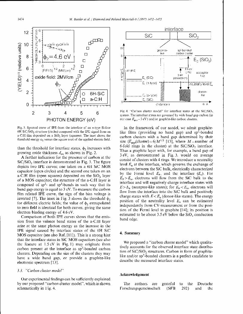
1474 M. Bassleretal. / Diamond and Related Materials 6 (1997) 1472-1475
'E
0) >
CD
Q _i UJ >-
12 - > D-
>-
10 - LU J
z LU
□ d4-
8 - CO LU tr
(
4>2=4.6 eV
i D £ 6 - ) 1 2 ; (FIELD) ' (MV/cm) ' n fY
4 - oxide field: 2MV/cm °
2 - \w O 6H-SiC
n ' Ur^gf^ffl^?, , D a-C:H
1 1 I 1 1 1 1 I -!"'""'
interface
2 3 4 5 6
PHOTON ENERGY (eV)
Fig. 3. Spectral curve of IPE from the interface of an «-type Si-face 6H SiC/Si02 structure (circles) compared with the IPE signal from an a-C:H film deposited on a Si02 layer (squares). The inset shows the threshold energy (j>2 versus the square root of the applied electric field.
than the threshold for interface states, 4>2 increases with growing oxide thickness dox as shown in Fig. 2.
A further indication for the presence of carbon at the SiC/Si02 interface is demonstrated in Fig. 3. The figure depicts two IPE curves; one taken on a 6H SiC MOS capacitor (open circles) and the second one taken on an a-C:H film (open squares) deposited on the Si02 layer of a MOS capacitor; the structure of the a-C:H layer is composed of sp2- and sp3-bonds in such way that its band gap energy is equal to 3 eV. To measure the carbon film related IPE curve, the sign of the bias voltage is inverted [7]. The inset in Fig. 3 shows the threshold fy2
for different electric fields; the value of fy2 extrapolated to zero field is identical for both curves, giving the same electron binding energy of 4.6 eV.
Comparison of both IPE curves shows that the emis- sion from the valence band states of the a-C:H layer arise at the same photon energy as the increase in the IPE signal caused by interface states of the 6H SiC MOS capacitor (see also Ref. [11]). This is a strong hint that the interface states in SiC MOS capacitors (see also the feature at 1.5 eV in Fig. 1) may originate from carbon present at the interface as sp2-bonded carbon clusters. Depending on the size of the clusters they may have a wide band gap, or provide a graphite-like electronic spectrum [13].
3.3. "Carbon cluster model"
Our experimental findings can be sufficiently explained by our proposed "carbon cluster model", which is shown schematically in Fig. 4.
SiC Si02
eVl
6
graphile- like
sp2-bonded carbon cluster
t Ec(Si02
6eV(IPE)
.Ec (SiC)
EF (n-type)
■ EF (p-type) Ev (SiC)
t4.6cV (IPE)
3eV (absorption)
acceptor- like
neutrality level E„
donor- like
distance x a. u.
Fig. 4. "Carbon cluster model" for interface states at the SiC/Si02
system. The interface states are governed by wide band gap carbon (in our case Egap = 3 eV) and/or graphite-like carbon clusters.
In the framework of our model, we admit graphite- like films (providing no band gap) and sp2-bonded carbon clusters with a band gap determined by their size (Egap(cluster) = 6/M1/2 [13], where Af=number of 6-fold rings in the cluster) at the SiC/Si02 interface. Thus a graphite layer with, for example, a band gap of 3 eV, as demonstrated in Fig. 3, would on average consist of clusters with 4 rings. We introduce a neutrality level En at the interface, which governs the exchange of electrons between the SiC bulk, electrically characterized by the Fermi level EF, and the interface (En). For EF>En, electrons will flow from the SiC bulk to the interface and will negatively charge interface states with E>En (acceptor-like states); for EF<En, electrons will flow from the interface into the SiC bulk and positively charge states with E<En (donor-like states). The energy position of the neutrality level En can be estimated independently from CV-measurement or from the posi- tion of the Fermi level in graphite [14]; its position is estimated to be about 3.5 eV below the Si02 conduction band edge.
4. Summary
We proposed a "carbon cluster model" which qualita- tively accounts for the observed interface state distribu- tion of SiC/Si02 structures. Carbon in form of graphite- like and/or sp2-bonded clusters is a perfect candidate to describe the measured interface states.
Acknowledgement
The authors are grateful to the Deutsche Forschungsgemeinschaft (SFB 292) and the

M. Bassler et al. I Diamond and Related Materials 6 (1997) 1472-1475 1475
Bundesministerium für Bildung, Wissenschaft, Forschung und Technologie (BMBF) for support of this work.
References
[1] T. Billon, E. Bano, L. DiCioccio, T. Ouisse, P. Lassagne, C. Jaus- sand, Microelect. Eng. 28 (1995) 193.
[2] E. Stein von Kamienski, F. Portheine, A. Göltz, H. Kurz, Inst. Phys. Conf. Series 142 (1996) 641.
[3] P. Friedrichs, E.P. Burte, R. Schörner, J. Appl. Phys. 79 (1996) 7814.
[4] L.A. Lipkin, J. Palmour, J. Elect. Mater. 25 (1996).
[5] J.N. Shenoy, J.A. Cooper Jr., M.R. Melloch, Appl. Phys. Lett. 68 (1996) 803.
[6] P. Friedrichs, E.P. Burte, R. Schörner, Appl. Phys. Lett. 65 (1994) 1665.
[7] V.V. Afanas'ev, A. Stesmans, M. Bassler, G. Pensl, M. Schulz, C.I. Harris, Appl. Phys. Lett. 68 (1996) 2141.
[8] E.H. Nicollian, A. Goetzberger, Bell Systems Technol. J. 46 (1966) 1055.
[9] M. Schulz, E. Klausmann, J. Appl. Phys. 18 (1979) 169. [10] V.K. Adamchuk, V.V. Afanas'ev, Prog. Surf. Sei. 41 (1992) 109. [11] V.V. Afanas'ev, M. Bassler, G. Pensl, M. Schulz, J. Appl. Phys.
79(1996) 3108. [12] B. Hornetz, H.-J. Michel, J. Halbritter, J. Mater. Res. 9 (1994)
3088. [13] J. Robertson, J. Non-Cryst. Solids 137/138 (1991) 825. [14] M. de Seta, P. Fiorini, F. Coppola, F. Evangelisti, J. Non-Cryst.
Solids 137/138(1991) 867.

ELSEVIER
DIAMOND AND
RELATED MATERIALS
Diamond and Related Materials 6 (1997) 1476-1479
Investigation of walk-out phenomena in SiC mesa diodes with Si02/Si3N4 passivation
Zoran Ovuka *, Mietek Bakowski Industrial Microelectronics Center, P. O. Box 1084, S-164 21 Kista, Sweden
Abstract
The drift or "walk-out" of the breakdown voltage in 6H-SiC mesa diodes passivated by a double layer of 1000 A Si02 and 3000 A Si3N4 was investigated. The drift characteristics of diodes having wet and dry oxide passivation were compared to each other and to diodes subjected to additional hydrogen plasma etching of the SiC surface prior to dry oxidation. The influence of the UV illumination supplied by a HeCd laser of wavelength 325 nm on the walk-out characteristics and on the reverse current was investigated. No significant differences in the amount of drift and saturation level of breakdown voltage was found between the different passivations. However, the saturation level was reached about one order of magnitude faster in the wet oxide. A significant difference was found in the level and time dependence of the reverse current under UV illumination between the wet and dry oxide passivated diodes. The results are consistent with the existence of large concentrations of positive charge and acceptor-type deep interface traps. The walk-out is the result of the acceptor states being filled by hot electrons through the mechanism of avalanche injection. © 1997 Elsevier Science S.A.
Keywords: Walk-out; Mesa diodes; Drift; Oxide passivation
1. Introduction
The high critical electric field of SiC, one order of magnitude higher than for Si, makes it an interesting material for high voltage devices. The realisation of reliable junction termination therefore becomes an issue of particular importance. To date, the same passivation schemes as for silicon are most readily available for SiC devices. Instabilities related to the charge injection and trapping pose a much more serious problem in the case of the SiC/Si02 system due to higher electric fields and lower energy barriers between semiconductor and insula- tor for both electrons and holes. In order to realise SiC devices using the natural passivants like Si02 it is necessary to reduce the electric field at the surface to values comparable to those of Si devices and to improve understanding of the SiC/Si02 system with respect to charge trapping in the interface states and in the interface and bulk traps. One fundamental instability is the fre- quently observed drift of the breakdown voltage caused by redistribution of the surface charges. This so called walk-out phenomenon can be measured by applying a
constant reverse current and recording the increase of the breakdown voltage as a function of time.
2. Experimental procedures
The diodes were made on Cree p+n-n+ wafers with doping concentrations of 9 x 1018 cm-3, 6.5 x 10¹⁵
cm-3 and 1.5 x 1018 cm"3, respectively. The thicknesses of the epitaxial layers are given in Fig. 1. The walk-out was measured, using a Keithley SMU 237 unit, for
jvation metal * /—Li , r1—i
_jy/ P+ 1 um\\
n" 9 urn
128 um
n+
' Corresponding author.
metal
Fig. 1. Cross-section of a mesa diode.
0925-9635/97/S17.00 © 1997 Published by Elsevier Science S.A. All rights reserved. PII S0925-9635(97)00075-7

Z. Ovuka, M. Bakowski / Diamond and Related Materials 6 (1997) 1476-1479 Uli
different values of the reverse current as a function of time. In many cases the reverse voltage drift was recorded for up to 10 h. The drift of the reverse voltage and evolution of the reverse current were also measured under DC stress conditions with 400 V applied reverse voltage. Finally the relaxation of the breakdown voltage was measured at room temperature and with zero applied bias on the diodes freshly charged during the walk-out measurements. The measurements were done both with and without UV illumination in order to investigate the influence of the UV on the walk-out phenomena. The UV source was a HeCd laser of wavelength 325 nm. The dry oxide was grown at 1250 °C for a period of 4 h and the wet oxide at 1150 °C for 8 h. A 1 h postoxidation anneal in N2 at the oxidation temperature was used in both cases. One wafer was subjected to hydrogen plasma etching at 1600 °C for 1 h followed by a 1 h anneal at 1250 °C in Ar prior to dry oxidation.
3. Results
Typical results of walk-out measurements at 2 |iA reverse current are shown in Fig. 2. The walk-out satu- rates faster in the wet oxide. The saturation level is, however, independent of the type of the oxide. Note the relative insensitivity of the walk-out to the UV exposure.
The results of the DC storage measurements at 400 V reverse bias under UV illumination are shown in Fig. 3. Note the dramatic difference in the behaviour of the reverse current between dry and wet oxide.
The results of discharge measurements with and with- out UV illumination are shown in Fig. 4. There is no significant relaxation of the breakdown voltage shift, in particular the breakdown voltage stays constant in the presence of UV. Without UV some initial relaxation of about 50 V is observed.
4. Discussion
The breakdown voltage drift (walk-out) is very pro- nounced in SiC mesa diodes [1]. We attribute this to the trapping of hot electrons in the deep acceptor type interface traps. The hot electrons are supplied through the process of avalanche injection [2], which is expected to be more pronounced in SiC as compared to Si. The energy barrier between 6H-SiC and the oxide conduction bands is about 0.25 eV smaller than in the case of Si while the electric field in the interface region is one order of magnitude higher [1,3]. A charge injection process originates close to the edge of the mesa and propagates outwards following the spreading of the space charge due to the new effective charge state of the surface. The oxidised surface is originally positively charged due to the fixed positive charge in the oxide [3]. This charge is gradually compensated by the nega- tive charge due to trapped electrons. No significant differences are observed in that respect between wet and dry oxides. The charge trapping kinetics, as reflected in the time dependence of the reverse voltage drift, differs between the wet and dry oxides. The concentration of the acceptor states, however, as reflected in the satura- tion level, is comparable. The charge trapped in acceptor states seems to be rather stable and no thermal discharge is observed at temperatures below 250 °C.
A significant difference between wet and dry oxide is observed in the behaviour of the reverse current under UV illumination. The reverse current is about one order of magnitude larger in the wet oxide. Furthermore, it rises with time during DC storage in the wet oxide while it decreases in the case of the dry oxide. The reverse current is determined by the surface generation current and the UV induced photocurrent. Let us assume that the photocurrent responsible for the increase of reverse current in the wet oxide case. This is consistent with the expansion of the space charge region along the surface increasing the carrier generation volume. The possible role of the fast interface states is at the same time
i i i i
800 ^
""" O)
4—< 600 - O > 0) 400 - p DRY OXIDE a> > 2Ü0 - or
i i i i
1000
20 40 60
Time (s)
80 100 5 10 15
Time (s)
20
Fig. 2. Walk-out of the breakdown voltage, without (solid line) and with UV illumination (dash-dot line) for dry and wet oxide.
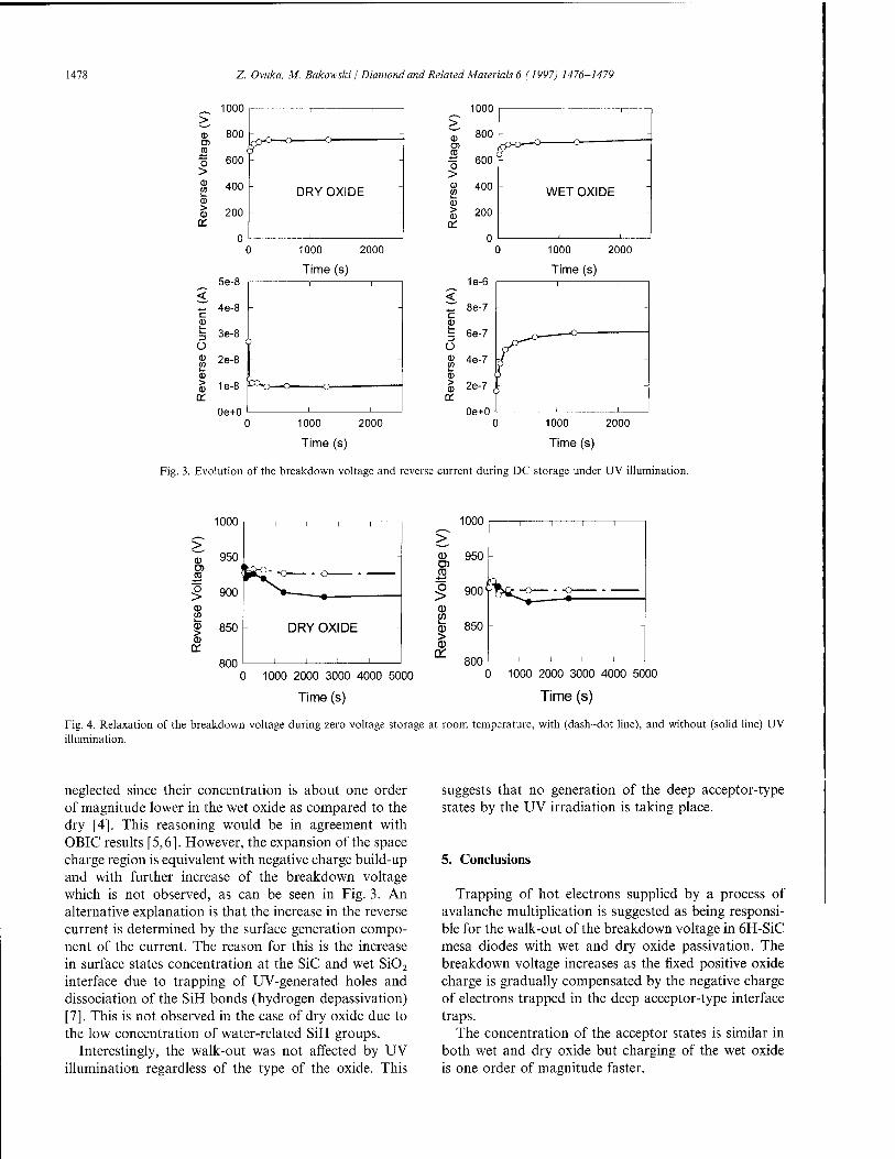
1478 Z. Ovuka, M. Bakowski I Diamond and Related Materials 6 (1997) 1476-1479
1000 2000
Time (s)
< ~ 4e-8 0
i i
i= 3e-8 - O \ % 2e-8
g 1e-8
1000
> at 800 n> en
600 o > 0) 400
0 > <l> 200
Qi 0
1e-6
< 8e-7
c 0 k_ 6e-7 Ü 0 4e-7
0 > 0 2e-7 a:
1000 2000
Time (s)
Oe+0 1000 2000
Time (s)
1000 2000
Time (s)
Fig. 3. Evolution of the breakdown voltage and reverse current during DC storage under UV illumination.
1000
CD
cc o >
CD CO l_ <B > CD rr
950 -
900 - >»
850
800
DRY OXIDE
0 1000 2000 3000 4000 5000
Time (s)
0 1000 2000 3000 4000 5000
Time (s)
Fig. 4. Relaxation of the breakdown voltage during zero voltage storage at room temperature, with (dash-dot line), and without (solid line) UV
illumination.
neglected since their concentration is about one order of magnitude lower in the wet oxide as compared to the dry [4]. This reasoning would be in agreement with OBIC results [5,6]. However, the expansion of the space charge region is equivalent with negative charge build-up and with further increase of the breakdown voltage which is not observed, as can be seen in Fig. 3. An alternative explanation is that the increase in the reverse current is determined by the surface generation compo- nent of the current. The reason for this is the increase in surface states concentration at the SiC and wet Si02
interface due to trapping of UV-generated holes and dissociation of the SiH bonds (hydrogen depassivation) [7]. This is not observed in the case of dry oxide due to the low concentration of water-related SiH groups.
Interestingly, the walk-out was not affected by UV illumination regardless of the type of the oxide. This
suggests that no generation of the deep acceptor-type states by the UV irradiation is taking place.
5. Conclusions
Trapping of hot electrons supplied by a process of avalanche multiplication is suggested as being responsi- ble for the walk-out of the breakdown voltage in 6H-SiC mesa diodes with wet and dry oxide passivation. The breakdown voltage increases as the fixed positive oxide charge is gradually compensated by the negative charge of electrons trapped in the deep acceptor-type interface traps.
The concentration of the acceptor states is similar in both wet and dry oxide but charging of the wet oxide is one order of magnitude faster.
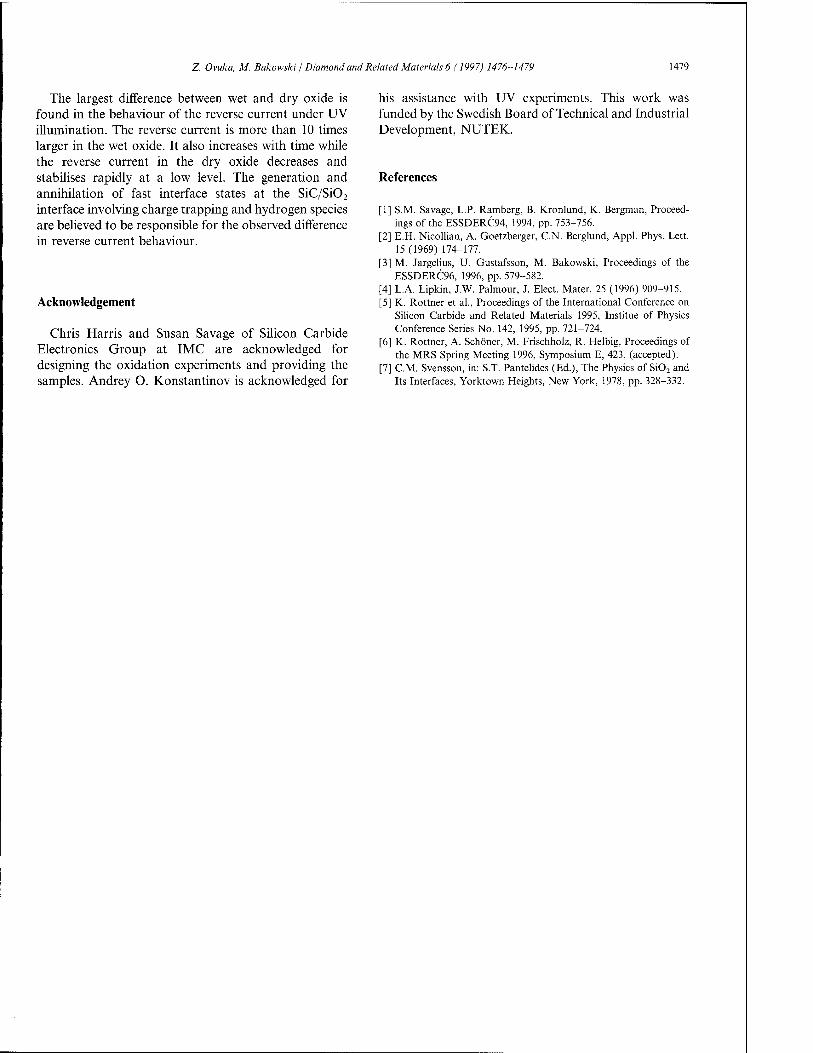
Z. Ovuka, M. Bakowski I Diamond and Related Materials 6 (1997) 1476-1479 1479
The largest difference between wet and dry oxide is found in the behaviour of the reverse current under UV illumination. The reverse current is more than 10 times larger in the wet oxide. It also increases with time while the reverse current in the dry oxide decreases and stabilises rapidly at a low level. The generation and annihilation of fast interface states at the SiC/Si02
interface involving charge trapping and hydrogen species are believed to be responsible for the observed difference in reverse current behaviour.
Acknowledgement
Chris Harris and Susan Savage of Silicon Carbide Electronics Group at IMC are acknowledged for designing the oxidation experiments and providing the samples. Andrey O. Konstantinov is acknowledged for
his assistance with UV experiments. This work was funded by the Swedish Board of Technical and Industrial Development, NUTEK.
References
[1] S.M. Savage, L.P. Ramberg, B. Kronlund, K. Bergman, Proceed- ings of the ESSDERC94, 1994, pp. 753-756.
[2] E.H. Nicollian, A. Goetzberger, C.N. Berglund, Appl. Phys. Lett. 15 (1969) 174-177.
[3] M. Jargelius, U. Gustafsson, M. Bakowski, Proceedings of the ESSDERC96, 1996, pp. 579-582.
[4] L.A. Lipkin, J.W. Palmour, J. Elect. Mater. 25 (1996) 909-915. [5] K. Rottner et al., Proceedings of the International Conference on
Silicon Carbide and Related Materials 1995, Institue of Physics Conference Series No. 142, 1995, pp. 721-724.
[6] K. Rottner, A. Schöner, M. Frischholz, R. Helbig, Proceedings of the MRS Spring Meeting 1996, Symposium E, 423, (accepted).
[7] CM. Svensson, in: S.T. Pantelides (Ed.), The Physics of Si02 and Its Interfaces, Yorktown Heights, New York, 1978, pp. 328-332.

ELSEVIER Diamond and Related Materials 6 (1997) 1480-1484
DIAMOND AND
RELATED MATERIALS
Overview of SiC power electronics
V.E. Chelnokov a-*, A.L. Syrkin b, V.A. Dmitrieva,c
1 A.F. Ioffe Institute, Russian Academy of Science, St. Petersburg, 194021, Russia b University Montpellier II, Montpellier, Cedex 5, 34095, France
'' MSRCE, School of Engineering, Howard University, Washington, DC 20059, USA
Abstract
This paper reviews the status of silicon carbide power electronics. Results on SiC high voltage rectifiers and thyristors are summarized. Current issues in silicon carbide power devices are discussed, including the small device area and high base region resistance of the devices. It is shown that micropipes are not the defects that limit SiC device area. It is some other defects which cause a premature breakdown. To overcome these problems, liquid phase epitaxial growth for high power SiC devices is proposed. © 1997 Elsevier Science S.A.
Keywords: Silicon carbide; Power semiconductor devices; Liquid phase epitaxy
1. Introduction
Silicon carbide (SiC) has been considered as the premier material for high power semiconductor electron- ics for a long time [1]. It was predicted [2,3] that, due to fundamental material parameters, SiC devices would have a higher breakdown voltage (at the same doping level) and would operate at a higher forward current density than Si devices. Recently, because of significant progress in SiC technology, these predictions have become reality. SiC rectifiers with blocking voltages of a few kilovolts, and devices operating at a forward current density of up to 1 kAcm"2, have been fabri- cated. However, the switching power (the product of blocking voltage and forward current) of SiC devices is still much smaller than that of Si devices. In this paper, we analyze the factors which currently limit the power performance of SiC devices.
2. Recent results on SiC power electronics
Recently, significant progress has been achieved on high voltage silicon carbide devices [4]. 4H-SiC Schottky diodes with reverse voltages of over 1 kV have been reported [5]. Barriers were formed on a 4H-SiC homoep- itaxial layer grown by chemical vapor deposition (CVD).
* Corresponding author.
The donor concentration and thickness of the layer were (3-20) x 1015 cm"3 and ~ 10 um, respectively. The edge termination was made by B+ ion implantation. The barriers were formed by vacuum evaporation of metals (Au, Ni, and Ti). The Ti/4H-SiC barrier showed a 1750 V blocking voltage and a forward current den- sity, j{, of 400 A cm"2 at 2 V voltage drop. "Specific on-resistance" for this device was 5 x 10"3 Q cm2.
6H-SiC high voltage p-n diodes have been fabricated using CVD techniques [6]. In these devices a 6H-SiC 45 urn thick low-doped layer was grown on an n+- SiC substrate followed by a 1.5 um thick p+-layer. Mesa diodes of 160 um diameter (device area, A=2x 10"4cm2) were formed. The maximum reverse voltage for the device exceeded 4.5 kV. The forward current density for these diodes was about 100 A cm"2
(forward current, 7f=0.02A) at a voltage drop, Vt, of 6 V, and the corresponding switching power was 90 W.
A 6H-SiC p-n diode with a 2.2 kV breakdown has been reported [7]. The structure, grown by CVD, con- sisted of n"-layer (Nd ~2-5 x 1015 cm"3, ~24 urn) and p+-layer (7Ya > 1018 cm"3, 1 um). For the device with a mesa area of 4 x 10 "4 cm2, the forward current density was ~ 1 A cm2 (7f ~4 x 10~4 A) at a 3.5 V voltage drop, and the corresponding switching power was ~0.9W. "Specific on-resistance" for this device was around 0.3 Q cm2.
A 4H-SiC p-n diode (A = l.46x 10"3cm2) with a blocking voltage of 1130 V has been realized [8].
0925-9635/97/S17.00 © 1997 Elsevier Science S.A. All rights reserved. PII S0925-9635(97)00120-9
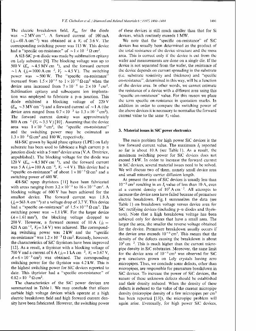
V.E. Chelnokov et al. I Diamond and Related Materials 6 (1997) 1480-1484 1481
The electric breakdown field, Em, for the diode was ~2MVcm_1. A forward current of 100 mA (y'f=68 Acm~2) was obtained at a V( of 3.6 V. The corresponding switching power was 113 W. This device had a "specific on-resistance" of ~ 1 x 10~2 Q cm2.
A 6H-SiC p-n diode was made by sublimation epitaxy on Lely substrate [9]. The blocking voltage was up to 500 V (Em ~4.5MVcmT1), and the forward current ~1A (yf=1000Acm~2, Vt -4.5 V). The switching power was ~500W. The "specific on-resistance" increased from 1.5 x 10~3 to 1 x 10~2 Q, cm2 when the device area increased from 7xl0~4 to 2xl0_2cm2. Sublimation epitaxy and subsequent ion implanta- tion was employed to fabricate a p-n junction. This diode exhibited a blocking voltage of 220 V (Em ~ 3 MV cm-1) and a forward current of ~ 1 A (the device area ranged from 0.7 x 10⁻³ to 1.3 x 10~3 cm2). The forward current density was approximately 800 A cm"2 (V{ ~3.5 V) [10]. Assuming that the device area was lxl0~3cm2, the "specific on-resistance" and the switching power may be estimated as 1.3 x 10~3 Q cm2 and 180 W, respectively.
6H-SiC grown by liquid phase epitaxy (LPE) on Lely substrate has been used to fabricate a high current p-n junction diode with a 5 mm2 device area (V.A. Dmitriev, unpublished). The blocking voltage for the diode was 120 V (Em ~4.5 MVcm"1), and the forward current was 5 A (;f = 100 A cm"2, V{ ~4 V). This device had a "specific on-resistance" of about 1 x 10"2Qcm2 and a switching power of 600 W.
4H-SiC npnp thyristors [11] have been fabricated with areas ranging from 3.2 x 10~3 to 16 x 10~3 cm2. A blocking voltage of 600 V has been achieved for the smallest device. The forward current was 1.8 A (jf = 563 A cm-2) at a voltage drop of 3.7 V. This device had a "specific on-resistance" of 1.5 x 10~3 Cl cm2. The switching power was ~1.1 kW. For the larger device (A = 1.61 mm2), the blocking voltage dropped to 200 V. However, a forward current of 10 A (j( = 621 A cm"2, Ff=3.6 V) was achieved. The correspond- ing switching power was 2 kW and the "specific on-resistance" was 1.2 x 10~3 Q cm2. Recently, however, the characteristics of SiC thyristors have been improved [12]. As a result, a thyristor with a blocking voltage of 700 V and a current of 6 A (jt= 1 kA cm"2, Vt = 3.67 V, A = 6 x 10 ~3 cm2) was obtained. The corresponding switching power for the thyristor was 4.2 kW. This is the highest switching power for SiC devices reported to date. This thyristor had a "specific on-resistance" of 0.82xl0_3Qcm2.
The characteristics of the SiC power devices are summarized in Table 1. We may conclude that silicon carbide high voltage devices which operate at a high electric breakdown field and high forward current den- sity have been fabricated. However, the switching power
of these devices is still much smaller than that for Si devices, which routinely exceeds 1 MW.
We note that the "specific on-resistance" of SiC devices has usually been determined as the product of the total resistance of the device structure and the mesa area. This is correct only if the device is cut from the wafer and measurements are done on a single die. If the device is not separated from the wafer, the resistance of the device depends on current spreading in the substrate (i.e. substrate resistivity and thickness) and "specific on-resistance", determined in this way, will be a function of the device area. In other words, we cannot estimate the resistance of a device with a different area using this "specific on-resistance" value. For this reason we place the term specific on-resistance in quotation marks. In addition in order to compare the switching power of the above devices it is necessary to normalize the forward current value to the same V{ value.
3. Material issues in SiC power electronics
The main problem for high power SiC devices is the low forward current value. The maximum I{ reported so far is about 10 A (see Table 1). As a result, the maximum switching power for SiC devices does not exceed 5 kW. In order to increase the forward current in SiC devices, several material issues need to be solved. We will discuss two of them, namely small device area and small minority carrier diffusion length.
At present the area of SiC devices is usually less than 10 ~2 cm2 resulting in an I{ value of less than 10 A, even at a current density of 103Acm~2. All attempts to increase the device area have failed because of premature electric breakdown. Fig. 1 summarizes the data (see Table 1) on breakdown voltage versus device area for SiC rectifying devices (including p-n diodes and thyris- tors). Note that a high breakdown voltage has been achieved only for devices that have a small area. The larger the area, the smaller the reverse voltage obtained for the device. Premature breakdown usually occurs if the device area exceeds 10~3cm2. This means that the density of the defects causing the breakdown is about 103 cm-2. This is much higher than the current micro- pipe density in SiC substrates. Moreover, the same limit for the device area of 10~3cm2 was observed for SiC p-n structures grown on Lely crystals having zero micropipes. Thus, we conclude some defects, other than micropipes, are responsible for premature breakdown in SiC devices. To increase the power of SiC devices, the nature of these unknown defects should be established and their density reduced. When the density of these defects is reduced to the value of the current micropipe density (micropipe density of a few micropipes per cm2
has been reported [13]), the micropipe problem will again arise. Eventually, for high power SiC devices,
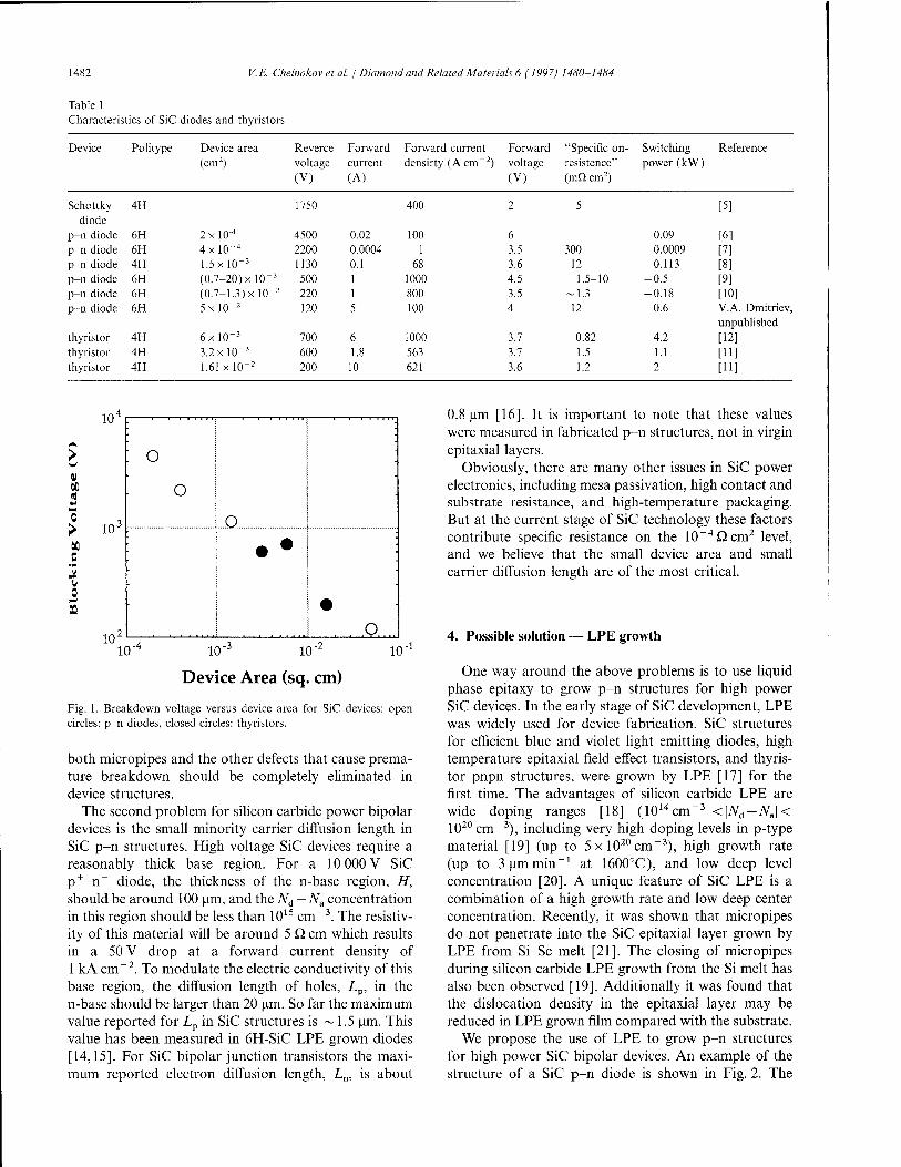
1482 V.E. Chelnokov et cd. / Diamond and Related Materials 6 (1997) 1480-1484
Table 1 Characteristics of SiC diodes and thyristors
Device Politype Device area (cm2)
Reverce Forward voltage current (V) (A)
Forward current densirty (A cm-2)
Forward voltage (V)
"Specific on- resistence" (m£i cm2)
Switching power (kW)
Reference
Schottky diode
p-n diode p-n diode p-n diode p-n diode p-n diode p-n diode
4H
6H 6H 4H 6H 6H 6H
thyristor 4H thyristor 4H thyristor 4H
2xl0"4
4xl(T4
1.5 xl(T3
(0.7-20) xl(T3
(0.7-1.3) xl0~3
5xl0~2
6xl0"3
3.2xl0"3
1.61 xl0~2
1750
4500 2200 1130 500 220 120
700 600 200
0.02 0.0004 0.1 1 1 5
6 1.8
10
400
100 1
68 1000 800 100
1000 563 621
2
6 3.5 3.6 4.5 3.5 4
3.7 3.7 3.6
300 12 1.5-10
-1.3 12
0.82 1.5 1.2
0.09 0.0009 0.113
-0.5 -0.18 0.6
4.2 1.1 2
[5]
[6] [V] [8] [9] [10] V.A. Dmitriev, unpublished [12] [H] [11]
10'
: o •
o o
■
• • • :
•
. .9..,.
0 > 10'
bfi
• H
u 0
10' 10 "4 10 'd 10_/ 10_1
Device Area (sq. cm)
Fig. 1. Breakdown voltage versus device area for SiC devices: open circles: p-n diodes, closed circles: thyristors.
both micropipes and the other defects that cause prema- ture breakdown should be completely eliminated in device structures.
The second problem for silicon carbide power bipolar devices is the small minority carrier diffusion length in SiC p-n structures. High voltage SiC devices require a reasonably thick base region. For a 10 000 V SiC p+-n~ diode, the thickness of the n-base region, H, should be around 100 pm, and the Nd — Na concentration in this region should be less than 1015 cm"3. The resistiv- ity of this material will be around 5 Q cm which results in a 50 V drop at a forward current density of 1 kA cm"2. To modulate the electric conductivity of this base region, the diffusion length of holes, Lp, in the n-base should be larger than 20 run. So far the maximum value reported for Lp in SiC structures is ~ 1.5 urn. This value has been measured in 6H-SiC LPE grown diodes [14,15]. For SiC bipolar junction transistors the maxi- mum reported electron diffusion length, Ln, is about
0.8 um [16]. It is important to note that these values were measured in fabricated p-n structures, not in virgin epitaxial layers.
Obviously, there are many other issues in SiC power electronics, including mesa passivation, high contact and substrate resistance, and high-temperature packaging. But at the current stage of SiC technology these factors contribute specific resistance on the 10"4Qcm2 level, and we believe that the small device area and small carrier diffusion length are of the most critical.
4. Possible solution — LPE growth
One way around the above problems is to use liquid phase epitaxy to grow p-n structures for high power SiC devices. In the early stage of SiC development, LPE was widely used for device fabrication. SiC structures for efficient blue and violet light emitting diodes, high temperature epitaxial field effect transistors, and thyris- tor pnpn structures, were grown by LPE [17] for the first time. The advantages of silicon carbide LPE are wide doping ranges [18] (1014cm~3 <|JVd —7VJ< 1020cm~3), including very high doping levels in p-type material [19] (up to 5xl020cmT3), high growth rate (up to 3 um min-1 at 1600°C), and low deep level concentration [20]. A unique feature of SiC LPE is a combination of a high growth rate and low deep center concentration. Recently, it was shown that micropipes do not penetrate into the SiC epitaxial layer grown by LPE from Si-Sc melt [21]. The closing of micropipes during silicon carbide LPE growth from the Si melt has also been observed [19]. Additionally it was found that the dislocation density in the epitaxial layer may be reduced in LPE grown film compared with the substrate.
We propose the use of LPE to grow p-n structures for high power SiC bipolar devices. An example of the structure of a SiC p-n diode is shown in Fig. 2. The

V.E. Chelnokov et al. I Diamond and Related Materials 6 (1997) 1480-1484 1483
Fig. 2. Schematic drawing of proposed LPE grown SiC high power diode: (1) Ohmic contact to p + -SiC, (2) p + -layer, (3) n~-base region, (4) micropipes, (5) n+-layer, (6) n + -4H-SiC substrate, (7) Ohmic con- tact to n+-SiC.
diode consists of a n + -4H-SiC substrate and a multilayer structure grown by LPE. The first n+-layer serves to cover micropipes and reduce the overall defect density. The following n"-layer is a base region of the diode. The thickness and doping concentration of the base are determined by required reverse voltage of the device. As mentioned above, for 10 000 V devices the required 7Vd — JVa concentration is about 1 x 1015 cm"3 and the thickness H is ~ 100 urn. This layer may be grown by LPE within a few hours, compared with a few days required by conventional CVD. The top p +-layer will be grown with a hole concentration higher than 102Ocm~3 which will ensure a low contact resistance. We believe that the low defect density and low deep level concentration in LPE grown material will allow us to increase the device area and improve minority carrier diffusion length.
5. Summary
Recently, significant progress in SiC technology has been achieved. SiC devices with blocking voltages of a few kilovolts and forward current densities of 1 kAcrrT2 have been fabricated. The next step toward high power SiC electronics is to increase the forward current of the devices. This step requires reduction of the on-resistance of the devices. Two main factors that
currently limit the resistance are: (1) device area, and (2) resistivity of the base region of the devices. In order to solve these problems, defect density in the p-n structures should be reduced. We propose to fabricate high power SiC devices, such as diodes and thyristors using liquid phase epitaxy for p-n structure formation. This method has been shown to reduce micropipe and dislocation density in SiC p-n structures and to produce material with the large diffusion length required to modulate electrical conductivity of base region.
Acknowledgement
This work was supported in part by Arizona State University.
References
[1] J.R. O'Connor, J. Simltens (Eds.) Silicon Carbide, A High Tem- perature Semiconductor, Pergamon Press, Oxford, 1960; H.K. Henisch, R. Roy (Eds.), Silicon carbide — 1968, Proceedings of the International Conference on Silicon Carbide, Pergamon Press, New York, 1969.
[2] A.E. Otblesk, V.E. Chelnokov, in: Problems of Physics and Tech- nology of Wide Band Gap Semiconductors, LETI, Leningrad, 1980 pp. 197-211 (in Russian).
[3] V.E. Chelnokov, Materials Science and Engineering B II (1992) 103.
[4] S. Nakashima, H. Matsunami, S. Yoshida, H. Harima (Eds.), Silicon Carbide and Related Materials 1995, Institute of Physics Conference Series No. 142, IOP Publishing, Bristol, 1996.
[5] A. Itoh, T. Kimoto, H. Matsunami, in: S. Nakashima, H. Matsu- nami, S. Yoshida, H. Harima (Eds.), Silicon Carbide and Related Materials 1995, Institute of Physics Conference Series No. 142, IOP Publishing, Bristol, pp. 689-692.
[6] O. Kordina, J.P. Bergman, A. Henry, E. Janzen, S. Savage, J. Andre, L.P. Ramberg, U. Lindefelt, W. Hermansson, K. Berga- man, Appl. Phys. Lett. 67 (11) (1995) 1561.
[7] P.G. Neudeck, DJ. Larkin, J.A. Powell, L.G. Matus, C.S. Salupo, Appl. Phys. Lett. 64 (11) (1994) 1386.
[8] J.W. Palmour, J.A. Edmond, H.S. Kong, C.H. Carter, Jr, in: M.G Spencer, R.P. Devaty, J.A. Edmond, M. Asif Khan, R. Kaplan, M. Rahman (Eds.), Institute of Physics Conference Series No. 137, IOP Publishing, Bristol, 1994, pp. 499-502.
[9] M.M. Anikin, P.A. Ivanov, A.A. Lebedev, S.N. Pytko, A.M. Strel'chuk, A.L. Syrkin, in: Semicinductor Interfaces and Micro- structures, World Scientific Publishing, Singapore, 1992, pp. 280-311.
[10] M.M. Anikin, A.A. Lebedev, I.V. Popov, V.E. Sevastyanov, A.L. Syrkin, A.L. Suvorov, V.E. Chelnokov, G.P. Shpiniev, Pisma v ZhTF 10 (17) (1984) 1053.
[11] J.W. Palmour, S.T. Allen, R. Singh, LA. Lipkin, D.G. Waltz, in: S. Nakashima, H. Matsunami, S. Yoshida, H. Harima (Eds.), Silicon Carbide and Related Materials 1995, Institute of Physics Conference Series No. 142, IOP Publishing, Bristol, 1996,pp. 813-816.
[12] J.W. Palmour, R. Singh, L.A. Lipkin, D.G. Waltz, in: Transac- tions of the Third International High Temperature Electronics Conference, Albuquerque, New Mexico, June 9-14, 1996, vol. 2, p. XVI-9.
[13]V.F. Tsevtkov, S.T. Allen H.S. Kong, C.H. Carter, Jr, in: S. Nakashima, H. Matsunami, S. Yoshida, H. Harima (Eds.), Sili-

1484 V.E. Chelnokov et al. / Diamond and Related Materials 6 (1997) 1480-1484
con Carbide and Related Materials 1995, Institute of Physics Con- ference Series No. 142, IOP Publishing, Bristol, 1996,pp. 17-22.
[14] A.M. Strelchuk, A.L. Syrkin, V.E. Chelnokov, A.E. Cherenkov, V.A. Dmitriev, in: M.G. Spencer, R.P. Devaty, JA. Edmond, M. Asif Khan, R. Kaplan, M. Rahman (Eds.), Institute of Physics Conference Series No. 137, IOP Publishing, Bristol, 1994, pp. 549-552.
[15] A.M. Strel'chuk, Semiconductors 29 (1995) 614. [16] Y. Wang, W. Xie, J.A. Cooper, Jr, M.R. Melloch, J.W. Palmour,
in: S. Nakashima, H. Matsunami, S. Yoshida, H. Harima (Eds.), Silicon Carbide and Related Materials 1995, Institute of Physics Conference Series No. 142, IOP Publishing, Bristol, 1996,pp. 809-812.
[17] For review see V.A. Dmirriev, in: G.L. Harries (Ed.), Properties of Silicon Carbide, IEE, 1994, pp. 214-227; and V.A. Dmitriev, PhysicaB 185(1993)440.
[18] W. Munch, W. Kurzinger, Solid State Electronics 21 (1978) 1129.
[19] S.N. Rendakova, to be published. [20] M.M. Anikin, A.S. Zubrilov, A.A. Lebedev, A.P. Strel'chuk, V.E.
Chelnokov, Sov. Phys. Semicond. 25 (1991) 289. [21] R. Yakimova, M. Tuominen, A.S. Bakin, J.-O. Fornell, A. Veha-
nen, E, Jansen, in: S. Nakashima, H. Matsunami, S. Yoshida, H. Harima (Eds.), Silicon Carbide and Related Materials 1995, Insti- tute of Physics Conference Series No. 142, IOP Publishing, Bris- tol, 1996, pp. 101-104.

«^Äift
ELSEVIER Diamond and Related Materials 6 (1997) 1485-1488
DIAMOND AND
RELATED MATERIALS
2.5 kV ion-implanted/?+« diodes in 6H-SiC
K.H. Rottnera-*, A. Schönera, S.M. Savagea, M. Frischholza, C. Hallin b, O. Kordina b, E. Janzen b
a IMC, PO Box 1084, S-16421 Stockholm-Kista, Sweden b Department of Physics and Measurement Technology, Linköping University, S-58183 Linköping, Sweden
Abstract
High-voltage diodes which can block up to 2.5 kV have been fabricated by ion implantation of/>-type dopants. Junctions with a low forward voltage drop and a leakage current level sufficiently low to allow stable device operation have been demonstrated. This was achieved using a combination of boron and aluminum as implanted acceptor for the ^-type emitter. The junction termination to control the surface electric field was achieved by the unintentionally induced negative surface charge. For reference, devices with a junction termination extension were also fabricated. Both device types are shown to block the same voltage limited by external flash-over. Using optical beam induced current (OBIC) measurements, we visualized the depletion region of the implanted pn junctions and found that all devices have a considerably enlarged lateral depletion width, which is indicative of the expected high surface charge acting on the "self-terminated devices as surface field reduction. © 1997 Elsevier Science S.A.
Keywords: OBIC; Diodes; Ion implantation; Termination
1. Introduction
Ion implantation to incorporate dopant atoms into SiC has recently become a more-available technology for devices [1-5]. We have fabricated planar high- voltage diodes using ion implantation of boron and co-implantation of boron and aluminum into low doped »-type CVD layers. Junction termination was achieved by boron implantation around the periphery of the emitter in order to form a junction termination extension (JTE) structure.
For high-voltage devices, junction termination is a very important issue in order to keep the surface electri- cal field low enough to prevent premature breakdown. The presence of surface charge effects lowering the surface field and thus providing unintentional termina- tion has been published earlier [6,7]. To visualize this effect, we used optical beam induced current (OBIC) measurements. The objective of this work was to make use of the unintentional termination due to surface charge and evaluate its effectiveness with respect to diodes with a JTE structure.
' Corresponding author.
2. Experiments
2.1. Device structures
Three types of device were processed: devices with a boron implanted emitter (denoted as B devices), devices with aluminum and boron implanted emitters (Al-B devices) and devices with JTE and boron implanted emitters (JTE devices). For the ^-anodes of the diodes, two different implantation profiles were implemented: for the B-devices boron was used to form the anode, while for the Al-B devices, boron and aluminum were implanted. Boron is known to diffuse rather quickly during the implantation annealing [1]. In particular, close to the surface, an out diffusion of p-type dopants might result in a poor contact formation on the implanted region [12]. Owing to the diffusion of boron, the metallurgical pn junction is located deeper in the bulk, in a region not damaged by the implantation process. This is expected to increase the blocking capa- bility and decrease the leakage current of the />« junction. The differences in diffusion were established by SIMS measurements [1].
The implantation of the dopants was carried out at 600 °C to remove the implantation damage and to electrically activate the implanted species, the samples
0925-9635/97/S17.00 © 1997 Elsevier Science S.A. All rights reserved. PII S0925-9635(97)00060-5
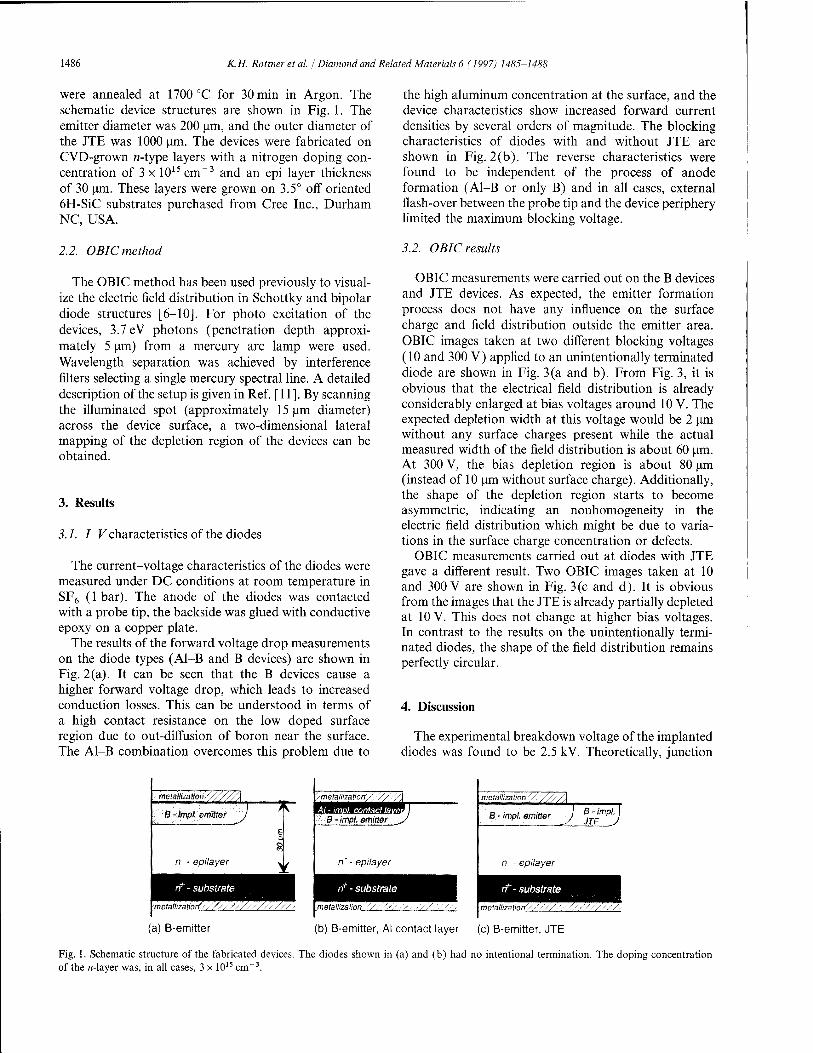
1486 K.H. Rottneretal. / Diamond and Related Materials 6 (1997) 1485-1488
were annealed at 1700 °C for 30 min in Argon. The schematic device structures are shown in Fig. 1. The emitter diameter was 200 um, and the outer diameter of the JTE was 1000 um. The devices were fabricated on CVD-grown «-type layers with a nitrogen doping con- centration of3xl015cm~3 and an epi layer thickness of 30 um. These layers were grown on 3.5° off oriented 6H-SiC substrates purchased from Cree Inc., Durham NC, USA.
2.2. OBICmethod
The OBIC method has been used previously to visual- ize the electric field distribution in Schottky and bipolar diode structures [6-10]. For photo excitation of the devices, 3.7 eV photons (penetration depth approxi- mately 5 um) from a mercury arc lamp were used. Wavelength separation was achieved by interference filters selecting a single mercury spectral line. A detailed description of the setup is given in Ref. [ 11 ]. By scanning the illuminated spot (approximately 15 urn diameter) across the device surface, a two-dimensional lateral mapping of the depletion region of the devices can be obtained.
3. Results
3.1. I-V characteristics of the diodes
The current-voltage characteristics of the diodes were measured under DC conditions at room temperature in SF6 (1 bar). The anode of the diodes was contacted with a probe tip, the backside was glued with conductive epoxy on a copper plate.
The results of the forward voltage drop measurements on the diode types (Al-B and B devices) are shown in Fig. 2(a). It can be seen that the B devices cause a higher forward voltage drop, which leads to increased conduction losses. This can be understood in terms of a high contact resistance on the low doped surface region due to out-diffusion of boron near the surface. The Al-B combination overcomes this problem due to
the high aluminum concentration at the surface, and the device characteristics show increased forward current densities by several orders of magnitude. The blocking characteristics of diodes with and without JTE are shown in Fig. 2(b). The reverse characteristics were found to be independent of the process of anode formation (Al-B or only B) and in all cases, external flash-over between the probe tip and the device periphery limited the maximum blocking voltage.
3.2. OBIC results
OBIC measurements were carried out on the B devices and JTE devices. As expected, the emitter formation process does not have any influence on the surface charge and field distribution outside the emitter area. OBIC images taken at two different blocking voltages (10 and 300 V) applied to an unintentionally terminated diode are shown in Fig. 3 (a and b). From Fig. 3, it is obvious that the electrical field distribution is already considerably enlarged at bias voltages around 10 V. The expected depletion width at this voltage would be 2 um without any surface charges present while the actual measured width of the field distribution is about 60 um. At 300 V, the bias depletion region is about 80 urn (instead of 10 urn without surface charge). Additionally, the shape of the depletion region starts to become asymmetric, indicating an nonhomogeneity in the electric field distribution which might be due to varia- tions in the surface charge concentration or defects.
OBIC measurements carried out at diodes with JTE gave a different result. Two OBIC images taken at 10 and 300 V are shown in Fig. 3(c and d). It is obvious from the images that the JTE is already partially depleted at 10 V. This does not change at higher bias voltages. In contrast to the results on the unintentionally termi- nated diodes, the shape of the field distribution remains perfectly circular.
4. Discussion
The experimental breakdown voltage of the implanted diodes was found to be 2.5 kV. Theoretically, junction
■metallization//.
B *:lmpl. «mitter
n~ - epilayer
if - substrate
(a) B-emitter
■metallization'//'/
B-irnpl. emitter
n' - epilayer
if - substrate
_J ß • impl. emitter } B- impl, I
n~ - epilayer
rf - substrate
Imetamzalion/.
(b) B-emitter, Al contact layer (c) B-emitter, JTE
Fig. 1. Schematic structure of the fabricated devices. The diodes shown in (a) and (b) had no intentional termination. The doping concentration of the «-layer was, in all cases, 3 x 1015 cm~3.

K.H. Rottneretal. / Diamond and Related Materials 6 (1997) 1485-1488 1487
o 10° >^AI+B implanted anode f
* I ^^ ,m
£.10-1 1 ^•^^"^ to
5 io-2 1 ••• 1 .•• B-implanted anode T> 8 •
| IO3 8 *
ü 10"4 O
a)
2 3 4 5 6 7 8 Forward voltage drop (V)
O 10 -3000 -2000 -1000 0
Blocking voltage (V)
b) Fig. 2. (a) I-V characteristics of diodes with boron implanted anodes in comparison with anodes formed by a combination of Al and B implantations, (b) Blocking curves of a diode with JTE and one without termination. Although the leakage current levels were different, the maximum blocking voltage was the same for botht types.
termination structures would be necessary in order to keep the surface electric fields low enough to avoid premature breakdown. However, the experimental find- ing that SiC diodes block higher voltages than two- dimensional simulation (neglecting surface charge) pre- dicts was already established in previous studies [6,7] where clear indication was found that on «-SiC, the negative surface charge, acting as junction termination, is responsible for this effect. In agreement with these previous results, our devices did not suffer from having no intentional junction termination. Both device types
- with and without JTE - blocked the same voltage. The OBIC results show significant lateral extension of the depletion region already at very low blocking voltages at the diodes both with and without JTE.
The results of the I-V measurements show that the combination of Al and B for the anode formation by ion implantation is a viable way to achieve decent pn junctions. The reverse leakage current levels at low voltages were found to be around 10~5Acm~2at 500 V. With higher voltages, an increase of the leakage current was observed, together with soft breakdown characteris-
200 Mm 10V
300V
10V
300V
Fig. 3. (a and b) Greyscale encoded OBIC images taken at 10 V (a) and 300 V (b) blocking voltage of diodes without intentional termination. The circular area in the center corresponds to the emitter with the metallization, (c and d) Greyscale encoded OBIC image of a device with JTE at 10 V (c) and 300 V (d) blocking voltage. In (a) the outer diameter of the JTE and the position of the emitter are shown. A further feature is caused by shading effects due to the bonding wire contacting the emitter.

1488 K.H. Rottneretal. / Diamond and Related Materials 6 (1997) 1485-1488
tics. The breakdown itself occurred by external flash- over. This might be due to the lack of any surface passivation and insulation, making devices very sensitive to "environmental" effects - e.g. humidity. The surface electric field distribution is very critical for surface leakage, and since it was not possible to determine exactly where this leakage current is actually flowing, it is premature to speculate about the underlying physical mechanism. However, the current level was low enough to maintain stable device operation without thermal runaway due to power dissipation (approximately 500 Wem"2 at 2.5 kV)
The forward current voltage curves of these diodes showed an exponential behavior in a large current range with an ideality factor of 1.05. In the high current density region, limitations by serial resistivities were observed, which can be assigned partly to the external circuitry of the I-V measurement setup.
5. Conclusion
The feasibility of ion implanted diodes for high- voltage applications has been demonstrated. The ter- mination concept of JTE structures was implemented successfully. The OBIC method has proven to be a powerful tool in investigating and visualizing surface charge induced effects on the electric field distribution of devices. We could visualize the effects of the JTE and the surface charges on the lateral depletion width.
Acknowledgement
The work was financed by Asea Brown Boveri and the Swedish National Board for Industrial and Technical Development (NUTEK).
References
[1] G. Pensl, Proc. in SiC and Related Materials, IoP Publishing no. 142, Bristol and Philadelphia, 1996, p. 275.
[2] M. Ghezzo, D.M. Brown, E. Downey, J. Kretchmer, J.J. Kopan- ski, Appl. Phys. Letters 63 (1993) 1206.
[3] N. Ramangul, V. Khemka, R. Tyagi, T.P. Chow, M. Ghezzo, P.G. Neudeck, J. Kretchmer, W. Hennessy, D.M. Brown, in: SiC and Related Materials, IoP Publishing no. 142, Bristol and Phila- delphia, 1996, p. 713.
[4] P.M. Shenoy, B.J. Baliga, IEEE Electron. Device Lett. 16 (10) (1995)454.
[5] D. Planson, M. Locatelli, S. Ortolland, J.P. Chante, H. Mitlehner, D. Stephani, Proceedings of the 1st International Power Electron- ics and Motion Control Conference '94, Beijing (accepted for publication).
[6] K. Rottner, S. Savage, J. Andre, L. Ramberg, M. Frischholz, R. Helbig, in: SiC and Related Materials, Institute of Physics Publishing, Bristol, Conference Series No. 142, 1996, p. 721.
[7] K. Rottner, A. Schöner, M. Frischholz, R. Helbig, Proceedings of the Material Research Society, Symposium E, Spring Meeting 96, San Francisco, Proc. vol. 423.
[8] R. Stengl, IEEE Trans. Electron. Devices 34 (4) (1987) 911. [9] J. Sandoe, J. Hughes, Acta Electron. 25 (3) (1983) 201.
[10] S. Lindsay, Phys. Stat. Sol. (a) 53 (1979) 311. [11] M. Frischholz, R. Helbig, Appl. Surf. Sei 65 (1993) 784. [12] N. Nordell, S. Savage, A. Schöner, in: SiC and Related Materials,
IoP Publishing no. 142, Bristol, 1996, p. 573.

DIAMOND AND
RELATED MATERIALS
ELSEVIER Diamond and Related Materials 6 (1997) 1489-1493
High field and high temperature stress of n-SiC MOS capacitors
E. Banoa>*, T. Ouissea, C. Leonhard b, A. Gölz b, E.G. Stein Von Kamienskib
1 Laboratoire de Physique des Composants ä Semiconducteurs (LPCS), UMR-CNRS 5531, ENSERG, 23 rue des Martyrs, 38016 Grenoble, France
b Institut für Halbleitertechnik, Lehrstuhl II, RWTH Aachen, Sommer-feldstr. 24, D-52074 Aachen, Germany
Abstract
The development of reliable oxides built on SiC has become a very important issue with respect to either passivation processes or metal-oxide-semiconductor (MOS) applications. The aim of this paper is to present a detailed investigation of Fowler-Nordheim electron injections in n-type silicon carbide (SiC) MOS capacitors. A systematic variation in the temperature and in the average oxide field Eox applied during the stress allowed us to evidence both a positive charge and electron trapping. The positive charge build-up is shown to emerge above a threshold field close to 7 MVcm"1. It decreases with temperature, and can be dissociated into two different exponential time processes. The overall results agree with mechanisms based on impact ionization in the oxide, leading to pair creation and subsequent hole trapping. © 1997 Elsevier Science S.A.
Keywords: Silicon carbide; Metal-oxide-semiconductor; Impact-ionization; Fowler-Nordheim injection
1. Introduction
Silicon carbide (SiC) is a promising candidate for high temperature and high power applications [1,2]. The development of reliable oxides built on SiC has become an important issue with respect to metal-oxide— semiconductor (MOS) applications. Several authors have already reported a detailed investigation of the SiC/Si02 interface properties [3-9]. In the case of p-type layers, a high interface disorder has been evidenced, which strongly affects the transport properties in the inversion layer of SiC MOS transistors [2,10,11]. Although it has been demonstrated that most of the fixed charge was localised close to the interface [12], only a few reports deal with the properties of bulk traps into the oxide [13-15]. Systematic data, including influ- ence of fabrication conditions, were presented elsewhere for lower oxide fields [13], and here we focus on the build-up of an anomalous positive charge at higher fields. It will be shown that this positive charge build-up most probably results from impact ionization in the oxide, followed by hole trapping. Such phenomena have already been clearly identified in the case of silicon MOS technology. From a comparison between our results and similar data already published in the MOS silicon litera-
' Corresponding author. Fax: 33 76 85 60 70; e-mail: [email protected]
ture, we wish to demonstrate that, in the case of SiC, these mechanisms remain essentially unchanged.
2. Devices and experimental details
Fowler-Nordheim electron injections have been car- ried out on 6H SiC MOS capacitors fabricated at RWTH, using n-type nitrogen-doped epitaxial layers grown on n-type substrates bought from Cree Research Inc. The net doping level of the epitaxial layer was ND — NA =7 x 1015 cm"3. After a wet chemical cleaning process, an oxide layer of 44 nm was grown at 1150 °C in dry oxygen followed by a 60 mn anneal in Ar at the same temperature. A poly-Si layer of 200 nm was depos- ited by a standard LPCVD process which was implanted with As and annealed at 1150 °C for 20 s. The poly-Si was metallized with Ti and Au and patterned to dots of 200 and 400 itm diameter. Both the electric field and stress temperature dependence have been investigated, from T=291 to 473 K with a constant injection current 7inj of 3 x 10 ~5 A cm"2, and with Iini varying from 10"6 to 7 x 10"5 A cm"2 at T=313 K with total injec- tion doses up to 1019 charges cm"2. We studied both the variation in the fiat-band voltage FFB and the Fowler-Nordheim voltage VFN, defined here as the volt- age required for imposing 7inj. However, after each
0925-9635/97/517.00 © 1997 Elsevier Science S.A. All rights reserved. PII S0925-9635(97)00061-7

1490 E. Bano et al. j Diamond and Related Materials 6 (1997) 1489-1493
extraction of FFB from the C(V) curve, even on a small gate voltage interval, a discontinuous jump was always observed in the VFN shift curve (Fig. 1). In fact, a partial recovery of the trapped charges occurred due to the time and bias needed for C(V) measurement. To avoid these transients and have a real account of the trapped charges, we only monitored VFN, except in a restricted number of cases, to assess the evolution of the small signal capacitance and conductance characteristics with the injected dose. In such a case, an increase of the conductance peak with the injected charge, especially for the lower doses, reflected an increase in the interface state density (Fig. 2). Besides, no broadening of the peak was observed, which seems to show that the potential fluctuations were not substantially increased, and therefore that the injection was spatially homogeneous.
3. Results and discussion
T=298K, f= 30Hz I .c
3 - ^■»s
1 1
E /\ ^-"^ / \ -' o
2 ? ' AN //
X
0.8 ü o „ ' r\f / o
LU
' / lA / UJ
0.6^ z"1 ' 1 \ <
'A\ i- < ,/ ' \ o 1- o
1 i \ 0.4 < Q.
3 ■jC^y / / \ ^N-\. < 9 0 " 'S VA
^ o z -^^^ o 0.2 o . .ieni i sample
after injection -1 i 0
6 -5 -4 -3 -2 -1 0 GATE VOLTAGE (V)
Typical AVFN shifts are shown in Figs. 3(a) and (b). The two kinds of charge build-up suggest to analyse the data in terms of a multiple trapping model. A plot In |dAFFN/df| versus time shows a number of transitions equal to that of the processes involved. Then, the analytical fit of the data gives the trap density Ntt and the capture cross section at for the ;'th trap centre. First, an anomalous positive charge is always prevailing, decreasing with temperature and increasing with current density. This positive charge build-up can be dissociated
> n >
> <
-0.3
-0.4
-0.5
-0.6
-0.7
T=298K
- V linj=30|jA/cm2
- %yj 9 o oo <j < Q
- AVfb
_ AVfn
10 15 10 16 10 17 101
-2Y INJECTED DOSE (cm )
Fig. 1. Fowler-Nordheim and flatband voltage shift as a function of electron dose injected from the substrate, for different steps of injection and 7™ = 30 uA cm"2, at T=298 K.
Fig. 2. Conductance and capacitance vs gate voltage for a small signal frequency (/=30Hz), at room temperature, after and before an injected dose of 3 x 10¹⁷ electrons per cm2.
-0.5 10
) i i i i nil iii '''' "Hi j i_i,i.u,|
14 1015 1016 1017 1018 1019
INJECTED DOSE (cm"2)
Fig. 3. Variation of the Fowler-Nordheim voltage as a function of electron injected dose: (a) 7"=291 to 473 K at 7inj = 30 uA cm"2, and (b)7inj = 3 to 30LiAcm"2at J=373K.

E. Banoetal. / Diamond and Related Materials 6 (1997) 1489-1493 1491
into two different time processes (z'=l and 2) which prevail respectively before and after doses around 1015cm~2. Then, at higher doses, a turn around effect clearly shows that a negative trapping (z = 3) emerges. The time law used for fitting the three different first- order exponential time processes was
AKFN(0 = -^— £ ötNti[l~exp (-/injff,-t/q)],
where 5t= — 1 for /= 1 and 2 (positive charge trapping) and +1 for z'=3 (electron trapping), q is the elementary charge, tm is the oxide thickness and eox the dielectric constant of the oxide. In the case of a positive charge build-up, this modelling might a priori be questionable. For instance, the creation of water and hydrogen-related traps [13,15] should not necessarily obey such a time process. Nevertheless, this procedure will be justified by analysing the electric field and temperature dependence of the trapping parameters.
From Fig. 4, no charge is trapped before a threshold field of around 6.75 MV cm-1, from which the positive charge build-up depends almost linearly on the average electric field Eox. Such a behaviour has already been observed in Si MOS technology [16,17]. Although the cause of an anomalous positive charge formation has been controversial during several years, DiMaria, Arnold and Cartier demonstrated that such a charge build-up was due to impact ionization inside the oxide,
6.8 7 7.2 7.4 7.6 7.8 AVERAGE ELECTRIC FIELD (MV/cm)
Fig. 4. Dependence of the Fowler-Nordheim shift on the average oxide electric field, for an injected dose of 1016 cm-2 at r=373 K, and varia- tion of the total apparent hole trap density vs electric field, as deduced from numerical fits (this density corresponds to the sum of the two positive trapping processes).
followed by a subsequent hole trapping [16], provided that the oxide film was sufficiently thick (>20nm). In Si02 on Si films and for E0X>1 MV cm-1, they showed that a hot electron energy distribution tail exceeding 9 eV was resulting from high field electron transport in the oxide layer, and such an energy was large enough so as to enable impact ionization [16,17]. The subse- quent trapping mechanism can still be modelled by a first-order rate equation, taking into account both hole trapping and free electron-trapped hole annihilation processes, characterised by their capture and annihila- tion cross section, ap and ae respectively
P(t) = aapNt
[ 1 - exp (- 7inj («ffp + (je)t/q)],
where a is the band gap ionisation probability, i.e. the appropriate factor which must be multiplied by the electron current to obtain the hole current passing though the oxide. Dimaria et al. demonstrated that a dramatically increases with Eox and with the oxide thickness, since this allows enough space for the electron distribution to develop a high energy tail [16]. When ce is large against aerp, one expects to find an apparent hole trap density equal to (a<7p/<xe)./Vt, whereas the appar- ent capture cross section is now almost given by <re. Roughly interpolating and extrapolating the data pre- sented in Fig. 2 of Ref. [16], we would expect a values in the range of 10 ~4 around 300 K, with a total variation of about a factor of 10 for oxide fields between 7 and 8MVcm_1. Considering capture cross sections in the same range as that found in Ref. [16], i.e. ae around 10~16cm2 and <rp around 10~14cm2, one would have cxe much larger than <xop. Hence the apparent capture cross section should be almost equal to <re, whereas the apparent hole trap density should be given by {aav/ae)Nv This hypothesis seems to be confirmed by Fig. 4: the apparent hole trap density depends linearly on Eox, and roughly increases by a factor of 10 between 6.9 and 7.8 MVcm"1. Besides, the fact that the experi- mental values of the apparent cross sections (in the 10~16-10~15 cm2 range) always remain much larger than the value of aap estimated above reinforces the compati- bility of the model with experiment. Taking from Ref. [16] an a value in the range of 10"4 and a real trap density in the range of 1-5 x 1012 cm~2, one would expect apparent trap densities of the order of 1011 cm~2 which is in agreement with the values extracted from the data fit (Fig. 4).
To further confirm that hole trapping is induced by impact ionisation in the oxide, Fowler-Nordheim injec- tions have also been investigated as a function of stress temperature (Fig. 3(a)). The turn around effect shifts to lower doses and Fig. 5 show opposite trends of the positive and negative trapping mechanisms, whereas the

1492 E. Bano et al I Diamond and Related Materials 6 (1997) 1489-1493
2.5 3 TEMPERATURE 1000/T (K"
3.5
Fig. 5. Extracted values of the apparent trap density corresponding to the three trapping processes, as a function of reciprocal temperature; 4,j = 30 uAcm~2.
capture cross sections were found to remain almost constant (Fig. 6). The decrease of the apparent hole trap density can be due either to thermal reemission from traps, or a lowered rate of impact ionization. In the case of a dominant thermal detrapping [13], it should appear in a correlated way on the apparent
14 10
\ io-15
g IO"16
o UJ
co 10"17
o 0 IO"18
UJ DC
1 10"19
< o 10 20
▲ A
• Trap1 + ■ Trap2+ |inj=30MA/cm2
▲ Trap3- i i i i i i i i i i_
2.5 3.5 -1,
TEMPERATURE 1000H"(K )
Fig. 6. Extracted values of the capture cross sections corresponding to the three trapping processes, as a function of reciprocal temperature; /inj = 30 uAcm"2.
capture cross section and on the trap density. This is not consistent with the temperature behaviour. We there- fore concluded that this decrease is essentially due to that of a. This is an additional indication that hole trapping is due to impact ionization. The increase of T involves a gradual change from a prevailing hole trap- ping process to electron trapping.
4. Conclusion
Fowler-Nordheim injections have been carried out in n-type SiC MOS capacitors. The high electric field and high temperature dependence allowed us to evidence both a positive charge and electron trapping. The posi- tive charge build-up can be dissociated in two different exponential processes, emerges at a threshold field close to 7MVcm_1 and depends almost linearly on Eox. Besides, it is noticeably reduced by increasing the tem- perature. The evolution of the apparent trap densities and capture cross sections are given as a function of electric field and temperature. The overall results agree with mechanisms based on impact ionization processes inside the oxide, leading to pair creation and subsequent hole trapping. Such phenomena have already been clearly identified in the case of silicon MOS technology, with moderately thin oxides [16,17]. We can conclude that these processes remain essentially unchanged in the case of n-type SiC. Furthermore, the trap densities are also quite comparable.
Acknowledgement
This work was financially supported by PROCOPE funding.
References
[1] M. Bhatnagar, B.J. Baliga, IEEE Trans. Electron Dev. 40 (3) (1993) 645.
[2] J.W. Palmour, J.A. Edmond, H.S. Kong, C.H. Carter Jr, Physica B 185(1993)461.
[3] T. Ouisse, N. Becourt, C. Jaussaud, F. Templier, J. Appl. Phys. 75(1) (1994) 604.
[4] E. Stein von amienski, A. Götz, H. Kurz, Mat. Sei. Eng. B 29 (1995) 131.
[5] D. Alok, P.K. McLarty, B.J. Baliga, Appl. Phys. Lett. 65 (1994)2177.
[6] S.T. Sheppard, J.A. Cooper Jr, M.R. Melloch, J. Appl. Phys. 75 (1994)3205.
[7] J.N. Shenoy, M.K. Das, G.L. Chindalore, J.A. Cooper Jr, M.R. Melloch, J.W. Palmour, K.G. Irvine, Inst. Phys. Conf. Ser. 142(1996)745.
[8] E. Bano, T. Ouisse, L. Di Cioccio, S. Karmann, Appl. Phys. Lett. 65(1994)2723.
[9] N. Singh, A. Rys, J. Appl. Phys. 73 (1993) 1279. [10] T. Ouisse, T. Billon, Philos. Mag. B 71 (1995) 413.

E. Banoetal. / Diamond and Related Materials 6 (1997) 1489-1493 1493
[11] T. Ouisse, Philos. Mag. B 73 (1996) 325. [15] E. Stein von Kamienski, C. Leonhard, F. Portheine, A. Gölz, H. [12] E. Bano, T. Ouisse, P. Lassagne, T. Billon, C. Jaussaud, Inst. Kurz, Mat. Sei. Eng. B 46 (1997) 263-266.
Phys. Conf. Ser. 142(1996)729. [16] DJ. DiMaria, D. Arnold, E. Carrier, Appl. Phys. Lett. 60 [13] E. Stein von Kamienski, F. Portheine, J. Stein, A. Gölz, H. Kurz, (1992) 2118.
J. Appl. Phys. 79 (1996) 2529. [17] D.J. DiMaria, E. Carrier, D. Arnold, J. Appl. Phys. 73 (1993) [14] V.V. Afanas'ev, M. Bassler, G. Pensl, M.J. Schulz, Microelectron. 3367.
Engineering 28 (1995) 197.

DIAMOND AND
RELATED MATERIALS
ELSEVIER Diamond and Related Materials 6 (1997) 1494-1496
Low frequency noise in silicon carbide Schottky diodes
L. Anghela, T. Ouissea'*, T. Billon b, P. Lassagne b, C. Jaussaud b
1 Laboratoire de Physique des Composants ä Semiconducteurs (LPCS) UMR-CNRS 5531, ENSERG, 23 rue des Martyrs, 38016 Grenoble, France
b LETI (CEA-Technologies Avancees), DMITEC-CEN/G, 85XF38041 Grenoble, France
Abstract
The excess low frequency noise of silicon carbide Schottky diodes has been systematically measured on «-type SiC devices with Ti gates. The noise results have been related to general properties such as barrier height and doping level. The 1//noise closely follows a model proposed in Ref. [3] [T.G.M. Kleinpenning, Solid State Electron. 22 (1979) 121-128] and is thus most probably due to mobility fluctuations in the depletion region of the Schottky barrier. © 1997 Elsevier Science S.A.
Keywords: Electrical noise; Schottky diode; Silicon carbide
1. Introduction
The fabrication of high-quality Schottky barriers is a key aspect for developing various SiC components [1]. Devices such as power Schottky diodes and SiC MESFETs would represent serious competitors with respect to silicon and gallium arsenide in the field of fast power switches and high frequency/high power transistors, respectively. Owing to relatively recent improvement in material quality, a detailed investigation of their properties and performance is therefore required. Noise analysis can be useful not only for improving device performance, but also for gaining substantial information on the physical properties of the SiC mate- rial. The aim of this paper is to present a systematic evaluation of the low frequency excess noise in 6H-SiC Ti Schottky diodes fabricated at LETI and then to give a quantitative interpretation of the data. We also wish to demonstrate that from the point of view of noise, these devices are, in fact, very conventional and do not exhibit any excess noise that could be due to large defect densities or anomalous properties.
2. Devices
The Schottky diodes have been fabricated at LETI by depositing Ti on 5° off, Si-face, «-type 6H-SiC
10u
10"
3-10-6
10"
10 -12
OBn=0.96 eV
Rs=40 Q
Ti/6H-SiC Schottky Diode LxW=5x880|jm2
T=300K
j—i—i—i i i i i i i i i__i iii'i'
0 1
* Corresponding author.
2 3 4
VF(V)
Fig. 1. Typical current voltage characteristic in the forward regime.
epitaxial layers grown on 6H-SiC substrates (Cree Research, Inc., Raileigh, NC). The device area ranged from 100 x 1 urn to 800 x 100 um. The doping level was ^D
—-WA = 1017 cm-3.1(V) and C(V) characteristics were
monitored from 25 °C up to 300 °C. The low frequency (LF) noise measurements (100-100 kHz) were per- formed at room temperature. Only the forward regime has been investigated by noise measurements in the part where the series resistance was negligible.
0925-9635/97/S17.00 © 1997 Elsevier Science S.A. All rights reserved. PII S0925-9635(97)00055-l

L. Anghelet al. I Diamond and Related Materials 6 (1997) 1494-1496 1495
3. Current-voltage characteristics
Typical 7(F) curves are given in Fig. 1. For all devices, the ideality factor always remained close to one, as can be seen in Fig. 2. This indicates that the thermo-ionic model can safely be used as a first-order approximation for modelling the data in the forward conduction regime. To extract the barrier height, we used plots of IF/T
2 vs. 1/r (Fig. 3), extrapolations of ln(/F) at VF = 0 or C{V) characteristics. All methods gave similar values, i.e. from 0.93 to 0.96 eV, in agreement with previous results published by other groups [2].
Ä 3 u.
>
5- 2
a- w 1
Ti/6H-SiC Schottky Diode LxW=5x880(jm2
T=300K
_i I I I I I 1 i_
0.3 0.6
VF(V)
Fig. 2. Assessment of the ideality factor.
0.9
10"'
10 -11
V=0.5V
Ti/6H-SiC(n) Schottky Diode 0>Bn=0.96 eV
_i i i_ _i i i i i_
2.5 2.7 2.9 3.1 3.3 3.5 TEMPERATURE 1000/T (K1)
Fig. 3. Extraction of the barrier height by a Richardson's plot.
X
C/5
o Z
Ti/6H-SiC n-Schottky diode v69uA L x W = 5 x 880 um2
T = 300 K ,
10 Frequency (Hz)
Fig. 4. Typical noise spectra in the forward current regime.
In contrast to the forward bias regime, the activation energy corresponding to the reverse current does not correspond to the barrier height and largely varies depending on the VR value. Besides, the field dependence of this variation is not compatible with a conventional effect such as Schottky lowering of the effective barrier height. It is worth noting that there was no linear dependence of the reverse current on the sample area. This probably means that part of the reverse current is induced by leakage through the sample edges.
4. Noise results and interpretation
Typical noise spectra in the forward current regime are given in Fig. 4. At low frequency, the diodes exhibit 1//noise and the power spectral density of the current fluctuations is described by the empirical relation SwKl¥lf
y, where IF is the forward current, / is the frequency, 1 < ß < 1.4, and y remains very close to one, in agreement with experimental results obtained with Schottky diodes fabricated with other semiconductors [3]. It is worth noting that if the limiting conduction mechanism was pure thermo-ionic emission, there would be no reason to observe mobility 1//noise because the carrier mobility does not appear anywhere in such a model. The possible sources of 1//noise can therefore originate either from barrier height fluctuations or mobility noise arising from correction factors to the thermo-ionic model.
Several theories have been proposed to account for the \jf noise appearing in Schottky barriers, most of them invoking carriers number fluctuations: Hsu [4] has interpreted this noise in terms of trapping and multistep tunnelling processes in the depletion region. These pro- cesses induce a random fluctuation in the occupancy of the trap centres, which finally leads to local fluctuations of the barrier height and eventually to current noise; besides, other experiments showed that 1/f noise could also be generated at the periphery of the diode through
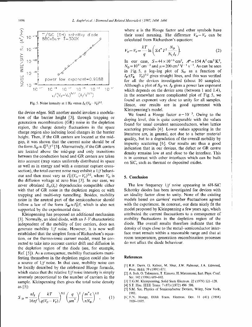
1496 L. Angheietal. /Diamond and Related Materials 6 (1997) 1494-1496
< 10
in 10
t to 7 10 -20
i 1 h- 7
10 -ri
1 1 in o z 10
Ti/SiC (6H) schottky diode 880x5um T=300K
power law exponent = 0.9988
10 10 1 0 ~7 10 10 10
lr/(VD-VF)5/2 (A/V5/2)
Fig. 5. Noise intensity at 1 Hz versus IF/(VD— KF)5'2.
the device edges. Still another model invokes a modula- tion of the barrier height [3], through trapping or generation-recombination (GR) noise in the depletion region, the charge density fluctuations in the space charge region also inducing local changes in the barrier height. Then, if the GR centers are located at the mid- gap, it was shown that the current noise should be of the form SlFxIF
/2/f2 [3]. Alternatively, if the GR centers are located above the mid-gap and only transitions between the conduction band and GR centers are taken into account (trap states uniformly distributed in space as well as in energy and with a constant capture cross- section), the total current noise may exhibit a 1//behavi- our and then must vary as IF/(VD — VF)
312, where VD is the diffusion voltage at zero bias [3]. In our case, we never obtained .SIF(/F) dependencies compatible either with that of GR noise in the depletion region or with trapping and multi-step tunnelling. Besides, mobility noise in the neutral part of the semiconductor should follow a law of the form SJFxIF/f, which is also not supported by the experimental data.
Kleinpenning has proposed an additional mechanism [3]. Normally, an ideal diode, with an I-Vcharacteristic independent of the mobility of free carriers, does not generate mobility l/f noise. However, it is now well established that the simplest form of Richardson's equa- tion, or the thermo-ionic current model, must be cor- rected to take into account carrier drift and diffusion in the depletion region of the diode (see, for example, Ref. [5]). As a consequence, mobility fluctuations mani- festing themselves in the depletion region could also be a source of l/f noise. In that case, mobility noise can be locally described by the celebrated Hooge formula, which states that the relative l/f noise intensity is simply inversely proportional to the number of carriers in the sample. Kleinpenning then gives the total noise density as [5]:
O IF —
ah kT 5/2 / g \2
l6nf\q(VD—VF)J \/J,m / \izND
m e 1/2
(1)
where a is the Hooge factor and other symbols have their usual meaning. The difference VD—VF can be calculated from Richardson's equation:
K -D-FF= — In \SA*T2^- . NCIF
(2)
' = 154 A2 cm2 K2, In our case, S=44x 10~6cm2
/yD = 1017 cm~3 and ^ = 200 cm2 V-1 s-1. As can be seen in Fig. 5, a log-log plot of 5IF as a function of IFI(VT>
— ^F)5/2
gives straight lines, and this was verified for all the devices investigated (about 10 samples). Although a plot of S1F vs. IF gives a power law exponent which depends on the device area (between 1 and 1.4), in the somewhat more complicated plot of Fig. 5, we found an exponent very close to unity for all samples. Hence, our results are in good agreement with Kleinpenning's model.
We found a Hooge factor a = 10~3. Owing to the doping level, this is quite comparable with the values found for usual covalent semiconductors, when lattice scattering prevails [6]. Lower values appearing in the literature are, in general, not due to a better material quality, but to a degradation of the overall mobility by impurity scattering [6]. Our results are thus a good indication that in our devices, the defect or GR centre density remains low at and close to the interface. This is in contrast with other interfaces which can be built on SiC, such as thermal or deposited oxides.
5. Conclusion
The low frequency l/f noise appearing in 6H-SiC Schottky diodes has been investigated for devices with an ideality factor close to unity. None of the existing models based on carriers' number fluctuations agreed with the experiment. In contrast, our data nicely fit the model proposed by Kleinpenning a few years ago, which attributed the current fluctuations to a consequence of mobility fluctuations in the depletion region of the diode. The overall results therefore indicate that the density of traps close to the metal-semiconductor inter- face must remain within a reasonable range and that at room temperature, generation-recombination processes do not affect the diode behaviour.
References
[1] R.F. Davis, G. Keiner, M. Shur, J.W. Palmour, J.A. Edmond, Proc. IEEE 79(1991)677.
[2] A. Itoh, O. Takemura, T. Kimoto, H. Matsunami, Inst. Phys. Conf. Ser. 142(1996)689-692.
[3] T.G.M. Kleinpenning, Solid State Electron. 22 (1979) 121-128. [4] S.T. Hsu, IEEE Trans. 7 (17) (1972) 496-506. [5] S.M. Sze, Physics of Semiconductor Devices, Wiley, New York,
1981. [6]F.N. Hooge, IEEE Trans. Electron. Dev. 11 (41) (1994)
1926-1935.

WSm&K
ELSEVIER
DIAMOND AND
RELATED MATERIALS
Diamond and Related Materials 6 (1997) 1497-1499
Passivation of interface traps in MOS-Devices on n- andj9-type 6H-SiC
E.G. Stein von Kamienski, C. Leonhard, S. Scharnholz *, A. Gölz, H. Kurz Inst. f. HalbleitertechnikII, RWTHAachen, Sommerfeldstr. 24, D-52074 Aachen, Germany
Abstract
Interface traps in the Si02-6H-SiC system can be passivated by a high temperature anneal in hydrogen or moistrous atmosphere. The passivation is very effective for deep donor like traps which are reduced towards the 1011cm"2eV"1 range. The electrical properties of «-channel MOSFETs show that the gate oxides contain only a low density of fixed oxide charges in the low 10n cm"2 range for the passivated and the unpassivated state. It is further demonstrated that deep donor-like interface states hardly affect the electrical properties of «-channel MOSFETs on 6H-SiC. © 1997 Elsevier Science S.A.
Keywords: Gate oxide; MOSFEET; Passivation; SiC
1. Introduction
MOSFETs (metal oxide semiconductor field effect transistor) on SiC are promising devices for low-loss power applications [1]. Their calculated superior device properties depend crucially on the qualities of the gate oxide and the oxide-SiC interfaces. Oxide charges as well as interface states affect the threshold voltage and the conducting behavior of the device. In the Si02-Si system, these defects can effectively be passivated by hydrogen achieving densities below 10locm"2 [2]. The work of several research groups revealed lower oxide charge densities for wet oxidized SiC-wafers compared with dry oxidized ones, especially for/?-type SiC [3-5]. The influence of hydrogen was already assumed to be the reason for this effect [3]. In this report, a defect passivation for the Si02-SiC system will be presented. It will be demonstrated that the passivation is very effective for deep donor-like traps. This offers the possi- bility to investigate the influence of these deep donor like traps on the electrical properties of «-channel MOSFETs on SiC.
2. Experiment
MOS-capacitors are fabricated using n- and />-type 6H-SiC epitaxial layers on substrates from Cree Research, Inc., Durham, NC, USA. After a wet chemical cleaning sequence, the oxidation is performed in wet
* Corresponding author.
oxygen at 1150 °C resulting in an oxide thickness of 40 nm. The samples are cooled down in the oxidizing athmosphere and heated again to 1150 °C in Ar or Ar/H2 (90:10) for POA (post-oxidation anneal). This process results in water saturated samples for the unan- nealed case. A detailed process sequence is described elsewhere [6].
TV-channel MOSFETs with different gate lengths of 3, 10 and 50 um and a gate width of 500 um on /?-type 6H-SiC are fabricated using a non-self-aligned process. The source and drain diodes are implanted with N at energies ranging from 30 to 200 keV up to a total dose of 2 x 1015 cm"2, followed by an Ar anneal at 1300 °C. A field oxide of 300 nm thickness is deposited by a PECVD (plasma enhanced chemical vapour deposition) process. MOSFETs with two different gate oxidation processes are fabricated (Ml and M2): the first gate oxidation is performed in dry oxygen followed by a POA in Ar for 60min (Ml). The second oxide is fabricated in wet oxygen and annealed in Ar/H2 (90:10) (M2). Both processes are performed at 1150 °C and result in an oxide thickness of 50 nm. For metallization of the source and drain diodes as well as the gate contacts, a Ti/Au double-layer is used. No PMA (post- metallization anneal) is performed.
The MOS capacitors as well as the gate oxides of the MOSFETs are characterized by CV (capacitance- voltage) measurements after illumination in deep depletion/inversion. Similar to the Jenq technique [7], the accumulated density of interface traps can be derived from the position of the interface state ledges in the CV
0925-9635/97/S17.00 © 1997 Elsevier Science S.A. All rights reserved. PII S0925-9635(97)00049-6

1498 E. G. Stein von Kamienski et al. / Diamond and Related Materials 6 (1997) 1497-1499
curves. This method allows to detect interface states on «-type SiC, which are located deep below the conduction band edge, as described in more detail elsewhere [8]. The MOSFET-parameters threshold voltage VT, channel mobility /ic, interface state density Dit and serial resis- tance Rs are measured at room temperature as described inRefs[9,10].
3. Results and discussion
CVcurves from Ar-annealed oxides on «-type 6H-SiC reveal a moderate V^ (flatband voltage) shift, but an interface state ledge at —30 V. Equally fabricated oxides on p-type 6H-SiC show a large V^ shift of —30 V, but an interface state ledge at moderate bias. These results on the two substrate types correspond to a low density of interface states in the upper half of the band gap in the 1011cm~2eV~1 range, but a high density in the > 1012cm~2eV_1 range of deep donor-like traps in the lower half of the band gap. Deep donor-like interface traps do not affect the Va value of MOS capacitors on «-type SiC because these defects are filled, and thus neutral at flatband condition. These results demonstrate that the defect densities on the n- and p-type samples are comparable.
The unannealed (wet) and Ar/H2-annealed samples show moderate V^ values for both p- and «-type sub- strates (Fig. 1). The interface state ledges for the two oxides on n-type SiC again correspond well with the Vn, values of the p-type samples. These results indicate drasti- cally reduced densities of deep donor-like interface traps towards the range of 1011 cm~2 eV~J for these oxides, as compared with the dry oxidized samples. Additionally, the Ar/H2-annealed samples reveal reduced hysteresis in
the CV characteristics. For the «-type sample, this indi- cates a reduced density of flat interface states near the conduction band edge. For the /»-type sample this effect corresponds well to the reduction of deep donor-like interface states near the valence band edge.
The low defect densities for the unannealed (wet) and in Ar/H2-annealed samples give strong evidence for a defect passivation by OH-groups and/or hydrogen. Thus, a passivated and a unpassivated state of the Si02-SiC system can be defined. Obviously, the passiv- ation is very effective for the donor-type defects.
Additional high-temperature treatments of the passiv- ated samples above 300 °C increase the negative V^ and interface state ledge-shifts for the p- and «-type samples, respectively (data not shown here). At the end, these treatments result in identical C-V curves, compared with the dry processed samples. From this, it can be concluded that the passivation is lost at temperatures above 300 °C, which can be explained by an outdiffusion of hydrogen. Furthermore, the passivation causes increased oxide trap densities, which are worse for the wet samples [8]. The results from the MOS capacitors can be explained by the passivation of interface states. From the CV data, a low density in the <10ncm~2
range of fixed oxide charges might be expected for all of the presented samples. However, the polarity and density of fixed oxide charges cannot be derived from room temperature CV measurements because the influ- ences of interface states and fixed oxide charges cannot be distinguished. To investigate this item, the electrical properties of MOSFETs containing gate-oxides with and without passivation are discussed in the following paragraphs (Figs. 2-4).
The fixed oxide charges directly affect the threshold voltage of MOSFETs. A high density of positive oxide charges would result in a negative VT value. Instead of
-20 -10 0 Voltage [V]
20
Fig. 1. CV data of MOS capacitors on p- (bottom) and n-type (top) 6H-SiC; wet oxidation (dashed) and POA at 1150 °C in Ar (solid) or Ar/H2 atmosphere (dotted). The capacitance drop at —20, —8 and —4 V is an artifact caused by the measurement setup.
^OC = 5 V
0 5 10 15 20 25 30 35 40
VDS [V] Fig. 2. ID versus VDS characteristic of 6H-SiC MOSFET, W/L = 500/10 urn, unpassivated gate oxide: dry oxidation and 60 min POA in Ar.
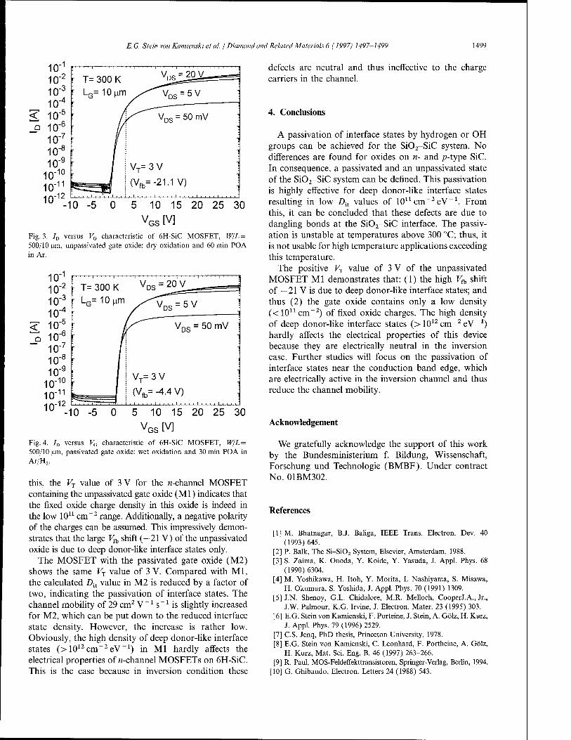
E. G. Stein von Kamienski et al. / Diamond and Related Materials 6 (1997) 1497-1499 1499
10" T= 300 K LG= 10 i^m
< Q
10 15 20 25 30
VGS [V]
Fig. 3. ID versus VG characteristic of 6H-SiC MOSFET, WjL = 500/10 (im, unpassivated gate oxide: dry oxidation and 60 min POA in Ar.
10 T= 300 K
r LG= 10 (j.m
< Q
10 15 20 25 30
VGS [V]
Fig. 4. ID versus Va characteristic of 6H-SiC MOSFET, W/L = 500/10 Jim, passivated gate oxide: wet oxidation and 30 min POA in Ar/H2.
this, the VT value of 3 V for the «-channel MOSFET containing the unpassivated gate oxide (Ml) indicates that the fixed oxide charge density in this oxide is indeed in the low 1011 cm-2 range. Additionally, a negative polarity of the charges can be assumed. This impressively demon- strates that the large V^ shift (—21 V) of the unpassivated oxide is due to deep donor-like interface states only.
The MOSFET with the passivated gate oxide (M2) shows the same VT value of 3 V. Compared with Ml, the calculated Dit value in M2 is reduced by a factor of two, indicating the passivation of interface states. The channel mobility of 29 cm2 V ~* s ~* is slightly increased for M2, which can be put down to the reduced interface state density. However, the increase is rather low. Obviously, the high density of deep donor-like interface states (>1012cm"2eV-1) in Ml hardly affects the electrical properties of «-channel MOSFETs on 6H-SiC. This is the case because in inversion condition these
defects are neutral and thus ineffective to the charge carriers in the channel.
4. Conclusions
A passivation of interface states by hydrogen or OH groups can be achieved for the Si02-SiC system. No differences are found for oxides on n- and />-type SiC. In consequence, a passivated and an unpassivated state of the Si02-SiC system can be defined. This passivation is highly effective for deep donor-like interface states resulting in low Dit values of 1011 cm~2eV_1. From this, it can be concluded that these defects are due to dangling bonds at the Si02-SiC interface. The passiv- ation is unstable at temperatures above 300 °C; thus, it is not usable for high temperature applications exceeding this temperature.
The positive VT value of 3 V of the unpassivated MOSFET Ml demonstrates that: (1) the high Va shift of —21 V is due to deep donor-like interface states; and thus (2) the gate oxide contains only a low density (<10n cm~2) of fixed oxide charges. The high density of deep donor-like interface states (>1012cm~2 eV"1) hardly affects the electrical properties of this device because they are electrically neutral in the inversion case. Further studies will focus on the passivation of interface states near the conduction band edge, which are electrically active in the inversion channel and thus reduce the channel mobility.
Acknowledgement
We gratefully acknowledge the support of this work by the Bundesministerium f. Bildung, Wissenschaft, Forschung und Technologie (BMBF). Under contract No. 01BM302.
References
[1] M. Bhatnagar, BJ. Baliga, IEEE Trans. Electron. Dev. 40 (1993) 645.
[2] P. Balk, The Si-Si02 System, Elsevier, Amsterdam, 1988. [3] S. Zaima, K. Onoda, Y. Koide, Y. Yasuda, J. Appl. Phys. 68
(1990) 6304. [4] M. Yoshikawa, H. Itoh, Y. Morita, I. Nashiyama, S. Misawa,
H. Okumura, S. Yoshida, J. Appl. Phys. 70 (1991) 1309. [5] J.N. Shenoy, G.L. Chidalore, M.R. Melloch, CooperJ.A., Jr.,
J.W. Palmour, K.G. Irvine, J. Electron. Mater. 23 (1995) 303. [6] E.G. Stein von Kamienski, F. Porteine, J. Stein, A. Gölz, H. Kurz,
J. Appl. Phys. 79(1996)2529. [7] C.S. Jenq, PhD thesis, Princeton University, 1978. [8] E.G. Stein von Kamienski, C. Leonhard, F. Portheine, A. Gölz,
H. Kurz, Mat. Sei. Eng. B. 46 (1997) 263-266. [9] R. Paul, MOS-Feldeffekttransistoren, Springer-Verlag, Berlin, 1994.
[10] G. Ghibaudo, Electron. Letters 24 (1988) 543.

ELSEVIER
DIAMOND AND
RELATED MATERIALS
Diamond and Related Materials 6 (1997) 1500-1503
Numerical study of avalanche breakdown of 6H-SiC planar/?-« junctions
E. Stefanov a>*, L. Bailon b, J. Barbolla b
a LÄAS- CNRS, 7, Avenue Colonel Roche, 31077 Toulouse, Cedex, France b Department of Electricity and Electronics - Faculty of Sciences, University of Valladolid, 47071 Valladolid, Spain
Abstract
The effect of the junction curvature, oxide charge density and «-epitaxial layer doping on 6H-SiC planar /?-«junction breakdown capabilities is reported. The calculated breakdown voltage of a cylindrical unprotected junction is compared with that of field- plate- (FP-) and multiple field-limiting-ring- (FLR-) guarded junctions with optimized geometries. © 1997 Elsevier Science S.A.
Keywords: Breakdown voltage; GH-SiC, p-n junction; Junction termination extensions; Floating ring; 2-D numerical analysis
1. Introduction
The design of power devices relies considerably on the design of junctions that have the necessary high voltage handling capabilities. Recent technology devel- opments to fabricate planar devices based on 6H-SiC are encouraging [1], and the opportunity to use some junction termination extension (JTE) techniques directly from Si technology becomes realistic. Various JTEs for planar junctions [2-4] have been reported for SiC devices, but only 50% of the ideal plane breakdown voltage was observed.
We report a numerical study of the effect of the junction curvature on breakdown voltage Vm for planar p-n junctions in 6H-SiC. The effect of the junction radius rp background doping 7VB and fixed charge density Nf on FBR is analyzed for a cylindrical p-n junction with a gaussian profile. Two concepts for planar JTE (r—lum and A^B=1.5 x 1016cm"3) are studied: (1) FP-; and (2) multiple-FLR-structures. Ninety per- cent of the ideal plane parallel junction breakdown voltage was obtained for an optimized FLR system with five rings. The two-dimensional off-state program POWER was used to simulate the breakdown.
2. The program
The two-dimensional off-state simulator POWER [5] is a user-oriented program for power devices. The simu-
lation is based on the solution of Poisson's equation for an arbitrary two-dimensional structure:
VeVil/=-q(N$ -NA +p-„)-P[, (1)
' Corresponding author.
where \j/ is the electrostatic potential; pf is the fixed charge density; e is the permitivity, q is the elementary charge, n and p are the electron and hole densities, respectively, and N£ and N^ are the ionized donor and acceptor densities. The ionization integrals for the carri- ers from the resulted electric field are calculated. The criterion for achieving breakdown is when these integrals tend to unity. A special algorithm included in the program ensures fast and automatic search of break- down voltage. The generation rates were calculated by using the average set of the ionization parameters for 6H-SiC given by Ruff et al. [6]. The program has been extended by an efficient algorithm to reduce the number of iterations when adjusting the quasi-Fermi potential of floating guard rings.
3. Device structure and simulation results
Plane parallel p-n junctions with depths Xh and planar cylindrical junctions with curvature radius r3 of 0.1, 0.3, 1, 3 and 10 um are studied. The doping profile in all p-n junctions is approximated by a gaussian in both the vertical and lateral directions. The profile has a surface concentration N,— 1 x 1020 cm-3. The ratio of lateral to vertical diffusion for the planar junction is assumed to be unity. The background doping A^ is in
0925-9635/97/$ 17.00 © 1997 Elsevier Science S.A. All rights reserved. PII S0925-9635(97)00056-3
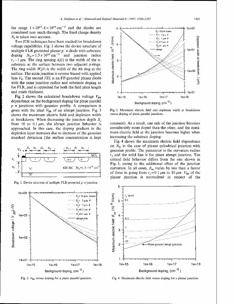
E. Stefanov et al. / Diamond and Related Materials 6 (1997) 1500-1503 1501
the range 1 x 10¹⁵-1 x 1018cm~3 and the diodes are considered non reach-through. The fixed charge density Nt is taken into account.
Two JTE techniques have been studied for breakdown voltage capabilities. Fig. 1 shows the device structure of multiple FLR protected planar/?"1"« diode with substrate doping ND = 1.5 x 1016cm~3 and junction radius Yj = 1 um. The ring spacing dT(i) is the width of the n- substrate at the surface between two adjacent /»-rings. The ring width Wr(i) is the width of the z'th ring at the surface. The main junction is reverse biased with applied bias VR. The second JTE is an FP-guarded planar diode with the same junction radius and substrate doping as for FLR, and is optimized for both the field plate length and oxide thickness.
Fig. 2 shows the calculated breakdown voltage VEK
dependence on the background doping for plane parallel p-n junctions with gaussian profile. A comparison is given with the ideal VBR of an abrupt junction. Fig. 3 shows the maximum electric field and depletion width at breakdown. When decreasing the junction depth Xj from 10 to 0.1 um, the abrupt junction behavior is approached. In this case, the doping gradient in the depletion layer increases due to decrease of the gaussian standard deviation (the surface concentration is kept
1e+02
SiO,
6H-SC ND=l,5.1016cm"3
Fig. 1. Device structure of multiple FLR-protected p-n junction.
1e+04 _i—i ■ ■ ■ ■ ■ ■
X.= 10 urn Gauss J
X.= 3 um # J
X.= 1 um #
X.=0.3 um #
X =0.1 um #
abrupt June
1e+01
Background doping, (cm" )
Fig. 2. KBR versus doping for a plane parallel junction.
1e+15 1e+16 1e+17 1e+18
Background doping, (cm )
Fig. 3. Maximum electric field and depletion width at breakdown versus doping of plane parallel junctions.
constant). As a result, one side of the junction becomes considerably more doped than the other, and the maxi- mum electric field at the junction becomes higher when increasing the substrate doping.
Fig. 4 shows the maximum electric field dependence on NB in the case of planar cylindrical junction with gaussian profile. The parameter is the curvature radius Yj and the solid line is for plane abrupt junction. The critical field behavior differs from the one shown in Fig. 3, owing to the additional effect of the junction curvature. In all cases, Em varies by less than a factor of three in going from rj = 0.1 um to 10 um. FBR of the planar junction is normalized in respect of the
-1 1 1—I I I I I I 1 1 1—I I MM 1 1 1—I I I I I
1e+15 1e+16 1e+17 1e+18
Background doping, (cm )
Fig. 4. Maximum electric field versus doping for a planar junction.

1502 E. Stefanov et cd. / Diamond and Related Materials 6 (1997) 1500-1503
breakdown voltage in plane parallel gaussian doped junction with the same junction depth rj = Xj. Both Vm and normalized breakdown voltage versus the sub- strate doping is given in Fig. 5 for radius r, = 0.1, 0.3, 1, 3 and 10 um.
The relatively high fixed charge density present at the Siü2-SiC interface was numericaly investigated on unprotected cylindrical p-n junctions for Nt in the range 0-5 x 1012 cm"2. Fig. 6 shows both VBK and the normal- ized breakdown voltage versus background doping for fj = 1 um. The effect of Nr is much more pronounced for lower doped substrates due to the reduced screening effect of the substrate.
In the FP technique the effect of oxide thickness dox, FP length LFP and oxide charge are analyzed in order to obtain the maximum VBK. For a non-reach-through junction with Xj = 1 um, background doping
1e+04 -3
1e+03
0
s ö >
T3 1e+02
1e+01
-0.8
'\~B.
-Q-r.-10|im
--X--r.= 3 um
•-©■•• r - 1 um
--■--r.=0.3 um J
■•■■ r.=0.1 urn J r
1.0
-0.6 o- tr
hO.4 |
ft) to
0.2 to
1e+15
TTTT|
1e+16
TTTT|
1e+17
0.0 1e+18
1.5 x 1016 cm"3, the optimal FBR = 640 V is obtained by using Jox = 0.4um, and LFP=10um. An increase of some 60% for the breakdown compared with that for an unprotected cylindrical junction is shown. The nor- malized breakdown voltage is 0.65 V. The multiple FLR concept was studied by using a new effective method [7] to optimize the basic parameters, exerting influence on the breakdown capabilities: ring-to-ring spacing dT, ring width WT, and number of rings. This method consists of modeling the breakdown capabilities of a main junc- tion protected by one ring. The breakdown voltage of such a structure is examinated as a function of dr and Wr. These results are extended to a multiple ring system. As a result, a structure with five floating rings was optimized to give a breakdown at FBR = 863 V, showing an increase of 110% of the breakdown compared with that for a cylindrical unprotected junction. The normal- ized breakdown voltage is 0.9 V. The optimized widths of the rings are 8, 4, 2, 2 and 2 um and the spacings are 0.5, 0.6, 0.7, 1.1 and 1.9 um. The lateral spread of the structure extends some 30 um in respect of the main junction. Fig. 8 shows the two-dimensional equipotential lines for the optimized five-FLR system at breakdown.
The VBR sensitivity of both techniques was studied in respect of the oxide charge and compared with that for a cylindrical unprotected junction. The VBR dependence on Nt for the optimized FLR structure is plotted on Fig. 7 (solid line). Fig. 7 gives also a comparison of the normalized breakdown versus Nr for an unprotected junction (dashed line), an FP- (long dashed line) and an FLR-protected (dotted line) junction. The decrease in VBR with the increase in Nt is smaller for an FP junction in the whole calculated range of charge densi-
Background doping, (cm )
Fig. 5. Vm versus doping; N,=5 x 1010 cm"
1e+03
1e+02
1e+15 1e+16 1e+17
Background doping, (cm )
Fig. 6. VVR versus doping; Nc is parameter.
900
875
725-
700
Cylindrical junction FP 5FLRs
1.0
0.0
1e+10 1e+11 1e+12
Fixed charge density N. {cm'2)
Fig. 7. KBR versus Nr for the optimal FLR system. Comparison of the normalized KBR between the FP- and five-FLR systems, and unpro- tected cylindrical junction.

E. Stefanov et al. / Diamond and Related Materials 6 (1997) 1500-1503
0.0075 -
0.0070
1503
0.0065
0.000 0.001 0.003 0.004 0.002
X axe, (cm)
Fig. 8. Two-dimensional equipotential lines for a five-floating-rings protected junction at breakdown, FBR = 863 V.
ties. The plate, by means of the field effect, spreads the maximum electric field away from the junction curvature and increases the depletion width. As a result, the electric field reduces and VBR increases. In the FLR structure, two adjacent ring junctions act on the maxi- mum field locus by pushing it deeply in the bulk around the junction curvature. Our optimized five-ring structure was optimized for Nt= 1 x 1011 cm-2 and saves its excel- lent breakdown capabilities in the range 0-4xl012cm~2 by showing a negligible decrease. In order to expand the validity for larger N{, additional optimization of FLR geometry has to be made by increasing the rings number and decreasing the spacings.
for shallow junctions. These results could serve as design constraints when designing power devices based on 6H-SiC.
Acknowledgement
This work is supported by EUROFORM-TRTI Human Capital and Mobility Program under Contract No. ERBCHBG CT940696, and by Spanish C.I.C. y T. and Junta de Castilla y Leon.
References
4. Conclusion
We analyzed the effect of planar junction radius, «-epitaxy doping and Si02-6H-SiC interface properties on p-n junction breakdown capabilities by two-dimen- sional device simulation. The efficacity of device termina- tion design has been examined for both field-plate- and five-floating-rings systems' protected junctions. The results presented in the report clearly demonstrate the superiority of the FLR concept, and also the possibility to achieve near ideal efficiency of breakdown capabilities
[1] S. Sheppard, M. Melloch, J. Cooper, IEEE Trans. Ellectron. Devices 41 (1994) 1257.
[2] T. Wang, T. Chow, D. Brown, M. Ghezzo, Proceedings of the 4th International Symposium ISPSD and ICS, Tokyo, 1992, p. 303.
[3] M. Bhatnagar, H. Nakanishi, S. Bothra, P. McLarthy, B. Baliga, Proceedings of the of the 5th ISPSD, vol. 5, 1993, p. 89.
[4] Dev Alok, B. Baliga, Proceedings of the 7th ISPSD, vol. 7, 1995, pp. 96-100.
[5] E. Stefanov, G. Charitat, POWER.2D - User's Guide, Rapport LAAS no. 93306, Toulouse, France, 1993.
[6] M. Ruff, H. Mitlehner, R. Helbig, IEEE Trans. Electron. Devices 41 (1994) 1040.
[7] E. Stefanov, L. Bailon, J. Barbolla, Solid State Electron. (submitted).
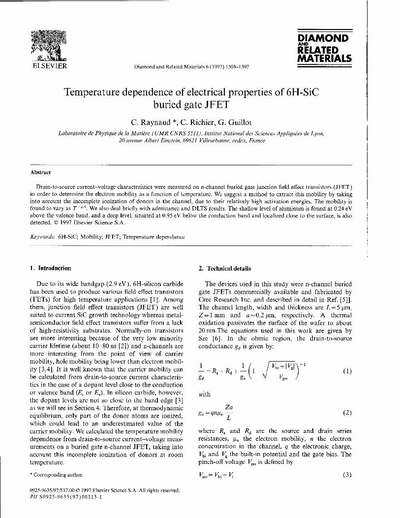
:■•&"!;■
ELSEVIER
DIAMOND AND
RELATED MATERIALS
Diamond and Related Materials 6 (1997) 1504-1507
Temperature dependence of electrical properties of 6H-SiC buried gate JFET
C. Raynaud *, C. Richier, G. Guillot Laboratoire de Physique de la Matter e (UMR CNRS 5511), Institut National des Sciences Appliquees de Lyon,
20 avenue Albert Einstein, 69621 Villeurbanne, cedex, France
Abstract
Drain-to-source current-voltage characteristics were measured on n-channel buried gate junction field effect transistors (JFET) in order to determine the electron mobility as a function of temperature. We suggest a method to extract this mobility by taking into account the incomplete ionization of donors in the channel, due to their relatively high activation energies. The mobility is found to vary as T~2A. We also deal briefly with admittance and DLTS results. The shallow level of aluminum is found at 0.24 eV above the valence band, and a deep level, situated at 0.95 eV below the conduction band and localized close to the surface, is also detected. © 1997 Elsevier Science S.A.
Keywords: 6H-SiC; Mobility; JFET; Temperature dependance
1. Introduction 2. Technical details
Due to its wide bandgap (2.9 eV), 6H-silicon carbide has been used to produce various field effect transistors (FETs) for high temperature applications [1]. Among them, junction field effect transistors (JFET) are well suited to current SiC growth technology whereas metal- semiconductor field effect transistors suffer from a lack of high-resistivity substrates. Normally-on transistors are more interesting because of the very low minority carrier lifetime (about 10-80 ns [2]) and n-channels are more interesting from the point of view of carrier mobility, hole mobility being lower than electron mobil- ity [3,4]. It is well known that the carrier mobility can be calculated from drain-to-source current characteris- tics in the case of a dopant level close to the conduction or valence band (Ec or Ey). In silicon carbide, however, the dopant levels are not so close to the band edge [3] as we will see in Section 4. Therefore, at thermodynamic equilibrium, only part of the donor atoms are ionized, which could lead to an underestimated value of the carrier mobility. We calculated the temperature mobility dependence from drain-to-source current-voltage meas- urements on a buried gate n-channel JFET, taking into account this incomplete ionization of donors at room temperature.
The devices used in this study were n-channel buried gate JFETs commercially available and fabricated by Cree Research Inc. and described in detail in Ref. [5]]. The channel length, width and thickness are L = 5 urn, Z=lmm and a~0.2 um, respectively. A thermal oxidation passivates the surface of the wafer to about 20 nm.The equations used in this work are given by Sze [6]. In the ohmic region, the drain-to-source conductance gd is given by:
1 1 — =RS+Rd + — gd go
v*+\v,\ (1)
with
go=gn/j,n
Za
L (2)
where Rs and Rd are the source and drain series resistances, u,, the electron mobility, n the electron concentration in the channel, q the electronic charge, Vbi and V% the built-in potential and the gate bias. The pinch-off voltage Vpo is defined by
' Corresponding author. vpo = vbi+vt (3)
0925-9635/97/S17.00 © 1997 Elsevier Science S.A. All rights reserved. PIT S0925-9635(97)00113-l

C. Raynaudetal. I Diamond and Related Materials 6 (1997) 1504-1507 1505
where Vt is the threshold voltage, and is related to the effective thickness of the channel by
V„ qNä
2e, (4)
Nd is the doping density in the channel, es the dielectric constant of 6H-SiC.
In the saturation region, the drain-to-source satura- tion current is given by
Iäsat=ß(Vg-Vt)2 (5)
where ß is a coefficient depending on the geometrical parameters of the transistors, on Vp, \xn and the electron saturation drift velocity.
The built-in potential is given by
kT nnPp Vhi= — \n'
1 (6)
where «n and pp are the free electron and hole concen- trations in the n-type and p-type material respectively, k the Boltzmann constant, «; the intrinsic carrier concentration.
It is important to notice that Eq. (2) is given by Sze with Nd instead of n. In fact the conductance g0 is proportionnal to the concentration of free carriers in the channel. When the donor levels are very close to Ec (as in silicon), all uncompensated donors are ionized and Nd = n at usual temperatures. In silicon carbide, shallow levels are not so close to Ec and therefore, n<Nd at thermodynamic equilibrium (as it is the case in the channel). But in a space charge region, where the electric field sweeps out the electrons emitted by the dopants, n is equal to Nd, so that CV measurements give the doping level, and more precisely Nd — 7Va.
14-
12-
10- / /^ V = -0.8 V
V =-0.4V_
8- V =-1.2V
'6- /// s^~~^ V =-1.6V
4- /// s ■ s—
V =-2V & = 1////'^-—■ ' v =-2.4V
2- -
U- P- ' 1 1 1 1 H 1
2.8 V
■3.6 V
0 2 y 4(V) 6 8 ds
Fig. 1. Drain-to-source current-voltage measurements as a function of gate bias at 323 K.
1000
4 5 6 7 8 1/(1-((V +V )/V )1/2)
bi g p
Fig. 2. Reciprocal drain-to-source conductance as a function of recip- rocal P4/2. The slope is proportional to the product n\i„.
3. Electrical characterization
CV measurements performed at 100 kHz to avoid the effects of series resistance give a doping level in the channel of 2.7 x 1017 cm"3 and a built-in potential Fbi(300 K) of 2.55 V. Drain-to-source IV measurements as a function of gate bias and temperature have been performed. Fig. 1 shows results obtained at 323 K. From /ds2 versus V% curve, we deduce the thres- hold voltage Ft(300K) and from Eqs. (3) and (4), Fpo(300 K)= —4.5 V and the effective channel thickness a = 0.17 mm. Now we suppose that u11(300K) = 280 cm2 V"1 s"1, according to Schaffer et al. [4], the value determined by Hall effect measurements for a n-type material with a similar doping level. The slope of the straight line shown in Fig. 2 therfore gives «(300 K) = l.l x 1017 cm"3 and Rs + Rd 25 Q.
We developed theoretical calculations based on two ionization energy levels both for N and Al. Taking
Nd—Na = 2.7 x 1017cm~3 and assuming there are twice as many cubic sites (with an activation energy of £d2 = 0.14eV) as hexagonal sites (Edl = 0.082 eV), it is possible to fit the concentration of each impurity level so that «(300K) = l.lxl017cnr3 (Fig. 3). Table 1 summarizes all the values used in our calculations. The compensation ratio is found to be less than 1%.
The next step is to calculate Fbi(T). ^P(T) is calculated by assuming that the p-type layer is doped at 2x 1018cm~3 [5] and using two activation energies of £al = 0.22eV and £a2 = 0.25eV, with NSi2 = 2N^ [7]. It is worth noting that using a single energy level of 0.24 eV with a total concentration Na = NaZ + Nlil gives about the same result. Moreover, an error in p-value leads to a small error in the built-in potential, and a smaller one in g0(T), as shown in Eq. (1).
Knowing nn(T) and pp(T), and calculating «i(T), (Eq. (6)) leads to Vbi(T). It is now easy to obtain g0(T) in the same manner as at room temperature and

1506
10'
1017-
1016
Sio'5ir u
s 101"
IO'H
C. Raynaudetal. / Diamond and Related Materials 6 (1997) 1504-1507
1Q12 0
N =9xlO'6cm-3
dl
N = 1.8xlO'7cnv3
d2
N = 10>5 cnr3
1 1 1 1 h 200 300 400
Temperature (K) 500 600
Fig. 3. Theoretical free electron concentration versus temperature.
Table 1 Parameters used for theoretical calculations of free carrier concen- trations as a function of temperature
n-type p-type
Activation energies of dopants
Spin degeneracy factor g
Mc* Density-of-states
effective mass
82 and 137 meV (h and k sites) 2
0.3 for electrons
220 and 225 meV (h and k sites) 4
1 for holes
*Mc: number of equivalent conduction band minima.
250 300 350 400 450 Temperature (K)
Fig. 4. Electron mobility versus temperature with £f = 2.9eV (D), with E% dependant on temperature (+).
finally to obtain ^n(T). Fig. 4 shows the electron mobil- ity calculated by taking Et = 2.9 eV and by taking into account the temperature dependence of the bandgap £g as reported by Dalven [8]. The mobility varies as r" with H=-2.4 + 0.1 if £, = 2.9 eV, which is in
agreement with previous Hall effect studies on p-type substrates [9].
4. Admittance spectroscopy and DLTS measurements
Admittance spectroscopy was performed, as described in Ref. [10], as a function of frequency (from 1 kHz to 1 Mhz). A defect with an activation energy of £a = (0.24 +0.01) eV. This value agrees with other values of aluminum activation energies reported in the litera- ture [3,4,7] and justifies the need to take into account the incomplete ionization of dopants to calculate the free carrier mobility, as done below.
DLTS measurements are suitable for detecting deeper levels. Study of the drain-to-source current transients can be used in FETs with a better sensibility than conventionnal capacitance DLTS [11]. In our experi- ments, the drain-to-source voltage is set to 50 mV, so that the transistor works in the ohmic regime. The reverse gate bias Vx must be close to the pinch-off voltage, for example VT = — 5 V. The pulse is 5 V high during rp==lus. Fig. 5 shows typical DLTS spectra recorded during such filling pulse conditions. The pres- ence of a peak PI indicates a deep level with an apparent activation energy of £„ = 0.95 eV and a capture cross- section of an = 7 x 10 ~16 cm2. The presence of a "smooth peak" P2, which disappears at lower filling times, could be attributed to interface states with a low capture coefficient. The variation of amplitude from one window rate to another may indicate incomplete filling of the traps during the pulse.
Capacitance DLTS measurements carried out at vari- ous pulse heights indicate that this defect is located very close to the etched trench. Flatresse and Ouisse [12], who performed noise measurements on similar devices, conclude that the surface generates noise. The presence
0.25-
' 1 ' 1
e =46.5 s-i / \ 11 \ / \ 0.20- 1 \
e =23.25 s-i / \
^0.15- e=11.6s-i ^—' 11 \ <
0.10J "^~— fi\ \ \ " 0.05-
0.00- ^^f—^ -p"" 1 , 1 . 1 . 250 300 350 400 450 500 550
Temperature (K)
Fig. 5. Drain-to-source current DLTS spectra obtained with VT= — 5 V, Vp = 0 V, tp = l ms, Vds = 50 mV, for three emission times.
C. Raynaud et al. I Diamond and Related Materials 6 (1997) 1504-1507 1507
of a deep level close to the surface could be at the origin of this noise. Therefore, it could be reduced by an improvement of the surface quality.
5. Conclusion
We proposed a procedure to calculate electron mobil- ity from drain-to-source current voltage measurements on JFETs, taking into account the incomplete ionization of impurities as a function of temperature, which is necessary when dopant impurity levels are relatively deep. We found that electron mobility increases with decreasing temperature as T~2A. Finally, DLTS measurements reveal the presence of a deep level at Ec= — 0.95 eV, located very close to the surface, and probably due to etching or surface treatment.
References
[1] J.W. Palmour, et al., Proceedings of the 1st High Temperature Electronics Conference, Albuquerque, NM, June 1991, pp. 511-518.
[2]A.V. Naumov, V.l. Sankin, Sov. Phys. Semicond. 23 (1989) 630-633.
[3] G. Pensl, W.J. Choyke, Physica B 185 (1993) 264-283. [4] W.J. Schaffer et al., Institute of Physics Conference Series No. 137,
pp. 155-159. [5] J.M. McGarrity et al. IEEE Transactions, Nuclear Sciences 39
(1992) 1974. [6] S.M. Sze, Physics of Semiconductor Devices, 2nd edition, Wiley,
New York, 1981. [7] C. Raynaud et al, Materials Science and Engineering 29 (1995)
122-125. [8] R. Dalven, J. Phys. Chem. Solids 46 (1965) 439-441. [9] S. Karmann et al., Physica B 185 (1993) 75-78.
[10] C. Raynaud et al., J. Appl. Phys. 76 (1994) 1956-1958. [11] I.D. Hawkins, A.R. Peaker, Appl. Phys. Lett. 48 (1986) 227-229. [12] P. Flatresse, T. Ouisse, Solid State Electronics (submitted).

ELSEVIER Diamond and Related Materials 6 (1997) 1508-1511
DIAMOND AND
RELATED MATERIALS
Microwave Power MESFET on 4H-SiC
O. Noblanc *, E. Chartier, C. Arnodo, C. Brylinski THOMSON CSF, Laboratoire Central de Recherches Domaine de Corbeville, 91404 Orsay, CEDEX, France
Abstract
We present static and microwave characterization of MESFETs processed on n+ 4H-SiC wafers supplied by Cree Research. An eight-level technology including airbridge interconnections has been performed. Transistors with total gate width up to 6 mm and 1.2 um gate length optically designed are obtained. High breakdown voltage (up to 140 V) and high drain current (up to 0.7 A) show the high power capability of the transistors. RF characterization was performed. Because of the use of a conductive substrate, parasitic capacitances account for the relatively low values of /T and /mlx (4 and 9 GHz, respectively). Power measurements were carried out at 1 and 2 GHz in cw. Output powers up to 1.7 W mm-1 were measured with a power added efficiency of 37% at 2 GHz. © 1997 Elsevier Science S.A.
Keywords: MESFET; Power and microwave characteristics; Silicon carbide
1. Introduction
Silicon carbide belongs to the wide band gap semicon- ductor family. Depending on the polytype (more than 100 are identified), the band gap varies between 2.2 and 3.3 eV. This property makes SiC suitable for high- temperarure applications. Other physical properties are also very interesting in the same field. The most impor- tant are the high breakdown electric field (an order of magnitude higher than in silicon or gallium arsenide), the high thermal conductivity (3 times higher than in silicon) and the high saturation velocity. Besides, SiC wafers and homoepitaxial layers are now commercialy available. This explains why SiC is now extensively studied for possible use in most areas of power electron- ics. However, a major drawback of SiC is the poor quality of the material. Wafers are still small (1.375" in diameter in 1996), very expensive and contain high defect densities (dislocations and micropipes). Epitaxial layer quality has to improve in order to obtain high current densities. Nevertheless, SiC devices are being developed and very encouraging results have been pub- lished, mainly in the fields of Schottky diodes [1,2], microwave power FETs [3,4] and power thyristors [5]. SiC microwave power devices have been identified as possible future candidates for high impedance applica- tions [6]. Presently, at frequencies over 1 GHz,
: Corresponding author.
MESFET transistors are the main SiC devices for which microwave results have been published [3,4]. The best power measurement results presently published are Pout=3.5W; PAE = 45.5% at 6 GHz at Fds = 40V on a 2 mm periphery MESFET processed on a 6H-SiC semi- insulating wafer [3].
In this paper, we report static and microwave charac- terization, including power measurements, of MESFETs fabricated on conductive substrates. Because of the non- uniformity of the active layer doping thickness, the following results concern transistors belonging to the best part of the wafers. The characterizations are per- formed on MESFETs of various peripheries. In particu- lar, power measurements on 1, 3.6 and 4 mm periphery transistors are presented.
2. MESFET technology
4H-SiC epitaxial structures were supplied by Cree Research, Durham, North Carolina. Conductive sub- strates were used since semi-insulating substrates were not available at that time. A p" buffer layer (Na?»3 x 1016 cm-3, 10 |j.m thick) has been incorporated in the epi structure between the n+ substrate and the n active layer (0.25 urn thick; Nd«1.5 x 1017cm"3). An n+ cap layer (Nd«l x 1019 cm~3, 0.2 |im thick) ends the epitaxial structure.
The first steps in the MESFET process consist of
0925-9635/97/S17.00 © 1997 Elsevier Science S.A. All rights reserved. PII S0925-9635(97)00059-9

O. Noblancetal. / Diamond and Related Materials 6 (1997) 1508-1511 1509
reactive ion etching for mesa isolation and channel recess. Then thermal oxidation is performed in a wet oxidation furnace at 1150 °C. Evaporated nickel metalli- zation is applied for the source and drain ohmic contacts using the lift-off technique. Rapid thermal annealing is used for the alloying of the contacts. Specific contact resistance in the field of 1 x 10~6 Q. cm2 and sheet resis- tance around 1.4 Q, are measured after alloying. Ti/Pt/Au multilayer metal is evaporated to make the gate contact. The ideality factor and the barrier height of the Schottky contact are in the range of 1.1 and 1 eV, respectively. The leakage current is in the range of 1 uA and the breakdown voltage between 150 and 200 V depending on the wafers. An offset of the gate towards the source side in order to increase the breakdown voltage and reduce source series resistance is performed. The drain- gate and source-gate spacings are 2.5 and 0.5 mn, respec- tively. Devices with gate lengths of 1.2 \im processed by optical lithography have been reproducibly obtained with 2, 4, 8, 16 and 24 x 250 urn fingers, giving maximum gate widths up to 6 mm (Fig. 1). PECVD-deposited Si02 and Si3N4 are used for passivation. Source fingers are interconnected by airbridges.
3. DC characterization
DC characterization is performed using a 370 Tektronix curve tracer. Fig. 2(a-c) shows the DC char- acteristics Id(Vds, Vgs), the transfer characteristics gm(Vgs) and Id(Vgs) and the transconductance over the output conductance gm:gd ratio of a 100 ^im-wide MESFET. Fig. 3 (a and b) shows the DC characterisitics
Id(Yd,, ^gs) of a 4 mm wide MESFET (16x250 ^m fingers). In order to limit the dissipated power, the load has been altered to show both the saturated drain current 7dss [Fig. 3(a)] at low source-drain voltage and the source-drain breakdown voltage BVds [Fig. 3(b)]. An 7dss value of 700 mA at Vgs = 0 V and a BVds of 140 V are observed. The maximum output power for a class A amplifier should be at first order greater than 11 W according to the DC characteristics. The observed break- down cause is not fully understood. The correlation between gate-drain spacing and BVds is not clear. There is presently evidence of breakdown occuring below the ohmic contacts due to the presence of conductive sub- strate and p-type buffer layer. This was evidenced by a breakdown voltage BVds independent on the gate volt- age Vgs (not shown). A smooth breakdown phenomenon due to the reverse leakage current of the Schottky metallization is more often observed.
4. RF characterization
The dies were cut and packaged in order to use a standard Wiltron test fixture. Small-signal (S) parame- ters were measured using a HP8510 network analyser. Various source-drain bias voltages were used up to 40 V. MESFETs with periphery up to 6 mm were measured. At Vds = 40 V, a maximum frequency of oscillation /max
of 9 GHz is measured, mainly limited by the parasitic pads capacitances in relation with the use of conductive substrates. The current gain cut-off frequency fT is 4 GHz. At 2 GHz, the highest small signal maximum
':- .Ä^ÄÄW^fe-:
''Ss&j%feWfe%£v
Ä ' Äb«*^fP**!«M» 4&J^§>>: •! ^^^S^^^^^^^^^^
4 '«W-Y -- <r
Fig. 1. 6 mm periphery MESFET fabricated on an n+ 4H-SiC wafer.
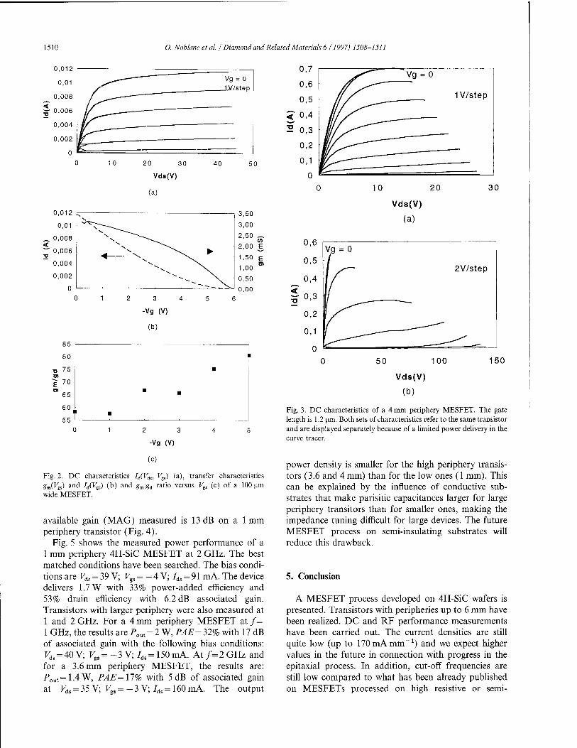
1510 0. Noblanc et al. / Diamond and Related Materials 6 (1997) 1508-1511
85
80
■o 75 o> E 70
ra65
60
55
0 12 3 4 5
-vg (V)
(c)
Fig. 2. DC characteristics /d(Kds, Vis) (a), transfer characteristics gm(V„) and Id(Vts) (b) and gm:gd ratio versus Kgs (c) of a 100 um wide MESFET.
available gain (MAG) measured is 13 dB on a 1 mm periphery transistor (Fig. 4).
Fig. 5 shows the measured power performance of a 1 mm periphery 4H-SiC MESFET at 2 GHz. The best matched conditions have been searched. The bias condi- tions are Vdt = 39 V; ViS = -4 V; Ids = 91 mA. The device delivers 1.7 W with 33% power-added efficiency and 53% drain efficiency with 6.2 dB associated gain. Transistors with larger periphery were also measured at 1 and 2 GHz. For a 4 mm periphery MESFET at /= 1 GHz, the results are Pout = 2 W, PAE= 32% with 17 dB of associated gain with the following bias conditions: Vds = 40 V; Vts = - 3 V; Id, = 150 mA. At /= 2 GHz and for a 3.6 mm periphery MESFET, the results are: Pout = 1.4W, PAE=\1% with 5 dB of associated gain at Vds = 35 V; V„ = - 3 V; Jd, = 160 mA. The output
150
Fig. 3. DC characteristics of a 4 mm periphery MESFET. The gate length is 1.2 um. Both sets of characteristics refer to the same transistor and are displayed separately because of a limited power delivery in the curve tracer.
power density is smaller for the high periphery transis- tors (3.6 and 4 mm) than for the low ones (1 mm). This can be explained by the influence of conductive sub- strates that make parisitic capacitances larger for large periphery transitors than for smaller ones, making the impedance tuning difficult for large devices. The future MESFET process on semi-insulating substrates will reduce this drawback.
5. Conclusion
A MESFET process developed on 4H-SiC wafers is presented. Transistors with peripheries up to 6 mm have been realized. DC and RF performance measurements have been carried out. The current densities are still quite low (up to 170 mA mm"1) and we expect higher values in the future in connection with progress in the epitaxial process. In addition, cut-off frequencies are still low compared to what has been already published on MESFETs processed on high resistive or semi-

O. Noblancetal. I Diamond and Related Materials 6 (1997) 1508-1511 1511
30
25
20 m ■o
15
10
£^
0,1 10
frequency (GHz)
Fig. 4. Small-signal RF characteristics for a 1.2 um gate length 4H-SiC MESFET of 1 mm periphery made on an n+ substrate. The bias conditions are K,„ = 40 V and V„= -4 V.
35
30
m 5 25
20
15
* -^ r ►
40
30
20 UJ < a.
10
10 15 20
Pin(dBm)
25 30
Fig. 5. Power performance for a 1.2 urn gate length 4H-SiC MESFET of 1 mm periphery at 2 GHz. The bias conditions are I^s = 40 V and K„=-4V.
insulating substrate [3,4]. Nevertheless power character- istics of those transistors at 1 and 2 GHz are promising. The future use of semi-insulating substrates is expected to increase the performance of the transistors and make the matching easier for large periphery MESFETs.
Acknowledgement
We would like to thank J.M. Coupas for RF power measurements at 1GHz and D. Floriot for his precious advice. This work has been partly supported by the French Ministry of Defense (DRET).
References
[1] A. Itoh, T. Kimoto and H. Matsunami, IEEE Electron Device Letters 16(6) (1995) 280.
[2] A. Itoh, T. Kimoto and H. Matsunami, IEEE Electron Device Letters 17 (3) (1996) 139.
[3] CD. Brandt et al., Proceedings of the ICSCRM 95 Conference (Kyoto), September 1995, p. 659.
[4] S.T. Allen, J.W. Palmour, V.F. Tsvetkov, S.J. Macko, C.H. Carter Jr, K.E. Moore, C.E. Weitzel, K.J. Nordquist, L.L. Pond III, Pro- ceedings of the ICSCRM 95 Conference (Kyoto), September 1995, p. 761.
[5] J.W. Palmour, S.T. Allen, R. Singh, L.A. Lipkin, D.G. Waltz, Proceedings of the ICSCRM 95 Conference (Kyoto), September 1995, p. 813.
[6] C.E. Weitzel, IEEE Electron Device Letters 16 (10) (1995) 451.

DIAMOND AND
RELATED MATERIALS
ELSEVIER Diamond and Related Materials 6 (1997) 1512-1514
The potential of SiC and GaN for application in high speed devices
F. Schwierz *, M. Kittler, H. Förster, D. Schipanski Technische Universität Ilmenau, Fachgebiet Festkörperelektronik, Postfach 100565, 98694 Ilmenau, Germany
Abstract
The potential for high frequency applications of MESFETs made from the wide band gap semiconductors cubic GaN, hexagonal GaN, and 3C-SiC has been investigated by means of device modeling. For comparison, also Si and GaAs MESFETs have been modeled. The influence of nonstationary carrier transport on FET behavior has been estimated using the relaxation time approximation, and taken into account. The three wide band gap semiconductors show considerable potential for application in high frequency MESFETs. Cut-off frequencies exceeding 100 GHz have been predicted for sub-quarter micron gate cubic GaN MESFETs. © 1997 Elsevier Science S.A.
Keywords: Device modeling; High speed devices; MESFET; Wide band gap semiconductors
1. Introduction
In recent years, there has been an increasing interest in using the wide band gap semiconductors SiC and GaN for microwave power amplification. Recently, an experimental 0.5 um gate SiC MESFET with a maxi- mum frequency of oscillation (/max) of 42 GHz and a cut-off frequency (fT) of 13.2 GHz has been reported [1]. Furthermore, AlGaN/GaN heterostructure FETs with/max above 70 GHz and/T above 20 GHz have been demonstrated [2,3].
These encouraging results raise the question about the frequency limits of SiC and GaN based FETs. Several figures of merit have been defined to assess the high frequency potential of semiconductor materials (e.g. Keyes' and Baligas figure of merit [4]), but none of these seems to be useful in estimating the properties of real SiC or GaN based devices.
The aim of this work is to assess the potential of SiC and GaN for high frequency devices. This will be done by modeling 3C-SiC and GaN microwave MESFETs, rather than establishing some figure of merit based on material properties.
2. Transistor model
For our calculations, we used the two region MESFET model proposed by Statz et al. [5]. The main features
of the model are depicted in Fig. 1. The transistor is divided into two regions: (1) the ohmic region (region I), where the carrier
velocity follows v = [i0E, and (2) the saturation region (region II), where the carriers
have attained their constant saturation velocity vs.
At the boundary between the two regions, the electric field reaches its critical value Ec. A key point of the transistor model are the two-piece linear velocity-field (v-E) characteristics. The v-E characteristics include the main transport properties of the semiconductor material (i.e. the low field and high field transport properties in
Source Gate Drain
1 1 l
Rs ) RD
]=J
region 1 region II v = vs
* Corresponding author.
Electric Field
Fig. 1. Two region MESFET model used in this work.
0925-9635/97/S17.00 © 1997 Elsevier Science S.A. All rights reserved. PII S0925-9635(97)00050-2
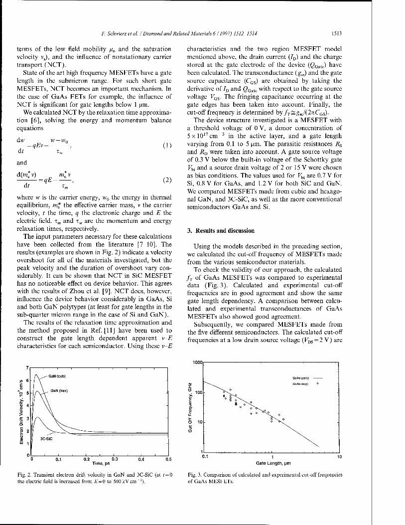
F. Schwierz et al. I Diamond and Related Materials 6 (1997) 1512-1514 1513
terms of the low field mobility ix0 and the saturation velocity vs), and the influence of nonstationary carrier transport (NCT).
State of the art high frequency MESFETs have a gate length in the submicron range. For such short gate MESFETs, NCT becomes an important mechanism. In the case of GaAs FETs for example, the influence of NCT is significant for gate lengths below 1 um.
We calculated NCT by the relaxation time approxima- tion [6], solving the energy and momentum balance equations
dw
dt ~
and
-qEv- W — Wr,
d(mc v) mc v = qE ,
At Tm
(1)
(2)
where w is the carrier energy, w0 the energy in thermal equilibrium, m* the effective carrier mass, v the carrier velocity, t the time, q the electronic charge and E the electric field. xm and TW are the momentum and energy relaxation times, respectively.
The input parameters necessary for these calculations have been collected from the literature [7-10]. The results (examples are shown in Fig. 2) indicate a velocity overshoot for all of the materials investigated, but the peak velocity and the duration of overshoot vary con- siderably. It can be shown that NCT in SiC MESFET has no noticeable effect on device behavior. This agrees with the results of Zhou et al. [9]. NCT does, however, influence the device behavior considerably in GaAs, Si and both GaN polytypes (at least for gate lengths in the sub-quarter micron range in the case of Si and GaN).
The results of the relaxation time approximation and the method proposed in Ref. [11] have been used to construct the gate length dependent apparent v-E characteristics for each semiconductor. Using these v-E
characteristics and the two region MESFET model mentioned above, the drain current (ID) and the charge stored at the gate electrode of the device (ßGate) have been calculated. The transconductance (gm) and the gate source capacitance (CGS) are obtained by taking the derivative of ID and öGate with respect to the gate source voltage VGS. The fringing capacitance occurring at the gate edges has been taken into account. Finally, the cut-off frequency is determined by fT=gm/(2nCGS).
The device structure investigated is a MESFET with a threshold voltage of 0 V, a donor concentration of 5xl017cm~3 in the active layer, and a gate length varying from 0.1 to 5 urn. The parasitic resistances Rs
and RD were taken into account. A gate source voltage of 0.3 V below the built-in voltage of the Schottky gate Vbi and a source drain voltage of 2 or 15 V were chosen as bias conditions. The values used for Vbi are 0.7 V for Si, 0.8 V for GaAs, and 1.2 V for both SiC and GaN. We compared MESFETs made from cubic and hexago- nal GaN, and 3C-SiC, as well as the more conventional semiconductors GaAs and Si.
3. Results and discussion
Using the models described in the preceding section, we calculated the cut-off frequency of MESFETs made from the various semiconductor materials.
To check the validity of our approach, the calculated fT of GaAs MESFETs was compared to experimental data (Fig. 3). Calculated and experimental cut-off frequencies are in good agreement and show the same gate length dependency. A comparison between calcu- lated and experimental transconductances of GaAs MESFETs also showed good agreement.
Subsequently, we compared MESFETs made from the five different semiconductors. The calculated cut-off frequencies at a low drain source voltage (FDS=2V) are
1000
f\^ GaN (cub)
r\ V- GaN (hex>
3C-SiC
0.1 0.2 0.3
Time, ps 0.4 0.5
9= O
100
0.1 10 Gate Length, \im
Fig. 2. Transient electron drift volocity in GaN and 3C-SiC (at 7 = 0 the electric field is increased from E=0 to 500 kV cm-1).
Fig. 3. Comparison of calculated and experimental cut-off frequencies of GaAs MESFETs.

1514 F. Schwierz et al. / Diamond and Rehted Materials 6 (1997) 1512-1514
1000
100 I
o
o
0.01 0.1 1 10
Gate Length, um
Fig. 4. Calculated cut-off frequency vs gate length (VDS = 2 V).
shown in Fig. 4. Over the entire range of gate lengths, the cut-off frequency of 3C-SiC MESFETs is lower than that of Si MESFETs (with the same gate length), which in turn is lower than that of GaAs MESFETs. The relatively low/T for 3C-SiC MESFETs is a result of the low low-field mobility of SiC which overshadows the influence of the high saturation velocity. Note that even for low FDS, cubic GaN MESFETs exhibit higher cut- off frequencies than GaAs MESFETs, for gate lengths below 0.4 um. This is caused by the relatively high low- field mobility and the high saturation velocity of cubic GaN. The saturation velocity of cubic GaN is about the same as that of hexagonal GaN, but its low-field mobility is about two times higher compared to hexagonal GaN.
When VDS is increased to 15 V (Fig. 5), the behavior
1000
0.01 0.1 1
Gate Length, \im
10
Fig. 5. Calculated cut-off frequency vs gate length (FDS=15V for 3C-SiC and GaN, VDS = 2 V for Si and GaAs).
of the GaN and 3C-SiC FETs improves considerable. Fig. 5 also shows the experimental data for 4H-SiC and 6H-SiC MESFETs, which are close to the calculated 3C-SiC curve. Zhou et al. [9] analyzed 3C-SiC MESFETs by means of 2D hydrodynamic simulations, and predicted cut-off frequencies over 1 THz for transis- tors with gate lengths between 12 and 90 nm. These high cut-off frequencies appear too optimistic. For a 100 nm gate 3C-SiC MESFET we obtained an fT of 210 GHz. Because of the low breakdown fields of Si and GaAs, we made no calculations for Si and GaAs MESFETs at VDS= 15 V. For GaN MESFETs with gate lengths below 0.3 urn, the predicted cut-off frequency exceeds 75 and 100 GHz in the case of hexagonal and cubic material, respectively. These values demonstrate the potential of both GaN polytypes for application in high frequency devices.
4. Conclusion
The results obtained by device modeling show that the wide band gap semiconductors SiC and GaN have considerable potential for high frequency operation. Especially cubic GaN seems to be a superior material for microwave devices, because it combines the poten- tial for high speed with a high breakdown field. Unfortunately, among all the materials considered, its technology is least developed.
References
[I] S. Sriram, G. Augustine, A.A. Burk, R.C. Glass, H.M. Hobgood, P.A. Orphanos, L.B. Rowland, T.J. Smith, CD. Brandt, M.C. Driver, R.H. Hopkins, IEEE Electron Device Lett. 15 (1996) 369.
[2] M.A. Khan, M.S. Shur, J.N. Kuznia, Q. Chen, J. Burm, W. Schaff, Appl. Phys. Lett. 66 (1995) 1083.
[3] J. Burm, W.J. Schaff, L.F. Eastman, H. Amano, I. Akasaki, Appl. Phys. Lett. 68(1996)2849.
[4] T.P. Chow, R. Tyagi, Proc. 5th Int. Symp. on Power Semiconduc- tor Devices and ICs (1993) 84.
[5] H. Statz, H.A. Haus, R.A. Pucel, IEEE Trans. Electron Dev. 21 (1974) 549.
[6] M. Shur, Electron. Lett. 12 (1976) 615. [7] P. Honisch, Ph.D. thesis, TU Ilmenau, 1990. [8] P. Graf, F.M. Butler, B. Meinerzhagen, W.L. Engl, Proc. 40th Int.
Sei. Coll. TU Ilmenau (1995) part 3, p. 411. [9] J.-R. Zhou, D. Vasileska, D.K. Ferry, Solid-State Electron. 36
(1993) 1289. [10] J. Kolnik, I.H. Oguzman, K.F. Brennan, R. Wang, P.P. Ruden,
Y. Wang, J. Appl. Phys. 78 (1995) 1033. [II] F. Schwierz, M. Roßberg, D. Nuernbergk, H. Förster,
D. Schipanski, J.J. Liou, Solid-State Electron. 39 (1996) 1522.
ELSEVIER
DIAMOND AND
RELATED MATERIALS
Diamond and Related Materials 6 (1997) 1515-1523
Thermodynamics and high-Pressure growth of (Al, Ga, In)N single crystals
S. Krukowski High Pressure Research Center, Polish Academy of Sciences, ul. Sokolowska 29/37, 01-142 Warsaw, Poland
Abstract
Thermodynamical properties of A1N, GaN and InN are reviewed. It is shown that significant differences in melting conditions, thermal stability and solubilities in liquid III group metals lead to different possibilities of growing crystals from high-temperature solutions at N2 pressures up to 20 kbar. It is shown that the best conditions for crystal growth at available pressure and temperature conditions can be achieved for GaN. High-quality 6-10 mm GaN single crystals have been grown at high N2 pressures in 60-150 hour-long processes. The mechanisms of nucleation and growth of GaN crystals are discussed on the basis of the experimental results. The crystallization of A1N is less efficient owing to the relatively low solubility of A1N in liquid Al. The possibility for the growth of InN crystals is strongly limited since this compound loses its stability at T>600 °C, even at 2 GPa N2 pressure. The crystals of GaN grown at high pressure are the first to be used for homoepitaxial layer deposition. Both MOCVD and MBE methods have been successfully applied. Structural, electrical and optical properties of both GaN single crystals and homoepitaxial layers are reviewed. © 1997 Elsevier Science S.A.
Keywords: Optoelectronics; III-V nitrides; Thermodynamics; Crystal growth
1. Introduction
In recent years, considerable progress has been achieved in the technology of optoelectronic devices based on nitride semiconductors [1]. The landmark of this development was the fabrication of a highly efficient blue LED by Nakamura [2]. Recently, a new type of blue LED has been manufactured with higher efficiency and better spectral properties [3]. These devices are fabricated by the Metaloorganic Chemical Vapour Deposition (MOCVD) method using sapphire as a substrate.
In parallel, Cree Research Inc., Durham, NC, USA, has been fabricating nitride based blue LEDs using SiC single crystals as substrates [4]. Despite a smaller lattice misfit which is 3.4% for GaN/SiC as compared with 16% for GaN/Al203, these devices have smaller effi- ciencies than those fabricated on sapphire. However, it seems that GaN/SiC-based devices have the potential to match the results obtained by Nakamura on sapphire substrates.
Progress in the technology of nitride-based laser devices is much slower. This has been caused by the higher requirements demanded by laser technology, i.e. vertical cavity and cleaved mirror lasers, which have
been announced only recently [5]. The efficiency of these devices is fairly low so that they can operate only for very short times.
Further progress can be achieved in laser technology by the use of lattice matched substrates; gallium nitride single crystals are the best candidates for such purposes. The prospects for their use are good since considerable progress has been achieved in the growth of single crystals of GaN [6]. GaN single crystals are grown from nitrogen solution in liquid gallium under a high nitrogen pressure. The size of these crystals has been increased from 2 mm to 1 cm recently.
Parallel attempts to obtain single crystals of the other nitrides have been less successful. In fact, high-quality A1N crystals of not more than 0.1 mm in size have been grown by the high-pressure method [7]. Even less satisfy- ing results have been achieved in growth of InN crystals with sizes no larger than several pm [8]. The difference in these results is caused by the thermodynamic proper- ties of these three nitrides [7].
In this paper, the thermodynamic properties of the nitrides will be reviewed with an emphasis on their consequences on crystal growth processes. GaN crystals obtained in high-pressure growth experiments will be characterized. A summary of the other nitride crystal
0925-9635/97/S17.00 © 1997 Elsevier Science S.A. All rights reserved. PII S0925-9635(97)00121-0

1516 S. Krukowski I Diamond and Related Materials 6 (1997) 1515-1523
growth experiments will also be given. A short discussion of growth of homoepitaxial layers on GaN substrates will be presented. The properties of the homoepitaxial layers, obtained by MOCVD and Molecular Beam Epitaxy (MBE) methods, will be also described.
2. Thermodynamics
Group III metal nitrides are characterized by high- bonding energies which are 2.88, 2.24 and 1.88 eV bond_1 for A1N, GaN and InN, respectively [9]. These values are considerably lower than the 3.17 and 3.68 eVbond-1 for SiC and diamond, respectively, but much higher than for GaAs, i.e. 1.63 eV bond_1. Therefore, the thermodynamical properties of the nit- rides should locate them in between these two groups of semiconductors. However, in some aspects, nitrides are different from group IV and other III-V compound semiconductors. The difference originates from strong bonding of the nitrogen molecule — the bonding energy is 226 kcal mole"1. Therefore, the Gibbs free energy of the constituents G(T), i.e. metal and nitrogen N, is low. Hence, the stability of the system is shifted towards Me and N2. Accordingly, high nitrogen pressure is necessary in order to attain the stability condition for nitride semiconductors, particularly at higher temperatures.
The nitrogen properties are significantly affected by high pressure [10]; high-pressure isobars are presented in Fig. 1(a). For pressures above 1 kbar, the deviation from ideal gas behavior due to strong repulsion of atomic cores plays a significant role in the increase of the nitrogen chemical potential. The pressure contribu- tion to the nitrogen chemical potential can be expressed by the use of nitrogen activity defined as:
Afi = kT\n a(pN , T). (1)
The nitrogen activity plays the role of high-pressure contributer to the ideal gas pressure (for ideal gas, the activity is essentially equal to pressure and is expressed in dimensionless units). The change in the nitrogen activity for high pressure is presented in Fig. 1(b). It is shown that high-pressure activity can be one to two orders of magnitude higher than the pressure. The steep increase of the nitrogen activity plays crucial role in stabilizing of the nitride semiconductors.
The free energies of Me (Me = Al, Ga, In) + N2 sys- tems are presented in Fig. 2. The curves present the results of low-pressure (1 bar) and high-pressure (11 kbar) calculations. It is shown that the pressure of the order of 11 kbar allows an increase in the equilibrium temperature of GaN by several hundreds of degrees Celsius.
Owing to high bonding energies, melting temperatures are very high. The corresponding pressures are very
300 600 900 1200 1500 1800
T[K]
A|j,N = RT In a
7= 1500K
T=2000K
(0
10000
p[bar]
15000 20000
Fig. 1. The nitrogen properties under high pressures: (a) density; and (b) activity.
different, starting from extremely high for InN to rela- tively low for A1N. The estimated values of melting temperatures and pressures are presented in Table 1. These conditions are unavailable in present-day high- pressure gas equipment; therefore, single nitride crystals can be grown only from the solution. The solubility of nitrogen in liquid metals also suffers from high bonding energies of N2. The maximum nitrogen solubility, corre- sponding to the equilibrium between MeN (Me = Al, Ga, In) and nitrogen solution in molten metal, is pre- sented in Fig. 3.
These data indicate the main technical obstacles in the crystallization of high-quality, large single crystals of A1N, GaN and InN. The extremely high nitrogen

S. Krukowski / Diamond and Related Materials 6 (1997) 1515-1523 1517
temperature, K
1000 2000 3000
1 g-100
v-200
to
M-300 CD
•
1 ' 1
^__ Al
-~ ■-. 2
/VW^ AI+1/2N
v 2
-V"- EJAIN)
-.- 1 1 1 i i
0
temperature, K
1000 2000 3000
.3?
s ■100
$-200
CD
;§ CD"
-300
-400
Ga
1/2 N
1bar
11kter
0
temperature, K
1000 2000 3000
(D
1 1 1- 1 1
O
I -100 - In Ö ""~—~^__ -*
"~~ ■—--.
1 fe -200 \^vT InN
1/2N -» __ 2
a> \ \
«fa EJInN) ln+1/2N
(o -300 s. ■Q :0 CD
i 1 i 1
Fig. 2. Gibbs free energies of MeN semiconductors and their constitu- ents: (a) A1N; (b) GaN; and (c) InN.
pressures required for InN stability prevents the use of higher temperatures. For low temperatures, solubility of nitrogen in indium is low; thus, the growth of microcrys- tals of InN has been achieved [8]. For A1N, the solubility of N in liquid Al is low up to temperatures of 2000 °C, which requires an extremely long growth process [14]. For higher temperatures, the precise control of the thermal conditions, necessary to obtain good quality crystals, is impossible. The optimum choice is therefore to obtain GaN single crystals which can be achieved using temperatures close to 1500 °C and pressures close to 15 kbar. The results of the growth experiments of GaN crystals and their main physical properties are presented below.
3. Growth of group III nitrides single crystals
The experimental system used for GaN growth has been designed for crystal growth processes of a duration longer than 100 h under nitrogen pressures close to 15 kbar and in temperatures higher than 1500 °C. The system has to fulfil all the requirements concerning the purity necessary to avoid growth disturbances and to comply with the standards posed by optoelectronic applications [6].
The system used in high-pressure growth consists of a chamber with both a compressor and temperature control apparatus. The temperature is controlled by a set of four thermocouples arranged along the crucible. The internal diameters of the chamber were: 40, 46 and 60 mm. The diameter of the crucible depends on the diameter of the chamber: it varies from 10 to 22 mm. In order to obtain desired temperature distribution in the growth zone, one- and multi-zone furnaces were used. The scheme of the typical one-zone growth appara- tus is presented in Fig. 4. In addition, the results of finite element calculations of the temperature distribu- tion, corresponding to the typical growth conditions, are presented in Fig. 4 [15].
3.1. Gallium nitride
During a typical growth process, the entire crucible is maintained at a temperature lower than the GaN stability temperature for the pressure of the experiment. The growth process then consists of several stages [16]. To begin with, the surface reaction between nitrogen and liquid Ga takes place. We believe that liquid Ga exerts a strong catalytic effect on the decomposition of N2 molecules. Nitrogen dissolution in liquid Ga creates a thin surface layer of highly supersaturated solution, which leads to the growth of a thin polycrystalline layer of GaN on the entire surface of liquid Ga. The creation of the layer terminates the direct dissolution reaction of nitrogen in liquid Ga. The example of the polycrystalline
1518 S. Krukowski / Diamond and Related Materials 6 (1997) 1515-1523
Table 1 Melting temperatures and decomposition N2 pressures for A1N, GaN and InN
Nitride rM(K) Reference Pm* (kbar) PN2b experimental (kbar) Reference
A1N GaN InN
3487 2791 2146
[11]
[11] [11,12]
0.2 45 60
>0.1 >30 >35
[13] [14] [7]
"Extrapolation of experimental data bThe highest pressure at which the decomposition was observed.
4000
3000
■3 2000
I 1000 -,
/Technical limj^———
AIN
GaN
InN
'InN stability limit
i i.i.i
0.1 0.2 0.3 0.4 0.5
x. attraction H
Fig. 3. Nitrogen solubility on molten HI group metals — three phase equilibrium line.
crust obtained during growth of GaN crystals under a high nitrogen pressure is presented in Fig. 5.
Following this, the course of the growth process depends on the temperature distribution in the crucible and the crucible sizes. Generally, GaN is dissolved in the hot part of the crucible and transported via diffusion and convection into the cold zone. The supersaturation in the cold zone is determined by the temperature difference between the hot and cold zones. In the cold zone, the growth process occurs via elimination of less- favored growth centers. Since the diffusion length, obtained from the estimated growth velocity and the nitrogen diffusivity, is larger than the size of the crucible, the growth centers act as a collective single concentration sink, without creating strong concentration gradients in liquid Ga. The depleted zone is uniform with the highest concentration close to the crucible axis and the smallest at the polycrystalline layer. The nitrogen transport and the growth of the crystals on the internal side of the crust is presented on Fig. 6.
GaN is a strongly anisotropic crystal. Therefore, the
growth velocity strongly depends on the crystallographic orientation of the surface. In our experiments, we observed two basic habits: plate-like and needle-like, depending on the temperature, pressure and temperature gradients of the process. Both plate-like and needle-like crystals have a fast growth direction perpendicular to the polycrystalline surface layer. The fast growth direc- tion of the needle-like crystals is {0001} and for the plate-like crystals is {1010}. The intermediate forms have much reduced sizes, which suggest that the habit selection mechanism is based on the presence or absence of one growth mode.
The needle-like crystals usually have unstable mor- phology: most frequently they have the skeletal form and are not suitable for application in epitaxial technol- ogy. The plate-like crystals are usually of better quality. Examples of such crystals are presented in Fig. 7. The crystalline quality of the obtained crystals depends on the size of the crystals. For the small platelets of 2 mm size, the full width at half maximum (FWHM) of the X-ray rocking curve of (0004)CuKa reflection is equal to 20 arc sec; for larger sizes, it is wider, i.e. up to 40 arc sec for 4 mm crystals. For larger platelets, the rocking curves are split into several 30-40 arc sec peaks indicating the presence of low-angle (1-3 arc min) grain boundaries. Misorientation of the grains increases monotonically from one to the other side of the platelet. Detailed studies of the GaN platelets revealed that they usually consist of two layers which have slightly differ- ence lattice constants [17]. The X-ray intensity of both sides of the platelets and the homoepitaxial layer is presented in Fig. 8. The difference in the lattice constants induces strain in the crystal, which leads to its "bending" and contributes to the generation of dislocations during the growth process. The model of the creation of low- angle grain boundaries is presented in Fig. 9. The esti- mated density of the dislocation is of order of 104 cm"2.
The polarity of GaN crystals has been determined by the convergent beam electron diffraction (CBED) method [18]. It has been shown that one side which has better morphological properties is gallium terminated, and the rough one is nitrogen terminated. Detailed microscopic studies of the crystals have been made using transmission electron microscopy (TEM), atomic force microscopy (AFM) and scanning electron microscopy

S. Krukowski / Diamond and Related Materials 6 (1997) 1515-1523 1519
1-N2, 2 - steel 3 - thermal isolation 4 - pyrophillite 5 - boron nitride 6 - graphite 7 - Ga (liquid) 8 - AI2O3 (ceramic)
Fig. 4. One zone high-pressure crystal growth apparatus: (a) scheme of the apparatus; and (b) temperature distribution, calculated using finite element code FIDAP.
(SEM) techniques. These revealed that the gallium terminated surface is atomically flat with occasional monoatomic steps [19,20]. The nitrogen-terminated sur- face structure strongly depends on the location and the temperature variation during the process. For some
locations, pyramidal structure has been observed, whereas in others, a number of multiatomic steps have been observed. The steps can coalesce creating ridges several microns high. For higher supersaturation the growth instabilities lead to formation of inclusions.
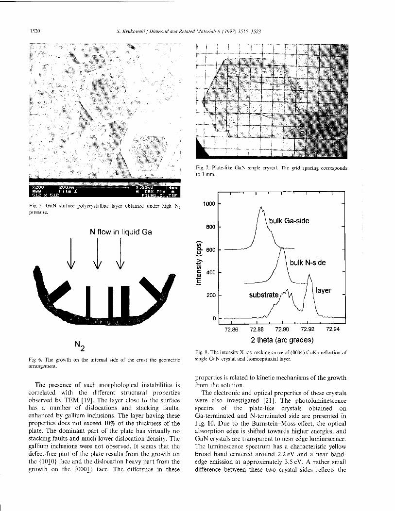
1520 S. Krukowski / Diamond and Related Materials 6 (1997) 1515-1523
X200 200J>« ttag Fi im x SIE x 512
3 .OOkU 14 m CBH PAN
FILMl-Ol.TIF
Fig. 5. GaN surface polycrystalline layer obtained under high N2
pressure.
N flow in liquid Ga
V V V
N,
Fig. 6. The growth on the internal side of the crust the geometric arrangement.
The presence of such morphological instabilities is correlated with the different structural properties observed by TEM [19]. The layer close to the surface has a number of dislocations and stacking faults, enhanced by gallium inclusions. The layer having these properties does not exceed 10% of the thickness of the plate. The dominant part of the plate has virtually no stacking faults and much lower dislocation density. The gallium inclusions were not observed. It seems that the defect-free part of the plate results from the growth on the {1010} face and the dislocation heavy part from the growth on the {0001} face. The difference in these
M
L *X
!~4.l
ipE
i-H
* ■•;-- ...•V_1_wp^- «jrffj£- .-It»..-. , , I ; ■■ . ?■ •.,r*y'-'-:- J .
k-,4 !.-T ■.■*'■; ■^■% 1 ; 1 '":^li;J
Fig. 7. Plate-like GaN single crystal. The grid spacing corresponds to 1 mm.
1000 -
800
g- 600
(A £ 400 c
200
0 -
bulk Ga-side
bulk N-side
72.86 72.88 72.90 72.92
2 theta (arc grades)
72.94
Fig. 8. The intensity X-ray rocking curve of (0004) CuKa reflection of single GaN crystal and homoepitaxial layer.
properties is related to kinetic mechanisms of the growth from the solution.
The electronic and optical properties of these crystals were also investigated [21]. The photoluminescence spectra of the plate-like crystals obtained on Ga-terminated and N-terminated side are presented in Fig. 10. Due to the Burnstein-Moss effect, the optical absorption edge is shifted towards higher energies, and GaN crystals are transparent to near edge luminescence. The luminescence spectrum has a characteristic yellow broad band centered around 2.2 eV and a near band- edge emission at approximately 3.5 eV. A rather small difference between these two crystal sides reflects the

S. Krukowski / Diamond and Related Materials 6 (1997) 1515-1523 1521
gallium side
nitrogen side
low angle boundary overstoichiometric
gallium point defects
*• gallium precipitates
Fig. 9. The model of creation of low-angle boundaries due to the lattice constants difference.
0.10
c 3 0.08
■s CO
_ 0.06
CO C 0.04
0.02
0.00
1.0
I 1 1 1 1 . J ' 3.472
1
T=6K
't 0-8 \ 5**0'»
O- 0.2
1 bulk sample
0.0 8 / G 2.0 2.2 2.4 2.8 2
e/VERGYfeW
■
610"
- I.I.I.
epileyerl
i . i i
3.0 3.1 3.2 3.3 3.4 3.5
Energy, eV
3.6 3.7
Fig. 10. Photoluminescence spectra of single GaN crystals obtained from the solution.
different structural properties of both sides of the crystals.
GaN single crystals show metallic behavior in the range 4.2-300 K. The GaN electronic properties mea- sured include the Hall effect free carrier density and electron mobility. All GaN crystals are strongly «-type with the typical concentrations close to 5 x 1019 cm-3. No significant density variation was observed due to the change of the growth conditions. The free electron density is usually attributed to nitrogen vacancy [22]. The electron mobility is 30-90 cm2 V "1 due to the high density of native defects in these crystals. Ab initio calculations [23,24] and experimental results [25] con- firm that the source of free electrons in GaN are N-vacancies
3.2. Aluminium nitride
Aluminium nitride crystals have been obtained under partial nitrogen pressures higher than 7 kbars. At lower
pressures, the combustion process starts at temperatures close to 1000 °C [7]. The combustion results depend on the chemical compositions of the gas mixture. For a nitrogen dominant gas mixture, the combustion results in A1N ceramics. When neutral gas dominates, the obtained sample is almost perfectly converted to A1N powder. This result opens up a potential application of Al combustion in high nitrogen pressures for the fabrica- tion of high-quality A1N ceramics for electronic applica- tions. Single A1N crystals obtained from nitrogen solutions under high nitrogen pressures were 0.1 mm in size and were needle-like. The crystalline quality of these crystals is comparable with that of the needle-like GaN single crystals.
3.3. Indium nitride
The largest single crystals of InN, grown from the solution under high pressure of nitrogen, were several Um in size. They had irregular shapes and they were skeletal in forms [8,9]. The attempts to grow larger crystals from the solution under high pressure were not successful.
4. Epitaxial layers
The homoepitaxial layers were grown on GaN single crystals using both MOCVD and MBE techniques. The layers has been grown on plate-like crystals only.
4.1. MOCVD
The homoepitaxial layers were grown by the MOCVD method in a horizontal atmospheric pressure reactors. Usually as-grown crystals were etched, rinsed in deion- ized water and annealed at a temperature of 800 °C in the MOCVD reactor in an atmosphere of NH3 and H2
mixture. The growth was conducted using trimethylgal- lium (TMG) and ammonia in the temperature range 900-1100 °C. The best results were obtained in the temperature range 1020-1050 °C.
The growth of the layer depends crucially on the substrate polarity. On the gallium-terminated side, the growth is irregular with the tendency to form isolated islands and even the transition to three-dimensional growth is observed. For higher supersaturations, colum- nar growth has been observed. On the nitrogen-termi- nated side, the growth mode is two-dimensional. Depending on the TMG:ammonia ratio, the growth morphology changes from the strictly two-dimensional to island type. The two-dimensional growth is controlled by new layer creation. Both two-dimensional nucleation and screw dislocation edge sources have been observed [26].
Both j?-type and «-type layers have been obtained.

1522 S. Krukowski / Diamond and Related Materials 6 (1997) 1515-1523
The /»-doping was performed using the metalo-organic MCp2Mg and subsequent annealing in 700 °C in the presence of N2. The »-doping was obtained by the use of silicon as a controlled donor defect. The homoepitax- ial layers were characterized by X-ray and optical meth- ods. The X-ray studies confirmed good crystallographic quality of the layers; the optical measurements include photoluminescence and electroluminescence studies [27]. A typical photoluminescence spectrum is presented in Fig. 11.
4.2. MBE
Homoepitaxial layers were grown by the MBE method using the on surface cracking (OSC) technique of M. Kamp et al. [28]. The MBE system used ammonia as a nitrogen source. The substrate preparation was similar to that adopted for MOCVD grown layers and the substrate temperature during the growth was equal to 680 °C.
The obtained layers were characterized by X-ray, microscopic and optical methods. The maximum of CuKcd reflection was slightly shifted owing to a differ- ence in lattice constants caused by different free carrier densities in the layer and the substrate. Optical measure- ments include photoluminescence studies; an example of a photoluminescence spectrum is given in Fig. 12. The figure includes two lines attributed to donor bound excitons, one line attributed to acceptor bound exciton and, additionally, three narrow lines due to free excitons. They are due to three sub-bands of the valence band. The low-energy lines (i.e. ABE and DBEs) have a half width of the order of 0.4 meV, which is presently the narrowest line reported. The higher energy lines have a half-width of the order of 5 meV.
2.0 - .FEA3.474eV
1.5 -
80 K DBS 3.467 eV J
/ \^ FEB 3.478 eV
V. FE C 3.493 eV
1.0 DBE3.47MeV
0.5 - ABE 3.4663 eV \
\ FE A 3.4785 eV
4.2 K —' —
v \ FEB 3.483 eV Is—... . l 1
c
■6
C JS c
3.45 3.46 3.47 3.48 3.49 3.50
Energy, eV
Fig. 12. Photoluminescence spectra of MBE grown layers: (a) T= 4.2 K; and (b) r=80K.
5. Conclusions
The main results reported in this paper can be summa- rized as follows: (1) the best outlook for the growth of large-substrate
quality single crystals currently exists for GaN; InN and A1N suffer from severe thermodynamic obsta- cles, which makes the stable growth of single crystals extremely difficult;
(2) the development of high-pressure crystal growth technology allowed us to obtain the GaN single crystals of 10 mm in size;
(3) the best crystalline quality layers were obtained by the MOCVD method, using GaN as a substrate;
(4) the optical properties of the MBE grown layers indicates the high quality of the homoepitaxial layers;
(5) the development of homoepitaxial technology can lead to fabrication of highly efficient lasers, active in the blue and ultraviolet range of the spectrum.
1.2
1.0
5 0.8
■e « 0.6
C 0.4
0.2
0.0 3.42
3.484 eV 3.4678 »V
- 3.463 eV / 1
~ b_ I a
—i—-™—■—-f y/^ '
3.44 3.46 Energy, eV
3.48
Fig. 11. Photoluminescence spectra of MOCVD grown layers: (a) undoped; and (b) Mg doped, T=4.2 K.
Acknowledgement
The research reported in this work has been supported by the Polish Committee for Scientific Research grant nos. 2P 30B 00809 and 7783495 C/2399.
References
[1] H. Morkoc, S. Strite, G.B. Gac, M.E. Lin, B. Sverdlov, M. Burns, J. Appl. Phys. 76(1994) 1363.
[2] S. Nakamura, T. Mukai, M. Senoh, Jap. J. Appl. Phys. 30 (1991) L1998.
[3] S. Nakamura, M. Senoh, N. Iwasa, S. Nagahama, Jap. J. Appl. Phys. 30(1995) L979.
[4] D.V. Tsvetkov, A.S. Zubrilov, V.l. Nikolaev, V. Soloviev, V.A. Dmitriev, MRS Internet Journal of Nitride Semiconductor Research 1 (1996) no. 35.

S. Krukowski / Diamond and Related Materials 6 (1997) 1515-1523 1523
[5] S. Nakamura, M. Senoh, S. Nagahama, N. Iwasa, T. Yamada, T. Matsushita, H. Kiyoku, Y. Sugimoto, Jap. J. Appl. Phys. 35 (1996) L217.
[6] I. Grzegory, M. Bockowski, S. Krukowski, B. Lucznik, M. Wroblewski, S. Porowski, MRS Internet Journal of Nitride Semiconductor Research 1 (1996) no. 20.
[7] I. Grzegory, J. Jun, M. Bockowski, S. Krukowski, M. Wroblew- ski, B. Lucznik, S. Porowski, J. Phys. Chem. Solids 56 (1995) 639.
[8] I. Grzegory, S. Krukowski, J. Jun, M. Bockowski, M. Wroblew- ski, S. Porowski, AIP Conference Proceedings 309 (1994) 565.
[9] W. Harrison, Electronic Structure and Properties of Solids, Free- man, San Francisco, 1980.
[10] R.T. Jacobsen, R.T. Stewart, M. Jahangiri, J. Phys. Chem. Ref. Data 15(1986)735.
[11] J.A. Van Vechten, Phys. Rev. B7 (1973) 1479. [12] W. Class, Contract Report, NASA-Cr-1171, 1968. [13] J. Karpinski, J. Jun, S. Porowski, J. Cryst. Growth 66 (1984) 1. [14] G.A. Slack, T.F. MacNelly, J. Cryst. Growth 34 (1976) 276. [15] S. Krukowski, MRS Internet Journal of Nitride Semiconductor
Research 1 (1996) no. 27. [16] I. Grzegory, S. Krukowski, Phys. Scr. T39 (1991) 242. [17] M. Leszczynski, I. Grzegory, H. Teisseyre, T. Suski, M. Bockow-
ski, J. Jun, J.M. Baranowski, S. Porowski, J. Domagala, J. Cryst. Growth 169(1996)235.
[18] F.A. Ponce, P. Bour, W.T. Young, M. Saunders, J.W. Steeds, Appl. Phys. Lett. 69 (1996) 337.
[19] Z. Lilliental-Weber, C. Kisielowski, S. Ruvimov, Y. Chen, J. Washburn, I. Grzegory, M. Bockowski, J. Jun, S. Porowski, J. Electron. Mater. 25 (1996) 1545.
[20] Z. Lilliental-Weber, S. Ruvimov, C. Kisielowski, Y. Chen, W. Swider, J. Washburn, N. Newman, A. Gassmann, X. Liu, L. Schloss, E.R. Weber, I. Grzegory, M. Bockowski, J. Jun, T. Suski, K. Pakula, J.M. Baranowski, S. Porowski, H. Amano, I. Akasaki, Mater. Res. Soc. Proc. 395 (1996) 351.
[21] H. Teisseyre, P. Perlin, M. Leszczynski, T. Suski, I. Grzegory, J. Jun, S. Porowski, T.D. Moustakas, J. Appl. Phys. 76 (1994) 4909.
[22] H.P. Maruska, J.J. Tjetjen, Appl. Phys. Lett. 15 (1969) 327. [23] J. Neugebauer, CG. Van de Walle, Phys. Rev. B50 (1994) 8067. [24] P. Boguslawski, E. Briggs, J. Bernholz, Phys. Rev. B51 (1995)
17255. [25] P. Perlin, T. Suski, H. Teisseyre, M. Leszczynski, I. Grzegory,
J. Jun, S. Porowski, P. Boguslawski, J. Bernholz, J.C. Chervin, A. Polian, T.D. Moustakas, Phys. Rev. Lett. 75 (1995) 296.
[26] G. Nowak, S. Krukowski, I. Grzegory, S. Porowski, J. Baranow- ski, K. Pakula, J. Zak, MRS Internet Journal of Nitride Semicon- ductor Research 1 (1996) no. 5.
[27] A. Wysmolek, J.M. Baranowski, K. Pakula, K.P. Korona, I. Grzegory, M. Wroblewski, S. Porowski, Proceedings of the International Symposium on Blue Laser and Light Emitting Diodes, Chiba, Published by Ohmsha Ltd, Tokyo, Japan, 1996, p. 492.
[28] H. Teisseyre, G. Nowak, M. Leszczynski, I. Grzegory, M. Bockowski, S. Krukowski, S. Porowski, M. Mayer, A. Pelzman, M. Kamp, K.J. Ebeling, G. Karczewski, MRS Internet Journal of Nitride Semiconductor Research 1 (1996) no. 13.

ELSEVIER
DIAMOND AND
RELATED MATERIALS
Diamond and Related Materials 6 (1997) 1524-1527
Residual strains in GaN grown on 6H-SiC
LP. Nikitinaa'*, M.P. Sheglova, Yu.V. Melnika, K.G. Irvine b, V.A. Dmitriev a'b
1 A.F. Ioffe Institute, 26 Politechnicheskaya str., St. Petersburg, 194021, Russia
b Cree Research, Inc., 2810 Meridian Parkway, Durham, NC27713, USA
Abstract
The triple crystal modification of Bond method was used for lattice constant measurements and for the study of residual strains in GaN layers grown on 6H-SiC (0001) substrates. GaN layers grown by MOCVD employing A1N and AlGaN buffer layers and GaN layers grown by HVPE without buffer layer were investigated. It was found that the residual strains in GaN were considerably reduced by use of the AlGaN buffer layer. The dependence of residual strains on thickness and composition of buffer layer could be explained by the different degree of relaxation mismatch stresses and change of thermal stresses in GaN layers, grown on SiC with different buffer layers. © 1997 Elsevier Science S.A.
Keywords: Gallium nitride; Lattice constant; Buffer layer; Stress; Residual strains
1. Introduction
Epitaxial growth of GaN is a subject of great interest for fabrication of light emitting devices. Recently, high- quality GaN epitaxial layers have been grown on SiC and sapphire using different methods, such as MOCVD, HVPE, MBE [1-4]. It was shown that the lattice con- stant of thin GaN layers grown on SiC and sapphire is different from that for bulk GaN. The c-lattice constant for GaN grown on SiC substrate is usually smaller than that for bulk GaN. On the contrary, the c-lattice con- stant for GaN grown on sapphire is larger than that for bulk GaN (Table 1). These results indicate that con- siderable residual strain is always present in thin GaN heteroepitaxial layers. When the thickness of GaN layer exceeds a certain critical value, the formation of cracks is observed. Critical thickness depends on the substrate used, the buffer layer and the growth technique [5,10,11]. Two main factors may cause stresses and strains in epitaxial layers: (1) the lattice mismatch and (2) the difference in thermal expansion coefficients (TEC) between the layer and the substrate. The values of lattice constants and TEC for GaN, SiC, sapphire and A1N are shown in Table 2. The relaxation of stresses in GaN grown on sapphire was studied in several reports
* Corresponding author. Fax: +7 (812) 247-6425; e-mail: [email protected]
[10-12]. It was suggested that the observed residual strain is thermal in nature.
In this paper, we report on the effect of buffer layer on residual strains in GaN epitaxial layers grown on SiC substrates.
2. Experimental procedure and results
GaN layers were grown on SiC-6H (0001) by HVPE without buffer layer and by MOCVD using A1N and AlGaN buffer layers. The thickness of GaN layers ranged from 1 to 2.3 um. The thickness of A1N buffer was 500 A, and the thickness of the AlGaN buffer for different samples was 500, 1500 and 3000 A. The content of A1N in AlGaN buffer was 20, 30 and 50%. The thickness of the substrates was 300 um. All layers were free from cracks.
We examined crystal quality of GaN layers using a double crystal X-ray spectrometer. Rocking curves were measured at (co) and (co, 26) modes with the SiC-6H (0006) monoehromator. Typical RC(co) for three groups of samples are demonstrated in Fig. 1 [(a) for the GaN layer grown directly on SiC, (b) for GaN grown on SiC with A1N buffer layer and (c) for GaN grown with AlGaN buffer layer]. The FWHM of RC(co) ranged from 80 to 340 arcsec. Measurements of GaN lattice constants were performed using a triple crystal modification of the Bond method [13,14] on symmetric
0925-9635/97/$17.00 © 1997 Elsevier Science S.A. All rights reserved. PII S0925-9635(97)00122-2

LP. Nikitinaetal. j Diamond and Related Materials 6 (1997) 1524-1527 1525
Table 1 C-lattice constant in GaN layers grown on SiC and sapphire
Substrate Buffer layer Thic
Sapphire A1N 1.0 Sapphire A1N 0.75 Sapphire A1N 1.0 SiC-6H A1N 1.0 SiC-6H A1N 0.5 GaN bulk —
Thickness of GaN (jun) Lattice constant C (A) References
5.191 5.1930 5.1900 5.1816 5.178 5.18561
[5] [6] [7] [7] [8] [9]
Table 2 Lattice constants and TEC for GaN, SiC-6H, A1N and sapphire
c(A) a (A) arxl06 a„ x 106
GaN 5.18561 3.188 3.17 SiC-6H 15.1173 3.0806 4.68 A1N 4.9792 3.1114 5.3 Sapphire 12.991 4.758 8.5
5.59 4.2 4.2 7.5
S S
So z w Z
SiC-6H (0006)
GaN (0002)
-0.50
ANGLE (degrees) 0.00
Fig. 1. Typical RC(co) for three groups of samples: (a) for GaN layer grown directly on SiC; (b) for GaN grown on SiC with A1N buffer layer; and (c) for GaN grown with AlGaN buffer layer.
(0004) CuKa and asymmetric (1124) CuKa reflections. SiC-6H crystals served as monochromator and analyser. This method is more useful in the case of mosaic and bending crystals, especially for asymmetric reflections. This allowed us to determine lattice constants with an accuracy of 5 x 10"5 A.
To estimate normal and tangent strains in GaN layers, we compared measured values of the lattice constants with those for the bulk GaN crystal, referred by Leszczinski et al. [9]. These values at r=294°C are: c = 5.18561Ä, fl = 3.1880A. Residual strains were determined as:
and £|| ={ax— ab)/ab,where the index T corresponds to the layer, and the index 'b' corresponds to the bulk crystal.
The results obtained for all GaN layers are shown in Table 3. From the table, the following deductions can be made: (1) The largest residual strains are observed in the
layers grown directly on SiC. Normal strains are negative and tangent ones are positive.
(2) A1N thick 500 A buffer layer reduces the absolute values of the strains.
(3) AlGaN buffer layers cause further reduction of strains and may change the signs of them depending on the composition and thickness of the buffer layer.
3. Discussion
The analysis of obtained results allows us to assume that, for the GaN/SiC heterostructure, the relaxation of mismatch stresses is not complete, and the GaN layer lattice constants at the growth temperature are not equal
Table 3 Residual strains in GaN layers
-(Q-Cb)/Cb
NN Buffer % A1N in Thickness of exxl03 e, x 103
layer buffer buffer (A)
1 0 0 -1.14 + 2.51 2 0 0 -1.02 + 1.88 3 Non 0 0 -1.37 + 2.92 4 0 0 -1.35 + 2.79 5 20 1500 -0.35 + 0.77 6 20 1500 -0.31 + 0.72 7 20 1500 -0.45 + 0.75 8 20 1500 -0.28 + 0.50 9 20 3000 + 0.23 -0.35 10 AlGaN 30 3000 -0.02 0 11 30 3000 + 0.17 -0.41 12 30 3000 + 0.25 -0.44 13 30 3000 + 0.23 -0.44 14 30 3000 + 0.45 -0.78 15 50 500 -0.43 + 0.78 16 50 500 -0.31 + 0.69 17 100 500 -0.77 + 1.22 18 A1N 100 500 -0.58 + 1.22 19 100 500 -0.54 + 0.85
1526 LP. Nikitina et al /Diamond and Related Materials 6 (1997) 1524-1527
Table 4 FWHM of RC(tu) on (0002) and (1124) reflections
Sample Buffer layer FWHM (0002) arcsec FWHM (1124) arcsec £j. x 103 e„103
1 Non 115 4 Non 55 11 AlGaN 270 14 AlGaN 270
270 240 220 240
-1.14 + 2.51 -1.35 + 2.79 + 0.17 -0.41 + 0.45 -0.78
to those for bulk crystal. We think that this is true for GaN layers grown directly on SiC substrates and especi- ally for the layers grown with buffer layers. If this is true, at the growth temperature, the tangent strain should be negative, and the normal strain should be positive since the lattice constant a of the substrate is smaller than that of the layer. When the sample is cooled down from the growth temperature to room temperature, thermoelastic stresses appear. Since the TEC of SiC < TEC of GaN, the GaN layer expands in the (0001) plane, and therefore the tangent strain becomes positive. The resulting residual strains are defined by the relative values of mismatch and thermal stresses. The complete compensation of one stress by the other is possible if the lattice mismatch and the difference in TEC have the same signs. When we use A1N or AlGaN as a buffer layer, the lattice mismatch decreases on both interfaces. This leads to a decrease in the degree of relaxation of mismatch stresses. However, the TEC of solid solution is likely to be close to TEC of GaN. This results in a decrease in thermal stresses. Thus, an almost total compensation of stresses and strains is possible in GaN layers grown with AlGaN buffer layer (see sample 10 from Table 3).
As for the degree of relaxation of mismatch stresses, we believe that it is related to the type of threading dislocations (TD) in the GaN layer. We compared the FWHM of RC(co) for (0002) and (1124) reflections for the layers grown without buffer layer (they have the largest residual strains and Gj_<0, €|| >0) with those for the layers grown with the AlGaN buffer layer (they have residual strains with opposite signs). These FWHM values are shown in the Table 4. The half widths of RC(co) for (0002) reflection are smaller than that for (1124) reflection from the layers grown without buffer layer; in contrast, the half widths of RC for symmetric and asymmetric reflections from the layers, grown with AlGaN buffer layer are comparable. According to the conclusion given by Heying et al. [15], this would be explained by type of TD in the layers: a large difference between the half widths is caused by the formation of pure edge TDs with Burgers vector, parallel to the interface. Comparable half width values are associated with the formation of screw or mixed screw/edge TDs. Therefore, it can be assumed that the almost total relaxation of mismatch stresses is accompanied by the formation of pure edge type TDs. The degree of relax-
ation of mismatch stresses decreases in the case of the formation of screw or mixed screw/edge TDs. Furthermore, we suppose that this relaxation may be almost complete if an initial stage of the growth is accompanied by strong misorientation of GaN grains in the (0001) plane and weak misorientation around the [0001] direction.
4. Conclusion
Residual strains in GaN grown on SiC-6H without a buffer layer and with A1N and AlGaN buffer layers were studied using triple crystal modification of the Bond method. It was found that the AlGaN buffer layer considerably reduces residual strains in GaN layers. The GaN layers free of residual strains may be grown on SiC-6H substrates, varying thickness and composition of AlGaN buffer. It was assumed that: (1) residual strains are caused by a lattice mismatch as
well as a difference in TEC, acting in opposition; (2) AlGaN buffer layer decreases thermal stresses and
relaxation degree of mismatch stresses depending on its thickness and composition; and
(3) the relaxation degree of mismatch stresses is con- nected with the type of threading dislocations in the GaN layer.
Acknowledgement
The authors would like to thank Dr R. Kutt and K. Vassilevski for useful discussions.
References
[1] I. Akasaki, H. Amano, Y. Koide, K. Hiramatsu, N. Sawaki, J. Cryst. Growth 98 (1989) 209.
[2] M.E. Lin, B. Swerdlov, G.L. Zhou, H. Morcoc, Appl. Phys. Lett. 62 (1993) 3479.
[3] I. Akasaki, H. Amano, J. Electrochem. Soc. 141 (1994) 2266. [4] Yu.V. Melnik, LP. Nikitina, A.S. Zubrilov, A.A. Sitnikova, Yu.G.
Musikhin, V.A. Dmitriev, Inst. Phys. Conf. 142 (1996) 863. [5] K. Hiramatsu, Th. Detchprohm, I. Akasaki, J. Appl. Phis. 32 (4)
(1993) 1528. [6] W. Rieger, T. Metzger, H. Angerer, R. Dimitrov, O. Ambacher,
M. Stutzman, Appl. Phys. Lett. 68 (7) (1995) 970.

LP. Nikitina et al. j Diamond and Related Materials 6 (1997) 1524-1527 1527
[7] Wei Li, Wei Xin Ni, Appl. Phys. Lett. 68 (19) (1996) 2705. [8] F.A. Ponce, B.S. Kruger, MajorJ.S., Jr, W.E. Piano, D.F. Welch,
Appl. Phys. Lett. 67 (3) (1995) 410. [9] M. Leszczinski, T. Suski, H. Teisseyre, P. Perlin, I. Grzegory, J.
Jun, S. Porowski, T.D. Moustakas, J. Appl. Phys. 76 (8) (1994) 4909.
[10] N. Itoh, J.C. Rhee, T. Kawabata, S. Koike, J. Appl. Phys. 58 (1985) 1828.
[11] T. Kozawa, T. Kachi, H. Kano, H. Nagase, N. Koide, K. Manabe, J. Appl. Phys. 77 (9) (1995) 4389.
[12] T. Detchprohm, K. Hiramatsu, K. Itoh, I. Akasaki, Jpn. J. Appl. Phys. 31 (1992)L1454.
[13] E.I. Golovenchin, N.V. Morosov, S.S. Ruvimov, VA. Sanina, L.M. Sapognikova, L.M. Sorokin, P.P. Sirnikov, M.P. Sheglov, Superconductivity: Phys., Chem., Techn. (in Russian) 3 (5) (1990)773.
[14]P.F. Fewster, N.L. Andrew, J. Phys. D: Appl. Phys. 28 (4A) (1995) A97.
[15] B. Heying, X.H. Wu, S. Keller, Y. Li, D. Kapolnek, B.P. Keller, S.P. DenBaar, J.S. Speck, Appl. Phys. Lett. 68 (5) (1996) 64.
-£;,- DIAMOND AND
ELSEVIER
RELATED MATERIALS
Diamond and Related Materials 6 (1997) 1528-1531
Structural and electrical properties of Schottky barriers on n-GaN
E.V. Kalinina a'*, N.I. Kuznetsov a, A.I. Babanin a, V.A. Dmitriev a, A.V. Shchukarev b
* A.F. Ioffe Physico-Technical Institute, 26 Politechnicheskaya str., 194021 St. Petersburg, Russia h Mekhanobr Analyt Co., 8a 21 Liniya V.l., 199026 St. Petersburg, Russia
Abstract
Cr, Au and Ni Schottky barriers were formed on n-GaN. Fundamental parameters of the barriers (barrier height, electron affinity of GaN, and effective Richardson coefficient) were calculated from results of current-voltage and capacitance-voltage measurements. Interface chemistry of Cr, Au and Ni barriers on n-GaN was studied using Auger electron spectroscopy (AES) and angle-resolved X-ray photoelectron spectroscopy (AR XPS). A correlation between the chemical reactivity of metals and the value of the effective Richardson coefficient was established. © 1997 Elsevier Science S.A.
Keywords: GaN; Schottky barrier; Effective Richardson coefficient; Interface
1. Introduction
Recently extensive and detail study has been done on Schottky barriers formed on n-GaN. Different metals have been employed to form the Schottky barriers: Au [1], Pt, Pd [2], Au, Pd, Cr, Ti, Pt, Ni [3], Pd, Pt [4]. Epitaxial n-GaN layers grown by metal organic chemical vapor deposition (MOCVD) or hydride vapor phase epitaxy (HVPE) on sapphire substrates have been used for these studies. Characteristics of Cr, Au and Ni Schottky barriers formed on n-GaN epitaxial layers grown on SiC substrates have also been reported [5]. The values of the barrier height, built-in potential and the GaN electron affinity determined in those papers are in good agreement. However, the values of the effective Richardson coefficient differ significantly for the metals investigated. In the present work, we investi- gated the interface chemistry for the barriers described in Ref. [5].
by vacuum thermal evaporation of metals: Cr, Au and Ni. Al was evaporated to form Ohmic contacts to n-GaN. The metals were evaporated in a vacuum of approx. 3 x 10~4 Pa through shadow masks. The barrier area (S) was 7 x 10~4 cm2. The thickness of the metals ranged from 0.1 to 0.15/mi for electrical and AES measurements, and from 30 to 50 A for XPS measure- ments. A schematic drawing of the structure is shown in Fig. 1.
The current-voltage (J-V) characteristics of the barriers were measured in the temperature range from 100 to 450 K. The capacitance-voltage (C-V) character- istics were measured at frequencies of 1 and 10 kHz and 1 MHz at 300 K. The distribution of the chemical elements across of the metals/GaN structures was studied by AES depth profiling using Ar+ ions. Phase formations on metals/GaN interfaces were investigated by AR XPS. Photoelectron take-off angle varied from 15 to 75°.
2. Experimental procedure
Epitaxial n-GaN layers were grown by MOCVD on 6H-SiC (0001) substrates [5]. The concentration of uncompensated donors, Nj-N^, in the GaN layers ranged from 1016 to 1018cm~3. The thickness of the layers was approx. 1 /mi. Schottky barriers were formed
* Corresponding author. Fax: 00 7 812 247 6425.
Al (Cr,Au,Ni) Al y///////i mm ma ma ITOI WMM
n-GaN (1016-1018) cm"3
n - 6H-SiC
Fig. 1. Schematic drawing of a sample with Schottky barriers and Ohmic contacts.
0925-9635/97/S17.00 © 1997 Published by Elsevier Science S.A. All rights reserved. PII S0925-9635(97)00115-5
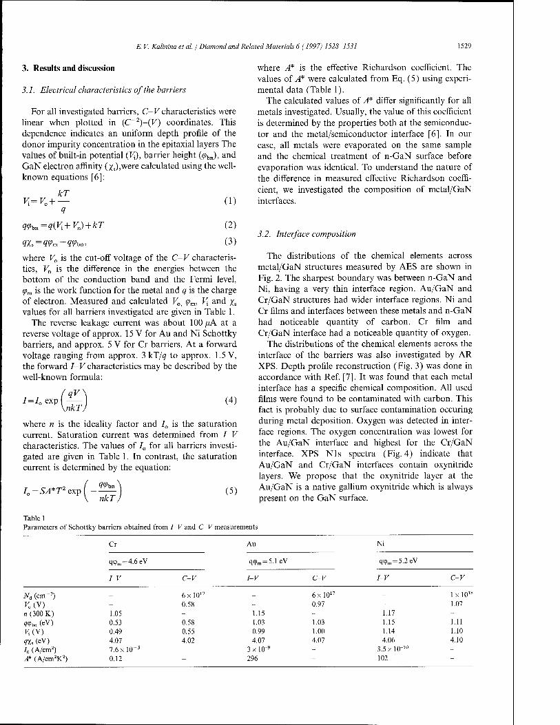
E. V. Kalinina et al. / Diamond and Related Materials 6 (1997) 1528-1531 1529
3. Results and discussion
3.1. Electrical characteristics of the barriers
For all investigated barriers, C-Vcharacteristics were linear when plotted in (C~2)-(T) coordinates. This dependence indicates an uniform depth profile of the donor impurity concentration in the epitaxial layers The values of built-in potential (Jfy, barrier height (tpbn), and GaN electron affinity (%s),were calculated using the well- known equations [6]:
Vi=V0+- kT
(1)
where A* is the effective Richardson coefficient. The values of A* were calculated from Eq. (5) using experi- mental data (Table 1).
The calculated values of A* differ significantly for all metals investigated. Usually, the value of this coefficient is determined by the properties both at the semiconduc- tor and the metal/semiconductor interface [6]. In our case, all metals were evaporated on the same sample and the chemical treatment of n-GaN surface before evaporation was identical. To understand the nature of the difference in measured effective Richardson coeffi- cient, we investigated the composition of metal/GaN interfaces.
q<Pbn=q(Vi+Vn) + kT
?Xs=Wm-Wbn,
(2)
(3)
where V0 is the cut-off voltage of the C-V characteris- tics, Vn is the difference in the energies between the bottom of the conduction band and the Fermi level, <pm is the work function for the metal and q is the charge of electron. Measured and calculated F0> q>m, V{ and xs
values for all barriers investigated are given in Table 1. The reverse leakage current was about 100 /JA at a
reverse voltage of approx. 15 V for Au and Ni Schottky barriers, and approx. 5 V for Cr barriers. At a forward voltage ranging from approx. 3 kT/q to approx. 1.5 V, the forward I-V characteristics may be described by the well-known formula:
I=I0 exp (qV_
\nkT (4)
where n is the ideality factor and I0 is the saturation current. Saturation current was determined from I-V characteristics. The values of I0 for all barriers investi- gated are given in Table 1. In contrast, the saturation current is determined by the equation:
I0=SA*T2exp q<Pbn
nkT (5)
3.2. Interface composition
The distributions of the chemical elements across metal/GaN structures measured by AES are shown in Fig. 2. The sharpest boundary was between n-GaN and Ni, having a very thin interface region. Au/GaN and Cr/GaN structures had wider interface regions. Ni and Cr films and interfaces between these metals and n-GaN had noticeable quantity of carbon. Cr film and Cr/GaN interface had a noticeable quantity of oxygen.
The distributions of the chemical elements across the interface of the barriers was also investigated by AR XPS. Depth profile reconstruction (Fig. 3) was done in accordance with Ref. [7]. It was found that each metal interface has a specific chemical composition. All used films were found to be contaminated with carbon. This fact is probably due to surface contamination occuring during metal deposition. Oxygen was detected in inter- face regions. The oxygen concentration was lowest for the Au/GaN interface and highest for the Cr/GaN interface. XPS Nls spectra (Fig. 4) indicate that Au/GaN and Cr/GaN interfaces contain oxynitride layers. We propose that the oxynitride layer at the Au/GaN is a native gallium oxynitride which is always present on the GaN surface.
Table 1 Parameters of Schottky barriers obtained from I-V and C-V measurements
Cr Au Ni
q<Pm = = 4.6 eV q<Pm = 5.1eV q<pm = 5.2eV
I-V C-V I-V C-V I-V C-V
Nd (cm-3) _ 6xl017 — 6xl017 - 1 x 10¹⁸
f.(V) - 0.58 - 0.97 - 1.07
n (300 K) 1.05 - 1.15 - 1.17 - OTb„ (eV) 0.53 0.58 1.03 1.03 1.15 1.11
K(V) 0.49 0.55 0.99 1.00 1.14 1.10
?Xs (eV) 4.07 4.02 4.07 4.07 4.06 4.10
I0 (A/cm2) 7.6 x 10~5 - 3 x 10"9 - 3.5 x 10 -10 - A* (A/cm2K2) 0.12 - 296 - 102 -
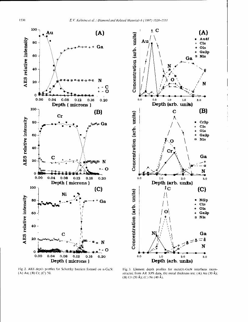
1530 E. V. Kalinina et al. / Diamond and Related Materials 6 (1997) 1528-1531
100
9 I I to
100
0.04 0.08 0.12 0.16
Depth ( microns ) 0.20
Ö ■S .3
I—< ü M
w
0.00 0.04 0.08 0.12 0.16 Depth ( microns)
0.20
100
a
.a I l"H
w
0.00 0.04 0.08 0.12 0.16 Depth ( microns )
0.20
Fig. 2. AES depth profiles for Schottky barriers formed on n-GaN: (A) Au; (B) Cr; (C) Ni.
0.5 1.0 1.5 2.0
Depth (arb. unite)
a
£1 u
a o
•-Ö
a u d o Ü
I'frtvr-*- 1.0 2.0
Depth (arb. units) 3.0
0.0 1.0 2.0
Depth (arb. units) 3.0
Fig. 3. Element depth profiles for metal/n-GaN interfaces recon- structed from AR XPS data, the metal thickness are: (A) Au (30 A); (B)Cr(50Ä); (C)Ni(40Ä).
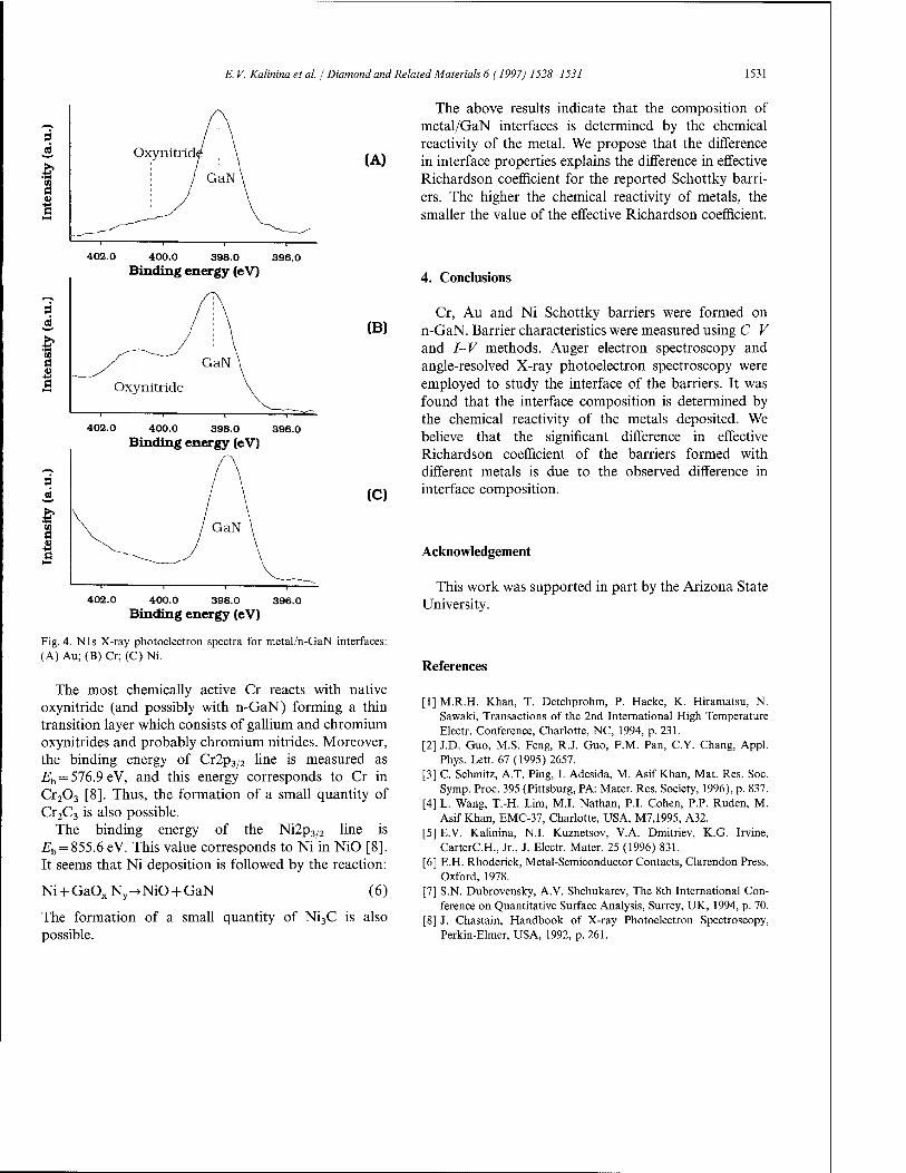
E. V. Kalinina et al. / Diamond and Related Materials 6 (1997) 1528-1531 1531
3
ö
3 es
t
3
in a I
Oxynitridi (A)
402.0 400.0 398.0 Binding energy (eV)
396.0
(B)
402.0 400.0 398.0 Binding energy (eV)
396.0
(C)
402.0 400.0 398.0 396.0 Binding energy (eV)
Fig. 4. Nls X-ray photoelectron spectra for metal/n-GaN interfaces: (A) Au; (B) Cr; (C) Ni.
The most chemically active Cr reacts with native oxynitride (and possibly with n-GaN) forming a thin transition layer which consists of gallium and chromium oxynitrides and probably chromium nitrides. Moreover, the binding energy of Cr2p3/2 line is measured as £,, = 576.9 eV, and this energy corresponds to Cr in Cr203 [8]. Thus, the formation of a small quantity of Cr2C3 is also possible.
The binding energy of the Ni2p3/2 line is Eb = 855.6 eV. This value corresponds to Ni in NiO [8]. It seems that Ni deposition is followed by the reaction:
Ni + GaOx Nv^NiO + GaN (6)
The formation of a small quantity of Ni3C is also possible.
The above results indicate that the composition of metal/GaN interfaces is determined by the chemical reactivity of the metal. We propose that the difference in interface properties explains the difference in effective Richardson coefficient for the reported Schottky barri- ers. The higher the chemical reactivity of metals, the smaller the value of the effective Richardson coefficient.
4. Conclusions
Cr, Au and Ni Schottky barriers were formed on n-GaN. Barrier characteristics were measured using C-V and I-V methods. Auger electron spectroscopy and angle-resolved X-ray photoelectron spectroscopy were employed to study the interface of the barriers. It was found that the interface composition is determined by the chemical reactivity of the metals deposited. We believe that the significant difference in effective Richardson coefficient of the barriers formed with different metals is due to the observed difference in interface composition.
Acknowledgement
This work was supported in part by the Arizona State University.
References
[1] M.R.H. Khan, T. Detchprohm, P. Hacke, K. Hiramatsu, N. Sawaki, Transactions of the 2nd International High Temperature Electr. Conference, Charlotte, NC, 1994, p. 231.
[2] J.D. Guo, M.S. Feng, R.J. Guo, F.M. Pan, C.Y. Chang, Appl. Phys. Lett. 67(1995)2657.
[3] C. Schmitz, A.T. Ping, I. Adesida, M. Asif Khan, Mat. Res. Soc. Symp. Proc. 395 (Pittsburg, PA: Mater. Res. Society, 1996), p. 837.
[4] L. Wang, T.-H. Lim, M.I. Nathan, P.I. Cohen, P.P. Rüden, M. Asif Khan, EMC-37, Charlotte, USA, M7,1995, A32.
[5] E.V. Kalinina, N.I. Kuznetsov, V.A. Dmitriev, K.G. Irvine, CarterC.H., Jr., J. Electr. Mater. 25 (1996) 831.
[6] E.H. Rhoderick, Metal-Semiconductor Contacts, Clarendon Press, Oxford, 1978.
[7] S.N. Dubrovensky, A.V. Shchukarev, The 8th International Con- ference on Quantitative Surface Analysis, Surrey, UK, 1994, p. 70.
[8] J. Chastain, Handbook of X-ray Photoelectron Spectroscopy, Perkin-Elmer, USA, 1992, p. 261.

DIAMOND AND
ELSEVIER
RELATED MATERIALS
Diamond and Related Materials 6 (1997) 1532-1535
Structural properties of GaN grown on SiC substrates by hydride vapor phase epitaxy
Yu.V. Melnik, LP. Nikitina *, A.E. Nikolaev, V.A. Dmitriev 1
A.F. Ioffe Institute and Cree Research Eastern European Division, 26 Politechnicheskaya St, St. Petersburg, Russia
Abstract
Hydride vapor phase epitaxy (HVPE) was used for GaN deposition on SiC substrates without a buffer layer. The influence of substrate parameters (structural perfection, surface polarity, misorientation) on the structural properties of GaN layers was investigated. X-ray differential diffractometry (XRDD) and the triple crystal modification of the Bond method were used to study the structural properties. The X-ray mapping was done over a 30 mm diameter 6H-SiC substrate. It was shown, that the full width at half maximum (FWHM) of X-ray co-scan rocking curves (RC) from GaN layers monotonically increases as the FWHM of the RC from the substrate increases. © 1997 Elsevier Science S.A.
Keywords: Epitaxy; Gallium nitrides; Substrates; Structural properties
1. Introduction
GaN is one of the most promising materials for application in blue and UV light emitting devices. One of the severest problems hindering progress in this field is the lack of a suitable substrate material for the growth of Ill-nitrides films. GaAs, SiC, ZnO, LiGaO, AlMgO and sapphire have all been used as substrates for the epitaxial growth of group Ill-nitrides.
The principal advantage of SiC substrates compared to sapphire substrates is the smaller lattice mismatch (3.5 versus 16%). High quality GaN films can be grown on SiC substrates by MOCVD or MBE [1,2], but in most cases the growth requires an A1N buffer, which restricts development of the vertical device configuration.
Recently, we reported a high-quality GaN grown on SiC substrates by hydride vapor phase epitaxy (HVPE) without a buffer layer [3]. In this study, we investigate the effect of substrate parameters on the surface mor- phology and crystal structure of GaN layers.
* Corresponding author. 'Current address: Howard University, 2300 Sixth Street, NW, Washington DC 20059, USA.
2. Experimental procedures
GaN epitaxial layers were grown using the HVPE growth system with a two-zone resistance furnace. In a horizontal open flow reactor, HC1 was reacted with liquid Ga to form GaCl gas which was transported to the growth zone and reacted with NH3 resulting in GaN deposition on the SiC substrate. Argon was used as an ambient gas. 6H-SiC and 4H-SiC 30 mm diameter wafers manufactured by Cree Research Inc. were used as sub- strates. Both on- and off-axis substrates were used. The GaN films were grown on both the silicon and carbon faces of the substrates. The growth temperature was usually kept at between 950 and 1050 °C and the GaN growth rate was controlled from 0.02 to 0.6 um min-1. The layer thickness ranged from 0.2 to 2 urn. The layers had a nonuniformity in thickness of less than 5% across the 30 mm-diameter SiC substrates.
3. Structural properties of GaN
The GaN film quality was found to be determined by a number of factors. They are: growth conditions and substrate properties, surface polarity, misorientation and perfection of crystal structure.
In contrast to MBE growth, in our study the quality of the films strongly depended on the SiC surface
0925-9635/97/S17.00 © 1997 Elsevier Science S.A. All rights reserved. PII S0925-9635(97)00114-3

Y. V. Melnik et al. j Diamond and Related Materials 6 (1997) 1532-1535 1533
polarity [4]. The best GaN layers were grown on the on-axis (0001)Si face of SiC substrates. These layers had a smooth, mirror-like surface over the entire wafer and a high crystal quality (Fig. 1(a)). Growth on the C-face resulted in GaN with a poor crystalline quality and rough surface. This agrees with the report on GaN film growth by MOCVD [5].
The films grown on (0001)Si off-axis substrates had
a stepped surface (Fig. 1(b)). No detectable effect of substrate polytype was observed on GaN surface mor- phology and crystal quality. All GaN layers described below were grown on the (0001)Si face of 6H-SiC on-axis wafers.
The structural quality of GaN films was studied by X-ray diffractometry (XRD) using double- and triple crystal spectrometers. RC in (co) and (co, 29) modes
t . (a)
Y..; 'V*- ^ 'V 3-. ^ v%-^ ' ^'
-x ■ ' -\
• t
liiflliit? f* Ulli ̂ ife *' > '
i^fölt ilit. = lit **!> ii„* '*?^F
K- i!!*1 %
Jv i$$fc %'*»%t
IB V ' 'f \
ffei ÄraK^j t'~*lir ,1 J# '^a J't'^f: " *^-™
Sibils pH%| »'I*1. Jllgl -i • *. ^n* äIPI ft»| »«Ar ̂ 1§f
" -H , , >* *" x.,
(b)
:"*l!. ;;*§♦
c \
V*.
■at'«
4.' : t^rifeuÄ
' \ .'
l\ '* *>-A ' j *t - ,
25 Mm
25 Mm
Fig. 1. SEM micrograph of surface morphology of GaN grown on on-axis (a), and 3.5° off-axis (b) SiC substrates.

1534 Y. V. Melnik et al. / Diamond and Related Materials 6 (1997) 1532-1535
Table 1 The FWHM values for RC and block sizes of GaN layers
Sample (0002) CuKa (0004) CuKa W(<a,20) (0004) / W(co,2ö) (0002)
Block size (A)
W(cü) (arcsec) W(w,20) (arcsec) W(co) (arcsec) W(&>,20) (arcsec)
1 2 3 4
420 220 150 70
120 90 70 34
440 300 150
240 180 120
2.0 2.0 1.7
1400 1850 2400 4900
were measured on (0002), (0004) and asymmetrical (1124) CuKa reflections. The FWHM of double crystal RC(ffl) for (0002) GaN reflection varied from 65 to 150 arcsec for the layers grown at the same growth conditions. The X-ray differential diffractometry (XRDD) method [ 1 ] was applied to evaluate a disloca- tion distribution in GaN layers. The results obtained are shown in Table 1. Analysis of these data allows us to conclude that the crystal structure of GaN layers may be described as an intermediate between a uniform dislocation distribution and a mosaic structure. Misorientation of mosaic blocks is responsible for RC(Cü) broadening. It is accompanied by decreases in block sizes from 4900 to 1400 A, resulting in the broad- ening of RC(co, 29).
The X-ray mapping was done over a 30 mm diameter 6H-SiC substrate at 24 points (Fig. 2). The thickness of epilayer was 0.6 um. It can be seen from Fig. 2 that the FWHM values at 7 points (shaded square) are consider- ably larger than those in the other 17. These are precisely the points where crystal quality of the substrate is poor. All these points are on the periphery of the substrate. It was found that the substrate has a domain structure in these 7 points (Fig. 3) and the layer does also. If the
r"79" "15*1 Layer
34 27 Subst.
72 74 69 92 20 30 22 22
#76 69 78 74 79 149A | 32 20 29 25 30 74 1 I 69 67 69 74 84 1131 \22 20 22 20 47 40/
72 72 74 92
17 20 22 27
76 80
L^5_ _2öJ Fig. 2. Wafer map of FWHM RC(co) from 30 mm diameter GaN/SiC-6H structure. The FWHM value for RC(co) is shown at the top of every square and the FWHM value for RC(co) measured from the SiC- substrate is shown at the bottom of every square.
misorientation angle between domains in the substrate is smaller than the FWHM of RC(a>) from every domain, an abnormal broadening of RC(cy) from the layer is observed (Fig. 3(a)). If the misorientation angle is comparable to FWHM or higher, separated peaks
>•
z z
(a)
z W f- z
(b)
N 6H-SiC (0006) \ FWHM=74 arc sec
GaN (0002) FWHM=92 arc sec
-0.1 0.0 ANGLE (degrees)
0.1
GaN (0002) FWHM=92 arc sec
6H-SiC (0006) FWHM=22 arc sec
-0.1 0.0 ANGLE (degrees)
0.1
Fig. 3. Rocking curves of an co-scan from GaN layer in areas, where the substrate has a domain structure: (a) misorientation angle between domains in the substrate is comparable with the FWHM RC(co) from every domain; (b) misorientation angle is larger than the FWHM RC(co) from every domain.

Y. V. Melnik et al. / Diamond and Related Materials 6 (1997) 1532-1535 1535
S
80 -
•
• •
•
•
75
70
•
•
t •
• 1
•
i
•
1
•
1
15 20 25 30 FWHM (substrate), arcsec
35
Fig. 4. The FWHM of RC(co) for GaN layer versus the FWHM of RC(co) for the SiC-6H substrate, excepting the shaded points on Fig. 2.
appear from the domains in the layer (Fig. 3(b)). For the 17 substrate points free from domains, the FWHM values measured from the GaN layer (Fig. 4) monotoni- cally increase as the FWHM of RC from the substrate increases. We believe that the spread of experimental data relative to the linear dependence can be explained by different degrees of misorientation in GaN grains in the (0001) plane at the initial stage of the growth. Thus the structural quality of GaN grown on SiC by HVPE is defined dominantly by the structural quality of the substrate.
As shown above, high quality GaN layers on SiC may be grown using HVPE without a buffer layer. Nevertheless there are rather large residual thermal strains in these layers [6]. If the thickness of the layer exceeds «1.5 um these strains cause cracks to form near GaN/SiC interface. As the thickness of the layer increases these cracks may propagate into the layer. To estimate normal (e±) and tangent (e^ strains in the layers the triple crystal modification of the Bond method was used. Residual strains were calculated using the
following lattice constants for the bulk GaN crystal: tf = 3.1880 Ä, c = 5.18561A [7]. The e± values ranged from -0.9 x 10"3 to -1.4 x 10~3. The eB values ranged from +1.0xl0"3 to +2.9 xlO"3. Such high residual strains are primarily thermal in nature and result in the formation of cracks when the thickness of the layer exceeds «1.5 um.
4. Summary
The structural properties of GaN grown on SiC substrates by hydride vapor phase epitaxy without a buffer layer were investigated. It was shown that high quality GaN layers may be grown on the Si-face of a SiC substrate. GaN layers grown on on-axis SiC sub- strate had a smooth mirror-like surface. The FWHM of double-crystal RC(a>) for (0002) GaN reflection varied from 65 to 150 arcsec for the layers grown at the same growth conditions. The FWHM of RC from GaN layers monotonically increases as the FWHM of RC from the substrate increases. Thus the structural quality of GaN is mainly defined by the structural quality of SiC substrate.
References
[1] I.P. Nikitina, V.A. Dmitriev, Inst. Phys. Conf. Series 141 (1994) 431-436.
[2] M.E. Lin, B. Swerdlov, G.L. Zhou, H. Morcoc, Appl. Phys. Lett. 62(1993)3479-3481.
[3] Yu.V. Melnik, LP. Nikitina, A.S. Zubrilov, A.A. Sitnikova, V.A. Dmitriev, Inst. Phys. Conf. Series 142 (1996) 863-866.
[4] S. Sinharoy, G. Augustine, L.B. Rowland, A.K. Agarwal, R.L. Messham, M.C. Driver, R.H. Hopkins, J. Vac. Sei. Technol. A 14 (3) (1996) 896-899.
[5] T. Sasaki, T. Matsuoka, J. Appl. Phys. 64 (9) (1988) 4531-4535. [6] LP. Nikitina, M.P. Sheglov, Yu.V. Melnik, K.G. Irvine,
V.A. Dmitriev, Diamond Relat. Mater, (this issue) [7] M. Leszczynski, T. Suski, H. Teisseyre, P. Perlin, I. Grzegory,
J. Jun, S. Porowski, T.D. Moustakas, J. Appl. Phys. 76 (8) (1994) 4909-4911.

DIAMOND AND
RELATED MATERIALS
ELSEVIER Diamond and Related Materials 6 (1997) 1536-1538
Contactless characterisation of 2D-electrons in GaN/AlGaN HFETs
H. Alausea'*, C. Skierbiszewskia, M. Dyakonova, W. Knapa, M.L. Sadowski b'\ S. Huantb, J. Youngc, M. Asif Khanc, Q. Chenc
1 Groupe d'Etudes des Semiconducteurs, Universite Montpellier 2 - C.N.R.S., UMR357, Place E. Bataillon, 34095 Montpellier, France b High Magnetic Field Laboratory, MPI-FKF and CNRS, BP 166, 38042 Grenoble, France
c A.P.A. Optics Inc., Blaine, MN, USA
Abstract
We report on properties of 2D carriers in an GaN/AlGaN heterojunction investigated by an optical method. This method consists of a cyclotron resonance (CR) experiment where optical absorption is measured under fixed magnetic fields up to 13 T. We introduce a theoretical approach that allows to interpret cyclotron resonance due to the thin 2D layer on the sapphire substrate. The presented contactless characterisation method gives access to some very important parameters of the bidimensional gas such as the carrier concentration, their mobility and their effective mass. © 1997 Elsevier Science S.A.
Keywords: GaN/GaAIN heterostructures; Bidimensional electron gas; Cyclotron resonance; Contactless characterisation
1. Introduction
III-V nitride transistor technology is maturing fast [1]. AlGaN/GaN heterostructures based FETs are focusing interest for their potential high temperature applications [2]. Traditional characterisation methods by transport measurements require technological pro- cesses of the samples which can be difficult to perform on these kind of samples. Another problem of transport measurements can arise in the presence of a highly doped layer or substrate which can induce parallel conduction.
In this work, we present an optical contactless charac- terisation: a cyclotron resonance experiment on a two- dimensional electron gas confined at the GaN/AlGaN interface. The high quality of the sample allowed the observation of well resolved cyclotron resonance (CR) absorption peaks. In view of an accurate modellisation of these experimental data, a complete calculation of the ratio of the optical transmissions T(B)/T(0) (under magnetic field and without magnetic field) was carried out including the exact resonant contribution of the
* Corresponding author. Fax: 33 67 14 3760; e-mail: [email protected] 'Institute of Experimental Physics, Warsaw University, Hoza 69, 0-681 Warsaw, Poland.
bidimensional electron gas and the effect of the multire- flections in the substrate.
2. Experiment
A fast Fourier transform (FFT) spectrometer and a superconducting coil have been used. The magnetic field was kept constant and we recorded the spectra as a function of the far-infrared radiation frequency. All measurements were performed at 2 K, in a magnetic field up to 13 T. Examples of experimental results for different spectral resolutions and magnetic fields are shown in Fig. 1.
The spectra taken with 0.5cm"1 resolution show oscillations mainly due to interferences in the sapphire substrate (Fig. 1, left). High resolution increases the coherence length of the FTIR beam and allows coherent multireflections in the substrate as schematised on Fig. 2. The oscillations are averaged for lower resolution (3cm"1) and the CR minimum that clearly moves to higher energies with an increasing magnetic field can be observed (Fig. 1, right).
The absorption peaks at different magnetic fields show a non-Lorentzian behaviour that must be fitted by an accurate function. Parameters of the fit are the carrier concentration Nt and mobility m. Effective mass can be
0925-9635/97/S17.00 © 1997 Elsevier Science S.A. All rights reserved. PII S0925-9635(97)00052-6
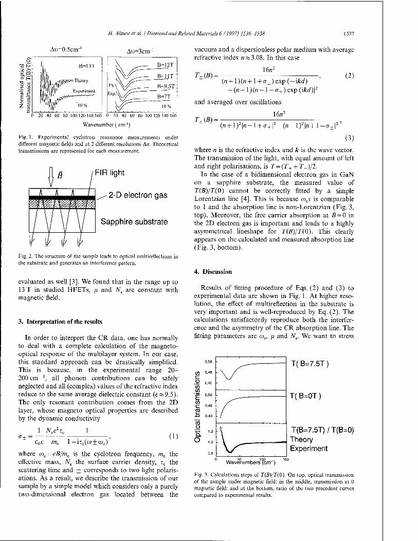
H. Alauseetal. / Diamond and Related Materials 6 (1997) 1536-1538 1537
Au=0.5cnr Au=3cnr
_JB=12T
- B=11T
m\V// . B=9.5T ExpA/^—~ B=7T
\y^ io% 0 20 40 60 80 100 120 140 160 0 20 40 60 80 100 120 140 160
Wavenumber (cm-1)
Fig. 1. Experimental cyclotron resonance measurements under different magnetic fields and at 2 different resolutions An. Theoretical transmissions are represented for each measurement.
FIR light
2-D electron gas
Sapphire substrate
Fig. 2. The structure of the sample leads to optical multireflections in the substrate and generates an interference pattern.
evaluated as well [3]. We found that in the range up to 13 T in studied HFETs, /i and Ns are constant with magnetic field.
3. Interpretation of the results
In order to interpret the CR data, one has normally to deal with a complete calculation of the magneto- optical response of the multilayer system. In our case, this standard approach can be drastically simplified. This is because, in the experimental range 20- 200 cm"1, all phonon contributions can be safely neglected and all (complex) values of the refractive index reduce to the same average dielectric constant (e«9.5). The only resonant contribution comes from the 2D layer, whose magneto optical properties are described by the dynamic conductivity
1 N«e2xc. 1
e0c mc l-hc(a>±coc) (1)
where coc = eB/mc is the cyclotron frequency, mc the effective mass, Ns the surface carrier density, TC the scattering time and + corresponds to two light polaris- ations. As a result, we describe the transmission of our sample by a simple model which considers only a purely two-dimensional electron gas located between the
vacuum and a dispersionless polar medium with average refractive index «äS3.08. In this case
I6n2
T±(B)= . \(n +1)(« +1 + a+) exp (-ikd)
— (n —1)(« — 1 — <7±) exp (ikd)\2
and averaged over oscillations
(2)
T±(B) = 16«2
(«+l)2|«+l+ff±|2-(«-l)2|«+l-fT + |2 '
(3)
where n is the refractive index and k is the wave vector. The transmission of the light, with equal amount of left and right polarisations, is T=(T+ + TJ)/2.
In the case of a bidimensional electron gas in GaN on a sapphire substrate, the measured value of T(B)/T(0) cannot be correctly fitted by a simple Lorentzian line [4]. This is because COCT is comparable to 1 and the absorption line is non-Lorentzian (Fig. 3, top). Moreover, the free carrier absorption at B=0 in the 2D electron gas is important and leads to a highly asymmetrical lineshape for T(B)/T(0). This clearly appears on the calculated and measured absorption line (Fig. 3, bottom).
4. Discussion
Results of fitting procedure of Eqs. (2) and (3) to experimental data are shown in Fig. 1. At higher reso- lution, the effect of multireflection in the substrate is very important and is well-reproduced by Eq. (2). The calculations satisfactorily reproduce both the interfer- ence and the asymmetry of the CR absorption line. The fitting parameters are a>c, fi and Ns. We want to stress
0,56
CO 0,48
.Q 0,40 co
-yf' CO "F 0,56
CO C 0'4e
4^ 0,40
Ü '4= 1,2 Q.
o 10
.
■.r \
0,8 ; V-
T(B=7.5T;
T(B=0T
T(B=7.5T)/T(B=0) Theory Experiment
0 ... 50 100 .. 150 Wavenumbers (cm-1)
Fig. 3. Calculations steps of T(B)/T(0). On top, optical transmission of the sample under magnetic field; in the middle, transmission at 0 magnetic field; and at the bottom, ratio of the two precedent curves compared to experimental results.
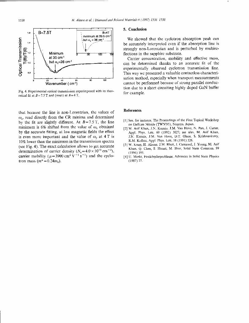
1538 H. Alauseetal. / Diamond and Related Materials 6 (1997) 1536-1538
Wavenumber (cm"1
Fig. 4. Experimental optical transmission superimposed with its theo- retical fit at ß = 7.5 T and (inset) at B = 4 T.
5. Conclusion
We showed that the cyclotron absorption peak can be accurately interpreted even if the absorption line is strongly non-Lorentzian and is perturbed by multire- flections in the sapphire substrate.
Carrier concentration, mobility and effective mass, can be determined thanks to an accurate fit of the experimentally observed cyclotron transmission line. This way we presented a valuable contactless characteri- sation method, especially when transport measurements cannot be performed because of strong parallel conduc- tion due to a short circuiting highly doped GaN buffer for example.
that because the line is non-Lorentzian, the values of <x>c, read directly from the CR minima and determined by the fit are slightly different. At 5 = 7.5 T, the line minimum is 6% shifted from the value of coc obtained by the accurate fitting, at low magnetic fields the effect is even more important and the value of coc at 4 T is 10% lower than the minimum in the transmission spectra (see Fig. 4). The exact calculation allows to get accurate determination of carrier density (iVs = 4.0x 1012cm~2), carrier mobility (/i = 3900 cm2 V"1 s"1) and the cyclo- tron mass (m*=0.24m0).
References
[ 1 ] See, for instance, The Proceedings of the First Topical Workshop on Gallium Nitride (TWN'95), Nagoya, Japan.
[2] M. Asif Khan, J.N. Kuznia, J.M. Van Hove, N. Pan, J. Carter, Appl. Phys. Lett. 60 (1992) 3027; see also, M. Asif Khan, J.N. Kuznia, J.M. Van Hove, D.T. Olson, S. Krishnankutty, R.M. Kolbas, Appl. Phys. Lett. 58 (1991) 526.
[3] W. Knap, H. Alause, J.M. Bluet, J. Camassel, J. Young, M. Asif Khan, Q. Chen, S. Huant, M. Shur, Solid State Commun. 99 (1996) 195.
[4] U. Merkt, Festkörpferprobleme, Advances in Solid State Physics (1987)27.
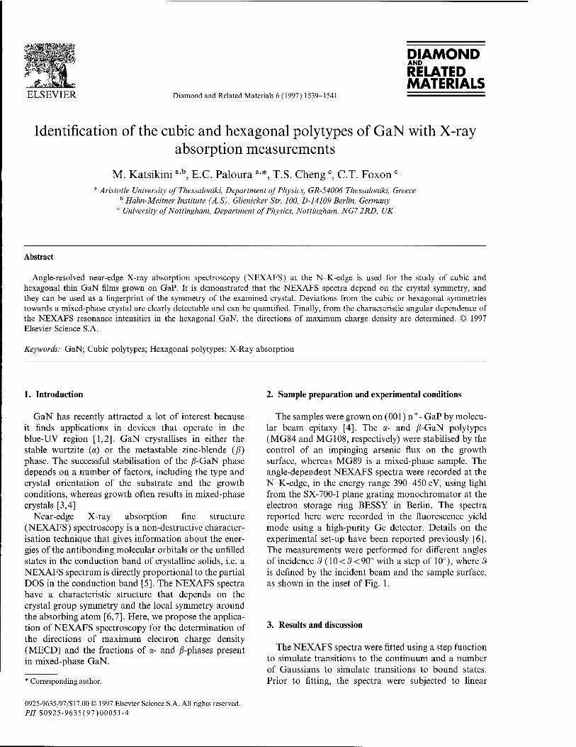
DIAMOND AND
RELATED MATERIALS
ELSEVIER Diamond and Related Materials 6 (1997) 1539-1541
Identification of the cubic and hexagonal polytypes of GaN with X-ray absorption measurements
M. Katsikinia,b, E.C. Palouraa'*, T.S. Chengc, C.T. Foxonc
a Aristotle University of Thessaloniki, Department of Physics, GR-54006 Thessaloniki, Greece
b Hahn-Meitner Institute (A.S), Glienicker Str. 100, D-14109 Berlin, Germany c University of Nottingham, Department of Physics, Nottingham, NG7 2RD, UK
Abstract
Angle-resolved near-edge X-ray absorption spectroscopy (NEXAFS) at the N-K-edge is used for the study of cubic and hexagonal thin GaN films grown on GaP. It is demonstrated that the NEXAFS spectra depend on the crystal symmetry, and they can be used as a fingerprint of the symmetry of the examined crystal. Deviations from the cubic or hexagonal symmetries towards a mixed-phase crystal are clearly detectable and can be quantified. Finally, from the characteristic angular dependence of the NEXAFS resonance intensities in the hexagonal GaN, the directions of maximum charge density are determined. © 1997 Elsevier Science S.A.
Keywords: GaN; Cubic polytypes; Hexagonal polytypes; X-Ray absorption
1. Introduction
GaN has recently attracted a lot of interest because it finds applications in devices that operate in the blue-UV region [1,2]. GaN crystallises in either the stable wurtzite (a) or the metastable zinc-blende (/?) phase. The successful stabilisation of the /?-GaN phase depends on a number of factors, including the type and crystal orientation of the substrate and the growth conditions, whereas growth often results in mixed-phase crystals [3,4]
Near-edge X-ray absorption fine structure (NEXAFS) spectroscopy is a non-destructive character- isation technique that gives information about the ener- gies of the antibonding molecular orbitals or the unfilled states in the conduction band of crystalline solids, i.e. a NEXAFS spectrum is directly proportional to the partial DOS in the conduction band [5]. The NEXAFS spectra have a characteristic structure that depends on the crystal group symmetry and the local symmetry around the absorbing atom [6,7]. Here, we propose the applica- tion of NEXAFS spectroscopy for the determination of the directions of maximum electron charge density (MECD) and the fractions of a- and ^-phases present in mixed-phase GaN.
* Corresponding author.
2. Sample preparation and experimental conditions
The samples were grown on (001)n + - GaP by molecu- lar beam epitaxy [4]. The a- and ß-GaN polytypes (MG84 and MG108, respectively) were stabilised by the control of an impinging arsenic flux on the growth surface, whereas MG89 is a mixed-phase sample. The angle-dependent NEXAFS spectra were recorded at the N-K-edge, in the energy range 390-450 eV, using light from the SX-700-I plane grating monochromator at the electron storage ring BESSY in Berlin. The spectra reported here were recorded in the fluorescence yield mode using a high-purity Ge detector. Details on the experimental set-up have been reported previously [6]. The measurements were performed for different angles of incidence 3 (10<5<90° with a step of 10°), where 9 is defined by the incident beam and the sample surface, as shown in the inset of Fig. 1.
3. Results and discussion
The NEXAFS spectra were fitted using a step function to simulate transitions to the continuum and a number of Gaussians to simulate transitions to bound states. Prior to fitting, the spectra were subjected to linear
0925-9635/97/S17.00 © 1997 Elsevier Science S.A. All rights reserved. PII S0925-9635(97)00051-4

1540 M. Katsikini et al. / Diamond and Related Materials 6 (1997) 1539-1541
410 420 Energy (eV)
430
Fig. 1. Fitting of an N-K-edge NEXAFS spectrum recorded from the a-GaN sample at 5 = 70°. 9 is measured with respect to the sample surface, as indicated in the inset.
background subtraction and normalisation to the atomic limit. The energy positions, AEb of the various reso- nances are measured relative to the absorption edge, which is defined as the inflection point of the step function. The fitting of a NEXAFS spectrum from the hexagonal sample MG84, recorded at 5 = 70°, is shown in Fig. 1. The error in the determination of the areas under the peaks can be found using the Thomas-Reihe-Kuhn sum rule [8], according to which, the total oscillator strength remains constant and does not depend on the angle of incidence. In the present case, the error is of the order of 2.5%.
For cubic symmetry and for the case of a Is initial state, the allowed transitions are lax-»-!^, where t2
belongs to a three-dimensional irreducible representa- tion (T2) of the group Td, and are observed with the same intensity at different angles of incidence. In con- trast to that, the NEXAFS spectra of a hexagonal sample (C6v) show angular dependence. The allowed dipole transitions that occur in a C6v material are la^a* and la^e*, which are strongest for grazing and normal incidence, respectively. In the lax->a* trans- ition, the final state results from mixing of s and pz
atomic orbitals, whereas in la^e*, the final state can result from px and py atomic orbitals [9].
From the fitting of the spectra of the cubic sample, it was found that the energy positions AEb the FWHM and the area under the resonances are, within the experimental error, independent of 3, as theoretically expected. Contrary to the behaviour of the cubic sample, the NEXAFS spectra of the hexagonal a-GaN sample have a strong angular dependence as shown in Fig. 2, and the areas under the peaks have a linear dependence on cos2.9. The reduced intensity of a NEXAFS resonance is defined as the area under the resonance normalised to that corresponding to the magic angle 3 = 54.7°. The
WO 410 420 430 440 450 Energy (eV)
Fig. 2. The angular dependence of the NEXAFS spectra shown for normal incidence (3 = 90°, top curve), grazing incidence ($ = 20°, bottom curve) and the angle of 3 = 50° (middle curve). The positions of the absorption edge and the atomic limit are shown in dashed lines.
magic angle is the characteristic angle for a sample with hexagonal symmetry for which the NEXAFS spectra are independent of the angle between the final state vector or plane molecular orbital and the normal to the sample surface.
From the angular dependence of the reduced inten- sities of the NEXAFS resonances, the directions of maximum electron charge density (MECD) with respect to the surface normal can be determined. For the laj-^et transition, the reduced intensity I of the trans- ition is given by:
7=1.6[l-0.5sin2y^(l-1.5sin2y)cos23], (1)
where y is the angle of the normal to the plane orbital to the surface normal. For the la^at, the reduced intensity /' is given by:
/'=1.33sin2a-r-(2.67-4sin2a)cos25, (2)
where a is the angle of the vector orbital with the sample surface. Using Eqs. (1) and (2), the directions of MECD can be determined with an error of about +5°. The transitions labelled G4 and G6 correspond to plane orbitals parallel to the surface (y = 0°) and vector orbitals normal to the surface (a = 0°), respectively. G3 corres- ponds to vector orbitals, which are at an angle of 53.4° with the c-axis. The transition Gx is independent of the angle of incidence and therefore corresponds to angle equal to 54.7°, which is the magic angle. Finally, the Gaussians G2 and G5 give angles with a mean average of about 37°.
Besides the information resulting from the intensity of the transitions, further information can be extracted about the crystal structure from the values of AEj. Our measurements show that for the pure cubic and hexago- nal samples, the energy positions of the resonances as

M. Katsikini et al. I Diamond and Related Materials 6 (1997) 1539-1541 1541
Table 1 Energy positions of the NEXAFS resonances for the pure cubic and hexagonal GaN films
Sample AEt (eV) AE2 (eV) AE3 (eV) AE4 (eV) AE5 (eV) AE6(eV)
ß-GaN 1.94 4.79 7.23 8.71 a-GaN 1.91 4.26 6.54 9.00
11.39 10.52 12.70
e
I2
e
%
cubic . hexagonal
.7,1 ■ experimental ^* ' 1 - 50%*cubic+50%*hexagonal
/ »i1
I J/**\.
\^/ ^^""*
J . 1 ■ ■ • -■-
00 410 420 Energy (eV)
430 440
Fig. 3. NEXAFS spectra from the mixed, the cubic and the hexagonal samples and the calculated spectrum assuming 50% cubic and 50% hexagonal fractions, respectively.
well as their FWHM do not change with the angle of incidence. Therefore, the angular resolved NEXAFS spectra can be used as a fingerprint of the structure of an unknown sample. The measured values of the zfE; are listed in Table 1. Angular dependence of the FWHM and zfE; of the Gaussians is an indication of coexistence of hexagonal and cubic phases. Given the constancy of the zlEj for the pure cubic and hexagonal structure, it is proposed that the NEXAFS spectra of a mixed phase sample can be approximated as a weighted average of the spectra from the pure cubic and hexagonal samples recorded at the same angle of incidence. Following this procedure, the NEXAFS spectra from the mixed phase sample MG89 can be reproduced by averaging the NEXAFS spectra from pure cubic and hexagonal samples weighted by 50% and 50%, respectively. The resulting spectrum is shown in Fig. 3 (continuous line) along with the recorded spectra from the mixed (thick dashed line), the cubic (dashed line) and hexagonal (dotted line) samples. As shown in Fig. 3, this simple model for the NEXAFS structure of a mixed crystal predicts quite accurately the experimental spectrum.
4. Conclusions
It is demonstrated that the N-K-edge NEXAFS spectra, which probe the nitrogen p partial density of
unfilled states, can be used as a fingerprint of the cubic or hexagonal symmetry in GaN thin films. Deviations from the a- or /J-GaN structures towards a mixed phase crystal are clearly detectable since they lead to angular dependent shifts of the NEXAFS resonances. The NEXAFS spectra from a mixed-phase crystal can be simulated using a weighted average of the spectra from the pure a- and jS-GaN samples, and thus the fractions of the coexisting a- and /^-phases can be determined. It should be pointed out that NEXAFS is a non-destructive technique and can be applied to the as-received samples. Therefore, the measurements are free of artefacts induced by damage during surface cleaning or sample preparation. Finally, from the 5-dependence of the resonance intensities in the spectra of a hexagonal sample, the directions of MECD are determined, and they are found to deviate from the directions of the bond angles. This result is in agreement with the calcula- tions of Miwa et al., according to which, the directions of MECD are within 30° on either side of the bond axis [10].
Acknowledgement
This work was realised with financial support from the EC-HCM (CHGE-CT93-0027) program.
References
[1] S. Strite, H. Morkoc, J. Vac. Sei. Technol. BIO (1992) 1237. [2] S. Nakamura, T. Mukai, M. Senoh, Appl. Phys. Lett. 64 (1994)
1687. [3] T. Lei, M. Fanciulli, R.J. Molnar, T.D. Moustakas, RJ. Graham,
J. Scanlon, Appl. Phys. Lett. 59 (1991) 944. [4] T.S. Cheng, L.C. Jenkins, S.E. Hooper, C.T. Foxon, J.W. Orton,
D.E. Lacklison, Appl. Phys. Lett. 66 (1995) 1509. [5] J.C. Fuggle, J.E. Inglesfield, Unoccupied Electrical States: Funda-
mentals for XANES, EELS, IPS and BLS, Springer, Berlin, 1992. [6] M. Katsikini, E.C. Paloura, T.D. Moustakas, Appl. Phys. Lett.
69(1996)4206. [7] J. Stöhr, NEXAFS Spectroscopy, Springer, Berlin, 1992. [8] J. Berkowitz, in: Photoabsorption, Photoionization and Photo-
electron Spectroscopy, Academic Press, New York, 1979, p. 56. [9] FA. Cotton, Chemical Applications of Group Theory, Wiley-
Interscience, New York, 1971. [10] K. Miwa, A. Fukumoto, Phys. Rev. B48 (1993) 7897.
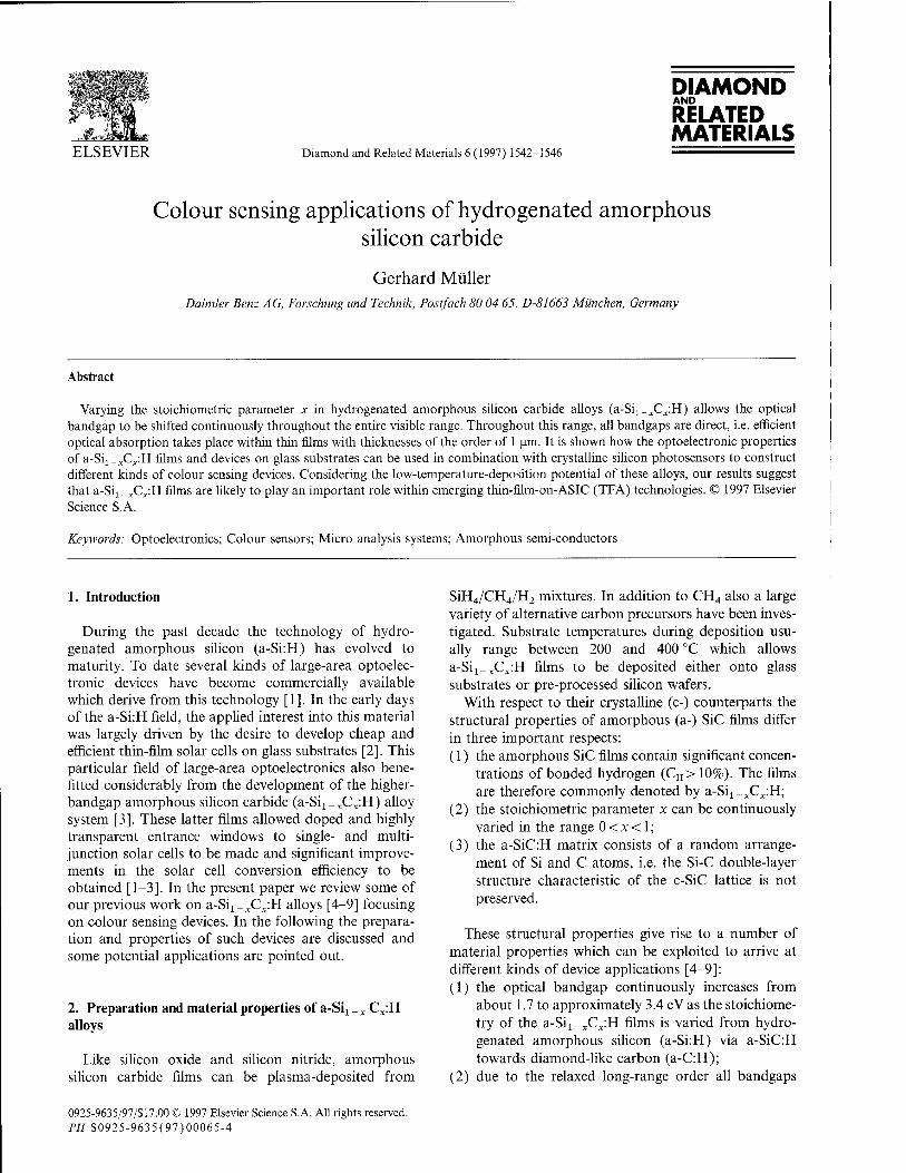
DIAMOND AND
RELATED MATERIALS
ELSEVIER Diamond and Related Materials 6 (1997) 1542-1546
Colour sensing applications of hydrogenated amorphous silicon carbide
Gerhard Müller Daimler Benz AG, Forschung und Technik, Postfach 80 04 65, D-81663 München, Germany
Abstract
Varying the stoichiometric parameter x in hydrogenated amorphous silicon carbide alloys (a-Si^^C^H) allows the optical bandgap to be shifted continuously throughout the entire visible range. Throughout this range, all bandgaps are direct, i.e. efficient optical absorption takes place within thin films with thicknesses of the order of 1 urn. It is shown how the optoelectronic properties of a-Sij.^C^H films and devices on glass substrates can be used in combination with crystalline silicon photosensors to construct different kinds of colour sensing devices. Considering the low-temperature-deposition potential of these alloys, our results suggest that a-Sij-^C^H films are likely to play an important role within emerging thin-film-on-ASIC (TFA) technologies. © 1997 Elsevier Science S.A.
Keywords: Optoelectronics; Colour sensors; Micro analysis systems; Amorphous semi-conductors
1. Introduction
During the past decade the technology of hydro- genated amorphous silicon (a-Si:H) has evolved to maturity. To date several kinds of large-area optoelec- tronic devices have become commercially available which derive from this technology [1]. In the early days of the a-Si:H field, the applied interest into this material was largely driven by the desire to develop cheap and efficient thin-film solar cells on glass substrates [2]. This particular field of large-area optoelectronics also bene- fltted considerably from the development of the higher- bandgap amorphous silicon carbide (a-Si^^C.,.:!!) alloy system [3]. These latter films allowed doped and highly transparent entrance windows to single- and multi- junction solar cells to be made and significant improve- ments in the solar cell conversion efficiency to be obtained [1-3]. In the present paper we review some of our previous work on a-Si^^C^H alloys [4-9] focusing on colour sensing devices. In the following the prepara- tion and properties of such devices are discussed and some potential applications are pointed out.
2. Preparation and material properties of a-Six ^x CX:H alloys
Like silicon oxide and silicon nitride, amorphous silicon carbide films can be plasma-deposited from
SiH4/CH4/H2 mixtures. In addition to CH4 also a large variety of alternative carbon precursors have been inves- tigated. Substrate temperatures during deposition usu- ally range between 200 and 400 °C which allows a-Sii-^C^H films to be deposited either onto glass substrates or pre-processed silicon wafers.
With respect to their crystalline (c-) counterparts the structural properties of amorphous (a-) SiC films differ in three important respects: (1) the amorphous SiC films contain significant concen-
trations of bonded hydrogen (CH> 10%). The films are therefore commonly denoted by a-Si^^C,.:!!;
(2) the stoichiometric parameter x can be continuously varied in the range 0<x< 1;
(3) the a-SiC:H matrix consists of a random arrange- ment of Si and C atoms, i.e. the Si-C double-layer structure characteristic of the c-SiC lattice is not preserved.
These structural properties give rise to a number of material properties which can be exploited to arrive at different kinds of device applications [4-9]: (1) the optical bandgap continuously increases from
about 1.7 to approximately 3.4 eV as the stoichiome- try of the a-Si!_xCx:H films is varied from hydro- genated amorphous silicon (a-Si:H) via a-SiC:H towards diamond-like carbon (a-C:H);
(2) due to the relaxed long-range order all bandgaps
0925-9635/97/$ 17.00 © 1997 Elsevier Science S.A. All rights reserved. PII S0925-9635(97)00065-4
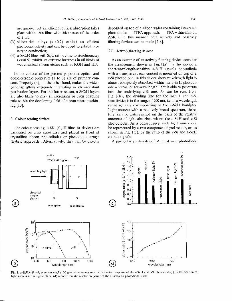
G. Müller / Diamond and Related Materials 6 (1997) 1542-1546 1543
are quasi-direct, i.e. efficient optical absorption takes place within thin films with thicknesses of the order of 1 (xm;
(3) silicon-rich alloys (x<0.2) exhibit an efficient photoconductivity and can be doped to exhibit p or n-type conduction;
(4) a-SiC:H films with Si/C ratios close to stoichiometry (x«0.5) exhibit an extreme inertness in all kinds of wet chemical silicon etches such as KOH and HF.
In the context of the present paper the optical and optoelectronic properties (1 to 3) are of primary con- cern. Property (4), on the other hand, makes the wider- bandgap alloys extremely interesting as etch-resistant passivation layers. For this latter reason, a-SiC:H layers are also likely to play an increasing or even enabling role within the developing field of silicon micromachin- ing[10].
3. Colour sensing devices
For colour sensing, a-Six-^C^H films or devices are deposited on glass substrates and placed in front of crystalline silicon photodiodes or photodiode arrays (hybrid approach). Alternatively, they can be directly
deposited on top of a silicon wafer containing integrated photodiodes (TFA-approach; TFA = thin-film-on ASIC). In this manner both actively and passively filtering devices can be made [7,8].
3.1. Actively filtering devices
As an example of an actively filtering device, consider the arrangement shown in Fig. 1(a). In this device a short-wavelength-sensitive a-Si:H (x = 0) photodiode with a transparent rear contact is mounted on top of a c-Si photodiode. In this device short-wavelength light is almost completely absorbed within the a-Si:H photodi- ode whereas longer-wavelength light is able to penetrate into the underlying c-Si one. As can be seen from Fig. 1(b), the dividing line for the a-Si:H and c-Si sensitivities is in the range of 700 nm, i.e. in a wavelength range roughly corresponding to the a-Si:H bandgap. Light sources with a relatively broad spectrum, there- fore, can be distinguished on the basis of the relative amounts of light absorbed within the a-Si:H and c-Si photodiodes. As a consequence, each light source can be represented by a two-component signal vector, or, as shown in Fig. 1(c), by the ratio of the c-Si and a-Si:H output signals.
A particularly interesting feature of such photodiode
©
a-Si:H
ITO/pin/ITO/glass c-Si
incoming light
electrical output signals
blue/green ©
2.0
1.8
1.6
1.4
1.2
1.0
0.8
0.6
0.4
0.2
0.0
<0 > =5 «> £ 2
> CO
Ü
o B o D) JC TZJ
SZ Ol ra a 0} -C
c <u
o c
■ ro -C t£i O)
o I 1 1 ro sz. 1
I 1 0) o 1 ■ 1 1 1 1 1 1 - 1 1 o 3 1 1 1 ro
■ ■ **- I I I . 1 . 1 m 1 1 1 1
©
10
10"
o 10"
10"
: \/^\,
: a-Si:H \ A
c-Si \
A ■ i . \
400 600 800 1000 1200 wavelength (nm) © 640 680 720
wavelength (nm)
Fig. 1. a-Si:H/c-Si colour sensor stacks: (a) geometric arrangement; (b) spectral response of the a-Si:H and c-Si photodiodes; (c) classification of light sources in the signal plane; (d) monochromatic resolution power of the a-Si:H/c-Si photodiode stack.

1544 G. Müller / Diamond and Related Materials 6 (1997) 1542-1546
stacks is that their monochromatic resolution is limited by the exponential tailing of the a-Si:H valence and conduction bands which is a general property of amor- phous semiconductor materials. As shown in Fig. 1(d) this tailing leads to a wavelength interval, about 100 nm wide, in which the ratio of the c-Si and a-Si:H output signals varies exponentially as the wavelength of a monochromatic light source is scanned from short to increasingly longer wavelengths. Quantitatively, we esti- mate the monochromatic resolution Al in this wave- length interval to be somewhere in the range between 0.1 to 1 nm. Experimentally, we find that our sensor can easily distinguish arterial from venous blood, for instance, or different brands of red wine, i.e. colour differences hardly visible or even invisible to the human eye [7].
Varying the thickness of the a-Si:H photodiodes, the wavelength interval of high monochromatic resolution can be shifted to some extent. Larger changes are possible by shifting the a-Si:H bandgap towards larger or smaller photon energies by means of alloying with carbon or germanium, respectively. In this context it has to be noted that the density of recombination centres in the amorphous semiconductor films is relatively low in the a-Si:H case whereas it increases sharply as the optical gap is shifted towards higher or lower photon energies [3]. Due to this effect highly performing thin- film photodiodes are limited to a bandgap range extend- ing from about 1.5 up to 1.9 eV. Sticking to the principle of active filtering, the thin-film photodiodes can be replaced by thin-film photoconductors which only rely on majority carrier transport. In this latter case, a somewhat larger bandgap range from about 1.2 up to 2.1 eV is accessible to the actively filtering mode.
3.2. Passively filtering devices
In the examples presented above the amorphous semi- conductor materials served the double purpose of actively generating an electrical output signal and of passively filtering the light entering the underlying c-Si photodiodes. Considerably more freedom of design is possible in case the amorphous semiconductor films are used as passive optical filters for c-Si photodiodes and photodiode arrays only. A possible arrangement for a passively filtering device is shown in Fig. 2. In this latter case the entire bandgap range accessible within the a-Si^x CX:H alloy system can be used to give a pair of c-Si photodiodes with different handicaps with respect to their short-wavelength photoresponse. With Eg vary- ing from 1.7 eV (x = 0) to 3.4 eV (x=l), the region of high monochromatic resolution can be scanned through the entire visible range. With devices of this latter kind, colour sensors with a monochromatic resolution in the blue and ultraviolet region of the visible spectrum have been realised [8].
hv
alloy 1 alloy 2
Si02
n n
p-Si
PH L
Fig. 2. Cross section through a passively filtering device using two a-Si!_xCx:H filters with different values of x on both pixel elements.
From the above it is clear that a colour sensitivity can be reached by replacing conventional photodiodes with a scalar grey-scale output by devices with a higher- dimensional vectorial output. The examples described above have shown that surprising results can already be obtained by setting up devices generating simple two- component outputs. A possible approach to obtaining higher-dimensional output signals is depositing laterally graded a-S^^C^H alloy films. The method of growing such films is illustrated in Fig. 3. As shown there, a narrow slit diaphragm is slowly moved across a glass or a semiconductor substrate during deposition by means of a stepping motor. During this motion the relative abundance of the silicon and carbon bearing precursor gases is varied so that a lateral grading of the optical bandgap is obtained.
A graded bandgap filter deposited in this way is shown in Fig. 4(a). In this case the substrate has been a piece of Corning 7059 glass. For colour discrimination purposes we have mounted such filters in front of a commercial CCD line sensor. Upon illumination with defocused light, different spatial intensity patterns are developed by the CCD line sensor with the form of the patterns being characteristic of the spectral content of the light sources. In order to give an idea of the spectral discrimination power of such devices we have illumi- nated our sensors with narrow-band quasi-monochro-

G. Müller / Diamond and Related Materials 6 (1997) 1542-1546 1545
gas composition
SiH , 4
CH 4
f
PECVD reactor y
\
slit w
\
f
V /
computer
dia- phragm
7 fZ:
/ stepper motor
substrate Fig. 3. Method of growing laterally graded bandgap filters.
matic light sources. Fig. 4(b) shows that short- wavelength light is only transmitted through the higher- bandgap parts of the filters. Longer-wavelength light, on the other hand, is seen to penetrate material of increasingly smaller bandgap. From this latter figure it is easily seen that wavelength differences of several nm are easily distinguishable.
More complex spectra result in spatial intensity patterns different from the ones shown in Fig. 4(b). Fig. 5(a) shows a pattern produced by superimposing two quasi-monochromatic light sources (Al = 25 nm) on the surface of the colour sensing device. The superposit- ion of the light sources is seen to result in some additional structure in the spatial intensity pattern. This additional structure is revealed more clearly from the differentiated pattern shown in Fig. 5(b). There, two lines clearly show up, corresponding to sources centred at 1 = 500 and 650 nm. Although such a differentiation technique can give only a rough idea about the optical input spectra [7], this method does not give precise results due to the neglect of interference effects within the graded-bandgap filters and/or effects of non-uniform illumination. Different light sources, however, can be distinguished with considerable resolution by applying pattern recognition techniques to the spatial intensity patterns produced at the output of the CCD line sensor. Such techniques are commonly used to analyse output data arising from gas sensor arrays.
3.3. Colour sensors versus spectrometers
The above results have shown that interesting opto- electronic applications are possible using a-Si^^C^H
(a)
B o
(b) Pixel
Fig. 4. (a) Graded-bandgap filter produced by varying the stoichiomet- ric parameter x along one of the substrate dimensions. Along this dimension the optical bandgap increases continuously from 1.7 to 3.4 eV; (b) spatial intensity patterns obtained by illuminating the graded-bandgap filter with defocussed monochromatic light. The monochromatic wavelength was increased from 450 to 650 nm in 25 nm steps.
films. Such sensors cannot replace conventional spec- trometers with diffraction gratings which directly yield physically interpretable information about the spectral content of light sources. The advantage of our devices, however, is that very small and rugged devices can be built. As a consequence, they are much more easily integrated into complex measurement systems than con- ventional spectrometers whose size is limited by the lengths of internal light paths which can often amount to several centimetres.
A possible future application of such sensors is in the field of chemical analysis. As is well known, many chemical analysis techniques rely on colour change reactions in which suitable indicator molecules are added to the liquid samples to be analysed. Currently, many

1546 G. Müller I Diamond and Related Materials 6 (1997) 1542-1546
m I o
m
in z UJ
250
200-
150-
100-
1000 2000 3000
NUMBER OF PHOTOELEMENT ( 3456-ELEMENT CCO )
Fig. 5. Response of a graded-bandgap colour sensor to two quasi-monochromatic light sources: (a) spatial intensity pattern produced by the graded-bandgap filter; (b) differentiated spatial intensity pattern. The filter grading is indicated by the shadowing in the top.
micromachining approaches are being taken towards complete microanalysis systems [11]. The ruggedness of our colour sensing devices makes them ideal subsystems within such miniaturised and automated analysis sys- tems. Whether a hybrid approach or a fully monolithic TFA approach is to be taken depends on purely econom- ical boundary conditions such as the market size for such medical and environmental analysis systems and the price a customer is willing to pay for an individual device.
Acknowledgement
The author is indebted to continuous interest and support by Drs. B. Thomas, S. Paasche and M. Königer.
References
[1] For a review see: J. Kanicki (Ed.), Amorphous and Microcrystal- line Semiconductor Devices, Artech House, Boston, 1991.
[2] A. Catalano, Solar cells made of amorphous and microcrystalline semiconductors, Ref. [2], pp. 9-76.
[3] For a review see: W. Luft, Y.S. Tsuo, Hydrogenated Amorphous Silicon Alloy Deposition Processes, Marcel Dekker, Inc., New York, Basel, Hong Kong, 1993.
[4] G. Müller, G. Krötz, SiC as a new sensor material, Proc. 7th Int. Conf. on Solid State Sensors and Actuators, Yokohama, Japan, May 1993.
[5] G. Müller, G. Krötz, E. Niemann, SiC for sensors and high- temperature electronics, Sensors and Actuators 43 (1994) 259-268.
[6] G. Krötz, G. Müller, G. Derst, Ch. Wilbertz, S. Kalbitzer, Thin- film SiC as an optical and optoelectronic material, Diamond Relat. Mater. 3 (1994) 917-921.
[7] J. Wind, G. Krötz, R. Schmiedgen, W. Legner, J. Binder, V. Hechtenberg, G. Müller, Colour detection using amorphous semi- conductor thin-films, Sensors and Actuators A 36 (1993) 187-192.
[8] Final report BRITE/Euram Project, Diamond and Silicon Car- bide Sensors (DISCS), 1993.
[9] G. Müller, P.P. Deimel, W. Hellmich, Chr. Wagner, Proc. EMRS Spring Conf. 1996, Straßburg; Symposium B.
[10] W. Lang, Silicon microstructuring technology, Materials Science and Engineering, R17, No 1, 1 September 1996.
[11] M. Lambrechts, W. Sansen, Biosensors: Microelectrochemical Devices, Institute of Physics Publishing, Bristol, Philadelphia, New York, 1992.

:*fi"!?'-*! DIAMOND AND
RELATED MATERIALS
ELSEVIER Diamond and Related Materials 6 (1997) 1547-1549
Surface and bulk effects in ex-situ hydrogenated a-SiC thin films
J. Kalomirosa, E.C. Paloura a'*, C. Janowitz b, B. Theysc, A. Anagnostopoulosa
a Aristotle University of Thessaloniki, Department of Physics, GR-54006 Thessaloniki, Greece b Humboldt University, Institute of Physics, Invalidenstrasse 110, D-10115 Berlin, Germany
c CNRS, Laboratoire de Physique des Solides de Bellevue, 1 Place A. Briand, 92195 Meudon, Cedex, France
Abstract
The effect of ex-situ hydrogenation on the bulk and surface properties of amorphous SiC (a-SiC) thin films has been investigated using a number of bulk- and surface-sensitive characterisation techniques. The diffusion coefficient of deuterium in a-SiC is found to be equal to 3-4 x 10"15 cm2 s"1. It is shown that atomic hydrogen causes drastic changes in the dielectric function, due to preferential Si etching from the film surface, and the formation of a carbon surface layer rich in sp2 bonds. Furthermore, the atomic hydrogen diffuses in the bulk and causes an increase of the optical band gap and a concurrent decrease in conductivity, due to partial passivation of dangling bonds. © 1997 Elsevier Science S.A.
Keywords: A-SiC; Etching; Hydrogenation; Ellipsometry
1. Introduction Amorphous Si-C alloys (cx-SiC) have been the subject
of intensive study due to their potential applications in micro- and optoelectronic devices [1]. The problem of in-situ (during growth) hydrogen incorporation and the resulting changes in bulk and surface properties has been addressed in the past [2]. However, the effect of ex-situ hydrogenation (low-temperature annealing in a hydrogen rf glow discharge) on the surface and bulk properties of oc-SiC has not yet been studied in detail. Ex-situ hydrogenation simulates processing environ- ments such as plasma-enhanced chemical vapour depos- ition and reactive ion etching, where atomic hydrogen coexists with other reactive species. Furthermore, atomic hydrogen is highly reactive and thus finds applications in the surface cleaning and plasma etching of several material systems [3] as well as in the passivation of point and extended defects [4].
In this paper we present a study of the concurrent bulk and surface modifications occurring in thin a-SiC films upon exposure to atomic hydrogen. To date the effect of ex-situ hydrogenation on cc-SiC has been limited to the study of surface-property modification [5-7].
2. Sample preparation and experimental details The amorphous SiC films were deposited at room
temperature by rf sputtering on Corning glass 7059
substrates from a SiC target of constant composition [2]. The film thickness of the as-grown films was in the range 0.8-1 um. The films were annealed for 2h in a hydrogen or deuterium glow discharge at 13.56 MHz in a capacitively coupled quartz reactor. During the process the sample temperature was 230 °C, the hydrogen pres- sure ranged from 100 to 150 mTorr, while the rf power took values in the range 100-150 W. In the following, the ratio of the rf power over the hydrogen pressure (W/P) is used to describe the plasma conditions (the reference as-grown sample is labelled S0). The process was applied repeatedly, and yielded reproducible results which are unique to the plasma hydrogenation process and are not observed in control samples which were annealed at 230 °C either in vacuum or in molecular H2.
The dark conductivity measurements were conducted in the four-probe configuration geometry in the temper- ature range 130-450 K using low-resistance ohmic con- tacts fabricated using indium evaporation. The optical transmission and the visible ultraviolet (VUV) ellip- sometry spectra were recorded in the energy ranges 1.5-3.0 eV and 2.5-24 eV, respectively. The ellipsometry measurements were conducted using the linearly pola- rised radiation at the 2m-Seya Namioka beamline at the electron storage ring BESSY in Berlin [9]. Finally, the deuterium profiles were obtained using a Cameca IMS 4f SIMS (secondary ion mass spectroscopy) analyser using a cesium primary beam.
* Corresponding author. E-mail: [email protected]

1548 /. Kalomiros et al. / Diamond and Related Materials 6 (1997) 1547-1549
3. Results and discussion
3.1. Bulk properties: absorption, conductivity and SIMS profiling
The bulk-diffused atomic hydrogen passivates dan- gling bonds, leading to an increase of the optical band gap and a reduction in the DC conductivity. The diffu- sion of atomic hydrogen in the bulk was verified by SIMS profiling of deuterated samples, which shows that deuterium (and consequently hydrogen) diffuse in the bulk of the film to a depth which depends on the hydrogenation conditions and is of the order of a few hundred nm. In a sample deuterated for 2 h at 150 mTorr and with 150 W of coupled rf power, the deuterium concentration reaches the SIMS detection limit at a depth of 250 nm from the surface. The deuterium profile is correctly fitted with an erfc function, with a diffusion coefficient of 3-4 x 10 ~15 cm2 s_1.
The variation of the absorption coefficient a versus the incident photon energy E for the hydrogenated (Si-S^ and the reference (S0) samples are shown in Fig. 1. The dependence of the optical band gap Eg on hydrogenation conditions was determined using the Taue approximation, i.e. in a plot of (ais)1/2 versus photon energy, and the linear part is extrapolated to the a = 0 value. The values of the Eg are listed in Table 1 along with the corresponding W/P ratios. The Eg of the material is found to increase with hydrogen incorpora-
E o o
2.3 2.7
Energy (eV)
Fig. 1. Absorption coefficient a versus the photon energy E for the
reference and a series of hydrogenated films.
Table 1
Ec as a function of the plasma hydrogenation conditions
Sample
So
Si s2 s3 s4
W/P (W/mbar) £g(£
1.28 0.67 1.39 0.33 1.47 0.5 1.52 1.0 1.57
tion, the effect being stronger for higher values of W/P. It should be noted that the effect is clearly seen in films hydrogenated either in the embedded (between the rf and ground electrodes) or downstream configuration. Among the films discussed here, Sj was hydrogenated in a downstream configuration where the effect of sur- face bombardment and UV enhancement is reduced. The measured increase of E% is attributed to saturation of dangling bonds and elimination of states at the band edges [8].
The dark DC conductivity curves of a typical hydro- genated (a-SiC:H) and the reference (cc-SiC) samples are shown in Fig. 2. The overall decrease in the values of conductivity after hydrogenation is attributed to the partial passivation of defect states in the gap, resulting in a decrease of the DOS at the Fermi level. The activation energy for conduction for both the as-grown and hydrogenated samples, calculated from the (j-103/Tcurves, is found equal to about 0.2 and 0.075 eV in the high- and low-temperature ranges, respectively. This result indicates that conduction is dominated by a hopping transport process, in agreement with previously reported results [9,10].
3.2. Surface properties: VUV ellipsometry
To study loss features related to plasmon excitation we measured the dielectric function in the photon energy range 2.5-24.0 eV by means of VUV spectroscopic ellipsometry. The data were analysed with an isotropic two-phase model and assuming an ideal interface between the isotropic sample and vacuum. The loss function as calculated from the dielectric function is shown in Fig. 3. The loss function is not shown in the energy range 10 eV < hv < 15 eV due to a possible contri-
VJ. 1 i i i i i
V ' 0.01 - \ E
• • • •
E V *. a - SiC o 0.001 • b ■ • • •
n r\r>.r\-\
a -SiC:H • • • • • • •
i i i* . i i
5 9
103/T (K"1)
13
Fig. 2. Dark DC conductivity curves versus 103/J for the reference and a hydrogenated sample.

J. Kalomiros et al. I Diamond and Related Materials 6 (1997) 1547-1549 1549
2.8
2.2
1.6
1.0
0.4
IL 1.6 £
1.0
0.4
a-SiC
_i I I I i i I i I I I I i i I i i i L
a-SiC:H
J i i i i i i i i J i i i i i i i i i i_
a-SiC:H
j I I I i I i i i I I i i I i i i L
3 7 11 15 19 23
Energy (eV)
Fig. 3. Loss function (Im (— 1/e)) calculated from the dielectric func- tion spectra.
4. Conclusions
From the results presented above it is evident that ex-situ hydrogenation is a processing step which can drastically change both the bulk and the surface electronic properties of a-SiC films. The bulk changes amount to passivation of dangling bonds and widening of the optical gap, an effect which is also observed in in-situ hydrogenated cx-SiC films. The diffusion coeffi- cient of 2H was determined from the SIMS profiles of deuterated samples, and was found to be 3-4 x 10"15 cm2 s"1. To the best of our knowledge, this is the first time that the diffusion coefficient of 2H in a-SiC has been reported as measured from controlled diffusion experiments. However, the concurrent changes of the surface properties is a phenomenon which has not been observed in rf-sputtered in-situ hydrogenated films, and is characteristic of the ex-situ process. Atomic hydrogen induces preferential Si etching which promotes the formation of a surface carbon layer which is rich in sp2 bonding, which has to be solely attributed to the properties of atomic hydrogen. The above results can contribute to a better understanding of the mechanisms for residue formation, which occurs during dry etching of SiC.
Acknowledgement
We wish to thank Ms. M. Miloche for the SIMS measurements. This work was realised with financial support from the GSRT (PENED 1432).
bution from second-order radiation. Furthermore, meas- urements at E> 10 eV are impeded by the surface roughness induced by the hydrogenation process [5]. As shown in Fig. 3, the as-grown a-SiC films do no have peaks below 19 eV while the hydrogenated samples have strong features around 6.5 eV. The plasmon in the energy range 6-7 eV is characteristic of C compounds with some degree of sp2 bonding [11]. Among the elements which could be involved in the formation of the surface layer (Si, C, H and to a minor degree O), only carbon can produce loss features in the 6-7 eV range. Therefore, we ascribe the 7 eV loss peak in our spectra to n bonds of carbon atoms. Based on the ellipsometry results we can conclude that the surface of the ex-situ hydrogenated films consists of carbon atoms with some fraction in sp2 configuration, possibly also bonded to hydrogen and, to a minor degree, oxygen atoms. This view is also corroborated by surface investi- gation with X-ray diffraction and X-ray photoelectron spectroscopy [7,8].
References
[1] T. Matsuoka, Y. Kuwano, IEEE Trans. Electron Dev. 37 (1990) 397.
[2] J.A. Kalomiros, A. Papadopoulos, S. Logothetidis, L. Magafas, N. Georgoulas, A. Thanailakis, Phys. Rev. B 49 (1994) 8191.
[3] W. Tsai, M. Delfino, M.E. Day, T. Sheng, B.C. Chung, S. Sali- mian, J. Vac. Sei. Technol. A 11 (1993) 2525.
[4] S.J. Pearton (Ed.), Hydrogen in Compound Semiconductors, Trans Tech, Zürich, 1994, and references therein.
[5] J.A. Kalomiros, E.C. Paloura, A. Ginoudi, S. Kennou, S. Ladas, Ch. Lioutas, N. Vouroutzis, G. Voutsas, D. Girginoudi, N. Geor- goulas, A. Thanailakis, Solid State Commun. 96 (1995) 735.
[6] S. Kennou, S. Ladas, E.C. Paloura, J.A. Kalomiros, Appl. Surf. Sei. 90(1995)283.
[7] C. Janowitz, J. Kalomiros, A. Ginoudi, E.C. Paloura, R.L. John- son, Solid State Commun. 99 (1996) 29.
[8] E.A. Fagen, in: J. Stuke (Ed.), Proceedings of the International Conference on Amorphous and Liquid Semiconductors, Taylor and Francis, London, 1973, p. 601.
[9] R. Dutta, P.K. Banerjee, S.S. Mitra, Solid State Commun. 42 (1982)219.
[10] J. Bullot, M.P. Schmidt, Phys. Status Solidi b 143 (1987) 345. [11] P. Kovarik, E.B.D. Bourdon, R.H. Prince, Phys. Rev. B 48
(1993) 12123.

ELSEVIER Diamond and Related Materials 6 (1997) 1550-1554
DIAMOND AND
RELATED MATERIALS
Optical study of boron nitride thin films prepared by plasma- enhanced chemical vapor deposition
M.C. Polo M, M. Ben el Mekkia, J.L. Andüjar b, N. Mestresc, J. Pascuala
* Departament de Fisica, Universität Autönoma de Barcelona, E-08193 Bellaterra, Spain ' Departament de Fisica Aplicada i Electrdnica, Universität de Barcelona, Av. Diagonal 647, E-08028 Barcelona, Spain
c Institut de Ciencia de Materials de Barcelona, E-08193 Bellaterra, Spain
Abstract
We investigate the effects of finite off-normal incidence on the polarized infrared reflectivity spectra of hexagonal boron nitride films deposited on Si substrates by radio frequency plasma enhanced chemical vapor deposition, using B2H6 (1% in H2) and NH3 gases. The experimental observation of a sharp structure associated to the coupling of the incident light with the LO component of the twofold stretching mode, and the absence of similar coupling effects with the LO component of the bending mode, indicates that the c-axis is parallel to the film surface. We also show that the infrared spectra are not modified when one rotates the sample perpendicularly to the growth direction. Therefore, we conclude that the principal axis of the polycrystalline boron nitride films is randomly oriented within the plane parallel to the film surface. Finally, we show that these optical results are in full agreement with high resolution transmission electron microscopy studies. © 1997 Elsevier Science S.A.
Keywords: BN films; Polarized IR reflection spectroscopy; R.f. Plasma CVD; TEM
1. Introduction
Recently, an important research activity has been focused on the preparation of thin films of boron nitride (BN) owing to the outstanding properties of this III-V compound such as high hardness, optical transparency, chemical inertness, high thermal conductivity, high electrical resistivity and low dielectric losses. Boron nitride shows several structures [1]: cubic, hexagonal (h-BN), turbostratic - which is a disordered modifica- tion of h-BN, and amorphous. In particular, h-BN films have been successfully applied as optical and mechanical protective coatings and as dielectric layers in microelec- tronics devices [2]. However, a better knowledge of the properties of the BN films is necessary to further devel- opment of their applications.
Transmission electron microscopy (TEM) has been widely used to study the microstructure of the BN films [3-5]. The major disadvantage of this technique is that it requires a laborious sample preparation which becomes more difficult in the case of hard films. Fourier- transform infrared (FT-IR) spectroscopy is, on the other
1 Permanent address: Departament de Fisica Aplicada i Electrönica, Universität de Barcelona, Av. Diagonal 647, E-08028 Barcelona, Spain.
hand, a non-destructive technique that has been proved as a powerful characterization tool to identify the several phases of BN. Most studies deal with absorption meas- urements in transmission mode at normal incidence [6,7] where only the TO vibrational modes can be excited. In contrast, very few studies report reflection measurements [8] and, to our knowledge, only two papers performed polarized infrared reflection (PIRR) spectroscopy [9,10]. Besides the TO modes, the LO modes can be observed in the infrared reflection spectra of thin films, which gives more information about the film properties. In this work we present a PIRR study to determine the structure of h-BN thin films obtained by radio frequency plasma-enhanced chemical vapor deposition (rf-PECVD). As the optical properties of h-BN are anisotropic, different vibration modes can be excited depending on both, the orientation of the sp2-bonded basal planes with respect to the surface substrate and the polarization of the light. We have simulated the reflectance spectra for each possible con- figuration using the classical oscillator model and the Fresnel equations, and, as an application of this theoreti- cal model, we have determined the c-axis orientation of h-BN films. Finally, we have used high resolution cross- sectional TEM studies of the films to confirm the PIRR results.
0925-9635/97/S17.00 © 1997 Published by Elsevier Science S.A. All rights reserved. PII S0925-9635(97)00064-2

M.C. Polo et al. I Diamond and Related Materials 6 (1997) 1550-1554 1551
2. Crystal structure and IR activity
The hexagonal phase of BN belongs to the space group Dgh. At the center of the Brillouin zone, of the 12 normal modes of vibration 3 are infrared active, a non-degenerated mode (A2u) and a twofold degenerated mode (Elu). More specifically, the A2u mode is an out- of-plane bending vibration excited by polarized light parallel to the principal axis. The corresponding <aT0
and coLO frequencies are 783 and 828 cm"1 respectively, measured in bulk BN. The Elu mode corresponds to an in-plane stretching vibration and can be excited with polarized light perpendicular to the threefold axis. The corresponding coTO and coLO frequencies are 1367 and 1610 cm-1 respectively, again measured in the bulk [11].
For very thin layers, with thicknesses below the micro- metric scale, the reflectivity spectra show a sharp feature at the TO frequency of the corresponding IR active mode [12]. For the standard analysis of the infrared reflectivity one always assumes normal incidence condi- tions. However, most experimental apparatus support finite values of the angle of incidence. In most cases this is sufficient to allow the observation of fine structures in the IRR spectra associated to the longitudinal polar modes. These features can be greatly enhanced when performing experiments under wide incident angle condi- tions [9,13].
In the case of h-BN with two IR active modes, one polarized parallel and the other perpendicular to the principal axis, off-normal incidence PIRR experiments can be used to determine the orientation of the grown films. Fig. 1 shows the reflectivity spectra one expects for the incident electric field polarized perpendicular (s) or parallel (p) to the plane of incidence. The three configurations correspond to cases where the principal axis: (i) is parallel to the film surface and perpendicular to the plane of incidence (Fig. 1(a)); (ii) is parallel to both, the film surface and the plane of incidence (Fig. 1 (b)); and (iii) is perpendicular to the film surface (Fig. 1(c)). In the three cases, the interface reflection matrices are always diagonal and the reflectivity is easily calculated from the three-phases (ambient-film-sub- strate) system [14]. We use the standard Lorenz approach to give the complex dielectric dispersion of en and e± in terms of oscillators with parameters obtained from optimum fits to IRR spectra of bulk BN [11]. The angle of incidence considered here is 30°. Notice that the LO component of Elu is only allowed when the principal axis is lying in the film (Figs. 1(a) and (b)). On the contrary, the LO mode of A2u is only allowed when the c-axis is perpendicular to the sample surface. Cases (i) and (ii) can be distinguished from each other if one observes that both TO modes, Elu
and A2u, cannot be simultaneously detected for a given polarization.
LTJ 50 _] LL
8!
800 1200 1600 WAVENUMBER(cm"1)
2000
Fig. 1. Calculated polarized IR reflectivity spectra of a 200 nm h-BN film and for an angle of incidence of 30° when: (a) the c-axis is perpen- dicular to the plane of incidence and parallel to the film surface; (b) the c-axis is parallel to both, the plane of incidence and the film surface; and (c) the c-axis is parallel to the plane of incidence and perpendicular to the film surface.
3. Experimental procedure
The BN films were grown on silicon (100) in a RF (13.56 MHz) capacitively coupled by glow discharge decomposition of B2H6 (1% in H2) and NH3 gases. In the discharges, the gas flow rate of NH3 was 5 seem and the flow rate of the B2H<;-H2 gas mixture was varied from 50 to 100 seem. Other deposition conditions were: total gas pressure, 30 Pa; substrate temperature, 300 °C; and RF power density, 0.5 W cm""2. Different film thick- nesses were obtained in the range 100-600 nm by chang- ing the deposition time. The atomic ratio was close to the stoichiometric value (B:N = 1:1) as calculated by X-ray photoelectron spectroscopy (XPS). The films were highly transparent in the visible-near UV region (250-800 nm). Atomic force microscopy revealed a sur- face roughness of the films below 2 nm, calculated as the standard deviation of all heights in a selected area of 10 umx 10 urn.
Infrared transmission and PIRR spectra were obtained under vacuum with a DA3 Bomem FT-IR
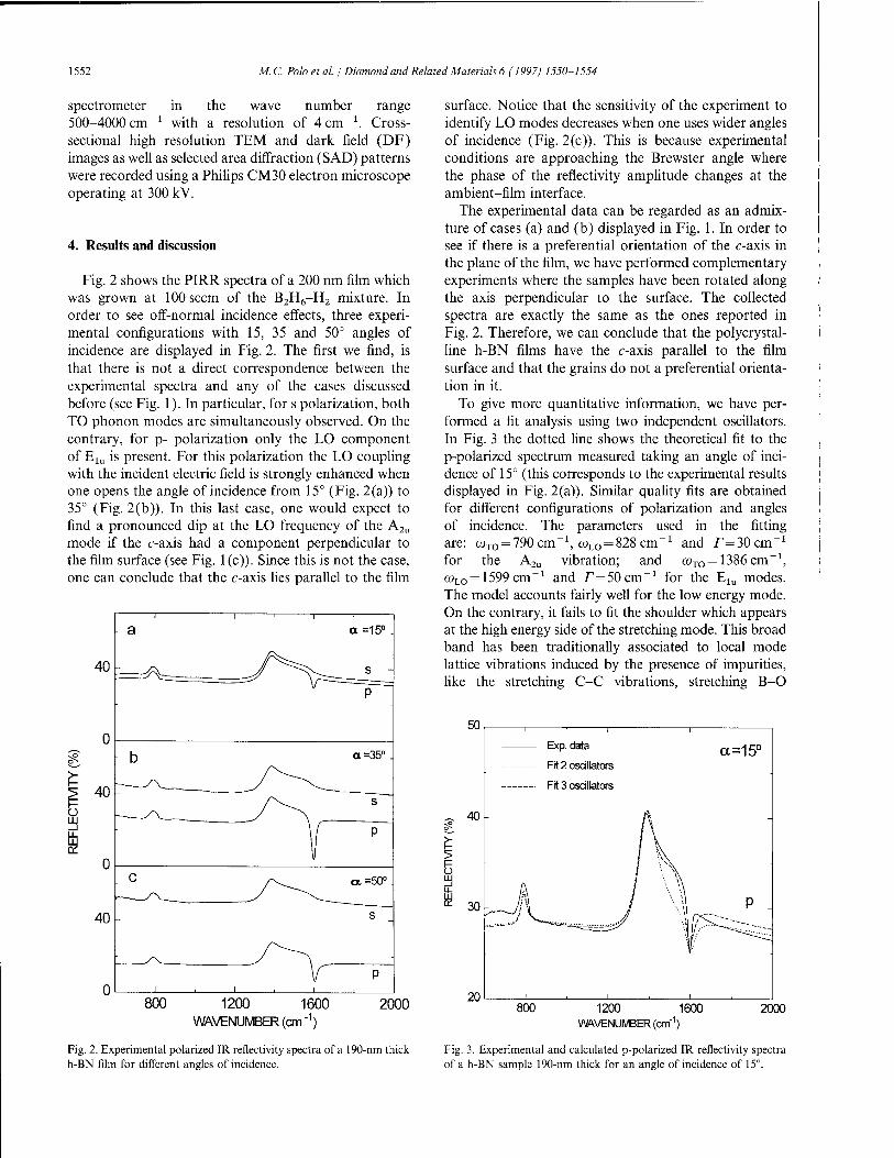
1552 M. C. Polo et al. / Diamond and Related Materials 6 (1997) 1550-1554
spectrometer in the wave number range 500-4000 cm"1 with a resolution of 4 cm-1. Cross- sectional high resolution TEM and dark field (DF) images as well as selected area diffraction (SAD) patterns were recorded using a Philips CM30 electron microscope operating at 300 kV.
4. Results and discussion
Fig. 2 shows the PIRR spectra of a 200 nm film which was grown at 100 seem of the B2H6-H2 mixture. In order to see off-normal incidence effects, three experi- mental configurations with 15, 35 and 50° angles of incidence are displayed in Fig. 2. The first we find, is that there is not a direct correspondence between the experimental spectra and any of the cases discussed before (see Fig. 1). In particular, for s polarization, both TO phonon modes are simultaneously observed. On the contrary, for p- polarization only the LO component of Elu is present. For this polarization the LO coupling with the incident electric field is strongly enhanced when one opens the angle of incidence from 15° (Fig. 2(a)) to 35° (Fig. 2(b)). In this last case, one would expect to find a pronounced dip at the LO frequency of the A2u
mode if the c-axis had a component perpendicular to the film surface (see Fig. 1(c)). Since this is not the case, one can conclude that the c-axis lies parallel to the film
40 -
^ 40
a £
40 ~
1 ' 1
a 1 1 '
a =15° .
-<y ^—s ~ p
■
b a =35°.
/^\ s
—-^——_ V p" c /\^_^ <x =50° .
s -
V P 1,1,1,
800 1200 1600 2000 WWENUMBER(cm"1)
surface. Notice that the sensitivity of the experiment to identify LO modes decreases when one uses wider angles of incidence (Fig. 2(c)). This is because experimental conditions are approaching the Brewster angle where the phase of the reflectivity amplitude changes at the ambient-film interface.
The experimental data can be regarded as an admix- ture of cases (a) and (b) displayed in Fig. 1. In order to see if there is a preferential orientation of the c-axis in the plane of the film, we have performed complementary experiments where the samples have been rotated along the axis perpendicular to the surface. The collected spectra are exactly the same as the ones reported in Fig. 2. Therefore, we can conclude that the poly crystal- line h-BN films have the c-axis parallel to the film surface and that the grains do not a preferential orienta- tion in it.
To give more quantitative information, we have per- formed a fit analysis using two independent oscillators. In Fig. 3 the dotted line shows the theoretical fit to the p-polarized spectrum measured taking an angle of inci- dence of 15° (this corresponds to the experimental results displayed in Fig. 2(a)). Similar quality fits are obtained for different configurations of polarization and angles of incidence. The parameters used in the fitting are: coTO = 790cm_1, caLO = 828 cm-1 and /,= 30cm~1
for the A2u vibration; and coTO= 1386 cm-1, <x>LO = 1599 cm-1 and r=50cm_1 for the Elu modes. The model accounts fairly well for the low energy mode. On the contrary, it fails to fit the shoulder which appears at the high energy side of the stretching mode. This broad band has been traditionally associated to local mode lattice vibrations induced by the presence of impurities, like the stretching C-C vibrations, stretching B-O
50
u. 8
20
Exp. data
Fit 2 oscillators
Fit 3 oscillators
a =15°
800 1200 1600 VWENUMBER(crrf1)
2000
Fig. 2. Experimental polarized IR reflectivity spectra of a 190-nm thick h-BN film for different angles of incidence.
Fig. 3. Experimental and calculated p-polarized IR reflectivity spectra of a h-BN sample 190-nm thick for an angle of incidence of 15°.

M. C. Polo et al. j Diamond and Related Materials 6 (1997) 1550-1554 1553
vibrations, and also bending N-H2 vibrations [15]. Nevertheless, we believe that all these possibilities have to be ruled out for our samples. XPS analysis shows that the contamination with carbon is negligible and only affects the uppermost atomic layers near the surface. The same argument is valid for oxygen. Besides, the Is peak of B has a maximum at 190.6 eV, in agreement with B-N bond surrounding, and the lineshape of the peak does not show any asymmetry near 193.0 eV, the energy associated to the presence of B-0 bonds. Finally, from IRR and transmission measurements in our samples, a band is found at 3430 cm"1 which correspond to the N-H stretching vibration. Since the band is very weak, one would expect a much weaker IR activity for the corresponding N-H2 bending vibration at 1540 cm"1. Thus, it would not justify the intense shoulder found in this energy region. Gieck et al. [ 11 ] have suggested that the broad shoulder is probably due to the contribution of two-phonons processes. We simulate all two-phonon contributions with an oscillator of frequencies cu-r T510cm and w Lcr 1640 cm" and a broad damping r= 150 cm-1. The addition of this average mode to the fitting model gives a calculated spectrum (dashed line in Fig. 3) in good agreement with the experimental data in the whole energy range.
The results of these optical studies are ascertained by TEM measurements. Fig. 4 shows a cross-sectional high resolution TEM image and SAD pattern of the investi- gated BN film. Interestingly, a textured microstructure is observed throughout the film, showing h-BN lattice fringes aligned nearly perpendicular to the substrate with an interplanar distance of about 0.35 nm. The SAD pattern shows two bright arcs, corresponding to h-BN(002) reflection along with continuous rings ascribed to (100) and (110) h-BN reflections. This orientation is corroborated in DF images [16] obtained by tilting the incident beam so that the beams diffracted towards the arcs passed through the objective aperture. In such conditions, bright areas denote h-BN crystallites contributing to (002) reflection and having their c-axis parallel to the substrate surface. However, such a con- trast is not observed in the DF image made using the dark part of the (002) h-BN ring.
5. Conclusions
We have shown that a careful analysis of the stretching and bending vibrational modes observed in the PIRR spectra of h-BN thin films can be used to determine the orientation of the principal axis in a non-destructive and very easy way. We find that poly crystalline h-BN thin films deposited on (001) Si substrates by RF plasma enhanced CVD, have the c-axis contained in the plane parallel to the film surface and randomly oriented. The optical studies coincide with high resolution TEM
np 5 nml
Fig. 4. Cross-sectional high resolution TEM image and selected area difraction pattern of a 190-nm thick BN film showing a h-BN ori- ented structure.
results. Therefore, PIRR spectroscopy appears as a very powerful tool to investigate structural properties of anisotropic thin films.
Acknowledgement
This work was partially supported by the Comisiön Interministerial de Ciencia y Tecnologia of the Spanish Government under contract MAT93-0298. Technical assistance of the Serveis Cientifico-Tecnics of UB is gratefully acknowledged. One of us (M.B.M.) acknowl- edges financial support from the Agencia Espanola de Cooperaciön Internacional.
References
[1] J.J. Pouch, S.A. Alterovitz (Eds.), Synthesis and Properties of Boron Nitride, Trans Tech, Zürich, 1990.

1554 M.C. Polo et al. I Diamond and Related Materials 6 (1997) 1550-1554
[2] D.R. Cote, S.V. Nguyen, W.J. Cote, S.L. Pennington, A.K. Stamper, D.V. Podlesnik, IBM J. Res. Dev. 39 (1995) 437.
[3] D.J. Kester, K.S. Ailey, R.F. Davis, K.L. More, J. Mater. Res. 8(1993) 1213.
[4] D.L. Medlin, T.A. Friedmami, P.B. Mirkarimi, MJ. Mills, K.F. McCarty, J. Appl. Phys. 76 (1994) 295.
[5] S. Watanabe, S. Miyake, W. Zhou, Y. Ikuhara, T. Suzuki, M. Murakawa, Appl. Phys. Lett. 66 (1995) 1478.
[6] A.S. Rozenberg, Y.A. Sinenko, N.V. Chukanov, J. Mater. Sei. 28 (1993) 5675.
[7] S. Jäger, K. Bewilogua, C.P. Klages, Thin Solid Films 245 (1994) 50.
[8] T.A. Friedmann, P.B. Mirkarimi, D.L. Medlin, K.F. McCarty, E.J. Klaus, D.R. Boehme, H.A. Johnsen, M.J. Mills, D.K. Ottesen, J. Appl. Phys. 76 (1994) 308.
[9] M. Okamoato, Y. Utsumi, Y. Osaka, Jpn. J. Appl. Phys. 31 (1992)3455.
[10] M.F. Plass, W. Fukarek, S. Mändl, W. Mailer, Appl. Phys. Lett. 69(1996)46.
[11] R. Geick, C.H. Perry, G. Rupprecht, Phys. Rev. 146 (1966) 543. [12] R.T. Holm, P.H. Klein, P.E.R. Nordquist, J. Appl. Phys. 60
(1996) 1479. [13] A. Goullet, J. Camassel, L. Martin, J. Pascual, E. Philippot, Phys.
Rev. B 40 (1989) 5750. [14] R.M.A. Azzam, N.M. Bashara, Ellipsometry and Polarized Light,
North-Holland, Amsterdam, 1977. [15] C. Gömez-Aleixandre, A. Essafti, M. Fernandez, J.L.G. Fierro,
J.M. Albella, J. Phys. Chem. and references therein 100 (1996) 2148.
[16] J.L. Andüjar, E. Berträn, Y. Maniette, J. Appl. Phys. 80 (1996) 6553.

DIAMOND AND
RELATED MATERIALS
ELSEVIER Diamond and Related Materials 6 (1997) 1555-1558
Electrical properties of PECVD amorphous silicon-carbon alloys from amorphous-crystalline heterojunctions
L.F. Marsala'*, J. Pallaresa, X. Correiga, M. Dominguez b, D. Bardesb, J. Calderer b, R. Alcubilla b
a Departament d'Enginyeria Electrönica, Universität Rovira i Virgili, Autovia de Salou s/n, 43006 Tarragona, Spain b Departament d'Enginyeria Electrönica, Universität Politecnica de Catalunya, C/Gran Capita s/n, Campus Nord C-4,
08071 Barcelona, Spain
Abstract
Heterojunction diodes fabricated by plasma enhanced chemical vapour deposition of «-type amorphous silicon carbide on p-type crystalline silicon are analysed by measuring their current-voltage characteristics. Two carrier transport mechanisms are believed to be at the origin of the forward current. At low bias voltage, the current is due to recombination in the amorphous side of the space charge region, while at higher voltages, the current becomes space charge limited. At reverse bias, the current can be explained by tunnelling models. The space charge limited currents in these heterojunctions have been used to determine the density of states in the w-type a-Sij^C^H gap. The results show the increase in localized states when approaching the conduction band edge. © 1997 Elsevier Science S.A.
Keywords: Amorphous silicon-carbon alloys; mechanisms
Density of states; Heterojunction; Space-charge limited current; Transport
1. Introduction
Hydrogenated amorphous silicon carbon alloys (a-Si!_xCx:H) are of great interest because of their wide optical band gap (1.7-3 eV), which can be controlled by varying the carbon composition and also because they can be deposited at low temperature. a-S^-^C^H films are used in many different electronic and optoelec- tronic applications such as thin film light emitting diodes [1], heterojunction bipolar transistors [2], etc. Despite all the research into the physics and technology of this material, many problems still remain unsolved. Of these, one of the most important is the determination of defect states in the gap. It is of paramount importance to know the density of states in the gap if the optoelectronic properties of the resulting devices are to be predicted.
A variety of optical and electrical measurement tech- niques have been developed to determine the density of states in the gap (DOS): field effect [3], DLTS [4], etc. The results seem to be dependent on the deposition process (sputtering, glow discharge, etc.), deposition
»Corresponding author: Tel: +34 77 559625; Fax: +34 77559710; E-mail: [email protected]
parameters (substrate temperature, doping, etc.), type of test structure (Schottky, p-'i-n, MIS, etc.) and meas- urement technique (optical, electrical). Hence, the results obtained by different groups are often difficult to compare.
In this context, and in order to assess the utility of a-Sii^C^H in device applications, hydrogenated amor- phous (a) silicon carbon-crystalline (c) silicon hetero- junction diodes (a-Si^^Q-c-Si) were fabricated and their electrical properties investigated by measuring their current-voltage characteristics. Finally, from the exis- tence of space charge limited currents [5] the energy distribution of localized states in the gap in the a-Si!_xCx layer was determined.
2. Experimental details
(«) a-Si1_xCx:H-(^) c-Si heterojunctions were studied using a diode structure. The starting material is ^-type Czochralski silicon, with <100> orientation and an average resistivity value of 1 Q cm. A back boron diffu- sion was carried out to improve the back contact. A
0925-9635/97/$ 17.00 © 1997 Elsevier Science S.A. All rights reserved. PII S0925-9635(97)00054-X

1556 L.F. Marsaletal. / Diamond and Related Materials 6 (1997) 1555—1558
0.4 um-thick a-Sij-X^H layer was deposited by plasma enhanced chemical vapour deposition (PECVD) from a mixture of methane (CH4) and silane (SiH4) and with a substrate temperature of 350 °C. iV-type doping was achieved by adding phosphine (PH3) to silane. In order to reach dopant saturation, a PH3:SiH4 ratio of 1:20 was used. Before film deposition, the reactor bell jar was cleaned using CF4/02 plasma and evacuated down to 1 x 10 ~3 torr. A parallel-plate radio frequency (RF) reactor has been used with a power density of 31 mWcm~2 supplied at 13.56 MHz. The semiconduc- tor surface was HF etched prior to deposition. A 1:10 HF etching was carried out before the metal deposition. Finally, ohmic contacts were obtained by evaporating pure aluminium with an area of 625 um2. The gas flow ratio r = 0.6 (r = [CH4]/[CH4] + [SiH4]) was used and the carbon content x = 0.2 was determined by X-ray photoelectron spectroscopy (XPS). A mobility gap Egx 1.95 eV has been reported as a reference value. The dark current-voltage was measured between —5 and 5 V with an HP4145A semiconductor parameter ana- lyser at room temperature.
3. Results and discussion
3.1. Diode current-voltage characteristics
Fig. 1 shows the current versus voltage characteristics of a representative («) a-Si1_xCx:H-(/7) c-Si heterojunc- tion diode measured at room temperature. As shown in Fig. 1, the forward current measured has two distinct
^-rPD 10 "2
10-3 -
10 "4
^ 10-5
1? 0 a D
-
a <D D tl a. D
3 10 "6 -Lh a — u
Hj a
10-7
to
—
10-8 □ D
1 1 1 1 1 1 1 1
Applied Voltage (V)
Fig. 1. Current-voltage characteristics of a («) a-Si^^C^H-C/i) c-Si heterojunction diode measured at room temperature.
regions. In the low forward voltage region, the behaviour can be described by an exponential function. However, at higher forward biases, a non-negligible part of the applied voltage falls in the quasi-neutral bulk region of the a-Sii-^Cj layer and the characteristic deviates from exponential behaviour.
Hence, at forward bias and low current (<0.4 V) the relationship between the current and the applied voltage can be written as:
/=/„ eXP,S,1"1 (1)
where I0 is the saturation current, k is Boltzmann's constant, T is the absolute temperature, q is the electron charge and r\ is the ideality factor. The values of the ideality factor and the saturation current obtain- ed in this low-voltage region are f/=1.3 and /0 = 6.3 x 10~9 A. This value of r\ may correspond to a recombination mechanism in the amorphous side of the space charge region if there is a trap distribution with a high density of tail states [6]. Comparable results have been reported by other authors in similar structures: Magafas et al. [7] proposed that recombination is the dominant transport mechanism in a-SiC-c-Si (p) hetero- junctions and Rahman et al. [8] explained the low bias range I-V characteristic in a-SiC (p + )-c-Si («) hetero- structures at low temperature through recombination and tunnelling mechanisms.
Fig. 2 shows the forward current characteristic on a log-log scale. As can be seen, at high voltages (F>0.4), the current increases superlinearly, which suggests that the current was not limited by the resistance of the a-Sii-X^H layer. This superlinear or power-law depen-
1 1 1 1 1 1 11 1 1 1 1 1 1II1 1 1 1 1 1 1 11
10 "2 - y 10-3 _ f
< rf V
10 "4 - IaV24
<u O
U 10 ~s - ,-'o
■n u ,-' o C3
10 "6 ,' o ' o —
O / o U-i
io -1
IQ"8
''' -'' o
1 1
o
1 1
o
1 1
o
ll 1 i i i 1111
0.01 0.1 1
Voltage (V) 10
Fig. 2. Forward current characteristic on a log-log scale of an («) a-Si1_ICx:H-(/)) c-Si heterojunction diode.

L.F. Marsaletal. / Diamond and Related Materials 6 (1997) 1555—1558 1557
dence between current and voltage is characteristic of space-charge limited currents (SCLC) [5]. When the carriers injected into the a-Si1_xCx:H layer are enough to significantly displace the Fermi level from its equilib- rium position (>kT), the current increases superlinearly. In these conditions the current-voltage relationship is given by:
I=KV" (2)
where m depends on the density of states in the a-Si^xC^H bandgap and ^depends on film thickness, trap distribution and conductivity. The values obtain- ed by fitting in this region are: m = 2A and
JS:=1.9xl0^4AV~2-4. As can be seen in Fig. 1, the reverse characteristics
show higher currents than those expected for a mecha- nism of generation in the depletion region. Given the structural disorder in the amorphous-Si^ ^C^, two pos- sible current transport mechanisms are considered: a multi-step tunnelling of holes from the silicon valence band into the a-SiC conduction band via the bandgap states [9] and a Zener-type tunnelling of holes from the Si valence band into the a-S^ -XCX conduction band [10].
So, assuming the band gap states exist, the reverse current can be expressed as [9]:
-ABNtVtexp[ = DWE?2(Vd- Fr)"1/2], (3)
where A is the area, Nt is the density of available states in the depletion region, ET is the tunnelling barrier for each step, W is the number of steps required to traverse the entire energy barrier, Vd is the diffusion voltage, and B and D are constants. However, the reverse characteris- tic behaves quite differently. Fig. 3 (a and b) shows the reverse characteristic at low and high voltages, respec- tively. This experimental current-voltage characteristic can be fitted better by the following empirical relation- ship:
7ra-Frexp(-CKr), (4)
where C is a constant. Eq. (4) is an agreement with Eq. (3) if the average barrier ET is a function of the electric field. This seems physically reasonable; however, the functional variation required is complex.
3.2. Space charge limited current: density of states
The existence of applied voltages over 0.4 V of space charge limited currents in these heterojunctions enables this device to be used as a test structure for a first-order measurement of the density of states. The density of states distribution for «-type a-Si^xC^H has been obtained by the differential method of Nespurek and Sworoski [11], This method, although it is approxima- tive and leads only to a qualitative estimation of g(E) above the Fermi level, requires only the current-voltage
10-5
— 10-6
a t u
> ID
C4
10-7
io-
1 i
- D D D
D
/
-
,--d'
p-'ilrialVrl
- ,,-cf
&'''
i i
(a) 0.01 0.1 1
Reverse Voltage I V I 10
io-5
io -6
io-7
(b)
1 2 3
Reverse Voltage I V r I (V)
Fig. 3. (a) Logarithmic plot of the reverse current-voltage curve; (b) semi-logarithic plot of the reverse |Ir/Vr| versus voltage curve.
characteristic to be known, a measurement that is rou- tinely carried out in device characterization.
The Fermi level shift relative to the conduction band, due to the applied voltage, is given by [11]:
E.—Ef. =kT In qANcficx1 V
IL (5)
where Ec is the conduction band edge, Nc is the effective density of states at the conduction band, L is the sample thickness, ,uc is the mobility and Xi is a constant which lies between 1 and 2 and that takes into account the non-uniformities of the carrier density within the film.

1558 L.F. Marsaletal. j Diamond and Related Materials 6 (1997) 1555—1558
The density of localized states is given by [11]:
g(Efm) = X2 ee„ V
qL2kT m — \ (6)
where ee0 is the dielectric constant of the a-Sii-^C^H, x2 is a constant which lies between 0.5 and 1 and takes into account the non-uniformities of the internal field, and m is the voltage dependent slope of the I-V curve. The experimental dark forward log(I)-log(V) data were fitted to a polynomial function and m was obtained by direct differentiation of this function, «? = d(ln I)/d(ln V). The states distribution g{E) versus E—Ec for «-type a-Sij-^G^H obtained from SCLC measurements is shown in Fig. 4. In the same Fig. 4, the results are compared with the density of states for a-Si:H-c-Si heterojunction determined by SCLC [12]. The results confirm the increase in localized states when approaching the conduction band edge. The shallow states, constituting the conduction band tail, increase in density upon carbon alloying. However, the slopes of the distribution (kTc) do not significantly change over the range of the scanned energies. The results are in agreement with recent published results: Bayley et al. [13], who found kTcx22-67 meV for the same range of the scanned energies in a-Si^^C^H glow- discharge films through transient photocurrent decay measurements.
4. Conclusions
This paper discusses the manufacture of «-type a-Sii-jC^H-p-type Si heterojunction diodes using PECVD deposition process. The electrical properties were investigated by measuring their current-voltage characteristics. The forward current was characterized in two different bias range: at low bias voltage, the current is probably dominated by recombination in the space charge region; at high bias voltage the current becomes space charge limited. The reverse characteristics show a leakage current and it can be described by multi- step tunnelling-recombination mechanisms. The results show that there is an increase in localized states when approaching the conduction band edge.
Acknowledgement
This work was partially supported by the Comision Interministerial de Ciencia y Tecnologia (CICYT) pro- gram No. TIC96-1058.
References
>
a-SiiH rof.(12]
kT,» 30 meV
-0.34 -0.3 -0.26 -0.22
E - Ec (eV)
-0.18
Fig. 4. Comparison between bulk density of states profile versus E-Ec for (n) a-Sij^C^H-^) c-Si and (n) a-Si:H(/>) c-Si.
[1] S.P. Lau, J.M. Marshall, T.E. Dyer, A.R. Hepburn, J.F. Davies, J. Non-Cryst. Solids 164-166 (1993) 813.
[2] K. Sasaki, M.M. Rahman, S. Furukawa, IEEE Electron. Devices Lett. 6(1985)311.
[3] A. Madan, P.G. LeComber, W.E. Spear, J. Non-Cryst. Solids 20 (1976) 239.
[4] D.V. Lang, J.D. Cohen, J.P. Harbison, Phys. Rev. B 25 (1982) 5285.
[5] Murray A. Lampert and Peter Mark, Current Injection In Solids, Academic Press, New York, 1970.
[6] J. Pallares, L.F. Marsal, X. Correig, J. Calderer, R. Alcubilla, Solid State Electron. 41 (1997) 17.
[7] L. Magafas, N. Georgoulas, A. Thanailakis, Semiconductor Sei. Technol. 7(1992) 1363.
[8] M.M. Rahman, C.Y. Yang, D. Suguarto, A.S. Byrne, M. Ju, K. Tran, K.H. Lui, T. Asano, W.F. Stickle, J. Appl. Phys. 67 (1990) 7065.
[9] A.R. Riben, D.L. Feucht, Int. J. Electron. 20 (1966) 583. [10] A.R. Riben, D.L. Feucht, Solid State Electron. 9 (1966) 1055. [11] S. Nespurek, J. Swaroski, J. Appl. Phys. 51 (1980) 2098. [12] L.F. Marsal, J. Pallares, X. Correig, J. Calderer, R. Alcubilla,
Proceedings of the 18th IEEE International Semiconductor Con- ference, CAS'95, Sinaia, Romania, 1995, p. 111.
[13] P.A. Bayley, J.M. Marshall, C. Main, D.P. Webb, R.A.C.M.M. Van Swaaij, J. Bezemer, J. Non-Cryst. Solids 198-200 (1996) 161.

äSFSHWf TIP '■■■*"'•" ' DIAMOND
AND
ELSEVIER
RELATED MATERIALS
Diamond and Related Materials 6 (1997) 1559-1563
Effects of thermal and laser annealing on silicon carbide nanopowder produced in radio frequency glow discharge
G. Viera *, S.N. Sharma, J. Costa, R.Q. Zhang, J.L. Andüjar, E. Bertran LFCF, Departament de Fisica Aplicada i Electrönica, Universität de Barcelona. Av. Diagonal 647, E08028 Barcelona, Spain
Abstract
Hydrogenated SiC nanoparticles of high purity have been produced in radio frequency (RF) glow discharges from silane and methane gas mixtures. These nanoparticles show high surface reactivity and can undergo spontaneous oxidation when exposed to the atmosphere. In order to analyze the chemical stability of SiC particles, we present a study of the structural, chemical and compositional modifications induced by thermal annealing at different temperatures (400, 600 and 800 °C). The post-treated powder was analyzed by RAMAN, FTIR and XPS spectroscopy. The effects of the thermal annealing of SiC powder include: change of colour from yellow to dark brown; hydrogen desorption; and an increase in C-C and Si-C bonds in detriment to Si-Si bonds. In addition, annealing with a KrF excimer laser induced the presence of Si and SiC nanocrystallites. © 1997 Elsevier Science S.A.
Keywords: Glow discharge; Nanoparticles; Thermal annealing; Silicon carbide; Laser annealing; Powder
1. Introduction
Nanometric SiC powder is a promising raw material for advanced ceramic engineering due to its high melting point [1]. The materials sintered from SiC powder exhibit new mechanical properties such as superplasticity [2] and high strength at high temperatures [3]. Moreover, nanoscale filters or the support for a catalytic surface might be interesting applications of the SiC nanopowder.
Low pressure (< 1 torr) and low temperature RF plasmas (or plasma-enhanced chemical vapour depos- ition, PECVD) of methane and silane gas mixtures are claimed to be a suitable source of silicon carbide nano- particles [4,5]. This technique has already been used in our laboratory to produce ultrafine silicon particles [6- 8]. A review of other preparation methods can be found in Ref. [1]. The PECVD technique allows an easy con- trol of the size distribution, composition and structure through the variation of process parameters (pressure, gas flow, RF power density and RF power modulation).
The nanometric size (20-80 nm) and the high hydrogen content of SiC particles produced in RF glow discharge has been previously reported [4,5].
' Corresponding author.
Furthermore, spectroscopic studies showed that: (1) the hydrogen atoms are bonded to carbon atoms rather than to silicon [4]; and (2) the optical gap decreases as the silicon content increases [4]. One problem related to PECVD nanometric powders is their chemical sta- bility [5]. In this paper, an intensive study of the effects of thermal and laser annealing on the structural proper- ties of the SiC nanometric powder and on their chemical activity is presented. The powder was prepared rich in silicon in order to monitor better the evolution of Si-O and Si-Si bonds. We evaluated the induced changes by diverse structural and vibrational characterization tech- niques (TEM, FTIR, XPS and Raman). The properties of our nanometric powders were compared with those of standard /?-SiC micrometric powder.
2. Experimental
The nanoparticles were produced in a capacitively- coupled RF PECVD reactor [8] by glow discharge decomposition of methane and silane mixtures at room temperature. The RF power source operated at 13.56 MHz and was modulated externally by a square- wave generator at 200 mHz with a duty cycle of 50%. The averaged power absorbed in the discharge,
0925-9635/97/S17.00 © 1997 Elsevier Science S.A. All rights reserved. PII S0925-9635(97)00057-5

1560 G. Vieraetal. I Diamond and Related Materials 6 (1997) 1559-1563
98 100 102 Binding energy (eV)
282 284 286 Binding energy (eV)
288
Fig. 1. XPS spectra of C(ls) (a) and Si(2p) (b) core-levels of Si0.63C037 powder at different annealing temperatures and /?-SiC powder.
o o
o VI
X> <
i 1 r Si-c as-deposited
/—2 si-Hn Si-O-Si and , , 2
/Si-(CH2)n-Si^
500 1000 1500 2000 2500 wavenumber (cm"1)
3000
Fig. 2. Infrared vibrational spectra of Si0.63C037 powder at different annealing temperatures. The spectra have been normalized to the Si-O peak area, which is considered contant since the thermal annealing was performed in vacuum conditions (10~4 Pa). The inset in the figure corresponds to IR spectra of as-deposited Si063 C037 powder.
calculated via the sub tractive method [9], was around 58 W (145 mW cm-2). In order to produce silicon-rich powder, the relative gas flow fraction of silane,
i? = [SiH4]/([SiH4] + [CH4]), was fixed at 0.4 and the pressure was kept constant at 40 Pa [4,5].
The as-deposited samples were annealed rapidly (-250 "Cmin"1) to 400, 600 and 800 °C in a vacuum chamber at 10~4Pa, where the temperature was then held for a further 30 min. In addition, they were treated with a pulsed KrF excimer laser.
Electron microscopy images and electron diffraction patterns were obtained with a Philips CM30 microscope operating at 300 kV. The vibrational analysis was carried out on an FTIR Nicolet 5ZDX in the spectral wavenumber range 400-4000 cm"1. Micro-RAM AN back-scattering measurements were performed with the 488 nm line of an Ar laser. XPS analysis was performed using a Perkin-Elmer PHI 5500 ESCA system, with the K-a line of Al (1486.6 eV) as the monochromatic X-ray source.
3. Results and discussion
The Si(2p) (a) and C(ls) (b) XPS curves for silicon rich Si0 63C0 37 nanometric (composition estimated by this technique) and ß-SiC micrometric powders are shown in Fig. 1. For our as-deposited powder, the spectrum is an envelope of XPS peaks arising from silicon bonded to silicon at 99.4 eV and to carbon at 100.2 eV [10]. With the increase in annealing temper- ature from 400 to 800 °C, the Si(2p) XPS curves show a slight increase in the binding energy as compared with unannealed powders. This can be attributed to the increment in Si-C/Si-Si bonds owing to a change in the chemical environment of the Si atoms from a carbon- free environment to a carbon-containing environment. In the C(ls) XPS spectra, there are contributions from

G. Vieraetal. / Diamond and Related Materials 6 (1997) 1559-1563 1561
22 0
-A
111.
fej
B
50 nm
Fig. 3. TEM image of as-deposited SiC powder (A) and powder crystallized with a pulsed KrF excimer laser (B). The inset shows the electron diffraction pattern corresponding to the crystallized powder.
3 d
VI C o
c at
£ CO
Wavenumber (cm" )
Fig. 4. Raman spectrum of KrF excimer laser annealed Si063 C0.3
powder. The laser power density on the sample was 2.4 mW um~2.
Si-C, C-C and C-H species corresponding to binding energies of 283.2, 284.6 and 285 eV, respectively [11]. As the annealing temperature is raised from 400 to 800 °C, the shift of the C(ls) XPS curves towards higher binding energy points to the predominant formation of C-C bonds. The increment in both C-C and Si-C bonds with the increase in annealing temperature could be a result of hydrogen evolution due to the breaking of Si-H and C-H related bonds. The reduction in Si-Si bonds and the increase in C-C bonds with increase in annealing temperature is in agreement with earlier reports, where carbon clusters have been found to replace Si-Si bonds since the C-C-C nearest neighbour distance is 4.12 A in diamond and 4.26 A in graphite, which matches with the Si-Si bond length of 3.8 A in crystalline Si [12]. Thus, in order to increase the number density of SiC bonds over C-C bonds, higher annealing temperatures (> 1000 °C) are required [11].
From both Si(2p) and C( Is) XPS curves, the structure of our annealed powders was found to resemble standard ß-SiC powders, as evident from their similar peak posi- tions, thus indicating similar chemical environments.
The infrared (IR) vibrational spectra corresponding to Si0.63C037 powders at different annealing temper-

1562 G. Vieraetal. / Diamond and Related Materials 6 (1997) 1559-1563
atures are shown in Fig. 2. The spectra have been normalized to the Si-0 peak area, which is supposed to be constant since the powder was annealed in a vacuum chamber at a low pressure at 10~4 Pa. This supposition was supported by O(ls) XPS measurements. The inset in the figure represents the IR spectra of as-deposited Sio.63Co.37 powders, which show the usual IR features of hydrogenated silicon-carbon alloy thin films [13]. The stretching band of silicon-hydrogen modes appeared at 2100 cm_1, their SiH2 bending vibrations at ~900 cm"1, and their SiH wagging modes at ~650 cm-1. A band around 775 cm-1 suggested the presence of Si-C modes [14] or SiCH3 [13] wagging modes. The peak at 1040 cm-1 could be due to an envelope of Si-CH„ [10], Si-O-Si [16] and Si-O-C [15] vibrations. The peaks at 870 and at 930 cm"1 can be identified as 03-SiH and 02-SiH2 bending vibrations, respectively [16]. For the C-H absorption bands, the peaks at ~ 1400 cm"1 and between 2800 and 3000 cm"1 correspond to CHn bending vibrations and stretching vibrations, respectively.
In the IR spectrum of Fig. 2, corresponding to an annealing temperature of 400 °C, SiH stretching vibrations were found to be absent and only weak signals of C-H vibrations can be observed, which vanish at higher temperatures (>400 °C); this is related to the fact that the C-H bond has a higher heat of formation than the Si-H bond [4]. The absorption at 1038 cm-1
at 400 °C could be due to an enhancement of the Si(CH2)nSi groups as a consequence of the breaking of Si-H bonds or it could also be associated with Si-0 related modes owing to the oxidation from residual gas in the reactor (H20). Between 400 and 600 °C, a different structural change was observed due to the complete breaking of C-H bonds, leading to an enhancement of the number of Si-C bonds. Moreover, beyond 600 °C, no appreciable change in the number density of SiC/SiO bonds could be observed.
As shown in Fig. 2, with increase in annealing temper- ature, the positions of the silicon-carbon and silicon-ox- ygen related modes are found to shift to higher wavenumbers, i.e. from 775 and 1022 cm"1 at room temperature, to 781 and 1038 cm"1 at 400 °C, to 788 and 1047 cm-1 at 600 °C, and to 797 and 1051 cm"1 at 800 °C, respectively. This is due to the different inter- actions of the Si-C oscillator with its surroundings [17] and due to the change in the oxidation state of silicon [11], respectively, with the increase in annealing temperature.
TEM studies revealed that thermal treatments up to 800 °C do not apparently produce changes in size and shape of the powder. In order to crystallize the powder, a pulsed KrF excimer laser was used. Fig. 3 shows a TEM image of amorphous and spherical as-deposited powder and sinterized crystallized powder. The inset shows the electron diffraction pattern of the crystallized
portion, which contains individual diffraction spots from Si and SiC crystals. HRTEM images revealed the pres- ence of Si and SiC crystalline domains around of 20 nm. In addition, the Raman spectrum of crystallized Sio.63Co.37 powder (Fig. 4), shows the Si-Si crystalline mode at 508 cm"1 with contributions from Si-C at 790 and 970 cm"1 [17]. The difference between the Si and SiC peak intensities can be related to the higher silicon content of this powder and to the higher Raman efficiency of the Si bonds over the SiC bonds.
4. Conclusions
Silicon-rich SiC nanometric powder was produced at room temperature from methane and silane gas mixtures in a capacitively-coupled RF plasma reactor. The IR studies at higher annealing temperatures indicated the enhancement in the number of Si-C bonds with concur- rent development of higher oxidation states of silicon XPS studies at higher annealing temperatures showed the dominance of mainly C-C and Si-C bonds and a decrease in Si-Si bonds. TEM micrographs and electron diffraction pattern of Si-rich powder upon laser annea- ling showed the presence of Si and SiC nanocrystals.
Acknowledgement
The authors thank the Serveis Cientifico-Tecnics of the Universität de Barcelona for the TEM, XPS and Raman measurements, and the group of our laboratory, Capas Finas y Dispositivos Superconductores, for the use of the pulsed KrF excimer laser. This work was partially supported by the BRITE-EURAM programme of the European Community and by the CICYT of the Ministerio de Educaiön y Ciencia of Spain.
References
[1] R.A. Andrievski, J. Mater. Sei. 29 (1994) 614. [2] P. Greif G. Petzow, H. Tanaka, Ceramics Int. 13 (1987) 19. [3] J.W. Chen, L.A. Xue, J. Am. Ceramic Soc. 73 (1994) 421. [4] E. Bertran, J. Costa, G. Viera, R.Q. Zhang, J. Vacuum Sei.
Technol. A 14 (1996) 567. [5] J. Costa, G. Viera, R.Q. Zhang, J.L. Andüjar, E. Pascual,
E. Bertran, Mater. Res. Soc. Symp. Proc. 410 (1996) 173. [6] E. Bertran, J. Costa, G Sardin, J. Campmany, J.L. Andüjar,
A. Canillas, Plasma Sources Sei. Technol. 3 (1994) 348. [7] P. Roura, J. Costa, G. Sardin, J.R. Morante, E. Bertran, Phys.
Rev. B 50 (1994) 18124. [8] J. Costa, G. Sardin, J. Campmany, E. Bertran, Vacuum 45
(1994) 1117. [9] CM. Horwitz, J. Vacuum Sei. Technol. A 1 (1983) 1795.
[10] E. Gat, M.A. El Klakani, M. Charker, A. Jean, S. Boily, H. Pepin, J.C. Kieffer, J. Durand, B. Cros, F. Rousseaux, S. Gujrathi, J. Mater. Res. 7 (1992) 2478.

G. Viera et al. / Diamond and Related Materials 6 (1997) 1559-1563 1563
[11] E. Bouillon, F. Langlais, R. Pailler, R. Naslain, F. Cruege, [14] Y. Catherine, G. Turban, Thin Solid Films 70 (1980) 101. J.C. Sarthou, A. Delpuech, C. Laffon, P. Lagarde, M. Monthioux, [15] D.S. Kim, Y.H. Lee, Thin Sol. Films 26 (1995) 192. A. Oberlin, J. Mater. Sei 26 (1991) 1333. [16] D.V. Tsu, G. Lucovsky, B.N. Davidson, Phys. Rev. B 40
[12] Y. Katayama, K. Usami, T. Shimada, Phil. Mag. 43 (1981) 283. (1989) 1795. [13] H. Wieder, M. Cardona, R.C. Guarniv, Phys. Stat. Sol. 92 [17] B. Pivac, K. Furio, M. Milun, T. Valla, A. Borghesi, A. Sassella,
(1979) 99. J. Appl. Phys. 75 (1994) 3586.

DIAMOND AND
ELSEVIER
RELATED MATERIALS
Diamond and Related Materials 6 (1997) 1564-1567
Emission and excitation spectra of silicon-related luminescent centers in CVD-grown diamond films
M.C. Rossia'*, S. Salvatori a, F. Galluzzia, R.M. Montereali b, F. Sommac
a Third University of Rome, Department of Electronic Engineering, Via Vasca Navale 84, 00146 Rome, Italy b ENEA, Dipartimento Innovazione, CR Frascati, PO Box 65, 00044 Frascati, (RM), Italy
c Third University of Rome, Deptartment of Physics, Via Vasca Navale 84, 00146 Rome, Italy
Abstract
Luminescence properties of silicon-related centers in CVD-grown diamond films and their spatial distribution along the growth direction have been investigated. It is found that the lineshape and peak position of the emission band depend both on excitation energy and light focalization depth, suggesting the coexistence of two optical centers related to isolated vacancies and to silicon- vacancy complexes. A simple model of the electronic structure of this defect is proposed. © 1997 Elsevier Science S.A.
Keywords: CVD diamond; Photoluminescence; Defect centers
1. Introduction
The understanding of nucleation processes in CVD diamond films grown on silicon is a key factor for controlling material quality and its applications. Actually, the carbon-silicon interface region is strongly defected owing to both silicon surface pretreatments and interdiffusion processes [1,2]. In order to under- stand the interactions between Si and C during the diamond growth, a detailed investigation on Si-related defects is here reported based on photoluminescence (PL) and Raman spectroscopies. Both techniques repre- sent powerfool tools for polycrystalline diamond charac- terization, the former giving information on the structure and the distribution of defects [3], the latter giving insight into crystalline quality and residual stress [4].
2. Experimental
Polycrystalline diamond films have been grown by hot filament chemical vapor deposition (HFCVD) on /»-type <100> oriented Si substrates. Details on the growth conditions can be found elsewhere [5]. Emission spectra were measured at room temperature and at 77 K using excitation by different lines from He-Ne, Ar + and
' Corresponding author.
dye lasers. Spectra were analyzed by a 1681 SPEX monochromator using 1200 lines mm-1 gratings in first order and detected by a cooled RCA 7102 photomulti- plier. Raman spectra, excited at 633 nm, were recorded at room temperature by a DILOR system with microfo- cusing optics.
3. Results and discussion
A typical PL spectrum excited at 457 nm is reported in Fig. 1. The main feature is a strong zero phonon band at about 1.68 eV and its vibronic structure, in particular one- and two-phonon replicas, located at 1.62 and 1.56 eV, respectively. From a standard fitting pro- cedure, a Huang-Rhys factor of about 0.1 was deduced, indicating a weak electron-phonon coupling, in agreement with previous works [6]. In addition to the 1.68 eV band, PL spectra also show a featureless broad emission (see Fig. 1), which can be related to amorphous carbon phases. Lineshape and peak position of the 1.68 eV emission band depend on the excitation wave- length, as it is shown in Fig. 2 (a and b). At variance with previous results [7], from the deconvolution of the emission band, two distinct components were found, a Lorentzian line peaked at 1.673 with a linewidth W= 8meV, and a gaussian line peaked at 1.681 eV with
0925-9635/97/S17.00 © 1997 Elsevier Science S.A. All rights reserved. PII S0925-9635(97)00058-7

M. C. Rossi et al. / Diamond and Related Materials 6 (1997) 1564-1567 1565
3 «
u C a» u to 01 C
1 "o •4-»
o PL!
T = 77K
X = 457 nm
-p^ , ■ i
1.4 1.6 1.8 2
Energy (eV)
2.2 2.4
Fig. 1. Photoluminescence spectrum for CVD-grown diamond film (dots). Continuous line represents a best fit for PL data subtracted off background (see text for details).
1.65
I
(b) ' I I
T = 77 K 3 [' ' w A, = 457 nm CO v ex 0) 7 o c 0> u (A O c » *• ' F /- , 3 x/ O '\ o
SZ , ' < I I I I I I
1.66 1.67 1.68
Energy (eV)
1.69 1.7
Fig. 2. Lineshapes of the emission band at different excitation wavelengths: (a) 630 nm; (b) 457 nm. The dotted lines represent deconvolution of spectral data with a lorentzian component peaked at 1.672 eV and with a gaussian component peaked at 1.681 eV.
W= 5 meV. Peak energies of the two components are very close to the position of two phonon lines frequently reported in the literature and attributed to isolated carbon vacancies (GR1 center at 1.673 eV) [8], and to silicon-vacancy complexes (center at 1.681 eV) [9].
Excitation profiles of these components, measured in the 1.9-2.0 eV (dye laser excitation) and 2.5-2.7 eV (Ar+ laser excitation) ranges, are shown in Fig. 3. Their behavior is very similar in both excitation ranges, exhib- iting a sharp resonant enhancement in the red region and a monotonic decrease in the blue region. This fact suggests a very similar electronic configuration for the two centers.
The observed sharp resonance in the excitation spectra can be attributed to the presence of a second excited state, about 0.3 eV higher than the first excited state at 1.68 eV. These transition energies appear to be in fair
agreement with energies calculated for a simple hydrogenic center, having an ionization energy of about 2.2-2.3 eV, as sketched in Fig. 4. According to this figure, irradiation with 1.7-2.2 eV photon energies induces radiative transitions to bound excited states, which are followed by nonradiative transitions to the lowest-lying excited state, responsible for luminescence. On the other hand, under excitation with photon ener- gies higher than the ionization energy, free carriers are generated, which can be trapped back by the centers, relax to the first excited state and eventually make a radiative transition to the ground state.
The spatial distribution of 1.673 and 1.681 compo- nents and their relationship with the film micro structure have been investigated by photoluminescence and Raman measurements at different light focalization depths. Indeed Raman data obtained by focusing the
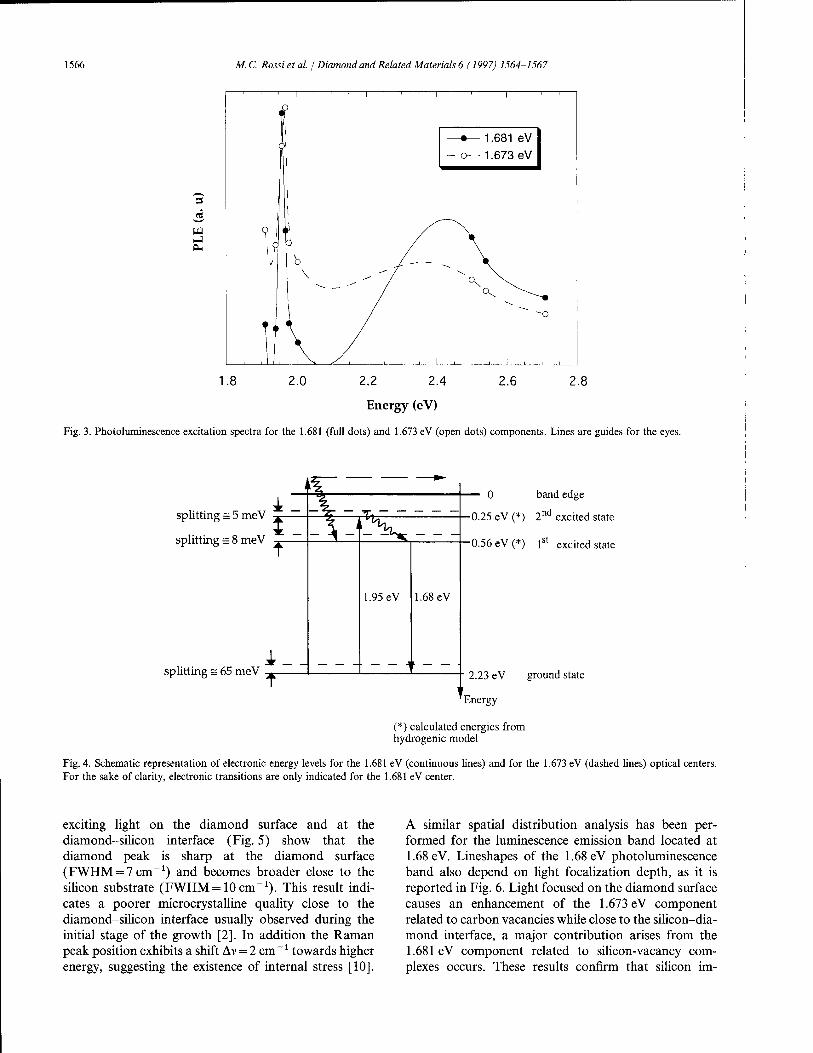
1566 M.C. Rossietal. / Diamond and Related Materials 6 (1997) 1564-1567
3 ■3 w
1
1 ■ 1 RH1 o\/
1 - o- -1.673 eV
1
if
1 1 I
.{. i x y i
1.8 2.0 2.6 2.8 2.2 2.4
Energy (eV)
Fig. 3. Photoluminescence excitation spectra for the 1.681 (full dots) and 1.673 eV (open dots) components. Lines are guides for the eyes.
splitting = 5 meV
splitting = 8 meV
±_
f
splitting = 65 meV Jr
S. 1.95 eV
-■ -"
1.68 eV
band edge
-0.25 eV (*) 2nd excited state
-0.56 cV(*) 1st excited state
■ 2.23 eV ground state
Energy
(*) calculated energies from hydrogenic model
Fig. 4. Schematic representation of electronic energy levels for the 1.681 eV (continuous lines) and for the 1.673 eV (dashed lines) optical centers. For the sake of clarity, electronic transitions are only indicated for the 1.681 eV center.
exciting light on the diamond surface and at the diamond-silicon interface (Fig. 5) show that the diamond peak is sharp at the diamond surface (FWHM = 7cm_1) and becomes broader close to the silicon substrate (FWHM = 10cm_1). This result indi- cates a poorer microcrystalline quality close to the diamond-silicon interface usually observed during the initial stage of the growth [2]. In addition the Raman peak position exhibits a shift Av = 2 cm ~* towards higher energy, suggesting the existence of internal stress [10].
A similar spatial distribution analysis has been per- formed for the luminescence emission band located at 1.68 eV. Lineshapes of the 1.68 eV photoluminescence band also depend on light focalization depth, as it is reported in Fig. 6. Light focused on the diamond surface causes an enhancement of the 1.673 eV component related to carbon vacancies while close to the silicon-dia- mond interface, a major contribution arises from the 1.681 eV component related to silicon-vacancy com- plexes occurs. These results confirm that silicon im-

M. C. Rossi et cd. / Diamond and Related Materials 6 (1997) 1564-1567 1567
B
T3
O 2
1310 1320 1330 1340
Wavenumber (cm" )
1350 1360
Fig. 5. Diamond Raman peak for different light focalization depths (corresponding to different depths within the film thickness): (a) growth side and (b) silicon-diamond interface.
■a 0.9
o Z
0.8
0.7
735 736 737 738 739 740 741
Wavelength (nm)
742 743
Fig. 6. Lineshapes of the 1.68 eV PL band excited at A = 633 nm for light focused on the diamond growth side (dashed line), in the middle of the film (dotted line) and close to the silicon-diamond interface.
impurities are preferentially distributed close to the diamond-silicon interface, where small size diamond
grains and large distributions of grain boundaries are expected.
4. Conclusion
Photoluminescence and Raman spectroscopies have been used to study electronic properties and spatial distribution of Si-related defects in polycrystalline dia- mond films. PL spectra are mainly characterized by a strongly asymmetric emission band, which has been deconvoluted into two lines, whose contribution to the main band depends both on excitation energy and light penetration depth within the film thickness. Quite similar PL excitation spectra have been detected for these two components, suggesting that both emission lines are related to carbon vacancies, either isolated or close to silicon atom impurities. The spatial dependence of PL peak energies and lineshapes reflects the spatial profile of silicon impurities incorporated during the diamond growth.
References
[1] W.J.P. Van Enckevort, in: H.E. Spear, J.P. Dismukes (Eds.), Syn- thetic Diamond: Emerging CVD Science and Technology, Wiley, New York, 1994.
[2] W. Zhu in: L.S. Pan, D.R. Kania (eds), Diamond: Electronic Properties and Applications, Kluwer, Dordrecht, 1995.
[3] A.T. Collins, Diamon Relat. Mater. 1 (1992) 457. [4] P. Ascarelli, E. Cappelli, G. Mattei, F. Pinzari, S. Martelli, Dia-
mond Relat. Mater. 4 (1995) 464. [5] G. De Cesare, S. Salvatori, R. Vincenzoni, P. Ascarelli, E. Cap-
pelli, F. Pinzari, F. Galluzzi, Diamond Relat. Mater. 4 (1995) 628. [6] A.T. Collins, L. Alters, C.J.H. Wort, G.A. Scarsbrook, Diamond
Relat. Mater. 3(1994)932. [7] L. Bergman, R.J. Nemanich, J. Appl. Phys. 78 (1995) 6709. [8] A.T. Collins, M. Kamo, Y. Sato, J. Mater. Res. 5 (1990) 2507. [9] JA. Freitas, U. Strom, A.T. Collins, Diamond Relat. Mater. 2
(1993) 87. [10] E. Gheeraert, A. Deneuville, M. Bonnot, L. Abello, Diamond
Relat. Mater. 1 (1992) 525.

«ataM&Mtr
II11M
ELSEVIER
DIAMOND AND
RELATED MATERIALS
Diamond and Related Materials 6 (1997) 1568-1571
Amorphous GaAs!_xNx thin films on crystalline Si substrates: growth and characterizations
Dave Lollman *, Khalifa Aguir, Benoit Roumiguieres, Herve Carchano Laboratoire EPCM, Service A62, Faculte des Sciences de Saint Jerome, Universite d'Aix-Marseille III, 13397 Marseille
cedex 20, France
Abstract
This work deals with the growth and study of a new nitride in thin films: GaAsj _XNX. The material is deposited in its amorphous form on crystalline Si substrates by means of RF sputtering of a GaAs target in an atmosphere of argon and ammonia. Raman spectroscopy used to study the physico-chemical properties of the film structure pointed out that GaASi_xNx is a wide gap material which is formed by the substitution of arsenic by nitrogen in the GaAs network (J. Bandet, K. Aguir, D. Lollman, A. Fennouh, H. Carchano, Jpn. J. Appl. Phys., 36 (1997) 11.
In order to investigate the electrical properties of GaAs^JSf* in view of potential applications in optoelectronic systems, J-V and C-V characteristics have been performed. J-V results show that the heterostructures exhibit a drastic increase in resistivity with nitrogen incorporation. The conduction passes from a diode-type one for x = 0 to an approximately symmetrical one with nitridation, i.e. for x > 0. The films present convenient high resistivity values for insulating character consideration. Furthermore, C-V results obtained present a manifest MIS-like behaviour with however the existence of a flat-band voltage (FFB). © 1997 Elsevier Science S.A.
Keywords: Amorphous III-V semiconductors; GaAs^^N^ thin films; High resistivity; MIS structures
1. Introduction
With the advent of reduced dimensions of very large scale integrated (VLSI) devices, there has been increas- ing interests in recent years to control the composition of alternate thin film depositions with specific built-in properties. As far as silicon-based devices are concerned, much of the success of this basic semiconductor used is due to the exceptionally opportune properties of the Si02/Si interface. The fabrication of thermal Si02/Si interfaces has been drastically optimized to give electron- ically active interface state densities of less than one defect per 104— 106 interfacial Si atoms [1]. This small interfacial state density is critical for metal-insulator-se- miconductor (MIS) device operation enabling the Fermi level to move throughout the forbidden band gap in order to achieve inversion.
The techniques that have received considerable atten- tion include anodic, thermal or plasma-oxidation and dielectric deposition. Even though some of these tech- niques have achieved a certain degree of feasibility on
' Corresponding author. Tel: 04 91 28 81 53; Fax: 04 91 28 94 03.
GaAs-based MOSFETs and MISFETs [2], the MOS and MIS properties of these structures are relatively poor. The prime reason for that is due to the mediocre surface electronic properties detained by GaAs. These undesirable properties include high state density, high surface recombination density and pinning of its Fermi level. All of these limit considerably the use of GaAs in VLSI device applications. Aiming at overcoming this barrier, considerable efforts have been undertaken to develop a MOS or MIS technology for GaAs (and other III-IV semiconductors) similar to that of Si. As work progressed, it became apparent that, unlike the Si02/Si interface, the chemistry between the III-IV semiconduc- tors and their native oxides do not lead to a chemically stable and defect-free interface.
For these reasons, and in view of investigating the fabrication of a successful integrated MIS structure device, we retained the approach of depositing a high- quality dielectric layer onto the semiconductor surface to act as the gate insulator. As we focused our study, in a first stage, on the insulating layer itself, we have grown amorphous GaAs^^N^ thin films on Si sub- strates for easy preliminary investigations. The long
0925-9635/97/$17.00 © 1997 Elsevier Science S.A. All rights reserved. PII S0925-9635(97)00053-8

D. Lollman et at / Diamond and Related Materials 6 (1997) 1568-1571 1569
term objective would be, of course, a study of MIS structures using GaAs as a substrate.
2. Device fabrication and experimental set-up
The substrates used were Si wafers (p-type) because of their relatively low cost and the high purity of their surface obtained by means of classical chemical process- ing. The surface oxides and impurities were etched by Shiraki technique [3] prior to film deposition. The cleaning processes, after degreasing in trichloroethylene, acetone and ethanol successively, consisted of a first surface chemical etching in a solution of H2S04/H202
(1:1), then boiling in pure HN03, and the oxide etched off in a dilute (10%) HF solution.
Thin films of amorphous GaAs^^N^ (thickness« 5000 A) were then grown using a conventional cap- acitive coupled RF (13.56 MHz) sputtering of a water- cooled polycrystalline GaAs target by means of a plas- ma mixture of argon and a nitrogen carrier gas (NH3). The deposition chamber (Fig. 1) is pumped down to high vacuum conditions (approx. 7xl0~7mbar) and the partial pressure of NH3 (PNH3) is adjusted to the desired value (from 0 to 10 x 10"3mbar) by means of an MKS capacitive gauge. Argon is then introduced into the chamber through a mass flow controller, bring- ing the total working pressure to 50 x 10 ~3 mbar. The gases (supplied by Air Liquide Co.) rated purities of 99.9997%. The RF input power was 25 W corresponding
to a self bias voltage Vuc of 600 V. During deposition, the substrate temperature was maintained at 150 °C.
In order to fabricate a simple heterojunction diode, an ohmic contact was formed on the back side of the c-Si wafer by evaporating aluminium. Gate contacts were formed by depositing gold discs of 5 x 10 "3 cm2
area, 1000 Ä thick, on the as-deposited a-GaAsj-^N, films. The Au contacts act as excellent ohmic contacts with a-GaAs [4], and this property has been verified for our a-GaAsj.^N^ films as well in our laboratory.
The J-V characteristics were carried out at room temperature by means of an HP 4140B pico-ampere- meter/d.c.-voltage source and C-V characteristics per- formed by an HP 4275A.
3. Electrical characterizations
3.1. Current-voltage characteristics
J-V characteristics of the a-GaAs1_;cNx/c-Si(p) heter- ojunctions have been performed at room temperature as a function of applied bias voltage in order to study the influence of nitrogen incorporation in the depos- ited films.
Fig. 2 shows the PNH3 and the voltage dependence of the current density / from which it can be seen that the a-GaAs!_xNx/c-Si(p) junctions exhibit a drastic falling off of forward and reverse currents with nitrogen incor- poration. The conduction passes from a diode-type
XY plotter
P.M
substrate heating thermocouple
quartz window
position detector
V/A ground
H insulator
monochromator
substrate
GaAs target xrr\
f f water cooling
pumping system
mass flow controller
TjTIf argon NH
capacitively coupled R.F. power supply
Fig. 1. Experimental set-up for RF sputtering.
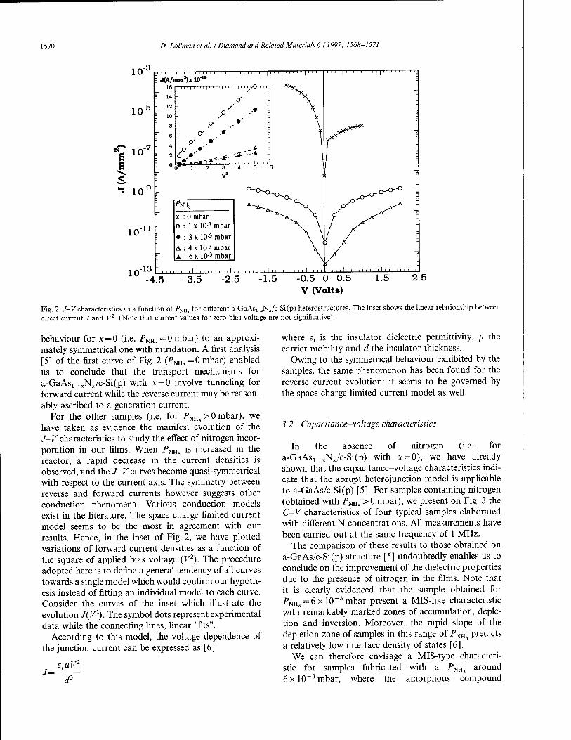
1570 D. Lollman et al. / Diamond and Related Materials 6 (1997) 1568-1571
10
10"
-3
% 10'7
^ 10"9
10 -11
10
''III111111 JlA/mm^xlO
'r
i ■' Iii. 1 i . /»'"-.
r
7 .•' .•
L V .• J
if;' -^f " -£" ~ A J
. 1 , . , .'
o"'*l ' 2 3 4 5 6
J°NH3
X 0 mbar 0 1 x 10⁻³ mbar
• : 3 x 10⁻³ mbar
A 4 x 10⁻³ mbar ▲ : 6 x 10⁻³ mbar
-13 -4.5 -3.5 -2.5 -1.5 -0.5 0 0.5 1.5 2.5
V (Volts)
Fig. 2. J-Vcharacteristics as a function of PNH3 for different a-GaAs^NJc-SiCp) heterostructures. The inset shows the linear relationship between direct current / and V2. (Note that current values for zero bias voltage are not significative).
behaviour for x = 0 (i.e. PNH3 = 0mbar) to an approxi- mately symmetrical one with nitridation. A first analysis [5] of the first curve of Fig. 2 (PNHj =0 mbar) enabled us to conclude that the transport mechanisms for a-GaASi-JSrjc-SiCp) with x = 0 involve tunneling for forward current while the reverse current may be reason- ably ascribed to a generation current.
For the other samples (i.e. for PNH3>0mbar), we have taken as evidence the manifest evolution of the J-V characteristics to study the effect of nitrogen incor- poration in our films. When PNH3 is increased in the reactor, a rapid decrease in the current densities is observed, and the J-V curves become quasi-symmetrical with respect to the current axis. The symmetry between reverse and forward currents however suggests other conduction phenomena. Various conduction models exist in the literature. The space charge limited current model seems to be the most in agreement with our results. Hence, in the inset of Fig. 2, we have plotted variations of forward current densities as a function of the square of applied bias voltage (V2). The procedure adopted here is to define a general tendency of all curves towards a single model which would confirm our hypoth- esis instead of fitting an individual model to each curve. Consider the curves of the inset which illustrate the evolution J(V2). The symbol dots represent experimental data while the connecting lines, linear "fits".
According to this model, the voltage dependence of the junction current can be expressed as [6]
/= CißV2
where e; is the insulator dielectric permittivity, y. the carrier mobility and d the insulator thickness.
Owing to the symmetrical behaviour exhibited by the samples, the same phenomenon has been found for the reverse current evolution: it seems to be governed by the space charge limited current model as well.
3.2. Capacitance-voltage characteristics
In the absence of nitrogen (i.e. for a-GaAs!^xNx/c-Si(p) with x = 0), we have already shown that the capacitance-voltage characteristics indi- cate that the abrupt heterojunction model is applicable to a-GaAs/c-Si(p) [5]. For samples containing nitrogen (obtained with PNHs >0 mbar), we present on Fig. 3 the C-V characteristics of four typical samples elaborated with different N concentrations. All measurements have been carried out at the same frequency of 1 MHz.
The comparison of these results to those obtained on a-GaAs/c-Si(p) structure [5] undoubtedly enables us to conclude on the improvement of the dielectric properties due to the presence of nitrogen in the films. Note that it is clearly evidenced that the sample obtained for pNH3=6x 10"3 mbar present a MIS-like characteristic with remarkably marked zones of accumulation, deple- tion and inversion. Moreover, the rapid slope of the depletion zone of samples in this range of PNH3 predicts a relatively low interface density of states [6].
We can therefore envisage a MIS-type characteri- stic for samples fabricated with a PNli3 around 6 x 10 "3 mbar, where the amorphous compound

D. Lollman et al. / Diamond and Related Materials 6 (1997) 1568-1571 1571
1
0.9
u 0.8
Ü 0-7
^ 0.6
0.5
0.4
0.3
l ' ' ' ' i ' ' ' ' l
P
D
• 2xl0~3mbar
3xl0~3mbar
6x 10 mbar ♦ - 8xl0"3mbar
Innl
I ' ' ' ' I i I i i i > I > i i
"inöOnöDÜDDODÖ
-4 -1 0 1 V (Volts)
Fig. 3. C-V characteristics of a-GaAs^N^/c-SUp) heterostructures as a function of PNH3 measured at 1 MHz.
(a-GaAs^-JNy would behave like a dielectric layer with high resistivity [7].
C-V measurements show a remarkable MIS charac- teristic for samples fabricated with a _PNH3 of around 6xl0~3mbar.
4. Conclusion
In conclusion, a-GaAs1_xNx/c-Si(p) heterojunctions have been successfully fabricated by RF reactive sputter- ing, and studied electrically by current-voltage and capacitance-voltage measurements.
The current-voltage measurements suggest that the forward current in these junctions when PNIi3 = 0 mbar involves multi-tunneling capture-emission for forward current and a generation mechanism for reverse current. For PNH3>0mbar samples (i.e. x>0), the system rapidly tends to a MIS-type behaviour. The hypothesis of a conduction by space charge limited current is proposed.
References
[1] J.J. Simonne, J. Buxo, Insulating Films on Semiconductors, Elsev- ier Science, Amsterdam, 1986.
[2] A. Colquhoun, E. Kohn, H.L. Hartnagel, IEEE Trans. Electron. Devices 25 (1978)375.
[3] A. Ishizaka, Y. Shiraki, J. Electrochem. Soc. 133 (1986) 666. [4] K. Aguir, PhD Thesis, Toulouse, France, 1987. [5] K. Aguir, A. Fennouh, H. Carchano, J.L. Seguin, B. El Hadadi,
F. Lalande, Thin Solid Films 257 (1995) 98. [6] S.M. Sze, Physics of Semiconductors Devices, 2nd Edn., Wiley,
New York, 1981. [7] K. Aguir, A. Fennouh, H. Carchano, D. Lollman, J. Phys. Ill 5
(1995)1573.

ELSEVIER
DIAMOND AND
RELATED MATERIALS
Diamond and Related Materials 6 (1997) 1573-1574
Conference Calendar
Title Place Date Further Information from:
Diamond Films '97
13th International Symposium on Plasma Chemistry
Edinburgh, UK August 3-8 Ms. Glenda Bland 1997 Conference Secretariat
22 Pias Taliesin Portway Village Marina Penarth CF64 1TN Wales United Kingdom Tel: 44 (0) 1222 700053 Fax: 44 (0)1222 700665 E-mail: [email protected]
Beijing August 14-23 Dr. Lin He China 1997 The Chinese Society of Theoretical & A
Mechanics 15 Zhong Guan Cun Road Beijing 100080 China Fax: (86-10) 62559588 E-mail: [email protected]
International Conference on Ion Sources (ICIS 97)
10th International Conference on Surface Modification of Metals by Ion Beams
Lasers in Synthesis, Characterization and Processing of Diamond
24th International thermal Conductivity Conference and 12th International thermal Expansion Symposium
Taormina Italy
September 7-13 1997
Dr. Giovanni Ciavola INFN-LNS, Via S. Sofia 44 95123 Catania Italy Tel/fax: 39 95 542300 E-mail: [email protected]
Gatlinburg, Tennessee, USA
September 21-26 1997
Vicki Barnes Oak Ridge National Laboratory Building 3137, MS-6057 Oak Ridge TN 37831-6057 E-mail: [email protected]
Tashkent Uzbekistan
October 6-9 1997
Dr. Victor Ralchenko General Physics Institute ul. Vavilova 38 117942 Moscow Russia Tel: 7 (095) 132-8229 Fax: 7(095) 135-3002 E-mail: [email protected]
Pittsburgh, PA USA
October 26-29 1997
Peter S. Gaal Conference Chairman Anter Corporation 1700 Universal Road Pittsburgh, PA 15235 Tel: 412 795 6410 Fax: 412 795 8225 E-mail: [email protected] Conference home page: http://www.anter.com.conferences
Elsevier Science S.A.

1574 Conference Calendar
Title Place Date Further Information from:
Gordon Conference on Diamond Synthesis
Queen's College Oxford England
August 23-28 Karen K. Gleason 1998 Department of Chemical Engineering
Room 66-468 Massachusetts Institute of Technology Cambridge, MA 02139 Tel: 617 253 5066 Fax: 617 258 5042 E-mail: [email protected]

HHKÜÄ
ELSEVIER
DIAMOND AND
RELATED MATERIALS
Diamond and Related Materials, 6 (1997) 1575-1580
Author Index for Volume 6
Aboelfotoh, M.O., 1388 Achete, CA., 551 Achtziger, N., 1436 Aebi, P., 282 Afanas'ev, V., 1472 Aguir, K., 1568 Agullö-Rueda, F., 1210 Ahn, J., 48 Akaishi, M., 356 Akkerman, Z., 153 Ako, F., 847 Alause, H„ 1536 Albrecht, M., 747, 1467 Alcubilla, R., 1555 Aldinger, F., 608 Alexenko, A.E., 89 Allers, L., 353 Allon-Alaluf, M., 555 Alnot, P., 107, 505 Amaratunga, G.A.J, 207, 700 Anagnostopoulos, A., 1226, 1494, 1547 Änderte, M., 559 Ando, T., 1036 Andreyev, A.V., 28 Andujar, J.L., 579, 589, 604, 1550,1559 AngheLL., 1226, 1494, 1547 Anikin, M., 1249 Anthony, T.R., 120 Apakina, V.N., 564 Arnault, J.C., 235 Arnodo, C, 1428, 1508 Ashfold, M.N.R., 247, 569, 817, 898 AsifKhan, M., 1536 Aslam, D.M., 394 Asmussen, J., 1097 Aspnes, D.E., 196 Auer, N., 944 Avigal,Y.,381,526
Babaev, V.G., 89, 640 Babanin, A.I., 1528 Babina, V.M., 640 Bacon, D., 687 Badzian, A., 130 Baiion, L., 1500 Bakowski, M., 1476 Baldwin, S.K. Jr., 202 Balster, T., 1353 Bano, E., 1489 Baral, B., 374, 869 Baränkovä, H., 224 Baranov, A.M., 902, 1106 Barbolla.J., 1500 Bardes, D., 1555 Bärdos, L., 224
Barrat, S., 41 Barrett, D.L., 1262 Baruchel, J., 1249 Bassler, M., 1472 Batori, V., 645 Battaile, C.C., 1198 Bauer-Grosse, E., 41 Baumann, P.K., 398, 403 Beardmore, G., 450 Beccard, R., 1301 Bechstedt, F., 1346 Beera, R.A., 430 Behr,D., 654, 1111 Belyavina, N.N., 927 BenelMekki, M., 1550 Benko, E., 931, 1192 Benndorf, C, 533, 964 Berberich, S., 1306 Bergman, J.P., 1324 Berg, S., 224 Bernard, C, 1249 Bernhardt, J., 1349 Bertran, E., 589, 1559 Bewick, A., 1135 Bezhenar, N.P., 927 Bielanska, E.,931 Bill, J., 608 Billon, T., 1226, 1494, 1547 Blanquet, E., 1249 Bluet, J.M., 1385, 1463 Bobrov, K., 736 Bodganovic, I., 320 Boettger, E., 298 Boiko, Y., 860 Boman, M., 1143 Bonnot, R., 1463 Borges, C.F.M., 440 Borges, C.P., 551 Borst, T., 329 Bougdira, J., 107, 505 Bozeman, S.P., 398, 403 Bozhko, S.A., 927 Bozzolo, N., 41 Bregadze, A.Y., 89 Bremser, M.D., 191, 196 Brenn, R., 149, 654 Breskin, A., 687 Brierley, C.J., 386 Brookes, CA., 348 Brown, W.D., 430, 952 Bruch, C, 107, 505 Brumitt, K., 390 Brunet, F., 774, 778, 843 Brylinski, C, 1405, 1428, 1508 Buchkremer-Hermanns, H., 411 Buckley-Golder, I.M., 344
Burdina, K.P., 987 Butler, J.E., 1135, 1198
Cabioc'h, T., 261 Calderer, J., 1555 Calliari, L., 559 Camassel, J., 1385, 1463 Cappuccio, G, 807 Carchano, HL, 1568 Carlsson, J.-O., 1143 Carlsson, J.O., 85 Carter, C.H., 1400 Cassette, S., 1428 Chakk, Y., 681 Chakrabarti, K.,991 Chakrabarti, R., 991 Chalker, P.R., 333, 344, 839 Chan, S.S.M, 333, 374 Chartier,E., 1508 Chatei, H., 107, 505 Chaudhuri, S., 991 Chechik, R., 687 Chelnokov, V.E., 1480 Chen, D., 983 Cheng, T.S., 1539 Chen, Q., 1536 Chen,W.M., 1378, 1381 Chhowalla, M., 207 Chin, K.K., 940 Chourou, K., 1249 Choyke, W.J., 1243,1333 Christiansen, K., 1467 Christiansen, S., 1467 Cimalla,V., 1311 Clavaguera-Mora, M.T., 1306 Clavaguera, N., 1306 Clement, R.E., 169 Clough, F.J., 879 Colineau, E., 778 Collaborationb, ISOLD., 1436 Collins, A.T., 516 Collins, R.W., 55 Constantinidis, G, 1459 Constant, L., 664 Contreras, S., 1329 Cooper, M.A., 1226, 1494, 1547 Corat, E.J., 472,490, 1172 Cordery, A., 537 Correig,X., 1555 Costa, J., 1559 Couto, M.S., 975 Cremades, A., 95 Croitoru, N., 555, 1152 Cunningham, A.J., 1000
Elsevier Science S.A.
1576 Author Index for Volume 6
D'Evelyn, M.P., 511, 791,812 Dalibor.T., 1333, 1396 Davidson, J.L., 398, 403 Davis, R.F., 196, 1282 Davis, T.J., 1062, 1135 Da, Y., 673 Day, A.R., 325 Dedulle, J.M., 1249 Deguchi, M., 367 Delafond, J., 261 Delclos, S., 758 De Martino, C, 559 Dementjev, A.P., 486 Demo, P., 1092 Demuynck, L., 235 Deneuville, A., 516, 774, 778, 843 Demiig, P.A., 1036 Der Sahaguian, S., 721 Devaty, R.P., 1243, 1333 Dezauzier, C, 1329 Dieguez, I., 41 Dimitrakopulos, G.P., 1362 Dluzniewski, M., 721 Dmitriev, V.A., 1480, 1524, 1528, 1532 Dominguez, M., 1555 Donnelly, CM., 787 Donnelly, K., 390 Dontas, I., 1424 Dorignac, D., 758 Dorsch, W., 1269 Dowling, D.P., 390 Doyle, J.P., 1388 Drawl, W., 55 Dreher, E., 830, 1129 Dub, S.N., 574 Dumkum, C, 802 Dyakonov, M., 1536
Ebert, W., 329, 940 Ecke, G., 1311 Eckstein, R., 1269 Edwards, N.V., 196 Egdell, R.G., 874 Egilsson, T., 1289 Egret, S., 879 Ehrhardt, H., 255, 621,645 Eichhorn, G, 1311 ElFelk,Z., 1306 Ellison, A., 1272, 1289, 1369 Eloy, R., 390 Erler, F., 1414 Esteve, J., 579 Etsion, I., 381 Everitt a, N.M., 826, 826, 826
Fabis, P.M., 191 Falkovsky, L.A., 1385 Fanciulli, M., 725 Fan, Q.H., 422 Fecht, HJ., 308, 344, 839 Fedorinin, I.A., 640 Feldermann, H., 1129 Femandes, A., 769 Ferreira, N.G., 472, 490, 1172 Filippov, V.B., 1005
Fisgeer, B., 526, 736 Fisher, D., 146 Fissel,A., 1316 Fizzotti, F., 320, 1051 Flodström, A., 81 Flöter, A., 298 Flynn, D., 230 Folman, M., 681, 736 Fookes, A., 893 Foord, J.S., 219, 658, 676, 869, 874 Forkel-Wirth, D., 1436 Förster, H., 1512 Fourches-Coulon, N., 542 Fox, N.A., 450, 569, 1135 Foxon, CT., 1539 Franceschini, D.F., 551, 631 Francois, N., 959 Franke, M., 1349 Frauenheim, T., 207 Freire, F.L., 551 Freire, F.L. Jr, 551 Freitag, K., 1436 Freudenstein, R., 584 Friedbacher, G., 1031 Friedrich, M., 33, 612 Frischholz, M„ 1396, 1485 Fuchs, N., 752, 1010 Fujimori, N., 1057 Fukarek, W., 594 Fukui, M., 1 Furthmüller, J., 1346 Fusco, G., 559, 725, 783
Galluzzi, F., 361, 712, 1564 Garcia, I., 1210 Gärtner, H., 149 Gat, R., 791 Geddes, J., 787 George, M.A., 398, 403 Germi, P., 774 Gheeraert, E., 516, 774, 778, 843 Gilmore, A., 1062 Gimeno, S., 604 Girshick, S.L.,481 Giudice, A.L., 1051 Glozman, O., 381,796 Gluche, P., 329 Golding, B., 325 Gölz, A., 1374, 1420, 1489, 1497 Gonon, P., 314, 860 Gonzalez, M., 856 Gonzalez Sirgo, M., 1445 Gösele, U., 1365 Gouzman, I., 526 Gracio, J., 422 Gradinaru, G., 1392 Gradinaru, S.A., 1392 Grant, D.M., 802 Grasserbauer, M., 1031 Graupner, R., 1358 Gray, K.J., 191 Griffith, P.W., 822 Grillenberger, J., 1436 Gröning, P., 282 Groß, S., 1420 Gross, M., 1129
Grossman, E Gu, C, 673 Guillot, G., 1504 Güllich, H., 654 Guo, W.H., 12 Guseva, M.B., 89 Gutheit, T., 649 Güttier, H., 649
687
640
Hahn, I.T., 959 Hahn, J., 612, 1005 Hakovirta, M., 694 Hallin, C, 1289, 1297, 1369, 1378, 1381, 1485 Halperin, G, 381 Hammerschmidt, A., 944 Hartmann, P., 456, 763 Hase, N., 367 Hashimoto, M., 1047 Hassard, J.F., 353 Hatanaka, Y., 1081 Hatta,A.,717, 743, 1015, 1041 Hattori, R., 884, 889 Haubner, R., 240, 286,406,456, 494, 763 Hayashi, K., 303 Hayashi,Y., 1117, 1117 Heera, V., 1432 Heindl, J., 1269 Heinz, K., 1349 Heissenstein, H, 1440 Helbig, R., 1293, 1321, 1440, 1467 Hemer, R., 752 Henry, A., 1289,1369 Herres, N., 654 Heszler, P., 85 Heydemann, V.D., 1262 Hinneberg, H.-J., 1019 Hiraki.A., 717,743, 1015, 1041 Hirakuri, K.K., 1031 Hoffman, A., 381, 526, 681, 687, 736, 796 Hofmann, D., 1269 Hofsäss, H., 830, 1129 Hokazono, A., 339, 865 Hollering, M., 1358, 1451 Holmes, D.S., 308 Hong, B., 55 Howard, A.S., 353 Huang, J.T., 12 Huant, S., 1536 Hudson, J.B., 511,791 Hudson, M.D., 386 Hug, G, 261 Hurtös, E., 1306 Hwang, J., 12 Hylen, A.-L., 1456 Hyun, S., 325
Ibach, H., 1353 Ibarra, A., 856 Iha, K., 490, 1172 Imai, T., 1057 Inushima, T., 835, 852 Irvine, K.G., 1524 Ishikura, T., 339 Isoya, J., 99, 356 Ito, T., 717, 743, 1015, 1041

Author Index for Volume 6 1577
Ivanov, I.G., 1289 Iwasaki, Y., 889
Jackman, R.B., 219, 333, 374, 658, 676, %• 874
Jaeger, M.D., 325 Jäger, W., 649 Jaksic, M., 320 Jamieson, D., 314 Jamieson, D.N., 860 Janowitz, C, 1226, 1494, 1547 Janssen, R., 1420 Janzen, E„ 1266, 1272, 1289, 1297, 1369,
1378, 1381, 1456, 1485 Jaouen, M., 261 Järrendahl, K., 1282 Jaussaud, C, 1226, 1494, 1547 Jeon, M.H., 743 Jian-xia, L., 673 Jiang, N., 743, 1041 Jin, Z., 673 Ji, R., 48 Johnson, J.N., 1000 Johnson, S.E., 569 Johnston, C, 333, 344, 839 Jr, 551, 1400 Jürgensen, H., 1301
Käckell,P., 1346 Kaiser, U., 1316 Kajimura, K., 303 Kalaugher a, E., 826, 826, 826 Kalinina, E.V., 1528 Kalisha,R., 516, 526,687 Kalomiros, J., 1226, 1494, 1547 Kalss, W., 240 Kartenhäuser, M., 1436 Kanda, H., 28, 99, 146, 356, 708 Kang, W.P., 398, 403 Karakostas, T., 1362 Karasawa, S., 835 Karuzskii, A.L., 564 Katsikini, M., 1539 Kawarada, H., 277, 339, 865 Kawasaki, S., 889 Kelly, T.C., 390 Ke, N., 983 Kennou, S., 1424 Kern, R.S., 1282 Kerns, D.V., 398,403 Khanolkar, A.A., 430 Kharlashina, N.N., 172 Khin,Y.Y., 1015 Khomich, A.V., 417 Khriachtchev, L.Yu., 694,1026 Khvostov, V.V., 89, 640 Kiflawi, I., 146 Kimoto,T., 1276, 1333 Kim, S.H., 959 Kimura, T., 1047 Kitabatake, M., 367 Kitagawa, M., 367 Kittler,M., 1512 Klages, C.-P., 293 Klibanov, L., 1152
Klose, S., 308, 344, 839 Klotzbücher, T., 599 Knapper, M.P., 569 Knap, W., 1536 Knuyt, G., 435, 1092 Kobashi, K„ 266, 272 Kogan, M.S., 564 Kohly, W„ 308 Kohn, E., 329, 940 Koide, Y., 847 Koidl, P., 149,654, 1111 Kola, P.V., 390 Kolitsch, A., 594 Komarov, S.F., 511,791 Komninou, P., 1362 Komori, M., 501 Kondrashov, P.E., 902 Kono, S., 463 Konov, V.l., 417 Konstantinov, A.O., 1297 Konwerska-Hrabowska, J., 617 Konyashin, I., 608 Konyashin, I.Y., 89 Kordina, O., 1289, 1297, 1369, 1378, 1381,
1485 Korony,G., 1392 Kotera, H., 367 Kozisek, Z., 1092 Krannich, G, 1005 Kreissig, U., 626 Kreutz, E.W., 599 Krötz, G, 1338 Kruger, C.H., 202,476 Krüger, J.K., 107, 505 Krukowski, S., 1515 Kuang, Y., 55 Kühn, M., 626 Kulisch, W., 584, 906 Kumazawa, Y., 1057 Kuo, K.-P., 1097 Kupfer, H., 33 Kurz, H., 1374, 1420, 1497 Kusakabe, K, 668 Küttel, O.M., 282 Kuzmik, J., 1459 Kuznetsov, N.I., 1528 Kvit, A.V., 564
Labeau, M., 1249 Lacerda, M.M., 631 Lacher, F., 1111 Ladas, S., 1424 Lade, R.J., 569 Lagrange, J.P., 516, 778 Laimer, J., 406 Lam,Y.W., 521,635 Lancin, M., 542 Lang,A.R., 1226, 1494, 1547 Lappalainen, R., 694, 1026, 1207 Larson, J.M., 481 Lash, A.A., 640 Lassagne, P., 1226, 1494,1547 Laufer, S., 1019 Lawson, S.C., 99 Lebedev, Y.A., 224 Leckey, R.C.G., 1358
Lee, C.S., 521, 635 Lee, J., 55 Lee, J.-J., 511 Lee, J.-W., 959 Lee,N., 130 Lee, S.T., 635 Leidich, D., 1365 Leite, N.F., 472, 490, 1172 Lempert, G.D., 687 Le Normand, F., 235, 664 Leonhard, C, 1489, 1497 Leoni, M., 807 Leveque, G., 1463 Leycuras, A., 1385 Ley, L., 730, 747, 1358, 1451 Liao, X.Z., 521 Licht, T., 1436 Lifshitz, Y., 687 Lindefeit, U., 1289 Lindner, J., 1414 Lindsay, J.W., 481 Lindström, J.L., 1378 Linnarsson, M., 1293 Lipkin, L.A., 1400 Lippold, G, 906 Lisicki, M., 617 Li, X., 1117, 1117 Lloyd, L., 390 Loader, C.B., 822 Locher, R., 149, 308, 654 Loeffler, J., 608 Loginova, O.B.,931 Loh, K.P., 219, 874 Lollman, D., 1568 Lorenz, H.P., 6 Lossy, R., 1445 Lousa, A., 604 Lucazeau, E., 843 Ludena, G.M.L., 89 Luithardt, W., 533 Lupich, I.N., 574 Lüpke.G., 1374 Lu, X., 673 Lux, B., 240, 286, 406, 456,494, 763
Machet, J., 970 Madar, R., 1249, 1369 Maeda, H., 668 Maillard-Schaller, E., 282 Mainwood, A., 353 Mainz, B., 1019 Maity, A.B., 991 Makepeace, A.P.W., 1226, 1494, 1547 Malave, A., 906 Malogolovets, V.G., 574 Malov, Y., 1097 Malshe, A.P., 430, 952 Mambou, J., 774, 778 Manfredotti, C, 320, 1051 Mankelevich, Y.A., 1051 Marek, T., 1269 Marhic, C, 542 Marinelli, M., 717 Mariotto, G, 631 ,Markiv, V.Ya., 927 'Marsal, L.F., 1555
1578 Author Index for Volume 6
Marshall, R.D., 374, 676 Martineau, P.M., 1226, 1494, 1547 Martinu, L., 440 Mary, S., 1135 Maslyuk, B.A., 574 Matsunami, H., 1276, 1333 Mattern, B., 1358 Matthee, T., 293 Matz, W., 1432 Ma, Y., 476 May, P.W., 247, 348,450, 1135 McCarty, K.F., 1219 McColl, I.R., 802 McCullough, R.W., 787 McGrath, J.J., 394 McKeag, R.D., 374 McKenzie, D.R., 207 Meaden, G., 893, 898 Meaden, G.M., 822 Mediin, D.L., 1219 Meilunas, R.J., 1157 Melnik, N.N., 564 Melnik, Y., 1524, 1532 Mendes de Barros, R.C., 472,490, 1172 Meng, Q., 673 Meng, Y., 120 Mergens, M., 599 Messier, .R., 55 Mestres, N., 1550 Meunier, F., 970 Meyer, C, 1374 Meykens, K., 435, 1092 Michelakis, K., 1459 Migulin, V.V.,417 Mihalcea, C, 906 Mikhailuts, E.Y., 1106 Milita, S., 1249, 1369 Miller, A.J., 386 Milne, W.I., 48, 783, 879 Milosavljevic, I., 398, 403 Mina, G, 559 Mirri, K., 320 Mitchel,W., 1392 Mitsuda, Y., 468 Mitsuhashi, M., 852 Mitura, E., 721 Mitura, S., 721 Mityagin, Y.A., 564 Miyata, K., 266 Mizuochi, Y., 277 Moelle, C, 344, 839 Moisan, M., 440 Mollä, J., 856 Möller, W., 594 Moll, J.A., 721 Moll, J.J., 721 Monemar, B., 1378, 1381 Montereali, R.M., 1564 Morita, Y., 356 Mori, Y., 743, 1015 Morooka, S., 668 Morris, W.G., 791 Mounier, E., 1182 Mucera, G, 1051 Müller, G, 1542 Müller, S., 1269 Murakami, M., 847
Murzin, V.N., 564 Mutsukura, N, 547
Nagano, M., 501 Nagasawa, H., 277 Nakai, H., 1047 Nakama, T., 852 Nakaraura, K., 339 Nakamura, N., 1047 Nakanishi, Y., 1081 Nam, O.H., 196 Naseem, H.A., 430, 952 Nazare, M.H., 769 Nemanich, R.J., 398, 403 Nennewitz, O., 1414 Neslädek, M., 435, 704, 1092 Nesteruk, I.G, 1067 Neves, A., 769 Nicholson b, E.D., 826, 826, 826 Nicholson, E., 898 Nicholson, E.D., 817, 893 Nicholson, J., 898 Nickel, K.G., 935 Niedzielski, P., 721 Niemann, E., 1365 Nikitina, I.P., 1524, 1532 Nikolaev, A.E., 1532 Nishimori, T., 463 Nishino, S., 1117, 1117 Nishino, T., 717 Nishitani-Gamo, M., 1036 Nistor, L.C., 159 Noblanc, O., 1428, 1508 Noda, H., 865 Nordeil, N, 1293, 1388 Nöth, H., 286 Novikov, N.V., 574 Novoselova, E.G., 902 Nugent, K., 314 Nyberg, T., 85, 224
Obermeier, E., 1445, 1448 Obraztsova, E.D., 159 Obraztsov, A.N., 1124 Oelhafen, P., 830 Oesterschulze, E., 906 Ogasawara, A., 835 Ogawa,T., 1015 Ohshima, T., 356 Ohya, S., 835 Okamoto, M., 1015 Oksman, M., 1152 Okushi, H., 303, 1124 Oku, T., 847 Olejniczak, W., 1081 Olszyna, A., 617 Opalev, O.A., 426 Opyrchal, H., 940 Orlikovsky, A.A., 564 Otsuki, A., 847 Ouisse, T., 1226, 1489, 1494, 1547 Ovuka, Z., 1476 Owano, T.G, 202, 476
Pace, E., 361 Paderno, Y., 1005 Pal,A.K., 991 Pallares, J., 1555 Palmour, J.W., 1400 Paloura, E.C., 1226, 1494, 1539, 1547 Pang, L.Y.S., 333 Paoletti, A., 717 Papaioannou, V., 1362 Parikh, N, 196 Park, Y.S., 959 Partridge, P.G., 893, 898 Pascual, J., 1550 Pauleau, Y., 1182 Pauser, H., 406 Pavlovsky, I.Y., 1124 Pawlowski, S., 1081 Pearce, T., 893 Pecz, B., 1297, 1362, 1428 Pekko, P., 1207 Peng, S., 983 Pensl, G., 1262, 1333, 1396, 1472 Peppermüller, C, 1293, 1321, 1440 Pereira, E., 422 Perestoronin, A.V., 564 Pereverteilo, V.M., 931 Pernet, M., 774 Perry, W.G., 196 Petukhov, M.N., 486 Pezoldt,J., 1311,1414 Pfennighaus, K., 1316 Phillipp, F., 758 Philosoph, B., 516 Pickard, C.D.O., 1062 Pintaske, R., 1005 Piqueras, J., 95 Plass, M.F., 594 Plitzko, J., 935 Pobol, I.L., 1067 Pochet, T., 320 Podzyarey, G.A., 574 Polesello, P., 320, 1051 Polini, R., 235 Polo, M.C., 579, 1550 Polushin, N.I., 987 Polyakov, V.B., 172 Pongratz, P., 752, 763, 1010 Pons, M., 1249 Prawer, S., 314, 860 Prieur, E., 1272 Przymusiala, P., 721
Quaeyhaegens, C, 435, 1092
Rackaitis, M., 1 Radamson, H., 1369 Radnöczi, G., 1428 Ralchenko, V.G., 159,417 Ramesham, R., 17 Räsänen, M., 694, 1026 Rats, D., 758 Ravindra, N.M., 1157 Rawles, R.E., 791 Raynaud, C, 1504 Reece, D.M., 386

Author Index for Volume 6 1579
Rego, CA., 247 Schmitz, D., 1301 Stauden, T., 1311 Reichert, W., 1445, 1448 Scholz, R., 1365 Steeds, J.W., 1062, 1135 Reiß, H., 298 Scholz, W., 906 Stefanov, E., 1500 Reinke, S., 584 Schöner, A., 1293, 1321, 1388, 1396, 1485 Stein von Kamienski, E., 1374, 1420 Reislöhner, U., 1436 Schreck, M., 95, 752, 1010 Stein Von Kamienski, E.G., 1489, 1497 Remy, M., 107, 505 Schröter, B., 1316 Stenberg,G, 1143 Ren, H., 411 Schultrich, B., 687 Stöckel, R., 747 Richier,C, 1504 Schulze, N., 1262 Stoemenos, J., 1306, 1362, 1448 Richter, F., 612, 626, 1005 Schulz, G, 649 Stokes, E.B., 511 Richter, V., 516 Schwan, J., 645 Störi, H., 406
Richter, W., 1316 Schwierz, F., 1512 Strauch, G., 1301
Riley, J.D., 1358 Seal, M., 975 Strausser, Y.E., 55
Ristein, J., 730 Sebastian, M., 1129 Strel'mtskij, V.E., 426
Rittmayer, G., 944 Seidman, A., 1152 Stritzker, B., 752, 1010
Riviere, J.P., 261 Sekiguchi, T., 303 Strunk, H.P., 747, 1269, 1467
Robert, J.L., 1329 Sekita, M., 1036 Sudarshan, T.S., 1392
Robertson, J., 212, 255, 700, 783, 879 Semoto, K., 1047 Suetin,N.V., 1051
Rochotzki, R., 33 Sergeichev, K.F., 417 Sugino, T., 884, 889
Rodriguez-Viejo, J., 1306 Serin, V., 758 Sun, Y., 230
Rodway, D., 658 Sessa, V., 444, 807 Sun, Z., 230
Romanus, H., 1414 Sharma, S.N., 1559 Suvorov, A.V., 1400
Ronning, C, 830, 1129 Shatwell, R.A., 822 Svensson, B.G., 1388
Rosa, J., 704, 1092 Shchukarev, A.V., 1528 Sychov, I.A., 417
Rose, M.F., 17 Shechter, H., 736 Syrkin, A.L., 1463, 1480
Rösler, M., 935 Shefer, E., 687 Syväjärvi, M., 1266,1456
Rosser, K.N., 247,450, 569 Sheglov, M.P., 1524 Szeles, C, 1157
Rossi, M., 444 Shima, S., 367 Szmidt, J., 721
Rossi, M.C., 361, 712, 1564 Shimizu, R., 272 Szücs, F., 344, 839
Rössler,U., 1342 Shintani, Y., 266, 272 Rottner, K., 1293, 1321, 1396 Shiomi, H., 835 Rottner, K.H., 1485 Shipko, A.A., 1067 Tachibana, T., 266, 272
Roumiguieres, B., 1568 Shirafuji, J., 884, 889 Tadic, T., 320
Rüb, M., 1436 Shiraishi, T., 835, 852 Tagliaferro, A., 559, 725, 783
Rusli, 700 Shiryaev, A.A., 172 Takai, Y., 272
Shi, X., 230 Takakuwa, Y., 463
Sieber, N., 1451 Tanabe, K., 1057 Tanaka, S., 1282
Sachdev, H., 286,494 Silva, R.F., 769 Tarutani, M., 272
Sadowski, M.L., 1536 Simünek, A., 944 Tass, Z., 255
Saito, T., 668 Singh, M., 1378 Tautz, F.S., 1353
Sakai, S., 468 Singh, R., 1400 Tay, B.K., 230
Sakamoto, H., 463 Siokou, A., 1424 Tereshin, A.A., 1097
Salvatori, S., 361, 712, 1564 Sirineni, G.M.R., 952 Terranova, M.L., 444, 807
Samlenski, R., 149, 654 Sittas, G., 146 Theel, T., 645 Samokhvalov, N.V., 426 Skierbiszewski, C, 1536 Therin, M., 390 Sanchez, G., 579 Skorupa, W., 1414, 1432, 1445 Theys, B., 1226, 1494, 1547 Sänchez Olias, J., 1210 Slater, D.B., 1400 Thiele, J.-U., 830 Sasaki, T., 743, 1015, 1041 Smirnov, I.S., 902 Thomas, P., 1329 Sato, Y., 99, 1036 Smith, F.W., 153 Thompson, DJ., 676 Sattel, S., 255 Smolin, A.A., 159,417 Thorpe, M.F., 325 Savage, J.A., 386, 658 Snitka, V., 1 Thürer, K.-H., 1010 Savage, S.M., 1485 Sokolowska, A., 721 Tkachenko, S.D., 564 Scardi, P., 807 Somma, F., 1564 Tong, F.-M., 1157 Schaarschmidt, G, 1019 Son, N.T., 1378, 1381 Tong Lee, S., 521 Schaefer, J.A., 1353 Sörman, E., 1378, 1381 Tracey, S., 676 Schäfer, J., 730 Souw,E.-K., 1157 Trava-Airoldi, V.J., 472, 490, 1172 Schäfer, L., 293 Spaeth, C, 626 Tsang, R.S., 247 Schardt,J., 1349 Speisser, C, 235 Tsong, T.T., 55 Scharmann, F., 1311 Spie, L., 1414 Tsuno, T., 1057 Scharnholz, S., 1497 Sridhara, S., 1333 Tsuruga, S., 668 Scheibe, HJ., 687 Srolovitz, DJ., 1198 Tucciarone, A., 717 Scheib, M., 255, 645 Stals, L.M., 435, 704, 1092 Tuominen, M., 1272, 1369,1456 Schelz, S., 440 Stammler, M., 747 Tuomi,T., 1272, 1369 Schilling, W., 6 Stampfl, A.P.J., 1358 Turban, G., 542 Schipanski, D., 1311,1512 Stanishevsky, A., 721 Schlapbach, L., 282 Stanishevsky, A.V., 1026 Schmidt, A., 293 Starke, U., 1349 Ubhi, H.S., 822 Schmidt, I., 964 Staryga, E., 721 Uhlig, H., 608
1580 Author Index for Volume 6
Uhrmacher, M., 1436 Ulcinas, A., 1 Ulrich, S., 621, 645 Urasaki, T., 501 Urban, K., 649 Utsch,J.,411 Uzan-Saguy, C, 516
Vackäf, J., 944 Vandenbulcke, L., 758 Vandevelde, T., 435 Vanecek, M., 704, 1092 van Enckevort, W.J.P., 975 Van Landuyt, J., 159 Vanzetti, L., 559 Vasquez, S., 551 Vazquez, A.J., 1210 Vehanen, A., 1272 Verhoeven, H., 298 Vescan, A., 329 Viera, G., 1559 Vila, R., 856 Vittone, E., 320, 1051 Vlasov,I.I.,417 Voellmar, S., 687 Volchkov, N.A., 564 Volkov, Y.Y., 426 Vorlicek, V., 704 Voronina, S.V., 417 Voronkin, M.A., 574
Wächter, R., 537 Wagner, C, 1338 Wahl, E.H., 476 Wakiyama, K., 501 Wang, L.C., 743 Wang, W.L., 579 Wang, W.N., 569, 1062, 1135 Wang, X., 230 Ward, B.L., 398,403
Watanabe, H., 303, 1124 Watanabe, K., 99, 708, 1036 Watanabe, T., 852 Weeks, J.R., 817 Wei, A., 983 Weill, N., 390 Weishart, H., 1414, 1432 Weiss, H., 411 Wellenhofer, G., 1342 Welzel, T., 33 Werner, M., 308, 344, 839 Werninghaus, T., 612, 1019 Wesner, D.A., 599 White, M., 394 Whitfield, M.D., 658, 676 Wickramanayaka, S., 1081 Widmayer, P., 621 Wiech, G, 944 Wiescher, D., 255 Wild, C, 1111 Winnacker, A., 1269 Wisbey, A., 822, 898 Wischmeyer, F., 1365 Witthuhn, W., 1436 Wittig, J., 398,403 Wittorf, D., 649 Woelk, E.G., 1301 Wong, K.W., 635 Wong, S.P., 983 Won, J., 1041 Won, J.H., 743 Woo, H.K., 635 Wröbel, A.M., 1081 Wurzinger, P., 752, 763
Xiu-di, S., 673
Yagi, H., 1041 Yakimova, R., 1266, 1272, 1369, 1456 Yamamoto, K., 1036
Yamamoto, Y., 1057 Yamanaka, S., 303 Yamashita, S., 339 Yang, B.X., 153 Yang, G.S., 394 Yin, Y., 207 Yin.Z., 153 Yokoba, M., 847 Yokota, Y., 266 Yoon, S.F., 48 Yoshida, K.-i., 547 Yoshii, M., 1031 Younes, CM., 450 Young, J., 1536 Yugo, S., 1047 Yun, W.S., 959 Yu,Z., 81
Zachai, R., 298, 649 Zahn,D.R.T., 33, 612, 1019 Zak,J., 721 Zalicki, P., 476 Zangheilini, E., 551 Zare, R.N., 476 Zarrabian, M., 542 Zekentes, K., 1362 Zgonc, K., 812 Zhang, L.Y., 348 Zhang, R.J., 521 Zhang, R.Q., 589, 1559 Zhang, Y., 635 Zhao, M., 202 Zheleva, T., 196 Zheng, Z., 230 Zhong-de, X., 673 Zhou, G, 272 Zhuk, A.Z., 640 Ziegler, A., 1358 Ziemann, P., 621 Zou, G, 673 Zukauskas, D., 1

SHE
111111
ELSEVIER
DIAMOND AND
RELATED MATERIALS
Diamond and Related Materials 6 (1997) 1581-1586
Subject Index
2-D numerical analysis Numerical study of avalanche breakdown of 6H-SiC planar p-n
junctions, 1500 3C-SiC heteroepitaxy
Optical investigation of thick 3C-SiC layers deposited on bulk silicon by CVD, 1385
4H-SiC Growth-related structural defects in seeded sublimation-grown
SiC, 1272 High quality 4H-SiC grown on various substrate orientations,
1289 4H silicon carbide
Radiation-induced defect centers in 4H silicon carbide, 1333 6H-, 4H-SiC
Hydrogen incorporation in epitaxial layers of 4H- and 6H-silicon carbide grown by vapor phase epitaxy, 1293
6H-SiC Growth-related structural defects in seeded sublimation-grown
SiC, 1272 Angle resolved photoemission and the band structure of 6H-SiC,
1358 OBIC studies on 6H-SiC Schottky rectifiers with different surface
pretreatments, 1396 Temperature dependence of electrical properties of 6H-SiC buried
gate JFET, 1504 a-Axis
High quality 4H-SiC grown on various substrate orientations, 1289
A-SiC Low frequency noise in silicon carbide Schottky diodes, 1494 Surface and bulk effects in ex-situ hydrogenated a-SiC thin films,
1547 Al-, B-doping
Hydrogen incorporation in epitaxial layers of 4H- and 6H-silicon carbide grown by vapor phase epitaxy, 1293
Aluminum nitride Growth and doping via gas-source molecular beam epitaxy of SiC
and SiC/AIN heterostructures and their microstructural and electrical characterization, 1282
Amorphous III-V semiconductors Amorphous GaAst-^N,, thin films on crystalline Si substrates:
growth and characterizations, 1568 Amorphous semi-conductors
Colour sensing applications of hydrogenated amorphous silicon carbide, 1542
Amorphous silicon-carbon alloys Electrical properties of PECVD amorphous silicon-carbon alloys
from amorphous-crystalline heterojunctions, 1555 Atomic force microscopy
Aluminium implantation ofp-SiC for ohmic contacts, 1414 Atomic structure
Investigation of modified 3C SiC(lOO) surfaces by surface- sensitive techniques, 1353
Band structure Progress in the study of optical and related properties of SiC since
1992, 1243
Bending Wafer warpage, crystal bending and interface properties of
4H-SiC epi-wafers, 1369 Bidimensional electron gas
Contactless characterisation of 2D-electrons in GaN/AlGaN HFETs, 1536
BN films Optical study of boron nitride thin films prepared by plasma-
enhanced chemical vapor deposition, 1550 Bonded SOI
ß-SiC films on SOI substrates for high temperature applications, 1448
Boron Hydrogen-, boron-, and hydrogen-boron-related low temperature
photoluminescence of 6H-SiC, 1321 Breakdown voltage
Numerical study of avalanche breakdown of 6H-SiC planar/;-« junctions, 1500
Buffer layer Residual strains in GaN grown on 6H-SiC, 1524
c-Axis High quality 4H-SiC grown on various substrate orientations,
1289 C/Si ratio dependance
Surface polarity dependence in step-controlled epitaxy: progress in SiC epitaxy, 1276
Carbon cluster model "Carbon cluster model" for electronic states at SiC/Si02
interfaces, 1472 Carbonization
Micropipe defects and voids at /?-SiC/Si(100) interfaces, 1365 Carvier density of p SiC
Valence band dispersion of hexagonal SiC, 1342 Chemical
Preferential etching of SiC crystals, 1456 Chemical bonding
Investigation of modified 3C SiC(100) surfaces by surface- sensitive techniques, 1353
CMOS SiC device technology: remaining issues, 1400
Colour sensors Colour sensing applications of hydrogenated amorphous silicon
carbide, 1542 Contactless characterisation
Contactless characterisation of 2D-electrons in GaN/AlGaN HFETs, 1536
Crystal growth Thermodynamics and high-Pressure growth of (Al, Ga, In)N
single crystals, 1515 Cubic polytypes
Identification of the cubic and hexagonal polytypes of GaN with X-ray absorption measurements, 1539
CVD diamond Emission and excitation spectra of silicon-related luminescent
centers in CVD-grown diamond films, 1564
Elsevier Science SA.
1582 Subject Index for Volume 6
Cyclotron resonance Contactless characterisation of 2D-electrons in GaN/AlGaN
HFETs, 1536 Deep levels
Deep luminescent centres in electron-irradiated 6H SiC, 1378 Characterization of electrically active deep level defects in 4H and
6HSiC, 1388 Deep level transient spectroscopy
Radiation-induced defect centers in 4H silicon carbide, 1333 Defect centers
Emission and excitation spectra of silicon-related luminescent centers in CVD-grown diamond films, 1564
Defects Defects formation in sublimation grown 6H-SiC single crystal
boules, 1249 Deep luminescent centres in electron-irradiated 6H SiC, 1378 Optically detected magnetic resonance studies of defects in 3C
SiC epitaxial layers, 1381 Characterization of electrically active deep level defects in 4H and
6H SiC, 1388 Preferential etching of SiC crystals, 1456
Density of interface states "Carbon cluster model" for electronic states at SiC/Si02
interfaces, 1472 Density of states
Electrical properties of PECVD amorphous silicon-carbon alloys from amorphous-crystalline heterojunctions, 1555
Device modeling The potential of SiC and GaN for application in high speed
devices, 1512 Diodes
2.5 kV ion-implanted p+n diodes in 6H-SiC, 1485 Dissolution
Growth of SiC from the liquid phase: wetting and dissolution of SiC, 1266
DLTS Characterization of electrically active deep level defects in 4H and
6H SiC, 1388 Drift
Investigation of walk-out phenomena in SiC mesa diodes with Si02/Si3N4 passivation, 1476
Effective masses Progress in the study of optical and related properties of SiC since
1992, 1243 Effective Richardson coefficient
Structural and electrical properties of Schottky barriers on n-GaN, 1528
Electrical activation Investigation of the effects of high temperature implantation and
post implantation annealing on the electrical behavior of nitrogen implanted ß-SiC films, 1445
Electrical noise Low frequency noise in silicon carbide Schottky diodes, 1494 Surface and bulk effects in ex-situ hydrogenated a-SiC thin films,
1547 Electronic band structure
Valence band dispersion of hexagonal SiC, 1342 Electronic field
High field/high temperature performance of semi-insulating silicon carbide, 1392
Electronic states Angle resolved photoemission and the band structure of 6H-SiC,
1358 Electron irradiation
Deep luminescent centres in electron-irradiated 6H SiC, 1378
Electron microscopy Micropipe defects and voids at /3-SiC/Si(100) interfaces, 1365 TEM study of Ni and Ni2Si ohmic contacts to SiC, 1428
Ellipsometry Low frequency noise in silicon carbide Schottky diodes, 1494 Surface and bulk effects in ex-situ hydrogenated a-SiC thin films,
1547 Epitaxial /?-SiC
Topology of twin junctions in epitaxial /J-SiC, 1362 Epitaxial layer uniformity
Optical investigation of thick 3C-SiC layers deposited on bulk silicon by CVD, 1385
Epitaxy The origin of 3C polytype inclusions in epitaxial layers of silicon
carbide grown by chemical vapour deposition, 1297 Structural properties of GaN grown on SiC substrates by hydride
vapor phase epitaxy, 1532 Etching
Preferential etching of SiC crystals, 1456 Low frequency noise in silicon carbide Schottky diodes, 1494 Surface and bulk effects in ex-situ hydrogenated a-SiC thin films,
1547 Experiments
Progress in the study of optical and related properties of SiC since 1992, 1243
Extended crystalline defects Sublimation growth of 4H- and 6H-SiC boule crystals, 1262
First principles calculation Polytypism and surface structure of SiC, 1346
Floating ring Numerical study of avalanche breakdown of 6H-SiC planar p-n
junctions, 1500 Fowler-Nordheim injection
High field and high temperature stress of n-SiC MOS capacitors, 1489
GaAs! .JNJ thin films Amorphous GaAsj _,N, thin films on crystalline Si substrates:
growth and characterizations, 1568 Gallium nitride
Residual strains in GaN grown on 6H-SiC, 1524 Gallium nitrides
Structural properties of GaN grown on SiC substrates by hydride vapor phase epitaxy, 1532
GaN Structural and electrical properties of Schottky barriers on
n-GaN, 1528 Identification of the cubic and hexagonal polytypes of GaN with
X-ray absorption measurements, 1539 GaN/GaAIN heterostructures
Contactless characterisation of 2D-electrons in GaN/AlGaN HFETs, 1536
Gate oxide Passivation of interface traps in MOS-Devices on n- andp-type
6H-SiC, 1497 ß-SiC
Investigation of the effects of high temperature implantation and post implantation annealing on the electrical behavior of nitrogen implanted ß-SiC films, 1445
ß-SiC; Hall effect; High temperature Analysis of transport properties of ß-SiC films: determination of
donor density and compensation ratio, 1329 ß-SiC on SOI
ß-SiC films on SOI substrates for high temperature applications, 1448
GH-SiC, p-n junction Numerical study of avalanche breakdown of 6H-SiC planar p-n
junctions, 1500
Subject Index for Volume 6 1583
Glow discharge JFET Effects of thermal and laser annealing on silicon carbide Temperature dependence of electrical properties of 6H-SiC buried
nanopowder produced in radio frequency glow discharge, gate JFET, 1504 1559 Junction termination extensions
Growth Numerical study of avalanche breakdown of 6H-SiC planar p-n Growth of SiC from the liquid phase: wetting and dissolution of junctions, 1500
SiC, 1266 Kinetics Growth model Growth and doping via gas-source molecular beam epitaxy of SiC
The kinetic growth model applied to micropipes in 6H-SiC, 1269 and SiC/AIN heterostructures and their microstructural and Hafnium electrical characterization, 1282
Hafnium, cadmium and indium impurities in 4H-SiC observed by Laser annealing perturbed angular correlation spectroscopy, 1436 Effects of thermal and laser annealing on silicon carbide
Heat diffusion nanopowder produced in radio frequency glow discharge, Thermal properties of ß-SiC epitaxial layers between 150 °C and 1559
500 °C measured by using microstructures, 1338 Lattice constant Heterojunction Residual strains in GaN grown on 6H-SiC, 1524
Electrical properties of PECVD amorphous silicon-carbon alloys Liquid phase from amorphous-crystalline heterojunctions, 1555 Growth of SiC from the liquid phase: wetting and dissolution of
Hexagonal polytypes SiC, 1266 Identification of the cubic and hexagonal polytypes of GaN with Liquid phase epitaxy
X-ray absorption measurements, 1539 Overview of SiC power electronics, 1480 High resistivity Low-energy electron diffraction
Amorphous GaAs^JM., thin films on crystalline Si substrates: Structure and morphology of SiC surfaces studied by LEED, growth and characterizations, 1568 AES, HREELS and STM, 1349
High speed devices Low temperature photoluminescence The potential of SiC and GaN for application in high speed Radiation-induced defect centers in 4H silicon carbide, 1333
devices, 1512 LPCVD High temperature Growth of SiC films obtained by LPCVD, 1306
Thermal properties of ß-SiC epitaxial layers between 150 C and Mesa diodes 500 C measured by using microstructures, 1338 Investigation of walk-out phenomena in SiC mesa diodes with
ß-SiC films on SOI substrates for high temperature applications, Si02/Si3N4 passivation, 1476 1448 MESFET
High temperature nitrogen implantation Microwave Power MESFET on 4H-SiC, 1508 Investigation of the effects of high temperature implantation and The potential of SiC and GaN for application in high speed
post implantation annealing on the electrical behavior of devices, 1512 nitrogen implanted ß-SiC films, 1445 Metal-organic precursors
Hydrogen Growth of SiC films obtained by LPCVD, 1306 Hydrogen-, boron-, and hydrogen-boron-related low temperature Metal-oxide-semiconductor
photoluminescence of 6H-SiC, 1321 High field and high temperature stress of n-SiC MOS capacitors, Hydrogenation 1489
Low frequency noise in silicon carbide Schottky diodes, 1494 Metallization Surface and bulk effects in ex-situ hydrogenated ot-SiC thin films, Aluminium implantation of p-SiC for ohmic contacts, 1414
1547 Micro analysis systems Hydrogen incorporation Colour sensing applications of hydrogenated amorphous silicon
Hydrogen incorporation in epitaxial layers of 4H- and 6H-silicon carbide, 1542 carbide grown by vapor phase epitaxy, 1293 Micropipes
III-V nitrides The kinetic growth model applied to micropipes in 6H-SiC, 1269 Thermodynamics and high-Pressure growth of (Al, Ga, In)N Micropipe defects and voids at /J-SiC/Si(100) interfaces, 1365
single crystals, 1515 SiC device technology: remaining issues, 1400 Impact-ionization Microtwins development
High field and high temperature stress of n-SiC MOS capacitors, Growth of SiC films obtained by LPCVD, 1306 1489 Microwave power
Implantation Silicon carbide for microwave power applications, 1405 Ion beam assisted deposition of a tungsten compound layer on MIS structures
6H-silicon carbide, 1432 Amorphous GaAs^^N^ thin films on crystalline Si substrates: Hafnium, cadmium and indium impurities in 4H-SiC observed by growth and characterizations, 1568
perturbed angular correlation spectroscopy, 1436 Mobility Interface Temperature dependence of electrical properties of 6H-SiC buried
Wafer warpage, crystal bending and interface properties of gate JFET, 1504 4H-SiC epi-wafers, 1369 MOCVD
Structural and electrical properties of Schottky barriers on SiC and group III nitride growth in MOVPE production reactors, n-GaN, 1528 1301
Interfacial connectivity Modelling Topology of twin junctions in epitaxial /?-SiC, 1362 SiC and group III nitride growth in MOVPE production reactors,
Ion implantation 1301 SiC device technology: remaining issues, 1400 Molecular beam epitaxy 2.5 kV ion-implanted p+n diodes in 6H-SiC, 1485 Growth and doping via gas-source molecular beam epitaxy of SiC

1584 Subject Index for Volume 6
and SiC/AIN heterostructures and their microstructural and electrical characterization, 1282
Chemical conversion of Si to SiC by solid source MBE and RTCVD, 1311
Hexagonal and cubic SiC thin films on SiC deposited by solid source MBE, 1316
Morphology Growth of SiC from the liquid phase: wetting and dissolution of
SiC, 1266 Structure and morphology of SiC surfaces studied by LEED,
AES, HREELS and STM, 1349 MOS-structure
"Carbon cluster model" for electronic states at SiC/Si02
interfaces, 1472 MOSFEET
Passivation of interface traps in MOS-Devices on n- andp-type 6H-SiC, 1497
Nanoparticles Effects of thermal and laser annealing on silicon carbide
nanopowder produced in radio frequency glow discharge, 1559
Nitride SiC and group III nitride growth in MOVPE production reactors,
1301 Nitrogen donors
Sublimation growth of 4H- and 6H-SiC boule crystals, 1262 Nondestructive testing
Nonlinear optical mapping of 3C-inclusions in 6H-SiC-epilayers, 1374
OBIC OBIC studies on 6H-SiC Schottky rectifiers with different surface
pretreatments, 1396 2.5 kV ion-implantedp+n diodes in 6H-SiC, 1485
ODMR Optically detected magnetic resonance studies of defects in 3C
SiC epitaxial layers, 1381 Ohmic contact
Aluminium implantation of p-SiC for ohmic contacts, 1414 Ohmic contacts
TEM study of Ni and Ni2Si ohmic contacts to SiC, 1428 Optoelectronics
Thermodynamics and high-Pressure growth of (Al, Ga, In)N single crystals, 1515
Colour sensing applications of hydrogenated amorphous silicon carbide, 1542
Oxide interface SiC device technology: remaining issues, 1400
Oxide passivation Investigation of walk-out phenomena in SiC mesa diodes with
Si02/Si3N4 passivation, 1476 PAC
Hafnium, cadmium and indium impurities in 4H-SiC observed by perturbed angular correlation spectroscopy, 1436
Passivation Passivation of interface traps in MOS-Devices on n- andp-type
6H-SiC, 1497 Phosphorous
Nuclear transmutation doping of 6H-silicon carbide with phosphorous, 1440
Photoelectron spectroscopy Angle resolved photoemission and the band structure of 6H-SiC,
1358 Surface chemistry of 6H-SiC(000l) after reactive ion etching,
1451 Photoluminescence
High quality 4H-SiC grown on various substrate orientations, 1289
Hydrogen-, boron-, and hydrogen-boron-related low temperature photoluminescence of 6H-SiC, 1321
Deep luminescent centres in electron-irradiated 6H SiC, 1378 Optically detected magnetic resonance studies of defects in 3C
SiC epitaxial layers, 1381 Nuclear transmutation doping of 6H-silicon carbide with
phosphorous, 1440 Emission and excitation spectra of silicon-related luminescent
centers in CVD-grown diamond films, 1564 Planar defects
Topology of twin junctions in epitaxial /J-SiC, 1362 pn-junction
Nuclear transmutation doping of 6H-silicon carbide with phosphorous, 1440
Polarized IR reflection spectroscopy Optical study of boron nitride thin films prepared by plasma-
enhanced chemical vapor deposition, 1550 Poly-SiC
Growth of SiC films obtained by LPCVD, 1306 Polytypism
Chemical conversion of Si to SiC by solid source MBE and RTCVD, 1311
Post implantation annealing Investigation of the effects of high temperature implantation and
post implantation annealing on the electrical behavior of nitrogen implanted ß-SiC films, 1445
Powder Effects of thermal and laser annealing on silicon carbide
nanopowder produced in radio frequency glow discharge, 1559
Power and microwave characteristics Microwave Power MESFET on 4H-SiC, 1508
Power semiconductor devices Overview of SiC power electronics, 1480
Pre-deposition processing Fabrication of high-quality oxides on SiC by remote PECVD,
1420 Preferential
Preferential etching of SiC crystals, 1456 Radiation-induced deep defect centers
Radiation-induced defect centers in 4H silicon carbide, 1333 Reactive ion etching
Surface chemistry of 6H-SiC(000/) after reactive ion etching, 1451
Schottky contact investigation on reactive ion etched 6H a-SiC, 1459
Reflection high energy electron diffraction Chemical conversion of Si to SiC by solid source MBE and
RTCVD, 1311 Remote PECVD
Fabrication of high-quality oxides on SiC by remote PECVD, 1420
Residual strains Residual strains in GaN grown on 6H-SiC, 1524
Resistivity High field/high temperature performance of semi-insulating
silicon carbide, 1392 Review
Progress in the study of optical and related properties of SiC since 1992, 1243
R.f. Plasma CVD Optical study of boron nitride thin films prepared by plasma-
enhanced chemical vapor deposition, 1550 Rhenium
An interface study of vapor-deposited rhenium with the two (0001) polar faces of single crystal 6H-SiC, 1424
Subject Index for Volume 6 1585
RIE Comparative investigation of ECR-RIE patterns on Si and C
faces of 6H-SiC using a CF4/02 gas mixture, 1463 Roughness
Optical investigation of thick 3C-SiC layers deposited on bulk silicon by CVD, 1385
Rutherford backscattering spectrometry Anisotropie oxidation of silicon carbide, 1467
Scanning force microscopy The kinetic growth model applied to micropipes in 6H-SiC, 1269
Schottky barrier Structural and electrical properties of Schottky barriers on
n-GaN, 1528 Schottky contacts
OBIC studies on 6H-SiC Schottky rectifiers with different surface pretreatments, 1396
Schottky contact investigation on reactive ion etched 6H a-SiC, 1459
Schottky diode Low frequency noise in silicon carbide Schottky diodes, 1494 Surface and bulk effects in ex-situ hydrogenated a-SiC thin films,
1547 Schottky diodes
SiC device technology: remaining issues, 1400 Second harmonic generation
Nonlinear optical mapping of 3C-inclusions in 6H-SiC-epilayers, 1374
SiC The origin of 3C polytype inclusions in epitaxial layers of silicon
carbide grown by chemical vapour deposition, 1297 SiC and group III nitride growth in MOVPE production reactors,
1301 Hydrogen-, boron-, and hydrogen-boron-related low temperature
photoluminescence of 6H-SiC, 1321 Thermal properties of ß-SiC epitaxial layers between 150 C and
500 C measured by using microstructures, 1338 Deep luminescent centres in electron-irradiated 6H SiC, 1378 SiC device technology: remaining issues, 1400 Nuclear transmutation doping of 6H-silicon carbide with
phosphorous, 1440 Preferential etching of SiC crystals, 1456 Comparative investigation of ECR-RIE patterns on Si and C
faces of 6H-SiC using a CF4/02 gas mixture, 1463 Passivation of interface traps in MOS-Devices on n- and p-type
6H-SiC, 1497 SiC; Bound excitation; Time resolved; Minority car
Carrier lifetimes in SiC, studied by time resolved photoluminescence spectroscopy, 1324
SiC/Si02-interface "Carbon cluster model" for electronic states at SiC/Si02
interfaces, 1472 SiCOI
ß-SiC films on SOI substrates for high temperature applications, 1448
SiC polytypes Sublimation growth of 4H- and 6H-SiC boule crystals, 1262
SiC thin films Optically detected magnetic resonance studies of defects in 3C
SiC epitaxial layers, 1381 SiC vapor phase epitaxy
Hydrogen incorporation in epitaxial layers of 4H- and 6H-silicon carbide grown by vapor phase epitaxy, 1293
Silicon carbide Progress in the study of optical and related properties of SiC since
1992, 1243 Defects formation in sublimation grown 6H-SiC single crystal
boules, 1249
Growth of SiC from the liquid phase: wetting and dissolution of SiC, 1266
Growth and doping via gas-source molecular beam epitaxy of SiC and SiC/AIN heterostructures and their microstructural and electrical characterization, 1282
Chemical conversion of Si to SiC by solid source MBE and RTCVD, 1311
Hexagonal and cubic SiC thin films on SiC deposited by solid source MBE, 1316
Polytypism and surface structure of SiC, 1346 Structure and morphology of SiC surfaces studied by LEED,
AES, HREELS and STM, 1349 Micropipe defects and voids at /?-SiC/Si( 100) interfaces, 1365 High field/high temperature performance of semi-insulating
silicon carbide, 1392 Silicon carbide for microwave power applications, 1405 Fabrication of high-quality oxides on SiC by remote PECVD,
1420 An interface study of vapor-deposited rhenium with the two
(0001) polar faces of single crystal 6H-SiC, 1424 TEM study of Ni and Ni2Si ohmic contacts to SiC, 1428 Ion beam assisted deposition of a tungsten compound layer on
6H-silicon carbide, 1432 Hafnium, cadmium and indium impurities in 4H-SiC observed by
perturbed angular correlation spectroscopy, 1436 Surface chemistry of 6H-SiC(0007) after reactive ion etching,
1451 Schottky contact investigation on reactive ion etched 6H a-SiC,
1459 Anisotropie oxidation of silicon carbide, 1467 Overview of SiC power electronics, 1480 High field and high temperature stress of n-SiC MOS capacitors,
1489 Low frequency noise in silicon carbide Schottky diodes, 1494 Microwave Power MESFET on 4H-SiC, 1508 Surface and bulk effects in ex-situ hydrogenated a-SiC thin films,
1547 Effects of thermal and laser annealing on silicon carbide
nanopowder produced in radio frequency glow discharge, 1559
SIMS Characterization of electrically active deep level defects in 4H and
6HSiC, 1388 Space-charge limited current
Electrical properties of PECVD amorphous silicon-carbon alloys from amorphous-crystalline heterojunctions, 1555
Spin orbit interaction Valence band dispersion of hexagonal SiC, 1342
Stacking fault The origin of 3C polytype inclusions in epitaxial layers of silicon
carbide grown by chemical vapour deposition, 1297 Step-controlled epitaxy
Surface polarity dependence in step-controlled epitaxy: progress in SiC epitaxy, 1276
Step bunching Surface polarity dependence in step-controlled epitaxy: progress
in SiC epitaxy, 1276 Strain relaxation
Optical investigation of thick 3C-SiC layers deposited on bulk silicon by CVD, 1385
Stress Residual strains in GaN grown on 6H-SiC, 1524
Structural properties Structural properties of GaN grown on SiC substrates by hydride
vapor phase epitaxy, 1532

1586 Subject Index for Volume 6
Sublimation Growth-related structural defects in seeded sublimation-grown
SiC, 1272 Sublimation growth
Sublimation growth of 4H- and 6H-SiC boule crystals, 1262 Substrates
Structural properties of GaN grown on SiC substrates by hydride vapor phase epitaxy, 1532
Surface characterization Investigation of modified 3C SiC(lOO) surfaces by surface-
sensitive techniques, 1353 Surface energy
Growth of SiC from the liquid phase: wetting and dissolution of SiC, 1266
Surface morphology Comparative investigation of ECR-RIE patterns on Si and C
faces of 6H-SiC using a CF4/02 gas mixture, 1463 Surface polarity dependance
Surface polarity dependence in step-controlled epitaxy: progress in SiC epitaxy, 1276
Surface pretreatment OBIC studies on 6H-SiC Schottky rectifiers with different surface
pretreatments, 1396 Surface structure
Polytypism and surface structure of SiC, 1346 Structure and morphology of SiC surfaces studied by LEED,
AES, HREELS and STM, 1349 Synchroton radiation
Defects formation in sublimation grown 6H-SiC single crystal boules, 1249
Synchroton X-ray photography Growth-related structural defects in seeded sublimation-grown
SiC, 1272 TEM
Optical study of boron nitride thin films prepared by plasma- enhanced chemical vapor deposition, 1550
Temperature High field/high temperature performance of semi-insulating
silicon carbide, 1392 Temperature dependance
Temperature dependence of electrical properties of 6H-SiC buried gate JFET, 1504
Termination 2.5 kV ion-implantedp+n diodes in 6H-SiC, 1485
Theory Polytypism and surface structure of SiC, 1346
Thermal annealing Effects of thermal and laser annealing on silicon carbide
nanopowder produced in radio frequency glow discharge, 1559
Thermal conductivity Thermal properties of ß-SiC epitaxial layers between 150 C and
500 C measured by using microstructures, 1338
Thermal oxidation Fabrication of high-quality oxides on SiC by remote PECVD,
1420 Anisotropie oxidation of silicon carbide, 1467
Thermal stability Radiation-induced defect centers in 4H silicon carbide, 1333
Thermodynamics Thermodynamics and high-Pressure growth of (Al, Ga, In)N
single crystals, 1515 Thin films
Nonlinear optical mapping of 3C-inclusions in 6H-SiC-epilayers, 1374
Thyristors SiC device technology: remaining issues, 1400
Topography Wafer warpage, crystal bending and interface properties of
4H-SiC epi-wafers, 1369 Transmission electron microscopy
Aluminium implantation of p-SiC for ohmic contacts, 1414 Anisotropie oxidation of silicon carbide, 1467
Transmission electron microscopy (TEM) The origin of 3C polytype inclusions in epitaxial layers of silicon
carbide grown by chemical vapour deposition, 1297 Transport mechanisms
Electrical properties of PECVD amorphous silicon-carbon alloys from amorphous-crystalline heterojunctions, 1555
Tungsten Carbide Ion beam assisted deposition of a tungsten compound layer on
6H-silicon carbide, 1432 Vacancy complexes
Deep luminescent centres in electron-irradiated 6H SiC, 1378 Vibrational spectroscopy
Investigation of modified 3C SiC (100) surfaces by surface- sensitive techniques, 1353
Walk-out Investigation of walk-out phenomena in SiC mesa diodes with
Si02/Si3N4 passivation, 1476 Wetting
Growth of SiC from the liquid phase: wetting and dissolution of SiC, 1266
Wide band gap semiconductors The potential of SiC and GaN for application in high speed
devices, 1512 Work function
An interface study of vapor-deposited rhenium with the two (0001) polar faces of single crystal 6H-SiC, 1424
X-Ray absorption Identification of the cubic and hexagonal polytypes of GaN with
X-ray absorption measurements, 1539 X-ray diffraction
Wafer warpage, crystal bending and interface properties of 4H-SiC epi-wafers, 1369
X-ray photoelectron spectroscopy An interface study of vapor-deposited rhenium with the two
(0001) polar faces of single crystal 6H-SiC, 1424