siemens - programmable controller s5-010w - adegis
TRANSCRIPT
SIEMENS Programmable Controller S5-010W
Manual Order No.: 6ES5 998-OCA21
Issue 1
lnstructions
Contents
Instructions
Programming Instructions
Programming lnstructions
Order No.:
GWA 4NEB 807 1021 -02
GWA4NEB 807 1071-02
SIEMENS AKTIENGESELLSCHAFT
SIMATIC S5-O10W Programmable Controller
Operating Instructions
SIEMENS
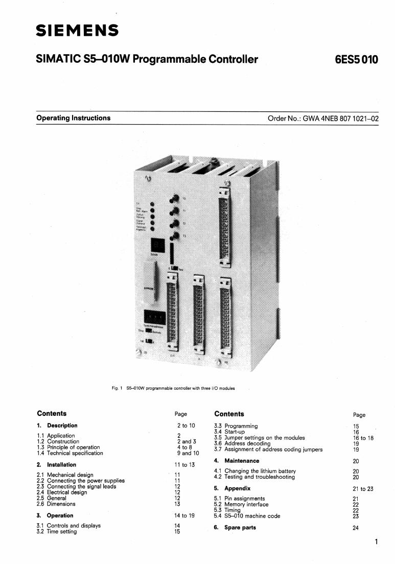
SlMATlC S5-010W Programmable Controller
Operating Instructions Order No.: GWA 4NEB 807 1021-02
Fig. 1 S501OW programmable controller with three 110 modules
Contents Page Contents Page
1. Description 3.3 Programming 3.4 Start-up 3.5 Jumper settings on the modules 3.6 Address decoding 3.7 Assignment of address coding jumpers
1.1 Application 1.2 Construction 1.3 Principle of operation 1.4 Technical specification
2 2 and 3 4 to 8 9 and 10
4. Maintenance 2. Installation
4.1 Changing the lithium battery 4.2 Testing and troubleshooting 2.1 Mechanical design
2.2 Connecting the power supplies 2.3 Connecting the signal leads 2.4 Electrical design 2.5 General 2.6 Dimensions
5. Appendix
5.1 Pin assignments 5.2 Memory interface 5.3 Timing 5.4 S5-010 machine code 3. Operation
3.1 Controls and displays 3.2 Time setting
6. Spare parts
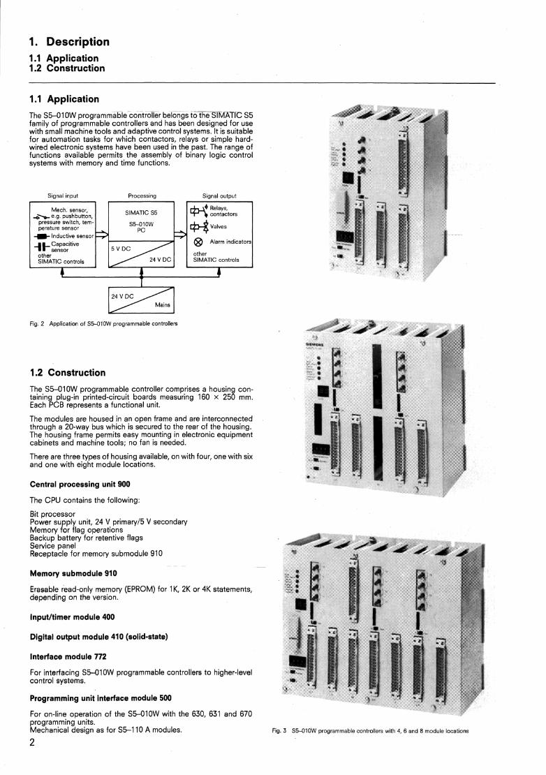
1. Description 1.1 Application 1.2 Construction
1 .l Application
The S5-010W programmable controller belongs to the-SIMATIC S5 family of programmable controllers and has been designed for use with small machine tools and adaptive control systems. It is suitable for automation tasks for which contactors, relays or simple hard- wired electronic systems have been used in the past. The range of functions available permits the assembly of binary logic control systems with memory and time functions.
Signal input Processing Signal output
24 V DC
Fig. 2 Application of S W l O W programmable controllers
, Mech. sensor,
,\e.g. pushbutton, pressure switch, tem- perature sensor
I n d u c t i v e sensor
-1 zny0itive other SlMATlC controls
1.2 Construction
SlMATlC S5
S5-010W PC I+-$ valves 3 @ Alarm indicators
other SlMATlC controls
The S5-010W programmable controller comprises a housing con- taining plug-in printed-circuit boards measuring 160 X 250 mm. Each PCB represents a functional unit.
k 1
The modules are housed in an open frame and are interconnected through a 20-way bus which is secured to the rear of the housing. The housing frame permits easy mounting in electronic equipment cabinets and machine tools; no fan is needed.
There are three types of housing available, on with four, one with six and one with eight module locations.
Central processing unit 900
The CPU contains the following:
Bit processor Power supply unit, 24 V primary15 V secondary Memory for flag operations Backup battery for retentive flags Service panel Receptacle for memory submodule 910
Memory submodule 910
Erasable read-only memory (EPROM) for 1 K, 2K or 4K statements, depending on the version.
Inputltimer module 400
Digital output module 410 (solid-state)
Interface module 772
For interfacing S5-010W programmable controllers to higher-level control systems.
Programming unit interface module 500
For on-line operation of the S5-010W with the 630, 631 and 670 programming units. Mechanical des~gn as for S5-110 A modules. Flg 3 S5-010W programmable controllers wlth 4, 6 and 8 module locations
2
1. Description
1.2 Construction
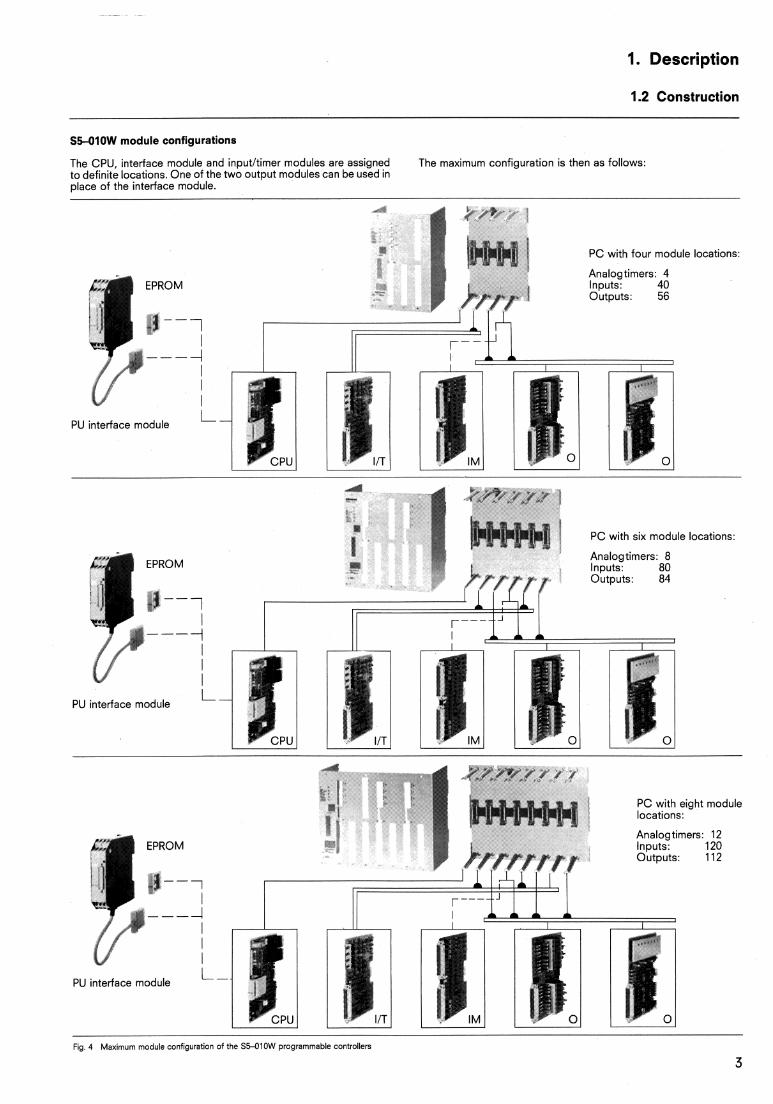
S5-010W module configurations
The CPU, interface module and inputltimer modules are assigned The maximum configuration is then as follows: to definite locations. One of the two output modules can be used in place of the interface module.
PC with four module locations:
Analog timers: 4 Inputs: 40 Outputs: 56
EPROM
($--l
--p 4 I I I
PU interface module L
PC with six module locations
EPROM Analogtimers 8
Outputs 84
I#--1 --- i
l I I
PU interface module L
EPROM
I#--1
PC with six module locations.
Analogtimers 8 -- Inputs: 80
Outputs: 84
l
I I
PU interface module L
EPROM
( 3 - 7 --- 4
l l I L-
PU interface module
l PC with etght module locat~ons
Analogtimers 12 Inputs. 120 Outputs 112
Fig. 4 Maximum module configuration of the S55 lOW programmable controllers
3
1. Description
1.3 Principle of operation
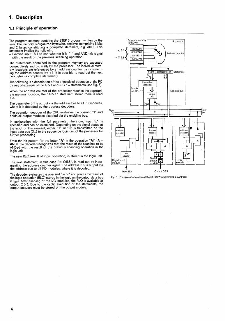
The program memory contains the STEP 5 program written by the user. The memory is organized bytewise, one byte comprising 8 bits and 2 bytes constituting a complete statement, e.g. A1 5.1. This statement implies the following: -Examine input 15.1 to see whether it is "1 " and AND this signal
with the result of the previous scanning operation.
The statements contained in the program memory are executed consecutively and cyclically by the processor. The individual mem- ory locations are referenced by an address counter. By increment- ing the address counter by +l, it is possible to read out the next two bytes (a complete statement).
The following is a description of the principle of operation of the PC by way of example of the A1 5.1 and = Q 5.3 statements (see Fig. 5).
When the address counter of the processor reaches the appropri- ate memory location, the "AI 5.1" statement stored there is read out.
The parameter 5.1 is output via the address bus to all I10 modules, where it is decoded by the address decoders.
The operation decoder of the CPU evaluates the operand "I" and holds all output modules disabled via the enabling bus.
In conjunction with the full parameter, therefore, input 5.1 is specified and can be examined. ?pending on the signal status at the input of this element, either 1" or "0" is transmitted on the input data bus (DIN) to the sequence logic unit of the processor for further processing.
From the bit pattern for the letter "A" in the operation "AI" (A = AND), the decoder recognizes that the result of the scan has to be ANDed with the result of the previous scanning operation in the logic unit.
The new RLO (result of logic operation) is stored in the logic unit.
The next statement, in this case "= Q5.3", is read out by incre- menting the address counter again. The address 5.3 is output via the address bus to all I10 modules, where it is decoded.
The decoder evaluates the operand "= Q" and places the result of the logic operation (RLO) stored in the logic on the output data bus (DouT). After enabling of the I10 modules, the RLO is available at output Q5.3. Due to the cyclic execution of the statements, the output statuses must be stored on the output module.
Program memory (EPROM)
Address counter
11000 8 00100000101 Statement r,2e = Q 5 3 1 i Operation I
Dour 1 1 1
DIN F T l 7 T-\
I
Input 15.1 Output Q5.3
Fig. 5 Principle of operation of the S5OlOW programmable controller
1. Description
1.3 Principle of operation
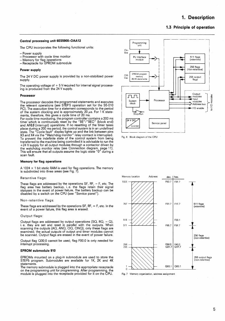
Central processing unit 6ES5900-OAA12
The CPU incorporates the following functional units:
- Power supply - Processor with cycle time monitor - Memory for flag operations - Receptacle for EPROM submodule
Power supply
The 24 V D C power supply is provided by a non-stabilized power supply.
The operating voltage of + 5 V required for internal signal process- ing is produced from the 24 V supply.
Processor
The processor decodes the programmed statements and executes the relevant operations (see STEP5 operation set for the S5-010 PC). The execution time for a statement corresponds to the period of the system clocking and is approximately 20 ys. For 1 K state- ments, therefore, this gives a cycle time of 20 ms. For cycle time monitoring, the program controller contains a 200 ms timer which is continuously reset by the "BE"/"BEC" (block end) and AFO.O (interrupt) operations. If no resetting of the timer takes place during a 200 rns period, the control system is in an undefined state. The "Cycle fault" display lights up and the link between pins X3 and X4 via the "Watchdog monitor" relay contact is interrupted. To prevent the indefinite state of the control system from being transferred to the machine being controlled it is advisable to run the +24 V supply for all output modules through a contactor driven by the watchdog monitor relay (see Connection diagram, page 11). This will ensure that all outputs assume the logic state "0" during a scan fault.
Memory for flag operations
A 1024 X 1 bit static RAM is used for flag operations. The memory is subdivided into three areas (see Fig. 7).
Retent ive f lags:
These flags are addressed by the operations SF, RF, = F, etc. The flag area has battery backup, i. e. the flags retain their signal statuses in the event of power failure. The battery backup can be disabled by a switch on the CPU (see "Service panel").
Non- re ten t i ve f lags:
These flags are addressed by the operations SF, RF, = F, etc. In the event of a power failure, this flag area is erased.
O u t p u t f lags:
Output flags are addressed by output operations (SQ, RQ, = Q), i. e. they are set and reset in parallel with the outputs. When scanning the outputs (AQ, ANQ, OQ, ONQ), only these flags are examined; the actual outputs of output and timer modules cannot be scanned. Output flags are erased in the event of power failure.
Output flag 000.0 cannot be used; flag FOO.O is only needed for interrupt processing.
EPROM submodule 910
EPROMs mounted on a plug-in submodule are used to store the STEP5 program. Submodules are available for IK, 2K and 4K statements. The memory submodule is plugged into the appropriate receptacle on the programming unit for programming. After programming, the module is plugged into the receptacle provided for it on the CPU.
On- line ~ i
Oif- line
Processor
256 flags 1 ;do.,te",e) I ,
Fig. 6 Block diagram of the CPU
Memory locatlon Address dec. I hex.
F1F 7 51 1 flags (retentive)
256 flags (non-retentive)
255 output flags (non-retentive)
Q00.1
Fig. 7 Memory organization, address assignment
1. Description
1.3 Principle of operation
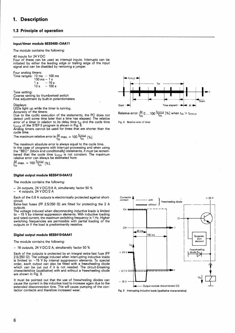
Inputlt imer module 6ES5400-OAAI 1
The module contains the following:
40 inputs for 24 V D C Four of these can be used as interrupt inputs. Interrupts can be initiated by either the leading edge or trailing edge of the input signal and can be disabled by removing a jumper.
Four analog timers: Time ranges: 10 ms - 100 ms
l o o m s - 1 s I s - 1 0 s 10s - 100s
Time setting: Coarse setting by thumbwheel switch Fine adjustment by built-in potentiometers
Displays: LEDs light up while the timer is running. Accuracy of the timers: Due to the cyclic execution of the statements, the PC does not detect until some time later that a time has elapsed. The relative error of a timer in relation to its delay time tZs and the cycle time t,,,,, of the STEP 5 program is shown in Fig. 8. Analog timers cannot be used for times that are shorter than the cycle time.
At The maximum relative error is - max. = 100 [%I, t zs tzs
The maximum absolute error is always equal to the cycle time. In the case of programs with interrupt processing and when using the "BEC" (block end conditionally) statements, it must be remem- bered that the cycle time tCYqLE is not constant. The maximum relative error can always be estrmated from At - max. = I O O ~ [%I. tzs tzs
Digital output module 6ES5410-OM12
The module contains the following:
- 24 outputs, 24 V DCl0.8 A; simultaneity factor 50 % - 4 outputs, 24 V DC12 A
Each of the 0.8 A outputs is electronically protected against short- circuit. Extra-fast fuses (FF 2.51250 G) are fitted for protecting the 2 A outputs. The voltage induced when disconnecting inductive loads is limited to -15 V by internal suppression elements. With inductive loading and rated current, the maximum switching frequency is 1 Hz. Higher switching frequencies are permissible with partial loading of the outputs or if the load is predominantly resistive.
Digital output module 6ES5410-OAA41
The module contains the following:
- 16 outputs, 24 V DC12 A; simultaneity factor 50 %
Each of the outputs is protected by an integral extra-fast fuse (FF 2.51250 G). The voltage induced when interrupting inductive loads is limited to -15 V by internal suppression elements. To special order, each output can also be fitted with a freewheeling diode which can be cut out if it is not needed. The circuit-breaking characteristics (qualitative) with and without a freewheeling diode are shown in Fig. 9.
It must be pointed out that the use of freewheeling diodes can cause the current in the inductive load to increase again due to the extended disconnection time. This will cause pumping of the con- tactor contacts and therefore increased wear.
Start T~me elapsed
Relative error: 0 . . ,100 [%l when tZs > tCYCLE tzs tzs
Fig. 8 Relative error of timer
Contactor contact ----- t with I freerherlmg d~ode 1 --3 without ) t7
On -----
Off t
+ 24 V
- 0.7 V t
- 15v
L Output module disconnected (Q) A- Fig. 9 Interrupting inductive loads (qualitative characteristics)
1. Description
1.3 Principle of operation
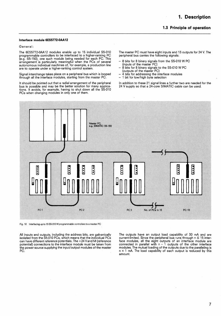
Interface module 6ES5772-OAA12
Genera l :
The 6ES5772-OAA12 modules enable up to 15 individual S5-010 The master PC must have eiaht inputs and 13 outputs for 24 V. The programmable controllers to be interfaced to a higher-ranking PC peripheral bus carries the fdlowing signals: (e.g. S5-150), one such module being needed for each PC. This arrangement is particularly meaningful when the PCs of several - 8 bits for 8 binary signals from the SS-010 W PC autonomous individual machines of, for example, a production line (inputs of the master PC) are to oaerate under a hiaher-rankina control svstem. - 8 bits for 8 binary signals to the S5-010 W PC
v (outputs of the master PC) Signal interchange takes place on a peripheral bus which is looped - 4 bits for addressing the interface modules through all the interface modules, starting from the master PC. - 1 bit for lowlhigh byte selection
It should be pointed out that a radial arrangement of the peripheral In addition to these 21 signal lines a further two are needed for the bus is possible and may be the better solution for many applica- 24 V supply so that a 24-core SlMATlC cable can be used. tions. It avoids, for example, having to shut down all the S5-010 PCs when changing modules in only one of them.
Fig. 10 Interfacing up to 15 55-010 Wprogrammable controllers to a master PC
PC 2 PC; 3 No of E s 5 15
All inputs and outputs, including the address bits, are galvanically The outputs have an output load capability of 30 mA and are isolated from the S5-010 PCs, which means that the individual PCs current-limited. Since the peripheral bus runs through n d 15 inter- can have different reference potentials. The +24 Vand M (reference face modules, all the eight outputs of an interface module are potential) connections to the interface module must be taken from connected in parallel with n - 1 outputs of the other interface the power source supplying the inputloutput modules of the master modules. The mutual loading of the outputs due to the paralleling is PC. n X 1 mA. The load capability of each output is reduced by this
amount.
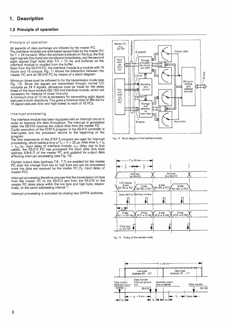
1. Description
Pr inc ip le o f opera t ion
AI! aspects of data exchange are initiated by the master PC. The interface modules are addressed sequentially by the master PC for T = 24 ms each. When the address is placed on the bus, the first eight signals (low byte) are transferred immediately, and the second eight signals (high byte) after T/2 = 12 ms, and buffered on the interface module or recalled from the buffer. Seen frorn the S5-010 PC, the interface module is a module with l 6 inputs and 16 outputs. Fig. 11 shows the interaction between the master PC and an S5-010 PC by means of a block diagram.
Minimum times rnust be adhered to for the transmission mode (see Fig. 12). Since the signals are transmitted through normal I/O modules as 24 V signals, allowance must be made for the delay times of the input module (S5-150) and interface module, which are necessary for reasoi?s of noise immunity. A rr~inirnum time of 12 ms is necessary for transmitting eight signal statuses in both directions. This gives a minimum time of 360 ms for 16 signal statuses (low and high bytes) to each of 15 PCs.
I n t e r r u p t p rocess ing
The interface module nas been equipped with an interrupt circuit in order to improve the data throughput. The interrupt is generated when the S5-010 receives the output data frorn the master PC. Cyclic execution of the STEP 5 program of the 55-010 controlier is interrupted and the processor returns to the beginning of the program. The first statements of the STEP 5 program are used for interrupt processing, which needs a time of T, = n X 20 ps. After time TB + tK + t,, (t,: input delay of interface module; to: delay due to bus cable), the S5-010 PC Ihas processed the input data (low byte address 6.E-6.7) of the master PC and updated its output data affecting interr~~pt processing (see Fig. 13).
Certain output data (address 7.0.. 7.7) are enabled for the master PC after the change from low 10 high byte and can be processed once rhe data are received by the master PC (TE: input delay of master PC).
Interrupt processing therelore ensures that the transmission of data from the master PC to the S5-010 and from the SF?-010 to the master PC takes place within the low byte and high byte, respec- tively, of the same addressing interval T.
interrupt processing is activated by closing two DIPFIX switches
I - ._ .1 L A
Fig. l ? Block diagram o i the kterface module
I Data read by idterface module 1 1 !
Fig. 12 1-iming of tile transfer mode
High byte I Low byte ! 1 Address 601 . . . E.7 I Address 7@ ... 7.7 1
l I 1 Data trar~sfer l
Data output Interrupt genera- Upda:ed o u t p ~ t l
Address output !ion data available Data transier
-..+ l
1. Description
l .4 "hchnica! specification
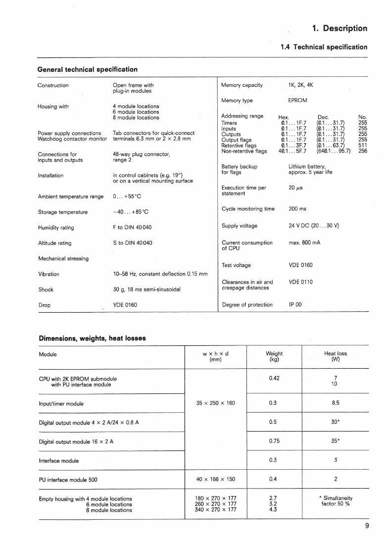
General technical specification -p--p--
Construction Open frame with plug-in modules
Memory capacity 1 K, ?K, 4K
Memory type EPROM Housing with 4 module locations
6 moduie locations 8 niodule locations Addressing range t+ex. Dec. No.
Timers D.1 . . . 1F.7 (D.1 . . .31.3) 255 Inputs 0.1 . . . IF.? (8.1 . . .31.7) 255 outputs a1 IF.^ (11.1 . . .31.7) 255 Output flags a1 . . . 1F.7 (0.1 . . .31.7) 255 Retentive flags 0.7 . . . 5 . 7 (0.1 . . . 63.7) 511 Non-retentive flags 4D.l . . .5F.7 (6411.1 . . .95.7) 256
Power supply connections Tab connectors for quick-connect Watchdog contactor monitor terminals 6.3 mm or 2 X 2.8 mm
Fonnections for 48-way plug connector, inputs arid outputs rarige 2
Battery backup for flags
Lithium battery, approx. 5 year life
20 us
Installation in control cabinets (e.g. 19") or on a vertical mounting surface
Execution time per statement Ambient temperature range 0 . . . +55"C
Cycle monitoring time 200 ms
24 V DC (20.. .30 V)
max. 800 mA
Storage temperature -40.. . +85"C
Supply voltage Humidity rating F to DIN 40040
Altitude rating S to DIN 40040 Current cor~sumption of CPU
Mechanical stressing Test voltage VDE 0160
VDE 01 l 0 Vibration 10-58 Hz, constant deflection 0.15 mm
Clearances in air and creepage distances Shock 30 g, 18 ms semi-sinusoidal
Drop VDE 0160 Degree of protection
Dimensions, weights, heat losses
Module w x h x d (mm)
Weight (kg)
Heat loss (W)
CPU with 2K EPROM submodule with PU interface module
Input/tirner module
Digital output module 4 X 2 AI24 X 0.8 A
Digital output module 16 x 2 A
Interface module
PU intetface module 500
Empty housing with 4 module locations 6 module locations 8 module locations
* Simultaneity factor 50 %
1. Description
1.4 Technical specification
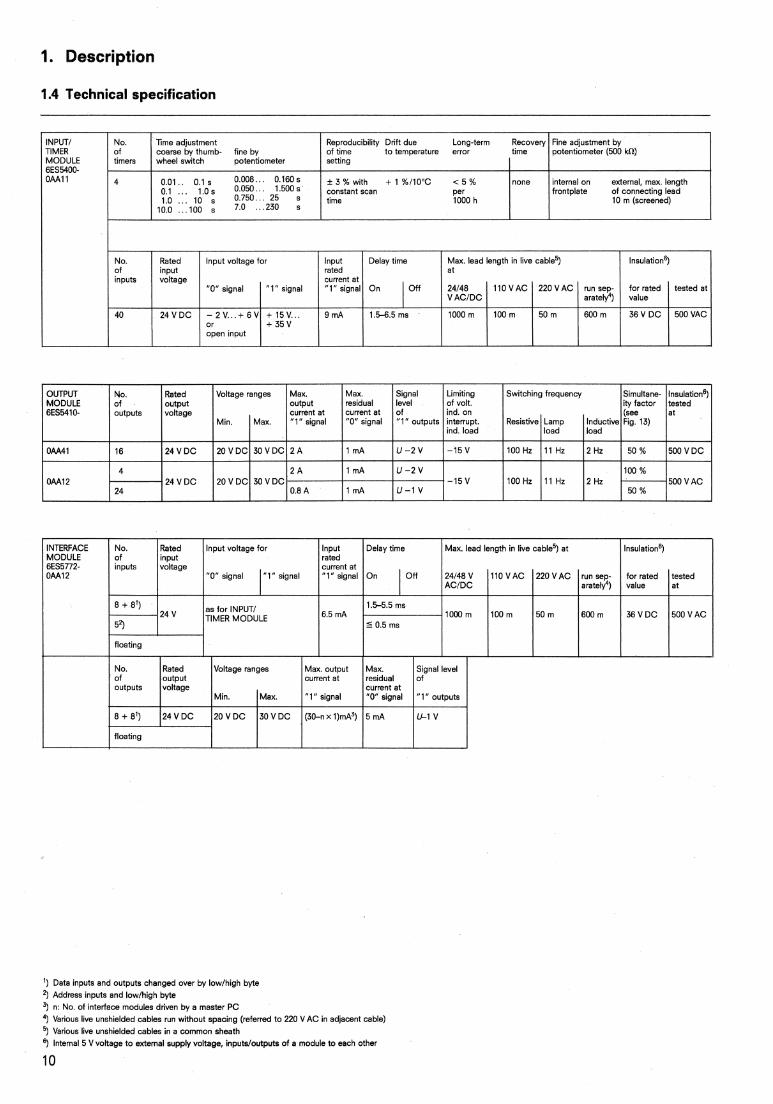
INPUT/ TIMER MODULE
No. Time adjustment of I coarse by thumb- fine 4 timers wheel switch potentiometer
+ 3 % with + l %/lO0C < 5 % lnone 1 internal on external, max. length constant scan Per frontplate of connecting lead time 1000 h 10 m (screened)
Reproducibility Drift due Long-term Recovery of time to temperature error time setting 1
Fine adjustment by potentiometer (500 kfl)
OUTPUT MODULE 6ES5410-
No. Rated Input voltage for of input inputs voltage
"0" signal "1" signal
2 4 V D C - 2 V . . + 6 V + 1 5 V . . .
open input
Input rated current at "l" signal
9mA
No. of outputs
16
4
24
l ) Data inputs and outputs changed over by lowlhigh byte ') Address inputs and lowlhigh byte =) n: No. of interface modules driven by a master PC
Various live unshielded cables run without spacing (referred to 220 VAC in adjacent cable) Various live unshielded cables in a common sheath
6, Internal 5 V voltage to external supply voltage, inputs/outputs of a module to each other
10
INTERFACE MODULE 6ES5772- OM12
Rated output voltage
2 4 V D C
2 4 V D C
Delay time
No. of inputs
8 + 8')
S2)
On
Max. lead length in live cable5) at
Off
Voltage ranges
floating
Rated input voltage
24 V
Insulation6)
1.5-6.5ms
Max. output current at "1" signal
2 A
2 A
0.8 A
Min.
2 0 V D C
2OVDC
for rated value
3 6 V D C
24/48 V ACIDC
1OOOm
Max.
3 0 V D C
3 0 V D C -
tested at
500VAC
l l 0 V A C
100m
220 VAC
5 0 m
Max. residual current at "0" signal
l mA
l mA
l mA
Input voltage for
run sep- arately4)
6OOm
Input rated current at "1" signal
6.5 mA
"0" signal
Signal level of "l" outputs
U - 2 V
U - 2 V
U - 1 V
"1" signal
as for INPUT/ TIMER MODULE
Limiting of volt. ind. on interrupt. ind. load
-15 V
-15V
Delay time
On Off
Max. lead length in live cable5) at
Switching frequency
1.5-5.5 ms
S 0.5 ms
24/48 V ACIDC
1OOOm
Insulation6)
Simultane- ity factor (see Fig. 13)
50 %
100 %
50 %
Resistive
l 0 0 Hz
100Hz
for rated value
3 6 V D C
Insulationfi) tested at
500 V D C
5 0 0 V A C
l10 V A C
100m
tested at
500VAC
Lamp load
l 1 Hz
l l H z
Inductive load
2 Hz
2Hz
220 VAC
5 0 m
run sep- arately4)
600m
2. Installation 2.1 Mechanical design
2.2 Connecting the power supplies
2.1 Mechanical design
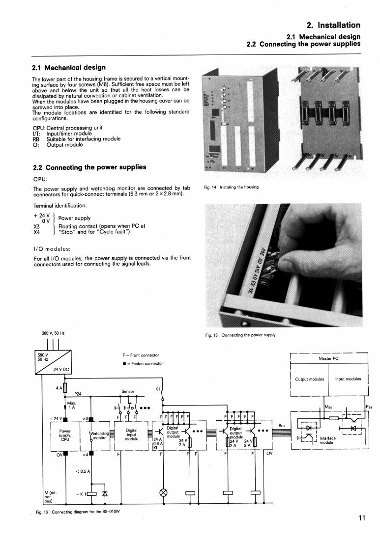
The lower part of the housing frame is secured to a vertical mount- ing surface by four screws (M6). Sufficient free space must be left above and below the unit so that all the heat losses can be dissipated by natural convection or cabinet ventilation. When the modules have been plugged in the housing cover can be screwed into place. The module locations are identified for the following standard configurations.
CPU: Central processing unit IIT: Inputltimer module RB: Suitable for interfacing module 0: Output module
2.2 Connecting the power supplies
CPU:
The power supply and watchdog monitor are connected by tab Fig. 14 Installing the housing
connectors for quick-connect terminals (6.3 mm or 2 X 2.8 mm).
Terminal identification:
+ 2: 1 Power supply
Floating contact (opens when PC at "Stop" and for "Cycle fault")
I f 0 modules:
For all I10 modules, the power supply is connected via the front connectors used for connecting the signal leads.
380 V, 50 Hz Fig. 15 Connecting the power supply
Fig. 16 Connecting diagram for the S!%.OlOW
2. installation 2.3 Connecting the signal leads 2.4 Electrical design 2.5 General
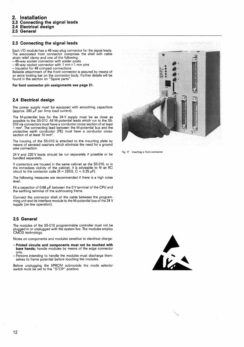
2.3 Connecting the signal leads
Each I10 module has a 48-way plug connector for the signal leads. The associated front connector comprises the shell with cable strain relief clamp and one of the following: - 48-way socket connector with solder posts - 48-way socket connector with 1 mm X 1 mm pins -Insulator for 48 crimped connections Reliable attachment of the front connector is assured by means of an extra locking bar or1 the connector body. Further details will be found in the section on "Spare parts".
For front connector pin assignments see page 21.
2.4 Electrical design
The power supply rriust be equipped with smoothing capacitors (approx. 200 yF per Amp load current).
The M-potential bus for the 24 V supply must be as close as possible to the S5-010. All M-potential leads which run to the S5- 010 via connectors must have a conductor cross-section of at least 1 mm2. The connecting lead between the M-potential bus and the protective earth conductor (PE) must have a conductor cross- section of at least 70 mmz.
-Printed circuits and components must not be touched with bare hands; handle modules by means of the edge connector only.
-Persons intending to handle the modules must discharge them- selves to frame potential before touching the modules.
The housing of the S5-010 is attached to the mounting plate by % means of serrated washers which eliminate the need for a ground wire connection.
Fig 17 Inserting a front connectof 24 V and 220 V leads should be run separarely if possible or be bundled separately.
If contactors are housed in the same cabinet as the S5-010, or in the immediate vicinity of the cabinet, it is advisable to fit an RC circuit to the contactor coils (R = 220f1, C = 0.25 yF).
The following measures are recommended if there is a high noise level:
Fit a capacitor of 0.68 PF between the O V terminal of the CPU and the earthing terminal of the subhousing frame.
Connect the connector shell of the cable between the proyram- ming unit and its interface module to the M-potential bus of the 24 V supply (on-line operation).
2.5 General The modules of the S5-010 programmable controller must not be plugged in or unplugged with the system live. The modules employ CMOS technology.
Notes on components and modules sensitive to electrical charge:
Before unplugging the EPROM submodule the mode selector switch must be set to the "STOP" position.
2. Installation
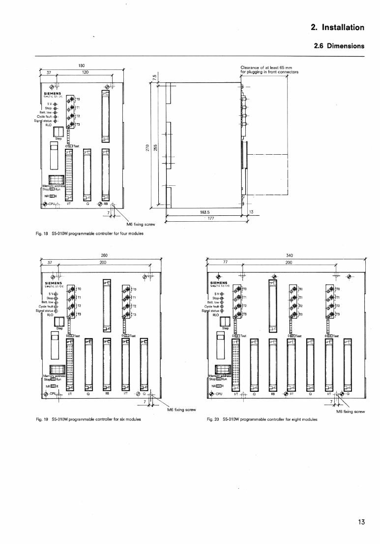
2.6 Dimensions
M6 fixing
Fig 18 S5-010W programmable controller for four modules
l
M6 fixing screw
Fig. 19 S5-010W programmable controller for six modules
M6 f ~ x ~ n g screw
Fig 20 S5-010W programmable controller for e~ght modules
3. Operation
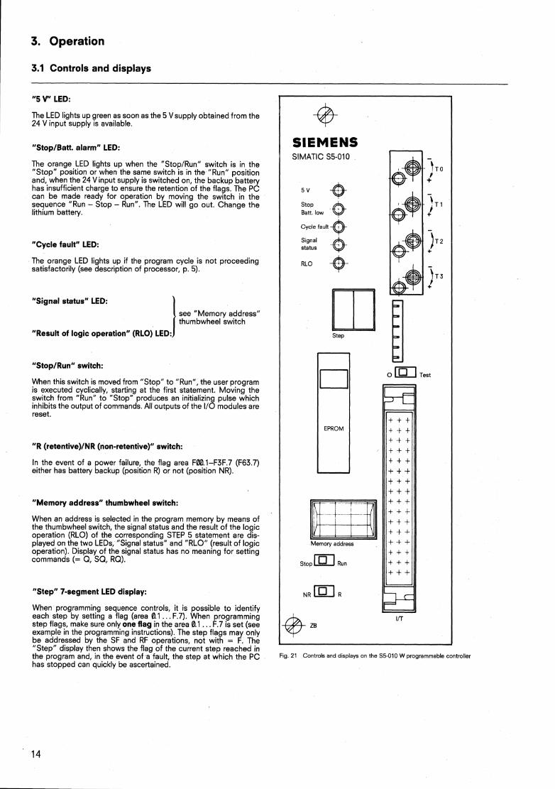
3.1 Controls and displays
"5 V" LED:
The LED lights up green as soon as the 5 Vsupply obtained from the 24 V input supply is available.
"Stop/Batt. alarm" LED:
The orange LED lights up when the "Stop/Run" switch is in the "Stop" position or when the same switch is in the "Run" position and, when the 24 V input supply is switched on, the backup battery has insufficient charge to ensure the retention of the flags. The PC can be made ready for operation by moving the switch in the sequence "Run - Stop - Run". The LED will go out. Change the lithium battery.
"Cycle fault" LED:
The orange LED lights up if the program cycle is not proceeding satisfactorily (see description of processor, p. 5).
"Signal status" LED:
see "Memory address" thumbwheel switch
"Result of logic operation" (RLO) LED:
"Stop/Run" switch:
When this switch is moved from "Stop" to "Run", the user program is executed cyclically, starting at the first statement. Moving the switch from "Run" to "Stop" produces an initializing pulse which inhibits the output of commands. All outputs of the I/O modules are reset.
"R (retentive)/NR (non-retentive)" switch:
In the event of a power failure, the flag area FmP).I-F3F.7 (F63.7) either has battery backup (position R) or not (position NR).
"Memory address" thumbwheel switch:
When an address is selected in the program memory by means of the thumbwheel switch, the signal status and the result of the logic operation (RLO) of the corresponding STEP 5 statement are dis- played on the two LEDs, "Signal status" and "RLO" (result of logic operation). Display of the signal status has no meaning for setting commands (= Q, SQ, RQ).
"Step" 7-segment LED display:
EPROM I
h
SIEMENS SlMATlC S5-010 -
\ T 0 I +
5 " -
E: low ((3 ;Tl
+ C.. fault $ -
@ 1.2
RLO + -
) ~ 3
Q Step
0 m Test
When programming sequence controls, it is possible to identify each step by setting a flag (area 0.1 . . . F.7). When programming step flags, make sure only one flag in the area 0.1 . . . F.7 is set (see example in the programming instructions). The step flags may only be addressed by the SF and RF operations, not with = F. The "Step" display then shows the flag of the current step reached in the program and, in the event of a fault, the step at which the PC has stopped can quickly be ascertained.
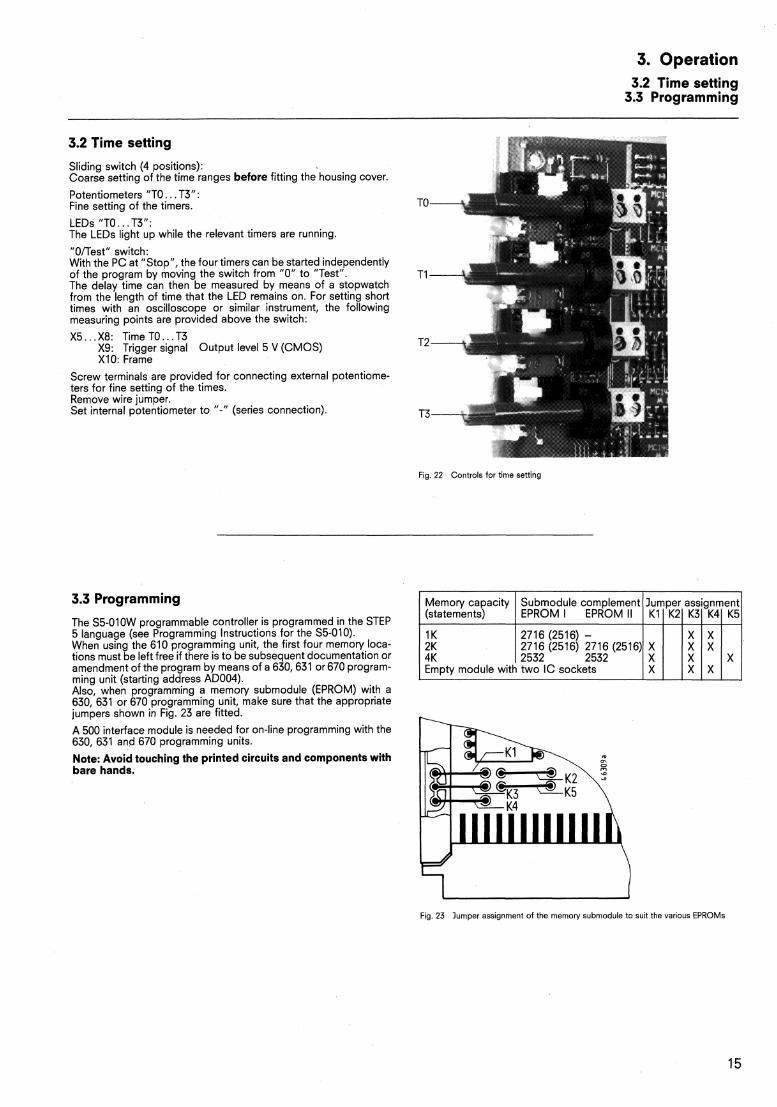
Fig. 21 Controls and displays on the S5-010 W ~ro~rarnrnable controller
3. Operation 3.2 Time setting
3.3 Programming --
3.2 Time setting
Sliding switch (4 positions): Coarse setting of the time ranges before fitting the housing cover.
Potentiometers "TO.. . T3": Fine setting of the timers.
LEDs "TO.. . T3": The LEDs light up while the relevant timers are running.
"O/Test" switch: With the PC at "Stop", the four timers can be started independently of the program by moving the switch from "0" to "Test". The delay time can then be measured by means of a stopwatch from the length of time that the LED remains on. For setting short times with an oscilloscope or similar instrument, the following measuring points are provided above the switch:
X5 . . . X8: TimeTO ... T3 X9: Trigger signal Output level 5 V (CMOS) X10: Frame
Screw terminals are provided for connecting external potentiome- ters for fine setting of the times. Remove wire jumper. Set internal potentiometer to "-" (series connection).
Fig. 22 Controls for time setting
Fig. 23 lumper assignment of the memory submodule to suit the various EPROMs
3.3 Programming
The S5-010W programmable controller is programmed in the STEP 5 language (see Programming Instructions for the S5-010). When using the 610 programming unit, the first four memory loca- tions must be left free if there is to be subsequent documentation or amendment of the program by means of a 630,631 or 670 program- ming unit (starting address AD004). Also, when programming a memory submodule (EPROM) with a 630, 631 or 670 programming unit, make sure that the appropriate jumpers shown in Fig. 23 are fitted.
A 500 interface module is needed for on-line programming with the 630, 631 and 670 programming units.
Note: Avoid touching the printed circuits and components with bare hands.
Memory capacity (statements)
1 K 2~ 4~
Submodule complement EPROM I EPROM II
2716 (2516) - 2716 (2516) 2716 (2516) 2532 2532
~~~t~ module with two IC sockets
Jumper assignment K1
X X X
K2
X
K3
X X X
X X
K4
X X
K5
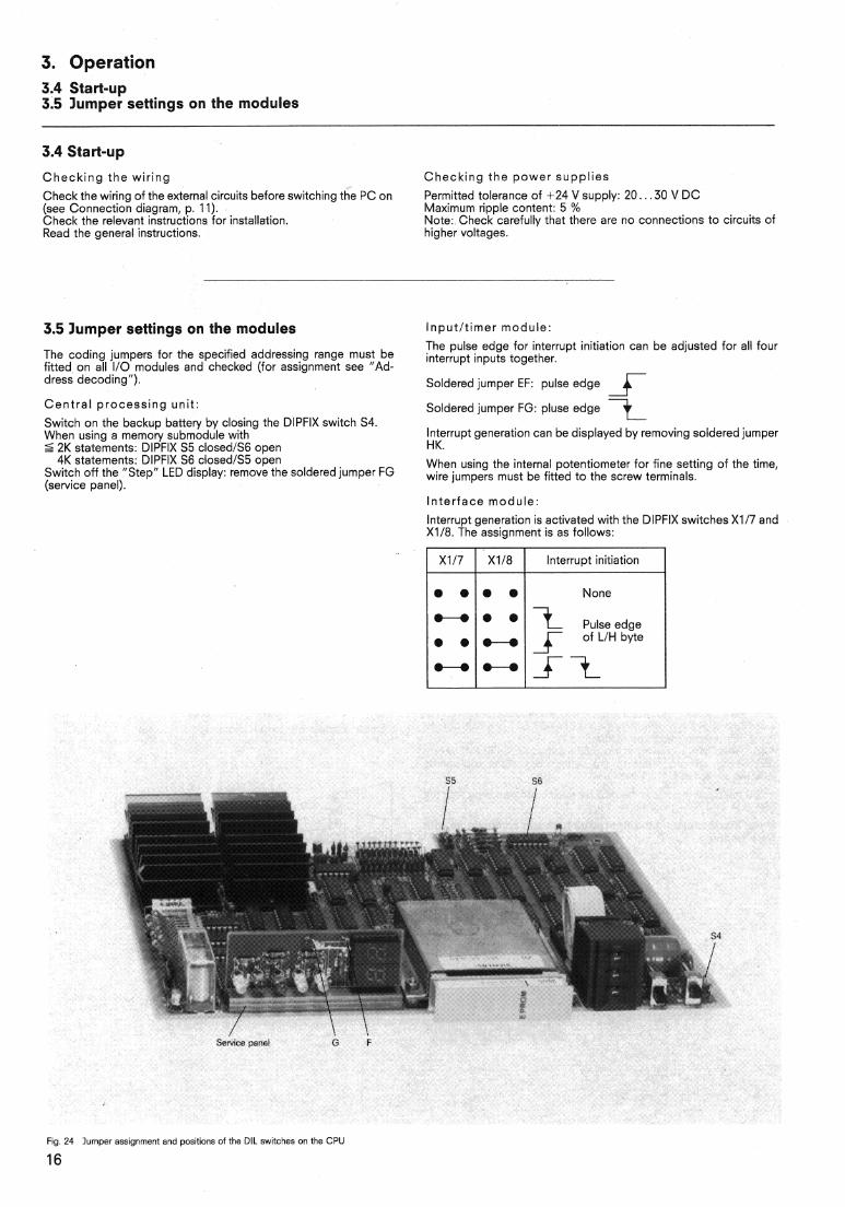
3. Operation 3.4 Start-up 3.5 lumper settings on the modules
3.4 Start-up
C h e c k i n g the w i r ing
Check the wiring of the external circuits before switching the PC on (see Connection diagram, p. 11). Check the relevant instructions for installation. Read the general instructions.
3.5 Jumper settings on the modules
The coding jumpers for the specified addressing range must be fitted on all I10 modules and checked (for assignment see "Ad- dress decoding").
C e n t r a l p rocess ing uni t :
Switch on the backup battery by closing the DlPFlX switch S4. When using a memory submodule with 5 2K statements: DlPFlX S5 closedIS6 open
4K statements: DlPFlX S6 closedIS5 open Switch off the "Step" LED display: remove the soldered jumper FG (service panel).
Check ing the power suppl ies
Permitted tolerance of +24 V supply: 20.. .30 V DC Maximum ripple content: 5 % Note: Check carefully that there are no connections to circuits of higher voitages.
I n p u t l t i m e r modu le :
The pulse edge for interrupt initiation can be adjusted for ail four interrupt inputs together.
Soldered jumper EF: pulse edge
Soldered jumper FG: piuse edge t lnterrupt generation can be displayed by removing soldered jumper HK.
When using the internal potentiometer for fine setting of the time, wire jumpers must be fitted to the screw terminals.
In te r face module:
Interrupt generation is activated with the DlPFlX switches X117 and X118. The assignment is as follows:
None
1 Pulse edge
4 Of byte st
X117
Fig. 24 Jumper assignment and positions of the DIL switches on the CPU
16
I I
X118 Interrupt initiation
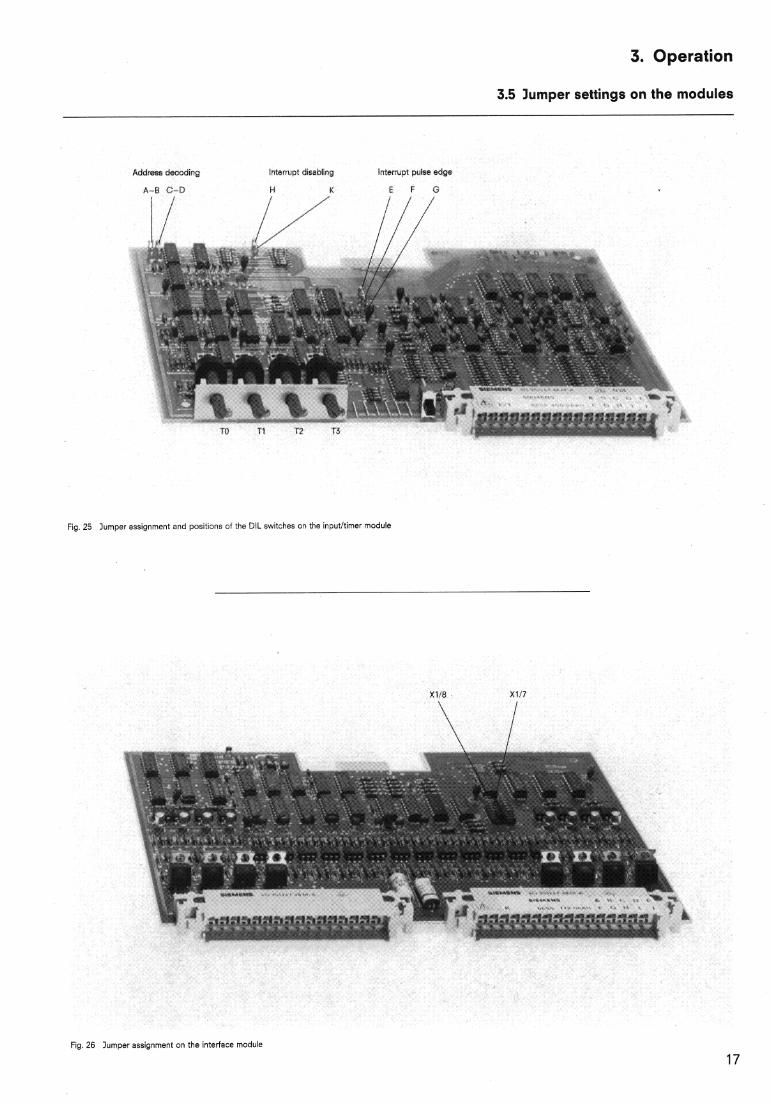
3. Operation
3.5 lumper settings on the modules
Address decrodiny
Fig. 25 lumper assignment and posi:ioi?s 31' :he DIL switches o? ine inputltimer nodule
Fig. 26 Jumper assignment on the interface module
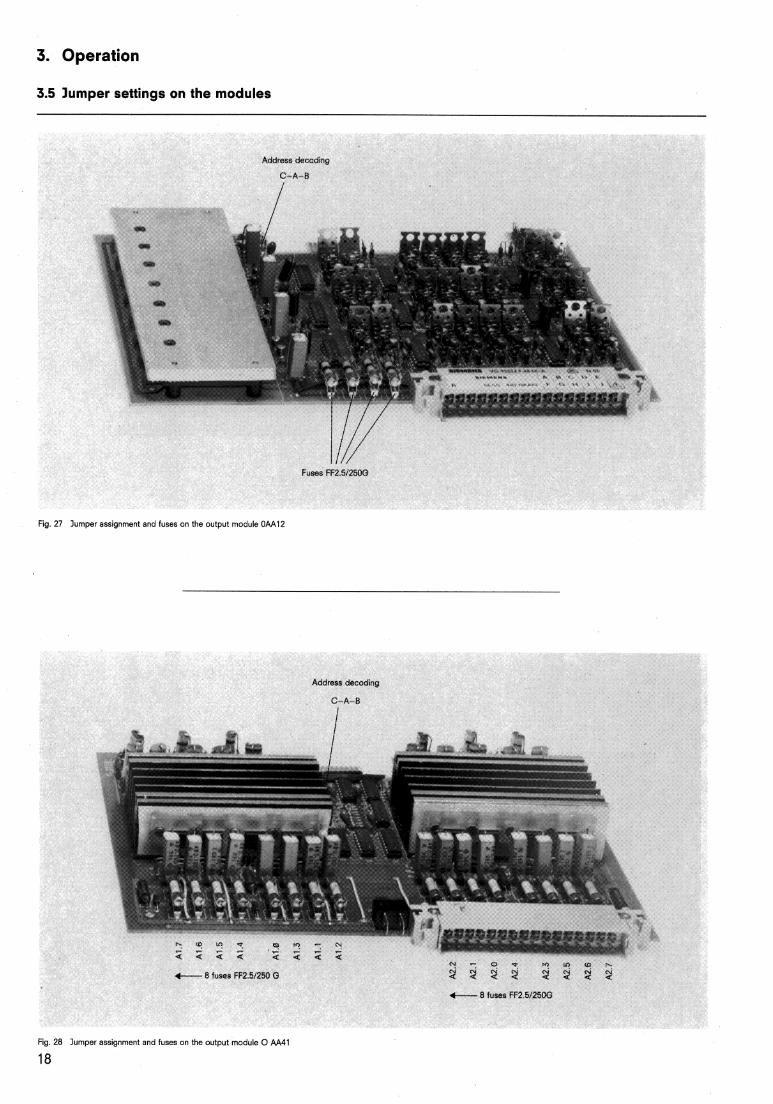
3. Operation
3.5 Jumper settings on the modules
Address decodiqg
C-A-B
Fuses FF2 X 5 0 0
Fig. 27 Jumper assignment and fuses on the output module OM12
Address decoding
c-A-B
Fig. 28 Jumper assignment and fuses on the output module 0 AA41
18
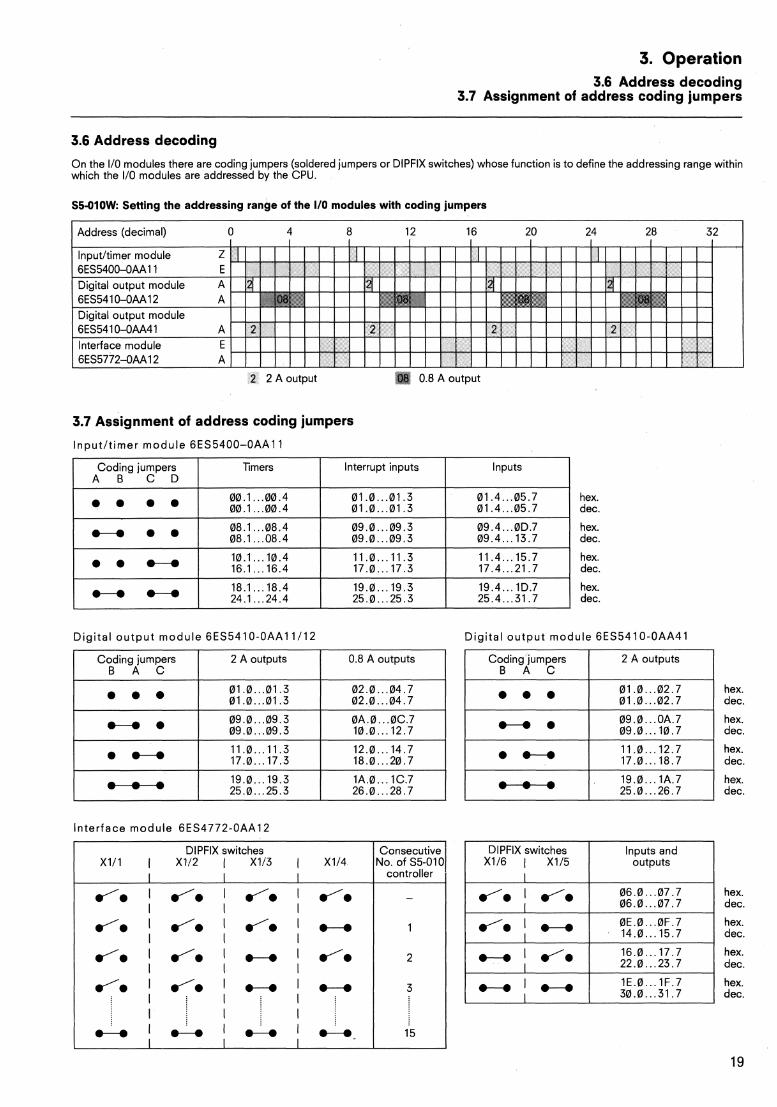
3. Operation 3.6 Address decoding
3.7 Assignment of address coding jumpers
3.6 Address decoding
On the I/O modules there are coding jumpers (soldered jumpers or DlPFlX switches) whose function is to define the addressing range within which the I10 modules are addressed by the CPU.
S5-010W: Setting the addressing range of the 110 modules with coding jumpers
1 Address (decimal) 0 4 8 12 16 20 24 28 32
Inputltimer module
2 2 A output m 0.8 A output
3.7 Assignment of address coding jumpers
Input l t imer module 6ES5400-OAA11
Coding jumpers I Iimers I Interrupt inputs I Inputs
I A B C D I hex. dec.
I l I
18.1 ... 18.4 19.0 ... 19.3 19.4 ... 1D.7 hex. I H 1 24 .1 .24.1 1 25.0 . . . 25.3 1 25.4 . . . 31.7 I dec.
hex. dec.
I I I
Dig i ta l output module 6ES541O-OAAI 1/12
01.4 ... 05.7 01.4 . . . 05.7 a . . .
hex. dec.
I I I
Dig i ta l output module 6ES5410-OAA41
.--. 0 .
I Coding jumpers 1 2 A outputs I 0.8 A outputs B A C I
00.1 ... 00.4 00.1 . . . 00.4
09.0 . . . 09.3 09.0 ... 09.3
08.1 ... 08.4 08.1 ... 08.4
0 .
I Coding jumpers B A C / A 1
01.0 ... 01.3 01.0 ... 01.3
09.4 ... 0D.7 09.4 ... 13.7
11.0 . . . 11.3 17.0 ... 17.3
10.1 . . . 10.4 16.1 ... 16.4
01.0 ... 02.7 hex. I 1 0 1 . 0 0 2 . 7 I dec.
11.4 . . . 15.7 17.4 ... 21.7
hex. dec.
I
Interface module 6ES4772-OAA12
M . hex. dec.
I
DlPFlX switches X111 I X112 I X113 1 X114
09.0 . . . OA.7 09.0 ... 10.7 . ,
hex. dec. -
U'. I U'. I 0'. I U'. I l I
11.0 . . . 12.7 17.0 ... 18.7
19.0 ... 1A.7 25.0 . . . 26.7
U'. I U'. I U'. I l I I
U'. I U'. I c I U'. I I I
Consecutive No. of S5-010
controller
1
2
3
15
DlPFlX switches Inputs and I X116 I X115 outputs I hex. dec.
U'. 1 .---. hex. dec.
OE.O . . . 0F.7 14.0 . . . 15.7
hex. dec.
hex. dec.
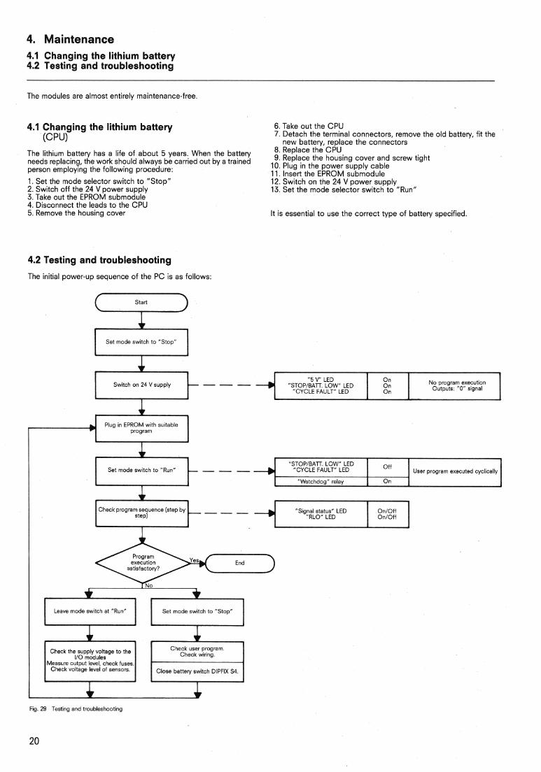
4. Maintenance 4.1 Changing the lithium battery 4.2 Testing and troubleshooting
The modules are almost entirely maintenance-free
4.1 Changing the lithium battery (CPU)
The lithium battery has a life of about 5 years. When the battery needs replacing, the work should always be carried out by a trained person employing the following procedure:
1. Set the mode selector switch to "Stop" 2. Switch off the 24 V power supply 3. Take out the EPROM submodule 4. Disconnect the leads to the CPU 5. Remove the housing cover
6. Take out the CPU 7. Detach the terminal connectors, remove the old battery, fit the
new battery, replace the connectors 8. Replace the CPU 9. Replace the housing cover and screw tight
10. Plug in the power supply cable 11. Insert the EPROM submodule 12. Switch on the 24 V power supply 13. Set the mode selector switch to "Run"
It is essential to use the correct type of battery specified.
4.2 Testing and troubleshooting
The initial power-up sequence of the PC is as follows:
Start G==)
Switch on 24 V supply ---
Check program sequence (step by step) l-
Check the supply voltage to the I10 modules
Measure output level, check fuses. Check voltage level of sensors.
Fig. 29 Testing and troubleshooting
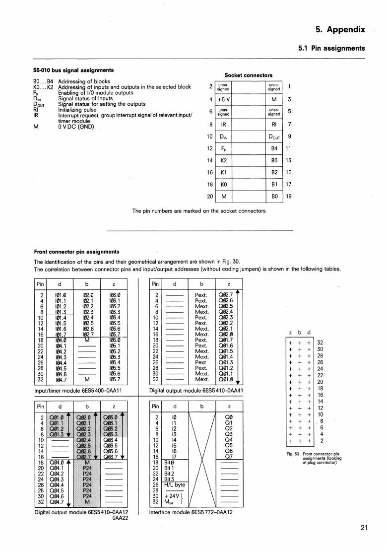
5. Appendix
5.1 Pin assignments
S5-010 bus signal assignments Socket connectors
B0 . . . B4 Addressing of blocks KO.. . K2 Addressing of inputs and outputs in the selected block 2 1 FP Enabling of I10 module outputs DIN Signal status of inputs 4 3 D,, Signal status for setting the outputs RI Initializing pulse IR Interrupt request, group interrupt signal of relevant input/
6 5
timer module M 0 V DC (GND) 8 7
The pin numbers are marked on the socket connectors.
Front connector pin assignments
The identification of the pins and their geometrical arrangement are shown in Fig. 30. The correlation between connector pins and inputloutput addresses (without coding jumpers) is shown in the following tables.
Input/timer module 6ES5400-OAA11 Digital output module 6ES54104AA41
Pin
2 4 6 8
10 12 14 16 18 20 22 24 26 28 30 32
Pin d b z
Q0 Q 1 Q2 Q3 Q4 Q5 Q6
16 17 Q7
b
102.0 102.1 102.2 102.3 102.4 102.5 102.6 102.7 M - - - - - -
M
d
101.0 101.1 101.2 101.3 101.4 101.5 101.6 181.7 104.0 104.1 104.2 104.3 104.4 104.5 104.6 104.7
z b d
2
103.0 103.1 103.2 103.3 103.4 103.5 103.6 103.7 ,
105.0 lffi. l 1ffi.2 16.3 1'23.4 16.5 IE.6 Iffi.7
Fig. 30 Front connector pin assignments (looking at plug connector)
Digital output module 6ES5410-OAA12 1 Interface module 6ES5 7724AA12 OAA22
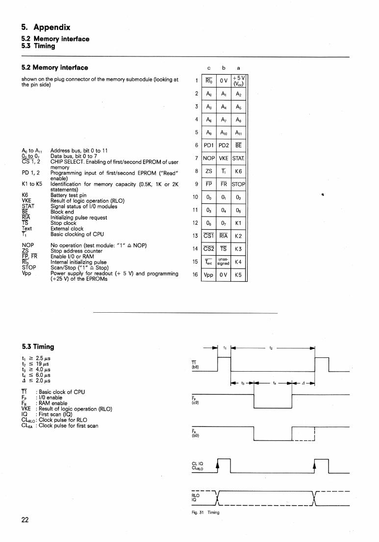
5. Appendix 5.2 Memory interface 5.3 Timing
5.2 Memory interface c b a
shown on the plug connector of the memory submodule (looking at 1 the pin side)
2
A, to All Address bus, bit 0 to 11 0 , 0 7 Data bus, bit 0 to 7 CS 1, 2 CHIP SELECT. Enabling of firstlsecond EPROM of user
memory PD 1, 2 Programming input of firstlsecond EPROM ("Read"
enable) K1 to K5 Identification for memory capacity (0.5K, 1K or 2K
statements) K6 Battery test pin VKE Result of logic operation (RLO) STAT Signal status of I10 modules W Block end RI A Initializing pulse request fS Stop clock Text - External clock TI Basic clocking of CPU
NOP No oweration (test module: "1" e NOP) 3- Stop'address 'counter FP, FR Enable I10 or RAM Rio Internal initializing pulse 15 STOP ScanIStop ( " l " e Stop) VPP Power supply for readout (+ 5 V) and programming 16
(+25 V) of the EPROMs
5.3 Timing
- T1 : Basic clock of CPU FP : l10 enable Fa : RAM enable VKE : Result of logic operation (RLO) IQ : First scan (IQ) CL,,,: Clock pulse for RLO CLEA : Clock pulse for first scan
Fig. 31 Timing
5. Appendix
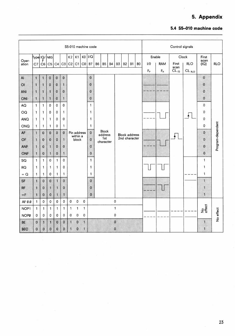
5.4 S5-010 machine code
S5-010 machine code Control signals
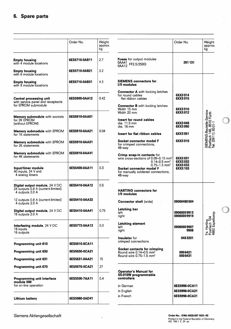
6. Spare parts
Weight approx kg
Order No. Order No.
Fuses for output modules
FF2.51250G
Weight approx. kg
Empty housing with 4 module locations
Empty housing with 6 module locations
Empty housing with 8 module locations
SIEMENS connectors for I10 modules
Connector A with locking latches for round cables
flat ribbon cables Central processing unit with service panel and receptacle for EPROM submodule Connector B with locking latches
Width 15 mm Width 20 mm
Memory submodule with sockets for 2K EPROM (without EPROM)
Insert for round cables dia. 11.5 mm dia. 16 mm
Memory submodule with EPROM for 1 K statements Insert for flat ribbon cables
Socket connector model F for crimped connections, 48-way
Memory submodule with EPROM for 2K statements
Memory submodule with EPROM for 4K statements Crimp snap-in contacts for
wire cross-sections of 0.09-0.15 mmi 0.14-0.5 mm2 0.75-1.5 mm2
Socket connector model F for manually soldered connections, 48-way
Inputltimer module 40 inputs, 24 V and 4 analog timers
Digital output module, 24 V DC 24 outputs 0.8 A (current-limited) 4 outputs 2.0 A HARTING connectors for
I10 modules
12 outputs 0.8 A (current-limited) 4 outputs 2.0 A Connector shell (wide)
Latching bar left right
Digital output module, 24 V DC 16 outputs 2.0 A
Interfacing module, 24 V D C 16 inputs 16 outputs
Latching element left right
Insulator for crimped connections
Programming unit 610
Programming unit 630
Programming unit 631
Programming unit 670
Socket contacts for crimping Round wire 0.14-0.5 mm2 Round wire 0.75-1.5 mm2
Operator's Manual for S5-010W programmable controllers Programming unit interface
module 500 for on-line operation in German
in English
in French
Siemens Aktiengesellschaft
Lithium battery
Order No.: GWA 4NEB 807 1021-02 Printed in the Federal Republic of Germany AG 184.1 E 24 en
6ES5980-OAD41

Siemens Aktiengesellschaft Subject to change without prior notice Order No.: GWA 4NEB 807 1021-02 Printed in the Federal Republic of Germany AG 184.1 E 24 en