shallow trench isolation double-diobe electrostatic discharge circuit and interaction with dram...
TRANSCRIPT

Journal of Electrostatics, 31 (1993) 237 262 237 Elsevier
Shallow trench isolation double-diode electrostatic discharge circuit and interaction with DRAM output circuitry
Steven H. Voldman, a V a u g h n P. Gross, a Michae l J. Ha rg rove , a J a m e s M. Never , ~ J a m e s A. S l inkman , ~ M a r t i n P .O 'Boy le b Tom S. Scotff and J o s e p h J. Delecki a
aIBM Technology Products, Essex Junction, VT 05452, USA bIBM Thomas J. Watson Reearch Center, Yorktown Heights, NY, USA ¢IBM Federal Systems Company, Manassas, VA, USA
(Received October 7, 1992; accepted in revised form April 20, 1993)
S u m m a r y
Electrostatic discharge (ESD) performance of a shallow-trench-isolation double-diode protection circuit in CMOS technology is discussed. This paper highlights the sensitivities of these devices to semiconductor process parameters, interaction with chip circuitry and advanced failure analysis techniques.
1. I n t r o d u c t i o n
Elec t ro s t a t i c d i scha rge (ESD) in advanced CMOS, BiCMOS logic and D R A M techno log ies is of g rowing in te res t t oday as s emiconduc to r devices scale to sub-0.5-/~m m i n i m u m fea tu re size. As m a n u f a c t u r i n g ESD requ i r emen t s increase , p rov id ing ESD p ro tec t ion in s emiconduc to r e n v i r o n m e n t s becomes more difficult. These ESD devices mus t be compa t ib le wi th the fu tu re d i rec t ion of s emiconduc to r t echnology . Sha l low t rench- i so la t ion double-diode (STIDD) ESD p ro t ec t i on devices are capab le of ach iev ing these object ives. This pape r h igh l igh t s the c i rcu i t ope ra t i on of these STIDD devices as a func t ion of process pa r ame te r s , the i r i n t e r a c t i o n wi th pad c i rcui t ry , the p a c k a g i n g issues invo lved and new fa i lure ana lys i s techniques . Two s igni f icant expe r imen ta l d iscover ies
© 1992, Reprinted with permission, after revision, from Electrical Overstress/Electrostatic Discharge Symposium Proceedings, EOS-14, Dallas, TX, USA, September 16-18, 1992.
0304-3886/93/$06.00 © 1993 Elsevier Science Publishers B.V. All rights reserved.

238 S.H. Voldman et al./ESD performance in CMOS technology
discussed are the dependence of ESD performance on well and epitaxial thick- ness variations and the effect of t i tanium salicide. Protect device scaling, hybridization and radiation hardness are also discussed for future extensions of this ESD protection circuit.
Compatibility with future technology features and requirements are only some of the advantages of double-diode ESD protection circuits [1]. Unlike some MOSFET ESD circuits, these ESD circuits neither have resistor elements nor high input capacitance. Double-diode ESD circuits take full advantage of well structures and parasitic elements contained in CMOS and BiCMOS technologies. The process sensitivities of these structures, on the other hand, have not been demonstrated in the literature. Our experiments show that n-well/epitaxial thickness design has an influence on ESD performance which can be optimized. Additionally, in our experiments, ESD performance im- proved with salicided double-diode ESD protection circuits. MOSFET ESD protection networks show salicided junctions significantly degrade ESD pro- tection [2-5]. These circuits can be extended to mixed-voltage interface circuits for logic technologies, synthesized and hybridized with other ESD protection circuit networks for improved ESD protection.
The advantages of shallow-trench isolation (STI) for ESD performance in the 16-Mb DRAM fabrication process, the 16-Mb DRAM chip itself, its package, and how the ESD protection circuit is implemented are discussed in the following sections. Specifically, this paper addresses ESD circuit design and layout, the circuit model, the circuit interaction with output circuitry, and process isssues. This will be followed by the test site, module chip testing procedure, and ESD results. Failure analysis using scanning electron micro- scope (SEM), optical microscope, Kelvin Force Probe microscope (KPFM), and emission microscope (EMMI) tools are combined for a complete analysis of the ESD failure mechanism. The paper concludes with a discussion of how circuit layout can be improved to eliminate these failure mechanisms, thereby extend- ing these ESD protection network concepts to future technologies.
2. STI- and LOCOS-de f ined d iode s t r u c t u r e s
Current isolation processes, such as LOCOS and shallow trench isolation (STI), can influence the performance of ESD protection circuits. STI struc- tures, in particular, are used in IBM's advanced 16-Mb CMOS DRAM and logic technologies [6]. STI-defined implants offer two advantages for the ESD indus- try: good diode electric-field scaling characteristics and lower perimeter capacitance.
The radius of curvature of junctions has an important influence on electric- field scaling and, hence, ESD performance. High electric fields, current densit- ies, and temeperature effects as well as non-uniform current flow in non-planar junctions tend to degrade ESD performance and are the primary points for device failure [7]. Avalanche and secondary breakdown of cylindrical and spherical junctions occur prior to "planar" diode junction region [7-9]. In
S.H. Voldman et al./ESD performance in CMOS technology
(a}
(b)
come, J S"
I . C ~ ~ J ' ~ / / / ~ Planar
" = '
239
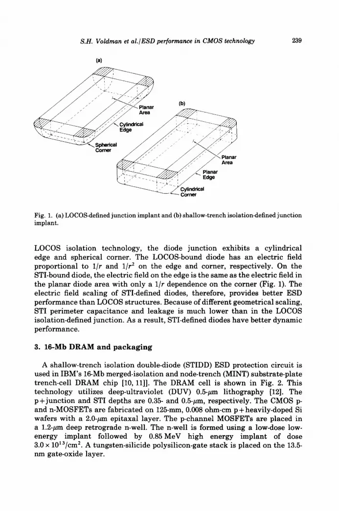
Fig. 1. (a) LOCOS-defined junction implant and (b) shallow-trench isolation-defined junction implant.
LOCOS isolation technology, the diode junction exhibits a cylindrical edge and spherical corner. The LOCOS-bound diode has an electric field proportional to 1/r and 1/r 2 on the edge and corner, respectively. On the STI-bound diode, the electric field on the edge is the same as the electric field in the planar diode area with only a 1/r dependence on the corner (Fig. 1). The electric field scaling of STI-defined diodes, therefore, provides better ESD performance than LOCOS structures. Because of different geometrical scaling, STI perimeter capacitance and leakage is much lower than in the LOCOS isolation-defined junction. As a result, STI-defined diodes have better dynamic performance.
3. 16-Mb DRAM and p a c k a g i n g
A shallow-trench isolation double-diode (STIDD) ESD protection circuit is used in IBM's 16-Mb merged-isolation and node-trench (MINT) substrate-plate trench-cell DRAM chip [10, 11]]. The DRAM cell is shown in Fig. 2. This technology utilizes deep-ultraviolet (DUV) 0.5-#m lithography [12]. The p+ junc t ion and STI depths are 0.35- and 0.5-/~m, respectively. The CMOS p- and n-MOSFETs are fabricated on 125-mm, 0.008 ohm-cm p + heavily-doped Si wafers with a 2.0-#m epitaxal layer. The p-channel MOSFETs are placed in a 1.2-/~m deep retrograde n-well. The n-well is formed using a low-dose low- energy implant followed by 0.85MeV high energy implant of dose 3.0 x 10¹³/cm 2. A tungsten-silicide polysilicon-gate stack is placed on the 13.5- nm gate-oxide layer.

240 S.H. Voldman et al.IESD performance in CMOS technology
Bit Line \
Sujtace Strap
N-Well P+ Substrate Trench
Fig. 2. 16-Mb MINT DRAM cell.
vcc
DC20
DC21
W
RE
DS0
DSl
vcc
Fig. 3. Packaging leads to ESD device/pad.

S.H. Voldman et al./ ESD performance in CMOS technology 241
The DRAM chip is packaged in a 32-pin, and 28/24-pin SOJ module. This package has dual in-line leads at a 50-mil lead pitch. Two rows of ESD devices are placed in the center of the chip with packaging leads extending over the array area (Fig. 3). The package has short wire bonds and lead lengths, which reduce input resistance, capacitance and inductance.
4. STIDD ESD circuit s tructure and layout
The STIDD ESD structure is fabricated by placing an STI-defined p + diode in an n+re t rograde n-well (Fig. 4). The n-well is connected to the internal n-well voltage reference Vdd, forming a p-n diode between the output pad and power supply. A second diode is formed using an STI-defined n ÷ implant inside a retrograde n-well. This is simply a diode-stack between the power supply and substrate. STI defines the p÷ and n÷implants . The n-well containing the p+diode extends around the n-well-to-substrate diode element. These are separated by a p+float ing guardring structure. The entire structure is en- closed in an n + guardring that is attached to a p + substrate contact.
Parasitic elements also play a key role in ESD protection (Fig. 5). A vertical pnp transistor exists as well as the p÷diode component (e.g., the p÷diode, n-well and p ÷ substrate). High current gain vertical bipolars are advantageous from an ESD perspective, but problematic for technology scaling due to CMOS latchup. The vertical pnp parasitic transistor has low p ÷ emitter capacitance for good dynamic response, but poor bipolar current gain because of the large base width and high n-well doping concentration. A lateral pnp formed by the p ÷ diode, n-well and p-epi layer also is present. A distinction from the LOCOS- isolation double-diode ESD protection circuit, the STIDD lateral pnp gain is insignificant, even without guardrings and minimal design spacing. This
.a0 T oC,rcu,
N ÷ Retrograde Well
)
. . . .
Fig. 4. Shallow trench isolation double-diode ESD protection network.

242 S.H. Voldrnan et al./ESD performance in CMOS technology
RM
VSub VDD ~ Rcontact ~ Rcontact VDD Vsu b
\ RSub \ / Sub ) \ Vertical Lateral N-Well Diode J
PNP NPN to Ground
Fig. 5. STIDD ESD incremental model with device parasitics.
makes the STIDD ESD circuits insensitive to p +/n-well spacing, maintaining good ESD control and minimizing latchup concerns. Because the n-well (which is tied to the power supply) acts as a guardring to the n-well diode, a lateral npn also exists between the two n-well structures. In addition, the n + guardring is tied to a p+ implan t and then grounded through metal wiring to collect residual charge. Figure 6 shows the STIDD ESD layout, with the metal pattern interwoven to allow for access to the pad and Vdd along the broadside of the ESD structure.
5. STIDD ESD circuit operat ion
ESD circuit operation is dependent on the ESD test mode. When the power supply (Vdd) is grounded and the input pad is biased positively, the p + diode forward-biases. For the negative human body model (HBM) mode, the lateral npn formed by the n-well diode, the substrate and the n-well tub discharges the current to the Vdd supply rail. When the substrate, Vss, is grounded and Vdd is floating, with a positive HBM, the charge discharges to the Vdd supply. For the case of negative HBM, the well diode discharges to the p + substrate. This is verified using an emission microscope. The dependence on parasitic pnp and npn transistors requires a semiconductor process that achieves good parametric control of n-well sheet resistance, substrate doping and epitaxial thickness. As MOSFETs scale for future technologies, these devices will natural ly scale with the technology. The diodes can be visualized as ideal diodes with a series resistance element which is a function of semicon- ductor process parameters. To better understand the STIDD ESD structure, a refined model that quantifies process- and structure-related resistance elements will be discussed.

S.H. Voldman et al./ ESD performance in CMOS technology
N + Guard Ring / N-Well Contact
243
+ Substrate ontact
1 D
P+ Diode N-Well Diode to VDD to Substrate
Fig. 6. STIDD ESD c i rcu i t layout .
6. STIDD ESD s e m i c o n d u c t o r proces s i s sues
In STIDD ESD circuits, semiconductor process variations, such as n-well, p +, and n + sheet resistane, can lead to variations in the ESD protection level. By understanding the process sensitivities, the semiconductor process can be optimized to produce the best ESD performance
N-well profiling and epitaxial thickness in CMOS trench DRAM technolo- gies is a key design technology issue. N-well design influences the n-well sheet resistance, n-well and p+ junc t ion breakdown and capacitance, lateral and vertical bipolar transistors, vertical sidewall trench FETs, and DRAM reten- tion. In STIDD ESD circuits, n-well variation affects the diode and parasitic bipolars. N-well sheet resistance variations are a function of the n-well retro- grade implant dose and energy, epitaxial thickness, substrate doping concen- tration, and hot process in CMOS heavily doped substrate technologies

244 S.H. Voldman et al./ ESD performance in CMOS technology
[13, 14]. The n-well sheet resistance increases as the epitaxial layer thickness decreases or substrate doping concentration and semiconductor total hot process AT increases. This is caused by compensation of the n-well implant by the heavily-doped substrate, which reduces the base width of the vertical-pnp transistor, thereby increasing the bipolar gain. At the same time, the base series resistance has increased, thereby limiting pnp bipolar action. Variation in the n-well sheet resistance influences ESD protection by increasing the series resistance of the n-well diode to ground. As we will show, ESD perfor- mance degrades with increased n-well sheet resistance.
In salicided junction technology, the p + and n + sheet resistance is domin- ated by salicide thickness. N+ sheet resistance variations affect both ESD HBM pulse polarity test modes. P÷ resistance variations affect only the positive ESD pulse mode by limiting current redistribution in the p + diode. High-sheet resistance in the n +implant leads to large resistive elements for both diodes in the ESD device. N+res is tance also increases the base series resistance of the vertical parasitic transistor. Hence, changes in the sheet resistance caused by a lack of salicide or poor salicide formation can lead to degraded ESD performance.
Poor contact resistance to the p + diode implants and n ÷ n-well contacts can also degrade ESD performance. In this technology, W-stud contact resistance is well controlled. However, when contact resistance is high because of poor interface resistivity (e.g., residual films, poor contact surface cleaning, poor interface metallurgy formation), ESD results are degraded.
7. STIDD ESD c ircui t mode l
For simulation of an ESD event and circuit modeling, large-signal high- frequency diode and bipolar models are used (Fig. 7). For large-signal high- frequency modeling, ideal diodes and Eber-Moll type bipolar models with charge storage element terms and resistive elements are used for switching analysis. Circuit topology contains a series-resistance element to simulate metal input resistance and a capacitor element for pad capacitance. Resistors are used for the contact and sheet resistance elements discussed in the prior section. Temperature-dependent ideal-diode elements are assumed with the series resistor elements. Diode elements are simulated by perimeter and area depletion capacitors, and voltage-dependent current sources. For the parasitic bipolar transistors, base diffusion capacitance elements are needed to properly simulate the ESD device high frequency response in either a switching mode or ESD event.
8. STIDD ESD c ircui t i n t e r a c t i o n wi th o u t p u t c ircui t s
In our implementation, no resistor elements are used between the STIDD ESD circuit and input/output circuitry. With proper design of the STIDD ESD protect device and output circuit, good ESD protection can be achieved when

S.H. Voldman et al.IESD performance in CMOS technology 245
p VDD
GL Packaging
Lead Frame
Lateral NPN
Fig. 7. STIDD high frequency-large signal circuit model.
7 T T 7 -=_ _; 7
Address Pin with N-Channel Pin with P-Channel Receiver Pin Bleed Transistor Bleed Transistor
Pin with Full-Pass Transistor Gate
Fig. 8. Input/output pad circuitry types.
* +
Pin with OCD Circuit
the ESD device charge-shares with the output circuitry. This is especially true when the ESD-limiting performance is the ESD device itself.
When the impedance of the I/O circuitry is low, the ESD protection circuit and I/O circuitry both play a role in the ESD event. The families of output circuitry typical to DRAM and logic circuits are receivers, drivers, n-channel “bleed transistors”, and p-channel ‘bleed transistors’ for devices in a parallel configuration with the STIDD circuit (Fig. 8). On some pins, half- and full-pass

246 S.H. Voldman et al./ESD performance in CMOS technology
transistor elements are in series with the STIDD ESD device. Increasing ESD performance of the STIDD circuit with properly designed pad circuitry in the positive pulse mode are: pins with gate only, n-channel bleed transistors, p-channel bleed transistors, full-pass transistor circuits, and off-chip drivers (OCD). A bleed transistor is a narrow-width, long-channel MOSFET that is in parallel with the ESD protection device and with a gate that is biased normally 'on'. The channel width-to-length ratio is 1 : 50 to 1 : 100 with a channel width of 1-#m. In n-channel bleed transistors, the gate is biased at Vdd, while in p-channel bleed transistors, it is biased at ground. These 'on' transistors have low current drive and, hence, do not impact circuit functionality. Because these MOSFETs are long, snapback does not occur in these devices in either positive or negative HBM pulse modes. In the positive pulse mode, the p- channel bleed device source forward biases when the p ÷ implant is raised above the n-well bias voltage. N-channel bleed device drain current is caused by 3-D MOSFET gate-induced drain leakage (GIDL) that occurs prior to avalanche breakdown. As a result, the p-channel bleed transistor responds faster than n-channel bleed transistors.
Pads with full-pass transistors have both p- and n-channel MOSFETs in series with the ESD device and are parallel to each other. In contrast to bleed devices, these transistors typically have higher-than-unity W/L ratios with short-channel devices to minimize delay times. In positive pulse mode, the p-channel source will forward-bias while the n-channel MOSFET attempts to snapback. In this case, because the n-channel device is in series with both the pad and gate, no significant current is drawn and the n-channel MOSFET of the pass transistor will not enter the high current snapback mode.
Careful layout of the p- and n-channel MOSFETs can lead to improved ESD protection when OCD circuit "charge sharing" occurs. In OCDs, the n-channel MOSFET is electrically between the pad node and substrate, while p-channel MOSFETs are between pad node and the power supply node. To obtain positive results, antiparallel metal bussing [16], high contact density, and contact- to-gate space design criteria should be followed. Optimum ESD protection occurs by either improving the dynamic response of the STIDD ESD device or increasing the n-MOSFET channel length. Selection of an appropriate length ensures that the STIDD protect device "turn-on" occurs prior to n-channel snapback.
9. STIDD HBM ESD tes t ing
ESD test-site development and effective use of technology design passes can drive ESD performance, quality and learning. ESD test site macro structures are constructed so that their response could be analyzed with OCD and receiver circuits (Fig. 9). Kerf macro structures are wire-bonded in ceramic dip packages and attached to an automated ESD HBM machine for testing. An IMCS 5000 ESD simulator was used for testing. The tester pulse conformed to the human body model (HBM) as set by the MIL-STD-883C code. The capacitor

S.H. Voldman et al./ESD performance in CMOS technology 247
Receiver
ESD Device
VSub Ground Bus
Pad (Load)
.------ Output Driver P-Channel
Bus
'•-• Output Driver N-Channel
Pad (Input) I ~ - - - - - - E S D Device
Fig. 9. ESD protect device test site for receiver and off-chip driver analysis.
is charged using a regulated high-voltage supply. The HBM circuit is a 100 pF capacitor which discharges through a 1500-ohm resistor into the device-under- test through a mercury switch. ESD testing of the STIDD structure is com- pleted on test sites for preliminary design work and then transferrred to the product chip for implementation.
10. STIDD c i rcu i t wi th ga te s t r u c t u r e ESD results
To understand the response of the STIDD ESD structure, we will discuss the ESD results as inputs to gate structures on packaged 16-Mb SOJ modules. In the negative HBM pulse mode, ESD protection is over 10 kV with respect to Vss and Vdd. In the positive pulse mode, ESD protection (for a nominally centered process) is over 4.5 kV on all address pins. On the other hand, for high n-well sheet resistances, ESD performance degraded. Over a wide range of n-well sheet resistance values, ESD protection on all packaged modules re- mained well above 3 kV. In every instance, the fail-limiting ESD mechanism proved to be the ESD protection circuit rather than the gate structure.

248 S.H. Voldman et al./ ESD performance in CMOS technology
11. STIDD circuit with pad c ircui try ESD resul t s
STIDD ESD performance with pad circuitry is above pins with only gate structures as inputs. In the positive pulse mode, ESD protection levels varied according to the input circuitry with special functions typically achieving the highest ESD result. In the 16-Mb DRAM, data-select pins have a 1/50-#m n-channel bleed transistor in parallel with the ESD protection circuit. In these devices, n-channel snapback does not occur. Pins with the n-channel bleed transistors have higher ESD performance compared to the address pin popula- tion (independent of the process variables). This is more observable when the Vss pin is grounded and Vdd pin is floating.
In the positive pulse mode, pins with p-channel bleed transistors achieved ESD protection of 4.8 kV, because of forward biasing of the p-channel diffusion implant on the device. In both cases, the fail-limiting structure was the STIDD protect device, which carried the majority of the ESD HBM pulse current. When bleed transistors are in parallel with the STIDD circuit, there is a clear difference in the ESD fail signature. Pins with these additional transistors exhibited a fail on only one edge of the ESD protection device, while the others failed on both ends. This indicates that charge sharing occurs.
When a full-pass transistor is placed in series with the ESD STIDD circuit, ESD performance improves further because of p-channel forward biasing. Again, the ESD fail occurred less often on both ends of the p +implant. This indicates that pins with additional pad circuitry reduce the current density in the STIDD circuit, thereby causing a higher ESD fail value and less ESD damage in the STIDD circuitry. In this instance, the ESD protection was 500 V higher than the STIDD device input into a gate, thus achieving ESD protection levels to 4.9 kV at centered n-well sheet resistance.
12. STIDD circuit with OCD ESD resul t s
In early development, pins with OCD circuitry showed ESD performance was degraded due to n-channel MOSFET snapback. For a nominal design point, this performance degraded from 4.5 to 3.0 kV because of a small width 40: 0.65- pm n-channel MOSFET. Failure analysis revealed that failure occured in the center of the n-channel MOSFET transistor between the two diffusions. A new stacked n-channel drive circuit ESD performance typically achieved above 8.9 kV with respect to Vdd and Vss. In the stacked n-channel design, the ESD performance increased 4.6 kV above the inherent protection level of the STIDD ESD protect circuit. The ESD limiting-fail mechanism in these OCD pins occurs in the n-channel MOSFETs.
13. P a c k a g i n g and b u s s i n g inf luence on ESD resul t s
Analysis of ESD fails on the 16-Mb DRAM revealed that individual pin failure was systematic. Pins with the shortest lead frame and the largest

S.H. Voldman et al./ ESD performance in CMOS technology 249
distance from the Vdd pad had the highest ESD performance. For example, in the address pin family, pin A9 with the shortest wire bond and lead frame length and further distance from the Vdd pad, had the highest ESD perfor- mance (Fig. 3). Further ESD experiments using unencapsulated packages and internal probing show that the ESD performance variation is dominated by the placement of the STIDD circuit on the internal chip Vdd power bussing. ESD performance improved as the protect circuit was further from the Vdd pad (chip center). These results show that power bus and packaging design play a role in ESD protection distributions in a given module.
14. S T I D D E S D r e s u l t s v s N - w e l l s h e e t r e s i s t a n c e
ESD performance of the STIDD ESD device as a function of process variables was discussed previously. N-well sheet resistance, which varies the p-n diode and vertical bipolar transistor performance, is a function of epitaxial layer thickness, n-well implant dose, substrate doping concentration and hot pro- cessing. As the epitaxial layer becomes thinner, the substrate compensates the n-well implant, thereby increasing n-well sheet resistance. As this sheet resist- ance increases, vertical pnp bipolar gain increases. Concurrently, the diode performance degrades because the series resistance of the diode and pnp base increases. Vertical pnp current gain ranged from 2.0 to 4.0 (over the range of epitaxial layer thickness). Vertical pnp bipolar gain of 8.0 is achieved by reduc- tion of the retrograde implant dose by 3X from the nominal dose. Figure 10 shows STIDD ESD protection as a function of the n-well sheet resistance and input pad circuitry for a positive HBM pulse (with respect to Vss). Figure 11 shows STIDD ESD protection with respect to Vdd. In each instance, the ESD performance degrades with increasing n-well sheet resistance. Results show that ESD protection decreases approximately 2-3 V for every ohm/square increase in n-well sheet resistance. New results show that by increasing the n-well retrograde dose or increasing the epitaxial thickness, ESD performance in the STIDD ESD circuit can be increased to 8 kV [14, 15]. Further results show that ESD performance is a function of both effective film thickness and the n-well sheet resistance [15].
15. S T I D D E S D r e s u l t s v s t i t a n i u m s a l i c i d e
A significant experimental discovery as part of this study was that ESD perforamnce improved with titanium salicide in our design. It has been re- ported that ESD protection degrades with titanium salicide junctions that use gated thick and thin oxide MOSFET ESD protection circuits. High current densities carried by salicided junctions lead to thermal hot spots, causing ESD protect device failure at the MOSFET gate-to-drain overlap region. Because STIDD ESD structures do not use gated components, they do not experience the salicide-induced gate-to-drain ESD failure mechanism. In our experiments, salicided junctions improve the ESD performance of STIDD circuits. ESD

250 S.H. Voldman et al./ESD performance in CMOS technology
5.0
E
z 4.0
s E ‘0 t
p”
5f w
3.0
m Full Pass Transistor 0 P-Channel Bleed Device IJ N-Channel Bleed Device l Address Pin
Vsub -Ground V,,-Float Positive HBM Pulse
I I I I I 1
650 700 750 800 850
N-Well Sheet Resistance (Q/sq)
Fig. 10. ESD performance vs n-well sheet resistance (with respect to V,,,).
5.0 r
l Full-Pass Transistor 0 P-Channel Bleed Device 0 N-Channel Bleed Device l Address Pin
3.0 L I I I I , J 650 700 750 800 850
N-Well Sheet Resistance (Q/sq)
Fig. 11. ESD performance vs n-well sheet resistance (with respect to V,,).

S.H. Voldman et al./ESD performance in CMOS technology 251
4.2
4.1
4.0
3.9
3 .8
3.7
~ 3 ,6 o "c 3.5
a 3 .4
" 3 .3
3.2
3.1
3.0
D o o
D o
Tes t - Pos i t i ve HBM • =
- Sal ic ide o Vsu b = Gnd • • OVDD = G n d
- N o Sa l i c l de ; vsub = Gnd • • VDD Gnd •
4 Sal icided Junct ion ~, . * - -Non-Sal ic ided Junc t i on - - * . l i * i i ] i i t ' ~ i l i i i i i i
2.6 2.8 3.0 3.2 3.4 ~ 22 24 26 28
N+ Shee t Res is tance (g~/sq)
Fig. 12. ESD performance vs N ÷ sheet resistance (as a function of salicide/no salicide).
4 . 2 []
4 . 0
v • 3 . 8 o c
E 3.6
n a 3 . 4
UI
3 . 2
3.0
O O Vsu b = G r o u n d
o n a VDO = Ground
Q
o o
r~ Is
o Is
IS
Salicided Non-Salicided J u n c t i o n " " Junc t ion "
i i i i
2 1 6 ' 2 : 8 ' 3 ' . 0 ' 1 ; 2 ; ' 2'2 24 2'8 P+ Sheet Res is tance (f~/sq)
Fig. 13. ESD performance vs P÷ sheet resistance (as a function of salicide/no salicide).
s t r u c t u r e s were tes ted wi th and w i t hou t t i t a n i u m sal ic ide (TiSi2) f rom the same e x p e r i m e n t a l lot. The p + i m p l an t sheet r e s i s t ance was 2.5 ohms / squa re and 22.5 ohms / squa re wi th and w i t hou t TiSi2, respect ive ly . We not only con- s i s ten t ly obse rved no degrada t ion , but observed an i m p r o v e m e n t in STIDD ESD p ro t ec t i on by 600 vol t s wi th TiSi2 in all pos i t ive t es t modes for more t h a n one type of STIDD ESD circui t . F igures 12, 13 and 14 show ESD p e r f o r m a n c e as

252 S.H. Voldman et al./ ESD performance in CMOS technology
v
o c
o
a. a
w
4.2
4.0
o 3 . 8 -
~1._ o 3,6 ~ l ¢0 - t ~ OeJ
3.4
3.2
l
70O
[ 3
[3 O O
Test - Posit ive HBM
Sal ic ide [] VSub = Gnd o VDD = Gnd
No Salicide • Vsub = Gnd • VDD = Gnd
%
o o
~ OJO ~ , 800 9 0 1 0 1100 1200
NW Sheet Resistance (~/sq)
Fig. 14. ESD performance vs NW sheet resistance (salicide/no salicide experiment).
a function of the n ÷, p ÷ and n-well sheet resistance with and without TiSi2 junctions, respectively. In STIDD circuits, the lower the series resistance, the better the current distribution along the entire diode structure---a key factor in extending certain ESD protection devices to future technologies.
16. S T I D D E S D r e s u l t s v s c o n t a c t r e s i s t a n c e
Our experiments have shown that high series-resistance degrades STIDD ESD protection. The tungsten-stud contact process, which was used in these devices, achieves very low contact resistance. High contact resistance impacts p ÷ implant-to-Vdd diode ESD performance in a positive HBM pulse mode. For negative HBM pulses, high contact resistance impacts n-well-to-substrate diode response.
In early development, contact resistance was high because of residual films in the contact holes (with 5-20 ohms per contact). Initial ESD testing of lots with high contact resistance typically showed 3.8 to 4.1 kV in the positive pulse mode. Currently, new ti tanium deposition and etch cleaning processes provide improved contact resistance (less than 2 ohms/contact). ESD performance of 4.3 to 4.8 kV was demonstrated on hardware with good contact resistance. The improvement with good contact resistance was approximately 600 V. With high contact resistance, ESD failure was distributed over 6-10 contacts on the ends of the p ÷ implant (Fig. 15). With low resistance contacts, ESD failure was limited to the last one or two contacts (Fig. 16). It appears that with low contact resistance, the single contact carried the higher current density,

S.H. Voldman et al./ESD performance in CMOS technology 253
Fig. 15. ESD fail with high contact resistance. ESD fail occurs on P+ diode in positive HBM pulse mode.
Fig. 16. ESD fail with good contact resistance (Rcontac t < 2 •).

254 S.H. Voldman et al./ ESD performance in CMOS technology
whereas, with high resistance contacts, a larger number of contacts were needed to supply the same current to the corner of the p + implant. The fail signature of the high resistive contact is repeatable and very consistent.
17. Failure analysis: liquid crystal and SEM
Significant understanding was achieved by combining failure analysis tech- niques to analyze the STIDD ESD fail mechanisms. This analysis was initially performed with liquid crystal techniques. BDH K15, used for liquid crystal analysis, has a 34 degree Celsius transition temperature. When localized heating occurs, BDH K15 changes from a clear-to-dark state in either ramp- or pulse-test mode. When the defective pin is pulsed, the dark region flickers, which pinpoints the region of ESD failure. Liquid crystal analysis shows ESD failure occurring in silicon.
SEM samples were prepared with a 5-minute HF dip etch, with all material removed above the silicon surface. The samples were placed in a 1000X optical microscope and 5000X SEM for visual inspection. Two fail signatures were observed. For the OCD pins, ESD failure occurs in the OCD circuitry. In all other pins, ESD failure occurs in the STIDD ESD device.
For the OCDs, ESD failure occurred in a small-width minimum-channel length 40/0.65-#m n-channel MOSFET OCD circuit between pad node and ground. SEM failure analysis of the second set of OCD circuit pins showed ESD failure occured in the n-channel MOSFETs of the OCD circuit and in a 3-to-5 volt internal interface circuit. Early catastrophic failure occurs at 5.4 to 6 kV on the 0.75-#m n-channel MOSFETs. Presently, ESD fails occur at 8.9 kV in 0.65-/~m n-channel MOSFETs. The fail pattern shows that the multiple-clustered fails occur symmetrically along the channel, highlighting the antiparallel voltage distribution and regions of the snapback turn-on [16]. SEM results verified the benefit of good OCD design practices in achieving the additional 1-2 kV ESD protection.
On all other pins, ESD failure occurs at the corner of the STI-defined p+implant . When the STIDD ESD circuit input is only a MOSFET gate, ESD failure typically occurs on both ends of the STIDD ESD p+diode. This indicates the diode failure mechanism is not a defect-initiated failure, but rather due to high current densities and thermal heating. On special function pins, ESD failure typically occurs on one end. This indicates that the additional circuitry decreased the current density in the STIDD ESD circuit.
A study of SEM fails showed that high current "streamers" were present between the p + diode and the n + n-well contacts under the STI surface. These streamers began with the first contact at the p + implant corner. This indicates that localized high-current density paths occurred at the end of the device. In some pins, streamers appeared off the flat end of the p + diode. From the SEM photos, it can be observed that the dopant in the n + implant had moved under the STI in the streamer regions (Fig. 17).

S.H. Voldman et al./ ESD performance in CMOS technology 255
Fig. 17. ESD fail at P+ corner.
18. Failure Analysis: Kelvin Probe Force Microscope
One method used to investigate the ESD fail region was with a Kelvin Probe Force Microscope (KPFM) [17, 18]. The KPFM tool is a member of the family of atomic force and tunnelling microscopes that use different capabilities for different materials and applications. The KPFM can simultan- eously measure surface topography and contact potential difference. The potential variations can be a function of surface charge, adsorption layers, silicon doping concentration, and material/ temperature differences in the sample.
Figure 18 shows a high-level diagram of the KPFM system. The system is simply a probe tip and electronic feedback circuits to manuever the tip over the sample. The first feedback loop, locked in at a given frequency, maintains a constant distance between the 50-nm probe tip and the ESD fail sample surface. This yields a topographic image of the sample. The second loop, operated at another frequency, simultaneously nulls the local electric field between the probe tip and the sample. The nulling voltage (known as the contact potential difference) is proportional to the local workfunction differ- ence between the tip and the sample (along with any charge that exists between them). This has significant value for exploring ESD dielectric damage,

256 S.H. Voldman et al./ ESD performance in CMOS technology
Sample \ Etched Tip
Laser Beam \ '\
Displacement ~ Sensor
IZ Feedback ~
Computer / ~ I Stack
CO 1
~ ~)olk.ln Amp I X,Y Control
X•Y Piezo
Lock-ln Amp ~2
Tip Bias (AC + Da)
Fig. 18. Kelvin probe microscope (KPFM) high level diagram.
atomic-level pin holes, and latent damage of ESD structures that cannot be found with either SEM, TEM, or photoemission techniques. In our case, we are interested in obtaining a high-level resolution for analysis of the ESD fail and to explore the nature of the ESD fail mechanism. The Kelvin probe feature also allows for dopant redistribution analysis in the ESD fail region in the silicon surface. This can be used to understand the magnitude of thermal heating in the ESD fail region.
The sample used for SEM analysis was measured with the KPFM tool. Figure 19 contains both SEM and KPFM tool results. The topology map shows the silicon variations under the STI region as well as in the depressions at the first single contact. Clearly, the location of the first single contact near the corner and 2-D diode effect on the end lead to high current densities and significant thermal heating to produce silicon failure.
Preliminary KPFM contact potential maps shows surface potential vari- ations in the region of the ESD fail mechanism. Peak potential variations are present in the location of the maximum ESD damage in the p + implant.
19. Failure analysis: Photoemission Analysis Technique
Photoemission techniques were used for ESD/EOS analysis to find ESD/ EOS-induced fail mechanisms such as gate oxide breakdown, substrate dam- age, contact punchthrough, and other defect mechanisms [19-21]. An Emission Microscope (EMMI) tool consists of (a) an optical microscope stage, (b) a micro-channel intensifier, (c) a solid state camera, and (d) an image process- ing computer (Fig. 20). Photoemissions are observed by the optical microscope

S.H. Voldman et al./ ESD performance in CMOS technology 257
STI P+ N + Region Implant Guard
Ring
P+ Implant
Fig. 19. SEM and K P F M results of ESD corner fail.

258 S.H. Voldrnan et al./ESD performance in CMOS technology
Solid-State Camera
Microchannel Intensifier
Optical Microscope
l ESD
Device
Video Image Processor
I Video
Monitor
Fig. 20. High level diagram of photo-emission microscope.
projecting the image on the micro-channel image intensifiers. This photoemis- sion signal is then amplified and fed into the solid state camera, where it is converted to a video signal. This signal is digitized and sent to an image processor computer. The image intensifier is sensitive to radiation with wavelengths from 380 nm to 920 nm [19]. In our tests, photoemission analysis is used to determine current density distribution in the ESD device. This tech- nique is being used to verify that ESD failure is due to high current density at the end of the trench isolation defined p + implant and to observe nonuni- formities.
The EMMI tool was used in the forward-biased diode mode. In this mode, photoemissions are due to radiative emissions from recombination of minority carriers. When the output pad was biased above Vdd, photon emissions were visible along the complete length of the p + diode where metal was not present. Second, photoemission intensity on the reversed biased n-well diode was well below that observed on the forward bias p+ implan t (which was consistent with SEM and Kelvin probe results). In this STIDD ESD device, the metal pattern is symmetrically spaced, which "digitized" the photoemission pattern. Figure 21 shows increasing photon emission density along the diode length with peak emission at the end of the p + implant. Figure 22 shows a 3-D mapping of the photon count. Three photon emission peaks are observable at the end of the p + implant. The highest peak is at the end of the p + implant, while the two other peaks are near the corners of the p + implant. This location is consistent with the SEM and KPFM results for the high current density streamers.

S.H. Voldman et al./ESD performance in CMOS technology 259
P÷ Implant Comer . . ~
J Fig. 21. Photon count along P+ diode implant. Results show peak photon emissions at P÷ implant corner. The photon "null" points due to metal patterning.
e -
Fig. 22. Photo-emissions of P ÷ diode. 3-D photon count show peak photon count on edge and corner of P+ implant. Counter map below is projection of 3-D photon distribution.
20. STIDD ESD layout improvements
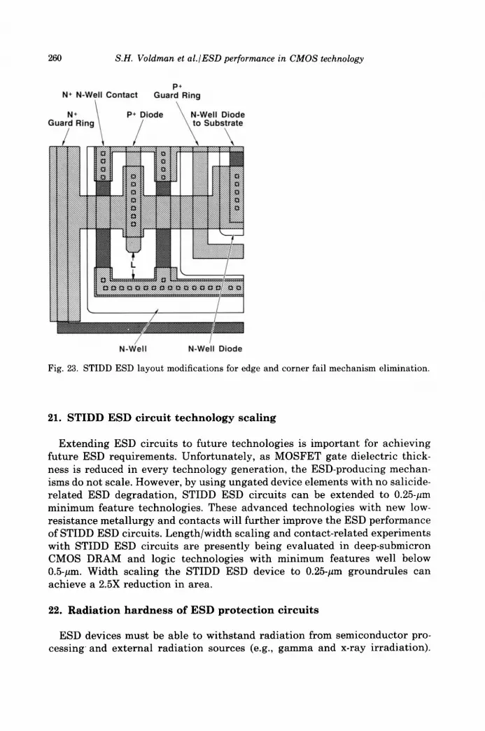
To e l imina te the 3-D end and corne r fail m e c h a n i s m observed in the ESD s t ruc tu re , four i m p r o v e m e n t s were made to p r e v e n t h igh c u r r e n t densi t ies (Fig. 23). First , the p + i m p l an t edge-to-n + n-well con tac t space was increased. The first t h ree con tac t s n e a r the p + i m p l a n t edge were t hen r emoved to es tab l i sh a res i s t ive p a t h be tween the first con t ac t and the edge. In addi t ion, the co rne r s of the p ÷ i m p l a n t were ang led to cur ren t - l imi t the co rne r and sof ten the STI cy l indr ica l corners . F inal ly , n-well con t ac t s were r emoved n e a r the p + i m p l a n t corners . P r e l i m i n a r y ESD resu l t s show the end / co rne r defect m e c h a n i s m was e l imina ted wi th these changes . Fa i lu re analys is , a f t e r these changes were implemented , shows the fa i lu re po in t does no t occur a t the end of the p + diode, bu t a t the las t t h ree con tac t s a w a y f rom the corner .
260 S.H. Voldman et al./ ESD performance in CMOS technology
p+ N ÷ N-Well Contact Guard Ring
N-Well N-Well Diode
Fig. 23. STIDD ESD layout modifications for edge and corner fail mechanism elimination.
21. STIDD ESD c ircui t t e c h n o l o g y sca l ing
Extending ESD circuits to future technologies is important for achieving future ESD requirements. Unfortunately, as MOSFET gate dielectric thick- ness is reduced in every technology generation, the ESD-producing mechan- isms do not scale. However, by using ungated device elements with no salicide- related ESD degradation, STIDD ESD circuits can be extended to 0.25-gm minimum feature technologies. These advanced technologies with new low- resistance metallurgy and contacts will further improve the ESD performance of STIDD ESD circuits. Length/width scaling and contact-related experiments with STIDD ESD circuits are presently being evaluated in deep-submicron CMOS DRAM and logic technologies with minimum features well below 0.5-gm. Width scaling the STIDD ESD device to 0.25-#m groundrules can achieve a 2.5X reduction in area.
22. Rad ia t ion h a r d n e s s of ESD p r o t e c t i o n c ircu i t s
ESD devices must be able to withstand radiation from semiconductor pro- cessing and external radiation sources (e.g., gamma and x-ray irradiation).

S.H. Voldman et al./ ESD performance in CMOS technology 261
Double-diode ESD protection circuits exhibit good radiation hardness results because they have no gate structures. Modules were first exposed to gamma- ray total-dose radiation and then ESD tested. Total dose experiments were done using a Cobalt-60 gamma source. Gamma ray emissions of 1 MeV im- pinged on the packaged module at a dose rate of 10, 20, 50, 100 and 200 krads. ESD testing showed no degradation with irradiation on any pin in the positive HBM pulse mode (with respect to the power supply). For example, ESD results were 4.4 to 4.6 kV for all dose splits on the address pins. OCD ESD results were 5.0 to 7.2 kV, with no degradation as the gamma dose rate increased. X-ray irradiation of the ESD protect circuits from 0 to 60 krad also showed no degradation in the ESD performance. This shows that STIDD protection cir- cuits can withstand radiation environments and can maintain good ESD performance at these exposure levels.
23. E x t e n s i o n o f STIDD ESD circui ts
Double-diode circuits can be integated into CMOS, BiCMOS logic and DRAM technologies. These devices are designed so that modification and hybridization of these devices with other ESD protection components are possible. Components such as resistor elements, MOSFETs, high-performance bipolar transistors and vertical trench FET structures can be integrated into the double-diode concept, thereby synthesizing new ESD protection circuits for achieving higher ESD protection.
24. C o n c l u s i o n
Shallow-trench isolation has advantages over LOCOS isolation technology for ESD protection in MOSFET and diode structures. STIDD ESD circuits obtain good ESD performance and are compatible with future circuit perfor- mance, and both device and process directions for CMOS and BiCMOS tech- nologies. The compatibility with TiSi2 junctions, retrograde n-well design, and WSi contact process features has been demonstrated. Good ESD performance also is a function of the pad circuitry, OCD design and packaging consider- ations. The combined use of SEM, KPFM, and EMMI tools for failure analysis provides the capability to understand ESD fail mechanisms so that ESD struc- ture layout and design can be improved. As a result, these devices are suitable for sub-0.5-pm logic technologies and both 64- and 256-Mb DRAM generations.
A c k n o w l e d g e m e n t
The authors thank Reg Wilcox for his enthusiasm and Jim McNichol for his support. The authors would also like to thank Butch Chamberlain and Jerome Burnell for their assistance in ESD test, wirebonding and packaging. The authors would like to thank JoAnn Howard for graphics, and Greg Nuttal for EMMI tool assistance, and Joe Damato for the gamma dose irradiation testing.

262 S.H. Voldman et al./ ESD performance in CMOS technology
T h e a u t h o r s w o u l d l i k e to t h a n k L .K. W a n g for x - r a y i r r a d i a t i o n e x p e r i m e n t s a n d u s a g e o f t h e I B M S R D C x - r a y f a c i l i t y . T h e a s s i s t a n c e p r o v i d e d b y t h e I B M s 16-Mb d e v e l o p m e n t t e a m is a l s o a p p r e c i a t e d .
References
[1] M. Jaffe and P. Cottrell, Electrostatic discharge protection in a 14-Mb DRAM, EOS/ESD Proceedings (1990) 51.
[2] R.A. McPhee, Effect of advanced process variations on thick oxide electrostatic dis- charge networks, MS Thesis, Clarkson University, December 1985.
[3] C. Duvvury, R.A. McPhee, D.A. Baglee and R.N. Rountree, ESD protection in one micron CMOS technology, IEEE International Reliability Physics Symposium (April 1986) 199.
[4] R.A. McPhee, C. Duvvury, R.N. Rountree and H. Domingos, Thick oxide device ESD performance under process variations, EOS/ESD Proceedings (1986) 173.
[5] D.J. Wilson, H. Domingos and M.M.S. Hassan, Electrial overstress in NMOS silicided devices, EOS/ESD Proceedings (1987) 265.
[6] B. Davari et al., A variable-size shallow trench isolation (STI) technology with diffused sidewall doping for submicron CMOS, IEDM Tech. Dig. (December 1988) 92.
[7] A.R. Pelella and H. Domingos, A design methodology for ESD protection networks, EOS/ESD Proceedings (1985) 24.
[8] S.M. Sze, Physics of Semiconductor devices, Section 2.5, Junction Breakdown, Wiley, New York, 1981.
[9] S.M. Sze and G. Gibbons, Effect of junction curvature on breakdown voltages in semiconductors', Solid State Electronics, 9 (1966) 831.
[10] D. Kenney et al., 16-Mb Merged Isolation and Node Trench SPT Cell (MINT), Sympo- sium on VLSI Tech. Dig. of Tech. Papers, Sess, IV-1 (1988) 25.
[11] H.L. Kalter et al., A 50 ns 16-Mb DRAM with a 10-ns data rate and on-chip ECC, IEEE J. of Sol. St. Cir., 25 (5) (Oct. 1990).
[12] P. Bakeman et al., A high-performance 16-Mb DRAM technology, 1990 VLSI Techology Symposium, June 5-7, 1990.
[13] P. Cottrell, S. Warley, S. Voldman, W. Leipold and C. Long, N-well design for trench DRAM arrays, IEDM Tech. Dig., Sess. 14 (December 1988) 584.
[14] S. Voldman et al., Retrograde well and epitaxial thickness optimization for shallow and deep trench collar merged isolation and node trench SPT DRAM cell and CMOS logic technology, IEDM Tech. Dig., Sess. 32 (December 1992) 811.
[15] S. Voldman and V. Gross, Scaling, optimization and design considerations of electros- tatic discharge protection circuits in CMOS technology, EOS/ESD Conference Proc.(1993).
[16] G. Krieger, Nonuniform ESD current distribution due to improper metal routing, EOS/ESD Proceedings (1991) 104.
[17] M. Nonnenmacher, M.P. O'boyle and H.K. Wickramasinghe, Kelvin probe microscopy, Applied Physics Letters, 58(25) (1991) 2921.
[18] J.A. Slinkman, C.C. Williams, D.W. Abraham and H.K. Wickramasinghe, Lateral dopant profilling in MOS structures on a 100 nm scale using scanning capacitance microscopy, IEDM Tech. Dig. (1990) 73.
[19] N. Khurana and C.L. Chiang, Dynamic imaging of current conduction in dielectric films by emission microscopy, International Reliability Physics Symposium (1987) 72.
[20] N. Khurana and C.L. Chiang, Imaging and detection of current conduction in dielectric films by emission microscopy, IEDM Tech. Digest (1986) 672.
[21] K.S. Willis, C. Duvvury and O. Adams, Photoemission testing for ESD fai lures-- advantages and disadvantages, EOS/ESD Conference Proc. (1988) 53.