embedded dram design and architecture for the ibm 0.11-µm asic offering
TRANSCRIPT
by J. E. Barth, Jr.J. H. DreibelbisE. A. NelsonD. L. AnandG. PomichterP. JakobsenM. R. NelmsJ. LeachG. M. Belansek
EmbeddedDRAM designand architecturefor the IBM0.11-�m ASICoffering
This paper presents an overview of the macrodesign, architecture, and built-in self-test(BIST) implementation as part of the IBM third-generation embedded dynamic random-accessmemory (DRAM) for the IBM Blue Logic®
0.11-�m application-specific integratedcircuit (ASIC) design system (CU-11). Issuesassociated with embedding DRAM in an ASICdesign are identified and addressed, includingfundamental DRAM core function, userinterface, test, and diagnosis. Macro operationand organization are detailed and contrastedwith traditional DRAM designs. The use ofBIST, a key enabler for embedded DRAM, isdiscussed while highlighting innovationsrequired by the embedded DRAM.
IntroductionAs application-specific integrated circuit (ASIC)technologies expand into new markets, the need fordenser embedded memory grows. To accommodate thisincreased demand, embedded DRAM macros have beenoffered in state-of-the-art ASIC library portfolios [1, 2].This paper describes an embedded DRAM macro that
extends the on-chip capacity to more than 40 MB,allowing historically off-chip memory to be integrated onchip and enabling System-on-a-Chip (SoC) designs. Withmemory on the chip, applications can take advantage ofthe high bandwidth naturally offered by a wide-I/ODRAM and achieve data rates greater than thosepreviously limited by pin count and off-chip pinrates. Applications for this memory include networkprocessors, digital signal processors, and cache chips formicroprocessors. The integration of embedded DRAMinto ASIC designs has intensified the focus on how bestto architect, design, and test a high-performance, high-density macro as complex as dynamic RAM in an ASIClogic environment. The ASIC environment itself presentsmany difficult elements that have historically challengedDRAMs—specifically wide voltage and temperatureoperating ranges and uncertainties in surrounding noiseconditions. These challenges dictate a robust architecturethat is noise-tolerant and can operate at high voltage forperformance and at low voltage for reduced power. Withthe advent of embedded DRAM offerings in a logic-basedASIC technology [3], the performance of embeddedDRAM macros has improved significantly over thatof DRAM-based technologies. Users are increasinglyreplacing SRAM implementations with embedded DRAM,
�Copyright 2002 by International Business Machines Corporation. Copying in printed form for private use is permitted without payment of royalty provided that (1) eachreproduction is done without alteration and (2) the Journal reference and IBM copyright notice are included on the first page. The title and abstract, but no other portions, of thispaper may be copied or distributed royalty free without further permission by computer-based and other information-service systems. Permission to republish any other portion of
this paper must be obtained from the Editor.
0018-8646/02/$5.00 © 2002 IBM
IBM J. RES. & DEV. VOL. 46 NO. 6 NOVEMBER 2002 J. E. BARTH, JR., ET AL.
675
placing additional pressure on macro performance andrandom cycle time. This pressure extends into testing,where use of traditional direct memory access (DMA)is costly in silicon area and wiring complexity, andintroduces uncertainty in performance-critical tests. Amore attractive solution to this test problem is the useof a built-in self-test (BIST) system that is adapted toprovide all of the necessary elements required for highfault coverage on DRAM, including the calculationof a two-dimensional redundancy solution, patternprogramming flexibility, at-speed testing, and test-modeapplication for margin testing [4, 5]. This paper presentsan overview of the macro design, architecture, and BISTimplementation as part of the IBM third-generationembedded DRAM for the IBM Blue Logic* 0.11-�mASIC design system (CU-11), offering a 4� densityadvantage over SRAM.
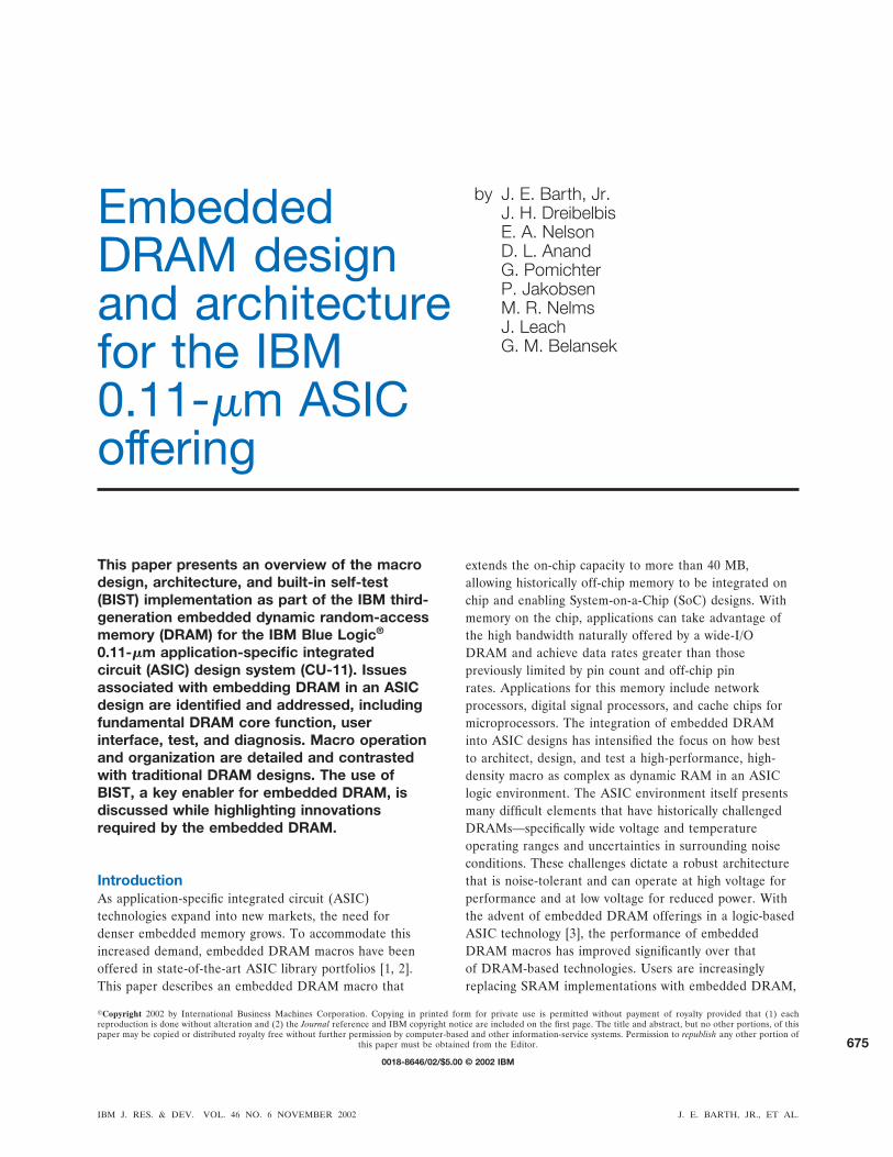
Fundamental DRAM operationDRAM memory arrays are composed of wordlines (orrows) and bitlines (columns); see Figure 1. At the cross-point of every row and column is a storage cell consistingof a transistor and capacitor [6]. The data state of the cellis stored as charge on the capacitor, with the transistoracting as a switch controlling access to the capacitor. Withthe switch on (wordline activated), charge can be readfrom or written to the storage cell. The rest of the DRAMsupport circuits are dedicated to controlling the wordlinesand bitlines to read and write the memory array.
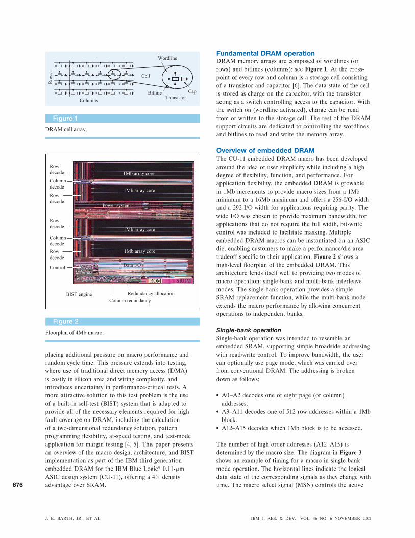
Overview of embedded DRAMThe CU-11 embedded DRAM macro has been developedaround the idea of user simplicity while including a highdegree of flexibility, function, and performance. Forapplication flexibility, the embedded DRAM is growablein 1Mb increments to provide macro sizes from a 1Mbminimum to a 16Mb maximum and offers a 256-I/O widthand a 292-I/O width for applications requiring parity. Thewide I/O was chosen to provide maximum bandwidth; forapplications that do not require the full width, bit-writecontrol was included to facilitate masking. Multipleembedded DRAM macros can be instantiated on an ASICdie, enabling customers to make a performance/die-areatradeoff specific to their application. Figure 2 shows ahigh-level floorplan of the embedded DRAM. Thisarchitecture lends itself well to providing two modes ofmacro operation: single-bank and multi-bank interleavemodes. The single-bank operation provides a simpleSRAM replacement function, while the multi-bank modeextends the macro performance by allowing concurrentoperations to independent banks.
Single-bank operationSingle-bank operation was intended to resemble anembedded SRAM, supporting simple broadside addressingwith read/write control. To improve bandwidth, the usercan optionally use page mode, which was carried overfrom conventional DRAM. The addressing is brokendown as follows:
● A0 –A2 decodes one of eight page (or column)addresses.
● A3–A11 decodes one of 512 row addresses within a 1Mbblock.
● A12–A15 decodes which 1Mb block is to be accessed.
The number of high-order addresses (A12–A15) isdetermined by the macro size. The diagram in Figure 3shows an example of timing for a macro in single-bank-mode operation. The horizontal lines indicate the logicaldata state of the corresponding signals as they change withtime. The macro select signal (MSN) controls the active
Figure 2
Floorplan of 4Mb macro.
1Mb array core
1Mb array core
1Mb array core
1Mb array core
Power system
Column redundancy
Data I/OControl
BIST engine
ROM SROM
Redundancy allocation
Row
decode
Row
decode
Row
decode
Row
decode
Column
decode
Column
decode
Figure 1
DRAM cell array.
Row
s
ColumnsTransistor
Cap
Wordline
Bitline
Cell
J. E. BARTH, JR., ET AL. IBM J. RES. & DEV. VOL. 46 NO. 6 NOVEMBER 2002
676
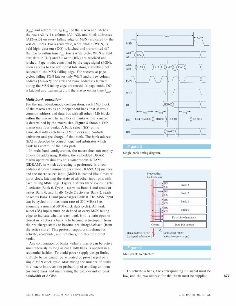
(tactp) and restore timing (tres) of the macro and latchesthe row (A3–A11), column (A0 –A2), and block addresses(A12–A15) on every falling edge of MSN (indicated by thevertical lines). For a read cycle, write enable (WEN) isheld high; data-out (DO) is latched and transmitted offthe macro within time tacc. For a write cycle, WEN is heldlow; data-in (DI) and bit write (BW) are received andlatched. Page mode, controlled by the page signal (PGN),allows access to the additional bits along a wordline notselected at the MSN falling edge. For successive pagecycles, falling PGN latches only WEN and a new columnaddress (A0 –A2); the row and bank addresses latchedduring the MSN falling edge are reused. In page mode, DOis latched and transmitted off the macro within time taccp.
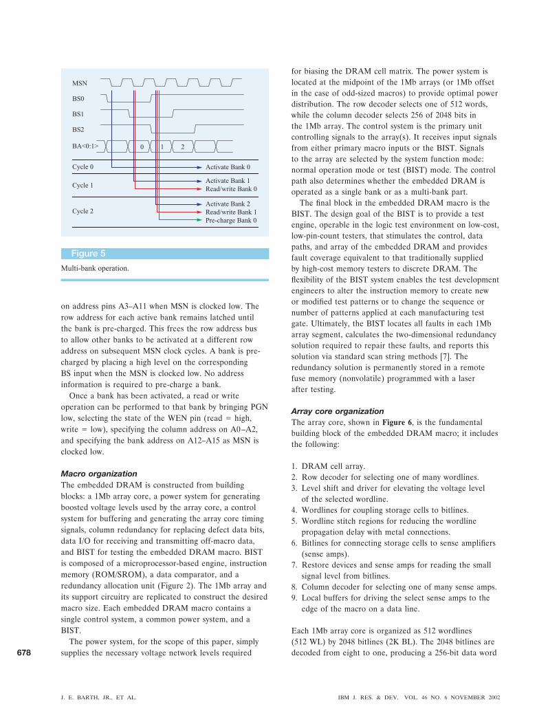
Multi-bank operationFor the multi-bank-mode configuration, each 1Mb blockof the macro acts as an independent bank that shares acommon address and data bus with all other 1Mb blockswithin the macro. The number of banks within a macrois determined by the macro size. Figure 4 shows a 4Mbmacro with four banks. A bank select (BS) pin isassociated with each bank (1Mb block) and controlsactivation and pre-charge of that bank. The bank address(BA) is decoded by control logic and arbitrates whichbank has control of the data path.
In multi-bank configuration, the macro does not employbroadside addressing. Rather, the embedded DRAMmacro operates similarly to a synchronous DRAM(SDRAM), in which addressing is performed in a row-address strobe/column-address strobe (RAS/CAS) mannerand the macro select input (MSN) is treated like a masterinput clock, latching the state of all other input pins witheach falling MSN edge. Figure 5 shows three cycles: Cycle0 activates Bank 0, Cycle 1 activates Bank 1 and reads orwrites Bank 0, and finally Cycle 2 activates Bank 2, readsor writes Bank 1, and pre-charges Bank 0. The MSN inputcan be cycled at a maximum rate of 250 MHz (4 nsassuming a nominal 50/50 clock duty cycle). All bankselect (BS) inputs must be defined at every MSN fallingedge to indicate whether each bank is to remain open orclosed or whether a bank is to become active/open (fromthe pre-charge state) or become pre-charged/closed (fromthe active state). This protocol supports simultaneousactivate, read/write, and pre-charge to three differentbanks.
Any combination of banks within a macro can be activesimultaneously as long as each 1Mb bank is opened in asequential fashion. To avoid power-supply design limits,multiple banks cannot be activated or pre-charged on asingle MSN clock cycle. Maximizing the number of banksin a macro improves the probability of avoiding an open(or busy) bank and maintaining the pseudorandom peakbandwidth of 8 GB/s.
To activate a bank, the corresponding BS signal must below, and the row address for that bank must be supplied
Figure 4
Multi-bank architecture.
Data I/O latches
Data-bit redundancy
Bank 0CS
BS
Bank 3CS
BS
Bank 2CS
BS
Bank 1CS
BS
Control
Bank select <0:3>
(activation/pre-charge)
Bank address <0:1>
(data path arbitration)
Predecoded
bank address
Figure 3
Single-bank timing diagram.
MSN
A00–
A02
PGN
WEN
DI
DO
BW
CA2CA1 CA3
DI002
DO001DO000 DO003
CA0
BW002
Last read data
RA0
tres
taccp
tacc
taccp
tactp
A03–
Ax
IBM J. RES. & DEV. VOL. 46 NO. 6 NOVEMBER 2002 J. E. BARTH, JR., ET AL.
677
on address pins A3–A11 when MSN is clocked low. Therow address for each active bank remains latched untilthe bank is pre-charged. This frees the row address busto allow other banks to be activated at a different rowaddress on subsequent MSN clock cycles. A bank is pre-charged by placing a high level on the correspondingBS input when the MSN is clocked low. No addressinformation is required to pre-charge a bank.
Once a bank has been activated, a read or writeoperation can be performed to that bank by bringing PGNlow, selecting the state of the WEN pin (read � high,write � low), specifying the column address on A0 –A2,and specifying the bank address on A12–A15 as MSN isclocked low.
Macro organizationThe embedded DRAM is constructed from buildingblocks: a 1Mb array core, a power system for generatingboosted voltage levels used by the array core, a controlsystem for buffering and generating the array core timingsignals, column redundancy for replacing defect data bits,data I/O for receiving and transmitting off-macro data,and BIST for testing the embedded DRAM macro. BISTis composed of a microprocessor-based engine, instructionmemory (ROM/SROM), a data comparator, and aredundancy allocation unit (Figure 2). The 1Mb array andits support circuitry are replicated to construct the desiredmacro size. Each embedded DRAM macro contains asingle control system, a common power system, and aBIST.
The power system, for the scope of this paper, simplysupplies the necessary voltage network levels required
for biasing the DRAM cell matrix. The power system islocated at the midpoint of the 1Mb arrays (or 1Mb offsetin the case of odd-sized macros) to provide optimal powerdistribution. The row decoder selects one of 512 words,while the column decoder selects 256 of 2048 bits inthe 1Mb array. The control system is the primary unitcontrolling signals to the array(s). It receives input signalsfrom either primary macro inputs or the BIST. Signalsto the array are selected by the system function mode:normal operation mode or test (BIST) mode. The controlpath also determines whether the embedded DRAM isoperated as a single bank or as a multi-bank part.
The final block in the embedded DRAM macro is theBIST. The design goal of the BIST is to provide a testengine, operable in the logic test environment on low-cost,low-pin-count testers, that stimulates the control, datapaths, and array of the embedded DRAM and providesfault coverage equivalent to that traditionally suppliedby high-cost memory testers to discrete DRAM. Theflexibility of the BIST system enables the test developmentengineers to alter the instruction memory to create newor modified test patterns or to change the sequence ornumber of patterns applied at each manufacturing testgate. Ultimately, the BIST locates all faults in each 1Mbarray segment, calculates the two-dimensional redundancysolution required to repair these faults, and reports thissolution via standard scan string methods [7]. Theredundancy solution is permanently stored in a remotefuse memory (nonvolatile) programmed with a laserafter testing.
Array core organizationThe array core, shown in Figure 6, is the fundamentalbuilding block of the embedded DRAM macro; it includesthe following:
1. DRAM cell array.2. Row decoder for selecting one of many wordlines.3. Level shift and driver for elevating the voltage level
of the selected wordline.4. Wordlines for coupling storage cells to bitlines.5. Wordline stitch regions for reducing the wordline
propagation delay with metal connections.6. Bitlines for connecting storage cells to sense amplifiers
(sense amps).7. Restore devices and sense amps for reading the small
signal level from bitlines.8. Column decoder for selecting one of many sense amps.9. Local buffers for driving the select sense amps to the
edge of the macro on a data line.
Each 1Mb array core is organized as 512 wordlines(512 WL) by 2048 bitlines (2K BL). The 2048 bitlines aredecoded from eight to one, producing a 256-bit data word
Figure 5
Multi-bank operation.
MSN
BS0
BS1
BS2
BA<0:1> 0 1 2
Activate Bank 0
Activate Bank 1
Read/write Bank 0
Activate Bank 2
Read/write Bank 1
Pre-charge Bank 0
Cycle 0
Cycle 1
Cycle 2
J. E. BARTH, JR., ET AL. IBM J. RES. & DEV. VOL. 46 NO. 6 NOVEMBER 2002
678
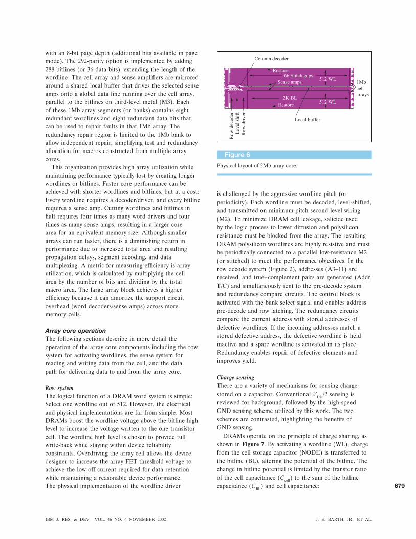
with an 8-bit page depth (additional bits available in pagemode). The 292-parity option is implemented by adding288 bitlines (or 36 data bits), extending the length of thewordline. The cell array and sense amplifiers are mirroredaround a shared local buffer that drives the selected senseamps onto a global data line running over the cell array,parallel to the bitlines on third-level metal (M3). Eachof these 1Mb array segments (or banks) contains eightredundant wordlines and eight redundant data bits thatcan be used to repair faults in that 1Mb array. Theredundancy repair region is limited to the 1Mb bank toallow independent repair, simplifying test and redundancyallocation for macros constructed from multiple arraycores.
This organization provides high array utilization whilemaintaining performance typically lost by creating longerwordlines or bitlines. Faster core performance can beachieved with shorter wordlines and bitlines, but at a cost:Every wordline requires a decoder/driver, and every bitlinerequires a sense amp. Cutting wordlines and bitlines inhalf requires four times as many word drivers and fourtimes as many sense amps, resulting in a larger corearea for an equivalent memory size. Although smallerarrays can run faster, there is a diminishing return inperformance due to increased total area and resultingpropagation delays, segment decoding, and datamultiplexing. A metric for measuring efficiency is arrayutilization, which is calculated by multiplying the cellarea by the number of bits and dividing by the totalmacro area. The large array block achieves a higherefficiency because it can amortize the support circuitoverhead (word decoders/sense amps) across morememory cells.
Array core operationThe following sections describe in more detail theoperation of the array core components including the rowsystem for activating wordlines, the sense system forreading and writing data from the cell, and the datapath for delivering data to and from the array core.
Row systemThe logical function of a DRAM word system is simple:Select one wordline out of 512. However, the electricaland physical implementations are far from simple. MostDRAMs boost the wordline voltage above the bitline highlevel to increase the voltage written to the one transistorcell. The wordline high level is chosen to provide fullwrite-back while staying within device reliabilityconstraints. Overdriving the array cell allows the devicedesigner to increase the array FET threshold voltage toachieve the low off-current required for data retentionwhile maintaining a reasonable device performance.The physical implementation of the wordline driver
is challenged by the aggressive wordline pitch (orperiodicity). Each wordline must be decoded, level-shifted,and transmitted on minimum-pitch second-level wiring(M2). To minimize DRAM cell leakage, salicide usedby the logic process to lower diffusion and polysiliconresistance must be blocked from the array. The resultingDRAM polysilicon wordlines are highly resistive and mustbe periodically connected to a parallel low-resistance M2(or stitched) to meet the performance objectives. In therow decode system (Figure 2), addresses (A3–11) arereceived, and true– complement pairs are generated (AddrT/C) and simultaneously sent to the pre-decode systemand redundancy compare circuits. The control block isactivated with the bank select signal and enables addresspre-decode and row latching. The redundancy circuitscompare the current address with stored addresses ofdefective wordlines. If the incoming addresses match astored defective address, the defective wordline is heldinactive and a spare wordline is activated in its place.Redundancy enables repair of defective elements andimproves yield.
Charge sensingThere are a variety of mechanisms for sensing chargestored on a capacitor. Conventional VDD/2 sensing isreviewed for background, followed by the high-speedGND sensing scheme utilized by this work. The twoschemes are contrasted, highlighting the benefits ofGND sensing.
DRAMs operate on the principle of charge sharing, asshown in Figure 7. By activating a wordline (WL), chargefrom the cell storage capacitor (NODE) is transferred tothe bitline (BL), altering the potential of the bitline. Thechange in bitline potential is limited by the transfer ratioof the cell capacitance (Ccell) to the sum of the bitlinecapacitance (CBL) and cell capacitance:
Figure 6
Physical layout of 2Mb array core.
2K BL512 WL
Local buffer
Sense amps
Column decoder
Row
decoder
Level
shif
t
Row
dri
ver
Restore
Restore
66 Stitch gaps512 WL
1Mb
cell
arrays
IBM J. RES. & DEV. VOL. 46 NO. 6 NOVEMBER 2002 J. E. BARTH, JR., ET AL.
679
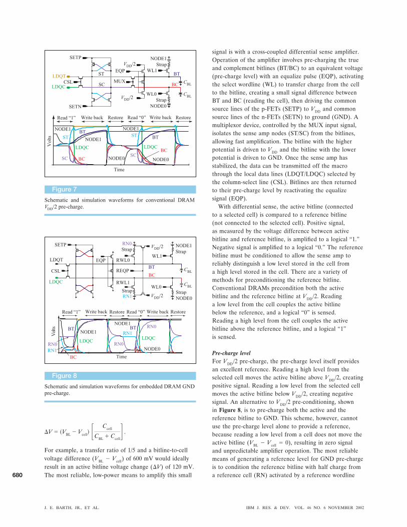
�V � �VBL � Vcell� � Ccell
CBL � Ccell� .
For example, a transfer ratio of 1/5 and a bitline-to-cellvoltage difference (VBL � Vcell) of 600 mV would ideallyresult in an active bitline voltage change (�V) of 120 mV.The most reliable, low-power means to amplify this small
signal is with a cross-coupled differential sense amplifier.Operation of the amplifier involves pre-charging the trueand complement bitlines (BT/BC) to an equivalent voltage(pre-charge level) with an equalize pulse (EQP), activatingthe select wordline (WL) to transfer charge from the cellto the bitline, creating a small signal difference betweenBT and BC (reading the cell), then driving the commonsource lines of the p-FETs (SETP) to VDD and commonsource lines of the n-FETs (SETN) to ground (GND). Amultiplexor device, controlled by the MUX input signal,isolates the sense amp nodes (ST/SC) from the bitlines,allowing fast amplification. The bitline with the higherpotential is driven to VDD and the bitline with the lowerpotential is driven to GND. Once the sense amp hasstabilized, the data can be transmitted off the macrothrough the local data lines (LDQT/LDQC) selected bythe column-select line (CSL). Bitlines are then returnedto their pre-charge level by reactivating the equalizesignal (EQP).
With differential sense, the active bitline (connectedto a selected cell) is compared to a reference bitline(not connected to the selected cell). Positive signal,as measured by the voltage difference between activebitline and reference bitline, is amplified to a logical “1.”Negative signal is amplified to a logical “0.” The referencebitline must be conditioned to allow the sense amp toreliably distinguish a low level stored in the cell froma high level stored in the cell. There are a variety ofmethods for preconditioning the reference bitline.Conventional DRAMs precondition both the activebitline and the reference bitline at VDD/2. Readinga low level from the cell couples the active bitlinebelow the reference, and a logical “0” is sensed.Reading a high level from the cell couples the activebitline above the reference bitline, and a logical “1”is sensed.
Pre-charge levelFor VDD/2 pre-charge, the pre-charge level itself providesan excellent reference. Reading a high level from theselected cell moves the active bitline above VDD/2, creatingpositive signal. Reading a low level from the selected cellmoves the active bitline below VDD/2, creating negativesignal. An alternative to VDD/2 pre-conditioning, shownin Figure 8, is to pre-charge both the active and thereference bitline to GND. This scheme, however, cannotuse the pre-charge level alone to provide a reference,because reading a low level from a cell does not move theactive bitline (VBL � Vcell � 0), resulting in zero signaland unpredictable amplifier operation. The most reliablemeans of generating a reference level for GND pre-chargeis to condition the reference bitline with half charge froma reference cell (RN) activated by a reference wordline
Figure 8
Schematic and simulation waveforms for embedded DRAM GND
pre-charge.
SETP
CSL
LDQT
LDQC
EQP
Strap
NODE0
WL0
BT
BC
Strap
RN1
RWL1
Strap
RN0
RWL0
REQP
NODE1
StrapWL1
NODE0
BT BT
RN0
BC
RN1
LDQCLDQC
RN1
RN0
RN0NODE1
NODE1
Vol
ts
Time
Write back RestoreWrite backRestore Read “0” Read “1”
VDD
/2
VDD
/2
CBL
CBL
Figure 7
Schematic and simulation waveforms for conventional DRAM
VDD
/2 pre-charge.
SETP
SETN
CSL
LDQT
LDQC
MUX
EQP
VDD
/2
VDD
/2
Strap
NODE0
WL0
CBL
CBL
ST
SC
BT
BC
NODE1
Strap
WL1
Write back Restore
ST
SC
BT
BC
LDQC
NODE1
NODE1 NODE1
NODE0 NODE0
ST
SC
BT
BCLDQC
Write backRestore Read “0” Read “1”
Volt
s
Time
J. E. BARTH, JR., ET AL. IBM J. RES. & DEV. VOL. 46 NO. 6 NOVEMBER 2002
680
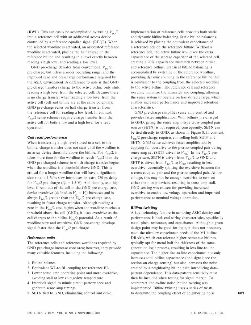
(RWL). This can easily be accomplished by writing VDD/2into a reference cell with an additional access devicecontrolled by a reference equalize signal (REQP). Whenthe selected wordline is activated, an associated referencewordline is activated, placing the half charge on thereference bitline and resulting in a level exactly betweenreading a high level and reading a low level.
GND pre-charge deviates from conventional VDD/2pre-charge, but offers a wider operating range, and theimproved read and pre-charge performance required bythe ASIC environment. A difference to note is that GNDpre-charge transfers charge to the active bitline only whilereading a high level from the selected cell. Because thereis no charge transfer when reading a low level from theactive cell (cell and bitline are at the same potential),GND pre-charge relies on half charge transfer fromthe reference cell for reading a low level. In contrast,VDD/2 sense schemes require charge transfer from theactive cell for both a low and a high level for a readoperation.
Cell read performanceWhen transferring a high level stored in a cell to thebitline, charge transfer does not start until the wordline isan array device threshold above the bitline. For VDD/2, ittakes more time for the wordline to reach VDD/2 than theGND pre-charged scheme in which charge transfer beginswhen the wordline is a threshold above GND. This iscritical for a longer wordline that will have a significantslew rate: a 1-V/ns slew introduces an extra 750-ps delayfor VDD/2 pre-charge (@ � 1.5 V). Additionally, as a highlevel is read out of the cell in the GND pre-charge case,device overdrive (defined as Vgs � Vt) increases and isalways VDD/2 greater than the VDD/2 pre-charge case,resulting in faster charge transfer. Although reading azero in the VDD/2 case begins when the wordline reaches athreshold above the cell (GND), it loses overdrive as thecell charges to the bitline VDD/2 potential. As a result ofwordline slew and overdrive, GND pre-charge developssignal faster than the VDD/2 pre-charge.
Reference cellsThe reference cells and reference wordlines required byGND pre-charge increase core area; however, they providemany valuable features, including the following:
1. Bitline balance.2. Equivalent WL-to-BL coupling for reference BL.3. Lower sense amp operating point and more overdrive,
avoiding stall at low voltage/low temperature.4. Interlock signal to mimic circuit performance and
generate sense amp timings.5. SETN tied to GND, eliminating control and drive.
Implementation of reference cells provides both staticand dynamic bitline balancing. Static bitline balancingis achieved by placing the equivalent capacitance ofa reference cell on the reference bitline. Without areference cell, the active bitline would see the extracapacitance of the storage capacitor of the selected cell,creating a 20% capacitance mismatch between bitlineand reference bitline. Transient bitline balancing isaccomplished by switching of the reference wordline,providing dynamic coupling to the reference bitline thatis equivalent to the coupling from the selected wordlineto the active bitline. The reference cell and referencewordline minimize the mismatch and coupling, allowingthe sense system to operate on less stored charge, whichenables increased performance and improved retentioncharacteristics.
GND pre-charge simplifies sense amp control andprovides faster amplification. With bitlines pre-chargedto GND, gating the sense amp n-type cross-coupled pairsource (SETN) is not required; consequently, SETN canbe tied directly to GND, as shown in Figure 8. In contrast,VDD/2 pre-charge requires controlling both SETP andSETN. GND sense achieves faster amplification byapplying full overdrive to the p-cross-coupled pair duringsense amp set (SETP driven to VDD). In the VDD/2 pre-charge case, SETN is driven from VDD/2 to GND andSETP is driven from VDD/2 to VDD, resulting in lessoverdrive, essentially splitting the overdrive between then-cross-coupled pair and the p-cross-coupled pair. At lowvoltage, this may not be enough overdrive to turn oneither the n or p devices, resulting in sense amp stall.GND sensing was chosen for providing increasedoverdrive to enable low-voltage operation and improvedperformance at nominal voltage operation.
Bitline twistingA key technology feature in achieving ASIC density andperformance is back-end wiring characteristics, specificallymetal pitch, resistance, and capacitance. Although a givendesign point may be good for logic, it does not necessarymeet the ultralow-capacitance needs of the M1 bitline.DRAMs, which can tolerate higher-resistance bitlines,typically opt for metal half the thickness of the same-generation logic process, resulting in less line-to-linecapacitance. The higher line-to-line capacitance not onlyincreases total bitline capacitance (and signal; see thesection on charge sensing) but also increases the noisecreated by a neighboring bitline pair, introducing data-pattern dependence. This data-pattern sensitivity mustthen be included when testing for signal margin. Tocounteract line-to-line noise, bitline twisting wasimplemented. Bitline twisting uses a series of twiststo distribute the coupling effect of neighboring noise
IBM J. RES. & DEV. VOL. 46 NO. 6 NOVEMBER 2002 J. E. BARTH, JR., ET AL.
681
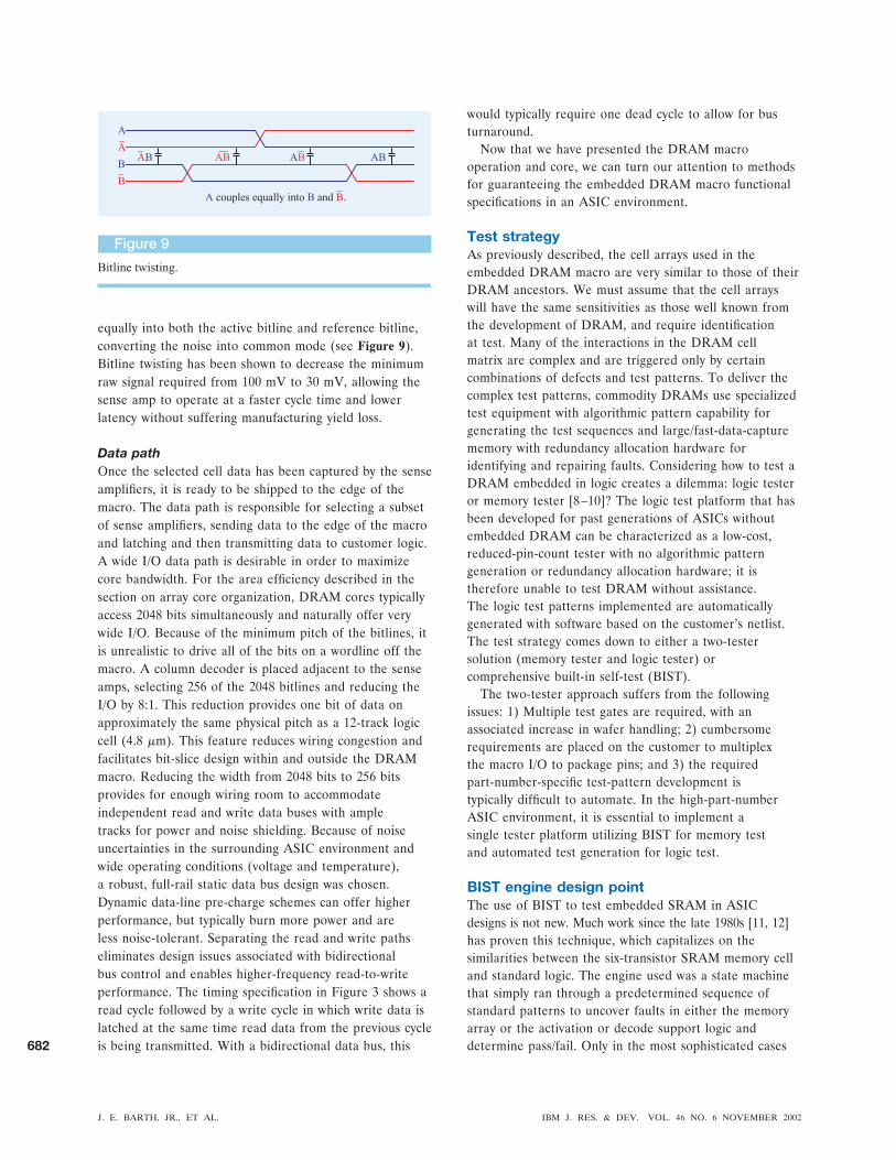
equally into both the active bitline and reference bitline,converting the noise into common mode (see Figure 9).Bitline twisting has been shown to decrease the minimumraw signal required from 100 mV to 30 mV, allowing thesense amp to operate at a faster cycle time and lowerlatency without suffering manufacturing yield loss.
Data pathOnce the selected cell data has been captured by the senseamplifiers, it is ready to be shipped to the edge of themacro. The data path is responsible for selecting a subsetof sense amplifiers, sending data to the edge of the macroand latching and then transmitting data to customer logic.A wide I/O data path is desirable in order to maximizecore bandwidth. For the area efficiency described in thesection on array core organization, DRAM cores typicallyaccess 2048 bits simultaneously and naturally offer verywide I/O. Because of the minimum pitch of the bitlines, itis unrealistic to drive all of the bits on a wordline off themacro. A column decoder is placed adjacent to the senseamps, selecting 256 of the 2048 bitlines and reducing theI/O by 8:1. This reduction provides one bit of data onapproximately the same physical pitch as a 12-track logiccell (4.8 �m). This feature reduces wiring congestion andfacilitates bit-slice design within and outside the DRAMmacro. Reducing the width from 2048 bits to 256 bitsprovides for enough wiring room to accommodateindependent read and write data buses with ampletracks for power and noise shielding. Because of noiseuncertainties in the surrounding ASIC environment andwide operating conditions (voltage and temperature),a robust, full-rail static data bus design was chosen.Dynamic data-line pre-charge schemes can offer higherperformance, but typically burn more power and areless noise-tolerant. Separating the read and write pathseliminates design issues associated with bidirectionalbus control and enables higher-frequency read-to-writeperformance. The timing specification in Figure 3 shows aread cycle followed by a write cycle in which write data islatched at the same time read data from the previous cycleis being transmitted. With a bidirectional data bus, this
would typically require one dead cycle to allow for busturnaround.
Now that we have presented the DRAM macrooperation and core, we can turn our attention to methodsfor guaranteeing the embedded DRAM macro functionalspecifications in an ASIC environment.
Test strategyAs previously described, the cell arrays used in theembedded DRAM macro are very similar to those of theirDRAM ancestors. We must assume that the cell arrayswill have the same sensitivities as those well known fromthe development of DRAM, and require identificationat test. Many of the interactions in the DRAM cellmatrix are complex and are triggered only by certaincombinations of defects and test patterns. To deliver thecomplex test patterns, commodity DRAMs use specializedtest equipment with algorithmic pattern capability forgenerating the test sequences and large/fast-data-capturememory with redundancy allocation hardware foridentifying and repairing faults. Considering how to test aDRAM embedded in logic creates a dilemma: logic testeror memory tester [8 –10]? The logic test platform that hasbeen developed for past generations of ASICs withoutembedded DRAM can be characterized as a low-cost,reduced-pin-count tester with no algorithmic patterngeneration or redundancy allocation hardware; it istherefore unable to test DRAM without assistance.The logic test patterns implemented are automaticallygenerated with software based on the customer’s netlist.The test strategy comes down to either a two-testersolution (memory tester and logic tester) orcomprehensive built-in self-test (BIST).
The two-tester approach suffers from the followingissues: 1) Multiple test gates are required, with anassociated increase in wafer handling; 2) cumbersomerequirements are placed on the customer to multiplexthe macro I/O to package pins; and 3) the requiredpart-number-specific test-pattern development istypically difficult to automate. In the high-part-numberASIC environment, it is essential to implement asingle tester platform utilizing BIST for memory testand automated test generation for logic test.
BIST engine design pointThe use of BIST to test embedded SRAM in ASICdesigns is not new. Much work since the late 1980s [11, 12]has proven this technique, which capitalizes on thesimilarities between the six-transistor SRAM memory celland standard logic. The engine used was a state machinethat simply ran through a predetermined sequence ofstandard patterns to uncover faults in either the memoryarray or the activation or decode support logic anddetermine pass/fail. Only in the most sophisticated cases
Figure 9
Bitline twisting.
A
A
B
B
AB ABABAB
A couples equally into B and B.
J. E. BARTH, JR., ET AL. IBM J. RES. & DEV. VOL. 46 NO. 6 NOVEMBER 2002
682
was redundancy even considered, and then only in the rowdimension.
Since the same set of six to eight SRAM test patternshave remained constant for a number of generations,little, if any, capability to alter the SRAM test sequencewas required. However, DRAM is sensitive to far moresubtle systematic and random process variations anddefects, requiring a more complicated and dynamic testsequence to identify and repair these faults. It is generallynot possible to predict all data patterns or write/readpatterns that will ultimately be needed to reduce thetest escape rate to less than ten parts per million(10 ppm). The complicated dynamic pattern set and themultidimensional redundancy allocation (row and column)required by DRAM testing rendered earlier generations ofBIST technology inadequate for DRAM testing. The newfail mechanism and pattern sensitivities specific to DRAMrequired reconsideration of the BIST engine dexterity. Toaddress unique requirements of embedded DRAM test,a processor-based BIST engine with a high degree ofprogram flexibility was developed [1]. A programmableBIST engine design provides a very flexible test patterndevelopment system as well as a standard set of patternsfor manufacturing test. This enables the test andcharacterization engineers to define the necessary patternsused at each test gate and the order in which they areapplied. Test instructions that communicate with testerpin stimulation allow for external control of pauses usedduring retention-time testing and provide extendedcapability for exercises such as burn-in.
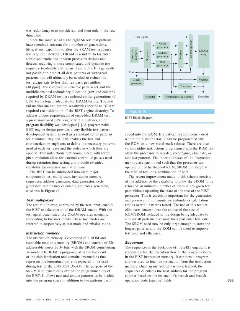
The BIST can be subdivided into eight majorcomponents: test multiplexor, instruction memory,sequencer, address generator, data generator, cyclegenerator, redundancy calculator, and clock generator,as shown in Figure 10.
Test multiplexorThe test multiplexor, controlled by the test input, enablesthe BIST to take control of the DRAM macro. With thetest signal deactivated, the DRAM operates normally,responding to the user inputs. These two modes arereferred to respectively as test mode and mission mode.
Instruction memoryThe instruction memory is composed of a ROM andscannable read-only memory (SROM) and consists of 226addressable words by 34 bits, with the SROM contributing34 words. The ROM is programmed in the back endof the chip fabrication and contains instructions thatrepresent predetermined patterns expected to be usedduring test of the embedded DRAM. The purpose of theSROM is to dynamically extend the programmability ofthe BIST. It allows new and unique patterns to be loadedinto the program space in addition to the patterns hard-
coded into the ROM. If a pattern is continuously usedwithin the register array, it can be programmed intothe ROM on a new metal mask release. There are alsovarious utility instructions programmed into the ROM thatallow the processor to reorder, reconfigure, eliminate, oradd test patterns. The index addresses of the instructionmemory are partitioned such that the processor canoperate out of hard-coded ROM, SROM initialized atthe start of test, or a combination of both.
The recent improvement made to this scheme consistsof the addition of the capability to allow the SROM to bereloaded an unlimited number of times in any given testpass without upsetting the state of the rest of the BISTprocessor. This is especially important for the generationand preservation of cumulative redundancy calculationresults over all patterns tested. The use of this featureeliminates concern over the choice of the size ofROM/SROM included in the design being adequate tocontain all patterns necessary for a particular test gate.The SROM need now be only large enough to store thelongest pattern, and the ROM can be sized to improvetest time and efficiency.
SequencerThe sequencer is the backbone of the BIST engine. It isresponsible for the execution flow of the programs storedin the BIST instruction memory. It contains a programcounter used to fetch an instruction from the instructionmemory. Once an instruction has been fetched, thesequencer calculates the next address for the programcounter based on the instruction’s branch and branchoperation code (opcode) fields.
Figure 10
BIST block diagram.
DRAM
array
Sequencer
Address
generator
Data
generator
Cycle
generator
Clock
generator
Inst
ructi
on
mem
ory
Regis
ter
User inputs
Register
Test
Test
mult
iple
xor
Register
Compare
Redundancy calculator User data
IBM J. RES. & DEV. VOL. 46 NO. 6 NOVEMBER 2002 J. E. BARTH, JR., ET AL.
683
Two types of instructions are used in the BIST. Thefirst is a normal instruction indicated when bit 31 of theinstruction word is set to a logical “0.” The second type ofinstruction is a test-mode instruction, indicated when bit31 of the instruction word is set to a logical “1.” It is usedto set various latches in the BIST. These latches controlmodes of operation, set digital-to-analog converts (DACs)to offset internal voltages and timings for margin testing,program the data scramble, and set the utility counter.
Address generatorThe address generator is responsible for generating theaddressing for the array during self-test. This is done withthe aid of three counters: row, column, and block, whichare controlled by the appropriate fields of the BISTinstruction. The counters can be incremented ordecremented as defined by the increment/decrementbit of the instruction.
Data generatorBecause of the difficulty in predicting what actual datapatterns will be necessary in the embedded DRAM arraymatrix to activate and expose subtle faults, a flexible datagenerator was introduced. The previous versions allowedonly a short list of pre-coded patterns that providedblanket lows or highs, checkerboard lows/highs, rowstripes, and column stripes to the matrix. This approachwas found to be inadequate for proper test-patterndevelopment and not directly reusable for varying arrayarchitectures. Thus, a design that accounts for current rowand column address, adjacent data bit, and physical orlogical data state stipulated in the pattern was added[4, 13]. The algorithm to be used by the data generatorfor a given test is specified with a mode-set instructionprior to executing any writes or reads to the DRAM. Thisinstruction alters the states of latches in the design thatgovern the operation of the generator. Odd and even databits are generated and replicated across the 256-bit dataword. Odd and even data bits are a function of theprogram data scramble (PDS), the current address, andthe data state specified in the read or write instruction.The PDS contains latches that are programmed with atest-mode instruction. These latches allow the test patternto generate stripes of various sizes, checkerboards, orother desired patterns in the 1Mb array(s).
The term logical data refers to the state of the data atthe macro inputs, logical “1” being a high voltage leveland logical “0” being a low voltage level. Logical data issimply written as is, regardless of the bitline connectionto the sense amp and its location in the array. The termphysical data refers to the voltage level stored on theDRAM cell capacitor. DRAM architectures routinelyinvert logical data when writing to the cell; i.e., a logical“1” may be stored as a physical “0.” Inversion is address-
dependent and is acceptable as long the architecturereinverts the data when it is read. Controlling physicaldata is required because many defect mechanisms aresensitive to the physical data state stored. When physicaldata is desired, the data is modified according to thebitline connection to either the true or complement sideof the sense amp. Also taken into consideration is thelocation of the bit with respect to array topography.During a read or write operation, data is generated atthe time of instruction execution. In a write operation,data is sent directly to the data path latches. During aread operation, the data generator produces expecteddata for the comparator.
Cycle generatorThe cycle generator is responsible for generating the rowand column signals used in single-bank mode for the 1Mbarray(s). When in multi-bank mode, the cycle generatormust generate the bank select signals as well. Theprotocols for the single-bank and multi-bank modes ofoperation are different. Examples of the signals requiredin each of these modes are shown in Figure 3 and Figure 5.These signals are created as a function of the internalBIST clocks and the cycle opcode defined by theinstruction.
When running BIST prior to redundancy repair, thecontrol signals, generated to stimulate the array, arerestricted to a single 1Mb array, so only the single-bankoperating mode is required. The logical addressing to the1Mb array under test is defined by a group of latchesin the BIST. This restriction is enforced because theredundancy calculator can compute a solution for onlya single 1Mb array at a time.
Once a redundancy solution has been computed foreach 1Mb array, the macro can be repaired. The macrocan then be stimulated either through the single-bank orthe multi-bank protocol as a complete macro. If a fail isfound at any point after the macro has been repaired, themacro is considered a reject.
Redundancy calculatorA key enhancement to BIST schemes used previously forembedded SRAM macros is the inclusion of a redundancycalculator, also referred to as redundancy allocation logic(RAL), for two-dimensional redundancy. The function ofthe redundancy calculator is to compare data read fromthe array with expect data from the BIST engine andoptimally allocate redundancy for array fails. In thissystem [1], the BIST processor calculates row and data-bitredundancy for wide-I/O embedded DRAM macros. Each1Mb array contains its own redundant elements, whichmay not be shared with other 1Mb arrays. For thisreason, BIST calculates and stores only 1Mb worth of aredundancy solution at a time. Calculation of the full
J. E. BARTH, JR., ET AL. IBM J. RES. & DEV. VOL. 46 NO. 6 NOVEMBER 2002
684
16Mb repair solution would require 16 times the numberof fail counters and address registers, increasing thesilicon area required for the BIST to an unacceptablelevel.
Several further enhancements have been made to thissystem to heighten manufacturability. The first of theseenhancements deals with the definition of a “must-fix”data bit. A fault was previously defined as a “must-fix”data bit if there were more row addresses failing within adata bit than there were redundant row elements availableto fix them. This was hard-coded into the calculator logicas the true must-fix limit. The redundancy calculatorwas modified to allow the option of specifying, at thebeginning of test, what definition of must-fix data bit thecalculator will use. The choices supported are one quarter,one half, or the full number of available redundant rowelements. The choice is communicated to the redundancycalculator via scan initialization. With this option,decisions can be made as to how faults will be fixed if thefabricator may be prone to a certain mix of fault types.
The second enhancement to the RAL portion of theBIST is the integration of redundant row testing. Toensure high final module yield, redundant rows must betested prior to use. In the previous BIST design [1],redundant rows were tested with a separate set ofpatterns. The results from redundant row test were thenmerged offline with the RAL solution from the normaltest patterns, producing a modified laser fuse solutionwhen defective redundant rows were identified. Toeliminate the need for multiple-pass testing and offlinedata manipulation, the failing row address calculatorportion of the RAL was modified along with the rowaddress generator in the processor. The row address wasextended to a nonbinary value to include address space forselecting the redundant rows in each address schedule.The choice to include redundant addresses in the patternis optional via test mode. The content-addressablememory (CAM) in the failing row address calculatorrecognizes failing redundant rows and eliminates themfrom the final redundancy solution reported at the end oftest. With this combination of modifications, a single testpass provides a redundancy solution that accounts forfailing redundant elements and their effect on total macrofixability.
The third and final enhancement to the redundancycalculator comes with the capability to reload the SROMinstruction memory discussed earlier. By segmenting thescan string and reloading only the SROM, neither thestate of the BIST engine nor the current state of the RALcalculated redundancy solution is upset. Thus, additionalpatterns can continue to be applied one after another,with the redundancy solution being calculated on thecumulative failure set from all patterns.
Clock generatorThe final component of the BIST is the clock generator,which is responsible for generating all of the necessaryclocks needed for self-test of the DRAM. It has the abilityto receive external clocks and pass them directly to theBIST, or generate its own clocks from an externaloscillator.
To maximize system performance, 250-MHz timing rulesare provided to describe the RAM core performance.Testing at speed (high-frequency or ac testing) becomesessential to ensure the high-performance timings,especially in the presence of speed-sensitive failscommonly found in DRAMs. As the complexity of chip-level integration grows, so do the challenges for ac test.The DRAM core performance specifications include onlythose delay elements within the core boundary. Accurateevaluation of these delays requires that they be measuredeither directly at the core boundary or from test pointswhere the delay from the macro boundary to said testpoint is known.
Effective ac testing requires that the stimuli be providedwith sufficient speed and accuracy, and efficient ac testingrequires that constraints for cost-competitive manufacturingbe met. A basic BIST design can be enhanced to providean effective, efficient means of ensuring ac performancespecifications for cycle and access times.
Placing BIST units in such a way that the delaysbetween the BIST and the RAM core boundary areminimized and predictable greatly simplifies ac testdevelopment. An example of such a design is one in whicheach instance of a RAM core comes with its own BIST.While this approach may use more silicon area thanothers, savings in design, test development, and test costcan be realized through the reuse of the same integratedRAM/BIST core across a wide range of applications. Insome environments, the results that can be derived from afinite design and test development resource are enhancedby focusing on the development of a reusable core ratherthan the development of a specific customer part number.The RAM/BIST integrated core design point enableseffective ac test by reducing the delay between the RAMand the BIST that minimizes the timing uncertaintiesintroduced by process variability and typical testerhardware. Efficient ac test is realized by leveraging theself-test concept. Performing data compare and storingfail locations in the BIST reduce the demands ontester resources to input only. Eliminating the need forexpensive high-speed data capture hardware in the testhead greatly simplifies requirements from the point ofview of both bandwidth and calibration. Another largestep toward reducing tester demands by containing criticaltimings within a BIST is taken when clock multiplicationcapability is added.
IBM J. RES. & DEV. VOL. 46 NO. 6 NOVEMBER 2002 J. E. BARTH, JR., ET AL.
685
Clock multiplierFor example, with very modest test equipment a 10-MHzclock can be used as input to a 20:1 clock multiplier,creating a 200-MHz BIST test environment. The clockmultiplier receives a single clock from a tester andmultiplies it by a factor (MULT) ranging from 2 to 32.The multiplier is designed such that the only restrictionon the tester clock cycle, t(CYCTESTER), is that
t�CYCTESTER�
MULT� t�CYCTARGET� .
The range of target cycle, t(CYCTARGET), is limited bysilicon area, process, and operating conditions. If aninternal target of a 2.5-ns cycle is desired and a 50-nstester clock cycle is used, MULT should be 20.
DRAM random-access cycle and data path cycle timestypically differ by factors of three to eight times. Thefaster data path cycle time allows for higher bandwidthin spite of the relatively slow random-access cycle time.A clock-shaping function can simplify the creation ofappropriate DRAM test patterns from a single high-speedclock. Within the BIST, the multiplied clock is “shaped”to create control signals with the desired duty cycle.Specifically, the BIST shapes the clock into row andcolumn controls that are used to stress row cycles andcolumn cycles. For example, the BIST can shape the clockto generate a six-cycle row active, two-cycle row pre-charge, one-cycle column low, and one-cycle column high.As another example, a 200-MHz input to a clock shapercan be used in such a way that data path operations occurevery 5 ns, while random-access events occur at 15-nsintervals. The random-access duty factor for this examplewould be 2/3 active, 1/3 pre-charge. Allowing selectionfrom any number of high-speed clock periods from oneto 16 for each basic DRAM core event enables the testengineer to selectively stress individual timing values. Thecombination of clock-shaping and clock-multiplicationcapabilities provides a very flexible and highly accuratetest environment for DRAM cores with minimal demandson test equipment and device interface hardware.
dc testDRAMs require voltages above VDD and below GND toprovide a sufficient difference between array transistoron- and off-currents. If the off-current is not low enough,DRAM retention time is compromised; if the on-current isnot high enough, cycle time is compromised. Charge pumpcircuits are used to generate high-voltage supplies and aredelivered to the DRAM array via distribution networks.For efficiency, from the point of view of both silicon areaand power consumption, these pump systems are designedwith modest overhead and standby operating modes.Defects in the pumps or on the networks can inhibit
proper operation and must be detected. While functionalpatterns could be created to detect these defects, it isoften more efficient to use dc test modes. For example,a functional failure can occur when a parasitic networkleakage exceeds the capacity of the standby portion of thepump system. The functional test to detect this failurewould require putting the DRAM into a standby stateprior to activating each address. The time required forthis type of functional test is much longer than the timerequired to perform the dc test that checks the networkfor parasitic leakage. This type of dc testing requires atest-mode control that turns the pump system off andprovides access to the network from the tester such thatthe network leakage can be measured. Another means ofenhancing DRAM test coverage is to check for operatingmargins around the nominal set-points for these networkvoltages. Methods selected for exciting these margin testscould use the same tester connection as the leakage test,or the pump output voltage set-point can be modified.Providing these types of test modes and enabling test-mode activation through BIST instructions improve testeffectiveness and efficiency.
Test and diagnostic capabilityIn the ASIC environment, where the BIST has all of thecapability and flexibility to test the DRAM with minimaltester interaction, the tester must still obtain the resultsfrom the BIST. Upon completion of a functional pattern,several types of data must be acquired from the BIST.Each of these data types has been considered in designingthe BIST and the rules for integration of the DRAM/BISTcore into an ASIC design system. The most frequentlyneeded type of information is pass/fail data, which issupplied by three bits: one bit to flag successfulcompletion of the BIST sequence; one bit to separate“perfect” from “not perfect”; one bit to separate “fixable”from “not fixable.” Since the design system integrationrules are set up in such a way that these bits areimmediately accessible, overhead for the results-unloadoperation is minimized. Another data type to beconsidered is the repair data needed for fusing. Thethree pass/fail bits are the first out during a serial unloadoperation. If the part is fixable, the redundancy solution isunloaded from the BIST and passed on to the fusing toolfor permanent redundancy implementation. If the part iseither perfect or not fixable, no further BIST unloading isnecessary. Skipping the redundancy unload step forperfect and non-fixable parts further reduces overhead.Another data type that deserves design-for-test attention isbit-map results. The essential elements for BIST bit-mapping are the ability to identify failing cycles andacquire the data-out states for the failing cycles.Enhancements to this minimum requirement cansignificantly reduce the effort required to create bit-
J. E. BARTH, JR., ET AL. IBM J. RES. & DEV. VOL. 46 NO. 6 NOVEMBER 2002
686
maps. Specifically, the failing address is acquired directly,eliminating the need to create and query a cycle countto address cross-reference. The failing data-out state isflagged and positioned for easy acquisition from the BISTcomparator, so the need to create and query a cycle countto expected data cross-reference is eliminated. Providingeasy access to a synchronized set of address and comparestates makes it possible to create bit-maps for any BISTpattern with a minimal amount of offline processing. Inthis scheme, BIST design-for-test efforts have had asignificant positive impact on both test overhead costsand diagnostic capabilities.
In the early stages of embedded DRAM development,painful steps involving an iterative process of trial anderror were taken to ensure the validity of the BISTpatterns for manufacturing test. This process required theinteractions of several individuals and many hours becauseof the lack of a methodology and an environment for test-pattern developers to use when coding and verifyingpatterns. Patterns were initially developed as binaryvectors or strings of 1s and 0s that were loaded into theBIST scan chains. It was virtually impossible to ensurethat the correct bits were set without sitting at a testerand debugging the vectors. This led to the developmentof a microcode for constructing ROM patterns and asoftware package to ensure the correctness of the binaryvector and of the pattern developed.
The test-pattern development methodology involvesthree steps centered around logic simulation. These stepsform a cyclical path of verification performed bya pattern developer. The first step involves writing thetest-pattern file (TPF). Once the TPF is written, it istranslated into a vector that can then be applied tothe macro using a simulator. When the simulator hassuccessfully completed, the final step involves verifying theresults and extracting the initialization vector and expectvector required by manufacturing test. The final steprequired to produce a valid manufacturing test vector isto extract the data from the simulation graphics file. Thedata extractor takes as input the same scan-chain filesused by the compiler and the graphics file generated fromsimulation. The extractor parses the graphics file andextracts the initialization vector and expect vector from adesired trigger provided as an argument. Once the datahas been extracted, the vectors can be written to a fileformat appropriate for the tester platform to be usedduring manufacturing test.
Future workFuture work in this area includes development of acompiler system that expands the configurations offeredand provides the customer with the ability to optimizeperformance, density, power, and aspect ratio. Thecompiler also facilitates support of multiple core designs in
which each core can be tailored for the performance/densitytradeoff. This will open the door for novel architecturesthat target specific design goals such as fast cycle or lowlatency. BIST enhancements include enabling the BISTto test the entire memory space without unloading theredundancy solution between repair regions. Eliminatingredundancy unload is key to reducing test time andminimizing tester interaction. Maintaining the entirerepair solution on-chip, combined with electrically blownfuses, enables module-level repair, further improvingmanufacturing productivity.
SummaryThis paper has presented an overview of the macro design,architecture, and BIST implementation as part of the IBMthird-generation embedded DRAM for the 0.11-�m ASICdesign system (CU-11). A growable embedded DRAMarchitecture with a simple SRAM-like memory interfacewas chosen to provide customers with the highest degreeof flexibility while maximizing design and characterizationreuse. A robust GND sensing array core has enabled thewide range of operating conditions required by a diverseset of ASIC applications. The advantages of the built-inself-test implementation have been described, along witha series of features designed to satisfy the demandingrequirements of DRAM test in a logic environment. Weexpect to see continuing growth of embedded DRAMutilization as performance and density continue to enablenew applications.
Note: Portions of this paper are based on “A 300 MHz Multi-Banked, eDRAM Macro Featuring GND Sense, Bit-LineTwisting and Direct Reference Cell Write,” by J. Barth, D.Anand, J. Dreibelbis, and E. Nelson, 2002 IEEE InternationalSolid State Circuits Conference, Digest of Technical Papers, Vol.45, � 2002 IEEE.
*Trademark or registered trademark of International BusinessMachines Corporation.
References1. J. Dreibelbis, J. Barth, H. Kalter, and R. Kho, “Processor
Based Built-In Self Test for Embedded DRAM,” IEEE J.Solid-State Circuits 33, No. 11, 1731–1740 (November1998).
2. T. Yabe, S. Miyano, K. Sato, M. Wada, R. Haga,O. Wada, M. Enkaku, T. Hojyo, K. Mimoto, M. Tazawa,T. Ohkubo, and K. Numata, “A Configurable DRAMMacro Design for 2112 Derivative Organizations to beSynthesized Using a Memory Generator,” IEEE J. Solid-State Circuits 33, No. 11, 1752–1757 (November 1998).
3. S. Crowder, R. Hannon, H. Ho, D. Sinitsky, S. Wu,K. Winstel, B. Khan, S. R. Stiffler, and S. S. Iyer,“Integration of Trench DRAM into a High Performance0.18-�m Logic Technology with Copper BEOL,”International Electron Devices Meeting, Digest ofTechnical Papers, 1998, pp. 1017–1020.
4. T. Obremski, “Advanced Non-Concurrent BISTArchitecture for Deep Sub-Micron Embedded DRAMMacros,” Ph.D. Dissertation, University of Vermont,Burlington, May 2001.
IBM J. RES. & DEV. VOL. 46 NO. 6 NOVEMBER 2002 J. E. BARTH, JR., ET AL.
687

5. N. Watanabe, F. Morishita, Y. Taito, A. Yamazaki, T.Tanizaki, K. Dosaka, Y. Morooka, F. Igaue, K. Furue,Y. Nagura, T. Komoike, T. Morihara, A. Hachisuka, K.Arimoto, and H. Ozaki, “An Embedded DRAM HybridMacro with Auto Signal Management and Enhanced onChip Tester,” IEEE International Solid-State CircuitsConference, Digest of Technical Papers, 2001, pp. 388 –389,469.
6. R. H. Dennard, “Field Effect Transistor Memory,” U.S.Patent 3,387,286, June 4, 1968.
7. E. B. Eichelberger and T. W. Williams, “A Logic DesignStructure for LSI Testability,” J. Design Automat. Fault-Tolerant Comput. 2, 165–178 (May 1978).
8. J. Dreibelbis, J. Barth, H. Kalter, and R. Kho, “Built-InSelf Test for Embedded DRAM,” Proceedings of the IEEENorth Atlantic Test Workshop, West Greenwich, RI, 1997,pp. 19 –27.
9. R. McConnell, U. Moller, and D. Richter, “How We TestSiemens’ Embedded DRAM Cores,” Proceedings of theInternational Test Conference, 1998, pp. 1120 –1125.
10. R. Aitken, “On-Chip Versus Off-Chip Test: An ArtificialDichotomy,” Proceedings of the International TestConference, 1998, p. 1146.
11. J. Dreibelbis, J. Barth, Jr., R. Kho, and T. Kalter, “AnASIC Library Granular DRAM Macro with Built-In SelfTest,” IEEE International Solid-State Circuits Conference,Digest of Technical Papers, 1998, pp. 74 –75.
12. H. A. Bonges III, R. D. Adams, A. J. Allen, R. Flaker,K. S. Gray, E. L. Hedberg, W. T. Holman, G. M.Lattimore, D. A. Lavalette, K. Y. T. Nguyen, and A. L.Roberts, “A 576K 3.5ns Access BiCMOS ECL Static Ramwith Array Built-in Self Test,” IEEE J. Solid-State Circuits27, No. 4, 649 – 656 (April 1992).
13. P. Jakobsen, J. Dreibelbis, G. Pomichter, D. Anand, J.Barth, M. Nelms, J. Leach, and G. Belansek, “EmbeddedDRAM Built In Self Test and Methodology for TestInsertion,” Proceedings of the International TestConference, 2001, pp. 975–984.
Received October 23, 2001; accepted for publicationJuly 26, 2002
John E. Barth, Jr. IBM Microelectronics Division,Burlington facility, Essex Junction, Vermont 05452([email protected]). Mr. Barth received the B.S.E.E. degreefrom Northeastern University in 1987, and the M.S.E.E.degree from National Technological University in 1992.During his B.S. degree work he was a co-op student from1984 to 1985 at the Timeplex Development Laboratoryin Rochelle Park, New Jersey, where he wrote datacommunications and network monitoring software. He wasalso a co-op student in 1986 at the IBM DevelopmentLaboratory in Essex Junction, Vermont, where he wasinvolved in the design and characterization of the 1MbDRAM product. After receiving his B.S. degree, Mr. Barthjoined IBM at the Development Laboratory in Essex Junction,and was involved in the design of a 16Mb DRAM productfeaturing embedded ECC and SRAM cache. Following this,he worked on array design for the 16/18Mb DRAM product.In 1994 he began work in his current field of wide-I/O, high-performance DRAM macros for embedded applications.
Jeffrey H. Dreibelbis IBM Microelectronics Division,Burlington facility, Essex Junction, Vermont 05452([email protected]). Mr. Dreibelbis received the B.S. degreein electrical engineering from Lehigh University in 1973.Upon graduation, he joined the U.S. Air Force, where heserved as a Communications Electronics Engineer for theUSAF Communications Service at Griffiss AFB, Rome,New York, until 1977. In 1977 he joined the semiconductordevelopment laboratory of the IBM Microelectronics Divisionin Essex Junction, Vermont, where he first worked in n-MOSSRAM and DRAM product design. He later became a keydeveloper in CMOS SRAM projects, CMOS commodityDRAM designs, and embedded SRAM macros. He iscurrently a Senior Technical Staff Member in the IBMAdvanced Memory Design group, working on thedevelopment of embedded DRAM macros for IBM ASICofferings. Mr. Dreibelbis is a member of Tau Beta Pi, EtaKappa Nu, and the IEEE.
Erik A. Nelson IBM Microelectronics Division, Burlingtonfacility, Essex Junction, Vermont 05452 ([email protected]).Mr. Nelson received the B.S.Ch.E. degree from CornellUniversity. He joined IBM in East Fishkill, New York, in1982, working on wafer fabrication process developmentfor bipolar transistor products. In addition to processdevelopment, he has experience in electrical characterizationand wafer manufacturing. Since 1993, Mr. Nelson has workedon DRAM product development in Essex Junction, Vermont.After working with IBM development partners on 64Mb to256Mb commodity DRAMs, he turned his attention toembedded DRAM, contributing to product developmentand introduction to manufacturing for SA-27E and CU-11products.
Darren L. Anand IBM Microelectronics Division, Burlingtonfacility, Essex Junction, Vermont 05452 ([email protected]).Mr. Anand received a B.S.C.E. degree from ClarksonUniversity in 1997. After his junior year at Clarkson, heinterned with IBM Microelectronics in Essex Junction,Vermont, in 1996, working in the PowerPC developmentgroup. In 1997, he became a full-time employee of IBMMicroelectronics in Essex Junction, working on high-performance 16Mb SGRAM design. In 1998, he began workin his current field, high-performance embedded DRAMmacro design. In addition to eDRAM data path and array
J. E. BARTH, JR., ET AL. IBM J. RES. & DEV. VOL. 46 NO. 6 NOVEMBER 2002
688
design, Mr. Anand has worked on a 144Mb SRAMreplacement based on the eDRAM macro and has doneextensive work on eFuse development.
Gerald (Gary) Pomichter IBM MicroelectronicsDivision, Burlington facility, Essex Junction, Vermont 05452([email protected]). Mr. Pomichter received his B.S.C.E.degree from Clarkson University in 1990. He subsequentlyjoined the IBM Workstation Division in Kingston, New York,where he was involved with high-speed 3D workstationgraphics controller design. After moving to the IBMMicroelectronics Division in Essex Junction, Vermont, in1994, he helped to design the IBM family of synchronousgraphics RAMs. Since 1998, he has been working on the IBMwide-I/O, high-performance DRAM macros for embeddedapplications.
Peter Jakobsen IBM Microelectronics Division, Burlingtonfacility, Essex Junction, Vermont 05452 ([email protected]).Mr. Jakobsen received the B.S.C.E. degree from PennsylvaniaState University in 1997. During his B.S. degree work he wasa co-op student with IBM in Essex Junction, Vermont, wherehe tested 4Mb SGRAM and wrote data extraction softwareto analyze circuit simulation data. In 1998 he joined theIBM SDRAM development group which later developedRAMBUS. In 2000 he began work in his current fieldof wide-I/O, high-performance DRAM macros forembedded applications.
Michael R. Nelms IBM Microelectronics Division, Burlingtonfacility, Essex Junction, Vermont 05452 ([email protected]).Mr. Nelms received a B.S.E.E. degree from the Universityof Vermont in 1998. During his B.S. degree work, he wasan intern at Game Financial Corporation in Plymouth,Minnesota, writing and maintaining software for a customercall center. He also was a co-op student at IBM in EssexJunction, Vermont, where he modeled 256MB DIMMs andmotherboard configurations. After graduation, he joined IBMin Essex Junction, where he now works on developingembedded DRAM macros for the IBM ASICs program.
Jeffrey Leach (current address unavailable). Mr. Leachreceived a B.S. degree in computer engineering from ClarksonUniversity in 2000. In 1998 he was a co-op student at GEPower Systems as a Y2K database design engineer. In 1999he was a co-op student with IBM on the ASIC ROMdevelopment team writing software to automate schematicverification. At Clarkson he was a software systemsarchitecture teaching assistant. After receiving his bachelor’sdegree, Mr. Leach joined the IBM Microelectronicsembedded DRAM design team in Essex Junction, Vermont,as a circuit design engineer. He left IBM in November 2001.
George M. Belansek IBM Microelectronics Division,Burlington facility, Essex Junction, Vermont 05452([email protected]). Mr. Belansek received his B.S.E.E.degree from Pennsylvania State University in 1983, and hisM.S.E.E. degree from the University of Vermont in 1990.While an undergraduate, he twice interned with IBM in theEssex Junction, Vermont, facility working in final test andDRAM design. Upon graduation he joined the IBM
Microelectronics Division in Essex Junction. Mr. Belansekhas held various assignments at IBM, including leadcharacterization engineer for IBM SRAM products, ProjectManager for the IBM graphic memory (SGRAM) productline, and, currently, Design Manager of the high-performanceembedded DRAM and SRAM development team.
IBM J. RES. & DEV. VOL. 46 NO. 6 NOVEMBER 2002 J. E. BARTH, JR., ET AL.
689