12ec4804 asic design 1. m.j.s .smith, "application specific
TRANSCRIPT
12EC4804 ASIC Design
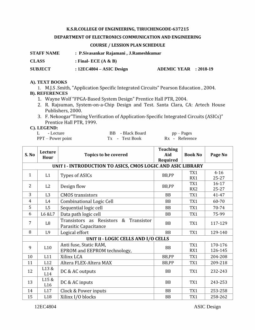
K.S.R.COLLEGE OF ENGINEERING, TIRUCHENGODE-637215
DEPARTMENT OF ELECTRONICS COMMUNICATION AND ENGINEERING
COURSE / LESSION PLAN SCHEDULE
STAFF NAME : P.Sivasankar Rajamani , J.Rameshkumar
CLASS : Final- ECE (A & B)
SUBJECT : 12EC4804 – ASIC Design ADEMIC YEAR : 2018-19
A). TEXT BOOKS
1. M.J.S .Smith, "Application Specific Integrated Circuits” Pearson Education , 2004. B). REFERENCES
1. Wayne Wolf “FPGA-Based System Design” Prentice Hall PTR, 2004. 2. R. Rajsuman, System-on-a-Chip Design and Test. Santa Clara, CA: Artech House
Publishers, 2000. 3. F. Nekoogar”Timing Verification of Application-Specific Integrated Circuits (ASICs)”
Prentice Hall PTR, 1999. C). LEGEND:
L - Lecture BB - Black Board pp – Pages
PPT – Power point Tx - Text Book Rx - Reference
S. No Lecture
Hour Topics to be covered
Teaching Aid
Required Book No Page No
UNIT I - INTRODUCTION TO ASICS, CMOS LOGIC AND ASIC LIBRARY
1 L1 Types of ASICs BB,PP TX1 RX1
4-16 25-27
2 L2 Design flow BB,PP TX1 RX2
16-17 25-27
3 L3 CMOS transistors BB TX1 41-47
4 L4 Combinational Logic Cell BB TX1 60-70
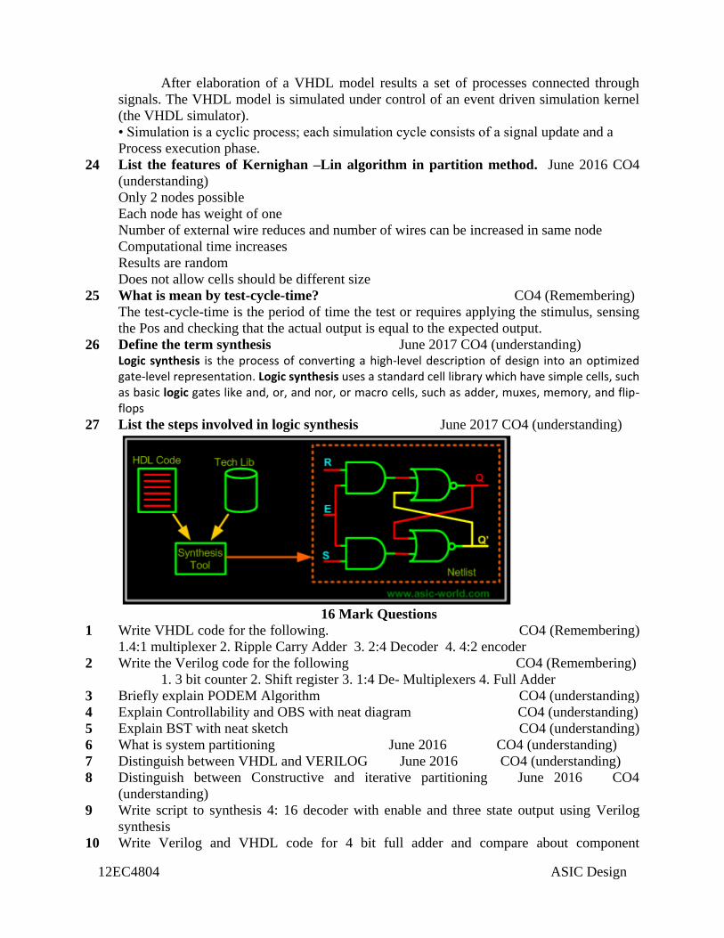
5 L5 Sequential logic cell BB TX1 70-74
6 L6 &L7 Data path logic cell BB TX1 75-99
7 L8 Transistors as Resistors & Transistor Parasitic Capacitance
BB TX1 117-129
8 L9 Logical effort BB TX1 129-140
UNIT II - LOGIC CELLS AND I/O CELLS
9 L10 Anti fuse, Static RAM, EPROM and EEPROM technology,
BB TX1 RX1
170-176 126-145
10 L11 Xilinx LCA BB,PP TX1 204-208
11 L12 Altera FLEX-Altera MAX BB,PP TX1 209-218
12 L13 &
L14 DC & AC outputs BB TX1 232-243
13 L15 &
L16 DC & AC inputs BB TX1 243-253
14 L17 Clock & Power inputs BB TX1 253-258
15 L18 Xilinx I/O blocks BB TX1 258-262
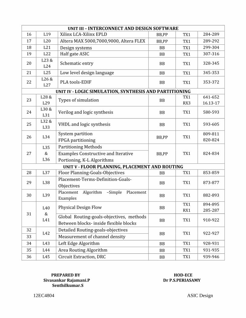
12EC4804 ASIC Design
UNIT III – INTERCONNECT AND DESIGN SOFTWARE 16 L19 Xilinx LCA-Xilinx EPLD BB,PP TX1 284-289
17 L20 Altera MAX 5000,7000,9000, Altera FLEX BB,PP TX1 289-292
18 L21 Design systems BB TX1 299-304
19 L22 Half gate ASIC BB TX1 307-316
20 L23 &
L24 Schematic entry BB TX1 328-345
21 L25 Low level design language BB TX1 345-353
22 L26 &
L27 PLA tools-EDIF BB TX1 353-372
UNIT IV - LOGIC SIMULATION, SYNTHESIS AND PARTITIONING
23 L28 &
L29 Types of simulation BB
TX1
RX3
641-652
16.13-17
24 L30 &
L31 Verilog and logic synthesis BB TX1 580-593
25 L32 &
L33 VHDL and logic synthesis BB TX1 593-605
26 L34 System partition
FPGA partitioning BB,PP TX1
809-811
820-824
27
L35
&
L36
Partitioning Methods
BB,PP TX1 824-834 Examples Constructive and Iterative
Portioning, K-L Algorithms
UNIT V - FLOOR PLANNING, PLACEMENT AND ROUTING
28 L37 Floor Planning-Goals-Objectives BB TX1 853-859
29 L38 Placement-Terms-Definition-Goals-
Objectives BB TX1 873-877
30 L39 Placement Algorithm –Simple Placement
Examples BB TX1 882-893
31
L40
&
L41
Physical Design Flow BB TX1
RX1
894-895
285-287
Global Routing-goals-objectives, methods
Between blocks- inside flexible blocks BB TX1 910-922
32 L42
Detailed Routing-goals-objectives BB TX1 922-927
33 Measurement of channel density
34 L43 Left Edge Algorithm BB TX1 928-931
35 L44 Area Routing Algorithm BB TX1 931-935
36 L45 Circuit Extraction, DRC BB TX1 939-946
PREPARED BY HOD-ECE Sivasankar Rajamani.P Dr P.S.PERIASAMY Senthilkumar.S
12EC4804 ASIC Design
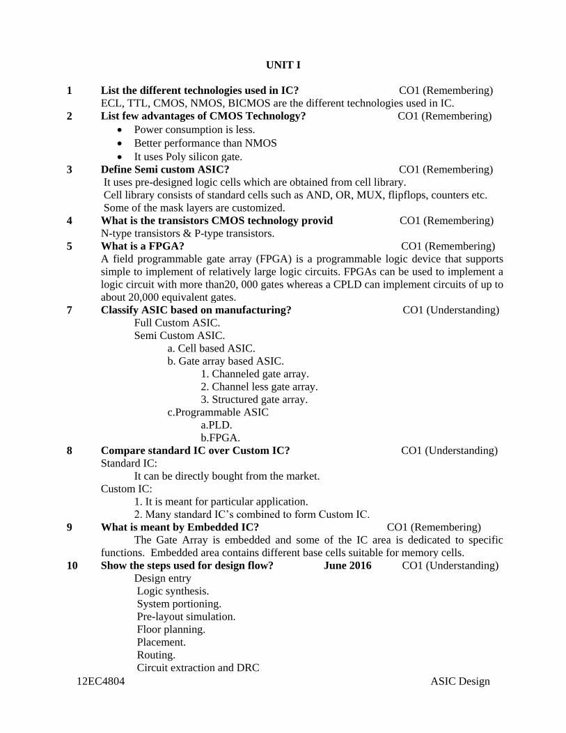
UNIT I
1 List the different technologies used in IC? CO1 (Remembering)
ECL, TTL, CMOS, NMOS, BICMOS are the different technologies used in IC.
2 List few advantages of CMOS Technology? CO1 (Remembering)
Power consumption is less.
Better performance than NMOS
It uses Poly silicon gate.
3 Define Semi custom ASIC? CO1 (Remembering)
It uses pre-designed logic cells which are obtained from cell library.
Cell library consists of standard cells such as AND, OR, MUX, flipflops, counters etc.
Some of the mask layers are customized.
4 What is the transistors CMOS technology provid CO1 (Remembering)
N-type transistors & P-type transistors.
5 What is a FPGA? CO1 (Remembering)
A field programmable gate array (FPGA) is a programmable logic device that supports
simple to implement of relatively large logic circuits. FPGAs can be used to implement a
logic circuit with more than20, 000 gates whereas a CPLD can implement circuits of up to
about 20,000 equivalent gates.
7 Classify ASIC based on manufacturing? CO1 (Understanding)
Full Custom ASIC.
Semi Custom ASIC.
a. Cell based ASIC.
b. Gate array based ASIC.
1. Channeled gate array.
2. Channel less gate array.
3. Structured gate array.
c.Programmable ASIC
a.PLD.
b.FPGA.
8 Compare standard IC over Custom IC? CO1 (Understanding)
Standard IC:
It can be directly bought from the market.
Custom IC:
1. It is meant for particular application.
2. Many standard IC’s combined to form Custom IC.
9 What is meant by Embedded IC? CO1 (Remembering)
The Gate Array is embedded and some of the IC area is dedicated to specific
functions. Embedded area contains different base cells suitable for memory cells.
10 Show the steps used for design flow? June 2016 CO1 (Understanding)
Design entry
Logic synthesis.
System portioning.
Pre-layout simulation.
Floor planning.
Placement.
Routing.
Circuit extraction and DRC
12EC4804 ASIC Design
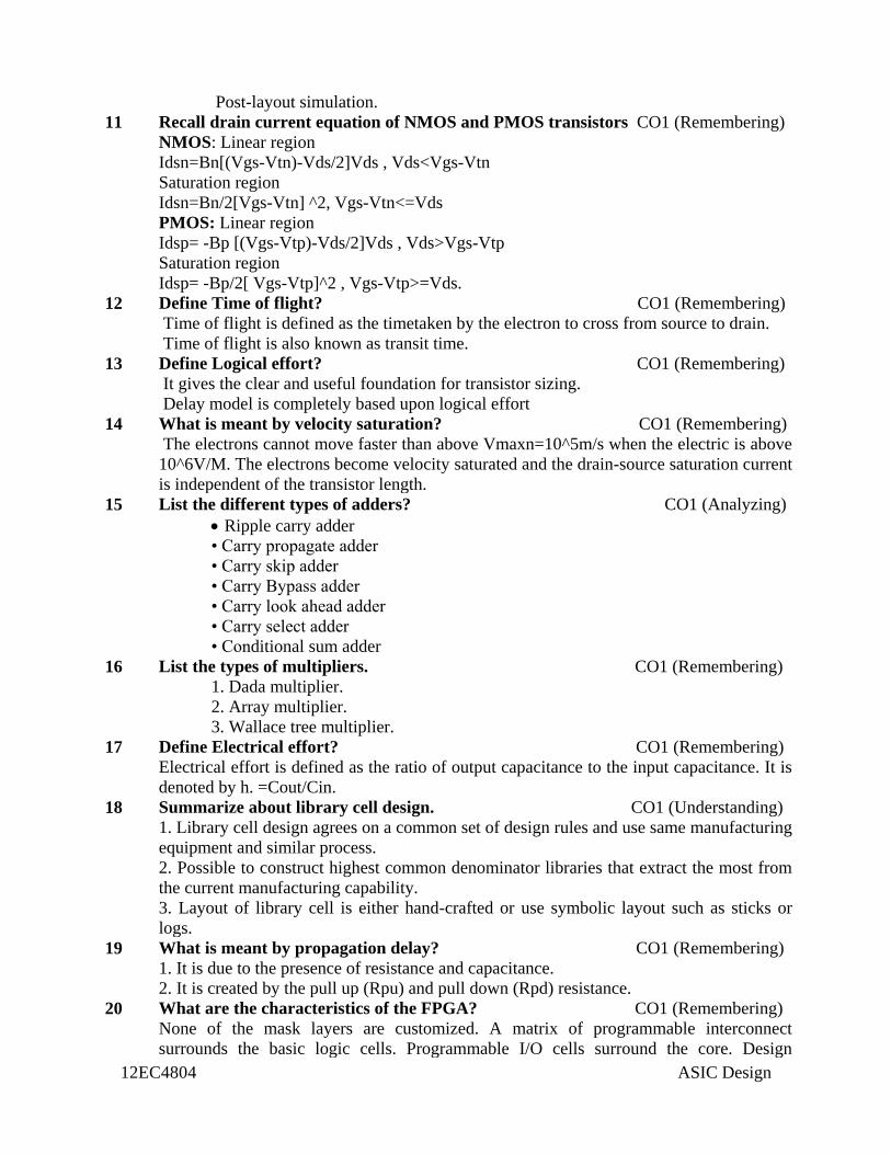
Post-layout simulation.
11 Recall drain current equation of NMOS and PMOS transistors CO1 (Remembering)
NMOS: Linear region
Idsn=Bn[(Vgs-Vtn)-Vds/2]Vds , Vds<Vgs-Vtn
Saturation region
Idsn=Bn/2[Vgs-Vtn] ^2, Vgs-Vtn<=Vds
PMOS: Linear region
Idsp= -Bp [(Vgs-Vtp)-Vds/2]Vds , Vds>Vgs-Vtp
Saturation region
Idsp= -Bp/2[ Vgs-Vtp]^2 , Vgs-Vtp>=Vds.
12 Define Time of flight? CO1 (Remembering)
Time of flight is defined as the timetaken by the electron to cross from source to drain.
Time of flight is also known as transit time.
13 Define Logical effort? CO1 (Remembering)
It gives the clear and useful foundation for transistor sizing.
Delay model is completely based upon logical effort
14 What is meant by velocity saturation? CO1 (Remembering)
The electrons cannot move faster than above Vmaxn=10^5m/s when the electric is above
10^6V/M. The electrons become velocity saturated and the drain-source saturation current
is independent of the transistor length.
15 List the different types of adders? CO1 (Analyzing)
Ripple carry adder
• Carry propagate adder
• Carry skip adder
• Carry Bypass adder
• Carry look ahead adder
• Carry select adder
• Conditional sum adder
16 List the types of multipliers. CO1 (Remembering)
1. Dada multiplier.
2. Array multiplier.
3. Wallace tree multiplier.
17 Define Electrical effort? CO1 (Remembering)
Electrical effort is defined as the ratio of output capacitance to the input capacitance. It is
denoted by h. =Cout/Cin.
18 Summarize about library cell design. CO1 (Understanding)
1. Library cell design agrees on a common set of design rules and use same manufacturing
equipment and similar process.
2. Possible to construct highest common denominator libraries that extract the most from
the current manufacturing capability.
3. Layout of library cell is either hand-crafted or use symbolic layout such as sticks or
logs.
19 What is meant by propagation delay? CO1 (Remembering)
1. It is due to the presence of resistance and capacitance.
2. It is created by the pull up (Rpu) and pull down (Rpd) resistance.
20 What are the characteristics of the FPGA? CO1 (Remembering)
None of the mask layers are customized. A matrix of programmable interconnect
surrounds the basic logic cells. Programmable I/O cells surround the core. Design
12EC4804 ASIC Design
turnaround is a few hours.
21 What is meant by design entry? CO1 (Remembering)
Enter the design into an ASIC design system, either using a hardware description
language (HDL) or schematic entry.
22 What is meant by Logic synthesis? CO1 (Remembering)
Use an HDL (VHDL or VERILOG) and a logic synthesis tool to produce a net-list-a
description of the logic cells and their connections.
23 What is meant by System partitioning? CO1 (Remembering)
Dividing a large system into ASIC-sized pieces.
24 What is meant by Floor planning? CO1 (Remembering)
Arranging the blocks of net list on the chip.
25 What is the full custom ASIC design? June 2017 CO1 (Remembering)
In a full custom ASIC, an engineer designs some or all of the logic cells, circuits or layout
specifically for one ASIC. It makes sense to take this approach only if there are no
suitable existing cell libraries available that can be used for the entire design.
26 What is the standard cell-based ASIC design? CO1 (Remembering)
A cell-based ASIC (CBIC) uses predesigned logic cells known as standard cells. The
standard cells are as also called flexible blocks in a CBIC are built of rows of standard
cells. The ASIC designer defines only the placement of standard cells and the interconnect
in a CBIC. All they ask layers of a CBIC are customized and are unique to a particular
customer.
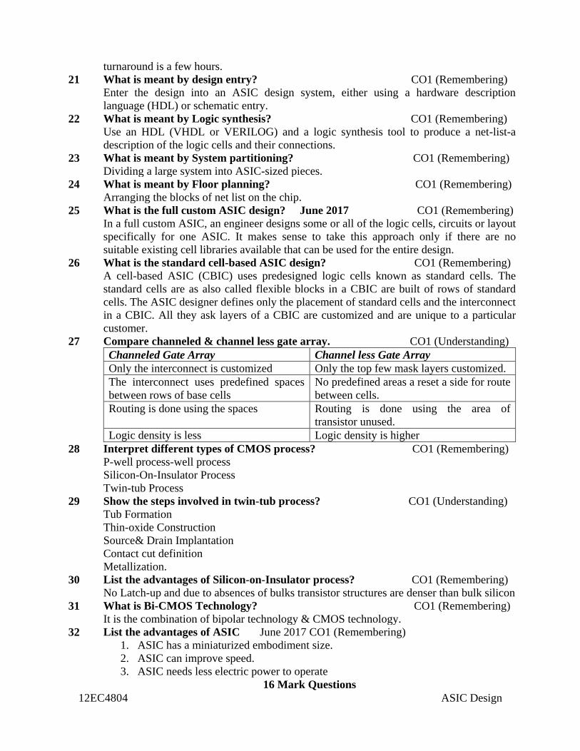
27 Compare channeled & channel less gate array. CO1 (Understanding)
Channeled Gate Array Channel less Gate Array
Only the interconnect is customized Only the top few mask layers customized.
The interconnect uses predefined spaces
between rows of base cells
No predefined areas a reset a side for route
between cells.
Routing is done using the spaces Routing is done using the area of
transistor unused.
Logic density is less Logic density is higher
28 Interpret different types of CMOS process? CO1 (Remembering)
P-well process-well process
Silicon-On-Insulator Process
Twin-tub Process
29 Show the steps involved in twin-tub process? CO1 (Understanding)
Tub Formation
Thin-oxide Construction
Source& Drain Implantation
Contact cut definition
Metallization.
30 List the advantages of Silicon-on-Insulator process? CO1 (Remembering)
No Latch-up and due to absences of bulks transistor structures are denser than bulk silicon
31 What is Bi-CMOS Technology? CO1 (Remembering)
It is the combination of bipolar technology & CMOS technology.
32 List the advantages of ASIC June 2017 CO1 (Remembering)
1. ASIC has a miniaturized embodiment size.
2. ASIC can improve speed.
3. ASIC needs less electric power to operate
16 Mark Questions
12EC4804 ASIC Design
1 Explain the ASICs design flow June 2017 CO1 (Understanding)
2 Recall CMOS process and Explain sheet resistance which is involved in CMOS process
June 2016 CO1 (Understanding)
3 Discuss in detail about any 4 types of ASIC’s June 2016 CO1 (Remembering)
4 With neat diagram explain about custom ASICs? CO1 (Understanding)
5 Explain about logical effort? June 2016 CO1 (Understanding)
6 Demonstrate the drain current equation? CO1 Understanding)
7 Explain transistor as resistor and different capacitance June 2017 CO1 (Understanding)
8 With neat sketch explain on CMOS inverter June 2017 CO1 (Understanding)
UNIT II
1 Recall the types of programmable ASICs. CO2 (Remembering)
Programmable logic devices
Field programmable gate array
The distinction between the two is their heritage.
2 Define “Antifuse”? CO2 (Remembering)
An Antifuse is opposite of a regular fuse. Antifuse is normally an open circuit until you
force a programming current through. (about 5 mA)
Types of antifuse.Poly silicon Antifuse.
• Metal- Metal Antifuse.
(Or)
An antifuse is normally high resistance (>100MΩ). On application of appropriate
programming voltages, the antifuse is changed permanently to a low-resistance structure
(200-500Ω).
3 Define “PREP Bench marks”. CO2 (Remembering)
Programmable Electronic Performance Company (PREP) is a non profitable organization
that organized a series of bench marks for programmable ASICS. Totally 9 Bench marks
are available.
1) A small state machine
2) A larger state machine
3) A 16 bit address decoder
4) A 16 bit accumulator
4 Classify the different types of basic logic cell. CO2 (Understanding)
Multiplexer based
Look up table based
Programmable array logic
5 Justify why Actel architecture is called as a non deterministic architecture?
CO2 (Understanding)
We cannot predict the exact delays on an Actel chip until we have performed the place
and route step and know how much delay is contributed by the interconnect, since we
cannot determine the exact delay before physical layout is complete, we call the Actel
Architecture non deterministic.
6 Define “speed grading”. CO2 (Remembering)
Most FGPA vendors sort chips according to their speed, the sorting is known as speed
grading or speed binning.
12EC4804 ASIC Design
7 Define “worst case timing”. CO2 (Remembering)
The maximum delays that may encounter, which we call the worst case timing.
Maximum delays in CMOS logic occur when operating under minimum voltage,
maximum temperature, and slow-slow process condition
8 Define “propagation delay”. CO2 (Remembering)
The propagation delay is defined as the average of the rising and falling propagation
delays of the logic module.
9 Define “AC input” and “DC input”. June 2017 CO2 (Remembering)
AC input:
Example sources are high-speed logic signals (higher than 1MHz) from another chip.
DC input:
Example sources are a switch, sensor, or another logic chip.
10 Define “AC output”. CO2 (Remembering)
Driving a resistive load at DC or low frequency (less than 1MHz) logic signal off-chip.
Example loads are other logic chips, a data or address bus, ribbon cable.
11 Identify Shannon’s Expansion theorem CO2 (Applying)
F= A.F (A=’1’) + A’.F (A=’0’)
12 Define “DC output”. CO2 (Remembering)
DC output is driving a resistive load at DC or low frequency (less than 1MHz).
Examples, LEDs, relays, small motors.
13 Define “Derating factors”. CO2 (Remembering)
To convert nominal or typical timing figures to the worst case or best case, we use
measured or empirically derived constants called derating factors.
14 Define “Power input”. CO2 (Remembering)
We need to supply power to the I/O cells and the logic in the core without introducing
voltage drop or noise
15 Define “clock input”. CO2 (Remembering)
Examples are system clocks or signals on a synchronous bus.
16 Write the different types of terminations used in transmission line.
• Open-circuit or capacitance termination
• Parallel resistive termination
• Thevenin termination
• Series termination at the source parallel termination with a voltage bias
• Parallel termination with a series capacitance.
17 Name the types of ports in Verilog CO2 (Remembering)
Types of port Keyword
Input port
Input Output port
Output Bidirectional port
In Out
18 What is Programmable Interconnects? CO2 (Remembering)
In a PAL, the device is programmed by changing the characteristics if the switching
element. An alternative would be to program the routing.
19 Classify programming of PALs? CO2 (Understanding)
The programming of PALs is done in three main ways
• Fusible links
• UV –Erasable EPROM
• EEPROM (E2PROM)–Electrically Erasable Programmable ROM.
12EC4804 ASIC Design
20 Criticize the metal- metal antifuse over poly diffusion antifuse June 2016 CO2
(Remembering)
s.no metal- metal antifuse poly diffusion antifuse
1 Metal–metal antifuse ( ViaLink ‘ ).
The link is an alloy of tungsten,
titanium, and silicon
poly–diffusion antifuse with an oxide–
nitride–oxide (ONO) dielectric
sandwich of: silicon dioxide (SiO 2 )
grown over the n -type antifuse
diffusion, a silicon nitride (Si 3 N 4 )
layer, and another thin SiO 2 layer.
2 The n- type antifuse diffusion and
antifuse polysilicon require an extra
two masks and a 40 nm (thicker than
normal) gate oxide (for the high-
voltage transistors that handle 18 V
to program the antifuses) uses one
more masking step
The actual thickness is less than 10
nm
3 bulk resistance of about 500 mW cm Increasing the programming current to
15 mA might reduce the average
antifuse resistance to 100 W.
21 Define power on reset JUNE 2016 CO2 (Remembering)
Each FPGA has its own power on reset sequences for example a Xilinx FPGA configures
All flipflops (either the CLB’S or IOB’s) as either SET or RESET. After chip
programming is complete the global SET /RESET signlas forces all flipflops on the chip
to know state .this is important since it determine the initial state of a state machine
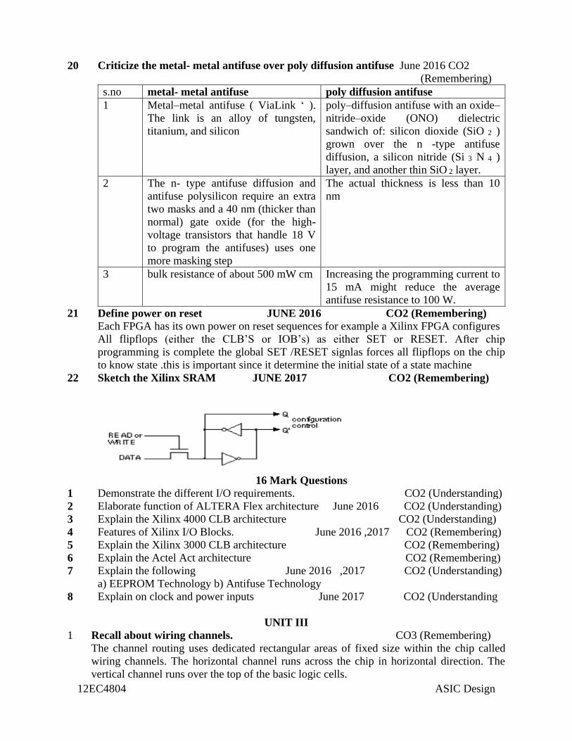
22 Sketch the Xilinx SRAM JUNE 2017 CO2 (Remembering)
16 Mark Questions
1 Demonstrate the different I/O requirements. CO2 (Understanding)
2 Elaborate function of ALTERA Flex architecture June 2016 CO2 (Understanding)
3 Explain the Xilinx 4000 CLB architecture CO2 (Understanding)
4 Features of Xilinx I/O Blocks. June 2016 ,2017 CO2 (Remembering)
5 Explain the Xilinx 3000 CLB architecture CO2 (Remembering)
6 Explain the Actel Act architecture CO2 (Remembering)
7 Explain the following June 2016 ,2017 CO2 (Understanding)
a) EEPROM Technology b) Antifuse Technology
8 Explain on clock and power inputs June 2017 CO2 (Understanding
UNIT III
1 Recall about wiring channels. CO3 (Remembering)
The channel routing uses dedicated rectangular areas of fixed size within the chip called
wiring channels. The horizontal channel runs across the chip in horizontal direction. The
vertical channel runs over the top of the basic logic cells.
12EC4804 ASIC Design
2 Write about routing resources used in Actel ACT. CO3 (Remembering)
The ACT1 interconnection architecture uses 22 horizontal tracks per channel for signal
routing with three tracks dedicated to VDD, GND and the global clock making a total 25
tracks per channel.
3 Inspect the details of antifuses for Actel ACT family. CO3 (Remembering)
a) An input stub (1 channel) connects to 25 antifuses.
b) An output stub (4 channels) connects to 100(25*4) antifuses.
c) An LVT (1010, 8 channels) connects to 200(25*8) antifuses.
d) An LVT (1020, 14 channels) connects to 350(25*14) antifuses.
e) A four-column horizontal track connects to 52(13*4) antifuses.
f) A 44-column horizontal track connects to 572(13*44) antifuses
4 Define “Channel Density”. CO3 (Remembering)
The channel density is the absolute minimum number of tracks needed in a channel to make
a given set.
5 Define “PIPs” and “BIDI”. CO3 (Remembering)
The programmable Interconnection Point (PIPs) is programmable pass transistor that
connects
the CLB inputs and outputs to the routing network.
The Bidirectional (BIDI) interconnects buffers restore the logic level and logic strength on
long interconnect path.
6 Summarize on Altera MAX 5000 and 7000. CO3 (Remembering)
Altera MAX 5000 devices and all MAX 7000 devices use a programmable interconnect
array. PIA is the cross point switch for logic signals traveling between LABs.
7 List some points about Altera MAX 9000. CO3 (Remembering)
The size of the LAB arrays vary between 4*5(Rows*Columns)
It is extremely coarse-grain architecture.
8 Dissect the components of Programmable ASICs. CO3 (Remembering)
The programming technology
The basic logic cell
Row Fast Track
Column Fast Track
The I/O cell
The Interconnect.
The design Software.
9 Write some hardware description languages. CO3 (Remembering)
• VHDL
• Verilog
• ABEL
• CUPL
• PALASM
10 Define “OEM”. CO3 (Remembering)
FPGA vendors sell design kits that include all the software and hardware that a designer
needs. Many of these kits use design entry software produced by different company. Often
designers buy that software from FPGA vendor. This is called an original equipment
manufacturer.
11 Write some important file types used in Actel act. CO3 (Remembering)
• ADL – Main design net list
• IPF - Partial or complete pin assignment for the design
12EC4804 ASIC Design
• CRT – Net critically
• VALIDATED – Audit information
• STF – Back-annotation timing.
12 Outline features of Altera. CO3 (understanding)
Altera uses self contained design system for its complex PLDs that performs design
entry, simulation and programming parts. Altera also provides an input and output interface
to EDIF so that designers may use third party schematic entry or a logic synthesizer.
13 Justify how the logic minimization can be made. CO3 (Understanding)
The logic minimization can be usually performed in two ways, either using a set of rules or
using algorithms.
14 Define “Half gate ASICs”. June 2017 CO3 (Remembering)
FPGA design using a very simple inverter, the hidden details of the design and
construction of this “half gate FPGA”, are quite complex. Fortunately most of the inner
working of the design software is normally hidden from the designer.
15 16. Define “Schematic entry”. CO3 (Remembering)
Schematic entry is the most common method of design entry. For ASICs and is
likely to be useful in one form or another for some time. HDLs are replacing conventional
gate -level schematic entry, but new graphical tools based on schematic entry are now being
used to create large amounts of HDL code.
16 Outline hierarchical design. CO3 (Understanding)
Hierarchy reduces the size and complexity of a schematic.
17 Define “CAD Frame Initiative (CFI)”. CO3 (Remembering)
The CAD Frame Initiative (CFI) is a non profitable organization working on the creation of
standards for the electronic CAD industry. One of the area in which CFI is working is the
definition of standards for design representation (DR).
18 Merits of half gate ASIC design June 2016 CO3 (Understanding)
How things work can be understand
Fixing of the problems can be done easily manner
Hidden details can be understood
Software will break the whole program into small modules
19 Classify of timing control? CO3 (Remembering)
Methods of timing control:
1. Delay-based timing control
2. Event-based timing control
3. Level-sensitive timing control
Type’s of delay-based timing control:
1. Regular delay control
2. Intra-assignment delay control
3. Zero delay control
Types of event-based timing control:
1. Regular event control
2. Named event control
3. Event OR control
4. Level-sensitive timing control
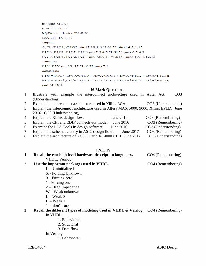
20 Interpret the 4:1 Mux using ABEL statement. June 2016,2017 CO3 (Understanding)
12EC4804 ASIC Design
16 Mark Questions:
1 Illustrate with example the interconnect architecture used in Actel Act. CO3
(Understanding)
2 Explain the interconnect architecture used in Xilinx LCA. CO3 (Understanding)
3 Explain the interconnect architecture used in Altera MAX 5000, 9000, Xilinx EPLD. June
2016 CO3 (Understanding)
4 Explain the Xilinx design flow. June 2016 CO3 (Remembering)
5 Explain the CFI and EDIF connectivity model. June 2016 CO3 (Remembering)
6 Examine the PLA Tools in design software June 2016 CO3 (Understanding)
7 Explain the schematic entry in ASIC design flow. June 2017 CO3 (Remembering)
8 Explain the architecture of XC3000 and XC4000 CLB June 2017 CO3 (Understanding)
UNIT IV
1 Recall the two high level hardware description languages. CO4 (Remembering)
VHDL, Verilog
2 List the important packages used in VHDL. CO4 (Remembering)
U – Uninitialized
X - Forcing Unknown
0 – Forcing zero
1 - Forcing one
Z – High Impedance
W – Weak unknown
L – Weak 0
H – Weak 1
‘-‘– don’t care
3 Recall the different types of modeling used in VHDL & Verilog CO4 (Remembering)
In VHDL
1. Behavioral
2. Structural
3. Data flow
In Verilog
1. Behavioral
12EC4804 ASIC Design
2. Structural
3. Gate level
4. Switch level
4 Write short notes on concurrent assertation statement. CO4 (Remembering)
A concurrent assertation statement is equivalent to a passive process statement (with
sensitivity list) that contains an assertion statement followed by a wait statement.
5 Write the structure for generate statement CO4 (Remembering)
generate statement: = generate_label for generate parameter specification if Boolean
expression generate block declarative item begin concurrent statement end generate
generate 4 label
6 Write the verilog code for multiplexer (2:1)? CO4 (Remembering)
Module mux_21a (sel,a,b);
Input sel,a,b;
Output z;
Reg z;
always@(a or b or sel)
begin case (a or b or sel)
begin case (sel) 1’b0: z<a; 1’b1:
z<b;end
End module
7 Define BST. CO4 (Remembering)
Boundary Scan Test (BST) is a method of testing boards using a four wire interface. The
BST Standard Interface was designed to test boards. But is also useful to test an ASIC.
8 Classify the various faults? CO4 (Understanding)
Physical fault
Stuck-at-fault model
Logical
9 Write short notes on serial fault simulation? CO4 (Remembering)
Serial fault simulation is the simplest fault simulation algorithm. We simulate two
copies of the circuit. The first copy is a good circuit. We then pick fault and insert into a
fault circuit. In test terminology the circuits are called machines.
10 What is concurrent fault simulation? CO4 (Remembering)
The concurrent fault simulation is the most widely used fast simulation algorithm and take
advantages of the fact a fault does not affect the whole circuit. In concurrent simulation we
first completely simulate the circuit.
11 What are the various cells used in BST? CO4 (Remembering)
TDR-Test Data Registers
DR-Data Register Cells
BST-Boundary Scan registers
ID-Instruction Register
Tap Controller
12 Define “fault Coverage”? CO4 (Remembering)
Fault coverage = detected faults/ detectable fault
13 Define “soft detected fault”? CO4 (Remembering)
If the PO of the good circuit changes between a ‘1’and a ‘0’, while the faulty circuit
remains at ‘x’ then we have soft detected fault
14 What are the types of fault occurring in the CMOS circuit? CO4 (Remembering)
* Hard detected fault
12EC4804 ASIC Design
* Definitely detected fault
* Untested fault
* Un-testable fault
* Impossible fault
* Possible detected fault
* Soft detected fault.
15 What are the different types of tests conducted in ASIC’S CO4 (Remembering)
First ASIC’S are tested at two stages during manufacture using Production test. First the
silicon
die are tested after fabrication is complete at wafer test or wafer sort. Each wafer is tested,
one die at a time. A second, final test is carried out on the packaged ASIC before the ASIC
is shipped into the customer.
16 Write the program for JK flip-flop using Verilog. CO4 (Applying)
Module jk flipflop(q,j,k,clk,RST);
Input j,k,clk,RST;
Output q;
always@(posedge clk or negedge rst)
if(rst= = 0)q<= #1 reset_value
else q<= #1(j & k) / (j & k &!q)/ (!j &! k &Q) ;
end module
17 Classify types of simulations. CO4 (Remembering)
* Behavioral simulation
* Functional simulation
* Static timing analysis
* Gate level simulation
* Switch level simulation
* Transistor - level simulation .
18 Write short notes on logic simulation. CO4 (Remembering)
Logic simulation or Gate level simulation can also be used to check the timing
performance of ASIC .In a Gate level a logic gate or logic cell (NAND,NOR and so on)is
treated as a black box as modeled by a function whose variables are the inputs .
19 What is Switch level simulation? CO4 (Remembering)
In Switch level simulation which models transistor as switches on or off.
Switch level simulation can provide more accurate timing predictors than Gate level
simulation. The most accurate but also most complex and time consuming form of
simulation is transistor level simulation.
20 Mention the levels at which testing of a chip can be done? CO4 (Remembering)
a) At the wafer level
b) At the packaged-chip level
c) At the board level
d) At the system level
e) In the field
21 What are the categories of testing? CO4 (Remembering)
a) Functionality tests b) Manufacturing tests
22 What is the functionality tests indented for? CO4 (Remembering)
Functionality tests verify that the chip performs its intended
23 Steps involved in VHDL Simulation cycle June 2016 CO4 (Remembering)
12EC4804 ASIC Design
After elaboration of a VHDL model results a set of processes connected through
signals. The VHDL model is simulated under control of an event driven simulation kernel
(the VHDL simulator).
• Simulation is a cyclic process; each simulation cycle consists of a signal update and a
Process execution phase.
24 List the features of Kernighan –Lin algorithm in partition method. June 2016 CO4
(understanding)
Only 2 nodes possible
Each node has weight of one
Number of external wire reduces and number of wires can be increased in same node
Computational time increases
Results are random
Does not allow cells should be different size
25 What is mean by test-cycle-time? CO4 (Remembering)
The test-cycle-time is the period of time the test or requires applying the stimulus, sensing
the Pos and checking that the actual output is equal to the expected output.
26 Define the term synthesis June 2017 CO4 (understanding) Logic synthesis is the process of converting a high-level description of design into an optimized gate-level representation. Logic synthesis uses a standard cell library which have simple cells, such as basic logic gates like and, or, and nor, or macro cells, such as adder, muxes, memory, and flip-flops
27 List the steps involved in logic synthesis June 2017 CO4 (understanding)
16 Mark Questions
1 Write VHDL code for the following. CO4 (Remembering)
1.4:1 multiplexer 2. Ripple Carry Adder 3. 2:4 Decoder 4. 4:2 encoder
2 Write the Verilog code for the following CO4 (Remembering)
1. 3 bit counter 2. Shift register 3. 1:4 De- Multiplexers 4. Full Adder
3 Briefly explain PODEM Algorithm CO4 (understanding)
4 Explain Controllability and OBS with neat diagram CO4 (understanding)
5 Explain BST with neat sketch CO4 (understanding)
6 What is system partitioning June 2016 CO4 (understanding)
7 Distinguish between VHDL and VERILOG June 2016 CO4 (understanding)
8 Distinguish between Constructive and iterative partitioning June 2016 CO4
(understanding)
9 Write script to synthesis 4: 16 decoder with enable and three state output using Verilog
synthesis
10 Write Verilog and VHDL code for 4 bit full adder and compare about component
12EC4804 ASIC Design
instantiation June 2017 CO4 (understanding)
11 Illustrate KL partitioning algorithm with an example June 2017 CO4 (understanding)
UNIT V
1 What is meant by system partitioning? CO5 (Remembering)
If a functional block is too large to fit in one ASIC, we may have to split, or partition, the
function into pieces using goals and objectives that we need to specify.
2 List objectives and goals of system partitioning? CO5 (Remembering)
Objectives:
A maximum size for each ASIC
A maximum number of ASICs
A maximum number of connections for each ASICs
A maximum number of total connections between all ASIC
Goals:
To divide this part of the system so that each partition is single ASIC.
3 Summarize the constraints used in system partitioning? CO5 (Understanding)
• Timing constraints
• Power constraints
• Technology constraints
• Cost constraints
• Test constraints
4 How “Simulated annealing” helps in partitioning. CO5 (Remembering)
A different approach to solving large graph problems that arise in VLSI layout, including
system partitioning uses the simulated annealing algorithm.
• It takes an existing solution and then makes successive changes in a series of random
moves.
• Each move is accepted or rejected based on an energy function, calculated for each new
trail configuration.
• The minimums of the energy function correspond to the possible.
• The best solution is the global minimum.
5 What are the different algorithms used in system partitioning. CO5 (Remembering)
There are 2 types
• Constructive partitioning
• Iterative partitioning improvement (or) Iterative partitioning refinement.
6 How do you find out the gain in system partitioning? CO5 (Remembering)
Let the network split in to 2 partitions A and B, Find 2 nodes ai and bi from B. So that the
gain
from swapping them is maximum. The gain is gi=Dai+Dbi-2CaibiThe total gain is Gn=gi.
7 Define "floor planning". CO5 (Remembering)
Floor planning allows us to predict this interconnect delay by estimating interconnect
length.
8 Write the goals and objectives of floor planning. june 2016 CO5 (Remembering)
Goals: Arrange the blocks on a chip
Decide the location of I/O pads
Decide the location and number of the power pads
12EC4804 ASIC Design
Decide the location and type of clock distribution.
Objectives: Minimize the chip area and minimize delay.
9 What is meant by “iterative system portioning”? CO5 (Remembering)
Iterative system portioning improvement takes an existing solution and tries to improve it
10 What are the different types of algorithm used in placement? CO5 (Remembering)
1. Constructive placement-----use set of rules
2 Iterative placements
3.Min-cut algorithm Eigen value placement algorithm
11 What is meant by Placement? CO5 (Remembering)
Placement means decoding the location of cells in a block
12 Write the steps used in” Min- cut algorithm”. CO5 (Remembering)
The steps involved are as follows
• Divide the chip into number of bins using a grid
• Merge all the connections into a centre of each bin
• Cut the placement and swap the logic cell to minimize the cut cost
• Take the cut piece and throughout all the edges that are not inside the cut piece
• Repeat the process with the new cut and continue until we reach the individual bin
13 Define sliceable floor plan. CO5 (Remembering)
If the floor plan is sliced into pieces without cutting the block it is called sliceable
floor plan.
14 What are cyclic constraints? CO5 (Remembering)
We cannot cut the chip all the way across with the knife without chopping a circuit
block into two .This means we cannot route any of the channels in this floor plan without
routing all of the other channels first . We say there is a cyclic constrain in this floor plan.
15 Define back annotation. CO5 (Remembering)
The global router can give us not just an estimate of the total net length, but the
resistance and capacitance of each path in each net .This RC information is used to
calculate the net delays. We can back annotate this net delay information to the synthesis
tool for in –place optimization or to a timing verifier to make sure there are no timing
surprises. Differences in timing prediction at this point arise due to different ways in which
the different algorithms estimates the path and the way the global router actually builds the
path.
16 What are the value sets in Verilog? CO5 (Remembering)
Verilog supports four levels for the values needed to describe hardware referred to
as value sets. Value levels Condition in hardware Circuits
0 Logic zero, false condition
1 Logic one, true condition
X Unknown logic value
Z High impedance,
Floating state.
17 List some of the important CAD tools. CO5 (Remembering)
Some of the important CAD tools are:
i) Layout editors
ii) Design Rule checkers (DRC)
iii) Circuit extraction
18 Recall left edge algorithm June 2016 CO5 (Remembering)
Sort the left most of the horizontal segment
Assign the first net on the list to the first free track
12EC4804 ASIC Design
Assign the next net on the list which will fit to the track
Repeat the process from step 3 until no more nets fit the current track
Repeat the process 2 and 4 until all nets have been assigned to the track
Connect the net segment to the top and bottom of the channel.
19 Mention the advantages of routing June 2017 CO5 (Remembering)
Routing is an important step in the design of integrated circuits (ICs). It generates wiring to
interconnect pins of the same signal, while obeying the manufacturing design rules. As IC
process advances to nanometer technology, foundries may fabricate billions of transistors
in a single chip, and the number of transistors per die will still grow drastically in the near
future. This increasing complexity imposes substantial challenges for physical design,
especially for routing.
20 List out the goals of detailed routing June 2017 CO5 (Remembering) Detailed routing does the actual connections. Different constraints that are to be taken care during the routing are DRC, wire length, timing etc.
16 Mark Questions:
1 How KL algorithm helps for system partitioning in SOC? CO5 (Remembering)
2 Explain detailed routing with neat diagram? CO5 (Understanding)
3 Briefly explain global routing with neat diagram? CO5 (Understanding)
4 Elaborate about Eigen value algorithm for placement? CO5 (Understanding)
5 Illustrate about circuit extraction and DRC? June 2016 CO5 (Understanding)
6 Recall detailed routing June 2016 CO5 (Understanding)
7 Explain the function and measurement of channel density June 2016 CO5 (Understanding)
8 Discuss goals, objectives and methods of global routing June 2016 CO5 (Understanding)
9 Compare and construct good placement and bad placement. June 2016 CO5
(Understanding)
10 Brief about iterative placement improvement and timing driven placement method. June
2017 CO5 (Understanding)
11 Illustrate the procedure on left edge algorithm and constraint and routing graph. June 2017
CO5 (Understanding)