cmos asic design of multi-frequency multi-constellation
TRANSCRIPT
POUR L'OBTENTION DU GRADE DE DOCTEUR ÈS SCIENCES
acceptée sur proposition du jury:
Prof. K. Aminian, président du juryProf. P.-A. Farine, Dr C. Botteron, directeurs de thèse
Prof. F. Alimenti, rapporteurDr G. Tasselli, rapporteurProf. H. Shea, rapporteur
CMOS ASIC Design of Multi-frequency Multi-constellation GNSS Front-ends
THÈSE NO 7045 (2016)
ÉCOLE POLYTECHNIQUE FÉDÉRALE DE LAUSANNE
PRÉSENTÉE LE 20 JUIN 2016
À LA FACULTÉ DES SCIENCES ET TECHNIQUES DE L'INGÉNIEURLABORATOIRE D'ÉLECTRONIQUE ET TRAITEMENT DU SIGNAL
PROGRAMME DOCTORAL EN GÉNIE ÉLECTRIQUE
Suisse2016
PAR
Saeed GHAMARI


Dedicated to
my beloved mother, Tahereh, and my beloved father, Einollah ...

AcknowledgementsFirst and foremost, I am grateful to the God for his blessings and for the good health and
wellbeing that were necessary to complete this work. I would also like to express my gratitude
to several people without whom this work would not have been accomplished. First, I would
like to express my sincere gratitude to my kind supervisor Prof. Dr Pierre-André Farine, head
of ESPLAB, for giving me the opportunity to be part of ESPLAB and providing me with the
most favorable work conditions during my Ph.D.
Special thanks go to Dr Cyril Botteron for being such a supportive and motivating su-
pervisor, for his guidance and support throughout the period of this dissertation as well
as continuous review of my work. I have been extremely lucky to have such a committed
co-supervisor who cared so much about me and my work.
I would also like to express my gratitude to the rest of the thesis jury committee, Prof.
Kamiar Aminian, Dr Gabriele Tasselli, Prof. Federico Alimenti and Prof. Herbert Shea for
accepting to review my dissertation and evaluate this work.
My sincere gratitude goes to Dr Gabriele Tasselli, my friend and former officemate for the
continuous support of my Ph.D. study and related research, for his patience, motivation, and
immense knowledge. His guidance helped me all the time of research and writing of this thesis.
I could not have imagined accomplishing this work without his advices.
Special thanks go to Christian Robert for his support and help regarding any questions
and problems involving Cadence and PCB design. I am also thankful to him for the French
translation of the abstract of this thesis.
Moreover, I would like to thank Christelle Emery and Vincenzo Capuano for their skills in
regard with travel organization inside and outside of Switzerland. I thank also all my former
and current colleagues at ESPLAB, Aleksandar, Alexis, Ban, Biswajit, Chao, Flavien, Hugo,
Jean-Pierre, Jérôme, Laurent, Marcel, Marko, Martin, Mathieu, Miguel, Mitko, Patrick, Paul,
Pavel, Sara, Urs, Vasili and Youssef for their friendship and creating a very nice atmosphere
and wonderful time during the last five years. My appreciation goes to Mrs. Joelle Banjac for
all the administrative helps and supports she provided me during my Ph.D.
My special thanks go to my Iranian friends, Alaleh, Mohssen, Abbas, Milad and Ali Dabirian
for making the life in Neuchâtel much easier despite being away from my home town.
Finally, I would like to express my sincere gratitude to my parents, Tahereh and Einollah to
whom I owe my life, my brother Madjid and my sister Mahshid for their unconditional love
and for supporting me throughout my life.
Neuchâtel, le 19 Mai 2016 S. Gh.
i

AbstractWith the emergence of the new global navigation satellite systems (GNSSs) such as Galileo,
COMPASS and GLONASS, the Global Positioning System (GPS) is no longer the sole player
in satellite navigation systems. These new systems offer not only new services but also new
frequency bands and signal structures, and challenge engineers to exploit them. Moreover,
the deployment of the new satellites will increase the number of visible satellites by three to
four times in the near future. The increase in visible satellites and interoperability among
the GNSSs open a new door towards multi-constellation multi-frequency GNSS receivers.
This creates a new series of challenges for engineers with regard to improving positioning
accuracy, precision, robustness, and reliability, and opens the possibility for new applications
that are limited only by our imagination. In the course of this dissertation, two application-
specific integrated circuit (ASIC) GNSS front-ends (FEs) were designed to address some of
these challenges.
Although Galileo is the first global positioning service under civilian control, it offers
specialized services such as the public regulated service (PRS). The PRS is a proprietary en-
crypted navigation service that is designed to be more robust and reliable, with anti-jamming
and pseudo-random number (PRN) encryption mechanisms. This service provides position
and timing to a specific group of users, authorized governmental bodies, who require a high
continuity of service. The PRS as a new service demands a class of advanced FEs that can
satisfy its stringent requirements. The project that this thesis is part of, aims to develop a multi-
frequency PRS receiver by filling some of the technological gaps in order to enable affordable
and robust solutions for future demanding applications that rely on the continuous availability
of the PRS. These developments respond to the growing need for low-cost multi-frequency
radio modules adapted for professional applications.
Towards this end, the design of a dual-frequency PRS receiver that is capable of simul-
taneous reception of both the E1 and E6 PRS signals is presented. In order to increase the
robustness of the receiver in the presence of interference, the receiver incorporates two inde-
pendent FEs. The entire radio frequency (RF) chain, including a low-noise amplifier (LNA), a
quadrature mixer, a frequency synthesizer (FS), two intermediate frequency (IF) filters, two
variable-gain amplifiers (VGAs) and two analog-to-digital converters (ADCs), is the object of
research and development within this project. Each FE provides 50 MHz of IF bandwidth to
accommodate wide-band PRS signals. Moreover, it achieves 65 dB of gain and 30 dB of gain
dynamic range. It features a 6-bit ADC that allows for the implementation of interference
mitigation algorithms in the baseband processor in order to withstand strong interferers and
iii
Abstract
improve the robustness of the receiver. The complete FE occupies a die area of 11.5 mm2 on
0.18 μm complementary metal-oxide-semiconductor (CMOS) while consuming 115 mW.
Furthermore, to address civilian applications and exploit the interoperability among
GNSSs, this thesis also presents a reconfigurable single-channel FE. The receiver operates in
two modes: in the “narrow-band” mode, it shows an IF bandwidth of 8 MHz and can receive
Beidou-B1 while drawing 22.85 mA from a 1.8 V supply, and in the “wide-band” mode, with
an IF bandwidth of 23 MHz, it can accommodate simultaneous reception of Beidou-B1/GPS-
L1/Galileo-E1 while consuming 28.45 mA. Measures to improve the linearity are taken, and
the FE shows very good linearity with an input-referred 1 dB compression point (IP1dB) of
better than -27.6 dBm. The FE achieves a gain dynamic range of 19.1 dB and a maximum gain
of 58 dB. The complete FE including the LNA, quadrature mixer, VGAs, 6-bit ADCs and the IF
filters occupies an active die area of only 2.6 mm2 on 0.18 μm CMOS.
To accommodate the wide-band PRS signals in the IF section of the PRS FE, as well as to
provide the dual-mode functionality in the reconfigurable single-channel FE, a highly selective
wide-tuning-range 4 th-order Gm-C elliptic low-pass filter is employed in both FEs. The filter
features a continuous tuning range that is achieved by means of a new tuning circuit that
adjusts the bias current of the Gm cell’s input stage to control the cutoff frequency. With
this tuning circuit, power efficiency is achieved by scaling down the power consumption
proportionally to the cutoff frequency while keeping the linearity near constant over a wide
range of bandwidths. Moreover, a quality factor (Q) enhancement and common-mode (CM)
stability methods are employed in the design of the Gm cell. To extend the tuning range of the
filter, Gm switching, which also acts on the Gm cell’s input stage without adding any switches
in the signal path, was employed. The filter was fabricated using 0.18 μm CMOS technology
on an active die area of 0.23 mm2. Its cutoff frequency ranges continuously from 7.4 MHz to
27.4 MHz. Not only does this wide tuning range make the filter suitable for modern wide-band
GNSS signals in low-IF and zero-IF receivers, but the abrupt roll-off of up to 66 dB/octave, which
can mitigate out-of-band interference, also fits the filter better in PRS applications. The filter
consumes 2.1 mA and 7.5 mA from a 1.8 V supply at its lowest and highest cutoff frequencies,
respectively, and achieves a high input-referred third-order intercept point (IIP3) of up to
-1.3 dBVRMS. The measured in-band average non-linear phase error of the filter is less than
6.2°, which satisfies the stringent non-linear phase error requirement of the PRS receiver.
Key words: Galileo, global navigation satellite system (GNSS), Global Positioning System
(GPS), Beidou, front-end, receiver, reconfigurable, complementary metal-oxide-semiconductor
(CMOS), multi-frequency, multi-constellation, application-specific integrated circuit (ASIC),
low-noise amplifier (LNA), passive mixer, gyrator, operational transconductance amplifier
(OTA), quality factor (Q), active inductors, active filter, continuous-time filters, Gm-C, quality
factor (Q) enhancement, common-mode stability, selectivity enhancement, resonator, analog-
to-digital converter (ADC), variable-gain amplifier (VGA), wide-tuning-range filters, elliptic,
public regulated service (PRS), zero-IF, low-IF, voltage-controlled oscillator (VCO)
iv
RésuméL’émergence de nouveaux systèmes globaux de navigation par satellites (GNSS) tels que Ga-
lileo, COMPASS et GLONASS, font que le système de positionnement américain (GPS) n’est
dorénavant plus l’unique solution de localisation terrestre. Si ces systèmes proposent de
nouveaux services, ils exploitent aussi un certain nombre de fréquences distinctes ainsi que
des structures de signaux différentes de celles du GPS. Si bientôt par ces nouvelles constella-
tions un récepteur au sol verra le nombre de satellites visibles multiplié par trois ou quatre,
apportant ainsi des améliorations notables en termes de précision, de robustesse et de fiabi-
lité, avec à la clef de nouvelles applications inédites, les nuances inter-systèmes sont autant
de contraintes et de défis pour qui veut développer des solutions de réception génériques
capables de gérer nativement ce nouvel environnement multi-fréquentiel et multi-systèmes.
C’est dans le but de répondre à certains de ces défis qu’ont été conçus les deux circuits analo-
giques radiofréquences frontaux intégrés à application spécifique (ASIC-FE) présentés dans
cette thèse.
Le 1 er ASIC-FE est un récepteur PRS permettant la réception simultanée des bandes Gali-
leo E1 et E6. Bien que Galileo soit le premier GNSS sous contrôle civil, il inclut des services dits
spécialisés tels que le service public réglementé (PRS). Ce service, munis de protection contre
le brouillage ainsi que de mécanismes de cryptage, est réservé à des utilisateurs spécifiques, et
permet de fournir de manière plus fiable et précise à la fois la position et le temps. Toutefois,
ce service demande l’usage de FEs spécifiques aux performances accrues. Le premier projet
dont est issu cette thèse vise donc à développer un récepteur multifréquence compatible PRS,
encore rare sur ce nouveau marché en pleine expansion. Celui-ci devra allier prix abordable et
solution robuste pour une implantation dans des applications professionnelles où la disponi-
bilité continue du signal PRS est primordiale. Afin d’optimiser la robustesse en milieu perturbé,
ce circuit inclut deux FEs indépendantes. La chaîne radiofréquence (RF), objet principal de
la recherche au sein de ce projet, est composée d’un amplificateur d’entrée à faible bruit
(LNA), d’un mélangeur en quadrature, d’un synthétiseur de fréquence (FS), de deux filtres
pour fréquence intermédiaire (IF), de deux amplificateurs à gain variable (VGA) et enfin de
deux convertisseurs analogique-numérique (ADC). Afin de permettre la réception de signaux
PRS large bande, chaque FE couvre une largeur de bande de 50 MHz et inclut un gain fixe
de 35 dB extensible dynamiquement jusqu’à 65 dB. En fin de chaîne, l’ADC de 6 bits permet
un interfaçage direct au processeur de bande de base. Gravé dans une technologie de type
semi-conducteur à oxyde de métal complémentaire (CMOS) ayant finesse de 0,18 microns,
la superficie du récepteur complet (incluant les deux FEs) occupe 11.5 mm2 et consomme
v
Résumé
115 mW sous une alimentation de 1,8 V.
Le 2 nd ASIC vise les applications civiles et permet par un canal FE unique et reconfigurable
à la volée de bénéficier de l’interopérabilité des systèmes GNSS. Ce FE possède 2 modes de
fonctionnement : le premier, dit « bande étroite », propose une bande passante en IF de 8 MHz
afin de recevoir la bande Beidou-B1. Le second, dit «large bande », possède une bande passante
de 23 MHz permettant ainsi la réception simultanée de Beidou-B1/GPS-L1/Galileo-E1. Le
courant consommé est, respectivement, de 22.85 mA et de 28.45 mA sous une tension de 1.8 V.
Durant la conception, une attention particulière a été portée à la linéarité. Ce FE atteint ainsi
une très bonne valeur pour son point de compression à 1 dB (IP1dB) avec plus de -27.6 dBm.
Il possède encore un gain variable dynamiquement sur plus de 19 dB avec un maximum à
58 dB. Développé en CMOS 0.18 micron, le FE complet (LNA, mélangeur en quadrature, VGAs,
ADCs, filtres IF) occupe, pour sa partie active, une superficie totale de seulement 2.6 mm2.
Afin de tenir compte de la largeur de bande étendue des signaux PRS en bande IF, pour
le 1 er ASIC ainsi que pour l’implantation du double mode du 2 nd, un filtre passe-bas ellip-
tique réglable du 4ème ordre de type transconductance-Capacité (Gm-C) a été mis au point.
L’ajustement de sa fréquence de coupure (Fc) est réalisé via une solution novatrice qui agit sur
le courant de polarisation de l’étage d’entrée de la cellule Gm. L’originalité principale de ce
circuit réside dans le fait qu’il rend la consommation proportionnelle à Fc, et offre une linéarité
quasi-constante sur une large gamme de fréquence. De plus, l’optimisation du facteur de
qualité (Q) et la stabilité du mode commun (CM) ont été centraux lors de la conception de la
cellule Gm. Pour étendre au mieux la plage de réglage du filtre, un système, dit à commutation
de Gm, agissant sur l’étage d’entrée, a été implanté. Il a comme avantage majeur de ne pas
insérer de commutateurs sur le chemin du signal. Ce filtre occupe, pour sa partie active, une
surface de 0.23 mm2. Sa plage de réglage s’étend de 7.4 MHz à 27.4 MHz, le rendant ainsi
parfaitement adapté à une intégration dans des récepteurs de type « Low-IF » et « Zéro-IF ». De
plus, son affaiblissement, allant jusqu’à 66 dB/octave, permet une forte atténuation des interfé-
rences hors bandes, idéal pour les applications PRS. Le filtre consomme, respectivement, pour
Fc minimum et maximum, 2.1 mA et 7.5 mA. Le point d’interception du troisième harmonique
(IIP3), a été mesuré à -1.3 dBVRMS, et la mesure de l’erreur de non-linéarité de phase montre
un résultat inférieur à 6.2°, ce qui satisfait pleinement l’exigence particulièrement stricte des
systèmes PRS en ce domaine.
Mots clés : Galileo, global navigation satellite system (GNSS), Global Positioning System
(GPS), Beidou, front-end, receiver, reconfigurable, complementary metal-oxide-semiconductor
(CMOS), multi-frequency, multi-constellation, application-specific integrated circuit (ASIC),
low-noise amplifier (LNA), passive mixer, gyrator, operational transconductance amplifier
(OTA), quality factor (Q), active inductors, active filter, continuous-time filters, Gm-C, quality
factor (Q) enhancement, common-mode stability, selectivity enhancement, resonator, analog-
to-digital converter (ADC), variable-gain amplifier (VGA), wide-tuning-range filters, elliptic,
public regulated service (PRS), zero-IF, low-IF, voltage-controlled oscillator (VCO)
vi
ContentsAcknowledgements i
Abstract iii
Résumé v
List of figures xiii
List of tables xxi
1 Introduction 1
1.1 Motivation . . . . . . . . . . . . . . . . . . . . . . . . . . . . . . . . . . . . . . . . . 1
1.2 Thesis organization . . . . . . . . . . . . . . . . . . . . . . . . . . . . . . . . . . . . 2
1.3 GNSS signals and systems . . . . . . . . . . . . . . . . . . . . . . . . . . . . . . . . 3
1.3.1 GPS . . . . . . . . . . . . . . . . . . . . . . . . . . . . . . . . . . . . . . . . . 3
1.3.2 Galileo . . . . . . . . . . . . . . . . . . . . . . . . . . . . . . . . . . . . . . . 4
1.3.2.1 Open service (OS) . . . . . . . . . . . . . . . . . . . . . . . . . . . 4
1.3.2.2 Commercial service (CS) . . . . . . . . . . . . . . . . . . . . . . . 5
1.3.2.3 Public regulated service (PRS) . . . . . . . . . . . . . . . . . . . . 6
1.3.3 Beidou . . . . . . . . . . . . . . . . . . . . . . . . . . . . . . . . . . . . . . . 6
1.3.4 GLONASS . . . . . . . . . . . . . . . . . . . . . . . . . . . . . . . . . . . . . 7
1.4 GNSS radio-frequency front-end (RFFE) . . . . . . . . . . . . . . . . . . . . . . . 7
1.4.1 Front-end topology . . . . . . . . . . . . . . . . . . . . . . . . . . . . . . . . 8
1.4.1.1 Direct conversion . . . . . . . . . . . . . . . . . . . . . . . . . . . 8
1.4.1.2 Low-IF . . . . . . . . . . . . . . . . . . . . . . . . . . . . . . . . . . 9
1.4.2 Radio architectures . . . . . . . . . . . . . . . . . . . . . . . . . . . . . . . . 9
1.4.2.1 Broadband front-end . . . . . . . . . . . . . . . . . . . . . . . . . 9
1.4.2.2 Front-end arrays . . . . . . . . . . . . . . . . . . . . . . . . . . . . 10
1.4.2.3 Overlay front-end . . . . . . . . . . . . . . . . . . . . . . . . . . . 10
1.4.2.4 Front-end with additional frequency translation . . . . . . . . . 10
1.4.2.5 Direct sampling front-end . . . . . . . . . . . . . . . . . . . . . . 12
1.5 State of the art . . . . . . . . . . . . . . . . . . . . . . . . . . . . . . . . . . . . . . . 13
1.5.1 Single-frequency front-end . . . . . . . . . . . . . . . . . . . . . . . . . . . 13
1.5.1.1 Channel bandwidth (IF-BW) . . . . . . . . . . . . . . . . . . . . . 13
vii
Contents
1.5.1.2 Topology . . . . . . . . . . . . . . . . . . . . . . . . . . . . . . . . . 14
1.5.1.3 Intermediate frequency (IF) . . . . . . . . . . . . . . . . . . . . . 14
1.5.1.4 Noise figure (NF) . . . . . . . . . . . . . . . . . . . . . . . . . . . . 14
1.5.1.5 Voltage gain . . . . . . . . . . . . . . . . . . . . . . . . . . . . . . . 14
1.5.1.6 Linearity . . . . . . . . . . . . . . . . . . . . . . . . . . . . . . . . . 14
1.5.1.7 Image rejection . . . . . . . . . . . . . . . . . . . . . . . . . . . . . 15
1.5.1.8 Synthesizer . . . . . . . . . . . . . . . . . . . . . . . . . . . . . . . 15
1.5.1.9 ADC and AGC . . . . . . . . . . . . . . . . . . . . . . . . . . . . . . 15
1.5.1.10 Area . . . . . . . . . . . . . . . . . . . . . . . . . . . . . . . . . . . 15
1.5.1.11 Power consumption . . . . . . . . . . . . . . . . . . . . . . . . . . 15
1.5.2 Multi-frequency front-end . . . . . . . . . . . . . . . . . . . . . . . . . . . 16
1.5.3 Conclusion . . . . . . . . . . . . . . . . . . . . . . . . . . . . . . . . . . . . . 20
1.6 ASIC technology choice . . . . . . . . . . . . . . . . . . . . . . . . . . . . . . . . . 20
1.6.1 Limits of low power . . . . . . . . . . . . . . . . . . . . . . . . . . . . . . . . 21
1.6.2 Scaling and transistor properties . . . . . . . . . . . . . . . . . . . . . . . . 22
1.6.2.1 DC properties at constant voltage headroom . . . . . . . . . . . 22
1.6.2.2 DC properties at decreasing voltage headroom . . . . . . . . . . 22
1.6.2.3 AC properties . . . . . . . . . . . . . . . . . . . . . . . . . . . . . . 22
1.6.3 Review of the latest IEEE publications and commercial products related
to L1 Galileo RF-FEs . . . . . . . . . . . . . . . . . . . . . . . . . . . . . . . 23
1.6.4 Conclusions . . . . . . . . . . . . . . . . . . . . . . . . . . . . . . . . . . . . 23
2 Public regulated service receiver 27
2.1 PRS applications . . . . . . . . . . . . . . . . . . . . . . . . . . . . . . . . . . . . . 28
2.1.1 Emergency services . . . . . . . . . . . . . . . . . . . . . . . . . . . . . . . . 28
2.1.2 Regulatory tracking . . . . . . . . . . . . . . . . . . . . . . . . . . . . . . . . 28
2.1.3 Energy generation and distribution . . . . . . . . . . . . . . . . . . . . . . 28
2.1.4 Telecommunication systems . . . . . . . . . . . . . . . . . . . . . . . . . . 28
2.1.5 Critical infrastructure . . . . . . . . . . . . . . . . . . . . . . . . . . . . . . 29
2.1.6 Security forces . . . . . . . . . . . . . . . . . . . . . . . . . . . . . . . . . . . 29
2.2 ARMOURS RF front-end architecture . . . . . . . . . . . . . . . . . . . . . . . . . 29
2.2.1 Band selection . . . . . . . . . . . . . . . . . . . . . . . . . . . . . . . . . . . 29
2.2.1.1 GNSS signals overview . . . . . . . . . . . . . . . . . . . . . . . . . 29
2.2.1.2 Services and functionalities . . . . . . . . . . . . . . . . . . . . . . 30
2.2.1.3 Implications of band selection on the MFFE requirements . . . 31
2.2.1.4 Band selection conclusions . . . . . . . . . . . . . . . . . . . . . . 33
2.2.2 Architecture selection . . . . . . . . . . . . . . . . . . . . . . . . . . . . . . 34
2.2.2.1 Broadband front-end . . . . . . . . . . . . . . . . . . . . . . . . . 34
2.2.2.2 Front-end arrays . . . . . . . . . . . . . . . . . . . . . . . . . . . . 34
2.2.2.3 Overlay front-end . . . . . . . . . . . . . . . . . . . . . . . . . . . 35
2.2.2.4 Front-end with additional frequency translation . . . . . . . . . 35
2.2.2.5 Direct-sampling front-end . . . . . . . . . . . . . . . . . . . . . . 35
viii
Contents
2.2.3 ARMOURS architecture and frequency plan . . . . . . . . . . . . . . . . . 36
2.3 ARMOURS RF front-end specification . . . . . . . . . . . . . . . . . . . . . . . . . 37
2.3.1 Power consumption . . . . . . . . . . . . . . . . . . . . . . . . . . . . . . . 37
2.3.2 Noise figure . . . . . . . . . . . . . . . . . . . . . . . . . . . . . . . . . . . . 40
2.3.3 Gain . . . . . . . . . . . . . . . . . . . . . . . . . . . . . . . . . . . . . . . . . 40
2.3.4 Channel frequency response . . . . . . . . . . . . . . . . . . . . . . . . . . 41
2.3.5 Subsystems’ specifications . . . . . . . . . . . . . . . . . . . . . . . . . . . 43
2.3.5.1 Gain and noise budget . . . . . . . . . . . . . . . . . . . . . . . . . 43
2.3.5.2 Low-noise amplifier . . . . . . . . . . . . . . . . . . . . . . . . . . 43
2.3.5.3 Low-noise downconverter . . . . . . . . . . . . . . . . . . . . . . 44
2.3.5.4 Frequency synthesizer . . . . . . . . . . . . . . . . . . . . . . . . . 44
2.3.5.5 Active IF filters . . . . . . . . . . . . . . . . . . . . . . . . . . . . . 44
2.3.5.6 Variable-gain amplifiers . . . . . . . . . . . . . . . . . . . . . . . . 46
2.3.5.7 Analog-to-digital converters . . . . . . . . . . . . . . . . . . . . . 46
2.4 Subsystems’ design . . . . . . . . . . . . . . . . . . . . . . . . . . . . . . . . . . . . 49
2.4.1 Analog-to-digital converter . . . . . . . . . . . . . . . . . . . . . . . . . . . 49
2.4.1.1 Differential to single-ended . . . . . . . . . . . . . . . . . . . . . . 51
2.4.1.2 Buffer stages . . . . . . . . . . . . . . . . . . . . . . . . . . . . . . 51
2.4.1.3 Comparators . . . . . . . . . . . . . . . . . . . . . . . . . . . . . . 52
2.4.1.4 Resistor ladder . . . . . . . . . . . . . . . . . . . . . . . . . . . . . 55
2.4.1.5 Binary encoder . . . . . . . . . . . . . . . . . . . . . . . . . . . . . 56
2.4.1.6 Measurements . . . . . . . . . . . . . . . . . . . . . . . . . . . . . 56
2.5 ASIC measurements . . . . . . . . . . . . . . . . . . . . . . . . . . . . . . . . . . . 58
2.5.1 Input matching . . . . . . . . . . . . . . . . . . . . . . . . . . . . . . . . . . 59
2.5.2 Frequency synthesizer . . . . . . . . . . . . . . . . . . . . . . . . . . . . . . 61
2.5.3 Frequency response . . . . . . . . . . . . . . . . . . . . . . . . . . . . . . . 61
2.5.4 Quadrature matching . . . . . . . . . . . . . . . . . . . . . . . . . . . . . . 62
2.5.5 Noise figure . . . . . . . . . . . . . . . . . . . . . . . . . . . . . . . . . . . . 63
2.5.6 Power consumption . . . . . . . . . . . . . . . . . . . . . . . . . . . . . . . 65
2.6 Conclusions . . . . . . . . . . . . . . . . . . . . . . . . . . . . . . . . . . . . . . . . 65
3 Wide-tuning-range continuous-time active filter 67
3.1 Controlled-Q resonator . . . . . . . . . . . . . . . . . . . . . . . . . . . . . . . . . 68
3.1.1 Introduction . . . . . . . . . . . . . . . . . . . . . . . . . . . . . . . . . . . . 68
3.1.2 From resonator specifications to OTA requirements . . . . . . . . . . . . 69
3.1.2.1 The resonator’s Q . . . . . . . . . . . . . . . . . . . . . . . . . . . . 70
3.1.2.2 Sensitivity of the resonator’s Q . . . . . . . . . . . . . . . . . . . . 73
3.1.2.3 Stability . . . . . . . . . . . . . . . . . . . . . . . . . . . . . . . . . 75
3.1.3 Design methodology for a controlled-Q resonator . . . . . . . . . . . . . . 75
3.1.4 Conclusions . . . . . . . . . . . . . . . . . . . . . . . . . . . . . . . . . . . . 78
3.2 Common-mode stability of OTA-based gyrators . . . . . . . . . . . . . . . . . . . 79
3.2.1 Common-mode stability: Modeling and analysis . . . . . . . . . . . . . . 80
ix
Contents
3.2.1.1 Common-mode stability of an OTA . . . . . . . . . . . . . . . . . 80
3.2.1.2 Common-mode stability of a gyrator . . . . . . . . . . . . . . . . 82
3.2.1.3 Real poles . . . . . . . . . . . . . . . . . . . . . . . . . . . . . . . . 84
3.2.1.4 Complex conjugate poles . . . . . . . . . . . . . . . . . . . . . . . 84
3.2.2 Common-mode stability: Design methodology . . . . . . . . . . . . . . . 85
3.2.2.1 Stability at low frequencies . . . . . . . . . . . . . . . . . . . . . . 85
3.2.2.2 Stability at high frequencies . . . . . . . . . . . . . . . . . . . . . 86
3.2.2.3 Stability within the transition band . . . . . . . . . . . . . . . . . 86
3.2.3 Design procedure for common-mode stability . . . . . . . . . . . . . . . . 87
3.2.4 Case study: A high-quality-factor high-frequency resonator . . . . . . . . 88
3.2.5 Conclusion . . . . . . . . . . . . . . . . . . . . . . . . . . . . . . . . . . . . . 94
3.3 Continuous-time active filter . . . . . . . . . . . . . . . . . . . . . . . . . . . . . . 96
3.3.1 Active filter topologies . . . . . . . . . . . . . . . . . . . . . . . . . . . . . . 97
3.3.2 A wide-tuning-range 4 th-order Gm-C elliptic filter . . . . . . . . . . . . . 98
3.3.3 OTA design . . . . . . . . . . . . . . . . . . . . . . . . . . . . . . . . . . . . . 99
3.3.4 Tuning filter’s cut-off frequency . . . . . . . . . . . . . . . . . . . . . . . . 101
3.3.4.1 Fine tuning . . . . . . . . . . . . . . . . . . . . . . . . . . . . . . . 102
3.3.4.2 Coarse tuning . . . . . . . . . . . . . . . . . . . . . . . . . . . . . . 103
3.3.5 Linearity improvement . . . . . . . . . . . . . . . . . . . . . . . . . . . . . 104
3.3.6 Measurement results . . . . . . . . . . . . . . . . . . . . . . . . . . . . . . . 106
3.3.7 Conclusion . . . . . . . . . . . . . . . . . . . . . . . . . . . . . . . . . . . . . 114
3.4 Effect of Q enhancement on the selectivity of the filter . . . . . . . . . . . . . . . 115
3.4.1 Tuning considerations for Gm-C filters . . . . . . . . . . . . . . . . . . . . 115
3.4.2 Filter selectivity . . . . . . . . . . . . . . . . . . . . . . . . . . . . . . . . . . 115
3.4.3 Conclusion . . . . . . . . . . . . . . . . . . . . . . . . . . . . . . . . . . . . . 118
4 Multi-constellation L1/E1/B1 receiver 119
4.1 Beidou RF front-end architecture . . . . . . . . . . . . . . . . . . . . . . . . . . . 120
4.1.1 Band selection . . . . . . . . . . . . . . . . . . . . . . . . . . . . . . . . . . . 120
4.1.2 Architecture selection . . . . . . . . . . . . . . . . . . . . . . . . . . . . . . 120
4.1.3 Frequency plan . . . . . . . . . . . . . . . . . . . . . . . . . . . . . . . . . . 122
4.2 Beidou RF front-end specifications . . . . . . . . . . . . . . . . . . . . . . . . . . 124
4.2.1 Power supply . . . . . . . . . . . . . . . . . . . . . . . . . . . . . . . . . . . 124
4.2.2 Noise and sensitivity . . . . . . . . . . . . . . . . . . . . . . . . . . . . . . . 124
4.2.3 Gain . . . . . . . . . . . . . . . . . . . . . . . . . . . . . . . . . . . . . . . . . 125
4.2.4 Subsystems specifications . . . . . . . . . . . . . . . . . . . . . . . . . . . . 126
4.2.4.1 Gain and noise budget . . . . . . . . . . . . . . . . . . . . . . . . . 126
4.2.4.2 Active antenna . . . . . . . . . . . . . . . . . . . . . . . . . . . . . 126
4.2.4.3 RF filter . . . . . . . . . . . . . . . . . . . . . . . . . . . . . . . . . 127
4.2.4.4 Low-noise amplifier . . . . . . . . . . . . . . . . . . . . . . . . . . 127
4.2.4.5 Downconverter . . . . . . . . . . . . . . . . . . . . . . . . . . . . . 127
4.2.4.6 Frequency synthesizer . . . . . . . . . . . . . . . . . . . . . . . . . 128
x
Contents
4.2.4.7 Active IF filter . . . . . . . . . . . . . . . . . . . . . . . . . . . . . . 128
4.2.4.8 Variable-gain amplifier . . . . . . . . . . . . . . . . . . . . . . . . 129
4.2.4.9 Analog-to-digital converter . . . . . . . . . . . . . . . . . . . . . . 130
4.3 Subsystems design . . . . . . . . . . . . . . . . . . . . . . . . . . . . . . . . . . . . 130
4.3.1 Low-noise amplifier . . . . . . . . . . . . . . . . . . . . . . . . . . . . . . . 130
4.3.2 Downconverter . . . . . . . . . . . . . . . . . . . . . . . . . . . . . . . . . . 132
4.3.2.1 Current-driven passive mixer . . . . . . . . . . . . . . . . . . . . 133
4.3.2.2 25% duty-cycle divider . . . . . . . . . . . . . . . . . . . . . . . . 139
4.3.3 Frequency synthesizer . . . . . . . . . . . . . . . . . . . . . . . . . . . . . . 140
4.3.3.1 VCO . . . . . . . . . . . . . . . . . . . . . . . . . . . . . . . . . . . 142
4.3.3.2 PLL . . . . . . . . . . . . . . . . . . . . . . . . . . . . . . . . . . . . 146
4.3.3.3 Phase frequency detector . . . . . . . . . . . . . . . . . . . . . . . 147
4.3.3.4 Charge pump . . . . . . . . . . . . . . . . . . . . . . . . . . . . . . 148
4.3.3.5 Loop filter . . . . . . . . . . . . . . . . . . . . . . . . . . . . . . . . 148
4.3.3.6 Prescaler . . . . . . . . . . . . . . . . . . . . . . . . . . . . . . . . . 152
4.3.4 Active IF filter . . . . . . . . . . . . . . . . . . . . . . . . . . . . . . . . . . . 155
4.3.5 Variable-gain amplifiers . . . . . . . . . . . . . . . . . . . . . . . . . . . . . 156
4.3.6 Analog-to-digital converter . . . . . . . . . . . . . . . . . . . . . . . . . . . 158
4.4 Measurement results . . . . . . . . . . . . . . . . . . . . . . . . . . . . . . . . . . . 159
4.4.1 Frequency synthesizer . . . . . . . . . . . . . . . . . . . . . . . . . . . . . . 160
4.4.2 Front-end die and packaging . . . . . . . . . . . . . . . . . . . . . . . . . . 164
4.4.3 Measurement setup . . . . . . . . . . . . . . . . . . . . . . . . . . . . . . . 164
4.4.4 LNA input matching . . . . . . . . . . . . . . . . . . . . . . . . . . . . . . . 166
4.4.5 Frequency response . . . . . . . . . . . . . . . . . . . . . . . . . . . . . . . 166
4.4.6 VGA gain . . . . . . . . . . . . . . . . . . . . . . . . . . . . . . . . . . . . . . 171
4.4.7 Quadrature matching . . . . . . . . . . . . . . . . . . . . . . . . . . . . . . 173
4.4.8 Noise figure . . . . . . . . . . . . . . . . . . . . . . . . . . . . . . . . . . . . 173
4.4.9 Linearity . . . . . . . . . . . . . . . . . . . . . . . . . . . . . . . . . . . . . . 175
4.4.10 Power consumption . . . . . . . . . . . . . . . . . . . . . . . . . . . . . . . 176
4.4.11 Performance comparison . . . . . . . . . . . . . . . . . . . . . . . . . . . . 177
4.5 Conclusions . . . . . . . . . . . . . . . . . . . . . . . . . . . . . . . . . . . . . . . . 178
5 Conclusions and perspectives 179
5.1 Achievements . . . . . . . . . . . . . . . . . . . . . . . . . . . . . . . . . . . . . . . 179
5.2 Future work . . . . . . . . . . . . . . . . . . . . . . . . . . . . . . . . . . . . . . . . 181
Bibliography 183
Acronyms 197
Curriculum Vitae 201
xi

List of Figures1.1 Spectra of all GPS signals with their respective carrier frequencies and modulations. 4
1.2 Spectra of all Galileo signals with their respective carrier frequencies and modu-
lations. . . . . . . . . . . . . . . . . . . . . . . . . . . . . . . . . . . . . . . . . . . . 5
1.3 Spectra of all Beidou signals with their respective carrier frequencies and modu-
lations. . . . . . . . . . . . . . . . . . . . . . . . . . . . . . . . . . . . . . . . . . . . 7
1.4 Spectra of GLONASS L1 and L2 signals with their respective carrier frequencies
and modulations. . . . . . . . . . . . . . . . . . . . . . . . . . . . . . . . . . . . . . 8
1.5 Broadband front-end with complex downconversion. . . . . . . . . . . . . . . . 10
1.6 Front-end arrays. . . . . . . . . . . . . . . . . . . . . . . . . . . . . . . . . . . . . . 11
1.7 Dual-frequency overlay front-end. . . . . . . . . . . . . . . . . . . . . . . . . . . . 11
1.8 Dual-frequency front-end with additional frequency translation. . . . . . . . . . 12
1.9 Direct sampling front-end. . . . . . . . . . . . . . . . . . . . . . . . . . . . . . . . 12
2.1 Dual-frequency front-end arrays as ARMOURS architecture. . . . . . . . . . . . 37
2.2 The frequency plan for both the E6 and E1 bands of the ARMOURS receiver. . . 38
2.3 (a) Phase variation of a 4 th-order elliptic filter with 2 dB ripple and cut-off
frequency at 1 Hz compared to linear fit and (b) non-linear phase error. . . . . . 42
2.4 Frequency response of 4 th-order Chebyshev I and elliptic filters (2 dB ripple). . 45
2.5 BOC(15,2.5) autocorrelation for different channel ripple values. . . . . . . . . . 46
2.6 Overall block diagram of a 6-bit flash ADC. . . . . . . . . . . . . . . . . . . . . . . 50
2.7 (a) Schematic of the Miller amplifier and (b) block diagram of the differential to
single-ended amplifier. . . . . . . . . . . . . . . . . . . . . . . . . . . . . . . . . . . 51
2.8 Simulated frequency response of the amplifier in Figure 2.7a. . . . . . . . . . . . 52
2.9 Simulated frequency response of the differential to single-ended amplifier. . . . 53
2.10 The frequency response of the first buffer stage (before sample and hold (S/H)). 53
2.11 Schematic of the symmetrical amplifier for the second buffer stage. . . . . . . . 54
2.12 Simulated frequency response of the second buffer stage (after S/H). . . . . . . 55
2.13 Double-tail latch-type voltage sense amplifier. . . . . . . . . . . . . . . . . . . . . 55
2.14 Micro photograph of the ADC. . . . . . . . . . . . . . . . . . . . . . . . . . . . . . 56
2.15 Static characterization of the 6-bit ADC. . . . . . . . . . . . . . . . . . . . . . . . . 57
2.16 Measured DNL of the ADC, maximum DNL is +0.85/−0.48 LSB. . . . . . . . . . 57
2.17 Measured INL of the ADC, maximum INL is +2.46/−1.58 LSB. . . . . . . . . . . 58
xiii
List of Figures
2.18 Measured ADC output spectra with a tone at 3.87 MHz sampling at 52 MS/s, the
measured SNDR is 27.63 dB resulting in a ENOB of 4.3. . . . . . . . . . . . . . . . 58
2.19 Measured ADC output spectra with a tone at 20.14 MHz sampling at 52 MS/s, the
measured SNDR is 26.97 dB resulting in a ENOB of 4.19. . . . . . . . . . . . . . . 59
2.20 The layout of the ARMOURS front-end ASIC. . . . . . . . . . . . . . . . . . . . . . 59
2.21 The E1 LNA’s input impedance before and after matching. . . . . . . . . . . . . . 60
2.22 The E6 LNA’s input impedance before and after matching. . . . . . . . . . . . . . 60
2.23 The quadrature VCO tunable range; dots represent the target frequencies 1278.75 MHz
and 1575.42 MHz. . . . . . . . . . . . . . . . . . . . . . . . . . . . . . . . . . . . . . 61
2.24 Amplitude frequency response (a) E1 and (b) E6. . . . . . . . . . . . . . . . . . . 62
2.25 E1 I/Q outputs at fIF = 5 MHz showing both distortion and trigger problems. . . 63
2.26 E1 I/Q outputs in time-domain, filtered and fitted at fIF = 5 MHz. . . . . . . . . . 63
3.1 A resonator consists of an active inductor (in black) and a loading capacitance
cR with its equivalent RLC circuit. gm is the transconductance. cp and ro = 1/go
are the output parasitic capacitance and output resistance of the OTA, respectively. 70
3.2 Design chart of the variation of the resonator’s Q versus β=ω2/Qiω0 (see (3.7))
while sweeping the second pole (ω2) of the OTA; Qi is the Q when the OTA does
not have the second pole (i.e. ω2 →∞) and ω0 is the resonance frequency of the
resonator. . . . . . . . . . . . . . . . . . . . . . . . . . . . . . . . . . . . . . . . . . 73
3.3 The zero-resistance frequency (ωN ) of the active inductor versus β=ω2/Qiω0
(see (3.7)) while sweeping the second pole (ω2) of the OTA; ω0 is the resonance
frequency of the resonator that is made by the active inductor loaded by capaci-
tance cL , and Qi is the Q of the resonator when ω2 →∞. . . . . . . . . . . . . . . 73
3.4 Variation in gain and Q with tuning of ω0 (at 18.7, 21, 23 MHz) for the two cases
of β= 3 and β= 80, along with the resonator’s response in ideal case when the
OTA has no second pole (ω2 →∞). . . . . . . . . . . . . . . . . . . . . . . . . . . . 74
3.5 Micro photograph of the resonator implemented in UMC 0.18 μm CMOS tech-
nology; the resonator occupies 370×475 μm. . . . . . . . . . . . . . . . . . . . . . 76
3.6 Schematic of the folded cascode OTA; cL=1.2 pF. . . . . . . . . . . . . . . . . . . . 76
3.7 Measured resonator responses tuned at 8, 15 and 20 MHz. . . . . . . . . . . . . . 78
3.8 Fully differential representation of the gyrator-based active inductor in Figure 3.1
with its equivalent RLC circuit. . . . . . . . . . . . . . . . . . . . . . . . . . . . . . 79
3.9 CM equivalent circuit of a gyrator realized by two OTAs; the gyrator’s CM path is
shown by the dashed line. . . . . . . . . . . . . . . . . . . . . . . . . . . . . . . . . 80
3.10 Block diagram of a CM representation of an OTA with its common-mode feed-
back (CMFB) amplifier F ( jω); GC M ( jω) is the CM transfer function of the OTA
without its CMFB amplifier. . . . . . . . . . . . . . . . . . . . . . . . . . . . . . . . 81
3.11 Block diagram of a CM representation of a resonator; H( jω) is the CM transfer
function of the OTA with its CMFB amplifier (Figure 3.10). . . . . . . . . . . . . . 82
3.12 Bode magnitude plot of GC M ( jω), F ( jω) and H( jω), for the case of real poles in
H( jω). . . . . . . . . . . . . . . . . . . . . . . . . . . . . . . . . . . . . . . . . . . . 83
xiv
List of Figures
3.13 Bode magnitude plot of GC M ( jω), F ( jω) and H( jω), for the case of complex
conjugate poles in H( jω). . . . . . . . . . . . . . . . . . . . . . . . . . . . . . . . . 85
3.14 Schematic of the implemented circuit to examine the CM stability of the resonator. 89
3.15 Micro photograph of the chip implemented in United Microelectronics Corpora-
tion (UMC) 0.18 μm CMOS technology. . . . . . . . . . . . . . . . . . . . . . . . . 89
3.16 Schematic of the folded cascode OTA with a differential load of cL . . . . . . . . . 90
3.17 Common-mode feedback amplifier with the error amplifier in black. . . . . . . 91
3.18 Required range of Vcmf to set the output common mode. . . . . . . . . . . . . . 92
3.19 Simulated CM gain and phase of the main OTA (GC M ( jω)) and the CMFB ampli-
fier (F ( jω)). . . . . . . . . . . . . . . . . . . . . . . . . . . . . . . . . . . . . . . . . 93
3.20 Effect of tuning the width (wd) of MC4 on the CM stability. . . . . . . . . . . . . 93
3.21 Measured resonator response tuned at 20 MHz; the estimated quality factor is 22. 94
3.22 Measured resonator CM response to a 300 mV step signal applied as a CM signal
to the resonator input. . . . . . . . . . . . . . . . . . . . . . . . . . . . . . . . . . . 94
3.23 A 4 th-order elliptic LC-ladder low-pass filter with its active representation; Gm
cells are identical and the components’ values are shown in Table 3.3. . . . . . . 98
3.24 Comparison between the transfer function of the ideal LC-ladder 4 th-order
elliptic low-pass filter and the same ladder when the inductor’s Q is 20. . . . . . 99
3.25 Block diagram of the 4 th-order elliptic Gm-C low-pass filter with dual-input
OTAs (Gm cells); Gm cells are identical and the capacitors’ values are shown in
Table 3.3. . . . . . . . . . . . . . . . . . . . . . . . . . . . . . . . . . . . . . . . . . . 100
3.26 Schematic of the dual-input OTA (Gm cell in Figure 3.25); the geometry of the
transistors and bias current are presented in Table 3.4. . . . . . . . . . . . . . . . 101
3.27 Schematic of the CMFB amplifier for the OTA in Figure 3.26; the geometry of
transistors and bias current are presented in Table 3.4. . . . . . . . . . . . . . . . 102
3.28 Fine tuning scheme of the transconductance; the gm control circuit is shown in
blue. . . . . . . . . . . . . . . . . . . . . . . . . . . . . . . . . . . . . . . . . . . . . . 103
3.29 Simulation shows perfect matching between IM2 and IM5 = IM5a + IM5b (see
Figure 3.28) for the gm tuning range. . . . . . . . . . . . . . . . . . . . . . . . . . . 104
3.30 Schematic of a dual-input OTA with gm fine- and coarse-tuning schemes. . . . 105
3.31 Schematic of the bias circuit and tuning circuit for the filter. . . . . . . . . . . . . 106
3.32 Conventional (a) and linearity improved (b) Gm-C integrators. . . . . . . . . . . 107
3.33 Micro photograph of the chip. . . . . . . . . . . . . . . . . . . . . . . . . . . . . . 107
3.34 Measured frequency response of the 4 th-order elliptic low-pass filter with tun-
able cut-off frequency of 7.4–27.4 MHz; LB tuning range (red) is 7.4–16.8 MHz
and HB tuning range (blue) is 13.2–27.4 MHz. . . . . . . . . . . . . . . . . . . . . 108
3.35 Measured filter’s group delay when it is set to 25 MHz of bandwidth. . . . . . . . 109
3.36 Measured phase of the filter when it is set to 25 MHz of bandwidth; the average
non-linear phase error is 6.2°. . . . . . . . . . . . . . . . . . . . . . . . . . . . . . . 109
3.37 Measured input-refereed P1dB a tone at 6 MHz versus the cut-off frequency of
the filter between 7.4 and 27.4 MHz. LB and HB are the cases when the Gm cell
uses one or two unit cells at its input, respectively. . . . . . . . . . . . . . . . . . 110
xv
List of Figures
3.38 Measured IIP3 for two tones at 5 and 6 MHz versus the cut-off frequency of the
filter between 7.4 and 27.4 MHz. LB and HB are the cases when the Gm cell uses
one or two unit cells at its input, respectively. . . . . . . . . . . . . . . . . . . . . 110
3.39 Measured out-of-band IIP3 for two tones at 30 and 35 MHz for a filter cut-off
frequency set to 26 MHz; the IM3 is measured at 25 MHz. . . . . . . . . . . . . . 111
3.40 Measured dependence of the current consumption on the cut-off frequency of
the filter for both LB and HB bands of tuning. . . . . . . . . . . . . . . . . . . . . 111
3.41 Simulated noise figure of the system; including the filter, input and output
buffers and their matching networks. . . . . . . . . . . . . . . . . . . . . . . . . . 112
3.42 Simulated noise figure, input and output noise spectral noise voltages of the
standalone filter. . . . . . . . . . . . . . . . . . . . . . . . . . . . . . . . . . . . . . 113
3.43 Measured frequency response of the 4 th-order elliptic low-pass filter with a
tunable cut-off frequency from 7.4 to 27.4 MHz along with the simulated results
when the OTA is modeled with ideal transconductance and one internal pole at
880 MHz. . . . . . . . . . . . . . . . . . . . . . . . . . . . . . . . . . . . . . . . . . . 116
3.44 The roll-off of the pass-band to stop-band of the filter (α) versus its 3-dB cut-
off frequency for three different cases: (I) Measured roll-off of the filter, (II)
Simulated roll-off of the filter when its OTA is modeled by a transconductance
and its second pole, and (III) Simulated roll-off of the filter when its OTA is
modeled by a transconductance with no internal pole (ω2 →∞). . . . . . . . . . 117
4.1 Hybrid GPS/Galileo/Beidou front-end architecture. . . . . . . . . . . . . . . . . . 121
4.2 Frequency plan of the GNSS front-end: GPS L1 C/A, Galileo E1 B/C and Beidou
B1-I downconversion to IF. . . . . . . . . . . . . . . . . . . . . . . . . . . . . . . . 123
4.3 A resistive shunt feedback LNA. . . . . . . . . . . . . . . . . . . . . . . . . . . . . . 131
4.4 Schematic of the integrated LNA. . . . . . . . . . . . . . . . . . . . . . . . . . . . . 132
4.5 Simulated noise figure of the LNA in Figure 4.4. . . . . . . . . . . . . . . . . . . . 133
4.6 Downconversion current-driven passive mixer with a baseband impedance
ZBB (s), RF source IRF exp( jφRF ) and RF load ZL(s). . . . . . . . . . . . . . . . . . 134
4.7 Downconversion current-driven passive mixer driven by 25% duty-cycle clocks.
ZBB (s) is the baseband impedance, IRF exp( jφRF ) and ZL(s) are LNA models. . 136
4.8 Simulated overall downconversion gain achieved by the LNA, 25% duty-cycle
current-driven passive mixer and the low-pass filter. The local oscillator (LO) is
at 1555.2 MHz. The frequency axis, offset from the LO, indicates the IF. . . . . . 138
4.9 Demonstration of the frequency transformation property of the 25% duty-cycle
current-driven passive mixer. Simulated high- and low-side conversion gains
are shown by red and blue, respectively. . . . . . . . . . . . . . . . . . . . . . . . . 139
4.10 25% duty-cycle divider: (a) Schematic of the latch, and (b) the divider including
two latches in (a) and four inverters, along with its four-phases outputs to drive
the passive mixer. . . . . . . . . . . . . . . . . . . . . . . . . . . . . . . . . . . . . . 140
4.11 Block diagram of a FS and its associated signals. . . . . . . . . . . . . . . . . . . . 141
xvi
List of Figures
4.12 Top-biased cross-coupled LC-VCO topology. The frequency selective network is
comprised of both LC tanks, and RT is the equivalent differential resistance of
each tank. . . . . . . . . . . . . . . . . . . . . . . . . . . . . . . . . . . . . . . . . . 142
4.13 Simulated phase noise (PN) at 1 MHz frequency offset versus different values of
the Iss . . . . . . . . . . . . . . . . . . . . . . . . . . . . . . . . . . . . . . . . . . . . 143
4.14 Comparison among all available capacitors in the CMOS 0.18 μm technology:
VARMIS is the accumulation-mode MOS RF varactor, MIMCAP is the metal-
insulator-metal capacitor, and N and P MOSCAP are the n- and p-channel MOS
capacitors, respectively. . . . . . . . . . . . . . . . . . . . . . . . . . . . . . . . . . 144
4.15 Schematic of the differentially tuned LC-VCO. . . . . . . . . . . . . . . . . . . . . 145
4.16 Simulated oscillation frequency versus tuning of the differentially tuned VCO.
The desired frequency of 3.1104 GHz is indicated by the dashed line. . . . . . . 146
4.17 Simulated PN versus tuning of the differentially tuned VCO. Corresponding
oscillation frequencies are shown in Figure 4.16. . . . . . . . . . . . . . . . . . . . 147
4.18 Simulated PN of the VCO for S0,S1 = 1,0 and differential tuning voltage of 218.9 mV.147
4.19 The phase frequency detector consists of two simplified D-flip-flops. . . . . . . 148
4.20 Schematic of the phase-locked loop (PLL)’s differential charge pump. The geom-
etry of the transistors is noted in Table 4.12. . . . . . . . . . . . . . . . . . . . . . 149
4.21 Schematic of (a) the CMFB amplifier and (b) the bias circuit of the charge pump
in Figure 4.20. The geometry of the transistors is noted in Table 4.12. . . . . . . 149
4.22 The standard passive loop filter configuration for a type II current mode charge
pump PLL. . . . . . . . . . . . . . . . . . . . . . . . . . . . . . . . . . . . . . . . . . 150
4.23 PLL linear model. . . . . . . . . . . . . . . . . . . . . . . . . . . . . . . . . . . . . . 150
4.24 Schematic of the differential loop filter. The components’ values are noted in
Table 4.13. . . . . . . . . . . . . . . . . . . . . . . . . . . . . . . . . . . . . . . . . . 152
4.25 The simulated phase margin and open-loop gain. . . . . . . . . . . . . . . . . . . 153
4.26 Flip-flop-based divide-by-2 topology: (a) Schematic of the high-speed current-
mode logic (CML) D-latch, and (b) high level schematic of the divide-by-2 em-
ploying the D-latch on the left. The geometry of the transistors is noted in
Table 4.14. . . . . . . . . . . . . . . . . . . . . . . . . . . . . . . . . . . . . . . . . . 153
4.27 Synchronous counters for the conventional divide-by-3. . . . . . . . . . . . . . . 154
4.28 Synchronous counters for the conventional divide-by-5. . . . . . . . . . . . . . . 154
4.29 Block diagram of the 4 th-order elliptic Gm-C low-pass filter with dual input OTAs
(Gm cells). The Gm cells are identical and the capacitors’ values are shown in
Table 3.3. The Gm cell highlighted in red is removed to have a current input filter.155
4.30 Measured filter’s group delay when it is set to 8 MHz of bandwidth. . . . . . . . 156
4.31 Measured filter’s group delay when it is set to 23 MHz of bandwidth. . . . . . . . 156
4.32 Measured phase of the filter when it is set to 8 MHz of bandwidth. The average
non-linear phase error is 6°. . . . . . . . . . . . . . . . . . . . . . . . . . . . . . . . 157
4.33 Measured phase of the filter when it is set to 23 MHz of bandwidth. The average
non-linear phase error is 6.5°. . . . . . . . . . . . . . . . . . . . . . . . . . . . . . . 157
xvii
List of Figures
4.34 High level schematic of the VGA. The VGA consists of two AC-coupled pro-
grammable gain stages. . . . . . . . . . . . . . . . . . . . . . . . . . . . . . . . . . 158
4.35 Schematic of the VGA’s differential amplifier. . . . . . . . . . . . . . . . . . . . . . 158
4.36 Schematic of the (a) CMFB amplifierand (b) biasing circuit of the differential
amplifier in Figure 4.35. . . . . . . . . . . . . . . . . . . . . . . . . . . . . . . . . . 159
4.37 Simulated frequency response of the VGA for all 16 different gain steps. . . . . . 160
4.38 Micro photograph of the frequency synthesizer. . . . . . . . . . . . . . . . . . . . 160
4.39 Photograph of the characterization PCB for the frequency synthesizer. . . . . . 161
4.40 Measured oscillation frequency versus tuning of the differentially tuned VCO. . 161
4.41 Measured PN of the frequency synthesizer at 3000 MHz. The reference clock is
50 MHz and the PLL is configured with S0S1 = 0,0. . . . . . . . . . . . . . . . . . 162
4.42 Measured output spectrum of the frequency synthesizer for oscillation frequency
at 3000 MHz. The reference clock is 50 MHz and the PLL is configured with
S0S1 = 0,0. The measured spurs are approximately 42 dB below the carrier. . . . 163
4.43 Measured PN performance of the frequency synthesizer versus operating fre-
quency at 10 kHz and 1 MHz frequency offset. . . . . . . . . . . . . . . . . . . . . 163
4.44 Measured current consumption of the PLL (frequency synthesizer without the
VCO), from a 1.8 V supply, versus operating frequency. . . . . . . . . . . . . . . . 164
4.45 Micro photograph of the front-end ASIC implemented on UMC 0.18 μm CMOS.
The front-end including and excluding the pad rings occupies 1.525×3.24 mm2
and 1×2.6 mm2, respectively. . . . . . . . . . . . . . . . . . . . . . . . . . . . . . . 165
4.46 Photograph of the characterization PCB. . . . . . . . . . . . . . . . . . . . . . . . 165
4.47 Schematic of the characterization PCB. All the outputs of the front-end are
differential. . . . . . . . . . . . . . . . . . . . . . . . . . . . . . . . . . . . . . . . . . 166
4.48 Measured S11 of the LNA after matching. . . . . . . . . . . . . . . . . . . . . . . . 167
4.49 Comparison between front-end’s I and Q channel measured response. The front-
end bandwidth is set to 23 MHz. The IF bands of B1 and L1 are highlighted at
the left and right, respectively. . . . . . . . . . . . . . . . . . . . . . . . . . . . . . 167
4.50 Measured output spectrum of the front-end. The front-end bandwidth is set to
25 MHz. The IF bands of B1 and L1 are highlighted at the left and right, respectively.168
4.51 Measured output spectrum of the front-end. The front-end bandwidth is set
to 12 MHz. The IF bands of B1 and L1 are highlighted at the left and right,
respectively. The notch of the filter is clear at its stop-band. . . . . . . . . . . . . 168
4.52 Measured downconverted spectrum of a BPSK(1) signal transmitted at 1561.098 MHz.
B1-NB is the measured spectrum of the BPSK(1) signal when the FE is in NB
mode while B1-WB is the same signal received in the WB mode of the front-end.
The front-end’s bandwidth is 8 MHz for the NB mode and 23 MHz for the WB
mode. The frequency responses for both modes of operation are shown in the
figure. The IF bands of B1 ( fI F,B1 = 5.898 MHz) and L1 ( fI F,L1 = 20.22 MHz) are
highlighted at the left and right, respectively. . . . . . . . . . . . . . . . . . . . . . 169
xviii
List of Figures
4.53 Measured downconverted spectrum of two BPSK(1) input signals centered at
1561.098 MHz and 1575.42 MHz along with the front-end’s WB mode frequency
response. The IF bands of B1 ( fI F,B1 = 5.898 MHz) and L1 ( fI F,L1 = 20.22 MHz)
are highlighted at the left and right, respectively. . . . . . . . . . . . . . . . . . . 170
4.54 A BPSK(1) signal downconverted to the B1 IF at fI F,B1 = 5.898 MHz. No spur is
noticed up to 150 MHz. . . . . . . . . . . . . . . . . . . . . . . . . . . . . . . . . . 170
4.55 The front-end’s filter rejection: Two tone are applied at 1560.2 MHz and 1590.2 MHz
resulting in the IF of 5 MHz and 35 MHz, respectively. The filter bandwidth is set
to 23 MHz and the front-end gain is 39 dB. 30.7 dB of rejection is achieved at an
input power of -60 dBm. . . . . . . . . . . . . . . . . . . . . . . . . . . . . . . . . . 171
4.56 The front-end’s filter rejection over sweeping the input power: Two tones are
applied at 1560.2 MHz and 1590.2 MHz resulting in the IF of 5 MHz and 35 MHz,
respectively. The filter’s bandwidth is set to 23 MHz and front-end’s gain is 39 dB.
The output power at 5 and 35 MHz along with the filter rejection is plotted versus
the input power. Over 30 dB of rejection is achieved even at high output power. 171
4.57 Measured VGA gain steps. . . . . . . . . . . . . . . . . . . . . . . . . . . . . . . . . 172
4.58 Measured frequency response of the front-end for five different VGA gain steps.
The front-end bandwidth is set to 23 MHz. . . . . . . . . . . . . . . . . . . . . . . 172
4.59 Time domain signals at fI F,B1 = 5.898 MHz. Both the I and Q outputs are presented.173
4.60 Time domain signals at fI F,L1 = 20.22 MHz. Both the I and Q outputs are presented.174
4.61 Measured noise spectrum of the front-end. The band powers are indicated on
the figure for 1 MHz bandwidth. . . . . . . . . . . . . . . . . . . . . . . . . . . . . 174
4.62 Measured I-P1 dB for a tone at 1561.098 MHz (B1 band) at the minimum front-
end’s gain. . . . . . . . . . . . . . . . . . . . . . . . . . . . . . . . . . . . . . . . . . 175
4.63 Measured I-P1 dB for a tone at 1575.42 MHz (L1/E1 band) at the minimum front-
end’s gain. . . . . . . . . . . . . . . . . . . . . . . . . . . . . . . . . . . . . . . . . . 176
4.64 Measured IIP3 for two tones at 1560.598 MHz and 1561.598 MHz (B1 band) at
the minimum front-end’s gain. . . . . . . . . . . . . . . . . . . . . . . . . . . . . . 176
4.65 Measured IIP3 for two tones at 1574.92 MHz and 1575.92 MHz (L1 band) at the
minimum front-end’s gain. . . . . . . . . . . . . . . . . . . . . . . . . . . . . . . . 177
xix

List of Tables1.1 Literature review of single frequency GNSS receivers with more than 4 MHz of
channel bandwidth. . . . . . . . . . . . . . . . . . . . . . . . . . . . . . . . . . . . 13
1.2 Literature review of multi frequency GNSS receivers with more than 4 MHz of
channel bandwidth. . . . . . . . . . . . . . . . . . . . . . . . . . . . . . . . . . . . 16
1.3 E1 Galileo RF FE comparison. . . . . . . . . . . . . . . . . . . . . . . . . . . . . . . 24
2.1 Galileo and GPS signals. . . . . . . . . . . . . . . . . . . . . . . . . . . . . . . . . . 30
2.2 Band selection comparison. . . . . . . . . . . . . . . . . . . . . . . . . . . . . . . . 32
2.3 Comparison of multi-frequency front-end architectures. . . . . . . . . . . . . . . 34
2.4 Preliminary estimation of power consumption. . . . . . . . . . . . . . . . . . . . 38
2.5 Sub-systems’ noise and gain. . . . . . . . . . . . . . . . . . . . . . . . . . . . . . . 43
2.6 Low-noise amplifier requirements. . . . . . . . . . . . . . . . . . . . . . . . . . . . 44
2.7 Low-noise downconverter requirements. . . . . . . . . . . . . . . . . . . . . . . . 44
2.8 Frequency synthesizer requirements. . . . . . . . . . . . . . . . . . . . . . . . . . 45
2.9 Active IF filter requirements. . . . . . . . . . . . . . . . . . . . . . . . . . . . . . . 47
2.10 Variable gain amplifier requirements. . . . . . . . . . . . . . . . . . . . . . . . . . 47
2.11 Analog-to-digital converter requirements. . . . . . . . . . . . . . . . . . . . . . . 49
2.12 Geometry and operating point of the Miller amplifier’s transistors with its com-
ponents’ values. . . . . . . . . . . . . . . . . . . . . . . . . . . . . . . . . . . . . . . 52
2.13 Geometry and operating point of the symmetrical amplifier’s transistors with its
components’ values. . . . . . . . . . . . . . . . . . . . . . . . . . . . . . . . . . . . 54
2.14 Geometry of the transistors of the double-tail sense amplifier in Figure 2.13 . . . 55
2.15 Measured front-end noise figure. . . . . . . . . . . . . . . . . . . . . . . . . . . . . 64
2.16 Measured front-end Performance. . . . . . . . . . . . . . . . . . . . . . . . . . . . 66
3.1 Geometry and operating point of the OTA’s transistors in Figure 3.6. . . . . . . . 77
3.2 Geometry and operating point of transistors of the folded cascode OTA in Fig-
ure 3.16 and its CMFB amplifier in Figure 3.17. . . . . . . . . . . . . . . . . . . . . 91
3.3 Component values of the 4 th-order elliptic low-pass filter in Figure 3.23. . . . . 98
3.4 Geometry and operating point of the output stage’s transistors of the OTA in
Figure 3.26. . . . . . . . . . . . . . . . . . . . . . . . . . . . . . . . . . . . . . . . . . 100
3.5 Geometry of the transistors in the unit cell and the gm control in Figure 3.28. . 103
3.6 Geometry of the transistors of the bias circuit in Figure 3.31. . . . . . . . . . . . 106
xxi
List of Tables
3.7 Measured noise figure of the filter and the input-output buffers; at filter’s cut-off
frequency of 25 MHz. . . . . . . . . . . . . . . . . . . . . . . . . . . . . . . . . . . . 112
3.8 Performance comparison with state-of-the-art CMOS filters. . . . . . . . . . . . 114
4.1 Specifications of GPS L1, Galileo E1 and Beidou B1 open service signals. . . . . 120
4.2 Subsystems’ noise and gain. . . . . . . . . . . . . . . . . . . . . . . . . . . . . . . . 126
4.3 LNA requirements. . . . . . . . . . . . . . . . . . . . . . . . . . . . . . . . . . . . . 127
4.4 Downconverter requirements. . . . . . . . . . . . . . . . . . . . . . . . . . . . . . 127
4.5 Frequency synthesizer requirements. . . . . . . . . . . . . . . . . . . . . . . . . . 128
4.6 Active IF filter requirements. . . . . . . . . . . . . . . . . . . . . . . . . . . . . . . 129
4.7 Variable gain amplifier requirements. . . . . . . . . . . . . . . . . . . . . . . . . . 129
4.8 Analog-to-digital converter requirements. . . . . . . . . . . . . . . . . . . . . . . 130
4.9 Geometry and operating point of the LNA’s transistors with components’ values. 133
4.10 Geometry of the transistors of the latch in Figure 4.10 (a). . . . . . . . . . . . . . 140
4.11 Geometry of the VCO’s transistors with its components’ values. . . . . . . . . . . 146
4.12 Geometry of the transistors in the charge pump, its CMFB amplifier and its bias
circuit in Figure 4.20 and Figure 4.21. . . . . . . . . . . . . . . . . . . . . . . . . . 150
4.13 Component values of the loop filter in Figure 4.24. . . . . . . . . . . . . . . . . . 152
4.14 Geometry of the transistors in the flip-flop-based divide-by-2 in Figure 4.26. . . 154
4.15 Geometry and operating point of the amplifier’s transistors in Figure 4.35 and
Figure 4.36. . . . . . . . . . . . . . . . . . . . . . . . . . . . . . . . . . . . . . . . . . 159
4.16 16 gain steps for the VGA. . . . . . . . . . . . . . . . . . . . . . . . . . . . . . . . . 159
4.17 Front-end noise figure including the output buffer and matching network. . . . 175
4.18 Power breakdown of each building block. . . . . . . . . . . . . . . . . . . . . . . . 177
4.19 Performance summary and comparison to the state-of-the-art. . . . . . . . . . . 178
xxii
1 Introduction
The global navigation satellite system (GNSS) is a constellation of satellites that provide
autonomous geo-spatial positioning with global coverage. It allows small electronic receivers
to determine their location (longitude, latitude, and altitude) within a few meters using time
signals transmitted along a line-of-sight by radio from satellites.
Currently, the GPS, operated by the United States, is the most widely used GNSS system in
the world. Due to some security reasons as well as the large demand and potential market of
consumer electronics, some other countries have begun to develop their own GNSS systems.
Currently, besides GPS, there are three main GNSS systems; including GLONASS from Russia,
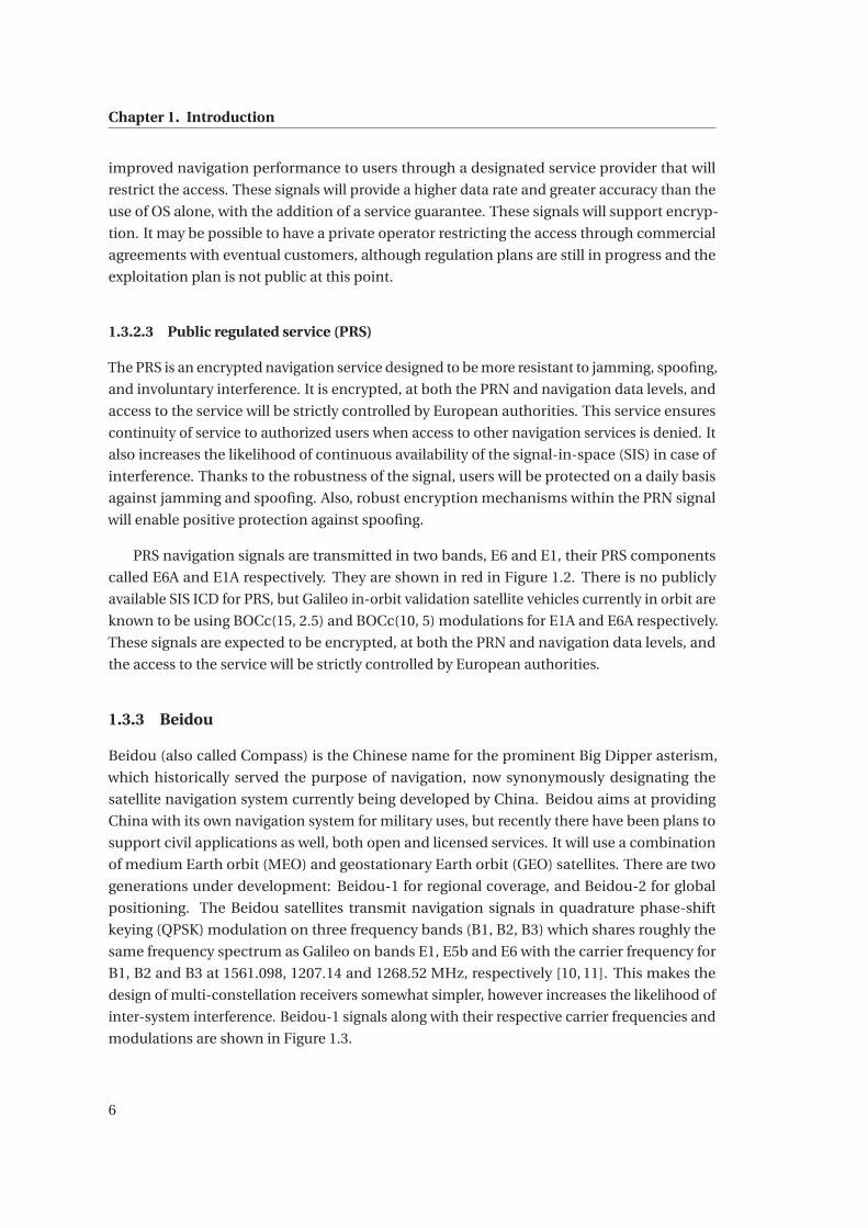
Galileo from the European Union and Beidou (COMPASS) from China. While GLONASS is
the second fully operational GNSS (together with GPS), Galileo has launched 10 navigation
satellites (as of February, 2016) and its initial services will be made available by the end of 2016.
The Galileo system is scheduled for completion in 2020. Additionally, China is constructing
the next-generation GNSS BeiDou-2 (BD-2) (also known as COMPASS), and the systems will
also be expanded into a fully operational GNSS by 2020 [1].
Any of these systems can be optimized or made functional for specific geographical re-
gions, which necessitates that the forthcoming GNSS receivers have backward compatibility
among these different standards and constellations. Although the Galileo and Beidou systems
are not yet fully functional, it is clear that there will be a great increase in satellite by the avail-
ability of these two systems, which brings opportunities for interoperation among different
constellations and challenges the engineers to exploit them.
1.1 Motivation
The interoperability among the GNSS increases the number of available satellites for a GNSS
receiver, thus can help to improve signal reliability in hostile environments, and system
reliability in the case of malfunctioning of one of the constellations. It also enables the receiver
to select the highest quality available signals which results in faster operation [2]. These can
1
Chapter 1. Introduction
be achieved at the cost of a reconfigurable radio front-end that can support multiple GNSS
systems.
Besides reliability, the positioning accuracy is another concern of GNSS receivers. One
optimization method that is generally applied as an answer to this concern is that of a multi-
frequency receiver. Excellent accuracy for many applications is currently achieved using only
single-frequency receivers, mainly by means of the ionospheric error modeling or differential
corrections. The simultaneous reception of two or more signals from the same GNSS system
that exhibit a sufficient frequency gap makes it possible to minimize the error introduced
by the first-order ionospheric group delay [3] and as a result offer an even greater degree of
accuracy. Therefore, in the coming years, multi-frequency multi-constellation receivers are
likely to become the product of choice for accurate positioning and personal navigation in
hostile signal environments. This is one of the challenges that is going to be addressed during
the course of this thesis.
The deployment of Galileo will bring not only an additional GNSS constellation for existing
applications, but also a series of new services that will require advanced wide-band receivers
and front-ends to be able to process the upcoming modulations at these new frequencies for
improved accuracy, reliability and robustness. One of these new services is a PRS, in which
wide-band signals transmitted on two different carrier frequencies and designed to provide
position, velocity and timing information to specific user groups requiring high continuity
and robustness of services, with controlled access ensured by encryption of ranging codes
and navigation data. This new service demands an advanced wide-band receiver, another
challenge that will be addressed in this thesis.
At present there is no commercial chip addressing a multi-band PRS GNSS receiver, and
it is still difficult to predict when multi-frequency GNSS FEs will reach the consumer mar-
ket (even if the trend is clear, [4]). However, if we look at present and future high-end and
professional applications, it seems clear that there could be a market for such a product.
In this sense, the possibility of offering a multi-frequency front-end (MFFE) ASIC capable
of covering several GNSS bands and with a sufficiently large bandwidth to cope with most
GNSS signals could represent a significant advance toward the reduction in cost and size of
non-mass-market receivers.
1.2 Thesis organization
Two main objectives are pursued in this thesis. The first is to provide a solution for multi-
frequency PRS receivers that meets the requirements of the PRS to serve specific users, au-
thorized governmental bodies, requiring a high continuity of service. The second objective is
to design and implement a multi-frequency multi-constellation GNSS FE to treat the pubic
demands for mass market applications.
In this regard, a summary of GNSS signals and services are presented in this chapter. It also
2
1.3. GNSS signals and systems
presents the advantages and drawbacks of a few important FE’s topologies and architectures.
Moreover, the most recent ASIC GNSS FEs are compared to provide a better insight in regards
of the architecture selection. A study on the technology choice is presented at the end of this
chapter that explores the trade-off of the technology scaling in the FE design.
Chapter 2 is focused on the PRS ASIC FE design. Possible applications for the PRS are dis-
cussed at the beginning of this chapter. The proposed FE architecture is presented afterward.
The PRS FE specifications are laid out in this chapter that is followed by sub-systems design.
The chapter is concluded by presenting the FE’s measurement results.
A wide-tuning-range continuous-time low-pass filter that is designed for the PRS receiver
is presented in chapter 3. This chapter starts by presenting a Q-enhancement method that
enhances the selectivity of the filter. It is followed then by the proposed methodology to
ensure the CM stability of a gyrator-based resonator. At the end of this chapter, the filter
measurement results and the effects of the Q-enhancement method on the selectivity of the
filter are presented.
Chapter 4 is dedicated to the design of the multi-frequency multi-constellation GNSS FE
that accommodates the simultaneous reception of the Beidou-B1, GPS-L1 and Galileo-E1. The
FE’s architecture selection and frequency plan are presented at the beginning of the chapter.
Then system specification were derived for all the sub-systems. This chapter also contains the
sub-systems design and is concluded by presenting measured characterizations of the FE.
Finally, chapter 5 summarizes all the achievements of this thesis and outlines its perspec-
tives.
1.3 GNSS signals and systems
1.3.1 GPS
Conceived and operated by the US Department of Defense, GPS is the most widely used
navigation system today. When it became operational in 1995, it was initially transmitted in
two bands only, L1 (centered at 1575.42 MHz) and L2 (1227.6 MHz) [5]. L1 comprises both
open and restricted signals intended for civil and military applications, respectively, while L2
has no open counterpart. The open signal from L1 is often named C/A or Coarse Acquisition
since it was intended to provide relatively simple and fast means of acquisition to speed up
the process for the encrypted military signals. The protected transmissions from L1 and L2,
designated as P(Y), use secret PRN codes to avoid signal tracking by non-authorized users.
However, many codeless techniques have been developed to use P(Y) signals as a positioning
aid for high precision commercial applications (for the removal of the ionospheric error using
a dual frequency receiver) even with degraded performance.
As part of the GPS modernization plan, an additional civilian band is being enabled at
3
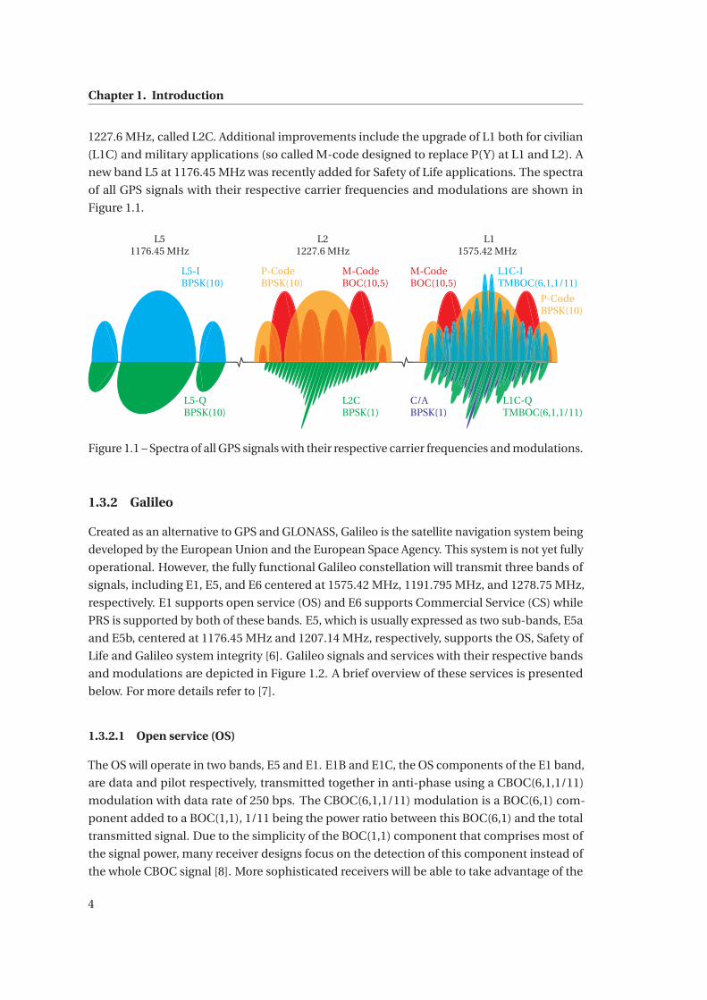
Chapter 1. Introduction
1227.6 MHz, called L2C. Additional improvements include the upgrade of L1 both for civilian
(L1C) and military applications (so called M-code designed to replace P(Y) at L1 and L2). A
new band L5 at 1176.45 MHz was recently added for Safety of Life applications. The spectra
of all GPS signals with their respective carrier frequencies and modulations are shown in
Figure 1.1.
1575.42 MHz1227.6 MHz1176.45 MHz
P-Code
BPSK(10)
M-Code
BOC(10,5)
C/A
BPSK(1)
L1C-Q
TMBOC(6,1,1/11)
L1C-I
TMBOC(6,1,1/11)
M-Code
BOC(10,5)
P-Code
BPSK(10)
L2C
BPSK(1)
L5-I
BPSK(10)
L5-Q
BPSK(10)
L5 L2 L1
Figure 1.1 – Spectra of all GPS signals with their respective carrier frequencies and modulations.
1.3.2 Galileo
Created as an alternative to GPS and GLONASS, Galileo is the satellite navigation system being
developed by the European Union and the European Space Agency. This system is not yet fully
operational. However, the fully functional Galileo constellation will transmit three bands of
signals, including E1, E5, and E6 centered at 1575.42 MHz, 1191.795 MHz, and 1278.75 MHz,
respectively. E1 supports open service (OS) and E6 supports Commercial Service (CS) while
PRS is supported by both of these bands. E5, which is usually expressed as two sub-bands, E5a
and E5b, centered at 1176.45 MHz and 1207.14 MHz, respectively, supports the OS, Safety of
Life and Galileo system integrity [6]. Galileo signals and services with their respective bands
and modulations are depicted in Figure 1.2. A brief overview of these services is presented
below. For more details refer to [7].
1.3.2.1 Open service (OS)
The OS will operate in two bands, E5 and E1. E1B and E1C, the OS components of the E1 band,
are data and pilot respectively, transmitted together in anti-phase using a CBOC(6,1,1/11)
modulation with data rate of 250 bps. The CBOC(6,1,1/11) modulation is a BOC(6,1) com-
ponent added to a BOC(1,1), 1/11 being the power ratio between this BOC(6,1) and the total
transmitted signal. Due to the simplicity of the BOC(1,1) component that comprises most of
the signal power, many receiver designs focus on the detection of this component instead of
the whole CBOC signal [8]. More sophisticated receivers will be able to take advantage of the
4
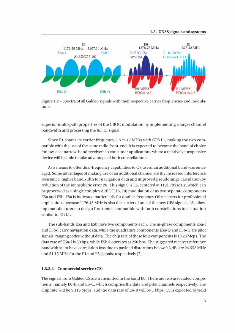
1.3. GNSS signals and systems
1575.42 MHz1278.75 MHz1176.45 MHz
E1 B/C(OS)
CBOC(6,1,1/11)
E6 B/C(CS)
BPSK(5)
E5b-I
E5 E6 E1
E5a-I
E5b-QE5a-Q
1207.14 MHz
AltBOC(15,10)
E6 A(PRS)
BOCc(10,5)
E1 A(PRS)
BOCc(15,2.5)
Figure 1.2 – Spectra of all Galileo signals with their respective carrier frequencies and modula-tions.
superior multi-path properties of the CBOC modulation by implementing a larger channel
bandwidth and processing the full E1 signal.
Since E1 shares its carrier frequency (1575.42 MHz) with GPS L1, making the two com-
patible with the use of the same radio front-end, it is expected to become the band of choice
for low-cost narrow-band receivers in consumer applications where a relatively inexpensive
device will be able to take advantage of both constellations.
As a means to offer dual-frequency capabilities to OS users, an additional band was envis-
aged. Some advantages of making use of an additional channel are the increased interference
resistance, higher bandwidth for navigation data and improved pseudorange calculation by
reduction of the ionospheric error [9]. This signal is E5, centered at 1191.795 MHz, which can
be processed as a single complex AltBOC(15, 10) modulation or as two separate components
E5a and E5b. E5a is indicated particularly for double-frequency OS receivers for professional
applications because 1176.45 MHz is also the carrier of one of the new GPS signals, L5, allow-
ing manufacturers to design front-ends compatible with both constellations in a situation
similar to E1/L1.
The sub-bands E5a and E5b have two components each. The in-phase components E5a-I
and E5b-I carry navigation data, while the quadrature components E5a-Q and E5b-Q are pilot
signals, ranging codes without data. The chip rate of these four components is 10.23 Mcps. The
data rate of E5a-I is 50 bps, while E5b-I operates at 250 bps. The suggested receiver reference
bandwidths, to have correlation loss due to payload distortions below 0.6 dB, are 24.552 MHz
and 51.15 MHz for the E1 and E5 signals, respectively [7].
1.3.2.2 Commercial service (CS)
The signals from Galileo CS are transmitted in the band E6. There are two associated compo-
nents, namely E6-B and E6-C, which comprise the data and pilot channels respectively. The
chip rate will be 5.115 Mcps, and the data rate of E6-B will be 1 kbps. CS is expected to yield
5
Chapter 1. Introduction
improved navigation performance to users through a designated service provider that will
restrict the access. These signals will provide a higher data rate and greater accuracy than the
use of OS alone, with the addition of a service guarantee. These signals will support encryp-
tion. It may be possible to have a private operator restricting the access through commercial
agreements with eventual customers, although regulation plans are still in progress and the
exploitation plan is not public at this point.
1.3.2.3 Public regulated service (PRS)
The PRS is an encrypted navigation service designed to be more resistant to jamming, spoofing,
and involuntary interference. It is encrypted, at both the PRN and navigation data levels, and
access to the service will be strictly controlled by European authorities. This service ensures
continuity of service to authorized users when access to other navigation services is denied. It
also increases the likelihood of continuous availability of the signal-in-space (SIS) in case of
interference. Thanks to the robustness of the signal, users will be protected on a daily basis
against jamming and spoofing. Also, robust encryption mechanisms within the PRN signal
will enable positive protection against spoofing.
PRS navigation signals are transmitted in two bands, E6 and E1, their PRS components
called E6A and E1A respectively. They are shown in red in Figure 1.2. There is no publicly
available SIS ICD for PRS, but Galileo in-orbit validation satellite vehicles currently in orbit are
known to be using BOCc(15, 2.5) and BOCc(10, 5) modulations for E1A and E6A respectively.
These signals are expected to be encrypted, at both the PRN and navigation data levels, and
the access to the service will be strictly controlled by European authorities.
1.3.3 Beidou
Beidou (also called Compass) is the Chinese name for the prominent Big Dipper asterism,
which historically served the purpose of navigation, now synonymously designating the
satellite navigation system currently being developed by China. Beidou aims at providing
China with its own navigation system for military uses, but recently there have been plans to
support civil applications as well, both open and licensed services. It will use a combination
of medium Earth orbit (MEO) and geostationary Earth orbit (GEO) satellites. There are two
generations under development: Beidou-1 for regional coverage, and Beidou-2 for global
positioning. The Beidou satellites transmit navigation signals in quadrature phase-shift
keying (QPSK) modulation on three frequency bands (B1, B2, B3) which shares roughly the
same frequency spectrum as Galileo on bands E1, E5b and E6 with the carrier frequency for
B1, B2 and B3 at 1561.098, 1207.14 and 1268.52 MHz, respectively [10, 11]. This makes the
design of multi-constellation receivers somewhat simpler, however increases the likelihood of
inter-system interference. Beidou-1 signals along with their respective carrier frequencies and
modulations are shown in Figure 1.3.
6
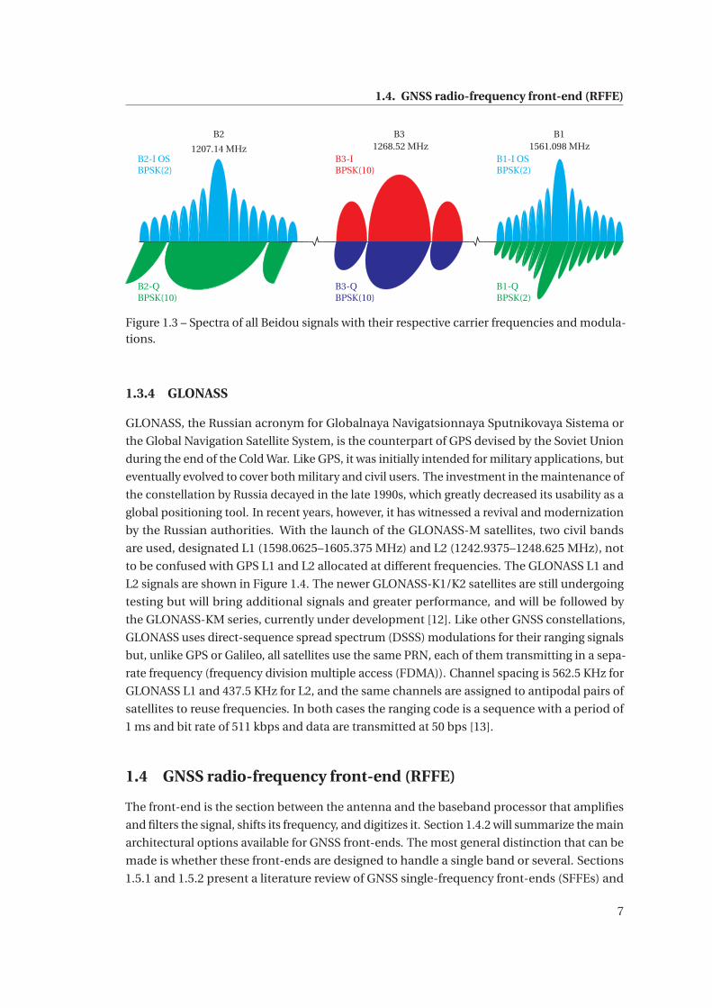
1.4. GNSS radio-frequency front-end (RFFE)
1561.098 MHz1268.52 MHz
B1-I OS
BPSK(2)
B3-I
BPSK(10)
B2 B3 B1
B2-I OS
BPSK(2)
B2-Q
BPSK(10)
1207.14 MHz
B3-Q
BPSK(10)
B1-Q
BPSK(2)
Figure 1.3 – Spectra of all Beidou signals with their respective carrier frequencies and modula-tions.
1.3.4 GLONASS
GLONASS, the Russian acronym for Globalnaya Navigatsionnaya Sputnikovaya Sistema or
the Global Navigation Satellite System, is the counterpart of GPS devised by the Soviet Union
during the end of the Cold War. Like GPS, it was initially intended for military applications, but
eventually evolved to cover both military and civil users. The investment in the maintenance of
the constellation by Russia decayed in the late 1990s, which greatly decreased its usability as a
global positioning tool. In recent years, however, it has witnessed a revival and modernization
by the Russian authorities. With the launch of the GLONASS-M satellites, two civil bands
are used, designated L1 (1598.0625–1605.375 MHz) and L2 (1242.9375–1248.625 MHz), not
to be confused with GPS L1 and L2 allocated at different frequencies. The GLONASS L1 and
L2 signals are shown in Figure 1.4. The newer GLONASS-K1/K2 satellites are still undergoing
testing but will bring additional signals and greater performance, and will be followed by
the GLONASS-KM series, currently under development [12]. Like other GNSS constellations,
GLONASS uses direct-sequence spread spectrum (DSSS) modulations for their ranging signals
but, unlike GPS or Galileo, all satellites use the same PRN, each of them transmitting in a sepa-
rate frequency (frequency division multiple access (FDMA)). Channel spacing is 562.5 KHz for
GLONASS L1 and 437.5 KHz for L2, and the same channels are assigned to antipodal pairs of
satellites to reuse frequencies. In both cases the ranging code is a sequence with a period of
1 ms and bit rate of 511 kbps and data are transmitted at 50 bps [13].
1.4 GNSS radio-frequency front-end (RFFE)
The front-end is the section between the antenna and the baseband processor that amplifies
and filters the signal, shifts its frequency, and digitizes it. Section 1.4.2 will summarize the main
architectural options available for GNSS front-ends. The most general distinction that can be
made is whether these front-ends are designed to handle a single band or several. Sections
1.5.1 and 1.5.2 present a literature review of GNSS single-frequency front-ends (SFFEs) and
7
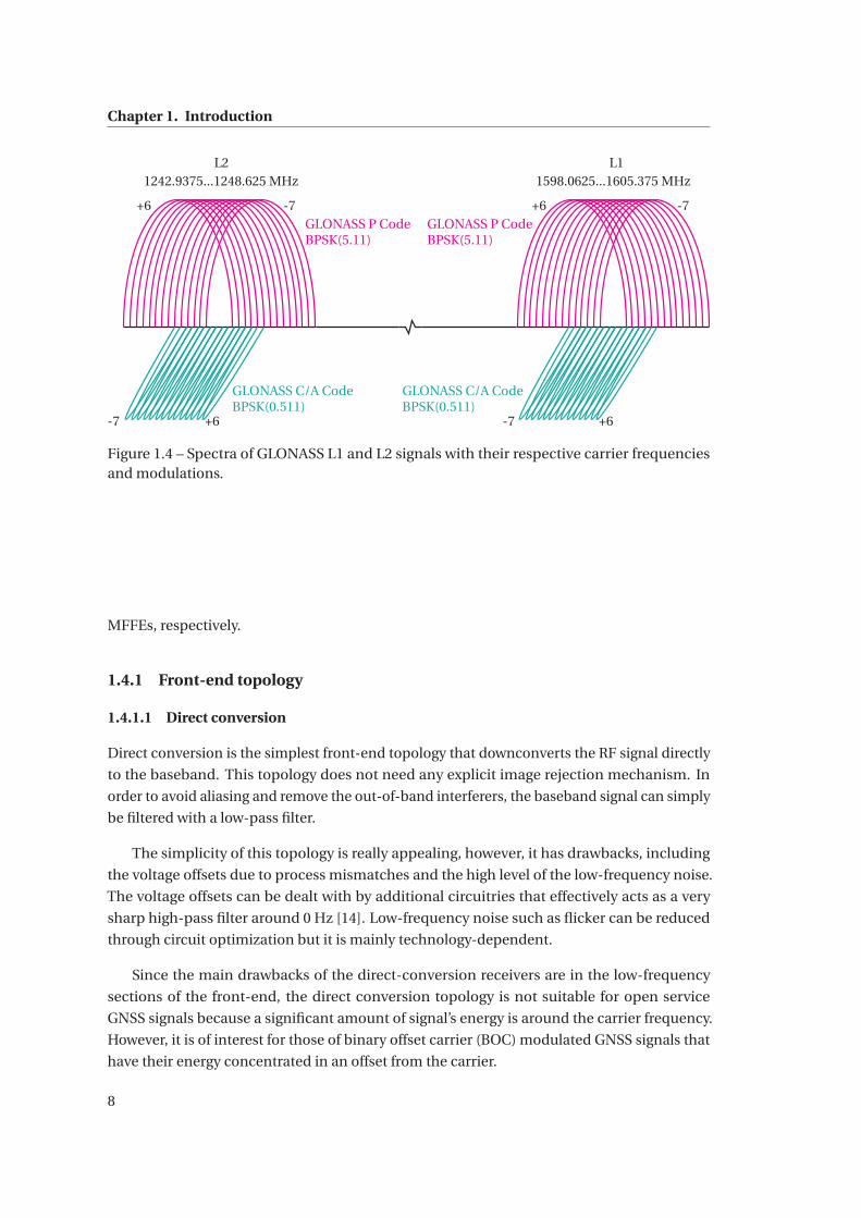
Chapter 1. Introduction
1598.0625...1605.375 MHz
L2 L1
GLONASS C/A Code
BPSK(0.511)
GLONASS P Code
BPSK(5.11)
1242.9375...1248.625 MHz
+6 +6 -7-7
+6-7+6-7
GLONASS C/A Code
BPSK(0.511)
GLONASS P Code
BPSK(5.11)
Figure 1.4 – Spectra of GLONASS L1 and L2 signals with their respective carrier frequenciesand modulations.
MFFEs, respectively.
1.4.1 Front-end topology
1.4.1.1 Direct conversion
Direct conversion is the simplest front-end topology that downconverts the RF signal directly
to the baseband. This topology does not need any explicit image rejection mechanism. In
order to avoid aliasing and remove the out-of-band interferers, the baseband signal can simply
be filtered with a low-pass filter.
The simplicity of this topology is really appealing, however, it has drawbacks, including
the voltage offsets due to process mismatches and the high level of the low-frequency noise.
The voltage offsets can be dealt with by additional circuitries that effectively acts as a very
sharp high-pass filter around 0 Hz [14]. Low-frequency noise such as flicker can be reduced
through circuit optimization but it is mainly technology-dependent.
Since the main drawbacks of the direct-conversion receivers are in the low-frequency
sections of the front-end, the direct conversion topology is not suitable for open service
GNSS signals because a significant amount of signal’s energy is around the carrier frequency.
However, it is of interest for those of binary offset carrier (BOC) modulated GNSS signals that
have their energy concentrated in an offset from the carrier.
8
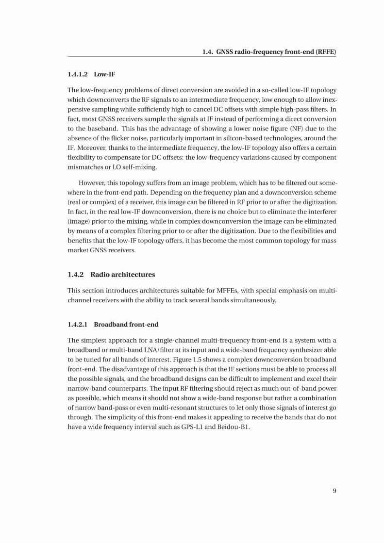
1.4. GNSS radio-frequency front-end (RFFE)
1.4.1.2 Low-IF
The low-frequency problems of direct conversion are avoided in a so-called low-IF topology
which downconverts the RF signals to an intermediate frequency, low enough to allow inex-
pensive sampling while sufficiently high to cancel DC offsets with simple high-pass filters. In
fact, most GNSS receivers sample the signals at IF instead of performing a direct conversion
to the baseband. This has the advantage of showing a lower noise figure (NF) due to the
absence of the flicker noise, particularly important in silicon-based technologies, around the
IF. Moreover, thanks to the intermediate frequency, the low-IF topology also offers a certain
flexibility to compensate for DC offsets: the low-frequency variations caused by component
mismatches or LO self-mixing.
However, this topology suffers from an image problem, which has to be filtered out some-
where in the front-end path. Depending on the frequency plan and a downconversion scheme
(real or complex) of a receiver, this image can be filtered in RF prior to or after the digitization.
In fact, in the real low-IF downconversion, there is no choice but to eliminate the interferer
(image) prior to the mixing, while in complex downconversion the image can be eliminated
by means of a complex filtering prior to or after the digitization. Due to the flexibilities and
benefits that the low-IF topology offers, it has become the most common topology for mass
market GNSS receivers.
1.4.2 Radio architectures
This section introduces architectures suitable for MFFEs, with special emphasis on multi-
channel receivers with the ability to track several bands simultaneously.
1.4.2.1 Broadband front-end
The simplest approach for a single-channel multi-frequency front-end is a system with a
broadband or multi-band LNA/filter at its input and a wide-band frequency synthesizer able
to be tuned for all bands of interest. Figure 1.5 shows a complex downconversion broadband
front-end. The disadvantage of this approach is that the IF sections must be able to process all
the possible signals, and the broadband designs can be difficult to implement and excel their
narrow-band counterparts. The input RF filtering should reject as much out-of-band power
as possible, which means it should not show a wide-band response but rather a combination
of narrow band-pass or even multi-resonant structures to let only those signals of interest go
through. The simplicity of this front-end makes it appealing to receive the bands that do not
have a wide frequency interval such as GPS-L1 and Beidou-B1.
9
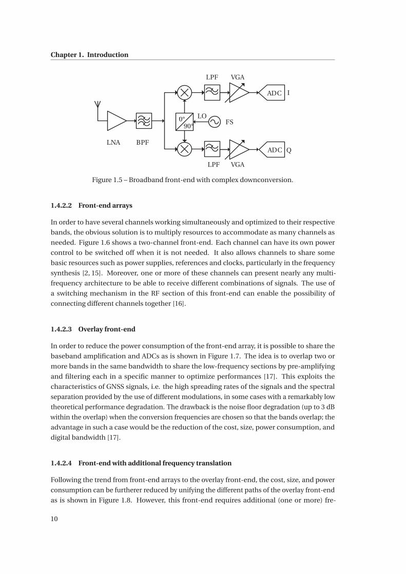
Chapter 1. Introduction
LNA
0° 90°
ADC
BPF
FSLO
ADC
VGA
VGA
LPF
LPF
I
Q
Figure 1.5 – Broadband front-end with complex downconversion.
1.4.2.2 Front-end arrays
In order to have several channels working simultaneously and optimized to their respective
bands, the obvious solution is to multiply resources to accommodate as many channels as
needed. Figure 1.6 shows a two-channel front-end. Each channel can have its own power
control to be switched off when it is not needed. It also allows channels to share some
basic resources such as power supplies, references and clocks, particularly in the frequency
synthesis [2, 15]. Moreover, one or more of these channels can present nearly any multi-
frequency architecture to be able to receive different combinations of signals. The use of
a switching mechanism in the RF section of this front-end can enable the possibility of
connecting different channels together [16].
1.4.2.3 Overlay front-end
In order to reduce the power consumption of the front-end array, it is possible to share the
baseband amplification and ADCs as is shown in Figure 1.7. The idea is to overlap two or
more bands in the same bandwidth to share the low-frequency sections by pre-amplifying
and filtering each in a specific manner to optimize performances [17]. This exploits the
characteristics of GNSS signals, i.e. the high spreading rates of the signals and the spectral
separation provided by the use of different modulations, in some cases with a remarkably low
theoretical performance degradation. The drawback is the noise floor degradation (up to 3 dB
within the overlap) when the conversion frequencies are chosen so that the bands overlap; the
advantage in such a case would be the reduction of the cost, size, power consumption, and
digital bandwidth [17].
1.4.2.4 Front-end with additional frequency translation
Following the trend from front-end arrays to the overlay front-end, the cost, size, and power
consumption can be furtherer reduced by unifying the different paths of the overlay front-end
as is shown in Figure 1.8. However, this front-end requires additional (one or more) fre-
10
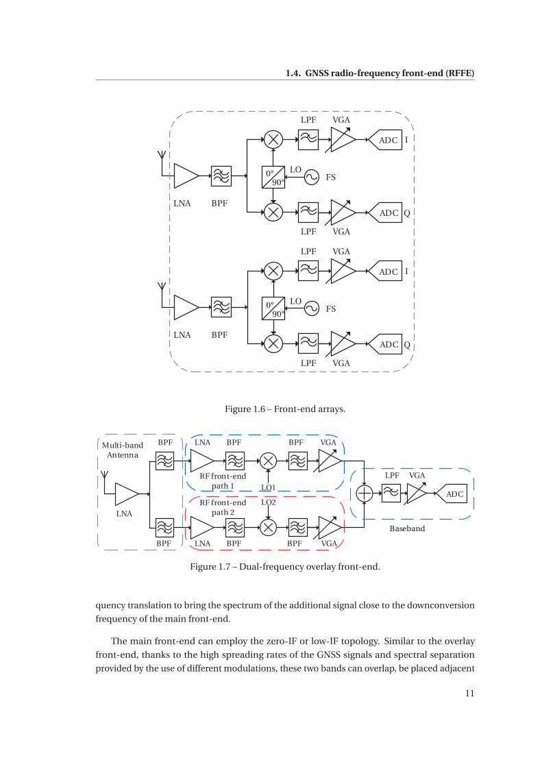
1.4. GNSS radio-frequency front-end (RFFE)
LNA
0° 90°
ADC
BPF
FSLO
ADC
VGA
VGA
LPF
LPF
I
Q
LNA
0° 90°
ADC
BPF
FSLO
ADC
VGA
VGA
LPF
LPF
I
Q
Figure 1.6 – Front-end arrays.
ADC
BPF
VGALPF
LNA
BPF
LO2
BPF
BPF
LO1
VGA
VGALNA
LNA BPF
BPF
Multi-band Antenna
Baseband
RF front-end path 1
RF front-end path 2
Figure 1.7 – Dual-frequency overlay front-end.
quency translation to bring the spectrum of the additional signal close to the downconversion
frequency of the main front-end.
The main front-end can employ the zero-IF or low-IF topology. Similar to the overlay
front-end, thanks to the high spreading rates of the GNSS signals and spectral separation
provided by the use of different modulations, these two bands can overlap, be placed adjacent
11
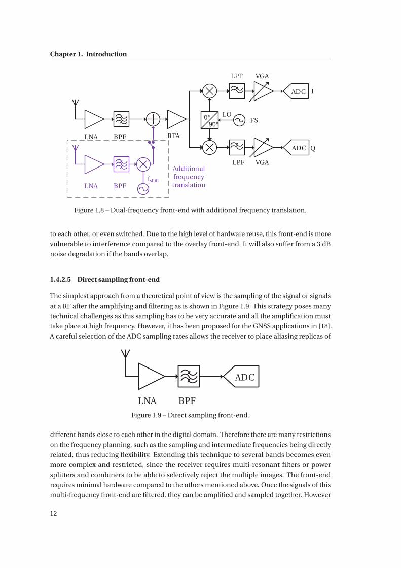
Chapter 1. Introduction
LNA
0° 90°
ADC
BPF
FSLO
ADC
VGA
VGA
LPF
LPF
I
Q
LNA BPFfshift
RFA
Additional frequency translation
Figure 1.8 – Dual-frequency front-end with additional frequency translation.
to each other, or even switched. Due to the high level of hardware reuse, this front-end is more
vulnerable to interference compared to the overlay front-end. It will also suffer from a 3 dB
noise degradation if the bands overlap.
1.4.2.5 Direct sampling front-end
The simplest approach from a theoretical point of view is the sampling of the signal or signals
at a RF after the amplifying and filtering as is shown in Figure 1.9. This strategy poses many
technical challenges as this sampling has to be very accurate and all the amplification must
take place at high frequency. However, it has been proposed for the GNSS applications in [18].
A careful selection of the ADC sampling rates allows the receiver to place aliasing replicas of
LNA
ADC
BPF
Figure 1.9 – Direct sampling front-end.
different bands close to each other in the digital domain. Therefore there are many restrictions
on the frequency planning, such as the sampling and intermediate frequencies being directly
related, thus reducing flexibility. Extending this technique to several bands becomes even
more complex and restricted, since the receiver requires multi-resonant filters or power
splitters and combiners to be able to selectively reject the multiple images. The front-end
requires minimal hardware compared to the others mentioned above. Once the signals of this
multi-frequency front-end are filtered, they can be amplified and sampled together. However
12
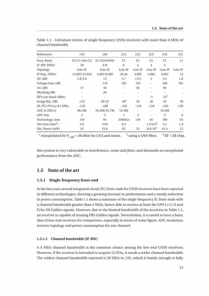
1.5. State of the art
Table 1.1 – Literature review of single frequency GNSS receivers with more than 4 MHz ofchannel bandwidth.
References [19] [20] [21] [22] [23] [24] [25]
Freq. Band E1/L1-E5a/L5 E1/GLONASS E1 E1 E1 E1 L1
IF-BW [MHz] 20 4/8 6 4 4 4 -
Topology Low-IF Low-IF Low-IF Low-IF Low-IF Low-IF Low-IF
IF freq. [MHz] 13.092/14.934 4.092/8.566 20.46 4.092 4.092 4.092 13
NF [dB] 2.8/2.6 <3 3.7 <3.3 2 4.5 1.8
Voltage Gain [dB] 119 103 105 - 108 105
ΔG [dB] 47 50 - 50 - 60 -
Blocking [dB] - 20 - - - - -
IIP3 out-band [dBm] - - - - -5 -271 -
Image Rej. [dB] >25 20/33 402 30 40 34 40
OL PN [dBc/Hz] @1 MHz -118 -108 -105 -110 -118 -126 -120
ADC fs [MS/s] 66.188 16.368/32.736 16.368 - - 16.368 -
ADC bits 2 3 1 4 - 2 6
Technology [nm] 130 65 350SiGe 130 65 180 65
Die Area [mm2] 2.9 4.65 8.4 - 1.4/6.63 5.2 1.9
Dis. Power [mW] 45 33.6 62 23 8.6/183 41.4 13
1 extrapolated by P1 dB=-38 dBm for LNA and mixer, 2 using a SAW filter, 3 RF / All chip.
this system is very vulnerable to interference, noise and jitter, and demands an exceptional
performance from the ADC.
1.5 State of the art
1.5.1 Single-frequency front-end
In the last years several integrated circuit (IC) front-ends for GNSS receivers have been reported
in different technologies, showing a growing increase in performance and a steady reduction
in power consumption. Table 1.1 shows a summary of the single-frequency IC front-ends with
a channel bandwidth greater than 4 MHz, hence able to receive at least the GPS L1 C/A and
E1bc OS Galileo signals. However, due to the limited bandwidth of the receivers in Table 1.1,
no receiver is capable of treating PRS Galileo signals. Nevertheless, it is useful to have a basic
idea of low-end receivers for comparison, especially in terms of noise figure, ADC resolution,
receiver topology and power consumption for one channel.
1.5.1.1 Channel bandwidth (IF-BW)
A 4 MHz channel bandwidth is the common choice among the low-end GNSS receivers.
However, if the receiver is intended to acquire L5/E5a, it needs a wider channel bandwidth.
The widest channel bandwidth reported is 20 MHz in [19], which is barely enough to fully
13
Chapter 1. Introduction
include the main lobe of the E5a signal.
1.5.1.2 Topology
The most common architecture for GNSS radios is the low-IF with image rejection mixer. In
fact, if the intermediate frequency is chosen so that the image band lies within the GPS band, so
that this image is substantially white noise, the low-IF topology allows alternating current (AC)
coupling in the IF chain. This eliminates the DC offset problem and low-frequency noise
(flicker and on-chip noise).
1.5.1.3 Intermediate frequency (IF)
It can be seen in Table 1.1 that the IF choice is driven by two factors: the IF bandwidth (a large
bandwidth requires a higher IF) and the power consumption. Indeed a lower IF is preferable
because the amplifiers can be designed with a lower gain-bandwidth product (GBW) resulting
in lower power consumption.
1.5.1.4 Noise figure (NF)
The average NF is around 3 dB, but it is not clear which front-end includes electrostatic
discharge (ESD) protection on the antenna input pad. Therefore it is difficult to determine the
best solution for the LNA in terms of NF.
1.5.1.5 Voltage gain
The overall voltage gain is between 103 dB and 119 dB and the automatic gain control
has a range of 50–60 dB. Gain depends on several parameters such as noise bandwidth,
ADC dynamic range/precision and linearity requirements. The front-end with the larger
IF-bandwidth (BW) requires less voltage gain [19].
1.5.1.6 Linearity
Since linearity requirements depend on the system applications, no clear common linearity
requirement could be extrapolated from the different implementations. In fact, some receivers
are intended for a stand-alone operation, in which the linearity requirements can be relaxed.
On the other hand, those requirements are usually more stringent for receivers that are
intended to operate together with other wireless systems, such as in mobile terminal where
the Global System for Mobile Communications (GSM) and GPS coexist [23].
14
1.5. State of the art
1.5.1.7 Image rejection
The image rejection capability achieved with the image rejection mixer is around 30 dB.
However, it was boosted to 40 dB by employing the active polyphase filter in [23,25]. The same
image rejection was achieved in [21], which could exploit the surface acoustic wave (SAW)
filter selectivity by having its IF high enough.
1.5.1.8 Synthesizer
Most solutions use a VCO that runs at twice the required frequency and a divide-by-2 to ensure
accurate quadrature phase generation for the complex mixer LO inputs. An integer-N PLL
with a standard reference of 16.368 MHz is widely used for low power consumption, even if a
fractional-N PLL allows the use of different clocks in embedded systems. Typically a phase
noise of -105 dBc/Hz at 1 MHz is sufficient even if a better performance is achievable.
1.5.1.9 ADC and AGC
Increasing the number of bits in the ADC used in a receiver system such as the GPS will
increase the signal-to-noise ratio (SNR) only moderately; therefore most of the solutions use
2 bits. However, to improve the immunity to jamming signal, the ADC is preferred to have
more bits such as in [22, 25]. The sampling frequency is derived from the reference signal or
generated by dividing the LO if the IF is higher than the reference. A loop that sets the duty
cycle of the MAG signal (most significant bit (MSB) of the ADC) at 33%, which is known to
provide negligible SNR loss, is typically used for automatic gain control (AGC) [16, 26, 27].
1.5.1.10 Area
The average layout area is 5 mm2, which easily fits with most of the commercially available
packages with more than 28 pins. Moreover it appears that using a more scaled technology
does not significantly pay in terms of layout area saving. Indeed the difference between
implementations with the most scaled technology [20] and the less scaled technology [24] is
less than 10%. Moreover, the extreme area reduction in [25] is achieved by embedding the
source-degeneration inductor of the LNA in the fan-out area of the package.
1.5.1.11 Power consumption
Power consumption between around 13 mW and 45 mW is shown for CMOS technology
regardless of scaling nodes. In fact, the power consumption is determined mainly by the
channel bandwidth and the linearity requirements.
15
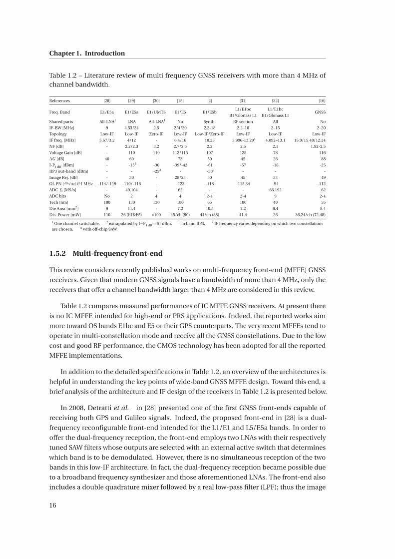
Chapter 1. Introduction
Table 1.2 – Literature review of multi frequency GNSS receivers with more than 4 MHz ofchannel bandwidth.
References [28] [29] [30] [15] [2] [31] [32] [16]
Freq. Band E1/E5a E1/E5a E1/UMTS E1/E5 E1/E5bL1/E1bc L1/E1bc
GNSSB1/Glonass L1 B1/Glonass L1
Shared parts All-LNA1 LNA All-LNA1 No Synth. RF section All No
IF-BW [MHz] 9 4.53/24 2.5 2/4/20 2.2-18 2.2–10 2–15 2–20
Topology Low-IF Low-IF Zero-IF Low-IF Low-IF/Zero-IF Low-IF Low-IF Low-IF
IF freq. [MHz] 5.67/3.2 4/12 - 6.4/16 10.23 3.996-13.294 4.092–13.1 15.9/15.48/12.24
NF [dB] - 2.2/2.3 3.2 2.7/2.5 2.2 2.5 2.1 1.92-2.5
Voltage Gain [dB] - 110 110 112/115 107 125 78 116
ΔG [dB] 40 60 - 73 50 45 26 88
I-P1 dB [dBm] - -155 -30 -39/-42 -61 -57 -18 -25
IIP3 out-band [dBm] - - -253 - -502 - - -
Image Rej. [dB] - 30 - 28/23 50 45 33 49
OL PN [dBc/Hz] @1 MHz -114/-119 -110/-116 - -122 -118 -115.34 -94 -112
ADC fs [MS/s] - 49.104 - 62 - - 66.192 62
ADC bits No 2 4 4 2-4 2-4 9 2-4
Tech [nm] 180 130 130 180 65 180 40 55
Die Area [mm2] 9 11.4 - 7.2 10.5 7.2 6.4 8.4
Dis. Power [mW] 110 26 (E1&E5) >100 45/ch (90) 44/ch (88) 41.4 26 36.24/ch (72.48)
1 One channel switchable, 2 extrapolated by I−P1 dB=-61 dBm, 3 in band IIP3, 4 IF frequency varies depending on which two constellationsare chosen, 5 with off-chip SAW.
1.5.2 Multi-frequency front-end
This review considers recently published works on multi-frequency front-end (MFFE) GNSS
receivers. Given that modern GNSS signals have a bandwidth of more than 4 MHz, only the
receivers that offer a channel bandwidth larger than 4 MHz are considered in this review.
Table 1.2 compares measured performances of IC MFFE GNSS receivers. At present there
is no IC MFFE intended for high-end or PRS applications. Indeed, the reported works aim
more toward OS bands E1bc and E5 or their GPS counterparts. The very recent MFFEs tend to
operate in multi-constellation mode and receive all the GNSS constellations. Due to the low
cost and good RF performance, the CMOS technology has been adopted for all the reported
MFFE implementations.
In addition to the detailed specifications in Table 1.2, an overview of the architectures is
helpful in understanding the key points of wide-band GNSS MFFE design. Toward this end, a
brief analysis of the architecture and IF design of the receivers in Table 1.2 is presented below.
In 2008, Detratti et al. in [28] presented one of the first GNSS front-ends capable of
receiving both GPS and Galileo signals. Indeed, the proposed front-end in [28] is a dual-
frequency reconfigurable front-end intended for the L1/E1 and L5/E5a bands. In order to
offer the dual-frequency reception, the front-end employs two LNAs with their respectively
tuned SAW filters whose outputs are selected with an external active switch that determines
which band is to be demodulated. However, there is no simultaneous reception of the two
bands in this low-IF architecture. In fact, the dual-frequency reception became possible due
to a broadband frequency synthesizer and those aforementioned LNAs. The front-end also
includes a double quadrature mixer followed by a real low-pass filter (LPF); thus the image
16
1.5. State of the art
rejection is realized only in the digital domain. The LPFs have their cut-off frequency at
9 MHz and are AC coupled to prevent offset errors. The external baseband processor can
use the double-side complex bandwidth of the I/Q outputs comprising the interval [-9 MHz,
9 MHz] minus the power around direct current (DC) due to the AC coupling. Even though this
bandwidth is sub-optimal compared to the total bandwidth of E5a, it is still sufficient for the
intended application according to their own studies. This front-end is designed for low noise
and high linearity to withstand interference, but the total power of this front-end is about
110 mW, not including ADCs.
The simultaneous reception of E1/L1 and E5a/L5 has been achieved in the dual-band
receiver presented in [29]. The front-end consists of separate RF and IF channels; one tuned for
E1/L1 and the other one for E5a/L5. However, to reduce power consumption, the LNA in the E1
band is shared with the E5a band. Both front-ends in [28] and [29] have the same architecture
as well as low-IF topology. Although the input stage of the mixer in [29] is single-ended, the
VCO adopts complementary cross-coupled topology for low power dissipation. The IF section
of both channels is composed of a VGA, the channel selection filter and the AGC blocks. In
the case of the L1/E1 band, the central frequency and the bandwidth of the downconverted
signal are 4 MHz. A 3 rd-order complex band-pass filter (BPF) is used for channel selection
and image rejection and there is no need for a polyphase filter (PPF), which relaxes the gain
specification of the VGA. On the other hand, the channel selection filter has to process 24 MHz
bandwidth L5/E5a at the IF frequency of 12 MHz. Therefore, a 3-stage passive PPF as well
as a 3 rd-order active-RC LPF are used as channel filters to cover the frequency specification
of the L5/E5a band. As already mentioned, the front-end in [29] is capable of simultaneous
reception of both L1/E1 and L5/E5a. However, sharing the LNA for both bands is not the best
choice from the point of view of interference mitigation. If the LNA falls in intermodulation,
or worse in saturation, due to an interference in one channel, it is not possible to avoid the
intermodulation on the other free channel.
In 2009, Miskiewicz et al. from Infineon Technologies proposed a single-chip radio receiver
capable of receiving GPS, Galileo, UMTS, CDMA2000 and GSM standards [30]. The proposed
analog zero-IF front-end employs two wide-band paths for the high- and low-band operation
with one integrated wide-band VCO. In order to optimize the size of the chip and power
consumption, both paths are combined at the mixer, using a switch. The front-end features a
reconfigurable analog baseband filter that is suitable for all implemented standards and offers
a high selectivity at interferer frequencies. The analog path is ended by two I/Q (in-phase
and quadrature) ΣΔ ADCs followed by a digital front-end performing the channel filtering,
adaptation of the system data rate to the common bit rate at the digital interface, the correction
of the group delay generated in the analog baseband filter and the removal of the DC offset.
The overall transfer characteristic of the IF section has a corner frequency of 240 KHz for GSM,
750 KHz for CDMA2000, and 2.5 MHz for UMTS and GPS/Galileo standards, respectively. The
bandwidth of the filter is tuned with a capacitive bank controlled by a 5-bit programmable
word. The front-end has a high level of hardware reuse; only LNAs and pre-selector filters are
channel dependent to achieve the simultaneous reception of GPS/Galileo and UMTS signals.
17
Chapter 1. Introduction
In [15] a reconfigurable dual-channel RF receiver that meets the demands for separate
or simultaneous reception of all-modes and all-bands of the GNSS signals is presented. Two
independent FSs, based on integer-N PLLs, provide wide-tuning-range quadrature LO sig-
nals for each channel. In each I/Q branch, a programmable gain amplifier (PGA) precedes
the complex BPF to relax its noise requirement and optimize the linearity performance. A
fully differential operational amplifier (opamp) with resistive feedback is utilized to realize
the PGA for low noise and high linearity. A 5 th-order Chebyshev-I complex BPF, based on
fully differential active-RC integrators, is implemented by means of two real LPF quadrature
coupled to achieve the frequency shift at IF. In order to reconfigure the center frequency of IF,
bandwidth and gain, all the capacitors and resistors in the filter are implemented as binary
arrays. Moreover, an automatic digital RC tuning block guarantees the frequency accuracy of
the IF and the bandwidth. The proposed front-end has almost no hardware reuse. In spite of
this, its power consumption of 45 mW/ch is in line with other architectures with more hardware
reuse. Moreover, two independent synthesizers allow the reception of any two bands at the
same time. The 20 MHz of bandwidth is enough for E5a, but is not enough for PRS even
though the channel could be switched to E6. The bandwidth of the E1 channel is insufficient
for E1-a PRS as well. However this is a good starting point for a hypothetical extension toward
the PRS receiver.
In 2012, Qi et al. in [2] presented a front-end very similar to the one in [15] that sup-
ports Compass/GPS/GLONASS/Galileo. It employs two independent channels with single-
conversion architecture for simultaneous dual-frequency signal receiving. However, contrary
to [15], a single fractional frequency synthesizer is shared by both channels, and an extra
clock generator provides programmable sampling and reference clocks for the ADCs, filters
and digital logic circuits. A reconfigurable filter is placed ahead of a PGA in each channel
to provide image rejection and out-of-band interference rejection. In order to get accurate
frequency selectivity for all operation modes, the IF filter is capable of switching its order, type,
center frequency and bandwidth. The receiver is configured to the low-IF architecture using a
5 th-order complex BPF, while for some wide-band applications it is reconfigured to zero-IF
architecture using a 3 th-order LPF. Moreover, all OTAs in the filter are arranged into arrays,
some of which can be shut down in low center frequency or narrow-bandwidth modes to
save power. Moreover an I/Q calibration module is presented to enhance the image rejection
where it achieved up to 20 dB of improvement. Due to the reuse of the synthesizer, only the
reception of the neighboring band is possible, and it is, therefore, not possible to receive E1
and E5 at the same time.
In 2013, Qi et al. developed his receiver’s architecture in [2] and proposed a dual-channel
multi-constellation receiver as in [31] that can receive GPS L1, Galileo E1bc, Beidou B1 as well
as GLONASS L1. Similar to the one in [2], the receiver features a simultaneous dual-system
signal reception for all the combinations of the GNSS signals except the pair of GLONASS-
Beidou. The proposed receiver is composed of two channels that adopt the low-IF architecture
in which the RF section and the FS are shared. In this case, however, the IF sections are
independent from each other. Each IF section consists of an I/Q mismatch calibration prior to
18
1.5. State of the art
the complex bandpass filter. The complex filter is used to remove the image and is followed by
a digitally controlled PGA to regulate the signal strength delivering to 2–4 bits ADC. Similar
to the receiver in [2], the RF section is composed of an LNA, a noise-canceling RF amplifier
and a Gilbert quadrature mixer. However, in this development, not only the FS but the
whole RF section is shared between two channels, which provides more hardware reuse. The
reconfigurable filter and the synthesizer result in a different IF bandwidth from 2.2 MHz to
10 MHz as well as different IF frequencies range from 3.996 MHz to 13.29 MHz in different
configurations.
More recently, Tan et al. proposed a receiver featuring the highest degree of hardware
reuse in [32]. The receiver is a one-channel reconfigurable low-IF quadrature receiver with
a fractional-N FS, and a digital baseband processor. It downconverts the GNSS signals as an
image of one another and then separates them in the digital domain. The FS is reconfigurable
to provide three LO signals which result in three cases of dual reception: In the case of
simultaneous GPS/Galileo and GLONASS dual reception, the LO is set to 1588.608 MHz; in the
case of simultaneous GPS/Galileo and Beidou dual reception, the LO is set to 1568.256 MHz;
and for GPS/Galileo-only reception, the LO is set to 1571.328 MHz. The front-end features
a noise-canceling inductorless wide-band LNA driving a current-driven quadrature passive
mixer. The mixer is followed by a cascade of two reconfigurable Butterworth biquad filters
where the second filter has a variable gain and performs also as a PGA. A 9-bit successive
approximation register (SAR) ADC is employed in each I and Q channel to accommodate large
interferer signals.
The last receiver in Table 1.2 was proposed by Li et al. in [16]. It is a fully integrated
reconfigurable all-band RF transceiver for GPS/GLONASS/Galileo/Beidou. The receiver em-
ploys two RF front-ends with different matching network to process the GNSS signals around
1.2 GHz and 1.6 GHz carrier frequencies. Moreover, two independent IF channels with con-
stant IF frequencies of 15.902 MHz and 15.48 MHz are incorporated. The receiver also features
a digitally assisted calibration scheme to compensate analog parameter variations. It incorpo-
rates the switching scheme proposed in [30] to connect the RF front-ends and IF channels.
This reduces the complexity of the IF channels and the die area of the eventual receiver. In or-
der to process all GNSS signals with different bandwidths, one of the IF channels is designed to
provide 2/4 MHz bandwidth to process narrow-band GNSS signals such as GPS-L1/L2, Galileo-
E1 and Beidou-B1. On the other hand, the other IF channel provides 10/20 MHz bandwidth
and deal with wide-band GNSS signals, such as GPS-L5, GLONASS-L1/L2, Galileo-E5a(b), and
Beidou-B2/B3. The receiver uses two FSs to provide flexible frequency planning to receive any
combination of two mentioned GNSS signals. This is possible thanks to the switching module
that connects the RF sections and IF channels. Note that the simultaneous dual reception of
some signals with the same or close bandwidth happens in the same IF channel owing to the
fact the GNSS signals are uncorrelated. To see the advantage of this method, let’s compare it
with the other methods utilized in [15,31,32] which make the simultaneous reception possible.
In [15, 31], two independent IF channels are utilized to provide the simultaneous reception,
which requires a bandwidth-reconfigurable IF channel and as a result increases the design
19
Chapter 1. Introduction
complexity and die area. Moreover, due to the limited flexibility of the IF channels in [15, 31],
in some cases two identical receivers must be used to provide the simultaneous reception.
On the other hand, only one receiving channel is incorporated in [32] to receive dual-band
GNSS signals simultaneously, which decreases the complexity, die area, and mostly current
consumption compared to the dual-channel ones in [15, 31]. However, the receiver does not
provide the image rejection function, and therefore the SNR will be degraded at least 3 dB and
the baseband processor will require an IF filter to filter out the out-of-band noise. Moreover,
due to the limited bandwidth of the LPF and narrow-tuning VCO, the signals processed in [32]
are only bandwidth-limited signals centered around 1.6 GHz.
1.5.3 Conclusion
As can be seen from the study of the state of the art on the recent RF front-ends, there are
currently no viable options readily available for ASIC front-ends to be used for the PRS signals.
Many designs exist for different combinations of the GNSS bands, but none of them is suitable
for PRS due to the size, power, bandwidth or linearity requirements demanded for a secure
and compact GNSS receiver. This however indicates that extending the current technology to
satisfy these requirements is feasible as there are many alternatives for ASIC multi-frequency
front-ends. The required bandwidth and frequency range for PRS are along similar lines to
recent developments, even though PRS is more demanding in terms of both bandwidth and
linearity, which will mean more power and overall cost for the front-end.
1.6 ASIC technology choice
The effects of deep sub-micron scaling of CMOS technologies in analog ASIC designs is
explained in this section. Considering the advantages and disadvantages of these technologies
will help us to choose the level of integration among the 180, 130 or 65 nm CMOS technologies.
In the last decades the scaling trend in CMOS technologies towards greater degrees of
integration has not stopped and is expected to follow a similar progression in the immediate
future. This evolution has allowed faster circuits (higher operating frequency), greater density
(more functionality per area unit) and lower power/more complex designs for a given power
budget. All of these are translated into increasing processing power/cost ratios every year [33].
Nowadays ASICs are mixed-signal systems that consist of a digital core with analog interface
blocks such as mixers, LNAs, synthesizers and so on. It is preferable to integrate all the
analog and digital modules on a single die. The evolution towards deep submicron in CMOS
technology is very beneficial for digital circuitries (increasing circuit speed and density).
However, this is not yet the case for analog circuits. Therefore, analog circuits must cope with
the CMOS evolution dictated by the digital circuit [34].
The power consumption of analog circuits is proportional to the signal frequency and
the specification of the system such as the NF. In other words, higher performance analog
20
1.6. ASIC technology choice
circuits demand higher power consumption [35, 36]. For a given power budget, the analog
performance degrades by incorporating newer technologies, because of their lower supply
voltages. The supply voltage, for example, has dropped from 1.8 V in 180 nm to 1 V in 65 nm.
The voltage degradation results in lower signal headroom which makes it difficult to design
analog circuits with sufficient signal integrity at reasonable power consumption levels [37].
This is probably the main challenge to designing analog circuits at low supply voltages [36].
In the miniaturization of CMOS transistors (scaling down of the gate length), because of
short-channel effects such as punch-through and hot-electron degradation [38], manufactur-
ers generally require scaling down of the oxide thickness, reducing the junction depths, and
increasing the substrate doping. Reducing the oxide thickness raises another issue which is
gate leakage. The thin gates start to show quantum-mechanics-related effects (tunnel currents)
that make the approximation of a perfect DC isolator no longer accurate. Despite the fact that
the magnitude of these currents is still very low, this can become significant in ultra-low power
applications [39]. It becomes more serious with gate leakage current mismatch, especially
for long transistors. In fact, for long transistors, mismatch mainly means gate leakage mis-
match. This effect puts a new upper limit on achievable matching performance. However, this
problem can be addressed by increasing power consumption [36].
In the following, the main effects of submicron CMOS technology on the performance
of analog circuits are gathered from scientific publications. It is followed by a performance
review of some recent GNSS FEs in different CMOS technologies.
1.6.1 Limits of low power
The first constraint for analog circuits is low power consumption, for which we have to sacrifice
speed or dynamic range, or vice versa. The absolute limit in analog circuits comes from the
necessity to keep the energy of the signal larger than the energy of the noise, to achieve the
required SNR [35]. This boundary does not directly depend on the technology but in sub-
micron technologies the signal headroom becomes too small and makes it difficult to design
circuits with sufficient signal integrity at reasonable power consumption levels. Therefore, in
analog circuits, power is proportional to frequency and to NF. Thanks to new technologies we
can fabricate low power circuits but keeping the same performance is always challenging.
There are also several technical obstacles on the approach of the low power design for
analog circuits such as the poor power efficiency of some blocks and losses in bias circuitry.
In downscaled processes with lower supply voltages, the coupling and noise through the
substrate is higher, partially because of the limitations of the substrate and well bias [40, 41].
Therefore, sometimes noise that is produced by the chip due to the digital blocks may be
orders of magnitude above the thermal noise, so to achieve the required dynamic range we
require a proportional increase in power.
21
Chapter 1. Introduction
1.6.2 Scaling and transistor properties
The CMOS technology evolution towards deep sub-micron alters the transistor characteristics.
In order to analyze the influence of sub-micron technology in CMOS, we need to consider
some of these characteristics.
1.6.2.1 DC properties at constant voltage headroom
Constant voltage headroom is the need to do fair comparison on the DC properties of CMOS
transistors. However, due to the degradation of the supply voltage in the new technologies,
these conditions are not usually satisfied.
Quasi-DC distortion (low distortion at quasi-DC frequencies) is typically caused by nonlin-
earities in the transistors’ transconductance (gm) and in their output conductance. Nonlinear-
ities of gm are almost constant over all technologies. But for the output conductance gd s it is
totally different. It faces larger voltage swings than gm and is more dependent on biasing, size
and technology [36].
Annema et al. in [36] have shown that the voltage loop gain at quasi-dc frequencies in
transistors is dependent on gm/gd s and its output conductance. They showed that, at constant
gate-overdrive voltage (VGT ) and fixed drain-source voltage, the voltage gain of transistors
decreases in newer technologies. However, with the same scaling, the output third-order
intercept point (IP3) improves. Therefore, at a fixed transistor length and at constant voltage
headroom, the quasi-dc circuit performance hardly changes over technology.
1.6.2.2 DC properties at decreasing voltage headroom
Since the supply voltage of analog circuits is decreased in the new CMOS technologies, the
voltage headroom and signal swing of each transistor are also decreased.
It is shown in [36] that, with reducing the drain-source voltage and the signal swing
proportional to the nominal supply voltage, but maintaining a constant transistor length, the
gm/gd s and output IP3 both decrease drastically. In this case, the amplitude of the higher
harmonic components may increase; therefore the total harmonic distortion (THD) increases
significantly too.
1.6.2.3 AC properties
The AC performance of transistors improves with the newer technologies. This is one of
the main benefits of newer CMOS technologies for analog circuits. Transistors’ intrinsic
and junction capacitances play an important role in the speed and bandwidth of the analog
circuits.
22
1.6. ASIC technology choice
The impact of the intrinsic capacitances is almost the same for transistors in different tech-
nologies with a fixed length [42]. Approximately, the unity gain frequency ( fT ) of transistors
depends only on the effective gate-overdrive voltage and on channel length.
fT ≈ gm
2πCoxW L∝ VGT
L2 , (1.1)
where Cox is the oxide capacitance per unit area and W and L are the width and length of
the channel, respectively. Therefore, in the newer technologies with shorter L, the higher
unity gain frequency is achievable. However, with the same transistor length (usually larger L
to achieve good voltage gain and matching accuracy), the transistor’s intrinsic speed hardly
changes over technology. In other words, there is always a trade-off between gain and speed via
transistor length (see also [43]). In fact, it is possible to achieve higher bandwidths for analog
circuits in newer CMOS technologies, but at the cost of degradation in quasi-DC performance.
Another aspect of AC performance is the junction capacitance. Toward the sub-micron
technology the actual junctions become shallower approximately proportional to the technol-
ogy size. Also, since the junction area scales in proportion to the minimum gate length while
the dope level does not increase significantly, the capacitance per area decreases with newer
CMOS technologies. This allows for better RF performance for CMOS circuits with technology
evolution.
1.6.3 Review of the latest IEEE publications and commercial products related toL1 Galileo RF-FEs
Comparing FE receivers is not straightforward due to the number of parameters to take into
account and the different ways in which they are measured or reported. In Table 1.3 we have
selected parameters that are meaningful to chosen the technology and to distinguish which
solution is suitable for receiving PRS or OS.
Table 1.3 underscores the fact that power consumption in the FE is mainly driven by
requirements, such as linearity, NF and bandwidth. These are slightly affected by the scaling
as shown by the comparison between [15, 50]. Both have very similar performances (NF,
large IF-BW, number of bits) and architectures (two independent channels with a shared
synthesizer) and also the same power consumption (around 45 mW per channel) despite their
implementation respectively on 180 nm and 65 nm CMOS technology. Furthermore, we note
that the lowest power consumption is in fact associated with the more narrow IF bandwidth
(only OS) and worse NF, regardless of technology.
1.6.4 Conclusions
It is clear that the use of a higher density process leads to an immediate power and area
reduction of all the digital blocks used in the FE. Moreover, the use of 65 nm CMOS tech-
23
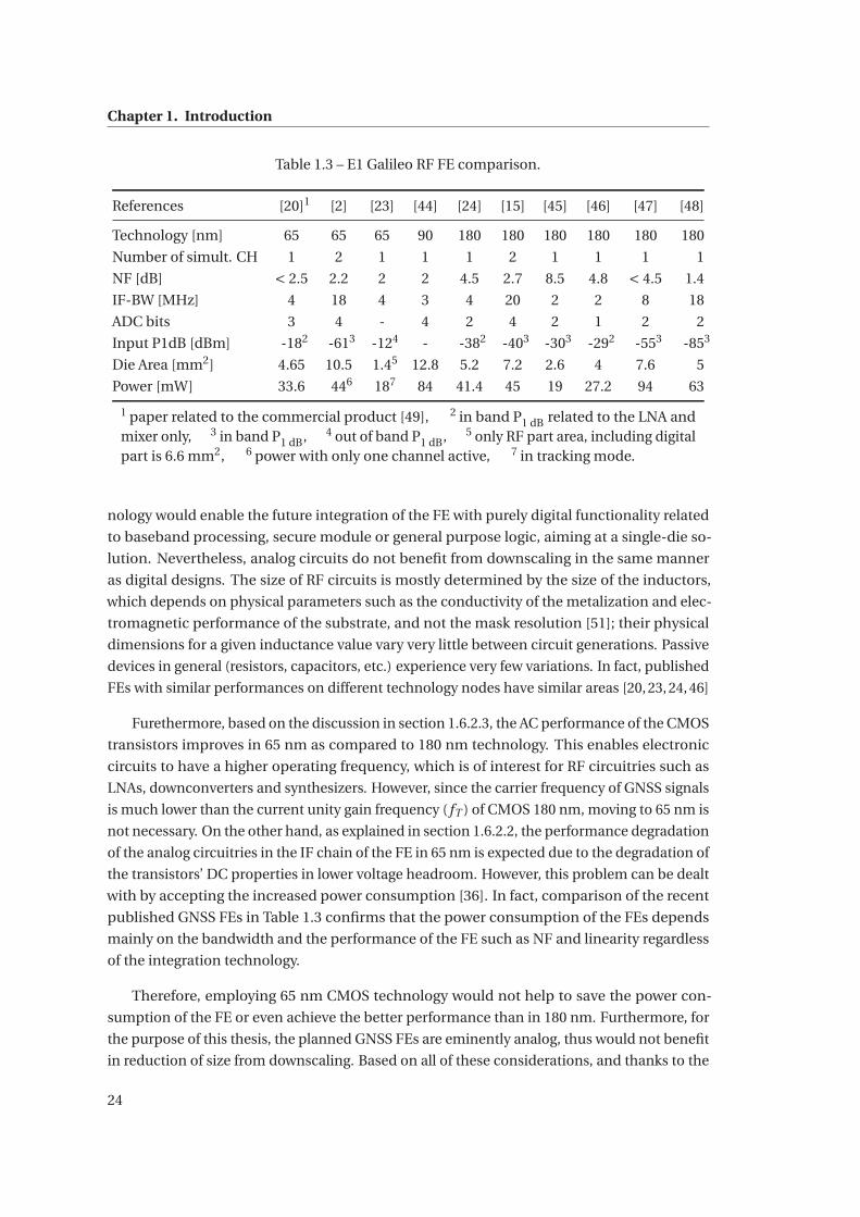
Chapter 1. Introduction
Table 1.3 – E1 Galileo RF FE comparison.
References [20]1 [2] [23] [44] [24] [15] [45] [46] [47] [48]
Technology [nm] 65 65 65 90 180 180 180 180 180 180
Number of simult. CH 1 2 1 1 1 2 1 1 1 1
NF [dB] < 2.5 2.2 2 2 4.5 2.7 8.5 4.8 < 4.5 1.4
IF-BW [MHz] 4 18 4 3 4 20 2 2 8 18
ADC bits 3 4 - 4 2 4 2 1 2 2
Input P1dB [dBm] -182 -613 -124 - -382 -403 -303 -292 -553 -853
Die Area [mm2] 4.65 10.5 1.45 12.8 5.2 7.2 2.6 4 7.6 5
Power [mW] 33.6 446 187 84 41.4 45 19 27.2 94 63
1 paper related to the commercial product [49], 2 in band P1 dB related to the LNA andmixer only, 3 in band P1 dB, 4 out of band P1 dB, 5 only RF part area, including digitalpart is 6.6 mm2, 6 power with only one channel active, 7 in tracking mode.
nology would enable the future integration of the FE with purely digital functionality related
to baseband processing, secure module or general purpose logic, aiming at a single-die so-
lution. Nevertheless, analog circuits do not benefit from downscaling in the same manner
as digital designs. The size of RF circuits is mostly determined by the size of the inductors,
which depends on physical parameters such as the conductivity of the metalization and elec-
tromagnetic performance of the substrate, and not the mask resolution [51]; their physical
dimensions for a given inductance value vary very little between circuit generations. Passive
devices in general (resistors, capacitors, etc.) experience very few variations. In fact, published
FEs with similar performances on different technology nodes have similar areas [20, 23, 24, 46]
Furethermore, based on the discussion in section 1.6.2.3, the AC performance of the CMOS
transistors improves in 65 nm as compared to 180 nm technology. This enables electronic
circuits to have a higher operating frequency, which is of interest for RF circuitries such as
LNAs, downconverters and synthesizers. However, since the carrier frequency of GNSS signals
is much lower than the current unity gain frequency ( fT ) of CMOS 180 nm, moving to 65 nm is
not necessary. On the other hand, as explained in section 1.6.2.2, the performance degradation
of the analog circuitries in the IF chain of the FE in 65 nm is expected due to the degradation of
the transistors’ DC properties in lower voltage headroom. However, this problem can be dealt
with by accepting the increased power consumption [36]. In fact, comparison of the recent
published GNSS FEs in Table 1.3 confirms that the power consumption of the FEs depends
mainly on the bandwidth and the performance of the FE such as NF and linearity regardless
of the integration technology.
Therefore, employing 65 nm CMOS technology would not help to save the power con-
sumption of the FE or even achieve the better performance than in 180 nm. Furthermore, for
the purpose of this thesis, the planned GNSS FEs are eminently analog, thus would not benefit
in reduction of size from downscaling. Based on all of these considerations, and thanks to the
24
1.6. ASIC technology choice
much lower cost, the UMC 180 nm CMOS technology is chosen for the FE integration in this
thesis.
25

2 Public regulated service receiver
This chapter presents the design and implementation of a custom ASIC FE capable of simulta-
neously receiving at least two Galileo PRS signals (E1 and E6), in the framework of the Antenna
and fRont-end MOdules for pUblic Regulated Service applications (ARMOURS) project. Given
the nature of the PRS signals, their users will be more protected on a daily basis against
jamming and spoofing than the users of the OS signals. Moreover, since there is a sufficient
frequency gap between the two PRS bands, the baseband processor will be able to account
for the the first-order ionospheric group delay (which is on the order of 1–50 m depending
on the ionospheric conditions, satellite elevation, season, and solar cycle) [3] and minimize
its error. On the other hand, the dual reception improves the receiver’s robustness over the
intrinsic robustness gained by the PRS signals; in fact, the simultaneous dual reception offers
the flexibility that the band of operation can be selected depending on the receiver operating
conditions, i.e. if strong jamming or spoofing is detected in one band the receiver can switch
off the band and use the other one.
ARMOURS as a part of FP7 collaborative project, in partnership with three other partners
(IMEC, ACORDE and SOFANT), was committed to the development of novel technologies for
the implementation of future multi-frequency PRS receivers, filling some of the technological
gaps to enable affordable and robust solutions for future demanding applications relying on
the continuous availability of the PRS service. The entire RF chain was object of research and
development within ARMOURS: from the receiving antennas, the RF filters and the ASIC FE.
However, ESPLAB was only involved in the specification definition of the ASIC front-end as
well as the design and test of the continuous-time IF filter and the ADC.
The possible applications for the PRS are presented at the beginning of this chapter. The
band selection and front-end architecture are laid out afterwards. The front-end needs to
fulfill a series of stringent requirements for a PRS receiver that will be discussed in detail.
Finally the measurements of the fabricated front-end are presented.
Disclaimer: The PRS information used in this thesis is freely available through references
of this thesis. No classified documents or information were used.
27
Chapter 2. Public regulated service receiver
2.1 PRS applications
The main goal of the PRS is to provide restricted and highly secure access to a reliable naviga-
tion signal. This access will be given by each European Union (EU) member state through a
designated Competent PRS Authority respecting the so-called Common Minimum Standards,
minimum requirements mandatory to all the PRS participants, as described by the PRS access
rules defined in [52]. This controlled access is intended for both military and civilian applica-
tions under government supervision where signal authentication, accuracy and robustness
are critical. Some of these applications are as follows.
2.1.1 Emergency services
The PRS is meant to provide a reliable and secure positioning and timing service under
difficult conditions such as interference or heavy multipath. Therefore, it is appropriate to be
used by emergency services in different applications such as coordinating search and rescue
operations, personnel deployment on the field and situation assessment to control fire, etc.
2.1.2 Regulatory tracking
Transportation of dangerous or regulated loads like nuclear waste or chemicals often un-
dergoes strict monitoring. The use of PRS receivers can provide satellite-based positioning
resistant to jamming and spoofing, ensuring a certain degree of reliability.
Civilian users are sometimes subject to position monitoring as well. For example, fishing
vessels in the EU must be equipped with homologated tracking devices to log and report
their position periodically to guarantee they operate in legal waters. Convicted criminals are
sometimes required by the authorities to remain in a controlled area or away from certain
locations. These tracking devices generally include anti-tamper measures and jamming or
spoofing detection/mitigation mechanisms, but their reliability can be greatly improved with
the use of PRS.
2.1.3 Energy generation and distribution
The GPS is a key tool for worldwide synchronization, and it plays a major role in the coordina-
tion of electrical power plants and distribution, oil and gas production, etc. These systems can
benefit from the PRS as well, as the reliability of this essential infrastructure is conditioned by
the availability of a secure and precise timing mechanism.
2.1.4 Telecommunication systems
Similar to power distribution, many telecommunication systems and pieces of equipment
use GPS as a means of synchronization and in many cases the continuity of this timing
28
2.2. ARMOURS RF front-end architecture
is critical for the seamless operation of the communications link. Therefore there is an
inherent vulnerability in systems relying on open signals for this kind of synchronization. The
PRS can provide a more solid mechanism to prevent system malfunctions due to accidental
interference or even hostile attacks against communication networks.
2.1.5 Critical infrastructure
Besides certain energy generation and distribution and telecommunications, there are other
vital systems that may rely on GNSS for their operation and need an increased availability
and protection to operate in adverse circumstances, such as airports or railway transport,
where positioning and timing are not merely informative but play a major role in their normal
operation.
2.1.6 Security forces
Despite Galileo being a primarily civil service, as with any global navigation system, the
military applications are undeniable. Most EU countries have shown interest in the potential
of Galileo for defense [53], and the implementation plans for the PRS already reflect these
future military uses. Still on the civilian segment, police units could take advantage of the PRS.
For similar reasons, coast guards could also use secure receivers to guarantee a certain degree
of reliability in their navigation despite potentially adverse conditions, something particularly
important when dealing with jurisdictional borders. This issue can be extended to border
control in general where security forces may need very accurate and trustworthy positioning.
2.2 ARMOURS RF front-end architecture
2.2.1 Band selection
2.2.1.1 GNSS signals overview
Most of the multi-frequency front-ends (MFFEs) intended for the mass market are designed
to receive E1-B/C and E5a or E5b signals because, with this combination, many of the de-
sired requirements—fast acquisition, precise ionospheric error correction, availability of the
integrity signal, increased precision and increased tracking accuracy—are achieved. Simi-
lar considerations could be made about the need for E1-A/E6-A in high-performance PRS
receivers. The only published PRS receiver, the Bavarian security receiver (BaSE) described
in [54], is based on L1C, E1-A, E1-B/C and E6 A to receive both PRS available signals and
to help the PRS signal acquisition and tracking by means of the Galileo OS signal. In order
to analyse services, functionalities and technical requirements, a summary of most of the
available Galileo and GPS signals is presented in Table 2.1.
The channel bandwidths shown in Table 2.1 indicate the minimum bandwidth allocated to
29
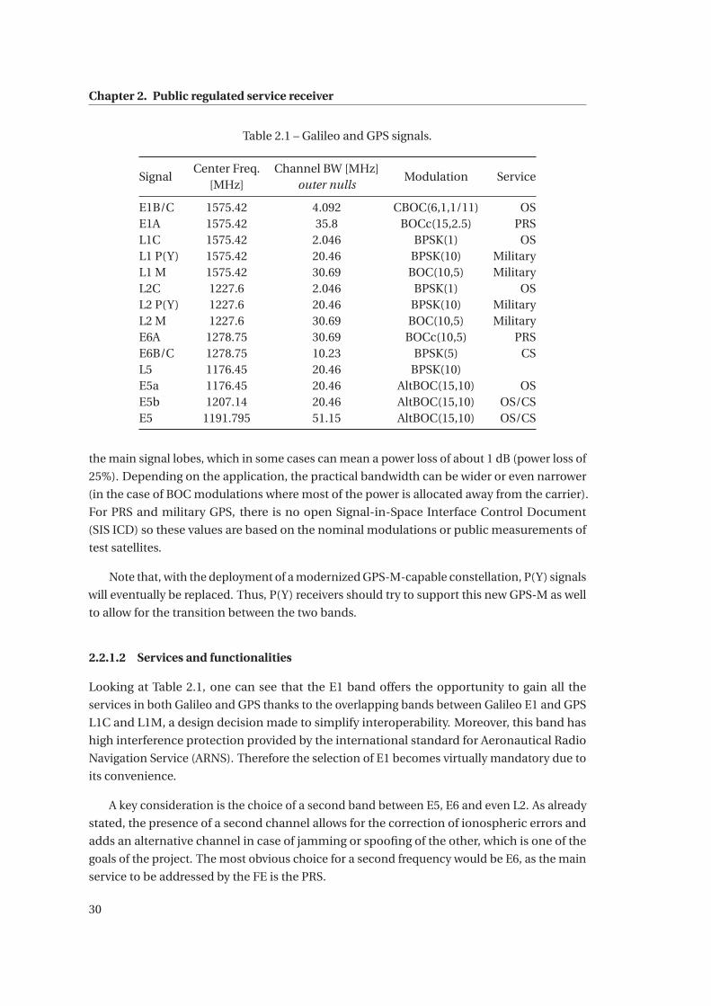
Chapter 2. Public regulated service receiver
Table 2.1 – Galileo and GPS signals.
SignalCenter Freq. Channel BW [MHz]
Modulation Service[MHz] outer nulls
E1B/C 1575.42 4.092 CBOC(6,1,1/11) OSE1A 1575.42 35.8 BOCc(15,2.5) PRSL1C 1575.42 2.046 BPSK(1) OSL1 P(Y) 1575.42 20.46 BPSK(10) MilitaryL1 M 1575.42 30.69 BOC(10,5) MilitaryL2C 1227.6 2.046 BPSK(1) OSL2 P(Y) 1227.6 20.46 BPSK(10) MilitaryL2 M 1227.6 30.69 BOC(10,5) MilitaryE6A 1278.75 30.69 BOCc(10,5) PRSE6B/C 1278.75 10.23 BPSK(5) CSL5 1176.45 20.46 BPSK(10)E5a 1176.45 20.46 AltBOC(15,10) OSE5b 1207.14 20.46 AltBOC(15,10) OS/CSE5 1191.795 51.15 AltBOC(15,10) OS/CS
the main signal lobes, which in some cases can mean a power loss of about 1 dB (power loss of
25%). Depending on the application, the practical bandwidth can be wider or even narrower
(in the case of BOC modulations where most of the power is allocated away from the carrier).
For PRS and military GPS, there is no open Signal-in-Space Interface Control Document
(SIS ICD) so these values are based on the nominal modulations or public measurements of
test satellites.
Note that, with the deployment of a modernized GPS-M-capable constellation, P(Y) signals
will eventually be replaced. Thus, P(Y) receivers should try to support this new GPS-M as well
to allow for the transition between the two bands.
2.2.1.2 Services and functionalities
Looking at Table 2.1, one can see that the E1 band offers the opportunity to gain all the
services in both Galileo and GPS thanks to the overlapping bands between Galileo E1 and GPS
L1C and L1M, a design decision made to simplify interoperability. Moreover, this band has
high interference protection provided by the international standard for Aeronautical Radio
Navigation Service (ARNS). Therefore the selection of E1 becomes virtually mandatory due to
its convenience.
A key consideration is the choice of a second band between E5, E6 and even L2. As already
stated, the presence of a second channel allows for the correction of ionospheric errors and
adds an alternative channel in case of jamming or spoofing of the other, which is one of the
goals of the project. The most obvious choice for a second frequency would be E6, as the main
service to be addressed by the FE is the PRS.
30
2.2. ARMOURS RF front-end architecture
The selection of E5 would entail a very wide-band compared to all other signals, which
is the reason why typical dual-frequency receivers are more likely to focus on either E5a or
E5b. However as in the course of this project, the allocated bandwidth for the PRS bands in
the front-end will be 50 MHz, the IF section of the FE should provide acceptable performance
for the complete E5 signal. A PRS-capable front-end for E6 would be technically similar to one
designed for E5. In addition to the OS and PRS, E5 offers compatibility with GPS L5 that is a
desirable function to consider because it can foster the market during the Galileo transition to
full operation. Let’s begin analyzing the technical repercussions of these possible choices.
2.2.1.3 Implications of band selection on the MFFE requirements
The most challenging technical point is related to the receiver channel bandwidth. From
Table 2.1 we can see that the widest signal is E5. These numbers do not reflect the full
bandwidth of every signal, but still show an interval where most of each signal’s power is
contained, ensuring low correlation losses. For this project, the required bandwidth for
the PRS (both E1-A and E6-A) is 50 MHz despite the outer nulls separation for the in-orbit
validation (IOV) signals as stated in Table 2.1.
The channel bandwidth affects both power consumption and circuital complexity in the IF
filters, IF amplifiers and ADCs, but RF sections only a little. Remembering that the bandwidth
of a large majority of IC FEs is typically lower than 20 MHz, it is clear that breaking this limit is
a challenge for the E1-A channel, which would demand more power. For a second channel,
besides E6, targeting a single lobe of the E5 or L2M is realistic by considering their relative
bandwidth compared to the PRS requirement of 50 MHz, so these goals would be similar.
Band selection affects also the tuning bandwidth of the local oscillators, the ones used for
selecting the received band in reconfigurable channels. For example, a single oscillator able to
tune E1 and E6 has a relative tuning range 2( fE1 − fE6)/( fE1 + fE6) of about 20%; it increases to
about 25% for E1/L2, and reaches 27% for E1 and E5b. The pair of E5b/E6 is quite convenient,
requiring a relative bandwidth of around 6%.
The reception of the OS signal is another issue to consider because it could be desirable
to achieve fast acquisition and basic operation without authority restriction, but it is not
for free in terms of technical requirements. In fact, even though E1-A and E1-B/C share the
same central frequency, they have distinct spectral shapes with different channel needs. In
section 1, it is seen that for BOC signals (large bandwidth and spectral energy shifted away
from central frequency) the preferred scheme is the direct conversion (or zero-IF) with AC
coupled IF stages to remove the DC offset and to avoid flicker noise. In contrast, for the Binary
Phase-Shift Keying (BPSK) signals used in OS, the preferred choice is the low-IF scheme,
where the high pass frequency response of the AC coupling does not affect the main signal
lobes. BOC modulations can also be affected by this if the cutoff is not sufficiently close to
0 Hz. Furthermore, flicker noise sources make low-IF preferable for moderately narrow-band
signals as the averaged NF can be significantly higher if too close to 0 Hz, while for wide-band
31
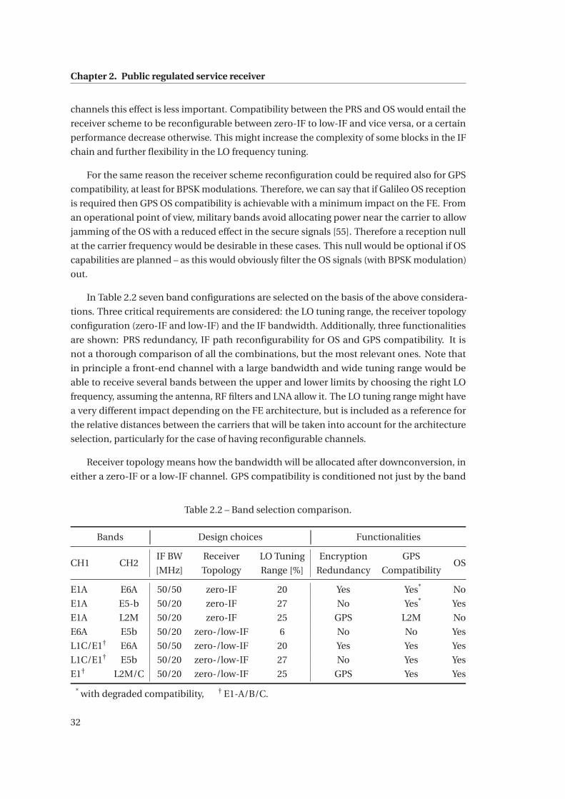
Chapter 2. Public regulated service receiver
channels this effect is less important. Compatibility between the PRS and OS would entail the
receiver scheme to be reconfigurable between zero-IF to low-IF and vice versa, or a certain
performance decrease otherwise. This might increase the complexity of some blocks in the IF
chain and further flexibility in the LO frequency tuning.
For the same reason the receiver scheme reconfiguration could be required also for GPS
compatibility, at least for BPSK modulations. Therefore, we can say that if Galileo OS reception
is required then GPS OS compatibility is achievable with a minimum impact on the FE. From
an operational point of view, military bands avoid allocating power near the carrier to allow
jamming of the OS with a reduced effect in the secure signals [55]. Therefore a reception null
at the carrier frequency would be desirable in these cases. This null would be optional if OS
capabilities are planned – as this would obviously filter the OS signals (with BPSK modulation)
out.
In Table 2.2 seven band configurations are selected on the basis of the above considera-
tions. Three critical requirements are considered: the LO tuning range, the receiver topology
configuration (zero-IF and low-IF) and the IF bandwidth. Additionally, three functionalities
are shown: PRS redundancy, IF path reconfigurability for OS and GPS compatibility. It is
not a thorough comparison of all the combinations, but the most relevant ones. Note that
in principle a front-end channel with a large bandwidth and wide tuning range would be
able to receive several bands between the upper and lower limits by choosing the right LO
frequency, assuming the antenna, RF filters and LNA allow it. The LO tuning range might have
a very different impact depending on the FE architecture, but is included as a reference for
the relative distances between the carriers that will be taken into account for the architecture
selection, particularly for the case of having reconfigurable channels.
Receiver topology means how the bandwidth will be allocated after downconversion, in
either a zero-IF or a low-IF channel. GPS compatibility is conditioned not just by the band
Table 2.2 – Band selection comparison.
Bands Design choices Functionalities
CH1 CH2IF BW Receiver LO Tuning Encryption GPS
OS[MHz] Topology Range [%] Redundancy Compatibility
E1A E6A 50/50 zero-IF 20 Yes Yes* No
E1A E5-b 50/20 zero-IF 27 No Yes* Yes
E1A L2M 50/20 zero-IF 25 GPS L2M No
E6A E5b 50/20 zero-/low-IF 6 No No Yes
L1C/E1† E6A 50/50 zero-/low-IF 20 Yes Yes Yes
L1C/E1† E5b 50/20 zero-/low-IF 27 No Yes Yes
E1† L2M/C 50/20 zero-/low-IF 25 GPS Yes Yes
* with degraded compatibility, † E1-A/B/C.
32
2.2. ARMOURS RF front-end architecture
choice but by its bandwidth allocation. Zero-IF configurations necessarily have a DC null
that corresponds to the carrier frequency, which means some power losses for L1 (and, to a
lesser extent, E1-B/C). This DC null results in degraded compatibility, meaning a low-IF design
would be better for this purpose. Depending on the precision of this AC coupling, these losses
may or may not degrade L1 operation significantly. Making the FE flexible enough to shift the
IF, or using low-IF despite the bandwidth of the PRS, would give better support to E1-B/C and
L1C.
Encryption redundancy indicates whether or not there is more than one secure band. E1
without E6 or the other way around does not provide an additional PRS channel, so jamming
one channel makes the receiver unable to provide a secure position, velocity and timing
solution from Galileo. L2M could be used as a secondary secure band in a dual-frequency dual-
constellation receiver, but this application is extremely specific, limited basically to military
devices. Besides, E1-A and L2M offer the fewest services: a partial PRS redundancy based on
GPS L2M service and no OS. Finally, double PRS would require the widest bandwidth, but
provides PRS encryption redundancy.
2.2.1.4 Band selection conclusions
Given the wide range of applications that take advantage of simultaneous dual-frequency
reception and the PRS-oriented character of this project, it seems clear that the main goal
should be the coverage of E1-A and E6-A with two channels for simultaneous operation.
Considering the wide-band requirements of the PRS, it might take comparatively little
effort to adjust the lower frequency channel E6 to receive E5 as well, or at least E5b, depending
on the flexibility given by the architecture. On the other hand, the bandwidth of E1-A and
E6-A also allows the reception of E1-B/C and E6-B/C, so such a front-end would be able to
demodulate OS and CS at the same time, with some GPS coverage (L1) despite a more than
likely DC decoupling.
The proposed band selection is therefore E1 and E6, with the latter showing some flexibility
to switch to E5b. This way the receiver could be used for pure PRS dual-frequency operation
or high-performance civil receivers (OS E1& E5b), with capabilities in the commercial band
(E6) or even hybrid operation (GPS/Galileo). The flexibility should be higher for the FE ASIC,
trying to optimize compatibility with non-PRS bands at these frequencies plus E5b or even
the whole E5, while the support for other bands below E6 would depend mainly on the filter
and antenna designs.
The use of a third simultaneous frequency was suggested in the description of work but
it is considered not critical for most applications. This additional frequency would further
improve the correction of ionospheric errors, and reduce the ranging variance, but it does
not extend redundancy significantly beyond having two channels able to cover three or more
bands (a triple-channel receiver with one band being jammed would offer two bands, just like
33
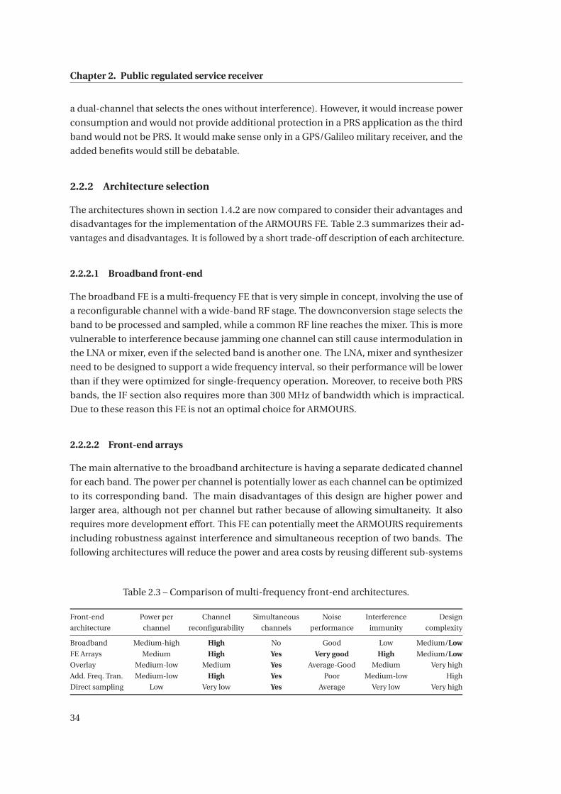
Chapter 2. Public regulated service receiver
a dual-channel that selects the ones without interference). However, it would increase power
consumption and would not provide additional protection in a PRS application as the third
band would not be PRS. It would make sense only in a GPS/Galileo military receiver, and the
added benefits would still be debatable.
2.2.2 Architecture selection
The architectures shown in section 1.4.2 are now compared to consider their advantages and
disadvantages for the implementation of the ARMOURS FE. Table 2.3 summarizes their ad-
vantages and disadvantages. It is followed by a short trade-off description of each architecture.
2.2.2.1 Broadband front-end
The broadband FE is a multi-frequency FE that is very simple in concept, involving the use of
a reconfigurable channel with a wide-band RF stage. The downconversion stage selects the
band to be processed and sampled, while a common RF line reaches the mixer. This is more
vulnerable to interference because jamming one channel can still cause intermodulation in
the LNA or mixer, even if the selected band is another one. The LNA, mixer and synthesizer
need to be designed to support a wide frequency interval, so their performance will be lower
than if they were optimized for single-frequency operation. Moreover, to receive both PRS
bands, the IF section also requires more than 300 MHz of bandwidth which is impractical.
Due to these reason this FE is not an optimal choice for ARMOURS.
2.2.2.2 Front-end arrays
The main alternative to the broadband architecture is having a separate dedicated channel
for each band. The power per channel is potentially lower as each channel can be optimized
to its corresponding band. The main disadvantages of this design are higher power and
larger area, although not per channel but rather because of allowing simultaneity. It also
requires more development effort. This FE can potentially meet the ARMOURS requirements
including robustness against interference and simultaneous reception of two bands. The
following architectures will reduce the power and area costs by reusing different sub-systems
Table 2.3 – Comparison of multi-frequency front-end architectures.
Front-end Power per Channel Simultaneous Noise Interference Design
architecture channel reconfigurability channels performance immunity complexity
Broadband Medium-high High No Good Low Medium/Low
FE Arrays Medium High Yes Very good High Medium/Low
Overlay Medium-low Medium Yes Average-Good Medium Very high
Add. Freq. Tran. Medium-low High Yes Poor Medium-low High
Direct sampling Low Very low Yes Average Very low Very high
34
2.2. ARMOURS RF front-end architecture
and resources of the FE. The consequence of this is the reduction of robustness against
interference and a greater design complexity.
2.2.2.3 Overlay front-end
The overlay architecture solves some of the limitations of the previous FE by keeping the
channels separated at the beginning of the IF chain. This gives some flexibility in the fre-
quency plan while allowing for the possibility of disabling one of the channels when a jammer
appears in it. The disadvantages are potential noise degradation and filter design complexity,
which depend heavily on understanding the power spectral density of the signals in order to
minimize the overlap of noise. This means a generic FE designed to work with an arbitrary or
unknown modulation will generally be more complex or will show worse noise performance.
The relationship between the IF of the different channels will also depend on this spectral
density (a 3 dB NF degradation would take place if they were overlapped without any further
assumptions), so reconfigurability also has some limitations.
2.2.2.4 Front-end with additional frequency translation
The FE with additional frequency translation is very similar to the overlay FE. There are several
ways of overlapping the different channels depending on the spectral allocation of the signals
and their respective filtering. However, if the main RF carrier is being jammed, no other
frequency can be used, as they share the same downconversion stage, unless this is made
variable as well, like a switching FE with an additional mixing stage for an extra channel. This
is a simpler solution than the overlay FE, however overall noise performance is worse.
2.2.2.5 Direct-sampling front-end
Among the architectures presented in section 1.4.2, direct-sampling FEs show the potentially
lowest power consumption, as the concept is merely a low-noise amplifier, a filter and an
ADC. However, there are many complications with this sort of design. Its frequency down-
conversion is based on aliasing. Because of this, there is a direct link between the sampling
frequency and the IF, so it is not possible to set these to arbitrary values. This also means
the frequency at which the baseband processor takes the samples is heavily restricted by the
downconversion and not freely adapted to the baseband needs, so if a different sampling
frequency is desirable the signal will have to be re-sampled. In general this sampling ratio will
be fractional, resulting in additional complications. The optimal sampling frequencies are
not likely to be obtained with standard crystal oscillators or integer multiple/submultiples of
these frequencies, meaning specific reference oscillators would have to be manufactured for
these receivers alone. Otherwise, these arbitrary frequencies would have to be generated with
additional synthesizers.
Regarding multi-frequency channels, even though it is theoretically possible to simultane-
35
Chapter 2. Public regulated service receiver
ously downconvert several bands to adjacent intervals of the spectrum through sampling, this
would impose further constraints to the possible frequency combinations, which would make
the FE less usable by a generic baseband processor, while requiring in any case, a particularly
large bandwidth. On the other hand, separating each band with a dedicated direct sampling
channel or ADCs would likely require different sampling frequencies, creating additional
synchronization complications for the baseband processor, and causing inter-channel cross-
interference of sampling spurs that are not present when using the same sampling rate for all
channels.
Its performance is severely limited by that of the filters and ADC, thus this architecture is
vulnerable to sampling jitter and aliasing noise. Sampling has to be particularly accurate, so
even if the topology of the FE is simple, achieving an ADC with such good characteristics is
not. Moreover, since for processing the GNSS signals a huge amplification ( typically > 80 dB)
is required, such a huge amplification at the RF prior to sampling, without down conversion
stages, may lead to instabilities in the RF amplification chain.
Because of this frequency translation through aliasing, this FE is extremely vulnerable
to interference; virtually any spurious tones become in-band. Therefore, anything not thor-
oughly filtered before the sampling process will necessarily overlap with the signals of interest.
Although it is an attractive solution for single-frequency narrowband receivers, overall this is
clearly unsuitable for PRS receivers.
2.2.3 ARMOURS architecture and frequency plan
Given that robustness against interference is a priority, the FE should make channels as
independent as possible. Low design complexity and good noise performance are desirable,
so the best option is to have a FE with either a dedicated channel for each frequency or a
single channel able to switch between bands as needed. Since simultaneous dual-frequency
operation is one of the aims of this project, the possibility of a single reconfigurable channel for
all of them has to be discarded. Consequently, the general architecture chosen for ARMOURS
is a dual-frequency front-end arrays as it is shown in Figure 2.1.
One of the channels will be fixed at E1, while the other will be designed for E6. The topology
of each channel will be that of a single-conversion zero-IF receiver with I/Q outputs, mainly
due to the difficulties of performing image rejection with complex filters at high frequencies
and the high-frequency requirements of the IF amplifiers otherwise. The frequency plan of
the receiver for both the E1 and E6 frond-end bands is shown in Figure 2.2. This means four
ADCs will be required, two per channel. The ASIC or FE core will comprise of an LNA, a pair of
low-noise I/Q down-converters with their respective filters, amplifiers and ADCs. Additionally,
external LNAs will be merged with the antennas to reduce the effect of the insertion losses
of the RF bandpass filters in the receiver sensitivity; these LNAs will be designed in the same
technology as the ASIC core, but packaged or integrated separately.
36
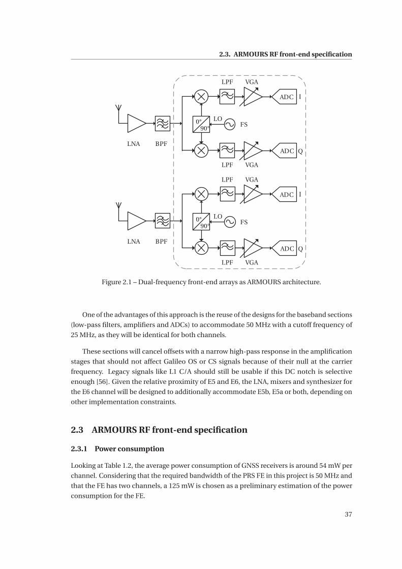
2.3. ARMOURS RF front-end specification
LNA
0° 90°
ADC
BPF
FSLO
ADC
VGA
VGA
LPF
LPF
I
Q
LNA
0° 90°
ADC
BPF
FSLO
ADC
VGA
VGA
LPF
LPF
I
Q
Figure 2.1 – Dual-frequency front-end arrays as ARMOURS architecture.
One of the advantages of this approach is the reuse of the designs for the baseband sections
(low-pass filters, amplifiers and ADCs) to accommodate 50 MHz with a cutoff frequency of
25 MHz, as they will be identical for both channels.
These sections will cancel offsets with a narrow high-pass response in the amplification
stages that should not affect Galileo OS or CS signals because of their null at the carrier
frequency. Legacy signals like L1 C/A should still be usable if this DC notch is selective
enough [56]. Given the relative proximity of E5 and E6, the LNA, mixers and synthesizer for
the E6 channel will be designed to additionally accommodate E5b, E5a or both, depending on
other implementation constraints.
2.3 ARMOURS RF front-end specification
2.3.1 Power consumption
Looking at Table 1.2, the average power consumption of GNSS receivers is around 54 mW per
channel. Considering that the required bandwidth of the PRS FE in this project is 50 MHz and
that the FE has two channels, a 125 mW is chosen as a preliminary estimation of the power
consumption for the FE.
37
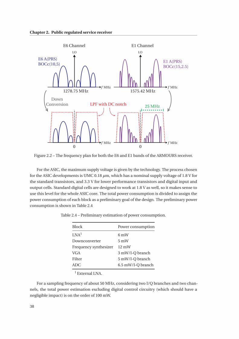
Chapter 2. Public regulated service receiver
1575.42 MHz1278.75 MHz
E6 Channel E1 Channel
E6 A(PRS)
BOCc(10,5)E1 A(PRS)
BOCc(15,2.5)
f MHzf MHz
LOLO
00
Down
Conversion LPF with DC notch
f MHzf MHz
25 MHz
Figure 2.2 – The frequency plan for both the E6 and E1 bands of the ARMOURS receiver.
For the ASIC, the maximum supply voltage is given by the technology. The process chosen
for the ASIC developments is UMC 0.18 μm, which has a nominal supply voltage of 1.8 V for
the standard transistors, and 3.3 V for lower performance transistors and digital input and
output cells. Standard digital cells are designed to work at 1.8 V as well, so it makes sense to
use this level for the whole ASIC core. The total power consumption is divided to assign the
power consumption of each block as a preliminary goal of the design. The preliminary power
consumption is shown in Table 2.4
Table 2.4 – Preliminary estimation of power consumption.
Block Power consumption
LNA1 6 mW
Downconverter 5 mW
Frequency synthesizer 12 mW
VGA 3 mW/I-Q branch
Filter 5 mW/I-Q branch
ADC 6.5 mW/I-Q branch
1 External LNA.
For a sampling frequency of about 50 MHz, considering two I/Q branches and two chan-
nels, the total power estimation excluding digital control circuitry (which should have a
negligible impact) is on the order of 100 mW.
38
2.3. ARMOURS RF front-end specification
This power consumption is only for the front-end itself and not the full GNSS receiver.
The total power of the PRS baseband processor is unknown a priori, and heavily dependent
on implementation. U-blox LEA-M8S modules [57] are high-performance, low-cost, low-
power multi-frequency receivers for L1/E1/B1. Their reported tracking sensitivity is -167 dBm,
4 dB better than the expected performance of the GNSS receiver integrated in [58], with
a power consumption of about 78 mW. This power can be divided into three main blocks:
front-end, and low- and high-level signal processing. The first two blocks are affected by
the signal bandwidth (greater analog bandwidth, higher sampling frequencies), while the
third block of the position, velocity and timing solution, computation, or navigation should
remain in the same order. PRS receivers, like current P(Y) modules, are also expected to
have additional circuitry executing secure operations like code generation or decryption. A
qualitative estimation indicates that such a receiver implementation that is optimized for
high performance, maintaining low noise and high bandwidth, would not be suitable for a
low-power device like the Terrestrial Trunked Radio (TETRA) transceiver [58].
However, the power consumption of the whole front-end does not have to be the power
consumption of the front-end under normal operation. Even if the GNSS receiver is expected
to be fully operative, a dual-frequency regime is a feature that may not be required in some
cases. One option would be to allow the user to disable either channel when simultaneous
reception is not required, effectively halving the power consumption. Another strategy im-
plemented in certain receivers where power management is critical is the continuous supply
control of different blocks to switch them on and off depending on the quality of service [59].
Undersampled DSSS signals keep their autocorrelation properties [60] reducing sampling
and processing power at the cost of effective C /N0. For example, decimating by a factor of two
theoretically causes a 3 dB SNR degradation at the correlator outputs. In the power breakdown
above, ADCs working at a sampling frequency of 52 MHz would account for about 25% of
all the front-end power, which could be dynamically reduced by modifying the duty cycle
(i.e. sampling at submultiples of 52 MHz). ADCs can be switched off easily and quickly by
bypassing the clock input, since their static power consumption can be very low.
A more effective power-saving strategy would be the switching off practically the whole
front-end. ADCs and most of the analog blocks could be controlled by a power-down signal
that would shut down most of the RF channel. To avoid lock transients, the frequency synthe-
sizer could remain on, but the rest would be switched on and off for a fraction of time. In this
scenario, total power would ideally be:
PFE = PSYN +τ (PLNA +PMIX +2PVGA +2PFIL +2PADC) ≈ 12mW+τ40mW. (2.1)
In high-quality signal conditions or when sensitivity values can be lower than optimal
(such as in the TETRA terminal described above), 6 dB losses would be affordable to reach
39
Chapter 2. Public regulated service receiver
a theoretical power consumption on the order of 22 mW per channel with a duty-cycle of
25%. This way the same high-performance receiver could be adjusted to different sensitivity
requirements by means of power management.
2.3.2 Noise figure
The noise figure (NF) has a direct effect on sensitivity; for a given baseband implementation,
sensitivity is degraded by 1 dB per 1 dB of NF. The noise specification is therefore the sensitivity
requirement for the receiver, and the sensitivity achieved by the baseband processor. The gap
between the two is approximately the maximum NF.
The sensitivity achieved by the baseband processor is usually expressed in two values:
acquisition and tracking sensitivity. Tracking sensitivity is generally higher (i.e. able to detect
weaker signals) because the effects of the combined dynamics of the satellites and the receiver
are estimated to a certain extent by the phase and code tracking loops. Acquisition sensitivity
does not generally make any assumption about local dynamics (cold start) and involves the
search of the space vehicle (SV) signals in a two-dimensional space (carrier phase/frequency
and code delay).
While the receiver sensitivity is typically given as a power level, commonly in an ideal
scenario with nominal antenna noise or temperature and no interference, the sensitivity of the
baseband processor is generally expressed in C /N0 or signal power over noise power density.
In reality, not all sources of signal degradation between the antenna and the signal pro-
cessor can be approximated as additive white noise. As will be seen, distortion, quantization,
interference, sampling jitter or phase noise causes an effective C /N0 reduction that does not
directly translate into a NF approximation. For this reason the maximum NF of the front-end is
only one of many factors that have to be taken into account to optimize the receiver sensitivity,
even if usually the most important as well.
Typical NF values in GNSS receivers are between 2 dB and 5 dB (see Table 1.1 and Table 1.2).
Given the bandwidth restrictions and novelty of the designs, 4 dB will be set as a reasonable
system goal for the NF of the receiver ( including the FE, RF filter and active antenna). As will
be seen, it is believed technically possible to achieve a lower NF, closer to 2 dB, so this will be
treated as an upper boundary or worst-case scenario.
2.3.3 Gain
As specified in [7], the minimum received power on ground, measured at the output of an
ideally matched right-hand circularly polarized (RHCP) 0 dBi user receiving antenna with the
SV elevation angle higher than 10 degrees, is approximately -157 dBW (-127 dBm) for the E1
signal and -155 dBW for the E5 and E6 signals. However, GNSS signals are DSSS, which means
their power density is low and the minimum bandwidth required to process them contains
40
2.3. ARMOURS RF front-end specification
mostly thermal noise.
Assuming an ADC input dynamic range of 500 mVpp and that we are using 4 bits of back-off
for interference mitigation, then the required ADC’s input voltage is around 31.25 mVpp. Given
that the GNSS signals are buried under the noise floor, we can consider 31.25 mVpp as three
times the standard deviation (σ) of the noise voltage at the ADC’s input. Therefore, the noise
voltage at the ADC’s input is:
Vn,ADC = 31.25 mVpp
3= 10.42 mVRMS. (2.2)
On the other hand, the input signal is basically thermal noise within the receiver bandwidth
and can be calculated by:
Pn,ant [dBm] = N0 +10log (BW ) ≈−100 dBm, (2.3)
where N0 is the noise spectral density (N0 ≈−174 dBm/Hz at room temperature of 300 °K) and
BW is the equivalent noise bandwidth approximated by that of the FE’s most-selective filter.
Over a bandwidth of 25 MHz, the equivalent input power is about -100 dBm, which can be
converted to volts root mean square (RMS) through the load impedance of R equal to 50 Ω by:
Vn,ant =√
R ×10Pn,ant [dBW]
10 = 2.23 μVRMS. (2.4)
Accordingly, the required receiver’s voltage gain can be calculated by:
Gv = 20log
(Vn,ADC
Vn,ant
)= 20l og
(10.42 mVRMS
2.23 μVRMS
)≈ 70.4 dB. (2.5)
Considering temperature variations and additional losses as well as the processing of smaller
bandwidth signals, a gain range of 60 dB to 80 dB would be an appropriate gain range.
2.3.4 Channel frequency response
Traveling through the receiving chain, from the antenna to the digital processing unit, the
GNSS signal is delayed by a comparatively large value (up to 1 μs). Absolute delay is not as
critical as relative variations given that the position, velocity and timing solution is calculated
based on phases between signals, so the absolute delay would mostly increase latency which is
considerably lower than the processing time. On the other hand, relative delays introduce an
error in positioning if not calibrated or estimated. These, also called hardware biases, are due
to the group delay variations versus both frequency and physical parameters (e.g. temperature
41
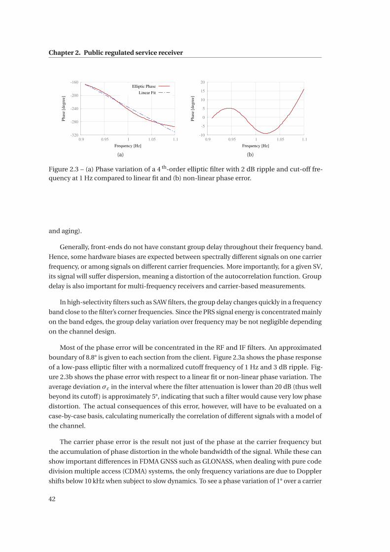
Chapter 2. Public regulated service receiver
-320
-280
-240
-200
-160
0.9 0.95 1 1.05 1.1
Ph
ase
[deg
ree]
Frequency [Hz]
Elliptic Phase
Linear Fit
(a)
-10
-5
0
5
10
15
20
0.9 0.95 1 1.05 1.1
Ph
ase
[deg
ree]
Frequency [Hz]
(b)
Figure 2.3 – (a) Phase variation of a 4 th-order elliptic filter with 2 dB ripple and cut-off fre-quency at 1 Hz compared to linear fit and (b) non-linear phase error.
and aging).
Generally, front-ends do not have constant group delay throughout their frequency band.
Hence, some hardware biases are expected between spectrally different signals on one carrier
frequency, or among signals on different carrier frequencies. More importantly, for a given SV,
its signal will suffer dispersion, meaning a distortion of the autocorrelation function. Group
delay is also important for multi-frequency receivers and carrier-based measurements.
In high-selectivity filters such as SAW filters, the group delay changes quickly in a frequency
band close to the filter’s corner frequencies. Since the PRS signal energy is concentrated mainly
on the band edges, the group delay variation over frequency may be not negligible depending
on the channel design.
Most of the phase error will be concentrated in the RF and IF filters. An approximated
boundary of 8.8° is given to each section from the client. Figure 2.3a shows the phase response
of a low-pass elliptic filter with a normalized cutoff frequency of 1 Hz and 3 dB ripple. Fig-
ure 2.3b shows the phase error with respect to a linear fit or non-linear phase variation. The
average deviation σε in the interval where the filter attenuation is lower than 20 dB (thus well
beyond its cutoff) is approximately 5°, indicating that such a filter would cause very low phase
distortion. The actual consequences of this error, however, will have to be evaluated on a
case-by-case basis, calculating numerically the correlation of different signals with a model of
the channel.
The carrier phase error is the result not just of the phase at the carrier frequency but
the accumulation of phase distortion in the whole bandwidth of the signal. While these can
show important differences in FDMA GNSS such as GLONASS, when dealing with pure code
division multiple access (CDMA) systems, the only frequency variations are due to Doppler
shifts below 10 kHz when subject to slow dynamics. To see a phase variation of 1° over a carrier
42
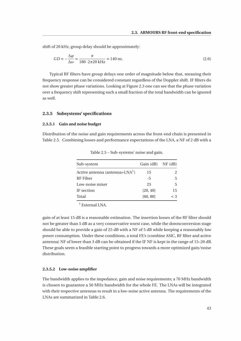
2.3. ARMOURS RF front-end specification
shift of 20 kHz, group delay should be approximately:
GD ≈−Δϕ
Δω≈ π
180 ·2π20 kHz≈ 140 ns. (2.6)
Typical RF filters have group delays one order of magnitude below that, meaning their
frequency response can be considered constant regardless of the Doppler shift. IF filters do
not show greater phase variations. Looking at Figure 2.3 one can see that the phase variation
over a frequency shift representing such a small fraction of the total bandwidth can be ignored
as well.
2.3.5 Subsystems’ specifications
2.3.5.1 Gain and noise budget
Distribution of the noise and gain requirements across the front-end chain is presented in
Table 2.5. Combining losses and performance expectations of the LNA, a NF of 2 dB with a
Table 2.5 – Sub-systems’ noise and gain.
Sub-system Gain (dB) NF (dB)
Active antenna (antenna+LNA1) 15 2
RF Filter -5 5
Low-noise mixer 25 5
IF section [20, 40] 15
Total [60, 80] < 3
1 External LNA.
gain of at least 15 dB is a reasonable estimation. The insertion losses of the RF filter should
not be greater than 5 dB as a very conservative worst case, while the downconversion stage
should be able to provide a gain of 25 dB with a NF of 5 dB while keeping a reasonably low
power consumption. Under these conditions, a total FE’s (combine ASIC, RF filter and active
antenna) NF of lower than 3 dB can be obtained if the IF NF is kept in the range of 15–20 dB.
These goals seem a feasible starting point to progress towards a more optimized gain/noise
distribution.
2.3.5.2 Low-noise amplifier
The bandwidth applies to the impedance, gain and noise requirements; a 70 MHz bandwidth
is chosen to guarantee a 50 MHz bandwidth for the whole FE. The LNAs will be integrated
with their respective antennas to result in a low-noise active antenna. The requirements of the
LNAs are summarized in Table 2.6.
43
Chapter 2. Public regulated service receiver
Table 2.6 – Low-noise amplifier requirements.
Requirement Value
Input impedance 50 Ω, single-ended, |S11| < −10 dB
Output impedance 50 Ω, single-ended, |S22| < −10 dB
Minimum gain 15 dB
Maximum NF 2 dB
Bandwidth1575.42±35 MHz
1278.75±35 MHz
Supply voltage 1.8 V
DC power consumption 6 mW
2.3.5.3 Low-noise downconverter
The design requirements of the low-noise downconverter are summarized in Table 2.7.
Table 2.7 – Low-noise downconverter requirements.
Requirement Value
Input impedance 50 Ω, single-ended, |S11| < −10 dB
Output impedance Match to IF filter
Minimum gain 25 dB
Maximum NF 5 dB
Bandwidth1575.42±35 MHz
1278.75±35 MHz
Supply voltage 1.8 V
DC power consumption 5 mW
2.3.5.4 Frequency synthesizer
In principle, the PLL frequency synthesizer will provide fixed outputs for direct conversion
(fLO−−fRF) but it will also provide some flexibility in situations where losing bandwidth by
shifting the IF can lead to less degradation of the signal caused by interference or jamming.
The requirements of the frequency synthesizer are summarized in Table 2.8.
2.3.5.5 Active IF filters
Figure 2.4 shows the frequency response of two sample 4 th-order filters like the ones that
could be implemented for the IF sections of the ASIC.
The elliptic configuration is particularly convenient because of the filter’s abrupt cutoff
44
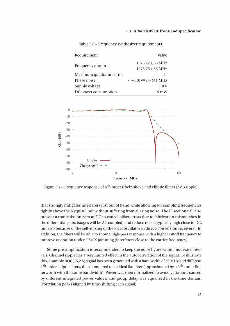
2.3. ARMOURS RF front-end specification
Table 2.8 – Frequency synthesizer requirements.
Requirement Value
Frequency output1575.42±35 MHz
1278.75±35 MHz
Maximum quadrature error 1°
Phase noise <−110 dBc/Hz @ 1 MHz
Supply voltage 1.8 V
DC power consumption 5 mW
-90
-80
-70
-60
-50
-40
-30
-20
-10
0
3 10 60
Gai
n [
dB
]
Frequency [MHz]
Elliptic
Chebyshev I
Figure 2.4 – Frequency response of 4 th-order Chebyshev I and elliptic filters (2 dB ripple).
that strongly mitigates interferers just out of band while allowing for sampling frequencies
tightly above the Nyquist limit without suffering from aliasing noise. The IF section will also
present a transmission zero at DC to cancel offset errors due to fabrication mismatches in
the differential pairs (stages will be AC coupled) and reduce noise (typically high close to DC,
but also because of the self-mixing of the local oscillator in direct-conversion receivers). In
addition, the filters will be able to show a high-pass response with a higher cutoff frequency to
improve operation under OS/CS jamming (interferers close to the carrier frequency).
Some pre-amplification is recommended to keep the noise figure within moderate inter-
vals. Channel ripple has a very limited effect in the autocorrelation of the signal. To illustrate
this, a sample BOC(15,2.5) signal has been generated with a bandwidth of 50 MHz and different
4 th-order elliptic filters, then compared to an ideal flat filter (approximated by a 9 th-order But-
terworth with the same bandwidth). Power was then normalized to avoid variations caused
by different integrated power values, and group delay was equalized in the time domain
(correlation peaks aligned by time-shifting each signal).
45
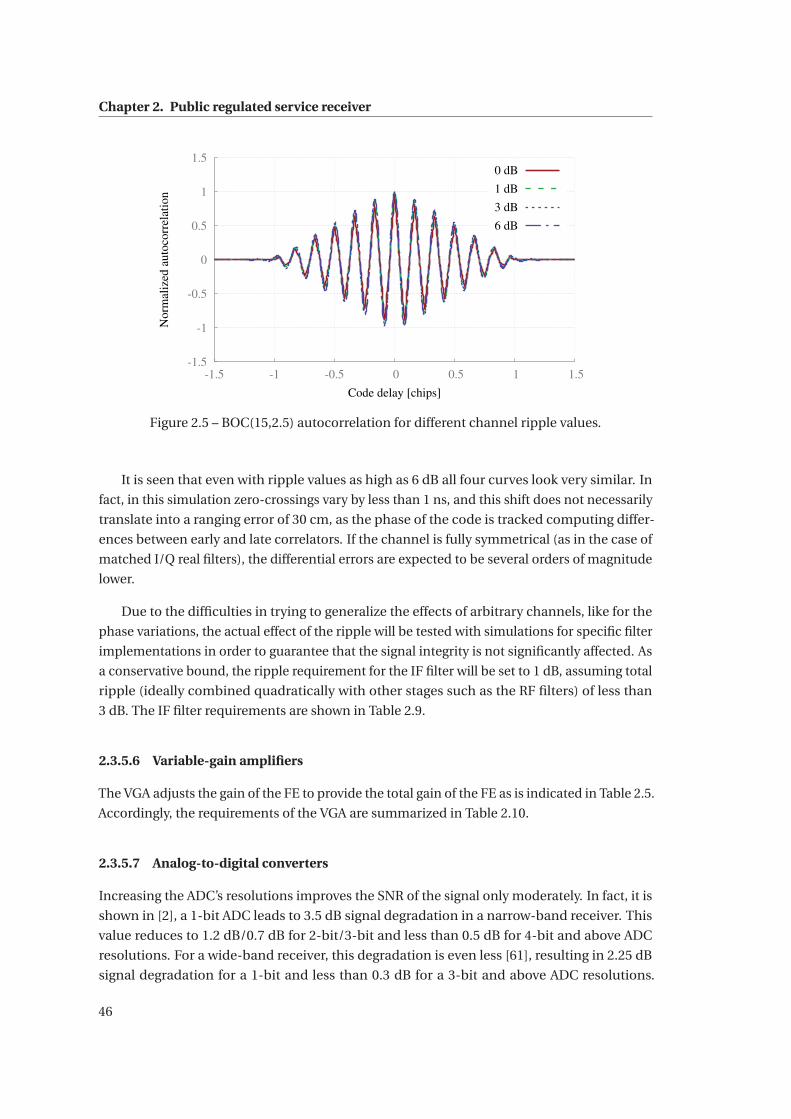
Chapter 2. Public regulated service receiver
-1.5
-1
-0.5
0
0.5
1
1.5
-1.5 -1 -0.5 0 0.5 1 1.5
Norm
aliz
ed a
uto
corr
elat
ion
Code delay [chips]
0 dB
1 dB
3 dB
6 dB
Figure 2.5 – BOC(15,2.5) autocorrelation for different channel ripple values.
It is seen that even with ripple values as high as 6 dB all four curves look very similar. In
fact, in this simulation zero-crossings vary by less than 1 ns, and this shift does not necessarily
translate into a ranging error of 30 cm, as the phase of the code is tracked computing differ-
ences between early and late correlators. If the channel is fully symmetrical (as in the case of
matched I/Q real filters), the differential errors are expected to be several orders of magnitude
lower.
Due to the difficulties in trying to generalize the effects of arbitrary channels, like for the
phase variations, the actual effect of the ripple will be tested with simulations for specific filter
implementations in order to guarantee that the signal integrity is not significantly affected. As
a conservative bound, the ripple requirement for the IF filter will be set to 1 dB, assuming total
ripple (ideally combined quadratically with other stages such as the RF filters) of less than
3 dB. The IF filter requirements are shown in Table 2.9.
2.3.5.6 Variable-gain amplifiers
The VGA adjusts the gain of the FE to provide the total gain of the FE as is indicated in Table 2.5.
Accordingly, the requirements of the VGA are summarized in Table 2.10.
2.3.5.7 Analog-to-digital converters
Increasing the ADC’s resolutions improves the SNR of the signal only moderately. In fact, it is
shown in [2], a 1-bit ADC leads to 3.5 dB signal degradation in a narrow-band receiver. This
value reduces to 1.2 dB/0.7 dB for 2-bit/3-bit and less than 0.5 dB for 4-bit and above ADC
resolutions. For a wide-band receiver, this degradation is even less [61], resulting in 2.25 dB
signal degradation for a 1-bit and less than 0.3 dB for a 3-bit and above ADC resolutions.
46
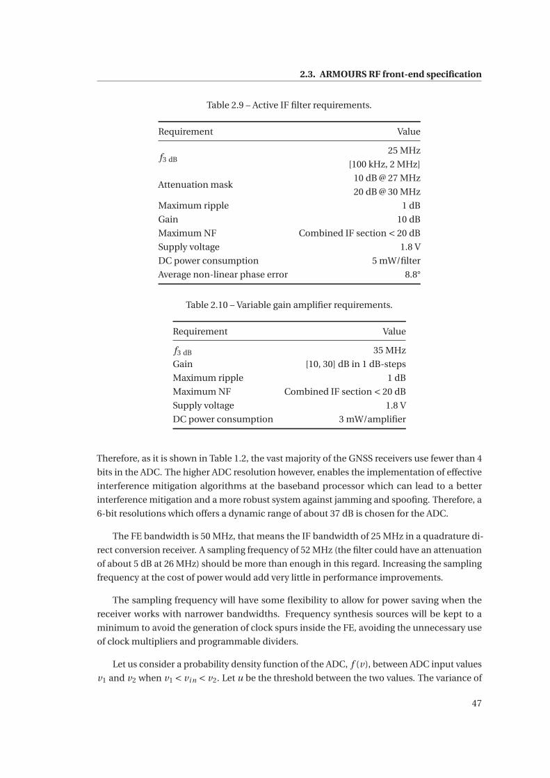
2.3. ARMOURS RF front-end specification
Table 2.9 – Active IF filter requirements.
Requirement Value
f3 dB25 MHz
[100 kHz, 2 MHz]
Attenuation mask10 dB @ 27 MHz
20 dB @ 30 MHz
Maximum ripple 1 dB
Gain 10 dB
Maximum NF Combined IF section < 20 dB
Supply voltage 1.8 V
DC power consumption 5 mW/filter
Average non-linear phase error 8.8°
Table 2.10 – Variable gain amplifier requirements.
Requirement Value
f3 dB 35 MHz
Gain [10, 30] dB in 1 dB-steps
Maximum ripple 1 dB
Maximum NF Combined IF section < 20 dB
Supply voltage 1.8 V
DC power consumption 3 mW/amplifier
Therefore, as it is shown in Table 1.2, the vast majority of the GNSS receivers use fewer than 4
bits in the ADC. The higher ADC resolution however, enables the implementation of effective
interference mitigation algorithms at the baseband processor which can lead to a better
interference mitigation and a more robust system against jamming and spoofing. Therefore, a
6-bit resolutions which offers a dynamic range of about 37 dB is chosen for the ADC.
The FE bandwidth is 50 MHz, that means the IF bandwidth of 25 MHz in a quadrature di-
rect conversion receiver. A sampling frequency of 52 MHz (the filter could have an attenuation
of about 5 dB at 26 MHz) should be more than enough in this regard. Increasing the sampling
frequency at the cost of power would add very little in performance improvements.
The sampling frequency will have some flexibility to allow for power saving when the
receiver works with narrower bandwidths. Frequency synthesis sources will be kept to a
minimum to avoid the generation of clock spurs inside the FE, avoiding the unnecessary use
of clock multipliers and programmable dividers.
Let us consider a probability density function of the ADC, f (v), between ADC input values
v1 and v2 when v1 < vi n < v2. Let u be the threshold between the two values. The variance of
47
Chapter 2. Public regulated service receiver
the quantization error becomes:
σ2 =u∫
v1
(v − v1)2 f (v)d v +v2∫
u
(v2 − v)2 f (v)d v . (2.7)
For a high resolution ADC, we can approximate this density function f (v) as locally flat for
most steps.
σ2 ≈ 1
v2 − v1
⎛⎝ u∫
v1
(v − v1)2d v +v2∫
u
(v2 − v)2d v
⎞⎠ . (2.8)
Ideally, if the threshold u is exactly between v1 and v2, we have [62]:
σ02 = (v1 − v2)2
12. (2.9)
Assuming a threshold shift Δu with respect to the distance between the two quantization steps,
we can express this threshold as:
u = v1 + v2
2+ (v2 − v1)Δu. (2.10)
Accordingly, the quantization error can be written as:
σ2 ≈ 1
v2 − v1
⎛⎝ u∫
v1
(v − v1)2d v +v2∫
u
(v2 − v)2d v
⎞⎠= (v1 − v2)2
12(1+Δu2). (2.11)
The noise factor (F ) of this shift in the threshold Δu is:
F ≈ σΔu2
σ02 = 1+Δu2, and (2.12)
N F = 10log10(F ). (2.13)
If we limit this NF to 0.1 dB, we get that the maximum threshold shift must be lower than
0.15 LSB by:
Δu ≤√
10N F10 −1. (2.14)
As a result, the requirements of the ADC are summarized in Table 2.11.
48
2.4. Subsystems’ design
Table 2.11 – Analog-to-digital converter requirements.
Requirement Value
Precision 6 bits
DNL 0.15 LSB
Maximum NF Combined IF section < 20 dB
Maximum sampling frequency 52 MSps
Supply voltage 1.8/3.3 V
DC power consumption 6.5 mW per ADC
2.4 Subsystems’ design
ARMOURS was part of an FP7 collaborative project in which four partners including IMEC,
ACORDE, SOFANT and ESPLAB were collaborating to fulfill the tasks of the project. In this
project, ESPLAB was involved in defining the system and subsystem specifications for the front-
end and was in charge of the design, testing and development of an ADC and a continuous-
time low-pass filter. The following section is dedicated to the design and testing of the ADC
employed in the ARMOURS. The filter design and its related topics are explained in detail in
chapter 3.
2.4.1 Analog-to-digital converter
There are a variety of architectures available to implement the ADC [63] using a CMOS process.
Based on the ADC requirements presented in Table 2.11, pipeline and two-step architectures
[64–67] are the potential candidates. However, they suffer from large latency. The ADC’s
latency is usually presented in its clock-cycle unit. The front-end overall latency is the sum of
the ADC latency and the frond-end group delay. Usually, this latency is constant and does not
degrade the position, velocity and timing accuracy of the receiver and, in the case of a high-
sampling-rate ADC, this latency is small. However, the latency increases in a reconfigurable
design approach in which the ADC needs to operate sometimes at a low sampling rate. Even
though the increase in the latency does not degrade the receiver accuracy, it will deteriorate
the capability of the baseband processor to mitigate interference. In fact, due to the latency,
the baseband processor requires more time to detect any interference, which may put the VGA
and analog buffers in the ADC in saturation and take some time to go back in full operation.
Therefore, in order to have a front-end that is robust against interference, an ADC architecture
with minimal latency is preferred.
Another possible architecture for the ADCs is folding architecture [68,69], which shows low
power and low latency as well as the ability to run at high sampling rates. However, it is limited
in dynamic performance due to bandwidth requirements on the circuitry that processes
the folded signal. According to these considerations, a full flash ADC architecture [70–72]
emerges as an optimal choice because the required resolution is only 6 bits, it shows good
49
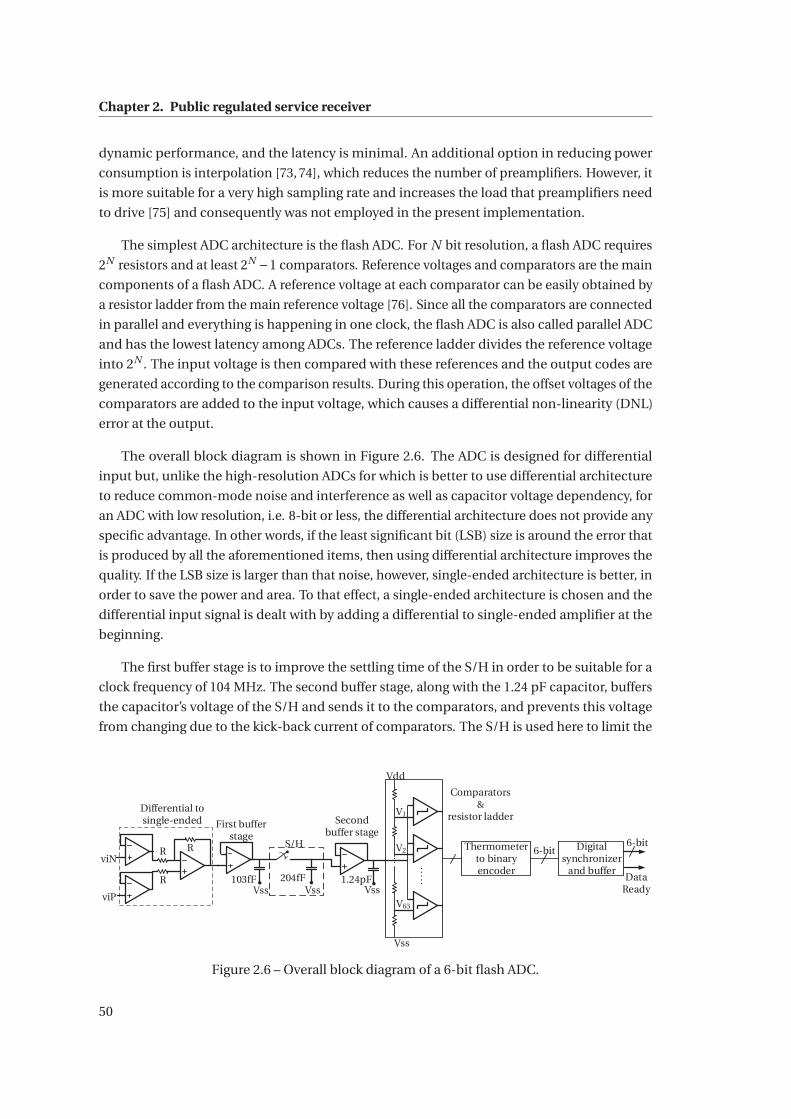
Chapter 2. Public regulated service receiver
dynamic performance, and the latency is minimal. An additional option in reducing power
consumption is interpolation [73, 74], which reduces the number of preamplifiers. However, it
is more suitable for a very high sampling rate and increases the load that preamplifiers need
to drive [75] and consequently was not employed in the present implementation.
The simplest ADC architecture is the flash ADC. For N bit resolution, a flash ADC requires
2N resistors and at least 2N −1 comparators. Reference voltages and comparators are the main
components of a flash ADC. A reference voltage at each comparator can be easily obtained by
a resistor ladder from the main reference voltage [76]. Since all the comparators are connected
in parallel and everything is happening in one clock, the flash ADC is also called parallel ADC
and has the lowest latency among ADCs. The reference ladder divides the reference voltage
into 2N . The input voltage is then compared with these references and the output codes are
generated according to the comparison results. During this operation, the offset voltages of the
comparators are added to the input voltage, which causes a differential non-linearity (DNL)
error at the output.
The overall block diagram is shown in Figure 2.6. The ADC is designed for differential
input but, unlike the high-resolution ADCs for which is better to use differential architecture
to reduce common-mode noise and interference as well as capacitor voltage dependency, for
an ADC with low resolution, i.e. 8-bit or less, the differential architecture does not provide any
specific advantage. In other words, if the least significant bit (LSB) size is around the error that
is produced by all the aforementioned items, then using differential architecture improves the
quality. If the LSB size is larger than that noise, however, single-ended architecture is better, in
order to save the power and area. To that effect, a single-ended architecture is chosen and the
differential input signal is dealt with by adding a differential to single-ended amplifier at the
beginning.
The first buffer stage is to improve the settling time of the S/H in order to be suitable for a
clock frequency of 104 MHz. The second buffer stage, along with the 1.24 pF capacitor, buffers
the capacitor’s voltage of the S/H and sends it to the comparators, and prevents this voltage
from changing due to the kick-back current of comparators. The S/H is used here to limit the
Differential to single-ended
viP
viN
S/H
Vss
Vdd
V1
V2
V63
R
R
R
VssVss Vss103fF 204fF 1.24pF
Thermometer to binary encoder
6-bit Digital synchronizer
and buffer
6-bit
Data Ready
First buffer stage
Second buffer stage
Comparators&
resistor ladder
Figure 2.6 – Overall block diagram of a 6-bit flash ADC.
50
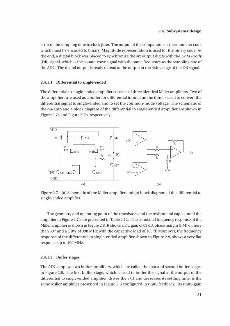
2.4. Subsystems’ design
error of the sampling time to clock jitter. The output of the comparators is thermometer code
which must be encoded to binary. Magnitude representation is used for the binary code. At
the end, a digital block was placed to synchronize the six output digits with the Data Ready
(DR) signal, which is the square-wave signal with the same frequency as the sampling rate of
the ADC. The digital output is ready to read at the output at the rising edge of the DR signal.
2.4.1.1 Differential to single-ended
The differential to single-ended amplifier consists of three identical Miller amplifiers. Two of
the amplifiers are used as a buffer for differential input, and the third is used to convert the
differential signal to single-ended and to set the common-mode voltage. The schematic of
the op-amp and a block diagram of the differential to single-ended amplifier are shown in
Figure 2.7a and Figure 2.7b, respectively.
Vin
Vo
Vip
M1 M2 M3
M4a M4b
M5 M6a M6b
VDD
GND
M7
Vtune
Rf Cc
(a)
viP
viNR
R
R
R
vcm
Vo
(b)
Figure 2.7 – (a) Schematic of the Miller amplifier and (b) block diagram of the differential tosingle-ended amplifier.
The geometry and operating point of the transistors and the resistor and capacitor of the
amplifier in Figure 2.7a are presented in Table 2.12. The simulated frequency response of the
Miller amplifier is shown in Figure 2.8. It shows a DC gain of 63 dB, phase margin (PM) of more
than 69 ° and a GBW of 398 MHz with the capacitive load of 103 fF. Moreover, the frequency
response of the differential to single-ended amplifier shown in Figure 2.9, shows a very flat
response up to 100 MHz.
2.4.1.2 Buffer stages
The ADC employs two buffer amplifiers, which are called the first and second buffer stages
in Figure 2.6. The first buffer stage, which is used to buffer the signal at the output of the
differential to single-ended amplifier, drives the S/H and decreases its settling time, is the
same Miller amplifier presented in Figure 2.8 configured in unity feedback. Its unity-gain
51
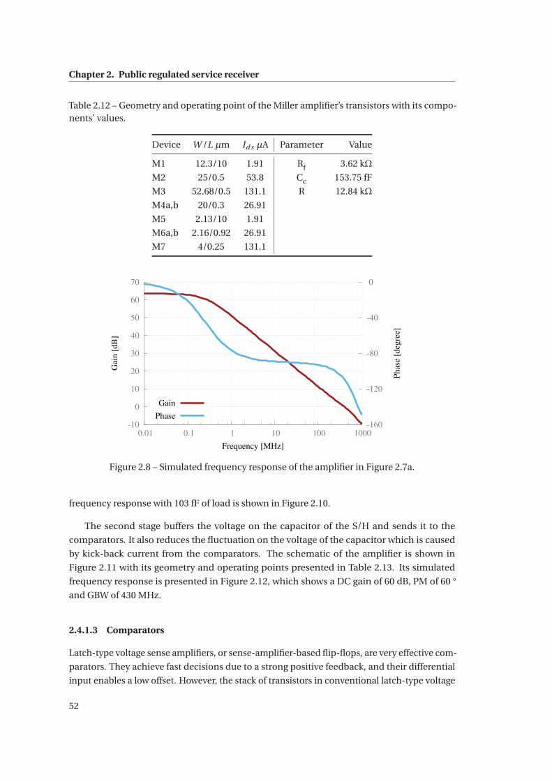
Chapter 2. Public regulated service receiver
Table 2.12 – Geometry and operating point of the Miller amplifier’s transistors with its compo-nents’ values.
Device W /L μm Id s μA Parameter Value
M1 12.3/10 1.91 Rf 3.62 kΩ
M2 25/0.5 53.8 Cc 153.75 fF
M3 52.68/0.5 131.1 R 12.84 kΩ
M4a,b 20/0.3 26.91
M5 2.13/10 1.91
M6a,b 2.16/0.92 26.91
M7 4/0.25 131.1
-10
0
10
20
30
40
50
60
70
0.01 0.1 1 10 100 1000-160
-120
-80
-40
0
Gai
n [
dB
]
Phas
e [d
egre
e]
Frequency [MHz]
Gain
Phase
Figure 2.8 – Simulated frequency response of the amplifier in Figure 2.7a.
frequency response with 103 fF of load is shown in Figure 2.10.
The second stage buffers the voltage on the capacitor of the S/H and sends it to the
comparators. It also reduces the fluctuation on the voltage of the capacitor which is caused
by kick-back current from the comparators. The schematic of the amplifier is shown in
Figure 2.11 with its geometry and operating points presented in Table 2.13. Its simulated
frequency response is presented in Figure 2.12, which shows a DC gain of 60 dB, PM of 60 °
and GBW of 430 MHz.
2.4.1.3 Comparators
Latch-type voltage sense amplifiers, or sense-amplifier-based flip-flops, are very effective com-
parators. They achieve fast decisions due to a strong positive feedback, and their differential
input enables a low offset. However, the stack of transistors in conventional latch-type voltage
52
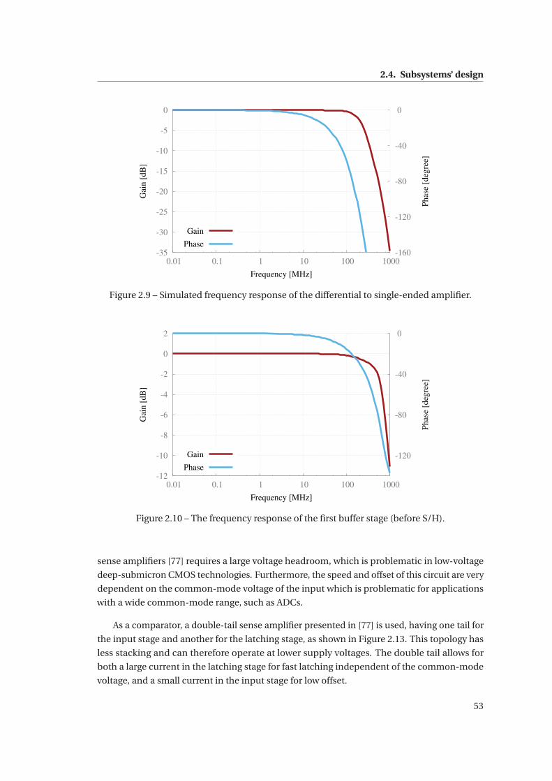
2.4. Subsystems’ design
-35
-30
-25
-20
-15
-10
-5
0
0.01 0.1 1 10 100 1000-160
-120
-80
-40
0
Gai
n [
dB
]
Phas
e [d
egre
e]
Frequency [MHz]
Gain
Phase
Figure 2.9 – Simulated frequency response of the differential to single-ended amplifier.
-12
-10
-8
-6
-4
-2
0
2
0.01 0.1 1 10 100 1000
-120
-80
-40
0
Gai
n [
dB
]
Phas
e [d
egre
e]
Frequency [MHz]
Gain
Phase
Figure 2.10 – The frequency response of the first buffer stage (before S/H).
sense amplifiers [77] requires a large voltage headroom, which is problematic in low-voltage
deep-submicron CMOS technologies. Furthermore, the speed and offset of this circuit are very
dependent on the common-mode voltage of the input which is problematic for applications
with a wide common-mode range, such as ADCs.
As a comparator, a double-tail sense amplifier presented in [77] is used, having one tail for
the input stage and another for the latching stage, as shown in Figure 2.13. This topology has
less stacking and can therefore operate at lower supply voltages. The double tail allows for
both a large current in the latching stage for fast latching independent of the common-mode
voltage, and a small current in the input stage for low offset.
53
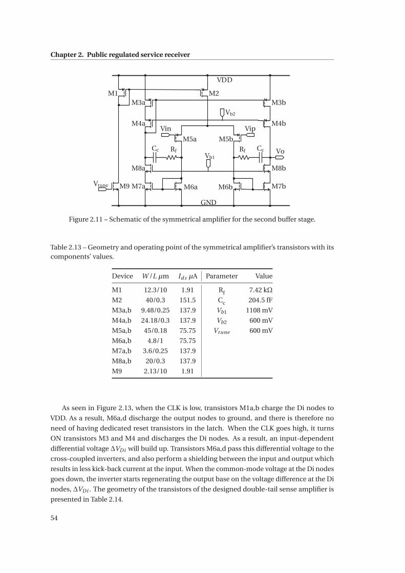
Chapter 2. Public regulated service receiver
Vin
Vo
Vip
M1 M2
M5a M5b
M9 M6a M6b
VDD
GND
Vtune
Rf CcRfCc
M3a M3b
M4a M4b
M8a M8b
M7a M7b
Vb1
Vb2
Figure 2.11 – Schematic of the symmetrical amplifier for the second buffer stage.
Table 2.13 – Geometry and operating point of the symmetrical amplifier’s transistors with itscomponents’ values.
Device W /L μm Id s μA Parameter Value
M1 12.3/10 1.91 Rf 7.42 kΩ
M2 40/0.3 151.5 Cc 204.5 fF
M3a,b 9.48/0.25 137.9 Vb1 1108 mV
M4a,b 24.18/0.3 137.9 Vb2 600 mV
M5a,b 45/0.18 75.75 Vtune 600 mV
M6a,b 4.8/1 75.75
M7a,b 3.6/0.25 137.9
M8a,b 20/0.3 137.9
M9 2.13/10 1.91
As seen in Figure 2.13, when the CLK is low, transistors M1a,b charge the Di nodes to
VDD. As a result, M6a,d discharge the output nodes to ground, and there is therefore no
need of having dedicated reset transistors in the latch. When the CLK goes high, it turns
ON transistors M3 and M4 and discharges the Di nodes. As a result, an input-dependent
differential voltage ΔVDi will build up. Transistors M6a,d pass this differential voltage to the
cross-coupled inverters, and also perform a shielding between the input and output which
results in less kick-back current at the input. When the common-mode voltage at the Di nodes
goes down, the inverter starts regenerating the output base on the voltage difference at the Di
nodes, ΔVDi . The geometry of the transistors of the designed double-tail sense amplifier is
presented in Table 2.14.
54
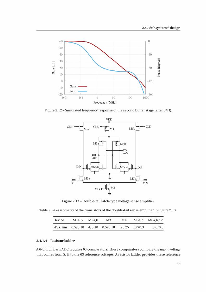
2.4. Subsystems’ design
-20
-10
0
10
20
30
40
50
60
0.01 0.1 1 10 100 1000-160
-120
-80
-40
0
Gai
n [
dB
]
Phas
e [d
egre
e]
Frequency [MHz]
Gain
Phase
Figure 2.12 – Simulated frequency response of the second buffer stage (after S/H).
M1a M1b
M2a M2b
M3
M4
M5a M5b
M6a,b M6c,d
VoN
VoP
ViP ViN
CLK____
CLK CLK
CLK
VDD
DiN DiP
Figure 2.13 – Double-tail latch-type voltage sense amplifier.
Table 2.14 – Geometry of the transistors of the double-tail sense amplifier in Figure 2.13 .
Device M1a,b M2a,b M3 M4 M5a,b M6a,b,c,d
W /L μm 0.5/0.18 4/0.18 0.5/0.18 1/0.25 1.2/0.3 0.6/0.3
2.4.1.4 Resistor ladder
A 6-bit full flash ADC requires 63 comparators. These comparators compare the input voltage
that comes from S/H to the 63 reference voltages. A resistor ladder provides these reference
55
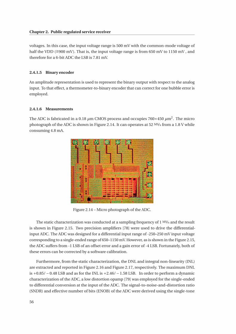
Chapter 2. Public regulated service receiver
voltages. In this case, the input voltage range is 500 mV with the common-mode voltage of
half the VDD (∼=900 mV). That is, the input voltage range is from 650 mV to 1150 mV , and
therefore for a 6-bit ADC the LSB is 7.81 mV.
2.4.1.5 Binary encoder
An amplitude representation is used to represent the binary output with respect to the analog
input. To that effect, a thermometer-to-binary encoder that can correct for one bubble error is
employed.
2.4.1.6 Measurements
The ADC is fabricated in a 0.18 μm CMOS process and occupies 760×450 μm2. The micro
photograph of the ADC is shown in Figure 2.14. It can operates at 52 MS/s from a 1.8 V while
consuming 4.8 mA.
Figure 2.14 – Micro photograph of the ADC.
The static characterization was conducted at a sampling frequency of 1 MS/s and the result
is shown in Figure 2.15. Two precision amplifiers [78] were used to drive the differential-
input ADC. The ADC was designed for a differential input range of -250–250 mV input voltage
corresponding to a single-ended range of 650–1150 mV. However, as is shown in the Figure 2.15,
the ADC suffers from -1 LSB of an offset error and a gain error of -4 LSB. Fortunately, both of
these errors can be corrected by a software calibration.
Furthermore, from the static characterization, the DNL and integral non-linearity (INL)
are extracted and reported in Figure 2.16 and Figure 2.17, respectively. The maximum DNL
is +0.85/−0.48 LSB and as for the INL is +2.46/−1.58 LSB. In order to perform a dynamic
characterization of the ADC, a low distortion opamp [79] was employed for the single-ended
to differential conversion at the input of the ADC. The signal-to-noise-and-distortion ratio
(SNDR) and effective number of bits (ENOB) of the ADC were derived using the single-tone
56
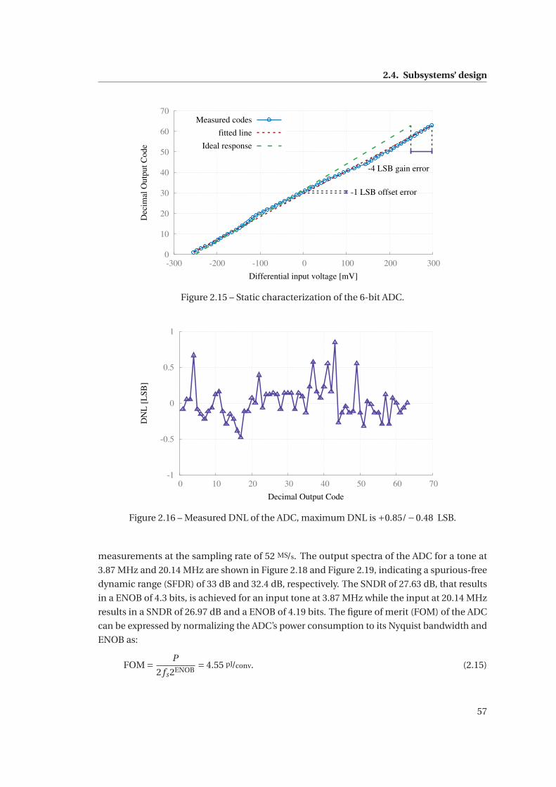
2.4. Subsystems’ design
0
10
20
30
40
50
60
70
-300 -200 -100 0 100 200 300
-1 LSB offset error
-4 LSB gain error
Dec
imal
Outp
ut
Code
Differential input voltage [mV]
Measured codes
fitted line
Ideal response
Figure 2.15 – Static characterization of the 6-bit ADC.
-1
-0.5
0
0.5
1
0 10 20 30 40 50 60 70
DN
L [
LS
B]
Decimal Output Code
Figure 2.16 – Measured DNL of the ADC, maximum DNL is +0.85/−0.48 LSB.
measurements at the sampling rate of 52 MS/s. The output spectra of the ADC for a tone at
3.87 MHz and 20.14 MHz are shown in Figure 2.18 and Figure 2.19, indicating a spurious-free
dynamic range (SFDR) of 33 dB and 32.4 dB, respectively. The SNDR of 27.63 dB, that results
in a ENOB of 4.3 bits, is achieved for an input tone at 3.87 MHz while the input at 20.14 MHz
results in a SNDR of 26.97 dB and a ENOB of 4.19 bits. The figure of merit (FOM) of the ADC
can be expressed by normalizing the ADC’s power consumption to its Nyquist bandwidth and
ENOB as:
FOM = P
2 fs2ENOB= 4.55 pJ/conv. (2.15)
57
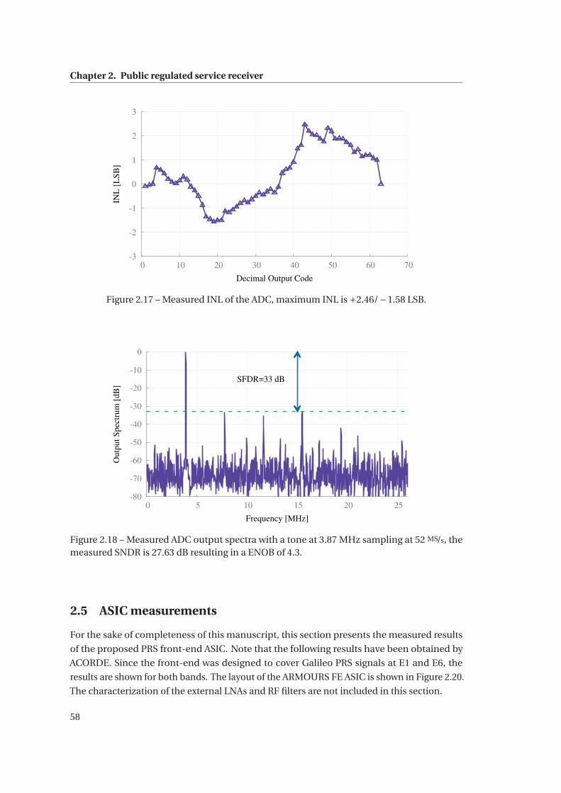
Chapter 2. Public regulated service receiver
-3
-2
-1
0
1
2
3
0 10 20 30 40 50 60 70
INL
[L
SB
]
Decimal Output Code
Figure 2.17 – Measured INL of the ADC, maximum INL is +2.46/−1.58 LSB.
-80
-70
-60
-50
-40
-30
-20
-10
0
0 5 10 15 20 25
SFDR=33 dB
Outp
ut
Spec
trum
[dB
]
Frequency [MHz]
Figure 2.18 – Measured ADC output spectra with a tone at 3.87 MHz sampling at 52 MS/s, themeasured SNDR is 27.63 dB resulting in a ENOB of 4.3.
2.5 ASIC measurements
For the sake of completeness of this manuscript, this section presents the measured results
of the proposed PRS front-end ASIC. Note that the following results have been obtained by
ACORDE. Since the front-end was designed to cover Galileo PRS signals at E1 and E6, the
results are shown for both bands. The layout of the ARMOURS FE ASIC is shown in Figure 2.20.
The characterization of the external LNAs and RF filters are not included in this section.
58
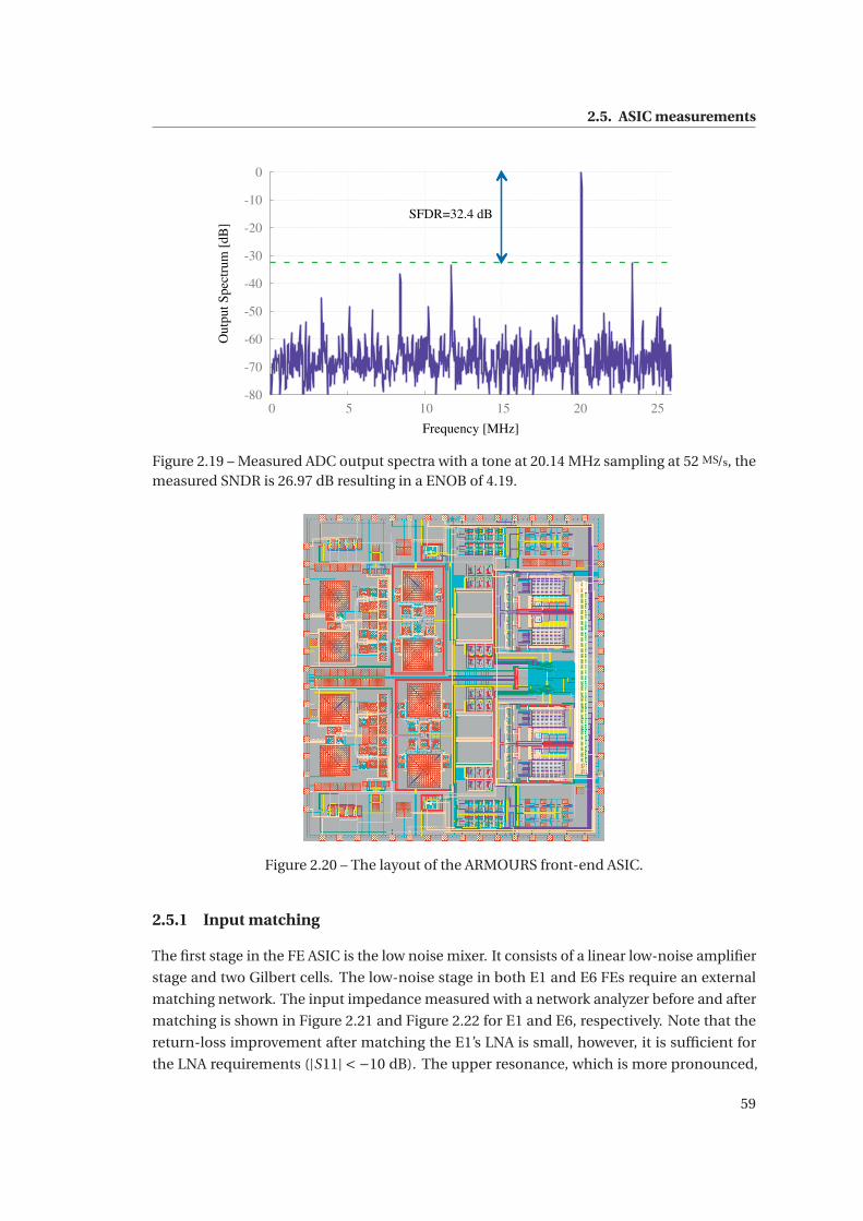
2.5. ASIC measurements
-80
-70
-60
-50
-40
-30
-20
-10
0
0 5 10 15 20 25
SFDR=32.4 dBO
utp
ut
Spec
trum
[dB
]
Frequency [MHz]
Figure 2.19 – Measured ADC output spectra with a tone at 20.14 MHz sampling at 52 MS/s, themeasured SNDR is 26.97 dB resulting in a ENOB of 4.19.
Figure 2.20 – The layout of the ARMOURS front-end ASIC.
2.5.1 Input matching
The first stage in the FE ASIC is the low noise mixer. It consists of a linear low-noise amplifier
stage and two Gilbert cells. The low-noise stage in both E1 and E6 FEs require an external
matching network. The input impedance measured with a network analyzer before and after
matching is shown in Figure 2.21 and Figure 2.22 for E1 and E6, respectively. Note that the
return-loss improvement after matching the E1’s LNA is small, however, it is sufficient for
the LNA requirements (|S11| < −10 dB). The upper resonance, which is more pronounced,
59
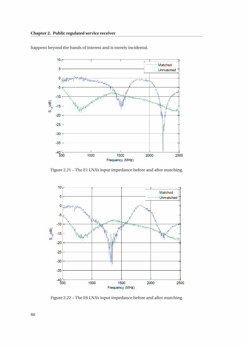
Chapter 2. Public regulated service receiver
happens beyond the bands of interest and is merely incidental.
Figure 2.21 – The E1 LNA’s input impedance before and after matching.
Figure 2.22 – The E6 LNA’s input impedance before and after matching.
60
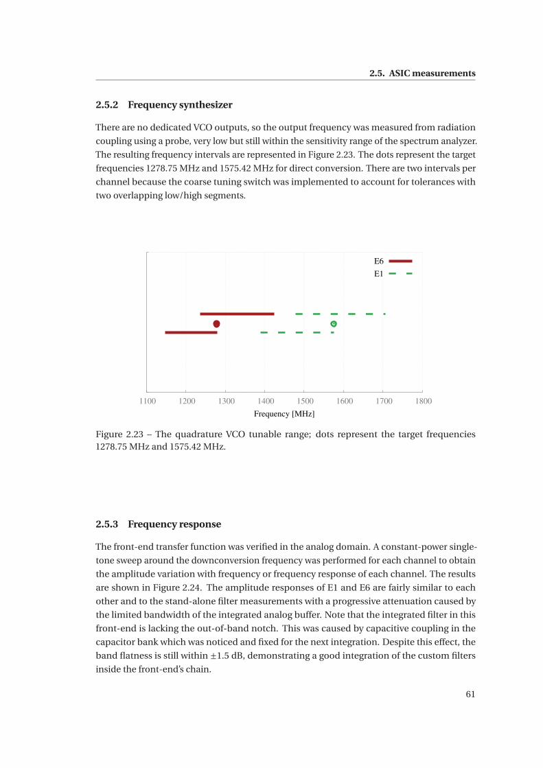
2.5. ASIC measurements
2.5.2 Frequency synthesizer
There are no dedicated VCO outputs, so the output frequency was measured from radiation
coupling using a probe, very low but still within the sensitivity range of the spectrum analyzer.
The resulting frequency intervals are represented in Figure 2.23. The dots represent the target
frequencies 1278.75 MHz and 1575.42 MHz for direct conversion. There are two intervals per
channel because the coarse tuning switch was implemented to account for tolerances with
two overlapping low/high segments.
1100 1200 1300 1400 1500 1600 1700 1800
Frequency [MHz]
E6
E1
Figure 2.23 – The quadrature VCO tunable range; dots represent the target frequencies1278.75 MHz and 1575.42 MHz.
2.5.3 Frequency response
The front-end transfer function was verified in the analog domain. A constant-power single-
tone sweep around the downconversion frequency was performed for each channel to obtain
the amplitude variation with frequency or frequency response of each channel. The results
are shown in Figure 2.24. The amplitude responses of E1 and E6 are fairly similar to each
other and to the stand-alone filter measurements with a progressive attenuation caused by
the limited bandwidth of the integrated analog buffer. Note that the integrated filter in this
front-end is lacking the out-of-band notch. This was caused by capacitive coupling in the
capacitor bank which was noticed and fixed for the next integration. Despite this effect, the
band flatness is still within ±1.5 dB, demonstrating a good integration of the custom filters
inside the front-end’s chain.
61
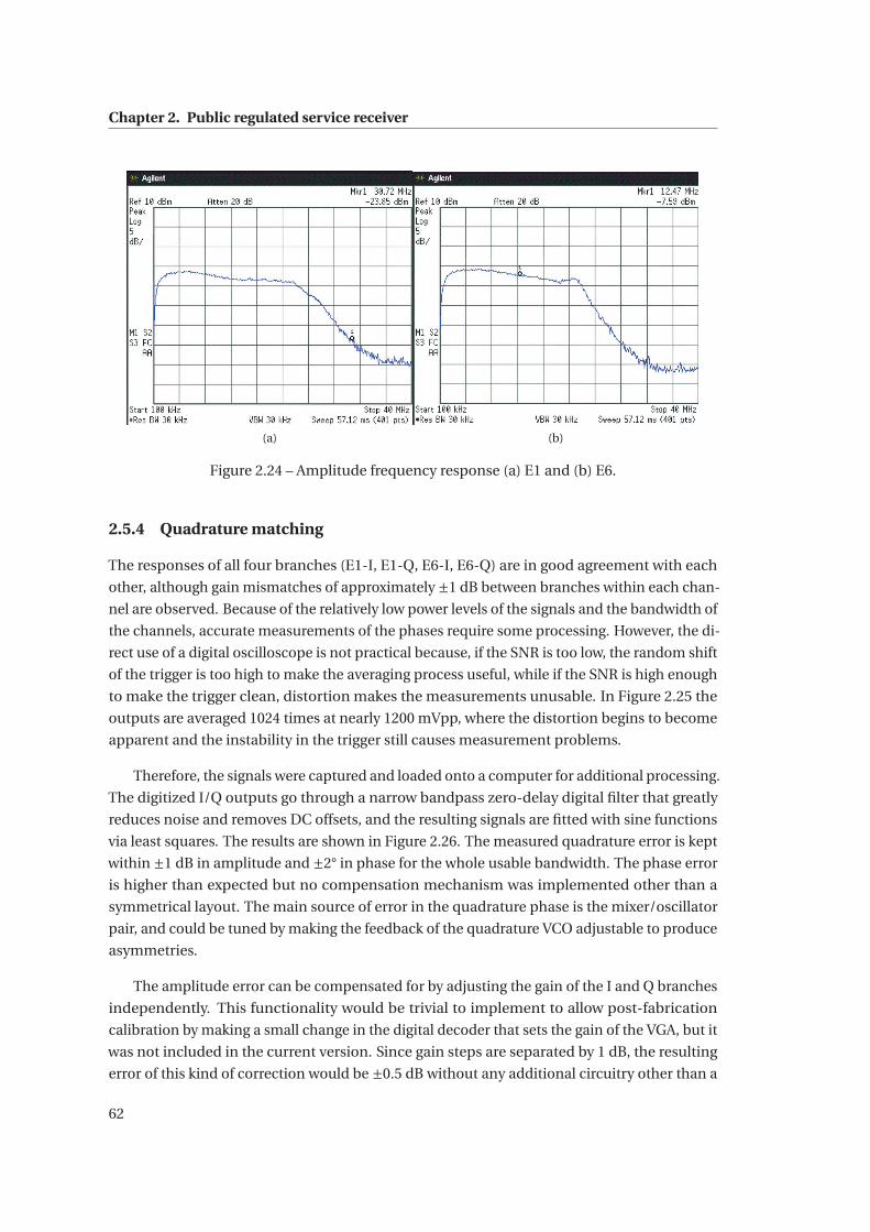
Chapter 2. Public regulated service receiver
(a) (b)
Figure 2.24 – Amplitude frequency response (a) E1 and (b) E6.
2.5.4 Quadrature matching
The responses of all four branches (E1-I, E1-Q, E6-I, E6-Q) are in good agreement with each
other, although gain mismatches of approximately ±1 dB between branches within each chan-
nel are observed. Because of the relatively low power levels of the signals and the bandwidth of
the channels, accurate measurements of the phases require some processing. However, the di-
rect use of a digital oscilloscope is not practical because, if the SNR is too low, the random shift
of the trigger is too high to make the averaging process useful, while if the SNR is high enough
to make the trigger clean, distortion makes the measurements unusable. In Figure 2.25 the
outputs are averaged 1024 times at nearly 1200 mVpp, where the distortion begins to become
apparent and the instability in the trigger still causes measurement problems.
Therefore, the signals were captured and loaded onto a computer for additional processing.
The digitized I/Q outputs go through a narrow bandpass zero-delay digital filter that greatly
reduces noise and removes DC offsets, and the resulting signals are fitted with sine functions
via least squares. The results are shown in Figure 2.26. The measured quadrature error is kept
within ±1 dB in amplitude and ±2° in phase for the whole usable bandwidth. The phase error
is higher than expected but no compensation mechanism was implemented other than a
symmetrical layout. The main source of error in the quadrature phase is the mixer/oscillator
pair, and could be tuned by making the feedback of the quadrature VCO adjustable to produce
asymmetries.
The amplitude error can be compensated for by adjusting the gain of the I and Q branches
independently. This functionality would be trivial to implement to allow post-fabrication
calibration by making a small change in the digital decoder that sets the gain of the VGA, but it
was not included in the current version. Since gain steps are separated by 1 dB, the resulting
error of this kind of correction would be ±0.5 dB without any additional circuitry other than a
62
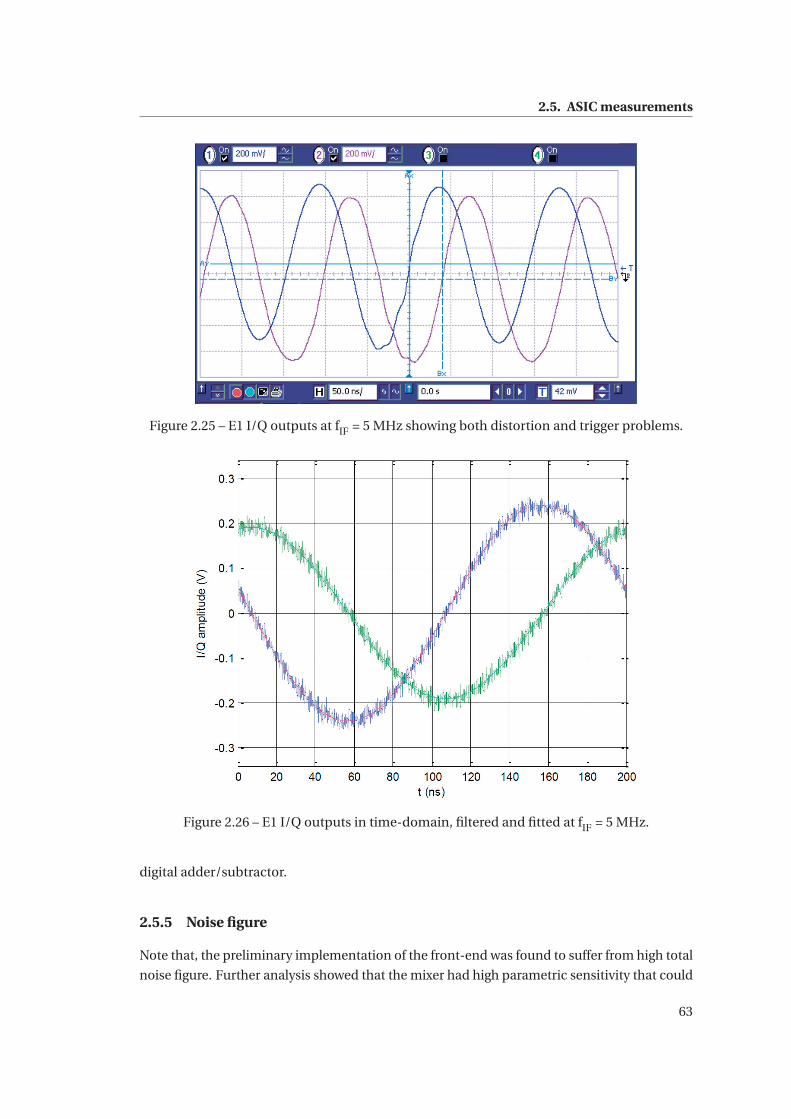
2.5. ASIC measurements
Figure 2.25 – E1 I/Q outputs at fIF = 5 MHz showing both distortion and trigger problems.
Figure 2.26 – E1 I/Q outputs in time-domain, filtered and fitted at fIF = 5 MHz.
digital adder/subtractor.
2.5.5 Noise figure
Note that, the preliminary implementation of the front-end was found to suffer from high total
noise figure. Further analysis showed that the mixer had high parametric sensitivity that could
63
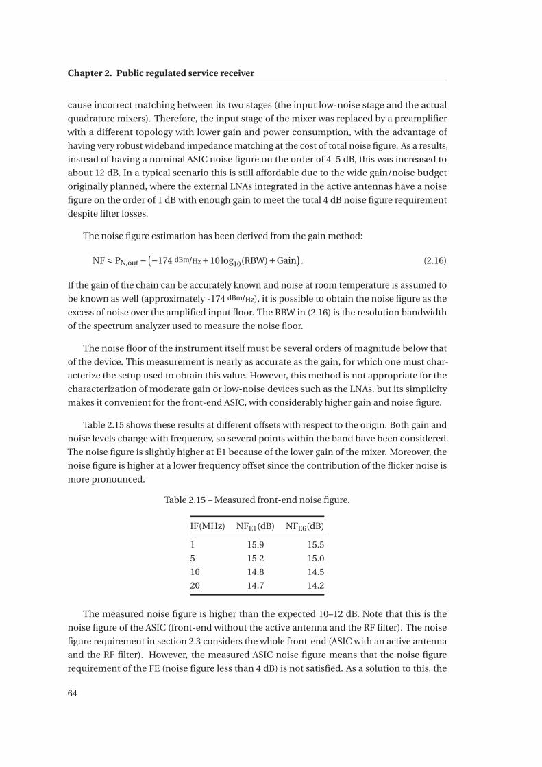
Chapter 2. Public regulated service receiver
cause incorrect matching between its two stages (the input low-noise stage and the actual
quadrature mixers). Therefore, the input stage of the mixer was replaced by a preamplifier
with a different topology with lower gain and power consumption, with the advantage of
having very robust wideband impedance matching at the cost of total noise figure. As a results,
instead of having a nominal ASIC noise figure on the order of 4–5 dB, this was increased to
about 12 dB. In a typical scenario this is still affordable due to the wide gain/noise budget
originally planned, where the external LNAs integrated in the active antennas have a noise
figure on the order of 1 dB with enough gain to meet the total 4 dB noise figure requirement
despite filter losses.
The noise figure estimation has been derived from the gain method:
NF ≈ PN,out −(−174 dBm/Hz+10log10(RBW)+Gain
). (2.16)
If the gain of the chain can be accurately known and noise at room temperature is assumed to
be known as well (approximately -174 dBm/Hz), it is possible to obtain the noise figure as the
excess of noise over the amplified input floor. The RBW in (2.16) is the resolution bandwidth
of the spectrum analyzer used to measure the noise floor.
The noise floor of the instrument itself must be several orders of magnitude below that
of the device. This measurement is nearly as accurate as the gain, for which one must char-
acterize the setup used to obtain this value. However, this method is not appropriate for the
characterization of moderate gain or low-noise devices such as the LNAs, but its simplicity
makes it convenient for the front-end ASIC, with considerably higher gain and noise figure.
Table 2.15 shows these results at different offsets with respect to the origin. Both gain and
noise levels change with frequency, so several points within the band have been considered.
The noise figure is slightly higher at E1 because of the lower gain of the mixer. Moreover, the
noise figure is higher at a lower frequency offset since the contribution of the flicker noise is
more pronounced.
Table 2.15 – Measured front-end noise figure.
IF(MHz) NFE1(dB) NFE6(dB)
1 15.9 15.5
5 15.2 15.0
10 14.8 14.5
20 14.7 14.2
The measured noise figure is higher than the expected 10–12 dB. Note that this is the
noise figure of the ASIC (front-end without the active antenna and the RF filter). The noise
figure requirement in section 2.3 considers the whole front-end (ASIC with an active antenna
and the RF filter). However, the measured ASIC noise figure means that the noise figure
requirement of the FE (noise figure less than 4 dB) is not satisfied. As a solution to this, the
64
2.6. Conclusions
external LNA designed for the active antennas can also be integrated with the front-end core in
the same package. The gain of the LNAs is adjustable (and to some extent parallel to the noise
figure performance), so this setup would result in an effective front-end with the intended
performance and essentially identical form factor, at the cost of power and efficiency.
2.5.6 Power consumption
The power consumption of the front-end ASIC was measured. The total current for nominal
settings was 48 mA for the analog sections and 23 mA for the digital ones, which resulted in a
total power of 162 mW. This is above the target of 100 mW in section 2.3.1, noting this version
includes additional analog buffers, filters and other support circuitry for testing. Although it is
not possible to measure the power of these devices separately, as they share internal supply
lines, conservative estimations based on simulations of the additional sub-circuits lower this
figure to about 115 mW.
2.6 Conclusions
A fully integrated reconfigurable dual-band GNSS receiver is implemented in 0.18 μm CMOS,
which can accommodate simultaneous reception of both E1 and E6 PRS signals. As for the
nature of the PRS, the front-end capable of receiving PRS signals needs to fulfill a series of
stringent requirements. These requirements were discussed in details as far as any classified
information was not involved. Some design efforts for high linearity and big dynamic range
have been made to improve the receiver robustness against interferences by utilizing highly
linear IF filter and high resolution ADC.
The receiver consumes 115 mW while achieving an average NF of 15.15/14.8 dB at E1
and E6, receptively. It offers an image rejection ratio (IMRR) of 18.7 dB, maximum voltage
gain of 65 dB and a gain dynamic range of 30 dB. The active die area for the whole receiver is
11.5 mm2.
The reception of E1 and E6 PRS signals not only improves the robustness of the receiver
against jamming, i.e. if strong jamming or spoofing is detected in one band the receiver could
be capable of switching off the band and using the other one, but also allows the receiver to
account for the ionosphere propagation and minimizes its error. Therefore, it acts in favor of
better GNSS navigation accuracy and availability.
At the time of writing this thesis, there is no publicly available chip addressing a multi-
band PRS GNSS receiver to enable us to compare the performances of this receiver with its
counterparts. However, the measurement results are summarized in Table 2.16.
65
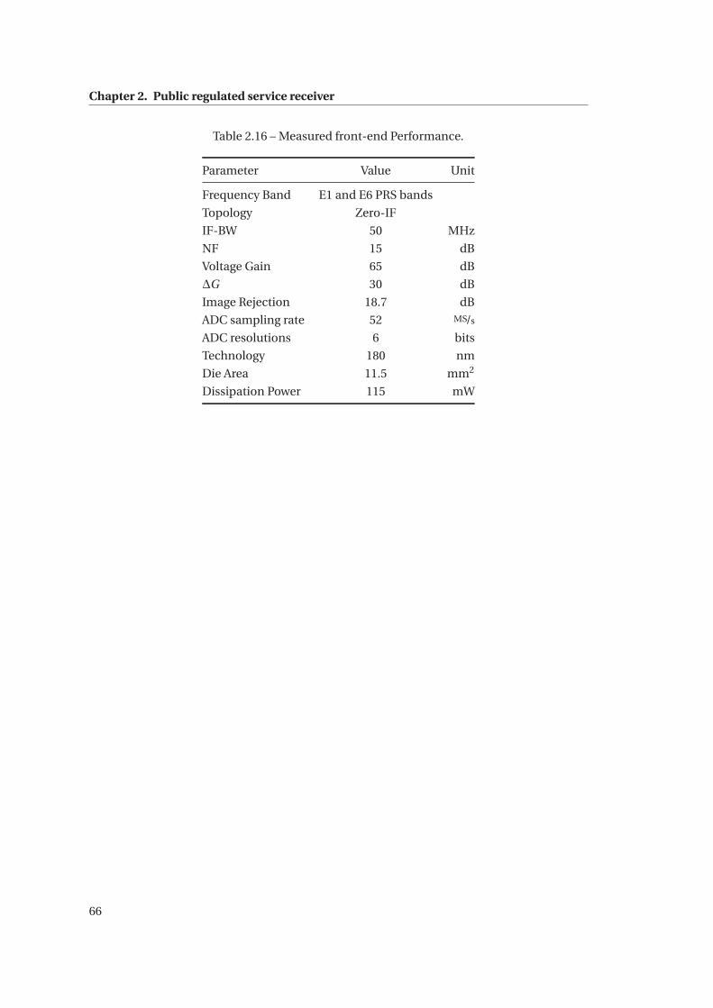
Chapter 2. Public regulated service receiver
Table 2.16 – Measured front-end Performance.
Parameter Value Unit
Frequency Band E1 and E6 PRS bands
Topology Zero-IF
IF-BW 50 MHz
NF 15 dB
Voltage Gain 65 dB
ΔG 30 dB
Image Rejection 18.7 dB
ADC sampling rate 52 MS/s
ADC resolutions 6 bits
Technology 180 nm
Die Area 11.5 mm2
Dissipation Power 115 mW
66
3 Wide-tuning-range continuous-timeactive filter
Mobile wireless communication systems, such as the GNSS, Wi-Fi and LTE, are adopting
signals with tens of megahertz of bandwidth in order to improve their performance [2, 80–83].
At the same time, greater mobility requires longer battery life and multi-standard compatibility
to deal with different service coverages. All these requirements are nowadays achievable thanks
to software-defined radios, which rely on flexible hardware architectures, such as direct-
conversion radio frequency front-end, as well as on low-power technologies such as CMOS.
Continuous-time active low-pass filters in CMOS technology are a key building block in direct-
conversion IC front-ends. In a design re-use approach, a reconfigurable continuous-time
low-pass filter that can satisfy requirements of the different standards is necessary. Moreover,
the coexistence of many systems (e.g., GNSS, Wi-Fi and LTE), on the same mobile equipment
is common nowadays and therefore interference rejection requirements are becoming more
and more stringent. This is directly reflected in the low-pass filter’s requirements in terms of
selectivity and linearity.
These filters can be realized by means of passive components such as resistors, capacitors
and inductors. However, passive inductors in CMOS technology are bulky and suffer from
a low Q. A well-known solution to this problem consists of adopting an active inductor
which occupies less chip area and provides a variable large inductance as well as a tunable Q.
Therefore, low-power high-Q active inductors are of interest in high-selective filter design.
Active inductors can be realized by transforming the impedance of a capacitor by means
of an active device [84]. To that effect gyrators provide the most direct way of realizing an
inductor and are commonly used in active filter design [85–88]. As a result, the Q of the active
inductors are directly related to the gyrators or more precisely to the OTAs within the gyrators.
Furthermore, system-on-chip integration demands that a fully differential configuration
be able to reject the CM disturbances generated by the digital circuitries, clock drivers, sub-
strate coupling and so on. On the other hand, CMFB amplifiers are an inevitable part of any
fully differential amplifier. Therefore, the CM stability of OTAs and gyrators must be consid-
ered during the design. Although the two OTAs in a gyrator configuration are in negative
67
Chapter 3. Wide-tuning-range continuous-time active filter
feedback for their differential signals, the loop still acts as a positive feedback for CM signals.
This positive feedback may cause CM oscillation or latching in a gyrator.
Therefore, in order to satisfy the selectivity requirement of the system, a comprehensive
analysis on the Q of the active inductor is necessary prior to the design of an active filter.
Moreover, in order to ensure the CM stability while optimizing the power of the active inductor,
a CM stability analysis is also required.
Towards this end, section 3.1 presents a design methodology for low-power high-Q OTA-
based resonators that takes advantage of the OTA’s second pole to enhance the resonator’s
Q with no extra power consumption. A comprehensive analysis that accounts for the CM
stability of the OTA-based gyrators is presented in section 3.2. Based on this analysis, a new
methodology that ensures the CM stability of OTA-based resonators is introduced. These
two methodologies are employed in the design of a highly selective 4 th-order Gm-C elliptic
low-pass filter in section 3.3. Finally, since the resonator’s Q plays a main role in the filter’s
selectivity in active filter design, section 3.4 demonstrates the effects of the Q-enhancement
method of section 3.1 on the selectivity of the filter of section 3.3.
3.1 Controlled-Q resonator
Active filters entail a minimum Q for their components, in particular for their active inductors,
to achieve a desired selectivity and frequency response. Towards this end, this section presents
a design methodology for a low-power high-Q OTA-based resonator in which the Q of the res-
onator is translated to the requirements of the OTA. The effects of the OTA’s imperfections on
the Q are investigated. The proposed methodology takes advantage of the OTA’s second pole
to enhance the resonator’s Q with no extra power consumption. A design chart is presented
that can be used to design an OTA fulfilling a given resonator’s Q. The design methodology
has been validated by realizing a resonator with 8 MHz resonance frequency and a Q of 10,
consuming 520 μA from 1.8 V, using UMC 0.18 μm CMOS technology.
3.1.1 Introduction
Gyrators usually consist of two identical OTAs that are joined in a negative feedback loop.
However, an OTA’s non-idealities such as its limited output impedance and internal poles
alter the Q as well as the frequency response of both the inductors and filters. Limited output
impedance results in a finite DC (low frequency) gain for an OTA, thereby limiting the maxi-
mum Q of the inductor or the resonator made from it [89]. Moreover, the internal poles of the
OTA produce a phase shift of the signal in the loop of the gyrator. This extra phase simulates a
negative resistance in parallel with the active inductor and enhances its Q. As the frequency of
the signal approaches these internal poles, the excess phase becomes larger and may result in
oscillations in the gyrator loop. To avoid these effects, a conventional design approach is to
place the internal poles of the OTA far beyond its unity-gain frequency. Although this reduces
68
3.1. Controlled-Q resonator
the excess phase caused by the internal poles at the OTA’s unity-gain frequency and therefore
limits their effects, it usually results in more power consumption for the OTA.
Some techniques have been proposed in the literature to compensate for this excess phase
and to cancel its effects. This is achieved in [90] by choosing the optimum input transistor
channel length to compensate for the excess phase at the center frequency of a band-pass
filter. Also a slave gyrator is used to compensate for the excess phase and boost the inductor’s
Q in [89], which results in higher power consumption.
However, the goal of this thesis is to take advantage of this excess phase to boost the Q of a
resonator to a desirable value with no extra power consumption. Based on this idea, a simple
design methodology for a controlled-Q resonator was presented in [91] and was validated by
simulations and measurements. In particular, a resonator with 8 MHz resonance frequency
and a Q of 10 was designed and fabricated, and it was shown that the enhanced Q can be
predicted with the proposed design chart. This section expands on this topic by examining
the effects of OTA’s internal poles on the resonator’s Q and deriving its theoretical equations.
Techniques to meet the resonator’s specification and measures to avoid oscillation in the
resonator are also described. The sensitivity of the resonator’s Q to the OTA’s second pole and
DC gain is analyzed.
This section is organized as follows. The Q of a resonator, as its main specification, is
translated to the requirements of the OTA. Moreover, the effects of the OTA’s finite output
resistance and internal poles are investigated in section 3.1.2. A step-by-step design method-
ology for a low-power high-Q resonator is proposed in section 3.1.3. A resonator with 8 MHz
resonance frequency and a Q of around 10 is fabricated using UMC 0.18 μm CMOS to validate
the proposed methodology. The key points and results of this section are summarized in
section 3.1.4.
3.1.2 From resonator specifications to OTA requirements
OTA-based resonators are commonly used in active filter design, thus their specifications are
imposed by the filter’s requirements. More precisely, the specifications of the filter translate to
the specifications of the OTA inside the resonator. Since the performance of the filter depends
on the most selective resonator of the filter, we will focus in this section on the specifications
of a resonator such as Q and resonance frequency ω0 and translate them to the specifications
of an OTA. An active inductor constructed from two identical OTAs and a capacitor cL is shown
in Figure 3.1 along with its equivalent circuit. Assuming that, in a narrow-band system, the
OTA has a constant transconductance of gm , a finite output resistance of ro = 1/go and an
input and output parasitic capacitance cp , the equivalent circuit’s parameters are
L = cL +cp
g 2m
, Rs = go
g 2m
, Rp = 1
go. (3.1)
69
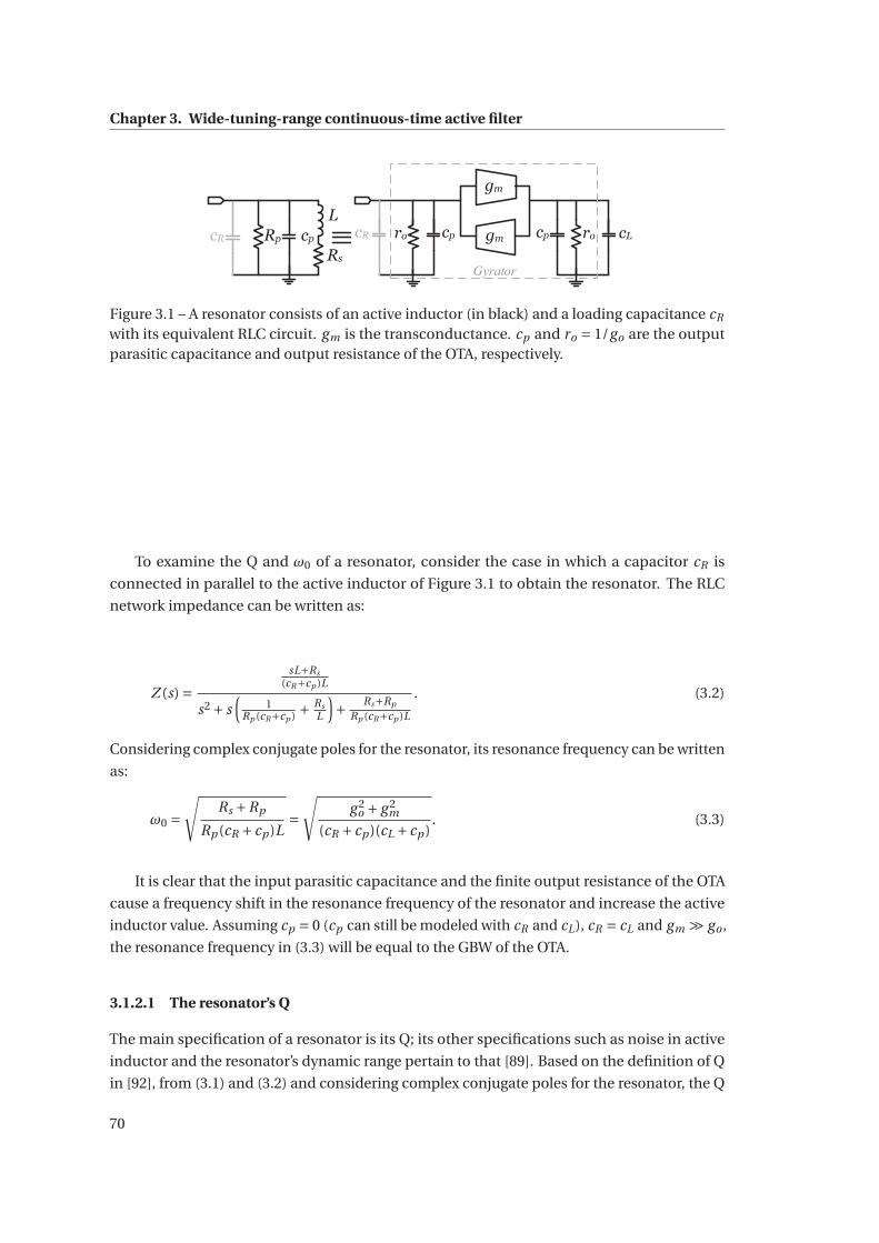
Chapter 3. Wide-tuning-range continuous-time active filter
cp ro cLro cpcR
gm
gmRp cpL
RscR
Gyrator
Figure 3.1 – A resonator consists of an active inductor (in black) and a loading capacitance cR
with its equivalent RLC circuit. gm is the transconductance. cp and ro = 1/go are the outputparasitic capacitance and output resistance of the OTA, respectively.
To examine the Q and ω0 of a resonator, consider the case in which a capacitor cR is
connected in parallel to the active inductor of Figure 3.1 to obtain the resonator. The RLC
network impedance can be written as:
Z (s) =sL+Rs
(cR+cp )L
s2 + s(
1Rp (cR+cp ) + Rs
L
)+ Rs+Rp
Rp (cR+cp )L
. (3.2)
Considering complex conjugate poles for the resonator, its resonance frequency can be written
as:
ω0 =√
Rs +Rp
Rp (cR +cp )L=
√g 2
o + g 2m
(cR +cp )(cL +cp ). (3.3)
It is clear that the input parasitic capacitance and the finite output resistance of the OTA
cause a frequency shift in the resonance frequency of the resonator and increase the active
inductor value. Assuming cp = 0 (cp can still be modeled with cR and cL), cR = cL and gm � go ,
the resonance frequency in (3.3) will be equal to the GBW of the OTA.
3.1.2.1 The resonator’s Q
The main specification of a resonator is its Q; its other specifications such as noise in active
inductor and the resonator’s dynamic range pertain to that [89]. Based on the definition of Q
in [92], from (3.1) and (3.2) and considering complex conjugate poles for the resonator, the Q
70
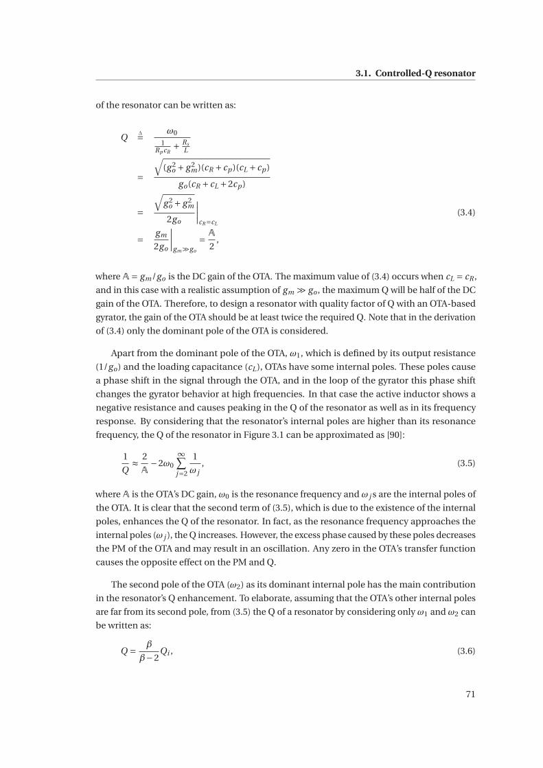
3.1. Controlled-Q resonator
of the resonator can be written as:
QΔ= ω0
1Rp cR
+ RsL
=√
(g 2o + g 2
m)(cR +cp )(cL +cp )
go(cR +cL +2cp )
=√
g 2o + g 2
m
2go
∣∣∣∣cR=cL
(3.4)
= gm
2go
∣∣∣∣gm�go
= A
2,
where A= gm/go is the DC gain of the OTA. The maximum value of (3.4) occurs when cL = cR ,
and in this case with a realistic assumption of gm � go , the maximum Q will be half of the DC
gain of the OTA. Therefore, to design a resonator with quality factor of Q with an OTA-based
gyrator, the gain of the OTA should be at least twice the required Q. Note that in the derivation
of (3.4) only the dominant pole of the OTA is considered.
Apart from the dominant pole of the OTA, ω1, which is defined by its output resistance
(1/go) and the loading capacitance (cL), OTAs have some internal poles. These poles cause
a phase shift in the signal through the OTA, and in the loop of the gyrator this phase shift
changes the gyrator behavior at high frequencies. In that case the active inductor shows a
negative resistance and causes peaking in the Q of the resonator as well as in its frequency
response. By considering that the resonator’s internal poles are higher than its resonance
frequency, the Q of the resonator in Figure 3.1 can be approximated as [90]:
1
Q≈ 2
A−2ω0
∞∑j=2
1
ω j, (3.5)
where A is the OTA’s DC gain, ω0 is the resonance frequency and ω j s are the internal poles of
the OTA. It is clear that the second term of (3.5), which is due to the existence of the internal
poles, enhances the Q of the resonator. In fact, as the resonance frequency approaches the
internal poles (ω j ), the Q increases. However, the excess phase caused by these poles decreases
the PM of the OTA and may result in an oscillation. Any zero in the OTA’s transfer function
causes the opposite effect on the PM and Q.
The second pole of the OTA (ω2) as its dominant internal pole has the main contribution
in the resonator’s Q enhancement. To elaborate, assuming that the OTA’s other internal poles
are far from its second pole, from (3.5) the Q of a resonator by considering only ω1 and ω2 can
be written as:
Q = β
β−2Qi , (3.6)
71
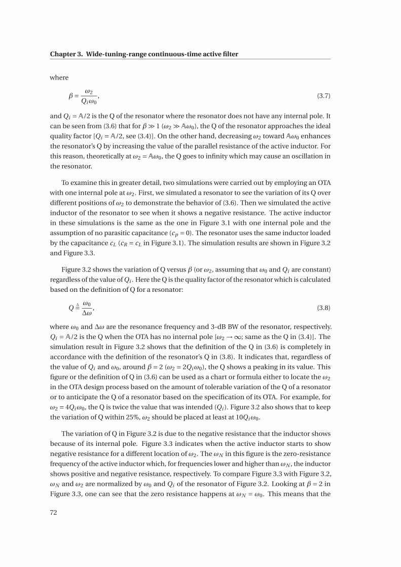
Chapter 3. Wide-tuning-range continuous-time active filter
where
β= ω2
Qiω0, (3.7)
and Qi =A/2 is the Q of the resonator where the resonator does not have any internal pole. It
can be seen from (3.6) that for β� 1 (ω2 �Aω0), the Q of the resonator approaches the ideal
quality factor [Qi =A/2, see (3.4)]. On the other hand, decreasing ω2 toward Aω0 enhances
the resonator’s Q by increasing the value of the parallel resistance of the active inductor. For
this reason, theoretically at ω2 =Aω0, the Q goes to infinity which may cause an oscillation in
the resonator.
To examine this in greater detail, two simulations were carried out by employing an OTA
with one internal pole at ω2. First, we simulated a resonator to see the variation of its Q over
different positions of ω2 to demonstrate the behavior of (3.6). Then we simulated the active
inductor of the resonator to see when it shows a negative resistance. The active inductor
in these simulations is the same as the one in Figure 3.1 with one internal pole and the
assumption of no parasitic capacitance (cp = 0). The resonator uses the same inductor loaded
by the capacitance cL (cR = cL in Figure 3.1). The simulation results are shown in Figure 3.2
and Figure 3.3.
Figure 3.2 shows the variation of Q versus β (or ω2, assuming that ω0 and Qi are constant)
regardless of the value of Qi . Here the Q is the quality factor of the resonator which is calculated
based on the definition of Q for a resonator:
QΔ= ω0
Δω, (3.8)
where ω0 and Δω are the resonance frequency and 3-dB BW of the resonator, respectively.
Qi =A/2 is the Q when the OTA has no internal pole [ω2 →∞; same as the Q in (3.4)]. The
simulation result in Figure 3.2 shows that the definition of the Q in (3.6) is completely in
accordance with the definition of the resonator’s Q in (3.8). It indicates that, regardless of
the value of Qi and ω0, around β= 2 (ω2 = 2Qiω0), the Q shows a peaking in its value. This
figure or the definition of Q in (3.6) can be used as a chart or formula either to locate the ω2
in the OTA design process based on the amount of tolerable variation of the Q of a resonator
or to anticipate the Q of a resonator based on the specification of its OTA. For example, for
ω2 = 4Qiω0, the Q is twice the value that was intended (Qi ). Figure 3.2 also shows that to keep
the variation of Q within 25%, ω2 should be placed at least at 10Qiω0.
The variation of Q in Figure 3.2 is due to the negative resistance that the inductor shows
because of its internal pole. Figure 3.3 indicates when the active inductor starts to show
negative resistance for a different location of ω2. The ωN in this figure is the zero-resistance
frequency of the active inductor which, for frequencies lower and higher than ωN , the inductor
shows positive and negative resistance, respectively. To compare Figure 3.3 with Figure 3.2,
ωN and ω2 are normalized by ω0 and Qi of the resonator of Figure 3.2. Looking at β = 2 in
Figure 3.3, one can see that the zero resistance happens at ωN = ω0. This means that the
72
3.1. Controlled-Q resonator
1
3
5
7
1 10 100
β
Q/Q
i
Figure 3.2 – Design chart of the variation of the resonator’s Q versus β=ω2/Qiω0 (see (3.7))while sweeping the second pole (ω2) of the OTA; Qi is the Q when the OTA does not have thesecond pole (i.e. ω2 →∞) and ω0 is the resonance frequency of the resonator.
inductor does not show any resistance and that is why the resonator shows a peaking of Q for
the same location of the internal pole.
0.1
1
10
0.1 1 4
β
Positive Res.
Negative Res.
ωN
/ω0
Figure 3.3 – The zero-resistance frequency (ωN ) of the active inductor versus β=ω2/Qiω0 (see(3.7)) while sweeping the second pole (ω2) of the OTA; ω0 is the resonance frequency of theresonator that is made by the active inductor loaded by capacitance cL , and Qi is the Q of theresonator when ω2 →∞.
3.1.2.2 Sensitivity of the resonator’s Q
As is shown in Figure 3.2, the resonator’s Q is a function of ω2 and A for a fixed resonance
frequency. Since the gain and the second pole of an OTA might change due to process, voltage
73
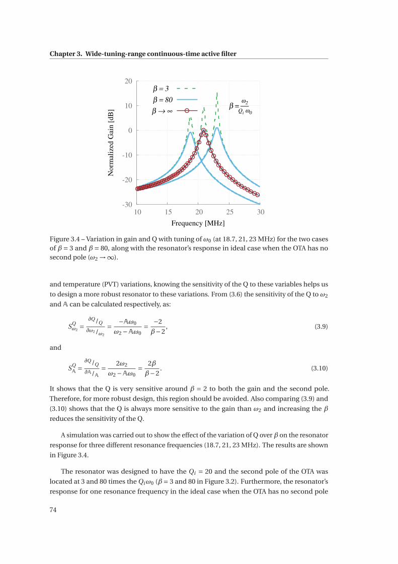
Chapter 3. Wide-tuning-range continuous-time active filter
-30
-20
-10
0
10
20
10 15 20 25 30
β = ⎯ω2
Qi ω0N
orm
aliz
ed G
ain
[d
B]
Frequency [MHz]
β = 3 β = 80β → ∞
Figure 3.4 – Variation in gain and Q with tuning of ω0 (at 18.7, 21, 23 MHz) for the two casesof β= 3 and β= 80, along with the resonator’s response in ideal case when the OTA has nosecond pole (ω2 →∞).
and temperature (PVT) variations, knowing the sensitivity of the Q to these variables helps us
to design a more robust resonator to these variations. From (3.6) the sensitivity of the Q to ω2
and A can be calculated respectively, as:
SQω2
=∂Q /Q
∂ω2 /ω2
= −Aω0
ω2 −Aω0= −2
β−2, (3.9)
and
SQA=
∂Q /Q
∂A/A= 2ω2
ω2 −Aω0= 2β
β−2. (3.10)
It shows that the Q is very sensitive around β = 2 to both the gain and the second pole.
Therefore, for more robust design, this region should be avoided. Also comparing (3.9) and
(3.10) shows that the Q is always more sensitive to the gain than ω2 and increasing the β
reduces the sensitivity of the Q.
A simulation was carried out to show the effect of the variation of Q over β on the resonator
response for three different resonance frequencies (18.7, 21, 23 MHz). The results are shown
in Figure 3.4.
The resonator was designed to have the Qi = 20 and the second pole of the OTA was
located at 3 and 80 times the Qiω0 (β= 3 and 80 in Figure 3.2). Furthermore, the resonator’s
response for one resonance frequency in the ideal case when the OTA has no second pole
74
3.1. Controlled-Q resonator
(ω2 →∞) is also shown in Figure 3.4. As was expected from Figure 3.2, the Q of the resonator
made by the OTA with its second pole at 80Qiω0 is coincident with the ideal case. In fact, in
this case, from (3.6) the variation of Q is less than 2.5% of the ideal case. However, there is
some peaking in the resonator response for the other case, which results in enhancing the Q.
Therefore, Figure 3.2 can be utilized to locate the second pole of the OTA in the design process
of the resonator based on the tolerable variation of the Q. However, since PVT variation effects
can cause a slight shift in ω2, a high ratio of Q/Qi , where the Q of a resonator is very sensitive
to ω2, should be avoided to have a predictable Q.
3.1.2.3 Stability
It has been shown that it is possible to take advantage of the OTA’s second pole to enhance the
Q of a resonator by placing it the right distance from ω0. This enhancement can be achieved
with no extra power consumption. However, as the ω2 approaches the ω0, the excess phase it
causes reduces the PM of the OTA. On the other hand, the OTA should have sufficient PM at
its unity-gain frequency to ensure its stability. The PM of the OTA, considering its dominant
and all internal poles, can be written as:
P M = 180◦ −∞∑
j=1tan−1
(ω0
ω j
). (3.11)
From (4.38) it can be deduced that for an OTA with no internal pole other than ω2, more than
68◦ of PM is achieved when
ω2 > 2.5ω0. (3.12)
Since the DC gain of the OTAs (A) is usually more than 2.5, to avoid possible oscillation and
peaking in resonator’s Q, the inequality in (3.12) can be written as:
ω2 >Aω0. (3.13)
Of course, as was shown before, due to the high sensitivity of the Q to ω2 around Aω0, this
region should be avoided for ω2. For OTAs with more than one internal pole, the inequality in
(3.13) is still valid to have less sensitive Q, however, the PM in (4.38) has to be considered for
the stability of the OTA.
3.1.3 Design methodology for a controlled-Q resonator
This section presents the design methodology for a resonator with a Q of 10 and a resonance
frequency at 8 MHz which was fabricated using UMC 0.18 μm CMOS technology. A photo-
graph of the test chip is shown in Figure 3.5.
The design procedure starts with choosing a value for the loading capacitance since all the
75
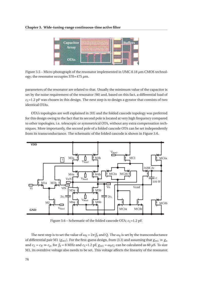
Chapter 3. Wide-tuning-range continuous-time active filter
CapacitorArray
OTAs
Buffers
Figure 3.5 – Micro photograph of the resonator implemented in UMC 0.18 μm CMOS technol-ogy; the resonator occupies 370×475 μm.
parameters of the resonator are related to that. Usually the minimum value of the capacitor is
set by the noise requirement of the resonator [90] and, based on this fact, a differential load of
cL=1.2 pF was chosen in this design. The next step is to design a gyrator that consists of two
identical OTAs.
OTA’s topologies are well explained in [93] and the folded cascode topology was preferred
for this design owing to the fact that its second pole is located at very high frequency compared
to other topologies, i.e. telescopic or symmetrical OTA, without any extra compensation tech-
niques. More importantly, the second pole of a folded cascode OTA can be set independently
from its transconductance. The schematic of the folded cascode is shown in Figure 3.6.
2cL
Vbias1
VDD
GND
M1a
M2
M3a1 MC1
MC2a
2xMC2c
MC3a
MC4b
MC4a
Vcmf
310 fF
2cL
c
Vbias2
Vbias3
Vbias4
Vbias2
ViNVi Vo
VoNM1b
M3b
M4a M4b
M5a M5b
M6a M6b
MC2b
MC3b
Figure 3.6 – Schematic of the folded cascode OTA; cL=1.2 pF.
The next step is to set the value of ω0 = 2π f0 and Q. The ω0 is set by the transconductance
of differential pair M1 (gm1). For the first-guess design, from (3.3) and assuming that gm1 � go
and cL = cR � cp , for f0 = 8 MHz and cL=1.2 pF, gm1 =ω0cL can be calculated as 60 μS. To size
M1, its overdrive voltage also needs to be set. This voltage affects the linearity of the resonator.
76
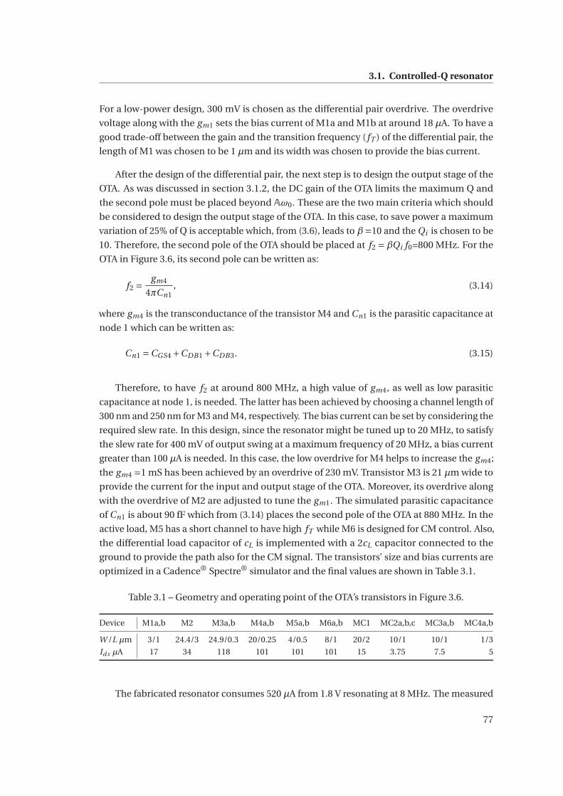
3.1. Controlled-Q resonator
For a low-power design, 300 mV is chosen as the differential pair overdrive. The overdrive
voltage along with the gm1 sets the bias current of M1a and M1b at around 18 μA. To have a
good trade-off between the gain and the transition frequency ( fT ) of the differential pair, the
length of M1 was chosen to be 1 μm and its width was chosen to provide the bias current.
After the design of the differential pair, the next step is to design the output stage of the
OTA. As was discussed in section 3.1.2, the DC gain of the OTA limits the maximum Q and
the second pole must be placed beyond Aω0. These are the two main criteria which should
be considered to design the output stage of the OTA. In this case, to save power a maximum
variation of 25% of Q is acceptable which, from (3.6), leads to β=10 and the Qi is chosen to be
10. Therefore, the second pole of the OTA should be placed at f2 =βQi f0=800 MHz. For the
OTA in Figure 3.6, its second pole can be written as:
f2 = gm4
4πCn1, (3.14)
where gm4 is the transconductance of the transistor M4 and Cn1 is the parasitic capacitance at
node 1 which can be written as:
Cn1 =CGS4 +CDB1 +CDB3. (3.15)
Therefore, to have f2 at around 800 MHz, a high value of gm4, as well as low parasitic
capacitance at node 1, is needed. The latter has been achieved by choosing a channel length of
300 nm and 250 nm for M3 and M4, respectively. The bias current can be set by considering the
required slew rate. In this design, since the resonator might be tuned up to 20 MHz, to satisfy
the slew rate for 400 mV of output swing at a maximum frequency of 20 MHz, a bias current
greater than 100 μA is needed. In this case, the low overdrive for M4 helps to increase the gm4;
the gm4 =1 mS has been achieved by an overdrive of 230 mV. Transistor M3 is 21 μm wide to
provide the current for the input and output stage of the OTA. Moreover, its overdrive along
with the overdrive of M2 are adjusted to tune the gm1. The simulated parasitic capacitance
of Cn1 is about 90 fF which from (3.14) places the second pole of the OTA at 880 MHz. In the
active load, M5 has a short channel to have high fT while M6 is designed for CM control. Also,
the differential load capacitor of cL is implemented with a 2cL capacitor connected to the
ground to provide the path also for the CM signal. The transistors’ size and bias currents are
optimized in a Cadence® Spectre® simulator and the final values are shown in Table 3.1.
Table 3.1 – Geometry and operating point of the OTA’s transistors in Figure 3.6.
Device M1a,b M2 M3a,b M4a,b M5a,b M6a,b MC1 MC2a,b,c MC3a,b MC4a,b
W /L μm 3/1 24.4/3 24.9/0.3 20/0.25 4/0.5 8/1 20/2 10/1 10/1 1/3
Id s μA 17 34 118 101 101 101 15 3.75 7.5 5
The fabricated resonator consumes 520 μA from 1.8 V resonating at 8 MHz. The measured
77
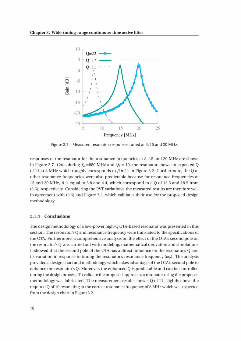
Chapter 3. Wide-tuning-range continuous-time active filter
-25
-20
-15
-10
-5
0
5
10
5 10 15 20 25
Gai
n [
dB
]
Frequency [MHz]
Q=22
Q=17
Q=11
Figure 3.7 – Measured resonator responses tuned at 8, 15 and 20 MHz.
responses of the resonator for the resonance frequencies at 8, 15 and 20 MHz are shown
in Figure 3.7. Considering f2 =880 MHz and Qi = 10, the resonator shows an expected Q
of 11 at 8 MHz which roughly corresponds to β = 11 in Figure 3.2. Furthermore, the Q at
other resonance frequencies were also predictable because for resonance frequencies at
15 and 20 MHz, β is equal to 5.8 and 4.4, which correspond to a Q of 15.5 and 18.5 from
(3.6), respectively. Considering the PVT variations, the measured results are therefore well
in agreement with (3.6) and Figure 3.2, which validates their use for the proposed design
methodology.
3.1.4 Conclusions
The design methodology of a low-power high-Q OTA-based resonator was presented in this
section. The resonator’s Q and resonance frequency were translated to the specifications of
the OTA. Furthermore, a comprehensive analysis on the effect of the OTA’s second pole on
the resonator’s Q was carried out with modeling, mathematical derivation and simulations.
It showed that the second pole of the OTA has a direct influence on the resonator’s Q and
its variation in response to tuning the resonator’s resonance frequency (ω0). The analysis
provided a design chart and methodology which takes advantage of the OTA’s second pole to
enhance the resonator’s Q. Moreover, the enhanced Q is predictable and can be controlled
during the design process. To validate the proposed approach, a resonator using the proposed
methodology was fabricated. The measurement results show a Q of 11, slightly above the
required Q of 10 resonating at the correct resonance frequency of 8 MHz which was expected
from the design chart in Figure 3.2.
78
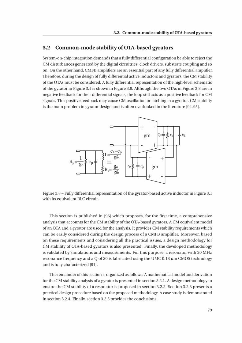
3.2. Common-mode stability of OTA-based gyrators
3.2 Common-mode stability of OTA-based gyrators
System-on-chip integration demands that a fully differential configuration be able to reject the
CM disturbances generated by the digital circuitries, clock drivers, substrate coupling and so
on. On the other hand, CMFB amplifiers are an essential part of any fully differential amplifier.
Therefore, during the design of fully differential active inductors and gyrators, the CM stability
of the OTAs must be considered. A fully differential representation of the high-level schematic
of the gyrator in Figure 3.1 is shown in Figure 3.8. Although the two OTAs in Figure 3.8 are in
negative feedback for their differential signals, the loop still acts as a positive feedback for CM
signals. This positive feedback may cause CM oscillation or latching in a gyrator. CM stability
is the main problem in gyrator design and is often overlooked in the literature [94, 95].
+
+
gm
-
+
+
-
-
cL
gm
-ro
ro cp
cp
Rp= cp
L=
Rs=
cL+cp
gm2
go
gm2
1 go
Figure 3.8 – Fully differential representation of the gyrator-based active inductor in Figure 3.1with its equivalent RLC circuit.
This section is published in [96] which proposes, for the first time, a comprehensive
analysis that accounts for the CM stability of the OTA-based gyrators. A CM equivalent model
of an OTA and a gyrator are used for the analysis. It provides CM stability requirements which
can be easily considered during the design process of a CMFB amplifier. Moreover, based
on these requirements and considering all the practical issues, a design methodology for
CM stability of OTA-based gyrators is also presented. Finally, the developed methodology
is validated by simulations and measurements. For this purpose, a resonator with 20 MHz
resonance frequency and a Q of 20 is fabricated using the UMC 0.18 μm CMOS technology
and is fully characterized [91].
The remainder of this section is organized as follows: A mathematical model and derivation
for the CM stability analysis of a gyrator is presented in section 3.2.1. A design methodology to
ensure the CM stability of a resonator is proposed in section 3.2.2. Section 3.2.3 presents a
practical design procedure based on the proposed methodology. A case study is demonstrated
in section 3.2.4. Finally, section 3.2.5 provides the conclusions.
79
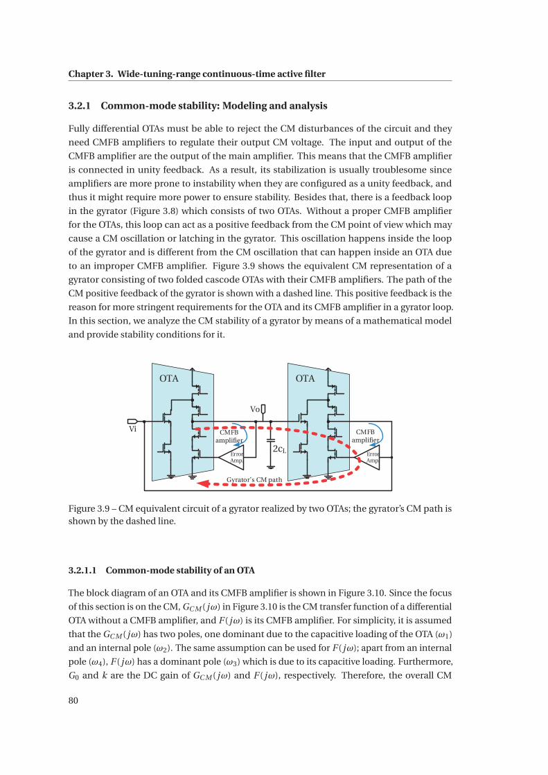
Chapter 3. Wide-tuning-range continuous-time active filter
3.2.1 Common-mode stability: Modeling and analysis
Fully differential OTAs must be able to reject the CM disturbances of the circuit and they
need CMFB amplifiers to regulate their output CM voltage. The input and output of the
CMFB amplifier are the output of the main amplifier. This means that the CMFB amplifier
is connected in unity feedback. As a result, its stabilization is usually troublesome since
amplifiers are more prone to instability when they are configured as a unity feedback, and
thus it might require more power to ensure stability. Besides that, there is a feedback loop
in the gyrator (Figure 3.8) which consists of two OTAs. Without a proper CMFB amplifier
for the OTAs, this loop can act as a positive feedback from the CM point of view which may
cause a CM oscillation or latching in the gyrator. This oscillation happens inside the loop
of the gyrator and is different from the CM oscillation that can happen inside an OTA due
to an improper CMFB amplifier. Figure 3.9 shows the equivalent CM representation of a
gyrator consisting of two folded cascode OTAs with their CMFB amplifiers. The path of the
CM positive feedback of the gyrator is shown with a dashed line. This positive feedback is the
reason for more stringent requirements for the OTA and its CMFB amplifier in a gyrator loop.
In this section, we analyze the CM stability of a gyrator by means of a mathematical model
and provide stability conditions for it.
2cL
Vi
OTA
CMFBamplifier
ErrorAmp.
OTA
ErrorAmp.
CMFBamplifier
Gyrator’s CM path
Vo
Figure 3.9 – CM equivalent circuit of a gyrator realized by two OTAs; the gyrator’s CM path isshown by the dashed line.
3.2.1.1 Common-mode stability of an OTA
The block diagram of an OTA and its CMFB amplifier is shown in Figure 3.10. Since the focus
of this section is on the CM, GC M ( jω) in Figure 3.10 is the CM transfer function of a differential
OTA without a CMFB amplifier, and F ( jω) is its CMFB amplifier. For simplicity, it is assumed
that the GC M ( jω) has two poles, one dominant due to the capacitive loading of the OTA (ω1)
and an internal pole (ω2). The same assumption can be used for F ( jω); apart from an internal
pole (ω4), F ( jω) has a dominant pole (ω3) which is due to its capacitive loading. Furthermore,
G0 and k are the DC gain of GC M ( jω) and F ( jω), respectively. Therefore, the overall CM
80
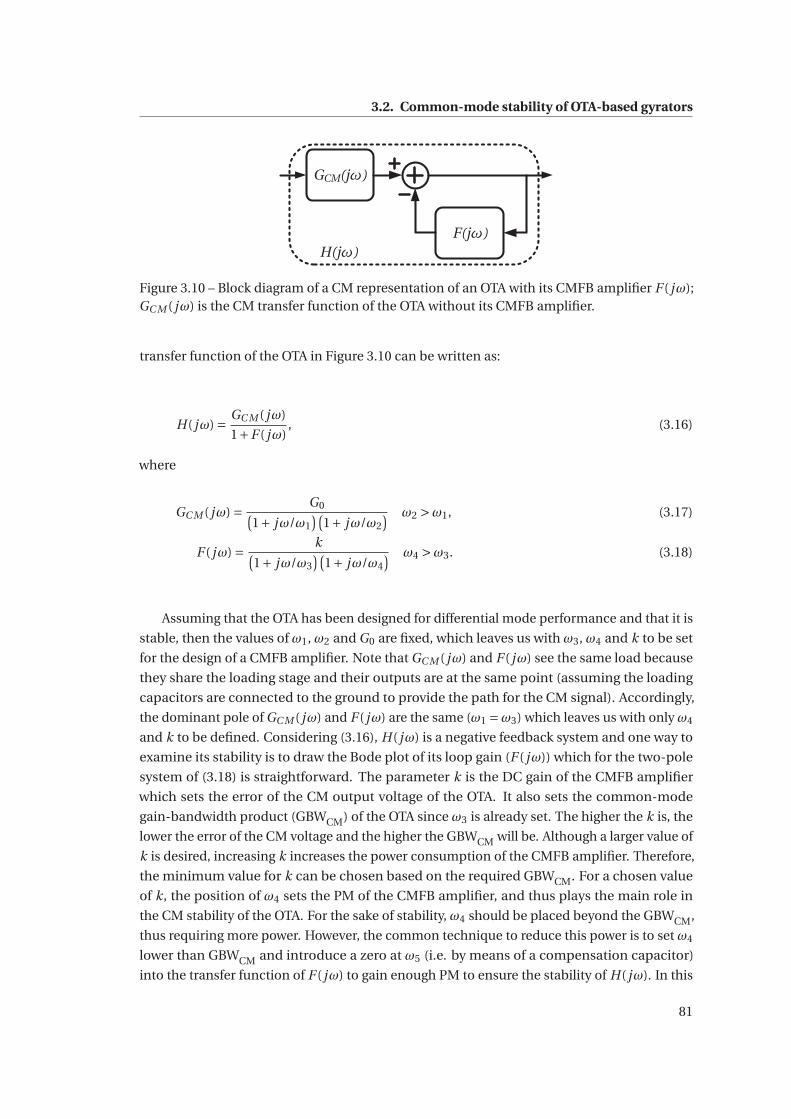
3.2. Common-mode stability of OTA-based gyrators
GCM(jω)
F(jω)H(jω)
Figure 3.10 – Block diagram of a CM representation of an OTA with its CMFB amplifier F ( jω);GC M ( jω) is the CM transfer function of the OTA without its CMFB amplifier.
transfer function of the OTA in Figure 3.10 can be written as:
H( jω) = GC M ( jω)
1+F ( jω), (3.16)
where
GC M ( jω) = G0(1+ jω/ω1
)(1+ jω/ω2
) ω2 >ω1, (3.17)
F ( jω) = k(1+ jω/ω3
)(1+ jω/ω4
) ω4 >ω3. (3.18)
Assuming that the OTA has been designed for differential mode performance and that it is
stable, then the values of ω1, ω2 and G0 are fixed, which leaves us with ω3, ω4 and k to be set
for the design of a CMFB amplifier. Note that GC M ( jω) and F ( jω) see the same load because
they share the loading stage and their outputs are at the same point (assuming the loading
capacitors are connected to the ground to provide the path for the CM signal). Accordingly,
the dominant pole of GC M ( jω) and F ( jω) are the same (ω1 =ω3) which leaves us with only ω4
and k to be defined. Considering (3.16), H( jω) is a negative feedback system and one way to
examine its stability is to draw the Bode plot of its loop gain (F ( jω)) which for the two-pole
system of (3.18) is straightforward. The parameter k is the DC gain of the CMFB amplifier
which sets the error of the CM output voltage of the OTA. It also sets the common-mode
gain-bandwidth product (GBWCM) of the OTA since ω3 is already set. The higher the k is, the
lower the error of the CM voltage and the higher the GBWCM will be. Although a larger value of
k is desired, increasing k increases the power consumption of the CMFB amplifier. Therefore,
the minimum value for k can be chosen based on the required GBWCM. For a chosen value
of k, the position of ω4 sets the PM of the CMFB amplifier, and thus plays the main role in
the CM stability of the OTA. For the sake of stability, ω4 should be placed beyond the GBWCM,
thus requiring more power. However, the common technique to reduce this power is to set ω4
lower than GBWCM and introduce a zero at ω5 (i.e. by means of a compensation capacitor)
into the transfer function of F ( jω) to gain enough PM to ensure the stability of H( jω). In this
81
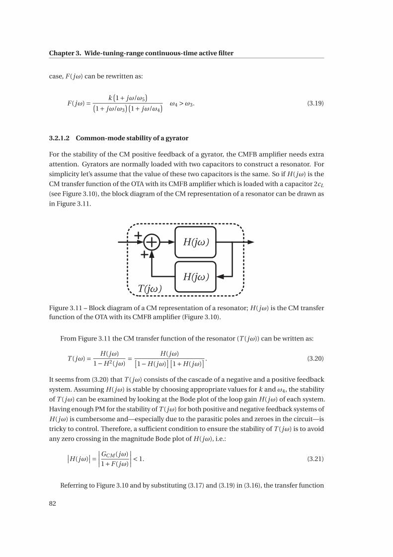
Chapter 3. Wide-tuning-range continuous-time active filter
case, F ( jω) can be rewritten as:
F ( jω) = k(1+ jω/ω5
)(1+ jω/ω3
)(1+ jω/ω4
) ω4 >ω3. (3.19)
3.2.1.2 Common-mode stability of a gyrator
For the stability of the CM positive feedback of a gyrator, the CMFB amplifier needs extra
attention. Gyrators are normally loaded with two capacitors to construct a resonator. For
simplicity let’s assume that the value of these two capacitors is the same. So if H( jω) is the
CM transfer function of the OTA with its CMFB amplifier which is loaded with a capacitor 2cL
(see Figure 3.10), the block diagram of the CM representation of a resonator can be drawn as
in Figure 3.11.
H(jω)
H(jω)T(jω)
Figure 3.11 – Block diagram of a CM representation of a resonator; H( jω) is the CM transferfunction of the OTA with its CMFB amplifier (Figure 3.10).
From Figure 3.11 the CM transfer function of the resonator (T ( jω)) can be written as:
T ( jω) = H( jω)
1−H 2( jω)= H( jω)[
1−H( jω)][
1+H( jω)] . (3.20)
It seems from (3.20) that T ( jω) consists of the cascade of a negative and a positive feedback
system. Assuming H( jω) is stable by choosing appropriate values for k and ω4, the stability
of T ( jω) can be examined by looking at the Bode plot of the loop gain H( jω) of each system.
Having enough PM for the stability of T ( jω) for both positive and negative feedback systems of
H( jω) is cumbersome and—especially due to the parasitic poles and zeroes in the circuit—is
tricky to control. Therefore, a sufficient condition to ensure the stability of T ( jω) is to avoid
any zero crossing in the magnitude Bode plot of H( jω), i.e.:
∣∣H( jω)∣∣= ∣∣∣∣GC M ( jω)
1+F ( jω)
∣∣∣∣< 1. (3.21)
Referring to Figure 3.10 and by substituting (3.17) and (3.19) in (3.16), the transfer function
82
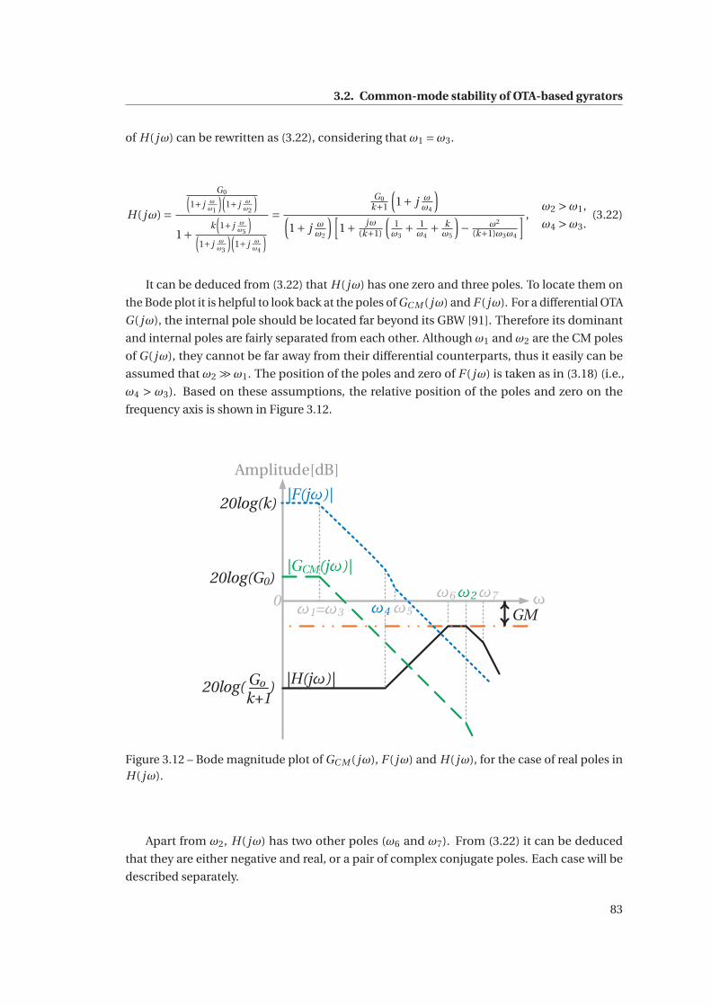
3.2. Common-mode stability of OTA-based gyrators
of H( jω) can be rewritten as (3.22), considering that ω1 =ω3.
H( jω) =G0(
1+ j ωω1
)(1+ j ω
ω2
)
1+ k(1+ j ω
ω5
)(1+ j ω
ω3
)(1+ j ω
ω4
)=
G0k+1
(1+ j ω
ω4
)(1+ j ω
ω2
)[1+ jω
(k+1)
(1ω3
+ 1ω4
+ kω5
)− ω2
(k+1)ω3ω4
] ,ω2 >ω1,
ω4 >ω3.(3.22)
It can be deduced from (3.22) that H( jω) has one zero and three poles. To locate them on
the Bode plot it is helpful to look back at the poles of GC M ( jω) and F ( jω). For a differential OTA
G( jω), the internal pole should be located far beyond its GBW [91]. Therefore its dominant
and internal poles are fairly separated from each other. Although ω1 and ω2 are the CM poles
of G( jω), they cannot be far away from their differential counterparts, thus it easily can be
assumed that ω2 �ω1. The position of the poles and zero of F ( jω) is taken as in (3.18) (i.e.,
ω4 > ω3). Based on these assumptions, the relative position of the poles and zero on the
frequency axis is shown in Figure 3.12.
ω ω1=ω3 ω4 0 ω2 ω6 ω7
GM
|GCM(jω)|
|F(jω)|
|H(jω)|
ω5
20log(k)
20log(G0)
20log( )Go
k+1
Amplitude[dB]
Figure 3.12 – Bode magnitude plot of GC M ( jω), F ( jω) and H( jω), for the case of real poles inH( jω).
Apart from ω2, H( jω) has two other poles (ω6 and ω7). From (3.22) it can be deduced
that they are either negative and real, or a pair of complex conjugate poles. Each case will be
described separately.
83
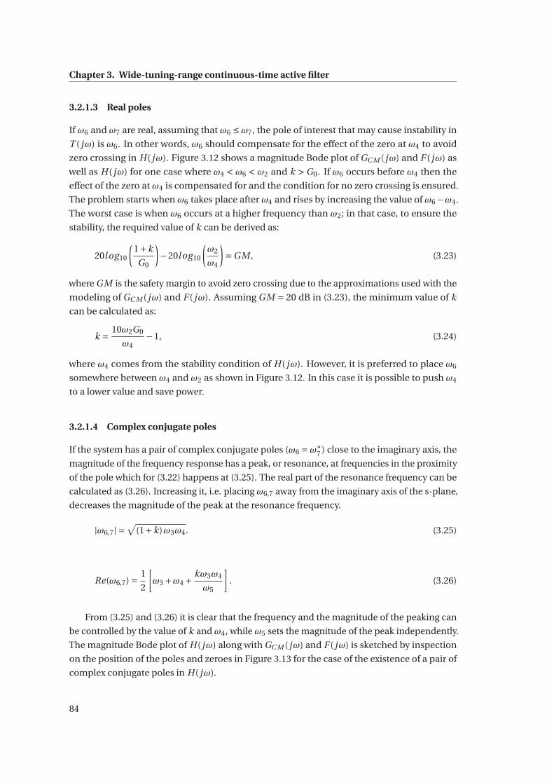
Chapter 3. Wide-tuning-range continuous-time active filter
3.2.1.3 Real poles
If ω6 and ω7 are real, assuming that ω6 ≤ω7, the pole of interest that may cause instability in
T ( jω) is ω6. In other words, ω6 should compensate for the effect of the zero at ω4 to avoid
zero crossing in H( jω). Figure 3.12 shows a magnitude Bode plot of GC M ( jω) and F ( jω) as
well as H( jω) for one case where ω4 < ω6 < ω2 and k > G0. If ω6 occurs before ω4 then the
effect of the zero at ω4 is compensated for and the condition for no zero crossing is ensured.
The problem starts when ω6 takes place after ω4 and rises by increasing the value of ω6 −ω4.
The worst case is when ω6 occurs at a higher frequency than ω2; in that case, to ensure the
stability, the required value of k can be derived as:
20log10
(1+k
G0
)−20log10
(ω2
ω4
)=GM , (3.23)
where GM is the safety margin to avoid zero crossing due to the approximations used with the
modeling of GC M ( jω) and F ( jω). Assuming GM = 20 dB in (3.23), the minimum value of k
can be calculated as:
k = 10ω2G0
ω4−1, (3.24)
where ω4 comes from the stability condition of H( jω). However, it is preferred to place ω6
somewhere between ω4 and ω2 as shown in Figure 3.12. In this case it is possible to push ω4
to a lower value and save power.
3.2.1.4 Complex conjugate poles
If the system has a pair of complex conjugate poles (ω6 =ω∗7 ) close to the imaginary axis, the
magnitude of the frequency response has a peak, or resonance, at frequencies in the proximity
of the pole which for (3.22) happens at (3.25). The real part of the resonance frequency can be
calculated as (3.26). Increasing it, i.e. placing ω6,7 away from the imaginary axis of the s-plane,
decreases the magnitude of the peak at the resonance frequency.
|ω6,7| =√
(1+k)ω3ω4. (3.25)
Re(ω6,7) = 1
2
[ω3 +ω4 + kω3ω4
ω5
]. (3.26)
From (3.25) and (3.26) it is clear that the frequency and the magnitude of the peaking can
be controlled by the value of k and ω4, while ω5 sets the magnitude of the peak independently.
The magnitude Bode plot of H( jω) along with GC M ( jω) and F ( jω) is sketched by inspection
on the position of the poles and zeroes in Figure 3.13 for the case of the existence of a pair of
complex conjugate poles in H( jω).
84
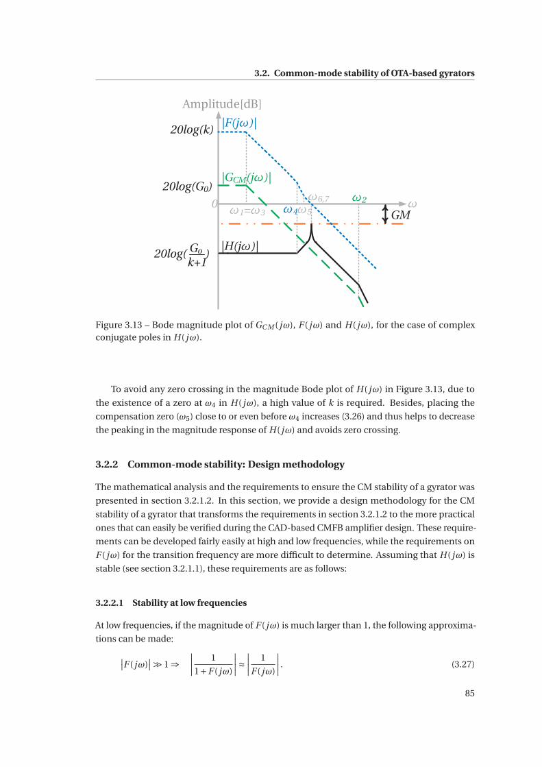
3.2. Common-mode stability of OTA-based gyrators
ω ω1=ω3 0 ω2 ω6,7
GMω4
|GCM(jω)|
|F(jω)|
|H(jω)|
ω5
20log(k)
20log(G0)
20log( )Go
k+1
Amplitude[dB]
Figure 3.13 – Bode magnitude plot of GC M ( jω), F ( jω) and H( jω), for the case of complexconjugate poles in H( jω).
To avoid any zero crossing in the magnitude Bode plot of H( jω) in Figure 3.13, due to
the existence of a zero at ω4 in H( jω), a high value of k is required. Besides, placing the
compensation zero (ω5) close to or even before ω4 increases (3.26) and thus helps to decrease
the peaking in the magnitude response of H( jω) and avoids zero crossing.
3.2.2 Common-mode stability: Design methodology
The mathematical analysis and the requirements to ensure the CM stability of a gyrator was
presented in section 3.2.1.2. In this section, we provide a design methodology for the CM
stability of a gyrator that transforms the requirements in section 3.2.1.2 to the more practical
ones that can easily be verified during the CAD-based CMFB amplifier design. These require-
ments can be developed fairly easily at high and low frequencies, while the requirements on
F ( jω) for the transition frequency are more difficult to determine. Assuming that H( jω) is
stable (see section 3.2.1.1), these requirements are as follows:
3.2.2.1 Stability at low frequencies
At low frequencies, if the magnitude of F ( jω) is much larger than 1, the following approxima-
tions can be made:
∣∣F ( jω)∣∣� 1 ⇒
∣∣∣∣ 1
1+F ( jω)
∣∣∣∣≈∣∣∣∣ 1
F ( jω)
∣∣∣∣ . (3.27)
85
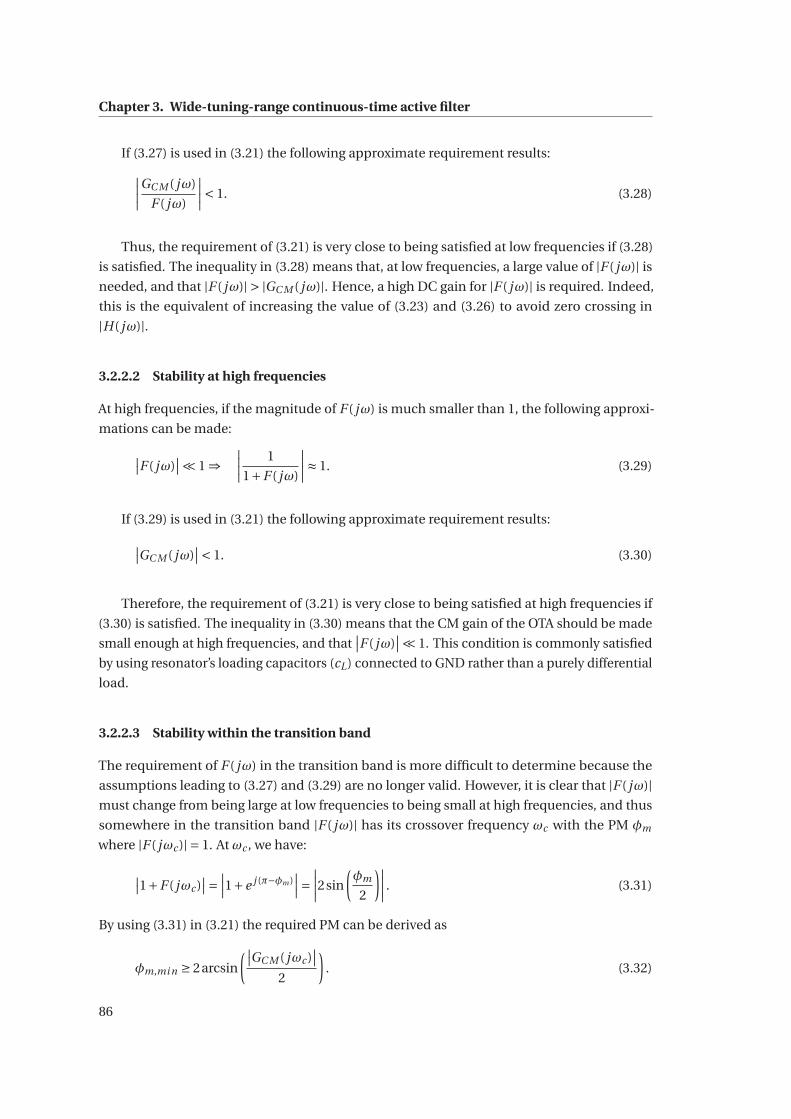
Chapter 3. Wide-tuning-range continuous-time active filter
If (3.27) is used in (3.21) the following approximate requirement results:
∣∣∣∣GC M ( jω)
F ( jω)
∣∣∣∣< 1. (3.28)
Thus, the requirement of (3.21) is very close to being satisfied at low frequencies if (3.28)
is satisfied. The inequality in (3.28) means that, at low frequencies, a large value of |F ( jω)| is
needed, and that |F ( jω)| > |GC M ( jω)|. Hence, a high DC gain for |F ( jω)| is required. Indeed,
this is the equivalent of increasing the value of (3.23) and (3.26) to avoid zero crossing in
|H( jω)|.
3.2.2.2 Stability at high frequencies
At high frequencies, if the magnitude of F ( jω) is much smaller than 1, the following approxi-
mations can be made:
∣∣F ( jω)∣∣� 1 ⇒
∣∣∣∣ 1
1+F ( jω)
∣∣∣∣≈ 1. (3.29)
If (3.29) is used in (3.21) the following approximate requirement results:
∣∣GC M ( jω)∣∣< 1. (3.30)
Therefore, the requirement of (3.21) is very close to being satisfied at high frequencies if
(3.30) is satisfied. The inequality in (3.30) means that the CM gain of the OTA should be made
small enough at high frequencies, and that∣∣F ( jω)
∣∣� 1. This condition is commonly satisfied
by using resonator’s loading capacitors (cL) connected to GND rather than a purely differential
load.
3.2.2.3 Stability within the transition band
The requirement of F ( jω) in the transition band is more difficult to determine because the
assumptions leading to (3.27) and (3.29) are no longer valid. However, it is clear that |F ( jω)|must change from being large at low frequencies to being small at high frequencies, and thus
somewhere in the transition band |F ( jω)| has its crossover frequency ωc with the PM φm
where |F ( jωc )| = 1. At ωc , we have:
∣∣1+F ( jωc )∣∣= ∣∣∣1+e j (π−φm )
∣∣∣= ∣∣∣∣2sin
(φm
2
)∣∣∣∣ . (3.31)
By using (3.31) in (3.21) the required PM can be derived as
φm,mi n ≥ 2arcsin
( ∣∣GC M ( jωc )∣∣
2
). (3.32)
86
3.2. Common-mode stability of OTA-based gyrators
Equation (3.32) determines the minimum required PM, but to ensure the stability practi-
cally, it must be made larger than the minimum requirement to handle PVT variations.
3.2.3 Design procedure for common-mode stability
Assuming that an OTA has been designed for differential mode performance and is stable,
based on the proposed methodology in section 3.2.2, we present the procedure to design a
CMFB amplifier that ensures the CM stability of the gyrator or the resonator constructed by
that OTA, as follows:
1. Before the CMFB amplifier is designed, its topology has to be chosen. A topology that
allows control of the GBWCM independent from the differential-mode gain-bandwidth
product (GBWDM) is preferred. The GBWCM should be set higher than the GBWDM of
the main amplifier. Indeed, if the CMFB amplifier were slow, a high-speed spike in
the substrate or supply line would put some transistors of the main amplifier in the
linear region. The noise or spur generated from digital circuitry or intermodulation (IM)
products of an analog part falling within the BW of the main amplifier could cause
the same problem. A slow CMFB amplifier would take too much time to restore the
biasing, and during that time, the main amplifier would be out of operation. So a CMFB
amplifier with a GBW higher than that of the main amplifier is necessary to avoid this
situation [93].
2. Part of the output stage of the main OTA is shared between the OTA and its CMFB
amplifier. In fact, the CMFB amplifier consists of this shared part and an error amplifier
(EA). Therefore, after choosing the topology of the CMFB amplifier, the design narrows
to the design of an EA. A static analysis is necessary to find the required output range
of the EA to set the CM voltage for the whole possible range of the CM input. At first
an ideal amplifier can be used as an EA to simulate and find this range. It is especially
important for the gyrator because the two amplifiers are connected in CM positive
feedback. Besides, during the startup of the circuit, the CM voltage will sweep from
GND to its nominal value. Therefore, the CMFB amplifier should set the right CM output
level for all possible CM input ranges or at least avoid any latch up in the output stage
of the main amplifier. After finding this range, the EA can be designed to provide this
output voltage range. This voltage range is the result of transistors’ width ratios in the
EA. Indeed, the design in this stage is to set the size of the transistors of the EA to provide
this voltage range. The gain and GBWCM will be set later. Note that the ratios of the
transistors’ width from this stage should be preserved during the rest of the design.
3. Another consideration is the capacitance loading of the CMFB amplifier if connected
to GND. The CMFB amplifier sees twice the capacitive load of the main differential
amplifier, which directly affects the GBWCM and the PM, and should be taken into
account during simulation [97].
87
Chapter 3. Wide-tuning-range continuous-time active filter
4. Finally the frequency response of the CMFB amplifier has to be shaped and the GBWCM
has to be set. The simulation setup to find the GBWCM and PM of the CMFB amplifier
needs particular attention due to the fact that open-loop simulations are required. In fact
the CMFB loop should be broken for these simulations but opening the loop unbalances
the biasing of the circuit. A CMFB amplifier provides biasing for the main amplifier as
well as for itself since part of the circuit is shared between the two. Therefore, simulating
the CMFB amplifier with a fixed and approximated biasing of the main amplifier is not
possible. To that effect, the feedback loop should be closed for the DC signal but of
course broken for the AC signal. Opening the loop for a small signal is possible with
an ideal loop probe or controlled source along with an ideal low-pass filter. Having
regard to these considerations as well as stability conditions presented in section 3.2.2,
the design process for the CMFB amplifier continues to shape its frequency response
and set its GBWCM. The frequency response of a CMFB amplifier (F ( jω)) is divided
into three regions (low, high and transition frequencies), for which the CMFB amplifier
should satisfy some conditions to ensure the CM stability of the gyrator.
At low frequencies, conditions (3.27) and (3.28) should be satisfied so a high DC gain
for F ( jω) is required. This can be achieved by increasing the transconductance of the
input transistors of the EA which also increases the GBWCM of the CMFB amplifier. Note
that the transistors’ width ratios which were obtained during the static design must be
preserved.
At high frequencies, conditions (3.29) and (3.30) should be satisfied. The CMFB amplifier
has the same loading capacitance as the OTA, except that the OTA sees it in differential
mode (i.e. cL) and the CMFB amplifier sees it in common mode (i.e. 2cL). To satisfy
(3.29) and (3.30) the capacitive load or a part of it should be connected to GND to provide
the path also for the CM signals.
At transition frequency, of course the CMFB amplifier should have enough PM for its
own stability, but to ensure the stability of the gyrator it should satisfy (3.32) at its unity-
gain frequency (ωc ). More PM can be achieved by means of a compensation capacitor
which introduces a zero in the transfer function of the CMFB amplifier. In fact, gaining
more PM by introducing a zero close to the second pole of F ( jω) increases (3.26) and
places the ω6,7 away from the imaginary axis of the s-plane.
3.2.4 Case study: A high-quality-factor high-frequency resonator
To clarify and validate the proposed methodology, a resonator with 20 MHz resonance fre-
quency and quality factor around 20 was designed and fabricated using UMC 0.18 μm CMOS
technology. The schematic of the test-chip is shown in Figure 3.14 together with the die
photograph in Figure 3.15. As the differential mode design was presented in [91], here we
focus on the design of the CMFB amplifier.
88
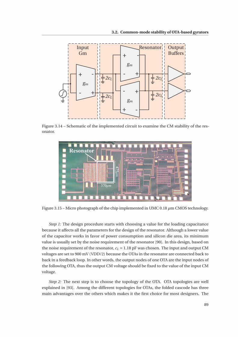
3.2. Common-mode stability of OTA-based gyrators
+
+
gm
-
+
+
-
-
gm
-
2cL
OutputBuffers
+
+
gm
-
-
2cL
2cL
2cL
ResonatorInputGm
Figure 3.14 – Schematic of the implemented circuit to examine the CM stability of the res-onator.
475μ
m
370μm
Resonator
Figure 3.15 – Micro photograph of the chip implemented in UMC 0.18 μm CMOS technology.
Step 1: The design procedure starts with choosing a value for the loading capacitance
because it affects all the parameters for the design of the resonator. Although a lower value
of the capacitor works in favor of power consumption and silicon die area, its minimum
value is usually set by the noise requirement of the resonator [90]. In this design, based on
the noise requirement of the resonator, cL = 1.18 pF was chosen. The input and output CM
voltages are set to 900 mV (VDD/2) because the OTAs in the resonator are connected back to
back in a feedback loop. In other words, the output nodes of one OTA are the input nodes of
the following OTA, thus the output CM voltage should be fixed to the value of the input CM
voltage.
Step 2: The next step is to choose the topology of the OTA. OTA topologies are well
explained in [93]. Among the different topologies for OTAs, the folded cascode has three
main advantages over the others which makes it the first choice for most designers. The
89
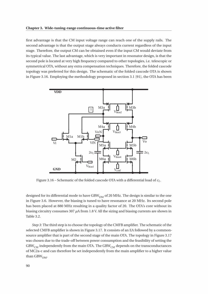
Chapter 3. Wide-tuning-range continuous-time active filter
first advantage is that the CM input voltage range can reach one of the supply rails. The
second advantage is that the output stage always conducts current regardless of the input
stage. Therefore, the output CM can be obtained even if the input CM would deviate from
its typical value. The last advantage, which is very important in resonator design, is that the
second pole is located at very high frequency compared to other topologies, i.e. telescopic or
symmetrical OTA, without any extra compensation techniques. Therefore, the folded cascode
topology was preferred for this design. The schematic of the folded cascode OTA is shown
in Figure 3.16. Employing the methodology proposed in section 3.1 [91], the OTA has been
2cL
Vbias1
VDD
GND
M1a
M2
M3a1
2cL
Vbias2
Vbias3
Vbias4
ViNVi Vo
VoNM1b
M3b
M4a M4b
M5a M5b
M6a M6b
Vcmf
Figure 3.16 – Schematic of the folded cascode OTA with a differential load of cL .
designed for its differential mode to have GBWDM of 20 MHz. The design is similar to the one
in Figure 3.6. However, the biasing is tuned to have resonance at 20 MHz. Its second pole
has been placed at 880 MHz resulting in a quality factor of 20. The OTA’s core without its
biasing circuitry consumes 307 μA from 1.8 V. All the sizing and biasing currents are shown in
Table 3.2.
Step 3: The third step is to choose the topology of the CMFB amplifier. The schematic of the
selected CMFB amplifier is shown in Figure 3.17. It consists of an EA followed by a common-
source amplifier that is part of the second stage of the main OTA. The topology in Figure 3.17
was chosen due to the trade-off between power consumption and the feasibility of setting the
GBWCM independently from the main OTA. The GBWCM depends on the transconductances
of MC2a-c and can therefore be set independently from the main amplifier to a higher value
than GBWDM.
90
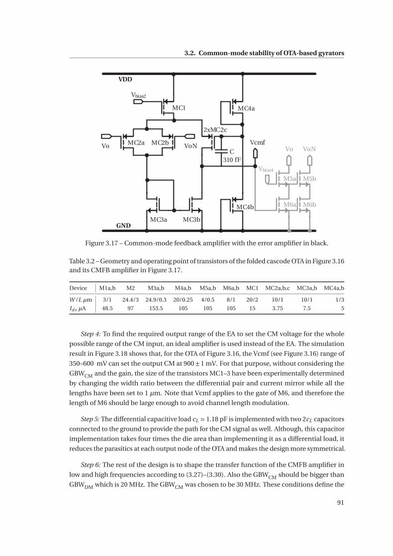
3.2. Common-mode stability of OTA-based gyrators
VDD
GND
MC1
MC2a
2xMC2c
MC3a
MC4b
MC4a
Vcmf
310 fFC
Vbias2
Vo VoNMC2b
MC3b
M5b
M6b
M5a
M6a
Vo VoN
Vbias4
Figure 3.17 – Common-mode feedback amplifier with the error amplifier in black.
Table 3.2 – Geometry and operating point of transistors of the folded cascode OTA in Figure 3.16and its CMFB amplifier in Figure 3.17.
Device M1a,b M2 M3a,b M4a,b M5a,b M6a,b MC1 MC2a,b,c MC3a,b MC4a,b
W /L μm 3/1 24.4/3 24.9/0.3 20/0.25 4/0.5 8/1 20/2 10/1 10/1 1/3
Id s μA 48.5 97 153.5 105 105 105 15 3.75 7.5 5
Step 4: To find the required output range of the EA to set the CM voltage for the whole
possible range of the CM input, an ideal amplifier is used instead of the EA. The simulation
result in Figure 3.18 shows that, for the OTA of Figure 3.16, the Vcmf (see Figure 3.16) range of
350–600 mV can set the output CM at 900±1 mV. For that purpose, without considering the
GBWCM and the gain, the size of the transistors MC1–3 have been experimentally determined
by changing the width ratio between the differential pair and current mirror while all the
lengths have been set to 1 μm. Note that Vcmf applies to the gate of M6, and therefore the
length of M6 should be large enough to avoid channel length modulation.
Step 5: The differential capacitive load cL = 1.18 pF is implemented with two 2cL capacitors
connected to the ground to provide the path for the CM signal as well. Although, this capacitor
implementation takes four times the die area than implementing it as a differential load, it
reduces the parasitics at each output node of the OTA and makes the design more symmetrical.
Step 6: The rest of the design is to shape the transfer function of the CMFB amplifier in
low and high frequencies according to (3.27)–(3.30). Also the GBWCM should be bigger than
GBWDM which is 20 MHz. The GBWCM was chosen to be 30 MHz. These conditions define the
91
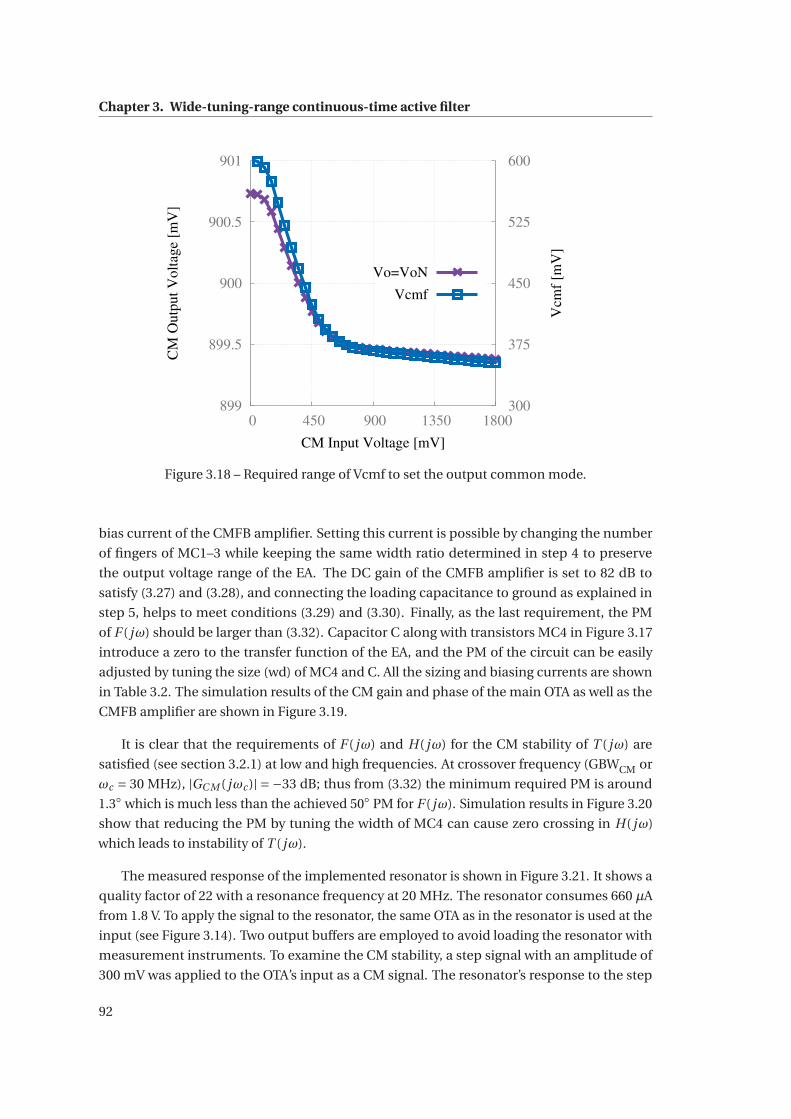
Chapter 3. Wide-tuning-range continuous-time active filter
899
899.5
900
900.5
901
0 450 900 1350 1800 300
375
450
525
600C
M O
utp
ut
Vo
ltag
e [m
V]
Vcm
f [m
V]
CM Input Voltage [mV]
Vo=VoN
Vcmf
Figure 3.18 – Required range of Vcmf to set the output common mode.
bias current of the CMFB amplifier. Setting this current is possible by changing the number
of fingers of MC1–3 while keeping the same width ratio determined in step 4 to preserve
the output voltage range of the EA. The DC gain of the CMFB amplifier is set to 82 dB to
satisfy (3.27) and (3.28), and connecting the loading capacitance to ground as explained in
step 5, helps to meet conditions (3.29) and (3.30). Finally, as the last requirement, the PM
of F ( jω) should be larger than (3.32). Capacitor C along with transistors MC4 in Figure 3.17
introduce a zero to the transfer function of the EA, and the PM of the circuit can be easily
adjusted by tuning the size (wd) of MC4 and C. All the sizing and biasing currents are shown
in Table 3.2. The simulation results of the CM gain and phase of the main OTA as well as the
CMFB amplifier are shown in Figure 3.19.
It is clear that the requirements of F ( jω) and H( jω) for the CM stability of T ( jω) are
satisfied (see section 3.2.1) at low and high frequencies. At crossover frequency (GBWCM or
ωc = 30 MHz), |GC M ( jωc )| = −33 dB; thus from (3.32) the minimum required PM is around
1.3◦ which is much less than the achieved 50◦ PM for F ( jω). Simulation results in Figure 3.20
show that reducing the PM by tuning the width of MC4 can cause zero crossing in H( jω)
which leads to instability of T ( jω).
The measured response of the implemented resonator is shown in Figure 3.21. It shows a
quality factor of 22 with a resonance frequency at 20 MHz. The resonator consumes 660 μA
from 1.8 V. To apply the signal to the resonator, the same OTA as in the resonator is used at the
input (see Figure 3.14). Two output buffers are employed to avoid loading the resonator with
measurement instruments. To examine the CM stability, a step signal with an amplitude of
300 mV was applied to the OTA’s input as a CM signal. The resonator’s response to the step
92
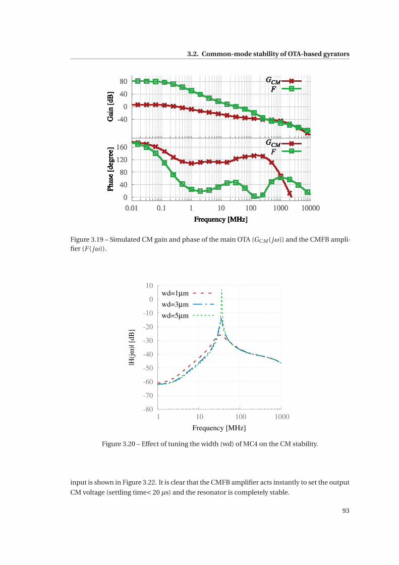
3.2. Common-mode stability of OTA-based gyrators
0
40
80
120
160
0.01 0.1 1 10 100 1000 10000
GCM
Ph
ase
[deg
ree]
Frequency [MHz]
0
40
80
120
160
0.01 0.1 1 10 100 1000 10000
GCM
Ph
ase
[deg
ree]
Frequency [MHz]
0
40
80
120
160
0.01 0.1 1 10 100 1000 10000
GCM
Ph
ase
[deg
ree]
Frequency [MHz]
0
40
80
120
160
0.01 0.1 1 10 100 1000 10000
GCMF
Ph
ase
[deg
ree]
Frequency [MHz]
0
40
80
120
160
0.01 0.1 1 10 100 1000 10000
GCMF
Ph
ase
[deg
ree]
Frequency [MHz]
0
40
80
120
160
0.01 0.1 1 10 100 1000 10000
GCMF
Ph
ase
[deg
ree]
Frequency [MHz]
-40
0
40
80 GCMF
Gai
n [
dB
]
-40
0
40
80 GCMF
Gai
n [
dB
]
-40
0
40
80 GCMF
Gai
n [
dB
]
-40
0
40
80 GCMF
Gai
n [
dB
]
-40
0
40
80 GCMF
Gai
n [
dB
]
-40
0
40
80 GCMF
Gai
n [
dB
]
Figure 3.19 – Simulated CM gain and phase of the main OTA (GC M ( jω)) and the CMFB ampli-fier (F ( jω)).
-80
-70
-60
-50
-40
-30
-20
-10
0
10
1 10 100 1000
|H(j
ω)|
[d
B]
Frequency [MHz]
wd=1μm
wd=3μm
wd=5μm
Figure 3.20 – Effect of tuning the width (wd) of MC4 on the CM stability.
input is shown in Figure 3.22. It is clear that the CMFB amplifier acts instantly to set the output
CM voltage (settling time< 20 μs) and the resonator is completely stable.
93
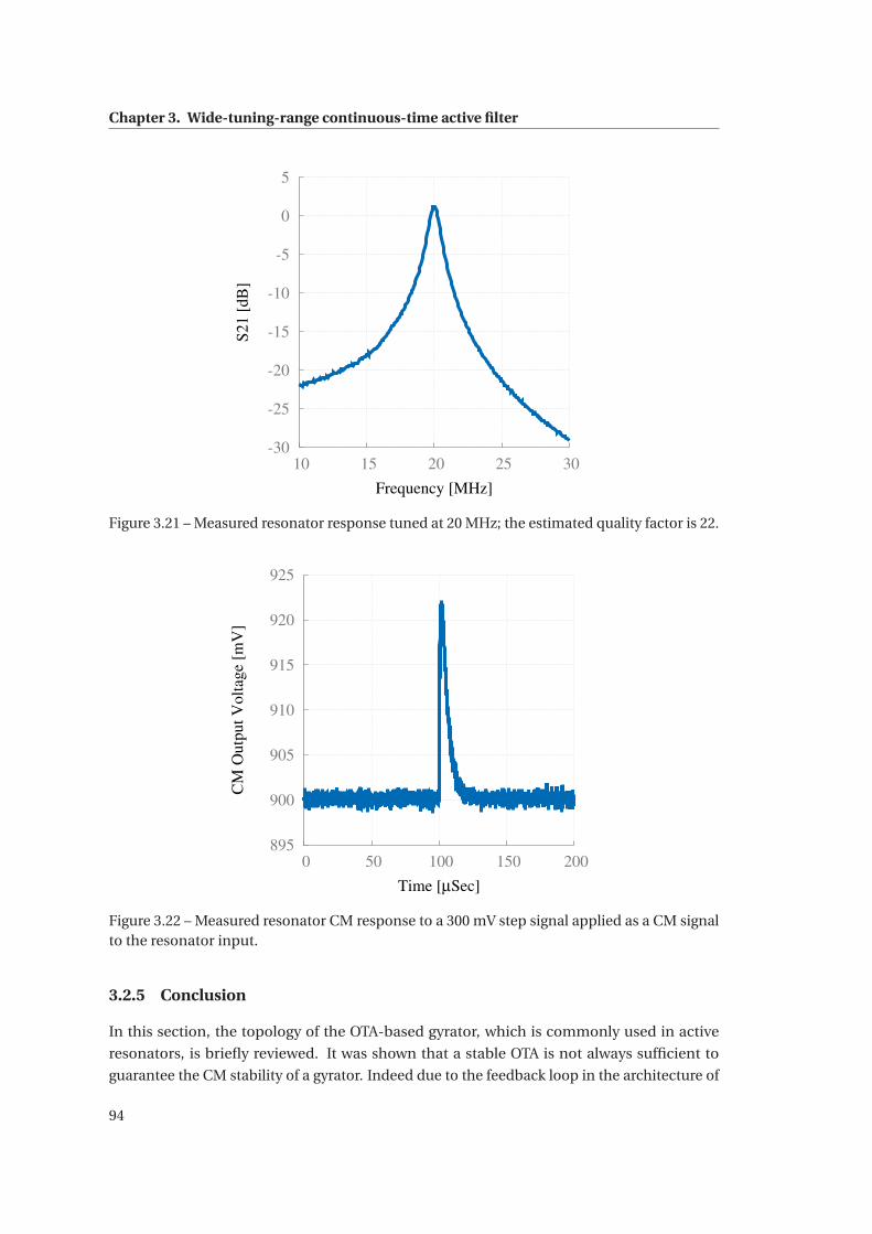
Chapter 3. Wide-tuning-range continuous-time active filter
-30
-25
-20
-15
-10
-5
0
5
10 15 20 25 30
S2
1 [
dB
]
Frequency [MHz]
Figure 3.21 – Measured resonator response tuned at 20 MHz; the estimated quality factor is 22.
895
900
905
910
915
920
925
0 50 100 150 200
CM
Ou
tpu
t V
olt
age
[mV
]
Time [μSec]
Figure 3.22 – Measured resonator CM response to a 300 mV step signal applied as a CM signalto the resonator input.
3.2.5 Conclusion
In this section, the topology of the OTA-based gyrator, which is commonly used in active
resonators, is briefly reviewed. It was shown that a stable OTA is not always sufficient to
guarantee the CM stability of a gyrator. Indeed due to the feedback loop in the architecture of
94
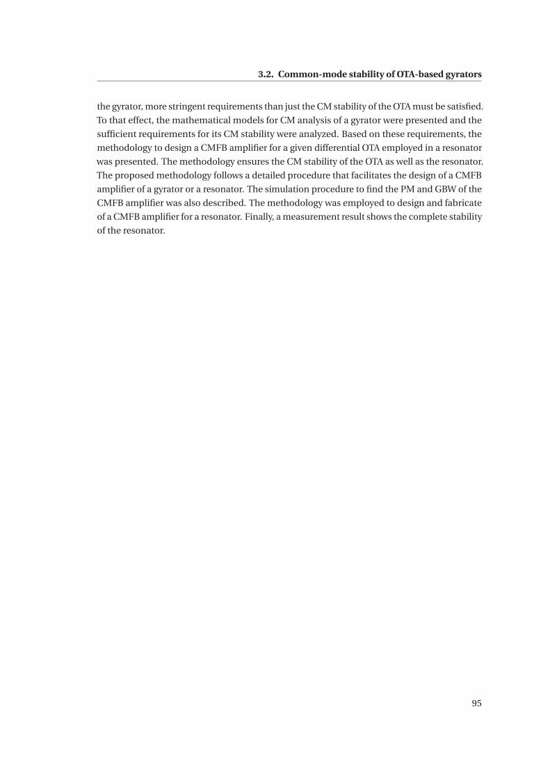
3.2. Common-mode stability of OTA-based gyrators
the gyrator, more stringent requirements than just the CM stability of the OTA must be satisfied.
To that effect, the mathematical models for CM analysis of a gyrator were presented and the
sufficient requirements for its CM stability were analyzed. Based on these requirements, the
methodology to design a CMFB amplifier for a given differential OTA employed in a resonator
was presented. The methodology ensures the CM stability of the OTA as well as the resonator.
The proposed methodology follows a detailed procedure that facilitates the design of a CMFB
amplifier of a gyrator or a resonator. The simulation procedure to find the PM and GBW of the
CMFB amplifier was also described. The methodology was employed to design and fabricate
of a CMFB amplifier for a resonator. Finally, a measurement result shows the complete stability
of the resonator.
95
Chapter 3. Wide-tuning-range continuous-time active filter
3.3 Continuous-time active filter
Integrated analog baseband filters are the indispensable building blocks in wireless receivers
or transceivers. The most common application of this type of filter in wireless receivers is is for
anti-aliasing, to limit a signal’s bandwidth before sampling. The anti-aliasing filters have to be
continuous-time filters and typically consume several milliwatts to tens of milliwatts, which is
non-negligible in the total power consumption of the whole receiver or transceiver. In fact,
continuous-time filters can sometimes be the only alternative to high-frequency filters, for
which the clock feed-through problem in switched-capacitor filters escalates at high speeds,
making them power hungry.
In a design re-use approach, a reconfigurable or tunable continuous-time low-pass fil-
ter that can satisfy the requirements of the different standards is necessary. Moreover, the
coexistence of many systems (ex. GNSS, Wi-Fi and LTE) on the same mobile equipment,
which is very common nowadays, has tightened the interference rejection requirements of the
receivers. This is directly reflected in the low-pass filter’s requirements in terms of selectivity
and linearity.
In the case of GNSS applications, the elliptic configuration for the low-pass filter is of
interest because of its better selectivity and steeper roll-off transition as compared to the
same order filters of the other configurations. The abrupt roll-off transition strongly mitigates
out-of-band interferers while allowing sampling frequencies to be slightly above the Nyquist
limit. This enables lower clock frequencies for analog-to-digital converters which means lower
power consumption without suffering from aliasing noise.
Towards this end, this section presents a 4 th-order Gm-C elliptic low-pass filter in CMOS
technology for modern GNSS receiver IC front-ends. It employs a new Gm control circuit to
tune its cut-off frequency as well as to improve the usual weak linearity of the Gm-C filters
over tuning its cut-off frequency. The filter also incorporates Gm switching to achieve a wide
continuous tuning range of 7.4–27.4 MHz. The large continuous tuning range can cover the
bandwidth of all new GNSS signals (such as Galileo-E5) in zero-IF or low-IF receivers.
This section is organized as follows. Several filter topologies are briefly compared in
section 3.3.1. A 4 th-order Gm-C elliptic low-pass filter in CMOS technology for modern GNSS
receiver IC front-ends is presented in section 3.3.2. The OTA design and a new Gm control
circuit to improve the usual weak linearity of the Gm-C filters over tuning its cut-off frequency
are presented in sections 3.3.3 and 3.3.4, respectively. A topological linearity improvement
technique is described in section 3.3.5. The filter measurement results are presented in
section 3.3.6. Finally, section 3.3.7 concludes this section by summarizing the key points and
results.
96
3.3. Continuous-time active filter
3.3.1 Active filter topologies
Several topologies of integrated continuous-time filters have been developed, including the
active-RC [98–101], MOSFET-C [102], active-Gm-RC [103], Gm-C [104–106], source-follower-
based [107] architecture, and so on.
One popular approach for continuous-time filters is active-RC topology. Active-RC filters
consist of opamps with resistors and capacitors in feedback. Because of their closed-loop
nature and high loop gain of the opamp, active-RC filters show very low distortion at low
frequencies, thus perform excellent linearity [108]. The same reason allows them to handle
a large signal swing, resulting in a large dynamic range (DR) [109]. At higher frequencies,
however, the loop gain decreases and the distortion increases. Active-RC topology uses the
absolute value of resistors and capacitors; because of the low absolute accuracies of these
passive components in CMOS technology, characteristic tuning for these filters is required. In
fact, tuning is the main issue in these filters. Passive components cannot be tuned. Therefore,
resistor or capacitor banks that lead to a discrete tuning are required for tuning the filter.
Substituting resistors with metal–oxide–semiconductor field-effect transistors (MOSFETs)
in active-RC filters results in MOSFET-C filters, which solves the problem of the tuning. The
ON-resistance of a MOSFET is inversely proportional to its gate voltage, allowing for tuning of
the filter characteristics. However, for large signal swings, this resistance is no longer linear
and introduces distortions and limits the DR of the filter. Moreover, the large value of the
resistance requires a very large channel length of the MOSFET which results in limiting the
performance of the filter at high frequencies. Employing opamps in filter topologies provides
the highest DR of the filter for the low frequencies where the loop gain of the opamp is high.
The need for an opamp bandwidth much larger than the filter cut-off frequency leads to high
power consumption for high-frequency filters.
As an alternative, Gm-C filters reduce the power consumption at the cost of a lower linearity.
In fact, Gm-C topology is more power efficient than active-RC and MOSFET-C topologies.
Moreover, it has the great potential of working at high frequency [110], [111], since the Gm-C
integrator is based on the open loop and the minimum GBW of the Gm cell is required to
be not less than the filter’s cut-off frequency only. However, Gm-C filters suffer from poor
linearity due to their open-loop nature. Linearity enhancement techniques [112, 113] can
be applied, but higher excess noise would be produced, which implies additional power is
necessary to sustain a high dynamic range. The cut-off frequency of Gm-C filters can be tuned
continuously with dedicated circuitry.
Gm-C filters are capable of reasonable performance at the higher frequencies. At low
frequencies, however, active-RC filters provide the highest dynamic range. The other types of
filters provide a performance in between the two. Active-Gm-RC filters have a closed-loop
structure that exploits the opamp frequency response in the filter transfer function. They
propose an efficient trade-off between active-RC and Gm-C solutions. However, as with
active-RC, they employ resistors, which results in higher in-band noise.
97
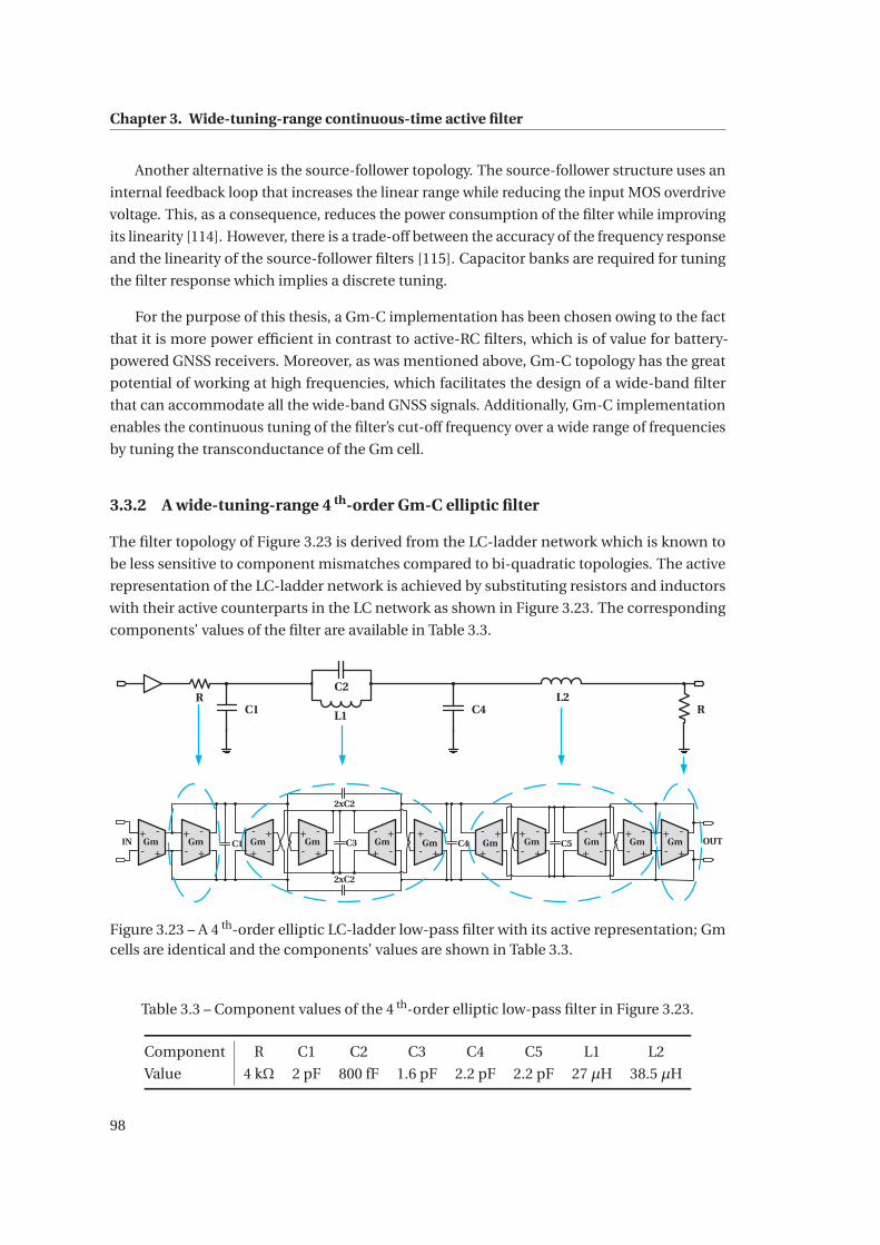
Chapter 3. Wide-tuning-range continuous-time active filter
Another alternative is the source-follower topology. The source-follower structure uses an
internal feedback loop that increases the linear range while reducing the input MOS overdrive
voltage. This, as a consequence, reduces the power consumption of the filter while improving
its linearity [114]. However, there is a trade-off between the accuracy of the frequency response
and the linearity of the source-follower filters [115]. Capacitor banks are required for tuning
the filter response which implies a discrete tuning.
For the purpose of this thesis, a Gm-C implementation has been chosen owing to the fact
that it is more power efficient in contrast to active-RC filters, which is of value for battery-
powered GNSS receivers. Moreover, as was mentioned above, Gm-C topology has the great
potential of working at high frequencies, which facilitates the design of a wide-band filter
that can accommodate all the wide-band GNSS signals. Additionally, Gm-C implementation
enables the continuous tuning of the filter’s cut-off frequency over a wide range of frequencies
by tuning the transconductance of the Gm cell.
3.3.2 A wide-tuning-range 4 th-order Gm-C elliptic filter
The filter topology of Figure 3.23 is derived from the LC-ladder network which is known to
be less sensitive to component mismatches compared to bi-quadratic topologies. The active
representation of the LC-ladder network is achieved by substituting resistors and inductors
with their active counterparts in the LC network as shown in Figure 3.23. The corresponding
components’ values of the filter are available in Table 3.3.
-
+ -
+C1
-
+-
+ -
+ -
+ -
+-
+ -
+ -
+ -
+-
+ -
+ -
+ -
+-
+ -
+ -
+ -
+ -
+
2xC2
2xC2
C3 C4 C5 OUTIN Gm Gm Gm Gm Gm Gm Gm Gm Gm Gm
C1
C2
L1
RC4
L2R
-
+ -
+Gm
Figure 3.23 – A 4 th-order elliptic LC-ladder low-pass filter with its active representation; Gmcells are identical and the components’ values are shown in Table 3.3.
Table 3.3 – Component values of the 4 th-order elliptic low-pass filter in Figure 3.23.
Component R C1 C2 C3 C4 C5 L1 L2
Value 4 kΩ 2 pF 800 fF 1.6 pF 2.2 pF 2.2 pF 27 μH 38.5 μH
98
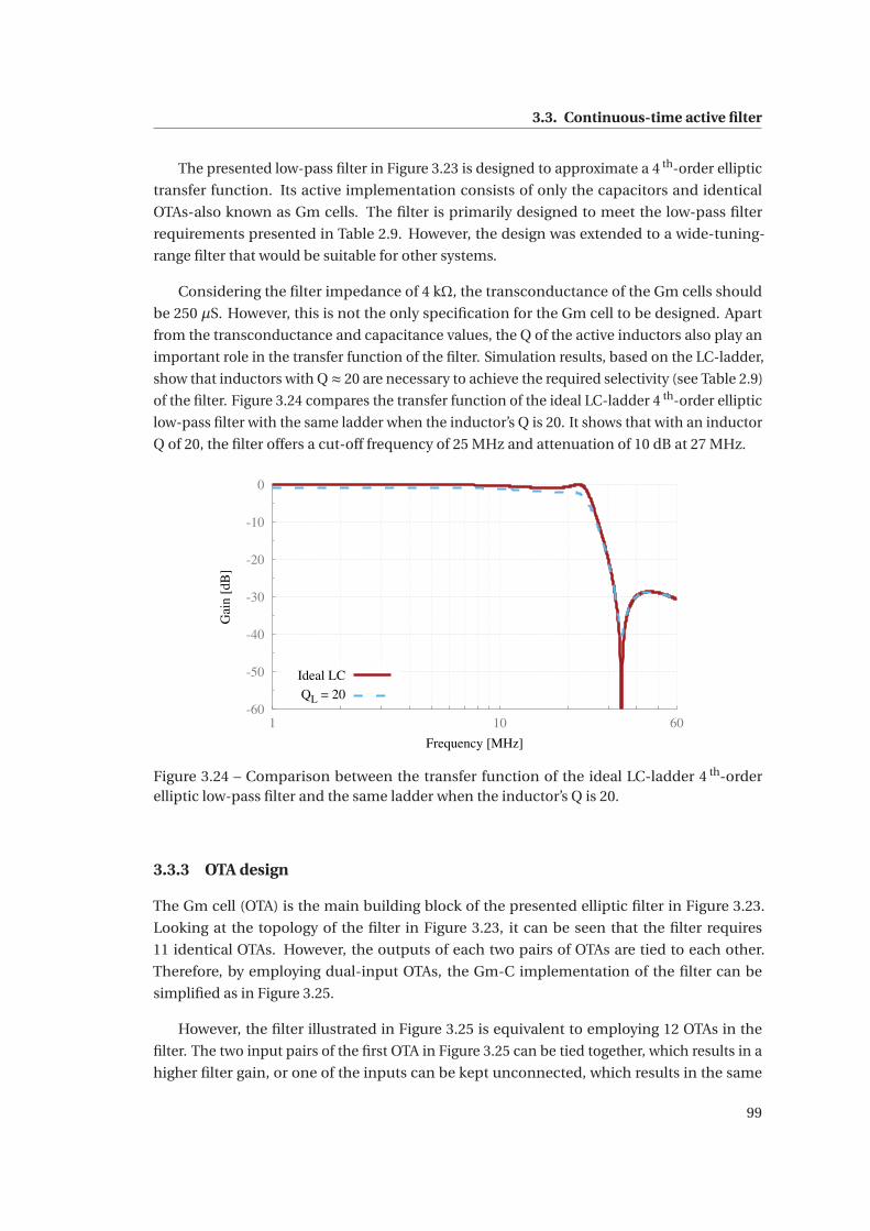
3.3. Continuous-time active filter
The presented low-pass filter in Figure 3.23 is designed to approximate a 4 th-order elliptic
transfer function. Its active implementation consists of only the capacitors and identical
OTAs-also known as Gm cells. The filter is primarily designed to meet the low-pass filter
requirements presented in Table 2.9. However, the design was extended to a wide-tuning-
range filter that would be suitable for other systems.
Considering the filter impedance of 4 kΩ, the transconductance of the Gm cells should
be 250 μS. However, this is not the only specification for the Gm cell to be designed. Apart
from the transconductance and capacitance values, the Q of the active inductors also play an
important role in the transfer function of the filter. Simulation results, based on the LC-ladder,
show that inductors with Q ≈ 20 are necessary to achieve the required selectivity (see Table 2.9)
of the filter. Figure 3.24 compares the transfer function of the ideal LC-ladder 4 th-order elliptic
low-pass filter with the same ladder when the inductor’s Q is 20. It shows that with an inductor
Q of 20, the filter offers a cut-off frequency of 25 MHz and attenuation of 10 dB at 27 MHz.
-60
-50
-40
-30
-20
-10
0
1 10 60
Gai
n [
dB
]
Frequency [MHz]
Ideal LC
QL = 20
Figure 3.24 – Comparison between the transfer function of the ideal LC-ladder 4 th-orderelliptic low-pass filter and the same ladder when the inductor’s Q is 20.
3.3.3 OTA design
The Gm cell (OTA) is the main building block of the presented elliptic filter in Figure 3.23.
Looking at the topology of the filter in Figure 3.23, it can be seen that the filter requires
11 identical OTAs. However, the outputs of each two pairs of OTAs are tied to each other.
Therefore, by employing dual-input OTAs, the Gm-C implementation of the filter can be
simplified as in Figure 3.25.
However, the filter illustrated in Figure 3.25 is equivalent to employing 12 OTAs in the
filter. The two input pairs of the first OTA in Figure 3.25 can be tied together, which results in a
higher filter gain, or one of the inputs can be kept unconnected, which results in the same
99
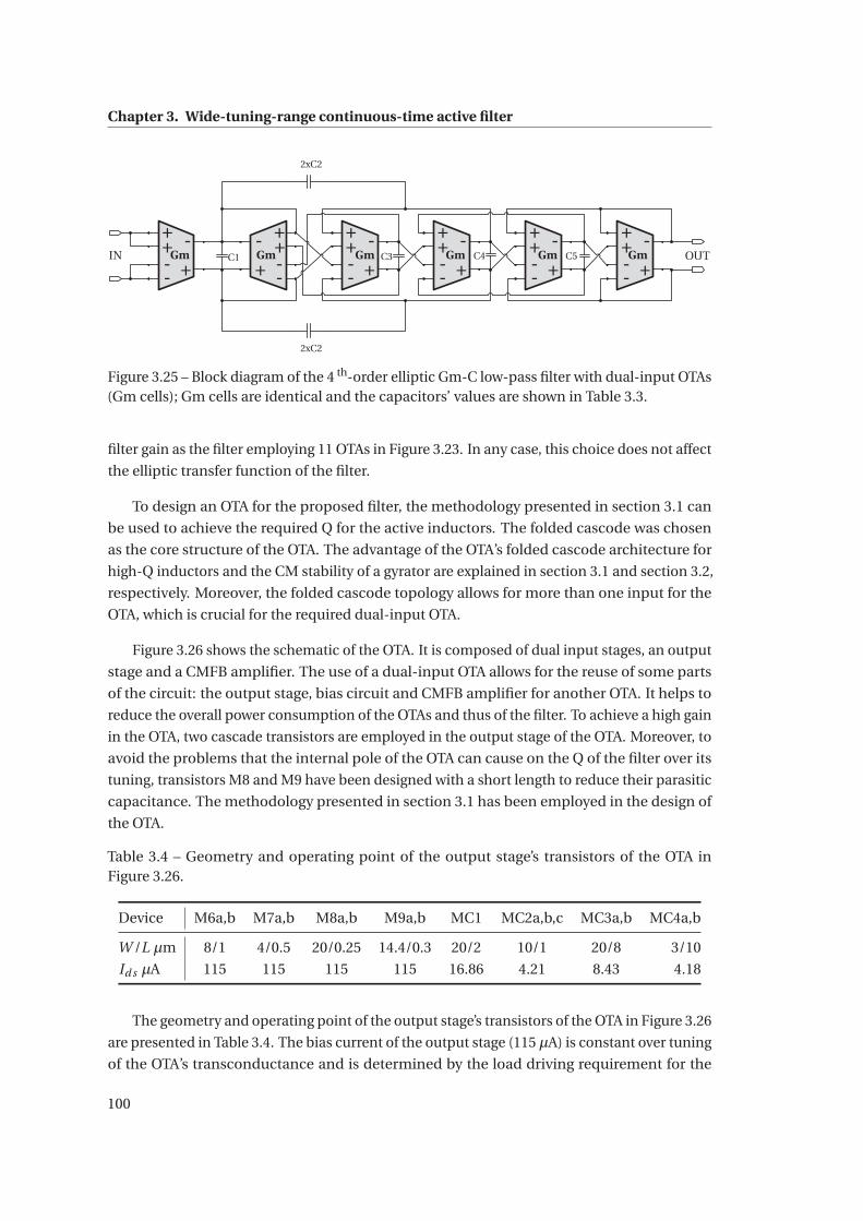
Chapter 3. Wide-tuning-range continuous-time active filter
+
+
-
-
+-
+
+
-
-
+-
+
+
-
-
+-
+
+
-
-
+-
+
+
-
-
+-C4
2xC2
2xC2
+
+
-
-
+-C1 C3IN OUTGm Gm Gm Gm Gm GmC5
Figure 3.25 – Block diagram of the 4 th-order elliptic Gm-C low-pass filter with dual-input OTAs(Gm cells); Gm cells are identical and the capacitors’ values are shown in Table 3.3.
filter gain as the filter employing 11 OTAs in Figure 3.23. In any case, this choice does not affect
the elliptic transfer function of the filter.
To design an OTA for the proposed filter, the methodology presented in section 3.1 can
be used to achieve the required Q for the active inductors. The folded cascode was chosen
as the core structure of the OTA. The advantage of the OTA’s folded cascode architecture for
high-Q inductors and the CM stability of a gyrator are explained in section 3.1 and section 3.2,
respectively. Moreover, the folded cascode topology allows for more than one input for the
OTA, which is crucial for the required dual-input OTA.
Figure 3.26 shows the schematic of the OTA. It is composed of dual input stages, an output
stage and a CMFB amplifier. The use of a dual-input OTA allows for the reuse of some parts
of the circuit: the output stage, bias circuit and CMFB amplifier for another OTA. It helps to
reduce the overall power consumption of the OTAs and thus of the filter. To achieve a high gain
in the OTA, two cascade transistors are employed in the output stage of the OTA. Moreover, to
avoid the problems that the internal pole of the OTA can cause on the Q of the filter over its
tuning, transistors M8 and M9 have been designed with a short length to reduce their parasitic
capacitance. The methodology presented in section 3.1 has been employed in the design of
the OTA.
Table 3.4 – Geometry and operating point of the output stage’s transistors of the OTA inFigure 3.26.
Device M6a,b M7a,b M8a,b M9a,b MC1 MC2a,b,c MC3a,b MC4a,b
W /L μm 8/1 4/0.5 20/0.25 14.4/0.3 20/2 10/1 20/8 3/10
Id s μA 115 115 115 115 16.86 4.21 8.43 4.18
The geometry and operating point of the output stage’s transistors of the OTA in Figure 3.26
are presented in Table 3.4. The bias current of the output stage (115 μA) is constant over tuning
of the OTA’s transconductance and is determined by the load driving requirement for the
100
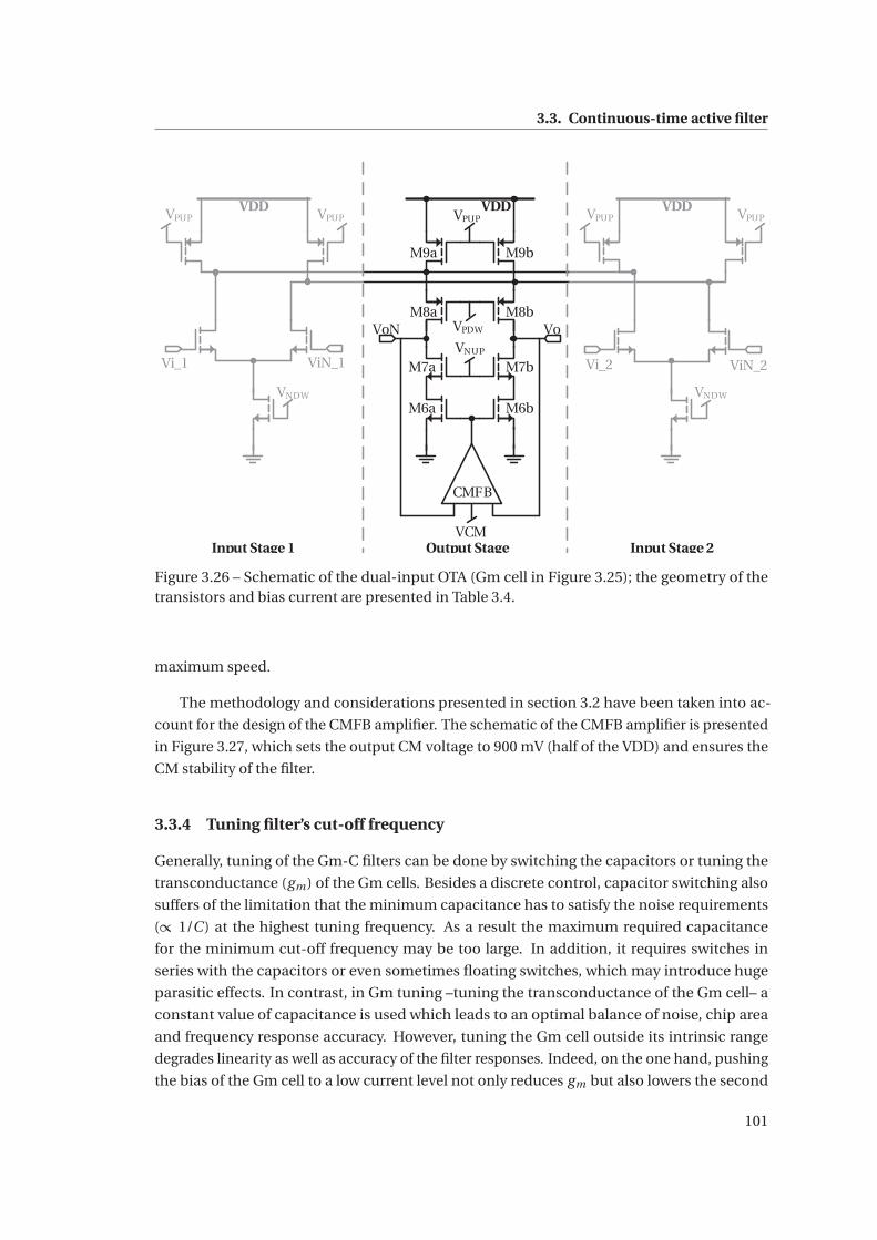
3.3. Continuous-time active filter
VPUP
VPDW
VNUP
ViN_1Vi_1
VoVoN
ViN_2Vi_2
CMFB
VCM
VNDWVNDW
VPUP VPUP VPUP VPUPVDD
Output Stage
VDD
M6a M6b
M7a M7b
M8a M8b
M9a M9b
Input Stage 1 Input Stage 2
VDD
Figure 3.26 – Schematic of the dual-input OTA (Gm cell in Figure 3.25); the geometry of thetransistors and bias current are presented in Table 3.4.
maximum speed.
The methodology and considerations presented in section 3.2 have been taken into ac-
count for the design of the CMFB amplifier. The schematic of the CMFB amplifier is presented
in Figure 3.27, which sets the output CM voltage to 900 mV (half of the VDD) and ensures the
CM stability of the filter.
3.3.4 Tuning filter’s cut-off frequency
Generally, tuning of the Gm-C filters can be done by switching the capacitors or tuning the
transconductance (gm) of the Gm cells. Besides a discrete control, capacitor switching also
suffers of the limitation that the minimum capacitance has to satisfy the noise requirements
(∝ 1/C ) at the highest tuning frequency. As a result the maximum required capacitance
for the minimum cut-off frequency may be too large. In addition, it requires switches in
series with the capacitors or even sometimes floating switches, which may introduce huge
parasitic effects. In contrast, in Gm tuning –tuning the transconductance of the Gm cell– a
constant value of capacitance is used which leads to an optimal balance of noise, chip area
and frequency response accuracy. However, tuning the Gm cell outside its intrinsic range
degrades linearity as well as accuracy of the filter responses. Indeed, on the one hand, pushing
the bias of the Gm cell to a low current level not only reduces gm but also lowers the second
101
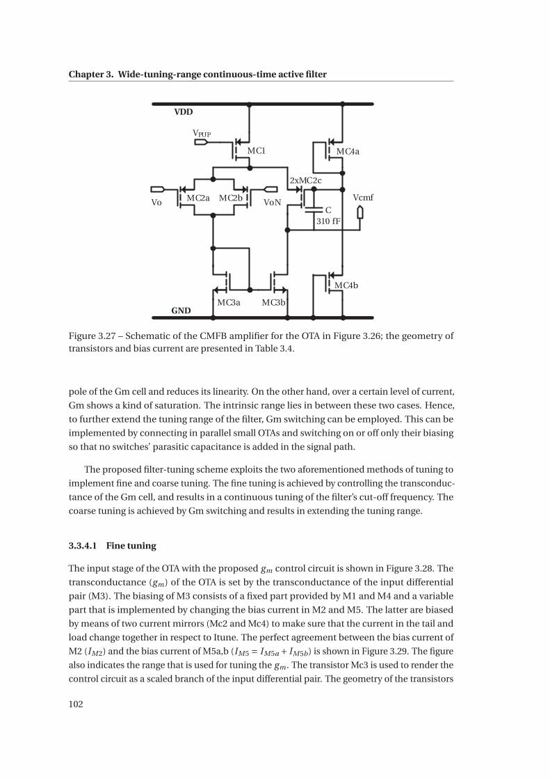
Chapter 3. Wide-tuning-range continuous-time active filter
VDD
GND
MC1
MC2a
2xMC2c
MC3a
MC4b
MC4a
Vcmf
310 fFC
VPUP
Vo VoNMC2b
MC3b
Figure 3.27 – Schematic of the CMFB amplifier for the OTA in Figure 3.26; the geometry oftransistors and bias current are presented in Table 3.4.
pole of the Gm cell and reduces its linearity. On the other hand, over a certain level of current,
Gm shows a kind of saturation. The intrinsic range lies in between these two cases. Hence,
to further extend the tuning range of the filter, Gm switching can be employed. This can be
implemented by connecting in parallel small OTAs and switching on or off only their biasing
so that no switches’ parasitic capacitance is added in the signal path.
The proposed filter-tuning scheme exploits the two aforementioned methods of tuning to
implement fine and coarse tuning. The fine tuning is achieved by controlling the transconduc-
tance of the Gm cell, and results in a continuous tuning of the filter’s cut-off frequency. The
coarse tuning is achieved by Gm switching and results in extending the tuning range.
3.3.4.1 Fine tuning
The input stage of the OTA with the proposed gm control circuit is shown in Figure 3.28. The
transconductance (gm) of the OTA is set by the transconductance of the input differential
pair (M3). The biasing of M3 consists of a fixed part provided by M1 and M4 and a variable
part that is implemented by changing the bias current in M2 and M5. The latter are biased
by means of two current mirrors (Mc2 and Mc4) to make sure that the current in the tail and
load change together in respect to Itune. The perfect agreement between the bias current of
M2 (IM2) and the bias current of M5a,b (IM5 = IM5a + IM5b) is shown in Figure 3.29. The figure
also indicates the range that is used for tuning the gm . The transistor Mc3 is used to render the
control circuit as a scaled branch of the input differential pair. The geometry of the transistors
102
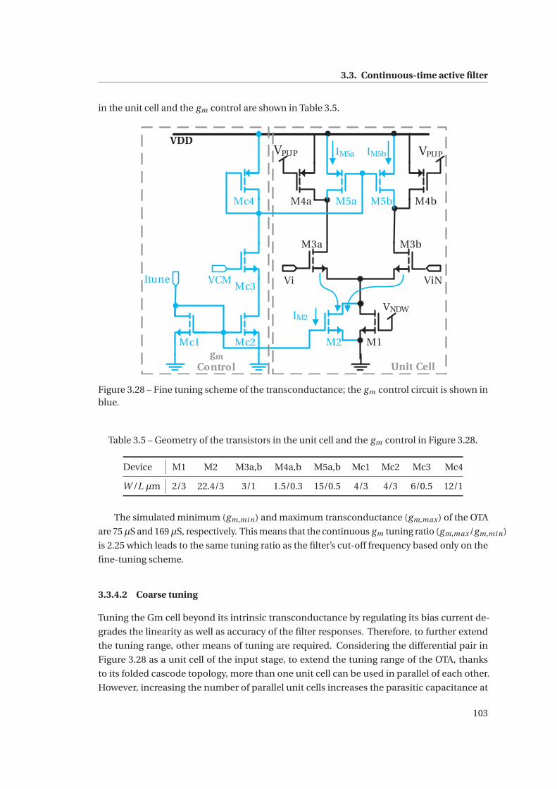
3.3. Continuous-time active filter
in the unit cell and the gm control are shown in Table 3.5.
ViNVi
VNDW
VDDVPUPVPUP
M1M2
M4a
M3b
M4bM5a M5b
M3a
Itune VCM
Mc2Mc1
Mc3
Mc4
Unit Cellgm
Control
IM5a IM5b
IM2
Figure 3.28 – Fine tuning scheme of the transconductance; the gm control circuit is shown inblue.
Table 3.5 – Geometry of the transistors in the unit cell and the gm control in Figure 3.28.
Device M1 M2 M3a,b M4a,b M5a,b Mc1 Mc2 Mc3 Mc4
W /L μm 2/3 22.4/3 3/1 1.5/0.3 15/0.5 4/3 4/3 6/0.5 12/1
The simulated minimum (gm,mi n) and maximum transconductance (gm,max ) of the OTA
are 75μS and 169μS, respectively. This means that the continuous gm tuning ratio (gm,max /gm,mi n)
is 2.25 which leads to the same tuning ratio as the filter’s cut-off frequency based only on the
fine-tuning scheme.
3.3.4.2 Coarse tuning
Tuning the Gm cell beyond its intrinsic transconductance by regulating its bias current de-
grades the linearity as well as accuracy of the filter responses. Therefore, to further extend
the tuning range, other means of tuning are required. Considering the differential pair in
Figure 3.28 as a unit cell of the input stage, to extend the tuning range of the OTA, thanks
to its folded cascode topology, more than one unit cell can be used in parallel of each other.
However, increasing the number of parallel unit cells increases the parasitic capacitance at
103
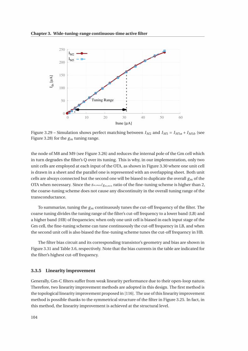
Chapter 3. Wide-tuning-range continuous-time active filter
0
50
100
150
200
250
0 10 20 30 40 50 60
Tuning Range
I ds
[μA
]
Itune [μA]
IM2
IM5
Figure 3.29 – Simulation shows perfect matching between IM2 and IM5 = IM5a + IM5b (seeFigure 3.28) for the gm tuning range.
the node of M8 and M9 (see Figure 3.26) and reduces the internal pole of the Gm cell which
in turn degrades the filter’s Q over its tuning. This is why, in our implementation, only two
unit cells are employed at each input of the OTA, as shown in Figure 3.30 where one unit cell
is drawn in a sheet and the parallel one is represented with an overlapping sheet. Both unit
cells are always connected but the second one will be biased to duplicate the overall gm of the
OTA when necessary. Since the gm,max/gm,mi n ratio of the fine-tuning scheme is higher than 2,
the coarse-tuning scheme does not cause any discontinuity in the overall tuning range of the
transconductance.
To summarize, tuning the gm continuously tunes the cut-off frequency of the filter. The
coarse tuning divides the tuning range of the filter’s cut-off frequency to a lower band (LB) and
a higher band (HB) of frequencies; when only one unit cell is biased in each input stage of the
Gm cell, the fine-tuning scheme can tune continuously the cut-off frequency in LB, and when
the second unit cell is also biased the fine-tuning scheme tunes the cut-off frequency in HB.
The filter bias circuit and its corresponding transistor’s geometry and bias are shown in
Figure 3.31 and Table 3.6, respectively. Note that the bias currents in the table are indicated for
the filter’s highest cut-off frequency.
3.3.5 Linearity improvement
Generally, Gm-C filters suffer from weak linearity performance due to their open-loop nature.
Therefore, two linearity improvement methods are adopted in this design. The first method is
the topological linearity improvement proposed in [116]. The use of this linearity improvement
method is possible thanks to the symmetrical structure of the filter in Figure 3.25. In fact, in
this method, the linearity improvement is achieved at the structural level.
104
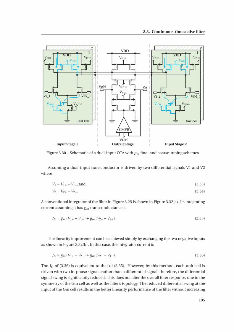
3.3. Continuous-time active filter
VPUP
VPDW
VNUP
ViN_1Vi_1
VoVoN
ViN_2Vi_2
CMFB
VCM
VNDWVNDW
VPUP VPUP VPUP VPUPVDD
Output Stage
VDD
Input Stage 1 Input Stage 2
12
12
VDD
Unit Cell Unit Cell
VtUP
VtDW VtDW
VtUP
Figure 3.30 – Schematic of a dual-input OTA with gm fine- and coarse-tuning schemes.
Assuming a dual-input transconductor is driven by two differential signals V1 and V2
where
V1 =V1+−V1−,and (3.33)
V2 =V2+−V2−. (3.34)
A conventional integrator of the filter in Figure 3.25 is shown in Figure 3.32(a). Its integrating
current assuming it has gm transconductance is
IC = gm (V1+−V1−)+ gm (V2−−V2+) . (3.35)
The linearity improvement can be achieved simply by exchanging the two negative inputs
as shown in Figure 3.32(b). In this case, the integrator current is
IC = gm (V1+−V2+)+ gm (V2−−V1−) . (3.36)
The IC of (3.36) is equivalent to that of (3.35). However, by this method, each unit cell is
driven with two in-phase signals rather than a differential signal; therefore, the differential
signal swing is significantly reduced. This does not alter the overall filter response, due to the
symmetry of the Gm cell as well as the filter’s topology. The reduced differential swing at the
input of the Gm cell results in the better linearity performance of the filter without increasing
105
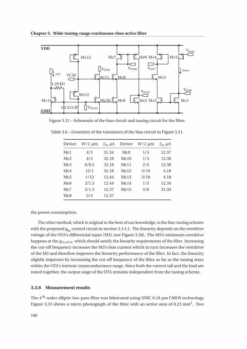
Chapter 3. Wide-tuning-range continuous-time active filter
Mc12
1.29 kΩ
215 fF
VPUP
Mc5
VPDW
VNUP
VNDW
VtDW
Mc1Mc2
Mc4
VCM
VtUP
Mc3
Mc6Mc7
Mc8
Mc9Mc10
Mc11
Mc14
Mc13 Mc15
VtuneVDD
GND
ItuneIref
Figure 3.31 – Schematic of the bias circuit and tuning circuit for the filter.
Table 3.6 – Geometry of the transistors of the bias circuit in Figure 3.31.
Device W /L μm Id s μA Device W /L μm Id s μA
Mc1 4/3 31.34 Mc9 1/3 12.37
Mc2 4/3 32.18 Mc10 1/3 12.38
Mc3 6/0.5 32.18 Mc11 2/4 12.38
Mc4 12/1 32.18 Mc12 3/10 4.18
Mc5 1/12 12.44 Mc13 3/10 4.18
Mc6 2/1.5 12.44 Mc14 1/3 12.34
Mc7 2/1.5 12.37 Mc15 5/6 31.34
Mc8 2/4 12.37
the power consumption.
The other method, which is original to the best of our knowledge, is the fine-tuning scheme
with the proposed gm control circuit in section 3.3.4.1. The linearity depends on the overdrive
voltage of the OTA’s differential input (M3) (see Figure 3.28). The M3’s minimum overdrive
happens at the gm,mi n , which should satisfy the linearity requirements of the filter. Increasing
the cut-off frequency increases the M3’s bias current which in turn increases the overdrive
of the M3 and therefore improves the linearity performance of the filter. In fact, the linearity
slightly improves by increasing the cut-off frequency of the filter as far as the tuning stays
within the OTA’s intrinsic transconductance range. Since both the current tail and the load are
tuned together, the output stage of the OTA remains independent from the tuning scheme.
3.3.6 Measurement results
The 4 th-order elliptic low-pass filter was fabricated using UMC 0.18 μm CMOS technology.
Figure 3.33 shows a micro photograph of the filter with an active area of 0.23 mm2. Two
106
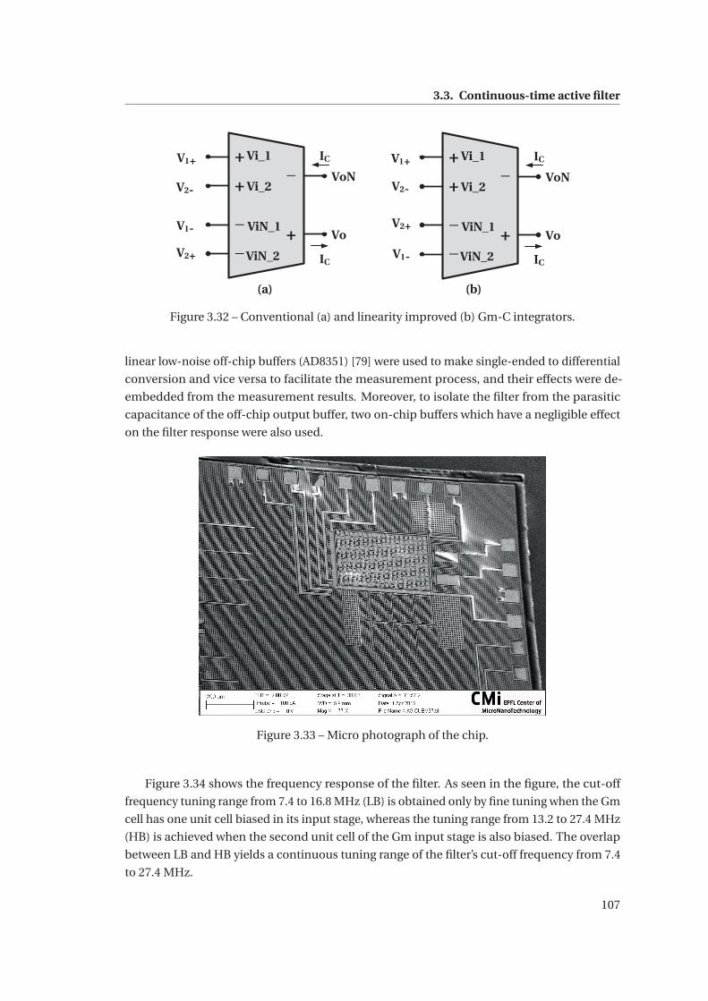
3.3. Continuous-time active filter
+
+
+
_
Vi_1
Vi_2
ViN_1
ViN_2_
_ VoN
Vo
V1+
V2+
V2-
V1-
+
+
+
_
Vi_1
Vi_2
ViN_1
ViN_2_
_ VoN
Vo
V1+
V2+
V2-
V1-
(a) (b)
IC
IC
IC
IC
Figure 3.32 – Conventional (a) and linearity improved (b) Gm-C integrators.
linear low-noise off-chip buffers (AD8351) [79] were used to make single-ended to differential
conversion and vice versa to facilitate the measurement process, and their effects were de-
embedded from the measurement results. Moreover, to isolate the filter from the parasitic
capacitance of the off-chip output buffer, two on-chip buffers which have a negligible effect
on the filter response were also used.
Figure 3.33 – Micro photograph of the chip.
Figure 3.34 shows the frequency response of the filter. As seen in the figure, the cut-off
frequency tuning range from 7.4 to 16.8 MHz (LB) is obtained only by fine tuning when the Gm
cell has one unit cell biased in its input stage, whereas the tuning range from 13.2 to 27.4 MHz
(HB) is achieved when the second unit cell of the Gm input stage is also biased. The overlap
between LB and HB yields a continuous tuning range of the filter’s cut-off frequency from 7.4
to 27.4 MHz.
107
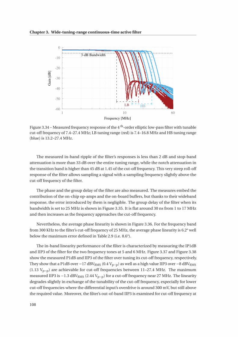
Chapter 3. Wide-tuning-range continuous-time active filter
-60
-50
-40
-30
-20
-10
0
1 10 60
3-dB Bandwidth
LB HB
Gai
n [
dB
]
Frequency [MHz]
Figure 3.34 – Measured frequency response of the 4 th-order elliptic low-pass filter with tunablecut-off frequency of 7.4–27.4 MHz; LB tuning range (red) is 7.4–16.8 MHz and HB tuning range(blue) is 13.2–27.4 MHz.
The measured in-band ripple of the filter’s responses is less than 2 dB and stop-band
attenuation is more than 33 dB over the entire tuning range, while the notch attenuation in
the transition band is higher than 45 dB at 1.45 of the cut-off frequency. This very steep roll-off
response of the filter allows sampling a signal with a sampling frequency slightly above the
cut-off frequency of the filter.
The phase and the group delay of the filter are also measured. The measures embed the
contribution of the on-chip op-amps and the on-board buffers, but thanks to their wideband
response, the error introduced by them is negligible. The group delay of the filter when its
bandwidth is set to 25 MHz is shown in Figure 3.35. It is flat around 30 ns from 1 to 17 MHz
and then increases as the frequency approaches the cut-off frequency.
Nevertheless, the average phase linearity is shown in Figure 3.36. For the frequency band
from 300 KHz to the filter’s cut-off frequency of 25 MHz, the average phase linearity is 6.2° well
below the maximum error defined in Table 2.9 (i.e. 8.6°).
The in-band linearity performance of the filter is characterized by measuring the IP1dB
and IIP3 of the filter for the two frequency tones at 5 and 6 MHz. Figure 3.37 and Figure 3.38
show the measured P1dB and IIP3 of the filter over tuning its cut-off frequency, respectively.
They show that a P1dB over −17 dBVRMS (0.4 Vp−p) as well as a high value IIP3 over −8 dBVRMS
(1.13 Vp−p) are achievable for cut-off frequencies between 11–27.4 MHz. The maximum
measured IIP3 is −1.3 dBVRMS (2.44 Vp−p) for a cut-off frequency near 27 MHz. The linearity
degrades slightly in exchange of the tunability of the cut-off frequency, especially for lower
cut-off frequencies where the differential input’s overdrive is around 300 mV, but still above
the required value. Moreover, the filter’s out-of-band IIP3 is examined for cut-off frequency at
108
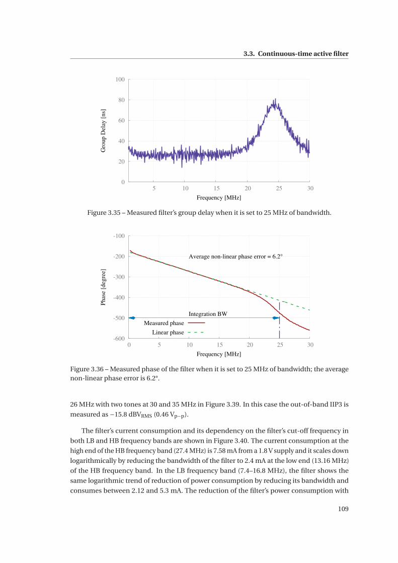
3.3. Continuous-time active filter
0
20
40
60
80
100
5 10 15 20 25 30
Gro
up D
elay
[ns]
Frequency [MHz]
Figure 3.35 – Measured filter’s group delay when it is set to 25 MHz of bandwidth.
-600
-500
-400
-300
-200
-100
0 5 10 15 20 25 30
Integration BW
Average non-linear phase error = 6.2°
Phas
e [d
egre
e]
Frequency [MHz]
Measured phase
Linear phase
Figure 3.36 – Measured phase of the filter when it is set to 25 MHz of bandwidth; the averagenon-linear phase error is 6.2°.
26 MHz with two tones at 30 and 35 MHz in Figure 3.39. In this case the out-of-band IIP3 is
measured as −15.8 dBVRMS (0.46 Vp−p).
The filter’s current consumption and its dependency on the filter’s cut-off frequency in
both LB and HB frequency bands are shown in Figure 3.40. The current consumption at the
high end of the HB frequency band (27.4 MHz) is 7.58 mA from a 1.8 V supply and it scales down
logarithmically by reducing the bandwidth of the filter to 2.4 mA at the low end (13.16 MHz)
of the HB frequency band. In the LB frequency band (7.4–16.8 MHz), the filter shows the
same logarithmic trend of reduction of power consumption by reducing its bandwidth and
consumes between 2.12 and 5.3 mA. The reduction of the filter’s power consumption with
109
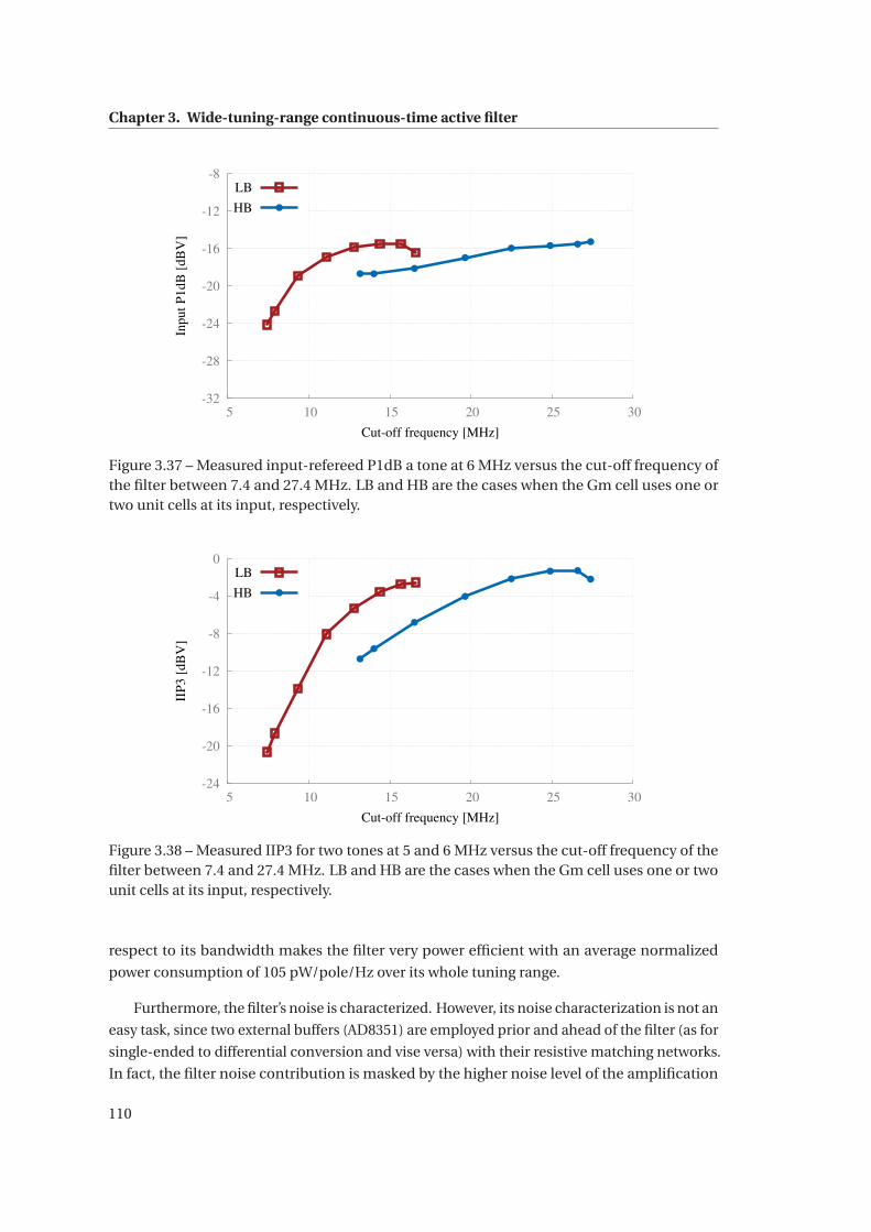
Chapter 3. Wide-tuning-range continuous-time active filter
-32
-28
-24
-20
-16
-12
-8
5 10 15 20 25 30
Input
P1dB
[dB
V]
Cut-off frequency [MHz]
LB
HB
Figure 3.37 – Measured input-refereed P1dB a tone at 6 MHz versus the cut-off frequency ofthe filter between 7.4 and 27.4 MHz. LB and HB are the cases when the Gm cell uses one ortwo unit cells at its input, respectively.
-24
-20
-16
-12
-8
-4
0
5 10 15 20 25 30
IIP
3 [
dB
V]
Cut-off frequency [MHz]
LB
HB
Figure 3.38 – Measured IIP3 for two tones at 5 and 6 MHz versus the cut-off frequency of thefilter between 7.4 and 27.4 MHz. LB and HB are the cases when the Gm cell uses one or twounit cells at its input, respectively.
respect to its bandwidth makes the filter very power efficient with an average normalized
power consumption of 105 pW/pole/Hz over its whole tuning range.
Furthermore, the filter’s noise is characterized. However, its noise characterization is not an
easy task, since two external buffers (AD8351) are employed prior and ahead of the filter (as for
single-ended to differential conversion and vise versa) with their resistive matching networks.
In fact, the filter noise contribution is masked by the higher noise level of the amplification
110
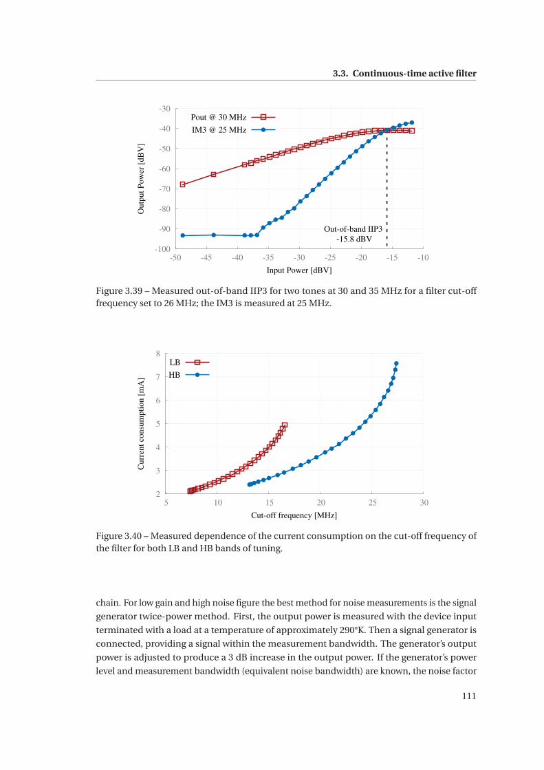
3.3. Continuous-time active filter
-100
-90
-80
-70
-60
-50
-40
-30
-50 -45 -40 -35 -30 -25 -20 -15 -10
Out-of-band IIP3
-15.8 dBV
Outp
ut
Pow
er [
dB
V]
Input Power [dBV]
Pout @ 30 MHz
IM3 @ 25 MHz
Figure 3.39 – Measured out-of-band IIP3 for two tones at 30 and 35 MHz for a filter cut-offfrequency set to 26 MHz; the IM3 is measured at 25 MHz.
2
3
4
5
6
7
8
5 10 15 20 25 30
Curr
ent
consu
mpti
on [
mA
]
Cut-off frequency [MHz]
LB
HB
Figure 3.40 – Measured dependence of the current consumption on the cut-off frequency ofthe filter for both LB and HB bands of tuning.
chain. For low gain and high noise figure the best method for noise measurements is the signal
generator twice-power method. First, the output power is measured with the device input
terminated with a load at a temperature of approximately 290°K. Then a signal generator is
connected, providing a signal within the measurement bandwidth. The generator’s output
power is adjusted to produce a 3 dB increase in the output power. If the generator’s power
level and measurement bandwidth (equivalent noise bandwidth) are known, the noise factor
111
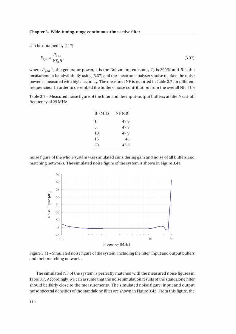
Chapter 3. Wide-tuning-range continuous-time active filter
can be obtained by [117]:
Fs y s =Pg en
kT0B, (3.37)
where Pg en is the generator power, k is the Boltzmann constant, T0 is 290°K and B is the
measurement bandwidth. By using (3.37) and the spectrum analyser’s noise marker, the noise
power is measured with high accuracy. The measured NF is reported in Table 3.7 for different
frequencies. In order to de-embed the buffers’ noise contribution from the overall NF. The
Table 3.7 – Measured noise figure of the filter and the input-output buffers; at filter’s cut-offfrequency of 25 MHz.
IF (MHz) NF (dB)
1 47.9
5 47.9
10 47.9
15 48
20 47.6
noise figure of the whole system was simulated considering gain and noise of all buffers and
matching networks. The simulated noise figure of the system is shown in Figure 3.41.
46
48
50
52
54
56
58
60
62
0.1 1 10 30
Nois
e F
igure
[dB
]
Frequency [MHz]
Figure 3.41 – Simulated noise figure of the system; including the filter, input and output buffersand their matching networks.
The simulated NF of the system is perfectly matched with the measured noise figures in
Table 3.7. Accordingly, we can assume that the noise simulation results of the standalone filter
should be fairly close to the measurements. The simulated noise figure, input and output
noise spectral densities of the standalone filter are shown in Figure 3.42. From this figure, the
112
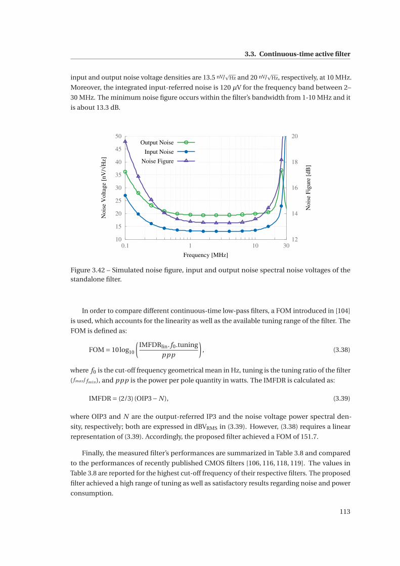
3.3. Continuous-time active filter
input and output noise voltage densities are 13.5 nV/�
Hz and 20 nV/�
Hz, respectively, at 10 MHz.
Moreover, the integrated input-referred noise is 120 μV for the frequency band between 2–
30 MHz. The minimum noise figure occurs within the filter’s bandwidth from 1-10 MHz and it
is about 13.3 dB.
10
15
20
25
30
35
40
45
50
0.1 1 10 30 12
14
16
18
20
Nois
e V
olt
age
[nV
/√H
z]
Nois
e F
igure
[dB
]
Frequency [MHz]
Output Noise
Input Noise
Noise Figure
Figure 3.42 – Simulated noise figure, input and output noise spectral noise voltages of thestandalone filter.
In order to compare different continuous-time low-pass filters, a FOM introduced in [104]
is used, which accounts for the linearity as well as the available tuning range of the filter. The
FOM is defined as:
FOM = 10log10
(IMFDRlin. f0.tuning
ppp
), (3.38)
where f0 is the cut-off frequency geometrical mean in Hz, tuning is the tuning ratio of the filter
( fmax/fmi n), and ppp is the power per pole quantity in watts. The IMFDR is calculated as:
IMFDR = (2/3)(OIP3−N ), (3.39)
where OIP3 and N are the output-referred IP3 and the noise voltage power spectral den-
sity, respectively; both are expressed in dBVRMS in (3.39). However, (3.38) requires a linear
representation of (3.39). Accordingly, the proposed filter achieved a FOM of 151.7.
Finally, the measured filter’s performances are summarized in Table 3.8 and compared
to the performances of recently published CMOS filters [106, 116, 118, 119]. The values in
Table 3.8 are reported for the highest cut-off frequency of their respective filters. The proposed
filter achieved a high range of tuning as well as satisfactory results regarding noise and power
consumption.
113
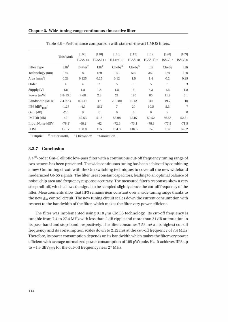
Chapter 3. Wide-tuning-range continuous-time active filter
Table 3.8 – Performance comparison with state-of-the-art CMOS filters.
This Work[106] [118] [116] [119] [112] [120] [109]
TCAS’14 TCASI’11 E-Lett.’11 TCAS’10 TCAS-I’07 JSSC’07 JSSC’06
Filter Type Elli1 Butter2 Elli1 Cheby3 Cheby3 Elli Cheby Elli
Technology [nm] 180 180 180 130 500 350 130 120
Area [mm2] 0.23 0.125 0.25 0.12 1.5 1.4 0.2 0.25
Order 4 4 3 5 3 5 5 3
Supply [V] 1.8 1.8 1.8 1.5 5 3.3 1.5 1.8
Power [mW] 3.8-13.6 4.68 2.3 21 180 85 11.2 6.1
Bandwidth [MHz] 7.4-27.4 0.3-12 17 70-280 6-12 30 19.7 10
IIP3 [dBVRMS] -1.27 -4.3 15.2 7 20 10.5 5.3 7
Gain [dB] -2.5 0 0 0 0 0 2 0
IMFDR [dB] 49 42.63 51.5 53.08 62.07 59.52 56.55 52.31
Input Noise [dBV] -78.44 -68.2 -62 -72.6 -73.1 -78.8 -77.5 -71.5
FOM 151.7 150.8 155 164.3 146.6 152 156 149.2
1 Elliptic, 2 Butterworth, 3 Chebyshev, 4 Simulation.
3.3.7 Conclusion
A 4 th-order Gm-C elliptic low-pass filter with a continuous cut-off frequency tuning range of
two octaves has been presented. The wide continuous tuning has been achieved by combining
a new Gm tuning circuit with the Gm switching techniques to cover all the new wideband
modernized GNSS signals. The filter uses constant capacitors, leading to an optimal balance of
noise, chip area and frequency response accuracy. The measured filter’s responses show a very
steep roll-off, which allows the signal to be sampled slightly above the cut-off frequency of the
filter. Measurements show that IIP3 remains near constant over a wide tuning range thanks to
the new gm control circuit. The new tuning circuit scales down the current consumption with
respect to the bandwidth of the filter, which makes the filter very power efficient.
The filter was implemented using 0.18 μm CMOS technology. Its cut-off frequency is
tunable from 7.4 to 27.4 MHz with less than 2 dB ripple and more than 31 dB attenuation in
its pass-band and stop-band, respectively. The filter consumes 7.58 mA at its highest cut-off
frequency and its consumption scales down to 2.12 mA at the cut-off frequency of 7.4 MHz,
Therefore, its power consumption depends on its bandwidth which makes the filter very power
efficient with average normalized power consumption of 105 pW/pole/Hz. It achieves IIP3 up
to −1.3 dBVRMS for the cut-off frequency near 27 MHz.
114
3.4. Effect of Q enhancement on the selectivity of the filter
3.4 Effect of Q enhancement on the selectivity of the filter
In the active filter design, the selectivity of the filter, i.e., the sharpness of the filter’s amplitude
response in its transition band, depends on the type and order of the filter. However, in
practice, due to the limited inductor’s Q, the selectivity degrades from its ideal value. In fact,
the filter entails a minimum Q for its active inductors to achieve the required selectivity. On
the other hand, the method proposed in section 3.1 offers the possibility of improving the Q to
a desirable value without any extra power consumption. However, as shown in Figure 3.2, the
Q changes by tuning the resonance frequency, which should be taken into account during the
design of a tunable filter to ensure the minimum required Q over the tuning.
This section presents the measures to employ the method proposed in section 3.1 in the
design of a tunable continuous-time active low-pass filter. Moreover, the filter proposed
in section 3.3 is adopted to demonstrate the effects of the Q-enhancement method on the
selectivity of the filter.
3.4.1 Tuning considerations for Gm-C filters
Tunable Gm-C filters employ tunable resonators and inductors. In fact, tuning the resonator’s
resonance frequency or active inductor’s value tunes the cut-off frequency of the filter. On
the other hand, as Figure 3.2 shows, for β > 2 the resonator’s Q increases by increasing its
resonance frequency. In other words, the minimum resonator’s Q occurs at the minimum
filter’s cut-off frequency. Therefore, for a tunable filter, resonators (or more precisely, the OTA
of the resonator) should be designed at the very low end of the filter’s cut-off frequency tuning
range to yield a minimum Q that satisfies the required selectivity for the filter. Designing the
OTA (Gm cell) in this way ensures that the selectivity of the filter does not degrade by tuning
the filter’s cut-off frequency to a higher value. Nevertheless, the maximum cut-off frequency
of the filter restricts how far the second pole of the OTA should be placed to ensure that β does
not reach a value close to 2 in Figure 3.2 .
3.4.2 Filter selectivity
To show the effect of enhancing the Q of the resonator on the selectivity of the filter, a highly
selective 4 th-order elliptic low-pass filter presented in section 3.3 is adopted. The same design
procedure that was used for resonator design in section 3.1 was employed to design the
filter’s OTA. The filter’s architecture and its micro photograph are shown in Figure 3.25 and
Figure 3.33, respectively. Its cut-off frequency is tunable from 7.4 to 27.4 MHz. The tunable
cut-off frequency is achieved by employing a control circuit that adjusts the overdrive voltage
of M2 and M3 (see Figure 3.28) to tune the gm,M3 from 75 to 169 μS as well as Gm switching
which has been explained in section 3.3.4.2. Thanks to the folded cascode architecture of the
OTAs and the tuning scheme of the filter, the filter’s cut-off frequency can be tuned without
affecting the OTA’s second pole. This lowers the β and enhances the Q of the inductors and
115
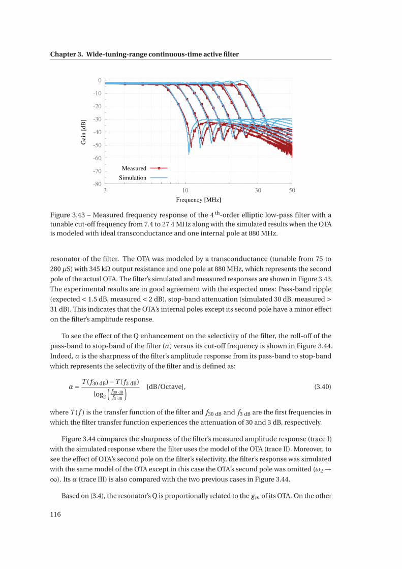
Chapter 3. Wide-tuning-range continuous-time active filter
-80
-70
-60
-50
-40
-30
-20
-10
0
3 10 30 50
Gai
n [
dB
]
Frequency [MHz]
Measured
Simulation
Figure 3.43 – Measured frequency response of the 4 th-order elliptic low-pass filter with atunable cut-off frequency from 7.4 to 27.4 MHz along with the simulated results when the OTAis modeled with ideal transconductance and one internal pole at 880 MHz.
resonator of the filter. The OTA was modeled by a transconductance (tunable from 75 to
280 μS) with 345 kΩ output resistance and one pole at 880 MHz, which represents the second
pole of the actual OTA. The filter’s simulated and measured responses are shown in Figure 3.43.
The experimental results are in good agreement with the expected ones: Pass-band ripple
(expected < 1.5 dB, measured < 2 dB), stop-band attenuation (simulated 30 dB, measured >31 dB). This indicates that the OTA’s internal poles except its second pole have a minor effect
on the filter’s amplitude response.
To see the effect of the Q enhancement on the selectivity of the filter, the roll-off of the
pass-band to stop-band of the filter (α) versus its cut-off frequency is shown in Figure 3.44.
Indeed, α is the sharpness of the filter’s amplitude response from its pass-band to stop-band
which represents the selectivity of the filter and is defined as:
α= T ( f30 dB)−T ( f3 dB)
log2
(f30 dB
f3 dB
) [dB/Octave], (3.40)
where T ( f ) is the transfer function of the filter and f30 dB and f3 dB are the first frequencies in
which the filter transfer function experiences the attenuation of 30 and 3 dB, respectively.
Figure 3.44 compares the sharpness of the filter’s measured amplitude response (trace I)
with the simulated response where the filter uses the model of the OTA (trace II). Moreover, to
see the effect of OTA’s second pole on the filter’s selectivity, the filter’s response was simulated
with the same model of the OTA except in this case the OTA’s second pole was omitted (ω2 →∞). Its α (trace III) is also compared with the two previous cases in Figure 3.44.
Based on (3.4), the resonator’s Q is proportionally related to the gm of its OTA. On the other
116
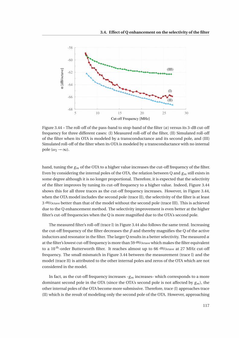
3.4. Effect of Q enhancement on the selectivity of the filter
-68
-66
-64
-62
-60
-58
5 10 15 20 25 30
(I)
(II)
(III)
α [d
B/o
ctav
e]
Cut-off Frequency [MHz]
Figure 3.44 – The roll-off of the pass-band to stop-band of the filter (α) versus its 3-dB cut-offfrequency for three different cases: (I) Measured roll-off of the filter, (II) Simulated roll-offof the filter when its OTA is modeled by a transconductance and its second pole, and (III)Simulated roll-off of the filter when its OTA is modeled by a transconductance with no internalpole (ω2 →∞).
hand, tuning the gm of the OTA to a higher value increases the cut-off frequency of the filter.
Even by considering the internal poles of the OTA, the relation between Q and gm still exists in
some degree although it is no longer proportional. Therefore, it is expected that the selectivity
of the filter improves by tuning its cut-off frequency to a higher value. Indeed, Figure 3.44
shows this for all three traces as the cut-off frequency increases. However, in Figure 3.44,
when the OTA model includes the second pole (trace II), the selectivity of the filter is at least
3 dB/Octave better than that of the model without the second pole (trace III). This is achieved
due to the Q enhancement method. The selectivity improvement is even better at the higher
filter’s cut-off frequencies when the Q is more magnified due to the OTA’s second pole.
The measured filter’s roll-off (trace I) in Figure 3.44 also follows the same trend. Increasing
the cut-off frequency of the filter decreases the β and thereby magnifies the Q of the active
inductors and resonator in the filter. The larger Q results in a better selectivity. The measured α
at the filter’s lowest cut-off frequency is more than 59 dB/Octave which makes the filter equivalent
to a 10 th-order Butterworth filter. It reaches almost up to 66 dB/Octave at 27 MHz cut-off
frequency. The small mismatch in Figure 3.44 between the measurement (trace I) and the
model (trace II) is attributed to the other internal poles and zeros of the OTA which are not
considered in the model.
In fact, as the cut-off frequency increases -gm increases- which corresponds to a more
dominant second pole in the OTA (since the OTA’s second pole is not affected by gm), the
other internal poles of the OTA become more submissive. Therefore, trace (I) approaches trace
(II) which is the result of modeling only the second pole of the OTA. However, approaching
117
Chapter 3. Wide-tuning-range continuous-time active filter
the limit of the OTA’s intrinsic range (see section 3.3.4) deteriorates the accuracy of the filter
response and thus degrades its selectivity as can be seen for trace (I) of Figure 3.44 for the
cut-off frequencies above 25 MHz.
3.4.3 Conclusion
This section described how to employ the Q-enhancement methodology presented in sec-
tion 3.1 in the design of a wide-tuning-range filter. Moreover, the effects of Q-enhancement
on the selectivity of the filter were described and the considerations for the OTA design based
on the tuning range of the filter were presented.
It has been shown that, in a proper design, the OTA’s internal poles except its second
pole have a minor effect on the filter’s amplitude response. To that end, the highly-selective
4 th-order elliptic low-pass filter of section 3.3 was adopted and modeled by OTAs with only
one internal pole which corresponds to the second pole of the filter’s OTA. The simulation
responses of the model and measured responses of the filter were in good agreement with
one another. Both filter’s cut-off frequencies are tunable from 7.4 to 27.4 MHz with less than
2 dB ripple and more than 31 dB attenuation in their pass-band and stop-band, respectively.
Moreover, the measured pass-band to stop-band’s roll-off of the filter at its lowest cut-off
frequency is more than 59 dB/Octave which is the same as the ideal selectivity of a 10 th-order
Butterworth filter. The selectivity increases nearly to 66 dB/Octave at 25 MHz cut-off frequency
as was expected from the model.
118
4 Multi-constellation L1/E1/B1 receiver
Although the GPS was devised and developed primarily for military purposes, its civil use
has increased considerably since the end of the Cold War. Recently, the demand for a higher
position accuracy and availability has increased, which GPS-L1 C/A only receivers cannot
fully satisfy. Indeed, the current GPS-L1 C/A open signal has poor sensitivity performance
in a multipath environment [15]. Fortunately, multi-band GPS receivers can provide better
accuracy [45]. However, since the GPS bands are located far away from each other in the
frequency domain, multi-band GPS receivers require front-ends that consume more power
and are therefore not the best choice for mass-market applications requiring ultra-low power
consumption.
Currently, as stated in section 1.3, besides GPS, the Russian GLONASS is also fully opera-
tional, and two more systems, the Chinese Beidou and the EU Galileo, will become operational
in the near future. These additional GNSSs can be used to improve the performance of GPS
receivers. Indeed, a much improved availability can be achieved by employing different con-
stellations, which increases the number of visible satellites for the receiver. Inter-operation
among the GNSS systems can improve signal reliability in hostile environments and system
reliability in case of malfunctioning of one of the constellations [15, 16].
To that end, the purpose of this research was to design a hybrid GPS/Galileo/Beidou front-
end (FE) for mass-market civil applications. As mass-market applications demand compact,
low-power and low-cost solutions, the front-end has been integrated on a cost-effective
0.18 μm CMOS process. Moreover, the front-end is intended to be capable of receiving Beidou
B1-I, GPS L1C, and Galileo E1 B/C simultaneously.
The FE’s architecture selection and frequency plan are laid out in section 4.1. By having
in mind that the FE is targeting the mass market applications, system specifications were
derived for all the sub-systems in section 4.2. The design of each sub-system is presented in
section 4.3. Finally, this chapter is concluded by presenting the measured characterizations of
the FE in section 4.4.
119
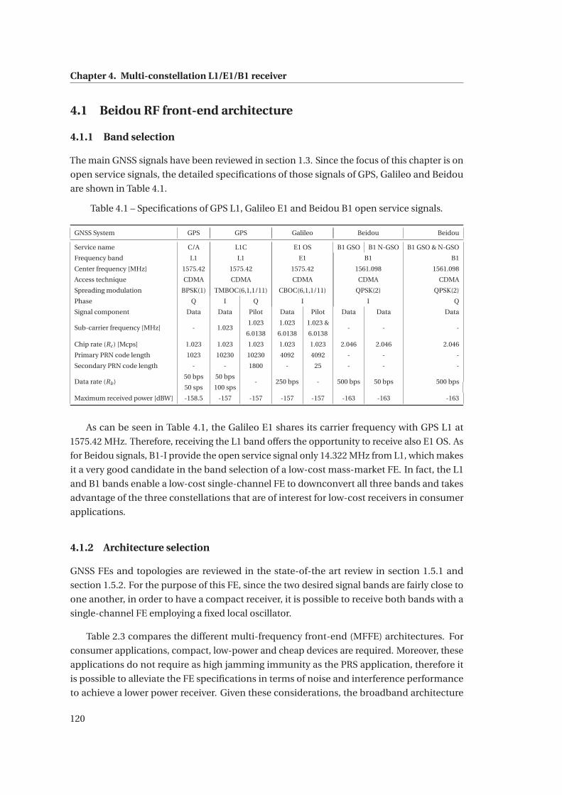
Chapter 4. Multi-constellation L1/E1/B1 receiver
4.1 Beidou RF front-end architecture
4.1.1 Band selection
The main GNSS signals have been reviewed in section 1.3. Since the focus of this chapter is on
open service signals, the detailed specifications of those signals of GPS, Galileo and Beidou
are shown in Table 4.1.
Table 4.1 – Specifications of GPS L1, Galileo E1 and Beidou B1 open service signals.
GNSS System GPS GPS Galileo Beidou Beidou
Service name C/A L1C E1 OS B1 GSO B1 N-GSO B1 GSO & N-GSO
Frequency band L1 L1 E1 B1 B1
Center frequency [MHz] 1575.42 1575.42 1575.42 1561.098 1561.098
Access technique CDMA CDMA CDMA CDMA CDMA
Spreading modulation BPSK(1) TMBOC(6,1,1/11) CBOC(6,1,1/11) QPSK(2) QPSK(2)
Phase Q I Q I I Q
Signal component Data Data Pilot Data Pilot Data Data Data
Sub-carrier frequency [MHz] - 1.0231.023 1.023 1.023 &
- - -6.0138 6.0138 6.0138
Chip rate (Rc ) [Mcps] 1.023 1.023 1.023 1.023 1.023 2.046 2.046 2.046
Primary PRN code length 1023 10230 10230 4092 4092 - - -
Secondary PRN code length - - 1800 - 25 - - -
Data rate (Rb)50 bps 50 bps
- 250 bps - 500 bps 50 bps 500 bps50 sps 100 sps
Maximum received power [dBW] -158.5 -157 -157 -157 -157 -163 -163 -163
As can be seen in Table 4.1, the Galileo E1 shares its carrier frequency with GPS L1 at
1575.42 MHz. Therefore, receiving the L1 band offers the opportunity to receive also E1 OS. As
for Beidou signals, B1-I provide the open service signal only 14.322 MHz from L1, which makes
it a very good candidate in the band selection of a low-cost mass-market FE. In fact, the L1
and B1 bands enable a low-cost single-channel FE to downconvert all three bands and takes
advantage of the three constellations that are of interest for low-cost receivers in consumer
applications.
4.1.2 Architecture selection
GNSS FEs and topologies are reviewed in the state-of-the art review in section 1.5.1 and
section 1.5.2. For the purpose of this FE, since the two desired signal bands are fairly close to
one another, in order to have a compact receiver, it is possible to receive both bands with a
single-channel FE employing a fixed local oscillator.
Table 2.3 compares the different multi-frequency front-end (MFFE) architectures. For
consumer applications, compact, low-power and cheap devices are required. Moreover, these
applications do not require as high jamming immunity as the PRS application, therefore it
is possible to alleviate the FE specifications in terms of noise and interference performance
to achieve a lower power receiver. Given these considerations, the broadband architecture
120
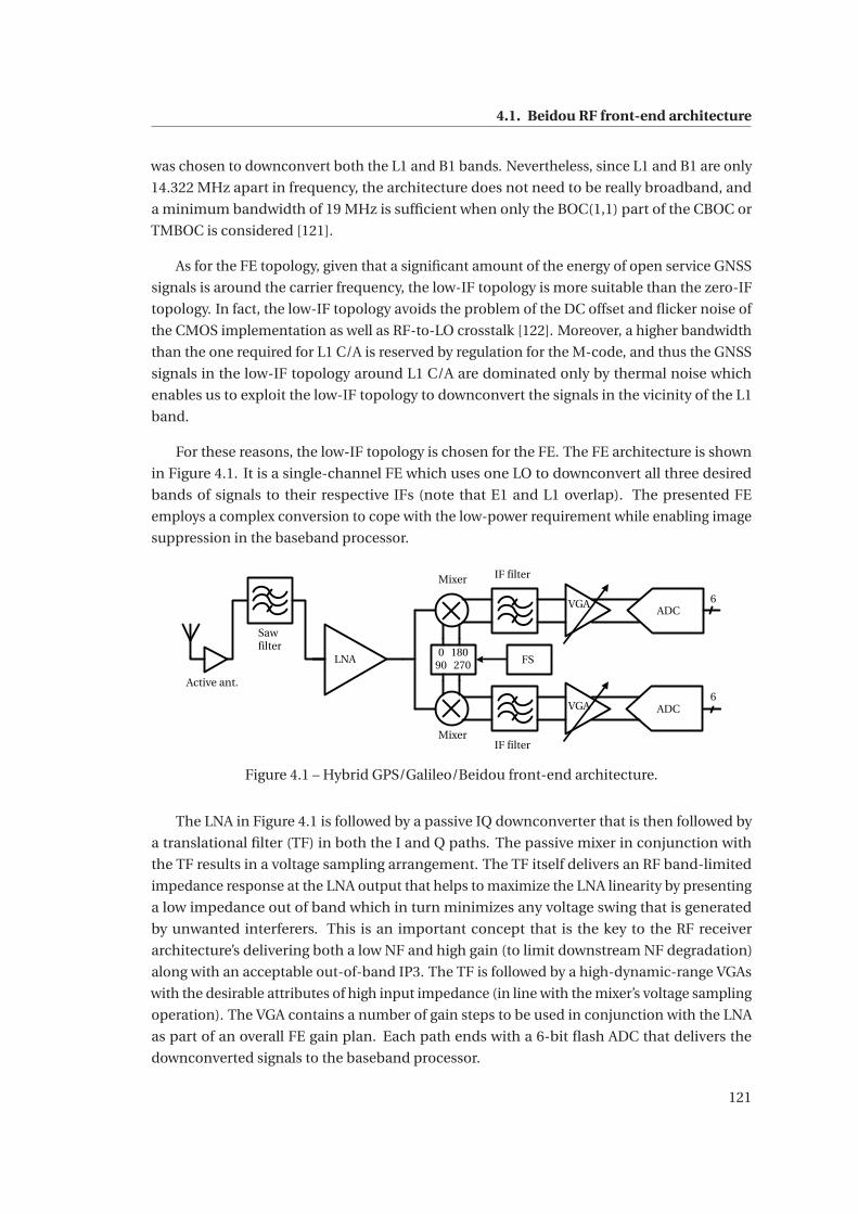
4.1. Beidou RF front-end architecture
was chosen to downconvert both the L1 and B1 bands. Nevertheless, since L1 and B1 are only
14.322 MHz apart in frequency, the architecture does not need to be really broadband, and
a minimum bandwidth of 19 MHz is sufficient when only the BOC(1,1) part of the CBOC or
TMBOC is considered [121].
As for the FE topology, given that a significant amount of the energy of open service GNSS
signals is around the carrier frequency, the low-IF topology is more suitable than the zero-IF
topology. In fact, the low-IF topology avoids the problem of the DC offset and flicker noise of
the CMOS implementation as well as RF-to-LO crosstalk [122]. Moreover, a higher bandwidth
than the one required for L1 C/A is reserved by regulation for the M-code, and thus the GNSS
signals in the low-IF topology around L1 C/A are dominated only by thermal noise which
enables us to exploit the low-IF topology to downconvert the signals in the vicinity of the L1
band.
For these reasons, the low-IF topology is chosen for the FE. The FE architecture is shown
in Figure 4.1. It is a single-channel FE which uses one LO to downconvert all three desired
bands of signals to their respective IFs (note that E1 and L1 overlap). The presented FE
employs a complex conversion to cope with the low-power requirement while enabling image
suppression in the baseband processor.
Mixer
Saw
filter
Active ant.
LNA
IF filter
FS
VGAADC
6
0
90
180
270
Mixer
IF filter
VGA ADC6
Figure 4.1 – Hybrid GPS/Galileo/Beidou front-end architecture.
The LNA in Figure 4.1 is followed by a passive IQ downconverter that is then followed by
a translational filter (TF) in both the I and Q paths. The passive mixer in conjunction with
the TF results in a voltage sampling arrangement. The TF itself delivers an RF band-limited
impedance response at the LNA output that helps to maximize the LNA linearity by presenting
a low impedance out of band which in turn minimizes any voltage swing that is generated
by unwanted interferers. This is an important concept that is the key to the RF receiver
architecture’s delivering both a low NF and high gain (to limit downstream NF degradation)
along with an acceptable out-of-band IP3. The TF is followed by a high-dynamic-range VGAs
with the desirable attributes of high input impedance (in line with the mixer’s voltage sampling
operation). The VGA contains a number of gain steps to be used in conjunction with the LNA
as part of an overall FE gain plan. Each path ends with a 6-bit flash ADC that delivers the
downconverted signals to the baseband processor.
121
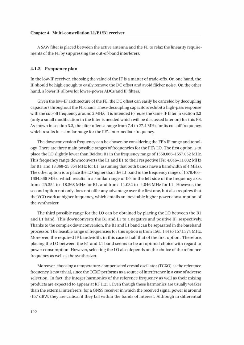
Chapter 4. Multi-constellation L1/E1/B1 receiver
A SAW filter is placed between the active antenna and the FE to relax the linearity require-
ments of the FE by suppressing the out-of-band interferers.
4.1.3 Frequency plan
In the low-IF receiver, choosing the value of the IF is a matter of trade-offs. On one hand, the
IF should be high enough to easily remove the DC offset and avoid flicker noise. On the other
hand, a lower IF allows for lower-power ADCs and IF filters.
Given the low-IF architecture of the FE, the DC offset can easily be canceled by decoupling
capacitors throughout the FE chain. These decoupling capacitors exhibit a high-pass response
with the cut-off frequency around 2 MHz. It is intended to reuse the same IF filter in section 3.3
(only a small modification in the filter is needed which will be discussed later on) for this FE.
As shown in section 3.3, the filter offers a range from 7.4 to 27.4 MHz for its cut-off frequency,
which results in a similar range for the FE’s intermediate frequency.
The downconversion frequency can be chosen by considering the FE’s IF range and topol-
ogy. There are three main possible ranges of frequencies for the FE’s LO. The first option is to
place the LO slightly lower than Beidou B1 in the frequency range of 1550.066–1557.052 MHz.
This frequency range downconverts the L1 and B1 to their respective IFs: 4.046–11.032 MHz
for B1, and 18.368–25.354 MHz for L1 (assuming that both bands have a bandwidth of 4 MHz).
The other option is to place the LO higher than the L1 band in the frequency range of 1579.466–
1604.866 MHz, which results in a similar range of IFs in the left side of the frequency axis:
from -25.354 to -18.368 MHz for B1, and from -11.032 to -4.046 MHz for L1. However, the
second option not only does not offer any advantage over the first one, but also requires that
the VCO work at higher frequency, which entails an inevitable higher power consumption of
the synthesizer.
The third possible range for the LO can be obtained by placing the LO between the B1
and L1 band. This downconverts the B1 and L1 to a negative and positive IF, respectively.
Thanks to the complex downconversion, the B1 and L1 band can be separated in the baseband
processor. The feasible range of frequencies for this option is from 1565.144 to 1571.374 MHz.
Moreover, the required IF bandwidth, in this case is half that of the first option. Therefore,
placing the LO between the B1 and L1 band seems to be an optimal choice with regard to
power consumption. However, selecting the LO also depends on the choice of the reference
frequency as well as the synthesizer.
Moreover, choosing a temperature-compensated crystal oscillator (TCXO) as the reference
frequency is not trivial, since the TCXO performs as a source of interference in a case of adverse
selection. In fact, the integer harmonics of the reference frequency as well as their mixing
products are expected to appear at RF [123]. Even though these harmonics are usually weaker
than the external interferers, for a GNSS receiver in which the received signal power is around
-157 dBW, they are critical if they fall within the bands of interest. Although in differential
122
4.1. Beidou RF front-end architecture
implementation the even harmonics of the reference frequency will be canceled, achieving
the perfect cancellation of the even harmonics requires a particular attention in the layout of
the FE to be completely symmetrical. This is hard to achieve and guarantee, and it is therefore
better to avoid having any harmonic in the desired bands. For this reason, a good practice is
to consider all the integer harmonics of the reference frequency and make sure that none of
them falls within the B1 and L1 bands.
As a consequence, even though the LO range of 1565.144–1571.374 MHz seems optimal
with regard to power consumption, the FE requires either a fractional-N PLL in the synthesizer
with any common practical TCXOs of 16.369, 26, 30.72, 49.125, 50.1, 50.625 or 51.84 MHz or
an integer-N with a big prime number divider. Therefore, for the simplicity of the design,
1555.2 MHz is chosen as the LO (LO below the B1 band). Since the downconverter requires
quadrature clocks, twice this frequency can be achieved by an integer-N PLL with N = 60 from
a TCXO of 51.84 MHz.
L1 C/A
BPSK(1)
L1/E1
B1-I OS
BPSK(2)
B1
E1 B/C(OS)
CBOC(6,1,1/11)
1575.42f MHz
1561.098
2 MHz4 MHz
4 MHz
1555.2
LO
20.22f MHz
5.8980
2 MHz4 MHz
4 MHz
Down-
conversion
LPF with
DC notch
NB mode-8 MHzWB mode-23 MHzLPF with
DC notch
Figure 4.2 – Frequency plan of the GNSS front-end: GPS L1 C/A, Galileo E1 B/C and BeidouB1-I downconversion to IF.
Accordingly, the frequency plan for this RF receiver is outlined in Figure 4.2. Setting the LO
at 1555.2 MHz results in the IFs of 5.898 and 20.22 MHz for the B1 and L1, respectively. As was
mentioned before, the IF filter’s fc is tunable which, in combination with this frequency plan,
results in a reconfigurable FE with two modes of operation: narrow-band (NB) and wide-band
(WB). For fc at 8 MHz, the FE is able to receive the B1-I with a 4 MHz BW in its NB mode, and
is capable of receiving both the L1 and B1-I for fc at 23 MHz in its WB mode.
123
Chapter 4. Multi-constellation L1/E1/B1 receiver
4.2 Beidou RF front-end specifications
4.2.1 Power supply
Since the front-end is designed for portable and battery-powered applications, its power con-
sumption is of course one concern of the design. Considering the state-of-the art GNSS MFFEs
in Table 1.2, the average power consumption of a FE is 54 mW. This value is half of the intended
power for the PRS receiver presented in section 2, which has two independent FE operating
simultaneously. Therefore, 54 mW is considered as the maximum power consumption for
the FE in its WB mode of operation. In the NB operating mode, however, the FE requires less
bandwidth in its IF section as well as lower sampling rate for its ADCs. Therefore, its power
consumption will be less than 54 mW.
4.2.2 Noise and sensitivity
The definition of the FE’s noise figure (NF) is stated in section 2.3.2. In this section the relation
between the noise and sensitivity of the FE is discussed to derive the maximum acceptable
NF of the FE. The NF of the FE will degrade its sensitivity as well as the positioning accuracy
of the receiver. The noise figure requirement of a FE is usually determined by FE’s minimum
acceptable SNR. Given that the received signal strength for the L1, E1 and B1 is around -
157 dBW, it is clear that these signals are dominated by thermal noise at the receiver’s input,
and therefore have negative SNRs. Fortunately, since GNSS signals are being DSSS, their SNRs
increase after despreading. Despreading correlates each signal with its respective PRN code
and as a result concentrates the energy of the signal to a narrower bandwidth equivalent to the
data rate (Rb) of the signal. On the other hand, since the noise is not correlated with the PRN
code, its power will not be concentrated in the narrower bandwidth which results in higher
SNR for the signal after the correlation. The boost in the SNR is determined by the processing
gain (GP ), which depends on the data rate (Rb) and the chip rate (Rc ) of the signal, and can be
calculated for any GNSS signal by:
GP = 10log10
(Rc
Rb
)[dB]. (4.1)
Note that the processing gain can be further increased by integrating the signal beyond
the bit boundary, either coherently or non-coherently depending on the knowledge or not
of the data bits. Nevertheless, with the coherent integration, from (4.1) and Table 4.1, the
GP is 43.1 dB for the L1 C/A and 36.1 dB for E1 and B1-I. However, despreading takes place
in the baseband processor and the SNR of these signals is negative throughout the FE. This
means that the bandwidth and SNR of the GNSS signals vary in the receivers from the FE to
the baseband processor. Pre-correlation SNRs are negative, whereas post-correlation SNRs
are positive. Therefore, it is convenient to normalize the SNR to 1 Hz and achieve a C /N0 that
124
4.2. Beidou RF front-end specifications
is independent of the signal’s bandwidth [61] (note that the signal’s bandwidths before and
after correlation are different). The C /N0 can easily be converted to SNR or Eb/N0 using the
following equation:
C
N0[ratio−Hz] =
(S
N
)[ratio] B [Hz] =
(Eb
N0
)[ratio] Rb [Hz], (4.2)
where B is the bandwidth of the signal and the terms in square brackets denote the units. The
minimum required C /N0 at the ADC’s output is determined by the specific algorithm and
integration time within the digital baseband processor. Once the minimum required C /N0 is
given by a digital correlator, to maintain the wanted acquisition or tracking performance, the
receiver sensitivity (S) is uniquely determined as [2]:
S [dBm] =(
C
N0
)mi n
[dB−Hz]+N0
[dBm
Hz
]+NF [dB]
=(
Eb
N0
)mi n
[dB]+10log10 Rb [dB−Hz]+N0
[dBm
Hz
]+NF [dB]. (4.3)
Note that N0 is the thermal noise power density, which is equal to -174 dBm/Hz, and the terms in
square brackets denote the units in which C /N0 is being expressed. Assuming that the digital
correlator yields a minimum C /N0 of 25 dB-Hz, with a NF of 4 dB the receiver can achieve
-145 dBm of sensitivity. Nevertheless, there is degradation of the receiver sensitivity due to the
limited resolution of the ADC which is less than 0.5 dB for a 6-bit ADC [2, 61]. Note that 4 dB
NF is for the FE including a RF filter and an active antenna. Considering, as a conservative
worst case, an active antenna with 20 dB of gain and 3 dB of NF followed by a RF filter with
5 dB of loss, the ASIC FE with a NF of 12 dB will result in an overall NF of less than 4 dB for the
receiver.
4.2.3 Gain
The required gain of the FE can be derived by considering the fact that it should amplify the
noise signal at its input to a detectable signal for its ADC. Similar to chapter 2 a 6-bit ADC with
a 500 mV full-scale input dynamic range is employed in this FE. With 4 bits of back-off for
interference mitigation, the required ADC’s input voltage is around 31.25 mVpp. Since for a
GNSS receiver, the signal that reaches the ADC is mainly thermal noise, it can be considered
that 31.25 mVpp is three times the standard deviation (σ) of the noise voltage. Therefore, the
required RMS voltage at the input of the ADC is 10.42 mVRMS. The ratio between this voltage
and the noise voltage at the input of the antenna determines the required voltage gain of the
FE. To that effect, the input noise power within the FE’s bandwidth of 21 MHz (WB mode) in
absence of any interference can be calculated by:
Pn,ant [dBm] = N0 +10log(B) ≈−101 dBm, (4.4)
125
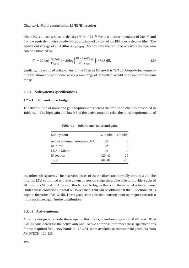
Chapter 4. Multi-constellation L1/E1/B1 receiver
where N0 is the noise spectral density (N0 ≈−174 dBm/Hz at a room temperature of 290 °K) and
B is the equivalent noise bandwidth approximated by that of the FE’s most selective filter. The
equivalent voltage of -101 dBm is 2 μVRMS. Accordingly, the required receiver’s voltage gain
can be estimated by:
Gv = 20log
(Vn,ADC
Vn,ant
)= 20log
(10.42 mVRMS
2 μVRMS
)≈ 74.3 dB. (4.5)
Similarly, the required voltage gain for the FE in its NB mode is 79.3 dB. Considering tempera-
ture variations and additional losses, a gain range of 68 to 88 dB would be an appropriate gain
range.
4.2.4 Subsystems specifications
4.2.4.1 Gain and noise budget
The distribution of noise and gain requirements across the front-end chain is presented in
Table 4.2. The high gain and low NF of the active antenna relax the noise requirements of
Table 4.2 – Subsystems’ noise and gain.
Sub-system Gain (dB) NF (dB)
Active antenna (antenna+LNA) 30 3
RF filter -2 2
LNA + Mixer 20 4
IF section [20, 40] 25
Total [68, 88] < 3
the other sub-systems. The insertion losses of the RF filters are normally around 2 dB. The
internal LNA combined with the downconversion stage should be able to provide a gain of
20 dB with a NF of 4 dB. However, this NF can be higher thanks to the external active antenna.
Under these conditions, a total NF lower than 4 dB can be obtained if the IF section’s NF is
kept on the order of 25–30 dB. These goals seem a feasible starting point to progress towards a
more optimized gain/noise distribution.
4.2.4.2 Active antenna
Antenna design is outside the scope of this thesis, therefore a gain of 30 dB and NF of
2 dB is considered for the active antenna. Active antennas that meet these specifications
for the required frequency bands (L1/E1/B1-I) are available as commercial products from
AMOTECH [124, 125].
126
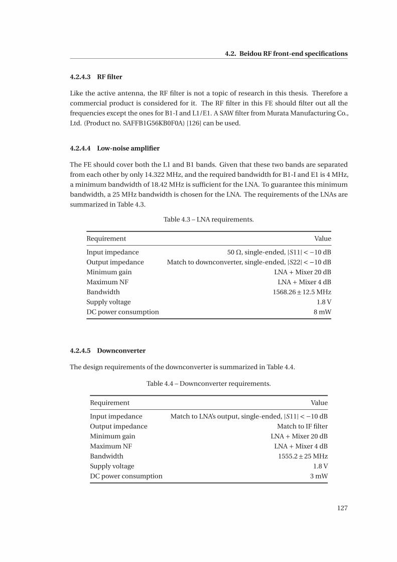
4.2. Beidou RF front-end specifications
4.2.4.3 RF filter
Like the active antenna, the RF filter is not a topic of research in this thesis. Therefore a
commercial product is considered for it. The RF filter in this FE should filter out all the
frequencies except the ones for B1-I and L1/E1. A SAW filter from Murata Manufacturing Co.,
Ltd. (Product no. SAFFB1G56KB0F0A) [126] can be used.
4.2.4.4 Low-noise amplifier
The FE should cover both the L1 and B1 bands. Given that these two bands are separated
from each other by only 14.322 MHz, and the required bandwidth for B1-I and E1 is 4 MHz,
a minimum bandwidth of 18.42 MHz is sufficient for the LNA. To guarantee this minimum
bandwidth, a 25 MHz bandwidth is chosen for the LNA. The requirements of the LNAs are
summarized in Table 4.3.
Table 4.3 – LNA requirements.
Requirement Value
Input impedance 50 Ω, single-ended, |S11| < −10 dB
Output impedance Match to downconverter, single-ended, |S22| < −10 dB
Minimum gain LNA + Mixer 20 dB
Maximum NF LNA + Mixer 4 dB
Bandwidth 1568.26±12.5 MHz
Supply voltage 1.8 V
DC power consumption 8 mW
4.2.4.5 Downconverter
The design requirements of the downconverter is summarized in Table 4.4.
Table 4.4 – Downconverter requirements.
Requirement Value
Input impedance Match to LNA’s output, single-ended, |S11| < −10 dB
Output impedance Match to IF filter
Minimum gain LNA + Mixer 20 dB
Maximum NF LNA + Mixer 4 dB
Bandwidth 1555.2±25 MHz
Supply voltage 1.8 V
DC power consumption 3 mW
127
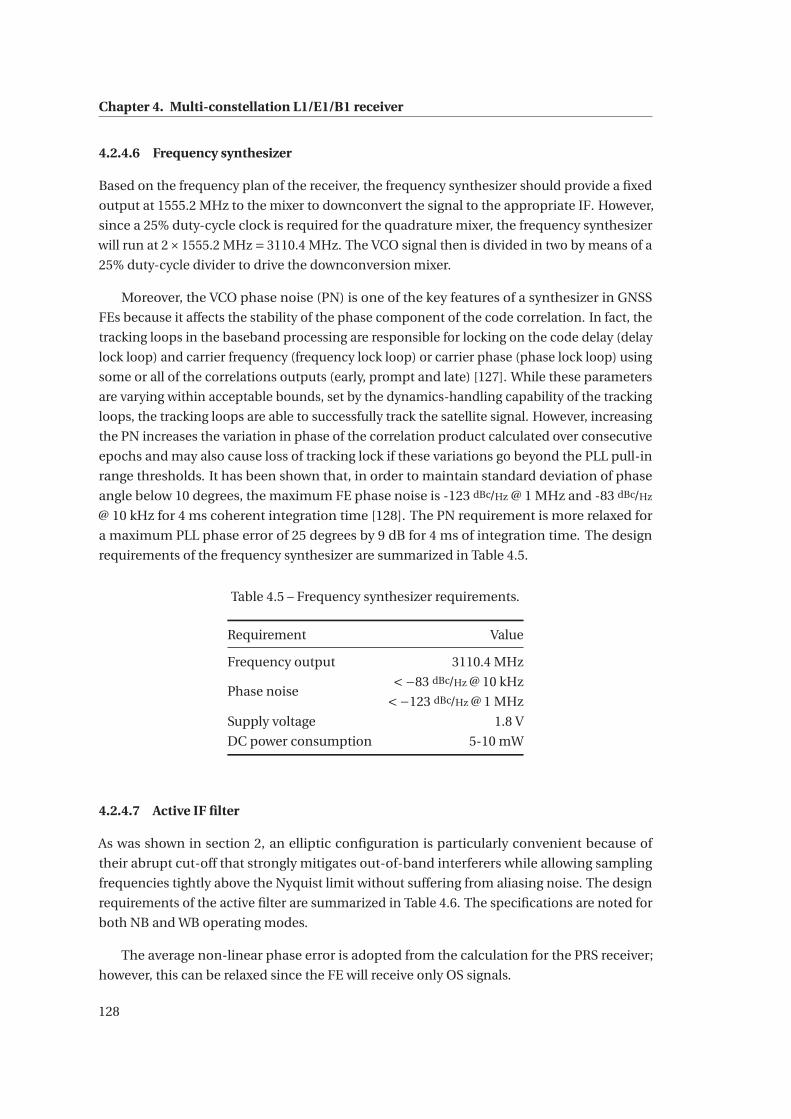
Chapter 4. Multi-constellation L1/E1/B1 receiver
4.2.4.6 Frequency synthesizer
Based on the frequency plan of the receiver, the frequency synthesizer should provide a fixed
output at 1555.2 MHz to the mixer to downconvert the signal to the appropriate IF. However,
since a 25% duty-cycle clock is required for the quadrature mixer, the frequency synthesizer
will run at 2×1555.2 MHz = 3110.4 MHz. The VCO signal then is divided in two by means of a
25% duty-cycle divider to drive the downconversion mixer.
Moreover, the VCO phase noise (PN) is one of the key features of a synthesizer in GNSS
FEs because it affects the stability of the phase component of the code correlation. In fact, the
tracking loops in the baseband processing are responsible for locking on the code delay (delay
lock loop) and carrier frequency (frequency lock loop) or carrier phase (phase lock loop) using
some or all of the correlations outputs (early, prompt and late) [127]. While these parameters
are varying within acceptable bounds, set by the dynamics-handling capability of the tracking
loops, the tracking loops are able to successfully track the satellite signal. However, increasing
the PN increases the variation in phase of the correlation product calculated over consecutive
epochs and may also cause loss of tracking lock if these variations go beyond the PLL pull-in
range thresholds. It has been shown that, in order to maintain standard deviation of phase
angle below 10 degrees, the maximum FE phase noise is -123 dBc/Hz @ 1 MHz and -83 dBc/Hz
@ 10 kHz for 4 ms coherent integration time [128]. The PN requirement is more relaxed for
a maximum PLL phase error of 25 degrees by 9 dB for 4 ms of integration time. The design
requirements of the frequency synthesizer are summarized in Table 4.5.
Table 4.5 – Frequency synthesizer requirements.
Requirement Value
Frequency output 3110.4 MHz
Phase noise<−83 dBc/Hz @ 10 kHz
<−123 dBc/Hz @ 1 MHz
Supply voltage 1.8 V
DC power consumption 5-10 mW
4.2.4.7 Active IF filter
As was shown in section 2, an elliptic configuration is particularly convenient because of
their abrupt cut-off that strongly mitigates out-of-band interferers while allowing sampling
frequencies tightly above the Nyquist limit without suffering from aliasing noise. The design
requirements of the active filter are summarized in Table 4.6. The specifications are noted for
both NB and WB operating modes.
The average non-linear phase error is adopted from the calculation for the PRS receiver;
however, this can be relaxed since the FE will receive only OS signals.
128
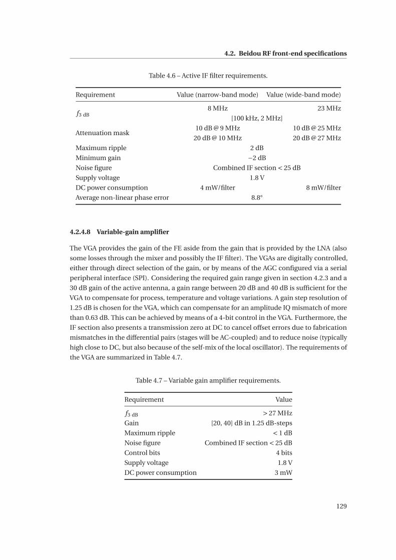
4.2. Beidou RF front-end specifications
Table 4.6 – Active IF filter requirements.
Requirement Value (narrow-band mode) Value (wide-band mode)
f3 dB8 MHz 23 MHz
[100 kHz, 2 MHz]
Attenuation mask10 dB @ 9 MHz 10 dB @ 25 MHz
20 dB @ 10 MHz 20 dB @ 27 MHz
Maximum ripple 2 dB
Minimum gain −2 dB
Noise figure Combined IF section < 25 dB
Supply voltage 1.8 V
DC power consumption 4 mW/filter 8 mW/filter
Average non-linear phase error 8.8°
4.2.4.8 Variable-gain amplifier
The VGA provides the gain of the FE aside from the gain that is provided by the LNA (also
some losses through the mixer and possibly the IF filter). The VGAs are digitally controlled,
either through direct selection of the gain, or by means of the AGC configured via a serial
peripheral interface (SPI). Considering the required gain range given in section 4.2.3 and a
30 dB gain of the active antenna, a gain range between 20 dB and 40 dB is sufficient for the
VGA to compensate for process, temperature and voltage variations. A gain step resolution of
1.25 dB is chosen for the VGA, which can compensate for an amplitude IQ mismatch of more
than 0.63 dB. This can be achieved by means of a 4-bit control in the VGA. Furthermore, the
IF section also presents a transmission zero at DC to cancel offset errors due to fabrication
mismatches in the differential pairs (stages will be AC-coupled) and to reduce noise (typically
high close to DC, but also because of the self-mix of the local oscillator). The requirements of
the VGA are summarized in Table 4.7.
Table 4.7 – Variable gain amplifier requirements.
Requirement Value
f3 dB > 27 MHz
Gain [20, 40] dB in 1.25 dB-steps
Maximum ripple < 1 dB
Noise figure Combined IF section < 25 dB
Control bits 4 bits
Supply voltage 1.8 V
DC power consumption 3 mW
129
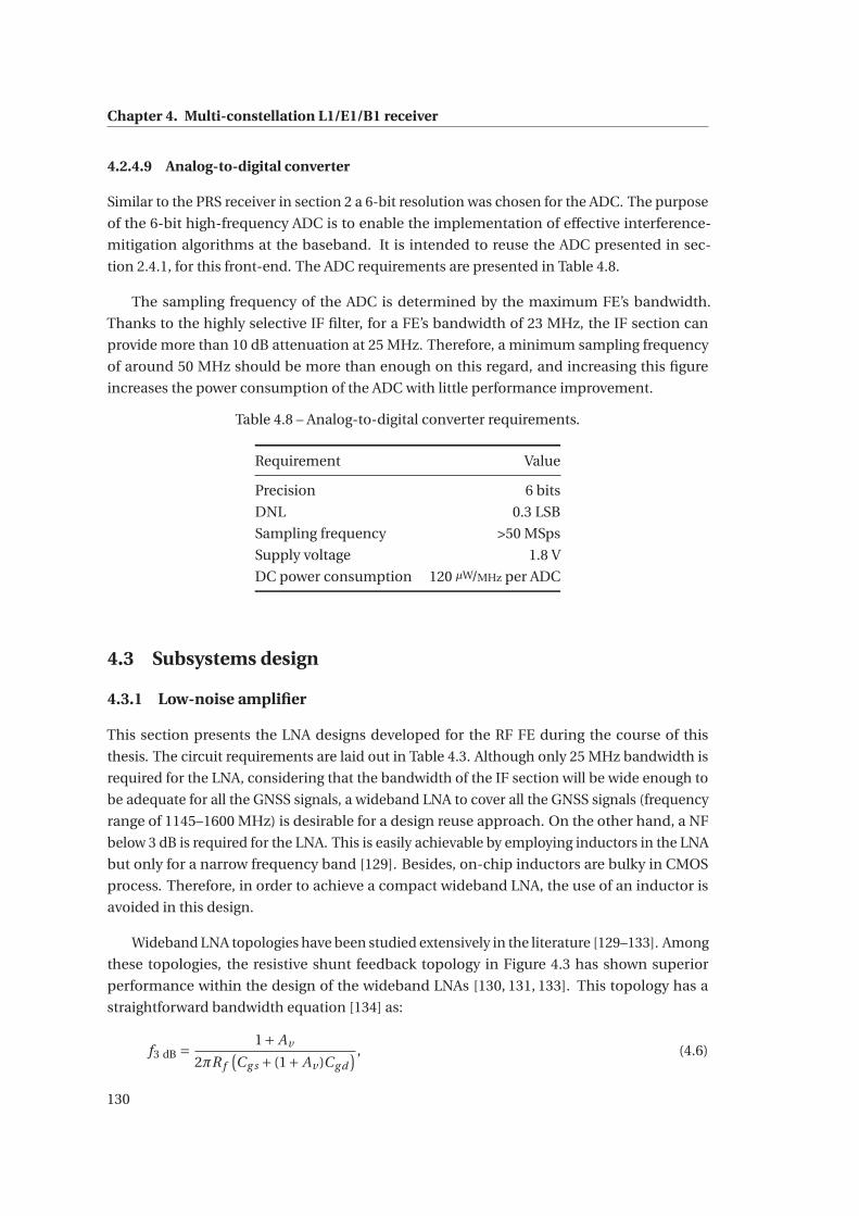
Chapter 4. Multi-constellation L1/E1/B1 receiver
4.2.4.9 Analog-to-digital converter
Similar to the PRS receiver in section 2 a 6-bit resolution was chosen for the ADC. The purpose
of the 6-bit high-frequency ADC is to enable the implementation of effective interference-
mitigation algorithms at the baseband. It is intended to reuse the ADC presented in sec-
tion 2.4.1, for this front-end. The ADC requirements are presented in Table 4.8.
The sampling frequency of the ADC is determined by the maximum FE’s bandwidth.
Thanks to the highly selective IF filter, for a FE’s bandwidth of 23 MHz, the IF section can
provide more than 10 dB attenuation at 25 MHz. Therefore, a minimum sampling frequency
of around 50 MHz should be more than enough on this regard, and increasing this figure
increases the power consumption of the ADC with little performance improvement.
Table 4.8 – Analog-to-digital converter requirements.
Requirement Value
Precision 6 bits
DNL 0.3 LSB
Sampling frequency >50 MSps
Supply voltage 1.8 V
DC power consumption 120 μW/MHz per ADC
4.3 Subsystems design
4.3.1 Low-noise amplifier
This section presents the LNA designs developed for the RF FE during the course of this
thesis. The circuit requirements are laid out in Table 4.3. Although only 25 MHz bandwidth is
required for the LNA, considering that the bandwidth of the IF section will be wide enough to
be adequate for all the GNSS signals, a wideband LNA to cover all the GNSS signals (frequency
range of 1145–1600 MHz) is desirable for a design reuse approach. On the other hand, a NF
below 3 dB is required for the LNA. This is easily achievable by employing inductors in the LNA
but only for a narrow frequency band [129]. Besides, on-chip inductors are bulky in CMOS
process. Therefore, in order to achieve a compact wideband LNA, the use of an inductor is
avoided in this design.
Wideband LNA topologies have been studied extensively in the literature [129–133]. Among
these topologies, the resistive shunt feedback topology in Figure 4.3 has shown superior
performance within the design of the wideband LNAs [130, 131, 133]. This topology has a
straightforward bandwidth equation [134] as:
f3 dB = 1+ Av
2πR f(Cg s + (1+ Av )Cg d
) , (4.6)
130
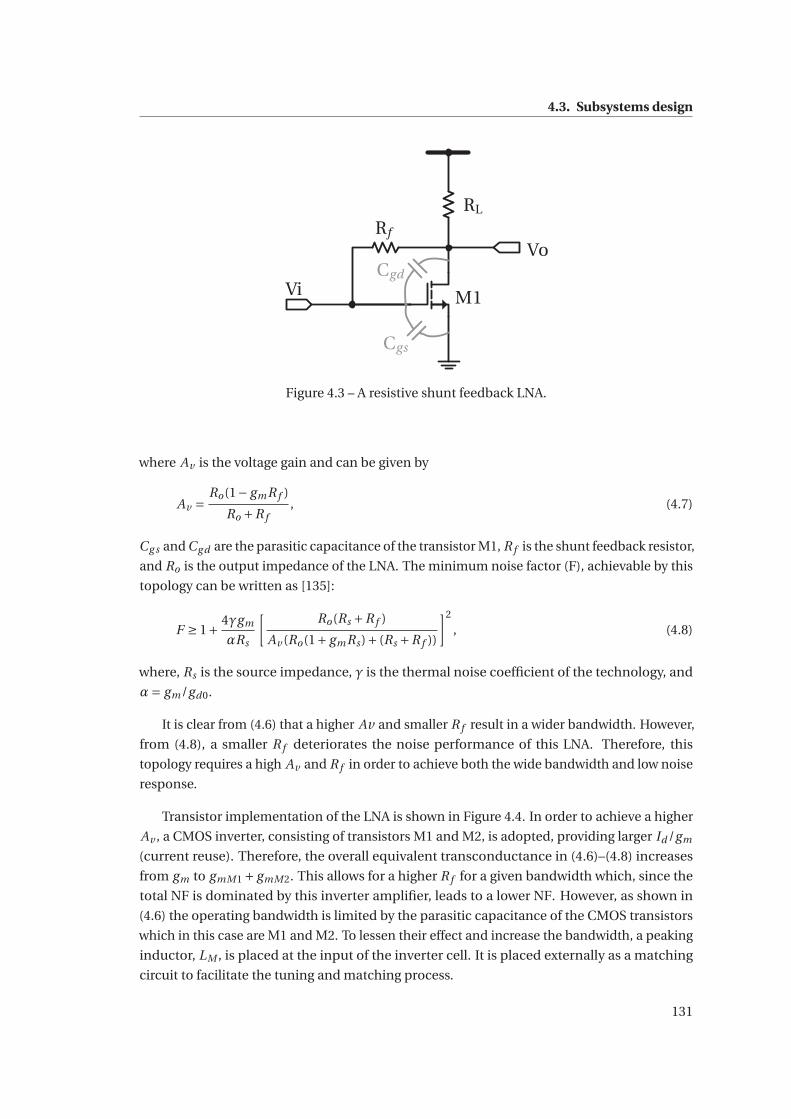
4.3. Subsystems design
Vi
VoRf
M1
RL
Cgd
Cgs
Figure 4.3 – A resistive shunt feedback LNA.
where Av is the voltage gain and can be given by
Av = Ro(1− gmR f )
Ro +R f, (4.7)
Cg s and Cg d are the parasitic capacitance of the transistor M1, R f is the shunt feedback resistor,
and Ro is the output impedance of the LNA. The minimum noise factor (F), achievable by this
topology can be written as [135]:
F ≥ 1+ 4γgm
αRs
[Ro(Rs +R f )
Av (Ro(1+ gmRs)+ (Rs +R f ))
]2
, (4.8)
where, Rs is the source impedance, γ is the thermal noise coefficient of the technology, and
α= gm/gd0.
It is clear from (4.6) that a higher Av and smaller R f result in a wider bandwidth. However,
from (4.8), a smaller R f deteriorates the noise performance of this LNA. Therefore, this
topology requires a high Av and R f in order to achieve both the wide bandwidth and low noise
response.
Transistor implementation of the LNA is shown in Figure 4.4. In order to achieve a higher
Av , a CMOS inverter, consisting of transistors M1 and M2, is adopted, providing larger Id /gm
(current reuse). Therefore, the overall equivalent transconductance in (4.6)–(4.8) increases
from gm to gmM1 + gmM2. This allows for a higher R f for a given bandwidth which, since the
total NF is dominated by this inverter amplifier, leads to a lower NF. However, as shown in
(4.6) the operating bandwidth is limited by the parasitic capacitance of the CMOS transistors
which in this case are M1 and M2. To lessen their effect and increase the bandwidth, a peaking
inductor, LM , is placed at the input of the inverter cell. It is placed externally as a matching
circuit to facilitate the tuning and matching process.
131
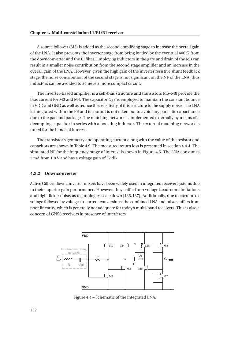
Chapter 4. Multi-constellation L1/E1/B1 receiver
A source follower (M3) is added as the second amplifying stage to increase the overall gain
of the LNA. It also prevents the inverter stage from being loaded by the eventual 400 Ω from
the downconverter and the IF filter. Employing inductors in the gate and drain of the M3 can
result in a smaller noise contribution from the second stage amplifier and an increase in the
overall gain of the LNA. However, given the high gain of the inverter resistive shunt feedback
stage, the noise contribution of the second stage is not significant on the NF of the LNA, thus
inductors can be avoided to achieve a more compact circuit.
The inverter-based amplifier is a self-bias structure and transistors M5–M8 provide the
bias current for M3 and M4. The capacitor CBP is employed to maintain the constant bounce
in VDD and GND as well as reduce the sensitivity of this structure to the supply noise. The LNA
is integrated within the FE and its output is not taken out to avoid any parasitic capacitance
due to the pad and package. The matching network is implemented externally by means of a
decoupling capacitor in series with a boosting inductor. The external matching network is
tuned for the bands of interest.
The transistor’s geometry and operating current along with the value of the resistor and
capacitors are shown in Table 4.9. The measured return loss is presented in section 4.4.4. The
simulated NF for the frequency range of interest is shown in Figure 4.5. The LNA consumes
5 mA from 1.8 V and has a voltage gain of 32 dB.
4.3.2 Downconverter
Active Gilbert downconverter mixers have been widely used in integrated receiver systems due
to their superior gain performance. However, they suffer from voltage headroom limitations
and high flicker noise, as technologies scale down [136, 137]. Additionally, due to current-to-
voltage followed by voltage-to-current conversions, the combined LNA and mixer suffers from
poor linearity, which is generally not adequate for today’s multi-band receivers. This is also a
concern of GNSS receivers in presence of interferers.
Vi Vo
VDD
GND
Rf
C
M1
M2 M4
M3
M6
M5
M8
M7
CBP
CDCLM
External matching network
Figure 4.4 – Schematic of the integrated LNA.
132
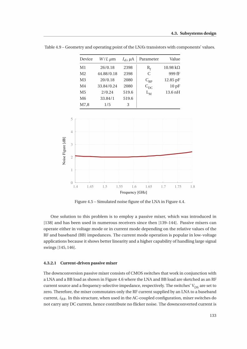
4.3. Subsystems design
Table 4.9 – Geometry and operating point of the LNA’s transistors with components’ values.
Device W /L μm Id s μA Parameter Value
M1 26/0.18 2398 Rf 10.98 kΩ
M2 44.88/0.18 2398 C 999 fF
M3 20/0.18 2080 CBP 12.85 pF
M4 33.84/0.24 2080 CDC 10 pF
M5 2/0.24 519.6 LM 13.6 nH
M6 33.84/1 519.6
M7,8 1/5 3
0
1
2
3
4
5
1.4 1.45 1.5 1.55 1.6 1.65 1.7 1.75 1.8
Nois
e F
igure
[dB
]
Frequency [GHz]
Figure 4.5 – Simulated noise figure of the LNA in Figure 4.4.
One solution to this problem is to employ a passive mixer, which was introduced in
[138] and has been used in numerous receivers since then [139–144]. Passive mixers can
operate either in voltage mode or in current mode depending on the relative values of the
RF and baseband (BB) impedances. The current mode operation is popular in low-voltage
applications because it shows better linearity and a higher capability of handling large signal
swings [145, 146].
4.3.2.1 Current-driven passive mixer
The downconversion passive mixer consists of CMOS switches that work in conjunction with
a LNA and a BB load as shown in Figure 4.6 where the LNA and BB load are sketched as an RF
current source and a frequency-selective impedance, respectively. The switches’ VDS are set to
zero. Therefore, the mixer commutates only the RF current supplied by an LNA to a baseband
current, iBB . In this structure, when used in the AC-coupled configuration, mixer switches do
not carry any DC current, hence contribute no flicker noise. The downconverted current is
133
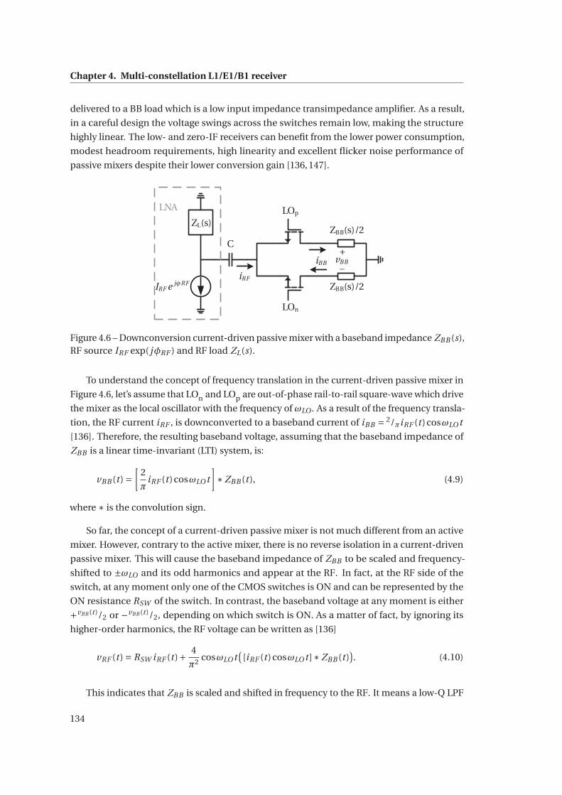
Chapter 4. Multi-constellation L1/E1/B1 receiver
delivered to a BB load which is a low input impedance transimpedance amplifier. As a result,
in a careful design the voltage swings across the switches remain low, making the structure
highly linear. The low- and zero-IF receivers can benefit from the lower power consumption,
modest headroom requirements, high linearity and excellent flicker noise performance of
passive mixers despite their lower conversion gain [136, 147].
ZL(s)
LNA
C
LOp
LOn
ZBB(s)/2
ZBB(s)/2
iBB
iRF
+_
vBB
IRF e jφRF
Figure 4.6 – Downconversion current-driven passive mixer with a baseband impedance ZBB (s),RF source IRF exp( jφRF ) and RF load ZL(s).
To understand the concept of frequency translation in the current-driven passive mixer in
Figure 4.6, let’s assume that LOn and LOp are out-of-phase rail-to-rail square-wave which drive
the mixer as the local oscillator with the frequency of ωLO . As a result of the frequency transla-
tion, the RF current iRF , is downconverted to a baseband current of iBB = 2/πiRF (t )cosωLO t
[136]. Therefore, the resulting baseband voltage, assuming that the baseband impedance of
ZBB is a linear time-invariant (LTI) system, is:
vBB (t ) =[
2
πiRF (t )cosωLO t
]∗ZBB (t ), (4.9)
where ∗ is the convolution sign.
So far, the concept of a current-driven passive mixer is not much different from an active
mixer. However, contrary to the active mixer, there is no reverse isolation in a current-driven
passive mixer. This will cause the baseband impedance of ZBB to be scaled and frequency-
shifted to ±ωLO and its odd harmonics and appear at the RF. In fact, at the RF side of the
switch, at any moment only one of the CMOS switches is ON and can be represented by the
ON resistance RSW of the switch. In contrast, the baseband voltage at any moment is either
+vBB (t )/2 or −vBB (t )/2, depending on which switch is ON. As a matter of fact, by ignoring its
higher-order harmonics, the RF voltage can be written as [136]
vRF (t ) = RSW iRF (t )+ 4
π2 cosωLO t(
[iRF (t )cosωLO t ]∗ZBB (t )). (4.10)
This indicates that ZBB is scaled and shifted in frequency to the RF. It means a low-Q LPF
134
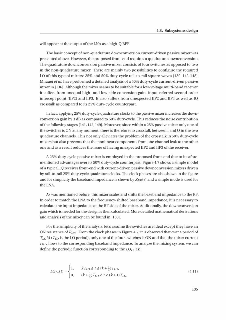
4.3. Subsystems design
will appear at the output of the LNA as a high-Q BPF.
The basic concept of non-quadrature downconversion current-driven passive mixer was
presented above. However, the proposed front-end requires a quadrature downconversion.
The quadrature downconversion passive mixer consists of four switches as opposed to two
in the non-quadrature mixer. There are mainly two possibilities to configure the required
LO of this type of mixers: 25% and 50% duty-cycle rail-to-rail square-waves [139–142, 148].
Mirzaei et al. have performed a detailed analysis of a 50% duty-cycle current-driven passive
mixer in [136]. Although the mixer seems to be suitable for a low-voltage multi-band receiver,
it suffers from unequal high- and low-side conversion gain, input-referred second-order
intercept point (IIP2) and IIP3. It also suffers from unexpected IIP2 and IIP3 as well as IQ
crosstalk as compared to its 25% duty-cycle counterpart.
In fact, applying 25% duty-cycle quadrature clocks to the passive mixer increases the down-
conversion gain by 3 dB as compared to 50% duty-cycle. This reduces the noise contribution
of the following stages [141, 142, 149]. Moreover, since within a 25% passive mixer only one of
the switches is ON at any moment, there is therefore no crosstalk between I and Q in the two
quadrature channels. This not only alleviates the problem of the crosstalk in 50% duty-cycle
mixers but also prevents that the nonlinear components from one channel leak to the other
one and as a result reduces the issue of having unexpected IIP2 and IIP3 of the receiver.
A 25% duty-cycle passive mixer is employed in the proposed front-end due to its afore-
mentioned advantages over its 50% duty-cycle counterpart. Figure 4.7 shows a simple model
of a typical IQ receiver front-end with current-driven passive downconversion mixers driven
by rail-to-rail 25% duty-cycle quadrature clocks. The clock phases are also shown in the figure
and for simplicity the baseband impedance is shown by ZBB (s) and a simple mode is used for
the LNA.
As was mentioned before, this mixer scales and shifts the baseband impedance to the RF.
In order to match the LNA to the frequency-shifted baseband impedance, it is necessary to
calculate the input impedance at the RF side of the mixer. Additionally, the downconversion
gain which is needed for the design is then calculated. More detailed mathematical derivations
and analysis of the mixer can be found in [150].
For the simplicity of the analysis, let’s assume the switches are ideal except they have an
ON resistance of RSW . From the clock phases in Figure 4.7, it is observed that over a period of
TLO/4 (TLO is the LO period), only one of the four switches is ON and that the mixer current
iMi x flows to the corresponding baseband impedance. To analyze the mixing system, we can
define the periodic function corresponding to the LOI+ as:
LOI+(t ) =⎧⎨⎩1, kTLO ≤ t ≤ (k + 1
4 )TLO ,
0, (k + 14 )TLO < t < (k +1)TLO ,
(4.11)
135
Chapter 4. Multi-constellation L1/E1/B1 receiver
LOI+
LOI-
ZBB(s)
IBB,I
iMixZL(s)
LNA model
IRF e jφRF
LOQ+
LOQ-
ZBB(s)
ZBB(s)
IBB,Q
LOI+
LOQ+
LOI-
LOQ-
CVRF
Zin(ω)
Figure 4.7 – Downconversion current-driven passive mixer driven by 25% duty-cycle clocks.ZBB (s) is the baseband impedance, IRF exp( jφRF ) and ZL(s) are LNA models.
where k is an integer number. Accordingly, the other LOs can be written:
LOQ+(t ) = LOI+(
t − TLO
4
), (4.12)
LOI−(t ) = LOI+(
t − TLO
2
), (4.13)
LOQ−(t ) = LOI+(
t − 3TLO
4
). (4.14)
Now, for example, the baseband current corresponding to I+ can be written as:
iBB ,I+(t ) = LOI+(t )iMi x (t ). (4.15)
and similarly for the other paths:
iBB ,Q+(t ) = LOQ+(t )iMi x (t ), (4.16)
iBB ,I−(t ) = LOI−(t )iMi x (t ), (4.17)
iBB ,Q−(t ) = LOQ−(t )iMi x (t ). (4.18)
These currents flow into the corresponding ZBB (s), which results in the following baseband
136
4.3. Subsystems design
voltages:
vBB ,I+(t ) = iBB ,I+(t )∗ZBB (t ), (4.19)
vBB ,Q+(t ) = iBB ,Q+(t )∗ZBB (t ), (4.20)
vBB ,I−(t ) = iBB ,I−(t )∗ZBB (t ), (4.21)
vBB ,Q−(t ) = iBB ,Q−(t )∗ZBB (t ), (4.22)
where ∗ is the convolution sign. In order to find the input impedance Zi n(s) at the RF side
of the mixer, first we have to find the vRF ( f ). This voltage is a result of the corresponding
baseband voltages vBB (t) translated to the RF, similar to the downconversion mechanism,
plus the voltage drop on the ON resistance of the switches RSW and can be written as:
vRF (t ) = RSW iMi x (t )+LOI+(t )vBB ,I+(t )+LOI−(t )vBB ,I−(t )
+LOQ+(t )vBB ,Q+(t )+LOQ−(t )vBB ,Q−(t ). (4.23)
Considering the Fourier series of (4.11)–(4.14) and considering (4.15)–(4.22), the input impedance
at the RF side of the mixer can be written as:
Zi n(ω) = VRF (ω)
IMi x (ω)∼= RSW + 2
π2 [ZBB (ω−ωLO)+ZBB (ω+ωLO)] . (4.24)
Note that (4.24) is approximated in the vicinity of the ωLO and that the term of ZBB (ω) at
the baseband as well as at higher harmonics of ωLO is omitted for simplicity. The elaborated
equations can be found in [150].
From (4.24), the input impedance is the switch resistance in series with the baseband
impedance, which is scaled and frequency-shifted to ωLO . The latter is called impedance
transformation; with this property a low-Q low-pass filter will be transferred to a high-Q
bandpass filter at the ωLO . The input impedance in (4.24) also can be used for impedance
matching between the LNA and the following stage of the mixer.
In order to calculate the downconversion gain of the mixer, first we need to calculate the
baseband current of interest for I (in-phase), iBB ,I = iBB ,I+− iBB ,I− and Q (quadrature phase),
iBB ,Q = iBB ,Q+−iBB ,Q−. Assuming that the RF is above the ωLO (as for the case of this FE), from
(4.15)–(4.18) and the Fourier series of (4.11)–(4.14) the baseband current can be written as:
IBB ,I = e− j π2 IBB ,Q =
�2
πIMi x e j (φMi x−π/4), (4.25)
where IMi x e jφMi x is the phasor representation of the current flowing to the mixer at the RF
side. Therefore, the downconversion gain, GC , can be written as:
GC =∣∣∣∣ IBB ,I
IMi x
∣∣∣∣=�
2
π, (4.26)
which is equal to -6.9 dB. However, the overall downconversion gain |IBB ,I /IRF | depends on
137
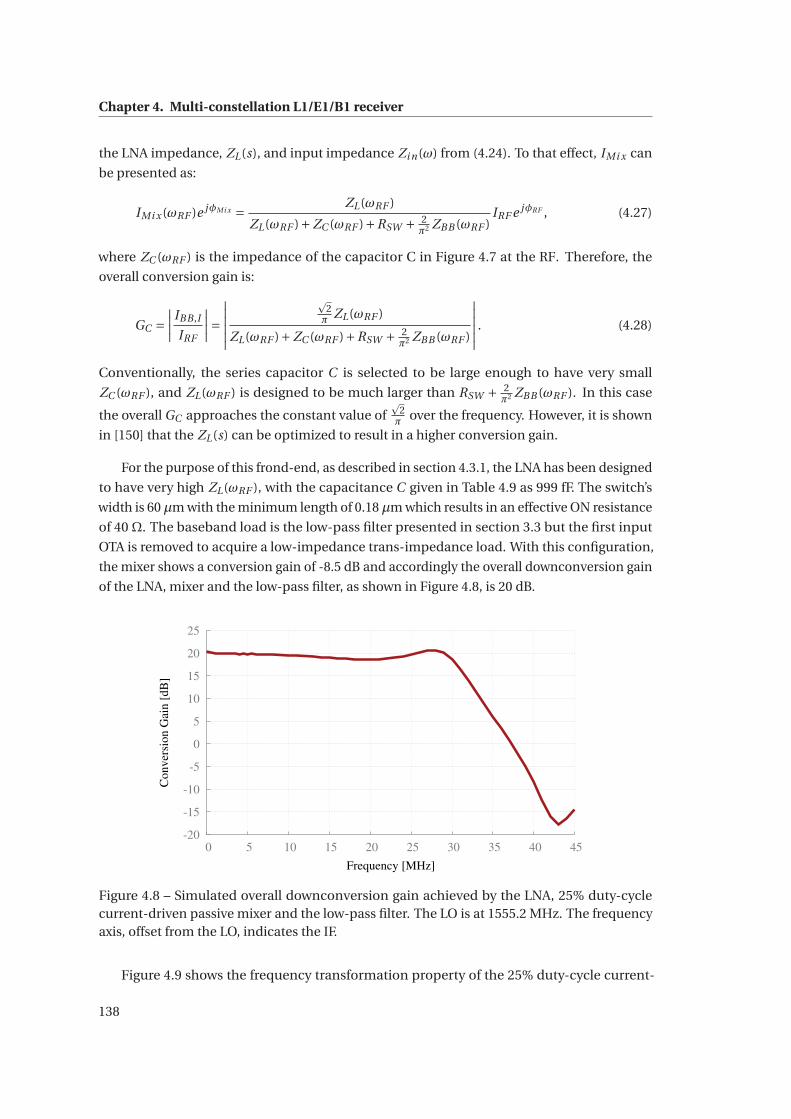
Chapter 4. Multi-constellation L1/E1/B1 receiver
the LNA impedance, ZL(s), and input impedance Zi n(ω) from (4.24). To that effect, IMi x can
be presented as:
IMi x (ωRF )e jφMi x = ZL(ωRF )
ZL(ωRF )+ZC (ωRF )+RSW + 2π2 ZBB (ωRF )
IRF e jφRF , (4.27)
where ZC (ωRF ) is the impedance of the capacitor C in Figure 4.7 at the RF. Therefore, the
overall conversion gain is:
GC =∣∣∣∣ IBB ,I
IRF
∣∣∣∣=∣∣∣∣∣∣
�2π ZL(ωRF )
ZL(ωRF )+ZC (ωRF )+RSW + 2π2 ZBB (ωRF )
∣∣∣∣∣∣ . (4.28)
Conventionally, the series capacitor C is selected to be large enough to have very small
ZC (ωRF ), and ZL(ωRF ) is designed to be much larger than RSW + 2π2 ZBB (ωRF ). In this case
the overall GC approaches the constant value of�
2π over the frequency. However, it is shown
in [150] that the ZL(s) can be optimized to result in a higher conversion gain.
For the purpose of this frond-end, as described in section 4.3.1, the LNA has been designed
to have very high ZL(ωRF ), with the capacitance C given in Table 4.9 as 999 fF. The switch’s
width is 60 μm with the minimum length of 0.18 μm which results in an effective ON resistance
of 40 Ω. The baseband load is the low-pass filter presented in section 3.3 but the first input
OTA is removed to acquire a low-impedance trans-impedance load. With this configuration,
the mixer shows a conversion gain of -8.5 dB and accordingly the overall downconversion gain
of the LNA, mixer and the low-pass filter, as shown in Figure 4.8, is 20 dB.
-20
-15
-10
-5
0
5
10
15
20
25
0 5 10 15 20 25 30 35 40 45
Conver
sion G
ain [
dB
]
Frequency [MHz]
Figure 4.8 – Simulated overall downconversion gain achieved by the LNA, 25% duty-cyclecurrent-driven passive mixer and the low-pass filter. The LO is at 1555.2 MHz. The frequencyaxis, offset from the LO, indicates the IF.
Figure 4.9 shows the frequency transformation property of the 25% duty-cycle current-
138
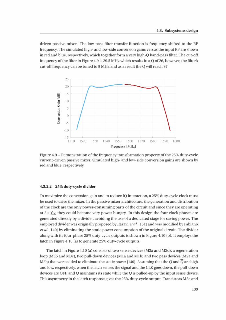
4.3. Subsystems design
driven passive mixer. The low-pass filter transfer function is frequency-shifted to the RF
frequency. The simulated high- and low-side conversion gains versus the input RF are shown
in red and blue, respectively, which together form a very high-Q band-pass filter. The cut-off
frequency of the filter in Figure 4.9 is 29.5 MHz which results in a Q of 26, however, the filter’s
cut-off frequency can be tuned to 8 MHz and as a result the Q will reach 97.
-15
-10
-5
0
5
10
15
20
25
1510 1520 1530 1540 1550 1560 1570 1580 1590 1600
Conver
sion G
ain [
dB
]
Frequency [MHz]
Figure 4.9 – Demonstration of the frequency transformation property of the 25% duty-cyclecurrent-driven passive mixer. Simulated high- and low-side conversion gains are shown byred and blue, respectively.
4.3.2.2 25% duty-cycle divider
To maximize the conversion gain and to reduce IQ interaction, a 25% duty-cycle clock must
be used to drive the mixer. In the passive mixer architecture, the generation and distribution
of the clock are the only power-consuming parts of the circuit and since they are operating
at 2× fLO they could become very power hungry. In this design the four clock phases are
generated directly by a divider, avoiding the use of a dedicated stage for saving power. The
employed divider was originally proposed by Razavi et al. [151] and was modified by Fabiano
et al. [140] by eliminating the static power consumption of the original circuit. The divider
along with its four-phase 25% duty-cycle outputs is shown in Figure 4.10 (b). It employs the
latch in Figure 4.10 (a) to generate 25% duty-cycle outputs.
The latch in Figure 4.10 (a) consists of two sense devices (M3a and M3d), a regeneration
loop (M3b and M3c), two pull-down devices (M1a and M1b) and two pass devices (M2a and
M2b) that were added to eliminate the static power [140]. Assuming that the Q and Q are high
and low, respectively, when the latch senses the signal and the CLK goes down, the pull-down
devices are OFF, and Q maintains its state while the Q is pulled-up by the input sense device.
This asymmetry in the latch response gives the 25% duty-cycle output. Transistors M2a and
139
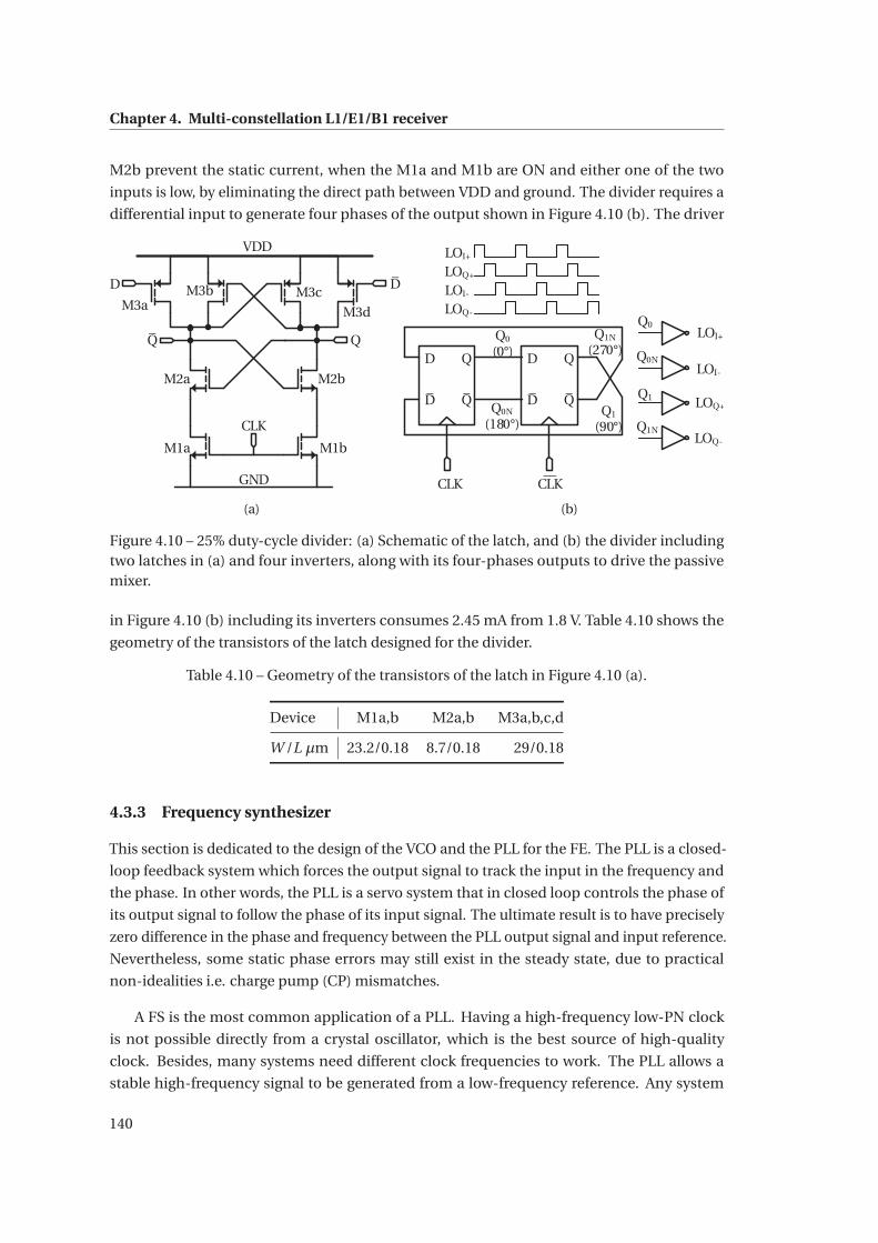
Chapter 4. Multi-constellation L1/E1/B1 receiver
M2b prevent the static current, when the M1a and M1b are ON and either one of the two
inputs is low, by eliminating the direct path between VDD and ground. The divider requires a
differential input to generate four phases of the output shown in Figure 4.10 (b). The driver
M1a M1b
M2a M2b
M3aM3b M3c
M3d
CLK
Q
D
VDD
GND
D_
Q_
D
D_
Q
Q_
D
D_
Q
Q_
CLK CLK__
Q1N
(270°) Q0
(0°)
Q0N (180°)
Q1
(90°)
LOI+
LOQ+
LOI-
LOQ-Q0
Q0N
Q1
Q1N
LOI+
LOQ+
LOI-
LOQ-
(a) (b)
Figure 4.10 – 25% duty-cycle divider: (a) Schematic of the latch, and (b) the divider includingtwo latches in (a) and four inverters, along with its four-phases outputs to drive the passivemixer.
in Figure 4.10 (b) including its inverters consumes 2.45 mA from 1.8 V. Table 4.10 shows the
geometry of the transistors of the latch designed for the divider.
Table 4.10 – Geometry of the transistors of the latch in Figure 4.10 (a).
Device M1a,b M2a,b M3a,b,c,d
W /L μm 23.2/0.18 8.7/0.18 29/0.18
4.3.3 Frequency synthesizer
This section is dedicated to the design of the VCO and the PLL for the FE. The PLL is a closed-
loop feedback system which forces the output signal to track the input in the frequency and
the phase. In other words, the PLL is a servo system that in closed loop controls the phase of
its output signal to follow the phase of its input signal. The ultimate result is to have precisely
zero difference in the phase and frequency between the PLL output signal and input reference.
Nevertheless, some static phase errors may still exist in the steady state, due to practical
non-idealities i.e. charge pump (CP) mismatches.
A FS is the most common application of a PLL. Having a high-frequency low-PN clock
is not possible directly from a crystal oscillator, which is the best source of high-quality
clock. Besides, many systems need different clock frequencies to work. The PLL allows a
stable high-frequency signal to be generated from a low-frequency reference. Any system
140
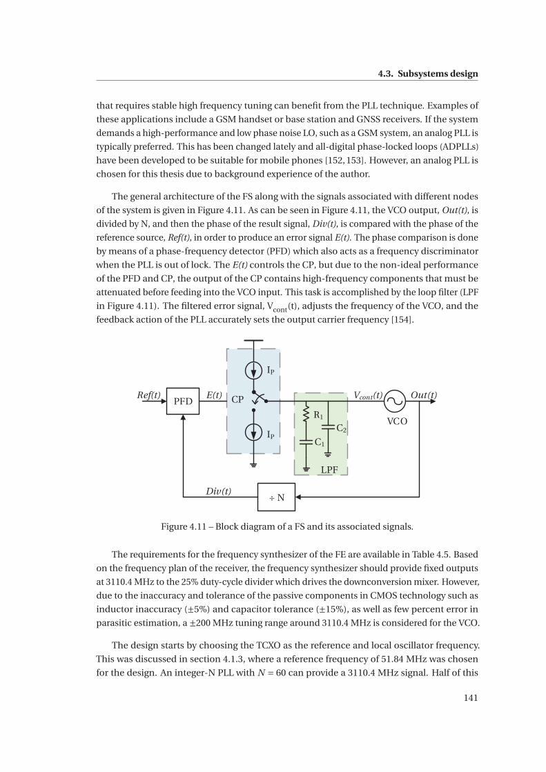
4.3. Subsystems design
that requires stable high frequency tuning can benefit from the PLL technique. Examples of
these applications include a GSM handset or base station and GNSS receivers. If the system
demands a high-performance and low phase noise LO, such as a GSM system, an analog PLL is
typically preferred. This has been changed lately and all-digital phase-locked loops (ADPLLs)
have been developed to be suitable for mobile phones [152, 153]. However, an analog PLL is
chosen for this thesis due to background experience of the author.
The general architecture of the FS along with the signals associated with different nodes
of the system is given in Figure 4.11. As can be seen in Figure 4.11, the VCO output, Out(t), is
divided by N, and then the phase of the result signal, Div(t), is compared with the phase of the
reference source, Ref(t), in order to produce an error signal E(t). The phase comparison is done
by means of a phase-frequency detector (PFD) which also acts as a frequency discriminator
when the PLL is out of lock. The E(t) controls the CP, but due to the non-ideal performance
of the PFD and CP, the output of the CP contains high-frequency components that must be
attenuated before feeding into the VCO input. This task is accomplished by the loop filter (LPF
in Figure 4.11). The filtered error signal, Vcont(t), adjusts the frequency of the VCO, and the
feedback action of the PLL accurately sets the output carrier frequency [154].
PFD
÷ N
VCO
LPF
C2
C1
R1
CP
IP
IP
Ref(t) Out(t)E(t) Vcont(t)
Div(t)
Figure 4.11 – Block diagram of a FS and its associated signals.
The requirements for the frequency synthesizer of the FE are available in Table 4.5. Based
on the frequency plan of the receiver, the frequency synthesizer should provide fixed outputs
at 3110.4 MHz to the 25% duty-cycle divider which drives the downconversion mixer. However,
due to the inaccuracy and tolerance of the passive components in CMOS technology such as
inductor inaccuracy (±5%) and capacitor tolerance (±15%), as well as few percent error in
parasitic estimation, a ±200 MHz tuning range around 3110.4 MHz is considered for the VCO.
The design starts by choosing the TCXO as the reference and local oscillator frequency.
This was discussed in section 4.1.3, where a reference frequency of 51.84 MHz was chosen
for the design. An integer-N PLL with N = 60 can provide a 3110.4 MHz signal. Half of this
141
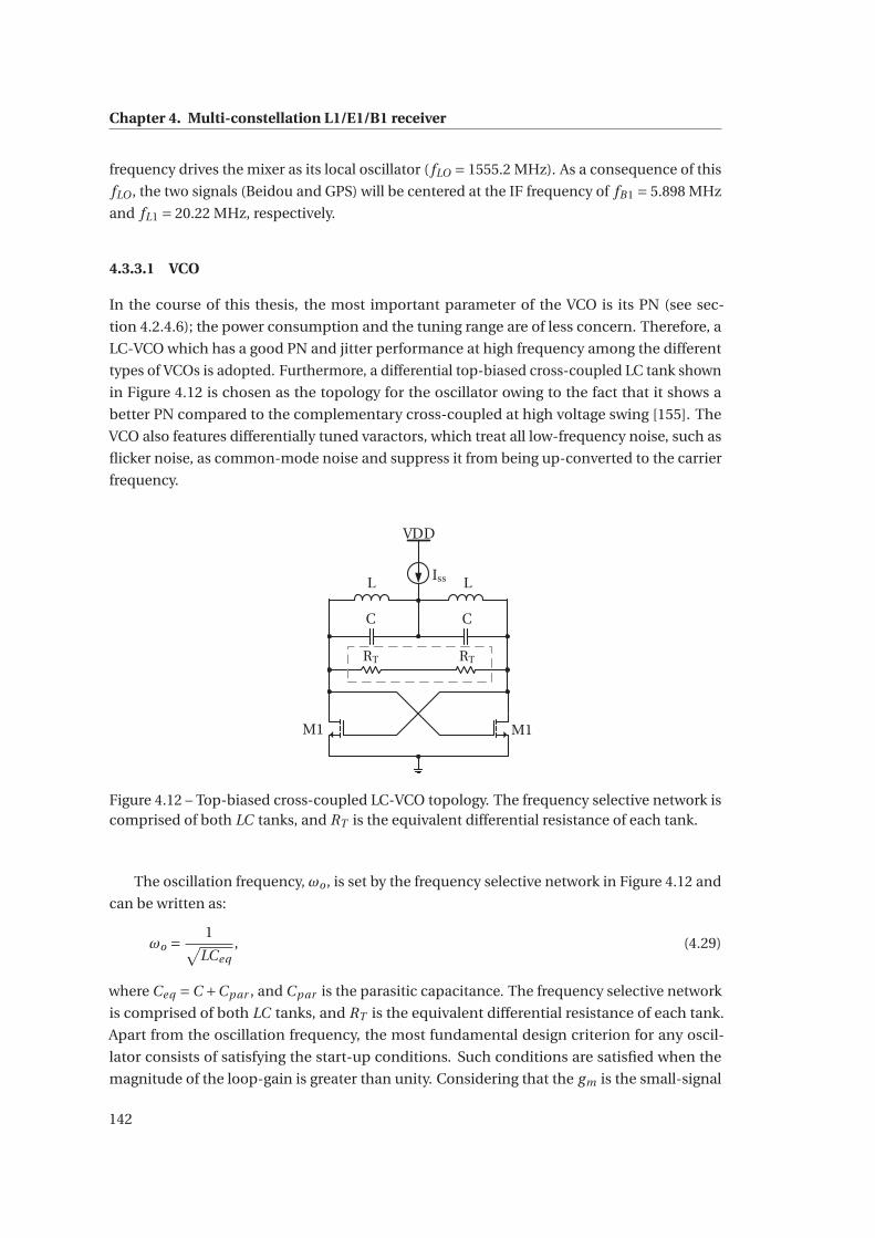
Chapter 4. Multi-constellation L1/E1/B1 receiver
frequency drives the mixer as its local oscillator ( fLO = 1555.2 MHz). As a consequence of this
fLO , the two signals (Beidou and GPS) will be centered at the IF frequency of fB1 = 5.898 MHz
and fL1 = 20.22 MHz, respectively.
4.3.3.1 VCO
In the course of this thesis, the most important parameter of the VCO is its PN (see sec-
tion 4.2.4.6); the power consumption and the tuning range are of less concern. Therefore, a
LC-VCO which has a good PN and jitter performance at high frequency among the different
types of VCOs is adopted. Furthermore, a differential top-biased cross-coupled LC tank shown
in Figure 4.12 is chosen as the topology for the oscillator owing to the fact that it shows a
better PN compared to the complementary cross-coupled at high voltage swing [155]. The
VCO also features differentially tuned varactors, which treat all low-frequency noise, such as
flicker noise, as common-mode noise and suppress it from being up-converted to the carrier
frequency.
L L
C C
M1 M1
Iss
RT RT
VDD
Figure 4.12 – Top-biased cross-coupled LC-VCO topology. The frequency selective network iscomprised of both LC tanks, and RT is the equivalent differential resistance of each tank.
The oscillation frequency, ωo , is set by the frequency selective network in Figure 4.12 and
can be written as:
ωo = 1√LCeq
, (4.29)
where Ceq =C +Cpar , and Cpar is the parasitic capacitance. The frequency selective network
is comprised of both LC tanks, and RT is the equivalent differential resistance of each tank.
Apart from the oscillation frequency, the most fundamental design criterion for any oscil-
lator consists of satisfying the start-up conditions. Such conditions are satisfied when the
magnitude of the loop-gain is greater than unity. Considering that the gm is the small-signal
142
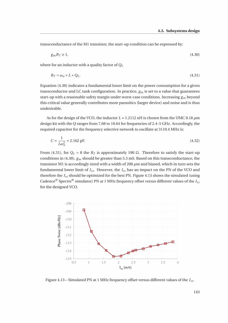
4.3. Subsystems design
transconductance of the M1 transistor, the start-up condition can be expressed by:
gmRT ≥ 1, (4.30)
where for an inductor with a quality factor of QL
RT =ωo ×L×QL . (4.31)
Equation (4.30) indicates a fundamental lower limit on the power consumption for a given
transconductor and LC tank configuration. In practice, gm is set to a value that guarantees
start-up with a reasonable safety margin under worst-case conditions. Increasing gm beyond
this critical value generally contributes more parasitics (larger device) and noise and is thus
undesirable.
As for the design of the VCO, the inductor L = 1.2112 nH is chosen from the UMC 0.18 μm
design kit with the Q ranges from 7.68 to 10.64 for frequencies of 2.4–5 GHz. Accordingly, the
required capacitor for the frequency selective network to oscillate at 3110.4 MHz is:
C = 1
Lω2o= 2.162 pF. (4.32)
From (4.31), for QL = 8 the RT is approximately 190 Ω. Therefore to satisfy the start-up
conditions in (4.30), gm should be greater than 5.3 mS. Based on this transconductance, the
transistor M1 is accordingly sized with a width of 200 μm and biased, which in turn sets the
fundamental lower limit of Iss . However, the Iss has an impact on the PN of the VCO and
therefore the Iss should be optimized for the best PN. Figure 4.13 shows the simulated (using
Cadence® Spectre® simulator) PN at 1 MHz frequency offset versus different values of the Iss
for the designed VCO.
-115
-114
-113
-112
-111
-110
-109
-108
0.5 1 1.5 2 2.5 3 3.5 4
Phas
e N
ois
e [d
Bc/
Hz]
Iss [mA]
Figure 4.13 – Simulated PN at 1 MHz frequency offset versus different values of the Iss .
143
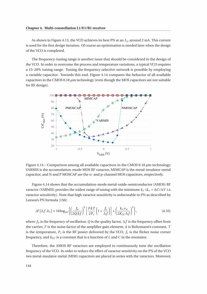
Chapter 4. Multi-constellation L1/E1/B1 receiver
As shown in Figure 4.13, the VCO achieves its best PN at an Iss around 2 mA. This current
is used for the first design iteration. Of course an optimization is needed later when the design
of the VCO is completed.
The frequency-tuning range is another issue that should be considered in the design of
the VCO. In order to overcome the process and temperature variations, a typical VCO requires
a 15–20% tuning range. Tuning the frequency selective network is possible by employing
a variable capacitor. Towards this end, Figure 4.14 compares the behavior of all available
capacitors in the CMOS 0.18 μm technology (even though the MOS capacitors are not suitable
for RF design).
20
30
40
50
60
70
80
90
100
-1 -0.5 0 0.5 1
PMOSCAP
VARMIS
NMOSCAP
MIMCAP
C/C
max
[%
]
VGDS [V]
Figure 4.14 – Comparison among all available capacitors in the CMOS 0.18 μm technology:VARMIS is the accumulation-mode MOS RF varactor, MIMCAP is the metal-insulator-metalcapacitor, and N and P MOSCAP are the n- and p-channel MOS capacitors, respectively.
Figure 4.14 shows that the accumulation-mode metal-oxide-semiconductor (AMOS) RF
varactor (VARMIS) provides the widest range of tuning with the minimum kv (kv =ΔC /ΔV i.e.
varactor sensitivity). Note that high varactor sensitivity is unfavorable to PN as described by
Leeson’s PN formula [156]:
L(Δ f ,kv
)= 10log10
{(fo
2QΔ f
)2 [F kT
2Ps
(1+ fc
Δ f
)]+
(kv vn
2KLCΔ f
)2}, (4.33)
where fo is the frequency of oscillation, Q is the quality factor, Δ f is the frequency offset from
the carrier, F is the noise factor of the amplifier gain element, k is Boltzmann’s constant, T
is the temperature, Ps is the RF power delivered by the VCO, fc is the flicker noise corner
frequency, and kLC is a constant that is a function of L and C in the resonator.
Therefore, the AMOS RF varactors are employed to continuously tune the oscillation
frequency of the VCO. In order to reduce the effect of varactor sensitivity on the PN of the VCO
two metal-insulator-metal (MIM) capacitors are placed in series with the varactors. Moreover,
144
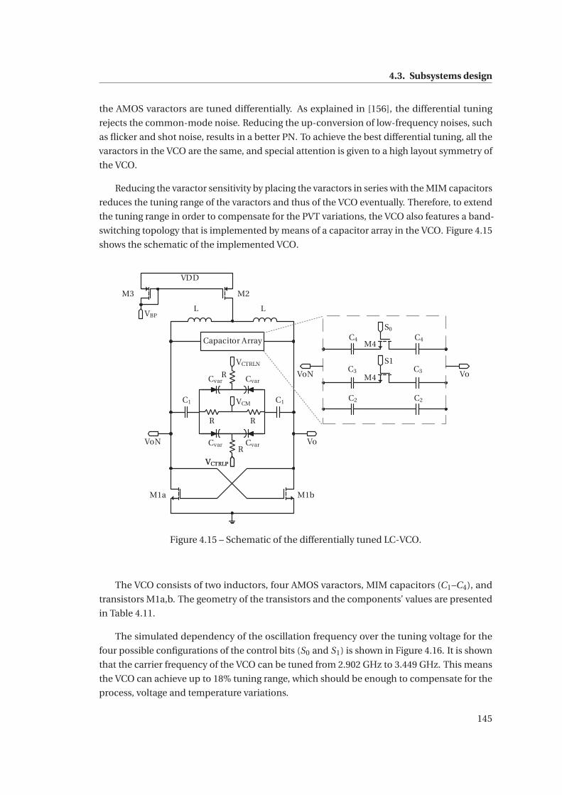
4.3. Subsystems design
the AMOS varactors are tuned differentially. As explained in [156], the differential tuning
rejects the common-mode noise. Reducing the up-conversion of low-frequency noises, such
as flicker and shot noise, results in a better PN. To achieve the best differential tuning, all the
varactors in the VCO are the same, and special attention is given to a high layout symmetry of
the VCO.
Reducing the varactor sensitivity by placing the varactors in series with the MIM capacitors
reduces the tuning range of the varactors and thus of the VCO eventually. Therefore, to extend
the tuning range in order to compensate for the PVT variations, the VCO also features a band-
switching topology that is implemented by means of a capacitor array in the VCO. Figure 4.15
shows the schematic of the implemented VCO.
VCTRLPVCTRLP
VCTRLN S1
S0
VCM
Capacitor Array
VoN Vo
VoN Vo
L L
RCvar
M1a
VDD
M1b
Cvar
Cvar Cvar
RR
R
C2C1 C1 C2
C3 C3
C4 C4
VBP
M2M3
M4
M4
Figure 4.15 – Schematic of the differentially tuned LC-VCO.
The VCO consists of two inductors, four AMOS varactors, MIM capacitors (C1–C4), and
transistors M1a,b. The geometry of the transistors and the components’ values are presented
in Table 4.11.
The simulated dependency of the oscillation frequency over the tuning voltage for the
four possible configurations of the control bits (S0 and S1) is shown in Figure 4.16. It is shown
that the carrier frequency of the VCO can be tuned from 2.902 GHz to 3.449 GHz. This means
the VCO can achieve up to 18% tuning range, which should be enough to compensate for the
process, voltage and temperature variations.
145
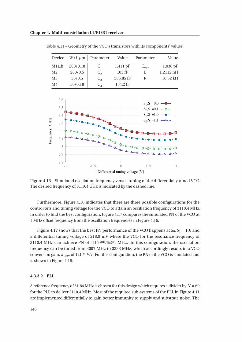
Chapter 4. Multi-constellation L1/E1/B1 receiver
Table 4.11 – Geometry of the VCO’s transistors with its components’ values.
Device W /L μm Parameter Value Parameter Value
M1a,b 200/0.18 C1 1.411 pF Cvar 1.038 pF
M2 280/0.5 C2 103 fF L 1.2112 nH
M3 35/0.5 C3 385.85 fF R 10.52 kΩ
M4 50/0.18 C4 184.2 fF
2.8
2.9
3
3.1
3.2
3.3
3.4
3.5
3.6
-1 -0.5 0 0.5 1
Fre
quen
cy [
GH
z]
Differential tuning voltage [V]
S0,S1=0,0
S0,S1=0,1
S0,S1=1,0
S0,S1=1,1
Figure 4.16 – Simulated oscillation frequency versus tuning of the differentially tuned VCO.The desired frequency of 3.1104 GHz is indicated by the dashed line.
Furthermore, Figure 4.16 indicates that there are three possible configurations for the
control bits and tuning voltage for the VCO to attain an oscillation frequency of 3110.4 MHz.
In order to find the best configuration, Figure 4.17 compares the simulated PN of the VCO at
1 MHz offset frequency from the oscillation frequencies in Figure 4.16.
Figure 4.17 shows that the best PN performance of the VCO happens at S0,S1 = 1,0 and
a differential tuning voltage of 218.9 mV where the VCO for the resonance frequency of
3110.4 MHz can achieve PN of -115 dBc/Hz@1 MHz. In this configuration, the oscillation
frequency can be tuned from 3097 MHz to 3338 MHz, which accordingly results in a VCO
conversion gain, kvco , of 121 MHz/V. For this configuration, the PN of the VCO is simulated and
is shown in Figure 4.18.
4.3.3.2 PLL
A reference frequency of 51.84 MHz is chosen for this design which requires a divider by N = 60
for the PLL to deliver 3110.4 MHz. Most of the required sub-systems of the PLL in Figure 4.11
are implemented differentially to gain better immunity to supply and substrate noise. The
146
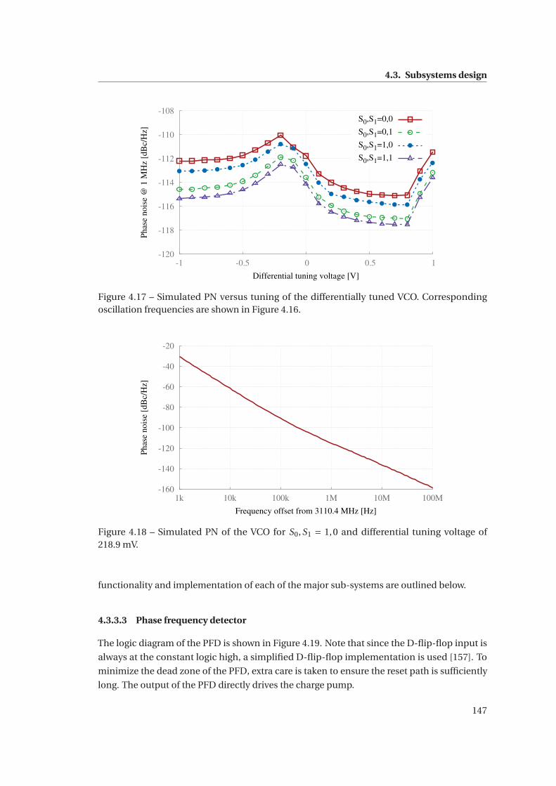
4.3. Subsystems design
-120
-118
-116
-114
-112
-110
-108
-1 -0.5 0 0.5 1
Phas
e nois
e @
1 M
Hz
[dB
c/H
z]
Differential tuning voltage [V]
S0,S1=0,0
S0,S1=0,1
S0,S1=1,0
S0,S1=1,1
Figure 4.17 – Simulated PN versus tuning of the differentially tuned VCO. Correspondingoscillation frequencies are shown in Figure 4.16.
-160
-140
-120
-100
-80
-60
-40
-20
1k 10k 100k 1M 10M 100M
Phas
e nois
e [d
Bc/
Hz]
Frequency offset from 3110.4 MHz [Hz]
Figure 4.18 – Simulated PN of the VCO for S0,S1 = 1,0 and differential tuning voltage of218.9 mV.
functionality and implementation of each of the major sub-systems are outlined below.
4.3.3.3 Phase frequency detector
The logic diagram of the PFD is shown in Figure 4.19. Note that since the D-flip-flop input is
always at the constant logic high, a simplified D-flip-flop implementation is used [157]. To
minimize the dead zone of the PFD, extra care is taken to ensure the reset path is sufficiently
long. The output of the PFD directly drives the charge pump.
147
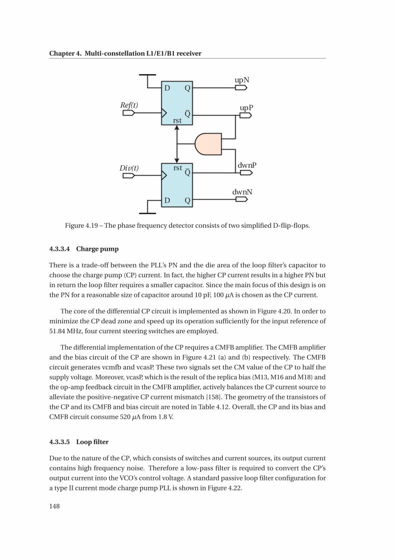
Chapter 4. Multi-constellation L1/E1/B1 receiver
D Q
Q_
D Q
Q_rst
rst
Ref(t)
Div(t)
upN
dwnN
dwnP
upP
Figure 4.19 – The phase frequency detector consists of two simplified D-flip-flops.
4.3.3.4 Charge pump
There is a trade-off between the PLL’s PN and the die area of the loop filter’s capacitor to
choose the charge pump (CP) current. In fact, the higher CP current results in a higher PN but
in return the loop filter requires a smaller capacitor. Since the main focus of this design is on
the PN for a reasonable size of capacitor around 10 pF, 100 μA is chosen as the CP current.
The core of the differential CP circuit is implemented as shown in Figure 4.20. In order to
minimize the CP dead zone and speed up its operation sufficiently for the input reference of
51.84 MHz, four current steering switches are employed.
The differential implementation of the CP requires a CMFB amplifier. The CMFB amplifier
and the bias circuit of the CP are shown in Figure 4.21 (a) and (b) respectively. The CMFB
circuit generates vcmfb and vcasP. These two signals set the CM value of the CP to half the
supply voltage. Moreover, vcasP, which is the result of the replica bias (M13, M16 and M18) and
the op-amp feedback circuit in the CMFB amplifier, actively balances the CP current source to
alleviate the positive-negative CP current mismatch [158]. The geometry of the transistors of
the CP and its CMFB and bias circuit are noted in Table 4.12. Overall, the CP and its bias and
CMFB circuit consume 520 μA from 1.8 V.
4.3.3.5 Loop filter
Due to the nature of the CP, which consists of switches and current sources, its output current
contains high frequency noise. Therefore a low-pass filter is required to convert the CP’s
output current into the VCO’s control voltage. A standard passive loop filter configuration for
a type II current mode charge pump PLL is shown in Figure 4.22.
148
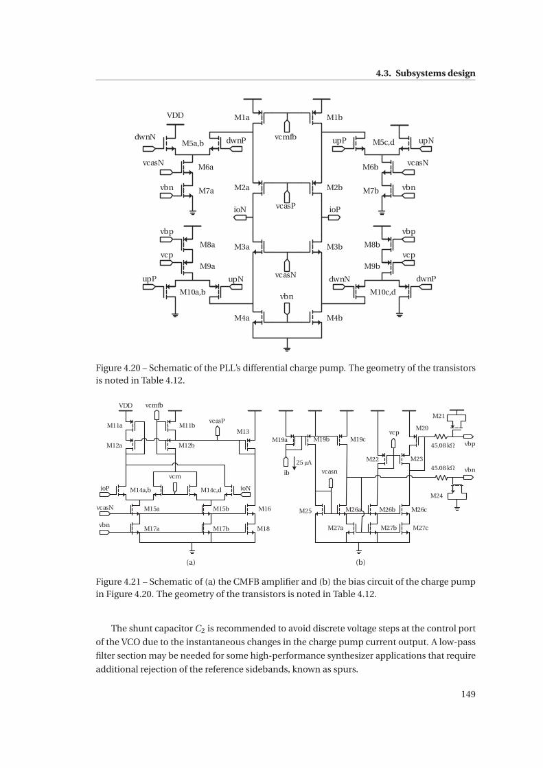
4.3. Subsystems design
M10a,b
M5a,b dwnP
upNupP
vcp
vbp
vbn
M10c,d
M5c,dupP
dwnN
upN
dwnP
vcp
vbp
vbn
ioN ioP
vcmfb
vcasP
vcasN
vbn
VDD
dwnN
vcasN vcasN
M1a M1b
M2a M2b
M3a M3b
M4a M4b
M6a M6b
M7a M7b
M8a M8b
M9a M9b
Figure 4.20 – Schematic of the PLL’s differential charge pump. The geometry of the transistorsis noted in Table 4.12.
M14a,b M14c,d
vcm
vcmfb
ioNioP
vcasP
vcasN
vbn
vcasn
vbp
vbn
vcp
VDD
ib
25 μA
M11a M11b
M12a M12b
M13
M15a M15b
M17a M17b
M16
M18
M19a M19b M19c
M20
M21
M23M22
M25 M26a M26b M26c
M24
M27a M27b M27c
45.08 kΩ
45.08 kΩ
(a) (b)
Figure 4.21 – Schematic of (a) the CMFB amplifier and (b) the bias circuit of the charge pumpin Figure 4.20. The geometry of the transistors is noted in Table 4.12.
The shunt capacitor C2 is recommended to avoid discrete voltage steps at the control port
of the VCO due to the instantaneous changes in the charge pump current output. A low-pass
filter section may be needed for some high-performance synthesizer applications that require
additional rejection of the reference sidebands, known as spurs.
149
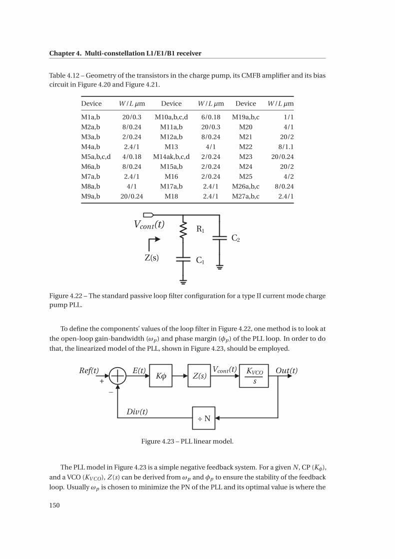
Chapter 4. Multi-constellation L1/E1/B1 receiver
Table 4.12 – Geometry of the transistors in the charge pump, its CMFB amplifier and its biascircuit in Figure 4.20 and Figure 4.21.
Device W /L μm Device W /L μm Device W /L μm
M1a,b 20/0.3 M10a,b,c,d 6/0.18 M19a,b,c 1/1
M2a,b 8/0.24 M11a,b 20/0.3 M20 4/1
M3a,b 2/0.24 M12a,b 8/0.24 M21 20/2
M4a,b 2.4/1 M13 4/1 M22 8/1.1
M5a,b,c,d 4/0.18 M14ak,b,c,d 2/0.24 M23 20/0.24
M6a,b 8/0.24 M15a,b 2/0.24 M24 20/2
M7a,b 2.4/1 M16 2/0.24 M25 4/2
M8a,b 4/1 M17a,b 2.4/1 M26a,b,c 8/0.24
M9a,b 20/0.24 M18 2.4/1 M27a,b,c 2.4/1
C2
C1
R1Vcont(t)
Z(s)
Figure 4.22 – The standard passive loop filter configuration for a type II current mode chargepump PLL.
To define the components’ values of the loop filter in Figure 4.22, one method is to look at
the open-loop gain-bandwidth (ωp ) and phase margin (φp ) of the PLL loop. In order to do
that, the linearized model of the PLL, shown in Figure 4.23, should be employed.
Kφ Z(s)KVCO
s
÷ N
_+
Ref(t) Out(t)E(t)
Div(t)
Vcont(t)
Figure 4.23 – PLL linear model.
The PLL model in Figure 4.23 is a simple negative feedback system. For a given N , CP (Kφ),
and a VCO (KV CO), Z (s) can be derived from ωp and φp to ensure the stability of the feedback
loop. Usually ωp is chosen to minimize the PN of the PLL and its optimal value is where the
150

4.3. Subsystems design
high-pass VCO noise contribution is equal to the total low-pass noise contribution from the
reference, PFD and CP. However, for the sake of the loop stability, the ωp should be less than
one tenth of the reference frequency. The phase margin (φp ) is usually chosen between 30◦
and 70◦. A higher φp results in a higher stability in return; however, the loop response time is
slower.
The impedance of the loop filter in Figure 4.22 is:
Z (s) = sC1R1 +1
s2C1R1C2 + sC1 + sC2. (4.34)
From (4.34) the loop gain of the PLL in Figure 4.23 can be written as:
H(s)
∣∣∣∣∣s= jω
= −KφKV CO(1+ jωT2)
ω2C2(1+ jωT1)
T1
T2, (4.35)
where T1 and T2 are defined as:
T1 = R1C1C2
C1 +C2, (4.36)
T2 = R1C1. (4.37)
For the loop gain in (4.35) the phase margin, as a function of ω can be written as:
φ(ω) = 180◦ + tan−1 (ωT2)− tan−1 (ωT1) . (4.38)
By setting the derivative of (4.38) equal to zero, the loop bandwidth will be obtained as a
function of T1 and T2:
ωp = 1�T1T2
. (4.39)
Based on the definition of the phase margin from (4.35), at ωp we have:
|H(s)|∣∣∣∣∣
s= jωp
= 1. (4.40)
From (4.36)–(4.40), T1 and T2 can then be obtained as:
T1 =sec(φp )− tan(φp )
ωp, (4.41)
T2 = 1
ω2p T1
. (4.42)
151
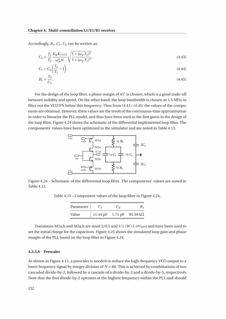
Chapter 4. Multi-constellation L1/E1/B1 receiver
Accordingly, R1, C1, C2 can be written as:
C2 = T1
T2
KφKV CO
ω2p N
√1+ (ωp T2)2
1+ (ωp T1)2 , (4.43)
C1 =C2
(T2
T1−1
), (4.44)
R1 = T2
C1. (4.45)
For the design of the loop filter, a phase margin of 45◦ is chosen, which is a good trade-off
between stability and speed. On the other hand, the loop bandwidth is chosen as 1.5 MHz to
filter out the VCO PN below this frequency. Thus from (4.41)–(4.45) the values of the compo-
nents are obtained. However, these values are the result of the continuous-time approximation
in order to linearize the PLL model, and thus have been used as the first guess in the design of
the loop filter. Figure 4.24 shows the schematic of the differential implemented loop filter. The
components’ values have been optimized in the simulator and are noted in Table 4.13.
VCM
2C2
2C2
½ C1½ C1
½ R1
½ R1
rstN
rstN
LFP
LFN
rst
M1a
M1b
M2a
M2b
Figure 4.24 – Schematic of the differential loop filter. The components’ values are noted inTable 4.13.
Table 4.13 – Component values of the loop filter in Figure 4.24.
Parameter C1 C2 R1
Value 11.44 pF 1.71 pF 95.39 kΩ
Transistors M1a,b and M2a,b are sized 2/0.5 and 1/1 (W /L μm/μm) and have been used to
set the initial charge for the capacitors. Figure 4.25 shows the simulated loop gain and phase
margin of the PLL based on the loop filter in Figure 4.24.
4.3.3.6 Prescaler
As shown in Figure 4.11, a prescaler is needed to reduce the high-frequency VCO output to a
lower frequency signal by integer division of N = 60. This is achieved by combinations of two
cascaded divide-by-2, followed by a cascade of a divide-by-3 and a divide-by-5, respectively.
Note that the first divide-by-2 operates at the highest frequency within the PLL and should
152
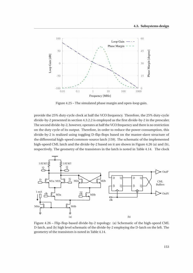
4.3. Subsystems design
-100
-50
0
50
100
0.01 0.1 1 10 100 1000 0
15
30
45
60
Loop G
ain [
dB
]
Phas
e M
argin
[deg
ree]
Frequency [MHz]
Loop Gain
Phase Margin
Figure 4.25 – The simulated phase margin and open-loop gain.
provide the 25% duty-cycle clock at half the VCO frequency. Therefore, the 25% duty-cycle
divide-by-2 presented in section 4.3.2.2 is employed as the first divide-by-2 in the prescaler.
The second divide-by-2, however, operates at half the VCO frequency and there is no restriction
on the duty cycle of its output. Therefore, in order to reduce the power consumption, this
divide-by-2 is realized using toggling D-flip-flops based on the master-slave structure of
the differential high-speed common-source latch [159]. The schematic of the implemented
high-speed CML latch and the divide-by-2 based on it are shown in Figure 4.26 (a) and (b),
respectively. The geometry of the transistors in the latch is noted in Table 4.14. The clock
DD
M1a M2a M2bM1b
M3a M3b
M4b
clk clk
1.02 kΩ
D
D_
Q
Q_
D
D_
Q
Q_
clk
OutP
OutN
(b)
_
_
_
(a)
CML Buffers
1.02 kΩ
M4a
1 mA
Figure 4.26 – Flip-flop-based divide-by-2 topology: (a) Schematic of the high-speed CMLD-latch, and (b) high level schematic of the divide-by-2 employing the D-latch on the left. Thegeometry of the transistors is noted in Table 4.14.
153
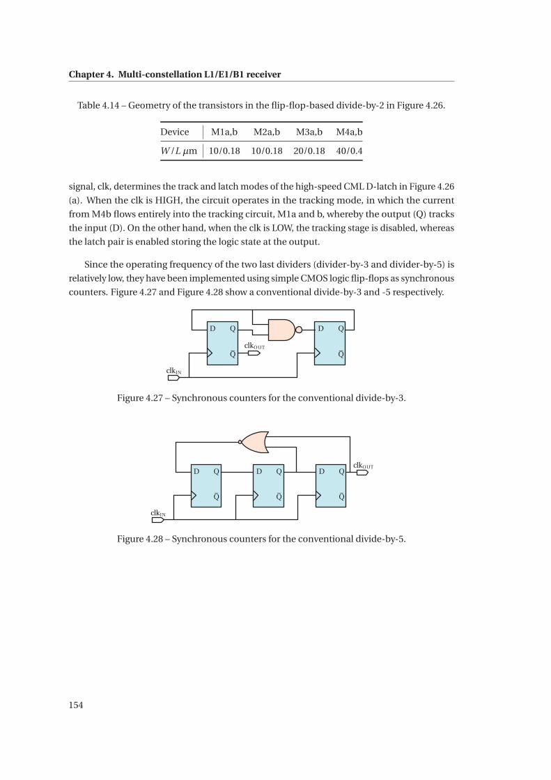
Chapter 4. Multi-constellation L1/E1/B1 receiver
Table 4.14 – Geometry of the transistors in the flip-flop-based divide-by-2 in Figure 4.26.
Device M1a,b M2a,b M3a,b M4a,b
W /L μm 10/0.18 10/0.18 20/0.18 40/0.4
signal, clk, determines the track and latch modes of the high-speed CML D-latch in Figure 4.26
(a). When the clk is HIGH, the circuit operates in the tracking mode, in which the current
from M4b flows entirely into the tracking circuit, M1a and b, whereby the output (Q) tracks
the input (D). On the other hand, when the clk is LOW, the tracking stage is disabled, whereas
the latch pair is enabled storing the logic state at the output.
Since the operating frequency of the two last dividers (divider-by-3 and divider-by-5) is
relatively low, they have been implemented using simple CMOS logic flip-flops as synchronous
counters. Figure 4.27 and Figure 4.28 show a conventional divide-by-3 and -5 respectively.
D Q
Q_
D Q
Q_
clkIN
clkOUT
Figure 4.27 – Synchronous counters for the conventional divide-by-3.
D Q
Q_
D Q
Q_
clkIN
clkOUTD Q
Q_
Figure 4.28 – Synchronous counters for the conventional divide-by-5.
154
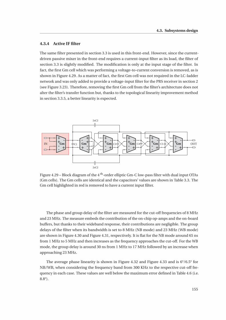
4.3. Subsystems design
4.3.4 Active IF filter
The same filter presented in section 3.3 is used in this front-end. However, since the current-
driven passive mixer in the front-end requires a current-input filter as its load, the filter of
section 3.3 is slightly modified. The modification is only at the input stage of the filter. In
fact, the first Gm cell which was performing a voltage-to-current conversion is removed, as is
shown in Figure 4.29. As a matter of fact, the first Gm cell was not required in the LC-ladder
network and was only added to provide a voltage-input filter for the PRS receiver in section 2
(see Figure 3.23). Therefore, removing the first Gm cell from the filter’s architecture does not
alter the filter’s transfer function but, thanks to the topological linearity improvement method
in section 3.3.5, a better linearity is expected.
+
+
-
-
+-
+
+
-
-
+-
+
+
-
-
+-
+
+
-
-
+-
+
+
-
-
+-C4
2xC2
2xC2
+
+
-
-
+-C1 C3IN OUTGm Gm Gm Gm Gm GmC5
Figure 4.29 – Block diagram of the 4 th-order elliptic Gm-C low-pass filter with dual input OTAs(Gm cells). The Gm cells are identical and the capacitors’ values are shown in Table 3.3. TheGm cell highlighted in red is removed to have a current input filter.
The phase and group delay of the filter are measured for the cut-off frequencies of 8 MHz
and 23 MHz. The measure embeds the contribution of the on-chip op-amps and the on-board
buffers, but thanks to their wideband response, their contributions are negligible. The group
delays of the filter when its bandwidth is set to 8 MHz (NB mode) and 23 MHz (WB mode)
are shown in Figure 4.30 and Figure 4.31, respectively. It is flat for the NB mode around 65 ns
from 1 MHz to 5 MHz and then increases as the frequency approaches the cut-off. For the WB
mode, the group delay is around 30 ns from 1 MHz to 17 MHz followed by an increase when
approaching 23 MHz.
The average phase linearity is shown in Figure 4.32 and Figure 4.33 and is 6°/6.5° for
NB/WB, when considering the frequency band from 300 KHz to the respective cut-off fre-
quency in each case. These values are well below the maximum error defined in Table 4.6 (i.e.
8.8°).
155
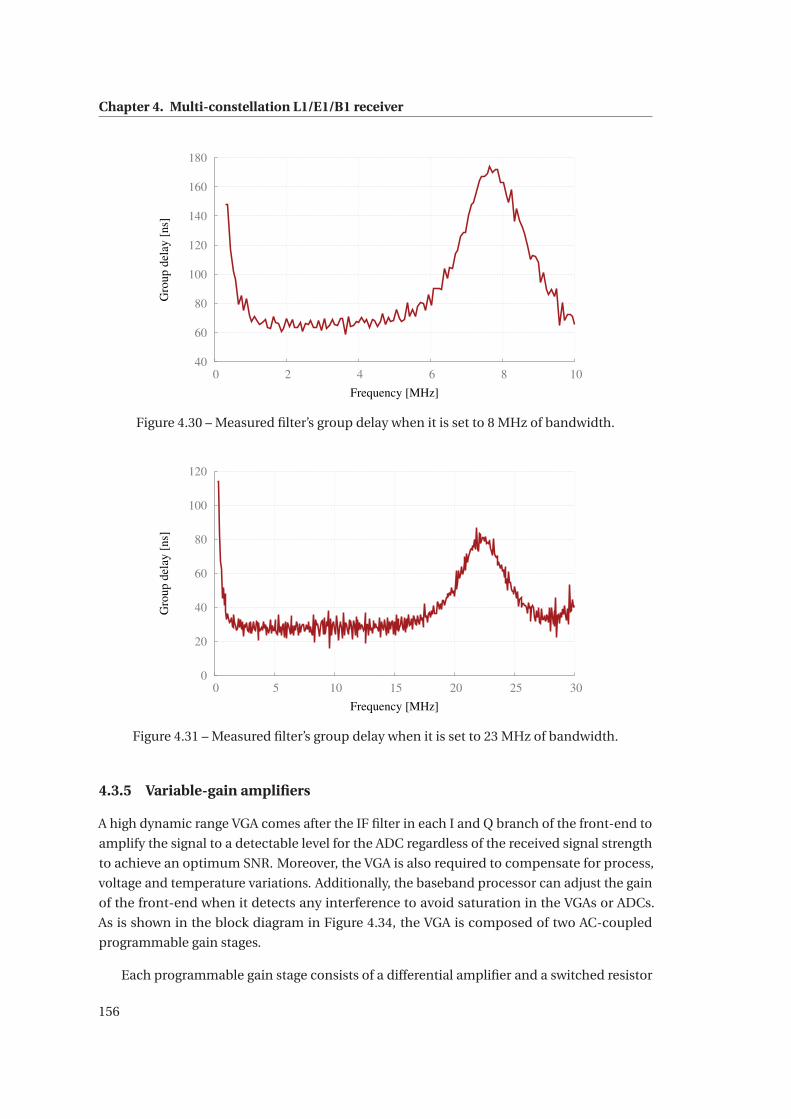
Chapter 4. Multi-constellation L1/E1/B1 receiver
40
60
80
100
120
140
160
180
0 2 4 6 8 10
Gro
up d
elay
[ns]
Frequency [MHz]
Figure 4.30 – Measured filter’s group delay when it is set to 8 MHz of bandwidth.
0
20
40
60
80
100
120
0 5 10 15 20 25 30
Gro
up d
elay
[ns]
Frequency [MHz]
Figure 4.31 – Measured filter’s group delay when it is set to 23 MHz of bandwidth.
4.3.5 Variable-gain amplifiers
A high dynamic range VGA comes after the IF filter in each I and Q branch of the front-end to
amplify the signal to a detectable level for the ADC regardless of the received signal strength
to achieve an optimum SNR. Moreover, the VGA is also required to compensate for process,
voltage and temperature variations. Additionally, the baseband processor can adjust the gain
of the front-end when it detects any interference to avoid saturation in the VGAs or ADCs.
As is shown in the block diagram in Figure 4.34, the VGA is composed of two AC-coupled
programmable gain stages.
Each programmable gain stage consists of a differential amplifier and a switched resistor
156
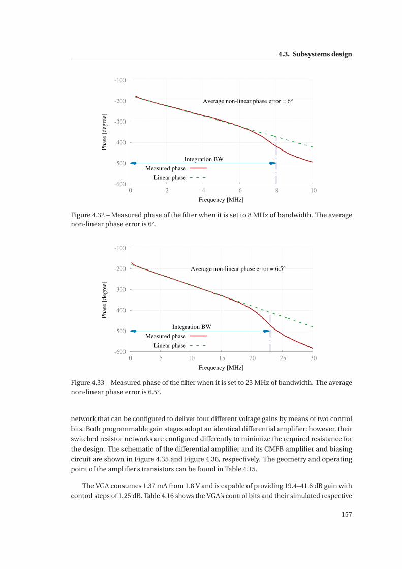
4.3. Subsystems design
-600
-500
-400
-300
-200
-100
0 2 4 6 8 10
Integration BW
Average non-linear phase error = 6°P
has
e [d
egre
e]
Frequency [MHz]
Measured phase
Linear phase
Figure 4.32 – Measured phase of the filter when it is set to 8 MHz of bandwidth. The averagenon-linear phase error is 6°.
-600
-500
-400
-300
-200
-100
0 5 10 15 20 25 30
Integration BW
Average non-linear phase error = 6.5°
Phas
e [d
egre
e]
Frequency [MHz]
Measured phase
Linear phase
Figure 4.33 – Measured phase of the filter when it is set to 23 MHz of bandwidth. The averagenon-linear phase error is 6.5°.
network that can be configured to deliver four different voltage gains by means of two control
bits. Both programmable gain stages adopt an identical differential amplifier; however, their
switched resistor networks are configured differently to minimize the required resistance for
the design. The schematic of the differential amplifier and its CMFB amplifier and biasing
circuit are shown in Figure 4.35 and Figure 4.36, respectively. The geometry and operating
point of the amplifier’s transistors can be found in Table 4.15.
The VGA consumes 1.37 mA from 1.8 V and is capable of providing 19.4–41.6 dB gain with
control steps of 1.25 dB. Table 4.16 shows the VGA’s control bits and their simulated respective
157
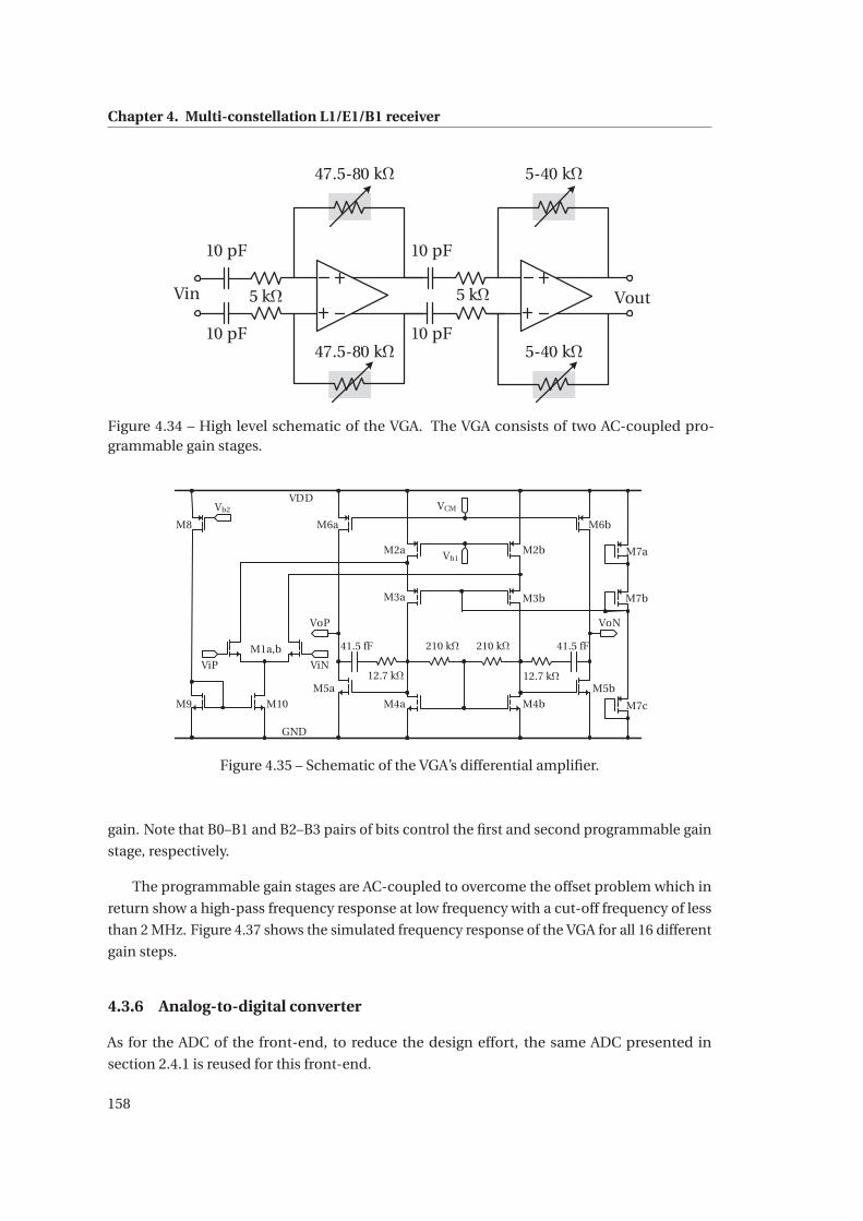
Chapter 4. Multi-constellation L1/E1/B1 receiver
Vin Vout5 kΩ
47.5-80 kΩ
47.5-80 kΩ
5 kΩ
5-40 kΩ
5-40 kΩ
10 pF
10 pF
10 pF
10 pF
Figure 4.34 – High level schematic of the VGA. The VGA consists of two AC-coupled pro-grammable gain stages.
ViNViP
VoP VoN
Vb2
Vb1
VCM
M8 M6a M6b
M2a M2b
M3a M3b
M1a,b
M5a M5b
M4a M4b
M7a
M7b
M7cM9 M10
210 kΩ 210 kΩ
12.7 kΩ
41.5 fF
12.7 kΩ
41.5 fF
VDD
GND
Figure 4.35 – Schematic of the VGA’s differential amplifier.
gain. Note that B0–B1 and B2–B3 pairs of bits control the first and second programmable gain
stage, respectively.
The programmable gain stages are AC-coupled to overcome the offset problem which in
return show a high-pass frequency response at low frequency with a cut-off frequency of less
than 2 MHz. Figure 4.37 shows the simulated frequency response of the VGA for all 16 different
gain steps.
4.3.6 Analog-to-digital converter
As for the ADC of the front-end, to reduce the design effort, the same ADC presented in
section 2.4.1 is reused for this front-end.
158
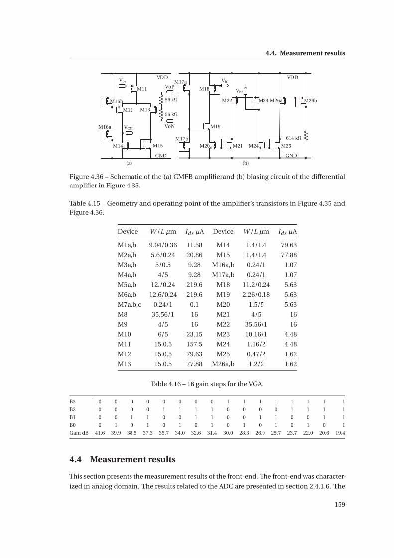
4.4. Measurement results
Vb1
Vb2
VCM
Vb2 M17a
(b)(a)
VDD
GND
VDD
GND
M13
M14 M15
M16a
M12
M11
M16b
M17b
M18
M19
M20 M21
M22 M23
M24 M25
M26a M26b
614 kΩ
56 kΩ
56 kΩ
VoP
VoN
Figure 4.36 – Schematic of the (a) CMFB amplifierand (b) biasing circuit of the differentialamplifier in Figure 4.35.
Table 4.15 – Geometry and operating point of the amplifier’s transistors in Figure 4.35 andFigure 4.36.
Device W /L μm Id s μA Device W /L μm Id s μA
M1a,b 9.04/0.36 11.58 M14 1.4/1.4 79.63
M2a,b 5.6/0.24 20.86 M15 1.4/1.4 77.88
M3a,b 5/0.5 9.28 M16a,b 0.24/1 1.07
M4a,b 4/5 9.28 M17a,b 0.24/1 1.07
M5a,b 12./0.24 219.6 M18 11.2/0.24 5.63
M6a,b 12.6/0.24 219.6 M19 2.26/0.18 5.63
M7a,b,c 0.24/1 0.1 M20 1.5/5 5.63
M8 35.56/1 16 M21 4/5 16
M9 4/5 16 M22 35.56/1 16
M10 6/5 23.15 M23 10.16/1 4.48
M11 15.0.5 157.5 M24 1.16/2 4.48
M12 15.0.5 79.63 M25 0.47/2 1.62
M13 15.0.5 77.88 M26a,b 1.2/2 1.62
Table 4.16 – 16 gain steps for the VGA.
B3 0 0 0 0 0 0 0 0 1 1 1 1 1 1 1 1
B2 0 0 0 0 1 1 1 1 0 0 0 0 1 1 1 1
B1 0 0 1 1 0 0 1 1 0 0 1 1 0 0 1 1
B0 0 1 0 1 0 1 0 1 0 1 0 1 0 1 0 1
Gain dB 41.6 39.9 38.5 37.3 35.7 34.0 32.6 31.4 30.0 28.3 26.9 25.7 23.7 22.0 20.6 19.4
4.4 Measurement results
This section presents the measurement results of the front-end. The front-end was character-
ized in analog domain. The results related to the ADC are presented in section 2.4.1.6. The
159
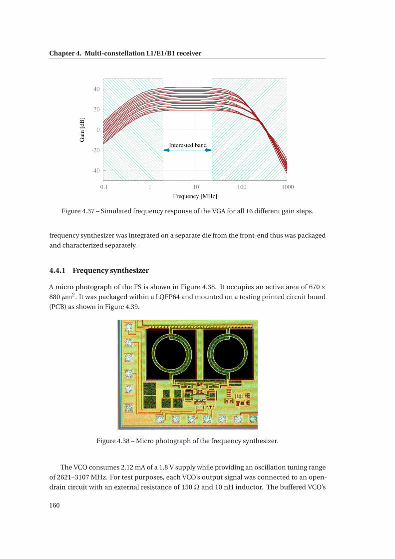
Chapter 4. Multi-constellation L1/E1/B1 receiver
-40
-20
0
20
40
0.1 1 10 100 1000
Interested band
Gai
n [
dB
]
Frequency [MHz]
Figure 4.37 – Simulated frequency response of the VGA for all 16 different gain steps.
frequency synthesizer was integrated on a separate die from the front-end thus was packaged
and characterized separately.
4.4.1 Frequency synthesizer
A micro photograph of the FS is shown in Figure 4.38. It occupies an active area of 670×880 μm2. It was packaged within a LQFP64 and mounted on a testing printed circuit board
(PCB) as shown in Figure 4.39.
Figure 4.38 – Micro photograph of the frequency synthesizer.
The VCO consumes 2.12 mA of a 1.8 V supply while providing an oscillation tuning range
of 2621–3107 MHz. For test purposes, each VCO’s output signal was connected to an open-
drain circuit with an external resistance of 150 Ω and 10 nH inductor. The buffered VCO’s
160
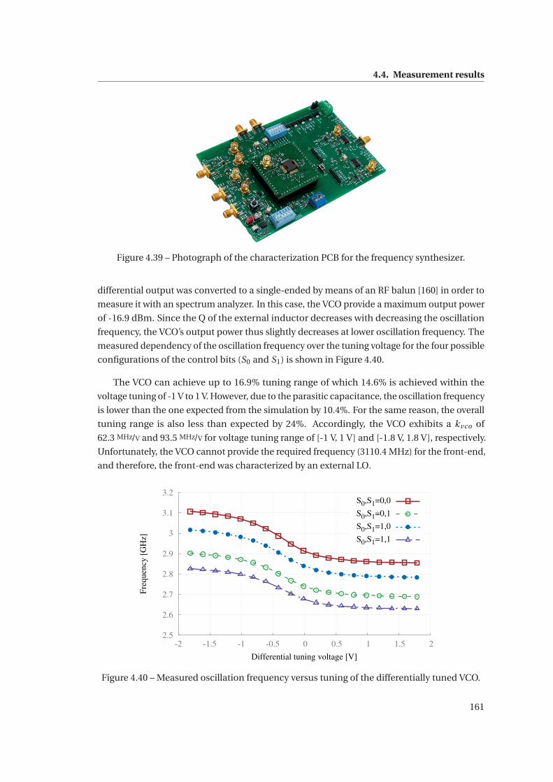
4.4. Measurement results
Figure 4.39 – Photograph of the characterization PCB for the frequency synthesizer.
differential output was converted to a single-ended by means of an RF balun [160] in order to
measure it with an spectrum analyzer. In this case, the VCO provide a maximum output power
of -16.9 dBm. Since the Q of the external inductor decreases with decreasing the oscillation
frequency, the VCO’s output power thus slightly decreases at lower oscillation frequency. The
measured dependency of the oscillation frequency over the tuning voltage for the four possible
configurations of the control bits (S0 and S1) is shown in Figure 4.40.
The VCO can achieve up to 16.9% tuning range of which 14.6% is achieved within the
voltage tuning of -1 V to 1 V. However, due to the parasitic capacitance, the oscillation frequency
is lower than the one expected from the simulation by 10.4%. For the same reason, the overall
tuning range is also less than expected by 24%. Accordingly, the VCO exhibits a kvco of
62.3 MHz/V and 93.5 MHz/V for voltage tuning range of [-1 V, 1 V] and [-1.8 V, 1.8 V], respectively.
Unfortunately, the VCO cannot provide the required frequency (3110.4 MHz) for the front-end,
and therefore, the front-end was characterized by an external LO.
2.5
2.6
2.7
2.8
2.9
3
3.1
3.2
-2 -1.5 -1 -0.5 0 0.5 1 1.5 2
Fre
quen
cy [
GH
z]
Differential tuning voltage [V]
S0,S1=0,0
S0,S1=0,1
S0,S1=1,0
S0,S1=1,1
Figure 4.40 – Measured oscillation frequency versus tuning of the differentially tuned VCO.
161
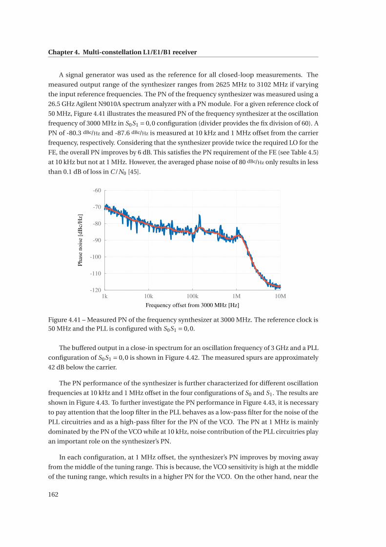
Chapter 4. Multi-constellation L1/E1/B1 receiver
A signal generator was used as the reference for all closed-loop measurements. The
measured output range of the synthesizer ranges from 2625 MHz to 3102 MHz if varying
the input reference frequencies. The PN of the frequency synthesizer was measured using a
26.5 GHz Agilent N9010A spectrum analyzer with a PN module. For a given reference clock of
50 MHz, Figure 4.41 illustrates the measured PN of the frequency synthesizer at the oscillation
frequency of 3000 MHz in S0S1 = 0,0 configuration (divider provides the fix division of 60). A
PN of -80.3 dBc/Hz and -87.6 dBc/Hz is measured at 10 kHz and 1 MHz offset from the carrier
frequency, respectively. Considering that the synthesizer provide twice the required LO for the
FE, the overall PN improves by 6 dB. This satisfies the PN requirement of the FE (see Table 4.5)
at 10 kHz but not at 1 MHz. However, the averaged phase noise of 80 dBc/Hz only results in less
than 0.1 dB of loss in C /N0 [45].
-120
-110
-100
-90
-80
-70
-60
1k 10k 100k 1M 10M
Phas
e nois
e [d
Bc/
Hz]
Frequency offset from 3000 MHz [Hz]
Figure 4.41 – Measured PN of the frequency synthesizer at 3000 MHz. The reference clock is50 MHz and the PLL is configured with S0S1 = 0,0.
The buffered output in a close-in spectrum for an oscillation frequency of 3 GHz and a PLL
configuration of S0S1 = 0,0 is shown in Figure 4.42. The measured spurs are approximately
42 dB below the carrier.
The PN performance of the synthesizer is further characterized for different oscillation
frequencies at 10 kHz and 1 MHz offset in the four configurations of S0 and S1. The results are
shown in Figure 4.43. To further investigate the PN performance in Figure 4.43, it is necessary
to pay attention that the loop filter in the PLL behaves as a low-pass filter for the noise of the
PLL circuitries and as a high-pass filter for the PN of the VCO. The PN at 1 MHz is mainly
dominated by the PN of the VCO while at 10 kHz, noise contribution of the PLL circuitries play
an important role on the synthesizer’s PN.
In each configuration, at 1 MHz offset, the synthesizer’s PN improves by moving away
from the middle of the tuning range. This is because, the VCO sensitivity is high at the middle
of the tuning range, which results in a higher PN for the VCO. On the other hand, near the
162
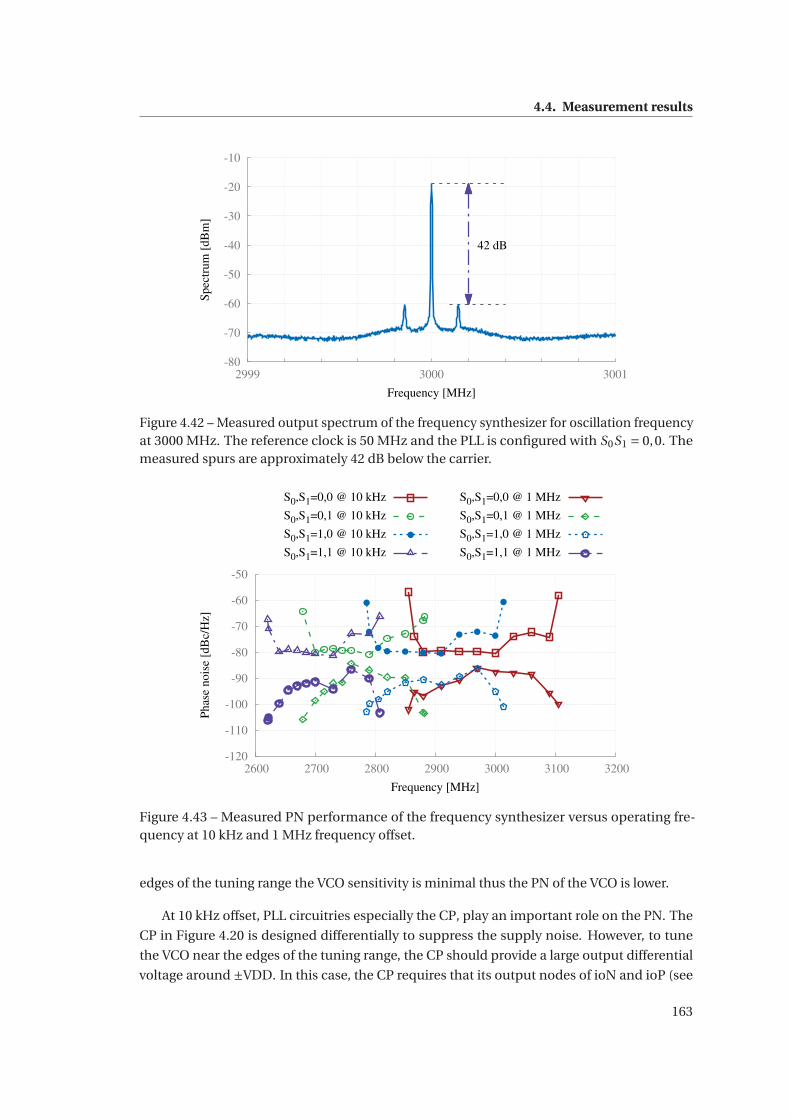
4.4. Measurement results
-80
-70
-60
-50
-40
-30
-20
-10
2999 3000 3001
42 dB
Spec
trum
[dB
m]
Frequency [MHz]
Figure 4.42 – Measured output spectrum of the frequency synthesizer for oscillation frequencyat 3000 MHz. The reference clock is 50 MHz and the PLL is configured with S0S1 = 0,0. Themeasured spurs are approximately 42 dB below the carrier.
-120
-110
-100
-90
-80
-70
-60
-50
2600 2700 2800 2900 3000 3100 3200
Phas
e nois
e [d
Bc/
Hz]
Frequency [MHz]
S0,S1=0,0 @ 10 kHz
S0,S1=0,1 @ 10 kHz
S0,S1=1,0 @ 10 kHz
S0,S1=1,1 @ 10 kHz
S0,S1=0,0 @ 1 MHz
S0,S1=0,1 @ 1 MHz
S0,S1=1,0 @ 1 MHz
S0,S1=1,1 @ 1 MHz
Figure 4.43 – Measured PN performance of the frequency synthesizer versus operating fre-quency at 10 kHz and 1 MHz frequency offset.
edges of the tuning range the VCO sensitivity is minimal thus the PN of the VCO is lower.
At 10 kHz offset, PLL circuitries especially the CP, play an important role on the PN. The
CP in Figure 4.20 is designed differentially to suppress the supply noise. However, to tune
the VCO near the edges of the tuning range, the CP should provide a large output differential
voltage around ±VDD. In this case, the CP requires that its output nodes of ioN and ioP (see
163
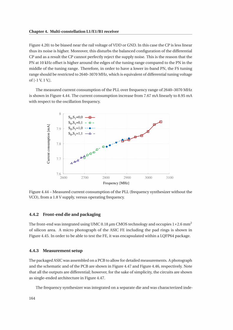
Chapter 4. Multi-constellation L1/E1/B1 receiver
Figure 4.20) to be biased near the rail voltage of VDD or GND. In this case the CP is less linear
thus its noise is higher. Moreover, this disturbs the balanced configuration of the differential
CP and as a result the CP cannot perfectly reject the supply noise. This is the reason that the
PN at 10 kHz offset is higher around the edges of the tuning range compared to the PN in the
middle of the tuning range. Therefore, in order to have a lower in-band PN, the FS tuning
range should be restricted to 2640–3070 MHz, which is equivalent of differential tuning voltage
of [-1 V, 1 V,].
The measured current consumption of the PLL over frequency range of 2640–3070 MHz
is shown in Figure 4.44. The current consumption increase from 7.67 mA linearly to 8.95 mA
with respect to the oscillation frequency.
7.6
7.7
7.8
7.9
8
2600 2700 2800 2900 3000 3100
Curr
ent
consu
mpti
on [
mA
]
Frequency [MHz]
S0,S1=0,0
S0,S1=0,1
S0,S1=1,0
S0,S1=1,1
Figure 4.44 – Measured current consumption of the PLL (frequency synthesizer without theVCO), from a 1.8 V supply, versus operating frequency.
4.4.2 Front-end die and packaging
The front-end was integrated using UMC 0.18 μm CMOS technology and occupies 1×2.6 mm2
of silicon area. A micro photograph of the ASIC FE including the pad rings is shown in
Figure 4.45. In order to be able to test the FE, it was encapsulated within a LQFP64 package.
4.4.3 Measurement setup
The packaged ASIC was assembled on a PCB to allow for detailed measurements. A photograph
and the schematic and of the PCB are shown in Figure 4.47 and Figure 4.46, respectively. Note
that all the outputs are differential; however, for the sake of simplicity, the circuits are shown
as single-ended architecture in Figure 4.47.
The frequency synthesizer was integrated on a separate die and was characterized inde-
164
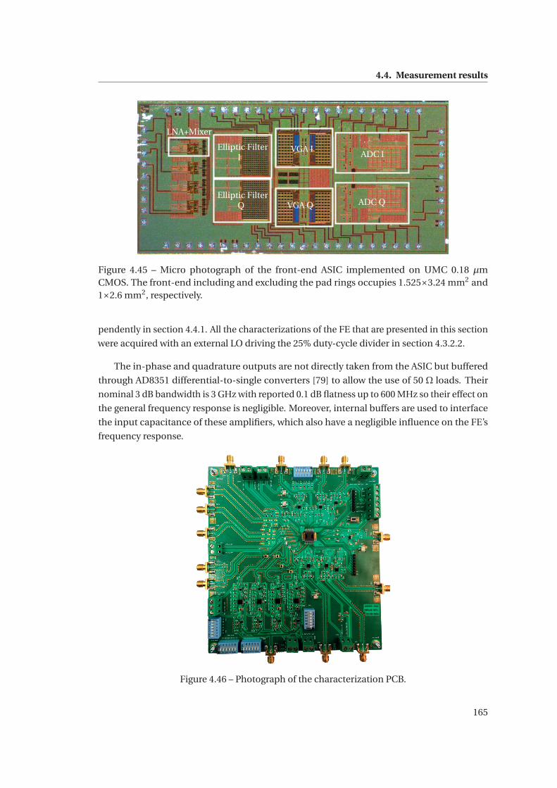
4.4. Measurement results
ADC I
ADC Q
VGA I
VGA Q
Elliptic Filter
I
Elliptic Filter
Q
LNA+Mixer
Figure 4.45 – Micro photograph of the front-end ASIC implemented on UMC 0.18 μmCMOS. The front-end including and excluding the pad rings occupies 1.525×3.24 mm2 and1×2.6 mm2, respectively.
pendently in section 4.4.1. All the characterizations of the FE that are presented in this section
were acquired with an external LO driving the 25% duty-cycle divider in section 4.3.2.2.
The in-phase and quadrature outputs are not directly taken from the ASIC but buffered
through AD8351 differential-to-single converters [79] to allow the use of 50 Ω loads. Their
nominal 3 dB bandwidth is 3 GHz with reported 0.1 dB flatness up to 600 MHz so their effect on
the general frequency response is negligible. Moreover, internal buffers are used to interface
the input capacitance of these amplifiers, which also have a negligible influence on the FE’s
frequency response.
Figure 4.46 – Photograph of the characterization PCB.
165
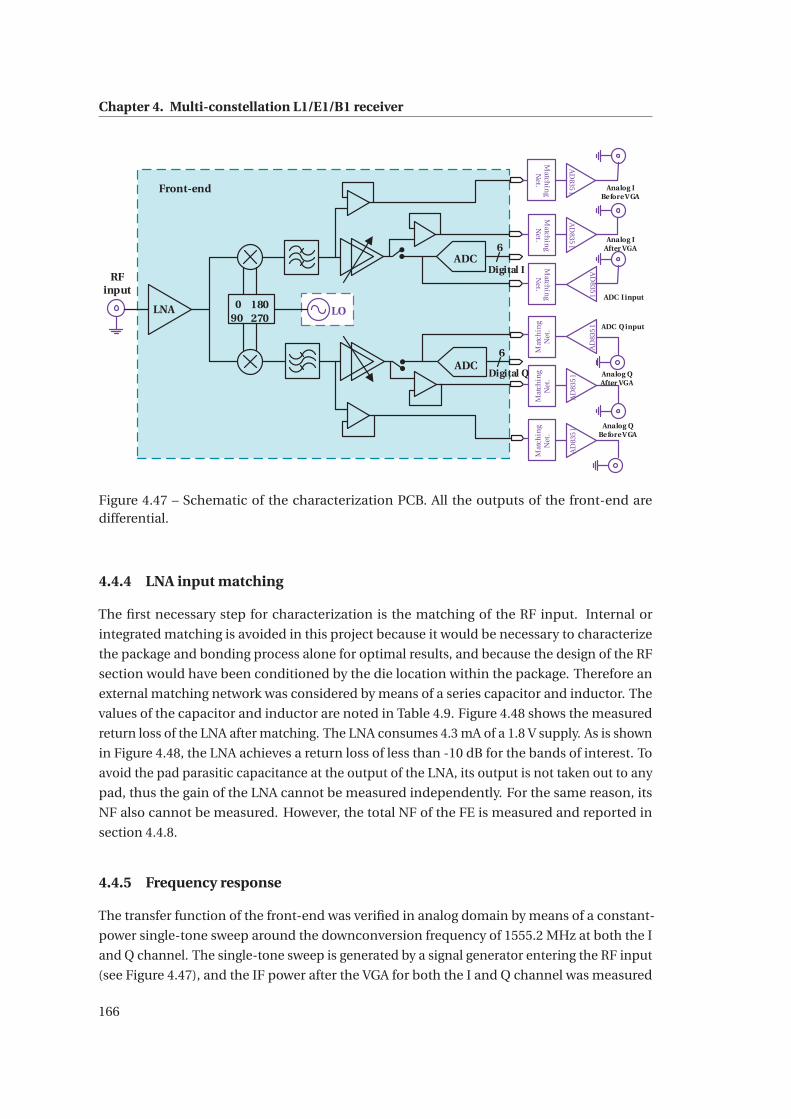
Chapter 4. Multi-constellation L1/E1/B1 receiver
0 18090 270
6
LNA
Mat
chin
g N
et.
AD
835
1
Mat
chin
g N
et.
Mat
chin
g N
et.
AD
835
1
AD
835
1
Match
ing
Net.
AD
8351
Match
ing
Net.
Match
ing
Net.
AD
8351
AD
8351
ADC
6ADC
Digital I
Digital Q
Analog IBefore VGA
Analog IAfter VGA
ADC I input
ADC Q input
Analog QAfter VGA
Analog QBefore VGA
RF input
LO
Front-end
Figure 4.47 – Schematic of the characterization PCB. All the outputs of the front-end aredifferential.
4.4.4 LNA input matching
The first necessary step for characterization is the matching of the RF input. Internal or
integrated matching is avoided in this project because it would be necessary to characterize
the package and bonding process alone for optimal results, and because the design of the RF
section would have been conditioned by the die location within the package. Therefore an
external matching network was considered by means of a series capacitor and inductor. The
values of the capacitor and inductor are noted in Table 4.9. Figure 4.48 shows the measured
return loss of the LNA after matching. The LNA consumes 4.3 mA of a 1.8 V supply. As is shown
in Figure 4.48, the LNA achieves a return loss of less than -10 dB for the bands of interest. To
avoid the pad parasitic capacitance at the output of the LNA, its output is not taken out to any
pad, thus the gain of the LNA cannot be measured independently. For the same reason, its
NF also cannot be measured. However, the total NF of the FE is measured and reported in
section 4.4.8.
4.4.5 Frequency response
The transfer function of the front-end was verified in analog domain by means of a constant-
power single-tone sweep around the downconversion frequency of 1555.2 MHz at both the I
and Q channel. The single-tone sweep is generated by a signal generator entering the RF input
(see Figure 4.47), and the IF power after the VGA for both the I and Q channel was measured
166
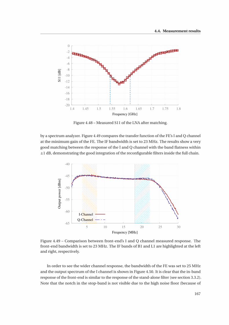
4.4. Measurement results
-20
-18
-16
-14
-12
-10
-8
-6
-4
-2
0
1.4 1.45 1.5 1.55 1.6 1.65 1.7 1.75 1.8
S11 [
dB
]
Frequency [GHz]
Figure 4.48 – Measured S11 of the LNA after matching.
by a spectrum analyzer. Figure 4.49 compares the transfer function of the FE’s I and Q channel
at the minimum gain of the FE. The IF bandwidth is set to 23 MHz. The results show a very
good matching between the response of the I and Q channel with the band flatness within
±1 dB, demonstrating the good integration of the reconfigurable filters inside the full chain.
-65
-60
-55
-50
-45
-40
5 10 15 20 25 30
Outp
ut
pow
er [
dB
m]
Frequency [MHz]
I-Channel
Q-Channel
Figure 4.49 – Comparison between front-end’s I and Q channel measured response. Thefront-end bandwidth is set to 23 MHz. The IF bands of B1 and L1 are highlighted at the leftand right, respectively.
In order to see the wider channel response, the bandwidth of the FE was set to 25 MHz
and the output spectrum of the I channel is shown in Figure 4.50. It is clear that the in-band
response of the front-end is similar to the response of the stand-alone filter (see section 3.3.2).
Note that the notch in the stop-band is not visible due to the high noise floor (because of
167
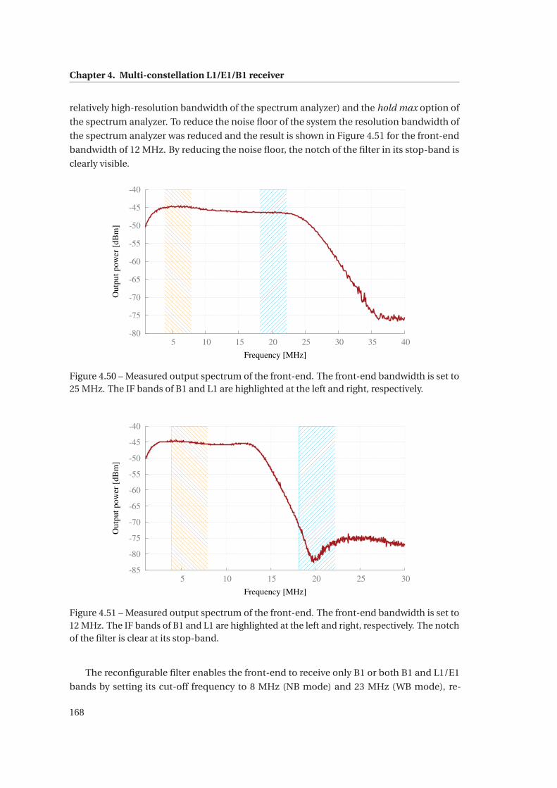
Chapter 4. Multi-constellation L1/E1/B1 receiver
relatively high-resolution bandwidth of the spectrum analyzer) and the hold max option of
the spectrum analyzer. To reduce the noise floor of the system the resolution bandwidth of
the spectrum analyzer was reduced and the result is shown in Figure 4.51 for the front-end
bandwidth of 12 MHz. By reducing the noise floor, the notch of the filter in its stop-band is
clearly visible.
-80
-75
-70
-65
-60
-55
-50
-45
-40
5 10 15 20 25 30 35 40
Outp
ut
pow
er [
dB
m]
Frequency [MHz]
Figure 4.50 – Measured output spectrum of the front-end. The front-end bandwidth is set to25 MHz. The IF bands of B1 and L1 are highlighted at the left and right, respectively.
-85
-80
-75
-70
-65
-60
-55
-50
-45
-40
5 10 15 20 25 30
Outp
ut
pow
er [
dB
m]
Frequency [MHz]
Figure 4.51 – Measured output spectrum of the front-end. The front-end bandwidth is set to12 MHz. The IF bands of B1 and L1 are highlighted at the left and right, respectively. The notchof the filter is clear at its stop-band.
The reconfigurable filter enables the front-end to receive only B1 or both B1 and L1/E1
bands by setting its cut-off frequency to 8 MHz (NB mode) and 23 MHz (WB mode), re-
168
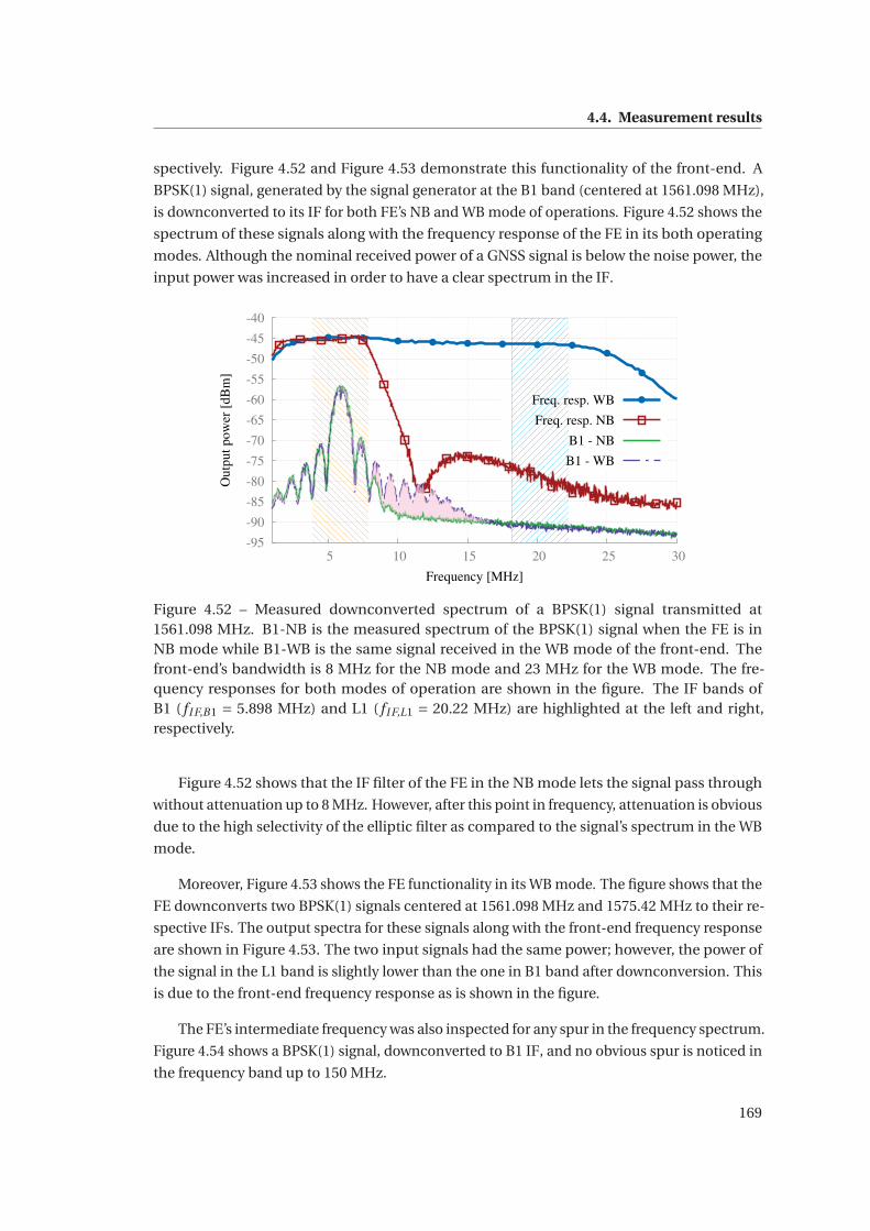
4.4. Measurement results
spectively. Figure 4.52 and Figure 4.53 demonstrate this functionality of the front-end. A
BPSK(1) signal, generated by the signal generator at the B1 band (centered at 1561.098 MHz),
is downconverted to its IF for both FE’s NB and WB mode of operations. Figure 4.52 shows the
spectrum of these signals along with the frequency response of the FE in its both operating
modes. Although the nominal received power of a GNSS signal is below the noise power, the
input power was increased in order to have a clear spectrum in the IF.
-95
-90
-85
-80
-75
-70
-65
-60
-55
-50
-45
-40
5 10 15 20 25 30
Outp
ut
pow
er [
dB
m]
Frequency [MHz]
Freq. resp. WB
Freq. resp. NB
B1 - NB
B1 - WB
Figure 4.52 – Measured downconverted spectrum of a BPSK(1) signal transmitted at1561.098 MHz. B1-NB is the measured spectrum of the BPSK(1) signal when the FE is inNB mode while B1-WB is the same signal received in the WB mode of the front-end. Thefront-end’s bandwidth is 8 MHz for the NB mode and 23 MHz for the WB mode. The fre-quency responses for both modes of operation are shown in the figure. The IF bands ofB1 ( fI F,B1 = 5.898 MHz) and L1 ( fI F,L1 = 20.22 MHz) are highlighted at the left and right,respectively.
Figure 4.52 shows that the IF filter of the FE in the NB mode lets the signal pass through
without attenuation up to 8 MHz. However, after this point in frequency, attenuation is obvious
due to the high selectivity of the elliptic filter as compared to the signal’s spectrum in the WB
mode.
Moreover, Figure 4.53 shows the FE functionality in its WB mode. The figure shows that the
FE downconverts two BPSK(1) signals centered at 1561.098 MHz and 1575.42 MHz to their re-
spective IFs. The output spectra for these signals along with the front-end frequency response
are shown in Figure 4.53. The two input signals had the same power; however, the power of
the signal in the L1 band is slightly lower than the one in B1 band after downconversion. This
is due to the front-end frequency response as is shown in the figure.
The FE’s intermediate frequency was also inspected for any spur in the frequency spectrum.
Figure 4.54 shows a BPSK(1) signal, downconverted to B1 IF, and no obvious spur is noticed in
the frequency band up to 150 MHz.
169
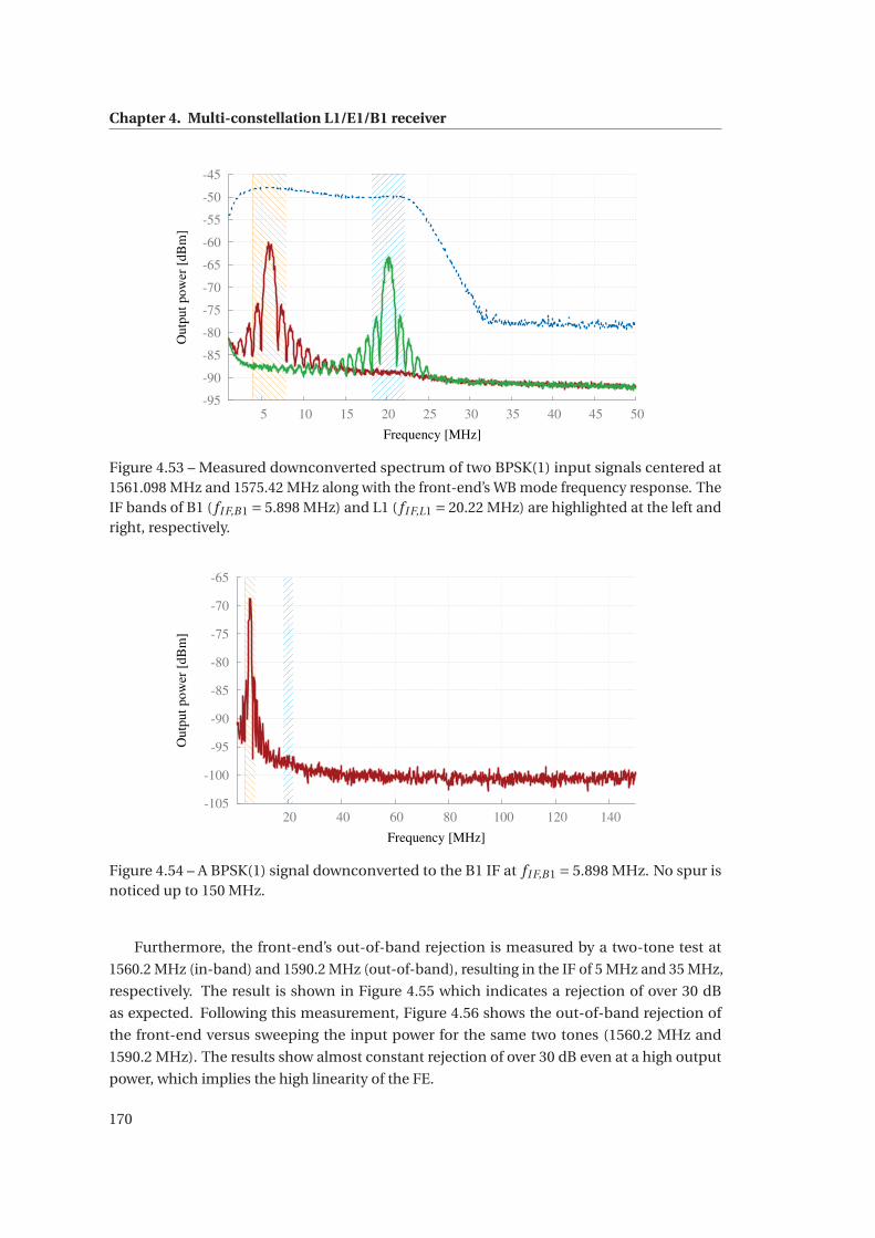
Chapter 4. Multi-constellation L1/E1/B1 receiver
-95
-90
-85
-80
-75
-70
-65
-60
-55
-50
-45
5 10 15 20 25 30 35 40 45 50
Outp
ut
pow
er [
dB
m]
Frequency [MHz]
Figure 4.53 – Measured downconverted spectrum of two BPSK(1) input signals centered at1561.098 MHz and 1575.42 MHz along with the front-end’s WB mode frequency response. TheIF bands of B1 ( fI F,B1 = 5.898 MHz) and L1 ( fI F,L1 = 20.22 MHz) are highlighted at the left andright, respectively.
-105
-100
-95
-90
-85
-80
-75
-70
-65
20 40 60 80 100 120 140
Outp
ut
pow
er [
dB
m]
Frequency [MHz]
Figure 4.54 – A BPSK(1) signal downconverted to the B1 IF at fI F,B1 = 5.898 MHz. No spur isnoticed up to 150 MHz.
Furthermore, the front-end’s out-of-band rejection is measured by a two-tone test at
1560.2 MHz (in-band) and 1590.2 MHz (out-of-band), resulting in the IF of 5 MHz and 35 MHz,
respectively. The result is shown in Figure 4.55 which indicates a rejection of over 30 dB
as expected. Following this measurement, Figure 4.56 shows the out-of-band rejection of
the front-end versus sweeping the input power for the same two tones (1560.2 MHz and
1590.2 MHz). The results show almost constant rejection of over 30 dB even at a high output
power, which implies the high linearity of the FE.
170
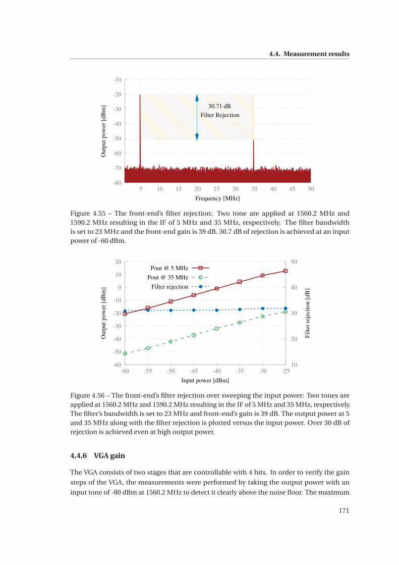
4.4. Measurement results
-80
-70
-60
-50
-40
-30
-20
-10
5 10 15 20 25 30 35 40 45 50
Filter Rejection
30.71 dBO
utp
ut
pow
er [
dB
m]
Frequency [MHz]
Figure 4.55 – The front-end’s filter rejection: Two tone are applied at 1560.2 MHz and1590.2 MHz resulting in the IF of 5 MHz and 35 MHz, respectively. The filter bandwidthis set to 23 MHz and the front-end gain is 39 dB. 30.7 dB of rejection is achieved at an inputpower of -60 dBm.
-60
-50
-40
-30
-20
-10
0
10
20
-60 -55 -50 -45 -40 -35 -30 -25 10
20
30
40
50
Outp
ut
pow
er [
dB
m]
Fil
ter
reje
ctio
n [
dB
]
Input power [dBm]
Pout @ 5 MHz
Pout @ 35 MHz
Filter rejection
Figure 4.56 – The front-end’s filter rejection over sweeping the input power: Two tones areapplied at 1560.2 MHz and 1590.2 MHz resulting in the IF of 5 MHz and 35 MHz, respectively.The filter’s bandwidth is set to 23 MHz and front-end’s gain is 39 dB. The output power at 5and 35 MHz along with the filter rejection is plotted versus the input power. Over 30 dB ofrejection is achieved even at high output power.
4.4.6 VGA gain
The VGA consists of two stages that are controllable with 4 bits. In order to verify the gain
steps of the VGA, the measurements were performed by taking the output power with an
input tone of -80 dBm at 1560.2 MHz to detect it clearly above the noise floor. The maximum
171
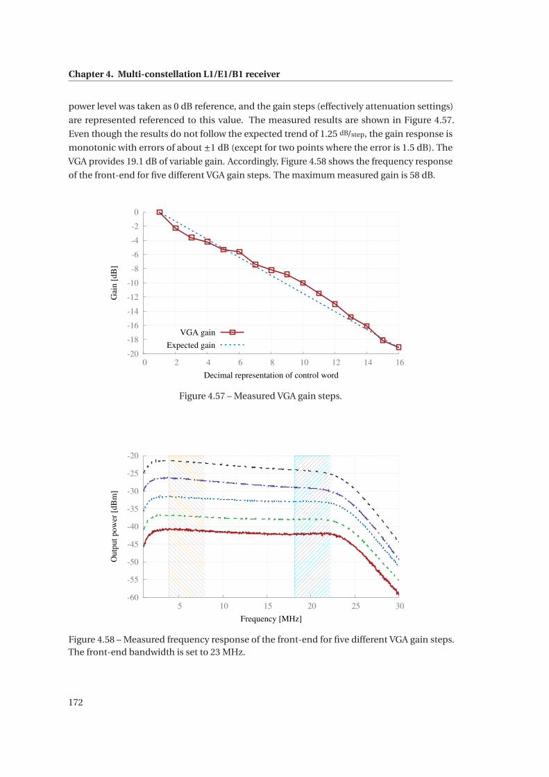
Chapter 4. Multi-constellation L1/E1/B1 receiver
power level was taken as 0 dB reference, and the gain steps (effectively attenuation settings)
are represented referenced to this value. The measured results are shown in Figure 4.57.
Even though the results do not follow the expected trend of 1.25 dB/step, the gain response is
monotonic with errors of about ±1 dB (except for two points where the error is 1.5 dB). The
VGA provides 19.1 dB of variable gain. Accordingly, Figure 4.58 shows the frequency response
of the front-end for five different VGA gain steps. The maximum measured gain is 58 dB.
-20
-18
-16
-14
-12
-10
-8
-6
-4
-2
0
0 2 4 6 8 10 12 14 16
Gai
n [
dB
]
Decimal representation of control word
VGA gain
Expected gain
Figure 4.57 – Measured VGA gain steps.
-60
-55
-50
-45
-40
-35
-30
-25
-20
5 10 15 20 25 30
Outp
ut
pow
er [
dB
m]
Frequency [MHz]
Figure 4.58 – Measured frequency response of the front-end for five different VGA gain steps.The front-end bandwidth is set to 23 MHz.
172
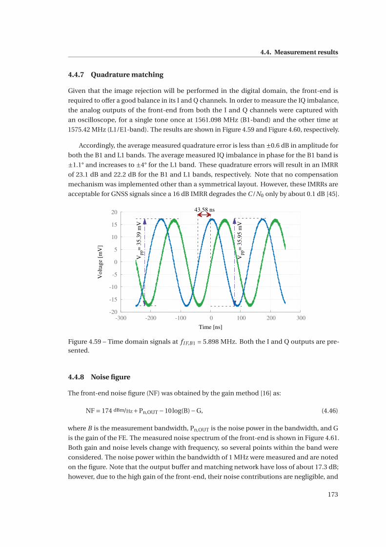
4.4. Measurement results
4.4.7 Quadrature matching
Given that the image rejection will be performed in the digital domain, the front-end is
required to offer a good balance in its I and Q channels. In order to measure the IQ imbalance,
the analog outputs of the front-end from both the I and Q channels were captured with
an oscilloscope, for a single tone once at 1561.098 MHz (B1-band) and the other time at
1575.42 MHz (L1/E1-band). The results are shown in Figure 4.59 and Figure 4.60, respectively.
Accordingly, the average measured quadrature error is less than ±0.6 dB in amplitude for
both the B1 and L1 bands. The average measured IQ imbalance in phase for the B1 band is
±1.1° and increases to ±4° for the L1 band. These quadrature errors will result in an IMRR
of 23.1 dB and 22.2 dB for the B1 and L1 bands, respectively. Note that no compensation
mechanism was implemented other than a symmetrical layout. However, these IMRRs are
acceptable for GNSS signals since a 16 dB IMRR degrades the C /N0 only by about 0.1 dB [45].
-20
-15
-10
-5
0
5
10
15
20
-300 -200 -100 0 100 200 300
Vp
p=
35.3
9 m
V
Vp
p=
35.9
5 m
V
43.58 ns
Volt
age
[mV
]
Time [ns]
Figure 4.59 – Time domain signals at fI F,B1 = 5.898 MHz. Both the I and Q outputs are pre-sented.
4.4.8 Noise figure
The front-end noise figure (NF) was obtained by the gain method [16] as:
NF = 174 dBm/Hz+Pn,OUT −10log(B)−G, (4.46)
where B is the measurement bandwidth, Pn,OUT is the noise power in the bandwidth, and G
is the gain of the FE. The measured noise spectrum of the front-end is shown in Figure 4.61.
Both gain and noise levels change with frequency, so several points within the band were
considered. The noise power within the bandwidth of 1 MHz were measured and are noted
on the figure. Note that the output buffer and matching network have loss of about 17.3 dB;
however, due to the high gain of the front-end, their noise contributions are negligible, and
173
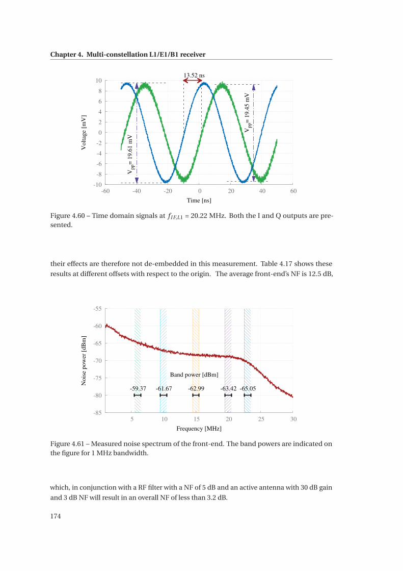
Chapter 4. Multi-constellation L1/E1/B1 receiver
-10
-8
-6
-4
-2
0
2
4
6
8
10
-60 -40 -20 0 20 40 60
Vp
p=
19.6
1 m
V
Vp
p=
19.4
5 m
V
13.52 ns
Volt
age
[mV
]
Time [ns]
Figure 4.60 – Time domain signals at fI F,L1 = 20.22 MHz. Both the I and Q outputs are pre-sented.
their effects are therefore not de-embedded in this measurement. Table 4.17 shows these
results at different offsets with respect to the origin. The average front-end’s NF is 12.5 dB,
-85
-80
-75
-70
-65
-60
-55
5 10 15 20 25 30
Band power [dBm]
-59.37 -61.67 -62.99 -63.42 -65.05
Nois
e pow
er [
dB
m]
Frequency [MHz]
Figure 4.61 – Measured noise spectrum of the front-end. The band powers are indicated onthe figure for 1 MHz bandwidth.
which, in conjunction with a RF filter with a NF of 5 dB and an active antenna with 30 dB gain
and 3 dB NF will result in an overall NF of less than 3.2 dB.
174
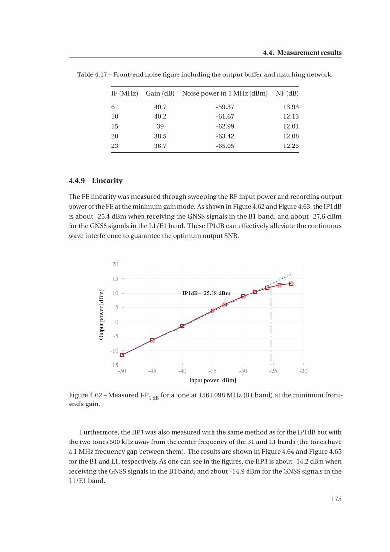
4.4. Measurement results
Table 4.17 – Front-end noise figure including the output buffer and matching network.
IF (MHz) Gain (dB) Noise power in 1 MHz [dBm] NF (dB)
6 40.7 -59.37 13.93
10 40.2 -61.67 12.13
15 39 -62.99 12.01
20 38.5 -63.42 12.08
23 36.7 -65.05 12.25
4.4.9 Linearity
The FE linearity was measured through sweeping the RF input power and recording output
power of the FE at the minimum gain mode. As shown in Figure 4.62 and Figure 4.63, the IP1dB
is about -25.4 dBm when receiving the GNSS signals in the B1 band, and about -27.6 dBm
for the GNSS signals in the L1/E1 band. These IP1dB can effectively alleviate the continuous
wave interference to guarantee the optimum output SNR.
-15
-10
-5
0
5
10
15
20
-50 -45 -40 -35 -30 -25 -20
IP1dB=-25.38 dBm
Outp
ut
pow
er [
dB
m]
Input power [dBm]
Figure 4.62 – Measured I-P1 dB for a tone at 1561.098 MHz (B1 band) at the minimum front-end’s gain.
Furthermore, the IIP3 was also measured with the same method as for the IP1dB but with
the two tones 500 kHz away from the center frequency of the B1 and L1 bands (the tones have
a 1 MHz frequency gap between them). The results are shown in Figure 4.64 and Figure 4.65
for the B1 and L1, respectively. As one can see in the figures, the IIP3 is about -14.2 dBm when
receiving the GNSS signals in the B1 band, and about -14.9 dBm for the GNSS signals in the
L1/E1 band.
175
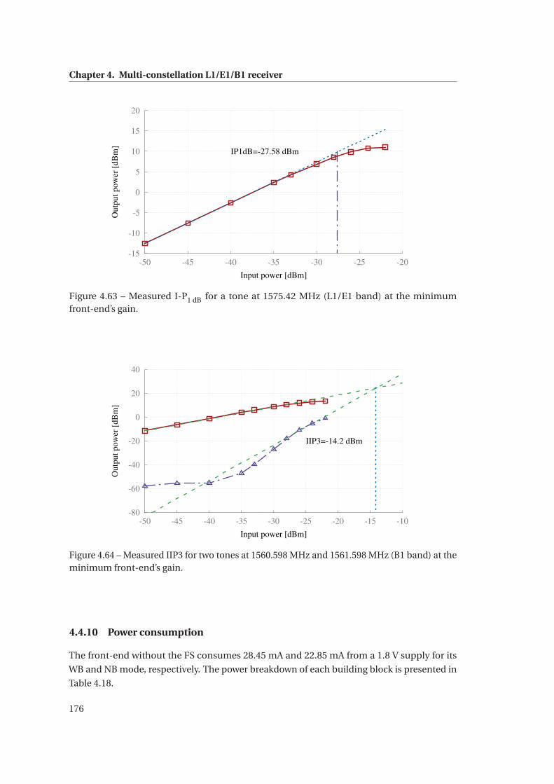
Chapter 4. Multi-constellation L1/E1/B1 receiver
-15
-10
-5
0
5
10
15
20
-50 -45 -40 -35 -30 -25 -20
IP1dB=-27.58 dBm
Outp
ut
pow
er [
dB
m]
Input power [dBm]
Figure 4.63 – Measured I-P1 dB for a tone at 1575.42 MHz (L1/E1 band) at the minimumfront-end’s gain.
-80
-60
-40
-20
0
20
40
-50 -45 -40 -35 -30 -25 -20 -15 -10
IIP3=-14.2 dBm
Outp
ut
pow
er [
dB
m]
Input power [dBm]
Figure 4.64 – Measured IIP3 for two tones at 1560.598 MHz and 1561.598 MHz (B1 band) at theminimum front-end’s gain.
4.4.10 Power consumption
The front-end without the FS consumes 28.45 mA and 22.85 mA from a 1.8 V supply for its
WB and NB mode, respectively. The power breakdown of each building block is presented in
Table 4.18.
176
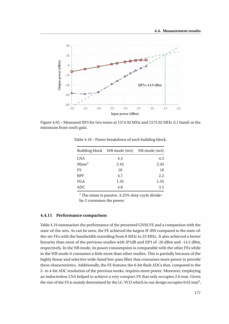
4.4. Measurement results
-80
-60
-40
-20
0
20
40
-50 -45 -40 -35 -30 -25 -20 -15 -10
IIP3=-14.9 dBm
Outp
ut
pow
er [
dB
m]
Input power [dBm]
Figure 4.65 – Measured IIP3 for two tones at 1574.92 MHz and 1575.92 MHz (L1 band) at theminimum front-end’s gain.
Table 4.18 – Power breakdown of each building block.
Building block WB mode [mA] NB mode [mA]
LNA 4.3 4.3
Mixer1 2.45 2.45
FS 10 10
BPF 4.7 2.2
VGA 1.35 1.35
ADC 4.8 3.5
1 The mixer is passive. A 25% duty-cycle divide-by-2 consumes the power.
4.4.11 Performance comparison
Table 4.19 summarizes the performance of the presented GNSS FE and a comparison with the
state-of-the-arts. As can be seen, the FE achieved the largest IF-BW compared to the state-of-
the-art FEs with the bandwidth extending from 8 MHz to 23 MHz. It also achieved a better
linearity than most of the previous studies with IP1dB and IIP3 of -26 dBm and -14.2 dBm,
respectively. In the NB mode, its power consumption is comparable with the other FEs while
in the WB mode it consumes a little more than other studies. This is partially because of the
highly linear and selective wide-band low-pass filter that consumes more power to provide
these characteristics. Additionally, the FE features the 6-bit flash ADCs that, compared to the
2- to 4-bit ADC resolution of the previous works, requires more power. Moreover, employing
an inductorless LNA helped to achieve a very compact FE that only occupies 2.6 mm. Given
the size of the FS is mainly determined by the LC-VCO which in our design occupies 0.63 mm2,
177
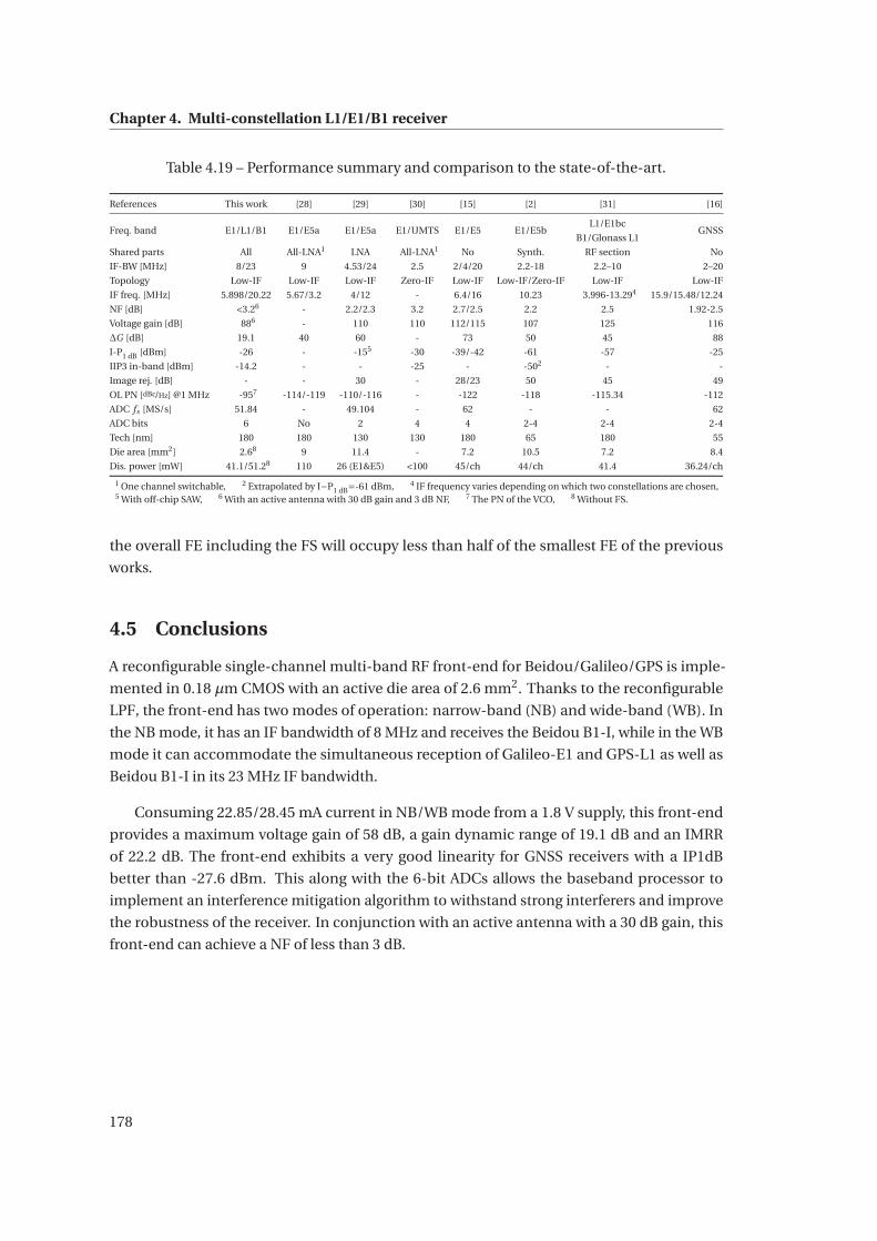
Chapter 4. Multi-constellation L1/E1/B1 receiver
Table 4.19 – Performance summary and comparison to the state-of-the-art.
References This work [28] [29] [30] [15] [2] [31] [16]
Freq. band E1/L1/B1 E1/E5a E1/E5a E1/UMTS E1/E5 E1/E5bL1/E1bc
GNSSB1/Glonass L1
Shared parts All All-LNA1 LNA All-LNA1 No Synth. RF section No
IF-BW [MHz] 8/23 9 4.53/24 2.5 2/4/20 2.2-18 2.2–10 2–20
Topology Low-IF Low-IF Low-IF Zero-IF Low-IF Low-IF/Zero-IF Low-IF Low-IF
IF freq. [MHz] 5.898/20.22 5.67/3.2 4/12 - 6.4/16 10.23 3.996-13.294 15.9/15.48/12.24
NF [dB] <3.26 - 2.2/2.3 3.2 2.7/2.5 2.2 2.5 1.92-2.5
Voltage gain [dB] 886 - 110 110 112/115 107 125 116
ΔG [dB] 19.1 40 60 - 73 50 45 88
I-P1 dB [dBm] -26 - -155 -30 -39/-42 -61 -57 -25
IIP3 in-band [dBm] -14.2 - - -25 - -502 - -
Image rej. [dB] - - 30 - 28/23 50 45 49
OL PN [dBc/Hz] @1 MHz -957 -114/-119 -110/-116 - -122 -118 -115.34 -112
ADC fs [MS/s] 51.84 - 49.104 - 62 - - 62
ADC bits 6 No 2 4 4 2-4 2-4 2-4
Tech [nm] 180 180 130 130 180 65 180 55
Die area [mm2] 2.68 9 11.4 - 7.2 10.5 7.2 8.4
Dis. power [mW] 41.1/51.28 110 26 (E1&E5) <100 45/ch 44/ch 41.4 36.24/ch
1 One channel switchable, 2 Extrapolated by I−P1 dB=-61 dBm, 4 IF frequency varies depending on which two constellations are chosen,5 With off-chip SAW, 6 With an active antenna with 30 dB gain and 3 dB NF, 7 The PN of the VCO, 8 Without FS.
the overall FE including the FS will occupy less than half of the smallest FE of the previous
works.
4.5 Conclusions
A reconfigurable single-channel multi-band RF front-end for Beidou/Galileo/GPS is imple-
mented in 0.18 μm CMOS with an active die area of 2.6 mm2. Thanks to the reconfigurable
LPF, the front-end has two modes of operation: narrow-band (NB) and wide-band (WB). In
the NB mode, it has an IF bandwidth of 8 MHz and receives the Beidou B1-I, while in the WB
mode it can accommodate the simultaneous reception of Galileo-E1 and GPS-L1 as well as
Beidou B1-I in its 23 MHz IF bandwidth.
Consuming 22.85/28.45 mA current in NB/WB mode from a 1.8 V supply, this front-end
provides a maximum voltage gain of 58 dB, a gain dynamic range of 19.1 dB and an IMRR
of 22.2 dB. The front-end exhibits a very good linearity for GNSS receivers with a IP1dB
better than -27.6 dBm. This along with the 6-bit ADCs allows the baseband processor to
implement an interference mitigation algorithm to withstand strong interferers and improve
the robustness of the receiver. In conjunction with an active antenna with a 30 dB gain, this
front-end can achieve a NF of less than 3 dB.
178
5 Conclusions and perspectives
5.1 Achievements
Two multi-band GNSS IC FEs are the main outcomes of this thesis. One FE addresses the
PRS and is capable of receiving Galileo-E1 and E6 signals simultaneously, to serve authorized
governmental bodies, while the other FE can accommodate the simultaneous reception of the
GPS-L1, Galileo-E1 and Beidou-B1 OS signals to respond to the mass market demands of the
multi-frequency multi-constellation GNSS receivers.
To the best of our knowledge, the presented FE in chapter 2 is the first documented multi-
band PRS IC FE. To start, the system specifications were derived for the FE and its sub-systems
and were laid out in chapter 2. A fundamental quality of the PRS is its robustness against
jamming and spoofing. Accordingly, all the sub-systems were designed and fabricated on a
single chip using 0.18 μm CMOS. The presented dual-frequency FE incorporates two fully
independent wide-band FEs consisting of the LNA, quadrature mixer, FS, IF filter, VGA and
ADC and, all told, occupies a die area of 11.5 mm2. The FE’s frequency band coverage is limited
only by the tuning range of the VCO, thanks to the wide-band design of all the sub-systems. As
a consequence, the FE not only covers the desired E1 and E6 bands but also provides partial
coverage of L5/E5 with the E6 channel while consuming 64 mA from a 1.8 V. It has a maximum
gain of 65 dB with a dynamic range of 30 dB.
One of the characteristics of the Galileo signals is their wide bandwidth that can reach
up to 51 MHz for some applications (E5). A challenge for this design was that the LPF is
the limiting factor of the FE’s bandwidth. This challenge was overcome by the proposed
reconfigurable wide-tuning-range LPF. As a result, the FE exhibits 50 MHz of bandwidth,
which is more than twice the largest IF bandwidth of the FEs reported in the state-of-the-art
(24 MHz in [29]). The integrated filter in the FE is a power-efficient 4 th-order Gm-C elliptic filter
with an almost two-octave continuous tuning of its cutoff frequency. The wide continuous
tuning was achieved by combining a new Gm tuning circuit with the Gm switching techniques,
with which the filter can accommodate any of the new wide-band modernized GNSS signals.
With the proposed tuning scheme, the power efficiency was achieved by scaling down the
179
Chapter 5. Conclusions and perspectives
filter’s power consumption proportionally to its cutoff frequency, which is of value in a design
reuse approach. A Q enhancement method was also incorporated in the filter, resulting in a
high selectivity of up to 66 dB/octave, which is of value for PRS applications to mitigate out-of-
band interferers. The filter achieves a high linearity over its tuning range with an IIP3 of up to
-1.3 dBVRMS thanks to the topological linearity enhancement method. The FE also features a
6-bit ADC with a sampling frequency of 52 MS/s (the state-of-the-art is 4 bits for IC receivers).
The high resolution of the ADC enables the baseband processor to implement mitigation
algorithms to improve the receiver’s immunity to jamming signals and interferences.
The FE is fully configurable through external tuning of passive components and a complete
serial interface. Overall, this FE offers a compact, low-power, wide-band solution for high-
precision dual-frequency GNSS receivers, not only for the PRS or military GPS, but also for
many open service signals.
The specifications of the FE presented in chapter 4 were derived while having in mind
that the FE aims at mass market applications which demand low power consumption and low
costs. In order to reduce the deign efforts, the FE utilizes the same ADC and LPF of the PRS
receiver. The FE features two modes of operation: wide-band (WB) and narrow-band (NB). In
the NB mode, the FE receives the Beidou-B1 signal, whereas in the WB mode, it simultaneously
receives the GPS-L1, Galileo-E1 and Beidou-B1 signal. In line with the low-cost solution, a
wide-band inductorless LNA was employed in the FE which results in reducing the silicon
area.
The FE also features a quadrature passive mixer that, in conjunction with the LPF, delivers
an RF band-limited impedance response at the LNA’s output. This helps to improve the LNA
linearity by presenting a low out-of-band impedance at the LNA, which in turn minimizes
any voltage swing that is generated by unwanted interferers. In order to reduce the power
consumption, no complex filtering was adopted, and thus image rejection will be performed
in the digital domain. The FE shows a gain dynamic range of 19.1 dB to compensate for the
PVT variations. At this stage, the FE uses an external LO and occupies an active die area of
only 2.6 mm2 while consuming 22.85/28.45 mA current in NB/WB mode from a 1.8 V supply.
It demonstrates a very good linearity with IP1dB of more than -27.6 dBm.
A FS that has an oscillation tuning range from 2625 MHz to 3102 MHz was designed and
fabricated separately from the FE. It consists of an LC-VCO and an integer-N PLL with a fixed
division of 60. The oscillation range is 10.4% less than expected, and therefore it needs a design
tuning for the final integration into the FE. This is mainly due to the capacitance parasitic,
which should be considered in the next integration. A PN of -80.3 dBc/Hz is measured at 10 kHz
offset from the carrier frequency of 3 GHz. Considering that the synthesizer provide twice the
required LO for the FE, the overall PN improves by 6 dB which means that the FS satisfies the
PN requirement of the FE at 10 kHz offset. The FS including the VCO consumes from 9.8 mA
to 11 mA with respect to the oscillation frequency from a 1.8 V supply.
180
5.2. Future work
5.2 Future work
Completing the design and integration of the FS is the most important step toward having a
stand-alone FE. In this regard, the designed VCO needs to be improved in terms of the tuning
range and PN.
In order to facilitate the control of the FE’s bandwidth, the filter requires an automatic
tuning circuit. This can be achieved by a feedback system that consists of a PLL-like circuit
and the most selective resonator of the filter.
For the OS FE, the next important step is to conduct experiments with the live satellite
signals and a baseband receiver to test the sensitivity of the FE. The FE, especially its LNA and
LPF, can be optimized for lower power consumption at the expense of lower linearity.
Adding an AGC is another necessary step toward the completeness of the FE. The AGC
is provisioned to be implemented in the baseband processor by monitoring the ADC’s out-
put. This provides flexibility to the baseband processor to implement different mitigation
algorithms to improve the robustness of the receiver.
Equipping the FE with an I/Q mismatch calibration circuit can guarantee a maximum
level of IQ imbalance, and thus result in a better image rejection.
The adopted architecture for the FE is very suitable for a phased-array FE, owing to the fact
that this architecture requires a minimal effort to combine a few phase-shifted RF signals (after
their downconversion) at the very beginning of the IF section. In fact, each array consists of
an LNA and a quadrature mixer. The phase shift can be applied to the LO that drives the mixer
instead of the RF signals. All the downconverted signals from the arrays can be combined
and fed the current-input LPF. Of course, the phased-array FE necessitates the design of a
phase shifter. However, considering that the phase shifter needs to operate only at the single
frequency of the LO, its design even at the high frequency of the LO is not complicated.
Future work on the PRS FE implementation includes the removal of the characterization
analog blocks, and the inclusion of standard ESD protection and voltage regulation cells using
the foundry’s intellectual property (IP) blocks. In addition, different automated calibration
methods could be applied to enable a more robust commercial implementation.
181

Bibliography
[1] G. X. Gao, A. Chen, S. Lo, D. De Lorenzo, T. Walter, and P. Enge, “Compass-M1 Broadcast
Codes in E2, E5b, and E6 Frequency Bands,” IEEE Journal of Selected Topics in Signal
Processing, vol. 3, no. 4, pp. 599–612, aug 2009. [Online].
[2] N. Qi, Y. Xu, B. Chi, X. Yu, X. Zhang, N. Xu, P. Chiang, W. Rhee, and Z. Wang, “A
Dual-Channel Compass/GPS/GLONASS/Galileo Reconfigurable GNSS Receiver in 65
nm CMOS With On-Chip I/Q Calibration,” IEEE Transactions on Circuits and Systems I:
Regular Papers, vol. 59, no. 8, pp. 1720–1732, aug 2012. [Online].
[3] S. Kedar, “The effect of the second order GPS ionospheric correction on receiver
positions,” Geophysical Research Letters, vol. 30, no. 16, p. 1829, 2003. [Online].
[4] E. Gakstatter. (2010, jun) What’s Going to Happen When High-Accuracy GPS is Cheap? :
GPS World - Last Access 23-03-2016. [Online].
[5] Navstar, “Global Positioning System Directorate Systems Engineering and Itegration:
Navstar GPS space Segment/Navigation User Interface(IS-GPS-200),” Navstar GPS space
Segment, 2013. [Online].
[6] European Union, “European GNSS (Galileo) Open Service Signal-In-Space Interface
Control Document (OS SIS ICD),” Tech. Rep. Issue 1.1, 2010. [Online].
[7] European Union, “European GNSS (Galileo) Open Service Signal-In-Space Interface
Control Document (OS SIS ICD),” Tech. Rep. Issue 1.2, 2014. [Online].
[8] F. Dovis, L. Lo Presti, M. Fantino, P. Mulassano, and J. Godet, “Comparison
between Galileo CBOC Candidates and BOC(1,1) in Terms of Detection Performance,”
International Journal of Navigation and Observation, vol. 2008, pp. 1–9, 2008. [Online].
[9] N. Gerein, M. Olynik, M. Clayton, J. Auld, and T. Murfin, “A Dual-frequency L1/E5a
Galileo Test Receiver,” in Proceedings of ENC-GNSS, Munich, jul 2005. [Online].
[10] China Satellite Navigation Office, “BeiDou navigation satellite system signal in space
interface control document (BDS-SIS-ICD-B1I-1.0),” Tech. Rep. Version 1.0, 2012.
[Online].
183
Bibliography
[11] O. Montenbruck, A. Hauschild, P. Steigenberger, U. Hugentobler, P. Teunissen, and
S. Nakamura, “Initial assessment of the COMPASS/BeiDou-2 regional navigation
satellite system,” GPS Solutions, vol. 17, no. 2, pp. 211–222, apr 2013. [Online].
[12] GPS World. (2015, Apr) First Launch of GLONASS-K2 Satellite Planned for 2018 - Last
Access 23-03-2016. [Online].
[13] Russian Institute of Space Device Engineering, “GLONASS Interface Control Document
(ICD L1, L2 GLONASS),” Tech. Rep., 2008. [Online].
[14] Yuanjin Zheng, Jiangnan Yan, and Yong Ping Xu, “A CMOS VGA With DC Offset
Cancellation for Direct-Conversion Receivers,” IEEE Transactions on Circuits and
Systems I: Regular Papers, vol. 56, no. 1, pp. 103–113, jan 2009. [Online].
[15] D. Chen, W. Pan, P. Jiang, and J. Jin, “Reconfigurable Dual-Channel Multiband RF
Receiver for GPS/Galileo/BD-2 Systems,” IEEE Transactions on Microwave Theory and
Techniques, vol. 60, no. 11, pp. 3491–3501, nov 2012. [Online].
[16] S. Li, J. Li, X. Gu, H. Wang, C. Li, J. Wu, and M. Tang, “Reconfigurable All-Band RF CMOS
Transceiver for GPS/GLONASS/Galileo/Beidou With Digitally Assisted Calibration,”
IEEE Transactions on Very Large Scale Integration (VLSI) Systems, vol. 23, no. 9, pp.
1814–1827, sep 2015. [Online].
[17] A. Rugamer, C. Mongredian, S. Urquijo, and G. Rohmer, “Optimal path-control
for dual-frequency overlay GNSS receivers,” in 2011 International Conference on
Localization and GNSS (ICL-GNSS). IEEE, jun 2011, pp. 158–163. [Online].
[18] C. Barth, I. R. Linscott, and U. S. Inan, “A 9mW direct RF sampling GPS receiver
front-end in 0.13um BiCMOS,” in 2012 IEEE International Symposium on Circuits and
Systems. IEEE, may 2012, pp. 1287–1290. [Online].
[19] G. Wistuba, A. Vasylyev, S. Haas, J. Driesen, L. Dalluge, D. Peitscher, B. Kramer,
C. Dohmen, and F. Henkel, “A highly integrated configurable GNSS receiver frontend
design for high bandwidth operation on E1/L1 and E5a/L5,” in 2011 International
Conference on Localization and GNSS (ICL-GNSS). IEEE, jun 2011, pp. 164–168.
[Online].
[20] G. Rivela, P. Scavini, D. Grasso, M. Castro, A. Calcagno, G. Avellone, A. Di Mauro, G. Cali,
and S. Scaccianoce, “A low power RF front-end for L1/E1 GPS/Galileo and GLONASS
signals in CMOS 65nm technology,” in 2011 International Conference on Localization
and GNSS (ICL-GNSS). IEEE, jun 2011, pp. 7–12. [Online].
[21] R. Berenguer, J. Mendizabal, U. Alvarado, D. Valderas, and A. Garcia-Alonso, “A Low
Power Low Noise Figure GPS/GALILEO Front-End for Handheld Applications in a 0.35
μm SiGe Process,” in IEEE Radio Frequency Integrated Circuits (RFIC) Symposium, 2006.
IEEE, 2006, pp. 5–8. [Online].
184
Bibliography
[22] B. Ong, M. Wu, W. Lien, C. Kuo, S. Chew, and C. Lu, “Low power CMOS GPS/GALILEO
RF front-end receiver,” in 2009 IEEE International Symposium on Radio-Frequency
Integration Technology (RFIT). IEEE, dec 2009, pp. 16–19. [Online].
[23] C.-H. Wu, W.-C. Tsai, C.-G. Tan, C.-N. Chen, K.-I. Li, J.-L. Hsu, C.-L. Lo, H.-H. Chen, S.-Y.
Su, K.-T. Chen, M. Chen, O. Shana’a, S.-H. Chou, and G. Chien, “A GPS/Galileo SoC
with adaptive in-band blocker cancellation in 65nm CMOS,” in 2011 IEEE International
Solid-State Circuits Conference. IEEE, feb 2011, pp. 462–464. [Online].
[24] Jun-Gi Jo, Jong-Ho Lee, Dojin Park, Young Gun Pu, Sung-Cheol Shin, Kang-Yoon Lee,
Sung-Eon Park, Suk-Joong Lee, and Changsik Yoo, “An L1-Band Dual-Mode RF Receiver
for GPS and Galileo in 0.18um CMOS,” IEEE Transactions on Microwave Theory and
Techniques, vol. 57, no. 4, pp. 919–927, apr 2009. [Online].
[25] V. Issakov, H. Doppke, A. Leyk, G. L. Villar, V. Christ, G. Finn, Z. Gu, H.-G. Kirchhoff,
Y. Wang, J. Tomasik, S. Devegowda, K. Hadjizada, M. Hammes, and R. Kreienkamp,
“Robust low power dual-mode GNSS receiver in 65-nm CMOS for multi-radio SoC
integration,” in 2015 IEEE MTT-S International Microwave Symposium. IEEE, may
2015, pp. 1–3. [Online].
[26] F. Amoroso, “Adaptive A/D Converter to Suppress CW Interference in DSPN Spread-
Spectrum Communications,” IEEE Transactions on Communications, vol. 31, no. 10, pp.
1117–1123, oct 1983. [Online].
[27] F. Amoroso and J. Bricker, “Performance of the Adaptive A/D Converter in Combined
CW and Gaussian Interference,” IEEE Transactions on Communications, vol. 34, no. 3,
pp. 209–213, mar 1986. [Online].
[28] M. Detratti, E. Lopez, E. Perez, and R. Palacio, “Dual-Band RF Front-End Solution
for Hybrid Galileo/GPS Mass Market Receivers,” in 2008 5th IEEE Consumer
Communications and Networking Conference. IEEE, 2008, pp. 603–607. [Online].
[29] Y. Moon, Sanghyun Cha, Gyusuck Kim, K. Park, Sunjun Ko, H. Park, J. Park, and J. Lee,
“A 26mW dual-mode RF receiver for GPS/Galileo with L1/L1F and L5/E5a bands,” in
2008 International SoC Design Conference, vol. 01. IEEE, nov 2008, pp. I–421–I–424.
[Online].
[30] A. Miskiewicz, A. Holm, F. Bachmann, G. Hueber, J. Zipper, C. Stoeger, and R. Weigel,
“GPS/Galileo System-on-Chip with UMTS/GSM Support for Location Based Services
Applications,” in 2009 IEEE Topical Meeting on Silicon Monolithic Integrated Circuits in
RF Systems. IEEE, jan 2009, pp. 1–4. [Online].
[31] N. Qi, B. Chi, Y. Xu, Z. Chen, Y. Xu, J. Xie, Z. Song, and Z. Wang, “A 180nm fully-integrated
dual-channel reconfigurable receiver for GNSS interoperations,” in 2013 Proceedings of
the ESSCIRC (ESSCIRC). IEEE, sep 2013, pp. 177–180. [Online].
185
Bibliography
[32] C. G. Tan, F. Song, T. Y. Choke, M. Kong, D.-C. Song, C.-H. Yong, W. Shu, Z. H. You,
Y.-H. Lin, and O. Shanaa, “A universal GNSS (GPS/Galileo/Glonass/Beidou) SoC with
a 0.25mm2 radio in 40nm CMOS,” in 2013 IEEE International Solid-State Circuits
Conference Digest of Technical Papers. IEEE, feb 2013, pp. 334–335. [Online].
[33] L. L. Lewyn, T. Ytterdal, C. Wulff, and K. Martin, “Analog Circuit Design in Nanoscale
CMOS Technologies,” Proceedings of the IEEE, vol. 97, no. 10, pp. 1687–1714, oct 2009.
[Online].
[34] D. Buss, “Technology in the Internet age,” in Solid-State Circuits Conference, 2002.
Digest of Technical Papers. ISSCC. 2002 IEEE International, vol. 1. IEEE, 2002, pp.
18–21. [Online].
[35] E. Vittoz, “Low-power design: ways to approach the limits,” in Proceedings of IEEE
International Solid-State Circuits Conference - ISSCC ’94. IEEE, 1994, pp. 14–18.
[Online].
[36] A.-J. Annema, B. Nauta, R. van Langevelde, and H. Tuinhout, “Analog circuits in
ultra-deep-submicron CMOS,” IEEE Journal of Solid-State Circuits, vol. 40, no. 1, pp.
132–143, jan 2005. [Online].
[37] A.-J. Annema, “Analog circuit performance and process scaling,” IEEE Transactions on
Circuits and Systems II: Analog and Digital Signal Processing, vol. 46, no. 6, pp. 711–725,
jun 1999. [Online].
[38] C. a. Mead, “Scaling of MOS technology to submicrometer feature sizes,” Analog
Integrated Circuits and Signal Processing, vol. 6, no. 1, pp. 9–25, jul 1994. [Online].
[39] A. Marras, I. De Munari, D. Vescovi, and P. Ciampolini, “Effects of gate-currents on
CMOS circuit behaviour,” in European Solid-State Device Research, 2003. ESSDERC ’03.
33rd Conference on. IEEE, sep 2003, pp. 577–580. [Online].
[40] J. Charlamov, R. Navickas, and A. Baskys, “Phase Noise Minimization in CMOS Voltage
Controlled Oscillators,” in 14th International Symposium Ultrafast Phenomena in
Semiconductors, vol. 119, no. 2, 2011, pp. 234–236. [Online].
[41] M. Badaroglu, P. Wambacq, G. Van der Plas, S. Donnay, G. Gielen, and H. De Man,
“Evolution of substrate noise generation mechanisms with CMOS technology scaling,”
IEEE Transactions on Circuits and Systems I: Regular Papers, vol. 53, no. 2, pp. 296–305,
feb 2006. [Online].
[42] H. Iwai, “CMOS technology-year 2010 and beyond,” IEEE Journal of Solid-State Circuits,
vol. 34, no. 3, pp. 357–366, mar 1999. [Online].
[43] M. Garg, S. Suryagandh, and J. Woo, “Scaling impact on analog performance of
sub-100nm MOSFETs for mixed mode applications,” in European Solid-State Device
Research, 2003. ESSDERC ’03. 33rd Conference on. IEEE, 2003, pp. 371–374. [Online].
186
Bibliography
[44] D. Sahu, A. Das, Y. Darwhekar, S. Ganesan, G. Rajendran, R. Kumar, B. Chandrashekar,
A. Ghosh, A. Gaurav, K. T., A. Goyal, S. Bhagavatheeswaran, Kah Mun Low, N. Yanduru,
S. Dhamankar, and S. Venkatraman, “A 90nm CMOS single-chip GPS receiver with
5dBm out-of-band IIP3 2.0dB NF,” in ISSCC. 2005 IEEE International Digest of Technical
Papers. Solid-State Circuits Conference, 2005. IEEE, 2005, pp. 308–310. [Online].
[45] Jinho Ko, Jongmoon Kim, Sanghyun Cho, and Kwyro Lee, “A 19-mW 2.6-$mmˆ2$ L1/L2
dual-band CMOS GPS receiver,” IEEE Journal of Solid-State Circuits, vol. 40, no. 7, pp.
1414–1425, jul 2005. [Online].
[46] G. Gramegna, P. Mattos, M. Losi, S. Das, M. Franciotta, N. Bellantone, M. Vaiana,
V. Mandara, and M. Paparo, “A 56-mW 23-mm2 Single-Chip 180-nm CMOS GPS
Receiver With 27.2-mW 4.1-mm2 Radio,” IEEE Journal of Solid-State Circuits, vol. 41,
no. 3, pp. 540–551, mar 2006. [Online].
[47] NTLab. (2011) Datasheet: NT1019RF "GPS/Galileo/GLONASS multisystem single-band
receiver" - Last Access 23-03-2016. [Online].
[48] Maxim-IC. (2010) Datasheet: MAX2741 "Integrated L1-Band GPS Receiver" - Last Access
23-03-2016. [Online].
[49] STMicroelectronics. (2010) Datasheet: STA5620 "Fully integrated RF front-end for GPS"
- Last Access 23-03-2016. [Online].
[50] N. Qi, Y. Xu, B. Chi, X. Yu, X. Zhang, and Z. Wang, “A dual-channel GPS/Compass/-
Galileo/GLONASS reconfigurable GNSS receiver in 65nm CMOS,” in 2011 IEEE Custom
Integrated Circuits Conference (CICC). IEEE, sep 2011, pp. 1–4. [Online].
[51] S. Blaakmeer, E. Klumperink, B. Nauta, and D. Leenaerts, “Wideband CMOS Receivers
exploiting Simultaneous Output Balancing and Noise/Distortion Canceling,” in 2008
European Microwave Integrated Circuit Conference, no. October. IEEE, oct 2008, pp.
163–166. [Online].
[52] The European Parliament and the Council, “Decision No 1104/2011/EU of the
European Parliament and of the Council of 25 October 2011 on the rules for access
to the public regulated service provided by the global navigation satellite system
established under the Galileo programme,” Official Journal of the European Union, no.
1104, pp. 1–8, 2011. [Online].
[53] A. C. Veclani, J.-P. Darnis, and V. V. Miranda, “The Galileo Programme: Management and
Financial Lessons Learned for Future Space Systems Paid Out of The EU Budget,” Study
for the European Parliament’s Subcommittee on Security and Defence, 2011. [Online].
[54] A.Ruegamer, I.Suberviola, F.Foerster, G.Rohmer, A.Konovaltsev, N.Basta, M.Meurer,
J.Wendel, M.Kaindl, and S.Baumann, “A Bavarian Initiative Towards a Robust Galileo
PRS Receiver,” in Proceedings of the 24th International Technical Meeting of The Satellite
187
Bibliography
Division of the Institute of Navigation (ION GNSS 2011), Portland, OR, 2011, pp. 3668 –
3678. [Online].
[55] B. C. Barker, J. W. Betz, J. E. Clark, J. T. Correia, J. T. Gillis, S. Lazar, K. A. Rehborn, and
J. R. Straton, “Overview of the GPS M Code Signal,” in National Technical Meeting of The
Institute of Navigation (ION NTM). Anaheim: ION, jan 2000, pp. 542–549. [Online].
[56] R. M. Weiler, B. Paul, P. Jales, M. Unwin, and S. Hodgart, “Performance of an L1/E5 GNSS
Receiver using a Direct Conversion Front-End Architecture,” in Proceedings of the 21st
International Technical Meeting of the Satellite Division of The Institute of Navigation
(ION GNSS 2008), Savannah, GA, sep 2008, pp. 1478–1489. [Online].
[57] U-blox. (2015) Datasheet: LEA-M8S: u-blox M8 concurrent GNSS module - Last Access
23-03-2016. [Online].
[58] Motorola. Datasheet: MTP8500Ex TETRA Portable Radio - Motorola Solutions Europe &
Africa - Last Access 23-03-2016. [Online].
[59] E. B. Rodal, “Low power GPS receiver-US Patent 5,650,785,” p. 9, jul 1997. [Online].
[60] T. Pany and B. Eissfeller, “Tracking of High Bandwidth GPS / Galileo Signals with a Low
Sample Rate Software Receiver,” in European Navigation Conference 2003 (ENC-GNSS
2003), no. November 2015, Graz, apr 2003. [Online].
[61] M. Braasch and A. van Dierendonck, “GPS receiver architectures and measurements,”
Proceedings of the IEEE, vol. 87, no. 1, pp. 48–64, 1999. [Online].
[62] R. Gray and D. Neuhoff, “Quantization,” IEEE Transactions on Information Theory,
vol. 44, no. 6, pp. 2325–2383, 1998. [Online].
[63] B. Razavi, Principles of Data Conversion System Design. Wiley-IEEE Press, 1995.
[Online].
[64] H. H. Boo, D. S. Boning, and H.-S. Lee, “15.6 12b 250MS/s pipelined ADC with virtual
ground reference buffers,” in 2015 IEEE International Solid-State Circuits Conference -
(ISSCC) Digest of Technical Papers. IEEE, feb 2015, pp. 1–3. [Online].
[65] D.-Y. Chang, C. Munoz, D. Daly, S.-K. Shin, K. Guay, T. Thurston, H.-S. Lee, K. Gulati,
and M. Straayer, “A 21mW 15b 48MS/s zero-crossing pipeline ADC in 0.13 μm CMOS
with 74dB SNDR,” in 2014 IEEE International Solid-State Circuits Conference Digest of
Technical Papers (ISSCC). IEEE, feb 2014, pp. 204–205. [Online].
[66] Y. Shimizu, S. Murayama, K. Kudoh, and H. Yatsuda, “A Split-Load Interpolation-
Amplifier-Array 300MS/s 8b Subranging ADC in 90nm CMOS,” in 2008 IEEE
International Solid-State Circuits Conference - Digest of Technical Papers. IEEE, feb
2008, pp. 552–635. [Online].
188
Bibliography
[67] G. Van der Plas and B. Verbruggen, “A 150MS/s 133 μW 7b ADC in 90nm digital
CMOS Using a Comparator-Based Asynchronous Binary-Search sub-ADC,” in 2008 IEEE
International Solid-State Circuits Conference - Digest of Technical Papers. IEEE, feb
2008, pp. 242–610. [Online].
[68] M. Flynn and B. Sheahan, “A 400-Msample/s, 6-b CMOS folding and interpolating ADC,”
IEEE Journal of Solid-State Circuits, vol. 33, no. 12, pp. 1932–1938, dec 1998. [Online].
[69] M. Miyahara, I. Mano, M. Nakayama, K. Okada, and A. Matsuzawa, “A 2.2GS/s
7b 27.4mW time-based folding-flash ADC with resistively averaged voltage-to-time
amplifiers,” in 2014 IEEE International Solid-State Circuits Conference Digest of
Technical Papers (ISSCC). IEEE, feb 2014, pp. 388–389. [Online].
[70] D. C. Daly and A. P. Chandrakasan, “A 6b 0.2-to-0.9V Highly Digital Flash ADC with
Comparator Redundancy,” in 2008 IEEE International Solid-State Circuits Conference -
Digest of Technical Papers. IEEE, feb 2008, pp. 554–635. [Online].
[71] G. Van der Plas, S. Decoutere, and S. Donnay, “A 0.16pJ/Conversion-Step 2.5mW
1.25GS/s 4b ADC in a 90nm Digital CMOS Process,” in 2006 IEEE International Solid
State Circuits Conference - Digest of Technical Papers, vol. 28, no. 4. San Francisco, CA:
IEEE, 2006, p. 2310. [Online].
[72] S. Park, Y. Palaskas, and M. Flynn, “A 4GS/s 4b Flash ADC in 0.18 μm CMOS,” in 2006
IEEE International Solid State Circuits Conference - Digest of Technical Papers. IEEE,
feb 2006, pp. 2330–2339. [Online].
[73] A. Varzaghani, A. Kasapi, D. N. Loizos, S.-H. Paik, S. Verma, S. Zogopoulos, and
S. Sidiropoulos, “A 10.3-GS/s, 6-Bit Flash ADC for 10G Ethernet Applications,” IEEE
Journal of Solid-State Circuits, vol. 48, no. 12, pp. 3038–3048, dec 2013. [Online].
[74] V. H.-C. Chen and L. Pileggi, “22.2 A 69.5mW 20GS/s 6b time-interleaved ADC with
embedded time-to-digital calibration in 32nm CMOS SOI,” in 2014 IEEE International
Solid-State Circuits Conference Digest of Technical Papers (ISSCC). IEEE, feb 2014, pp.
380–381. [Online].
[75] I. Mehr and D. Dalton, “A 500-MSample/s, 6-bit Nyquist-rate ADC for disk-drive
read-channel applications,” IEEE Journal of Solid-State Circuits, vol. 34, no. 7, pp.
912–920, jul 1999. [Online].
[76] K.-L. Lin, A. Kemna, and B. Hosticka, Modular Low-Power, High-Speed CMOS
Analog-to-Digital Converter for Embedded Systems, ser. The International Series in
Engineering and Computer Science. Boston: Kluwer Academic Publishers, 2003, vol.
722, no. 1. [Online].
[77] D. Schinkel, E. Mensink, E. Klumperink, E. van Tuijl, and B. Nauta, “A Double-Tail
Latch-Type Voltage Sense Amplifier with 18ps Setup+Hold Time,” in 2007 IEEE
189
Bibliography
International Solid-State Circuits Conference. Digest of Technical Papers. IEEE, feb
2007, pp. 314–605. [Online].
[78] Texas Instruments. (2013) Datasheet: OPA2333-HT - "1.8V, micro Power , CMOS
Operational Amplifiers , Zero-Drift Series" - Last Access 23-03-2016. [Online].
[79] Analog Device. (2015) Datasheet: AD8351- "Low Distortion Differential RF / IF
Amplifie" - Last Access 23-03-2016. [Online].
[80] ETSI (TS 136 211), “LTE; Evolved Universal Terrestrial Radio Access (E-UTRA); Physical
channels and modulation (3GPP TS 36.211 version 12.4.0 Release 12),” ETSI, Standard
12.4.0, 2014. [Online].
[81] H. Xie, O. Oliaei, P. Rakers, R. Fernandez, J. Xiang, J. Parkes, J. Riches, R. Verellen,
M. Rahman, V. Bhan, and D. B. Schwartz, “Single-Chip Multiband EGPRS and SAW-Less
LTE WCDMA CMOS Receiver With Diversity,” IEEE Transactions on Microwave Theory
and Techniques, vol. 60, no. 5, pp. 1390–1396, may 2012. [Online].
[82] D. Morche, G. Masson, S. De Rivaz, F. Dehmas, S. Paquelet, A. Bisiaux, O. Fourquin,
J. Gaubert, and S. Bourdel, “Double-Quadrature UWB Receiver for Wide-Range
Localization Applications With Sub-cm Ranging Precision,” IEEE Journal of Solid-State
Circuits, vol. 48, no. 10, pp. 2351–2362, oct 2013. [Online].
[83] F. Chastellain, C. Botteron, and P.-A. Farine, “Looking Inside Modern Receivers,” IEEE
Microwave Magazine, vol. 12, no. 2, pp. 87–98, apr 2011. [Online].
[84] F. Yuan, “CMOS gyrator-C active transformers,” IET Circuits, Devices & Systems, vol. 1,
no. 6, p. 494, 2007. [Online].
[85] X. Zhang and E. I. El-Masry, “A Novel CMOS OTA Based on Body-Driven MOSFETs and
its Applications in OTA-C Filters,” IEEE Transactions on Circuits and Systems I: Regular
Papers, vol. 54, no. 6, pp. 1204–1212, jun 2007. [Online].
[86] A. Liscidini, A. Pirola, and R. Castello, “A 1.25mW 75dB-SFDR CT filter with in-band
noise reduction,” in 2009 IEEE International Solid-State Circuits Conference - Digest of
Technical Papers. IEEE, feb 2009, pp. 336–337,337a. [Online].
[87] I. Akita, K. Wada, and Y. Tadokoro, “A 0.6-V Dynamic Biasing Filter With 89-dB Dynamic
Range in 0.18um CMOS,” IEEE Journal of Solid-State Circuits, vol. 44, no. 10, pp.
2790–2799, oct 2009. [Online].
[88] A. Handkiewicz, P. Katarzynski, S. Szczesny, A. Wencel, and P. Sniatała, “Analog filter
pair design on the basis of a gyrator–capacitor prototype circuit,” International Journal
of Circuit Theory and Applications, vol. 40, no. 6, pp. 539–550, 2012. [Online].
[89] Y.-T. Wang and A. Abidi, “CMOS active filter design at very high frequencies,” IEEE
Journal of Solid-State Circuits, vol. 25, no. 6, pp. 1562–1574, 1990. [Online].
190
Bibliography
[90] H. Khorramabadi and P. Gray, “High-frequency CMOS continuous-time filters,” IEEE
Journal of Solid-State Circuits, vol. 19, no. 6, pp. 939–948, dec 1984. [Online].
[91] S. Ghamari, G. Tasselli, C. Botteron, and P.-A. Farine, “Design methodology for
controlled-Q resonators in OTA-based filters,” in 2015 IEEE Radio Frequency Integrated
Circuits Symposium (RFIC). Phoenix: IEEE, may 2015, pp. 371–374. [Online].
[92] W. M. Siebert, Circuits, Signals, and Systems. MIT Press, 1985. [Online].
[93] W. M. C. Sansen, Analog Design Essentials, ser. The International Series in Engineering
and Computer Science. Boston, MA: Springer US, 2006, vol. 859. [Online].
[94] A. Antoniou, “Stability properties of some gyrator circuits,” Electronics Letters, vol. 4,
no. 23, p. 510, 1968. [Online].
[95] P. Monsurrò, S. Pennisi, G. Scotti, and A. Trifiletti, “High-tuning-range CMOS band-pass
IF filter based on a low- Q cascaded biquad optimization technique,” International
Journal of Circuit Theory and Applications, vol. 43, no. 11, pp. 1615–1636, nov 2015.
[Online].
[96] S. Ghamari, G. Tasselli, C. Botteron, and P.-A. Farine, “Design methodology for
common-mode stability of OTA-based gyrators,” International Journal of Circuit Theory
and Applications, vol. 44, no. 5, pp. 1142–1155, may 2016. [Online].
[97] T.-Y. Lo and C.-C. Hung, “A 1 GHz Equiripple Low-Pass Filter With a High-Speed
Automatic Tuning Scheme,” IEEE Transactions on Very Large Scale Integration (VLSI)
Systems, vol. 19, no. 2, pp. 175–181, feb 2011. [Online].
[98] Mingdeng Chen, J. Silva-Martinez, S. Rokhsaz, and M. Robinson, “A 2-Vpp 80–200-MHz
fourth-order continuous-time linear phase filter with automatic frequency tuning,”
IEEE Journal of Solid-State Circuits, vol. 38, no. 10, pp. 1745–1749, oct 2003. [Online].
[99] L. Ye, C. Shi, H. Liao, R. Huang, and Y. Wang, “Highly Power-Efficient Active-RC Filters
With Wide Bandwidth-Range Using Low-Gain Push-Pull Opamps,” IEEE Transactions
on Circuits and Systems I: Regular Papers, vol. 60, no. 1, pp. 95–107, jan 2013. [Online].
[100] J. Liu, L. Chen, H. Liao, J. Wang, and L. Ye, “460 μW 32 dB image rejection
ratio second-order active-RC complex filter with improved power efficient opamp,”
Electronics Letters, vol. 49, no. 1, pp. 18–20, jan 2013. [Online].
[101] B. Wu and Y. Chiu, “A 40 nm CMOS Derivative-Free IF Active-RC BPF With
Programmable Bandwidth and Center Frequency Achieving Over 30 dBm IIP3,” IEEE
Journal of Solid-State Circuits, vol. 50, no. 8, pp. 1772–1784, aug 2015. [Online].
[102] A. Tajalli and Y. Leblebici, “A widely-tunable and ultra-low-power MOSFET-C filter
operating in subthreshold,” in 2009 IEEE Custom Integrated Circuits Conference, no.
Cicc. IEEE, sep 2009, pp. 593–596. [Online].
191
Bibliography
[103] S. D’Amico, V. Giannini, and A. Baschirotto, “A 4th-Order Active-Gm-RC Reconfigurable
(UMTS/WLAN) Filter,” IEEE Journal of Solid-State Circuits, vol. 41, no. 7, pp. 1630–1637,
jul 2006. [Online].
[104] D. Chamla, A. Kaiser, A. Cathelin, and D. Belot, “A G m-C low-pass filter for zero-IF
mobile applications with a very wide tuning range,” IEEE Journal of Solid-State Circuits,
vol. 40, no. 7, pp. 1443–1450, jul 2005. [Online].
[105] S. Ghamari, G. Tasselli, C. Botteron, and P.-A. Farine, “A wide tuning range 4th-order
Gm-C elliptic filter for wideband multi-standards GNSS receivers,” in ESSCIRC
Conference 2015 - 41st European Solid-State Circuits Conference (ESSCIRC). IEEE, sep
2015, pp. 40–43. [Online].
[106] S. Hori, N. Matsuno, T. Maeda, and H. Hida, “Low-Power Widely Tunable Gm-C Filter
Employing an Adaptive DC-blocking, Triode-Biased MOSFET Transconductor,” IEEE
Transactions on Circuits and Systems I: Regular Papers, vol. 61, no. 1, pp. 37–47, jan 2014.
[Online].
[107] S. D’Amico, M. De Matteis, and A. Baschirotto, “A 6th-Order 100uA 280MHz
Source-Follower-Based Single-loop Continuous-Time Filter,” in 2008 IEEE International
Solid-State Circuits Conference - Digest of Technical Papers. IEEE, feb 2008, pp. 72–596.
[Online].
[108] L. P. Huelsman, Active and Passive Analog Filter Design: An Introduction, ser. Electrical
engineering series. McGraw-Hill, 1993. [Online].
[109] A. Vasilopoulos, G. Vitzilaios, G. Theodoratos, and Y. Papananos, “A Low-Power
Wideband Reconfigurable Integrated Active-RC Filter With 73 dB SFDR,” IEEE Journal
of Solid-State Circuits, vol. 41, no. 9, pp. 1997–2008, sep 2006. [Online].
[110] J. Silva-Martinez, J. Adut, J. Rocha-Perez, M. Robinson, and S. Rokhsaz, “A 60-mW
200-MHz continuous-time seventh-order linear phase filter with on-chip automatic
tuning system,” IEEE Journal of Solid-State Circuits, vol. 38, no. 2, pp. 216–225, feb 2003.
[Online].
[111] P. Pandey, J. Silva-Martinez, and Xuemei Liu, “A CMOS 140-mW fourth-order
continuous-time low-pass filter stabilized with a class AB common-mode feedback
operating at 550 MHz,” IEEE Transactions on Circuits and Systems I: Regular Papers,
vol. 53, no. 4, pp. 811–820, apr 2006. [Online].
[112] A. J. Lewinski and J. Silva-Martinez, “A 30-MHz Fifth-Order Elliptic Low-Pass CMOS
Filter With 65-dB Spurious-Free Dynamic Range,” IEEE Transactions on Circuits and
Systems I: Regular Papers, vol. 54, no. 3, pp. 469–480, mar 2007. [Online].
[113] M. S. Savadi Oskooei, N. Masoumi, M. Kamarei, and H. Sjoland, “A CMOS 4.35-mW
+22-dBm IIP3 Continuously Tunable Channel Select Filter for WLAN/WiMAX Receivers,”
IEEE Journal of Solid-State Circuits, vol. 46, no. 6, pp. 1382–1391, jun 2011. [Online].
192
Bibliography
[114] M. De Matteis, A. Pezzotta, S. D’Amico, and A. Baschirotto, “A 33-MHz 70dB-SNR
super-source-follower-based low-pass analog filter,” in ESSCIRC 2014 - 40th European
Solid State Circuits Conference (ESSCIRC). Venice Lido: IEEE, 2014, pp. 363–366.
[Online].
[115] S. D’Amico, M. Conta, and A. Baschirotto, “A 4.1-mW 10-MHz Fourth-Order
Source-Follower-Based Continuous-Time Filter With 79-dB DR,” IEEE Journal of
Solid-State Circuits, vol. 41, no. 12, pp. 2713–2719, dec 2006. [Online].
[116] W. Li, Y. Huang, and Z. Hong, “70-280 MHz 21 mW 53 dB SFDR Gm-C Filter,” Electronics
Letters, vol. 46, no. 17, p. 1187, 2010. [Online].
[117] Agilent Technologies, “Agilent Fundamentals of RF and Microwave Power Measurements
Application Note,” Application Note, no. 57-1, p. 31, 2002. [Online].
[118] N. Krishnapura, A. Agrawal, and S. Singh, “A High-IIP3 Third-Order Elliptic Filter With
Current-Efficient Feedforward-Compensated Opamps,” IEEE Transactions on Circuits
and Systems II: Express Briefs, vol. 58, no. 4, pp. 205–209, apr 2011. [Online].
[119] L. Acosta, M. Jimenez, R. Carvajal, A. Lopez-Martin, and J. Ramirez-Angulo, “Highly
Linear Tunable CMOS Gm-C Low-Pass Filter,” IEEE Transactions on Circuits and
Systems I: Regular Papers, vol. 56, no. 10, pp. 2145–2158, oct 2009. [Online].
[120] S. Kousai, M. Hamada, R. Ito, and T. Itakura, “A 19.7 MHz, fifth-order active-RC
chebyshev LPF for draft IEEE802.11n with automatic quality-factor tuning scheme,” in
IEEE Journal of Solid-State Circuits, vol. 42, no. 11, nov 2007, pp. 2326–2337. [Online].
[121] G. W. Hein, J.-Á. Ávila-Rodríguez, S. Wallner, J. W. Betz, C. J. Hegarty, J. J. Rushanan, A. L.
Kraay, A. R. Pratt, L. S. Lenahan, J. Owen, J.-L. Issler, and T. A. Stansell, “MBOC : The
New Optimized Spreading Modulation,” InsideGNSS, vol. May/June 2, pp. 57–66, 2006.
[Online].
[122] J. Crols and M. Steyaert, “Low-IF topologies for high-performance analog front ends of
fully integrated receivers,” IEEE Transactions on Circuits and Systems II: Analog and
Digital Signal Processing, vol. 45, no. 3, pp. 269–282, mar 1998. [Online].
[123] J. Nurmi, E. S. Lohan, S. Sand, and H. Hurskainen, GALILEO Positioning Technology, ser.
Signals and Communication Technology. Dordrecht: Springer Netherlands, 2015, vol.
182. [Online].
[124] AMOTECH. (2014) Datasheet: GPS & Glonass & Beidou Active Antenna (AGA363913-S0-
A1) - Last Access 23-03-2016. [Online].
[125] AMOTECH. (2014) Datasheet: GPS & Beidou Active Antenna (AGA363913-S0-A3) - Last
Access 23-03-2016. [Online].
[126] Murata Manufacturing Co. (2012) Datasheet: SAW Filter SAFFB1G56KB0F0A - Last
Access 23-03-2016. [Online].
193
Bibliography
[127] E. D. Kaplan and C. J. Hegarty, Understanding GPS - Principles and Applications.
Artech House, 2005. [Online].
[128] S. Thombre, J. Raasakka, H. Hurskainen, J. Nurmi, M. Valkama, and S. Lohan, “Local
oscillator phase noise effects on phase angle component of GNSS code correlation,” in
2011 International Conference on Localization and GNSS (ICL-GNSS). IEEE, jun 2011,
pp. 110–115. [Online].
[129] F. Bruccoleri, E. Klumperink, and B. Nauta, “Noise cancelling in wideband CMOS LNAs,”
in 2002 IEEE International Solid-State Circuits Conference. Digest of Technical Papers
(Cat. No.02CH37315), vol. 1. IEEE, 2002, pp. 406–407. [Online].
[130] Adiseno, H. Magnusson, and H. Olsson, “A 1.8-V wide-band CMOS LNA for multiband
multistandard front-end receiver,” in ESSCIRC 2004 - 29th European Solid-State Circuits
Conference (IEEE Cat. No.03EX705). IEEE, 2004, pp. 141–144. [Online].
[131] S. Andersson, C. Svenson, and O. Drugge, “Wideband LNA for a multistandard wireless
receiver in 0.18 μm CMOS,” in ESSCIRC 2004 - 29th European Solid-State Circuits
Conference (IEEE Cat. No.03EX705). IEEE, 2003, pp. 655–658. [Online].
[132] F. Bruccoleri, E. Klumperink, and B. Nauta, “Wide-Band CMOS Low-Noise Amplifier
Exploiting Thermal Noise Canceling,” IEEE Journal of Solid-State Circuits, vol. 39, no. 2,
pp. 275–282, feb 2004. [Online].
[133] C.-W. Kim, M.-S. Jung, and S.-G. Lee, “Ultra-wideband CMOS low noise amplifier,”
Electronics Letters, vol. 41, no. 7, p. 384, 2005. [Online].
[134] M. Ingels, G. Van Der Plas, J. Crols, and M. Steyaert, “A CMOS 18 THzΩ 248 Mb/s
transimpedance amplifier and 155 Mb/s LED-driver for low cost optical fiber links,”
IEEE Journal of Solid-State Circuits, vol. 29, no. 12, pp. 1552–1559, 1994. [Online].
[135] M. Parvizi, K. Allidina, and M. N. El-Gamal, “A Sub-mW, Ultra-Low-Voltage, Wideband
Low-Noise Amplifier Design Technique,” IEEE Transactions on Very Large Scale
Integration (VLSI) Systems, vol. 23, no. 6, pp. 1111–1122, jun 2015. [Online].
[136] A. Mirzaei, H. Darabi, J. C. Leete, X. Chen, K. Juan, and A. Yazdi, “Analysis and
Optimization of Current-Driven Passive Mixers in Narrowband Direct-Conversion
Receivers,” IEEE Journal of Solid-State Circuits, vol. 44, no. 10, pp. 2678–2688, oct 2009.
[Online].
[137] H. Khatri, P. Gudem, and L. Larson, “Distortion in Current Commutating Passive CMOS
Downconversion Mixers,” IEEE Transactions on Microwave Theory and Techniques,
vol. 57, no. 11, pp. 2671–2681, nov 2009. [Online].
[138] W. Redman-White and D. M. W. Leenaerts, “1/f noise in passive CMOS mixers for low
and zero IF integrated receivers,” in Solid-State Circuits Conference, 2001. ESSCIRC 2001.
Proceedings of the 27th European, Villach, Austria, sep 2001, pp. 41–44. [Online].
194
Bibliography
[139] C. Andrews and A. C. Molnar, “A passive-mixer-first receiver with baseband-controlled
RF impedance matching, < 6dB NF, and > 27dBm wideband IIP3,” in 2010 IEEE
International Solid-State Circuits Conference - (ISSCC). IEEE, feb 2010, pp. 46–47.
[Online].
[140] I. Fabiano, M. Sosio, A. Liscidini, and R. Castello, “SAW-Less Analog Front-End Receivers
for TDD and FDD,” IEEE Journal of Solid-State Circuits, vol. 48, no. 12, pp. 3067–3079,
dec 2013. [Online].
[141] B. W. Cook, A. Berny, A. Molnar, S. Lanzisera, and K. S. J. Pister, “Low-Power 2.4-GHz
Transceiver With Passive RX Front-End and 400-mV Supply,” IEEE Journal of Solid-State
Circuits, vol. 41, no. 12, pp. 2757–2766, dec 2006. [Online].
[142] D. Kaczman, M. Shah, M. Alam, M. Rachedine, D. Cashen, L. Han, and A. Raghavan, “A
Single-Chip 10-Band WCDMA/HSDPA 4-Band GSM/EDGE SAW-less CMOS Receiver
With DigRF 3G Interface and $+$90 dBm IIP2,” IEEE Journal of Solid-State Circuits,
vol. 44, no. 3, pp. 718–739, mar 2009. [Online].
[143] A. Mirzaei, X. Chen, A. Yazdi, J. Chiu, J. Leete, and H. Darabi, “A frequency translation
technique for SAW-less 3G receivers,” in VLSI Circuits, 2009 Symposium on, no. 949.
Kyoto: IEEE, jun 2009, pp. 280–281. [Online].
[144] J. Li, D. Chen, R. Guan, P. Qin, Z. Lu, and J. Zhou, “Low-power high-linearity
area-efficient multi-mode GNSS RF receiver in 40nm CMOS,” in 2012 IEEE International
Symposium on Circuits and Systems. IEEE, may 2012, pp. 1291–1294. [Online].
[145] S. Chehrazi, A. Mirzaei, and A. A. Abidi, “Second-Order Intermodulation in Current-
Commutating Passive FET Mixers,” IEEE Transactions on Circuits and Systems I: Regular
Papers, vol. 56, no. 12, pp. 2556–2568, 2009. [Online].
[146] S. Zhou and M.-C. Chang, “A CMOS passive mixer with low flicker noise for low-power
direct-conversion receiver,” Solid-State Circuits, IEEE Journal of, vol. 40, no. 5, pp.
1084–1093, may 2005. [Online].
[147] M. Sosio, A. Liscidini, and R. Castello, “An Intuitive Current-Driven Passive Mixer Model
Based on Switched-Capacitor Theory,” IEEE Transactions on Circuits and Systems II:
Express Briefs, vol. 60, no. 2, pp. 66–70, feb 2013. [Online].
[148] M. Soer, E. Klumperink, Z. Ru, F. van Vliet, and B. Nauta, “A 0.2-to-2.0GHz 65nm
CMOS receiver without LNA achieving >11dBm IIP3 and <6.5 dB NF,” in 2009 IEEE
International Solid-State Circuits Conference - Digest of Technical Papers. IEEE, feb
2009, pp. 222–223,223a. [Online].
[149] H. Khatri, L. Liu, T. Chang, P. S. Gudem, and L. E. Larson, “A SAW-less CDMA receiver
front-end with single-ended LNA and single-balanced mixer with 25% duty-cycle LO in
65nm CMOS,” 2009 IEEE Radio Frequency Integrated Circuits Symposium, pp. 13–16,
2009. [Online].
195
Bibliography
[150] A. Mirzaei, H. Darabi, J. C. Leete, and Y. Chang, “Analysis and Optimization of
Direct-Conversion Receivers With 25% Duty-Cycle Current-Driven Passive Mixers,”
IEEE Transactions on Circuits and Systems I: Regular Papers, vol. 57, no. 9, pp. 2353–2366,
sep 2010. [Online].
[151] B. Razavi, K. Lee, and R. Yan, “Design of high-speed, low-power frequency dividers and
phase-locked loops in deep submicron CMOS,” IEEE Journal of Solid-State Circuits,
vol. 30, no. 2, pp. 101–109, 1995. [Online].
[152] R. Staszewski, J. Wallberg, S. Rezeq, O. Eliezer, S. Vemulapalli, C. Fernando, K. Maggio,
R. Staszewski, N. Barton, P. Cruise, M. Entezari, K. Muhamma, and D. Leipold,
“All-digital PLL and transmitter for mobile phones,” IEEE Journal of Solid-State Circuits,
vol. 40, no. 12, pp. 2469–2482, dec 2005. [Online].
[153] R. B. Staszewski, K. Waheed, F. Dulger, and O. E. Eliezer, “Spur-Free Multirate All-Digital
PLL for Mobile Phones in 65 nm CMOS,” IEEE Journal of Solid-State Circuits, vol. 46,
no. 12, pp. 2904–2919, dec 2011. [Online].
[154] M. H. Perrott, “Techniques for High Data Rate Modulation and Low Power Operation
of Fractional-N Frequency Synthesizers,” PhD, Massachusetts Institute of Technology,
1997. [Online].
[155] A. D. Berny, “Analysis and Design of Wideband LC VCOs,” Doctor of Philosophy,
University of California, Berkeley, 2006. [Online].
[156] N. Fong, J.-O. Plouchart, N. Zamdmer, Duixian Liu, L. Wagner, C. Plett, and N. Tarr, “A
1-V 3.8-5.7-GHz wide-band VCO with differentially tuned accumulation MOS varactors
for common-mode noise rejection in CMOS SOI technology,” IEEE Transactions on
Microwave Theory and Techniques, vol. 51, no. 8, pp. 1952–1959, aug 2003. [Online].
[157] B. Razavi, Design of Monolithic PhaseLocked Loops and Clock Recovery Circuits–A
Tutorial. Wiley-IEEE Press, 1996, pp. 1–39. [Online].
[158] J.-S. Lee, M.-S. Keel, S.-I. Lim, and S. Kim, “Charge pump with perfect current matching
characteristics in phase-locked loops,” Electronics Letters, vol. 36, no. 23, p. 1907, nov
2000. [Online].
[159] R. Mohanavelu and P. Heydari, “A novel ultra high-speed flip-flop-based frequency
divider,” in Circuits and Systems, 2004. ISCAS ’04. Proceedings of the 2004 International
Symposium on, vol. 4. IEEE, 2004, pp. IV–169–72. [Online].
[160] TDK. (2015) Datasheet: HHM1583B1-Multilayer Balun - Last Access 23-03-2016.
[Online].
196
Acronyms
AC alternating current
ADC analog-to-digital converter
ADPLL all-digital phase-locked loop
AGC automatic gain control
AMOS accumulation-mode metal-oxide-semiconductor
ARMOURS Antenna and fRont-end MOdules for pUblic Regulated Service applications
ARNS Aeronautical Radio Navigation Service
ASIC application-specific integrated circuit
BaSE Bavarian security receiver
BB baseband
BOC binary offset carrier
BPF band-pass filter
BPSK Binary Phase-Shift Keying
BW bandwidth
CDMA code division multiple access
CM common-mode
CMFB common-mode feedback
CML current-mode logic
CMOS complementary metal-oxide-semiconductor
CP charge pump
CS Commercial Service
197
Acronyms
DC direct current
DNL differential non-linearity
DR dynamic range
DSSS direct-sequence spread spectrum
EA error amplifier
ENOB effective number of bits
ESD electrostatic discharge
EU European Union
F noise factor
FDMA frequency division multiple access
FE front-end
FOM figure of merit
FS frequency synthesizer
GBW gain-bandwidth product
GBWCM common-mode gain-bandwidth product
GBWDM differential-mode gain-bandwidth product
GEO geostationary Earth orbit
GNSS global navigation satellite system
GPS Global Positioning System
GSM Global System for Mobile Communications
IC integrated circuit
IF intermediate frequency
IIP2 input-referred second-order intercept point
IIP3 input-referred third-order intercept point
IM intermodulation
IMRR image rejection ratio
INL integral non-linearity
198
Acronyms
IOV in-orbit validation
IP intellectual property
IP1dB input-referred 1 dB compression point
IP3 third-order intercept point
LNA low-noise amplifier
LO local oscillator
LPF low-pass filter
LSB least significant bit
LTI linear time-invariant
MEO medium Earth orbit
MFFE multi-frequency front-end
MIM metal-insulator-metal
MOSFET metal–oxide–semiconductor field-effect transistor
MSB most significant bit
NF noise figure
opamp operational amplifier
OS open service
OTA operational transconductance amplifier
PCB printed circuit board
PFD phase-frequency detector
PGA programmable gain amplifier
PLL phase-locked loop
PM phase margin
PN phase noise
PPF polyphase filter
PRN pseudo-random number
PRS public regulated service
199
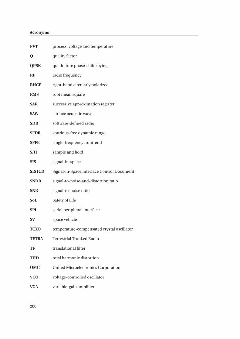
Acronyms
PVT process, voltage and temperature
Q quality factor
QPSK quadrature phase-shift keying
RF radio frequency
RHCP right-hand circularly polarized
RMS root mean square
SAR successive approximation register
SAW surface acoustic wave
SDR software-defined radio
SFDR spurious-free dynamic range
SFFE single-frequency front-end
S/H sample and hold
SIS signal-in-space
SIS ICD Signal-in-Space Interface Control Document
SNDR signal-to-noise-and-distortion ratio
SNR signal-to-noise ratio
SoL Safety of Life
SPI serial peripheral interface
SV space vehicle
TCXO temperature-compensated crystal oscillator
TETRA Terrestrial Trunked Radio
TF translational filter
THD total harmonic distortion
UMC United Microelectronics Corporation
VCO voltage-controlled oscillator
VGA variable-gain amplifier
200

CURRICULUM VITAE
Saeed GhamariRue de Maillefer 20,CH-2000, Neuchâtel,SwitzerlandCell: +41 79 305 [email protected], [email protected]
born on July 8,1985Male, SingleIranianLast update:March 11, 2016
EducationPh.D. Student - Microelectronics May 2011–presentÉcole Polytechnique Fédérale de Lausanne, CH-2000 Neuchâtel, Switzerland
Thesis: CMOS ASIC Design of Multi-Frequency Multi-Constellation GNSS Front-Ends
M.Sc., Fields and Waves, Communications, Electrical Engineering Sept. 2007–April 2010Amirkabir University of Technology, Tehran, Iran
Thesis: Design, Nonlinear Analysis and Implementation of Power Amplifier using Predistortion LinearizationTechnique for 3G Mobile Communication
B.Sc., Communications, Electrical Engineering Sept. 2003–Sep. 2007Khaje Nasir Toosi University of Technology (KNTU) Tehran, Iran
Thesis: Design a Watermarking Algorithm for Telephone Channel
ExperiencePh.D. Student/Doctoral Assistant - Analog IC Design May 2011–presentÉcole Polytechnique Fédérale de Lausanne, 2000 Neuchâtel, Switzerland
Projects:� C-Maxin collaboration with EM Microelectronic - Marin SA, Marin, Switzerland
• design of the RF amplification stage• extensive simulations to meet specifications of commercial product
� ARMOURS - Antenna and fRont-end Modules for pUblic Regulated Service applicationsin collaboration with ACORDE Technologies S.A., Sofant Technologies, Interuniversitair Micro-ElectronicaCentrum vzw (IMEC)
• design of a dual-frequency PRS FE ASIC• design of a 6-bit flash ADC• design of a reconfigurable continuous-time wide-tuning-range elliptic filter• PCB development and testing
� Dual-frequency Beidou/GPS/Galileo RF Front-End for Mass Market Applications
• design of a dual-frequency GNSS FE ASIC• design of all the building blocks of the GNSS FE including an LNA, mixer, IF filter, VGA, ADC, VCO• design of a reconfigurable continuous-time wide-tuning-range elliptic filter• PCB development and testing
Research Assistant at iRadio Lab July 2010–April 2011University of Calgary, Calgary, Alberta, Canada
Projects:� Development of a passive reflectometer using a six-port junction
Research Assistant at MMWCLAmirkabir University of Technology, Tehran, Iran Sep. 2007–April 2010
Projects:� Design and implementation of a Five Port Receiver at 2.14 GHz� Design and implementation of Power Amplifier Linearization Circuits base on Predistortion� Design and implementation of a Doherty Power Amplifier Linearization Circuits.
201
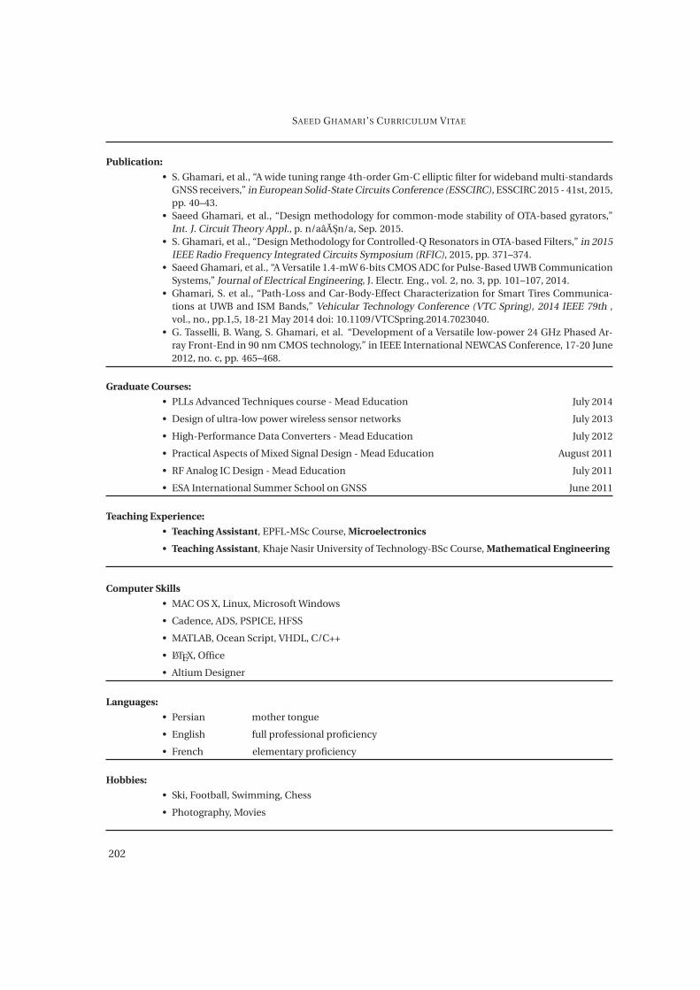
SAEED GHAMARI’S CURRICULUM VITAE
Publication:
• S. Ghamari, et al., “A wide tuning range 4th-order Gm-C elliptic filter for wideband multi-standardsGNSS receivers,” in European Solid-State Circuits Conference (ESSCIRC), ESSCIRC 2015 - 41st, 2015,pp. 40–43.
• Saeed Ghamari, et al., “Design methodology for common-mode stability of OTA-based gyrators,”Int. J. Circuit Theory Appl., p. n/aâASn/a, Sep. 2015.
• S. Ghamari, et al., “Design Methodology for Controlled-Q Resonators in OTA-based Filters,” in 2015IEEE Radio Frequency Integrated Circuits Symposium (RFIC), 2015, pp. 371–374.
• Saeed Ghamari, et al., “A Versatile 1.4-mW 6-bits CMOS ADC for Pulse-Based UWB CommunicationSystems,” Journal of Electrical Engineering, J. Electr. Eng., vol. 2, no. 3, pp. 101–107, 2014.
• Ghamari, S. et al., “Path-Loss and Car-Body-Effect Characterization for Smart Tires Communica-tions at UWB and ISM Bands,” Vehicular Technology Conference (VTC Spring), 2014 IEEE 79th ,vol., no., pp.1,5, 18-21 May 2014 doi: 10.1109/VTCSpring.2014.7023040.
• G. Tasselli, B. Wang, S. Ghamari, et al. “Development of a Versatile low-power 24 GHz Phased Ar-ray Front-End in 90 nm CMOS technology,” in IEEE International NEWCAS Conference, 17-20 June2012, no. c, pp. 465–468.
Graduate Courses:
• PLLs Advanced Techniques course - Mead Education July 2014
• Design of ultra-low power wireless sensor networks July 2013
• High-Performance Data Converters - Mead Education July 2012
• Practical Aspects of Mixed Signal Design - Mead Education August 2011
• RF Analog IC Design - Mead Education July 2011
• ESA International Summer School on GNSS June 2011
Teaching Experience:
• Teaching Assistant, EPFL-MSc Course, Microelectronics
• Teaching Assistant, Khaje Nasir University of Technology-BSc Course, Mathematical Engineering
Computer Skills
• MAC OS X, Linux, Microsoft Windows
• Cadence, ADS, PSPICE, HFSS
• MATLAB, Ocean Script, VHDL, C/C++
• LATEX, Office
• Altium Designer
Languages:
• Persian mother tongue
• English full professional proficiency
• French elementary proficiency
Hobbies:
• Ski, Football, Swimming, Chess
• Photography, Movies
202
