self-timed circuitry for global clocking
TRANSCRIPT
Self-timed circuitry for global clocking
Scott FairbanksCambridge University
Simon MooreCambridge University
Abstract
We present an apparatus used to distribute a timing ref-erence or clock across the extent of a digital system. Self-timed circuitry both generates and distributes a clock sig-nal, while using less power and less skew compared to aclock tree. HSpice simulations in a 180nm CMOS processcomparing theDistributed Clock Generatorpresented inthis paper and an H-tree clock distribution system, eachclocking a 16mm× 16mm area suggests a 30% power sav-ings. Also worst case skew was reduced from 27ps to 2pswhile using a clock period equivalent to 9 FO4 gates.
1. Introduction
1.1. Related Work
This paper extends the thread of research that investigatesthe timing relationship of the handshaking control signalsgenerated by self-timed FIFO circuitry as it passes data to-kens.
Ebergen, Fairbanks, and Sutherland [4] showed that datatokens in self-timed linear FIFOs can act as if they exertforces on each other. They showed that the forces are some-times repellent and sometimes attractive. TheCharlie effectwas the name given to the repellent force.
The Charlie effect describes how a second token is re-pelled as it nears a first token that is before it in the FIFO.They identified the source of the Charlie effect as the in-creased delay of the logic gates in the FIFO control whenthe inputs to the logic gate change near the same time. Theincreased logic gate delay results in the FIFO stage takinglonger to move the second token forward. The increasedmove delay pushes the second token back away from thefirst token.
Winstanley, Garivier and Greenstreet [12] placed data to-kens into a ring FIFO and designed novel circuitry thatcould vary the relative strength of the attractive and re-pelling forces, alternately causing the tokens to bunch andspread in the FIFO. When they increased the strength of therepelling force they noticed that the tokens spread evenlythrough the FIFO.
In [5] we designed a simple Micropipeline-style [11]FIFO control that amplified and exploited the Charlie ef-
fect, so that the tokens in a FIFO spread throughout it with-out the aid of an external control. We formulated the rela-tionship between the FIFO’s occupancy and the phase rela-tionship of the signals on the handshake control wires. Wealso outlined a method of distributing the FIFO over an area,loading the FIFO with some number of tokens, and usingthe resulting high frequency signals with precise phase re-lationships for various timing applications.
We then described how this Micropipeline style FIFOcontrol, while using digital handshake protocols to controlthe ordering of tokens, was acting as an analog feedback cir-cuit. The delay of the many FIFO control elements varieddepending on the relative arrival and departure times of datatokens. This effect ensured that the timing signals on thehandshake wires had a phase relationship that could be pre-dicted with pico-second accuracy even in the face of transis-tor mismatch. Suggested applications ranged from high fre-quency sampling to generating control signals for dominologic.
1.2. The Task
This paper once again uses self-timed circuitry to achievehigh precision timing. Rather than address the task of sam-pling at high frequency or controlling domino logic as in ourprevious paper, the concern of this work is global clocking.The former tasks involve generating timing many signalswith precise phase relationships. Global clocking in its sim-plest form requires a timing standard of a single phase dis-tributed to many widely separated nodes. Both problems re-quire high precision timing and both solutions actively cor-rect timing errors using the token spreading feedback mech-anism. However, the particular demands of clocking a largedigital system leads us to a different and novel circuit topol-ogy than that presented in our earlier paper.
Three concerns motivate the drive for a new self-timedcircuit topology beyond that presented in [5] for use as aglobal clock distribution system. First, power consumptionis of elevated concern in clock distribution. Second, the ge-ometry of the clock distribution system is of ever increasingperformance. A clock distribution system capable of clock-ing a billion-plus transistor system at frequencies greaterthan a giga-hertz must have a topology that integrates well

with the power distribution apparatus and functional unitsthat compose the rest of the digital system. Third, designtime and design complexity is a factor. The practice ofbalancing a growing number of electrical paths between aclock source and the state holding elements is increasinglyuntenable.
Power and skew The task in clock distribution is ensuringthat periodic events occur in many location at the same in-stant in time. The prevalent clock tree solution prescribesmany electrically equivalent paths from a single source tothe many locations. Because this is a passive or open-loopsolution, the longer the paths are from the source, the moreskewed in time are the many clock events at their destina-tions due to inevitable fabrication mismatches.
Designs often employ two remedies to control theskew between the clock events at the different desti-nations. The first remedy makes the electrical distancebetween the source and the leaves shorter using wider con-ductors and larger amplifiers. This reduces latency and thetime over which events can drift when branching from a sin-gle node. The second remedy is to make low resistancepaths between the many places needing the clock sig-nal, in essence, ‘shorting together’ the nodes requiring theclock signal. A clock grid employs this strategy.
The enabling commodity in both solutions is power. Bothrequire more hardware, which presents capacitance thatmust be charged and discharged in each cycle. Reducingpower and reducing skew in the clock distribution appa-ratus are largely the same problem. If power is available,skew can be reduced. Unfortunately the efforts of supply-ing power to and removing heat from the chip themselvespresent formidable challenges. A compelling clock distri-bution solution should suffer less skew for a given powerbudget.
Regularity and geometry State of the art VLSI chips arebillion-plus transistor systems. Their complexity necessi-tates the integration of the complete interconnect architec-ture [13]. The power distribution system, clock distributionapparatus, and signal interconnect utilize the same intercon-nect stack. The design of one system must consider and bal-ance the needs of the others.
If we consider a microprocessor with a view to its geom-etry, the most salient detail is its ’rectangularity,’ see Figure1.
Signal routes are confined to run parallel to the X and Yaxis of the chip. The functional units are typically of a rect-angular shape. The power is typically distributed in a rect-angular mesh whether sourced through peripheral pads orthrough a flip-chip bonding array. Power and ground railsare available at regular intervals along the X and Y axis ofthe chip. The VLSI fabrication process lends itself to rect-angular topologies. Fabrication equipment steps along one
Figure 1. Image of Typical MicroprocessorChip
axis of the silicon, laying down masks and etching in the ap-propriate place.
Continued progress in the art of VLSI relies upon theability to confine materials, voltages, and currents to spe-cific places and paths. Regular and congruent structures fa-cilitate this goal. The clock tree structure that is employedto amplify a signal from a single source and distribute it-self over a large two dimensional area is incongruent withthe power grid and the rectangular shapes of the other struc-tures. A clock distribution solution streamlined with the ex-isting geometry of the functional and power distributionsystems facilitates our ability to trace current paths, iso-late noisy from sensitive signals, and allocate physical re-sources.
Design time The costs spent in tools, design time, andcomputer cycles achieving design closure must be consid-ered. The incongruous relationship of a clock tree topologyand the other systems on the chip requires making difficultconcessions with respect to routing, sizing, and placement.Each alteration in the place or route of circuitry could re-quire a complete clock tree re-balance because it is verydifficult not to confound routes for the clock signal with theroutes of other signals.
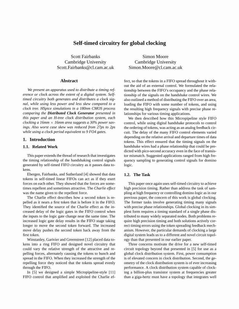
2. Pulse control for global clockFigure 2 shows two stages ofDynamic asPFIFO con-
trol. Dynamic asPhas been previously disclosed only inthe form of a patent [7]. The overall control uses two typesof alternating FIFO control stages. The potential on the stateconductor that connects stages is changed to alert a controlelement to the presence of a data token. Each FIFO controlelement sets the potential on the up and down stream stateconductors simultaneously to the same value when a tokenis moved forward by a FIFO control element. The presenceof a token in a stage is signaled by setting the potential onthe state conductor to a certain potential. The stage=FULL
signal is assigned to opposite polarities in alternating stages.Dynamic asPFIFO control also needs latches that becometransparent on opposite polarities in alternating stages.
Dynamic asP FIFO Control
Pull-down stage
Pull-up stage
The state-conductor is the long wire between stagesalong with the keeper.
Figure 2. One Pull-up and One Pull-downstage of Dynamic asP FIFO control
The alternating nature ofDynamic asPmakes it a lessthan ideal FIFO control. ButDynamic asPis attractive forthe purposes of generating and distributing a clock signal.When this FIFO control is loaded with a number of tokenswithin some range, then the tokens spread apart because ofthe Charlie effect. If the number of tokens is equivalent tohalf the number of stages, then the signals on the state con-ductors that connect the control elements will oscillate inphase. These signals can be buffered and used as clock sig-nals.
We believe thatDynamic asPFIFO is the minimal FIFOcontrol for producing single phase handshaking signals.Furthermore the handshaking protocol is enacted on a sin-gle communication wire. These two factors suggest that thisFIFO control could distribute a single phase signal mosteconomically with respect to power and hardware.
2.1. Proposal
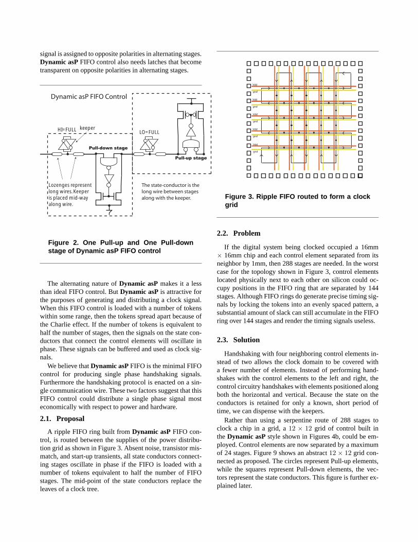
A ripple FIFO ring built fromDynamic asPFIFO con-trol, is routed between the supplies of the power distribu-tion grid as shown in Figure 3. Absent noise, transistor mis-match, and start-up transients, all state conductors connect-ing stages oscillate in phase if the FIFO is loaded with anumber of tokens equivalent to half the number of FIFOstages. The mid-point of the state conductors replace theleaves of a clock tree.
Vdd
gnd
Vdd
gnd
Vdd
gnd
Vdd
gnd
Vdd
gnd
Figure 3. Ripple FIFO routed to form a clockgrid
2.2. Problem
If the digital system being clocked occupied a 16mm× 16mm chip and each control element separated from itsneighbor by 1mm, then 288 stages are needed. In the worstcase for the topology shown in Figure 3, control elementslocated physically next to each other on silicon could oc-cupy positions in the FIFO ring that are separated by 144stages. Although FIFO rings do generate precise timing sig-nals by locking the tokens into an evenly spaced pattern, asubstantial amount of slack can still accumulate in the FIFOring over 144 stages and render the timing signals useless.
2.3. Solution
Handshaking with four neighboring control elements in-stead of two allows the clock domain to be covered witha fewer number of elements. Instead of performing hand-shakes with the control elements to the left and right, thecontrol circuitry handshakes with elements positioned alongboth the horizontal and vertical. Because the state on theconductors is retained for only a known, short period oftime, we can dispense with the keepers.
Rather than using a serpentine route of 288 stages toclock a chip in a grid, a12 × 12 grid of control built intheDynamic asPstyle shown in Figures 4b, could be em-ployed. Control elements are now separated by a maximumof 24 stages. Figure 9 shows an abstract12 × 12 grid con-nected as proposed. The circles represent Pull-up elements,while the squares represent Pull-down elements, the vec-tors represent the state conductors. This figure is further ex-plained later.
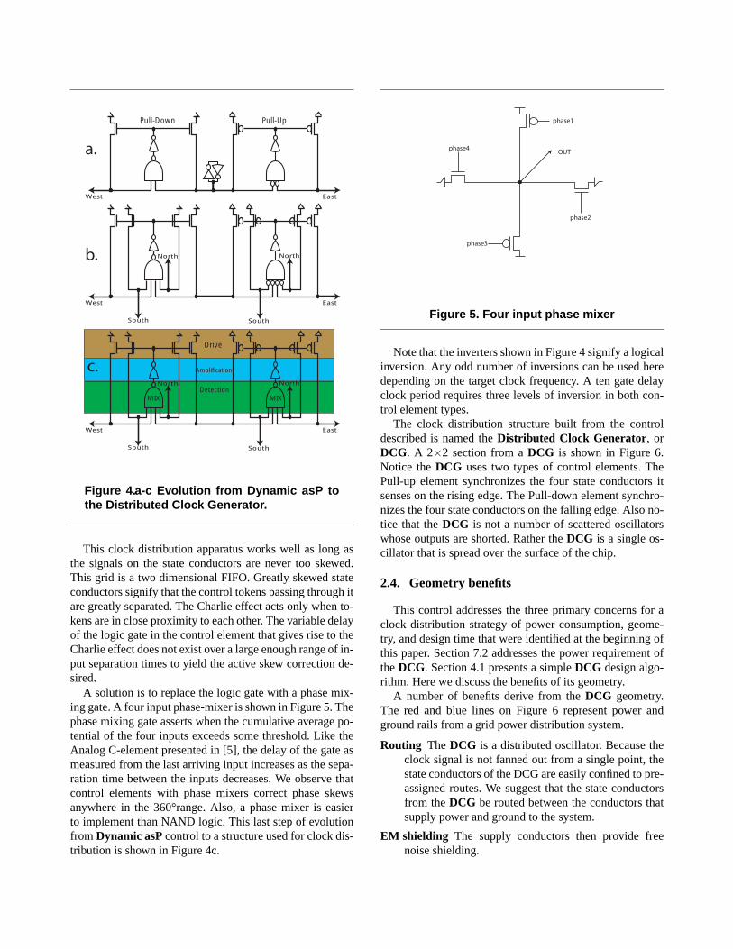
a.
b.
c.
Figure 4.a-c Evolution from Dynamic asP tothe Distributed Clock Generator.
This clock distribution apparatus works well as long asthe signals on the state conductors are never too skewed.This grid is a two dimensional FIFO. Greatly skewed stateconductors signify that the control tokens passing through itare greatly separated. The Charlie effect acts only when to-kens are in close proximity to each other. The variable delayof the logic gate in the control element that gives rise to theCharlie effect does not exist over a large enough range of in-put separation times to yield the active skew correction de-sired.
A solution is to replace the logic gate with a phase mix-ing gate. A four input phase-mixer is shown in Figure 5. Thephase mixing gate asserts when the cumulative average po-tential of the four inputs exceeds some threshold. Like theAnalog C-element presented in [5], the delay of the gate asmeasured from the last arriving input increases as the sepa-ration time between the inputs decreases. We observe thatcontrol elements with phase mixers correct phase skewsanywhere in the 360°range. Also, a phase mixer is easierto implement than NAND logic. This last step of evolutionfrom Dynamic asPcontrol to a structure used for clock dis-tribution is shown in Figure 4c.
phase1
phase2
phase3
phase4OUT
Figure 5. Four input phase mixer
Note that the inverters shown in Figure 4 signify a logicalinversion. Any odd number of inversions can be used heredepending on the target clock frequency. A ten gate delayclock period requires three levels of inversion in both con-trol element types.
The clock distribution structure built from the controldescribed is named theDistributed Clock Generator, orDCG. A 2×2 section from aDCG is shown in Figure 6.Notice theDCG uses two types of control elements. ThePull-up element synchronizes the four state conductors itsenses on the rising edge. The Pull-down element synchro-nizes the four state conductors on the falling edge. Also no-tice that theDCG is not a number of scattered oscillatorswhose outputs are shorted. Rather theDCG is a single os-cillator that is spread over the surface of the chip.
2.4. Geometry benefits
This control addresses the three primary concerns for aclock distribution strategy of power consumption, geome-try, and design time that were identified at the beginning ofthis paper. Section 7.2 addresses the power requirement oftheDCG. Section 4.1 presents a simpleDCG design algo-rithm. Here we discuss the benefits of its geometry.
A number of benefits derive from theDCG geometry.The red and blue lines on Figure 6 represent power andground rails from a grid power distribution system.
Routing The DCG is a distributed oscillator. Because theclock signal is not fanned out from a single point, thestate conductors of the DCG are easily confined to pre-assigned routes. We suggest that the state conductorsfrom theDCG be routed between the conductors thatsupply power and ground to the system.
EM shielding The supply conductors then provide freenoise shielding.

Predictable current return paths The current returnpaths of the clock signal are then simple to traceand short because they run along the supply conduc-tors. They are also consistent and predictable.
Split Inverter The drains of the PMOS and NMOS drivetransistors in theDCG are separated by a long wire.The gates are driven by different signals, but ones thatshould be of the same phase. We call this the split in-verter. In a normal inverter, the drains of the PMOSand NMOS transistors share the same node.
Notice that current moves in a single direction alongthe wire. When charging and discharging the load ona long wire, the split-inverter causes approximatelyequal currents on the wire. When a normal invertercharges and discharges the load on a long wire, itcauses approximately equal but opposite currents onthe wire. Equation 1 suggests that the split inverter in-duces a magnetic field with half the peak variationssince its magnetic field curls in a single direction.
~B =µ0
~I
2πr(1)
3. Mechanics
Each control element can be divided into three compo-nents. These components are shown in Figure 4c.
Detection The detection component is simply the phasemixing gate. It uses two PMOS and two NMOS transis-tors. These transistors are labeledpm1-pm4for a phase mix-ing gate in a Pull-down element in Figure 7a. When used inthe Pull-up element, a falling transition signals that the cu-mulative state of the four state conductors it senses are setLO and should be reset HI. The falling transition is a re-sult of two actions. When the state conductorssceandscwin Figure 7a go HI, the NMOS transistors start dischargingthe output of the phase mixing gate. When the state conduc-torsscnandscsgo HI, the PMOS transistors stop conduct-ing charge to the output of the phase mixing gate and ceaseto resist the falling transition. When the four state conduc-tors oscillate in phase, the phase mixing gate is indistin-guishable from two inverters connected in parallel. Whenthe four state conductors are out of phase, the PMOS andNMOS transistors oppose each other. The delay of the mix-ing gate from an early arriving clock signal is long. The de-lay of the mixing gate from a late arriving clock signal isquick because the potential is removed from the supply volt-age when the input arrives and less charge needs to be con-ducted to the output to cause a change in the logical valueof the output.
When the four state conductors are out of phase, then thetransistors in the logic gate burn static power. Fortunately,
in the suggested topology, these logic gates are four gatesof amplification removed from the large drive transistors,nd1-nd4andpd1-pd4, that charge the state conductors. As-sume that the electrical amplification from gate to gate inthe control elements for theDCG is chosen to be 4. The cur-rent at the output of the four input logic transistors that com-pose the phase mixing gate are then about three to the fourthpower, or1/256, smaller than the currents of the drive tran-sistors. This current is negligible.
Amplification The amplification component has an oddnumber of inverting amplifiers. It is detailed in Figure 7b.The amplification component serves three purposes.
1. The amplifiers take the relatively weak assertion sig-nal provided by the detection circuitry and amplifies itto a strength that will drive four transistors capable ofdriving interconnect of lengths on the order of a mil-limeter.
2. The amplification component is responsible for reset-ting the clock network. The first amplifier in the ampli-fication component is implemented with an asymmet-ric NAND gate and receives thestart signal. One in-put of the NAND gate connects to the output of theDetection component. The other input connects to thestart signal. Before the start signal asserts, the out-put of this NAND is HI. Pull-down elements are forcedto drive all the state conductors LO while Pull-up ele-ments disable their PMOS drivers.
3. The remaining amplifiers implement speed con-trol functionality. A simple speed control places a se-ries NMOS transistor in the pull-down path of oneor more of the inverters in the amplification com-ponent. This transistor limits the amount of currentavailable to discharge the gate’s output node. De-grading the ability of these inverters to source currentwill slow the clock frequency. The speed control sig-nal is a very low frequency analog signal requiringlittle care when distributing.
Three is the most practical number of gates for am-plification. One gate of amplification results in aggres-sive cycle times. A significant amount of skew beginsto accumulate in five or more amplifiers is chosen.
Drive A single transistor drives each of the four state con-ductor. The gates of the four drive transistors occupy thesame electrical node. This ensures that the four drive tran-sistors act in unison and synchronize the signal on the fourstate conductors on the rising or falling transition. The drivetransistors are left unencumbered from any speed control orlogic. Their sole responsibility is efficiently driving the stateconductors. The drive transistors are labelednd1-nd4andpd1-pd4in Figure 7a.

VDD GND VDD GND
VDD
GND
VDD
GND
Figure 6. 2 x 2 section of a DCG grid
4. Design
4.1. Gate sizing
Below is a seven step algorithm to designing aDCG.
1. Choose a value for the electrical amplification fromgate to gate in the control elements. Larger values re-sult in lower power designs but result in signals withgreater slew. The more slew of a signal the more vul-nerable it is to noise.
2. Choose a value for the PMOS/NMOS transistor widthratio, γ.The best options are 1, 1.5 and 2. Aγ of 1results in Pull-up and Pull-down elements having thesame footprint in the silicon. This choice is appeal-ing from a geometric and regularity argument. Unfor-tunately, unless the chosen electrical amplification forthe system is small, the rising transitions can be ane-mic and be vulnerable to noise.
The minimal average delay for the rising and fallingtransition of an inverter is achieved with aγ valueequivalent to the square root of the conductivity ratioof the electron and hole doped silicon used to constructthe transistors [10]. This optimal value is about 1.6 inthe process used for simulations in this paper. 1.5 is agood approximation of this value.
A gamma of 2 balances the need for speed, tolera-ble slew rates, and circuits size.
3. Build a Spice model of the Pull-up and Pull-downcontrol elements. Connect a wire between terminalsN,S,E,W in one element to the similar terminal inthe other control element. Be sure that wire uses anadequate RC or RCL model for the necessary wirelength.
Each gate’s size should be paramaterized in Spice tobe a function of the size of the PMOS drive transistorin the Pull-up control element. The last inverter in theamplification component of the Pull-up element shouldhave a total transistor width equivalent to the transistorwidth of the four drive transistors divided by the cho-sen electrical amplification. The next gate should be re-duced by another factor of the electrical amplification.The transistors in the phase mixer of the Pull-up ele-ment should have a total size equal to the size of thePMOS drive transistors divided by the electrical am-plification raised to the fourth power. The transistorsin the Pull-down elements should be scaled by fromthe transistors in the Pull-up element by1/γ.
4. This circuit should oscillate as is. Step the size of thePMOS transistor until theDCG oscillates at the target

pm1
pm2
pm3
pm4
scn
sce
scs
scw
nd1
nd2
nd3
nd4
pd1
pd2
pd3
pd4
a.
b.
N N
SS
WWE E
Pull-down stage Pull-up stage
Amplifier circuit
Variable delay invertersAmplifier icon
speed control
start
detect
boundary
Figure 7.a-b Pull-up and Pull-down control elements in detail
cycle time. If the circuit doesn’t reach the target cycletime, then a lower electrical amplification might givethe speed desired. Another option is widening the stateconductors wires.
5. Adjust the duty cycle by adjusting the speed controlsection of one type of control. If the duty cycle is toolong, the delay through the Pull-up control elementsneeds to be increased by adjusting the speed control.
6. If the voltage swing at the clock output is insufficient,the electrical amplification chosen earlier needs to bereduced.
7. Take control element with resulting transistor sizes andarrange the control elements in a grid.
4.2. Interconnect optimization
The regularity of theDCG allows the interconnect to beoptimized to a degree impractical in a clock tree. The di-
mensions of the state conductor that connects control ele-ments need only be designed once and then these dimen-sions are duplicated many times throughout the design.Tapering the width of long interconnects along its lengthyields marginal but real speed and power savings [2]. Opti-mal tapering improves delay by up to 8% [1].
The optimal uniform state conductor width of length1333µm when the PMOS driver was 42µm wide and theNMOS driver was 21µm is 1µm. We used a simple algo-rithm that segmented the state conductor into 9 sections.Each segment took a width centered around the optimal uni-form width. Each segment was replaced by a simple RCmodel and the Elmore delay for the state conductor was cal-culated. The resulting optimal widths were 1.2, 1.1, 1.1, 1.2,1.2, 1.2,1.2, 1.3,1.3. These are the widths of the state con-ductor starting from the side connected to the NMOS drivetransistor. The replacement wire has an Elmore delay of 495ps versus 525 ps for the wire of uniform width.

The state conductor can be drawn once and then dupli-cated throughout the system.
5. Mechanics
5.1. Initialization and starting
When thestart signal is LO or unasserted, a HI poten-tial is applied to the gates of the transistors in the drive com-ponent of each control element. Consequently all state con-ductors are driven LO. TheDCG begins oscillating whenthestart signal asserts. It is not critical that thestart signalarrives at each control element simultaneously. If thestartsignal is greatly skewed, then the state conductors initiallyoscillate out of phase but they quickly lock into phase soonafter thestart signal distributes to all elements. The mech-anism that forces the state conductors into the same phasesis the Charlie effect which is enacted by the variable delayof the mixing gate in the detection component of the con-trol.
Converging clock
Start signals
time (sec)
time (sec)
Volt
age
(v)
Volt
age
(v)
Figure 8. Top plot shows start signals assert-ing at random times, bottom plot shows sixclock taps converging
Figure 8 shows two windows of a waveform viewer. Thetop window shows a number of start signals that are ran-domly chosen from a uniform distribution of a single clockperiod. These start signals are sent to the control elementsin a12×12 DCG. The bottom window shows the signals on
a number of state conductors. Notice that the various clocksignals are locked with respect to each other within 10ns.
5.2. Synchronization
When the combined potential on the four state conduc-tors reaches a potential that causes the detection componentto assert, the amplification component amplifies the assertedsignal and causes the drive transistors to charge the stateconductors to the opposite potential. Because the gates ofthe four drive transistors share the same electrical node, thefour signals reset simultaneously irrespective of the phasesof the signals when they arrived at the stage.
6. Hazards
6.1. Timing constraints
The drive from the state conductors is removed three gatedelays after the detection circuitry signals that the potentialon the state conductors has changed. The drive transistorsfirst charge the state conductor wires near the detection cir-cuitry. Then the charge spreads along the length of the wire.A small hazard exists if an insufficient amount of charge issourced onto the state conductor to charge the whole lengthof the state conductor before the drive transistors are dis-abled. This is not a concern if the design methodology isdisciplined and ensures that each gate in theDCG has thesame electrical amplification required of it. Under this con-straint the time allotted to charge the wire is always propor-tional to the capabilities of the drive transistors and this haz-ard is avoided.
6.2. Supply variations
Notice that current moves in one direction on the stateconductors. A large amount of charge is sourced by thePull-up elements and sunk by the Pull-down elements. If thepower supply conductors are resistive then supply gradientsexist between the two types of control. The supply voltagenear the Pull-down elements is greater by an amount equiv-alent to the IR drop in the current return paths.
6.3. Mode lock
Mode lock is a stable system equilibrium in which thephase averaging mechanism used to couple the oscillatorssettles the oscillators in a non-zero phase relationship [8].If two of the phases contributing to the average are of equalbut opposite magnitude then an undesired and stable phaseequilibrium occurs.
The criteria for avoiding mode lock in a two input phasemixer stipulates that the delay of the phase mixer must in-crease linearly for phase differences between +/-90° and de-creases between 90°and 270°. This error function is easy to
plot and visualize for a two input phase mixer but is sub-stantially more difficult to formulate and visually representwith four inputs.
We present an empirical argument to show that theDCGis not susceptible to mode lock. Using HSpice, 100 simula-tions were ran of a 4x4DCG whose clock period was 675ps.A test setup ensured that each element received its ownstart signal. The individualstart signals asserted at a timepicked from a uniform distribution between 0ps and 675ps.For this simulation transistor mismatch was not modeled.In all cases, the state conductors locked into phase by 20ns.The large number of initial phase relationships between thestate conductors that did not excite the mode lock conditiongives reasonable assurance that this behavior is not exhib-ited by theDCG.
7. Comparison
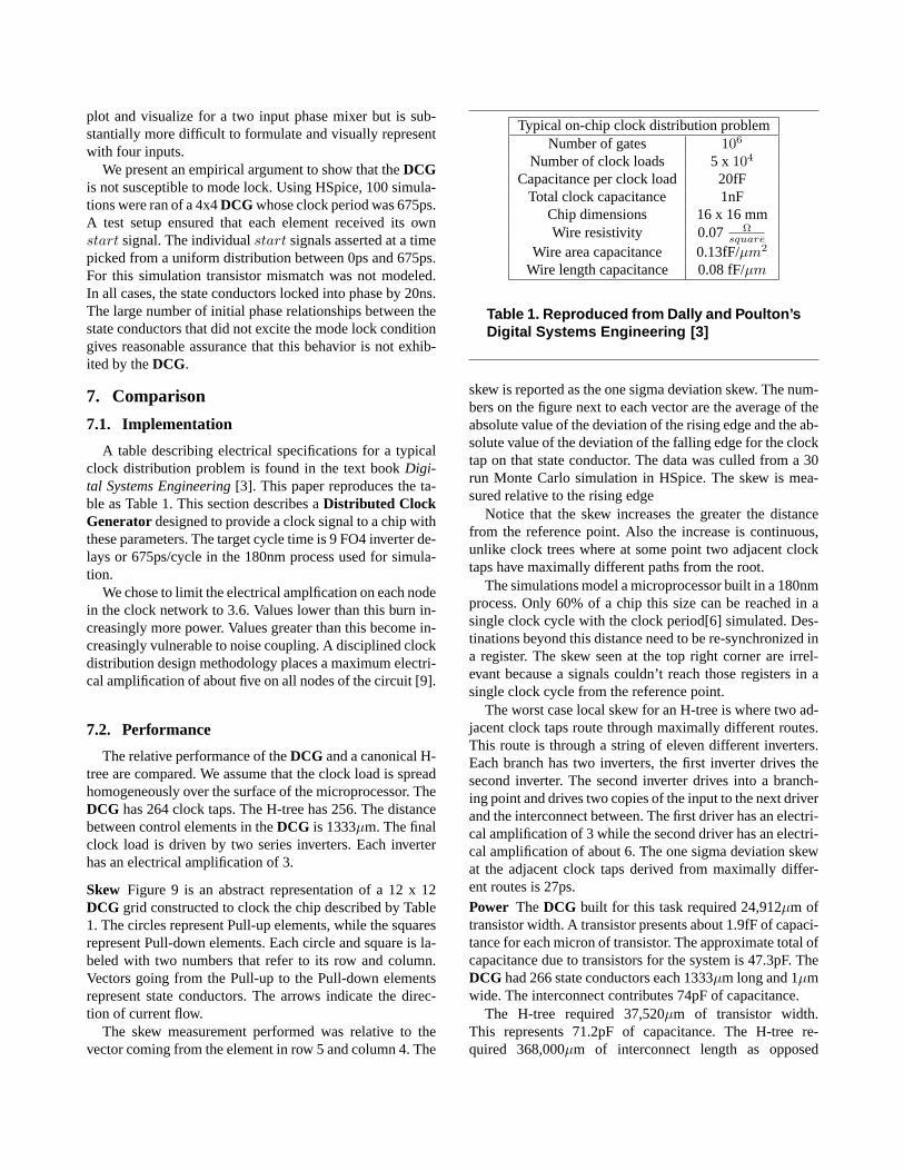
7.1. Implementation
A table describing electrical specifications for a typicalclock distribution problem is found in the text bookDigi-tal Systems Engineering[3]. This paper reproduces the ta-ble as Table 1. This section describes aDistributed ClockGenerator designed to provide a clock signal to a chip withthese parameters. The target cycle time is 9 FO4 inverter de-lays or 675ps/cycle in the 180nm process used for simula-tion.
We chose to limit the electrical amplfication on each nodein the clock network to 3.6. Values lower than this burn in-creasingly more power. Values greater than this become in-creasingly vulnerable to noise coupling. A disciplined clockdistribution design methodology places a maximum electri-cal amplification of about five on all nodes of the circuit [9].
7.2. Performance
The relative performance of theDCG and a canonical H-tree are compared. We assume that the clock load is spreadhomogeneously over the surface of the microprocessor. TheDCG has 264 clock taps. The H-tree has 256. The distancebetween control elements in theDCG is 1333µm. The finalclock load is driven by two series inverters. Each inverterhas an electrical amplification of 3.
Skew Figure 9 is an abstract representation of a 12 x 12DCG grid constructed to clock the chip described by Table1. The circles represent Pull-up elements, while the squaresrepresent Pull-down elements. Each circle and square is la-beled with two numbers that refer to its row and column.Vectors going from the Pull-up to the Pull-down elementsrepresent state conductors. The arrows indicate the direc-tion of current flow.
The skew measurement performed was relative to thevector coming from the element in row 5 and column 4. The
Typical on-chip clock distribution problemNumber of gates 106
Number of clock loads 5 x 10⁴
Capacitance per clock load 20fFTotal clock capacitance 1nF
Chip dimensions 16 x 16 mmWire resistivity 0.07 Ω
square
Wire area capacitance 0.13fF/µm2
Wire length capacitance 0.08 fF/µm
Table 1. Reproduced from Dally and Poulton’sDigital Systems Engineering [3]
skew is reported as the one sigma deviation skew. The num-bers on the figure next to each vector are the average of theabsolute value of the deviation of the rising edge and the ab-solute value of the deviation of the falling edge for the clocktap on that state conductor. The data was culled from a 30run Monte Carlo simulation in HSpice. The skew is mea-sured relative to the rising edge
Notice that the skew increases the greater the distancefrom the reference point. Also the increase is continuous,unlike clock trees where at some point two adjacent clocktaps have maximally different paths from the root.
The simulations model a microprocessor built in a 180nmprocess. Only 60% of a chip this size can be reached in asingle clock cycle with the clock period[6] simulated. Des-tinations beyond this distance need to be re-synchronized ina register. The skew seen at the top right corner are irrel-evant because a signals couldn’t reach those registers in asingle clock cycle from the reference point.
The worst case local skew for an H-tree is where two ad-jacent clock taps route through maximally different routes.This route is through a string of eleven different inverters.Each branch has two inverters, the first inverter drives thesecond inverter. The second inverter drives into a branch-ing point and drives two copies of the input to the next driverand the interconnect between. The first driver has an electri-cal amplification of 3 while the second driver has an electri-cal amplification of about 6. The one sigma deviation skewat the adjacent clock taps derived from maximally differ-ent routes is 27ps.Power TheDCG built for this task required 24,912µm oftransistor width. A transistor presents about 1.9fF of capaci-tance for each micron of transistor. The approximate total ofcapacitance due to transistors for the system is 47.3pF. TheDCG had 266 state conductors each 1333µm long and 1µmwide. The interconnect contributes 74pF of capacitance.
The H-tree required 37,520µm of transistor width.This represents 71.2pF of capacitance. The H-tree re-quired 368,000µm of interconnect length as opposed

0 0
h0 1
0 2
h0 3
0 4
h0 5
0 6
h0 7
0 8
h0 9
0 10
h0 11
h1 0
1 1
h1 2
1 3
h1 4
1 5
h1 6
1 7
h1 8
1 9
h1 10
1 11
2 0
h2 1
2 2
h2 3
2 4
h2 5
2 6
h2 7
2 8
h2 9
2 10
h2 11
h3 0
3 1
h3 2
3 3
h3 4
3 5
h3 6
3 7
h3 8
3 9
h3 10
3 11
4 0
h4 1
4 2
h4 3
4 4
h4 5
4 6
h4 7
4 8
h4 9
4 10
h4 11
h5 0
5 1
h5 2
5 3
h5 4
5 5
h5 6
5 7
h5 8
5 9
h5 10
5 11
6 0
h6 1
6 2
h6 3
6 4
h6 5
6 6
h6 7
6 8
h6 9
6 10
h6 11
h7 0
7 1
h7 2
7 3
h7 4
7 5
h7 6
7 7
h7 8
7 9
h7 10
7 11
8 0
h8 1
8 2
h8 3
8 4
h8 5
8 6
h8 7
8 8
h8 9
8 10
h8 11
h9 0
9 1
h9 2
9 3
h9 4
9 5
h9 6
9 7
h9 8
9 9
h9 10
9 11
10 0
h10 1
10 2
h10 3
10 4
h10 5
10 6
h10 7
10 8
h10 9
10 10
h10 11
h11 0
11 1
h11 2
11 3
h11 4
11 5
h11 6
11 7
h11 8
11 9
h11 10
11 11
?
-
6
-
7p
9p
8p
9p
?
-
6
-
6p
7p
7p
7p
?
-
6
-
6p
6p
5p
6p
?
-
6
-
9p
7p
8p
7p
?
-
6
-
8p
9p
8p
9p
?
- ?
-
10p
9p
10p
9p
?
-
6
7p
6p
6p7p
?
-
6
6p
7p
6p6p
?
-
6
5p
4p
4p5p
?
-
6
8p
6p
6p8p
?
-
6
7p
8p
8p7p
?
- ?8p
7p
8p9p
?
-
6
5p
4p
6p5p
?
-
6
4p
5p
4p4p
?
-
6
4p
3p
2p3p
?
-
6
8p
5p
7p6p
?
-
6
7p
8p
8p8p
?
- ?7p
7p
7p8p
?
-
6
7p
8p
9p8p
?
-
6
3p
5p
5p4p
?
-
6
3p
3p
3p2p
?
-
6
6p
4p
5p6p
?
-
6
6p
7p
8p8p
?
- ?7p
6p
7p7p
?
-
6
7p
7p
8p9p
?
-
6
6p
7p
7p6p
?
-
6
5p
6p
6p4p
?
-
6
5p
5p
5p5p
?
-
6
9p
7p
8p8p
?
- ?8p
8p
8p7p
?
-
6
7p
7p
8p8p
?
-
6
7p
8p
9p7p
?
-
6
7p
7p
7p7p
?
-
6
7p
7p
7p6p
?
-
6
11p
8p
11p9p
?
- ?12p
11p
12p10p
6
-
6
8p
9p7p9p
?
-
6
7p
7p
8p7p
?
-
6
4p
5p
4p5p
?
-
6
7p
6p
6p7p
?
-
6
8p
9p
10p10p
?
-
6
8p
7p
7p8p
6
-
6
5p
6p4p5p
?
-
6
5p
6p
6p7p
?
-
6
4p
5p
3p5p
?
-
6
6p
5p
6p7p
?
-
6
8p
7p
9p9p
?
-
6
7p
7p
6p7p
6
-
6
5p
5p6p5p
?
-
6
5p
6p
6p7p
?
-
6
0.
3p
3p2p
?
-
6
5p
3p
5p6p
?
-
6
8p
7p
7p8p
?
-
6
7p
8p
8p8p
6
-
6
7p
7p6p7p
?
-
6
6p
7p
7p7p
?
-
6
5p
5p
6p4p
?
-
6
4p
4p
5p5p
?
-
6
7p
5p
5p6p
?
-
6
6p
7p
7p6p
6
-
6
7p
7p7p7p
?
-
6
6p
8p
8p7p
?
-
6
6p
6p
6p6p
?
-
6
5p
6p
7p6p
?
-
6
8p
6p
7p7p
?
-
6
10p
10p
11p10p
6
6
8p
8p
8p
8p
?
6
10p
7p
10p
9p
?
6
7p
7p
7p
7p
?
6
8p
7p
8p
8p
?
6
10p
7p
10p
8p
?
6
13p
12p
13p
13p
Figure 9. Skew expectation over the surface of microprocessor due to transistor mismatch
to 353,000µm of length for theDCG. All levels ex-cept for the final ’H’ used 3µm wide wire. The total wirecapacitance for the H-tree is 104.8pF.
The total H-tree capacitance is 176pF while the totalDCG capacitance is 121pF. If both systems used the samesupply voltage and identical clock frequencies, then theDCG would consume121176 = 0.68 of the power as the H-tree.
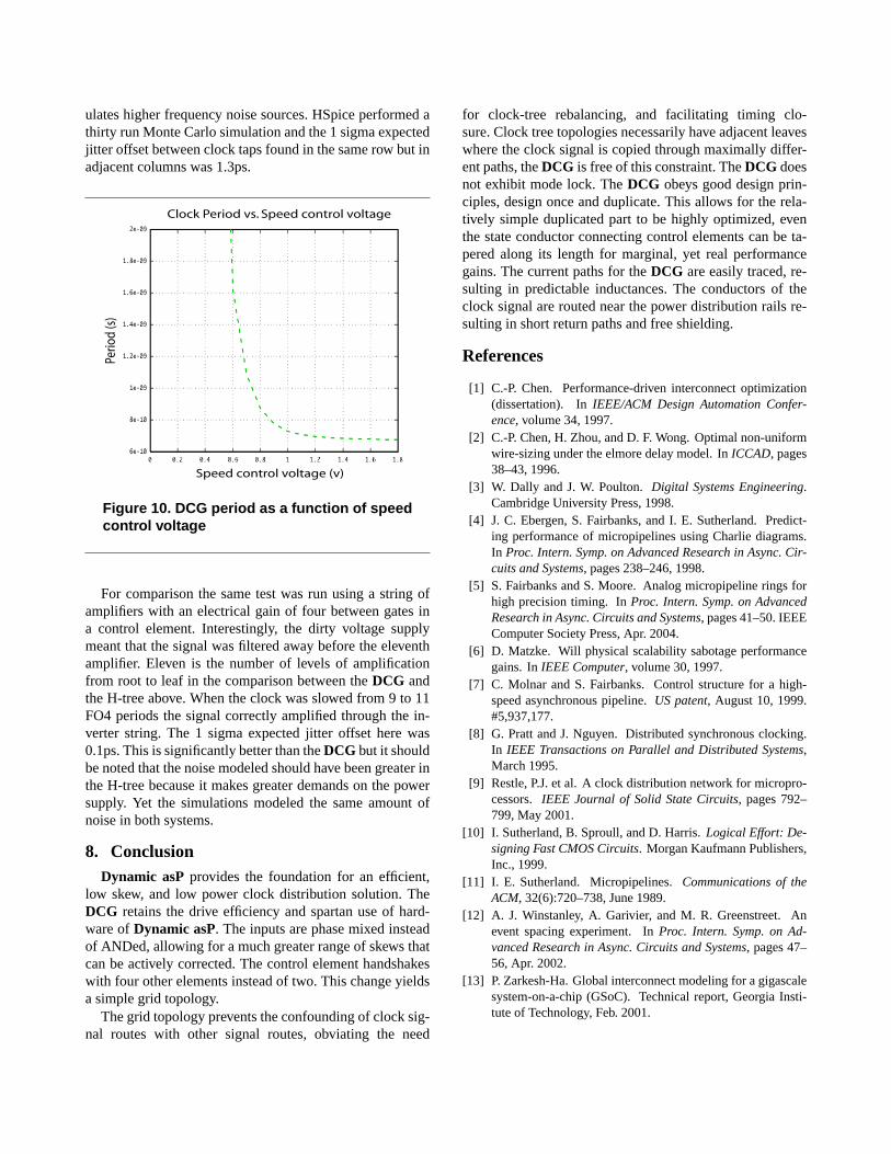
Speed control The simple speed control circuitry yieldsa wide range of clock periods. The relationship betweenspeed control voltage and the resulting period is shown in
Figure 10
Jitter Each transistor connected to the supply voltage inthe DCG was connected to a unique dirty supply. Thedirty supplies were created by connecting the dirty node totwo voltage sources, each through a very large transparenttransistor.The first supply swung between 0.9×Vsupply and1×Vsupply with a frequency of 9×FO4 delays. The secondsupply had the same voltage swing but the period was cho-sen from a uniform random distribution between 150ps and250ps. The first supply simulates noise contributed from theoutput resistance of the supply while the second supply sim-
ulates higher frequency noise sources. HSpice performed athirty run Monte Carlo simulation and the 1 sigma expectedjitter offset between clock taps found in the same row but inadjacent columns was 1.3ps.
Clock Period vs. Speed control voltage
Speed control voltage (v)
Perio
d (s
)
Figure 10. DCG period as a function of speedcontrol voltage
For comparison the same test was run using a string ofamplifiers with an electrical gain of four between gates ina control element. Interestingly, the dirty voltage supplymeant that the signal was filtered away before the eleventhamplifier. Eleven is the number of levels of amplificationfrom root to leaf in the comparison between theDCG andthe H-tree above. When the clock was slowed from 9 to 11FO4 periods the signal correctly amplified through the in-verter string. The 1 sigma expected jitter offset here was0.1ps. This is significantly better than theDCG but it shouldbe noted that the noise modeled should have been greater inthe H-tree because it makes greater demands on the powersupply. Yet the simulations modeled the same amount ofnoise in both systems.
8. ConclusionDynamic asPprovides the foundation for an efficient,
low skew, and low power clock distribution solution. TheDCG retains the drive efficiency and spartan use of hard-ware ofDynamic asP. The inputs are phase mixed insteadof ANDed, allowing for a much greater range of skews thatcan be actively corrected. The control element handshakeswith four other elements instead of two. This change yieldsa simple grid topology.
The grid topology prevents the confounding of clock sig-nal routes with other signal routes, obviating the need
for clock-tree rebalancing, and facilitating timing clo-sure. Clock tree topologies necessarily have adjacent leaveswhere the clock signal is copied through maximally differ-ent paths, theDCG is free of this constraint. TheDCG doesnot exhibit mode lock. TheDCG obeys good design prin-ciples, design once and duplicate. This allows for the rela-tively simple duplicated part to be highly optimized, eventhe state conductor connecting control elements can be ta-pered along its length for marginal, yet real performancegains. The current paths for theDCG are easily traced, re-sulting in predictable inductances. The conductors of theclock signal are routed near the power distribution rails re-sulting in short return paths and free shielding.
References
[1] C.-P. Chen. Performance-driven interconnect optimization(dissertation). InIEEE/ACM Design Automation Confer-ence, volume 34, 1997.
[2] C.-P. Chen, H. Zhou, and D. F. Wong. Optimal non-uniformwire-sizing under the elmore delay model. InICCAD, pages38–43, 1996.
[3] W. Dally and J. W. Poulton.Digital Systems Engineering.Cambridge University Press, 1998.
[4] J. C. Ebergen, S. Fairbanks, and I. E. Sutherland. Predict-ing performance of micropipelines using Charlie diagrams.In Proc. Intern. Symp. on Advanced Research in Async. Cir-cuits and Systems, pages 238–246, 1998.
[5] S. Fairbanks and S. Moore. Analog micropipeline rings forhigh precision timing. InProc. Intern. Symp. on AdvancedResearch in Async. Circuits and Systems, pages 41–50. IEEEComputer Society Press, Apr. 2004.
[6] D. Matzke. Will physical scalability sabotage performancegains. InIEEE Computer, volume 30, 1997.
[7] C. Molnar and S. Fairbanks. Control structure for a high-speed asynchronous pipeline.US patent, August 10, 1999.#5,937,177.
[8] G. Pratt and J. Nguyen. Distributed synchronous clocking.In IEEE Transactions on Parallel and Distributed Systems,March 1995.
[9] Restle, P.J. et al. A clock distribution network for micropro-cessors. IEEE Journal of Solid State Circuits, pages 792–799, May 2001.
[10] I. Sutherland, B. Sproull, and D. Harris.Logical Effort: De-signing Fast CMOS Circuits. Morgan Kaufmann Publishers,Inc., 1999.
[11] I. E. Sutherland. Micropipelines.Communications of theACM, 32(6):720–738, June 1989.
[12] A. J. Winstanley, A. Garivier, and M. R. Greenstreet. Anevent spacing experiment. InProc. Intern. Symp. on Ad-vanced Research in Async. Circuits and Systems, pages 47–56, Apr. 2002.
[13] P. Zarkesh-Ha. Global interconnect modeling for a gigascalesystem-on-a-chip (GSoC). Technical report, Georgia Insti-tute of Technology, Feb. 2001.