rf iv waveform measurement and engineering
TRANSCRIPT

1
Centre for High FrequencyEngineeringSchool of EngineeringCardiff University
RF IV Waveform Measurement and Engineering- Role in Transistor Characterization
and Amplifier Design -
Contact information
Prof. Paul J Tasker –[email protected]: www.engin.cf.ac.uk/chfe
IEEE MTT-S DistinguishedMicrowave Lecturer
2008-2010

2
RF Waveform Measurement and Engineering- powerful dynamic transistor characterization tool
Basic Concept– Use RF Waveform Measurement and Engineering Systems to investigated
both the transistors dynamic I-V (Current-Voltage) plane and its Q-V(Charge-Voltage) plane
Both qualitative and quantitative Alternatives: DC I-V, Pulsed I-V, bias dependent s-parameters
Applications Technology Evaluation
– Observe and quantify its dynamic large signal response
Technology Optimization– Link technology design to system performance
Technology Modelling– support the development of CAD tools
Circuit Design Tool– Support the development of Power Amplifiers

3
RF Waveform Measurement and Engineering- powerful dynamic transistor characterization tool
Transistor Characterization: Case Study– Use RF Waveform Measurement and Engineering Systems to investigated
general performance of Transistor Technology
Current Limits, Modes of Operation, RF Cooling

4
Transistor RF I-V Waveforms– Detailed Insight into Dynamic Behaviour Limitations
- 2 0 0-3
-1 0 0
-2
0
-1
100
0
200
1
2
3
5004003002001000
T im e (p s e c )
Gate C
urrent [mA
/mm
]
Gat
e V
olta
ge [V
]
Measure Input voltage and current waveforms– function of input drive level
Detailed Insight into DynamicBehaviour
– Gate Diode: Forward DiodeConduction and ReverseBreakdown
– Gate Capacitance
Relevant information for both– Device Engineer– PA Circuit Designer
AlGaAs/InGaAs HFET @ 4 GHz

5
Transistor RF I-V Waveforms– Detailed Insight into Dynamic Behaviour Limitations
Measure Output voltage and current waveforms– function of input drive level
Detailed Insight into DynamicBehaviour
– Drain Current Saturation: KneeRegion and Breakdown
– Gate-Drain Trans-capacitance
Relevant information for both– Device Engineer– PA Circuit Designer
AlGaAs/InGaAs HFET @ 4 GHz
5004003002001000
Tim e (psec)
10
8
6
4
2
0
600
500
400
300
200
100
0D
rain Current [m
A/m
m]D
rain
Vol
tage
[V]

6
Device Response Waveform Shapes
– Insight provided by eliminating time axes Effects of dynamic transfer characterisation
clearly observed DC/RF Dispersion
Effects of Delay/Trans-capacitance clearlyobserved
I-Q Extraction
@ 4.0 GHz
-3
-2
-1
0
1
Gat
e V
olt
age
[V]
5004003002001000
Time (psec)
500
400
300
200
100
0
Drain
Curren
t [mA
/mm
]Dynamic Transfer CharacteristicMeasurements
500
400
300
200
100
0
Dra
in C
urr
ent
[mA
/mm
]
-3 -2 -1 0 1
Gate Voltage [V]
Transistor RF I-V Waveforms– Detailed Insight into Dynamic Behaviour Limitations

7
Transistor RF I-V Waveforms– Detailed Insight into Dynamic Behaviour Limitations
Quadratic RF Breakdown Locus
Vgs = -1.1 Vds = 3.5
Vgs = -0.6 Vds = 5.5
DC I/VMeasured
Load Lines
800700
600500400300200100
0
Dra
in C
urre
nt [m
A/m
m]
15.012.510.07.55.02.50.0Drain Voltage [V]
Dynamic Breakdown in Low Noise AlGaAs/InGaAs HFET’s
Device Response Waveform Shapes
– Insight provided by eliminating time axes Effects of dynamic gate-drain breakdown
clearly observed

8
Transistor RF I-V Waveforms– Detailed Insight into Dynamic Behaviour Limitations
160
120
80
40
0
Coll
ecto
r C
urr
ent
[mA
]
1086420
Collector Voltage [volts]
RF Dynamic LoadLinesmeasured at 2 GHz
RF Cooling inHandset PAAlGaAs/InGaAs HBT’s
Device Response Waveform Shapes
– Insight provided by eliminating time axes Effects of dynamic RF cooling clearly
observed
– Linked with pulsed RF I-V technique

9
Performance UnderstandingReactive Non-Linearity's
-10
-5
0
5
10
Gat
e C
urre
nt I gs
[mA]
-8 -6 -4 -2 0 2Gate Voltage Vgs [V]
Input Characteristic
160
120
80
40
0Dra
in C
urre
nt I ds
[mA]
-8 -6 -4 -2 0 2Gate Voltage Vgs [V]
Transfer Characteristic
Technology
Waveform MeasurementPower Sweep @ 1.8 GHz
-10
-5
0
5
10
Gat
e C
urre
nt I d [m
A]
7205403601800Phase [°]
-8-6-4
-20
2 Gate Voltage Vgs [m
A]160
120
80
40
0Dra
in C
urre
nt I d [m
A]
7205403601800Phase [°]
16
12
8
4
0
Drain Voltage Vds [m
A]
Extraction State Functions I & QReactive strongly second order
-10
-5
0
5
10
Gat
e C
urre
nt I gs [m
A]
-8 -6 -4 -2 0 2Gate Voltage Vgs [V]
1.0
0.8
0.6
0.4
0.2
0.0
Gate C
apacitance [pF]
160
120
80
40
0Dra
in C
urre
nt I ds
[mA]
-8 -6 -4 -2 0 2Gate Voltage Vgs [V]
-1.0-0.8-0.6-0.4-0.2
0.0 Trans Capacitance [pF]
Measured RF I-V Waveforms– Unifying Analysis Tool
Performance EvaluationWeak AM-PM observed
30
20
10
0
Out
put p
ower
[dBm
]
2018161412108642Input Power [dBm]
-60
-40
-20
0
20
f0 2f0 3f0
18013590450
-45-90
Phas
e [d
eg]
2018161412108642Input Power [dBm]
174
172
170
168
166
f0 2f0 3f0
Performance
Performance UnderstandingReactive Non-Linearity's
-10
-5
0
5
10
Gat
e C
urre
nt I gs
[mA]
-8 -6 -4 -2 0 2Gate Voltage Vgs [V]
Input Characteristic
160
120
80
40
0Dra
in C
urre
nt I ds
[mA]
-8 -6 -4 -2 0 2Gate Voltage Vgs [V]
Transfer Characteristic
Technology

10GaAs HBT Performance as a function of Load Impedance
-30
-20-10
01.25
1.30
1.35
-30
-20
-10
0
10
20
-30
-20
-10
0
10
20
[dBm]
[dBm]
VBE [V]Pin [dBm]
Output Power versus Input Power and Base Bias Voltage
-30
-20
-10
01.25
1.30
1.35
0
10
20
30
40
50
0
10
20
30
40
50
[%]
[%]
VBE [V]Pin [dBm]
Efficiency versus Input Power and Base Bias Voltage
-30-20
-100
1.25
1.30
1.35
-35
-30
-25
-20
-15
-10
-5
-35
-30
-25
-20
-15
-10
-5
[dBc]
[dBc]
VBE [V]
Pin [dBm]
2nd Harmonic Output Power versus Input Power and Base Bias Voltage
-30-20
-100
1.25
1.30
1.35
-60
-50
-40
-30
-20
-60
-50
-40
-30
-20
[dBc]
[dBc]
VBE [V]
Pin [dBm]
3rd Harmonic Output Power versus Input Power and Base Bias Voltage
Experimental Emulatethe affect of varyingexternal parameters:In this case input drivelevel and input DCbias voltage
Note, have allinformation onmagnitude and phaseof all voltage andcurrent Fouriercomponents
Measured RF I-V Waveforms– General purpose Analysis Tool

11
RF Waveform Measurement and Engineering- powerful dynamic transistor characterization tool
Transistor Characterization: Case Study– Use RF Waveform Measurement and Engineering Systems to investigated
factor limiting the observed power performance of the emerging GaNTransistor Technology
Current Collapse, Knee Walkout, Poor Pinch-off

12
Approach: Drive the GaN transitor in tocompression while measuring RFOutput V & I Waveforms (840MHz)
Plot against one another to give theRF Load-line
Waveforms show compression at RFBoundaries differs from the DC
Boundaries, hence clearly identifyingsource of the problem: knee walkout or
current collapse
30
25
20
15
10Out
put V
olta
ge V
D [V
]
7205403601800Phase [deg]
120
80
40
0
Out
put C
urre
nt ID [m
A]
7205403601800Phase [deg]
250
200
150
100
50
0
Outp
ut C
urr
ent I D
[mA
]
4035302520151050Output Voltage VD [V]
Transistor Characterization: GaN Case Study- visualizing the DC-RF Dispersion Problem
Commonly observed that the RF Power Performance of the GaNtransistor was less than predicted (DC I-V & s-parameters)

13
Measured drain current with fundamental load-pull only– Complex load-lines are more difficult to interpret: cause concern in extracting boundaries
Measured drain current with 3-harmonic load-pull– Simple load-lines are easy to interpret: no ambiguity in extracting boundaries
For quantitative results make full use of waveform engineering, however,fundamental alone does provide for qualitative insight.
140
120
100
80
60
40
20
0
-20
I D [m
A]
7203600Phase [°]
140
120
100
80
60
40
20
0
I D [m
A]
7203600Phase [°]
160
140
120
100
80
60
40
20
0
Out
put C
urre
nt I
C [m
A]
50403020100Output Voltage V C [V]
Dynamic Load Lines
160
140
120
100
80
60
40
20
0
50403020100
Transistor Characterization: GaN Case Study- visualizing the DC-RF Dispersion Problem

14
• Investigate factors that influence the knee walkout or current collapseproblem: Quiescent Drain Bias Voltage
The Dynamic RF kneeboundary shifts as DC drain
bias increases
(10, 15 and 20V)
This limits achievablepower densities
250
200
150
100
50
0
Outp
ut C
urr
ent I D
[mA
]
4035302520151050Output Voltage VD [V]
Still unclear whether should relateproblem to knee walkout or current
collapse
Transistor Characterization: GaN Case Study- visualizing the DC-RF Dispersion Problem

15
800
600
400
200
0Out
put C
urre
nt [m
A/m
m]
403020100Output Voltage [V]
Use active load-pull to take a series ofmeasurements for increasing loadvalues on a 250um device: RF “Fan”Diagram @ 0.83 GHz
Small Load (almost a short) RL ≈ 5Ω
High Load (approaching an open)RL ≈ 1500Ω
RF “Fan Diagram”: GaN HFET Application- evaluation of trapping (“knee walkout”) problem
Harmonically rich waveforms

16
250
200
150
100
50
0
Outp
ut C
urr
ent ID
[mA
]
80757065605550454035302520151050Output Voltage VD [V]
RF “Fan Diagram”: GaN HFET Application- evaluation of trapping (“knee walkout”) problem
Repeat for a Range of Drain BiasValues to Observe Detailed Features
– Clearly identifies the problem: kneewalkout
– guide development of appropriatephysical models
– guide optimum use in circuitapplications

17
200
150
100
50
0Out
put C
urre
nt I D
[mA
]6050403020100
Output Voltage VD [V]
RF Dynamic Load Lines
DC Quiescent Bias Point
Comparison with pulsed I-V Measurements– Determine boundaries by simultaneously pulsing both gate and drain voltage (DIVA
System) from quiescent Class A bias point
Compressed current waveforms confirm thatthe device is in compression
16012080400
IG [m
A]
7006005004003002001000 Phase [。]
Clearly observe both predictvery similar “RF knee-walkout” as VD increases
Transistor Characterization: GaN Case Study- Class A RF I-V Waveforms versus Pulsed I-V

18
Comparison with pulsed I-V Measurements– Problem in this case is that the quiescent bias point is not on the DC I-V plane:
Where do we pulse from?
“RF knee-walkout” is sensitive tomode of operation
Transistor Characterization: GaN Case Study- Class B RF I-V Waveforms versus Pulsed I-V
150
100
50
0Out
put C
urre
nt I
D [
mA
]
706050403020100Output Voltage VD [V]
IV Bias Point
RF Self Bias Point
Same voltage VG bias point– poor agreement
150
100
50
0Outp
ut C
urr
ent I
D
[m
A]
706050403020100Output Voltage VD [V]
Bias Points
Same current ID bias point– good agreement
6
4
2
0
Max
Pow
er [W
/mm
]
403020100Drain Voltage Vd [V]
Theoretical Predicted Measured Class A Measured Class B Measured Class F
Best performance – tuned Class F, 5.5 W/mm, 70% efficiency

19
RF Waveform Measurement and Engineering- powerful dynamic transistor characterization tool
Transistor Characterization: Technology Evaluation andOptimization
– Poor Pinch-off very similar to knee walkout investigations
– Reliability and device stress: emerging area.
20
250
200
150
100
50
0
Outp
ut C
urr
ent I D
[mA
]
80706050403020100Output Voltage VD [V]
250
200
150
100
50
0
Outp
ut C
urr
ent I D
[mA
]
80706050403020100Output Voltage V
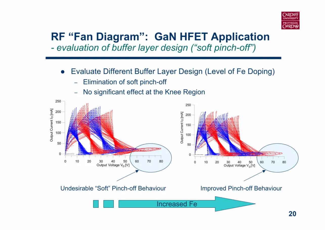
D [V]
Undesirable “Soft” Pinch-off Behaviour Improved Pinch-off Behaviour
Evaluate Different Buffer Layer Design (Level of Fe Doping)– Elimination of soft pinch-off– No significant effect at the Knee Region
RF “Fan Diagram”: GaN HFET Application- evaluation of buffer layer design (“soft pinch-off”)
Increased Fe

21
Transistor RF I-V Waveforms: GaN HFET Application– Detailed Insight into Dynamic stress/reliability Limitations
RF waveforms were periodically sampled 100 times during the 1.5hour RF stress period 1.8GHz Large-signal CW (≈ 3dB of gain compression), VD = 20V, Class A, Zf0 ≈ POUT
-20
-10
0
10
20
Input C
urr
ent IG
[m
A]
7006005004003002001000
Phase [°]
Initial Waveform
Final W aveform
-20
-10
0
10
20
Input C
urr
ent IG
[m
A]
-10 -8 -6 -4 -2 0 2 4Input Voltage VG [V]
Input Characteristics
Initial
Final
Dynamic Input Characteristics– Highlights the displacement current
through CGS– A small increase in leakage can be
seen at the breakdown end-8
-6
-4
-2
0
2
Input V
olta
ge V
G [V
]
7006005004003002001000
Phase [°]

22
Transistor RF I-V Waveforms: GaN HFET Application– Detailed Insight into Dynamic stress/reliability Limitations
Dynamic Load lines (overlaid on DC-IVs)– Useful for visualising DC-RF dispersion – a non-permanent
problem– Here the degradation is permanent suggesting a different
mechanism
300
250
200
150
100
50
0
Outp
ut C
urr
ent ID
[mA
]
403020100Output Voltage VD [V]
Initial Load Line
Pre-Stress Post-Stress
Final Load Line
250
200
150
100
50
0O
utp
ut C
urr
ent ID
[m
A]
-10 -8 -6 -4 -2 0 2 4Input Voltage VG [V]
Initial Transfer Characteristic
Final Transfer Characteristic
Dynamic Transfer Characteristics– Very little degradation until VG swings
above -3V– No change around VT ≈ -6V

23
RF Waveform Measurement and Engineering- powerful “real time” design tool
Basic Concept– Use RF Waveform Measurement and Engineering Systems to
investigated and achieve the required circuit/system performance. Key: Performance is theoretically defined in terms of the voltage
and/or current waveforms Alternatives: build and test, CAD tools (requires non-linear model)
Relevant Circuit Design Problem– Those that involve strongly non-linear (‘large signal”) device
operation, not weakly non-linear or linear operation Power Amplifier Design beyond Class A/AB Switching Amplifiers Frequency Multipliers/Dividers

24
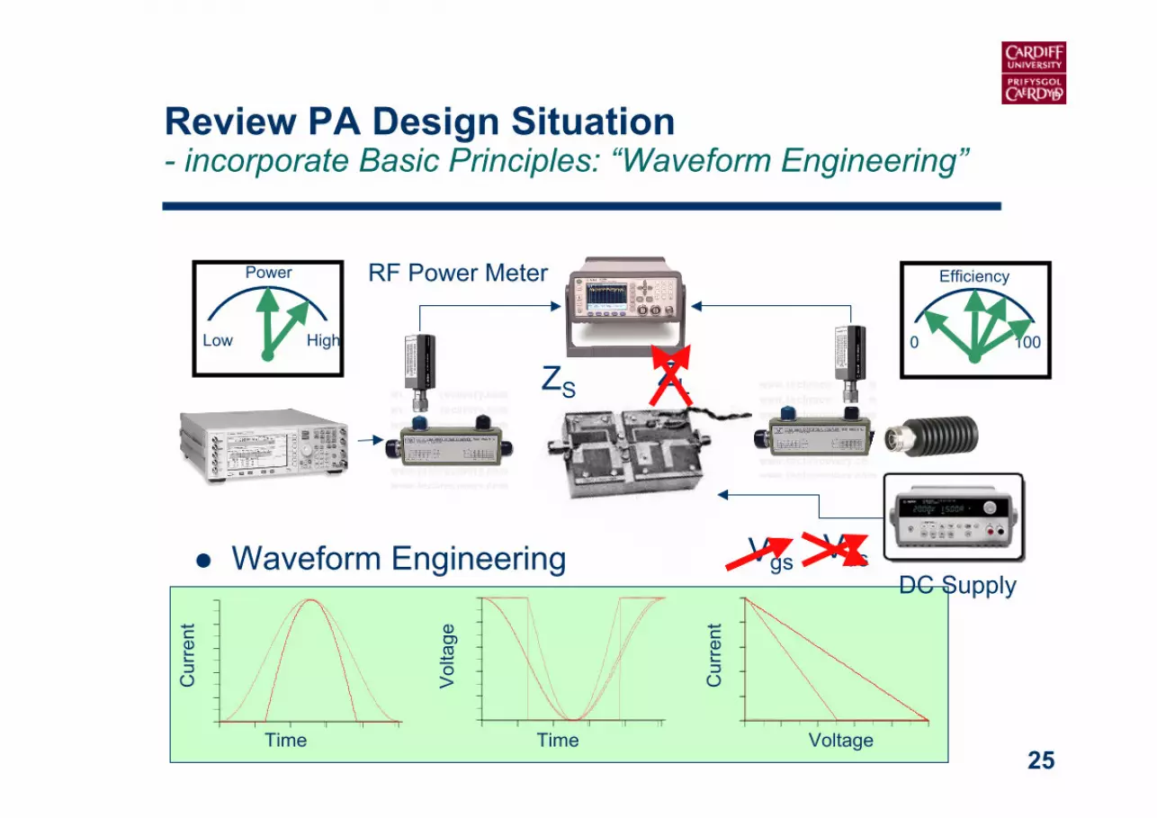
Review PA Design Situation- too reliant on Build & Test
Vgs VdsDC Supply
RF Power Meter
ZS ZL
Design Approach Experimental Data Essential
– I-V, s-parameters, load-pull contours Design Knowledge: mode of operation, class A, AB,
– Efficiency Demands: Move to more complex modes B, F, E or switching modes Build, Evaluate and Adjust
– Bias point– Load and Source impedance @ fundamental (and harmonics)
High
Power
Low 0 100
Efficiency
25
Review PA Design Situation- incorporate Basic Principles: “Waveform Engineering”
Vgs VdsDC Supply
RF Power Meter
ZS ZL
Waveform Engineering
High
Power
Low 0 100
Efficiency
Cur
rent
Vol
tage
Cur
rent
Time Time Voltage

26Design Example: Class B Amplifier Emulation/Measurement
Efficiency increasedfrom 44% to 55%
“Class B Operation”
200
150
100
50
0Col
lect
or C
urre
nt [m
A]
121086420Collector Voltage [volts]
@ 2.0 GHz12
8
4
0
Col
lect
or V
olta
ge [V
]
10008006004002000
Time [psec]
200
150
100
50
0
Collector C
urrent [mA
]
HBT biased to operate in class B, low quiescent current• Current waveform is half rectified• Voltage waveform is not sinusoidal
12
8
4
0Col
lect
or V
olta
ge [V
]
10008006004002000Time [psec]
200
150
100
50
0
Collector C
urrent [mA
]
@ 2.0 GHz
Engineer harmonic impedances: Short second/third harmonic• Current waveform is half rectified• Voltage waveform is now sinusoidal
RF I-V Waveform Engineering- insight provided by having measured waveforms

27Design Example: Class F Amplifier Emulation/Measurement
Efficiency increasedfrom 44% to 65%
“Class F Operation”
200
150
100
50
0Col
lect
or C
urre
nt [m
A]
121086420Collector Voltage [volts]
12
8
4
0Col
lect
or V
olta
ge [V
]
10008006004002000Time [psec]
200
150
100
50
0
Collector C
urrent [mA
]
@ 2.0 GHz
RF I-V Waveform Engineering- insight provided by having measured waveforms
HBT biased to operate in class B, low quiescent current• Current waveform is half rectified• Voltage waveform is not sinusoidal
Engineer harmonic impedances: Short/open second/thirdharmonic
• Current waveform is half rectified• Voltage waveform is now a square wave
@ 2.0 GHz12
8
4
0Col
lect
or V
olta
ge [V
]
10008006004002000
Time [psec]
200
150
100
50
0
Collector C
urrent [mA
]

28
RF Waveform Measurement and Engineering- “on-line” direct utilization in amplifier design cycle
Waveform Data
EngineerWaveforms and
document desiredload impedances
Output Match
CADLayout Fabricate
Direct u
tiliza
tion
Direct u
tiliza
tion
of characteriz
ation
of characteriz
ation
systemsystem
in design loop
in design loop
Relevant Circuit Design Problems– Those that involve strongly non-linear
(‘large signal”) device operation. Power Amplifier Design beyond
Class A/AB Switching Amplifiers Frequency Multipliers/Dividers Etc.
29
RF Waveform Measurement and Engineering- powerful dynamic transistor amplifier design tool
Transistor Amplifier Design: Case Study– Use RF Waveform Measurement and Engineering Systems to investigated
how to realize in practice the theoretically predicted high efficiency modesof operation
Class B, Class F or their variants

30
Design of Highly Efficient RF Power Amplifier- requires engineer of voltage and current waveforms
Simple Theoretical Understanding
Practical solution
Transistorcharacteristics
CircuitBandwidth
Advanced Theoretical Understanding
V & I engineering100
80
60
40
20
0
-207006005004003002001000
76543210
Out
put C
urre
nt [m
A] Output Voltage [V]]
Phase
100
80
60
40
20
07006005004003002001000
76543210O
utpu
t Cur
rent
[mA]
Output Voltage [V]]
Phase
Designed in an intelligent manner a classF efficient RF Power Amplifier
Maximized Output Power Realized 75% PAE
Ready for realization

31
100
80
60
40
20
0
Outp
ut C
urr
ent ID
[m
A]
7006005004003002001000
Phase [°]
7
6
5
4
3
2
1
0
Outp
ut V
olta
ge V
D [V]
100
80
60
40
20
0
Outp
ut C
urr
ent ID
[m
A]
7006005004003002001000
Phase [°]
Ideal Class F occurs if the current and voltage waveforms are simultaneouslyengineered such that:
The currentwaveform
contains f0 andcorrect
proportions ofthe even
harmonics
The voltagewaveformcontains f0 andcorrectproportions ofthe oddharmonics
If this is achieved there is no overlap between the waveforms, resultingin no dissipated power and 100% efficiency.
Design of Highly Efficient RF Power Amplifier- review of theoretical understanding: Class F

32
• The achievable efficiency in a real design is constrained by ourability to correctly engineer the ideal waveforms.
• Circuit Bandwidth• In real PA designs harmonic control is commonly limited to 2f0 and 3f0 due to the
complexity of matching circuits.
• Following the analysis of Rhodes,* for a Class F design with harmonics only up to 3f0ideally terminated, the maximum achievable efficiency is limited to an upper limit of90.6% - assuming your matching network is lossless!
!
"current = iRF 2 # IDC( )
!
"voltage = vRF 2 #VDC( )
We can quantify the ability to engineer ideal waveforms by two factorsηcurrent and ηvoltage using the DC and fundamental RF components:
* J.D. Rhodes “Output universality in maximum efficiency linear power amplifiers”International Journal of Circuit Theory and Applications, volume 31, 2003, pp.385-405
Design of Highly Efficient RF Power Amplifier- review of practical constraints: System and Circuit Bandwidth

33
100
80
60
40
20
0
Curr
ent [m
A]
7006005004003002001000
Phase [°]
1.0
0.8
0.6
0.4
0.2
0.0
Voltage [
V]
6004002000
Phase [º]
1.0
0.8
0.6
0.4
0.2
0.0
Voltage [
V]
6004002000
Phase [º]
1.0
0.8
0.6
0.4
0.2
0.0
Voltage [
V]
6004002000
Phase [º]
90.60.8161.111F (3f0)
1000.9001.111F (Ideal)
78.50.7071.111B
500.7070.707A
η = ηcurrent x ηvoltage x 100 [%]ηvoltageηcurrentClass
100
80
60
40
20
0
Curr
ent [m
A]
6004002000
Phase [º]
Design of Highly Efficient RF Power Amplifier- review of practical constraints: System and Circuit Bandwidth

34
100
80
60
40
20
0
Ou
tpu
t C
urr
en
t ID
[mA
]
1086420Output Voltage V
D [V]
Imin
Vmin
Area of IV Plane available forconversion into RF power
• A further limitation on achievable efficiency in practical designs arises fromfeatures of real transistor characteristics which make a fraction of the dcdissipated power unavailable for conversion to RF power:
Achievableefficiency isscaled by theratio ofAvailable toUnavailableIV plane Area
Design of Highly Efficient RF Power Amplifier- review of practical constraints: Transistor Limitations
!
"current = iRF 2 # IDC( )
!
"voltage = vRF 2 #VDC( )
We can quantify the ability to engineer ideal waveforms by two factorsηcurrent and ηvoltage using the DC and fundamental RF components:

35
70
60
50
40
30
20
10
0
-10
ID [m
A]
7006005004003002001000
Phase [°]
7
6
5
4
3
2
1
0
VD [V
]
Ratio = 0.170
60
50
40
30
20
10
0
-10
ID [m
A]
7006005004003002001000
Phase [°]
7
6
5
4
3
2
1
0
VD [V
]
Ratio = 1
DC average
70
60
50
40
30
20
10
0
-10
ID [m
A]
7006005004003002001000
Phase [°]
7
6
5
4
3
2
1
0
VD [V
]
Ratio = 0.870
60
50
40
30
20
10
0
-10
ID [m
A]
7006005004003002001000
Phase [°]
7
6
5
4
3
2
1
0
VD [V
]
Ratio = 0.670
60
50
40
30
20
10
0
-10
ID [m
A]
7006005004003002001000
Phase [°]
7
6
5
4
3
2
1
0
VD [V
]
Ratio = 0.470
60
50
40
30
20
10
0
-10
ID [m
A]
7006005004003002001000
Phase [°]
7
6
5
4
3
2
1
0
VD [V
]
Ratio = 0.2
-j50
-j10
-j25 -j100
-j250
10 25 50 100 2500
j50
j10
j25 j100
j250
S21
Radius=1.0 S12
Radius=1.0
2f0 f0 = Ropt
-j50
-j10
-j25 -j100
-j250
10 25 50 100 2500
j50
j10
j25 j100
j250
S21
Radius=1.0 S12
Radius=1.0
2f0 f0 = Ropt
-j50
-j10
-j25 -j100
-j250
10 25 50 100 2500
j50
j10
j25 j100
j250
S21
Radius=1.0 S12
Radius=1.0
2f0 f0 = Ropt
-j50
-j10
-j25 -j100
-j250
10 25 50 100 2500
j50
j10
j25 j100
j250
S21
Radius=1.0 S12
Radius=1.0
2f0 f0 = Ropt
-j50
-j10
-j25 -j100
-j250
10 25 50 100 2500
j50
j10
j25 j100
j250
S21
Radius=1.0 S12
Radius=1.0
2f0 f0 = Ropt
60
55
50
45
40
Effic
iency [%
]
1.00.80.60.40.20.0
Harmonic Termination Ratio
• Starting with Class B bias for a half rectified current waveform, what is theeffect of tuning the second harmonic to a short?
-j50
-j10
-j25 -j100
-j250
10 25 50 100 2500
j50
j10
j25 j100
j250
S21
Radius=1.0 S12
Radius=1.0
2f0 f0 = Ropt
60
55
50
45
40
Effic
iency [%
]
1.00.80.60.40.20.0
Harmonic Termination Ratio
60
55
50
45
40
Effic
iency [%
]
1.00.80.60.40.20.0
Harmonic Termination Ratio
60
55
50
45
40
Effic
iency [%
]
1.00.80.60.40.20.0
Harmonic Termination Ratio
60
55
50
45
40
Effic
iency [%
]
1.00.80.60.40.20.0
Harmonic Termination Ratio
60
55
50
45
40
Effic
iency [%
]
1.00.80.60.40.20.0
Harmonic Termination Ratio
Eliminated 2nd harmonic fromvoltage waveform
Harmonic Termination Ratio:Z @ 2f0 normalised by Z @ f0
Design of Highly Efficient RF Power Amplifier- review of practical constraints: Impedance Scaling

36
Good short circuits harder to achieverelative to a Small Ropt
Makes high efficiency harder toachieve in large devices
Possible solution - include numerousshort circuits integrated onto the die toallow subsets of transistor cells to begiven a better short…
Packaging parasitics can form a filterblocking higher harmonics…
60
55
50
45
40
Effic
iency [%
]
1.00.80.60.40.20.0
Harmonic Termination Ratio
Harmonic Termination Ratio:Z @ 2f0 normalised by Z @ f0
Design of Highly Efficient RF Power Amplifier- review of practical constraints: Impedance Scaling

37
Need to select a suitable drive level for harmonicgeneration (approaching P1dB)
Ideally we need to ensure we have separated theharmonics:– only odds in the voltage waveform– only evens in the current waveform
…but will the practical device allow this!
Design of Highly Efficient RF Power Amplifier- review of practical constraints: Transistor Transfer Characteristic

38
50
40
30
20
10
0
Fundam
enta
l dc a
nd 2
nd [m
A]
-1.0 -0.8 -0.6 -0.4 -0.2 0.0
Gate Bias [V]
5
4
3
2
1
0
Oth
er H
arm
onic
s [m
A]
dc f0 2f
0 3f
0 4f
0 5f
0
• Practical constraints:• Other harmonics are not zero
• Optimum bias is a function of voltage waveform “shape” and RF drive level
Engineering The Current Waveform– Gate bias control to null the odd harmonics
Optimumbias atVG=-0.7Vto null 3f0
• In class F optimum performance will only occur if the most significant oddharmonics (usually only consider 3f0) are not present in the current waveform.
• Using Fourier analysis of the measured current waveforms we can locate thisoptimal case…
Odd harmonicnulls do not occursimultaneously

39
• Engineering the voltage waveform to a square wave involves tuning the 3rd
harmonic to an open and increasing the fundamental load to maintain thesame current swing.
• Note, the optimum Class F behaviour will only occur if the current at 3f0remains null.
Engineering The Voltage Waveform- Open tuned 3rd harmonic gate bias sweep
1.0
0.8
0.6
0.4
0.2
0.0
Ra
tio
-1.5 -1.4 -1.3 -1.2 -1.1 -1.0 -0.9 -0.8 -0.7 -0.6 -0.5 -0.4
Gate Bias [V]
100
80
60
40
20
0
Efficie
ncy [%
] PO
UT [W
]
Ratio = 0.224
Ratio Efficiency POUT
1.0
0.8
0.6
0.4
0.2
0.0
Ra
tio
-1.5 -1.4 -1.3 -1.2 -1.1 -1.0 -0.9 -0.8 -0.7 -0.6 -0.5 -0.4
Gate Bias [V]
100
80
60
40
20
0
Efficie
ncy [%
] PO
UT [W
]
Ratio = 0.224
Ratio Efficiency POUT
1.0
0.8
0.6
0.4
0.2
0.0
Ra
tio
-1.5 -1.4 -1.3 -1.2 -1.1 -1.0 -0.9 -0.8 -0.7 -0.6 -0.5 -0.4
Gate Bias [V]
100
80
60
40
20
0
Efficie
ncy [%
] PO
UT [W
]
Ratio = 0.224
Ratio Efficiency POUT
1.0
0.8
0.6
0.4
0.2
0.0
Ra
tio
-1.5 -1.4 -1.3 -1.2 -1.1 -1.0 -0.9 -0.8 -0.7 -0.6 -0.5 -0.4
Gate Bias [V]
100
80
60
40
20
0
Efficie
ncy [%
] PO
UT [W
]
Ratio = 0.224
Ratio Efficiency POUT 100
80
60
40
20
0
-20
ID [m
A]
7006005004003002001000
Phase [°]
7
6
5
4
3
2
1
0
VD[V
]
100
80
60
40
20
0
-20
ID [m
A]
7006005004003002001000
Phase [°]
7
6
5
4
3
2
1
0
VD[V
]
100
80
60
40
20
0
-20
ID [m
A]
7006005004003002001000
Phase [°]
7
6
5
4
3
2
1
0
VD[V
]
100
80
60
40
20
0
-20
ID [m
A]
7006005004003002001000
Phase [°]
7
6
5
4
3
2
1
0
VD[V
]• Since Class F requires an open termination at 3f0, it is impossible to verify this
condition has been met by direct measurement of the 3f0 harmonic current.- Consider v3rd/vfund ratio. Theory predicts 1/6 (=0.167)

40
1.0
0.8
0.6
0.4
0.2
0.0
Voltage [
V]
6004002000
Phase [º]
1.0
0.8
0.6
0.4
0.2
0.0
Voltage [
V]
6004002000
Phase [º]
• Plotting the dynamic load-line for thefinal design shows the interaction ofthe waveforms with the knee region.
• The final experimentallyengineered “class F” waveformsachieved a drain efficiency valueof 75%,
• This is extremely high given theboundary conditions and drainbias of the real device used.
• Ideal square wave requires allharmonics – we only control the first 3
1.0
0.8
0.6
0.4
0.2
0.0
Voltage [
V]
6004002000
Phase [º]
• Optimal 3 harmonic only voltagewaveform has a v3rd/vfund ratio of 1/6 if theboundary conditions are ideal (vertical)• However due to the finite on-resistanceof the real knee boundary the optimalratio is higher, at almost 1/4
Engineering The Voltage Waveform- Why was extra third harmonic developed?

41
50
40
30
20
10
0
Fund
amen
tal d
c an
d 2n
d [m
A]
-1.0 -0.8 -0.6 -0.4 -0.2 0.0
Gate Bias [V]
5
4
3
2
1
0
Other H
armonics [m
A]
dc f0 2f
0 3f
0 4f
0 5f
0
RF Waveform Measurement and Engineering- “on-line” direct utilization in amplifier design cycle
Simple Theoretical Understanding: Provides If not How and Why
Simple bias requirement
developing theoretically based but practically relevant waveformengineering design methodologies
Transistorcharacteristics
CircuitBandwidth
2nd Harmonicshort circuit
Advanced Theoretical Understanding: Must provide How and Why
3rd
harmonic:open
circuit“relaxation”
revise bias requirement
706050403020100
-10
ID [m
A]
7006005004003002001000Phase [。]
76543210
VD [V
]
Ratio = 0.6
I engineering
706050403020100
-10
ID [m
A]
7006005004003002001000Phase [。]
76543210
VD [V
]
Ratio = 0.1
V engineering
100
80
60
40
20
0
Out
put C
urre
nt I
D [m
A]
7006005004003002001000Phase [。]
76543210
Output V
oltage V D [V]

42
High Power Class F Design
5W Si LDMOS @ 900 MHz
Class F clearly achieved High Power 36.0 dBm (4W) High Efficiency 77.2%
5W Si LDMOS @ 2100 MHz
Class F clearly achieved High Power 35.9 dBm (4W) High Efficiency 77.1%
Engineered and Measured Intrinsic Waveforms: Design Aid
800
600
400
200
0
Cur
rent
(mA)
8006004002000time (ps)
60
50
40
30
20
10
0
Voltage (V)
800
600
400
200
0
Cur
rent
(mA
)
2000150010005000time (ps)
60
50
40
30
20
10
0
Voltage (V
)
Apply Waveform Design Methodology- 5W Si LDMOS into Class F Emulation/Design

43
Apply Waveform Design Methodology- 10W GaN HFET & 5W Si LDMOS into Inverse Class F
5W Si LDMOS @ 900 MHz
Inverse Class F clearly achieved High Power 37.3 dBm (5.4W) High Efficiency 73%
0.8
0.6
0.4
0.2
0
Cur
rent
(A)
2.01.51.00.50Time (ns)
80
60
40
20
0
Voltage (V)
0.5 1.0 1.5 2.00.0
10203040506070
0
80
0.00.20.40.60.81.0
-0.2
1.2
Time (ns)
Cur
rent
(A) Voltage (V)
10W GaN HFET @ 900 MHz
Inverse Class F clearly achieved High Power 40.8 dBm (12W) High Efficiency 81.5%
Engineered and Measured Intrinsic Waveforms: Design Aid

44
• ‘Right first time’ waveform based designthrough the realisation of a high-performance inverse class-F PA
• Impressive efficiency of 81% at high outputpowers
• High Power achieving 12W form a 10Wdevice
.
12W Inverse class-F Amplifier Realisation– right first time design using CREE 10W device
First P
ass Design
First P
ass Design
Success
Success

45
RF Waveform Measurement and Engineering- powerful dynamic transistor amplifier design tool
Investigation of “New Design Space”– Use RF Waveform Measurement and Engineering Systems to stimulate
new theoretically investigations in alternative high efficiency modes ofoperation
– Move beyond the discrete design point thinking to design continuumthinking
– The Class B to Class J Continuum New Theory Improved Bandwidth

46-1.0
-0.5
0.0
0.5
1.0
-1.0 -0.5 0.0 0.5 1.0
RF Waveform Measurement and Engineering- provides for new theoretical insight
Consider the Class B and Class J Mode ofoperation
– Both have a half rectified current waveform– Both have the same theoretical power and
efficiency values– But have very different voltages waveforms
Different fundamental and 2nd harmonicreactance’s
3.0
2.0
1.0
0.0
No
rma
lize
d V
olta
ge
720630540450360270180900
Phase
Normalised Class B voltage waveform
3.0
2.0
1.0
0.0
No
rma
lize
d V
olta
ge
720630540450360270180900
Phase
Normalised Class J voltage waveform
* J.D. Rhodes “Output universality in maximum efficiency linear power amplifiers”International Journal of Circuit Theory and Applications, volume 31, 2003, pp.385-405
Are these not just different solutions of thesame mode?
– Rhodes* provide some mathematical insight Optimum fundamental reactance is mathematical
defined by harmonic reactive terminations
FundamentalImpedance
2nd harmonicImpedance

47-1.0
-0.5
0.0
0.5
1.0
-1.0 -0.5 0.0 0.5 1.0
RF Waveform Measurement and Engineering- provides for new theoretical insight
They are just different solutions of the samemode?
– The Class J - Class B - Class J* Continuum
– Many more possible solutions
3.0
2.0
1.0
0.0
No
rma
lize
d V
olta
ge
720630540450360270180900
Phase
Normalised Class J voltage waveform
α = 1
3.0
2.0
1.0
0.0
No
rma
lize
d V
olta
ge
720630540450360270180900
Phase
Normalised Class B voltage waveform
α = 0
3.0
2.0
1.0
0.0
No
rma
lize
d V
olta
ge
720630540450360270180900
Phase
Normalised Class J voltage waveform
α = -1

48
80
60
40
20
0
Dra
in V
olta
ge
(V
)
2000150010005000
Normalised Time (samples)
RF Output Voltage ! = -1.05 (Class-J*)
! = -0.85
! = -0.75
! = -0.65
! = 0 (Class-B)
! = 0.65
! = 0.75
! = 0.85 (~Class-J)
80
60
40
20
0
Dra
in V
olta
ge
(V
)
10008006004002000
Normalised Time (samples)
RF Output Voltage500
400
300
200
100
0
Dra
in C
urr
en
t (m
A)
10008006004002000
Normalised Time (samples)
RF Output Current
On Cree 2W on-wafer device:• Maintain constant Pin to device• Vary Z(f0) = Ropt + j k Ropt
• Vary Z(f2) = - j k Ropt -1 ≤ k ≤ 1
α = X1/R1 = -X2/R1
RF Waveform Measurement and Engineering- experimental validation of new theoretical insight

49 Increased design flexibility
-100
-50
0
50
100
X2 (
j !)
-80 -60 -40 -20 0 20X
1 (j!)
58
56
56
54
52
52
52
50
50
48
46
46
46
4
4
42
On Cree 2W on-wafer device:• R1 held to Ropt, R2 held to 1.5Ω• X1 and X2 were swept to
examine the impact of thedeviation off the Class-JBcontinuum contour
Results• Class-JB continuum visually
identifiable with a high efficiencycontour
• Roll-off of efficiency is greater for adeviation in fundamental loadcompared to second harmonic
RF Waveform Measurement and Engineering- Class J-B-J* Continuum Sensitivity Analysis

50
Class-J output matching schematic:
– Compromises need to be made/considered across this size of bandwidth.
– Fundamental load impedance matching given priority.
– Second harmonic already close to optimum class-J reactance at centre frequency ofdesired bandwidth as a result of output capacitance Cds Z2f0 allowed more latitude during the design.
– Shunt shorted-stub increases the effective capacitive reactance of second harmonicload at lower frequencies.
Realising Class-J Matching
DUT+output
parasitics
DC biasfeed PA
Output
Cds
(0.000 to 0.000)
output_deembed_gamma[3]
output_deembed_gamma[2]
output_deembed_gamma[1]
(0.000 to 0.000)
output_deembed_gamma[3]
output_deembed_gamma[2]
output_deembed_gamma[1]
Z2f0
Zf0

51
80
70
60
50
40
30
Dra
in E
ffic
ien
cy /
%
2.52.42.32.22.12.01.91.81.71.61.51.41.31.2
Frequency / GHz
80
70
60
50
40
30
Dra
in E
fficie
ncy / %
Realised PA Drain Efficiency80
70
60
50
40
30
Dra
in E
ffic
ien
cy /
%
2.52.42.32.22.12.01.91.81.71.61.51.41.31.2
Frequency / GHz
80
70
60
50
40
30
Dra
in E
fficie
ncy / %
Realised PA Drain Efficiency
Model-Predicted Efficiency
Device Efficiency, Under Load-Pull
60%+ efficiency between1.35 and 2.25GHz
Performance of PA Prototype (1st it.)
The PA shows a measured 60%-and-above drain efficiency across thefrequency range 1.35-2.25GHz.
Drain efficiency measured for PA, model simulation and load-pullemulation.
Closely agreeing results with the load-pull emulation. Output power across this same bandwidth is 9-11Watts (device-rated power).
Proposed bandwidth not met entirely, but still a 50% bandwidth PA achieved.

52
Second design iteration extending high-efficiency operation across theoriginally intended PA bandwidth of 1.5-2.5GHz
Input matched PA Resulting gain and PAE profiles
80
70
60
50
40
30
Dra
in E
ffic
ien
cy /
%
2.72.62.52.42.32.22.12.01.91.81.71.61.51.41.3
Frequency / GHz
80
70
60
50
40
30
Dra
in E
fficie
ncy / %
1st Design Iteration
2nd Design Iteration
Performance of PA Prototype (2nd it.)
70
60
50
40
30
20
10
0
Eff
icie
ncy,
PA
E,
Po
ut,
Ga
in /
%,
%,
dB
m,
dB
2.72.62.52.42.32.22.12.01.91.81.71.61.51.4
Frequency / GHz
70
60
50
40
30
20
10
0
Effic
ien
cy, P
AE
, Po
ut, G
ain
/ %, %
, dB
m, d
B
10dB minimum gain
More than 50% PAE
Efficiency improvement withsecond design

53
RF Waveform Measurements and Engineering – a powerful tool and concept
Device Technology System ApplicationCircuit Design/Emulation
Waveform are the unifying link between device technology,circuit design and system performance
Analysis Tool
Doherty PA
Circuit EmulationDesign/Evaluation
Tool
Design/CADTool
load-pull