on supporting rapid exploration of memory hierarchies onto fpgas
TRANSCRIPT
Journal of Systems Architecture 59 (2013) 78–90
Contents lists available at SciVerse ScienceDirect
Journal of Systems Architecture
journal homepage: www.elsevier .com/locate /sysarc
On supporting rapid exploration of memory hierarchies onto FPGAs
Harry Sidiropoulos, Kostas Siozios ⇑, Dimitrios Soudris9 Heroon Polytechneiou, Zographou Campus, 15780 Athens, Greece
a r t i c l e i n f o
Article history:Available online 21 November 2012
Keywords:Heterogeneous FPGACAD toolExploration framework
1383-7621/$ - see front matter � 2012 Elsevier B.V. Ahttp://dx.doi.org/10.1016/j.sysarc.2012.10.003
⇑ Corresponding author. Tel.: +30 210 772 3653.E-mail address: [email protected] (K. Siozios
a b s t r a c t
This paper introduces a novel methodology for enabling fast yet accurate exploration of memoryorganizations onto FPGA devices. The proposed methodology is software supported by a newopen-source tool framework, named NAROUTO. This framework is the only public available solutionfor performing architecture-level exploration, as well as application mapping onto FPGA devices withdifferent memory organizations, under a variety of design criteria (e.g. delay improvement, poweroptimization, area savings, etc.). Experimental results with a number of industrial oriented kernels provethe efficiency of the proposed solution, as compared to similar approaches, since it provides bettermanipulation of memory blocks, leading to architectures with higher performance in terms of area,power and delay.
� 2012 Elsevier B.V. All rights reserved.
1. Introduction level exploration for homogeneous FPGAs (i.e. devices consisted so-
Recent years, reconfigurable architectures and more specificallyField Programmable Gate Arrays (FPGAs) have become efficientalternatives to Application Specific Integrated Circuits (ASICs).The characteristics and capabilities of these architectures havechanged and improved significantly the last two decades, fromarrays of Look-Up Tables (LUTs), to heterogeneous devices thatintegrate a number of hardware components (e.g. LUTs with differ-ent sizes, microprocessors, DSP modules, RAM blocks, etc.). In otherwords, the logic fabric of an FPGA changed gradually from ahomogeneous and regular architecture to a heterogeneous (orpiece-wise homogeneous) device.
Previous studies [12–14] show that one of the upmost impor-tant tasks for designing an efficient FPGA device is the architec-ture-level exploration. This task among others determines thenumber, the organization (i.e. floor-plan), as well as the parametersfor the device components (e.g. look-up table size, channel width,array size, etc.). Note that the problem of sufficient and accuratearchitecture-level exploration becomes far more important nowa-days, due to the increased complexity posed by heterogeneous IPblocks found in FPGA platforms.
In order to accomplish this task, a number of methodologies andComputer-Aided Design (CAD) tools have been proposed. Thesesolutions involve among others synthesis and technology mapping[1,2], placement and routing (P&R) [3,13], as well as power andenergy estimation [6] techniques.
The development of new tools targeting the reconfigurable do-main is tackled both by academia and industry. More specifically,tools developed in academia have mainly focused on architecture-
ll rights reserved.
).
lely from configurable logic blocks (CLBs)). Even though these solu-tions are sufficient for evaluating new CAD algorithms, they cannothandle additional Intellectual Property (IP) blocks (e.g. memories,DSPs, embedded CPUs, etc.) found in reconfigurable architectures.On the other hand, commercial frameworks support FPGA deviceswith numerous heterogeneous IP blocks, but unfortunately they al-low only a small degree of architecture-level exploration.
Recently, two frameworks, one from academia and the otherfrom industry, were released that provide some kind of flexibilityin performing architecture-level exploration for heterogeneousFPGAs. These frameworks are based on a commercial synthesizer,Altera’s Quartus [7], while the P&R step is performed with algo-rithms found in VPR tool [3]. Even though the combination of thesetwo solutions potentially can alleviate the limitation about hetero-geneity support, the derived results lack accuracy. In addition, theapplication’s implementation could not be evaluated in terms ofpower and energy dissipation. Since FPGAs are usually powerlimited devices [4,5,15], this limitation is a crucial drawback forscoring the efficiency of retrieved architectural solutions.
In this paper we propose a new framework for supporting thetasks of architecture-level exploration and application mappingonto heterogeneous FPGAs. The proposed framework, named NARO-UTO, is based on a number of open source tools. This flow is publiclyavailable for downloading, extending and improving [8], in order tosupport more advanced heterogeneous blocks (e.g. CPUs) [14,21].
The contributions of this work, as compared to prior publica-tions are summarized as follows:
� Introduction of a novel software-supported methodology forenabling rapid architecture-level exploration for heterogeneousFPGAs that consist of different memory organizations and/orhierarchies.

H. Sidiropoulos et al. / Journal of Systems Architecture 59 (2013) 78–90 79
� Development of a new tool framework that enables applicationmapping onto these heterogeneous FPGAs.� Rather than similar frameworks that support only one type of
heterogeneous block (e.g. memory of a given size), our solutionexhibits additional flexibility, enabling among others simulta-neous handling of heterogeneous blocks with different typesand/or properties.� Apart from the delay metric, the evaluation of application
implementations onto a target heterogeneous FPGA can alsobe performed in terms of power and energy dissipation (bothstatic and dynamic).
The rest of the paper is organized as follows: Section 2 high-lights the main limitations found in similar approaches targetingarchitecture-level exploration, whereas Section 3 gives an over-view of the employed heterogeneous FPGA. The proposed method-ology, as well as the supporting tool framework are described inSections 4 and 5, respectively. Section 6 provides a number of qual-itative and quantitative comparisons that prove the efficiency ofthe proposed solution, as compared to the state-of-art approach.Finally, conclusions are summarized in Section 7.
2. Motivation example
A common limitation found to existing software frameworksthat perform architecture-level exploration affects that none ofthem can handle macro-blocks, apart from logic resources (slices)and interconnect fabric. On the other hand, commercial tools arenot easily adapted to evaluate reconfigurable architectures thatdiffer from the actually fabricated devices. Additionally, since thesesolutions are based exclusively with academic tools, usually theyare evaluated with the usage of synthetic benchmarks (as availableacademic synthesizers are able to tackle only designs with reducedcomplexity). Hence, there is a limitation of software-supportedtools that are able to perform fast and accurate evaluation of differ-ent architectural selections. This section highlights the main limi-tations found in existing tools for supporting architecture-levelexploration, as well as application mapping onto FPGAs consistingof heterogeneous blocks.
Starting from an application’s description in VHDL or Verilogformat, first of all we perform synthesis with the usage of AlteraQuartus Framework [7], whereas the output is reported at BLIF(Berkeley Logic Interchange Format) format [9]. This format corre-sponds to a gate-level netlist with basic primitives for input, out-put, logic gates, flip/flops, etc. Even though BLIF is a widelyaccepted format for academic tools, it is rather restrictive, as it isunable to express heterogeneous components, such as RAM blocks,DSP blocks (e.g. multiplier), processors, etc. Furthermore, it cannotexpress arithmetic carry chains without converting them to gates.
Instead of these components, the BLIF netlist uses ‘‘BlackBoxes’’(BBs) to enable transparent signal propagation. However, since BBsdo not have any meaningful functionality, the derived netlist lacksin accuracy. Additionally, as we will depict later, existing toolsprovide a non-optimal way for handling designs with BBs.
Next, we summarize the main drawbacks of existing (academic/commercial) software solutions:
� The application’s functionality described at BLIF netlist differsfrom the application’s RTL description, since the BBs do not pro-vide any functionality.� For a given design, all the BBs are marked with the same key-
word (‘‘.blackbox’’), regardless of their actual functionality. Thisimposes that each design can employ only one type of BB (e.g.only memory, DSP, or embedded CPU).
� Additionally, all these BBs are assumed to have the same prop-erties (e.g. size, throughput, power/energy consumption, etc.),regardless of their usage.� In case the design incorporates BlockRAMs, the usage of existing
tools (Quartus and VPR-5.0) assumes an excessive number ofdistinct BBs, each of which corresponds to a few memory’swords which are part of a whole memory block.� This overestimation in number of BBs results to mentionable
delay, power and area overheads due to the additional routingresources needed for signal communication.� Finally, existing approaches cannot support the evaluation of
architectural selections based on different memory organiza-tions and/or hierarchies.
3. Target architecture
Our target architecture is a generic FPGA device similar to re-cent FPGAs from Altera (Stratix) [10] and Xilinx (Virtex) [11] archi-tectures, consisting of logic resources, memory blocks, specialpurpose components (e.g. embedded processor, DPS blocks, etc.)and input/output pads. The glue logic of our FPGA device is orga-nized into an array of slices, while the communication amonghardware blocks is provided through a hierarchical interconnec-tion network of fast and versatile routing resources. By the termslice we refer to the CLB, the up and right routing segments, as wellas the corresponding switch box. The next level of hierarchy as-sumes that each CLB is formed by a number of Basic Logic Elements(BLEs), while each of the BLEs is formed by a Look-Up Table (LUT), aflip/flop, a number of multiplexers (at inputs and outputs), as wellas the required wires for local connectivity. Such an architecturalarrangement allows local interconnects between BLEs to be opti-mized [13]. Fig. 1 depicts a template of the employed architecturewith embedded Ram and DSP blocks [12].
The previously mentioned architecture parameters for CLBs dif-fer among vendors and FPGA families, since their values affect thedevice performance and power/energy consumption. For instance,the Altera Stratix FPGAs group 10 BLEs in order to form a LogicArray Block (LAB) [10]. Similarly, regarding the Xilinx Virtex-II-Pro devices, 2 LUTs are contained in a BLE, while 4 BLEs are joinedto form a slice [11].
Apart from the logic and routing infrastructure, our FPGA archi-tecture incorporates also a number of heterogeneous blocks.Throughout this paper, we employ this feature in order to studythe impact of different memory hierarchies. More specifically,two different approaches, depicted in Figs. 2 and 3, are evaluatedwith our software-supported framework. These memory hierar-chies are summarized as follows:
� ‘‘Scenario 1’’, depicted schematically in Fig. 2, affects the sharedmemory architecture. Typically this memory organizationassumes a large block of RAM which is accessible by several dif-ferent CLBs. Even though application mapping onto a devicethat provides such a memory hierarchy is a relatively easy task,however, a number of limitations might arise when multipleCLBs need fast access to memory. Additionally, an architecturewith shared memory cannot scale very well.� ‘‘Scenario 2’’ affects the shared-distributed memory architec-
ture. This approach, depicted schematically in Fig. 3, apart froma number of shared memories (as discussed previously), incor-porates a mechanism that supports each CLB to have directaccess to a private (dedicated) memory. The key advantage ofshared-distributed memory is the unified address space inwhich all data can be found. Additionally, this memory hierar-chy is more easily scaled with an application’s requirements.

Fig. 1. Template of the employed heterogeneous FPGA device.
Fig. 2. An instantiation of the shared memory architecture (denoted as scenario 1).
80 H. Sidiropoulos et al. / Journal of Systems Architecture 59 (2013) 78–90
For both data-memory architecture models, a shared back-ground (usually off-chip) memory module is assumed. Throughoutthis paper, we do not study issues related to how data are mappedonto these memories, since this task is tackled by the synthesis andtechnology mapping tools. Also, for both hierarchies we assumethat shared memories may be simultaneously accessed by multipleCLBs. In order to physically implement these hierarchies, a numberof special purpose routing tracks that provide signal connectivityamong memory blocks, are employed. Note that the performancemetrics (e.g. delay and power/energy consumption) of these dedi-cated routing paths are taken into consideration during the appli-cation mapping.
Even though our framework can handle any memory hierarchy,if it is appropriately modeled, throughout this paper we select to
study these two scenarios because they are widely accepted inthe computer architecture field.
4. Proposed methodology
This section describes in detail the proposed methodology forperforming architecture-level exploration to heterogeneous FPGAs.More specifically, the introduced methodology, depicted schemat-ically in Fig. 4, studies two complementary design problems: prob-lem (1) the architecture-level exploration in order to determine anumber of architectural parameters that affect heterogeneouscomponents and problem (2) the application implementation ontothese heterogeneous FPGA devices. Even though this methodology

Fig. 3. An instantiation of the shared-distributed memory architecture (denoted as scenario 2).
H. Sidiropoulos et al. / Journal of Systems Architecture 59 (2013) 78–90 81
is able to handle devices consisting of different types of heteroge-neous blocks, throughout this paper we evaluate only its efficiencyin terms of handling architectures with alternative memory orga-nizations. In this case, the heterogeneity affects the properties ofthese memory blocks (e.g. size, delay, power/energy consumption,etc).
As input to our methodology we use the application’s descrip-tion in VHDL or Verilog, which is synthesized and technology
Fig. 4. The proposed
mapped, while the output is extracted in BLIF format. We have al-ready mentioned that BLIF format exhibits limited support for de-signs with heterogeneous components. Hence, in order to preservethe functionality of the design, the derived netlist has to be appro-priately modified. However, before applying such modification, it iscrucial to perform application profiling in order to determine thedifferent types of Black-Boxes (BBs) found in the design (e.g. mem-ories with different properties), as well as the number of instanti-
methodology.

82 H. Sidiropoulos et al. / Journal of Systems Architecture 59 (2013) 78–90
ations per BB (each of which has different properties). The profilingtask becomes even more important because a single heterogeneousblock is usually reported as multiple BBs from the synthesis andtechnology mapping tools.
Next, the architecture selection picks from the component li-brary the appropriate instances for BBs. During this task, the effi-ciency of multiple components per functionality (e.g. memorieswith different properties), or the organization of these components(e.g. memory hierarchies), can be evaluated. For additional accu-racy, the delay, power/energy dissipation and silicon area charac-terization of heterogeneous blocks found in these libraries arebased on a number of well-established models [18–20]. By appro-priately selecting combinations among these BBs, it is possible toperform a sufficient architecture-level exploration in terms of thenumber of BBs, as well as their organization. The outcome fromthis task is a set of Pareto curves that balance the studied criteria.Based on these curves, an architect is able to design an optimizedFPGA device.
Then, an application’s netlist is placed and routed (P&R) ontothe selected FPGA. The output of this task provides a number ofmetrics (e.g. delay, power, area) that allow sufficient evaluationof an application’s implementation. In case the derived solutiondoes not meet system specifications, there is a feedback loop foradditional improvements. More specifically, if we are primarilyinterest to find out the optimal organization of hardware resources,or BBs, over an FPGA (referred as ‘‘Problem i’’), the feedback loopaffects the architectural selections. During this step, differenttopologies and/or instantiations of BBs (e.g. memory blocks withdifferent organization) are selected. On the other hand, wheneverour goal is to maximize the performance metrics by enabling amore effective application implementation (Problem ii), then thefeedback loop goes to the P&R step.
5. The proposed NAROUTO framework
This section introduces the NAROUTO framework [14], whichsoftware supports the proposed architecture-level explorationmethodology for heterogeneous FPGA devices. This framework, de-picted schematically in Fig. 5, is composed by a number of open-source CAD tools that either have been developed from scratch,or have been extensively modified to be aware of the additionalfunctionality required for sufficient handling of designs with mul-tiple BBs. Even though the NAROUTO framework supports devicesconsisting of different types of heterogeneous components,throughout this study, the BBs are tuned to represent BlockRAMs.For this scope, two candidate memory hierarchies are evaluated(described in Figs. 2 and 3).
5.1. Synthesis and technology mapping
The first task of the NAROUTO framework deals with applica-tion synthesis and technology mapping. Even though a numberof academic tools (e.g. ABC [1], SIS [2]) could be employed, we pre-fer to accomplish it with a well-established commercial tool. Forthis purpose, the Altera Quartus tool [7] is employed, since its out-put (hierarchical netlist in BLIF format) is complementary to theacademic tools. Note that the BLIF format is a pre-requisite forthe majority of academic tools dealing with FPGAs.
In order to enable Quartus to report the output in BLIF format,where the heterogeneous components are replaced with BBs, thefollowing TCL command is applied:
set_global_assignment -name INI_VARS ‘‘no_add_ops = on;dump_blif_after_lut_map = on’’A limitation of the derived output affects the excessive high
number of BBs found in the BLIF netlist, which does not correspond
to the actual number of utilized macro blocks. To make mattersworse, there is no justification between BBs belonging to differentheterogeneous blocks (e.g. memory contents that are stored in dif-ferent BlockRAMs). Hence, the tools from the NAROUTO frameworkthat are described in this section provide a mechanism to alleviatethis limitation.
5.2. Activity estimation
The next step in our framework involves the generation ofactivity files for power/energy estimation. For this purpose, a num-ber of well-established models are employed [6,18–20]. Addition-ally, since existing versions of the ACE tool [6] cannot support BLIFnetlists with BB (s), a special pre-processing step that deals withthe computation of static probabilities and transition densitiesfrom primary inputs to primary outputs for all the networks ofthe design that include at least one BB, has been introduced.
The new tool, named Hb_for_ACE, initially removes all the BBsfrom the BLIF netlist, and then it connects the BB input and outputpins to the BLIF’s primary outputs and primary inputs, respectively.By applying this technique, it is feasible to remove from the designdescription all the BB (s), and hence enable the ACE 2.0 tool to besufficiently applied. On the other hand, regarding networks that in-clude at least one BB, the corresponding values of static probabilityand transition density are retrieved from an exhaustive simulation.
Algorithm 1 provides the pseudo-code for the open-sourceHB_for_ACE (transform Hierarchical Blifs for ACE) tool:
Algorithm 1. Pseudo-code for HB_for_ACE tool.
function hb_for_ace (Input_blif) {
// Input: blif netlist with BBs// Output: blif netlist compatible with ACE
BB_inputs[ ];// Array for storing all BBs input pinsBB_outputs[ ];// Array for storing all BBs output pinsprimary_inputs[ ];// Array for storing primary inputpinsprimary_outputs[ ];// Array for storing primary outputpins// Get the primary I/O pins of the design
primary_inputs[ ] = get_primary_inputs(Input_blif);primary_outputs[ ] = get_primary_outputs(Input_blif);// Get the blackboxes’ I/O pins
BB_inputs[ ] = get_blackbox_inputs (Input_blif);BB_outputs[ ] = get_blackbox_outputs(Input_blif);// Delete any reference to blackboxes from the
blif netlist
delete_blackbox_subcircuits (Input_blif);delete_blackbox_models (Input_blif);// Connect the BBs I/Os to the design’s primary O/I
pins
append (primary_inputs[ ], BB_outputs[ ]);
append (primary_outputs[ ], BB_inputs[ ]);
// Print the ACE compatible blif netlist
printout_final_blif (Output_blif_filename);}
5.3. Technology mapping onto heterogeneous FPGAs
Having as input the application’s BLIF description that includesalso information about the BBs, the next task in our methodology

Fig. 5. The proposed NAROUTO framework.
H. Sidiropoulos et al. / Journal of Systems Architecture 59 (2013) 78–90 83
deals with the packaging of technology mapped cells on logicblocks (CLBs). The size of derived clusters depends on the under-line FPGA architecture. This task is supported with a set of CADtools, which are based on T-VPack [3,13]. These tools were appro-priately extended in order to be aware of multiple types of BBs,each of which might have different properties. Additionally, thesetools alleviate the limitation of Quartus synthesizer in effectivelyhandling netlists with BBs.
Upcoming subsections describe in more detail the tools devel-oped to support the technology mapping onto heterogeneous FPGA.
5.3.1. BlackBox profilerThe BlackBox_Profiler parses the application description in
order to identify different types of BBs, as well as how many in-stances of each of them are utilized for application implementa-tion. Part of this procedure also deals with appropriate modeling

84 H. Sidiropoulos et al. / Journal of Systems Architecture 59 (2013) 78–90
of these BBs, in order to better meet the specifications of heteroge-neous components that it actually replaces. Typical examples ofthese specifications are the functionality of heterogeneous compo-nents (e.g. memory, DSP, etc.), its size, as well as the number of I/Opins. In order to retrieve these properties, we parse the applicationnetlist to identify all the partial BBs that belong to a single macroblock. This task is feasible to be accomplished since all these partialBBs use the same signals (e.g. the read/write enable inputs of aRAM) for control and communication with the rest FPGA compo-nents. Then, the specifications for each BB are retrieved from thecorresponding technology library, as it was discussed in Section4. These values will be employed later for performing applicationevaluation in terms of delay, power/energy dissipation, and areametrics. Algorithm 2 depict the pseudo-code for BB-awareprofiling.
Algorithm 2. Pseudo-code for Blackbox_Profiler.
function blackbox-aware_technology_mapping {struct Blackbox {blackbox_name; blackbox_inputs[];
blackbox_outputs[];};struct Type {blackbox_name; blackbox_inputs[];
blackbox_outputs[];instances_num; blackbox_func;
};struct Type blackbox_types[];struct Blackbox blackboxes[];
// Find BBs utilized into the design
blackboxes[] = get_blackboxes_instances ();
blackboxes_array_size = get_size (blackboxes[]);
blackbox_types_array_size = 0;new_type_flag = 1;
for (i = 0;i < blackboxes_array_size;i++) {for (j = 0;j < blackbox_types_array_size;j++) {// Search all known BB types by comparing
control signals
if (control_pins_match(blackboxes[i],blackbox_types[j])) {
blackbox_types[j].instances num++;
new_type_flag = 0;break;
}}if (new_type_flag==1) {// Create a new instance for this BB type
struct Type new;
new.blackbox_name = blackboxes[i].name;
new.blackbox_inputs = blackboxes[i].inputs;
new.blackbox_outputs= blackboxes[i].outputs;
new.blackbox_instances_num = 1;
add element to array (new, blackbox_types[]);blackbox_types_array_size++;
}}// Find properties for this BB from a technology
library
for (i = 0;i < blackbox_types_array_size;i++) {blackbox types[i].func
= get_info_from_tech_lib ();
}}
5.3.2. BlackBox packingThe output from BlackBox_Profiler gives a number of guidelines
regarding how to collapse all the partial BBs that belong to thesame macro block, into a single BB. This task, referred as ‘‘Single-Packing’’ or SP, in the NAROUTO framework is software supportedwith the BlackBox_Packing tool. Additionally, the introducedframework supports one more level of packing, mentioned as‘‘Full-Packed’’ or FP. The goal of this additional packing is to col-lapse recursively all the BBs of the same type, into a largersuper-BB. For instance, assume that the memory requirementsfor a given application is 16 � 1 kByte RAM blocks. The BLIF netlist,as it is retrieved from Quartus reports that the design contains16,384 (16 � 1024) BBs, each of which actually corresponds toone byte. After applying SP, the resulting netlist has 16 BBs, eachof which represents 1 kByte, whereas with the second level ofpacking (FP), the netlist will contain only 1 super-BB with size16 kBytes. Note that during SP and FP packing, we take into consid-eration the desired memory hierarchy (as it is defined by the em-ployed architecture description file). Additional details about howthis is applied to our framework can be found in Section 3.
Algorithms 3 and 4 give the corresponding pseudo-codes for BBpacking level 1 (SP) and level 2 (FP), respectively.
Algorithms 3. Algorithm for black-box Packing level 1.
function BB_Packing_Level_1 {// Stores the BB types. This info was already
extracted during
// BB profiling
blackbox_types[];// Stores all the BB instances, as they found
during BB profiling
blackboxes[];
// Stores the new packed BBs
packed_blackboxes[] = blackbox_types[];for (i = 0;i<blackboxes_array_size;i++) {// For each BB instance
for (j = 0;j<blackbox_types_array_size;j++) {// Search all known BB types by comparing their
control signals
if (control_pins_match (blackboxes[i],
blackbox_types[j])) {// If the BB’s type is found, then it is merged
with the
// BB instance
packed_blackboxes[j] =
merge (packed_blackboxes[j],blackboxes[i]);
break;
}}// End of the BB types loop
// End of the BB instances loop
}
Algorithm 4. Algorithm for black-box Packing level 2.
function BB_Packing_Level_2 {// Stores the packed BBs, as they already
retrieved from BB
// packing level 1
packed_blackboxes[];// An super-block which stores the FP BB
full_packed_blackbox;for (i = 0;i < packed_blackboxes_array_size;i++) {
H. Sidiropoulos et al. / Journal of Systems Architecture 59 (2013) 78–90 85
full_packed_blackbox=merge (full_packed_blackbox,
packed_blackboxes[i]);}// End of the packed BB loop
}
5.3.3. Pin multiplexingApart from the number of partial BBs that are retrieved after
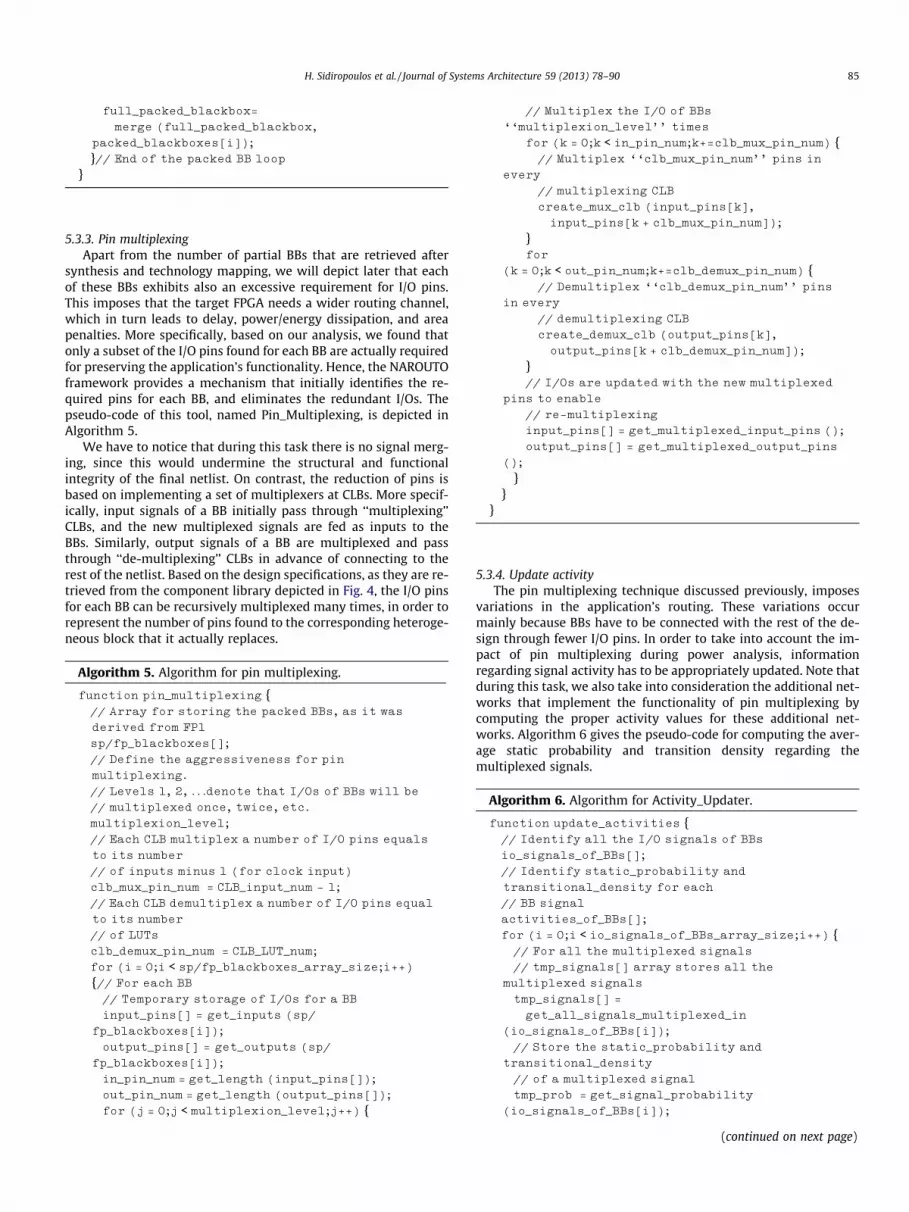
synthesis and technology mapping, we will depict later that eachof these BBs exhibits also an excessive requirement for I/O pins.This imposes that the target FPGA needs a wider routing channel,which in turn leads to delay, power/energy dissipation, and areapenalties. More specifically, based on our analysis, we found thatonly a subset of the I/O pins found for each BB are actually requiredfor preserving the application’s functionality. Hence, the NAROUTOframework provides a mechanism that initially identifies the re-quired pins for each BB, and eliminates the redundant I/Os. Thepseudo-code of this tool, named Pin_Multiplexing, is depicted inAlgorithm 5.
We have to notice that during this task there is no signal merg-ing, since this would undermine the structural and functionalintegrity of the final netlist. On contrast, the reduction of pins isbased on implementing a set of multiplexers at CLBs. More specif-ically, input signals of a BB initially pass through ‘‘multiplexing’’CLBs, and the new multiplexed signals are fed as inputs to theBBs. Similarly, output signals of a BB are multiplexed and passthrough ‘‘de-multiplexing’’ CLBs in advance of connecting to therest of the netlist. Based on the design specifications, as they are re-trieved from the component library depicted in Fig. 4, the I/O pinsfor each BB can be recursively multiplexed many times, in order torepresent the number of pins found to the corresponding heteroge-neous block that it actually replaces.
Algorithm 5. Algorithm for pin multiplexing.
function pin_multiplexing {// Array for storing the packed BBs, as it was
derived from FP1
sp/fp_blackboxes[];// Define the aggressiveness for pin
multiplexing.
// Levels 1, 2, . . .denote that I/Os of BBs will be
// multiplexed once, twice, etc.
multiplexion_level;// Each CLB multiplex a number of I/O pins equals
to its number
// of inputs minus 1 (for clock input)
clb_mux_pin_num = CLB_input_num - 1;
// Each CLB demultiplex a number of I/O pins equal
to its number
// of LUTs
clb_demux_pin_num = CLB_LUT_num;for (i = 0;i < sp/fp_blackboxes_array_size;i++){// For each BB
// Temporary storage of I/Os for a BB
input_pins[] = get_inputs (sp/
fp_blackboxes[i]);output_pins[] = get_outputs (sp/
fp_blackboxes[i]);in_pin_num = get_length (input_pins[]);out_pin_num = get_length (output_pins[]);for (j = 0;j < multiplexion_level;j++) {
// Multiplex the I/O of BBs
‘‘multiplexion_level’’ times
for (k = 0;k < in_pin_num;k+=clb_mux_pin_num) {// Multiplex ‘‘clb_mux_pin_num’’ pins in
every
// multiplexing CLB
create_mux_clb (input_pins[k],input_pins[k + clb_mux_pin_num]);
}for
(k = 0;k < out_pin_num;k+=clb_demux_pin_num) {// Demultiplex ‘‘clb_demux_pin_num’’ pins
in every
// demultiplexing CLB
create_demux_clb (output_pins[k],output_pins[k + clb_demux_pin_num]);
}// I/Os are updated with the new multiplexed
pins to enable
// re-multiplexing
input_pins[] = get_multiplexed_input_pins ();output_pins[] = get_multiplexed_output_pins
();
}}
}
5.3.4. Update activityThe pin multiplexing technique discussed previously, imposes
variations in the application’s routing. These variations occurmainly because BBs have to be connected with the rest of the de-sign through fewer I/O pins. In order to take into account the im-pact of pin multiplexing during power analysis, informationregarding signal activity has to be appropriately updated. Note thatduring this task, we also take into consideration the additional net-works that implement the functionality of pin multiplexing bycomputing the proper activity values for these additional net-works. Algorithm 6 gives the pseudo-code for computing the aver-age static probability and transition density regarding themultiplexed signals.
Algorithm 6. Algorithm for Activity_Updater.
function update_activities {// Identify all the I/O signals of BBs
io_signals_of_BBs[];// Identify static_probability and
transitional_density for each
// BB signal
activities_of_BBs[];for (i = 0;i < io_signals_of_BBs_array_size;i++) {// For all the multiplexed signals
// tmp_signals[] array stores all the
multiplexed signals
tmp_signals[] =
get_all_signals_multiplexed_in(io_signals_of_BBs[i]);// Store the static_probability and
transitional_density// of a multiplexed signal
tmp_prob = get_signal_probability(io_signals_of_BBs[i]);
(continued on next page)

TaQu
86 H. Sidiropoulos et al. / Journal of Systems Architecture 59 (2013) 78–90
tmp_dens = get_signal_density(io_signals_of_BBs[i]);for (j = 0;j < tmp_signals_array_size;j++) {// Compute static_probability and
transitional_density for
// multiplexed signals
static_probability = calculate_static_prob(tmp_prob);
transitional_density = calculate (tmp_dens);// Update the signal’s activity
update_activity (tmp_signals[j],static_probability
,transitional_density);}
}}
5.4. Placement and routing
The last task our proposed framework deals, is the task of appli-cation placement and routing onto the FPGA. For this purpose weemploy a simulated annealing algorithm for placement and a con-gestion pathfinder routing. Both of these algorithms are based onVPR [3,13], but they have been extensively modified in order tobe aware of the inherent constraints posed by heterogeneous com-ponents. More specifically, the implementation of these algorithmsin the NAROUTO framework provides techniques for efficient han-dling multiple types of heterogeneous BBs, as well as estimation ofpower/energy dissipation (through appropriately extension of thePowermodel tool [6]). Note that the new tool can handle heteroge-neous FPGAs with embedded macro blocks other than memories,represented as new types of BBs, if they are appropriately modeledin the component library.
6. Experimental results
This section provides a number of qualitative and quantitativecomparisons that prove the efficiency of the introduced frame-work, named NAROUTO, as compared to the state-of-art solution(VPR-5.0 tool [3]). Note that for the sake of completeness, applica-tion synthesis and technology mapping both for the proposed, aswell as the existing solution, were performed with the usage ofQuartus toolset [7].
Table 1 gives a qualitative comparison among the introducedframework, the state-of-the-art solution, as well as a commerciallyavailable toolset. This comparison is performed under a number ofdifferent criteria than span from architecture-oriented (e.g. heter-ogeneity support), application-oriented (e.g. constraint application
ble 1alitative comparison in supported features.
Feature NAROUTO
Support BBs YesDifferent types of BBs UnlimitedRealistic number of BBs YesRealistic number of I/Os per BBs YesPower estimation YesConstraints during application mapping Timing power area trade-oModular tools YesPart of complete framework Yes
Open source Yes
mapping), as well as implementation-oriented (e.g. completeframework) parameters.
A number of conclusions can be derived from this table. Theproposed framework supports more efficiently designs with BBs,whereas the power and energy estimation features are similar tothose found in relevant commercial approaches. Additionally, wehave to notice that only academic flows (e.g. NAROUTO and VPR-5.0) enable architecture-level exploration. Hence, the commercialflow tackle exclusively ‘‘Problem No. 2’’ (see Fig. 1), whereas theproposed solution supports also ‘‘Problem No. 1’’. Even thoughthe first problem could be handled by VPR-5.0, the lack ofpower/energy support, as well as the non-sufficient usage of BBs,introduce a number of problems.
For evaluation purposes, the alternative toolflows are quantifiedwith the usage of DSP applications from Altera’s Quip toolkit [16].Table 2 summarizes the main characteristics of the employedbenchmark suite, whereas the complexity of these applicationsguarantees that the derived conclusions are valid for the majorityof digital designs implemented onto FPGAs.
Note that our framework does not focus on minimizing eitherthe memory requirements, or the memory accesses, since we as-sume that these problems were tackled during application synthe-sis with Altera Quartus. Regarding the glue logic of target FPGA, itconsists of 10 4-input LUTs and 22/10 input/output pins per CLB,whereas the FPGA array, as well as the routing channel width, de-pends on the target application. More specifically, the values ofthese two parameters correspond to the minimum array and chan-nel width, respectively, for successful application P&R.
6.1. Evaluation of different memory hierarchies
Initially, we evaluate maximum operation frequency and powerconsumption regarding the two memory hierarchies studiedthroughout this paper. For this purpose Table 3 quantifies maxi-mum operation frequency for the alternative memory hierarchies,mentioned as ‘‘Scenario 1’’ and ‘‘Scenario 2’’ in Figs. 2 and 3,respectively. As a reference to this analysis we also provide the cor-responding results when using the VPR-5.0 tool [3].
Based on Table 3 we can conclude that the usage of the pro-posed methodology leads to mentionable performance enhance-ment, as compared to the corresponding gains retrieved whenapplication implementation is performed with VPR-5.0. More spe-cifically, scenarios 1 and 2 achieve on average performanceenhancement of 1.96� and 2.07�, respectively.
Apart from the performance improvement, our proposed meth-odology is expected to achieve also mentionable power savings.The results of this analysis are summarized in Table 4. Based onthem, our two case studies (‘‘Scenario 1’’ and ‘‘Scenario 2’’) leadto average power reduction compared to reference implementa-tion (with the usage of VPR-5.0) of 13.5% and 43.7%, respectively.
These results denote that memory hierarchies lead to superiorperformance due to better manipulation of data transfers. Since
VPR-5.0 [3] QUARTUS [7]
Yes Yes1 UnlimitedNo NoNo NoNo Yes
ff Timing Timing power area trade-offYes NoNo Yes
Yes No
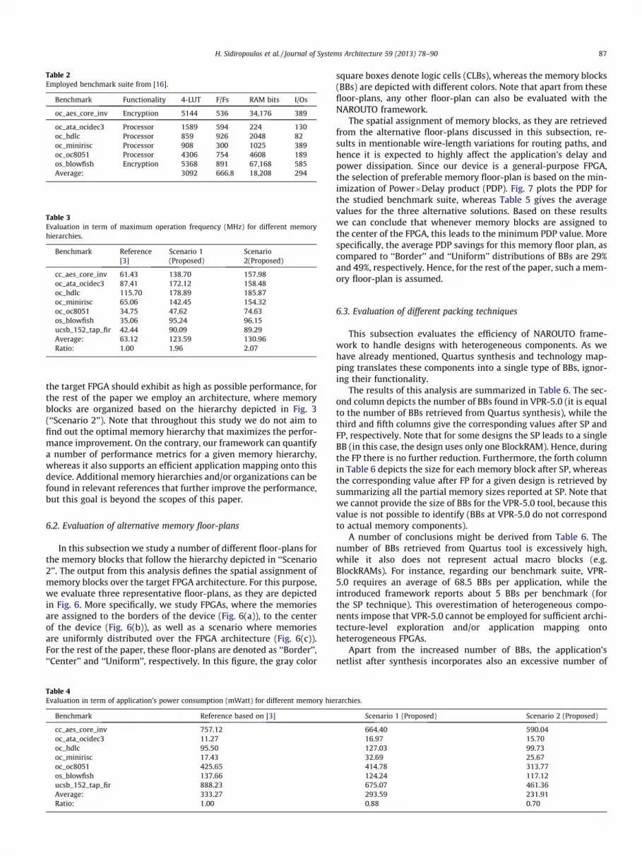
Table 2Employed benchmark suite from [16].
Benchmark Functionality 4-LUT F/Fs RAM bits I/Os
oc_aes_core_inv Encryption 5144 536 34,176 389
oc_ata_ocidec3 Processor 1589 594 224 130oc_hdlc Processor 859 926 2048 82oc_minirisc Processor 908 300 1025 389oc_oc8051 Processor 4306 754 4608 189os_blowfish Encryption 5368 891 67,168 585Average: 3092 666.8 18,208 294
Table 3Evaluation in term of maximum operation frequency (MHz) for different memoryhierarchies.
Benchmark Reference[3]
Scenario 1(Proposed)
Scenario2(Proposed)
cc_aes_core_inv 61.43 138.70 157.98oc_ata_ocidec3 87.41 172.12 158.48oc_hdlc 115.70 178.89 185.87oc_minirisc 65.06 142.45 154.32oc_oc8051 34.75 47.62 74.63os_blowfish 35.06 95.24 96.15ucsb_152_tap_fir 42.44 90.09 89.29Average: 63.12 123.59 130.96Ratio: 1.00 1.96 2.07
H. Sidiropoulos et al. / Journal of Systems Architecture 59 (2013) 78–90 87
the target FPGA should exhibit as high as possible performance, forthe rest of the paper we employ an architecture, where memoryblocks are organized based on the hierarchy depicted in Fig. 3(‘‘Scenario 2’’). Note that throughout this study we do not aim tofind out the optimal memory hierarchy that maximizes the perfor-mance improvement. On the contrary, our framework can quantifya number of performance metrics for a given memory hierarchy,whereas it also supports an efficient application mapping onto thisdevice. Additional memory hierarchies and/or organizations can befound in relevant references that further improve the performance,but this goal is beyond the scopes of this paper.
6.2. Evaluation of alternative memory floor-plans
In this subsection we study a number of different floor-plans forthe memory blocks that follow the hierarchy depicted in ‘‘Scenario2’’. The output from this analysis defines the spatial assignment ofmemory blocks over the target FPGA architecture. For this purpose,we evaluate three representative floor-plans, as they are depictedin Fig. 6. More specifically, we study FPGAs, where the memoriesare assigned to the borders of the device (Fig. 6(a)), to the centerof the device (Fig. 6(b)), as well as a scenario where memoriesare uniformly distributed over the FPGA architecture (Fig. 6(c)).For the rest of the paper, these floor-plans are denoted as ‘‘Border’’,‘‘Center’’ and ‘‘Uniform’’, respectively. In this figure, the gray color
Table 4Evaluation in term of application’s power consumption (mWatt) for different memory hie
Benchmark Reference based on [3]
cc_aes_core_inv 757.12oc_ata_ocidec3 11.27oc_hdlc 95.50oc_minirisc 17.43oc_oc8051 425.65os_blowfish 137.66ucsb_152_tap_fir 888.23Average: 333.27Ratio: 1.00
square boxes denote logic cells (CLBs), whereas the memory blocks(BBs) are depicted with different colors. Note that apart from thesefloor-plans, any other floor-plan can also be evaluated with theNAROUTO framework.
The spatial assignment of memory blocks, as they are retrievedfrom the alternative floor-plans discussed in this subsection, re-sults in mentionable wire-length variations for routing paths, andhence it is expected to highly affect the application’s delay andpower dissipation. Since our device is a general-purpose FPGA,the selection of preferable memory floor-plan is based on the min-imization of Power�Delay product (PDP). Fig. 7 plots the PDP forthe studied benchmark suite, whereas Table 5 gives the averagevalues for the three alternative solutions. Based on these resultswe can conclude that whenever memory blocks are assigned tothe center of the FPGA, this leads to the minimum PDP value. Morespecifically, the average PDP savings for this memory floor plan, ascompared to ‘‘Border’’ and ‘‘Uniform’’ distributions of BBs are 29%and 49%, respectively. Hence, for the rest of the paper, such a mem-ory floor-plan is assumed.
6.3. Evaluation of different packing techniques
This subsection evaluates the efficiency of NAROUTO frame-work to handle designs with heterogeneous components. As wehave already mentioned, Quartus synthesis and technology map-ping translates these components into a single type of BBs, ignor-ing their functionality.
The results of this analysis are summarized in Table 6. The sec-ond column depicts the number of BBs found in VPR-5.0 (it is equalto the number of BBs retrieved from Quartus synthesis), while thethird and fifth columns give the corresponding values after SP andFP, respectively. Note that for some designs the SP leads to a singleBB (in this case, the design uses only one BlockRAM). Hence, duringthe FP there is no further reduction. Furthermore, the forth columnin Table 6 depicts the size for each memory block after SP, whereasthe corresponding value after FP for a given design is retrieved bysummarizing all the partial memory sizes reported at SP. Note thatwe cannot provide the size of BBs for the VPR-5.0 tool, because thisvalue is not possible to identify (BBs at VPR-5.0 do not correspondto actual memory components).
A number of conclusions might be derived from Table 6. Thenumber of BBs retrieved from Quartus tool is excessively high,while it also does not represent actual macro blocks (e.g.BlockRAMs). For instance, regarding our benchmark suite, VPR-5.0 requires an average of 68.5 BBs per application, while theintroduced framework reports about 5 BBs per benchmark (forthe SP technique). This overestimation of heterogeneous compo-nents impose that VPR-5.0 cannot be employed for sufficient archi-tecture-level exploration and/or application mapping ontoheterogeneous FPGAs.
Apart from the increased number of BBs, the application’snetlist after synthesis incorporates also an excessive number of
rarchies.
Scenario 1 (Proposed) Scenario 2 (Proposed)
664.40 590.0416.97 15.70127.03 99.7332.69 25.67414.78 313.77124.24 117.12675.07 461.36293.59 231.910.88 0.70

(a) (b)
(c)
Fig. 6. Alternative floor-plans for memory blocks: (a) placed in borders, (b) placed in center, and (c) uniformly distributed.
Fig. 7. Power�Delay product for different floor-plans of memory blocks.
Table 5Average PDP for different floor-plans of memory blocks.
Border Center Uniform
Average PDP 0.57 0.44 0.66
Ratio: 1.29 1.00 1.49
88 H. Sidiropoulos et al. / Journal of Systems Architecture 59 (2013) 78–90
input/output pins. In order to evaluate the efficiency of the NARO-UTO framework to handle designs with realistic number of I/Os,Table 7 summarizes the total and the average number of I/O pinsper BB. More specifically, second and fourth columns refer to thenumber of I/Os retrieved from Quartus tool, whereas the thirdand fifth columns give the corresponding values after the SP ap-proach (by applying the Pin_Multiplexing tool), respectively. Notethat for this study we assume, without affecting the efficiency ofproposed methodology, that only SP is applied.
Based on the results depicted in this table, the pin multiplexingtechnique leads to designs where each BB incorporates a more
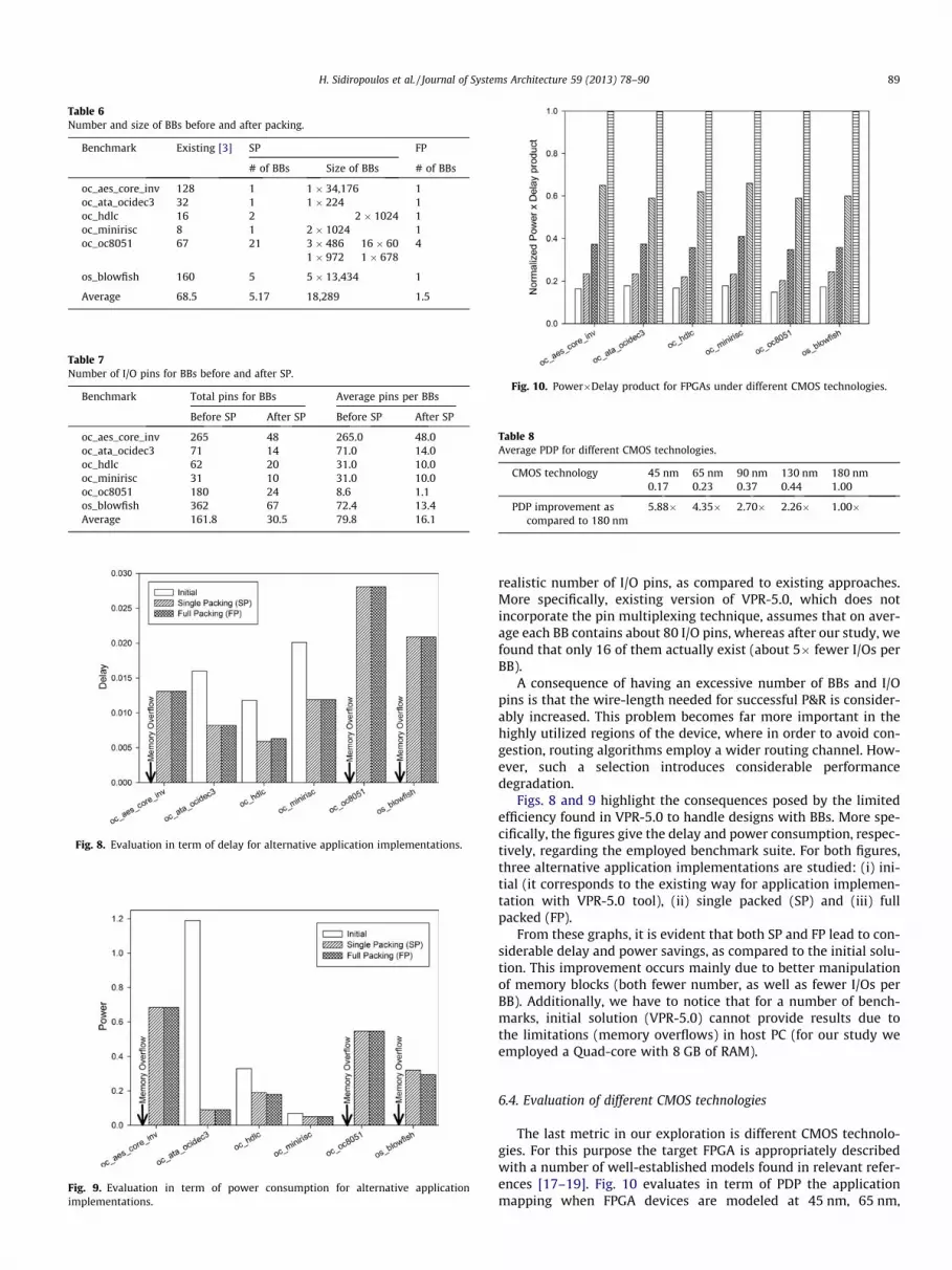
Table 6Number and size of BBs before and after packing.
Benchmark Existing [3] SP FP
# of BBs Size of BBs # of BBs
oc_aes_core_inv 128 1 1 � 34,176 1oc_ata_ocidec3 32 1 1 � 224 1oc_hdlc 16 2 2 � 1024 1oc_minirisc 8 1 2 � 1024 1oc_oc8051 67 21 3 � 486 16 � 60 4
1 � 972 1 � 678
os_blowfish 160 5 5 � 13,434 1
Average 68.5 5.17 18,289 1.5
Table 7Number of I/O pins for BBs before and after SP.
Benchmark Total pins for BBs Average pins per BBs
Before SP After SP Before SP After SP
oc_aes_core_inv 265 48 265.0 48.0oc_ata_ocidec3 71 14 71.0 14.0oc_hdlc 62 20 31.0 10.0oc_minirisc 31 10 31.0 10.0oc_oc8051 180 24 8.6 1.1os_blowfish 362 67 72.4 13.4Average 161.8 30.5 79.8 16.1
Fig. 8. Evaluation in term of delay for alternative application implementations.
Fig. 9. Evaluation in term of power consumption for alternative applicationimplementations.
Fig. 10. Power�Delay product for FPGAs under different CMOS technologies.
Table 8Average PDP for different CMOS technologies.
CMOS technology 45 nm 65 nm 90 nm 130 nm 180 nm0.17 0.23 0.37 0.44 1.00
PDP improvement ascompared to 180 nm
5.88� 4.35� 2.70� 2.26� 1.00�
H. Sidiropoulos et al. / Journal of Systems Architecture 59 (2013) 78–90 89
realistic number of I/O pins, as compared to existing approaches.More specifically, existing version of VPR-5.0, which does notincorporate the pin multiplexing technique, assumes that on aver-age each BB contains about 80 I/O pins, whereas after our study, wefound that only 16 of them actually exist (about 5� fewer I/Os perBB).
A consequence of having an excessive number of BBs and I/Opins is that the wire-length needed for successful P&R is consider-ably increased. This problem becomes far more important in thehighly utilized regions of the device, where in order to avoid con-gestion, routing algorithms employ a wider routing channel. How-ever, such a selection introduces considerable performancedegradation.
Figs. 8 and 9 highlight the consequences posed by the limitedefficiency found in VPR-5.0 to handle designs with BBs. More spe-cifically, the figures give the delay and power consumption, respec-tively, regarding the employed benchmark suite. For both figures,three alternative application implementations are studied: (i) ini-tial (it corresponds to the existing way for application implemen-tation with VPR-5.0 tool), (ii) single packed (SP) and (iii) fullpacked (FP).
From these graphs, it is evident that both SP and FP lead to con-siderable delay and power savings, as compared to the initial solu-tion. This improvement occurs mainly due to better manipulationof memory blocks (both fewer number, as well as fewer I/Os perBB). Additionally, we have to notice that for a number of bench-marks, initial solution (VPR-5.0) cannot provide results due tothe limitations (memory overflows) in host PC (for our study weemployed a Quad-core with 8 GB of RAM).
6.4. Evaluation of different CMOS technologies
The last metric in our exploration is different CMOS technolo-gies. For this purpose the target FPGA is appropriately describedwith a number of well-established models found in relevant refer-ences [17–19]. Fig. 10 evaluates in term of PDP the applicationmapping when FPGA devices are modeled at 45 nm, 65 nm,

90 H. Sidiropoulos et al. / Journal of Systems Architecture 59 (2013) 78–90
90 nm, 130 nm and 180 nm CMOS technologies, whereas Table 8gives the average PDP values among the studied benchmarks. Fordemonstration purposes, the values plotted in this figure arenormalized over the maximum PDP for each benchmark.
A number of conclusions might be derived from this analysis.More specifically, the maximum PDP occurs when 180 nmtechnology is assumed, whereas the ratio of PDP improvement isnot linear with technology scaling. Additionally, the performanceenhancement between alternative CMOS technologies seems tobe application independent. The last conclusion is very importantsince it enables our proposed NAROUTO framework to evaluatethe architectural selections of the underlying FPGA device.
7. Conclusions
A novel methodology, as well as the supporting tool framework,for enabling architecture-level exploration of heterogeneousFPGAs, was proposed. This framework was tuned in order to enableefficient handling of memory hierarchies onto general-purposereconfigurable devices. Experimental results prove the efficiencyof proposed solution, since we achieve mentionable delay, power,and area savings, as compared to the state-of-the-art approach.Finally, the introduced NAROUTO framework is the only soft-ware-supported approach that enables evaluation of power andenergy dissipation metrics of heterogeneous FPGA devices.
References
[1] J. Pistorius, M. Hutton, A. Mishchenko, R. Brayton, Benchmarking method anddesigns targeting logic synthesis for FPGAs, in: Proc. of International Workshopon Logic and Synthesis (IWLS), 2007, pp. 230–237.
[2] M. Gao, J.H. Jiang, Y. Jiang, Y. Li, S. Sinha, R. Brayton, MVSIS, InternationalWorkshop on Logic Synthesis, 2001.
[3] J. Luu, I. Kuon, P. Jamieson, T. Campbell, A. Ye, W.M. Fang, J. Rose, VPR 5.0: FPGACAD and Architecture Exploration Tools with Single-Driver Routing,heterogeneity and process scaling, in: Proc. of the ACM/SIGDA InternationalSymposium on Field Programmable Gate Arrays (FPGA), 2009, pp. 133–142.
[4] S. Sharp, Conquering the Three Challenges of Power Consumption: Why ispower such an issue? Power Managmenet, vol. 1, p. 5. August 2005.
[5] K. Nowak, J. Meerbergen, An FPGA architecture with enhanced datapathfunctionality, in: Proc. of the 2003 ACM/SIGDA 11th International Symposiumon Field Programmable Gate Arrays (FPGA), 2003, pp. 195–204.
[6] K. Poon, S. Wilton, A. Yan, A detailed power model for field-programmable gatearrays, in: ACM Transactions on Design Automation of Electronic Systems(TODAES), vol. 10(2), April 2005, pp. 279–302.
[7] Altera, Corporation, Quartus II Software.[8] CAD tools for FGPAs. Available at: <http://proteas.microlab.ntua.gr/ksiop/
software.html>.[9] Berkeley Logic Interchange Format (BLIF), University of California, Berkeley,
1992.[10] Altera Stratix Device Handbook. Available at: <http://www.altera.com/
literature/hb/stx/stratix_handbook.pdf>.[11] Xilinx Virtex-II Pro Handbook. Available at: <http://www.xilinx.com/support/
documentation/virtex-ii_pro.htm>.[12] S. Vassiliadis, D. Soudris, Fine and Coarse-Grain Reconfigurable Systems,
Springer, 2007.[13] V. Betz, J. Rose, A. Marquardt, Architecture and CAD for Deep-Submicron
FPGAs, Kluwer Academic Publishers, 1999.[14] C. Sidiropoulos, Development of a design framework for Power/Energy
consumption estimation in heterogeneous FPGA architectures, Master thesis,NTUA, Greece, 2010. Available at: <http://proteas.microlab.ntua.gr/ksiop/software/narouto>.
[15] International Technology Roadmap for Semiconductors (ITRS), ChapterInterconnect, Edition 2009.
[16] Altera, Corporation, Quartus-II University Interface Program.[17] W. Zhao, Y. Cao, New generation of Predictive Technology Model for sub-
45 nm early design exploration, IEEE Transactions on Electron Devices 53 (11)(2006) 2816–2823.
[18] Available from: <http://www.eecg.utoronto.ca/vpr/architectures/architecture_table.html>.
[19] S. Wilton, N. Jouppi, CACTI: an enhanced cache access and cycle time model,IEEE Journal of Solid-State Circuits 31 (5) (1996) 677–688, http://dx.doi.org/10.1109/4.509850.
[20] J.M. Rabaey, Low Power Design Essentials, Series on Integrated Circuits andSystems, Springer, New York, NY, 2009.
[21] Available from: <http://proteas.microlab.ntua.gr/ksiop/software.html>.
Harry Sidiropoulos received his Diploma in Electricaland Computer Engineering from the National TechnicalUniversity of Athens, Greece, in 2010. He is currentlyworking towards his Ph.D. in the same university. Hisresearch interests include FPGAs and CAD algorithms.
Dr. Kostas Siozios received his Diploma, Master andPh.D. Degree in Electrical and Computer Engineeringfrom the Democritus University of Thrace, Greece, in2001, 2003 and 2009, respectively. Now he is workingas research associate in the National Technical Univer-sity of Athens, Greece. His research interests includeCAD algorithms, low-power reconfigurable architec-tures and parallel architectures. He has published morethan 53 papers in international journals and confer-ences. Also, he has contributed in 4 books of Kluwer andSpringer. The last years he works as principal investi-gator in numerous research projects funded from the
European Commission (EC), as well as the Greek Government and Industry.
Prof. Dimitrios Soudris received his Diploma inElectrical Engineering from the University of Patras,Greece, in 1987. He received the Ph.D. Degree inElectrical Engineering, from the University of Patras in1992. He was working as a Professor in Dept. of Elec-trical and Computer Engineering, Democritus Universityof Thrace for 13 years since 1995. He is currentlyworking as Ass. Professor in School of Electrical andComputer Engineering, Dept. Computer Science ofNational Technical University of Athens, Greece. Hisresearch interests include embedded systems design,low power VLSI design and reconfigurable architectures.
He has published more than 210 papers in international journals and conferences.Also, he is coauthor/coeditor in five bo oks of Kluwer and Springer. He is leader andprincipal investigator in numerous research projects funded from the Greek Gov-
ernment and Industry as well as the European Commission (ESPRIT II-III-IV and 5th& 7th IST). He has served as General Chair and Program Chair for PATMOS 99 and2000, respectively, and General Chair of IFIP-VLSI-SOC 2008. Also, he received anaward from INTEL and IBM for the EU project LPGD 25256 and awards in ASP-DAC05 and VLSI 05 for EU AMDREL project IST-2001-34379. He is a member of the IEEE,the VLSI Systems and Applications Technical Committee of IEEE CAS and the ACM.