minimizing fir filter designs implemented in fpgas utilizing
TRANSCRIPT

Florida State University Libraries
Electronic Theses, Treatises and Dissertations The Graduate School
2009
Minimizing FIR Filter Designs Implementedin FPGAs Utilizing Minimized Adder GraphTechniquesCharles D. Howard
Follow this and additional works at the FSU Digital Library. For more information, please contact [email protected]

FLORIDA STATE UNIVERSITY
FAMU–FSU COLLEGE OF ENGINEERING
MINIMIZING FIR FILTER DESIGNS IMPLEMENTED IN FPGAS
UTILIZING MINIMIZED ADDER GRAPH TECHNIQUES
By
CHARLES D. HOWARD
A Thesis submitted to the
Department of Electrical & Computer Engineering
in partial fulfillment of the
requirements for the degree of
Master of Science
Degree Awarded:
Spring Semester, 2009

The members of the Committee approve the Thesis of Charles D. Howard defended onDecember 1, 2008.
Linda S. DeBrunnerProfessor Directing Thesis
Victor DeBrunnerCommittee Member
Bruce A. HarveyCommittee Member
The Office of Graduate Studies has verified and approved the above named committee members.
ii

TABLE OF CONTENTS
List of Tables . . . . . . . . . . . . . . . . . . . . . . . . . . . . . . . . . . . . . . v
List of Figures . . . . . . . . . . . . . . . . . . . . . . . . . . . . . . . . . . . . . vi
List of Listings . . . . . . . . . . . . . . . . . . . . . . . . . . . . . . . . . . . . . ix
Abstract . . . . . . . . . . . . . . . . . . . . . . . . . . . . . . . . . . . . . . . . x
1. INTRODUCTION . . . . . . . . . . . . . . . . . . . . . . . . . . . . . . . . . 1
2. OPTIMIZING FIR FILTER IMPLEMENTATIONS . . . . . . . . . . . . . . 32.1 Digit-based Recoding . . . . . . . . . . . . . . . . . . . . . . . . . . . . . 32.2 Graph Based Approaches to Constant Multiplications . . . . . . . . . . . 42.3 Minimum Adder Graph Algorithms . . . . . . . . . . . . . . . . . . . . . 6
3. BACKGROUND . . . . . . . . . . . . . . . . . . . . . . . . . . . . . . . . . . 83.1 Delta-sigma Converters . . . . . . . . . . . . . . . . . . . . . . . . . . . . 83.2 Loop Filter . . . . . . . . . . . . . . . . . . . . . . . . . . . . . . . . . . 103.3 CSD Real-time Recoding . . . . . . . . . . . . . . . . . . . . . . . . . . . 12
4. VHDLGEN, A VHDL GENERATOR . . . . . . . . . . . . . . . . . . . . . . 134.1 VHDLGen Example Usage . . . . . . . . . . . . . . . . . . . . . . . . . . 134.2 VHDL Filter Generation Using Other Implementation Schemes . . . . . 194.3 Analysis . . . . . . . . . . . . . . . . . . . . . . . . . . . . . . . . . . . . 204.4 Anatomy of the VHDLGen API . . . . . . . . . . . . . . . . . . . . . . . 24
5. MINIMIZED ADDER GRAPHS IN FPGA DEVICES . . . . . . . . . . . . . 385.1 Inference Approach: Hybrid I . . . . . . . . . . . . . . . . . . . . . . . . 395.2 Direct Instantiation Approach: Hybrid II . . . . . . . . . . . . . . . . . . 405.3 Hybrid Filter Results . . . . . . . . . . . . . . . . . . . . . . . . . . . . . 41
6. PROGRAMMABLE ADDER GRAPH . . . . . . . . . . . . . . . . . . . . . . 476.1 Proposed Programmable Adder Graph . . . . . . . . . . . . . . . . . . . 486.2 Fundamental Modules . . . . . . . . . . . . . . . . . . . . . . . . . . . . 506.3 Connection Matrix . . . . . . . . . . . . . . . . . . . . . . . . . . . . . . 526.4 Programmer . . . . . . . . . . . . . . . . . . . . . . . . . . . . . . . . . . 57
iii

6.5 Design Issues . . . . . . . . . . . . . . . . . . . . . . . . . . . . . . . . . 596.6 Sizing . . . . . . . . . . . . . . . . . . . . . . . . . . . . . . . . . . . . . 606.7 Applications . . . . . . . . . . . . . . . . . . . . . . . . . . . . . . . . . . 66
7. CONCLUSIONS AND FUTURE WORK . . . . . . . . . . . . . . . . . . . . 69
REFERENCES . . . . . . . . . . . . . . . . . . . . . . . . . . . . . . . . . . . . . 71
BIOGRAPHICAL SKETCH . . . . . . . . . . . . . . . . . . . . . . . . . . . . . 74
iv

LIST OF TABLES
3.1 Double precision coefficients of previously designed sparse loop filter . . . . . 11
5.1 Filters used in hybrid filter research . . . . . . . . . . . . . . . . . . . . . . . 42
v

LIST OF FIGURES
1.1 Block diagram of ∆Σ modulator used in radar system . . . . . . . . . . . . . 2
2.1 Hardware implemtation of digit based encoding. . . . . . . . . . . . . . . . . 5
2.2 Adder Graph and implementation for multiplication of (29)10 . . . . . . . . 6
2.3 Transposed FIR filter using an MCM multiplier block . . . . . . . . . . . . . 6
3.1 Rudimentary first order ∆Σ modulator . . . . . . . . . . . . . . . . . . . . . 9
3.2 Implementation of the rudimentary first order ∆Σ modulator in digital form. 9
3.3 The error-feedback structure of a ∆Σ modulator. . . . . . . . . . . . . . . . 10
3.4 Frequency response of the sparse loop having only ten non-zero coefficients. . 11
4.1 Frequency response of the 8th order sample filter. . . . . . . . . . . . . . . . 16
4.2 Research workflow . . . . . . . . . . . . . . . . . . . . . . . . . . . . . . . . 20
4.3 Filter response graphs of a sample filter . . . . . . . . . . . . . . . . . . . . . 23
4.4 UML class diagram of VHDLGen . . . . . . . . . . . . . . . . . . . . . . . . 25
4.5 VHDLGen Flow Diagram . . . . . . . . . . . . . . . . . . . . . . . . . . . . 26
4.6 Circuit created when using the FIRFilterData filter data object . . . . . . . 29
4.7 Circuit created when using the FIRFilterDataMCM filter data object . . . . . 32
4.8 Circuit created when using the FIRFilterDataHybrid filter data object . . . 34
4.9 Circuit created when using the FIRFilterDataHybridDSP filter data object . 36
5.1 Circuit created when using the FIRFilterDataHybrid filter data object. . . 40
5.2 Direct DSP48 primitive instantiation, Hybrid II. . . . . . . . . . . . . . . . . 41
5.3 Hybrid filter results of Filter A . . . . . . . . . . . . . . . . . . . . . . . . . 44
vi

5.4 Hybrid filter results of Filter B . . . . . . . . . . . . . . . . . . . . . . . . . 45
5.5 Hybrid filter results of Filter C . . . . . . . . . . . . . . . . . . . . . . . . . 46
6.1 Programable Adder Graph (PAG) Layout. . . . . . . . . . . . . . . . . . . . 50
6.2 The Fundamental Module . . . . . . . . . . . . . . . . . . . . . . . . . . . . 51
6.3 Programmable hardware shift module . . . . . . . . . . . . . . . . . . . . . . 53
6.4 Four bit connection patterns to apply a left wire shift. . . . . . . . . . . . . . 53
6.5 Four bit connection patterns to apply an arithmetic right wire shift. . . . . . 54
6.6 Four bit, four node, one row connection matrix . . . . . . . . . . . . . . . . . 55
6.7 Connection circuit using a CMOS transmission gates. . . . . . . . . . . . . . 56
6.8 Connection circuit using a tri-state NOT gate. . . . . . . . . . . . . . . . . . 56
6.9 PAG Programmer. . . . . . . . . . . . . . . . . . . . . . . . . . . . . . . . . 58
6.10 Dual PAG Module. . . . . . . . . . . . . . . . . . . . . . . . . . . . . . . . . 60
6.11 Highpass filter limits . . . . . . . . . . . . . . . . . . . . . . . . . . . . . . . 65
6.12 Highpass filter limits with max depth of four . . . . . . . . . . . . . . . . . . 65
6.13 Bandstop filter limits. . . . . . . . . . . . . . . . . . . . . . . . . . . . . . . 67
6.14 Bandstop filter limits with max depth of four . . . . . . . . . . . . . . . . . 67
6.15 Embedded PAG block . . . . . . . . . . . . . . . . . . . . . . . . . . . . . . 68
vii

LIST OF LISTINGS
4.1 VHDLGen Run File . . . . . . . . . . . . . . . . . . . . . . . . . . . . . . . 15
4.2 Filter Creation using firpm . . . . . . . . . . . . . . . . . . . . . . . . . . . 16
4.3 Saving the coefficients to the run file manually . . . . . . . . . . . . . . . . . 17
4.4 Creating the coefficient file in Matlab . . . . . . . . . . . . . . . . . . . . . . 18
4.5 VHDL entity statement created by the sample run file . . . . . . . . . . . . . 19
4.6 Code snippet from a VHDL test bench . . . . . . . . . . . . . . . . . . . . . 22
4.7 Matlab code to generate white noise . . . . . . . . . . . . . . . . . . . . . . . 23
4.8 Matlab code to create the frequency plot data from filtered noise . . . . . . . 24
4.9 The CreateArchitectureHeader() method in the VHDLCircuit class . . . . 27
4.10 The setCoeffs() method of the FIRFilterData class . . . . . . . . . . . . 29
4.11 Loading Coefficients from a File . . . . . . . . . . . . . . . . . . . . . . . . . 30
4.12 The quantizeCoeffs() method of the FIRFilterData class . . . . . . . . . 30
4.13 The implementCoeff() method of the FIRFilterData class . . . . . . . . . 31
4.14 The addVHDLFunctions() method of the FIRFilterDataMCM class . . . . . . 33
4.15 The MCM Multiplication block . . . . . . . . . . . . . . . . . . . . . . . . . 33
4.16 The implementHybridCoeff() method . . . . . . . . . . . . . . . . . . . . . 35
6.1 Function to compute required PAG size. . . . . . . . . . . . . . . . . . . . . 62
6.2 Function to count the required fundamentals . . . . . . . . . . . . . . . . . . 62
6.3 Function to create an FIR filter . . . . . . . . . . . . . . . . . . . . . . . . . 63
6.4 Function to create a MAG given a filter . . . . . . . . . . . . . . . . . . . . . 64
viii

6.5 Band stop filter specifications . . . . . . . . . . . . . . . . . . . . . . . . . . 66
ix

ABSTRACT
Multiple constant multiplications (MCM) is a graph based optimization technique that is
well suited to DSP implementations. Using MCM, all coefficient multiplications are grouped
into one efficient block of wired shifts and adds. One problem when using graph based
optimizations is that most of the high-speed embedded blocks on modern FPGA devices are
not used to help improve the design. We show that better results can be achieved using a
hybrid technique to mix MCM and the embedded blocks in a single implementation. Another
disadvantage of using MCM is the requirement of knowing the filter coefficients a priori. Due
to this limitation, MCM optimizations cannot be used in many applications. We propose
a programmable adder graph (PAG) circuit that can implement multiplication using shift
and add techniques without prior knowledge of the multiplier value. The PAG circuit allows
any programmable device to be optimized using MCM for a wide range of DSP applications,
including adaptive filters.
x

CHAPTER 1
INTRODUCTION
In response to the need for a demanding ∆Σ converter for a high performance radar system,
we have focused on improving the implementation of the ∆Σ converter’s loop filter. As the
loop filter is a key component of the ∆Σ converter, we will focus on a fast implementation
that also has low area. Previous work on this project has focused on a design that has
the potential for high performance, but that work does not consider the specific target
implementation platform.
Figure 1.1 shows a block diagram of the ∆Σ converter used for the radar system. The
implementation of the loop filter shown in the diagram is the single concern of this work,
however, it is important to understand how it relates to the rest of the system. The remaining
blocks shown are the usual suspects of a ∆Σ converter.
Due to the requirement that the system be implemented using FPGA devices, this
work concentrates on the unexpected problems FPGA devices introduce when traditional
filter optimization techniques are employed. This work concentrates on a very effective
implementation technique: minimum adder graphs (MAG). While MAG optimization
provides a considerable reduction of the circuitry needed to implement the required filter, it
does not make the best use of the programmable area on the FPGA device. Specifically the
high-speed embedded DSP building blocks available are not effectively used.
Hybrid filter implementations are proposed in this work to overcome this MAG limi-
tation. By cleverly altering the filter coefficient multiplications in VHDL to use various
implementations, more of the FPGA device can be utilized. The primary goal of the hybrid
filter research is to move as much of the logic required to fully implement the coefficient
multiplications into the high-speed embedded blocks. Once the embedded blocks have been
fully utilized, the remaining logic is then implemented in the traditional programmable logic
1

Loop Filtere(n)
y(n)x(n)Q
Quantizer
Figure 1.1: Block diagram of ∆Σ modulator used in radar system
of the FPGA device using the well established MAG optimizations.
The hybrid filter approach is not useful for FPGA devices that have enough embedded
blocks to implement the entire filter. For this situation there is no need to use MAG
optimizations. The embedded blocks are fixed and highly competitive, such as the DSP48
Slice found on Xilinx’s Vertex series FPGAs[1]. It is very difficult and most likely not feasible
to outperform the embedded DSP blocks using the traditional programmable logic, even with
MAG optimizations.
To allow future FPGAs to implement filters that can approach ASIC speeds, this
work also proposes a new structure: the programmable adder graph (PAG). A PAG is
a programmable circuit that can implement high-speed constant multiplications that have
been converted into a MAG. Once the PAG is programmed, it simulates a hardware multiple
multiplication block used in traditional MAG designs. A PAG enabled FPGA device is a
more realistic implementation platform for the required loop filter. Aided by the PAG
block, the loop filter would be able to obtain clock rates that are not currently possible on
programmable devices.
The digital filter optimizations used in this work, most notably MAG optimizations,
are reviewed in Chapter 2. Chapter 3 covers the areas of the previous research that are
most important to this work. Chapters 4, 5 and 6 contain all original work. Chapter 4
introduces a custom tool designed specifically for the hybrid filter research: VHDLGen.
Chapter 5 covers the hybrid filter research that blends traditional filter optimizations with
the available embedded blocks of modern FPGAs. Chapter 6 finishes with the proposed
PAG circuit which expands the number of situations in which MAG optimizations can be
utilized.
2

CHAPTER 2
OPTIMIZING FIR FILTER IMPLEMENTATIONS
2.1 Digit-based Recoding
While traditional general purpose multipliers have an important place in circuit design,
they can be inefficient for DSP applications. Multiplication in digital filter designs often
involves multiplication by a constant. For example, in the case of an FIR filter with constant
coefficients as shown in Figure 2.1. 2.1.
y[n] =
n∑
i=0
bix(n − 1) (2.1)
Knowing the constants ahead of time, highly optimized constant multipliers can be designed
to implement the coefficient multiplications.
The shift and add loop of traditional multipliers can be replaced with a set of high
speed wire-shifts and then added in one quick step while still fulfilling the same binary
multiplication shown in Equation 2.2.
K =n∑
i=0
2iki (2.2)
This optimization is sometimes referred to as “multiplierless” design, although the shift
and add structure created does still implement a multiplier. Single constant multiplication
(SCM) is also a term that is used to describe the optimized constant multipliers.
A straightforward way of obtaining the shift and add structure of an SCM is to first
convert the constant multiplicand into its binary form. For example, the constant (29)10 is
converted to (11101)2. Then to multiply x by (29)10, shift x a set amount for each 1 digit
in the binary encoding. The amount of the shift is determined by the order of magnitude of
that particular bit position. For (29)10, the MSB of the binary encoding is a 1, so x needs to
3
be shifted left by four because the MSB has the magnitude of 24. The final step is to then
add all of shifted values to compute the product.
The number of 2-input additions necessary perform the constant multiplication is the
number of nonzero digits of the binary representation minus one. The example coefficient
(29)10, (11101)2, requires three adders to form a product because there are four nonzero
digits. While this optimization for constant multiplications is useful, it is not optimal. As
the number of zero digits increase the amount of logic required to implement the SCM
decreases.
Specialized number encoding schemes can be employed to further optimize the SCM
problem. Signed-digit (SD) is a common encoding representation preferable to the standard
binary encoding[2]. SD adds an additional digit, 1, to represent a negative one value.
Although an additional digit is added to the encoding, SD remains a radix two number
system. The fact that SD is a binary numbering system with three digits allows multiple
encodings for a single value. This non-uniqueness opens up the possibility to arrange an SD
number into a representation that can be more preferable to another.
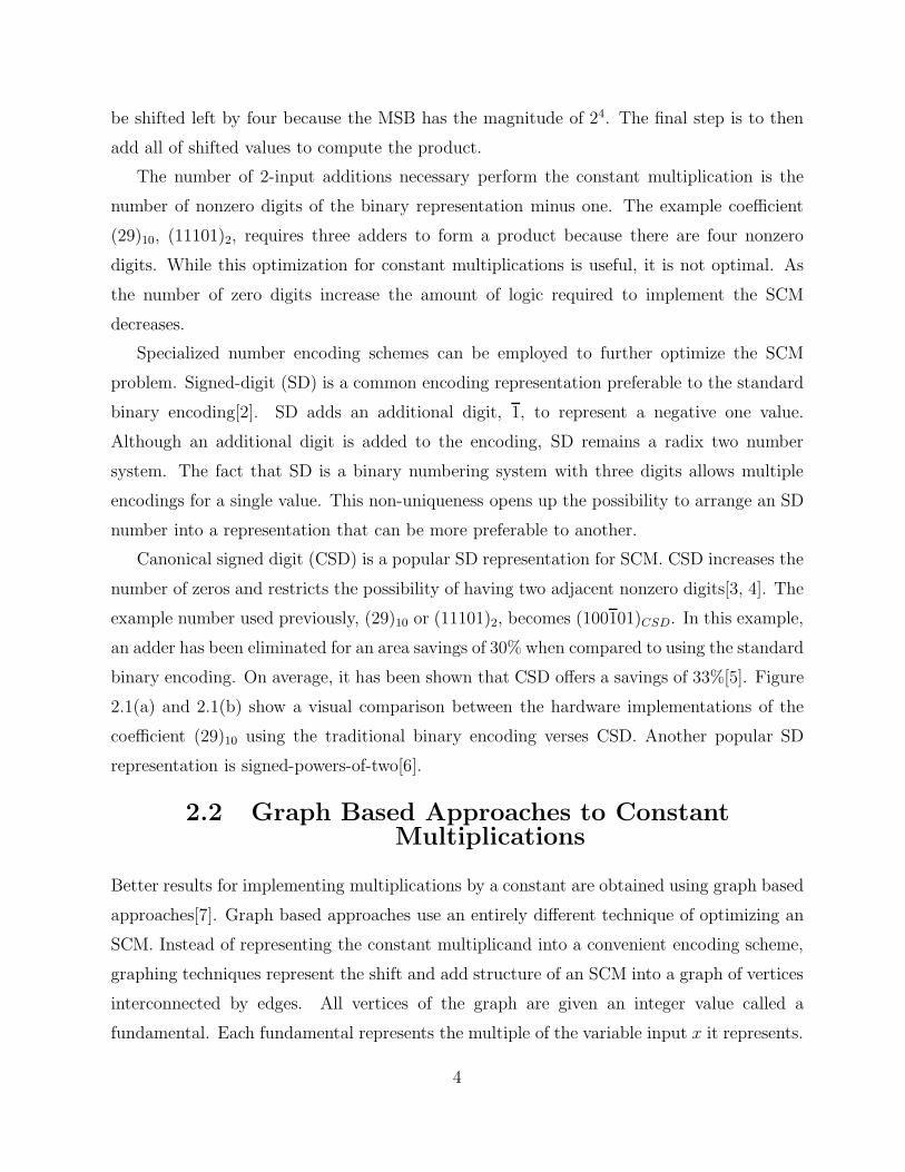
Canonical signed digit (CSD) is a popular SD representation for SCM. CSD increases the
number of zeros and restricts the possibility of having two adjacent nonzero digits[3, 4]. The
example number used previously, (29)10 or (11101)2, becomes (100101)CSD. In this example,
an adder has been eliminated for an area savings of 30% when compared to using the standard
binary encoding. On average, it has been shown that CSD offers a savings of 33%[5]. Figure
2.1(a) and 2.1(b) show a visual comparison between the hardware implementations of the
coefficient (29)10 using the traditional binary encoding verses CSD. Another popular SD
representation is signed-powers-of-two[6].
2.2 Graph Based Approaches to ConstantMultiplications
Better results for implementing multiplications by a constant are obtained using graph based
approaches[7]. Graph based approaches use an entirely different technique of optimizing an
SCM. Instead of representing the constant multiplicand into a convenient encoding scheme,
graphing techniques represent the shift and add structure of an SCM into a graph of vertices
interconnected by edges. All vertices of the graph are given an integer value called a
fundamental. Each fundamental represents the multiple of the variable input x it represents.
4

x[n]
29x[n]
≪ 3 ≪ 2≪ 4
(a) Traditional Binary Multiplier
x[n]
29x[n]
≪ 2≪ 5
(b) CSD Multiplier
Figure 2.1: Hardware implementations of the constant multiplication of 29 based off differentnumber encodings.
All graphing techniques require a starting vertex having a value of 1. The value of 1 represents
the unaltered input x (i.e. x× 1). The edges that interconnect the vertices represent a shift
amount applied to the vertex from which it branches.
A common constraint is to limit the fundamentals to having only two input graph edges,
however this is not always the case[8]. This constraint allows the fundamentals to be
implemented in hardware using a single adder. The value of the fundamental corresponds
to the output of the adder, an integer multiple of the graph’s input x. To create an adder
graph for the constant 29, three vertices are required: 1, 33 and 29. The first vertex is the
starting point of the graph and represents the unmodified input, x, and as such does not
require an adder to implement. The other two vertices represent the required fundamentals
needed to form the final product. Both fundamentals require a single adder, giving an adder
count of two. Figure 2.2 shows an adder graph along with its hardware implementation to
achieve a constant multiplication of (20)10.
As previously stated, graphing methods can achieve a more optimal SCM solution.
Graphing techniques also open up the possibility to optimize multiple SCM’s into one adder
graph. This process is known as multiple constant multiplications (MCM). When using MCM
instead of SCM, an added savings can be accomplished by reusing fundamentals between
5

1 33 29
32
1
1
-4
(a) Adder graph
x[n]29x[n]
≪ 2
≪ 5
bb
(b) Hardware implementation
Figure 2.2: Figure of the adder graph for the constant multiplication of (29)10 2.2(a) alongwith the corresponding hardware implementation 2.2(b).
MCM Blockxh0xh1xhn−1xhn
y[n]
x[n] xhn−2
z−1 z−1 z−1 z−1b b b
Figure 2.3: Transposed FIR filter using an MCM multiplier block
the constants. The MCM adder graph is attractive to digital filter designs because it solves
a critical need. The transposed FIR structure is helpful for this optimization as it has one
common input which needs to be multiplied by a series of constants as shown in Figure 2.3,
the exact operation the MCM provides.
2.3 Minimum Adder Graph Algorithms
Determining what fundamentals to use and how to connect them to form a minimum adder
graph (MAG) becomes a complex problem as the number of constant multiples and bit width
increase. Several algorithms[9, 10, 11, 12] have been proposed over the last three decades to
accomplish this task, and even today work continues on finding ways to improve them.
6

Bull and Horrocks published a paper in 1991[9] that is heavily cited as a starting point
in the MAG algorithm research. They proposed a number of algorithms, the most notable
one that allows shifts, additions and subtractions in the same graph. That particular MAG
algorithm has come to be known as Bull Horrocks Algorithm (BH). A few years after the BH
algorithm was proposed Dempster and Macleod proposed a modification to the BH algorithm
known as BHM[13].
The BHM algorithm provided a couple of improvements over the BH algorithm, most
notably the restriction of only allowing odd fundamentals in the adder graph. The idea to
only allow odd fundamentals stems from the assumption that the shifts have no impact on
the circuit cost. This assumption is generally considered feasible because the shifts are static
and can be implemented using a trivial wire shift. All even numbers have an LSB of 0 and
can be shifted right at least one bit without losing any information of the signal. The same
concept can be revised to say that odd numbers can be shifted right to form all numbers
that are a power of two multiple larger. This observation allowed Dempster and Macleod to
reduce the search space of the BH algorithm by adding the odd fundamental constraint. Only
a year after publishing a paper on BHM, Dempster and Macleod further improved their work
with the release of the RAG-n algorithm[10]. Research on MAG algorithms remained silent
until Voronenko and Puschel added more algorithms to the list, most notably HCUB[11].
Recently Gustafsson has proposed a new algorithm, DiffAG, that can offer slight savings
over HCUB for word lengths under 19bits[12].
7

CHAPTER 3
BACKGROUND
3.1 Delta-sigma Converters
The primary motivation behind this research is to find ways to build faster and more accurate
analog to digital converters (ADCs) for highly demanding communication systems. To realize
this goal, high order delta-sigma (∆Σ ) converters are used over conventional converters[14].
∆Σ converters are clocked at much higher rates than conventional converters which are
clocked at the Nyquist rate[15] of the input signal. Due to the high clock rate, which is
above the Nyquist rate, ∆Σ converters are grouped into a category of converters known as
oversampled ADCs. Similar to other oversampled converters, ∆Σ converters represent an
analog signal in a high speed low resolution, usually one bit, signal. A decimation filter is
required to convert the high speed low resolution signal into the high resolution Nyquist
rate format expected from an ADC. By oversampling the input signal, the converter noise
injected by ∆Σ’s low resolution quantizer and non-linear components is at a much higher
frequency than the input signal and can be easily filtered. This technique is known as noise
shaping. While Nyquist rate ADCs will not generate as much quantization noise, the noise
cannot be filtered, because it is within the input signal’s bandwidth. Another key benefit
to oversampled ADCs is the relaxation of the strict requirements for circuit components
that Nyquist rate converters demand. Oversampled converters instead require high speed
components which are available in VLSI circuits.
At the core of any ∆Σ converter lies a ∆Σ modulator which is responsible for doing the
actual work of converting the input signal into the high speed low resolution signal. Figure
3.1 shows a rudimentary first order ∆Σ modulator. The active part of the modulator is a
filter which for the first order modulator is simply an integrator. The noise produced by the
modulator is represented by the signal e(n). Due to the negative feedback loop, the output
8

b b1z−1x(n) y(n)
e(n)
Figure 3.1: Rudimentary first order ∆Σ modulator
bbx(n) yREG Quantizer
DDCn 1
1n
n
Figure 3.2: Implementation of the rudimentary first order ∆Σ modulator in digital form.
signal y(n) is on average equal to the input signal x(n).
The circuit shown in Figure 3.1 is used for circuit analysis of ∆Σ converters and is not the
actual implementation. The non-linear elements have been removed and represented with the
noise signal. Figure 3.2 shows how a first order ∆Σ modulator can be constructed. A simple
digital integrator is constructed using an adder, register and feedback path. The multi-bit
output of the integrator is then quantized into a single bit signal. The quantizer, while
sounding elaborate, is a simple comparator referencing zero. The one bit digital quantizer is
realized simply by dropping all of the bits except the MSB (assuming the signal is encoded
in 2’s complement representation). A digital to digital converter (DDC) is used to convert
the single bit of the modulator’s output back into a multi-bit signal that can be subtracted
from the modulator’s input. From Figure 3.2 it is easy to see how the term ∆Σ was coined.
Since the ∆Σ modulators have the active filter in the forward path instead of the feedback
loop, the signal is first subtracted and then added. The Greek letters delta(∆) and sigma
(Σ) are used because they are commonly used as mathematical operators for representing
differences and summations respectively.
As the order of the loop filter is increased the theoretical noise shaping properties of the
∆Σ modulator are also improved. Unfortunately the complexity of the modulator quickly
9

bbx(n) y(n)
g(n)
Quantizer
−e(n)
Figure 3.3: The error-feedback structure of a ∆Σ modulator.
increases along with the order. Due to the feedback nature of the modulator, instabilities
are increasingly hard to eliminate in higher orders. A simplification used in ∆Σ digital
to analog converters is shown in Figure 3.3. This alternative modulator architecture is
known as the error-feedback structure. With the filter in the feedback loop, at first glance
the circuit appears as delta modulator. With closer observation the filter is not in the
traditional feedback loop but in altered feedback loop of an error signal, e(n), rather then
the modulator output, y(n). This structure is simpler and allows FIR filters to be used to
implement the loop filter, g(n), albeit while limiting the use of the ∆Σ modulator to digital
to analog converters only due to the demanding precision required from the loop filter and
the limitations of analog filters.[14].
3.2 Loop Filter
A large amount of research has been focused on implementing a loop filter for an error-
feedback ∆Σ [16, 17]. It is paramount for the loop filter to have a high throughput
and yet still maintain a realistic implementation. The first step in creating a realizable
loop filter has already been accomplished. A sparse loop filter[18] was designed by Naval
Research Laboratory (NRL) with an order of 198 and only ten non-zero coefficients. The
coefficients are shown as Table 3.1. With a large enough word length the sparse loop
filter can reach attenuation levels of 90dB with only nine multipliers! Figure 3.4 shows
the frequency response of the loop filter. Even though the loop filter design is very sparse,
the implementation of the filter is still important. The bulk of the research covered in this
work is directed toward implementation schemes for the previously designed loop filter using
field programmable gate arrays (FPGAs).
10

-80
-60
-40
-20
0
20
0 0.2 0.4 0.6 0.8 1
Gai
n(d
B)
Normalized Frequency
Figure 3.4: Frequency response of the sparse loop having only ten non-zero coefficients.
Table 3.1: Double precision coefficients of previously designed sparse loop filter
0 1.000000000000000000000000000000000000000000000000000000000002 1.31250000000000000000000000000000000000000000000000000000000
12 0.1877412115387347424366737413947703316807746887207031250000014 -0.2153068975462586742697368435983662493526935577392578125000038 0.1259469857632670442004751976128318347036838531494140625000072 0.05259400350726096268205722594757389742881059646606445312500
110 0.02609589652509324356199904570985381724312901496887207031250150 -0.01514283000938064678575489807599296909756958484649658203125182 0.01039960540337357339235602182725415332242846488952636718750198 -0.00427255251708819235034741979006867040880024433135986328125
11

3.3 CSD Real-time Recoding
Although this work concentrates on the implementation of fixed coefficient FIR fitlers, some
of our work is applicable to filters that have coefficents that change over time, such as
adaptive filters. The graphing optimization techniques described in Section 2.2, while being
superior for static filters, were previously not considered as viable options for adaptive filter
implementations due to the real-time limitations.
To avoid these problems, the previous work reverted back to digit based optimization to
deal with the variable coefficients of the adaptive filters. To perform the digit encoding, a
real-time CSD recoder known as fastCSD was proposed [19]. Work has continued on the
fastCSD design to show how high speed multipliers for adaptive filters could be implemented
[20, 21, 22].
12

CHAPTER 4
VHDLGEN, A VHDL GENERATOR
For this research a specialized program, VHDLGen, was created that is capable of writing
VHDL files. Currently VHDLGen is only used for creating transposed FIR filters, although
it could be extended to support a wider range of filters. VHDLGen is an important part
of this research, without it a great deal of time would have been required creating filters
in VHDL. Creating just one VHDL filter by hand can be a tedious job, especially for high
order filters. Creating the filters separately by hand also increases human error which can
further delay the results. With VHDLGen, hundreds of filters can be generated of varying
implementations in seconds.
VHDLGen is built using PHP[23]. PHP is a general-purpose scripting language that has
been popular for a decade[24]. The name PHP is a recursive acronym that stands for PHP:
Hypertext Preprocessor. Although PHP is most widely used for Web development, over
the years it has become popular as a general purpose language, fulfilling the same needs as
languages such as Perl and VBS. PHP is the technology of choice for VHDLGen for many
reasons. PHP offers a relatively simple syntax similar to C and Perl. PHP is an open source
technology, allowing PHP to be distributed and used free of charge. Similar to many other
open source projects, PHP is also multi-platform allowing VHDLGen to be executed on
Linux, BSD, Solaris, Mac OS and Microsoft Windows.
4.1 VHDLGen Example Usage
This section demonstrates how VHDLGen can be used to easily create a variety of VHDL
circuit files. A small filter has been chosen and used throughout this section to keep the
examples simple. In order to use VHDLGen, a run file must be written. Refer to Listing
4.1 to see the run file used for this example. Basic knowledge of PHP is required to write
13

a run file for VHDLGen, although when starting from the sample only minor programming
experience should be required.
To mark the beginning of the run file or any PHP script1, the phrase “<?php” is required
to denote the start of the script, every line after will be executed as PHP code until the
phrase “?>” is reached. It is recommended that the next few lines of the script contain the
required include statements to allow access to the VHDLGen libraries. The example run file
in this section as well as the template file in the appendix, define the autoload() function
to perform all the necessary include statements in only a few lines of code. PHP 5 has a
special use for the autoload() function, and if defined it will be called every time a PHP
class that has not yet been defined is instantiated. Without this function definition many
lines of code would be required to include the VHDLGen class files.
Creating the FIRFilterData object is the next step to creating a run file. The implemen-
tation strategy of the resulting VHDL file is dependent on the type of FIRFilterData object
created. The example run file in this section creates the base FIRFilterData object which
will produce a VHDL FIR filter implementation using the standard VHDL multiplication
operator ‘*’. Once the FIRFilterData object is instantiated, it needs to be correctly initiated
with the filter-specific information such as the bit width and coefficient data.
VHDLGen assumes that the coefficients will be encoded as two’s complement fixed
point numbers, although the FIRFilterData class could be extended to provide support
for different encodings. As demonstrated in the example run file, the hardware limits for
the fixed point numbers can be set using the setBitWidth() and setDecimalPlaces()2
methods.
4.1.1 Filter Creation
Next the coefficient data is loaded into the FIRFilterData object. Matlab provides a
convenient environment to create filters via firpm, the Parks-McClellan optimal FIR filter
design command but any filter design technique can be used. VHDLGen only requires a set
of coefficients, which are assumed to be in transposed form.
1The “<?php” and “?>” are actually not always required. If for some reason it is not preferable to havePHP’s open and close tags included, the PHP script could still be executed from the console with additionof the -r switch.
2The setDecimalPlaces() might be better thought of as setBinaryPlaces() since it is actually settingthe number bits that are considered to be fractional.
14

Listing 4.1: VHDLGen Run File
<?php/∗∗ Load VHDLGen API∗/
f unct i on au to load ( $c las s name ) {r equ i r e on c e "lib/$class_name.class.php" ;
}
/∗∗ Create and se tup the∗ FIRFi l terData Objec t∗/
$ f i r = new FIRFilterData ( ) ;$ f i r −>setBitWidth ( 1 8 ) ;$ f i r −>setDec imalPlace s ( 1 6 ) ;$ f i r −>l oadCoef f sFromFi le ( ’coeffs.txt’ ) ;
/∗∗ Create and se tup the∗ VHDLCircuitFIR Objec t∗/
$VHDLGenerator = new VHDLCircuitFIR ( $ f i r ) ;$VHDLGenerator−>entityName = "example" ;$VHDLGenerator−> l i b r a r i e s = array (’ieee’ ) ;$VHDLGenerator−>l i bUse [ ] = ’ieee.std_logic_1164.ALL’ ;$VHDLGenerator−>l i bUse [ ] = ’ieee.std_logic_signed.ALL’ ;$VHDLGenerator−>l i bUse [ ] = ’ieee.numeric_std.ALL’ ;$VHDLGenerator−>l i bUse [ ] = ’ieee.numeric_bit.ALL’ ;$VHDLGenerator−> l i b r a r i e s [ ] = ’UNISIM’ ;$VHDLGenerator−>l i bUse [ ] = ’UNISIM.vcomponents.all’ ;$VHDLGenerator−>por t s [ ’X’ ] = array (’direction’ => ’IN’ ,’type’ =>
’STD_LOGIC_VECTOR(W-1 DOWNTO 0)’ ) ;$VHDLGenerator−>por t s [ ’CLK’ ] = array ( ’direction’ => ’IN’ ,’type’ =>
’STD_LOGIC’ ) ;$VHDLGenerator−>por t s [ ’RST’ ] = array ( ’direction’ => ’IN’ ,’type’ =>
’STD_LOGIC’ ) ;$VHDLGenerator−>por t s [ ’Y’ ] = array (’direction’ => ’OUT’ , ’type’ =>
’STD_LOGIC_VECTOR(W-1 DOWNTO 0)’ ) ;
/∗∗ Save the f i l t e r to a∗ VHDL f i l e∗/
$VHDLGenerator−>save ( ) ;?>
15

Listing 4.2: Filter Creation using firpm
order = 8 ;f r e q s = [0 . 3 . 7 1 ] ;f r eq power s = [0 0 1 1 ] ;b = f irpm ( order , f r eq s , f r eq power s ) ;
-90
-80
-70
-60
-50
-40
-30
-20
-10
0
10.70.30
Gain
(dB
)
Normalized Frequency
Figure 4.1: Frequency response of the 8th order sample filter.
The sample filter that will be used throughout this section is an 8th order high-pass filter
that transitions from stopband to passband between the normalized frequencies of 0.3 and
0.7. Listing 4.2 shows the Matlab script used to create the sample filter. The script could be
written in one line, but has been written in such a way so that the code is self commenting.
The first three lines store values in variables that are used in the fourth line where the actual
call to firpm occurs. The first line sets a variable called order. The next two lines set
the freqs and freq powers variables which are vectors that together hold the attenuation
levels for a set of frequencies. In this case freqs is set to [0 .3 .7 1] and freq powers
is set to [0 0 1 1] which set the filter design constraints to a high pass filter that will
stop frequencies below 0.3 and pass frequencies above 0.7. Figure 4.1 shows the frequency
response for the filter that is created by the script in Listing 4.2.
16

After executing the commands in Listing 4.2 all of the coefficients are stored in the vector
b. The next step is to export the coefficients into a format that can be read by VHDLGen.
This can be accomplished in many ways. The simplest, albeit inefficient, method of exporting
the coefficients is to manually type them into your run file. To dump the coefficients stored
in Matlab to the console simply type b and then press the enter key. Matlab’s output format
should be set correctly, since the default will quantize the coefficients heavily when printed to
the console. For example Matlab’s output format can be changed by running format long
which will display the coefficients in 15-digit fixed point format. The coefficients then need
to be copied to the PHP run file that will use the VHDLGen API to generate the VHDL
circuit files. The coefficients must be stored in an array and loaded into an FIRFilterData
object. Refer to Listing 4.3 to see how this can be accomplished. Section 4.4.2 explains the
FIRFilterData and the setCoeffs() methods in detail.
Listing 4.3: Saving the coefficients to the run file manually
$ f i r −>s e tCo e f f s (array (
0.00000000000000 ,0.06352200530103 ,0.00000000000000 ,
−0.30065644924146 ,0.50000000000000 ,
−0.30065644924146 ,0.00000000000000 ,0.06352200530103 ,0.00000000000000
)) ;
In most situations it is more convenient to export the coefficients to a coefficient file,
which is the recommended method for loading the coefficient data into VHDLGen. Saving
the coefficient files will help with situations such as handling large filters, requiring higher
precision, the ability to easily reuse the filters and creating multiple filters in a single run. A
coefficient file is a text file that has one number per line. VHDLGen will attempt to convert
each line from a string to a numeric value. Any line that cannot be read as a number will be
silently ignored and treated as a comment. This allows many different file formats to be read
with VHDLGen, even fcf files exported from fdatools[25]. Listing 4.4 shows a set of Matlab
17

commands that will export vector b to a file named coeffs.txt. The coefficient file can then
be loaded with VHDLGen using a statement like $fir−>loadCoeffsFromFile(’coeffs.txt’)
provided that the coeffs.txt file is in the same directory as the run file. If the coefficient
file is in another directory, the correct relative or global path is required.
Listing 4.4: Creating the coefficient file in Matlab
f i d = fopen (’coeffs.txt’ , ’w’ ) ;fpr intf ( f id , ’%-2.20f\n’ , b ) ;fc lose ( f i d ) ;
4.1.2 VHDLCircuitFIR Object Creation
After the FIRFilterData object has been created and initialized with the coefficient data,
it can then be loaded into an VHDLCircuitFIR object. The VHDLCircuitFIR class is
responsible for building the VHDL circuit entity and outlining architecture statements while
the FIRFilterData class is focused completely on the building the actual VHDL code located
inside the architecture statement. As shown in the example run files, the VHDLCircuitFIR
object is created using “$VHDLGenerator = new VHDLCircuitFIR($fir);”, where $fir is the
FIRFilterData object. The next step is to set the VHDL entity name by loading a value
into the entityName property of the VHDLCircuitFIR. This is done in the example run file,
Listing 4.1, by the following line of code, “$VHDLGenerator−>entityName = "example";”.
The run file is required to perform some setup tasks on the VHDLCircuit object before
the VHDL files can be generated. All of the VHDL libraries and ports are required to be
setup directly using the VHDLCircuitFIR object in the run file, currently the FIRFilterData
object is not responible for this task, although it expects particular port names to be defined
and the required libraries to be loaded. Most of the work in Listing 4.1 fulfills this task,
starting from the line that sets the entityName to just before the end of the script. The last
line of the run file is where VHDLGen actually does all of its work. The call to the save()
method calls the toString() method and then saves the returned value to the current output
directory with a filename based off of the entityName property.
Listing 4.5 shows the VHDL entity statement that is created after executing the example
run file. While the VHDLCircuitFIR class is responsible for this part of the VHDL file, it
does provide hooks for the FIRFilterData object to alter the code under its control. This,
18

for example, allows the FIRFitlerData object to setup the generic contant definitions also
shown in Listing 4.5.
Listing 4.5: VHDL entity statement created by the sample run file
ENTITY example IS
GENERIC(W : i n t e g e r := 18 ;F BITS : i n t e g e r := 16 ;H COUNT : i n t e g e r := 4 ;ORDER : i n t e g e r := 8
) ;PORT(
X : IN STD LOGIC VECTOR(W−1 DOWNTO 0 ) ;CLK : IN STD LOGIC;RST : IN STD LOGIC;Y : OUT STD LOGIC VECTOR(W−1 DOWNTO 0)
) ;END example ;
Completing the process to this point, will result in a VHDL file being saved as
example.vhd in the directory that the run file was executed. The VHDL file can now
be opened, synthesized and simulated with Xilinx ISE just like any other VHDL file.
4.2 VHDL Filter Generation Using OtherImplementation Schemes
Section 4.1 outlined the steps necessary to create a VHDL filter using the VHDLGen API.
The filter that is created internally uses the standard VHDL multiplication operator because
the FIRFilterData object was used. Very similar steps are used to create a filter that
is optimized with MCM, only minor adjustments to the run file are required. Simply
replacing the baseline FIRFilterData object with the FIRFiltedrDataMCM object is all that
is required. Section 4.4.2 covers the FIRFiltedrDataMCM and other FIRFilterData classes in
detail. Replacing the FIRFilterData object will change and all the necessary components of
the VHDL circuit such as the generic constants, functions, types and signals. For example, to
create a filter using the DSP48 slices in a Xilinx Virtex device, replace the FIRFilterData
object with the FIRFiltedrDataDSP48 object. Currently the FIRFilterDataHybrid and
FIRFilterDataHybridDSP48 classes require extra information to be set in the constructor.
19

FIR Coefficient File
0.000080.000120.000000.000230.002350.000120.000000.02471
VHDL Files
LIBRARYUSE ieee
ENTITYPORT(X : INCLK : INRST : IN
VHDLGen MATLAB
XilinxISE
Data Input File
0.000080.000120.000000.000230.002350.000120.000000.02471
MATLAB
Simulated Data
0.000080.000120.000000.000230.002350.000120.000000.02471
Results
0.000080.000120.000000.000230.002350.000120.000000.02471
Figure 4.2: Research workflow
4.3 Analysis
After generating a VHDL file, it is important to verify that the circuit performs correctly
before relying on it for further research. The circuit must be verified in a VHDL simulator
to ensure the VHDL code has been written properly. Unfortunately the step from verifying
filters in a comfortable Matlab environment to verifying hardware simulations can be
daunting, but it is critical.
Figure 4.2 outlines the steps required to verify the VHDL code using the Xilinx ISE VHDL
simulator[26]. As shown in the figure, the circuit verification is a process requiring multiple
steps. The preliminary steps have already been explained in the previous sections. Matlab
is used to design an FIR filter and then used to export the filter coefficients into a portable
file. After the coefficients have been exported into the coefficient file, the VHDLGen API
20

can then be used to generate VHDL files of varying implementation schemes. The VHDL
files are then ready to be simulated in a VHDL simulator such as Xilinx ISE which was used
in for this research.
All of the steps stated so far in the verification work flow are fairly straightforward. The
process becomes a bit more complicated once the circuit is running and its output needs to
be verified. In order to show that the VHDL filter is working as designed in Matlab, a large
data set is required.
The first step in using a larger data set in a VHDL simulation is creating a VHDL test
bench capable of streaming the data from an input file and then saving the simulated output
into an output file. This can be accomplished using the VHDL file type. Listing 4.6 shows
how the VHDL file type was used in this research. A single process block is designed to
read the current output value Y and write it to the output file “output.txt” on the negative
edge of the clock signal CLK. Then the next value is read from the input file “input.txt” and
assigned to the input signal X. As shown in the VHDL listing, the current value of X is also
saved in the output file for convenience.
Once the simulation is complete, the corresponding data files must be analyzed to
verify the filter is running as expected. At this point the work flow returns to the Matlab
environment in which human readable graphs can be created such as the step, impulse and
frequency responses.
Depending on what type of analysis is planned, different data input files are required.
The first analysis to perform is to verify that the impulse and step responses of the filter are
correct. Both responses are time domain operations that are simple to perform and inspect,
and as such are a quick first test of the filter circuits. Figures 4.3(a) and 4.3(b) show the
impulse and step responses of the 8th order sample filter. Both figures show the input and
output values from the data files. The impulse response corresponds to the filter coefficients.
The step response can be used to verify the steady state value of the filter is as expected.
The step and impulse responses are useful tools to verify the correct output of filter
circuits, but even if they are generated correctly, further analysis is still required. To
determine the exact behavior of the filter, the frequency response is needed. Figure 4.3(c)
shows the nominal frequency response generated in Matlab for the 8th order sample filter.
Obtaining the frequency response in Matlab is a trivial process that occurs during the filter
design process. The challenge is obtaining the frequency response from the VHDL filter
21

Listing 4.6: Code snippet from a VHDL test bench
wr i t e i npu t : process (CLK)f i l e fhandleWrite : TEXT open WRITEMODE i s "output.txt" ;f i l e fhandleRead : TEXT open READMODE i s "input.txt" ;variable my input l in e : LINE ;variable my output l ine : LINE ;variable readData : i n t e g e r ;
begin
i f CLK’ event and CLK= ’0 ’ then
−−read the current inputr e ad l i n e ( fhandleRead , my input l in e ) ;read ( my input l ine , readData ) ;
−−save the inputwr i t e ( my output l ine , readData−OFFSET) ;wr i t e ( my output l ine , " " ) ;
−−save the outputwr i t e ( my output l ine , t o i n t e g e r ( s igned (Y) ) ;
−−wr i t e to f i l ew r i t e l i n e ( fhandleWrite , my output l ine ) ;
end i f ;X <= conv s t d l o g i c v e c t o r ( readData ,W) ;
end process ;
circuit.
To accomplish the task, zero-mean Gaussian white noise is used for the input file. In
the frequency domain the white noise can be thought of as a constant value from which the
filter can carve out its signature, the frequency response. Listing 4.7 shows the Matlab code
used to create the white noise. An important setting in this code listing is adjusting the
maximum value of the noise signal. The randn function does not return numbers bound
by plus or minus one. This behavior can easily over saturate the filter and cause an erratic
response. Care must be taken so that none of the values in the noise vector overrun the
bounds of the filter.
Once the input noise file is created, it can be used by Xilinx ISE VHDL simulator to
generate the output file. The output contains the filtered noise although it appears very
similar to the white noise when viewed in the time domain. Now that both the input and
output noise files have been created the frequency response of the actual simulated hardware
22

-5000
0
5000
0
5000
10000
0 5 10 15 20 25 30 35 40 45 50
Sig
nalLev
el
Time (samples)
X (Input Level)
Y (Output Level)
(a) Impulse response.
-5000
0
5000
0
5000
10000
0 5 10 15 20 25 30 35 40 45 50
Sig
nalLev
el
Time (samples)
X (Input Level)
Y (Output Level)
(b) Step response
-90
-80
-70
-60
-50
-40
-30
-20
-10
0
10.70.30
Gain
(dB
)
Normalized Frequency
(c) Nominal frequency response.
-90
-80
-70
-60
-50
-40
-30
-20
-10
0
10.70.30
Gain
(dB
)
Normalized Frequency
(d) Simulated frequency response.
Figure 4.3: Impulse and step response from the 8th order sample filter. 4.3(a) Impulseresponse. 4.3(b) Step response. 4.3(c) Nominal frequency response. 4.3(d) Frequencyresponse from simulated hardware using white noise.
Listing 4.7: Matlab code to generate white noise
b itwidth = 18 ;no i s e samp le s = 100000;no i se raw = randn( no i se samples , 1 ) ;noise max = max(abs ( no i se raw ) ) ;n o i s e = round( 2ˆ( b itwidth −1) ∗ ( no i se raw /noise max ) ) ;f i d = fopen (’white_noise.txt’ , ’w’ ) ;fpr intf ( f id , ’%-20.0f\n’ , n o i s e ) ;fc lose ( f i d ) ;
23

can be obtained by transforming both input and output signals into the frequency domain
and then dividing the output by the input. This process is shown in Listing 4.8. Notice that
the input values is saved in the first column of the output file for convenience.
Listing 4.8: Matlab code to create the frequency plot data from filtered noise
f i d = fopen (’filtered_noise.txt’ , ’r’ ) ;a = fscanf ( f id , ’ %d %d’ , [ 2 i n f ] ) ;input = a ( 1 , : ) ;output = a ( 2 , : ) ;fc lose ( f i d )f r eq ou t = 20∗ log10 (abs ( f f t ( output ) . / f f t ( input ) ) ) ;f i d = fopen (’freq_response.txt’ , ’w’ ) ;for i =1: length ( s im output )
fpr intf ( f id , ’%f\n’ , output ( i ) ) ;end
fclose ( f i d ) ;
4.4 Anatomy of the VHDLGen API
Given a particular FIR filter, or more simply, a set of coefficients, VHDLGen can create
an array of different circuit implementations. The type of filter circuit that VHDLGen
creates depends on the type of filter data object used to load the coefficients. The filter
data object contains the information needed to realize each coefficient into VHDL, along
with any other types, signals, generics or functions needed. Currently, there are four types
of FIR filter data objects. The first, FIRFilterData, only provides the information needed
to create a straightforward transposed FIR filter using the VHDL multiplication operator
“*”. The rest of the filter data objects extend FIRFilterData and override the methods
necessary to construct a different FIR implementation. The FIRFilterData subclasses are
FIRFilterDataMCM, FIRFilterDataHybrid and FIRFilterDataHybridDSP48.
Using object oriented design principles, VHDLGen’s core functionally is contained in
base classes intended to be extended by other classes to implement specific tasks. The
base class of VHDLGen is the VHDLCircuit class. VHDLCircuit is extended by the
VHDLCircuitFIR class adding the necessary functionality needed to create transposed FIR
filters. The VHDLCircuitFIR class adds the requirement of an FIRFilterData object in the
class constructor. The FIRFilterData object is used to provide all filter specific information
24

VHDLCircuit
VHDLCircuitFIR1
FIRFilterData
FIRCoeff
1
1 1..*
...MCM
entityNameoutputDirectorylibrarieslibUseportsgenericstypessignalsconstantsfunctions
toStringsave
indexesdecimalPlacesbitWidth
addVHDLFunctionsaddVHDLSignalsaddVHDLTypesaddVHDLGenerics
setCoeffsloadCoeffsFromFile
...Hybrid ...DSP48
getCurrentIndexValuegetPositionsetPositiongetTypesetValuegetValuetoVHDL
...DSP48
FIRCoeffIndex
1..*
1
...MCM...Zero...Simple resetincrementdecrementgetIndexgetMax
Figure 4.4: UML class diagram of VHDLGen
needed to create the filter. Using the given FIRFilterData object the VHDLCircuitFIR
class creates an array of FIRCoeff objects that represent the filter coefficients. The
VHDLCircuitFIR then loops though the coefficient objects and joins them together into
a coherent block of VHDL code. Figure 4.4 shows the basic outline of the entire VHDLGen
API as a UML class diagram[27]. Only the FIRFilterData class needs to be extended to
create different variations of transposed FIR filters; the VHDLCircuitFIR does not need to be
extended any further as it is designed to work with all of the FIRFilterData types. Figure
4.5 shows a simple flow diagram of how these classes interact to create the required VHDL
code.
25

b b b
VHDL FIR CircuitGenerator
FIR Filter Data
CO CO CO
FIR Coefficient File
VHDL File
0.000080.000120.000000.000230.002350.000120.000000.02471
LIBRARYUSE ieee
ENTITYPORT(X : INCLK : INRST : IN
FIR Coefficient Objects
loadCoeffsFromFile()
save()
Figure 4.5: VHDLGen Flow Diagram
4.4.1 VHDLCircuit Class
The VHDLCircuit class contains the most generic information needed for generating
VHDL files. The two most important methods are the CreateArchitectureHeader()
and createArchitectureBody() methods, both return a string containing the information
needed to form the VHDL file. The createArchitectureBody() method is simply a
placeholder for child classes to extend, while the CreateArchitectureHeader() method
has a set structure that does not need any further extension. To see the exact structure of
the CreateArchitectureHeader() method, refer to Listing 4.9.
CreateArchitectureHeader() relies on a set of associative arrays3 containing the
necessary information needed to construct the header section of the VHDL architecture
statement. The arrays are stored as public member data in the VHDLCircuit class and can
be easily appended to when extended functionally is needed. The first array called by the
CreateArchitectureHeader() method is the types array. The types array contains the
VHDL types needed in the circuit. The keys of the array correspond to the VHDL type
3An associative array is a special PHP array that allows alpha-numeric names to be used as the keysof the array. This is similar to Perl’s hashes or VBS’s dictionary objects. Although in PHP there is not aspecial definition for associative arrays, they are defined the same way standard arrays are except the key isspecified along with the value.
26

Listing 4.9: The CreateArchitectureHeader() method in the VHDLCircuit class
protec ted funct i on cr eateArch i t ec tu r eHeader ( ){$VHDLStr = ’’ ;
//Create Types$ i = 0 ;foreach ( $th i s−>types as $name => $value ){
$VHDLStr .= $th i s−>tab ( 1 ) . "type $name is $value;\n" ;$ i++;
}i f ( $ i ) $VHDLStr .= "\n" ;
//Create S i gna l s$ i = 0 ;foreach ( $th i s−>s i g n a l s as $name => $type ){
$VHDLStr .= $th i s−>tab ( 1 ) . "signal $name : $type;\n" ;$ i++;
}i f ( $ i ) $VHDLStr .= "\n" ;
//Create Constants$ i = 0 ;foreach ( $th i s−>contants as $name => $value ){
$VHDLStr .= $th i s−>tab ( 1 ) . "constant $name : $value;\n" ;$ i++;
}i f ( $ i ) $VHDLStr .= "\n" ;
//Create Functionsforeach ( $th i s−>f u n c t i on s as $name => $body ){
$VHDLStr .= $th i s−>tab ( 1 ) . "function ${name}${body}"
. $th i s−>tab ( 1 ) . "end function;\n\n" ;}r eturn ($VHDLStr ) ;
}
names. Each array key links to a value that contains the VHDL type assignment. For
example, to generate the reg array type used in the fir filters, the key is set to “reg array”
and the value is set to “array (0 to ORDER-1) of signed(W-1 downto 0)”. This entry in the
types array produces “type reg array is array (0 to ORDER−1) of signed(W−1 downto 0);”
in the header of the VHDL architecture statement. The remaining arrays used by the
CreateArchitectureHeader() method are the signals, constants, and functions arrays.
27

The arrays follow the same convention as the types array, each storing the VHDL name in
the key of the array and body of the VHDL statement in the associated value. This manner
of storing the VHDL definitions may seem strange, but it provides a simple yet powerful
means of extensibility while conforming to a set structure. Using the arrays also eliminates
the possibility of duplicate entries, both are important traits for a class that will be inherited
by many classes not yet defined.
To obtain the complete VHDL circuit description, the VHDLCircuit class also contains the
toString() and save() methods. As the name suggest, the toString() returns the entire
VHDL circuit in a string variable which can be printed to the console or stored for later use.
The toString() method has the responsibility of assembling the various parts of the VHDL
circuit that are not included in the architecture statement such as the library, generics and
port statements. Using the same techniques as the CreateArchitectureHeader() method,
the toString() method uses associative arrays for statements that require multiple entries
that also need to be extensible. The arrays used by toString() are the libraries, libUse,
entityName, generics and ports array. The toString() method also uses the public
property entityName for the title of the ENTITY statement in the VHDL file. The save()
method saves the VHDL circuit to a file, an important functionality when generating many
VHDL circuits in one run. The save() method also uses the entityName property to
determine the file name to save to. Since both the toString() and save() method use the
entityName property, the VHDL file name and the VHDL entity statement are forced to
match, helping to avoid the confusing scenario that is caused when they do not. The save()
method will save the VHDL file to the current working directory unless the outputDirectory
property contains a value, if so it will be used instead.
4.4.2 FIRFilterData Classes
As previously stated the FIRFilterData contains the FIR filter specific information, such as
the filter coefficients and extra VHDL functions, types and signals needed to implement the
filter in VHDL. To give VHDLGen the ability to create different FIR circuit implementations,
the FIRFilterData class is designed to be extended using methods that are easily overridden.
The base FIRFilterData class is programmed to create a simple FIR filter circuit using the
VHDL multiplication operator for all multiplications. Figure 4.6 shows the basic transposed
FIR structure created by the base FIRFilterData class. Currently there are three classes
28

h0h1hn−1hn
y[n]
x[n]
hn−2
z−1 z−1 z−1 z−1b b b
Figure 4.6: Circuit created when using the FIRFilterData filter data object
that extend FIRFilterData’s functionality, the FIRFilterDataMCM, FIRFilterDataHybrid
and FIRFilterDataHybridDSP48 classes.
Listing 4.10: The setCoeffs() method of the FIRFilterData class
pub l i c funct i on s e tCo e f f s ( $a ){$a = $th is−>quant i zeCoe f f s ( $a ) ;
for ( $ i =0; $ i < count ( $a ) ; $ i++){$th i s−>implementCoeff ( $a [ $ i ] ) ;
}
// s e t the Max s e t t i n g s f o r the indexe sforeach ( $th i s−>indexes as $index ){
$index−>setMax ( $index−>getIndex ( ) ) ;}
// r e c y c l e the indexe s f o r c i r c u i t b u i l d i n g useforeach ( $th i s−>indexes as $index ){
$index−>reset ( ) ;}
r eturn ( $a ) ;}
The filter coefficients are loaded into the FIRFilterData using the setCoeffs()
method. The setCoeffs() method has one parameter, an array of double precision
coefficients. Refer to Listing 4.10 to see how the setCoeffs() method is constructed.
The first step of the setCoeffs() method is quantizing the coefficients provided to the
hardware limits. The hardware limits are set using the public methods setBitWidth()
and setDecimalPlaces(), which store the information in the public variables bitWidth
and decimalPlaces in the FIRFilterData class. The FIRFilterData also includes the
29

loadCoeffsFromFile() method which wraps the setCoeffs() method by reading the
coefficients from a text file and then passing them to the setCoeffs() method. Listing
4.11 shows the loadCoeffsFromFile() method definition. Refer to section 4.1 for detailed
information describing the format of the coefficient text file.
Listing 4.11: Loading Coefficients from a File
pub l i c funct i on loadCoef f sFromFi le ( $f i leName ){$ l i n e s = f i l e ( $f i leName ) ;foreach ( $ l i n e s as $ l i n e ){
i f ( is numeric ( trim ( $ l i n e ) ) ){$ l i n e s F i l t e r e d [ ] = $ l i n e ;
}}$th i s−>s e tCo e f f s ( $ l i n e s F i l t e r e d ) ;
}
The private quantizeCoeffs() method, Listing 4.12, is used to accomplish the task of
quantizing the double precision coefficients. Quantization is accomplished using equation
4.1 where fp is the number of fractional binary digits in the fixed point representation and
k is a vector of the double precision filter coefficients.
Kq = round(2fpK) (4.1)
It is important that the bitWidth and decimalPlaces are set before calling the setCoeffs()
method to guarantee proper quantization. If not set, the bitWidth and decimalPlaces
variables will default to 16 and 14 respectively.
Listing 4.12: The quantizeCoeffs() method of the FIRFilterData class
protec ted funct i on quant i zeCoe f f s ( $aCoef f s ){$dec imalPlaces = $th i s−>dec imalPlaces ;$a In tCoe f f s = array ( ) ;$shiftAmount = pow(2 , $dec imalPlaces ) ;foreach ( $aCoef f s as $ c o e f f ){
$aIn tCoe f f s [ ] = round( $ c o e f f ∗ $shiftAmount ) ;}r eturn ( $aIn tCoe f f s ) ;
}
30

After quantization, each coefficient is used in turn with the private method implementCoeff().
The implementCoeff() method is responsible for instantiating the FIRCoeff coefficient
objects and initializing them with the proper information. Listing 4.13 shows the
implementCoeff() method. The base FIRFilterData class provides the ability to create a
standard FIR filter using only the FIRCoeffZero and FIRCoeffSimple coefficient objects,
which will be described further in section 4.4.3. The input to the implementCoeff() method
is the quantized integer coefficients that the FIRCoeff objects will need to represent. After
creating one of the FIRCoeff objects, the implementCoeff() method stores it in the coeffs
array. The classes that extend the base FIRFilterData class override the implementCoeff()
to support additional FIRCoeff objects. For example, the FIRFilterDataMCM class adds
support for MCM coefficients by instantiating the FIRCoeffMCM class instead of the
FIRCoeffSimple. This assigns the important job of deciding which type of FIRCoeff
object to instantiate for each of the filter coefficients solely to the implementCoeff()
method. In this light, implementCoeff() is the method that determines the behavior of
a FIRFilterData class.
Listing 4.13: The implementCoeff() method of the FIRFilterData class
protec ted funct i on implementCoeff ( $value ){$th i s−>indexes [ ’main’]−> increment ( ) ;i f ( $value == 0){
$th i s−>indexes [ ’zero’]−> increment ( ) ;$coeffTemp = new FIRCoeffZero (
$value , $th i s−>indexes [ ’main’ ] , $th i s−>indexes [ ’zero’ ]) ;
} else {$th i s−>indexes [ ’simple’]−> increment ( ) ;$coeffTemp = new FIRCoeffSimple (
$value , $th i s−>indexes [ ’main’ ] , $th i s−>indexes [ ’simple’ ]) ;
}$th i s−>c o e f f s [ ] = $coeffTemp ;$coeffTemp = nu l l ;
}
MCM support for VHDLGen is made possible by the FIRFilterDataMCM class. The
FIRFilterDataMCM class optimizes the FIR filter by extracting all of the multiplications
into a single multiplication block that can be heavily optimized shown in Figure 4.7. The
31

MCM Blockxh0xh1xhn−1xhn
y[n]
x[n] xhn−2
z−1 z−1 z−1 z−1b b b
Figure 4.7: Circuit created when using the FIRFilterDataMCM filter data object
more coefficients the FIR filter has, the greater the possibility of circuit reduction. The
FIRFilterDataMCM class overrides the addVHDLFunctions() method to accomplish this
task since the MCM multiplication block is coded using a VHDL function. The VHDL
function created is a combination logic block of simple shifts and adds, a “multiplierless”
implementation. To obtain the data needed to create the multiplication block, the MCMSynth
class is used to create the shift and add logic.
MCMSynth is a wrapper class for the acm program from the SPIRAL project[28]. The
constructor of the MCMSynth class requires an array of quantized integer coefficients and
the hardware limits of the target circuit. Using this information, MCMSynth runs the acm
program with the default HCUB algorithm when its run() method is called. MCMSynth
scans the output of acm for the section of generated C code and then parses it into a
simple data structure of associative arrays. Once the output has been fully parsed, the
toVHDLFunction() method can be called to transform the parsed data into VHDL code.
The addVHDLFunctions() method of the FIRFilterDataMCM class uses the above steps
to create the VHDL function that is responsible for handling all of the multiplications
needed by the FIR filter. Listing 4.14 shows the addVHDLFunctions() method. The first
step is to collect all of the MCM coefficient objects in the FIRFilterDataMCM object. All
other coefficient types that might be present are ignored, for the FIRFilterDataMCM class
the only other possible coefficient object type is FIRCoeffZero. Remember the decision
making process of which FIRCoeff object to use for a given coefficient is performed by the
implementCoeff() method which is assumed to have already been indirectly called by the
setCoeffs() method.
The principal goal of the VHDLGen API is the ability to easily interchange and mix
digital filter implementation topologies. The FIRFilterDataHybrid class is first class
32

Listing 4.14: The addVHDLFunctions() method of the FIRFilterDataMCM class
pub l i c funct i on addVHDLFunctions ( ){$ f un c t i on s = array ( ) ;$aMCM = array ( ) ;foreach ( $th i s−>c o e f f s as $ c o e f f ){
i f ( $ co e f f−>getType ( ) == ’mcm’ ){$aMCM[ ] = $coe f f−>getValue ( ) ;
}}//CREATE AND RUN THE MCM OBJECT$mcm = new MCMSynth($aMCM, $th i s−>bitWidth , $th i s−>dec imalPlaces ) ;$mcm−>run ( ) ;$ f un c t i on s [ ’MCM_BLOCK’ ] = $mcm−>toVHDLFunction ( ) ;r eturn ( $ f un c t i on s ) ;
}
Listing 4.15: The MCM Multiplication block
function MCMBLOCK( t0 : s igned ) return mcm out i s
type mcm internal i s
array (0 to 110) of s igned (2∗W−1 downto 0 ) ;variable t : mcm internal ;variable r e s u l t : mcm out ;
begin
t (0 ) := (others => t0 ( t0 ’LEFT) ) ;t ( 0 ) (W−1 downto 0) := t0 ;t (75) := SHIFT LEFT( t ( 0 ) , 2 ) ;t (69) := t (75) − t ( 0 ) ;
. . .
. . .
. . .t (50) := t ( 2 ) ; −− (MCM OUTPUT: : −361 ∗ t0 )
t (51) := t ( 1 ) ; −− (MCM OUTPUT: : −87 ∗ t0 )for i in 1 to MCMMAX loop
r e s u l t ( i ) := t ( i ) (W+F BITS−1 downto F BITS ) ;end loop ;return r e s u l t ;
end function ;
33

MCM Blockxh0xh1xhn−1xhn
y[n]
x[n]
xhn−2
z−1 z−1
z−1 z−1b b b
b b b
z−1 z−1 b b bb b b
b
b
Standard Multiplication
Figure 4.8: Circuit created when using the FIRFilterDataHybrid filter data object
mentioned so far that coalesces multiple implementation topologies to implement a single
filter. The FIRFilterDataHybrid class is based off the FIRFilterData class but also uses
logic from the FIRFitlerDataMCM class to implement a selection of coefficients using an
MCM multiplier block. Figure 4.8 shows the circuit diagram of this process. As shown in
the figure, a section of the coefficients in the center of the FIR filter are implemented using
standard multipliers instead of the MCM multiplication block. It is important to remember
that the standard multipliers are simply the VHDL multiplication operator, not an actual
hardware multiplier. The VHDL synthesizer may choose to use an embedded block available
in the target FPGA device or simply use the traditional programmable logic of the FPGA
to implement the multiplication by a constant.
The actual decision of which coefficients to implement as simple multiplication is made
in the setCoeffs() method. The setCoeffs() method is similar to the one in the
FIRFilterData class, the main difference being a call to the implementHybridCoeff()
method. The mimplementHybridCoeff method loops though all of the coefficients that have
been set in the setCoeffs() methods and replaces them with an MCM coefficient object if
certain conditions are met. Listing 4.16 shows the implementHybridCoeff() method.
Similar to the FIRFilterDataHybrid class the FIRFilterDataHybridDSP48 class merges
34

Listing 4.16: The implementHybridCoeff() method
protec ted function implementHybridCoeff ( ){
$mid = $th is−>middleCoef f ;
i f ( $th i s−>c o e f f s [ $mid]−>getType ( ) != ’ zero ’ ){$th i s−>replaceMCMwSimple( $mid ) ;
}
$ i = 1 ;while ( $th i s−>multCount > 0 && $ i < count ( $th i s−>c o e f f s ) ){
i f ( ( $mid + $ i ) < count ( $th i s−>c o e f f s ) && ($mid − $ i ) > 0){i f ( $th i s−>c o e f f s [ $mid + $ i ]−>getType ( ) != ’ zero ’ ){
$th i s−>replaceMCMwSimple( $mid + $ i ) ;}
i f ( $th i s−>c o e f f s [ $mid − $ i ]−>getType ( ) != ’ zero ’&& $th is−>multCount > 0){$th i s−>replaceMCMwSimple( $mid − $ i ) ;
}}$ i++;
}}
two implementation topologies together to form a single filter. Instead of using the
FIRFilterData class for the baseline structure however, the FIRFilterDataHybridDSP48
class is based on the ccFIRFitlerDataMCM. Then, a select set of coefficients are im-
plemented using the DSP48 slices available on the Xilinx Vertex FPGA devices. The
FIRFilterDataHybridDSP48 class also has an implementHybridCoeff() method decide
which coefficients should be replaced with DSP48 slices as shown in Figure 4.9. The
main difference in implementHybridCoeff() besides using DSP48 slices is that even zero
coefficients are replaced by DSP48 slices. Previously this was not done because zero
coefficients could be implemented with only a single register. When using DSP48 slices
however, it is helpful to connect all of the DSP48 slices together in a coherent chain. If gaps
are introduced into the DSP48 chain the VHDL compiler will be forced to route the signals
into the traditional programmable logic to implement the gap and then route back to the
DSP48 chain.
35

MCM Blockxh0xh1xhn−1xhn
y[n]
x[n]
z−1 z−1 z−1b b bb b b
DSP48Slice
PCIN PCOUT
A B
DSP48Slice
PCIN PCOUT
A B
xhm xhm−1
b
b
Figure 4.9: Circuit created when using the FIRFilterDataHybridDSP filter data object
The DSP48Slice class contains the needed information to create the VHDL needed
to directly instantiate a DSP48 Slice primitive. After the DSP48Slice class has been
instantiated and fully initialized with the correct data the toString() method is called to
return the VHDL code needed to use a single DSP48 Slice. The FIRFilterDataHybridDSP48
class actually only uses the DSP48Slice class to generate three DSP48 slice primitive calls.
Two of these are used for the start and end of the DSP48 slice chain, the other is used in
conjunction with a VHDL generate statement to form the middle segment.
4.4.3 FIRCoeff Classes
The FIRCoeff class is a vital component to the VHDLGen API that has only briefly been
mentioned. The idea behind using the FIRCoeff design is to allow the higher logic in the
FIRFilterData class to rearrange the different coefficient objects as needed and rely on
the FIRCoeff objects to independently determine the VHDL needed to implement the filter
coefficient they represent. This type of design is arguably too elaborate for filters only
having a single implementation scheme, but when using multiple implementation schemes
this design simplifies the programming needed. The FIRCoeff class itself is considered to
be purely abstract and is not intended to be used directly. Instead there are currently
four concrete classes that extend the FIRCoeff class. The primary extension point to the
FIRCoeff class is the toVHDL() method. This method returns the VHDL needed to realize
the represented filter coefficient into VHDL code.
36

The FIRCoeffSimple class is used to implement a filter coefficient that relies on the
VHDL multiplication operator. Using the mulipication operator is the most straightforward
method for creating the FIR filter, hence the name “Simple”. The FIRCoeffZero class is
another simplistic coefficient class. It is intended to be used for coefficients having a value
of zero. This allows further simplifications in the filter, because only a register is needed for
zero coefficients, the adder and bulky multiplier can be removed.
The other two coefficient classes are used to implemented coefficients having speical
implementation schemes, the FIRCoeffMCM and FIRCoeffDSP48 classes. Just as the pre-
viously stated coefficient classes, the FIRCoeffMCM and FIRCoeffDSP48 classes have the
responsibility of generating the corrected VHDL based on their location and type.
37

CHAPTER 5
MINIMIZED ADDER GRAPHS IN FPGA DEVICES
The loop filter introduced in Section 3.2 is very sparse and well sutied for traditional ASIC
implementations. However, while an FPGA design can correctly operate in lieu of an ASIC
design, without some adjustments the circuit may not perform as well as expected.
The VHDLGen API described in Chapter 4 was created to aid in finding the best
implementation topology available for the loop filter when implemented in an FPGA. This
work introduces using MAG techniques along with the abundant embedded DSP blocks
available on many FPGA devices. In this work, we refer to our approach as a hybrid
implementation[29].
Traditional MAG optimizations provide obvious advantages in ASIC designs, but when
implemented in FPGAs the advantages become blurred. First, it is important to note that
modern VHDL compilers do a fair job at optimizing constant multiplications without any
extra effort on the part of the circuit designer. This can be easily shown by using VHDL
signals or variables instead of constants when declaring the coefficients of an FIR filter.
In addition, most modern FPGA devices have specialized embedded hardware blocks that
provide additions, multiplications and other arithmetic operations. VHDL compilers can
infer this specialized hardware automatically so that many VHDL designs are improved
without any extra effort from the VHDL programmer.
Unfortunately MAG designs are not well-suited to the automatic inference of specialized
hardware. The compiler cannot convert the shift-and-add structure into a multiplication
operation. However, VHDL compilers have knowledge of what is intended by the VHDL
multiplication operator “∗” and can properly infer special hardware such as the DSP48 Slices
on the Virtex-4 FPGA devices. This lack of support for MAG designs provided by VHDL
compilers can lead to the situation in which a simple multiplier-based FIR implementation
38

can be implemented using fewer resources of the FPGA than a MAG design.
With a limited number of specialized hardware blocks (e.g. multipliers) on a given
device, the VHDL synthesizer must construct the remaining coefficients using the traditional
programmable logic of the FPGA device. The idea behind our hybrid filter implementation
research is to use MAG optimizations for the logic in the traditional FGPA programmable
logic where this approach can still improve the implementation. If the FIR filter is of
sufficient size, worthwhile improvements can be accomplished with the remaining coefficients
being implemented with an MCM block. The hybrid implementations can be thought of as
a way of reducing the traditional FGPA programmable logic required; the hybrid research is
focused on this design factor.
5.1 Inference Approach: Hybrid I
Since VHDL synthesizers understand the standard VHDL multiplication operator “∗”, this
operator can be used to implement some of the coefficient multiplications to provide the
VHDL compiler the freedom to infer embedded multipliers where applicable. This concept
is the principle behind the first proposed hybrid circuit approach. The circuit is similar
to MAG filter implementations, except for a given number of non-zero coefficients, n, that
are removed from the MCM block. The selected coefficients are then replaced with the
multiplication operator as shown in Figure 5.1.
Depending on the order of the filter being implemented and the number of embedded
multipliers available on the FPGA, the best choice for n varies. Using a smaller set moves
more of the coefficients into the MCM block where they can be highly optimized, but
using too few does not provide the VHDL compiler with the freedom to implement enough
embedded multipliers for the hybrid design to be beneficial. To demonstrate how different
values of n can change the outcome of the design, we created many different Hybrid I circuits
with varying sizes of multiplications replaced by the VHDL multiplication operator.
Due to the fixed nature of the embedded multipliers, there is no benefit or loss incurred
by multiplying by differently-sized operands, up to the size of the multipliers. Therefore,
the embedded multipliers (rather than the MCM block) should be used to implement the
multiplications resulting in products with the greatest number of bits, unless additional bits
are required. In an attempt to follow this concept in a general sense, the subset of replaced
coefficients was selected from the center of the filters in the expectation that the center
39
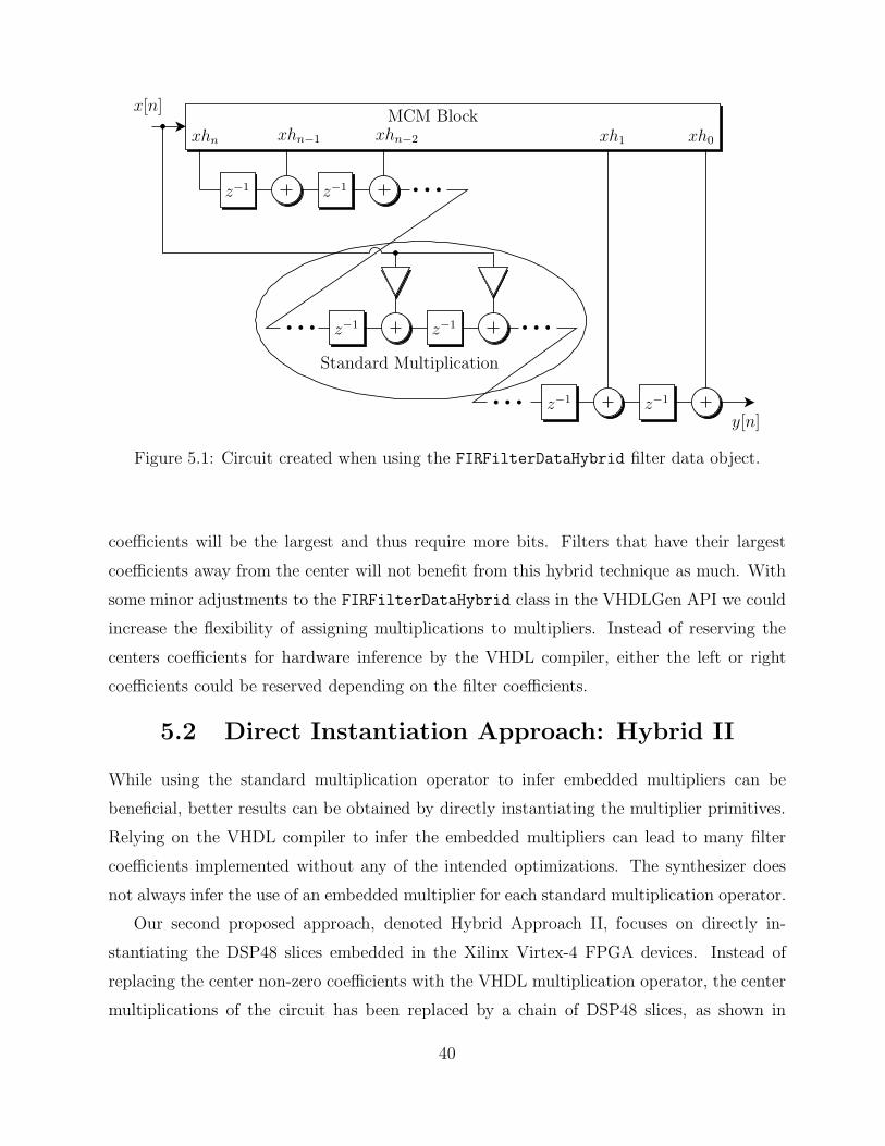
MCM Blockxh0xh1xhn−1xhn
y[n]
x[n]
xhn−2
z−1 z−1
z−1 z−1b b b
b b b
z−1 z−1 b b bb b b
b
b
Standard Multiplication
Figure 5.1: Circuit created when using the FIRFilterDataHybrid filter data object.
coefficients will be the largest and thus require more bits. Filters that have their largest
coefficients away from the center will not benefit from this hybrid technique as much. With
some minor adjustments to the FIRFilterDataHybrid class in the VHDLGen API we could
increase the flexibility of assigning multiplications to multipliers. Instead of reserving the
centers coefficients for hardware inference by the VHDL compiler, either the left or right
coefficients could be reserved depending on the filter coefficients.
5.2 Direct Instantiation Approach: Hybrid II
While using the standard multiplication operator to infer embedded multipliers can be
beneficial, better results can be obtained by directly instantiating the multiplier primitives.
Relying on the VHDL compiler to infer the embedded multipliers can lead to many filter
coefficients implemented without any of the intended optimizations. The synthesizer does
not always infer the use of an embedded multiplier for each standard multiplication operator.
Our second proposed approach, denoted Hybrid Approach II, focuses on directly in-
stantiating the DSP48 slices embedded in the Xilinx Virtex-4 FPGA devices. Instead of
replacing the center non-zero coefficients with the VHDL multiplication operator, the center
multiplications of the circuit has been replaced by a chain of DSP48 slices, as shown in
40

MCM Blockxh0xh1xhn−1xhn
y[n]
x[n]
z−1 z−1 z−1b b bb b b
DSP48Slice
PCIN PCOUT
A B
DSP48Slice
PCIN PCOUT
A B
xhm xhm−1
b
b
Figure 5.2: Direct DSP48 primitive instantiation, Hybrid II.
Figure 5.2. This approach guarantees a one-to-one correlation, so the number of coefficients
that are removed from the MCM block is set to be the number of DPS48 slices available on
the target FPGA.
The DSP48 slices are grouped in pairs to form XtremeDSP tiles. The tiles are
interconnected so that they can create larger structures without relying on any of the
traditional programmable logic on the FGPA. The DSP48 slices include an 18x18 multiplier
along with a three input 48-bit adder. The slices are highly configurable and even allow
internal timings to be adjusted by programmable registers. One limitation when using the
DSP48 slices in our hybrid design is that even zero coefficients consume an entire DSP48
slice. This limitation comes from the way that the DSP48 are tiled in pairs. [1]
5.3 Hybrid Filter Results
To study the effects of the hybrid filter implementations two baseline circuits and two hybrid
circuits were generated for three FIR filters of varying sizes and synthesized using Xilinx
XST[30]. Unlike the other circuits, the Hybrid I design requires multiple VHDL circuits to
be generated so that a varying amount of coefficient subset sizes could be simulated. The
Hybrid II design has a fixed number of DSP48 slices requiring only one circuit per filter and
FPGA device.
The hybrid filter results of the filters in Table 5.1 are shown in Figures 5.3, 5.4 and 5.5.
Figure 5.3(a) shows a special case; it gives the results from Filter A. In this case the SX25
41

Table 5.1: Filters used in hybrid filter research
Filter A 100th-order Bandstop FIR FilterFilter B 250th-order Bandstop FIR FilterFilter C 300th-order Bandstop FIR Filter
FPGA contains 128 DSP48 slices, which is more than the number of filter coefficients (101).
None of the Hybrid I designs obtain better results than the simple baseline circuit using
the standard VHDL operator. The Hybrid II circuit is not defined in this case, because the
filter can be implemented entirely with DSP48 slices. The circuit for this filter is no longer
a hybrid, but is instead a chain of DSP48 slices.
Due to the nature of the Hybrid I implementation approach, there is no predefined
number of coefficients to replace. The Hybrid I implementation relies on the synthesizer to
infer hardware when needed; therefore it is reasonable to replace more or less coefficients
than the amount of embedded hardware available. To demonstrate the effect the number
of replaced coefficients has on the filter implementation, multiple VHDL filter circuits are
studied in every scenario with varying numbers of replaced coefficients. The number of
coefficients that have been replaced is denoted by an integer value after the Hybrid I label
in the result graphs. For example, the section of the graph labeled “Hybrid I (40)” contains
the results for the Hybrid I filter implementation where 40 coefficients are replaced. This
extra information is not required for the Hybrid II implementations because the number of
replaced coefficients is always equal to the number of DSP48 slices available on the target
FPGA device.
Figure 5.3(b), showing the results of when Filter A is implemented on an LX15, strays
from the expected. With fewer DSP48 slices then the SX25, it was expected that the
hybrid filter implementations would perform better. Upon closer review, half of the filter’s
coefficients are zero after quantization down to eighteen bits, leaving only 50 multiplications
needed. Figures 5.4(a) and 5.5(a) both show improvements in FPGA utilization when using
the Hybrid II approach. The Hybrid I circuits, on the other hand, still do not provide any
improvements over the simple baseline circuit.
The LX15 only has 32 DSP48 slices leaving a large portion of the filter’s coefficients
implemented with the traditional slices and LUTs of the FPGA. This reduction of DSP48
42

slices provides a better opportunity for the MCM optimizations to reduce FPGA utilization.
As expected, the results in Figure 5.4(b) and Figure 5.5(b) show all the hybrid designs, and
even the MCM design, outperform the simple baseline circuit.
43

MC
M B
ase
lin
e
Hy
bri
d I
(40
)
Hy
bri
d I
(80
)
Ba
seli
ne
SlicesLUTsDSP48s
0
5
10
15
20
25
FP
GA
Uti
liza
tio
n (
%)
(a) Filter A implemented on a Virtex-4 SX25.
0
20
40
60
80
100
FP
GA
Uti
liza
tio
n (
%)
SlicesLUTsDSP48s
MC
M B
ase
lin
e
Hy
bri
d II
Hy
bri
d I
(40
)
Hy
bri
d I
(80
)
Ba
seli
ne
(b) Filter A implemented on a Virtex-4 LX15.
Figure 5.3: Hybrid filter results of Filter A
44

0
20
40
60
80
100
MC
M B
ase
lin
e
Hy
bri
d II
Hy
bri
d I
(40
)
Hy
bri
d I
(80
)
Hy
bri
d I
(12
0)
Hy
bri
d I
(16
0)
Ba
seli
ne
FP
GA
Uti
liza
tio
n (
%)
SlicesLUTsDSP48s
(a) Filter B implemented on a Virtex-4 SX25.
0
20
40
60
80
100
FP
GA
Uti
liza
tio
n (
%)
SlicesLUTsDSP48s
MC
M B
ase
lin
e
Hy
bri
d II
Hy
bri
d I
(40
)
Hy
bri
d I
(80
)
Hy
bri
d I
(12
0)
Hy
bri
d I
(16
0)
Ba
seli
ne
(b) Filter B implemented on a Virtex-4 LX15.
Figure 5.4: Hybrid filter results of Filter B
45

Hy
bri
d I
(20
0)
Hy
bri
d I
(24
0)
Hy
bri
d I
(28
0) 0
20
40
60
80
100
FP
GA
Uti
liza
tio
n (
%)
SlicesLUTsDSP48s
MC
M B
ase
lin
e
Hy
bri
d II
Hy
bri
d I
(40
)
Hy
bri
d I
(80
)
Hy
bri
d I
(12
0)
Hy
bri
d I
(16
0)
Ba
seli
ne
(a) Filter C implemented on a Virtex-4 SX25.
SlicesLUTsDSP48s
0
20
40
60
80
100
FP
GA
Uti
liza
tio
n (
%)
MC
M B
ase
lin
e
Hy
bri
d II
Hy
bri
d I
(40
)
Hy
bri
d I
(80
)
Hy
bri
d I
(12
0)
Hy
bri
d I
(16
0)
Ba
seli
ne
(b) Filter C implemented on a Virtex-4 LX15.
Figure 5.5: Hybrid filter results of Filter C
46

CHAPTER 6
PROGRAMMABLE ADDER GRAPH
The hybrid research is focused on making the best use of an FPGA device by utilizing the
embedded multipliers as well as MCM optimizations in the standard programmable area.
There are two important design issues that are not fully considered in hybrid implementation
research. First, the maximum clock speed was not an important metric for the research,
primarily because the embedded hardware blocks have a fixed maximum clock speed. Also,
given the maximum clock rate of a single LUT, it is difficult to compete with the embedded
hardware blocks.
The second glaring issue turns into more of a paradox; what if there are enough embedded
hardware blocks to completely implement the required design? No hybrid design exists
for this situation because the goal of the research was to save as much of the standard
programmable logic as possible by shifting the burden over to the available high speed
embedded hardware blocks. If the design can be fully implemented using the embedded
fixed hardware, then MCM can no longer provide any space savings because the process of
using MCM uses more of the programmable area of the chip.
MCM designs in general have limitations when compared to designs that utilize the
embedded hardware blocks. Given the well organized structure of common filters, the fixed
hardware blocks benefit from reduced routing problems. As stated in Section 5.2, Xilinx’s
DSP48 slices are designed to be connected in long chains with no extra routing required from
the LUT logic in the FPGA device. Even if a DSP48 slice in the chain was designated to
implement a zero coefficient, it is arguable to “waste” that slice’s internal multiplier to avoid
the expensive situation of routing the signal to an external register and then back. When
using the standard programmable logic of the FPGA device to implement a filter, there will
be a greater chance of having longer connections in the circuit.
47

Another benefit to using the embedded DSP blocks is the ability to change the coefficients
over time. Both the Altera DSP Blocks[31] and the Xilinx DSP48 slices use high speed
general purpose multipliers. Both inputs of the multiplier can change every clock cycle. In
the standard MCM approach, all of the coefficients need to be known in the design phase of
the filter, which in most cases is not an issue since the coefficients are usually constant over
the entire life of the filter.
The previous work performed at the Naval Research Laboratory to develop a sparse filter
that can be implemented with MCM, does not take into account the underlying FPGA
structure, particularly the availability of the embedded blocks. No matter how novel the
design, filters designed in FPGAs that do not leverage the additional support of the embedded
hardware will have to contend with previously stated problems. In today’s environment
where there are many high speed DSP FPGA devices that come standard with building
blocks for digital filters, how can the added development time of a highly specialized MCM
filter be justified? If at best the highly customized filter can only perform at the same level
as a much simpler design which leverages the power of the complete FPGA device. This
argument can be further extended to say there is a financial benefit to purchasing specialized
FPGA devices that provide the needed DSP functionality to fully implement the required
filter. FPGA manufactures have already committed large portions of their development
to DSP applications in order to stay competitive; it would be wise not to take them for
granted. As the FPGA manufacturers compete for the DSP market, the chances of finding
a specialized chip to fulfill the design requirements will only increase.
6.1 Proposed Programmable Adder Graph
There is no doubt that MAG optimizations are powerful for digital filter implementations
in ASICs and custom VLSI, especially for transposed FIR filters, but what about FPGA
implementations? With the abundance of FPGA devices that come standard with high
speed embedded DSP blocks, the optimizations that MAG techniques provide may not be
beneficial to the design as a whole. While this may be true when MAGs are used to implement
filters in the traditional programmable logic of an FPGA device, it however does not apply
to the situation where MAGs could be used to optimize the FPGA’s hardwired embedded
blocks. If the general purpose multipliers in the DSP blocks are replaced with multipliers
48

optimized for constant multiplications, DSP blocks having a greater clock rate in less area
while consuming less power could be achieved.
The obvious problem to overcome when using an MCM block to construct a general
purpose multiplier useful in an FPGA device is MCM’s requirement to have the constant
operands known before circuit can be designed. Without the knowledge of the constants
ahead of time, the MCM algorithm cannot be run and the corresponding adder graph
constructed. This same requirement has also eliminated MCM optimization techniques from
being used for adaptive filter implementations. To overcome this limitation and obtain
the ability to move MAG optimizations into an FPGA embedded block, we propose a
programmable adder graph (PAG) block[32]. The PAG block is capable of being programmed
with the constant multiples at any time to create the required constant multipliers.
The proposed programmable adder graph (PAG) block is made possible by a shift-and-
add platform that can be programmed to implement the required design. The platform is
divided into two partitions: fundamental modules responsible for performing the addition
operations and a shift/connect matrix that binds the fundamental modules into an adder
graph. Figure 6.1 shows how the PAG block is constructed. The ability to connect the
addition operations together through programming allows an MCM block to be constructed
after circuit fabrication, eliminating MCM’s primary limitation.
As the name suggests, a fundamental module (FM) represents one fundamental in the
adder graph. The FMs are similar to A-operations in HCUB[11] without the shifts. The
way in which the FMs are connected determines the overall multiplier that is constructed
from the PAG block. As stated earlier, FMs satisfy the addition requirements of the adder
graph and as such primarily consist of a single adder. Any adder can be used in this design,
but it is important that additions be performed as fast as possible, since they contribute the
largest factor of the critical path. The adders must also support subtraction so that an FM
can generate a fundamental value from the sum or difference of previous fundamentals.
Along with selecting the appropriate bus connections, all of the shifting requirements of
the adder graph are also fulfilled by the circuitry that interconnects the FMs, referred to as
the connection matrix. This technique allows a fundamental to be selected and the value
shifted using the same circuitry. Shift registers are not used. Shift registers, while being able
to correctly implement the shifting function, are not in MAG designs because they require
multiple clock cycles to implement a singe shift, along with using a relatively large amount
49

Row
Dri
ver
sR
owD
river
s
xk0xk1xk2xk3
ProgramingInterfacex
FM
rsrsrsrs rs
rsrsrs rs
rsrsrs rs
rsrsrs rs
rsrsrs rs
rsrsrs rs
rsrsrs rs
rsrsrsb
b
b
b
rsrsrsrs rs
rsrsrs rs
rsrsrs rs
rsrsrs
Connection
FM FM FM
FM FM FM FM
Row
Dri
ver
s
FM
rsrsrsrs rs
rsrsrs rs
rsrsrs rs
rsrsrs rs
rsrsrs rs
rsrsrs rs
rsrsrs rs
rsrsrsb
b
b
b
FM FM FM
Matrix
FundamentalModules
b b b
b
b
b
b
b
Figure 6.1: Programable Adder Graph (PAG) Layout.
of area and power. Instead the connection circuitry implements a hardware wired shift by
making the correct connections in a grid formed from the inputs crossed over the outputs.
Refer to Figure 6.3 to see how a programmable wired shift is constructed.
6.2 Fundamental Modules
Fundamental modules (FMs) are one of the core building blocks of the proposed PAG.
The circuitry of FMs are divided into two sections, an arithmetic unit which computes the
output of the FM and a control unit that governs it. The FM is shown in Figure 6.2. The
two sections are signified by dashed lines. Every FM has two inputs and one output, not
50

ControlUnit
+/-
ProgrammingInput A Input BInterface
Register
PL1 0
BYPASS
b
b
Out
1 0
Figure 6.2: The Fundamental Module
including the control and programming signals. The two inputs in the figure, Input A and
Input B, are connected to the outputs of other FMs via the connection circuitry. The other
input shown in the figure, the programming interface, connects to the circuit responsible for
programming the PAG.
The arithmetic unit is the left most section shown in Figure 6.2. Through the use of
two multiplexers, the arithmetic unit has the ability to implement different functions. The
simplest function is to set both of the multiplexers to zero to implement pure addition.
Setting the output multiplexer to one diverts the output of the adder through a register.
This setting allows the PAG to be pipelined. These two settings are the most important as
they fulfill the primary need in an adder graph, addition. Using the pipelined setting the
throughput can be increased.
The other multiplexer is used as an adder bypass. While setting one of the inputs to
zero would simulate an adder bypass without requiring any additional control logic, it still
requires the signal to pass though the adder. The adder adds a significant delay from input
to output of the FM along with increased energy use. Instead, if the adder is not needed for
the function the FM is to perform, the signal is routed around the adder instead of through.
This also allows the adder to be omitted to reduce power consumption. The bypass is an
important function of the FMs. Since the PAG block is a fixed circuit, there will undoubtedly
51

be areas in the adder graph where there are more FMs than needed. The bypass allows the
outputs of the adder graph to be quickly routed though the remaining FMs to the output of
the PAG.
The last remaining setting is where both multiplexers are set to one, which causes the FM
to implement a pipeline bypass we will refer to as a shim. Shims are used in the pipelined
adder graphs when outputs of FMs in lower depths need to be routed to higher FMs. If the
FMs have a difference in depth greater than one, it is critical that the path the signal travels
takes the same amount of time as the rest of the data in the adder graph. Shims can be
used to resolve this timing issue.
The other section of the FM is the control unit, the right section of Figure 6.2. As
shown in the figure, there is one input and three internal signals that govern the arithmetic
unit. The first control signal shown in Figure 6.2, +/-, instructs the adder to perform either
addition or subtraction of the two inputs. The BYPASS and PL control signals operate the two
multiplexers in the arithmetic unit that perform the adder bypass and pipelining functions.
The input, programming interface, could have many different forms which are not yet
fully considered in this work since they could vary from implementation to implementation.
For example, the programming interface could use the classic computer architecture design
having an address and data bus. Each FM would be assigned a unique address and would
only respond to the signal in the data bus when the address bus was set to its address. This
approach would minimize the logic needed within each FM, but would require large buses
to be routed throughout the PAG block. A more modern approach of using a serial protocol
such as RapidIO[33] could be used as the programming interface instead of the slower parallel
buses. While requiring each FM to support the serial protocol, the programming instructions
would be sent though a switched network that would simplify the programming network.
6.3 Connection Matrix
The connection matrix of the PAG block is made up of connectable buses that run
perpendicular to each other. The buses form a grid with a connection circuitry at every
node similar to a crossbar switch. This grid, or matrix, provides a workable and organized
solution to the routing issue, albeit while taking large area of the circuit layout. As stated
earlier, all shifts are applied in the connection matrix of the PAG block. Instead of merely
connecting the correct buses together like a crossbar switch, the connection circuits must
52

x0+m
x1+m
x2+m
x3+m
x0 x1 x2 x3
r r r r
rrrr
r r r r
rrrr
r
r
r
r
Figure 6.3: A programmable hardware wire shifter. The shift amount is denoted as m.
x0−0
x1−0
x2−0
x3−0
x0 x1 x2 x3
r r r r
rrrr
r r r r
rrrr
r
r
r
r r
r
r
r
x0−1
x1−1
x2−1
x3−1
x0 x1 x2 x3
r r r r
rrrr
r r r r
rrrr
r
r
r
rr
r
r
r
x0−2
x1−2
x2−2
x3−2
x0 x1 x2 x3
r r r r
rrrr
r r r r
rrrr
r
r
r
rr
r
r
r
x0−3
x1−3
x2−3
x3−3
x0 x1 x2 x3
r r r r
rrrr
r r r r
rrrr
r
r
r
rr
r
r
r
Figure 6.4: Four bit connection patterns to apply a left wire shift.
also connect the buses in such a way that a wired shift is applied. This technique allows
a fundamental to be selected and shifted all within the connection matrix, minimizing the
circuitry needed to realize the PAG block.
Wired shifts are usually not thought of as being programmable, but with careful
manipulation of how the input bits are connected to the output bits, a wired shift of any
value can be applied when connecting two buses. To avoid shifting, each input bit must be
connected to its corresponding output bit, yn = xn, as is expected in a standard crossbar
switch. A left shift by one is applied by connecting each input bit to the next more significant
output bit, yn = xn−1. Figure 6.4 shows this concept visually. A right wired shift can be
perform in the same manner as shown in Figure 6.5.
As with any binary left shift operation, the lower order bits that have been evacuated
need to be filled with zeros. Some extra logic is required in the bus connection circuitry to
accomplish this task. This requirement is the reason for the extra four connection circuits
per node in four bit shifter figures. A column, permanently tied to logical zero, allows the
53

x0+0
x1+0
x2+0
x3+0
x0 x1 x2 x3
r r r r
rrrr
r r r r
rrrr
r
r
r
r r
r
r
r
x0+1
x1+1
x2+1
x3+1
x0 x1 x2 x3
r r r r
rrrr
r r r r
rrrr
r
r
r
r r
r
r
r
x0+2
x1+2
x2+2
x3+2
x0 x1 x2 x3
r r r r
rrrr
r r r r
rrrr
r
r
r
r r
r
r
r
x0+3
x1+3
x2+3
x3+3
x0 x1 x2 x3
r r r r
rrrr
r r r r
rrrr
r
r
r
r r
r
r
r
Figure 6.5: Four bit connection patterns to apply an arithmetic right wire shift.
shifter to fill zeros when needed. Figure 6.6 also shows this extra zero signal and how it
interacts with the rest of the connection matrix. However, due to the constant nature of the
zero fill signal, only a single MOSFET is required. Right shifts normally do not require any
zero filling as arithmetic right shifts are most commonly used for our application. Performing
an arithmetic right shift is actually quite simple as shown in Figure 6.5. Instead of filling
evacuated bits with zero, they are filled with the value of the most significant bit. This
allows two’s complement numbers to maintain the proper sign during shifting operations.
Using this bus interconnection technique in the connection matrix of the PAG block, any
wire shift can be implemented in a programmable manner.
A detailed drawing of the connection matrix is shown in Figure 6.6. The figure shows
a four by four, four bit matrix having sixteen nodes. A node in the connection matrix
is considered the crossing of two buses, not bits. Since four bit buses are used sixteen
connection circuits are needed per node, plus an extra four connections for the zero fill logic.
The circuitry that controls the connection circuits is referred to as the matrix driver and
is shown in the figure. The matrix driver on the right of the figure selects which output
bus an input bus is connected to. The matrix driver on the top of the figure selects which
of the bits in the selected node are activated based on the shift amount needed. The data
signals are represented by thicker lines, the thin lines designate the control signals needed to
operate the connection circuits. To see how the connection matrix is used within the PAG
block refer back to Figure 6.1. Figure 6.1 requires three connection matrices designated by
dashed lines.
Two connection circuit designs are proposed for use in the connection matrix. Figure
6.7 shows the first proposed connection circuit, using only two transistors per connectable
bit. The principal concept is nothing new; it is simply a CMOS transmission gate that
54

a0
d0
d1
d2
d3r r r r
rrrrr r r r
rrrr
r r r rrrrr
r r r rrrrr
r r r rrrrr
r r r rrrrr
r r r rrrrr
r r r rrrrr
r r r r r r r r r r r r r r r rr
rr
r
c0
c1
c2
c3 r r r rrrrr
r r r rrrrr
r r r rrrrr
r r r rrrrr
r r r rrrrr
r r r rrrrr
r r r rrrrr
r r r rrrrr
r r r r r r r r r r r r r r r r
b0
b1
b2
b3r r r r
rrrrr r r r
rrrr
r r r rrrrr
r r r rrrrr
r r r rrrrr
r r r rrrrr
r r r rrrrr
r r r rrrrr
r r r r r r r r r r r r r r r rrr
rr
a0
a1
a2
a3 r r r rrrrr
r r r rrrrr
r r r rrrrr
r r r rrrrr
r r r rrrrr
r r r rrrrr
r r r rrrrr
r r r rrrrr
r r r r r r r r r r r r r r r rr
rr
r node0
node1
node2
node3
MatrixDriver
Matrix Driver (Shift Patterns)
(nodeselect)
r
rr
r
a1 a2 a3 4d04d14d24d3 2d02d12d22d3 8b0 8b1 8b2 8b3
Figure 6.6: Four bit, four node, one row connection matrix selecting node two and incurringa left shift of one.
55

b
b
b
b
Zero Fill Control
b
b
b
b
b
b
b
b
b
b
b
b
Vss Vss
IN B
Row B Control
Row B Control
OUT AOUT B
IN A
Row A Control
Row A Control
Figure 6.7: Connection circuit using a CMOS transmission gates.
b b
bbbb
b b b b
bb
Vdd
Vdd
Vdd
Vdd
VssVss
Vss Vss
Zero Fill Control
IN B
Row B Control
Row B Control
IN A
Row A Control
Row A Control
OUT AOUT B
Vss Vss
Figure 6.8: Connection circuit using a tri-state NOT gate.
56

has been twisted to conform to the grid pattern. The figure shows the transmission gate
connections circuits needed to construct a two bit connection matrix node. The second
proposed connection circuit is shown in Figure 6.8. Instead of using a transmission gate, the
second method uses a tri-state NOT gate to construct a two bit connection matrix node.
Both solutions provide useful benefits and depending on the design requirements either one
could be a better choice.
The first connection solution, using a single transmission gate, has the obvious advantage
of only requiring two transistors per node. Lowering the total number of transistors per node
could very easily become a critical factor as the size of the connection matrix is increased.
Every bit of every bus that crosses in the matrix will need one of these connection circuits,
along with the addition control signals.
The second connection solution using a tri-state NOT gate only passes a clean digital
signal at the cost of using more transistors. The tri-state gates also help strengthen the
signals instead of attenuating them like the transmission gates. As the wire runs and fan-outs
become larger the NOT gates could become a critical aspect in the design acting as a buffer
to overcome the increased capacitance and resistance. Tri-state buffers are not considered in
this work since they increase the transistor count by two per connection circuit, an increase of
50 percent. To deal with the inverted signals, the output of the connection must be inverted
before entering the next FM layer.
6.4 Programmer
In order to use the PAG block, it first needs to be programmed to implement the required
multiplications. As proposed, the PAG block needs to be programmed every time the circuit
is powered up. For adaptive filter designs, the PAG block will also need to be programmed
with new coefficients from time to time. To accomplish this task, some sort of programming
circuit is required along with the PAG block to complete design. The programmer obtains
data about the adder graph and then fits the adder graph to the PAG block. The process of
programming the PAG block is an iterative task requiring every FM and connection matrix
to be set with the correct values. The programming process will take a lengthy amount of
time compared to the data rate of the data path. While the programming time could cause
problems, it is only a short period of time when compared to overall operating time of the
PAG block. After the PAG block is programmed, it mimics a fixed MCM design with only
57

b
b
b
xk0
xk1
xkn−1
xkn
x
PAGBlock Programmer
Processor
PAG
FlashMemory
OR
Figure 6.9: PAG Programmer.
the connection circuitry and additional routing to hinder the maximum clock rate.
There are two methods considered for the programmer to obtain the adder graph data,
a preprogrammed flash memory block or a coprocessor design that can compute any set of
coefficients on the fly. The flash programmer has many advantages over the coprocessor
design. It reduces the complexity of the final PAG block by moving more of the work to the
design process. All of the filter coefficients are required to be known before the PAG block
can be utilized. However, it is important not to confuse this restriction with the classic
adder graph restriction of having to know the coefficients before circuit fabrication. The
coefficients are only required to be known before the PAG block can be programmed, not
before the fabrication of the PAG block. The adder graph data used to program the PAG
block would most likely be computed by the same software that was synthesizing the rest of
the HDL design to take advantage of the readily available computing power of the modern
PC. The flash memory programmer could also work for adaptive designs by storing multiple
sets of pre-computed coefficients that can be used to reprogram the PAG block when needed.
The other proposed method for programming the PAG block, a coprocessor design, allows
the possibility for the surrounding logic to set the coefficients without being bound to a set of
pre-computed values. An embedded processor is used to do all of the computations needed to
properly program the PAG block. To make this possible, the MAG algorithm has to be run
first to obtain the shift-and-add logic. More work is required to move the MAG algorithm
to an embedded processor. In this situation it might be best to use the simplest heuristics
to avoid a lengthy programming time. This method of programming the PAG block takes
more memory, power and time to program, but if it is not feasible to limit the coefficients
58

to a predefined set, it is required. The coprocessor method would most likely be beneficial
to adaptive filters designs that need to set the coefficients of a filter based on their current
environment, static filters have no need for an embedded processor. It is possible for some
cases that dedicated hardware can be used to perform the adaptation calculations rather
than a more general embedded processor.
6.5 Design Issues
One concern that might arise is the apparent “waste” of hardware. For any given adder graph
that is loaded into the PAG block, there may be many FMs that are not used, especially for
smaller designs. With every FM that is unused, there is a high speed adder, shifting logic
and control logic that is abandoned. While this sounds alarming, it is not a new concept
to FPGA manufactures. All FPGAs, being programmable devices, have hardware that will
ultimately be wasted when the HDL synthesis tool does not find a use for it. It is important
to remember, however, that unused FMs can be deactivated and bypassed to save power and
avoid significantly increasing the critical path.
Another concern with the PAG design, and perhaps the most challenging, is the
uncertainty of the multiplier output during a coefficient change. Reprogramming the PAG
block is a lengthy process when compared to its clock rate, allowing many multiplications to
take place before the PAG block is correctly reprogrammed. This is only a concern during
circuit power up or coefficient changes for adaptive filter designs. While the reprogramming
is taking place erroneous multiplication will occur due to the invalid intermediate adder
graph. When the PAG block is used to compute the multiplications for a digital filter the
erroneous output from the multiplier could lead to serious side effects.
Temporarily muting the output of the filter is one way to deal with the programming
latency. While being a very simple option, muting is a viable solution for static filter designs
that only need to worry about the programming latency during circuit initiation. Muting,
however, will not work for adaptive filters along with designs requiring a continuous output
from the PAG block during coefficient updates. The proposed solution in this case is to use
two PAG blocks in place of one to form a dual PAG (DPAG) block.
The dual PAG (DPAG) block is capable of producing a continuous output even during
reprogramming. Figure 6.10 shows how the DPAG block is constructed. It comes at the
cost of doubling the required logic, but depending on the size of a single PAG block it might
59

Multiplier Input
PAGBlock Programmer
PAGPAGBlock
Multiplexer
ProgrammingBuses
Multiplier Output
Figure 6.10: Dual PAG Module.
still be practical. Even with the doubled size, the DPAG block can still reduce the overall
circuit size. Remember that a single PAG block will service every constant multiplication
needed for the entire circuit. The DPAG block works by multiplexing the output of the two
PAG blocks. At any given time, the output of the PAG block will be sourced from only
one of the paired PAG blocks. When a coefficient change is required, the disconnected PAG
block is first reprogrammed to avoid the erroneous output while reprogramming. When the
disconnected PAG block has been fully reprogrammed and its output is valid the multiplexer
is toggled and the DPAG block now outputs the multiplications of the new coefficients in
one quick switch.
6.6 Sizing
Due to the fixed nature of the PAG block, the MAG algorithm that is computing the adder
graph will also need some information about the hardware limits of the PAG. Without
knowing the hardware limits the adder graph produced might not fit into the PAG. To make
the best use of resources the PAG block needs to be sized to accommodate many different
adder graphs while using the least amount of circuitry possible. This moves the research to
attempt to answer the question of what the depth and width a general purpose PAG block
should be.
The depth of the PAG refers to the number of FM layers there are and is synonymous
60

with the depth of an adder graph. The depth determines the latency of the adder graph.
The width of the PAG refers to how many FMs are in a single layer. The wider an adder
graph is the more computations can be produced in one clock cycle. However, adder graphs
with larger depths have more opportunity to reuse the fundamentals allowing the adder to be
implemented with less logic. Depending on the design requirements an adder graph could be
optimized for speed or reduced circuitry and the PAG required to implement the filter would
need a large width or depth respectively. In order to determine a working solution for both
situations, the PAG needs to be correctly sized while maintaining a realistic implementation.
Using Matlab and a MAG algorithm, the PAG sizes can be determined given an FIR
filter. All of the Matlab code to achieve this is shown in this section. Listing 6.1 shows
a Matlab function that computes the depth and width requirements of a given filter. The
function first sets the filter requirements, as it is shown in the code listing. In this situation a
high pass filter will be analyzed due to the values set in the freqs and freq powers vectors.
The next line sets the bitwidth variable that will determine how the filter coefficients are
quantized. Next the filter loops over a set range of orders denoted by the variable i. For
every order the script calls the paglimits function using the filter requirements previously
set. The data returned from the paglimits function is then reorganized into a format that
is graph friendly. This reorganizing is performed by another for loop that loops over the
depths that will be graphed (using the variable j to denote the depth).
The paglimits function is shown in Listing 6.2. This function returns a vector that
contains the number of fundamentals in every depth of the adder graph created from the given
filter. To accomplish this task, the script first initializes the vector that will hold the counts,
depthcount, for every depth, and defaults the value to zero. Next the createfir function is
called to produce the integer coefficients. The coefficients are then passed to the createmag
function to compute the adder graph. Most of the information returned by the createmag
function is ignored, only the depth is needed for each of the fundamentals returned. Finally
a loop iterates over each fundamental to obtain its depth and then increments the correct
index of the depthcounts vector. Once the loop has finished the function will return the
depthcounts vector which will now contain the correct counts.
Listing 6.3 shows the createfir function. This function is quite simple and is mostly
a wrapper function for Matlab’s firpm filter creation tool. This function is also responsible
for quantizing the coefficients into fixed point integers. The quantization is performed on
61

Listing 6.1: Function to compute required PAG size.
function depthcounts = pag l im i t g r aph e r ( )f r e q s = [0 0 .4 0 .6 1 ] ;f r eq power s = [0 0 1 1 ] ;b i tw idth = 18 ;depthcounts = [ ] ;gdata = [ ] ;for i =10:2:130
depthcounts = [ depthcounts ; . . .i p ag l im i t s ( i , f r eq s , f r eq powers , b i tw idth ) ] ;
for i =1: s ize ( depthcounts , 1 )for j =2:1:16
gdata = [ gdata ; depthcounts ( i , 1 ) j−1 depthcounts ( i , j ) ] ;end
end
end
gdata
Listing 6.2: Function to count the required fundamentals
function depthcount = pag l im i t s ( order , f r eq s , f r eq powers , b i tw idth )depthcount = zeros ( 1 , 2 0 ) ;b = c r e a t e f i r ( order , f r eq s , f r eq powers , b i tw idth ) ;% funds => [ fund depth op1 s h i f t 1 neg1 op2 s h i f t 2 neg2 ]funds = createmag (b ) ;for i =1: s ize ( funds , 1 )
depth = funds ( i , 2 ) ;depthcount ( depth ) = depthcount ( depth ) + 1 ;
end
the second line of the function.
The last custom function is shown in Listing 6.4. This function is responsible for obtaining
the information needed to create the adder graph given the integer filter coefficients. The
first two lines of the function clean up the given coefficients by removing all duplicate and
zero values. Zeros are left out because multiplication by a constant zero is trivial. Duplicate
coefficients will be implemented identically in the adder graph so only unique values are
needed. The remaining lines of this function deal with calling the synth program[28], which
uses HCUB to determine the fundamentals of the adder graph. The most complicated part
of this process is parsing the returned text into a data structure that is more convenient to
work with.
62

Listing 6.3: Function to create an FIR filter
function b int = c r e a t e f i r ( order , f r eq s , f r eq powers , b i tw idth )b = f irpm ( order , f r eq s , f r eq power s ) ;b int = round( (2ˆ bitwidth −1)∗b ) ;
The first set of results from the PAG limit research is shown in Figures 6.11 and 6.12.
Both figures show the results for an eighteen bit high pass filter design with orders varying
from 10 to a 120. The figures demonstrate how the PAG usage varies as the order of the
filter increases. The results are displayed as three-dimensional graphs showing the variations
of the width and depth requirements as the order of the high pass filter is increased. The
two horizontal axes show the filter order and required depth of the corresponding filter. The
vertical axis shows the number of fundamentals needed in the adder graph at each depth
and filter order. Three-dimensional graphs were used in favor of multiple two-dimensional
graphs to display the results in a concise manner. The points in the graphs represent the
number of fundamentals required at a given depth and filter order.
Figure 6.11 shows the results obtained from the default HCUB algorithm. The advantages
of MCM can be seen in this single graph. Notice how the number of fundamentals, or adders,
only slightly increases as the order of the filter increases. The number of fundamentals
remains an order of magnitude less than the filter order. Also, as the filter order is increased,
the additional number of adders required is reduced. This is due to the MAG algorithm
having more fundamentals to work with, therefore allowing a higher degree of fundamental
reuse. Another interesting result from this graph is that the required depth of the filter
only slightly increases as the order is increased. Since both the number of fundamentals and
the depth do not increase at the same rate as the order of the filter, realistically sized PAG
blocks can be designed even for large filters.
Figure 6.12 shows the results from the same filter, but for this graph HCUB was confined
to use a maximum depth of four using a modified version of HCUB[34]. Surprisingly this
graphs shows only a slight increase in the number of fundamentals needed even though the
depth of the MAG has been reduced by half. Figures 6.13 and 6.14 show the results for a
different filter design. These graphs were generated from a more demanding band stop filter
generated with the filter specifications shown in Listing 6.5. It is clear from the graph that
while the results are similar and have the same magnitude, this filter does require more from
63

Listing 6.4: Function to create a MAG given a filter
function funds = createmag ( c o e f f s )c o e f f s = unique ( c o e f f s ) ;c o e f f s = c o e f f s ( c o e f f s ˜=0);command = ’./synth ’ ;for k=1: length ( c o e f f s )
command = sprintf (’%s %d’ ,command , c o e f f s ( k ) ) ;end ;command = [ command , ’ -ga’ ] ;%%Switch the f o l l ow i n g l i n e wi th%%the l i n e above to cons t ra in depth to four%command = [ command , ’ −maxdepth 4 −ga ’ ] ;[ err , ou t s t r ] = unix (command ) ;i f e r r
error ( sprintf (’error %d from unix() call to synth\n%s’ , . . .err , ou t s t r ) ) ;
end ;expr = ’([0-9]+)\s=\sadder\(([0-9]+),\s([0-9]+),\s([-]?)([0-9]+)/...
([-]?)([0-9]+),\s([0-9]+)\)’ ;t = regexp ( s t r t r im ( ou t s t r ) , expr , ’tokens’ ) ;funds = [ ] ;for k=1: length ( t )
va l s = t (k ) ;fund = str2num ( va l s {1}{1}) ;op1 = str2num ( va l s {1}{2}) ;op2 = str2num ( va l s {1}{3}) ;neg1 = va l s {1}{4} ;s h i f t 1 = str2num ( va l s {1}{5}) ;neg2 = va l s {1}{6} ;s h i f t 2 = str2num ( va l s {1}{7}) ;depth = str2num ( va l s {1}{8}) ;i f strcmp( neg1 , ’-’ )
neg1 = 1 ;else
neg1 = 0 ;end
i f strcmp( neg2 , ’-’ )neg2 = 1 ;
else
neg2 = 0 ;end
funds = [ funds ; fund depth op1 s h i f t 1 neg1 . . .op2 s h i f t 2 neg2 ] ;
end ;
64
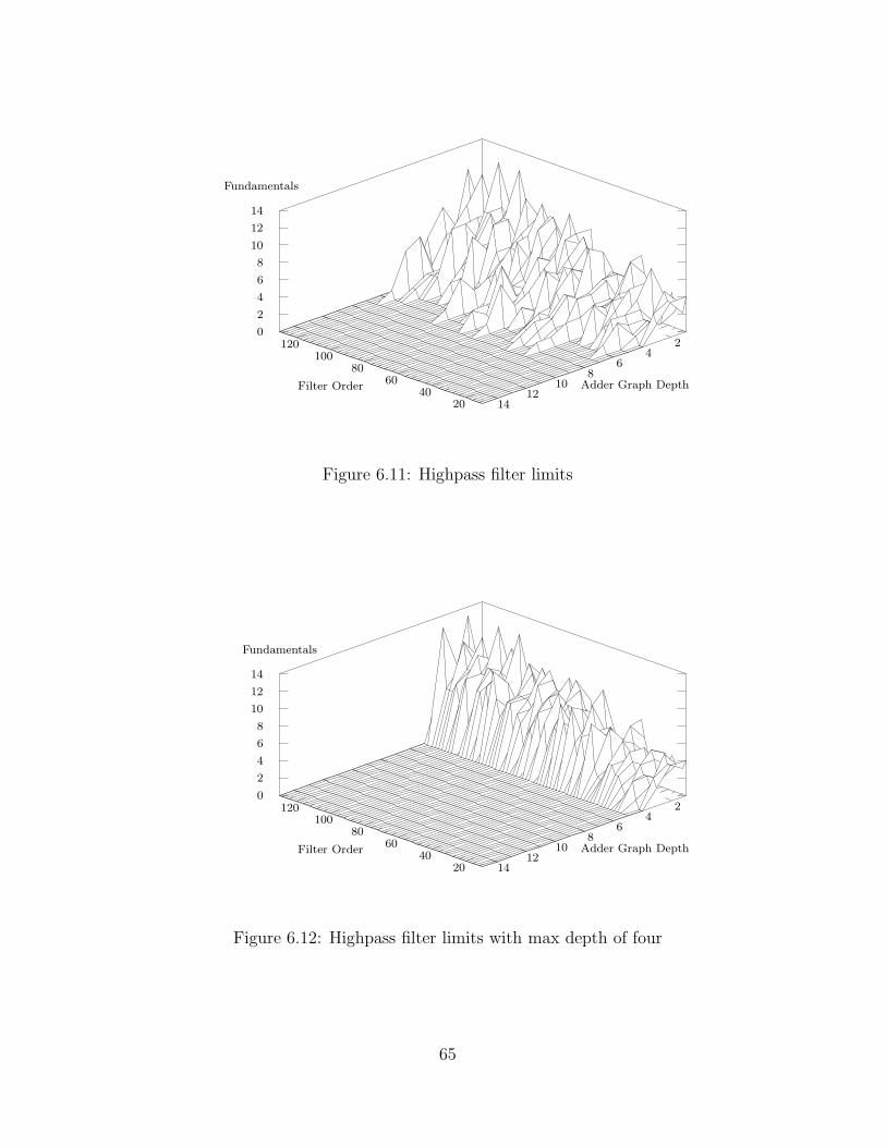
Fundamentals
2040
6080
100120
Filter Order
24
68
1012
14
Adder Graph Depth
0
2
4
6
8
10
12
14
Figure 6.11: Highpass filter limits
Fundamentals
2040
6080
100120
Filter Order
24
68
1012
14
Adder Graph Depth
0
2
4
6
8
10
12
14
Figure 6.12: Highpass filter limits with max depth of four
65

the PAG block. First notice that in Figure 6.13 the number of fundamentals increases by a
factor of two through the range of orders shown. Also in Figure 6.14, when constrained to a
maximum depth of four, the number of fundamentals increases greatly, almost to thirty for
two of the depths at the highest order.
Listing 6.5: Band stop filter specifications
f r e q s = [0 0 .4 0 .6 1 ] ;f r eq power s = [0 0 1 1 ] ;b i tw idth = 18 ;
These graphs are used to help determine the best size for a general purpose PAG block.
Using the results from this research, 16x16 is a realistic size for a PAG block. This means a
PAG block having only sixteen layers of sixteen fundamentals could implement most common
filters. Alternatively, a PAG block having two hundred and fifty-six adders along with the
required registers, routing and control logic. The results also show that the width is more
critical than the depth. Another PAG block size oriented towards high speed designs could
have a width of thirty-two and a depth of eight. While requiring the same number of adders,
faster MAGs could be constructed as long as the MAG algorithm can constrain the maximum
depth to eight.
6.7 Applications
The target application for the PAG block in this research is an embedded FPGA block.
Similar to other high speed DSP building blocks found on today’s FPGA devices, a PAG
block could be a beneficial part to many FPGA designs. No longer would the MCM blocks
for high performance filters need to be implemented in the traditional programming logic of
the FPGA. Instead, any circuit that can benefit from adder graph optimization techniques
could use the embedded PAG block to obtain near ASIC speeds.
Figure 6.15 shows the embedded PAG block design. As the figure shows, not only is
a PAG block is required, but also a multiply and accumulate (MAC) chain is also needed.
The MAC chain allows the output values of the PAG block to be handled by fixed high
speed adders and registers along a simple routing path, thereby avoiding the bottleneck of
using the traditional programming logic. This design could also be implemented on a single
integrated circuit and used as a customizable high speed FIR filter chip.
66

Fundamentals
1020
3040
5060
70
Filter Order
24
68
1012
14
Adder Graph Depth
0
2
4
6
8
10
12
14
Figure 6.13: Bandstop filter limits.
Fundamentals
2030
4050
6070
Filter Order
2
4
6
8
10
Adder Graph Depth
0
5
10
15
20
25
30
Figure 6.14: Bandstop filter limits with max depth of four
67

xk0xk1xkn−1xkn
y[n]
xkn−2
z−1 z−1 z−1 z−1b b b
x[n]
b b b
PAG BLOCK
Figure 6.15: Embedded PAG block
The PAG block might also prove to be useful for adaptive filter designs as a way to
implement high speed filters using MAGs while still remaining changeable. As previously
stated, the primary problem with using PAGs for adaptive filters is the relatively lengthy
programming delay. Either the adaptive algorithms need to calculate large changes infre-
quently or further PAG research is needed to investigate methods of performing incremental
changes to the adder graph to accomplish the required coefficient changes. Adaptive filters
with slower adaptation rates are thus better suited to PAG implementations than those that
have very fast updates.
68
CHAPTER 7
CONCLUSIONS AND FUTURE WORK
This work has proposed two new approaches of implementing MAG optimized digital filters
in FPGA devices along with a programming API for creating FIR filters in VHDL. FIR
filter implementations are of particular interest, because they are essential in creating a high
performance ∆Σ converter. Without a high performance loop filter, the ∆Σ converter will
not perform to the required specification.
The first proposed approach in this work shows that varying the coefficient implementa-
tions in a single filter, referred to as a hybrid filter implementation, can achieve slight savings.
Unfortunately these savings are dependent on the FPGA device that is used. Hybrid filters
can also lead to increased routing issues due to the need to route the signals to and from
the embedded blocks of the FPGA device. The proposed hybrid filter implementations also
provide no speed or power consumption improvements over traditional designs, however if
the space usage is reduced sufficiently there is more possibility to increase the throughput
by parallelizing the design.
VHDLGen is a programming API created to aid the hybrid filter research. While being
primarily focused on creating filters with varying coefficient implementations, it has proven
useful for other research projects. More specifically, projects that require many FIR filters
to be created in VHDL before results can be obtained have found VHDLGen considerably
useful.
In order to achieve the necessary clock rates, the slower programmable logic must be dealt
with. The possibility of using many FPGA devices in a parallel fashion to overcome the slow
FPGA clock speeds was not considered. Instead a more elegant approach was asserted: use
the proposed PAG block to fully implement the loop filter on a single chip. This is the
second proposed approach. This work shows the basic concept of how the PAG block is
69

structured. Future work is needed to create the actual circuit which can be simulated and
then fabricated for actual testing. Future work is also needed to make MAG algorithms
aware of the PAG block constraints. It is critical that the MAG algorithms are bound to
the actual hardware limits of the target PAG block.
Although the PAG is still only a theoretical circuit, and as such requires more research
and adoption by FPGA manufacturers before it is a viable option, it demonstrates how the
required loop filter could be implemented to have the required clock rate while still remaining
on an inexpensive programmable device.
70

REFERENCES
[1] Xilinx, XtremeDSP Design Considerations User Guide, Xilinx, ug073 (v1.2) edition,Feb. 2005. 1, 5.2
[2] S. Kawahito, M. Kameyama, and T. Higuchi, “Multiple-valued radix-2 signed-digitarithmetic circuits for high-performance VLSI systems,” vol. 25, no. 1, pp. 125–131,1990. 2.1
[3] A. Avizienis, “Signed-digit number representation for fast parallel arithmetic,” in IRETransactions on Electronic Computers EC-10, 1961, pp. 389–400. 2.1
[4] Y.M. Hasan, L.J. Karam, M. Falkinburg, A. Helwig, and M. Ronning, “Canonic signeddigit FIR filter design,” in Conference Record of the Thirty-Fourth Asilomar Conferenceon Signals, Systems and Computers, 2000, vol. 2, pp. 1653–1656 vol.2. 2.1
[5] In-Cheol Park and Hyeong-Ju Kang, “Digital filter synthesis based on minimal signeddigit representation,” in Proc. Design Automation Conference, 2001, pp. 468–473. 2.1
[6] Yong Lim and S. Parker, “FIR filter design over a discrete powers-of-two coefficientspace,” IEEE Transactions on Acoustics, Speech and Signal Processing, vol. 31, no. 3,pp. 583–591, 1983. 2.1
[7] M.D. Macleod and A.G. Dempster, “Multiplierless FIR filter design algorithms,” vol.12, no. 3, pp. 186–189, 2005. 2.2
[8] O. Gustafsson and L. Wanhammar, “Low-complexity constant multiplication usingcarry-save arithmetic for high-speed digital filters,” in Proc. 5th International Sym-posium on Image and Signal Processing and Analysis ISPA 2007, 2007, pp. 212–217.2.2
[9] D.R. Bull and D.H. Horrocks, “Primitive operator digital filters,” in Circuits, Devicesand Systems, IEE Proceedings G, June 1991, vol. 138, pp. 401–412. 2.3
[10] A.G. Dempster and M.D. Macleod, “Use of minimum-adder multiplier blocks in FIRdigital filters,” Circuits and Systems II: Analog and Digital Signal Processing, IEEETransactions on [see also Circuits and Systems II: Express Briefs, IEEE Transactionson], vol. 42, no. 9, pp. 569–577, Sept. 1995. 2.3
[11] Yevgen Voronenko and Markus Puschel, “Multiplierless multiple constant multiplica-tion,” ACM Trans. Algorithms, vol. 3, no. 2, pp. 11, 2007. 2.3, 6.1
71

[12] O. Gustafsson, “A difference based adder graph heuristic for multiple constantmultiplication problems,” in Proc. IEEE International Symposium on Circuits andSystems ISCAS 2007, 2007, pp. 1097–1100. 2.3
[13] A.G. Dempster and M.D. Macleod, “Constant integer multiplication using minimumadders,” in Circuits, Devices and Systems, IEE Proceedings-, Oct. 1994, vol. 141, pp.407–413. 2.3
[14] G. C. Schreier, R. Temes, Understanding Delta-Sigma Data Converters, John Wiley &Sons, 2005. 3.1, 3.1
[15] Don Johnson, “The Nyquist frequency,” Connexions Web Site, 2008, [Online;http://cnx.org/content/m0090/2.7/; accessed October 20th, 2008]. 3.1
[16] D.P. Scholnik, “A parallel digital architecture for delta-sigma modulation,” in Proc.MWSCAS-2002 Circuits and Systems The 2002 45th Midwest Symposium on, 2002,vol. 1, pp. I–352–5 vol.1. 3.2
[17] D.P. Scholnik and J.O. Coleman, “Space-time vector delta-sigma modulation,” in Proc.IEEE International Symposium on Circuits and Systems ISCAS 2002, 2002, vol. 3, pp.III–719–III–722 vol.3. 3.2
[18] O. Gustafsson, L.S. DeBrunner, V. DeBrunner, and H. Johansson, “On the design ofsparse half-band like FIR filters,” in Conference Record of the Forty-First AsilomarConference on Signals, Systems and Computers ACSSC 2007, 2007, pp. 1098–1102. 3.2
[19] Yunhua Wang, L.S. DeBrunner, Zhou. Dayong, and V.E. DeBrunner, “A novelmultiplierless hardware implementation method for adaptive filter coefficients,” in Proc.IEEE International Conference on Acoustics, Speech and Signal Processing ICASSP2007, 2007, vol. 2, pp. II–57–II–60. 3.3
[20] Yunhua Wang, L.S. DeBrunner, J.P. Havlicek, and Dayong Zhou, “Iterative radix-8multiplier structure based on a novel real-time CSD recoding,” in Conference Record ofthe Forty-First Asilomar Conference on Signals, Systems and Computers ACSSC 2007,2007, pp. 977–981. 3.3
[21] Yunhua Wang, L.S. DeBrunner, Dayong Zhou, and V.E. DeBrunner, “A multiplierstructure based on a novel real-time CSD recoding,” in Proc. IEEE InternationalSymposium on Circuits and Systems ISCAS 2007, 2007, pp. 3195–3198. 3.3
[22] Yunhua Wang, Linda S. DeBrunner, Victor E. DeBrunner, and Dayong Zhou, “A multi-input multiplier unit suitable for DSP algorithm implementations,” in Proc. FortiethAsilomar Conference on Signals, Systems and Computers ACSSC ’06, 2006, pp. 1465–1468. 3.3
[23] The PHP Group, “PHP manual,” www.php.net/manual/en/, 2008. 4
[24] The PHP Group, “PHP usage stats,” www.php.net/usage.php, 2008. 4
72

[25] The MathWorks, Inc., “Signal Processing Toolbox 6.10,” www.mathworks.com, 2008.4.1.1
[26] Xilinx, Inc., “ISE simulator,” www.xilinx.com, 2008. 4.3
[27] Randy Miller, “Practical UML: A hands-on introduction for developers,”http://dn.codegear.com/article/31863, 2008. 4.4
[28] SPIRAL, “Multiplierless constant multiplication,” SPIRAL Web Site, 2008, [Online;http://www.spiral.net/hardware/multless.html; accessed September 23rd, 2008].4.4.2, 6.6
[29] C.D. Howard, L.S. DeBrunner, and V. DeBrunner, “Hybrid MCM implementationfor FIR filters in FPGA devices,” in Conference Record of the Forty-First AsilomarConference on Signals, Systems and Computers ACSSC 2007, 2007, pp. 1422–1425. 5
[30] Xilinx, Inc., “Xilinx synthesis technology (XST),” www.xilinx.com, 2008. 5.3
[31] Altera, Stratix Device Handbook, Volume 2, Section 4, Chapter 6: DSP Blocks in Stratix& Stratix GX Devices, Altera, s52006-2.2 edition, July 2005. 6
[32] C.D. Howard and L.S. DeBrunner, “High speed DSP block for FPGA devices usinga programmable adder graph,” in to appear in the Proc. Digital Signal ProcessingWorkshop, 13th - Signal Processing Education Workshop 5th, 2009. 6.1
[33] RapidIO Trade Association, “RapidIO technology solves the communications fabricconundrum,” www.rapidio.org, 2008. 6.2
[34] Yevgen Voronenko, “HCUB with depth limitation,” personal communication, 2006. 6.6
73

BIOGRAPHICAL SKETCH
Charles D. Howard
Charles D. Howard was born October 18th, 1980, in Tallahassee, Florida. He received
the Bachelor of Science in Electrical Engineering from Florida State University in 2003. He
obtained his Masters degree in the Spring semester of 2009 under the advisement of Dr. Linda
S. DeBrunner. He has published papers in the Asilomar Conference on Signals, Systems and
Computers in 2007 and in the 2009 Digital Signal Processing and Education Workshop.
He is interested primarily in device programing. Any type of programming, from high level
languages such as PHP and Maltab to the lowest level of programing, assembly programming
of devices such as PIC microcontrollers. He started his career at the National High Magnetic
Field Laboratory in 1996 where he worked as a graphics technician, web developer and
photomicrographer and today continues a career in computers as a Java programer and web
developer.
74