designing with fpgas and cplds
TRANSCRIPT
Designing with
FPGAs and CPLDs
Bob Zeidman
CMP Books
Lawrence, Kansas 66046

CMP BooksCMP Media LLC1601 West 23rd Street, Suite 200Lawrence, Kansas 66046USAwww.cmpbooks.com
Designations used by companies to distinguish their products are often claimed as trademarks. Inall instances where CMP Books is aware of a trademark claim, the product name appears in initialcapital letters, in all capital letters, or in accordance with the vendor’s capitalization preference.Readers should contact the appropriate companies for more complete information on trademarksand trademark registrations. All trademarks and registered trademarks in this book are the prop-erty of their respective holders.
Copyright © 2002 by CMP Books, except where noted otherwise. Published by CMP Books, CMPMedia LLC. All rights reserved. Printed in the United States of America. No part of this publica-tion may be reproduced or distributed in any form or by any means, or stored in a database orretrieval system, without the prior written permission of the publisher.
The programs in this book are presented for instructional value. The programs have been carefullytested, but are not guaranteed for any particular purpose. The publisher does not offer any war-ranties and does not guarantee the accuracy, adequacy, or completeness of any information hereinand is not responsible for any errors or omissions. The publisher assumes no liability for damagesresulting from the use of the information in this book or for any infringement of the intellectualproperty rights of third parties that would result from the use of this information.
Acquisition Editor: Robert Ward Layout design & production: Justin Fulmer and Michelle O’NealManaging Editor: Michelle O’NealCover art design: Damien Castaneda
Distributed in the U.S. by: Distributed in Canada by:
Publishers Group West Jaguar Book Group1700 Fourth Street 100 Armstrong AvenueBerkeley, California 94710 Georgetown, Ontario M6K 3E7 Canada1-800-788-3123 905-877-4483www.pgw.com
ISBN: 1-57820-112-8

This book is dedicated to two smart, dedicated, inspiring teachers who departed this
world much too soon, but left a legacy of enthusiastic engineers, mathematicians, and sci-
entists.
Mrs. Anita Field was my ninth grade teacher at George Washington High School in Phila-
delphia. She demonstrated to classes of restless, awkward, prepubescent boys and girls
that math could be fun and exciting. She showed by her example that those who studied
math could be cultured, well-rounded, and even pretty.
Mr. Gordon Stremlau was a human calculating machine with a dry sense of humor that
we only understood when we were seniors at GWHS. What we first thought were snide
remarks and nasty smirks, as freshman, we later came to realize were clever comments
and inside jokes. It was only after some level of maturity that we could appreciate the sub-
tlety of his wit.
Both of these people were mentors, and friends, and I wish that I had the opportunity to
thank them personally. And though I’m saddened by the fact that there are few others like
them, as dedicated and excited, teaching our children, there is some comfort in knowing
that I and my friends have benefited from knowing them.

This Page Intentionally Left Blank
v
Table of ContentsForeword . . . . . . . . . . . . . . . . . . . . . . . . . . . . . . . . . . . . . . . . . . ix
Preface . . . . . . . . . . . . . . . . . . . . . . . . . . . . . . . . . . . . . . . . . . . . xiBook Organization . . . . . . . . . . . . . . . . . . . . . . . . . . . . . . . . . . . . . . . . . . . . . . . xiIntended Audience . . . . . . . . . . . . . . . . . . . . . . . . . . . . . . . . . . . . . . . . . . . . . . . xivContent . . . . . . . . . . . . . . . . . . . . . . . . . . . . . . . . . . . . . . . . . . . . . . . . . . . . . . . . xvSupport and Feedback . . . . . . . . . . . . . . . . . . . . . . . . . . . . . . . . . . . . . . . . . . . . . xvAcknowledgments . . . . . . . . . . . . . . . . . . . . . . . . . . . . . . . . . . . . . . . . . . . . . . . xvi
Chapter 1 Prehistory: Programmable Logic to ASICs . . . . . 1Objectives . . . . . . . . . . . . . . . . . . . . . . . . . . . . . . . . . . . . . . . . . . . . . . . . . . . . . . .11.1 Programmable Read Only Memories (PROMs). . . . . . . . . . . . . . . . . . . . . . . .21.2 Programmable Logic Arrays (PLAs) . . . . . . . . . . . . . . . . . . . . . . . . . . . . . . . .51.3 Programmable Array Logic (PALs) . . . . . . . . . . . . . . . . . . . . . . . . . . . . . . . . .61.4 The Masked Gate Array ASIC. . . . . . . . . . . . . . . . . . . . . . . . . . . . . . . . . . . .131.5 CPLDs and FPGAs . . . . . . . . . . . . . . . . . . . . . . . . . . . . . . . . . . . . . . . . . . . .151.6 Summary . . . . . . . . . . . . . . . . . . . . . . . . . . . . . . . . . . . . . . . . . . . . . . . . . . . .15Exercises . . . . . . . . . . . . . . . . . . . . . . . . . . . . . . . . . . . . . . . . . . . . . . . . . . . . . . .16
Chapter 2 Complex Programmable Logic Devices (CPLDs) 17Objectives . . . . . . . . . . . . . . . . . . . . . . . . . . . . . . . . . . . . . . . . . . . . . . . . . . . . . .172.1 CPLD Architectures. . . . . . . . . . . . . . . . . . . . . . . . . . . . . . . . . . . . . . . . . . . .182.2 Function Blocks. . . . . . . . . . . . . . . . . . . . . . . . . . . . . . . . . . . . . . . . . . . . . . .182.3 I/O Blocks . . . . . . . . . . . . . . . . . . . . . . . . . . . . . . . . . . . . . . . . . . . . . . . . . . .20
vi Table of Contents
2.4 Clock Drivers. . . . . . . . . . . . . . . . . . . . . . . . . . . . . . . . . . . . . . . . . . . . . . . . 202.5 Interconnect. . . . . . . . . . . . . . . . . . . . . . . . . . . . . . . . . . . . . . . . . . . . . . . . . 212.6 CPLD Technology and Programmable Elements . . . . . . . . . . . . . . . . . . . . . 232.7 Embedded Devices . . . . . . . . . . . . . . . . . . . . . . . . . . . . . . . . . . . . . . . . . . . . 252.8 Summary: CPLD Selection Criteria . . . . . . . . . . . . . . . . . . . . . . . . . . . . . . . 27Exercises . . . . . . . . . . . . . . . . . . . . . . . . . . . . . . . . . . . . . . . . . . . . . . . . . . . . . . 30
Chapter 3 Field Programmable Gate Arrays (FPGAs) . . . . .33Objectives . . . . . . . . . . . . . . . . . . . . . . . . . . . . . . . . . . . . . . . . . . . . . . . . . . . . . 333.1 FPGA Architectures . . . . . . . . . . . . . . . . . . . . . . . . . . . . . . . . . . . . . . . . . . . 343.2 Configurable Logic Blocks . . . . . . . . . . . . . . . . . . . . . . . . . . . . . . . . . . . . . . 343.3 Configurable I/O Blocks . . . . . . . . . . . . . . . . . . . . . . . . . . . . . . . . . . . . . . . 373.4 Embedded Devices . . . . . . . . . . . . . . . . . . . . . . . . . . . . . . . . . . . . . . . . . . . . 403.5 Programmable Interconnect . . . . . . . . . . . . . . . . . . . . . . . . . . . . . . . . . . . . . 403.6 Clock Circuitry . . . . . . . . . . . . . . . . . . . . . . . . . . . . . . . . . . . . . . . . . . . . . . 423.7 SRAM vs. Antifuse Programming . . . . . . . . . . . . . . . . . . . . . . . . . . . . . . . . 433.8 Emulating and Prototyping ASICs . . . . . . . . . . . . . . . . . . . . . . . . . . . . . . . . 453.9 Summary . . . . . . . . . . . . . . . . . . . . . . . . . . . . . . . . . . . . . . . . . . . . . . . . . . . 48Exercises . . . . . . . . . . . . . . . . . . . . . . . . . . . . . . . . . . . . . . . . . . . . . . . . . . . . . . 51
Chapter 4 Universal Design Methodology for Programmable
Devices . . . . . . . . . . . . . . . . . . . . . . . . . . . . . . . . . . . . . . .55Objectives . . . . . . . . . . . . . . . . . . . . . . . . . . . . . . . . . . . . . . . . . . . . . . . . . . . . . 554.1 What is UDM and UDM-PD? . . . . . . . . . . . . . . . . . . . . . . . . . . . . . . . . . . . 564.2 Writing a Specification. . . . . . . . . . . . . . . . . . . . . . . . . . . . . . . . . . . . . . . . . 574.3 Specification Review . . . . . . . . . . . . . . . . . . . . . . . . . . . . . . . . . . . . . . . . . . 634.4 Choosing Device and Tools . . . . . . . . . . . . . . . . . . . . . . . . . . . . . . . . . . . . . 634.5 Design . . . . . . . . . . . . . . . . . . . . . . . . . . . . . . . . . . . . . . . . . . . . . . . . . . . . . 634.6 Verification . . . . . . . . . . . . . . . . . . . . . . . . . . . . . . . . . . . . . . . . . . . . . . . . . 654.7 Final Review . . . . . . . . . . . . . . . . . . . . . . . . . . . . . . . . . . . . . . . . . . . . . . . . 684.8 System Integration and Test. . . . . . . . . . . . . . . . . . . . . . . . . . . . . . . . . . . . . 684.9 Ship Product! . . . . . . . . . . . . . . . . . . . . . . . . . . . . . . . . . . . . . . . . . . . . . . . . 684.10 Summary . . . . . . . . . . . . . . . . . . . . . . . . . . . . . . . . . . . . . . . . . . . . . . . . . . 69Exercises . . . . . . . . . . . . . . . . . . . . . . . . . . . . . . . . . . . . . . . . . . . . . . . . . . . . . . 70
Chapter 5 Design Techniques, Rules,
and Guidelines . . . . . . . . . . . . . . . . . . . . . . . . . . . . . . . . .73Objectives . . . . . . . . . . . . . . . . . . . . . . . . . . . . . . . . . . . . . . . . . . . . . . . . . . . . . 745.1 Hardware Description Languages . . . . . . . . . . . . . . . . . . . . . . . . . . . . . . . . 74
Table of Contents vii
5.2 Top-Down Design . . . . . . . . . . . . . . . . . . . . . . . . . . . . . . . . . . . . . . . . . . . . .885.3 Synchronous Design . . . . . . . . . . . . . . . . . . . . . . . . . . . . . . . . . . . . . . . . . . .925.4 Floating Nodes . . . . . . . . . . . . . . . . . . . . . . . . . . . . . . . . . . . . . . . . . . . . . .1085.5 Bus Contention . . . . . . . . . . . . . . . . . . . . . . . . . . . . . . . . . . . . . . . . . . . . . .1095.6 One-Hot State Encoding . . . . . . . . . . . . . . . . . . . . . . . . . . . . . . . . . . . . . . .1105.7 Design For Test (DFT) . . . . . . . . . . . . . . . . . . . . . . . . . . . . . . . . . . . . . . . .1115.8 Testing Redundant Logic. . . . . . . . . . . . . . . . . . . . . . . . . . . . . . . . . . . . . . .1135.9 Initializing State Machines. . . . . . . . . . . . . . . . . . . . . . . . . . . . . . . . . . . . . .1155.10 Observable Nodes . . . . . . . . . . . . . . . . . . . . . . . . . . . . . . . . . . . . . . . . . . .1165.11 Scan Techniques . . . . . . . . . . . . . . . . . . . . . . . . . . . . . . . . . . . . . . . . . . . .1165.12 Built-In Self-Test (BIST). . . . . . . . . . . . . . . . . . . . . . . . . . . . . . . . . . . . . . .1185.13 Signature Analysis . . . . . . . . . . . . . . . . . . . . . . . . . . . . . . . . . . . . . . . . . . .1205.14 Summary . . . . . . . . . . . . . . . . . . . . . . . . . . . . . . . . . . . . . . . . . . . . . . . . . .120Exercises . . . . . . . . . . . . . . . . . . . . . . . . . . . . . . . . . . . . . . . . . . . . . . . . . . . . . .123
Chapter 6 Verification . . . . . . . . . . . . . . . . . . . . . . . . . . . . 131Objectives . . . . . . . . . . . . . . . . . . . . . . . . . . . . . . . . . . . . . . . . . . . . . . . . . . . . .1316.1 What is Verification?. . . . . . . . . . . . . . . . . . . . . . . . . . . . . . . . . . . . . . . . . .1326.2 Simulation . . . . . . . . . . . . . . . . . . . . . . . . . . . . . . . . . . . . . . . . . . . . . . . . . .1326.3 Static Timing Analysis . . . . . . . . . . . . . . . . . . . . . . . . . . . . . . . . . . . . . . . . .1366.4 Assertion Languages . . . . . . . . . . . . . . . . . . . . . . . . . . . . . . . . . . . . . . . . . .1376.5 Formal Verification . . . . . . . . . . . . . . . . . . . . . . . . . . . . . . . . . . . . . . . . . . .1376.6 Summary . . . . . . . . . . . . . . . . . . . . . . . . . . . . . . . . . . . . . . . . . . . . . . . . . . .138Exercises . . . . . . . . . . . . . . . . . . . . . . . . . . . . . . . . . . . . . . . . . . . . . . . . . . . . . .139
Chapter 7 Electronic Design Automation Tools . . . . . . . . 141Objectives . . . . . . . . . . . . . . . . . . . . . . . . . . . . . . . . . . . . . . . . . . . . . . . . . . . . .1427.1 Simulation Software . . . . . . . . . . . . . . . . . . . . . . . . . . . . . . . . . . . . . . . . . .1427.2 Testbench Generators . . . . . . . . . . . . . . . . . . . . . . . . . . . . . . . . . . . . . . . . .1507.3 In Situ Tools . . . . . . . . . . . . . . . . . . . . . . . . . . . . . . . . . . . . . . . . . . . . . . . .1517.4 Synthesis Software. . . . . . . . . . . . . . . . . . . . . . . . . . . . . . . . . . . . . . . . . . . .1517.5 Automatic Test Pattern Generation (ATPG) . . . . . . . . . . . . . . . . . . . . . . . .1537.6 Scan Insertion Software . . . . . . . . . . . . . . . . . . . . . . . . . . . . . . . . . . . . . . . .1537.7 Built-In Self-Test (BIST) Generators . . . . . . . . . . . . . . . . . . . . . . . . . . . . . .1547.8 Static Timing Analysis Software . . . . . . . . . . . . . . . . . . . . . . . . . . . . . . . . .1557.9 Formal Verification Software . . . . . . . . . . . . . . . . . . . . . . . . . . . . . . . . . . .1577.10 Place and Route Software . . . . . . . . . . . . . . . . . . . . . . . . . . . . . . . . . . . . .1577.11 Programming Tools. . . . . . . . . . . . . . . . . . . . . . . . . . . . . . . . . . . . . . . . . .1597.12 Summary . . . . . . . . . . . . . . . . . . . . . . . . . . . . . . . . . . . . . . . . . . . . . . . . . .160
viii Table of Contents
Exercises . . . . . . . . . . . . . . . . . . . . . . . . . . . . . . . . . . . . . . . . . . . . . . . . . . . . . 163
Chapter 8 Today and the Future. . . . . . . . . . . . . . . . . . . . .165Objectives . . . . . . . . . . . . . . . . . . . . . . . . . . . . . . . . . . . . . . . . . . . . . . . . . . . . 1658.1 Cores . . . . . . . . . . . . . . . . . . . . . . . . . . . . . . . . . . . . . . . . . . . . . . . . . . . . . 1658.2 Special I/O Drivers. . . . . . . . . . . . . . . . . . . . . . . . . . . . . . . . . . . . . . . . . . . 1698.3 New Architectures . . . . . . . . . . . . . . . . . . . . . . . . . . . . . . . . . . . . . . . . . . . 1698.4 ASICs with Embedded FPGA Cells . . . . . . . . . . . . . . . . . . . . . . . . . . . . . . 1708.5 Summary . . . . . . . . . . . . . . . . . . . . . . . . . . . . . . . . . . . . . . . . . . . . . . . . . . 172
Appendix A Answer Key . . . . . . . . . . . . . . . . . . . . . . . . . . . . . . . .173Chapter 1, “Prehistory: Programmable Logic to ASICs” . . . . . . . . . . . . . . . . . 173Chapter 2, “Complex Programmable Logic Devices (CPLDs)”. . . . . . . . . . . . . 174Chapter 3, “Field Programmable Gate Arrays (FPGAs)” . . . . . . . . . . . . . . . . . 175Chapter 4, “Universal Design Methodology for Programmable Devices” . . . . . 176Chapter 5, “Design Techniques, Rules, and Guidelines” . . . . . . . . . . . . . . . . . 178Chapter 6, “Verification” . . . . . . . . . . . . . . . . . . . . . . . . . . . . . . . . . . . . . . . . . 180Chapter 7, “Electronic Design Automation Tools”. . . . . . . . . . . . . . . . . . . . . . 181
Appendix B Verilog Code for Schematics in Chapter 5 . . . . . . . . .183
Glossary . . . . . . . . . . . . . . . . . . . . . . . . . . . . . . . . . . . . . . . . . .205
References . . . . . . . . . . . . . . . . . . . . . . . . . . . . . . . . . . . . . . . .213About the Author . . . . . . . . . . . . . . . . . . . . . . . . . . . . . . . . . . . . . . . . . . . . . . 214
Index . . . . . . . . . . . . . . . . . . . . . . . . . . . . . . . . . . . . . . . . . . . . .215
ix
ForewordDesign is a process whereby the designer realizes an embodiment of an objectiveor specification. Design is necessarily a selection among alternatives, usuallymany alternatives. The goal for the designer is to pick the “best” alternative.Usually designs are not unique. Many different designs can serve a commonfunction. Indeed, there can be several “best” designs, each satisfying a differentcriterion: design effort, reliability, manufacturability, item cost, functionalrobustness, etc. Inferior designs are simply designs that on any criteria couldhave been better.
This book deals with a particular type of logical device design: programma-ble logic devices (or PLDs). Given the ongoing advance in electronics, thesedevices have grown significantly in capability and complexity. The two mostinteresting types of PLDs: C(complex)PLD and FPGA (field programmable gatearrays) are the focus of the book’s interest. PLDs, being programmable, have theimportant capability of being re-configurable. They can be reprogrammed torapidly realize another function. This valuable capability can easily seduce theunwary designer into a design trap. Quickly produce an inferior design with theintent on reconfiguring to a better design later. Unfortunately there may not beenough time or PLD flexibility to realize the better design.
This book is well aware of design pitfalls. The author, Bob Zeidman, has aspecial combination of talents: he’s a well-known and experienced designer andhe has the ability to see and explain the whole design process. His secrets forgood design include planning ahead with a well thought out specification andthrough verification at each step of the design process. A special feature of the

x Foreword
book is Bob’s first hand design experience. He presents this through sidebars aspersonal notes and observations applied to particular design principles.
A really unique contribution of the book is contained in Chapter 4 — Univer-sal Design Methodology for Programmable Devices. This Universal DesignMethodology is a must read for any PLD designer. Following this methodologyis probably the best way to avoid inferior PLD designs and insure working andreliable PLD systems. The methodology is based heavily on Bob’s experienceand is tailored here to PLD design issues. It’s overall an important contributionto logic design.
Michael J. FlynnEmeritus Professor of Electrical EngineeringStanford University
xi
PrefaceComplex Programmable Logic Devices (CPLDs) and Field Programmable GateArrays (FPGAs) have become a critical part of every system design. The abilityto test designs, fix bugs in the field, and adapt existing hardware to new proto-cols and standards is attractive to all electrical engineers. Unfortunately, thisability to speed up the design process by assuming that these devices can be fixedlater is also attractive to many engineers and managers. This can lead to sloppydesign and incomplete testing. One purpose of this book is to give you informa-tion on how to design programmable devices quickly yet thoroughly so thatredesigns are needed only to add or change functionality, not to correct bugs.
Many vendors offer many different architectures and technologies for pro-grammable devices. Which one is right for your design? How do you design asystem so that it works correctly and functions as you expect in your entire sys-tem? How do you plan resources and prepare a schedule for the chip design?These are questions that this book sets out to answer.
Book OrganizationThe book is organized into eight chapters. If you’re thorough and have a deepthirst for knowledge, you can read all of them. If you have a busy schedule, youcan read only those chapters that pertain to your role in the project. In the fol-lowing section, “Intended Audience,” I give suggestions for those chapters thatpertain to specific job functions.
xii Preface
PrefaceThis is the chapter you are now reading.
Chapter 1: Prehistory: Programmable Logic to ASICsThis chapter talks about the history of programmable devices before CPLDs andFPGAs and examines their benefits and limitations. It also discusses applicationspecific integrated circuits (ASICs) built from uncommitted gate arrays. It pro-vides an understanding of the basic technologies of programmable devices andthe market forces that created a need for them. No detailed knowledge of elec-trical engineering is required for understanding this chapter, but it certainlyhelps.
Chapter 2: Complex Programmable Logic Devices (CPLDs)This chapter deals with the internal architecture of CPLDs and the semiconduc-tor technologies upon which they are based. The basic architectural blocks areexamined in detail. I assume that the reader has a basic understanding of elec-tronics and digital circuit design.
Chapter 3: Field Programmable Gate Arrays (FPGAs)This chapter deals with the internal architecture of FPGAs and the semiconduc-tor technologies upon which they are based. The basic architectural blocks areexamined in detail. I assume that the reader has a basic understanding of elec-tronics and digital circuit design.
Chapter 4: Universal Design Methodology for Programmable
DevicesThis chapter presents a design methodology for creating fully functional, reli-able chips. It includes a design flow for a CPLD-based or FPGA-based projectthat conforms to this methodology. This chapter describes all of the phases ofthe design that need to be planned, allowing a designer or project manager toallocate resources and create a schedule. You need no particular knowledge ofengineering to understand this chapter.
Chapter 5: Design Techniques, Rules, and GuidelinesThis chapter examines in detail the issues that arise when designing a circuit thatis to be implemented in a CPLD or FPGA. These are detailed technical issuesand require at least an undergraduate level knowledge of electronics and digitalcircuit design. The concepts presented in this chapter are essential to designing a
Book Organization xiii
chip that functions correctly in your system and will be reliable throughout thelifetime of your product.
Chapter 6: VerificationThis chapter examines in detail the issues that arise when verifying the correct-ness of a CPLD or FPGA design. The chapter focuses on designing for testabilityand how to exhaustively simulate your design. The issues examined are detailedtechnical issues and require at least an undergraduate level knowledge of elec-tronics and digital circuit design. The concepts presented in this chapter areessential to designing a chip that functions correctly in your system and will bereliable throughout the lifetime of your product.
Chapter 7: Electronic Design Automation ToolsIn this chapter I discuss the various tools used for CPLD and FPGA design. Thefunctionality of each kind of tool is examined, including the variations from var-ious EDA tool vendors. I assume that the reader has a basic understanding ofelectronics and digital circuit design.
Chapter 8: Today and the FutureThe final chapter discusses new types of programmable devices, new uses forprogrammable devices, and hybrid devices that combine aspects of programma-bility with aspects of ASICs. Technical knowledge is helpful for reading thischapter, but in-depth knowledge of engineering is not needed.
Appendix A: Answer KeyHere you can find all of the answers to the questions at the end of each chapter.Wouldn’t it be great if life were this easy?
Appendix B: Verilog Code for Schematics in Chapter 5This section contains the Verilog code for many of the schematics that appear infigures in Chapter 5. Each schematic is identified and the corresponding code isgiven.
GlossaryThis section contains definitions of important words, terms, acronyms, andabbreviations used throughout the book.
xiv Preface
ReferencesThis section contains useful books and websites for further information aboutthe topics covered in this book.
Intended AudienceThis book can be read by different people for different purposes. Engineers whoare designing their first circuit to be implemented in a programmable device willfind that the book provides great guidelines for the entire process. Experiencedengineers will find tips and techniques that will speed up the design process andgive them a better chance for a working, reliable design. Engineering managerswill gain an understanding of the design process and will be in a better positionto schedule a CPLD or FPGA design and plan the necessary resources for it.Sales and Marketing personnel will find the book useful for gaining a broadunderstanding of programmable devices.
Although I hope that you’ll have the time to read the book from cover tocover for it’s great wealth of information, I realize that you may not have thetime. Here are my suggestions if you’re going to skip around.• Design Engineers
I suggest that design engineers read Chapters 2 through 4 to gain the technicalunderstanding needed before attempting a design. Chapter 8 will give you anunderstanding of newer technologies that are just now becoming available.• Engineering Project Leaders
I suggest that project leaders read Chapters 2 through 4. These chapters willenable you to understand the technology and also plan the resources and createa realistic schedule. Chapter 4, which covers the Universal Design Methodology,will give you a good understanding of the overall design process. Chapter 8 willgive you an understanding of newer technologies that are just now becomingavailable.• Managers
Managers will find Chapter 4 on the Universal Design Methodology to be themost useful. This will enable you to plan the resources and create a realisticschedule.• Sales and Marketing
People employed in Sales and Marketing will find Chapter 1 helpful for under-standing the market need that CPLDs and FPGAs have filled. Chapters 2 and 3will be useful for understanding the basic technology of the various devices fromdifferent manufacturers, and their advantages and trade-offs. Chapter 8 willgive you some insight into current state of the art as well as into technologiesdown the road.

Content xv
ContentI have created this book from my years of experience designing not only CPLDsand FPGAs, but digital design of all kinds including ASICs, printed circuitboards, and systems. Each chapter contains practical information for planning,creating, programming, testing, and maintaining a programmable device.
In my attempt to make this book useful and relevant, I have included dia-grams, code samples, and practical examples wherever possible. The diagramsare labeled, the code is documented, and the examples are explained in detail.
ExercisesIn order to reinforce the concepts, there are exercises at the end of each chapter.Obviously, it is up to you to determine whether to take the quizzes — I won’t begrading you — but I think completing the quizzes will make the concepts stickbetter in your mind. In this way, the quizzes are designed as learning tools. TheAnswer Key begins on page 173.
Depth Control — Sidebars and NotesA unique aspect of this book is the concept of “Depth Control,” where addi-tional content is included to help clarify or illustrate the concepts being dis-cussed or to simply add to your knowledge in general. Areas that fall into thecategory of Depth Control are presented in sidebars throughout the book. Oftenthis material consists of detailed technical information relating to the topic. Thistechnical information is more in-depth than you need, or is not essential forunderstanding the topic, but you may find it interesting. Also, I sometimes usethese sidebars to give personal observations or relate personal experiences thatare relevant to the material being discussed. You can skip these sections withoutmissing any of the most important concepts, but I think that these diversions notonly make the subject more interesting, they can give it a real-world perspective.
Support and FeedbackI welcome your comments. I’ve made a good effort to check the correctness ofthe book and the exercises at the end of each chapter. Other people have dou-ble-checked my work. Of course, there’s still a possibility that something got by.If you find any mistakes or have suggestions for improvements, please contactme.

xvi Preface
AcknowledgmentsAs they say, no man is an island, no great thing is created suddenly, nobodyknows the trouble I’ve seen, and no book is the work of only one person. Withthat in mind, I’d like to acknowledge and thank those people who helped,shaped, pushed, prodded, annoyed, cajoled, and assisted with this book.
First is Robert Ward, Editor, at CMP Books. Robert, thanks for your encour-agement and assistance in making this a much easier effort. And thanks for yourrigorous review of the manuscript and excellent suggestions for modificationsand additions.
Next I’d like to thank the entire staff at Chalkboard who has been patientwith me and supportive of my extra-curricular literary efforts.
Many people provided insight and information and took the time to fill outmy online surveys about FPGA design and FPGA tools. I'd like to thank the fol-lowing people for their input, in reverse alphabetical order: Doug Warmke,Carlo Treves, John Tobey, Bob Slee, Dan Pugh, Chris Phillips, Jonathan Parlan,Sam Ochi, Ghulam Nurie, Charlie Neuhauser, Ike Nassi, Jay Michlin, KenMcElvain, Joe McAlexander, Lance Leventhal, Brian Jackman, Faisal Haque,Dan Hafeman, Miguel Gomez, Jason Feinsmith, Nader Fathi, Steve Eliscu,Brian Dipert, Giovanni De Micheli, Mitch Dale, Donald Cramb, Mike Breen,Pawan Agrawal, and Vishal Abrol.
I'd particularly like to thank Mike Flynn who graciously took the time towrite the foreword and, more importantly, has encouraged me, and actuallyjoined me, in many of my endeavors.
Finally, I’d like to thank my wife, Carrie, because she’d be annoyed if I didn’tmention her. Mainly she’d be annoyed because she helped so much with thegraphics in the book. And, of course, she put up with one more project of minethat went from idea to obsession
Bob ZeidmanCupertino, [email protected]
1
Chapter 1
Prehistory: Programmable Logic to ASICs
Programmable devices have progressed through a long evolution to reach thecomplexity today to support an entire system on a chip (SOC). This chaptergives an approximately chronological discussion of these devices from leastcomplex to most complex. I say “approximately” because there is definitelyoverlap between the various devices, which are still in use today. The chapterincludes a discussion on application specific integrated circuits (ASICs) and howCPLDs and FPGAs fit within the spectrum of programmable logic and ASICs.
ObjectivesThe objectives of this chapter are to become aware of the different programma-ble devices available and how they led to the current state-of-the-art device.These objectives are summarized here:
• Learn the history of programmable devices.
• Obtain a basic knowledge of the technologies of programmable devices.
• Understand the architectures of earlier programmable devices.
• Discover the speed, power, and density limitations of earlier programmabledevices.
In this chapter...
• Programmable Read Only
Memories (PROMs)
• Programmable Logic Arrays
(PLAs)
• Programmable Array Logic
(PALs)
• The Masked Gate Array ASIC
2 Chapter 1: Prehistory: Programmable Logic to ASICs
• Appreciate the needs that arose and that were not addressed by existingdevices, and that created a market for CPLDs and FPGAs.
1.1 Programmable Read Only Memories (PROMs)The first field programmabledevices were created as alternativesto expensive mask-programmedROM. Storing code in a ROM wasan expensive process that requiredthe ROM vendor to create a uniquesemiconductor mask set for eachcustomer. Changes to the code wereimpossible without creating a newmask set and fabricating a newchip. The lead time for makingchanges to the code and gettingback a chip to test was far too long.
PROMs solved this problem byallowing the user, rather than the chip vendor, to store code in the device using asimple and relatively inexpensive desktop programmer. This new device wascalled a programmable read only memory (PROM). The process for storing the
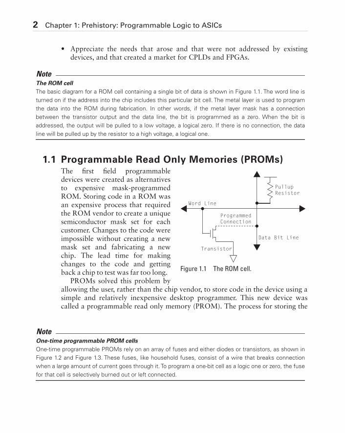
NoteThe ROM cell
The basic diagram for a ROM cell containing a single bit of data is shown in Figure 1.1. The word line is
turned on if the address into the chip includes this particular bit cell. The metal layer is used to program
the data into the ROM during fabrication. In other words, if the metal layer mask has a connection
between the transistor output and the data line, the bit is programmed as a zero. When the bit is
addressed, the output will be pulled to a low voltage, a logical zero. If there is no connection, the data
line will be pulled up by the resistor to a high voltage, a logical one.
Word Line
ProgrammedConnection
Transistor
PullupResistor
Data Bit Line
Figure 1.1 The ROM cell.
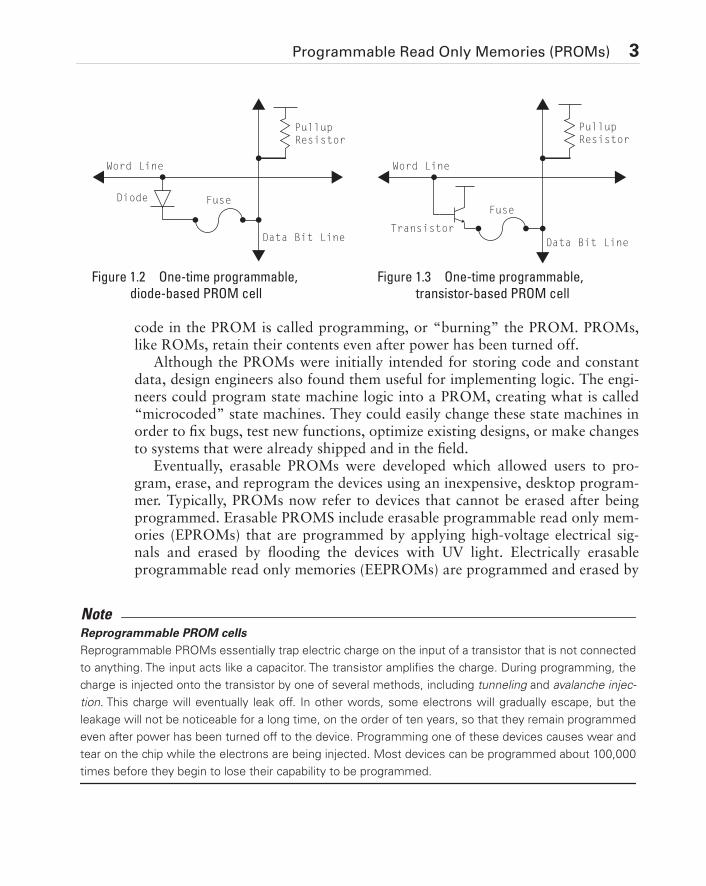
NoteOne-time programmable PROM cells
One-time programmable PROMs rely on an array of fuses and either diodes or transistors, as shown in
Figure 1.2 and Figure 1.3. These fuses, like household fuses, consist of a wire that breaks connection
when a large amount of current goes through it. To program a one-bit cell as a logic one or zero, the fuse
for that cell is selectively burned out or left connected.
Programmable Read Only Memories (PROMs) 3
code in the PROM is called programming, or “burning” the PROM. PROMs,like ROMs, retain their contents even after power has been turned off.
Although the PROMs were initially intended for storing code and constantdata, design engineers also found them useful for implementing logic. The engi-neers could program state machine logic into a PROM, creating what is called“microcoded” state machines. They could easily change these state machines inorder to fix bugs, test new functions, optimize existing designs, or make changesto systems that were already shipped and in the field.
Eventually, erasable PROMs were developed which allowed users to pro-gram, erase, and reprogram the devices using an inexpensive, desktop program-mer. Typically, PROMs now refer to devices that cannot be erased after beingprogrammed. Erasable PROMS include erasable programmable read only mem-ories (EPROMs) that are programmed by applying high-voltage electrical sig-nals and erased by flooding the devices with UV light. Electrically erasableprogrammable read only memories (EEPROMs) are programmed and erased by
Word Line
PullupResistor
Data Bit Line
FuseDiode
Figure 1.2 One-time programmable,
diode-based PROM cell
Word Line
PullupResistor
Data Bit Line
Fuse
Transistor
Figure 1.3 One-time programmable,
transistor-based PROM cell
NoteReprogrammable PROM cells
Reprogrammable PROMs essentially trap electric charge on the input of a transistor that is not connected
to anything. The input acts like a capacitor. The transistor amplifies the charge. During programming, the
charge is injected onto the transistor by one of several methods, including tunneling and avalanche injec-
tion. This charge will eventually leak off. In other words, some electrons will gradually escape, but the
leakage will not be noticeable for a long time, on the order of ten years, so that they remain programmed
even after power has been turned off to the device. Programming one of these devices causes wear and
tear on the chip while the electrons are being injected. Most devices can be programmed about 100,000
times before they begin to lose their capability to be programmed.
4 Chapter 1: Prehistory: Programmable Logic to ASICs
applying high voltages to the device. Flash EPROMs are programmed anderased electrically and have sections that can be erased electrically in a shorttime and independently of other sections within the device. For the rest of thischapter, I use the term PROM generically to refer to all of these devices unless Ispecifically state otherwise.
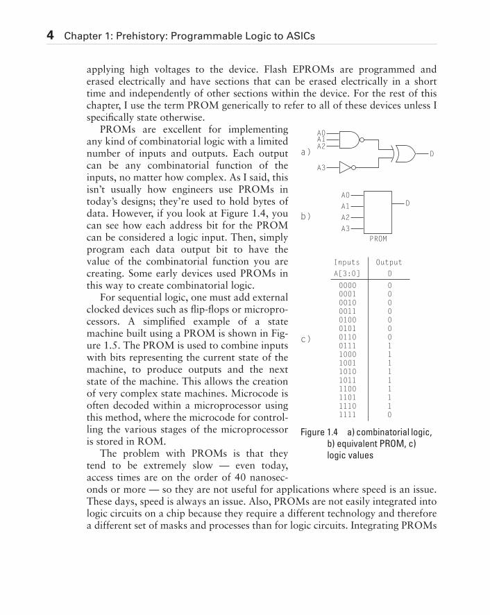
PROMs are excellent for implementingany kind of combinatorial logic with a limitednumber of inputs and outputs. Each outputcan be any combinatorial function of theinputs, no matter how complex. As I said, thisisn’t usually how engineers use PROMs intoday’s designs; they’re used to hold bytes ofdata. However, if you look at Figure 1.4, youcan see how each address bit for the PROMcan be considered a logic input. Then, simplyprogram each data output bit to have thevalue of the combinatorial function you arecreating. Some early devices used PROMs inthis way to create combinatorial logic.
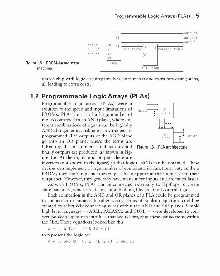
For sequential logic, one must add externalclocked devices such as flip-flops or micropro-cessors. A simplified example of a statemachine built using a PROM is shown in Fig-ure 1.5. The PROM is used to combine inputswith bits representing the current state of themachine, to produce outputs and the nextstate of the machine. This allows the creationof very complex state machines. Microcode isoften decoded within a microprocessor usingthis method, where the microcode for control-ling the various stages of the microprocessoris stored in ROM.
The problem with PROMs is that theytend to be extremely slow — even today,access times are on the order of 40 nanosec-onds or more — so they are not useful for applications where speed is an issue.These days, speed is always an issue. Also, PROMs are not easily integrated intologic circuits on a chip because they require a different technology and thereforea different set of masks and processes than for logic circuits. Integrating PROMs
A0A1A2
A3
Da)
A0D
A3
A2
A1
PROM
b)
c)
Inputs Output
A[3:0]
0000000100100011010001010110011110001001101010111100110111101111
D
0000000111111110
Figure 1.4 a) combinatorial logic,
b) equivalent PROM, c)
logic values
Programmable Logic Arrays (PLAs) 5
onto a chip with logic circuitry involves extra masks and extra processing steps,all leading to extra costs.
1.2 Programmable Logic Arrays (PLAs)Programmable logic arrays (PLAs) were asolution to the speed and input limitations ofPROMs. PLAs consist of a large number ofinputs connected to an AND plane, where dif-ferent combinations of signals can be logicallyANDed together according to how the part isprogrammed. The outputs of the AND planego into an OR plane, where the terms areORed together in different combinations andfinally outputs are produced, as shown in Fig-ure 1.6. At the inputs and outputs there areinverters (not shown in the figure) so that logical NOTs can be obtained. Thesedevices can implement a large number of combinatorial functions, but, unlike aPROM, they can’t implement every possible mapping of their input set to theiroutput set. However, they generally have many more inputs and are much faster.
As with PROMs, PLAs can be connected externally to flip-flops to createstate machines, which are the essential building blocks for all control logic.
Each connection in the AND and OR planes of a PLA could be programmedto connect or disconnect. In other words, terms of Boolean equations could becreated by selectively connecting wires within the AND and OR planes. Simplehigh level languages — ABEL, PALASM, and CUPL — were developed to con-vert Boolean equations into files that would program these connections withinthe PLA. These equations looked like this:
a = (b & !c) | (b & !d & e)
to represent the logic for
A = (B AND NOT C) OR (B & NOT D AND E)
D QA0input1
input2
input3
A1
A2
A3
D3
D2
D1
D0 output1
output2
output3
PROM
flip-flop
next state current state
Figure 1.5 PROM-based state
machine
Inputs
Outputs
ANDplane
ORplane
Figure 1.6 PLA architecture
6 Chapter 1: Prehistory: Programmable Logic to ASICs
This added a new dimension to programmable devices in that logic couldnow be described in readable programs at a level higher than ones and zeroes.
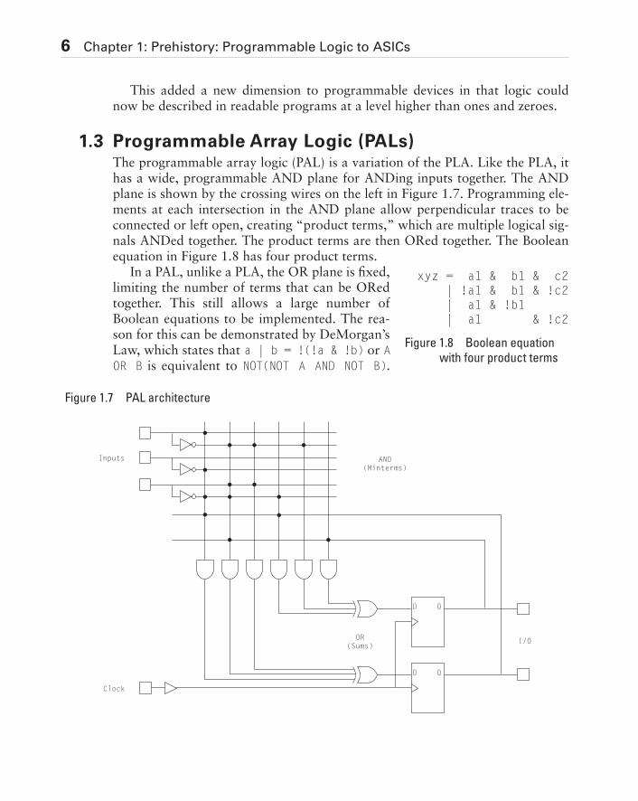
1.3 Programmable Array Logic (PALs)The programmable array logic (PAL) is a variation of the PLA. Like the PLA, ithas a wide, programmable AND plane for ANDing inputs together. The ANDplane is shown by the crossing wires on the left in Figure 1.7. Programming ele-ments at each intersection in the AND plane allow perpendicular traces to beconnected or left open, creating “product terms,” which are multiple logical sig-nals ANDed together. The product terms are then ORed together. The Booleanequation in Figure 1.8 has four product terms.
In a PAL, unlike a PLA, the OR plane is fixed,limiting the number of terms that can be ORedtogether. This still allows a large number ofBoolean equations to be implemented. The rea-son for this can be demonstrated by DeMorgan’sLaw, which states that a | b = !(!a & !b) or AOR B is equivalent to NOT(NOT A AND NOT B).
D Q
D Q
Inputs AND(Minterms)
OR(Sums)
I/O
Clock
Figure 1.7 PAL architecture
xyz = a1 & b1 & c2 | !a1 & b1 & !c2 | a1 & !b1 | a1 & !c2
Figure 1.8 Boolean equation
with four product terms
Programmable Array Logic (PALs) 7
That means if you use inverters on the inputs and outputs, you can create all thelogic you need with either a wide AND plane or a wide OR plane, but you don’tneed both.
Including inverters reduced the need for the large OR plane, which in turnallowed the extra silicon area on the chip to be used for other basic logicdevices, such as multiplexers, exclusive ORs, and latches. Most importantly,clocked elements, typically flip-flops, could be included in PALs. These deviceswere now able to implement a large number of logic functions, includingclocked sequential logic needed for state machines. This was an important devel-opment that allowed PALs to replace much of the standard logic in manydesigns. PALs are also extremely fast. With PALs, high-speed controllers couldbe designed in programmable logic.
Notice the architecture of a PAL, shown in Figure 1.7. The AND plane isshown in the upper-left corner as a switch matrix. The dots show where connec-tions have been programmed. The fixed-size ORs are represented as OR gates. Aclock input is used to clock the flip-flops. The outputs of the flip-flops can bedriven off the chip, or they can be fed back to the AND plane in order to createa state machine.
The inclusion of extra logic devices, particularly flip-flops, greatly increasedthe complexity and potential uses of PALs, creating a need for new methods ofprogramming that were flexible and readable. Thus the first hardware descrip-tion languages (HDLs) were born. These simple HDLs included ABEL, CUPL,and PALASM, the precursors of Verilog and VHDL, much more complex lan-guages that are in use today for CPLD, FPGA, and ASIC design.
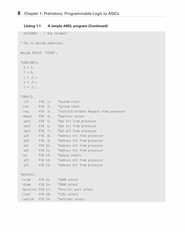
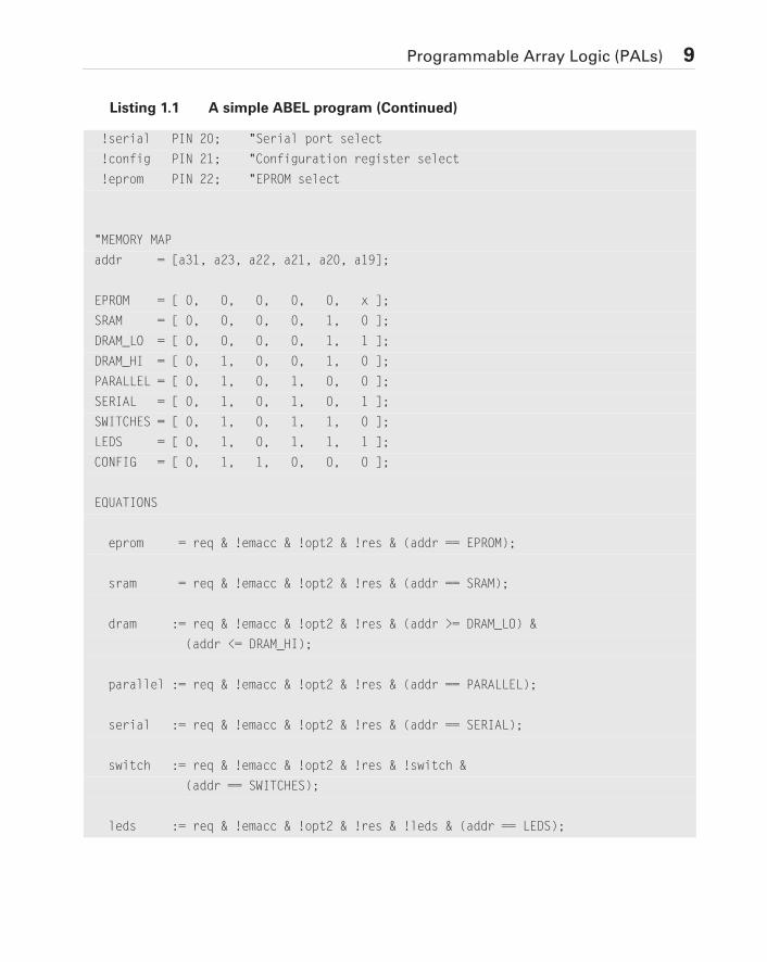
A simple ABEL program for a PAL is shown in Listing 1.1. Don’t worryabout trying to understand the details — it’s for illustration purposes only.Notice that the programming language allows the use of simulation test vectorsin the code. The simulation vectors are at the end of the program. This simula-tion capability brought better reliability and verification of programmabledevices, something that was critical when CPLDs and FPGAs were developed.
Listing 1.1 A simple ABEL program
MODULE DECODE;
FLAG '-R3','-T1','-V','-F0','-G','-Q2';
TITLE'
CHIP : Decode PAL - Version A
DATE : July 17, 1991
8 Chapter 1: Prehistory: Programmable Logic to ASICs
DESIGNER : Bob Zeidman'
" PAL to decode addresses.
decode DEVICE 'P20R6';
"CONSTANTS:
h = 1;
l = 0;
c = .C.;
x = .X.;
z = .Z.;
"INPUTS:
clk PIN 1; "System clock
!res PIN 2; "System reset
!req PIN 3; "Instruction/Data Request from processor
!emacc PIN 4; "Emulator access
opt0 PIN 5; "Opt bit from processor
opt1 PIN 6; "Opt bit from processor
opt2 PIN 7; "Opt bit from processor
a19 PIN 8; "Address bit from processor
a20 PIN 9; "Address bit from processor
a21 PIN 10; "Address bit from processor
a22 PIN 11; "Address bit from processor
!oe PIN 13; "Output enable
a23 PIN 14; "Address bit from processor
a31 PIN 23; "Address bit from processor
"OUTPUTS:
!sram PIN 15; "SRAM select
!dram PIN 16; "DRAM select
!parallel PIN 17; "Parallel port select
!leds PIN 18; "LEDs select
!switch PIN 19; "Switches select
Listing 1.1 A simple ABEL program (Continued)
Programmable Array Logic (PALs) 9
!serial PIN 20; "Serial port select
!config PIN 21; "Configuration register select
!eprom PIN 22; "EPROM select
"MEMORY MAP
addr = [a31, a23, a22, a21, a20, a19];
EPROM = [ 0, 0, 0, 0, 0, x ];
SRAM = [ 0, 0, 0, 0, 1, 0 ];
DRAM_LO = [ 0, 0, 0, 0, 1, 1 ];
DRAM_HI = [ 0, 1, 0, 0, 1, 0 ];
PARALLEL = [ 0, 1, 0, 1, 0, 0 ];
SERIAL = [ 0, 1, 0, 1, 0, 1 ];
SWITCHES = [ 0, 1, 0, 1, 1, 0 ];
LEDS = [ 0, 1, 0, 1, 1, 1 ];
CONFIG = [ 0, 1, 1, 0, 0, 0 ];
EQUATIONS
eprom = req & !emacc & !opt2 & !res & (addr == EPROM);
sram = req & !emacc & !opt2 & !res & (addr == SRAM);
dram := req & !emacc & !opt2 & !res & (addr >= DRAM_LO) &
(addr <= DRAM_HI);
parallel := req & !emacc & !opt2 & !res & (addr == PARALLEL);
serial := req & !emacc & !opt2 & !res & (addr == SERIAL);
switch := req & !emacc & !opt2 & !res & !switch &
(addr == SWITCHES);
leds := req & !emacc & !opt2 & !res & !leds & (addr == LEDS);
Listing 1.1 A simple ABEL program (Continued)
10 Chapter 1: Prehistory: Programmable Logic to ASICs
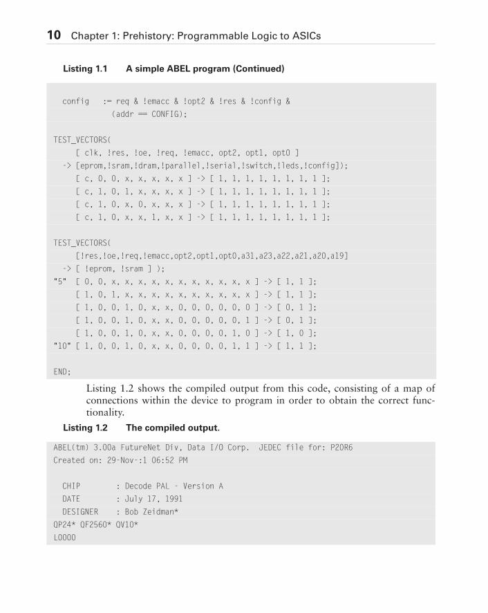
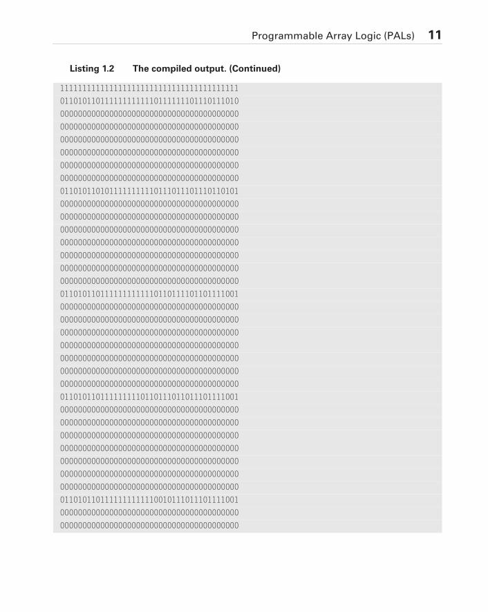
Listing 1.2 shows the compiled output from this code, consisting of a map ofconnections within the device to program in order to obtain the correct func-tionality.
config := req & !emacc & !opt2 & !res & !config &
(addr == CONFIG);
TEST_VECTORS(
[ clk, !res, !oe, !req, !emacc, opt2, opt1, opt0 ]
-> [eprom,!sram,!dram,!parallel,!serial,!switch,!leds,!config]);
[ c, 0, 0, x, x, x, x, x ] -> [ 1, 1, 1, 1, 1, 1, 1, 1 ];
[ c, 1, 0, 1, x, x, x, x ] -> [ 1, 1, 1, 1, 1, 1, 1, 1 ];
[ c, 1, 0, x, 0, x, x, x ] -> [ 1, 1, 1, 1, 1, 1, 1, 1 ];
[ c, 1, 0, x, x, 1, x, x ] -> [ 1, 1, 1, 1, 1, 1, 1, 1 ];
TEST_VECTORS(
[!res,!oe,!req,!emacc,opt2,opt1,opt0,a31,a23,a22,a21,a20,a19]
-> [ !eprom, !sram ] );
"5" [ 0, 0, x, x, x, x, x, x, x, x, x, x, x ] -> [ 1, 1 ];
[ 1, 0, 1, x, x, x, x, x, x, x, x, x, x ] -> [ 1, 1 ];
[ 1, 0, 0, 1, 0, x, x, 0, 0, 0, 0, 0, 0 ] -> [ 0, 1 ];
[ 1, 0, 0, 1, 0, x, x, 0, 0, 0, 0, 0, 1 ] -> [ 0, 1 ];
[ 1, 0, 0, 1, 0, x, x, 0, 0, 0, 0, 1, 0 ] -> [ 1, 0 ];
"10" [ 1, 0, 0, 1, 0, x, x, 0, 0, 0, 0, 1, 1 ] -> [ 1, 1 ];
END;
Listing 1.1 A simple ABEL program (Continued)
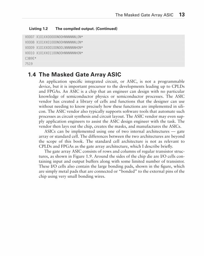
Listing 1.2 The compiled output.
ABEL(tm) 3.00a FutureNet Div, Data I/O Corp. JEDEC file for: P20R6
Created on: 29-Nov-:1 06:52 PM
CHIP : Decode PAL - Version A
DATE : July 17, 1991
DESIGNER : Bob Zeidman*
QP24* QF2560* QV10*
L0000
Programmable Array Logic (PALs) 11
1111111111111111111111111111111111111111
0110101101111111111110111111101110111010
0000000000000000000000000000000000000000
0000000000000000000000000000000000000000
0000000000000000000000000000000000000000
0000000000000000000000000000000000000000
0000000000000000000000000000000000000000
0000000000000000000000000000000000000000
0110101101011111111110111011101110110101
0000000000000000000000000000000000000000
0000000000000000000000000000000000000000
0000000000000000000000000000000000000000
0000000000000000000000000000000000000000
0000000000000000000000000000000000000000
0000000000000000000000000000000000000000
0000000000000000000000000000000000000000
0110101101111111111110110111101101111001
0000000000000000000000000000000000000000
0000000000000000000000000000000000000000
0000000000000000000000000000000000000000
0000000000000000000000000000000000000000
0000000000000000000000000000000000000000
0000000000000000000000000000000000000000
0000000000000000000000000000000000000000
0110101101111111110110111011011101111001
0000000000000000000000000000000000000000
0000000000000000000000000000000000000000
0000000000000000000000000000000000000000
0000000000000000000000000000000000000000
0000000000000000000000000000000000000000
0000000000000000000000000000000000000000
0000000000000000000000000000000000000000
0110101101111111111110010111011101111001
0000000000000000000000000000000000000000
0000000000000000000000000000000000000000
Listing 1.2 The compiled output. (Continued)

12 Chapter 1: Prehistory: Programmable Logic to ASICs
0000000000000000000000000000000000000000
0000000000000000000000000000000000000000
0000000000000000000000000000000000000000
0000000000000000000000000000000000000000
0000000000000000000000000000000000000000
0110101101111111111110111011101101111001
0000000000000000000000000000000000000000
0000000000000000000000000000000000000000
0000000000000000000000000000000000000000
0000000000000000000000000000000000000000
0000000000000000000000000000000000000000
0000000000000000000000000000000000000000
0000000000000000000000000000000000000000
0110101101111111111110111011111110111001
0110101101111111111110111111101110111001
0110101101111111111110110111011111111110
0110101101111111111110111111111101111110
0110101101111111111110111111111111110110
0000000000000000000000000000000000000000
0000000000000000000000000000000000000000
0000000000000000000000000000000000000000
1111111111111111111111111111111111111111
0110101101111111111110111011011110111010
0000000000000000000000000000000000000000
0000000000000000000000000000000000000000
0000000000000000000000000000000000000000
0000000000000000000000000000000000000000
0000000000000000000000000000000000000000
0000000000000000000000000000000000000000*
V0001 C0XXXXXXXXXN0XHHHHHHHHXN*
V0002 C11XXXXXXXXN0XHHHHHHHHXN*
V0003 C1X0XXXXXXXN0XHHHHHHHHXN*
V0004 C1XXXX1XXXXN0XHHHHHHHHXN*
V0005 X0XXXXXXXXXN0XHNNNNNNHXN*
V0006 X11XXXXXXXXN0XHNNNNNNHXN*
Listing 1.2 The compiled output. (Continued)
The Masked Gate Array ASIC 13
1.4 The Masked Gate Array ASICAn application specific integrated circuit, or ASIC, is not a programmabledevice, but it is important precursor to the developments leading up to CPLDsand FPGAs. An ASIC is a chip that an engineer can design with no particularknowledge of semiconductor physics or semiconductor processes. The ASICvendor has created a library of cells and functions that the designer can usewithout needing to know precisely how these functions are implemented in sili-con. The ASIC vendor also typically supports software tools that automate suchprocesses as circuit synthesis and circuit layout. The ASIC vendor may even sup-ply application engineers to assist the ASIC design engineer with the task. Thevendor then lays out the chip, creates the masks, and manufactures the ASICs.
ASICs can be implemented using one of two internal architectures — gatearray or standard cell. The differences between the two architectures are beyondthe scope of this book. The standard cell architecture is not as relevant toCPLDs and FPGAs as the gate array architecture, which I describe briefly.
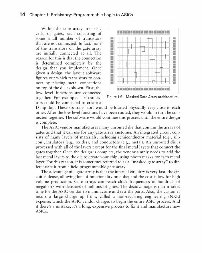
The gate array ASIC consists of rows and columns of regular transistor struc-tures, as shown in Figure 1.9. Around the sides of the chip die are I/O cells con-taining input and output buffers along with some limited number of transistor.These I/O cells also contain the large bonding pads, shown in the figure, whichare simply metal pads that are connected or “bonded” to the external pins of thechip using very small bonding wires.
V0007 X101XX00000N00HNNNNNNL0N*
V0008 X101XX01000N00HNNNNNNL0N*
V0009 X101XX00100N00LNNNNNNH0N*
V0010 X101XX01100N00HNNNNNNH0N*
C3B9E*
7519
Listing 1.2 The compiled output. (Continued)
14 Chapter 1: Prehistory: Programmable Logic to ASICs
Within the core array are basiccells, or gates, each consisting ofsome small number of transistorsthat are not connected. In fact, noneof the transistors on the gate arrayare initially connected at all. Thereason for this is that the connectionis determined completely by thedesign that you implement. Oncegiven a design, the layout softwarefigures out which transistors to con-nect by placing metal connectionson top of the die as shown. First, thelow level functions are connectedtogether. For example, six transis-tors could be connected to create aD flip-flop. These six transistors would be located physically very close to eachother. After the low level functions have been routed, they would in turn be con-nected together. The software would continue this process until the entire designis complete.
The ASIC vendor manufactures many unrouted die that contain the arrays ofgates and that it can use for any gate array customer. An integrated circuit con-sists of many layers of materials, including semiconductor material (e.g., sili-con), insulators (e.g., oxides), and conductors (e.g., metal). An unrouted die isprocessed with all of the layers except for the final metal layers that connect thegates together. Once the design is complete, the vendor simply needs to add thelast metal layers to the die to create your chip, using photo masks for each metallayer. For this reason, it is sometimes referred to as a “masked gate array” to dif-ferentiate it from a field programmable gate array.
The advantage of a gate array is that the internal circuitry is very fast; the cir-cuit is dense, allowing lots of functionality on a die; and the cost is low for highvolume production. Gate arrays can reach clock frequencies of hundreds ofmegahertz with densities of millions of gates. The disadvantage is that it takestime for the ASIC vendor to manufacture and test the parts. Also, the customerincurs a large charge up front, called a non-recurring engineering (NRE)expense, which the ASIC vendor charges to begin the entire ASIC process. Andif there’s a mistake, it’s a long, expensive process to fix it and manufacture newASICs.
Figure 1.9 Masked Gate Array architecture
CPLDs and FPGAs 15
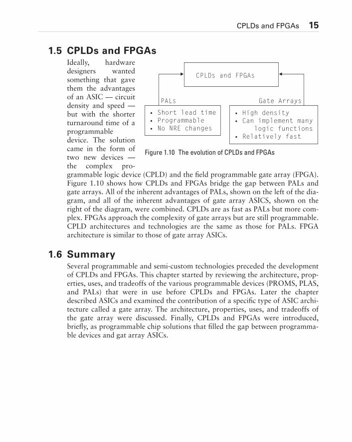
1.5 CPLDs and FPGAsIdeally, hardwaredesigners wantedsomething that gavethem the advantagesof an ASIC — circuitdensity and speed —but with the shorterturnaround time of aprogrammabledevice. The solutioncame in the form oftwo new devices —the complex pro-grammable logic device (CPLD) and the field programmable gate array (FPGA).Figure 1.10 shows how CPLDs and FPGAs bridge the gap between PALs andgate arrays. All of the inherent advantages of PALs, shown on the left of the dia-gram, and all of the inherent advantages of gate array ASICS, shown on theright of the diagram, were combined. CPLDs are as fast as PALs but more com-plex. FPGAs approach the complexity of gate arrays but are still programmable.CPLD architectures and technologies are the same as those for PALs. FPGAarchitecture is similar to those of gate array ASICs.
1.6 SummarySeveral programmable and semi-custom technologies preceded the developmentof CPLDs and FPGAs. This chapter started by reviewing the architecture, prop-erties, uses, and tradeoffs of the various programmable devices (PROMS, PLAS,and PALs) that were in use before CPLDs and FPGAs. Later the chapterdescribed ASICs and examined the contribution of a specific type of ASIC archi-tecture called a gate array. The architecture, properties, uses, and tradeoffs ofthe gate array were discussed. Finally, CPLDs and FPGAs were introduced,briefly, as programmable chip solutions that filled the gap between programma-ble devices and gat array ASICs.
PALs Gate Arrays
CPLDs and FPGAs
• Short lead time• Programmable• No NRE changes
• High density• Can implement many logic functions• Relatively fast
Figure 1.10 The evolution of CPLDs and FPGAs

16 Chapter 1: Prehistory: Programmable Logic to ASICs
Exercises
1. What does the term ASIC stand for?
(a) Application standard integrated chip
(b) Applied system integrated circuit
(c) Application specific integrated circuit
2. Match each programmable device with its description.
3. Choose the correct device for each statement — PALs or ASICs.
(a) ________ have a short lead time.
(b) ________ are high-density devices.
(c) ________ can implement very complex functions.
(d) ________ do not have NRE charges.
(e) ________ are programmable.
(a) PROM (A) A memory device that can be programmed once and read many times.
(b) PLA (B) A logic device that can be used to design large functions like an ASIC, except that it can be programmed quickly and inexpen-sively.
(c) PAL (C) A logic device that is made up of many PAL devices.
(d) CPLD (D) A logic device with a large AND plane and a large OR plane for implementing different combinations of Boolean logic.
(e) FPGA (E) A logic device with a large AND plane and a small, fixed num-ber of OR gates for implementing Boolean logic and state machines.
17
Chapter 2
Complex Programmable Logic Devices (CPLDs)
Complex Programmable Logic Devices are exactly what they claim to be: logicdevices that are complex and programmable. There are two main engineeringfeatures to understand about CPLDs that separate them from their cousins,FPGAs. One feature is the internal architecture of the device and how this archi-tecture implements various logic functions. The second feature is the semicon-ductor technology that allows the devices to be programmed and allows variousstructures in the device to be connected.
ObjectivesThis chapter focuses on the architecture and technologies of CPLDs. This chap-ter should help you:
• Understand the internal architecture of CPLDs
• Gain knowledge of the technologies used for programming and con-necting internal blocks of CPLDs
• Learn the advantages and tradeoffs of different architectures and tech-nologies
In this chapter...
• CPLD Architectures
• Function Blocks
• I/O Blocks
• CPLD Technology and Pro-
grammable Elements
• CPLD Selection Criteria
• Example CPLD Families
18 Chapter 2: Complex Programmable Logic Devices (CPLDs)
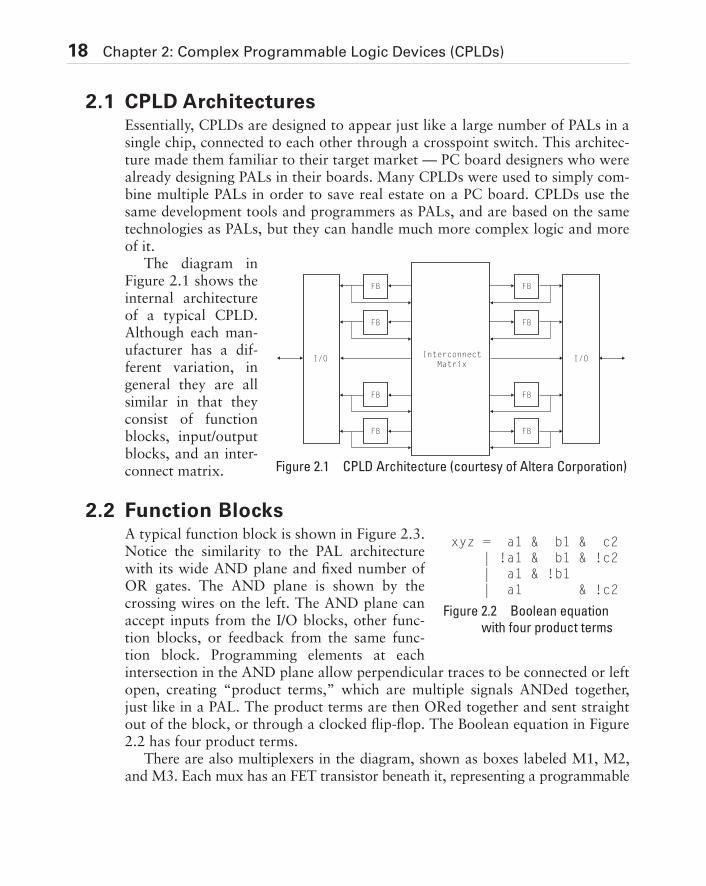
2.1 CPLD ArchitecturesEssentially, CPLDs are designed to appear just like a large number of PALs in asingle chip, connected to each other through a crosspoint switch. This architec-ture made them familiar to their target market — PC board designers who werealready designing PALs in their boards. Many CPLDs were used to simply com-bine multiple PALs in order to save real estate on a PC board. CPLDs use thesame development tools and programmers as PALs, and are based on the sametechnologies as PALs, but they can handle much more complex logic and moreof it.
The diagram inFigure 2.1 shows theinternal architectureof a typical CPLD.Although each man-ufacturer has a dif-ferent variation, ingeneral they are allsimilar in that theyconsist of functionblocks, input/outputblocks, and an inter-connect matrix.
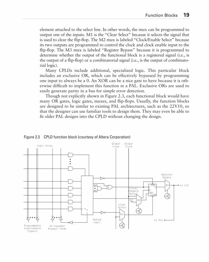
2.2 Function BlocksA typical function block is shown in Figure 2.3.Notice the similarity to the PAL architecturewith its wide AND plane and fixed number ofOR gates. The AND plane is shown by thecrossing wires on the left. The AND plane canaccept inputs from the I/O blocks, other func-tion blocks, or feedback from the same func-tion block. Programming elements at eachintersection in the AND plane allow perpendicular traces to be connected or leftopen, creating “product terms,” which are multiple signals ANDed together,just like in a PAL. The product terms are then ORed together and sent straightout of the block, or through a clocked flip-flop. The Boolean equation in Figure2.2 has four product terms.
There are also multiplexers in the diagram, shown as boxes labeled M1, M2,and M3. Each mux has an FET transistor beneath it, representing a programmable
InterconnectMatrix
I/O I/O
FB
FB
FB
FB
FB
FB
FB
FB
Figure 2.1 CPLD Architecture (courtesy of Altera Corporation)
xyz = a1 & b1 & c2 | !a1 & b1 & !c2 | a1 & !b1 | a1 & !c2
Figure 2.2 Boolean equation
with four product terms
Function Blocks 19
element attached to the select line. In other words, the mux can be programmed tooutput one of the inputs. M1 is the “Clear Select” because it selects the signal thatis used to clear the flip-flop. The M2 mux is labeled “Clock/Enable Select” becauseits two outputs are programmed to control the clock and clock enable input to theflip-flop. The M3 mux is labeled “Register Bypass” because it is programmed todetermine whether the output of the functional block is a registered signal (i.e., isthe output of a flip-flop) or a combinatorial signal (i.e., is the output of combinato-rial logic).
Many CPLDs include additional, specialized logic. This particular blockincludes an exclusive OR, which can be effectively bypassed by programmingone input to always be a 0. An XOR can be a nice gate to have because it is oth-erwise difficult to implement this function in a PAL. Exclusive ORs are used toeasily generate parity in a bus for simple error detection.
Though not explicitly shown in Figure 2.3, each functional block would havemany OR gates, logic gates, muxes, and flip-flops. Usually, the function blocksare designed to be similar to existing PAL architectures, such as the 22V10, sothat the designer can use familiar tools to design them. They may even be able tofit older PAL designs into the CPLD without changing the design.
Logic Array
ProgrammableInterconnect
Signals
16 EspanderProduct Terms
SharedLogic
GlobalClear
GlobalClock
ClearSelect
Clock/EnbableSelect
VCC
RegisterBypass
to PIA
to I/O
M1
M2
M3PRN
CLRN
D Q
ENA
Figure 2.3 CPLD function block (courtesy of Altera Corporation)
20 Chapter 2: Complex Programmable Logic Devices (CPLDs)
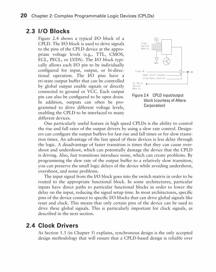
2.3 I/O BlocksFigure 2.4 shows a typical I/O block of aCPLD. The I/O block is used to drive signalsto the pins of the CPLD device at the appro-priate voltage levels (e.g., TTL, CMOS,ECL, PECL, or LVDS). The I/O block typi-cally allows each I/O pin to be individuallyconfigured for input, output, or bi-direc-tional operation. The I/O pins have atri-state output buffer that can be controlledby global output enable signals or directlyconnected to ground or VCC. Each outputpin can also be configured to be open drain.In addition, outputs can often be pro-grammed to drive different voltage levels,enabling the CPLD to be interfaced to manydifferent devices.
One particularly useful feature in high speed CPLDs is the ability to controlthe rise and fall rates of the output drivers by using a slew rate control. Design-ers can configure the output buffers for fast rise and fall times or for slow transi-tion times. An advantage of the fast speed of these devices is less delay throughthe logic. A disadvantage of faster transition is times that they can cause over-shoot and undershoot, which can potentially damage the device that the CPLDis driving. Also, fast transitions introduce noise, which can create problems. Byprogramming the slew rate of the output buffer to a relatively slow transition,you can preserve the small logic delays of the device while avoiding undershoot,overshoot, and noise problems.
The input signal from the I/O block goes into the switch matrix in order to berouted to the appropriate functional block. In some architectures, particularinputs have direct paths to particular functional blocks in order to lower thedelay on the input, reducing the signal setup time. In most architectures, specificpins of the device connect to specific I/O blocks that can drive global signals likereset and clock. This means that only certain pins of the device can be used todrive these global signals. This is particularly important for clock signals, asdescribed in the next section.
2.4 Clock DriversAs Section 5.3 (in Chapter 5) explains, synchronous design is the only accepteddesign methodology that will ensure that a CPLD-based design is reliable over
VCC
GND
FromSwitchMatrix
From FB
Open-Drain Output
Slow-Rate Control
To FB orSwitchMatrix
Figure 2.4 CPLD input/output
block (courtesy of Altera
Corporation)
Interconnect 21
its lifetime. In order to design synchronous CPLDs, the clock signal must arriveat each flip-flop in the design at about the same time and with very little delayfrom the input pin. In order to accomplish this, special I/O blocks have clockdrivers that use very fast input buffers and which drive the input clock signalonto an internal clock tree. The clock tree is so named because it resembles atree, with each branch driving the clock input of a fixed number of flip-flops.The clock driver is designed to drive the entire tree very quickly. The trees aredesigned to minimize the skew between clock signals arriving at differentflip-flops throughout the device. Each branch of the tree is of approximatelyequal length, or if not, internal buffers are used to balance the skew along thedifferent branches. It is important that clock signals are only driven through theclock input pins that connect to these special drivers.
In large devices, there may be several clock input pins connected to differentclock drivers. This feature helps in designs that use multiple clocks. You need tohave at least as many clock drivers in the CPLD as you need clocks in yourdesign. Also, the different clocks must be considered to be asynchronous withrespect to each other, because the CPLD vendor does not typically guaranteeskew between multiple clocks. Signals clocked by one clock will need to be syn-chronized with the other clock before use by any logic clocked by the secondclock. For more information on synchronous design and synchronizing asyn-chronous signals, see Section 5.3.
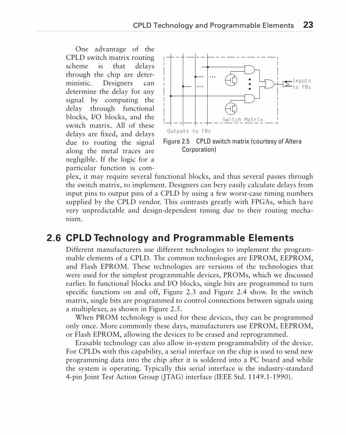
2.5 InterconnectThe CPLD interconnect is a very large programmable switch matrix that allowssignals from all parts of the device to go to all other parts of the device. Figure2.5 shows the architecture of the switch matrix. The switch matrix takes theoutputs of the functional blocks and is programmed to send those outputs tofunctional blocks. This way, the designer can route any output signal to any des-tination.

22 Interconnect
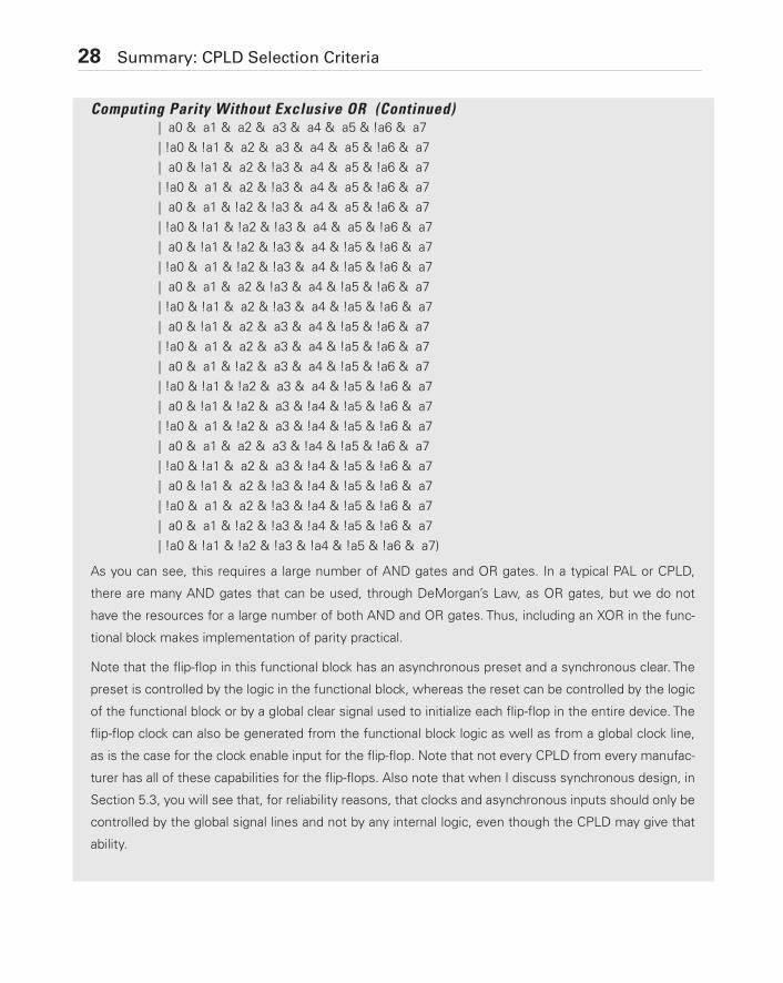
Computing Parity Without Exclusive ORThe Boolean expression for generating even parity for a bus is shown in the following equation:
parity = a0 ^ a1 ^ a2 ^ a3 ^ a4 ^ a5 ^ a6 ^ a7
If we implement this equation using AND and OR logic, the result is
parity = a0 & !a1 & !a2 & !a3 & !a4 & !a5 & !a6 & !a7
| !a0 & a1 & !a2 & !a3 & !a4 & !a5 & !a6 & !a7
| a0 & a1 & a2 & !a3 & !a4 & !a5 & !a6 & !a7
| !a0 & !a1 & a2 & !a3 & !a4 & !a5 & !a6 & !a7
| a0 & !a1 & a2 & a3 & !a4 & !a5 & !a6 & !a7
| !a0 & a1 & a2 & a3 & !a4 & !a5 & !a6 & !a7
| a0 & a1 & !a2 & a3 & !a4 & !a5 & !a6 & !a7
| !a0 & !a1 & !a2 & a3 & !a4 & !a5 & !a6 & !a7
| a0 & !a1 & !a2 & a3 & a4 & !a5 & !a6 & !a7
| !a0 & a1 & !a2 & a3 & a4 & !a5 & !a6 & !a7
| a0 & a1 & a2 & a3 & a4 & !a5 & !a6 & !a7
| !a0 & !a1 & a2 & a3 & a4 & !a5 & !a6 & !a7
| a0 & !a1 & a2 & !a3 & a4 & !a5 & !a6 & !a7
| !a0 & a1 & a2 & !a3 & a4 & !a5 & !a6 & !a7
| a0 & a1 & !a2 & !a3 & a4 & !a5 & !a6 & !a7
| !a0 & !a1 & !a2 & !a3 & a4 & !a5 & !a6 & !a7
| a0 & !a1 & !a2 & !a3 & a4 & a5 & !a6 & !a7
| !a0 & a1 & !a2 & !a3 & a4 & a5 & !a6 & !a7
| a0 & a1 & a2 & !a3 & a4 & a5 & !a6 & !a7
| !a0 & !a1 & a2 & !a3 & a4 & a5 & !a6 & !a7
| a0 & !a1 & a2 & a3 & a4 & a5 & !a6 & !a7
| !a0 & a1 & a2 & a3 & a4 & a5 & !a6 & !a7
| a0 & a1 & !a2 & a3 & a4 & a5 & !a6 & !a7
| !a0 & !a1 & !a2 & a3 & a4 & a5 & !a6 & !a7
| a0 & !a1 & !a2 & a3 & !a4 & a5 & !a6 & !a7
| !a0 & a1 & !a2 & a3 & !a4 & a5 & !a6 & !a7
| a0 & a1 & a2 & a3 & !a4 & a5 & !a6 & !a7
| !a0 & !a1 & a2 & a3 & !a4 & a5 & !a6 & !a7
| a0 & !a1 & a2 & !a3 & !a4 & a5 & !a6 & !a7
| !a0 & a1 & a2 & !a3 & !a4 & a5 & !a6 & !a7
| a0 & a1 & !a2 & !a3 & !a4 & a5 & !a6 & !a7
| !a0 & !a1 & !a2 & !a3 & !a4 & a5 & !a6 & !a7
CPLD Technology and Programmable Elements 23
One advantage of theCPLD switch matrix routingscheme is that delaysthrough the chip are deter-ministic. Designers candetermine the delay for anysignal by computing thedelay through functionalblocks, I/O blocks, and theswitch matrix. All of thesedelays are fixed, and delaysdue to routing the signalalong the metal traces arenegligible. If the logic for aparticular function is com-plex, it may require several functional blocks, and thus several passes throughthe switch matrix, to implement. Designers can bery easily calculate delays frominput pins to output pins of a CPLD by using a few worst-case timing numberssupplied by the CPLD vendor. This contrasts greatly with FPGAs, which havevery unpredictable and design-dependent timing due to their routing mecha-nism.
2.6 CPLD Technology and Programmable ElementsDifferent manufacturers use different technologies to implement the program-mable elements of a CPLD. The common technologies are EPROM, EEPROM,and Flash EPROM. These technologies are versions of the technologies thatwere used for the simplest programmable devices, PROMs, which we discussedearlier. In functional blocks and I/O blocks, single bits are programmed to turnspecific functions on and off, Figure 2.3 and Figure 2.4 show. In the switchmatrix, single bits are programmed to control connections between signals usinga multiplexer, as shown in Figure 2.5.
When PROM technology is used for these devices, they can be programmedonly once. More commonly these days, manufacturers use EPROM, EEPROM,or Flash EPROM, allowing the devices to be erased and reprogrammed.
Erasable technology can also allow in-system programmability of the device.For CPLDs with this capability, a serial interface on the chip is used to send newprogramming data into the chip after it is soldered into a PC board and whilethe system is operating. Typically this serial interface is the industry-standard4-pin Joint Test Action Group (JTAG) interface (IEEE Std. 1149.1-1990).
Outputs to FBs
Switch Matrix
Inputsto FBs
Figure 2.5 CPLD switch matrix (courtesy of Altera
Corporation)

24 CPLD Technology and Programmable Elements
| a0 & !a1 & !a2 & !a3 & !a4 & a5 & a6 & !a7
| !a0 & a1 & !a2 & !a3 & !a4 & a5 & a6 & !a7
| a0 & a1 & a2 & !a3 & !a4 & a5 & a6 & !a7
| !a0 & !a1 & a2 & !a3 & !a4 & a5 & a6 & !a7
| a0 & !a1 & a2 & a3 & !a4 & a5 & a6 & !a7
| !a0 & a1 & a2 & a3 & !a4 & a5 & a6 & !a7
| a0 & a1 & !a2 & a3 & !a4 & a5 & a6 & !a7
| !a0 & !a1 & !a2 & a3 & !a4 & a5 & a6 & !a7
| a0 & !a1 & !a2 & a3 & a4 & a5 & a6 & !a7
| !a0 & a1 & !a2 & a3 & a4 & a5 & a6 & !a7
| a0 & a1 & a2 & a3 & a4 & a5 & a6 & !a7
| !a0 & !a1 & a2 & a3 & a4 & a5 & a6 & !a7
| a0 & !a1 & a2 & !a3 & a4 & a5 & a6 & !a7
| !a0 & a1 & a2 & !a3 & a4 & a5 & a6 & !a7
| a0 & a1 & !a2 & !a3 & a4 & a5 & a6 & !a7
| !a0 & !a1 & !a2 & !a3 & a4 & a5 & a6 & !a7
| a0 & !a1 & !a2 & !a3 & a4 & !a5 & a6 & !a7
| !a0 & a1 & !a2 & !a3 & a4 & !a5 & a6 & !a7
| a0 & a1 & a2 & !a3 & a4 & !a5 & a6 & !a7
| !a0 & !a1 & a2 & !a3 & a4 & !a5 & a6 & !a7
| a0 & !a1 & a2 & a3 & a4 & !a5 & a6 & !a7
| !a0 & a1 & a2 & a3 & a4 & !a5 & a6 & !a7
| a0 & a1 & !a2 & a3 & a4 & !a5 & a6 & !a7
| !a0 & !a1 & !a2 & a3 & a4 & !a5 & a6 & !a7
| a0 & !a1 & !a2 & a3 & !a4 & !a5 & a6 & !a7
| !a0 & a1 & !a2 & a3 & !a4 & !a5 & a6 & !a7
| a0 & a1 & a2 & a3 & !a4 & !a5 & a6 & !a7
| !a0 & !a1 & a2 & a3 & !a4 & !a5 & a6 & !a7
| a0 & !a1 & a2 & !a3 & !a4 & !a5 & a6 & !a7
| !a0 & a1 & a2 & !a3 & !a4 & !a5 & a6 & !a7
| a0 & a1 & !a2 & !a3 & !a4 & !a5 & a6 & !a7
| !a0 & !a1 & !a2 & !a3 & !a4 & !a5 & a6 & !a7
| a0 & !a1 & !a2 & !a3 & !a4 & !a5 & a6 & a7
| !a0 & a1 & !a2 & !a3 & !a4 & !a5 & a6 & a7
| a0 & a1 & a2 & !a3 & !a4 & !a5 & a6 & a7
| !a0 & !a1 & a2 & !a3 & !a4 & !a5 & a6 & a7
| a0 & !a1 & a2 & a3 & !a4 & !a5 & a6 & a7
Computing Parity Without Exclusive OR (Continued)
Embedded Devices 25
2.7 Embedded DevicesA relatively recent addition to the architecture of many CPLD devices is embed-ded devices, which consists of large devices integrated into the CPLD. Thesedevices can be connected to the rest of the CPLD via the switch matrix. Theavailability of embedded devices brings designers closer to the concept of a sys-tem on a programmable chip (SOPC). Engineers can now move the processors,memory, and other complex standard devices that would normally be on a cir-cuit board along with a CPLD directly into the CPLD.
The main advantages of embedded devices are cost reduction, reduced circuitboard space, and often lower power consumption. A disadvantage is that ittends to tie your design into a specific CPLD offered by a single CPLD vendorbecause different vendors supply different embedded devices in their CPLDs, ifthey offer them at all.
The number and kinds of embedded devices that are being integrated intoCPLDs are increasing annually. Currently, these devices include
• SRAM memories
• Flash memories
Table 2.1 JTAG signals
Signal Description
TCK Test Clock InputA clock signal used to shift test instructions, test data, and control inputs into the chip on the rising edge and to shift the output data from the chip on the falling edge.
TMS Test Mode Select Serial input for controlling the internal JTAG state machine. The state of this bit on the rising edge of each clock determines which actions the chip is to take.
TDI Test Data InputSerial input for instructions and program data. Data is captured on the rising edge of the clock.
TDO Test Data Output Serial output for test instruction and program data from the chip. Valid data is driven out on the falling edge of the clock.
TRST Test Reset Input (Extended JTAG only)An asynchronous active low reset that is used to initialize the JTAG con-troller.

26 Embedded Devices
| !a0 & a1 & a2 & a3 & !a4 & !a5 & a6 & a7
| a0 & a1 & !a2 & a3 & !a4 & !a5 & a6 & a7
| !a0 & !a1 & !a2 & a3 & !a4 & !a5 & a6 & a7
| a0 & !a1 & !a2 & a3 & a4 & !a5 & a6 & a7
| !a0 & a1 & !a2 & a3 & a4 & !a5 & a6 & a7
| a0 & a1 & a2 & a3 & a4 & !a5 & a6 & a7
| !a0 & !a1 & a2 & a3 & a4 & !a5 & a6 & a7
| a0 & !a1 & a2 & !a3 & a4 & !a5 & a6 & a7
| !a0 & a1 & a2 & !a3 & a4 & !a5 & a6 & a7
| a0 & a1 & !a2 & !a3 & a4 & !a5 & a6 & a7
| !a0 & !a1 & !a2 & !a3 & a4 & !a5 & a6 & a7
| a0 & !a1 & !a2 & !a3 & a4 & a5 & a6 & a7
| !a0 & a1 & !a2 & !a3 & a4 & a5 & a6 & a7
| a0 & a1 & a2 & !a3 & a4 & a5 & a6 & a7
| !a0 & !a1 & a2 & !a3 & a4 & a5 & a6 & a7
| a0 & !a1 & a2 & a3 & a4 & a5 & a6 & a7
| !a0 & a1 & a2 & a3 & a4 & a5 & a6 & a7
| a0 & a1 & !a2 & a3 & a4 & a5 & a6 & a7
| !a0 & !a1 & !a2 & a3 & a4 & a5 & a6 & a7
| a0 & !a1 & !a2 & a3 & !a4 & a5 & a6 & a7
| !a0 & a1 & !a2 & a3 & !a4 & a5 & a6 & a7
| a0 & a1 & a2 & a3 & !a4 & a5 & a6 & a7
| !a0 & !a1 & a2 & a3 & !a4 & a5 & a6 & a7
| a0 & !a1 & a2 & !a3 & !a4 & a5 & a6 & a7
| !a0 & a1 & a2 & !a3 & !a4 & a5 & a6 & a7
| a0 & a1 & !a2 & !a3 & !a4 & a5 & a6 & a7
| !a0 & !a1 & !a2 & !a3 & !a4 & a5 & a6 & a7
| a0 & !a1 & !a2 & !a3 & !a4 & a5 & !a6 & a7
| !a0 & a1 & !a2 & !a3 & !a4 & a5 & !a6 & a7
| a0 & a1 & a2 & !a3 & !a4 & a5 & !a6 & a7
| !a0 & !a1 & a2 & !a3 & !a4 & a5 & !a6 & a7
| a0 & !a1 & a2 & a3 & !a4 & a5 & !a6 & a7
| !a0 & a1 & a2 & a3 & !a4 & a5 & !a6 & a7
| a0 & a1 & !a2 & a3 & !a4 & a5 & !a6 & a7
| !a0 & !a1 & !a2 & a3 & !a4 & a5 & !a6 & a7
| a0 & !a1 &a2 & a3 & a4 & a5 & !a6 & a7
| !a0 & a1 & !a2 & a3 & a4 & a5 & !a6 & a7
Computing Parity Without Exclusive OR (Continued)
Summary: CPLD Selection Criteria 27
• microcontrollers
• microprocessors
• Digital Signal Processors (DSPs)
• Phase Locked Loops (PLLs)
• network processors
2.8 Summary: CPLD Selection CriteriaThe internal architecture and the semiconductor technology used to implementit’s programmable elements strongly influence how well it “fits” a particularapplication. When designing a CPLD you should take the following architec-tural and technological issues into account:
• The programming technology — PROM, EPROM, EEPROM, or FlashEPROM. This will determine the equipment you will need to program thedevices and whether they can be programmed only once or many times. Theability to reprogram during development will reduce your cost for parts,though that’s not usually a significant part of the entire development cost.
• In-system programmability — This feature will allow engineers to updatefunctionality in the field. This creates many options for upgrading existingcustomers, including network or Internet-based upgrades and fully automaticupgrades via software. Of course, developing the software to support anin-field upgrade for a system may require a lot of effort. Sending personnelout to upgrade hardware manually may or may not be cost effective for allapplications. And the CPLDs in some systems simply cannot be disabled in
NoteJTAG interface
The JTAG interface, IEEE Standard 1149.1, is a simple serial interface specification created by the Joint
Test Action Group of the Institute of Electrical and Electronic Engineers. This interface is typically used
for adding boundary scan testability to a chip. Recently, though, programmers have begun using JTAG for
programming CPLDs and FPGAs while the chip is in an active system. This capability is called in-system
programming, or ISP.
A JTAG interface is defined as having four pins, as described in Table 2.1 (page 25). Extended JTAG
includes a fifth reset pin. Instructions can be serially shifted into the chip on the TDI input. The TMS input
controls the stepping through internal state machines to allow the programming of the device. Internal
registers and the current state of the state machine can be shifted out via the TDO pin. The TRST pin is
used to asynchronously initialize the internal state machine to prepare the chip for programming.
28 Summary: CPLD Selection Criteria
As you can see, this requires a large number of AND gates and OR gates. In a typical PAL or CPLD,
there are many AND gates that can be used, through DeMorgan’s Law, as OR gates, but we do not
have the resources for a large number of both AND and OR gates. Thus, including an XOR in the func-
tional block makes implementation of parity practical.
Note that the flip-flop in this functional block has an asynchronous preset and a synchronous clear. The
preset is controlled by the logic in the functional block, whereas the reset can be controlled by the logic
of the functional block or by a global clear signal used to initialize each flip-flop in the entire device. The
flip-flop clock can also be generated from the functional block logic as well as from a global clock line,
as is the case for the clock enable input for the flip-flop. Note that not every CPLD from every manufac-
turer has all of these capabilities for the flip-flops. Also note that when I discuss synchronous design, in
Section 5.3, you will see that, for reliability reasons, that clocks and asynchronous inputs should only be
controlled by the global signal lines and not by any internal logic, even though the CPLD may give that
ability.
| a0 & a1 & a2 & a3 & a4 & a5 & !a6 & a7
| !a0 & !a1 & a2 & a3 & a4 & a5 & !a6 & a7
| a0 & !a1 & a2 & !a3 & a4 & a5 & !a6 & a7
| !a0 & a1 & a2 & !a3 & a4 & a5 & !a6 & a7
| a0 & a1 & !a2 & !a3 & a4 & a5 & !a6 & a7
| !a0 & !a1 & !a2 & !a3 & a4 & a5 & !a6 & a7
| a0 & !a1 & !a2 & !a3 & a4 & !a5 & !a6 & a7
| !a0 & a1 & !a2 & !a3 & a4 & !a5 & !a6 & a7
| a0 & a1 & a2 & !a3 & a4 & !a5 & !a6 & a7
| !a0 & !a1 & a2 & !a3 & a4 & !a5 & !a6 & a7
| a0 & !a1 & a2 & a3 & a4 & !a5 & !a6 & a7
| !a0 & a1 & a2 & a3 & a4 & !a5 & !a6 & a7
| a0 & a1 & !a2 & a3 & a4 & !a5 & !a6 & a7
| !a0 & !a1 & !a2 & a3 & a4 & !a5 & !a6 & a7
| a0 & !a1 & !a2 & a3 & !a4 & !a5 & !a6 & a7
| !a0 & a1 & !a2 & a3 & !a4 & !a5 & !a6 & a7
| a0 & a1 & a2 & a3 & !a4 & !a5 & !a6 & a7
| !a0 & !a1 & a2 & a3 & !a4 & !a5 & !a6 & a7
| a0 & !a1 & a2 & !a3 & !a4 & !a5 & !a6 & a7
| !a0 & a1 & a2 & !a3 & !a4 & !a5 & !a6 & a7
| a0 & a1 & !a2 & !a3 & !a4 & !a5 & !a6 & a7
| !a0 & !a1 & !a2 & !a3 & !a4 & !a5 & !a6 & a7)
Computing Parity Without Exclusive OR (Continued)
Summary: CPLD Selection Criteria 29
the field, so in-system programmability may not be an option. Consider all ofthese factors before deciding whether this feature is useful for the design.
• The function block capability — Although most CPLDs have similar functionblocks, there are differences, for example, in the number of flip-flops and thenumber of inputs to each block. Try to find a function block architecture thatfits your design. If the design is dominated by combinatorial logic, you willprefer function blocks with large numbers of inputs. If the design performs alot of parity checking, you will prefer function blocks with built-in XORgates. If the design has many pipelined stages, you will prefer function blockswith several flip-flops.
• The number of function blocks in the device — This will determine howmuch logic the device can hold and how easily the design will fit into it.
• The kind of flip-flop controls available (e.g., clock enable, reset, preset, polar-ity control) and the number of global controls — CPLDs typically have glo-bal resets that simplify the design for initializing registers and state machines.Clock enables can often be useful in state machine design if you can takeadvantage of them.
• Embedded devices — Does the design interface with devices like a microcon-troller or a PLL? Many CPLDs now incorporate specialized functions likethese, which will make your job much easier and allow you to integrate moredevices into a single CPLD.
• The number and type of I/O pins — Obviously, the CPLD will need to sup-port the number of I/O pins in your design. Also, determine how many ofthese are general purpose I/O and how many are reserved for special func-tions like clock input, master reset, etc.
• The number of clock input pins — Clock signals can be driven only into par-ticular pins. If the design has several clock domains (i.e., sections driven byseparate clocks), you will need a CPLD that has that many clock input pins.
You must take into account other issues for all programmable chips that youintend to use in the design. For a list of these general issues, refer to Section 4.2about the chip specification.

30 Chapter 2: Complex Programmable Logic Devices (CPLDs)
Exercises
1. What does the term CPLD mean?
(a) Complex programmable logic device
(b) Combinatorial programmable logic device
(c) Combinatorial programmable local device
2. Select all of the parts of a typical CPLD.
(a) I/O block
(b) ALU block
(c) Decode logic
(d) Function block
(e) Interconnect matrix
3. Which technology is not used for CPLD programmable elements?
(a) Flash EPROM
(b) EEPROM
(c) EPROM
(d) DRAM
4. Which is not a characteristic of clock drivers?
(a) High current output
(b) Drives many flip-flops
(c) Low power
(d) Are the only acceptable means of driving clock signals
5. The layout of traces that connects a clock driver to the flip-flops in a CPLD is called
(a) A clock tree
(b) A long line
(c) A short line
(d) Synchronous design
Exercises 31
6. One advantage of the CPLD switch matrix routing scheme is that delays through thechip are
(a) Less than a nanosecond
(b) Deterministic
(c) Slow
(d) Adjustable
7. Embedded devices are (select one)
(a) Devices that are used for programming CPLDs
(b) Devices that are embedded inside a CPLD
(c) CPLDs that can be embedded into an ASIC
(d) Any device that is created from one or more CPLDs

32 Chapter 2: Complex Programmable Logic Devices (CPLDs)
This Page Intentionally Left Blank
33
Chapter 3
Field Programmable Gate Arrays (FPGAs)
Field Programmable Gate Arrays are given this name because they are struc-tured very much like a gate array ASIC. Like an ASIC, the FPGA consists of aregular array of logic, an architecture that lends itself to very complex designs.
ObjectivesThis chapter describes the architecture and technologies of FPGAs. This chaptershould help you:
• Understand the internal architecture of FPGAs
• Gain knowledge of the technologies used for programming and connectinginternal blocks of FPGAs
• Learn the advantages and trade-offs of different architectures and technolo-gies
• Learn the differences between CPLDs and FPGAs
In this chapter...
• FPGA architectures
• Configurable logic blocks
• Configurable I/O blocks
• Embedded devices
• Programmable interconnect
• Clock circuitry
• Antifuse vs. SRAM program-
ming
• Emulating and prototyping
ASICs
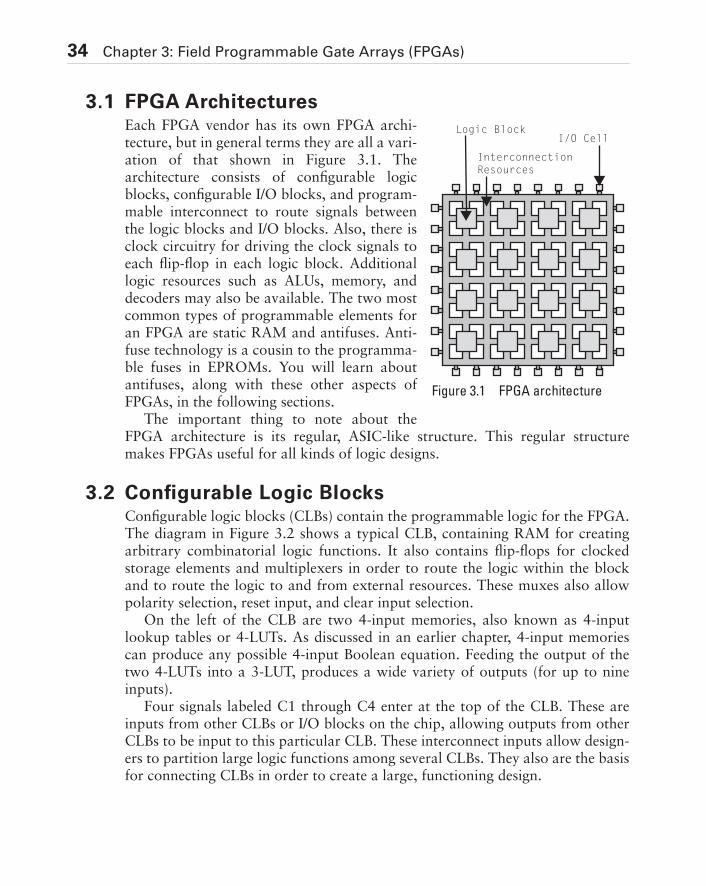
34 Chapter 3: Field Programmable Gate Arrays (FPGAs)
3.1 FPGA ArchitecturesEach FPGA vendor has its own FPGA archi-tecture, but in general terms they are all a vari-ation of that shown in Figure 3.1. Thearchitecture consists of configurable logicblocks, configurable I/O blocks, and program-mable interconnect to route signals betweenthe logic blocks and I/O blocks. Also, there isclock circuitry for driving the clock signals toeach flip-flop in each logic block. Additionallogic resources such as ALUs, memory, anddecoders may also be available. The two mostcommon types of programmable elements foran FPGA are static RAM and antifuses. Anti-fuse technology is a cousin to the programma-ble fuses in EPROMs. You will learn aboutantifuses, along with these other aspects ofFPGAs, in the following sections.
The important thing to note about theFPGA architecture is its regular, ASIC-like structure. This regular structuremakes FPGAs useful for all kinds of logic designs.
3.2 Configurable Logic BlocksConfigurable logic blocks (CLBs) contain the programmable logic for the FPGA.The diagram in Figure 3.2 shows a typical CLB, containing RAM for creatingarbitrary combinatorial logic functions. It also contains flip-flops for clockedstorage elements and multiplexers in order to route the logic within the blockand to route the logic to and from external resources. These muxes also allowpolarity selection, reset input, and clear input selection.
On the left of the CLB are two 4-input memories, also known as 4-inputlookup tables or 4-LUTs. As discussed in an earlier chapter, 4-input memoriescan produce any possible 4-input Boolean equation. Feeding the output of thetwo 4-LUTs into a 3-LUT, produces a wide variety of outputs (for up to nineinputs).
Four signals labeled C1 through C4 enter at the top of the CLB. These areinputs from other CLBs or I/O blocks on the chip, allowing outputs from otherCLBs to be input to this particular CLB. These interconnect inputs allow design-ers to partition large logic functions among several CLBs. They also are the basisfor connecting CLBs in order to create a large, functioning design.
Logic Block
InterconnectionResources
I/O Cell
Figure 3.1 FPGA architecture
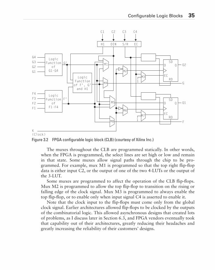
Configurable Logic Blocks 35
The muxes throughout the CLB are programmed statically. In other words,when the FPGA is programmed, the select lines are set high or low and remainin that state. Some muxes allow signal paths through the chip to be pro-grammed. For example, mux M1 is programmed so that the top right flip-flopdata is either input C2, or the output of one of the two 4-LUTs or the output ofthe 3-LUT.
Some muxes are programmed to affect the operation of the CLB flip-flops.Mux M2 is programmed to allow the top flip-flop to transition on the rising orfalling edge of the clock signal. Mux M3 is programmed to always enable thetop flip-flop, or to enable only when input signal C4 is asserted to enable it.
Note that the clock input to the flip-flops must come only from the globalclock signal. Earlier architectures allowed flip-flops to be clocked by the outputsof the combinatorial logic. This allowed asynchronous designs that created lotsof problems, as I discuss later in Section 6.3, and FPGA vendors eventually tookthat capability out of their architectures, greatly reducing their headaches andgreatly increasing the reliability of their customers’ designs.
G
F
1Logic
Functionof F', G'and H1
M1
M4
M8
M6
M5
M2
M3
M7
LogicFunction
ofG1-G4
G4
G3
G2
G1
G'
LogicFunction
ofF1-F4
F4
F3
F2
F1
F'
H1 DIN S/R EC
C1 C2 C3 C4
SD
RD
D Q
EC
Q2
SD
RD
D Q
EC
Q1
1
K(Clock)
Figure 3.2 FPGA configurable logic block (CLB) (courtesy of Xilinx Inc.)
36 Chapter 3: Field Programmable Gate Arrays (FPGAs)
Note that the logic outputs do not need to go through the flip-flops. Design-ers can use a CLB to create simple combinatorial logic. Because of this, multipleCLBs can, and often are, connected together to implement complex Booleanlogic. This advantage of FPGAs over CPLDs means that designers can imple-ment very complex logic by stringing together several CLBs. Unfortunately,routing delay in an FPGA is a significant amount of the overall delay. So thisadvantage also results in an overall decrease in the speed of the design.
Fine-grained vs. large-grained CLBs
In theory, there are two types of CLBs, depending on the amount and type of logic that is contained
within them. These two types are called “large grain” and “fine grain.”
In a large grain FPGA, the CLB contains larger functionality logic. For example, it can contain two or
more flip-flops. A design that does not need many flip-flops will leave many of these flip-flops
unused, poorly utilizing the logic resources in the CLBs and in the chip. A design that requires lots of
combinatorial logic will be required to use up the LUTs in the CLBs while leaving the flip-flops
untouched.
Fine grain FPGAs resemble ASIC gate arrays in that the CLBs contain only small, very basic ele-
ments such as NAND gates, NOR gates, etc. The philosophy is that small elements can be con-
nected to make larger functions without wasting too much logic. If a flip-flop is needed, one can be
constructed by connecting NAND gates. If it’s not needed, then the NAND gates can be used for
other features. In theory, this apparent efficiency seemed to be an advantage. Also, because they
more closely resembled ASICs, it seemed that any eventual conversion of the FPGA to ASIC would
be easier.
However, one key fact renders the fine grain architecture less useful and less efficient. It turns out
that routing resources are the bottleneck in any FPGA design in terms of utilization and speed. In
other words, it is often difficult to connect CLBs together using the limited routing resources on the
chip. Also, in an FPGA, unlike an ASIC, the majority of the delay comes from routing, not logic. Fine
grain architectures require many more routing resources, which take up space and insert a large
amount of delay, which can more than compensate for their better utilization. This is why all FPGA
vendors currently use large grain architectures for their CLBs.
In the early days of the industry several FPGA manufacturers produced fine grain architectures for
their devices. Thinking like ASIC vendors, they missed the significance of the routing issues. All of
these vendors have either fallen by the wayside or have abandoned their fine grain architectures for
large grain ones.
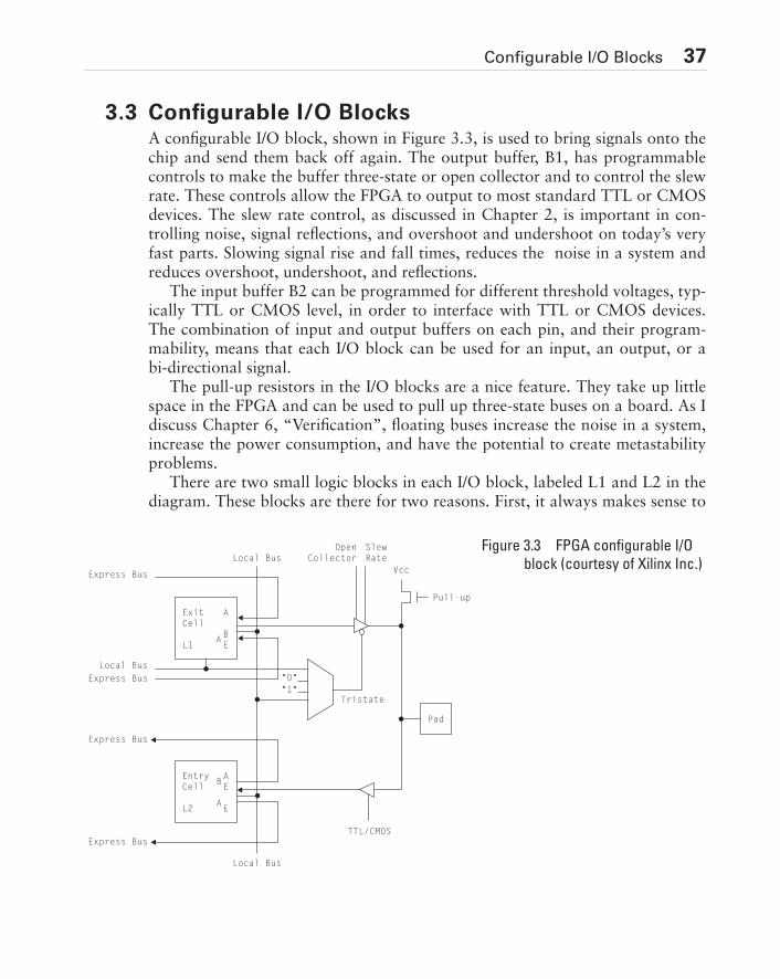
Configurable I/O Blocks 37
3.3 Configurable I/O BlocksA configurable I/O block, shown in Figure 3.3, is used to bring signals onto thechip and send them back off again. The output buffer, B1, has programmablecontrols to make the buffer three-state or open collector and to control the slewrate. These controls allow the FPGA to output to most standard TTL or CMOSdevices. The slew rate control, as discussed in Chapter 2, is important in con-trolling noise, signal reflections, and overshoot and undershoot on today’s veryfast parts. Slowing signal rise and fall times, reduces the noise in a system andreduces overshoot, undershoot, and reflections.
The input buffer B2 can be programmed for different threshold voltages, typ-ically TTL or CMOS level, in order to interface with TTL or CMOS devices.The combination of input and output buffers on each pin, and their program-mability, means that each I/O block can be used for an input, an output, or abi-directional signal.
The pull-up resistors in the I/O blocks are a nice feature. They take up littlespace in the FPGA and can be used to pull up three-state buses on a board. As Idiscuss Chapter 6, “Verification”, floating buses increase the noise in a system,increase the power consumption, and have the potential to create metastabilityproblems.
There are two small logic blocks in each I/O block, labeled L1 and L2 in thediagram. These blocks are there for two reasons. First, it always makes sense to
"0""1"
Local Bus
Express Bus
Express Bus
Express Bus
Express Bus
ExitCell
L1
A
BE
A
EntryCell
L2
AE
E
B
A
Local Bus
Local Bus
Tristate
TTL/CMOS
Vcc
Pull-up
Pad
OpenCollector
SlewRate
Figure 3.3 FPGA configurable I/O
block (courtesy of Xilinx Inc.)
38 Configurable I/O Blocks
Pull-ups, Floating Buses, and Stubbornness
I would think it’s obvious to anyone who understands CMOS technology that floating buses are bad.
CMOS devices dissipate power unnecessarily when the inputs are floating, and floating signals are
more prone to noise. A pull-up resistor is a very simple, small, low-power, inexpensive solution to the
problem of floating buses. In my career, though, I have encountered, on two occasions, a religious fer-
vor about not putting pull-ups on potentially floating buses. I still don’t completely understand the rea-
sons.
In one case, a career marketing manager at a large semiconductor company, who still prided himself on
being a top-notch engineer, did a board design that I was asked to optimize, lay out, and debug. When I
saw that he had omitted any pull-up resistors, I simply put them back in the schematic. When he saw
this, he became angry. He told me that in all his years, he had never seen a problem, nor had he ever
encountered a metastability problem. I replied that a reliability problem like metastability might only be
seen once every year on a continually running board. It’s not something that can be measured. This
manager went so far as to inform the layout designer to tell me that she couldn’t fit the pull-up resistor
pack (nine pins on a small sliver of material) on the board. I could tell she felt ridiculous about this
because she was telling me that she couldn’t do something that any fresh-out-of-school layout designer
could accomplish with the cheapest layout software package available.
In the other case, I was brought in to do a sanity check of a board design that was nearing completion.
A small startup had a contract to design some specialized network boards for Cisco Systems. A con-
sultant had been hired to design the board, and the project manager then hired me to review the
design. In my review, one of the potential problems I found was, yes, no pull-up resistors on the buses.
I mentioned this casually, and the board designer became irate for the same reasons as the manager I
had met. There was no reason for it. They were too expensive (actually about $.01 per resistor), and
they took up too much space (a pack of ten resistors takes a few square millimeters). Finally he said,
“We met with those guys at Cisco and they said the same thing. They wanted those stupid, unneces-
sary resistors on the buses. I just won’t waste my time doing it.” Later, in private, I talked with the
project manager. “You may not think there’s a need for those resistors,” I said, “and you may not trust
my judgment. But if I were selling boards to Cisco and they said to spread peanut butter on the boards,
I’d break out the Skippy®.”
The point of these stories is that internal resistors on I/O pins of FPGAs make this problem go away.
With internal resistors on the I/O pins, you can connect pull-ups to all of your buses, saving the tiny cost
and area of a resistor pack, and no one will be the wiser.
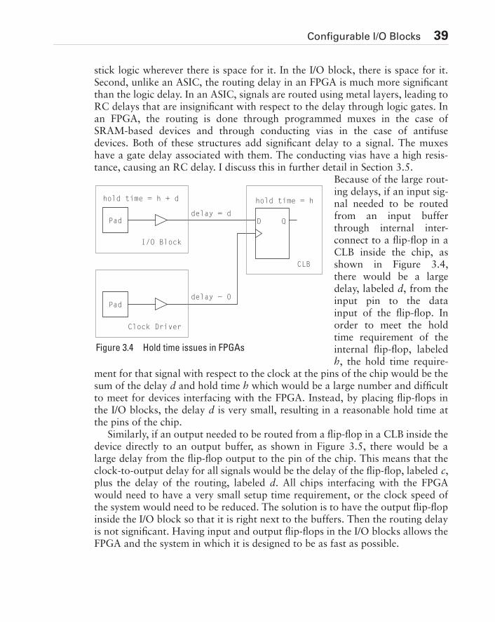
Configurable I/O Blocks 39
stick logic wherever there is space for it. In the I/O block, there is space for it.Second, unlike an ASIC, the routing delay in an FPGA is much more significantthan the logic delay. In an ASIC, signals are routed using metal layers, leading toRC delays that are insignificant with respect to the delay through logic gates. Inan FPGA, the routing is done through programmed muxes in the case ofSRAM-based devices and through conducting vias in the case of antifusedevices. Both of these structures add significant delay to a signal. The muxeshave a gate delay associated with them. The conducting vias have a high resis-tance, causing an RC delay. I discuss this in further detail in Section 3.5.
Because of the large rout-ing delays, if an input sig-nal needed to be routedfrom an input bufferthrough internal inter-connect to a flip-flop in aCLB inside the chip, asshown in Figure 3.4,there would be a largedelay, labeled d, from theinput pin to the datainput of the flip-flop. Inorder to meet the holdtime requirement of theinternal flip-flop, labeledh, the hold time require-
ment for that signal with respect to the clock at the pins of the chip would be thesum of the delay d and hold time h which would be a large number and difficultto meet for devices interfacing with the FPGA. Instead, by placing flip-flops inthe I/O blocks, the delay d is very small, resulting in a reasonable hold time atthe pins of the chip.
Similarly, if an output needed to be routed from a flip-flop in a CLB inside thedevice directly to an output buffer, as shown in Figure 3.5, there would be alarge delay from the flip-flop output to the pin of the chip. This means that theclock-to-output delay for all signals would be the delay of the flip-flop, labeled c,plus the delay of the routing, labeled d. All chips interfacing with the FPGAwould need to have a very small setup time requirement, or the clock speed ofthe system would need to be reduced. The solution is to have the output flip-flopinside the I/O block so that it is right next to the buffers. Then the routing delayis not significant. Having input and output flip-flops in the I/O blocks allows theFPGA and the system in which it is designed to be as fast as possible.
D QPad
hold time = h + d
I/O Block
Pad
Clock Driver
delay = d
delay ~ 0
hold time = h
CLB
Figure 3.4 Hold time issues in FPGAs
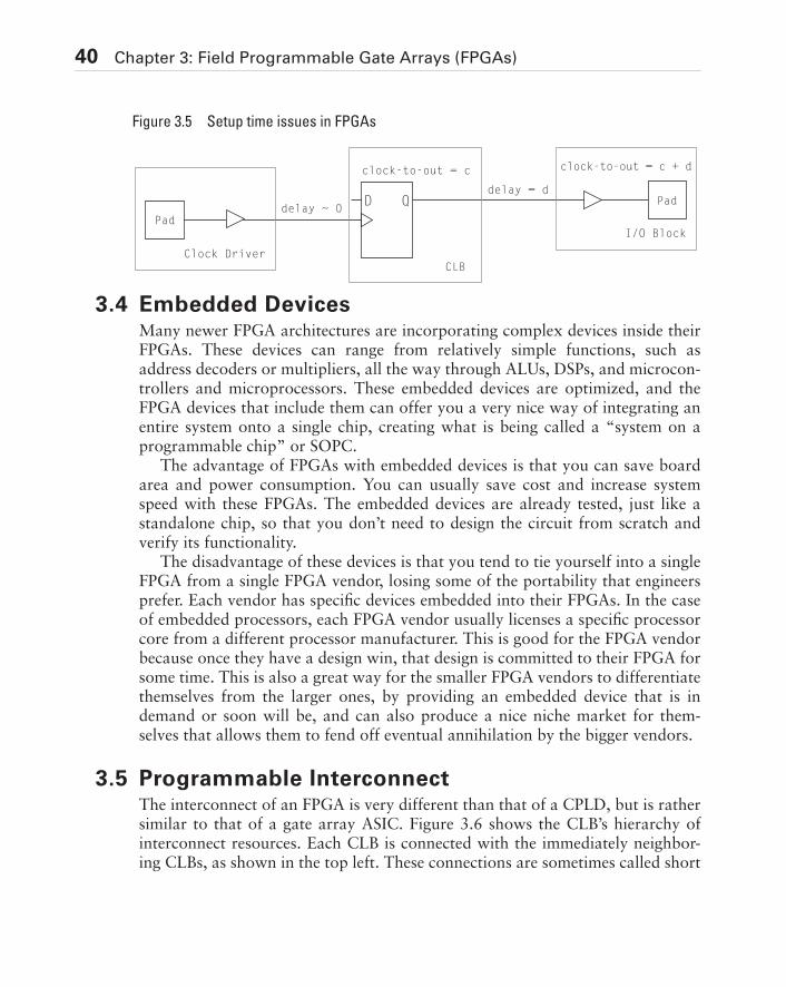
40 Chapter 3: Field Programmable Gate Arrays (FPGAs)
3.4 Embedded DevicesMany newer FPGA architectures are incorporating complex devices inside theirFPGAs. These devices can range from relatively simple functions, such asaddress decoders or multipliers, all the way through ALUs, DSPs, and microcon-trollers and microprocessors. These embedded devices are optimized, and theFPGA devices that include them can offer you a very nice way of integrating anentire system onto a single chip, creating what is being called a “system on aprogrammable chip” or SOPC.
The advantage of FPGAs with embedded devices is that you can save boardarea and power consumption. You can usually save cost and increase systemspeed with these FPGAs. The embedded devices are already tested, just like astandalone chip, so that you don’t need to design the circuit from scratch andverify its functionality.
The disadvantage of these devices is that you tend to tie yourself into a singleFPGA from a single FPGA vendor, losing some of the portability that engineersprefer. Each vendor has specific devices embedded into their FPGAs. In the caseof embedded processors, each FPGA vendor usually licenses a specific processorcore from a different processor manufacturer. This is good for the FPGA vendorbecause once they have a design win, that design is committed to their FPGA forsome time. This is also a great way for the smaller FPGA vendors to differentiatethemselves from the larger ones, by providing an embedded device that is indemand or soon will be, and can also produce a nice niche market for them-selves that allows them to fend off eventual annihilation by the bigger vendors.
3.5 Programmable InterconnectThe interconnect of an FPGA is very different than that of a CPLD, but is rathersimilar to that of a gate array ASIC. Figure 3.6 shows the CLB’s hierarchy ofinterconnect resources. Each CLB is connected with the immediately neighbor-ing CLBs, as shown in the top left. These connections are sometimes called short
Pad
Clock Driver
delay ~ 0Pad
clock-to-out = c + d
I/O Block
delay = dD Q
clock-to-out = c
CLB
Figure 3.5 Setup time issues in FPGAs
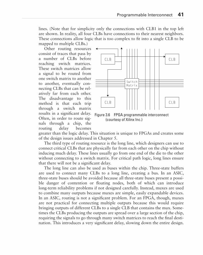
Programmable Interconnect 41
lines. (Note that for simplicity only the connections with CLB1 in the top leftare shown. In reality, all four CLBs have connections to their nearest neighbors.These connections allow logic that is too complex to fit into a single CLB to bemapped to multiple CLBs.)
Other routing resourcesconsist of traces that pass bya number of CLBs beforereaching switch matrices.These switch matrices allowa signal to be routed fromone switch matrix to anotherto another, eventually con-necting CLBs that can be rel-atively far from each other.The disadvantage to thismethod is that each tripthrough a switch matrixresults in a significant delay.Often, in order to route sig-nals through a chip, therouting delay becomesgreater than the logic delay. This situation is unique to FPGAs and creates someof the design issues addressed in Chapter 5.
The third type of routing resource is the long line, which designers can use toconnect critical CLBs that are physically far from each other on the chip withoutinducing much delay. These lines usually go from one end of the die to the otherwithout connecting to a switch matrix. For critical path logic, long lines ensurethat there will not be a significant delay.
The long line can also be used as buses within the chip. Three-state buffersare used to connect many CLBs to a long line, creating a bus. In an ASIC,three-state buses should be avoided because all three-state buses present a possi-ble danger of contention or floating nodes, both of which can introducelong-term reliability problems if not designed carefully. Instead, muxes are usedto combine many outputs because muxes are simple, easily expandable devices.In an ASIC, routing is not a significant problem. For an FPGA, though, muxesare not practical for connecting multiple outputs because this would requirebringing outputs of different CLBs to a single CLB that contains the mux. Some-times the CLBs producing the outputs are spread over a large section of the chip,requiring the signals to go through many switch matrices to reach the final desti-nation. This introduces a very significant delay, slowing down the entire design.
SwitchMatrix
CLB CLB
CLB CLB
Figure 3.6 FPGA programmable interconnect
(courtesy of Xilinx Inc.)
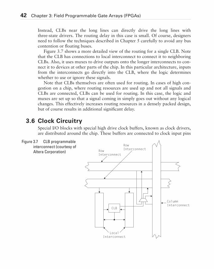
42 Chapter 3: Field Programmable Gate Arrays (FPGAs)
Instead, CLBs near the long lines can directly drive the long lines withthree-state drivers. The routing delay in this case is small. Of course, designersneed to follow the techniques described in Chapter 5 carefully to avoid any buscontention or floating buses.
Figure 3.7 shows a more detailed view of the routing for a single CLB. Notethat the CLB has connections to local interconnect to connect it to neighboringCLBs. Also, it uses muxes to drive outputs onto the longer interconnects to con-nect it to devices at other parts of the chip. In this particular architecture, inputsfrom the interconnects go directly into the CLB, where the logic determineswhether to use or ignore these signals.
Note that CLBs themselves are often used for routing. In cases of high con-gestion on a chip, where routing resources are used up and not all signals andCLBs are connected, CLBs can be used for routing. In this case, the logic andmuxes are set up so that a signal coming in simply goes out without any logicalchanges. This effectively increases routing resources in a densely packed design,but of course results in additional significant delay.
3.6 Clock CircuitrySpecial I/O blocks with special high drive clock buffers, known as clock drivers,are distributed around the chip. These buffers are connected to clock input pins
LocalInterconnect
ColumnInterconnect
RowInterconnect
CLB
RowInterconnect
Figure 3.7 CLB programmable
interconnect (courtesy of
Altera Corporation)
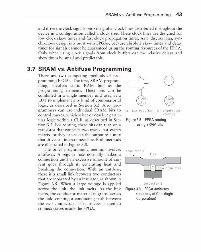
SRAM vs. Antifuse Programming 43
and drive the clock signals onto the global clock lines distributed throughout thedevice in a configuration called a clock tree. These clock lines are designed forlow clock skew times and fast clock propagation times. As I discuss later, syn-chronous design is a must with FPGAs, because absolute skew times and delaytimes for signals cannot be guaranteed using the routing resources of the FPGA.Only when using clock signals from clock buffers can the relative delays andskew times be small and predictable.
3.7 SRAM vs. Antifuse ProgrammingThere are two competing methods of pro-gramming FPGAs. The first, SRAM program-ming, involves static RAM bits as theprogramming elements. These bits can becombined in a single memory and used as aLUT to implement any kind of combinatoriallogic, as described in Section 3.2. Also, pro-grammers can use individual SRAM bits tocontrol muxes, which select or deselect partic-ular logic within a CLB, as described in Sec-tion 3.2. For routing, these bits can turn on atransistor that connects two traces in a switchmatrix, or they can select the output of a muxthat drives an interconnect line. Both methodsare illustrated in Figure 3.8.
The other programming method involvesantifuses. A regular fuse normally makes aconnection until an excessive amount of cur-rent goes through it, generating heat andbreaking the connection. With an antifuse,there is a small link between two conductorsthat are separated by an insulator, as shown inFigure 3.9. When a large voltage is appliedacross the link, the link melts. As the linkmelts, the conductor material migrates acrossthe link, creating a conducting path betweenthe two conductors. This process is used toconnect traces inside the FPGA.
SRAMbit
a) mux routing
SRAMbit
b) transistor routing
Figure 3.8 FPGA routing
using SRAM bits
conductor 1
conductor 2
link
insulator
Figure 3.9 FPGA antifuses
(courtesy of Quicklogic
Corporation)
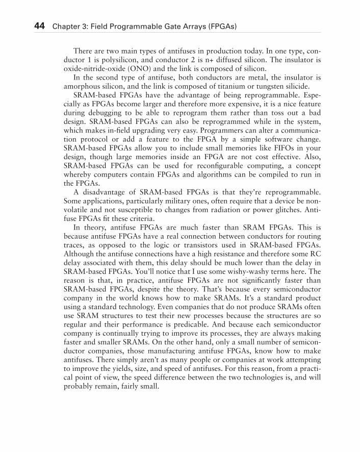
44 Chapter 3: Field Programmable Gate Arrays (FPGAs)
There are two main types of antifuses in production today. In one type, con-ductor 1 is polysilicon, and conductor 2 is n+ diffused silicon. The insulator isoxide-nitride-oxide (ONO) and the link is composed of silicon.
In the second type of antifuse, both conductors are metal, the insulator isamorphous silicon, and the link is composed of titanium or tungsten silicide.
SRAM-based FPGAs have the advantage of being reprogrammable. Espe-cially as FPGAs become larger and therefore more expensive, it is a nice featureduring debugging to be able to reprogram them rather than toss out a baddesign. SRAM-based FPGAs can also be reprogrammed while in the system,which makes in-field upgrading very easy. Programmers can alter a communica-tion protocol or add a feature to the FPGA by a simple software change.SRAM-based FPGAs allow you to include small memories like FIFOs in yourdesign, though large memories inside an FPGA are not cost effective. Also,SRAM-based FPGAs can be used for reconfigurable computing, a conceptwhereby computers contain FPGAs and algorithms can be compiled to run inthe FPGAs.
A disadvantage of SRAM-based FPGAs is that they’re reprogrammable.Some applications, particularly military ones, often require that a device be non-volatile and not susceptible to changes from radiation or power glitches. Anti-fuse FPGAs fit these criteria.
In theory, antifuse FPGAs are much faster than SRAM FPGAs. This isbecause antifuse FPGAs have a real connection between conductors for routingtraces, as opposed to the logic or transistors used in SRAM-based FPGAs.Although the antifuse connections have a high resistance and therefore some RCdelay associated with them, this delay should be much lower than the delay inSRAM-based FPGAs. You’ll notice that I use some wishy-washy terms here. Thereason is that, in practice, antifuse FPGAs are not significantly faster thanSRAM-based FPGAs, despite the theory. That’s because every semiconductorcompany in the world knows how to make SRAMs. It’s a standard productusing a standard technology. Even companies that do not produce SRAMs oftenuse SRAM structures to test their new processes because the structures are soregular and their performance is predicable. And because each semiconductorcompany is continually trying to improve its processes, they are always makingfaster and smaller SRAMs. On the other hand, only a small number of semicon-ductor companies, those manufacturing antifuse FPGAs, know how to makeantifuses. There simply aren’t as many people or companies at work attemptingto improve the yields, size, and speed of antifuses. For this reason, from a practi-cal point of view, the speed difference between the two technologies is, and willprobably remain, fairly small.
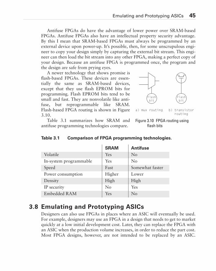
Emulating and Prototyping ASICs 45
Antifuse FPGAs do have the advantage of lower power over SRAM-basedFPGAs. Antifuse FPGAs also have an intellectual property security advantage.By this I mean that SRAM-based FPGAs must always be programmed by anexternal device upon power-up. It’s possible, then, for some unscrupulous engi-neer to copy your design simply by capturing the external bit stream. This engi-neer can then load the bit stream into any other FPGA, making a perfect copy ofyour design. Because an antifuse FPGA is programmed once, the program andthe design are safe from prying eyes.
A newer technology that shows promise isflash-based FPGAs. These devices are essen-tially the same as SRAM-based devices,except that they use flash EPROM bits forprogramming. Flash EPROM bits tend to besmall and fast. They are nonvolatile like anti-fuse, but reprogrammable like SRAM.Flash-based FPGA routing is shown in Figure3.10.
Table 3.1 summarizes how SRAM andantifuse programming technologies compare.
3.8 Emulating and Prototyping ASICsDesigners can also use FPGAs in places where an ASIC will eventually be used.For example, designers may use an FPGA in a design that needs to get to marketquickly at a low initial development cost. Later, they can replace the FPGA withan ASIC when the production volume increases, in order to reduce the part cost.Most FPGA designs, however, are not intended to be replaced by an ASIC.
Table 3.1 Comparison of FPGA programming technologies.
SRAM Antifuse
Volatile Yes No
In-system programmable Yes No
Speed Fast Somewhat faster
Power consumption Higher Lower
Density High High
IP security No Yes
Embedded RAM Yes No
Flashbit
a) mux routing
Flashbit
b) transistor routing
Figure 3.10 FPGA routing using
flash bits
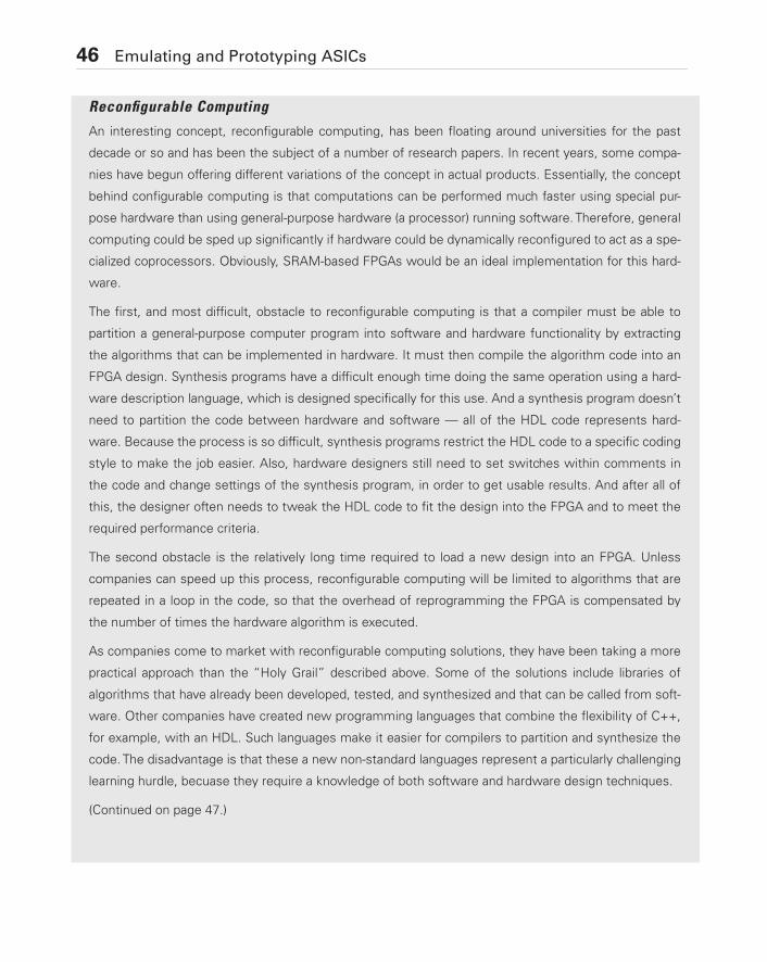
46 Emulating and Prototyping ASICs
Reconfigurable Computing
An interesting concept, reconfigurable computing, has been floating around universities for the past
decade or so and has been the subject of a number of research papers. In recent years, some compa-
nies have begun offering different variations of the concept in actual products. Essentially, the concept
behind configurable computing is that computations can be performed much faster using special pur-
pose hardware than using general-purpose hardware (a processor) running software. Therefore, general
computing could be sped up significantly if hardware could be dynamically reconfigured to act as a spe-
cialized coprocessors. Obviously, SRAM-based FPGAs would be an ideal implementation for this hard-
ware.
The first, and most difficult, obstacle to reconfigurable computing is that a compiler must be able to
partition a general-purpose computer program into software and hardware functionality by extracting
the algorithms that can be implemented in hardware. It must then compile the algorithm code into an
FPGA design. Synthesis programs have a difficult enough time doing the same operation using a hard-
ware description language, which is designed specifically for this use. And a synthesis program doesn’t
need to partition the code between hardware and software — all of the HDL code represents hard-
ware. Because the process is so difficult, synthesis programs restrict the HDL code to a specific coding
style to make the job easier. Also, hardware designers still need to set switches within comments in
the code and change settings of the synthesis program, in order to get usable results. And after all of
this, the designer often needs to tweak the HDL code to fit the design into the FPGA and to meet the
required performance criteria.
The second obstacle is the relatively long time required to load a new design into an FPGA. Unless
companies can speed up this process, reconfigurable computing will be limited to algorithms that are
repeated in a loop in the code, so that the overhead of reprogramming the FPGA is compensated by
the number of times the hardware algorithm is executed.
As companies come to market with reconfigurable computing solutions, they have been taking a more
practical approach than the “Holy Grail” described above. Some of the solutions include libraries of
algorithms that have already been developed, tested, and synthesized and that can be called from soft-
ware. Other companies have created new programming languages that combine the flexibility of C++,
for example, with an HDL. Such languages make it easier for compilers to partition and synthesize the
code. The disadvantage is that these a new non-standard languages represent a particularly challenging
learning hurdle, becuase they require a knowledge of both software and hardware design techniques.
(Continued on page 47.)
Emulating and Prototyping ASICs 47
FPGAs tend to be used where programmability, up-front cost, and time to mar-ket are more important than part cost, speed, or circuit density.
There are two methodologies in integrated circuit chip design where FPGAsare being used to assist in the development of chips and the development of soft-ware that depends on these chips. These methodologies are known as emulationand prototyping.
3.8.1 EmulationSeveral companies provide standalone hardware boxes for emulating the func-tion of an ASIC or a custom integrated circuit. These hardware emulators can beprogrammed with a design for a chip. Once programmed, the emulator can bephysically connected to a target circuit board where the chip would normally beconnected. Then, the entire target system can be run as if the chip were actuallyavailable and functioning. You can then debug the design using real world hard-ware and real world software. You can stop and start the hardware emulator inorder to examine internal nodes of the design. You can capture waveform tracesof internal and I/O signals for debugging. You can make changes to the design tocorrect mistakes or to improve performance, before the design is committed tosilicon.
I believe that these practical, but limited solutions will eventually produce a real-world product that
will have some use in specific areas. The progress of reconfigurable computing will probably paral-
lel that of silicon compilation. In the early 1980s, some companies, such as Silicon Compilers, Inc.,
were touting the ability to go directly from a schematic diagram to a chip layout. The problem turned
out to be bigger than these advocates thought; the algorithms needed were much more complex
than they originally believed, and the computing power to execute the algorithms just wasn’t avail-
able yet at a reasonable cost. So these companies all folded, but not without first producing corpo-
rate offspring and cousins, such as Synopsys Corporation, that decided they could tackle a much
easier problem and still provide a solution that engineers could use. Their solution was software
synthesis — software that could produce a gate level description from an RTL level description.
This much less ambitious but much more achievable solution was a great success and may still
eventually lead to the ultimate solution of silicon compilation. Many successful new products in the
engineering design automation (EDA) industry follow this same trajectory. An ambitious first prod-
uct fails, leading others to attempt smaller, less costly, more achievable products that succeed. In
the same way, I believe, restricted solutions to reconfigurable computingwill make their way into
the marketplace and be successful, and eventually lead to more and more complex implementa-
tions.
48 Chapter 3: Field Programmable Gate Arrays (FPGAs)
For example, if you are designing a new microprocessor, you could load themicroprocessor design into a hardware emulator, plug the emulator into a targetpersonal computer motherboard, and actually boot Linux or any other operat-ing system. You could even run real applications. Of course, a hardware emula-tor runs at a fraction of the speed of the final chip, but it affords a form oftesting that is otherwise not possible, except with prototyping.
Different hardware emulators from different manufacturers have differentinternal architectures. Many of them, though, use large sets of FPGAs to emu-late the chip design, because FPGAs allow users to easily load and modifydesigns, stop the design while it is in the system, and easily examine internalnodes and external I/O.
3.8.2 PrototypingAs FPGAs become faster and denser, and ASICs become larger, prototyping hasbecome an important alternative to emulation. Prototyping involves loading achip design into one or more FPGAs. If the chip design fits into a single FPGA,the FPGA can be plugged into a socket or soldered into a target circuit boardwhere the final chip will ultimately go. The board can then be powered up andtested using real data. If the design cannot fit into a single FPGA, a board can bedesigned that contains several FPGAs into which the chip design is partitioned.Companies now provide software that will automatically partition a chip designinto multiple FPGAs.
These design-specific FPGA prototypes generally run faster than a hardwareemulator because they do not have the overhead required for a general purposemachine, and there are fewer FPGAs — only the exact number required toimplement your chip design. On the other hand, they do not have the built-indiagnostic capabilities of a hardware emulator, and they do not come withapplication engineers to support you. FPGA prototypes are generally cheaperthan hardware emulators, but you must do all of the work, including partition-ing the design, designing the board to hold the FPGAs, and designing whateverdebug capabilities you require.
3.9 SummaryThis section summarizes the various aspects of FPGAs that we have learned inthis chapter. This section also provides a list of factors to use when decidingwhether to choose a CPLD or FPGA for your design.
Summary 49
3.9.1 FPGA Selection CriteriaKnowledge of the internal architecture of FPGAs and the semiconductor tech-nologies used to implement the programmable elements is critical for consider-ing which FPGA to use in your design. When making that decision, you shouldtake into account the following architectural and technological issues:
• Configurable logic blocks — Although most FPGAs have similar logic blocks,there are differences, for example, in the number of flip-flops and the widthof the lookup tables. Try to find a CLB architecture that fits your design. Ifyour design has wide combinatorial functions, choose an FPGA using CLBswith large numbers of inputs. If your design has many pipelined stages, youwill prefer CLBs with several flip-flops. Newer architectures are always beingdeveloped that fit the needs of specific types of designs, such as digital signalprocessing.
• The number of CLBs in the device — This will determine how much logic thedevice can hold and how easily your design will fit into it.
• The number and type of I/O pins — Obviously, the FPGA will need to sup-port the number of I/O pins in your design. Also, determine how many ofthese are general purpose I/O and how many are reserved for special func-tions such as clock input, master reset, etc.
• The number of clock input pins — Clock signals can be driven only into par-ticular pins. If your design has several clock domains (i.e., sections driven byseparate clocks), you will need an FPGA that has that many clock input pins.
• Embedded devices — Does your design interface with devices such as amicrocontroller or a PLL? Many FPGAs now incorporate specialized func-tions like these, which will make your job much easier and allow you to inte-grate more devices into a single FPGA.
• Antifuse vs. SRAM programming — Which technology makes sense for yourdesign? Do you need the speed, low power, nonvolatility, and security of anantifuse device, or do you need the reprogrammability of an SRAM-baseddevice?
• Emulating and prototyping ASICs — FPGAs can be found in off-the-shelfhardware emulators for testing the design of an ASIC in a real-world targetbefore it goes to silicon. Or you can use FPGAs to create your own customprototype of an ASIC for the same kind of pre-silicon real-world testing.
Other issues must be taken into account for all programmable chips that youintend to use in your design. For a list of these general issues, refer to Section 4.2about the chip specification.
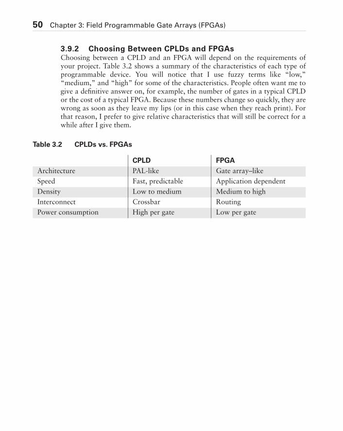
50 Chapter 3: Field Programmable Gate Arrays (FPGAs)
3.9.2 Choosing Between CPLDs and FPGAsChoosing between a CPLD and an FPGA will depend on the requirements ofyour project. Table 3.2 shows a summary of the characteristics of each type ofprogrammable device. You will notice that I use fuzzy terms like “low,”“medium,” and “high” for some of the characteristics. People often want me togive a definitive answer on, for example, the number of gates in a typical CPLDor the cost of a typical FPGA. Because these numbers change so quickly, they arewrong as soon as they leave my lips (or in this case when they reach print). Forthat reason, I prefer to give relative characteristics that will still be correct for awhile after I give them.
Table 3.2 CPLDs vs. FPGAs
CPLD FPGA
Architecture PAL-like Gate array–like
Speed Fast, predictable Application dependent
Density Low to medium Medium to high
Interconnect Crossbar Routing
Power consumption High per gate Low per gate
Exercises 51
Exercises
1. What does the term FPGA mean?
(a) Formally Programmable Gate Array
(b) Field Programmable Gate Array
(c) Finite Programmable Gate Array
2. Select all of the parts of a typical FPGA architecture.
(a) Configurable logic blocks
(b) Configurable program blocks
(c) Programmable interconnect
(d) Configurable I/O blocks
(e) Programmable address decode blocks
3. Select TRUE or FALSE for the following statements:
(a) TRUE or FALSE: Configurable I/O blocks contain flip-flops on the inputs toenable a designer to reduce the hold-time requirement for the inputs.
(b) TRUE or FALSE: Configurable I/O blocks contain flip-flops on the outputs toenable the designer to decrease the clock-to-output times of the outputs.
(c) TRUE or FALSE: FPGA programmable interconnect consists of lines that startat one end of the chip and continue to the other end to enable all CLBs to beconnected.
(d) TRUE or FALSE: Programmable switches inside the chip allow the connectionof CLBs to interconnect lines.
(e) TRUE or FALSE: Programmable switches inside the chip allow the connectionof interconnect lines to each other and to the switch matrix.
(f) TRUE or FALSE: Each flip-flop in an FPGA has its own unique clock line andclock buffer to reduce skew.
(g) TRUE or FALSE: Any input to an FPGA can be used for the clock input.
(h) TRUE or FALSE: Antifuse FPGAs use an industry standard process.
(i) TRUE or FALSE: Antifuse technology is faster than SRAM technology, in theory.
(j) TRUE or FALSE: SRAM FPGAs are more common than antifuse FPGAs.

52 Chapter 3: Field Programmable Gate Arrays (FPGAs)
4. Select all potential advantages of embedded devices
(a) Reduced board area
(b) Reduced power consumption
(c) Reduced cost
(d) Increased system speed
(e) No need to design and test the embedded device
5. Select TRUE or FALSE for each of the following statements about SRAM-basedFPGAs and antifuse FPGAs:
(a) SRAM-based FPGAs are based on an industry standard technology.
(b) In theory, SRAM-based FPGAs are much slower than antifuse FPGAs.
(c) Antifuse FPGAs retain their programming after being powered off and then onagain.
(d) Antifuse FPGAs can be erased and reprogrammed.
(e) SRAM-based FPGAs can be erased and reprogrammed.
(f) In practice, SRAM-based FPGAs are much slower than antifuse FPGAs.
(g) SRAM-based FPGAs are programmed using high voltages.
(h) Antifuse FPGAs are programmed using high voltages.
6. Clock trees are designed for (select one)
(a) Low speed and low power
(b) Small delay and low power
(c) Small delay and low skew
(d) Low inductance and low skew
(e) Low power and high density
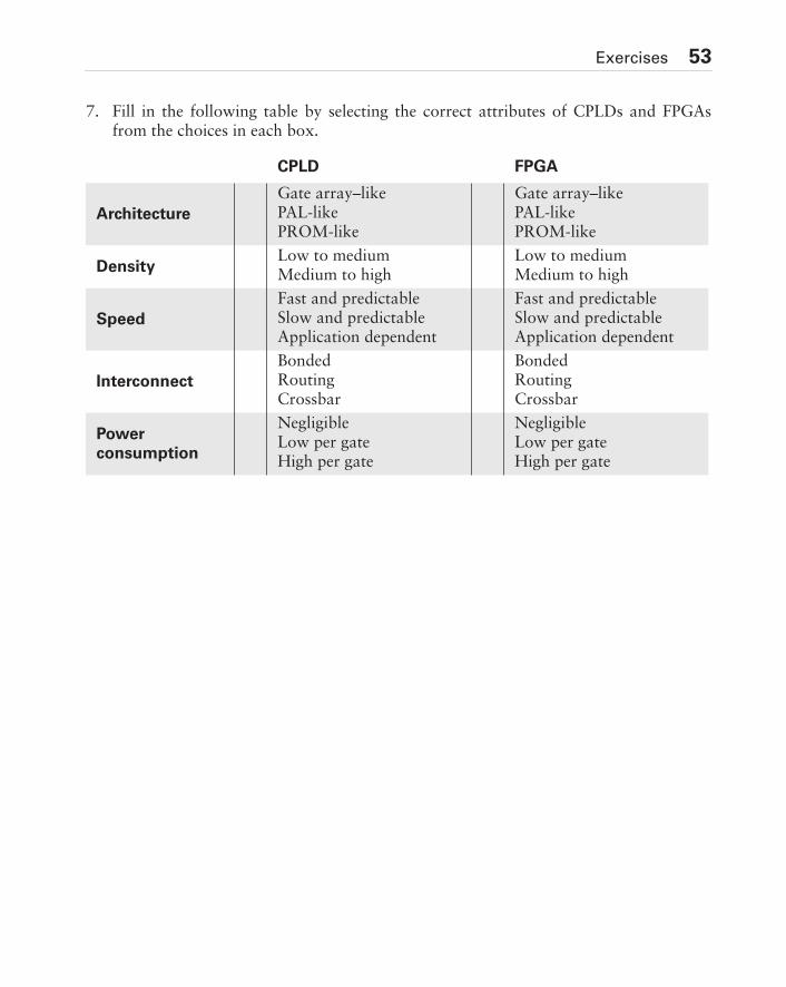
Exercises 53
7. Fill in the following table by selecting the correct attributes of CPLDs and FPGAsfrom the choices in each box.
CPLD FPGA
Architecture
Gate array–likePAL-likePROM-like
Gate array–likePAL-likePROM-like
DensityLow to mediumMedium to high
Low to mediumMedium to high
Speed
Fast and predictable Slow and predictableApplication dependent
Fast and predictable Slow and predictableApplication dependent
Interconnect
BondedRoutingCrossbar
BondedRoutingCrossbar
Power consumption
NegligibleLow per gateHigh per gate
NegligibleLow per gateHigh per gate

54 Chapter 3: Field Programmable Gate Arrays (FPGAs)
This Page Intentionally Left Blank
55
Chapter 4
Universal Design Methodology for Programmable Devices(UDM-PD)
This chapter describes the Universal Design Methodology for programmabledevices. This method, based on my years of experience designing many types ofprogrammable devices for small and large companies in different industries, laysout the entire process for designing a programmable device. Following the UDMguarantees that you will not overlook any steps and that you will have the bestchance of creating a chip that functions correctly in your system.
ObjectivesIn this chapter, using Universal Design Methodology as a reference model, youwill learn what steps are necessary to create working, reliable chips that func-tion correctly in your system. The first section of this chapter explains UDM andspecifically UDM-PD for programmable devices. The following sections detaileach step of the design process and how it relates to the method. Reading thischapter will help you:
• Understand the UDM and UDM-PD methods.
In this chapter...
• UDM and UDM-PD
• Specification and
specification review
• Devices and tools
• Design, simulate, and review
• Testing
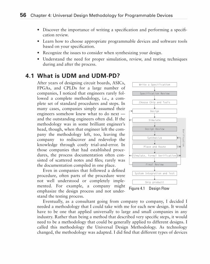
56 Chapter 4: Universal Design Methodology for Programmable Devices
• Discover the importance of writing a specification and performing a specifi-cation review.
• Learn how to choose appropriate programmable devices and software toolsbased on your specification.
• Recognize the issues to consider when synthesizing your design.
• Understand the need for proper simulation, review, and testing techniquesduring and after the process.
4.1 What is UDM and UDM-PD?After years of designing circuit boards, ASICs,FPGAs, and CPLDs for a large number ofcompanies, I noticed that engineers rarely fol-lowed a complete methodology, i.e., a com-plete set of standard procedures and steps. Inmany cases, companies simply assumed theirengineers somehow knew what to do next —and the outstanding engineers often did. If themethodology was in some brilliant engineer’shead, though, when that engineer left the com-pany the methodology left, too, leaving thecompany to rediscover and redevelop theknowledge through costly trial-and-error. Inthose companies that had established proce-dures, the process documentation often con-sisted of scattered notes and files; rarely wasthe documentation compiled in one place.
Even in companies that followed a definedprocedure, often parts of the procedure werenot well understood or completely imple-mented. For example, a company mightemphasize the design process and not under-stand the testing process.
Eventually, as a consultant going from company to company, I decided Ineeded a methodology that I could take with me for each new design. It wouldhave to be one that applied universally to large and small companies in anyindustry. Rather than being a method that described very specific steps, it wouldneed to be a methodology that could be generally applied to different designs. Icalled this methodology the Universal Design Methodology. As technologychanged, the methodology was adapted. I did find that different types of devices
Write a Specification
Specification Review
Choose Chip and Tools
Design
Simulate
Design Review
Synthesize
Simulate, Formal Verification
Final Review
System Integration and Test
Ship product!
Verification
Place and Route
Figure 4.1 Design Flow
Writing a Specification 57
required slightly different methodologies. ASICs and printed circuit boardsrequired slightly different methodologies than FPGAs and CPLDs. The method-ology described here is specifically for programmable devices, and I call itUDM-PD.
4.1.1 The Goals of UDMThe goals of the Universal Design Methodology are these:
• Design a device that
• Is free from manufacturing defects
• Works reliably over the lifetime of the device
• Functions correctly in your system
• Design this device efficiently, meaning
• In the least amount of time
• Using the least amount of resources, including personnel
• Plan the design efficiently, meaning
• Create a reasonable schedule as early in the process as possible
• Know all necessary resources up front and allocate them as early in the pro-cess as possible
4.1.2 The Design Flow of UDM-PDUDM-PD specifies a design flow that enables you to reach the UDM designgoals when designing a programmable device. The design flow consists of thesteps shown in Figure 4.1. Each particular design will have slight variations inthe specifics of each step, but essentially the steps will be the same. By under-standing the entire flow before the project begins, you will be able to meet goalnumber three, a better understanding of how to schedule and allocate resourcesfor the development process.
4.2 Writing a SpecificationI cannot overstate the importance of a specification. A specification is an abso-lute must, especially as a guide for choosing the right device and the right tech-nology and for making your needs known to the vendor. All too often I’ve beencalled in to consult for a company, and when I ask to see the spec, I am told thatit doesn’t exist. Or I am given a copy of a spec, but told to ignore it because it isnot up to date.
A specification allows each engineer to understand the entire design and hispiece of it. It allows the engineer to design the correct interface to the rest of the
58 Chapter 4: Universal Design Methodology for Programmable Devices
chip. It also saves time and thus cost, and helps avoid misunderstanding. Thereis no excuse for not having a written specification.
A specification should include the following information:
• External block diagram showing how the chip fits into the system
• Internal block diagram showing each major functional section
• Description of the I/O pins, including:
• Output drive capability
• Input threshold level (e.g., CMOS, TTL, ECL, etc.)
• Timing estimates, including:
• Setup and hold times for input pins
• Propagation times for output pins
• Clock cycle time
• Gate count estimate
• Package type
• Power consumption target
• Price target
• Test procedures
It is very important to understand that the specification is a living document.Many sections will have best guesses in them, but these will become more accu-rate as the chip is being designed. Engineering problems will arise that willrequire compromises in functionality. Market changes may require changes inthe specification. All of these decisions must use the specification as anup-to-date reference and all subsequent changes must be entered into the specifi-cation.
4.2.1 External Block DiagramThe external block diagram must show how the device fits into the system. Thisdiagram will help describe the overall functionality of the device and will be agood reference for the system designers, PC board designers, designers of otherchips in the system, and software developers.
4.2.2 Internal Block DiagramThe internal block diagram will be the starting point for the behavioral descrip-tion of the device. As the behavioral HDL code changes, these changes must beincorporated into the internal block diagram. As other factors necessitatechanges in the internal block diagram, these changes can also be incorporatedeasily into the behavioral HDL code.
Writing a Specification 59
4.2.3 Description of the I/O PinsThe device that you choose is often restricted by the requirements of the I/Opins. The number of pins will help decide which package you will need. Theelectrical characteristics of the I/O will determine which vendors and whichtechnologies can be used.
Life Without Specification
One of my first jobs out of school was at a large semiconductor company. Although this company
had developed some unique analog parts and a few digital parts in its history, the company was
known mostly for second sourcing “jelly beans.” That was the term for high volume, small density
parts such as TTL logic. They were able to crank them out in volume at cut-rate prices. To their credit,
they saw the future of high-end microprocessors and microprocessor peripherals that had much
lower volumes but much higher profit margins. What they didn’t understand was that these parts
were much more complex and that they accordingly required more sophisticated design methods
and procedures to produce. Instead, the engineers, project leaders, and managers at this company
continued to use the same old procedures that they had for the small jellybean parts.
The inability to recognize the need for better procedures and methodologies really doomed this
company to failure over the next decade. When other companies, like Intel, were rising to domi-
nance, this company’s revenues had a steady decline, and it was eventually bought by a much larger
company.
One example of this shortsightedness was with regard to specifications. I was recruited out of col-
lege to join the microprocessor group, which had the mandate to create complex peripheral devices,
such as memory managers and cache controllers, for the Motorola family of processors. Typically,
two or three of the best engineers in the department were assigned to a single chip. The entire doc-
umentation for the chip consisted of handfuls of schematics and lab books with handwritten notes.
Without the necessary direction or planning that these large designs required, they often dragged
on, missing schedule after schedule. Eventually, these engineers would leave the company, frus-
trated at not being able to get their designs out the door. Each time this happened, there was no
specification to turn to. It was impossible to bring a new engineer onto the project because one
third or one half of the entire specification had walked out the door in the head of the engineer who
had left. I saw all four major chip designs in this division die for exactly these reasons. Eventually,
without a single significant product in over two years, the division was closed down.

60 Writing a Specification
A Living Document
My last full-time employer (before becoming a full-time consultant) was a telecom startup. The com-
pany had lots of problems and became a great example of what not to do when designing a product or
running a company.
One of these problems should have been an early warning sign for me. I joined the company as the
main ASIC designer--employee number nine and the only one with any experience designing chips. One
of the chips that needed to be designed was a simple buffer between a board and a backplane. The
logic requirements of the design were extremely simple, but the current drive requirements — 48 mA
per signal for 8 signals — was more than most ASIC vendors could produce at the time. We found that
one company, NCR Corporation, had the technology. Because the logic design was so simple, we
decided that I would produce a written specification that would be handed off to the engineers at NCR.
I would supervise their progress while I did the real design work on another important chip.
At the end of the design review, one of the engineers at the company adamantly stated that we should
demand that NCR meet the specifications that we had written. If not, he proclaimed, we would not pay
them. That would give them the incentive they needed to design the chip to our specifications. I said
that it made more sense for us to work with them to understand any issues that might arise. If NCR
couldn’t meet the specification, we would work with them to get the best results possible and see how
we could change the specifications, and the specifications of our system, to get the best results possi-
ble. He was insistent. We argued for some time, the other engineers at the review sitting quietly and
uncomfortably. Finally, I told him that I agreed. If NCR couldn’t manufacture the chip, we should refuse
to pay them. We would then save the $20,000 NRE fee. He smiled. I then said that we could all go
home because we had saved all that money, had no chips for our boards, no working product, no com-
pany, and no jobs. I think I then called him an idiot.
Luckily the president of this company saw my logic immediately and agreed that we should work with
NCR to produce the best product that we could. If, along the way the specifications needed to be
changed, we would change them. The written specification is not gospel; it’s a living, changing roadmap
that gets you where you’re going even if a lightning storm suddenly throws a tree along the road. You
must be specific enough to create your design, and flexible enough to make changes when necessary.
And by the way, don’t call anyone an idiot at a company meeting, even if it’s true. It makes an enemy for
a long time — an enemy who can take revenge in secret ways, refuse to cooperate on important
projects, and blame you for all of his mistakes. I’m speaking from experience.
Writing a Specification 61
4.2.4 Timing EstimatesTiming estimates are needed to determine which devices, vendors, and technolo-gies can be used. You should have a good understanding of the clock frequencyrequired for the design and also the setup and hold time requirements of the I/O.(These requirements are determined by the interface between your device andthe other chips in the system.)
Remember to identify all asynchronous input signals. You can then discussmetastability issues with the vendors that you are considering. This will give youan idea about how well the vendor has characterized their devices and the tech-nical proficiency of their own engineers — a definite factor in choosing a vendor.
4.2.5 Gate Count EstimateAs you gain experience designing programmable devices, estimating gate countswill become easier. For your first few designs, talk to the various vendors youare considering. They will be able to help you construct reasonable estimatesand determine which of their devices are appropriate for your design.
4.2.6 Package TypePackage type is often a very large percentage of the entire cost of an FPGA.Understand the package options offered by different vendors. Also, you willneed to understand the capabilities of your PC board layout designers and fabri-cation facilities to work with the different package types.
4.2.7 Power Consumption TargetBe certain you understand the variables that affect the device’s power consump-tion. You must also understand how the device’s operation will affect overallboard and system power consumption. Finally, whoever is designing or choosingthe power supply will need to know how much power, typical case and worstcase, each chip in the system will require.
4.2.8 Price TargetFor most projects, you will need a realistic price target. This target can help youdetermine the necessary tradeoffs between pin count, functionality, speed, pack-age type, and other factors.
4.2.9 Test ProceduresTest procedures must be known at a very early stage of the design flow. Toooften, design teams leave test procedures for the end of the design flow at whichtime they discover that the device cannot be tested completely or accurately. Ifthe tests require software, the software team must begin planning the tests very

62 Writing a Specification
The Correct Way To Calculate Power Consumption
Engineers often ask me about power calculations for circuit boards or systems. When they add up the
worst-case power consumption numbers for all of the parts in the system, they end up with a number
so large that it seems unreasonable. They can’t justify designing in a power supply that large, or the
necessary cooling needed to get the predicted temperature down to something acceptable. When they
put the system together, the power numbers are often much closer to the typical power consumption
numbers than the worst-case power consumption numbers. Many engineers simply shrug or apply
some rule of thumb such as cutting the worst-case power number by a factor of two. Some engineers
are bothered by the fact that the numbers are off. Some know the secret to correctly calculating
worst-case power consumption, and I’m about to reveal that secret to you.
The power numbers which manufacturer’s report for individual components are statistical numbers. The
best case and worst case numbers are usually values three sigma in either direction from the mean
(looking at a standard Bell curve). In other words, there is an insignificant probability that the power
consumption is more than the worst-case numbers or less than the best-case numbers. If you treat the
individual components statistically, you should treat the entire circuit board or system statistically.
Therefore, to get a realistic number of the best-case, typical-case, and worst-case power consumption
for a system, use the following formulae (which are standard formulae for the mean and standard devi-
ation of a discrete random variable):
Minimum system power
Typical system power
Maximum system power
where
is the minimum power of component i
is the typical power of component i
is the maximum power of component i
Using the formula for worst-case maximum power consumption of a system, you’ll find that the more
components in the system, the closer this maximum power is to the typical power. And this makes
sense. For a system with many components, it is more likely that most of them are running under typi-
cal conditions and only a few of them are running at worst-case conditions.
Pmin Pi typ,∑ Pi typ, Pi min,–( )∑ 2–=
Ptyp Pi typ,∑=
Pmax Pi typ,∑ Pi max, Pi typ,–( )∑ 2+=
Pi min,Pi typ,Pi max,
Specification Review 63
early, and they must have input into the hardware design so that testability isbuilt in from the beginning.
4.3 Specification ReviewAt the end of the specification phase, it is very important to have a designreview. As many people as are interested should take part in this review, becausethis specification is the basis for the entire chip. You want to know right now ifanything is wrong or has been left out. Invite people from all departments whoare specifically involved with the chip and the system, including marketing,sales, software, applications, etc.
4.4 Choosing Device and ToolsOnce a specification has been written, the design team can use it to find the bestvendor with a technology and price structure that best meets their requirements.They can also choose tools to work well together and with the device and tech-nology they have chosen.
One important case in point for choosing the device and tools at this earlystage is that of synthesis. The selection of a synthesis tool will determine thecoding style for the RTL HDL. A specific coding style is necessary because syn-thesis tools cannot do a good job if they must handle too many code possibili-ties. For example, there are many ways to code state machines. If the synthesistool needs to understand each possible way, it becomes more complex and thusmore error prone. To avoid problems like this, synthesis tool vendors specifycoding guidelines guaranteeing that their tools will recognize the structures youare designing and synthesize them correctly to gate level descriptions.
4.5 DesignWhen designing the chip, remember to design according to the rules that are dis-cussed in detail in Chapter 5. These are
• Use top-down design
• Work with the device architecture
• Do synchronous design
• Protect against metastability
• Avoid floating nodes
• Avoid bus contention

64 Design
A Testing Horror Story
If you’re frightened easily, don’t read further. Some years ago I was called into a small startup company
that was designing medical imaging equipment. The founder of the company, an engineer, had been
kicked out by the investors. The senior members of the engineering team, maybe three or four people,
left with him. The company called me in as a consultant to help them figure out why the hardware they
had didn’t work. Through a painful reverse engineering process (the fleeing engineers had left no docu-
mentation), I found a slew of reliability problems that I corrected one by one. At that point, although we
had a working board covered by blue wires, I suggested that we redesign the board. The company
agreed. I then submitted a plan, including a test plan, whereby the software engineers would write
code to test the hardware.
When the board had been redesigned and it came back from fabrication and assembly, I went to the
software engineers to get the code to begin testing. The software engineers told me that the new Vice
President of Engineering had changed all of the priorities so that the test code was dead last on the list.
I went to the VP’s office for an explanation. He explained that getting the next round of funding was
contingent on getting a beta site for our system. If we had a system working in a hospital, then we
could get funding to keep going. Otherwise the company would be out of business. How could we get
the system working, I asked, if we couldn’t test the hardware. Wouldn’t it be better if we put a working
system into a beta site than a nonworking one? He told me that he trusted my abilities so much that he
was sure my hardware worked perfectly. I told him that I appreciated his confidence, but even I don’t
deserve that kind of responsibility.
The story gets worse. I decided to write some software tests at that time. It was difficult because I
didn’t understand all of the software running on this system. I was able to get a test running that looped
random data throughout this imaging system. Lo and behold, sometimes the data sent out came back
corrupted. I showed this to the VP and to the CEO of the company. Their response? Don’t worry. It’s
only a few pixels that get corrupted. No one will miss them. What if these pixels were enough to look
like a tumor to a doctor reviewing the image, I asked. Or worse, God forbid, they covered up a real
tumor? Don’t worry, was the reply I got again. We’ll fix it after we get the funding.
I finished up my work at the company, collected my check, and left when the contract expired. A year
later they had been turned down for more funding and went out of business.
Verification 65
4.6 VerificationVerification is a “super-phase” because it consists of several other phases of thedesign process. Which exact phases that make up verification is open to argu-ment, but generally verification can be broken into several phases, each of whichis essential to the entire process. These steps consist of
• Simulation
• Design review
• Synthesis
• Place and route
• Formal verification
The components of verification are discussed further in the following sectionsand in much greater detail in Chapter 6.
4.6.1 SimulationSimulation is an ongoing process; some kind of simulation will be performed aspart of nearly every stage of the design process. Small sections of the designshould be simulated separately before hooking them up to larger sections, asdescribed in Chapter 7. There will be many iterations of design and simulationin order to get the correct functionality.
4.6.2 Design ReviewOnce design and simulation are finished, another design review must take placeso that other engineers can check the design. It is important to get other engi-neers to look over the simulations. At this stage, they should be looking formissed details and improper assumptions. This is one of the most importantreviews because only with correct and complete simulation will you know thatthe chip will work correctly in your system.
In addition to the chip design team, you should invite engineers who werenot involved in the actual chip design to this review. Often, the chip designerswill inadvertently make assumptions that outsiders would question. These out-siders can also suggest corner cases that were not already simulated that willoften uncover additional problems in the design.
4.6.3 SynthesisThe next step is to synthesize the chip. This involves using synthesis software tooptimally translate your RTL design into a gate level design that can be mappedto logic blocks in the FPGA. This may involve specifying switches and optimiza-tion criteria in the HDL code, or playing with parameters of the synthesis soft-ware in order to ensure good timing and utilization.
66 Chapter 4: Universal Design Methodology for Programmable Devices
After synthesis, the chip must be resimulated using the gate level output ofthe synthesis tool. If everything has gone well up to this point, the gate level sim-ulation results will agree with the RTL results. Another possibility is to use aformal verification tool that will logically compare the RTL description to thegate level description. Whichever method is used, the design team will need toaddress any discrepancies. Discrepancies discovered at this stage often are theresult of processing RTL code that doesn’t conform to the style rules expected
The Need For Specification Reviews
After about two years at the large semiconductor company that employed me right out of school, I
was given my first responsibility as a project leader designing a dual universal asynchronous receiver
transmitter, or dual UART. I had another engineer reporting to me, and I was pretty excited about
this. The project had some visibility within the division and people would periodically stop me to find
out about my progress. What confused me, though, was that different people from different depart-
ments had different ideas about what I was designing. One day, a sales person would ask me about
the quad UART. I would explain that it was a dual UART. They would say something about customers
needing four, not two, on a chip. Another day, a marketing person would ask me about the UART. I
would explain that it was a dual UART. They would say something about the customers who had
been waiting for a UART to drop into their existing systems. When I mentioned a quad UART to the
people in semiconductor processing, they would laugh, saying it wasn’t possible to put a device that
large on a single die and still fit into an existing package.
I finally decided to hold a specification review — something that I then realized should have been
held at the beginning of the project. I invited the managers from engineering, sales, marketing, test-
ing, and production. In going over the specifications I found that the product I was in charge of met
no one’s expectations and could probably not be sold. Had we known this at the beginning, we
could have modified the specifications or spent our energies on a product that would actually make
money.
Afterwards, I was told to continue working on the chip, despite the fact that we couldn’t sell it,
because we had already announced it and wanted to show that at least once we could produce
something we had publicized. Demoralized about my new project, I continued with the company
long enough to get the chip design on the right track and put it in the hands of my colleague. The
design was fully documented, a rarity at this company, and I left to find other work. Later I found out
that the design was cancelled right before production because someone higher up found out that no
one really wanted to buy it.
Verification 67
by the synthesis tool. Correcting these problems is usually a straightforwardmatter of rewriting the code in the correct format.
4.6.4 Place and RouteThe next step is to lay out the chip, resulting in a real layout for a real chip. Thisinvolves using the vendor’s software tools to place various functions into theavailable blocks in the device and to route the blocks together. The software willfigure out the bits needed to program the chip to implement the design. If youcannot successfully place the design into the device and route it, you may needto tweak the design. In some cases, you will need to make radical changes, suchas eliminating some functionality or using a larger device. If you have followedall of the procedures outlined in this book, the chances of a major problem atthis stage, resulting in a major design change, will be minimized.
Once the place and route is successful, the design team must perform timinganalysis. The timing analysis will determine whether the designmeets the timinggoals. Typically, the design team will need to redesign and resimulate certainpaths in order to get the correct timing. In some cases, they will need to changefunctionality, or they will need to change the timing specifications of the chip, inorder to get the design to work.
4.6.5 Resimulation and Formal VerificationAt this stage, the design team must check the results of synthesis to make surethat the RTL design that was fully simulated is functionally equivalent to thegate level design that was produced after synthesis. In some cases, it may also benecessary to show that the configuration of the programmable device behavesidentically to the RTL description. There are two ways to do this: by resimulat-ing the lower level design or by using formal verification. In some cases, bothtechniques can be used for further certainty.
Resimulation
The most common method of determining that the input circuit and the final cir-cuit are correct is to resimulate the final circuit using all of the tests that wereused to simulate the original circuit. These tests are called regression tests. Theresults of both circuits should be identical for each clock edge.
Equivalency Checking
The formal verification that takes place at this stage is known as equivalencychecking. This kind of formal verification involves a software tool that com-pares the RTL design with the gate level design created by the synthesis soft-ware, or possibly even compares it with the resulting configuration of the FPGA
68 Chapter 4: Universal Design Methodology for Programmable Devices
or CPLD. This software performs a mathematical comparison of the functional-ity of both circuits in order to confirm that both circuits will operate correctly.
4.7 Final ReviewThe final review of the chip should be a formality at this point. If the designteam has followed all of the other steps and the other reviews have taken place,this review should be a simple sign-off that verifies that the design has beencoded, simulated, synthesized, laid out and routed, and is now ready to go intothe system.
4.8 System Integration and TestFor a one-time programmable device such as most CPLDs or an antifuse FPGA,you simply program the device at this time, and you immediately have your pro-totypes. For a reprogrammable chip, such as an SRAM-based FPGA, you placea blank chip into your system, and the system programs it during power up. Ineither case, you have the responsibility to determine that the entire system, withyour programmable device, actually works correctly.
If you have followed the procedure up to this point, chances are very goodthat your system will perform correctly with only minor problems. The designteam can often work around these minor problems by modifying the system orchanging the system software. The team needs to test and document these prob-lems so that they can fix them on the next revision of the chip. System integra-tion and system testing is necessary at this point to ensure that all parts of thesystem work correctly together.
When the chips are put into production, the production process shouldinclude some sort of burn-in test that continually tests the system over somelong amount of time. If a chip has been designed correctly, it will only failbecause of marginal physical defects that will usually show up with this kind ofstress testing.
4.9 Ship Product!At this point you are done. It is time to ship your product and take that longawaited vacation.
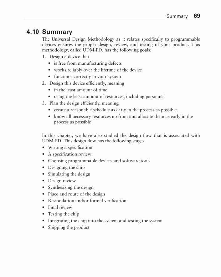
Summary 69
4.10 SummaryThe Universal Design Methodology as it relates specifically to programmabledevices ensures the proper design, review, and testing of your product. Thismethodology, called UDM-PD, has the following goals:
1. Design a device that
• is free from manufacturing defects
• works reliably over the lifetime of the device
• functions correctly in your system
2. Design this device efficiently, meaning
• in the least amount of time
• using the least amount of resources, including personnel
3. Plan the design efficiently, meaning
• create a reasonable schedule as early in the process as possible
• know all necessary resources up front and allocate them as early in the process as possible
In this chapter, we have also studied the design flow that is associated withUDM-PD. This design flow has the following stages:
• Writing a specification
• A specification review
• Choosing programmable devices and software tools
• Designing the chip
• Simulating the design
• Design review
• Synthesizing the design
• Place and route of the design
• Resimulation and/or formal verification
• Final review
• Testing the chip
• Integrating the chip into the system and testing the system
• Shipping the product
70 Chapter 4: Universal Design Methodology for Programmable Devices
Exercises
1. Select the three major goals of UDM-PD.
(a) Design the device efficiently
(b) Design a device synchronously
(c) Plan to design a device
(d) Design a device that works reliably over the lifetime of the device
(e) Allocate a maximum number of resources in the minimum amount of time
(f) Plan the design efficiently
2. UDM is a methodology to design a device that (choose all that apply)
(a) Is free from manufacturing defects
(b) Can be tested automatically
(c) Functions correctly in your system
(d) Works reliably over the lifetime of the device
(e) Is inexpensive
3. UDM is a methodology to design a device efficiently, meaning (choose all that apply)
(a) In the least amount of time
(b) Using the least number of people
(c) Using the least amount of resources
4. UDM is a methodology to plan a design efficiently, meaning (choose all that apply)
(a) Writing a specification that will not change
(b) Knowing all necessary resources up front and allocating them as early in theprocess as possible
(c) Creating a reasonable schedule as early in the process as possible
(d) Planning to ship products while testing the design
5. Put each phase of the design flow in the correct order.
(a) Ship product!
(b) System integration and test
(c) Write a specification
(d) Final review
(e) Specification review
Exercises 71
(f) Resimulation
(g) Choose device and tools
(h) Simulate
(i) Place and route
(j) Design review
(k) Design
(l) Synthesis
6. A design specification should include the following (select all that apply):
(a) The name of the FPGA vendor
(b) A description of the I/O pins, including output drive capabilities and inputthreshold levels
(c) The estimated gate count
(d) The target power consumption
(e) Test procedures, including in-system test requirements
(f) An external block diagram showing how the FPGA fits into the system
(g) A notice that the document, once approved, cannot be changed
(h) An internal block diagram showing each major functional section
(i) Timing estimates, including setup and hold times for input pins, propagationtimes for output pins, and the clock cycle time
(j) The target price
(k) The package type

72 Chapter 4: Universal Design Methodology for Programmable Devices
This Page Intentionally Left Blank
73
Chapter 5
Design Techniques, Rules,and Guidelines
This chapter presents design techniques, rules, and guidelines that are critical toFPGA and CPLD design. By understanding these concepts, you increase yourchances of producing a working, reliable device that will work for different chipvendor processes and continue to work for the lifetime of your system.
In certain sections of this chapter, I show a number of examples of incorrector inefficient designs, and the equivalent function designed correctly. I assumethat you are using, or will be using, a hardware description language (HDL) likeVerilog or VHDL to design your CPLD or FPGA. Most, if not all CPLDs andFPGAs are designed using HDLs. This chapter presents these design examplesusing schematics, but I also give the equivalent Verilog code for many of thesecircuits in Appendix B. Although HDLs are much more efficient for creatinglarge designs, schematics are still preferred for illustrating small designs becausethey give a nice visual representation of what is going on.
Note that EDA tools that enable many of the techniques in this chapter aredescribed in detail in Chapter 7.
In this chapter...
• Hardware description
languages
• Top-down design
• Synchronous design
• Floating nodes
• Bus contention
• Design for test (DFT)
• Built-in self-test (BIST)
• Signature analysis
74 Chapter 5: Design Techniques, Rules, and Guidelines
ObjectivesThis chapter focuses on the potential problems that an engineer must recognizewhen designing an FPGA or CPLD and the design techniques that are used toavoid these problems. More specifically, reading this chapter will help you:
• Learn the fundamental concepts of hardware description languages.
• Appreciate the process of top-down design and how it is used to organize adesign and speed up the development time.
• Comprehend how FPGA and CPLD architecture and internal structuresaffect your design.
• Understand the concept of synchronous design, know how to spot asynchro-nous circuits, and how to redesign an asynchronous circuit to be synchro-nous.
• Recognize what problems floating internal nodes can cause and learn how toavoid these problems.
• Understand the consequences of bus contention and techniques for avoiding it.
• Comprehend one-hot state encoding for optimally creating state machines inFPGAs.
• Design testability into a circuit from the beginning and understand varioustestability structures that are available.
5.1 Hardware Description LanguagesDesign teams can use a hardware description language to design at any level ofabstraction, from high level architectural models to low-level switch models.These levels, from least amount of detail to most amount of detail are as fol-lows:
• Behavioral models
• Algorithmic
• Architectural
• Structural models
• Register Transfer Level (RTL)
• Gate level
• Switch level
These levels refer to the types of models that are used to represent a circuitdesign. The top two levels use what are called behavioral models, whereas thelower three levels use what are called structural models. Behavioral models con-
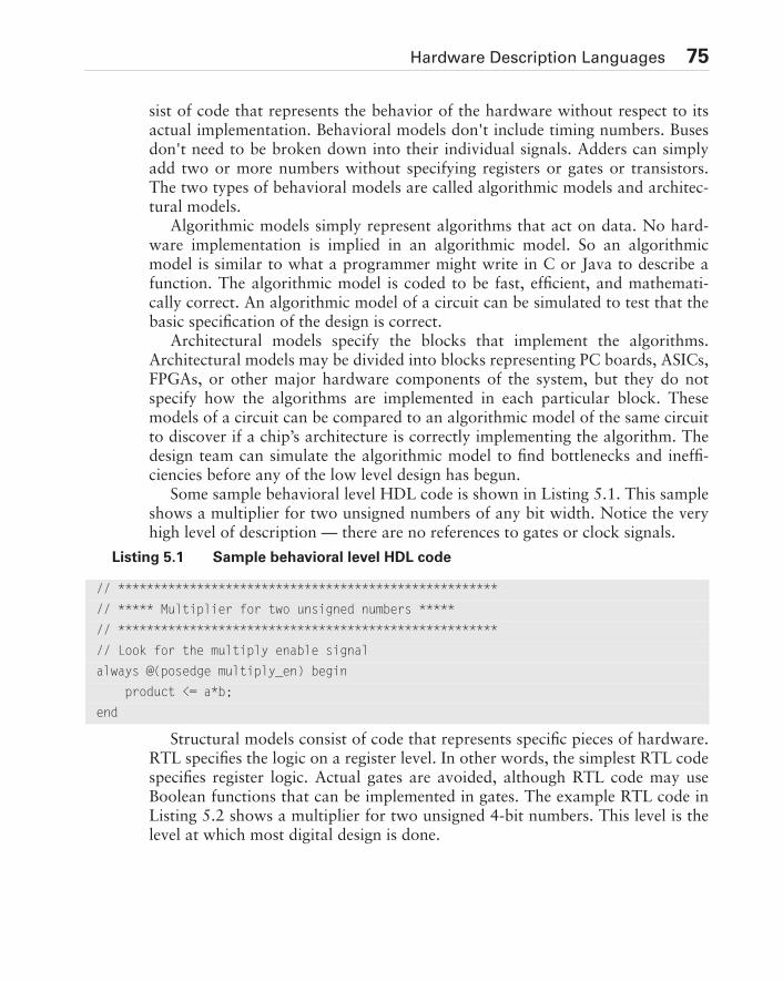
Hardware Description Languages 75
sist of code that represents the behavior of the hardware without respect to itsactual implementation. Behavioral models don't include timing numbers. Busesdon't need to be broken down into their individual signals. Adders can simplyadd two or more numbers without specifying registers or gates or transistors.The two types of behavioral models are called algorithmic models and architec-tural models.
Algorithmic models simply represent algorithms that act on data. No hard-ware implementation is implied in an algorithmic model. So an algorithmicmodel is similar to what a programmer might write in C or Java to describe afunction. The algorithmic model is coded to be fast, efficient, and mathemati-cally correct. An algorithmic model of a circuit can be simulated to test that thebasic specification of the design is correct.
Architectural models specify the blocks that implement the algorithms.Architectural models may be divided into blocks representing PC boards, ASICs,FPGAs, or other major hardware components of the system, but they do notspecify how the algorithms are implemented in each particular block. Thesemodels of a circuit can be compared to an algorithmic model of the same circuitto discover if a chip’s architecture is correctly implementing the algorithm. Thedesign team can simulate the algorithmic model to find bottlenecks and ineffi-ciencies before any of the low level design has begun.
Some sample behavioral level HDL code is shown in Listing 5.1. This sampleshows a multiplier for two unsigned numbers of any bit width. Notice the veryhigh level of description — there are no references to gates or clock signals.
Structural models consist of code that represents specific pieces of hardware.RTL specifies the logic on a register level. In other words, the simplest RTL codespecifies register logic. Actual gates are avoided, although RTL code may useBoolean functions that can be implemented in gates. The example RTL code inListing 5.2 shows a multiplier for two unsigned 4-bit numbers. This level is thelevel at which most digital design is done.
Listing 5.1 Sample behavioral level HDL code
// *****************************************************
// ***** Multiplier for two unsigned numbers *****
// *****************************************************
// Look for the multiply enable signal
always @(posedge multiply_en) begin
product <= a*b;
end
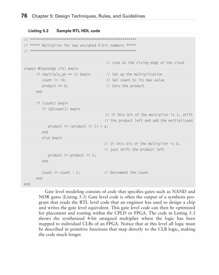
76 Chapter 5: Design Techniques, Rules, and Guidelines
Gate level modeling consists of code that specifies gates such as NAND andNOR gates (Listing 5.3) Gate level code is often the output of a synthesis pro-gram that reads the RTL level code that an engineer has used to design a chipand writes the gate level equivalent. This gate level code can then be optimizedfor placement and routing within the CPLD or FPGA. The code in Listing 5.3shows the synthesized 4-bit unsigned multiplier where the logic has beenmapped to individual CLBs of an FPGA. Notice that at this level all logic mustbe described in primitive functions that map directly to the CLB logic, makingthe code much longer.
Listing 5.2 Sample RTL HDL code
// *****************************************************
// ***** Multiplier for two unsigned 4-bit numbers *****
// *****************************************************
// Look at the rising edge of the clock
always @(posedge clk) begin
if (multiply_en == 1) begin // Set up the multiplication
count <= ~0; // Set count to its max value
product <= 0; // Zero the product
end
if (count) begin
if (b[count]) begin
// If this bit of the multiplier is 1, shift
// the product left and add the multiplicand
product <= (product << 1) + a;
end
else begin
// If this bit of the multiplier is 0,
// just shift the product left
product <= product << 1;
end
count <= count - 1; // Decrement the count
end
end
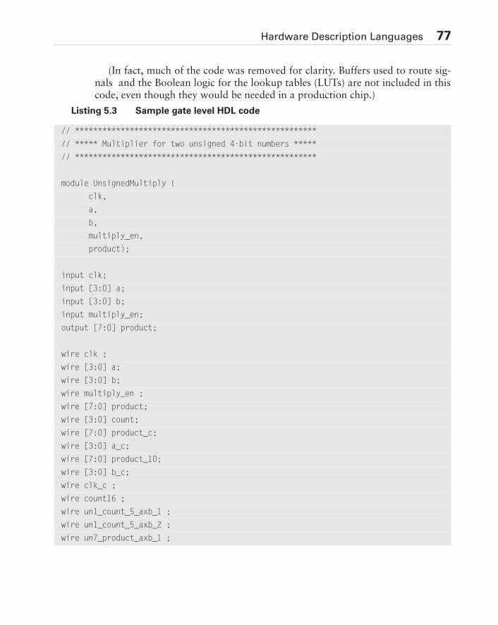
Hardware Description Languages 77
(In fact, much of the code was removed for clarity. Buffers used to route sig-nals and the Boolean logic for the lookup tables (LUTs) are not included in thiscode, even though they would be needed in a production chip.)
Listing 5.3 Sample gate level HDL code
// *****************************************************
// ***** Multiplier for two unsigned 4-bit numbers *****
// *****************************************************
module UnsignedMultiply (
clk,
a,
b,
multiply_en,
product);
input clk;
input [3:0] a;
input [3:0] b;
input multiply_en;
output [7:0] product;
wire clk ;
wire [3:0] a;
wire [3:0] b;
wire multiply_en ;
wire [7:0] product;
wire [3:0] count;
wire [7:0] product_c;
wire [3:0] a_c;
wire [7:0] product_10;
wire [3:0] b_c;
wire clk_c ;
wire count16 ;
wire un1_count_5_axb_1 ;
wire un1_count_5_axb_2 ;
wire un7_product_axb_1 ;
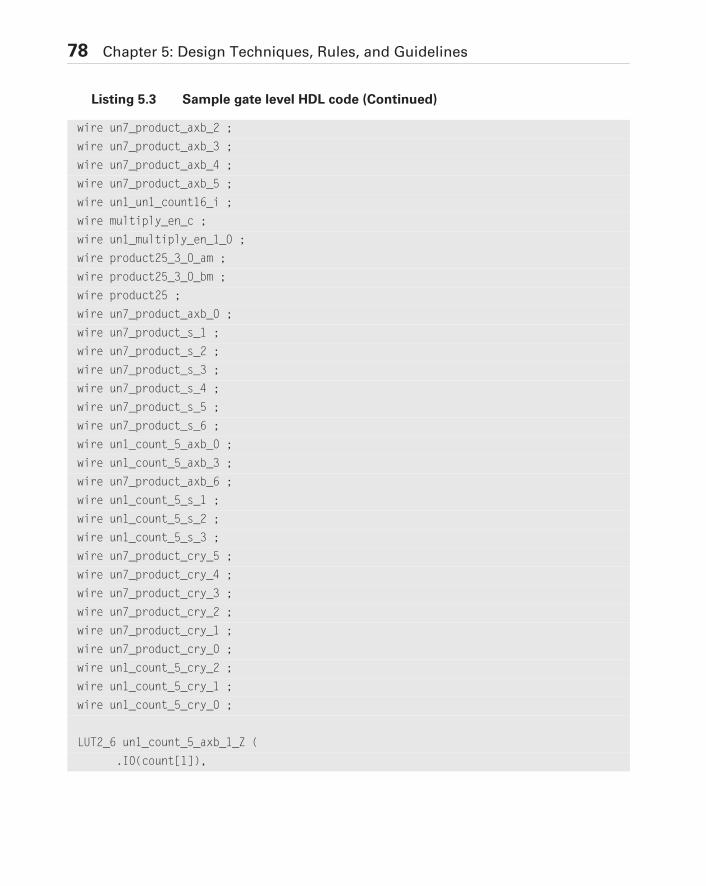
78 Chapter 5: Design Techniques, Rules, and Guidelines
wire un7_product_axb_2 ;
wire un7_product_axb_3 ;
wire un7_product_axb_4 ;
wire un7_product_axb_5 ;
wire un1_un1_count16_i ;
wire multiply_en_c ;
wire un1_multiply_en_1_0 ;
wire product25_3_0_am ;
wire product25_3_0_bm ;
wire product25 ;
wire un7_product_axb_0 ;
wire un7_product_s_1 ;
wire un7_product_s_2 ;
wire un7_product_s_3 ;
wire un7_product_s_4 ;
wire un7_product_s_5 ;
wire un7_product_s_6 ;
wire un1_count_5_axb_0 ;
wire un1_count_5_axb_3 ;
wire un7_product_axb_6 ;
wire un1_count_5_s_1 ;
wire un1_count_5_s_2 ;
wire un1_count_5_s_3 ;
wire un7_product_cry_5 ;
wire un7_product_cry_4 ;
wire un7_product_cry_3 ;
wire un7_product_cry_2 ;
wire un7_product_cry_1 ;
wire un7_product_cry_0 ;
wire un1_count_5_cry_2 ;
wire un1_count_5_cry_1 ;
wire un1_count_5_cry_0 ;
LUT2_6 un1_count_5_axb_1_Z (
.I0(count[1]),
Listing 5.3 Sample gate level HDL code (Continued)
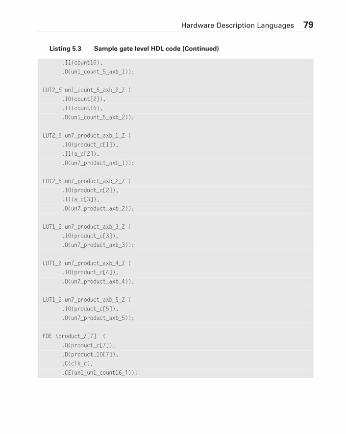
Hardware Description Languages 79
.I1(count16),
.O(un1_count_5_axb_1));
LUT2_6 un1_count_5_axb_2_Z (
.I0(count[2]),
.I1(count16),
.O(un1_count_5_axb_2));
LUT2_6 un7_product_axb_1_Z (
.I0(product_c[1]),
.I1(a_c[2]),
.O(un7_product_axb_1));
LUT2_6 un7_product_axb_2_Z (
.I0(product_c[2]),
.I1(a_c[3]),
.O(un7_product_axb_2));
LUT1_2 un7_product_axb_3_Z (
.I0(product_c[3]),
.O(un7_product_axb_3));
LUT1_2 un7_product_axb_4_Z (
.I0(product_c[4]),
.O(un7_product_axb_4));
LUT1_2 un7_product_axb_5_Z (
.I0(product_c[5]),
.O(un7_product_axb_5));
FDE \product_Z[7] (
.Q(product_c[7]),
.D(product_10[7]),
.C(clk_c),
.CE(un1_un1_count16_i));
Listing 5.3 Sample gate level HDL code (Continued)
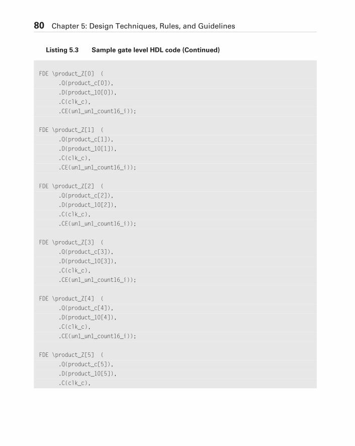
80 Chapter 5: Design Techniques, Rules, and Guidelines
FDE \product_Z[0] (
.Q(product_c[0]),
.D(product_10[0]),
.C(clk_c),
.CE(un1_un1_count16_i));
FDE \product_Z[1] (
.Q(product_c[1]),
.D(product_10[1]),
.C(clk_c),
.CE(un1_un1_count16_i));
FDE \product_Z[2] (
.Q(product_c[2]),
.D(product_10[2]),
.C(clk_c),
.CE(un1_un1_count16_i));
FDE \product_Z[3] (
.Q(product_c[3]),
.D(product_10[3]),
.C(clk_c),
.CE(un1_un1_count16_i));
FDE \product_Z[4] (
.Q(product_c[4]),
.D(product_10[4]),
.C(clk_c),
.CE(un1_un1_count16_i));
FDE \product_Z[5] (
.Q(product_c[5]),
.D(product_10[5]),
.C(clk_c),
Listing 5.3 Sample gate level HDL code (Continued)
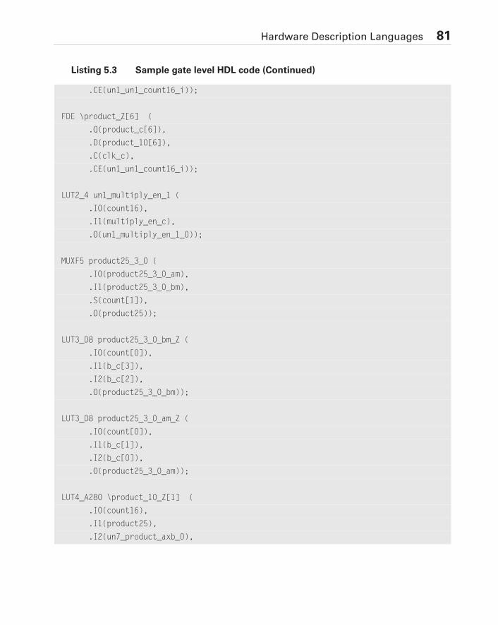
Hardware Description Languages 81
.CE(un1_un1_count16_i));
FDE \product_Z[6] (
.Q(product_c[6]),
.D(product_10[6]),
.C(clk_c),
.CE(un1_un1_count16_i));
LUT2_4 un1_multiply_en_1 (
.I0(count16),
.I1(multiply_en_c),
.O(un1_multiply_en_1_0));
MUXF5 product25_3_0 (
.I0(product25_3_0_am),
.I1(product25_3_0_bm),
.S(count[1]),
.O(product25));
LUT3_D8 product25_3_0_bm_Z (
.I0(count[0]),
.I1(b_c[3]),
.I2(b_c[2]),
.O(product25_3_0_bm));
LUT3_D8 product25_3_0_am_Z (
.I0(count[0]),
.I1(b_c[1]),
.I2(b_c[0]),
.O(product25_3_0_am));
LUT4_A280 \product_10_Z[1] (
.I0(count16),
.I1(product25),
.I2(un7_product_axb_0),
Listing 5.3 Sample gate level HDL code (Continued)
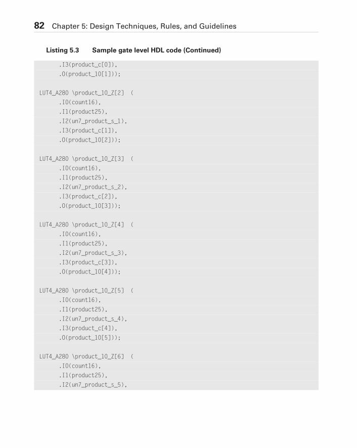
82 Chapter 5: Design Techniques, Rules, and Guidelines
.I3(product_c[0]),
.O(product_10[1]));
LUT4_A280 \product_10_Z[2] (
.I0(count16),
.I1(product25),
.I2(un7_product_s_1),
.I3(product_c[1]),
.O(product_10[2]));
LUT4_A280 \product_10_Z[3] (
.I0(count16),
.I1(product25),
.I2(un7_product_s_2),
.I3(product_c[2]),
.O(product_10[3]));
LUT4_A280 \product_10_Z[4] (
.I0(count16),
.I1(product25),
.I2(un7_product_s_3),
.I3(product_c[3]),
.O(product_10[4]));
LUT4_A280 \product_10_Z[5] (
.I0(count16),
.I1(product25),
.I2(un7_product_s_4),
.I3(product_c[4]),
.O(product_10[5]));
LUT4_A280 \product_10_Z[6] (
.I0(count16),
.I1(product25),
.I2(un7_product_s_5),
Listing 5.3 Sample gate level HDL code (Continued)

Hardware Description Languages 83
.I3(product_c[5]),
.O(product_10[6]));
LUT4_A280 \product_10_Z[7] (
.I0(count16),
.I1(product25),
.I2(un7_product_s_6),
.I3(product_c[6]),
.O(product_10[7]));
LUT2_6 un1_count_5_axb_0_Z (
.I0(count[0]),
.I1(count16),
.O(un1_count_5_axb_0));
LUT2_6 un1_count_5_axb_3_Z (
.I0(count[3]),
.I1(count16),
.O(un1_count_5_axb_3));
LUT2_6 un7_product_axb_0_Z (
.I0(product_c[0]),
.I1(a_c[1]),
.O(un7_product_axb_0));
LUT1_2 un7_product_axb_6_Z (
.I0(product_c[6]),
.O(un7_product_axb_6));
LUT4_FFFE count16_Z (
.I0(count[2]),
.I1(count[3]),
.I2(count[0]),
.I3(count[1]),
.O(count16));
Listing 5.3 Sample gate level HDL code (Continued)
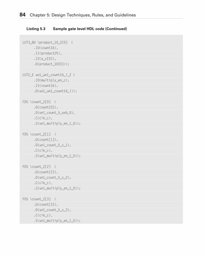
84 Chapter 5: Design Techniques, Rules, and Guidelines
LUT3_80 \product_10_Z[0] (
.I0(count16),
.I1(product25),
.I2(a_c[0]),
.O(product_10[0]));
LUT2_E un1_un1_count16_i_Z (
.I0(multiply_en_c),
.I1(count16),
.O(un1_un1_count16_i));
FDS \count_Z[0] (
.Q(count[0]),
.D(un1_count_5_axb_0),
.C(clk_c),
.S(un1_multiply_en_1_0));
FDS \count_Z[1] (
.Q(count[1]),
.D(un1_count_5_s_1),
.C(clk_c),
.S(un1_multiply_en_1_0));
FDS \count_Z[2] (
.Q(count[2]),
.D(un1_count_5_s_2),
.C(clk_c),
.S(un1_multiply_en_1_0));
FDS \count_Z[3] (
.Q(count[3]),
.D(un1_count_5_s_3),
.C(clk_c),
.S(un1_multiply_en_1_0));
Listing 5.3 Sample gate level HDL code (Continued)
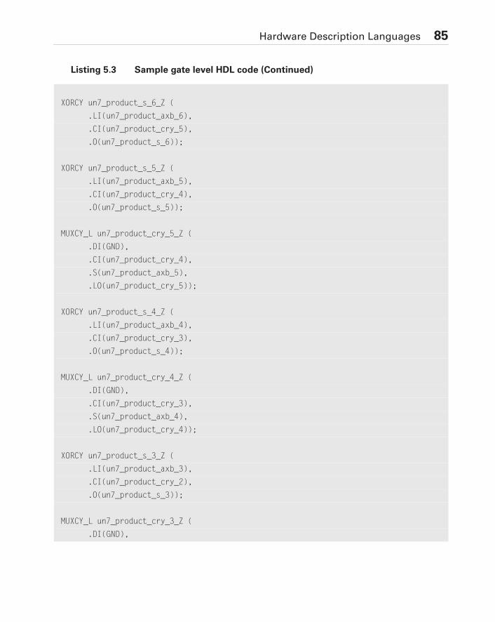
Hardware Description Languages 85
XORCY un7_product_s_6_Z (
.LI(un7_product_axb_6),
.CI(un7_product_cry_5),
.O(un7_product_s_6));
XORCY un7_product_s_5_Z (
.LI(un7_product_axb_5),
.CI(un7_product_cry_4),
.O(un7_product_s_5));
MUXCY_L un7_product_cry_5_Z (
.DI(GND),
.CI(un7_product_cry_4),
.S(un7_product_axb_5),
.LO(un7_product_cry_5));
XORCY un7_product_s_4_Z (
.LI(un7_product_axb_4),
.CI(un7_product_cry_3),
.O(un7_product_s_4));
MUXCY_L un7_product_cry_4_Z (
.DI(GND),
.CI(un7_product_cry_3),
.S(un7_product_axb_4),
.LO(un7_product_cry_4));
XORCY un7_product_s_3_Z (
.LI(un7_product_axb_3),
.CI(un7_product_cry_2),
.O(un7_product_s_3));
MUXCY_L un7_product_cry_3_Z (
.DI(GND),
Listing 5.3 Sample gate level HDL code (Continued)
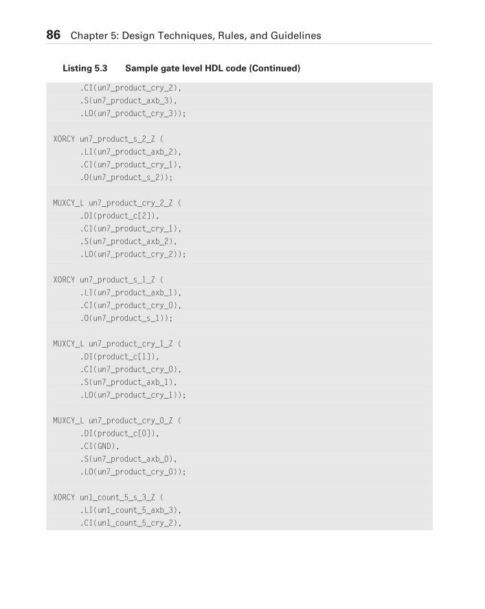
86 Chapter 5: Design Techniques, Rules, and Guidelines
.CI(un7_product_cry_2),
.S(un7_product_axb_3),
.LO(un7_product_cry_3));
XORCY un7_product_s_2_Z (
.LI(un7_product_axb_2),
.CI(un7_product_cry_1),
.O(un7_product_s_2));
MUXCY_L un7_product_cry_2_Z (
.DI(product_c[2]),
.CI(un7_product_cry_1),
.S(un7_product_axb_2),
.LO(un7_product_cry_2));
XORCY un7_product_s_1_Z (
.LI(un7_product_axb_1),
.CI(un7_product_cry_0),
.O(un7_product_s_1));
MUXCY_L un7_product_cry_1_Z (
.DI(product_c[1]),
.CI(un7_product_cry_0),
.S(un7_product_axb_1),
.LO(un7_product_cry_1));
MUXCY_L un7_product_cry_0_Z (
.DI(product_c[0]),
.CI(GND),
.S(un7_product_axb_0),
.LO(un7_product_cry_0));
XORCY un1_count_5_s_3_Z (
.LI(un1_count_5_axb_3),
.CI(un1_count_5_cry_2),
Listing 5.3 Sample gate level HDL code (Continued)
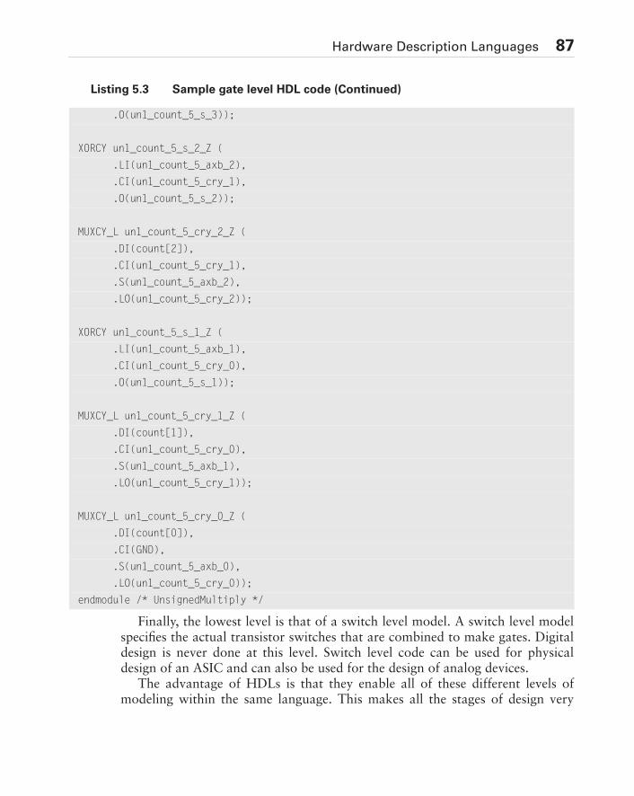
Hardware Description Languages 87
Finally, the lowest level is that of a switch level model. A switch level modelspecifies the actual transistor switches that are combined to make gates. Digitaldesign is never done at this level. Switch level code can be used for physicaldesign of an ASIC and can also be used for the design of analog devices.
The advantage of HDLs is that they enable all of these different levels ofmodeling within the same language. This makes all the stages of design very
.O(un1_count_5_s_3));
XORCY un1_count_5_s_2_Z (
.LI(un1_count_5_axb_2),
.CI(un1_count_5_cry_1),
.O(un1_count_5_s_2));
MUXCY_L un1_count_5_cry_2_Z (
.DI(count[2]),
.CI(un1_count_5_cry_1),
.S(un1_count_5_axb_2),
.LO(un1_count_5_cry_2));
XORCY un1_count_5_s_1_Z (
.LI(un1_count_5_axb_1),
.CI(un1_count_5_cry_0),
.O(un1_count_5_s_1));
MUXCY_L un1_count_5_cry_1_Z (
.DI(count[1]),
.CI(un1_count_5_cry_0),
.S(un1_count_5_axb_1),
.LO(un1_count_5_cry_1));
MUXCY_L un1_count_5_cry_0_Z (
.DI(count[0]),
.CI(GND),
.S(un1_count_5_axb_0),
.LO(un1_count_5_cry_0));
endmodule /* UnsignedMultiply */
Listing 5.3 Sample gate level HDL code (Continued)
88 Chapter 5: Design Techniques, Rules, and Guidelines
convenient to implement. You don't need to learn different tools. You can easilysimulate the design at a behavioral level, and then substitute various behavioralcode modules with structural code modules. For system simulation, this allowsyou to analyze your entire project using the same set of tools. First, you can testand optimize the algorithms. Next, you can use the behavioral models to parti-tion the hardware into boards, ASIC, and FPGAs. You can then write the RTLcode and substitute it for behavioral blocks, one at a time, to easily test the func-tionality of each block. From that, you can synthesize the design, creating gateand switch level blocks that can be resimulated with timing numbers to getactual performance measurements. Finally, you can use this low-level code togenerate a netlist for layout. All stages of the design have been performed usingthe same basic tool.
The main HDLs in existence today are Verilog and VHDL. Both are openstandards, maintained by standards groups of the Institute of Electrical andElectronic Engineers (IEEE). VHDL is maintained as IEEE-STD-1076; Verilog ismaintained as IEEE-STD-1364. Although some engineers prefer one languageover the other, the differences are minor. As these standard languages progresswith new versions, the differences become even fewer. Also, several languages,including C++, are being offered as a system level language, which would enableengineers to design and simulate an entire system consisting of multiple chips,boards, and software. These system level design languages are still evolving.
5.2 Top-Down DesignTop-down design is the design methodology whereby high level functions aredefined first, and the lower level implementation details are filled in later. Adesign can be viewed as a hierarchical tree, as shown in Figure 5.1. The top levelblock represents the entire chip. The next lower level blocks also represent theentire chip but divided into the major function blocks of the chip. Intermediatelevel blocks divide the functionality into more manageable pieces. The bottomlevel contains only gates and macrofunctions, which are vendor-supplied highlevel functions.
5.2.1 Use of Hardware Design LanguagesTop-down design methodology lends itself particularly well to using HDLs, thegenerally accepted method of designing complex CPLDs and FPGAs. Each blockin the design corresponds to the code for a self-contained module. The top-levelblocks correspond to the behavioral models that comprise the chip. The inter-mediate levels correspond to the RTL models that will become input to the syn-thesis process. The lowest level of the hierarchy corresponds to gate level code
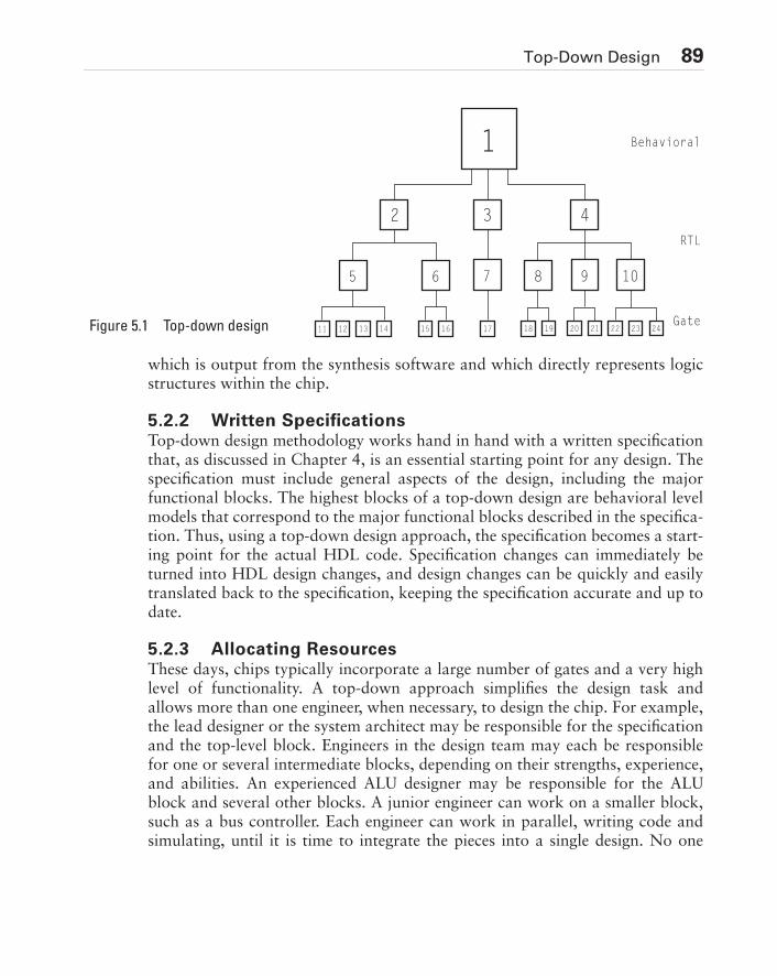
Top-Down Design 89
which is output from the synthesis software and which directly represents logicstructures within the chip.
5.2.2 Written SpecificationsTop-down design methodology works hand in hand with a written specificationthat, as discussed in Chapter 4, is an essential starting point for any design. Thespecification must include general aspects of the design, including the majorfunctional blocks. The highest blocks of a top-down design are behavioral levelmodels that correspond to the major functional blocks described in the specifica-tion. Thus, using a top-down design approach, the specification becomes a start-ing point for the actual HDL code. Specification changes can immediately beturned into HDL design changes, and design changes can be quickly and easilytranslated back to the specification, keeping the specification accurate and up todate.
5.2.3 Allocating ResourcesThese days, chips typically incorporate a large number of gates and a very highlevel of functionality. A top-down approach simplifies the design task andallows more than one engineer, when necessary, to design the chip. For example,the lead designer or the system architect may be responsible for the specificationand the top-level block. Engineers in the design team may each be responsiblefor one or several intermediate blocks, depending on their strengths, experience,and abilities. An experienced ALU designer may be responsible for the ALUblock and several other blocks. A junior engineer can work on a smaller block,such as a bus controller. Each engineer can work in parallel, writing code andsimulating, until it is time to integrate the pieces into a single design. No one
11 12 13 14 15 16 17 18 19 20 21 22 23 24
5 6
1
2 3 4
8 1097
Behavioral
RTL
GateFigure 5.1 Top-down design
90 Chapter 5: Design Techniques, Rules, and Guidelines
person can slow down the entire design. With a top-down design, yournot-too-bright colleague in the next cubicle won’t delay the entire project ormake you look bad. That may be the single best reason for using this designmethodology.
5.2.4 Design PartitioningEven if you are the only engineer designing the chip, this methodology allowsyou to break the design into simpler functions that you (or others) can designand simulate independently from the rest of the design. A large, complex designbecomes a series of independent smaller ones that are easier to design and simu-late.
5.2.5 Flexibility and OptimizationTop-down design allows flexibility. Teams can remove sections of the design andreplace them with higher-performance or optimized designs without affectingother sections of the design. Adding new or improved functionality involves sim-ply redesigning one section of the design and substituting it for the current sec-tion.
5.2.6 ReusabilityReusability is an important topic in chip design these days. In the days when aCPLD consisted of a few small state machines, it was no big deal to design itfrom scratch. Nowadays, CPLDs and FPGAs contain so much logic that reusingany function from a previous design can save days, weeks, or months of designtime. When one group has already designed a certain function, say a fast, effi-cient 64-bit multiplier, HDLs allow you to take the design and reuse it in yourdesign. If you need a 64-bit multiplier, you can simply take the designed, verifiedcode and plop it into your design. Or you can purchase the code from a thirdparty. But it will only fit easily into your design if you have used a top-downapproach to break the design into smaller pieces, one of which is a 64-bit multi-plier.
5.2.7 FloorplanningFloorplanning is another important topic in chip design these days. As chipsbecome larger, it may be necessary to help the design tools place the variousfunctions in the device. If you have used a top-down approach, you will be ableto plan the placement of each block in the chip. The FBs or CLBs that imple-ment the logic in each block can be placed in proximity to each other. The rela-tionship between blocks will also be apparent, and so you can understand whichblocks should be placed near each other.
Top-Down Design 91
5.2.8 VerificationVerification, discussed at length in Chapter 6, has become an extremely impor-tant aspect of the design process, but can be very resource-intensive and thusoften needs to be optimized. Top-down design is one important means forimproving verification. A top-down design approach allows each module to besimulated independently from the rest of the design. This is important for com-plex designs where an entire design can take weeks to simulate and days todebug. By using a top-down approach, design teams can efficiently performbehavioral, RTL, and gate level simulations and use the results to verify func-tionality at each level of design.
In summary, top-down design facilitates these good design practices:
• Use of hardware design languages
• Writing accurate and up-to-date specifications
• Allocation of resources for the design task
• Simplification and easy partitioning of the design task
• Flexibility in experimenting with different designs and optimizing the design
• Reusing previous designs
• Floorplanning
• Improved verification and less time spent on verification
5.2.9 Know the ArchitectureLook at the particular architecture for the CPLD or FPGA that you are using todetermine which logic devices fit best into it. You should choose a device with anarchitecture that fits well with your particular design. In addition, as you design,keep in mind the architecture of the device. For example, you may be using aCPLD that includes exclusive ORs. When you are deciding which kind of errordetection to use, you could perform parity checking efficiently in this device.Similarly, if the device includes a fast carry chain, make sure that you are able touse it for any adders that you are designing.
Many FPGA and CPLD vendors now include specialized logic functions intheir devices. For example, vendors may offer a device with a built-in digital sig-nal processor (DSP). This device will not be useful, and is the wrong choice, ifyour design does not use a DSP. On the other hand, if you are implementing sig-nal processing functions, you should make sure you use this DSP function asmuch as possible throughout the design.
The vendor will be able to offer advice about their device architecture andhow to efficiently utilize it. Most synthesis tools can target their results to a spe-cific FPGA or CPLD family from a specific vendor, taking advantage of thearchitecture to provide you with faster, more optimal designs.
92 Chapter 5: Design Techniques, Rules, and Guidelines
5.3 Synchronous DesignOne of the most important concepts in chip design, and one of the hardest toenforce on novice chip designers, is that of synchronous design. Once a chipdesigner uncovers a problem due to a design that is not synchronous (i.e., asyn-chronous) and attempts to fix it, he or she usually becomes an evangelical con-vert to synchronous design practices. This is because asynchronous designproblems often appear intermittently due to subtle variations in the voltage,temperature, or semiconductor process. Or they may appear only when the ven-dor changes its semiconductor process. Asynchronous designs that work foryears in one process may suddenly fail when the programmable part is manufac-tured using a newer process.
Unlike technologies like printed circuit boards, the semiconductor processesfor creating FPGAs change very rapidly. Moore’s Law, an observation aboutsemiconductor technology improvements, currently says that the number oftransistors per square inch doubles every 18 months. This doubling is due torapid increases in semiconductor process technology and advances in themachinery used to create silicon structures. Due to these improvements, theFPGA or CPLD device that holds your design today will have different, fastertiming parameters than the one that holds your design a year from now. Thevendor will no doubt have improved its process by that time.
Even if you were certain that the semiconductor process for your program-mable device would remain constant for each device in your system, each pro-cess has natural variations from chip to chip and even within a single chip. Toadd even more uncertainty, the exact timing for a programmable device dependson the specific routing and logic implementation. Essentially, you cannot deter-mine exact delay numbers; you can only know timing ranges and relative delays.Synchronous design is a formal methodology for ensuring that your design willwork correctly and within your speed requirements as long as the timing num-bers remain within certain ranges and with delays that remain relatively con-trolled, if not absolutely controlled.
Synchronous design is not only more reliable than asynchronous design, butfor the most part, EDA tools now assume that your design is synchronous. Inthe early days of EDA software for digital circuits, the tools made no assump-tions about the design. As chip designs grew, the software tools became moredifficult to develop, the algorithms became more complex, and the tools becameslower and less efficient. The EDA vendors finally realized that synchronousdesign was required anyway, for the reasons I gave previously. So the EDA ven-dors also began enforcing synchronous design rules, which made their algo-rithms simpler, the software complexity more manageable, and the tools fasterand more efficient.
Synchronous Design 93
5.3.1 Five Rules of Synchronous DesignI use five rules to define synchronous design for a single clock domain. (A singleclock domain means that all logic is clocked by a single clock signal.)
1. All data is passed through combinatorial logic, and through delay elements,typically flip-flops, that are synchronized to a single clock.
2. Delay is always controlled by delay elements, not combinatorial logic.
3. No signal that is generated by combinatorial logic can be fed back to thesame combinatorial logic without first going through a synchronizing delayelement.
4. Clocks cannot be gated; clocks must go directly to the clock inputs of thedelay elements without going through any combinatorial logic.
5. Data signals must go only to combinatorial logic or data inputs of delay ele-ments.
Note that I use the term “delay elements.” Typically, these elements will beflip-flops because those are the common delay element devices in use. Strictlyspeaking, the delay elements do not need to be flip-flops, they can be any ele-ment whose delay is predictable and synchronized to a clock signal.
A design may have multiple clocks and thus multiple clock domains. In otherwords, there will be logic clocked by one clock signal and logic clocked byanother clock signal, but the design must treat all signals passed between thetwo domains as asynchronous signals. In Section Section 5.3.7, you will see howto deal with asynchronous signals.
The following sections cover common asynchronous design problems, whatspecific problems they can cause, and how to design the same functionality usingsynchronous logic. In my career, I have seen many of these problems in realdesigns and, unfortunately, I have had to debug many of them.
5.3.2 Race ConditionsFigure 5.2 shows an asynchronous race condition where a clock signal is con-nected to the asynchronous reset of a flip-flop. This violates rules 2 and either 4or 5. It violates rule 2 because an asynchronous reset has a delay that is con-trolled by the internal design of the flip-flop, not by a delay element. It violatesrule 4 if SIG2 is a clock signal, because it should not go to the CLR input. Oth-erwise, if SIG2 is a data signal, it should not go to the CLK input.
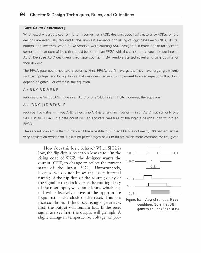
94 Chapter 5: Design Techniques, Rules, and Guidelines
Gate Count Controversy
What, exactly is a gate count? The term comes from ASIC designs, specifically gate array ASICs, where
designs are eventually reduced to the simplest elements consisting of logic gates — NANDs, NORs,
buffers, and inverters. When FPGA vendors were courting ASIC designers, it made sense for them to
compare the amount of logic that could be put into an FPGA with the amount that could be put into an
ASIC. Because ASIC designers used gate counts, FPGA vendors started advertising gate counts for
their devices.
The FPGA gate count had two problems. First, FPGAs don’t have gates. They have larger grain logic
such as flip-flops, and lookup tables that designers can use to implement Boolean equations that don’t
depend on gates. For example, the equation
A = B & C & D & E & F
requires one 5-input AND gate in an ASIC or one 5-LUT in an FPGA. However, the equation
A = ((B & C) | ( D & E)) & ~F
requires five gates — three AND gates, one OR gate, and an inverter — in an ASIC, but still only one
5-LUT in an FPGA. So a gate count isn’t an accurate measure of the logic a designer can fit into an
FPGA.
The second problem is that utilization of the available logic in an FPGA is not nearly 100 percent and is
very application dependant. Utilization percentages of 60 to 80 are much more common for any given
How does this logic behave? When SIG2 islow, the flip-flop is reset to a low state. On therising edge of SIG2, the designer wants theoutput, OUT, to change to reflect the currentstate of the input, SIG1. Unfortunately,because we do not know the exact internaltiming of the flip-flop or the routing delay ofthe signal to the clock versus the routing delayof the reset input, we cannot know which sig-nal will effectively arrive at the appropriatelogic first — the clock or the reset. This is arace condition. If the clock rising edge arrivesfirst, the output will remain low. If the resetsignal arrives first, the output will go high. Aslight change in temperature, voltage, or pro-
SIG1
SIG2
OUT
SIG1
SIG2
OUT
D Q
CLK
CLR
Figure 5.2 Asynchronous: Race
condition. Note that OUT
goes to an undefined state.
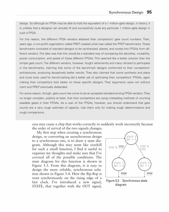
Synchronous Design 95
design. So although an FPGA may be able to hold the equivalent of a 1 million–gate design, in theory, it
is unlikely that a designer can actually fit and successfully route any particular 1 million–gate design in
such a FPGA.
For this reason, the different FPGA vendors attacked their competitors’ gate count numbers. Then,
years ago, a non-profit organization called PREP created what was called the PREP benchmarks. These
benchmarks consisted of standard designs to be synthesized, placed, and routed into FPGAs from dif-
ferent vendors. The idea was that this would be a standard way of comparing the densities, routability,
power consumption, and speed of these different FPGAs. This seemed like a better solution than the
simple gate count. The different vendors, however, fought vehemently and many refused to participate
in the benchmarks, claiming that some of the benchmark designs conformed to their competitors’
architectures, producing deceptively better results. They also claimed that some synthesis and place
and route tools used for benchmarking did a better job of optimizing their competitors’ FPGAs, again
making their competitors look better on these specific designs. Their arguments were not without
merit and PREP eventually disbanded.
For some reason, though, gate count has come to be an accepted standard among FPGA vendors. They
no longer complain, publicly at least, that their competitors are using misleading methods of counting
available gates in their FPGAs. As a user of the FPGAs, however, you should understand that gate
counts are a very rough estimate of capacity. Use them only for making rough determinations and
rough comparisons.
cess may cause a chip that works correctly to suddenly work incorrectly becausethe order of arrival of the two signals changes.
My first step when creating a synchronousdesign, or converting an asynchronous designto a synchronous one, is to draw a state dia-gram. Although this may seem like overkillfor such a small function, I find it useful toorganize my thoughts and make sure that I’vecovered all of the possible conditions. Thestate diagram for this function is shown inFigure 5.3. From this diagram, it is easy todesign the more reliable, synchronous solu-tion shown in Figure 5.4. Here the flip-flop isreset synchronously on the rising edge of afast clock. I’ve introduced a new signal,STATE, that together with the OUT signal,
STATE 1OUT = 0
SIG2 SIG2
STATE 2OUT = 1
STATE 0OUT = 0
SIG2 &SIG1
SIG2 & SIG1
Figure 5.3 Synchronous state
diagram
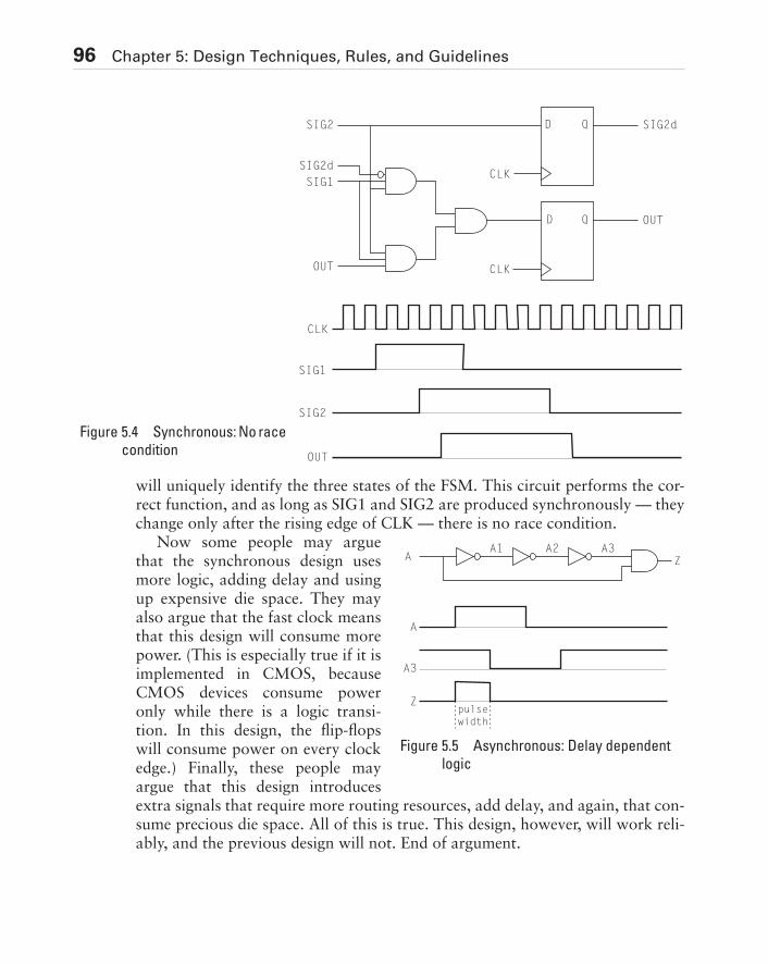
96 Chapter 5: Design Techniques, Rules, and Guidelines
will uniquely identify the three states of the FSM. This circuit performs the cor-rect function, and as long as SIG1 and SIG2 are produced synchronously — theychange only after the rising edge of CLK — there is no race condition.
Now some people may arguethat the synchronous design usesmore logic, adding delay and usingup expensive die space. They mayalso argue that the fast clock meansthat this design will consume morepower. (This is especially true if it isimplemented in CMOS, becauseCMOS devices consume poweronly while there is a logic transi-tion. In this design, the flip-flopswill consume power on every clockedge.) Finally, these people mayargue that this design introducesextra signals that require more routing resources, add delay, and again, that con-sume precious die space. All of this is true. This design, however, will work reli-ably, and the previous design will not. End of argument.
D Q
D QSIG2
SIG2d
SIG1
OUT
CLK
CLK
SIG2d
OUT
CLK
SIG1
SIG2
OUT
Figure 5.4 Synchronous: No race
condition
Figure 5.5 Asynchronous: Delay dependent
logic
A Z
A
A3
Z
A1 A2 A3
pulsewidth
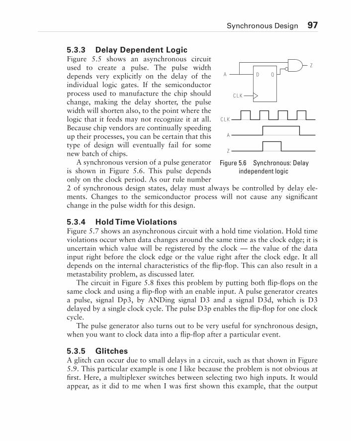
Synchronous Design 97
5.3.3 Delay Dependent LogicFigure 5.5 shows an asynchronous circuitused to create a pulse. The pulse widthdepends very explicitly on the delay of theindividual logic gates. If the semiconductorprocess used to manufacture the chip shouldchange, making the delay shorter, the pulsewidth will shorten also, to the point where thelogic that it feeds may not recognize it at all.Because chip vendors are continually speedingup their processes, you can be certain that thistype of design will eventually fail for somenew batch of chips.
A synchronous version of a pulse generatoris shown in Figure 5.6. This pulse dependsonly on the clock period. As our rule number2 of synchronous design states, delay must always be controlled by delay ele-ments. Changes to the semiconductor process will not cause any significantchange in the pulse width for this design.
5.3.4 Hold Time ViolationsFigure 5.7 shows an asynchronous circuit with a hold time violation. Hold timeviolations occur when data changes around the same time as the clock edge; it isuncertain which value will be registered by the clock — the value of the datainput right before the clock edge or the value right after the clock edge. It alldepends on the internal characteristics of the flip-flop. This can also result in ametastability problem, as discussed later.
The circuit in Figure 5.8 fixes this problem by putting both flip-flops on thesame clock and using a flip-flop with an enable input. A pulse generator createsa pulse, signal Dp3, by ANDing signal D3 and a signal D3d, which is D3delayed by a single clock cycle. The pulse D3p enables the flip-flop for one clockcycle.
The pulse generator also turns out to be very useful for synchronous design,when you want to clock data into a flip-flop after a particular event.
5.3.5 GlitchesA glitch can occur due to small delays in a circuit, such as that shown in Figure5.9. This particular example is one I like because the problem is not obvious atfirst. Here, a multiplexer switches between selecting two high inputs. It wouldappear, as it did to me when I was first shown this example, that the output
CLK
A
Z
D Q
CLK
A
Z
Figure 5.6 Synchronous: Delay
independent logic

98 Synchronous Design
Changing Processes
Years ago I was working on a project designing some controller boards for a small client company. The
vice president of manufacturing approached me and told me about a problem they were having and
asked if I had any ideas. It seems that they had been shipping a particular board for about two years.
Suddenly, every board would fail the preship tests they ran on it. They had assigned an engineer to look
into it, but he couldn’t find anything. What was particularly strange was that no part of the design had
changed in two years.
I took time to look at the board and at the tests they were running on it. I narrowed the problem down
to a particular FPGA and began examining the design. I found that there was one asynchronous circuit
where a logic signal was being used to clock a flip-flop. I decided to call up the FPGA vendor and ask
them whether they had recently changed their manufacturing process. They said that they had moved
their devices over to a faster semiconductor process about two months ago. That corresponded exactly
to the time when these boards started failing.
This illustrates a very important point about synchronous design. When you design synchronously, you
are immune to process speedups because the chip vendor ensures that any speedups result with clock
signals that are still much faster than data signals. However, if you have designed an asynchronous cir-
cuit, it works because the relationship between data signals has a specific timing relationship. In a new
semiconductor process, these relationships between data signals may no longer hold.
Also, you will notice that FPGA vendors do not specify minimum delay times. This is because they want
to have the ability to move older devices to newer, faster processes. When a semiconductor process is
new, the bugs haven’t been worked out, and the yields tend to be low. The vendor will charge more for
denser, faster chips based on this process. Once the bugs are worked out and yields go up to a reason-
able level, the vendor does not want to maintain two different processes because it is too expensive.
Instead, the vendor will move the “slower” chips over to the faster process. So these so-called
“slower” chips are now faster than before. As long as they have not specified the minimum times, the
timing numbers for these “slower” chips are still within the specifications. And as long as you have
designed synchronously, you will not have the problem that this client of mine did.
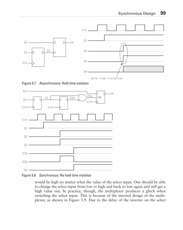
Synchronous Design 99
would be high no matter what the value of the select input. One should be ableto change the select input from low to high and back to low again and still get ahigh value out. In practice, though, the multiplexer produces a glitch whenswitching the select input. This is because of the internal design of the multi-plexer, as shown in Figure 5.9. Due to the delay of the inverter on the select
D Q
D QD3
CLK
D1
D2 D4
D4
Hold time violation
D2
D3
CLK
D1
Figure 5.7 Asynchronous: Hold time violation
D QD Q
CLK
CLK
CLK
D1
D2
D3 D3dD3p
D4DENA
Q
D3d
D3
D2
D1
CLK
D3p
D4
Figure 5.8 Synchronous: No hold time violation
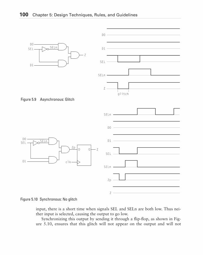
100 Chapter 5: Design Techniques, Rules, and Guidelines
input, there is a short time when signals SEL and SELn are both low. Thus nei-ther input is selected, causing the output to go low.
Synchronizing this output by sending it through a flip-flop, as shown in Fig-ure 5.10, ensures that this glitch will not appear on the output and will not
D0
D1
SEL SELn
Z
SELn
SEL
D1
D0
Z
glitch
Figure 5.9 Asynchronous: Glitch
D0
D1
SEL SELn
ZZp
D Q
SELn
SEL
SELn
Zp
D0
D1
Z
clk
Figure 5.10 Synchronous: No glitch
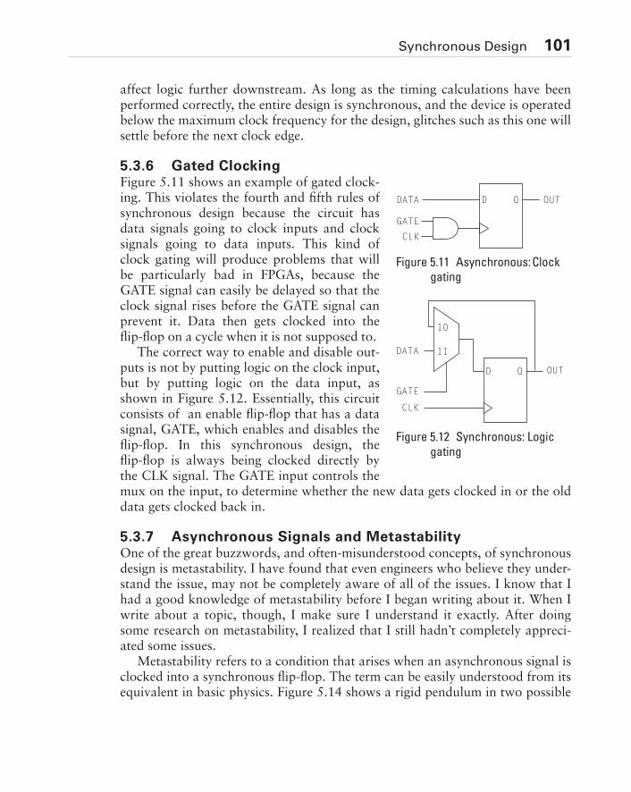
Synchronous Design 101
affect logic further downstream. As long as the timing calculations have beenperformed correctly, the entire design is synchronous, and the device is operatedbelow the maximum clock frequency for the design, glitches such as this one willsettle before the next clock edge.
5.3.6 Gated ClockingFigure 5.11 shows an example of gated clock-ing. This violates the fourth and fifth rules ofsynchronous design because the circuit hasdata signals going to clock inputs and clocksignals going to data inputs. This kind ofclock gating will produce problems that willbe particularly bad in FPGAs, because theGATE signal can easily be delayed so that theclock signal rises before the GATE signal canprevent it. Data then gets clocked into theflip-flop on a cycle when it is not supposed to.
The correct way to enable and disable out-puts is not by putting logic on the clock input,but by putting logic on the data input, asshown in Figure 5.12. Essentially, this circuitconsists of an enable flip-flop that has a datasignal, GATE, which enables and disables theflip-flop. In this synchronous design, theflip-flop is always being clocked directly bythe CLK signal. The GATE input controls themux on the input, to determine whether the new data gets clocked in or the olddata gets clocked back in.
5.3.7 Asynchronous Signals and MetastabilityOne of the great buzzwords, and often-misunderstood concepts, of synchronousdesign is metastability. I have found that even engineers who believe they under-stand the issue, may not be completely aware of all of the issues. I know that Ihad a good knowledge of metastability before I began writing about it. When Iwrite about a topic, though, I make sure I understand it exactly. After doingsome research on metastability, I realized that I still hadn’t completely appreci-ated some issues.
Metastability refers to a condition that arises when an asynchronous signal isclocked into a synchronous flip-flop. The term can be easily understood from itsequivalent in basic physics. Figure 5.14 shows a rigid pendulum in two possible
D QDATA
GATE
CLK
OUT
Figure 5.11 Asynchronous: Clock
gating
D Q
10
11DATA
GATE
CLK
OUT
Figure 5.12 Synchronous: Logic
gating
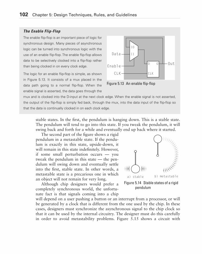
102 Chapter 5: Design Techniques, Rules, and Guidelines
stable states. In the first, the pendulum is hanging down. This is a stable state.The pendulum will tend to go into this state. If you tweak the pendulum, it willswing back and forth for a while and eventually end up back where it started.
The second part of the figure shows a rigidpendulum in a metastable state. If the pendu-lum is exactly in this state, upside-down, itwill remain in this state indefinitely. However,if some small perturbation occurs — youtweak the pendulum in this state — the pen-dulum will swing down and eventually settleinto the first, stable state. In other words, ametastable state is a precarious one in whichan object will not remain for very long.
Although chip designers would prefer acompletely synchronous world, the unfortu-nate fact is that signals coming into a chipwill depend on a user pushing a button or an interrupt from a processor, or willbe generated by a clock that is different from the one used by the chip. In thesecases, designers must synchronize the asynchronous signal to the chip clock sothat it can be used by the internal circuitry. The designer must do this carefullyin order to avoid metastability problems. Figure 5.15 shows a circuit with
The Enable Flip-Flop
The enable flip-flop is an important piece of logic for
synchronous design. Many pieces of asynchronous
logic can be turned into synchronous logic with the
use of an enable flip-flop. The enable flip-flop allows
data to be selectively clocked into a flip-flop rather
than being clocked in on every clock edge.
The logic for an enable flip-flop is simple, as shown
in Figure 5.13. It consists of a mux placed in the
data path going to a normal flip-flop. When the
enable signal is asserted, the data goes through the
mux and is clocked into the D-input at the next clock edge. When the enable signal is not asserted,
the output of the flip-flop is simply fed back, through the mux, into the data input of the flip-flop so
that the data is continually clocked in on each clock edge.
OutEnable
Data
CLK
I0
I1
D Q
CLK
Figure 5.13 An enable flip-flop
a) stable b) metastable
Figure 5.14 Stable states of a rigid
pendulum
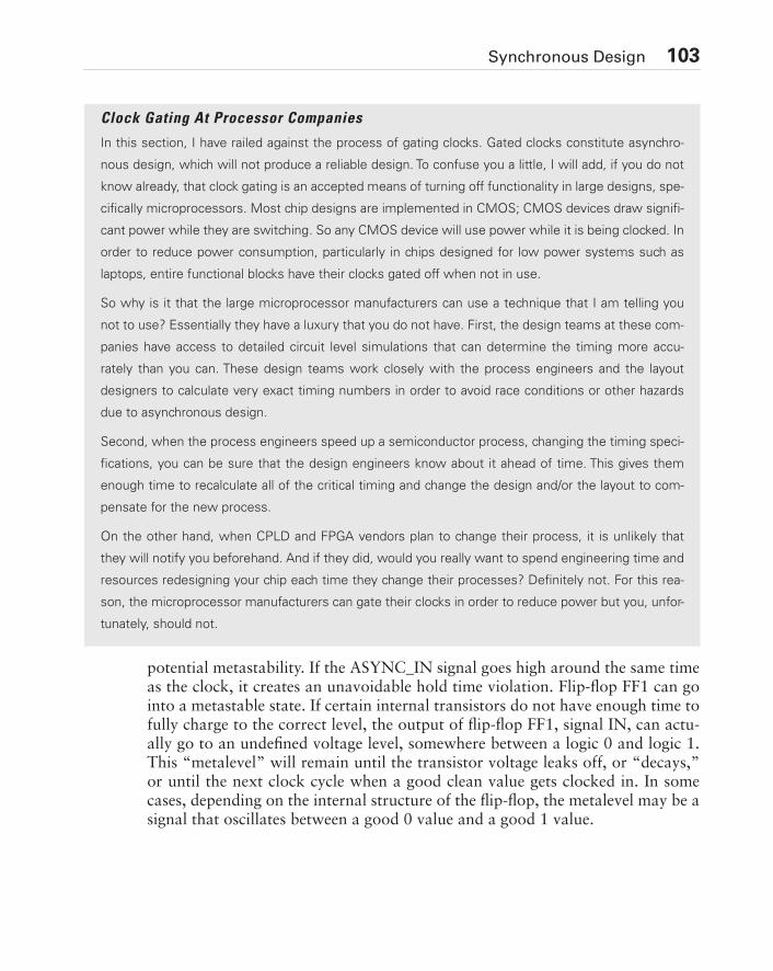
Synchronous Design 103
potential metastability. If the ASYNC_IN signal goes high around the same timeas the clock, it creates an unavoidable hold time violation. Flip-flop FF1 can gointo a metastable state. If certain internal transistors do not have enough time tofully charge to the correct level, the output of flip-flop FF1, signal IN, can actu-ally go to an undefined voltage level, somewhere between a logic 0 and logic 1.This “metalevel” will remain until the transistor voltage leaks off, or “decays,”or until the next clock cycle when a good clean value gets clocked in. In somecases, depending on the internal structure of the flip-flop, the metalevel may be asignal that oscillates between a good 0 value and a good 1 value.
Clock Gating At Processor Companies
In this section, I have railed against the process of gating clocks. Gated clocks constitute asynchro-
nous design, which will not produce a reliable design. To confuse you a little, I will add, if you do not
know already, that clock gating is an accepted means of turning off functionality in large designs, spe-
cifically microprocessors. Most chip designs are implemented in CMOS; CMOS devices draw signifi-
cant power while they are switching. So any CMOS device will use power while it is being clocked. In
order to reduce power consumption, particularly in chips designed for low power systems such as
laptops, entire functional blocks have their clocks gated off when not in use.
So why is it that the large microprocessor manufacturers can use a technique that I am telling you
not to use? Essentially they have a luxury that you do not have. First, the design teams at these com-
panies have access to detailed circuit level simulations that can determine the timing more accu-
rately than you can. These design teams work closely with the process engineers and the layout
designers to calculate very exact timing numbers in order to avoid race conditions or other hazards
due to asynchronous design.
Second, when the process engineers speed up a semiconductor process, changing the timing speci-
fications, you can be sure that the design engineers know about it ahead of time. This gives them
enough time to recalculate all of the critical timing and change the design and/or the layout to com-
pensate for the new process.
On the other hand, when CPLD and FPGA vendors plan to change their process, it is unlikely that
they will notify you beforehand. And if they did, would you really want to spend engineering time and
resources redesigning your chip each time they change their processes? Definitely not. For this rea-
son, the microprocessor manufacturers can gate their clocks in order to reduce power but you, unfor-
tunately, should not.
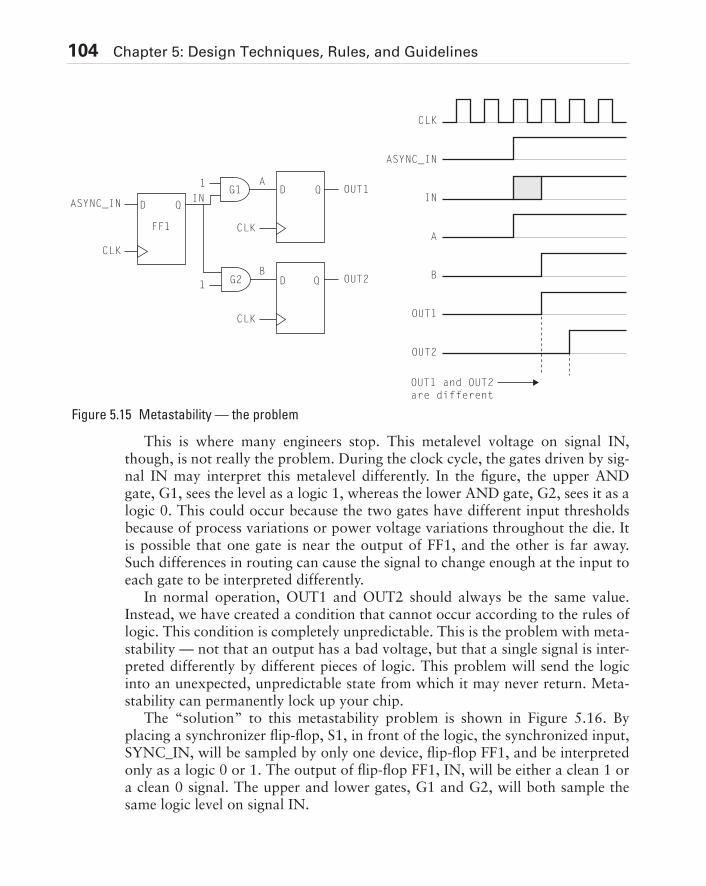
104 Chapter 5: Design Techniques, Rules, and Guidelines
This is where many engineers stop. This metalevel voltage on signal IN,though, is not really the problem. During the clock cycle, the gates driven by sig-nal IN may interpret this metalevel differently. In the figure, the upper ANDgate, G1, sees the level as a logic 1, whereas the lower AND gate, G2, sees it as alogic 0. This could occur because the two gates have different input thresholdsbecause of process variations or power voltage variations throughout the die. Itis possible that one gate is near the output of FF1, and the other is far away.Such differences in routing can cause the signal to change enough at the input toeach gate to be interpreted differently.
In normal operation, OUT1 and OUT2 should always be the same value.Instead, we have created a condition that cannot occur according to the rules oflogic. This condition is completely unpredictable. This is the problem with meta-stability — not that an output has a bad voltage, but that a single signal is inter-preted differently by different pieces of logic. This problem will send the logicinto an unexpected, unpredictable state from which it may never return. Meta-stability can permanently lock up your chip.
The “solution” to this metastability problem is shown in Figure 5.16. Byplacing a synchronizer flip-flop, S1, in front of the logic, the synchronized input,SYNC_IN, will be sampled by only one device, flip-flop FF1, and be interpretedonly as a logic 0 or 1. The output of flip-flop FF1, IN, will be either a clean 1 ora clean 0 signal. The upper and lower gates, G1 and G2, will both sample thesame logic level on signal IN.
ASYNC_IN
A
B
OUT1
OUT2
OUT1 and OUT2are different
CLK
IN
1
1
ASYNC_IN INOUT1
OUT2
A
B
D Q
CLK
FF1
D Q
CLK
D Q
CLK
G1
G2
Figure 5.15 Metastability — the problem
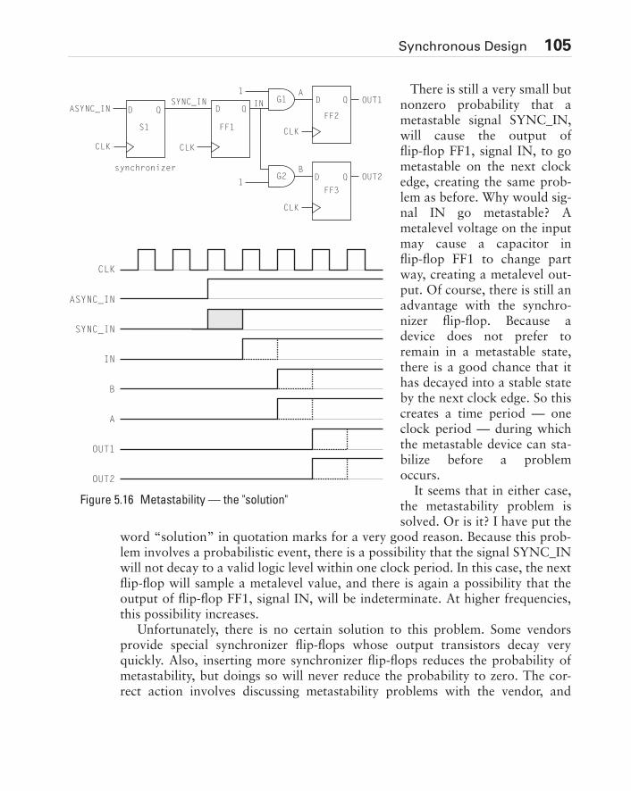
Synchronous Design 105
There is still a very small butnonzero probability that ametastable signal SYNC_IN,will cause the output offlip-flop FF1, signal IN, to gometastable on the next clockedge, creating the same prob-lem as before. Why would sig-nal IN go metastable? Ametalevel voltage on the inputmay cause a capacitor inflip-flop FF1 to change partway, creating a metalevel out-put. Of course, there is still anadvantage with the synchro-nizer flip-flop. Because adevice does not prefer toremain in a metastable state,there is a good chance that ithas decayed into a stable stateby the next clock edge. So thiscreates a time period — oneclock period — during whichthe metastable device can sta-bilize before a problemoccurs. It seems that in either case,the metastability problem issolved. Or is it? I have put the
word “solution” in quotation marks for a very good reason. Because this prob-lem involves a probabilistic event, there is a possibility that the signal SYNC_INwill not decay to a valid logic level within one clock period. In this case, the nextflip-flop will sample a metalevel value, and there is again a possibility that theoutput of flip-flop FF1, signal IN, will be indeterminate. At higher frequencies,this possibility increases.
Unfortunately, there is no certain solution to this problem. Some vendorsprovide special synchronizer flip-flops whose output transistors decay veryquickly. Also, inserting more synchronizer flip-flops reduces the probability ofmetastability, but doings so will never reduce the probability to zero. The cor-rect action involves discussing metastability problems with the vendor, and
IN
1
1
SYNC_INASYNC_IN
CLK
D Q
S1
D Q
CLK
FF1
OUT1A
D Q
CLK
FF2
OUT2B
D Q
CLK
FF3
synchronizer
ASYNC_IN
CLK
SYNC_IN
IN
A
B
OUT1
OUT2
G1
G2
Figure 5.16 Metastability — the "solution"
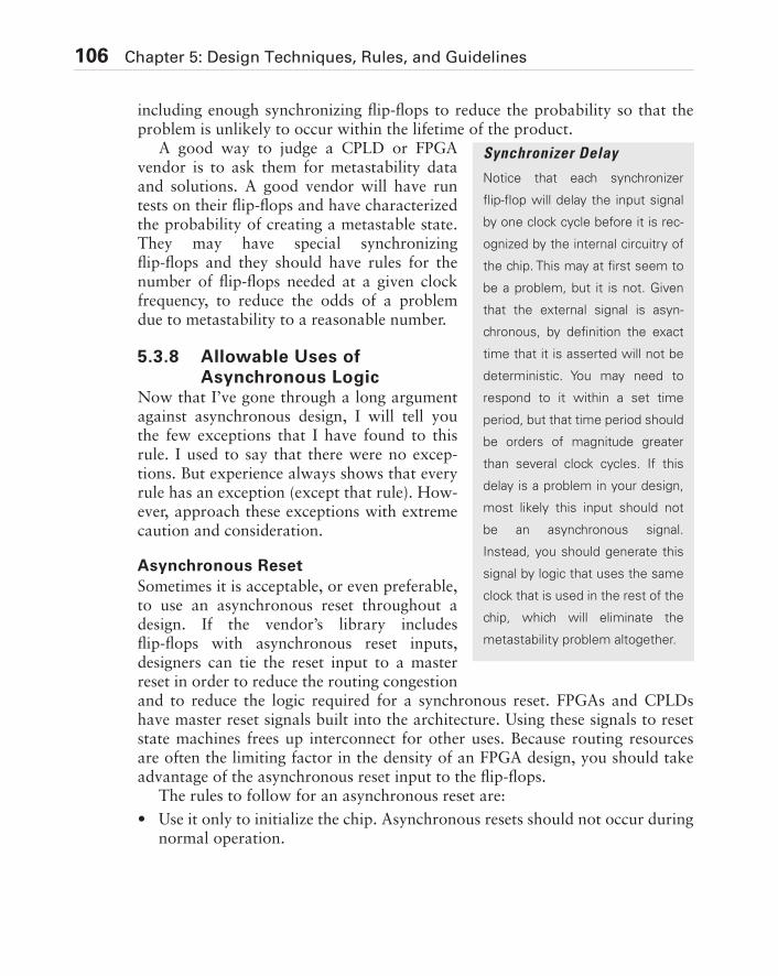
106 Chapter 5: Design Techniques, Rules, and Guidelines
including enough synchronizing flip-flops to reduce the probability so that theproblem is unlikely to occur within the lifetime of the product.
A good way to judge a CPLD or FPGAvendor is to ask them for metastability dataand solutions. A good vendor will have runtests on their flip-flops and have characterizedthe probability of creating a metastable state.They may have special synchronizingflip-flops and they should have rules for thenumber of flip-flops needed at a given clockfrequency, to reduce the odds of a problemdue to metastability to a reasonable number.
5.3.8 Allowable Uses of Asynchronous Logic
Now that I’ve gone through a long argumentagainst asynchronous design, I will tell youthe few exceptions that I have found to thisrule. I used to say that there were no excep-tions. But experience always shows that everyrule has an exception (except that rule). How-ever, approach these exceptions with extremecaution and consideration.
Asynchronous Reset
Sometimes it is acceptable, or even preferable,to use an asynchronous reset throughout adesign. If the vendor’s library includesflip-flops with asynchronous reset inputs,designers can tie the reset input to a masterreset in order to reduce the routing congestionand to reduce the logic required for a synchronous reset. FPGAs and CPLDshave master reset signals built into the architecture. Using these signals to resetstate machines frees up interconnect for other uses. Because routing resourcesare often the limiting factor in the density of an FPGA design, you should takeadvantage of the asynchronous reset input to the flip-flops.
The rules to follow for an asynchronous reset are:
• Use it only to initialize the chip. Asynchronous resets should not occur duringnormal operation.
Synchronizer Delay
Notice that each synchronizer
flip-flop will delay the input signal
by one clock cycle before it is rec-
ognized by the internal circuitry of
the chip. This may at first seem to
be a problem, but it is not. Given
that the external signal is asyn-
chronous, by definition the exact
time that it is asserted will not be
deterministic. You may need to
respond to it within a set time
period, but that time period should
be orders of magnitude greater
than several clock cycles. If this
delay is a problem in your design,
most likely this input should not
be an asynchronous signal.
Instead, you should generate this
signal by logic that uses the same
clock that is used in the rest of the
chip, which will eliminate the
metastability problem altogether.
Synchronous Design 107
• Assert the reset signal for at least one clock cycle.
• After reset, ensure that the chip is in a stable state such that no flip-flops willchange until an input changes. In other words, after reset every state machineshould be in an idle state waiting for an input signal to change.
• The inputs to the chip should be stable and not change for at least one clockcycle after the reset is removed.
Asynchronous Latches on Inputs
Some buses, such as the VME bus, are designed to be asynchronous. In order tointerface with these buses, designers need to use asynchronous latches to captureaddresses or data. Once the data is captured, it must be synchronized to theinternal clock. One suitable technique is to synchronize each incoming signalwith its own synchronizing flip-flop. (This is what I suggested in the previousdiscussion on metastability.)
However, it is usually much more efficient to use asynchronous latches tocapture the bus signals initially. Many buses have an address latch enable (ALE)
Synchronous VME Bus Is Not Synchronous
The VME bus has been in existence for a relatively long time now. It’s a standard, a workhorse. In use
since the early days of microprocessors, it’s the granddaddy of all buses. And it’s asynchronous, like
most of the buses that came after it. Asynchronous buses are easier to implement over different media
using various components. Synchronous buses require a lot of coordination between different devices,
and they need carefully controlled timing.
When synchronous design became more recognized and more important for chip design for all of the
reasons I discussed, synchronous buses such as PCI and SBUS started popping up. Synchronous
buses have tighter timing requirements, but they can be much more efficient at transferring data.
Some engineer or standards committee or perhaps a marketing person decided to make a synchronous
VME bus by adding a clock to it. Unfortunately, no relationship exists between the signals of the bus
and the clock. The clock was simply added to the existing asynchronous bus, resulting in an asynchro-
nous bus with a clock.
I discovered this the hard way when I was asked to interface an FPGA with the “synchronous” VME
bus. The overhead of logic and clock cycles required to synchronize this “synchronous” bus made data
transfers very inefficient. My advice is this: When interfacing to a bus, look at the timing relationships
to determine whether it is really synchronous. If these relationships are synchronous, a synchronous
interface will be very efficient. Otherwise, despite the label that the bus may have, treat it as asynchro-
nous and design the interface accordingly.
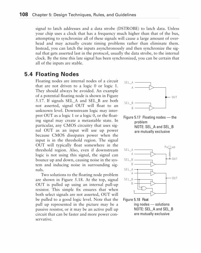
108 Chapter 5: Design Techniques, Rules, and Guidelines
signal to latch addresses and a data strobe (DSTROBE) to latch data. Unlessyour chip uses a clock that has a frequency much higher than that of the bus,attempting to synchronize all of these signals will cause a large amount of over-head and may actually create timing problems rather than eliminate them.Instead, you can latch the inputs asynchronously and then synchronize the sig-nal that gets asserted last in the protocol, usually the data strobe, to the internalclock. By the time this late signal has been synchronized, you can be certain thatall of the inputs are stable.
5.4 Floating NodesFloating nodes are internal nodes of a circuitthat are not driven to a logic 0 or logic 1.They should always be avoided. An exampleof a potential floating node is shown in Figure5.17. If signals SEL_A and SEL_B are bothnot asserted, signal OUT will float to anunknown level. Downstream logic may inter-pret OUT as a logic 1 or a logic 0, or the float-ing signal may create a metastable state. Inparticular, any CMOS circuitry that uses sig-nal OUT as an input will use up powerbecause CMOS dissipates power when theinput is in the threshold region. The signalOUT will typically float somewhere in thethreshold region. Also, even if downstreamlogic is not using this signal, the signal canbounce up and down, causing noise in the sys-tem and inducing noise in surrounding sig-nals.
Two solutions to the floating node problemare shown in Figure 5.18. At the top, signalOUT is pulled up using an internal pull-upresistor. This simple fix ensures that whenboth select signals are not asserted, OUT willbe pulled to a good logic level. Note that thepull up represented in the picture may be apassive resistor, or it may be an active pull upcircuit that can be faster and more power con-servative.
A
B
SEL_A
SEL_B
OUT
SEL_A
A
B
SEL_B
Pullup
OUT
ASEL_A
B
SEL_B OUT
Figure 5.17 Floating nodes — the
problem
NOTE: SEL_A and SEL_B
are mutually exclusive
Figure 5.18 Float
ing nodes — solutions
NOTE: SEL_A and SEL_B
are mutually exclusive
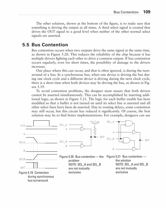
Bus Contention 109
The other solution, shown at the bottom of the figure, is to make sure thatsomething is driving the output at all times. A third select signal is created thatdrives the OUT signal to a good level when neither of the other normal selectsignals are asserted.
5.5 Bus ContentionBus contention occurs when two outputs drive the same signal at the same time,as shown in Figure 5.20. This reduces the reliability of the chip because it hasmultiple drivers fighting each other to drive a common output. If bus contentionoccurs regularly, even for short times, the possibility of damage to the driversincreases.
One place where this can occur, and that is often ignored, is during the turn-around of a bus. In a synchronous bus, when one device is driving the bus dur-ing one clock cycle and a different device is driving during the next clock cycle,there is a short time when both devices may be driving the bus, as shown in Fig-ure 5.19.
To avoid contention problems, the designer must ensure that both driverscannot be asserted simultaneously. This can be accomplished by inserting addi-tional logic, as shown in Figure 5.21. The logic for each buffer enable has beenmodified so that a buffer is not turned on until its select line is asserted and allother select lines have been de-asserted. Due to routing delays, some contentionmay still occur, but this circuit has reduced it significantly. Of course, the bestsolution may be to find better implementations. For example, designers can use
Figure 5.19 Contention
during synchronous
bus turnaround
CLK
A
SELA
B
SELB
OUT
A
B
SEL_A
SEL_B
OUT
Pullup
Figure 5.20 Bus contention — the
problem
NOTE: SEL_A and SEL_B
are not mutually
exclusive
SEL_B
SEL_A
A
B
OUT
Figure 5.21 Bus contention —
the solution
NOTE: SEL_A and SEL_B
are not mutually
exclusive
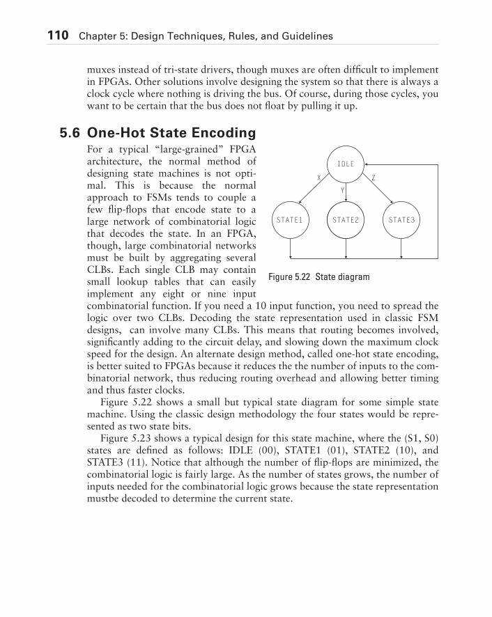
110 Chapter 5: Design Techniques, Rules, and Guidelines
muxes instead of tri-state drivers, though muxes are often difficult to implementin FPGAs. Other solutions involve designing the system so that there is always aclock cycle where nothing is driving the bus. Of course, during those cycles, youwant to be certain that the bus does not float by pulling it up.
5.6 One-Hot State EncodingFor a typical “large-grained” FPGAarchitecture, the normal method ofdesigning state machines is not opti-mal. This is because the normalapproach to FSMs tends to couple afew flip-flops that encode state to alarge network of combinatorial logicthat decodes the state. In an FPGA,though, large combinatorial networksmust be built by aggregating severalCLBs. Each single CLB may containsmall lookup tables that can easilyimplement any eight or nine inputcombinatorial function. If you need a 10 input function, you need to spread thelogic over two CLBs. Decoding the state representation used in classic FSMdesigns, can involve many CLBs. This means that routing becomes involved,significantly adding to the circuit delay, and slowing down the maximum clockspeed for the design. An alternate design method, called one-hot state encoding,is better suited to FPGAs because it reduces the the number of inputs to the com-binatorial network, thus reducing routing overhead and allowing better timingand thus faster clocks.
Figure 5.22 shows a small but typical state diagram for some simple statemachine. Using the classic design methodology the four states would be repre-sented as two state bits.
Figure 5.23 shows a typical design for this state machine, where the (S1, S0)states are defined as follows: IDLE (00), STATE1 (01), STATE2 (10), andSTATE3 (11). Notice that although the number of flip-flops are minimized, thecombinatorial logic is fairly large. As the number of states grows, the number ofinputs needed for the combinatorial logic grows because the state representationmustbe decoded to determine the current state.
IDLE
X Z
Y
STATE1 STATE2 STATE3
Figure 5.22 State diagram
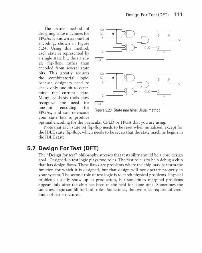
Design For Test (DFT) 111
The better method ofdesigning state machines forFPGAs is known as one-hotencoding, shown in Figure5.24. Using this method,each state is represented bya single state bit, thus a sin-gle flip-flop, rather thanencoded from several statebits. This greatly reducesthe combinatorial logic,because designers need tocheck only one bit to deter-mine the current state.Many synthesis tools nowrecognize the need forone-hot encoding forFPGAs, and can re-encodeyour state bits to produceoptimal encoding for the particular CPLD or FPGA that you are using.
Note that each state bit flip-flop needs to be reset when initialized, except forthe IDLE state flip-flop, which needs to be set so that the state machine begins inthe IDLE state.
5.7 Design For Test (DFT) The “Design for test” philosophy stresses that testability should be a core designgoal. Designed-in test logic plays two roles. The first role is to help debug a chipthat has design flaws. These flaws are problems where the chip may perform thefunction for which it is designed, but that design will not operate properly inyour system. The second role of test logic is to catch physical problems. Physicalproblems usually show up in production, but sometimes marginal problemsappear only after the chip has been in the field for some time. Sometimes thesame test logic can fill for both roles. Sometimes, the two roles require differentkinds of test structures.
RESET
SOS1V
S1
Z
D Q
RESET
SOS1X
S1
Z
D Q
CLK
CLK
Figure 5.23 State machine: Usual method
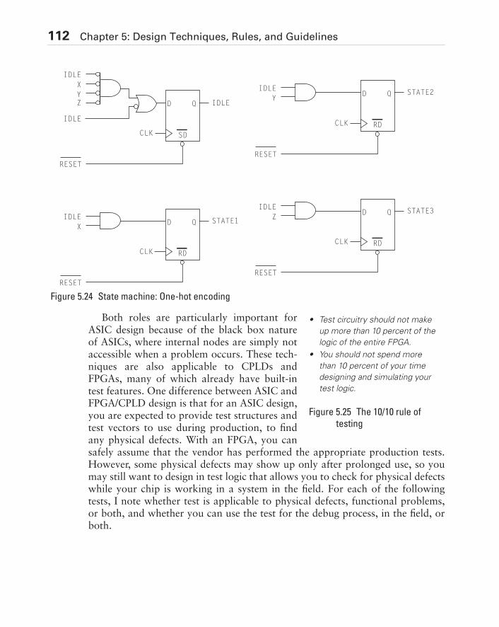
112 Chapter 5: Design Techniques, Rules, and Guidelines
Both roles are particularly important forASIC design because of the black box natureof ASICs, where internal nodes are simply notaccessible when a problem occurs. These tech-niques are also applicable to CPLDs andFPGAs, many of which already have built-intest features. One difference between ASIC andFPGA/CPLD design is that for an ASIC design,you are expected to provide test structures andtest vectors to use during production, to findany physical defects. With an FPGA, you cansafely assume that the vendor has performed the appropriate production tests.However, some physical defects may show up only after prolonged use, so youmay still want to design in test logic that allows you to check for physical defectswhile your chip is working in a system in the field. For each of the followingtests, I note whether test is applicable to physical defects, functional problems,or both, and whether you can use the test for the debug process, in the field, orboth.
IDLEXYZ
RESET
CLK
IDLE
IDLE
SD
D Q
SD
STATE1IDLEX
RESET
CLK
D Q
RD
STATE2IDLEY
RESET
CLK
D Q
RD
STATE3IDLEZ
RESET
CLK
D Q
RD
Figure 5.24 State machine: One-hot encoding
• Test circuitry should not make
up more than 10 percent of the
logic of the entire FPGA.
• You should not spend more
than 10 percent of your time
designing and simulating your
test logic.
Figure 5.25 The 10/10 rule of
testing
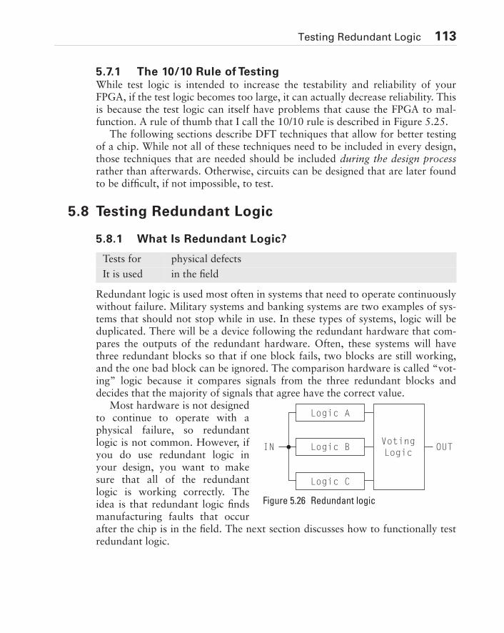
Testing Redundant Logic 113
5.7.1 The 10/10 Rule of TestingWhile test logic is intended to increase the testability and reliability of yourFPGA, if the test logic becomes too large, it can actually decrease reliability. Thisis because the test logic can itself have problems that cause the FPGA to mal-function. A rule of thumb that I call the 10/10 rule is described in Figure 5.25.
The following sections describe DFT techniques that allow for better testingof a chip. While not all of these techniques need to be included in every design,those techniques that are needed should be included during the design processrather than afterwards. Otherwise, circuits can be designed that are later foundto be difficult, if not impossible, to test.
5.8 Testing Redundant Logic
5.8.1 What Is Redundant Logic?
Redundant logic is used most often in systems that need to operate continuouslywithout failure. Military systems and banking systems are two examples of sys-tems that should not stop while in use. In these types of systems, logic will beduplicated. There will be a device following the redundant hardware that com-pares the outputs of the redundant hardware. Often, these systems will havethree redundant blocks so that if one block fails, two blocks are still working,and the one bad block can be ignored. The comparison hardware is called “vot-ing” logic because it compares signals from the three redundant blocks anddecides that the majority of signals that agree have the correct value.
Most hardware is not designedto continue to operate with aphysical failure, so redundantlogic is not common. However, ifyou do use redundant logic inyour design, you want to makesure that all of the redundantlogic is working correctly. Theidea is that redundant logic findsmanufacturing faults that occurafter the chip is in the field. The next section discusses how to functionally testredundant logic.
Tests for physical defects
It is used in the field
Logic A
Logic BVotingLogic
IN OUT
Logic C
Figure 5.26 Redundant logic
114 Chapter 5: Design Techniques, Rules, and Guidelines
5.8.2 How to Test Redundant Logic
Testing redundant logic is a separate issue. Figure 5.27 shows a circuit that hasredundant logic. However, because the circuit is not testable, the effect is not asuseful as it should be. If a design flaw exists, or a physical defect occurs beforethe chip is shipped, the redundant logic will hide the problem. If a defect occursin the field, the chip will simply produce incorrect results — the incorrect redun-dant logic will not prevent failure. Thus, if it is to contribute meaningfully toreliability, redundant logic must properly tested before it is shipped.
The circuit in Figure 5.27 shows how modify Figure 5.26 for testing. Theextra test lines allow you to disable some of the redundant logic and test each
Tests for functional problems
It is used during debugging
Redundant Logic and the Battle Switch
Years ago, I worked for ROLM Corporation, the premiere Silicon Valley company of its day. ROLM was
flying high, employing lots of people, and recording great revenue growth in the telecommunications
industry. At the time, everyone wanted to work at ROLM. ROLM offered great salaries, stock option
plans, and benefits. They epitomized the Silicon Valley workplace with large offices for engineers in spa-
cious buildings on “campuses” that were nested among trees and artificial lakes. The cafeterias were
subsidized by the company and served a great variety of foods in a quiet, elegant atmosphere. Most
notably, the ROLM campus included a full health club with basketball courts, racquetball courts, weight
room, swimming pool, Jacuzzi, and offered aerobics classes every day.
ROLM really defined the Silicon Valley company. It’s sad that it grew too fast and didn’t have the money
to support the growth. It ended up being bought by IBM, split up, sold off in pieces, and eventually
absorbed into several other companies. ROLM is a distant memory and most Silicon Valley engineers
haven’t even heard of it.
The reason I mention ROLM is that I worked in the Mil-Spec Computer Division, which manufactured
computers for the military. We had to design fault tolerance and redundancy into the computers. On
the side of our computers was a switch labeled the “battle switch,” which no one really talked about.
One day I asked a project leader about the function of this switch. He explained it this way. Throwing
that switch turned off all error checking and fault tolerance. I asked him why. He replied that in a war,
particularly a nuclear war, it’s better to have a faulty computer fire off as many missiles as possible,
even if some hit friendly targets, as long as one of them reaches the enemy. Pretty scary thought. I
guess that’s why no one discussed it, and I didn’t either after that.
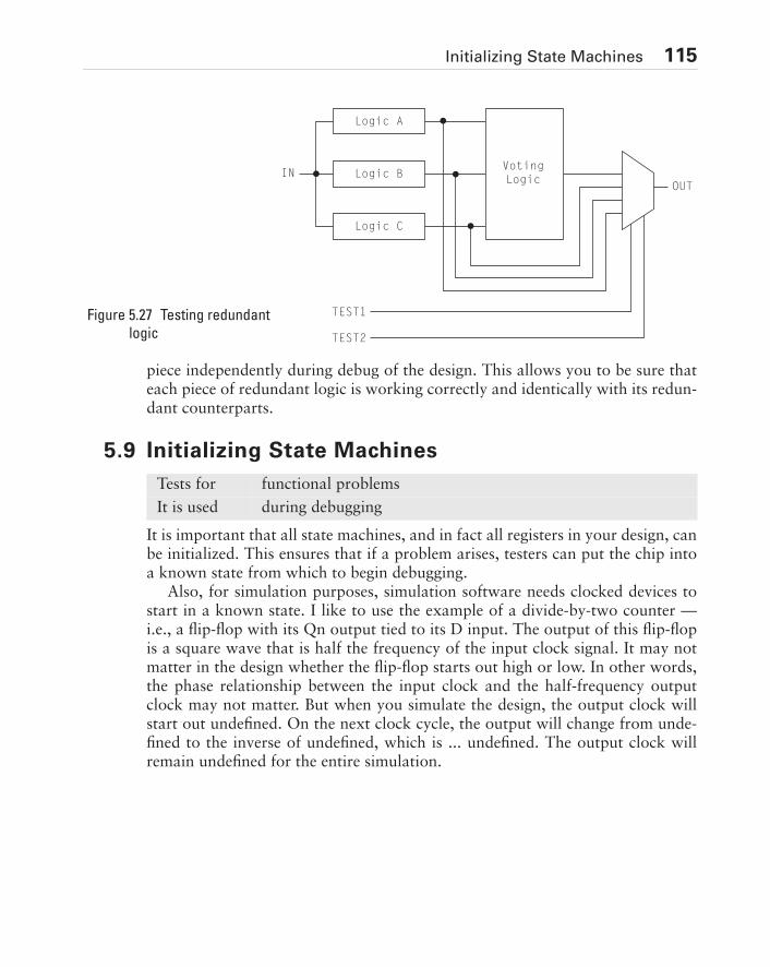
Initializing State Machines 115
piece independently during debug of the design. This allows you to be sure thateach piece of redundant logic is working correctly and identically with its redun-dant counterparts.
5.9 Initializing State Machines
It is important that all state machines, and in fact all registers in your design, canbe initialized. This ensures that if a problem arises, testers can put the chip intoa known state from which to begin debugging.
Also, for simulation purposes, simulation software needs clocked devices tostart in a known state. I like to use the example of a divide-by-two counter —i.e., a flip-flop with its Qn output tied to its D input. The output of this flip-flopis a square wave that is half the frequency of the input clock signal. It may notmatter in the design whether the flip-flop starts out high or low. In other words,the phase relationship between the input clock and the half-frequency outputclock may not matter. But when you simulate the design, the output clock willstart out undefined. On the next clock cycle, the output will change from unde-fined to the inverse of undefined, which is ... undefined. The output clock willremain undefined for the entire simulation.
VotingLogic
IN
TEST1
TEST2
OUT
Logic C
Logic B
Logic A
Figure 5.27 Testing redundant
logic
Tests for functional problems
It is used during debugging
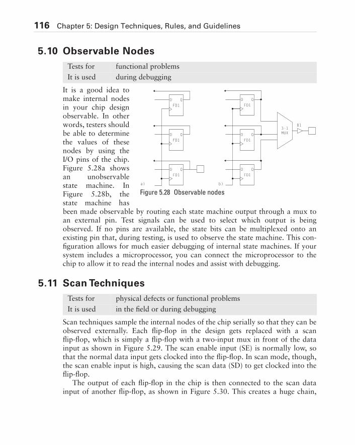
116 Chapter 5: Design Techniques, Rules, and Guidelines
5.10 Observable Nodes
It is a good idea tomake internal nodesin your chip designobservable. In otherwords, testers shouldbe able to determinethe values of thesenodes by using theI/O pins of the chip.Figure 5.28a showsan unobservablestate machine. InFigure 5.28b, thestate machine hasbeen made observable by routing each state machine output through a mux toan external pin. Test signals can be used to select which output is beingobserved. If no pins are available, the state bits can be multiplexed onto anexisting pin that, during testing, is used to observe the state machine. This con-figuration allows for much easier debugging of internal state machines. If yoursystem includes a microprocessor, you can connect the microprocessor to thechip to allow it to read the internal nodes and assist with debugging.
5.11 Scan Techniques
Scan techniques sample the internal nodes of the chip serially so that they can beobserved externally. Each flip-flop in the design gets replaced with a scanflip-flop, which is simply a flip-flop with a two-input mux in front of the datainput as shown in Figure 5.29. The scan enable input (SE) is normally low, sothat the normal data input gets clocked into the flip-flop. In scan mode, though,the scan enable input is high, causing the scan data (SD) to get clocked into theflip-flop.
The output of each flip-flop in the chip is then connected to the scan datainput of another flip-flop, as shown in Figure 5.30. This creates a huge chain,
Tests for functional problems
It is used during debugging
D Q
FD1
D Q
FD1
D Q
FD1
a)
B1
D Q
FD1
D Q
FD1
b)
3-1MUX
D Q
FD1
Figure 5.28 Observable nodes
Tests for physical defects or functional problems
It is used in the field or during debugging
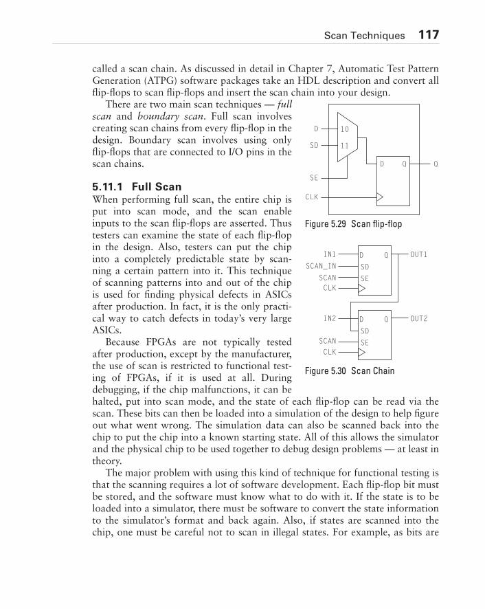
Scan Techniques 117
called a scan chain. As discussed in detail in Chapter 7, Automatic Test PatternGeneration (ATPG) software packages take an HDL description and convert allflip-flops to scan flip-flops and insert the scan chain into your design.
There are two main scan techniques — fullscan and boundary scan. Full scan involvescreating scan chains from every flip-flop in thedesign. Boundary scan involves using onlyflip-flops that are connected to I/O pins in thescan chains.
5.11.1 Full ScanWhen performing full scan, the entire chip isput into scan mode, and the scan enableinputs to the scan flip-flops are asserted. Thustesters can examine the state of each flip-flopin the design. Also, testers can put the chipinto a completely predictable state by scan-ning a certain pattern into it. This techniqueof scanning patterns into and out of the chipis used for finding physical defects in ASICsafter production. In fact, it is the only practi-cal way to catch defects in today’s very largeASICs.
Because FPGAs are not typically testedafter production, except by the manufacturer,the use of scan is restricted to functional test-ing of FPGAs, if it is used at all. Duringdebugging, if the chip malfunctions, it can behalted, put into scan mode, and the state of each flip-flop can be read via thescan. These bits can then be loaded into a simulation of the design to help figureout what went wrong. The simulation data can also be scanned back into thechip to put the chip into a known starting state. All of this allows the simulatorand the physical chip to be used together to debug design problems — at least intheory.
The major problem with using this kind of technique for functional testing isthat the scanning requires a lot of software development. Each flip-flop bit mustbe stored, and the software must know what to do with it. If the state is to beloaded into a simulator, there must be software to convert the state informationto the simulator’s format and back again. Also, if states are scanned into thechip, one must be careful not to scan in illegal states. For example, as bits are
D Q Q
10
11
D
SD
SE
CLK
Figure 5.29 Scan flip-flop
D Q
SD
SE
D Q
SD
SE
IN1
SCAN_IN
SCAN
CLK
IN2
SCAN
CLK
OUT1
OUT2
Figure 5.30 Scan Chain
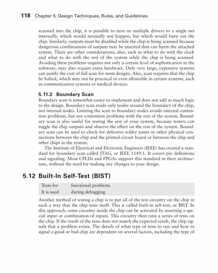
118 Chapter 5: Design Techniques, Rules, and Guidelines
scanned into the chip, it is possible to turn on multiple drivers to a single netinternally, which would normally not happen, but which would burn out thechip. Similarly, outputs must be disabled while the chip is being scanned becausedangerous combinations of outputs may be asserted that can harm the attachedsystem. There are other considerations, also, such as what to do with the clockand what to do with the rest of the system while the chip is being scanned.Avoiding these problems requires not only a certain level of sophistication in thesoftware, may also require extra hardware. Only very large, expensive systemscan justify the cost of full scan for most designs. Also, scan requires that the chipbe halted, which may not be practical or even allowable in certain systems, suchas communication systems or medical devices.
5.11.2 Boundary ScanBoundary scan is somewhat easier to implement and does not add as much logicto the design. Boundary scan reads only nodes around the boundary of the chip,not internal nodes. Limiting the scan to boundary nodes avoids internal conten-tion problems, but not contention problems with the rest of the system. Bound-ary scan is also useful for testing the rest of your system, because testers cantoggle the chip outputs and observe the effect on the rest of the system. Bound-ary scan can be used to check for defective solder joints or other physical con-nections between the chip and the printed circuit board or between the chip andother chips in the system.
The Institute of Electrical and Electronic Engineers (IEEE) has created a stan-dard for boundary scan called JTAG, or IEEE 1149.1. It covers pin definitionsand signaling. Most CPLDs and FPGAs support this standard in their architec-ture, without the need for making any changes to your design.
5.12 Built-In Self-Test (BIST)
Another method of testing a chip is to put all of the test circuitry on the chip insuch a way that the chip tests itself. This is called built-in self-test, or BIST. Inthis approach, some circuitry inside the chip can be activated by asserting a spe-cial input or combination of inputs. This circuitry then runs a series of tests onthe chip. If the result of the tests does not match the expected result, the chip sig-nals that a problem exists. The details of what type of tests to run and how tosignal a good or bad chip are dependent on several factors, including the type of
Tests for functional problems
It is used during debugging
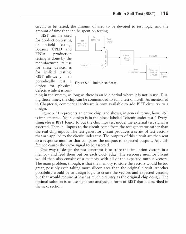
Built-In Self-Test (BIST) 119
circuit to be tested, the amount of area to be devoted to test logic, and theamount of time that can be spent on testing.
BIST can be usedfor production testingor in-field testing.Because CPLD andFPGA productiontesting is done by themanufacturer, its usefor these devices isfor in-field testing.BIST allows you toperiodically test adevice for physicaldefects while it is run-ning in the system, as long as there is an idle period where it is not in use. Dur-ing those times, the chip can be commanded to run a test on itself. As mentionedin Chapter 4, commercial software is now available to add BIST circuitry to adesign.
Figure 5.31 represents an entire chip, and shows, in general terms, how BISTis implemented. Your design is in the block labeled “circuit under test.” Every-thing else is BIST logic. To put the chip into test mode, the external test signal isasserted. Then, all inputs to the circuit come from the test generator rather thanthe real chip inputs. The test generator circuit produces a series of test vectorsthat are applied to the circuit under test. The outputs of this circuit are then sentto a response monitor that compares the outputs to expected outputs. Any dif-ference causes the error signal to be asserted.
One way to design the test generator is to store the simulation vectors in amemory and feed them out on each clock edge. The response monitor circuitwould then also consist of a memory with all of the expected output vectors.The main problem, though, is that the memory to store the vectors would be toogreat, possibly even taking more silicon area than the original circuit. Anotherpossibility would be to design logic to create the vectors and expected vectors,but that would require at least as much circuitry as the original chip design. Theoptimal solution is to use signature analysis, a form of BIST that is described inthe next section.
Figure 5.31 Built-in self-test
Inputs
Testgeneratorcircuit
Circuitundertest
Responsemonitorcircuit
1
0
Multiplexer
Testpatterns Test
signal
Testresponses
Errorsignal
Outputs
120 Chapter 5: Design Techniques, Rules, and Guidelines
5.13 Signature Analysis
A problem with the BIST technique, in general, is that the test generation andresponse monitoring circuitry can be extremely complex and take up a lot of sil-icon. Any test structure that is too large or complex ends up reducing the reli-ability of a design rather than increasing it, because now there is a significantchance that the test circuitry itself fails. Also, large test circuits increase the costof a chip, another unwanted effect.
Signature analysis avoids these problems. BIST designs based on signatureanalysis use a test generation circuit that creates a pseudorandom sequence oftest vectors. “Pseudorandom” means that the test vectors are distributed asthough they were random, but they are actually predictable and repeatable. Theresponse monitor takes the sequence of output vectors and compresses theminto a single vector. This final compressed output vector is called the chip’s sig-nature. Although this type of testing is not exhaustive, if done right it can detecta very large number of failures. It is also possible that a nonworking chip willproduce a correct signature, but if the number of bits in the signature is large,the probability of a bad device producing a good signature is very small.
Another significant advantage of signature analysis is that the pseudorandomnumber generation and the output vector compression can both be performedby a linear feedback shift register (LFSR), which is a very small device — simplya shift register and several XOR gates. Almost no silicon area is given up, andthus almost no additional cost is involved.
5.14 SummaryIn this chapter, I have laid out specific design rules and guidelines that increaseyour chances of producing a working, reliable device — one that will work fordifferent chip vendor processes and continue to work for the lifetime of yoursystem. I have shown a number of examples of incorrect or inefficient designs,and the equivalent function designed correctly.
Specifically, after reading this chapter, you should be acquainted with theseCPLD and FPGA design issues:
• Hardware description languages and different levels of design modeling.
• Top-down design, an approach to designing complex chips that allows you tobetter utilize or implement these important design capabilities:
• Use of HDLs
Tests for physical defects
It is used in the field
Summary 121
• Written specifications
• Allocating resources
• Design partitioning
• Flexibility and optimization
• Reusability
• Floorplanning
• Verification
• The significance of architectural differences and how they affect designtrade-offs.
• Synchronous design — A requirement for creating devices that will functionreliably over their entire lifetimes.
• Floating nodes — A condition that must be avoided in order to avoid excessnoise and power consumption.
• Bus contention — Another condition that must be avoided to increase thelong-term reliability of your chip.
• One-hot state encoding — A method of designing state machines that takesadvantage of the architecture of FPGAs.
• Testing redundant logic — Why it’s important and the typical design struc-tures for implementing such tests.
• Initializing state machines — Designing a chip so that all internal statemachines are initialized.
• Observable nodes — Bringing internal nodes to external pins so that theinternal states of the chip can be observed.
• Scan techniques — Connecting flip-flops inside the chip (either boundarynodes, or both boundary and internal nodes) into one or more chains so thatyou can easily get 100 percent fault coverage to guard against manufacturingproblems.
• Built-in self-test (BIST) — A method of including circuitry inside a chip thatlets it test itself for physical problems.
• Signature analysis — A method using linear feedback shift registers (LFSRs)to simplify BIST circuitry.
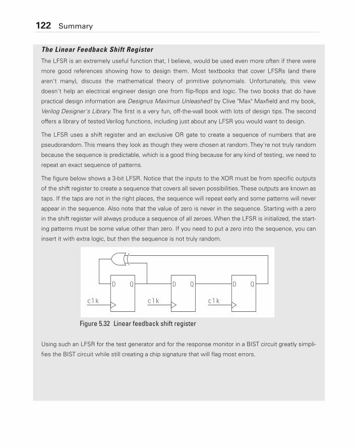
122 Summary
The Linear Feedback Shift Register
The LFSR is an extremely useful function that, I believe, would be used even more often if there were
more good references showing how to design them. Most textbooks that cover LFSRs (and there
aren't many), discuss the mathematical theory of primitive polynomials. Unfortunately, this view
doesn't help an electrical engineer design one from flip-flops and logic. The two books that do have
practical design information are Designus Maximus Unleashed! by Clive "Max" Maxfield and my book,
Verilog Designer's Library. The first is a very fun, off-the-wall book with lots of design tips. The second
offers a library of tested Verilog functions, including just about any LFSR you would want to design.
The LFSR uses a shift register and an exclusive OR gate to create a sequence of numbers that are
pseudorandom. This means they look as though they were chosen at random. They're not truly random
because the sequence is predictable, which is a good thing because for any kind of testing, we need to
repeat an exact sequence of patterns.
The figure below shows a 3-bit LFSR. Notice that the inputs to the XOR must be from specific outputs
of the shift register to create a sequence that covers all seven possibilities. These outputs are known as
taps. If the taps are not in the right places, the sequence will repeat early and some patterns will never
appear in the sequence. Also note that the value of zero is never in the sequence. Starting with a zero
in the shift register will always produce a sequence of all zeroes. When the LFSR is initialized, the start-
ing patterns must be some value other than zero. If you need to put a zero into the sequence, you can
insert it with extra logic, but then the sequence is not truly random.
Using such an LFSR for the test generator and for the response monitor in a BIST circuit greatly simpli-
fies the BIST circuit while still creating a chip signature that will flag most errors.
D Q D QD Q
clk clk clk
Figure 5.32 Linear feedback shift register

Exercises 123
Exercises
1. The term HDL stands for
(a) Hardware description language
(b) High dollar lovin’
(c) Hardware development language
(d) High level design language
2. Match the model level on the left with the correct description on the right.
3. Which of the following HDL levels are considered behavioral levels?
(a) Switch level
(b) Algorithmic level
(c) Gate level
(d) Architectural level
(e) Register transfer level
4. Which of the following HDL levels are considered structural levels?
(a) Switch level
(b) Algorithmic level
(c) Gate level
(d) Architectural level
(e) Register transfer level
(a) Algorithmic A. Describes a design in terms of mathematical functionality.
(b) Architectural B. Describes a design in terms of basic logic, such as NANDs and NORs.
(c) Register transfer level C. Describes a design in terms of transistors and basic electronic components.
(d) Gate level D. Describes a design in terms of functional blocks.
(e) Switch level E. Describes a design in terms of Boolean logic and storage devices.

124 Chapter 5: Design Techniques, Rules, and Guidelines
5. Select all of the statements that are true about top-down design.
(a) Allows better allocation of resources
(b) Allows each small function to be simulated independently
(c) Speeds up simulations
(d) Facilitates behavioral modeling of the device
(e) Results in lower power consumption designs
(f) Allows a design to be split efficiently among the various team members
6. Select the five rules of synchronous design.
(a) Data signals must go only to combinatorial logic or data inputs of flip-flops.
(b) All data is passed through combinatorial logic and flip-flops that are synchro-nized to a single clock.
(c) Clocks cannot be gated — in other words, clocks must go directly to the clockinputs of the flip-flops without going through any combinatorial logic.
(d) No combinatorial logic can have more than eight inputs.
(e) Clock signals traces must be equal length to each flip-flop in the design.
(f) No two logic gates can be connected together without a flip-flop between them.
(g) All combinatorial logic must have a smaller delay than the worst-case setup timeof the slowest flip-flop in the circuit.
(h) No signal that is generated by combinatorial logic can be fed back to the samecombinatorial logic without first going through a synchronizing flip-flop.
(i) Delay is always controlled by flip-flops, not combinatorial logic.
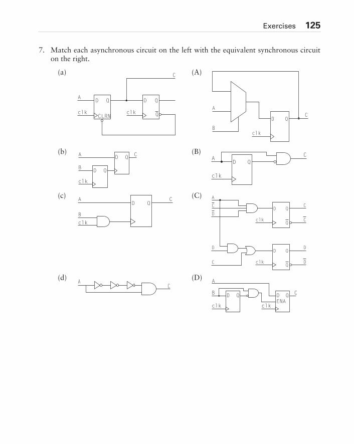
Exercises 125
7. Match each asynchronous circuit on the left with the equivalent synchronous circuiton the right.
(a) (A)
(b) (B)
(c) (C)
(d) (D)
clk
D Q
CLRN
D Q
Qclk
A
C
clk
D Q
A
B
C
A CD Q
D Q
clk
B
CA
clk
D Q
clk
B
A CD Q
A
D
C
C
DD Q
Qclk
D
D
D Q
Qclk
C
C
AC
clk
A
C
clk
B D QENAD Q

126 Chapter 5: Design Techniques, Rules, and Guidelines
8. Select TRUE or FALSE for the following statements.
(a) TRUE or FALSE: Synchronizing flip-flops are used to eliminate metastability.
(b) TRUE or FALSE: In theory, a device can remain metastable forever.
(c) TRUE or FALSE: The chances of a device going metastable increases with higherclock frequencies.
(d) TRUE or FALSE: The chances of a device going metastable decreases withhigher input voltage thresholds.
(e) TRUE or FALSE: Schmidt trigger inputs with hysteresis can eliminate metasta-bility.
(f) TRUE or FALSE: Metastability is caused by faulty circuits.
(g) TRUE or FALSE: Metastability is caused by asynchronous signals coming intosynchronous circuits.
9. Check all allowable uses of asynchronous logic.
(a) To latch inputs from and outputs to an asynchronous bus as long as the signalsare synchronized for use inside the design.
(b) For logic that must be extremely fast.
(c) Asynchronous reset if it is done according to specific rules.
(d) For designs that must save on power consumption.
10. Select TRUE or FALSE for the following statements:
(a) TRUE or FALSE: Floating buses can create signal noise.
(b) TRUE or FALSE: Floating buses can cause extra power consumption.
(c) TRUE or FALSE: Floating buses should be avoided in your design.
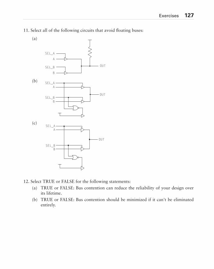
Exercises 127
11. Select all of the following circuits that avoid floating buses:
12. Select TRUE or FALSE for the following statements:
(a) TRUE or FALSE: Bus contention can reduce the reliability of your design overits lifetime.
(b) TRUE or FALSE: Bus contention should be minimized if it can't be eliminatedentirely.
(a)
(b)
(c)
OUT
SEL_A
A
SEL_B
B
OUT
SEL_AA
SEL_BB
OUT
SEL_AA
SEL_BB
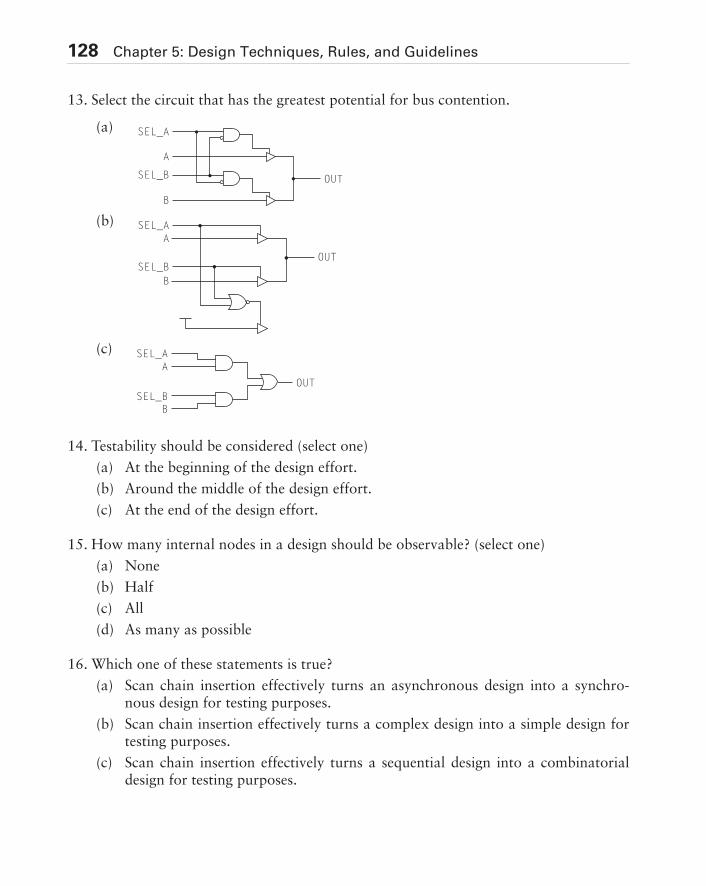
128 Chapter 5: Design Techniques, Rules, and Guidelines
13. Select the circuit that has the greatest potential for bus contention.
14. Testability should be considered (select one)
(a) At the beginning of the design effort.
(b) Around the middle of the design effort.
(c) At the end of the design effort.
15. How many internal nodes in a design should be observable? (select one)
(a) None
(b) Half
(c) All
(d) As many as possible
16. Which one of these statements is true?
(a) Scan chain insertion effectively turns an asynchronous design into a synchro-nous design for testing purposes.
(b) Scan chain insertion effectively turns a complex design into a simple design fortesting purposes.
(c) Scan chain insertion effectively turns a sequential design into a combinatorialdesign for testing purposes.
(a)
(b)
(c)
SEL_A
SEL_B OUT
A
B
OUT
SEL_AA
SEL_BB
OUT
SEL_AA
SEL_BB

Exercises 129
17. Which of the following structures is not required for BIST?
(a) Multiplexer
(b) Response monitor
(c) Linear feedback shift register (LFSR)
(d) Test pattern generator
18. The 10/10 rule of testing is:
(a) You should test 10 times every 10 days.
(b) You should have 10 tests for every 10 percent of the design.
(c) Testing circuitry should not up take more than 10 percent of the total circuitryand should not require more than 10 percent of the design and debug time.

130 Chapter 5: Design Techniques, Rules, and Guidelines
This Page Intentionally Left Blank
131
Chapter 6
VerificationThis chapter deals with verification, a group of methods and techniques used todetect design errors before a chip is created. This chapter describes the activitiesthat are part of the verification process, including how to design testability intoa chip and how to fully simulate a chip to ensure that it will function correctly ina completed system. The importance of and effort committed to verification isgrowing as CPLD and FPGA designs increase in size. In recent projects, I’vefound that more manpower is designated for verification than any other phaseof the project. Also, all kinds of EDA tools are coming to the market to helpwith verification. Some of these tools are generic tools, and others are specifi-cally for certain types of chips.
The EDA tools that enable many of the techniques in this chapter aredescribed in detail in Chapter 7.
Objectives
• Understand the use of functional and multilevel simulation for catchingdesign flaws
• Understand the need for regression testing to ensure that changes do notbreak the design.
• Learn how you can use static timing analysis to very quickly examine adesign and determine the maximum frequency and flag all critical paths.
In this chapter...
• Defining verification
• Simulation
• Static timing analysis
• Assertion languages
• Formal verification
132 Chapter 6: Verification
• Discover uses of assertion languages for simulation and formal verification.
• Learn where formal verification is appropriate and learn the differencebetween equivalency checking and functional verification.
6.1 What is Verification?The term “verification” is a little nebulous. In the larger domain of IC design,“verification” generally refers to any technique that is used to verify that thechip will work correctly. These can include simulating the functionality of thechip, performing a timing analysis of the chip, running a formal verification ofthe design, emulating the chip, prototyping the chip, creating test vectors forautomatic test equipment (ATE), writing software tests for in-system testing,and running long tests on the chip in the system. Not all of these techniques areapplicable to programmable devices, though, and I cover only those that areapplicable.
As chip sizes have grown large, in terms of gates and functionality, verifica-tion has become the part of the design process that usually requires the mosttime and manpower. Verification is an extremely important consideration inchip design because a chip cannot be blue-wired after production. For this rea-son, teams must perform simulation extensively before the chip is sent for fabri-cation. Verification has become an extremely important aspect of the designprocess that needs to be optimized.
6.2 SimulationPerhaps the most important tool for chip verification is simulation. Simulationcan save many frustrating hours debugging a chip in your system. Doing a goodjob at simulation uncovers errors before they are set in silicon, and can helpdetermine that your chip will function correctly in your system.
Designers of programmable devices sometimes rush through or ignore thesimulation phase of a design due to pressures to get a chip in a system. Some-times the thinking is that the device will be placed in a board so that other mem-bers of the design team can debug the rest of the bug and so that softwaredevelopment can begin. Unfortunately, FPGAs in particular are very difficult tochange once a pinout has been selected. FPGA software often has a difficult timeplacing logic within a chip and routing it when constraints exist. Pin placementis a definite constraint.
Also, skipping or postponing the simulation phase can result in a chip in yoursystem that has significant problems. The engineers debugging the system or thesoftware may end up fighting bugs in the chip that could have been discoveredduring simulation. My advice is to simulate a programmable chip as fully aspossible before setting its pinout or committing it to a board.
Simulation 133
6.2.1 Functional SimulationFunctional simulation involves simulating the functionality of a device to deter-mine that it is working the way the specification describes and that it will pro-duce correct results within your system. This type of simulation is importantinitially in order to get as many bugs out of the device as possible and to deter-mine that the chip will work correctly in your system.
When performing functional simulation, knowing how much simulation toperform and when to stop is sometimes difficult. It’s not possible to simulate allpossible combinations of inputs. One measure of simulation effectiveness, calledcode coverage, measures the percentage of the HDL statements that are exer-cised in all possible ways during simulation. As an example of “all possibleways,” consider simulating an if-then statement. The simulation achieives fullcode coverage only if it simulates both conditions of the statement— one wherethe condition is true and the statement is executed, and one where the conditionis false and the statement is not executed.
Some software tools calculate code coverage, and you should at least have100 percent coverage before feeling good about the simulation. Even 100 per-cent coverage can still leave many potential faults uncovered, but it signifies thateach state machine has been simulated and no part of the circuit has gone unex-amined.
Why Verify When I Can Reprogram?
One question that inevitably arises is “Why do I need to spend so much time simulating and verifying
my design if I can simply reprogram the chip whenever I need to?” There are a lot of answers to this
question. The first one is that verifying a chip extensively before putting it in a system is simply a
smart thing to do. Problems with the chip can range from minor functional problems to major electri-
cal problems that can potentially destroy the system in which it is used. A second answer is that a
verification environment allows you to control every input to the device in very specific ways. This
means that you can test functionality repeatedly until it is correct. You can create tests that exercise
various functions of the chip in different situations. A real system rarely has this kind of controllability
and repeatability. Finally, when a design is committed to a programmable device, and that device is
soldered onto a circuit board, certain constraints are put on the design. Most notably, the pins of the
device are then constrained to specific locations. The more constraints imposed on a specific design,
especially I/O pin locations, the more difficult it is to make changes, even minor ones, to the place-
ment and routing of the design. The placement and routing algorithms often have problems with
small changes because the layout then becomes more difficult to optimize. Even when the place-
ment and routing can be changed, the routing change is often accompanied by a significant change in
the internal chip timing.
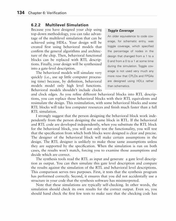
134 Chapter 6: Verification
6.2.2 Multilevel SimulationBecause you have designed your chip usingtop-down methodology, you can take advan-tage of the multilevel simulation that can beachieved using HDLs. Your design will becreated first using behavioral models thatconfirm the general algorithms and architec-ture of the chip. Then, behavioral functionalblocks can be replaced with RTL descrip-tions. Finally, your design will be synthesizedinto a gate-level description.
The behavioral models will simulate veryquickly (i.e., use up little computer process-ing time) because, by definition, behavioralmodels model only high level functions.Behavioral models shouldn’t include clocksand clock edges. As you refine different behavioral blocks into RTL descrip-tions, you can replace those behavioral blocks with their RTL equivalents andresimulate the design. This resimulation, with some behavioral blocks and someRTL blocks will take less computer resources and finish much faster than a fullRTL simulation.
I strongly suggest that the person designing the behavioral block work inde-pendently from the person designing the same block in RTL. If the behavioraland RTL code are developed independently, when you substitute the RTL blockfor the behavioral block, you will not only test the functionality, you will testthat the specification from which both blocks were designed is clear and precise.The designer of the behavioral block will make certain assumptions in thedesign. The RTL designer is unlikely to make those same assumptions unlessthey are supported by the specification. When the simulation is run on bothcases, the results won’t match, forcing you to examine those assumptions anddecide which are correct.
The synthesis tools read the RTL as input and generate a gate level descrip-tion as output. You can then simulate this gate level description and comparethe results against the simulation of the RTL and behavioral level descriptions.This comparison serves two purposes. First, it tests that the synthesis programhas performed correctly. Second, it ensures that you did not accidentally use astructure in your code that the synthesis software has misinterpreted.
Note that these simulations are typically self-checking. In other words, thesimulation should check its own results for the correct output. Even so, youshould hand check the first few tests to make sure that the checking code has
Toggle Coverage
An older equivalence to code cov-
erage, for schematic entry, was
toggle coverage, which specified
the percentage of nodes in the
design that changed from a 1 to a
0 and from a 0 to a 1 at some time
during the simulation. Toggle cov-
erage is not used very much any
more now that CPLDs and FPGAs
are designed using HDLs rather
than schematics.
Simulation 135
been written correctly. Also, spot check simulations by hand from time to timeto make sure that they are not passing off bad data as good.
Until basic flaws are eliminated and the basic functionality seems correct, thepieces of the design (especially of the RTL-level version) should be simulated assmall independent blocks, each excercised separately from the entire design.This approach speeds up the debug process because each simulation will be con-cerned with only its small block of code and will not be affected by other blocksin the design – blocks that may or may not be working correctly. For these smallscale simulations, it is reasonable to check for low-level functionality, for exam-ple, that specific events occur on specific clock edges. Once you have determinedthat the small block seems to be working, you can put it into the larger designand simulate the entire chip consisting of a combination of RTL and behavioralblocks.
The simulations of the entire chip should check for high-level functionality.For example, a simulation of an Ethernet switch might check that all incomingpackets were retransmitted, though the simulation would probably not be con-cerned with the exact ordering or latency of the packets. Such a simulationwould also not be checking for specific events on specific clock edges. As thedesign evolves, specific events may change, but the overall functionality shouldremain fairly constant.
6.2.3 Regression TestingRegression testing involves repeatedly running a set of simulation tests on adesign that has been modified, to ensure that the modifications have not intro-duced new bugs. Regression testing is often initiated after a designer hasattempted to fix a bug or has added a new function to the design that may haveinadvertently introduced errors. Regression tests are a quality control measureto ensure that the newly-modified code still complies with its specified require-ments and that unmodified code has not been affected by the new code. Withregard to the type of tests, regression tests typically represent the major func-tionality of the design and also several extreme situations known as “cornercases.”
Corner cases are situations where extreme things are happening to the logicin the chip. Corner cases represent conditions most likely to make the chip fail.Examples of extreme cases include situations where an internal buffer gets filledand there is an attempt to write one more piece of data. Another example is anattempt to read an empty FIFO. Situations where several signals get assertedsimultaneously could be a corner case. The designer is often a good person todetermine some corner cases. On the other hand, outsiders (who bring fewer
136 Chapter 6: Verification
assumptions to the test process) can often come up with good tests for cornercases — tests that might not be obvious to the designer.
Regression tests, consisting of the main functional tests and corner case tests,are repeatedly run against the design to determine that it is working correctly.Whenever a new section of logic or other modification is completed the design-ers should run these tests again to determine that nothing broke. After synthesis,designers need to run the regression tests to determine that the synthesizeddesign is functionally equivalent to the original design. Though formal verifica-tion programs, specifically for equivalence checking, are available that can logi-cally compare two design descriptions for equivalence, designers typically useregression testing for anything other than minor changes to a design description.This is particularly true when a design has undergone major changes that makeit similar but not identical to the previous design.
6.2.4 Timing SimulationTiming simulations are simply functional simulations with timing information.The timing information allows the designer to confirm that signals change in thecorrect timing relationship with each other. There is no longer any reason to per-form timing simulations on a fully synchronous design.
As chips become larger, this type of compute-intensive simulation takeslonger and longer to run. Even so, these simulations cannot simulate every pos-sible combination of inputs in every possible sequence; many transitions thatresult in problems will be missed. This means that certain long delay paths neverget evaluated and a chip with timing problems can still pass timing simulation.
Instead, fully synchronous designs should be evaluated using a software toolcalled a static timing analyzer, which is described in the next section.
6.3 Static Timing AnalysisStatic timing analysis is a process that examines a synchronous design and deter-mines its highest operating frequency. Static timing analysis software considersthe path from every flip-flop in the design to every other flip-flop to which it isconnected through combinatorial logic. The tool calculates all best-case andworst-case delays through these paths. Any paths that violate the setup or holdtiming requirements of a flip-flop, or that are longer than the clock period for agiven clock frequency, are flagged. These paths can then be adjusted to meet thedesign requirements. Any asynchronous parts of the design (they should be few,if any) must be examined by hand.
Assertion Languages 137
6.4 Assertion LanguagesAssertion languages are used to check properties of a design during simulationand during formal verification. Assertions allow designers to check that certain“invariant” properties or behaviors are consistently present. For example, asequence of events that must always occur in a specific order could be checkedwith an assertion. These assertions may be legal or illegal conditions in thedesign. For example, a legal condition may be that all state machines are initial-ized when the reset signal is asserted. An illegal condition may be that two buff-ers are simultaneously driving a three-state bus.
For simulation, these tools allow you to check the inputs and outputs of adevice, and often the internal states of the device. During simulation, theseassertions confirm that events are occurring when they should, or they notify theuser when illegal events occur or illegal states are entered by the design.
For formal verification, which I discuss in the next section, assertions areused for verifying that two design descriptions are equivalent by comparing thesequence of events and the internal states for both devices during simulation.
6.5 Formal VerificationFormal verification is the process of mathematically checking that a design isbehaving correctly. There are two types of formal verification: equivalencychecking and functional verification.
6.5.1 Equivalency CheckingEquivalency checking is the process of comparing two different design descrip-tions to determine whether they are equivalent. Design descriptions go throughmany different transformations. These include manual tweaking of a design bythe design engineers, and also include the normal transformations required bythe design process. Of these normal transformations, synthesis is the one that alldesigns must go through. Equivalency checking software can determine whetherthe RTL description that was input to the synthesis software is functionallyequivalent to the gate level description that is output. Other types of transfor-mations to the design occur when designers add BIST logic or scan logic, forexample, or when designers perform any kind of automatic optimization. Equiv-alency checking is useful to make sure that functionality is not accidentallychanged in any of these situations and, if an unintentional change occurs, thesoftware can point the engineer to the malfunctioning part of the design.
138 Chapter 6: Verification
6.5.2 Functional VerificationFunctional verification is the process of proving whether specific conditions,called properties or assertions, occur in a design. These assertions may be legalor illegal conditions in the design. For example, a legal condition may be that aFIFO must assert the full signal when all locations in the FIFO have valid data.An illegal condition may be an assertion that the FIFO within a design can over-flow. These assertions are written by an engineer, using an assertion language, asdescribed in Section 6.4. A functional verification tool then determines, mathe-matically and rigorously, whether these condition could possibly occur underany legal situations. Functional verification tools must check that all legal asser-tions do occur and that all illegal assertions cannot occur.
6.6 SummaryThis chapter defines one of the most significant, and resource consuming, stepsin the design process — verification. Though simulation is central to most verifi-cation methods, the goal of this simulation is to test the functionality of thedesign, sometimes against the design specs, and sometimes against another ver-sion of the design. The major tools and strategies used in verification are:
• Functional simulation — Needed for verifying the correct functionality ofyour chip.
• Multilevel simulation — Simulation performed at different levels of abstrac-tion — behavioral level, RTL, and gate level — in order to speed up the sim-ulation effort, verify that your chip meets its specifications, and confirm thatsynthesis tools did not alter your design.
• Regression testing — Needed to confirm that all necessary functionality hasbeen simulated and that any changes to your design have not affected previ-ously simulated functionality.
• Timing simulation — Time consuming, inaccurate, and has been renderedobsolete by static timing analysis programs.
• Static timing analysis — Used to check the timing numbers for your designand verify that it will operate at the specified clock frequency or flag anypaths that do not meet your timing requirements.
• Assertion languages — Enables you to set conditions and properties of yourdesign in the HDL code so that software can determine whether these condi-tions can possibly be met and whether the properties are true.
• Formal verification — Allows you to mathematically verify the functionalityof a design and verify that two design descriptions are functionally equiva-lent.
Exercises 139
Exercises
1. What is meant by the term "functional simulation?"
(a) Simulating how a design functions, without regard to timing
(b) Simulating the functional equivalence of a design
(c) Simulating the mathematical function that is represented by the design
2. What is meant by the term "toggle coverage?"
(a) The number of nodes in a design that change state during simulation as a per-centage of the total number of nodes
(b) The number of nodes in a design that change state from 0 to 1 and from 1 to 0during simulation as a percentage of the total number of possible state transi-tions
(c) The number of nodes in a design that change state from 0 to 1 and from 1 to 0during simulation as a percentage of the total number of nodes
3. What is meant by the term "code coverage?"
(a) The percentage of code statements in a design that change state from 0 to 1 andfrom 1 to 0 during simulation as a percentage of the total number of code state-ments
(b) The percentage of code statements in a design that have been executed duringsimulation
(c) The percentage of code statements in a design that have been executed duringsimulation in every possible manner
4. What is meant by the term "timing simulation?"
(a) A process that looks at a synchronous design and determines the highest operat-ing frequency that does not violate any setup and hold times
(b) A simulation that includes timing delays
(c) A process that looks at an asynchronous design and fixes all critical paths to bewithin a certain time constraint
5. Why is timing simulation typically no longer done for a design?
(a) Timing simulation does not produce accurate timing results.
(b) Timing simulation software is not reliable.
(c) Static timing analysis is a faster, more exhaustive analysis of whether a designmeets its timing requirements.

140 Chapter 6: Verification
6. What is meant by the term "static timing analysis?"
(a) A process that looks at a synchronous design and determines the highest operat-ing frequency that does not violate any setup and hold-times
(b) A simulation that includes timing delays
(c) A process that looks at an asynchronous design and fixes all critical paths to bewithin a certain time constraint
7. What are the two types of formal verification?
(a) Functional verification and equivalency checking
(b) Functional checking and equivalency timing
(c) Static verification and dynamic verification
(d) Functional checking and equivalency verification
141
Chapter 7
Electronic Design Automation Tools
Electronic design automation (EDA) tools are an extremely important factor inthe design of CPLDs and FPGAs. Initially, PAL vendors and manufacturers ofdesktop devices for programming PALs provided some very simple HDLs forcreating simple designs. Special simulation tools were created to simulate thesesimple programmable devices. EDA tool vendors added simple features thatallowed engineers to use the tools to develop these simple devices.
When more complex devices, CPLDs and FPGAs, arrived on the scene, sche-matic capture tools were adapted to create designs for these devices. When thetools did not provide the design engineer with enough features to take advan-tage of device architectures that were growing in complexity, CPLD and FPGAvendors created their own tools.
Eventually, two realizations among programmable device vendors and EDAsoftware tool vendors changed the landscape for these software tools. First,device vendors realized that better, cheaper tools sold their products. When anengineer was deciding on a device to use in his design, the software tools forenabling that design were often just as important as the architecture, size, andtechnology of the device itself. The device vendors that discovered this fact toolate were relegated to the role of niche players; many of them are now out ofbusiness or still trying to catch up to the big players.
In this chapter...
• Software tools for simulation
• Tools for synthesis, formal
verification, place and route,
and floorplanning
• Testbench, scan insertion,
and built-in self-test (BIST)
generators
• In situ and programming
tools
• Static timing analysis
142 Chapter 7: Electronic Design Automation Tools
The other realization, by the software tool vendors, was that these newdevices needed their own set of tools in order to take full advantage of theirtechnologies and architectures. It wasn’t good enough to simply add switchesand parameters to existing tools. This realization came late to some of the bigEDA companies, allowing smaller startups to establish themselves in this new,growing market.
Objectives
• Learn how to evaluate and choose appropriate software tools to simplify andexpedite the design process.
• Understand and utilize testbench and built-in self-test (BIST) generators totest your chip during the design process.
• Learn about other tools and techniques to aid in your chip design.
7.1 Simulation SoftwareSimulation software allows you to exercise the functionality of a design in orderto test whether it will work correctly in the intended system. Many vendors pro-vide simulation software. Because CPLD and FPGA designs are now commonlycreated using an HDL, as are ASICs, you can use the same simulation tools forany of these devices.
Ironically simulators use four signal values to simulate binary logic. First arethe two binary states of 1 and 0. However, because the goal is to simulate realhardware, not ideal logic circuits, the simulator tracks non-ideal states as well.The two additional states typically are represented by the symbols Z and X. A Zor “floating” signal represents a high impedance value. When no device is driv-ing a a signal line, the line will be assigned the value Z. An X represents anundefined state. When the simulator cannot determine which of the other threestates to assign to the signal, it will mark it X. This usually means that there is aproblem with the design. An X state could mean that two devices are simulta-neously driving a signal and that one device is attempting to drive it to a 1 valuewhile the other device is attempting to drive it to a 0 value.
Some simulators also have additional states that can be assigned to signals todistinguish specific undefined states or to give the user more information aboutthe hardware that is driving a signal. The high output of a buffer may be given avalue that represents a “strong” 1, whereas a pull-up resistor on a signal may beassigned a value that represents a “weak” 1. However, with a digital circuit,especially in an FPGA where the user has little control over the specific hard-ware used to implement a logic function, these intermediate values give onlymarginal extra information and are rarely used.
Simulation Software 143
Simulators also have the capability to aggregate signals into buses and repre-sent them as numbers. For example, simulators can aggregate eight signals intoa single 8-bit number and represent it in hex or decimal. This capability makes iteasier to view buses as bytes or addresses, but has no effect on the actual opera-tion of the circuit.
Altera Catches Up To Xilinx
Xilinx was the inventor of the FPGA, and for years was the only company offering these devices in
any significant numbers. Xilinx had easily captured the small but growing FPGA market. As the
market grew, CPLD vendors began to offer their own FPGAs, but Xilinx was able to maintain about
a 70 percent market share for a number of years.
Then along came Altera. Altera had been successfully selling CPLDs for years when it entered the
FPGA market with its own device. As you will see in Section 7.10, place and route software is typi-
cally supplied by the FPGA vendor. Xilinx had been providing a place and route tool and charging a
pretty high price for it. Their philosophy was that Xilinx was the market leader, and thus the major-
ity of engineers needed their version of the tool and should pay for it. Altera realized that it could
use the software tools to sell the hardware. After all, they were a hardware company — not a soft-
ware company. So Altera created a nice integrated package of EDA tools and offered it at a very
low price. Engineers loved it, and for the first time in years, a company was able to take market
share away from Xilinx.
A personal example of how well this strategy worked was that when Altera started offering their
tools, I got a phone call from a local representative. She told me that consultants were being given
the entire software package for free and they just needed my shipping address. They realized that
I would gain expertise in their tools, recommend their parts in designs, and they would sell more
chips.
I called up Xilinx and told them about this deal. I explained that when a client called me up to do a
design I could tell them that I could start on an Altera design today, or the client could purchase
the Xilinx tools and I could learn them and start the design in a couple of weeks. Which vendor do
you think the client would chose? The Xilinx sales rep said they would choose the market leader
and offered me a 50 percent discount on the tools, which I turned down.
Several years later, when Altera had actually surpassed Xilinx in market share, Xilinx woke up and
began producing much better software at competitive prices. In fact, I later talked to an application
engineer at Xilinx and once again mentioned that Altera had given me their tools for free. The next
day I found a package at my doorstep containing a full suite of Xilinx software.
144 Chapter 7: Electronic Design Automation Tools
Listing 7.1 shows Verilog code for verifying a circuit that performs a cyclicredundancy check (CRC). Note that the code in the figure does not perform theCRC itself. The code in the figure consists of a module called crc_sim() thattests that some other module, called crc(), performs a CRC correctly. Thiscrc_sim() module is called a testbench because it applies stimuli to a hardwaredesign to test whether the hardware design works correctly. The crc_sim() test-bench module and the crc() hardware module are compiled together and thensimulated together. I do not expect you to understand the details of the Verilogcode — that is beyond the scope of this book — but notice the $display state-ments in the code. These statements allow text to be output to the screen duringsimulation in order to debug the design.
Listing 7.1 CRC generator testbench
/*********************************************************/
// MODULE: CRC simulation
//
// FILE NAME: crc_sim.v
// VERSION: 1.0
// DATE: January 1, 1999
// AUTHOR: Bob Zeidman, Zeidman Consulting
//
// CODE TYPE: Simulation
//
// DESCRIPTION: This module provides stimuli for simulating
// a CRC generator/verifier. It creates a large, random,
// frame of data which is shifted through an LFSR to produce
// an FCS which is appended to the frame. In every even
// frame, a single bit is corrupted. Each frame, with the
// appended FCS, is then shifted through the LFSR again. For
// uncorrupted frames, the LFSR is expected to contain zero
// at the end. For corrupted frames, the LFSR is expected to
// have a non-zero value.
//
/*********************************************************/
// DEFINES
`define FCS 8 // Number of bits in the fcs
`define FRAME 128 // Number of bytes in the frame
Simulation Software 145
`define BFRAME (`FRAME*8) // Number of bits in the frame
`define TOT_BITS (`BFRAME+`FCS) // Total number of bits
// including frame and FCS
`define FRAME_CNT 16 // Number of frames to test
// TOP MODULE
module crc_sim();
// INPUTS
// OUTPUTS
// INOUTS
// SIGNAL DECLARATIONS
reg clk;
reg reset;
wire bit_in;
wire [`FCS-1:0] fcs;
integer cycle_count; // Counts clock cycles
integer frame_count; // Counts frames
reg [`TOT_BITS-1:0] frame_data; // Frame data bits
reg gen_check; // Generate/check CRC
// = 1 to generate CRC
// = 0 to check CRC
integer // Temporary variable
// PARAMETERS
// ASSIGN STATEMENTS
assign bit_in = frame_data[cycle_count];
// MAIN CODE
Listing 7.1 CRC generator testbench (Continued)
146 Chapter 7: Electronic Design Automation Tools
// Instantiate the CRC logic
CRC crc( .clk(clk),
.reset(reset),
.bit_in(bit_in),
.fcs(fcs));
// Initialize inputs
initial begin
clk = 0;
reset = 1; // Reset the FCS
gen_check = 1; // Generate FCS
cycle_count = `TOT_BITS - 1;
frame_count = `FRAME_CNT;
// Initialize random number generator
frame_data = $random(0);
// Create random frame data of `FRAME bytes
for (i = 0; i < `FRAME; i = i + 1) begin
frame_data = (frame_data << 8) | ({$random} % 256);
end
// Then shift it left `FCS places
frame_data = frame_data << `FCS;
end
// Generate the clock
always #100 clk = ~clk;
// Simulate
always @(negedge clk) begin
// If reset is on, turn it off
if (reset)
reset = 0;
else begin
if (cycle_count === 0) begin
Listing 7.1 CRC generator testbench (Continued)
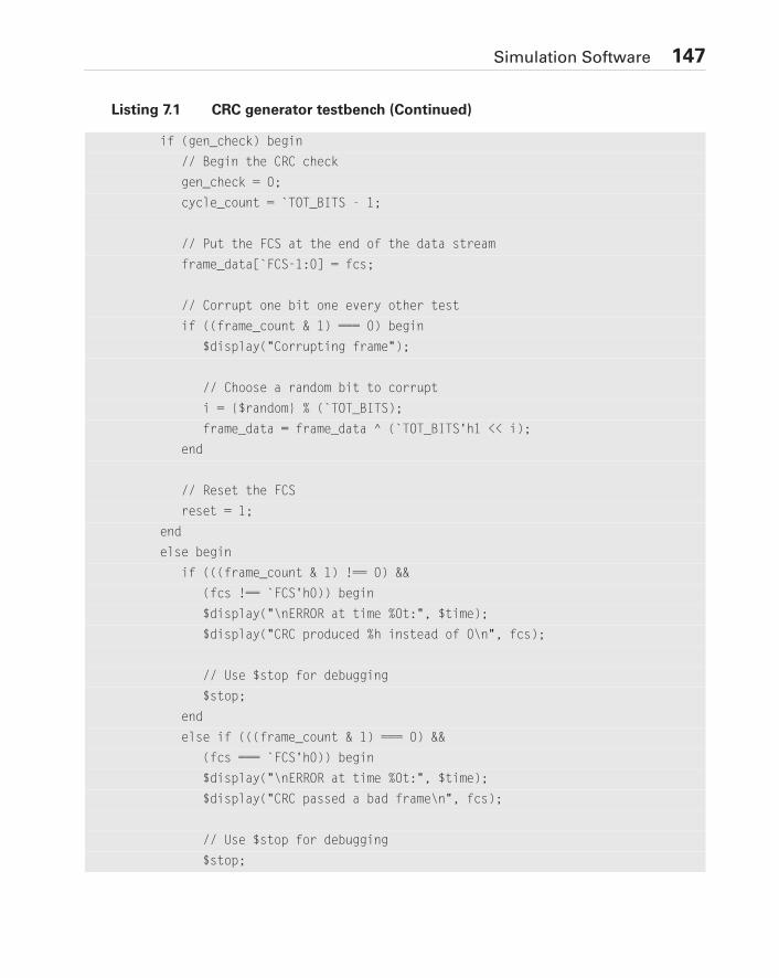
Simulation Software 147
if (gen_check) begin
// Begin the CRC check
gen_check = 0;
cycle_count = `TOT_BITS - 1;
// Put the FCS at the end of the data stream
frame_data[`FCS-1:0] = fcs;
// Corrupt one bit one every other test
if ((frame_count & 1) === 0) begin
$display("Corrupting frame");
// Choose a random bit to corrupt
i = {$random} % (`TOT_BITS);
frame_data = frame_data ^ (`TOT_BITS'h1 << i);
end
// Reset the FCS
reset = 1;
end
else begin
if (((frame_count & 1) !== 0) &&
(fcs !== `FCS'h0)) begin
$display("\nERROR at time %0t:", $time);
$display("CRC produced %h instead of 0\n", fcs);
// Use $stop for debugging
$stop;
end
else if (((frame_count & 1) === 0) &&
(fcs === `FCS'h0)) begin
$display("\nERROR at time %0t:", $time);
$display("CRC passed a bad frame\n", fcs);
// Use $stop for debugging
$stop;
Listing 7.1 CRC generator testbench (Continued)
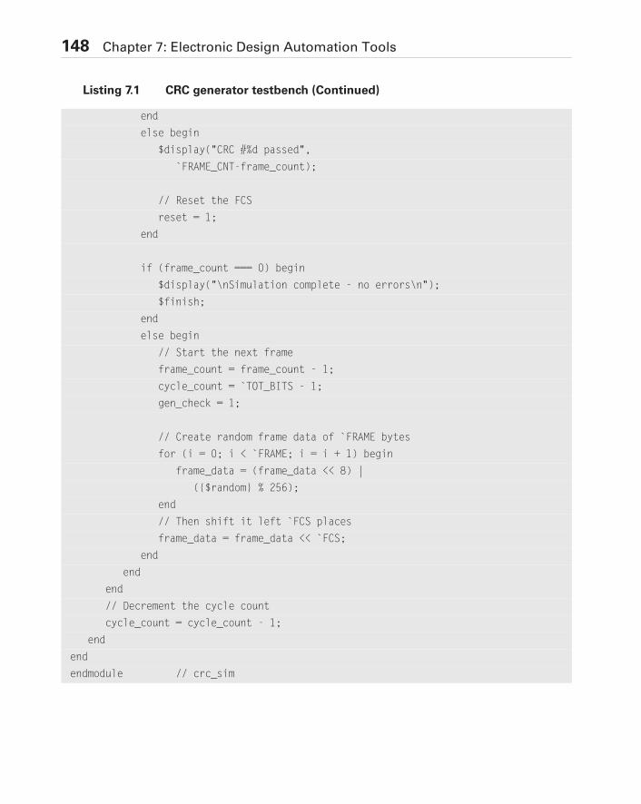
148 Chapter 7: Electronic Design Automation Tools
end
else begin
$display("CRC #%d passed",
`FRAME_CNT-frame_count);
// Reset the FCS
reset = 1;
end
if (frame_count === 0) begin
$display("\nSimulation complete - no errors\n");
$finish;
end
else begin
// Start the next frame
frame_count = frame_count - 1;
cycle_count = `TOT_BITS - 1;
gen_check = 1;
// Create random frame data of `FRAME bytes
for (i = 0; i < `FRAME; i = i + 1) begin
frame_data = (frame_data << 8) |
({$random} % 256);
end
// Then shift it left `FCS places
frame_data = frame_data << `FCS;
end
end
end
// Decrement the cycle count
cycle_count = cycle_count - 1;
end
end
endmodule // crc_sim
Listing 7.1 CRC generator testbench (Continued)
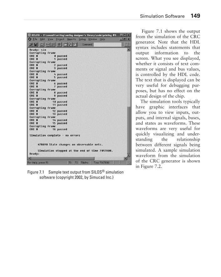
Simulation Software 149
Figure 7.1 shows the outputfrom the simulation of the CRCgenerator. Note that the HDLsyntax includes statements thatoutput information to thescreen. What you see displayed,whether it consists of text com-ments or signal and bus values,is controlled by the HDL code.The text that is displayed can bevery useful for debugging pur-poses, but has no effect on theactual design of the chip. The simulation tools typicallyhave graphic interfaces thatallow you to view inputs, out-puts, and internal signals, buses,and states as waveforms. Thesewaveforms are very useful forquickly visualizing and under-standing the relationshipbetween different signals beingsimulated. A sample simulationwaveform from the simulationof the CRC generator is shownin Figure 7.2.
Figure 7.1 Sample text output from SILOS® simulation
software (copyright 2002, by Simucad Inc.)
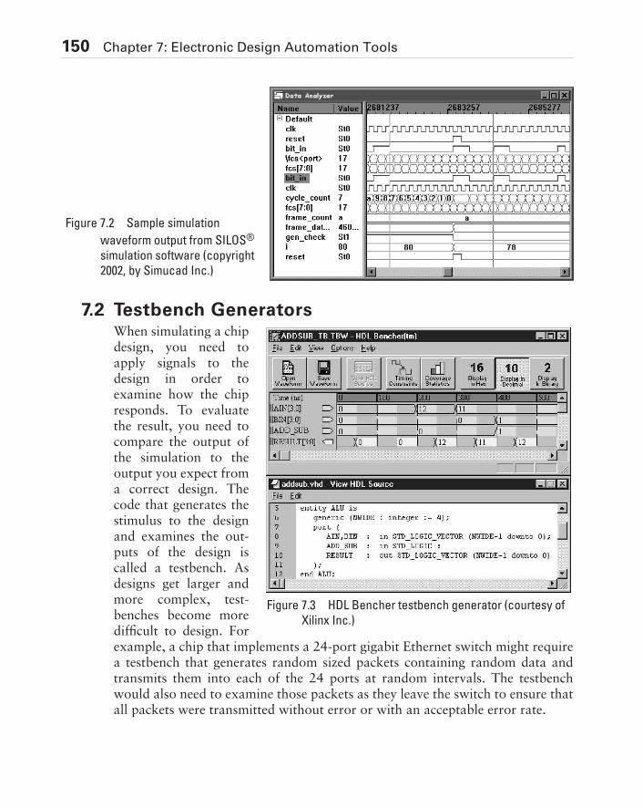
150 Chapter 7: Electronic Design Automation Tools
7.2 Testbench GeneratorsWhen simulating a chipdesign, you need toapply signals to thedesign in order toexamine how the chipresponds. To evaluatethe result, you need tocompare the output ofthe simulation to theoutput you expect froma correct design. Thecode that generates thestimulus to the designand examines the out-puts of the design iscalled a testbench. Asdesigns get larger andmore complex, test-benches become moredifficult to design. Forexample, a chip that implements a 24-port gigabit Ethernet switch might requirea testbench that generates random sized packets containing random data andtransmits them into each of the 24 ports at random intervals. The testbenchwould also need to examine those packets as they leave the switch to ensure thatall packets were transmitted without error or with an acceptable error rate.
Figure 7.2 Sample simulation
waveform output from SILOS®
simulation software (copyright
2002, by Simucad Inc.)
Figure 7.3 HDL Bencher testbench generator (courtesy of
Xilinx Inc.)
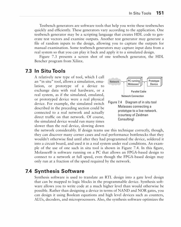
In Situ Tools 151
Testbench generators are software tools that help you write these testbenchesquickly and efficiently. These generators vary according to the application. Onetestbench generator may be a scripting language that creates HDL code to gen-erate test vectors and examine outputs. Another test generator may generate afile of random inputs to the design, allowing you to capture the outputs formanual examination. Some testbench generators may capture input data from areal system so that you can play it back and apply it to a simulated design.
Figure 7.3 presents a screen shot of one testbench generator, the HDLBencher program from Xilinx.
7.3 In Situ ToolsA relatively new type of tool, which I callan “in situ” tool, allows a simulation, emu-lation, or prototype of a device toexchange data with real hardware, or areal system, as if the simulated, emulated,or prototyped device were a real physicaldevice. For example, the simulated switchdescribed in the preceding section could beconnected to a real network and actuallydirect traffic on that network. Of course,the simulated device would run many timesslower than the real device, slowing downthe network considerably. If design teams use this technique correctly, though,they can discover many corner cases and real performance bottlenecks that theywouldn’t otherwise find until after they had programmed the device, soldered itinto a circuit board, and used it in a real system under real conditions. An exam-ple of the use of one such in situ tool is shown in Figure 7.4. In this figure,Molasses® is software running on a PC that allows an FPGA-based design toconnect to a network at full speed, even though the FPGA-based design mayonly run at a fraction of the speed required by the network.
7.4 Synthesis SoftwareSynthesis software is used to translate an RTL design into a gate level designthat can be mapped to logic blocks in the programmable device. Synthesis soft-ware allows you to write code at a much higher level than would otherwise bepossible. Rather than designing a device in terms of NAND and NOR gates, youcan design it using Boolean equations and high level devices such as counters,ALUs, decoders, and microprocessors. Also, the synthesis software optimizes the
Network Prototype
Device
PC running
Molasses®
Network Connection
Parallel Cable
Figure 7.4 Diagram of in situ tool
Molasses connecting a
prototype to a live network.
(courtesy of Zeidman
Consulting)
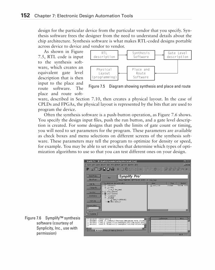
152 Chapter 7: Electronic Design Automation Tools
design for the particular device from the particular vendor that you specify. Syn-thesis software frees the designer from the need to understand details about thechip architecture. Synthesis software is what makes RTL-coded designs portableacross device to device and vendor to vendor.
As shown in Figure7.5, RTL code is inputto the synthesis soft-ware, which creates anequivalent gate leveldescription that is theninput to the place androute software. Theplace and route soft-ware, described in Section 7.10, then creates a physical layout. In the case ofCPLDs and FPGAs, the physical layout is represented by the bits that are used toprogram the device.
Often the synthesis software is a push-button operation, as Figure 7.6 shows.You specify the design input files, push the run button, and a gate level descrip-tion is created. For some designs that push the limits of gate count or timing,you will need to set parameters for the program. These parameters are availableas check boxes and menu selections on different screens of the synthesis soft-ware. These parameters may tell the program to optimize for density or speed,for example. You may be able to set switches that determine which types of opti-mization algorithms to use so that you can test different ones on your design.
RTLdescription
SynthesisSoftware
Gate Leveldescription
PhysicalLayout
(programming)
Place andRoute
Software
Figure 7.5 Diagram showing synthesis and place and route
Figure 7.6 Symplify™ synthesis
software (courtesy of
Synplicity, Inc., use with
permission)
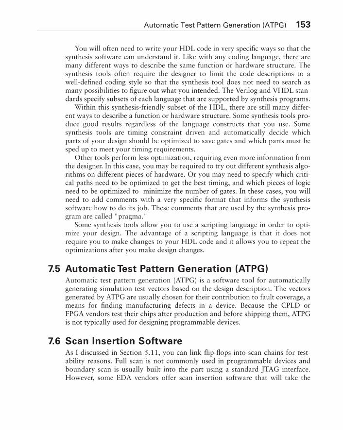
Automatic Test Pattern Generation (ATPG) 153
You will often need to write your HDL code in very specific ways so that thesynthesis software can understand it. Like with any coding language, there aremany different ways to describe the same function or hardware structure. Thesynthesis tools often require the designer to limit the code descriptions to awell-defined coding style so that the synthesis tool does not need to search asmany possibilities to figure out what you intended. The Verilog and VHDL stan-dards specify subsets of each language that are supported by synthesis programs.
Within this synthesis-friendly subset of the HDL, there are still many differ-ent ways to describe a function or hardware structure. Some synthesis tools pro-duce good results regardless of the language constructs that you use. Somesynthesis tools are timing constraint driven and automatically decide whichparts of your design should be optimized to save gates and which parts must besped up to meet your timing requirements.
Other tools perform less optimization, requiring even more information fromthe designer. In this case, you may be required to try out different synthesis algo-rithms on different pieces of hardware. Or you may need to specify which criti-cal paths need to be optimized to get the best timing, and which pieces of logicneed to be optimized to minimize the number of gates. In these cases, you willneed to add comments with a very specific format that informs the synthesissoftware how to do its job. These comments that are used by the synthesis pro-gram are called "pragma."
Some synthesis tools allow you to use a scripting language in order to opti-mize your design. The advantage of a scripting language is that it does notrequire you to make changes to your HDL code and it allows you to repeat theoptimizations after you make design changes.
7.5 Automatic Test Pattern Generation (ATPG)Automatic test pattern generation (ATPG) is a software tool for automaticallygenerating simulation test vectors based on the design description. The vectorsgenerated by ATPG are usually chosen for their contribution to fault coverage, ameans for finding manufacturing defects in a device. Because the CPLD orFPGA vendors test their chips after production and before shipping them, ATPGis not typically used for designing programmable devices.
7.6 Scan Insertion SoftwareAs I discussed in Section 5.11, you can link flip-flops into scan chains for test-ability reasons. Full scan is not commonly used in programmable devices andboundary scan is usually built into the part using a standard JTAG interface.However, some EDA vendors offer scan insertion software that will take the
154 Chapter 7: Electronic Design Automation Tools
flip-flops in your HDL code and insert the appropriate logic to create scanchains and the control for the scan chains. This additional logic doesn’t affectthe function of your chip, although it will change the timing slightly. These toolsare more commonly used for ASICs than CPLDs or FPGAs.
7.7 Built-In Self-Test (BIST) GeneratorsAnother method of testing your chip is to put all of the test circuitry on the chipin such a way that the chip tests itself. This is called built-in self-test or BIST,
Synplicity vs. Synopsys
Synopsys was the inventor of synthesis software and was by far the powerhouse EDA company in
this area for many years. Synopsys targeted its software at ASIC designs, initially a much bigger
market than CPLDs and FPGAs. As CPLDs and FPGAs became more complex and required synthe-
sis tools, Synopsys added switches to its software to allow it to optimize its results better for
FPGAs. Two friends of mine, Ken McElvain and Alisa Yaffa, realized that this kluge method of synthe-
sis could not produce optimal results for the unique architectures of CPLDs and FPGAs and formed
their own company for targeting specific vendor chips. In other words, to synthesize a design for a
specific chip from a specific vendor, the synthesis software needed to understand that specific
architecture.
Synopsys initially scoffed at the idea. But not for long as Synplicity grabbed market share away from
them in what was becoming a very important, and large, market. An example of how well the Syn-
plicity concept worked comes from my personal experience. I was designing some bus controller
CPLDs for an ATM router at Cisco Systems. I worked late into the evening attempting to get Synop-
sys Design Compiler software to synthesize my design into the CPLD I had chosen. I was changing
parameters and switches in the software, and though I knew instinctively that the chip had more
than enough resources, I couldn’t get the Synopsys software to do it. At this time, Synplicity con-
sisted of two employees – Ken and Alisa – in a very small office. At about ten o’clock in the evening
I called up Ken, who was of course still working also, and explained my dilemma. He told me to
e-mail him my HDL code along with the vendor and chip that I was targeting, and he’d see what his
beta software could do. Twenty minutes later I received an e-mail back that included a fitted design
with a clock speed that was faster than the Synopsys results. Knowing only the chip architecture,
the Synplicity software was able to optimize and fit the design. Cisco management was impressed
enough to invite them in for a demo and eventually became a major customer. After a while, Synop-
sys realized that it needed better tools for CPLDs and FPGAs if it was going to compete in this mar-
ket.
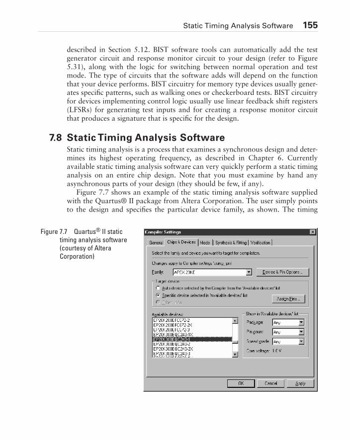
Static Timing Analysis Software 155
described in Section 5.12. BIST software tools can automatically add the testgenerator circuit and response monitor circuit to your design (refer to Figure5.31), along with the logic for switching between normal operation and testmode. The type of circuits that the software adds will depend on the functionthat your device performs. BIST circuitry for memory type devices usually gener-ates specific patterns, such as walking ones or checkerboard tests. BIST circuitryfor devices implementing control logic usually use linear feedback shift registers(LFSRs) for generating test inputs and for creating a response monitor circuitthat produces a signature that is specific for the design.
7.8 Static Timing Analysis SoftwareStatic timing analysis is a process that examines a synchronous design and deter-mines its highest operating frequency, as described in Chapter 6. Currentlyavailable static timing analysis software can very quickly perform a static timinganalysis on an entire chip design. Note that you must examine by hand anyasynchronous parts of your design (they should be few, if any).
Figure 7.7 shows an example of the static timing analysis software suppliedwith the Quartus® II package from Altera Corporation. The user simply pointsto the design and specifies the particular device family, as shown. The timing
Figure 7.7 Quartus® II static
timing analysis software
(courtesy of Altera
Corporation)
156 Chapter 7: Electronic Design Automation Tools
numbers depend on which device the design uses. The software loads the timingnumbers for the device, which it gets from a vendor-supplied database. It thengoes through you’re the candidate (synchronous) design and examines each pathbetween flip-flops to produce a very accurate timing analysis.
Before static timing analysis tools were available, engineers used timing simu-lation to verify the timing of designs. Timing simulation involves simulating thefunctionality of a design by using accurate timing values in the simulation.Delays from one signal to another could be viewed in a waveform. Timing prob-lems became apparent when borderline timing caused flip-flop outputs to go
NeoCAD
To my knowledge, there has only been one attempt at producing generic place and route software for
use on FPGAs from different vendors. Years ago, a few software engineers out of Xilinx formed a
company called NeoCAD. These engineers had created the place and route software for Xilinx and
decided that they would form a business based on a model like those of the simulation and synthesis
software companies. In other words, they would produce generic place and route software that cus-
tomers could fine tune for chips from different FPGA vendors. In this way, customers would not be
obligated to use layout tools from the particular vendor. It would also make FPGA designs a little
more portable from vendor to vendor.
They started, of course, with tools for Xilinx. These tools were very good — in fact, they usually out-
performed the tools from Xilinx. They had a problem, though, with their business model. The place
and route tools require an intimate knowledge of the vendor’s architecture, and most vendors consid-
ered this proprietary information that they weren’t interested in sharing. Some small FPGA compa-
nies were willing to give this information to NeoCAD in the hopes that NeoCAD would expand their
customer base. The big players weren’t willing to do this. Xilinx was particularly unhappy and made a
point of withholding this information.
NeoCAD, with their intimate knowledge of Xilinx architecture, was able to continue to write place and
route tools for Xilinx FPGAs that actually outperformed the Xilinx tools. For other vendors, they were
not quite as successful.
One day I met a software engineer who had recently left Xilinx. He told me that the head of software
there was pretty upset that NeoCAD, with their lack of detailed, up-to-date knowledge of the Xilinx
architecture, could still create tools that outperformed Xilinx. He gave his team an ultimatum. Either
the next toolset outperforms NeoCAD or they’d all be fired. Well, they worked hard and came out
with a new place and route tool. Several months later, Xilinx purchased NeoCAD and had a new team
of software engineers and a new place and route tool.
Formal Verification Software 157
undefined. Signals that extended beyond one clock cycle into the next causedserious functionality problems. The drawbacks to timing simulation are three-fold: the timing simulations take a lot of computing power and thus a lot of timeto complete; the results often require much direct examination of waveforms tofind problems; and, marginal problems in a path where the simulation did notexercise all possible transitions, are very easy to miss. In the days when designswere less than 10,000 gates, timing simulation was a tedious process that oftenmissed many marginal paths. With the sizes of modern designs, timing simula-tion simply doesn’t work.
7.9 Formal Verification SoftwareFormal verification software mathematically checks that a design is behavingcorrectly. There are two types of formal verification: equivalency checking andfunctional verification. Equivalency checking software compares two differentdesign descriptions to determine whether they are equivalent. Functional verifi-cation software proves whether specific conditions, called properties or asser-tions, occur in a design. Both types of formal verification are described in moredetail in Section 6.5.
7.10 Place and Route SoftwareThe vendor usually provides the place and route software tools. These tools takethe gate level design created by the synthesis software and figure out which logicblocks in the chip should contain which logic and how they should be con-nected. This process is shown in the diagram in Figure 7.5. The place and routesoftware next determines the bit sequence that will be loaded into the device inorder to program each logic block and each routing connection to obtain thecorrect functionality. A screen shot of software from Actel Corporation, calledDesigner, is shown in Figure 7.8. The button labeled “Layout” initiates the placeand route function; the button labeled “Fuse” creates the file containing the bitpattern for programming the device.
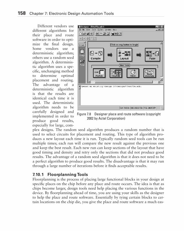
158 Chapter 7: Electronic Design Automation Tools
Different vendors usedifferent algorithms fortheir place and routesoftware in order to opti-mize the final design.Some vendors use adeterministic algorithm;others use a random seedalgorithm. A determinis-tic algorithm uses a spe-cific, unchanging methodto determine optimalplacement and routing.The advantage of adeterministic algorithmis that the results areidentical each time it isused. The deterministicalgorithm needs to becarefully designed andimplemented in order toproduce good results,especially for large, com-plex designs. The random seed algorithm produces a random number that isused to select circuits for placement and routing. This type of algorithm pro-duces a new layout each time it is run. Typically random seed tools can be runmultiple times; each run will compare the new result against the previous oneand keep the best result. Each new run can keep sections of the layout that havegood timing and density and retry only the sections that did not produce goodresults. The advantage of a random seed algorithm is that it does not need to bea perfect algorithm to produce good results. The disadvantage is that it may runthrough a large number of iterations before it finds acceptable results.
7.10.1 Floorplanning ToolsFloorplanning is the process of placing large functional blocks in your design atspecific places on the chip before any place and route occurs. The idea is that aschips become larger, design tools need help placing the various functions in thedevice. By floorplanning ahead of time, you are using your skills as the designerto help the place and route software. Essentially by tying certain blocks to cer-tain locations on the chip die, you give the place and route software a much eas-
Figure 7.8 Designer place and route software (copyright
2002 by Actel Corporation)
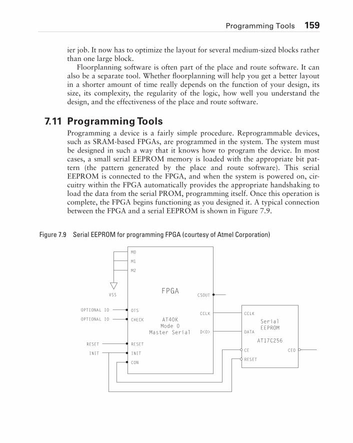
Programming Tools 159
ier job. It now has to optimize the layout for several medium-sized blocks ratherthan one large block.
Floorplanning software is often part of the place and route software. It canalso be a separate tool. Whether floorplanning will help you get a better layoutin a shorter amount of time really depends on the function of your design, itssize, its complexity, the regularity of the logic, how well you understand thedesign, and the effectiveness of the place and route software.
7.11 Programming ToolsProgramming a device is a fairly simple procedure. Reprogrammable devices,such as SRAM-based FPGAs, are programmed in the system. The system mustbe designed in such a way that it knows how to program the device. In mostcases, a small serial EEPROM memory is loaded with the appropriate bit pat-tern (the pattern generated by the place and route software). This serialEEPROM is connected to the FPGA, and when the system is powered on, cir-cuitry within the FPGA automatically provides the appropriate handshaking toload the data from the serial PROM, programming itself. Once this operation iscomplete, the FPGA begins functioning as you designed it. A typical connectionbetween the FPGA and a serial EEPROM is shown in Figure 7.9.
M0
M1
M2
OTSOPTIONAL IO
VSS
CHECK
CSOUT
CCLK CCLK
D<0> DATA
CE
RESET
OPTIONAL IO
RESETRESET
INITINIT
CON
FPGA
AT40KMode 0
Master Serial
SerialEEPROM
AT17C256
CEO
Figure 7.9 Serial EEPROM for programming FPGA (courtesy of Atmel Corporation)
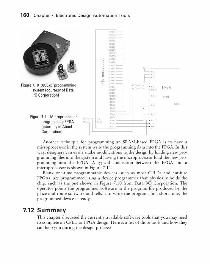
160 Chapter 7: Electronic Design Automation Tools
Another technique for programming an SRAM-based FPGA is to have amicroprocessor in the system write the programming data into the FPGA. In thisway, designers can easily make modifications to the design by loading new pro-gramming files into the system and having the microprocessor load the new pro-gramming into the FPGA. A typical connection between the FPGA and amicroprocessor is shown in Figure 7.11.
Blank one-time programmable devices, such as most CPLDs and antifuseFPGAs, are programmed using a device programmer that physically holds thechip, such as the one shown in Figure 7.10 from Data I/O Corporation. Theoperator points the programmer software to the program file produced by theplace and route software and tells it to write the program. In a short time, theprogrammed device is ready.
7.12 SummaryThis chapter discussed the currently available software tools that you may needto complete an CPLD or FPGA design. Here is a list of those tools and how theycan help you during the design process:
IO<31>
IO<30>
IO<29>
IO<28>
IO<27>
IO<26>
IO<25>
IO<24>
IO<23>
IO<22>
IO<21>
IO<20>
IO<19>
IO<18>
IO<17>
IO<16>
IO<15>
IO<14>
IO<13>
IO<12>
IO<11>
IO<10>
IO<9>
IO<8>
IO<7>
IO<6>
IO<5>
IO<4>
IO<3>
IO<2>
IO<1>
CLKCLOCK
ResetRESET
IO<0>
OPTIONAL IO
OPTIONAL IO
VDD
M0
M1
M2
OTS
CHECK
CSOUT
RESET
INIT
CON
FPGA
AT40K
D<0>
CS0
CCLK
Microprocessor
Figure 7.11 Microprocessor
programming FPGA
(courtesy of Atmel
Corporation)
Figure 7.10 3980xpi programming
system (courtesy of Data
I/O Corporation)
Summary 161
• Simulation tools allow you to test the functionality of your design under nor-mal conditions and under extreme conditions.
• Testbench generators automatically generate simulation testbenches from asimple test description.
• In situ tools enable you to connect your simulation, emulation, or prototypeto a live system for testing.
• Synthesis tools enable you to design your chip at a very high level and thensynthesize it into a low level design for place and route.
• Automatic test pattern generation (ATPG) tools automatically create testinputs to your chip for simulation or testing of the physical chip.
Floorplanning
Years ago, in the early days of ASICs, floorplanning was touted as a way to use human intelligence
and experience to assist layout software for creating optimal layout. The concept of floorplanning is
that a design engineer specifies where to place particular function blocks of a chip on the chip die.
The software can then place the remaining function blocks and route the entire design. In this way,
the engineer performs a placement of critical functions and the place-and-route software does not
have as many constraints and does not need to consider as many possibilities. This makes the soft-
ware run faster and gives it the capability to do more optimizations within these constraints.
The results of this type of floorplanning were, to be honest, terrible. First, an engineer does not have
the ability to consider all of the myriad connections in a design. Although some functions may appear
to need to be placed close to each other, doing so places them far from other blocks that may prove
to be equally critical. As ASIC designs, and later FPGA and CPLD designs, grew larger, the ability for
an engineer to instinctively know how to constrain layouts became even worse. And with less than
ideal placements, the software had difficulty working within these constraints. In the meantime, soft-
ware algorithms got better and computing power increased so that the place and route software
could do a much better job than the engineer. The method of floorplanning simply did not work.
Recently, though, some changes have made floorplanning useful in some real, but limited, ways. Chip
designs have now grown so large that the software to perform a complete place and route can take
an extremely long time to find optimal results, even despite the increasing computational power avail-
able. Because of this, for large designs it can make sense to perform an initial placement of very large
functional blocks (but not small functional blocks). The place and route software can then optimize the
design within the blocks, creating a usable design in a reasonable amount of time.
162 Chapter 7: Electronic Design Automation Tools
• Built-in self-test (BIST) tools automatically create logic in your chip thatenables it to test itself while it is in a system to determine that it is still func-tioning correctly.
• Static timing analysis software checks the timing numbers for your designand verifies that it will operate at the specified clock frequency or flags anypaths that do not meet your timing requirements.
• Formal verification tools allow you to mathematically verify the functionalityof a design and verify that two design descriptions are functionally equiva-lent.
• Place and route tools take the synthesized design description, determine howto optimally place the logic in the programmable device, how to optimallyconnect the logic together, and then create the bits used to program thedevice to implement your design.
• Floorplanning tools allow you to manually place high level blocks of logic inorder to help the place and route tools finish faster.
• Programming tools create a bit pattern for the programmable device andload it into the device so that it implements your design.
Exercises 163
Exercises
1. A testbench generator
(a) Builds you a bench to sit on while testing your design.
(b) Generates a benchmark test to compare different programmable devices.
(c) Generates simulation tests for your design from your high level description ofthe test.
(d) Tests assertions about the design.
2. An in situ tool
(a) Allows a simulated device to communicate with another simulated device.
(b) Allows a simulated device to communicate with a prototype device.
(c) Allows a simulated, emulated, or prototype device to connect to a system andcommunicate in real time.
(d) Allows a system to be simulated in real time.
3. Synthesis software
(a) Converts a low level design description to a functionally equivalent high leveldescription.
(b) Converts a design in one HDL to an equivalent design in another HDL.
(c) Creates a set of test vectors from a design description.
(d) Creates a low level design description from a functionally equivalent high leveldesign description.
4. ATPG stands for
(a) Automatic test pattern generation
(b) Asynchronous test pattern generation
(c) Automatic timing property generation
(d) Autonomous time priority generation
5. BIST stands for
(a) Bring in some toast
(b) Build internal synchronous test
(c) Built-in standard test
(d) Built-in self-test
164 Chapter 7: Electronic Design Automation Tools
6. Static timing analysis tools
(a) Simulate a design using real timing numbers.
(b) Analyze a design for all worst-case timing and determine whether the designmeets your timing requirements.
(c) Analyze your schedule for designing a chip and determine whether it is realisticand which tasks will take longer than expected.
(d) Determine the precise timing your design will have when it is placed and routed.
7. Place and route tools
(a) Create the bits that are used to program the device to implement your design.
(b) Place the logic for your design in the programmable device and connect thatlogic together.
(c) Find you a nice home and a good way to get to work.
(d) Both a and b.
8. Select TRUE or FALSE for the following statements:
(a) TRUE or FALSE: Static timing analysis has replaced timing simulation for deter-mining the timing numbers for FPGA designs.
(b) TRUE or FALSE: Dynamic timing analysis is a technique that will soon replacestatic timing analysis.
(c) TRUE or FALSE: Scan insertion software is used to insert boundary scan chainsinto an FPGA.
(d) TRUE or FALSE: Formal verification is a mathematic method of assuring that adesign meets its timing requirements.
(e) TRUE or FALSE: Floorplanning software allows you to place large chunks ofyour design in specific locations on the chip.
(f) TRUE or FALSE: SRAM-based FPGAs are programmed in the system.
(g) TRUE or FALSE: Serial PROMs are often used to load a design into anSRAM-based FPGA.
165
Chapter 8
Today and the FutureIn this final chapter, I discuss some of the newer architectures and technologiesthat are becoming available or are on the horizon. I give my opinions on whichones are interesting and which aren’t, which are overhyped and which are unde-rhyped, and which will succeed and which won’t.
Objectives
• Understand the newer devices that are becoming available or will be avail-able in the future.
• Learn how these new technologies and design concepts relate to currentdesigns
8.1 CoresBy a “core” I mean the basic functionality, excluding any extraneous circuitssuch as I/O buffers, that is found on a processor chip. There are two types ofcores: soft cores and hard cores. The soft core, known as an IP core, is describedby its logic function rather than by any physical implementation. Soft cores usu-ally delivered to the customer as HDL code, which is then synthesized as part ofthe customer’s design. Hard cores, on the other hand, consist of physical imple-mentations of a function. With respect to CPLDs and FPGAs, these hard cores
In this chapter...
• Cores
• Special I/O drivers
• New architectures
• ASICs with FPGA cells
166 Chapter 8: Today and the Future
are known as embedded cores because they are physically embedded onto thedie and surrounded by programmable logic.
Many of the FPGA and CPLD vendors have begun offering cores. As the den-sity of programmable devices increases, these cores allow engineers to createwhat is called a system on a programmable chip (SOPC) using a programmabledevice. In other words, whereas programmable devices were initially developedto replace glue logic, engineers can now place entire systems on a single pro-grammable device. Systems consist of all kinds of complicated devices like pro-cessors. In order to place these complex functions within a programmabledevice, there are three options: Design the function yourself, purchase the HDLcode for the function and incorporate it into your HDL code, or get the vendorto include the function as a cell in the programmable device. The second optionis the IP core; the third option is the embedded core.
8.1.1 IP CoresIP cores are often sold by third-party vendors that specialize in creating thesefunctions. Recently, CPLD and FPGA vendors have begun offering their ownsoft cores. IP cores reduce the time and manpower requirements for the FPGAdesigner. IP cores have already been designed, characterized, and verified. Also,IP cores are often modifiable, meaning that you can add or subtract functional-ity to suit your needs.
But IP cores may also be expensive in terms of chip resources. IP cores can beoptimized to a certain degree, but the complete optimization depends on its usein a particular device and also depends on the logic to which it is connected. IPpurchased from a third party may not be optimized for a particular CPLD orFPGA vendor. Because of that, you may not be able to meet your speed or powerrequirements, especially after you have placed and routed it.
8.1.2 Embedded CoresThe embedded core is in many ways ideal for users, which is one reason whyprogrammable device vendors are now offering embedded cores in their devices.The embedded core is optimized for the vendor’s process, so that it achievesgood timing and power consumption numbers. The embedded function isplaced as a single cell on the silicon die, so its performance does not depend onthe rest of your design because it will not need to be placed and routed.
Some embedded cores are analog devices that cannot be designed into anordinary CPLD or FPGA. By integrating these functions into the device, you canavoid the difficult process of designing analog devices, and save the chips andcomponents that would otherwise be required outside the programmable device.
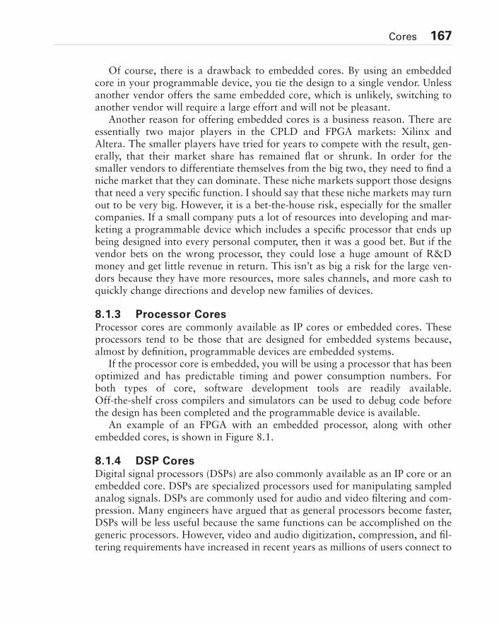
Cores 167
Of course, there is a drawback to embedded cores. By using an embeddedcore in your programmable device, you tie the design to a single vendor. Unlessanother vendor offers the same embedded core, which is unlikely, switching toanother vendor will require a large effort and will not be pleasant.
Another reason for offering embedded cores is a business reason. There areessentially two major players in the CPLD and FPGA markets: Xilinx andAltera. The smaller players have tried for years to compete with the result, gen-erally, that their market share has remained flat or shrunk. In order for thesmaller vendors to differentiate themselves from the big two, they need to find aniche market that they can dominate. These niche markets support those designsthat need a very specific function. I should say that these niche markets may turnout to be very big. However, it is a bet-the-house risk, especially for the smallercompanies. If a small company puts a lot of resources into developing and mar-keting a programmable device which includes a specific processor that ends upbeing designed into every personal computer, then it was a good bet. But if thevendor bets on the wrong processor, they could lose a huge amount of R&Dmoney and get little revenue in return. This isn’t as big a risk for the large ven-dors because they have more resources, more sales channels, and more cash toquickly change directions and develop new families of devices.
8.1.3 Processor CoresProcessor cores are commonly available as IP cores or embedded cores. Theseprocessors tend to be those that are designed for embedded systems because,almost by definition, programmable devices are embedded systems.
If the processor core is embedded, you will be using a processor that has beenoptimized and has predictable timing and power consumption numbers. Forboth types of core, software development tools are readily available.Off-the-shelf cross compilers and simulators can be used to debug code beforethe design has been completed and the programmable device is available.
An example of an FPGA with an embedded processor, along with otherembedded cores, is shown in Figure 8.1.
8.1.4 DSP CoresDigital signal processors (DSPs) are also commonly available as an IP core or anembedded core. DSPs are specialized processors used for manipulating sampledanalog signals. DSPs are commonly used for audio and video filtering and com-pression. Many engineers have argued that as general processors become faster,DSPs will be less useful because the same functions can be accomplished on thegeneric processors. However, video and audio digitization, compression, and fil-tering requirements have increased in recent years as millions of users connect to
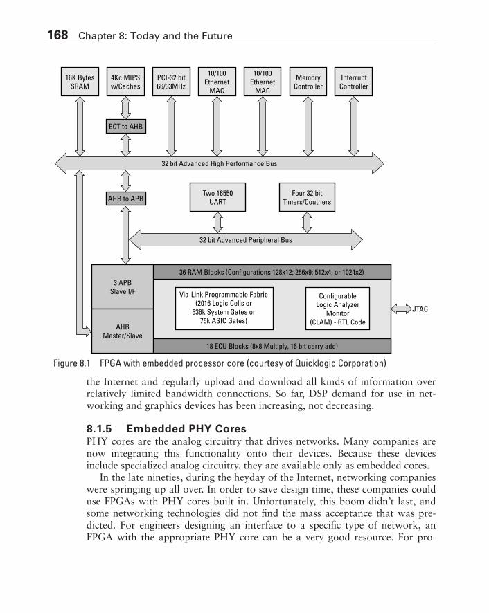
168 Chapter 8: Today and the Future
the Internet and regularly upload and download all kinds of information overrelatively limited bandwidth connections. So far, DSP demand for use in net-working and graphics devices has been increasing, not decreasing.
8.1.5 Embedded PHY CoresPHY cores are the analog circuitry that drives networks. Many companies arenow integrating this functionality onto their devices. Because these devicesinclude specialized analog circuitry, they are available only as embedded cores.
In the late nineties, during the heyday of the Internet, networking companieswere springing up all over. In order to save design time, these companies coulduse FPGAs with PHY cores built in. Unfortunately, this boom didn’t last, andsome networking technologies did not find the mass acceptance that was pre-dicted. For engineers designing an interface to a specific type of network, anFPGA with the appropriate PHY core can be a very good resource. For pro-
Four 32 bit
Timers/Coutners
Two 16550
UART
36 RAM Blocks (Configurations 128x12; 256x9; 512x4; or 1024x2)
18 ECU Blocks (8x8 Multiply, 16 bit carry add)
3 APB
Slave I/F
AHB
Master/Slave
16K Bytes
SRAM
PCI-32 bit
66/33MHz
10/100
Ethernet
MAC
10/100
Ethernet
MAC
Memory
Controller
Interrupt
Controller
ECT to AHB
AHB to APB
4Kc MIPS
w/Caches
32 bit Advanced High Performance Bus
32 bit Advanced Peripheral Bus
JTAG
Configurable
Logic Analyzer
Monitor
(CLAM) - RTL Code
Via-Link Programmable Fabric
(2016 Logic Cells or
536k System Gates or
75k ASIC Gates)
Figure 8.1 FPGA with embedded processor core (courtesy of Quicklogic Corporation)
Special I/O Drivers 169
grammable device vendors, it can be something of a risk to support a particularPHY core that may not end up being the standard that they expect or have themass market acceptance that they are counting on.
Figure 8.2 shows an example of an FPGA with an embedded PHY core thatcan be programmed to interface to a variety of different networks.
8.2 Special I/O DriversSpecial I/O drivers are now being embedded into programmable devices. Thenewer buses inside personal computers need special high-drive, impedancematched drive circuits and input circuits with very specific voltage threshold val-ues. Many vendors now offer programmable devices with I/O that meet thesespecial requirements. Many times, these devices are the only way to design aprogrammable device that can interface with these buses.
8.3 New ArchitecturesVendors are developing new architectures for CPLDs and FPGAs. Some vendorsstill make occasional attempts to create a fine-grained architecture where thelogic blocks consist of small logic functions. Most of these attempts, I believe,
FPGA Logic(up to 400K gates)
Ideal for implementing
comm. interfaces:
- XGM8
- POS-PHY4
- 153 MHz PECL
- User-Defined
Reference Clock
TransmitPLLs
ReceivePLLs
16:64 deMUXor
16:128 deMUX
16:64 deMUXor
16:128 deMUXTransmit Clock
Four 2.5Gbps Rx Clocks
64- or 128-bit
10Gb RX CLX(161MHz-78MHz)
Receive Data:- 16x622 or
- 16x645 or
- 16x667 Mbps
Transmit Data:- 16x622 or
- 16x645 or
- 16x667 Mbps
10Gb Tx CLK(161MHz-78MHz)
Figure 8.2 FPGA with embedded
PHY core (copyright 2002
by Lattice Semiconductor
Corporation)
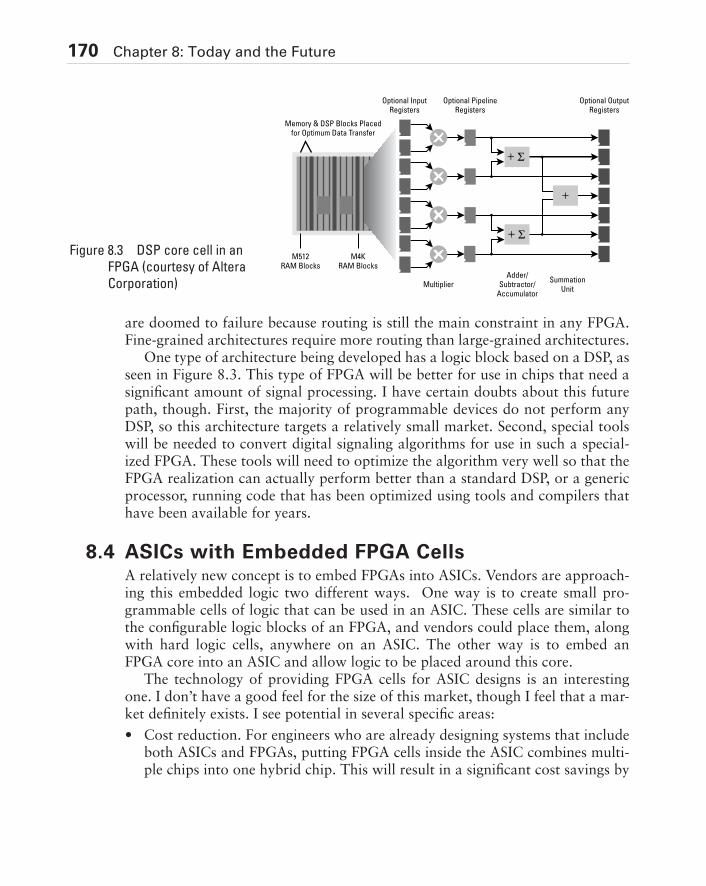
170 Chapter 8: Today and the Future
are doomed to failure because routing is still the main constraint in any FPGA.Fine-grained architectures require more routing than large-grained architectures.
One type of architecture being developed has a logic block based on a DSP, asseen in Figure 8.3. This type of FPGA will be better for use in chips that need asignificant amount of signal processing. I have certain doubts about this futurepath, though. First, the majority of programmable devices do not perform anyDSP, so this architecture targets a relatively small market. Second, special toolswill be needed to convert digital signaling algorithms for use in such a special-ized FPGA. These tools will need to optimize the algorithm very well so that theFPGA realization can actually perform better than a standard DSP, or a genericprocessor, running code that has been optimized using tools and compilers thathave been available for years.
8.4 ASICs with Embedded FPGA CellsA relatively new concept is to embed FPGAs into ASICs. Vendors are approach-ing this embedded logic two different ways. One way is to create small pro-grammable cells of logic that can be used in an ASIC. These cells are similar tothe configurable logic blocks of an FPGA, and vendors could place them, alongwith hard logic cells, anywhere on an ASIC. The other way is to embed anFPGA core into an ASIC and allow logic to be placed around this core.
The technology of providing FPGA cells for ASIC designs is an interestingone. I don’t have a good feel for the size of this market, though I feel that a mar-ket definitely exists. I see potential in several specific areas:
• Cost reduction. For engineers who are already designing systems that includeboth ASICs and FPGAs, putting FPGA cells inside the ASIC combines multi-ple chips into one hybrid chip. This will result in a significant cost savings by
Optional OutputRegisters
Optional PipelineRegisters
Optional InputRegisters
MultiplierAdder/
Subtractor/Accumulator
SummationUnit
Memory & DSP Blocks Placedfor Optimum Data Transfer
M4KRAM Blocks
M512RAM Blocks
Figure 8.3 DSP core cell in an
FPGA (courtesy of Altera
Corporation)
ASICs with Embedded FPGA Cells 171
eliminating chips. For engineers who are considering a design that includesASIC technology and FPGA technology, this solution saves PC board space,and the resulting hybrid chip will generally require fewer external pinsbecause the ASIC/FPGA interface is now inside the chip. Smaller PC boardsresults in lower cost. More importantly, lower pin count on a chip results insignificantly lower costs because package size is a large percentage of theoverall per-piece cost of an ASIC.
• Changing communication protocols. We've already seen manufacturers useflash memory technology extensively in modem designs so that they couldrelease modems before a communication protocol was finalized. This gavemodem manufacturers that used this technology a head start in the market.When the protocol was finalized, the user simply needed to update themodem firmware. Manufacturers can use this technology in switches androuters and other complicated communication devices in the same way. Net-work device manufacturers can ship devices before a protocol is fully defined.Of course, they can do that now using discrete FPGAs in their design, but thistechnology offers cost advantages by placing all logic, both fixed and flexible,onto a single chip.
• Bus interfaces and memory interfaces. These are other areas that are goodcandidates for this technology. The FPGA functionality allows the engineerto fine tune the logic while it is in the field. I believe that the opportunity forthis kind of market exists for very new interfaces that may not be welldefined or for which accurate simulation models don't yet exist. However, Ialso believe that accurate simulation models exist for older, well-definedinterfaces, so the technology will not be applied as much for supporting theselegacy interfaces.
• Architecture enhancements. One interesting idea that this technology furtherenables is the ability to make architectural changes after a product has beenmanufactured and shipped. In my experience, manufacturers perform verylittle analysis of complex equipment to locate performance bottlenecks. Thistechnology enables manufacturers to test changes to a system's architecturein the field. They can then incorporate those changes that resulted in betteroperation into the design. Also, different uses of a device may require differ-ent designs. Manufacturers can customize a device for particular customersbased on the customer’s environment and requirements.
• Reconfigurable computing. The concept of using FPGA devices to performsome of the algorithmic work of a general-purpose computer has excitedresearchers for several years. Currently, the work is mostly confined to uni-versities and R&D labs because of the complexity and challenges from the
172 Chapter 8: Today and the Future
design of the software and the hardware. In particular, it has been difficult todevelop compilers or interpreters that can take general algorithms, written ingeneral programming languages like C, and map the functionality ontoreconfigurable hardware. If researchers can resolve these issues, and reconfig-urable computing becomes successful, this technology could be an ideal plat-form for it because it enables the tight integration of high-speed logic andreconfigurable logic on the same chip.
The example in Figure 8.4 shows a block diagram of an implementation of a32-tap FIR filter. The shaded blocks are implemented in FPGA cells; theunshaded blocks are implemented in ASIC cells. The RAM is much easier toimplement, and more efficient to implement, as a RAM cell than in an FPGA. Byimplementing the address generator and ROM in FPGA cells, the algorithm caneasily be reprogrammed.
8.5 SummaryThe latest programmable devices and future programmable devices hold greatpromise for smaller chip designs, cost reductions, and increased flexibility. I’vegiven you my opinions about these devices. I may turn out to be wrong. Thingsmay change and by the time you read this, you may be seeing devices I haven’teven predicted yet. “Core” technology, special I/O drivers, new architectures,and ASICs embedded with FPGA cells all offer potential improvements in FPGAand CPLD design. I can only leave you with the immortal words of the amazingand mysterious Criswell from that unforgettable film, Plan Nine From OuterSpace, “We are all interested in the future, for that is where you and I are goingto spend the rest of our lives.”
Key
FPGA
ASIC
REG REG REG X
ADDRESSGENERATOR
32x16COEFFICIENT
ROM
ADDR ADDR
2Kx16DUAL-PORT
RAM
DATA DATA 40-BITACCUM.
REG
Figure 8.4 Mixed ASIC/FPGA design (copyright 2002, by Leopard Logic Corporation)

173
Appendix A
Answer Key
Chapter 1, “Prehistory: Programmable Logic to ASICs”
1. What does the term ASIC mean?
(c) Application Specific Integrated Circuit
2. Each programmable device is matched with its description in the following table.
a. PROM (A) A memory device that can be programmed once and read many times.
b. PLA (D) A logic device with a large AND plane and a large OR plane for implementing different combinations of Boolean logic.
c. PAL (E) A logic device with a large AND plane and a small, fixed number of OR gates for implementing Boolean logic and state machines.
d. CPLD (C) A logic device that is made up of many PAL devices.
e. FPGA (B) A logic device that can be used to design large functions like an ASIC except that it can be programmed quickly and inexpensively.
174 Appendix A: Answer Key
3. Listed is the correct device for each statement — PALs or ASICs.
(a) PALs have a short lead-time.
(b) ASICs are high-density devices.
(c) ASICs can implement very complex functions.
(d) PALs do not have NRE charges.
(e) PALs are programmable.
Chapter 2, “Complex Programmable Logic Devices (CPLDs)”
1. What does the term CPLD mean?
(a) Complex Programmable Logic Device
2. These are all of the parts of a typical CPLD.
(a) I/O Block
(d) Function Block
(e) Interconnect Matrix
3. Which technology is not used for CPLD programmable elements?
(d) DRAM
4. Which is not a characteristic of clock drivers
(c) Low power
5. The layout of traces that connects a clock driver to the flip-flops in a CPLD is called
(a) A clock tree
6. One advantage of the CPLD switch matrix routing scheme is that delays through thechip are
(b) Deterministic
7. Embedded devices are (select one)
(b) Devices that are embedded inside a CPLD
Chapter 3, “Field Programmable Gate Arrays (FPGAs)” 175
Chapter 3, “Field Programmable Gate Arrays (FPGAs)”
1. What does the term FPGA mean?
(b) Field Programmable Gate Array
2. Here are all of the parts of a typical FPGA architecture.
(a) Configurable Logic Blocks
(c) Programmable Interconnect
(d) Configurable I/O Blocks
3. TRUE or FALSE is selected for the following statements.
(a) TRUE: Configurable I/O Blocks contain flip-flops on the inputs to enable adesigner to reduce the hold-time requirement for the inputs.
(b) TRUE: Configurable I/O Blocks contain flip-flops on the outputs to enable thedesigner to decrease the clock-to-output times of the outputs.
(c) FALSE: FPGA programmable interconnect consists of lines that start at one endof the chip and continue to the other end to enable all CLBs to be connected.
(d) TRUE: Programmable switches inside the chip allow the connection of CLBs tointerconnect lines
(e) TRUE: Programmable switches inside the chip allow the connection of intercon-nect lines to each other and to the switch matrix.
(f) FALSE: Each flip-flop in an FPGA has its own unique clock line and clock bufferto reduce skew.
(g) FALSE: Any input to an FPGA can be used for the clock input.
(h) FALSE: Antifuse FPGAs use an industry standard process.
(i) TRUE: Antifuse technology is faster than SRAM technology, in theory.
(j) TRUE: SRAM FPGAs are more common than antifuse FPGAs.
4. These are all potential advantages of embedded devices
(a) Reduced board area
(b) Reduced power consumption
(c) Reduced cost
(d) Increased system speed
(e) You don’t need to design and test the embedded device
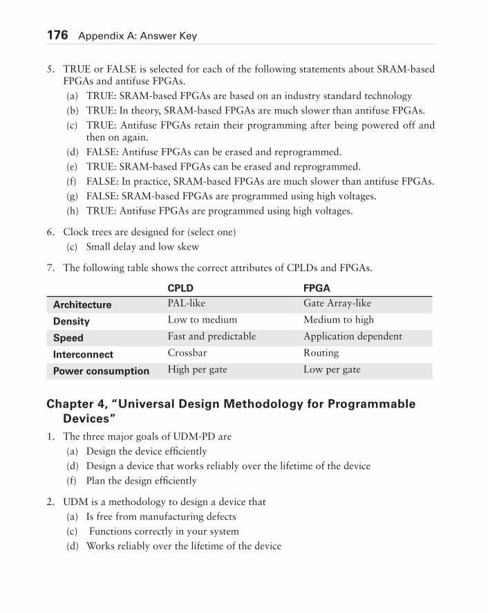
176 Appendix A: Answer Key
5. TRUE or FALSE is selected for each of the following statements about SRAM-basedFPGAs and antifuse FPGAs.
(a) TRUE: SRAM-based FPGAs are based on an industry standard technology
(b) TRUE: In theory, SRAM-based FPGAs are much slower than antifuse FPGAs.
(c) TRUE: Antifuse FPGAs retain their programming after being powered off andthen on again.
(d) FALSE: Antifuse FPGAs can be erased and reprogrammed.
(e) TRUE: SRAM-based FPGAs can be erased and reprogrammed.
(f) FALSE: In practice, SRAM-based FPGAs are much slower than antifuse FPGAs.
(g) FALSE: SRAM-based FPGAs are programmed using high voltages.
(h) TRUE: Antifuse FPGAs are programmed using high voltages.
6. Clock trees are designed for (select one)
(c) Small delay and low skew
7. The following table shows the correct attributes of CPLDs and FPGAs.
Chapter 4, “Universal Design Methodology for Programmable
Devices”
1. The three major goals of UDM-PD are
(a) Design the device efficiently
(d) Design a device that works reliably over the lifetime of the device
(f) Plan the design efficiently
2. UDM is a methodology to design a device that
(a) Is free from manufacturing defects
(c) Functions correctly in your system
(d) Works reliably over the lifetime of the device
CPLD FPGA
Architecture PAL-like Gate Array-like
Density Low to medium Medium to high
Speed Fast and predictable Application dependent
Interconnect Crossbar Routing
Power consumption High per gate Low per gate
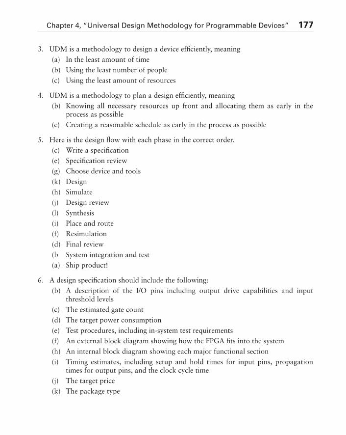
Chapter 4, “Universal Design Methodology for Programmable Devices” 177
3. UDM is a methodology to design a device efficiently, meaning
(a) In the least amount of time
(b) Using the least number of people
(c) Using the least amount of resources
4. UDM is a methodology to plan a design efficiently, meaning
(b) Knowing all necessary resources up front and allocating them as early in theprocess as possible
(c) Creating a reasonable schedule as early in the process as possible
5. Here is the design flow with each phase in the correct order.
(c) Write a specification
(e) Specification review
(g) Choose device and tools
(k) Design
(h) Simulate
(j) Design review
(l) Synthesis
(i) Place and route
(f) Resimulation
(d) Final review
(b System integration and test
(a) Ship product!
6. A design specification should include the following:
(b) A description of the I/O pins including output drive capabilities and inputthreshold levels
(c) The estimated gate count
(d) The target power consumption
(e) Test procedures, including in-system test requirements
(f) An external block diagram showing how the FPGA fits into the system
(h) An internal block diagram showing each major functional section
(i) Timing estimates, including setup and hold times for input pins, propagationtimes for output pins, and the clock cycle time
(j) The target price
(k) The package type
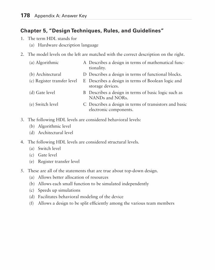
178 Appendix A: Answer Key
Chapter 5, “Design Techniques, Rules, and Guidelines”
1. The term HDL stands for
(a) Hardware description language
2. The model levels on the left are matched with the correct description on the right.
3. The following HDL levels are considered behavioral levels:
(b) Algorithmic level
(d) Architectural level
4. The following HDL levels are considered structural levels.
(a) Switch level
(c) Gate level
(e) Register transfer level
5. These are all of the statements that are true about top-down design.
(a) Allows better allocation of resources
(b) Allows each small function to be simulated independently
(c) Speeds up simulations
(d) Facilitates behavioral modeling of the device
(f) Allows a design to be split efficiently among the various team members
(a) Algorithmic A Describes a design in terms of mathematical func-tionality.
(b) Architectural D Describes a design in terms of functional blocks.
(c) Register transfer level E Describes a design in terms of Boolean logic and storage devices.
(d) Gate level B Describes a design in terms of basic logic such as NANDs and NORs.
(e) Switch level C Describes a design in terms of transistors and basic electronic components.

Chapter 5, “Design Techniques, Rules, and Guidelines” 179
6. The five rules of synchronous design are
(a) Data signals must go only to combinatorial logic or data inputs of flip-flops.
(b) All data is passed through combinatorial logic and flip-flops that are synchro-nized to a single clock.
(c) Clocks cannot be gated — in other words, clocks must go directly to the clockinputs of the flip-flops without going through any combinatorial logic.
(h) No signal that is generated by combinatorial logic can be fed back to the samecombinatorial logic without first going through a synchronizing flip-flop.
(i) Delay is always controlled by flip-flops, not combinatorial logic.
7. The asynchronous circuits on the left have been matched with the equivalent synchro-nous circuits on the right.
8. TRUE or FALSE is selected for the following statements.
(a) FALSE: Synchronizing flip-flops are used to eliminate metastability.
(b) TRUE: In theory, a device can remain metastable forever.
(c) TRUE: The chances of a device going metastable increases with higher clock fre-quencies.
(d) FALSE: The chances of a device going metastable decreases with higher inputvoltage thresholds.
(e) FALSE: Schmidt trigger inputs with hysteresis can eliminate metastability.
(f) FALSE: Metastability is caused by faulty circuits.
(g) TRUE: Metastability is caused by asynchronous signals coming into synchro-nous circuits.
9. These are all allowable uses of asynchronous logic.
(a) To latch inputs from and outputs to an asynchronous bus as long as the signalsare synchronized for use inside the design.
(c) Asynchronous reset if it is done according to specific rules.
(a) C
(b) D
(c) A
(d) B
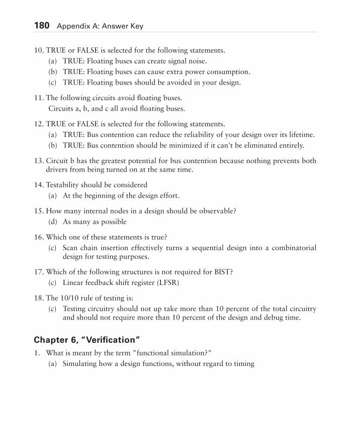
180 Appendix A: Answer Key
10. TRUE or FALSE is selected for the following statements.
(a) TRUE: Floating buses can create signal noise.
(b) TRUE: Floating buses can cause extra power consumption.
(c) TRUE: Floating buses should be avoided in your design.
11. The following circuits avoid floating buses.
Circuits a, b, and c all avoid floating buses.
12. TRUE or FALSE is selected for the following statements.
(a) TRUE: Bus contention can reduce the reliability of your design over its lifetime.
(b) TRUE: Bus contention should be minimized if it can't be eliminated entirely.
13. Circuit b has the greatest potential for bus contention because nothing prevents bothdrivers from being turned on at the same time.
14. Testability should be considered
(a) At the beginning of the design effort.
15. How many internal nodes in a design should be observable?
(d) As many as possible
16. Which one of these statements is true?
(c) Scan chain insertion effectively turns a sequential design into a combinatorialdesign for testing purposes.
17. Which of the following structures is not required for BIST?
(c) Linear feedback shift register (LFSR)
18. The 10/10 rule of testing is:
(c) Testing circuitry should not up take more than 10 percent of the total circuitryand should not require more than 10 percent of the design and debug time.
Chapter 6, “Verification”
1. What is meant by the term "functional simulation?"
(a) Simulating how a design functions, without regard to timing
Chapter 7, “Electronic Design Automation Tools” 181
2. What is meant by the term "toggle coverage?"
(b) The number of nodes in a design that change state from 0 to 1 and from 1 to 0during simulation as a percentage of the total number of possible state transi-tions.
3. What is meant by the term "code coverage?"
(c) The percentage of code statements in a design that have been executed duringsimulation in every possible manner.
4. What is meant by the term "timing simulation?"
(b) A simulation that includes timing delays.
5. Why is timing simulation typically no longer done for a design?
(c) Static timing analysis is a faster, more exhaustive analysis of whether a designmeets its timing requirements.
6. What is meant by the term "static timing analysis?"
(a) A process that looks at a synchronous design and determines the highest operat-ing frequency that does not violate any setup and hold-times.
7. What are the two types of formal verification?
(a) Functional verification and equivalency checking.
Chapter 7, “Electronic Design Automation Tools”
1. A testbench generator
(c) Generates simulation tests for your design from your high level description ofthe test.
2. An in situ tool
(c) Allows a simulated, emulated, or prototype device to connect to a system andcommunicate in real time.
3. Synthesis software
(d) Creates a low level design description from a functionally equivalent high leveldesign description.
4. ATPG stands for
(a) Automatic test pattern generation

182 Appendix A: Answer Key
5. BIST stands for
(d) Built-in self-test
6. Static timing analysis tools
(b) Analyze a design for all worst-case timing and determine whether the designmeets your timing requirements.
7. Place and route tools
(d) Both a and b (Create the bits that are used to program the device to implementyour design; and place the logic for your design in the programmable device andconnect that logic together)
8. TRUE or FALSE is given for the following statements:
(a) TRUE: Static timing analysis has replaced timing simulation for determining thetiming numbers for FPGA designs.
(b) FALSE: Dynamic timing analysis is a technique that will soon replace static tim-ing analysis.
(c) FALSE: Scan insertion software is used to insert boundary scan chains into anFPGA.
(d) FALSE: Formal verification is a mathematic method of assuring that a designmeets its timing requirements.
(e) TRUE: Floorplanning software allows you to place large chunks of your designin specific locations on the chip.
(f) TRUE: SRAM-based FPGAs are programmed in the system.
(g) TRUE: Serial PROMs are often used to load a design into an SRAM-basedFPGA.
183
Appendix B
Verilog Code for Schematics in Chapter 5
Listing B.1 Figure 5.2
/*********************************************************/
// MODULE: asynchronous race condition
//
// FILE NAME: arace.v
// VERSION: 1.0
// DATE: June 1, 2002
// AUTHOR: Bob Zeidman, Zeidman Consulting
//
// CODE TYPE: RTL
//
// DESCRIPTION: This module defines a circuit with an
// asynchronous race condition. Note that this circuit
// will simulate fine, but a synthesis program won't know
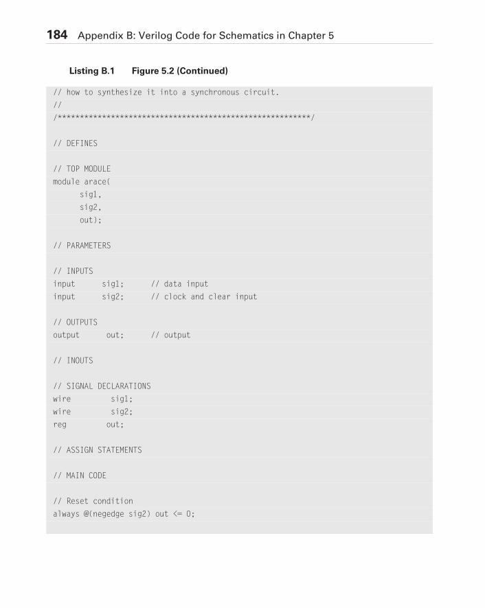
184 Appendix B: Verilog Code for Schematics in Chapter 5
// how to synthesize it into a synchronous circuit.
//
/*********************************************************/
// DEFINES
// TOP MODULE
module arace(
sig1,
sig2,
out);
// PARAMETERS
// INPUTS
input sig1; // data input
input sig2; // clock and clear input
// OUTPUTS
output out; // output
// INOUTS
// SIGNAL DECLARATIONS
wire sig1;
wire sig2;
reg out;
// ASSIGN STATEMENTS
// MAIN CODE
// Reset condition
always @(negedge sig2) out <= 0;
Listing B.1 Figure 5.2 (Continued)
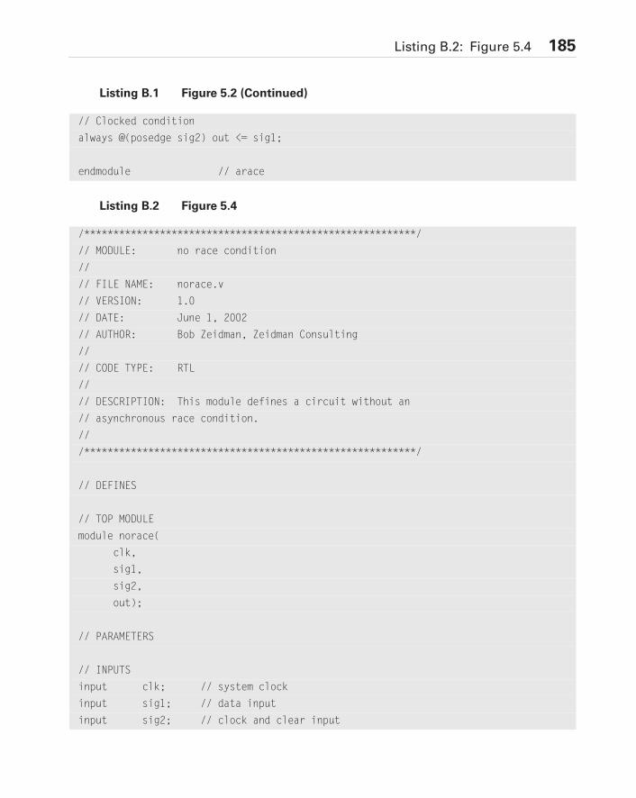
Listing B.2: Figure 5.4 185
// Clocked condition
always @(posedge sig2) out <= sig1;
endmodule // arace
Listing B.1 Figure 5.2 (Continued)
Listing B.2 Figure 5.4
/*********************************************************/
// MODULE: no race condition
//
// FILE NAME: norace.v
// VERSION: 1.0
// DATE: June 1, 2002
// AUTHOR: Bob Zeidman, Zeidman Consulting
//
// CODE TYPE: RTL
//
// DESCRIPTION: This module defines a circuit without an
// asynchronous race condition.
//
/*********************************************************/
// DEFINES
// TOP MODULE
module norace(
clk,
sig1,
sig2,
out);
// PARAMETERS
// INPUTS
input clk; // system clock
input sig1; // data input
input sig2; // clock and clear input
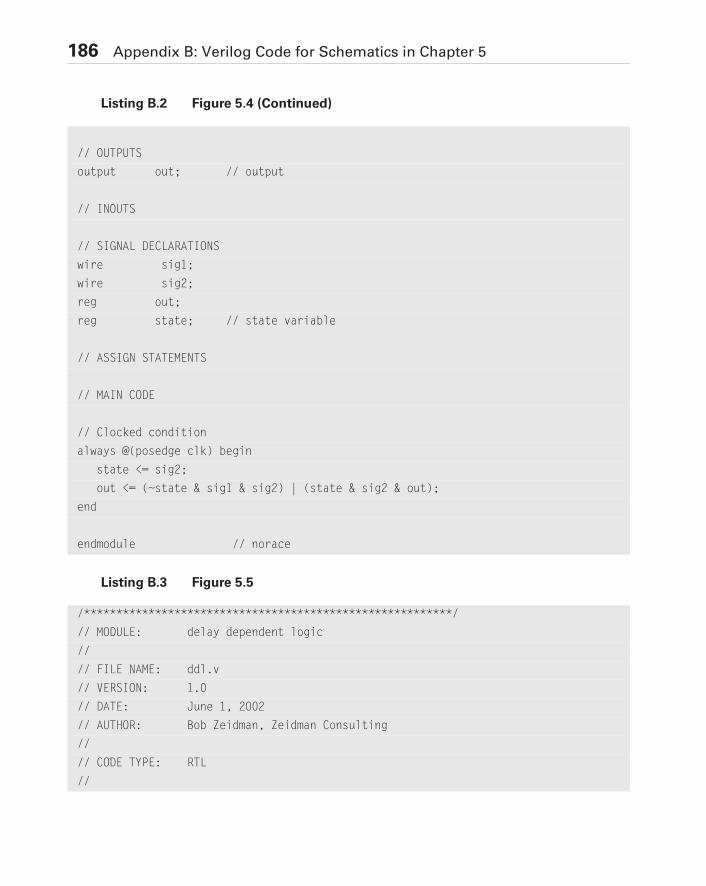
186 Appendix B: Verilog Code for Schematics in Chapter 5
// OUTPUTS
output out; // output
// INOUTS
// SIGNAL DECLARATIONS
wire sig1;
wire sig2;
reg out;
reg state; // state variable
// ASSIGN STATEMENTS
// MAIN CODE
// Clocked condition
always @(posedge clk) begin
state <= sig2;
out <= (~state & sig1 & sig2) | (state & sig2 & out);
end
endmodule // norace
Listing B.2 Figure 5.4 (Continued)
Listing B.3 Figure 5.5
/*********************************************************/
// MODULE: delay dependent logic
//
// FILE NAME: ddl.v
// VERSION: 1.0
// DATE: June 1, 2002
// AUTHOR: Bob Zeidman, Zeidman Consulting
//
// CODE TYPE: RTL
//
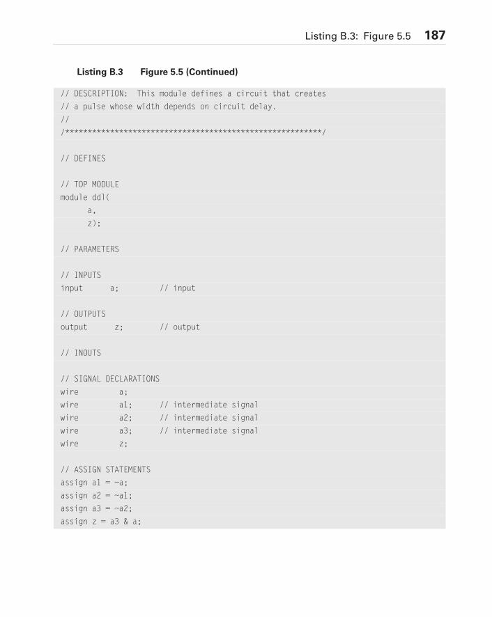
Listing B.3: Figure 5.5 187
// DESCRIPTION: This module defines a circuit that creates
// a pulse whose width depends on circuit delay.
//
/*********************************************************/
// DEFINES
// TOP MODULE
module ddl(
a,
z);
// PARAMETERS
// INPUTS
input a; // input
// OUTPUTS
output z; // output
// INOUTS
// SIGNAL DECLARATIONS
wire a;
wire a1; // intermediate signal
wire a2; // intermediate signal
wire a3; // intermediate signal
wire z;
// ASSIGN STATEMENTS
assign a1 = ~a;
assign a2 = ~a1;
assign a3 = ~a2;
assign z = a3 & a;
Listing B.3 Figure 5.5 (Continued)
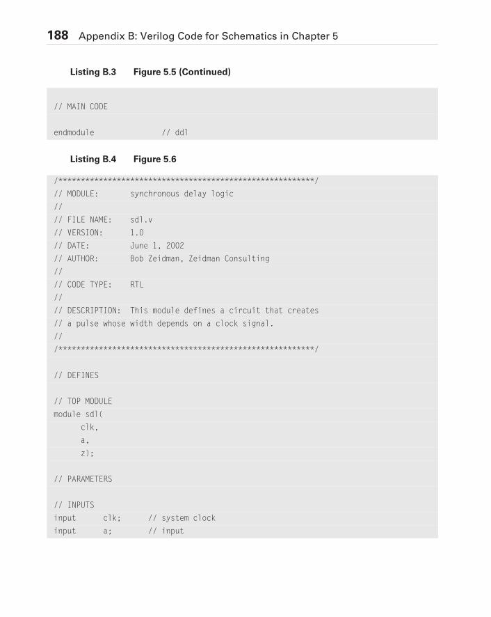
188 Appendix B: Verilog Code for Schematics in Chapter 5
// MAIN CODE
endmodule // ddl
Listing B.3 Figure 5.5 (Continued)
Listing B.4 Figure 5.6
/*********************************************************/
// MODULE: synchronous delay logic
//
// FILE NAME: sdl.v
// VERSION: 1.0
// DATE: June 1, 2002
// AUTHOR: Bob Zeidman, Zeidman Consulting
//
// CODE TYPE: RTL
//
// DESCRIPTION: This module defines a circuit that creates
// a pulse whose width depends on a clock signal.
//
/*********************************************************/
// DEFINES
// TOP MODULE
module sdl(
clk,
a,
z);
// PARAMETERS
// INPUTS
input clk; // system clock
input a; // input
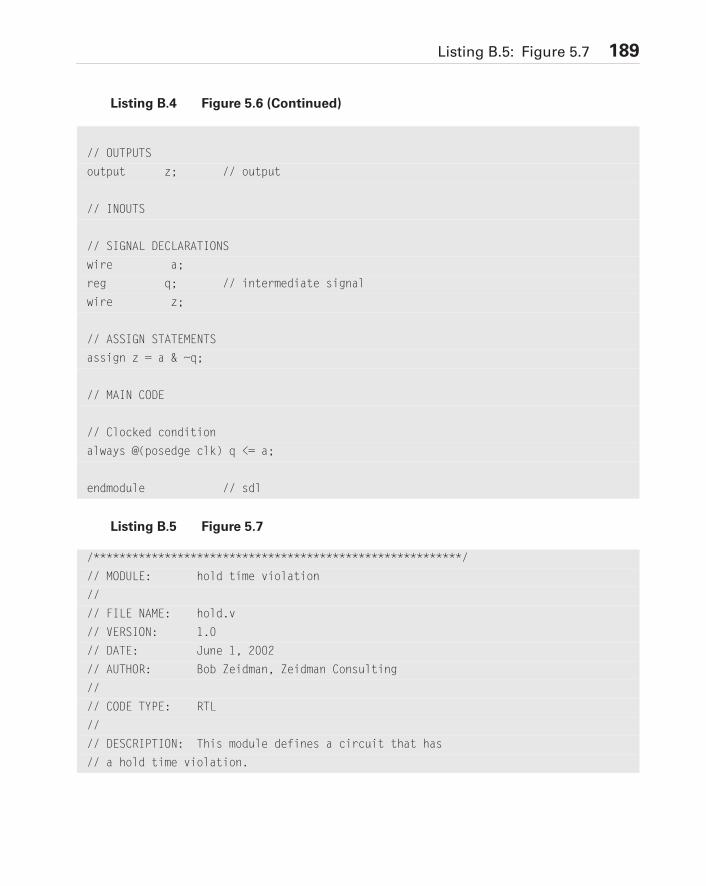
Listing B.5: Figure 5.7 189
// OUTPUTS
output z; // output
// INOUTS
// SIGNAL DECLARATIONS
wire a;
reg q; // intermediate signal
wire z;
// ASSIGN STATEMENTS
assign z = a & ~q;
// MAIN CODE
// Clocked condition
always @(posedge clk) q <= a;
endmodule // sdl
Listing B.4 Figure 5.6 (Continued)
Listing B.5 Figure 5.7
/*********************************************************/
// MODULE: hold time violation
//
// FILE NAME: hold.v
// VERSION: 1.0
// DATE: June 1, 2002
// AUTHOR: Bob Zeidman, Zeidman Consulting
//
// CODE TYPE: RTL
//
// DESCRIPTION: This module defines a circuit that has
// a hold time violation.
190 Appendix B: Verilog Code for Schematics in Chapter 5
//
/*********************************************************/
// DEFINES
// TOP MODULE
module hold(
clk,
d1,
d2,
d4);
// PARAMETERS
// INPUTS
input clk; // system clock
input d1; // input
input d2; // input
// OUTPUTS
output d4; // output
// INOUTS
// SIGNAL DECLARATIONS
wire clk;
wire d1;
wire d2;
reg d3; // intermediate signal
reg d4;
// ASSIGN STATEMENTS
// MAIN CODE
Listing B.5 Figure 5.7 (Continued)
Listing B.6: Figure 5.8 191
// Clocked condition
always @(posedge clk) d3 <= d1;
// Clocked condition
always @(posedge d3) d4 <= d2;
endmodule // hold
Listing B.5 Figure 5.7 (Continued)
Listing B.6 Figure 5.8
/*********************************************************/
// MODULE: no hold time violation
//
// FILE NAME: no_hold.v
// VERSION: 1.0
// DATE: June 1, 2002
// AUTHOR: Bob Zeidman, Zeidman Consulting
//
// CODE TYPE: RTL
//
// DESCRIPTION: This module defines a circuit that does
// not have a hold time violation.
//
/*********************************************************/
// DEFINES
// TOP MODULE
module no_hold(
clk,
d1,
d2,
d4);
// PARAMETERS
192 Appendix B: Verilog Code for Schematics in Chapter 5
// INPUTS
input clk; // system clock
input d1; // input
input d2; // input
// OUTPUTS
output d4; // output
// INOUTS
// SIGNAL DECLARATIONS
wire clk;
wire d1;
wire d2;
reg d3; // intermediate signal
reg d3d; // intermediate signal
wire d3p; // intermediate signal
reg d4;
// ASSIGN STATEMENTS
assign d3p = d3 & ~d3d;
// MAIN CODE
// Clocked condition
always @(posedge clk) begin
d3 <= d1;
d3d <= d3;
if (d3p) d4 <= d2;
end
endmodule // no_hold
Listing B.6 Figure 5.8 (Continued)
Listing B.7: Figure 5.13 193
Listing B.7 Figure 5.13
/*********************************************************/
// MODULE: the enable flip-flop
//
// FILE NAME: eff.v
// VERSION: 1.0
// DATE: June 1, 2002
// AUTHOR: Bob Zeidman, Zeidman Consulting
//
// CODE TYPE: RTL
//
// DESCRIPTION: This module defines an enable flip-slop.
//
/*********************************************************/
// DEFINES
// TOP MODULE
module eff(
clk,
data,
enable,
out);
// PARAMETERS
// INPUTS
input clk; // system clock
input data; // input
input enable; // input
// OUTPUTS
output out; // output
// INOUTS
194 Appendix B: Verilog Code for Schematics in Chapter 5
// SIGNAL DECLARATIONS
wire clk;
wire data;
wire enable;
reg out;
// ASSIGN STATEMENTS
// MAIN CODE
// Clocked condition
always @(posedge clk) begin
if (enable) out <= data;
end
endmodule // eff
Listing B.7 Figure 5.13 (Continued)
Listing B.8 Figure 5.9
/*********************************************************/
// MODULE: glitch
//
// FILE NAME: glitch.v
// VERSION: 1.0
// DATE: June 1, 2002
// AUTHOR: Bob Zeidman, Zeidman Consulting
//
// CODE TYPE: RTL
//
// DESCRIPTION: This module defines a mux circuit with a
// potential glitch.
//
/*********************************************************/
// DEFINES
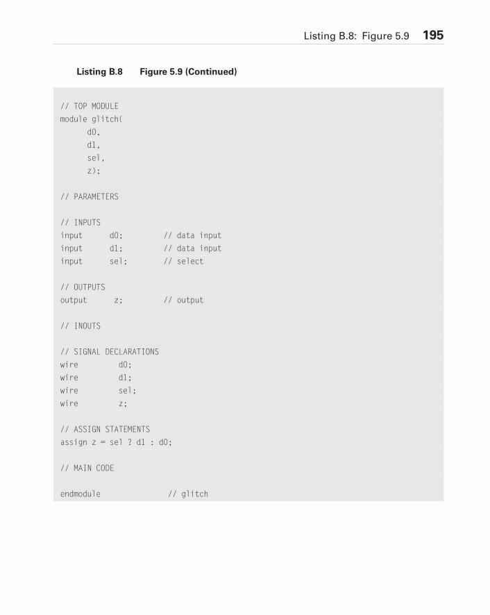
Listing B.8: Figure 5.9 195
// TOP MODULE
module glitch(
d0,
d1,
sel,
z);
// PARAMETERS
// INPUTS
input d0; // data input
input d1; // data input
input sel; // select
// OUTPUTS
output z; // output
// INOUTS
// SIGNAL DECLARATIONS
wire d0;
wire d1;
wire sel;
wire z;
// ASSIGN STATEMENTS
assign z = sel ? d1 : d0;
// MAIN CODE
endmodule // glitch
Listing B.8 Figure 5.9 (Continued)
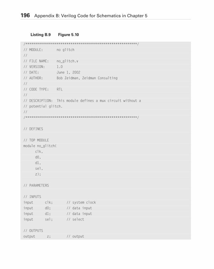
196 Appendix B: Verilog Code for Schematics in Chapter 5
Listing B.9 Figure 5.10
/*********************************************************/
// MODULE: no glitch
//
// FILE NAME: no_glitch.v
// VERSION: 1.0
// DATE: June 1, 2002
// AUTHOR: Bob Zeidman, Zeidman Consulting
//
// CODE TYPE: RTL
//
// DESCRIPTION: This module defines a mux circuit without a
// potential glitch.
//
/*********************************************************/
// DEFINES
// TOP MODULE
module no_glitch(
clk,
d0,
d1,
sel,
z);
// PARAMETERS
// INPUTS
input clk; // system clock
input d0; // data input
input d1; // data input
input sel; // select
// OUTPUTS
output z; // output
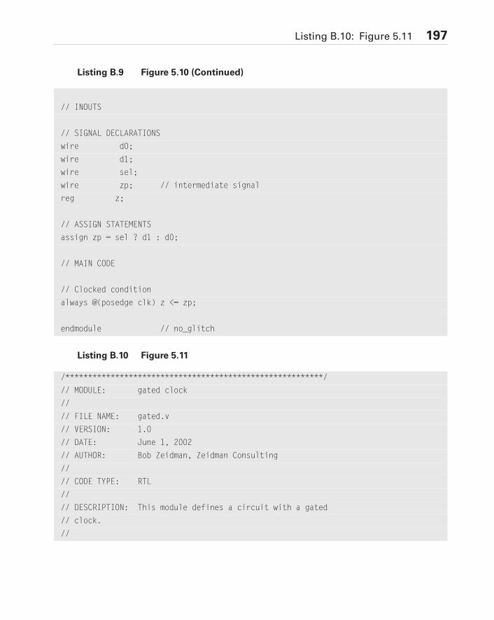
Listing B.10: Figure 5.11 197
// INOUTS
// SIGNAL DECLARATIONS
wire d0;
wire d1;
wire sel;
wire zp; // intermediate signal
reg z;
// ASSIGN STATEMENTS
assign zp = sel ? d1 : d0;
// MAIN CODE
// Clocked condition
always @(posedge clk) z <= zp;
endmodule // no_glitch
Listing B.9 Figure 5.10 (Continued)
Listing B.10 Figure 5.11
/*********************************************************/
// MODULE: gated clock
//
// FILE NAME: gated.v
// VERSION: 1.0
// DATE: June 1, 2002
// AUTHOR: Bob Zeidman, Zeidman Consulting
//
// CODE TYPE: RTL
//
// DESCRIPTION: This module defines a circuit with a gated
// clock.
//
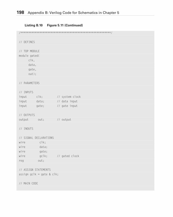
198 Appendix B: Verilog Code for Schematics in Chapter 5
/*********************************************************/
// DEFINES
// TOP MODULE
module gated(
clk,
data,
gate,
out);
// PARAMETERS
// INPUTS
input clk; // system clock
input data; // data input
input gate; // gate input
// OUTPUTS
output out; // output
// INOUTS
// SIGNAL DECLARATIONS
wire clk;
wire data;
wire gate;
wire gclk; // gated clock
reg out;
// ASSIGN STATEMENTS
assign gclk = gate & clk;
// MAIN CODE
Listing B.10 Figure 5.11 (Continued)
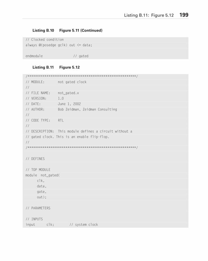
Listing B.11: Figure 5.12 199
// Clocked condition
always @(posedge gclk) out <= data;
endmodule // gated
Listing B.10 Figure 5.11 (Continued)
Listing B.11 Figure 5.12
/*********************************************************/
// MODULE: not gated clock
//
// FILE NAME: not_gated.v
// VERSION: 1.0
// DATE: June 1, 2002
// AUTHOR: Bob Zeidman, Zeidman Consulting
//
// CODE TYPE: RTL
//
// DESCRIPTION: This module defines a circuit without a
// gated clock. This is an enable flip-flop.
//
/*********************************************************/
// DEFINES
// TOP MODULE
module not_gated(
clk,
data,
gate,
out);
// PARAMETERS
// INPUTS
input clk; // system clock
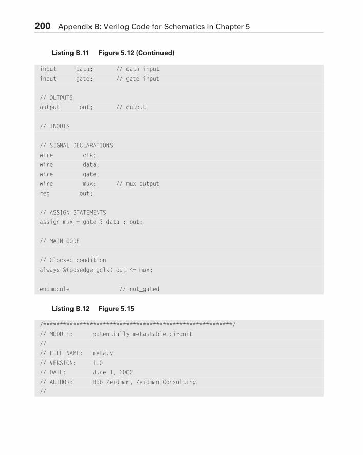
200 Appendix B: Verilog Code for Schematics in Chapter 5
input data; // data input
input gate; // gate input
// OUTPUTS
output out; // output
// INOUTS
// SIGNAL DECLARATIONS
wire clk;
wire data;
wire gate;
wire mux; // mux output
reg out;
// ASSIGN STATEMENTS
assign mux = gate ? data : out;
// MAIN CODE
// Clocked condition
always @(posedge gclk) out <= mux;
endmodule // not_gated
Listing B.11 Figure 5.12 (Continued)
Listing B.12 Figure 5.15
/*********************************************************/
// MODULE: potentially metastable circuit
//
// FILE NAME: meta.v
// VERSION: 1.0
// DATE: June 1, 2002
// AUTHOR: Bob Zeidman, Zeidman Consulting
//
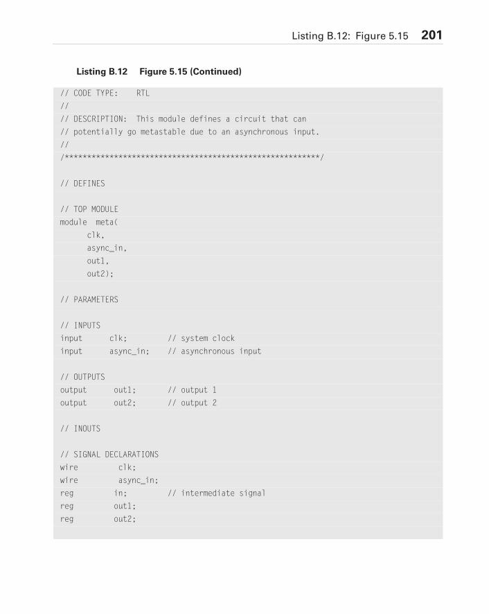
Listing B.12: Figure 5.15 201
// CODE TYPE: RTL
//
// DESCRIPTION: This module defines a circuit that can
// potentially go metastable due to an asynchronous input.
//
/*********************************************************/
// DEFINES
// TOP MODULE
module meta(
clk,
async_in,
out1,
out2);
// PARAMETERS
// INPUTS
input clk; // system clock
input async_in; // asynchronous input
// OUTPUTS
output out1; // output 1
output out2; // output 2
// INOUTS
// SIGNAL DECLARATIONS
wire clk;
wire async_in;
reg in; // intermediate signal
reg out1;
reg out2;
Listing B.12 Figure 5.15 (Continued)
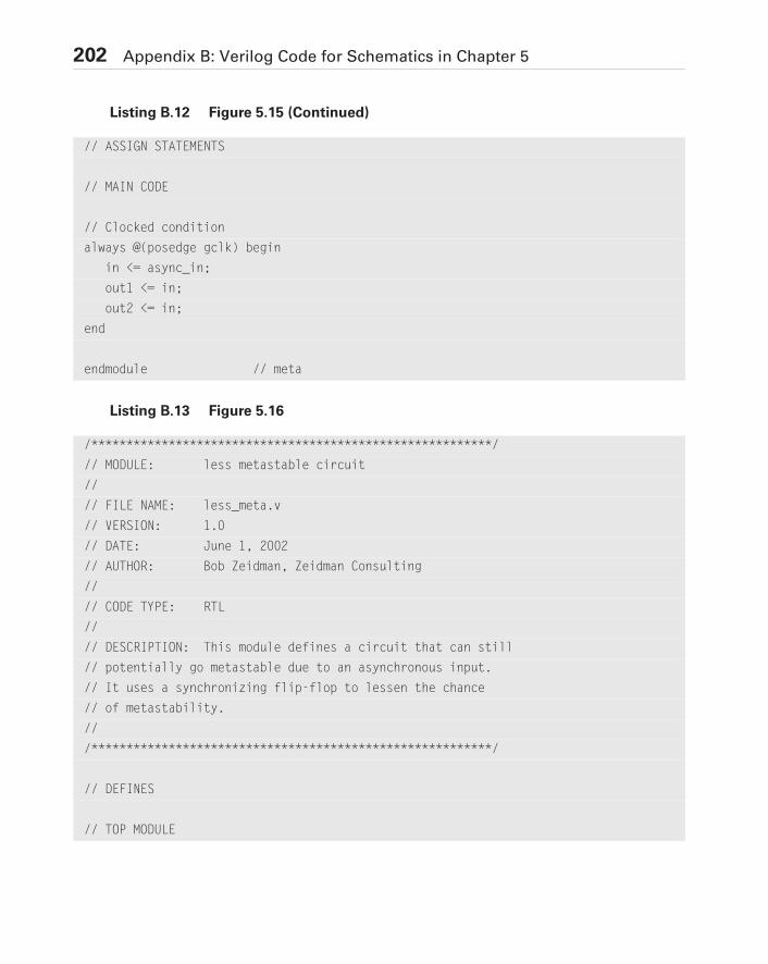
202 Appendix B: Verilog Code for Schematics in Chapter 5
// ASSIGN STATEMENTS
// MAIN CODE
// Clocked condition
always @(posedge gclk) begin
in <= async_in;
out1 <= in;
out2 <= in;
end
endmodule // meta
Listing B.12 Figure 5.15 (Continued)
Listing B.13 Figure 5.16
/*********************************************************/
// MODULE: less metastable circuit
//
// FILE NAME: less_meta.v
// VERSION: 1.0
// DATE: June 1, 2002
// AUTHOR: Bob Zeidman, Zeidman Consulting
//
// CODE TYPE: RTL
//
// DESCRIPTION: This module defines a circuit that can still
// potentially go metastable due to an asynchronous input.
// It uses a synchronizing flip-flop to lessen the chance
// of metastability.
//
/*********************************************************/
// DEFINES
// TOP MODULE
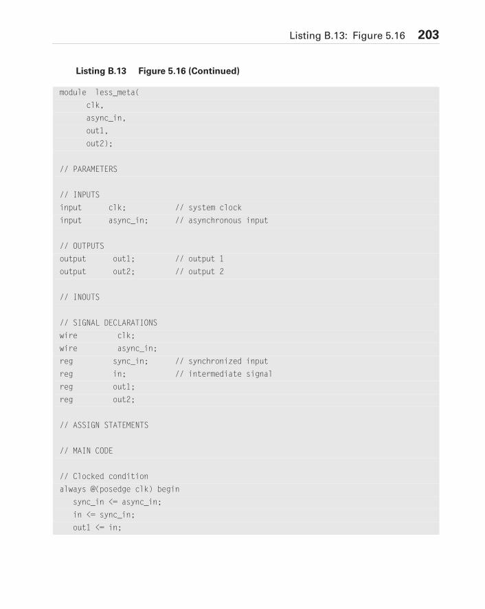
Listing B.13: Figure 5.16 203
module less_meta(
clk,
async_in,
out1,
out2);
// PARAMETERS
// INPUTS
input clk; // system clock
input async_in; // asynchronous input
// OUTPUTS
output out1; // output 1
output out2; // output 2
// INOUTS
// SIGNAL DECLARATIONS
wire clk;
wire async_in;
reg sync_in; // synchronized input
reg in; // intermediate signal
reg out1;
reg out2;
// ASSIGN STATEMENTS
// MAIN CODE
// Clocked condition
always @(posedge clk) begin
sync_in <= async_in;
in <= sync_in;
out1 <= in;
Listing B.13 Figure 5.16 (Continued)

204 Appendix B: Verilog Code for Schematics in Chapter 5
out2 <= in;
end
endmodule // less_meta
Listing B.13 Figure 5.16 (Continued)
205
GlossaryABEL — An early hardware description
language used to program PALs.
antifuse — Antifuses consist of microscopicstructures, which, unlike a regular fuse,normally make no connection. A cer-tain amount of current during program-ming of the device causes the two sidesof the antifuse to connect.
architecture — A chip architecture refers tothe high level structure of the chip.
asynchronous — An asynchronous design isany design that breaks a rule of syn-chronous design. An asynchronousdesign has delays that are not strictlycontrolled by a clock and therefore can-not be easily controlled and predicted.
ATM — Asynchronous Transfer Mode. Amethod of communicating networkdata at very high speeds.
BIST — Built-in self-test. This is a methodof including test generation and moni-toring circuitry in a chip design so thatthe chip can perform tests on itself todetermine whether it is still workingcorrectly.
Boolean Algebra — Invented by nineteenthcentury mathematician George Boole,this is an algebra that uses only the val-ues 1 and 0. In 1939, Claude Shannonwrote his revolutionary Master's thesisA Symbolic Analysis of Relay andSwitching Circuits that described forthe first time how Boolean algebracould be applied to the design of com-puters.
boundary scan — Boundary scan uses thescan methodology but scans only nodesaround the boundary of the chip, notinternal nodes. This is effective for test-ing the FPGA's connections to the cir-
206 Glossary
cuit board. It also uses much more referresources (CLBs and routing) than fullscan.
burn-in test — A burn-in test is one that isrun for a large number of hours or daysto stress the FPGA. Often, manufactur-ing problems where circuit parametersare marginal will not show up immedi-ately, but will cause a failure after ashort period of time.
CLB — Configurable logic blocks containthe logic for the FPGA. In a typicalarchitecture, called a “large-grained”architecture, these CLBs will containenough logic to create a small statemachine. In a “fine-grained” architec-ture, more like a true gate array ASIC,the CLB will contain only very basiclogic. All FPGAs available today have“large-grained” architectures.
CMOS — Complementary Metal Oxide Semi-conductor — a common, low power,type of circuit for implementing logicfunctions in which the output is drivenby two FET transistors.
code coverage — Code coverage measuresthe percentage of code statements inyour design that have been executedduring simulation in every possiblemanner.
combinatorial logic — This is the term forlogic that implements Boolean equa-tions and does not have any reliance ontiming or sequencing.
contention — Contention occurs when twoor more devices are driving the samewire at the same time.
core — The basic circuit of a specific func-tion, excluding any extraneous circuitssuch as I/O buffers that would be foundon a physical chip. For example, a pro-cessor core.
CPLD — Complex Programmable LogicDevices are chips that integrate a largenumber of PALs in a single chip, con-nected to each other through a cross-point switch.
CRC — Cyclic redundancy check — an errordetecting technique used to ensure theaccuracy of digital data transmissions.The transmitted messages are dividedinto predetermined lengths, calledframes, and a special code is appendedto the end of each frame. At the receiv-ing end, the computer recalculates theexpected code. If it does not match thetransmitted code, an error is detected.
CUPL — An early hardware descriptionlanguage used to program PALs.
decay — Decay refers to the amount oftime it takes for a signal to go from anunstable state to a stable one.
DeMorgan's Law — A law of Boolean Alge-bra that states that A & B = ~(~A | ~B)and that A | B = ~(~A & ~B). It wasnamed after the nineteenth centurymathematician Augustus De Morganwho discovered it.
Glossary 207
DFT — Design for test — This is the practiceof designing an FPGA with test circuitryincluded from the beginning.
DSP — Digital signal processor — a devicethat manipulates analog signals by con-verting them first to digital signals andthen performing digital processes onthem.
ECL — Emitter coupled logic — a commontype of circuit for implementing logicfunctions that have very fast switchingtimes.
EDA — Electronic design automation refersto tools for designing electronic devices.
EEPROM — Electrically erasable PROMsare read-only memories that can be pro-grammed and erased using a highervoltage than that used in normal opera-tion.
EPROM — Erasable PROMs are read-onlymemories that can be programmed withan electric current, but are erased usingprolonged exposure to ultraviolet light.
equivalency checking — A type of formalverification that uses mathematicaltechniques to compare one design toanother design to prove that they areequivalent. Thus if the first design isknown to work correctly, the seconddesign must also work correctly.
fine-grained architecture — Fine-grainedFPGAs resemble ASIC gate arrays inthat the CLBs contain only small, very
basic elements such as NAND gates,NOR gates, etc.
flash EPROM — Flash EPROM can be elec-trically programmed. Large sections canthen be electrically erased very quickly.These memories have very fast accesstimes compared to other types ofPROMs, which are very slow.
floating — A floating signal is one that isnot being actively driven to a logic 1 orlogic 0.
formal verification — A mathematical tech-nique for checking the functionality of adesign. There are two types of formalverification: equivalency checking andfunctional verification.
FPGA — Field Programmable Gate Arraysare programmable chips that are struc-tured very much like a gate array ASIC.
full scan — Full scan involves linking eachflip-flop in a design into a scan chain.Sequences of values can then be scannedinto and out of the chain in order to testthe FPGA.
functional simulation — This term refers tosimulating a design without consideringactual timing numbers. This gives agood idea of whether the basic design iscorrect.
functional verification — A type of formalverification that uses formal mathemati-cal techniques to prove that a condition
208 Glossary
(also called a property or assertion) canor cannot exist for a specific design.
glitch — An unexpected signal or shortduration.
HDL — Hardware description language —these languages, such as Verilog andVHDL, are used to design a complexchip using programming language state-ments.
hold time — This is the amount of time thata signal on the input to a clocked devicemust be stable after a clock edge inorder to guarantee that the clockeddevice will capture the correct value.
in-system programmability — The ability toreprogram a programmable devicewhile it is soldered in a system and thesystem is powered up. SRAM-baseddevices can be programmed in-system.EPROM-, EEPROM-, and FlashPROM–based devices can be pro-grammed in-system if the deviceincludes the pins and internal circuitryto support this feature.
IP — Intellectual property — the parts of achip design that are considered uniqueand are protected by patent laws. Usu-ally this refers to a particular functionthat has been designed and tested andcan be purchased to be used in anotherdesign. This type of IP does not have aphysical implementation, but is typi-cally represented by a hardware lan-guage description.
ISP — In-system programmability — theability to reprogram a programmabledevice while it is in a system that is cur-rently powered up and running.
JTAG — Joint Test Action Group — This termis commonly used to refer to the IEEEStandard 1149.1, which defines a spe-cific form of boundary scan implemen-tation. The name of the standard hascome to be known by the name of thegroup that developed the standard, inthe same way that the monster createdby Dr. Frankenstein has come to beknown by its creator's name.
large-grained architecture — In alarge-grained FPGA, the CLB containslarger functionality logic. For example,it can contain two or more flip-flopsand multiplexers and lookup tables(LUTs).
LUT — lookup table — the small SRAM in aCLB of an SRAM-based FPGA that isused to implement Boolean logic.
LVDS — low voltage differential signaling —a low noise, low power, low amplitudecircuit for transmitting data athigh-speeds.
macrofunction — A macrofunction, ormacro, is simply a large, predefined,tested circuit that can be used freely indifferent FPGA designs.
metastability — Metastability refers to astate of an object that is stable, but anysmall disturbance to the object will
Glossary 209
cause it to leave the state. For example,a spoon lying on the floor is in a stablestate. A spoon balanced on your nose isin a metastable state because any smalldisturbance will cause it to exit the cur-rent state and move into a stable state,on the floor. An asynchronous signalentering a synchronous circuit cancause the circuit to go into a metastablestate, causing the circuit to becomeunpredictable.
Moore’s Law — The original statement ofthis “law” in 1965 was that the numberof transistors per integrated circuit dou-ble every couple of years. This “law” isreally an observation that has heldapproximately true since 1965 when itwas first stated by Gordon Moore, afounder, President, CEO, and Chairmanof Intel Corporation. In order to remainaccurate, people have modified the“law” from time to time to compensatefor new observations. As of this writing,the “law” is that the number of inte-grated circuits per square inch doublesevery 18 months.
mux — This is simply the short name for amultiplexer.
node — A node is the output of any gate inthe design.
one-hot encoding — This is a method ofdesigning state machines whereby eachstate is represented by a single flip-flop.This design method greatly reduces thecombinatorial logic and uses moreflip-flops than traditional state machine
encoding, which makes more efficientuse of the “large-grained” CLBs in anFPGA, which are the only kind ofFPGAs currently available.
open drain — An output that can be drivento a low value or not driven at all. Itcannot be driven to a high value.
PAL — Programmable arrays of logic arechips that are good for implementingstate machines. Internally, like a PLA,they have large AND plane but a fixedsize OR plane. In addition, there areoften flip-flops and sometimes otherlogic such as XOR gates.
PALASM — An early hardware descriptionlanguage used to program PALs.
PECL — Positive emitter coupled logic — acommon type of circuit for implement-ing logic functions. Similar to ECL, butthe power supply for the logic is a posi-tive voltage.
PLA — Programmable logic arrays arechips that are good for implementingcombinatorial logic. Internally, theyhave a large number of inputs con-nected to an AND plane, the outputs ofwhich go into a large OR plane.
place — This refers to placing logic insideCLBs of an FPGA in order to imple-ment the FPGA design.
Plan Nine from Outer Space — The worstmovie of all time, directed by Ed Wood,
210 Glossary
the worst director of all time. Highlyrecommended.
pragma — A message written into HDLcode that tells the synthesis program tosynthesize the design in some fashionthat differs from the default method.For example, pragmas may alter thekinds of error messages that are gener-ated or optimize the design in someway.
product terms — Terms in a Boolean equa-tion that are ANDed together.
PROM — Programmable read only memorycan be easily programmed with specificcontents. Once programmed, the datacannot be erased.
pseudorandom — This refers to a sequenceof numbers that are predictable andrepeatable, but are produced in such away that they have the same character-istics and distribution as numbers thatare selected randomly.
race condition — A race condition occurs inan asynchronous circuit when the func-tion is dependent on which of two sig-nals get to a certain point first, and thewinner of this race depends not on acontrolled period of time, but the tim-ing characteristics of the circuit.
regression testing — Successively running aset of simulation tests on a design thathas been modified to determine that themodifications have not introduced newproblems.
route — This refers to connecting CLBsand I/O blocks inside the FPGA, usingthe routing resources, to implement theFPGA design.
RTL — Register transfer level — this is alevel of description using a hardwaredescription language (HDL) thatdescribes circuitry in terms of clocks,Boolean equations, and registers.
scan — Scan methodology involves creat-ing scan chains from the flip-flops in adesign so that sequences of values canbe scanned into and out of the chain inorder to test the FPGA.
scan chain — A scan chain is a structurewhere the output of each flip-flop in thechain is connected to the input of thenext flip-flop in the chain. In this way,sequences of values can be scanned intoand out of the chain in order to test theFPGA.
setup time — This refers to the amount oftime before a clock edge that a signalmust be stable on the input to a clockeddevice in order for the device to recordthe correct input value.
signature — The signature of an FPGArefers to the pattern that is expected tobe output from the chip after a longdeterministic sequence of inputs.
slew rate — The slew rate of a signal is areference to how quickly it changesvoltage.
Glossary 211
SOPC — System on a programmable chip —this term is used to describe a very com-plex and very dense programmabledevice, a CPLD or FPGA, that can con-tain so much logic that it can be consid-ered an entire system.
SRAM — Static random access memory ismemory that can be written and readnumerous times while in the system. Itis very fast, and loses its data when itloses power.
static timing analysis — Static timing analy-sis is a process that looks at a synchro-nous design and determines the highestoperating frequency of the design thatdoes not violate any setup and holdtimes.
sum terms — Terms in a Boolean equationthat are ORed together.
synchronous — Synchronous designadheres to the following rules:
• All data is passed through combi-natorial logic, and through delay elements (typically flip-flops) that are synchronized to a single clock.
• Delay is always controlled by delay elements, not combinatorial logic.
• No signal that is generated by combinatorial logic can be fed back to the same combinatorial logic without first going through a synchronizing delay element.
• Clocks cannot be gated; clocks must go directly to the clock inputs of the delay elements with-out going through any combina-torial logic.
• Data signals must go only to com-binatorial logic or data inputs of delay elements.
testbench — The simulation code that gen-erates stimulus to a design and exam-ines the outputs of the design.
threshold — The threshold of a gate is thevoltage value or range of the input atwhich the output begins to changevalue.
timing simulation — Timing simulationinvolves including timing informationin a functional simulation so that thereal behavior of the chip is simulated.As a method of timing analysis, it isbecoming less and less popular.
toggle coverage — When performing func-tional simulation, a rough estimate ofthe amount of simulation to perform iscalled toggle coverage, which measuresthe number of nodes in the FPGA thatchange state from 0 to 1 and from 1 to0 during simulation as a percentage ofthe total number of possible state tran-sitions (two per node because each nodecan change from 0 to 1 and from 1 to0).
top-down design — Top-down design is thedesign method whereby high level func-tions are defined first and the lower

212 Glossary
level implementation details are filled inlater.
TTL — Transistor-transistor logic — a com-mon type of circuit for implementinglogic functions in which the output isdriven by two BJT transistors.
Verilog — A standard hardware descriptionlanguage, maintained by the Institute ofElectrical and Electronic Engineers asIEEE-STD-1364.
VHDL — A standard hardware descriptionlanguage, maintained by the Institute ofElectrical and Electronic Engineers asIEEE-STD-1076.
213
ReferencesLogic Design Manual for ASICs. Santa Clara, CA: LSI Logic Corporation,
1989.
Davenport Jr., Wilbur B. Probability and Random Processes. New York, NY:McGraw-Hill Book Company, 1970.
Dorf, Richard C., editor. Electrical Engineering Handbook. Boca Raton, FL:CRC Press, Inc., 1993.
EDA Industry Working Groups Web site, www.eda.org
Maxfield, Clive “Max.” Designus Maximus Unleashed! Woburn, MA: Butter-worth-Heinemann, 1998.
Zeidman, Bob. Introduction to Verilog. Piscataway, NJ: Institute of Electricaland Electronic Engineers, 2000.
Zeidman, Bob. Verilog Designer’s Library. Upper Saddle River, NJ: Pren-tice-Hall, Inc., 1999.
214 References
About the AuthorBob Zeidman is the president of Zeidman Consulting (www.ZeidmanConsult-ing.com), an EDA firm offering tools for simulating, prototyping, and emulating net-work devices. He is also the founder and president of The Chalkboard Network(www.chalknet.com), which provides seminars and courses on high tech topics viathe Internet. Since the early eighties, Bob has designed integrated circuits and circuitboards and has written software for many different types of systems. As a consult-ant, his clients have included Apple Computer, Cisco Systems, Ikos Systems andTexas Instruments. Among his publications are technical papers on hardware andsoftware design methods as well as two textbooks — Verilog Designer’s Library pub-lished by Prentice-Hall and Introduction to Verilog published by IEEE Press. He hasinstructed courses at engineering conferences throughout the world. Bob earnedbachelor's degrees in physics and electrical engineering at Cornell University and amaster's degree in electrical engineering at Stanford University.
215
Index
Numerics10/10 rule 112–113, 1294-bit numbers 75
AABEL 5, 7, 205ABEL program 7Actel Corporation
Designer® 157algorithmic model 75Altera Corporation 143, 155,
167ALU 34, 89, 151AND 97, 104AND plane 5–6, 16, 18answer key
See Appendix Aantifuse 34, 43, 49, 205
connections 44programming 44
Application Specific Integrat-ed Circuit
See ASICarchitectural model 75architecture 169, 205ASIC 14–16, 36, 45, 48, 75,
87–88, 94, 112, 117,142
embedded FPGA cell170–172
emulating 45–48emulation 47prototyping 45, 48
ASICs xii–xiii, 1, 13assertion language 137–138asynchronous bus 107asynchronous clock 21
asynchronous design 35, 74,92, 95, 97–101, 103,106, 205
asynchronous latch 107asynchronous logic
uses 106–108asynchronous reset 93, 106asynchronous signals 101ATE 132ATM 205ATPG 117, 153, 161automatic test equipment
See ATEautomatic test pattern genera-
tionSee ATPG
avalanche injection 3
Bbattle switch 114behavioral block 134–135behavioral description 58behavioral level simulation
138behavioral model 74, 89BIST 118–121, 137, 142,
154–155, 162, 205logic 119
block diagram 58internal and external 58
bonding pads 13Boolean Algebra 205Boolean equation 5–6, 18, 34Boolean expression 94Boolean function 75Boolean logic 77boundary node 121boundary scan 117–118, 205
bufferinput 37output 39
built-in self-testSee BIST
burn-in test 206bus 37, 143
contention 42, 109, 121controller 89floating 38, 42three-state 41
CC language 75calculating
power consumption 62Chalkboard Network 214circuit layout 13circuit synthesis 13Cisco Systems 38CLB 34–36, 39–43, 49, 90,
110, 206fine grain vs. large grain
36clock 19, 21, 28–29, 101
buffers 42domain 93frequencies 14, 61gated 101input 7, 25, 29signal 49, 93skew times 43tree 43
clock driver 21, 30and CPLDs 21FPGA 42–43
CMOS 37–38, 96, 103, 108,206
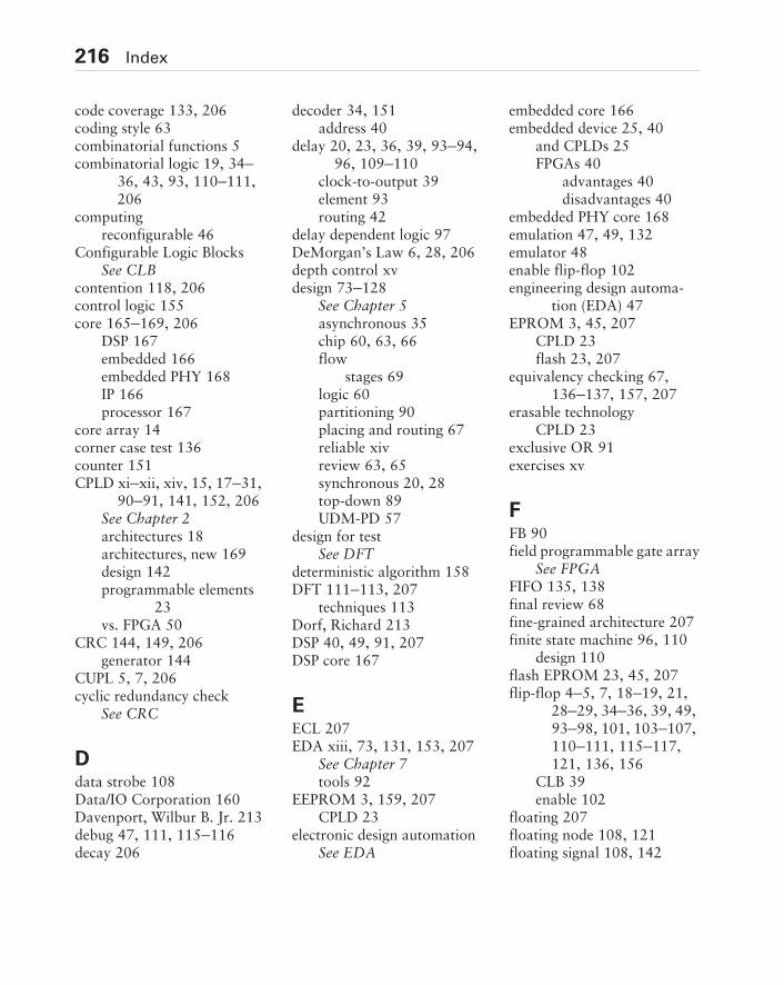
216 Index
code coverage 133, 206coding style 63combinatorial functions 5combinatorial logic 19, 34–
36, 43, 93, 110–111,206
computingreconfigurable 46
Configurable Logic BlocksSee CLB
contention 118, 206control logic 155core 165–169, 206
DSP 167embedded 166embedded PHY 168IP 166processor 167
core array 14corner case test 136counter 151CPLD xi–xii, xiv, 15, 17–31,
90–91, 141, 152, 206See Chapter 2architectures 18architectures, new 169design 142programmable elements
23vs. FPGA 50
CRC 144, 149, 206generator 144
CUPL 5, 7, 206cyclic redundancy check
See CRC
Ddata strobe 108Data/IO Corporation 160Davenport, Wilbur B. Jr. 213debug 47, 111, 115–116decay 206
decoder 34, 151address 40
delay 20, 23, 36, 39, 93–94,96, 109–110
clock-to-output 39element 93routing 42
delay dependent logic 97DeMorgan’s Law 6, 28, 206depth control xvdesign 73–128
See Chapter 5asynchronous 35chip 60, 63, 66flow
stages 69logic 60partitioning 90placing and routing 67reliable xivreview 63, 65synchronous 20, 28top-down 89UDM-PD 57
design for testSee DFT
deterministic algorithm 158DFT 111–113, 207
techniques 113Dorf, Richard 213DSP 40, 49, 91, 207DSP core 167
EECL 207EDA xiii, 73, 131, 153, 207
See Chapter 7tools 92
EEPROM 3, 159, 207CPLD 23
electronic design automationSee EDA
embedded core 166embedded device 25, 40
and CPLDs 25FPGAs 40
advantages 40disadvantages 40
embedded PHY core 168emulation 47, 49, 132emulator 48enable flip-flop 102engineering design automa-
tion (EDA) 47EPROM 3, 45, 207
CPLD 23flash 23, 207
equivalency checking 67,136–137, 157, 207
erasable technologyCPLD 23
exclusive OR 91exercises xv
FFB 90field programmable gate array
See FPGAFIFO 135, 138final review 68fine-grained architecture 207finite state machine 96, 110
design 110flash EPROM 23, 45, 207flip-flop 4–5, 7, 18–19, 21,
28–29, 34–36, 39, 49,93–98, 101, 103–107,110–111, 115–117,121, 136, 156
CLB 39enable 102
floating 207floating node 108, 121floating signal 108, 142
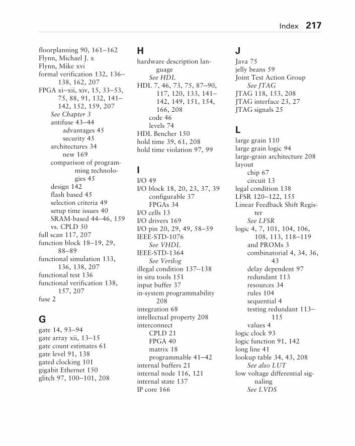
Index 217
floorplanning 90, 161–162Flynn, Michael J. xFlynn, Mike xviformal verification 132, 136–
138, 162, 207FPGA xi–xii, xiv, 15, 33–53,
75, 88, 91, 132, 141–142, 152, 159, 207
See Chapter 3antifuse 43–44
advantages 45security 45
architectures 34new 169
comparison of program-ming technolo-gies 45
design 142flash based 45selection criteria 49setup time issues 40SRAM-based 44–46, 159vs. CPLD 50
full scan 117, 207function block 18–19, 29,
88–89functional simulation 133,
136, 138, 207functional test 136functional verification 138,
157, 207fuse 2
Ggate 14, 93–94gate array xii, 13–15gate count estimates 61gate level 91, 138gated clocking 101gigabit Ethernet 150glitch 97, 100–101, 208
Hhardware description lan-
guageSee HDL
HDL 7, 46, 73, 75, 87–90,117, 120, 133, 141–142, 149, 151, 154,166, 208
code 46levels 74
HDL Bencher 150hold time 39, 61, 208hold time violation 97, 99
II/O 49I/O block 18, 20, 23, 37, 39
configurable 37FPGAs 34
I/O cells 13I/O drivers 169I/O pin 20, 29, 49, 58–59IEEE-STD-1076
See VHDLIEEE-STD-1364
See Verilogillegal condition 137–138in situ tools 151input buffer 37in-system programmability
208integration 68intellectual property 208interconnect
CPLD 21FPGA 40matrix 18programmable 41–42
internal buffers 21internal node 116, 121internal state 137IP core 166
JJava 75jelly beans 59Joint Test Action Group
See JTAGJTAG 118, 153, 208JTAG interface 23, 27JTAG signals 25
Llarge grain 110large grain logic 94large-grain architecture 208layout
chip 67circuit 13
legal condition 138LFSR 120–122, 155Linear Feedback Shift Regis-
terSee LFSR
logic 4, 7, 101, 104, 106,108, 113, 118–119
and PROMs 3combinatorial 4, 34, 36,
43delay dependent 97redundant 113resources 34rules 104sequential 4testing redundant 113–
115values 4
logic clock 93logic function 91, 142long line 41lookup table 34, 43, 208
See also LUTlow voltage differential sig-
nalingSee LVDS
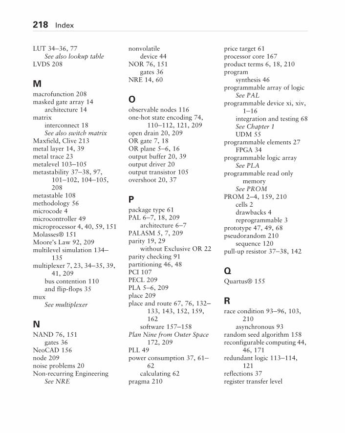
218 Index
LUT 34–36, 77See also lookup table
LVDS 208
Mmacrofunction 208masked gate array 14
architecture 14matrix
interconnect 18See also switch matrix
Maxfield, Clive 213metal layer 14, 39metal trace 23metalevel 103–105metastability 37–38, 97,
101–102, 104–105,208
metastable 108methodology 56microcode 4microcontroller 49microprocessor 4, 40, 59, 151Molasses® 151Moore’s Law 92, 209multilevel simulation 134–
135multiplexer 7, 23, 34–35, 39,
41, 209bus contention 110and flip-flops 35
muxSee multiplexer
NNAND 76, 151
gates 36NeoCAD 156node 209noise problems 20Non-recurring Engineering
See NRE
nonvolatiledevice 44
NOR 76, 151gates 36
NRE 14, 60
Oobservable nodes 116one-hot state encoding 74,
110–112, 121, 209open drain 20, 209OR gate 7, 18OR plane 5–6, 16output buffer 20, 39output driver 20output transistor 105overshoot 20, 37
Ppackage type 61PAL 6–7, 18, 209
architecture 6–7PALASM 5, 7, 209parity 19, 29
without Exclusive OR 22parity checking 91partitioning 46, 48PCI 107PECL 209PLA 5–6, 209place 209place and route 67, 76, 132–
133, 143, 152, 159,162
software 157–158Plan Nine from Outer Space
172, 209PLL 49power consumption 37, 61–
62calculating 62
pragma 210
price target 61processor core 167product terms 6, 18, 210program
synthesis 46programmable array of logic
See PALprogrammable device xi, xiv,
1–16integration and testing 68See Chapter 1UDM 55
programmable elements 27FPGA 34
programmable logic arraySee PLA
programmable read only memory
See PROMPROM 2–4, 159, 210
cells 2drawbacks 4reprogrammable 3
prototype 47, 49, 68pseudorandom 210
sequence 120pull-up resistor 37–38, 142
QQuartus® 155
Rrace condition 93–96, 103,
210asynchronous 93
random seed algorithm 158reconfigurable computing 44,
46, 171redundant logic 113–114,
121reflections 37register transfer level
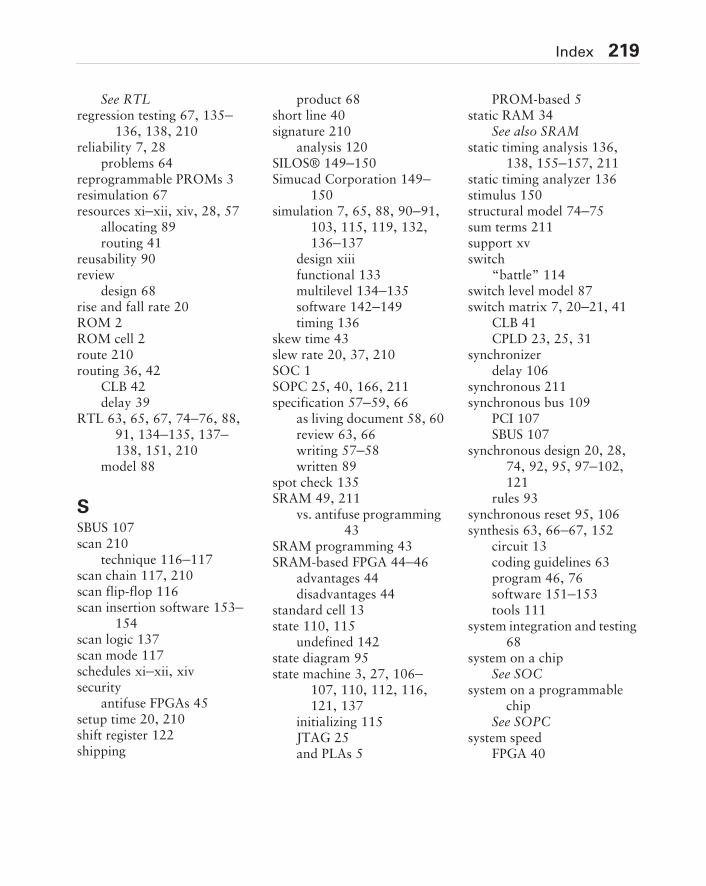
Index 219
See RTLregression testing 67, 135–
136, 138, 210reliability 7, 28
problems 64reprogrammable PROMs 3resimulation 67resources xi–xii, xiv, 28, 57
allocating 89routing 41
reusability 90review
design 68rise and fall rate 20ROM 2ROM cell 2route 210routing 36, 42
CLB 42delay 39
RTL 63, 65, 67, 74–76, 88,91, 134–135, 137–138, 151, 210
model 88
SSBUS 107scan 210
technique 116–117scan chain 117, 210scan flip-flop 116scan insertion software 153–
154scan logic 137scan mode 117schedules xi–xii, xivsecurity
antifuse FPGAs 45setup time 20, 210shift register 122shipping
product 68short line 40signature 210
analysis 120SILOS® 149–150Simucad Corporation 149–
150simulation 7, 65, 88, 90–91,
103, 115, 119, 132,136–137
design xiiifunctional 133multilevel 134–135software 142–149timing 136
skew time 43slew rate 20, 37, 210SOC 1SOPC 25, 40, 166, 211specification 57–59, 66
as living document 58, 60review 63, 66writing 57–58written 89
spot check 135SRAM 49, 211
vs. antifuse programming43
SRAM programming 43SRAM-based FPGA 44–46
advantages 44disadvantages 44
standard cell 13state 110, 115
undefined 142state diagram 95state machine 3, 27, 106–
107, 110, 112, 116,121, 137
initializing 115JTAG 25and PLAs 5
PROM-based 5static RAM 34
See also SRAMstatic timing analysis 136,
138, 155–157, 211static timing analyzer 136stimulus 150structural model 74–75sum terms 211support xvswitch
“battle” 114switch level model 87switch matrix 7, 20–21, 41
CLB 41CPLD 23, 25, 31
synchronizerdelay 106
synchronous 211synchronous bus 109
PCI 107SBUS 107
synchronous design 20, 28,74, 92, 95, 97–102,121
rules 93synchronous reset 95, 106synthesis 63, 66–67, 152
circuit 13coding guidelines 63program 46, 76software 151–153tools 111
system integration and testing68
system on a chipSee SOC
system on a programmable chip
See SOPCsystem speed
FPGA 40
220 Index
TTDI input 27TDO pin 27test circuitry 118Test Clock Input 25Test Data Input 25Test Data Output 25test logic 112–113, 119Test Mode Select 25Test Reset Input 25test vector 7, 120testbench 144, 150, 211
generator 144, 150–151testing 49, 61, 64, 68, 112
10/10 rule 129procedures 61redundant logic 113–115
three-state bus 137threshold 211
voltages 37timing 23, 65, 103
analysis 67, 132estimates 61number 23
timing simulation 136, 138,156, 211
TMS input 27toggle coverage 134, 211tool
floorplanning 158–159,161
place and route 143programming 159–160simulation 141
top-down design 88–91, 211allocating resources 89HDL use 88–89written specification 89
top-level block 89transistor-transistor logic
See TTLtri-state driver 110TRST pin 27TTL 37, 212tunneling 3
UUART 66UDM 55–57, 70
goals 57UDM-PD xii, 55–71
See Chapter 4design flow 57goals 69summary 69
undefined state 142undershoot 20, 37Universal Design Methodolo-
gySee UDM
Universal Design Methodolo-gy for Programmable
DevicesSee UDM-PD
utilization 65
Vvector 119–120verification 7, 65, 67, 91, 132
See Chapter 6software 157
Verilog xiii, 7, 73, 88, 212code 144
VHDL 7, 73, 88, 212VME bus 107voting logic 113
WWard, Robert xvi
XXilinx Corporation 143, 150,
156, 167XOR 19, 28
ZZeidman Consulting 214Zeidman, Bob ix, 213–214

Let’s compare your choices...
GO BACK TO SCHOOL... TAKE A CHALKBOARD COURSE...
Practical Statechartsin C/C++
In the spirit of eXtreme programming, the
author’s quantum programming is a light-
weight method that allows programmers to
quickly hand-code working, real-time systems
in C and C++ directly from UML statecharts.
You get a cookbook with step-by-step in-
structions and complete source code to the
state-oriented framework. CD-ROM included,
388pp, ISBN 1-57820-110-1, $44.95
by Miro Samek
Order direct 800-500-6875
fax 408-848-5784
e-mail: [email protected]
www.cmpbooks.com
Find CMP Books in your local bookstore.
An Introduction to Quantum Programming
Develop a solid understanding of the math
behind common functions — and learn
how to make your programs run faster and
more efficiently! You get a solid course in
applied math from the renowned
columnist of Embedded Systems
Programming Magazine — and a versatile
set of algorithms to use in your own
projects. CD-ROM included, 466pp,
ISBN 1-929629-09-5, $49.95
Math Toolkit forReal-Time Programming
by Jack W. Crenshaw
Free shippingin the US & Canadafrom
www.cmpbooks.com
TCP/IP LeanWeb Servers for Embedded Systems
by Jeremy Bentham
Order direct 800-500-6875
fax 408-848-5784
e-mail: [email protected]
www.cmpbooks.com
Find CMP Books in your local bookstore.
Second Edition
Implement dynamic Web programming
techniques with this hands-on guide to
TCP/IP networking. You get source code and
fully-functional utilities for a simple TCP/IP
stack that’s efficient to use in embedded
applications. This edition shows the Web
server porting to the PIC16F877 chip as well
as over an ethernet connection. Includes a demonstration port running on
Microchip’s PICDEM.Net demonstration board. CD-ROM included, 559pp,
ISBN 1-57820-108-X, $59.95
MicroC/OS-II,The Real-Time Kernel
Second Edition
by Jean J. Labrosse
Free shippingin the US & Canadafrom
www.cmpbooks.com
Learn the inner workings of an RTOS! This
release of MicroC/OS adds documentation for
several important new features of the latest
version of the software, including new real-
time services, floating points, and coding
conventions. It is a completely portable,
ROMable, preemptive real-time kernel. Complete code is
included for use in your own applications. Hardcover, CD-
ROM included, 606pp, ISBN 1-57820-103-9, $74.95
Order direct 800-500-6875
fax 408-848-5784
e-mail: [email protected]
www.cmpbooks.com
Find CMP Books in your local bookstore.
Simulation Engineering
by Jim Ledin
PPP forEmbedded Systems
by John Bartas
Learn when and how to use simulation
methods. The entire range of important
techniques are presented, beginning with
the fundamentals of mathematical models,
how to produce useful results, how to
analyze the data and how to validate the
models. Each chapter provides step-by-
step instructions for developing a working
simulation. Includes a review of state-of-
the-art tools and administrative guidelines on management and
communications. 303pp, ISBN 1-57820-080-6, $44.95
Adapt PPP to stand-alone, embedded
applications. You get details of the PPP
protocol, C implementations of key
algorithms, and a demonstration of a port
to a commonly used microcontroller. Learn
what kinds of special issues you may
encounter in embedded systems
implementations, as well as how the protocol will interact with other
network components. 336pp, ISBN 1-57820-123-3, $39.95.