message scrolling board based on sms relaying implemented using arduino mega and gsm modem methodist...
TRANSCRIPT
Message Scrolling Board based on SMS Relaying Implemented using Arduino Mega and GSM Modem
PROJECT REPORT
SUBMITTED IN PARTIAL FULLFILMENT OF THE REQUIREMENT FOR THE
AWARD OF THE DEGREE OF
BACHELOR OF ENGINEERING
ELECTRONICS AND COMMUNICATION ENGINEERING
Submitted by: Project Supervisor:
Khaja Ebadur Rahman (160712735054) Mr. M. Satish Yadav (Asst. Professor)
Bodampati Satish Chandra (160712735055)
Abdus Saboor Asad (160712735056) Internal Guide:
Mr. D. Suresh (Asst. Professor)
Methodist College of engineering and technology
King Koti, Hyderabad
2015-2016

CERTIFICATE
This is to certify that the dissertation work entitled ‘Message Scrolling Board based on SMS Relaying Implemented using Arduino Mega
and GSM Modem’ is the work done by _____________________________________________submitted in partial
fulfillment for the award of ‘MASTER OF ENGINEERING (M.E)’ in ____________________________ Engineering from ___________ College of
Engineering affiliated to _________ University , Hyderabad .
Internal Guide Head of the department Mr. D. Suresh (Asst.prof) DR.N.H.SHOBA REDDY Department of ECE MCET
EXTERNAL EXAMINER

ACKNOWLEDGEMENT
The satisfaction and euphoria that accompany the successful completion of any task
would be incomplete without the mentioning of the people whose constant guidance and
encouragement made it possible. We take pleasure in presenting before you, our project,
which is result of studied blend of both research and knowledge.
We express our earnest gratitude to our internal guide, Assistant Professor Mr.D.Suresh,
Department of ECE, our project guide, for his constant support, encouragement and
guidance. We are grateful for his cooperation and his valuable suggestions.

DECLARATION
We, the undersigned, declare that the project entitled ‘Message Scrolling Board based on SMS Relaying Implemented using Arduino Mega and GSM Modem’, being submitted in partial fulfillment for the award of Bachelor of Engineering
Degree in Electronics and Communication Engineering, affiliated to OSMANIA University, is the work carried out by us.
Khaja Ebad-ur-Rahman Bodampati Satish Chandra Abdus Saboor Asad
160712735054 160712735055 1607127355056

Contents
Abstract
Chapter-1: Overview of project
1.1 Introduction
1.2 Aim of our project
1.3 Block Diagram
1.4 Description of Block Diagram
Chapter 2: Arduino board with Atmega328 microcontroller
2.1 Introduction
2.2Characteristics of Arduino board
2.3 Board description
2.4 Pin configuration of Atmega328
2.5 Pin description
2.6 Block diagram
2.7 Why Arduino?
Chapter 3: GSM Technology
3.1 Introduction
3.2 Technical Details
A. Network Structure
B. Base Station Subsystem
C. GSM Carrier Frequencies
D. Subscriber Identity Module (SIM)
3.3 Phone Locking
3.4 History
3.5 GSM MODEM-PC Interfacing
3.6 GSM Modem (900/1800 MHz)
Chapter 4: Shift Registers
4.1 Introduction
4.2 Serial-in and serial-out (SISO)
4.3 Serial-in, parallel-out (SIPO)

4.4 Parallel-in, Serial-out (PISO)
4.5 Uses
4.6 History
4.7 74HC595 8 bit Shift Register Module for Arduino
A. General Description
B. Features and benefits
C. Applications
D. Pinning Info
4.8 Interfacing of Arduino and 74HC595Chapter 5: SD CARD & MODULE
Chapter 6: LIGHT EMITTING DIODES (LEDs)
6.1 Introduction
6.2 History
6.3 Working Principle
6.4 Applications
Chapter 7: Led Displays
7.1 Introduction
7.2 History
7.3 Dot Matrix Display
7.4 Seven Segment Display (SSD)
7.5 LED matrix
7.6 Interfacing LED Matrix with Arduino
Chapter 8: Software
8.1 Arduino IDE
Abstract
Message Scrolling Board based on SMS Relaying Implemented using Arduino Mega and GSM Modem
Every institution, organization or any commercial establishment would be glad to
announce any new event or activity to the public. Or there is a necessity to announce some
important headlines in public. This can be achieved by a person announcing for quite some time
or for convenience LED boards can be installed and the news scrolls on the LED board. Such
boards utilize microcontroller and the message to be displayed is fed to it only once. But it is
devoid of the flexibility of changing the message. Well this can also be achieved if there is a way
to feed the microcontroller with message dynamically.
Hence, this project aims at achieving the above purpose using GSM module which can
feed the message dynamically. There is one particular advantage of using GSM Modem in this
project. Since this involves SMS, the user can display message of choice even he/she is at any
given place.
GSM based Message Relaying and Displaying on LED Board is an automated
microcontroller electronic system which scrolls text on an LED board, the message to be
displayed can be dynamically changed using GSM module to which the user sends an SMS. The
user also gets an acknowledgement in form of SMS on successfully displaying the text. In this
project not all LEDs are switched ON at a time, but they are switched ON and OFF alternatively.
But the gap is made as small as 20ms (micro seconds). So the principle used here is PoV
(Persistence of Vision). They appear to be glowing all at a time. This way number of pins used is
reduced to minimal.
When the user sends a text to be displayed via SMS, GSM module receives and transfers
the text to Arduino. The code in Arduino converts each character in the text into a 2 Dimensional
array of 1’s and 0’s. The array size depends on the size of the LED matrix being used on the
LED display board. These 1’s and 0’s are fed to LED driver circuit, which does its own unique
role. If the message is successfully displayed, the Arduino sends a confirmation SMS to the user
through GSM module.

LED Matrix is an ‘n’ number of either 8x8 or 5x7 matrices or sometime a single matrix
of 96 columns and 7 rows made of LED’s, which receive data one after the other, i.e., they are
cascaded in series by the LDE driver circuit.
In conclusion, this microcontroller based displaying of text on LED matrices board is
advantageous, not to mention low cost, by providing dynamic yet simple and flexible aid to
institutions, organizations or commercial establishments to display and scroll texts. The scope of
application of this project can be expanded by the choice of the user. Our project is a modest
prototype of integrating GSM and LED scrolling.

CHAPTER 01
OVERVIEW OF PROJECT
1.1 INTRODUCTION
Over the last few years, the GSM cellular phone has grown from a luxury item owned by
the rich to something so common that one out of five people already owns one. This is amazing
when we look at the fact that our country is a developing one with almost half our population
living below the poverty line. This continuously growing popularity of the GSM cell phone has
spurred the growth of the country’s cellular network infrastructure. The primary reason we can
see for this tremendous and unexpected cellular boom is the popularity of the short message
service (SMS). A variety of services have grown around SMS.
The led Display System is aimed at the colleges and universities for displaying day-to-
day information continuously or at regular intervals during the working hours. Being GSM-based
system, it offers flexibility to display flash news or announcements faster than the programmable
system.[4] GSM-based display system can also be used at other public places like schools,
hospitals, railway stations, gardens etc. without affecting the surrounding environment. The led
display system mainly consists of a GSM receiver and a display toolkit which can be
programmed from an authorized mobile phone. It receives the SMS, validates the sending
Mobile Identification Number (MIN) and displays the desired information after necessary code
conversion. It can serve Mobile Identification Number (MIN) and displays the desired
information after necessary code conversion It can serve as an electronic notice board and
display the important notices instantaneously thus avoiding latency. Being wireless, the GSM
based led display is easy to expand and allows the user to add more display units at anytime and
at any location in the campus depending on the requirement of the institute.

1.2 AIM OF PROJECT
A text message is typed in the GSM mobile phone and sent it by using SMS service of
the mobile phone to LED moving display boards. A GSM modem is connected to the LED
display hardware is used to receive the SMS and send it to the controller circuit of the LED
display. Then the controller circuit of the LED display filters the message content in SMS and
changes the display text in LED display dynamically. [4]By using this SMS service it is possible
to change the text in the LED display board from anywhere in the country. The idea described in
this paper reduces the total cost that is required in the traditional LED display boards not only it
makes easier to send message to the LED display boards. The system uses a GSM modem at the
display side to receive SMS. An IC ATmega328 belongs to Arduino microcontroller board act as
controller to drive the LED display board. Along with these a power supply unit and supporting
hardware for microcontroller is used.
1.3 BLOCK DIAGRAM
There are mainly four components used for processing & performing the action which are as
follows:
Arduino board with atmega328 microcontroller
GSM Modem
LED Driver Circuit
LED Board
Fig no:1.1 Block Diagram of GSM LED SCROLLING BOARD
ARDUINO Microcontrolle
r
LED Driver Circuit
LED Matrix Display
GSM Modem
User Cell Phone
SD card Module

1.4 DESCRIPTION OF BLOCK DIAGRAM
1. Microcontroller: Arduino is an open-source prototyping platform based on easy-to-use
hardware and software. Arduino boards are able to read inputs - light on a sensor, a finger on a
button, or a Twitter message - and turn it into an output - activating a motor, turning on an LED,
publishing something online. You can tell your board what to do by sending a set of instructions
to the microcontroller on the board. To do so you use the Arduino programming language (based
on Wiring), and the Arduino Software (IDE), based on Processing.
Over the years Arduino has been the brain of thousands of projects, from everyday
objects to complex scientific instruments. A worldwide community of makers - students,
hobbyists, artists, programmers, and professionals - has gathered around this open-source
platform, their contributions have added up to an incredible amount of accessible knowledge that
can be of great help to novices and experts alike.
Arduino was born at the Ivrea Interaction Design Institute as an easy tool for fast
prototyping, aimed at students without a background in electronics and programming. As soon as
it reached a wider community, the Arduino board started changing to adapt to new needs and
challenges, differentiating its offer from simple 8-bit boards to products for IoT applications,
wearable, 3D printing, and embedded environments. All Arduino boards are completely open-
source, empowering users to build them independently and eventually adapt them to their
particular needs. The software, too, is open-source, and it is growing through the contributions of
users worldwide.

Fig no:1.2 Simple Arduino

CHAPTER 02
PROJECT TECHNOLOGIES
ARDUINO BOARD WITH ATMEGA 328 MICROCONTROLLER
2.1 Introduction of Arduino BoardArduino is an open-source electronics prototyping platform based on flexible, easy-to-use
hardware and software. It's intended for artists, designers, hobbyists, and anyone interested in
creating interactive objects or environments. Arduino can sense the environment by receiving
input from a variety of sensors and can affect its surroundings by controlling lights, motors, and
other actuators. The microcontroller on the board is programmed using the Arduino
programming language (based on Wiring) and the Arduino development environment (based
on Processing). Arduino projects can be stand-alone or they can communicate with software
running on a computer (e.g. Flash, Processing, and MaxMSP. It is a tool for making computers
that can sense and control more of the physical world than your desktop computer. It's an open-
source physical computing platform based on a simple microcontroller board, and a development
environment for writing software for the board. Arduino can be used to develop interactive
objects, taking inputs from a variety of switches or sensors, and controlling a variety of lights,
motors, and other physical outputs. Arduino projects can be stand-alone, or they can be
communicated with software running on your computer (e.g. Flash, Processing, MaxMSP.) The
boards can be assembled by hand or purchased preassembled; the open-source IDE can be
downloaded for free. The Arduino programming language is an implementation of Wiring, a
similar physical computing platform, which is based on the Processing multimedia programming
environment.
2.2 Characteristics of Arduino board
a) Inexpensive
Arduino boards are relatively inexpensive compared to other microcontroller platforms.
The least expensive version of the Arduino module can be assembled by hand, and even
the pre-assembled Arduino modules cost less than $50

b) Cross-platform The Arduino software runs on Windows, Macintosh OSX, and Linux
operating systems. Most microcontroller systems are limited to Windows.
c) Simple, clear programming environment
The Arduino programming environment is easy-to-use for beginners, yet flexible enough
for advanced users to take advantage of as well. For teachers, it's conveniently based on
the Processing programming environment, so students learning to program in that
environment will be familiar with the look and feel of Arduino
d) Open source and extensible software
The Arduino software and is published as open source tools, available for extension by
experienced programmers. The language can be expanded through C++ libraries, and
people wanting to understand the technical details can make the leap from Arduino to the
AVR C programming language on which it's based. SImilarly, you can add AVR-C code
directly into your Arduino programs if you want to.
e) Open source and extensible hardware
The Arduino is based on Atmel's ATMEGA8 and ATMEGA168microcontrollers. The
plans for the modules are published under a Creative Commons license, so experienced
circuit designers can make their own version of the module, extending it and improving
it.

Fig no:2.1 Simple Arduino UNO board
2.3 Board description`
The Arduino Uno is a microcontroller board based on the ATmega328. It has 14 digital
input/output pins (of which 6 can be used as PWM outputs), 6 analog inputs, a 16 MHz crystal
oscillator, a USB connection, a power jack, an ICSP header, and a reset button. It contains
everything needed to support the microcontroller; simply connect it to a computer with a USB
cable or power it with a AC-to-DC adapter or battery to get started. "Uno" means one in Italian
and is named to mark the upcoming release of Arduino 1.0.

2.4 Pin configuration of ATmega328
Fig no:2.2 Pin diagram of Atmega328
2.5 Pin Descriptions
VCC Digital supply voltage
GND Ground
Port B (PB7) Port B is an 8-bit bi-directional I/O port with internal pull-up resistors (selected
for each bit). The Port B output buffers have symmetrical drive characteristics with both high
sink and source capability. As inputs, Port B pins that are externally pulled low will source
current if the pull-up resistors are activated. The Port B pins are tri-stated when a reset
condition becomes active, even if the clock is not running. Depending on the clock selection
fuse settings, PB7 can be used as output from the inverting Oscillator amplifier.
PB6 Depending on the clock selection fuse settings, PB6 can be used as input to the inverting
Oscillator amplifier and input to the internal clock operating circuit.
Port C (PC5) Port C is a 7-bit bi-directional I/O port with internal pull-up resistors (selected for
each bit). The output buffers have symmetrical drive characteristics with both high sink and
source capability. As inputs, Port C pins that are externally pulled low will source current if the
pull-up resistors are activated. The Port C pins are tri-stated when a reset condition becomes
active, even if the clock is not running.
PC6 PC6 is used as an I/O pin. Note that the electrical characteristics of PC6 differ from those
of the other pins of Port C.; PC6 is used as a Reset input. A low level on this pin for longer than
the minimum pulse length will generate a Reset, even if the clock is not running.
Port D (PD7) Port D is an 8-bit bi-directional I/O port with internal pull-up resistors (selected
for each bit). The Port D output buffers have symmetrical drive characteristics with both high
sink and source capability. As inputs, Port D pins that are externally pulled low will source
current if the pull-up resistors are activated. The Port D pins are tri-stated when a reset
condition becomes active, even if the clock is not running.
AVcc AVCC is the supply voltage pin for the A/D Converter. It should be externally connected
to VCC, even if the ADC is not used. If the ADC is used, it should be connected to VCC
through a low-pass filter. Note that PC6...4 use digital supply voltage.
AREF AREF is the analog reference pin for the A/D Converter.

2.6 Block Diagram
Fig no: 2.3 Block Diagram of Arduino
2.7 Why Arduino?
Thanks to its simple and accessible user experience, Arduino has been used in thousands of different projects and applications. The Arduino software is easy-to-use for beginners, yet flexible enough for advanced users. It runs on Mac, Windows, and Linux. Teachers and students use it to build low cost scientific instruments, to prove chemistry and physics principles, or to get started with programming and robotics. Designers and architects build interactive prototypes, musicians and artists use it for installations and to experiment with new musical instruments. Makers, of course, use it to build many of the projects exhibited at the Maker Faire, for example. Arduino is a key tool to learn new things. Anyone - children, hobbyists, artists, programmers - can start tinkering just following the step by step instructions of a kit, or sharing ideas online with other members of the Arduino community.
There are many other microcontrollers and microcontroller platforms available for physical computing. Parallax Basic Stamp, Netmedia's BX-24, Phidgets, MIT's Handy board, and many others offer similar functionality. All of these tools take the messy details of microcontroller programming and wrap it up in an easy-to-use package. Arduino also simplifies the process of working with microcontrollers, but it offers some advantage for teachers, students, and interested amateurs over other systems:

Inexpensive - Arduino boards are relatively inexpensive compared to other microcontroller platforms. The least expensive version of the Arduino module can be assembled by hand, and even the pre-assembled Arduino modules cost less than $50
Cross-platform - The Arduino Software (IDE) runs on Windows, Macintosh OSX, and Linux operating systems. Most microcontroller systems are limited to Windows.
Simple, clear programming environment - The Arduino Software (IDE) is easy-to-use for beginners, yet flexible enough for advanced users to take advantage of as well. For teachers, it's conveniently based on the Processing programming environment, so students learning to program in that environment will be familiar with how the Arduino IDE works.
Open source and extensible software - The Arduino software is published as open source tools, available for extension by experienced programmers. The language can be expanded through C++ libraries, and people wanting to understand the technical details can make the leap from Arduino to the AVR C programming language on which it's based. Similarly, you can add AVR-C code directly into your Arduino programs if you want to.
Open source and extensible hardware - The plans of the Arduino boards are published under a Creative Commons license, so experienced circuit designers can make their own version of the module, extending it and improving it. Even relatively inexperienced users can build the breadboard version of the module in order to understand how it works and save money.

CHAPTER 03
GSM TECHNOLOGY
3.1 Introduction
GSM (Global System for Mobile Communications, originally Groupe Spécial Mobile), is a standard developed by the European Telecommunications Standards Institute (ETSI) to describe the protocols for second-generation (2G) digital cellular networks used by mobile phones, first deployed in Finland in July 1991. As of 2014 it has become the default global standard for mobile communications - with over 90% market share, operating in over 219 countries and territories.
2G networks developed as a replacement for first generation (1G) analog cellular networks, and the GSM standard originally described a digital, circuit-switched network optimized for full duplex voice telephony. This expanded over time to include data communications, first by circuit-switched transport, then by packet data transport via GPRS (General Packet Radio Services) and EDGE (Enhanced Data rates for GSM Evolution or EGPRS).
Subsequently, the 3GPP developed third-generation (3G) UMTS standards followed by fourth-generation (4G) LTE Advanced standards, which do not form part of the ETSI GSM standard."GSM" is a trademark owned by the GSM Association. It may also refer to the (initially)mos common voice codec used, Full Rate.
Fig no:3.1 GSM Logo

3.2 Technical Details
Fig no:3.2 Architecture of GSM Network
A. Network structure
The network is structured into a number of discrete sections:
Base Station Subsystem – the base stations and their controllers explained
Network and Switching Subsystem – the part of the network most similar to a fixed network, sometimes just called the "core network"
GPRS Core Network – the optional part which allows packet-based Internet connections
Operations support system (OSS) – network maintenance
B. Base Station Subsystem
GSM is a cellular network, which means that cell phones connect to it by searching for cells in the immediate vicinity. There are five different cell sizes in a GSM network—macro, micro, pico, femto, and umbrella cells. The coverage area of each cell varies according to the implementation environment. Macro cells can be regarded as cells where the base station antenna is installed on a mast or a building above average rooftop level. Micro cells are cells whose antenna height is under average rooftop level; they are typically used in urban areas. Picocells are small cells whose coverage diameter is a few dozen metres; they are mainly used indoors. Femtocells are cells designed for use in residential or small business environments and

connect to the service provider’s network via a broadband internet connection. Umbrella cells are used to cover shadowed regions of smaller cells and fill in gaps in coverage between those cells.
Cell horizontal radius varies depending on antenna height, antenna gain, and propagation conditions from a couple of hundred meters to several tens of kilometres. The longest distance the GSM specification supports in practical use is 35 kilometres (22 mi). There are also several implementations of the concept of an extended cell where the cell radius could be double or even more, depending on the antenna system, the type of terrain, and the timing advance.
Indoor coverage is also supported by GSM and may be achieved by using an indoor picocell base station, or an indoor repeater with distributed indoor antennas fed through power splitters, to deliver the radio signals from an antenna outdoors to the separate indoor distributed antenna system. These are typically deployed when significant call capacity is needed indoors, like in shopping centers or airports. However, this is not a prerequisite, since indoor coverage is also provided by in-building penetration of the radio signals from any nearby cell.
C. GSM carrier frequencies
GSM networks operate in a number of different carrier frequency ranges (separated into GSM frequency ranges for 2G andUMTS frequency bands for 3G), with most 2G GSM networks operating in the 900 MHz or 1800 MHz bands. Where these bands were already allocated, the 850 MHz and 1900 MHz bands were used instead (for example in Canada and the United States). In rare cases the 400 and 450 MHz frequency bands are assigned in some countries because they were previously used for first-generation systems.
Most 3G networks in Europe operate in the 2100 MHz frequency band. For more information on worldwide GSM frequency usage, see GSM frequency bands.
Regardless of the frequency selected by an operator, it is divided into timeslots for individual phones. This allows eight full-rate or sixteen half-rate speech channels per radio frequency. These eight radio timeslots (or burst periods) are grouped into a TDMA frame. Half-rate channels use alternate frames in the same timeslot. The channel data rate for all 8 channels is270.833 kbit/s, and the frame duration is 4.615 ms. The transmission power in the handset is limited to a maximum of 2 watts in GSM 850/900 and 1 watt in GSM 1800/1900.
D. Subscriber Identity Module (SIM)
One of the key features of GSM is the Subscriber Identity Module, commonly known as a SIM card. The SIM is a detachablesmart card containing the user's subscription information and phone book. This allows the user to retain his or her information after switching handsets. Alternatively, the user can also change operators while retaining the handset simply by changing the SIM. Some operators will block this by allowing the phone to use only a single SIM, or only a SIM issued by them; this practice is known as SIM locking.

3.3 Phone locking
Sometimes mobile network operators restrict handsets that they sell for use with their own network. This is called locking and is implemented by a software feature of the phone. A subscriber may usually contact the provider to remove the lock for a fee, utilize private services to remove the lock, or use software and websites to unlock the handset themselves.
3.4 History
In 1982, work began to develop a European standard for digital cellular voice telephony when the European Conference of Postal and Telecommunications Administrations (CEPT) created the Groupe Spécial Mobile committee and later provided a permanent technical support group based in Paris. Five years later, in 1987, 15 representatives from 13 European countries signed a memorandum of understanding in Copenhagen to develop and deploy a common cellular telephone system across Europe, and EU rules were passed to make GSM a mandatory standard. The decision to develop a continental standard eventually resulted in a unified, open, standard-based network which was larger than that in the United States.
In 1987 Europe produced the very first agreed GSM Technical Specification in February. Ministers from the four big EU countries cemented their political support for GSM with the Bonn Declaration on Global Information Networks in May and the GSM MoU was tabled for signature in September. The MoU drew-in mobile operators from across Europe to pledge to invest in new GSM networks to an ambitious common date. It got GSM up and running fast.
In this short 37-week period the whole of Europe (countries and industries) had been brought behind GSM in a rare unity and speed guided by four public officials Armin Silberhorn (Germany), Stephen Temple (UK), Philippe Dupuis (France), and Renzo Failli (Italy). In 1989, the Groupe Spécial Mobile committee was transferred from CEPT to the European Telecommunications Standards Institute (ETSI).
3.5 GSM MODEM-PC Interfacing
GSM Modem is used to receive message from the authorized user. This GSM modem requires a SIM card from a wireless carrier in order to operate. This SIM number is contact number of the receiving section.PCs use AT commands to control modems. Although GSM modem is interfaced with PC through Bluetooth using a VB program, a GSM modem can be tested before actually implementing into the system. The MS HyperTerminal is a handy tool when it comes to testing the GSM device. It can be found at Start -> Programs ->Accessories ->Communications -> HyperTerminal. Various parameters like connection name, icon, comm port, and correct port

settings are specified for our GSM modem. Finally in the hyper terminal main window, AT commands are sent and responds received from GSM modem can be seen. Screenshot of dialog box showing sending and receiving of AT commands is shown in figure below (Here mobile phone connection (is the connection name) Fig 6. The screenshot of MS yperTerminal’s main window in Windows 98. We will first have to type “AT” A response "OK" should be returned from the mobile phone or GSM modem. Now we will type "AT+CPIN?". The AT command AT+CPIN?" is used to query whether the mobile phone or GSM modem is waiting for a PIN (personal identification number, i.e. password). If the response is "+CPIN: READY", it means the SIM card is ready for use. After this, various AT commands depending on the used modem‟s instruction set are send to modem and responses are received. This process is very useful in testing GSM modems.
3.6 GSM modem (900/1800 MHz) A GSM modem is a wireless modem that works with a GSM wireless network. A wireless modem behaves like a dial-up modem. The main difference between them is that a dial-up modem sends and receives data through a fixed telephone line while a wireless modem sends and receives data through radio waves. Like a GSM mobile phone, a GSM modem requires a SIM card from a wireless carrier in order to operate. Generally, computers use AT commands to control modems. Reading of message from the SIM card inserted into the modem is done by sending the appropriate AT command to the modem. In addition to the standard AT commands, GSM modems support an extended set of AT commands. These extended AT commands are defined in the GSM standards. Some common basic SMS related AT Commands are shown in table below:
AT Commands

CHAPTER 04
SHIFT REGISTERS
4.1 Introduction
In digital circuits, a shift register is a cascade of flip flops, sharing the sameclock, in which the output of each flip-flop is connected to the "data" input of the next flip-flop in the chain, resulting in a circuit that shifts by one position the "bit array" stored in it, shifting in the data present at its input and shifting out the last bit in the array, at each transition of the clock input.
More generally, a shift register may be multidimensional, such that its "data in" and stage outputs are themselves bit arrays: this is implemented simply by running several shift registers of the same bit-length in parallel.
Shift registers can have both parallel and serial inputs and outputs. These are often configured as 'serial-in, parallel-out' (SIPO) or as 'parallel-in, serial-out' (PISO). There are also types that have both serial and parallel input and types with serial and parallel output. There are also 'bidirectional' shift registers which allow shifting in both directions: L→R or R→L. The serial input and last output of a shift register can also be connected to create a 'circular shift register'.
4.2 Serial-in and Serial-out (SISO)
These are the simplest kind of shift registers. The data string is presented at 'Data In', and is shifted right one stage each time 'Data Advance' is brought high. At each advance, the bit on the far left (i.e. 'Data In') is shifted into the first flip-flop's output. The bit on the far right (i.e. 'Data Out') is shifted out and lost.
The data are stored after each flip-flop on the 'Q' output, so there are four storage 'slots' available in this arrangement, hence it is a 4-bit Register. To give an idea of the shifting pattern, imagine that the register holds 0000 (so all storage slots are empty). As 'Data In' presents 1,0,1,1,0,0,0,0 (in that order, with a pulse at 'Data Advance' each time—this is called clocking or strobing) to the register, this is the result. The left hand column corresponds to the left-most flip-flop's output pin, and so on.
So the serial output of the entire register is 10110000. It can be seen that if data were to be continued to input, it would get exactly what was put in, but offset by four 'Data Advance' cycles. This arrangement is the hardware equivalent of a queue. Also, at any time, the whole register can be set to zero by bringing the reset (R) pins high.

This arrangement performs destructive readout - each datum is lost once it has been shifted out of the right-most bit.
4.3 Serial-in, parallel-out (SIPO)
Fig no:4.1 SIPO
This configuration allows conversion from serial to parallel format. Data is input serially, as described in the SISO section above. Once the data has been clocked in, it may be either read off at each output simultaneously, or it can be shifted out
In this configuration, each flip-flop is edge triggered. The initial flip-flop operates at the given clock frequency. Each subsequent flip-flop halves the frequency of its predecessor, which doubles its duty cycle. As a result, it takes twice as long for the rising/falling edge to trigger each subsequent flip-flop; this staggers the serial input in the time domain, leading to parallel output.
In cases where the parallel outputs should not change during the serial loading process, it is desirable to use a latched orbuffered output. In a latched shift register (such as the 74595) the serial data is first loaded into an internal buffer register, then upon receipt of a load signal the state of the buffer register is copied into a set of output registers. In general, the practical application of the serial-in/parallel-out shift register is to convert data from serial format on a single wire to parallel format on multiple wires.
4.4 Parallel-in, Serial-out (PISO)
This configuration has the data input on lines D1 through D4 in parallel format, being D1 the MSB. To write the data to the register, the Write/Shift control line must be held LOW. To shift the data, the W/S control line is brought HIGH and the registers are clocked. The arrangement now acts as a SISO shift register, with D1 as the Data Input. However, as long as the number of clock cycles is not more than the length of the data-string, the Data Output, Q, will be the parallel data read off in order.

Fig no:4.2 4-Bit PISO Shift Register
The animation below shows the write/shift sequence, including the internal state of the shift register.
4.5 Uses
One of the most common uses of a shift register is to convert between serial and parallel interfaces. This is useful as many circuits work on groups of bits in parallel, but serial interfaces are simpler to construct. Shift registers can be used as simple delay circuits. Several bidirectional shift registers could also be connected in parallel for a hardware implementation of astack.
SIPO registers are commonly attached to the output of microprocessors when more General Purpose Input/Output pins are required than are available. This allows several binary devices to be controlled using only two or three pins, but slower than parallel I/O - the devices in question are attached to the parallel outputs of the shift register, then the desired state of all those devices can be sent out of the microprocessor using a single serial connection. Similarly, PISO configurations are commonly used to add more binary inputs to a microprocessor than are available - each binary input (i.e. a button or more complicated circuitry) is attached to a parallel input of the shift register, then the data is sent back via serial to the microprocessor using several fewer lines than originally required.
Shift registers can also be used as pulse extenders. Compared to monostable multivibrators, the timing has no dependency on component values, however it requires external clock and the

timing accuracy is limited by a granularity of this clock. Example: Ronja Twister, where five 74164 shift registers create the core of the timing logic this way (schematic).
In early computers, shift registers were used to handle data processing: two numbers to be added were stored in two shift registers and clocked out into an arithmetic and logic unit (ALU) with the result being fed back to the input of one of the shift registers (the accumulator) which was one bit longer since binary addition can only result in an answer that is the same size or one bit longer.
Many computer languages include instructions to 'shift right' and 'shift left' the data in a register, effectively dividing by two or multiplying by two for each place shifted.
Very large serial-in serial-out shift registers (thousands of bits in size) were used in a similar manner to the earlier delay line memory in some devices built in the early 1970s. Such memories were sometimes called circulating memory. For example, the Datapoint 3300 terminal stored its display of 25 rows of 72 columns of upper-case characters using fifty-four 200-bit shift registers, arranged in six tracks of nine packs each, providing storage for 1800 six-bit characters. The shift register design meant that scrolling the terminal display could be accomplished by simply pausing the display output to skip one line of characters.
4.6 History
One of the first known examples of a shift register was in the Colossus, a code-breaking machine built in 1943. It was a five-stage device built of vacuum tubes and thyratrons. A shift register was also used in the IAS machine, built by John von Neumann and others at the Institute for Advanced Study in the late 1940s.
4.7 74HC595 8 bit Shift Register Module for Arduino
Fig no:4.3 Shift Register Module

A. General Description
This is a breakout board for 74HC595 8 bit Shift Register.The 74HCT595 are high-speed Si-gate CMOS devices and are pin compatible with Low-power Schottky TTL (LSTTL). They are specified in compliance with JEDEC standard No. 7A.The 74HC595; 74HCT595 are 8-stage serial shift registers with a storage register and 3-state outputs. The registers have separate clocks.Data is shifted on the positive-going transitions of the shift register clock input (SHCP). The data in each register is transferred to the storage register on a positive-going transition of the storage register clock input (STCP). If both clocks are connected together, the shift register will always be one clock pulse ahead of the storage register.The shift register has a serial input (DS) and a serial standard output (Q7S) for cascading. It is also provided with asynchronous reset (active LOW) for all 8 shift register stages. The storage register has 8 parallel 3-state bus driver outputs. Data in the storage register appears at the output whenever the output enable input (OE) is LOW.
B. Features and benefits
8-bit serial input8-bit serial or parallel outputStorage register with 3-state outputsShift register with direct clear100 MHz (typical) shift out frequencyESD protection:HBM JESD22-A114F exceeds 2 000 VMM JESD22-A115-A exceeds 200 VMultiple package options
C. Applications
Serial-to-parallel data conversionRemote control holding register
D. Pinning information

Fig no:4.4 74HC595 PIN OUT AND DESCRIPTION

4.8 Interfacing Of Arduino and 74HC595
Fig no:4.5 Interfacing Of Arduino and 74HC595

CHAPTER 05
SD CARD & SD CARD MODULE
5.1 Introduction to SD cards
Secure Digital (SD) is a non-volatile memory card format developed by theSD Card Association (SDA) for use in portable devices. The standard was introduced in August 1999 by joint efforts between SanDisk, Panasonic (Matsushita Electric) and Toshiba as an improvement over MultiMediaCards(MMC),and has become the de facto industry standard.
The three companies formed SD-3C, LLC, a company that licenses and enforces intellectual property rights associated with SD memory cards and SD host and ancillary products. The companies also formed the SD Association in January 2000 to promote SD Card standards. The SD Association is a non-profit organization that sets memory card standards intended to simplify the use and optimize the performance of consumer electronics products. SDA today has about 1,000 member companies.
Secure Digital includes four card families available in three different form factors. The four families are the original Standard-Capacity (SDSC), the High-Capacity (SDHC), the eXtended-Capacity (SDXC), and the SDIO, which combines input/output functions with data storage. The three form factors are the original size, the mini size, and the micro size. Electrically passive adapters allow a smaller card to fit and function in a device built for a larger card. The SD card's small footprint is an ideal storage medium for smaller, thinner and more portable electronic devices.
There are many combinations of form factors and device families, although as of 2013, the prevailing formats are full- or micro-size SDHC and full or micro SDXC
The SDA uses several trademarked logos owned and licensed by SD-3C, LLC to enforce compliance with its specifications and assure users of compatibility.
5.2 Overview of SD cards
SD
The second-generation Secure Digital (SDSC or Secure Digital Standard Capacity) card was developed to improve on theMultiMediaCard (MMC) standard, which continued to evolve, but in a different direction. Secure Digital changed the MMC design in several ways:
Asymmetrical slots in the sides of the SD card prevent inserting it upside down, while an MMC goes in most of the way but makes no contact if inverted.

Most SD cards are 2.1 mm (0.083 inches) thick, compared to 1.4 mm (0.055 inches) for MMCs. The SD specification defines a card called Thin SD with a thickness of 1.4 mm, but they are rare, as the SDA went on to define even smaller form factors.
The card's electrical contacts are recessed beneath the surface of the card, protecting them from contact with a user's fingers.
The SD specification envisioned capacities and transfer rates exceeding those of MMC, and these have both grown over time. For a comparison table, see below.
While MMC uses a single pin for data transfers, the SD card added a four-wire bus mode for higher data rates.
The SD card added Content Protection Recordable Media (CPRM) security circuitry for digital rights management(DRM) content protection.
Full-size SD cards do not fit into the slimmer MMC slots, and there are other issues that affect the ability to use one format in a host device designed for the other.
The main utilization of an SD card in Our project is ATMEGA328 USES IT TO STORE THE RECEIVED MESSAGE FOR LATER USES.
TYPES OF SD CARDS
SDHC
Official SDHC logo
The Secure Digital High Capacity (SDHC) format, announced in January 2006 and defined in version 2.0 of the SD specification, supports cards with capacities up to 32 GiB.[4] The SDHC trademark is licensed to ensure compatibility. SDHC cards are physically and electrically identical to standard-capacity SD cards (SDSC). The major compatibility issues between SDHC and SDSC cards are the redefinition of the Card-Specific Data (CSD) register in version 2.0 (see below), and the fact that SDHC cards are shipped preformatted with the FAT32 file system.
Version 2.0 also introduces a High-speed bus mode for both SDSC and SDHC cards, which doubles the original Standard Speed clock to produce 25 MB/s. SDHC host devices are required to accept older SD cards.However, older host devices do not recognize SDHC or SDXC memory cards, although some devices can do so through a firmware upgrade.Older Windows operating systems released before Windows 7 require patches or service packs to support access to SDHC cards.

SDXC
Official SDXC logo
The Secure Digital eXtended Capacity (SDXC) format, announced in January 2009 and defined in version 3.01 of the SD specification, supports cards up to 2 TiB (2048 GiB), compared to a limit of 32 GiB for SDHC cards in the SD 2.0 specification. SDXC adopts Microsoft's exFAT file system as a mandatory feature.
Version 3.0 also introduced the Ultra High Speed (UHS) bus for both SDHC and SDXC cards, with interface speeds from 50 MByte/s to 104 MByte/s for four-bit UHS-I bus.
Version 4.0, introduced in June 2011, allows speeds of 156 MByte/s to 312 MByte/s over the four-lane (two differential lanes) UHS-II bus, which requires an additional row of physical pins.
Version 5.0 was announced in February 2016 at CP+ 2106, and added "Video Speed Class" ratings to handle higher resolution video formats like 8K.The new speed ratings go up to 90 MB/s.
SDXC cards utilize the exFAT file system, the use of which is governed by a proprietary license, thereby limiting its legal availability to a small set of operating systems. Therefore, exFAT-formatted SDXC cards are not a universally readable exchange medium.
Windows Vista (SP1 and later) and OS X (10.6.5 and later) support exFAT out of the box. (Windows XP and Server 2003 can support exFAT via an optional update from Microsoft.) Most BSD and Linux distributions do not, for legal reasons; users must manually install third-party implementations of exFAT (as a FUSE module) in order to be able to mount exFAT-formatted volumes. However, SDXC cards can be reformatted to use any file system (such as ext2, UFS, orVFAT), alleviating the restrictions associated with exFAT availability.
Nevertheless, in order to be fully compliant with the SDXC card specification, many SDXC-capable host devices are firmware-programmed to expect exFAT on cards larger than 32 GB. Consequently, they may not accept SDXC cards reformatted as FAT32, even if the device supports FAT32 on smaller cards (for SDHC compatibility). Therefore, even if a file system is supported in general, it is not always possible to use alternative file systems on SDXC cards at all depending on how strictly the SDXC card specification has been implemented in the host
device. This bears a risk of accidental loss of data, as a host device may treat a card with an unrecognized file system as blank or damaged and reformat the card.
The SD Association provides a formatting utility for Windows and Mac OS X that checks and formats SD, SDHC, and SDXC cards.
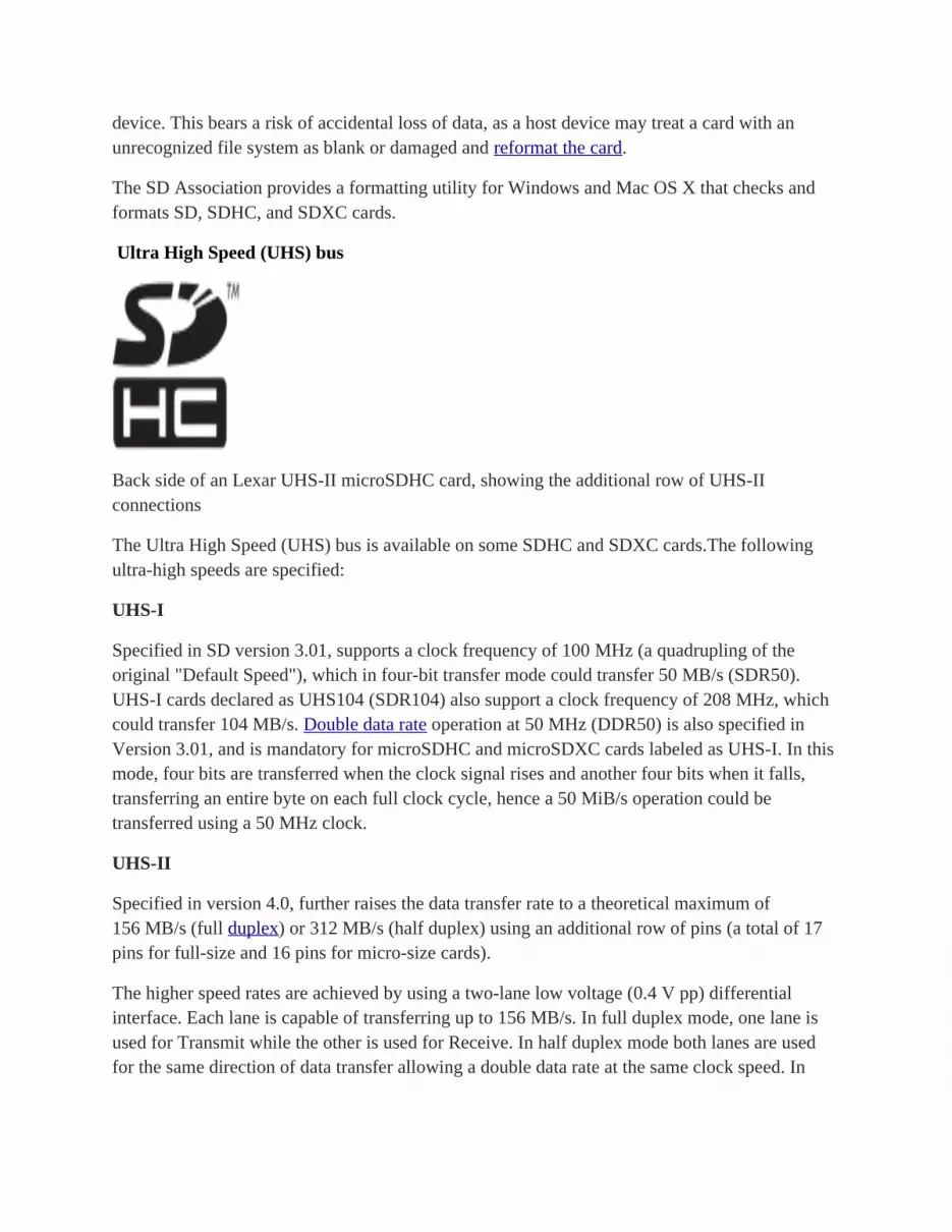
Ultra High Speed (UHS) bus
Back side of an Lexar UHS-II microSDHC card, showing the additional row of UHS-II connections
The Ultra High Speed (UHS) bus is available on some SDHC and SDXC cards.The following ultra-high speeds are specified:
UHS-I
Specified in SD version 3.01, supports a clock frequency of 100 MHz (a quadrupling of the original "Default Speed"), which in four-bit transfer mode could transfer 50 MB/s (SDR50). UHS-I cards declared as UHS104 (SDR104) also support a clock frequency of 208 MHz, which could transfer 104 MB/s. Double data rate operation at 50 MHz (DDR50) is also specified in Version 3.01, and is mandatory for microSDHC and microSDXC cards labeled as UHS-I. In this mode, four bits are transferred when the clock signal rises and another four bits when it falls, transferring an entire byte on each full clock cycle, hence a 50 MiB/s operation could be transferred using a 50 MHz clock.
UHS-II
Specified in version 4.0, further raises the data transfer rate to a theoretical maximum of 156 MB/s (full duplex) or 312 MB/s (half duplex) using an additional row of pins (a total of 17 pins for full-size and 16 pins for micro-size cards).
The higher speed rates are achieved by using a two-lane low voltage (0.4 V pp) differential interface. Each lane is capable of transferring up to 156 MB/s. In full duplex mode, one lane is used for Transmit while the other is used for Receive. In half duplex mode both lanes are used for the same direction of data transfer allowing a double data rate at the same clock speed. In

addition to enabling higher data rates, the UHS-II interface allows for lower interface power consumption, lower I/O voltage rates and lower electromagnetic interference (EMI).
Cards that comply with UHS show Roman numerals 'I' or 'II' next to the SD card logo and report this capability to the host device. Use of UHS-I requires that the host device command the card to drop from 3.3-volt to 1.8-volt operation over the I/O interface pins and select the four-bit transfer mode, while UHS-II requires 0.4-volt operation.
SDIO
Camera using the SDIO interface to connect to some HP iPAQ devices
An SDIO (Secure Digital Input Output) card is an extension of the SD specification to cover I/O functions. SDIO cards are only fully functional in host devices designed to support their input-output functions (typically PDAs like the Palm Treo, but occasionally laptops or mobile phones). These devices can use the SD slot to support GPS receivers, modems, barcode readers, FM radio tuners, TV tuners,RFID readers, digital cameras, and interfaces to Wi-Fi, Bluetooth, Ethernet, andIrDA. Many other SDIO devices have been proposed, but it is now more common for I/O devices to connect using the USB interface.
SDIO cards support most of the memory commands of SD cards. SDIO cards can be structured as eight logical cards, although currently, the typical way that an SDIO card uses this capability is to structure itself as one I/O card and one memory card.
The SDIO and SD interfaces are mechanically and electrically identical. Host devices built for SDIO cards generally accept SD memory cards without I/O functions. However, the reverse is not true, because host devices need suitable drivers and applications to support the card's I/O functions. For example, an HP SDIO camera usually does not work with PDAs that do not list it as an accessory. Inserting an SDIO card into any SD slot causes no physical damage nor disruption to the host device, but users may be frustrated that the SDIO card does not function fully when inserted into a seemingly compatible slot
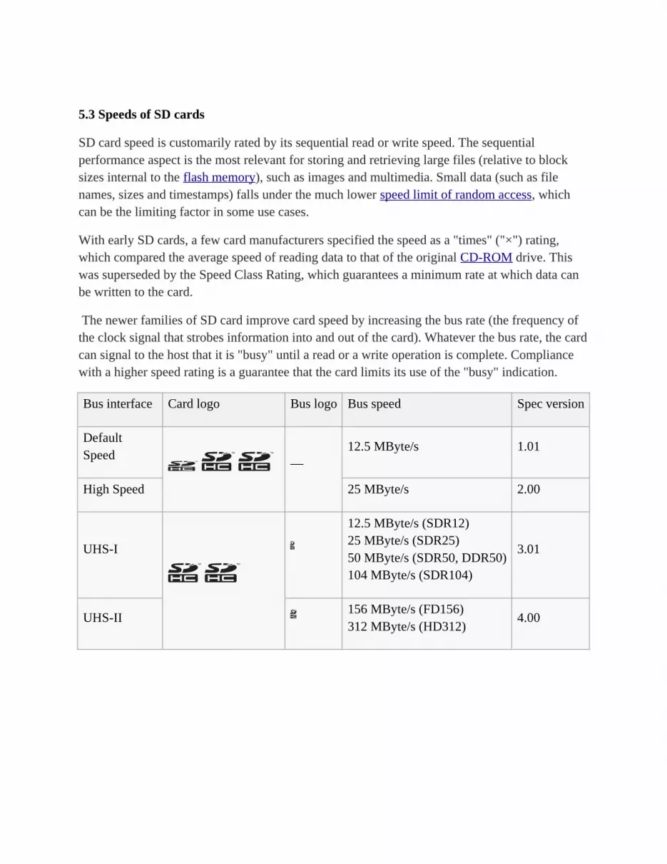
5.3 Speeds of SD cards
SD card speed is customarily rated by its sequential read or write speed. The sequential performance aspect is the most relevant for storing and retrieving large files (relative to block sizes internal to the flash memory), such as images and multimedia. Small data (such as file names, sizes and timestamps) falls under the much lower speed limit of random access, which can be the limiting factor in some use cases.
With early SD cards, a few card manufacturers specified the speed as a "times" ("×") rating, which compared the average speed of reading data to that of the original CD-ROM drive. This was superseded by the Speed Class Rating, which guarantees a minimum rate at which data can be written to the card.
The newer families of SD card improve card speed by increasing the bus rate (the frequency of the clock signal that strobes information into and out of the card). Whatever the bus rate, the card can signal to the host that it is "busy" until a read or a write operation is complete. Compliance with a higher speed rating is a guarantee that the card limits its use of the "busy" indication.
Bus interface Card logo Bus logo Bus speed Spec version
Default Speed
—12.5 MByte/s 1.01
High Speed 25 MByte/s 2.00
UHS-I
12.5 MByte/s (SDR12)25 MByte/s (SDR25)50 MByte/s (SDR50, DDR50)104 MByte/s (SDR104)
3.01
UHS-II156 MByte/s (FD156)312 MByte/s (HD312)
4.00

5.4 ARDUINO SD CARD MODULE
Fig no:5.1 ARDUINO SD CARD MODULE
The Arduino SD Card Shield is a simple solution for transferring data to and from a standard SD card. The pinout is directly compatible with Arduino, but can also be used with other microcontrollers. It allows you to add mass storage and data logging to your project.
Features
Break out board for standard SD card. Contains a switch to select the flash card slot Sits directly on a Arduino Also be used with other microcontrollers
Overview

SD Cards work only at 3.3V and both the power and I/O levels must be accommodated. The module shown here uses FETs for level shifting and a 3.3V regulator for power when operating from 5.0V . A switch allows the module to be used with Arduinos / Yourduino Robo1 or Minis etc. running at 3.3V. We have tested the YourDuinoRobo1 with it's power jumper set to 3.3V and the SD card module set at 3.3V and it works well.
This module also has a MicroSD socket on the back side, and we have tested 2Gb and 4Gb MicroSD cards plugged in there. They worked OK with the SdFAT library. These cards are formatted FAT32 and SD/HC
The communication between the microcontroller and the SD card uses SPI, which takes place on digital pins 11, 12, and 13 (on most Arduino boards) or 50, 51, and 52 (Arduino Mega). Additionally, another pin must be used to select the SD card. This can be the hardware SS pin - pin 10 (on most Arduino boards) or pin 53 (on the Mega) - or another pin specified in the call to SD.begin()
Formatting/Preparing the card
(NB : whenever referring to the SD card, it means SD and microSD sizes, as well as SD and SDHD formats)
Most SD cards work right out of the box, but it's possible you have one that was used in a computer or camera and it cannot be read by the SD library. Formatting the card will create a file system that the Arduino can read and write to.
It's not desirable to format SD cards frequently, as it shortens their life span.
You’ll need a SD reader and computer to format your card. The library supports the FAT16 and FAT32 filesystems, but useFAT16 when possible. The process to format is fairly straightforward.
Windows : right click on your card’s directory and choose “Format” from the drop down. Make sure you choose FAT as the filesystem.
OSX : Open Disk Utility (located in Applications>Utilities). Choose the Card, click on the erase tab, select MS-DOS(FAT) as the Format, and click Erase. NB: OSX places a number of “hidden” files on the device when it formats a drive. To format a SD car without the extra files on OSX, follow these notes on Ladyada’s site.
Linux: With a SD card inserted, open a terminal window. At the prompt, type df, and press enter. The windows will report the device name of your SD card, it should look something like /dev/sdb1. Unmount the SD card, but leave it in the computer. Type sudo mkdosfs -F 16 /dev/sdb1, replacing the device name with yours. Remove the SD card and replace it to verify it works.

File Naming
FAT file systems have a limitation when it comes to naming conventions. You must use the 8.3 format, so that file names look like “NAME001.EXT”, where “NAME001” is an 8 character or fewer string, and “EXT” is a 3 character extension. People commonly use the extensions .TXT and .LOG. It is possible to have a shorter file name (for example, mydata.txt, or time.log), but you cannot use longer file names.
Opening/Closing files
When you use file.write(), it doesn't write to the card until you flush() or close(). Whenever you open a file, be sure to close it to save your data.
As of version 1.0, it is possible to have multiple files open
Interfacing with Arduino Board
Fig no:5.2 SD Card Wiring Block Diagram

Fig no:5.3 SD Card Module Connected to Arduino Board
The Arduino shows the following pin names:*SPI:10 (SS) "Slave Select"11 (MOSI) "Master Out Slave In"12 (MISO) "Master In Slave Out"13 (SCK) "System Clock"
To clarify this: to connect this module you must connect:(Arduino Pin) - Module Pin10 (SS) to CS11 (MOSI) to DI12 (MISO) to DO13 (SCK) to CLKand G to GND and + to 5V

CHAPTER 06
LIGHT EMITTING DIODES (LEDs)
6.1 Introduction
A light-emitting diode (LED) is a two-lead semiconductor light source. It is a p–n junction diode, which emits light when activated.[4] When a suitable voltageis applied to the leads, electrons are able to recombine with electron holeswithin the device, releasing energy in the form of photons. This effect is calledelectroluminescence, and the color of the light (corresponding to the energy of the photon) is determined by the energy band gap of the semiconductor.
An LED is often small in area (less than 1 mm2) and integrated optical components may be used to shape its radiation pattern.
Appearing as practical electronic components in 1962, the earliest LEDs emitted low-intensity infrared light. Infrared LEDs are still frequently used as transmitting elements in remote-control circuits, such as those in remote controls for a wide variety of consumer electronics. The first visible-light LEDs were also of low intensity, and limited to red. Modern LEDs are available across the visible, ultraviolet, and infrared wavelengths, with very high brightness.
Early LEDs were often used as indicator lamps for electronic devices, replacing small incandescent bulbs. They were soon packaged into numeric readouts in the form of seven-segment displays, and were commonly seen in digital clocks.
Recent developments in LEDs permit them to be used in environmental and task lighting. LEDs have many advantages over incandescent light sources including lower energy consumption, longer lifetime, improved physical robustness, smaller size, and faster switching. Light-emitting diodes are now used in applications as diverse as aviation lighting, automotive headlamps, advertising, general lighting, traffic signals, camera flashes and even LED wallpaper. As of 2015, LEDs powerful enough for room lighting remain somewhat more expensive, and require more precise current and heat management, than compact fluorescent lamp sources of comparable output.LEDs have allowed new text, video displays, and sensors to be developed, while their high switching rates are also useful in advanced communications technology.
Fig no:6.1 Different Types Of LEDs

Fig no:6.2 Simple LED
6.2 History
Electroluminescence as a phenomenon was discovered in 1907 by the British experimenter H. J. Round of Marconi Labs, using a crystal of silicon carbide and acat's-whisker detector. Soviet inventor Oleg Losev reported creation of the first LED in 1927. His research was distributed in Soviet, German and British scientific journals, but no practical use was made of the discovery for several decades. Kurt Lehovec, Carl Accardo and Edward Jamgochian, explained these first light-emitting diodes in 1951 using an apparatus employing SiC crystals with a current source of battery or pulse generator and with a comparison to a variant, pure, crystal in 1953.
Rubin Braunstein of the Radio Corporation of America reported on infrared emission from gallium arsenide (GaAs) and other semiconductor alloys in 1955.Braunstein observed infrared emission generated by simple diode structures using gallium antimonide (GaSb), GaAs, indium phosphide (InP), and silicon-germanium (SiGe) alloys at room temperature and at 77 kelvins.
In 1957, Braunstein further demonstrated that the rudimentary devices could be used for non-radio communication across a short distance. As noted by Kroemer Braunstein".. had set up a simple optical communications link: Music emerging from a record player was used via suitable electronics to modulate the forward current of a GaAs diode. The emitted light was detected by a PbS diode some distance away. This signal was fed into an audio amplifier, and played back by a loudspeaker. Intercepting the beam stopped the music. We had a great deal of fun playing with this setup." This setup presaged the use of LEDs for optical communication applications.
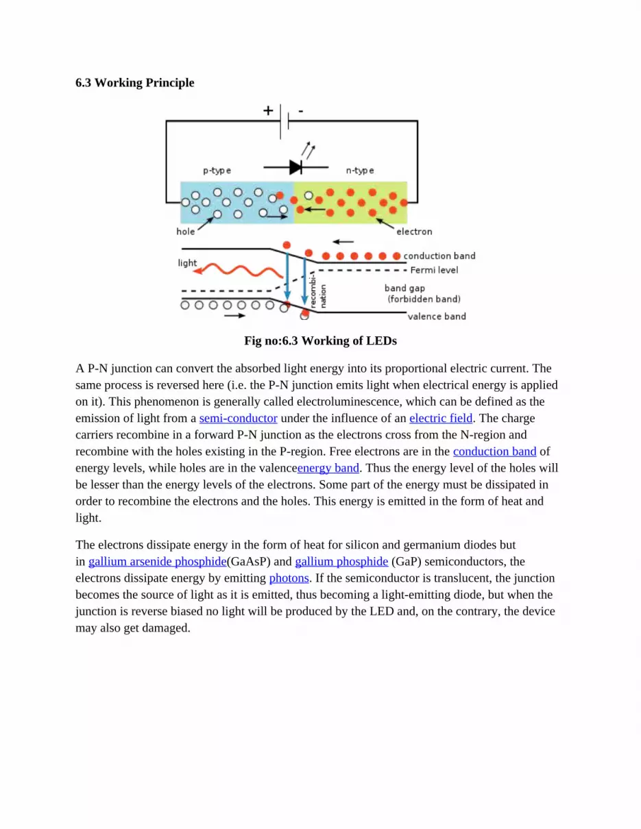
6.3 Working Principle
Fig no:6.3 Working of LEDs
A P-N junction can convert the absorbed light energy into its proportional electric current. The same process is reversed here (i.e. the P-N junction emits light when electrical energy is applied on it). This phenomenon is generally called electroluminescence, which can be defined as the emission of light from a semi-conductor under the influence of an electric field. The charge carriers recombine in a forward P-N junction as the electrons cross from the N-region and recombine with the holes existing in the P-region. Free electrons are in the conduction band of energy levels, while holes are in the valenceenergy band. Thus the energy level of the holes will be lesser than the energy levels of the electrons. Some part of the energy must be dissipated in order to recombine the electrons and the holes. This energy is emitted in the form of heat and light.
The electrons dissipate energy in the form of heat for silicon and germanium diodes but in gallium arsenide phosphide(GaAsP) and gallium phosphide (GaP) semiconductors, the electrons dissipate energy by emitting photons. If the semiconductor is translucent, the junction becomes the source of light as it is emitted, thus becoming a light-emitting diode, but when the junction is reverse biased no light will be produced by the LED and, on the contrary, the device may also get damaged.
6.4 Applications
LED uses fall into four major categories:
1. Visual signals where light goes more or less directly from the source to the human eye, to convey a message or meaning.
2. Illumination where light is reflected from objects to give visual response of these objects.
3. Measuring and interacting with processes involving no human vision.
4. Narrow band light sensors where LEDs operate in a reverse-bias mode and respond to incident light, instead of emitting light.
CHAPTER 07
LED DISPLAYS
7.1 Introduction
An LED display is a flat panel display, which uses an array of light-emitting diodesas pixels for a video display. Their brightness allows them to be used outdoors instore signs and billboards, and in recent years they have also become commonly used in destination signs on public transport vehicles. LED displays are capable of providing general illumination in addition to visual display, as when used for stage lighting or other decorative (as opposed to informational) purposes.
7.2 History
The first true all-LED flat panel television screen was possibly developed, demonstrated and documented by James P. Mitchell in 1977.[1] The modular, scalable display was initially designed with hundreds of MV50 LEDs and a newly available transistor-transistor logic memory addressing circuit from Texas Instruments.[2] The ¼-inch thin flat panel prototype and the scientific paper were displayed at the 29th ISEF expo in Washington D.C. in May 1978.[3] It received awards by NASA [4] and General Motors Corporation.[5] A liquid crystal display (LCD) matrix design was also cited in the LED paper as an alternative x-y scan technology and as a future alternate television display method. Additional recognition was provided by Westinghouse Educational Foundation "Honors Group" and the concept prototype was also a selected scientific paper at the Iowa Academy of Science of the University of Northern Iowa. The replacement of the 70 year+ high-voltage analog system (cathode-ray tube technology) with a digital x-y scan system has been a significant achievement. Displacement of the electromagnetic scan systems included the removal of inductive deflection, electron beam and color convergence circuits. The digital x-y scan system has helped the modern television to “collapse” into its current thin form factor.
The 1977 model was monochromatic by design. Efficient blue LEDs did not arrive for another decade. Large displays now use high-brightness diodes to generate a wide spectrum of colors. It took three decades and organic light-emitting diodesfor Sony to introduce an OLED TV, the Sony XEL-1 OLED screen which was marketed in 2009. Later, at CES 2012, Sony presented Crystal LED, a TV with a true LED-display (in which LEDs are used to produce actual images rather than acting as backlighting for other types of display, as in LED-backlit LCD displays which are commonly marketed as LED TVs), though no such models have entered mass production.

The 2011 UEFA Champions League Final match between Manchester United and Barcelona was broadcast live in 3Dformat in Gothenburg (Sweden), on an EKTA screen. It had a refresh rate of 100 Hz, a diagonal of 7.11 m (23 ft 3.92 in) and a display area of 6.192×3.483 m, and was listed in the Guinness Book of Records as the largest LED 3D TV.
The largest manufacturer of wall LED screen displays is Shenzhen, China-based Leyard Optoelectronic
7.3 Dot Matrix Display
A dot-matrix display is a display device used to display information on machines, clocks, railway departure indicators and many other devices requiring a simple display device of limited resolution.
The display consists of a dot matrix of lights or mechanical indicators arranged in a rectangular configuration (other shapes are also possible, although not common) such that by switching on or off selected lights, text or graphics can be displayed. A dot matrix controller converts instructions from a processor into signals which turns on or off lights in the matrix so that the required display is produced.
Usual character resolutions A common size for a character is 5×7 pixels, either separated with blank lines with no dots
(in most text-only displays), or with lines of blank pixels (making the real size 6x8). This is seen on most graphic calculators, such as Casiocalculators or TI-82 and superior.
A smaller size is 3×5 (or 4x6 when separated with blank pixels). This is seen on the TI-80 calculator as a "pure", fixed-size 3×5 font, or on most 7×5 calculators as a proportional (1×5 to 5×5) font. The disadvantage of the 7×5 matrix and smaller is that lower case characters withdescenders are not practical. A matrix of 11×9 is often used to give far superior resolution.
Dot matrix displays of sufficient resolution can be programmed to emulate the customary seven-segment numeral patterns.
A larger size is 5×9 pixels, which is used on many Natural Display calculators.
7.4 Seven Segment Displays (SSD)
A seven-segment display (SSD), or seven-segment indicator, is a form of electronic display device for displaying decimal numerals that is an alternative to the more complex dot matrix displays.
Seven-segment displays are widely used in digital clocks, electronic meters, basic calculators, and other electronic devices that display numerical information.
Concept and visual structure

The seven elements of the display can be lit in different combinations to represent the arabic numerals. Often the seven segments are arranged in an oblique(slanted) arrangement, which aids readability. In most applications, the seven segments are of nearly uniform shape and size (usually elongated hexagons, though trapezoids and rectangles can also be used), though in the case of adding machines, the vertical segments are longer and more oddly shaped at the ends in an effort to further enhance readability.
The numerals 6, 7 and 9 may be represented by two or more different glyphs on seven-segment displays, with or without a 'tail'.
The seven segments are arranged as a rectangle of two vertical segments on each side with one horizontal segment on the top, middle, and bottom. Additionally, the seventh segment bisects the rectangle horizontally. There are also fourteen-segment displays and sixteen-segment displays (for full alphanumerics); however, these have mostly been replaced by dot matrix displays.
The segments of a 7-segment display are referred to by the letters A to G, where the optional decimal point (an "eighth segment", referred to as DP) is used for the display of non-integer numbers.
Implementations
Fig no:7.1 A mechanical seven-segment display for displaying automotive fuel prices
Seven-segment displays may use a liquid crystal display (LCD), a light-emitting diode (LED) for each segment, or other light-generating or controlling techniques such

as cold cathode gas discharge, vacuum fluorescent, incandescent filaments, and others. For gasoline price totems and other large signs, vane displays made up of electromagnetically flipped light-reflecting segments (or "vanes") are still commonly used. An alternative to the 7-segment display in the 1950s through the 1970s was the cold-cathode, neon-lamp-like nixie tube. Starting in 1970, RCA sold a display device known as the Numitron that used incandescent filaments arranged into a seven-segment display.
In a simple LED package, typically all of the cathodes (negative terminals) or all of the anodes (positive terminals) of the segment LEDs are connected and brought out to a common pin; this is referred to as a "common cathode" or "common anode" device.[5] Hence a 7 segment plus decimal point package will only require nine pins, though commercial products typically contain more pins, and/or spaces where pins would go, in order to match standardIC sockets. Integrated displays also exist, with single or multiple digits. Some of these integrated displays incorporate their own internaldecoder, though most do not: each individual LED is brought out to a connecting pin as described.
Fig no:7.2 A multiplexed 4-digit, seven-segment display with only 12 pins
Multiple-digit LED displays as used in pocket calculators and similar devices used multiplexed displays to reduce the number of I/O pins required to control the display. For example, all the anodes of the A segments of each digit position would be connected together and to adriver circuit pin, while the cathodes of all segments for each digit would be connected. To operate any particular segment of any digit, the controlling integrated circuit would turn on the cathode driver for the selected digit, and the anode drivers for the desired segments; then after a short blanking interval the next digit would be selected and new segments lit, in a sequential fashion. In this manner an eight digit display with seven segments and a decimal point would require only 8 cathode drivers and 8 anode drivers, instead of sixty-four drivers and IC pins.[6] Often in pocket calculators the digit drive lines would be used to scan the keyboard as well, providing further savings; however, pressing multiple keys at once would produce odd results on the multiplexed display.
A single byte can encode the full state of a 7-segment-display. The most popular bit encodings are gfedcba and abcdefg, where each letter represents a particular segment in the display. In the gfedcba representation, a byte value of 0x06 would (in a common-anode circuit) turn on segments 'c' and 'b', which would display a '1'.
History

Seven-segment displays can be found in patents as early as 1908 (in U.S. Patent 974,943, F W Wood invented an 8-segment display, which displayed the number 4 using a diagonal bar). In 1910, a seven-segment display illuminated by incandescent bulbs was used on a power-plant boiler room signal panel.[7] They did not achieve widespread use until the advent of LEDs in the 1970s.
They are sometimes used in posters or tags, where the user either applies color to pre-printed segments, or applies color through a seven-segment digit template, to compose figures such as product prices or telephone numbers.For many applications, dot-matrix LCDs have largely superseded LED displays, though even in LCDs 7-segment displays are very common. Unlike LEDs, the shapes of elements in an LCD panel are arbitrary since they are formed on the display by a kind of printing process. In contrast, the shapes of LED segments tend to be simple rectangles, reflecting the fact that they have to be physically moulded to shape, which makes it difficult to form more complex shapes than the segments of 7-segment displays. However, the high common recognition factor of 7-segment displays, and the comparatively high visualcontrast obtained by such displays relative to dot-matrix digits, makes seven-segment multiple-digit LCD screens very common on basic calculators.
The seven-segment display has inspired type designers to produce typefaces reminiscent of that display (but more legible), such as New Alphabet (typeface), "DB LCD Temp", "ION B", etc.
Displaying CharactersHexadecimal digits can be displayed on seven-segment displays. A combination of uppercase and lowercase letters is used for A–F;[8] this is done to obtain a unique, unambiguous shape for each hexadecimal digit (otherwise, a capital D would look identical to an 0/O and a capital B would look identical to an 8). Also the digit 6 must be displayed with the top bar lit to avoid ambiguity with the letter b.
Fig no:7.3 Figure showing letters and numbers displayed as on Seven Segment Display
Hexadecimal encodings for displaying the digits 0 to F

Digitgfedcba
abcdefg a b c d e f g
0 0×3F 0×7E on on on on on on off
1 0×06 0×30 off on on offoff
off off
2 0×5B 0×6D on on off on on off on
3 0×4F 0×79 on on on onoff
off on
4 0×66 0×33 off on on offoff
on on
5 0×6D 0×5B on off on onoff
on on
6 0×7D 0×5F on off on on on on on
7 0×07 0×70 on on on offoff
off off
8 0×7F 0×7F on on on on on on on
9 0×6F 0×7B on on on onoff
on on
A 0×77 0×77 on on on off on on on
b 0×7C 0×1F off off on on on on on
C 0×39 0×4E on off off on on on off
d 0×5E 0×3D off on on on on off on
E 0×79 0×4F on off off on on on on
F 0×71 0×47 on off off off on on on

In addition, seven segment displays can be used to show various other letters of the latin, Cyrillic and Greek alphabetsincluding punctuation, but few representations are unambiguous and intuitive at the same time. Short messages giving status information (e.g. "no dISC" on a CD player) are also commonly represented on 7-segment displays. In the case of such messages it is not necessary for every letter to be unambiguous, merely for the words as a whole to be readable.
Similar displays with fourteen or sixteen segments are available allowing less-ambiguous representations of the alphabet.
Using a restricted range of letters that look like (upside-down) digits, seven-segment displays are commonly used by school children to form words and phrases using a technique known as "calculator spelling".
7.5 LED Matrix Display
Structure of Led MatrixIn a matrix format LEDs are arranged in rows and columns. You can also think of them as y and x coordinates. Lets assume we have 4×4 matrix. Rows would be marked from A to D and columns from 1 to 4. Now we can address each LED by row and column. Top left led would be (A,1). Bottom down led would be (D,4).
Led matrices come in two flavors. Common-row anode (left) and common-row cathode right).

Fig no:7.4 LEDs Connected In Matrix-Common-Row anode(left) and Common-Row cathode(right)
Figure above shows the different configurations. The difference between these two configurations is how you lit a led. With common-row anode current sources (positive voltage) are attached to rows A..D and currents sinks (negative voltage, ground) to columns 1..4. With common-row cathode current sinks are attached to rows A..D and currents sources to columns 1..4.
For example. To light bottom down led (D,4) of common cathode matrix you would feed positive voltage to column 4 and connect row D to ground. For sake of clarity I will using common-row cathode in examples for the rest of this article.
Building a LED MatrixTo build a 4×4 common-row cathode matrix you will need 16 LEDs, four resistors, some headers and prototyping board. I started by gluing the leds to prototyping board with epoxy glue. This way it is easier to have LEDs beautifully aligned.
When glue is dry it is time to bend and solder. First bend all cathodes to left as close to prototyping board as possible. Solder all cathodes in each row together. When cathodes are ready, bend all anodes. Anodes must not touch cathodes. I used piece of plastic tubing to help bending the anodes to form a bridge above cathodes.

Now solder together all anodes in each row. Solder the headers and connect cathode rows directly to the header.
Anode rows are connected to header with current limiting resistors. Value of the resistor depends on the LED used. Check the LED datasheet for forward voltage and current. LEDcalculator will help you finding out correct resistor. Matrix is now ready for testing.

Addressing Single LED
Connecting ground to row A and positive voltage to column 1 will light the top right LED (A,1).
Connecting ground to row D and positive voltage to column 4 will light the bottom down LED(D,4).

Intuition would say lighting the both (A,1) and (D,4) at the same time is just connecting all the four wires. This is not the case. There are four LEDs which are lit. This is because current is also flowing through (A,4) and (D,1).

Multiplexing and Persistence of VisionMultiplexing can be used to display arbitrary patterns with led matrices. Multiplexing is sometimes also called scanning. It scans rows (usually from up to down) and lights needed leds only in one row at time. Something like following:1. Start by having everything disconnected.
2. Connect positive voltage all the needed columns.
3. Connect row to ground. This lights the needed leds in the row.
4. Disconnect the row and all columns.
5. Do the same steps one by one to all rows and then start from the beginning.
6. Do this slowly and you would see blinking LED rows. Do it really fast and human eye can see the whole pattern. Phenomenon is called persistence of vision.
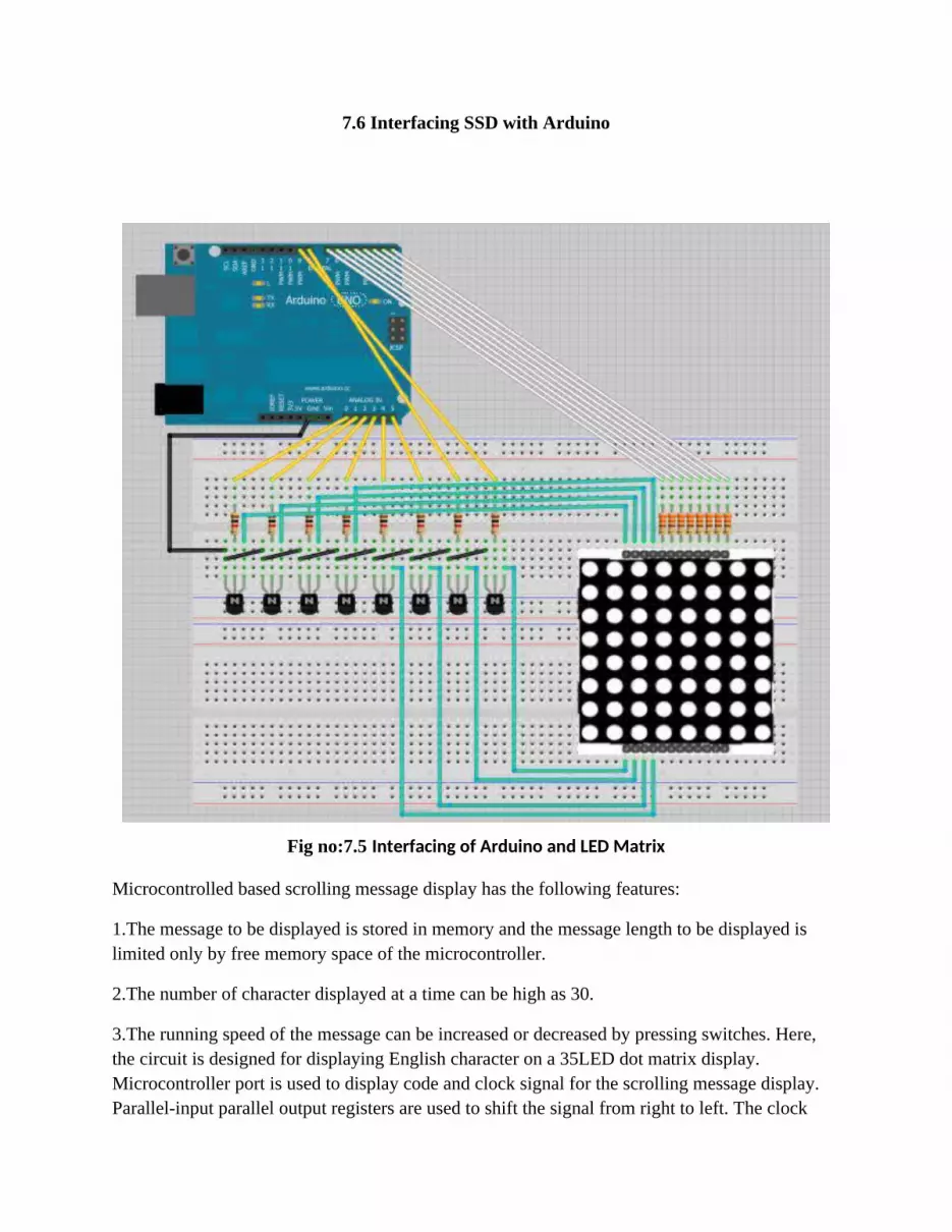
7.6 Interfacing SSD with Arduino
Fig no:7.5 Interfacing of Arduino and LED Matrix
Microcontrolled based scrolling message display has the following features:
1.The message to be displayed is stored in memory and the message length to be displayed is limited only by free memory space of the microcontroller.
2.The number of character displayed at a time can be high as 30.
3.The running speed of the message can be increased or decreased by pressing switches. Here, the circuit is designed for displaying English character on a 35LED dot matrix display. Microcontroller port is used to display code and clock signal for the scrolling message display. Parallel-input parallel output registers are used to shift the signal from right to left. The clock

pulse and code signal are generated by microcontroller program and output from the port. Theoretically, we can add infinite number of PIPO registers but the maximum number of registers is actually limited to the current triggering value of the clock pulse.
Fig no:7.6 The above diagram displays the Block Diagram of the system for one character.
As shown in diagram data is shifted out from the microcontroller and given to the shift register. When clock is given to the shift register it displays the data to LED and provides input to next shift register and the process goes on. The above block diagram is for single character and there are many such characters in system .The microcontroller is connected with GSM modem which is used to receive any message and that particular message will be displayed on the LED matrix display. Other special characters can be added as follows. Suppose you want to display character “A‟. Draw “A‟ on the 5x7 LED display.

Fig no:7.7 Character “A‟ on the 5x7 LED display
Suppose you want to display special character “<‟ on the 5 X 7display.
Fig no:7.8 Special character “<” on the 5 X 7display

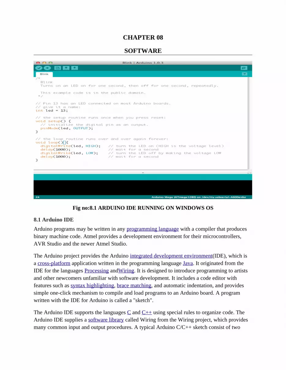
CHAPTER 08
SOFTWARE
Fig no:8.1 ARDUINO IDE RUNNING ON WINDOWS OS
8.1 Arduino IDE
Arduino programs may be written in any programming language with a compiler that produces binary machine code. Atmel provides a development environment for their microcontrollers, AVR Studio and the newer Atmel Studio.
The Arduino project provides the Arduino integrated development environment(IDE), which is a cross-platform application written in the programming language Java. It originated from the IDE for the languages Processing andWiring. It is designed to introduce programming to artists and other newcomers unfamiliar with software development. It includes a code editor with features such as syntax highlighting, brace matching, and automatic indentation, and provides simple one-click mechanism to compile and load programs to an Arduino board. A program written with the IDE for Arduino is called a "sketch".
The Arduino IDE supports the languages C and C++ using special rules to organize code. The Arduino IDE supplies a software library called Wiring from the Wiring project, which provides many common input and output procedures. A typical Arduino C/C++ sketch consist of two

functions that are compiled and linked with a program stub main() into an executable cyclic executive program:
setup(): a function that runs once at the start of a program and that can initialize settings.
loop(): a function called repeatedly until the board powers off.
After compiling and linking with the GNU toolchain, also included with the IDE distribution, the Arduino IDE employs the program avrdude to convert the executable code into a text file in hexadecimal coding that is loaded into the Arduino board by a loader program in the board's firmware.
PROGRAMMING
A typical program for a beginning Arduino programmer blinks a light-emitting diode (LED) on and off. This program is usually loaded in the Arduino board by the manufacturer. In the Arduino environment, a user might write such a program as shown:
#define LED_PIN 13
void setup() {
pinMode(LED_PIN, OUTPUT); // Enable pin 13 for digital output
}
void loop() {
digitalWrite(LED_PIN, HIGH); // Turn on the LED
delay(1000); // Wait one second (1000 milliseconds)
digitalWrite(LED_PIN, LOW); // Turn off the LED
delay(1000); // Wait one second
}

Fig no:8.2 Power LED (Red) and Integrated LED on Line 13 (Green) on Arduino Compatible Board (made in China)
Most Arduino boards contain an LED and a load resistor connected between the pin 13 and ground, which is a convenient feature for many simple tests. The previous code would not be seen by a standard C++ compiler as a valid program, so when the user clicks the "Upload to I/O board" button in the IDE, a copy of the code is written to a temporary file with an extra include header at the top and a very simple main() function at the bottom, to make it a valid C++ program.The Arduino IDE uses the GNU toolchain and AVR Libc to compile programs, and uses avrdude to upload programs to the board.As the Arduino platform uses Atmel microcontrollers, Atmel's development environment, AVR Studio or the newer Atmel Studio, may also be used to develop software for the Arduino.