magnetic navigation and actuation of nanorobotic systems
TRANSCRIPT
UNIVERSIDADE DE LISBOA
FACULDADE DE CIÊNCIAS
DEPARTAMENTO DE FÍSICA
Magnetic navigation and actuation of nanorobotic systems through
the use of Helmholtz coils
Daniel Filipe Vilhena Nunes
Mestrado em Física
Especialização em Física da Matéria Condensada e Nano-materiais
Dissertação orientada por:
Professor Doutor Hugo A. Ferreira
2018


ii
Acknowledgements
None of these pages could have been written without the help of several people. Without
some of those, these would actually have been written a lot faster. I digress.
First, I would like to thank my supervisor Hugo Ferreira for accepting me as his student and
making the connections needed for the development of this project. I also want to thank him for being
one of the few role models I managed to find during my life. A big and special thank you is due to
Susana Freitas for allowing us to develop the microrobots at INESC-MN. I thank Miguel Neto for the
patience to work with and preventing me from screwing up in this highly exploratory process. To all
my colleagues and friends that helped me survive the times inside the clean room or the lunch hours:
João Serra, Jorge Pereira, Débora Albuquerque, Tomás Martins, Sara Sequeira, Pedro Fonseca, Pedro
Correia and Tiago Costa. To professors Margarida Godinho and Margarida Cruz, I thank you from the
bottom of my heart for all the help you have given me during not only this project but during the
entirety of the Master program.
To those that are in the fourth year of their courses but will always be in the first in my head:
Andreia, Madalena and Catarina. Thank you for enabling my procrastination and showing me that I
can (sometimes) be a good influence. To Beatriz, for understanding my pains and feeling my
enthusiasm with this project. Sometimes, more than me. To Diogo Lourenço, for getting on my nerves
and making me focus on this. To Theias, for nerding out and having a similar passion for cinema.
To Cátia Rato and Carolina Rodrigues. We started this journey together and followed very
different paths. The years we shared were nothing but great. As we walk our different roads, I hope
that our ways cross again.
To those that have accompanied me outside the academic world. Xavier for being of the few
people to understand my dilemmas, Dana for being a constant source of amazement, and Zeca for
being Zeca.
Finally, to my family. My mother for always listening to my mumbling. My father for
supporting me and suggesting some actually very simple solutions to problems that did not appear as
simple. My brother, for making mistakes that I did not have to. My grandmother, for always taking
care of my brother and me, even though her mind is not fully here.
iii
Resumo
A navegação magnética de sistemas nano ou micro-robóticos é uma área de investigação na
qual o interesse académico é crescente – desde nanopartículas magnéticas a dispositivos nadadores de
tamanhos microscópicos. A utilização de campos magnéticos é também de grande interesse para
aplicações médicas. Estudos prévios recorrem à utilização de pares de bobines em configuração de
Helmholtz (campo magnético uniforme) e em configuração de Maxwell (gradiente magnético
uniforme), com o fim de criar campos magnéticos controláveis.
Existem várias opções para fornecer energia a nano ou microrobots, sendo as mais comuns a
elétrica e a magnética. Enquanto a maioria das soluções elétricas tem a fonte de alimentação no
próprio microrobot, as soluções magnéticas tendem a usar campos magnéticos externos de forma a
atuar os microrobots. Estas soluções tornam-se assim ideais para aplicações médicas devido ao já
estabelecido uso de máquinas de ressonância-magnética em medicina. O maior obstáculo a ultrapassar
no desenho destes sistemas microrobóticos a serem usados em aplicações médicas é o fluxo de
Stokes. Devido à reduzida dimensão das estruturas nano ou microrobóticas, o número de Reynolds
torna-se também pequeno, podendo ser inferior a 1. Nesse caso, o fluido no qual a estrutura se
encontra submersa comporta-se como o equivalente a um fluido de elevada viscosidade. Assim,
recorrer puramente a uma força magnética para “arrastar” o microrobot, implicaria o uso de
gradientes magnéticos elevados e de difícil criação. Utilizando bobines de Helmholtz e com
inspiração na propulsão de microrganismos, a locomoção é possibilitada usando somente campos
magnéticos de baixa intensidade. Estudos previamente existentes incluem a utilização de campos
alternos para locomoção de microrobots, oscilando-os de forma a que parte da sua estrutura (uma
cauda flexível) atue como leme. Campos magnéticos com precessão em torno de determinada direção,
permitem a rotação de microrobots com caudas helicoidais, também assim propulsionando-os.
Gradientes magnéticos são maioritariamente usados em nanorobots cuja componente magnética
possui elevando momento magnético (como no caso de nanopartículas superparamagnéticas). Assim,
este projeto baseou-se na utilização de campos de magnéticos uniformes gerados por pares de bobines
em configuração de Helmholtz para o controlo de microrobots constituídos por materiais flexíveis e
com componente magnética capaz de realinhar toda a estrutura.
Foram fabricados três pares ortogonais de bobines de Helmholtz ligados a uma fonte de
alimentação DC programável (Hameg HMP4040). Esta fonte foi controlada através de uma interface
de utilizador gráfica desenvolvida em LabVIEW o que permitiu o controlo da intensidade do campo
no plano XY das bobines e na direção do terceiro par de bobines, tal como ângulo que o campo faz
com a direção X. No entanto, a fonte tem limitações. Apenas valores positivos de corrente
conseguiram ser gerados e a frequência máxima possível foi de 1 Hz. Usando um íman permanente de
neodímio com cinco milímetros como objeto de teste, o controlo da direção do campo foi
comprovado. A fase seguinte consistiu na fabricação de microrobots (nViper) para testes de controlo
em meio fluídico e à microescala.
Os nViper foram microrobots fabricados com o intuito de testar as capacidades do sistema de
bobines e da fonte de alimentação. O seu desenho geral foi inspirado na estrutura de espermatozoides
(uma cabeça e uma cauda), enquanto a geometria da cabeça foi baseada na morfologia de bactérias
(coccus e bacillus) e também espermatozoides. Os microrobots foram fabricados em poliamida (base
e encapsulamento), um polímero flexível e biocompatível, e uma liga de cobalto-crómio-platina
(CoCrPt), uma liga de material ferromagnético (componente magnético na cabeça do microrobot).
Seguiram-se três processos diferentes de fabricação. O primeiro teve como objetivo
determinar a possibilidade de enrolamento das caudas de forma a obter propulsão com um campo
iv
magnético rotativo e uma cauda helicoidal. Para tal, as estruturas foram desenvolvidas por cima de
uma camada sacrificial composta por alumínio (na maioria da área) e crómio (por debaixo das
cabeças). Ao remover o alumínio, as caudas soltaram-se e a estrutura manteve-se presa ao substrato
pela área coberta por crómio. Ao não se verificar o enrolamento, o segundo processo foi simplificado
com a suposição que seria possível soltar as estruturas diretamente do substrato de vidro. Ou seja, os
microrobots nViper foram fabricados diretamente no vidro. Visto que não foi possível removê-los
diretamente do vidro, no terceiro processo voltou a incluir-se uma camada de sacrificial de alumínio.
O primeiro processo teve resultados positivos quanto à definição das estruturas, mas o
enrolamento das caudas não ocorreu, observando-se, no entanto, ligeiras curvas nas caudas soltas do
substrato. Foi também possível verificar que CoCrPt é corroído pelo etchant de alumínio e também
pelo de crómio. Após a conclusão do segundo processo, observaram-se restos de CoCrPt à volta da
base de poliamida que anteriormente foram confundidos com resíduos de alumínio. O terceiro
processo foi concluído com sucesso, terminando na remoção da camada sacrificial e recuperação dos
microrobots para o interior de Eppendorfs de capacidade 1.5 mL com água.
Foi desenvolvido um script em Python para seguir o movimento dos nViper em caso de
locomoção, esta vertente do script não foi necessária. No entanto, este foi usada para captação de
imagens através do microscópio USB Veho VMS-004 Delux e poderá ser futuramente utilizado em
continuações deste projeto.
Os resultados obtidos demonstram sucesso inicial na fabricação e controlo de microrobots
com o sistema atual. Após o final do terceiro processo de fabricação existem ainda passos a ser
otimizados: a camada de encapsulamento de poliamida, a remoção e recuperação dos microrobots. A
utilização dos microrobots nViper com o atual sistema de bobines foi um êxito como primeira prova
de conceito para futuras aplicações de novos sistemas microrobóticos ou melhoramentos a serem
efetuados nos nViper. Ao se colocar uma gota com microrobots numa lâmina de vidro hidrofóbica, e
com o campo ligado na direção Z durante a colocação, foi possível posteriormente realinhar um
microrobot. Um campo na direção X foi aplicado e de seguida rodado 20º. O microrobot em questão
seguiu com uma rotação de 19.07º, valor calculado através de medições de pixéis das imagens
obtidas. Outros microrobots realinharam-se com a mudança do campo noutras tentativas, no entanto o
resultado anterior foi o mais aproximado da rotação efetuada pelo campo. Numa última abordagem,
foi utilizado um íman permanente de neodímio com aproximadamente cinco centímetros para testar
outra forma de controlo. Verificou-se que os microrobots foram capazes de se realinharem com o
campo magnético produzido pelo íman permanente após uma breve perturbação causada ao sistema
por um pequeno movimento devido a uma súbita oscilação do suporte da lâmina de vidro. A
necessidade de alguma forma de perturbação ou alinhamento prévio com o campo na direção Z antes
da gota atingir a lâmina de vidro, indica que as estruturas, por forças de atração, são adsorvidas ao
substrato de vidro.
Em suma, o atual sistema provou ser capaz de controlar estruturas macroscópicas e
microscópicas de forma satisfatória. A fabricação de microrobots constituídos por poliamida e CoCrPt
mostrou-se possível e os resultados funcionais, embora com espaço para otimização do processo.
Embora locomoção não tenha sido atingida, tal poderá ser realizável com recurso a uma fonte de
corrente AC programável e utilizando frequências superiores a 5 Hz. Um sistema microfluídico
poderá ser utilizado de forma a evitar a deposição dos microrobots e também simular os canais
encontrados em sistemas vasculares e assim estudar possíveis aplicações e desenhos para os
microrobots nViper em aplicações que incluam o sistema cardiovascular.
Palavras-chave: Magnético, microrobótica, microfabricação, navegação
v
Abstract
Magnetic navigation of nano or microrobotic systems is a research area with growing
academic interest – from magnetic nanoparticles to microscopic swimmers. While other options for
power supply do exist, magnetic fields are widely used with medical applications already in sight, as
the adaptation of magnetic-resonance imaging equipment for the control of said magnetic nano or
microrobots is a widely presented possibility.
The major obstacle to overcome at the scale that the robots are to operate in is the drag of the
fluid surrounding them. As their size decreases so does the corresponding Reynolds number, leading
to the equivalent of being submerged in a highly viscous fluid – also known as Stokes flow. In turn,
this implies the need of a strong magnetic force. With small volumes, it means a strong magnetic
gradient is necessary to overcome the drag force of the surrounding fluid on the robot.
As an alternative to applying strong magnetic gradients, previous studies took inspiration in
microorganisms that navigate in similar regimes (examples include bacteria and spermatozoa). In this
dissertation, nViper, a microrobot that follows that line of thought, is presented. It is composed of
polyimide, a flexible and biocompatible polymer, and a ferromagnetic alloy of cobalt-chromium-
platinum. Fabrication included stages of chemical etch and lift-off process, with lithography stages
performed with direct laser writing. nViper’s structure is alike spermatozoa’s, possessing a head and a
tail, both composed of polyimide. On the head, an extra layer of the ferromagnetic alloy was added.
A controllable magnetic field was created with three orthogonal pairs of coils in Helmholtz
configuration. The microrobots were tested in a water droplet on top of a hydrophobic glass substrate
in the centre of the coil setup. Trials consisted in altering the magnetic field’s direction and verifying
changes to the alignment of the several nViper on the droplet. While some of the structures adhered to
the glass and needed mechanical disturbance of the system to realign, when a droplet with nViper
microrobots was poured with the magnetic field already on, structures were observed to realign in real
time when the field’s direction changed.
Keywords: Magnetic, microrobotics, microfabrication, navigation

vi
Contents
1 Introduction ..................................................................................................................................... 1
1.1 µn-robotics .............................................................................................................................. 1
1.1.1 Power source ................................................................................................................... 2
1.1.2 Stokes flow ...................................................................................................................... 3
1.2 Magnetic µn-robotics .............................................................................................................. 4
1.3 Objectives ............................................................................................................................... 7
2 Methods and Materials .................................................................................................................... 8
2.1 nViper microrobot and Helmholtz coils .................................................................................. 8
2.1.1 Helmholtz coils ............................................................................................................... 8
2.1.2 Overcoming drag............................................................................................................. 8
2.1.3 Geometry choices ............................................................................................................ 9
2.1.4 Material choices ............................................................................................................ 11
2.2 Magnetic field ....................................................................................................................... 12
2.2.1 Coil system .................................................................................................................... 13
2.2.2 HMP4040 power source ................................................................................................ 14
2.2.3 Field limitations ............................................................................................................ 14
2.2.4 LabVIEW graphical user interface................................................................................ 16
2.3 Fabrication process validation and tests ................................................................................ 17
2.3.1 Etchant selectivity determination .................................................................................. 17
2.3.2 Polyimide etch characterization .................................................................................... 17
2.4 nViper fabrication process .................................................................................................... 18
2.4.1 Machines and main methods used ................................................................................ 18
2.4.2 First run ......................................................................................................................... 21
2.4.3 Second run .................................................................................................................... 24
2.4.4 Third run ....................................................................................................................... 24
2.5 nViper navigation .................................................................................................................. 26
2.5.1 Object tracking script .................................................................................................... 26
2.5.2 Control test .................................................................................................................... 27
3 Results ........................................................................................................................................... 28
3.1 Coil system ............................................................................................................................ 28
3.1.1 Electrical resistance ....................................................................................................... 28
3.1.2 Magnetic field intensity and control ............................................................................. 29
3.2 Validation tests ...................................................................................................................... 30

vii
3.2.1 Etchant selectivity ......................................................................................................... 30
3.2.2 Polyimide etch rate........................................................................................................ 30
3.3 nViper fabrication ................................................................................................................. 31
3.3.1 First run ......................................................................................................................... 32
3.3.2 Second run .................................................................................................................... 34
3.3.3 Third run ....................................................................................................................... 36
3.4 nViper navigation .................................................................................................................. 39
3.4.1 Tracking script .............................................................................................................. 39
3.4.2 Control test .................................................................................................................... 40
4 Discussion ..................................................................................................................................... 45
5 Conclusion .................................................................................................................................... 47
5.1 Future work ........................................................................................................................... 47
6 References ..................................................................................................................................... 49
A. Python script ................................................................................................................................. 52
B. Arduino sketch .............................................................................................................................. 56
C. Polyimide etch rate photographs ................................................................................................... 58
D. Example runsheet .......................................................................................................................... 61
viii
List of Figures
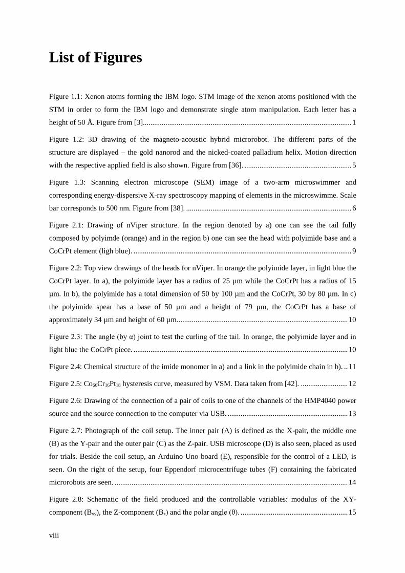
Figure 1.1: Xenon atoms forming the IBM logo. STM image of the xenon atoms positioned with the
STM in order to form the IBM logo and demonstrate single atom manipulation. Each letter has a
height of 50 Å. Figure from [3]............................................................................................................... 1
Figure 1.2: 3D drawing of the magneto-acoustic hybrid microrobot. The different parts of the
structure are displayed – the gold nanorod and the nicked-coated palladium helix. Motion direction
with the respective applied field is also shown. Figure from [36]. ......................................................... 5
Figure 1.3: Scanning electron microscope (SEM) image of a two-arm microswimmer and
corresponding energy-dispersive X-ray spectroscopy mapping of elements in the microswimme. Scale
bar corresponds to 500 nm. Figure from [38]. ........................................................................................ 6
Figure 2.1: Drawing of nViper structure. In the region denoted by a) one can see the tail fully
composed by polyimde (orange) and in the region b) one can see the head with polyimide base and a
CoCrPt element (ligh blue). .................................................................................................................... 9
Figure 2.2: Top view drawings of the heads for nViper. In orange the polyimide layer, in light blue the
CoCrPt layer. In a), the polyimide layer has a radius of 25 µm while the CoCrPt has a radius of 15
µm. In b), the polyimide has a total dimension of 50 by 100 µm and the CoCrPt, 30 by 80 µm. In c)
the polyimide spear has a base of 50 µm and a height of 79 µm, the CoCrPt has a base of
approximately 34 µm and height of 60 µm. .......................................................................................... 10
Figure 2.3: The angle (by α) joint to test the curling of the tail. In orange, the polyimide layer and in
light blue the CoCrPt piece. .................................................................................................................. 10
Figure 2.4: Chemical structure of the imide monomer in a) and a link in the polyimide chain in b). .. 11
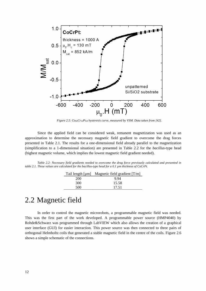
Figure 2.5: Co66Cr16Pt18 hysteresis curve, measured by VSM. Data taken from [42]. ......................... 12
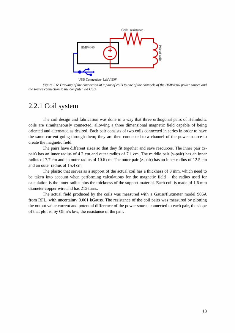
Figure 2.6: Drawing of the connection of a pair of coils to one of the channels of the HMP4040 power
source and the source connection to the computer via USB. ................................................................ 13
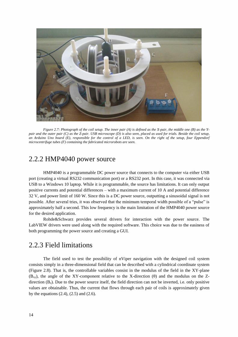
Figure 2.7: Photograph of the coil setup. The inner pair (A) is defined as the X-pair, the middle one
(B) as the Y-pair and the outer pair (C) as the Z-pair. USB microscope (D) is also seen, placed as used
for trials. Beside the coil setup, an Arduino Uno board (E), responsible for the control of a LED, is
seen. On the right of the setup, four Eppendorf microcentrifuge tubes (F) containing the fabricated
microrobots are seen. ............................................................................................................................ 14
Figure 2.8: Schematic of the field produced and the controllable variables: modulus of the XY-
component (Bxy), the Z-component (Bz) and the polar angle (θ). ......................................................... 15
ix
Figure 2.9: LabVIEW GUI developed for the control of nViper with the coil system. The three input
variables are “X-current”, the current that passes through the X-pair of coils, “Angle”, the polar angle
between the field vector and the X-pair’s axis, and “Z-current”, the current that passes through the Z-
pair of coils. In “Instrument Descriptor” the communication port is selected, with the power source
corresponding to a COM port (not depicted). If the correct descriptor is selected, in the text box to the
right of the descriptor dropdown menu the name of the power source appears. In “XY-field”, the
theoretical magnitude of the field in the XY place is determined through equation (2.1). In “Z-field”,
the field in the Z-direction is also calculated through equation (2.1). In “Maximum angle”, the
maximum polar angle is calculated through inequation (2.8). .............................................................. 17
Figure 2.10: The conversion of a drawing to the exposure pattern. In the beginning, the drawing to
expose, with desired exposure parts in brown. Then the drawing is transformed to a set of stripes with
200 µm width each. Zooming in, we can see the actual exposure pattern as pixels of 0.2 by 0.2 µm. 19
Figure 2.11: The difference between non-inverted and inverted lithography mask. In the CAD
drawing (black) can be seen the drawn pattern. If the mask is non-inverted the photoresist is exposed
to that same pattern (dark red), while in an inverted mask everything is exposed except the drawn
pattern (light red) .................................................................................................................................. 19
Figure 2.12: Overview of the process used in the first run. Sacrificial layer is defined with AlSiCu
(dark purple) and chromium (blue), followed by definition of polyimide (orange), definition of
CoCrPt head (light blue) and finally the selective etch of the AlSiCu in the sacrificial layer. ............. 22
Figure 2.13: Sidecut drawings of the process used to define the sacrificial layer used in this run. In
step 1, the glass (gray) was coated with photoresist, which was then exposed to the laser. Non-
exposed photoresist is seen in red and exposed photoresist in dark red. Step 2 shows the remaining
photoresist after development and the AlSiCu (dark purple) deposited at Nordiko 7000. In step 3, lift-
off of the AlSiCu was done by removing the photoresist. In step 4, chromium (blue) was deposited at
Alcatel SCM450. In step 5 can be seen the exposure of the photoresist, while the profile image in the
drawing is rectangular, the actual profile would show a more curved edge at the depression. In step 6,
the exposed photoresist was removed. In step 7, chromium not protected by the photoresist was
chemically removed. In step 8, the remaining photoresist was removed. ............................................. 22
Figure 2.14: Sidecut drawings of the process used to define the polyimide layer. In step 1, uncured
polyimide (yellow) was spin-coated on the sample and soft-baked afterwards. In step 2, unexposed
photoresist (red) was spin-coated on the sample and in step 3 it was exposed to the laser (dark red).
The polyimide was then chemically etched with the photoresist developer with 5 second development
steps. Step 4 shows the profile after the exposed photoresist was fully removed and in step 5 the
finished etch of the polyimide. In step 6, the remaining photoresist was removed and step 7 shows the
polyimide after cure (orange). ............................................................................................................... 23
x
Figure 2.15: Sidecut drawings of the process to define the magnetic heads. CoCrPt (light blue) was
deposited at Alcatel SCM450 in step 1. In step 2, the photoresist was spin-coated and exposed to the
laser (non-exposed in red, exposed in dark red). In step 3, the exposed photoresist was removed with
the developer. In step 4, the sample was physically etched by ion milling. Note that the remaining
photoresist is also etched, but at a different rate that the CoCrPt. In step 4, the surviving photoresist
was removed. ........................................................................................................................................ 23
Figure 2.16: Overview of the process used in the second run. In stage 1, the polyimide (orange) base
is defined. In stage 2, the definition of CoCrPt (light blue) and finally, in stage 3, the release of the
full structure. ......................................................................................................................................... 24
Figure 2.17: Overview of the process used in the third fabrication run. In the first stage, the sacrificial
layer is defined with AlSiCu (dark purple). Then the first polyimide (orange) layer is defined. In the
third stage, the head is defined with two layers of Ru (light purple) and one of CoCrPt (light blue). On
the fourth stage, the second polyimide layer is defined. Finally, in the fifth stage, the AlSiCu is
dissolved and the structure released. ..................................................................................................... 25
Figure 2.18: Sidecut drawings of the definition of the magnetic heads. In step 1, the thick photoresist
(red) was spin-coated and exposed (dark red). In step 2, the photoresist was developed (leaving only
the non-exposed photoresist) and the Ru (light purple) and CoCrPt (light blue) layers deposited. In
step 3, the photoresist was removed, defining the magnetic heads by lift-off. ..................................... 26
Figure 3.1: Plot of the measured current and potential difference values from HMP4040 power source.
Current values have an uncertainty of 0.001 A and potential difference values have an uncertainty of
0.001 V. ................................................................................................................................................. 28
Figure 3.2: Plot of the measured field intensity values for each coil. Measured magnetic field values
have an uncertainty of 0.001 T and the current input values have an uncertainty of 0.001 A. ............. 29
Figure 3.3: Photographs at 20x magnification of a neodymium magnet’s alignment control with the
field produced by the coil setup. In a), the field had an angle of 0º - i.e., the green line is parallel to the
X-pair axis. In b), the field was rotated 15º. In c). 30º and in d), 60º. Scale bar corresponds to 3 mm.30
Figure 3.4: Microscope photographs at 10x magnification of the dye the exposed with energy file 90.
In a), total development time was 5 seconds. In b), 10 seconds. In c), 15 seconds. Scale bar
corresponds to 100 µm for all photographs. ......................................................................................... 31
Figure 3.5: Plot of the etched thickness versus the total development time for each exposure energy
file. The horizontal line marks the average photoresist thickness (around 1.5 μm). Full etch of the
polyimide corresponds to a thickness measurement of approximately 5.3 μm – sum of the unexposed
photoresist thickness with the polyimide layer below it. ...................................................................... 31

xi
Figure 3.6: Figure containing microscope images (at 10x magnification) from the sample after
definition of the AlSiCu part of the layer. In A the dye for the coccus type head, in B the dye for the
bacillus type head and in C the dye for the sperm type head. In D is a photograph a test structure used
to confirm if the sample dimensions matched the ones drawn in the CAD mask. The green colour is
due to the green light of the microscope. In said green, one can see the AlSiCu and in black the glass
substrate. Scale bar corresponds to 100 µm for all photographs........................................................... 32
Figure 3.7: Figure containing microscope images at 50x magnification of the chromium structures that
will hold the structure to the glass substrate after removing the AlSiCu. In A the coccus head, in B the
bacillus head and in C the sperm head. In each image, the overlap between the chromium and the
AlSiCu can be seen. The lighter grey is the AlSiCu, while the darker shade corresponds to the
chromium. Scale bar corresponds to 50 µm for all photographs. ......................................................... 32
Figure 3.8: In this figure, the evolution of patterning the polyimide is seen. In a), a total of 5 seconds
of development time. In b), a total of 10 seconds. In c), a total of 15 seconds. Finally, in d), the
structure is post-cure. Images taken at 100x magnification. Scale bar corresponds to 50 µm for all
photographs. .......................................................................................................................................... 33
Figure 3.9: Microscope photos at 50x magnification of the three different head designs. In a), the
coccus type, in b), the bacillus type and in c) the sperm type. The CoCrPt is seen as a light grey on top
of the previously defined polyimide structure. Scale bar corresponds to 50 µm for all photographs. .. 33
Figure 3.10: Microscope photographs at 50x magnification of the three different structure types after
approximately 19 hours in aluminium etchant. Metallic residues are seen around the structures, as
well as corrosion of the CoCrPt heads. Scale bar corresponds to 50 µm for all photographs. ............. 34
Figure 3.11: Images of four different dyes of the coccus type device, at 10x magnification, after
approximately 19 hours in aluminium etchant. In a), the tail has length 200 µm and an angle of 0º. In
b), the same length but angle of 50º. In c), 500 µm and angle of 0º. In d), 500 µm and angle of 50º. In
the last image, a slight bend of the tail is seen. Scale bar corresponds to 100 µm for all photographs. 34
Figure 3.12: Images of the three different types of heads, at 50x magnification, after approximately 40
minutes in chromium etchant. Further corrosion of the CoCrPt is observed as well as a slight decrease
in the amount of residues surrounding the structures. Scale bar corresponds to 50 µm for all
photographs. .......................................................................................................................................... 34
Figure 3.13: Photographs of the AlSiCu frame used for alignment marks - in A and in B – and
identification of test structures in D. Scale bar corresponds to 100 µm for all photographs. ............... 35
Figure 3.14: Photographs of the sperm type head during polyimide definition. In A, the total
development time was 5 seconds. In B, the total time was 6 seconds. Finally, in C, the post-cure
image. Scale bar corresponds to 20 µm for all photographs. ................................................................ 35
xii
Figure 3.15: Photographs after the definition of the magnetic heads. In these, a misalignment between
the two layers is seen, as well as metallic residues surrounding the structure. Scale bar corresponds to
20 µm for all photographs. .................................................................................................................... 36
Figure 3.16: Photograph of the alignment marks defined on the sacrificial layer by lift-off. In green,
the AlSiCu, in black, its voids – the glass substrate. Scale bar corresponds to 100 µm. ...................... 37
Figure 3.17: Photographs of the definition of the polyimide base at 50x magnification. In A, total
development time was 5 seconds. In B, 7 seconds. In C, 9 seconds. In D, the structure after the cure
step. Scale bar corresponds to 20 µm for all photographs. ................................................................... 37
Figure 3.18: Photographs of the definition of the magnetic head. In A, after the development of the
thick photoresist. In white, the photoresist “hole” is seen. In B, after the lift-off of the metallic layers.
The head is seen inside the polyimide base. Scale bar corresponds to 20 µm for all photographs. ...... 38
Figure 3.19: Photographs of the sperm type head at 500x magnification. In a), after 6 seconds of
development. In b) after 7 seconds. In c), after 9 seconds. In d), after the cure step – one can also
observe leftover polyimide surrounding the base structure. Scale bar corresponds to 20 µm for all
photographs. .......................................................................................................................................... 38
Figure 3.20: Images of the released and successfully retrieved nViper structures at 400x
magnification. In A, the sperm type is seen. In B and C, the bacillus type. Photographs were taken
with USB microscope and the devices were in a water droplet on top of a glass substrate that covered
a white LED. Scale bar corresponds to 150 µm for all photographs. ................................................... 39
Figure 3.21: Plot of the fps values obtained during video capture. The average value is marked by the
vertical line. Each dot represents the relative frequency of value intervals with range 0.5 fps. The
interval with most frequency contains the average. .............................................................................. 39
Figure 3.22: Microscope images (20x magnification) of a first set of conditions. In A1 and A2, images
were taken before the magnetic field rotation. In B1 and B2, images were taken after the rotation of
the field. In A1 and B1 the structure that moved is not marked. In A2 and B2 a line is drawn across
the symmetry axis of the structure, in order to emphasize the rotation, and a circle is drawn around it
to emphasize its location. Debris surrounding the structure in question are easily seen. Scale bar
corresponds to 1 mm for all photographs. ............................................................................................. 41
Figure 3.23: Microscope images (20x magnification) of a second set of conditions. In A1 and A2,
images were taken before the magnetic field rotation. In B1 and B2, images were taken after the
rotation of the field. In A1 and B1 the structure that moved is not marked. In A2 and B2 a line is
drawn across the symmetry axis of the structure, in order to emphasize the rotation, and a circle is
drawn around it to emphasize its location. Debris surrounding the structure in question are easily seen.
Scale bar corresponds to 1 mm for all photographs. ............................................................................. 42

xiii
Figure 3.24: Microscope images (20x magnification) of a third set of conditions. In A1 and A2,
images were taken before the magnetic field rotation. In B1 and B2, images were taken after the
rotation of the field. In A1 and B1 the structure that moved is not marked. In A2 and B2 a line is
drawn across the symmetry axis of the structure, in order to emphasize the rotation, and a circle is
drawn around it to emphasize its location. Debris surrounding the structure in question are easily seen.
Scale bar corresponds to 1 mm for all photographs. A purple light was used for better contrast. ........ 43
Figure 3.25: Microscope image at 20x magnification of a droplet containing nViper structures. In A1,
droplet after deposition on the glass substrate without applied magnetic field. In A2, realignment of
circled structures towards a permanent magnet after disturbance. In B1, the magnet was removed, and
droplet disturbed once again. In B2, circled structures realigned with the permanent magnet after
disturbing the system. Scale bar corresponds to 1 mm for all photographs. ......................................... 44
xiv
List of Tables
Table 2.1: Table with a drag force approximation for the nViper structures (approximating the design
to a needle, assuming the fluid is water at 20ºC and a flow velocity of 0.92 m/s). Force is presented in
nN while the tail length is presented in µm. ......................................................................................... 10
Table 2.2: Necessary field gradients needed to overcome the drag force previously calculated and
presented in table 2.1. These values are calculated for the bacillus-type head for a 0.1 µm thickness of
CoCrPt. ................................................................................................................................................. 12
Table 2.3: Table showing the general parameters for the modules used with the respective operation.
.............................................................................................................................................................. 20
Table 2.4: Table showing the general parameters for the deposition of chromium and the two CoCrPt
alloys used, at Alcatel SCM450. ........................................................................................................... 20
Table 2.5: Conditions for the processes used at Nordiko 7000. The soft etch was performed previously
to the deposition in order to improve adhesion and remove nanometric impurities. ............................ 21
Table 2.6: Table showing the overall stages of the fabrication process. In stage 1, the sacrificial layer
is defined with AlSiCu and chromium. In stage 2, the polyimide base of the structures is defined by
chemical etch with the standard photoresist developer. In stage 3, the magnetic head is defined by ion-
milling etch at Nordiko 3600. In stage 4, the materials of the sacrificial layer are selectively etched
with chemical etchants. ......................................................................................................................... 22
Table 2.7: Stages of the second fabrication run. In stage 1, an AlSiCu frame is defined to identify
different dyes and define alignment marks. In stage 2, the polyimide base is again defined by
chemical etch with the standard photoresist developer. In stage 3, the magnetic head is defined by ion-
milling etch at Nordiko 3600. In stage 4, attempts at lifting the polyimide directly from the glass with
different solvents. .................................................................................................................................. 24
Table 2.8: The five stages of the third fabrication run. In stage 1, an AlSiCu sacrificial layer is
defined. In stage 2 and stage 4, the polyimide layer is defined by chemical etch with the standard
photoresist developer. In stage 3, the Ru/CoCrPt/Ru head is defined by lift-off with a thick
photoresist. Finally, in stage 5, the structures are released by fully etching away the sacrificial layer.25
Table 3.1: Table containing the resistance values of each coil pair. ..................................................... 29
Table 3.2 Table containing the obtained slopes, the slopes given by equation (2.1) and the relative
deviation between the two values. ........................................................................................................ 29
xv
Table 3.3: Table containing the measured angles of the symmetry axis of the neodymium magnet
relative to the 0º input angle magnetic field produced by the coils. Angles were measured using the
ruler tool of Adobe Photoshop CS6, with an uncertainty of 0.1º. ......................................................... 30
Table 3.4: Table containing the target thickness values for the materials of the sacrificial layer and the
actual obtained thicknesses along with the relative deviation between each value. ............................. 32
Table 3.5: Table containing the measured thicknesses of the polyimide test structures during the
definition steps. Thicknesses during development include the thickness of the non-developed
photoresist. Remaining thicknesses are of the polyimide only. ............................................................ 33
Table 3.6: Table containing the measurement of thicknesses pertaining to the ion-milling etch step.
CoCrPt thickness was measured on a test sample where the material was deposited simultaneously
with the fabrication sample. Polyimide thickness was measured on the respective test structures after
etch. ....................................................................................................................................................... 33
Table 3.7: Table containing the thickness measurements of the polyimide definition on the second
fabrication run. As previously, the thicknesses during development include the thickness of the non-
developed photoresist and the rest are of the polyimide only. .............................................................. 35
Table 3.8: Value of the deposited CoCrPt. Thickness was measured on a test sample where the
material was deposited simultaneously with the fabrication sample. ................................................... 36
Table 3.9: Table with the conditions of the release attempts of the second fabrication run. Each test
was performed with 1.5 microliter centrifuge tube that contained a dye containing nViper structures
and the specified solvent. ...................................................................................................................... 36
Table 3.10: Table with the thickness values during the development of the polyimide base. .............. 37
Table 3.11: Table with the thickness measurements of the thick PR used for CoCrPt lift-off and the
thickness of CoCrPt deposited on a test sample simultaneously with the fabrication sample. ............. 37
Table 3.12: Thickness of the polyimide stack during the definition stage. In the development steps, the
thickness includes the thickness of the non-developed photoresist. The other measurements are
relative to the combined thickness of two polyimide layers. ................................................................ 38

xvi
List of Acronyms
blood-brain barrier (BBB) ....................................................................................................................... 4
computer-assisted drawing (CAD)........................................................................................................ 18
frames per second (fps) ......................................................................................................................... 25
graphical user interface (GUI) .............................................................................................................. 12
hexamethyldisilazane (HMDS) ............................................................................................................. 17
ion-beam deposition (IBD) ................................................................................................................... 20
isopropanol (IPA).................................................................................................................................. 20
magnetic nanoparticles (MNPs) .............................................................................................................. 4
magnetic-resonance imaging (MRI) ....................................................................................................... 4
magnetoelectric nanorobot (MENR) ....................................................................................................... 4
microelectromechanical systems (MEMS) ............................................................................................. 2
Multiple Instance Learning (MIL) ........................................................................................................ 26
nanoelectromechanical systems (NEMS) ............................................................................................... 2
region of interest (ROI) ......................................................................................................................... 26
rotations per minute (rpm) .................................................................................................................... 17
scanning electron microscope (SEM) ..................................................................................................... 1
superparamagnetic iron oxide nanoparticles (SPION) ............................................................................ 4
1
1 Introduction
In this chapter a small review of the status of micro/nanorobotics (referred henceforth as µn-
robotics) is given. The principal actuation options are described and the physics of a fluid at the
micro/nanoscale is described. Some examples of magnetic µn-robots are given. In the last section of
the chapter, project objectives are provided.
1.1 µn-robotics
In 1965, Gordon Moore introduced what is now known as Moore’s law [1] – the average
number of transistors in an integrated circuit doubles every two years. While not accurate in the
quantity, it does show a tendency that has been observed since it was first postulated. While originally
applied to the evolution of integrated circuits, other technology fields have also followed this
tendency. One field that follows Moore’s law is the area of robotics. Depending on the characteristic
scale, these small robots are called micro (from 0.1 µm to 1 mm) or nanorobots (1 nm to 100 nm).
The first mention of a µn-robot in a scientific context was by Richard Feynman in his There’s
Plenty of Room at the Bottom speech in December of 1959 [2]. In it, he described a simple thought
experiment of reducing a surgical doctor to a small enough size so that he could operate from inside
the human body at a cellular level.
Several types of µn-robotic systems are possible and are not limited to the popular image
described by science fiction. For a µn-robotic system to classify as such, it only needs to operate in a
programmable fashion at the respective scale. The earliest example can be traced to the early 1990s -
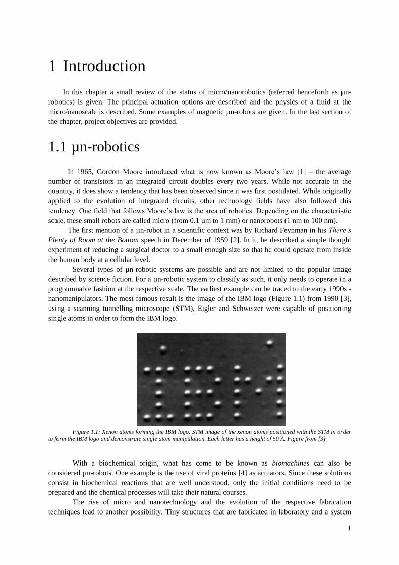
nanomanipulators. The most famous result is the image of the IBM logo (Figure 1.1) from 1990 [3],
using a scanning tunnelling microscope (STM), Eigler and Schweizer were capable of positioning
single atoms in order to form the IBM logo.
Figure 1.1: Xenon atoms forming the IBM logo. STM image of the xenon atoms positioned with the STM in order
to form the IBM logo and demonstrate single atom manipulation. Each letter has a height of 50 Å. Figure from [3]
With a biochemical origin, what has come to be known as biomachines can also be
considered µn-robots. One example is the use of viral proteins [4] as actuators. Since these solutions
consist in biochemical reactions that are well understood, only the initial conditions need to be
prepared and the chemical processes will take their natural courses.
The rise of micro and nanotechnology and the evolution of the respective fabrication
techniques lead to another possibility. Tiny structures that are fabricated in laboratory and a system
2
that is designed for their control. These are the ones that most resemble the image propagated through
science fiction and will be the focus of this remaining section. When designing these devices, the
main problems become their power source and the low Reynolds number that such small structures
are subject to.
1.1.1 Power source
A regular robot can fit a regular battery, be connected to the power grid, have solar cells, and
other possible options. A µn-robot can’t have any of those with the same efficiency, although some
have reported results with solar cells [5], usually these complete structures are in the millimetre range.
Providing a power source capable of operating in the micro or nanometre range is essential to the
operation of these small structures. In the following paragraphs, the two most common alternatives
are briefly described.
Electric
Using electric current to power a device is probably the first thought of many. Electric power
for robots is dominant in normal robotics. When reducing to the micro or nanoscale, the usual
electrical power sources become a nuisance. Several solutions for robots in the millimetre scale
embody a solid chassis [6] and thus oblige a greater size of the structure. An answer to this issue is the
use of microelectromechanical systems (MEMS) [7], as it allows for size reduction and lower power
consumption (1.1 W in 1999 [6] versus 1.0 mW in 2018 [8]). It also extends the range of movement
possibilities and allows the mimicry of insect-like movement [6] [9] [10]. In recent years, the
evolution in artificial intelligence has also allowed the inclusion of neural network chips to control the
movement [9] [10].
This solution allows µn-robots with untethered power sources [11] or on-board sources [5]
[12]. It seems ideal for ex vivo microrobots and the evolving field of nanoelectromechanical systems
(NEMS) is a rather unexplored approach to nanorobotics [13].
Magnetic
Magnetic solutions for µn-robotics tend to use an outside power source – a magnetic field
generator. By using an external source, the size of the robot can be greatly reduced. They can range
from nanoparticles [14], to magnetotactic bacteria [15], to adding magnetic functions to biological
entities [16] and to micrometre-sized structures [17]. While in electrically powered µn-robots, several
types of movement have been achieved, in magnetically powered µn-robots, these are limited to
simply following the magnetic field or be driven by the environment, with simple navigational
corrections by adjusting the field.
In section 1.2, several magnetic µn-robots are presented. When applying a magnetic field to a
magnetic volume, this volume will have a force and torque applied – equations (1.1) and (1.2).
𝑭𝑚 = 𝑉𝑚(𝑴. 𝛁)𝑩
(1.1)
𝝉𝑚 = 𝑉𝑚𝑴 × 𝑩
(1.2)
3
With 𝑉𝑚 being the volume of the magnetic component, M the magnetization and B the
magnetic field. The magnetic force is later compared to the drag force in Stokes flow. Torque is
relevant for robots that propel through realignment with the magnetic field, such as MagnetoSperm
[17].
1.1.2 Stokes flow
Reducing the scale of devices has implications in the governing equations of the medium
surrounding said device. If something with characteristic length in the nano or microscale is to operate
inside a fluid, the equations that dictate the behaviour of the fluid’s flow are to be adapted – that is to
say, the Navier-Stokes equation (equation (1.3)) is simplified.
𝜌𝑓
𝑑𝑽
𝑑𝑡= −𝛁𝑝 + 𝜂∇2𝑽
(1.3)
Where V is the velocity vector field, p is the pressure scalar field, 𝜌𝑓 is the constant density of
the fluid and 𝜂 is its dynamic viscosity. The equation can be rewritten with several variable changes
(equation (1.4)) in order to show the importance of the Reynolds number (ratio between the inertial
and viscous forces), see equation (1.5).
�̃� =𝑥
𝐿; �̃� =
𝑽
𝜇; �̃� =
𝑡 𝜇
𝐿; �̃� =
𝑝𝐿
𝜂𝜇
(1.4)
With L being the characteristic length of the object, x a Cartesian coordinate and µ the
magnitude of the velocity of the object concerning the medium. These changes result in equation
(1.5).
(𝜌𝑓𝜇𝐿
𝜂)
𝑑𝑽
𝑑𝑡= −𝛁𝑝 + ∇2𝑽
(1.5)
Where (𝜌𝑓𝜇𝐿
𝜂) is the Reynolds number (Re). Reducing the size of the submerged object to the
micro or nanoscale, the temporal term of the rewritten Navier-Stokes equation becomes negligible,
which results in what is known as Stokes flow (equation (1.6)) – the flow pattern does not appear to
change and becomes reversible.
𝛁𝑝 ≈ ∇2𝑽
(1.6)
According to [18] [19], the geometry of the body becomes negligible at Re < 1 and the drag
force (given by Stokes’ law in equation (1.6)) can be approximated by the drag force on a spherical
body with diameter d (equation (1.7)).
4
𝑭𝑑𝑟𝑎𝑔 = 3𝜋𝜂𝑑𝝁
(1.7)
Therefore, for a small enough magnetic object to only be guided by a magnetic field, the
equivalent magnetic force’s magnitude needs to surpass the drag force’s. The challenge arises from
the size dependence of each force: drag varies linearly with the diameter, while magnetic varies with
the volume. Which is to say, as the object gets smaller, the magnetic force decreases faster than the
drag force. Comparing the two forces for a small spherical magnet allows us to see that the needed
magnetic field gradient to overcome the drag force scales as 1𝑟2⁄ . As a simple comparison, moving a
1-millimetre sized sphere of a magnetic material would require a field gradient with magnitude
0,0001% of the needed field gradient to move a sphere of the same material in the same conditions but
with 1 micrometre radius.
1.2 Magnetic µn-robotics
Several magnetic results already exist in the field of µn-robotics and operate in both the nano
and the microscale. In this section, some of these devices are presented along with some of the most
characteristic approaches.
Magnetic nanoparticles
The smallest type of nanorobotic technology uses magnetic nanoparticles (MNPs). With
controllable sizes, MNPs can be smaller than most cells and in the same size scale as virus, proteins
and genes [20]. These can be used with several different purposes [21]: drug delivery [22],
hyperthermia [23], magnetic-resonance imaging (MRI) contrast enhancement [24] [25], and magnetic
separation [26]. Design specifications for drug delivery and imaging can be seen in [27].
MNPs’ size makes them ideal to assist in drug delivery to the needed locations. This is
especially important in cancer therapies, such as chemotherapy, that have secondary effects in the
entire body. Crossing the blood-brain barrier (BBB) also allows the delivery of drugs directly to the
brain [28]. The most widely used type of MNPs are superparamagnetic iron oxide nanoparticles
(SPION) [29]. The main advantages of SPIONs for drug delivery are the wide range of functions they
can fulfil simultaneously, all these derived from their magnetic behaviour [29]. Using MRI they can
be easily tracked and enhance contrast [29] and with alternating magnetic fields they can be used for
highly localized hyperthermia treatments [29]. MNPs tend to aggregate, for prevention, they are
usually combined with polymers [29].
Another way of using MNPs for drug delivery can be seen in a semi-biological approach,
where microorganisms that are already apt for the medium in question are modified so that they are
magnetically controllable [16]. This approach is inspired from the use of magnetotactic bacteria (of
the Magnetospirillum genus) [15], where a magnetossome – a magnetic chain – inside the bacteria
allows manipulation through a controllable magnetic field.
Using MNPs as the core for core-shell nanocomposites is also an option, making a
magnetoelectric nanorobot (MENR) a possibility [30]. These MENR can be used for targeted cell
manipulation by altering the magnetic field characteristics, which changes how the MENR interacts
with its target [30]. Direct application of MNPs in the medical field, via the use of MRI machines for
control and detection is a highly discussed and presented possibility [14].
5
Magnetic microrobots
Going from the nano to the microscale, there are several microorganisms capable of
navigation and the hydrodynamics of their movement mechanisms are already well studied [31].
Three propulsion types have been experimented with for microrobotic technology:
1) Body deformation with finite degrees of freedom (such as Purcell’s three-link swimmer [32]);
2) Continuous body deformation (mimicking flagella found in microorganisms and some
eukaryotic cells [33])
3) Chemical fuel (glucose is a recurrent fuel [34])
From these three, only the second is relevant for the work developed and is the basis of
flexible swimmers’ design [35]. Rigid and helical magnetic swimmers also exist and are controlled
with rotating magnetic fields [35]. Surface walkers are also mentioned in [35] and move mostly by
either rolling or tumbling across a surface.
MagnetoSperm [17] is an example of a simple flexible microstructure capable of navigation
with weak magnetic fields. It has spermatozoa-like geometry made of SU-8 polymer and the magnetic
component (Co80Ni20) is found on the head. Using an oscillating magnetic field that imposes a
magnetic torque on the head, realigning it with the field, bending the SU-8 base making it work like a
flagellum. Its maximum velocity – 158±32 µm/s - in water was obtained at a frequency of 45 Hz.
Lower or higher frequency decreased its velocity.
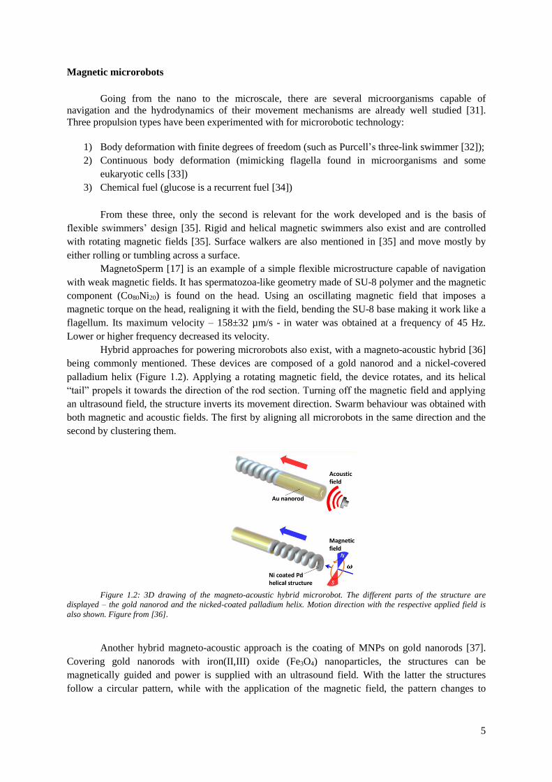
Hybrid approaches for powering microrobots also exist, with a magneto-acoustic hybrid [36]
being commonly mentioned. These devices are composed of a gold nanorod and a nickel-covered
palladium helix (Figure 1.2). Applying a rotating magnetic field, the device rotates, and its helical
“tail” propels it towards the direction of the rod section. Turning off the magnetic field and applying
an ultrasound field, the structure inverts its movement direction. Swarm behaviour was obtained with
both magnetic and acoustic fields. The first by aligning all microrobots in the same direction and the
second by clustering them.
Figure 1.2: 3D drawing of the magneto-acoustic hybrid microrobot. The different parts of the structure are
displayed – the gold nanorod and the nicked-coated palladium helix. Motion direction with the respective applied field is
also shown. Figure from [36].
Another hybrid magneto-acoustic approach is the coating of MNPs on gold nanorods [37].
Covering gold nanorods with iron(II,III) oxide (Fe3O4) nanoparticles, the structures can be
magnetically guided and power is supplied with an ultrasound field. With the latter the structures
follow a circular pattern, while with the application of the magnetic field, the pattern changes to
6
linear. According to [36] and [37], a magneto-acoustic approach seems a viable approach for the
research of several motion types.
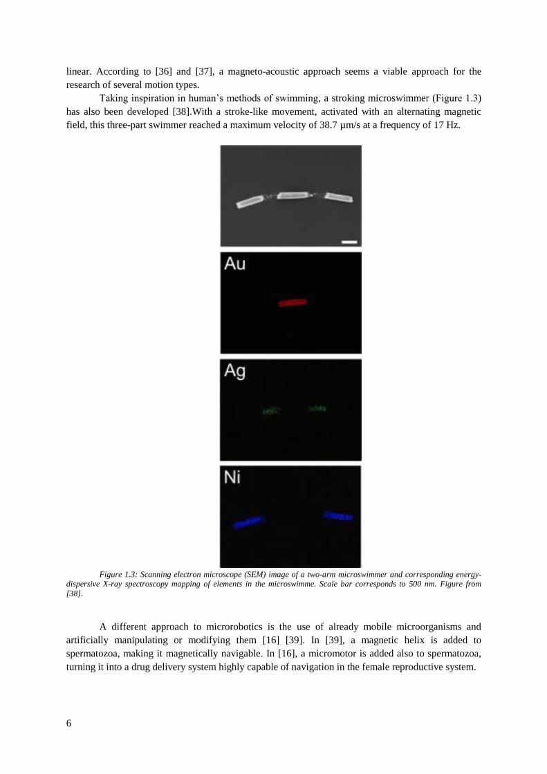
Taking inspiration in human’s methods of swimming, a stroking microswimmer (Figure 1.3)
has also been developed [38].With a stroke-like movement, activated with an alternating magnetic
field, this three-part swimmer reached a maximum velocity of 38.7 µm/s at a frequency of 17 Hz.
Figure 1.3: Scanning electron microscope (SEM) image of a two-arm microswimmer and corresponding energy-
dispersive X-ray spectroscopy mapping of elements in the microswimme. Scale bar corresponds to 500 nm. Figure from
[38].
A different approach to microrobotics is the use of already mobile microorganisms and
artificially manipulating or modifying them [16] [39]. In [39], a magnetic helix is added to
spermatozoa, making it magnetically navigable. In [16], a micromotor is added also to spermatozoa,
turning it into a drug delivery system highly capable of navigation in the female reproductive system.

7
1.3 Objectives
The main objective of this project consists in the development of a microrobotic system
composed of magnetic microstructures (nViper) and three orthogonal pairs of coils in Helmholtz
configuration capable of generating a three-dimensional magnetic field. In its turn, the Helmholtz
coils are powered by a programmable DC power source that will enable control of the magnetic field.
This larger goal is divided in several stages:
• Design and fabrication of the three Helmholtz coil pairs;
• Implementation of control software with LabVIEW;
• Fabrication of nViper microrobots at INESC-MN;
• Testing nViper microrobots behaviour with the coil system;
8
2 Methods and Materials
In this chapter, the methodology and materials used are described. In the first section, an
overview of the components of the system is given. Afterwards, the system through which the
magnetic field was applied to the nViper devices is described and what considerations were taken.
This includes the coils used, the programmable power source (that alters the field as the user
determines), the considerations taken when designing the LabVIEW interface and the microscope
used to observe the devices and record their movement, as well as the script used to trace their
velocity from the video recordings. Afterwards, the fabrication of the nViper devices at INESC-MN is
described, as well as the machinery used and the tests conducted to validate and/or optimize parts of
the process. The navigation tests were done at IBEB, FCUL.
All figures in this chapter are by the author, except where noted.
2.1 nViper microrobot and Helmholtz coils
In order to test the possible control of microrobots in a liquid using magnetic fields,
fabrication of actual microrobotic structures is the ideal option. This led to the design of the
microrobots named nViper (n pertaining to nano, viper to their geometry) – microrobots with
magnetic head and polymer body.
In this section follows information relevant to the choices made concerning the control system
and the microrobots developed during the project. Firstly, the magnetic field produced by pairs of
coils in Helmholtz configuration is presented. The conditions necessary to achieve propulsion solely
by magnetic force are described and the design choices for nViper elaborated.
2.1.1 Helmholtz coils
Establishing a constant magnetic field is necessary to actuate the microrobots. For this, pairs
of coils in Helmholtz configuration are used. A pair of coils is considered to be in Helmholtz
configuration when they are equally sized (same radius and number of loops), the distance between
them is equal to their radius and the current passing through each coil is of the same value. Following
the Biot-Savart law for the magnetic field generated by a constant current, the field is found to be
stable at the centre of the pair and determined by equation (2.1).
𝐵 = 8𝜇0𝑁𝐼
5√5𝑅
(2.1)
2.1.2 Overcoming drag
As a quick overview, nViper consists of two main parts: a tail and a head. The tail consists
solely of a flexible polymer (polyimide), while the head has a magnetic component (cobalt-
chromium-platinum alloy) that will be used to guide the full structure by applying a magnetic field.
This can be seen in Figure 2.1.
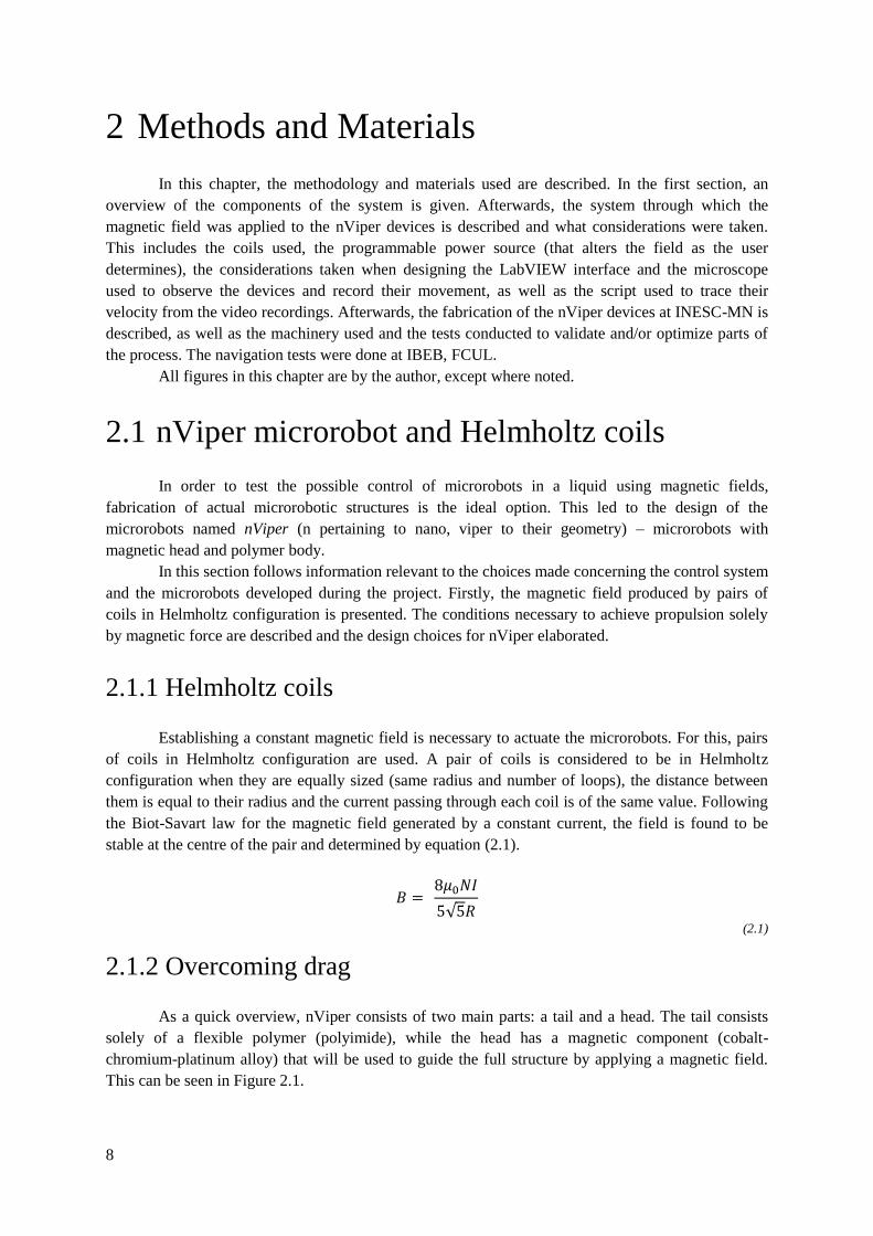
9
Figure 2.1: Drawing of nViper structure. In the region denoted by a) one can see the tail fully composed by
polyimde (orange) and in the region b) one can see the head with polyimide base and a CoCrPt element (ligh blue).
Using the same approximation as [17], said design can be seen as a thin needle with length l
and diameter d, the drag force is then given by equation (2.2).
𝑭𝑑𝑟𝑎𝑔 = 𝜂𝑙
ln (2𝑙𝑑
) − 0.81𝝁
(2.2)
By comparing with the magnetic force, so that the latter is greater we obtain inequation (2.3).
𝑉𝑚(𝑴. 𝛁)𝑩 ≥ 𝜂𝑙
ln (2𝑙𝑑
) − 0.81𝝁
(2.3)
Inequation (2.3) becomes the main condition for an nViper microrobot to overcome the drag
force solely by magnetic force. Similar to [17], actual propulsion would be attempted by swimming-
like motion. Proof-of-concept that such attempt is at least possible is the realignment of the structure
with the magnetic field.
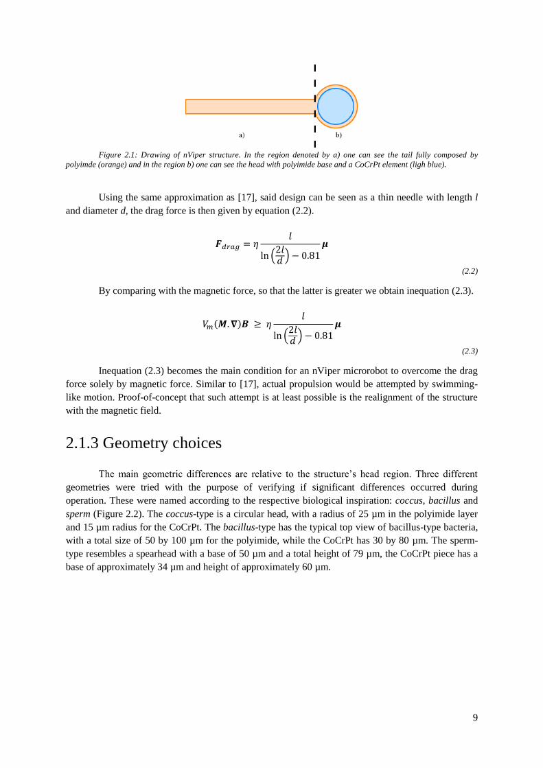
2.1.3 Geometry choices
The main geometric differences are relative to the structure’s head region. Three different
geometries were tried with the purpose of verifying if significant differences occurred during
operation. These were named according to the respective biological inspiration: coccus, bacillus and
sperm (Figure 2.2). The coccus-type is a circular head, with a radius of 25 µm in the polyimide layer
and 15 µm radius for the CoCrPt. The bacillus-type has the typical top view of bacillus-type bacteria,
with a total size of 50 by 100 µm for the polyimide, while the CoCrPt has 30 by 80 µm. The sperm-
type resembles a spearhead with a base of 50 µm and a total height of 79 µm, the CoCrPt piece has a
base of approximately 34 µm and height of approximately 60 µm.
10
Figure 2.2: Top view drawings of the heads for nViper. In orange the polyimide layer, in light blue the CoCrPt
layer. In a), the polyimide layer has a radius of 25 µm while the CoCrPt has a radius of 15 µm. In b), the polyimide has a
total dimension of 50 by 100 µm and the CoCrPt, 30 by 80 µm. In c) the polyimide spear has a base of 50 µm and a height of
79 µm, the CoCrPt has a base of approximately 34 µm and height of 60 µm.
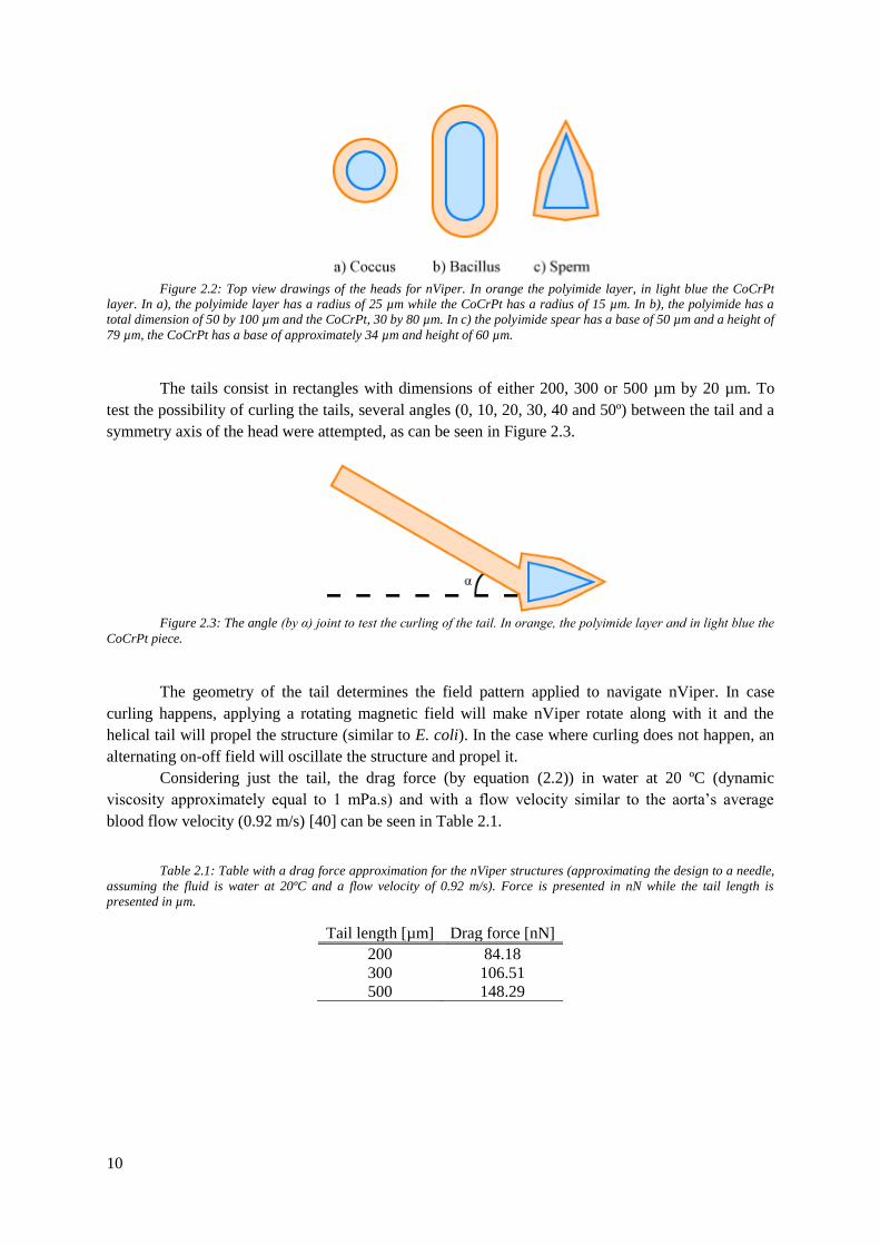
The tails consist in rectangles with dimensions of either 200, 300 or 500 µm by 20 µm. To
test the possibility of curling the tails, several angles (0, 10, 20, 30, 40 and 50º) between the tail and a
symmetry axis of the head were attempted, as can be seen in Figure 2.3.
Figure 2.3: The angle (by α) joint to test the curling of the tail. In orange, the polyimide layer and in light blue the
CoCrPt piece.
The geometry of the tail determines the field pattern applied to navigate nViper. In case
curling happens, applying a rotating magnetic field will make nViper rotate along with it and the
helical tail will propel the structure (similar to E. coli). In the case where curling does not happen, an
alternating on-off field will oscillate the structure and propel it.
Considering just the tail, the drag force (by equation (2.2)) in water at 20 ºC (dynamic
viscosity approximately equal to 1 mPa.s) and with a flow velocity similar to the aorta’s average
blood flow velocity (0.92 m/s) [40] can be seen in Table 2.1.
Table 2.1: Table with a drag force approximation for the nViper structures (approximating the design to a needle,
assuming the fluid is water at 20ºC and a flow velocity of 0.92 m/s). Force is presented in nN while the tail length is
presented in µm.
Tail length [µm] Drag force [nN]
200 84.18
300 106.51
500 148.29
11
2.1.4 Material choices
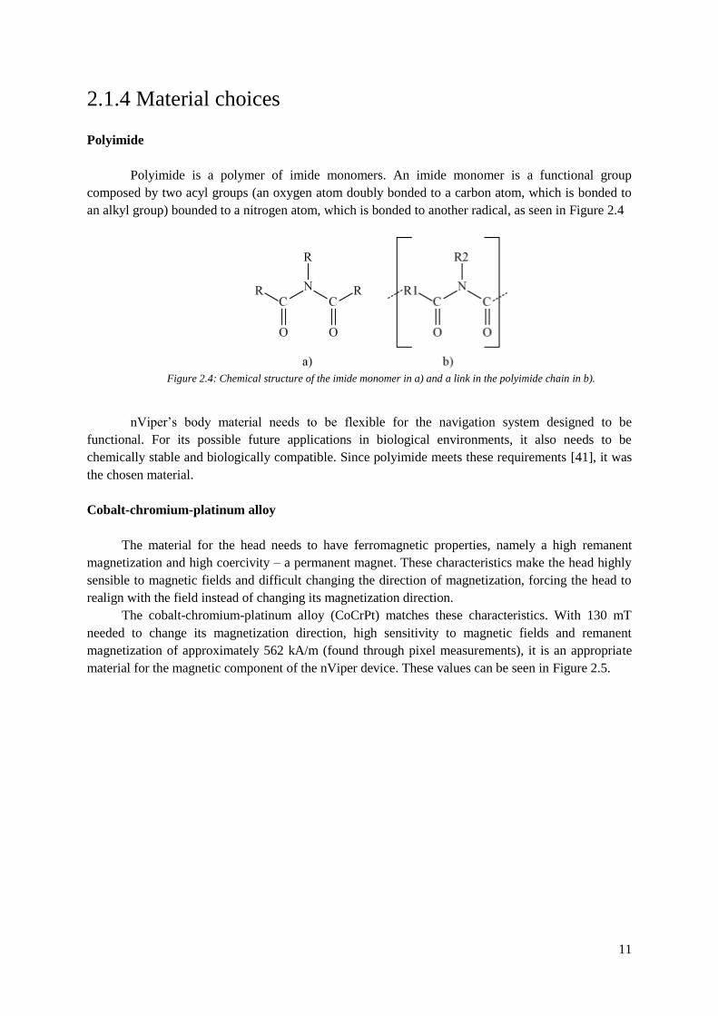
Polyimide
Polyimide is a polymer of imide monomers. An imide monomer is a functional group
composed by two acyl groups (an oxygen atom doubly bonded to a carbon atom, which is bonded to
an alkyl group) bounded to a nitrogen atom, which is bonded to another radical, as seen in Figure 2.4
Figure 2.4: Chemical structure of the imide monomer in a) and a link in the polyimide chain in b).
nViper’s body material needs to be flexible for the navigation system designed to be
functional. For its possible future applications in biological environments, it also needs to be
chemically stable and biologically compatible. Since polyimide meets these requirements [41], it was
the chosen material.
Cobalt-chromium-platinum alloy
The material for the head needs to have ferromagnetic properties, namely a high remanent
magnetization and high coercivity – a permanent magnet. These characteristics make the head highly
sensible to magnetic fields and difficult changing the direction of magnetization, forcing the head to
realign with the field instead of changing its magnetization direction.
The cobalt-chromium-platinum alloy (CoCrPt) matches these characteristics. With 130 mT
needed to change its magnetization direction, high sensitivity to magnetic fields and remanent
magnetization of approximately 562 kA/m (found through pixel measurements), it is an appropriate
material for the magnetic component of the nViper device. These values can be seen in Figure 2.5.
12
Figure 2.5: Co66Cr16Pt18 hysteresis curve, measured by VSM. Data taken from [42].
Since the applied field can be considered weak, remanent magnetization was used as an
approximation to determine the necessary magnetic field gradient to overcome the drag forces
presented in Table 2.1. The results for a one-dimensional field already parallel to the magnetization
(simplification to a 1-dimensional situation) are presented in Table 2.2 for the bacillus-type head
(highest magnetic volume, which implies the lowest magnetic field gradient needed).
Table 2.2: Necessary field gradients needed to overcome the drag force previously calculated and presented in
table 2.1. These values are calculated for the bacillus-type head for a 0.1 µm thickness of CoCrPt.
Tail length [µm] Magnetic field gradient [T/m]
200 9.94
300 15.58
500 17.51
2.2 Magnetic field
In order to control the magnetic microrobots, a programmable magnetic field was needed.
This was the first part of the work developed. A programmable power source (HMP4040) by
Rohde&Schwarz was programmed through LabVIEW which also allows the creation of a graphical
user interface (GUI) for easier interaction. This power source was then connected to three pairs of
orthogonal Helmholtz coils that generated a stable magnetic field in the centre of the coils. Figure 2.6
shows a simple schematic of the connections.
13
Figure 2.6: Drawing of the connection of a pair of coils to one of the channels of the HMP4040 power source and
the source connection to the computer via USB.
2.2.1 Coil system
The coil design and fabrication was done in a way that three orthogonal pairs of Helmholtz
coils are simultaneously connected, allowing a three dimensional magnetic field capable of being
oriented and alternated as desired. Each pair consists of two coils connected in series in order to have
the same current going through them; they are then connected to a channel of the power source to
create the magnetic field.
The pairs have different sizes so that they fit together and save resources. The inner pair (x-
pair) has an inner radius of 4.2 cm and outer radius of 7.1 cm. The middle pair (y-pair) has an inner
radius of 7.7 cm and an outer radius of 10.6 cm. The outer pair (z-pair) has an inner radius of 12.5 cm
and an outer radius of 15.4 cm.
The plastic that serves as a support of the actual coil has a thickness of 3 mm, which need to
be taken into account when performing calculations for the magnetic field – the radius used for
calculation is the inner radius plus the thickness of the support material. Each coil is made of 1.6 mm
diameter copper wire and has 215 turns.
The actual field produced by the coils was measured with a Gauss/fluxmeter model 906A
from RFL, with uncertainty 0.001 kGauss. The resistance of the coil pairs was measured by plotting
the output value current and potential difference of the power source connected to each pair, the slope
of that plot is, by Ohm’s law, the resistance of the pair.
14
Figure 2.7: Photograph of the coil setup. The inner pair (A) is defined as the X-pair, the middle one (B) as the Y-
pair and the outer pair (C) as the Z-pair. USB microscope (D) is also seen, placed as used for trials. Beside the coil setup,
an Arduino Uno board (E), responsible for the control of a LED, is seen. On the right of the setup, four Eppendorf
microcentrifuge tubes (F) containing the fabricated microrobots are seen.
2.2.2 HMP4040 power source
HMP4040 is a programmable DC power source that connects to the computer via either USB
port (creating a virtual RS232 communication port) or a RS232 port. In this case, it was connected via
USB to a Windows 10 laptop. While it is programmable, the source has limitations. It can only output
positive currents and potential differences – with a maximum current of 10 A and potential difference
32 V, and power limit of 160 W. Since this is a DC power source, outputting a sinusoidal signal is not
possible. After several tries, it was observed that the minimum temporal width possible of a “pulse” is
approximately half a second. This low frequency is the main limitation of the HMP4040 power source
for the desired application.
Rohde&Schwarz provides several drivers for interaction with the power source. The
LabVIEW drivers were used along with the required software. This choice was due to the easiness of
both programming the power source and creating a GUI.
2.2.3 Field limitations
The field used to test the possibility of nViper navigation with the designed coil system
consists simply in a three-dimensional field that can be described with a cylindrical coordinate system
(Figure 2.8). That is, the controllable variables consist in the modulus of the field in the XY-plane
(Bxy), the angle of the XY-component relative to the X-direction (θ) and the modulus on the Z-
direction (Bz). Due to the power source itself, the field direction can not be inverted, i.e. only positive
values are obtainable. Thus, the current that flows through each pair of coils is approximately given
by the equations (2.4), (2.5) and (2.6).
A
B C
D
E
F
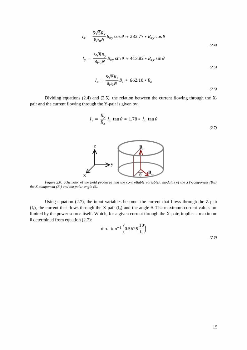
15
𝐼𝑥 = 5√5𝑅𝑥
8𝜇0𝑁𝐵𝑥𝑦 cos 𝜃 ≈ 232.77 ∗ 𝐵𝑥𝑦 cos 𝜃
(2.4)
𝐼𝑦 = 5√5𝑅𝑦
8𝜇0𝑁𝐵𝑥𝑦 sin 𝜃 ≈ 413.82 ∗ 𝐵𝑥𝑦 sin 𝜃
(2.5)
𝐼𝑧 = 5√5𝑅𝑧
8𝜇0𝑁𝐵𝑧 ≈ 662.10 ∗ 𝐵𝑧
(2.6)
Dividing equations (2.4) and (2.5), the relation between the current flowing through the X-
pair and the current flowing through the Y-pair is given by:
𝐼𝑦 = 𝑅𝑦
𝑅𝑥 𝐼𝑥 tan 𝜃 ≈ 1.78 ∗ 𝐼𝑥 tan 𝜃
(2.7)
Figure 2.8: Schematic of the field produced and the controllable variables: modulus of the XY-component (Bxy),
the Z-component (Bz) and the polar angle (θ).
Using equation (2.7), the input variables become: the current that flows through the Z-pair
(Iz), the current that flows through the X-pair (Ix) and the angle θ. The maximum current values are
limited by the power source itself. Which, for a given current through the X-pair, implies a maximum
θ determined from equation (2.7):
𝜃 < tan−1 (0.562510
𝐼𝑥)
(2.8)
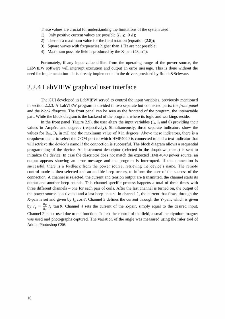
16
These values are crucial for understanding the limitations of the system used:
1) Only positive current values are possible (𝐼𝑥 ≥ 0 𝐴);
2) There is a maximum value for the field rotation (equation (2.8));
3) Square waves with frequencies higher than 1 Hz are not possible;
4) Maximum possible field is produced by the X-pair (43 mT);
Fortunately, if any input value differs from the operating range of the power source, the
LabVIEW software will interrupt execution and output an error message. This is done without the
need for implementation – it is already implemented in the drivers provided by Rohde&Schwarz.
2.2.4 LabVIEW graphical user interface
The GUI developed in LabVIEW served to control the input variables, previously mentioned
in section 2.2.3. A LabVIEW program is divided in two separate but connected parts: the front panel
and the block diagram. The front panel can be seen as the frontend of the program, the interactable
part. While the block diagram is the backend of the program, where its logic and workings reside.
In the front panel (Figure 2.9), the user alters the input variables (Ix, Iz and θ) providing their
values in Ampère and degrees (respectively). Simultaneously, three separate indicators show the
values for Bxy, Bz in mT and the maximum value of θ in degrees. Above these indicators, there is a
dropdown menu to select the COM port to which HMP4040 is connected to and a text indicator that
will retrieve the device’s name if the connection is successful. The block diagram allows a sequential
programming of the device. An instrument descriptor (selected in the dropdown menu) is sent to
initialize the device. In case the descriptor does not match the expected HMP4040 power source, an
output appears showing an error message and the program is interrupted. If the connection is
successful, there is a feedback from the power source, retrieving the device’s name. The remote
control mode is then selected and an audible beep occurs, to inform the user of the success of the
connection. A channel is selected, the current and tension output are transmitted, the channel starts its
output and another beep sounds. This channel specific process happens a total of three times with
three different channels – one for each pair of coils. After the last channel is turned on, the output of
the power source is activated and a last beep occurs. In channel 1, the current that flows through the
X-pair is set and given by 𝐼𝑥 cos 𝜃. Channel 3 defines the current through the Y-pair, which is given
by 𝐼𝑦 = 𝑅𝑦
𝑅𝑥 𝐼𝑥 tan 𝜃. Channel 4 sets the current of the Z-pair, simply equal to the desired input.
Channel 2 is not used due to malfunction. To test the control of the field, a small neodymium magnet
was used and photographs captured. The variation of the angle was measured using the ruler tool of
Adobe Photoshop CS6.
17
Figure 2.9: LabVIEW GUI developed for the control of nViper with the coil system. The three input variables are
“X-current”, the current that passes through the X-pair of coils, “Angle”, the polar angle between the field vector and the
X-pair’s axis, and “Z-current”, the current that passes through the Z-pair of coils. In “Instrument Descriptor” the
communication port is selected, with the power source corresponding to a COM port (not depicted). If the correct descriptor
is selected, in the text box to the right of the descriptor dropdown menu the name of the power source appears. In “XY-
field”, the theoretical magnitude of the field in the XY place is determined through equation (2.1). In “Z-field”, the field in
the Z-direction is also calculated through equation (2.1). In “Maximum angle”, the maximum polar angle is calculated
through inequation (2.8).
2.3 Fabrication process validation and tests
In order to proceed with the fabrication, some small processes had to be run. The materials for
the sacrificial layer were tested to know if one could be etched without affecting the other; the etch
process of polyimide was also characterized.
2.3.1 Etchant selectivity determination
To determine if the process planned for the first run was viable, the selectivity of each etchant
needed to be tested. The materials chosen were aluminium alloy (deposited at Nordiko 7000) and
chromium (deposited at Alcatel SCM450). The respective etchants were tested: TechniEtch Al80
(aluminium etchant) and chromium etchant produced by Sigma-Aldrich.
1000 Å of aluminium alloy were deposited on two 1 by 1-inch glass substrate, the same was
done for chromium. Each sample was then immersed in either aluminium or chromium etchant, and
its thickness measured in several time intervals to determine the corresponding etch rate of the etchant
on the specific material.
The difference between each consecutive measurement was then plotted against the
corresponding etching time.
2.3.2 Polyimide etch characterization
In order to characterize the development time and exposure conditions needed to etch the
polyimide as desired, a simple etching test with thickness measurements was done. Polyimide was
spin-coated on a 6-inch silicon wafer. The lithography step consisted in the same mask exposed in
twelve adjacent locations, each exposure performed with a different energy value. Development was
18
done in several steps followed by microscope photographs and thickness measurements. These were
done with the Tencor Alphastep 200 profilometer, due to its yellow light not reacting with the
photoresist that still covered the sample. Measurements were performed from an unexposed portion of
the sample to an exposed one. The measured thicknesses were then plotted against the respective total
development time.
2.4 nViper fabrication process
This section follows the description of the three processes used for the fabrication of the
nViper devices. The processes described consist in the development of polyimide structures with
permanently magnetic heads. Three different processes were attempted and are here described. The
three processes differ in objectives. In the first run, the goal was to verify if curling of the polyimide
tails was possible through a simple chemically selective etch. The second run’s purpose was to test the
possible release of the nViper microrobots directly from the glass substrate. In the third and final
fabrication run, a sacrificial layer was added to ensure release from the substrate.
2.4.1 Machines and main methods used
Spin coating and development – Silicon Valley Group coater
There are two different tracks in the Silicon Valley Group (SVG) coater equipment. Tracks
contain two shelves, one to hold the sample before processing and other to store the sample after the
process. Both also contain an oven module, but each has a different set temperature. A robotic arm
handles the sample’s transfer between modules.
Track #1 was used for the development of photoresist post-exposure, pre-development before
exposure for lift-off procedure and for the polyimide etch with the same developer. The modules of
the track operate in the following order: start shelf, oven (temperature of 110 ºC), cooling, developer,
end shelf. The cooling module is a thermally isolating plate where the sample cools before proceeding
to the development, in order not to damage the holder in the following module.
The developer module consists of a holder that secures the sample with vacuum during
rotation, taps to dispense deionized water and the appropriate developer, and a waster container
around the holder, and finally, the end shelf.
The standard development procedure will heat the sample with the exposed photoresist at 110
ºC for 60 seconds, let it cool down for 30 seconds and then pour the standard developer on the sample
where it will rest for 60 seconds. After the development time finishes, the sample is sprayed with
deionized water and spun in order to remove excess material. For the development steps of the
polyimide etch, or the pre-development before lift-off, the track was operated in manual mode and
only the development module used.
Track #2 was used for spin coating materials (photoresist, polyimide) or clean samples with
acetone. It consists of the start shelf, a holder where the sample rotates and is secured with vacuum,
which also possess a waste container surrounding it, an oven (temperature of 85 ºC) and the end shelf.
Before spin-coating, it is recommended to put the sample in the vapour priming machine,
where it will receive a coating of hexamethyldisilazane (HMDS) to improve the adhesion of the
polymer to the substrate. Photoresist coating starts with the sample spinning at 800 rotations per
minute (rpm) for 5 seconds while the photoresist (PFR7790) is poured. The sample then spins at 2500
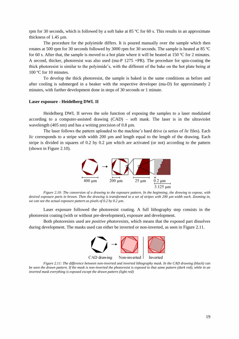
19
rpm for 30 seconds, which is followed by a soft bake at 85 ºC for 60 s. This results in an approximate
thickness of 1.45 µm.
The procedure for the polyimide differs. It is poured manually over the sample which then
rotates at 500 rpm for 30 seconds followed by 3000 rpm for 30 seconds. The sample is heated at 85 ºC
for 60 s. After that, the sample is moved to a hot plate where it will be heated at 150 ºC for 2 minutes.
A second, thicker, photoresist was also used (ma-P 1275 +PR). The procedure for spin-coating the
thick photoresist is similar to the polyimide’s, with the different of the bake on the hot plate being at
100 ºC for 10 minutes.
To develop the thick photoresist, the sample is baked in the same conditions as before and
after cooling is submerged in a beaker with the respective developer (ma-D) for approximately 2
minutes, with further development done in steps of 30 seconds or 1 minute.
Laser exposure - Heidelberg DWL II
Heidelberg DWL II serves the sole function of exposing the samples to a laser modulated
according to a computer-assisted drawing (CAD) – soft mask. The laser is in the ultraviolet
wavelength (405 nm) and has a writing precision of 0.8 µm.
The laser follows the pattern uploaded to the machine’s hard drive (a series of lic files). Each
lic corresponds to a stripe with width 200 µm and length equal to the length of the drawing. Each
stripe is divided in squares of 0.2 by 0.2 µm which are activated (or not) according to the pattern
(shown in Figure 2.10).
Figure 2.10: The conversion of a drawing to the exposure pattern. In the beginning, the drawing to expose, with
desired exposure parts in brown. Then the drawing is transformed to a set of stripes with 200 µm width each. Zooming in,
we can see the actual exposure pattern as pixels of 0.2 by 0.2 µm.
Laser exposure followed the photoresist coating. A full lithography step consists in the
photoresist coating (with or without pre-development), exposure and development.
Both photoresists used are positive photoresists, which means that the exposed part dissolves
during development. The masks used can either be inverted or non-inverted, as seen in Figure 2.11.
Figure 2.11: The difference between non-inverted and inverted lithography mask. In the CAD drawing (black) can
be seen the drawn pattern. If the mask is non-inverted the photoresist is exposed to that same pattern (dark red), while in an
inverted mask everything is exposed except the drawn pattern (light red)
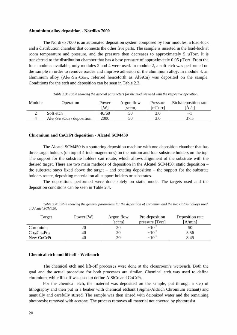
20
Aluminium alloy deposition - Nordiko 7000
The Nordiko 7000 is an automated deposition system composed by four modules, a load-lock
and a distribution chamber that connects the other five parts. The sample is inserted in the load-lock at
room temperature and pressure, and the pressure then decreases to approximately 5 µTorr. It is
transferred to the distribution chamber that has a base pressure of approximately 0.05 µTorr. From the
four modules available, only modules 2 and 4 were used. In module 2, a soft etch was performed on
the sample in order to remove oxides and improve adhesion of the aluminium alloy. In module 4, an
aluminium alloy (Al98.5Si1.0Cu0.5, referred henceforth as AlSiCu) was deposited on the sample.
Conditions for the etch and deposition can be seen in Table 2.3.
Table 2.3: Table showing the general parameters for the modules used with the respective operation.
Module Operation Power
[W]
Argon flow
[sccm]
Pressure
[mTorr]
Etch/deposition rate
[Å /s]
2 Soft etch 40/60 50 3.0 ~1
4 Al98.5Si1.0Cu0.5 deposition 2000 50 3.0 37.5
Chromium and CoCrPt deposition - Alcatel SCM450
The Alcatel SCM450 is a sputtering deposition machine with one deposition chamber that has
three target holders (on top of 4-inch magnetrons) on the bottom and four substrate holders on the top.
The support for the substrate holders can rotate, which allows alignment of the substrate with the
desired target. There are two main methods of deposition in the Alcatel SCM450: static deposition –
the substrate stays fixed above the target – and rotating deposition – the support for the substrate
holders rotate, depositing material on all support holders or substrates.
The depositions performed were done solely on static mode. The targets used and the
deposition conditions can be seen in Table 2.4.
Table 2.4: Table showing the general parameters for the deposition of chromium and the two CoCrPt alloys used,
at Alcatel SCM450.
Target Power [W] Argon flow
[sccm]
Pre-deposition
pressure [Torr]
Deposition rate
[Å/min]
Chromium 20 20 ~10-7 50
Co66Cr16Pt18 40 20 ~10-7 5.56
New CoCrPt 40 20 ~10-7 8.45
Chemical etch and lift-off - Wetbench
The chemical etch and lift-off processes were done at the cleanroom’s wetbench. Both the
goal and the actual procedure for both processes are similar. Chemical etch was used to define
chromium, while lift-off was used to define AlSiCu and CoCrPt.
For the chemical etch, the material was deposited on the sample, put through a step of
lithography and then put in a beaker with chemical etchant (Sigma-Aldrich Chromium etchant) and
manually and carefully stirred. The sample was then rinsed with deionized water and the remaining
photoresist removed with acetone. The process removes all material not covered by photoresist.
21
For the lift-off, the sample is first put through a step of lithography and only then the material
is deposited. Afterwards, the sample goes inside a beaker with MicroStrip 3001 and is moved to an
ultrasound chamber. The sample is then cleaned with isopropanol (IPA) and deionized water. This
process removes the remaining photoresist and all material that is deposited on top of it. For the
CoCrPt lift-off, the thicker photoresist was used and removed with acetone instead of MicroStrip
3001.
Ion milling etch and ruthenium deposition - Nordiko 3600
Nordiko 3600 is an ion-beam deposition (IBD) machine that can also perform etch by ion
milling. It has two ion guns, the assist gun (used for deposition and etch) and the deposition gun (used
only for deposition). The plate holding the sample’s wafer is tilted during etch/deposition, forming an
angle between its surface and the ion beam.
For the deposition, a xenon plasma (Xe+) is formed in the deposition gun’s chamber, which is
then accelerated towards the target, by a potential difference applied to the respective grids. This
ejects atoms from the target, which deposit on the sample.
For the ion milling, the plasma is accelerated towards the sample. The transfer of momentum,
between the accelerated ions and the atoms of the surface of the sample, cause the ejection of those
atoms, which lead to strong directional and non-selective etch. The conditions used can be seen in
Table 2.5.
Table 2.5: Conditions for the processes used at Nordiko 7000. The soft etch was performed previously to the
deposition in order to improve adhesion and remove nanometric impurities.
Module Operation Power
[W]
Argon flow
[sccm]
Pressure
[mTorr]
Etch/deposition rate
[Å /s]
2 Soft etch 40/60 50 3.0 ~1
4 Al98.5Si1.0Cu0.5 deposition 2000 50 3.0 37.5
Thickness measurement - Profilometers
The control of several steps of the process was performed by thickness measurement. For this,
two different profilometers were used: Dektak 3030 and Tencor Alphastep 200. The Dektak 3030 is
located inside the cleanroom and was used for the measurements in which photoresist was fully
developed. The Tencor Alphastep 200 is located in a room outside the cleanroom and was used for
measurements in which photoresist was not fully developed. This was possible due to it having yellow
light – the used photoresist is not sensible to that wavelength interval - and the possibility of having
the room’s lights turned off only yellow lights lit.
Dektak 3030 has a measurement uncertainty of 0.1 nm and Tencor Alphastep 200 has an
uncertainty of 5 nm.
2.4.2 First run
The first process designed had the goal of creating structures with a magnetic head and a
spiralled tail. In order to do this, a partial release of the polyimide layer was planned. This was done
with a sacrificial layer made of two materials – AlSiCu and chromium. The nViper structures were
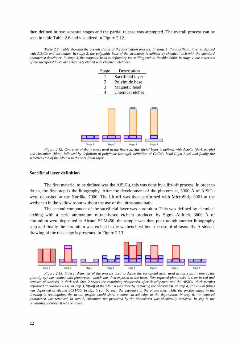
22
then defined in two separate stages and the partial release was attempted. The overall process can be
seen in table Table 2.6 and visualized in Figure 2.12.
Table 2.6: Table showing the overall stages of the fabrication process. In stage 1, the sacrificial layer is defined
with AlSiCu and chromium. In stage 2, the polyimide base of the structures is defined by chemical etch with the standard
photoresist developer. In stage 3, the magnetic head is defined by ion-milling etch at Nordiko 3600. In stage 4, the materials
of the sacrificial layer are selectively etched with chemical etchants.
Stage Description
1 Sacrificial layer
2 Polyimide base
3 Magnetic head
4 Chemical etches
Figure 2.12: Overview of the process used in the first run. Sacrificial layer is defined with AlSiCu (dark purple)
and chromium (blue), followed by definition of polyimide (orange), definition of CoCrPt head (light blue) and finally the
selective etch of the AlSiCu in the sacrificial layer.
Sacrificial layer definition
The first material to be defined was the AlSiCu, this was done by a lift-off process. In order to
do so, the first step is the lithography. After the development of the photoresist, 3000 Å of AlSiCu
were deposited at the Nordiko 7000. The lift-off was then performed with MicroStrip 3001 at the
wetbench in the yellow room without the use of the ultrasound bath.
The second component of the sacrificial layer was chromium. This was defined by chemical
etching with a ceric ammonium nitrate-based etchant produced by Sigma-Aldrich. 3000 Å of
chromium were deposited at Alcatel SCM450, the sample was then put through another lithography
step and finally the chromium was etched in the wetbench without the use of ultrasounds. A sidecut
drawing of the this stage is presented in Figure 2.13
Figure 2.13: Sidecut drawings of the process used to define the sacrificial layer used in this run. In step 1, the
glass (gray) was coated with photoresist, which was then exposed to the laser. Non-exposed photoresist is seen in red and
exposed photoresist in dark red. Step 2 shows the remaining photoresist after development and the AlSiCu (dark purple)
deposited at Nordiko 7000. In step 3, lift-off of the AlSiCu was done by removing the photoresist. In step 4, chromium (blue)
was deposited at Alcatel SCM450. In step 5 can be seen the exposure of the photoresist, while the profile image in the
drawing is rectangular, the actual profile would show a more curved edge at the depression. In step 6, the exposed
photoresist was removed. In step 7, chromium not protected by the photoresist was chemically removed. In step 8, the
remaining photoresist was removed.
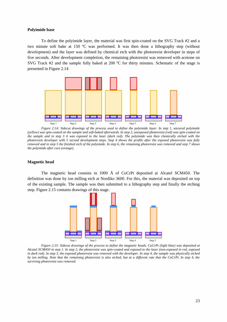
23
Polyimide base
To define the polyimide layer, the material was first spin-coated on the SVG Track #2 and a
two minute soft bake at 150 ºC was performed. It was then done a lithography step (without
development) and the layer was defined by chemical etch with the photoresist developer in steps of
five seconds. After development completion, the remaining photoresist was removed with acetone on
SVG Track #2 and the sample fully baked at 200 ºC for thirty minutes. Schematic of the stage is
presented in Figure 2.14
Figure 2.14: Sidecut drawings of the process used to define the polyimide layer. In step 1, uncured polyimide
(yellow) was spin-coated on the sample and soft-baked afterwards. In step 2, unexposed photoresist (red) was spin-coated on
the sample and in step 3 it was exposed to the laser (dark red). The polyimide was then chemically etched with the
photoresist developer with 5 second development steps. Step 4 shows the profile after the exposed photoresist was fully
removed and in step 5 the finished etch of the polyimide. In step 6, the remaining photoresist was removed and step 7 shows
the polyimide after cure (orange).
Magnetic head
The magnetic head consists in 1000 Å of CoCrPt deposited at Alcatel SCM450. The
definition was done by ion milling etch at Nordiko 3600. For this, the material was deposited on top
of the existing sample. The sample was then submitted to a lithography step and finally the etching
step. Figure 2.15 contains drawings of this stage.
Figure 2.15: Sidecut drawings of the process to define the magnetic heads. CoCrPt (light blue) was deposited at
Alcatel SCM450 in step 1. In step 2, the photoresist was spin-coated and exposed to the laser (non-exposed in red, exposed
in dark red). In step 3, the exposed photoresist was removed with the developer. In step 4, the sample was physically etched
by ion milling. Note that the remaining photoresist is also etched, but at a different rate that the CoCrPt. In step 4, the
surviving photoresist was removed.
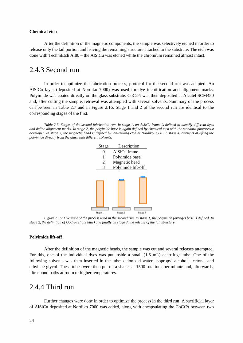
24
Chemical etch
After the definition of the magnetic components, the sample was selectively etched in order to
release only the tail portion and leaving the remaining structure attached to the substrate. The etch was
done with TechniEtch Al80 – the AlSiCu was etched while the chromium remained almost intact.
2.4.3 Second run
In order to optimize the fabrication process, protocol for the second run was adapted. An
AlSiCu layer (deposited at Nordiko 7000) was used for dye identification and alignment marks.
Polyimide was coated directly on the glass substrate. CoCrPt was then deposited at Alcatel SCM450
and, after cutting the sample, retrieval was attempted with several solvents. Summary of the process
can be seen in Table 2.7 and in Figure 2.16. Stage 1 and 2 of the second run are identical to the
corresponding stages of the first.
Table 2.7: Stages of the second fabrication run. In stage 1, an AlSiCu frame is defined to identify different dyes
and define alignment marks. In stage 2, the polyimide base is again defined by chemical etch with the standard photoresist
developer. In stage 3, the magnetic head is defined by ion-milling etch at Nordiko 3600. In stage 4, attempts at lifting the
polyimide directly from the glass with different solvents.
Stage Description
0 AlSiCu frame
1 Polyimide base
2 Magnetic head
3 Polyimide lift-off
Figure 2.16: Overview of the process used in the second run. In stage 1, the polyimide (orange) base is defined. In
stage 2, the definition of CoCrPt (light blue) and finally, in stage 3, the release of the full structure.
Polyimide lift-off
After the definition of the magnetic heads, the sample was cut and several releases attempted.
For this, one of the individual dyes was put inside a small (1.5 mL) centrifuge tube. One of the
following solvents was then inserted in the tube: deionized water, isopropyl alcohol, acetone, and
ethylene glycol. These tubes were then put on a shaker at 1500 rotations per minute and, afterwards,
ultrasound baths at room or higher temperatures.
2.4.4 Third run
Further changes were done in order to optimize the process in the third run. A sacrificial layer
of AlSiCu deposited at Nordiko 7000 was added, along with encapsulating the CoCrPt between two
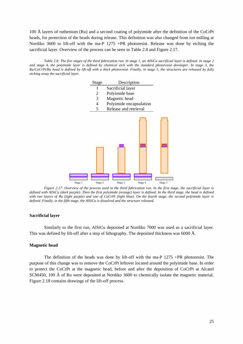
25
100 Å layers of ruthenium (Ru) and a second coating of polyimide after the definition of the CoCrPt
heads, for protection of the heads during release. This definition was also changed from ion milling at
Nordiko 3600 to lift-off with the ma-P 1275 +PR photoresist. Release was done by etching the
sacrificial layer. Overview of the process can be seen in Table 2.8 and Figure 2.17.
Table 2.8: The five stages of the third fabrication run. In stage 1, an AlSiCu sacrificial layer is defined. In stage 2
and stage 4, the polyimide layer is defined by chemical etch with the standard photoresist developer. In stage 3, the
Ru/CoCrPt/Ru head is defined by lift-off with a thick photoresist. Finally, in stage 5, the structures are released by fully
etching away the sacrificial layer.
Stage Description
1 Sacrificial layer
2 Polyimide base
3 Magnetic head
4 Polyimide encapsulation
5 Release and retrieval
Figure 2.17: Overview of the process used in the third fabrication run. In the first stage, the sacrificial layer is
defined with AlSiCu (dark purple). Then the first polyimide (orange) layer is defined. In the third stage, the head is defined
with two layers of Ru (light purple) and one of CoCrPt (light blue). On the fourth stage, the second polyimide layer is
defined. Finally, in the fifth stage, the AlSiCu is dissolved and the structure released.
Sacrificial layer
Similarly to the first run, AlSiCu deposited at Nordiko 7000 was used as a sacrificial layer.
This was defined by lift-off after a step of lithography. The deposited thickness was 6000 Å.
Magnetic head
The definition of the heads was done by lift-off with the ma-P 1275 +PR photoresist. The
purpose of this change was to remove the CoCrPt leftover located around the polyimide base. In order
to protect the CoCrPt at the magnetic head, before and after the deposition of CoCrPt at Alcatel
SCM450, 100 Å of Ru were deposited at Nordiko 3600 to chemically isolate the magnetic material.
Figure 2.18 contains drawings of the lift-off process.
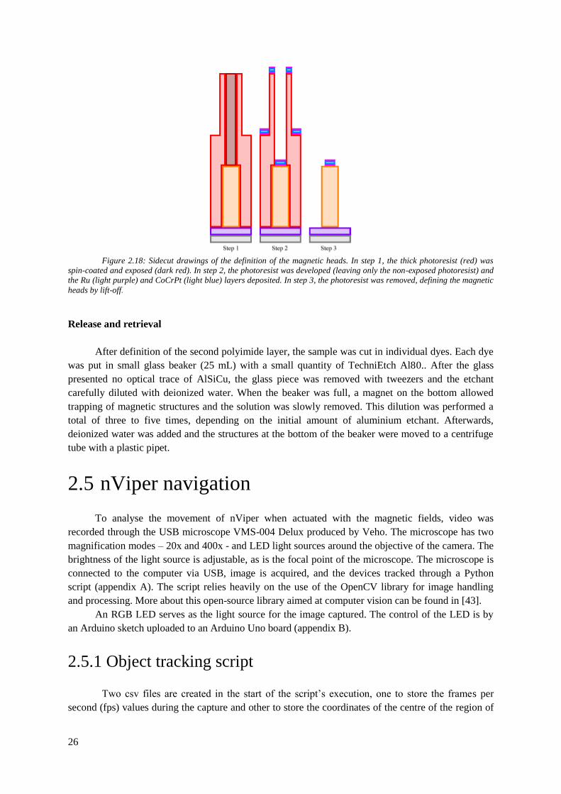
26
Figure 2.18: Sidecut drawings of the definition of the magnetic heads. In step 1, the thick photoresist (red) was
spin-coated and exposed (dark red). In step 2, the photoresist was developed (leaving only the non-exposed photoresist) and
the Ru (light purple) and CoCrPt (light blue) layers deposited. In step 3, the photoresist was removed, defining the magnetic
heads by lift-off.
Release and retrieval
After definition of the second polyimide layer, the sample was cut in individual dyes. Each dye
was put in small glass beaker (25 mL) with a small quantity of TechniEtch Al80.. After the glass
presented no optical trace of AlSiCu, the glass piece was removed with tweezers and the etchant
carefully diluted with deionized water. When the beaker was full, a magnet on the bottom allowed
trapping of magnetic structures and the solution was slowly removed. This dilution was performed a
total of three to five times, depending on the initial amount of aluminium etchant. Afterwards,
deionized water was added and the structures at the bottom of the beaker were moved to a centrifuge
tube with a plastic pipet.
2.5 nViper navigation
To analyse the movement of nViper when actuated with the magnetic fields, video was
recorded through the USB microscope VMS-004 Delux produced by Veho. The microscope has two
magnification modes – 20x and 400x - and LED light sources around the objective of the camera. The
brightness of the light source is adjustable, as is the focal point of the microscope. The microscope is
connected to the computer via USB, image is acquired, and the devices tracked through a Python
script (appendix A). The script relies heavily on the use of the OpenCV library for image handling
and processing. More about this open-source library aimed at computer vision can be found in [43].
An RGB LED serves as the light source for the image captured. The control of the LED is by
an Arduino sketch uploaded to an Arduino Uno board (appendix B).
2.5.1 Object tracking script
Two csv files are created in the start of the script’s execution, one to store the frames per
second (fps) values during the capture and other to store the coordinates of the centre of the region of
27
interest (ROI). The video capture is initiated and the tracker type selected. The ROI is then drawn on
the first frame read from the video capture and folders to save the frames are created. A while loop to
show the live feed from the microscope with the tracked ROI starts and can be interrupted by pressing
the ESC key. In this loop, frames are read and stored, and the fps value is updated on each frame. The
tracked bounding box of the ROI is drawn and displayed on the frame. When this loop finishes, a
second for loop iterates over the array storing frames with the drawn box, finding this box’s contours
and the coordinates of its centre (which are then stored in the second csv file). A dot marking that
point is drawn on the frames in a third for loop.
The resulting data was then uploaded into an Excel file to determine the average fps value of
the capture and its standard deviation. This average value would be used to compute the velocity of
the nViper devices.
The tracking of the ROI is done with the Multiple Instance Learning (MIL) tracking
algorithm, provided by the OpenCV library. More information about this algorithm can be found in
[44]. While the tracking skills of the script were not used to acquire results, the full script is found in
appendix A.
2.5.2 Control test
To verify if nViper can be controlled with the current coil setting, simple tests were
performed. These consisted simply in extracting the devices from the centrifuge tube containing them
with a plastic pipet and dropping a small amount (one to three drops) on a hydrophobic surface. The
microscope was lowered and focused, the LED turned on and image capture initiated. The test was
done by applying a field in the Z-direction with increments of 1 A, up to 6 A. Then, a field-
component is added in the X-direction, with increments of 1 A, up to 8 A. Afterwards, the angle value
was changed to check if the structures direction followed the change in field.
A second and third tests were done with an initial field applied while pouring the droplets. In
the second, it was only active in the Z-direction, while in the third in both X and Z-direction. A fourth
test was performed with a permanent magnet.
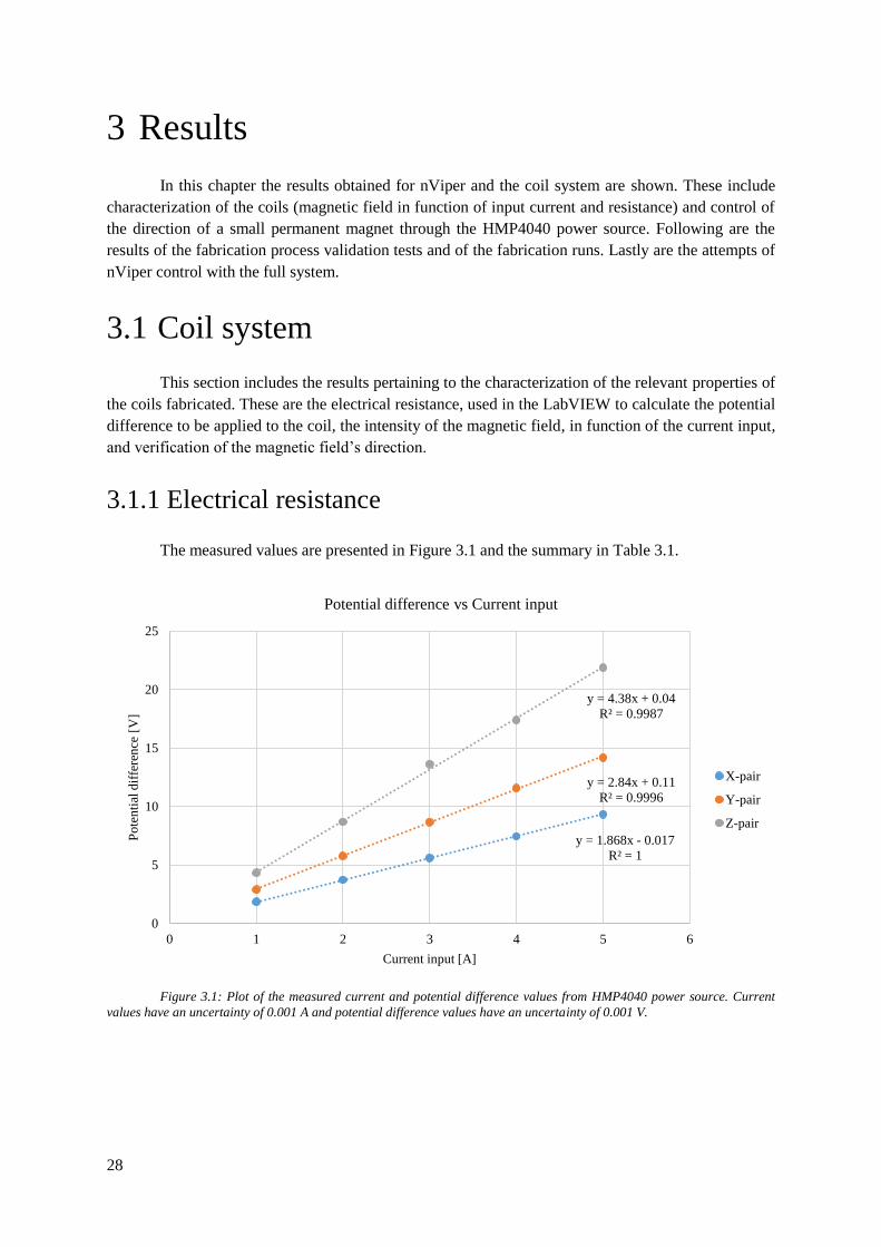
28
3 Results
In this chapter the results obtained for nViper and the coil system are shown. These include
characterization of the coils (magnetic field in function of input current and resistance) and control of
the direction of a small permanent magnet through the HMP4040 power source. Following are the
results of the fabrication process validation tests and of the fabrication runs. Lastly are the attempts of
nViper control with the full system.
3.1 Coil system
This section includes the results pertaining to the characterization of the relevant properties of
the coils fabricated. These are the electrical resistance, used in the LabVIEW to calculate the potential
difference to be applied to the coil, the intensity of the magnetic field, in function of the current input,
and verification of the magnetic field’s direction.
3.1.1 Electrical resistance
The measured values are presented in Figure 3.1 and the summary in Table 3.1.
Figure 3.1: Plot of the measured current and potential difference values from HMP4040 power source. Current
values have an uncertainty of 0.001 A and potential difference values have an uncertainty of 0.001 V.
y = 1.868x - 0.017
R² = 1
y = 2.84x + 0.11
R² = 0.9996
y = 4.38x + 0.04
R² = 0.9987
0
5
10
15
20
25
0 1 2 3 4 5 6
Po
ten
tial
dif
fere
nce
[V
]
Current input [A]
Potential difference vs Current input
X-pair
Y-pair
Z-pair
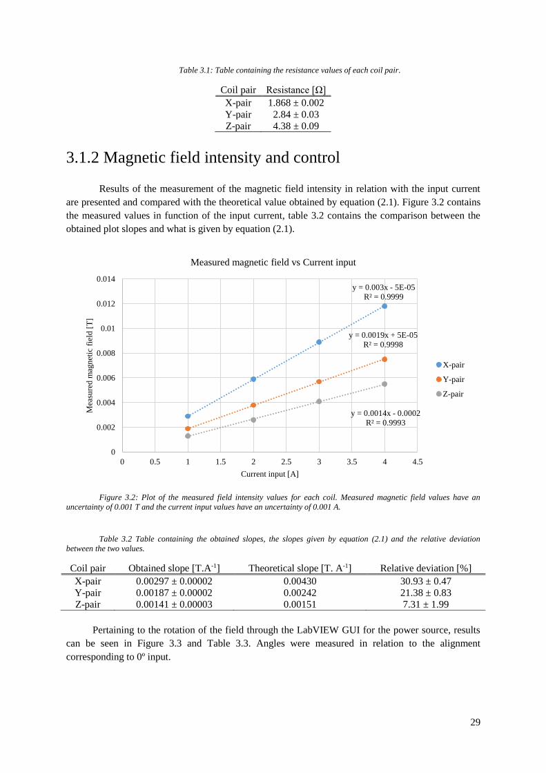
29
Table 3.1: Table containing the resistance values of each coil pair.
Coil pair Resistance [Ω]
X-pair 1.868 ± 0.002
Y-pair 2.84 ± 0.03
Z-pair 4.38 ± 0.09
3.1.2 Magnetic field intensity and control
Results of the measurement of the magnetic field intensity in relation with the input current
are presented and compared with the theoretical value obtained by equation (2.1). Figure 3.2 contains
the measured values in function of the input current, table 3.2 contains the comparison between the
obtained plot slopes and what is given by equation (2.1).
Figure 3.2: Plot of the measured field intensity values for each coil. Measured magnetic field values have an
uncertainty of 0.001 T and the current input values have an uncertainty of 0.001 A.
Table 3.2 Table containing the obtained slopes, the slopes given by equation (2.1) and the relative deviation
between the two values.
Coil pair Obtained slope [T.A-1] Theoretical slope [T. A-1] Relative deviation [%]
X-pair 0.00297 ± 0.00002 0.00430 30.93 ± 0.47
Y-pair 0.00187 ± 0.00002 0.00242 21.38 ± 0.83
Z-pair 0.00141 ± 0.00003 0.00151 7.31 ± 1.99
Pertaining to the rotation of the field through the LabVIEW GUI for the power source, results
can be seen in Figure 3.3 and Table 3.3. Angles were measured in relation to the alignment
corresponding to 0º input.
y = 0.003x - 5E-05
R² = 0.9999
y = 0.0019x + 5E-05
R² = 0.9998
y = 0.0014x - 0.0002
R² = 0.9993
0
0.002
0.004
0.006
0.008
0.01
0.012
0.014
0 0.5 1 1.5 2 2.5 3 3.5 4 4.5
Mea
sure
d m
agn
etic
fie
ld [
T]
Current input [A]
Measured magnetic field vs Current input
X-pair
Y-pair
Z-pair
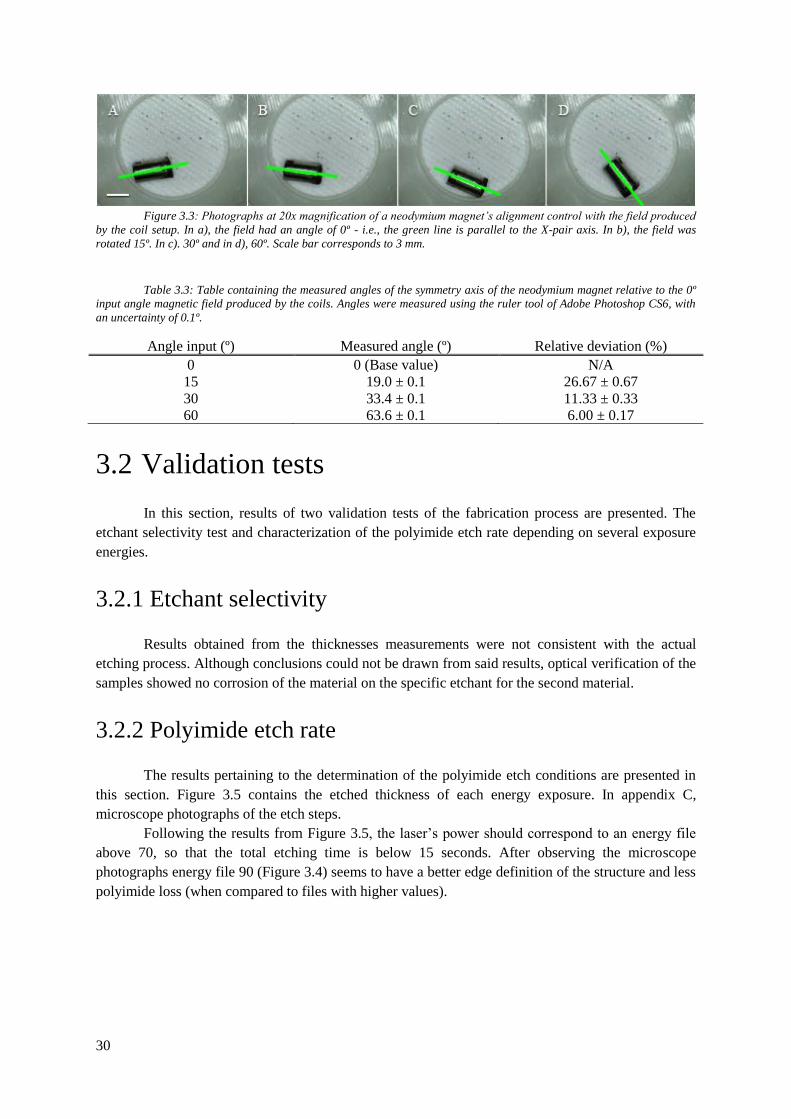
30
Figure 3.3: Photographs at 20x magnification of a neodymium magnet’s alignment control with the field produced
by the coil setup. In a), the field had an angle of 0º - i.e., the green line is parallel to the X-pair axis. In b), the field was
rotated 15º. In c). 30º and in d), 60º. Scale bar corresponds to 3 mm.
Table 3.3: Table containing the measured angles of the symmetry axis of the neodymium magnet relative to the 0º
input angle magnetic field produced by the coils. Angles were measured using the ruler tool of Adobe Photoshop CS6, with
an uncertainty of 0.1º.
Angle input (º) Measured angle (º) Relative deviation (%)
0 0 (Base value) N/A
15 19.0 ± 0.1 26.67 ± 0.67
30 33.4 ± 0.1 11.33 ± 0.33
60 63.6 ± 0.1 6.00 ± 0.17
3.2 Validation tests
In this section, results of two validation tests of the fabrication process are presented. The
etchant selectivity test and characterization of the polyimide etch rate depending on several exposure
energies.
3.2.1 Etchant selectivity
Results obtained from the thicknesses measurements were not consistent with the actual
etching process. Although conclusions could not be drawn from said results, optical verification of the
samples showed no corrosion of the material on the specific etchant for the second material.
3.2.2 Polyimide etch rate
The results pertaining to the determination of the polyimide etch conditions are presented in
this section. Figure 3.5 contains the etched thickness of each energy exposure. In appendix C,
microscope photographs of the etch steps.
Following the results from Figure 3.5, the laser’s power should correspond to an energy file
above 70, so that the total etching time is below 15 seconds. After observing the microscope
photographs energy file 90 (Figure 3.4) seems to have a better edge definition of the structure and less
polyimide loss (when compared to files with higher values).
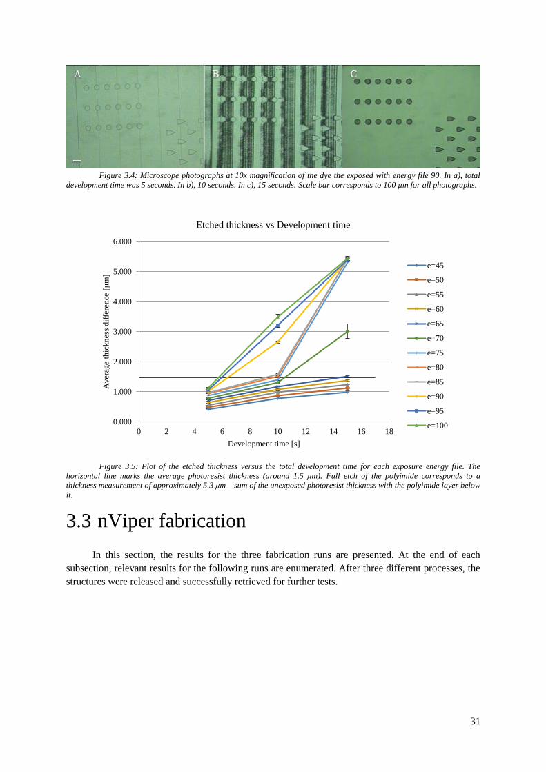
31
Figure 3.4: Microscope photographs at 10x magnification of the dye the exposed with energy file 90. In a), total
development time was 5 seconds. In b), 10 seconds. In c), 15 seconds. Scale bar corresponds to 100 µm for all photographs.
Figure 3.5: Plot of the etched thickness versus the total development time for each exposure energy file. The
horizontal line marks the average photoresist thickness (around 1.5 μm). Full etch of the polyimide corresponds to a
thickness measurement of approximately 5.3 μm – sum of the unexposed photoresist thickness with the polyimide layer below
it.
3.3 nViper fabrication
In this section, the results for the three fabrication runs are presented. At the end of each
subsection, relevant results for the following runs are enumerated. After three different processes, the
structures were released and successfully retrieved for further tests.
0.000
1.000
2.000
3.000
4.000
5.000
6.000
0 2 4 6 8 10 12 14 16 18
Aver
age
thic
kn
ess
dif
fere
nce
[μ
m]
Development time [s]
Etched thickness vs Development time
e=45
e=50
e=55
e=60
e=65
e=70
e=75
e=80
e=85
e=90
e=95
e=100
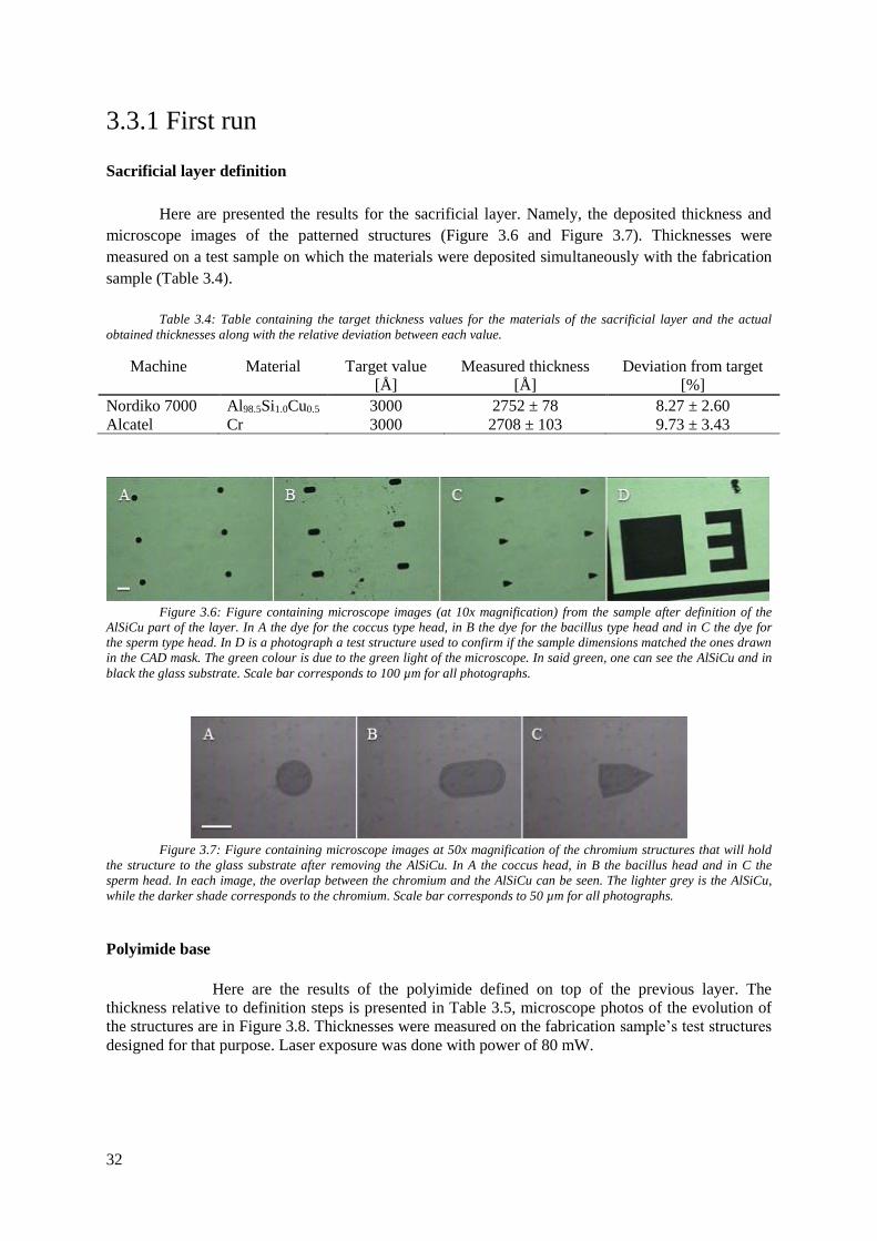
32
3.3.1 First run
Sacrificial layer definition
Here are presented the results for the sacrificial layer. Namely, the deposited thickness and
microscope images of the patterned structures (Figure 3.6 and Figure 3.7). Thicknesses were
measured on a test sample on which the materials were deposited simultaneously with the fabrication
sample (Table 3.4).
Table 3.4: Table containing the target thickness values for the materials of the sacrificial layer and the actual
obtained thicknesses along with the relative deviation between each value.
Machine Material Target value
[Å]
Measured thickness
[Å]
Deviation from target
[%]
Nordiko 7000 Al98.5Si1.0Cu0.5 3000 2752 ± 78 8.27 ± 2.60
Alcatel Cr 3000 2708 ± 103 9.73 ± 3.43
Figure 3.6: Figure containing microscope images (at 10x magnification) from the sample after definition of the
AlSiCu part of the layer. In A the dye for the coccus type head, in B the dye for the bacillus type head and in C the dye for
the sperm type head. In D is a photograph a test structure used to confirm if the sample dimensions matched the ones drawn
in the CAD mask. The green colour is due to the green light of the microscope. In said green, one can see the AlSiCu and in
black the glass substrate. Scale bar corresponds to 100 µm for all photographs.
Figure 3.7: Figure containing microscope images at 50x magnification of the chromium structures that will hold
the structure to the glass substrate after removing the AlSiCu. In A the coccus head, in B the bacillus head and in C the
sperm head. In each image, the overlap between the chromium and the AlSiCu can be seen. The lighter grey is the AlSiCu,
while the darker shade corresponds to the chromium. Scale bar corresponds to 50 µm for all photographs.
Polyimide base
Here are the results of the polyimide defined on top of the previous layer. The
thickness relative to definition steps is presented in Table 3.5, microscope photos of the evolution of
the structures are in Figure 3.8. Thicknesses were measured on the fabrication sample’s test structures
designed for that purpose. Laser exposure was done with power of 80 mW.
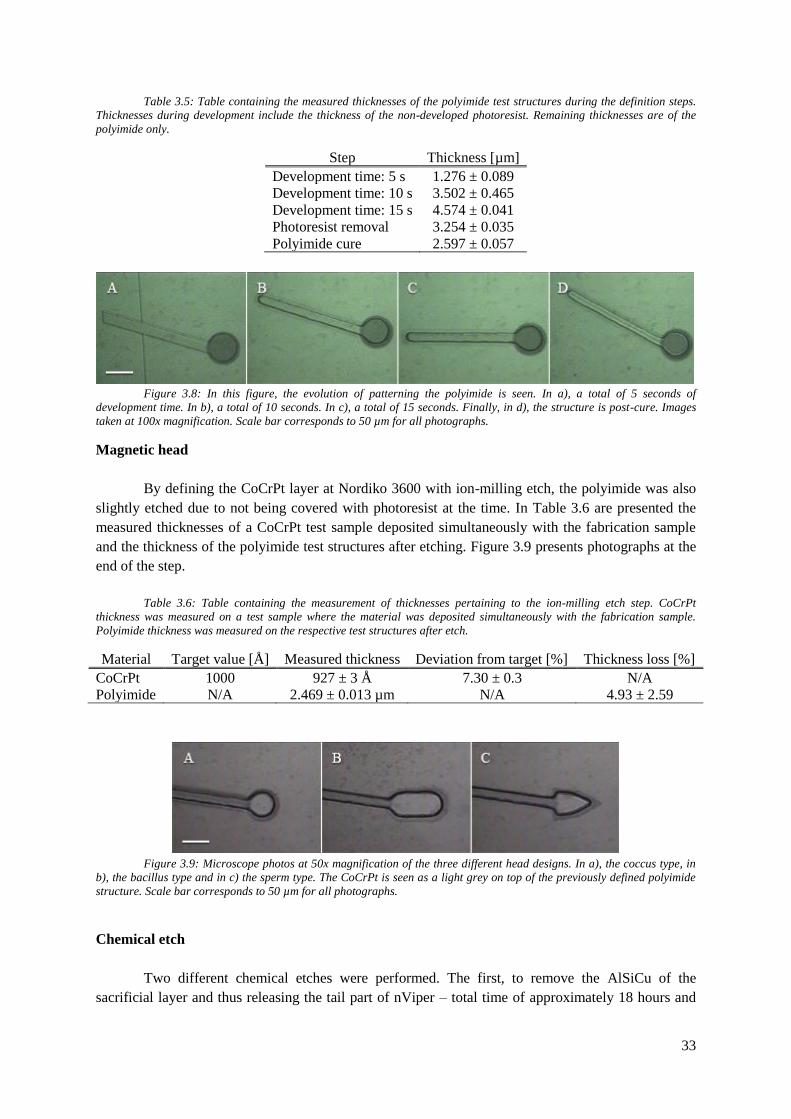
33
Table 3.5: Table containing the measured thicknesses of the polyimide test structures during the definition steps.
Thicknesses during development include the thickness of the non-developed photoresist. Remaining thicknesses are of the
polyimide only.
Step Thickness [µm]
Development time: 5 s 1.276 ± 0.089
Development time: 10 s 3.502 ± 0.465
Development time: 15 s 4.574 ± 0.041
Photoresist removal 3.254 ± 0.035
Polyimide cure 2.597 ± 0.057
Figure 3.8: In this figure, the evolution of patterning the polyimide is seen. In a), a total of 5 seconds of
development time. In b), a total of 10 seconds. In c), a total of 15 seconds. Finally, in d), the structure is post-cure. Images
taken at 100x magnification. Scale bar corresponds to 50 µm for all photographs.
Magnetic head
By defining the CoCrPt layer at Nordiko 3600 with ion-milling etch, the polyimide was also
slightly etched due to not being covered with photoresist at the time. In Table 3.6 are presented the
measured thicknesses of a CoCrPt test sample deposited simultaneously with the fabrication sample
and the thickness of the polyimide test structures after etching. Figure 3.9 presents photographs at the
end of the step.
Table 3.6: Table containing the measurement of thicknesses pertaining to the ion-milling etch step. CoCrPt
thickness was measured on a test sample where the material was deposited simultaneously with the fabrication sample.
Polyimide thickness was measured on the respective test structures after etch.
Material Target value [Å] Measured thickness Deviation from target [%] Thickness loss [%]
CoCrPt 1000 927 ± 3 Å 7.30 ± 0.3 N/A
Polyimide N/A 2.469 ± 0.013 µm N/A 4.93 ± 2.59
Figure 3.9: Microscope photos at 50x magnification of the three different head designs. In a), the coccus type, in
b), the bacillus type and in c) the sperm type. The CoCrPt is seen as a light grey on top of the previously defined polyimide
structure. Scale bar corresponds to 50 µm for all photographs.
Chemical etch
Two different chemical etches were performed. The first, to remove the AlSiCu of the
sacrificial layer and thus releasing the tail part of nViper – total time of approximately 18 hours and
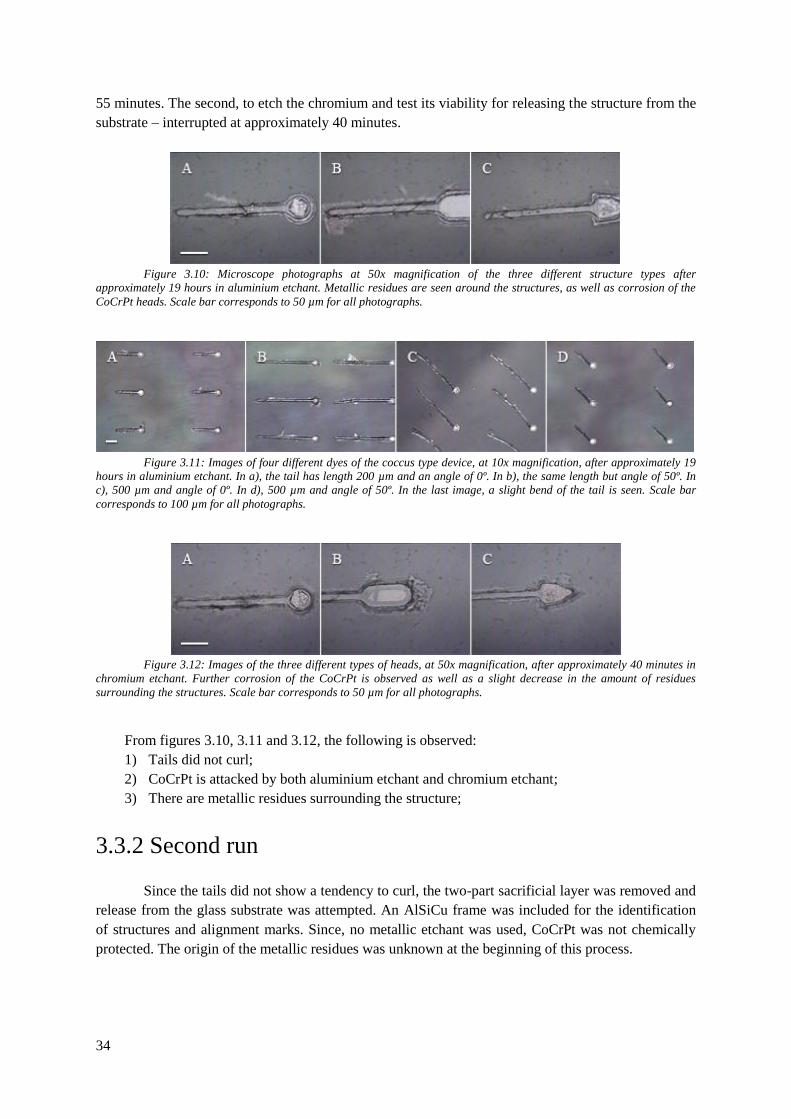
34
55 minutes. The second, to etch the chromium and test its viability for releasing the structure from the
substrate – interrupted at approximately 40 minutes.
Figure 3.10: Microscope photographs at 50x magnification of the three different structure types after
approximately 19 hours in aluminium etchant. Metallic residues are seen around the structures, as well as corrosion of the
CoCrPt heads. Scale bar corresponds to 50 µm for all photographs.
Figure 3.11: Images of four different dyes of the coccus type device, at 10x magnification, after approximately 19
hours in aluminium etchant. In a), the tail has length 200 µm and an angle of 0º. In b), the same length but angle of 50º. In
c), 500 µm and angle of 0º. In d), 500 µm and angle of 50º. In the last image, a slight bend of the tail is seen. Scale bar
corresponds to 100 µm for all photographs.
Figure 3.12: Images of the three different types of heads, at 50x magnification, after approximately 40 minutes in
chromium etchant. Further corrosion of the CoCrPt is observed as well as a slight decrease in the amount of residues
surrounding the structures. Scale bar corresponds to 50 µm for all photographs.
From figures 3.10, 3.11 and 3.12, the following is observed:
1) Tails did not curl;
2) CoCrPt is attacked by both aluminium etchant and chromium etchant;
3) There are metallic residues surrounding the structure;
3.3.2 Second run
Since the tails did not show a tendency to curl, the two-part sacrificial layer was removed and
release from the glass substrate was attempted. An AlSiCu frame was included for the identification
of structures and alignment marks. Since, no metallic etchant was used, CoCrPt was not chemically
protected. The origin of the metallic residues was unknown at the beginning of this process.
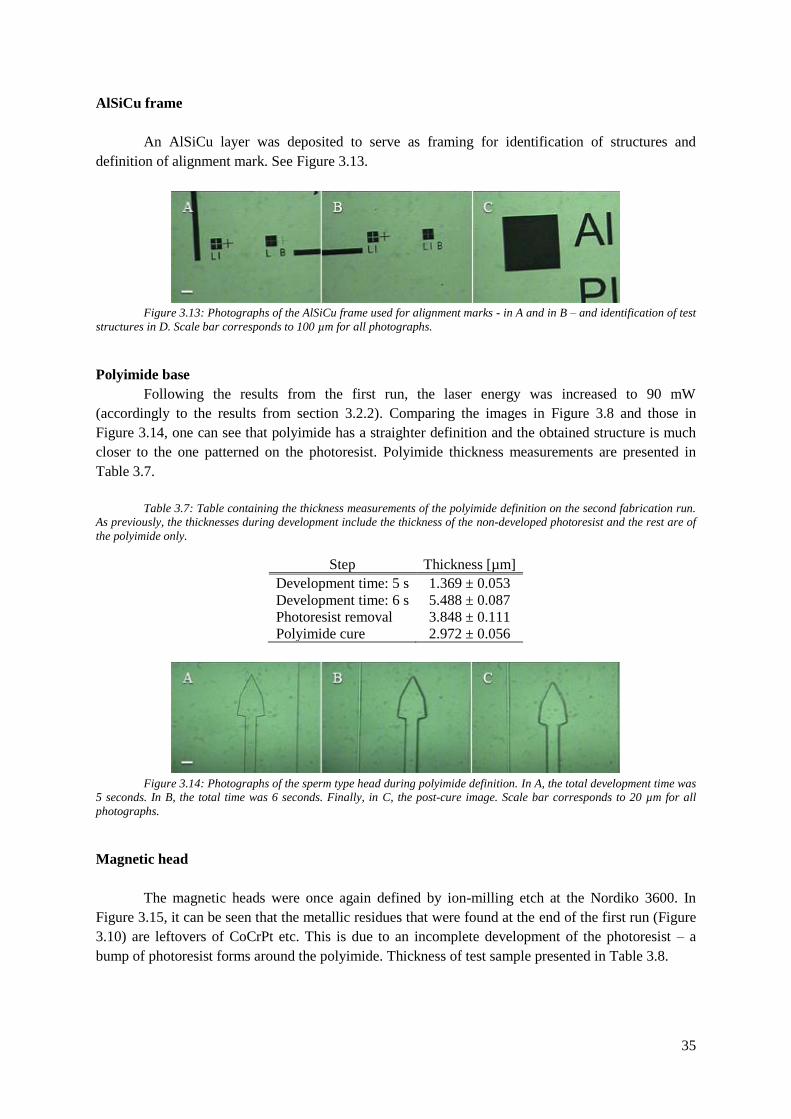
35
AlSiCu frame
An AlSiCu layer was deposited to serve as framing for identification of structures and
definition of alignment mark. See Figure 3.13.
Figure 3.13: Photographs of the AlSiCu frame used for alignment marks - in A and in B – and identification of test
structures in D. Scale bar corresponds to 100 µm for all photographs.
Polyimide base
Following the results from the first run, the laser energy was increased to 90 mW
(accordingly to the results from section 3.2.2). Comparing the images in Figure 3.8 and those in
Figure 3.14, one can see that polyimide has a straighter definition and the obtained structure is much
closer to the one patterned on the photoresist. Polyimide thickness measurements are presented in
Table 3.7.
Table 3.7: Table containing the thickness measurements of the polyimide definition on the second fabrication run.
As previously, the thicknesses during development include the thickness of the non-developed photoresist and the rest are of
the polyimide only.
Step Thickness [µm]
Development time: 5 s 1.369 ± 0.053
Development time: 6 s 5.488 ± 0.087
Photoresist removal 3.848 ± 0.111
Polyimide cure 2.972 ± 0.056
Figure 3.14: Photographs of the sperm type head during polyimide definition. In A, the total development time was
5 seconds. In B, the total time was 6 seconds. Finally, in C, the post-cure image. Scale bar corresponds to 20 µm for all
photographs.
Magnetic head
The magnetic heads were once again defined by ion-milling etch at the Nordiko 3600. In
Figure 3.15, it can be seen that the metallic residues that were found at the end of the first run (Figure
3.10) are leftovers of CoCrPt etc. This is due to an incomplete development of the photoresist – a
bump of photoresist forms around the polyimide. Thickness of test sample presented in Table 3.8.
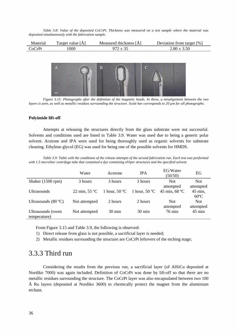
36
Table 3.8: Value of the deposited CoCrPt. Thickness was measured on a test sample where the material was
deposited simultaneously with the fabrication sample.
Material Target value [Å] Measured thickness [Å] Deviation from target [%]
CoCrPt 1000 972 ± 35 2.80 ± 3.50
Figure 3.15: Photographs after the definition of the magnetic heads. In these, a misalignment between the two
layers is seen, as well as metallic residues surrounding the structure. Scale bar corresponds to 20 µm for all photographs.
Polyimide lift-off
Attempts at releasing the structures directly from the glass substrate were not successful.
Solvents and conditions used are listed in Table 3.9. Water was used due to being a generic polar
solvent. Acetone and IPA were used for being thoroughly used as organic solvents for substrate
cleaning. Ethylene glycol (EG) was used for being one of the possible solvents for HMDS.
Table 3.9: Table with the conditions of the release attempts of the second fabrication run. Each test was performed
with 1.5 microliter centrifuge tube that contained a dye containing nViper structures and the specified solvent.
Water Acetone IPA
EG/Water
(50/50) EG
Shaker (1500 rpm) 3 hours 3 hours 3 hours Not
attempted
Not
attempted
Ultrasounds 22 min, 55 ºC 1 hour, 50 ºC 1 hour, 50 ºC 45 min, 68 ºC 45 min,
60ºC
Ultrasounds (80 ºC) Not attempted 2 hours 2 hours Not
attempted
Not
attempted
Ultrasounds (room
temperature)
Not attempted 30 min 30 min 76 min 45 min
From Figure 3.15 and Table 3.9, the following is observed:
1) Direct release from glass is not possible, a sacrificial layer is needed;
2) Metallic residues surrounding the structure are CoCrPt leftovers of the etching stage;
3.3.3 Third run
Considering the results from the previous run, a sacrificial layer (of AlSiCu deposited at
Nordiko 7000) was again included. Definition of CoCrPt was done by lift-off so that there are no
metallic residues surrounding the structure. The CoCrPt layer was also encapsulated between two 100
Å Ru layers (deposited at Nordiko 3600) to chemically protect the magnet from the aluminium
etchant.
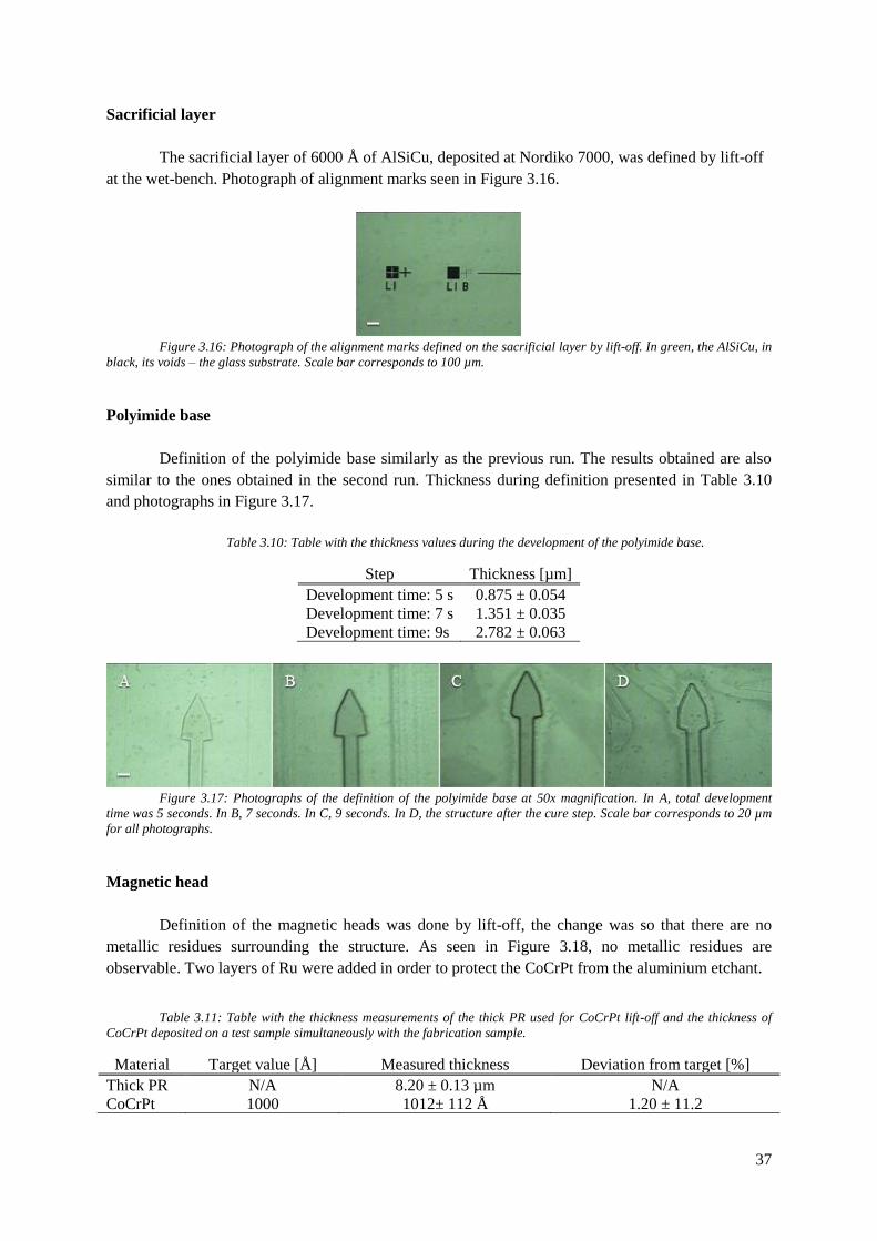
37
Sacrificial layer
The sacrificial layer of 6000 Å of AlSiCu, deposited at Nordiko 7000, was defined by lift-off
at the wet-bench. Photograph of alignment marks seen in Figure 3.16.
Figure 3.16: Photograph of the alignment marks defined on the sacrificial layer by lift-off. In green, the AlSiCu, in
black, its voids – the glass substrate. Scale bar corresponds to 100 µm.
Polyimide base
Definition of the polyimide base similarly as the previous run. The results obtained are also
similar to the ones obtained in the second run. Thickness during definition presented in Table 3.10
and photographs in Figure 3.17.
Table 3.10: Table with the thickness values during the development of the polyimide base.
Step Thickness [µm]
Development time: 5 s 0.875 ± 0.054
Development time: 7 s 1.351 ± 0.035
Development time: 9s 2.782 ± 0.063
Figure 3.17: Photographs of the definition of the polyimide base at 50x magnification. In A, total development
time was 5 seconds. In B, 7 seconds. In C, 9 seconds. In D, the structure after the cure step. Scale bar corresponds to 20 µm
for all photographs.
Magnetic head
Definition of the magnetic heads was done by lift-off, the change was so that there are no
metallic residues surrounding the structure. As seen in Figure 3.18, no metallic residues are
observable. Two layers of Ru were added in order to protect the CoCrPt from the aluminium etchant.
Table 3.11: Table with the thickness measurements of the thick PR used for CoCrPt lift-off and the thickness of
CoCrPt deposited on a test sample simultaneously with the fabrication sample.
Material Target value [Å] Measured thickness Deviation from target [%]
Thick PR N/A 8.20 ± 0.13 µm N/A
CoCrPt 1000 1012± 112 Å 1.20 ± 11.2
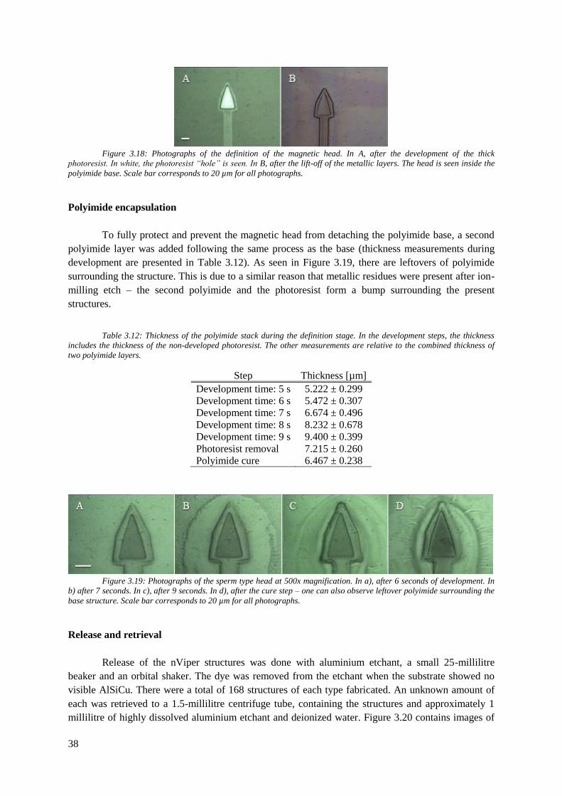
38
Figure 3.18: Photographs of the definition of the magnetic head. In A, after the development of the thick
photoresist. In white, the photoresist “hole” is seen. In B, after the lift-off of the metallic layers. The head is seen inside the
polyimide base. Scale bar corresponds to 20 µm for all photographs.
Polyimide encapsulation
To fully protect and prevent the magnetic head from detaching the polyimide base, a second
polyimide layer was added following the same process as the base (thickness measurements during
development are presented in Table 3.12). As seen in Figure 3.19, there are leftovers of polyimide
surrounding the structure. This is due to a similar reason that metallic residues were present after ion-
milling etch – the second polyimide and the photoresist form a bump surrounding the present
structures.
Table 3.12: Thickness of the polyimide stack during the definition stage. In the development steps, the thickness
includes the thickness of the non-developed photoresist. The other measurements are relative to the combined thickness of
two polyimide layers.
Step Thickness [µm]
Development time: 5 s 5.222 ± 0.299
Development time: 6 s 5.472 ± 0.307
Development time: 7 s 6.674 ± 0.496
Development time: 8 s 8.232 ± 0.678
Development time: 9 s 9.400 ± 0.399
Photoresist removal 7.215 ± 0.260
Polyimide cure 6.467 ± 0.238
Figure 3.19: Photographs of the sperm type head at 500x magnification. In a), after 6 seconds of development. In
b) after 7 seconds. In c), after 9 seconds. In d), after the cure step – one can also observe leftover polyimide surrounding the
base structure. Scale bar corresponds to 20 µm for all photographs.
Release and retrieval
Release of the nViper structures was done with aluminium etchant, a small 25-millilitre
beaker and an orbital shaker. The dye was removed from the etchant when the substrate showed no
visible AlSiCu. There were a total of 168 structures of each type fabricated. An unknown amount of
each was retrieved to a 1.5-millilitre centrifuge tube, containing the structures and approximately 1
millilitre of highly dissolved aluminium etchant and deionized water. Figure 3.20 contains images of
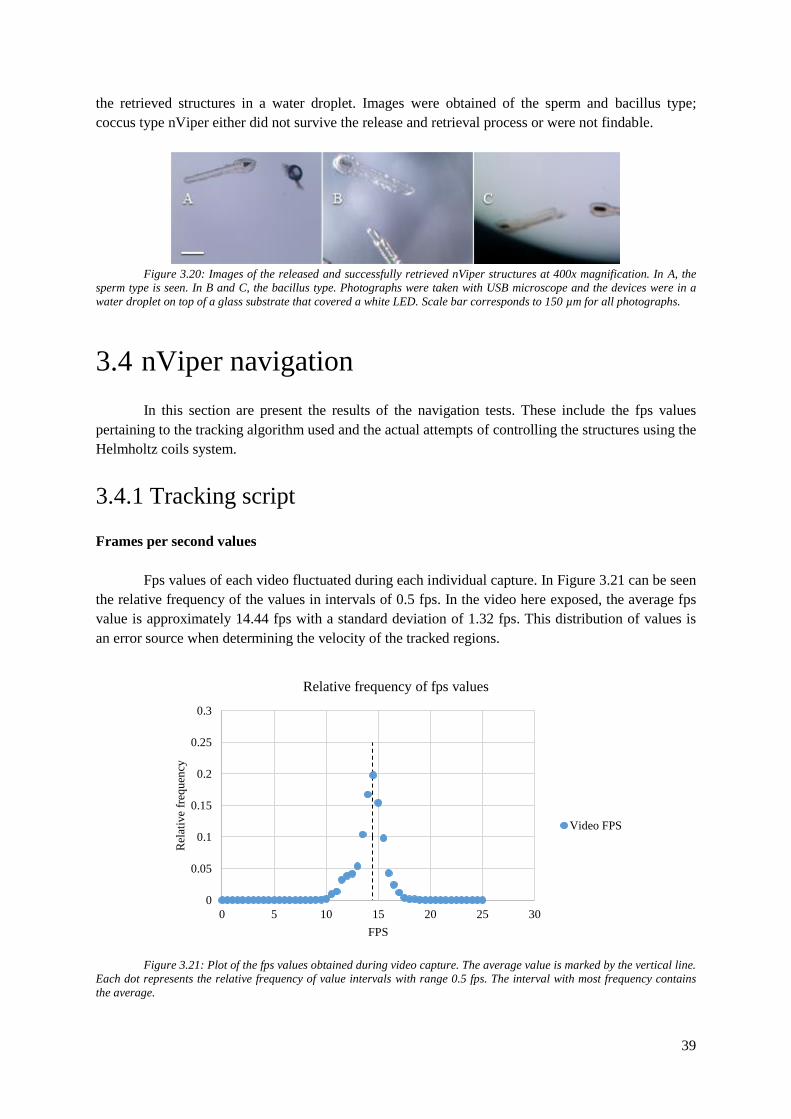
39
the retrieved structures in a water droplet. Images were obtained of the sperm and bacillus type;
coccus type nViper either did not survive the release and retrieval process or were not findable.
Figure 3.20: Images of the released and successfully retrieved nViper structures at 400x magnification. In A, the
sperm type is seen. In B and C, the bacillus type. Photographs were taken with USB microscope and the devices were in a
water droplet on top of a glass substrate that covered a white LED. Scale bar corresponds to 150 µm for all photographs.
3.4 nViper navigation
In this section are present the results of the navigation tests. These include the fps values
pertaining to the tracking algorithm used and the actual attempts of controlling the structures using the
Helmholtz coils system.
3.4.1 Tracking script
Frames per second values
Fps values of each video fluctuated during each individual capture. In Figure 3.21 can be seen
the relative frequency of the values in intervals of 0.5 fps. In the video here exposed, the average fps
value is approximately 14.44 fps with a standard deviation of 1.32 fps. This distribution of values is
an error source when determining the velocity of the tracked regions.
Figure 3.21: Plot of the fps values obtained during video capture. The average value is marked by the vertical line.
Each dot represents the relative frequency of value intervals with range 0.5 fps. The interval with most frequency contains
the average.
0
0.05
0.1
0.15
0.2
0.25
0.3
0 5 10 15 20 25 30
Rel
ativ
e fr
equ
ency
FPS
Relative frequency of fps values
Video FPS
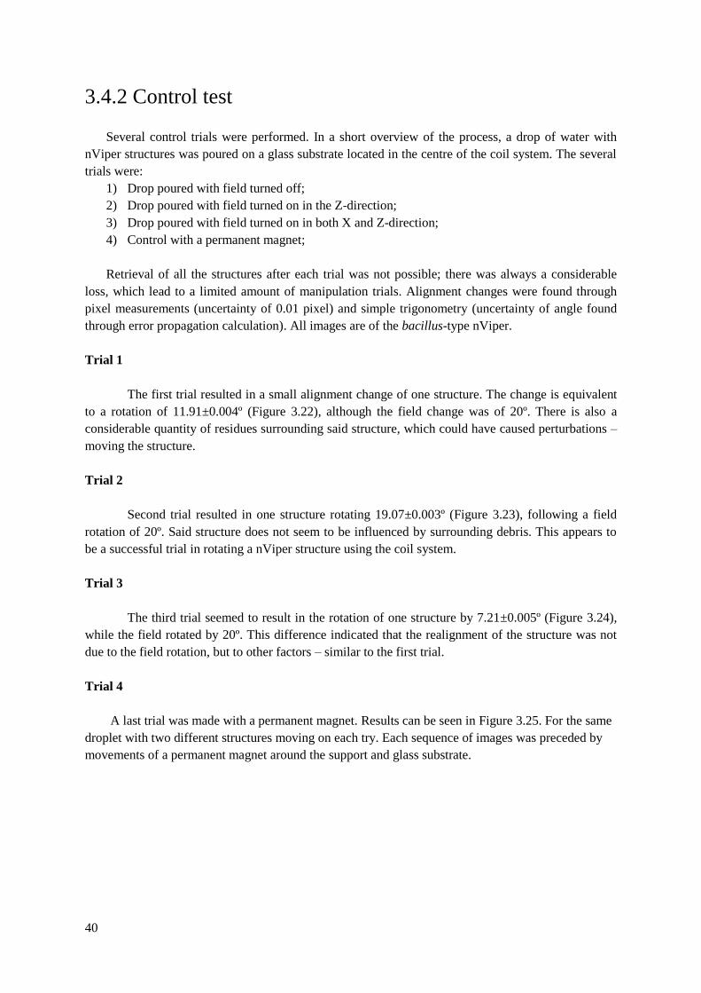
40
3.4.2 Control test
Several control trials were performed. In a short overview of the process, a drop of water with
nViper structures was poured on a glass substrate located in the centre of the coil system. The several
trials were:
1) Drop poured with field turned off;
2) Drop poured with field turned on in the Z-direction;
3) Drop poured with field turned on in both X and Z-direction;
4) Control with a permanent magnet;
Retrieval of all the structures after each trial was not possible; there was always a considerable
loss, which lead to a limited amount of manipulation trials. Alignment changes were found through
pixel measurements (uncertainty of 0.01 pixel) and simple trigonometry (uncertainty of angle found
through error propagation calculation). All images are of the bacillus-type nViper.
Trial 1
The first trial resulted in a small alignment change of one structure. The change is equivalent
to a rotation of 11.91±0.004º (Figure 3.22), although the field change was of 20º. There is also a
considerable quantity of residues surrounding said structure, which could have caused perturbations –
moving the structure.
Trial 2
Second trial resulted in one structure rotating 19.07±0.003º (Figure 3.23), following a field
rotation of 20º. Said structure does not seem to be influenced by surrounding debris. This appears to
be a successful trial in rotating a nViper structure using the coil system.
Trial 3
The third trial seemed to result in the rotation of one structure by 7.21±0.005º (Figure 3.24),
while the field rotated by 20º. This difference indicated that the realignment of the structure was not
due to the field rotation, but to other factors – similar to the first trial.
Trial 4
A last trial was made with a permanent magnet. Results can be seen in Figure 3.25. For the same
droplet with two different structures moving on each try. Each sequence of images was preceded by
movements of a permanent magnet around the support and glass substrate.
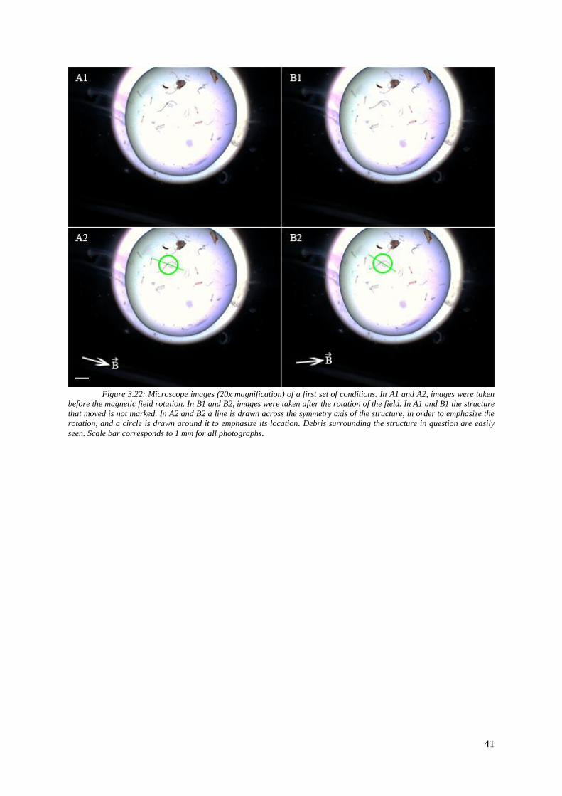
41
Figure 3.22: Microscope images (20x magnification) of a first set of conditions. In A1 and A2, images were taken
before the magnetic field rotation. In B1 and B2, images were taken after the rotation of the field. In A1 and B1 the structure
that moved is not marked. In A2 and B2 a line is drawn across the symmetry axis of the structure, in order to emphasize the
rotation, and a circle is drawn around it to emphasize its location. Debris surrounding the structure in question are easily
seen. Scale bar corresponds to 1 mm for all photographs.
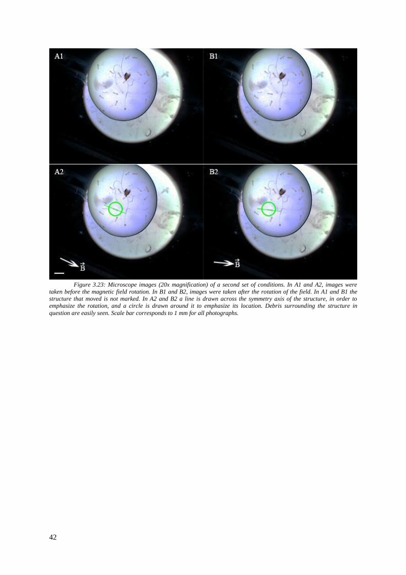
42
Figure 3.23: Microscope images (20x magnification) of a second set of conditions. In A1 and A2, images were
taken before the magnetic field rotation. In B1 and B2, images were taken after the rotation of the field. In A1 and B1 the
structure that moved is not marked. In A2 and B2 a line is drawn across the symmetry axis of the structure, in order to
emphasize the rotation, and a circle is drawn around it to emphasize its location. Debris surrounding the structure in
question are easily seen. Scale bar corresponds to 1 mm for all photographs.
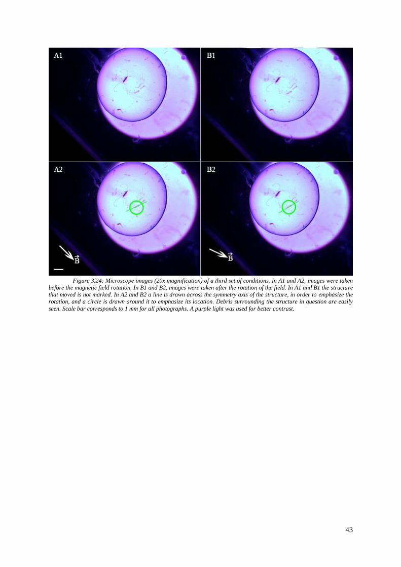
43
Figure 3.24: Microscope images (20x magnification) of a third set of conditions. In A1 and A2, images were taken
before the magnetic field rotation. In B1 and B2, images were taken after the rotation of the field. In A1 and B1 the structure
that moved is not marked. In A2 and B2 a line is drawn across the symmetry axis of the structure, in order to emphasize the
rotation, and a circle is drawn around it to emphasize its location. Debris surrounding the structure in question are easily
seen. Scale bar corresponds to 1 mm for all photographs. A purple light was used for better contrast.
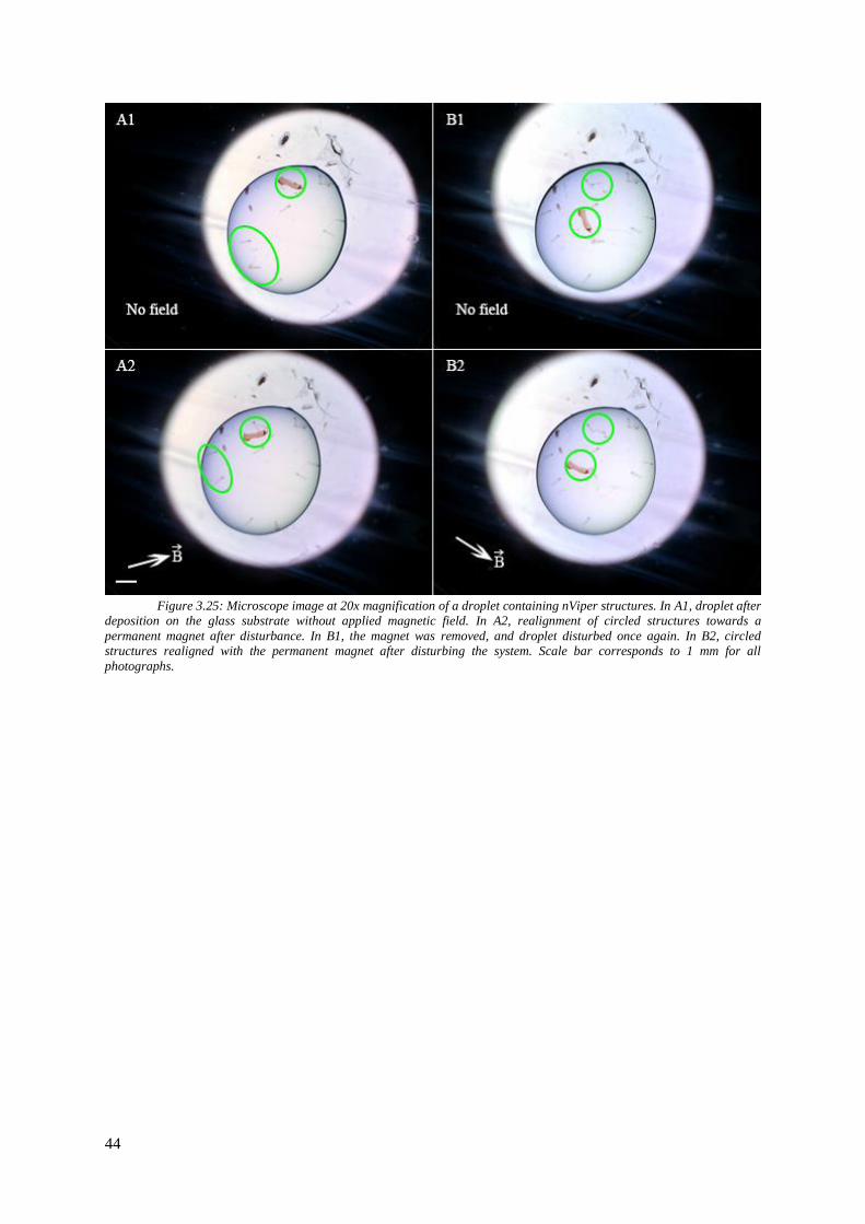
44
Figure 3.25: Microscope image at 20x magnification of a droplet containing nViper structures. In A1, droplet after
deposition on the glass substrate without applied magnetic field. In A2, realignment of circled structures towards a
permanent magnet after disturbance. In B1, the magnet was removed, and droplet disturbed once again. In B2, circled
structures realigned with the permanent magnet after disturbing the system. Scale bar corresponds to 1 mm for all
photographs.
45
4 Discussion
The designed coil system is capable of realignment of magnetic structures as can be seen in
section 3.1.2. While results like these are not new and have been obtained by other groups with
similar [17] or greatly different [45] setups, they can serve as a future control system for other (or
improvements on nViper) microrobotic or even nanorobotic systems (untested). A coil system was
previously produced at IBEB [46], but it lacked the capability of generating a truly three-dimensional
field. With that in the mind, the new coil setup together with the programmable power source is a
definitive improvement. The major downside of the new setup is its incapacity to generate a constant
magnetic field gradient, which the old one was capable of (due to containing a pair of coils in
Maxwell configuration).
The fabrication process used resulted in viable microscopic structures capable of being
magnetically actuated – while the results are not optimal, they do serve as a proof-of-concept. In the
end, the structures were not as well defined as desired. This happened in the second polyimide layer,
its thickness was not uniform – the already defined polyimide structures caused the second coating to
have bumps in thickness. Such can be corrected by adjusting the exposure mask of the second
polyimide layer, so that it contains the bump – i.e. the second polyimide pattern has to be larger than
the first. Although the CoCrPt layer was defined using a thicker photoresist, by defining the material
through lift-off, the standard photoresist could have been used. The thicker photoresist was used to
minimize the bump caused by the first polyimide layer – similar to the previous problem. The release
process, while functional, is not optimal and needs improvement. This could be done with a different
sacrificial layer or maybe if the vapor-prime steps were skipped in the process described in section
2.4.3. Selecting a different sacrificial layer material that does not require an etchant that reacts with
the magnetic component should be investigated. After the release, the retrieval itself needs
improvement. A microfluidic device with magnetic guides could be applied to separate the
microrobots. Summarizing, what needs to be changed in future processes: second polyimide layer’s
size needs to account for the bump; release (including choice of sacrificial material) and retrieval
process needs to be optimized.
Navigation using the magnetic fields generated by the coils seems possible. Results in section
3.1.2 indicate that rotating the field is able to realign magnetic structures. From section 3.4.2, it is
observed that this works even in the microscale. The formulated hypothesis why only one or some
structures moved is a simple one, as the droplet containing the microrobots makes contact with the
glass substrate, these adhere to the glass. A possibly solution is the use of a system where the fluid is
not still (as in the case of the droplet) but has a non-null flow. That system could be a “two in one”
solution by also serving as an artificial blood vessel system. Then the navigation of the devices would
be tested in a medium closer to an in vivo environment.
While the previously mentioned results are positive, and the problems found are easily solved
or simple inconveniences, there are big changes to be made for the system to work as desired. The
complete setup can be seen as a macro and a micro component. The biggest challenges in the micro
component were relative to the fabrication process. These were either solved or a possible solution
provided. The bigger change resides in the macro component. While the magnetic field was capable
of realigning the structures, for them to propel with this method the frequency of the field was not
enough. Comparing with the frequency values of [17] (5 Hz minimum, maximum velocity at 45 Hz),
there was no reason to assume a priori that nViper devices would propel like the structures in [17]
with the HMP4040 power source. Replacing the HMP4040 DC power source with a programmable
AC power source appears to be the simplest and most direct solution for this. With this change,

46
simulations of the electromagnetic behaviour of the coils need to be made but higher frequencies
could be attained.
The results presented in this dissertation serve as proof of concept that the combination of the
produced coils and fabricated nViper devices is functional. The use of polyimide as a flexible base
material allow, in vivo application of the structures. Using magnetic fields as form of actuation of a
CoCrPt magnetic head allows the implementation of the system in medical treatments by modification
of MRI machinery. Although actual propulsion was not obtained, results indicate that the control of
microscale structures is possible.
47
5 Conclusion
This project had the main goal of developing a magnetic nano/microrobotic system to be
actuated with a setup of coils in Helmholtz configuration. With this in mind, three pairs of Helmholtz
coils were designed and ordered to be used with a Hameg HMP4040 programmable DC power
source. The control was done with a GUI, created in LabVIEW, where the values for the radial
component of the field, the polar angle and the z-component of the field were inserted. With this
apparatus, it was possible to realign and rotate magnetic structures by also rotating the field. This was
first tested with a small 5-millimeter neodymium magnet.
With the system working at the macroscale, it was time to move into the micro world and test
with simple microrobots. With inspiration from [17], a simple microrobot called nViper was
developed with polyimide – a biocompatible flexible polymer - and CoCrPt – a ferromagnetic
material with high coercivity and saturation magnetization. While the structure did not achieve
propulsion, realignment with the magnetic field was demonstrated in some structures. The main
problem being their adherence to the glass substrate used in the tests.
The fabrication process, although successful, was not optimal. There remains room for
improvement as was described in the previous chapter. Even though the tested structures had
fabrication flaws, these did not seem to prevent the structure from aligning with the field. These
results are seen as proof of concept that the coil system designed is capable of controlling the
direction of the structure.
Polyimide as the base material for the nViper microrobot proved to be possible and feasible
for the desired goal. Bending during realignment was not observed, for that to happen higher
frequencies might be needed.
CoCrPt as the magnetic component was also effective. Its high coercivity allows the
magnetization direction to remain fixed when applying a magnetic field. Its high saturation
magnetization value might be used to induce some degree of swarm behaviour in a nViper group,
similar to the one found in [36]. The high magnetization of CoCrPt with a weak field translates in a
high sensitivity to changes in the magnetic field, allowing the complete structure to respond quickly
and strongly to the changes.
In the end, the project served as a basis for future microrobotic projects to be built upon what
has been described during this dissertation. In the following section, future work and possible
improvements are described.
5.1 Future work
There is still plenty of room for improvement in future continuations of this project. Changes
can be made both in the micro and the macro components.
Addressing the macro parts of the setup. As previously mentioned, while the coils do work as
expected, the power source is not capable of generating the needed signal type. Replacing the
HMP4040 DC power source by a programmable AC power source expands the possibilities. This
would require simple changes in the LabVIEW GUI already developed. The use of an alternate
current would need simulations of the coils’ behaviour, mainly due to induction caused by the time-
varying magnetic field. Concerning the GUI there is also improvement to be done. LabVIEW was
used for its simplicity and the already existing drivers. Using a lower level language (like C) for
communication with the power source, minimization of execution time would be possible. Other

48
functions that are not implementable through LabVIEW would also be feasible, such as real-time
input and control.
In the microscale, the fabrication process needs optimization. The release and retrieval stages
are not optimized. Quantifying the amount of structures recovered in the end would be beneficial for
the user. Minimum definable dimensions of the polyimide through the used process should also be
investigated, in a simple manner: how small can we go.
49
6 References
[1] R. R. Schaller, “Moore's law: past, present and future,” Spectrum, IEEE, vol. 34, pp. 52-59,
1997.
[2] R. Feynman, “There's plenty of room at the bottom,” in Anual meeting of the American Physical
Society at Caltech, 1960.
[3] D. K. Schweizer and E. K. Eigler, Positioning single atoms with a scanning tunneling microscop,
vol. 344, 1990, pp. 524-525.
[4] A. Dubey, C. Mavroidis, A. Thornton, K. Nikitczuk and M. L. Yarmush, “Viral protein linear
(VPL) nano-actuators,” Proceedings of the IEEE Conference on Nanotechnology, vol. 1, pp. 140-
143, 2003.
[5] S. Hollar, A. Flynn, C. Bellew and K. S. J. Pister, “Solar powered 10 mg silicon robot,” The
Sixteenth Annual International Conference on Micro Electro Mechanical Systems, 2003. MEMS-
03 Kyoto. IEEE, pp. 706-711.
[6] T. Ebefors, J. Mattsson, E. Kälvesten and G. Stemme, “A walking silicon micro-robot,” Proc.
Transducers' 99, pp. 1202-1205, 1999.
[7] B. R. Donald, C. G. Levey, C. G. McGray, I. Paprotny and D. Rus, “An untethered, electrostatic,
globally controllable MEMS micro-robot,” Journal of Microelectromechanical Systems, vol. 15,
pp. 1-15, 2006.
[8] K. Saito, D. S. Contreras, Y. Takeshiro, Y. Okamoto, Y. Nakata, T. Tanaka, S. Kawamura, M.
Kaneko, F. Uchikoba, Y. Mita and K. S. J. Pister, “Heterogeneous Integration,” pp. 33-37, 2018.
[9] K. Iwata, Y. Okane, Y. Ishihara and K. Sugita, “Insect-type microrobot with mounted bare chip
IC articial neural networks,” pp. 1204-1207, 2016.
[10] K. Sugita, “Hexapod Type MEMS Microrobot Equipped with an Artificial Neural Networks IC,”
vol. 4, pp. 28-31, 2017.
[11] B. R. Donald, C. G. Levey, C. D. McGray, D. Rus and M. Sinclair, “Power delivery and
locomotion of untethered microactuators,” Journal of Microelectromechanical Systems, vol. 12,
pp. 947-959, 2003.
[12] N. N. Bolotnik, V. G. Gradetsky, A. A. Zhukov, D. V. Kozlov, I. P. Smirnov and V. G.
Chashchukhin, “Mobile microrobotics for space exploration: the state-of-the-art and prospects,”
Advances in Cooperative Robotics. Proc. of the 19th Int. Conf. of Climbing and Walking Robots
(CLAWAR), pp. 739-746, 2016.
[13] G. V. Luz, “Nanorobotics in Drug Delivery Systems for Treatment of Cancer: A Review,”
Journal of Materials Science and Engineering A, vol. 6, pp. 167-180, 2016.
[14] S. Martel, O. Felfoul, J.-b. Mathieu, A. Chanu, S. Tamaz, M. Mohammadi, M. Mankiewicz and
N. Tabatabaei, “MRI-base Medical Nanorobotic Platform for the Control of Magnetic
Nanoparticles and Flagellated Bacteria for Target Interventions in Human Capillaries,” vol. 28,
pp. 1169-1182, 2009.
[15] S. Martel, C. C. Tremblay, S. Ngakeng and G. Langlois, “Controlled manipulation and actuation
of micro-objects with magnetotactic bacteria,” Applied Physics Letters, vol. 89, pp. 14-17, 2006.
[16] H. Xu, M. Medina-Sánchez, V. Magdanz, L. Schwarz, F. Hebenstreit and O. G. Schmidt,
“Sperm-Hybrid Micromotor for Targeted Drug Delivery,” ACS Nano, vol. 12, pp. 327-337, 2018.
[17] I. S. M. Khalil, H. C. Dijkslag, L. Abelmann and S. Misra, “MagnetoSperm: A microrobot that
50
navigates using weak magnetic fields,” Applied Physics Letters, vol. 104, 2014.
[18] P. Ii, “Robotics in the Small Part 1,” pp. 111-121, 2007.
[19] K. B. Yesin, P. Exner, K. Vollmers and B. J. Nelson, “Design and Control of In-Vivo Magnetic
Microrobots,” pp. 819-826, 2005.
[20] Q. A. Pankhurst, J. Connolly, K. Jones S and J. Dobson, “Applications of magnetic nanoparticles
in biomedicine,” Journal of physics D: Applied Physics, vol. 36, pp. R167--R181, 2003.
[21] M. K. Lima-Tenório, E. A. Gómez Pineda, N. M. Ahmad, H. Fessi and A. Elaissari, “Magnetic
nanoparticles: In vivo cancer diagnosis and therapy,” International Journal of Pharmaceutics,
vol. 493, pp. 313-327, 2015.
[22] X. Mou, Z. Ali, S. Li and N. He, “Applications of Magnetic Nanoparticles in Targeted Drug
Delivery System,” Journal of Nanoscience and Nanotechnology, vol. 15, pp. 54-62, 2015.
[23] Z. Hedayatnasab, F. Abnisa and W. M. A. W. Daud, “Review on magnetic nanoparticles for
magnetic nanofluid hyperthermia application,” Materials and Design, vol. 123, pp. 174-196,
2017.
[24] K. K. Cheng, P. S. Chan, S. Fan, S. M. Kwan, K. L. Yeung, Y. X. J. Wáng, A. H. L. Chow, E. X.
Wu and L. Baum, “Curcumin-conjugated magnetic nanoparticles for detecting amyloid plaques
in Alzheimer's disease mice using magnetic resonance imaging (MRI),” Biomaterials, vol. 44,
pp. 155-172, 2015.
[25] B. W.-C. Tse, G. J. Cowin, C. Soekmadji, L. Jovanovic, R. S. Vasireddy, M.-T. Ling, A. Khatri,
T. Liu, B. Thierry and P. J. Russell, “PSMA-targeting iron oxide magnetic nanoparticles enhance
MRI of preclinical prostate cancer,” Nanomedicine, vol. 10, pp. 375-386, 2015.
[26] M. Wierucka and M. Biziuk, “Application of magnetic nanoparticles for magnetic solid-phase
extraction in preparing biological, environmental and food samples,” TrAC - Trends in Analytical
Chemistry, vol. 59, pp. 50-58, 2014.
[27] O. Veiseh, J. W. Gunn and M. Zhang, “Design and fabrication of magnetic nanoparticles for
targeted drug delivery and imaging,” Advanced Drug Delivery Reviews, vol. 62, pp. 284-304,
2010.
[28] S. D. Kong, J. Lee, S. Ramachandran, B. P. Eliceiri, V. I. Shubayev, R. Lal and S. Jin, “Magnetic
targeting of nanoparticles across the intact blood-brain barrier,” Journal of Controlled Release,
vol. 164, pp. 49-57, 2012.
[29] K. Ulbrich, K. Holá, V. Šubr, A. Bakandritsos, J. Tuček and R. Zbořil, “Targeted Drug Delivery
with Polymers and Magnetic Nanoparticles: Covalent and Noncovalent Approaches, Release
Control, and Clinical Studies,” Chemical Reviews, vol. 116, pp. 5338-5431, 2016.
[30] S. Betal, A. K. Saha, E. Ortega, M. Dutta, A. K. Ramasubramanian, A. S. Bhalla and R. Guo,
“Core-shell magnetoelectric nanorobot - A remotely controlled probe for targeted cell
manipulation,” Scientific Reports, vol. 8, pp. 1-9, 2018.
[31] E. Lauga and T. R. Powers, “The hydrodynamics of swimming microorganisms,” Reports on
Progress in Physics, vol. 72, 2009.
[32] J. Grover, J. Zimmer, T. Dear, M. Travers, H. Choset and S. D. Kelly, “Geometric Motion
Planning for a Three-Link Swimmer in a Three-Dimensional Low Reynolds-Number Regime,”
pp. 6067-6074, 2018.
[33] R. Dreyfus, J. Baudry, M. L. Roper, M. Fermigier, H. A. Stone and J. Bibette, “Microscopic
artificial swimmers,” Nature, vol. 437, pp. 862-865, 2005.
[34] N. Mano and A. Heller, “Bioelectrochemical propulsion,” Journal of the American Chemical
51
Society, vol. 127, pp. 11574-11575, 2005.
[35] X. Z. Chen, M. Hoop, F. Mushtaq, E. Siringil, C. Hu, B. J. Nelson and S. Pané, “Recent
developments in magnetically driven micro- and nanorobots,” Applied Materials Today, vol. 9,
pp. 37-48, 2017.
[36] J. Li, T. Li, T. Xu, M. Kiristi, W. Liu, Z. Wu and J. Wang, “Magneto-Acoustic Hybrid
Nanomotor,” Nano Letters, vol. 15, pp. 4814-4821, 2015.
[37] S. Zheng, J. Han, S. Cho, V. D. Nguyen, S. Y. Ko, J. O. Park and S. Park, “Motility steering of
bacteriobots using chemical gradient microchannel,” Proceedings of the IEEE RAS and EMBS
International Conference on Biomedical Robotics and Biomechatronics, Vols. %1 de %22016-
July, pp. 140-144, 2016.
[38] T. Li, J. Li, K. I. Morozov, Z. Wu, T. Xu, I. Rozen, A. M. Leshansky, L. Li and J. Wang,
“Highly efficient freestyle magnetic nanoswimmer,” Nano Letters, vol. 17, pp. 5092-5098, 2017.
[39] M. Medina-Sánchez, L. Schwarz, A. K. Meyer, F. Hebenstreit and O. G. Schmidt, “Cellular
Cargo Delivery: Toward Assisted Fertilization by Sperm-Carrying Micromotors,” Nano Letters,
vol. 16, pp. 555-561, 2016.
[40] J. M. Gardin, C. S. Burn, W. J. Childs and W. L. Henry, “Evaluation of blood flow velocity in
the ascending aorta and main pulmonary artery of normal subjects by Doppler
echocardiography,” American Heart Journal, vol. 107, pp. 310-319, 1984.
[41] R. R. Richardson, J. A. Miller and W. M. Reichert, “Polyimides as biomaterials: preliminary
biocompatibility testing,” Biomaterials, vol. 14, pp. 627-635, 1993.
[42] J. Valadeiro, “Magnetoresistive sensors with pico-Tesla sensitivities,” p. 74, 2014.
[43] OpenCV library.
[44] B. Baben and S. Belongie, “Visual tracking with online Multiple Instance Learning,” 2009 IEEE
Conference on Computer Vision and Pattern Recognition, pp. 983-990, 2009.
[45] M. P. Kummer, J. J. Abbott, B. E. Kratochvil, R. Borer, A. Sengul and B. J. Nelson, “Octomag:
An electromagnetic system for 5-DOF wireless micromanipulation,” IEEE Transactions on
Robotics, vol. 26, pp. 1006-1017, 2010.
[46] P. Zoio, “Modeling and design of an electromagnetic actuation system for the manipulation of
microrobots in blood vessels,” 2015.
52
A. Python script
# -*- coding: utf-8 -*-
"""
Created on Mon Apr 23 19:21:08 2018
@author: Daniel Vilhena
@email: [email protected]
This script serves to access the image feed of a USB video device and track
a user-selected ROI. This is to be used for the tracking of the
nViper devices designed at IBEB-FCUL and fabricated at INESC-MN.
These devices are located in a small water droplet and have around 0.4 mm
of length. They are operated with three pairs of orthogonal Helmholtz coils
capable of producing a field of ~43 mT, located at IBEB.
Summarizing the script:
1) Opening and creating the desired files, folders, video capture and video
tracker
2) Accessing the video feed and, after selecting a ROI in the first captured
frame, tracking the ROI while registering the device's fps
3) Determining the center of the ROI and saving said coordinates
4) Drawing the ROI and its center on aquired images
"""
import cv2 # OpenCV library
import os # Library for directory handling
import csv # Library for csv files handling
##### Opening a csv file to register fps #####
csvfile = open('fps.csv', 'w')
testW = csv.writer(csvfile, delimiter = '\t', quotechar = '|', quoting = csv.QUOTE_MINIMAL)
##### Opening a csv file to save coordinates #####
filePos = open('pos.csv', 'w')
posW = csv.writer(filePos, delimiter = '\t', quotechar = '|', quoting = csv.QUOTE_MINIMAL)
##### Starting the capture #####
cap = cv2.VideoCapture(1)
##### Selecting tracking method #####
(major_ver, minor_ver, subminor_ver) = (cv2.__version__).split('.')
tracker_types = ['BOOSTING', 'MIL', 'KCF', 'TLD', 'MEDIANFLOW', 'GOTURN']
tracker_type = tracker_types[1]
##### Creating the tracker #####
53
if int(minor_ver) < 3:
tracker = cv2.Tracker_create(tracker_type)
else:
if tracker_type == 'BOOSTING':
tracker = cv2.TrackerBoosting_create()
if tracker_type == 'MIL':
tracker = cv2.TrackerMIL_create()
if tracker_type == 'KCF':
tracker = cv2.TrackerKCF_create()
if tracker_type == 'TLD':
tracker = cv2.TrackerTLD_create()
if tracker_type == 'MEDIANFLOW':
tracker = cv2.TrackerMedianFlow_create()
if tracker_type == 'GOTURN':
tracker = cv2.TrackerGOTURN_create()
##### Read first frame #####
ok, frameTrack = cap.read()
##### Select ROI #####
bbox = cv2.selectROI(frameTrack, False)
##### Initialize tracker with first frame #####
ok = tracker.init(frameTrack, bbox)
##### Counters for files - names and rows indexing #####
i = 0
j = 0
k = 1
##### Directories to save images #####
# If said directory does not exist, create it
# Folder for images without ROI drawn
if not os.path.exists("./raw"):
os.makedirs("./raw")
# Folder for images with ROI box drawn
if not os.path.exists("./track"):
os.makedirs("./track")
# Folder for images with ROI box and its central point drawn
if not os.path.exists("./dot"):
os.makedirs("./dot")
##### Image arrays to save frames #####
frameList = [] # Array for images without ROI box
frameBoxList = [] # Array for images with ROI box
##### Start live track #####
while True:
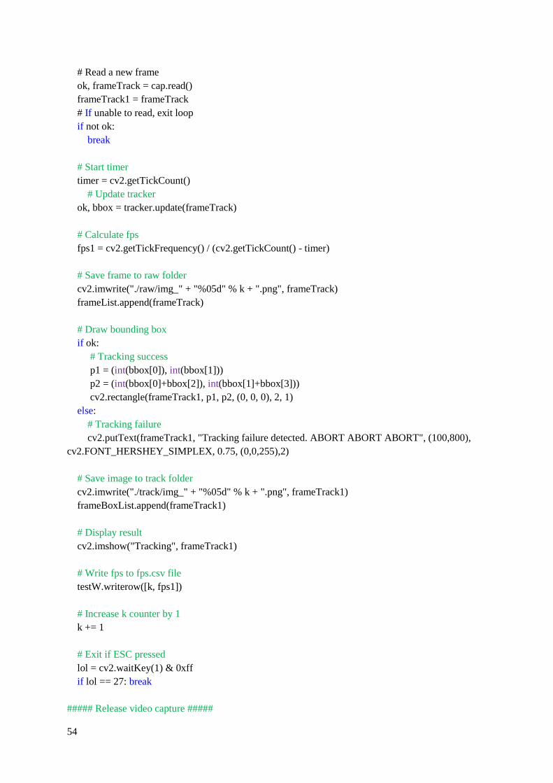
54
# Read a new frame
ok, frameTrack = cap.read()
frameTrack1 = frameTrack
# If unable to read, exit loop
if not ok:
break
# Start timer
timer = cv2.getTickCount()
# Update tracker
ok, bbox = tracker.update(frameTrack)
# Calculate fps
fps1 = cv2.getTickFrequency() / (cv2.getTickCount() - timer)
# Save frame to raw folder
cv2.imwrite("./raw/img_" + "%05d" % k + ".png", frameTrack)
frameList.append(frameTrack)
# Draw bounding box
if ok:
# Tracking success
p1 = (int(bbox[0]), int(bbox[1]))
p2 = (int(bbox[0]+bbox[2]), int(bbox[1]+bbox[3]))
cv2.rectangle(frameTrack1, p1, p2, (0, 0, 0), 2, 1)
else:
# Tracking failure
cv2.putText(frameTrack1, "Tracking failure detected. ABORT ABORT ABORT", (100,800),
cv2.FONT_HERSHEY_SIMPLEX, 0.75, (0,0,255),2)
# Save image to track folder
cv2.imwrite("./track/img_" + "%05d" % k + ".png", frameTrack1)
frameBoxList.append(frameTrack1)
# Display result
cv2.imshow("Tracking", frameTrack1)
# Write fps to fps.csv file
testW.writerow([k, fps1])
# Increase k counter by 1
k += 1
# Exit if ESC pressed
lol = cv2.waitKey(1) & 0xff
if lol == 27: break
##### Release video capture #####
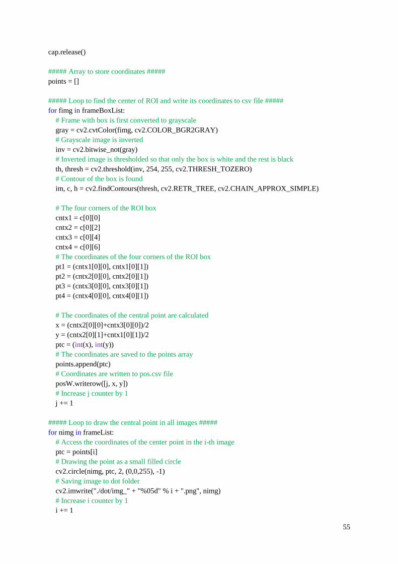
55
cap.release()
##### Array to store coordinates #####
points = []
##### Loop to find the center of ROI and write its coordinates to csv file #####
for fimg in frameBoxList:
# Frame with box is first converted to grayscale
gray = cv2.cvtColor(fimg, cv2.COLOR_BGR2GRAY)
# Grayscale image is inverted
inv = cv2.bitwise_not(gray)
# Inverted image is thresholded so that only the box is white and the rest is black
th, thresh = cv2.threshold(inv, 254, 255, cv2.THRESH_TOZERO)
# Contour of the box is found
im, c, h = cv2.findContours(thresh, cv2.RETR_TREE, cv2.CHAIN_APPROX_SIMPLE)
# The four corners of the ROI box
cntx1 = c[0][0]
cntx2 = c[0][2]
cntx3 = c[0][4]
cntx4 = c[0][6]
# The coordinates of the four corners of the ROI box
pt1 = (cntx1[0][0], cntx1[0][1])
pt2 = (cntx2[0][0], cntx2[0][1])
pt3 = (cntx3[0][0], cntx3[0][1])
pt4 = (cntx4[0][0], cntx4[0][1])
# The coordinates of the central point are calculated
x = (cntx2[0][0]+cntx3[0][0])/2
y = (cntx2[0][1]+cntx1[0][1])/2
ptc = (int(x), int(y))
# The coordinates are saved to the points array
points.append(ptc)
# Coordinates are written to pos.csv file
posW.writerow([j, x, y])
# Increase j counter by 1
j += 1
##### Loop to draw the central point in all images #####
for nimg in frameList:
# Access the coordinates of the center point in the i-th image
ptc = points[i]
# Drawing the point as a small filled circle
cv2.circle(nimg, ptc, 2, (0,0,255), -1)
# Saving image to dot folder
cv2.imwrite("./dot/img_" + "%05d" % i + ".png", nimg)
# Increase i counter by 1
i += 1
56
B. Arduino sketch
boolean newData = false;
const byte numChars = 4;
char received[numChars];
int red = 0;
int green = 0;
int blue = 0;
int redPin = 11;
int greenPin = 10;
int bluePin = 12;
// the setup function runs once when you press reset or power the board
void setup() {
// initialize digital pin LED_BUILTIN as an output.
Serial.begin(9600);
}
// the loop function runs over and over again forever
void loop() {
showNewData();
receive();
//showNewData();
ledState();
}
void receive() {
static byte ndx = 0;
char endMarker = '\n';
char rc;
while (Serial.available()> 0 && newData ==false) {
rc = Serial.read();
if(rc != endMarker) {
received[ndx] = rc;
ndx++;
if(ndx >= numChars) {
ndx = numChars-1;
}
}
else {
received[ndx] = '\0';
ndx = 0;
newData = true;
}
}
}
57
void showNewData() {
if(newData == true) {
Serial.println("The LED now has configuration: ");
Serial.print("Red: ");
Serial.println(red);
Serial.print("Green: ");
Serial.println(green);
Serial.print("Blue: ");
Serial.println(blue);
newData = false;
}
}
void ledState() {
int value = colorValue(received);
switch(received[0]) {
case 'r':
analogWrite(redPin, value);
red = value;
break;
case 'g':
analogWrite(greenPin, value);
green = value;
break;
case 'b':
analogWrite(bluePin, value);
blue = value;
break;
case 'w':
analogWrite(redPin, value);
analogWrite(greenPin, value);
analogWrite(bluePin, value);
red = value;
green = value;
blue = value;
break;
}
}
int colorValue(char color[]) {
return color[1]*100+color[2]*10+color[3];}
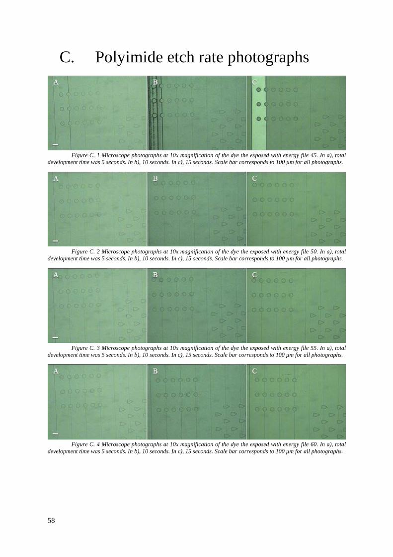
58
C. Polyimide etch rate photographs
Figure C. 1 Microscope photographs at 10x magnification of the dye the exposed with energy file 45. In a), total
development time was 5 seconds. In b), 10 seconds. In c), 15 seconds. Scale bar corresponds to 100 µm for all photographs.
Figure C. 2 Microscope photographs at 10x magnification of the dye the exposed with energy file 50. In a), total
development time was 5 seconds. In b), 10 seconds. In c), 15 seconds. Scale bar corresponds to 100 µm for all photographs.
Figure C. 3 Microscope photographs at 10x magnification of the dye the exposed with energy file 55. In a), total
development time was 5 seconds. In b), 10 seconds. In c), 15 seconds. Scale bar corresponds to 100 µm for all photographs.
Figure C. 4 Microscope photographs at 10x magnification of the dye the exposed with energy file 60. In a), total
development time was 5 seconds. In b), 10 seconds. In c), 15 seconds. Scale bar corresponds to 100 µm for all photographs.
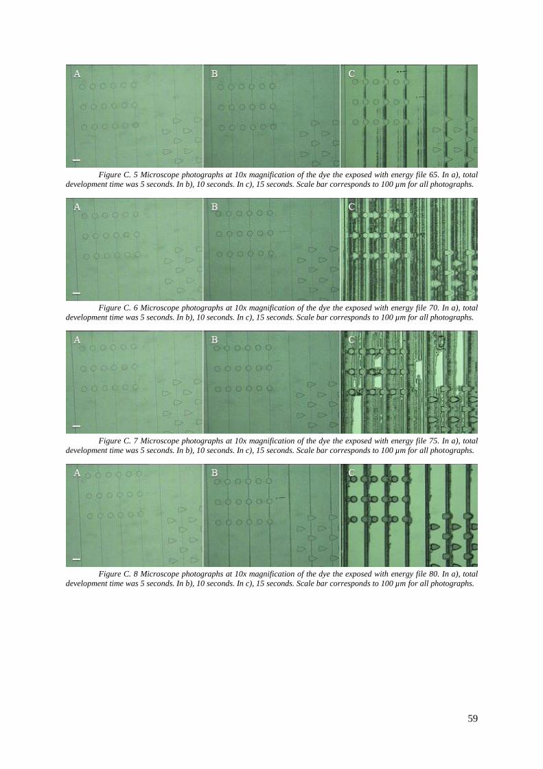
59
Figure C. 5 Microscope photographs at 10x magnification of the dye the exposed with energy file 65. In a), total
development time was 5 seconds. In b), 10 seconds. In c), 15 seconds. Scale bar corresponds to 100 µm for all photographs.
Figure C. 6 Microscope photographs at 10x magnification of the dye the exposed with energy file 70. In a), total
development time was 5 seconds. In b), 10 seconds. In c), 15 seconds. Scale bar corresponds to 100 µm for all photographs.
Figure C. 7 Microscope photographs at 10x magnification of the dye the exposed with energy file 75. In a), total
development time was 5 seconds. In b), 10 seconds. In c), 15 seconds. Scale bar corresponds to 100 µm for all photographs.
Figure C. 8 Microscope photographs at 10x magnification of the dye the exposed with energy file 80. In a), total
development time was 5 seconds. In b), 10 seconds. In c), 15 seconds. Scale bar corresponds to 100 µm for all photographs.
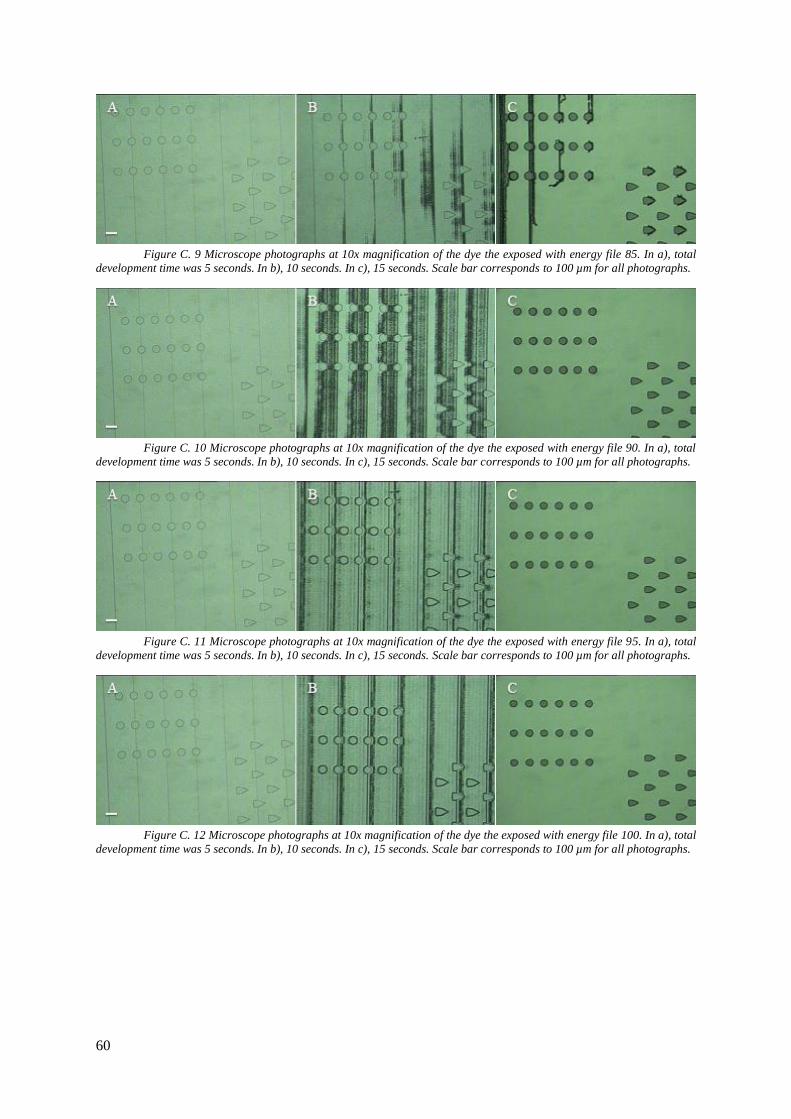
60
Figure C. 9 Microscope photographs at 10x magnification of the dye the exposed with energy file 85. In a), total
development time was 5 seconds. In b), 10 seconds. In c), 15 seconds. Scale bar corresponds to 100 µm for all photographs.
Figure C. 10 Microscope photographs at 10x magnification of the dye the exposed with energy file 90. In a), total
development time was 5 seconds. In b), 10 seconds. In c), 15 seconds. Scale bar corresponds to 100 µm for all photographs.
Figure C. 11 Microscope photographs at 10x magnification of the dye the exposed with energy file 95. In a), total
development time was 5 seconds. In b), 10 seconds. In c), 15 seconds. Scale bar corresponds to 100 µm for all photographs.
Figure C. 12 Microscope photographs at 10x magnification of the dye the exposed with energy file 100. In a), total
development time was 5 seconds. In b), 10 seconds. In c), 15 seconds. Scale bar corresponds to 100 µm for all photographs.
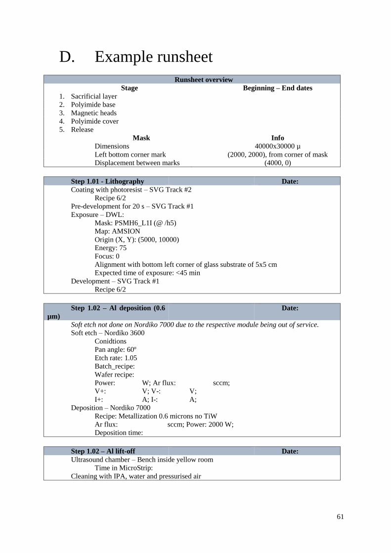
61
D. Example runsheet
Runsheet overview
Stage Beginning – End dates
1. Sacrificial layer
2. Polyimide base
3. Magnetic heads
4. Polyimide cover
5. Release
Mask Info
Dimensions 40000x30000 µ
Left bottom corner mark (2000, 2000), from corner of mask
Displacement between marks (4000, 0)
Step 1.01 - Lithography Date:
Coating with photoresist – SVG Track #2
Recipe 6/2
Pre-development for 20 s – SVG Track #1
Exposure – DWL:
Mask: PSMH6_L1I (@ /h5)
Map: AMSION
Origin (X, Y): (5000, 10000)
Energy: 75
Focus: 0
Alignment with bottom left corner of glass substrate of 5x5 cm
Expected time of exposure: <45 min
Development – SVG Track #1
Recipe 6/2
Step 1.02 – Al deposition (0.6
µm)
Date:
Soft etch not done on Nordiko 7000 due to the respective module being out of service.
Soft etch – Nordiko 3600
Conidtions
Pan angle: 60º
Etch rate: 1.05
Batch_recipe:
Wafer recipe:
Power: W; Ar flux: sccm;
V+: V; V-: V;
I+: A; I-: A;
Deposition – Nordiko 7000
Recipe: Metallization 0.6 microns no TiW
Ar flux: sccm; Power: 2000 W;
Deposition time:
Step 1.02 – Al lift-off Date:
Ultrasound chamber – Bench inside yellow room
Time in MicroStrip:
Cleaning with IPA, water and pressurised air
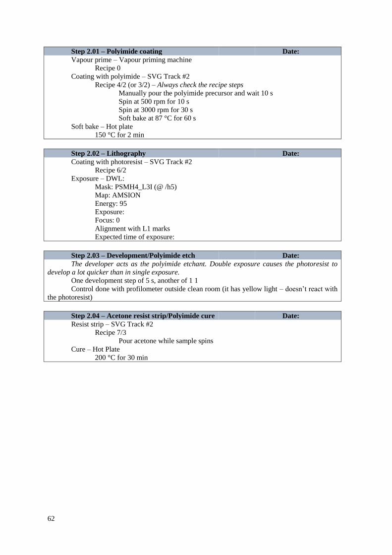
62
Step 2.01 – Polyimide coating Date:
Vapour prime – Vapour priming machine
Recipe 0
Coating with polyimide – SVG Track #2
Recipe 4/2 (or 3/2) – Always check the recipe steps
Manually pour the polyimide precursor and wait 10 s
Spin at 500 rpm for 10 s
Spin at 3000 rpm for 30 s
Soft bake at 87 °C for 60 s
Soft bake – Hot plate
150 °C for 2 min
Step 2.02 – Lithography Date:
Coating with photoresist – SVG Track #2
Recipe 6/2
Exposure – DWL:
Mask: PSMH4_L3I (@ /h5)
Map: AMSION
Energy: 95
Exposure:
Focus: 0
Alignment with L1 marks
Expected time of exposure:
Step 2.03 – Development/Polyimide etch Date:
The developer acts as the polyimide etchant. Double exposure causes the photoresist to
develop a lot quicker than in single exposure.
One development step of 5 s, another of 1 1
Control done with profilometer outside clean room (it has yellow light – doesn’t react with
the photoresist)
Step 2.04 – Acetone resist strip/Polyimide cure Date:
Resist strip – SVG Track #2
Recipe 7/3
Pour acetone while sample spins
Cure – Hot Plate
200 °C for 30 min
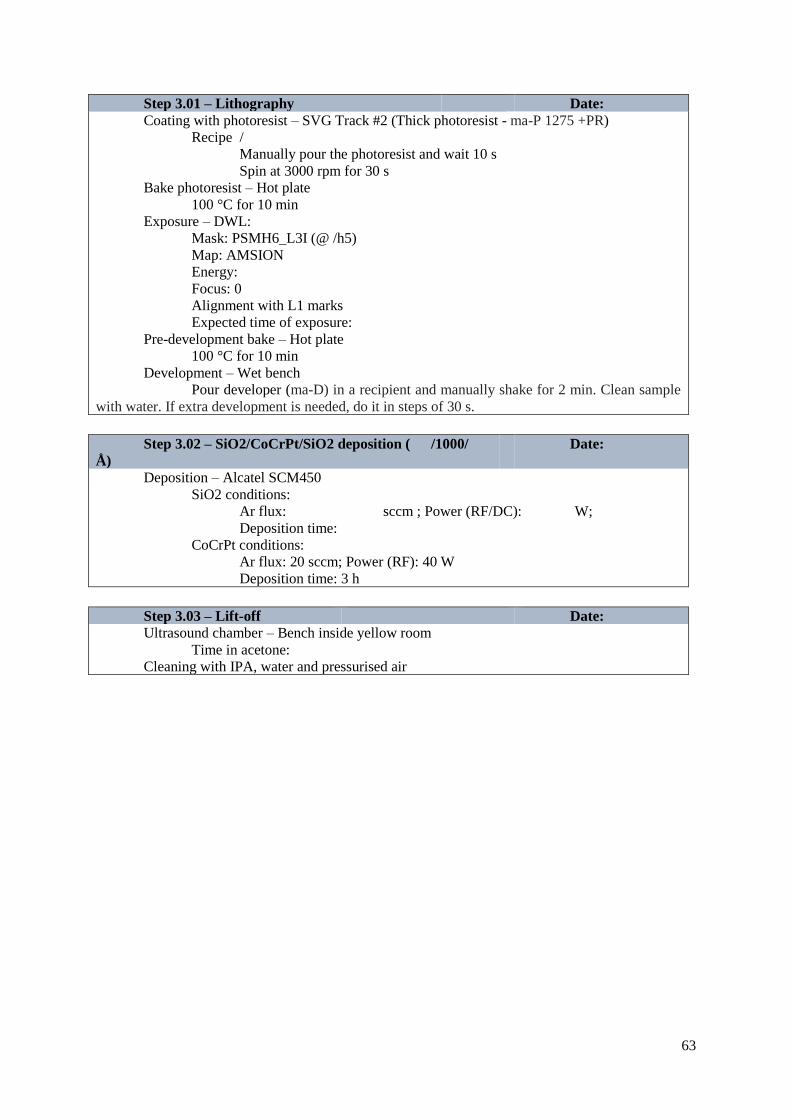
63
Step 3.01 – Lithography Date:
Coating with photoresist – SVG Track #2 (Thick photoresist - ma-P 1275 +PR)
Recipe /
Manually pour the photoresist and wait 10 s
Spin at 3000 rpm for 30 s
Bake photoresist – Hot plate
100 °C for 10 min
Exposure – DWL:
Mask: PSMH6_L3I (@ /h5)
Map: AMSION
Energy:
Focus: 0
Alignment with L1 marks
Expected time of exposure:
Pre-development bake – Hot plate
100 °C for 10 min
Development – Wet bench
Pour developer (ma-D) in a recipient and manually shake for 2 min. Clean sample
with water. If extra development is needed, do it in steps of 30 s.
Step 3.02 – SiO2/CoCrPt/SiO2 deposition ( /1000/
Å)
Date:
Deposition – Alcatel SCM450
SiO2 conditions:
Ar flux: sccm ; Power (RF/DC): W;
Deposition time:
CoCrPt conditions:
Ar flux: 20 sccm; Power (RF): 40 W
Deposition time: 3 h
Step 3.03 – Lift-off Date:
Ultrasound chamber – Bench inside yellow room
Time in acetone:
Cleaning with IPA, water and pressurised air
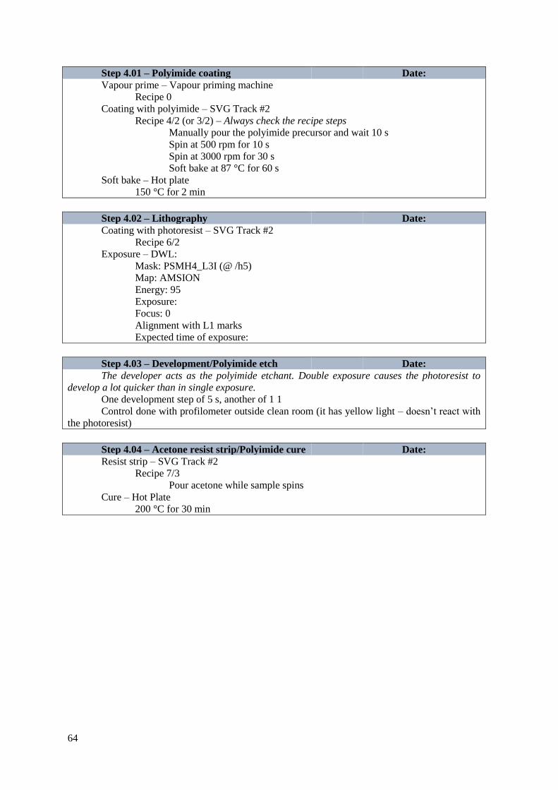
64
Step 4.01 – Polyimide coating Date:
Vapour prime – Vapour priming machine
Recipe 0
Coating with polyimide – SVG Track #2
Recipe 4/2 (or 3/2) – Always check the recipe steps
Manually pour the polyimide precursor and wait 10 s
Spin at 500 rpm for 10 s
Spin at 3000 rpm for 30 s
Soft bake at 87 °C for 60 s
Soft bake – Hot plate
150 °C for 2 min
Step 4.02 – Lithography Date:
Coating with photoresist – SVG Track #2
Recipe 6/2
Exposure – DWL:
Mask: PSMH4_L3I (@ /h5)
Map: AMSION
Energy: 95
Exposure:
Focus: 0
Alignment with L1 marks
Expected time of exposure:
Step 4.03 – Development/Polyimide etch Date:
The developer acts as the polyimide etchant. Double exposure causes the photoresist to
develop a lot quicker than in single exposure.
One development step of 5 s, another of 1 1
Control done with profilometer outside clean room (it has yellow light – doesn’t react with
the photoresist)
Step 4.04 – Acetone resist strip/Polyimide cure Date:
Resist strip – SVG Track #2
Recipe 7/3
Pour acetone while sample spins
Cure – Hot Plate
200 °C for 30 min
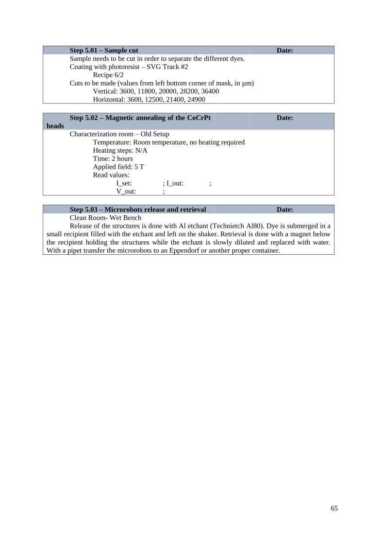
65
Step 5.01 – Sample cut Date:
Sample needs to be cut in order to separate the different dyes.
Coating with photoresist – SVG Track #2
Recipe 6/2
Cuts to be made (values from left bottom corner of mask, in µm)
Vertical: 3600, 11800, 20000, 28200, 36400
Horizontal: 3600, 12500, 21400, 24900
Step 5.02 – Magnetic annealing of the CoCrPt
heads
Date:
Characterization room – Old Setup
Temperature: Room temperature, no heating required
Heating steps: N/A
Time: 2 hours
Applied field: 5 T
Read values:
I_set: ; I_out: ;
V_out: ;
Step 5.03 – Microrobots release and retrieval Date:
Clean Room- Wet Bench
Release of the structures is done with Al etchant (Technietch Al80). Dye is submerged in a
small recipient filled with the etchant and left on the shaker. Retrieval is done with a magnet below
the recipient holding the structures while the etchant is slowly diluted and replaced with water.
With a pipet transfer the microrobots to an Eppendorf or another proper container.