femtosecond laser ablation for controlling micro and nano
TRANSCRIPT
Femtosecond laser ablation for controlling micro
and nano structuration
Dissertation
zur Erlangung des Grades des Doktors der Ingenieurwissenschaften
der Naturwissenschaftlich-Technischen Fakultät II
- Physik und Mechatronik -
der Universität des Saarlandes
Cotutelle-Promotion mit der Universität St. Etienne (Frankreich)
von
David Bruneel
Saarbrücken
(2010)


“When a […] scientist states that something is possible,
He is almost certainly right
When he states that something is impossible,
He is very probably wrong.”
Arthur C. Clarke

Abstract
The current development of technology makes constant the necessity of getting smaller
and smaller features sizes down to micrometer and sub micrometer scales. Laser ablation,
which has the great advantage of precise material removal, is a promising candidate. In this
dissertation we have demonstrated the feasibility to take advantage of the interaction of
femtosecond laser pulses with matter for micro- and nano-structuration and this by having
developed a compact and high accurate and flexible apparatus. An analyse of the specific
physical mechanisms of laser-matter interaction in the femtosecond regime is presented.
Investigations on processing time efficiency as well as the effect of the repetition rate during
ablation of metals have been performed. The potential of the multifunctional tool coupled
with a compact high repetition rate femtosecond oscillator is shown for different applications
in biotechnology. Results on large area mapping as well as accurate nanoprocessing of
biological tissue and various materials are presented. This versatile tool covers wide research
fields from the nanoprocessing of biological samples as well as the nanostructuring of
different type of materials. It is of great interest for many applications in material science,
nanobiotechnology and nanomedicine.
Kurzdarstellung
Die augenblickliche Technologieentwicklung macht ein Design immer kleinerer
Bauteile, bis hin zu mikrometer- und sub-mikrometer Bereichen notwendig.
Materialabtragung durch einen Laser wird durch die erreichbare hohe Präzision zu einer
vielversprechenden Methode, diese gewünschten Bereiche zu erreichen. In dieser Dissertation
wird die Möglichkeit, den Vorteil der Interaktion von femtosekunden Laserpulsen mit für eine
Mikro- und Nanostrukturierung geeignetem Material durch ein eigens entwickeltes,
kompaktes, hochpräzises und flexibles System demonstriert. Eine Analyse der spezifischen
physikalischen Mechanismen der Laser – Materie Interaktion im femtosekunden Bereich wird
präsentiert. Untersucht wurden sowohl die Effizienz unterschiedlicher Bearbeitungsdauern als
auch der Einfluss der Repetitionsrate während des Materialabtrags. Das Potential des
erstellten multifunktionellen Gerätes in Kopplung mit einem kompakten femtosekunden
Oszillator hoher Repetitionsrate wird für verschiedene Applikationen in der Biotechnologie
aufgezeigt. Ergebnisse einer Abbildung von Bereichen, die mehr als den eigentlichen
Scanbereich umfassen, und präziser Nanoabtrag biologischen Gewebes und verschiedener
Materialien werden präsentiert. Das entwickelte vielfältige System deckt wichtige Bereiche
der aktuellen Forschung von der Nanobearbeitung biologischer Proben bis hin zur
Nanostrukturierung verschiedener Materialien ab. Dies ist von großem Interesse für viele
Anwendungen in Materialwissenschaften, Nanobiotechnologie und Nanomedizin.
Résumé succinct
Le développement actuel de la technologie induit une constante nécessité d’obtenir des
tailles de plus en plus petites pouvant descendre jusqu’à des dimensions micrométriques et
sub micrométriques. L’ablation laser, qui a le grand avantage d’un enlèvement de matière très
précis, et un candidat prometteur. Dans cette thèse on démontre la faisabilité de tirer avantage
des impulsions laser femtosecondes avec la matière pour la micro et nano structuration, et
ceci en ayant développé une machine compacte de grande précision et flexibilité. Une
approche théorique comparant les régimes d’interaction à haute et basse cadence est
présentée. Des investigations de l’efficacité du temps de procédé aussi bien que l’effet de la
cadence pendant l’ablation de métaux ont été effectuées. Le potentiel de l’outil
multifonctionnel couplé avec un oscillateur laser femtoseconde à haute cadence est montré
pour différentes applications en biotechnologie. Les résultats sur la cartographie d’une large
zone aussi bien que la nano découpe de précision de tissus biologiques et de matériaux variés
sont présentés. Cet outil polyvalent couvre de larges domaines de recherche de la nano
découpe d’échantillons biologiques aussi bien que la nanostructuration de différents types de
matériaux. C’est d’un grand intérêt pour de nombreuses applications en science des
matériaux, nanobiotechnologie et nanomédecine.
Summary
The current development of technology makes constant the necessity of getting smaller
and smaller features sizes down to micrometer and sub micrometer scales. Such small sizes
strongly restrict the use of conventional tools. However several concurrent technologies
attempt to push limits of small feature sizes. In this race, the laser is a promising candidate.
In this dissertation, the feasibility to take advantage of the interaction of femtosecond
laser pulses with matter for micro- and nano-structuration is demonstrated and this by having
developed a compact and high accurate and flexible apparatus.
An overview of actual nanostructuring technologies, especially focusing on benefits of
femtosecond lasers are discussed in this work. An analyse of the specific physical
mechanisms of laser-matter interaction in the femtosecond regime is presented. In the case of
high repetition rate laser matter interaction, physical mechanisms seem to be governed by heat
accumulation effect phenomenon. A theoretical approach comparing high and low repetition
rate interaction regime is given.
A detailed description of the consequent work performed in engineering for the
development of the multifunctional tool for nanostructuring and imaging is given in this
dissertation. This development implies the implementation and control of a multitude of
parameters and devices such as translation stages, piezo driven, shutter, camera,... as well as a
good knowledge in optics engineering. Hardware and software have been intensively
developed under LabVIEW in an easy to manage and user-friendly environment. The
flexibility of the device allows to perform complex 2D as well as 3D patterns.
A new method for processing time calculation on metals in the case of laser machining
at kilohertz repetition rate is presented in this work. primary results are demonstrated on the
possibility to get an estimation of processing time for femtosecond machining. This method
put in evidence the physical time, the time during which ablation processes are active in the
machining. The comparison of calculated processing time and measured total process time
can give concrete information on process characteristics, which have to be optimized to
improve the manufacturing efficiency. Furthermore, results on the influence of laser repetition
rate show the way to another field of improvements. Indeed, in our experiments, the ablation
rate is not affected by the increase of laser repetition rate up to some tens of KHz. Hence, it
means that it is possible to decrease the processing time by increasing the repetition rate. On
the other hand, experimental results on the effects of the repetition rate at megahertz repetition
rate show different characteristics and put in evidence a controllable phenomenon of
“growing” matter. It seems to grow up depending on the strength of the heat accumulation
effect. This phenomenon is discussed.
This dissertation focuses finally on the potential of the multifunctional tool for different
applications in biotechnology. Results on large area mapping with a very high resolution, in
transmission, in reflexion, or using two photons imaging are presented. This allows targeting
a precise location on a large area of a sample and makes possible the nanodissection of
biological samples, cells, chromosomes… Nanodissection with ultra short laser pulses opens
new horizons for scientists, who are primarily interested in investigation of cells, and tissues
processes. This versatile tool allows to covers wide research fields from the nanoprocessing of
biological samples as well as the nanostructuring of different type of materials as polymers,
dielectrics or metals. It is of great interest for many applications in material science,
nanobiotechnology and nanomedicine.
Zusammenfasung
Die gegenwärtige Technologieentwicklung verlangt immer kleinere Bauteile mit
Größen im Mikrometer- und Submikrometerbereich. Diese winzigen Abmessungen schränken
den Gebrauch konventioneller Werkzeuge stark ein. Gegenwärtig versuchen verschiedene
Technologien die machbaren Grenzen für immer kleinere Bauteile nach unten zu verschieben.
Hier kommt die Lasertechnologie als aussichtsreiche Technik ins Spiel.
In dieser Dissertation wird Machbarkeit und Vorteil der Interaktion von femtosekunden
Laserpulsen mit Materie bei Mikro- und Nanostrukturierungen mit einem eigens entwickelten
kompakten, flexiblen und hochpräzisen Gerät untersucht.
Ein Überblick über aktuelle Technologien zur Nanostrukturierung mit besonderem
Schwerpunkt auf den Vorteilen von femtosekunden Lasern wird in dieser Arbeit gegeben und
diskutiert. Eine Analyse der spezifischen physikalischen Mechanismen der Laser / Materie
Interaktion im Femtosekundenbereich wird präsentiert. Interagiert ein Laser mit hoher
Repetitionsrate mit Materie, scheinen diese physikalischen Vorgänge durch das Phänomen
der Hitze-Akkumulation beeinflusst zu werden. Ein theoretischer Ansatz hierzu wird durch
einen Vergleich von hohen und niedrigen Repetitionsraten während der Interaktion, gegeben.
Anschließend wird in dieser Dissertation eine detaillierte Beschreibung der
Entwicklungsarbeit für ein Multifunktionsgerät für Nanostrukturierung und Abbildung
gegeben. Diese Entwicklung beinhaltete die Implementierung und Kontrolle von sehr
verschiedenen Parametern und Bauteilen, wie Verschiebetisch, Piezo-Antrieb, Shutter,
Kamera,....in Verbindung mit einer guten Kenntnis in optischer Konstruktion und
Entwicklung. Hard- und Software wurden unter LabVIEW so konstruiert, dass eine einfach
zu handhabende und benutzerfreundliche Oberfläche entstand. Die Flexibilität des Gerätes
erlaubt Entwicklung und Ausführung komplexer 2D und 3D Strukturen.
In dieser Arbeit wird eine neue Methode für die Kalkulation der Bearbeitungszeit von
Metallen mit einem Laser mit Kilohertz- Repetitionsrate vorgestellt. Erste Ergebnisse für eine
mögliche Bestimmung der Bearbeitungszeitdauer mit einem Femtosekunden-System werden
dargestellt. Diese Methode berücksichtigt die physikalische Zeitdauer, die Zeit während der
Abtragprozesse tatsächlich aktiv in der Bearbeitung stattfinden. Der Vergleich der
kalkulierten Bearbeitungszeitdauer und der gemessenen gesamten Prozessdauer kann
konkrete Informationen über Prozesscharakteristika geben, die optimiert die Effizienz der
Bearbeitung steigern können. Außerdem zeigen die Resultate aus den Versuchen zum
Einfluss der Laser-Repetitionsrate, dass sich hier ein anderes Feld für Verbesserungen ergibt.
Tatsächlich ergaben unsere Experimente, dass die Abtragsrate nicht durch einen Anstieg der
Laser-Repetitionsrate bis hin zu einigen KHz beeinflusst wird. Dies bedeutet, dass es möglich
ist, die eigentliche Bearbeitungszeit zu reduzieren, wenn die Repetitionsrate erhöht wird.
Andererseits zeigen die Ergebnisse aus den Untersuchungen zu Effekten der Repetitionsrate,
dass im MHz Bereich andere Charakteristika zu Berücksichtigen sind und Anzeichen für ein
kontrollierbares Phänomen von "wachsendem" Material zum Tragen kommen. Dieses
Phänomen scheint abhängig von der Stärke der akkumulierten Hitze zu sein und wird
diskutiert.
Abschließend liegt der Fokus dieser Dissertation auf dem Potential des
multifunktionellen Systems für verschiedene Anwendungen in der Biotechnologie. Die
Resultate der Implementierung der Darstellung großer Areale mit sehr hoher Auflösung in
Transmission, Reflexion oder durch Zwei-Photonen angeregte Fluoreszenz werden
präsentiert. Dies erlaubt eine präzise Lokalisation und Ansteuerung interessierender Punkte
innerhalb eines größeren Areals und macht eine gezielte Nanodissektion von biologischen
Proben, Zellen, Chromosomen, ...usw. möglich. Nanodissektion mit ultrakurzen Laserpulsen
eröffnet neue Horizonte für Wissenschaftler, die primär in Untersuchungen von Prozessen in

Zellen und Geweben eingebunden sind. Dieses innovative System deckt eine Reihe von
wissenschaftlichen Gebieten von Nanoprozessierung von biologischen Proben bis hin zu
Nanostrukturierung verschiedener Materialien wie Polymere, Nicht-Leiter und Metalle, ab.
Dies ist für viele Anwendungen in Materialwissenschaften, Nanobiotechnologie und
Nanomedizin von großem Interesse.
Résumé
Le développement actuel de la technologie induit une constante nécessité d’obtenir des
tailles de plus en plus petites pouvant descendre jusqu’à des dimensions micrométriques, et
sub micrométriques. De telles tailles d’objet restreint énormément l’utilisation des outils
conventionnels. Cependant plusieurs technologies concurrentes tentent de repousser les
limites des petites dimensions. Dans cette course, le laser se présente comme un candidat
prometteur.
Dans cette thèse est démontré la faisabilité de tirer avantage de l’interaction des
impulsions laser femtosecondes avec la matière pour la micro et nano structuration, et ceci en
ayant développé une machine compacte de grande précision et haute flexibilite.
Une vue d’ensemble des technologies actuelles de nanostructuration, mettant l’accent
sur les avantages des lasers femtosecondes est discutée dans ce travail. Une analyse des
mécanismes physiques particuliers de l’interaction laser-matière en régime femtoseconde est
présentée. Dans le cas de l’interaction laser-matière à haute cadence, les mécanismes
physiques semblent être gouvernés par le phénomène d’accumulation de chaleur. Une
approche théorique comparant les régimes d’interaction à haute et basse cadence est
présentée.
Une description détaillée du travail conséquent effectué en ingénierie pour le
développement de l’outil multifonctionnel pour la structuration et l’imagerie est donnée dans
cette thèse. Ce développement implique l’implémentation et le control d’une multitude de
paramètres et d’appareils tels que des platines de déplacement, des drivers piezoélectriques,
un shutter, une caméra, … mais aussi une bonne connaissance en ingénierie optique. Les
parties matérielle et logicielle ont été développées sous LabVIEW dans un environnement
convivial et simple d’utilisation. La flexibilité de la machine permet d’effectuer des motifs
complexes 2D et 3D.
Dans ce travail une nouvelle méthode est présentée pour le calcul du temps de procédé
sur les métaux dans le cas d’usinages laser à des taux de repetition dans la gamme du
kilohertz. Les résultats préliminaires démontrent la possibilité d’avoir une estimation du
temps de procédé pour l’usinage femtoseconde. Cette méthode met en évidence le temps
physique, le temps pendant lequel les processus d’ablation sont actifs. La comparaison du
temps de procédé calculé avec le temps de procédé total mesuré peut donner une information
concrète sur les caractéristiques du processus à optimiser pour améliorer l’efficacité de la
fabrication. De plus, les résultats de l’influence de la cadence laser montre le chemin d’un
autre domaine d’améliorations. En effet, dans nos expériences, le taux d’ablation n’est pas
affecté par l’augmentation de la cadence jusqu’à plusieurs dizaines de kilohertz. Par
conséquent, ceci signifie qu’il est possible de diminuer le temps de procédé en augmentant le
taux de répétition. D’un autre côté, les résultats expérimentaux sur les effets de la cadence à
une cadence de l’ordre du mégahertz montre différentes caractéristiques et mettent en
évidence un phénomène de « croissance » de la matière. Il semble croître de façon dépendante
de la force de l’effet cumulatif. Ce phénomène est discuté.
Pour finir, cette these se concentre finalement sur le potentiel de l’outil multifonctionnel
pour différentes applications en biotechnologie. Les résultats de cartographie de grande
surface avec une très haute résolution, en transmission, en réflexion, ou en utilisant l’imagerie
à deux photons sont présentés. Ceci permet le ciblage précis sur une grande zone de
l’échantillon et rend possible la nanodissection d’échantillons biologiques, cellules,
chromosomes … La nanodissection avec des impulsions laser ultracourtes ouvre de nouveaux
horizons aux scientifiques, qui sont premièrement intéressés dans l’investigation des
processus de cellules et tissus organiques. Cet outil polyvalent permet de couvrir de larges

domaines de recherche du traitement d’échantillons biologiques aussi bien que de
nanostructuration de différents types de matériaux comme les polymères, les diélectriques ou
les métaux. C’est d’un grand intérêt pour de nombreuses applications en science des
matériaux, nanobiologie et nanomédecine.


Contents
CONTENTS.....................................................................................................................................................- 17 -
INTRODUCTION.............................................................................................................................................- 1 -
CHAPTER I ......................................................................................................................................................- 3 -
OVERVIEW OF NANOSTRUCTURING TECHNIQUES..........................................................................- 3 -
1. INTRODUCTION ...................................................................................................................................... - 5 - 2. NANOSTRUCTURING WITH LITHOGRAPHY.............................................................................................. - 6 -
2.1. Energetic beams ..........................................................................................................................- 8 - 2.2. Low energetic beams...................................................................................................................- 9 - 2.3. Extreme UV lithography..............................................................................................................- 9 - 2.4. X-ray lithography ......................................................................................................................- 10 - 2.5. Imprint lithography ...................................................................................................................- 10 - 2.6. Laser stereolithography ............................................................................................................- 12 -
3. LASER APPROACH ................................................................................................................................ - 14 - 3.1. Physical aspect of interaction for ultrafast pulses ....................................................................- 15 - 3.2. Thermalization ..........................................................................................................................- 16 - 3.3. Femtosecond pulses and longer pulses (ps or ns) .....................................................................- 18 - 3.4. UV laser micromachining .........................................................................................................- 21 - 3.5. Principle of nanomachining ......................................................................................................- 22 - 3.6. Ultrafast nanomachining techniques.........................................................................................- 23 -
3.6.1. Direct grating writing ...........................................................................................................................- 23 - 3.6.2. Illumination of an atomic microscope tip .............................................................................................- 25 - 3.6.3. Interference of ultrafast laser pulses .....................................................................................................- 26 - 3.6.4. Self-organized structures (LIPSS) ........................................................................................................- 27 -
4. EFFECT OF HEAT ACCUMULATION: THEORETICAL APPROACH .............................................................. - 32 - 4.1. Description of the simulation code............................................................................................- 32 - 4.2. Results for heat accumulation ...................................................................................................- 34 -
5. CONCLUSION ....................................................................................................................................... - 39 -
CHAPTER II ...................................................................................................................................................- 41 -
DEVELOPMENT OF A TOOL FOR NANOSTRUCTURING AND MULTIPHOTON IMAGING ....- 41 -
1. INTRODUCTION .................................................................................................................................... - 43 - 3. DEVICE DEVELOPMENT........................................................................................................................ - 45 - 4. CHARACTERIZATION OF THE LASER BEAM FOR AN OPTIMAL COUPLING INTO THE DEVICE ................... - 53 -
4.1. Spot size determination .............................................................................................................- 53 - 4.2. Fluence determination of a Gaussian shaped intensity profile .................................................- 57 - 4.3. Average power ..........................................................................................................................- 59 - 4.4. Autocorrelation (at laser output and after objective)................................................................- 60 -
5. DEVELOPMENT OF AN AUTOFOCUS METHOD........................................................................................ - 63 - 5.1. Principle....................................................................................................................................- 63 - 5.2. The algorithm............................................................................................................................- 63 -
6. CONTROL AND SOFTWARE DEVELOPMENT........................................................................................... - 66 - 6.1. The Camera control ..................................................................................................................- 67 - 6.2. x,y translation stage control......................................................................................................- 67 - 6.3. Scanning area control ...............................................................................................................- 68 -
7. CAD DRAWING TO NANOMACHINING .................................................................................................. - 71 - 7.1. Size control................................................................................................................................- 71 - 7.2. Shutter control...........................................................................................................................- 72 - 7.3. 3D structuring ...........................................................................................................................- 74 -
CHAPTER III .................................................................................................................................................- 77 -
EFFECTS OF HIGH REPETITION RATE FEMTOSECOND PULSES ON METALS .......................- 77 -
1. INTRODUCTION .................................................................................................................................... - 79 - 1.1. Processing time .........................................................................................................................- 80 -
1.1.1. Analytical method of processing time calculation ................................................................................- 80 - 1.1.2. Results and discussion ..........................................................................................................................- 83 -
a) Case of copper ......................................................................................................................................- 85 - b) Case of stainless steel ...........................................................................................................................- 86 -
i. Processing time ...............................................................................................................................- 86 - ii. Influence of the repetition rate.........................................................................................................- 88 -
2. OVERVIEW OF HIGH REPETITION RATE PULSES EFFECTS ON MATTER ................................................... - 89 - 2.1. Case of dielectrics .....................................................................................................................- 89 -
2.1.1. Heat accumulation phenomenon...........................................................................................................- 90 - 2.1.2. Hillocks phenomenon ...........................................................................................................................- 93 -
2.2. Case of metals ...........................................................................................................................- 94 - 2.3. Case of semiconductors.............................................................................................................- 98 -
3. EXPERIMENTAL CONDITIONS AND PARAMETERS................................................................................ - 102 - 3.1. Results .....................................................................................................................................- 104 - 3.2. Discussion:..............................................................................................................................- 107 -
3.2.1. Heat accumulation effect on ablation rate...........................................................................................- 107 - 3.2.2. Influence of speed and fluence on the height of protrudes..................................................................- 109 -
4. CONCLUSION ..................................................................................................................................... - 114 -
CHAPTER IV................................................................................................................................................- 115 -
RESULTS AND APPLICATIONS IN BIOTECHNOLOGIES................................................................- 115 -
1. INTRODUCTION .................................................................................................................................. - 117 - 2. MAPPING OF MICRO AREA.................................................................................................................. - 118 - 3. TARGETING AND NANODISSECTION ................................................................................................... - 123 - 4. MICRO-NANO-PROCESSING OF COMPLEX PATTERNS .......................................................................... - 128 - 5. TWO-PHOTON POLYMERIZATION ....................................................................................................... - 132 - 6. CONCLUSION ..................................................................................................................................... - 135 -
CONCLUSION .............................................................................................................................................- 137 -
LIST OF FIGURES ......................................................................................................................................- 139 -
BIBLIOGRAPHY .........................................................................................................................................- 143 -
APPENDIX A ................................................................................................................................................- 161 -
OWN PUBLICATION LIST .......................................................................................................................- 171 -
ACKNOWLEDGMENTS ............................................................................................................................- 173 -
DECLARATION...........................................................................................................................................- 177 -
CURRICULUM VITAE...............................................................................................................................- 179 -
Introduction ___________________________________________________________________________
- 1 -
Introduction
The current development of technology leads to more and more important necessity of
miniaturization. Scientists and industrial try hard to develop these micro and nano
technologies, in different fields such as physics, chemistry and biology. The market of these
technologies is estimated at several billion in 2020. Many industries are concerned by these
future advances that have applications in many fields such as medical, military, cosmetics,
marketing, traceability, etc. Applications in nanomanufacturing fields such as material
nanostructuring, nanoelectronics, nanobiotechnology are widely recognized to be critical. The
integration of nanoscale elements into nano/micro scale products needs to achieve a great
development in the various branches of science and engineering such as surface chemistry,
electrostatics, fluid flow, adhesion, etc.
The production of these nano-technologies requires the development of 2D and 3D dedicated
tools. Ultrafast lasers thanks to its intrinsic properties enable to reach a very high precision
and a very good quality. Femtosecond lasers meet the quality requirements necessary to reach
features sizes down to nanometre scale. Indeed, the interaction of pulses of the order of
femtosecond with the matter has got properties making a femtosecond laser a very precise
tool for mechanics. For constant energy inside a pulse, the decrease to such pulse duration
results in a high increasing of the peak power of the pulse. The focal volume is high confined
and the matter is ablated with a very high precision. This property enables many
developments in surface micro- nano-structuration.
Introduction ___________________________________________________________________________
- 2 -
These arguments are the reason of the work done during this thesis. This work is organised
into several chapters:
• The chapter I presents an overview of nanostructuring technologies, especially focused
on benefits of femtosecond lasers and their place in the market. A discussion of
physical mechanisms of the interaction of such short laser pulses with the matter is
done.
• The chapter II gives a detailed description of the multifunctional tool developed in
order to use multiple promising possibilities given by the femtosecond pulses. This
implies the control of many parameters for 2D and 3D micro and nano processing, as
well as high resolution imaging.
• In the chapter III, the effects of the repetition rate on the ablation of materials and in
particularly on metals is studied. Phenomenon known as heat accumulation at
repetition rates in the MHz range are expected. Results of the litterarure have been
discussed...Experimental results on the effects of the repetition rate on copper are
presented. Results put in evidence a controllable phenomenon of “growing” matter. A
short discussion is done about this phenomenon.
• In the chapter IV the potential of the multifunctional tool for different applications in
biotechnology is shown. Results on large area multiphoton imaging as well as
nanoprocessing of biological tissue and various materials are presented.
Chapter I: Overview of nanostrucuring techniques ___________________________________________________________________________
- 3 -
Chapter I
Overview of nanostructuring techniques

Chapter I: Overview of nanostrucuring techniques ___________________________________________________________________________
- 4 -
Chapter I: Overview of nanostrucuring techniques ___________________________________________________________________________
- 5 -
1. Introduction
In the following we will shortly present several types of current nanostructuring technologies.
At first, we will present different types of lithography and their principles, which are the most
widely used technology both in industry and in research. Moreover, nanostructuring can be
performed also with lasers which are another growing technology with a huge potential. In
this work we are mainly interested in femtosecond lasers, their benefits and their place in the
market. A brief discussion of specific physical mechanisms of laser-matter interaction in the
femtosecond regime is presented which explains why it is specific and huge of interest, and
then we will focus on different techniques for nanostructuring achievable with femtosecond
laser. Finally self-nanostructuring of the matter under single laser irradiation is also presented,
even if this is not the topic of the present work. The mechanisms of such structures formation
are not yet well understood and many fundamental studies are still under progress.
Chapter I: Overview of nanostrucuring techniques ___________________________________________________________________________
- 6 -
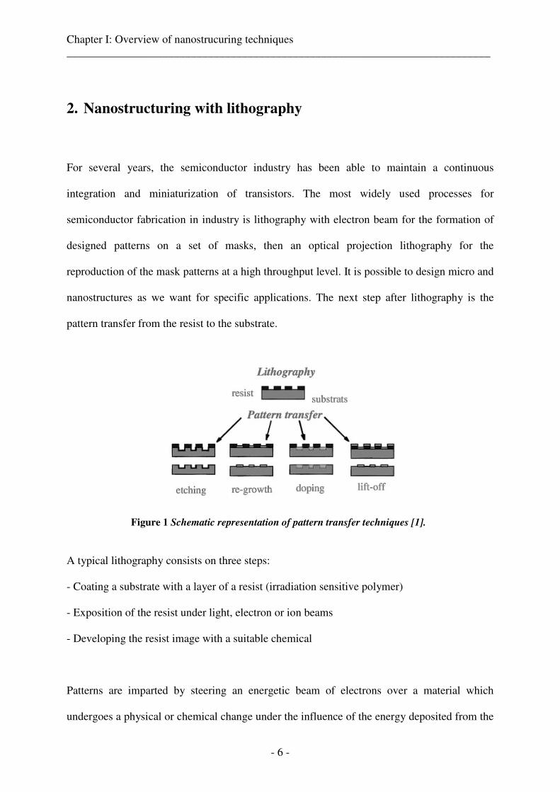
2. Nanostructuring with lithography
For several years, the semiconductor industry has been able to maintain a continuous
integration and miniaturization of transistors. The most widely used processes for
semiconductor fabrication in industry is lithography with electron beam for the formation of
designed patterns on a set of masks, then an optical projection lithography for the
reproduction of the mask patterns at a high throughput level. It is possible to design micro and
nanostructures as we want for specific applications. The next step after lithography is the
pattern transfer from the resist to the substrate.
Figure 1 Schematic representation of pattern transfer techniques [1].
A typical lithography consists on three steps:
- Coating a substrate with a layer of a resist (irradiation sensitive polymer)
- Exposition of the resist under light, electron or ion beams
- Developing the resist image with a suitable chemical
Patterns are imparted by steering an energetic beam of electrons over a material which
undergoes a physical or chemical change under the influence of the energy deposited from the
Chapter I: Overview of nanostrucuring techniques ___________________________________________________________________________
- 7 -
electron beam. The energy deposition creates a latent image in the material, also called a
resist. A chemical development washes away the exposed (positive resist) or unexposed
(negative resist) leaving the pattern wanted. Other energetic beams such as ions or photons
can be used in this way. The principle is the same but each type of beam has its own particular
set of advantages and disadvantages. For example, energetic ions deposit energy much more
locally than electrons but the shorter range of ions requires thin resists. A further disadvantage
is that the most mature ion source is gallium, a liquid metal ion, which is left behind, i.e.,
implanted, in the sample. But, and perhaps most telling, the available tooling for electron
beam lithography is much more sophisticated, which is perhaps the single-most reason it is
much more widely used.
In order to produce a tightly focused spot of electrons on the sample, highly energetic (>25
keV) beams are needed in conventional electron optical columns. However it is possible to
use very low energy beams (<100 eV) where the energy deposition can be constrained much
more locally.
Chapter I: Overview of nanostrucuring techniques ___________________________________________________________________________
- 8 -
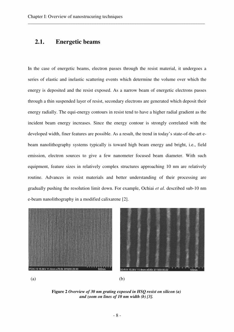
2.1. Energetic beams
In the case of energetic beams, electron passes through the resist material, it undergoes a
series of elastic and inelastic scattering events which determine the volume over which the
energy is deposited and the resist exposed. As a narrow beam of energetic electrons passes
through a thin suspended layer of resist, secondary electrons are generated which deposit their
energy radially. The equi-energy contours in resist tend to have a higher radial gradient as the
incident beam energy increases. Since the energy contour is strongly correlated with the
developed width, finer features are possible. As a result, the trend in today’s state-of-the-art e-
beam nanolithography systems typically is toward high beam energy and bright, i.e., field
emission, electron sources to give a few nanometer focused beam diameter. With such
equipment, feature sizes in relatively complex structures approaching 10 nm are relatively
routine. Advances in resist materials and better understanding of their processing are
gradually pushing the resolution limit down. For example, Ochiai et al. described sub-10 nm
e-beam nanolithography in a modified calixarene [2].
Figure 2 Overview of 30 nm grating exposed in HSQ resist on silicon (a)
and zoom on lines of 10 nm width (b) [3].
(b) (a)
Chapter I: Overview of nanostrucuring techniques ___________________________________________________________________________
- 9 -
2.2. Low energetic beams
The detrimental effect of electron scattering has led many researchers to consider using very
low energy primary electrons as a way of mitigating the resolution degradation caused by
inelastic electron scattering. Various techniques have been and, no doubt, will continue to be
explored in this context. Most of the early work on the advantages of the low energy e-beam
approach used the scanning tunnelling microscope (STM) and/or atomic force microscope
(AFM) as electron sources to perform resist exposure [4]. These experiments demonstrated
the advantages of such an approach. In addition, a number of other nanofabrication techniques
based on proximal probes have been identified. These include selective oxidation [6], [7],
field ionization [8], field induced evaporation [9], indentation [10], and chemical etching [11].
Industrial applications need fast, reliable and cost-effective techniques. Optical projection
lithography with deep UV light is now used. As next generation lithography, several non-
optical techniques have been developed including extreme UV, X-ray lithography and
projection lithography with either ions or electrons.
2.3. Extreme UV lithography
Extreme UV lithography refers to the exposure technique developed with 13,4 nm radiation
and a reflective reduction system [12]. For this selective wavelength, the radiation is obtained
from laser-induced plasmas or synchrotron radiation. The radiation is first projected on the
reflective mask with a couple of mirrors acting as the condenser. Then, it is focused with
Chapter I: Overview of nanostrucuring techniques ___________________________________________________________________________
- 10 -
another mirror system onto the wafer. The advantage of extreme UV lithography relies on its
projection configuration and its high potentiality for several generation manufacturing.
Fabrication of 100 nm line-and-space and 70 nm isolated lines have already been
demonstrated [13].
2.4. X-ray lithography
For smaller wavelengths ranging from 0.5 to 4 nm (soft X-rays), no materials can be used for
the construction of a projection system but a shadow technique is relevant. A typical X-ray
mask consists of 2 µm thick membrane of silicon carbide and absorber features of heavy
metals such as Au, W, or Ta. The resolution of X-ray lithography is defined by the Fresnel
diffraction and the diffusion of photoelectrons in the resist. From 50 nm to 30 nm lines were
reproduced. The X-ray lithography is nearly ready for industrial use [14] [15] [16] but some
technical issues remain open such as the mechanical and radiation stability of the masks, the
avaibility of high throughput e-beam systems for mask making, and the reliability of high
accuracy alignment.
2.5. Imprint lithography
The need for a simple parallel ‘‘printing’’ method capable of filling the 10–100 nm gap has
caused a rapid proliferation in the variety of imprint lithographic techniques. These methods
hold great promise as flexible, high resolution, replication methods. Most prominent among
these methods are stamping methods or ‘‘soft lithography’’ such as microcontact printing [17]
Chapter I: Overview of nanostrucuring techniques ___________________________________________________________________________
- 11 -
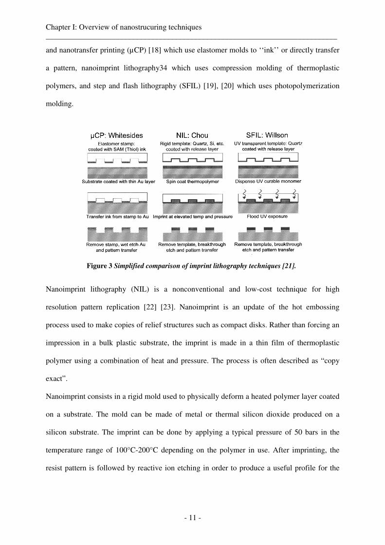
and nanotransfer printing (µCP) [18] which use elastomer molds to ‘‘ink’’ or directly transfer
a pattern, nanoimprint lithography34 which uses compression molding of thermoplastic
polymers, and step and flash lithography (SFIL) [19], [20] which uses photopolymerization
molding.
Figure 3 Simplified comparison of imprint lithography techniques [21].
Nanoimprint lithography (NIL) is a nonconventional and low-cost technique for high
resolution pattern replication [22] [23]. Nanoimprint is an update of the hot embossing
process used to make copies of relief structures such as compact disks. Rather than forcing an
impression in a bulk plastic substrate, the imprint is made in a thin film of thermoplastic
polymer using a combination of heat and pressure. The process is often described as “copy
exact”.
Nanoimprint consists in a rigid mold used to physically deform a heated polymer layer coated
on a substrate. The mold can be made of metal or thermal silicon dioxide produced on a
silicon substrate. The imprint can be done by applying a typical pressure of 50 bars in the
temperature range of 100°C-200°C depending on the polymer in use. After imprinting, the
resist pattern is followed by reactive ion etching in order to produce a useful profile for the
Chapter I: Overview of nanostrucuring techniques ___________________________________________________________________________
- 12 -
subsequent hard material pattern transfer. The mold can be re-used many times without
damage. Structures as small as 6 nm can be produced [23].
2.6. Laser stereolithography
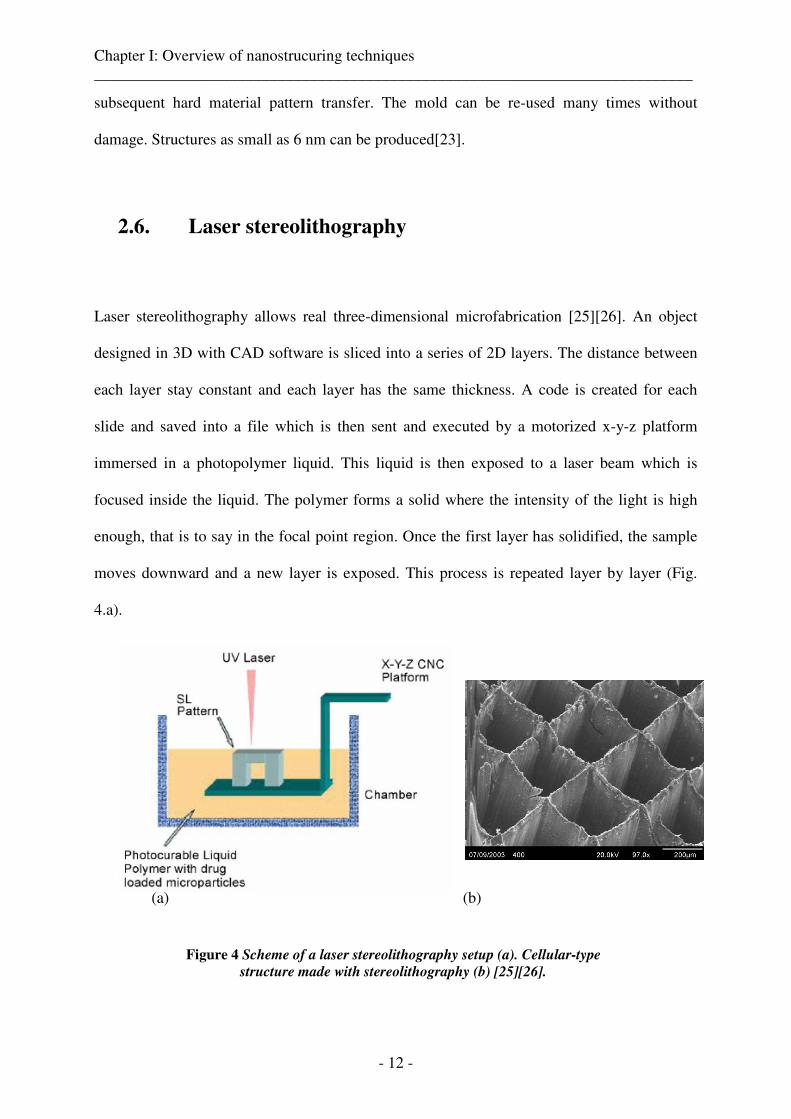
Laser stereolithography allows real three-dimensional microfabrication [25] [26]. An object
designed in 3D with CAD software is sliced into a series of 2D layers. The distance between
each layer stay constant and each layer has the same thickness. A code is created for each
slide and saved into a file which is then sent and executed by a motorized x-y-z platform
immersed in a photopolymer liquid. This liquid is then exposed to a laser beam which is
focused inside the liquid. The polymer forms a solid where the intensity of the light is high
enough, that is to say in the focal point region. Once the first layer has solidified, the sample
moves downward and a new layer is exposed. This process is repeated layer by layer (Fig.
4.a).
Figure 4 Scheme of a laser stereolithography setup (a). Cellular-type
structure made with stereolithography (b) [25] [26].
(a) (b)
Chapter I: Overview of nanostrucuring techniques ___________________________________________________________________________
- 13 -
This process enables complex internal structures such as curved surfaces, or passageways
with high accuracy. This tool is very useful for fabrication of cellular structure (Fig. 4.b)
composed of vertical walls with a 400 µm interline spacing and a thichness < 800 nm. It is
also possible to control the spatial distribution of fluorescein and rhodamine microparticles
inside a polymer layer. This kind of structures is very used in biological researches on cell
adhesion or cell growth in specific conditions.
Lithography enables to reach up to sizes of fabrication down to tens of nanometers. This
technology of micro/nano fabrication can be applied on big surfaces and consequently allows
a high throughput level of production. However, this technology is not very flexible. In
another hand, we can see that in the case of stereolithography, such small sizes are reached
thanks to laser. Indeed, in this example size of the feature depends on optical parameters such
as wavelength, focusing strength and on the interaction of the laser beam with the polymer.
This put the laser to the front of the nanofabrication stage. Laser process is not known to
fabricate nanostructures with a high throughput level but brings more flexibility. Pulsed lasers
are used for machining. High repetition rate lasers enable to increase machining speed while
preserving same sizes of machining.
Chapter I: Overview of nanostrucuring techniques ___________________________________________________________________________
- 14 -
3. Laser approach
Advantages of laser processing is to be a noncontact and flexible setup that can operate in air,
vacuum or liquid environment, making it very attractive as manufacturing tool in many
applications. Lasers can be easily focused down to the micrometer scale. These advantages
are exploited extensively in modern microelectronics industries applications such as marking,
drilling, annealing and surface modification. As a concrete example, wafer singulation is one
of the key processes in microelectronics production lines using laser microfabrication to
separate thousands of integrated circuits on wafers. The dicing technique using a fast diamond
saw rotating over the wafer surface usually causes chipping and cracking of the thin wafers.
There are also technical difficulties in separating different and multilayered substrates such as
glass, sapphire, diamond, and glass/Si/glass multilayered device structures [26].
Pulsed lasers are a good solution to these problems. Short laser pulses ablation is a fast and
explosive process useful for removal of substrate materials thanks to the possibility to focus a
laser beam down to few micrometers. The heat-affected zone (HAZ), which depends on the
pulse duration and the light absorption depth, can be limited to a small volume. Currently, the
shortest pulse duration available are produced by femtosecond laser. These lasers can delivers
laser pulses with duration down to few tens of femtoseconds. This kind of laser is a good
solution for micro and nanomachining because of the specificity of the interaction. Indeed,
such short pulses interacting with a material induce a very small heat-affected zone which
allows to machine down to sub-micrometer sizes. The whole femtosecond technology is based
on this originality of the interaction.
Chapter I: Overview of nanostrucuring techniques ___________________________________________________________________________
- 15 -
3.1. Physical aspect of interaction for ultrafast pulses
This section discusses about femtosecond pulse accuracy and of the phenomena of the
interaction of femtosecond laser pulses with a metal. A presentation of the phenomena is
described as a function of the time, for each instant from the absorption of the pulse until the
removal of material. A solid can be described as a network of ions surrounded by an electron
cloud in which each electron is more or less connected, depending more or less on the
conductive nature of the material. We focus primarily on the case of metals which have a high
conductivity due to their quasi-free electrons. These quasi-free electrons absorb linearly
energy of the incident photons in a quasi-instantaneous time (<1 fs). This radiation is
absorbed on a thin surface layer whose thickness is of the order of the inverse of the linear
absorption coefficient. The electrons acquire energy and their temperature rises very quickly.
The interest of pulses in the order of hundred femtoseconds is that their duration is shorter
than the energy transfer duration from electronic network to the network of ions, typically
from 1 to 10 ps, which means that the evolution of ionic and electronic dynamics are
decoupled. It has to be noticed that for pulses of duration in the order of picosecond or
nanosecond, this decoupling is neglected because the energy transfer occurs in a few
picoseconds. The solid is formed of a gas of hot electrons surrounding an ion in which the
temperature is still at its initial value. This fast increase in temperature is equivalent to a
thermal shock.
Chapter I: Overview of nanostrucuring techniques ___________________________________________________________________________
- 16 -
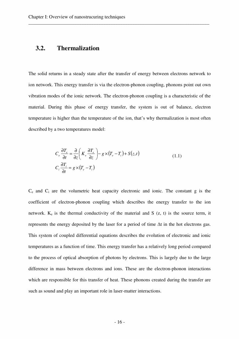
3.2. Thermalization
The solid returns in a steady state after the transfer of energy between electrons network to
ion network. This energy transfer is via the electron-phonon coupling, phonons point out own
vibration modes of the ionic network. The electron-phonon coupling is a characteristic of the
material. During this phase of energy transfer, the system is out of balance, electron
temperature is higher than the temperature of the ion, that’s why thermalization is most often
described by a two temperatures model:
( ) ( )
( )ie
i
i
ie
e
e
e
e
TTgt
TC
tzSTTgz
TK
zt
TC
−×=∂
∂
+−×−
∂
∂
∂
∂=
∂
∂,
Ce and Ci are the volumetric heat capacity electronic and ionic. The constant g is the
coefficient of electron-phonon coupling which describes the energy transfer to the ion
network. Ke is the thermal conductivity of the material and S (z, t) is the source term, it
represents the energy deposited by the laser for a period of time ∆t in the hot electrons gas.
This system of coupled differential equations describes the evolution of electronic and ionic
temperatures as a function of time. This energy transfer has a relatively long period compared
to the process of optical absorption of photons by electrons. This is largely due to the large
difference in mass between electrons and ions. These are the electron-phonon interactions
which are responsible for this transfer of heat. These phonons created during the transfer are
such as sound and play an important role in laser-matter interactions.
(1.1)
Chapter I: Overview of nanostrucuring techniques ___________________________________________________________________________
- 17 -
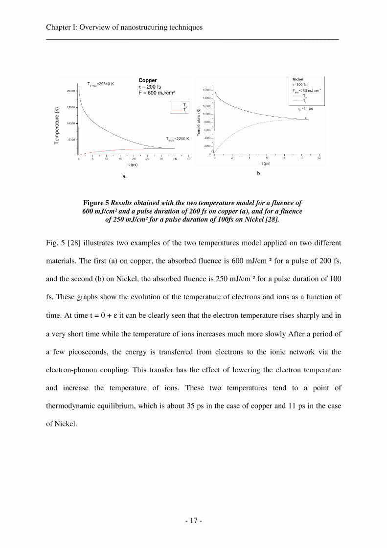
Figure 5 Results obtained with the two temperature model for a fluence of
600 mJ/cm² and a pulse duration of 200 fs on copper (a), and for a fluence
of 250 mJ/cm² for a pulse duration of 100fs on Nickel [28].
Fig. 5 [28] illustrates two examples of the two temperatures model applied on two different
materials. The first (a) on copper, the absorbed fluence is 600 mJ/cm ² for a pulse of 200 fs,
and the second (b) on Nickel, the absorbed fluence is 250 mJ/cm ² for a pulse duration of 100
fs. These graphs show the evolution of the temperature of electrons and ions as a function of
time. At time t = 0 + ε it can be clearly seen that the electron temperature rises sharply and in
a very short time while the temperature of ions increases much more slowly After a period of
a few picoseconds, the energy is transferred from electrons to the ionic network via the
electron-phonon coupling. This transfer has the effect of lowering the electron temperature
and increase the temperature of ions. These two temperatures tend to a point of
thermodynamic equilibrium, which is about 35 ps in the case of copper and 11 ps in the case
of Nickel.
Copper
Tem
pera
ture
(k)
Copper
τ = 200 fs F = 600 mJ/cm²
Chapter I: Overview of nanostrucuring techniques ___________________________________________________________________________
- 18 -
3.3. Femtosecond pulses and longer pulses (ps or ns)
In the case of a longer pulse, we are talking here of a pulse whose duration is higher than the
thermalization time of the solid, there is also a change in the material. But this change is
governed by a classical heat deposition to electrons, the impulse is longer so the energy
deposition is accompanied at the same time by a heat transfer between electrons and ions.
Throughout the duration of the pulse, the electrons and the crystal remain in thermodynamical
equilibrium. This type of long interaction is purely thermal. This process explains the
difference in quality machining achieved with femtosecond pulses and nanosecond pulses.
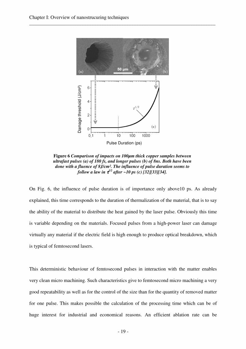
The following figure illustrates the difference between two impacts made on a sheet of copper
100 µm thick at a fluence of 8 J/cm ², with a pulse of 180 fs (a) and a pulse of 8 ns (b) [105]
and the evolution of the influence of pulse duration on the threshold of damage (c). According
to this curve, for pulses longer than ~10 ps, we see clearly the increase of the influence of
pulse duration that would follow a law in τ1/2 as verified by many experiments [29] , where τ
is the pulse duration.
Chapter I: Overview of nanostrucuring techniques ___________________________________________________________________________
- 19 -
Figure 6 Comparison of impacts on 100µm thick copper samples between
ultrafast pulses (a) of 180 fs, and longer pulses (b) of 8ns. Both have been
done with a fluence of 8J/cm². The influence of pulse duration seems to
follow a law in ττττ1/2 after ~10 ps (c) [32] [33] [34].
On Fig. 6, the influence of pulse duration is of importance only above10 ps. As already
explained, this time corresponds to the duration of thermalization of the material, that is to say
the ability of the material to distribute the heat gained by the laser pulse. Obviously this time
is variable depending on the materials. Focused pulses from a high-power laser can damage
virtually any material if the electric field is high enough to produce optical breakdown, which
is typical of femtosecond lasers.
This deterministic behaviour of femtosecond pulses in interaction with the matter enables
very clean micro machining. Such characteristics give to femtosecond micro machining a very
good repeatability as well as for the control of the size than for the quantity of removed matter
for one pulse. This makes possible the calculation of the processing time which can be of
huge interest for industrial and economical reasons. An efficient ablation rate can be
Pulse Duration (ps)
Dam
age t
hre
sho
ld (
J/c
m²)

Chapter I: Overview of nanostrucuring techniques ___________________________________________________________________________
- 20 -
determined for each material, in a corresponding fluence range [97] [98] [99] [100] [97]. This
deterministic behaviour offers the possibility to decrease machining sizes down to sub
micrometric scales. Such small sizes are reachable by pulses with very small energy in order
to be close to the threshold of the matter. This range of energy is very easy to reach with high
repetition rate lasers with a good control of the amount of the energy per pulse down to nano
joule.
Chapter I: Overview of nanostrucuring techniques ___________________________________________________________________________
- 21 -
3.4. UV laser micromachining
Most of materials absorb light more strongly as the optical wavelength decreases. Many
polymers, crystals and metals that either highly transmit or reflect light for wavelengths in
infrared and visible range, absorb strongly in the UV range. This means that the penetration
depth is small. This allows a very fine control of the drilling depth. Another benefit of
ultraviolet lasers is that they can be focused into a spot of the order of its wavelength. Indeed,
this is due to the linear dependence of the minimum feature size and the wavelength [35].
UV wavelengths correspond to high energy photons (3-7 eV) [36] can be used to break the
chemical bonds especially for plastics. Indeed polymers absorb ultraviolet light of sufficiently
short wavelength. The material escapes as small particles and gaz. This is considered as “cold
cutting”, and so very few damage are observed to surrounding material. However, for metals
even more energy is required. Moreover, electrons absorb first the laser pulse energy and
transform it into heat which leads to the melting and the evaporation of the metal.
That’s why femtosecond lasers are another good option. Pulse durations are so short that
many photons are delivered on a time that electrons are hit by several photons simultaneously.
This kind of absorption has the same effect than absorption of one photon of higher energy.
This brings the benefit to lower the importance of the wavelength, because the energy is
transferred by several photons simultaneously. This gives an advantage for ultrafast lasers.
Indeed, these lasers do not need specific optics to operate with.
Chapter I: Overview of nanostrucuring techniques ___________________________________________________________________________
- 22 -
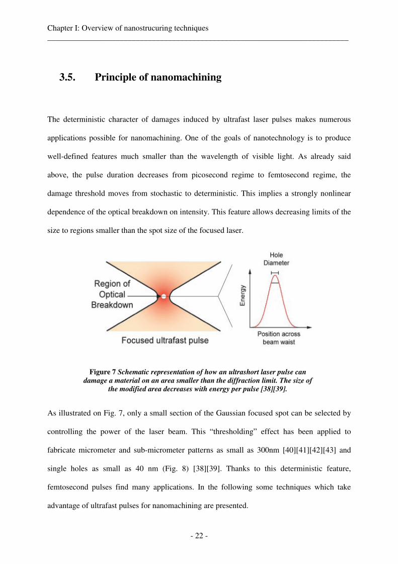
3.5. Principle of nanomachining
The deterministic character of damages induced by ultrafast laser pulses makes numerous
applications possible for nanomachining. One of the goals of nanotechnology is to produce
well-defined features much smaller than the wavelength of visible light. As already said
above, the pulse duration decreases from picosecond regime to femtosecond regime, the
damage threshold moves from stochastic to deterministic. This implies a strongly nonlinear
dependence of the optical breakdown on intensity. This feature allows decreasing limits of the
size to regions smaller than the spot size of the focused laser.
Figure 7 Schematic representation of how an ultrashort laser pulse can
damage a material on an area smaller than the diffraction limit. The size of
the modified area decreases with energy per pulse [38] [39].
As illustrated on Fig. 7, only a small section of the Gaussian focused spot can be selected by
controlling the power of the laser beam. This “thresholding” effect has been applied to
fabricate micrometer and sub-micrometer patterns as small as 300nm [40] [41] [42] [43] and
single holes as small as 40 nm (Fig. 8) [38] [39]. Thanks to this deterministic feature,
femtosecond pulses find many applications. In the following some techniques which take
advantage of ultrafast pulses for nanomachining are presented.
Chapter I: Overview of nanostrucuring techniques ___________________________________________________________________________
- 23 -
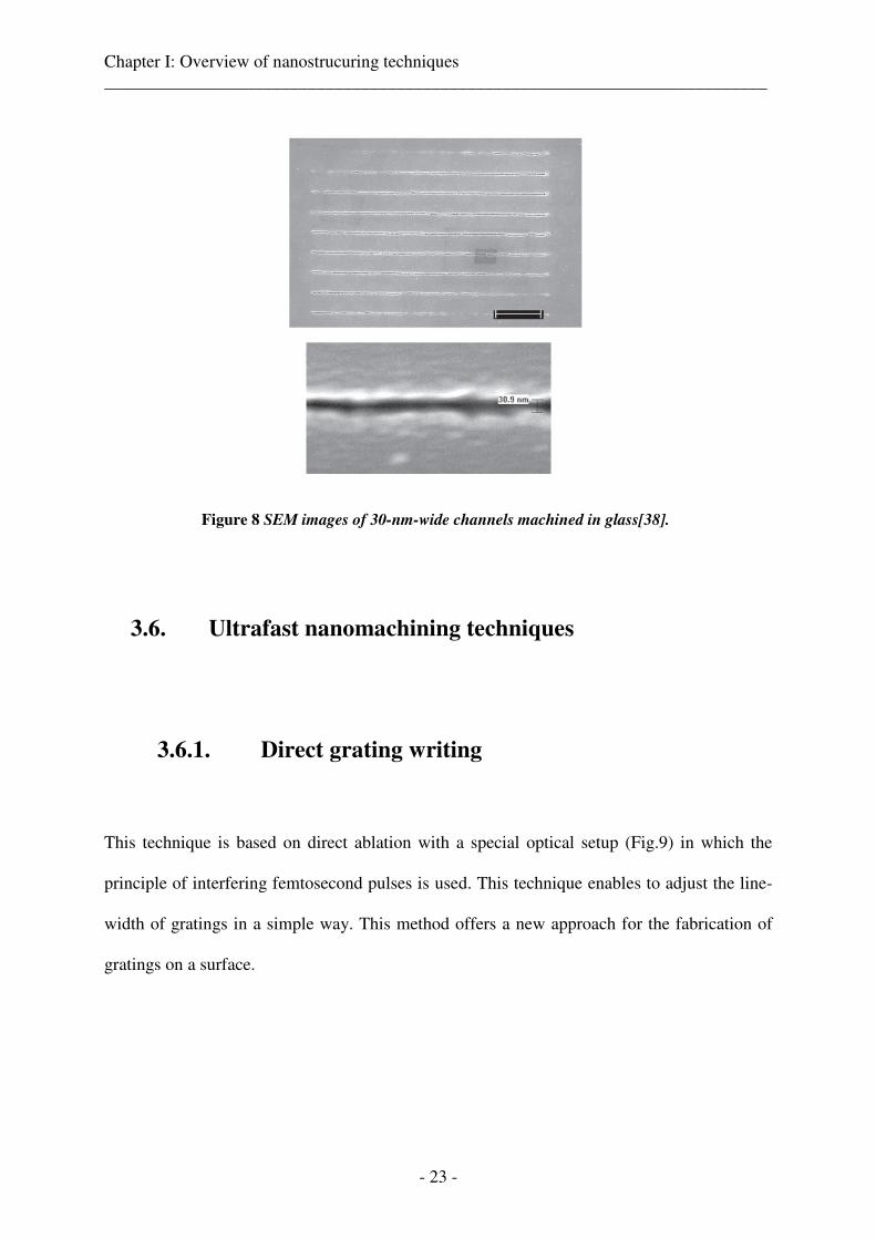
Figure 8 SEM images of 30-nm-wide channels machined in glass [38].
3.6. Ultrafast nanomachining techniques
3.6.1. Direct grating writing
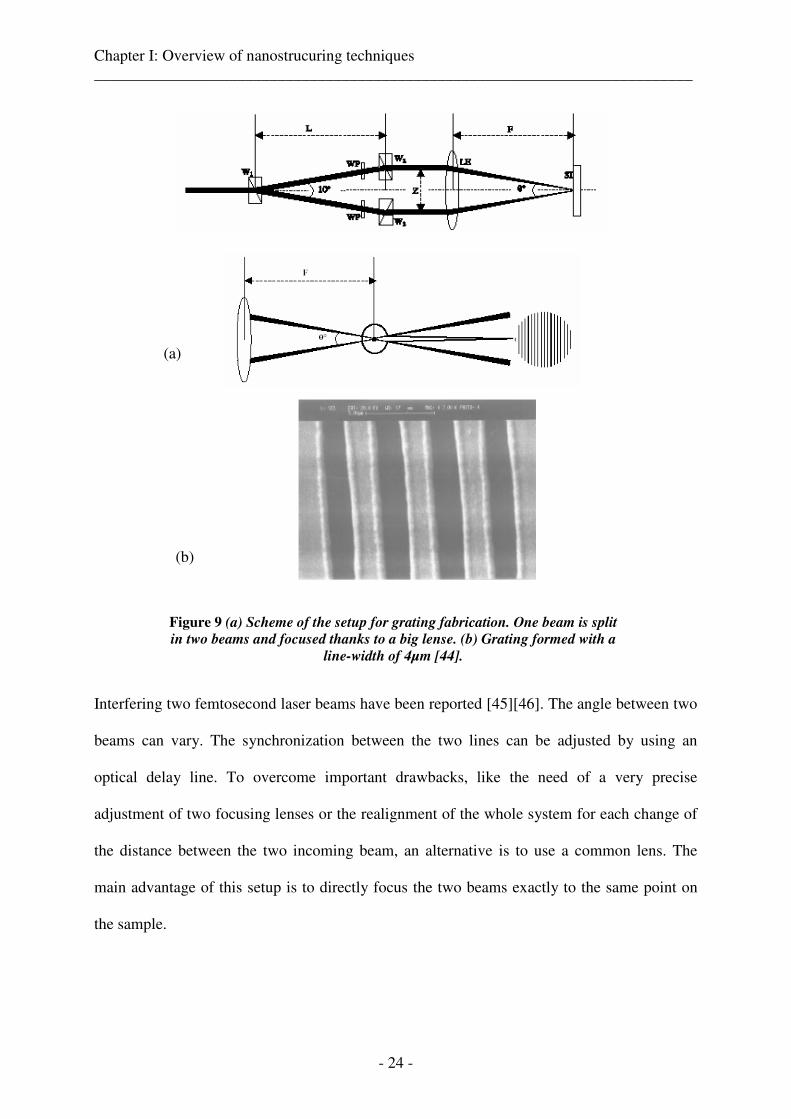
This technique is based on direct ablation with a special optical setup (Fig.9) in which the
principle of interfering femtosecond pulses is used. This technique enables to adjust the line-
width of gratings in a simple way. This method offers a new approach for the fabrication of
gratings on a surface.
Chapter I: Overview of nanostrucuring techniques ___________________________________________________________________________
- 24 -
Figure 9 (a) Scheme of the setup for grating fabrication. One beam is split
in two beams and focused thanks to a big lense. (b) Grating formed with a
line-width of 4µm [44].
Interfering two femtosecond laser beams have been reported [45] [46]. The angle between two
beams can vary. The synchronization between the two lines can be adjusted by using an
optical delay line. To overcome important drawbacks, like the need of a very precise
adjustment of two focusing lenses or the realignment of the whole system for each change of
the distance between the two incoming beam, an alternative is to use a common lens. The
main advantage of this setup is to directly focus the two beams exactly to the same point on
the sample.
(a)
(b)
Chapter I: Overview of nanostrucuring techniques ___________________________________________________________________________
- 25 -
3.6.2. Illumination of an atomic microscope tip
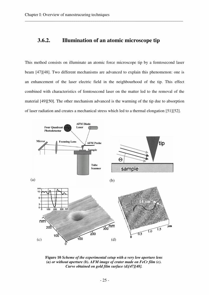
This method consists on illuminate an atomic force microscope tip by a femtosecond laser
beam [47] [48]. Two different mechanisms are advanced to explain this phenomenon: one is
an enhancement of the laser electric field in the neighbourhood of the tip. This effect
combined with characteristics of femtosecond laser on the matter led to the removal of the
material [49] [50]. The other mechanism advanced is the warming of the tip due to absorption
of laser radiation and creates a mechanical stress which led to a thermal elongation [51] [52].
Figure 10 Scheme of the experimental setup with a very low aperture lens
(a) or without aperture (b). AFM image of crater made on FeCr film (c).
Curve obtained on gold film surface (d) [47] [48].
(c) (d)
(b)
(a)
Chapter I: Overview of nanostrucuring techniques ___________________________________________________________________________
- 26 -
This technique enables to produce complex shapes like curves (Fig. 10.d), grid patterns, with
a constant width less than 20 nm. This process combines advantages of femtosecond laser
pulses with accuracy of atomic force microscope. Spacing can be done with a very high
accuracy. This technique can be improved to multi-array structure with several tips. Thanks to
the very high confinement of the tip on the surface, scattering should not be significant. A
spatial resolution less than 10 nm has been demonstrated on a thin gold film.
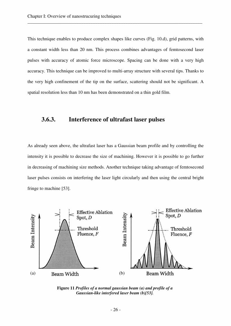
3.6.3. Interference of ultrafast laser pulses
As already seen above, the ultrafast laser has a Gaussian beam profile and by controlling the
intensity it is possible to decrease the size of machining. However it is possible to go further
in decreasing of machining size methods. Another technique taking advantage of femtosecond
laser pulses consists on interfering the laser light circularly and then using the central bright
fringe to machine [53].
Figure 11 Profiles of a normal gaussian beam (a) and profile of a
Gaussian-like interfered laser beam (b) [53].
(a) (b)
Chapter I: Overview of nanostrucuring techniques ___________________________________________________________________________
- 27 -
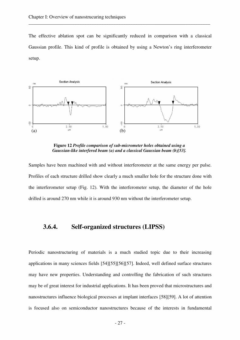
The effective ablation spot can be significantly reduced in comparison with a classical
Gaussian profile. This kind of profile is obtained by using a Newton’s ring interferometer
setup.
Figure 12 Profile comparison of sub-micrometer holes obtained using a
Gaussian-like interfered beam (a) and a classical Gaussian beam (b) [53].
Samples have been machined with and without interferometer at the same energy per pulse.
Profiles of each structure drilled show clearly a much smaller hole for the structure done with
the interferometer setup (Fig. 12). With the interferometer setup, the diameter of the hole
drilled is around 270 nm while it is around 930 nm without the interferometer setup.
3.6.4. Self-organized structures (LIPSS)
Periodic nanostructuring of materials is a much studied topic due to their increasing
applications in many sciences fields [54] [55] [56] [57]. Indeed, well defined surface structures
may have new properties. Understanding and controlling the fabrication of such structures
may be of great interest for industrial applications. It has been proved that microstructures and
nanostructures influence biological processes at implant interfaces [58] [59]. A lot of attention
is focused also on semiconductor nanostructures because of the interests in fundamental
(a) (b)
Chapter I: Overview of nanostrucuring techniques ___________________________________________________________________________
- 28 -
physics as well as the great potential for industrial applications. For example, nanostructuring
of ZnO which is a promising material for a broad range of high technology applications such
as field emission, UV light-emitting diodes, piezo-electric devices, nanoresonators and
biosensors [60] [61] [62]. The development of simple and reliable methods to control the
morphology of self assembled nanostructures is a huge challenge. As we saw in a previous
paragraph, methods to form nanostructures mainly use electron beam lithography,
nanoimprint lithography, or chemical methods [63] [64] but the possibility to do
nanostructures with lasers is now well known. In the past, surface structures were produced
using long-pulse lasers, including nanosecond Nd:YAG laser, copper vapour laser,
nanosecond excimer lasers.
The formation of ripples has been observed long time ago by many researchers who study the
interaction between intense lasers and material with a power laser beam near or equal to the
threshold of damage. The formation of a pattern of damage similar to a grating, resulting from
the illumination of a single laser beam of high intensity, has often been observed on the
surfaces of metals, dielectrics and semiconductors. These observations were made with both
continuous lasers and with pulsed lasers. We saw that most patterns are similar and
independent of material properties. When the beam arrives at a normal incidence to the
surface of the material, the damage appears as parallel and periodical lines. The period is in
the range of the wavelength of the beam.
Several explanations for such periodic damage have been advanced based on the properties of
the laser beam [65] [66], or surface acoustic waves [67], or condensation of plasmon
[68] [69] [70] [71]. We also noticed that the orientation of the ripples depends strongly on the
polarization of the incident laser beam. These observations have made a model evolved
Chapter I: Overview of nanostrucuring techniques ___________________________________________________________________________
- 29 -
explaining the formation of ripples as a result of inhomogeneity in the energy arriving, which
could be due to interference between the incident laser beam and a surface wave scattered
maybe from a scratch on the surface of the material [72] [73]. Indeed fringes created nearly a
scratch have been observed, suggesting that roughness plays a role in the creation of periodic
structures. Interference creates the energy arriving directly translated into a variation of
ablation depth and the structure of ripples is an image of the interference pattern. The
frequency modulation pattern of ripples is controlled by the wavelength of the incident beam,
the angle of incidence and taking into account the refractive index of the material, it is given
by the formula:
( )θ
λ
sin1±=Λ
n
This model was applied for years to explain the observations of different kinds of periodic
structures. However this model does not take into account certain structures generated more
or less in contradiction with this model, such as bifurcations in the lines of ripples, sinuous
structures or the formation of cones.
Recently much attention is paid to formation of LIPSS with ultrafast lasers. In general, the
pulse lengths are shorter than the assumed time of ablation. However structures are always
observed [74] [75] As in previous observations, two different systems of ripples appear
perpendicular to each other which one of them has a characteristic size smaller than the
wavelength.
As already demonstrated, ripples with large ridges and grooves very narrow were obtained
and the structures of cones auto-arranged in two dimensions [77] [78] [79]. Most experiments
were made with linear polarization. The orientation of structures is strongly dependent on
polarization, fine ripples are always formed perpendicular to the electric field of the beam
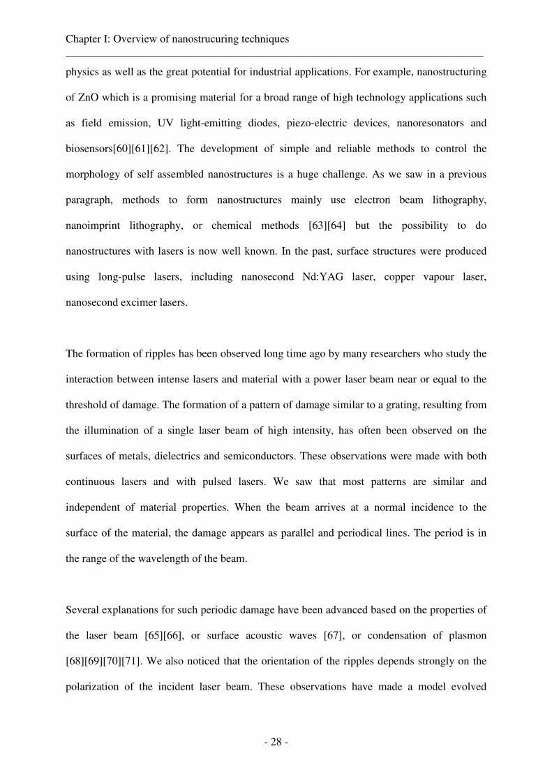
[76] (Fig.13)
((1.2)
Chapter I: Overview of nanostrucuring techniques ___________________________________________________________________________
- 30 -
Figure 13 Two systems of ripples perpendicular to each other. The laser
polarization is given by the double arrow. This result has been obtained
with a Ti:Sapphire laser with a wavelength of 800 nm on BaF2 [76].
.
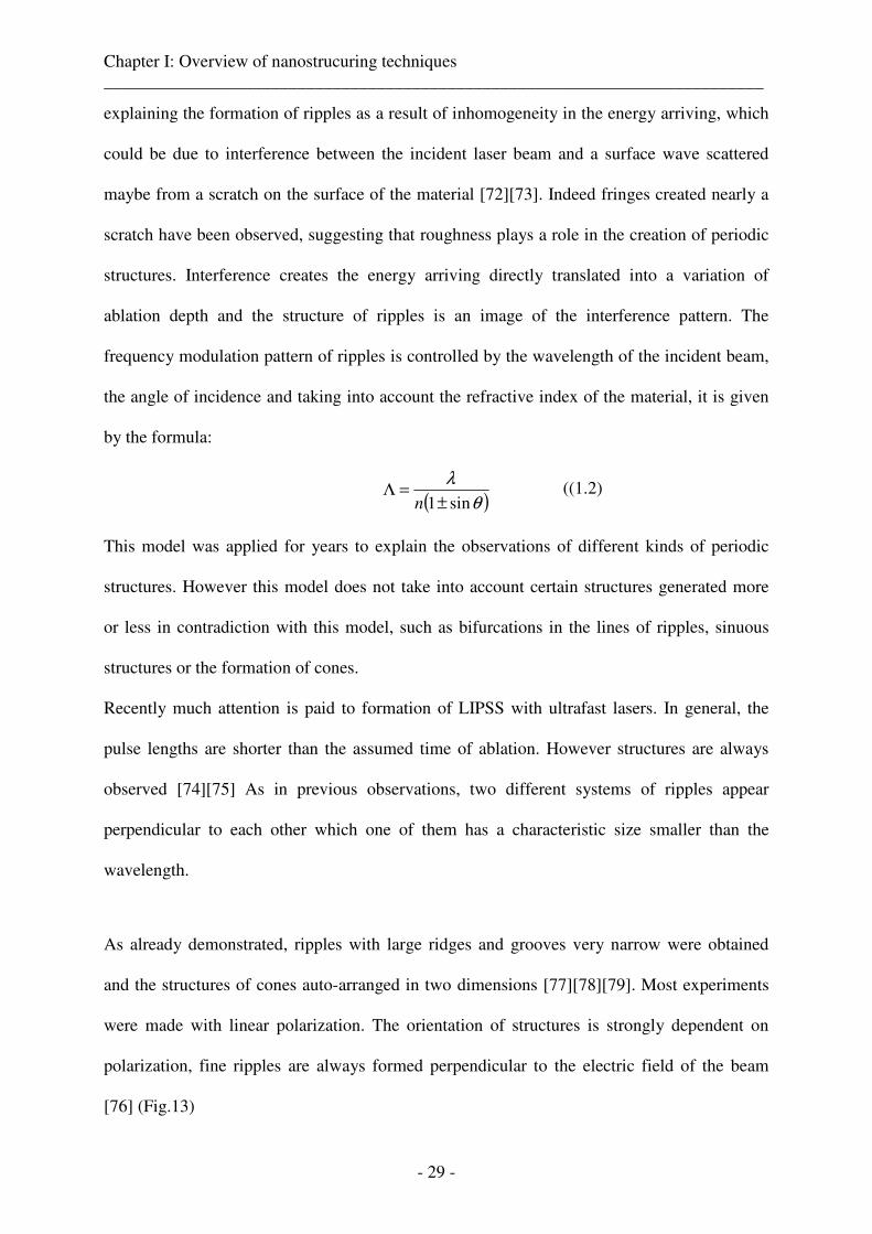
Figure 14 Arrows indicate the polarization’s orientation of the beam
respectively of 0° (a), 40° (b) and 90° (c). The dependence of the
orientation of ripples on the polarization is obvious. Notice that in the
picture (a) there are both coarse and fine ripples oriented in the same
direction. Fine ripples are on the edge of the crater, coarse ripples are in
the center [76].
Fig. 14 shows fine ripples on the crater edge, and coarse ripples in the center of the crater
where the beam intensity is the highest. The period of ripples depends on the intensity, but in
a non-continuous way. In the centre of the crater, period of ripples is approximately 10 times
Chapter I: Overview of nanostrucuring techniques ___________________________________________________________________________
- 31 -
higher than the ripples from the edge. In many experiments no influence of the wavelength or
angle of incidence was observed over the period of ripples. However periodic structures have
also been obtained under the effect of ion bombardment [80]. These structures have
approximately the same size as the ripples obtained under laser irradiation [81] [82] [83]. This
result brought the idea of self-organization of matter from instabilities [75].
To summarize, in the current state of our knowledge, several physical phenomena are
responsible for the formation of ripples. Firstly, when a laser pulse hit the surface of a
material, the electric field E interacts with the surface electrons vibrate at the same frequency
than the laser wave. Then the energy is absorbed by the ionic network which is accompanied
by a sudden increase in temperature, pressure waves are formed, the material arrives in
unstable states which gives way to a phenomenon of nucleation, with formation of cavities or
bubbles that may appear in the material. Then a self-organization is set up comparable with
the ripples observed on the sand dunes. This effect of self-organization currently remains to
be explained and is the subject of extensive research in order to approach a global
understanding of the phenomenon.
Chapter I: Overview of nanostrucuring techniques ___________________________________________________________________________
- 32 -
4. Effect of heat accumulation: theoretical approach
The use of high repetition rate lasers asks the question to know if the interaction with the
matter is the same than with low repetition rate lasers, around kilohertz, such as amplified
laser systems. The next paragraph gives a theoretical approach of the interaction and tries to
answer this question.
In order to have a better understanding of the interaction at high repetition rates, it is possible
to use results obtained from a simulation program. For instance a code is developed in our
laboratory by Jean-Philippe Colombier [84] [85] [86].
4.1. Description of the simulation code
This code has been developed in collaboration with the CEA Saclay (Commissariat à
l’Energie Atomique). Its applications are oriented to study materials behaviour when they are
excited by an ultra fast laser pulse. The approach of fluids’ dynamics is based on multi-phase
states equations of the material. The absorption of the electromagnetic energy is taken into
account by this code named “ESTHER” by the heating of the material through several steps.
In a first step, the resolve of the Helmholtz equation enables to determine the electromagnetic
field in the illuminated area by the laser. This resolve takes into account the amplitude of the
electric field, the frequency of the laser and the complex conductivity of the material.
Chapter I: Overview of nanostrucuring techniques ___________________________________________________________________________
- 33 -
As previously said in paragraph (3.1), the electromagnetic energy is absorbed by electrons of
conduction. This energy is stacked in the electronic system and redistributed in electron-
electron collisions. Three types of collisions occur: electron-electron, electron-ion, and
electron-phonon. All of them describe the thermalization process, particularly the collisions
electron-phonon which contributes to the heating of the crystalline network. The effect of the
energy absorption on optical properties is taken into account step by step in order to reproduce
in the most realistic way the laser-matter coupling. The two temperatures model describes the
thermal forwarding of the energy from electrons to the ionic network.
Ultrafast irradiation is associated with the decoupling between electronic and ionic
temperatures. It makes necessary to introduce specific electronic parameters. It so supposed
that free electrons follows a thermal distribution law during the interaction. The Fermi-dirac
distribution is used to determine electronic properties (energy, pressure and calorific capacity)
depending on the density and the temperature. These parameters make possible to write
hydrodynamics equations in there Lagrangian form not only for the ionic system but also by
taking into account the contribution of the electronic system. These equations are coupled
with multi-phase state equations which represents the studied material in order to reproduce
the changing process of this material after a laser irradiation. In particular, simulations give
thermodynamic paths of the matter through the pressure, the density and the temperature also
by taking into account possible effects in relation with the non-equilibrium regime of first
times of the irradiation. So a wide spectrum of states is available thanks to this code.
Chapter I: Overview of nanostrucuring techniques ___________________________________________________________________________
- 34 -
4.2. Results for heat accumulation
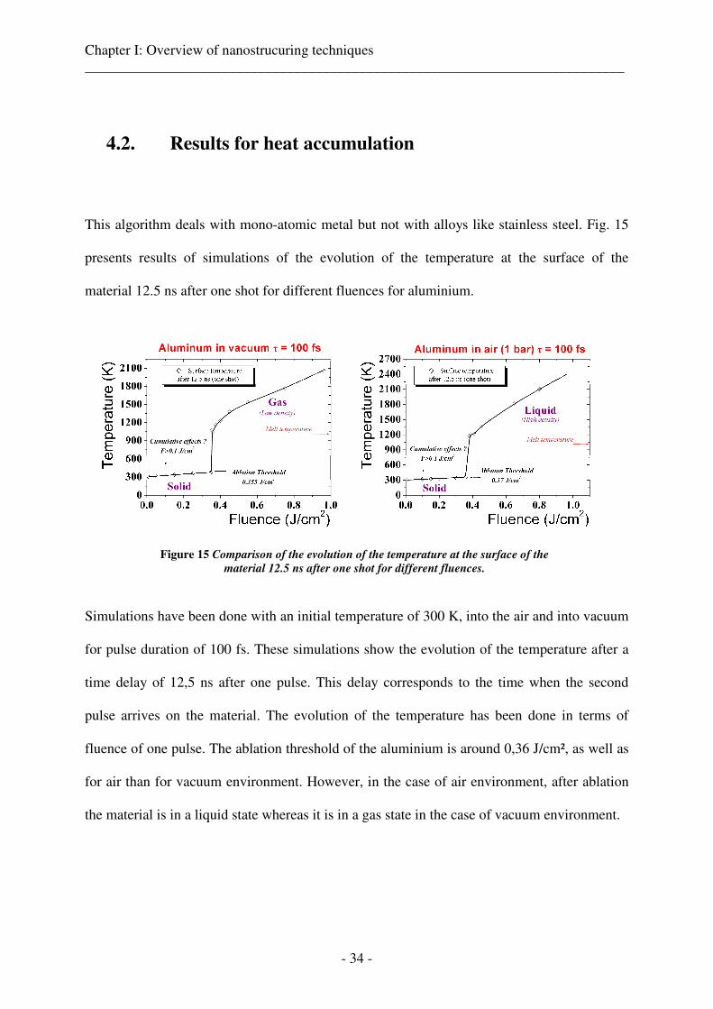
This algorithm deals with mono-atomic metal but not with alloys like stainless steel. Fig. 15
presents results of simulations of the evolution of the temperature at the surface of the
material 12.5 ns after one shot for different fluences for aluminium.
Figure 15 Comparison of the evolution of the temperature at the surface of the
material 12.5 ns after one shot for different fluences.
Simulations have been done with an initial temperature of 300 K, into the air and into vacuum
for pulse duration of 100 fs. These simulations show the evolution of the temperature after a
time delay of 12,5 ns after one pulse. This delay corresponds to the time when the second
pulse arrives on the material. The evolution of the temperature has been done in terms of
fluence of one pulse. The ablation threshold of the aluminium is around 0,36 J/cm², as well as
for air than for vacuum environment. However, in the case of air environment, after ablation
the material is in a liquid state whereas it is in a gas state in the case of vacuum environment.
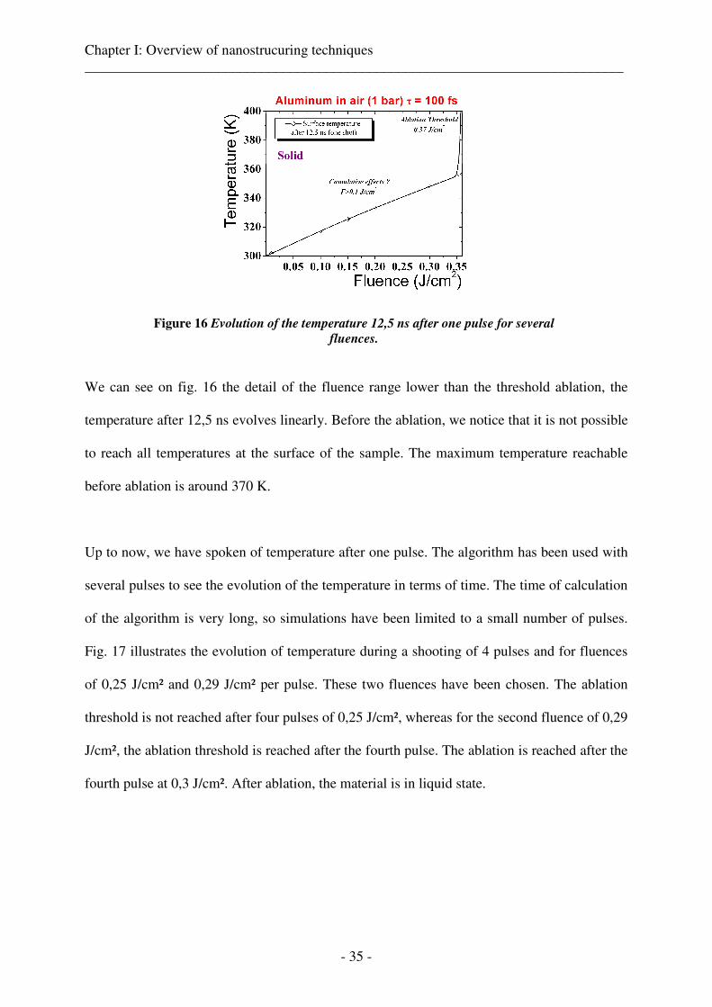
Chapter I: Overview of nanostrucuring techniques ___________________________________________________________________________
- 35 -
Figure 16 Evolution of the temperature 12,5 ns after one pulse for several
fluences.
We can see on fig. 16 the detail of the fluence range lower than the threshold ablation, the
temperature after 12,5 ns evolves linearly. Before the ablation, we notice that it is not possible
to reach all temperatures at the surface of the sample. The maximum temperature reachable
before ablation is around 370 K.
Up to now, we have spoken of temperature after one pulse. The algorithm has been used with
several pulses to see the evolution of the temperature in terms of time. The time of calculation
of the algorithm is very long, so simulations have been limited to a small number of pulses.
Fig. 17 illustrates the evolution of temperature during a shooting of 4 pulses and for fluences
of 0,25 J/cm² and 0,29 J/cm² per pulse. These two fluences have been chosen. The ablation
threshold is not reached after four pulses of 0,25 J/cm², whereas for the second fluence of 0,29
J/cm², the ablation threshold is reached after the fourth pulse. The ablation is reached after the
fourth pulse at 0,3 J/cm². After ablation, the material is in liquid state.
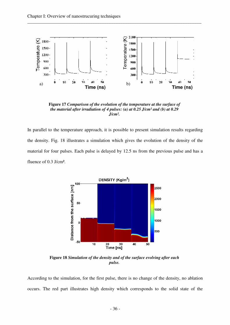
Chapter I: Overview of nanostrucuring techniques ___________________________________________________________________________
- 36 -
Figure 17 Comparison of the evolution of the temperature at the surface of
the material after irradiation of 4 pulses: (a) at 0.25 J/cm² and (b) at 0.29
J/cm².
In parallel to the temperature approach, it is possible to present simulation results regarding
the density. Fig. 18 illustrates a simulation which gives the evolution of the density of the
material for four pulses. Each pulse is delayed by 12.5 ns from the previous pulse and has a
fluence of 0.3 J/cm².
Figure 18 Simulation of the density and of the surface evolving after each
pulse.
According to the simulation, for the first pulse, there is no change of the density, no ablation
occurs. The red part illustrates high density which corresponds to the solid state of the
a) b) Time (ns) Time (ns)
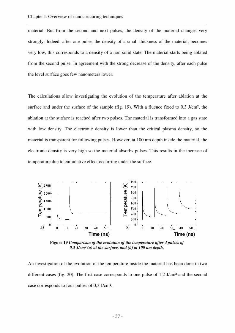
Chapter I: Overview of nanostrucuring techniques ___________________________________________________________________________
- 37 -
material. But from the second and next pulses, the density of the material changes very
strongly. Indeed, after one pulse, the density of a small thickness of the material, becomes
very low, this corresponds to a density of a non-solid state. The material starts being ablated
from the second pulse. In agreement with the strong decrease of the density, after each pulse
the level surface goes few nanometers lower.
The calculations allow investigating the evolution of the temperature after ablation at the
surface and under the surface of the sample (fig. 19). With a fluence fixed to 0,3 J/cm², the
ablation at the surface is reached after two pulses. The material is transformed into a gas state
with low density. The electronic density is lower than the critical plasma density, so the
material is transparent for following pulses. However, at 100 nm depth inside the material, the
electronic density is very high so the material absorbs pulses. This results in the increase of
temperature due to cumulative effect occurring under the surface.
Figure 19 Comparison of the evolution of the temperature after 4 pulses of
0.3 J/cm² (a) at the surface, and (b) at 100 nm depth.
An investigation of the evolution of the temperature inside the material has been done in two
different cases (fig. 20). The first case corresponds to one pulse of 1,2 J/cm² and the second
case corresponds to four pulses of 0,3 J/cm².
Time (ns) Time (ns)
a) b)
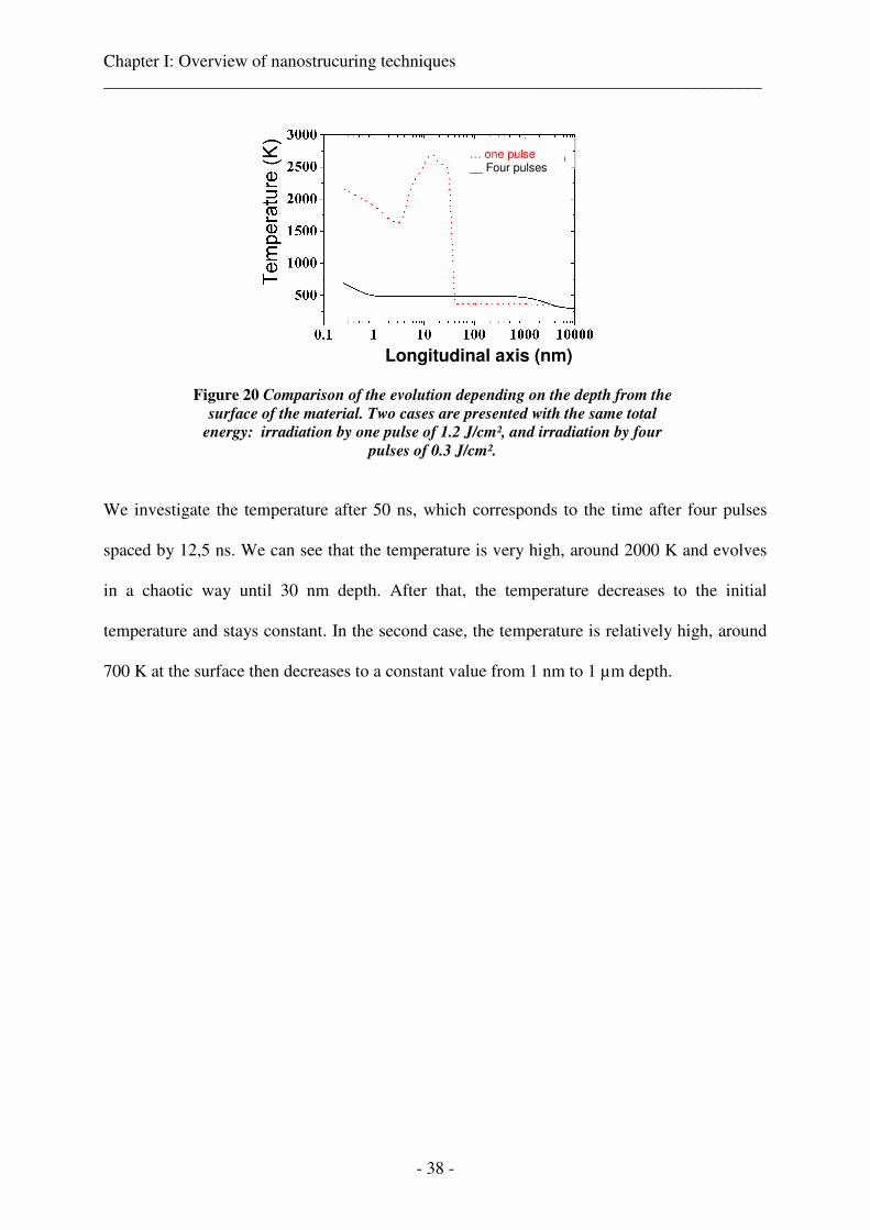
Chapter I: Overview of nanostrucuring techniques ___________________________________________________________________________
- 38 -
Figure 20 Comparison of the evolution depending on the depth from the
surface of the material. Two cases are presented with the same total
energy: irradiation by one pulse of 1.2 J/cm², and irradiation by four
pulses of 0.3 J/cm².
We investigate the temperature after 50 ns, which corresponds to the time after four pulses
spaced by 12,5 ns. We can see that the temperature is very high, around 2000 K and evolves
in a chaotic way until 30 nm depth. After that, the temperature decreases to the initial
temperature and stays constant. In the second case, the temperature is relatively high, around
700 K at the surface then decreases to a constant value from 1 nm to 1 µm depth.
Longitudinal axis (nm)
… one pulse __ Four pulses
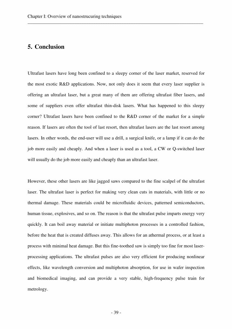
Chapter I: Overview of nanostrucuring techniques ___________________________________________________________________________
- 39 -
5. Conclusion
Ultrafast lasers have long been confined to a sleepy corner of the laser market, reserved for
the most exotic R&D applications. Now, not only does it seem that every laser supplier is
offering an ultrafast laser, but a great many of them are offering ultrafast fiber lasers, and
some of suppliers even offer ultrafast thin-disk lasers. What has happened to this sleepy
corner? Ultrafast lasers have been confined to the R&D corner of the market for a simple
reason. If lasers are often the tool of last resort, then ultrafast lasers are the last resort among
lasers. In other words, the end-user will use a drill, a surgical knife, or a lamp if it can do the
job more easily and cheaply. And when a laser is used as a tool, a CW or Q-switched laser
will usually do the job more easily and cheaply than an ultrafast laser.
However, these other lasers are like jagged saws compared to the fine scalpel of the ultrafast
laser. The ultrafast laser is perfect for making very clean cuts in materials, with little or no
thermal damage. These materials could be microfluidic devices, patterned semiconductors,
human tissue, explosives, and so on. The reason is that the ultrafast pulse imparts energy very
quickly. It can boil away material or initiate multiphoton processes in a controlled fashion,
before the heat that is created diffuses away. This allows for an athermal process, or at least a
process with minimal heat damage. But this fine-toothed saw is simply too fine for most laser-
processing applications. The ultrafast pulses are also very efficient for producing nonlinear
effects, like wavelength conversion and multiphoton absorption, for use in wafer inspection
and biomedical imaging, and can provide a very stable, high-frequency pulse train for
metrology.
Chapter I: Overview of nanostrucuring techniques ___________________________________________________________________________
- 40 -
We have attempted to do a comparison between several techniques for nanofabrication. In
material processing, patterns are generated either via lithography that implies the use of
masks, or via direct writing that implies to use a multi axis translation stages. The specific
area of direct writing, where the sample or the laser beam moves, has the capability to
increase the resolution to sub micron to nanometer dimensions. We see that these two
technologies are competing. Indeed, they reach equivalent size of patterns but with different
advantages. Indeed the specificity of the interaction of femtosecond pulses with a material
allows doing micro/nano machining, micro/nano surgery, multiphotonic imaging, and also 3D
machining thanks to multiphoton photopolymerization.
The work presented here concerns the development of a tool allowing multiple applications.
This tool has been developed in order to simplify and to make easily available benefits of
femtosecond laser pulses.
Chapter II: Development of a tool for nanostructuring and multiphoton imaging ___________________________________________________________________________
- 41 -
Chapter II
Development of a tool for
nanostructuring and multiphoton
imaging

Chapter II: Development of a tool for nanostructuring and multiphoton imaging ___________________________________________________________________________
- 42 -
Chapter II: Development of a tool for nanostructuring and multiphoton imaging ___________________________________________________________________________
- 43 -
1. Introduction
This chapter describes the development of the multifunctional tool for nanostructuring and
imaging. This development implies the implementation and control of a multitude of devices
such as translation stages, piezo driven, shutter, camera,... as well as a good knowledge in
optics engineering. Hardware and software have been intensively developed under LabVIEW
in an easy to manage and user-friendly environment. Such a flexible apparatus can be used for
a wide range of materials from metals to biological samples.
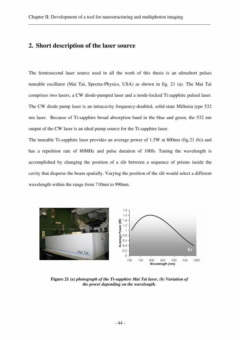
Chapter II: Development of a tool for nanostructuring and multiphoton imaging ___________________________________________________________________________
- 44 -
2. Short description of the laser source
The femtosecond laser source used in all the work of this thesis is an ultrashort pulses
tuneable oscillator (Mai Tai, Spectra-Physics, USA) as shown in fig. 21 (a). The Mai Tai
comprises two lasers, a CW diode-pumped laser and a mode-locked Ti:sapphire pulsed laser.
The CW diode pump laser is an intracavity frequency-doubled, solid-state Millenia type 532
nm laser. Because of Ti:sapphire broad absorption band in the blue and green, the 532 nm
output of the CW laser is an ideal pump source for the Ti:sapphire laser.
The tuneable Ti-sapphire laser provides an average power of 1.5W at 800nm (fig.21 (b)) and
has a repetition rate of 80MHz and pulse duration of 100fs. Tuning the wavelength is
accomplished by changing the position of a slit between a sequence of prisms inside the
cavity that disperse the beam spatially. Varying the position of the slit would select a different
wavelength within the range from 710nm to 990nm.
Figure 21 (a) photograph of the Ti-sapphire Mai Tai laser, (b) Variation of
the power depending on the wavelength.
a)
b)
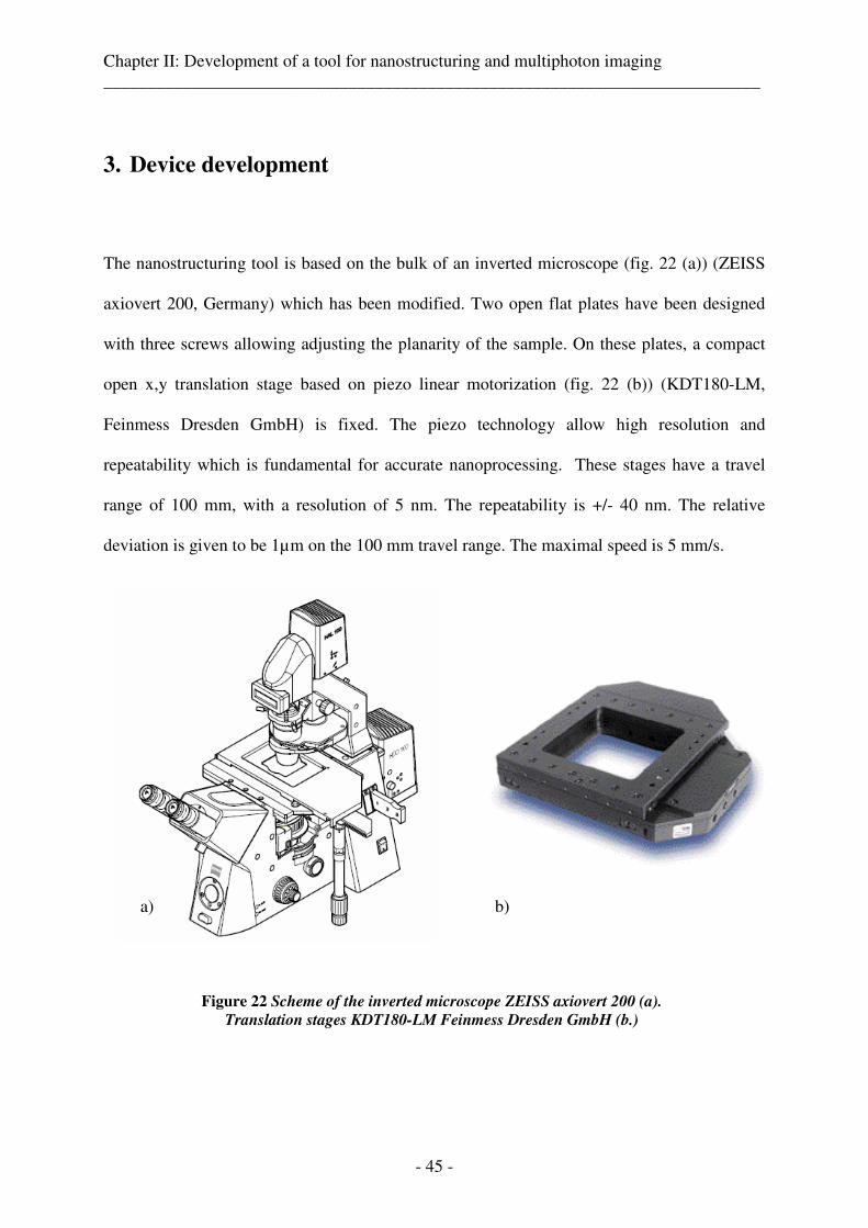
Chapter II: Development of a tool for nanostructuring and multiphoton imaging ___________________________________________________________________________
- 45 -
3. Device development
The nanostructuring tool is based on the bulk of an inverted microscope (fig. 22 (a)) (ZEISS
axiovert 200, Germany) which has been modified. Two open flat plates have been designed
with three screws allowing adjusting the planarity of the sample. On these plates, a compact
open x,y translation stage based on piezo linear motorization (fig. 22 (b)) (KDT180-LM,
Feinmess Dresden GmbH) is fixed. The piezo technology allow high resolution and
repeatability which is fundamental for accurate nanoprocessing. These stages have a travel
range of 100 mm, with a resolution of 5 nm. The repeatability is +/- 40 nm. The relative
deviation is given to be 1µm on the 100 mm travel range. The maximal speed is 5 mm/s.
Figure 22 Scheme of the inverted microscope ZEISS axiovert 200 (a).
Translation stages KDT180-LM Feinmess Dresden GmbH (b.)
a) b)
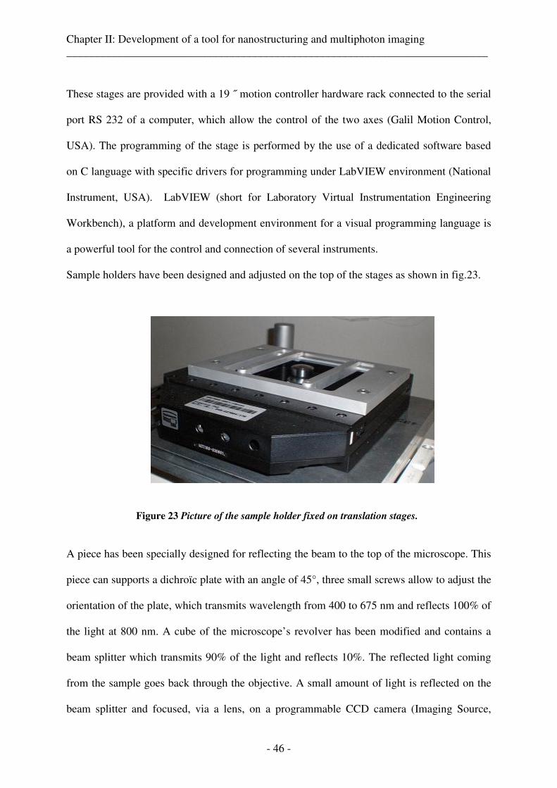
Chapter II: Development of a tool for nanostructuring and multiphoton imaging ___________________________________________________________________________
- 46 -
These stages are provided with a 19 ˝ motion controller hardware rack connected to the serial
port RS 232 of a computer, which allow the control of the two axes (Galil Motion Control,
USA). The programming of the stage is performed by the use of a dedicated software based
on C language with specific drivers for programming under LabVIEW environment (National
Instrument, USA). LabVIEW (short for Laboratory Virtual Instrumentation Engineering
Workbench), a platform and development environment for a visual programming language is
a powerful tool for the control and connection of several instruments.
Sample holders have been designed and adjusted on the top of the stages as shown in fig.23.
Figure 23 Picture of the sample holder fixed on translation stages.
A piece has been specially designed for reflecting the beam to the top of the microscope. This
piece can supports a dichroïc plate with an angle of 45°, three small screws allow to adjust the
orientation of the plate, which transmits wavelength from 400 to 675 nm and reflects 100% of
the light at 800 nm. A cube of the microscope’s revolver has been modified and contains a
beam splitter which transmits 90% of the light and reflects 10%. The reflected light coming
from the sample goes back through the objective. A small amount of light is reflected on the
beam splitter and focused, via a lens, on a programmable CCD camera (Imaging Source,
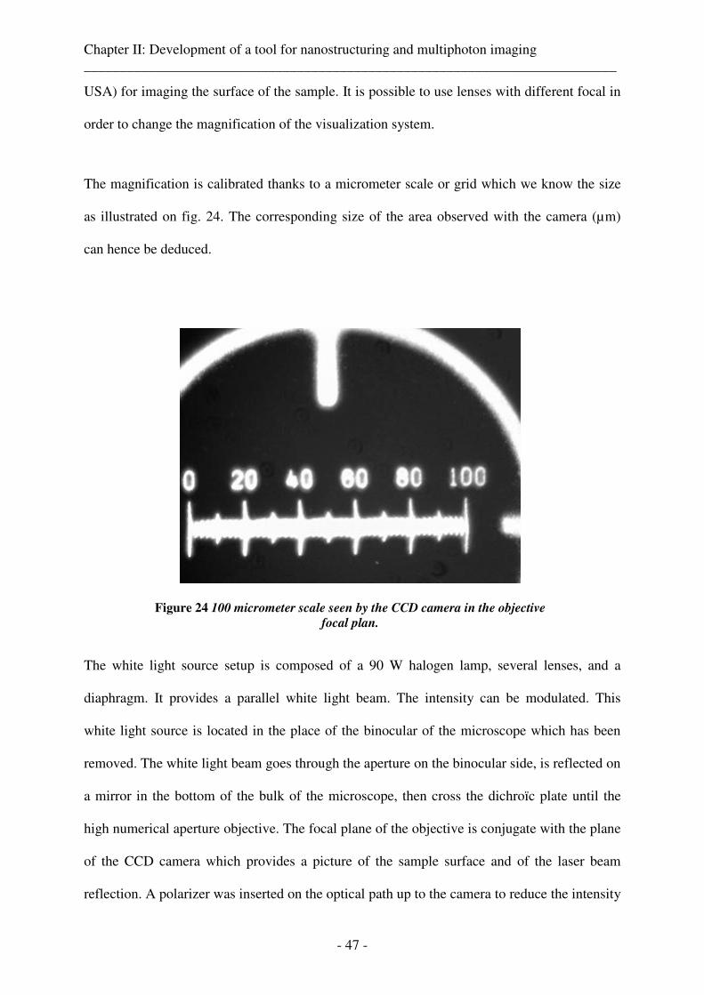
Chapter II: Development of a tool for nanostructuring and multiphoton imaging ___________________________________________________________________________
- 47 -
USA) for imaging the surface of the sample. It is possible to use lenses with different focal in
order to change the magnification of the visualization system.
The magnification is calibrated thanks to a micrometer scale or grid which we know the size
as illustrated on fig. 24. The corresponding size of the area observed with the camera (µm)
can hence be deduced.
Figure 24 100 micrometer scale seen by the CCD camera in the objective
focal plan.
The white light source setup is composed of a 90 W halogen lamp, several lenses, and a
diaphragm. It provides a parallel white light beam. The intensity can be modulated. This
white light source is located in the place of the binocular of the microscope which has been
removed. The white light beam goes through the aperture on the binocular side, is reflected on
a mirror in the bottom of the bulk of the microscope, then cross the dichroïc plate until the
high numerical aperture objective. The focal plane of the objective is conjugate with the plane
of the CCD camera which provides a picture of the sample surface and of the laser beam
reflection. A polarizer was inserted on the optical path up to the camera to reduce the intensity
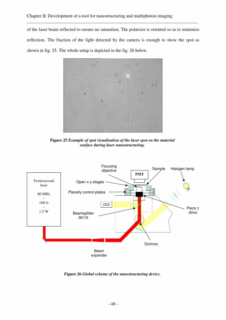
Chapter II: Development of a tool for nanostructuring and multiphoton imaging ___________________________________________________________________________
- 48 -
of the laser beam reflected to ensure no saturation. The polarizer is oriented so as to minimize
reflection. The fraction of the light detected by the camera is enough to show the spot as
shown in fig. 25. The whole setup is depicted in the fig. 26 below.
Figure 25 Example of spot visualisation of the laser spot on the material
surface during laser nanostructuring.
Figure 26 Global scheme of the nanostructuring device.
Translation stages
Planeity control plates
Halogen lamp Sample
Piezo z drive
Dichroic
Beam expander
Beamsplitter 90/10
Focusing objective
PMT
Femtosecond laser
80 MHz
– 100 fs
– 1,5 W
Open x-y stages
Planeity control plates
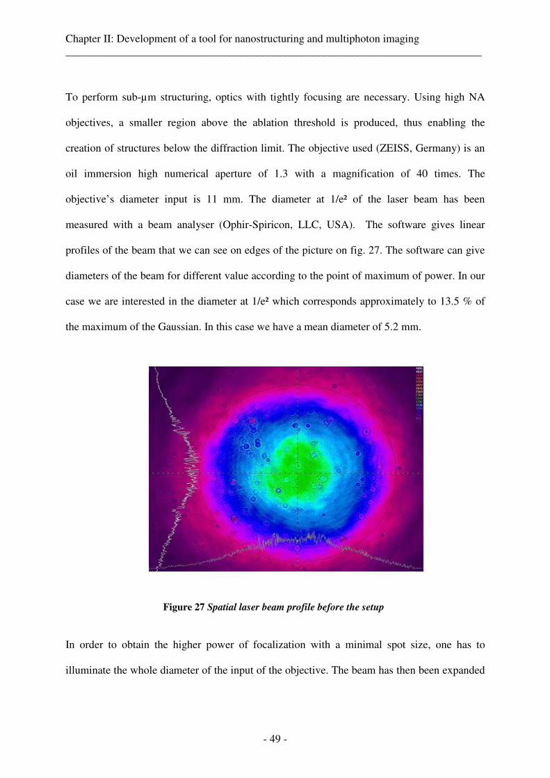
Chapter II: Development of a tool for nanostructuring and multiphoton imaging ___________________________________________________________________________
- 49 -
To perform sub-µm structuring, optics with tightly focusing are necessary. Using high NA
objectives, a smaller region above the ablation threshold is produced, thus enabling the
creation of structures below the diffraction limit. The objective used (ZEISS, Germany) is an
oil immersion high numerical aperture of 1.3 with a magnification of 40 times. The
objective’s diameter input is 11 mm. The diameter at 1/e² of the laser beam has been
measured with a beam analyser (Ophir-Spiricon, LLC, USA). The software gives linear
profiles of the beam that we can see on edges of the picture on fig. 27. The software can give
diameters of the beam for different value according to the point of maximum of power. In our
case we are interested in the diameter at 1/e² which corresponds approximately to 13.5 % of
the maximum of the Gaussian. In this case we have a mean diameter of 5.2 mm.
Figure 27 Spatial laser beam profile before the setup
In order to obtain the higher power of focalization with a minimal spot size, one has to
illuminate the whole diameter of the input of the objective. The beam has then been expanded
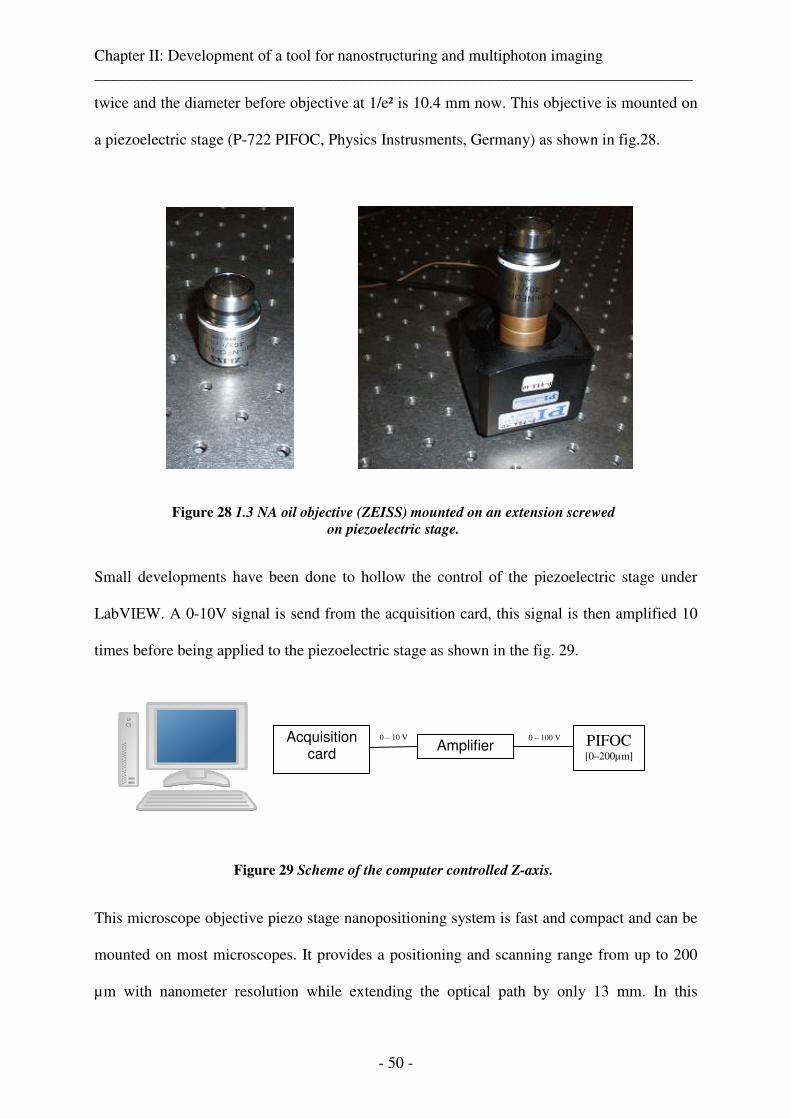
Chapter II: Development of a tool for nanostructuring and multiphoton imaging ___________________________________________________________________________
- 50 -
twice and the diameter before objective at 1/e² is 10.4 mm now. This objective is mounted on
a piezoelectric stage (P-722 PIFOC, Physics Instrusments, Germany) as shown in fig.28.
Figure 28 1.3 NA oil objective (ZEISS) mounted on an extension screwed
on piezoelectric stage.
Small developments have been done to hollow the control of the piezoelectric stage under
LabVIEW. A 0-10V signal is send from the acquisition card, this signal is then amplified 10
times before being applied to the piezoelectric stage as shown in the fig. 29.
Figure 29 Scheme of the computer controlled Z-axis.
This microscope objective piezo stage nanopositioning system is fast and compact and can be
mounted on most microscopes. It provides a positioning and scanning range from up to 200
µm with nanometer resolution while extending the optical path by only 13 mm. In this
Acquisition card
Amplifier PIFOC [0–200µm]
0 – 10 V 0 – 100 V
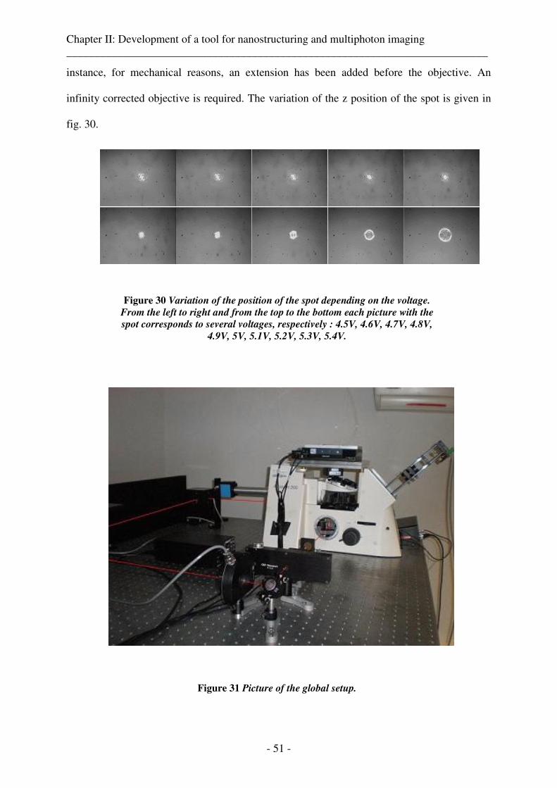
Chapter II: Development of a tool for nanostructuring and multiphoton imaging ___________________________________________________________________________
- 51 -
instance, for mechanical reasons, an extension has been added before the objective. An
infinity corrected objective is required. The variation of the z position of the spot is given in
fig. 30.
Figure 30 Variation of the position of the spot depending on the voltage.
From the left to right and from the top to the bottom each picture with the
spot corresponds to several voltages, respectively : 4.5V, 4.6V, 4.7V, 4.8V,
4.9V, 5V, 5.1V, 5.2V, 5.3V, 5.4V.
Figure 31 Picture of the global setup.

Chapter II: Development of a tool for nanostructuring and multiphoton imaging ___________________________________________________________________________
- 52 -
A picture of the global device is given in fig. 31. The setup includes a shutter (Uniblitz, USA)
which is indirectly controlled by computer via the signals generated by the controller of the
translation stage. Its exposure and delay interval range is adjustable from 1ms to 2.8 hours.
The shutter has an opening and closing time of 50 ms typically for an aperture diameter of 20
mm.
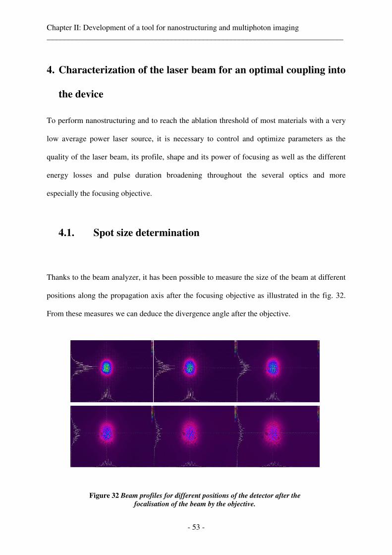
Chapter II: Development of a tool for nanostructuring and multiphoton imaging ___________________________________________________________________________
- 53 -
4. Characterization of the laser beam for an optimal coupling into
the device
To perform nanostructuring and to reach the ablation threshold of most materials with a very
low average power laser source, it is necessary to control and optimize parameters as the
quality of the laser beam, its profile, shape and its power of focusing as well as the different
energy losses and pulse duration broadening throughout the several optics and more
especially the focusing objective.
4.1. Spot size determination
Thanks to the beam analyzer, it has been possible to measure the size of the beam at different
positions along the propagation axis after the focusing objective as illustrated in the fig. 32.
From these measures we can deduce the divergence angle after the objective.
Figure 32 Beam profiles for different positions of the detector after the
focalisation of the beam by the objective.
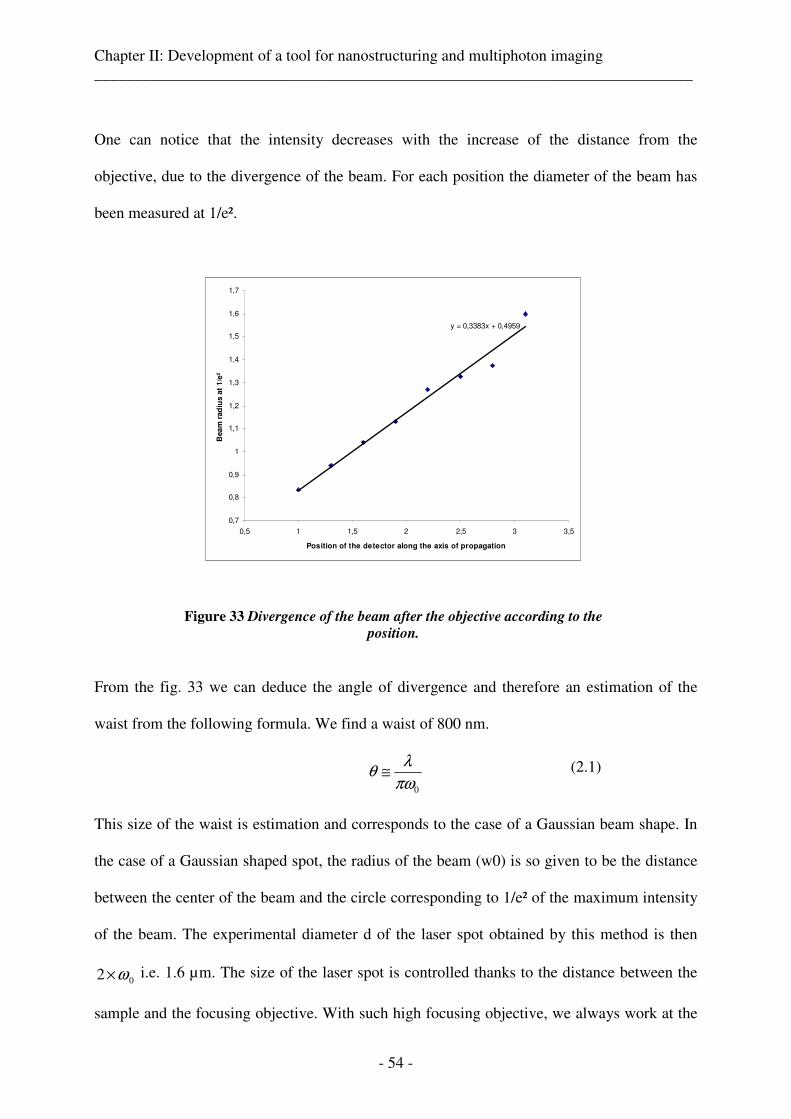
Chapter II: Development of a tool for nanostructuring and multiphoton imaging ___________________________________________________________________________
- 54 -
One can notice that the intensity decreases with the increase of the distance from the
objective, due to the divergence of the beam. For each position the diameter of the beam has
been measured at 1/e².
Figure 33 Divergence of the beam after the objective according to the
position.
From the fig. 33 we can deduce the angle of divergence and therefore an estimation of the
waist from the following formula. We find a waist of 800 nm.
0πω
λθ ≅
This size of the waist is estimation and corresponds to the case of a Gaussian beam shape. In
the case of a Gaussian shaped spot, the radius of the beam (w0) is so given to be the distance
between the center of the beam and the circle corresponding to 1/e² of the maximum intensity
of the beam. The experimental diameter d of the laser spot obtained by this method is then
02 ω× i.e. 1.6 µm. The size of the laser spot is controlled thanks to the distance between the
sample and the focusing objective. With such high focusing objective, we always work at the
y = 0,3383x + 0,4959
0,7
0,8
0,9
1
1,1
1,2
1,3
1,4
1,5
1,6
1,7
0,5 1 1,5 2 2,5 3 3,5
Position of the detector along the axis of propagation
Beam
rad
ius a
t 1/e
²
(2.1)
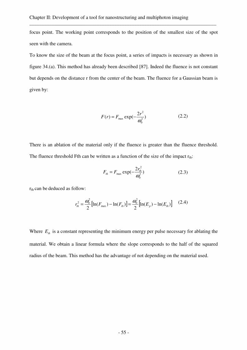
Chapter II: Development of a tool for nanostructuring and multiphoton imaging ___________________________________________________________________________
- 55 -
focus point. The working point corresponds to the position of the smallest size of the spot
seen with the camera.
To know the size of the beam at the focus point, a series of impacts is necessary as shown in
figure 34.(a). This method has already been described [87]. Indeed the fluence is not constant
but depends on the distance r from the center of the beam. The fluence for a Gaussian beam is
given by:
)2
exp()(20
2
maxω
rFrF −=
There is an ablation of the material only if the fluence is greater than the fluence threshold.
The fluence threshold Fth can be written as a function of the size of the impact rth:
)2
exp(20
2
maxω
thth
rFF −=
rth can be deduced as follow:
[ ] [ ])ln()ln(2
)ln()ln(2
20
max
202
thpthth EEFFr −=−=ωω
Where thE is a constant representing the minimum energy per pulse necessary for ablating the
material. We obtain a linear formula where the slope corresponds to the half of the squared
radius of the beam. This method has the advantage of not depending on the material used.
(2.2)
(2.3)
(2.4)
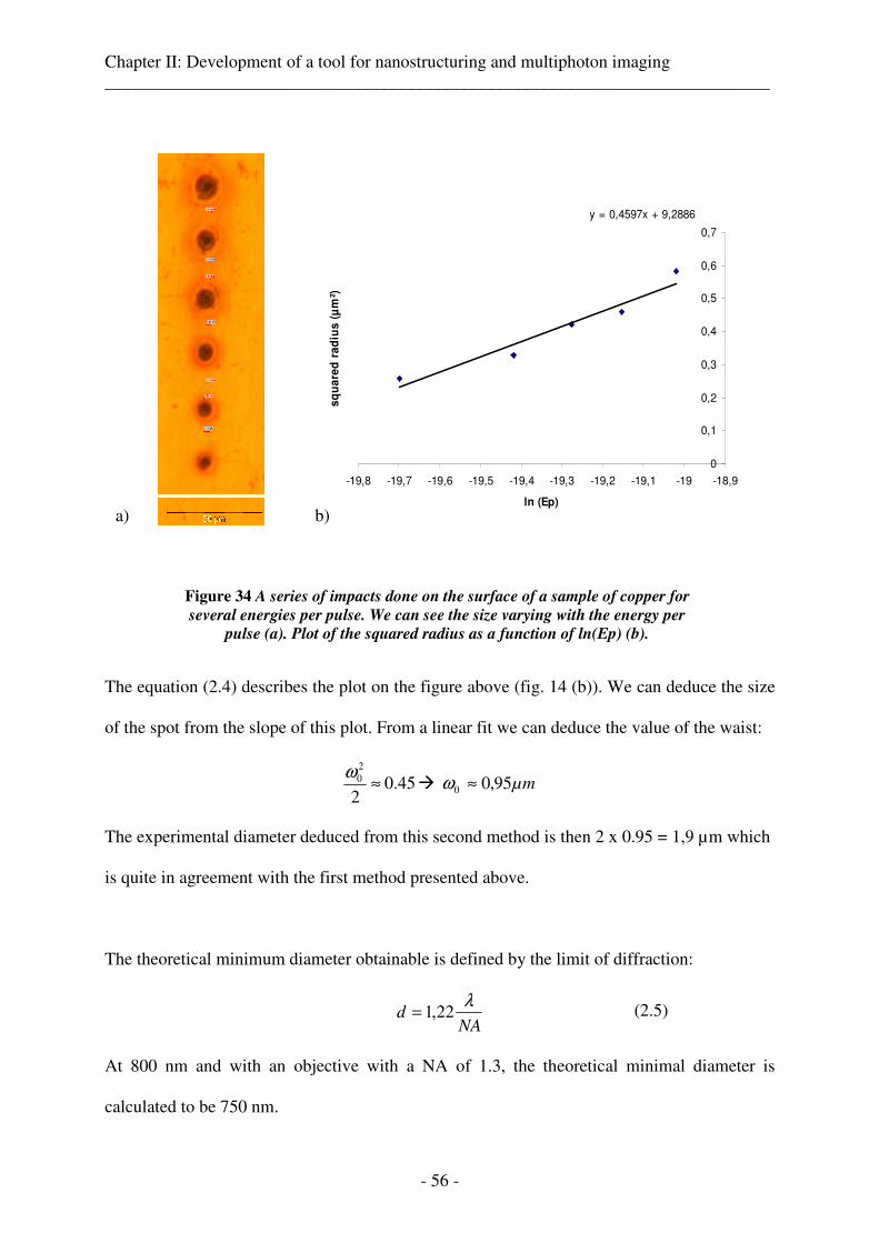
Chapter II: Development of a tool for nanostructuring and multiphoton imaging ___________________________________________________________________________
- 56 -
Figure 34 A series of impacts done on the surface of a sample of copper for
several energies per pulse. We can see the size varying with the energy per
pulse (a). Plot of the squared radius as a function of ln(Ep) (b).
The equation (2.4) describes the plot on the figure above (fig. 14 (b)). We can deduce the size
of the spot from the slope of this plot. From a linear fit we can deduce the value of the waist:
45.02
20 ≈
ω� µm95,00 ≈ω
The experimental diameter deduced from this second method is then 2 x 0.95 = 1,9 µm which
is quite in agreement with the first method presented above.
The theoretical minimum diameter obtainable is defined by the limit of diffraction:
NAd
λ22,1=
At 800 nm and with an objective with a NA of 1.3, the theoretical minimal diameter is
calculated to be 750 nm.
y = 0,4597x + 9,2886
0
0,1
0,2
0,3
0,4
0,5
0,6
0,7
-19,8 -19,7 -19,6 -19,5 -19,4 -19,3 -19,2 -19,1 -19 -18,9
ln (Ep)
sq
ua
red
ra
diu
s (
µm
²)
a) b)
(2.5)
Chapter II: Development of a tool for nanostructuring and multiphoton imaging ___________________________________________________________________________
- 57 -
The experimental results are then twice the value of the limit of diffraction. This could easily
be expected because it is very dependent on the beam and objective quality. The theoretical
estimation is provided for an ideal illumination. However, this limit of diffraction is obtained
only with a uniform intensity illumination of the pupil. As a laser beam is always Gaussian
shaped, this implies too much losses of power in order to get a uniform illumination. For
example, in the case of a Gaussian beam two times larger than the aperture diameter of the
objective, there are around 60% of losses. In order to be able to machine materials, it is
necessary to have enough energy; this is why we illuminated the objective aperture with a
beam quite smaller than the aperture as said above.
4.2. Fluence determination of a Gaussian shaped intensity
profile
All experiments have been done at the focus point of the objective such as we have a
Gaussian (Sech2) shaped intensity profile. During experiments, it is necessary to control
experimental conditions such as the fluence. The fluence is defined as a quantity of energy on
a surface (J/cm²).
S
EF
p=
With Ep the energy per pulse (J) and S the surface of the beam (cm²). It is also possible to
describe this expression as a function of laser source characteristics.
kS
PF
avg=
(2.6)
(2.7)
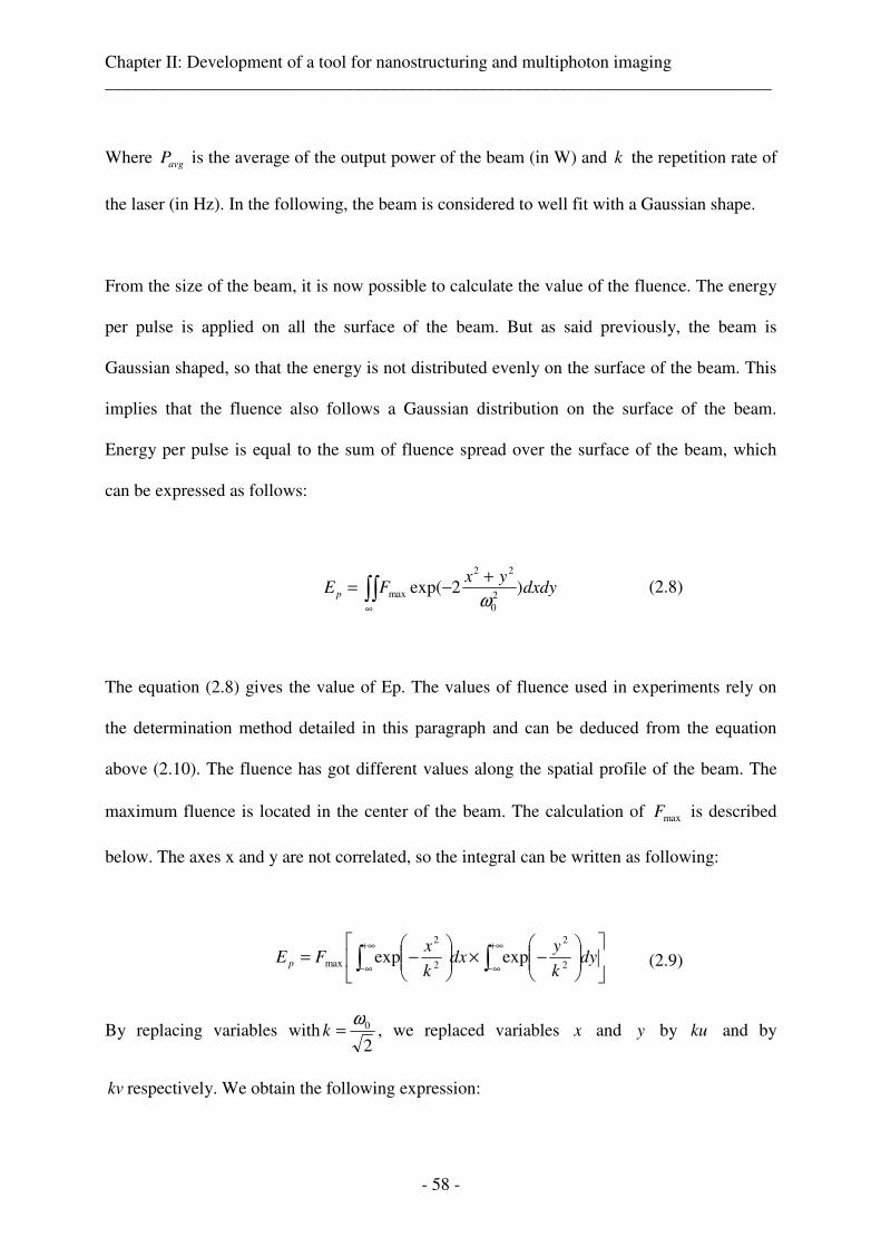
Chapter II: Development of a tool for nanostructuring and multiphoton imaging ___________________________________________________________________________
- 58 -
Where avgP is the average of the output power of the beam (in W) and k the repetition rate of
the laser (in Hz). In the following, the beam is considered to well fit with a Gaussian shape.
From the size of the beam, it is now possible to calculate the value of the fluence. The energy
per pulse is applied on all the surface of the beam. But as said previously, the beam is
Gaussian shaped, so that the energy is not distributed evenly on the surface of the beam. This
implies that the fluence also follows a Gaussian distribution on the surface of the beam.
Energy per pulse is equal to the sum of fluence spread over the surface of the beam, which
can be expressed as follows:
∫∫∞
+−= dxdy
yxFEp )2exp(
20
22
maxω
The equation (2.8) gives the value of Ep. The values of fluence used in experiments rely on
the determination method detailed in this paragraph and can be deduced from the equation
above (2.10). The fluence has got different values along the spatial profile of the beam. The
maximum fluence is located in the center of the beam. The calculation of maxF is described
below. The axes x and y are not correlated, so the integral can be written as following:
−×
−= ∫∫
∞+
∞−
∞+
∞−dy
k
ydx
k
xFE p 2
2
2
2
max expexp
By replacing variables with20ω
=k , we replaced variables x and y by ku and by
kv respectively. We obtain the following expression:
(2.8)
(2.9)
Chapter II: Development of a tool for nanostructuring and multiphoton imaging ___________________________________________________________________________
- 59 -
−×
−= ∫∫
+∞
∞−
+∞
∞−
kdvk
vkkdu
k
ukFE p 2
22
2
22
max expexp
( ) ( ) π××=
−×−×= ∫∫
+∞
∞−
+∞
∞−
2max
222max expexp kFdvvduukFE p
�20
max
2
πωpE
F =
4.3. Average power
We measured the power available at different locations of the setup. These measures have
been made with the power meter PM10 (Coherent, USA). At the entrance of the microscope
the laser beam power is 1,25 W and suffers no losses through the dichroïc. After the beam
splitter the power decreases down to 1 W, this represents 80 % of the power left. Then after
the objective, the power goes down to 710 mW. This represents 57 % of the incoming power
into the system. The global path through optical components brings 43 % of losses. The
biggest losses come from the objective, where the light crosses 4 cm thick glass. Other losses
come from the beam splitter where the light loses 10 % more than the percentage said in the
datasheet of this beam splitter.
(2.10)
(2.11)
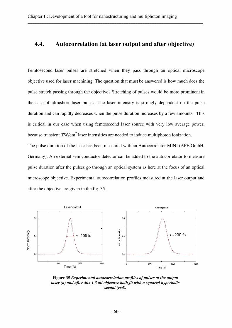
Chapter II: Development of a tool for nanostructuring and multiphoton imaging ___________________________________________________________________________
- 60 -
4.4. Autocorrelation (at laser output and after objective)
Femtosecond laser pulses are stretched when they pass through an optical microscope
objective used for laser machining. The question that must be answered is how much does the
pulse stretch passing through the objective? Stretching of pulses would be more prominent in
the case of ultrashort laser pulses. The laser intensity is strongly dependent on the pulse
duration and can rapidly decreases when the pulse duration increases by a few amounts. This
is critical in our case when using femtosecond laser source with very low average power,
because transient TW/cm2 laser intensities are needed to induce multiphoton ionization.
The pulse duration of the laser has been measured with an Autocorrelator MINI (APE GmbH,
Germany). An external semiconductor detector can be added to the autocorrelator to measure
pulse duration after the pulses go through an optical system as here at the focus of an optical
microscope objective. Experimental autocorrelation profiles measured at the laser output and
after the objective are given in the fig. 35.
Figure 35 Experimental autocorrelation profiles of pulses at the output
laser (a) and after 40x 1.3 oil objective both fit with a squared hyperbolic
secant (red).
Chapter II: Development of a tool for nanostructuring and multiphoton imaging ___________________________________________________________________________
- 61 -
The pulse duration measured at the output of the laser and after the objective at full width at
half maximum (FWHM) are respectively 155 fs and 200 fs. The intensity time profile is fit
with a hyperbolic secant squared pulse (red). For hyperbolic secant squared shaped pulses, the
autocorrelation width is 1.54 times longer than the real width of the pulse, but this conversion
factor depends on the pulse shape. Therefore, in our case the real pulse duration is defined by:
65.0×= measuredreal ττ
Thus the real pulse durations at the output of the laser and after the objective respectively are
100 fs and 150 fs.
The difference of the pulse duration before and after of the objective is 30 fs which is not
negligible but not critical to reach sufficient intensities to overcome the ablation threshold of
most of materials. If the stretching was more pronounced it would have been necessary to add
a negative pre-chirp in the laser path to reduce the dispersion of the pulses. The optical index
of a transparent material is not the same for all wavelengths. Thus, the speed of the light is not
the same inside a transparent material and depends on the wavelength. This involves a phase
difference. This phenomenon is known as Group Velocity Dispersion (GVD). The term can
also be used as a precisely defined quantity, namely the derivative of the inverse group
velocity with respect to the angular frequency (or sometimes the wavelength):
The group velocity dispersion is the group delay dispersion per unit length. The basic units
are s2/m. For example, the group velocity dispersion of silica is + 35 fs2/mm at 800 nm. After
passing through a transparent medium, the pulse duration in relation to the input pulse
duration is given by:
(2.12)
(2.13)
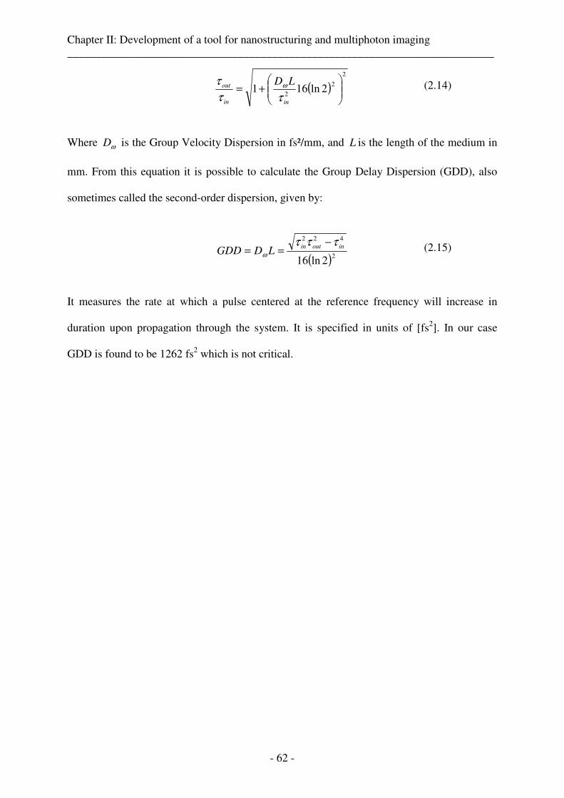
Chapter II: Development of a tool for nanostructuring and multiphoton imaging ___________________________________________________________________________
- 62 -
( )2
2
22ln161
+=
inin
out LD
ττ
τ ω
Where ωD is the Group Velocity Dispersion in fs²/mm, and L is the length of the medium in
mm. From this equation it is possible to calculate the Group Delay Dispersion (GDD), also
sometimes called the second-order dispersion, given by:
( )2
422
2ln16
inoutinLDGDD
τττω
−==
It measures the rate at which a pulse centered at the reference frequency will increase in
duration upon propagation through the system. It is specified in units of [fs2]. In our case
GDD is found to be 1262 fs2 which is not critical.
(2.14)
(2.15)
Chapter II: Development of a tool for nanostructuring and multiphoton imaging ___________________________________________________________________________
- 63 -
5. Development of an autofocus method
The configuration of the system allows the establishment of an autofocus by coupling the
position along the z axis with the camera. For each position of the objective along the z axis,
the size of the spot changes depending on the distance between the objective and the sample.
The purpose of this system is to place automatically the sample in the focus plane of the
objective.
5.1. Principle
The feedback needed for the autofocus system is provided by pictures from the camera. First
we ensure that the spot is at the center of the image. Each picture taken by the camera is kept
inside a memory buffer and used for the autofocus positioning calculation. The longitudinal
position is controlled thanks to the z piezo stage as described above. In order to reduce
calculating time, the algorithm deals with a smaller part of the picture of 512 x 512 pixels².
This part is in the center of the picture where the spot is.
5.2. The algorithm
The algorithm used is based on the calculation of the standard deviation of grey levels from
an image of the surface to find the focal point of the objective. This standard deviation is used
as the feedback signal for autofocusing. When the standard deviation is at the maximum it
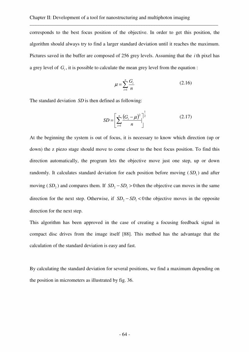
Chapter II: Development of a tool for nanostructuring and multiphoton imaging ___________________________________________________________________________
- 64 -
corresponds to the best focus position of the objective. In order to get this position, the
algorithm should always try to find a larger standard deviation until it reaches the maximum.
Pictures saved in the buffer are composed of 256 grey levels. Assuming that the i th pixel has
a grey level of iG , it is possible to calculate the mean grey level from the equation :
∑=
=n
i
i
n
G
1
µ
The standard deviation SD is then defined as following:
( ) 2
1
1
2
−= ∑
=
n
i
i
n
GSD
µ
At the beginning the system is out of focus, it is necessary to know which direction (up or
down) the z piezo stage should move to come closer to the best focus position. To find this
direction automatically, the program lets the objective move just one step, up or down
randomly. It calculates standard deviation for each position before moving ( 1SD ) and after
moving ( 2SD ) and compares them. If 012 >− SDSD then the objective can moves in the same
direction for the next step. Otherwise, if 012 <− SDSD the objective moves in the opposite
direction for the next step.
This algorithm has been approved in the case of creating a focusing feedback signal in
compact disc drives from the image itself [88]. This method has the advantage that the
calculation of the standard deviation is easy and fast.
By calculating the standard deviation for several positions, we find a maximum depending on
the position in micrometers as illustrated by fig. 36.
(2.16)
(2.17)
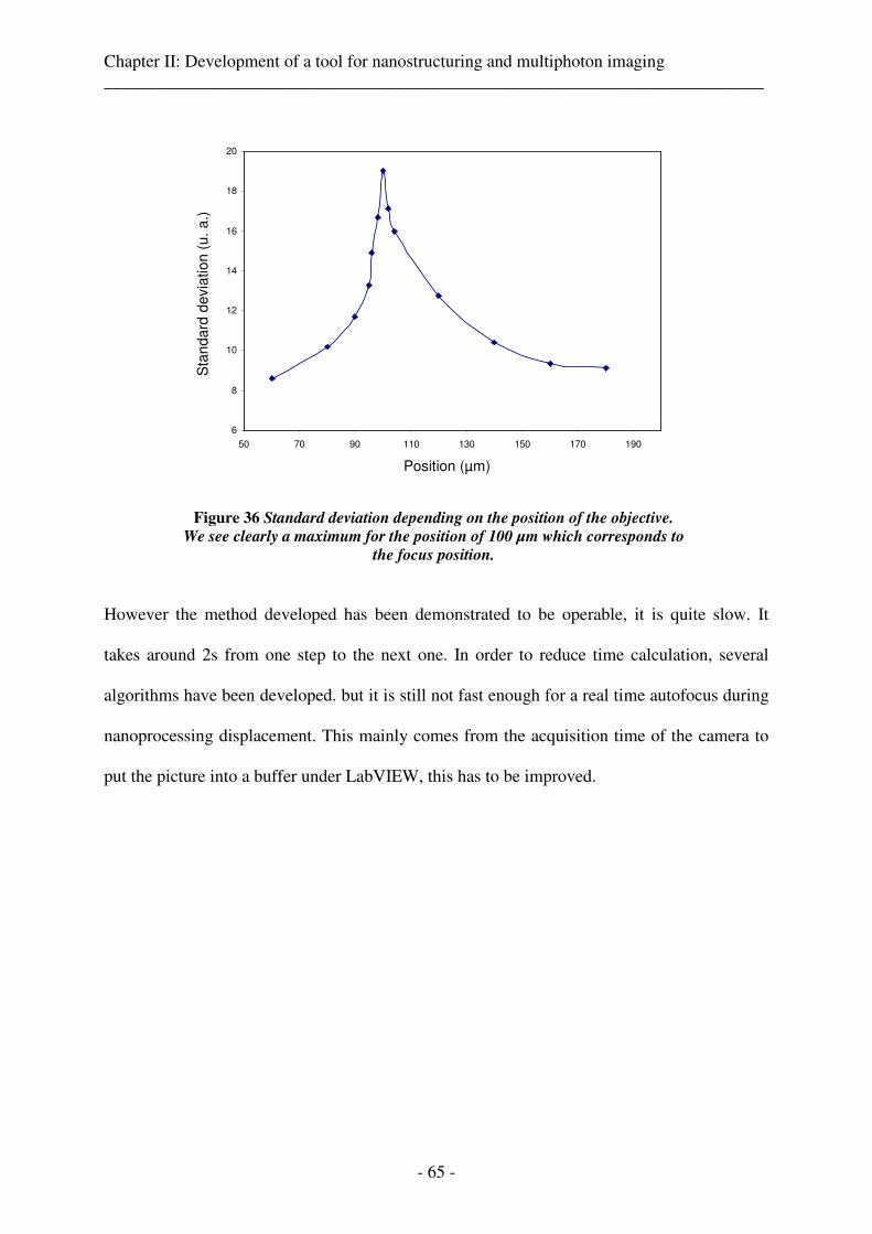
Chapter II: Development of a tool for nanostructuring and multiphoton imaging ___________________________________________________________________________
- 65 -
Figure 36 Standard deviation depending on the position of the objective.
We see clearly a maximum for the position of 100 µm which corresponds to
the focus position.
However the method developed has been demonstrated to be operable, it is quite slow. It
takes around 2s from one step to the next one. In order to reduce time calculation, several
algorithms have been developed. but it is still not fast enough for a real time autofocus during
nanoprocessing displacement. This mainly comes from the acquisition time of the camera to
put the picture into a buffer under LabVIEW, this has to be improved.
6
8
10
12
14
16
18
20
50 70 90 110 130 150 170 190
Position (µm)Position (µm)
Sta
ndard
devia
tion (
u.
a.)
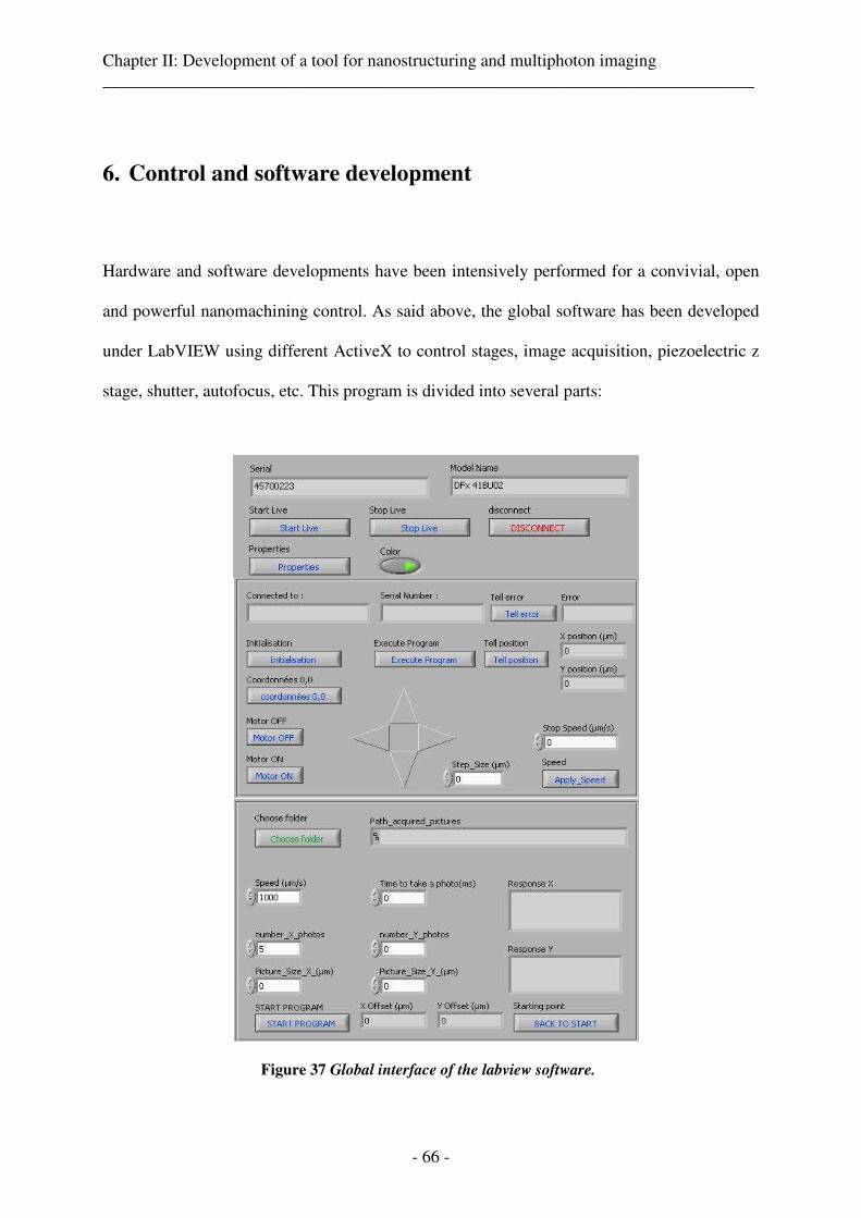
Chapter II: Development of a tool for nanostructuring and multiphoton imaging ___________________________________________________________________________
- 66 -
6. Control and software development
Hardware and software developments have been intensively performed for a convivial, open
and powerful nanomachining control. As said above, the global software has been developed
under LabVIEW using different ActiveX to control stages, image acquisition, piezoelectric z
stage, shutter, autofocus, etc. This program is divided into several parts:
Figure 37 Global interface of the labview software.
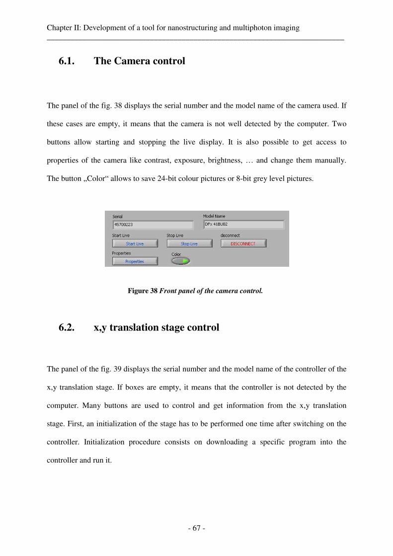
Chapter II: Development of a tool for nanostructuring and multiphoton imaging ___________________________________________________________________________
- 67 -
6.1. The Camera control
The panel of the fig. 38 displays the serial number and the model name of the camera used. If
these cases are empty, it means that the camera is not well detected by the computer. Two
buttons allow starting and stopping the live display. It is also possible to get access to
properties of the camera like contrast, exposure, brightness, … and change them manually.
The button „Color“ allows to save 24-bit colour pictures or 8-bit grey level pictures.
Figure 38 Front panel of the camera control.
6.2. x,y translation stage control
The panel of the fig. 39 displays the serial number and the model name of the controller of the
x,y translation stage. If boxes are empty, it means that the controller is not detected by the
computer. Many buttons are used to control and get information from the x,y translation
stage. First, an initialization of the stage has to be performed one time after switching on the
controller. Initialization procedure consists on downloading a specific program into the
controller and run it.
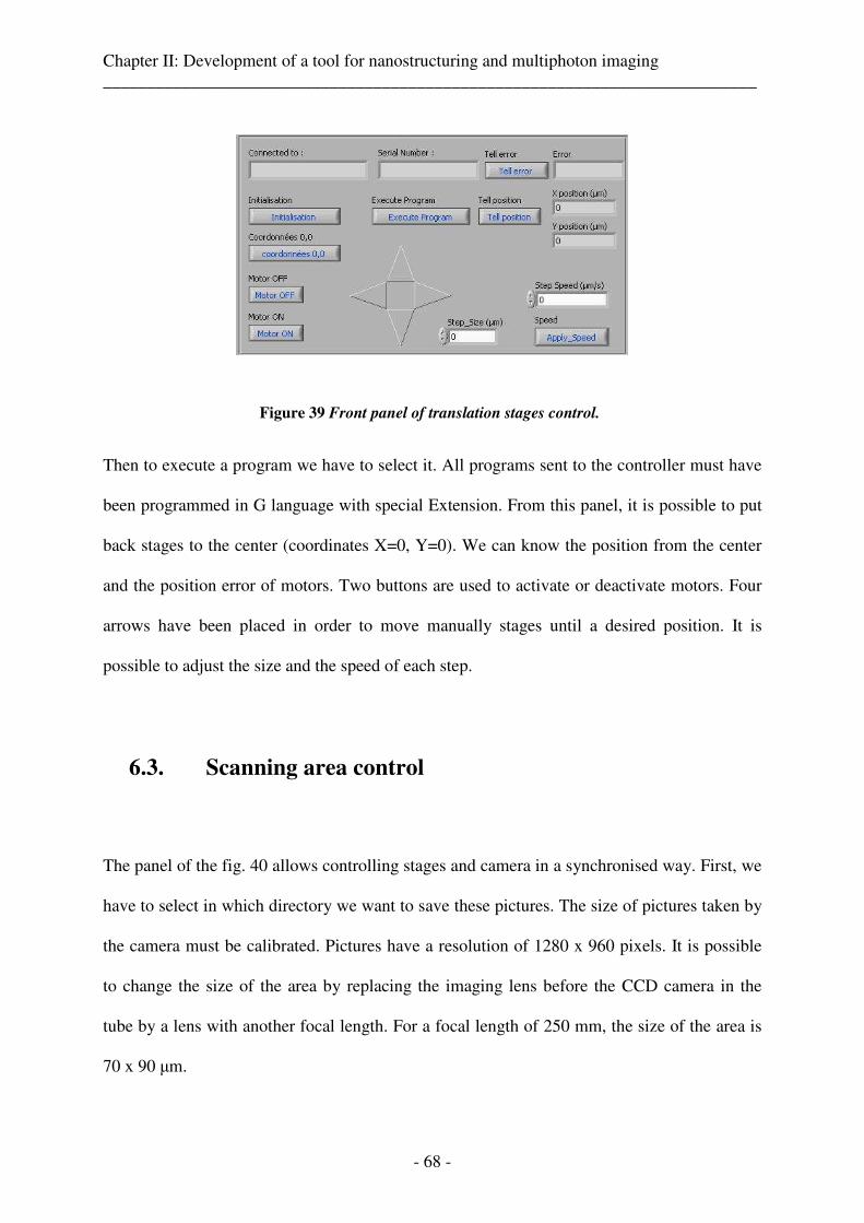
Chapter II: Development of a tool for nanostructuring and multiphoton imaging ___________________________________________________________________________
- 68 -
Figure 39 Front panel of translation stages control.
Then to execute a program we have to select it. All programs sent to the controller must have
been programmed in G language with special Extension. From this panel, it is possible to put
back stages to the center (coordinates X=0, Y=0). We can know the position from the center
and the position error of motors. Two buttons are used to activate or deactivate motors. Four
arrows have been placed in order to move manually stages until a desired position. It is
possible to adjust the size and the speed of each step.
6.3. Scanning area control
The panel of the fig. 40 allows controlling stages and camera in a synchronised way. First, we
have to select in which directory we want to save these pictures. The size of pictures taken by
the camera must be calibrated. Pictures have a resolution of 1280 x 960 pixels. It is possible
to change the size of the area by replacing the imaging lens before the CCD camera in the
tube by a lens with another focal length. For a focal length of 250 mm, the size of the area is
70 x 90 µm.
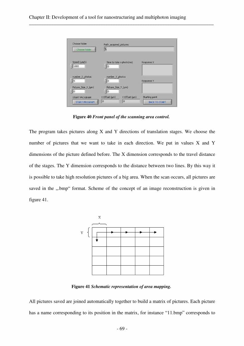
Chapter II: Development of a tool for nanostructuring and multiphoton imaging ___________________________________________________________________________
- 69 -
Figure 40 Front panel of the scanning area control.
The program takes pictures along X and Y directions of translation stages. We choose the
number of pictures that we want to take in each direction. We put in values X and Y
dimensions of the picture defined before. The X dimension corresponds to the travel distance
of the stages. The Y dimension corresponds to the distance between two lines. By this way it
is possible to take high resolution pictures of a big area. When the scan occurs, all pictures are
saved in the „.bmp“ format. Scheme of the concept of an image reconstruction is given in
figure 41.
Figure 41 Schematic representation of area mapping.
All pictures saved are joined automatically together to build a matrix of pictures. Each picture
has a name corresponding to its position in the matrix, for instance “11.bmp” corresponds to

Chapter II: Development of a tool for nanostructuring and multiphoton imaging ___________________________________________________________________________
- 70 -
the first position in the matrix. This part takes into account the number of pictures wanted in
the scanning area control along the X and Y axis. A dividing coefficient can be applied,
number of pixels can be controlled in order to reduce the size of the picture.
Chapter II: Development of a tool for nanostructuring and multiphoton imaging ___________________________________________________________________________
- 71 -
7. CAD drawing to nanomachining
To approach industrial standards of machining, a CAD to G language software converter has
also been added and developed in the Labview software to generate automatically a program
of CAD files which allow performing laser structuring from drawing supports.
7.1. Size control
As mentioned previously, you can download programs with “.DMC” format executable by the
controller. 2D drawings can be made with any software that saves files in DXF format. These
files are then converted to DMC via specific software which is named CAD2DMC (GALIL
Motion Control, USA). In order that the drawing can be interpreted by the controller, some
rules have to be respected. First of all, the design must be decomposed into a series of
continuous lines. Each drawing must include a starting point and ending point, marked on the
drawing itself, respectively by the words "FIRST" and "LAST". Some features may be added
through the use of macros which have to be inserted directly on the drawing, such as scale to
control the size of patterns desired, or the opening and closing of a shutter. Fig. 40, shows an
example of conversion.
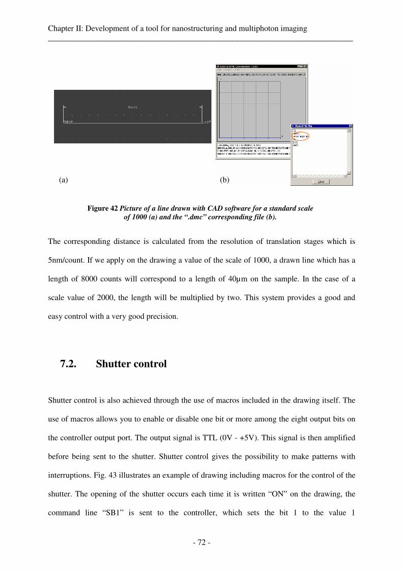
Chapter II: Development of a tool for nanostructuring and multiphoton imaging ___________________________________________________________________________
- 72 -
Figure 42 Picture of a line drawn with CAD software for a standard scale
of 1000 (a) and the “.dmc” corresponding file (b).
The corresponding distance is calculated from the resolution of translation stages which is
5nm/count. If we apply on the drawing a value of the scale of 1000, a drawn line which has a
length of 8000 counts will correspond to a length of 40µm on the sample. In the case of a
scale value of 2000, the length will be multiplied by two. This system provides a good and
easy control with a very good precision.
7.2. Shutter control
Shutter control is also achieved through the use of macros included in the drawing itself. The
use of macros allows you to enable or disable one bit or more among the eight output bits on
the controller output port. The output signal is TTL (0V - +5V). This signal is then amplified
before being sent to the shutter. Shutter control gives the possibility to make patterns with
interruptions. Fig. 43 illustrates an example of drawing including macros for the control of the
shutter. The opening of the shutter occurs each time it is written “ON” on the drawing, the
command line “SB1” is sent to the controller, which sets the bit 1 to the value 1
(a) (b)
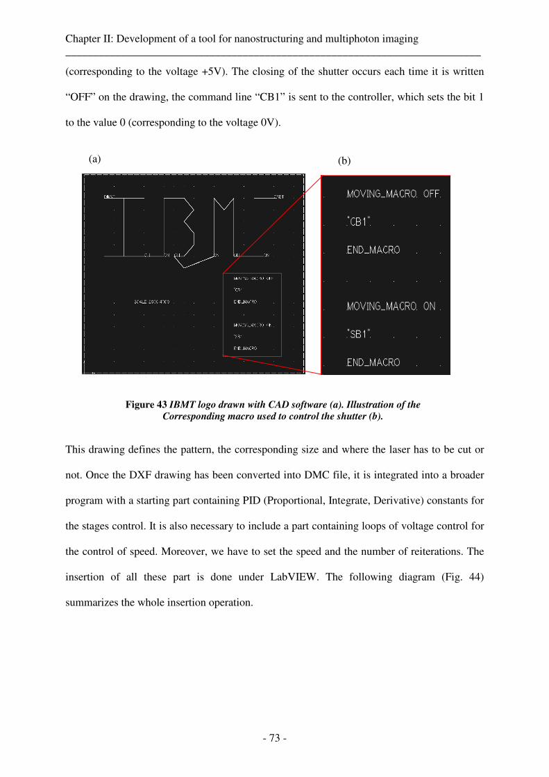
Chapter II: Development of a tool for nanostructuring and multiphoton imaging ___________________________________________________________________________
- 73 -
(corresponding to the voltage +5V). The closing of the shutter occurs each time it is written
“OFF” on the drawing, the command line “CB1” is sent to the controller, which sets the bit 1
to the value 0 (corresponding to the voltage 0V).
Figure 43 IBMT logo drawn with CAD software (a). Illustration of the
Corresponding macro used to control the shutter (b).
This drawing defines the pattern, the corresponding size and where the laser has to be cut or
not. Once the DXF drawing has been converted into DMC file, it is integrated into a broader
program with a starting part containing PID (Proportional, Integrate, Derivative) constants for
the stages control. It is also necessary to include a part containing loops of voltage control for
the control of speed. Moreover, we have to set the speed and the number of reiterations. The
insertion of all these part is done under LabVIEW. The following diagram (Fig. 44)
summarizes the whole insertion operation.
(a) (b)
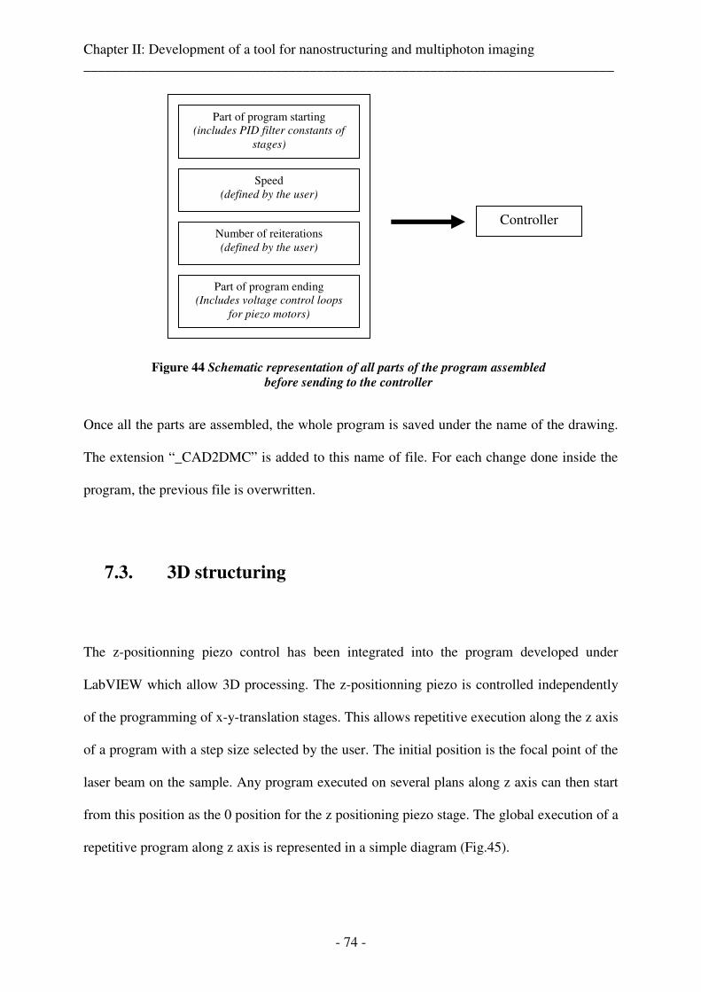
Chapter II: Development of a tool for nanostructuring and multiphoton imaging ___________________________________________________________________________
- 74 -
Figure 44 Schematic representation of all parts of the program assembled
before sending to the controller
Once all the parts are assembled, the whole program is saved under the name of the drawing.
The extension “_CAD2DMC” is added to this name of file. For each change done inside the
program, the previous file is overwritten.
7.3. 3D structuring
The z-positionning piezo control has been integrated into the program developed under
LabVIEW which allow 3D processing. The z-positionning piezo is controlled independently
of the programming of x-y-translation stages. This allows repetitive execution along the z axis
of a program with a step size selected by the user. The initial position is the focal point of the
laser beam on the sample. Any program executed on several plans along z axis can then start
from this position as the 0 position for the z positioning piezo stage. The global execution of a
repetitive program along z axis is represented in a simple diagram (Fig.45).
Part of program starting (includes PID filter constants of
stages)
Speed (defined by the user)
Number of reiterations (defined by the user)
Part of program ending (Includes voltage control loops
for piezo motors)
Controller
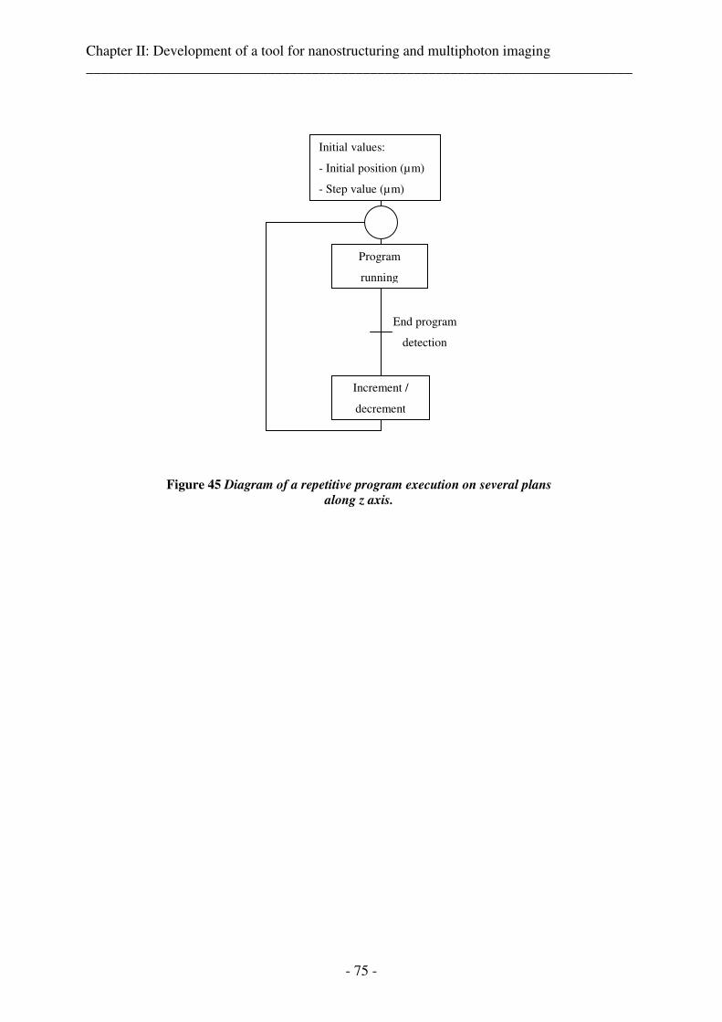
Chapter II: Development of a tool for nanostructuring and multiphoton imaging ___________________________________________________________________________
- 75 -
Figure 45 Diagram of a repetitive program execution on several plans
along z axis.
Initial values:
- Initial position (µm)
- Step value (µm)
Program
running
Increment /
decrement
End program
detection
Chapter II: Development of a tool for nanostructuring and multiphoton imaging ___________________________________________________________________________
- 76 -
8. Conclusion
Here we have demonstrated the development of an efficient, accurate and powerful
nanoprocessing apparatus. The device is multifunctional, high flexible with a strong hardware
and software environment which allow a high range of applications and performances.The
development of this tool opens the door to many applications using low average power
femtosecond laser pulses.
The workstation is compact and designed to be coupled with low average power laser systems
which are more cost-effective and reliable compared to amplified laser systems (µJ or
mJ/pulse).
However some questions concerning effects of the repetition rate laser pulses on the matter
need more investigations. This is the topic of the next chapter.
Chapter III : Effects of high repetition rate femtosecond pulses on metals ___________________________________________________________________________
- 77 -
Chapter III
Effects of high repetition rate
femtosecond pulses on metals

Chapter III : Effects of high repetition rate femtosecond pulses on metals ___________________________________________________________________________
- 78 -
Chapter III : Effects of high repetition rate femtosecond pulses on metals ___________________________________________________________________________
- 79 -
1. Introduction
In this chapter we investigate the processing time of metals with femtosecond laser systems.
Indeed, ultrafast laser pulses are becoming more and more interesting for industrial
applications, so the processing time becomes an important factor in order to evaluate the
economical interest of femtosecond processing. Moreover, a study of the influence of the
repetition rate on the processing time puts in evidence a linear relation. These results are
based on ablation rates obtained for repetition rates in the range of kilohertz. The following of
this chapter is devoted to a study of the interaction between high repetition rate laser pulses
and the matter in order to obtain ablation rates in the megahertz repetition rate range. A part
consists of a discussion of effects of this interaction from results observed in the literature
concerning dielectrics, metals and semi-conductors. Then an analysis of a dedicated
experiment of interaction with copper is presented. Observations are discussed and a
qualitative explanation is suggested.
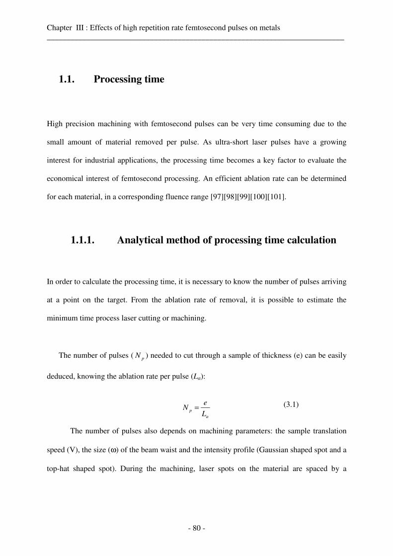
Chapter III : Effects of high repetition rate femtosecond pulses on metals ___________________________________________________________________________
- 80 -
1.1. Processing time
High precision machining with femtosecond pulses can be very time consuming due to the
small amount of material removed per pulse. As ultra-short laser pulses have a growing
interest for industrial applications, the processing time becomes a key factor to evaluate the
economical interest of femtosecond processing. An efficient ablation rate can be determined
for each material, in a corresponding fluence range [97] [98] [99] [100] [101].
1.1.1. Analytical method of processing time calculation
In order to calculate the processing time, it is necessary to know the number of pulses arriving
at a point on the target. From the ablation rate of removal, it is possible to estimate the
minimum time process laser cutting or machining.
The number of pulses ( pN ) needed to cut through a sample of thickness (e) can be easily
deduced, knowing the ablation rate per pulse (La):
The number of pulses also depends on machining parameters: the sample translation
speed (V), the size (ω) of the beam waist and the intensity profile (Gaussian shaped spot and a
top-hat shaped spot). During the machining, laser spots on the material are spaced by a
a
pL
eN = (3.1)
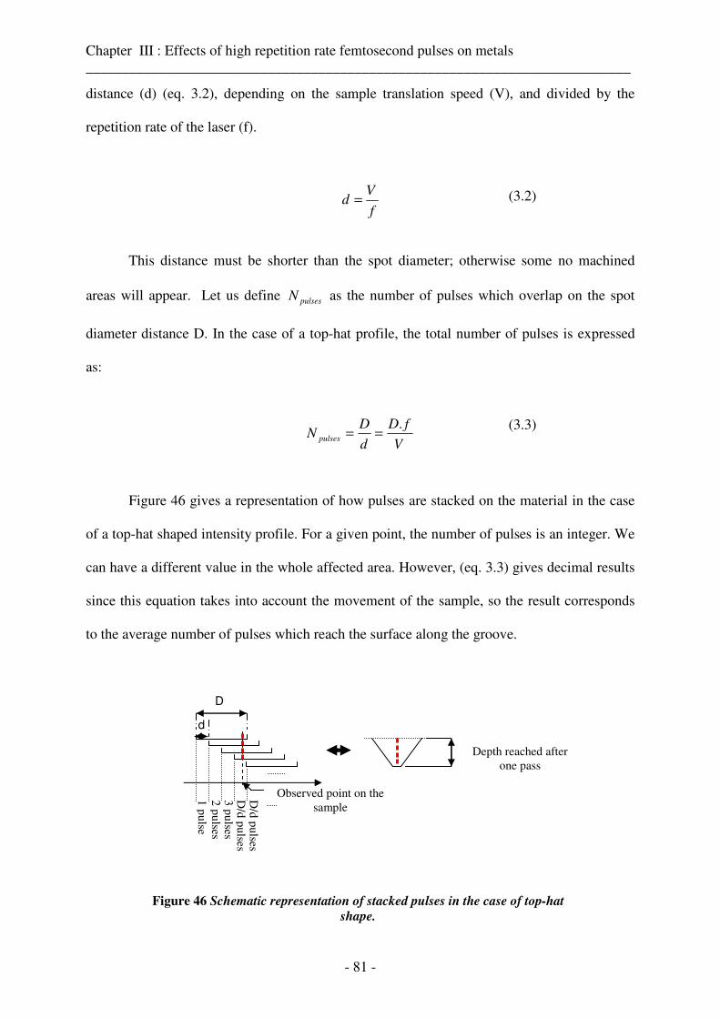
Chapter III : Effects of high repetition rate femtosecond pulses on metals ___________________________________________________________________________
- 81 -
distance (d) (eq. 3.2), depending on the sample translation speed (V), and divided by the
repetition rate of the laser (f).
This distance must be shorter than the spot diameter; otherwise some no machined
areas will appear. Let us define pulsesN as the number of pulses which overlap on the spot
diameter distance D. In the case of a top-hat profile, the total number of pulses is expressed
as:
Figure 46 gives a representation of how pulses are stacked on the material in the case
of a top-hat shaped intensity profile. For a given point, the number of pulses is an integer. We
can have a different value in the whole affected area. However, (eq. 3.3) gives decimal results
since this equation takes into account the movement of the sample, so the result corresponds
to the average number of pulses which reach the surface along the groove.
Figure 46 Schematic representation of stacked pulses in the case of top-hat
shape.
1 pulse 2 pulses 3 pulses D
/d pulses D
/d pulses
D
d
Observed point on the sample
Depth reached after one pass
f
Vd =
V
fD
d
DN pulses
.==
(3.2)
(3.3)
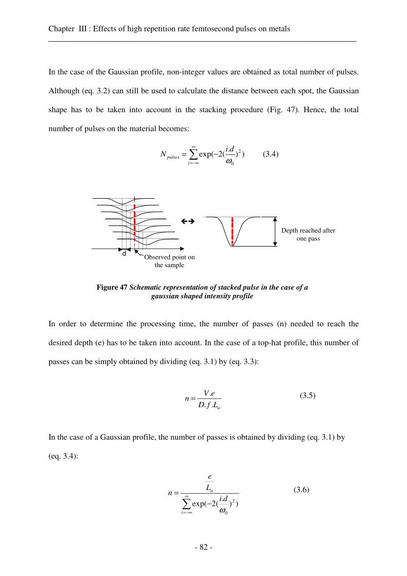
Chapter III : Effects of high repetition rate femtosecond pulses on metals ___________________________________________________________________________
- 82 -
In the case of the Gaussian profile, non-integer values are obtained as total number of pulses.
Although (eq. 3.2) can still be used to calculate the distance between each spot, the Gaussian
shape has to be taken into account in the stacking procedure (Fig. 47). Hence, the total
number of pulses on the material becomes:
Figure 47 Schematic representation of stacked pulse in the case of a
gaussian shaped intensity profile
In order to determine the processing time, the number of passes (n) needed to reach the
desired depth (e) has to be taken into account. In the case of a top-hat profile, this number of
passes can be simply obtained by dividing (eq. 3.1) by (eq. 3.3):
In the case of a Gaussian profile, the number of passes is obtained by dividing (eq. 3.1) by
(eq. 3.4):
�
x
Observed point on the sample
d
Depth reached after one pass
∑∞
−∞=
−=i
pulses
diN ))
.(2exp( 2
0ω
aLfD
eVn
..
.=
∑∞
−∞=
−
=
i
a
di
L
e
n
)).
(2exp( 2
0ω
(3.4)
(3.5)
(3.6)
Chapter III : Effects of high repetition rate femtosecond pulses on metals ___________________________________________________________________________
- 83 -
Finally, the processing time depends on the length of the groove (l), the number of pass and
the speed (V)
From equations (eq. 3.5), (eq. 3.6) and (eq. 3.7) processing time for a top-hat (eq. 3.8) and
Gaussian intensity profile (eq. 3.9) can be expressed as:
Obviously these times correspond to “physical” times since there are deduced from the
ablation rates. They correspond to the minimal value that can be observed during machining.
1.1.2. Results and discussion
Two laser sources have been used. A 1 to 5 KHz commercial laser with a pulse width of 120
fs, an average power of 2 W, corresponding to a maximum of 400 µJ per pulse at 5 kHz and a
1 to 10-kHz-repetition rate prototype laser system (Thales laser, France) which is based on a
single and non-cryogenic regenerative amplifier [102]. This latter has a pulse energy of 350µJ
at a 10 kHz with a 60 fs pulsewidth. By overclocking the pump it is possible to reach a 15
kHz repetition rate.
V
nlt
.=
aLfD
el
V
nlt
..
..==
∑∞
−∞=
−
==
i
a
diLV
el
V
nlt
)).
(2exp(..
..
2
0ω
(3.7)
(3.8)
(3.9)
Chapter III : Effects of high repetition rate femtosecond pulses on metals ___________________________________________________________________________
- 84 -
The laser beam is focused through a lens with a focal length of 50 or 200 mm. A polarizer and
a half-wave plate are placed in the laser beam path in order to control the laser power. In this
experiment two beam shapes are used. The Gaussian profile of the laser and a filtered beam
using an adjustable diaphragm in order to obtain a controllable top-hat shaped spot at the
image plane of the diaphragm. The size of the top-hat shaped spot is experimentally
controlled by measuring the diameter of the impacts with an optical microscope.
The metal samples, copper (Goodfellow, purity: 99 %,) and stainless steel (Goodfellow 316L)
have a thickness of 25 µm and/or 50 µm. The samples were mounted on an accurate
microprocessing workstation composed of x,y,z motorized translation stages. The accuracy of
translation stages is given to be +/- 3 µm with a repeatability of 0.1 µm, with speeds up to 500
mm/s.
Processing time measurements have been performed on copper and stainless steel samples in
the case of a very simple machined pattern which consists on drilling a 3 mm radius disc at 9
mm/s until the disc drop down. The purpose is here to have direct access to “physical” times
since other potential contributions to machining times (computing, mechanical) can be
neglected considering such simple pattern. Measurements are performed using a 5 kHz laser
repetition rate, and a fluence of 2.5 J/cm². This fluence has not been chosen haphazard. As
already mentioned in the introduction, there is an optimal fluence for which good quality and
high ablation speed can be obtained [97]. To investigate on the pertinence of the processing
time analytical solution compared to measurements, drilling with a top-hat shape was tested
on copper and with a Gaussian shape on stainless steel.
Chapter III : Effects of high repetition rate femtosecond pulses on metals ___________________________________________________________________________
- 85 -
a) Case of copper
Thanks to the calculations of Colombier et al [97], the ablation rate corresponding to the
optimal fluence of 2.5 J/cm2 is given to be 100 nm/pulse. This value was taken for the
processing time calculation. Two samples of copper have been machined, one with a
thickness of 25 µm, and the other of 50 µm. The machining was performed through the whole
thickness of the sample. The spot diameter for the top-hat profile was 100 µm. We found that
for the 25 µm thick copper sample, the experimental processing time is 9s, in good agreement
with a calculated time of 9.4s. In the case of 50 µm thick copper sample the experimental and
calculated processing times were 19s and 18.8s respectively.
Obviously, the calculated processing time is critically dependent on the chosen ablation rate
value. The theoretical value of 100 nm/pulse taken is in good agreement with experimental
results found in the literature [97] [98] [99] [100] [97]. Processing times calculated with these
experimental values are shown in table 1.
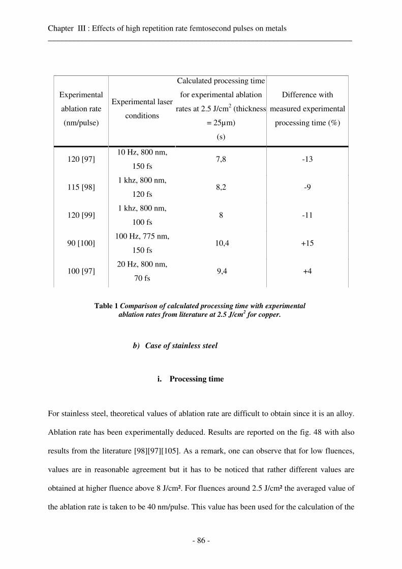
Chapter III : Effects of high repetition rate femtosecond pulses on metals ___________________________________________________________________________
- 86 -
Experimental
ablation rate
(nm/pulse)
Experimental laser
conditions
Calculated processing time
for experimental ablation
rates at 2.5 J/cm2 (thickness
= 25µm)
(s)
Difference with
measured experimental
processing time (%)
120 [97] 10 Hz, 800 nm,
150 fs 7,8 -13
115 [98] 1 khz, 800 nm,
120 fs 8,2 -9
120 [99] 1 khz, 800 nm,
100 fs 8 -11
90 [100] 100 Hz, 775 nm,
150 fs 10,4 +15
100 [97] 20 Hz, 800 nm,
70 fs 9,4 +4
Table 1 Comparison of calculated processing time with experimental
ablation rates from literature at 2.5 J/cm2 for copper.
b) Case of stainless steel
i. Processing time
For stainless steel, theoretical values of ablation rate are difficult to obtain since it is an alloy.
Ablation rate has been experimentally deduced. Results are reported on the fig. 48 with also
results from the literature [98] [97] [105]. As a remark, one can observe that for low fluences,
values are in reasonable agreement but it has to be noticed that rather different values are
obtained at higher fluence above 8 J/cm². For fluences around 2.5 J/cm² the averaged value of
the ablation rate is taken to be 40 nm/pulse. This value has been used for the calculation of the
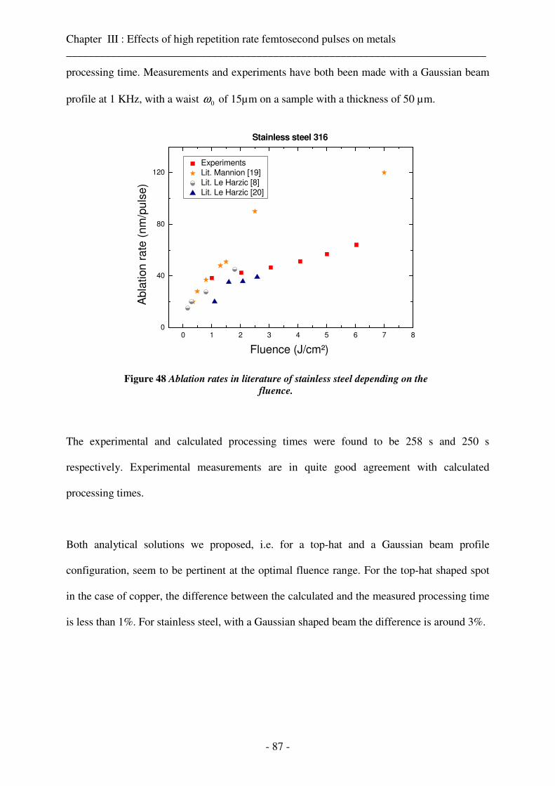
Chapter III : Effects of high repetition rate femtosecond pulses on metals ___________________________________________________________________________
- 87 -
processing time. Measurements and experiments have both been made with a Gaussian beam
profile at 1 KHz, with a waist 0ω of 15µm on a sample with a thickness of 50 µm.
Figure 48 Ablation rates in literature of stainless steel depending on the
fluence.
The experimental and calculated processing times were found to be 258 s and 250 s
respectively. Experimental measurements are in quite good agreement with calculated
processing times.
Both analytical solutions we proposed, i.e. for a top-hat and a Gaussian beam profile
configuration, seem to be pertinent at the optimal fluence range. For the top-hat shaped spot
in the case of copper, the difference between the calculated and the measured processing time
is less than 1%. For stainless steel, with a Gaussian shaped beam the difference is around 3%.
0 1 2 3 4 5 6 7 80
40
80
120
Stainless steel 316
A
bla
tion r
ate
(nm
/puls
e)
Fluence (J/cm²)
Experiments Lit. Mannion [19] Lit. Le Harzic [8] Lit. Le Harzic [20]
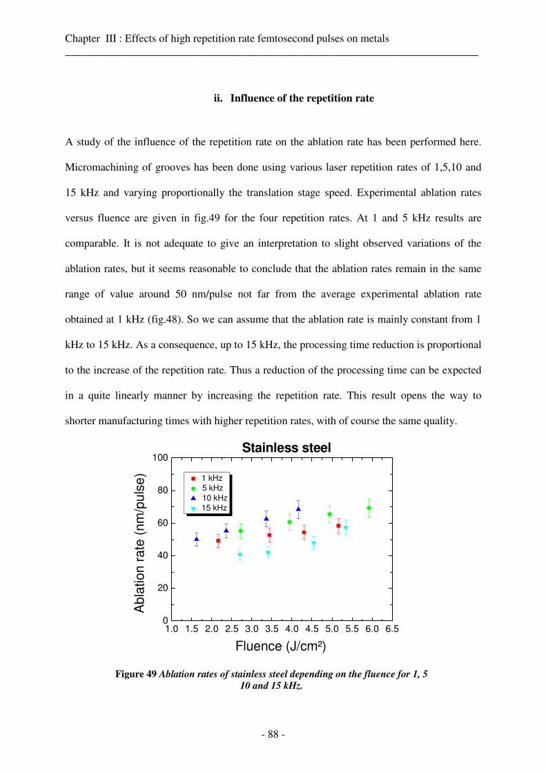
Chapter III : Effects of high repetition rate femtosecond pulses on metals ___________________________________________________________________________
- 88 -
ii. Influence of the repetition rate
A study of the influence of the repetition rate on the ablation rate has been performed here.
Micromachining of grooves has been done using various laser repetition rates of 1,5,10 and
15 kHz and varying proportionally the translation stage speed. Experimental ablation rates
versus fluence are given in fig.49 for the four repetition rates. At 1 and 5 kHz results are
comparable. It is not adequate to give an interpretation to slight observed variations of the
ablation rates, but it seems reasonable to conclude that the ablation rates remain in the same
range of value around 50 nm/pulse not far from the average experimental ablation rate
obtained at 1 kHz (fig.48). So we can assume that the ablation rate is mainly constant from 1
kHz to 15 kHz. As a consequence, up to 15 kHz, the processing time reduction is proportional
to the increase of the repetition rate. Thus a reduction of the processing time can be expected
in a quite linearly manner by increasing the repetition rate. This result opens the way to
shorter manufacturing times with higher repetition rates, with of course the same quality.
Figure 49 Ablation rates of stainless steel depending on the fluence for 1, 5
10 and 15 kHz.
1.0 1.5 2.0 2.5 3.0 3.5 4.0 4.5 5.0 5.5 6.0 6.50
20
40
60
80
100
Abla
tion
ra
te (
nm
/pu
lse
)
Stainless steel
Fluence (J/cm²)
1 kHz
5 kHz
10 kHz
15 kHz
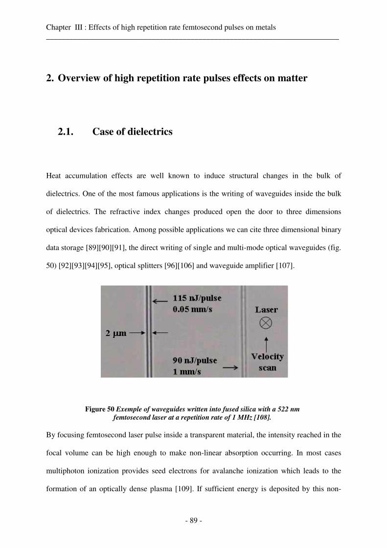
Chapter III : Effects of high repetition rate femtosecond pulses on metals ___________________________________________________________________________
- 89 -
2. Overview of high repetition rate pulses effects on matter
2.1. Case of dielectrics
Heat accumulation effects are well known to induce structural changes in the bulk of
dielectrics. One of the most famous applications is the writing of waveguides inside the bulk
of dielectrics. The refractive index changes produced open the door to three dimensions
optical devices fabrication. Among possible applications we can cite three dimensional binary
data storage [89] [90] [91], the direct writing of single and multi-mode optical waveguides (fig.
50) [92] [93] [94] [95], optical splitters [96] [106] and waveguide amplifier [107].
Figure 50 Exemple of waveguides written into fused silica with a 522 nm
femtosecond laser at a repetition rate of 1 MHz [108].
By focusing femtosecond laser pulse inside a transparent material, the intensity reached in the
focal volume can be high enough to make non-linear absorption occurring. In most cases
multiphoton ionization provides seed electrons for avalanche ionization which leads to the
formation of an optically dense plasma [109]. If sufficient energy is deposited by this non-
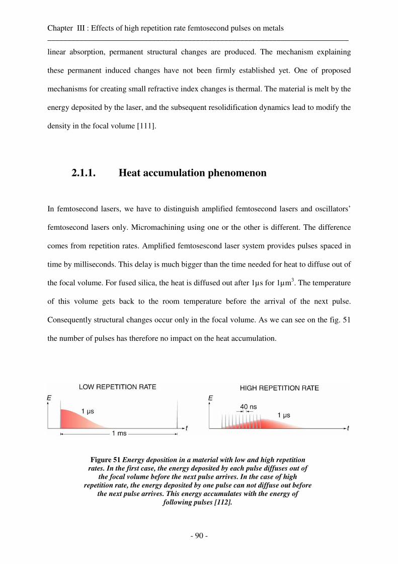
Chapter III : Effects of high repetition rate femtosecond pulses on metals ___________________________________________________________________________
- 90 -
linear absorption, permanent structural changes are produced. The mechanism explaining
these permanent induced changes have not been firmly established yet. One of proposed
mechanisms for creating small refractive index changes is thermal. The material is melt by the
energy deposited by the laser, and the subsequent resolidification dynamics lead to modify the
density in the focal volume [111].
2.1.1. Heat accumulation phenomenon
In femtosecond lasers, we have to distinguish amplified femtosecond lasers and oscillators’
femtosecond lasers only. Micromachining using one or the other is different. The difference
comes from repetition rates. Amplified femtosescond laser system provides pulses spaced in
time by milliseconds. This delay is much bigger than the time needed for heat to diffuse out of
the focal volume. For fused silica, the heat is diffused out after 1µs for 1µm3. The temperature
of this volume gets back to the room temperature before the arrival of the next pulse.
Consequently structural changes occur only in the focal volume. As we can see on the fig. 51
the number of pulses has therefore no impact on the heat accumulation.
Figure 51 Energy deposition in a material with low and high repetition
rates. In the first case, the energy deposited by each pulse diffuses out of
the focal volume before the next pulse arrives. In the case of high
repetition rate, the energy deposited by one pulse can not diffuse out before
the next pulse arrives. This energy accumulates with the energy of
following pulses [112].
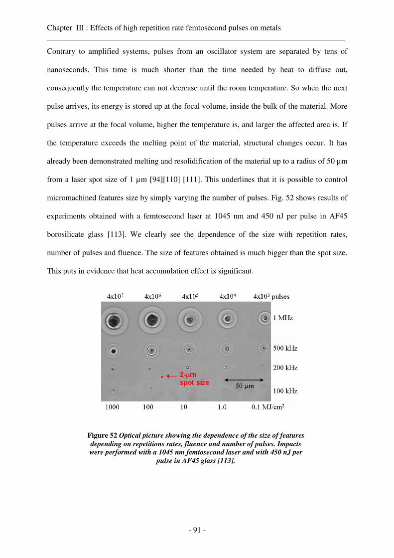
Chapter III : Effects of high repetition rate femtosecond pulses on metals ___________________________________________________________________________
- 91 -
Contrary to amplified systems, pulses from an oscillator system are separated by tens of
nanoseconds. This time is much shorter than the time needed by heat to diffuse out,
consequently the temperature can not decrease until the room temperature. So when the next
pulse arrives, its energy is stored up at the focal volume, inside the bulk of the material. More
pulses arrive at the focal volume, higher the temperature is, and larger the affected area is. If
the temperature exceeds the melting point of the material, structural changes occur. It has
already been demonstrated melting and resolidification of the material up to a radius of 50 µm
from a laser spot size of 1 µm [94] [110] [111]. This underlines that it is possible to control
micromachined features size by simply varying the number of pulses. Fig. 52 shows results of
experiments obtained with a femtosecond laser at 1045 nm and 450 nJ per pulse in AF45
borosilicate glass [113]. We clearly see the dependence of the size with repetition rates,
number of pulses and fluence. The size of features obtained is much bigger than the spot size.
This puts in evidence that heat accumulation effect is significant.
Figure 52 Optical picture showing the dependence of the size of features
depending on repetitions rates, fluence and number of pulses. Impacts
were performed with a 1045 nm femtosecond laser and with 450 nJ per
pulse in AF45 glass [113].
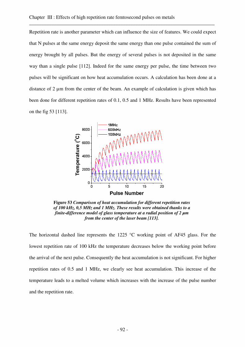
Chapter III : Effects of high repetition rate femtosecond pulses on metals ___________________________________________________________________________
- 92 -
Repetition rate is another parameter which can influence the size of features. We could expect
that N pulses at the same energy deposit the same energy than one pulse contained the sum of
energy brought by all pulses. But the energy of several pulses is not deposited in the same
way than a single pulse [112]. Indeed for the same energy per pulse, the time between two
pulses will be significant on how heat accumulation occurs. A calculation has been done at a
distance of 2 µm from the center of the beam. An example of calculation is given which has
been done for different repetition rates of 0.1, 0.5 and 1 MHz. Results have been represented
on the fig 53 [113].
Figure 53 Comparison of heat accumulation for different repetition rates
of 100 kHz, 0,5 MHz and 1 MHz. These results were obtained thanks to a
finite-difference model of glass temperature at a radial position of 2 µm
from the center of the laser beam [113].
The horizontal dashed line represents the 1225 °C working point of AF45 glass. For the
lowest repetition rate of 100 kHz the temperature decreases below the working point before
the arrival of the next pulse. Consequently the heat accumulation is not significant. For higher
repetition rates of 0.5 and 1 MHz, we clearly see heat accumulation. This increase of the
temperature leads to a melted volume which increases with the increase of the pulse number
and the repetition rate.
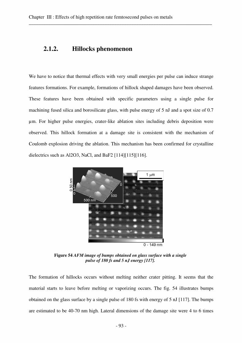
Chapter III : Effects of high repetition rate femtosecond pulses on metals ___________________________________________________________________________
- 93 -
2.1.2. Hillocks phenomenon
We have to notice that thermal effects with very small energies per pulse can induce strange
features formations. For example, formations of hillock shaped damages have been observed.
These features have been obtained with specific parameters using a single pulse for
machining fused silica and borosilicate glass, with pulse energy of 5 nJ and a spot size of 0.7
µm. For higher pulse energies, crater-like ablation sites including debris deposition were
observed. This hillock formation at a damage site is consistent with the mechanism of
Coulomb explosion driving the ablation. This mechanism has been confirmed for crystalline
dielectrics such as Al2O3, NaCl, and BaF2 [114] [115] [116].
Figure 54 AFM image of bumps obtained on glass surface with a single
pulse of 180 fs and 5 nJ energy [117].
The formation of hillocks occurs without melting neither crater pitting. It seems that the
material starts to leave before melting or vaporizing occurs. The fig. 54 illustrates bumps
obtained on the glass surface by a single pulse of 180 fs with energy of 5 nJ [117]. The bumps
are estimated to be 40-70 nm high. Lateral dimensions of the damage site were 4 to 6 times
Chapter III : Effects of high repetition rate femtosecond pulses on metals ___________________________________________________________________________
- 94 -
smaller than the spot size on the sample. These dimensions put in evidence that a multiphoton
phenomenon induced this mechanism. Indeed, inside a transparent material, as one photon of
visible light has not enough energy to excite an electron from the valence to the conduction
band, so a transparent material does not absorb the laser light linearly. In order to excite an
electron over this gap, several simultaneous photons are necessary so that the total energy of
all photons equal or greater than the band gap of the material. This multiphoton effect is
achievable with focused high intensity laser pulses, especially in the centre of the beam where
the intensity is the highest.
2.2. Case of metals
Due to high concentration of free electrons, metals have a very good conductivity. Metals are
good electric and heat conductors. As said in chapter I, fabrication of nanostructures is
possible by direct ablation with tightly focused femtosecond laser pulses with a resolution
down to some hundreds of nm. However, due to specific interactions between metals and
femtosecond laser pulses, other phenomena appear like porosity. Submicrometer structures
fabrication with femtosecond laser pulses can be dominated by solidified flow dynamics in
molten material [118]. Two phenomenons are presented here which differ from ablation and
machining of holes or grooves.
In literature, the hillock phenomenon has been observed on metals. In the case of metals,
results were obtained with pulses of 130 fs and a repetition rate from 1 Hz to 1 kHz on
chromium film of 80 nm thick deposited on a quartz substrate. In these experiments,
formations of microcolumns were observed after cumulative pulses with energy close to the
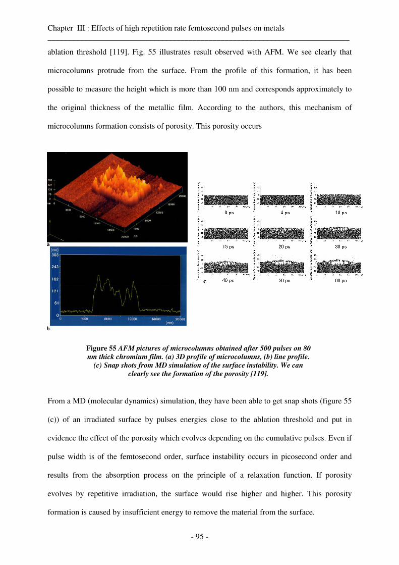
Chapter III : Effects of high repetition rate femtosecond pulses on metals ___________________________________________________________________________
- 95 -
ablation threshold [119]. Fig. 55 illustrates result observed with AFM. We see clearly that
microcolumns protrude from the surface. From the profile of this formation, it has been
possible to measure the height which is more than 100 nm and corresponds approximately to
the original thickness of the metallic film. According to the authors, this mechanism of
microcolumns formation consists of porosity. This porosity occurs
Figure 55 AFM pictures of microcolumns obtained after 500 pulses on 80
nm thick chromium film. (a) 3D profile of microcolumns, (b) line profile.
(c) Snap shots from MD simulation of the surface instability. We can
clearly see the formation of the porosity [119].
From a MD (molecular dynamics) simulation, they have been able to get snap shots (figure 55
(c)) of an irradiated surface by pulses energies close to the ablation threshold and put in
evidence the effect of the porosity which evolves depending on the cumulative pulses. Even if
pulse width is of the femtosecond order, surface instability occurs in picosecond order and
results from the absorption process on the principle of a relaxation function. If porosity
evolves by repetitive irradiation, the surface would rise higher and higher. This porosity
formation is caused by insufficient energy to remove the material from the surface.
c
Chapter III : Effects of high repetition rate femtosecond pulses on metals ___________________________________________________________________________
- 96 -
As said in chapter I, femtosecond laser pulses induce in metals a strong thermal non-
equilibrium between electrons and lattice of ions. The relaxation of this non-equilibrium
occurs after the laser pulse and depends on several materials properties. A slow increase of
the temperature of the lattice results in a longer existence of the molten phase, in consequence
this increase influences ablation results. High repetition rates might lead to melting and
increased heat affected zones. The fig. 56 shows an example of molten stainless steel obtained
at higher repetition rate by Ancona et al. [120]
Figure 56 SEM pictures of holes obtained with percussion drilling
technique with energy of 30 µJ at (a) 100 kHz and (b) at 400 kHz [120] .
Both of these holes have been performed with the same pulse energy of 30 µJ but with
different repetition rates. In the first case (fig. 56 (a)), the hole has been drilled at 100 kHz. In
the case of 400 kHz (fig. 56 (b)), we can clearly see a big bump of molten material all around
the hole. This indicates that at a repetition rate higher than 100 kHz, heat accumulation has to
be taken into account and can influence the size and the shape of machined structures. The
same kind of phenomenon has been observed on thin film of gold by Koch et al. [118]. The
fig- 57 illustrates results obtained on gold and chromium 100 nm thick films performed by
one pulse. We can see a strong melting dynamic whereas no visible melt material in the case
of chromium. The pulse fluence used is 1.5 times the ablation threshold fluence. According to
the authors, metals ablation occurs out of the molten phase for weak electron-phonon
coupling of metals like gold whereas for metals with strong electron-phonon coupling like
Chapter III : Effects of high repetition rate femtosecond pulses on metals ___________________________________________________________________________
- 97 -
chromium, ablation occurs almost without melting [121], indeed, the energy transfer depends
on the electron-phonon coupling as predicted by the two temperature model.
Figure 57 SEM pictures of single pulse ablation of gold and chromium 100
nm thick films [118].
As shown by [118] melting dynamics can be a way to fabricate sub micrometer metal
structures by using complex processes occurring at the same time than ablation. The authors
demonstrate the possibility to fabricate nanojets (fig. 58) on thin gold films. Nanojets always
appear after a formation of a bump-like structure. This process induced by a femtosecond
laser pulse in a molten gold layer is not yet fully understood.
Figure 58 SEM pictures of sub-wavelength surface structures produced in
60 nm thick gold film by focused femtosecond laser pulses with different
pulse energies [118].
Chapter III : Effects of high repetition rate femtosecond pulses on metals ___________________________________________________________________________
- 98 -
2.3. Case of semiconductors
This phenomenon can also induce structures on semiconductors. In literature, embossed lines
have been observed on silicon [122]. Authors observed three different regimes depending on
the fluence and the scanning speed (fig. 59). At low fluence and high speed, they observed a
slight modification with a colour-change but without breakdown of the material. With a
higher fluence and a scanning speed adjusted in order to have a heat accumulation which
reaches a constant temperature in the oxidation range temperature, embossed lines were
created, until hundred of nanometers above the surface. Then, by adjusting fluence and
scanning speed parameters in order to reach a temperature over the oxidation range
temperatures, they observed material removal, and ablation occurs.
Figure 59 Lines on silicon surface irradiated by femtosecond laser pulses at 1W
and for several repetition rates, from left to right respectively : 8, 13 and 26
MHz [122].
Authors do a proceeding description of the cooling cycle after irradiation. They start from a
finite absorption and temperature-independent material parameters with a gaussian shaped
Chapter III : Effects of high repetition rate femtosecond pulses on metals ___________________________________________________________________________
- 99 -
beam. They use a single temporal-rectangular pulse. They approximate the analytical
expression of the temperature cooling ( [123]) in the laser irradiated point by:
Dtkt
wIT la
π
τ
4
20=∆
where aI is the absorbed laser-light intensity, 0w the radius of the laser focal spot, lτ the
pulse duration, k the thermal conductivity, D the heat diffusivity and f
t1
= pulse interval
( f is the repetition rate of the laser).
By taking into account laser parameters such as the intensity of the laser light on the sample,
the repetition rate, the wavelength and properties of the material such as the reflectivity at 800
nm [124], authors demonstrate that it is possible to deduce the equation giving the
temperature at the end of Nth pulse irradiation and for a given energy per pulse:
Dtk
fERKNT P
24
)1(
π
××−=
Recent simulations using various thermal models have shown that thermal oxidation of silicon
takes place at temperatures in the range of 700~1300 °C [125] [126] [127] [128] [129] . In the
following analysis, it is assumed that if the temperature of the silicon surface is brought up
and kept in the range of 700~1300°C (1000~1600 K), oxidization occurs (let take 1400 K as
average value). To reach the average oxidation temperature and to keep it more or less
constant, one need NP-T≈1400K= 15442 pulses to overlap at a constant scan speed of 4 mm/s.
(3.10)
(3.11)
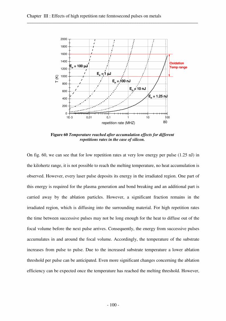
Chapter III : Effects of high repetition rate femtosecond pulses on metals ___________________________________________________________________________
- 100 -
Figure 60 Temperature reached after accumulation effects for different
repetitions rates in the case of silicon.
On fig. 60, we can see that for low repetition rates at very low energy per pulse (1.25 nJ) in
the kilohertz range, it is not possible to reach the melting temperature, no heat accumulation is
observed. However, every laser pulse deposits its energy in the irradiated region. One part of
this energy is required for the plasma generation and bond breaking and an additional part is
carried away by the ablation particles. However, a significant fraction remains in the
irradiated region, which is diffusing into the surrounding material. For high repetition rates
the time between successive pulses may not be long enough for the heat to diffuse out of the
focal volume before the next pulse arrives. Consequently, the energy from successive pulses
accumulates in and around the focal volume. Accordingly, the temperature of the substrate
increases from pulse to pulse. Due to the increased substrate temperature a lower ablation
threshold per pulse can be anticipated. Even more significant changes concerning the ablation
efficiency can be expected once the temperature has reached the melting threshold. However,
1E-3 0,01 0,1 1 10 100
0
200
400
600
800
1000
1200
1400
1600
1800
2000
EP = 100 µJ
EP = 1 µJ
EP = 100 nJ
EP = 10 nJ
T (
K)
repetition rate (MHZ)
Oxidation
Temp range
EP = 1.25 nJ
80

Chapter III : Effects of high repetition rate femtosecond pulses on metals ___________________________________________________________________________
- 101 -
the heat accumulation is detrimental to the quality since a large amount of molten material is
generated.
To conclude we can say that by using high repetition rates we see thermal effects due to heat
accumulation, although laser matter interaction using femtosecond laser pulses is considered
as athermal. The heat accumulation influences the formation of such protrudes of matter
above the surface.
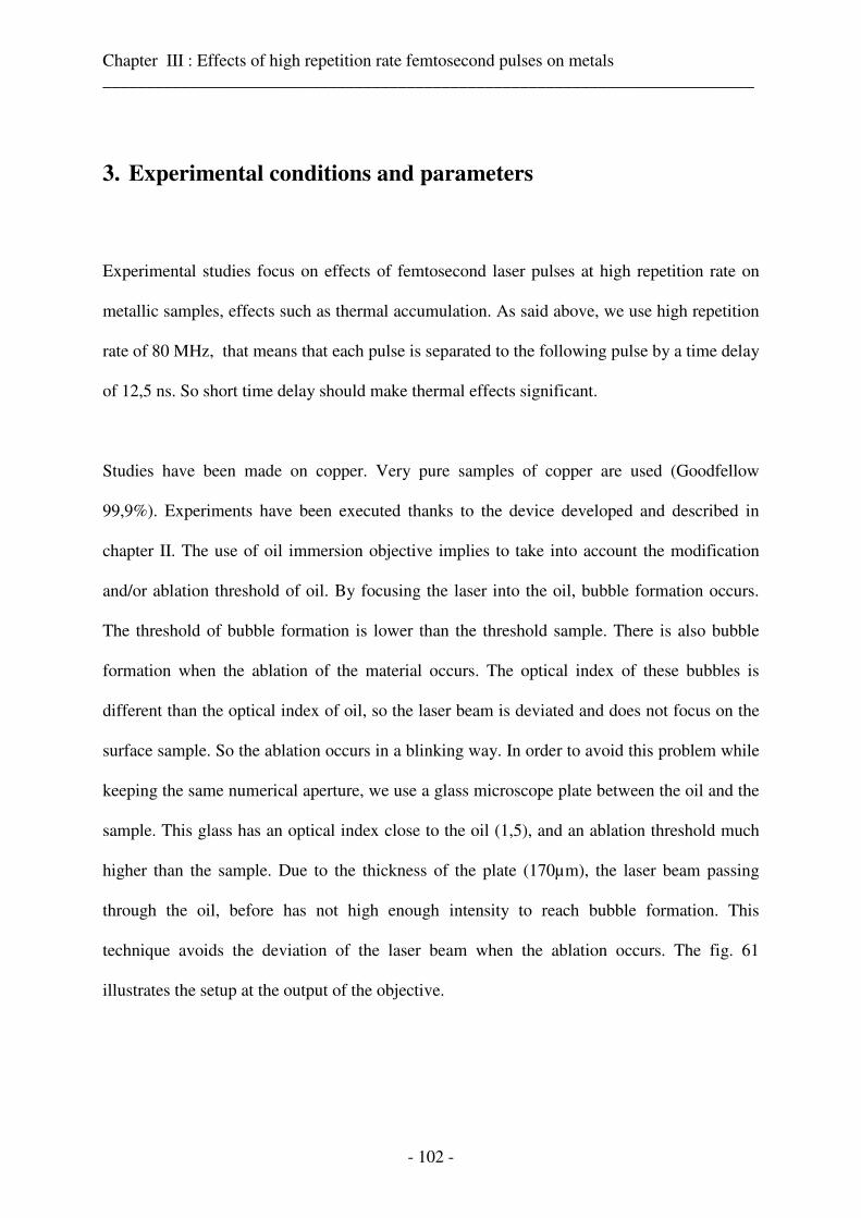
Chapter III : Effects of high repetition rate femtosecond pulses on metals ___________________________________________________________________________
- 102 -
3. Experimental conditions and parameters
Experimental studies focus on effects of femtosecond laser pulses at high repetition rate on
metallic samples, effects such as thermal accumulation. As said above, we use high repetition
rate of 80 MHz, that means that each pulse is separated to the following pulse by a time delay
of 12,5 ns. So short time delay should make thermal effects significant.
Studies have been made on copper. Very pure samples of copper are used (Goodfellow
99,9%). Experiments have been executed thanks to the device developed and described in
chapter II. The use of oil immersion objective implies to take into account the modification
and/or ablation threshold of oil. By focusing the laser into the oil, bubble formation occurs.
The threshold of bubble formation is lower than the threshold sample. There is also bubble
formation when the ablation of the material occurs. The optical index of these bubbles is
different than the optical index of oil, so the laser beam is deviated and does not focus on the
surface sample. So the ablation occurs in a blinking way. In order to avoid this problem while
keeping the same numerical aperture, we use a glass microscope plate between the oil and the
sample. This glass has an optical index close to the oil (1,5), and an ablation threshold much
higher than the sample. Due to the thickness of the plate (170µm), the laser beam passing
through the oil, before has not high enough intensity to reach bubble formation. This
technique avoids the deviation of the laser beam when the ablation occurs. The fig. 61
illustrates the setup at the output of the objective.
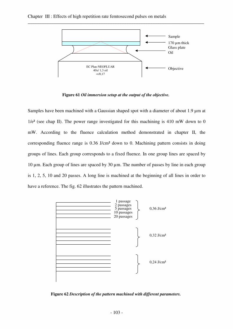
Chapter III : Effects of high repetition rate femtosecond pulses on metals ___________________________________________________________________________
- 103 -
Figure 61 Oil immersion setup at the output of the objective.
Samples have been machined with a Gaussian shaped spot with a diameter of about 1.9 µm at
1/e² (see chap II). The power range investigated for this machining is 410 mW down to 0
mW. According to the fluence calculation method demonstrated in chapter II, the
corresponding fluence range is 0.36 J/cm² down to 0. Machining pattern consists in doing
groups of lines. Each group corresponds to a fixed fluence. In one group lines are spaced by
10 µm. Each group of lines are spaced by 30 µm. The number of passes by line in each group
is 1, 2, 5, 10 and 20 passes. A long line is machined at the beginning of all lines in order to
have a reference. The fig. 62 illustrates the pattern machined.
Figure 62 Description of the pattern machined with different parameters.
5 passages 10 passages
1 passage 2 passages
20 passages
0,36 J/cm²
0,32 J/cm²
0,24 J/cm²
170 µm thick Glass plate
Sample
Oil
EC Plan-NEOFLUAR 40x/ 1,3 oil
∞/0,17
Objective
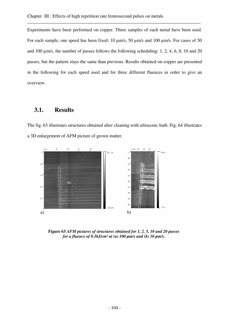
Chapter III : Effects of high repetition rate femtosecond pulses on metals ___________________________________________________________________________
- 104 -
Experiments have been performed on copper. Three samples of each metal have been used.
For each sample, one speed has been fixed: 10 µm/s, 50 µm/s and 100 µm/s. For cases of 50
and 100 µm/s, the number of passes follows the following scheduling: 1, 2, 4, 6, 8, 10 and 20
passes, but the pattern stays the same than previous. Results obtained on copper are presented
in the following for each speed used and for three different fluences in order to give an
overview.
3.1. Results
The fig. 63 illustrates structures obtained after cleaning with ultrasonic bath. Fig. 64 illustrates
a 3D enlargement of AFM picture of grown matter.
Figure 63 AFM pictures of structures obtained for 1, 2, 5, 10 and 20 passes
for a fluence of 0.36J/cm² at (a) 100 µm/s and (b) 10 µm/s.
a) b)
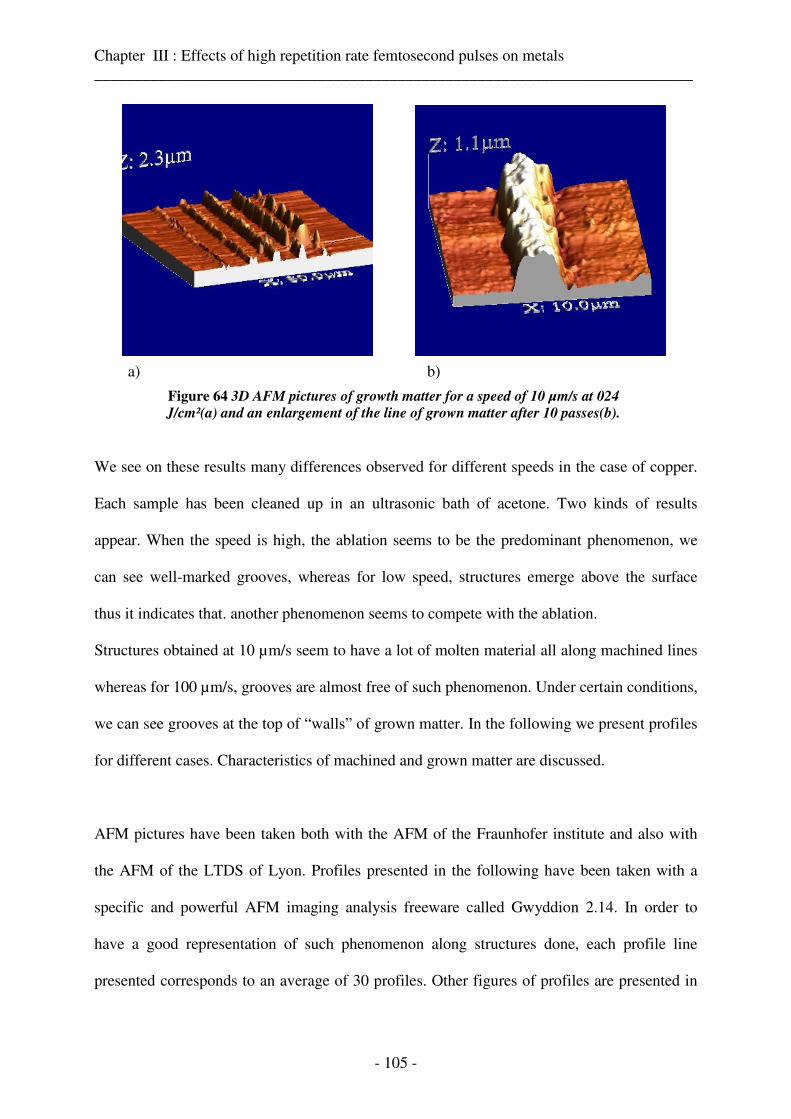
Chapter III : Effects of high repetition rate femtosecond pulses on metals ___________________________________________________________________________
- 105 -
Figure 64 3D AFM pictures of growth matter for a speed of 10 µm/s at 024
J/cm²(a) and an enlargement of the line of grown matter after 10 passes(b).
We see on these results many differences observed for different speeds in the case of copper.
Each sample has been cleaned up in an ultrasonic bath of acetone. Two kinds of results
appear. When the speed is high, the ablation seems to be the predominant phenomenon, we
can see well-marked grooves, whereas for low speed, structures emerge above the surface
thus it indicates that. another phenomenon seems to compete with the ablation.
Structures obtained at 10 µm/s seem to have a lot of molten material all along machined lines
whereas for 100 µm/s, grooves are almost free of such phenomenon. Under certain conditions,
we can see grooves at the top of “walls” of grown matter. In the following we present profiles
for different cases. Characteristics of machined and grown matter are discussed.
AFM pictures have been taken both with the AFM of the Fraunhofer institute and also with
the AFM of the LTDS of Lyon. Profiles presented in the following have been taken with a
specific and powerful AFM imaging analysis freeware called Gwyddion 2.14. In order to
have a good representation of such phenomenon along structures done, each profile line
presented corresponds to an average of 30 profiles. Other figures of profiles are presented in
a) b)
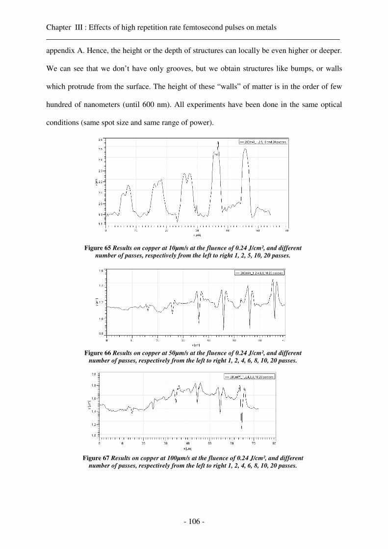
Chapter III : Effects of high repetition rate femtosecond pulses on metals ___________________________________________________________________________
- 106 -
appendix A. Hence, the height or the depth of structures can locally be even higher or deeper.
We can see that we don’t have only grooves, but we obtain structures like bumps, or walls
which protrude from the surface. The height of these “walls” of matter is in the order of few
hundred of nanometers (until 600 nm). All experiments have been done in the same optical
conditions (same spot size and same range of power).
Figure 65 Results on copper at 10µm/s at the fluence of 0.24 J/cm², and different
number of passes, respectively from the left to right 1, 2, 5, 10, 20 passes.
Figure 66 Results on copper at 50µm/s at the fluence of 0.24 J/cm², and different
number of passes, respectively from the left to right 1, 2, 4, 6, 8, 10, 20 passes.
Figure 67 Results on copper at 100µm/s at the fluence of 0.24 J/cm², and different
number of passes, respectively from the left to right 1, 2, 4, 6, 8, 10, 20 passes.
Chapter III : Effects of high repetition rate femtosecond pulses on metals ___________________________________________________________________________
- 107 -
3.2. Discussion:
A quick analysis put in evidence the difference between results corresponding to different
number of pulses. In the case of the speed of 10 µm/s, we obtain “bumps” or “walls” of
molten matter whereas for 100 µm/s we obtained grooves with much less molten matter on
the edge of grooves, which does not protrude so height from the surface. At the speed of 50
µm/s we obtained features which seem to be intermediate between structures obtained at 10
µm/s and structures obtained at 100 µm/s.
3.2.1. Heat accumulation effect on ablation rate
For 10 µm/s no groove are detectable so ablation rate has been studied only in cases of 50
µm/s and 100 µm/s. The depth of each groove has been measured. In order to avoid wrong
values due to the size of the AFM tip, values which are the same than measured just before
are not taken into account. Indeed, identical maximum values mean that the tip can’t go to
bottom of the groove. For all lines and for each fluence, the depth has been averaged to one
pass. Depth has been measured from the bottom of each groove to the surface level around the
groove analysed.
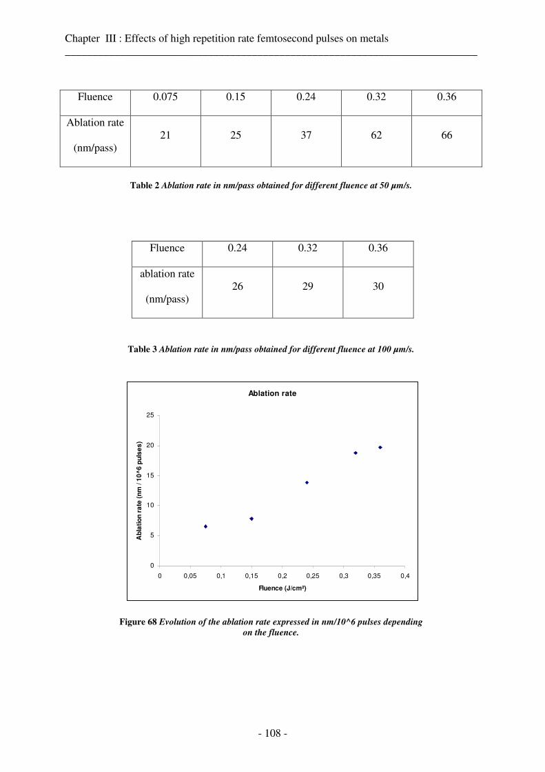
Chapter III : Effects of high repetition rate femtosecond pulses on metals ___________________________________________________________________________
- 108 -
Fluence 0.075 0.15 0.24 0.32 0.36
Ablation rate
(nm/pass) 21 25 37 62 66
Table 2 Ablation rate in nm/pass obtained for different fluence at 50 µm/s.
Fluence 0.24 0.32 0.36
ablation rate
(nm/pass) 26 29 30
Table 3 Ablation rate in nm/pass obtained for different fluence at 100 µm/s.
Ablation rate
0
5
10
15
20
25
0 0,05 0,1 0,15 0,2 0,25 0,3 0,35 0,4
Fluence (J/cm²)
Ab
lati
on
ra
te (
nm
/ 1
0^
6 p
uls
es
)
Figure 68 Evolution of the ablation rate expressed in nm/10^6 pulses depending
on the fluence.
Chapter III : Effects of high repetition rate femtosecond pulses on metals ___________________________________________________________________________
- 109 -
According to the literature, the ablation threshold of copper is estimated to be around 0.18
J/cm² [130] or 0.35 J/cm² [131]. The difference between these two values mainly comes from
a difference between the methods for calculating the fluence. In the first case, the fluence is
calculated in relation to the surface of the spot at 1/e² of the Gaussian beam, using the
formula: 20πω
PEF = , whereas in the second case, the fluence has been determined at the top of
the Gaussian beam using the formula : 20
2
πωPE
F = as demonstrated in the chapter II. So there is
thus a factor two between the two results. If we take into consideration the first value of
threshold and we multiply it by two in order to get the value at the top of the Gaussian used,
the threshold fluence value becomes 0.36 J/cm². In our experiment, this value corresponds to
the maximal fluence used. However, at this fluence we see that ablation occurs, and even for
fluences down to 0.075 J/cm², which is lower than reported in literature. This can be
explained by the heat accumulation effect which occurs for high repetition rates. This effect
enables machining of metals even with very low fluences. Ablation rates obtained are
expressed for a very high number of pulses. Indeed, in this case, the ablation rate expressed
for one pulse is so small, with a dimension of 10-6 nm/pulse, that would not be significant,
moreover this ablation is due to an accumulation of many pulses.
3.2.2. Influence of speed and fluence on the height of
protrudes
As illustrated on figures 65,66 and 67, two phenomena occur : ablation and growth of matter.
The phenomenon of growth of matter is predominant for very low speeds. There are 10 times
more pulses in the case of bumps than in the case of grooves. There are 16.106 pulses per
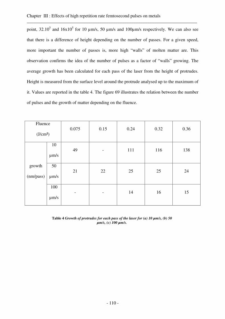
Chapter III : Effects of high repetition rate femtosecond pulses on metals ___________________________________________________________________________
- 110 -
point, 32.105 and 16x105 for 10 µm/s, 50 µm/s and 100µm/s respectively. We can also see
that there is a difference of height depending on the number of passes. For a given speed,
more important the number of passes is, more high “walls” of molten matter are. This
observation confirms the idea of the number of pulses as a factor of “walls” growing. The
average growth has been calculated for each pass of the laser from the height of protrudes.
Height is measured from the surface level around the protrude analysed up to the maximum of
it. Values are reported in the table 4. The figure 69 illustrates the relation between the number
of pulses and the growth of matter depending on the fluence.
Fluence
(J/cm²) 0.075 0.15 0.24 0.32 0.36
10
µm/s 49 - 111 116 138
50
µm/s 21 22 25 25 24
growth
(nm/pass)
100
µm/s - - 14 16 15
Table 4 Growth of protrudes for each pass of the laser for (a) 10 µm/s, (b) 50
µm/s, (c) 100 µm/s.
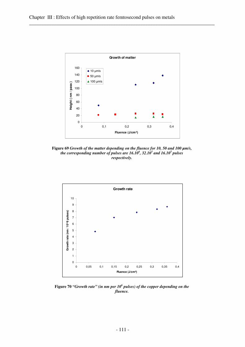
Chapter III : Effects of high repetition rate femtosecond pulses on metals ___________________________________________________________________________
- 111 -
Growth of matter
0
20
40
60
80
100
120
140
160
0 0,1 0,2 0,3 0,4
Fluence (J/cm²)
Heig
ht
( n
m / p
ass )
10 µm/s
50 µm/s
100 µm/s
Figure 69 Growth of the matter depending on the fluence for 10, 50 and 100 µm/s,
the corresponding number of pulses are 16.106, 32.10
5 and 16.10
5 pulses
respectively.
Growth rate
0
1
2
3
4
5
6
7
8
9
10
0 0,05 0,1 0,15 0,2 0,25 0,3 0,35 0,4
Fluence (J/cm²)
Gro
wth
ra
te (
nm
/ 1
0^
6 p
uls
es
)
Figure 70 “Growth rate” (in nm per 106 pulses) of the copper depending on the
fluence.
Chapter III : Effects of high repetition rate femtosecond pulses on metals ___________________________________________________________________________
- 112 -
The figure 69 illustrates the average height of grown matter for each pass of the laser beam on
the sample. We can see clearly that the dependence of the grown matter on the fluence is very
significant only for a high number of pulses. Indeed, for speeds of 50 µm/s and 100 µm/s, the
height of grown matter does not exceed 25 nm even for a high fluence whereas height reaches
138 nm at 10 µm/s. However, we can see that matter is slightly higher in the case of 50µm/s
with a maximum of 25 nm, than in the case of 100µm/s where the maximum reaches 16 nm
only. From this analysis we deduce a “growth rate” for many pulses as shown on figure 70.
We can see that the growth rate increases with the fluence. However, for highest fluences we
can see on profiles that grooves inside protrudes appear. That shows that for high fluences,
the ablation occurs and tends to get the upper hand. It suggests that for higher fluences the
growth rate should present a kind of cut off value of fluence after which the ablation is the
dominant process.
As said at the beginning of the chapter, a same kind of phenomenon has already been
observed. At such repetition rate (80 MHz) and with a so high number of pulses a heat
accumulation effect occurs. As we have seen using simulation results, the evolution of the
temperature inside the material, even limited to four pulses, heat accumulation effect occurs.
In the case of much higher number of pulses, the heat accumulation occurring should be thus
much more important. We think that phenomenon is linked and/or of the same order than
which occurred during growing of nanojets on gold film observed by [118]. As seen with
simulations in chapter one, for an amount of constant energy, the temperature goes deeper and
deeper inside the material depending on the number of pulses. If this hypothesis of the depth
propagation of the temperature is verified, so we can say that with 10 µm/s the temperature
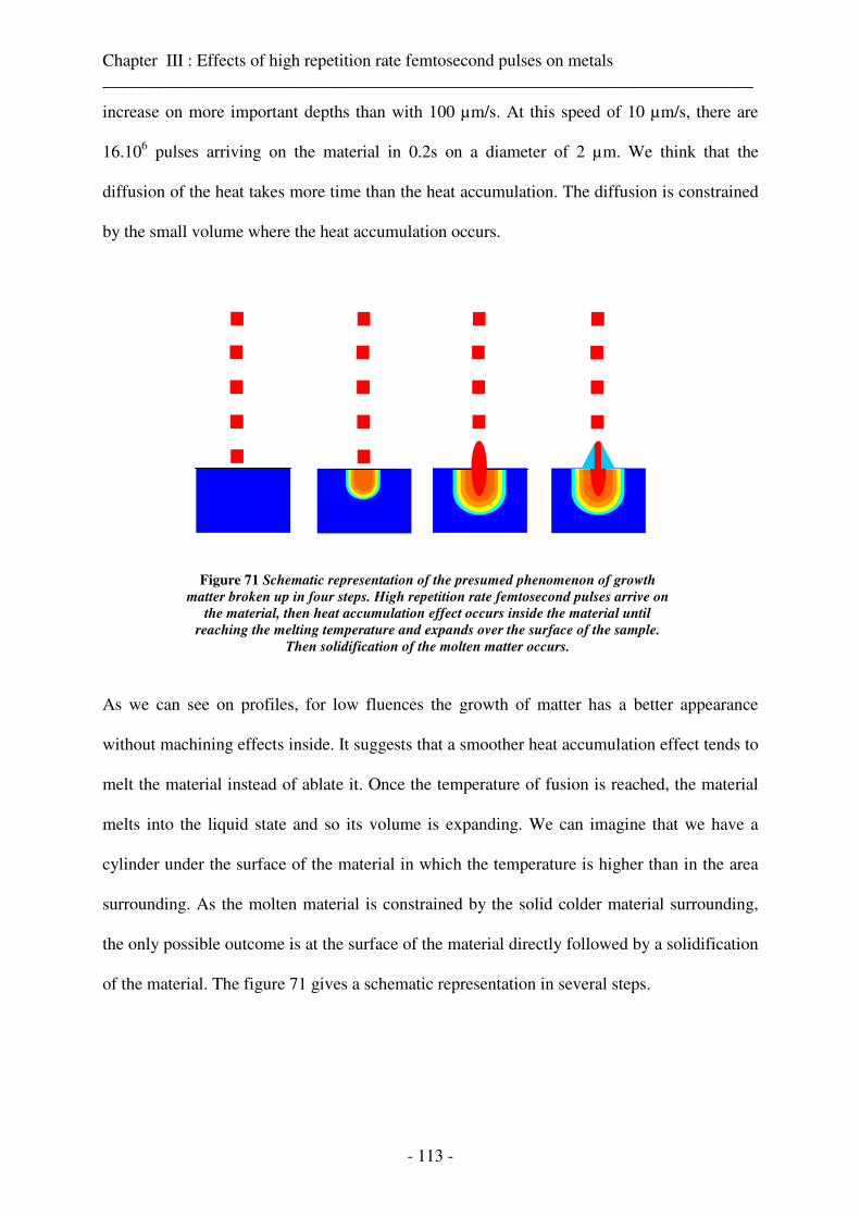
Chapter III : Effects of high repetition rate femtosecond pulses on metals ___________________________________________________________________________
- 113 -
increase on more important depths than with 100 µm/s. At this speed of 10 µm/s, there are
16.106 pulses arriving on the material in 0.2s on a diameter of 2 µm. We think that the
diffusion of the heat takes more time than the heat accumulation. The diffusion is constrained
by the small volume where the heat accumulation occurs.
Figure 71 Schematic representation of the presumed phenomenon of growth
matter broken up in four steps. High repetition rate femtosecond pulses arrive on
the material, then heat accumulation effect occurs inside the material until
reaching the melting temperature and expands over the surface of the sample.
Then solidification of the molten matter occurs.
As we can see on profiles, for low fluences the growth of matter has a better appearance
without machining effects inside. It suggests that a smoother heat accumulation effect tends to
melt the material instead of ablate it. Once the temperature of fusion is reached, the material
melts into the liquid state and so its volume is expanding. We can imagine that we have a
cylinder under the surface of the material in which the temperature is higher than in the area
surrounding. As the molten material is constrained by the solid colder material surrounding,
the only possible outcome is at the surface of the material directly followed by a solidification
of the material. The figure 71 gives a schematic representation in several steps.
Chapter III : Effects of high repetition rate femtosecond pulses on metals ___________________________________________________________________________
- 114 -
4. Conclusion
The interaction of high repetition rate laser pulses on the matter induces phenomena which do
not appear with lower repetition rate lasers. Indeed, the time delay between two pulses is so
small that the energy stacked into the volume irradiated can not escape before the arrival of
next pulses. Hence, an accumulation phenomenon of the energy occurs inside the material.
This slow accumulation of small amounts of energy modifies the kind of ablation. Molten
matter has been observed. It seems to grow up depending on the strength of the heat
accumulation effect. Indeed, highest structures have been observed for the highest number of
pulses interacting with the material. This new phenomenon depends on laser parameters. This
implies that size and height of structures can be controlled. This open the way to a new field
of applications using high repetition rate femtosecond laser pulses.
Chapter IV: Results and applications in biotechnologies ___________________________________________________________________________
- 115 -
Chapter IV
Results and applications in
biotechnologies

Chapter IV: Results and applications in biotechnologies ___________________________________________________________________________
- 116 -
Chapter IV: Results and applications in biotechnologies ___________________________________________________________________________
- 117 -
1. Introduction
Lasers have become irreplaceable tools in modern medicine, spanning a wide spectrum of
applications from laser surgery [132] to optical imaging [133]. Laser ablation, which has the
great advantage of precise material removal, is a promising method in processing and
treatment of biological tissues [134] [135] [136], biodegradable polymers [137] [138], dental
implants [139], etc. In this chapter the potential of the multifunctional tool presented in
chapter 2 for different applications in biotechnology is shown. Results on large area
multiphoton imaging as well as nanoprocessing of biological tissue and various materials are
presented.
Chapter IV: Results and applications in biotechnologies ___________________________________________________________________________
- 118 -
2. Mapping of micro area
As describe in the chapter 2 in the section 5.3, the setup developed allows imaging a large
area of a sample with high resolution. The field of view of a 40×/1.3 NA objective lens is of
0.625 mm. The magnification has been furthermore increased by a factor of about 10 x to
obtain high detailed images through the focusing setup of variable lenses inserted before the
CCD camera. After calibration, the final field of view is of 57x76 µm2 and 70x90 µm² when
using a lens of 300 mm and 250 mm focal length respectively. Two-dimensional matrix of
images is captured and stitched in software to create a mosaic that displays a large field of
view. As already said in chapter 2, the matrix of images is acquired with a continuous step-
and-capture routine while translating the sample with the pizo-driven linear XY stages. Due
to the high resolution translation stages, junctions of pictures are very fine with non
significant overlapping. The software developed is high flexible, it allows to capture a
undefined number of images in X and Y, with desired resolution and at any desired location.
To minimize possible illumination vignetting effects, shading bands at the edges between
pairs of neighbouring, images were corrected by brightness averaging. All images and the
complete mapping are saved in bmp format. Processing routine and time of individual image
capture, transferring, archiving and complete mosaic have been optimized to be relatively fast.
Of course, it depends on the number and the resolution of individual images. The number of
pixels of individual image can be selected in the software in order to find compromise
between resolution and time processing. In the fig. 72, an example of a mosaic of 5 x 5
images of blood cells (standard size: 6-8 µm) is given.
Chapter IV: Results and applications in biotechnologies ___________________________________________________________________________
- 119 -
Figure 72 Schematic representation of area mapping of blood cells.
Each image consist of 1280 × 960 pixels, is 24-bit greyscale and requires 4,6 MB of memory.
Thus, a mosaic of 5 × 5 images at full resolution consists of 6400 × 4800 pixels and requires
about 115 MB of memory. For acquisition of a mosaic, a continuous step-and-capture routine
requires around 30 s for 5 × 5 images. Transferring and archiving images followed by
processing to create a mosaic requires another 60 s on a PC with a Pentium 2.2-GHz
processor. Thus, total time to create a mosaic is 90 s. One can observe the high overlapping
quality and the good illumination uniformity at the edges.
Such an image reconstruction allows high control and inspection of small features. Various
examples are presented in the fig. 73: A large area mosaic of a 6 × 6 (a) and 12 × 12 (b) grid
pattern performed on Su8 photoresist under lithography, a 5 × 5 mosaic of bird feather (c).
76 µm
57
µm
Chapter IV: Results and applications in biotechnologies ___________________________________________________________________________
- 120 -
Figure 73 Mapping of 6 × 6 (a) and 12 × 12 (b) images of a grid pattern
performed on Su8 photoresist under lithography, (b) 5 × 5 mosaic of a bird
feather.
The mosaicing system is also suitable for other kind of microscopy imaging as confocal or
two photon laser scanning microscopy. Confocal microscopy is a technique for obtaining
high-resolution optical images with depth selectivity [140]. Two-photon microscopy is a
fluorescence imaging technique that allows imaging living tissue up to a depth of one
millimetre [141]. For very thin objects such as isolated cells, single-photon (confocal)
microscopes can produce images with higher optical resolution due to their shorter excitation
wavelengths. In scattering tissue, on the other hand, the superior optical sectioning and light
detection capabilities of the two-photon microscope result in better performance Two-photon
excitation can be a superior alternative to confocal microscopy due to its deeper tissue
(a)
70
µm
90 µm
(c)
76 µm
57
µm
57 µ
m 90 µm
(b)
Chapter IV: Results and applications in biotechnologies ___________________________________________________________________________
- 121 -
penetration, efficient light detection and reduced phototoxicity. Nowadays, multiphoton
microscopy typically uses sources like Ti:sapphire lasers with high repetition rate like 70 - 80
MHz and pulses duration shorter than 150 fs.
The large area mapping system has been coupled and tested with a commercial two-photon
laser scanning microscope (TauMap, JenLab GmbH, Germany). The system is based on a
conventional fluorescence microscope equipped with a high numerical aperture (1.3)
objective, a special compact scanning module and a photomultiplier detector attached to the
microscope ports. The laser “Mai Tai” used has already been depicted in the chapter 2. Single
high resolution two photon images are performed by the scanner. The scan field of each
image is limited to a maximal area of 350 × 350 µm² due to the high numerical aperture
objective and the request resolution.
A sample composed of fluorescent sphere (beads) with different sizes has been mapped (fig.
74). The mosaic of 3 × 2 images has a dimension of 624 × 384 µm² (the size of each image is
192 × 208 µm²). Each individual image has a resolution of 512 x 512 pixels ant thus 1,5x10⁶
pixels for the full mapping.
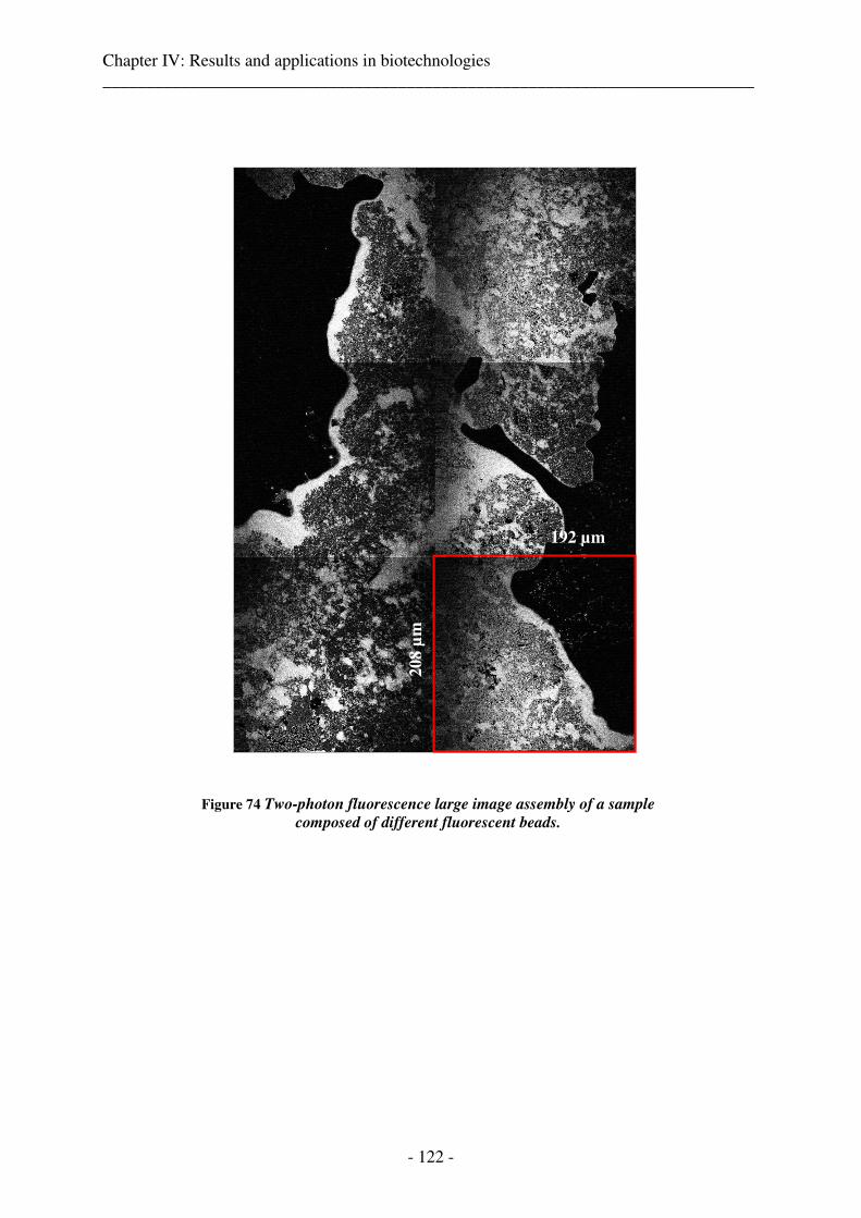
Chapter IV: Results and applications in biotechnologies ___________________________________________________________________________
- 122 -
Figure 74 Two-photon fluorescence large image assembly of a sample
composed of different fluorescent beads.
208 µ
m
192 µm
Chapter IV: Results and applications in biotechnologies ___________________________________________________________________________
- 123 -
3. Targeting and nanodissection
Tissue processing with femtosecond laser pulses has been of growing interest since its high
precision was demonstrated on a variety of different tissue types [142]. Due to its sub µm
precision, it is possible to perform for example surgical procedures like refractive surgery
inside the human eye [143]. Near-infrared (NIR) femtosecond laser pulses with low average
power are novel tools for ultraprecise intracellular and intratissue surgery, cell isolation, tissue
engineering, stem cell research, gene therapy, the production of DNA vaccines for examples.
Multiphoton ablation can be achieved with low nanojoule energy laser pulses when using
focusing optics of high numerical aperture. The high peak powers at a moderate average
power provided by the pulsed laser in combination with high numerical aperture optics leads
to photon fluxes of more than 1027 photons s-1 cm-2 and therefore high light intensities in the
TW/cm2 region at the target material. NIR light at such high intensities results in multi-photon
absorption which leads via multi-photon ionization and avalanche ionization to an optical
breakdown and the formation of a spatially confined micro-plasma [144] [145]. It has been
shown that processing of biological with a spatial resolution in the order of some hundred
nanometer and lower is possible [146] [147] [148] [149] [150] [151] [152] [153]. Nanodissection
with ultra short laser pulses opens new horizons for scientists, who are primarily interested in
investigation of cells, and tissues processes. High accurate, compact and flexible workstations
as the one developed in this work are needed.
The mapping presented in the previous paragraph can be a useful tool to locate a precise
position on a large area for enabling laser processing as for example cell perforation or
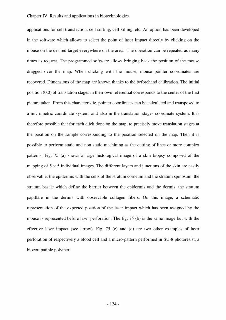
Chapter IV: Results and applications in biotechnologies ___________________________________________________________________________
- 124 -
applications for cell transfection, cell sorting, cell killing, etc. An option has been developed
in the software which allows to select the point of laser impact directly by clicking on the
mouse on the desired target everywhere on the area. The operation can be repeated as many
times as request. The programmed software allows bringing back the position of the mouse
dragged over the map. When clicking with the mouse, mouse pointer coordinates are
recovered. Dimensions of the map are known thanks to the beforehand calibration. The initial
position (0,0) of translation stages in their own referential corresponds to the center of the first
picture taken. From this characteristic, pointer coordinates can be calculated and transposed to
a micrometric coordinate system, and also in the translation stages coordinate system. It is
therefore possible that for each click done on the map, to precisely move translation stages at
the position on the sample corresponding to the position selected on the map. Then it is
possible to perform static and non static machining as the cutting of lines or more complex
patterns. Fig. 75 (a) shows a large histological image of a skin biopsy composed of the
mapping of 5 × 5 individual images. The different layers and junctions of the skin are easily
observable: the epidermis with the cells of the stratum corneum and the stratum spinosum, the
stratum basale which define the barrier between the epidermis and the dermis, the stratum
papillare in the dermis with observable collagen fibers. On this image, a schematic
representation of the expected position of the laser impact which has been assigned by the
mouse is represented before laser perforation. The fig. 75 (b) is the same image but with the
effective laser impact (see arrow). Fig. 75 (c) and (d) are two other examples of laser
perforation of respectively a blood cell and a micro-pattern performed in SU-8 photoresist, a
biocompatible polymer.
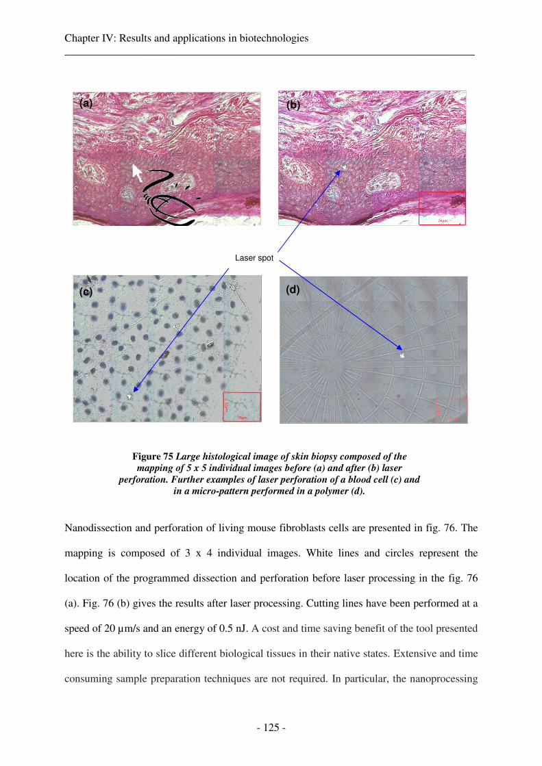
Chapter IV: Results and applications in biotechnologies ___________________________________________________________________________
- 125 -
Figure 75 Large histological image of skin biopsy composed of the
mapping of 5 x 5 individual images before (a) and after (b) laser
perforation. Further examples of laser perforation of a blood cell (c) and
in a micro-pattern performed in a polymer (d).
Nanodissection and perforation of living mouse fibroblasts cells are presented in fig. 76. The
mapping is composed of 3 x 4 individual images. White lines and circles represent the
location of the programmed dissection and perforation before laser processing in the fig. 76
(a). Fig. 76 (b) gives the results after laser processing. Cutting lines have been performed at a
speed of 20 µm/s and an energy of 0.5 nJ. A cost and time saving benefit of the tool presented
here is the ability to slice different biological tissues in their native states. Extensive and time
consuming sample preparation techniques are not required. In particular, the nanoprocessing
Laser spot
(a)
(c)
(b)
(d)
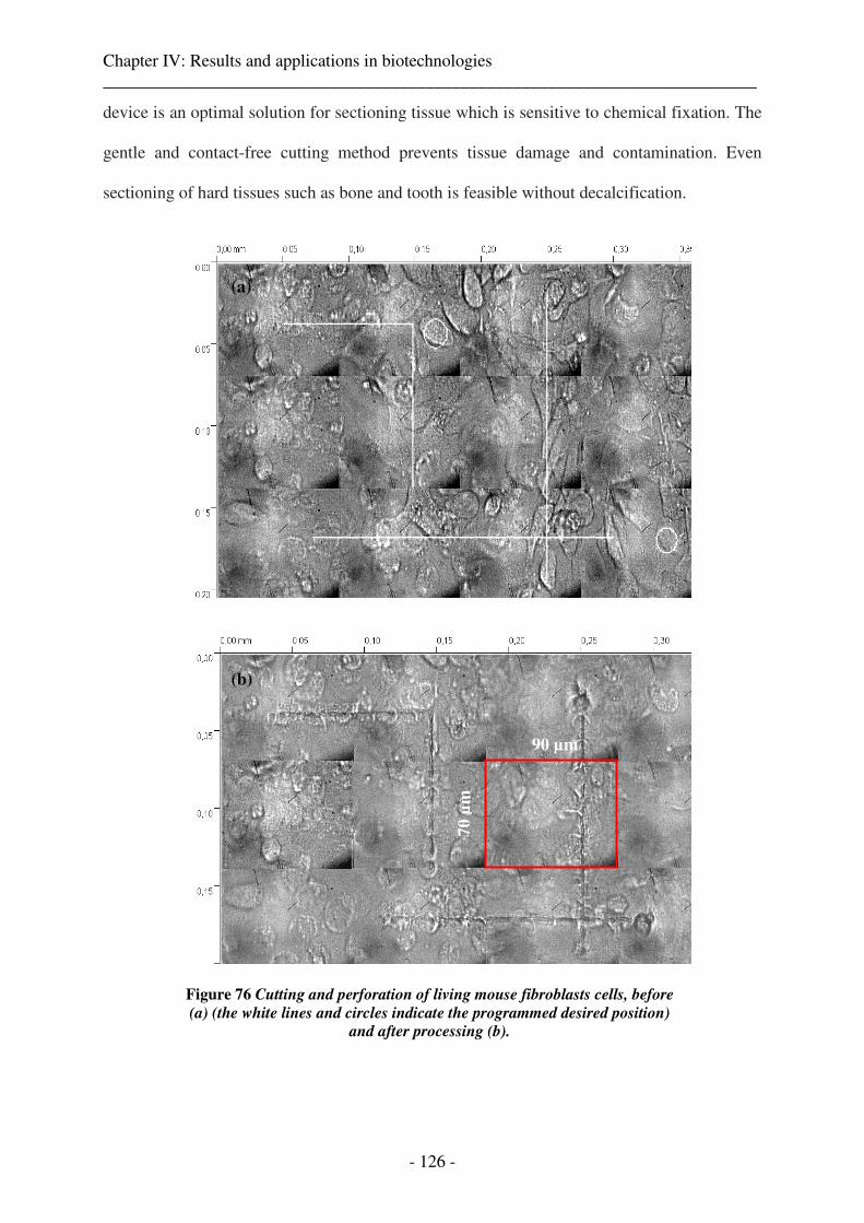
Chapter IV: Results and applications in biotechnologies ___________________________________________________________________________
- 126 -
device is an optimal solution for sectioning tissue which is sensitive to chemical fixation. The
gentle and contact-free cutting method prevents tissue damage and contamination. Even
sectioning of hard tissues such as bone and tooth is feasible without decalcification.
Figure 76 Cutting and perforation of living mouse fibroblasts cells, before
(a) (the white lines and circles indicate the programmed desired position)
and after processing (b).
(a)
(b)
90 µm
70 µ
m
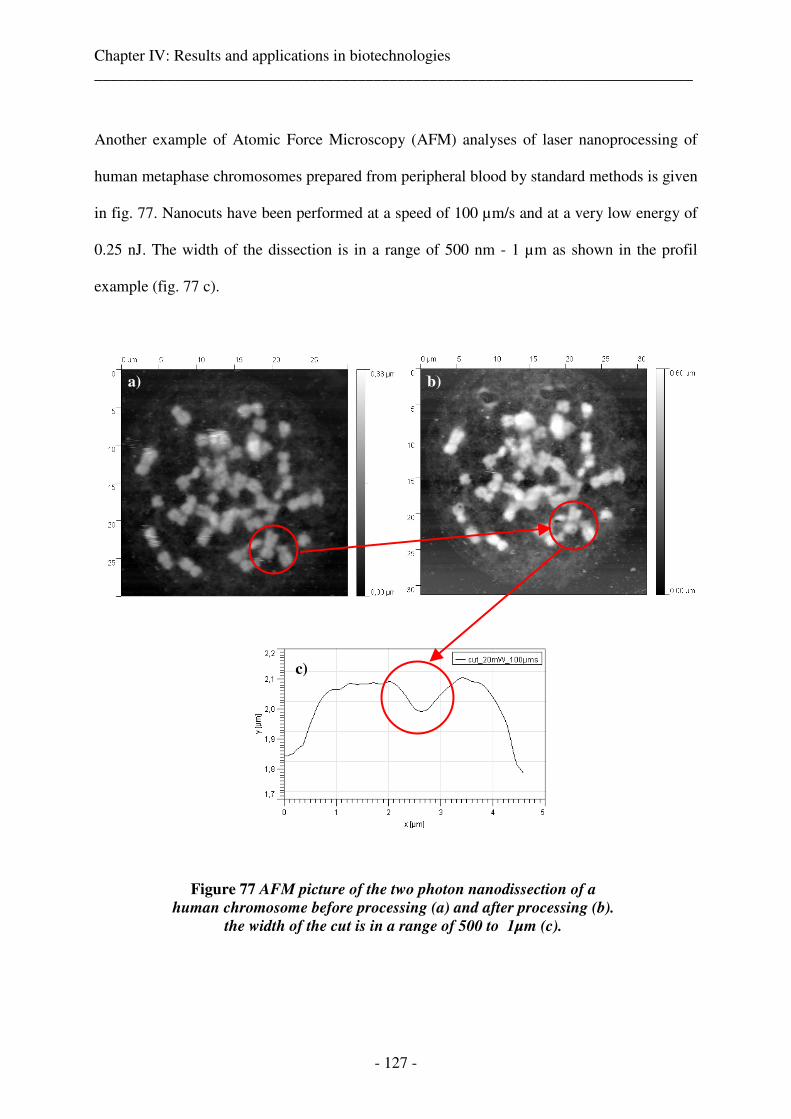
Chapter IV: Results and applications in biotechnologies ___________________________________________________________________________
- 127 -
Another example of Atomic Force Microscopy (AFM) analyses of laser nanoprocessing of
human metaphase chromosomes prepared from peripheral blood by standard methods is given
in fig. 77. Nanocuts have been performed at a speed of 100 µm/s and at a very low energy of
0.25 nJ. The width of the dissection is in a range of 500 nm - 1 µm as shown in the profil
example (fig. 77 c).
Figure 77 AFM picture of the two photon nanodissection of a
human chromosome before processing (a) and after processing (b).
the width of the cut is in a range of 500 to 1µm (c).
a) b)
c)
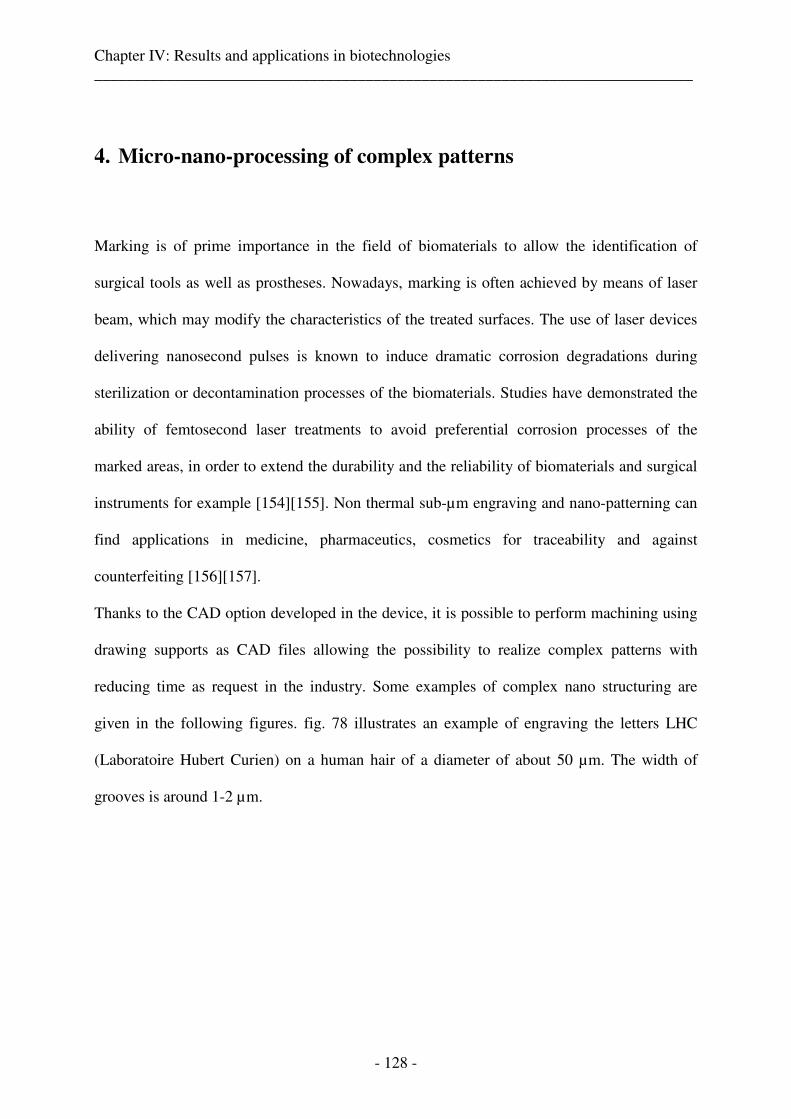
Chapter IV: Results and applications in biotechnologies ___________________________________________________________________________
- 128 -
4. Micro-nano-processing of complex patterns
Marking is of prime importance in the field of biomaterials to allow the identification of
surgical tools as well as prostheses. Nowadays, marking is often achieved by means of laser
beam, which may modify the characteristics of the treated surfaces. The use of laser devices
delivering nanosecond pulses is known to induce dramatic corrosion degradations during
sterilization or decontamination processes of the biomaterials. Studies have demonstrated the
ability of femtosecond laser treatments to avoid preferential corrosion processes of the
marked areas, in order to extend the durability and the reliability of biomaterials and surgical
instruments for example [154] [155]. Non thermal sub-µm engraving and nano-patterning can
find applications in medicine, pharmaceutics, cosmetics for traceability and against
counterfeiting [156] [157].
Thanks to the CAD option developed in the device, it is possible to perform machining using
drawing supports as CAD files allowing the possibility to realize complex patterns with
reducing time as request in the industry. Some examples of complex nano structuring are
given in the following figures. fig. 78 illustrates an example of engraving the letters LHC
(Laboratoire Hubert Curien) on a human hair of a diameter of about 50 µm. The width of
grooves is around 1-2 µm.
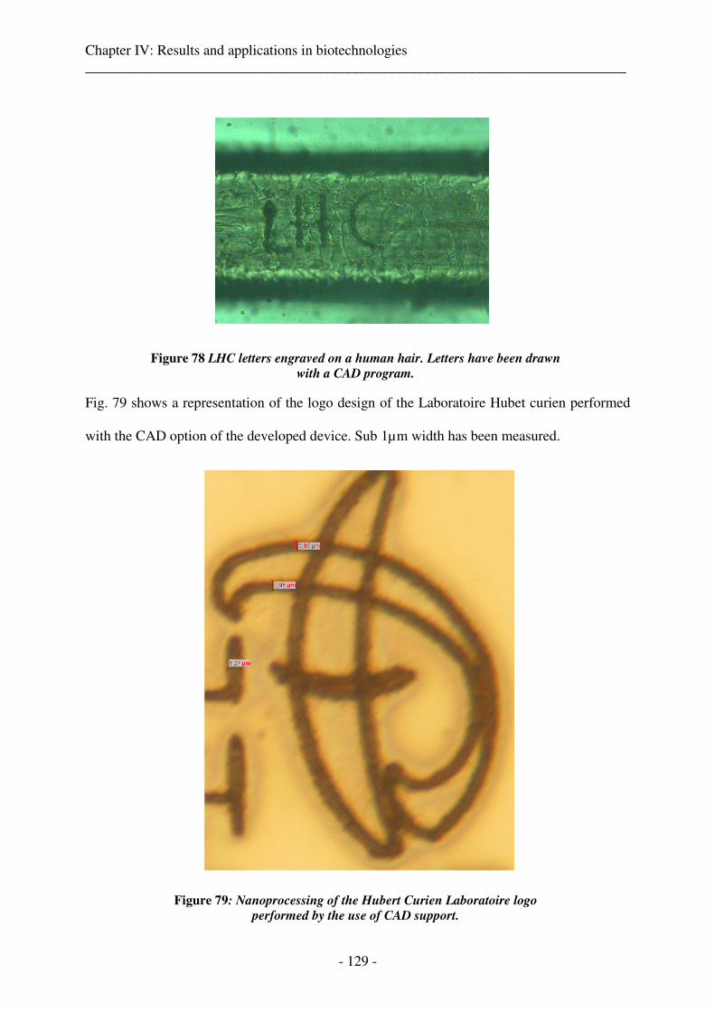
Chapter IV: Results and applications in biotechnologies ___________________________________________________________________________
- 129 -
Figure 78 LHC letters engraved on a human hair. Letters have been drawn
with a CAD program.
Fig. 79 shows a representation of the logo design of the Laboratoire Hubet curien performed
with the CAD option of the developed device. Sub 1µm width has been measured.
Figure 79: Nanoprocessing of the Hubert Curien Laboratoire logo
performed by the use of CAD support.
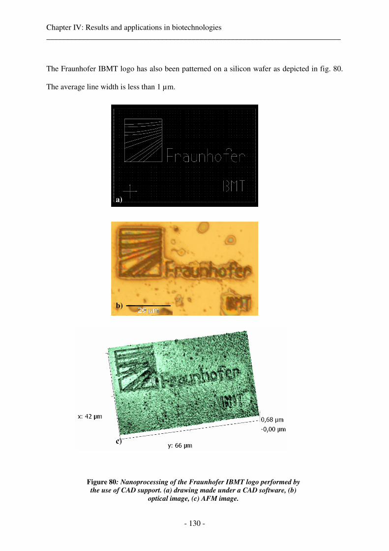
Chapter IV: Results and applications in biotechnologies ___________________________________________________________________________
- 130 -
The Fraunhofer IBMT logo has also been patterned on a silicon wafer as depicted in fig. 80.
The average line width is less than 1 µm.
Figure 80: Nanoprocessing of the Fraunhofer IBMT logo performed by
the use of CAD support. (a) drawing made under a CAD software, (b)
optical image, (c) AFM image.
b)
c)
a)
Chapter IV: Results and applications in biotechnologies ___________________________________________________________________________
- 131 -
Laser micro-nano-patterning could be also applied in surface texturing to fabricate
superhydrophobic surfaces, phenomenon known as the “Lotus effect”. In nature, lotus leaf
and other plants have superhydrophobic surface with self-cleaning effect. Water drop does not
adhere to lotus leaf and completely rolls off the leaf, carrying away undesirable particles
[158] [159]. The influence of material topography on cellular behaviour has shown that
different structures such as pores, grooves and pits in micrometer and nanometer dimensions
affect cell morphology, orientation, adhesion, and proliferation of cells. Material hydrophilic /
hydrophobic character depends on nano- and microscale surface topography. Furthermore, it
has been demonstrated that hydrophilic/hydrophobic materials influence cellular adhesion and
cytoskeletal organization. The hydrophobic properties of femtosecond laser fabricated
structures and their effects on cell proliferation shows interesting results [160]. Often hard
implants undergo detachment from the host tissue due to inadequate biocompatibility and
poor osteointegration. Changing surface chemistry and physical topography of the surface
influences biocompatibility. Potential of nano-patterning of implant and prosthesis with
femtosecond laser pulses on materials such as Titanium have been shown [161] [162].
Chapter IV: Results and applications in biotechnologies ___________________________________________________________________________
- 132 -
5. Two-photon polymerization
It has been shown that nonlinear optical lithography based on two-photon polymerization
(2PP) of photosensitive resins allows the fabrication of true 3D nanostructures and therefore
of 3D photonic crystals [163] [164] [165] [166] [167] [168]. When tightly focused into the
volume of a photosensitive resin, the polymerization process can be initiated by nonlinear
absorption of femtosecond laser pulses within the focal volume. By moving the laser focus
three-dimensionally through the resin any 3D nanostructure with a resolution down to 100 nm
can be fabricated. There are many well known applications for single-photon polymerization
(1-PP) like UV-photolithography or stereolithography, where a single UV-photon is needed to
initiate the polymerization process on the surface of a photosensitive resin. Depending on the
concentration of photo-initiators and of added absorber molecules, UV light is absorbed
within the first few µm. Therefore, single-photon polymerization is a planar process restricted
to the surface of the resin.
However, the photosensitive resins used are transparent to near-infrared light, so it is possible
to focus near-infrared femtosecond pulses into the volume of the resin. If the photon density
reaches the threshold value, two-photon absorption occurs within the focal volume, initiating
the polymerization process. If the laser focus is moved three-dimensionally through the
volume of the resin, the polymerization process is initiated along the track of the focus,
allowing the fabrication of any 3D microstructure. There are several advantages of the two-
photon polymerization compared to one-photon polymerization. The most important is that
polymerization can be initiated into the volume of the resin, that is to say the 2-PP is a true 3D
process whereas 1-PP is a planar process. 1-PP allows making of 3D structures but only layer
Chapter IV: Results and applications in biotechnologies ___________________________________________________________________________
- 133 -
by layer. A new approach to photolithography in which multiphoton absorption of pulsed 800-
nanometer (nm) light is used to initiate cross-linking in a polymer photoresist and one-photon
absorption of continuous-wave 800-nm light is used simultaneously to deactivate the
photopolymerization allow to achieve λ/20 (40 nm) structures [169].
Patterns in photoresist SU-8 2000 using the 3D structuring system have been tested. SU-8
2000 is a high contrast, epoxy based photoresist designed for micromachining and
applications, where a thick, chemically and thermally stable image is desired. SU-8 2000 is an
improved formulation of SU-8, which has been widely used by MEMS producers for many
years. Photoresist is most commonly exposed with conventional UV radiation, from 350 to
400 nm, although 365 nm is the recommended wavelength. SU-8 2000 may also be exposed
with e-beam or x-ray radiation. It is also possible to expose SU-8 2000 with femtosecond
laser emitting at a wavelength of 800 nm. Indeed, due to typical very high peak power,
several photons of smaller energy together can produce the same absorption effect than
normally produced by the absorption of a single photon of higher energy.
Thanks to the 3D option developed as presented in the chapter 2, features have been
performed in the volume of SU-8 as shown in fig. 81. The pattern is made of 2 rows of 6
tubes each with a diameter of 15 µm imbricated into each other. The structure is 30 µm high
which was the thickness of the SU-8 film.
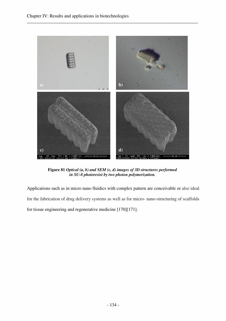
Chapter IV: Results and applications in biotechnologies ___________________________________________________________________________
- 134 -
Figure 81 Optical (a, b) and SEM (c, d) images of 3D structures performed
in SU-8 photoresist by two photon polymerization.
Applications such as in micro nano fluidics with complex pattern are conceivable or also ideal
for the fabrication of drug delivery systems as well as for micro- nano-structuring of scaffolds
for tissue engineering and regenerative medicine [170] [171].
a) b)
c) d)
Chapter IV: Results and applications in biotechnologies ___________________________________________________________________________
- 135 -
6. Conclusion
Here we have demonstrated the development of an efficient and powerful nanoprocessing
apparatus for biotechnological applications. The device is high flexible and adaptable with a
strong hardware and software environment which allow a high range of applications and
performances for medicine, biology, pharmaceutics, cosmetics, etc. Such a device is also
potentially useful for materials nanoprocessing in a general manner as the manufacture of
waveguides, gratings, micro fluidic devices, nanocontainers, data storage, nanolithography,
nanomarking, etc. Of course one of the limitation is the processing speed for high-volume and
high-rate nanomanufacturing.

___________________________________________________________________________
- 136 -
Conclusion ___________________________________________________________________________
- 137 -
Conclusion
Miniaturization is an attribute of today's photonic industry, determining an intense and
global effort in micro- and nano-technology, and in this context, materials micro/nano
structuring has become the backbone of rapidly expanding application areas in emerging
technologies. Further progress in telecommunications, optics, electronics, biomaterials,
medicine, and transport strongly depends on the availability of reliable and rapid processing
techniques. Laser-based micro technology holds great promises and the evolution will be
dictated by the development of inexpensive yet precise processing tools that can develop and
structure materials with a high degree of controllability, accuracy, and reduced residual
damage.
New processes are presented as well as for micro machining as for nano machining
ranges. Due to deterministic behaviour of femtosecond laser pulses, it has been possible to
develop an innovative method to calculate processing time for micro machining process. This
method enables the calculation of the time when the ablation of the material is active. This
enables to evaluate time processing due to external reasons such as mechanical or computing
which is full of interest for industries. Indeed, that gives concrete information and to what
extent improvements are possible.
In this work we have demonstrated the feasibility to take advantage of the interaction of
femtosecond laser pulses with matter and this by having developed a compact and flexible
apparatus. This device is of great interest and covers wide research fields such as
nanoprocessing of biological samples, nanostructuring of different type of materials, hence is
Conclusion ___________________________________________________________________________
- 138 -
of great interest for many applications in material science, nanobiotechnology and
nanomedicine. This workstation enables the mapping of a large area with a very high
resolution, as well as transmission and reflexion imaging than two photons imaging. This
allows targeting a precise location on a large area of a sample and makes possible the
nanodissection of biological samples, cells, chromosomes …
The use of high numerical aperture focusing objective enables to reach very high
intensities in a very small volume. This can initiate a two photon effect due to high peak
power reached at the focus point. Two photon of the same energy can produce the same
absorption effect than the absorption of one photon which has two times more energy. This
effect occurs in a smaller volume than on photon and so is huge of interest for real 3D
nanostructuring using photopolymerization of resins such as SU-8.
The whole device is controlled with a software developed to be easy to learn and easy to
work for a final customer. Moreover, the workstation is designed to be coupled with a low
average power femtosecond oscillator laser systems which are more cost-effective and more
reliable compared to amplified lasers.
However, there are still open questions concerning physical comprehension of
phenomenon of growing matter and heat accumulation effects on matter. Analysis put in
evidence a dependency between experimental parameters and the high and shape of protrudes
of matter. However, more investigations are still necessary to well understand this
phenomenon. The control of such phenomenon open a new way for nanostructuring and could
have many applications in fields such as cell adhesion or cell growth, tribology, electronics …
List of figures ___________________________________________________________________________
- 139 -
List of figures
Chapter I: Overview of nanostructuring techniques
FIGURE 1 SCHEMATIC REPRESENTATION OF PATTERN TRANSFER TECHNIQUES [1]................................................... - 6 - FIGURE 2 OVERVIEW OF 30 NM GRATING EXPOSED IN HSQ RESIST ON SILICON (A) AND ZOOM ON LINES OF 10 NM
WIDTH (B) [3].............................................................................................................................................. - 8 - FIGURE 3 SIMPLIFIED COMPARISON OF IMPRINT LITHOGRAPHY TECHNIQUES [21]. ............................................... - 11 - FIGURE 4 SCHEME OF A LASER STEREOLITHOGRAPHY SETUP (A). CELLULAR-TYPE STRUCTURE MADE WITH
STEREOLITHOGRAPHY (B) [25][26]............................................................................................................ - 12 - FIGURE 5 RESULTS OBTAINED WITH THE TWO TEMPERATURE MODEL FOR A FLUENCE OF 600 MJ/CM² AND A PULSE
DURATION OF 200 FS ON COPPER (A), AND FOR A FLUENCE OF 250 MJ/CM² FOR A PULSE DURATION OF 100FS ON
NICKEL [28]. ............................................................................................................................................ - 17 - FIGURE 6 COMPARISON OF IMPACTS ON 100µM THICK COPPER SAMPLES BETWEEN ULTRAFAST PULSES (A) OF 180 FS,
AND LONGER PULSES (B) OF 8NS. BOTH HAVE BEEN DONE WITH A FLUENCE OF 8J/CM². THE INFLUENCE OF PULSE
DURATION SEEMS TO FOLLOW A LAW IN τ1/2 AFTER ~10 PS (C) [32][33][34]. .............................................. - 19 -
FIGURE 7 SCHEMATIC REPRESENTATION OF HOW AN ULTRASHORT LASER PULSE CAN DAMAGE A MATERIAL ON AN AREA
SMALLER THAN THE DIFFRACTION LIMIT. THE SIZE OF THE MODIFIED AREA DECREASES WITH ENERGY PER PULSE
[38][39]................................................................................................................................................... - 22 - FIGURE 8 SEM IMAGES OF 30-NM-WIDE CHANNELS MACHINED IN GLASS[38]. ...................................................... - 23 - FIGURE 9 (A) SCHEME OF THE SETUP FOR GRATING FABRICATION. ONE BEAM IS SPLIT IN TWO BEAMS AND FOCUSED
THANKS TO A BIG LENSE. (B) GRATING FORMED WITH A LINE-WIDTH OF 4µM [44]. ...................................... - 24 - FIGURE 10 SCHEME OF THE EXPERIMENTAL SETUP WITH A VERY LOW APERTURE LENS (A) OR WITHOUT APERTURE (B).
AFM IMAGE OF CRATER MADE ON FECR FILM (C). CURVE OBTAINED ON GOLD FILM SURFACE (D)[47][48]. - 25 - FIGURE 11 PROFILES OF A NORMAL GAUSSIAN BEAM (A) AND PROFILE OF A GAUSSIAN-LIKE INTERFERED LASER BEAM
(B)[53]. .................................................................................................................................................... - 26 - FIGURE 12 PROFILE COMPARISON OF SUB-MICROMETER HOLES OBTAINED USING A GAUSSIAN-LIKE INTERFERED BEAM
(A) AND A CLASSICAL GAUSSIAN BEAM (B)[53]. ........................................................................................... - 27 - FIGURE 13 TWO SYSTEMS OF RIPPLES PERPENDICULAR TO EACH OTHER. THE LASER POLARIZATION IS GIVEN BY THE
DOUBLE ARROW. THIS RESULT HAS BEEN OBTAINED WITH A TI:SAPPHIRE LASER WITH A WAVELENGTH OF 800 NM
ON BAF2 [76]. .......................................................................................................................................... - 30 - FIGURE 14 ARROWS INDICATE THE POLARIZATION’S ORIENTATION OF THE BEAM RESPECTIVELY OF 0° (A), 40° (B) AND
90° (C). THE DEPENDENCE OF THE ORIENTATION OF RIPPLES ON THE POLARIZATION IS OBVIOUS. NOTICE THAT IN
THE PICTURE (A) THERE ARE BOTH COARSE AND FINE RIPPLES ORIENTED IN THE SAME DIRECTION. FINE RIPPLES
ARE ON THE EDGE OF THE CRATER, COARSE RIPPLES ARE IN THE CENTER [76]. ............................................ - 30 - FIGURE 15 COMPARISON OF THE EVOLUTION OF THE TEMPERATURE AT THE SURFACE OF THE MATERIAL 12.5 NS AFTER
ONE SHOT FOR DIFFERENT FLUENCES......................................................................................................... - 34 - FIGURE 16 EVOLUTION OF THE TEMPERATURE 12,5 NS AFTER ONE PULSE FOR SEVERAL FLUENCES. ...................... - 35 - FIGURE 17 COMPARISON OF THE EVOLUTION OF THE TEMPERATURE AT THE SURFACE OF THE MATERIAL AFTER
IRRADIATION OF 4 PULSES: (A) AT 0.25 J/CM² AND (B) AT 0.29 J/CM². .......................................................... - 36 - FIGURE 18 SIMULATION OF THE DENSITY AND OF THE SURFACE EVOLVING AFTER EACH PULSE.............................. - 36 - FIGURE 19 COMPARISON OF THE EVOLUTION OF THE TEMPERATURE AFTER 4 PULSES OF 0.3 J/CM² (A) AT THE
SURFACE, AND (B) AT 100 NM DEPTH.......................................................................................................... - 37 - FIGURE 20 COMPARISON OF THE EVOLUTION DEPENDING ON THE DEPTH FROM THE SURFACE OF THE MATERIAL. TWO
CASES ARE PRESENTED WITH THE SAME TOTAL ENERGY: IRRADIATION BY ONE PULSE OF 1.2 J/CM², AND
IRRADIATION BY FOUR PULSES OF 0.3 J/CM². .............................................................................................. - 38 - FIGURE 21 (A) PHOTOGRAPH OF THE TI-SAPPHIRE MAI TAI LASER, (B) VARIATION OF THE POWER DEPENDING ON THE
WAVELENGTH. ........................................................................................................................................... - 44 - FIGURE 22 SCHEME OF THE INVERTED MICROSCOPE ZEISS AXIOVERT 200 (A). TRANSLATION STAGES KDT180-LM
FEINMESS DRESDEN GMBH (B.)................................................................................................................. - 45 - FIGURE 23 PICTURE OF THE SAMPLE HOLDER FIXED ON TRANSLATION STAGES...................................................... - 46 - FIGURE 24 100 MICROMETER SCALE SEEN BY THE CCD CAMERA IN THE OBJECTIVE FOCAL PLAN. ......................... - 47 - FIGURE 25 EXAMPLE OF SPOT VISUALISATION OF THE LASER SPOT ON THE MATERIAL SURFACE DURING LASER
NANOSTRUCTURING. .................................................................................................................................. - 48 -
List of figures ___________________________________________________________________________
- 140 -
FIGURE 26 GLOBAL SCHEME OF THE NANOSTRUCTURING DEVICE......................................................................... - 48 - FIGURE 27 SPATIAL LASER BEAM PROFILE BEFORE THE SETUP.............................................................................. - 49 - FIGURE 28 1.3 NA OIL OBJECTIVE (ZEISS) MOUNTED ON AN EXTENSION SCREWED ON PIEZOELECTRIC STAGE....... - 50 - FIGURE 29 SCHEME OF THE COMPUTER CONTROLLED Z-AXIS............................................................................... - 50 - FIGURE 30 VARIATION OF THE POSITION OF THE SPOT DEPENDING ON THE VOLTAGE. FROM THE LEFT TO RIGHT AND
FROM THE TOP TO THE BOTTOM EACH PICTURE WITH THE SPOT CORRESPONDS TO SEVERAL VOLTAGES,
RESPECTIVELY : 4.5V, 4.6V, 4.7V, 4.8V, 4.9V, 5V, 5.1V, 5.2V, 5.3V, 5.4V. ................................................ - 51 - FIGURE 31 PICTURE OF THE GLOBAL SETUP. ....................................................................................................... - 51 - FIGURE 32 BEAM PROFILES FOR DIFFERENT POSITIONS OF THE DETECTOR AFTER THE FOCALISATION OF THE BEAM BY
THE OBJECTIVE.......................................................................................................................................... - 53 - FIGURE 33 DIVERGENCE OF THE BEAM AFTER THE OBJECTIVE ACCORDING TO THE POSITION. ............................... - 54 - FIGURE 34 A SERIES OF IMPACTS DONE ON THE SURFACE OF A SAMPLE OF COPPER FOR SEVERAL ENERGIES PER PULSE.
WE CAN SEE THE SIZE VARYING WITH THE ENERGY PER PULSE (A). PLOT OF THE SQUARED RADIUS AS A FUNCTION
OF LN(EP) (B)............................................................................................................................................ - 56 - FIGURE 35 EXPERIMENTAL AUTOCORRELATION PROFILES OF PULSES AT THE OUTPUT LASER (A) AND AFTER 40X 1.3 OIL
OBJECTIVE BOTH FIT WITH A SQUARED HYPERBOLIC SECANT (RED).............................................................. - 60 - FIGURE 36 STANDARD DEVIATION DEPENDING ON THE POSITION OF THE OBJECTIVE. WE SEE CLEARLY A MAXIMUM FOR
THE POSITION OF 100 µM WHICH CORRESPONDS TO THE FOCUS POSITION. .................................................. - 65 - FIGURE 37 GLOBAL INTERFACE OF THE LABVIEW SOFTWARE. ............................................................................... - 66 - FIGURE 38 FRONT PANEL OF THE CAMERA CONTROL............................................................................................ - 67 - FIGURE 39 FRONT PANEL OF TRANSLATION STAGES CONTROL............................................................................... - 68 - FIGURE 40 FRONT PANEL OF THE SCANNING AREA CONTROL. ............................................................................... - 69 - FIGURE 41 SCHEMATIC REPRESENTATION OF AREA MAPPING................................................................................ - 69 - FIGURE 42 PICTURE OF A LINE DRAWN WITH CAD SOFTWARE FOR A STANDARD SCALE OF 1000 (A) AND THE “.DMC”
CORRESPONDING FILE (B). ......................................................................................................................... - 72 - FIGURE 43 IBMT LOGO DRAWN WITH CAD SOFTWARE (A). ILLUSTRATION OF THE CORRESPONDING MACRO USED TO
CONTROL THE SHUTTER (B). ....................................................................................................................... - 73 - FIGURE 44 SCHEMATIC REPRESENTATION OF ALL PARTS OF THE PROGRAM ASSEMBLED BEFORE SENDING TO THE
CONTROLLER ............................................................................................................................................. - 74 - FIGURE 45 DIAGRAM OF A REPETITIVE PROGRAM EXECUTION ON SEVERAL PLANS ALONG Z AXIS. ........................... - 75 - FIGURE 46 SCHEMATIC REPRESENTATION OF STACKED PULSES IN THE CASE OF TOP-HAT SHAPE............................ - 81 - FIGURE 47 SCHEMATIC REPRESENTATION OF STACKED PULSE IN THE CASE OF A GAUSSIAN SHAPED INTENSITY PROFILE -
82 - FIGURE 48 ABLATION RATES IN LITERATURE OF STAINLESS STEEL DEPENDING ON THE FLUENCE. ........................... - 87 - FIGURE 49 ABLATION RATES OF STAINLESS STEEL DEPENDING ON THE FLUENCE FOR 1, 5 10 AND 15 KHZ. ............ - 88 - FIGURE 50 EXEMPLE OF WAVEGUIDES WRITTEN INTO FUSED SILICA WITH A 522 NM FEMTOSECOND LASER AT A
REPETITION RATE OF 1 MHZ [108]. ........................................................................................................... - 89 - FIGURE 51 ENERGY DEPOSITION IN A MATERIAL WITH LOW AND HIGH REPETITION RATES. IN THE FIRST CASE, THE
ENERGY DEPOSITED BY EACH PULSE DIFFUSES OUT OF THE FOCAL VOLUME BEFORE THE NEXT PULSE ARRIVES. IN
THE CASE OF HIGH REPETITION RATE, THE ENERGY DEPOSITED BY ONE PULSE CAN NOT DIFFUSE OUT BEFORE THE
NEXT PULSE ARRIVES. THIS ENERGY ACCUMULATES WITH THE ENERGY OF FOLLOWING PULSES [112]........... - 90 - FIGURE 52 OPTICAL PICTURE SHOWING THE DEPENDENCE OF THE SIZE OF FEATURES DEPENDING ON REPETITIONS
RATES, FLUENCE AND NUMBER OF PULSES. IMPACTS WERE PERFORMED WITH A 1045 NM FEMTOSECOND LASER
AND WITH 450 NJ PER PULSE IN AF45 GLASS [113]. ................................................................................... - 91 - FIGURE 53 COMPARISON OF HEAT ACCUMULATION FOR DIFFERENT REPETITION RATES OF 100 KHZ, 0,5 MHZ AND 1
MHZ. THESE RESULTS WERE OBTAINED THANKS TO A FINITE-DIFFERENCE MODEL OF GLASS TEMPERATURE AT A
RADIAL POSITION OF 2 µM FROM THE CENTER OF THE LASER BEAM [113].................................................... - 92 - FIGURE 54 AFM IMAGE OF BUMPS OBTAINED ON GLASS SURFACE WITH A SINGLE PULSE OF 180 FS AND 5 NJ ENERGY
[117]........................................................................................................................................................ - 93 - FIGURE 55 AFM PICTURES OF MICROCOLUMNS OBTAINED AFTER 500 PULSES ON 80 NM THICK CHROMIUM FILM. (A)
3D PROFILE OF MICROCOLUMNS, (B) LINE PROFILE. (C) SNAP SHOTS FROM MD SIMULATION OF THE SURFACE
INSTABILITY. WE CAN CLEARLY SEE THE FORMATION OF THE POROSITY [119]. ............................................. - 95 - FIGURE 56 SEM PICTURES OF HOLES OBTAINED WITH PERCUSSION DRILLING TECHNIQUE WITH ENERGY OF 30 µJ AT
(A) 100 KHZ AND (B) AT 400 KHZ[120] ..................................................................................................... - 96 - FIGURE 57 SEM PICTURES OF SINGLE PULSE ABLATION OF GOLD AND CHROMIUM 100 NM THICK FILMS [118]...... - 97 - FIGURE 58 SEM PICTURES OF SUB-WAVELENGTH SURFACE STRUCTURES PRODUCED IN 60 NM THICK GOLD FILM BY
FOCUSED FEMTOSECOND LASER PULSES WITH DIFFERENT PULSE ENERGIES [118]....................................... - 97 - FIGURE 59 LINES ON SILICON SURFACE IRRADIATED BY FEMTOSECOND LASER PULSES AT 1W AND FOR SEVERAL
REPETITION RATES, FROM LEFT TO RIGHT RESPECTIVELY : 8, 13 AND 26 MHZ[122]. ................................... - 98 -
List of figures ___________________________________________________________________________
- 141 -
FIGURE 60 TEMPERATURE REACHED AFTER ACCUMULATION EFFECTS FOR DIFFERENT REPETITIONS RATES IN THE CASE
OF SILICON. ............................................................................................................................................. - 100 - FIGURE 61 OIL IMMERSION SETUP AT THE OUTPUT OF THE OBJECTIVE. .............................................................. - 103 - FIGURE 62 DESCRIPTION OF THE PATTERN MACHINED WITH DIFFERENT PARAMETERS. ....................................... - 103 - FIGURE 63 AFM PICTURES OF STRUCTURES OBTAINED FOR 1, 2, 5, 10 AND 20 PASSES FOR A FLUENCE OF 0.36J/CM² AT
(A) 100 µM/S AND (B) 10 µM/S. ................................................................................................................ - 104 - FIGURE 64 3D AFM PICTURES OF GROWTH MATTER FOR A SPEED OF 10 µM/S AT 024 J/CM²(A) AND AN ENLARGEMENT
OF THE LINE OF GROWN MATTER AFTER 10 PASSES(B). .............................................................................. - 105 - FIGURE 65 RESULTS ON COPPER AT 10µM/S AT THE FLUENCE OF 0.24 J/CM², AND DIFFERENT NUMBER OF PASSES,
RESPECTIVELY FROM THE LEFT TO RIGHT 1, 2, 5, 10, 20 PASSES. ............................................................... - 106 - FIGURE 66 RESULTS ON COPPER AT 50µM/S AT THE FLUENCE OF 0.24 J/CM², AND DIFFERENT NUMBER OF PASSES,
RESPECTIVELY FROM THE LEFT TO RIGHT 1, 2, 4, 6, 8, 10, 20 PASSES......................................................... - 106 - FIGURE 67 RESULTS ON COPPER AT 100µM/S AT THE FLUENCE OF 0.24 J/CM², AND DIFFERENT NUMBER OF PASSES,
RESPECTIVELY FROM THE LEFT TO RIGHT 1, 2, 4, 6, 8, 10, 20 PASSES......................................................... - 106 - FIGURE 68 EVOLUTION OF THE ABLATION RATE EXPRESSED IN NM/10^6 PULSES DEPENDING ON THE FLUENCE. .. - 108 - FIGURE 69 GROWTH OF THE MATTER DEPENDING ON THE FLUENCE FOR 10, 50 AND 100 µM/S, THE CORRESPONDING
NUMBER OF PULSES ARE 16.106, 32.10
5 AND 16.10
5 PULSES RESPECTIVELY. .............................................. - 111 -
FIGURE 70 “GROWTH RATE” (IN NM PER 106 PULSES) OF THE COPPER DEPENDING ON THE FLUENCE. ................ - 111 -
FIGURE 71 SCHEMATIC REPRESENTATION OF THE PRESUMED PHENOMENON OF GROWTH MATTER BROKEN UP IN FOUR
STEPS. HIGH REPETITION RATE FEMTOSECOND PULSES ARRIVE ON THE MATERIAL, THEN HEAT ACCUMULATION
EFFECT OCCURS INSIDE THE MATERIAL UNTIL REACHING THE MELTING TEMPERATURE AND EXPANDS OVER THE
SURFACE OF THE SAMPLE. THEN SOLIDIFICATION OF THE MOLTEN MATTER OCCURS. ................................. - 113 - FIGURE 72 SCHEMATIC REPRESENTATION OF AREA MAPPING OF BLOOD CELLS. .................................................. - 119 - FIGURE 73 MAPPING OF 6 × 6 (A) AND 12 × 12 (B) IMAGES OF A GRID PATTERN PERFORMED ON SU8 PHOTORESIST
UNDER LITHOGRAPHY, (B) 5 × 5 MOSAIC OF A BIRD FEATHER. .................................................................. - 120 - FIGURE 74 TWO-PHOTON FLUORESCENCE LARGE IMAGE ASSEMBLY OF A SAMPLE COMPOSED OF DIFFERENT
FLUORESCENT BEADS............................................................................................................................... - 122 - FIGURE 75 LARGE HISTOLOGICAL IMAGE OF SKIN BIOPSY COMPOSED OF THE MAPPING OF 5 X 5 INDIVIDUAL IMAGES
BEFORE (A) AND AFTER (B) LASER PERFORATION. FURTHER EXAMPLES OF LASER PERFORATION OF A BLOOD CELL
(C) AND IN A MICRO-PATTERN PERFORMED IN A POLYMER (D).................................................................... - 125 - FIGURE 76 CUTTING AND PERFORATION OF LIVING MOUSE FIBROBLASTS CELLS, BEFORE (A) (THE WHITE LINES AND
CIRCLES INDICATE THE PROGRAMMED DESIRED POSITION) AND AFTER PROCESSING (B). ............................ - 126 - FIGURE 77 AFM PICTURE OF THE TWO PHOTON NANODISSECTION OF A HUMAN CHROMOSOME BEFORE PROCESSING (A)
AND AFTER PROCESSING (B). THE WIDTH OF THE CUT IS IN A RANGE OF 500 TO 1µM (C). ........................... - 127 - FIGURE 78 LHC LETTERS ENGRAVED ON A HUMAN HAIR. LETTERS HAVE BEEN DRAWN WITH A CAD PROGRAM. ... - 129 - FIGURE 79: NANOPROCESSING OF THE HUBERT CURIEN LABORATOIRE LOGO PERFORMED BY THE USE OF CAD
SUPPORT. ................................................................................................................................................ - 129 - FIGURE 80: NANOPROCESSING OF THE FRAUNHOFER IBMT LOGO PERFORMED BY THE USE OF CAD SUPPORT. (A)
DRAWING MADE UNDER A CAD SOFTWARE, (B) OPTICAL IMAGE, (C) AFM IMAGE. ..................................... - 130 - FIGURE 81 OPTICAL (A, B) AND SEM (C, D) IMAGES OF 3D STRUCTURES PERFORMED IN SU-8 PHOTORESIST BY TWO
PHOTON POLYMERIZATION. ...................................................................................................................... - 134 - FIGURE 82 RESULTS ON COPPER AT 10µM/S FOR SEVERAL FLUENCES 0.36, 0.32, 0.24, 0.15 AND 0.075 J/CM², AND
DIFFERENT NUMBER OF PASSES, RESPECTIVELY FROM THE LEFT TO RIGHT 1, 2, 5, 10, 20 PASSES................ - 165 - FIGURE 83 RESULTS ON COPPER AT 50µM/S FOR SEVERAL FLUENCES 0.36, 0.32, 0.24, 0.15 AND 0.075 J/CM², AND
DIFFERENT NUMBER OF PASSES, RESPECTIVELY FROM THE LEFT TO RIGHT 1, 2, 4, 6, 8, 10, 20 PASSES. ....... - 168 - FIGURE 84 RESULTS ON COPPER AT 100µM/S FOR SEVERAL FLUENCES 0.36, 0.32 AND 0.24 J/CM², AND DIFFERENT
NUMBER OF PASSES, RESPECTIVELY FROM THE LEFT TO RIGHT 1, 2, 4, 6, 8, 10, 20 PASSES.......................... - 170 -

___________________________________________________________________________
- 142 -
Bibliography ___________________________________________________________________________
- 143 -
Bibliography
[1] Yong Chen, Anne Pépin, Electrophoresis, Nanofabrication : conventional and
nonconventional methods, 22,187-207 (2001)
[2] Y. Ochiai, M. Ishida, J. Fujita, T. Ogura, J. Momoda, and E. Ohshima, MNE ’02,
Lugano Switzerland, 17–19 September (2002)
[3] M. J. Word, Ilesanmi Adesida, Paul R. Berger, Nanometer-period gratings in hydrogen
silsesquioxane fabricated by electron beam lithography, J. Vac. Technol. B, 21 (2003)
[4] M. A. McCord and R. F. W. Pease, Lift-off metallization using poly(methylmethacrylate)
exposed with a scanning tunnelling microscope J. Vac. Sci. Technol. B 6, 293 (1988)
[5] E. A. Dobisz and C. R. K. Marrian, Sub-30 nm lithography in a neative electron beam
resist with a vacuum scanning tunnelling microscope, Appl. Phys. Lett. 58, 22 (1991)
[6] J. A. Dagata, J. Schneir, H. H. Haray, C. J. Evans, M. T. Postek, and J. Bennett,
Modification of hydrogen-passivated silicon by a scanning tunnelling microscope
operating in air, Appl. Phys. Lett. 56, 2003 (1990)
[7] E. S. Snow and P. M. Campbell,Fabrication of Si nanostructures with an atomic force
microscope, Appl. Phys. Lett. 64, 1932 (1994)
[8] I.-W. Lyo and Ph. Avouris, Science 253, 173 (1991)
[9] H. J. Mamin, P. H. Guenther, and D. Rugar, Atomic emission from a gold scanning-
tunneling-microscope tip, Phys. Rev. Lett. 65, 2418 (1990)
[10] H. J. Mamin and D. Rugar, Thermomechanical writing with an atomic force microscope
tip, Appl. Phys. Lett. 61, 1003 (1992)
Bibliography ___________________________________________________________________________
- 144 -
[11] L. A. Nagahara, T. Thundat, and S. M. Lindsay, Nanolithography on semiconductor
surfaces under an etching solution, Appl. Phys. Lett. 57, 270 (1990)
[12] Gwyn, C. W., Stulen, R., Sweeney, D., Attwood, D., J. Vac. Sci. Technol. (1998), B16,
3142-3149
[13] Cardinale G. F., Henderson C. C., Goldsmith J. E. M., Mangat P. J. S., Cobb J., Hector
S. D. , J. Vac. Sci. Technol. 1999, B17, 2970-2974
[14] Viswanathan R., Seeger D., Bright A., Bucelot T., Pomerene A., Petrillo K., Blauner P.,
Agnello P., Warlaumont J., Conway J., Patel D., Fabrication of high performance 512K
static-random access memories in 0.25 µm complementary metal-oxide semiconductor
technology using x-ray lithography, J. Vac. Sci. Technol. , B 11, 2910 (1993)
[15] Deguchi K., Miyoshi K., Oda M., Matsuda T., Extendibility of synchrotron radiation
lithography to the sub-100 nm region, J.Vac. Sci. Technol., B 14, 4294 (1996)
[16] Silverman J. P., Challenges and progress in w-ray lithography, J. Vac. Sci. Technol., B
16, 3137 (1998)
[17] A. Kumar and G. M. Whitesides, Features of gold having micrometer to centimetre
dimensions can be formed through a combination of stamping with an elastomeric
stamp and an alkanethiol “ink” followed by chemical etching, Appl. Phys. Lett. 63,
2002 (1993)
[18] Y.-L. Loo, R. L. Willett, K. W. Baldwin, and J. A. Rogers, Additive, nanoscale
patterning of metal films with a stamp and a surface chemistry mediated transfer
process: Applications in plastic electronic, Appl. Phys. Lett. 81, 562 (2002)
[19] J. Haisma, M. Verheijen, and K. van den Heuvel, Mold-assisted nanolithography: A
process for reliable pattern replication, J. Vac. Sci. Technol. B 14, 4124 (1996)
[20] T. Bailey, B. J. Choi, M. Colburn, M. Meissl, S. Shaya, J. G. Ekerdt, S. V. Sreenivasan,
and C. G. Wilson, ibid. 18, 3572 (2000)
Bibliography ___________________________________________________________________________
- 145 -
[21] D.J. Resnick, W.J. Dauksher, D. Mancini, K.J. Nordquist, T.C. Bailey, S. Johnson, N.
Stacey, J.G. Ekerdt, C.G. Willson, S.V. Sreenivasan, and N. Schumaker,
Microlithography 2003, proc. Spie 5037, 12 (2003)
[22] Chou S. Y., Krauss P. R., Renstrom P. J., Appl. Phys.Lett. 76, 3114 (1995)
[23] Chou S. Y., Krauss P. R., Zhang W., Guo L., Zhang L., Sub-10 nm imprint lithigraphy
and applications, J. Vac. Sci. Technol., B 15, 2897 (1997)
[24] M. Okai, S. Tsuji, N. Chinone, and T. Harada, Novel method to fabricate corrugation
for a λ/4-shifted distributed feedback laser using a grating photomask, Appl. Phys. Lett.
55, 415 (1989)
[25] M.N. Cooke, J.P. Fisher, D. Dean, C. Rimnac, A.G. Mikos, Use of stereolithography to
manufacture critical-sized 3D biodegradable scaffolds for bone ingrowth, J. Biomed.
Mater Res. Part B: Appl Biomater. 64B, 65– 69 (2002)
[26] T. Matsuda, M. Mizutani, S.C. Arnold, Molecular design of photocurable liquid
bidegradable copolymers. 1.Synthesis and photocuring characteristics, Macromolecules
33, 795–800 (2000)
[27] M. H. Hong, Q. Xie, K. S. Tiaw, and T. C. Chong, Laser singulationof thin wafers &
difficult processed substrates: A niche area over saw dicing, J. Laser Micro/Nanoeng. 1,
84 (2006)
[28] E. Baubeau, Etude et réalisation d'une chaîne laser femtoseconde haute cadence et de
haute puissance moyenne. Applications au micro-usinage, PhD thesis. Universite Paris
XI Orsay, (2002)
[29] B.C. Stuart, M. D. Feit, S. Herman, A. M. Rubenchik, B. W. Shore, M. D. Perry,
Optical ablation by high-power short-pulse lasers, J. Opt. Soc. Am. B 13, 459 (1996),
[30] B.C. Stuart, Laser-induced damage in dielectrics with nanosecond to subpicoseond
pulses, Phys. Rev. Lett. 74, 2248 (1995)
Bibliography ___________________________________________________________________________
- 146 -
[31] J.H. Campbell, Laser-induces damage in optical materials, SPIE 1441, 444 (1990)
[32] B.C. Stuart, M.D. Feit, S. Herman, A.M. Rubenchik, B.W.Shore, and M.D. Perry,
Optical ablation by high-power short pulses lasers, J. Opt. Soc. Am. B 13, 459 (1996).
[33] E.G. Gamaly, A.V. Rode, B. Luther-Davies, and V.T. Tikhonchuk, Ablation of solids by
femtosecond laser: ablation mechanism and ablation thresholds for metals and
dielectrics, Phys. of Plasmas 949 (2002).
[34] B.C. Stuart, M.D. Feit, A.M. Rubenchik, B.W.Shore, and M.D. Perry, Laser-induced
damage in dielectrics with nanosecond to subpicosecond pulses, Phys. Rev. Lett. 74,
2248 (1995).
[35] J.F. Ready, LIA Handbook of laser materials processing, Magnolia Publ. Inc. (2001)
[36] J. Meijer, Laser beam machining (LBM) state of the art and new opportunities Journal
of Materials Processing Technology, 149 (2004), 2-17
[37] Bloembergen, N. (1974) IEEE J. Quantum Electron. QE-10, 375–386
[38] Ajit P. Joglekar, Hsiao-hua Liu, Edgar Meyhöfer, Gerard Mourou, and Alan J. Hunt,
Optics at critical intensity: Applications to nanomorphing, PNAS, (2004)
[39] A.P. Joglekar, H. Liu, G.J. Spooner, E. Meyhöfer, G. Mourou, A.J. Hunt, A study of the
deterministic character of optical damage by femtosecond laser pulses and applications
to nanomachining, Appl. Phys. B, 77, 25 (2003)
[40] X. Liu, D. Du, G. Mourou, Laser ablation and micromachining with ultrashort laser
pulses, IEEE J. Quantum Electron QE-33, 1706 (1997)
[41] D. Du, J. Squier, R. Kurtz, V. Elner, X. Liu, G. Gutmann, G. Mourou, ed. By P.F.
Barbara P. 254, Springer, New York (1995)
[42] P. Pronko, S. Dutta, J. Squier, J. Rudd, D. Du, G. Mourou, Machining of sub-micron
holes using a femtosecond laser at 800 nm, opt. Commun. 114,106 (1995)
Bibliography ___________________________________________________________________________
- 147 -
[43] K. Venkatakrishnan, B. Tran, P. Stanley, N. Sivakumar, The effect of polarization of
ultrashort pulsed laser ablation of thin metal films, J. Appl. Phys. 92,1604 (2002)
[44] Bo Tan, Narayanswamy, R. Sivakumar and KrishnanVenkatakrishnan, Direct grating
writing using femtosecond laser interference fringes formed at the focal point, J. Opt. A:
Pure and Applied Optics 7, 169 (2005)
[45] K. Kawamura, N. Sarujura and M. Hirano, Appl. Phys. B, 71 119-21, (2001)
[46] K. Kawamura, N. Sarujura, M. Hirano and H. Hosono, Holographic encoding of
permanent gratings embedded in diamond by two beam interference of a single
femtosecond near-infrared laser pulse, Japan J. Appl. Phys. 39, L767 (2000)
[47] A. Karsanov, A. Kiselev, A. Stepanov and N. Polushkin, J. Appl. Phys., 94, 10 (2003)
[48] A. Chimmalgi, T. Y. Choi, C. P. Grigoropoulos and K. Komvopoulos, Femtosecond
laser aperturless near-field nanomachining of metals assistedby scanning probe
microscopy, Appl. Phys. Lett., 82, 1146 (2003)
[49] J. Jersh and K. Dickmann, Nanostructure fabrication using laser field enhancement in
the near field of a scanning tunnelling microscope tip, Appl. Phys. Lett. 68, 868 (1996)
[50] A. A. Gorbunov and W. Pompe, Thin film nanoprocessing by laser/STM Combination,
Phys.Status Solidi A 145, 333 (1994)
[51] R. Huber, M. Koch and J. Feldmann, Laser-induced thermal expansion of a scanning
tunneling microscope tip measured with an atomic force microscope, Appl. Phys. Lett.
73, 2521 (1998)
[52] V.gerstuer, A. Thon and W. Pfeiffer, Thermal effects in pulsed laser assisted scanning
tunnelling microscopy, J. Appl. Phys., 87, 2574 (2000)
[53] S. F. Ho, B. K. A. Ngoi, Sub-microdrilling with ultrafast pulse laser interference, Appl.
Phys. B, 79, 99 (2004)
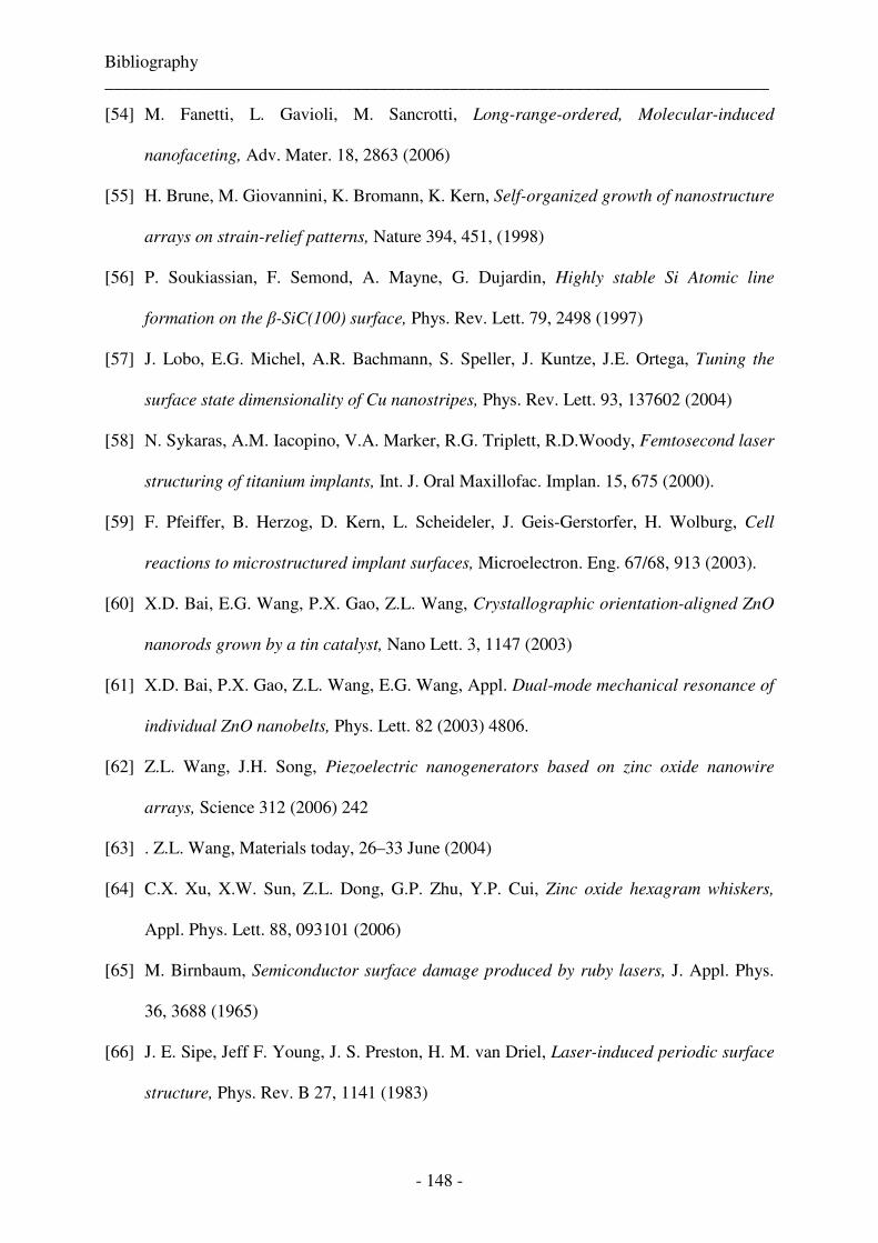
Bibliography ___________________________________________________________________________
- 148 -
[54] M. Fanetti, L. Gavioli, M. Sancrotti, Long-range-ordered, Molecular-induced
nanofaceting, Adv. Mater. 18, 2863 (2006)
[55] H. Brune, M. Giovannini, K. Bromann, K. Kern, Self-organized growth of nanostructure
arrays on strain-relief patterns, Nature 394, 451, (1998)
[56] P. Soukiassian, F. Semond, A. Mayne, G. Dujardin, Highly stable Si Atomic line
formation on the β-SiC(100) surface, Phys. Rev. Lett. 79, 2498 (1997)
[57] J. Lobo, E.G. Michel, A.R. Bachmann, S. Speller, J. Kuntze, J.E. Ortega, Tuning the
surface state dimensionality of Cu nanostripes, Phys. Rev. Lett. 93, 137602 (2004)
[58] N. Sykaras, A.M. Iacopino, V.A. Marker, R.G. Triplett, R.D.Woody, Femtosecond laser
structuring of titanium implants, Int. J. Oral Maxillofac. Implan. 15, 675 (2000).
[59] F. Pfeiffer, B. Herzog, D. Kern, L. Scheideler, J. Geis-Gerstorfer, H. Wolburg, Cell
reactions to microstructured implant surfaces, Microelectron. Eng. 67/68, 913 (2003).
[60] X.D. Bai, E.G. Wang, P.X. Gao, Z.L. Wang, Crystallographic orientation-aligned ZnO
nanorods grown by a tin catalyst, Nano Lett. 3, 1147 (2003)
[61] X.D. Bai, P.X. Gao, Z.L. Wang, E.G. Wang, Appl. Dual-mode mechanical resonance of
individual ZnO nanobelts, Phys. Lett. 82 (2003) 4806.
[62] Z.L. Wang, J.H. Song, Piezoelectric nanogenerators based on zinc oxide nanowire
arrays, Science 312 (2006) 242
[63] . Z.L. Wang, Materials today, 26–33 June (2004)
[64] C.X. Xu, X.W. Sun, Z.L. Dong, G.P. Zhu, Y.P. Cui, Zinc oxide hexagram whiskers,
Appl. Phys. Lett. 88, 093101 (2006)
[65] M. Birnbaum, Semiconductor surface damage produced by ruby lasers, J. Appl. Phys.
36, 3688 (1965)
[66] J. E. Sipe, Jeff F. Young, J. S. Preston, H. M. van Driel, Laser-induced periodic surface
structure, Phys. Rev. B 27, 1141 (1983)
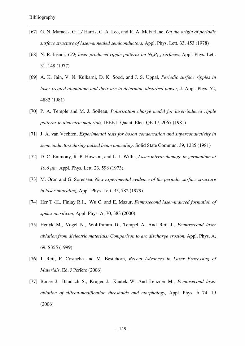
Bibliography ___________________________________________________________________________
- 149 -
[67] G. N. Maracas, G. L/ Harris, C. A. Lee, and R. A. McFarlane, On the origin of periodic
surface structure of laser-annealed semiconductors, Appl. Phys. Lett. 33, 453 (1978)
[68] N. R. Isenor, CO2 laser-produced ripple patterns on NixP1-x surfaces, Appl. Phys. Lett.
31, 148 (1977)
[69] A. K. Jain, V. N. Kulkarni, D. K. Sood, and J. S. Uppal, Periodic surface ripples in
laser-treated aluminium and their use to determine absorbed power, J. Appl. Phys. 52,
4882 (1981)
[70] P. A. Temple and M. J. Soileau, Polarization charge model for laser-induced ripple
patterns in dielectric materials, IEEE J. Quant. Elec. QE-17, 2067 (1981)
[71] J. A. van Vechten, Experimental tests for boson condensation and superconductivity in
semiconductors during pulsed beam annealing, Solid State Commun. 39, 1285 (1981)
[72] D. C. Emmony, R. P. Howson, and L. J. Willis, Laser mirror damage in germanium at
10.6 µm, Appl. Phys. Lett. 23, 598 (1973).
[73] M. Oron and G. Sorensen, New experimental evidence of the periodic surface structure
in laser annealing, Appl. Phys. Lett. 35, 782 (1979)
[74] Her T.-H., Finlay R.J., Wu C. and E. Mazur, Femtosecond laser-induced formation of
spikes on silicon, Appl. Phys. A, 70, 383 (2000)
[75] Henyk M., Vogel N., Wolfframm D., Tempel A. And Reif J., Femtosecond laser
ablation from dielectric materials: Comparison to arc discharge erosion, Appl. Phys. A,
69, S355 (1999)
[76] J. Reif, F. Costache and M. Bestehorn, Recent Advances in Laser Processing of
Materials. Ed. J Perière (2006)
[77] Bonse J., Baudach S., Kruger J., Kautek W. And Lenzner M., Femtosecond laser
ablation of silicon-modification thresholds and morphology, Appl. Phys. A 74, 19
(2006)
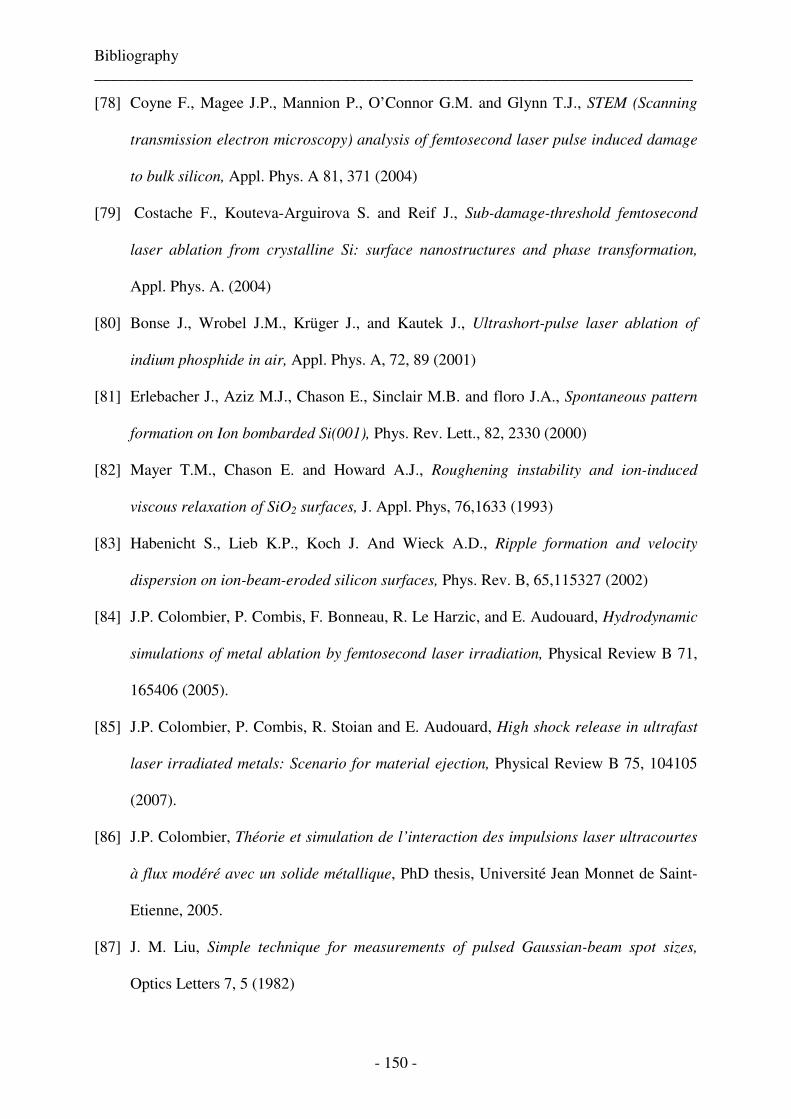
Bibliography ___________________________________________________________________________
- 150 -
[78] Coyne F., Magee J.P., Mannion P., O’Connor G.M. and Glynn T.J., STEM (Scanning
transmission electron microscopy) analysis of femtosecond laser pulse induced damage
to bulk silicon, Appl. Phys. A 81, 371 (2004)
[79] Costache F., Kouteva-Arguirova S. and Reif J., Sub-damage-threshold femtosecond
laser ablation from crystalline Si: surface nanostructures and phase transformation,
Appl. Phys. A. (2004)
[80] Bonse J., Wrobel J.M., Krüger J., and Kautek J., Ultrashort-pulse laser ablation of
indium phosphide in air, Appl. Phys. A, 72, 89 (2001)
[81] Erlebacher J., Aziz M.J., Chason E., Sinclair M.B. and floro J.A., Spontaneous pattern
formation on Ion bombarded Si(001), Phys. Rev. Lett., 82, 2330 (2000)
[82] Mayer T.M., Chason E. and Howard A.J., Roughening instability and ion-induced
viscous relaxation of SiO2 surfaces, J. Appl. Phys, 76,1633 (1993)
[83] Habenicht S., Lieb K.P., Koch J. And Wieck A.D., Ripple formation and velocity
dispersion on ion-beam-eroded silicon surfaces, Phys. Rev. B, 65,115327 (2002)
[84] J.P. Colombier, P. Combis, F. Bonneau, R. Le Harzic, and E. Audouard, Hydrodynamic
simulations of metal ablation by femtosecond laser irradiation, Physical Review B 71,
165406 (2005).
[85] J.P. Colombier, P. Combis, R. Stoian and E. Audouard, High shock release in ultrafast
laser irradiated metals: Scenario for material ejection, Physical Review B 75, 104105
(2007).
[86] J.P. Colombier, Théorie et simulation de l’interaction des impulsions laser ultracourtes
à flux modéré avec un solide métallique, PhD thesis, Université Jean Monnet de Saint-
Etienne, 2005.
[87] J. M. Liu, Simple technique for measurements of pulsed Gaussian-beam spot sizes,
Optics Letters 7, 5 (1982)
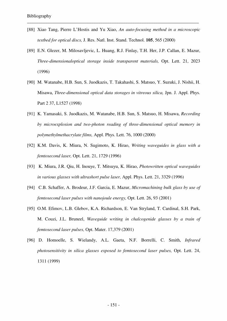
Bibliography ___________________________________________________________________________
- 151 -
[88] Xiao Tang, Pierre L’Hostis and Yu Xiao, An auto-focusing method in a microscopic
testbed for optical discs, J. Res. Natl. Inst. Stand. Technol. 105, 565 (2000)
[89] E.N. Glezer, M. Milosavljevic, L. Huang, R.J. Finlay, T.H. Her, J.P. Callan, E. Mazur,
Three-dimensionaloptical storage inside transparent materials, Opt. Lett. 21, 2023
(1996)
[90] M. Watanabe, H.B. Sun, S. Juodkazis, T. Takahashi, S. Matsuo, Y. Suzuki, J. Nishii, H.
Misawa, Three-dimensional optical data storages in vitreous silica, Jpn. J. Appl. Phys.
Part 2 37, L1527 (1998)
[91] K. Yamasaki, S. Juodkazis, M. Watanabe, H.B. Sun, S. Matsuo, H. Misawa, Recording
by microexplosion and two-photon reading of three-dimensional optical memory in
polymethylmethacrylate films, Appl. Phys. Lett. 76, 1000 (2000)
[92] K.M. Davis, K. Miura, N. Sugimoto, K. Hirao, Writing waveguides in glass with a
femtosecond laser, Opt. Lett. 21, 1729 (1996)
[93] K. Miura, J.R. Qiu, H. Inouye, T. Mitsuyu, K. Hirao, Photowritten optical waveguides
in various glasses with ultrashort pulse laser, Appl. Phys. Lett. 21, 3329 (1996)
[94] C.B. Schaffer, A. Brodeur, J.F. Garcia, E. Mazur, Micromachining bulk glass by use of
femtosecond laser pulses with nanojoule energy, Opt. Lett. 26, 93 (2001)
[95] O.M. Efimov, L.B. Glebov, K.A. Richardson, E. Van Stryland, T. Cardinal, S.H. Park,
M. Couzi, J.L. Bruneel, Waveguide writing in chalcogenide glasses by a train of
femtosecond laser pulses, Opt. Mater. 17,379 (2001)
[96] D. Homoelle, S. Wielandy, A.L. Gaeta, N.F. Borrelli, C. Smith, Infrared
photosensitivity in silica glasses exposed to femtosecond laser pulses, Opt. Lett. 24,
1311 (1999)
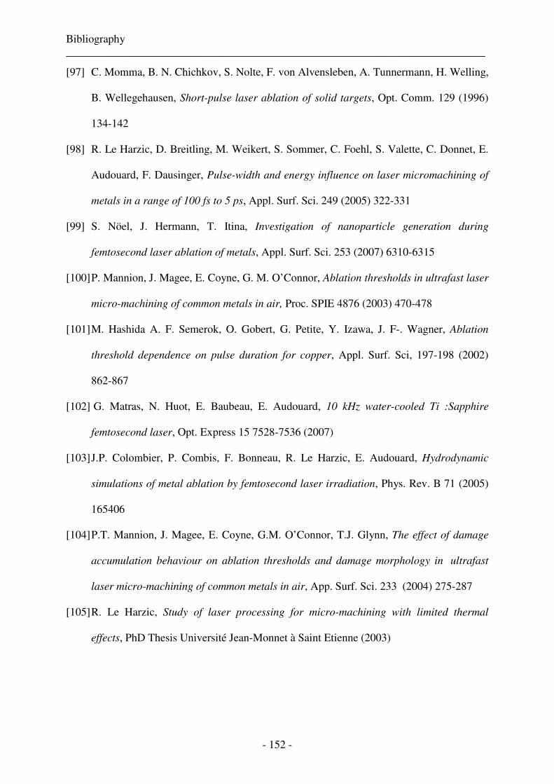
Bibliography ___________________________________________________________________________
- 152 -
[97] C. Momma, B. N. Chichkov, S. Nolte, F. von Alvensleben, A. Tunnermann, H. Welling,
B. Wellegehausen, Short-pulse laser ablation of solid targets, Opt. Comm. 129 (1996)
134-142
[98] R. Le Harzic, D. Breitling, M. Weikert, S. Sommer, C. Foehl, S. Valette, C. Donnet, E.
Audouard, F. Dausinger, Pulse-width and energy influence on laser micromachining of
metals in a range of 100 fs to 5 ps, Appl. Surf. Sci. 249 (2005) 322-331
[99] S. Nöel, J. Hermann, T. Itina, Investigation of nanoparticle generation during
femtosecond laser ablation of metals, Appl. Surf. Sci. 253 (2007) 6310-6315
[100] P. Mannion, J. Magee, E. Coyne, G. M. O’Connor, Ablation thresholds in ultrafast laser
micro-machining of common metals in air, Proc. SPIE 4876 (2003) 470-478
[101] M. Hashida A. F. Semerok, O. Gobert, G. Petite, Y. Izawa, J. F-. Wagner, Ablation
threshold dependence on pulse duration for copper, Appl. Surf. Sci, 197-198 (2002)
862-867
[102] G. Matras, N. Huot, E. Baubeau, E. Audouard, 10 kHz water-cooled Ti :Sapphire
femtosecond laser, Opt. Express 15 7528-7536 (2007)
[103] J.P. Colombier, P. Combis, F. Bonneau, R. Le Harzic, E. Audouard, Hydrodynamic
simulations of metal ablation by femtosecond laser irradiation, Phys. Rev. B 71 (2005)
165406
[104] P.T. Mannion, J. Magee, E. Coyne, G.M. O’Connor, T.J. Glynn, The effect of damage
accumulation behaviour on ablation thresholds and damage morphology in ultrafast
laser micro-machining of common metals in air, App. Surf. Sci. 233 (2004) 275-287
[105] R. Le Harzic, Study of laser processing for micro-machining with limited thermal
effects, PhD Thesis Université Jean-Monnet à Saint Etienne (2003)
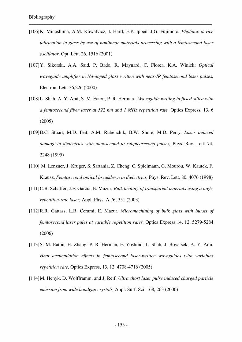
Bibliography ___________________________________________________________________________
- 153 -
[106] K. Minoshima, A.M. Kowalvicz, I. Hartl, E.P. Ippen, J.G. Fujimoto, Photonic device
fabrication in glass by use of nonlinear materials processing with a femtosecond laser
oscillator, Opt. Lett. 26, 1516 (2001)
[107] Y. Sikorski, A.A. Said, P. Bado, R. Maynard, C. Florea, K.A. Winick: Optical
waveguide amplifier in Nd-doped glass written with near-IR femtosecond laser pulses,
Electron. Lett. 36,226 (2000)
[108] L. Shah, A. Y. Arai, S. M. Eaton, P. R. Herman , Waveguide writing in fused silica with
a femtosecond fiber laser at 522 nm and 1 MHz repetition rate, Optics Express, 13, 6
(2005)
[109] B.C. Stuart, M.D. Feit, A.M. Rubenchik, B.W. Shore, M.D. Perry, Laser induced
damage in dielectrics with nanosecond to subpicosecond pulses, Phys. Rev. Lett. 74,
2248 (1995)
[110] M. Lenzner, J. Kruger, S. Sartania, Z. Cheng, C. Spielmann, G. Mourou, W. Kautek, F.
Krausz, Femtosecond optical breakdown in dielectrics, Phys. Rev. Lett. 80, 4076 (1998)
[111] C.B. Schaffer, J.F. Garcia, E. Mazur, Bulk heating of transparent maerials using a high-
repetition-rate laser, Appl. Phys. A 76, 351 (2003)
[112] R.R. Gattass, L.R. Cerami, E. Mazur, Micromachining of bulk glass with bursts of
femtosecond laser pules at variable repetition rates, Optics Express 14, 12, 5279-5284
(2006)
[113] S. M. Eaton, H. Zhang, P. R. Herman, F. Yoshino, L. Shah, J. Bovatsek, A. Y. Arai,
Heat accumulation effects in femtosecond laser-written waveguides with variables
repetition rate, Optics Express, 13, 12, 4708-4716 (2005)
[114] M. Henyk, D. Wolfframm, and J. Reif, Ultra short laser pulse induced charged particle
emission from wide bandgap crystals, Appl. Surf. Sci. 168, 263 (2000)
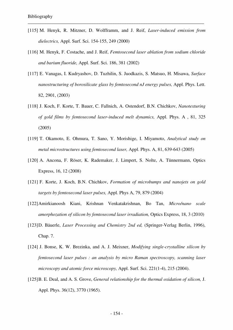
Bibliography ___________________________________________________________________________
- 154 -
[115] M. Henyk, R. Mitzner, D. Wolfframm, and J. Reif, Laser-induced emission from
dielectrics, Appl. Surf. Sci. 154-155, 249 (2000)
[116] M. Henyk, F. Costache, and J. Reif, Femtosecond laser ablation from sodium chloride
and barium fluoride, Appl. Surf. Sci. 186, 381 (2002)
[117] E. Vanagas, I. Kudryashov, D. Tuzhilin, S. Juodkazis, S. Matsuo, H. Misawa, Surface
nanostructuring of borosilicate glass by femtosecond nJ energy pulses, Appl. Phys. Lett.
82, 2901, (2003)
[118] J. Koch, F. Korte, T. Bauer, C. Fallnich, A. Ostendorf, B.N. Chichkov, Nanotexturing
of gold films by femtosecond laser-induced melt dynamics, Appl. Phys. A , 81, 325
(2005)
[119] T. Okamoto, E. Ohmura, T. Sano, Y. Morishige, I. Miyamoto, Analytical study on
metal microstructures using femtosecond laser, Appl. Phys. A, 81, 639-643 (2005)
[120] A. Ancona, F. Röser, K. Rademaker, J. Limpert, S. Nolte, A. Tünnermann, Optics
Express, 16, 12 (2008)
[121] F. Korte, J. Koch, B.N. Chichkov, Formation of microbumps and nanojets on gold
targets by femtosecond laser pulses, Appl. Phys A, 79, 879 (2004)
[122] Amirkianoosh Kiani, Krishnan Venkatakrishnan, Bo Tan, Micro/nano scale
amorphozation of silicon by femtosecond laser irradiation, Optics Express, 18, 3 (2010)
[123] D. Bäuerle, Laser Processing and Chemistry 2nd ed, (Springer-Verlag Berlin, 1996),
Chap. 7.
[124] J. Bonse, K. W. Brezinka, and A. J. Meixner, Modifying single-crystalline silicon by
femtosecond laser pulses : an analysis by micro Raman spectroscopy, scanning laser
microscopy and atomic force microscopy, Appl. Surf. Sci. 221(1-4), 215 (2004).
[125] B. E. Deal, and A. S. Grove, General relationship for the thermal oxidation of silicon, J.
Appl. Phys. 36(12), 3770 (1965).
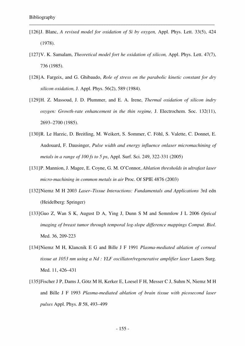
Bibliography ___________________________________________________________________________
- 155 -
[126] J. Blanc, A revised model for oxidation of Si by oxygen, Appl. Phys. Lett. 33(5), 424
(1978).
[127] V. K. Samalam, Theoretical model fort he oxidation of silicon, Appl. Phys. Lett. 47(7),
736 (1985).
[128] A. Fargeix, and G. Ghibaudo, Role of stress on the parabolic kinetic constant for dry
silicon oxidation, J. Appl. Phys. 56(2), 589 (1984).
[129] H. Z. Massoud, J. D. Plummer, and E. A. Irene, Thermal oxidation of silicon indry
oxygen: Growth-rate enhancement in the thin regime, J. Electrochem. Soc. 132(11),
2693–2700 (1985).
[130] R. Le Harzic, D. Breitling, M. Weikert, S. Sommer, C. Föhl, S. Valette, C. Donnet, E.
Audouard, F. Dausinger, Pulse width and energy influence onlaser micromachining of
metals in a range of 100 fs to 5 ps, Appl. Surf. Sci. 249, 322-331 (2005)
[131] P. Mannion, J. Magee, E. Coyne, G. M. O’Connor, Ablation thresholds in ultrafast laser
micro-machining in common metals in air Proc. Of SPIE 4876 (2003)
[132] Niemz M H 2003 Laser–Tissue Interactions: Fundamentals and Applications 3rd edn
(Heidelberg: Springer)
[133] Guo Z, Wan S K, August D A, Ying J, Dunn S M and Semmlow J L 2006 Optical
imaging of breast tumor through temporal log-slope difference mappings Comput. Biol.
Med. 36, 209-223
[134] Niemz M H, Klancnik E G and Bille J F 1991 Plasma-mediated ablation of corneal
tissue at 1053 nm using a Nd : YLF oscillator/regenerative amplifier laser Lasers Surg.
Med. 11, 426–431
[135] Fischer J P, Dams J, Götz M H, Kerker E, Loesel F H, Messer C J, Suhm N, Niemz M H
and Bille J F 1993 Plasma-mediated ablation of brain tissue with picosecond laser
pulses Appl. Phys. B 58, 493–499
Bibliography ___________________________________________________________________________
- 156 -
[136] Moss J P, Patel B C, Pearson G J, Arthur G and Lawes R A 1994 Krypton fluoride
excimer-laser ablation of tooth tissues: precision tissue machining Biomaterials 15,
1013–1018
[137] Chen S C, Kancharla V and Lu Y 2003 Laser-based microscale patterning of
biodegradable polymers for biomedical applications Int. J. Mater. Prod. Technol. 18,
457–68
[138] Aguilar C A, Lu Y, Mao S and Chen S 2005 Direct micro-patterning of biodegradable
polymers using ultraviolet and femtosecond lasers Biomaterials 26, 7642–7649
[139] Hallgren C, Reimers H, Chakarov D, Gold J and Wennerberg A 2003 An in vivo study of
bone response to implants topographically modified by laser micromachining
Biomaterials 24, 701–710
[140] Handbook of Biological Confocal Microscopy (3rd Ed.). Berlin: Springer. Pawley JB
(editor), 2006
[141] Denk W, Strickler J, Webb W (1990). Two-photon laser scanning fluorescence
microscopy. Science 248 (4951): 73–6
[142] Lubatschowski H, Heisterkamp A, Will F, Singh A I, Serbin J, Ostendorf A, Kerani O,
Heermann R, Welling H and Ertmer W 2003 Medical applications of ultrafast laser
pulses RIKEN Review 50, 113-118
[143] Juhasz T, Loesel F H, Kurtz R M, Horvath C, Bille J F, Mourou G A 1999 Corneal
refractive surgery with femtosecond laser IEEE J Quantum. Electron 5, 902–909
[144] Vogel A and Venugopalan V 2003 Mechanisms of Pulsed Laser Ablation of Biological
Tissues Chemical Reviews 103, 577-644
[145] Vogel A, Noack J, Huttman G, and Paltauf G 2005 Mechanisms of femtosecond laser
nanosurgery of cells and tissues Appl. Phys. B 81, 1015-1047
Bibliography ___________________________________________________________________________
- 157 -
[146] König K, Riemann I and Fritsche W 2001 Nanodissection of human chromosomes with
near-infrared femtosecond laser pulses Opt. Lett. 26, 819-821
[147] König K, Riemann I, Stracke F and Le Harzic R 2005 Nanoprocessing with nanojoule
near-infrared femtosecond laser pulses Med. Laser Appl. 20, 169-184
[148] Maxwell I, Chung S and Mazur E 2005 Nanoprocessing of subcellular targets using
femtosecond laser pulses Med. Laser Appl. 20, 193-200
[149] Watanabe W, Arakawa N, Matsunaga S, Higashi T, Fukui K, Isobe K and Itoh K 2004
Femtosecond laser disruption of subcellular organelles in a living cell Opt. Express 12,
4203-4213
[150] Kohli V, Elezzabi A and Acker J P 2005 Cell nanosurgery using ultrashort
(femtosecond) laser pulses: applications to membrane surgery and cell isolation Lasers
Surg. Med. 37, 227-230
[151] Shen N, Datta D, Schaffer C B, Le Duc P, Ingber D E and Mazur E 2005 Ablation of
cytoskeletal filaments and mitochondria in live cells using a femtosecond laser
microscissors Mech Chem Biosyst 2,17–26
[152] Huang H and Guo Z 2009 Human dermis separation via ultra-short pulsed laser
plasma-mediated ablation J. Phys. D:Appl. Phys. 42, 165204-165213
[153] Liu Y M, Sun S, Singha S, Cho M R and Gordon R J 2005 3D femtosecond laser
patterning of collagen for directed cell attachment Biomaterials 26 4597–4605
[154] Valette S, Steyer P, Richard L, Forest B, Donnet C and Audouard E 2006 Influence of
femtosecond laser marking on the corrosion resistance of stainless steels Appl. Surf.
Scie 252 4696-4701
[155] Steyer P, Valette S, Forest B, Millet J P, Donnet C and Audouard E 2006 Surface
modification of martensitic stainless steels by laser marking and its consequences
regarding corrosion resistance Surf. Eng. 22 167-172
Bibliography ___________________________________________________________________________
- 158 -
[156] Mottay E, Kupisiewicz A, Detroux G, Costet X, Simmons A, Vivarelli U, Lemaire P
and Lopez J 2008 Industrial ultrafast internal engraving laser system for anti-
counterfeiting applications Proc. SPIE 6881 66810H
[157] Le Harzic R, Sauer D, Riemann I and König K 2005 Nanoprocessing of semiconductors
and metals with nJ femtosecond laser pulses Proc. SPIE 5990, 189-198
[158] Groenendijk M 2008 Fabrication of Super Hydrophobic Surfaces by fs Laser Pulses
Laser Technik Journal 5, 44-47
[159] Zorba V, Persano L, Pisignano D, Athanassiou A, Stratakis E, Cingolani R, Tzanetakis
P and Fotakis C 2006 Making silicon hydrophobic: wettability control by two-
lengthscale simultaneous patterning with femtosecond laser irradiation Nanotechnology
17, 3234
[160] Fadeeva E, Schlie S, Koch J, Ngezahayo A and Chichkov BN 2009 The hydrophobic
properties of femtosecond laser fabricated spike structures and their effects on cell
proliferation Phys. Status Solidi A 206, 1348-1351
[161] Vorobyev AY and Guo C 2007 Femtosecond laser structuring of titanium implants
Appl. Surf. Scie. 253, 7272-7280
[162] Oliveira V, Ausset S and Vilar R 2009 Surface micro/nanostructuring of titanium under
stationary and non-stationary femtosecond laser irradiation Appl. Surf. Scie. 255,
7556-7560
[163] Maruo S, Nakamura O and Kawata S 1997 Three-Dimensional Microfabrication with
Two-Photon-Absorbed Photopolymerization Opt. Lett. 22, 132-134
[164] Cumpston BH, Ananthavel SP, Barlow S, Dyer DL, Ehrlich JE, Erskine LL, Heikal
AA, Kuebler SM, Lee IYS, McCord-Maughon D, Qin J, Rockel H, Rumi M, Wu X L,
Marder SR and Perry JW 1999 Two-Photon Polymerization Initiators for Three-
Dimensional Optical Data Storage and Microfabrication Nature 398, 51-54
Bibliography ___________________________________________________________________________
- 159 -
[165] Sun HB, Matsuo S and Misawa H 1999 Three-dimensional photonic crystal structures
achieved with twophoton- absorption photopolymerization of resin Appl. Phys. Lett.74,
786-788
[166] Kawata S, Sun HB, Tanaka T and Takada K 2001 Finer features for functional
microdevices Nature (London) 412, 697–698
[167] Serbin J, Egbert A, Ostendorf A, Chickov BN, Houbertz R, Domann G, Schulz J,
Cronauer C, Fröhlich L and Popall M 2003 Femtosecond laser-induced two-photon
polymerization of inorganic-organic hybrid materials for applications in photonics Opt.
Lett. 28, 301-303
[168] Mizeikis V, Seet KK, Juodkazis S and Misawa H 2004 Three-dimensional woodpile
photonic crystal templates for the infrared spectral range Opt. Lett. 29, 2061-2063
[169] Li L, Gattass RR, Gershgoren E, Hwang H and Fourkas JT 2009 Achieving λ/20
Resolution by One-Color Initiation and Deactivation of Polymerization Science 324,
910 - 913
[170] Ovsianikov A, Ostendorf A and Chichkov B 2007 Three-dimensional photofabrication
with femtosecond lasers for applicationsin photonics and biomedicine Appl. Surf. Sci.
253, 6599-6602
[171] Choi HW, Johnson JK, Nam J, Farson DF and Lannutti J 2007 Structuring electrospun
polycaprolactone nanofiber tissue scaffolds by femtosecond laser ablation J. Laser
Appl. 19, 225

___________________________________________________________________________
- 160 -

Appendix A ___________________________________________________________________________
- 161 -
APPENDIX A

Appendix A ___________________________________________________________________________
- 162 -
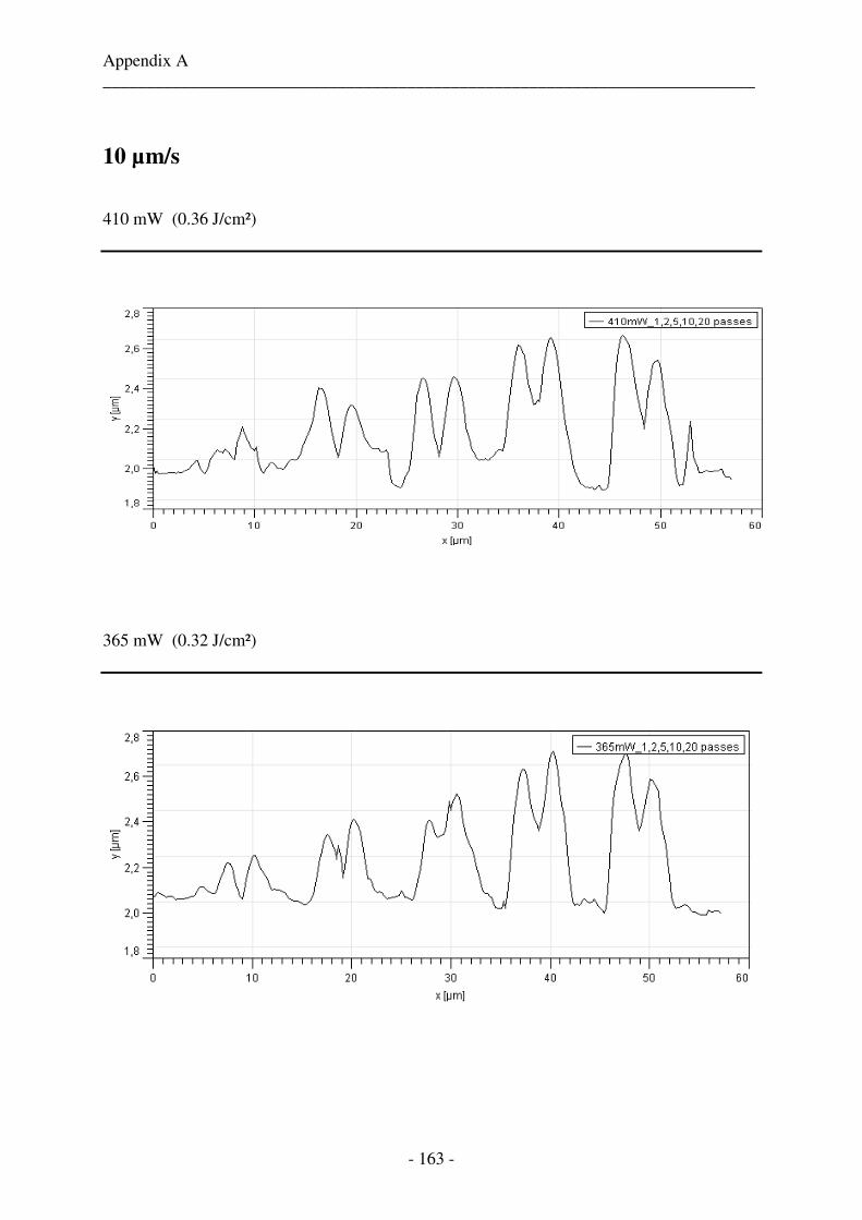
Appendix A ___________________________________________________________________________
- 163 -
10 µm/s
410 mW (0.36 J/cm²)
365 mW (0.32 J/cm²)
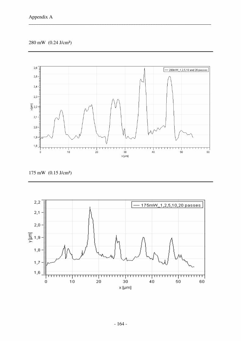
Appendix A ___________________________________________________________________________
- 164 -
280 mW (0.24 J/cm²)
175 mW (0.15 J/cm²)
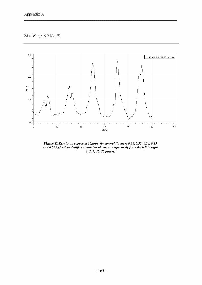
Appendix A ___________________________________________________________________________
- 165 -
85 mW (0.075 J/cm²)
Figure 82 Results on copper at 10µm/s for several fluences 0.36, 0.32, 0.24, 0.15
and 0.075 J/cm², and different number of passes, respectively from the left to right
1, 2, 5, 10, 20 passes.
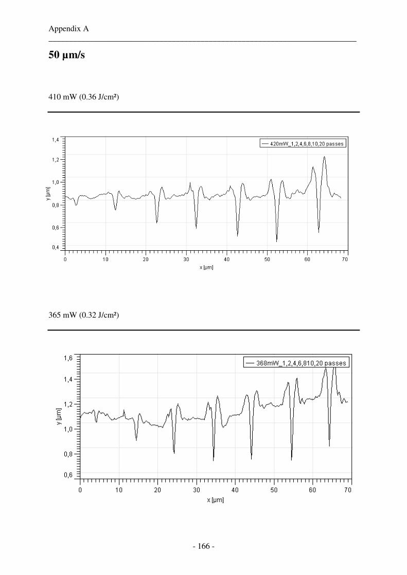
Appendix A ___________________________________________________________________________
- 166 -
50 µm/s
410 mW (0.36 J/cm²)
365 mW (0.32 J/cm²)
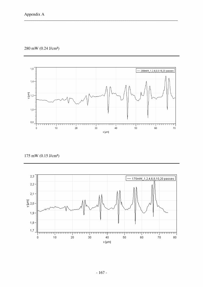
Appendix A ___________________________________________________________________________
- 167 -
280 mW (0.24 J/cm²)
175 mW (0.15 J/cm²)
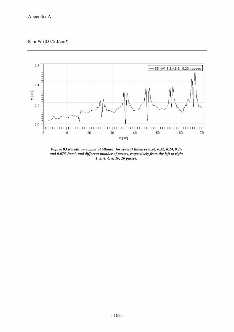
Appendix A ___________________________________________________________________________
- 168 -
85 mW (0.075 J/cm²)
Figure 83 Results on copper at 50µm/s for several fluences 0.36, 0.32, 0.24, 0.15
and 0.075 J/cm², and different number of passes, respectively from the left to right
1, 2, 4, 6, 8, 10, 20 passes.
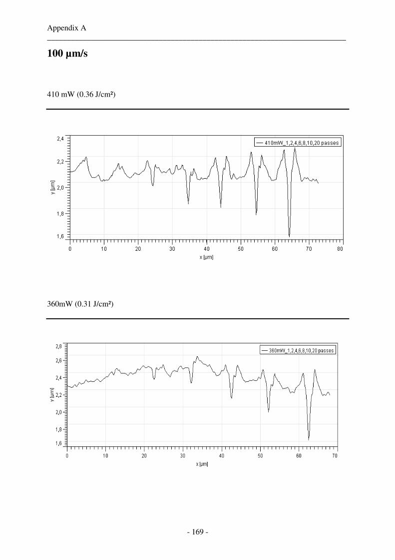
Appendix A ___________________________________________________________________________
- 169 -
100 µm/s
410 mW (0.36 J/cm²)
360mW (0.31 J/cm²)
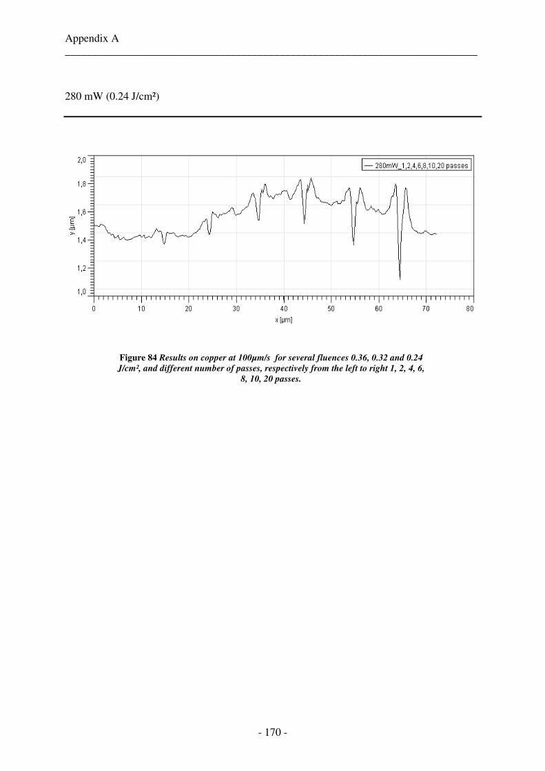
Appendix A ___________________________________________________________________________
- 170 -
280 mW (0.24 J/cm²)
Figure 84 Results on copper at 100µm/s for several fluences 0.36, 0.32 and 0.24
J/cm², and different number of passes, respectively from the left to right 1, 2, 4, 6,
8, 10, 20 passes.
Own publication list ___________________________________________________________________________
- 171 -
Own Publication list
Reviewed papers R. Le Harzic, M. Stark, H. Schuck,, P. Becker, E. Lai, D. Bruneel, F. Bauerfeld, D. Sauer, T.
Velten and K. König
“Nanostructuring with Nanojoule Femtosecond Laser Pulses”, Journal of Laser
Micro/Nanoengineering (JLMN) 3, 106-113 (2008).
D. Bruneel, G. Matras, R. Le Harzic, N. Huot, K. König, and E. Audouard
“Micromachining of metals with ultra-short Ti-Sapphire lasers: Prediction and optimization of
the processing time”, Optics and Lasers in Engineering 48, 268-271 (2010).
D. Bruneel, E. Audouard, K. König and R. Le Harzic
“Flexible tool for two photon laser nanoprocessing and large area mapping with high
resolution”, Optics and Lasers in Engineering 48, 1278-1284 (2010).
Proceedings
R. Le Harzic, C. Wüllner, D. Bruneel, C. Donitzky, and K. König
“Femtosecond refractive eye surgery: study of laser parameters for even more efficiency and
safety”, Proc. SPIE 6632, 663217 (2007), (Ophthalmic Technologies XIX , BIOS2007,
Photonics West, 21-22 January 2007, San Jose, California, USA)
Own publication list ___________________________________________________________________________
- 172 -
R. Le Harzic, C. Wüllner, D. Bruneel, C. Donitzky, and K. König
“New developments in femtosecond laser corneal refractive surgery”, Proceedings of the
Fourth International WLT-Conference on Lasers in Manufacturing (2007)
(Laser world of photonics 2007, June 2007, Munich, Germany)
R. Le Harzic, M. Stark, H. Schuck, P. Becker, E. Lai, D. Bruneel, F. Bauerfeld, D. Sauer, T.
Velten , K. König
“Nanostructuring with Nanojoule Femtosecond Laser Pulses”, Proceeding of the Laser
Precision Fabrication conference (LPM), (2007)
(LPM (Laser Precision Fabrication), 24-28 April 2007, Vienna, Austria)
D. Bruneel, M. Schwarz, E. Audouard, K. König, R. Le Harzic
“Development of a powerful tool for nanostructuring and multiphoton imaging with
nanojoule femtosecond laser pulses”, Proc. SPIE 7201, 720117 (2009)
(Laser Applications in Microelectronic and Optoelectronic Manufacturing VII, LASE2009,
Photonics West, 24-29 January 2009, San Jose, California, USA)
Poster
D.Bruneel, E. Audouard, N.Huot, R. Le Harzic, K. König
“Nanomarquage femtoseconde “, Opto 2007, 3eme journée d’étude : Marquage, micro et nano
gravure,25-27 septembre 2007, Paris, France
Acknowledgments ___________________________________________________________________________
- 173 -
Acknowledgments
My thanks go firstly to Pr. E. Audouard, R. Le Harzic, and Pr. K. Konig. Pr. E.
Audouard proposed to me to work on this so interesting topic. I would like to thank him for
having guided me all along this difficult work. I also thank for all discussions we could had,
concerning sciences but not only. I have to confess that I was very impressed concerning his
erudition, and his positivity. He is unmistakably a great driving force for the research to
industry translation.
I would like to thank Pr. K. Konig, to have accepted to be my german supervisor, and to
have enabled the possibility for me to integrate the team of laser Microsystems at the
Fraunhofer IBMT.
I want to particularly thank Dr. R. Le Harzic for his help and good advices. He often
unlocked pressing situations. He also followed all my work not only during the period I was
at the Fraunhofer institut, but from the beginning to the end of this thesis. Thanks to him for
all the help he gave me for my arrival and all along the period at the Fraunhofer IBMT. I have
really appreciated to work with him, for discussing, and trying to solve problems with
efficiency. Thanks again for translating and helping me in all the administrative German staff.
I would like to express a special thanks to Jean-Philippe Colombier, with who I liked to
discuss about physics of the interaction of femtosecond pulses with the matter and the time he
Acknowledgments ___________________________________________________________________________
- 174 -
passed doing the very long hydrodynamic simulations in trying to understand high repetition
rate interactions of femtosecond pulses with the matter.
I would like to thank all people with who I have worked during this time at the
laboratory Hubert Curien. I think especially to the team of ultrafast laser processing, with
Sébastien, Benjamin, Romain, Nicolas, Matthieu, Sébastien, … and from the company
impulsion with Hervé Soder as the director, Julien, Gregory, Anthony and Alexandra. I also
thank all the team of laser and Microsystems of the Fraunhofer institute with who I really
enjoyed to work and shared good moments inside the team, I think about Ronan, Iris, Martin,
Daniel D., Franck, Aisada, and, of course, Daniel S. for his efficiency and his great
availability.
I want to thank my family who throughout this long trek has shown great support and
without which the various severe tests met would have been as more difficult to overcome. I
especially express a thought to my grandmother who left us during this time while
maintaining her great presence and her good temper until the end.
I would like to thank all my friends, I think especially to Nico, Marie, Laurent, Claire,
Tobias, Elodie, and all others for good moments passed together and which were very
noticeable during this period. A special thought to Gonzague, Tobias and Christophe for great
discussions and their support during all these four years. Thanks to Claire, Nico, and Tobias
with who I spent very good time travelling and discovering new landscapes, new cities like
Berlin, Munich, Pragues, and more … where we could discover another culture, other mores,
as well as typical events, I particularly think about German Christmas markets, or the festival
of wine in Stuttgart (and yes, German white wine is good too), without forgetting the

Acknowledgments ___________________________________________________________________________
- 175 -
legendary festival “Oktoberfest” in Munich, and so many anecdotes associated to each of
these moments. Thanks to Tobias for giving us a very human welcome during this time. I
keep in mind unforgettable remembers of time spent in Germany.
I would like to thank my neighbours of St Etienne, women across the landing, for their
generosity, their kindness, and their humanity. They are to me, worthy people of the “cause
stéphanoise”.
I would like to thank French-German University and the région Rhône-Alpes for grant
support which helped me a lot when I was abroad. And thanks to the CNRS for funding me
during all this time.

Acknowledgments ___________________________________________________________________________
- 176 -
Declaration ___________________________________________________________________________
- 177 -
Declaration
I hereby declare that this thesis is the result of my own independent investigation and that all
contributions from other sources are duly acknowledged. No part of this thesis was previously
submitted for a degree at universities of Saarland, and of Saint Etienne or another university.
Hiermit versichere ich an Eides statt, dass ich die vorliegende Arbeit selbständig und ohne
Benutzung anderer als der angegebenen Hilfsmittel angefertigt habe. Die aus anderen Quellen
oder indirekt übernommenen Daten und Konzepte sind unter Angabe der Quelle
gekennzeichnet.
Die Arbeit wurde bisher weder im In- noch im Ausland in gleicher oder ähnlicher Form in
einem Verfahren zur Erlangung eines akademischen Grades vorgelegt.
David Bruneel
Saint Etienne, 5 October 2010

- 178 -
- 179 -
Curriculum Vitae
David Bruneel
Born September 21, 1982 in Montreuil-sur-mer (France)
Education
• 2003-2005 Master's degree in Engineering (Specialization in optics and electronics),
TELECOM Saint-Etienne, the State School of Engineering of the University of Saint-
Etienne, France.
• 2001-2003 Institut of technology specialized in physics and instrumental techniques,
University of Lille, France.
• 2001 High school diploma, specialized in physics and industrial techniques, Lycée E.
Woillez, Montreuil-sur-mer, France
Professional experience
• October 1rst, 2006 – September 30, 2009 PhD thesis of engineering "Femtosecond
laser ablation for controlling micro and nanostructuration" realized at Laboratoire
Hubert Curien in Saint Etienne (France) and at the Frauhofer Institut für
Biomedizinische Technik (IBMT) in Sankt Ingbert (Germany).
• January 1rst, 2010 – until now Reasearch assistant at the Laboratoire Hubert Curien of
the University of Saint Etienne (France).
• March 1, 2006 – August 31, 2006 Training period of six months as an engineer
realized at the Fraunhofer Institut für Biomedizinische Technik (IBMT) in Sankt
Ingbert (Germany).
• April 1, 2003 – June 30, 2003 Industrial training period in Valeo industry at Etaples
(France)

- 180 -