femtosecond ablation of ultrahard materials
TRANSCRIPT
Appl. Phys. A 74, 729–739 (2002)/ Digital Object Identifier (DOI) 10.1007/s003390101183 Applied Physics AMaterialsScience & Processing
Femtosecond ablation of ultrahard materialsG. Dumitru1,∗, V. Romano1, H.P. Weber1, M. Sentis2, W. Marine2
1 Institute of Applied Physics, University of Bern, Sidlerstrasse 5, 3012 Bern, Switzerland2 Groupement Interdisciplinaire Ablation Laser et Applications, LP3 FRE2165 CNRS – Universite de la Mediterranee et GPEC UMR 6631 CNRS,Faculte des Sciences de Luminy, Case 917, 13288 Marseille Cedex 9, France
Received: 31 August 2001/Accepted: 3 December 2001/Published online: 20 March 2002 – Springer-Verlag 2002
Abstract. Several ultrahard materials and coatings of def-inite interest for tribological applications were tested withrespect to their response when irradiated with fs laser pulses.Results on cemented tungsten carbide and on titanium car-bonitride are reported for the first time and compared withoutcomes of investigations on diamond and titanium ni-tride. The experiments were carried out in air, in a regimeof 5–8 J/cm2 fluences, using the beam of a commercialTi:sapphire laser. The changes induced in the surface morph-ology were analysed with a Nomarski optical microscope,and with SEM and AFM techniques. From the experimentaldata and from the calculated incident energy density dis-tributions, the damage and ablation threshold values weredetermined. As expected, the diamond showed the highestthreshold, while the cemented tungsten carbide exhibitedtypical values for metallic surfaces. The ablation rates deter-mined (under the above-mentioned experimental conditions)were in the range 0.1–0.2 µm per pulse for all the materialsinvestigated.
PACS: 42.62.Cf; 61.80.Ba; 81.40.Wx
The friction behaviour and wear resistance of tools are es-sential aspects for any product and the use of hard materials,or materials covered with films of great hardness, is an im-portant provision for improving these parameters. It has alsobeen shown by us [1] and by other authors that certain mod-ifications to the morphologies of the contacted surfaces (e.g.uniformly distributed micropores) can improve the above-mentioned tribological properties [1]. Laser ablation is a ver-satile technique for inducing such microstructures and anypossible way to perfect the laser microprocessing of ultrahardmaterials can lead to a notable improvement in tribologicalaspects and to technological developments, and should beinvestigated.
∗Corresponding author.(Fax: +41-31/631/3765, E-mail: [email protected])
For suitable pore depths and distributions, the effects oflaser microstructuring of tribological surfaces are impressive:a factor of 10 increase in the lifetime was demonstrated [2].We reported previously [1–3] on inducing microstructures onvarious materials using ns- and ps-lasers and complementarystudies carried out with ultrashort laser pulses (150 fs), aim-ing to achieve a higher quality for the laser structuring oftribological surfaces, are described in this work.
It is generally accepted that the use of short and ultrashortlaser pulses is a very important means of achieving preciselaser microprocessing of different materials. Reducing thetemporal width of the laser pulse (from ns- to fs-pulses) limitsthe thermal diffusion into the peripheries during the ablationprocess and increases the quality of the laser microprocessingof surfaces [4–7]. Furthermore, although the energy couplingmechanisms are different for various types of target materials,the energy absorption needed to enable ablative processing,occurs in practically all materials.
For the first time, to our knowledge, results on the abla-tion of tungsten carbide and of titanium carbonitride in the fslaser regime are presented. The paper also reports on investi-gations performed on diamond and titanium nitride, ultrahardmaterials of definite interest.
1 Theoretical considerations
In the case of ultrashort laser pulses, in a simplified represen-tation, the thermal dispersion of the incident energy from theirradiated spot can be neglected: thermal diffusivity lengthsof 1–2 nm can be calculated for a pulse length of 150 fs (e.g.steel). A large number of free electrons are generated andaccelerated, while the positive charge carriers (the ionised lat-tice atoms) are still in their initial positions; this ultrashortplasma phase has the density of the solid state. The interactionis one of extreme non-equilibrium, with much higher elec-tronic temperatures than lattice temperatures: the target doesnot melt, but it is directly vaporised.
The ablation process begins after a sufficient amount ofthe incident laser energy has been absorbed. In the case
730
of metals, which already have free electrons, the absorbedphoton energy yields an increase in their kinetic energy.For materials with a band gap smaller than the photon en-ergy, a relatively small amount of photon energy is suf-ficient to promote electrons into the conduction band andthe absorption is strong and linear (one photon absorp-tion). If the energy gap is larger than the photon energy,the excitation of the electrons occurs through multipho-ton absorption and the absorption process becomes non-linear.
If ultrashort laser beams are focused on small spots, in-tensities greater than 1015 W/cm2 may occur, correspondingto extremely strong electric fields. This can yield more com-plex ablation (also in the case of metals) and the deviationfrom linearity can lead to a lack of reproducibility. It mustbe pointed out [8] that collateral thermal effects and materialexpelled as melt were also observed in the case of metallictargets exposed to high fluence fs pulses. Furthermore, duethe strong electric fields, it may be possible to directly ionisethe air molecules in front of the target (air breakdown) andthis process is totally disadvantageous for precise materialmicroprocessing.
From the point of view of precise microprocessing, theabsence of heat-affected zones and good reproducibility arecentral goals to be aimed for. Additionally, from a practicalpoint of view, the possibility of working in air would alsobe an advantage, despite the oxidation processes accompa-nying laser ablation in air. If all these points are taken intoaccount, one can state that the regime of low fluences andhigh repetition rates is more interesting [4] in comparisonwith procedures based on high energy densities. Due to thelower laser fluence, the air breakdown can be avoided, theheat flow energy losses and the affected zones are minimisedand this allows the precise control of the ablated depth to beachieved.
2 Experimental
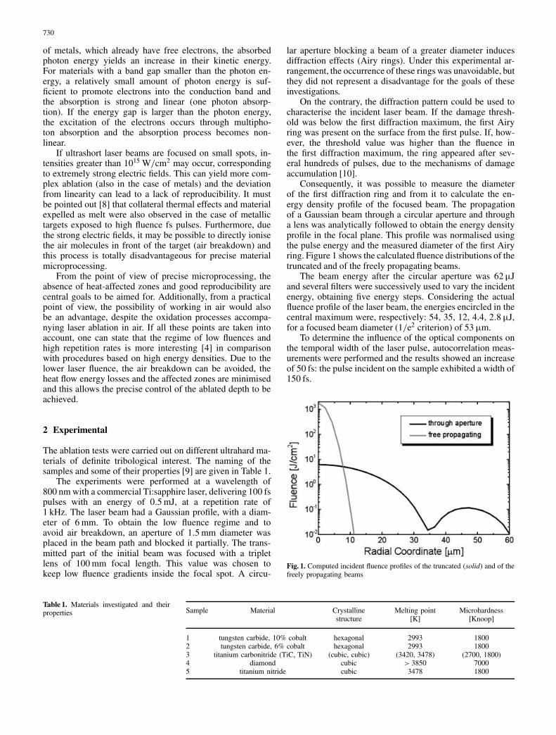
The ablation tests were carried out on different ultrahard ma-terials of definite tribological interest. The naming of thesamples and some of their properties [9] are given in Table 1.
The experiments were performed at a wavelength of800 nm with a commercial Ti:sapphire laser, delivering 100 fspulses with an energy of 0.5 mJ, at a repetition rate of1 kHz. The laser beam had a Gaussian profile, with a diam-eter of 6 mm. To obtain the low fluence regime and toavoid air breakdown, an aperture of 1.5 mm diameter wasplaced in the beam path and blocked it partially. The trans-mitted part of the initial beam was focused with a tripletlens of 100 mm focal length. This value was chosen tokeep low fluence gradients inside the focal spot. A circu-
Sample Material Crystalline Melting point Microhardnessstructure [K] [Knoop]
1 tungsten carbide, 10% cobalt hexagonal 2993 18002 tungsten carbide, 6% cobalt hexagonal 2993 18003 titanium carbonitride (TiC, TiN) (cubic, cubic) (3420, 3478) (2700, 1800)4 diamond cubic > 3850 70005 titanium nitride cubic 3478 1800
Table 1. Materials investigated and theirproperties
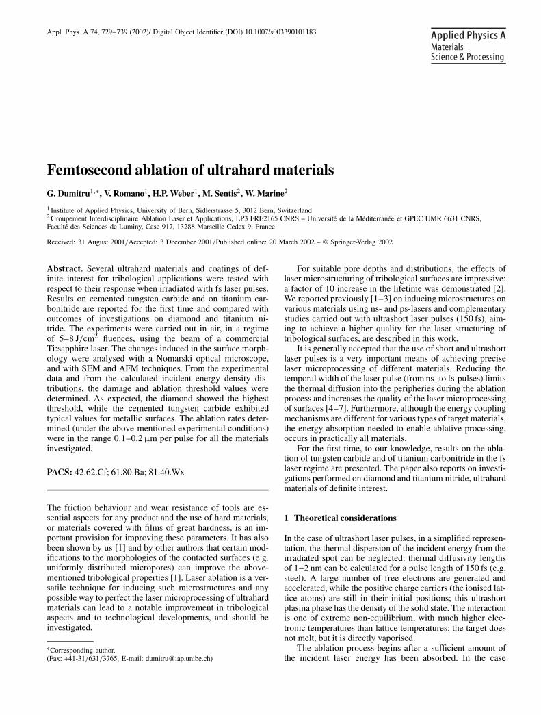
lar aperture blocking a beam of a greater diameter inducesdiffraction effects (Airy rings). Under this experimental ar-rangement, the occurrence of these rings was unavoidable, butthey did not represent a disadvantage for the goals of theseinvestigations.
On the contrary, the diffraction pattern could be used tocharacterise the incident laser beam. If the damage thresh-old was below the first diffraction maximum, the first Airyring was present on the surface from the first pulse. If, how-ever, the threshold value was higher than the fluence inthe first diffraction maximum, the ring appeared after sev-eral hundreds of pulses, due to the mechanisms of damageaccumulation [10].
Consequently, it was possible to measure the diameterof the first diffraction ring and from it to calculate the en-ergy density profile of the focused beam. The propagationof a Gaussian beam through a circular aperture and througha lens was analytically followed to obtain the energy densityprofile in the focal plane. This profile was normalised usingthe pulse energy and the measured diameter of the first Airyring. Figure 1 shows the calculated fluence distributions of thetruncated and of the freely propagating beams.
The beam energy after the circular aperture was 62 µJand several filters were successively used to vary the incidentenergy, obtaining five energy steps. Considering the actualfluence profile of the laser beam, the energies encircled in thecentral maximum were, respectively: 54, 35, 12, 4.4, 2.8 µJ,for a focused beam diameter (1/e2 criterion) of 53 µm.
To determine the influence of the optical components onthe temporal width of the laser pulse, autocorrelation meas-urements were performed and the results showed an increaseof 50 fs: the pulse incident on the sample exhibited a width of150 fs.
Fig. 1. Computed incident fluence profiles of the truncated (solid) and of thefreely propagating beams
731
For all the materials investigated, the same experimentalprocedure was applied. Using the above-mentioned five en-ergy steps and with 1, 5 and 10 pulses per spot, respectively,a matrix of 5 ×3 irradiation spots was induced. Afterwards,a line of 25 craters was generated, using only the maximalfluence with increasing numbers of pulses per spot.
The laser-irradiated samples were examined ex situ usinga phase-contrast optical microscope (Nomarski), a scan-ning electron microscope equipped with a triangulation-basedsoftware, enabling depth measurements, and with an atomicforce microscope (with exception of sample 4). With theseinvestigation techniques, it was possible to:
evidence the optical changes of the surfaces;obtain the diameters of the induced spots;measure crater depths;reveal the morphology of the irradiated material (SEM).
3 Experimental results
3.1 Tungsten carbide
Samples 1 and 2 were made of commercially available hardmetals, i.e. cemented tungsten carbide, with slightly differentcobalt percentages between the two samples. These materialswere obtained through a sintering process, a procedure imply-ing temperatures of 1350–1400 ◦C (depending on the cobaltpercentage) and in which the interacting phases are tungstencarbide (as grains) and liquid cobalt.
Sample 1 had 10% cobalt (WC-10 Co) and had an aver-age grain size of 0.5 µm. The sample surface was polished.This material has the most widespread use in the machineindustry because of its hardness and wear resistance. Typi-cal applications are, for instance, milling, planing, turning ofsteel and Ti-alloys and obtaining metal-tipped tools. Sample2 had 6% cobalt (WC-6 Co) and an average grain size of1.5 µm. The sample surface was lapped. This hard metal findsa large number of applications in finish-cut turning, finish-milling, shave-planing and fine machining.
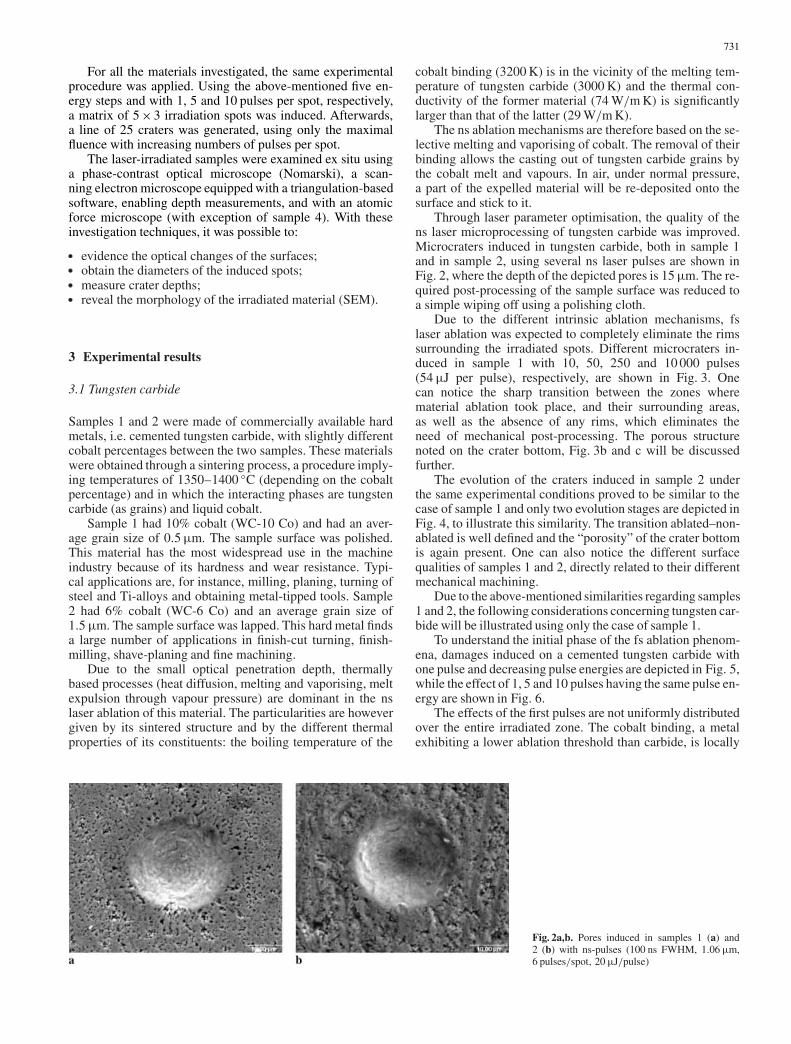
Due to the small optical penetration depth, thermallybased processes (heat diffusion, melting and vaporising, meltexpulsion through vapour pressure) are dominant in the nslaser ablation of this material. The particularities are howevergiven by its sintered structure and by the different thermalproperties of its constituents: the boiling temperature of the
Fig. 2a,b. Pores induced in samples 1 (a) and2 (b) with ns-pulses (100 ns FWHM, 1.06 µm,6 pulses/spot, 20 µJ/pulse)
cobalt binding (3200 K) is in the vicinity of the melting tem-perature of tungsten carbide (3000 K) and the thermal con-ductivity of the former material (74 W/m K) is significantlylarger than that of the latter (29 W/m K).
The ns ablation mechanisms are therefore based on the se-lective melting and vaporising of cobalt. The removal of theirbinding allows the casting out of tungsten carbide grains bythe cobalt melt and vapours. In air, under normal pressure,a part of the expelled material will be re-deposited onto thesurface and stick to it.
Through laser parameter optimisation, the quality of thens laser microprocessing of tungsten carbide was improved.Microcraters induced in tungsten carbide, both in sample 1and in sample 2, using several ns laser pulses are shown inFig. 2, where the depth of the depicted pores is 15 µm. The re-quired post-processing of the sample surface was reduced toa simple wiping off using a polishing cloth.
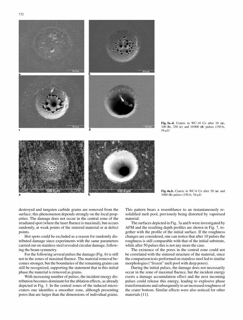
Due to the different intrinsic ablation mechanisms, fslaser ablation was expected to completely eliminate the rimssurrounding the irradiated spots. Different microcraters in-duced in sample 1 with 10, 50, 250 and 10 000 pulses(54 µJ per pulse), respectively, are shown in Fig. 3. Onecan notice the sharp transition between the zones wherematerial ablation took place, and their surrounding areas,as well as the absence of any rims, which eliminates theneed of mechanical post-processing. The porous structurenoted on the crater bottom, Fig. 3b and c will be discussedfurther.
The evolution of the craters induced in sample 2 underthe same experimental conditions proved to be similar to thecase of sample 1 and only two evolution stages are depicted inFig. 4, to illustrate this similarity. The transition ablated–non-ablated is well defined and the “porosity” of the crater bottomis again present. One can also notice the different surfacequalities of samples 1 and 2, directly related to their differentmechanical machining.
Due to the above-mentioned similarities regarding samples1 and 2, the following considerations concerning tungsten car-bide will be illustrated using only the case of sample 1.
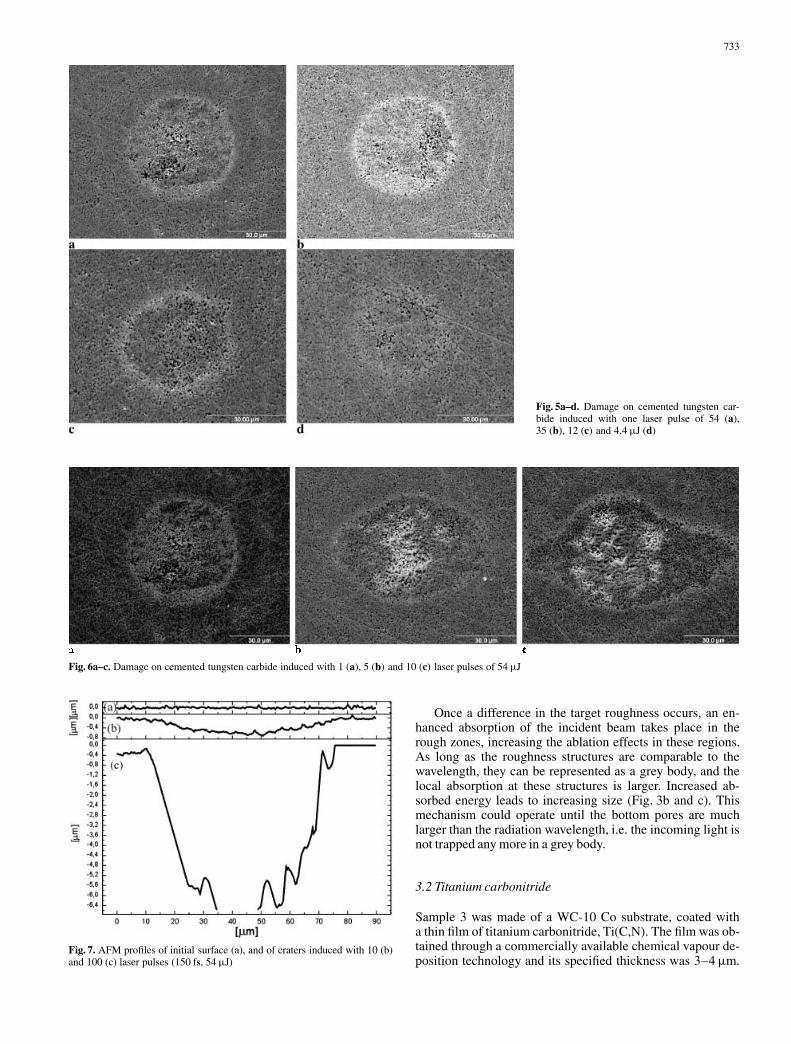
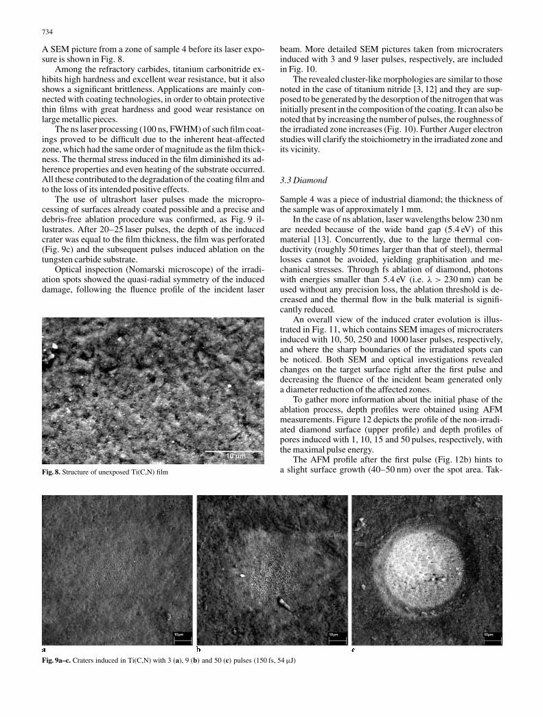
To understand the initial phase of the fs ablation phenom-ena, damages induced on a cemented tungsten carbide withone pulse and decreasing pulse energies are depicted in Fig. 5,while the effect of 1, 5 and 10 pulses having the same pulse en-ergy are shown in Fig. 6.
The effects of the first pulses are not uniformly distributedover the entire irradiated zone. The cobalt binding, a metalexhibiting a lower ablation threshold than carbide, is locally
732
Fig. 3a–d. Craters in WC-10 Co after 10 (a),100 (b), 250 (c) and 10 000 (d) pulses (150 fs,54 µJ)
Fig. 4a,b. Craters in WC-6 Co after 50 (a) and1000 (b) pulses (150 fs, 54 µJ)
destroyed and tungsten carbide grains are removed from thesurface; this phenomenon depends strongly on the local prop-erties. The damage does not occur in the central zone of theirradiated spot (where the laser fluence is maximal), but occursrandomly, at weak points of the sintered material or at defectpoints.
Hot spots could be excluded as a reason for randomly dis-tributed damage since experiments with the same parameterscarried out on stainless steel revealed circular damage, follow-ing the beam symmetry.
For the following several pulses the damage (Fig. 6) is stillnot in the zones of maximal fluence. The material removal be-comes stronger, but the boundaries of the remaining grains canstill be recognized, supporting the statement that in this initialphase the material is removed as grains.
With increasing number of pulses, the incident energy dis-tribution becomes dominant for the ablation effects, as alreadydepicted in Fig. 3. In the central zones of the induced micro-craters one identifies a smoother zone, although presentingpores that are larger than the dimensions of individual grains.
This pattern bears a resemblance to an instantaneously re-solidified melt pool, previously being distorted by vaporisedmaterial.
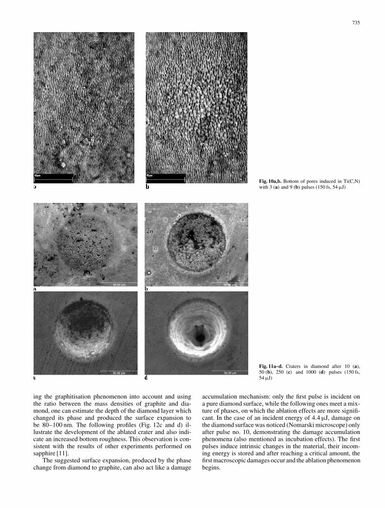
The surfaces depicted in Fig. 3a and b were investigated byAFM and the resulting depth profiles are shown in Fig. 7, to-gether with the profile of the initial surface. If the roughnesschanges are considered, one can notice that after 10 pulses theroughness is still comparable with that of the initial substrate,while after 50 pulses this is not any more the case.
The existence of the pores in the central zone could notbe correlated with the sintered structure of the material, sincethe comparison tests performed on stainless steel led to similarmorphologies (“frozen” melt pool with deep pores).
During the initial pulses, the damage does not necessarilyoccur in the zone of maximal fluence, but the incident energyexerts a damage accumulation effect and the next incomingpulses could release this energy, leading to explosive phasetransformations and subsequently to an increased roughness ofthe crater bottom. Similar effects were also noticed for othermaterials [11].
733
Fig. 5a–d. Damage on cemented tungsten car-bide induced with one laser pulse of 54 (a),35 (b), 12 (c) and 4.4 µJ (d)
Fig. 6a–c. Damage on cemented tungsten carbide induced with 1 (a), 5 (b) and 10 (c) laser pulses of 54 µJ
Fig. 7. AFM profiles of initial surface (a), and of craters induced with 10 (b)and 100 (c) laser pulses (150 fs, 54 µJ)
Once a difference in the target roughness occurs, an en-hanced absorption of the incident beam takes place in therough zones, increasing the ablation effects in these regions.As long as the roughness structures are comparable to thewavelength, they can be represented as a grey body, and thelocal absorption at these structures is larger. Increased ab-sorbed energy leads to increasing size (Fig. 3b and c). Thismechanism could operate until the bottom pores are muchlarger than the radiation wavelength, i.e. the incoming light isnot trapped any more in a grey body.
3.2 Titanium carbonitride
Sample 3 was made of a WC-10 Co substrate, coated witha thin film of titanium carbonitride, Ti(C,N). The film was ob-tained through a commercially available chemical vapour de-position technology and its specified thickness was 3–4 µm.
734
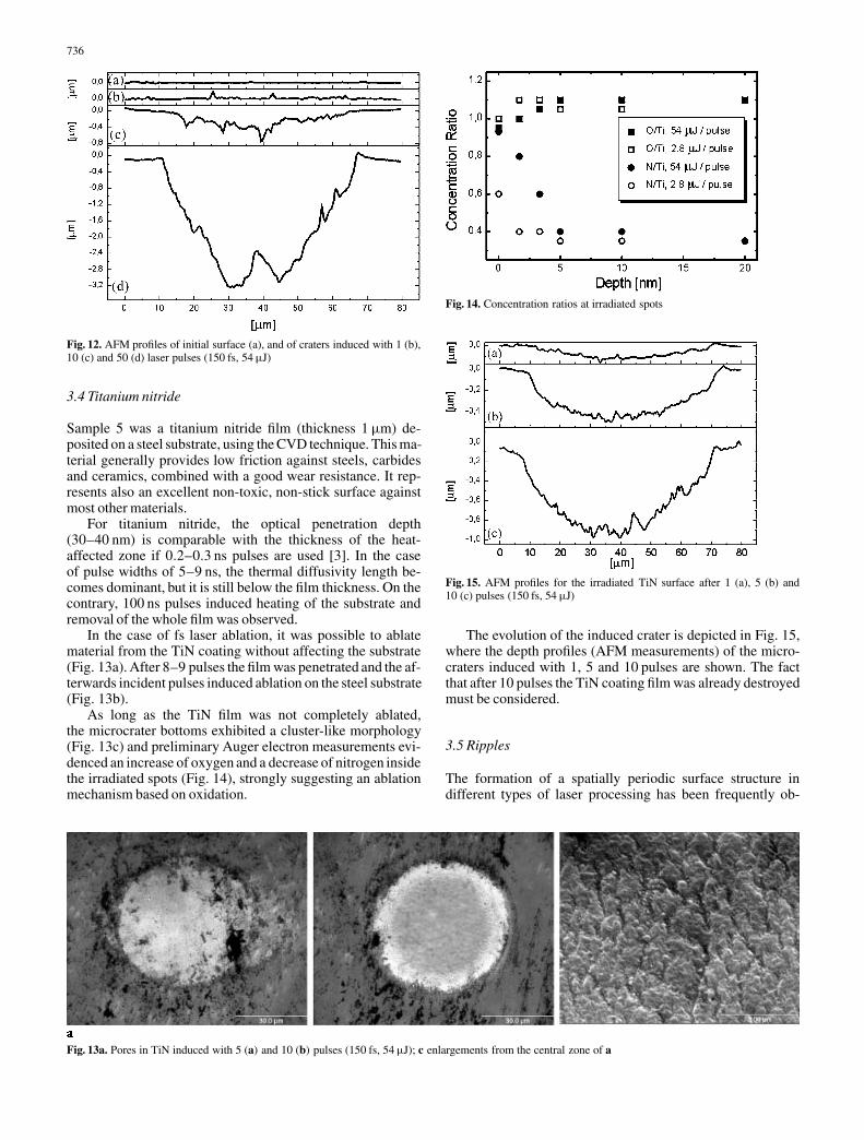
A SEM picture from a zone of sample 4 before its laser expo-sure is shown in Fig. 8.
Among the refractory carbides, titanium carbonitride ex-hibits high hardness and excellent wear resistance, but it alsoshows a significant brittleness. Applications are mainly con-nected with coating technologies, in order to obtain protectivethin films with great hardness and good wear resistance onlarge metallic pieces.
The ns laser processing (100 ns, FWHM) of such film coat-ings proved to be difficult due to the inherent heat-affectedzone, which had the same order of magnitude as the film thick-ness. The thermal stress induced in the film diminished its ad-herence properties and even heating of the substrate occurred.All these contributed to the degradation of the coating film andto the loss of its intended positive effects.
The use of ultrashort laser pulses made the micropro-cessing of surfaces already coated possible and a precise anddebris-free ablation procedure was confirmed, as Fig. 9 il-lustrates. After 20–25 laser pulses, the depth of the inducedcrater was equal to the film thickness, the film was perforated(Fig. 9c) and the subsequent pulses induced ablation on thetungsten carbide substrate.
Optical inspection (Nomarski microscope) of the irradi-ation spots showed the quasi-radial symmetry of the induceddamage, following the fluence profile of the incident laser
Fig. 8. Structure of unexposed Ti(C,N) film
Fig. 9a–c. Craters induced in Ti(C,N) with 3 (a), 9 (b) and 50 (c) pulses (150 fs, 54 µJ)
beam. More detailed SEM pictures taken from microcratersinduced with 3 and 9 laser pulses, respectively, are includedin Fig. 10.
The revealed cluster-like morphologies are similar to thosenoted in the case of titanium nitride [3, 12] and they are sup-posed to be generated by the desorption of the nitrogen that wasinitially present in the composition of the coating. It can also benoted that by increasing the number of pulses, the roughness ofthe irradiated zone increases (Fig. 10). Further Auger electronstudies will clarify the stoichiometry in the irradiated zone andits vicinity.
3.3 Diamond
Sample 4 was a piece of industrial diamond; the thickness ofthe sample was of approximately 1 mm.
In the case of ns ablation, laser wavelengths below 230 nmare needed because of the wide band gap (5.4 eV) of thismaterial [13]. Concurrently, due to the large thermal con-ductivity (roughly 50 times larger than that of steel), thermallosses cannot be avoided, yielding graphitisation and me-chanical stresses. Through fs ablation of diamond, photonswith energies smaller than 5.4 eV (i.e. λ > 230 nm) can beused without any precision loss, the ablation threshold is de-creased and the thermal flow in the bulk material is signifi-cantly reduced.
An overall view of the induced crater evolution is illus-trated in Fig. 11, which contains SEM images of microcratersinduced with 10, 50, 250 and 1000 laser pulses, respectively,and where the sharp boundaries of the irradiated spots canbe noticed. Both SEM and optical investigations revealedchanges on the target surface right after the first pulse anddecreasing the fluence of the incident beam generated onlya diameter reduction of the affected zones.
To gather more information about the initial phase of theablation process, depth profiles were obtained using AFMmeasurements. Figure 12 depicts the profile of the non-irradi-ated diamond surface (upper profile) and depth profiles ofpores induced with 1, 10, 15 and 50 pulses, respectively, withthe maximal pulse energy.
The AFM profile after the first pulse (Fig. 12b) hints toa slight surface growth (40–50 nm) over the spot area. Tak-
735
Fig. 10a,b. Bottom of pores induced in Ti(C,N)with 3 (a) and 9 (b) pulses (150 fs, 54 µJ)
Fig. 11a–d. Craters in diamond after 10 (a),50 (b), 250 (c) and 1000 (d) pulses (150 fs,54 µJ)
ing the graphitisation phenomenon into account and usingthe ratio between the mass densities of graphite and dia-mond, one can estimate the depth of the diamond layer whichchanged its phase and produced the surface expansion tobe 80–100 nm. The following profiles (Fig. 12c and d) il-lustrate the development of the ablated crater and also indi-cate an increased bottom roughness. This observation is con-sistent with the results of other experiments performed onsapphire [11].
The suggested surface expansion, produced by the phasechange from diamond to graphite, can also act like a damage
accumulation mechanism: only the first pulse is incident ona pure diamond surface, while the following ones meet a mix-ture of phases, on which the ablation effects are more signifi-cant. In the case of an incident energy of 4.4 µJ, damage onthe diamond surface was noticed (Nomarski microscope) onlyafter pulse no. 10, demonstrating the damage accumulationphenomena (also mentioned as incubation effects). The firstpulses induce intrinsic changes in the material, their incom-ing energy is stored and after reaching a critical amount, thefirst macroscopic damages occur and the ablation phenomenonbegins.
736
Fig. 12. AFM profiles of initial surface (a), and of craters induced with 1 (b),10 (c) and 50 (d) laser pulses (150 fs, 54 µJ)
3.4 Titanium nitride
Sample 5 was a titanium nitride film (thickness 1 µm) de-posited on a steel substrate, using the CVD technique. This ma-terial generally provides low friction against steels, carbidesand ceramics, combined with a good wear resistance. It rep-resents also an excellent non-toxic, non-stick surface againstmost other materials.
For titanium nitride, the optical penetration depth(30–40 nm) is comparable with the thickness of the heat-affected zone if 0.2–0.3 ns pulses are used [3]. In the caseof pulse widths of 5–9 ns, the thermal diffusivity length be-comes dominant, but it is still below the film thickness. On thecontrary, 100 ns pulses induced heating of the substrate andremoval of the whole film was observed.
In the case of fs laser ablation, it was possible to ablatematerial from the TiN coating without affecting the substrate(Fig. 13a). After 8–9 pulses the film was penetrated and the af-terwards incident pulses induced ablation on the steel substrate(Fig. 13b).
As long as the TiN film was not completely ablated,the microcrater bottoms exhibited a cluster-like morphology(Fig. 13c) and preliminary Auger electron measurements evi-denced an increase of oxygen and a decrease of nitrogen insidethe irradiated spots (Fig. 14), strongly suggesting an ablationmechanism based on oxidation.
Fig. 13a. Pores in TiN induced with 5 (a) and 10 (b) pulses (150 fs, 54 µJ); c enlargements from the central zone of a
Fig. 14. Concentration ratios at irradiated spots
Fig. 15. AFM profiles for the irradiated TiN surface after 1 (a), 5 (b) and10 (c) pulses (150 fs, 54 µJ)
The evolution of the induced crater is depicted in Fig. 15,where the depth profiles (AFM measurements) of the micro-craters induced with 1, 5 and 10 pulses are shown. The factthat after 10 pulses the TiN coating film was already destroyedmust be considered.
3.5 Ripples
The formation of a spatially periodic surface structure indifferent types of laser processing has been frequently ob-
737
served [14–16] and was first observed in 1965 on semiconduc-tor surfaces after ruby laser irradiation. Further investigationshave shown that the occurrence of ripples is practically al-ways observed within particular ranges of laser parameters.The mechanisms of ripple formation have been extensively in-vestigated and reported in literature [16].
To give an idea: ripples originate from the interference ofthe incident and reflected radiation with the scattered waves,or surface acoustic waves [14], on the laser-processed surface.The interference between the different waves yields inhomo-geneities of the energy distribution that, coupled with a pos-itive feedback, can cause periodic surface instabilities. Theperiod of the induced structures depends on the wavelength, onthe angle of incidence, on the time duration and on the polarisa-tion of the incident beam.
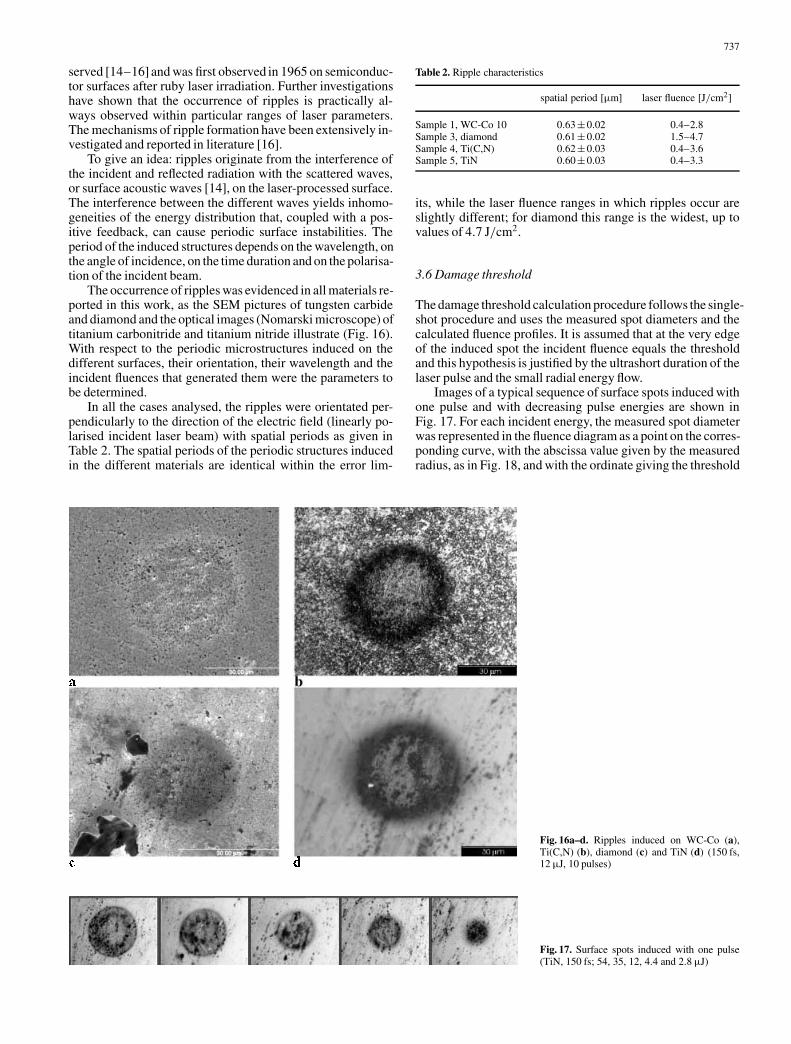
The occurrence of ripples was evidenced in all materials re-ported in this work, as the SEM pictures of tungsten carbideand diamond and the optical images (Nomarski microscope) oftitanium carbonitride and titanium nitride illustrate (Fig. 16).With respect to the periodic microstructures induced on thedifferent surfaces, their orientation, their wavelength and theincident fluences that generated them were the parameters tobe determined.
In all the cases analysed, the ripples were orientated per-pendicularly to the direction of the electric field (linearly po-larised incident laser beam) with spatial periods as given inTable 2. The spatial periods of the periodic structures inducedin the different materials are identical within the error lim-
Fig. 16a–d. Ripples induced on WC-Co (a),Ti(C,N) (b), diamond (c) and TiN (d) (150 fs,12 µJ, 10 pulses)
Fig. 17. Surface spots induced with one pulse(TiN, 150 fs; 54, 35, 12, 4.4 and 2.8 µJ)
Table 2. Ripple characteristics
spatial period [µm] laser fluence [J/cm2]
Sample 1, WC-Co 10 0.63±0.02 0.4–2.8Sample 3, diamond 0.61±0.02 1.5–4.7Sample 4, Ti(C,N) 0.62±0.03 0.4–3.6Sample 5, TiN 0.60±0.03 0.4–3.3
its, while the laser fluence ranges in which ripples occur areslightly different; for diamond this range is the widest, up tovalues of 4.7 J/cm2.
3.6 Damage threshold
The damage threshold calculation procedure follows the single-shot procedure and uses the measured spot diameters and thecalculated fluence profiles. It is assumed that at the very edgeof the induced spot the incident fluence equals the thresholdand this hypothesis is justified by the ultrashort duration of thelaser pulse and the small radial energy flow.
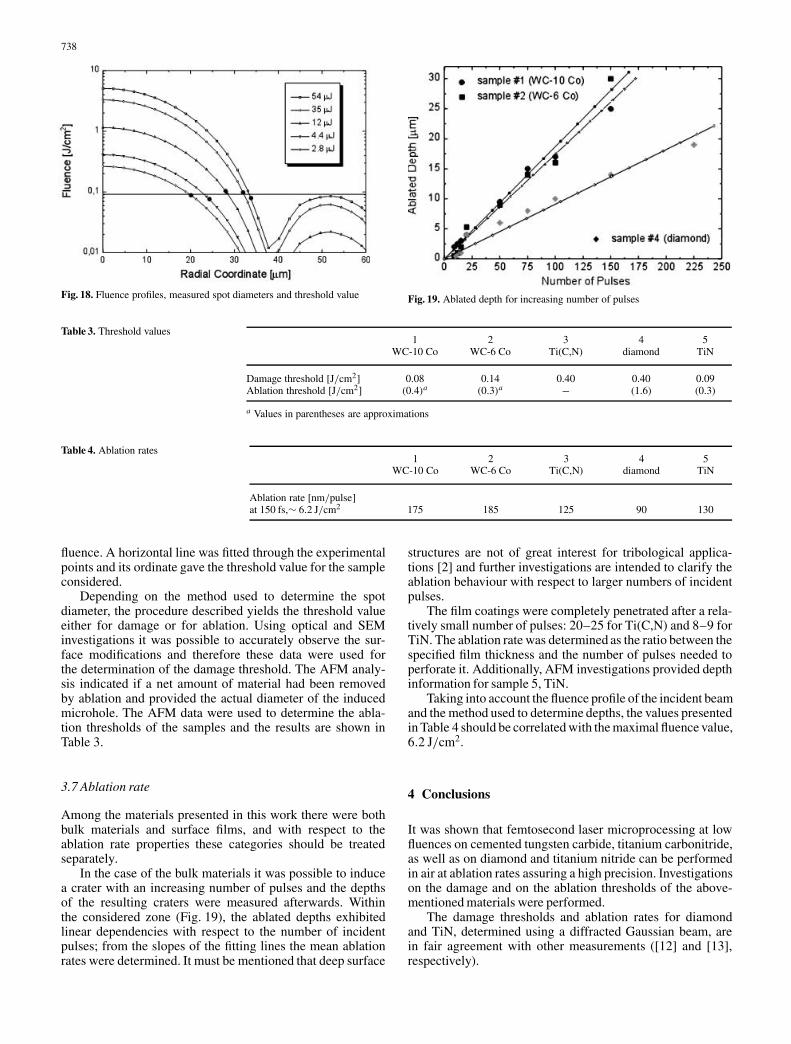
Images of a typical sequence of surface spots induced withone pulse and with decreasing pulse energies are shown inFig. 17. For each incident energy, the measured spot diameterwas represented in the fluence diagram as a point on the corres-ponding curve, with the abscissa value given by the measuredradius, as in Fig. 18, and with the ordinate giving the threshold
738
Fig. 18. Fluence profiles, measured spot diameters and threshold value
1 2 3 4 5WC-10 Co WC-6 Co Ti(C,N) diamond TiN
Damage threshold [J/cm2] 0.08 0.14 0.40 0.40 0.09Ablation threshold [J/cm2] (0.4)a (0.3)a − (1.6) (0.3)
a Values in parentheses are approximations
Table 3. Threshold values
1 2 3 4 5WC-10 Co WC-6 Co Ti(C,N) diamond TiN
Ablation rate [nm/pulse]at 150 fs,∼ 6.2 J/cm2 175 185 125 90 130
Table 4. Ablation rates
fluence. A horizontal line was fitted through the experimentalpoints and its ordinate gave the threshold value for the sampleconsidered.
Depending on the method used to determine the spotdiameter, the procedure described yields the threshold valueeither for damage or for ablation. Using optical and SEMinvestigations it was possible to accurately observe the sur-face modifications and therefore these data were used forthe determination of the damage threshold. The AFM analy-sis indicated if a net amount of material had been removedby ablation and provided the actual diameter of the inducedmicrohole. The AFM data were used to determine the abla-tion thresholds of the samples and the results are shown inTable 3.
3.7 Ablation rate
Among the materials presented in this work there were bothbulk materials and surface films, and with respect to theablation rate properties these categories should be treatedseparately.
In the case of the bulk materials it was possible to inducea crater with an increasing number of pulses and the depthsof the resulting craters were measured afterwards. Withinthe considered zone (Fig. 19), the ablated depths exhibitedlinear dependencies with respect to the number of incidentpulses; from the slopes of the fitting lines the mean ablationrates were determined. It must be mentioned that deep surface
Fig. 19. Ablated depth for increasing number of pulses
structures are not of great interest for tribological applica-tions [2] and further investigations are intended to clarify theablation behaviour with respect to larger numbers of incidentpulses.
The film coatings were completely penetrated after a rela-tively small number of pulses: 20–25 for Ti(C,N) and 8–9 forTiN. The ablation rate was determined as the ratio between thespecified film thickness and the number of pulses needed toperforate it. Additionally, AFM investigations provided depthinformation for sample 5, TiN.
Taking into account the fluence profile of the incident beamand the method used to determine depths, the values presentedin Table 4 should be correlated with the maximal fluence value,6.2 J/cm2.
4 Conclusions
It was shown that femtosecond laser microprocessing at lowfluences on cemented tungsten carbide, titanium carbonitride,as well as on diamond and titanium nitride can be performedin air at ablation rates assuring a high precision. Investigationson the damage and on the ablation thresholds of the above-mentioned materials were performed.
The damage thresholds and ablation rates for diamondand TiN, determined using a diffracted Gaussian beam, arein fair agreement with other measurements ([12] and [13],respectively).
739
The values for WC-10 Co and WC-6 Co are reportedfor the first time and they remain in the expected zone of0.1–0.2 J/cm2, typical for metals under fs irradiation. Thedifference between the reported values, however, lies withinthe uncertainty of the calculations. For titanium carbonitridea quite high threshold value (0.4 J/cm2), in comparison withthose for metallic surfaces, was found.
The measured ablation rates were in the range of0.1–0.2 µm per pulse, but some comments regarding the vari-ations between the materials must be brought to attention. Themorphologies of pores induced in cemented tungsten carbidehint at two ablation phases, a gentle phase for the first pulsesand an explosive one afterwards. The presence of cobalt inthe cemented tungsten carbide increases the ablation rate, ifcompared with titanium carbonitride. The values determinedfor titanium nitride and titanium carbonitride (both CVD filmcoatings) are almost equal. The ablation threshold of diamondis only a factor two smaller than that of WC-Co; higher thanone should expect. The graphitisation of diamond, mentionedin literature [17] and also discussed in this work, could repre-sent the reason why diamond exhibits an ablation rate compa-rable with the other materials despite its high threshold value.
Acknowledgements. The authors want to acknowledge the participation ofDr. H. Scheidiger in the SEM investigations of sample 4, the contribution ofDr. T. Kononenko during the Auger electron measurements, and the help ofMrs. E. Bigler.
References
1. G. Dumitru, V. Romano, H.P. Weber, H. Haefke, Y. Gerbig, E. Pflüger:Appl. Phys. A 70, 485 (2000)
2. G. Dumitru, V. Romano, H.P. Weber, H. Haefke, Y. Gerbig: Lasers inManufacturing 2001 (WLT eV, AT-Fachverlag, Stuttgart 2001), p. 351
3. T.V. Kononenko, S.V. Garnov, S.M. Pimenov, V.I. Konov, V. Romano,B. Borsos, H.P. Weber: Appl. Phys. A 71, 627 (2000)
4. M.D. Shirk, P.A. Molian: J. Laser Appl. 10, 18 (1998)5. S. Nolte, C. Momma, H. Jacobs, A. Tünnermann, B.N. Chichkov,
B. Wellegehausen, H. Welling: J. Opt. Soc. Am. B 14, 2716 (1997)6. J. Ihlemann, A. Scholl, H. Schmidt, B. Wolff-Rottke: Appl. Phys. A 60,
411 (1995)7. S. Küper, M. Stuke: Appl. Phys. Lett. 54, 4 (1989)8. B.N. Chichkov, C. Momma, S. Nolte, F. von Alvensleben, A. Tünner-
mann: Appl. Phys. A 63, 109 (1996)9. G.S. Upadhyaya: Sintered Metallic and Ceramic Materials (Wiley, New
York 2000)10. Y. Jee, M.F. Becker, R.M. Walser: J. Opt. Soc. Am. B 5, 648 (1988)11. D. Ashkenasi, A. Rosenfeld, H. Varel, M. Wähmer, E.E.B. Campbell:
Appl. Surf. Sci. 120, 65 (1997)12. J. Bonse, H. Sturm, D. Schmidt, W. Kautek: Appl. Phys. A 71, 657
(2000)13. S. Preuss, M. Stuke: Appl. Phys. Lett. 67, 338 (1995)14. D. Jost, W. Lüthy, H.P. Weber, R.P. Salathe: Appl. Phys. Lett. 49, 625
(1986)15. A.M. Ozkan, A.P. Malshe, T.A. Railkar, W.D. Brown, M.D. Shirk,
P.A. Molian: Appl. Phys. Lett. 75, 3716 (1999)16. D. Bäuerle: Laser Processing and Chemistry (Springer, Berlin 2000)17. H.O. Jeschke, M.E. Garcia, K.H. Bennemann: Phys. Rev. B 60, R3701
(1999)