sub-micron grating formation in ta2o5-waveguides by femtosecond uv-laser ablation
TRANSCRIPT
Sub-micron grating formation in Ta2O5-waveguides byfemtosecond UV-laser ablation
Beinhorn, Frank; Ihlemann, Jürgen; Simon, Peter; Marowsky, Gerd;Maisenhölder, Bernd; Edlinger, Johannes; Neuschäfer, Dieter; Anselmetti,
Dario
Beinhorn, Frank; Ihlemann, Jürgen; Simon, Peter; Marowsky, Gerd;Maisenhölder, Bernd; Edlinger, Johannes; Neuschäfer, Dieter; Anselmetti,
Dario
Suggested CitationBeinhorn, Frank ; Ihlemann, Jürgen ; Simon, Peter ; Marowsky, Gerd ; Maisenhölder, Bernd ;Edlinger, Johannes ; Neuschäfer, Dieter ; Anselmetti, Dario (1999) Sub-micron gratingformation in Ta2O5-waveguides by femtosecond UV-laser ablation. Applied surface science,138-139, pp. 107-110
Posted at BiPrints Repository, Bielefeld University.http://repositories.ub.uni-bielefeld.de/biprints/volltexte/2006/38
Sub-micron grating formation in Ta2O5-waveguides byfemtosecond UV-laser ablation
Abstract
Sub-micron-period surface gratings on Ta2O5 waveguide layers were produced by ablationwith a sub-ps-UV-laser. The structure is generated by projection imaging of a primarytransmission grating mask. A grating of 500 nm period with a surface modulation depth of 10nm on a sample area of about 300 µm × 300 µm can be produced with a single laser pulse ofabout 100 mJ/cm² at 248 nm. Adjustment of the modulation depth to specific requirements canbe accomplished by varying laser fluence or pulse number. The structures can be used asgrating couplers.

Ž .Applied Surface Science 138–139 1999 107–110
Sub-micron grating formation in Ta O -waveguides by2 5
femtosecond UV-laser ablation
F. Beinhorn a, J. Ihlemann a,), P. Simon a, G. Marowsky a, B. Maisenholder b,¨J. Edlinger b, D. Neuschafer c, D. Anselmetti c¨
a Laser-Laboratorium Gottingen, Hans-Adolf-Krebs-Weg 1, D-37077 Gottingen, Germany¨ ¨b Balzers Thin Films, Balzers, FL Liechtenstein, Switzerland
c NoÕartis, 4002 Basel, Switzerland
Abstract
Sub-micron-period surface gratings on Ta O waveguide layers were produced by ablation with a sub-ps-UV-laser. The2 5
structure is generated by projection imaging of a primary transmission grating mask. A grating of 500 nm period with asurface modulation depth of 10 nm on a sample area of about 300 mm=300 mm can be produced with a single laser pulseof about 100 mJrcm2 at 248 nm. Adjustment of the modulation depth to specific requirements can be accomplished byvarying laser fluence or pulse number. The structures can be used as grating couplers. q 1999 Elsevier Science B.V. Allrights reserved.
PACS: 79.20.Ds; 81.65.Cf; 42.79.Dj
Keywords: Laser ablation; Micro patterning; Grating; Femtosecond laser
1. Introduction
Ta O is a very important material in various2 5
areas of optical technology. Due to its good trans-Žparency and the high refractive index n)2.2 in the
.visible range it is used for multilayer dielectricw x w xmirrors or masks 1,2 and for planar waveguides 3 .
Planar waveguides find applications in opticalcommunications technology and integrated optical
) Corresponding author. Tel.: q49-551-503544; Fax: q49-551-503599; E-mail: [email protected]
w xsensors 4 . The efficient coupling of laser light intothe waveguide is of great importance. In most casesthis is accomplished by focusing the laser on a
Žsurface grating on the waveguide or on a cover.layer . These gratings can be produced by a litho-
graphic process, e.g., holographic exposure of a pho-toresist and subsequent dry etching.
In this paper we describe sub-mm-period gratingfabrication on Ta O by laser ablation using a short2 5
pulse laser system in combination with a high resolu-tion optical imaging arrangement, an approach whichhas already been successfully applied to the structur-
w x Ž . w xing of metals 5 and lithium-niobate LiNbO 6 .3
Until now UV-laser ablation of Ta O has been2 5w xinvestigated with respect to layer deposition 7 and
0169-4332r99r$ - see front matter q 1999 Elsevier Science B.V. All rights reserved.Ž .PII: S0169-4332 98 00390-0
( )F. Beinhorn et al.rApplied Surface Science 138–139 1999 107–110108
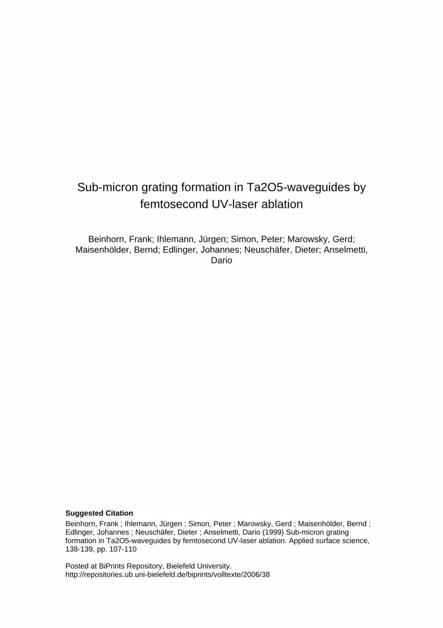
Fig. 1. Mask projection set-up with Schwarzschild objective.
w xplume analysis 8 , but not with the aim of mi-crostructuring.
2. Experiment
ŽTa O was deposited on glass substrates Corning2 5. Ž .7059 by reactive low voltage ion plating RLVIP
leading to extremely hard and dense layers. Thelayer thickness was 150 nm.
Ablation experiments were performed with a shortw xpulse KrF-laser system described elsewhere 9 . The
output is about 10 mJ at 248 nm with a pulseduration of 500 fs. Irradiation was carried out in amask projection set-up shown in Fig. 1. For maskimaging a Schwarzschild type reflective objectivewas used. This insures high power transmission in
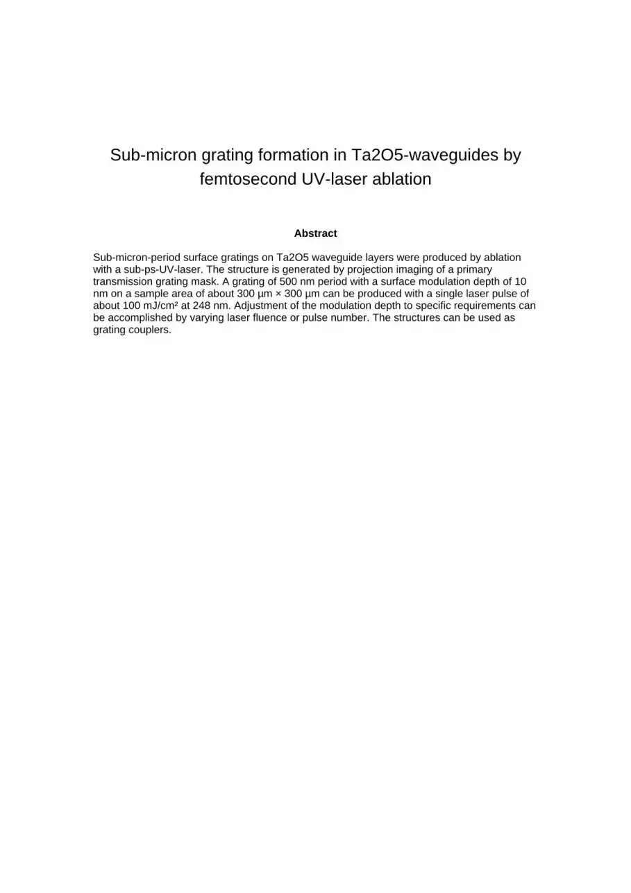
Fig. 2. SEM-micrograph of a Ta O -grating made with a single2 5Ž 2 .laser pulse 248 nm, 0.5 ps, 100 mJrcm , vacuum .
the UV and prohibits pulse front distortion for fem-tosecond pulses. This objective had a numerical aper-ture of 0.3 and was used with a demagnification of18.5= .
For the ablation of the periodic structures a trans-Ž .mission grating 55 linesrmm Cr on quartz was
imaged onto the samples. The zeroth order of thediffraction pattern was blocked in order to increasethe created line density by a factor of two. With thisarrangement an intensity pattern with a period ofabout 500 nm was projected onto the samples. Thefluence was varied with a dielectric attenuator be-tween 10 and 800 mJrcm2. To avoid air breakdownin the focus between objective and image plane,some of the experiments were performed in a vac-
Ž y1 .uum cell -10 mbar .
3. Results
Fig. 2 shows a surface grating produced with asingle pulse at a fluence of 100 mJrcm2 recorded by
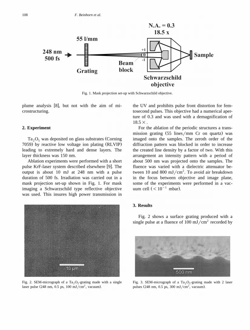
Fig. 3. SEM-micrograph of a Ta O -grating made with 2 laser2 5Ž 2 .pulses 248 nm, 0.5 ps, 300 mJrcm , vacuum .

( )F. Beinhorn et al.rApplied Surface Science 138–139 1999 107–110 109
Ž .scanning electron microscopy SEM . A smooth andhomogeneous structure is achieved over the wholeirradiated area of about 300 mm=300 mm. Fig. 3
shows a cross section of a Ta O -surface structure2 5
made by 2 pulses of 300 mJrcm2 resulting in asinusoidal profile. The dependence of the surface
Ž . Ž . 2 Ž . 2Fig. 4. AFM-records of Ta O -gratings made by laser ablation at 248 nm, 0.5 ps in air : a 30 mJrcm , 2 pulses, b 100 mJrcm , 12 5Ž . 2pulse, c 100 mJrcm , 100 pulses.

( )F. Beinhorn et al.rApplied Surface Science 138–139 1999 107–110110
modulation depth on fluence and pulse number canŽ .be seen from the atomic force microscope AFM
data shown in Fig. 4a–c. The fluence threshold forthe development of a periodic surface profile isabout 30 mJrcm2. With an average fluence of 30mJrcm2 the grating structure appears only in limited
Ž . 2areas of the irradiation spot Fig. 4a . At 100 mJrcma surface modulation of about 10 nm is reached with
Ž .a single laser pulse Fig. 4b . By applying severalpulses of this fluence, the layer can be structureddown to the glass substrate. Fig. 4c shows a gratingwith completely removed Ta O -layer in the grooves.2 5
Even the glass substrate is ablated to some extent.Using for comparison nanosecond laser pulses
Ž .20 ns instead of the sub-ps pulses, a maximummodulation depth of 1 nm with a single pulse and nomore than 3 nm with 5 pulses was observed.
4. Discussion
For the ability to generate structures with sub-mmfeature size not only the optical resolution but alsothe resolution limit of the material response due tothermal diffusion of the absorbed laser energy has tobe considered. A characteristic measure is the
Ž .0.5thermal diffusion length L s 2 Dt , whereDsLry1cy1 is the thermal diffusivity of the mate-p
Žrial L thermal conductivity, r density, c specificp.heat capacity and t the laser pulse duration, or, for
ultrashort pulses, the electron phonon coupling timedetermining the speed of lattice heating. If L ex-ceeds the optical resolution limit, which is of theorder of the used laser wavelength, lateral heat ex-change will prevent high contrast structure forma-tion.
Exact thermal conductivity data of layered materi-als are scarcely available. The data depend on depo-sition method, layer thickness, and temperature, anddiffer also for the various methods of measurementw x10,11 . For Ta O data range from 0.03 to 15 W2 5
my1 Ky1, leading to thermal diffusion lengths of 20
nm to 500 nm for a laser pulse duration of 20 ns.Assuming an average value of about one hundrednanometer, it is understandable, that with nanosec-ond pulses a period of some hundred nanometers isthe ultimate limit for ns-structuring leading only tothe observed shallow structures with no more than 3nm modulation depth. Using picosecond- or fem-tosecond pulses, heat diffusion can be neglected anddeep modulation is possible.
5. Conclusion
Laser ablation patterning can be used as a onestep process for the generation of surface gratings.Ultrashort UV-pulses lead to sub-mm structures ofhigh contrast on Ta O . A single laser pulse is2 5
sufficient for the fabrication of a grating that can beused for the coupling of light into a Ta O -wave-2 5
guide. Experiments for the detailed optical character-ization of the gratings are in progress.
References
w x1 M.L. Scott, Proc. Boulder Damage Symposium, 1983, p. 329w x Ž .2 C. Tessler, D. Tudryn, M. Geiger Ed. , Proc. of the 12th
International Congress Laser’95, Bamberg, 1995, p. 61.w x3 H.K. Pulker, Coatings on Glass, Elsevier, Amsterdam 1984,
p. 367.w x4 D. Neuschafer, W. Budach, E. Bar, M. Pawlak, G. Duve-¨ ¨
Ž .neck, Proc. SPIE 2836 1996 221.w x Ž .5 P. Simon, J. Ihlemann, Appl. Phys. A 63 1996 505.w x6 K. Chen, J. Ihlemann, P. Simon, I. Baumann, W. Sohler,
Ž .Appl. Phys. A 65 1997 517.w x7 N. Inoue, S. Kashiwabara, S. Toshima, R. Fujimoto, Appl.
Ž .Surf. Sci. 96 1996 656.w x Ž .8 Z.W. Fu, M.F. Zhou, Q.Z. Qin, Appl. Phys. A 65 1997
445.w x Ž .9 S. Szatmari, F.P. Schafer, Opt. Commun. 68 1988 196.´ ¨w x Ž .10 S.-M. Lee, D.G. Cahill, T.H. Allen, Phys. Rev. B 52 1995
253.w x11 D. Ristau, Proc. of the 4th International Workshop of Laser
Beam and Optics Characterization, VDI-Verlag 1997, pp.546–571.