oxygen annealing modification of conduction mechanism in thin rf sputtered ta2o5 on si
TRANSCRIPT

Oxygen annealing modification of conduction mechanismin thin rf sputtered Ta2O5 on Si
E. Atanassova a,*, N. Novkovski b, A. Paskaleva a, M. Pecovska-Gjorgjevich b
a Institute of Solid State Physics, Bulgarian Academy of Sciences, 72 Tzarigradsko Chaussee, 1784 Sofia, Bulgariab Faculty of Natural Science and Mathematics, Institute of Physics, St. Cyril and Methodius University, 91000 Skopje, Macedonia
Received 2 April 2001; received in revised form 8 February 2002; accepted 5 March 2002
Abstract
The effect of oxygen annealing at high temperature (873, 1123 K; 30 min) on the insulating properties and conduction
mechanism of rf sputtered Ta2O5 (25–80 nm) on Si has been investigated. It is found that the oxygen heating signifi-
cantly reduces the oxide charge (Qf < 1010 cm�2) and improves the breakdown characteristics (the effect is more pro-
nounced for the higher annealing temperature). It is accompanied by an increase of the effective dielectric constant (up
to 37 after 1123 K treatment). It is established that the influence of the oxygen treatment on the leakage current is
different depending on the film thickness, namely: a beneficial effect for the thinner and a deterioration of leakage
characteristics for thicker (80 nm) films. A leakage current density as low as 10�7 A/cm2 at 1 MV/cm applied field for 26
nm annealed layers has been obtained. The current reduction is considered to be due to a removal by annealing of
certain structural nonperfections present in the initial layers. Generally, the results are discussed in terms of simulta-
neous action of two opposite and competing processes taking place at high temperatures–– a real annealing of defects
and an appearance of a crystal phase and/or a neutral traps generation. The contribution of the neutral traps also is
involved to explain the observed weaker charge trapping in the as-fabricated films compared to the annealed ones.
The conduction mechanism of the as-deposited films is found to be of Poole–Frenkel (PF) type for a wide range of
applied fields. A change of the conduction mechanism for the annealed films at medium fields (0.8–1.3 MV/cm) is
established. This transition from PF process to the Schottky emission limited current is explained with an annealing of
bulk traps (oxygen vacancies and nonperfect bonds). It is concluded that the dominant conduction mechanism in the
intermediate fields can be effectively controlled by appropriate technological steps.
� 2002 Elsevier Science Ltd. All rights reserved.
1. Introduction
The development of storage capacitors for dynamic
random access memory (DRAM) generations of 64
Mbit and beyond requires alternative dielectric materials
because the conventional SiO2 based insulators have
reached their physical limits in the terms of thinning. To
overcome the reduced thickness problems the use of high
dielectric constant materials has been suggested. Thin
films of Ta2O5 have been widely investigated as a po-
tential dielectric material for use in DRAM capacitors
due to the high dielectric constant and chemical stability
[1–8]. There is also a great interest in utilization of high
dielectric constant insulators as a gate dielectric in sub-
micron MOST [1]. Ta2O5 is now in the closest position
to practical application among a number of metal oxides
and it might be utilized in high density DRAM with
oxide equivalent thickness of about 5 nm. During the
formation of Ta2O5 a silicon oxide layer is inevitably
observed at the interface with Si [4]. Its growth is fa-
vored by an oxidizing ambient at the beginning or
during the deposition step and by post fabrication
treatments performed in an oxygen atmosphere to repair
the oxygen vacancies. The integration of Ta2O5 in the
complete device fabrication process is still the subject of
ongoing investigations. Among the points to be taken
Solid-State Electronics 46 (2002) 1887–1898
www.elsevier.com/locate/sse
*Corresponding author. Fax: +359-2-975-3632.
E-mail address: [email protected] (E. Atanassova).
0038-1101/02/$ - see front matter � 2002 Elsevier Science Ltd. All rights reserved.
PII: S0038-1101 (02 )00134-X

into consideration is the conduction mechanism in close
relation with the presence of interfacial layer between
Si and Ta2O5 as well as the nature, the thickness and
the microstructure of Ta2O5. The structural parameters,
however, are a function of the technological conditions
and all post deposition steps. Therefore, the conduction
mechanisms in Ta2O5 films are a very important subject
and their relationship to the film formation conditions
should be thoroughly investigated. At present relatively
large leakage current in Ta2O5 films limits the applica-
tion in ULSI’s from a storage characteristics point of
view. Thus, improvement of the electrical properties of
Ta2O5 has attracted the attention of many researchers
[2,3,8]. Most of the reported electrical and dielectric
properties have been centered around Ta2O5 capaci-
tor having metal-oxide-semiconductor (MOS) structure,
where the formation of SiO2 interfacial layer was highly
recognized. This SiO2 affects significantly the conduction
mechanism and the associated leakage current density.
Several our studies on the properties of amorphous
Ta2O5 thin films on Si formed by thermal oxidation of
deposited Ta on Si [5–7,9–11] and rf sputtered Ta2O5[7,9,12–18] have been published. It has been established
that the formation of ultrathin SiO2 film at the interface
with Si is unavoidable process and is an attribute of the
two fabrication technologies used. Ta2O5 as well as SiO2are nonstoichiometric in depth and contain suboxides of
Ta and Si through the layers [5,12]. These structural
imperfections act as electrically active centers. In the
present paper a systematic study of the effect of the
technological conditions (with a focus on the oxygen
annealing (OA)) on the d.c. electrical conduction char-
acteristics and on the dielectric strength of rf sputtered
Ta2O5 films on Si is made. The reliability characteristics
under constant current stress (CCS) are also examined.
The study is motivated by the necessity to control the
most important parameter of the insulator to be used as
memory dielectric––the leakage current.
2. Experimental procedure
Chemically cleaned p-type (1 0 0) silicon wafers 15
X cm were used as substrates. Tantalum pentoxide wasdeposited by reactive sputtering of Ta target in a mixture
of Ar and O2 gases up to thickness d of 25–80 nm.
Presputtering of the target was carried out in Ar. The
total pressure of the Ar–O2 mixture during the deposi-
tion was 0.33 Pa and the gas composition was 10%
O2þ 90% Ar. The rf power density was 3.6 W/cm2; thedeposition rate �5 nm/min and the target to substratedistance 3.5 cm. The substrate temperature Ts, duringdeposition is 293 or 493 K. After the fabrication the
samples were annealed at 873 or 1123 K for 30 min in
dry O2. The electrical characterization of the Ta2O5layers was carried out using MOS capacitors with Al
gate electrodes with areas in the range of 1� 10�4–2:5� 10�3 cm2. The fixed oxide charge was evaluatedfrom high frequency capacitance–voltage (C–V ) curves.The dielectric constant of the layers eeff was deter-mined from the capacitance C0 at accumulation usingthe measured values of d. The thickness of Ta2O5 and
the refractive index were determined by ellipsometry
(k ¼ 632:8 nm). Ramped current–voltage (I–V ) charac-teristics were used to investigate the leakage current at
low and high voltages. The breakdown field Ebd wasdefined as the average applied field at which the current
density through the dielectric exceeds 4� 10�4 A/cm2.The breakdown voltage of approximately 30 capacitors
was measured on each sample (a quarter of 2-inch Si
wafer). In order to obtain additional information about
the traps in the Ta2O5 as well as the charge to break-
down Qbd of Ta2O5, the time dependent dielectricbreakdown (TDDB) measurements using constant cur-
rent stress (CCS) were performed. Capacitors with an
area of 1� 10�4 cm2 were stressed with constant currentof 50 mA/cm2 and the time evolution of the voltage Vgwas studied. The times used in our experiments ranged
from 3� 102 s up to 103 s. The gate was biased nega-tively, so that the stressing was done with p-Si substrate
in accumulation.
3. Results and discussion
3.1. Dielectric parameters and C–V curves
The values of the refractive index neff for the as-deposited layers are in the range of 1.905–2.1 without a
dependence on the substrate temperature. A slight ten-
dency to increase neff is observed for oxygen annealedfilms. Recently [7,9,13,14], we have reported that the
effective dielectric constant of the rf sputtered tantalum
pentoxide shows a thickness dependence, namely eeffrises with increasing d and the eeffðdÞ dependence cor-responds to a two-layers model assuming serially con-
nected capacitors with the dielectrics SiO2 and Ta2O5,
respectively. The results imply (and agree with the X-ray
photoelectron spectroscopy (XPS) data [18]) that a SiO2layer is formed at the interface Si–Ta2O5 during sput-
tering and the relation between d and eeff is attributed tothe existence of a transition SiO2 layer. So, for the 26–28
nm layers, eeff is 11.5–14 before and 14–16 after oxygenannealing (OA). The intrinsic dielectric constant, et ofthe bulk Ta2O5 layers assuming double layer model for
the Si–Ta2O5 system is determined to be 23–27 and 24–
37 for the as-deposited and the annealed layers, respec-
tively [7,9]. The higher Ts results in higher values of eeffand et and the effect of oxygen treatment is to increasethe values of et. This can be explained with a certaindensification of the layers after annealing. Surprisingly,
an additional detectable oxidation of silicon during an-
1888 E. Atanassova et al. / Solid-State Electronics 46 (2002) 1887–1898

nealing of the layers investigated does not occur as
evaluated from the fitting procedure of eeffðdÞ depen-dence [7,9] obtained from 1 MHz C–V measurements.The SiO2 thickness d0 in all the cases is 4 nm and is
independent of the preparation conditions in the range
of experimental accuracy. (This result does not cancel
the possibility of eventual (weak) additional oxidation of
Si and/or reaction of Ta2O5 and SiO2 during annealing.)
A possible explanation is that the effect of oxidation
during annealing is weak and could not be detected by
electrical measurements. An additional argument could
be also the fact that for the as-deposited layers the SiO2is thick enough so that a small increase of its thickness
does not affect the HF C–V curves. To give an accurateanswer of this question precise XPS and transmission
electron microscopy (TEM) investigations are needed.
This kind of investigations are in progress in our labo-
ratory for layers with thickness in the range 10–80 nm
before as well as after OA. As we have previously found
[9,12] XPS depth profile shows that for relatively thin
sputtered Ta2O5 layers (8.5 nm) OA at 1123 K leads
indeed to an additional oxidation of Si which manifested
as a slight increase of SiO2 thickness. For the Ta2O5thicknesses investigated here, however, we will focus our
attention on the data obtained from C–V measurements.So, the observed practically unchanged thickness of SiO2in combination with the higher et values after annealingleads to very good results about the equivalent SiO2thickness: deq varies from 7.4 to 9.1 nm before and from6.5 to 7.7 nm after OA. This means that the scaling to
the thickness of 8 nm of the films prepared by the regime
giving the highest et, (37) will result in an equivalentoxide thickness of 3.5 nm, which is suitable for 1 and 4
Gbit DRAM applications. The as-deposited samples
show negative values (�0.14 to 0.29 V) of flat bandvoltage Vfb, with respect to the ideal C–V curve (the
work function difference between Al and Si is 0.61 eV),
giving values of oxide charge Qf ¼ 2–6� 1011 cm�2––the
higher Qf corresponds to the higher Ts. After annealingQf is reduced significantly and is lower than 1010 cm�2
without a clear dependence on Ts and annealing tem-perature Ta. There are two possibilities for the observeddecrease of Qf : a net annealing (real reduction of Qf as aresult of an improvement of the oxide parameters) or a
partial compensation of the positive charge by a nega-
tive charge incorporation during the annealing. Having
in mind that usually the electrically active defects in
Ta2O5 are oxygen vacancies and the oxidizing nature of
oxygen treatment, we are inclined to assume that the
process of true annealing is more possible. We speculate
that the oxygen diffuses through Ta2O5 and reduces the
oxygen vacancies in the initial film, observed as fixed
oxide charge. However, an additional oxidation of the
underlying Si substrate during annealing with a subse-
quent increase of the interfacial SiO2 thickness does not
occur––d0 is not changed at all for both Ta used.
The as-deposited samples exhibit C–V hysteresis whenthe gate voltage is swept from accumulation to inversion
and back at a rate of 100 mV/s. This indicates the
presence of slow states, which recharge during each bias
cycle. The hysteresis is obtained to be �0.15 V for bothTs and the density Qsl of slow states is estimated to be3:9� 1011 cm�2. Qsl of annealed Ta2O5 films is stronglydependent on the annealing temperature––a hysteresis of
the annealed samples at 873 K is hardly observed (as low
as 0.05 V) and the curves are steep. After OA at 1123 K,
however, the hysteresis of hf C–V curves increases to
values of 0.2–0.3 V and changes its sign (the shift of the
curves is to more positive gate voltages) indicating
generation of some kind of slow traps located in Ta2O5very close to the interface with Si. Their density is
�ð6:5–10Þ � 1011 cm�2 as evaluated from the hystere-
sis. Generally, these measurements cannot answer the
question why the type of slow states changes after the
annealing. Further studies are needed to clarify and
determine the specific effects of high temperature treat-
ments on both the density and the nature of slow states.
One possibility may be the appearance of a crystal phase
of Ta2O5 after annealing. Then, the positive hysteresis
may be attributed to this phase. The more pronounced
hysteresis phenomenon for the samples showing crystal
structure is an additional support for this suggestion.
3.2. Leakage currents
Leakage current density J through Al–Ta2O5–Si ca-
pacitors as a function of applied voltage is shown in Fig.
1 for layers before and after OA. (There is no contri-
bution due to ramp voltage induced displacement cur-
rent in the figure.) As is seen, at low voltages (E � 1–1.2MV/cm) the current depends on the thickness of the as-
deposited layers: for d ¼ 80 nm, the current I < 10�9 Aand for 26 nm layers I 6 10�7 A. In general, the substratetemperature does not affect significantly the leakage
current. For thinner layers, however, there is a well-
pronounced tendency Ts ¼ 293 K to be more suitable interms of leakage current (Fig. 1b). Although the thick-
ness of SiO2 formed at the interface for both Ts is thesame, probably the observed dependence on substrate
temperature for thinner layers is related with the effect of
SiO2, namely with its microstructure corresponding to a
certain Ts. After annealing the leakage current behavioris different depending again on the film thickness: OA
provides lower leakage current through 26 nm layers,
and for higher fields (P1.2 MV/cm) the leakage currentis virtually independent of Ts and Ta for over three ordersof magnitude of variation in the current. On the con-
trary, even at low voltages J increases drastically after
annealing of 80 nm layers reaching quickly the break-
down. Since d0 is not changed after annealing for allcases studied we may rule out an additional oxidation of
the Si during annealing with subsequent influence of
E. Atanassova et al. / Solid-State Electronics 46 (2002) 1887–1898 1889

SiO2 thickness on the voltage redistribution and the
leakage current value. Then, the improvement of the
leakage characteristics for thinner layers can be ex-
plained with the repairing of oxygen vacancies and bond
defects in the initial oxide, as well as enhancement of the
interface properties due to the improved Si–SiO2 inter-
face quality. The thermal treatment induced deteriora-
tion of leakage current for thicker films can be due to the
inferior film structure and/or some kind of crystalliza-
tion effects which would reflect complexly the thickness
and microstructural status (chemical bonds, nonperfect
bonds, suboxides) of the initial layer.
In order to compare the characteristics of Ta2O5 with
those of SiO2 an effective field strength is calculated
using the equation: Eeff ¼ V =deq, deq is the equivalentoxide thickness, i.e. Eeff is defined assuming that the filmconsists of a single layer having a dielectric constant
of SiO2. For illustration, Fig. 2 shows J versus Eeff for26 nm layers before and after OA. The correspond-
ing equivalent film thickness d0eq (as-deposited), daeq(after annealing) are described in the figure. The layers
show improved JðEeffÞ characteristics after annealing,(J � 5–10� 10�8 A/cm2 for Eeff up to 4 MV/cm), whilethe leakage current of thicker, 80 nm layers increases
more than one order of magnitude after annealing-for
example, J � 2� 10�6 A/cm2 for 4 MV/cm. Neverthe-less, both layers have potential for submicron applica-
tion in the terms of leakage currents. So, the lowest
leakage current (Eeff 6 4 MV/cm) we have observed for26 nm layer after annealing (independent of Ts as well asof Ta). The fabrication regime, however, correspondingto Ts ¼ 493 K and annealing at 1123 K produces the
lowest equivalent thickness of 6.5 nm and in this sense it
is the most beneficial for high density DRAM applica-
tions (the layers are suitable for 256 Mbit memories).
3.3. Conduction mechanisms
From now on we will concentrate our investigation on
the 26 nm layers. At room temperature and in applied
voltage range of 1–3 V the conduction mechanism in the
as-deposited films, is dominated by normal Poole–
Frenkel (PF) (bulk limited) effect. If this mechanism is
assumed, the current through the dielectric is given by
Jc ¼ CtE expð�qðU � ðqE=pe0krÞ1=2Þ=kT Þ ð1Þ
Fig. 1. J–V characteristics of Ta2O5 films (inset, I–E charac-teristics): (a) d ¼ 80 nm, (�) as-deposited Ts ¼ 293 K, (�) as-deposited Ts ¼ 493 K, (þ) Ts ¼ 293 K, OA 1123 K, ()Ts ¼ 493 K, OA 1123 K; (b) d ¼ 26 nm, Ts ¼ 293 K, (�) as-deposited, () OA 873 K, (�) OA 1123 K, Ts ¼ 493 K, (M) as-deposited, (j) OA 873 K, (*) OA 1123 K.
Fig. 2. Current density as a function of effective electric field.
(The symbols are as in Fig 1b.)
1890 E. Atanassova et al. / Solid-State Electronics 46 (2002) 1887–1898

where Jc is the current density, Ct is a trap density re-lated constant, E is the electric field, q is the charge of
electron, U is the barrier height, e0 is the permitivity ofthe free space, kr is the dynamic dielectric constant, k isthe Boltzmann constant and T is the absolute tempera-
ture. Plotting lnðI=EÞ versus pE we obtain a linear plot(Fig. 3) suggesting PF mechanism (i.e. the leakage cur-
rent is governed by Ta2O5 itself) and from the slope of
the straight lines we have determined the values of kr: 4.9and 1.9 for as-deposited layers at Ts ¼ 293 and 493 Krespectively, i.e. we suggest that PF effect is actually
operating in the whole field region (�0.4–1.3 MV/cm)investigated here (for simplicity only data for Ts ¼ 293 Kare shown). After annealing the PF mechanism is ob-
served for fields E > 1:2 MV/cm and kr is in the range of2–3: the lower value corresponds to the higher annealing
temperatures. As is well known [19], only a self-consis-
tent dynamic dielectric constant can ensure that current
conduction is due to PF effect. Taking this into account
it is clear that the obtained low kr values deviate fromthe optical dielectric constant eopt, (typically <5, [19])and are not consistent with the ‘‘net’’ PF process. This
indicates that another mechanisms exist for the layers
with low kr, i.e. the PF mechanism has a strong influ-ence, but the effect of other mechanisms is also signifi-
cant. Therefore, only for the layers with kr ¼ 4:9, (i.e.eopt6 kr < e (1 MHz)) PF effect dominates the current atapplied fields of 0.4–1.2 MV/cm and the relation with
the refractive index, nr ¼pkr � 2:2, is also accurate. In
all other cases, the values of kr are not consistent with
the value of the refractive index, which rules out the PF
effect at high fields. We will return to this fact and will
try to explain it later on.
The conduction properties of these films were further
studied by plotting the data in the terms of Schottky
emission mechanism at lower fields. Fig. 4 shows that
when the top electrode (gate) is negatively biased (�Vg),i.e. the electrons are injected from the gate, the leakage
current of the annealed films can be well fitted by ln ðJÞversus
pE, indicating that the conduction is Schottky
emission in the medium field regime (0.8–1.3 MV/cm).
For E > 1:3 MV/cm, (V > 3:5 V), the I–V characteristicsare fitted by PF conduction mechanism as we have
shown above. Therefore, we observed a change of con-
duction mechanism for the annealed samples when
varying the electric field and the present data for
annealed samples can be best interpreted in terms of
transition from an electrode limited to bulk limited
process. In addition, the data suggest that the conduc-
tion mechanism is highly dependent on the preparation
conditions. The fact that Schottky emission controls the
leakage current in the annealed samples for applied
voltages of �1.8–3 V could have serious technologicalimplementation. The 64 Mbit–1 Gbit DRAMs for ex-
ample, operate in the above mentioned voltage region,
i.e. in the Schottky emission mode of conduction. Since
the Schottky process depends on the electrode material,
the leakage current observed with Al gate electrode
(which have been shown to be low enough to satisfy the
demands of 64 and 256 Mbit DRAMs) could be further
Fig. 3. I–E characteristics of Ta2O5 films represented in PFcoordinates, Ts ¼ 293 K, (j) as-deposited, (N) OA 873 K, (�)OA 1123 K.
Fig. 4. Schottky plot of I–E curves (E ¼ 0:8–1.3 MV/cm) ofannealed layers (Ts ¼ 293 K). (�) Ta ¼ 873 K; (�) Ta ¼ 1123 K.
E. Atanassova et al. / Solid-State Electronics 46 (2002) 1887–1898 1891

decreased by using an electrode material with a higher
work function than that of Al.
The current governed by the Schottky mechanism is
described by Richardson–Dushman equation.
J ¼ AT 2 exp½1=kT ðq3E=4pe0krÞ1=2 ;A ¼ CRD expð�Ub=kT Þ ð2Þ
The Schottky barrier height Ub is extracted from the
preexponential constant in the equation; Ub is found tobe about 0.9–1 eV assuming that the effective mass of
electrons in Ta2O5 is m� ¼ 0:5m0, (i.e. Richardson con-stant is CRD ¼ 60 Acm�2 K�2; for comparison CRD ¼120 Acm�2 K�2 for the free electron approximation). At
medium electric fields the conduction mechanism in the
films presented in Fig. 4 is via Schottky emission process
across the interface between the Ta2O5 and the Al as a
result of barrier lowering due to the applied field and the
image force. From these results we conclude that there
are two dominant conduction mechanisms (in the field
range 0.8–1.3 MV/cm) for the Ta2O5 films with different
technological history, namely: Schottky emission limited
current for annealed layers and PF mechanism for the
as-deposited films, i.e. the conduction mechanism is
critically related to the density of charged defects in the
films. The results suggest also that by changing the film
and the interface defect structure of the layers (by means
of appropriate technological steps) a transition from the
PF conduction process to the Schottky emission process
occurs.
As it was mentioned above and obtained in our pre-
vious papers [12–18,22] during the deposition of tanta-
lum pentoxide an interfacial silicon dioxide layer is
inevitably formed (directly detected by TEM [22]) at the
Ta2O5–Si interface. In these studies we have reported
that the presence of SiO2 is directly established by XPS
depth analysis as well as by cross-section TEM––the
thickness of SiO2 as evaluated by these two methods
[7,9,12,22] is in very good agreement with the values
obtained after fitting of the eeffðdÞ curves. The formationof this layer can lead to a reduction of the global di-
electric constant of the system and to modification of the
conduction mechanism of the double structure––this
phenomenon is related to the small thickness of SiO2 as
well as to the difference in both the dielectric constant
and the bandgap of Ta2O5 as compared to SiO2. (Ta2O5has a moderate bandgap, �4.5 eV [20], Fig. 5.) Thefigure can serve as a rough approximation to the energy
diagram describing the conduction process in Ta2O5because the experimental data necessary to draw the
complete (and in scale) energy diagram are not well es-
tablished and remain controversial. In fact the SiO2 and
the Ta2O5 act as series capacitors and due to the pres-
ence of SiO2 even at low applied voltages a high electric
field exist across SiO2 superior to the field in Ta2O5[17]. As the dielectric constant of SiO2 is much lower
than that of the Ta2O5, generally obtained to be about
25–37 for the layers investigated, the SiO2 layer domi-
nates the effective dielectric constant, causing it to de-
crease.
Fig. 5. Schematic illustration of the conduction mechanisms in Al–Ta2O5–SiO2–Si structures before (a) and after (b) OA.
1892 E. Atanassova et al. / Solid-State Electronics 46 (2002) 1887–1898
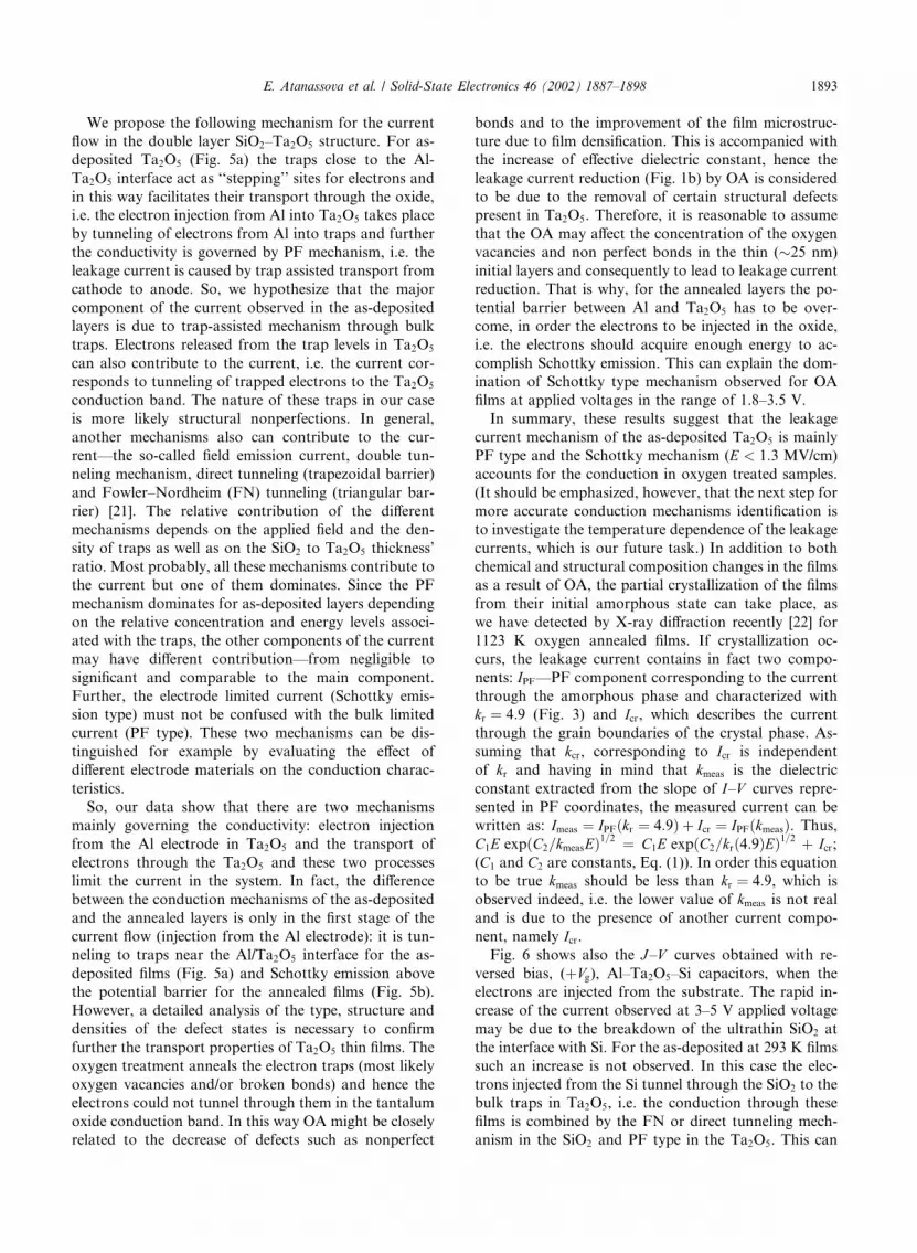
We propose the following mechanism for the current
flow in the double layer SiO2–Ta2O5 structure. For as-
deposited Ta2O5 (Fig. 5a) the traps close to the Al-
Ta2O5 interface act as ‘‘stepping’’ sites for electrons and
in this way facilitates their transport through the oxide,
i.e. the electron injection from Al into Ta2O5 takes place
by tunneling of electrons from Al into traps and further
the conductivity is governed by PF mechanism, i.e. the
leakage current is caused by trap assisted transport from
cathode to anode. So, we hypothesize that the major
component of the current observed in the as-deposited
layers is due to trap-assisted mechanism through bulk
traps. Electrons released from the trap levels in Ta2O5can also contribute to the current, i.e. the current cor-
responds to tunneling of trapped electrons to the Ta2O5conduction band. The nature of these traps in our case
is more likely structural nonperfections. In general,
another mechanisms also can contribute to the cur-
rent––the so-called field emission current, double tun-
neling mechanism, direct tunneling (trapezoidal barrier)
and Fowler–Nordheim (FN) tunneling (triangular bar-
rier) [21]. The relative contribution of the different
mechanisms depends on the applied field and the den-
sity of traps as well as on the SiO2 to Ta2O5 thickness’
ratio. Most probably, all these mechanisms contribute to
the current but one of them dominates. Since the PF
mechanism dominates for as-deposited layers depending
on the relative concentration and energy levels associ-
ated with the traps, the other components of the current
may have different contribution––from negligible to
significant and comparable to the main component.
Further, the electrode limited current (Schottky emis-
sion type) must not be confused with the bulk limited
current (PF type). These two mechanisms can be dis-
tinguished for example by evaluating the effect of
different electrode materials on the conduction charac-
teristics.
So, our data show that there are two mechanisms
mainly governing the conductivity: electron injection
from the Al electrode in Ta2O5 and the transport of
electrons through the Ta2O5 and these two processes
limit the current in the system. In fact, the difference
between the conduction mechanisms of the as-deposited
and the annealed layers is only in the first stage of the
current flow (injection from the Al electrode): it is tun-
neling to traps near the Al/Ta2O5 interface for the as-
deposited films (Fig. 5a) and Schottky emission above
the potential barrier for the annealed films (Fig. 5b).
However, a detailed analysis of the type, structure and
densities of the defect states is necessary to confirm
further the transport properties of Ta2O5 thin films. The
oxygen treatment anneals the electron traps (most likely
oxygen vacancies and/or broken bonds) and hence the
electrons could not tunnel through them in the tantalum
oxide conduction band. In this way OA might be closely
related to the decrease of defects such as nonperfect
bonds and to the improvement of the film microstruc-
ture due to film densification. This is accompanied with
the increase of effective dielectric constant, hence the
leakage current reduction (Fig. 1b) by OA is considered
to be due to the removal of certain structural defects
present in Ta2O5. Therefore, it is reasonable to assume
that the OA may affect the concentration of the oxygen
vacancies and non perfect bonds in the thin (�25 nm)initial layers and consequently to lead to leakage current
reduction. That is why, for the annealed layers the po-
tential barrier between Al and Ta2O5 has to be over-
come, in order the electrons to be injected in the oxide,
i.e. the electrons should acquire enough energy to ac-
complish Schottky emission. This can explain the dom-
ination of Schottky type mechanism observed for OA
films at applied voltages in the range of 1.8–3.5 V.
In summary, these results suggest that the leakage
current mechanism of the as-deposited Ta2O5 is mainly
PF type and the Schottky mechanism (E < 1:3 MV/cm)accounts for the conduction in oxygen treated samples.
(It should be emphasized, however, that the next step for
more accurate conduction mechanisms identification is
to investigate the temperature dependence of the leakage
currents, which is our future task.) In addition to both
chemical and structural composition changes in the films
as a result of OA, the partial crystallization of the films
from their initial amorphous state can take place, as
we have detected by X-ray diffraction recently [22] for
1123 K oxygen annealed films. If crystallization oc-
curs, the leakage current contains in fact two compo-
nents: IPF––PF component corresponding to the currentthrough the amorphous phase and characterized with
kr ¼ 4:9 (Fig. 3) and Icr, which describes the currentthrough the grain boundaries of the crystal phase. As-
suming that kcr, corresponding to Icr is independentof kr and having in mind that kmeas is the dielectricconstant extracted from the slope of I–V curves repre-sented in PF coordinates, the measured current can be
written as: Imeas ¼ IPFðkr ¼ 4:9Þ þ Icr ¼ IPFðkmeasÞ. Thus,C1E expðC2=kmeasEÞ1=2 ¼ C1E expðC2=krð4:9ÞEÞ1=2 þ Icr;(C1 and C2 are constants, Eq. (1)). In order this equationto be true kmeas should be less than kr ¼ 4:9, which isobserved indeed, i.e. the lower value of kmeas is not realand is due to the presence of another current compo-
nent, namely Icr.Fig. 6 shows also the J–V curves obtained with re-
versed bias, (þVg), Al–Ta2O5–Si capacitors, when theelectrons are injected from the substrate. The rapid in-
crease of the current observed at 3–5 V applied voltage
may be due to the breakdown of the ultrathin SiO2 at
the interface with Si. For the as-deposited at 293 K films
such an increase is not observed. In this case the elec-
trons injected from the Si tunnel through the SiO2 to the
bulk traps in Ta2O5, i.e. the conduction through these
films is combined by the FN or direct tunneling mech-
anism in the SiO2 and PF type in the Ta2O5. This can
E. Atanassova et al. / Solid-State Electronics 46 (2002) 1887–1898 1893

explain the existence of higher leakage current (V < 4 V)compared to the annealed ones and at the same time the
absence of abrupt current increase. On the other hand,
this is also electrical manifestation of the weakness of
the region close to the interface with Si. The weakness is
related to the classical interfacial defects such as dan-
gling bonds as well as to a strained and non perfect SiO2.
The interfacial silicon oxide is not ‘‘ideal’’ stoichiometric
SiO2 because Si is not perfectly oxidized due to the
spontaneous oxidation during sputtering in active oxy-
gen ambient. This results in the presence of Si suboxides
in this interfacial region as it was detected by XPS in our
recent investigation [7,12]. This incompletely oxidized Si
contributes also to the increase of the overall conduc-
tivity of the dielectric. As far as the thickness of SiO2practically does not change during OA, the lower leak-
age current levels for the annealed layers (�Vg) are re-lated generally with the improvement of the quality of
Ta2O5, namely reduction of the structural nonperfec-
tions and densification of the initial layers.
Fig. 7 compares I–V curves for the capacitors with
four different gate areas. The curves are generally iden-
tical suggesting that the current density is virtually in-
dependent of the gate area for over five orders of
magnitude. This is in agreement with the fact that the
conduction mechanism is limited rather by normal PF
effect than by modified one (usually referred to as PF
conduction with compensation) generally attributed to
oxides with very high density of bulk defects.
At the end of this section, it should be emphasized
that the physics of the conduction mechanism in Ta2O5is still speculative. It is clear, however, that it strongly
depends on the quality and technological history of the
samples, the fact that is confirmed also by our data. The
precise role of the process induced traps in Ta2O5 in
the net conductance and the detailed carrier transport
under different applied fields is still uncertain. The addi-
tional difficulty in the studies of these effects is the
presence of silicon oxide interface layer that affects sig-
nificantly the leakage current.
3.4. Reliability characteristics
Fig. 8 illustrates the breakdown electric field Ebdcharacteristics of Ta2O5 capacitors before and after ox-
ygen annealing. As is seen OA improves the breakdown
characteristics of the layers obtained at both Ts––theeffect is more pronounced for the higher temperature of
annealing (1123 K). The difference between Ebd corre-sponding to two Ts is practically small but neverthelessthe samples obtained at 493 K always show a slightly
better breakdown characteristics as compared to those
deposited at room temperature. These results indicate
that the higher Ts is more beneficial for optimal oxida-tion and guarantees layers with better quality in the
terms of breakdown properties. The annealing effectively
lowers the defect density and leads to an improvement
Fig. 6. J–V characteristics of Ta2O5 layers for both voltage
polarities. (The symbols are as in Fig. 1b).)
Fig. 7. J–V characteristics of Ta2O5 (as-deposited Ts ¼ 493 K)capacitors with different areas.
1894 E. Atanassova et al. / Solid-State Electronics 46 (2002) 1887–1898

not only of Ebd but to the improvement of the electricalparameters of the layers in general (leakage current re-
duction is also observed, Fig. 1b). This process of ad-
ditional oxidation, however, is not accompanied by an
increase of the thickness of the interfacial SiO2 layer and
offers a motivation for the use of high temperature an-
nealing processing in the fabrication of Ta2O5 based
devices. The physical understanding of breakdown in
Ta2O5 is still under research, but generally it is related to
the microscopic properties of Ta2O5 and the process
induced bulk as well as interface defects. In this context
breakdown is manifested by the formation of a con-
ductive path through the oxide initiated by the presence
of weak spots, and it is a result of the continuous de-
gradation of the bulk of Ta2O5 and its interface with
Si during high field electrical stress. Generally, Ebd isdefined as the electric field corresponding to the break-
down voltage (here we have in mind the hard break-
down). This parameter, however, is not very reliable,
since the oxide is not subjected to the wearout kinetics,
which governs the degradation prior to breakdown. It
can be regarded as a gross parameter, which gives an
estimation of the maximum electric field the dielec-
tric can sustain. The injected charge to breakdown
Qbd, the time to breakdown tbd, as well as the trappedoxide charge or hole fluence to breakdown, which can be
Fig. 8. Breakdown histograms of 26 nm Ta2O5 layers before (a) and after OA, Ta ¼ 873 K (b) and 1123 K (c) (##) Ts ¼ 293 K; (j) 493K).
E. Atanassova et al. / Solid-State Electronics 46 (2002) 1887–1898 1895

more rigorously defined are the quantities determining
the oxide reliability performance at nominal (working)
conditions.
In order to obtain information about these parame-
ters constant current stress measurements have been
carried out. We have not performed a detailed Qbdstudies, including statistical distribution of Qbd, depen-dence on stress current value, etc. All the samples show
tbd > 350 s, hence the charge to breakdown is estimatedto be >17 C/cm2. In Fig. 9a the time evolution of thevoltage Vg needed to maintain constant current equal to50 mA/cm2 is presented (the injection is from the gate,
i.e. the gate is biased negatively). It is seen that a higher
voltage is needed to force the same current: (i) through
the as-deposited Ta2O5 films than through the annealed
ones; (ii) through the deposited at 293 K than through
the deposited at 493 K. These results are surprising and
seem inconsistent with the better I–V and C–V charac-teristics of the annealed layers. In order to characterize
the ‘‘charge state’’ of the Ta2O5 the difference DVg be-tween the value of Vg and the starting voltage Vg0 (t ¼ 0)is used (Fig. 9b). The starting voltage (Fig. 9a) for the
samples investigated is in the range of 6–11.5 V (E ¼ 2–4.5 MV/cm). The oxide degradation is due to the con-
tinuous charge build-up. Since the dielectric is not ideal
the charge transport across Ta2O5, as it was mentioned
above, is related with some of the modifications of
PF type conduction mechanism. Respectively, the most
important wearout mechanisms are associated with the
charge trapping and trap generation.
The ‘‘charge state’’ of the layers strongly depends on
the technological history. A significant level of positive
charge trapping is observed in the as-deposited at 293 K
Ta2O5-Nf (t ¼ 100 s)¼ 1:4� 1012 cm�2. (All the values
of Nf are calculated at t ¼ 100 s, where the curves tend tosaturate.) After annealing of the 293 K layers, Vg de-creases steeply in the initial stage (trapping of positive
charge). The decrease is more pronounced for the higher
annealing temperature leading to the higher density of
trapped positive charge, i.e. the higher Ta the higher thedensity of trapped charge (Nf ¼ 3:8� 1012 cm�2 for OA
at 1123 K). The deposited at 493 K layers show dis-
tinctly different behavior. There is not such a steep de-
crease of DVg in the initial stage implying that the chargetrapping is reduced to a great extent. Even, a negative
charge trapping is detected for these films at the initial
stage (Fig. 9b). The density of the negative trapped
charge is estimated to be Nf ¼ �1:6� 1011 cm�2 (t ¼ 7s). The trapped positive charge for 493K deposited
layers is an order of magnitude lower (Nf ¼ 1:1� 1011cm�2 for the as-deposited and Nf ¼ 4:3� 1011 cm�2 for
the 1123 K annealed film) than that for the 293 K de-
posited ones.
Fig. 9b shows clearly that the trapping processes in
the as-deposited at 293 and 493 K Ta2O5 films are unlike
the trapping rates and the amount of the trapped posi-
tive charge are substantially different. These results
suggest that the deposition at higher temperature lead to
Ta2O5 layer with lower level of bulk traps. We suppose
that these traps are neutral, which under high applied
field (needed to maintain the constant current) are ion-
ized and become positively charged. That is why, the 293
K deposited layers demonstrate higher level of positive
charge trapping. The OA reduces the oxygen vacancies
and the structural nonperfections resulting in the de-
crease of Qf as is seen in Section 3.1. At the same time, asignificant level of positive charge trapping is observed
in annealed samples during the CCS––the higher the
annealing temperature, the larger Nf value is. The exis-tence of neutral bulk traps can explain also the observed
weaker charge trapping in the as-deposited layers com-
pared to the annealed ones. Most probably, two oppo-
site processes take place––trapping of injected electrons
in positively charged traps (revealing as a positive oxide
charge Qf in C–V curves) and impact ionization of
neutral bulk traps, which results in a release of electrons.
In the as-deposited at 493 K layers, where the density of
the neutral bulk traps is supposed to be lower the former
process dominates which leads to the observed negative
charge trapping in the initial stage. For the as-deposited
at 293 K films the neutralization of the positive oxideFig. 9. Evolution of Vg (a) and DVg (b) under CCS.
1896 E. Atanassova et al. / Solid-State Electronics 46 (2002) 1887–1898

charge by electron trapping only slows down the positive
charge build-up due to impact ionization of the neutral
traps. As Qf in the annealed films is very low (�1010cm�2) the dominating process in this case is the de-
trapping of electrons from the neutral traps, hence the
steeper DVgðtÞ curve.The hysteresis of C–V curves of the annealed layers is
positive (0.2–0.3 V) implying negative trapped charge
near the Si interface. Since the SiO2 thickness is 4 nm,
i.e. it is larger than the tunneling distance, we suppose
that the trapping is due to the slow states localized in
SiO2 rather than in Ta2O5. On the other hand, the
possibility positive DVfb to be attributed to the crystalphase of Ta2O5 provoked by OA can not be ruled out at
present. Recently, our XRD study [22] has shown that
the as-deposited and annealed at 873 K layers are
amorphous, whereas crystalline Ta2O5 (orthorhombic b-Ta2O5) was obtained after OA at 1123 K. The main
wear out parameters of thin dielectric generally are di-
vided into two categories: volume related, i.e. various
kind of oxide charge, and interface related reliability
characteristics basically associated to the interface state
density at Si. For the Ta2O5/Si system the strong effect of
the unavoidable interfacial SiO2 layer on the overall
conduction of the structure also should be taken into
consideration. Therefore, it is clear that the film micro-
structure plays an important role in the conduction
mechanisms as well as in the high field hardness of
Ta2O5. The present experiments, however, can not dis-
tinguish strictly the relative contribution of slow and
interfacial states in the leakage current.
4. Conclusion
In summary, the results presented allow to draw the
following conclusions:
(1) Thin rf sputtered Ta2O5 layers with good electrical
and dielectric properties can be obtained after dry OA at
873 and 1123 K. The results show a lower fixed oxide
charge (<1010 cm�2) and higher breakdown field after
OA (the effect is more pronounced for the higher an-
nealing temperature). A relative dielectric constant up to
37 is achieved after annealing and this value is about
twice as larger than that of the as-deposited films. The
annealing is also highly effective in suppressing leakage
current of the capacitors with thinner (�25 nm) Ta2O5layers. The lowest current (5–10� 10�8 A/cm2 for ap-plied field up to 4 MV/cm) we have obtained after OA at
1123 K. In the context of advanced technology this re-
gime also produces the lowest equivalent thickness (6.5
nm), allowing application of the layers in 256 Mbit
DRAMs. Since the additional oxidation of the Si during
annealing with a subsequent increase of the interfacial
SiO2 thickness does not occur, we correlate the im-
provement of the film parameters with the real annealing
of oxygen vacancies and bond defects, which are the
source of charged centers in Ta2O5–Si system.
(2) The high temperature OA degrades severely the
leakage current in the thicker (80 nm) layers. The cur-
rent increase may be caused by crystallization of 1123 K
annealed films detected previously by XRD (the grain
boundaries act as current paths). As far as the crystal-
lization effects are observed also in the thinner layers,
the reason for the difference in the high temperature OA
effect when varying the film thickness is not clear at
present. It is very likely that the two processes (anneal-
ing and crystallization) proceed simultaneously and that
one of them dominates for the layers with different
thickness. Precise structural analyses are required to
clarify the thickness related phenomena.
The higher annealing temperature tends to introduce
some sort of slow states––we speculate that they are
localized rather in SiO2 than in Ta2O5. The possible
explanation for the negatively charged slow states build-
up may be searched in: (i) appearance of a crystal phase
after 1123 K and (ii) OA induced generation of neutral
traps which charged negatively under low positive elec-
tric field and behave as slow states. At present it is not
possible to give preference to one of the hypotheses.
(3) The dominant conduction mechanism for the as-
deposited (� 25 nm) layers is due to PF effect in a wideapplied field range (0.4–1.3 MV/cm). Depending on the
applied voltage the conduction processes identified in the
annealed Ta2O5 are generally attributed to a Schottky
emission or PF effect––a transition from an electrode
limited (for medium field, 0.8–1.3 MV/cm) to bulk
limited (for fields larger than 1.3 MV/cm) process is
observed. As a result it may be concluded that there are
two dominant conduction mechanisms in the medium
fields range for the layers with different technological
history: PF mechanism for the as-deposited and Scho-
ttky emission limited current for the annealed films.
Since the conduction mechanism is critically related to
the density of charged defects in the films, the transition
from the PF mechanism to the Schottky emission can be
effectively (and successfully) controlled by means of
appropriate technological steps. For example, high tem-
perature oxygen treatment anneals electron traps within
Ta2O5 and hence the electrons could not tunnel through
them in the tantalum oxide conduction band. In this case
the electrons should acquire enough energy to accom-
plish Schottky emission above the barrier. The annealing
effect is accompanied by an increase of the effective
dielectric constant and a leakage current reduction. It
appears that the trap creation mechanism responsible
for PF conduction in the as-deposited films at medium
fields is oxygen vacancies related.
(4) CCS results suggest that neutral traps in the form
of bulk traps most likely are responsible for the observed
reliability characteristics of MOS capacitors. The den-
sity of these neutral traps depends on the fabrication
E. Atanassova et al. / Solid-State Electronics 46 (2002) 1887–1898 1897

conditions (including oxygen annealing) and it deter-
mines the level of the charge trapping in the layers––the
higher deposition temperature seems to result in Ta2O5layers with lower neutral trap density.
Acknowledgements
This work has been partly supported by Bulgarian
National Science Foundation under Contract F-901.
References
[1] Matsui M, Nagayoshi H, Muto G, Tanimoto S, Kuroiwa
K. Amorphous silicon thin film transistors employing
photoprocessed tantalum oxide films as gate insulators.
Jpn J Appl Phys 1990;29:62–6.
[2] Lo GQ, Kwong DL. Metal-oxide-semiconductor charac-
teristics of chemical vapor deposited Ta2O5 thin films. Appl
Phys Lett 1992;60:3286–8.
[3] Tanimoto S, Matsui M, Kamisako K, Kuroiwa K, Tarni
Y. Investigation of leakage current reduction of photo-
CVD tantalum oxide films accomplished by active oxygen
annealing. J Electrochem Soc 1992;139:320–8.
[4] Chaneliere C, Autran JL, Devine RAB, Baland B. Tanta-
lum pentoxide thin films for advanced dielectric applica-
tions. Mater Sci Eng R 1998;22:269–322.
[5] Atanassova E, Spassov D. X-ray photoelectron spectro-
scopy of thermal thin Ta2O5 films on Si. Appl Surf Sci
1998;135:71–82.
[6] Atanassova E, Spassov D. Hydrogen annealing effects on
the properties of thermal Ta2O5 on Si. Microelectron J
1999;30:265–74.
[7] Atanassova E. Thin RF sputtered and thermal Ta2O5 on Si
for high density DRAM application. Microelectron Reliab
1999;39:1185–217.
[8] Kamiyama S, Suzuki H, Watanabe H, Sakai A, Kimura H,
Mizuki J. Ultrathin tantalum oxide capacitor process using
oxygen-plasma annealing. J Electrochem Soc 1994;141:
1246–51.
[9] Atanassova E, Dimitrova T. Thin Ta2O5 layers on Si as an
alternative to SiO2 for high density DRAM applications.
In: Nalwa HS, editor. Handbook of surfaces and interfaces
of materials. San Diego, California, USA: Academic Press;
p. 439–79.
[10] Atanassova E, Spassov D. Electrical properties of thin
Ta2O5 films obtained by thermal oxidation of Ta on Si.
Microelectron Reliab 1998;38:827–32.
[11] Spassov D, Atanassova E. Thermally oxidized Ta2O5 on
Si––dielectric and breakdown characteristics. Proc 9th Int
School Cond Matt Phys. In: Marshall JM, Kirov N,
Vavrek A, Maud JM, editors. Future directions in thin film
science and technology. Singapore: World Scientific Sin-
gapore; 1997. p. 448–52.
[12] Atanassova E, Dimitrova T, Koprinarova J. AES and XPS
study of thin rf sputtered Ta2O5 layers. Appl Surf Sci
1995;84:193–202.
[13] Dimitrova T, Atanassova E. Electrical and transport
properties of rf sputtered Ta2O5 on Si. Solid-State Electron
1998;42:307–15.
[14] Atanassova E, Dimitrova T. Carrier mobility in inversion
layers of Si-thin Ta2O5 structures. Microelectron Reliab
1998;38:833–7.
[15] Atanassova ED, Dimitrova T, Koprinarova JB. Elemental
composition and structure properties of thin rf sputtered
Ta2O5 layer. Vacuum 1995;46:889–91.
[16] Atanassova E. In: Marshall JM, Kirov N, Vavrek A, Maud
JM, editors. Thin Ta2O5 layers as an alternative to
SiO2 for submicron application Proc 10th ISCMP, Thin
film materials and devices––developments in science and
technology. Singapore: World Scientific Singapore; 1999.
p. 109–16.
[17] Dimitrova T, Atanassova E, Koprinarova J. Dielectric
characteristics of MOS capacitors with rf sputtered Ta2O5.
Proc 22nd IEEE Int Conf Microelectron (MIEL 2000)
2000;1:373–6.
[18] Dimitrova T, Atanassova E. Interface and oxide properties
of rf sputtered Ta2O5–Si structures. Vacuum 1998;51:151–
2.
[19] Oehrlein GS. Oxidation temperature dependence of the dc
electrical conduction characteristics and dielectric strength
of thin Ta2O5 films on silicon. J Appl Phys 1986;59:1587–
95.
[20] Young PL. dc electrical conduction in thin Ta2O5 films. I.
Bulk limited conduction. J Appl Phys 1976;47:235–41.
[21] Chanelier C, Autran JL, Devine RAB. Conduction mech-
anisms in Ta2O5/SiO2 and Ta2O5/Si3N4 stacked structures
on Si. J Appl Phys 1999;86:480–6.
[22] Dimitrova T, Arshak K, Atanassova E. Crystallization
effects in oxygen annealed Ta2O5 thin films on Si. Thin
Solid Films 2001;381:31.
1898 E. Atanassova et al. / Solid-State Electronics 46 (2002) 1887–1898