conduction phenomena through gas and insulating solids in
TRANSCRIPT
THÈSEPour obtenir le grade de
DOCTEUR DE L’UNIVERSITÉ DE GRENOBLESpécialité : Génie Éléctrique
Arrêté ministériel : 7 Août 2006
Présentée par
Laëtitia ZAVATTONI
Thèse dirigée par Pr. Olivier LESAINTet codirigée par Dr. Olivier GALLOT-LAVALLÉE
préparée au sein du G2Elabet de École Doctorale EEATS
Conduction phenomena through gas and
insulating solids in HVDC Gas Insulated
Substations, and consequences on
electric field distribution
Thèse soutenue publiquement le 07/10/2014,devant le jury composé de :
Prof. François BURETProfesseur à l’école Centrale de Lyon, Rapporteur
Prof. Emmanuel ODICProfesseur à SUPELEC, Paris, Rapporteur
Prof. David MALECProfesseur à l’Université Paul Sabatier, Toulouse, Examinateur
Dr. Karim BOUSOLTANEChef de Projet à Siemens T&D, Grenoble, Examinateur
Prof. Olivier LESAINTDirecteur de recherche au CNRS-G2Elab, Directeur de thèse
Dr. Olivier Gallot-LavalléeMaître de conférences à l’Université Joseph Fourier, Grenoble, Co-Encadrant de
thèse


A la memoire de mon grand-pere...
«Aie le courage de te servir de ton propre entendement.»
Les philosophes des Lumieres
«I am somebody. I was somebody before I came,and I will be a better somebody when I’ll leave.»
Rita Pearson

Remerciements
Un grand merci a toutes et a tous ceux qui m’ont accompagne au cours de ces trois annees...
Je ne sais pas vraiment par qui ni par ou commencer et j’espere surtout que je ne vaisoublier personne. Allez je me lance!
Aussi ironique que cela puisse paraıtre je tiens tout d’abord a remercier Georges Gaudart,qui avant de quitter Siemens, a eu la bonne idee de me recruter pour cette these. Merci atoi Georges, mais aussi un grand merci a Sylvain Verger. Vous avez tous les deux su memotiver au debut de mon travail et me transmettre votre passion pour ce projet.
Je tiens egalement a remercier Christophe Descottes pour m’avoir permis d’integrer lastructure Siemens et l’equipe R& D de Grenoble. Merci a Aurelie Morin, qui a encadre mestravaux de recherche cote entreprise et qui m’a beaucoup appris en methode d’organisation.Tu as ete une chef geniale, toujours a l’ecoute des membres de l’equipe et tres disponible.Merci egalement a Karim Bousoltane.
Je voudrais aussi remercier mes encadrants du G2ELab. Merci a Olivier Gallot-Lavalleequi a co-encadre mes travaux de recherche au cours de ces trois ans. Merci aussi a Jean-LucReboud pour son aide precieuse en simulation numerique (mais surtout pour LA course apied!). Je remercie tout particulierement Olivier Lesaint, mon directeur de these, qui m’aaccompagnee, soutenue, guidee et conseillee tout au long de ma these. Tu as ete un vraisoutien au cours des experiences (on a eu de grosses frayeurs et on a aussi bien rigole), ainsique pendant la periode de redaction.
Un grand merci a tous ceux qui m’ont soutenue et aidee dans la realisation de mes bancsexperimentaux. Je pense ici bien sur a Alain Tisserand qui nous a quitte l’an dernier...Et qui a beaucoup contribue a la fabrication des differentes pieces. Je pense egalement aNene, Paul, Angelo, Gege, Gilou, Philippe, Alain, Jean-Luc, Christophe, Jean-Paul, Gregor,Patrick, Pierrot et messire Daniel avec qui j’ai travaille et aussi partage de bon fous rirespendant les essais/pauses cafes. Une pensee egalement a Serge, Alain et Jean-Luc. Jeremercie egalement mes collegues de bureau: Vincent, Marc, James, Frank, Thierry, Fabrice,Niston, Rosette et Stephan.
Je voudrai egalement remercier mes amis qui m’ont soutenue tout au long de cette these.Je remercie Soren, qui m’a supporte comme chef au cours de son stage et avec qui j’ai bienrigole, on a fait pas mal de poiiint et on a bien avance. Je remercie egalement Eric Durhonepour m’avoir conseille et travaille avec moi sur mon projet de these. Les multiples reunionset collaborations avec les allemands ne nous ont pas empeche de faire du beau travail! Jeremercie aussi Pierre d’avoir partage son bureau avec moi au labo et d’avoir invente le superventilateur en ete! Sans cela on serait certainement mort de chaud la premiere annee!
i
Je tiens egalement a remercier une amie qui m’est tres chere et qui a su me soutenir,me faire rire et m’encourager tout au long de cette derniere annee: Choukran Rrrrachelle!Ca a ete un vrai plaisir de squatter ton bureau et tes fous rires. Tu es une amie geniale ettu vas bien me manquer!
Je veux ici remercier tout particulierement un homme qui a change ma vie et qui est tresimportant a mes yeux. Je te remercie profondement Pablo Acosta, pour m’avoir accompagnependant les durs moments de la redaction, de m’avoir supporte, encourage, conseille, ecouteet aussi pour tes innombrables relectures. Je te remercie egalement pour tous ces moments,ces fous rires, ces folies et aventures que nous avons partagees. Je pourrai en ecrire biendavantage mais je vais en garder pour la suite ;) .
Je remercie enfin tous les membres de ma famille: Papa, Maman, Robert et Thomas.Sans votre appui et votre soutien je n’en serai sans doute pas la aujourd’hui. Notre famillea toujours ete une force et m’a toujours permis d’avancer sans me retourner puisque jesavais que vous veilliez sur mes arrieres. Vous avez toujours ete la pour moi et je vous aimetous tres fort. Je vous dis encore une fois MERCI.
Merci aussi a Pablo d’etre entre ainsi dans ma vie et m’avoir apporte joie et bonheur. Jete remercie aussi car grace a toi la famille s’est bien agrandie.. Par la je voudrais egalementremercier Ivonne, Joachim, Elizabeth y Diego. Gracias por dejarme entrar en su vida ygracias por compartir estos momentos importantes de mi vida. La preparacion de la defensafue un hermoso momento gracias a esta gran familia, fue una emocion grandısima, otra vezmuchas gracias por to’o.
Je termine ces remerciements en remerciant une fois encore toute ma famille et enemettant une pensee toute particuliere a mon grand-pere.
ii
Contents
Introduction 1
1 State of the art on electrical insulation for HVDC GIS 3
1.1 General considerations on electrical transport and distribution . . . . . . . 3
1.2 From Alternating Current to Direct Current . . . . . . . . . . . . . . . . . 41.2.1 Technical merits of HVDC . . . . . . . . . . . . . . . . . . . . . . . 51.2.2 Economic and environmental considerations . . . . . . . . . . . . . 6
1.3 Gas-Insulated-Substations (GIS) . . . . . . . . . . . . . . . . . . . . . . . . 71.3.1 Solid dielectrics . . . . . . . . . . . . . . . . . . . . . . . . . . . . . 81.3.2 SF6 gas . . . . . . . . . . . . . . . . . . . . . . . . . . . . . . . . . 9
1.4 Development and optimization of HVDC GIS . . . . . . . . . . . . . . . . 101.4.1 Charge accumulation . . . . . . . . . . . . . . . . . . . . . . . . . . 10
1.4.1.1 Field calculations . . . . . . . . . . . . . . . . . . . . . . . 111.4.2 Influencing parameters . . . . . . . . . . . . . . . . . . . . . . . . . 13
1.4.2.1 Insulator shape . . . . . . . . . . . . . . . . . . . . . . . . 131.4.2.2 Insulation properties and charging time estimation . . . . 151.4.2.3 Influence of insulator surface roughness . . . . . . . . . . . 161.4.2.4 Influence of electrode surface coating . . . . . . . . . . . . 171.4.2.5 Metallic particles . . . . . . . . . . . . . . . . . . . . . . . 18
1.4.3 Charge decay . . . . . . . . . . . . . . . . . . . . . . . . . . . . . . 191.4.3.1 Influence of relative humidity . . . . . . . . . . . . . . . . 201.4.3.2 Influence of surrounding gas . . . . . . . . . . . . . . . . . 21
1.4.4 Simulation models . . . . . . . . . . . . . . . . . . . . . . . . . . . 22
1.5 Conclusions . . . . . . . . . . . . . . . . . . . . . . . . . . . . . . . . . . . 22
Bibliography . . . . . . . . . . . . . . . . . . . . . . . . . . . . . . . . . . . . . 25
2 Charge generation in SF6 at high electric field 29
2.1 Review of charge generation in pressurized gases and vacuum . . . . . . . . 302.1.1 Natural ionization in gases at low electric field . . . . . . . . . . . . 302.1.2 Charge emission mechanisms in vacuum at high electric field . . . . 32
2.1.2.1 Primary emission . . . . . . . . . . . . . . . . . . . . . . . 322.1.2.2 Secondary emission . . . . . . . . . . . . . . . . . . . . . . 332.1.2.3 Theory of field emission . . . . . . . . . . . . . . . . . . . 332.1.2.4 Thermionic emission (Schottky effect) . . . . . . . . . . . 342.1.2.5 Fowler-Nordheim (FN) effect . . . . . . . . . . . . . . . . 35
2.1.3 Dark currents through pressurized gases (Air and SF6) at high electricfield . . . . . . . . . . . . . . . . . . . . . . . . . . . . . . . . . . . 36
iii
2.1.4 Influence of several parameters on current measured in vacuum athigh electric field . . . . . . . . . . . . . . . . . . . . . . . . . . . . 39
2.1.4.1 Influence of electrode polishing and cleaning . . . . . . . . 40
2.1.4.2 Influence of electrode nature . . . . . . . . . . . . . . . . . 40
2.1.4.3 Influence of surface roughness . . . . . . . . . . . . . . . . 41
2.1.4.4 Influence of gap distance . . . . . . . . . . . . . . . . . . . 43
2.1.5 Influence of the introduction of low pressure gases in vacuum experiments 44
2.1.6 Discussion and objectives of the study . . . . . . . . . . . . . . . . 45
2.2 Experimental systems . . . . . . . . . . . . . . . . . . . . . . . . . . . . . . 46
2.2.1 Small scale coaxial electrode system . . . . . . . . . . . . . . . . . . 47
2.2.2 Large scale plane-to-plane electrode system . . . . . . . . . . . . . . 49
2.2.3 Experimental protocols . . . . . . . . . . . . . . . . . . . . . . . . . 51
2.2.3.1 Electrodes . . . . . . . . . . . . . . . . . . . . . . . . . . . 52
2.2.3.2 Test cell conditioning . . . . . . . . . . . . . . . . . . . . . 52
2.3 Experimental results . . . . . . . . . . . . . . . . . . . . . . . . . . . . . . 54
2.3.1 Preliminary experiments: coaxial system . . . . . . . . . . . . . . . 54
2.3.1.1 Measurements in SF6 . . . . . . . . . . . . . . . . . . . . 54
2.3.1.2 Comments . . . . . . . . . . . . . . . . . . . . . . . . . . . 58
2.3.1.3 Experiments in air and influence of water . . . . . . . . . 60
2.3.1.4 Influence of high voltage electrode nature in positive polarity,for different pressures . . . . . . . . . . . . . . . . . . . . 63
2.3.2 Discrepancies between calculated and measured RH, and influenceon the current . . . . . . . . . . . . . . . . . . . . . . . . . . . . . . 64
2.3.2.1 Example 1: Measurements in SF6 versus pressure . . . . . 65
2.3.2.2 Example 2: Measurement in air mixtures with temperaturevariations . . . . . . . . . . . . . . . . . . . . . . . . . . . 67
2.3.2.3 Discussion: The crucial influence of test cell conditioning . 69
2.3.2.4 Influence of temperature in SF6 . . . . . . . . . . . . . . . 71
2.3.2.5 Synthesis: influence of RH in SF6 and air . . . . . . . . . 72
2.3.3 Parallel electrodes system . . . . . . . . . . . . . . . . . . . . . . . 74
2.3.3.1 Influence of gap distance and electric field in «standard» SF6
(RH > 15% at 0.6MPa) . . . . . . . . . . . . . . . . . . . 74
2.3.3.2 Influence of gap distance and electric field in dry SF6 (RH ≤5% at 0.6MPa and 1MPa) . . . . . . . . . . . . . . . . . 76
2.3.3.3 Influence of pressure and Relative Humidity RH . . . . . . 77
2.3.3.4 Comparison with measurements obtained in the coaxial system 80
2.3.3.5 Comparison with measurements in synthetic dry air . . . . 81
2.3.3.6 Influence of heating measurement electrode . . . . . . . . 82
2.4 Discussion . . . . . . . . . . . . . . . . . . . . . . . . . . . . . . . . . . . . 85
2.4.1 Physical mechanisms . . . . . . . . . . . . . . . . . . . . . . . . . . 85
2.4.1.1 Fowler-Nordheim emission . . . . . . . . . . . . . . . . . . 86
2.4.1.2 Schottky emission . . . . . . . . . . . . . . . . . . . . . . . 86
2.4.1.3 Field desorption of water . . . . . . . . . . . . . . . . . . 87
2.4.2 Consequences on the industrial application . . . . . . . . . . . . . . 89
2.5 Conclusions . . . . . . . . . . . . . . . . . . . . . . . . . . . . . . . . . . . 90
Bibliography . . . . . . . . . . . . . . . . . . . . . . . . . . . . . . . . . . . . . 91
iv
3 Electrical properties of insulator materials under DC voltage 95
3.1 Definition and technological standard used for electrical characterization . 963.1.1 Transient current in insulators . . . . . . . . . . . . . . . . . . . . . 963.1.2 Volume and surface resistivities . . . . . . . . . . . . . . . . . . . . 97
3.1.2.1 Volume resistivity . . . . . . . . . . . . . . . . . . . . . . 973.1.2.2 Surface resistivity . . . . . . . . . . . . . . . . . . . . . . . 98
3.1.3 Dielectric strength of insulators . . . . . . . . . . . . . . . . . . . . 98
3.2 Materials . . . . . . . . . . . . . . . . . . . . . . . . . . . . . . . . . . . . 99
3.3 Sample conditioning . . . . . . . . . . . . . . . . . . . . . . . . . . . . . . 1003.3.1 Determination of the drying time . . . . . . . . . . . . . . . . . . . 1003.3.2 Measurements of water absorption . . . . . . . . . . . . . . . . . . 101
3.4 Surface potential decay measurements . . . . . . . . . . . . . . . . . . . . . 1023.4.1 Experimental system . . . . . . . . . . . . . . . . . . . . . . . . . . 1033.4.2 Experimental protocols . . . . . . . . . . . . . . . . . . . . . . . . . 1043.4.3 Results . . . . . . . . . . . . . . . . . . . . . . . . . . . . . . . . . . 105
3.4.3.1 Preliminary experiments . . . . . . . . . . . . . . . . . . . 1053.4.3.2 SPD depending on Temperature and Relative Humidity for
dry materials A and B . . . . . . . . . . . . . . . . . . . . 1063.4.3.3 SPD depending sample on water content . . . . . . . . . . 1063.4.3.4 SPD depending on material’s composition . . . . . . . . . 1073.4.3.5 Comments . . . . . . . . . . . . . . . . . . . . . . . . . . . 108
3.5 Volume resistivity measurements . . . . . . . . . . . . . . . . . . . . . . . 1093.5.1 Experimental system . . . . . . . . . . . . . . . . . . . . . . . . . . 1093.5.2 Experimental protocol . . . . . . . . . . . . . . . . . . . . . . . . . 111
3.5.2.1 Preliminary experiments . . . . . . . . . . . . . . . . . . . 1113.5.3 Results and discussion . . . . . . . . . . . . . . . . . . . . . . . . . 113
3.5.3.1 Influence of electric field and temperature on dried materials1143.5.3.2 Influence of water content . . . . . . . . . . . . . . . . . . 1173.5.3.3 Simulation model . . . . . . . . . . . . . . . . . . . . . . . 1183.5.3.4 Additional investigations: influence of the material compo-
sition . . . . . . . . . . . . . . . . . . . . . . . . . . . . . 119
3.6 Surface resistivity measurements . . . . . . . . . . . . . . . . . . . . . . . . 1213.6.1 Experimental system and protocol . . . . . . . . . . . . . . . . . . . 1213.6.2 Preliminary experiments: creeping discharges . . . . . . . . . . . . 1223.6.3 Results and discussion . . . . . . . . . . . . . . . . . . . . . . . . . 122
3.6.3.1 Surface resistivity in dry gases . . . . . . . . . . . . . . . . 1223.6.3.2 Influence of electric field and temperature . . . . . . . . . 1233.6.3.3 Simulation model . . . . . . . . . . . . . . . . . . . . . . . 1243.6.3.4 Influence of relative humidity RH of the gas . . . . . . . . 1283.6.3.5 Further investigations: surface treatment . . . . . . . . . . 129
3.7 Conclusions . . . . . . . . . . . . . . . . . . . . . . . . . . . . . . . . . . . 132
Bibliography . . . . . . . . . . . . . . . . . . . . . . . . . . . . . . . . . . . . . 134
4 Numerical calculations in a GIS geometry 137
4.1 1st Step: Electric field distribution induced by the material volume resistivity1394.1.1 Difference between AC and DC (uniform temperature 20 C) . . . . 1394.1.2 Influence of a temperature gradient . . . . . . . . . . . . . . . . . . 140
v
4.1.3 Impact of solid water content with a temperature gradient . . . . . 1434.1.4 Comments . . . . . . . . . . . . . . . . . . . . . . . . . . . . . . . . 145
4.2 2nd Step: implementation of non-linear surface properties . . . . . . . . . . 1464.2.1 Uniform Temperature . . . . . . . . . . . . . . . . . . . . . . . . . 1474.2.2 Temperature gradient . . . . . . . . . . . . . . . . . . . . . . . . . . 149
4.3 Practical consequences . . . . . . . . . . . . . . . . . . . . . . . . . . . . . 151
4.4 Estimation of current from the gas . . . . . . . . . . . . . . . . . . . . . . 152
4.5 Conclusions . . . . . . . . . . . . . . . . . . . . . . . . . . . . . . . . . . . 154
Bibliography . . . . . . . . . . . . . . . . . . . . . . . . . . . . . . . . . . . . . 154
General Conclusions and Perspectives 155
Appendix A 158
Appendix B 160
vi
Introduction
The demand for reliable, economic and environment-friendly energy resources is increasing,
especially for long distance transmission. During the last ten years, the energy production
from wind turbines has strongly increased. The development of offshore wind farms brings
considerable economic opportunities. Indeed, it will represent 14% of Europe electricity
demand by 2030. These new energy sources are often located far from the consumption
areas, thus, new technologies are required to interconnect those power grids over long
distances.
Nowadays, the development of High Voltage Direct Current (HVDC) transmission lines is
very promising for next networks generations, which will overcome High Voltage Alternative
Current (HVAC) limitations. Gas Insulated Substations (GIS) constitute an important
element of power grids. Under HVAC, it has been thoroughly developed and optimized.
However, it remains really difficult to develop and optimize a reliable system under HVDC.
The knowledge about the DC behaviour of both insulating solid materials and gases is
essential for an optimized design and for the reliability of HVDC equipment.
The main purpose of this thesis is first to experimentally investigate conduction phenom-
ena in both solid and gaseous insulators, in HVDC GIS functional conditions of use. Based
on these data, the objective is to develop a numerical model to evaluate the influence of
various parameters and estimate their impact on conduction phenomena in solid insulator,
and hence on the electric field distribution which constitutes the basic data for design and
optimization.
In chapter 1, we review the existing challenges concerning energy transmission and
distribution across long distances. A comparison between Alternative Currents (AC) and
Direct Currents (DC) is first presented allowing to assess the main differences between
both techniques. Then, we describe the investigations performed so far in Gas Insulated
Substations under HVDC. Based on the existing work, we are able to define the key
parameters to investigate, in order to better understand and improve HVDC insulation
technology, and propose innovative solutions.
In chapter 2, we review the state of the art of current measured through pressurized
gas and vacuum, at low and high electric field. Then, we proceed with experimental
measurements on current through pressurized gases in two electric field geometries, and
analyze the results obtained to discuss the origins of these currents.
1

2 INTRODUCTION
In chapter 3, the experimental devices used for the characterization of conduction
phenomena through the solid insulator are presented. We investigate the influence of
temperature, electric field and relative humidity on the conduction through the insulator
volume and on its surface.
Finally, in chapter 4 we present several numerical calculations accounting for the
influence of parameter investigated in a real GIS insulator geometry. The contribution of
such parameters can be estimated and their impact on the conduction current and electric
field distribution through the solid insulator is evaluated.
1 | State of the art on electrical insulationfor HVDC GIS
Contents
1.1 General considerations on electrical transport and distribution . . . . . . . 3
1.2 From Alternating Current to Direct Current . . . . . . . . . . . . . . . . . 4
1.2.1 Technical merits of HVDC . . . . . . . . . . . . . . . . . . . . . . . 5
1.2.2 Economic and environmental considerations . . . . . . . . . . . . . 6
1.3 Gas-Insulated-Substations (GIS) . . . . . . . . . . . . . . . . . . . . . . . . 7
1.3.1 Solid dielectrics . . . . . . . . . . . . . . . . . . . . . . . . . . . . . 8
1.3.2 SF6 gas . . . . . . . . . . . . . . . . . . . . . . . . . . . . . . . . . 9
1.4 Development and optimization of HVDC GIS . . . . . . . . . . . . . . . . . 10
1.4.1 Charge accumulation . . . . . . . . . . . . . . . . . . . . . . . . . . 10
1.4.2 Influencing parameters . . . . . . . . . . . . . . . . . . . . . . . . . 13
1.4.3 Charge decay . . . . . . . . . . . . . . . . . . . . . . . . . . . . . . 19
1.4.4 Simulation models . . . . . . . . . . . . . . . . . . . . . . . . . . . 22
1.5 Conclusions . . . . . . . . . . . . . . . . . . . . . . . . . . . . . . . . . . . . 22
Bibliography . . . . . . . . . . . . . . . . . . . . . . . . . . . . . . . . . . . . . . 25
In this chapter we will first present the evolution of energy distribution networks
from High Voltage Alternating Current (HVAC ) transmission to High Voltage Direct
Current (HVDC ). A brief description of advantages and drawbacks of these techniques is
presented. The structure and operating conditions of Gas Insulated Substations (GIS) are
then introduced. Some existing HVDC technologies are detailed, highlighting the main
parameters to take into account to design and optimize HVDC GIS. Then, we will present
the current understanding of charge accumulation and relaxation on solid insulators, which
are of major importance for the reliability and optimization of HVDC technology. Finally,
the main objectives and topics addressed in this work are presented.
1.1 | General considerations on electrical transport and
distribution
High power production facilities, such as nuclear, hydraulic, photo-voltaic, and wind farms
power plants, are often located far away from consumers. To transport electrical energy
from the source toward consumers, the entire electrical network, basically composed of
3
4 State of the art on electrical insulation for HVDC GIS
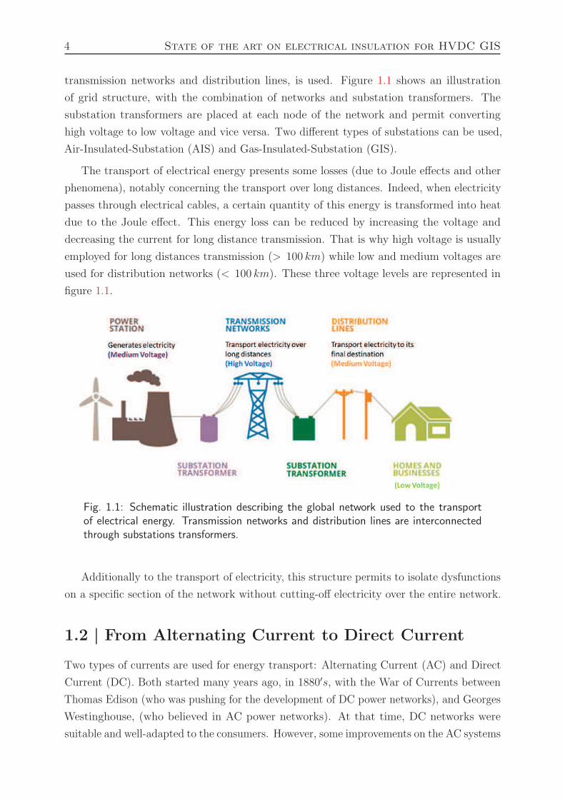
transmission networks and distribution lines, is used. Figure 1.1 shows an illustration
of grid structure, with the combination of networks and substation transformers. The
substation transformers are placed at each node of the network and permit converting
high voltage to low voltage and vice versa. Two different types of substations can be used,
Air-Insulated-Substation (AIS) and Gas-Insulated-Substation (GIS).
The transport of electrical energy presents some losses (due to Joule effects and other
phenomena), notably concerning the transport over long distances. Indeed, when electricity
passes through electrical cables, a certain quantity of this energy is transformed into heat
due to the Joule effect. This energy loss can be reduced by increasing the voltage and
decreasing the current for long distance transmission. That is why high voltage is usually
employed for long distances transmission (> 100 km) while low and medium voltages are
used for distribution networks (< 100 km). These three voltage levels are represented in
figure 1.1.
Fig. 1.1: Schematic illustration describing the global network used to the transportof electrical energy. Transmission networks and distribution lines are interconnectedthrough substations transformers.
Additionally to the transport of electricity, this structure permits to isolate dysfunctions
on a specific section of the network without cutting-off electricity over the entire network.
1.2 | From Alternating Current to Direct Current
Two types of currents are used for energy transport: Alternating Current (AC) and Direct
Current (DC). Both started many years ago, in 1880′s, with the War of Currents between
Thomas Edison (who was pushing for the development of DC power networks), and Georges
Westinghouse, (who believed in AC power networks). At that time, DC networks were
suitable and well-adapted to the consumers. However, some improvements on the AC systems
1.2. FROM ALTERNATING CURRENT TO DIRECT CURRENT 5
(creation of a transformer stage between the transmission network and consumer materials),
allowed higher power and insulation levels within one unit. This system was simple and only
required little maintenance. For these reasons, AC technology was introduced at a very early
stage in the development of electrical power systems. Nevertheless, HVAC transmission
technology presents some drawbacks which compelled a change to DC technology. The
transmission capacity and distance of AC links are limited by inductive and capacitive
phenomena occurring within overhead lines and cables. These issues are of major importance
for cables longer than about 100 km since the achievable transmission will be limited by the
charging current. Besides, it is not possible to directly connect two AC systems working at
different frequencies.
With the development of high voltage valves, it becomes possible to transmit power
at high voltages over long distances, giving rise to HVDC transmission systems. Such
technology has several advantages compared to the AC transmission which make it especially
attractive in certain transmission applications. HVDC systems are getting increasingly
important in the global development of energy sources and networks for technical, economical
and environmental reasons.
1.2.1 | Technical merits of HVDC
With an increased demand for energy and construction of new generation plants at remote
locations (e.g off-shore wind farms), the complexity of power system has grown and higher
voltages are needed to transmit energy across very long distances, with as low losses as
possible. As inductive and capacitive parameters do not limit the transmission capacity or
the maximum length of a DC cable, HVDC offers a suitable solution compared to HVAC
for such power systems.
A simplified representation of a HVDC interconnection is shown in figure 1.2. A
converter, operating as a rectifier will transform AC power to DC power. The latter is then
transmitted and applied to the DC terminals of a second converter, which allows the DC
power to flow into the receiving AC network. The composition of a HVDC system varies
with the technology used in converters. However, a common structure formed by AC filters,
transformers, converters, DC capacitors or reactors and DC cables, can be established.
Further detailed description of HVDC systems are made in a technological paper published
by Rudervall et al. [1].
6 State of the art on electrical insulation for HVDC GIS
Fig. 1.2: Simplified representation of HVDC interconnection between two AC networks.
1.2.2 | Economic and environmental considerations
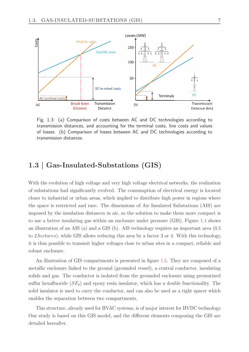
Depending on the transmission task, feasibility studies are performed to estimate the cost
of AC/DC lines according to losses and distances. Figure 1.3 shows (b) losses comparison
and (a) typical cost comparison curve between AC and DC transmission, accounting for the
terminal cost, line cost as well as the value of losses for each AC and DC technology. It can
be observed that on the one hand, the investment costs for HVDC stations are higher than
for HVAC. On the other hand, the costs of transmission medium and line per kilometer
are considerably lower for DC. The distance for which total AC and DC costs are equals is
named the break-even distance. It is usually in the range of 500 to 800 km, and depends
on project financing, loss evaluation, cost of right of way, etc. It can be observed that for
distance superior than the break-even distance, the total AC costs are higher than total DC
costs considering similar transmission distances.
The desire to limit environmental impact also conducts to a HVDC transmission system.
Indeed, HVDC network can transmit more power over fewer lines and hence reduce the
visual impact and save land compensation for other projects. Moreover, there is no induction
of alternating electro-magnetic fields from HVDC transmission, and lower underground
cable losses improves efficiency.
1.3. GAS-INSULATED-SUBSTATIONS (GIS) 7
Fig. 1.3: (a) Comparison of costs between AC and DC technologies according totransmission distances, and accounting for the terminal costs, line costs and valuesof losses. (b) Comparison of losses between AC and DC technologies according totransmission distances.
1.3 | Gas-Insulated-Substations (GIS)
With the evolution of high voltage and very high voltage electrical networks, the realization
of substations had significantly evolved. The consumption of electrical energy is located
closer to industrial or urban areas, which implied to distribute high power in regions where
the space is restricted and rare. The dimensions of Air Insulated Substations (AIS) are
imposed by the insulation distances in air, so the solution to make them more compact is
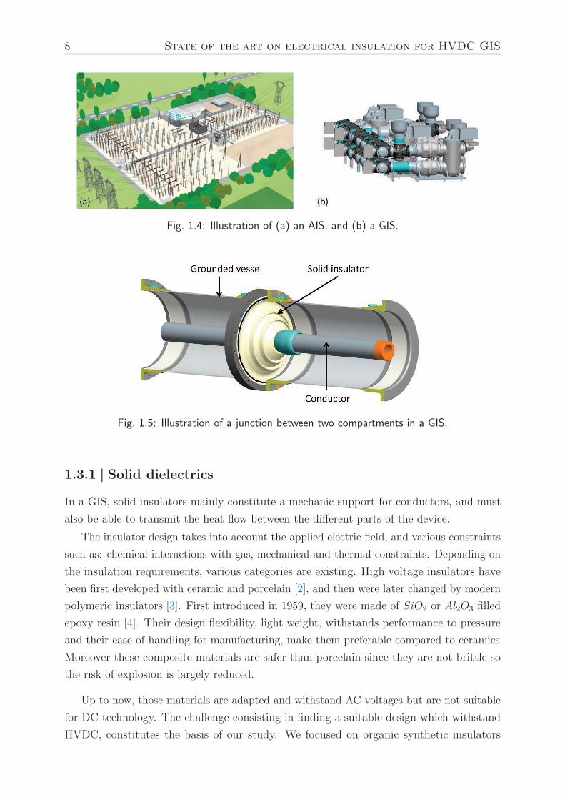
to use a better insulating gas within an enclosure under pressure (GIS). Figure 1.4 shows
an illustration of an AIS (a) and a GIS (b). AIS technology requires an important area (0.5
to 2hectares), while GIS allows reducing this area by a factor 3 or 4. With this technology,
it is thus possible to transmit higher voltages close to urban sites in a compact, reliable and
robust enclosure.
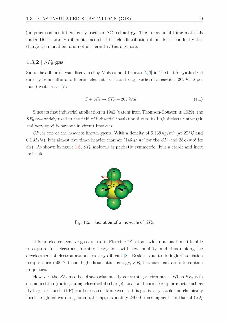
An illustration of GIS compartments is presented in figure 1.5. They are composed of a
metallic enclosure linked to the ground (grounded vessel), a central conductor, insulating
solids and gas. The conductor is isolated from the grounded enclosure using pressurized
sulfur hexafluoride (SF6) and epoxy resin insulator, which has a double functionality. The
solid insulator is used to carry the conductor, and can also be used as a tight spacer which
enables the separation between two compartments.
This structure, already used for HVAC systems, is of major interest for HVDC technology.
Our study is based on this GIS model, and the different elements composing the GIS are
detailed hereafter.
8 State of the art on electrical insulation for HVDC GIS
Fig. 1.4: Illustration of (a) an AIS, and (b) a GIS.
Fig. 1.5: Illustration of a junction between two compartments in a GIS.
1.3.1 | Solid dielectrics
In a GIS, solid insulators mainly constitute a mechanic support for conductors, and must
also be able to transmit the heat flow between the different parts of the device.
The insulator design takes into account the applied electric field, and various constraints
such as: chemical interactions with gas, mechanical and thermal constraints. Depending on
the insulation requirements, various categories are existing. High voltage insulators have
been first developed with ceramic and porcelain [2], and then were later changed by modern
polymeric insulators [3]. First introduced in 1959, they were made of SiO2 or Al2O3 filled
epoxy resin [4]. Their design flexibility, light weight, withstands performance to pressure
and their ease of handling for manufacturing, make them preferable compared to ceramics.
Moreover these composite materials are safer than porcelain since they are not brittle so
the risk of explosion is largely reduced.
Up to now, those materials are adapted and withstand AC voltages but are not suitable
for DC technology. The challenge consisting in finding a suitable design which withstand
HVDC, constitutes the basis of our study. We focused on organic synthetic insulators
1.3. GAS-INSULATED-SUBSTATIONS (GIS) 9
(polymer composite) currently used for AC technology. The behavior of these materials
under DC is totally different since electric field distribution depends on conductivities,
charge accumulation, and not on permittivities anymore.
1.3.2 | SF6 gas
Sulfur hexafluoride was discovered by Moissan and Lebeau [5,6] in 1900. It is synthesized
directly from sulfur and fluorine elements, with a strong exothermic reaction (262Kcal per
mole) written as, [7]:
S + 3F2 → SF6 + 262 kcal (1.1)
Since its first industrial application in 1940 (patent from Thomson-Houston in 1939), the
SF6 was widely used in the field of industrial insulation due to its high dielectric strength,
and very good behaviour in circuit breakers.
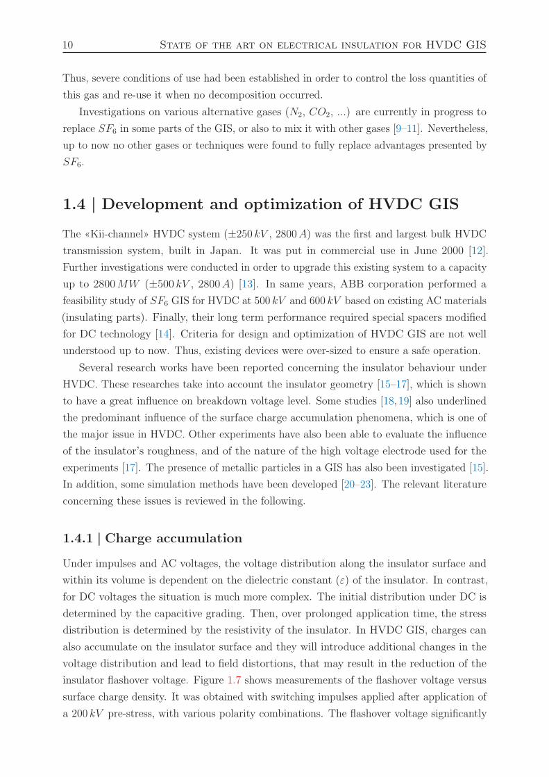
SF6 is one of the heaviest known gases. With a density of 6.139 kg/m3 (at 20 C and
0.1MPa), it is almost five times heavier than air (146 g/mol for the SF6 and 28 g/mol for
air). As shown in figure 1.6, SF6 molecule is perfectly symmetric. It is a stable and inert
molecule.
Fig. 1.6: Illustration of a molecule of SF6.
It is an electronegative gas due to its Fluorine (F) atom, which means that it is able
to capture free electrons, forming heavy ions with low mobility, and thus making the
development of electron avalanches very difficult [8]. Besides, due to its high dissociation
temperature (500 C) and high dissociation energy, SF6 has excellent arc-interruption
properties.
However, the SF6 also has drawbacks, mostly concerning environment. When SF6 is in
decomposition (during strong electrical discharge), toxic and corrosive by-products such as
Hydrogen Fluoride (HF) can be created. Moreover, as this gas is very stable and chemically
inert, its global warming potential is approximately 24000 times higher than that of CO2.
10 State of the art on electrical insulation for HVDC GIS
Thus, severe conditions of use had been established in order to control the loss quantities of
this gas and re-use it when no decomposition occurred.
Investigations on various alternative gases (N2, CO2, ...) are currently in progress to
replace SF6 in some parts of the GIS, or also to mix it with other gases [9–11]. Nevertheless,
up to now no other gases or techniques were found to fully replace advantages presented by
SF6.
1.4 | Development and optimization of HVDC GIS
The «Kii-channel» HVDC system (±250 kV , 2800A) was the first and largest bulk HVDC
transmission system, built in Japan. It was put in commercial use in June 2000 [12].
Further investigations were conducted in order to upgrade this existing system to a capacity
up to 2800MW (±500 kV , 2800A) [13]. In same years, ABB corporation performed a
feasibility study of SF6 GIS for HVDC at 500 kV and 600 kV based on existing AC materials
(insulating parts). Finally, their long term performance required special spacers modified
for DC technology [14]. Criteria for design and optimization of HVDC GIS are not well
understood up to now. Thus, existing devices were over-sized to ensure a safe operation.
Several research works have been reported concerning the insulator behaviour under
HVDC. These researches take into account the insulator geometry [15–17], which is shown
to have a great influence on breakdown voltage level. Some studies [18, 19] also underlined
the predominant influence of the surface charge accumulation phenomena, which is one of
the major issue in HVDC. Other experiments have also been able to evaluate the influence
of the insulator’s roughness, and of the nature of the high voltage electrode used for the
experiments [17]. The presence of metallic particles in a GIS has also been investigated [15].
In addition, some simulation methods have been developed [20–23]. The relevant literature
concerning these issues is reviewed in the following.
1.4.1 | Charge accumulation
Under impulses and AC voltages, the voltage distribution along the insulator surface and
within its volume is dependent on the dielectric constant (ε) of the insulator. In contrast,
for DC voltages the situation is much more complex. The initial distribution under DC is
determined by the capacitive grading. Then, over prolonged application time, the stress
distribution is determined by the resistivity of the insulator. In HVDC GIS, charges can
also accumulate on the insulator surface and they will introduce additional changes in the
voltage distribution and lead to field distortions, that may result in the reduction of the
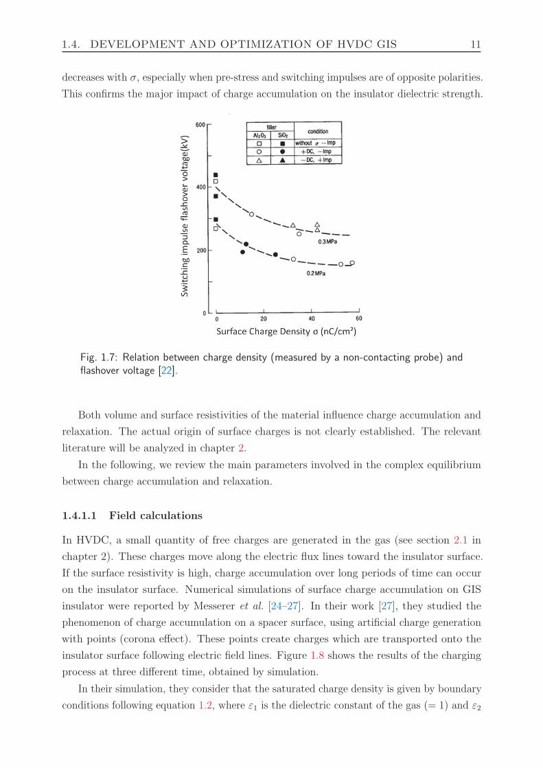
insulator flashover voltage. Figure 1.7 shows measurements of the flashover voltage versus
surface charge density. It was obtained with switching impulses applied after application of
a 200 kV pre-stress, with various polarity combinations. The flashover voltage significantly
1.4. DEVELOPMENT AND OPTIMIZATION OF HVDC GIS 11
decreases with σ, especially when pre-stress and switching impulses are of opposite polarities.
This confirms the major impact of charge accumulation on the insulator dielectric strength.
Fig. 1.7: Relation between charge density (measured by a non-contacting probe) andflashover voltage [22].
Both volume and surface resistivities of the material influence charge accumulation and
relaxation. The actual origin of surface charges is not clearly established. The relevant
literature will be analyzed in chapter 2.
In the following, we review the main parameters involved in the complex equilibrium
between charge accumulation and relaxation.
1.4.1.1 Field calculations
In HVDC, a small quantity of free charges are generated in the gas (see section 2.1 in
chapter 2). These charges move along the electric flux lines toward the insulator surface.
If the surface resistivity is high, charge accumulation over long periods of time can occur
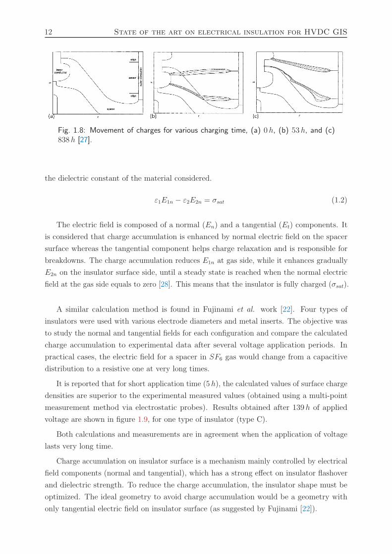
on the insulator surface. Numerical simulations of surface charge accumulation on GIS
insulator were reported by Messerer et al. [24–27]. In their work [27], they studied the
phenomenon of charge accumulation on a spacer surface, using artificial charge generation
with points (corona effect). These points create charges which are transported onto the
insulator surface following electric field lines. Figure 1.8 shows the results of the charging
process at three different time, obtained by simulation.
In their simulation, they consider that the saturated charge density is given by boundary
conditions following equation 1.2, where ε1 is the dielectric constant of the gas (= 1) and ε2
12 State of the art on electrical insulation for HVDC GIS
Fig. 1.8: Movement of charges for various charging time, (a) 0h, (b) 53h, and (c)838h [27].
the dielectric constant of the material considered.
ε1E1n − ε2E2n = σsat (1.2)
The electric field is composed of a normal (En) and a tangential (Et) components. It
is considered that charge accumulation is enhanced by normal electric field on the spacer
surface whereas the tangential component helps charge relaxation and is responsible for
breakdowns. The charge accumulation reduces E1n at gas side, while it enhances gradually
E2n on the insulator surface side, until a steady state is reached when the normal electric
field at the gas side equals to zero [28]. This means that the insulator is fully charged (σsat).
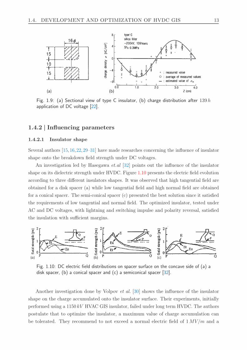
A similar calculation method is found in Fujinami et al. work [22]. Four types of
insulators were used with various electrode diameters and metal inserts. The objective was
to study the normal and tangential fields for each configuration and compare the calculated
charge accumulation to experimental data after several voltage application periods. In
practical cases, the electric field for a spacer in SF6 gas would change from a capacitive
distribution to a resistive one at very long times.
It is reported that for short application time (5h), the calculated values of surface charge
densities are superior to the experimental measured values (obtained using a multi-point
measurement method via electrostatic probes). Results obtained after 139h of applied
voltage are shown in figure 1.9, for one type of insulator (type C).
Both calculations and measurements are in agreement when the application of voltage
lasts very long time.
Charge accumulation on insulator surface is a mechanism mainly controlled by electrical
field components (normal and tangential), which has a strong effect on insulator flashover
and dielectric strength. To reduce the charge accumulation, the insulator shape must be
optimized. The ideal geometry to avoid charge accumulation would be a geometry with
only tangential electric field on insulator surface (as suggested by Fujinami [22]).
1.4. DEVELOPMENT AND OPTIMIZATION OF HVDC GIS 13
Fig. 1.9: (a) Sectional view of type C insulator, (b) charge distribution after 139happlication of DC voltage [22].
1.4.2 | Influencing parameters
1.4.2.1 Insulator shape
Several authors [15,16,22,29–31] have made researches concerning the influence of insulator
shape onto the breakdown field strength under DC voltages.
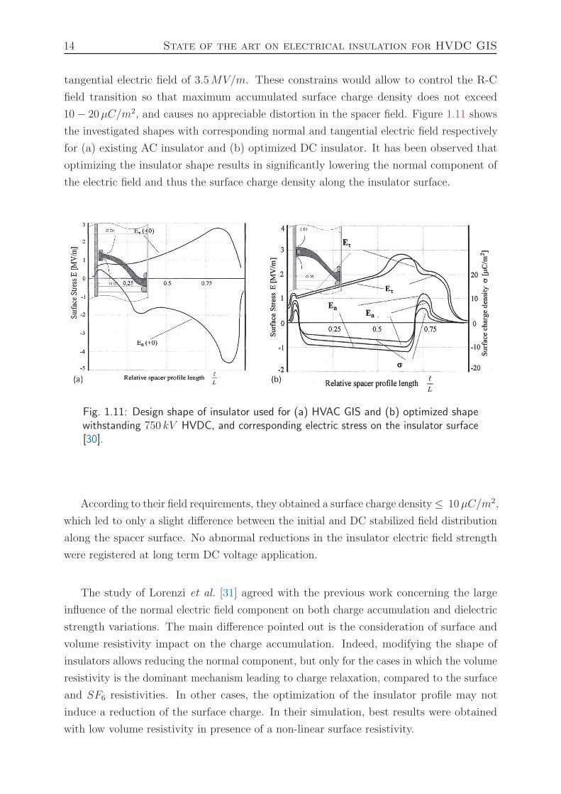
An investigation led by Hasegawa et.al [32] points out the influence of the insulator
shape on its dielectric strength under HVDC. Figure 1.10 presents the electric field evolution
according to three different insulators shapes. It was observed that high tangential field are
obtained for a disk spacer (a) while low tangential field and high normal field are obtained
for a conical spacer. The semi-conical spacer (c) presented the best solution since it satisfied
the requirements of low tangential and normal field. The optimized insulator, tested under
AC and DC voltages, with lightning and switching impulse and polarity reversal, satisfied
the insulation with sufficient margins.
Fig. 1.10: DC electric field distributions on spacer surface on the concave side of (a) adisk spacer, (b) a conical spacer and (c) a semiconical spacer [32].
Another investigation done by Volpov et al. [30] shows the influence of the insulator
shape on the charge accumulated onto the insulator surface. Their experiments, initially
performed using a 1150 kV HVAC GIS insulator, failed under long term HVDC. The authors
postulate that to optimize the insulator, a maximum value of charge accumulation can
be tolerated. They recommend to not exceed a normal electric field of 1MV/m and a
14 State of the art on electrical insulation for HVDC GIS
tangential electric field of 3.5MV/m. These constrains would allow to control the R-C
field transition so that maximum accumulated surface charge density does not exceed
10− 20µC/m2, and causes no appreciable distortion in the spacer field. Figure 1.11 shows
the investigated shapes with corresponding normal and tangential electric field respectively
for (a) existing AC insulator and (b) optimized DC insulator. It has been observed that
optimizing the insulator shape results in significantly lowering the normal component of
the electric field and thus the surface charge density along the insulator surface.
Fig. 1.11: Design shape of insulator used for (a) HVAC GIS and (b) optimized shapewithstanding 750 kV HVDC, and corresponding electric stress on the insulator surface[30].
According to their field requirements, they obtained a surface charge density≤ 10µC/m2,
which led to only a slight difference between the initial and DC stabilized field distribution
along the spacer surface. No abnormal reductions in the insulator electric field strength
were registered at long term DC voltage application.
The study of Lorenzi et al. [31] agreed with the previous work concerning the large
influence of the normal electric field component on both charge accumulation and dielectric
strength variations. The main difference pointed out is the consideration of surface and
volume resistivity impact on the charge accumulation. Indeed, modifying the shape of
insulators allows reducing the normal component, but only for the cases in which the volume
resistivity is the dominant mechanism leading to charge relaxation, compared to the surface
and SF6 resistivities. In other cases, the optimization of the insulator profile may not
induce a reduction of the surface charge. In their simulation, best results were obtained
with low volume resistivity in presence of a non-linear surface resistivity.
1.4. DEVELOPMENT AND OPTIMIZATION OF HVDC GIS 15
1.4.2.2 Insulation properties and charging time estimation
Charge accumulation results from an equilibrium between charges flowing onto the insulator
surface (surface resistivity), through its volume (volume resistivity) and charges coming
from the gas. Depending on these dynamics, different charge accumulations can be reported.
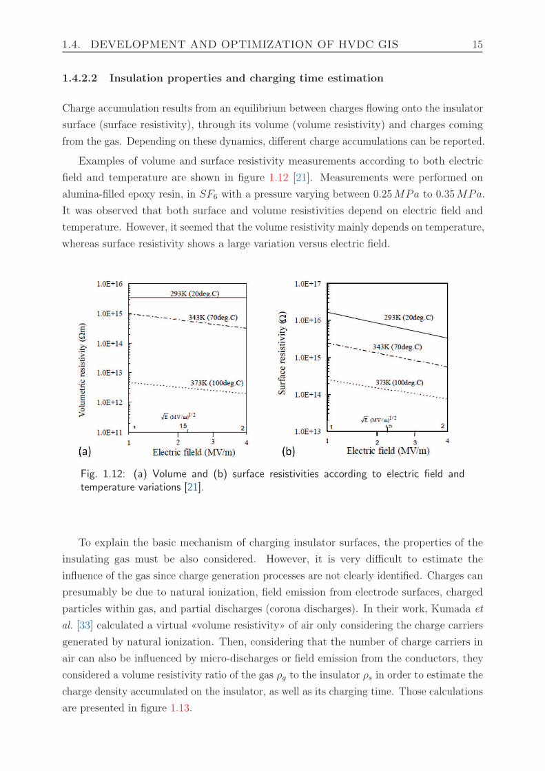
Examples of volume and surface resistivity measurements according to both electric
field and temperature are shown in figure 1.12 [21]. Measurements were performed on
alumina-filled epoxy resin, in SF6 with a pressure varying between 0.25MPa to 0.35MPa.
It was observed that both surface and volume resistivities depend on electric field and
temperature. However, it seemed that the volume resistivity mainly depends on temperature,
whereas surface resistivity shows a large variation versus electric field.
Fig. 1.12: (a) Volume and (b) surface resistivities according to electric field andtemperature variations [21].
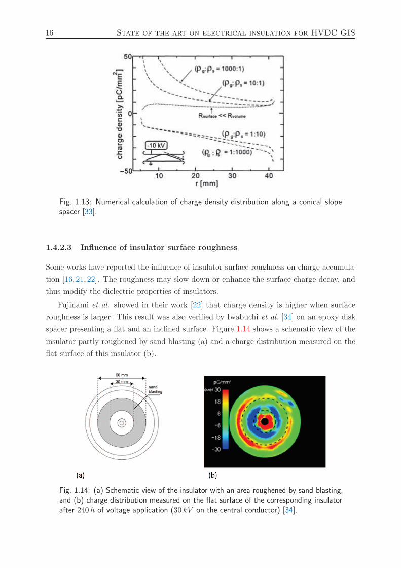
To explain the basic mechanism of charging insulator surfaces, the properties of the
insulating gas must be also considered. However, it is very difficult to estimate the
influence of the gas since charge generation processes are not clearly identified. Charges can
presumably be due to natural ionization, field emission from electrode surfaces, charged
particles within gas, and partial discharges (corona discharges). In their work, Kumada et
al. [33] calculated a virtual «volume resistivity» of air only considering the charge carriers
generated by natural ionization. Then, considering that the number of charge carriers in
air can also be influenced by micro-discharges or field emission from the conductors, they
considered a volume resistivity ratio of the gas ρg to the insulator ρs in order to estimate the
charge density accumulated on the insulator, as well as its charging time. Those calculations
are presented in figure 1.13.
16 State of the art on electrical insulation for HVDC GIS
Fig. 1.13: Numerical calculation of charge density distribution along a conical slopespacer [33].
1.4.2.3 Influence of insulator surface roughness
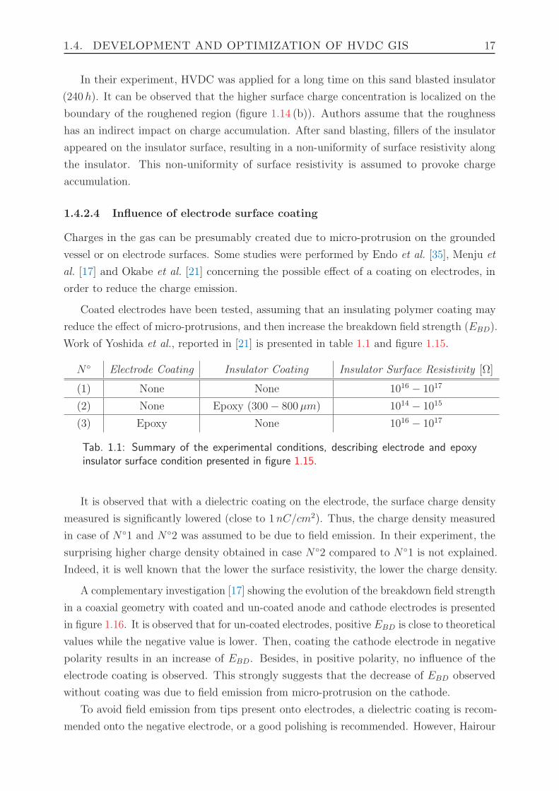
Some works have reported the influence of insulator surface roughness on charge accumula-
tion [16,21,22]. The roughness may slow down or enhance the surface charge decay, and
thus modify the dielectric properties of insulators.
Fujinami et al. showed in their work [22] that charge density is higher when surface
roughness is larger. This result was also verified by Iwabuchi et al. [34] on an epoxy disk
spacer presenting a flat and an inclined surface. Figure 1.14 shows a schematic view of the
insulator partly roughened by sand blasting (a) and a charge distribution measured on the
flat surface of this insulator (b).
Fig. 1.14: (a) Schematic view of the insulator with an area roughened by sand blasting,and (b) charge distribution measured on the flat surface of the corresponding insulatorafter 240h of voltage application (30 kV on the central conductor) [34].
1.4. DEVELOPMENT AND OPTIMIZATION OF HVDC GIS 17
In their experiment, HVDC was applied for a long time on this sand blasted insulator
(240h). It can be observed that the higher surface charge concentration is localized on the
boundary of the roughened region (figure 1.14 (b)). Authors assume that the roughness
has an indirect impact on charge accumulation. After sand blasting, fillers of the insulator
appeared on the insulator surface, resulting in a non-uniformity of surface resistivity along
the insulator. This non-uniformity of surface resistivity is assumed to provoke charge
accumulation.
1.4.2.4 Influence of electrode surface coating
Charges in the gas can be presumably created due to micro-protrusion on the grounded
vessel or on electrode surfaces. Some studies were performed by Endo et al. [35], Menju et
al. [17] and Okabe et al. [21] concerning the possible effect of a coating on electrodes, in
order to reduce the charge emission.
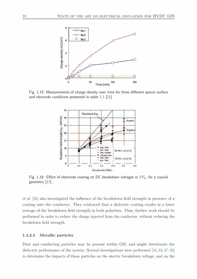
Coated electrodes have been tested, assuming that an insulating polymer coating may
reduce the effect of micro-protrusions, and then increase the breakdown field strength (EBD).
Work of Yoshida et al., reported in [21] is presented in table 1.1 and figure 1.15.
N Electrode Coating Insulator Coating Insulator Surface Resistivity [Ω]
(1) None None 1016 − 1017
(2) None Epoxy (300− 800µm) 1014 − 1015
(3) Epoxy None 1016 − 1017
Tab. 1.1: Summary of the experimental conditions, describing electrode and epoxyinsulator surface condition presented in figure 1.15.
It is observed that with a dielectric coating on the electrode, the surface charge density
measured is significantly lowered (close to 1nC/cm2). Thus, the charge density measured
in case of N1 and N2 was assumed to be due to field emission. In their experiment, the
surprising higher charge density obtained in case N2 compared to N1 is not explained.
Indeed, it is well known that the lower the surface resistivity, the lower the charge density.
A complementary investigation [17] showing the evolution of the breakdown field strength
in a coaxial geometry with coated and un-coated anode and cathode electrodes is presented
in figure 1.16. It is observed that for un-coated electrodes, positive EBD is close to theoretical
values while the negative value is lower. Then, coating the cathode electrode in negative
polarity results in an increase of EBD. Besides, in positive polarity, no influence of the
electrode coating is observed. This strongly suggests that the decrease of EBD observed
without coating was due to field emission from micro-protrusion on the cathode.
To avoid field emission from tips present onto electrodes, a dielectric coating is recom-
mended onto the negative electrode, or a good polishing is recommended. However, Hairour
18 State of the art on electrical insulation for HVDC GIS
Fig. 1.15: Measurements of charge density over time for three different spacer surfaceand electrode conditions presented in table 1.1 [21].
Fig. 1.16: Effect of electrode coating on DC breakdown voltages in SF6, for a coaxialgeometry [17].
et al. [36] also investigated the influence of the breakdown field strength in presence of a
coating onto the conductor. They evidenced that a dielectric coating results in a lower
average of the breakdown field strength in both polarities. Thus, further work should be
performed in order to reduce the charge injected from the conductor, without reducing the
breakdown field strength.
1.4.2.5 Metallic particles
Dust and conducting particles may be present within GIS, and might deteriorate the
dielectric performance of the system. Several investigations were performed [32,33,37–40]
to determine the impacts of those particles on the electric breakdown voltage, and on the
1.4. DEVELOPMENT AND OPTIMIZATION OF HVDC GIS 19
charge accumulation. It is known that in GIS, both free and attached particles can trigger
breakdown. The influence of particles will vary with their nature (dielectric or conductive),
shape and dimensions, location and orientation within the system. Those influences were
detailed by Cookson et al. [37, 39].
It is reported that for a DC field, a particle (in the absence of corona) is driven across
the gap electrodes until it strikes the opposite electrode, where it is oppositely charged,
and driven back to repeat the motion and oscillate between the electrodes. In the case
of negative polarity, particles float around the high voltage conductor, which is called
«firefly» phenomenon. During their random movement, particles may attach themselves to
the insulator, and greatly decrease its insulation strength. To increase insulation reliability
of DC GIS, a system allowing to remove particles should be developed.
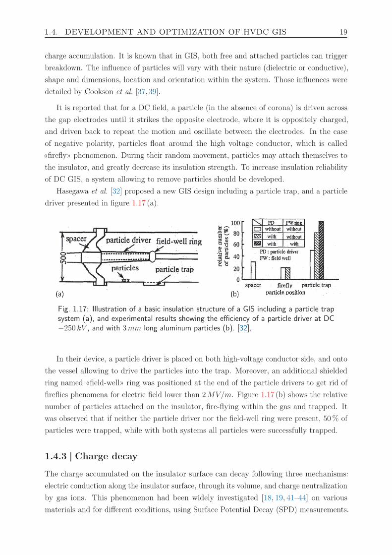
Hasegawa et al. [32] proposed a new GIS design including a particle trap, and a particle
driver presented in figure 1.17 (a).
Fig. 1.17: Illustration of a basic insulation structure of a GIS including a particle trapsystem (a), and experimental results showing the efficiency of a particle driver at DC−250 kV , and with 3mm long aluminum particles (b). [32].
In their device, a particle driver is placed on both high-voltage conductor side, and onto
the vessel allowing to drive the particles into the trap. Moreover, an additional shielded
ring named «field-well» ring was positioned at the end of the particle drivers to get rid of
fireflies phenomena for electric field lower than 2MV/m. Figure 1.17 (b) shows the relative
number of particles attached on the insulator, fire-flying within the gas and trapped. It
was observed that if neither the particle driver nor the field-well ring were present, 50% of
particles were trapped, while with both systems all particles were successfully trapped.
1.4.3 | Charge decay
The charge accumulated on the insulator surface can decay following three mechanisms:
electric conduction along the insulator surface, through its volume, and charge neutralization
by gas ions. This phenomenon had been widely investigated [18, 19, 41–44] on various
materials and for different conditions, using Surface Potential Decay (SPD) measurements.
20 State of the art on electrical insulation for HVDC GIS
SPD (detailed in [18]) consists in a deposition of charges created by corona discharge, on
a localized area of the insulator surface. Once charges are deposed, the potential on this
charged area is measured versus time. This technique allows investigating the dynamics
of charge versus various parameters (RH, time, charge deposited). Hereafter, only the
influence of relative humidity and surrounding gas are presented to point out the possible
influence of such parameters in the real application. However, it is worth noting that the
correlation between potential decay measurements and real case in GIS is questionable since
rather different conditions and geometries are used.
1.4.3.1 Influence of relative humidity
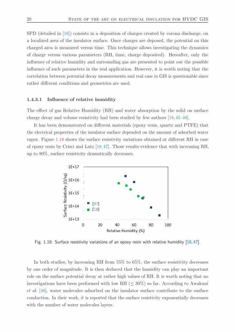
The effect of gas Relative Humidity (RH) and water absorption by the solid on surface
charge decay and volume resistivity had been studied by few authors [18,45–48].
It has been demonstrated on different materials (epoxy resin, quartz and PTFE) that
the electrical properties of the insulator surface depended on the amount of adsorbed water
vapor. Figure 1.18 shows the surface resistivity variations obtained at different RH in case
of epoxy resin by Crisci and Lutz [18, 47]. Those results evidence that with increasing RH,
up to 80%, surface resistivity dramatically decreases.
Fig. 1.18: Surface resistivity variations of an epoxy resin with relative humidity [18, 47].
In both studies, by increasing RH from 55% to 65%, the surface resistivity decreases
by one order of magnitude. It is then deduced that the humidity can play an important
role on the surface potential decay at rather high values of RH. It is worth noting that no
investigations have been performed with low RH (≤ 30%) so far. According to Awakuni
et al. [46], water molecules adsorbed on the insulator surface contribute to the surface
conduction. In their work, it is reported that the surface resistivity exponentially decreases
with the number of water molecules layers.
1.4. DEVELOPMENT AND OPTIMIZATION OF HVDC GIS 21
In addition, volume resistivity measurements have also been performed [45, 48]. The
results show that with increasing water concentration within the solid, its volume resistivity
significantly decreases.
1.4.3.2 Influence of surrounding gas
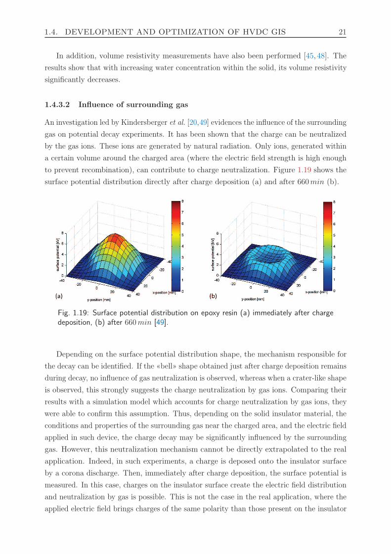
An investigation led by Kindersberger et al. [20,49] evidences the influence of the surrounding
gas on potential decay experiments. It has been shown that the charge can be neutralized
by the gas ions. These ions are generated by natural radiation. Only ions, generated within
a certain volume around the charged area (where the electric field strength is high enough
to prevent recombination), can contribute to charge neutralization. Figure 1.19 shows the
surface potential distribution directly after charge deposition (a) and after 660min (b).
Fig. 1.19: Surface potential distribution on epoxy resin (a) immediately after chargedeposition, (b) after 660min [49].
Depending on the surface potential distribution shape, the mechanism responsible for
the decay can be identified. If the «bell» shape obtained just after charge deposition remains
during decay, no influence of gas neutralization is observed, whereas when a crater-like shape
is observed, this strongly suggests the charge neutralization by gas ions. Comparing their
results with a simulation model which accounts for charge neutralization by gas ions, they
were able to confirm this assumption. Thus, depending on the solid insulator material, the
conditions and properties of the surrounding gas near the charged area, and the electric field
applied in such device, the charge decay may be significantly influenced by the surrounding
gas. However, this neutralization mechanism cannot be directly extrapolated to the real
application. Indeed, in such experiments, a charge is deposed onto the insulator surface
by a corona discharge. Then, immediately after charge deposition, the surface potential is
measured. In this case, charges on the insulator surface create the electric field distribution
and neutralization by gas is possible. This is not the case in the real application, where the
applied electric field brings charges of the same polarity than those present on the insulator
22 State of the art on electrical insulation for HVDC GIS
surface. In such conditions, the neutralization by the surrounding gas cannot occur.
1.4.4 | Simulation models
Various simulation models have been developed around phenomena involved in the charge
accumulation.
Some models [21,33] developed a simulation tool which enables to estimate the charge
on the insulator based on potential measurements along the insulator surface.
In [22–24, 30, 50], models taking into account the variations of volume and surface
resistivities with electric field were developed, considering solid and gaseous dielectrics to
be linear media. Such models allow describing the evolution of the electric field for various
types of insulators and estimate the charge accumulation along the insulator surface. Based
on those calculations, critical values for the maximum charge accumulated on the surface,
and also for the normal and tangential components of the applied electric field have been
determined (10 − 20µC/m2) [30].
However, in the above quoted models, the phenomena of charge transport through
gas were not considered. Volpov et al. recommend accounting for the processes of ion
generation, recombination and ion drift in compressed gases to establish a correct model.
Another simulation work reported by Kindersberger et al. [20] presents a simulation tool
describing the charge decay on a solid dielectric accounting for electric conduction of both
surface and volume, and also charge neutralization by gas ions. In their work, the influence
of gas was implemented in the model by calculating the ion pair generation by natural
ionization in their experimental devices. Then, based on this ion pair generation rate, the
resulting current density in electric field was estimated.
The existing models permit evidencing the influence of the insulator shape, electric
field orientation and solid and gaseous dielectric properties on the mechanism of charge
accumulation. However, up to now, no model describes those phenomena altogether.
Furthermore, additional mechanisms such as charge injected from the electrode surface may
also be considered in the simulation of charge accumulation.
1.5 | Conclusions
In this chapter, we have reviewed nowadays challenges which make HVDC GIS an attractive
technology for long distance transmission compared to AC technologies. Concerning HVDC
GIS insulation optimization, the charge accumulation mechanism occurring on the surface
of the dielectric solid has been mainly considered. The principal phenomena involved in
charge accumulation and relaxation have been detailed. It has been shown that charge
accumulation is strongly dependent on the electric field component orientation (normal
1.5. CONCLUSIONS 23
and tangential field). Based on numerical calculations considering the components of the
electric field, the insulator shape can be modified in such a way that charge accumulation
could be reduced.
In addition, the electric field distribution (and hence the charge accumulation) also
depends on the solid dielectric properties (surface and volume resistivities). Those properties
vary with the temperature, electric field, presence of water, but rather few works were
devoted to study the influence of these parameters.
Hence, the charge accumulation results in a complex equilibrium between electrical
conduction through the volume and on the surface of the dielectric solid, as well as charge
generation and transport through the dielectric gas. To reduce this charge accumulation, it
has been suggested to:
−→ Add a dielectric coating on the high voltage electrode surface to reduce the charge
injection,
−→ Implement a semi-conductive layer on the insulator surface to adjust its resistivity,
−→ Optimize the insulator shape,
−→ Reduce particle contamination within the device by the implementation of particles
traps.
However, those recommendations are not sufficient to allow the development and
optimization of a reliable HVDC GIS. It is then reasonable to suppose that other phenomena
and parameters, not yet investigated, may have an important contribution to the charge
accumulation. Hence, the purpose of this thesis is twofold. On the one hand we will
investigate the charge generation process within the insulating gas, and on the other hand
we will develop a numerical model allowing to estimate the electric field distribution and
calculate the leakage current through the solid insulator.
In chapter 2, we will first review the state of the art of charge generation processes in
gas and vacuum. Then, we will focus on two main questions:
1) The possible origins of those charges,
2) The parameters influencing those charges.
Thus, we will develop experimental test setup allowing to precisely measure low cur-
rents under HVDC (up to 250 kV ) and characterize these currents according to different
parameters.
Afterwards, a numerical model will be developed (chapter 4) in order to evaluate
the modification of electric field distribution and leakage current in presence of different
parameters. In a GIS, the conductor is often at higher temperature than the vessel, resulting
in a temperature gradient along the solid insulator. The influence of this temperature

24 State of the art on electrical insulation for HVDC GIS
gradient on the field distribution was not reported up to now. In addition, the presence
of water within solid insulator will be evidenced in chapter 3. The latter will also be
implemented within the model.
The model is based on characterization of solid insulators physical properties, using
typical conditions of GIS (SF6 environment, and electric field up to 5 kV/mm). Experimental
test setups able to measure low-noise currents under high voltages and different temperatures
will be developed and presented. Hence, solid dielectric will be characterized in conditions
relevant of GIS (in pressurized SF6 at high electric field), with a good control of sample
processing (drying) and following an optimized protocol.
Bibliography (Chapter 1) 25
Bibliography
[1] R. Rudervall, J. Charpentier, and R. Sharma, “High voltage direct current (hvdc)transmission systems technology review paper,” Energy week, vol. 2000, 2000. (cited inpage 5)
[2] J. Holtzhausen, “High voltage insulators,” in Electrical IDC technologies. (cited inpage 8)
[3] T. Sorquist and A. Vlastos, “Outdoor polymeric insulators long-term exposed tohvdc,” in Transmission and Distribution Conference, 1996. Proceedings., 1996 IEEE,pp. 135–142, IEEE, 1996. (cited in page 8)
[4] J. Kuffel, E. Kuffel, and W. S. Zaengl, High voltage engineering fundamentals. Newnes,2000. (cited in page 8)
[5] M. H, “Action d’un courant electrique sur l’acide fluorhydrique anhydre,” pp. 102–1544,1886. (cited in page 9)
[6] M. H,“Sur la decomposition de l’acide fluorhydrique par un courant electrique,”pp. 103–202, 1886. (cited in page 9)
[7] W. C. Schumb and E. L. Gamble, “The preparation of sulfur hexafluoride and someof its physical properties,” Journal of the American Chemical Society, vol. 52, no. 11,pp. 4302–4308, 1930. (cited in page 9)
[8] L. G. Christophorou, J. K. Olthoff, and R. J. Van Brunt, “Sulfur hexafluoride and theelectric power industry,”Electrical Insulation Magazine, IEEE, vol. 13, no. 5, pp. 20–24,1997. (cited in page 9)
[9] A. Winter, J. Kindersberger, M. Tenzer, V. Hinrichsen, L. Zavattoni, O. Lesaint,R. Muhr, and D. Imamovic, “Solid/gaseous insulation systems for compact hvdcsolutions,”CIGRE, pp. 8–9, 2014. (cited in page 10)
[10] H. Looe, J. Yan, and J. Spencer, “Development of a non-sf 6 self-blast type interrupterunit,” in Gas Discharges and Their Applications, 2008. GD 2008. 17th InternationalConference on, pp. 117–120, IEEE, 2008. (cited in page 10)
[11] K. Bousoltane, Alternatives au SF6 dans le disjoncteur haute tension. PhD thesis,These de doctorat de l’universite de Provence–Aix–Marseille 1, 2008. (cited in page 10)
[12] T. Shimato and al., “The kii channel hvdc link in japan,” CIGRE 14-106, 2002. (citedin page 10)
[13] M. Shikata, K. Yamaji, M. Hatano, E. Tsuchie, H. Takeuchi, and K. Inami, “Develop-ment and design of dc-gis,” Electrical Engineering in Japan, vol. 129, no. 2, pp. 51–61,1999. (cited in page 10)
[14] M. Mendik, S. Lowder, and F. Elliott, “Long term performance verification of highvoltage dc gis,” in Transmission and Distribution Conference, 1999 IEEE, vol. 2,pp. 484–488, IEEE, 1999. (cited in page 10)
26 Bibliography (Chapter 1)
[15] T. Hasegawa, K. Yamaji, M. Hatano, H. Aoyagi, Y. Taniguchi, and A. Kobayashi,“Dc dielectric characteristics and conception of insulation design for dc gis,” PowerDelivery, IEEE Transactions on, vol. 11, no. 4, pp. 1776–1782, 1996. (cited in pages 10and 13)
[16] Z. Jia, B. Zhang, X. Tan, and Q. Zhang, “Flashover characteristics along the insulatorin sf6 gas under dc voltage,” in Power and Energy Engineering Conference, 2009.APPEEC 2009. Asia-Pacific, pp. 1–4, IEEE, 2009. (cited in pages 10, 13 and 16)
[17] H. Hama, F. Endo, S. Okabe, J. Kindersberger, K. Juhre, S. Meijer, and U. Schichler,“Gas insulated systems for hvdc: Dc stress at dc and ac systems,” CIGRE Task forceD1.03.11105, 2011. (cited in pages 10, 17 and 18)
[18] A. Crisci, B. Gosse, J. Gosse, and V. Ollier-Dureault, “Surface-potential decay dueto surface conduction,” EPJ Applied physics, vol. 4, pp. 107–1116, 1998. (cited inpages 10, 19, 20 and 129)
[19] P. Molinie, “Measuring and modeling transient insulator response to charging: thecontribution of surface potential studies,”Dielectrics and Electrical Insulation, IEEETransactions on, vol. 12, no. 5, pp. 939–950, 2005. (cited in pages 10 and 19)
[20] J. Kindersberger and C. Lederle, “Surface charge decay on insulators in air andsulfurhexafluorid-part i: Simulation,” Dielectrics and Electrical Insulation, IEEETransactions on, vol. 15, no. 4, pp. 941–948, 2008. (cited in pages 10, 21 and 22)
[21] S. Okabe, “Phenomena and mechanism of electric charges on spacers in gas insulatedswitchgears,”Dielectrics and Electrical Insulation, IEEE Transactions on, vol. 14, no. 1,pp. 46–52, 2007. (cited in pages 10, 15, 16, 17, 18, 22, 41, 114 and 124)
[22] H. Fujinami, T. Takuma, M. Yashima, and T. Kawamoto, “Mechanism and effect of dccharge accumulation on sf 6 gas insulated spacers,”Power Delivery, IEEE Transactionson, vol. 4, no. 3, pp. 1765–1772, 1989. (cited in pages 10, 11, 12, 13, 16 and 22)
[23] E. Volpov, “Electric field modeling and field formation mechanism in hvdc sf 6 gasinsulated systems,”Dielectrics and Electrical Insulation, IEEE Transactions on, vol. 10,no. 2, pp. 204–215, 2003. (cited in pages 10, 22, 30 and 31)
[24] F. Messerer and W. Boeck, “Field optimization of an hvdc-gis-spacer,” in ElectricalInsulation and Dielectric Phenomena, 1998. Annual Report. Conference on, vol. 1,pp. 15–18, IEEE, 1998. (cited in pages 11 and 22)
[25] F. Messerer and W. Boeck, “Gas insulated substation (gis) for hvdc,” in ElectricalInsulation and Dielectric Phenomena, 2000 Annual Report Conference on, vol. 2,pp. 698–702, IEEE, 2000. (cited in page 11)
[26] F. Messerer, W. Boeck, H. Steinbigler, and S. Chakravorti, “Enhanced field calculationfor hvdc gis,” in Gaseous Dielectrics IX, pp. 473–483, Springer, 2001. (cited in page 11)
[27] F. Messerer, M. Finkel, and W. Boeck,“Surface charge accumulation on hvdc-gis-spacer,”in Electrical Insulation, 2002. Conference Record of the 2002 IEEE InternationalSymposium on, pp. 421–425, IEEE, 2002. (cited in pages 11 and 12)
Bibliography (Chapter 1) 27
[28] S. Sato, W. Zaengl, and A. Knecht, “A numerical analysis of accumulated surfacecharge on dc epoxy rrsin spaces,” Electrical Insulation, IEEE Transactions on, no. 3,pp. 333–340, 1987. (cited in page 12)
[29] T. Nitta and K. Nakanishi, “Charge accumulation on insulating spacers for hvdc gis,”Electrical Insulation, IEEE Transactions on, vol. 26, no. 3, pp. 418–427, 1991. (citedin page 13)
[30] E. Volpov, “Dielectric strength coordination and generalized spacer design rules forhvac/dc sf 6 gas insulated systems,”Dielectrics and Electrical Insulation, IEEE Trans-actions on, vol. 11, no. 6, pp. 949–963, 2004. (cited in pages 13, 14, 22 and 130)
[31] A. De Lorenzi, L. Grando, R. Gobbo, G. Pesavento, P. Bettini, R. Specogna, andF. Trevisan, “The insulation structure of the 1mv transmission line for the iter neutralbeam injector,” Fusion Engineering and Design, vol. 82, no. 5, pp. 836–844, 2007.(cited in pages 13 and 14)
[32] T. Hasegawa, K. Yamaji, M. Hatano, F. Endo, T. Rokunohe, and T. Yamagiwa,“Development of insulation structure and enhancement of insulation reliability of 500kv dc gis,”Power Delivery, IEEE Transactions on, vol. 12, no. 1, pp. 194–202, 1997.(cited in pages 13, 18 and 19)
[33] A. Kumada and S. Okabe, “Charge distribution measurement on a truncated conespacer under dc voltage,”Dielectrics and Electrical Insulation, IEEE Transactions on,vol. 11, no. 6, pp. 929–938, 2004. (cited in pages 15, 16, 18 and 22)
[34] H. Iwabuchi, T. Donen, S. Matsuoka, A. Kumada, K. Hidaka, M. Takei, and Y. Hoshina,“Influence of surface-conductivity distribution on charge accumulation of gis insulatorunder dc field,” Int’l. Sympos. High Voltage Engineering ISH, Hannover, Germany,Paper D-031, 2011. (cited in page 16)
[35] F. Endo, T. Kichikawa, R. Ishikawa, and J. Ozawa, “Dielectric characteristics of sf6 gasfor application to hvdc systems,” Power Apparatus and Systems, IEEE Transactionson, no. 3, pp. 847–855, 1980. (cited in pages 17, 36, 37, 38, 40 and 41)
[36] M. Hairour, Etude dielectrique d’une isolation hybride gaz-solide pour appareillage hautetension. PhD thesis, Universite Montpellier II-Sciences et Techniques du Languedoc,2007. (cited in page 18)
[37] A. H. Cookson, “Electrical breakdown for uniform fields in compressed gases,” inProceedings of the Institution of Electrical Engineers, vol. 117, pp. 269–280, IET, 1970.(cited in pages 18 and 19)
[38] A. Moukengue Imano, R. Schurer, and K. Feser, “The influence of a conductingparticle on a spacer on the insulation properties in sf6/n2 mixtures,” in IEE conferencepublication, pp. 3–232, Institution of Electrical Engineers, 1999. (cited in page 18)
[39] C. M. Cooke, R. E. Wootton, and A. H. Cookson, “Influence of particles on ac and dcelectrical performance of gas insulated systems at extra-high-voltage,”Power Apparatusand Systems, IEEE Transactions on, vol. 96, no. 3, pp. 768–777, 1977. (cited inpages 18 and 19)
28 Bibliography (Chapter 1)
[40] H. Anis and K. Srivastava, “Free conducting particles in compressed gas insulation,”Electrical Insulation, IEEE Transactions on, no. 4, pp. 327–338, 1981. (cited in page 18)
[41] M. Pepin and H. Wintle, “Charge injection and conduction on the surface of insulators,”Journal of applied physics, vol. 83, no. 11, pp. 5870–5879, 1998. (cited in page 19)
[42] P. Llovera and P. Molinie, “New methodology for surface potential decay measurements:application to study charge injection dynamics on polypropylene films,” Dielectricsand Electrical Insulation, IEEE Transactions on, vol. 11, no. 6, pp. 1049–1056, 2004.(cited in page 19)
[43] T. Sonnonstine and M. Perlman, “Surface-potential decay in insulators with field-dependent mobility and injection efficiency,” Journal of Applied Physics, vol. 46, no. 9,pp. 3975–3981, 2008. (cited in page 19)
[44] H. Wintle, “Surface-charge decay in insulators with nonconstant mobility and withdeep trapping,” Journal of Applied Physics, vol. 43, no. 7, pp. 2927–2930, 2003. (citedin page 19)
[45] B. Lutz and J. Kindersberger, “Influence of absorbed water on volume resistivity ofepoxy resin insulators,” in Solid Dielectrics (ICSD), 2010 10th IEEE InternationalConference on, pp. 1–4, IEEE, 2010. (cited in pages 20, 21 and 117)
[46] Y. Awakuni and J. Calderwood, “Water vapour adsorption and surface conductivity insolids,” Journal of Physics D: Applied Physics, vol. 5, no. 5, p. 1038, 1972. (cited inpage 20)
[47] B. Lutz and J. Kindersberger, “Influence of relative humidity on surface charge decayon epoxy resin insulators,” in Properties and Applications of Dielectric Materials, 2009.ICPADM 2009. IEEE 9th International Conference on the, pp. 883–886, IEEE, 2009.(cited in pages 20 and 129)
[48] D. K. Das-Gupta, “Electrical properties of surfaces of polymeric insulators,” ElectricalInsulation, IEEE Transactions on, vol. 27, no. 5, pp. 909–923, 1992. (cited in pages 20and 21)
[49] J. Kindersberger and C. Lederle, “Surface charge decay on insulators in air andsulfurhexafluorid-part ii: measurements,”Dielectrics and Electrical Insulation, IEEETransactions on, vol. 15, no. 4, pp. 949–957, 2008. (cited in page 21)
[50] E. Volpov, “Hvdc gas insulated apparatus: electric field specificity and insulation designconcept,” Electrical Insulation Magazine, IEEE, vol. 18, no. 2, pp. 7–36, 2002. (citedin page 22)
2 | Charge generation in SF6 at highelectric field
Contents
2.1 Review of charge generation in pressurized gases and vacuum . . . . . . . . 30
2.1.1 Natural ionization in gases at low electric field . . . . . . . . . . . . 30
2.1.2 Charge emission mechanisms in vacuum at high electric field . . . . 32
2.1.3 Dark currents through pressurized gases (Air and SF6) at highelectric field . . . . . . . . . . . . . . . . . . . . . . . . . . . . . . . 36
2.1.4 Influence of several parameters on current measured in vacuum athigh electric field . . . . . . . . . . . . . . . . . . . . . . . . . . . . 39
2.1.5 Influence of the introduction of low pressure gases in vacuum experi-ments . . . . . . . . . . . . . . . . . . . . . . . . . . . . . . . . . . . 44
2.1.6 Discussion and objectives of the study . . . . . . . . . . . . . . . . 45
2.2 Experimental systems . . . . . . . . . . . . . . . . . . . . . . . . . . . . . . 46
2.2.1 Small scale coaxial electrode system . . . . . . . . . . . . . . . . . . 47
2.2.2 Large scale plane-to-plane electrode system . . . . . . . . . . . . . 49
2.2.3 Experimental protocols . . . . . . . . . . . . . . . . . . . . . . . . . 51
2.3 Experimental results . . . . . . . . . . . . . . . . . . . . . . . . . . . . . . . 54
2.3.1 Preliminary experiments: coaxial system . . . . . . . . . . . . . . . 54
2.3.2 Discrepancies between calculated and measured RH, and influenceon the current . . . . . . . . . . . . . . . . . . . . . . . . . . . . . . 64
2.3.3 Parallel electrodes system . . . . . . . . . . . . . . . . . . . . . . . 74
2.4 Discussion . . . . . . . . . . . . . . . . . . . . . . . . . . . . . . . . . . . . 85
2.4.1 Physical mechanisms . . . . . . . . . . . . . . . . . . . . . . . . . . 85
2.4.2 Consequences on the industrial application . . . . . . . . . . . . . . 89
2.5 Conclusions . . . . . . . . . . . . . . . . . . . . . . . . . . . . . . . . . . . . 90
Bibliography . . . . . . . . . . . . . . . . . . . . . . . . . . . . . . . . . . . . . . 91
As explained in Chapter 1, in the case of HVDC GIS technology, the charge generation,
accumulation and relaxation on solid insulators are important mechanisms influencing the
dielectric strength of the system. It has also been mentioned that the origin of charges
coming from the gas is not well known, as well as the parameters influencing the charge
generation. The objective of this chapter is to get a better knowledge on these processes,
by trying to experimentally measure the currents flowing through the gas at high electric
field.
We will first review the state of the art about currents measured through pressurized
gases and vacuum for high applied electric fields. The current measured may have different
29
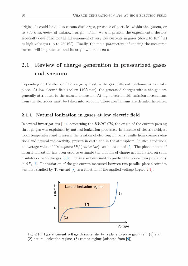
30 Charge generation in SF6 at high electric field
origins. It could be due to corona discharges, presence of particles within the system, or
to «dark currents» of unknown origin. Then, we will present the experimental devices
especially developed for the measurement of very low currents in gases (down to 10−13 A)
at high voltages (up to 250 kV ). Finally, the main parameters influencing the measured
current will be presented and its origin will be discussed.
2.1 | Review of charge generation in pressurized gases
and vacuum
Depending on the electric field range applied to the gas, different mechanisms can take
place. At low electric field (below 1 kV/mm), the generated charges within the gas are
generally attributed to the natural ionization. At high electric field, emission mechanisms
from the electrodes must be taken into account. These mechanisms are detailed hereafter.
2.1.1 | Natural ionization in gases at low electric field
In several investigations [1–4] concerning the HVDC GIS, the origin of the current passing
through gas was explained by natural ionization processes. In absence of electric field, at
room temperature and pressure, the creation of electron/ion pairs results from cosmic radia-
tions and natural radioactivity, present in earth and in the atmosphere. In such conditions,
an average value of 10 ion pairs IP/ ( cm3.s.bar) can be assumed [5]. The phenomenon of
natural ionization has been used to estimate the amount of charge accumulation on solid
insulators due to the gas [3, 6]. It has also been used to predict the breakdown probability
in SF6 [7]. The variation of the gas current measured between two parallel plate electrodes
was first studied by Townsend [8] as a function of the applied voltage (figure 2.1).
Fig. 2.1: Typical current voltage characteristic for a plane to plane gap in air, (1) and(2) natural ionization regime, (3) corona regime (adapted from [9]).
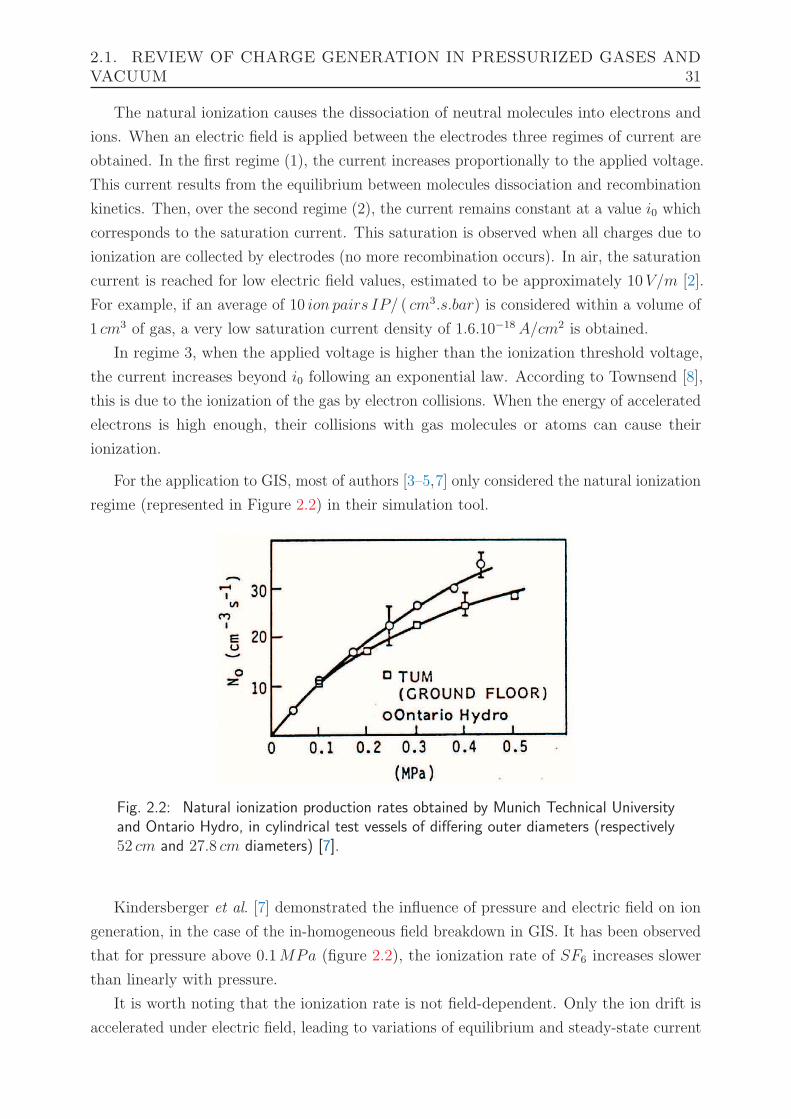
2.1. REVIEW OF CHARGE GENERATION IN PRESSURIZED GASES ANDVACUUM 31
The natural ionization causes the dissociation of neutral molecules into electrons and
ions. When an electric field is applied between the electrodes three regimes of current are
obtained. In the first regime (1), the current increases proportionally to the applied voltage.
This current results from the equilibrium between molecules dissociation and recombination
kinetics. Then, over the second regime (2), the current remains constant at a value i0 which
corresponds to the saturation current. This saturation is observed when all charges due to
ionization are collected by electrodes (no more recombination occurs). In air, the saturation
current is reached for low electric field values, estimated to be approximately 10V/m [2].
For example, if an average of 10 ion pairs IP/ ( cm3.s.bar) is considered within a volume of
1 cm3 of gas, a very low saturation current density of 1.6.10−18 A/cm2 is obtained.
In regime 3, when the applied voltage is higher than the ionization threshold voltage,
the current increases beyond i0 following an exponential law. According to Townsend [8],
this is due to the ionization of the gas by electron collisions. When the energy of accelerated
electrons is high enough, their collisions with gas molecules or atoms can cause their
ionization.
For the application to GIS, most of authors [3–5,7] only considered the natural ionization
regime (represented in Figure 2.2) in their simulation tool.
Fig. 2.2: Natural ionization production rates obtained by Munich Technical Universityand Ontario Hydro, in cylindrical test vessels of differing outer diameters (respectively52 cm and 27.8 cm diameters) [7].
Kindersberger et al. [7] demonstrated the influence of pressure and electric field on ion
generation, in the case of the in-homogeneous field breakdown in GIS. It has been observed
that for pressure above 0.1MPa (figure 2.2), the ionization rate of SF6 increases slower
than linearly with pressure.
It is worth noting that the ionization rate is not field-dependent. Only the ion drift is
accelerated under electric field, leading to variations of equilibrium and steady-state current
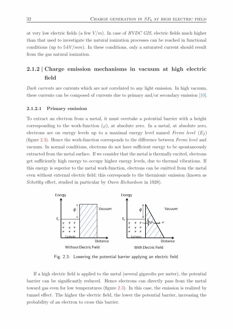
32 Charge generation in SF6 at high electric field
at very low electric fields (a few V/m). In case of HVDC GIS, electric fields much higher
than that used to investigate the natural ionization processes can be reached in functional
conditions (up to 5 kV/mm). In these conditions, only a saturated current should result
from the gas natural ionization.
2.1.2 | Charge emission mechanisms in vacuum at high electric
field
Dark currents are currents which are not correlated to any light emission. In high vacuum,
these currents can be composed of currents due to primary and/or secondary emission [10].
2.1.2.1 Primary emission
To extract an electron from a metal, it must overtake a potential barrier with a height
corresponding to the work-function (ϕ), at absolute zero. In a metal, at absolute zero,
electrons are on energy levels up to a maximal energy level named Fermi level (Ef)
(figure 2.3). Hence the work-function corresponds to the difference between Fermi level and
vacuum. In normal conditions, electrons do not have sufficient energy to be spontaneously
extracted from the metal surface. If we consider that the metal is thermally excited, electrons
get sufficiently high energy to occupy higher energy levels, due to thermal vibrations. If
this energy is superior to the metal work-function, electrons can be emitted from the metal
even without external electric field; this corresponds to the thermionic emission (known as
Schottky effect, studied in particular by Owen Richardson in 1928).
Fig. 2.3: Lowering the potential barrier applying an electric field.
If a high electric field is applied to the metal (several gigavolts per meter), the potential
barrier can be significantly reduced. Hence electrons can directly pass from the metal
toward gas even for low temperatures (figure 2.3). In this case, the emission is realized by
tunnel effect. The higher the electric field, the lower the potential barrier, increasing the
probability of an electron to cross this barrier.
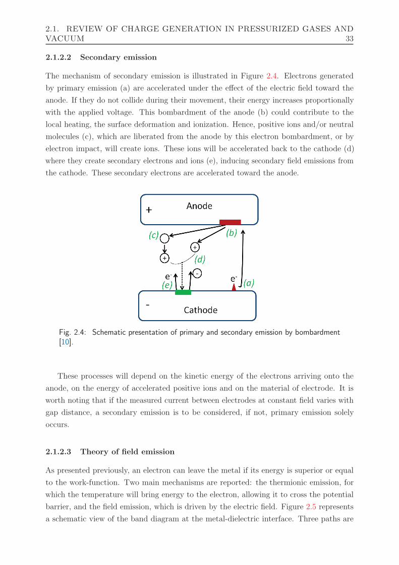
2.1. REVIEW OF CHARGE GENERATION IN PRESSURIZED GASES ANDVACUUM 33
2.1.2.2 Secondary emission
The mechanism of secondary emission is illustrated in Figure 2.4. Electrons generated
by primary emission (a) are accelerated under the effect of the electric field toward the
anode. If they do not collide during their movement, their energy increases proportionally
with the applied voltage. This bombardment of the anode (b) could contribute to the
local heating, the surface deformation and ionization. Hence, positive ions and/or neutral
molecules (c), which are liberated from the anode by this electron bombardment, or by
electron impact, will create ions. These ions will be accelerated back to the cathode (d)
where they create secondary electrons and ions (e), inducing secondary field emissions from
the cathode. These secondary electrons are accelerated toward the anode.
Fig. 2.4: Schematic presentation of primary and secondary emission by bombardment[10].
These processes will depend on the kinetic energy of the electrons arriving onto the
anode, on the energy of accelerated positive ions and on the material of electrode. It is
worth noting that if the measured current between electrodes at constant field varies with
gap distance, a secondary emission is to be considered, if not, primary emission solely
occurs.
2.1.2.3 Theory of field emission
As presented previously, an electron can leave the metal if its energy is superior or equal
to the work-function. Two main mechanisms are reported: the thermionic emission, for
which the temperature will bring energy to the electron, allowing it to cross the potential
barrier, and the field emission, which is driven by the electric field. Figure 2.5 represents
a schematic view of the band diagram at the metal-dielectric interface. Three paths are
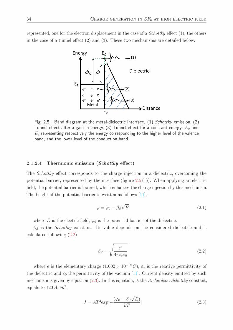
34 Charge generation in SF6 at high electric field
represented, one for the electron displacement in the case of a Schottky effect (1), the others
in the case of a tunnel effect (2) and (3). These two mechanisms are detailed below.
Fig. 2.5: Band diagram at the metal-dielectric interface. (1) Schottky emission, (2)Tunnel effect after a gain in energy, (3) Tunnel effect for a constant energy. Ev andEc representing respectively the energy corresponding to the higher level of the valenceband, and the lower level of the conduction band.
2.1.2.4 Thermionic emission (Schottky effect)
The Schottky effect corresponds to the charge injection in a dielectric, overcoming the
potential barrier, represented by the interface (figure 2.5 (1)). When applying an electric
field, the potential barrier is lowered, which enhances the charge injection by this mechanism.
The height of the potential barrier is written as follows [11],
ϕ = ϕ0 − βS
√E (2.1)
where E is the electric field, ϕ0 is the potential barrier of the dielectric.
βS is the Schottky constant. Its value depends on the considered dielectric and is
calculated following (2.2)
βS =
√
e3
4πεrε0(2.2)
where e is the elementary charge (1.602 × 10⁻¹⁹ C), εr is the relative permittivity of
the dielectric and ε0 the permittivity of the vacuum [11]. Current density emitted by such
mechanism is given by equation (2.3). In this equation, A the Richardson-Schottky constant,
equals to 120A.cm2.
J = AT 2exp[−(ϕ0 − βS
√E)
kT] (2.3)
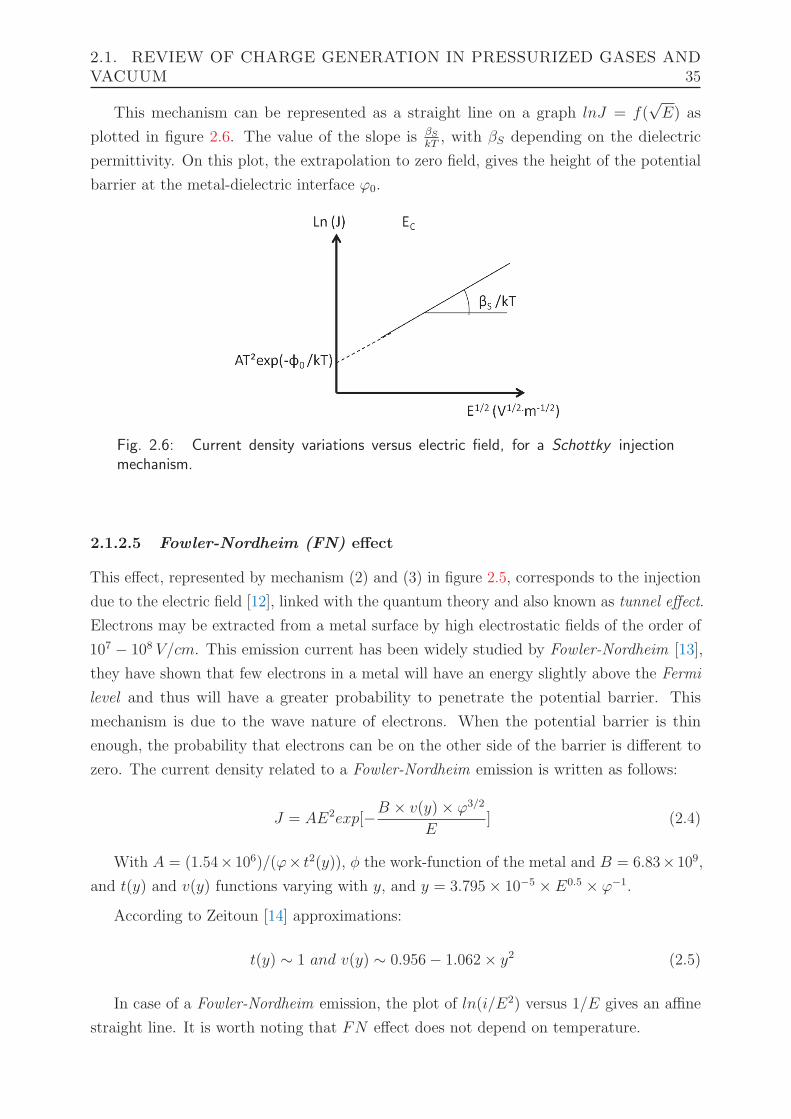
2.1. REVIEW OF CHARGE GENERATION IN PRESSURIZED GASES ANDVACUUM 35
This mechanism can be represented as a straight line on a graph lnJ = f(√E) as
plotted in figure 2.6. The value of the slope is βS
kT, with βS depending on the dielectric
permittivity. On this plot, the extrapolation to zero field, gives the height of the potential
barrier at the metal-dielectric interface ϕ0.
Fig. 2.6: Current density variations versus electric field, for a Schottky injectionmechanism.
2.1.2.5 Fowler-Nordheim (FN) effect
This effect, represented by mechanism (2) and (3) in figure 2.5, corresponds to the injection
due to the electric field [12], linked with the quantum theory and also known as tunnel effect.
Electrons may be extracted from a metal surface by high electrostatic fields of the order of
107 − 108 V/cm. This emission current has been widely studied by Fowler-Nordheim [13],
they have shown that few electrons in a metal will have an energy slightly above the Fermi
level and thus will have a greater probability to penetrate the potential barrier. This
mechanism is due to the wave nature of electrons. When the potential barrier is thin
enough, the probability that electrons can be on the other side of the barrier is different to
zero. The current density related to a Fowler-Nordheim emission is written as follows:
J = AE2exp[−B × v(y)× ϕ3/2
E] (2.4)
With A = (1.54× 10⁶)/(ϕ× t2(y)), φ the work-function of the metal and B = 6.83× 10⁹,
and t(y) and v(y) functions varying with y, and y = 3.795× 10⁻⁵ × E0.5 × ϕ−1.
According to Zeitoun [14] approximations:
t(y) ∼ 1 and v(y) ∼ 0.956− 1.062× y2 (2.5)
In case of a Fowler-Nordheim emission, the plot of ln(i/E2) versus 1/E gives an affine
straight line. It is worth noting that FN effect does not depend on temperature.
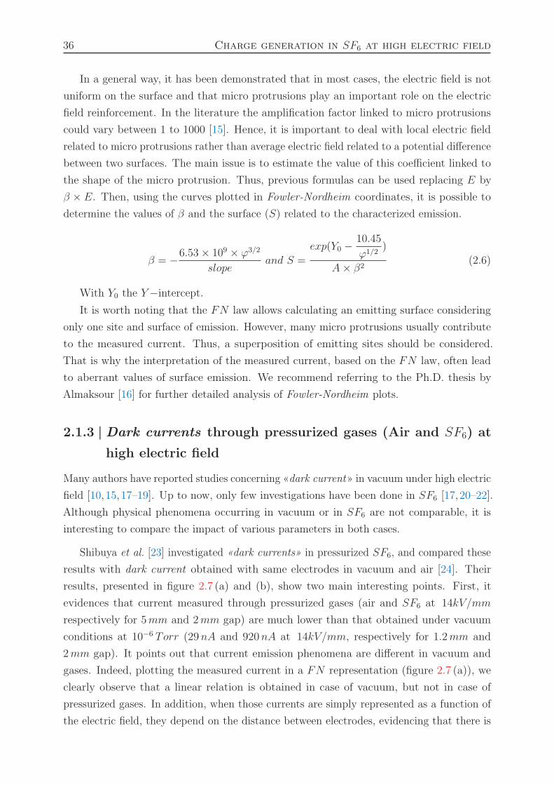
36 Charge generation in SF6 at high electric field
In a general way, it has been demonstrated that in most cases, the electric field is not
uniform on the surface and that micro protrusions play an important role on the electric
field reinforcement. In the literature the amplification factor linked to micro protrusions
could vary between 1 to 1000 [15]. Hence, it is important to deal with local electric field
related to micro protrusions rather than average electric field related to a potential difference
between two surfaces. The main issue is to estimate the value of this coefficient linked to
the shape of the micro protrusion. Thus, previous formulas can be used replacing E by
β × E. Then, using the curves plotted in Fowler-Nordheim coordinates, it is possible to
determine the values of β and the surface (S) related to the characterized emission.
β = −6.53× 10⁹ × ϕ3/2
slopeand S =
exp(Y0 −10.45
ϕ1/2)
A× β2(2.6)
With Y0 the Y−intercept.It is worth noting that the FN law allows calculating an emitting surface considering
only one site and surface of emission. However, many micro protrusions usually contribute
to the measured current. Thus, a superposition of emitting sites should be considered.
That is why the interpretation of the measured current, based on the FN law, often lead
to aberrant values of surface emission. We recommend referring to the Ph.D. thesis by
Almaksour [16] for further detailed analysis of Fowler-Nordheim plots.
2.1.3 | Dark currents through pressurized gases (Air and SF6) at
high electric field
Many authors have reported studies concerning «dark current» in vacuum under high electric
field [10,15,17–19]. Up to now, only few investigations have been done in SF6 [17,20–22].
Although physical phenomena occurring in vacuum or in SF6 are not comparable, it is
interesting to compare the impact of various parameters in both cases.
Shibuya et al. [23] investigated «dark currents» in pressurized SF6, and compared these
results with dark current obtained with same electrodes in vacuum and air [24]. Their
results, presented in figure 2.7 (a) and (b), show two main interesting points. First, it
evidences that current measured through pressurized gases (air and SF6 at 14kV/mm
respectively for 5mm and 2mm gap) are much lower than that obtained under vacuum
conditions at 10−6 Torr (29nA and 920nA at 14kV/mm, respectively for 1.2mm and
2mm gap). It points out that current emission phenomena are different in vacuum and
gases. Indeed, plotting the measured current in a FN representation (figure 2.7 (a)), we
clearly observe that a linear relation is obtained in case of vacuum, but not in case of
pressurized gases. In addition, when those currents are simply represented as a function of
the electric field, they depend on the distance between electrodes, evidencing that there is
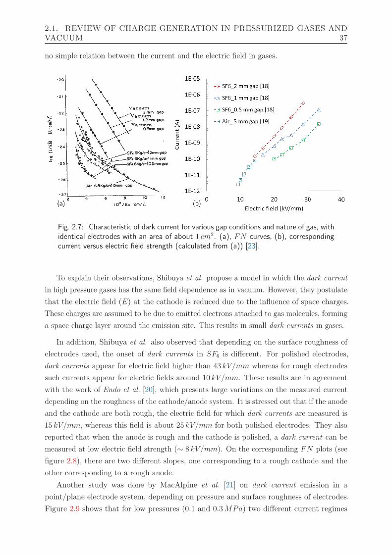
2.1. REVIEW OF CHARGE GENERATION IN PRESSURIZED GASES ANDVACUUM 37
no simple relation between the current and the electric field in gases.
Fig. 2.7: Characteristic of dark current for various gap conditions and nature of gas, withidentical electrodes with an area of about 1 cm2. (a), FN curves, (b), correspondingcurrent versus electric field strength (calculated from (a)) [23].
To explain their observations, Shibuya et al. propose a model in which the dark current
in high pressure gases has the same field dependence as in vacuum. However, they postulate
that the electric field (E) at the cathode is reduced due to the influence of space charges.
These charges are assumed to be due to emitted electrons attached to gas molecules, forming
a space charge layer around the emission site. This results in small dark currents in gases.
In addition, Shibuya et al. also observed that depending on the surface roughness of
electrodes used, the onset of dark currents in SF6 is different. For polished electrodes,
dark currents appear for electric field higher than 43 kV/mm whereas for rough electrodes
such currents appear for electric fields around 10 kV/mm. These results are in agreement
with the work of Endo et al. [20], which presents large variations on the measured current
depending on the roughness of the cathode/anode system. It is stressed out that if the anode
and the cathode are both rough, the electric field for which dark currents are measured is
15 kV/mm, whereas this field is about 25 kV/mm for both polished electrodes. They also
reported that when the anode is rough and the cathode is polished, a dark current can be
measured at low electric field strength (∼ 8 kV/mm). On the corresponding FN plots (see
figure 2.8), there are two different slopes, one corresponding to a rough cathode and the
other corresponding to a rough anode.
Another study was done by MacAlpine et al. [21] on dark current emission in a
point/plane electrode system, depending on pressure and surface roughness of electrodes.
Figure 2.9 shows that for low pressures (0.1 and 0.3MPa) two different current regimes
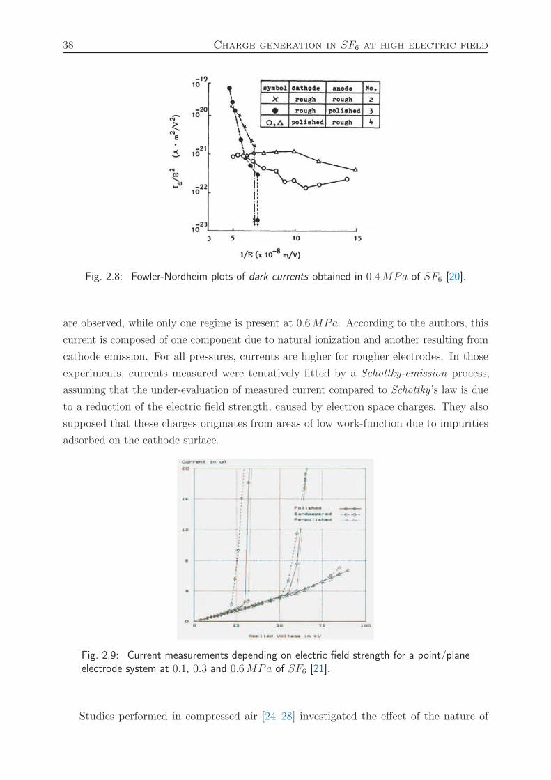
38 Charge generation in SF6 at high electric field
Fig. 2.8: Fowler-Nordheim plots of dark currents obtained in 0.4MPa of SF6 [20].
are observed, while only one regime is present at 0.6MPa. According to the authors, this
current is composed of one component due to natural ionization and another resulting from
cathode emission. For all pressures, currents are higher for rougher electrodes. In those
experiments, currents measured were tentatively fitted by a Schottky-emission process,
assuming that the under-evaluation of measured current compared to Schottky ’s law is due
to a reduction of the electric field strength, caused by electron space charges. They also
supposed that these charges originates from areas of low work-function due to impurities
adsorbed on the cathode surface.
Fig. 2.9: Current measurements depending on electric field strength for a point/planeelectrode system at 0.1, 0.3 and 0.6MPa of SF6 [21].
Studies performed in compressed air [24–28] investigated the effect of the nature of
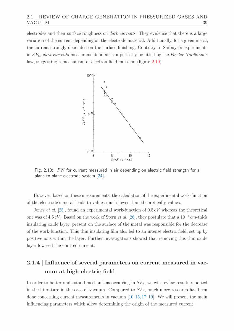
2.1. REVIEW OF CHARGE GENERATION IN PRESSURIZED GASES ANDVACUUM 39
electrodes and their surface roughness on dark currents. They evidence that there is a large
variation of the current depending on the electrode material. Additionally, for a given metal,
the current strongly depended on the surface finishing. Contrary to Shibuya’s experiments
in SF6, dark currents measurements in air can perfectly be fitted by the Fowler-Nordheim’s
law, suggesting a mechanism of electron field emission (figure 2.10).
Fig. 2.10: FN for current measured in air depending on electric field strength for aplane to plane electrode system [24].
However, based on these measurements, the calculation of the experimental work-function
of the electrode’s metal leads to values much lower than theoretically values.
Jones et al. [25], found an experimental work-function of 0.5 eV whereas the theoretical
one was of 4.5 eV . Based on the work of Stern et al. [26], they postulate that a 10−7 cm-thick
insulating oxide layer, present on the surface of the metal was responsible for the decrease
of the work-function. This thin insulating film also led to an intense electric field, set up by
positive ions within the layer. Further investigations showed that removing this thin oxide
layer lowered the emitted current.
2.1.4 | Influence of several parameters on current measured in vac-
uum at high electric field
In order to better understand mechanisms occurring in SF6, we will review results reported
in the literature in the case of vacuum. Compared to SF6, much more research has been
done concerning current measurements in vacuum [10, 15, 17–19]. We will present the main
influencing parameters which allow determining the origin of the measured current.
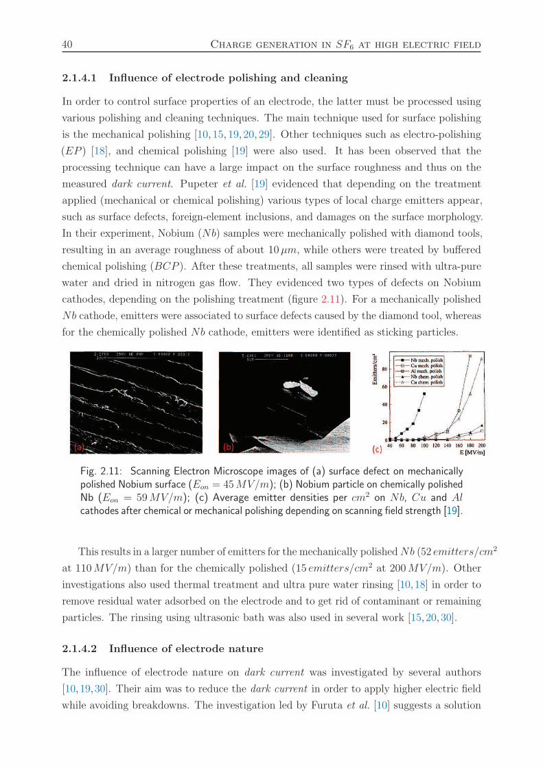
40 Charge generation in SF6 at high electric field
2.1.4.1 Influence of electrode polishing and cleaning
In order to control surface properties of an electrode, the latter must be processed using
various polishing and cleaning techniques. The main technique used for surface polishing
is the mechanical polishing [10, 15, 19, 20, 29]. Other techniques such as electro-polishing
(EP ) [18], and chemical polishing [19] were also used. It has been observed that the
processing technique can have a large impact on the surface roughness and thus on the
measured dark current. Pupeter et al. [19] evidenced that depending on the treatment
applied (mechanical or chemical polishing) various types of local charge emitters appear,
such as surface defects, foreign-element inclusions, and damages on the surface morphology.
In their experiment, Nobium (Nb) samples were mechanically polished with diamond tools,
resulting in an average roughness of about 10µm, while others were treated by buffered
chemical polishing (BCP ). After these treatments, all samples were rinsed with ultra-pure
water and dried in nitrogen gas flow. They evidenced two types of defects on Nobium
cathodes, depending on the polishing treatment (figure 2.11). For a mechanically polished
Nb cathode, emitters were associated to surface defects caused by the diamond tool, whereas
for the chemically polished Nb cathode, emitters were identified as sticking particles.
Fig. 2.11: Scanning Electron Microscope images of (a) surface defect on mechanicallypolished Nobium surface (Eon = 45MV/m); (b) Nobium particle on chemically polishedNb (Eon = 59MV/m); (c) Average emitter densities per cm2 on Nb, Cu and Alcathodes after chemical or mechanical polishing depending on scanning field strength [19].
This results in a larger number of emitters for the mechanically polishedNb (52 emitters/cm2
at 110MV/m) than for the chemically polished (15 emitters/cm2 at 200MV/m). Other
investigations also used thermal treatment and ultra pure water rinsing [10,18] in order to
remove residual water adsorbed on the electrode and to get rid of contaminant or remaining
particles. The rinsing using ultrasonic bath was also used in several work [15,20,30].
2.1.4.2 Influence of electrode nature
The influence of electrode nature on dark current was investigated by several authors
[10, 19, 30]. Their aim was to reduce the dark current in order to apply higher electric field
while avoiding breakdowns. The investigation led by Furuta et al. [10] suggests a solution
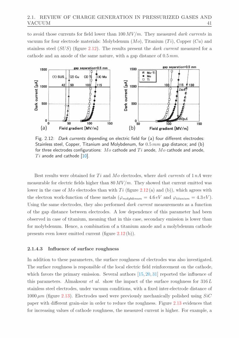
2.1. REVIEW OF CHARGE GENERATION IN PRESSURIZED GASES ANDVACUUM 41
to avoid those currents for field lower than 100MV/m. They measured dark currents in
vacuum for four electrode materials: Molybdenum (Mo), Titanium (T i), Copper (Cu) and
stainless steel (SUS) (figure 2.12). The results present the dark current measured for a
cathode and an anode of the same nature, with a gap distance of 0.5mm.
Fig. 2.12: Dark currents depending on electric field for (a) four different electrodes:Stainless steel, Copper, Titanium and Molybdenum, for 0.5mm gap distance; and (b)for three electrodes configurations: Mo cathode and T i anode, Mo cathode and anode,T i anode and cathode [10].
Best results were obtained for T i and Mo electrodes, where dark currents of 1nA were
measurable for electric fields higher than 80MV/m. They showed that current emitted was
lower in the case of Mo electrodes than with T i (figure 2.12 (a) and (b)), which agrees with
the electron work-function of these metals (ϕmolybdenum = 4.6 eV and ϕtitanium = 4.3 eV ).
Using the same electrodes, they also performed dark current measurements as a function
of the gap distance between electrodes. A low dependence of this parameter had been
observed in case of titanium, meaning that in this case, secondary emission is lower than
for molybdenum. Hence, a combination of a titanium anode and a molybdenum cathode
presents even lower emitted current (figure 2.12 (b)).
2.1.4.3 Influence of surface roughness
In addition to these parameters, the surface roughness of electrodes was also investigated.
The surface roughness is responsible of the local electric field reinforcement on the cathode,
which favors the primary emission. Several authors [15, 20, 31] reported the influence of
this parameters. Almaksour et al. show the impact of the surface roughness for 316L
stainless steel electrodes, under vacuum conditions, with a fixed inter-electrode distance of
1000µm (figure 2.13). Electrodes used were previously mechanically polished using SiC
paper with different grain-size in order to reduce the roughness. Figure 2.13 evidences that
for increasing values of cathode roughness, the measured current is higher. For example, a
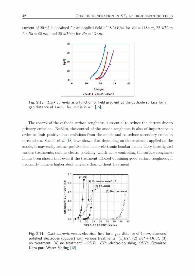
42 Charge generation in SF6 at high electric field
current of 20 pA is obtained for an applied field of 18MV/m for Ra = 118nm, 22MV/m
for Ra = 95nm, and 25MV/m for Ra = 13nm.
Fig. 2.13: Dark currents as a function of field gradient at the cathode surface for agap distance of 1mm. Ra unit is in nm [15].
The control of the cathode surface roughness is essential to reduce the current due to
primary emission. Besides, the control of the anode roughness is also of importance in
order to limit positive ions emissions from the anode and so reduce secondary emission
mechanisms. Suzuki et al. [18] have shown that depending on the treatment applied on the
anode, it may easily release positive ions under electronic bombardment. They investigated
various treatments, such as electro-polishing, which allow controlling the surface roughness.
It has been shown that even if the treatment allowed obtaining good surface roughness, it
frequently induces higher dark currents than without treatment.
Fig. 2.14: Dark currents versus electrical field for a gap distance of 1mm, diamondpolished electrodes (copper) with various treatments: (1)EP , (2) EP + OUR, (3)no treatment, (4) no treatment +OUR. EP : electro-polishing, OUR: OzonizedUltra-pure Water Rinsing [18].
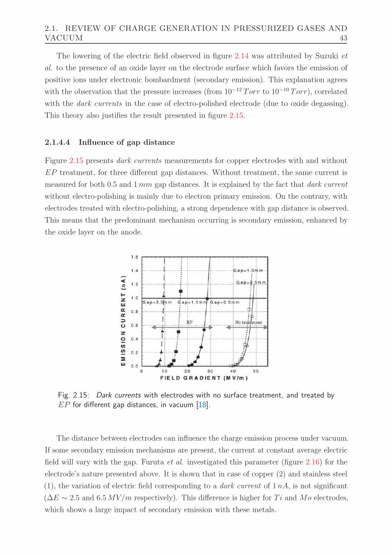
2.1. REVIEW OF CHARGE GENERATION IN PRESSURIZED GASES ANDVACUUM 43
The lowering of the electric field observed in figure 2.14 was attributed by Suzuki et
al. to the presence of an oxide layer on the electrode surface which favors the emission of
positive ions under electronic bombardment (secondary emission). This explanation agrees
with the observation that the pressure increases (from 10−12 Torr to 10−10 Torr), correlated
with the dark currents in the case of electro-polished electrode (due to oxide degassing).
This theory also justifies the result presented in figure 2.15.
2.1.4.4 Influence of gap distance
Figure 2.15 presents dark currents measurements for copper electrodes with and without
EP treatment, for three different gap distances. Without treatment, the same current is
measured for both 0.5 and 1mm gap distances. It is explained by the fact that dark current
without electro-polishing is mainly due to electron primary emission. On the contrary, with
electrodes treated with electro-polishing, a strong dependence with gap distance is observed.
This means that the predominant mechanism occurring is secondary emission, enhanced by
the oxide layer on the anode.
Fig. 2.15: Dark currents with electrodes with no surface treatment, and treated byEP for different gap distances, in vacuum [18].
The distance between electrodes can influence the charge emission process under vacuum.
If some secondary emission mechanisms are present, the current at constant average electric
field will vary with the gap. Furuta et al. investigated this parameter (figure 2.16) for the
electrode’s nature presented above. It is shown that in case of copper (2) and stainless steel
(1), the variation of electric field corresponding to a dark current of 1nA, is not significant
(∆E ∼ 2.5 and 6.5MV/m respectively). This difference is higher for T i and Mo electrodes,
which shows a large impact of secondary emission with these metals.
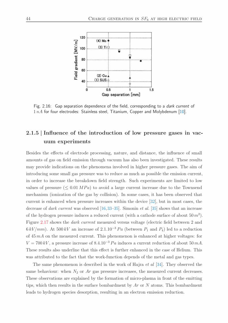
44 Charge generation in SF6 at high electric field
Fig. 2.16: Gap separation dependence of the field, corresponding to a dark current of1nA for four electrodes: Stainless steel, Titanium, Copper and Molybdenum [10].
2.1.5 | Influence of the introduction of low pressure gases in vac-
uum experiments
Besides the effects of electrode processing, nature, and distance, the influence of small
amounts of gas on field emission through vacuum has also been investigated. These results
may provide indications on the phenomena involved in higher pressure gases. The aim of
introducing some small gas pressure was to reduce as much as possible the emission current,
in order to increase the breakdown field strength. Such experiments are limited to low
values of pressure (≤ 0.01MPa) to avoid a large current increase due to the Townsend
mechanism (ionization of the gas by collision). In some cases, it has been observed that
current is enhanced when pressure increases within the device [32], but in most cases, the
decrease of dark current was observed [16,33–35]. Simonin et al. [35] shows that an increase
of the hydrogen pressure induces a reduced current (with a cathode surface of about 50m2).
Figure 2.17 shows the dark current measured versus voltage (electric field between 2 and
6 kV/mm). At 500 kV an increase of 2.1.10−3 Pa (between P1 and P4) led to a reduction
of 45mA on the measured current. This phenomenon is enhanced at higher voltages: for
V = 700 kV , a pressure increase of 8.4.10−3 Pa induces a current reduction of about 50mA.
These results also underline that this effect is further enhanced in the case of Helium. This
was attributed to the fact that the work-function depends of the metal and gas types.
The same phenomenon is described in the work of Hajra et al [34]. They observed the
same behaviour: when N2 or Ar gas pressure increases, the measured current decreases.
These observations are explained by the formation of micro-plasma in front of the emitting
tips, which then results in the surface bombardment by Ar or N atoms. This bombardment
leads to hydrogen species desorption, resulting in an electron emission reduction.
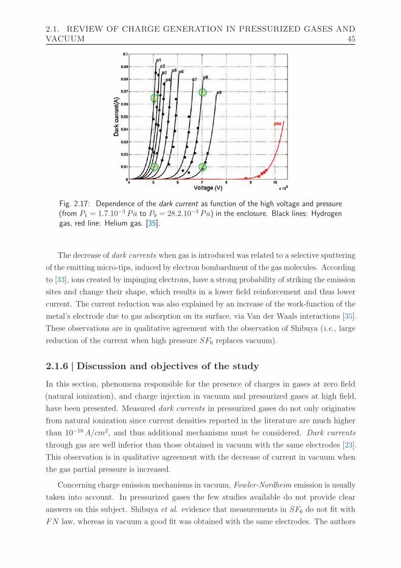
2.1. REVIEW OF CHARGE GENERATION IN PRESSURIZED GASES ANDVACUUM 45
Fig. 2.17: Dependence of the dark current as function of the high voltage and pressure(from P1 = 1.7.10−3 Pa to P9 = 28.2.10−3 Pa) in the enclosure. Black lines: Hydrogengas, red line: Helium gas. [35].
The decrease of dark currents when gas is introduced was related to a selective sputtering
of the emitting micro-tips, induced by electron bombardment of the gas molecules. According
to [33], ions created by impinging electrons, have a strong probability of striking the emission
sites and change their shape, which results in a lower field reinforcement and thus lower
current. The current reduction was also explained by an increase of the work-function of the
metal’s electrode due to gas adsorption on its surface, via Van der Waals interactions [35].
These observations are in qualitative agreement with the observation of Shibuya (i.e., large
reduction of the current when high pressure SF6 replaces vacuum).
2.1.6 | Discussion and objectives of the study
In this section, phenomena responsible for the presence of charges in gases at zero field
(natural ionization), and charge injection in vacuum and pressurized gases at high field,
have been presented. Measured dark currents in pressurized gases do not only originates
from natural ionization since current densities reported in the literature are much higher
than 10−18 A/cm2, and thus additional mechanisms must be considered. Dark currents
through gas are well inferior than those obtained in vacuum with the same electrodes [23].
This observation is in qualitative agreement with the decrease of current in vacuum when
the gas partial pressure is increased.
Concerning charge emission mechanisms in vacuum, Fowler-Nordheim emission is usually
taken into account. In pressurized gases the few studies available do not provide clear
answers on this subject. Shibuya et al. evidence that measurements in SF6 do not fit with
FN law, whereas in vacuum a good fit was obtained with the same electrodes. The authors
46 Charge generation in SF6 at high electric field
suppose that a space charge layer close to the electrode surface, leads to a modified emission
law. Another proposition, by MacAlpine et al. consists in applying a Schottky fit, and also
considering the presence of space charges. The last one, developed by Stern et al., and
re-used by Jones et al. in air, states that the dark current follows a FN injection process,
considering a thin insulating layer (of unknown nature) on the cathode surface. The latter
gets a large surface charge of positive ions, leads to lower «apparent» metal work-function,
and thus to a better FN fit of data.
As in vacuum, the influence of electrode surface roughness was observed in pressurized
air and SF6 (i.e., the current increases with the electrode roughness).
To get a better understanding of mechanisms occurring in SF6 in conditions relevant to
HVDC GIS, many additional investigations should be performed, concerning the influence
of several parameters:
- The gas pressure: this parameter has not been investigated in pressurized gases yet.
- The gap distance and applied electric field: the results of Shibuya et al. (figure 2.7)
show a large increase of current at constant electric field when the gap is increased (more
than one decade between 0.5 and 2mm). Experiments must be carried out in conditions
relevant of HVDC GIS, i.e., at much larger distances (several centimeters) and lower electric
fields (a few kV/mm).
- The polarity: experiments presented so far were only performed in negative polarity.
Measurements should be realized in positive polarity.
- The temperature: this parameter was not investigated, neither in vacuum nor in gases.
- The electrode roughness: typical surface roughness in real GIS applications are in the
range of Ra = 3µm.
- The gas purity: industrial gases are not of very high purity, and may contain other gases
(up to about 2%), and some water (a dew point of approximately −27 C corresponding to
3% relative humidity RH at atmospheric pressure is acceptable).
To perform measurements, we have developed two specific devices which allow measuring
currents with low noise level at high voltages, in two different electrodes configurations.
2.2 | Experimental systems
Two experimental devices have been built to perform dark current measurements in two
different electric field configurations: a small scale coaxial geometry, and a larger scale
parallel-plate electrodes system, with dimensions close to those of the real application.
Measurement of very low currents (down to 0.1 pA) at high voltage (up to 250 kV ) was
especially challenging, and required great care to reduce measurement noise, and protect
electrometers against breakdown.
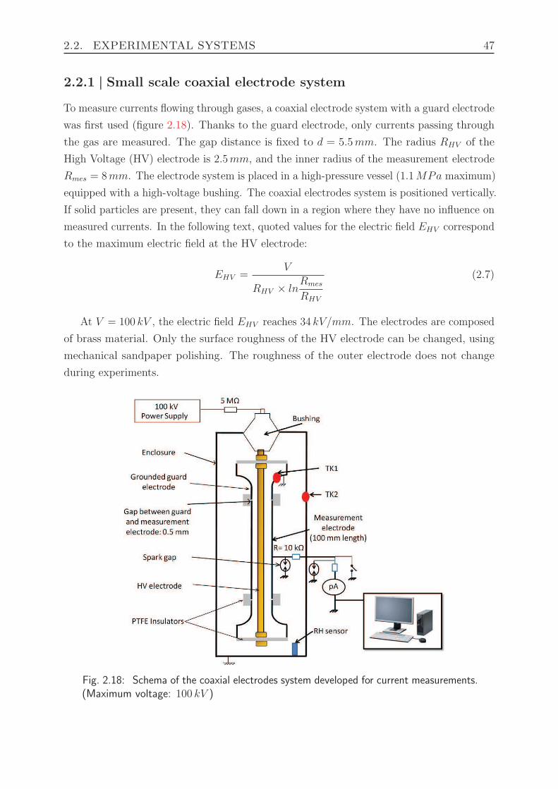
2.2. EXPERIMENTAL SYSTEMS 47
2.2.1 | Small scale coaxial electrode system
To measure currents flowing through gases, a coaxial electrode system with a guard electrode
was first used (figure 2.18). Thanks to the guard electrode, only currents passing through
the gas are measured. The gap distance is fixed to d = 5.5mm. The radius RHV of the
High Voltage (HV) electrode is 2.5mm, and the inner radius of the measurement electrode
Rmes = 8mm. The electrode system is placed in a high-pressure vessel (1.1MPa maximum)
equipped with a high-voltage bushing. The coaxial electrodes system is positioned vertically.
If solid particles are present, they can fall down in a region where they have no influence on
measured currents. In the following text, quoted values for the electric field EHV correspond
to the maximum electric field at the HV electrode:
EHV =V
RHV × lnRmes
RHV
(2.7)
At V = 100 kV , the electric field EHV reaches 34 kV/mm. The electrodes are composed
of brass material. Only the surface roughness of the HV electrode can be changed, using
mechanical sandpaper polishing. The roughness of the outer electrode does not change
during experiments.
Fig. 2.18: Schema of the coaxial electrodes system developed for current measurements.(Maximum voltage: 100 kV )
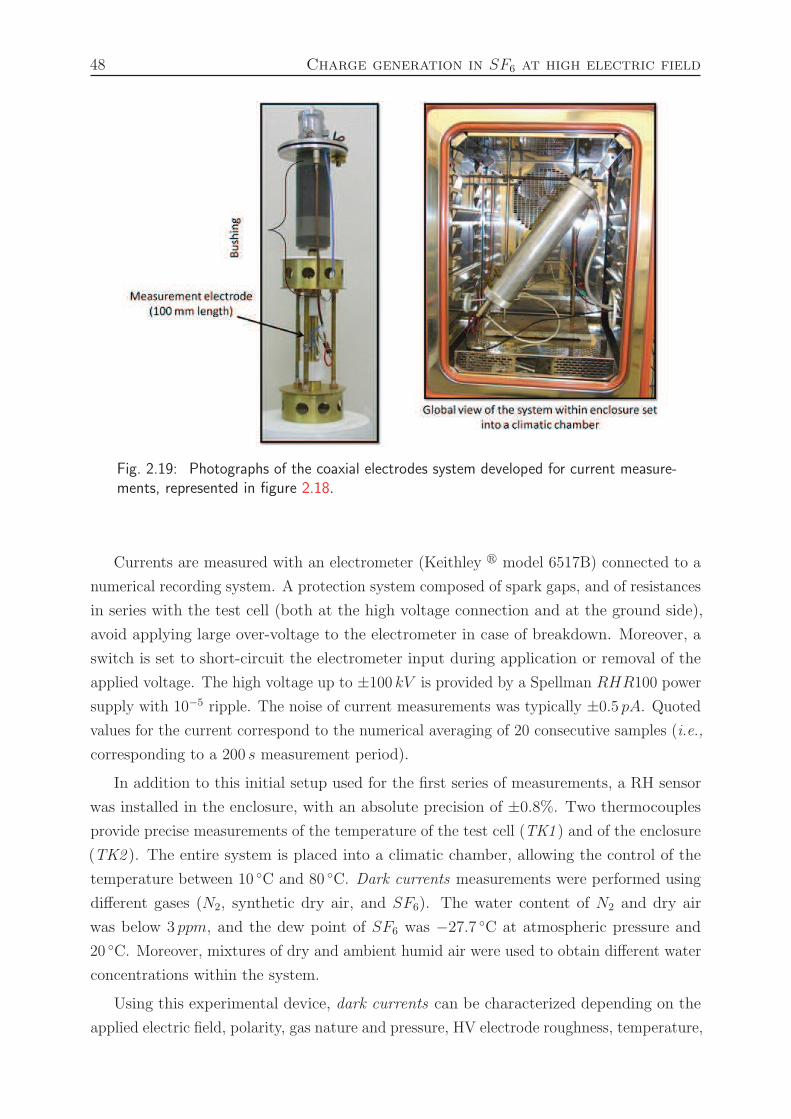
48 Charge generation in SF6 at high electric field
Fig. 2.19: Photographs of the coaxial electrodes system developed for current measure-ments, represented in figure 2.18.
Currents are measured with an electrometer (Keithley r model 6517B) connected to a
numerical recording system. A protection system composed of spark gaps, and of resistances
in series with the test cell (both at the high voltage connection and at the ground side),
avoid applying large over-voltage to the electrometer in case of breakdown. Moreover, a
switch is set to short-circuit the electrometer input during application or removal of the
applied voltage. The high voltage up to ±100 kV is provided by a Spellman RHR100 power
supply with 10−5 ripple. The noise of current measurements was typically ±0.5 pA. Quoted
values for the current correspond to the numerical averaging of 20 consecutive samples (i.e.,
corresponding to a 200 s measurement period).
In addition to this initial setup used for the first series of measurements, a RH sensor
was installed in the enclosure, with an absolute precision of ±0.8%. Two thermocouples
provide precise measurements of the temperature of the test cell (TK1 ) and of the enclosure
(TK2 ). The entire system is placed into a climatic chamber, allowing the control of the
temperature between 10 C and 80 C. Dark currents measurements were performed using
different gases (N2, synthetic dry air, and SF6). The water content of N2 and dry air
was below 3 ppm, and the dew point of SF6 was −27.7 C at atmospheric pressure and
20 C. Moreover, mixtures of dry and ambient humid air were used to obtain different water
concentrations within the system.
Using this experimental device, dark currents can be characterized depending on the
applied electric field, polarity, gas nature and pressure, HV electrode roughness, temperature,
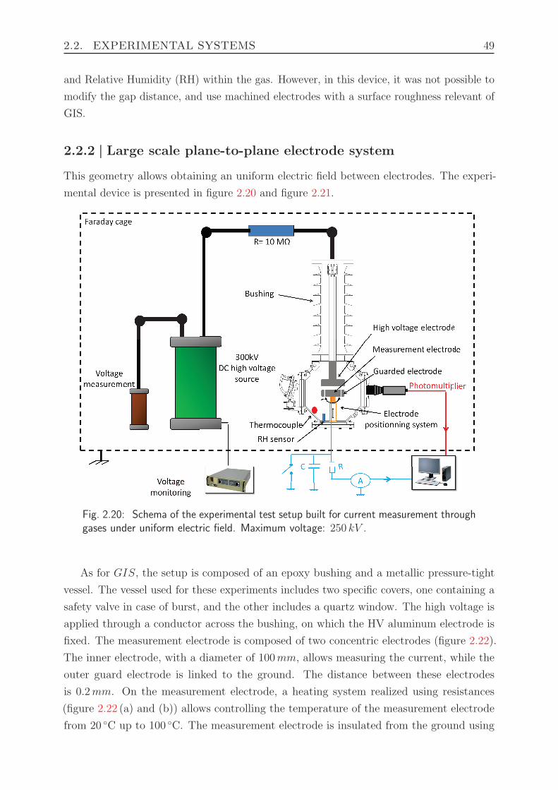
2.2. EXPERIMENTAL SYSTEMS 49
and Relative Humidity (RH) within the gas. However, in this device, it was not possible to
modify the gap distance, and use machined electrodes with a surface roughness relevant of
GIS.
2.2.2 | Large scale plane-to-plane electrode system
This geometry allows obtaining an uniform electric field between electrodes. The experi-
mental device is presented in figure 2.20 and figure 2.21.
Fig. 2.20: Schema of the experimental test setup built for current measurement throughgases under uniform electric field. Maximum voltage: 250 kV .
As for GIS, the setup is composed of an epoxy bushing and a metallic pressure-tight
vessel. The vessel used for these experiments includes two specific covers, one containing a
safety valve in case of burst, and the other includes a quartz window. The high voltage is
applied through a conductor across the bushing, on which the HV aluminum electrode is
fixed. The measurement electrode is composed of two concentric electrodes (figure 2.22).
The inner electrode, with a diameter of 100mm, allows measuring the current, while the
outer guard electrode is linked to the ground. The distance between these electrodes
is 0.2mm. On the measurement electrode, a heating system realized using resistances
(figure 2.22 (a) and (b)) allows controlling the temperature of the measurement electrode
from 20 C up to 100 C. The measurement electrode is insulated from the ground using
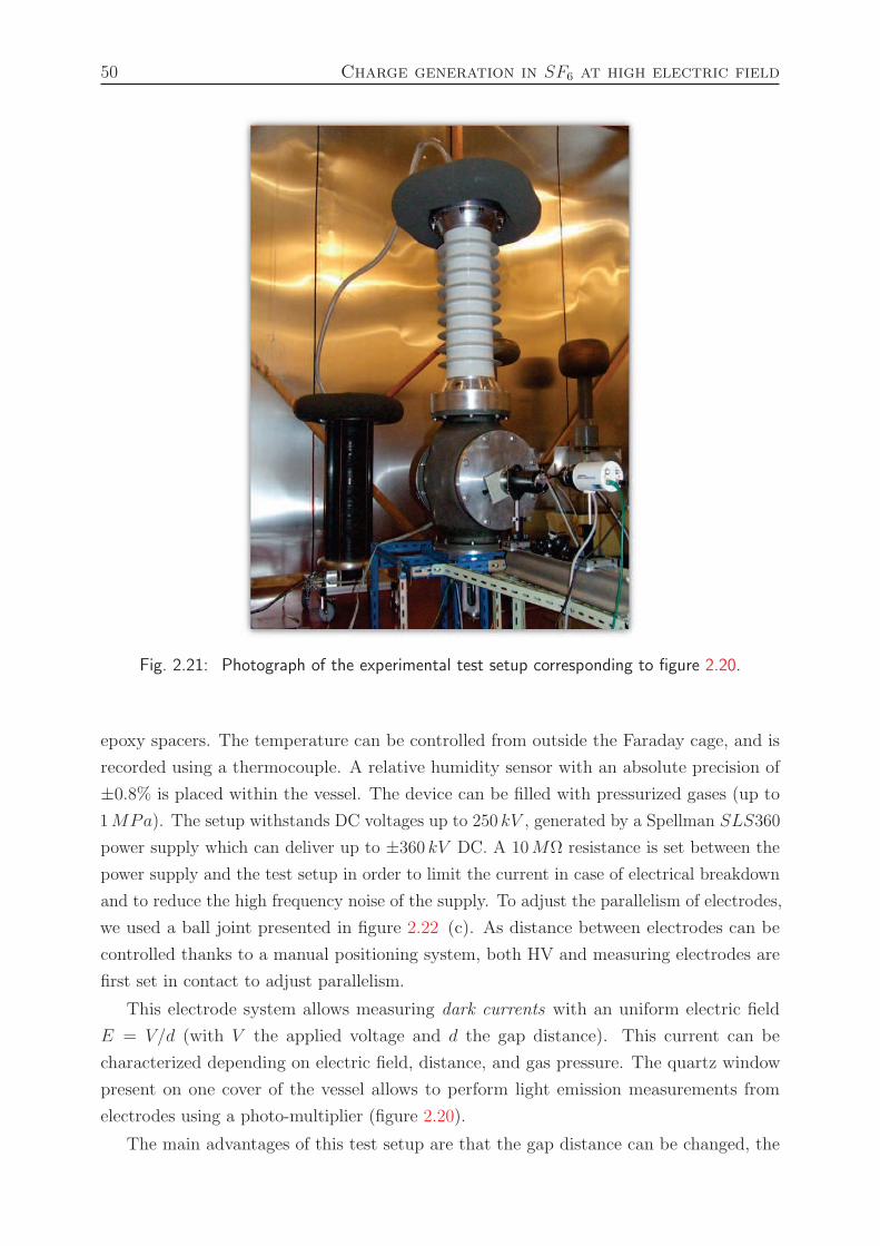
50 Charge generation in SF6 at high electric field
Fig. 2.21: Photograph of the experimental test setup corresponding to figure 2.20.
epoxy spacers. The temperature can be controlled from outside the Faraday cage, and is
recorded using a thermocouple. A relative humidity sensor with an absolute precision of
±0.8% is placed within the vessel. The device can be filled with pressurized gases (up to
1MPa). The setup withstands DC voltages up to 250 kV , generated by a Spellman SLS360
power supply which can deliver up to ±360 kV DC. A 10MΩ resistance is set between the
power supply and the test setup in order to limit the current in case of electrical breakdown
and to reduce the high frequency noise of the supply. To adjust the parallelism of electrodes,
we used a ball joint presented in figure 2.22 (c). As distance between electrodes can be
controlled thanks to a manual positioning system, both HV and measuring electrodes are
first set in contact to adjust parallelism.
This electrode system allows measuring dark currents with an uniform electric field
E = V/d (with V the applied voltage and d the gap distance). This current can be
characterized depending on electric field, distance, and gas pressure. The quartz window
present on one cover of the vessel allows to perform light emission measurements from
electrodes using a photo-multiplier (figure 2.20).
The main advantages of this test setup are that the gap distance can be changed, the
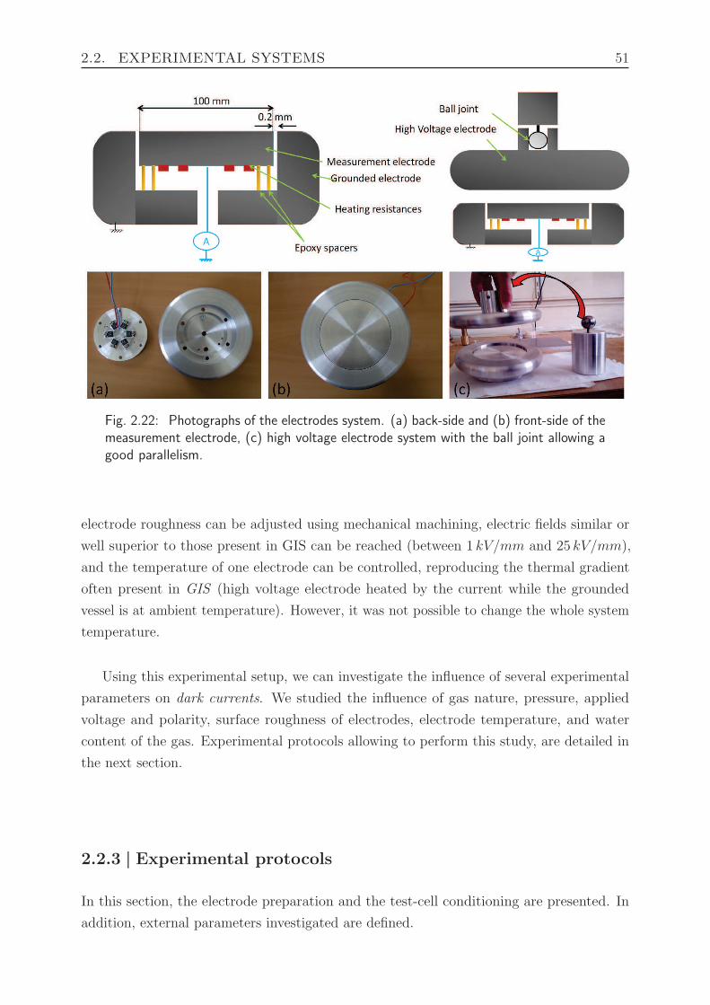
2.2. EXPERIMENTAL SYSTEMS 51
Fig. 2.22: Photographs of the electrodes system. (a) back-side and (b) front-side of themeasurement electrode, (c) high voltage electrode system with the ball joint allowing agood parallelism.
electrode roughness can be adjusted using mechanical machining, electric fields similar or
well superior to those present in GIS can be reached (between 1 kV/mm and 25 kV/mm),
and the temperature of one electrode can be controlled, reproducing the thermal gradient
often present in GIS (high voltage electrode heated by the current while the grounded
vessel is at ambient temperature). However, it was not possible to change the whole system
temperature.
Using this experimental setup, we can investigate the influence of several experimental
parameters on dark currents. We studied the influence of gas nature, pressure, applied
voltage and polarity, surface roughness of electrodes, electrode temperature, and water
content of the gas. Experimental protocols allowing to perform this study, are detailed in
the next section.
2.2.3 | Experimental protocols
In this section, the electrode preparation and the test-cell conditioning are presented. In
addition, external parameters investigated are defined.
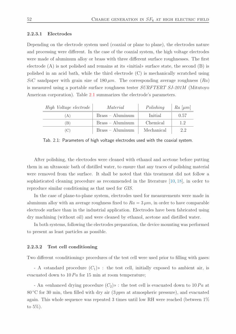
52 Charge generation in SF6 at high electric field
2.2.3.1 Electrodes
Depending on the electrode system used (coaxial or plane to plane), the electrodes nature
and processing were different. In the case of the coaxial system, the high voltage electrodes
were made of aluminum alloy or brass with three different surface roughnesses. The first
electrode (A) is not polished and remains at its «initial» surface state, the second (B) is
polished in an acid bath, while the third electrode (C) is mechanically scratched using
SiC sandpaper with grain size of 180µm. The corresponding average roughness (Ra)
is measured using a portable surface roughness tester SURFTERT SJ-201M (Mitutoyo
American corporation). Table 2.1 summarizes the electrode’s parameters.
High Voltage electrode Material Polishing Ra [µm]
(A) Brass – Aluminum Initial 0.57
(B) Brass – Aluminum Chemical 1.2
(C) Brass – Aluminum Mechanical 2.2
Tab. 2.1: Parameters of high voltage electrodes used with the coaxial system.
After polishing, the electrodes were cleaned with ethanol and acetone before putting
them in an ultrasonic bath of distilled water, to ensure that any traces of polishing material
were removed from the surface. It shall be noted that this treatment did not follow a
sophisticated cleaning procedure as recommended in the literature [10, 18], in order to
reproduce similar conditioning as that used for GIS.
In the case of plane-to-plane system, electrodes used for measurements were made in
aluminum alloy with an average roughness fixed to Ra = 3µm, in order to have comparable
electrode surface than in the industrial application. Electrodes have been fabricated using
dry machining (without oil) and were cleaned by ethanol, acetone and distilled water.
In both systems, following the electrodes preparation, the device mounting was performed
to present as least particles as possible.
2.2.3.2 Test cell conditioning
Two different «conditioning» procedures of the test cell were used prior to filling with gases:
- A «standard procedure (C1)» : the test cell, initially exposed to ambient air, is
evacuated down to 10Pa for 15 min at room temperature;
- An «enhanced drying procedure (C2)» : the test cell is evacuated down to 10Pa at
80 C for 30 min, then filled with dry air (3 ppm at atmospheric pressure), and evacuated
again. This whole sequence was repeated 3 times until low RH were reached (between 1%
to 5%).
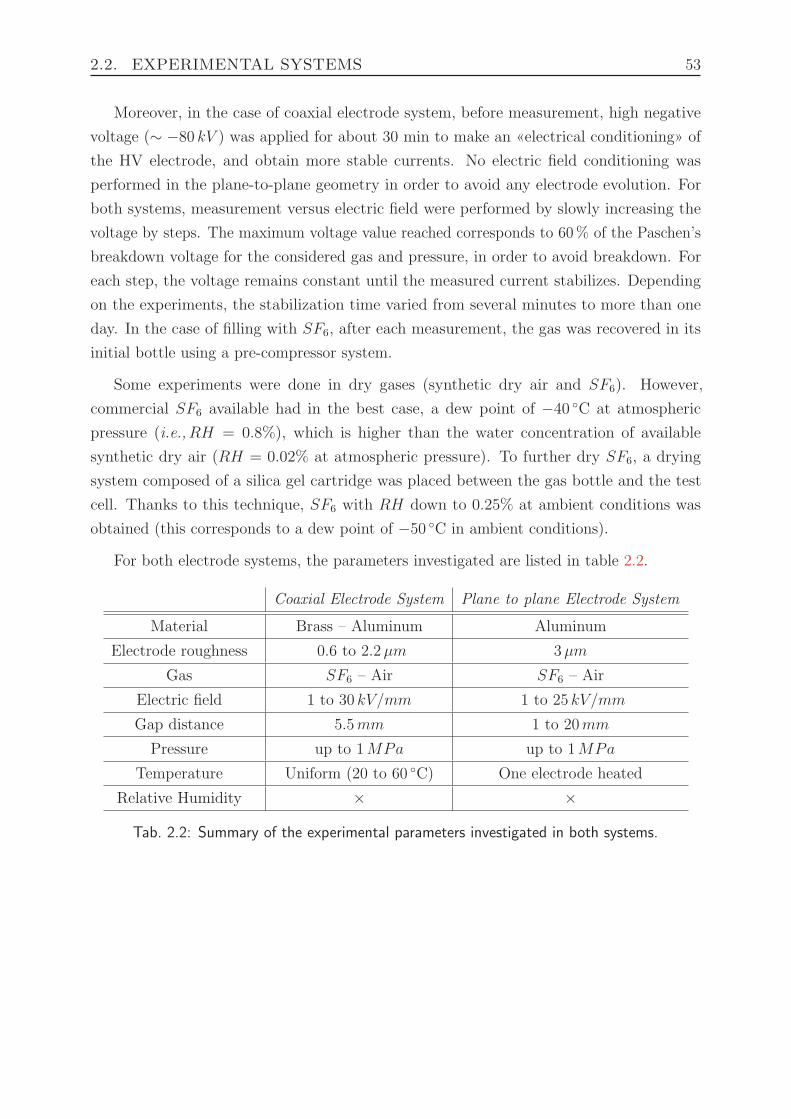
2.2. EXPERIMENTAL SYSTEMS 53
Moreover, in the case of coaxial electrode system, before measurement, high negative
voltage (∼ −80 kV ) was applied for about 30 min to make an «electrical conditioning» of
the HV electrode, and obtain more stable currents. No electric field conditioning was
performed in the plane-to-plane geometry in order to avoid any electrode evolution. For
both systems, measurement versus electric field were performed by slowly increasing the
voltage by steps. The maximum voltage value reached corresponds to 60% of the Paschen’s
breakdown voltage for the considered gas and pressure, in order to avoid breakdown. For
each step, the voltage remains constant until the measured current stabilizes. Depending
on the experiments, the stabilization time varied from several minutes to more than one
day. In the case of filling with SF6, after each measurement, the gas was recovered in its
initial bottle using a pre-compressor system.
Some experiments were done in dry gases (synthetic dry air and SF6). However,
commercial SF6 available had in the best case, a dew point of −40 C at atmospheric
pressure (i.e.,RH = 0.8%), which is higher than the water concentration of available
synthetic dry air (RH = 0.02% at atmospheric pressure). To further dry SF6, a drying
system composed of a silica gel cartridge was placed between the gas bottle and the test
cell. Thanks to this technique, SF6 with RH down to 0.25% at ambient conditions was
obtained (this corresponds to a dew point of −50 C in ambient conditions).
For both electrode systems, the parameters investigated are listed in table 2.2.
Coaxial Electrode System Plane to plane Electrode System
Material Brass – Aluminum Aluminum
Electrode roughness 0.6 to 2.2µm 3µm
Gas SF6 – Air SF6 – Air
Electric field 1 to 30 kV/mm 1 to 25 kV/mm
Gap distance 5.5mm 1 to 20mm
Pressure up to 1MPa up to 1MPa
Temperature Uniform (20 to 60 C) One electrode heated
Relative Humidity × ×
Tab. 2.2: Summary of the experimental parameters investigated in both systems.
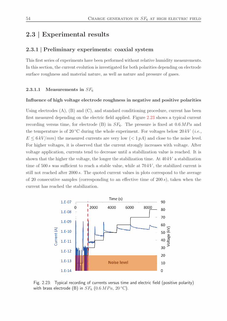
54 Charge generation in SF6 at high electric field
2.3 | Experimental results
2.3.1 | Preliminary experiments: coaxial system
This first series of experiments have been performed without relative humidity measurements.
In this section, the current evolution is investigated for both polarities depending on electrode
surface roughness and material nature, as well as nature and pressure of gases.
2.3.1.1 Measurements in SF6
Influence of high voltage electrode roughness in negative and positive polarities
Using electrodes (A), (B) and (C), and standard conditioning procedure, current has been
first measured depending on the electric field applied. Figure 2.23 shows a typical current
recording versus time, for electrode (B) in SF6. The pressure is fixed at 0.6MPa and
the temperature is of 20 C during the whole experiment. For voltages below 20 kV (i.e.,
E ≤ 6 kV/mm) the measured currents are very low (< 1 pA) and close to the noise level.
For higher voltages, it is observed that the current strongly increases with voltage. After
voltage application, currents tend to decrease until a stabilization value is reached. It is
shown that the higher the voltage, the longer the stabilization time. At 40 kV a stabilization
time of 500 s was sufficient to reach a stable value, while at 70 kV , the stabilized current is
still not reached after 2000 s. The quoted current values in plots correspond to the average
of 20 consecutive samples (corresponding to an effective time of 200 s), taken when the
current has reached the stabilization.
Fig. 2.23: Typical recording of currents versus time and electric field (positive polarity)with brass electrode (B) in SF6 (0.6MPa, 20 C).
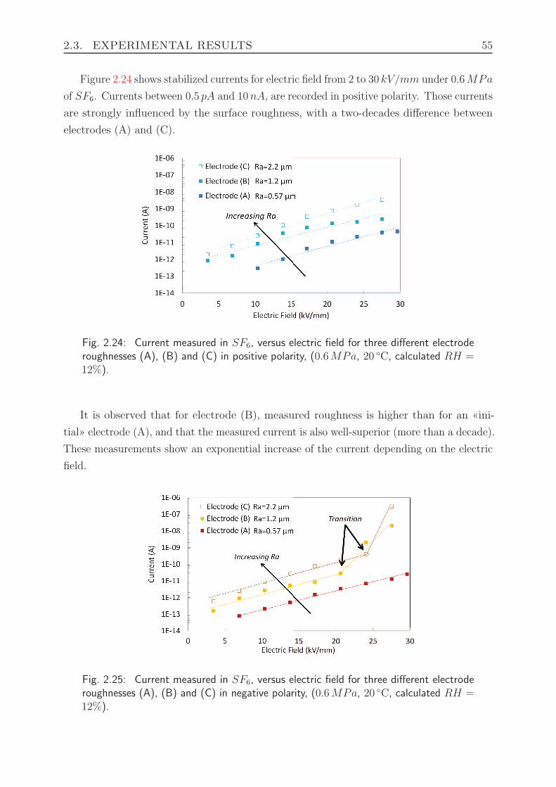
2.3. EXPERIMENTAL RESULTS 55
Figure 2.24 shows stabilized currents for electric field from 2 to 30 kV/mm under 0.6MPa
of SF6. Currents between 0.5 pA and 10nA, are recorded in positive polarity. Those currents
are strongly influenced by the surface roughness, with a two-decades difference between
electrodes (A) and (C).
Fig. 2.24: Current measured in SF6, versus electric field for three different electroderoughnesses (A), (B) and (C) in positive polarity, (0.6MPa, 20 C, calculated RH =12%).
It is observed that for electrode (B), measured roughness is higher than for an «ini-
tial» electrode (A), and that the measured current is also well-superior (more than a decade).
These measurements show an exponential increase of the current depending on the electric
field.
Fig. 2.25: Current measured in SF6, versus electric field for three different electroderoughnesses (A), (B) and (C) in negative polarity, (0.6MPa, 20 C, calculated RH =12%).
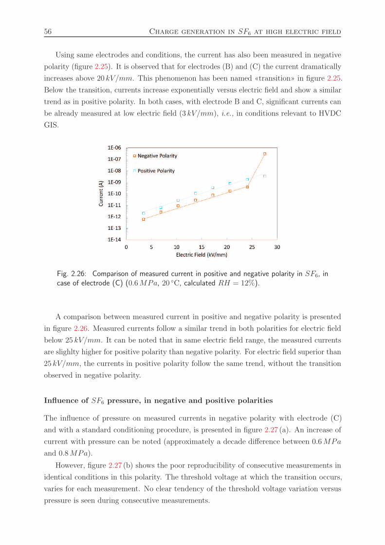
56 Charge generation in SF6 at high electric field
Using same electrodes and conditions, the current has also been measured in negative
polarity (figure 2.25). It is observed that for electrodes (B) and (C) the current dramatically
increases above 20 kV/mm. This phenomenon has been named «transition» in figure 2.25.
Below the transition, currents increase exponentially versus electric field and show a similar
trend as in positive polarity. In both cases, with electrode B and C, significant currents can
be already measured at low electric field (3 kV/mm), i.e., in conditions relevant to HVDC
GIS.
Fig. 2.26: Comparison of measured current in positive and negative polarity in SF6, incase of electrode (C) (0.6MPa, 20 C, calculated RH = 12%).
A comparison between measured current in positive and negative polarity is presented
in figure 2.26. Measured currents follow a similar trend in both polarities for electric field
below 25 kV/mm. It can be noted that in same electric field range, the measured currents
are slighlty higher for positive polarity than negative polarity. For electric field superior than
25 kV/mm, the currents in positive polarity follow the same trend, without the transition
observed in negative polarity.
Influence of SF6 pressure, in negative and positive polarities
The influence of pressure on measured currents in negative polarity with electrode (C)
and with a standard conditioning procedure, is presented in figure 2.27 (a). An increase of
current with pressure can be noted (approximately a decade difference between 0.6MPa
and 0.8MPa).
However, figure 2.27 (b) shows the poor reproducibility of consecutive measurements in
identical conditions in this polarity. The threshold voltage at which the transition occurs,
varies for each measurement. No clear tendency of the threshold voltage variation versus
pressure is seen during consecutive measurements.
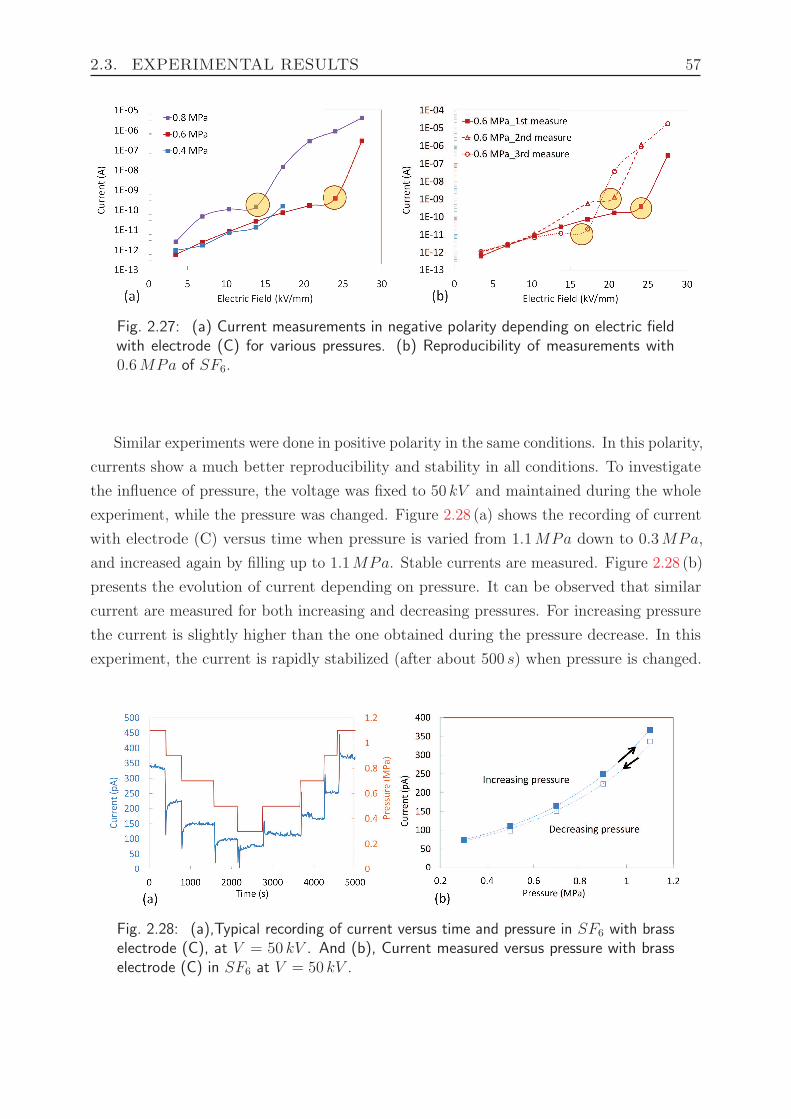
2.3. EXPERIMENTAL RESULTS 57
Fig. 2.27: (a) Current measurements in negative polarity depending on electric fieldwith electrode (C) for various pressures. (b) Reproducibility of measurements with0.6MPa of SF6.
Similar experiments were done in positive polarity in the same conditions. In this polarity,
currents show a much better reproducibility and stability in all conditions. To investigate
the influence of pressure, the voltage was fixed to 50 kV and maintained during the whole
experiment, while the pressure was changed. Figure 2.28 (a) shows the recording of current
with electrode (C) versus time when pressure is varied from 1.1MPa down to 0.3MPa,
and increased again by filling up to 1.1MPa. Stable currents are measured. Figure 2.28 (b)
presents the evolution of current depending on pressure. It can be observed that similar
current are measured for both increasing and decreasing pressures. For increasing pressure
the current is slightly higher than the one obtained during the pressure decrease. In this
experiment, the current is rapidly stabilized (after about 500 s) when pressure is changed.
Fig. 2.28: (a),Typical recording of current versus time and pressure in SF6 with brasselectrode (C), at V = 50 kV . And (b), Current measured versus pressure with brasselectrode (C) in SF6 at V = 50 kV .
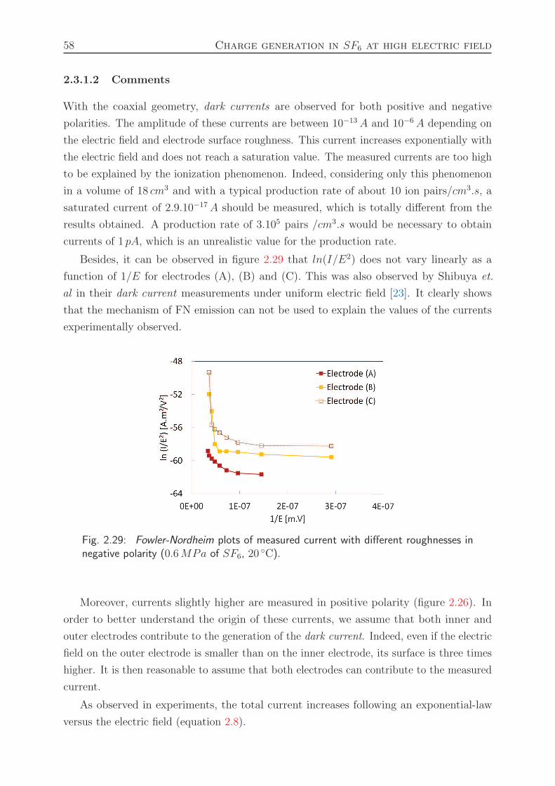
58 Charge generation in SF6 at high electric field
2.3.1.2 Comments
With the coaxial geometry, dark currents are observed for both positive and negative
polarities. The amplitude of these currents are between 10−13 A and 10−6 A depending on
the electric field and electrode surface roughness. This current increases exponentially with
the electric field and does not reach a saturation value. The measured currents are too high
to be explained by the ionization phenomenon. Indeed, considering only this phenomenon
in a volume of 18 cm3 and with a typical production rate of about 10 ion pairs/cm3.s, a
saturated current of 2.9.10−17 A should be measured, which is totally different from the
results obtained. A production rate of 3.105 pairs /cm3.s would be necessary to obtain
currents of 1 pA, which is an unrealistic value for the production rate.
Besides, it can be observed in figure 2.29 that ln(I/E2) does not vary linearly as a
function of 1/E for electrodes (A), (B) and (C). This was also observed by Shibuya et.
al in their dark current measurements under uniform electric field [23]. It clearly shows
that the mechanism of FN emission can not be used to explain the values of the currents
experimentally observed.
Fig. 2.29: Fowler-Nordheim plots of measured current with different roughnesses innegative polarity (0.6MPa of SF6, 20
C).
Moreover, currents slightly higher are measured in positive polarity (figure 2.26). In
order to better understand the origin of these currents, we assume that both inner and
outer electrodes contribute to the generation of the dark current. Indeed, even if the electric
field on the outer electrode is smaller than on the inner electrode, its surface is three times
higher. It is then reasonable to assume that both electrodes can contribute to the measured
current.
As observed in experiments, the total current increases following an exponential-law
versus the electric field (equation 2.8).
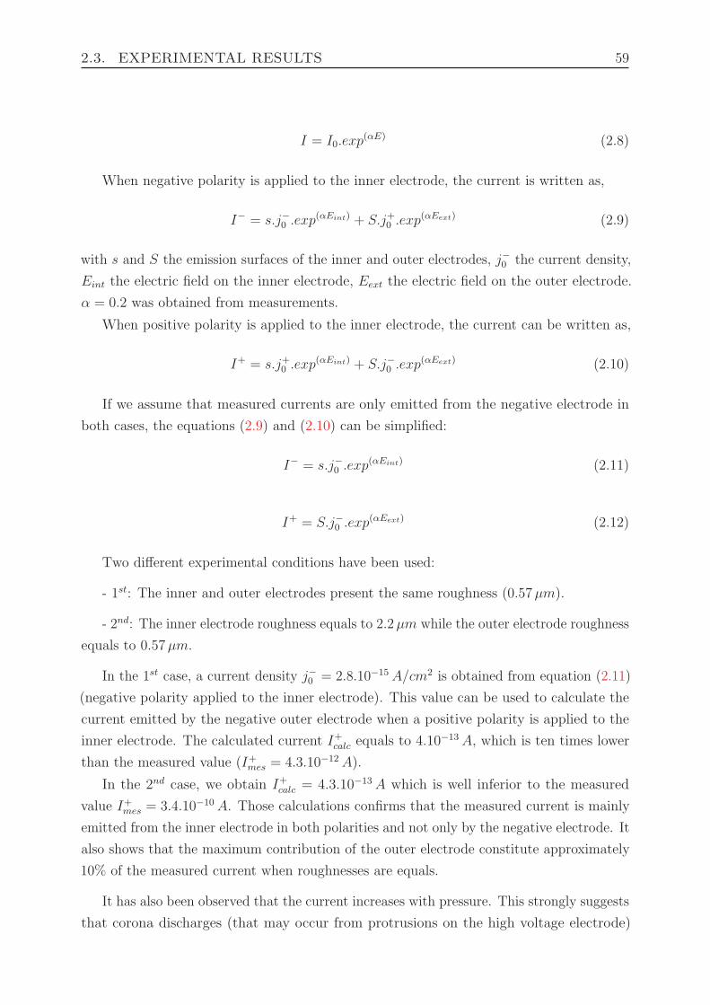
2.3. EXPERIMENTAL RESULTS 59
I = I0.exp(αE) (2.8)
When negative polarity is applied to the inner electrode, the current is written as,
I− = s.j−0 .exp(αEint) + S.j+0 .exp
(αEext) (2.9)
with s and S the emission surfaces of the inner and outer electrodes, j−0 the current density,
Eint the electric field on the inner electrode, Eext the electric field on the outer electrode.
α = 0.2 was obtained from measurements.
When positive polarity is applied to the inner electrode, the current can be written as,
I+ = s.j+0 .exp(αEint) + S.j−0 .exp
(αEext) (2.10)
If we assume that measured currents are only emitted from the negative electrode in
both cases, the equations (2.9) and (2.10) can be simplified:
I− = s.j−0 .exp(αEint) (2.11)
I+ = S.j−0 .exp(αEext) (2.12)
Two different experimental conditions have been used:
- 1st: The inner and outer electrodes present the same roughness (0.57µm).
- 2nd: The inner electrode roughness equals to 2.2µm while the outer electrode roughness
equals to 0.57µm.
In the 1st case, a current density j−0 = 2.8.10−15 A/cm2 is obtained from equation (2.11)
(negative polarity applied to the inner electrode). This value can be used to calculate the
current emitted by the negative outer electrode when a positive polarity is applied to the
inner electrode. The calculated current I+calc equals to 4.10−13 A, which is ten times lower
than the measured value (I+mes = 4.3.10−12 A).
In the 2nd case, we obtain I+calc = 4.3.10−13 A which is well inferior to the measured
value I+mes = 3.4.10−10 A. Those calculations confirms that the measured current is mainly
emitted from the inner electrode in both polarities and not only by the negative electrode. It
also shows that the maximum contribution of the outer electrode constitute approximately
10% of the measured current when roughnesses are equals.
It has also been observed that the current increases with pressure. This strongly suggests
that corona discharges (that may occur from protrusions on the high voltage electrode)
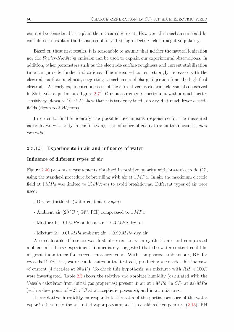
60 Charge generation in SF6 at high electric field
can not be considered to explain the measured current. However, this mechanism could be
considered to explain the transition observed at high electric field in negative polarity.
Based on these first results, it is reasonable to assume that neither the natural ionization
nor the Fowler-Nordheim emission can be used to explain our experimental observations. In
addition, other parameters such as the electrode surface roughness and current stabilization
time can provide further indications. The measured current strongly increases with the
electrode surface roughness, suggesting a mechanism of charge injection from the high field
electrode. A nearly exponential increase of the current versus electric field was also observed
in Shibuya’s experiments (figure 2.7). Our measurements carried out with a much better
sensitivity (down to 10−13 A) show that this tendency is still observed at much lower electric
fields (down to 3 kV/mm).
In order to further identify the possible mechanisms responsible for the measured
currents, we will study in the following, the influence of gas nature on the measured dark
currents.
2.3.1.3 Experiments in air and influence of water
Influence of different types of air
Figure 2.30 presents measurements obtained in positive polarity with brass electrode (C),
using the standard procedure before filling with air at 1MPa. In air, the maximum electric
field at 1MPa was limited to 15 kV/mm to avoid breakdowns. Different types of air were
used:
- Dry synthetic air (water content < 3ppm)
- Ambient air (20 C \ 54% RH) compressed to 1MPa
- Mixture 1 : 0.1MPa ambient air + 0.9MPa dry air
- Mixture 2 : 0.01MPa ambient air + 0.99MPa dry air
A considerable difference was first observed between synthetic air and compressed
ambient air. These experiments immediately suggested that the water content could be
of great importance for current measurements. With compressed ambient air, RH far
exceeds 100%, i.e., water condensates in the test cell, producing a considerable increase
of current (4 decades at 20 kV ). To check this hypothesis, air mixtures with RH < 100%
were investigated. Table 2.3 shows the relative and absolute humidity (calculated with the
Vaisala calculator from initial gas properties) present in air at 1MPa, in SF6 at 0.8MPa
(with a dew point of −27.7 C at atmospheric pressure), and in air mixtures.
The relative humidity corresponds to the ratio of the partial pressure of the water
vapor in the air, to the saturated vapor pressure, at the considered temperature (2.13). RH
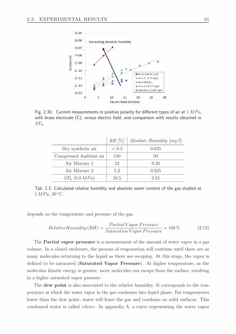
2.3. EXPERIMENTAL RESULTS 61
Fig. 2.30: Current measurements in positive polarity for different types of air at 1MPa,with brass electrode (C), versus electric field, and comparison with results obtained inSF6.
RH [%] Absolute Humidity [mg/l]
Dry synthetic air < 0.2 0.035
Compressed Ambient air 540 94
Air Mixture 1 52 9.26
Air Mixture 2 5.2 0.925
SF6 (0.8MPa) 16.5 2.85
Tab. 2.3: Calculated relative humidity and absolute water content of the gas studied at1MPa, 20 C.
depends on the temperature and pressure of the gas.
RelativeHumidity (RH) =Partial V apor Pressure
Saturation V apor Pressure× 100% (2.13)
The Partial vapor pressure is a measurement of the amount of water vapor in a gas
volume. In a closed enclosure, the process of evaporation will continue until there are as
many molecules returning to the liquid as there are escaping. At this stage, the vapor is
defined to be saturated (Saturated Vapor Pressure). At higher temperature, as the
molecular kinetic energy is greater, more molecules can escape from the surface, resulting
in a higher saturated vapor pressure
The dew point is also associated to the relative humidity. It corresponds to the tem-
perature at which the water vapor in the gas condenses into liquid phase. For temperatures
lower than the dew point, water will leave the gas and condense on solid surfaces. This
condensed water is called «dew». In appendix A, a curve representing the water vapor
62 Charge generation in SF6 at high electric field
pressure versus dew point is given [36].
On figure 2.30, an influence of water on currents is still seen at low water content (down
to RH = 5.2% in mixture 2), far from condensation conditions (Table 2.3). The comparison
of the different air types shows that current increases when RH is increased. At high RH
(compressed ambient air and mixture 1), a long «conditioning » sequence (several hours)
was necessary before stabilization of the current. During conditioning, a slow decrease of
current was observed. This effect was much reduced with dry gases, which rapidly provided
stable current.
On figure 2.30, measurements obtained in SF6 in identical conditions (same electrode)
at 0.8MPa are also plotted for comparison. With a dew point of −27.7 C at 0.1MPa
(i.e., SF6 of acceptable technical quality in GIS), the calculated relative humidity raises
to RH = 16.5% when the gas is compressed to 0.8MPa at 20 C. It is interesting to
observe that recorded currents agree with those measured in humid air, between mixture 2
(RH = 5.2%) and mixture 1 (RH = 52%).
Fig. 2.31: Current measurements in negative polarity versus electric field strength withelectrode (C) for various gas mixtures.
Same measurements were done in negative polarity. Figure 2.31 shows the current
measured for different air mixtures and SF6. Approximately same currents as measured
for positive polarity are seen for electric field lower than 14 kV/mm in air mixtures. The
influence of water is also noted for negative polarity in air. In case of SF6, currents are
higher than for the 10% air mixture while its absolute humidity is lower. This observation
can be explained by the poor reproducibility of measurements in SF6 in negative polarity.
In addition, we can note that the transition observed in SF6 is not observed for the various
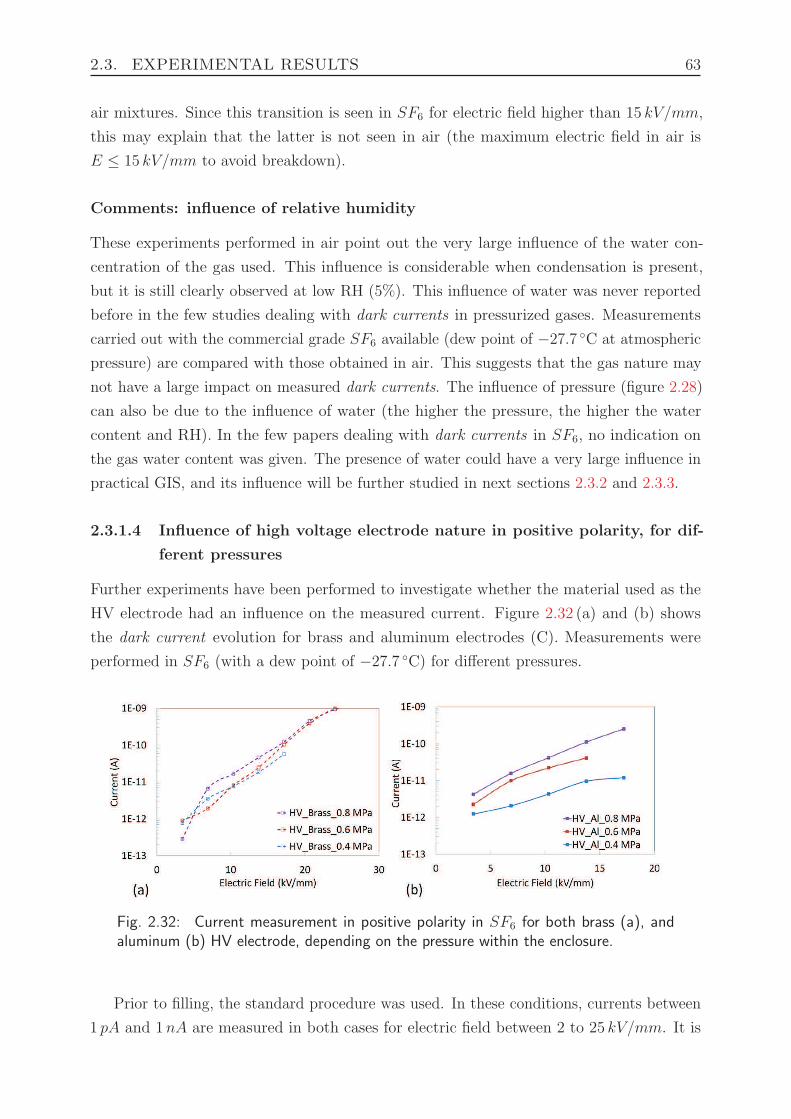
2.3. EXPERIMENTAL RESULTS 63
air mixtures. Since this transition is seen in SF6 for electric field higher than 15 kV/mm,
this may explain that the latter is not seen in air (the maximum electric field in air is
E ≤ 15 kV/mm to avoid breakdown).
Comments: influence of relative humidity
These experiments performed in air point out the very large influence of the water con-
centration of the gas used. This influence is considerable when condensation is present,
but it is still clearly observed at low RH (5%). This influence of water was never reported
before in the few studies dealing with dark currents in pressurized gases. Measurements
carried out with the commercial grade SF6 available (dew point of −27.7 C at atmospheric
pressure) are compared with those obtained in air. This suggests that the gas nature may
not have a large impact on measured dark currents. The influence of pressure (figure 2.28)
can also be due to the influence of water (the higher the pressure, the higher the water
content and RH). In the few papers dealing with dark currents in SF6, no indication on
the gas water content was given. The presence of water could have a very large influence in
practical GIS, and its influence will be further studied in next sections 2.3.2 and 2.3.3.
2.3.1.4 Influence of high voltage electrode nature in positive polarity, for dif-
ferent pressures
Further experiments have been performed to investigate whether the material used as the
HV electrode had an influence on the measured current. Figure 2.32 (a) and (b) shows
the dark current evolution for brass and aluminum electrodes (C). Measurements were
performed in SF6 (with a dew point of −27.7 C) for different pressures.
Fig. 2.32: Current measurement in positive polarity in SF6 for both brass (a), andaluminum (b) HV electrode, depending on the pressure within the enclosure.
Prior to filling, the standard procedure was used. In these conditions, currents between
1 pA and 1nA are measured in both cases for electric field between 2 to 25 kV/mm. It is
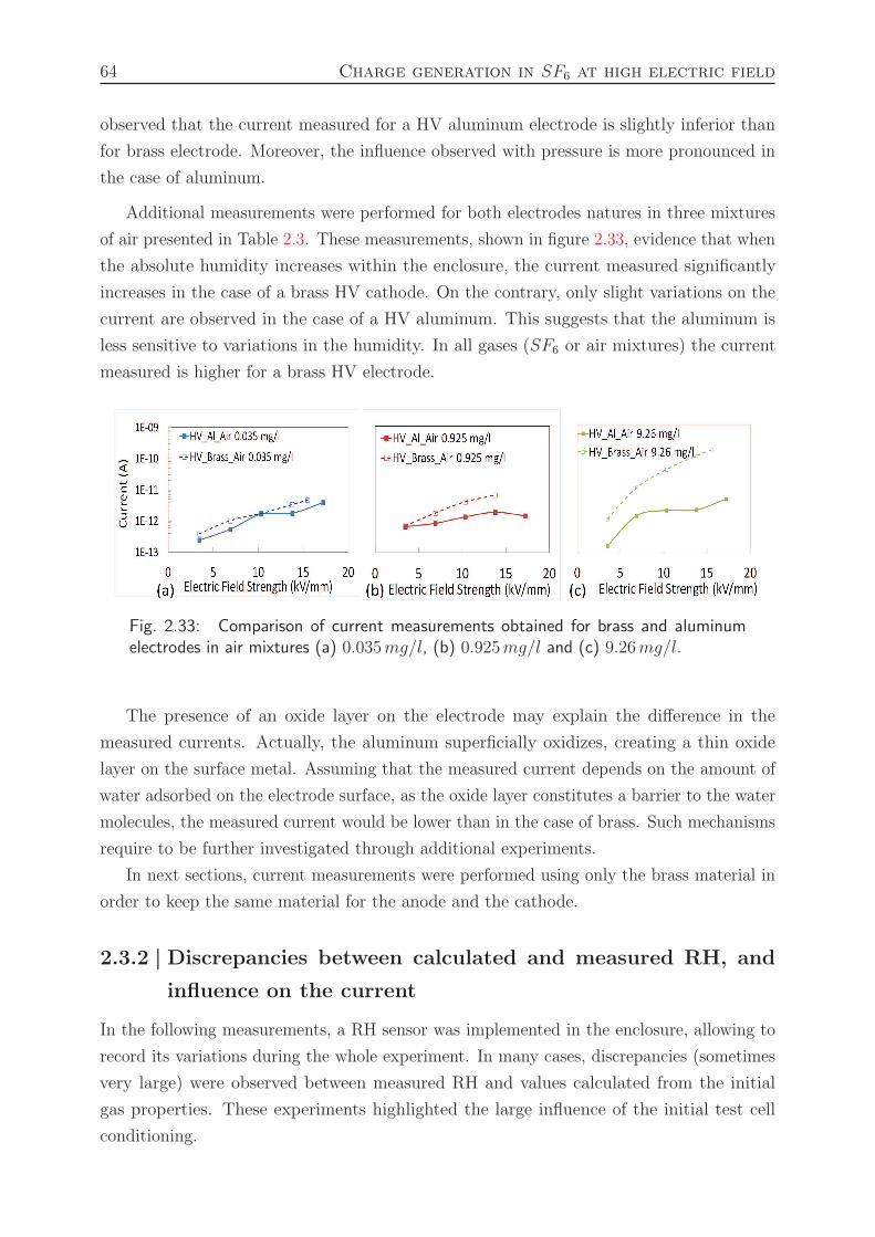
64 Charge generation in SF6 at high electric field
observed that the current measured for a HV aluminum electrode is slightly inferior than
for brass electrode. Moreover, the influence observed with pressure is more pronounced in
the case of aluminum.
Additional measurements were performed for both electrodes natures in three mixtures
of air presented in Table 2.3. These measurements, shown in figure 2.33, evidence that when
the absolute humidity increases within the enclosure, the current measured significantly
increases in the case of a brass HV cathode. On the contrary, only slight variations on the
current are observed in the case of a HV aluminum. This suggests that the aluminum is
less sensitive to variations in the humidity. In all gases (SF6 or air mixtures) the current
measured is higher for a brass HV electrode.
Fig. 2.33: Comparison of current measurements obtained for brass and aluminumelectrodes in air mixtures (a) 0.035mg/l, (b) 0.925mg/l and (c) 9.26mg/l.
The presence of an oxide layer on the electrode may explain the difference in the
measured currents. Actually, the aluminum superficially oxidizes, creating a thin oxide
layer on the surface metal. Assuming that the measured current depends on the amount of
water adsorbed on the electrode surface, as the oxide layer constitutes a barrier to the water
molecules, the measured current would be lower than in the case of brass. Such mechanisms
require to be further investigated through additional experiments.
In next sections, current measurements were performed using only the brass material in
order to keep the same material for the anode and the cathode.
2.3.2 | Discrepancies between calculated and measured RH, and
influence on the current
In the following measurements, a RH sensor was implemented in the enclosure, allowing to
record its variations during the whole experiment. In many cases, discrepancies (sometimes
very large) were observed between measured RH and values calculated from the initial
gas properties. These experiments highlighted the large influence of the initial test cell
conditioning.
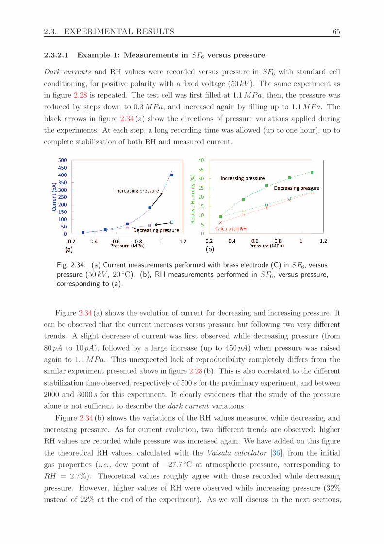
2.3. EXPERIMENTAL RESULTS 65
2.3.2.1 Example 1: Measurements in SF6 versus pressure
Dark currents and RH values were recorded versus pressure in SF6 with standard cell
conditioning, for positive polarity with a fixed voltage (50 kV ). The same experiment as
in figure 2.28 is repeated. The test cell was first filled at 1.1MPa, then, the pressure was
reduced by steps down to 0.3MPa, and increased again by filling up to 1.1MPa. The
black arrows in figure 2.34 (a) show the directions of pressure variations applied during
the experiments. At each step, a long recording time was allowed (up to one hour), up to
complete stabilization of both RH and measured current.
Fig. 2.34: (a) Current measurements performed with brass electrode (C) in SF6, versuspressure (50 kV , 20 C). (b), RH measurements performed in SF6, versus pressure,corresponding to (a).
Figure 2.34 (a) shows the evolution of current for decreasing and increasing pressure. It
can be observed that the current increases versus pressure but following two very different
trends. A slight decrease of current was first observed while decreasing pressure (from
80 pA to 10 pA), followed by a large increase (up to 450 pA) when pressure was raised
again to 1.1MPa. This unexpected lack of reproducibility completely differs from the
similar experiment presented above in figure 2.28 (b). This is also correlated to the different
stabilization time observed, respectively of 500 s for the preliminary experiment, and between
2000 and 3000 s for this experiment. It clearly evidences that the study of the pressure
alone is not sufficient to describe the dark current variations.
Figure 2.34 (b) shows the variations of the RH values measured while decreasing and
increasing pressure. As for current evolution, two different trends are observed: higher
RH values are recorded while pressure was increased again. We have added on this figure
the theoretical RH values, calculated with the Vaisala calculator [36], from the initial
gas properties (i.e., dew point of −27.7 C at atmospheric pressure, corresponding to
RH = 2.7%). Theoretical values roughly agree with those recorded while decreasing
pressure. However, higher values of RH were observed while increasing pressure (32%
instead of 22% at the end of the experiment). As we will discuss in the next sections,
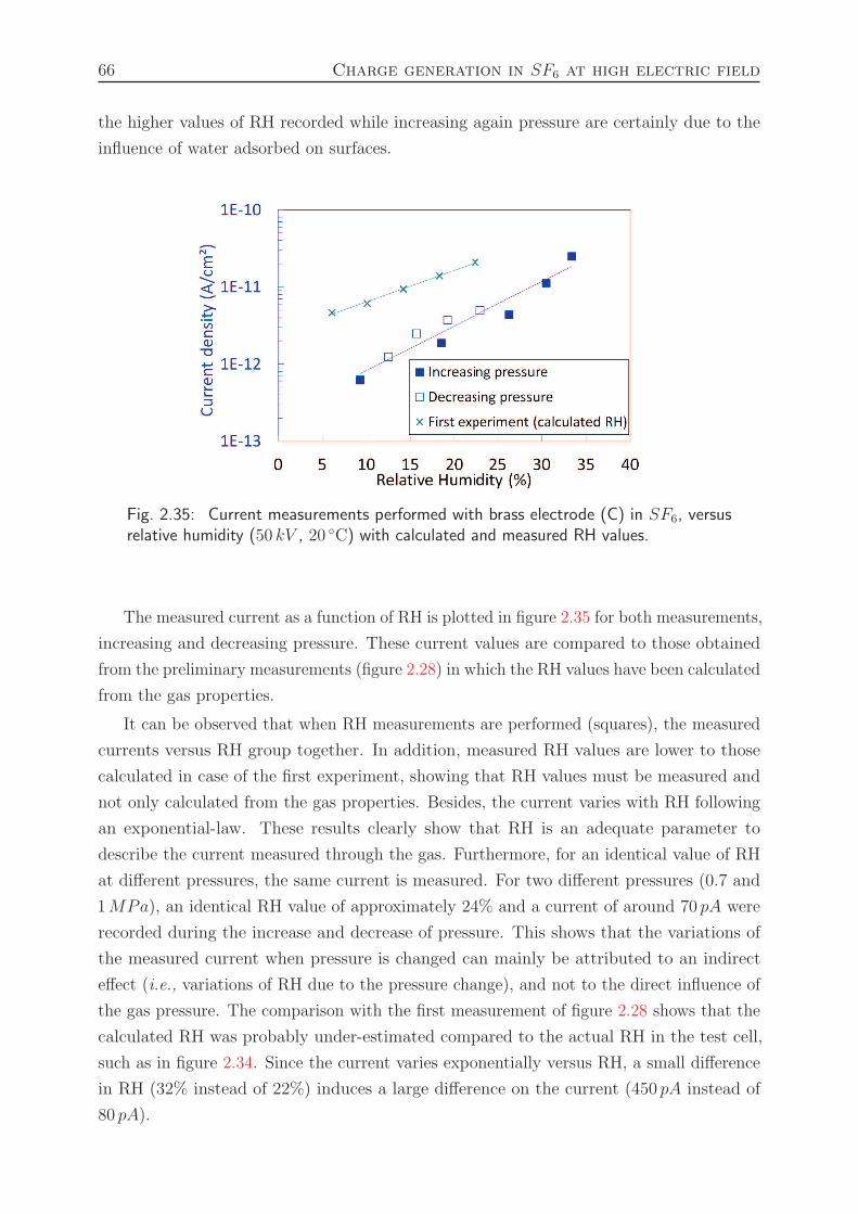
66 Charge generation in SF6 at high electric field
the higher values of RH recorded while increasing again pressure are certainly due to the
influence of water adsorbed on surfaces.
Fig. 2.35: Current measurements performed with brass electrode (C) in SF6, versusrelative humidity (50 kV , 20 C) with calculated and measured RH values.
The measured current as a function of RH is plotted in figure 2.35 for both measurements,
increasing and decreasing pressure. These current values are compared to those obtained
from the preliminary measurements (figure 2.28) in which the RH values have been calculated
from the gas properties.
It can be observed that when RH measurements are performed (squares), the measured
currents versus RH group together. In addition, measured RH values are lower to those
calculated in case of the first experiment, showing that RH values must be measured and
not only calculated from the gas properties. Besides, the current varies with RH following
an exponential-law. These results clearly show that RH is an adequate parameter to
describe the current measured through the gas. Furthermore, for an identical value of RH
at different pressures, the same current is measured. For two different pressures (0.7 and
1MPa), an identical RH value of approximately 24% and a current of around 70 pA were
recorded during the increase and decrease of pressure. This shows that the variations of
the measured current when pressure is changed can mainly be attributed to an indirect
effect (i.e., variations of RH due to the pressure change), and not to the direct influence of
the gas pressure. The comparison with the first measurement of figure 2.28 shows that the
calculated RH was probably under-estimated compared to the actual RH in the test cell,
such as in figure 2.34. Since the current varies exponentially versus RH, a small difference
in RH (32% instead of 22%) induces a large difference on the current (450 pA instead of
80 pA).
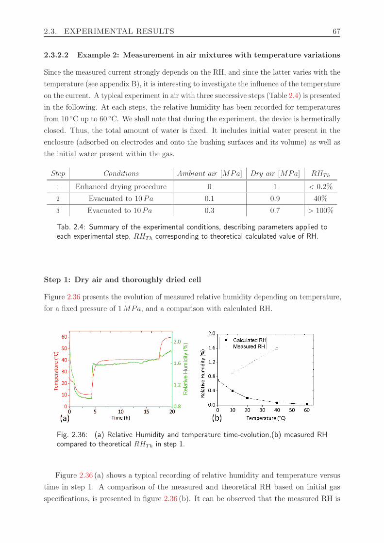
2.3. EXPERIMENTAL RESULTS 67
2.3.2.2 Example 2: Measurement in air mixtures with temperature variations
Since the measured current strongly depends on the RH, and since the latter varies with the
temperature (see appendix B), it is interesting to investigate the influence of the temperature
on the current. A typical experiment in air with three successive steps (Table 2.4) is presented
in the following. At each steps, the relative humidity has been recorded for temperatures
from 10 C up to 60 C. We shall note that during the experiment, the device is hermetically
closed. Thus, the total amount of water is fixed. It includes initial water present in the
enclosure (adsorbed on electrodes and onto the bushing surfaces and its volume) as well as
the initial water present within the gas.
Step Conditions Ambiant air [MPa] Dry air [MPa] RHTh
1 Enhanced drying procedure 0 1 < 0.2%
2 Evacuated to 10Pa 0.1 0.9 40%
3 Evacuated to 10Pa 0.3 0.7 > 100%
Tab. 2.4: Summary of the experimental conditions, describing parameters applied toeach experimental step, RHTh corresponding to theoretical calculated value of RH.
Step 1: Dry air and thoroughly dried cell
Figure 2.36 presents the evolution of measured relative humidity depending on temperature,
for a fixed pressure of 1MPa, and a comparison with calculated RH.
Fig. 2.36: (a) Relative Humidity and temperature time-evolution,(b) measured RHcompared to theoretical RHTh in step 1.
Figure 2.36 (a) shows a typical recording of relative humidity and temperature versus
time in step 1. A comparison of the measured and theoretical RH based on initial gas
specifications, is presented in figure 2.36 (b). It can be observed that the measured RH is
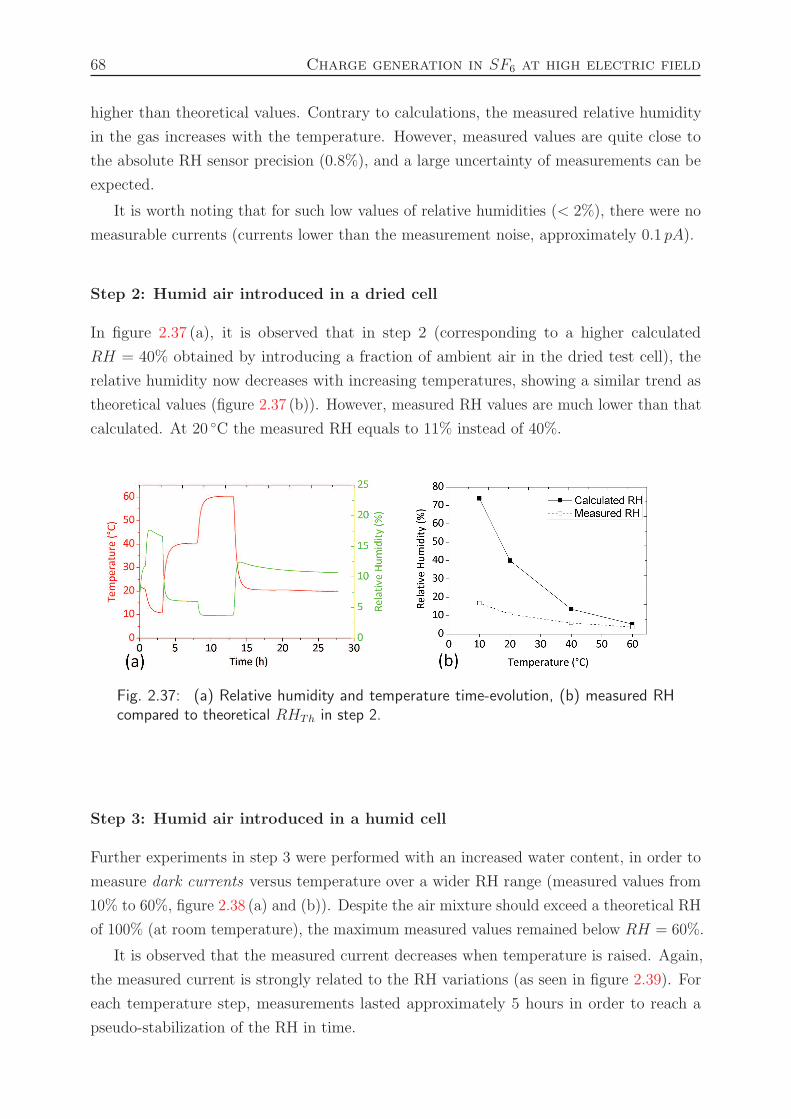
68 Charge generation in SF6 at high electric field
higher than theoretical values. Contrary to calculations, the measured relative humidity
in the gas increases with the temperature. However, measured values are quite close to
the absolute RH sensor precision (0.8%), and a large uncertainty of measurements can be
expected.
It is worth noting that for such low values of relative humidities (< 2%), there were no
measurable currents (currents lower than the measurement noise, approximately 0.1 pA).
Step 2: Humid air introduced in a dried cell
In figure 2.37 (a), it is observed that in step 2 (corresponding to a higher calculated
RH = 40% obtained by introducing a fraction of ambient air in the dried test cell), the
relative humidity now decreases with increasing temperatures, showing a similar trend as
theoretical values (figure 2.37 (b)). However, measured RH values are much lower than that
calculated. At 20 C the measured RH equals to 11% instead of 40%.
Fig. 2.37: (a) Relative humidity and temperature time-evolution, (b) measured RHcompared to theoretical RHTh in step 2.
Step 3: Humid air introduced in a humid cell
Further experiments in step 3 were performed with an increased water content, in order to
measure dark currents versus temperature over a wider RH range (measured values from
10% to 60%, figure 2.38 (a) and (b)). Despite the air mixture should exceed a theoretical RH
of 100% (at room temperature), the maximum measured values remained below RH = 60%.
It is observed that the measured current decreases when temperature is raised. Again,
the measured current is strongly related to the RH variations (as seen in figure 2.39). For
each temperature step, measurements lasted approximately 5 hours in order to reach a
pseudo-stabilization of the RH in time.
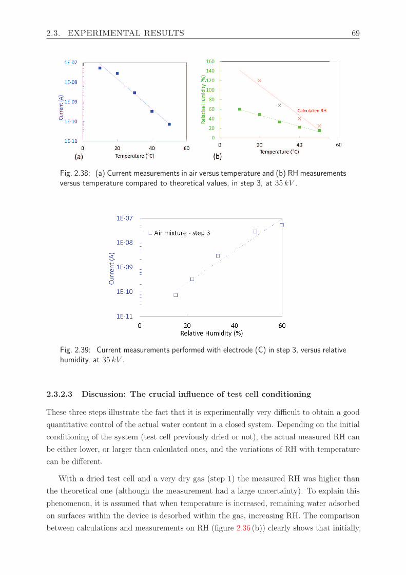
2.3. EXPERIMENTAL RESULTS 69
Fig. 2.38: (a) Current measurements in air versus temperature and (b) RH measurementsversus temperature compared to theoretical values, in step 3, at 35 kV .
Fig. 2.39: Current measurements performed with electrode (C) in step 3, versus relativehumidity, at 35 kV .
2.3.2.3 Discussion: The crucial influence of test cell conditioning
These three steps illustrate the fact that it is experimentally very difficult to obtain a good
quantitative control of the actual water content in a closed system. Depending on the initial
conditioning of the system (test cell previously dried or not), the actual measured RH can
be either lower, or larger than calculated ones, and the variations of RH with temperature
can be different.
With a dried test cell and a very dry gas (step 1) the measured RH was higher than
the theoretical one (although the measurement had a large uncertainty). To explain this
phenomenon, it is assumed that when temperature is increased, remaining water adsorbed
on surfaces within the device is desorbed within the gas, increasing RH. The comparison
between calculations and measurements on RH (figure 2.36 (b)) clearly shows that initially,
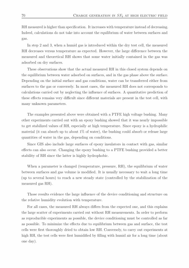
70 Charge generation in SF6 at high electric field
RH measured is higher than specification. It increases with temperature instead of decreasing.
Indeed, calculations do not take into account the equilibrium of water between surfaces and
gas.
In step 2 and 3, when a humid gas is introduced within the dry test cell, the measured
RH decreases versus temperature as expected. However, the large difference between the
measured and theoretical RH shows that some water initially contained in the gas was
adsorbed on dry surfaces.
These observations show that the actual measured RH in this closed system depends on
the equilibrium between water adsorbed on surfaces, and in the gas phase above the surface.
Depending on the initial surface and gas conditions, water can be transferred either from
surfaces to the gas or conversely. In most cases, the measured RH does not corresponds to
calculations carried out by neglecting the influence of surfaces. A quantitative prediction of
these effects remains very difficult since different materials are present in the test cell, with
many unknown parameters.
The examples presented above were obtained with a PTFE high voltage bushing. Many
other experiments carried out with an epoxy bushing showed that it was nearly impossible
to get stabilized values of RH, especially at high temperature. Since epoxy is a hydrophilic
material (it can absorb up to about 1% of water), the bushing could absorb or release large
quantities of water in the gas, depending on conditions.
Since GIS also include large surfaces of epoxy insulators in contact with gas, similar
effects can also occur. Changing the epoxy bushing to a PTFE bushing provided a better
stability of RH since the latter is highly hydrophobic.
When a parameter is changed (temperature, pressure, RH), the equilibrium of water
between surfaces and gas volume is modified. It is usually necessary to wait a long time
(up to several hours) to reach a new steady state (controlled by the stabilization of the
measured gas RH).
Those results evidence the large influence of the device conditioning and structure on
the relative humidity evolution with temperature.
For all cases, the measured RH always differs from the expected one, and this explains
the large scatter of experiments carried out without RH measurements. In order to perform
as reproducible experiments as possible, the device conditioning must be controlled as far
as possible. To minimize the effects due to equilibrium between gas and surface, the test
cells were first thoroughly dried to obtain low RH. Conversely, to carry out experiments at
high RH, the test cells were first humidified by filling with humid air for a long time (about
one day).
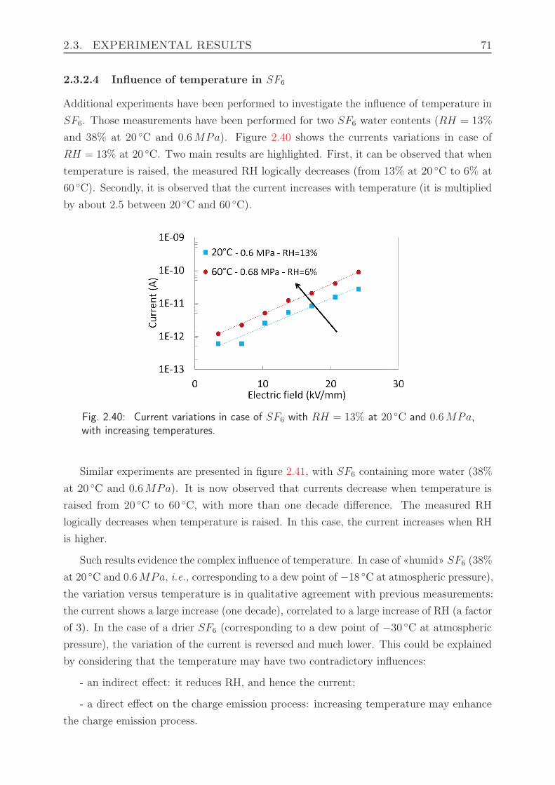
2.3. EXPERIMENTAL RESULTS 71
2.3.2.4 Influence of temperature in SF6
Additional experiments have been performed to investigate the influence of temperature in
SF6. Those measurements have been performed for two SF6 water contents (RH = 13%
and 38% at 20 C and 0.6MPa). Figure 2.40 shows the currents variations in case of
RH = 13% at 20 C. Two main results are highlighted. First, it can be observed that when
temperature is raised, the measured RH logically decreases (from 13% at 20 C to 6% at
60 C). Secondly, it is observed that the current increases with temperature (it is multiplied
by about 2.5 between 20 C and 60 C).
Fig. 2.40: Current variations in case of SF6 with RH = 13% at 20 C and 0.6MPa,with increasing temperatures.
Similar experiments are presented in figure 2.41, with SF6 containing more water (38%
at 20 C and 0.6MPa). It is now observed that currents decrease when temperature is
raised from 20 C to 60 C, with more than one decade difference. The measured RH
logically decreases when temperature is raised. In this case, the current increases when RH
is higher.
Such results evidence the complex influence of temperature. In case of «humid» SF6 (38%
at 20 C and 0.6MPa, i.e., corresponding to a dew point of −18 C at atmospheric pressure),
the variation versus temperature is in qualitative agreement with previous measurements:
the current shows a large increase (one decade), correlated to a large increase of RH (a factor
of 3). In the case of a drier SF6 (corresponding to a dew point of −30 C at atmospheric
pressure), the variation of the current is reversed and much lower. This could be explained
by considering that the temperature may have two contradictory influences:
- an indirect effect: it reduces RH, and hence the current;
- a direct effect on the charge emission process: increasing temperature may enhance
the charge emission process.
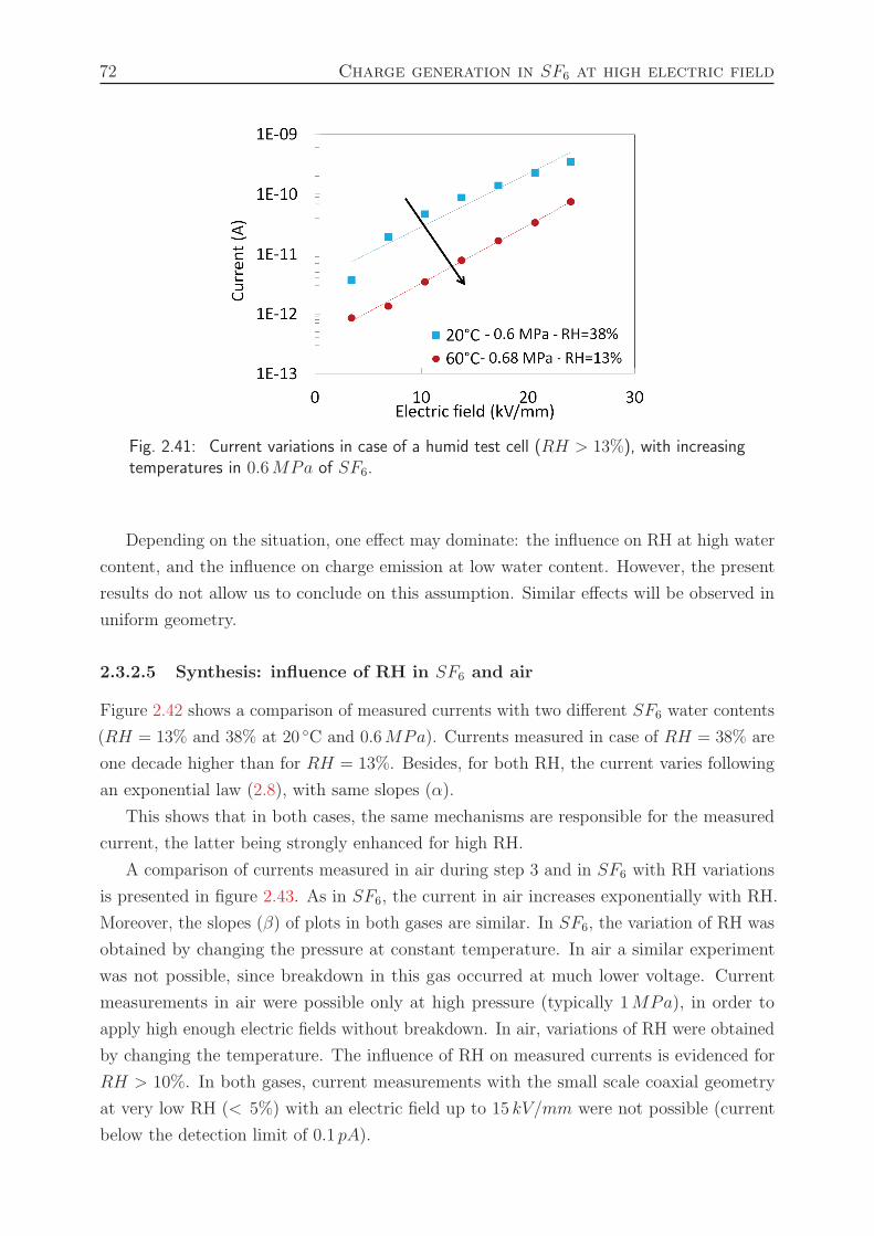
72 Charge generation in SF6 at high electric field
Fig. 2.41: Current variations in case of a humid test cell (RH > 13%), with increasingtemperatures in 0.6MPa of SF6.
Depending on the situation, one effect may dominate: the influence on RH at high water
content, and the influence on charge emission at low water content. However, the present
results do not allow us to conclude on this assumption. Similar effects will be observed in
uniform geometry.
2.3.2.5 Synthesis: influence of RH in SF6 and air
Figure 2.42 shows a comparison of measured currents with two different SF6 water contents
(RH = 13% and 38% at 20 C and 0.6MPa). Currents measured in case of RH = 38% are
one decade higher than for RH = 13%. Besides, for both RH, the current varies following
an exponential law (2.8), with same slopes (α).
This shows that in both cases, the same mechanisms are responsible for the measured
current, the latter being strongly enhanced for high RH.
A comparison of currents measured in air during step 3 and in SF6 with RH variations
is presented in figure 2.43. As in SF6, the current in air increases exponentially with RH.
Moreover, the slopes (β) of plots in both gases are similar. In SF6, the variation of RH was
obtained by changing the pressure at constant temperature. In air a similar experiment
was not possible, since breakdown in this gas occurred at much lower voltage. Current
measurements in air were possible only at high pressure (typically 1MPa), in order to
apply high enough electric fields without breakdown. In air, variations of RH were obtained
by changing the temperature. The influence of RH on measured currents is evidenced for
RH > 10%. In both gases, current measurements with the small scale coaxial geometry
at very low RH (< 5%) with an electric field up to 15 kV/mm were not possible (current
below the detection limit of 0.1 pA).
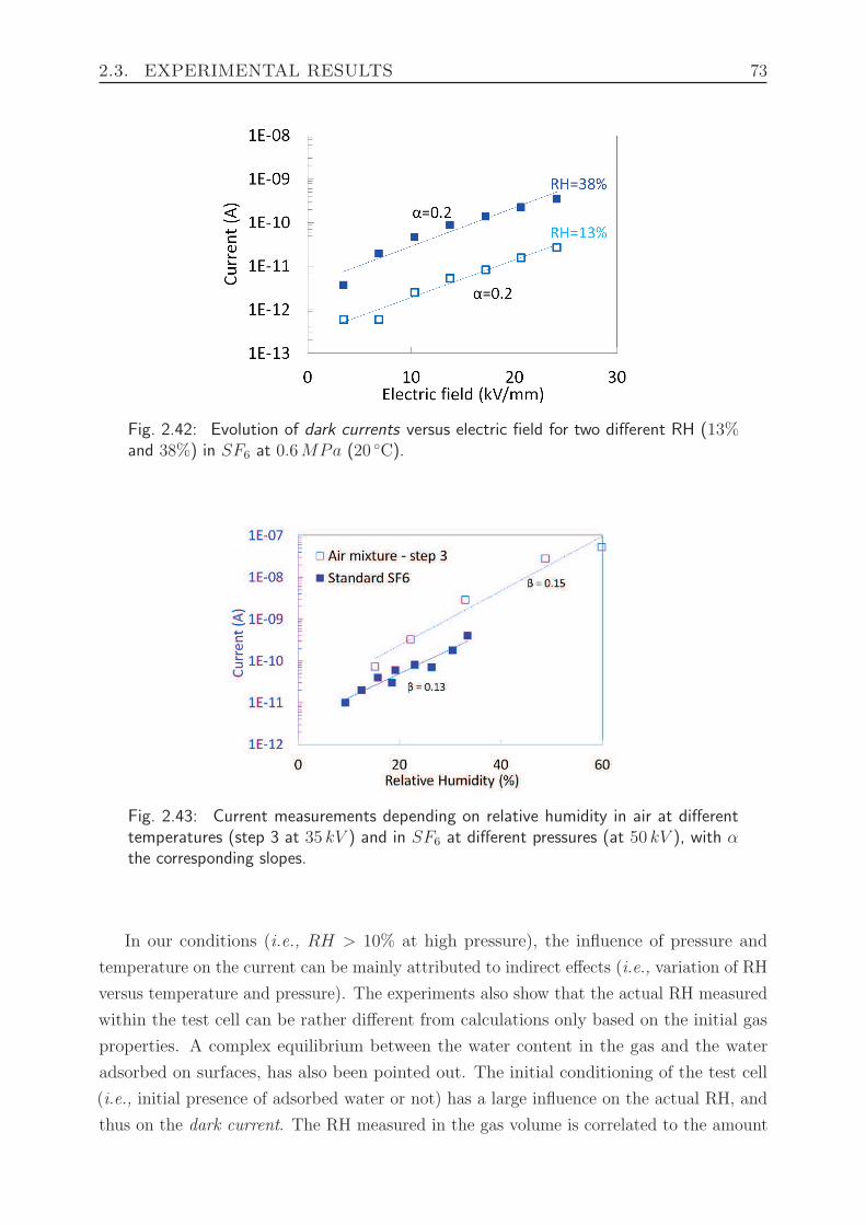
2.3. EXPERIMENTAL RESULTS 73
Fig. 2.42: Evolution of dark currents versus electric field for two different RH (13%and 38%) in SF6 at 0.6MPa (20 C).
Fig. 2.43: Current measurements depending on relative humidity in air at differenttemperatures (step 3 at 35 kV ) and in SF6 at different pressures (at 50 kV ), with αthe corresponding slopes.
In our conditions (i.e., RH > 10% at high pressure), the influence of pressure and
temperature on the current can be mainly attributed to indirect effects (i.e., variation of RH
versus temperature and pressure). The experiments also show that the actual RH measured
within the test cell can be rather different from calculations only based on the initial gas
properties. A complex equilibrium between the water content in the gas and the water
adsorbed on surfaces, has also been pointed out. The initial conditioning of the test cell
(i.e., initial presence of adsorbed water or not) has a large influence on the actual RH, and
thus on the dark current. The RH measured in the gas volume is correlated to the amount
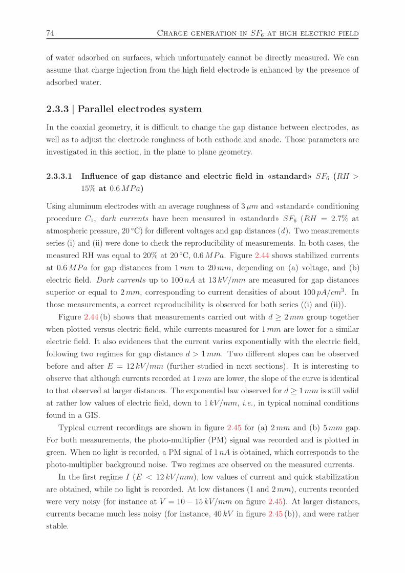
74 Charge generation in SF6 at high electric field
of water adsorbed on surfaces, which unfortunately cannot be directly measured. We can
assume that charge injection from the high field electrode is enhanced by the presence of
adsorbed water.
2.3.3 | Parallel electrodes system
In the coaxial geometry, it is difficult to change the gap distance between electrodes, as
well as to adjust the electrode roughness of both cathode and anode. Those parameters are
investigated in this section, in the plane to plane geometry.
2.3.3.1 Influence of gap distance and electric field in «standard» SF6 (RH >
15% at 0.6MPa)
Using aluminum electrodes with an average roughness of 3µm and «standard» conditioning
procedure C1, dark currents have been measured in «standard» SF6 (RH = 2.7% at
atmospheric pressure, 20 C) for different voltages and gap distances (d). Two measurements
series (i) and (ii) were done to check the reproducibility of measurements. In both cases, the
measured RH was equal to 20% at 20 C, 0.6MPa. Figure 2.44 shows stabilized currents
at 0.6MPa for gap distances from 1mm to 20mm, depending on (a) voltage, and (b)
electric field. Dark currents up to 100nA at 13 kV/mm are measured for gap distances
superior or equal to 2mm, corresponding to current densities of about 100 pA/cm3. In
those measurements, a correct reproducibility is observed for both series ((i) and (ii)).
Figure 2.44 (b) shows that measurements carried out with d ≥ 2mm group together
when plotted versus electric field, while currents measured for 1mm are lower for a similar
electric field. It also evidences that the current varies exponentially with the electric field,
following two regimes for gap distance d > 1mm. Two different slopes can be observed
before and after E = 12 kV/mm (further studied in next sections). It is interesting to
observe that although currents recorded at 1mm are lower, the slope of the curve is identical
to that observed at larger distances. The exponential law observed for d ≥ 1mm is still valid
at rather low values of electric field, down to 1 kV/mm, i.e., in typical nominal conditions
found in a GIS.
Typical current recordings are shown in figure 2.45 for (a) 2mm and (b) 5mm gap.
For both measurements, the photo-multiplier (PM) signal was recorded and is plotted in
green. When no light is recorded, a PM signal of 1nA is obtained, which corresponds to the
photo-multiplier background noise. Two regimes are observed on the measured currents.
In the first regime I (E < 12 kV/mm), low values of current and quick stabilization
are obtained, while no light is recorded. At low distances (1 and 2mm), currents recorded
were very noisy (for instance at V = 10− 15 kV/mm on figure 2.45). At larger distances,
currents became much less noisy (for instance, 40 kV in figure 2.45 (b)), and were rather
stable.
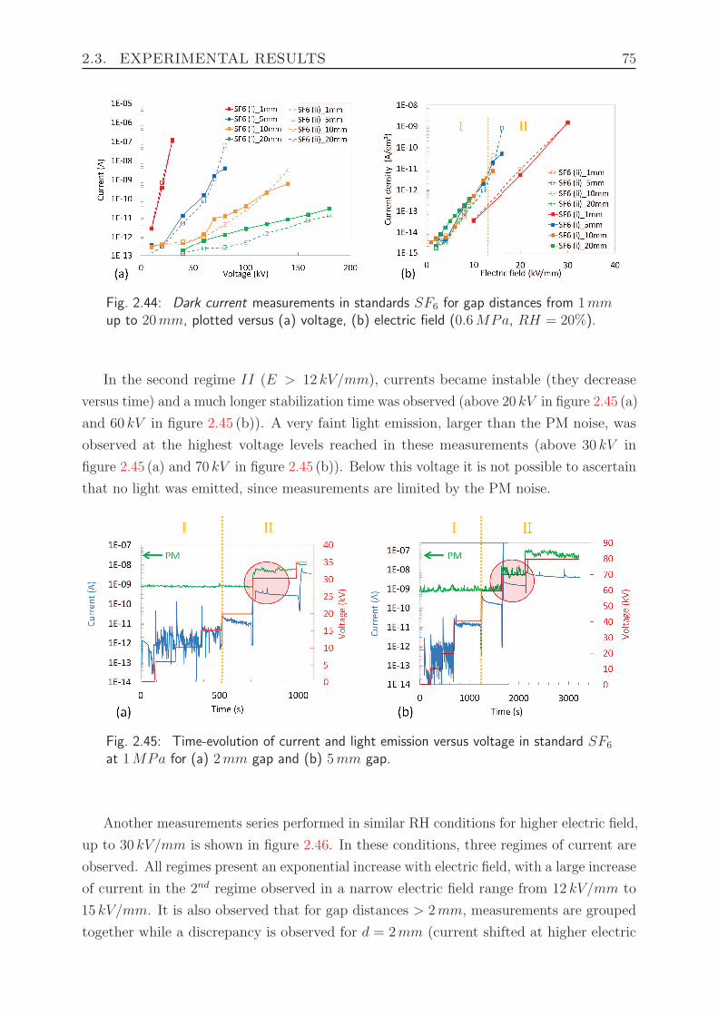
2.3. EXPERIMENTAL RESULTS 75
Fig. 2.44: Dark current measurements in standards SF6 for gap distances from 1mmup to 20mm, plotted versus (a) voltage, (b) electric field (0.6MPa, RH = 20%).
In the second regime II (E > 12 kV/mm), currents became instable (they decrease
versus time) and a much longer stabilization time was observed (above 20 kV in figure 2.45 (a)
and 60 kV in figure 2.45 (b)). A very faint light emission, larger than the PM noise, was
observed at the highest voltage levels reached in these measurements (above 30 kV in
figure 2.45 (a) and 70 kV in figure 2.45 (b)). Below this voltage it is not possible to ascertain
that no light was emitted, since measurements are limited by the PM noise.
Fig. 2.45: Time-evolution of current and light emission versus voltage in standard SF6
at 1MPa for (a) 2mm gap and (b) 5mm gap.
Another measurements series performed in similar RH conditions for higher electric field,
up to 30 kV/mm is shown in figure 2.46. In these conditions, three regimes of current are
observed. All regimes present an exponential increase with electric field, with a large increase
of current in the 2nd regime observed in a narrow electric field range from 12 kV/mm to
15 kV/mm. It is also observed that for gap distances > 2mm, measurements are grouped
together while a discrepancy is observed for d = 2mm (current shifted at higher electric
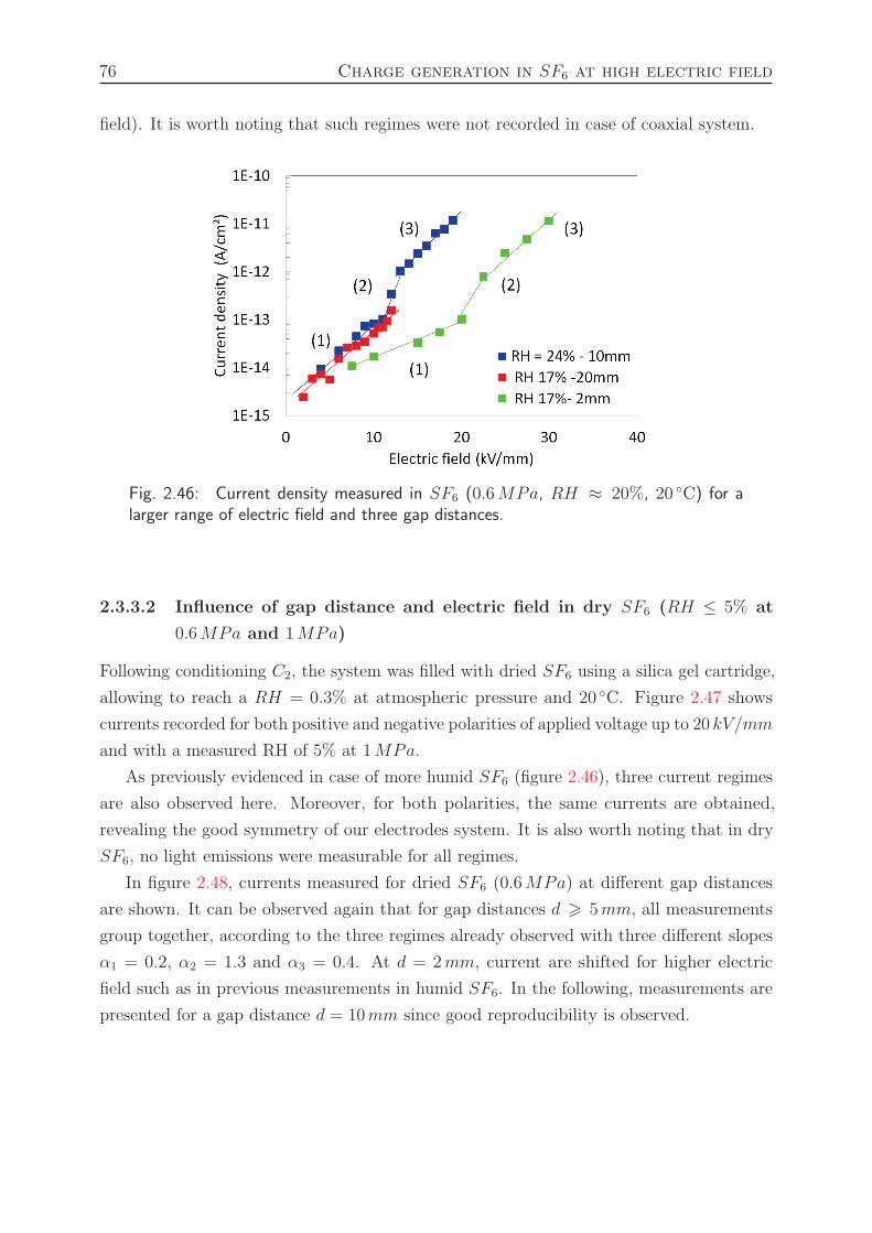
76 Charge generation in SF6 at high electric field
field). It is worth noting that such regimes were not recorded in case of coaxial system.
Fig. 2.46: Current density measured in SF6 (0.6MPa, RH ≈ 20%, 20 C) for alarger range of electric field and three gap distances.
2.3.3.2 Influence of gap distance and electric field in dry SF6 (RH ≤ 5% at
0.6MPa and 1MPa)
Following conditioning C2, the system was filled with dried SF6 using a silica gel cartridge,
allowing to reach a RH = 0.3% at atmospheric pressure and 20 C. Figure 2.47 shows
currents recorded for both positive and negative polarities of applied voltage up to 20 kV/mm
and with a measured RH of 5% at 1MPa.
As previously evidenced in case of more humid SF6 (figure 2.46), three current regimes
are also observed here. Moreover, for both polarities, the same currents are obtained,
revealing the good symmetry of our electrodes system. It is also worth noting that in dry
SF6, no light emissions were measurable for all regimes.
In figure 2.48, currents measured for dried SF6 (0.6MPa) at different gap distances
are shown. It can be observed again that for gap distances d > 5mm, all measurements
group together, according to the three regimes already observed with three different slopes
α1 = 0.2, α2 = 1.3 and α3 = 0.4. At d = 2mm, current are shifted for higher electric
field such as in previous measurements in humid SF6. In the following, measurements are
presented for a gap distance d = 10mm since good reproducibility is observed.
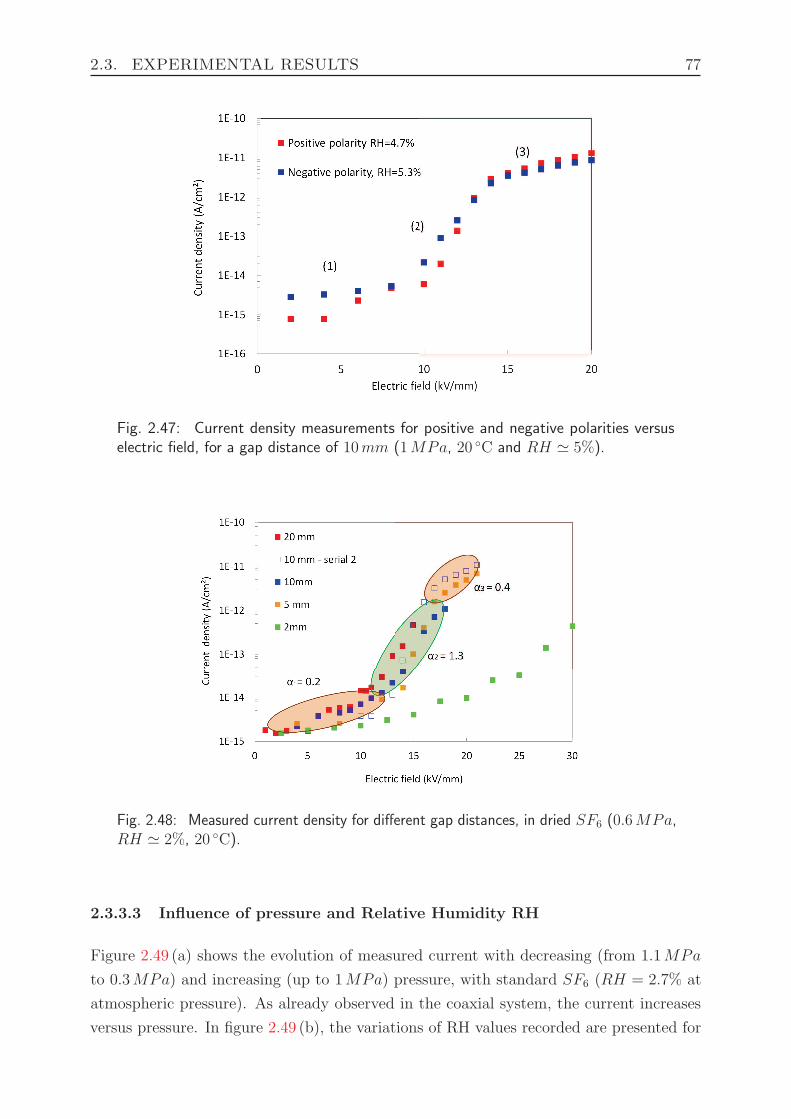
2.3. EXPERIMENTAL RESULTS 77
Fig. 2.47: Current density measurements for positive and negative polarities versuselectric field, for a gap distance of 10mm (1MPa, 20 C and RH ≃ 5%).
Fig. 2.48: Measured current density for different gap distances, in dried SF6 (0.6MPa,RH ≃ 2%, 20 C).
2.3.3.3 Influence of pressure and Relative Humidity RH
Figure 2.49 (a) shows the evolution of measured current with decreasing (from 1.1MPa
to 0.3MPa) and increasing (up to 1MPa) pressure, with standard SF6 (RH = 2.7% at
atmospheric pressure). As already observed in the coaxial system, the current increases
versus pressure. In figure 2.49 (b), the variations of RH values recorded are presented for
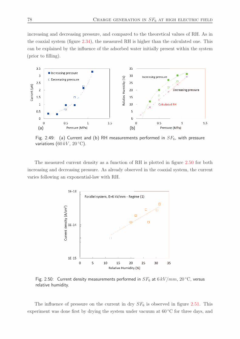
78 Charge generation in SF6 at high electric field
increasing and decreasing pressure, and compared to the theoretical values of RH. As in
the coaxial system (figure 2.34), the measured RH is higher than the calculated one. This
can be explained by the influence of the adsorbed water initially present within the system
(prior to filling).
Fig. 2.49: (a) Current and (b) RH measurements performed in SF6, with pressurevariations (60 kV , 20 C).
The measured current density as a function of RH is plotted in figure 2.50 for both
increasing and decreasing pressure. As already observed in the coaxial system, the current
varies following an exponential-law with RH.
Fig. 2.50: Current density measurements performed in SF6 at 6 kV/mm, 20 C, versusrelative humidity.
The influence of pressure on the current in dry SF6 is observed in figure 2.51. This
experiment was done first by drying the system under vacuum at 60 C for three days, and
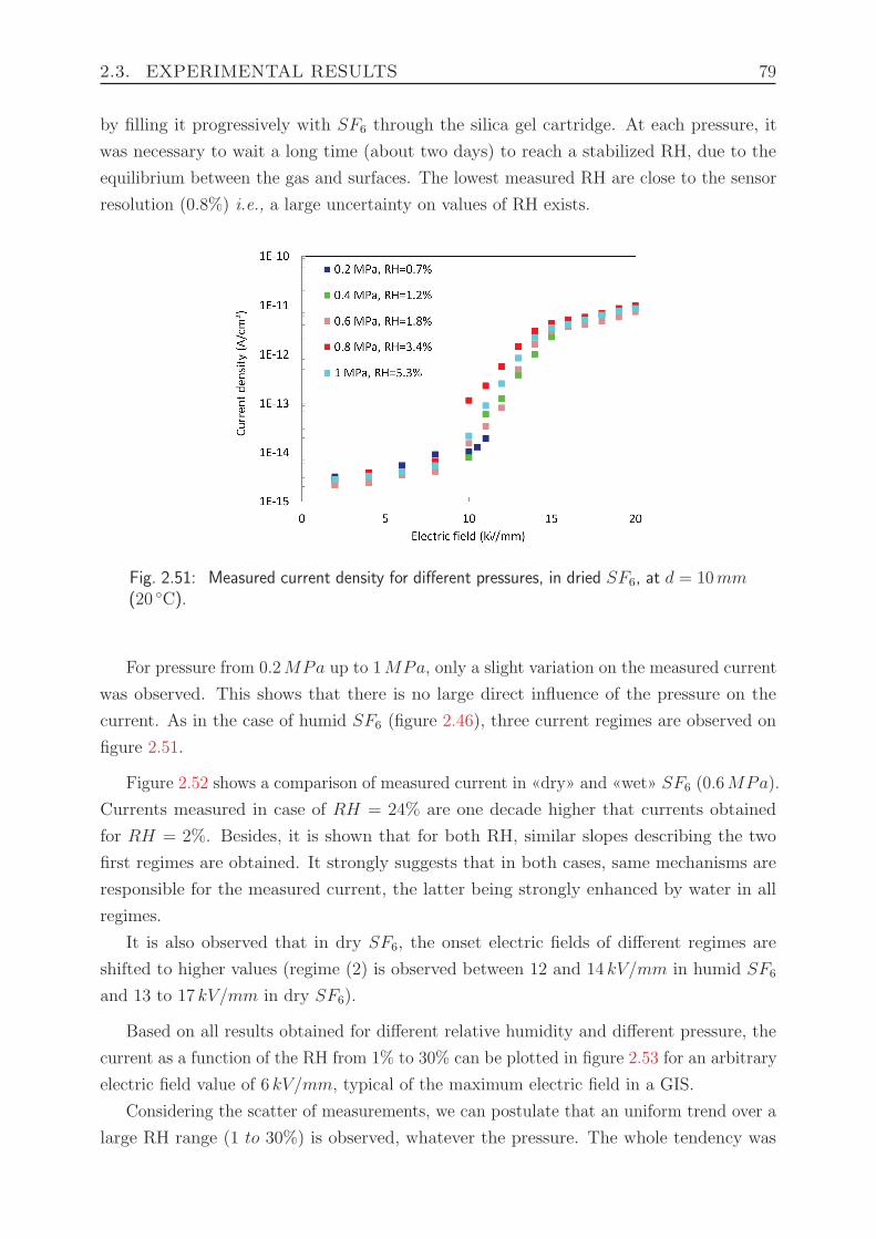
2.3. EXPERIMENTAL RESULTS 79
by filling it progressively with SF6 through the silica gel cartridge. At each pressure, it
was necessary to wait a long time (about two days) to reach a stabilized RH, due to the
equilibrium between the gas and surfaces. The lowest measured RH are close to the sensor
resolution (0.8%) i.e., a large uncertainty on values of RH exists.
Fig. 2.51: Measured current density for different pressures, in dried SF6, at d = 10mm(20 C).
For pressure from 0.2MPa up to 1MPa, only a slight variation on the measured current
was observed. This shows that there is no large direct influence of the pressure on the
current. As in the case of humid SF6 (figure 2.46), three current regimes are observed on
figure 2.51.
Figure 2.52 shows a comparison of measured current in «dry» and «wet» SF6 (0.6MPa).
Currents measured in case of RH = 24% are one decade higher that currents obtained
for RH = 2%. Besides, it is shown that for both RH, similar slopes describing the two
first regimes are obtained. It strongly suggests that in both cases, same mechanisms are
responsible for the measured current, the latter being strongly enhanced by water in all
regimes.
It is also observed that in dry SF6, the onset electric fields of different regimes are
shifted to higher values (regime (2) is observed between 12 and 14 kV/mm in humid SF6
and 13 to 17 kV/mm in dry SF6).
Based on all results obtained for different relative humidity and different pressure, the
current as a function of the RH from 1% to 30% can be plotted in figure 2.53 for an arbitrary
electric field value of 6 kV/mm, typical of the maximum electric field in a GIS.
Considering the scatter of measurements, we can postulate that an uniform trend over a
large RH range (1 to 30%) is observed, whatever the pressure. The whole tendency was
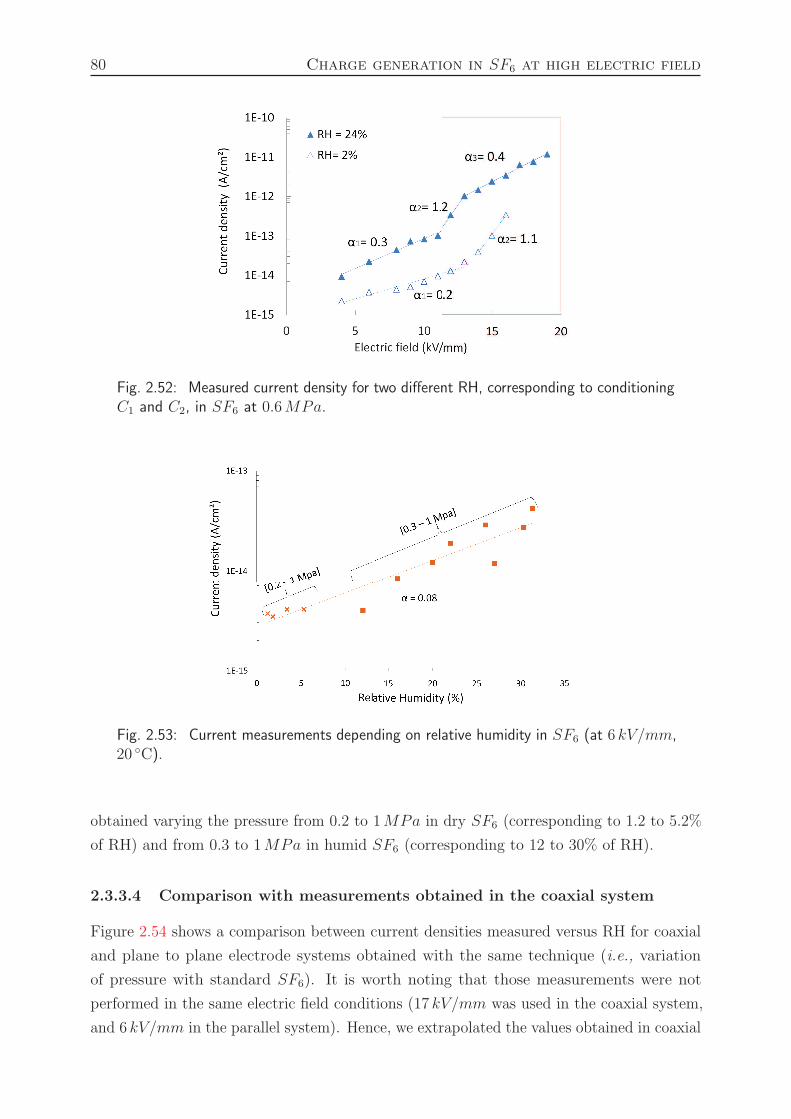
80 Charge generation in SF6 at high electric field
Fig. 2.52: Measured current density for two different RH, corresponding to conditioningC1 and C2, in SF6 at 0.6MPa.
Fig. 2.53: Current measurements depending on relative humidity in SF6 (at 6 kV/mm,20 C).
obtained varying the pressure from 0.2 to 1MPa in dry SF6 (corresponding to 1.2 to 5.2%
of RH) and from 0.3 to 1MPa in humid SF6 (corresponding to 12 to 30% of RH).
2.3.3.4 Comparison with measurements obtained in the coaxial system
Figure 2.54 shows a comparison between current densities measured versus RH for coaxial
and plane to plane electrode systems obtained with the same technique (i.e., variation
of pressure with standard SF6). It is worth noting that those measurements were not
performed in the same electric field conditions (17 kV/mm was used in the coaxial system,
and 6 kV/mm in the parallel system). Hence, we extrapolated the values obtained in coaxial
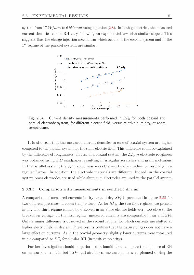
2.3. EXPERIMENTAL RESULTS 81
system from 17 kV/mm to 6 kV/mm using equation (2.8). In both geometries, the measured
current densities versus RH vary following an exponential-law with similar slopes. This
suggests that the charge injection mechanism which occurs in the coaxial system and in the
1st regime of the parallel system, are similar.
Fig. 2.54: Current density measurements performed in SF6 for both coaxial andparallel electrode system, for different electric field, versus relative humidity, at roomtemperature.
It is also seen that the measured current densities in case of coaxial system are higher
compared to the parallel system for the same electric field. This difference could be explained
by the difference of roughnesses. In case of a coaxial system, the 2.2µm electrode roughness
was obtained using SiC sandpaper, resulting in irregular scratches and grain inclusions.
In the parallel system, the 3µm roughness was obtained by dry machining, resulting in a
regular furrow. In addition, the electrode materials are different. Indeed, in the coaxial
system brass electrodes are used while aluminum electrodes are used in the parallel system.
2.3.3.5 Comparison with measurements in synthetic dry air
A comparison of measured currents in dry air and dry SF6 is presented in figure 2.55 for
two different pressures at room temperature. As for SF6, the two first regimes are present
in air. The third regime cannot be observed in air since electric fields were too close to the
breakdown voltage. In the first regime, measured currents are comparable in air and SF6.
Only a minor difference is observed in the second regime, for which currents are shifted at
higher electric field in dry air. These results confirm that the nature of gas does not have a
large effect on currents. As in the coaxial geometry, slightly lower currents were measured
in air compared to SF6 for similar RH (in positive polarity).
Further investigation should be performed in humid air to compare the influence of RH
on measured current in both SF6 and air. These measurements were planned during the
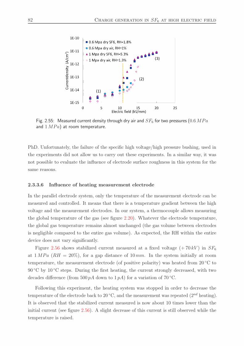
82 Charge generation in SF6 at high electric field
Fig. 2.55: Measured current density through dry air and SF6 for two pressures (0.6MPaand 1MPa) at room temperature.
PhD. Unfortunately, the failure of the specific high voltage/high pressure bushing, used in
the experiments did not allow us to carry out these experiments. In a similar way, it was
not possible to evaluate the influence of electrode surface roughness in this system for the
same reasons.
2.3.3.6 Influence of heating measurement electrode
In the parallel electrode system, only the temperature of the measurement electrode can be
measured and controlled. It means that there is a temperature gradient between the high
voltage and the measurement electrodes. In our system, a thermocouple allows measuring
the global temperature of the gas (see figure 2.20). Whatever the electrode temperature,
the global gas temperature remains almost unchanged (the gas volume between electrodes
is negligible compared to the entire gas volume). As expected, the RH within the entire
device does not vary significantly.
Figure 2.56 shows stabilized current measured at a fixed voltage (+ 70 kV ) in SF6
at 1MPa (RH = 20%), for a gap distance of 10mm. In the system initially at room
temperature, the measurement electrode (of positive polarity) was heated from 20 C to
90 C by 10 C steps. During the first heating, the current strongly decreased, with two
decades difference (from 500 pA down to 1 pA) for a variation of 70 C.
Following this experiment, the heating system was stopped in order to decrease the
temperature of the electrode back to 20 C, and the measurement was repeated (2nd heating).
It is observed that the stabilized current measured is now about 10 times lower than the
initial current (see figure 2.56). A slight decrease of this current is still observed while the
temperature is raised.
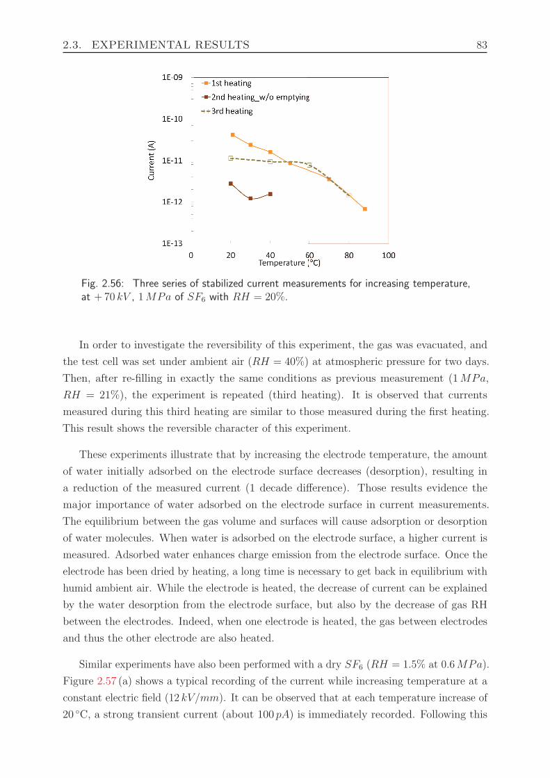
2.3. EXPERIMENTAL RESULTS 83
Fig. 2.56: Three series of stabilized current measurements for increasing temperature,at +70 kV , 1MPa of SF6 with RH = 20%.
In order to investigate the reversibility of this experiment, the gas was evacuated, and
the test cell was set under ambient air (RH = 40%) at atmospheric pressure for two days.
Then, after re-filling in exactly the same conditions as previous measurement (1MPa,
RH = 21%), the experiment is repeated (third heating). It is observed that currents
measured during this third heating are similar to those measured during the first heating.
This result shows the reversible character of this experiment.
These experiments illustrate that by increasing the electrode temperature, the amount
of water initially adsorbed on the electrode surface decreases (desorption), resulting in
a reduction of the measured current (1 decade difference). Those results evidence the
major importance of water adsorbed on the electrode surface in current measurements.
The equilibrium between the gas volume and surfaces will cause adsorption or desorption
of water molecules. When water is adsorbed on the electrode surface, a higher current is
measured. Adsorbed water enhances charge emission from the electrode surface. Once the
electrode has been dried by heating, a long time is necessary to get back in equilibrium with
humid ambient air. While the electrode is heated, the decrease of current can be explained
by the water desorption from the electrode surface, but also by the decrease of gas RH
between the electrodes. Indeed, when one electrode is heated, the gas between electrodes
and thus the other electrode are also heated.
Similar experiments have also been performed with a dry SF6 (RH = 1.5% at 0.6MPa).
Figure 2.57 (a) shows a typical recording of the current while increasing temperature at a
constant electric field (12 kV/mm). It can be observed that at each temperature increase of
20 C, a strong transient current (about 100 pA) is immediately recorded. Following this
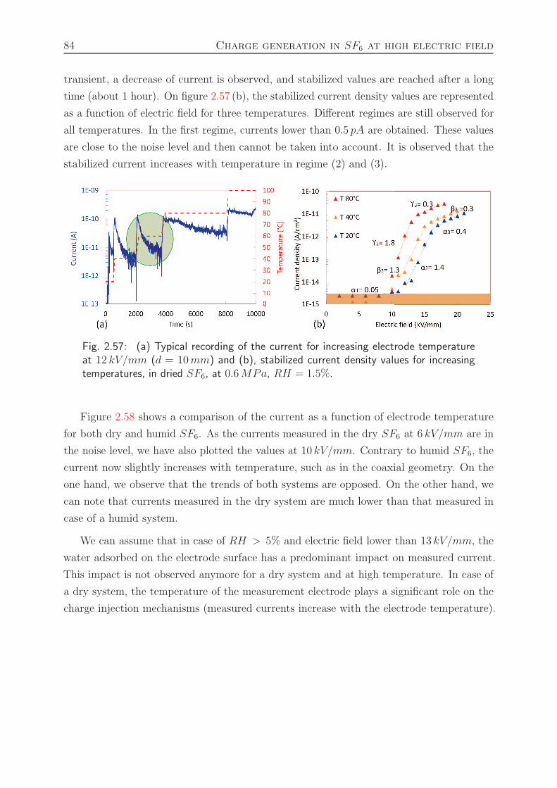
84 Charge generation in SF6 at high electric field
transient, a decrease of current is observed, and stabilized values are reached after a long
time (about 1 hour). On figure 2.57 (b), the stabilized current density values are represented
as a function of electric field for three temperatures. Different regimes are still observed for
all temperatures. In the first regime, currents lower than 0.5 pA are obtained. These values
are close to the noise level and then cannot be taken into account. It is observed that the
stabilized current increases with temperature in regime (2) and (3).
Fig. 2.57: (a) Typical recording of the current for increasing electrode temperatureat 12 kV/mm (d = 10mm) and (b), stabilized current density values for increasingtemperatures, in dried SF6, at 0.6MPa, RH = 1.5%.
Figure 2.58 shows a comparison of the current as a function of electrode temperature
for both dry and humid SF6. As the currents measured in the dry SF6 at 6 kV/mm are in
the noise level, we have also plotted the values at 10 kV/mm. Contrary to humid SF6, the
current now slightly increases with temperature, such as in the coaxial geometry. On the
one hand, we observe that the trends of both systems are opposed. On the other hand, we
can note that currents measured in the dry system are much lower than that measured in
case of a humid system.
We can assume that in case of RH > 5% and electric field lower than 13 kV/mm, the
water adsorbed on the electrode surface has a predominant impact on measured current.
This impact is not observed anymore for a dry system and at high temperature. In case of
a dry system, the temperature of the measurement electrode plays a significant role on the
charge injection mechanisms (measured currents increase with the electrode temperature).
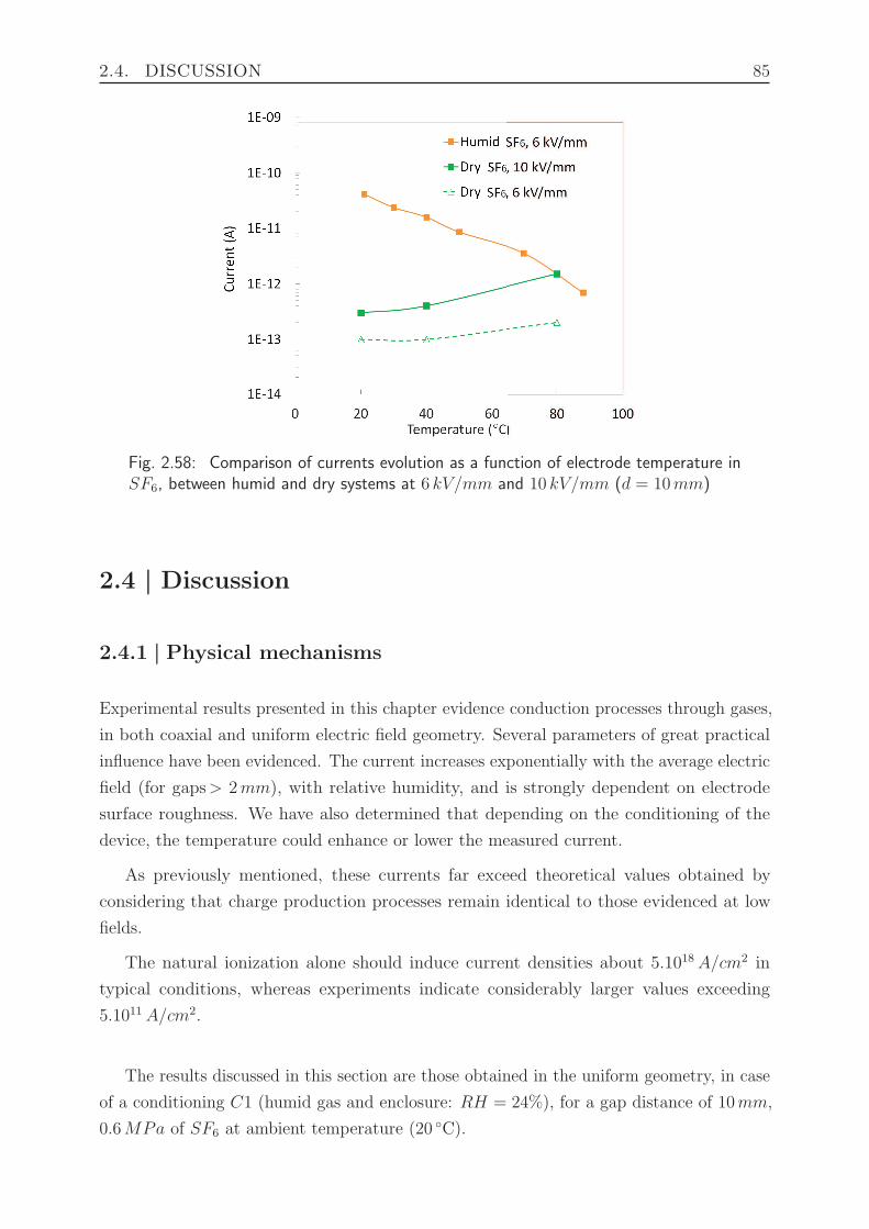
2.4. DISCUSSION 85
Fig. 2.58: Comparison of currents evolution as a function of electrode temperature inSF6, between humid and dry systems at 6 kV/mm and 10 kV/mm (d = 10mm)
2.4 | Discussion
2.4.1 | Physical mechanisms
Experimental results presented in this chapter evidence conduction processes through gases,
in both coaxial and uniform electric field geometry. Several parameters of great practical
influence have been evidenced. The current increases exponentially with the average electric
field (for gaps> 2mm), with relative humidity, and is strongly dependent on electrode
surface roughness. We have also determined that depending on the conditioning of the
device, the temperature could enhance or lower the measured current.
As previously mentioned, these currents far exceed theoretical values obtained by
considering that charge production processes remain identical to those evidenced at low
fields.
The natural ionization alone should induce current densities about 5.1018 A/cm2 in
typical conditions, whereas experiments indicate considerably larger values exceeding
5.1011 A/cm2.
The results discussed in this section are those obtained in the uniform geometry, in case
of a conditioning C1 (humid gas and enclosure: RH = 24%), for a gap distance of 10mm,
0.6MPa of SF6 at ambient temperature (20 C).
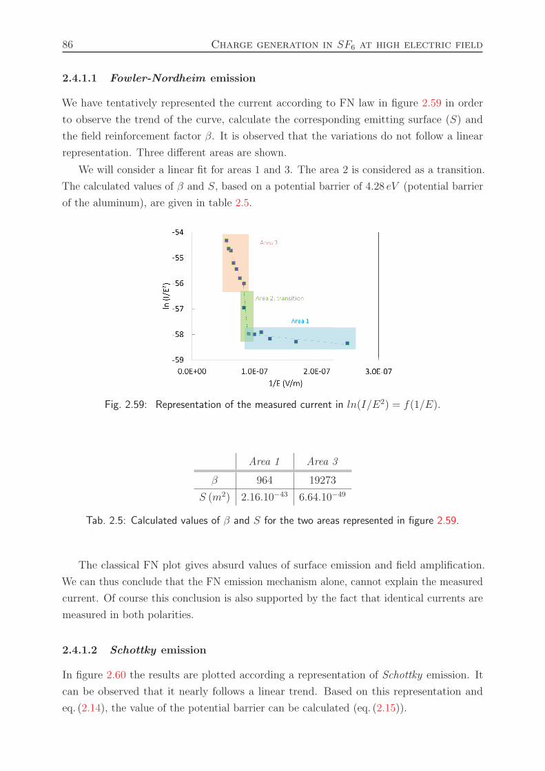
86 Charge generation in SF6 at high electric field
2.4.1.1 Fowler-Nordheim emission
We have tentatively represented the current according to FN law in figure 2.59 in order
to observe the trend of the curve, calculate the corresponding emitting surface (S) and
the field reinforcement factor β. It is observed that the variations do not follow a linear
representation. Three different areas are shown.
We will consider a linear fit for areas 1 and 3. The area 2 is considered as a transition.
The calculated values of β and S, based on a potential barrier of 4.28 eV (potential barrier
of the aluminum), are given in table 2.5.
Fig. 2.59: Representation of the measured current in ln(I/E2) = f(1/E).
Area 1 Area 3
β 964 19273
S (m2) 2.16.10−43 6.64.10−49
Tab. 2.5: Calculated values of β and S for the two areas represented in figure 2.59.
The classical FN plot gives absurd values of surface emission and field amplification.
We can thus conclude that the FN emission mechanism alone, cannot explain the measured
current. Of course this conclusion is also supported by the fact that identical currents are
measured in both polarities.
2.4.1.2 Schottky emission
In figure 2.60 the results are plotted according a representation of Schottky emission. It
can be observed that it nearly follows a linear trend. Based on this representation and
eq. (2.14), the value of the potential barrier can be calculated (eq. (2.15)).
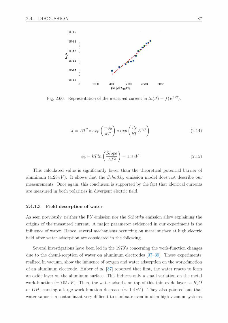
2.4. DISCUSSION 87
Fig. 2.60: Representation of the measured current in ln(J) = f(E1/2).
J = AT 2 ∗ exp(−φ0
kT
)
∗ exp(
βS
kTE1/2
)
(2.14)
φ0 = kT ln
(
Slope
AT 2
)
= 1.3 eV (2.15)
This calculated value is significantly lower than the theoretical potential barrier of
aluminum (4.28 eV ). It shows that the Schotkky emission model does not describe our
measurements. Once again, this conclusion is supported by the fact that identical currents
are measured in both polarities in divergent electric field.
2.4.1.3 Field desorption of water
As seen previously, neither the FN emission nor the Schottky emission allow explaining the
origins of the measured current. A major parameter evidenced in our experiment is the
influence of water. Hence, several mechanisms occurring on metal surface at high electric
field after water adsorption are considered in the following.
Several investigations have been led in the 1970′s concerning the work-function changes
due to the chemi-sorption of water on aluminum electrodes [37–39]. These experiments,
realized in vacuum, show the influence of oxygen and water adsorption on the work-function
of an aluminum electrode. Huber et al. [37] reported that first, the water reacts to form
an oxide layer on the aluminum surface. This induces only a small variation on the metal
work-function (±0.05 eV ). Then, the water adsorbs on top of this thin oxide layer as H2O
or OH, causing a large work-function decrease (∼ 1.4 eV ). They also pointed out that
water vapor is a contaminant very difficult to eliminate even in ultra-high vacuum systems.
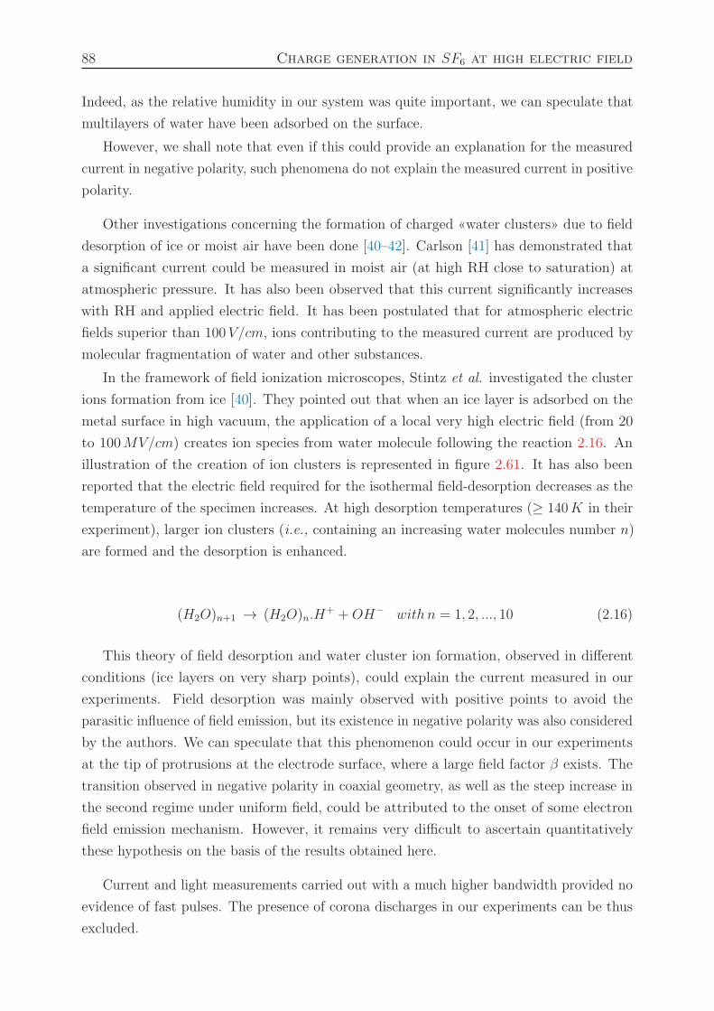
88 Charge generation in SF6 at high electric field
Indeed, as the relative humidity in our system was quite important, we can speculate that
multilayers of water have been adsorbed on the surface.
However, we shall note that even if this could provide an explanation for the measured
current in negative polarity, such phenomena do not explain the measured current in positive
polarity.
Other investigations concerning the formation of charged «water clusters» due to field
desorption of ice or moist air have been done [40–42]. Carlson [41] has demonstrated that
a significant current could be measured in moist air (at high RH close to saturation) at
atmospheric pressure. It has also been observed that this current significantly increases
with RH and applied electric field. It has been postulated that for atmospheric electric
fields superior than 100V/cm, ions contributing to the measured current are produced by
molecular fragmentation of water and other substances.
In the framework of field ionization microscopes, Stintz et al. investigated the cluster
ions formation from ice [40]. They pointed out that when an ice layer is adsorbed on the
metal surface in high vacuum, the application of a local very high electric field (from 20
to 100MV/cm) creates ion species from water molecule following the reaction 2.16. An
illustration of the creation of ion clusters is represented in figure 2.61. It has also been
reported that the electric field required for the isothermal field-desorption decreases as the
temperature of the specimen increases. At high desorption temperatures (≥ 140K in their
experiment), larger ion clusters (i.e., containing an increasing water molecules number n)
are formed and the desorption is enhanced.
(H2O)n+1 → (H2O)n.H+ +OH− with n = 1, 2, ..., 10 (2.16)
This theory of field desorption and water cluster ion formation, observed in different
conditions (ice layers on very sharp points), could explain the current measured in our
experiments. Field desorption was mainly observed with positive points to avoid the
parasitic influence of field emission, but its existence in negative polarity was also considered
by the authors. We can speculate that this phenomenon could occur in our experiments
at the tip of protrusions at the electrode surface, where a large field factor β exists. The
transition observed in negative polarity in coaxial geometry, as well as the steep increase in
the second regime under uniform field, could be attributed to the onset of some electron
field emission mechanism. However, it remains very difficult to ascertain quantitatively
these hypothesis on the basis of the results obtained here.
Current and light measurements carried out with a much higher bandwidth provided no
evidence of fast pulses. The presence of corona discharges in our experiments can be thus
excluded.
2.4. DISCUSSION 89
Fig. 2.61: Representation of mechanism proposed for water ion cluster formation,adapted from [43]. (a) Water molecule adsorbed on metal surface, (b) ionization ofwater molecule due to field desorption mechanism and (c), creation of a water clusterion.
2.4.2 | Consequences on the industrial application
In the electric field range of a typical GIS application (up to Emax = 10 kV/mm), it has been
evidenced that a non-negligible current can be injected in the gas, in both polarities. This
current is strongly influenced by several parameters that should have a great importance for
the practical application: electrode surface roughness, presence of water, and temperature.
These parameters provide useful indications for the optimization of GIS, with the objective
to reduce phenomena associated with electrostatic charging of solid insulators.
In a fixed GIS configuration, temperature appears to be an important parameter. Indeed,
it will modify the gas RH, the equilibrium between water adsorbed on surfaces and in
the gas volume, and also the volume and surface resistivities of solid insulators. All these
phenomena are coupled, and determine in a rather complex way the dynamics of charge
accumulation and decay. For instance, let us consider a «standard» GIS situation: 0.6MPa
SF6 with a RH = 4.8% at 20 C, and 6 kV/mm. In such system, a current density of about
5.10−15 pA/cm2 will be injected by the high voltage electrode in the gas.
If this GIS is submitted to low external temperatures (∼ −8 C), complex phenomena
may occur. Once the equilibrium is stabilized within the GIS, a RH of approximately 34%
should be measured within the system due to the temperature decrease. Thus, considering
RH = 34%, the current through gas should increase by about one decade. However, the
actual RH within the system differs from the calculated one due to adsorption/desorption
phenomena. Then, to estimate the current emitted within a GIS, a RH measurement
should be performed. The decrease of temperature results in a large increase of current
through gas, enhancing the charge accumulation on the solid insulator surface. However,
two other opposite phenomena will occur. On the one hand, the volume resistivity of the
90 1.5 CONCLUSIONS
solid insulator significantly increases with the decrease of temperature, which will also favor
the charge accumulation. On the other hand since the GIS surfaces and SF6 are «humid»,
the surface resistivity of the insulator will decrease, favoring the charge relaxation. Thus, it
is very difficult to estimate if charge accumulation or relaxation will be enhanced. Only a
numerical simulation of the processes can provide an information on the final tendency.
In another situation, if the temperature of the high voltage electrode rapidly increases,
a transition stage during which an important peak of emitted current (from 10 to 100 times
the steady current), appears. During this transition, the charge accumulation phenomena
may be further enhanced. Besides, as will be evidenced in chapter 4, the temperature
gradient along the insulator will induce a complete re-distribution of the electric field, and
an enhancement of the current through the insulator. Once again, the final influence on the
charge accumulation and the field distribution remains difficult to predict without a precise
numerical simulation.
2.5 | Conclusions
In this chapter, a conduction process through pressurized gas has been evidenced at high
electric field in both dry and «wet » systems. It has been shown that the measured current is
field-dependent and composed of three different regimes. The indirect influence of pressure
allows to highlight the significant impact of RH on the measured dark currents. In addition,
we have demonstrated that depending on the initial conditioning of the system, the influence
of temperature on the measured current and on the RH equilibrium of the system, can be
reversed.
To explain the mechanisms occuring within our system, we propose to consider the
phenomena of chemi-sorption and field desorption at the metal electrode after water
adsorption. This hypothesis fairly agrees with the higher currents measured with increasing
RH. Moreover, it also agrees with the measured current in both negative and positive
polarities. Further investigations should be realized to confirm this assumption.
Those results are very important for the GIS application since they point out an
additional source of charge generation, which will contribute to the charge accumulation
phenomenon on the solid insulator surface. Moreover, it raises the major issue of RH
equilibrium between gas and surfaces. Further investigations must be performed in order
to find an evolution law which could be implemented in a numerical model, in order to
estimate the charge accumulation due to those conduction processes in gas.
Bibliography (Chapter 2) 91
Bibliography
[1] J. Kindersberger and C. Lederle, “Surface charge decay on insulators in air andsulfurhexafluorid - part i: simulation,” Dielectrics and Electrical Insulation, IEEETransactions, vol. 15, pp. 941–948, August 2008. (cited in page 30)
[2] M. Saltzer, U. Gafvert, B. Kallstrand, K. Johansson, and L. Walfridsson, “Observationof space charge dynamics in air under DC electric fields,” in Electrical Insulation andDielectric Phenomena (CEIDP), 2011 Annual Report Conference, pp. 141–144, Oct2011. (cited in pages 30 and 31)
[3] A. Winter and J. Kindersberger, “Stationary resistive field distribution along epoxyresin insulators in air under DC voltage,”Dielectrics and Electrical Insulation, IEEETransactions, vol. 19, pp. 1732–1739, October 2012. (cited in pages 30 and 31)
[4] E. Volpov, “Electric field modeling and field formation mechanism in HVDC SF6 gasinsulated systems,”Dielectrics and Electrical Insulation, IEEE Transactions, vol. 10,pp. 204–215, April 2003. (cited in pages 10, 22, 30 and 31)
[5] N. Wiegart, L. Niemeyer, F. Pinnekamp, J. Kindersberger, R. Morrow, W. Zaengl,M. Zwicky, I. Gallimberti, and S. Boggs, “Inhomogeneous field breakdown in GIS-the prediction of breakdown probabilities and voltages. i. overview of a theory forinhomogeneous field breakdown in SF6,”Power Delivery, IEEE Transactions, vol. 3,pp. 923–930, Jul 1988. (cited in pages 30 and 31)
[6] U. Straumann, M. Schuller, and C. Franck, “Theoretical investigation of HVDC discspacer charging in SF6 gas insulated systems,”Dielectrics and Electrical Insulation,IEEE Transactions, vol. 19, pp. 2196–2205, December 2012. (cited in pages 30 and 145)
[7] J. Kindersberger, N. Wiegart, and S. Boggs, “Ion production rates in SF6 and therelevance thereof to gas-insulated switchgear,” in Conference on Electrical Insulationand Dielectric Phenomena, 1985. (cited in pages 30 and 31)
[8] J. S. E. Townsend and J. Townsend, Electricity in gases. Clarendon Press, 1915. (citedin pages 30 and 31)
[9] J. Kuffel, E. Kuffel, and W. S. Zaengl, High voltage engineering fundamentals. Newnes,2000. (cited in page 30)
[10] F. Furuta, T. Nakanishi, S. Okumi, T. Gotou, M. Yamamoto, M. Miyamoto, M. Kuwa-hara, N. Yamamoto, K. Naniwa, K. Yasui, et al., “Reduction of field emission darkcurrent for high-field gradient electron gun by using a molybdenum cathode andtitanium anode,” Nuclear Instruments and Methods in Physics Research Section A:Accelerators, Spectrometers, Detectors and Associated Equipment, vol. 538, no. 1,pp. 33–44, 2005. (cited in pages 32, 33, 36, 39, 40, 41, 44 and 52)
[11] Y. Segui, “Dielectriques, courants de conduction,” Techniques de l’Ingenieur, traiteGenie electrique D, vol. 2301, p. 2000, 2000. (cited in page 34)
[12] J. Simmons, “Conduction in thin dielectric films,” Journal of Applied Physics D, vol. 4,p. 613, 1971. (cited in page 35)
92 Bibliography (Chapter 2)
[13] N. L. Fowler, R.H, “Electron emission in intense electric fields,” in Proceedings of theRoyal Society of London. Series A, vol. 119, pp. 173–181, The Royal Society, 1928.(cited in page 35)
[14] W. T. Diamond, “New perspectives in vacuum high voltage insulation. i. the transitionto field emission,” Journal of Vacuum Science Technology A: Vacuum, Surfaces, andFilms, vol. 16, pp. 707–719, Mar 1998. (cited in page 35)
[15] K. Almaksour, M. Kirkpatrick, P. Dessante, E. Odic, D. Alamarguy, P. Teste, et al.,“Experimental study of dark current emission: Effects of surface morphology andinter-electrode gap distance,” in Actes de la 8eme Conference de la Societe Francaised’Electrostatique, pp. 223–226, 2012. (cited in pages 36, 39, 40, 41 and 42)
[16] K. Almaksour, “Etude de l’emission cathodique sous vide en presence d’un champelectrique intense et des parametres physiques gouvernant son intensite,”Ecole doctoraledes Sciences et Technologies de l’Information des Telecommunications et des Systemes,2013. (cited in pages 36 and 44)
[17] R. Latham, K. Bayliss, and B. Cox, “Spatially correlated breakdown events initiatedby field electron emission in vacuum and high-pressure SF6,” Journal of Physics D:Applied Physics, vol. 19, no. 2, p. 219, 1986. (cited in pages 36 and 39)
[18] C. Suzuki, T. Nakanishi, S. Okumi, T. Gotou, K. Togawa, F. Furuta, K. Wada,T. Nishitani, M. Yamamoto, J. Watanabe, et al., “Fabrication of ultra-clean coppersurface to minimize field emission dark currents,”Nuclear Instruments and Methodsin Physics Research Section A: Accelerators, Spectrometers, Detectors and AssociatedEquipment, vol. 462, no. 3, pp. 337–348, 2001. (cited in pages 36, 39, 40, 42, 43 and 52)
[19] N. Pupeter, T. Habermann, A. Kirschner, E. Mahner, G. Muller, and H. Piel, “Com-parative studies on enhanced field emission from mechanically and chemically polishedbroad-area nb, cu, and al cathodes,”Applied surface science, vol. 94, pp. 94–100, 1996.(cited in pages 36, 39 and 40)
[20] F. Endo, T. Kichikawa, R. Ishikawa, and J. Ozawa, “Dielectric characteristics of SF6 gasfor application to HVDC systems,” Power Apparatus and Systems, IEEE Transactions,no. 3, pp. 847–855, 1980. (cited in pages 17, 36, 37, 38, 40 and 41)
[21] J. MacAlpine and C. Shum, “Schottky emission currents in compressed sulphur hex-afluoride using a point/cup electrode system,” No. 4, pp. 111–1 – 111–4, IEEE, 1996.(cited in pages 36, 37 and 38)
[22] K. Nakanishi, A. Yoshioka, Y. Arahata, and Y. Shibuya, “Surface charging on epoxyspacer at DC stress in compressed SF6 gas,” Power Apparatus and Systems, IEEETransactions, no. 12, pp. 3919–3927, 1983. (cited in page 36)
[23] Y. Shibuya, N. Yamada, and T. Nitta, “Electrical breakdown and prebreakdown darkcurrent in compressed sulphur hexafluoride,” (cited in pages 36, 37, 45 and 58)
[24] J. Dutton and W. Morris, “The mechanism of the electrical breakdown of air in uniformfields at voltages up to 400 kv,” British Journal of Applied Physics, vol. 18, no. 8,p. 1115, 1967. (cited in pages 36, 38 and 39)
Bibliography (Chapter 2) 93
[25] F. L. Jones and C. Morgan, “Surface films and field emission of electrons,” Proceedingsof the Royal Society of London. Series A. Mathematical and Physical Sciences, vol. 218,no. 1132, pp. 88–103, 1953. (cited in pages 38 and 39)
[26] T. Stern, B. Gossling, and R. Fowler, “Further studies in the emission of electrons fromcold metals,” Proceedings of the Royal Society of London. Series A, vol. 124, no. 795,pp. 699–723, 1929. (cited in pages 38 and 39)
[27] A. H. Cookson, “Electrical breakdown for uniform fields in compressed gases,” inProceedings of the Institution of Electrical Engineers, vol. 117, pp. 269–280, IET, 1970.(cited in page 38)
[28] C. Duke and M. Alferieff, “Field emission through atoms adsorbed on a metal surface,”Journal of Chemical Physics, vol. 46, pp. 923–937, 1967. (cited in page 38)
[29] M. Jimenez, R. Noer, G. Jouve, C. Antoine, J. Jodet, and B. Bonin, “Electron fieldemission from selectively contaminated cathodes,” Journal of Physics D: AppliedPhysics, vol. 26, no. 9, p. 1503, 1993. (cited in page 40)
[30] F. Le Pimpec, R. Ganter, and R. Betemps, “Field emission dark current of technicalmetallic electrodes,” Nuclear Instruments and Methods in Physics Research SectionA: Accelerators, Spectrometers, Detectors and Associated Equipment, vol. 574, no. 1,pp. 7–16, 2007. (cited in page 40)
[31] S. Okabe, “Phenomena and mechanism of electric charges on spacers in gas insulatedswitchgears,”Dielectrics and Electrical Insulation, IEEE Transactions, vol. 14, no. 1,pp. 46–52, 2007. (cited in pages 10, 15, 16, 17, 18, 22, 41, 114 and 124)
[32] A. Zeitoun-Fakiris and B. Juttner, “Effect of anode gas liberation on prebreakdowncurrents in vacuum,”Electrical Insulation, IEEE Transactions, vol. 23, no. 1, pp. 83–86,1988. (cited in page 44)
[33] D. Alpert, D. Lee, E. Lyman, and H. Tomaschke, “Effect of gas pressure on electricalbreakdown and field emission,” Journal of Applied Physics, vol. 38, no. 2, pp. 880–881,1967. (cited in pages 44 and 45)
[34] M. Hajra, C. Hunt, M. Ding, O. Auciello, J. Carlisle, and D. Gruen, “Effect of gaseson the field emission properties of ultrananocrystalline diamond-coated silicon fieldemitter arrays,” Journal of applied physics, vol. 94, no. 6, pp. 4079–4083, 2003. (citedin page 44)
[35] A. Simonin, H. de Esch, L. Doceul, L. Christin, F. Faisse, and F. Villecroze, “Conceptualdesign of a high-voltage compact bushing for application to future n-nbi systems offusion reactors,” Fusion Engineering and Design, vol. 88, no. 1, pp. 1–7, 2013. (citedin pages 44 and 45)
[36] “Vaisala online calculator, available on http://www.vaisala.com,” (cited in pages 62and 65)
[37] E. Huber Jr and C. Kirk Jr, “Work function changes due to the chemisorption of waterand oxygen on aluminum,” Surface Science, vol. 5, no. 4, pp. 447–465, 1966. (cited inpage 87)
94 Bibliography (Chapter 2)
[38] T. Fort Jr and R. L. Wells, “Adsorption of water on clean aluminum by measurementof work function changes,” Surface Science, vol. 32, no. 3, pp. 543–553, 1972. (cited inpage 87)
[39] R. Batt and C. Mee, “A photoelectric technique for the study of adsorption: thealuminum-oxygen and aluminum—water systems,”Applied optics, vol. 9, no. 1, pp. 79–84, 1970. (cited in page 87)
[40] A. Stintz and J. Panitz, “Cluster ion formation in isothermal ramped field-desorptionof amorphous water ice from metal surfaces,” Surface science, vol. 296, no. 1, pp. 75–86,1993. (cited in page 88)
[41] H. R. Carlon, “Electrical properties of atmospheric moist air: A systematic, experi-mental study,” tech. rep., DTIC Document, 1988. (cited in page 88)
[42] R. Gomer, “Field emission, field ionization, and field desorption,” Surface science,vol. 299, pp. 129–152, 1994. (cited in page 88)
[43] V. Medvedev, C. Rothfuss, and E. Stuve, “Ionization of water in high electric fields atand near a metal electrode surface,”Electrochemical surface science, 2001. (cited inpage 89)
3 | Electrical properties of insulatormaterials under DC voltage
Contents
3.1 Definition and technological standard used for electrical characterization . 96
3.1.1 Transient current in insulators . . . . . . . . . . . . . . . . . . . . . 96
3.1.2 Volume and surface resistivities . . . . . . . . . . . . . . . . . . . . 97
3.1.3 Dielectric strength of insulators . . . . . . . . . . . . . . . . . . . . 98
3.2 Materials . . . . . . . . . . . . . . . . . . . . . . . . . . . . . . . . . . . . . 99
3.3 Sample conditioning . . . . . . . . . . . . . . . . . . . . . . . . . . . . . . . 100
3.3.1 Determination of the drying time . . . . . . . . . . . . . . . . . . . 100
3.3.2 Measurements of water absorption . . . . . . . . . . . . . . . . . . 101
3.4 Surface potential decay measurements . . . . . . . . . . . . . . . . . . . . . 102
3.4.1 Experimental system . . . . . . . . . . . . . . . . . . . . . . . . . . 103
3.4.2 Experimental protocols . . . . . . . . . . . . . . . . . . . . . . . . . 104
3.4.3 Results . . . . . . . . . . . . . . . . . . . . . . . . . . . . . . . . . . 105
3.5 Volume resistivity measurements . . . . . . . . . . . . . . . . . . . . . . . . 109
3.5.1 Experimental system . . . . . . . . . . . . . . . . . . . . . . . . . . 109
3.5.2 Experimental protocol . . . . . . . . . . . . . . . . . . . . . . . . . 111
3.5.3 Results and discussion . . . . . . . . . . . . . . . . . . . . . . . . . 113
3.6 Surface resistivity measurements . . . . . . . . . . . . . . . . . . . . . . . . 121
3.6.1 Experimental system and protocol . . . . . . . . . . . . . . . . . . 121
3.6.2 Preliminary experiments: creeping discharges . . . . . . . . . . . . 122
3.6.3 Results and discussion . . . . . . . . . . . . . . . . . . . . . . . . . 122
3.7 Conclusions . . . . . . . . . . . . . . . . . . . . . . . . . . . . . . . . . . . . 132
Bibliography . . . . . . . . . . . . . . . . . . . . . . . . . . . . . . . . . . . . . . 134
In this chapter, the objective is to characterize the current on surface and through the
volume of insulators used in a GIS. We will first review the usual parameters and mea-
surements techniques used to characterize materials. Then we will detail the experimental
system used and the protocol established to perform those measurements. Finally, the
results are presented and discussed.
95
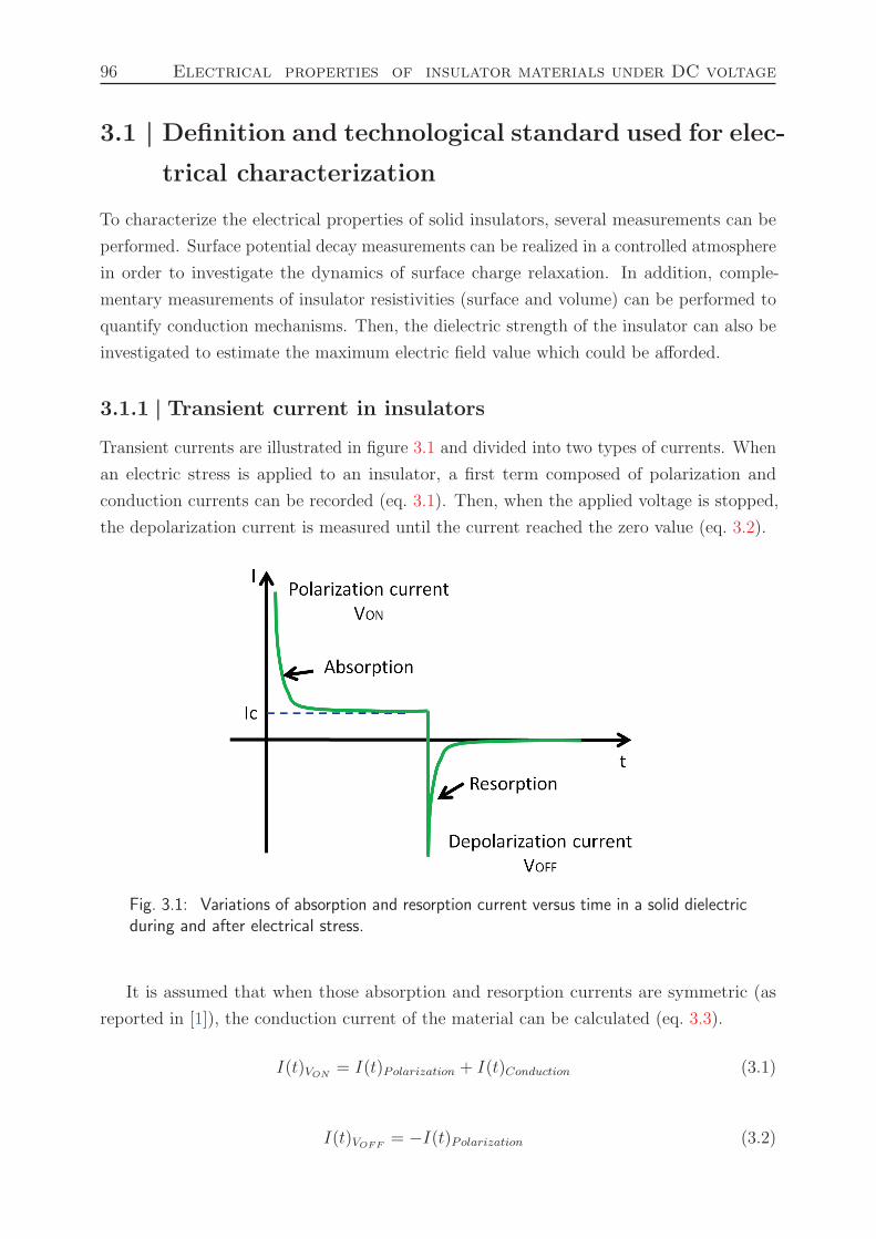
96 Electrical properties of insulator materials under DC voltage
3.1 | Definition and technological standard used for elec-
trical characterization
To characterize the electrical properties of solid insulators, several measurements can be
performed. Surface potential decay measurements can be realized in a controlled atmosphere
in order to investigate the dynamics of surface charge relaxation. In addition, comple-
mentary measurements of insulator resistivities (surface and volume) can be performed to
quantify conduction mechanisms. Then, the dielectric strength of the insulator can also be
investigated to estimate the maximum electric field value which could be afforded.
3.1.1 | Transient current in insulators
Transient currents are illustrated in figure 3.1 and divided into two types of currents. When
an electric stress is applied to an insulator, a first term composed of polarization and
conduction currents can be recorded (eq. 3.1). Then, when the applied voltage is stopped,
the depolarization current is measured until the current reached the zero value (eq. 3.2).
Fig. 3.1: Variations of absorption and resorption current versus time in a solid dielectricduring and after electrical stress.
It is assumed that when those absorption and resorption currents are symmetric (as
reported in [1]), the conduction current of the material can be calculated (eq. 3.3).
I(t)VON= I(t)Polarization + I(t)Conduction (3.1)
I(t)VOFF= −I(t)Polarization (3.2)
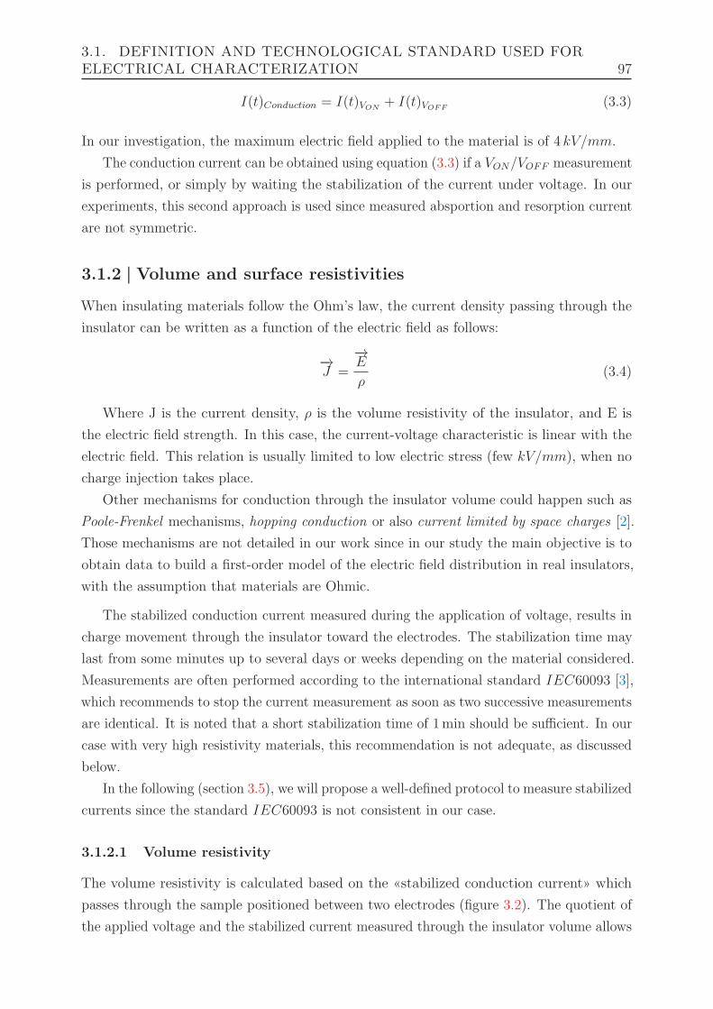
3.1. DEFINITION AND TECHNOLOGICAL STANDARD USED FORELECTRICAL CHARACTERIZATION 97
I(t)Conduction = I(t)VON+ I(t)VOFF
(3.3)
In our investigation, the maximum electric field applied to the material is of 4 kV/mm.
The conduction current can be obtained using equation (3.3) if a VON/VOFF measurement
is performed, or simply by waiting the stabilization of the current under voltage. In our
experiments, this second approach is used since measured absportion and resorption current
are not symmetric.
3.1.2 | Volume and surface resistivities
When insulating materials follow the Ohm’s law, the current density passing through the
insulator can be written as a function of the electric field as follows:
−→J =
−→E
ρ(3.4)
Where J is the current density, ρ is the volume resistivity of the insulator, and E is
the electric field strength. In this case, the current-voltage characteristic is linear with the
electric field. This relation is usually limited to low electric stress (few kV/mm), when no
charge injection takes place.
Other mechanisms for conduction through the insulator volume could happen such as
Poole-Frenkel mechanisms, hopping conduction or also current limited by space charges [2].
Those mechanisms are not detailed in our work since in our study the main objective is to
obtain data to build a first-order model of the electric field distribution in real insulators,
with the assumption that materials are Ohmic.
The stabilized conduction current measured during the application of voltage, results in
charge movement through the insulator toward the electrodes. The stabilization time may
last from some minutes up to several days or weeks depending on the material considered.
Measurements are often performed according to the international standard IEC60093 [3],
which recommends to stop the current measurement as soon as two successive measurements
are identical. It is noted that a short stabilization time of 1min should be sufficient. In our
case with very high resistivity materials, this recommendation is not adequate, as discussed
below.
In the following (section 3.5), we will propose a well-defined protocol to measure stabilized
currents since the standard IEC60093 is not consistent in our case.
3.1.2.1 Volume resistivity
The volume resistivity is calculated based on the «stabilized conduction current» which
passes through the sample positioned between two electrodes (figure 3.2). The quotient of
the applied voltage and the stabilized current measured through the insulator volume allows
98 Electrical properties of insulator materials under DC voltage
determining the volume resistivity, excluding the current along the surface, and according
to the electrodes dimensions. Here, the equation is written considering a circular geometry.
Further electrodes geometries are described in the standard IEC60093 [3].
ρv [Ω.cm] =V
IV∗ S
e(3.5)
With S = π ∗ (d1 + g)2
4, V the applied voltage, IV the current through the insulator
volume, and e the insulator thickness.
Fig. 3.2: Electrodes dimensions, d1 the diameter of the measurement electrode and g,the gap between electrodes.
3.1.2.2 Surface resistivity
The surface resistivity is calculated based on the stabilized conduction current which
passes along the sample surface, but also partly through the volume [4], in the electrodes
configuration presented in figure 3.2. The quotient of the applied voltage and the stabilized
current measured in a surface layer of an insulating material allows the calculation of this
parameter. As for volume resistivity, the geometry considered here is circular.
ρs [Ω/sq] =V
Is∗ P
g(3.6)
With P = π ∗ (d1 + g), and g the distance between the guarded and measurements
electrodes.
In HVDC, those properties must be very well-known, as well as their variations depending
on environmental conditions (temperature, relative humidity, electric field, and so on), since
the electric field distribution directly depends on those properties.
3.1.3 | Dielectric strength of insulators
The dielectric strength of an insulating material corresponds to the maximum electric field
value that can be applied on it without any non reversible damages on the insulator. Such
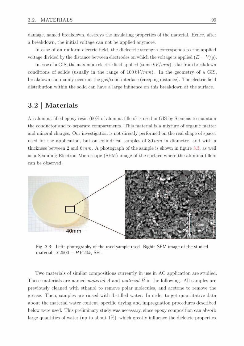
3.2. MATERIALS 99
damage, named breakdown, destroys the insulating properties of the material. Hence, after
a breakdown, the initial voltage can not be applied anymore.
In case of an uniform electric field, the dielectric strength corresponds to the applied
voltage divided by the distance between electrodes on which the voltage is applied (E = V/g).
In case of a GIS, the maximum electric field applied (some kV/mm) is far from breakdown
conditions of solids (usually in the range of 100 kV/mm). In the geometry of a GIS,
breakdown can mainly occur at the gas/solid interface (creeping distance). The electric field
distribution within the solid can have a large influence on this breakdown at the surface.
3.2 | Materials
An alumina-filled epoxy resin (60% of alumina fillers) is used in GIS by Siemens to maintain
the conductor and to separate compartments. This material is a mixture of organic matter
and mineral charges. Our investigation is not directly performed on the real shape of spacer
used for the application, but on cylindrical samples of 80mm in diameter, and with a
thickness between 2 and 6mm. A photograph of the sample is shown in figure 3.3, as well
as a Scanning Electron Microscope (SEM) image of the surface where the alumina fillers
can be observed.
Fig. 3.3: Left: photography of the used sample used. Right: SEM image of the studiedmaterial; X2500−HV 20k, SEI.
Two materials of similar compositions currently in use in AC application are studied.
Those materials are named material A and material B in the following. All samples are
previously cleaned with ethanol to remove polar molecules, and acetone to remove the
grease. Then, samples are rinsed with distilled water. In order to get quantitative data
about the material water content, specific drying and impregnation procedures described
below were used. This preliminary study was necessary, since epoxy composition can absorb
large quantities of water (up to about 1%), which greatly influence the dieletric properties.
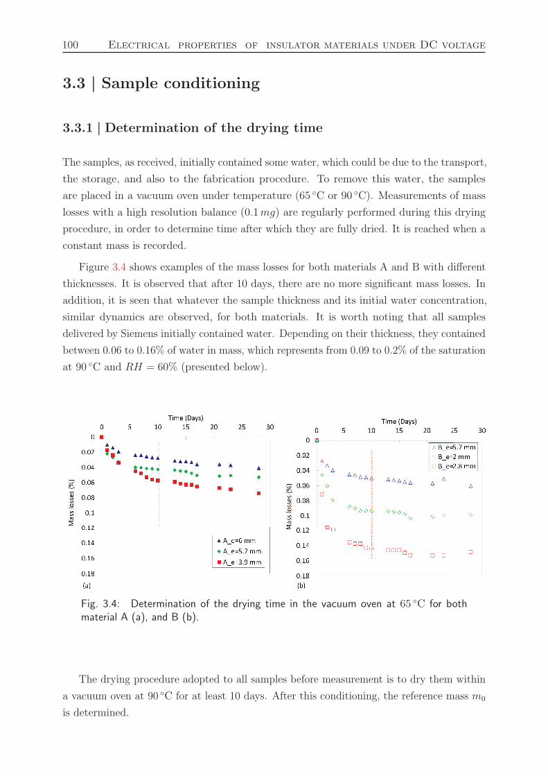
100 Electrical properties of insulator materials under DC voltage
3.3 | Sample conditioning
3.3.1 | Determination of the drying time
The samples, as received, initially contained some water, which could be due to the transport,
the storage, and also to the fabrication procedure. To remove this water, the samples
are placed in a vacuum oven under temperature (65 C or 90 C). Measurements of mass
losses with a high resolution balance (0.1mg) are regularly performed during this drying
procedure, in order to determine time after which they are fully dried. It is reached when a
constant mass is recorded.
Figure 3.4 shows examples of the mass losses for both materials A and B with different
thicknesses. It is observed that after 10 days, there are no more significant mass losses. In
addition, it is seen that whatever the sample thickness and its initial water concentration,
similar dynamics are observed, for both materials. It is worth noting that all samples
delivered by Siemens initially contained water. Depending on their thickness, they contained
between 0.06 to 0.16% of water in mass, which represents from 0.09 to 0.2% of the saturation
at 90 C and RH = 60% (presented below).
Fig. 3.4: Determination of the drying time in the vacuum oven at 65 C for bothmaterial A (a), and B (b).
The drying procedure adopted to all samples before measurement is to dry them within
a vacuum oven at 90 C for at least 10 days. After this conditioning, the reference mass m0
is determined.
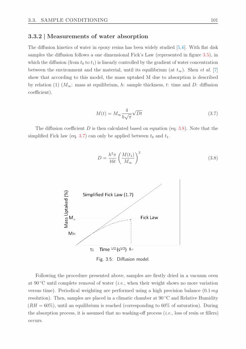
3.3. SAMPLE CONDITIONING 101
3.3.2 | Measurements of water absorption
The diffusion kinetics of water in epoxy resins has been widely studied [5, 6]. With flat disk
samples the diffusion follows a one dimensional Fick’s Law (represented in figure 3.5), in
which the diffusion (from t0 to t1) is linearly controlled by the gradient of water concentration
between the environment and the material, until its equilibrium (at t∞). Shen et al. [7]
show that according to this model, the mass uptaked M due to absorption is described
by relation (1) (M∞: mass at equilibrium, h: sample thickness, t: time and D: diffusion
coefficient).
M(t) = M∞
4
h√π
√Dt (3.7)
The diffusion coefficient D is then calculated based on equation (eq. 3.8). Note that the
simplified Fick law (eq. 3.7) can only be applied between t0 and t1.
D =h2π
16t
(
M(t1)
M∞
)2
(3.8)
Fig. 3.5: Diffusion model.
Following the procedure presented above, samples are firstly dried in a vacuum oven
at 90 C until complete removal of water (i.e., when their weight shows no more variation
versus time). Periodical weighting are performed using a high precision balance (0.1mg
resolution). Then, samples are placed in a climatic chamber at 90 C and Relative Humidity
(RH = 60%), until an equilibrium is reached (corresponding to 60% of saturation). During
the absorption process, it is assumed that no washing-off process (i.e., loss of resin or fillers)
occurs.
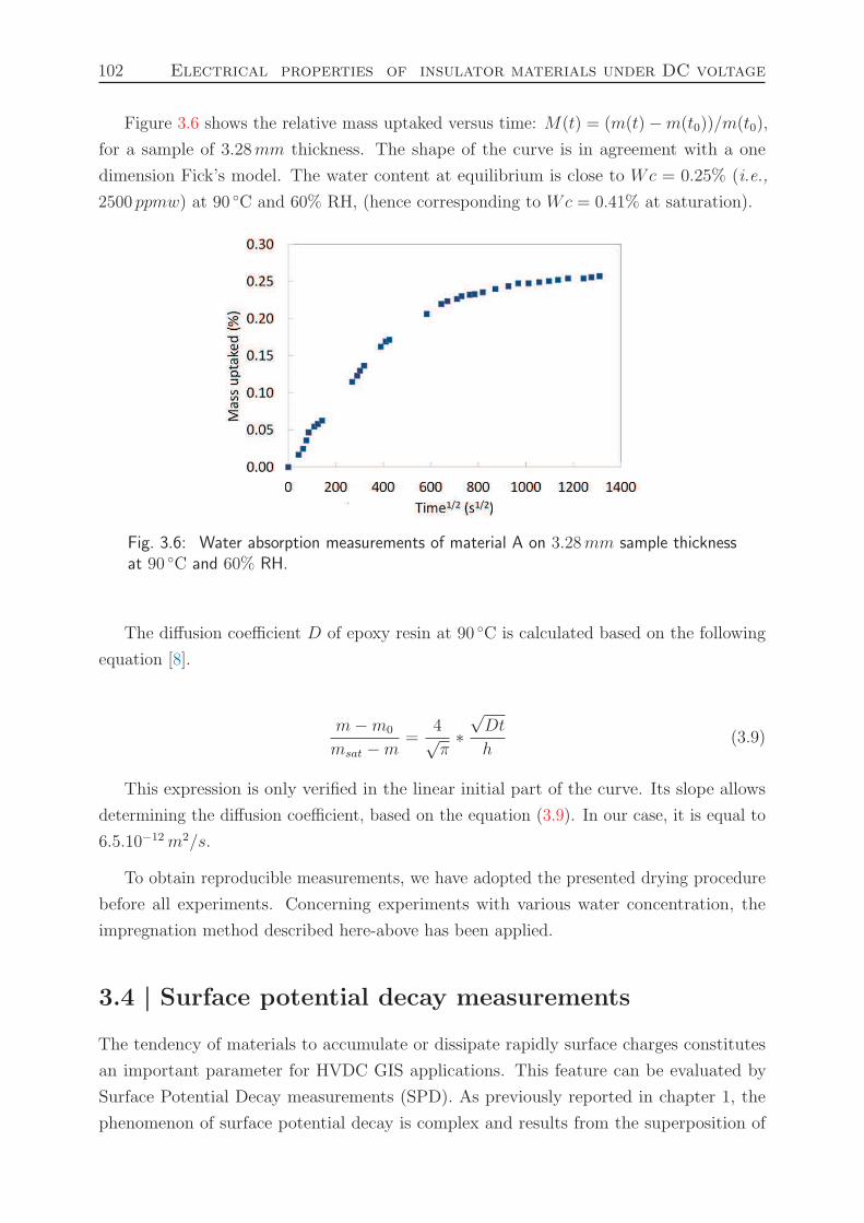
102 Electrical properties of insulator materials under DC voltage
Figure 3.6 shows the relative mass uptaked versus time: M(t) = (m(t)−m(t0))/m(t0),
for a sample of 3.28mm thickness. The shape of the curve is in agreement with a one
dimension Fick’s model. The water content at equilibrium is close to Wc = 0.25% (i.e.,
2500 ppmw) at 90 C and 60% RH, (hence corresponding to Wc = 0.41% at saturation).
Fig. 3.6: Water absorption measurements of material A on 3.28mm sample thicknessat 90 C and 60% RH.
The diffusion coefficient D of epoxy resin at 90 C is calculated based on the following
equation [8].
m−m0
msat −m=
4√π∗√Dt
h(3.9)
This expression is only verified in the linear initial part of the curve. Its slope allows
determining the diffusion coefficient, based on the equation (3.9). In our case, it is equal to
6.5.10−12 m2/s.
To obtain reproducible measurements, we have adopted the presented drying procedure
before all experiments. Concerning experiments with various water concentration, the
impregnation method described here-above has been applied.
3.4 | Surface potential decay measurements
The tendency of materials to accumulate or dissipate rapidly surface charges constitutes
an important parameter for HVDC GIS applications. This feature can be evaluated by
Surface Potential Decay measurements (SPD). As previously reported in chapter 1, the
phenomenon of surface potential decay is complex and results from the superposition of
3.4. SURFACE POTENTIAL DECAY MEASUREMENTS 103
various phenomena. Charges can dissipate following several ways: spreading over the
insulator surface, conduction through its volume, and neutralization by ions present in the
environment. In addition, displacement currents within the material, associated to long
term polarization effects, may also contribute to the variation of the surface potential.
In our work, we use this technique to obtain a qualitative assessment of influencing
parameters which worth to be studied, and to compare various materials. In this section,
we will first present the experimental system, then we will discuss the results obtained
according to various parameters.
3.4.1 | Experimental system
To measure the surface potential decay on insulator surfaces, the experiment is divided into
two parts. The first one consists in charging the insulator using corona discharge, and the
second step is the measurement of the surface potential decay during time. The experimental
setup is presented in figure 3.7. A motorized device allows to rotate the support and position
it under the charging system where a corona discharge occurs during 20 s, in order to charge
the material surface with ions. The initial uniform surface charge distribution is confined
into a 2 cm diameter area. The experimental arrangement is presented on figure 3.7 (b).
The corona discharge is created applying high voltage on a needle, which will ionize
the surrounding air around it and create ions. The latter are then injected toward the
sample direction. A polarized grid, placed between the needle and the sample surface, will
uniformly distribute charges over the insulator surface, and also fix the value of the desired
surface potential. Once the corona discharge ends, the sample is positioned back under
the measurement device where the non-contact electrostatic probe records the evolution of
the surface potential during time (figure 3.7 (c)). The surface potential is measured using
a vibrating Kelvin probe. This electrostatic voltmeter employs a field-nulling technique
that achieves DC stability and high accuracy, even if the probe-to-surface spacing changes.
The probe used is a Trek model 347r with probe model 6300 (range 0 to ±3 kV ; accuracy
better than 0.05% of full scale). The probe to surface separation is 2 ± 1mm.
During the whole experiment, the sample is fixed on its support to avoid any movements
during the rotation. In addition, to ensure a good contact between the back-side of the
sample and the grounded ring, a conductive inter-layer is placed between the sample and
the ring. It had also been observed that covering the back-side of the sample using a copper
tape enabled a better ground contact and a better reproducibility in measurements.
The system, placed in a climatic chamber, is remotely controlled using a software
program which allows controlling the motors and other relays.
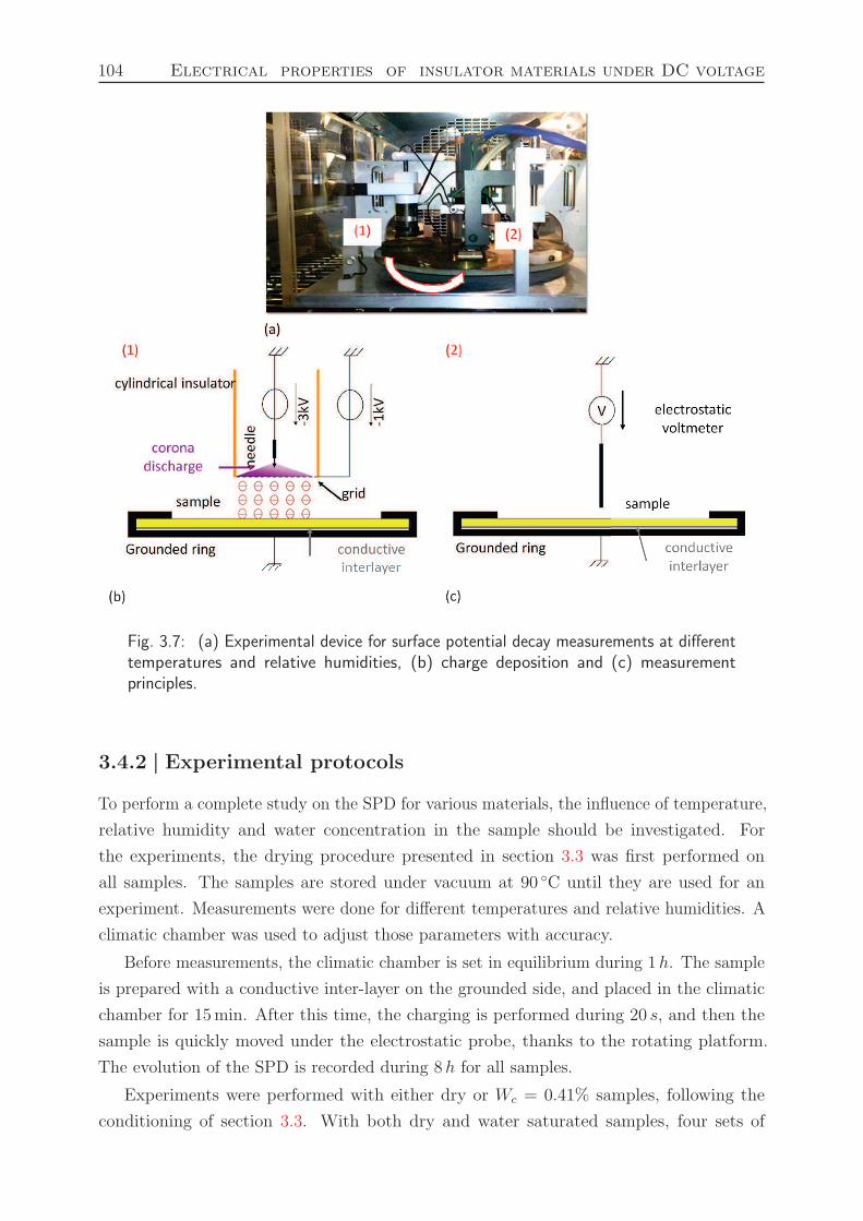
104 Electrical properties of insulator materials under DC voltage
Fig. 3.7: (a) Experimental device for surface potential decay measurements at differenttemperatures and relative humidities, (b) charge deposition and (c) measurementprinciples.
3.4.2 | Experimental protocols
To perform a complete study on the SPD for various materials, the influence of temperature,
relative humidity and water concentration in the sample should be investigated. For
the experiments, the drying procedure presented in section 3.3 was first performed on
all samples. The samples are stored under vacuum at 90 C until they are used for an
experiment. Measurements were done for different temperatures and relative humidities. A
climatic chamber was used to adjust those parameters with accuracy.
Before measurements, the climatic chamber is set in equilibrium during 1h. The sample
is prepared with a conductive inter-layer on the grounded side, and placed in the climatic
chamber for 15min. After this time, the charging is performed during 20 s, and then the
sample is quickly moved under the electrostatic probe, thanks to the rotating platform.
The evolution of the SPD is recorded during 8h for all samples.
Experiments were performed with either dry or Wc = 0.41% samples, following the
conditioning of section 3.3. With both dry and water saturated samples, four sets of
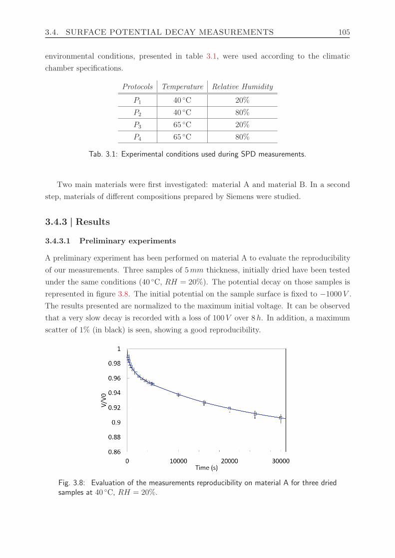
3.4. SURFACE POTENTIAL DECAY MEASUREMENTS 105
environmental conditions, presented in table 3.1, were used according to the climatic
chamber specifications.
Protocols Temperature Relative Humidity
P1 40 C 20%
P2 40 C 80%
P3 65 C 20%
P4 65 C 80%
Tab. 3.1: Experimental conditions used during SPD measurements.
Two main materials were first investigated: material A and material B. In a second
step, materials of different compositions prepared by Siemens were studied.
3.4.3 | Results
3.4.3.1 Preliminary experiments
A preliminary experiment has been performed on material A to evaluate the reproducibility
of our measurements. Three samples of 5mm thickness, initially dried have been tested
under the same conditions (40 C, RH = 20%). The potential decay on those samples is
represented in figure 3.8. The initial potential on the sample surface is fixed to −1000V .
The results presented are normalized to the maximum initial voltage. It can be observed
that a very slow decay is recorded with a loss of 100V over 8h. In addition, a maximum
scatter of 1% (in black) is seen, showing a good reproducibility.
Fig. 3.8: Evaluation of the measurements reproducibility on material A for three driedsamples at 40 C, RH = 20%.
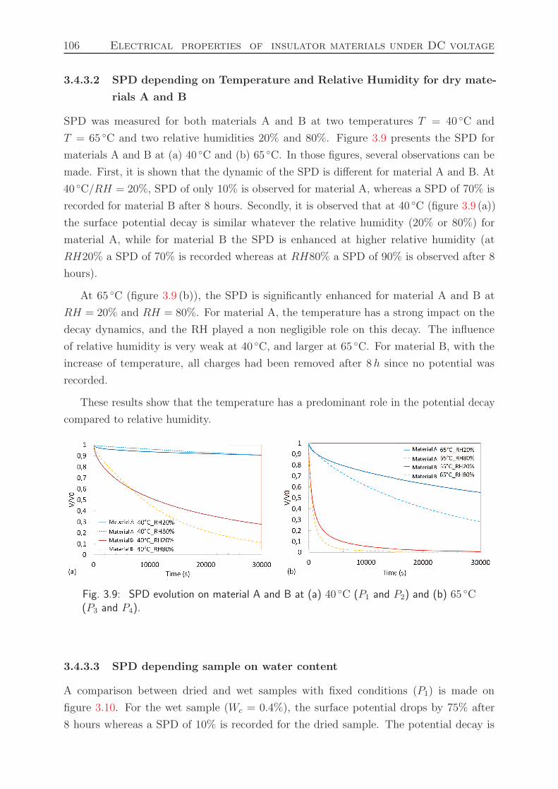
106 Electrical properties of insulator materials under DC voltage
3.4.3.2 SPD depending on Temperature and Relative Humidity for dry mate-
rials A and B
SPD was measured for both materials A and B at two temperatures T = 40 C and
T = 65 C and two relative humidities 20% and 80%. Figure 3.9 presents the SPD for
materials A and B at (a) 40 C and (b) 65 C. In those figures, several observations can be
made. First, it is shown that the dynamic of the SPD is different for material A and B. At
40 C/RH = 20%, SPD of only 10% is observed for material A, whereas a SPD of 70% is
recorded for material B after 8 hours. Secondly, it is observed that at 40 C (figure 3.9 (a))
the surface potential decay is similar whatever the relative humidity (20% or 80%) for
material A, while for material B the SPD is enhanced at higher relative humidity (at
RH20% a SPD of 70% is recorded whereas at RH80% a SPD of 90% is observed after 8
hours).
At 65 C (figure 3.9 (b)), the SPD is significantly enhanced for material A and B at
RH = 20% and RH = 80%. For material A, the temperature has a strong impact on the
decay dynamics, and the RH played a non negligible role on this decay. The influence
of relative humidity is very weak at 40 C, and larger at 65 C. For material B, with the
increase of temperature, all charges had been removed after 8h since no potential was
recorded.
These results show that the temperature has a predominant role in the potential decay
compared to relative humidity.
Fig. 3.9: SPD evolution on material A and B at (a) 40 C (P1 and P2) and (b) 65 C(P3 and P4).
3.4.3.3 SPD depending sample on water content
A comparison between dried and wet samples with fixed conditions (P1) is made on
figure 3.10. For the wet sample (Wc = 0.4%), the surface potential drops by 75% after
8 hours whereas a SPD of 10% is recorded for the dried sample. The potential decay is
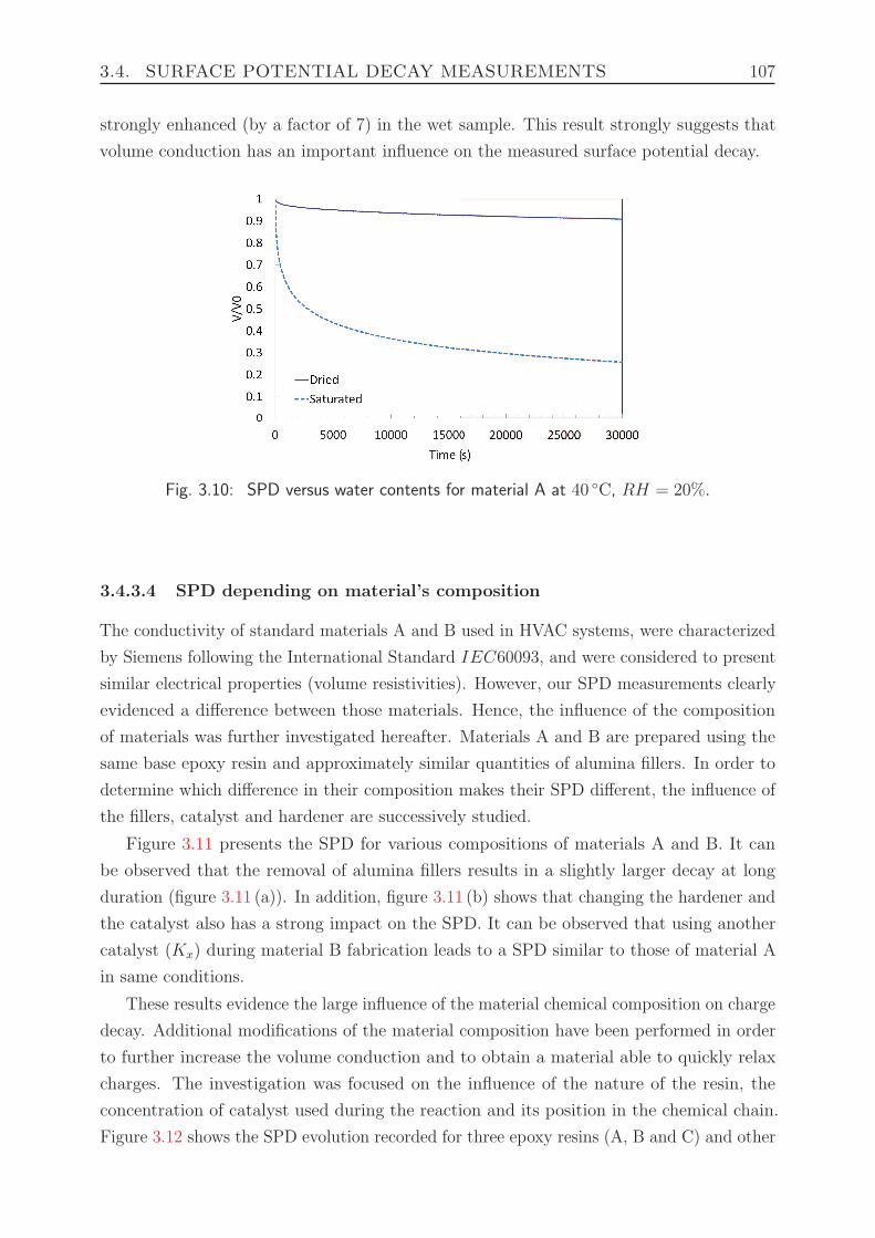
3.4. SURFACE POTENTIAL DECAY MEASUREMENTS 107
strongly enhanced (by a factor of 7) in the wet sample. This result strongly suggests that
volume conduction has an important influence on the measured surface potential decay.
Fig. 3.10: SPD versus water contents for material A at 40 C, RH = 20%.
3.4.3.4 SPD depending on material’s composition
The conductivity of standard materials A and B used in HVAC systems, were characterized
by Siemens following the International Standard IEC60093, and were considered to present
similar electrical properties (volume resistivities). However, our SPD measurements clearly
evidenced a difference between those materials. Hence, the influence of the composition
of materials was further investigated hereafter. Materials A and B are prepared using the
same base epoxy resin and approximately similar quantities of alumina fillers. In order to
determine which difference in their composition makes their SPD different, the influence of
the fillers, catalyst and hardener are successively studied.
Figure 3.11 presents the SPD for various compositions of materials A and B. It can
be observed that the removal of alumina fillers results in a slightly larger decay at long
duration (figure 3.11 (a)). In addition, figure 3.11 (b) shows that changing the hardener and
the catalyst also has a strong impact on the SPD. It can be observed that using another
catalyst (Kx) during material B fabrication leads to a SPD similar to those of material A
in same conditions.
These results evidence the large influence of the material chemical composition on charge
decay. Additional modifications of the material composition have been performed in order
to further increase the volume conduction and to obtain a material able to quickly relax
charges. The investigation was focused on the influence of the nature of the resin, the
concentration of catalyst used during the reaction and its position in the chemical chain.
Figure 3.12 shows the SPD evolution recorded for three epoxy resins (A, B and C) and other
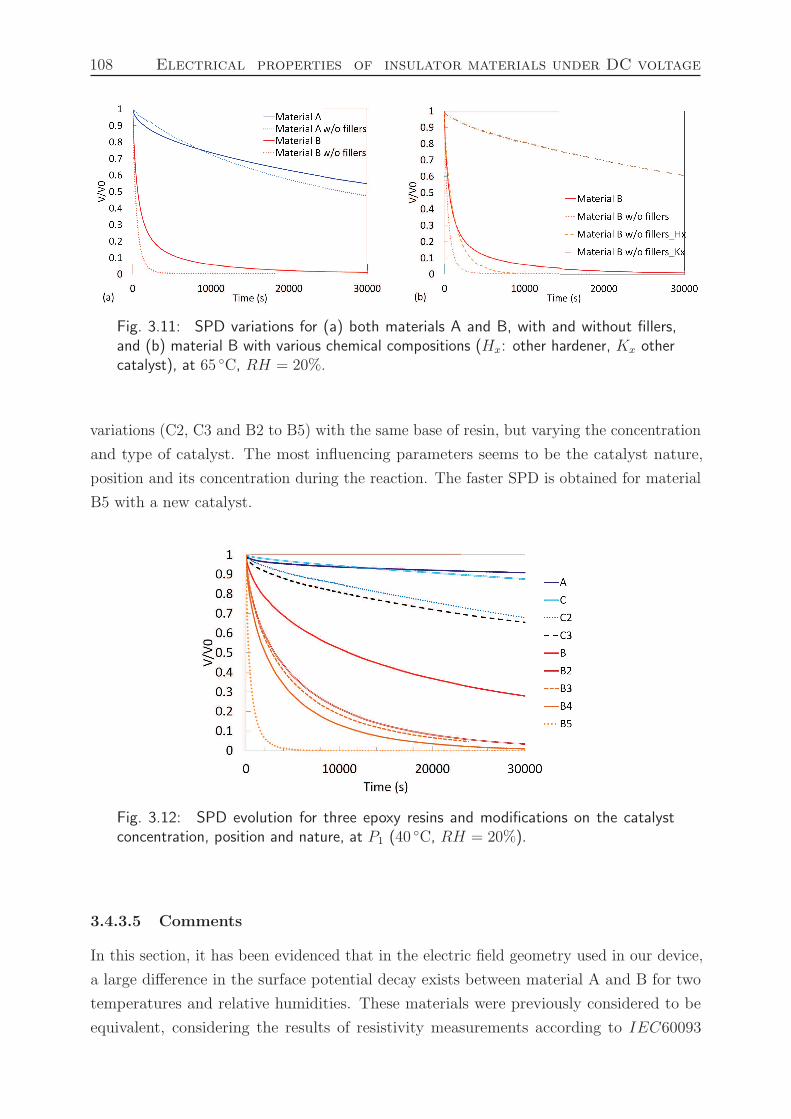
108 Electrical properties of insulator materials under DC voltage
Fig. 3.11: SPD variations for (a) both materials A and B, with and without fillers,and (b) material B with various chemical compositions (Hx: other hardener, Kx othercatalyst), at 65 C, RH = 20%.
variations (C2, C3 and B2 to B5) with the same base of resin, but varying the concentration
and type of catalyst. The most influencing parameters seems to be the catalyst nature,
position and its concentration during the reaction. The faster SPD is obtained for material
B5 with a new catalyst.
Fig. 3.12: SPD evolution for three epoxy resins and modifications on the catalystconcentration, position and nature, at P1 (40 C, RH = 20%).
3.4.3.5 Comments
In this section, it has been evidenced that in the electric field geometry used in our device,
a large difference in the surface potential decay exists between material A and B for two
temperatures and relative humidities. These materials were previously considered to be
equivalent, considering the results of resistivity measurements according to IEC60093
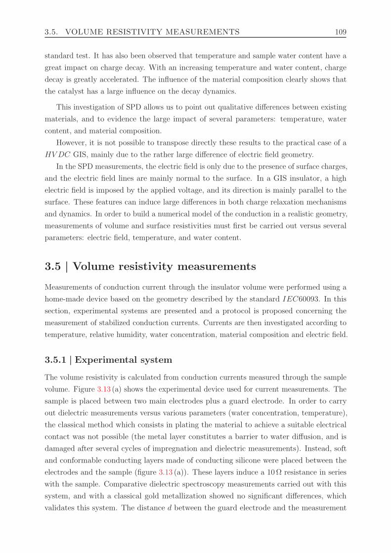
3.5. VOLUME RESISTIVITY MEASUREMENTS 109
standard test. It has also been observed that temperature and sample water content have a
great impact on charge decay. With an increasing temperature and water content, charge
decay is greatly accelerated. The influence of the material composition clearly shows that
the catalyst has a large influence on the decay dynamics.
This investigation of SPD allows us to point out qualitative differences between existing
materials, and to evidence the large impact of several parameters: temperature, water
content, and material composition.
However, it is not possible to transpose directly these results to the practical case of a
HVDC GIS, mainly due to the rather large difference of electric field geometry.
In the SPD measurements, the electric field is only due to the presence of surface charges,
and the electric field lines are mainly normal to the surface. In a GIS insulator, a high
electric field is imposed by the applied voltage, and its direction is mainly parallel to the
surface. These features can induce large differences in both charge relaxation mechanisms
and dynamics. In order to build a numerical model of the conduction in a realistic geometry,
measurements of volume and surface resistivities must first be carried out versus several
parameters: electric field, temperature, and water content.
3.5 | Volume resistivity measurements
Measurements of conduction current through the insulator volume were performed using a
home-made device based on the geometry described by the standard IEC60093. In this
section, experimental systems are presented and a protocol is proposed concerning the
measurement of stabilized conduction currents. Currents are then investigated according to
temperature, relative humidity, water concentration, material composition and electric field.
3.5.1 | Experimental system
The volume resistivity is calculated from conduction currents measured through the sample
volume. Figure 3.13 (a) shows the experimental device used for current measurements. The
sample is placed between two main electrodes plus a guard electrode. In order to carry
out dielectric measurements versus various parameters (water concentration, temperature),
the classical method which consists in plating the material to achieve a suitable electrical
contact was not possible (the metal layer constitutes a barrier to water diffusion, and is
damaged after several cycles of impregnation and dielectric measurements). Instead, soft
and conformable conducting layers made of conducting silicone were placed between the
electrodes and the sample (figure 3.13 (a)). These layers induce a 10Ω resistance in series
with the sample. Comparative dielectric spectroscopy measurements carried out with this
system, and with a classical gold metallization showed no significant differences, which
validates this system. The distance d between the guard electrode and the measurement
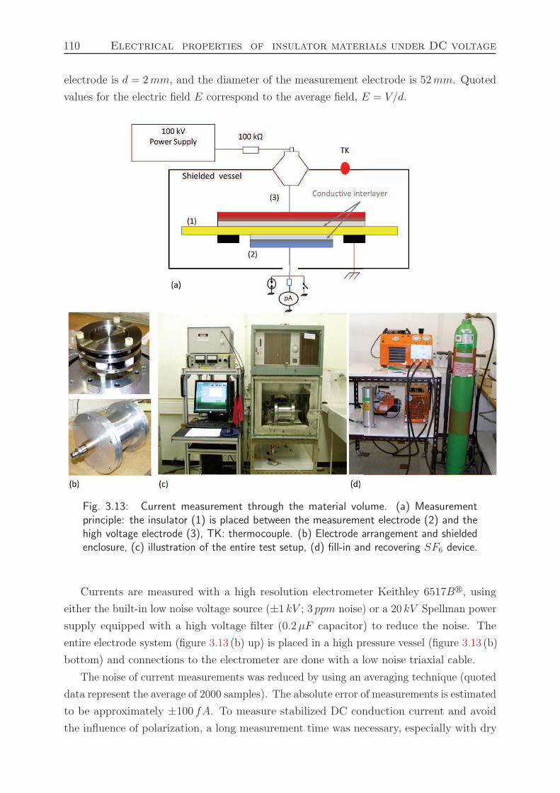
110 Electrical properties of insulator materials under DC voltage
electrode is d = 2mm, and the diameter of the measurement electrode is 52mm. Quoted
values for the electric field E correspond to the average field, E = V/d.
Fig. 3.13: Current measurement through the material volume. (a) Measurementprinciple: the insulator (1) is placed between the measurement electrode (2) and thehigh voltage electrode (3), TK: thermocouple. (b) Electrode arrangement and shieldedenclosure, (c) illustration of the entire test setup, (d) fill-in and recovering SF6 device.
Currents are measured with a high resolution electrometer Keithley 6517Br, using
either the built-in low noise voltage source (±1 kV ; 3 ppm noise) or a 20 kV Spellman power
supply equipped with a high voltage filter (0.2µF capacitor) to reduce the noise. The
entire electrode system (figure 3.13 (b) up) is placed in a high pressure vessel (figure 3.13 (b)
bottom) and connections to the electrometer are done with a low noise triaxial cable.
The noise of current measurements was reduced by using an averaging technique (quoted
data represent the average of 2000 samples). The absolute error of measurements is estimated
to be approximately ±100 fA. To measure stabilized DC conduction current and avoid
the influence of polarization, a long measurement time was necessary, especially with dry
3.5. VOLUME RESISTIVITY MEASUREMENTS 111
samples with a very high resistivity ρv (ρv > 1018 Ω.cm @ 20 C). The measurement lasted
in this case at least 2 days, in order to reach the complete stabilization, which occurred
when the polarization current becomes much lower than the conduction current.
The sealed enclosure can afford pressure up to 1.1MPa. It is placed within a regulated
oven (figure 3.13(c)) to accurately adjust the temperature from 20 C to 80 C. The latter
is measured during experiments thanks to a thermocouple placed within the enclosure. The
system is filled with SF6, and unfilled using compressor and pre-compressor (figure 3.13 (d)).
Such device permits to recover the SF6 down to 20mbar.
This experimental system allows determining the volume resistivity of materials according
to different temperature, electric field values and water concentration. A well-defined
experimental protocol, detailed hereafter, was needed to obtain reproducible and accurate
measurements.
3.5.2 | Experimental protocol
In this section, we describe the measurement procedure defined to obtain reproducible
measurements and to avoid the influence of charges pre-existing in the material.
3.5.2.1 Preliminary experiments
To measure the current passing through the insulator volume, a voltage of 1000V is applied
on material A of 3mm thickness, using the device presented above. For this experiment, the
measurement is performed in air at atmospheric pressure (40 C, RH = 20%). Figure 3.14
presents the variations of the current in time. It is observed that the current first decreases
from 0 to 60min, and tends to stabilize after. This result evidences that after 1min
(duration proposed in the IEC standard) the stabilized current is far from being reached.
Even at 160min the stabilized current is not reached yet. In this case, a longer stabilization
time is needed, superior than 2− 3 hours.
The volume resistivity has been calculated for material A and B based on stabilized
currents (figure 3.15). According to the standard method, volume resistivities for materials
A and B are very similar (approximately 1016Ω.cm at 20 C). On the contrary, volume
resistivities calculated from stabilized currents show a difference of one decade between
material A and B. For each material two measurements were performed on the same sample,
showing that measurements are repeatable.
Those results highlight two main points:
−→ Following IEC recommendations, no differences in volume resistivities are observed
between material A and B, but stable currents were not reached.
−→ Resistivities calculated from stabilized currents evidence one decade difference.
This difference is in agreement with the surface potential decay measurements presented
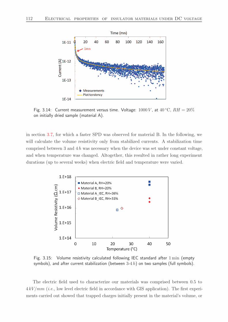
112 Electrical properties of insulator materials under DC voltage
Fig. 3.14: Current measurement versus time. Voltage: 1000V , at 40 C, RH = 20%on initially dried sample (material A).
in section 3.7, for which a faster SPD was observed for material B. In the following, we
will calculate the volume resistivity only from stabilized currents. A stabilization time
comprised between 3 and 4h was necessary when the device was set under constant voltage,
and when temperature was changed. Altogether, this resulted in rather long experiment
durations (up to several weeks) when electric field and temperature were varied.
Fig. 3.15: Volume resistivity calculated following IEC standard after 1min (emptysymbols), and after current stabilization (between 3-4h) on two samples (full symbols).
The electric field used to characterize our materials was comprised between 0.5 to
4 kV/mm (i.e., low level electric field in accordance with GIS application). The first experi-
ments carried out showed that trapped charges initially present in the material’s volume, or
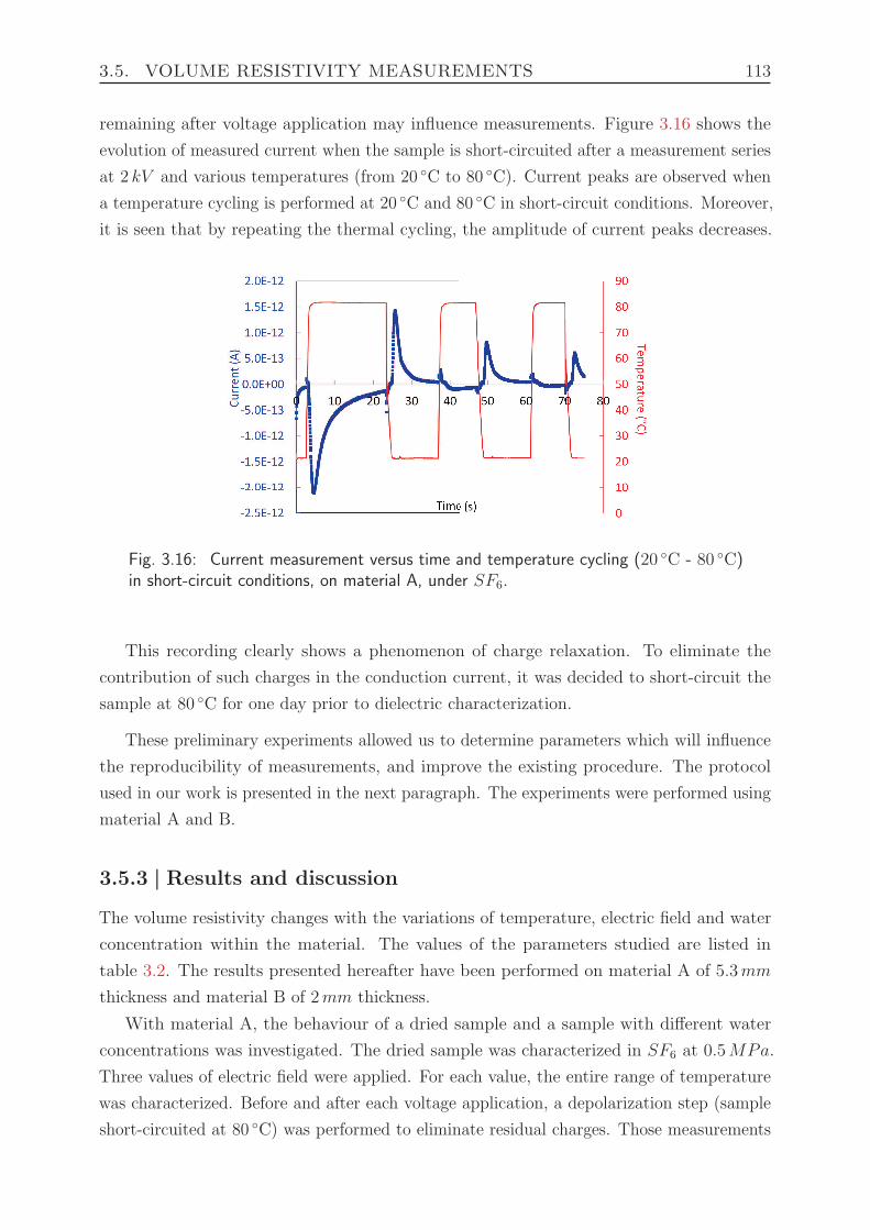
3.5. VOLUME RESISTIVITY MEASUREMENTS 113
remaining after voltage application may influence measurements. Figure 3.16 shows the
evolution of measured current when the sample is short-circuited after a measurement series
at 2 kV and various temperatures (from 20 C to 80 C). Current peaks are observed when
a temperature cycling is performed at 20 C and 80 C in short-circuit conditions. Moreover,
it is seen that by repeating the thermal cycling, the amplitude of current peaks decreases.
Fig. 3.16: Current measurement versus time and temperature cycling (20 C - 80 C)in short-circuit conditions, on material A, under SF6.
This recording clearly shows a phenomenon of charge relaxation. To eliminate the
contribution of such charges in the conduction current, it was decided to short-circuit the
sample at 80 C for one day prior to dielectric characterization.
These preliminary experiments allowed us to determine parameters which will influence
the reproducibility of measurements, and improve the existing procedure. The protocol
used in our work is presented in the next paragraph. The experiments were performed using
material A and B.
3.5.3 | Results and discussion
The volume resistivity changes with the variations of temperature, electric field and water
concentration within the material. The values of the parameters studied are listed in
table 3.2. The results presented hereafter have been performed on material A of 5.3mm
thickness and material B of 2mm thickness.
With material A, the behaviour of a dried sample and a sample with different water
concentrations was investigated. The dried sample was characterized in SF6 at 0.5MPa.
Three values of electric field were applied. For each value, the entire range of temperature
was characterized. Before and after each voltage application, a depolarization step (sample
short-circuited at 80 C) was performed to eliminate residual charges. Those measurements
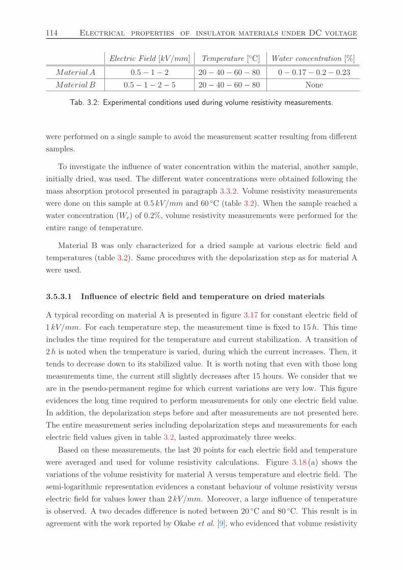
114 Electrical properties of insulator materials under DC voltage
Electric Field [kV/mm] Temperature [C] Water concentration [%]
Material A 0.5− 1− 2 20− 40− 60− 80 0− 0.17− 0.2− 0.23
Material B 0.5− 1− 2− 5 20− 40− 60− 80 None
Tab. 3.2: Experimental conditions used during volume resistivity measurements.
were performed on a single sample to avoid the measurement scatter resulting from different
samples.
To investigate the influence of water concentration within the material, another sample,
initially dried, was used. The different water concentrations were obtained following the
mass absorption protocol presented in paragraph 3.3.2. Volume resistivity measurements
were done on this sample at 0.5 kV/mm and 60 C (table 3.2). When the sample reached a
water concentration (Wc) of 0.2%, volume resistivity measurements were performed for the
entire range of temperature.
Material B was only characterized for a dried sample at various electric field and
temperatures (table 3.2). Same procedures with the depolarization step as for material A
were used.
3.5.3.1 Influence of electric field and temperature on dried materials
A typical recording on material A is presented in figure 3.17 for constant electric field of
1 kV/mm. For each temperature step, the measurement time is fixed to 15h. This time
includes the time required for the temperature and current stabilization. A transition of
2h is noted when the temperature is varied, during which the current increases. Then, it
tends to decrease down to its stabilized value. It is worth noting that even with those long
measurements time, the current still slightly decreases after 15 hours. We consider that we
are in the pseudo-permanent regime for which current variations are very low. This figure
evidences the long time required to perform measurements for only one electric field value.
In addition, the depolarization steps before and after measurements are not presented here.
The entire measurement series including depolarization steps and measurements for each
electric field values given in table 3.2, lasted approximately three weeks.
Based on these measurements, the last 20 points for each electric field and temperature
were averaged and used for volume resistivity calculations. Figure 3.18 (a) shows the
variations of the volume resistivity for material A versus temperature and electric field. The
semi-logarithmic representation evidences a constant behaviour of volume resistivity versus
electric field for values lower than 2 kV/mm. Moreover, a large influence of temperature
is observed. A two decades difference is noted between 20 C and 80 C. This result is in
agreement with the work reported by Okabe et al. [9], who evidenced that volume resistivity
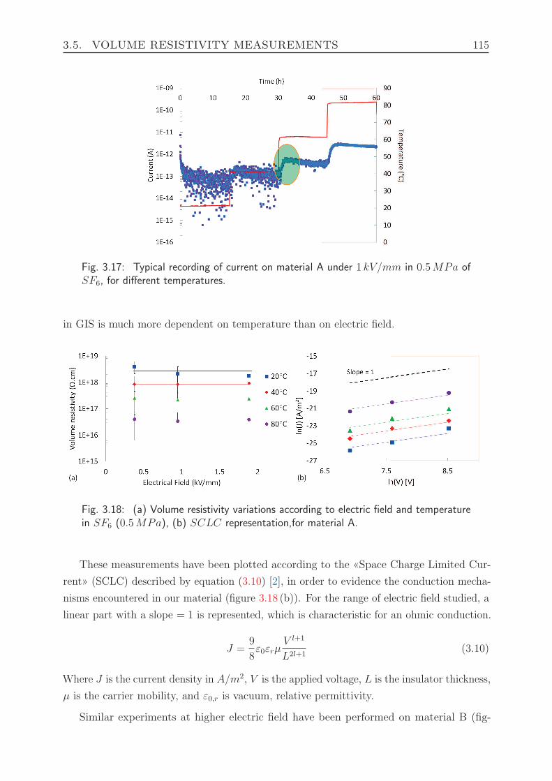
3.5. VOLUME RESISTIVITY MEASUREMENTS 115
Fig. 3.17: Typical recording of current on material A under 1 kV/mm in 0.5MPa ofSF6, for different temperatures.
in GIS is much more dependent on temperature than on electric field.
Fig. 3.18: (a) Volume resistivity variations according to electric field and temperaturein SF6 (0.5MPa), (b) SCLC representation,for material A.
These measurements have been plotted according to the «Space Charge Limited Cur-
rent» (SCLC) described by equation (3.10) [2], in order to evidence the conduction mecha-
nisms encountered in our material (figure 3.18 (b)). For the range of electric field studied, a
linear part with a slope = 1 is represented, which is characteristic for an ohmic conduction.
J =9
8ε0εrµ
V l+1
L2l+1(3.10)
Where J is the current density in A/m2, V is the applied voltage, L is the insulator thickness,
µ is the carrier mobility, and ε0,r is vacuum, relative permittivity.
Similar experiments at higher electric field have been performed on material B (fig-
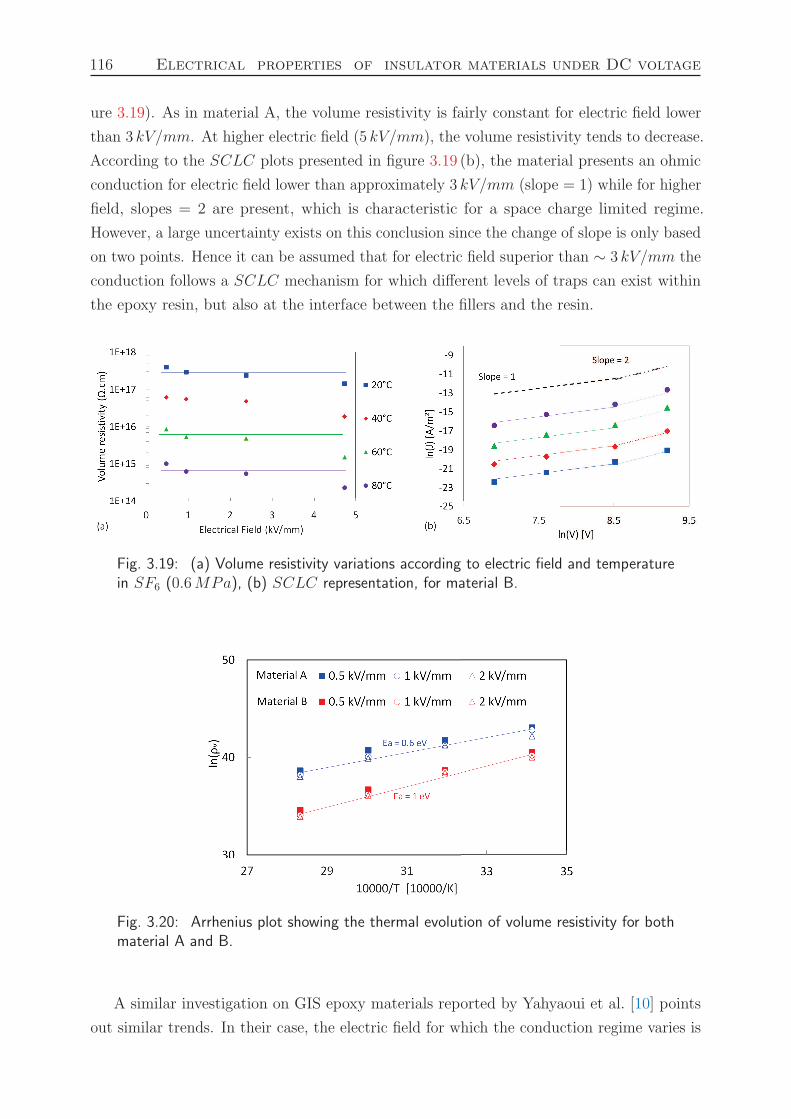
116 Electrical properties of insulator materials under DC voltage
ure 3.19). As in material A, the volume resistivity is fairly constant for electric field lower
than 3 kV/mm. At higher electric field (5 kV/mm), the volume resistivity tends to decrease.
According to the SCLC plots presented in figure 3.19 (b), the material presents an ohmic
conduction for electric field lower than approximately 3 kV/mm (slope = 1) while for higher
field, slopes = 2 are present, which is characteristic for a space charge limited regime.
However, a large uncertainty exists on this conclusion since the change of slope is only based
on two points. Hence it can be assumed that for electric field superior than ∼ 3 kV/mm the
conduction follows a SCLC mechanism for which different levels of traps can exist within
the epoxy resin, but also at the interface between the fillers and the resin.
Fig. 3.19: (a) Volume resistivity variations according to electric field and temperaturein SF6 (0.6MPa), (b) SCLC representation, for material B.
Fig. 3.20: Arrhenius plot showing the thermal evolution of volume resistivity for bothmaterial A and B.
A similar investigation on GIS epoxy materials reported by Yahyaoui et al. [10] points
out similar trends. In their case, the electric field for which the conduction regime varies is
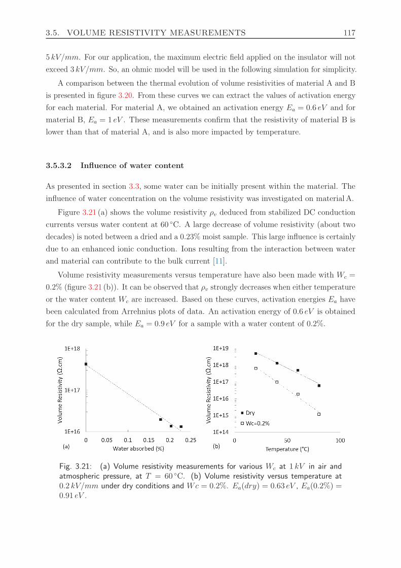
3.5. VOLUME RESISTIVITY MEASUREMENTS 117
5 kV/mm. For our application, the maximum electric field applied on the insulator will not
exceed 3 kV/mm. So, an ohmic model will be used in the following simulation for simplicity.
A comparison between the thermal evolution of volume resistivities of material A and B
is presented in figure 3.20. From these curves we can extract the values of activation energy
for each material. For material A, we obtained an activation energy Ea = 0.6 eV and for
material B, Ea = 1 eV . These measurements confirm that the resistivity of material B is
lower than that of material A, and is also more impacted by temperature.
3.5.3.2 Influence of water content
As presented in section 3.3, some water can be initially present within the material. The
influence of water concentration on the volume resistivity was investigated on material A.
Figure 3.21 (a) shows the volume resistivity ρv deduced from stabilized DC conduction
currents versus water content at 60 C. A large decrease of volume resistivity (about two
decades) is noted between a dried and a 0.23% moist sample. This large influence is certainly
due to an enhanced ionic conduction. Ions resulting from the interaction between water
and material can contribute to the bulk current [11].
Volume resistivity measurements versus temperature have also been made with Wc =
0.2% (figure 3.21 (b)). It can be observed that ρv strongly decreases when either temperature
or the water content Wc are increased. Based on these curves, activation energies Ea have
been calculated from Arrehnius plots of data. An activation energy of 0.6 eV is obtained
for the dry sample, while Ea = 0.9 eV for a sample with a water content of 0.2%.
Fig. 3.21: (a) Volume resistivity measurements for various Wc at 1 kV in air andatmospheric pressure, at T = 60 C. (b) Volume resistivity versus temperature at0.2 kV/mm under dry conditions and Wc = 0.2%. Ea(dry) = 0.63 eV , Ea(0.2%) =0.91 eV .
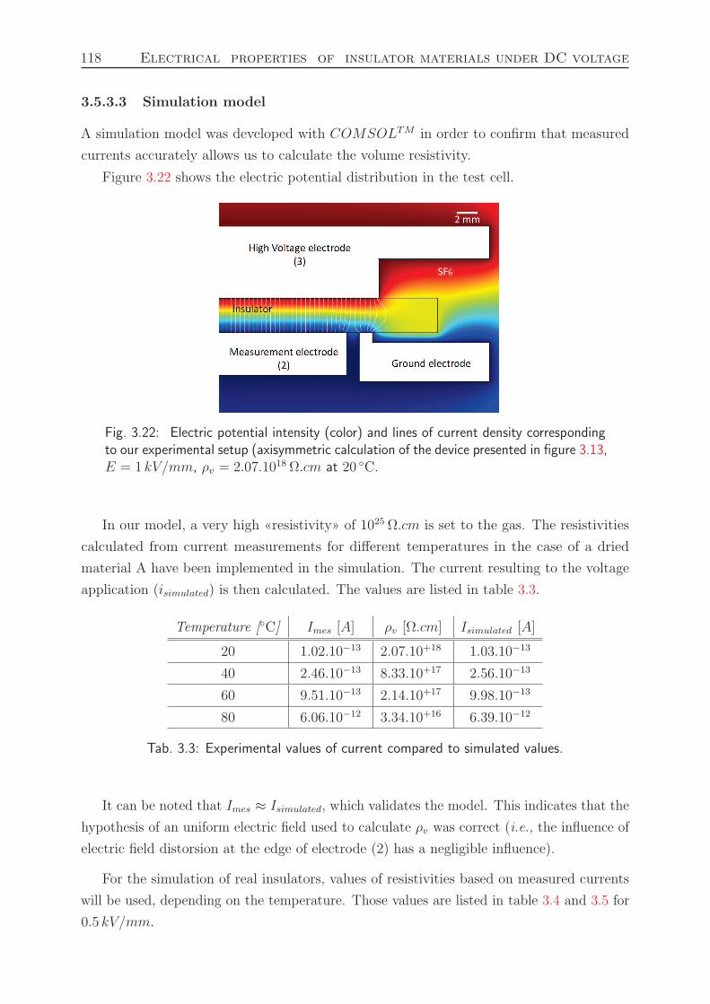
118 Electrical properties of insulator materials under DC voltage
3.5.3.3 Simulation model
A simulation model was developed with COMSOLTM in order to confirm that measured
currents accurately allows us to calculate the volume resistivity.
Figure 3.22 shows the electric potential distribution in the test cell.
Fig. 3.22: Electric potential intensity (color) and lines of current density correspondingto our experimental setup (axisymmetric calculation of the device presented in figure 3.13,E = 1 kV/mm, ρv = 2.07.1018 Ω.cm at 20 C.
In our model, a very high «resistivity» of 1025Ω.cm is set to the gas. The resistivities
calculated from current measurements for different temperatures in the case of a dried
material A have been implemented in the simulation. The current resulting to the voltage
application (isimulated) is then calculated. The values are listed in table 3.3.
Temperature [C] Imes [A] ρv [Ω.cm] Isimulated [A]
20 1.02.10−13 2.07.10+18 1.03.10−13
40 2.46.10−13 8.33.10+17 2.56.10−13
60 9.51.10−13 2.14.10+17 9.98.10−13
80 6.06.10−12 3.34.10+16 6.39.10−12
Tab. 3.3: Experimental values of current compared to simulated values.
It can be noted that Imes ≈ Isimulated, which validates the model. This indicates that the
hypothesis of an uniform electric field used to calculate ρv was correct (i.e., the influence of
electric field distorsion at the edge of electrode (2) has a negligible influence).
For the simulation of real insulators, values of resistivities based on measured currents
will be used, depending on the temperature. Those values are listed in table 3.4 and 3.5 for
0.5 kV/mm.

3.5. VOLUME RESISTIVITY MEASUREMENTS 119
Temperature [C] Dry ρv [Ω.cm] Wc = 0.2% ρv [Ω.cm]
20 3.88.10+18 6.42.10+17
40 8.41.10+17 9.81.10+16
60 2.5.10+17 1.88.10+16
80 4.10+16 1.18.10+15
Tab. 3.4: Experimental values of volume resistivity of material A calculated based onmeasured current for both dry and Wc = 0.2% sample, under 0.5 kV/mm.
Temperature [C] Dry ρv [Ω.cm]
20 3.9.10+17
40 6.15.10+16
60 8.6.10+15
80 1.02.10+15
Tab. 3.5: Experimental values of volume resistivity of dry material B calculated basedon measured current, under 0.5 kV/mm.
3.5.3.4 Additional investigations: influence of the material composition
Several investigations have been performed on new materials studied in section 3.7 to
characterize their volume properties and verify if such materials could be suitable for HVDC
applications. Indeed, a material with lower volume and surface resistivity should help charge
relaxation. Hereafter, investigations are presented on material B2, B3 and B4, without
alumina fillers.
Figure 3.23 shows typical recordings of currents measured through those materials at
1000V and for 20 C and 40 C. The pseudo-stabilization of currents is obtained after
10 hours at 20 C. However, at 40 C the current continuously increases with time, and
does not show any pseudo-stabilization. Although those materials present a faster surface
potential decay and a lower volume resistivity compared to materials A and B, they do not
have a stable behavior in time under high electric field and temperature.
Figure 3.24 (a) shows the evolution of the measured current through volume of material
B4 with fillers, at different temperatures. Opposed to the case of material B4 without fillers
(figure 3.23), it is observed that the current at 40 C now decreases with time, and reaches
a pseudo-stabilization after approximately 40 hours. The same behaviour is noted for the
other temperatures. Based on these measurements, the volume resistivity of material B4
with fillers is compared to material B at 20, 40, 60, and 80 C in figure 3.24. Material B4
with fillers shows a lower volume resistivity compared to material B, and a similar behaviour
versus temperature, with three decades difference between 20 C and 80 C. This result
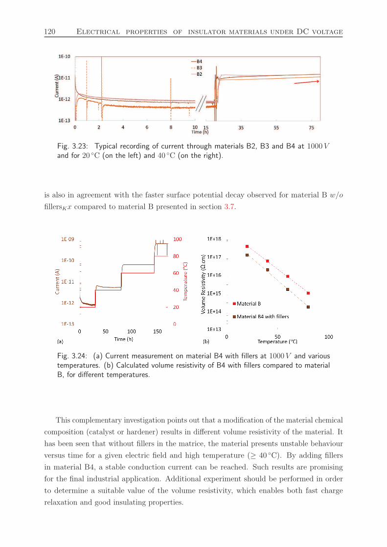
120 Electrical properties of insulator materials under DC voltage
Fig. 3.23: Typical recording of current through materials B2, B3 and B4 at 1000Vand for 20 C (on the left) and 40 C (on the right).
is also in agreement with the faster surface potential decay observed for material B w/o
fillersKx compared to material B presented in section 3.7.
Fig. 3.24: (a) Current measurement on material B4 with fillers at 1000V and varioustemperatures. (b) Calculated volume resistivity of B4 with fillers compared to materialB, for different temperatures.
This complementary investigation points out that a modification of the material chemical
composition (catalyst or hardener) results in different volume resistivity of the material. It
has been seen that without fillers in the matrice, the material presents unstable behaviour
versus time for a given electric field and high temperature (≥ 40 C). By adding fillers
in material B4, a stable conduction current can be reached. Such results are promising
for the final industrial application. Additional experiment should be performed in order
to determine a suitable value of the volume resistivity, which enables both fast charge
relaxation and good insulating properties.
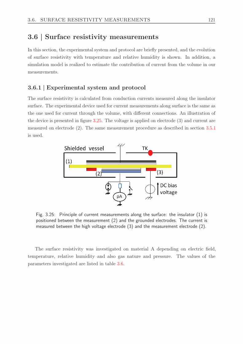
3.6. SURFACE RESISTIVITY MEASUREMENTS 121
3.6 | Surface resistivity measurements
In this section, the experimental system and protocol are briefly presented, and the evolution
of surface resistivity with temperature and relative humidity is shown. In addition, a
simulation model is realized to estimate the contribution of current from the volume in our
measurements.
3.6.1 | Experimental system and protocol
The surface resistivity is calculated from conduction currents measured along the insulator
surface. The experimental device used for current measurements along surface is the same as
the one used for current through the volume, with different connections. An illustration of
the device is presented in figure 3.25. The voltage is applied on electrode (3) and current are
measured on electrode (2). The same measurement procedure as described in section 3.5.1
is used.
Fig. 3.25: Principle of current measurements along the surface: the insulator (1) ispositioned between the measurement (2) and the grounded electrodes. The current ismeasured between the high voltage electrode (3) and the measurement electrode (2).
The surface resistivity was investigated on material A depending on electric field,
temperature, relative humidity and also gas nature and pressure. The values of the
parameters investigated are listed in table 3.6.
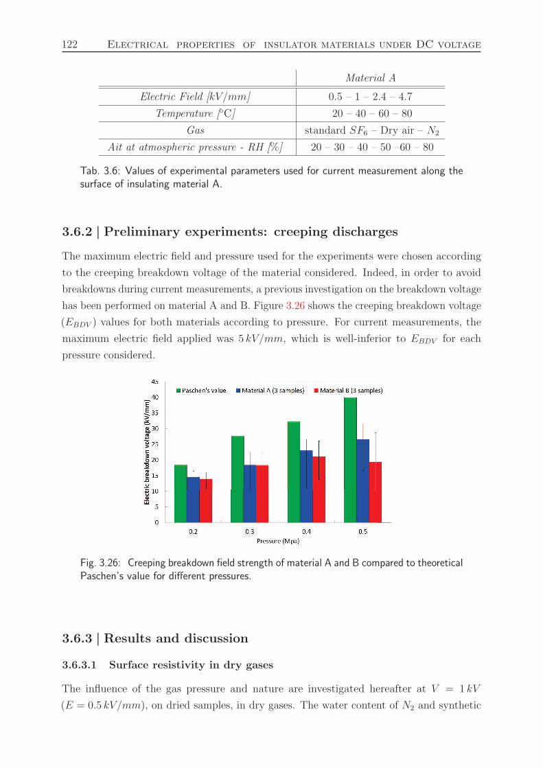
122 Electrical properties of insulator materials under DC voltage
Material A
Electric Field [kV/mm] 0.5 – 1 – 2.4 – 4.7
Temperature [C] 20 – 40 – 60 – 80
Gas standard SF6 – Dry air – N2
Ait at atmospheric pressure - RH [%] 20 – 30 – 40 – 50 –60 – 80
Tab. 3.6: Values of experimental parameters used for current measurement along thesurface of insulating material A.
3.6.2 | Preliminary experiments: creeping discharges
The maximum electric field and pressure used for the experiments were chosen according
to the creeping breakdown voltage of the material considered. Indeed, in order to avoid
breakdowns during current measurements, a previous investigation on the breakdown voltage
has been performed on material A and B. Figure 3.26 shows the creeping breakdown voltage
(EBDV ) values for both materials according to pressure. For current measurements, the
maximum electric field applied was 5 kV/mm, which is well-inferior to EBDV for each
pressure considered.
Fig. 3.26: Creeping breakdown field strength of material A and B compared to theoreticalPaschen’s value for different pressures.
3.6.3 | Results and discussion
3.6.3.1 Surface resistivity in dry gases
The influence of the gas pressure and nature are investigated hereafter at V = 1 kV
(E = 0.5 kV/mm), on dried samples, in dry gases. The water content of N2 and synthetic
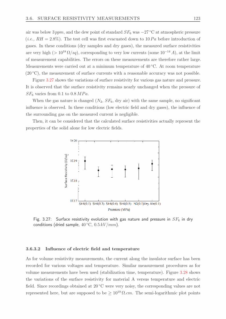
3.6. SURFACE RESISTIVITY MEASUREMENTS 123
air was below 3 ppm, and the dew point of standard SF6 was −27 C at atmospheric pressure
(i.e., RH = 2.8%). The test cell was first evacuated down to 10Pa before introduction of
gases. In these conditions (dry samples and dry gases), the measured surface resistivities
are very high (> 1018 Ω/sq), corresponding to very low currents (some 10−14 A), at the limit
of measurement capabilities. The errors on these measurements are therefore rather large.
Measurements were carried out at a minimum temperature of 40 C. At room temperature
(20 C), the measurement of surface currents with a reasonable accuracy was not possible.
Figure 3.27 shows the variations of surface resistivity for various gas nature and pressure.
It is observed that the surface resistivity remains nearly unchanged when the pressure of
SF6 varies from 0.1 to 0.8MPa.
When the gas nature is changed (N2, SF6, dry air) with the same sample, no significant
influence is observed. In these conditions (low electric field and dry gases), the influence of
the surrounding gas on the measured current is negligible.
Then, it can be considered that the calculated surface resistivities actually represent the
properties of the solid alone for low electric fields.
Fig. 3.27: Surface resistivity evolution with gas nature and pressure in SF6 in dryconditions (dried sample, 40 C, 0.5 kV/mm).
3.6.3.2 Influence of electric field and temperature
As for volume resistivity measurements, the current along the insulator surface has been
recorded for various voltages and temperature. Similar measurement procedures as for
volume measurements have been used (stabilization time, temperature). Figure 3.28 shows
the variations of the surface resistivity for material A versus temperature and electric
field. Since recordings obtained at 20 C were very noisy, the corresponding values are not
represented here, but are supposed to be ≥ 1019Ω.cm. The semi-logarithmic plot points
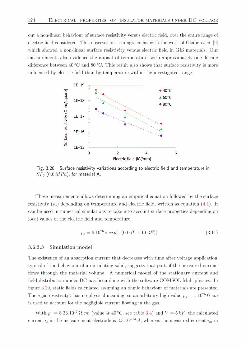
124 Electrical properties of insulator materials under DC voltage
out a non-linear behaviour of surface resistivity versus electric field, over the entire range of
electric field considered. This observation is in agreement with the work of Okabe et al. [9]
which showed a non-linear surface resistivity versus electric field in GIS materials. Our
measurements also evidence the impact of temperature, with approximately one decade
difference between 40 C and 80 C. This result also shows that surface resistivity is more
influenced by electric field than by temperature within the investigated range.
Fig. 3.28: Surface resistivity variations according to electric field and temperature inSF6 (0.6MPa), for material A.
These measurements allows determining an empirical equation followed by the surface
resistivity (ρs) depending on temperature and electric field, written as equation (4.1). It
can be used in numerical simulations to take into account surface properties depending on
local values of the electric field and temperature.
ρs = 6.1026 ∗ exp[−(0.06T + 1.03E)] (3.11)
3.6.3.3 Simulation model
The existence of an absorption current that decreases with time after voltage application,
typical of the behaviour of an insulating solid, suggests that part of the measured current
flows through the material volume. A numerical model of the stationary current and
field distribution under DC has been done with the software COMSOL Multiphysics. In
figure 3.29, static fields calculated assuming an ohmic behaviour of materials are presented.
The «gas resistivity» has no physical meaning, so an arbitrary high value ρg = 1.1025 Ω.cm
is used to account for the negligible current flowing in the gas.
With ρv = 8.33.1017Ω.cm (value @ 40 C, see table 3.4) and V = 5 kV , the calculated
current ic in the measurement electrode is 3.3.10−14 A, whereas the measured current im in
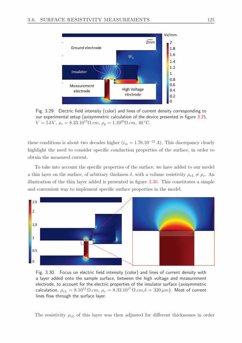
3.6. SURFACE RESISTIVITY MEASUREMENTS 125
Fig. 3.29: Electric field intensity (color) and lines of current density corresponding toour experimental setup (axisymmetric calculation of the device presented in figure 3.25,V = 5 kV , ρv = 8.33.1017Ω.cm, ρg = 1.1025Ω.cm, 40 C.
these conditions is about two decades higher (im = 1.76.10−12 A). This discrepancy clearly
highlight the need to consider specific conduction properties of the surface, in order to
obtain the measured current.
To take into account the specific properties of the surface, we have added to our model
a thin layer on the surface, of arbitrary thickness δ, with a volume resistivity ρvL 6= ρv. An
illustration of the thin layer added is presented in figure 3.30. This constitutes a simple
and convenient way to implement specific surface properties in the model.
Fig. 3.30: Focus on electric field intensity (color) and lines of current density witha layer added onto the sample surface, between the high voltage and measurementelectrode, to account for the electric properties of the insulator surface (axisymmetriccalculation, ρvL = 8.1015Ω.cm, ρv = 8.33.1017Ω.cm,δ = 320µm). Most of currentlines flow through the surface layer.
The resistivity ρvL of this layer was then adjusted for different thicknesses in order
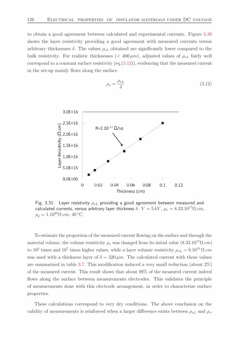
126 Electrical properties of insulator materials under DC voltage
to obtain a good agreement between calculated and experimental currents. Figure 3.30
shows the layer resistivity providing a good agreement with measured currents versus
arbitrary thicknesses δ. The values ρvL obtained are significantly lower compared to the
bulk resistivity. For realistic thicknesses (< 400µm), adjusted values of ρvL fairly well
correspond to a constant surface resistivity (eq.(3.12)), evidencing that the measured current
in the set-up mainly flows along the surface.
ρs =ρvLδ
(3.12)
Fig. 3.31: Layer resistivity ρvL providing a good agreement between measured andcalculated currents, versus arbitrary layer thickness δ. V = 5 kV , ρv = 8.33.1017Ω.cm,ρg = 1.1025Ω.cm, 40 C.
To estimate the proportion of the measured current flowing on the surface and through the
material volume, the volume resistivity ρv was changed from its initial value (8.33.1017Ω.cm)
to 102 times and 107 times higher values, while a layer volumic resistivity ρvL = 8.1015 Ω.cm
was used with a thickness layer of δ = 320µm. The calculated current with these values
are summarized in table 3.7. This modification induced a very small reduction (about 2%)
of the measured current. This result shows that about 98% of the measured current indeed
flows along the surface between measurements electrodes. This validates the principle
of measurements done with this electrode arrangement, in order to characterize surface
properties.
These calculations correspond to very dry conditions. The above conclusion on the
validity of measurements is reinforced when a larger difference exists between ρvL and ρv.
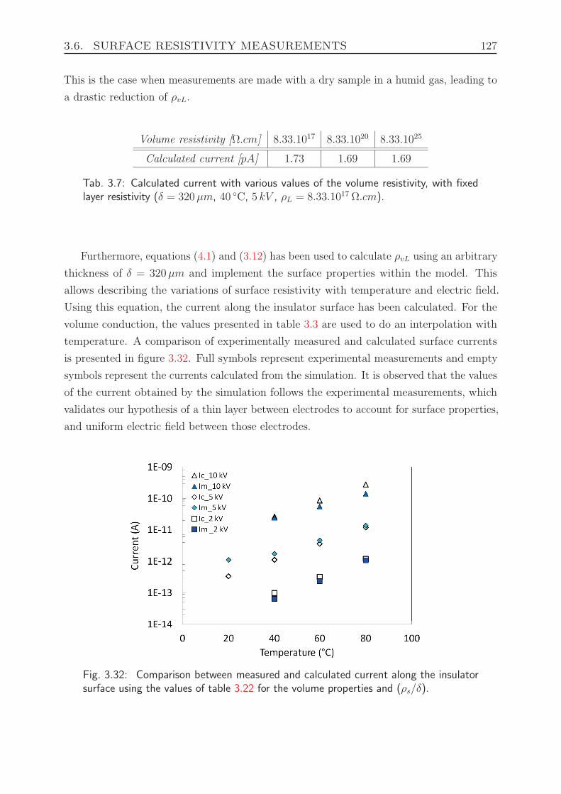
3.6. SURFACE RESISTIVITY MEASUREMENTS 127
This is the case when measurements are made with a dry sample in a humid gas, leading to
a drastic reduction of ρvL.
Volume resistivity [Ω.cm] 8.33.1017 8.33.1020 8.33.1025
Calculated current [pA] 1.73 1.69 1.69
Tab. 3.7: Calculated current with various values of the volume resistivity, with fixedlayer resistivity (δ = 320µm, 40 C, 5 kV , ρL = 8.33.1017 Ω.cm).
Furthermore, equations (4.1) and (3.12) has been used to calculate ρvL using an arbitrary
thickness of δ = 320µm and implement the surface properties within the model. This
allows describing the variations of surface resistivity with temperature and electric field.
Using this equation, the current along the insulator surface has been calculated. For the
volume conduction, the values presented in table 3.3 are used to do an interpolation with
temperature. A comparison of experimentally measured and calculated surface currents
is presented in figure 3.32. Full symbols represent experimental measurements and empty
symbols represent the currents calculated from the simulation. It is observed that the values
of the current obtained by the simulation follows the experimental measurements, which
validates our hypothesis of a thin layer between electrodes to account for surface properties,
and uniform electric field between those electrodes.
Fig. 3.32: Comparison between measured and calculated current along the insulatorsurface using the values of table 3.22 for the volume properties and (ρs/δ).
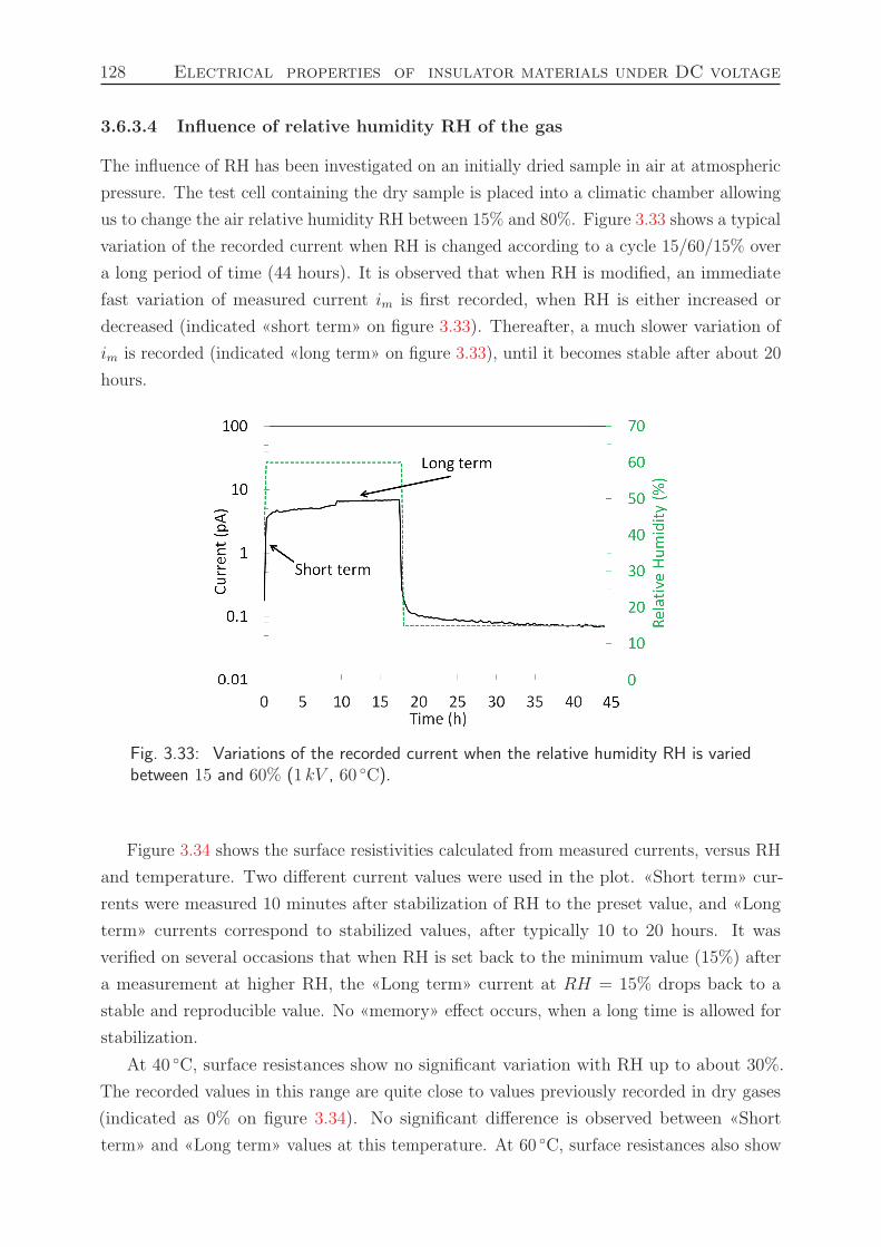
128 Electrical properties of insulator materials under DC voltage
3.6.3.4 Influence of relative humidity RH of the gas
The influence of RH has been investigated on an initially dried sample in air at atmospheric
pressure. The test cell containing the dry sample is placed into a climatic chamber allowing
us to change the air relative humidity RH between 15% and 80%. Figure 3.33 shows a typical
variation of the recorded current when RH is changed according to a cycle 15/60/15% over
a long period of time (44 hours). It is observed that when RH is modified, an immediate
fast variation of measured current im is first recorded, when RH is either increased or
decreased (indicated «short term» on figure 3.33). Thereafter, a much slower variation of
im is recorded (indicated «long term» on figure 3.33), until it becomes stable after about 20
hours.
Fig. 3.33: Variations of the recorded current when the relative humidity RH is variedbetween 15 and 60% (1 kV , 60 C).
Figure 3.34 shows the surface resistivities calculated from measured currents, versus RH
and temperature. Two different current values were used in the plot. «Short term» cur-
rents were measured 10 minutes after stabilization of RH to the preset value, and «Long
term» currents correspond to stabilized values, after typically 10 to 20 hours. It was
verified on several occasions that when RH is set back to the minimum value (15%) after
a measurement at higher RH, the «Long term» current at RH = 15% drops back to a
stable and reproducible value. No «memory» effect occurs, when a long time is allowed for
stabilization.
At 40 C, surface resistances show no significant variation with RH up to about 30%.
The recorded values in this range are quite close to values previously recorded in dry gases
(indicated as 0% on figure 3.34). No significant difference is observed between «Short
term» and «Long term» values at this temperature. At 60 C, surface resistances also show
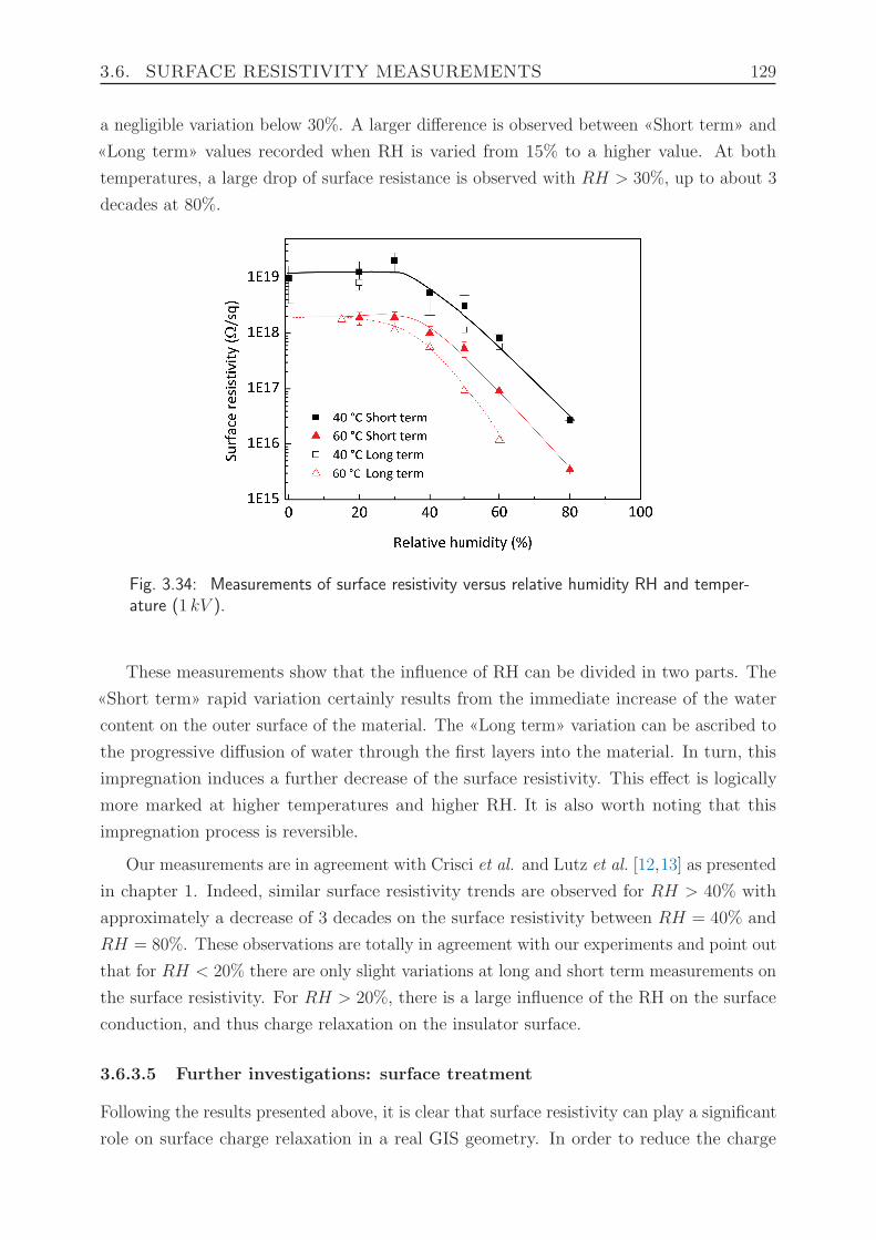
3.6. SURFACE RESISTIVITY MEASUREMENTS 129
a negligible variation below 30%. A larger difference is observed between «Short term» and
«Long term» values recorded when RH is varied from 15% to a higher value. At both
temperatures, a large drop of surface resistance is observed with RH > 30%, up to about 3
decades at 80%.
Fig. 3.34: Measurements of surface resistivity versus relative humidity RH and temper-ature (1 kV ).
These measurements show that the influence of RH can be divided in two parts. The
«Short term» rapid variation certainly results from the immediate increase of the water
content on the outer surface of the material. The «Long term» variation can be ascribed to
the progressive diffusion of water through the first layers into the material. In turn, this
impregnation induces a further decrease of the surface resistivity. This effect is logically
more marked at higher temperatures and higher RH. It is also worth noting that this
impregnation process is reversible.
Our measurements are in agreement with Crisci et al. and Lutz et al. [12,13] as presented
in chapter 1. Indeed, similar surface resistivity trends are observed for RH > 40% with
approximately a decrease of 3 decades on the surface resistivity between RH = 40% and
RH = 80%. These observations are totally in agreement with our experiments and point out
that for RH < 20% there are only slight variations at long and short term measurements on
the surface resistivity. For RH > 20%, there is a large influence of the RH on the surface
conduction, and thus charge relaxation on the insulator surface.
3.6.3.5 Further investigations: surface treatment
Following the results presented above, it is clear that surface resistivity can play a significant
role on surface charge relaxation in a real GIS geometry. In order to reduce the charge
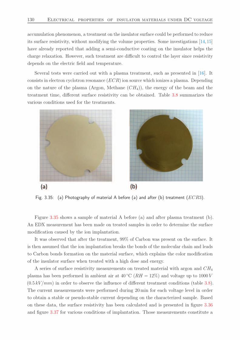
130 Electrical properties of insulator materials under DC voltage
accumulation phenomenon, a treatment on the insulator surface could be performed to reduce
its surface resistivity, without modifying the volume properties. Some investigations [14,15]
have already reported that adding a semi-conductive coating on the insulator helps the
charge relaxation. However, such treatment are difficult to control the layer since resistivity
depends on the electric field and temperature.
Several tests were carried out with a plasma treatment, such as presented in [16]. It
consists in electron cyclotron resonance (ECR) ion source which ionizes a plasma. Depending
on the nature of the plasma (Argon, Methane (CH4)), the energy of the beam and the
treatment time, different surface resistivity can be obtained. Table 3.8 summarizes the
various conditions used for the treatments.
Fig. 3.35: (a) Photography of material A before (a) and after (b) treatment (ECR3).
Figure 3.35 shows a sample of material A before (a) and after plasma treatment (b).
An EDX measurement has been made on treated samples in order to determine the surface
modification caused by the ion implantation.
It was observed that after the treatment, 99% of Carbon was present on the surface. It
is then assumed that the ion implantation breaks the bonds of the molecular chain and leads
to Carbon bonds formation on the material surface, which explains the color modification
of the insulator surface when treated with a high dose and energy.
A series of surface resistivity measurements on treated material with argon and CH4
plasma has been performed in ambient air at 40 C (RH = 12%) and voltage up to 1000V
(0.5 kV/mm) in order to observe the influence of different treatment conditions (table 3.8).
The current measurements were performed during 20min for each voltage level in order
to obtain a stable or pseudo-stable current depending on the characterized sample. Based
on these data, the surface resistivity has been calculated and is presented in figure 3.36
and figure 3.37 for various conditions of implantation. Those measurements constitute a
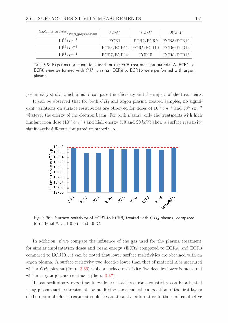
3.6. SURFACE RESISTIVITY MEASUREMENTS 131
Implantation doses/Energy of the beam 5 keV 10 keV 20 keV
1016 cm−2 ECR1 ECR2/ECR9 ECR3/ECR10
1015 cm−2 ECR4/ECR11 ECR5/ECR12 ECR6/ECR13
1014 cm−2 ECR7/ECR14 ECR15 ECR8/ECR16
Tab. 3.8: Experimental conditions used for the ECR treatment on material A. ECR1 toECR8 were performed with CH4 plasma. ECR9 to ECR16 were performed with argonplasma.
preliminary study, which aims to compare the efficiency and the impact of the treatments.
It can be observed that for both CH4 and argon plasma treated samples, no signifi-
cant variations on surface resistivities are observed for doses of 1014 cm−2 and 1015 cm−2
whatever the energy of the electron beam. For both plasma, only the treatments with high
implantation dose (1016 cm−2) and high energy (10 and 20 keV ) show a surface resistivity
significantly different compared to material A.
Fig. 3.36: Surface resistivity of ECR1 to ECR8, treated with CH4 plasma, comparedto material A, at 1000V and 40 C.
In addition, if we compare the influence of the gas used for the plasma treatment,
for similar implantation doses and beam energy (ECR2 compared to ECR9, and ECR3
compared to ECR10), it can be noted that lower surface resistivities are obtained with an
argon plasma. A surface resistivity two decades lower than that of material A is measured
with a CH4 plasma (figure 3.36) while a surface resistivity five decades lower is measured
with an argon plasma treatment (figure 3.37).
Those preliminary experiments evidence that the surface resistivity can be adjusted
using plasma surface treatment, by modifying the chemical composition of the first layers
of the material. Such treatment could be an attractive alternative to the semi-conductive
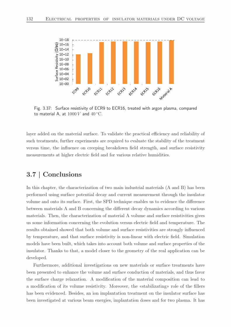
132 Electrical properties of insulator materials under DC voltage
Fig. 3.37: Surface resistivity of ECR9 to ECR16, treated with argon plasma, comparedto material A, at 1000V and 40 C.
layer added on the material surface. To validate the practical efficiency and reliability of
such treatments, further experiments are required to evaluate the stability of the treatment
versus time, the influence on creeping breakdown field strength, and surface resistivity
measurements at higher electric field and for various relative humidities.
3.7 | Conclusions
In this chapter, the characterization of two main industrial materials (A and B) has been
performed using surface potential decay and current measurement through the insulator
volume and onto its surface. First, the SPD technique enables us to evidence the difference
between materials A and B concerning the different decay dynamics according to various
materials. Then, the characterization of material A volume and surface resistivities gives
us some information concerning the evolution versus electric field and temperature. The
results obtained showed that both volume and surface resistivities are strongly influenced
by temperature, and that surface resistivity is non-linear with electric field. Simulation
models have been built, which takes into account both volume and surface properties of the
insulator. Thanks to that, a model closer to the geometry of the real application can be
developed.
Furthermore, additional investigations on new materials or surface treatments have
been presented to enhance the volume and surface conduction of materials, and thus favor
the surface charge relaxation. A modification of the material composition can lead to
a modification of its volume resistivity. Moreover, the «stabilizating» role of the fillers
has been evidenced. Besides, an ion implantation treatment on the insulator surface has
been investigated at various beam energies, implantation doses and for two plasma. It has
3.7. CONCLUSIONS 133
been observed that lower surface resistivity are obtained for high implantation dose and
energy beam. Such investigations give an alternative to fabricate new materials with well
controlled resistivities, in order to better define the electric field distribution under HVDC.
Depending on the geometry considered, a compromise between adjusting the volume and
surface resistivity can be determined to optimize the charge relaxation.
134 Bibliography (Chapter 3)
Bibliography
[1] D. D. Gupta and R. Brockley, “A study of’absorption currents’ in low-density polyethy-lene,” Journal of Physics D: Applied Physics, vol. 11, no. 6, p. 955, 1978. (cited inpage 96)
[2] Y. Segui, “Dielectriques, courants de conduction,” Techniques de l’Ingenieur, traiteGenie electrique D, vol. 2301, 2000. (cited in pages 97 and 115)
[3] “Methods of test for volume resistivity and surface resistivity of solid electrical insulatingmaterials,” 1980. (cited in pages 97 and 98)
[4] C. Menguy, Mesure des caracteristiques des materiaux isolants solides. Ed. TechniquesIngenieur, 1997. (cited in page 98)
[5] M. J. Adamson, “Thermal expansion and swelling of cured epoxy resin used ingraphite/epoxy composite materials,” Journal of Materials Science, vol. 15, no. 7,pp. 1736–1745, 1980. (cited in page 101)
[6] C. Zou, J. C. Fothergill, and S. W. Rowe, “The effect of water absorption on thedielectric properties of epoxy nanocomposites,”Dielectrics and Electrical Insulation,IEEE Transactions on, vol. 15, no. 1, pp. 106–117, 2008. (cited in page 101)
[7] C.-H. Shen and G. S. Springer, “Moisture absorption and desorption of compositematerials,” Journal of Composite Materials, vol. 10, no. 1, pp. 2–20, 1976. (cited inpage 101)
[8] Z. Chen, The effect of humidity and surface functionalisation on the dielectric propertiesof nanocomposites. PhD thesis, University of Leicester, 2007. (cited in page 102)
[9] S. Okabe, “Phenomena and mechanism of electric charges on spacers in gas insulatedswitchgears,”Dielectrics and Electrical Insulation, IEEE Transactions, vol. 14, no. 1,pp. 46–52, 2007. (cited in pages 10, 15, 16, 17, 18, 22, 41, 114 and 124)
[10] H. Yahyaoui, Etude des mecanismes de conduction d’une resine epoxy chargee d’alumine.PhD thesis, Private communication, 2013. (cited in page 116)
[11] B. Lutz and J. Kindersberger, “Influence of absorbed water on volume resistivity ofepoxy resin insulators,” in Solid Dielectrics (ICSD), 2010 10th IEEE InternationalConference, pp. 1–4, IEEE, 2010. (cited in pages 20, 21 and 117)
[12] A. Crisci, B. Gosse, J. Gosse, and V. Ollier-Dureault, “Surface-potential decay dueto surface conduction,” EPJ Applied physics, vol. 4, pp. 107–1116, 1998. (cited inpages 10, 19, 20 and 129)
[13] B. Lutz and J. Kindersberger, “Influence of relative humidity on surface charge decayon epoxy resin insulators,” in Properties and Applications of Dielectric Materials, 2009.ICPADM 2009. IEEE 9th International Conference, pp. 883–886, IEEE, 2009. (citedin pages 20 and 129)
Bibliography (Chapter 3) 135
[14] F. Messerer and W. Boeck, “High resistance surface coating of solid insulating com-ponents for HVDC metal enclosed equipment,” in High Voltage Engineering, 1999.Eleventh International Symposium on (Conf. Publ. No. 467), vol. 4, pp. 63–66, IET,1999. (cited in page 130)
[15] E. Volpov, “Dielectric strength coordination and generalized spacer design rules forhvac/dc sf 6 gas insulated systems,”Dielectrics and Electrical Insulation, IEEE Trans-actions, vol. 11, no. 6, pp. 949–963, 2004. (cited in pages 13, 14, 22 and 130)
[16] L. Salles, J. Reboul, D. Busardo, and B. Boudart, “Mesure des resistivites de sur-face et des charges d’espace par la methode de l’onde thermique alternative dans lepolycarbonate apres implantation ionique.,” 2012. (cited in page 130)

4 | Numerical calculations in a GISgeometry
Contents
4.1 1st Step: Electric field distribution induced by the material volume resistivity139
4.1.1 Difference between AC and DC (uniform temperature 20 C) . . . . 139
4.1.2 Influence of a temperature gradient . . . . . . . . . . . . . . . . . . 140
4.1.3 Impact of solid water content with a temperature gradient . . . . . 143
4.1.4 Comments . . . . . . . . . . . . . . . . . . . . . . . . . . . . . . . . 145
4.2 2nd Step: implementation of non-linear surface properties . . . . . . . . . . 146
4.2.1 Uniform Temperature . . . . . . . . . . . . . . . . . . . . . . . . . . 147
4.2.2 Temperature gradient . . . . . . . . . . . . . . . . . . . . . . . . . . 149
4.3 Practical consequences . . . . . . . . . . . . . . . . . . . . . . . . . . . . . 151
4.4 Estimation of current from the gas . . . . . . . . . . . . . . . . . . . . . . . 152
4.5 Conclusions . . . . . . . . . . . . . . . . . . . . . . . . . . . . . . . . . . . . 154
Bibliography . . . . . . . . . . . . . . . . . . . . . . . . . . . . . . . . . . . . . . 154
In this chapter, models with an insulator geometry resembling to actual shapes existing
in coaxial HVAC GIS systems (figure 4.1) are presented. Such solid insulator are designed
to withstand 245 kV AC and are thus tested up to 400 kV DC. From the previous chapters
2 and 3, it has been shown that solid insulator properties (volume and surface) and gas
properties, can influence the electric field distribution and the current passing onto the solid
insulator surface and through its volume (figure 4.1). Table 4.1 summarizes the parameters
influencing those properties.
In order to evaluate the relative influence of these phenomena, the results obtained by
the characterization of the material volume and surface are implemented into the model.
The calculations under HVDC are done with the FEM software COMSOL MultiphysicsTM ,
and the static fields are calculated assuming an Ohmic behaviour of materials through the
volume. The non-linearity of the surface resistivity versus electric field is implemented by
adding a layer on the insulator, and the resulting electric field distribution is studied.
With this model, we will first investigate the differences of AC/DC electric field distri-
bution and resulting currents for a simplified insulator geometry, close to the industrial
application. Then, in a first step, the electric field distribution and leakage currents induced
by the material volume resistivity, neglecting the surface properties, are considered. The
electric field repartition on both surfaces (lower and upper) are studied in case of uniform
137
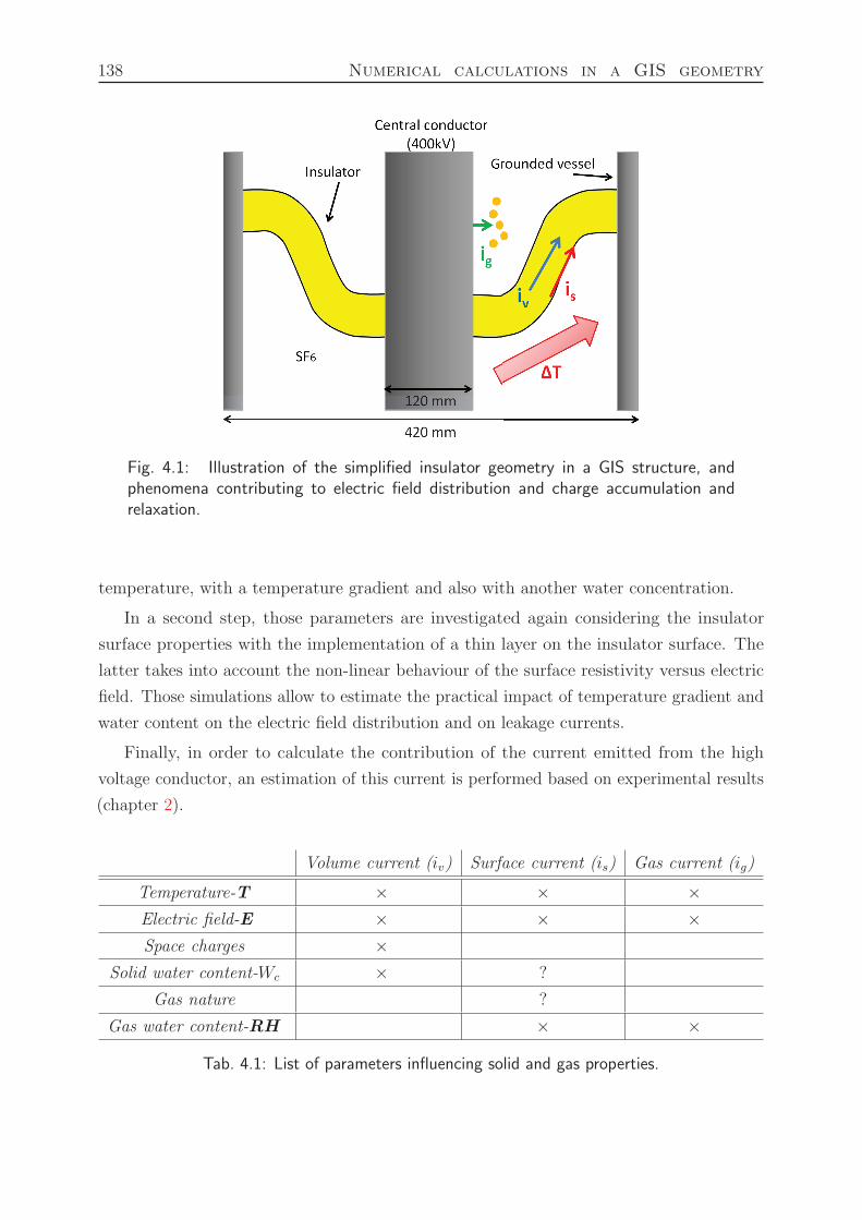
138 Numerical calculations in a GIS geometry
Fig. 4.1: Illustration of the simplified insulator geometry in a GIS structure, andphenomena contributing to electric field distribution and charge accumulation andrelaxation.
temperature, with a temperature gradient and also with another water concentration.
In a second step, those parameters are investigated again considering the insulator
surface properties with the implementation of a thin layer on the insulator surface. The
latter takes into account the non-linear behaviour of the surface resistivity versus electric
field. Those simulations allow to estimate the practical impact of temperature gradient and
water content on the electric field distribution and on leakage currents.
Finally, in order to calculate the contribution of the current emitted from the high
voltage conductor, an estimation of this current is performed based on experimental results
(chapter 2).
Volume current (iv) Surface current (is) Gas current (ig)
Temperature-T × × ×Electric field-E × × ×Space charges ×
Solid water content-Wc × ?
Gas nature ?
Gas water content-RH × ×
Tab. 4.1: List of parameters influencing solid and gas properties.
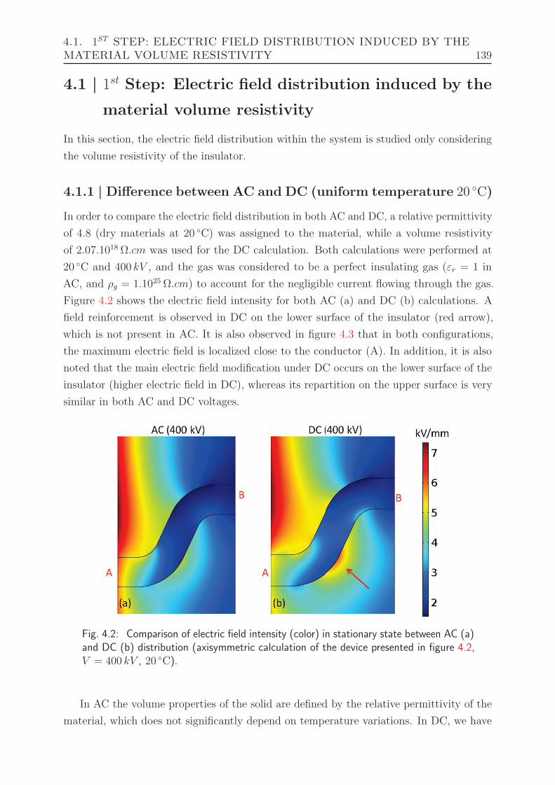
4.1. 1ST STEP: ELECTRIC FIELD DISTRIBUTION INDUCED BY THEMATERIAL VOLUME RESISTIVITY 139
4.1 | 1st Step: Electric field distribution induced by the
material volume resistivity
In this section, the electric field distribution within the system is studied only considering
the volume resistivity of the insulator.
4.1.1 | Difference between AC and DC (uniform temperature 20 C)
In order to compare the electric field distribution in both AC and DC, a relative permittivity
of 4.8 (dry materials at 20 C) was assigned to the material, while a volume resistivity
of 2.07.1018Ω.cm was used for the DC calculation. Both calculations were performed at
20 C and 400 kV , and the gas was considered to be a perfect insulating gas (εr = 1 in
AC, and ρg = 1.1025Ω.cm) to account for the negligible current flowing through the gas.
Figure 4.2 shows the electric field intensity for both AC (a) and DC (b) calculations. A
field reinforcement is observed in DC on the lower surface of the insulator (red arrow),
which is not present in AC. It is also observed in figure 4.3 that in both configurations,
the maximum electric field is localized close to the conductor (A). In addition, it is also
noted that the main electric field modification under DC occurs on the lower surface of the
insulator (higher electric field in DC), whereas its repartition on the upper surface is very
similar in both AC and DC voltages.
Fig. 4.2: Comparison of electric field intensity (color) in stationary state between AC (a)and DC (b) distribution (axisymmetric calculation of the device presented in figure 4.2,V = 400 kV , 20 C).
In AC the volume properties of the solid are defined by the relative permittivity of the
material, which does not significantly depend on temperature variations. In DC, we have
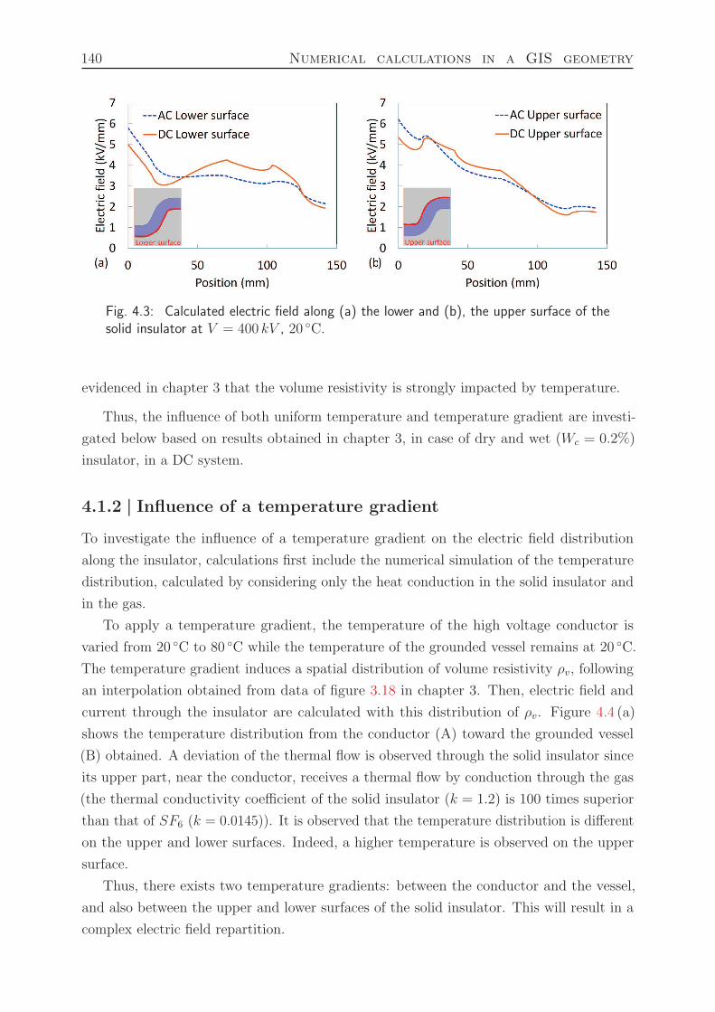
140 Numerical calculations in a GIS geometry
Fig. 4.3: Calculated electric field along (a) the lower and (b), the upper surface of thesolid insulator at V = 400 kV , 20 C.
evidenced in chapter 3 that the volume resistivity is strongly impacted by temperature.
Thus, the influence of both uniform temperature and temperature gradient are investi-
gated below based on results obtained in chapter 3, in case of dry and wet (Wc = 0.2%)
insulator, in a DC system.
4.1.2 | Influence of a temperature gradient
To investigate the influence of a temperature gradient on the electric field distribution
along the insulator, calculations first include the numerical simulation of the temperature
distribution, calculated by considering only the heat conduction in the solid insulator and
in the gas.
To apply a temperature gradient, the temperature of the high voltage conductor is
varied from 20 C to 80 C while the temperature of the grounded vessel remains at 20 C.
The temperature gradient induces a spatial distribution of volume resistivity ρv, following
an interpolation obtained from data of figure 3.18 in chapter 3. Then, electric field and
current through the insulator are calculated with this distribution of ρv. Figure 4.4 (a)
shows the temperature distribution from the conductor (A) toward the grounded vessel
(B) obtained. A deviation of the thermal flow is observed through the solid insulator since
its upper part, near the conductor, receives a thermal flow by conduction through the gas
(the thermal conductivity coefficient of the solid insulator (k = 1.2) is 100 times superior
than that of SF6 (k = 0.0145)). It is observed that the temperature distribution is different
on the upper and lower surfaces. Indeed, a higher temperature is observed on the upper
surface.
Thus, there exists two temperature gradients: between the conductor and the vessel,
and also between the upper and lower surfaces of the solid insulator. This will result in a
complex electric field repartition.
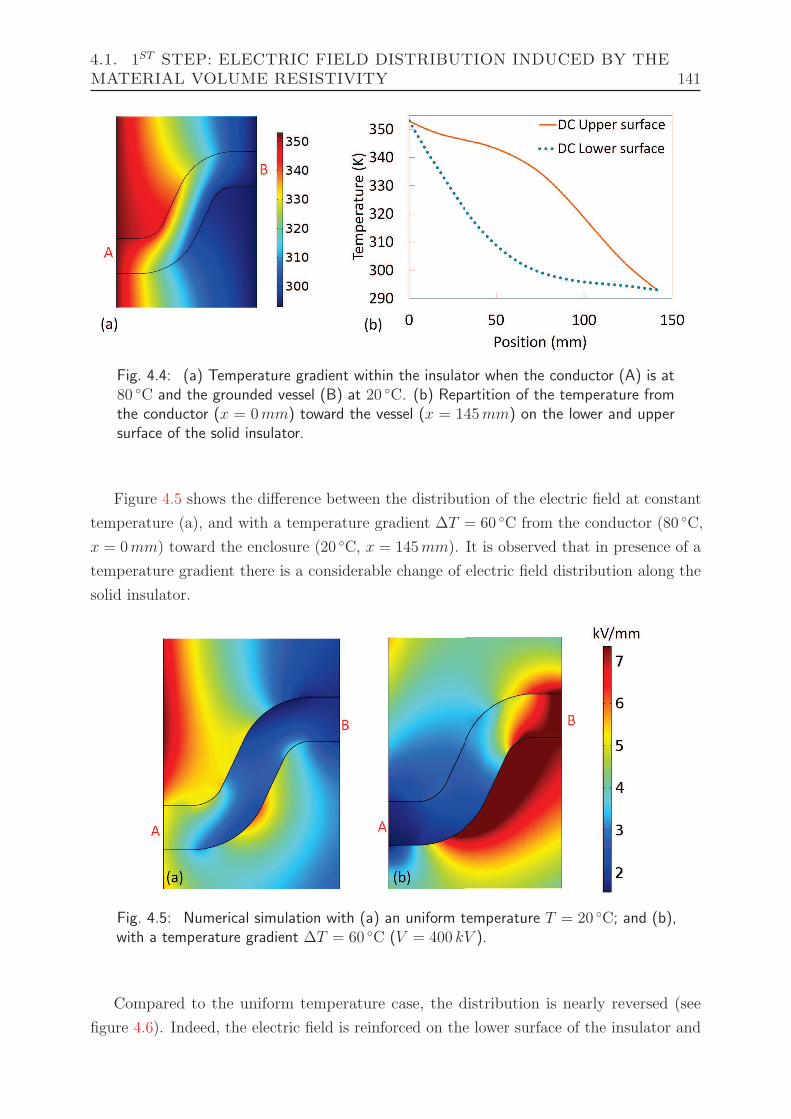
4.1. 1ST STEP: ELECTRIC FIELD DISTRIBUTION INDUCED BY THEMATERIAL VOLUME RESISTIVITY 141
Fig. 4.4: (a) Temperature gradient within the insulator when the conductor (A) is at80 C and the grounded vessel (B) at 20 C. (b) Repartition of the temperature fromthe conductor (x = 0mm) toward the vessel (x = 145mm) on the lower and uppersurface of the solid insulator.
Figure 4.5 shows the difference between the distribution of the electric field at constant
temperature (a), and with a temperature gradient ∆T = 60 C from the conductor (80 C,
x = 0mm) toward the enclosure (20 C, x = 145mm). It is observed that in presence of a
temperature gradient there is a considerable change of electric field distribution along the
solid insulator.
Fig. 4.5: Numerical simulation with (a) an uniform temperature T = 20 C; and (b),with a temperature gradient ∆T = 60 C (V = 400 kV ).
Compared to the uniform temperature case, the distribution is nearly reversed (see
figure 4.6). Indeed, the electric field is reinforced on the lower surface of the insulator and
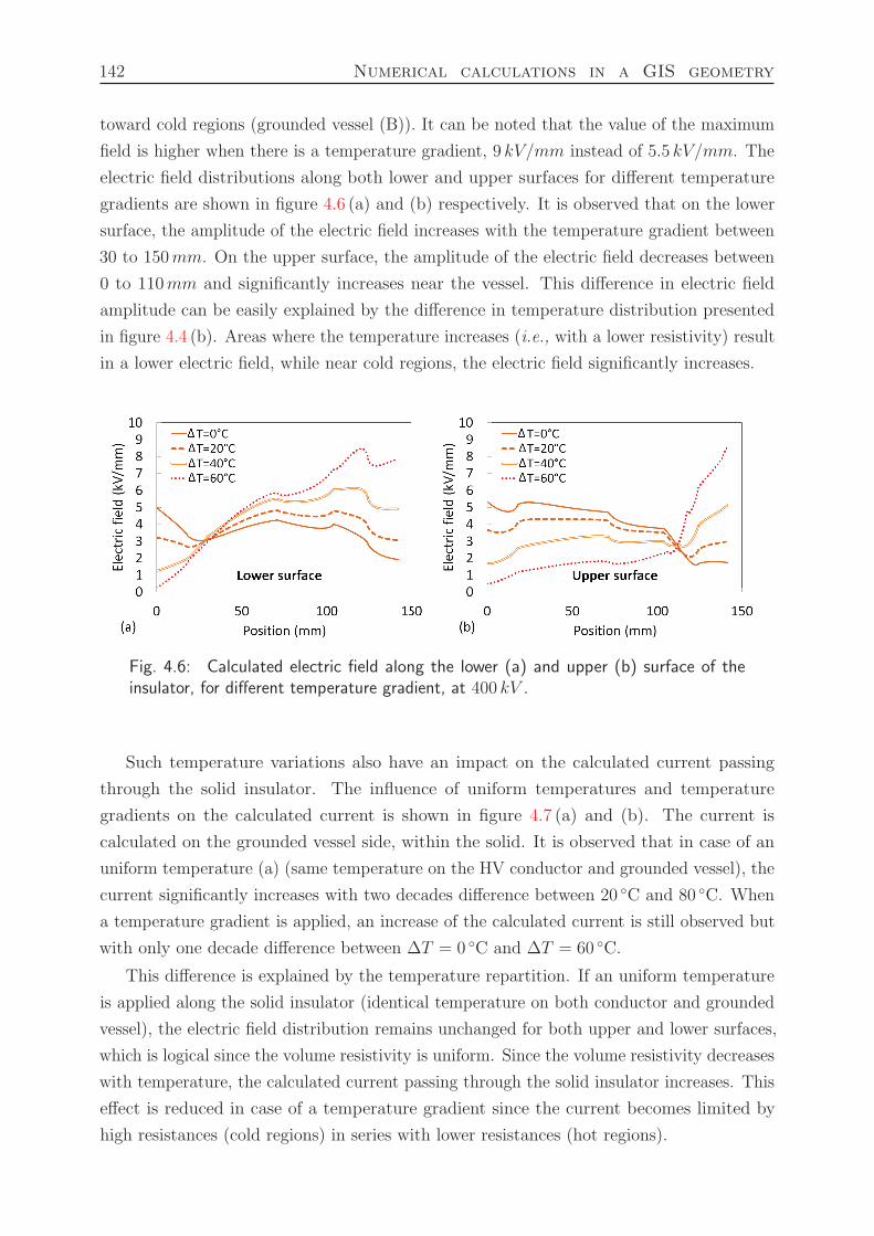
142 Numerical calculations in a GIS geometry
toward cold regions (grounded vessel (B)). It can be noted that the value of the maximum
field is higher when there is a temperature gradient, 9 kV/mm instead of 5.5 kV/mm. The
electric field distributions along both lower and upper surfaces for different temperature
gradients are shown in figure 4.6 (a) and (b) respectively. It is observed that on the lower
surface, the amplitude of the electric field increases with the temperature gradient between
30 to 150mm. On the upper surface, the amplitude of the electric field decreases between
0 to 110mm and significantly increases near the vessel. This difference in electric field
amplitude can be easily explained by the difference in temperature distribution presented
in figure 4.4 (b). Areas where the temperature increases (i.e., with a lower resistivity) result
in a lower electric field, while near cold regions, the electric field significantly increases.
Fig. 4.6: Calculated electric field along the lower (a) and upper (b) surface of theinsulator, for different temperature gradient, at 400 kV .
Such temperature variations also have an impact on the calculated current passing
through the solid insulator. The influence of uniform temperatures and temperature
gradients on the calculated current is shown in figure 4.7 (a) and (b). The current is
calculated on the grounded vessel side, within the solid. It is observed that in case of an
uniform temperature (a) (same temperature on the HV conductor and grounded vessel), the
current significantly increases with two decades difference between 20 C and 80 C. When
a temperature gradient is applied, an increase of the calculated current is still observed but
with only one decade difference between ∆T = 0 C and ∆T = 60 C.
This difference is explained by the temperature repartition. If an uniform temperature
is applied along the solid insulator (identical temperature on both conductor and grounded
vessel), the electric field distribution remains unchanged for both upper and lower surfaces,
which is logical since the volume resistivity is uniform. Since the volume resistivity decreases
with temperature, the calculated current passing through the solid insulator increases. This
effect is reduced in case of a temperature gradient since the current becomes limited by
high resistances (cold regions) in series with lower resistances (hot regions).
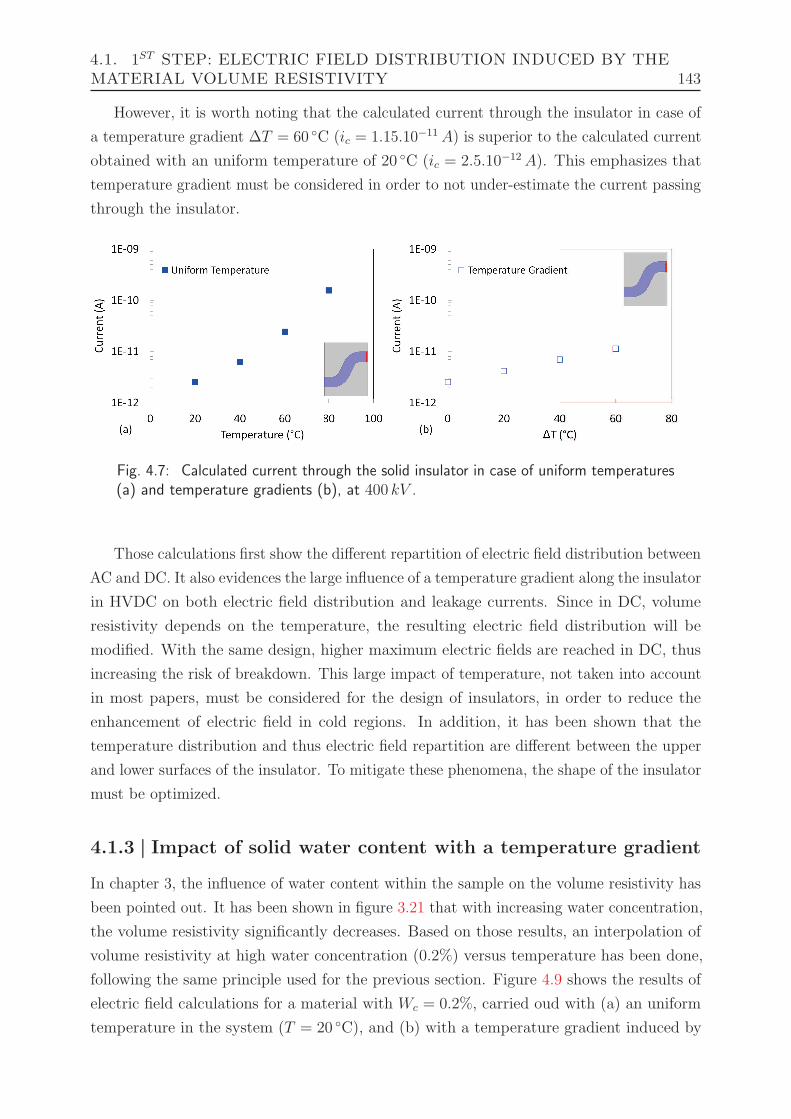
4.1. 1ST STEP: ELECTRIC FIELD DISTRIBUTION INDUCED BY THEMATERIAL VOLUME RESISTIVITY 143
However, it is worth noting that the calculated current through the insulator in case of
a temperature gradient ∆T = 60 C (ic = 1.15.10−11 A) is superior to the calculated current
obtained with an uniform temperature of 20 C (ic = 2.5.10−12 A). This emphasizes that
temperature gradient must be considered in order to not under-estimate the current passing
through the insulator.
Fig. 4.7: Calculated current through the solid insulator in case of uniform temperatures(a) and temperature gradients (b), at 400 kV .
Those calculations first show the different repartition of electric field distribution between
AC and DC. It also evidences the large influence of a temperature gradient along the insulator
in HVDC on both electric field distribution and leakage currents. Since in DC, volume
resistivity depends on the temperature, the resulting electric field distribution will be
modified. With the same design, higher maximum electric fields are reached in DC, thus
increasing the risk of breakdown. This large impact of temperature, not taken into account
in most papers, must be considered for the design of insulators, in order to reduce the
enhancement of electric field in cold regions. In addition, it has been shown that the
temperature distribution and thus electric field repartition are different between the upper
and lower surfaces of the insulator. To mitigate these phenomena, the shape of the insulator
must be optimized.
4.1.3 | Impact of solid water content with a temperature gradient
In chapter 3, the influence of water content within the sample on the volume resistivity has
been pointed out. It has been shown in figure 3.21 that with increasing water concentration,
the volume resistivity significantly decreases. Based on those results, an interpolation of
volume resistivity at high water concentration (0.2%) versus temperature has been done,
following the same principle used for the previous section. Figure 4.9 shows the results of
electric field calculations for a material with Wc = 0.2%, carried oud with (a) an uniform
temperature in the system (T = 20 C), and (b) with a temperature gradient induced by
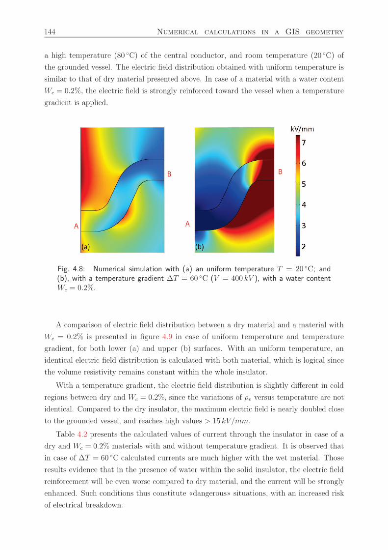
144 Numerical calculations in a GIS geometry
a high temperature (80 C) of the central conductor, and room temperature (20 C) of
the grounded vessel. The electric field distribution obtained with uniform temperature is
similar to that of dry material presented above. In case of a material with a water content
Wc = 0.2%, the electric field is strongly reinforced toward the vessel when a temperature
gradient is applied.
Fig. 4.8: Numerical simulation with (a) an uniform temperature T = 20 C; and(b), with a temperature gradient ∆T = 60 C (V = 400 kV ), with a water contentWc = 0.2%.
A comparison of electric field distribution between a dry material and a material with
Wc = 0.2% is presented in figure 4.9 in case of uniform temperature and temperature
gradient, for both lower (a) and upper (b) surfaces. With an uniform temperature, an
identical electric field distribution is calculated with both material, which is logical since
the volume resistivity remains constant within the whole insulator.
With a temperature gradient, the electric field distribution is slightly different in cold
regions between dry and Wc = 0.2%, since the variations of ρv versus temperature are not
identical. Compared to the dry insulator, the maximum electric field is nearly doubled close
to the grounded vessel, and reaches high values > 15 kV/mm.
Table 4.2 presents the calculated values of current through the insulator in case of a
dry and Wc = 0.2% materials with and without temperature gradient. It is observed that
in case of ∆T = 60 C calculated currents are much higher with the wet material. Those
results evidence that in the presence of water within the solid insulator, the electric field
reinforcement will be even worse compared to dry material, and the current will be strongly
enhanced. Such conditions thus constitute «dangerous» situations, with an increased risk
of electrical breakdown.
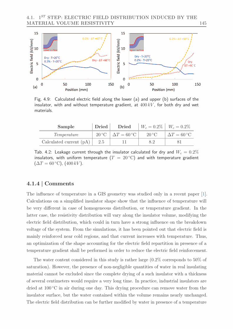
4.1. 1ST STEP: ELECTRIC FIELD DISTRIBUTION INDUCED BY THEMATERIAL VOLUME RESISTIVITY 145
Fig. 4.9: Calculated electric field along the lower (a) and upper (b) surfaces of theinsulator, with and without temperature gradient, at 400 kV , for both dry and wetmaterials.
Sample Dried Dried Wc = 0.2% Wc = 0.2%
Temperature 20 C ∆T = 60 C 20 C ∆T = 60 C
Calculated current (pA) 2.5 11 8.2 81
Tab. 4.2: Leakage current through the insulator calculated for dry and Wc = 0.2%insulators, with uniform temperature (T = 20 C) and with temperature gradient(∆T = 60 C), (400 kV ).
4.1.4 | Comments
The influence of temperature in a GIS geometry was studied only in a recent paper [1].
Calculations on a simplified insulator shape show that the influence of temperature will
be very different in case of homogeneous distribution, or temperature gradient. In the
latter case, the resistivity distribution will vary along the insulator volume, modifying the
electric field distribution, which could in turn have a strong influence on the breakdown
voltage of the system. From the simulations, it has been pointed out that electric field is
mainly reinforced near cold regions, and that current increases with temperature. Thus,
an optimization of the shape accounting for the electric field repartition in presence of a
temperature gradient shall be performed in order to reduce the electric field reinforcement.
The water content considered in this study is rather large (0.2% corresponds to 50% of
saturation). However, the presence of non-negligible quantities of water in real insulating
material cannot be excluded since the complete drying of a such insulator with a thickness
of several centimeters would require a very long time. In practice, industrial insulators are
dried at 100 C in air during one day. This drying procedure can remove water from the
insulator surface, but the water contained within the volume remains nearly unchanged.
The electric field distribution can be further modified by water in presence of a temperature
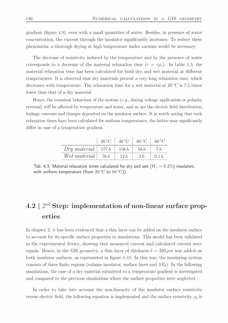
146 Numerical calculations in a GIS geometry
gradient (figure 4.9), even with a small quantities of water. Besides, in presence of water
concentration, the current through the insulator significantly increases. To reduce these
phenomena, a thorough drying at high temperature under vacuum would be necessary.
The decrease of resistivity induced by the temperature and by the presence of water
corresponds to a decrease of the material relaxation time (τ = ερv). In table 4.3, the
material relaxation time has been calculated for both dry and wet material at different
temperatures. It is observed that dry materials present a very long relaxation time, which
decreases with temperature. The relaxation time for a wet material at 20 C is 7.5 times
lower than that of a dry material.
Hence, the transient behaviour of the system (e.g., during voltage application or polarity
reversal) will be affected by temperature and water, and so are the electric field distribution,
leakage currents and charges deposited on the insulator surface. It is worth noting that such
relaxation times have been calculated for uniform temperatures, the lattice may significantly
differ in case of a temperature gradient.
20 C 40 C 60 C 80 C
Dry material 577h 158h 58h 7h
Wet material 76h 12h 2h 0.1h
Tab. 4.3: Material relaxation times calculated for dry and wet (Wc = 0.2%) insulators,with uniform temperature (from 20 C to 80 C)).
4.2 | 2nd Step: implementation of non-linear surface prop-
erties
In chapter 2, it has been evidenced that a thin layer can be added on the insulator surface
to account for its specific surface properties in simulations. This model has been validated
in the experimental device, showing that measured current and calculated current were
equals. Hence, in the GIS geometry, a thin layer of thickness δ = 320µm was added on
both insulator surfaces, as represented in figure 4.10. In this way, the insulating system
consists of three finite regions (volume insulator, surface layer and SF6). In the following
simulations, the case of a dry material submitted to a temperature gradient is investigated
and compared to the previous simulations where the surface properties were neglected.
In order to take into account the non-linearity of the insulator surface resistivity
versus electric field, the following equation is implemented and the surface resistivity ρs is
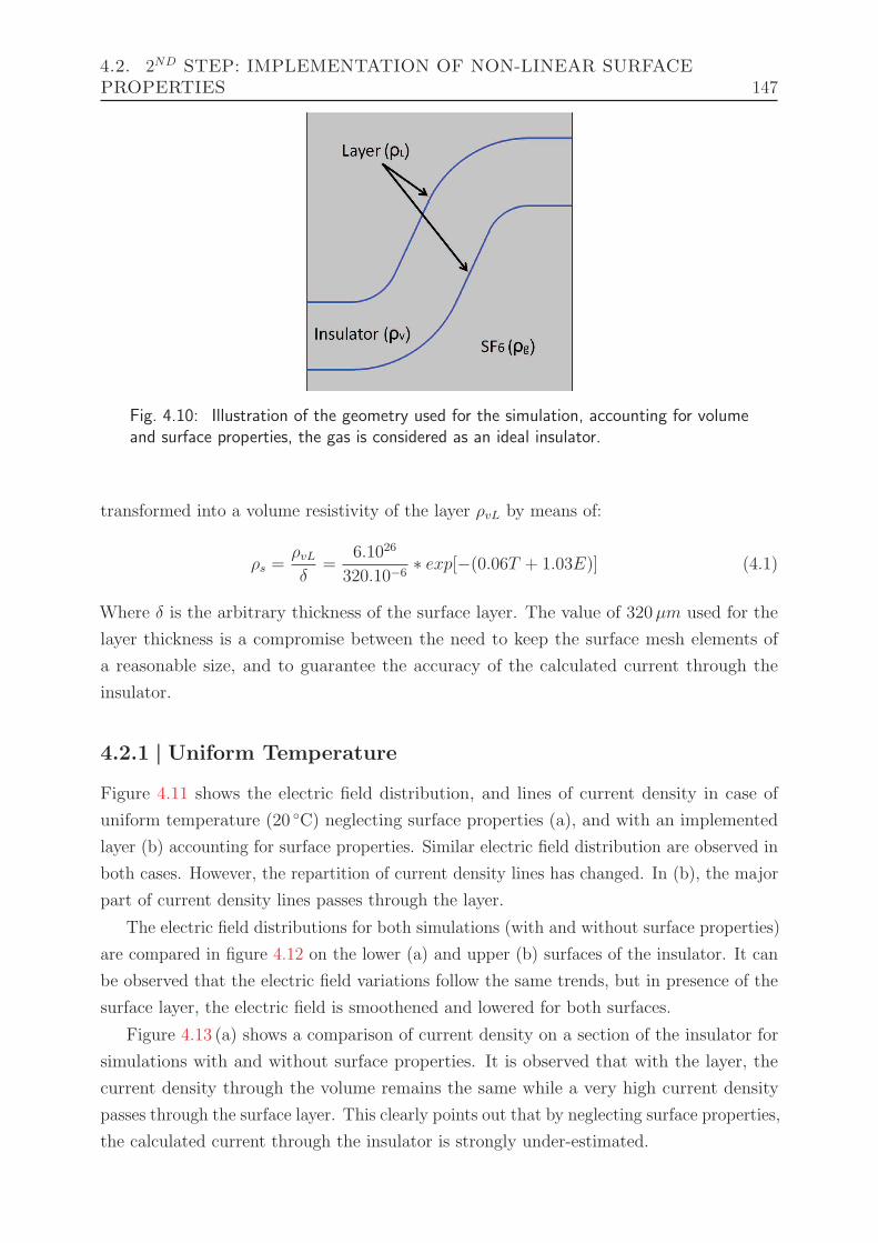
4.2. 2ND STEP: IMPLEMENTATION OF NON-LINEAR SURFACEPROPERTIES 147
Fig. 4.10: Illustration of the geometry used for the simulation, accounting for volumeand surface properties, the gas is considered as an ideal insulator.
transformed into a volume resistivity of the layer ρvL by means of:
ρs =ρvLδ
=6.1026
320.10−6∗ exp[−(0.06T + 1.03E)] (4.1)
Where δ is the arbitrary thickness of the surface layer. The value of 320µm used for the
layer thickness is a compromise between the need to keep the surface mesh elements of
a reasonable size, and to guarantee the accuracy of the calculated current through the
insulator.
4.2.1 | Uniform Temperature
Figure 4.11 shows the electric field distribution, and lines of current density in case of
uniform temperature (20 C) neglecting surface properties (a), and with an implemented
layer (b) accounting for surface properties. Similar electric field distribution are observed in
both cases. However, the repartition of current density lines has changed. In (b), the major
part of current density lines passes through the layer.
The electric field distributions for both simulations (with and without surface properties)
are compared in figure 4.12 on the lower (a) and upper (b) surfaces of the insulator. It can
be observed that the electric field variations follow the same trends, but in presence of the
surface layer, the electric field is smoothened and lowered for both surfaces.
Figure 4.13 (a) shows a comparison of current density on a section of the insulator for
simulations with and without surface properties. It is observed that with the layer, the
current density through the volume remains the same while a very high current density
passes through the surface layer. This clearly points out that by neglecting surface properties,
the calculated current through the insulator is strongly under-estimated.
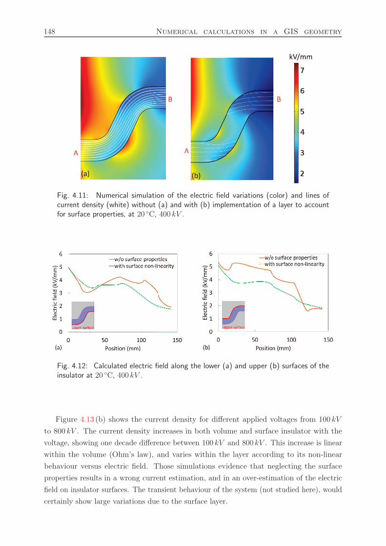
148 Numerical calculations in a GIS geometry
Fig. 4.11: Numerical simulation of the electric field variations (color) and lines ofcurrent density (white) without (a) and with (b) implementation of a layer to accountfor surface properties, at 20 C, 400 kV .
Fig. 4.12: Calculated electric field along the lower (a) and upper (b) surfaces of theinsulator at 20 C, 400 kV .
Figure 4.13 (b) shows the current density for different applied voltages from 100 kV
to 800 kV . The current density increases in both volume and surface insulator with the
voltage, showing one decade difference between 100 kV and 800 kV . This increase is linear
within the volume (Ohm’s law), and varies within the layer according to its non-linear
behaviour versus electric field. Those simulations evidence that neglecting the surface
properties results in a wrong current estimation, and in an over-estimation of the electric
field on insulator surfaces. The transient behaviour of the system (not studied here), would
certainly show large variations due to the surface layer.
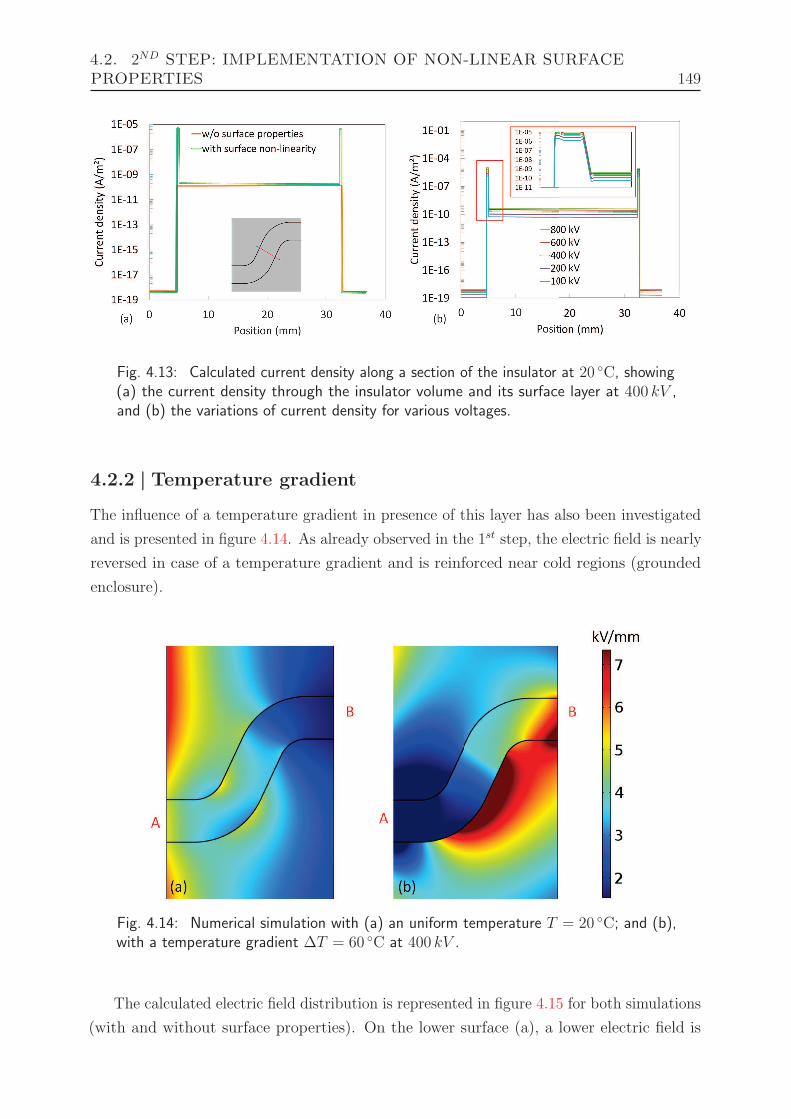
4.2. 2ND STEP: IMPLEMENTATION OF NON-LINEAR SURFACEPROPERTIES 149
Fig. 4.13: Calculated current density along a section of the insulator at 20 C, showing(a) the current density through the insulator volume and its surface layer at 400 kV ,and (b) the variations of current density for various voltages.
4.2.2 | Temperature gradient
The influence of a temperature gradient in presence of this layer has also been investigated
and is presented in figure 4.14. As already observed in the 1st step, the electric field is nearly
reversed in case of a temperature gradient and is reinforced near cold regions (grounded
enclosure).
Fig. 4.14: Numerical simulation with (a) an uniform temperature T = 20 C; and (b),with a temperature gradient ∆T = 60 C at 400 kV .
The calculated electric field distribution is represented in figure 4.15 for both simulations
(with and without surface properties). On the lower surface (a), a lower electric field is
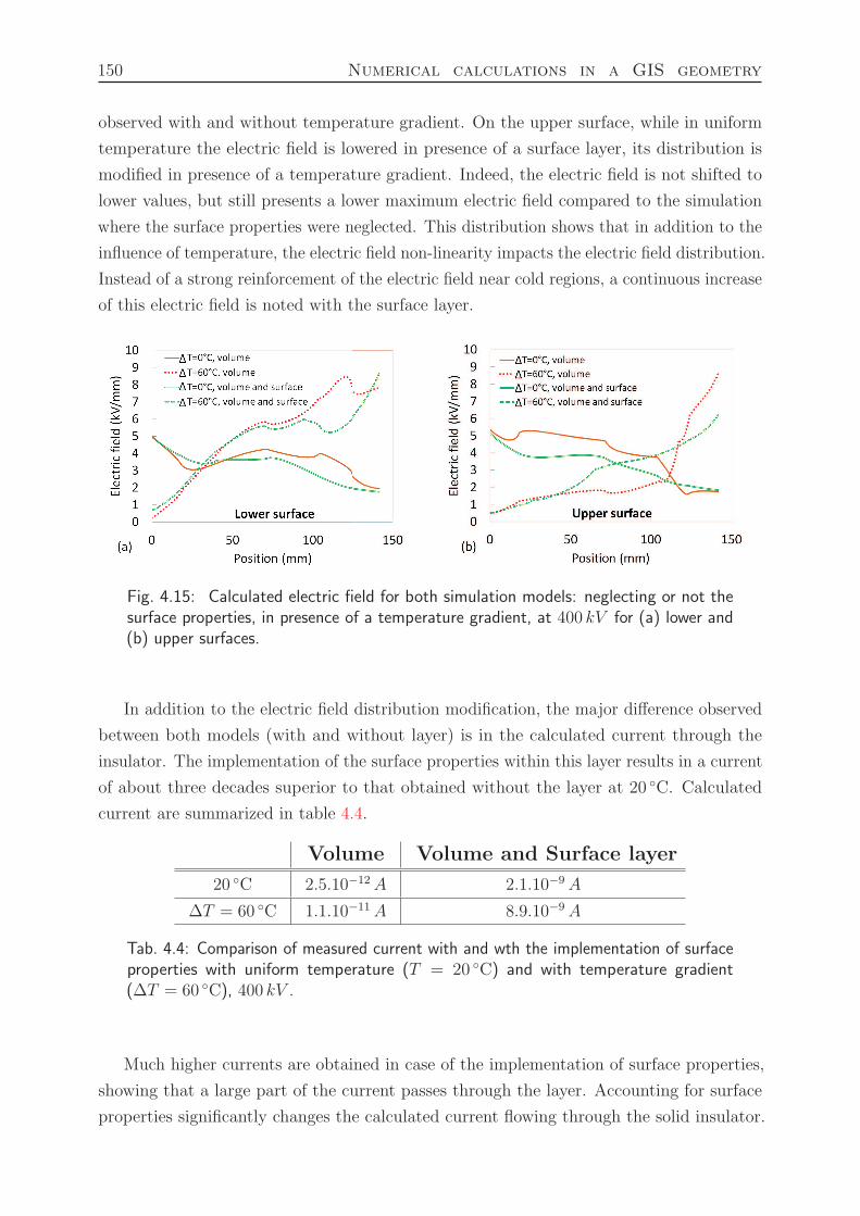
150 Numerical calculations in a GIS geometry
observed with and without temperature gradient. On the upper surface, while in uniform
temperature the electric field is lowered in presence of a surface layer, its distribution is
modified in presence of a temperature gradient. Indeed, the electric field is not shifted to
lower values, but still presents a lower maximum electric field compared to the simulation
where the surface properties were neglected. This distribution shows that in addition to the
influence of temperature, the electric field non-linearity impacts the electric field distribution.
Instead of a strong reinforcement of the electric field near cold regions, a continuous increase
of this electric field is noted with the surface layer.
Fig. 4.15: Calculated electric field for both simulation models: neglecting or not thesurface properties, in presence of a temperature gradient, at 400 kV for (a) lower and(b) upper surfaces.
In addition to the electric field distribution modification, the major difference observed
between both models (with and without layer) is in the calculated current through the
insulator. The implementation of the surface properties within this layer results in a current
of about three decades superior to that obtained without the layer at 20 C. Calculated
current are summarized in table 4.4.
Volume Volume and Surface layer
20 C 2.5.10−12 A 2.1.10−9 A
∆T = 60 C 1.1.10−11 A 8.9.10−9 A
Tab. 4.4: Comparison of measured current with and wth the implementation of surfaceproperties with uniform temperature (T = 20 C) and with temperature gradient(∆T = 60 C), 400 kV .
Much higher currents are obtained in case of the implementation of surface properties,
showing that a large part of the current passes through the layer. Accounting for surface
properties significantly changes the calculated current flowing through the solid insulator.
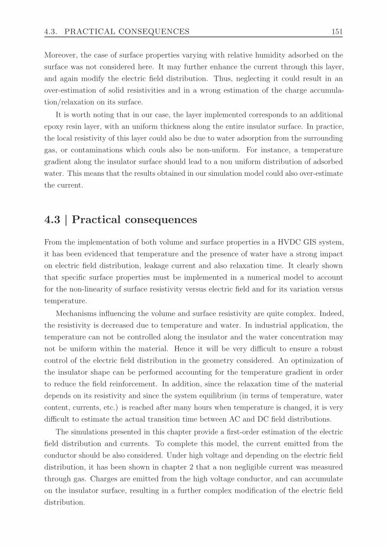
4.3. PRACTICAL CONSEQUENCES 151
Moreover, the case of surface properties varying with relative humidity adsorbed on the
surface was not considered here. It may further enhance the current through this layer,
and again modify the electric field distribution. Thus, neglecting it could result in an
over-estimation of solid resistivities and in a wrong estimation of the charge accumula-
tion/relaxation on its surface.
It is worth noting that in our case, the layer implemented corresponds to an additional
epoxy resin layer, with an uniform thickness along the entire insulator surface. In practice,
the local resistivity of this layer could also be due to water adsorption from the surrounding
gas, or contaminations which couls also be non-uniform. For instance, a temperature
gradient along the insulator surface should lead to a non uniform distribution of adsorbed
water. This means that the results obtained in our simulation model could also over-estimate
the current.
4.3 | Practical consequences
From the implementation of both volume and surface properties in a HVDC GIS system,
it has been evidenced that temperature and the presence of water have a strong impact
on electric field distribution, leakage current and also relaxation time. It clearly shown
that specific surface properties must be implemented in a numerical model to account
for the non-linearity of surface resistivity versus electric field and for its variation versus
temperature.
Mechanisms influencing the volume and surface resistivity are quite complex. Indeed,
the resistivity is decreased due to temperature and water. In industrial application, the
temperature can not be controlled along the insulator and the water concentration may
not be uniform within the material. Hence it will be very difficult to ensure a robust
control of the electric field distribution in the geometry considered. An optimization of
the insulator shape can be performed accounting for the temperature gradient in order
to reduce the field reinforcement. In addition, since the relaxation time of the material
depends on its resistivity and since the system equilibrium (in terms of temperature, water
content, currents, etc.) is reached after many hours when temperature is changed, it is very
difficult to estimate the actual transition time between AC and DC field distributions.
The simulations presented in this chapter provide a first-order estimation of the electric
field distribution and currents. To complete this model, the current emitted from the
conductor should be also considered. Under high voltage and depending on the electric field
distribution, it has been shown in chapter 2 that a non negligible current was measured
through gas. Charges are emitted from the high voltage conductor, and can accumulate
on the insulator surface, resulting in a further complex modification of the electric field
distribution.
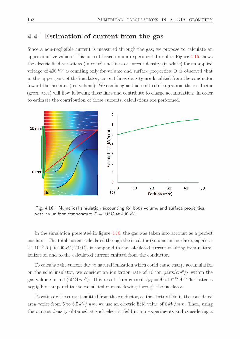
152 Numerical calculations in a GIS geometry
4.4 | Estimation of current from the gas
Since a non-negligible current is measured through the gas, we propose to calculate an
approximative value of this current based on our experimental results. Figure 4.16 shows
the electric field variations (in color) and lines of current density (in white) for an applied
voltage of 400 kV accounting only for volume and surface properties. It is observed that
in the upper part of the insulator, current lines density are localized from the conductor
toward the insulator (red volume). We can imagine that emitted charges from the conductor
(green area) will flow following those lines and contribute to charge accumulation. In order
to estimate the contribution of those currents, calculations are performed.
Fig. 4.16: Numerical simulation accounting for both volume and surface properties,with an uniform temperature T = 20 C at 400 kV .
In the simulation presented in figure 4.16, the gas was taken into account as a perfect
insulator. The total current calculated through the insulator (volume and surface), equals to
2.1.10−9 A (at 400 kV , 20 C), is compared to the calculated current resulting from natural
ionization and to the calculated current emitted from the conductor.
To calculate the current due to natural ionization which could cause charge accumulation
on the solid insulator, we consider an ionization rate of 10 ion pairs/cm3/s within the
gas volume in red (6029 cm3). This results in a current INI = 9.6.10−15 A. The latter is
negligible compared to the calculated current flowing through the insulator.
To estimate the current emitted from the conductor, as the electric field in the considered
area varies from 5 to 6.5 kV/mm, we use an electric field value of 6 kV/mm. Then, using
the current density obtained at such electric field in our experiments and considering a
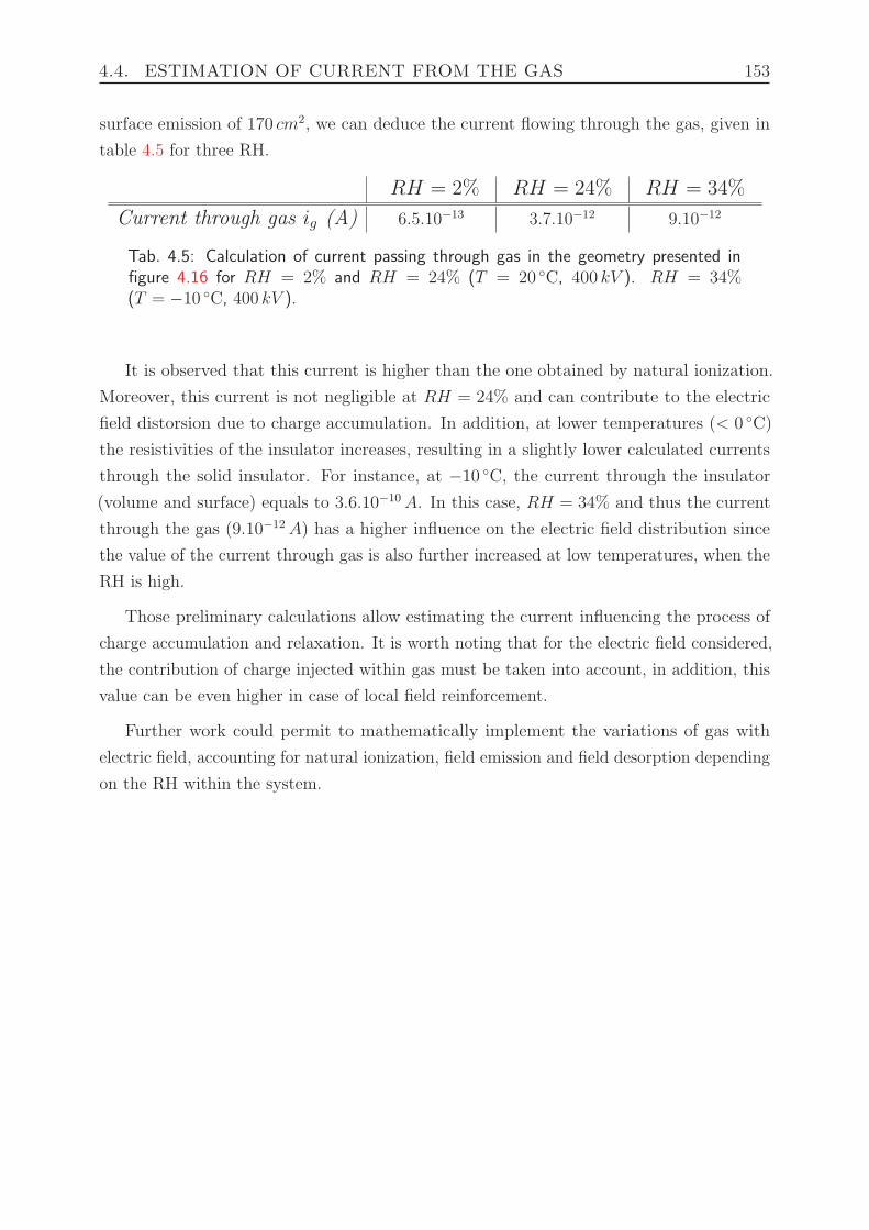
4.4. ESTIMATION OF CURRENT FROM THE GAS 153
surface emission of 170 cm2, we can deduce the current flowing through the gas, given in
table 4.5 for three RH.
RH = 2% RH = 24% RH = 34%
Current through gas ig (A) 6.5.10−13 3.7.10−12 9.10−12
Tab. 4.5: Calculation of current passing through gas in the geometry presented infigure 4.16 for RH = 2% and RH = 24% (T = 20 C, 400 kV ). RH = 34%(T = −10 C, 400 kV ).
It is observed that this current is higher than the one obtained by natural ionization.
Moreover, this current is not negligible at RH = 24% and can contribute to the electric
field distorsion due to charge accumulation. In addition, at lower temperatures (< 0 C)
the resistivities of the insulator increases, resulting in a slightly lower calculated currents
through the solid insulator. For instance, at −10 C, the current through the insulator
(volume and surface) equals to 3.6.10−10 A. In this case, RH = 34% and thus the current
through the gas (9.10−12 A) has a higher influence on the electric field distribution since
the value of the current through gas is also further increased at low temperatures, when the
RH is high.
Those preliminary calculations allow estimating the current influencing the process of
charge accumulation and relaxation. It is worth noting that for the electric field considered,
the contribution of charge injected within gas must be taken into account, in addition, this
value can be even higher in case of local field reinforcement.
Further work could permit to mathematically implement the variations of gas with
electric field, accounting for natural ionization, field emission and field desorption depending
on the RH within the system.
Conclusions 154
4.5 | Conclusions
In this chapter, a numerical model with an insulator geometry close to the real application
has been developed to evaluate the relative influence of the current passing through the solid
insulator and the one transported through gas. The influences of water concentration and
temperature gradient on the electric field distribution have been shown. In presence of a
temperature gradient, the electric field distribution is nearly reversed and field is reinforced
near cold areas. Moreover, it also impacts the calculated current through the insulator.
When temperature is increased, so is the current.
Furthermore, it has been evidenced that the implementation of surface properties by
adding a layer on the insulator surface considerably modifies the electric field distribution.
It is lowered and smoothened. In addition, the calculated current with the surface layer
has significanlty increased. All current lines density pass through this layer, and the latter
strongly depends on electric field. It clearly shows that if the surface properties are neglected,
the current flowing through the insulator is under-estimated and wrong calculations are
performed.
Finally, the calculations (based on experimental measurements) performed on current
emitted from the conductor, point out the presence of current flowing through gas in
presence of both dry and «wet» systems. Such currents must be considered since they
can strongly modify the electric field distribution on the insulator surface in case of cold
temperatures and humid systems.
Those calculations are of importance for the GIS application. Indeed, simulations are
usually performed to predict the behaviour of solid insulator under various conditions
(temperature, electric field) and thus reduce the experimental costs. In order to realize an
accurate model, all injection mechanisms from the conductor must be implemented (field
emission, natural ionization, field desorption). In addition, the non-linearity of surface
properties must be taken into account, as well as the influence of a temperature gradient.
Further work should be performed to realized a complete model accounting for those physical
mechanisms.
Bibliography
[1] U. Straumann, M. Schuller, and C. M. Franck, “Theoretical investigation of HVDC discspacer charging in SF6 gas insulated systems,” Dielectrics and Electrical Insulation,IEEE Transactions, vol. 19, no. 6, pp. 2196–2205, 2012. (cited in pages 30 and 145)
General Conclusions and Perspectives
The control of electric field distribution and charge accumulation and relaxation on solid
insulators within High Voltage Direct Current in Gas Insulated Substations, is an important
challenge for the energy transport, from a fundamental and industrial point of view. The
main objective of this thesis work was to investigate conduction processes and mechanisms
in solids and gaseous dielectrics composing a GIS, in order to identify the main parameters
which have an influence on electric field distribution and charge accumulation, and then
build a numerical model allowing to estimate their impact with a realistic insulator shape.
Since the electric field distribution strongly influences the charge accumulation, we have
reviewed the physical phenomena involved. This accumulation is particularly dependent
on electric field orientation, and solid dielectric properties. This dependence leads to a
complex equilibrium between electrical conduction through the dielectric solid (volume
and surface), and charge generation and transport through the dielectric gas. It is worth
noting that rather few studies were devoted to investigate the influence of other parameters
of great importance: the presence of a temperature gradient, the possible influence of
water present in the solid, and the non-linearity of surface conduction processes. Based on
this bibliographic review, we have defined experimental investigations which allows better
identifying the parameters and physical phenomena responsible of electric field distribution
induced by properties of the solid, and charge accumulation due to charge creation in the
gas.
We have developped two experimental setups allowing to measure very low currents
under HVDC in pressuized gases, and characterize those currents. We have been able to
investigate the influence of the amplitude and polarity of electric field, gap distance between
electrodes, pressure, electrode surface roughness, temperature and relative humidity (RH).
Many original results have been obtained, identifying the impact of different parameters.
It has been pointed out that in all cases, dark currents exponentially vary with the
electric field, and are strongly influenced by the electrode surface roughness. Then, a large
influence of pressure and temperature has been observed, resulting in the modification of the
relative humidity within the system. Consequently, we have studied different equilibrium
states to observe the evolution of the measured currents when pressure, temperature and
RH changed. In case of a «humid» system, the measured currents increase with RH, while
temperature decreases. On the contrary, in case of a «dry» system, the measured currents
increase with temperature, while RH decreases.
155
156 Conclusions and Perspectives
This points out the complex influence of temperature in the system equilibrium. By
varying the pressure and measuring the RH during experiments, we have highlighted that
pressure only has an indirect impact on dark currents. Indeed, the pressure change induces a
modification of the RH within the system which results in variations on measured currents.
We have also observed that influences of both temperature and RH do not modify
the tendency followed by the current versus electric field. We suggest that the injection
mechanisms at the origin of measured dark currents are similar in all our experimental
conditions. Additionally, we have evidenced that these mechanisms are only enhanced or
reduced by changing temperature and/or RH.
Our investigations in gases suggest that the predominant mechanism responsible of
charge injection in our system is related to the theory of field ionization and desorption
resulting in cluster ion formation from water molecules. These clusters, transported following
electric field lines, are responsible for the measured currents.
Concerning solid dielectric characterization, we have investigated the surface and volume
properties of different materials. Our approach was to develop experimental setups allowing
to perform current measurements at very low noise level under pressurized gases and at high
voltages. An experimental protocol was first defined in order to get reliable measurements
of conduction currents. This protocol includes a drying procedure, since delivered samples
contained some water, and a de-polarization procedure to remove pre-existing charges. Very
long measurements have been performed in order to obtain stabilized DC currents.
Using this protocol, we have observed that both properties of the material are tem-
perature dependent. Actually, the volume and the surface conductivities increase with
temperature. Moreover, those properties are also strongly influenced by the water absorbed
within the insulator and adsorbed on its surface. In both cases, the conduction increases
with the water concentration. Furthermore, in the considered electric field range (from 0.5
up to 5 kV/mm) we have shown that volume conduction follows a nearly Ohmic behaviour
while surface conductivity shows a large non-linearity with electric field variations. Those
results pointed out that the surface properties of solid insulators are of major importance,
and must be taken into account to build a numerical model. From these results, a data base
of solid dielectric behaviour versus temperature, electric field and RH has been created.
Additional investigations on new materials and on surface treatments have been per-
formed in order to modify the conduction properties of the solid material. We have observed
that a plasma treatment on the solid surface could result in lower surface resistivities. Thus,
by adjusting the implantation parameters, the surface resistivity of the solid material can
be controlled. Such investigations provide guidelines to fabricate new materials optimized
for HVDC. However further investigations would be necessary to confirm if these materials
can be used in industrial applications.
Conclusions and Perspectives 157
Finally, a numerical model with a geometry close to the real application has been
developed. First, volume properties were implemented, neglecting the influence of the
surface properties. It has been observed that in presence of a temperature gradient between
the conductor and the vessel, the electric field distribution is strongly modified, resulting
in a modification of the leakage current through the insulator. In addition, the non-linear
surface properties have been implemented via a thin layer on the insulator surface. It
has been shown that in this case, most of current density lines pass through the layer
and dramatically increase the calculated current. These investigations show that these
parameters (temperature gradient, surface properties) are very important for the actual
electric field distribution in a GIS geometry. Consequently, these parameters must be
included in the development and optimization of practical systems. Then, estimations
based on experimental measurements through gas, pointed out that the current through
gas in presence of «dry» , or «humid» systems is not negligible and may also modify the
electric field distribution. However, more accurate models are necessary to assess the actual
influence of charges coming from the gas on the electric field distribution.
In this work, we have identified many parameters which influence the solid insulator
properties and dark currents through gases. The results obtained show the great complexity
of the problem. Under HVDC, the electric field distribution depends on many parameters
(temperature, water content, electrode roughness, gas purity, etc.) which have a limited
influence in HVAC.
From the scientific point of view, further experiments should be performed in gases
in order to better understand the physical processus of charge injection, find a solution
to control the influence of RH within gas, and reduce the charge emission from the high
voltage electrode. From the industrial point of view, a more accurate numerical model,
accounting for charge injection, displacement, and neutralization should be developped
in order to consider all mechanisms participating to charge accumulation and relaxation.
Such model should permit to predict with accuracy the behaviour of the insulator in time,
versus temperature, electric field and relative humidity. Moreover, that would be also
very interesting to estimate the insulator behaviour during transients of electric field and
temperature.

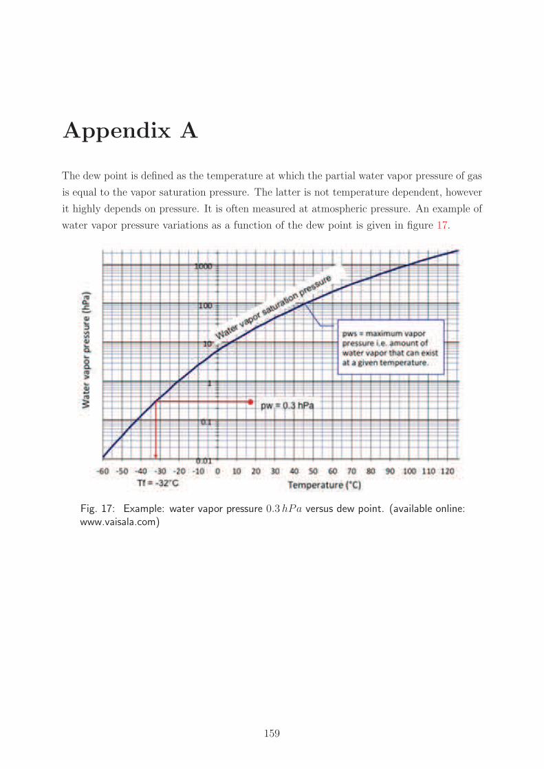
Appendix A
The dew point is defined as the temperature at which the partial water vapor pressure of gas
is equal to the vapor saturation pressure. The latter is not temperature dependent, however
it highly depends on pressure. It is often measured at atmospheric pressure. An example of
water vapor pressure variations as a function of the dew point is given in figure 17.
Fig. 17: Example: water vapor pressure 0.3hPa versus dew point. (available online:www.vaisala.com)
159

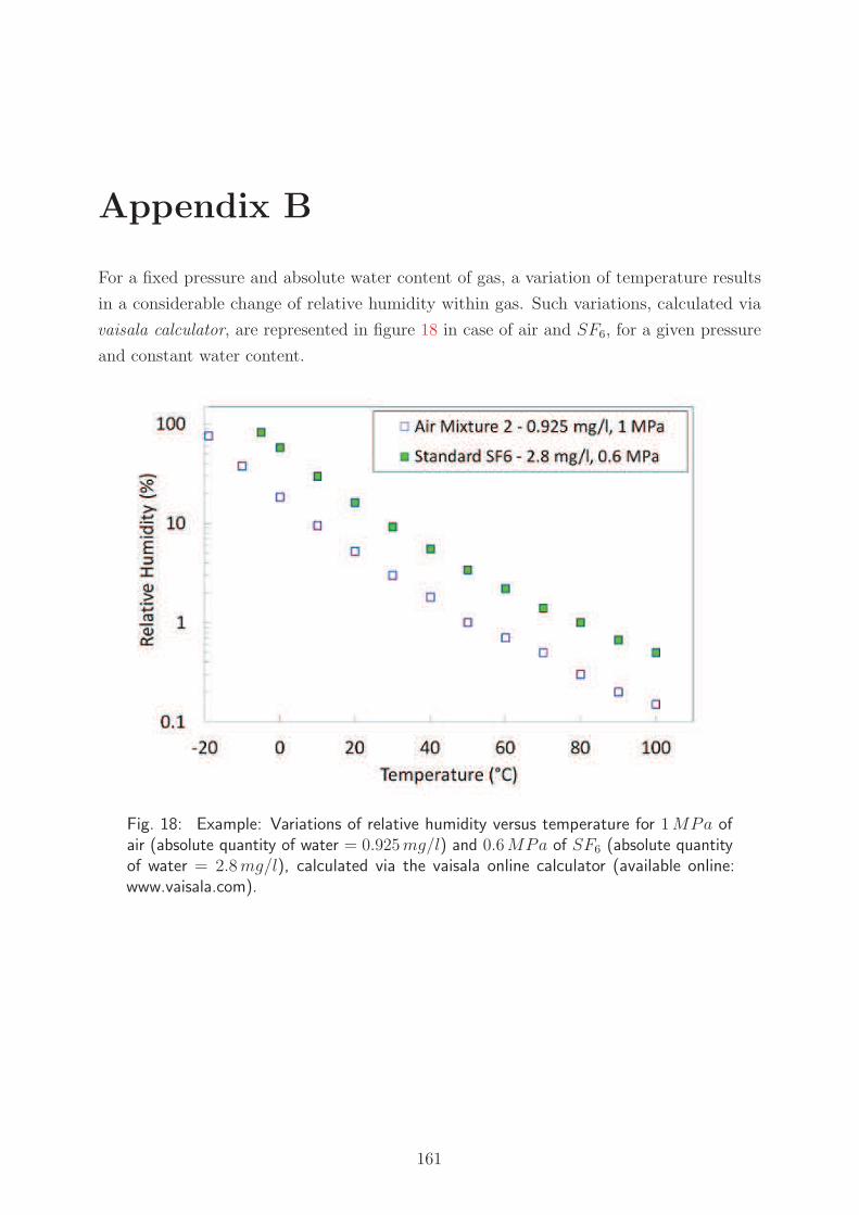
Appendix B
For a fixed pressure and absolute water content of gas, a variation of temperature results
in a considerable change of relative humidity within gas. Such variations, calculated via
vaisala calculator, are represented in figure 18 in case of air and SF6, for a given pressure
and constant water content.
Fig. 18: Example: Variations of relative humidity versus temperature for 1MPa ofair (absolute quantity of water = 0.925mg/l) and 0.6MPa of SF6 (absolute quantityof water = 2.8mg/l), calculated via the vaisala online calculator (available online:www.vaisala.com).
161