femtosecond pulsed laser deposited er3+-doped zinc-sodium
TRANSCRIPT
AIP Advances 9, 085324 (2019); https://doi.org/10.1063/1.5097506 9, 085324
© 2019 Author(s).
Femtosecond pulsed laser deposited Er3+-doped zinc-sodium tellurite glass on Si:Thin-film structural and photoluminescencepropertiesCite as: AIP Advances 9, 085324 (2019); https://doi.org/10.1063/1.5097506Submitted: 26 March 2019 . Accepted: 21 August 2019 . Published Online: 28 August 2019
Thomas Mann , Billy Richards, Eric Kumi-Barimah , Robert Mathieson, Matthew Murray, ZoranIkonic, Paul Steenson, Christopher Russell, and Gin Jose
ARTICLES YOU MAY BE INTERESTED IN
A study on the surface morphology evolution of the GH4619 using warm laser shockpeeningAIP Advances 9, 085030 (2019); https://doi.org/10.1063/1.5082755
Extreme brightness laser-based neutron pulses as a pathway for investigatingnucleosynthesis in the laboratoryMatter and Radiation at Extremes 4, 054402 (2019); https://doi.org/10.1063/1.5081666
Rare earth-implanted lithium niobate: Properties and on-chip integrationApplied Physics Letters 115, 071104 (2019); https://doi.org/10.1063/1.5098316
AIP Advances ARTICLE scitation.org/journal/adv
Femtosecond pulsed laser deposited Er3+-dopedzinc-sodium tellurite glass on Si: Thin-filmstructural and photoluminescence properties
Cite as: AIP Advances 9, 085324 (2019); doi: 10.1063/1.5097506Submitted: 26 March 2019 • Accepted: 21 August 2019 •Published Online: 28 August 2019
Thomas Mann,1 Billy Richards,1 Eric Kumi-Barimah,1 Robert Mathieson,1 Matthew Murray,1 Zoran Ikonic,2Paul Steenson,2 Christopher Russell,2 and Gin Jose1,a)
AFFILIATIONS1School of Chemical and Process Engineering, University of Leeds, Leeds LS2 9JT, UK2School of Electronic and Electrical Engineering, University of Leeds, Leeds LS2 9JT, UK
ABSTRACT
We characterise the thin-film structural properties and photoluminescence of femtosecond (40 fs, 800 nm) pulsed laser deposited Er3+-dopedzinc-sodium tellurite glass on Si as a function of laser fluence. The laser fluence regime required for the formation of films composed ofnanoparticles without droplets is found, the composition and crystallinity of the deposited material is reported and the photoluminescence ofthe films is characterised in dependence of film thickness.
© 2019 Author(s). All article content, except where otherwise noted, is licensed under a Creative Commons Attribution (CC BY) license(http://creativecommons.org/licenses/by/4.0/). https://doi.org/10.1063/1.5097506., s
I. INTRODUCTION
Tellurite glasses are particularly well suited as hosts for rare-earth (RE) ions due to their high rare-earth solubility and lowphonon energy.1–4 In particular, the 4I13/2 →
4I15/2 transition of Er3+
ions is centred at 1.54 μm, which lies in the low loss C-band of silicaand can therefore be exploited for telecommunications. As such, thefabrication of Er3+-doped tellurite-based glass thin films is of inter-est for optical applications including sensors, waveguide amplifiersand lasers.2,5
Pulsed laser deposition (PLD) has proven to be a valid and effi-cient technique for the stoichiometric transfer of material from tar-get to a film on a substrate, which is not possible with the growth offilms from atomic species.6 Nanosecond (ns) PLD has been used byseveral research groups to form Er3+-doped tellurite thin films.7–10
However, micrometer sized droplet formation resulting from vio-lent subsurface heating effects during vaporisation of the target andgas phase condensation of the large volume of ablated material bythe high energy pulses is a characteristic of ns-PLD that limits thecapability of this technique.11–13 Due to the non-thermal energydeposition and lower pulse energies required for femtosecond (fs)
laser ablation, the formation of droplets can be avoided provid-ing that the laser fluence is not too high.12,14 The formation ofnanoparticles in ns-PLD occurs during gas phase condensation ofan atomised plasma plume confined in a pressurised atmosphere.This is significantly different in fs-PLD, where nanoparticle gen-eration occurs in vacuum and is thought to be due to mechani-cal fragmentation of the highly pressurised fluid undergoing rapidquenching during the hydrodynamic expansion.14,15 The major-ity of fs-PLD fabricated nanostructured films result from the ran-dom stacking of nanoparticles (NPs), typically in the 10 - 60 nmrange.13,14,16–18
Er3+-doped zinc-sodium tellurite glass NPs have recently beenincorporated into polymers for low-cost integrated optical ampli-fiers using the fs-PLD technique.19 Similarly, the ultrafast laserplasma doping (ULPD) technique ablates a rare-earth (RE) dopedzinc-sodium tellurite target onto a heated silica based substrate suchthat the subsequent interfacial dissolution forms RE-doped hybridtellurite-silica thin films.20–23
The species (ions, nanoparticles and droplets) in the ablationplume are a direct consequence of the fs laser and target properties.The high energy ions and electrons (atomic species) typically only
AIP Advances 9, 085324 (2019); doi: 10.1063/1.5097506 9, 085324-1
© Author(s) 2019
AIP Advances ARTICLE scitation.org/journal/adv
make up a few percent of the total ablated matter.14 At a fixed fslaser wavelength, pulse width, spot size and repetition rate, the laserfluence relative to the target ablation threshold is the key parame-ter dictating the particle size distribution in the ablation plume.12,14
The ablation threshold of Er3+-doped zinc-sodium tellurite glass inatmosphere irradiated with a fs laser of pulse duration 100 fs andcentral wavelength of 800 nm has been characterised previously.24 Itwas found that the single shot ablation threshold was 0.32 J/cm2 anddropped to a multipulse value of 0.14 J/cm2 at a spot size of 32 μm.A characterisation of the nanoparticles and droplets in the fs abla-tion plume for tellurite glass does not exist in the literature and isthe purpose of this work.
Structural characterisation is achieved through scanning elec-tron microscopy studies of vacuum depositions on silicon substratesat varying laser fluences. The composition of the depositions andthe crystalline structure are studied with energy dispersive X-rayspectroscopy and grazing incidence X-ray diffraction, respectively.The effect of the target glass surface roughness on the laser ablationthreshold was also investigated. The radiative spontaneous emis-sion (SE) rate of the Er3+-doped films was measured using time-resolved photoluminescence (PL) spectroscopy and compared witha quantum-electrodynamical model for the average SE rate for ionsinside multilayer dielectric structures. An increase in decay rate forvery thin films is observed due to the electric field confinementwithin the film and an increase in the non-radiative recombinationprocesses. The latter is due to a combination of Auger quenchingand energy backtransfer, which are known to limit the efficiencyof room temperature Er3+ ion doped/deposited silicon based lightsources.25–28
II. EXPERIMENTAL SETUPA. Sample fabrication
Depositions were performed using an amplified solid-stateTi:sapphire laser (Wyvern 1000-10, KMLabs) producing an almostdiffraction limited beam (M2
< 1.3) at a central wavelength of800 nm (∼ 53 nm full width half maximum) and pulse duration of∼ 40 fs. The maximum pulse energy at a 1 kHz repetition rate was∼ 4 mJ. The linearly polarised beam exiting from the laser source wasfocused onto the target surface with a 56.5 cm focal length plano-convex lens at a 60○ angle of incidence. The elliptical laser spot onthe sample surface was measured prior to ablation and had an areaof A ≈ 8.5 × 10⁻⁵ cm2 (Gaussian beam waists of ∼ 82 and 33 μm).The laser energy was determined with a pyroelectric detector andenergy meter (PE50-DIF-C and Starlite Energy Meter, Ophir), andcontrolled with a half-wave plate and beam splitting polariser to givepulse energies Ep ranging from 18 to 433 μJ. In this work we reportthe average fluence of the laser pulse, F = Ep/A. All experiments werecarried out in a vacuum (<1 × 10⁻⁴ Torr) and at room temperature(23○C).
The target was an Er3+-doped zinc-sodium tellurite glassof composition 79TeO2-10ZnO-10Na2O-1Er2O3 mol.% (1ErTZN).Fabrication and characterisation of the target glass has been pre-sented in Ref. 24. The glass was wet polished with P1200 grit siliconcarbide (SiC) sandpaper to the dimensions of ∼ 30 × 30 × 3 mm.The resulting surface roughness Ra ≈ 108 nm (measured on a100 × 100 μm region). For investigations into the effect of target
surface quality on the ablation plume, the target glass was given anoptical polish to Ra ≈ 5 nm.
The substrate was a polished silicon wafer (P < 100 > B doped,resistivity of 1-20 ohm⋅cm, diced into 10 mm by 10 mm squares,Ra < 0.3 nm) placed parallel to and 40 mm above the target surface.Each substrate was cleaned for 5 minutes in an ultrasonic bath withacetone and then isopropanol prior to depositions. The Si substratewas rotated at 5 RPM around its centre to give a uniform depositionand each deposition constituted the application of 180k pulses percm2 to the target surface directly below the substrate. Specifically,the laser rastering involved scanning 180 lines at a speed of 10 mm/sover a length larger than the substrate (22 mm) and moving the tar-get in 0.1 mm steps perpendicular to the laser raster axis after eachline (18 mm length in total).
B. CharacterisationCharacterisation of the deposited films was studied by using
high resolution scanning electron microscopy (SEM, HitachiSU8230). In order to determine the size distribution of the parti-cles, several SEM images were processed using Fiji.29,30 Depositionthicknesses d were evaluated on cross-sections after snapping thesubstrate from the rear. Elemental identification of the depositionswas performed using energy-dispersive X-ray spectroscopy (EDX)coupled to the SEM (80mm2 X-Max detector, Oxford Instruments).Point measurements were taken at the centre of droplets to minimisethe effect of surface geometry on the results (the analysis assumes aflat surface). The strongest peak signal in the spectra correspond-ing to the Si substrate was not included in the analysis. Sodium andzinc both exhibit their L emission lines very close to each other andcould not be resolved in the spectra. As a result the relative ratio ofZn to Na are inaccurate and this also impacts the quantification ofthe weight % of other elements as the normalisation to 100% is notaccurate. As a result of these limitations, the compositional resultswith the EDX technique are semi-quantitative.
The average surface roughness Ra and the root mean squareroughness RRMS were characterised via atomic force microscopy(AFM) operating in tapping mode (Innova Atomic Force Micro-scope, Bruker with a μmasch AFM probe of 8 nm nominal tipradius) and averaging over areas at least several times larger than thelargest features. The data was analysed with the open source softwareGwyddion.31,32
The crystallinity of the 3.32 J/cm2 deposition was studied bygrazing incidence X-ray diffraction (GIXRD). This was preferredover the standard θ/2θ XRD configuration to avoid the signal fromthe silicon substrate that would otherwise swamp the spectral fea-tures of the thin film. GIXRD measurements were performed onan X-ray diffractometer (X’Pert, Phillips) using Cu-Kα radiation(1.5406 Å) across the 2θ range 10 - 80○ at an angle of incidenceof 2○ and a scan rate of 0.005○/second. The peaks in the measureddiffraction patterns were identified and indexed using the X’pertHigh Score Plus software package. The spectral shift in the GXIDspectra was -0.29○ and evaluated prior to fitting using a θ/2θ XRDscan on the same sample.33
PL measurements were performed using a fluorescence spec-trometer (FLS 920, Edinburgh Instruments) at room temperature.A 976 nm excitation laser source (BL976-PAG500976, Thorlabs),which resonates with the 4I15/2 →
4I11/2 transition of Er3+, with a
AIP Advances 9, 085324 (2019); doi: 10.1063/1.5097506 9, 085324-2
© Author(s) 2019
AIP Advances ARTICLE scitation.org/journal/adv
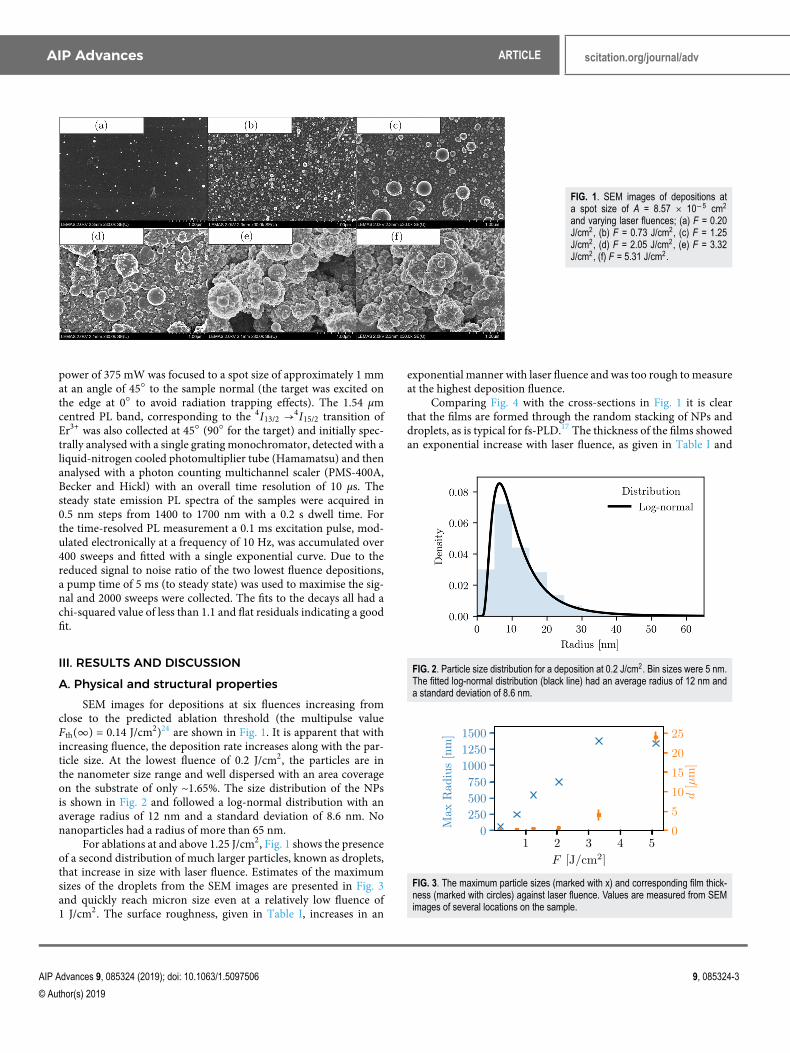
FIG. 1. SEM images of depositions ata spot size of A = 8.57 × 10⁻⁵ cm2
and varying laser fluences; (a) F = 0.20J/cm2, (b) F = 0.73 J/cm2, (c) F = 1.25J/cm2, (d) F = 2.05 J/cm2, (e) F = 3.32J/cm2, (f) F = 5.31 J/cm2.
power of 375 mW was focused to a spot size of approximately 1 mmat an angle of 45○ to the sample normal (the target was excited onthe edge at 0○ to avoid radiation trapping effects). The 1.54 μmcentred PL band, corresponding to the 4I13/2 →
4I15/2 transition ofEr3+ was also collected at 45○ (90○ for the target) and initially spec-trally analysed with a single grating monochromator, detected with aliquid-nitrogen cooled photomultiplier tube (Hamamatsu) and thenanalysed with a photon counting multichannel scaler (PMS-400A,Becker and Hickl) with an overall time resolution of 10 μs. Thesteady state emission PL spectra of the samples were acquired in0.5 nm steps from 1400 to 1700 nm with a 0.2 s dwell time. Forthe time-resolved PL measurement a 0.1 ms excitation pulse, mod-ulated electronically at a frequency of 10 Hz, was accumulated over400 sweeps and fitted with a single exponential curve. Due to thereduced signal to noise ratio of the two lowest fluence depositions,a pump time of 5 ms (to steady state) was used to maximise the sig-nal and 2000 sweeps were collected. The fits to the decays all had achi-squared value of less than 1.1 and flat residuals indicating a goodfit.
III. RESULTS AND DISCUSSIONA. Physical and structural properties
SEM images for depositions at six fluences increasing fromclose to the predicted ablation threshold (the multipulse valueFth(∞) = 0.14 J/cm2)24 are shown in Fig. 1. It is apparent that withincreasing fluence, the deposition rate increases along with the par-ticle size. At the lowest fluence of 0.2 J/cm2, the particles are inthe nanometer size range and well dispersed with an area coverageon the substrate of only ∼1.65%. The size distribution of the NPsis shown in Fig. 2 and followed a log-normal distribution with anaverage radius of 12 nm and a standard deviation of 8.6 nm. Nonanoparticles had a radius of more than 65 nm.
For ablations at and above 1.25 J/cm2, Fig. 1 shows the presenceof a second distribution of much larger particles, known as droplets,that increase in size with laser fluence. Estimates of the maximumsizes of the droplets from the SEM images are presented in Fig. 3and quickly reach micron size even at a relatively low fluence of1 J/cm2. The surface roughness, given in Table I, increases in an
exponential manner with laser fluence and was too rough to measureat the highest deposition fluence.
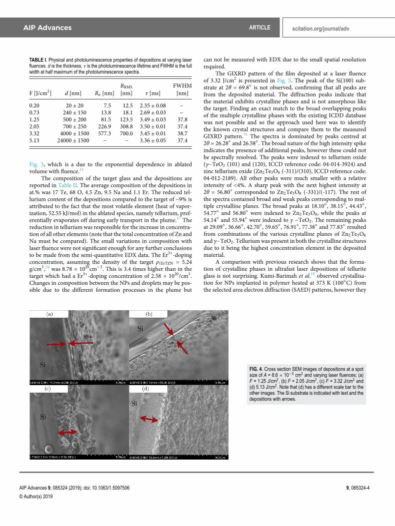
Comparing Fig. 4 with the cross-sections in Fig. 1 it is clearthat the films are formed through the random stacking of NPs anddroplets, as is typical for fs-PLD.17 The thickness of the films showedan exponential increase with laser fluence, as given in Table I and
FIG. 2. Particle size distribution for a deposition at 0.2 J/cm2. Bin sizes were 5 nm.The fitted log-normal distribution (black line) had an average radius of 12 nm anda standard deviation of 8.6 nm.
FIG. 3. The maximum particle sizes (marked with x) and corresponding film thick-ness (marked with circles) against laser fluence. Values are measured from SEMimages of several locations on the sample.
AIP Advances 9, 085324 (2019); doi: 10.1063/1.5097506 9, 085324-3
© Author(s) 2019
AIP Advances ARTICLE scitation.org/journal/adv
TABLE I. Physical and photoluminescence properties of depositions at varying laserfluences. d is the thickness, τ is the photoluminescence lifetime and FWHM is the fullwidth at half maximum of the photoluminescence spectra.
RRMS FWHMF [J/cm2] d [nm] Ra [nm] [nm] τ [ms] [nm]
0.20 20 ± 20 7.5 12.5 2.35 ± 0.08 −
0.73 240 ± 150 13.8 18.1 2.69 ± 0.03 −
1.25 500 ± 200 81.5 123.5 3.49 ± 0.03 37.82.05 700 ± 250 226.9 308.8 3.50 ± 0.01 37.43.32 4000 ± 1500 577.3 700.0 3.45 ± 0.01 38.75.13 24000 ± 1500 − − 3.36 ± 0.05 37.4
Fig. 3, which is a due to the exponential dependence in ablatedvolume with fluence.24
The composition of the target glass and the depositions arereported in Table II. The average composition of the depositions inat.% was 17 Te, 68 O, 4.5 Zn, 9.5 Na and 1.1 Er. The reduced tel-lurium content of the depositions compared to the target of ∼9% isattributed to the fact that the most volatile element (heat of vapor-ization, 52.55 kJ/mol) in the ablated species, namely tellurium, pref-erentially evaporates off during early transport in the plume.17 Thereduction in tellurium was responsible for the increase in concentra-tion of all other elements (note that the total concentration of Zn andNa must be compared). The small variations in composition withlaser fluence were not significant enough for any further conclusionsto be made from the semi-quantitative EDX data. The Er3+-dopingconcentration, assuming the density of the target ρ1ErTZN = 5.24g/cm3,24 was 8.78 × 1020cm−3. This is 3.4 times higher than in thetarget which had a Er3+-doping concentration of 2.58 × 10²⁰/cm3.Changes in composition between the NPs and droplets may be pos-sible due to the different formation processes in the plume but
can not be measured with EDX due to the small spatial resolutionrequired.
The GIXRD pattern of the film deposited at a laser fluenceof 3.32 J/cm2 is presented in Fig. 5. The peak of the Si(100) sub-strate at 2θ = 69.8○ is not observed, confirming that all peaks arefrom the deposited material. The diffraction peaks indicate thatthe material exhibits crystalline phases and is not amorphous likethe target. Finding an exact match to the broad overlapping peaksof the multiple crystalline phases with the existing ICDD databasewas not possible and so the approach used here was to identifythe known crystal structures and compare them to the measuredGIXRD pattern.34 The spectra is dominated by peaks centred at2θ = 26.28○ and 26.58○. The broad nature of the high intensity spikeindicates the presence of additional peaks, however these could notbe spectrally resolved. The peaks were indexed to tellurium oxide(γ−TeO2 (101) and (120), ICCD reference code: 04-014-3924) andzinc tellurium oxide (Zn2Te3O8 (-311)/(310), ICCD reference code:04-012-2189). All other peaks were much smaller with a relativeintensity of <4%. A sharp peak with the next highest intensity at2θ = 56.80○ corresponded to Zn2Te3O8 (-331)/(-117). The rest ofthe spectra contained broad and weak peaks corresponding to mul-tiple crystalline planes. The broad peaks at 18.10○, 38.15○, 44.43○,54.77○ and 56.80○ were indexed to Zn2Te3O8, while the peaks at54.14○ and 55.94○ were indexed to γ −TeO2. The remaining peaksat 29.09○, 36.66○, 42.70○, 59.65○, 76.91○, 77.38○ and 77.83○ resultedfrom combinations of the various crystalline planes of Zn2Te3O8and γ−TeO2. Tellurium was present in both the crystalline structuresdue to it being the highest concentration element in the depositedmaterial.
A comparison with previous research shows that the forma-tion of crystalline phases in ultrafast laser depositions of telluriteglass is not surprising. Kumi-Barimah et al.19 observed crystallisa-tion for NPs implanted in polymer heated at 373 K (100○C) fromthe selected area electron diffraction (SAED) patterns, however they
FIG. 4. Cross section SEM images of depositions at a spotsize of A = 8.6 × 10⁻⁵ cm2 and varying laser fluences; (a)F = 1.25 J/cm2, (b) F = 2.05 J/cm2, (c) F = 3.32 J/cm2 and(d) 5.13 J/cm2. Note that (d) has a different scale bar to theother images. The Si substrate is indicated with text and thedepositions with arrows.
AIP Advances 9, 085324 (2019); doi: 10.1063/1.5097506 9, 085324-4
© Author(s) 2019
AIP Advances ARTICLE scitation.org/journal/adv
TABLE II. The atomic composition of the 1ErTZN target glass and the depositions atdifferent laser fluences.
Element [at. %]
Te O Zn Na Er
Target 1ErTZNa 26.3 61.6 5.0 6.7 0.4
F [J/cm2]
1.25 17.0 66.1 5.3 10.5 1.12.05 16.4 69.6 4.3 8.7 1.03.32 17.6 69.1 3.8 8.5 1.05.13 17.2 67.1 4.5 10.1 1.1
aCalculated from the molecular formula of the target glass. The evaporation of Te duringmelting is not taken into account.
were unable to identify the crystals as no peaks were observed inthe XRD patterns. This was likely due to the fact that the polymersubstrate had a large background signal as the GIXRD method wasnot used. SAED patterns in room temperature deposited films onsilica have also shown unidentified crystalline phases.35 The crys-talline phases identified in this research explain the observations inboth these works, as the experimental conditions are similar. Wealso note that the substrate temperature during deposition on sil-ica plays a key role on the film crystallisation. XRD analysis of filmsfabricated at 673 K (400○ C) on silica-on-silicon has shown thepresence of Zn2Te3O8 with miller indices of (111) and (332) andNa2TeO3 with miller indices of (022) and (242) crystals.36 However,for higher temperatures of 843 K (⪆570○), dissolution between thedeposited target and the substrate glasses forming a hybrid layerresulted in amorphous films.21,36 The term ‘ultrafast laser plasmadoping’ is used for amorphous hybrid films fabricated in this tem-perature regime and using this technique.20–23,35–37 The progres-sive formation of TeO2, ZnO, Na2Si2O5 and SiO2 crystalline struc-tures during annealing above 923 K (650○ C) has also been shownusing XRD studies of amorphous hybrid tellurite-silica films byChandrappan et al.37
FIG. 5. Grazing incidence X-ray diffraction patterns of a deposition at F = 3.32J/cm2 on a logarithmic scale. The peaks are identified in the text.
The NPs and droplets have a similar composition to the targetglass, which has a melting temperature Tm ≈ 850 K (measured for75TeO2-20ZnO-2.25Na2O-2.25Li2O-0.5NaF (mol%) glass38), crys-tallisation temperature Tx = 694 K and transition temperatureTg = 565 K (measured for 80TeO2-10ZnO-10Na2O (mol%) glass39).Initial NP temperatures (1 mm distance from the target) depend onthe critical point and are typically of the order ≈ 2000 K for gold andsilicon.40 Assuming a similar heating regime, the NPs and dropletshave a temperature T > Tm and are in a molten state. Amorusoet al.41 have shown that radiative cooling dominates during latestage plume expansion and occurs at rates of 28 K/μs, 6.5 K/μs and0.9 K/μs for NPs at T of 2000 K, 1500 K and 1000 K, respectively.Impact and deposition on the substrate with a temperature < Tx willresult in a much more rapid quenching that would not favour crys-tallisation. The formation of crystalline phases must therefore occurduring plume transport and depends on the speed of the species andthe target-substrate distance. This conclusion is supported by thepreviously mentioned research that has found crystalline films for allsubstrate temperatures that are not ≫ Tx, (i.e. outside the ultrafastlaser plasma doping regime). Boulmer-Leborgne et al.13 found thatNPs travelled at a few 104 cm/s while droplets travelled with slightlyslower velocities of several 103 cm/s, regardless of the ablated mate-rial (metal, semiconductor and insulator). As a result the dropletsundergo longer periods of radiative cooling and are deposited ina colder and less compliant state. This is seen in Fig. 4(a) and (b)where the droplets have a highly spherical shape compared to thehemispherical NPs. We hypothesise that the fast NPs arrive at thesubstrate with T > Tx and so are deposited in an amorphous statewhile the slower droplets have crystallised and cooled sufficientlyto T < Tx before deposition. This raises the possibility of formingamorphous tellurite films through the use of low laser fluences toeliminate the presence of droplets.
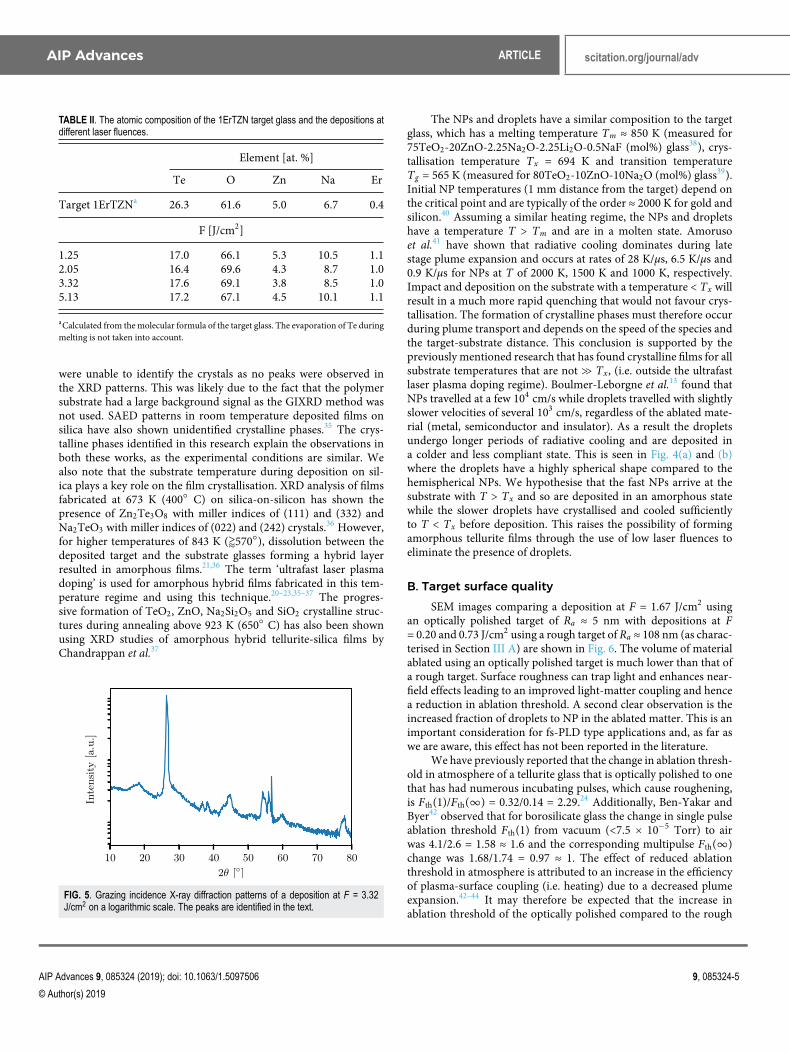
B. Target surface qualitySEM images comparing a deposition at F = 1.67 J/cm2 using
an optically polished target of Ra ≈ 5 nm with depositions at F= 0.20 and 0.73 J/cm2 using a rough target of Ra ≈ 108 nm (as charac-terised in Section III A) are shown in Fig. 6. The volume of materialablated using an optically polished target is much lower than that ofa rough target. Surface roughness can trap light and enhances near-field effects leading to an improved light-matter coupling and hencea reduction in ablation threshold. A second clear observation is theincreased fraction of droplets to NP in the ablated matter. This is animportant consideration for fs-PLD type applications and, as far aswe are aware, this effect has not been reported in the literature.
We have previously reported that the change in ablation thresh-old in atmosphere of a tellurite glass that is optically polished to onethat has had numerous incubating pulses, which cause roughening,is Fth(1)/Fth(∞) = 0.32/0.14 = 2.29.24 Additionally, Ben-Yakar andByer42 observed that for borosilicate glass the change in single pulseablation threshold Fth(1) from vacuum (<7.5 × 10⁻⁵ Torr) to airwas 4.1/2.6 = 1.58 ≈ 1.6 and the corresponding multipulse Fth(∞)change was 1.68/1.74 = 0.97 ≈ 1. The effect of reduced ablationthreshold in atmosphere is attributed to an increase in the efficiencyof plasma-surface coupling (i.e. heating) due to a decreased plumeexpansion.42–44 It may therefore be expected that the increase inablation threshold of the optically polished compared to the rough
AIP Advances 9, 085324 (2019); doi: 10.1063/1.5097506 9, 085324-5
© Author(s) 2019
AIP Advances ARTICLE scitation.org/journal/adv
FIG. 6. Depositions at different laser fluences F using a tar-get glass polished to (a) Ra ≈ 5 nm and (b, c) Ra ≈ 108 nm.(a) 1.67 J/cm2. (b) 0.20 J/cm2. (c) 0.73 J/cm2.
polished tellurite glass in vacuum is 2.29 × 1.6 ≈ 3.7. Hence, theF = 1.67 J/cm2 in Fig. 6(a) should give a similar deposition usinga rough polished target using F ≈ 0.45 J/cm2. This agrees well with avisual comparison of Fig. 6(b) and (c).
We conclude that for fs-PLD type applications the higher sur-face roughness is not only beneficial in terms of having a smallerparticle size but also results in a reduced laser energy requirement.In addition to this, the damage that typically occurs to the surfaceduring ablation typically results in a rough surface and should there-fore be maintained from the very start of the deposition by using anunpolished target. The increased droplet fraction from smooth sur-faces are also relevant for the more unique cases involving the abla-tion of liquids and requires more fundamental research to explainthis phenomenon.
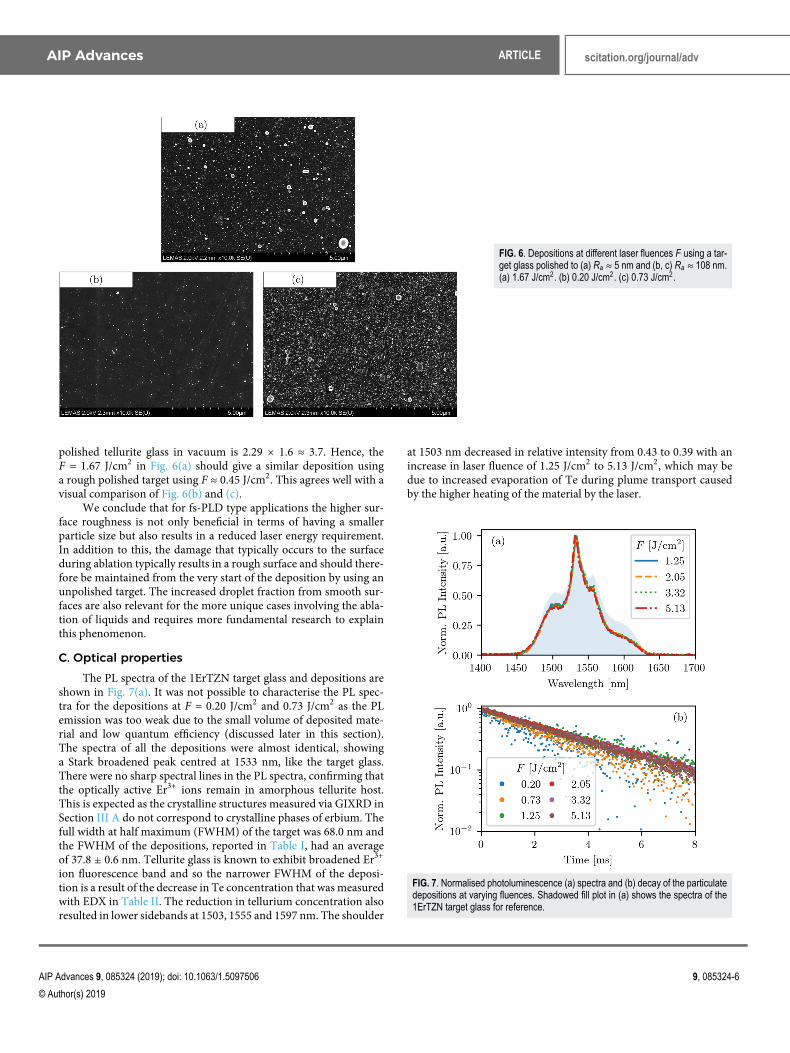
C. Optical propertiesThe PL spectra of the 1ErTZN target glass and depositions are
shown in Fig. 7(a). It was not possible to characterise the PL spec-tra for the depositions at F = 0.20 J/cm2 and 0.73 J/cm2 as the PLemission was too weak due to the small volume of deposited mate-rial and low quantum efficiency (discussed later in this section).The spectra of all the depositions were almost identical, showinga Stark broadened peak centred at 1533 nm, like the target glass.There were no sharp spectral lines in the PL spectra, confirming thatthe optically active Er3+ ions remain in amorphous tellurite host.This is expected as the crystalline structures measured via GIXRD inSection III A do not correspond to crystalline phases of erbium. Thefull width at half maximum (FWHM) of the target was 68.0 nm andthe FWHM of the depositions, reported in Table I, had an averageof 37.8 ± 0.6 nm. Tellurite glass is known to exhibit broadened Er3+
ion fluorescence band and so the narrower FWHM of the deposi-tion is a result of the decrease in Te concentration that was measuredwith EDX in Table II. The reduction in tellurium concentration alsoresulted in lower sidebands at 1503, 1555 and 1597 nm. The shoulder
at 1503 nm decreased in relative intensity from 0.43 to 0.39 with anincrease in laser fluence of 1.25 J/cm2 to 5.13 J/cm2, which may bedue to increased evaporation of Te during plume transport causedby the higher heating of the material by the laser.
FIG. 7. Normalised photoluminescence (a) spectra and (b) decay of the particulatedepositions at varying fluences. Shadowed fill plot in (a) shows the spectra of the1ErTZN target glass for reference.
AIP Advances 9, 085324 (2019); doi: 10.1063/1.5097506 9, 085324-6
© Author(s) 2019
AIP Advances ARTICLE scitation.org/journal/adv
The PL lifetime τ centred at 1.54 μm of the depositions were allshorter than the 4.34 ± 0.02 ms of the target, as shown in Fig. 7(b)and presented in Table I. For depositions at F ≥ 1.25 J/cm2 wherethe average film thickness d was greater than ∼500 nm, τ was 3.45 ±0.07 ms. The decrease in lifetime from the target to the depositedfilms is due to the increased erbium concentration (see Table II)giving rise to more efficient concentration quenching.45 For lowerfluence depositions, where d was smaller, τ continued to decrease.The shortest lifetime measured was 69% of the films with d ≥ 500 nmor F ≥ 1.25 J/cm2. NPs implanted in polymers generated throughfs laser ablation of Er3+-doped TZN glass in a 70 mTorr oxygenatmosphere with F ≈ 1 J/cm2 (spot size is estimated) exhibited iden-tical spectra with a FWHM of 39.2 nm and a similar lifetime of τ≈ 4 ms.19 The role of low pressure oxygen background is thereforenot important in determining the PL of ablated material. This maybe expected at such low pressures as collisions of the plume specieswith the background gas atoms is almost negligible.43,46
A decrease in PL lifetime with a decrease in laser fluencewas observed for F < 1.25 J/cm2. As all the lifetimes were mono-exponential it may be expected that the compositional differencesbetween the NPs and the droplets are small. The decrease in lifetimecan therefore not be attributed solely to the lack of droplets for theselow fluence depositions. Furthermore, the similarity in the PL spec-tra confirms this conclusion. The difference in τ is attributed to thefilm thickness as explained in the remainder of this section.
The decay rate Γ = 1/τ of an ion is composed of a radiative decayrate Γrad and a non-radiative decay rate Γnrad by
Γ = Γrad + Γnrad, (1)
where the non-radiative decay rate is composed of the internal non-radiative recombination rate Γint and the concentration quenchingrate due to ion-ion interactions Γq by Γnrad = Γint + Γq.
The spontaneous emission (SE) rate Γrad of a dipole is givenby Fermi’s golden rule and is proportional to the refractive indexin a homogeneous dielectric media.47–49 Inside stratified dielectricmedia, electric field confinement effects due to the index contrast atthe interfaces results in a position dependent Γrad(z), where z is theposition of the dipole in the axis perpendicular to the interfaces.50
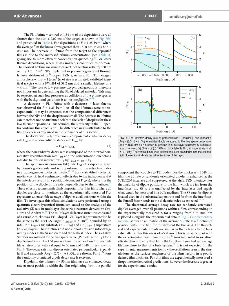
These effects become particularly important for thin films where alldipoles are close to interfaces as the experimentally measured Γradrepresents an ensemble average of dipoles at all positions within thefilm. To investigate this effect, simulations were performed using aquantum-electrodynamical formalism suited to the analysis of theradiative SE rate in multilayer dielectric structures derived by Cre-atore and Andreani.50 The multilayer dielectric structures consistedof a variable thickness d Er3+-doped TZN layer (approximated to bethe same as the 1ErTZN target n1ErTZN = 2.04824) bounded by aninfinite Si (nSi=3.48) substrate (z→ −∞) and air (nair=1) superstrate(z→∞) layers. The structures did not support emission into waveg-uiding modes as the Si substrate had the highest index. The radiativeSE rates normalised to the free space value (Purcell factor, Fp) for adipole emitting at λ = 1.54 μm as a function of position for two mul-tilayer structures with a d equal to 50 nm and 1540 nm is shown inFig. 8. The decay rates for dipoles orientated perpendicular �, paral-lel ∥ and randomly Avg = (2/3) ∥ + (1/3)� are shown. For Er3+ ionsthe randomly orientated dipole decay rate is relevant.
Dipoles in the thinner d = 50 nm film have an enhanced decayrate at most positions within the film originating from the parallel
FIG. 8. The radiative decay rate of perpendicular �, parallel ∥ and randomlyAvg = (2/3) ∥ + (1/3)� orientated dipole compared to the free space decay rateat λ = 1540 nm as a function of position in a multilayer structure; Si substrateis at z → −∞, (a) 50 nm or (b) 1540 nm thick tellurite film, air superstrate is atz→ −infty. The vertical black lines indicate the layer boundaries and the shadedlight blue regions indicate the refractive index of the layer.
component that couples to TE modes. For the thicker d = 1540 nmfilm, the SE rate of randomly orientated dipoles is enhanced at theSi/ErTZN interface and suppressed at the air/ErTZN interface. Forthe majority of dipole positions in the film, which are far from theinterfaces, the SE rate is unaffected by the interfaces and equalswhat would be measured in a bulk medium. The SE rate for dipoleslocated deep in the substrate/superstrate and far from the interfaces,the Purcell factor tends to the dielectric index as expected.47–49
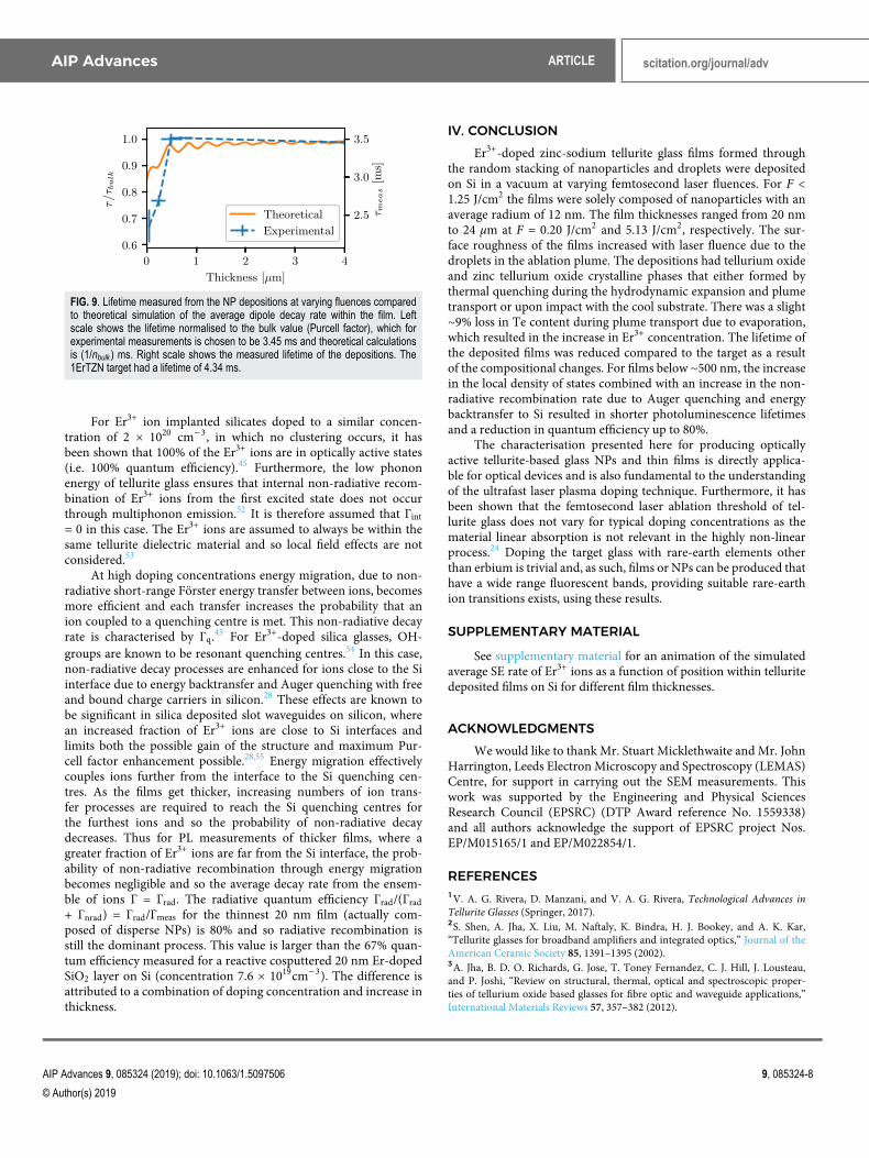
The theoretical average decay rate for randomly orientateddipoles averaged over all positions within a film, corresponding tothe experimentally measured τ, for d ranging from 5 to 4000 nmis plotted alongside the experimental data in Fig. 9 (supplementarymaterial shows an animation of the average SE rate as a function ofposition within the film for the different thicknesses). The theoret-ical and experimental trends are similar in that τ tends to the bulkvalue after a film thickness of ∼500 nm. This is in agreement withthe experimental measurements of Er3+ ions implanted in sodalimesilicate glass showing that films thicker than 1 μm had an averagelifetime close to that of a bulk system.51 It is not expected for theexperimental measurements to show the oscillations seen in the sim-ulations as the surface roughness of the films results in a poorlydefined film thickness. For thin films the experimentally measured τdrops like the theoretical predictions, however the decrease is greaterfor the experimental results.
AIP Advances 9, 085324 (2019); doi: 10.1063/1.5097506 9, 085324-7
© Author(s) 2019
AIP Advances ARTICLE scitation.org/journal/adv
FIG. 9. Lifetime measured from the NP depositions at varying fluences comparedto theoretical simulation of the average dipole decay rate within the film. Leftscale shows the lifetime normalised to the bulk value (Purcell factor), which forexperimental measurements is chosen to be 3.45 ms and theoretical calculationsis (1/nbulk ) ms. Right scale shows the measured lifetime of the depositions. The1ErTZN target had a lifetime of 4.34 ms.
For Er3+ ion implanted silicates doped to a similar concen-tration of 2 × 1020 cm−3, in which no clustering occurs, it hasbeen shown that 100% of the Er3+ ions are in optically active states(i.e. 100% quantum efficiency).45 Furthermore, the low phononenergy of tellurite glass ensures that internal non-radiative recom-bination of Er3+ ions from the first excited state does not occurthrough multiphonon emission.52 It is therefore assumed that Γint= 0 in this case. The Er3+ ions are assumed to always be within thesame tellurite dielectric material and so local field effects are notconsidered.53
At high doping concentrations energy migration, due to non-radiative short-range Förster energy transfer between ions, becomesmore efficient and each transfer increases the probability that anion coupled to a quenching centre is met. This non-radiative decayrate is characterised by Γq.45 For Er3+-doped silica glasses, OH-groups are known to be resonant quenching centres.54 In this case,non-radiative decay processes are enhanced for ions close to the Siinterface due to energy backtransfer and Auger quenching with freeand bound charge carriers in silicon.28 These effects are known tobe significant in silica deposited slot waveguides on silicon, wherean increased fraction of Er3+ ions are close to Si interfaces andlimits both the possible gain of the structure and maximum Pur-cell factor enhancement possible.28,55 Energy migration effectivelycouples ions further from the interface to the Si quenching cen-tres. As the films get thicker, increasing numbers of ion trans-fer processes are required to reach the Si quenching centres forthe furthest ions and so the probability of non-radiative decaydecreases. Thus for PL measurements of thicker films, where agreater fraction of Er3+ ions are far from the Si interface, the prob-ability of non-radiative recombination through energy migrationbecomes negligible and so the average decay rate from the ensem-ble of ions Γ = Γrad. The radiative quantum efficiency Γrad/(Γrad+ Γnrad) = Γrad/Γmeas for the thinnest 20 nm film (actually com-posed of disperse NPs) is 80% and so radiative recombination isstill the dominant process. This value is larger than the 67% quan-tum efficiency measured for a reactive cosputtered 20 nm Er-dopedSiO2 layer on Si (concentration 7.6 × 1019cm−3). The difference isattributed to a combination of doping concentration and increase inthickness.
IV. CONCLUSIONEr3+-doped zinc-sodium tellurite glass films formed through
the random stacking of nanoparticles and droplets were depositedon Si in a vacuum at varying femtosecond laser fluences. For F <1.25 J/cm2 the films were solely composed of nanoparticles with anaverage radium of 12 nm. The film thicknesses ranged from 20 nmto 24 μm at F = 0.20 J/cm2 and 5.13 J/cm2, respectively. The sur-face roughness of the films increased with laser fluence due to thedroplets in the ablation plume. The depositions had tellurium oxideand zinc tellurium oxide crystalline phases that either formed bythermal quenching during the hydrodynamic expansion and plumetransport or upon impact with the cool substrate. There was a slight∼9% loss in Te content during plume transport due to evaporation,which resulted in the increase in Er3+ concentration. The lifetime ofthe deposited films was reduced compared to the target as a resultof the compositional changes. For films below ∼500 nm, the increasein the local density of states combined with an increase in the non-radiative recombination rate due to Auger quenching and energybacktransfer to Si resulted in shorter photoluminescence lifetimesand a reduction in quantum efficiency up to 80%.
The characterisation presented here for producing opticallyactive tellurite-based glass NPs and thin films is directly applica-ble for optical devices and is also fundamental to the understandingof the ultrafast laser plasma doping technique. Furthermore, it hasbeen shown that the femtosecond laser ablation threshold of tel-lurite glass does not vary for typical doping concentrations as thematerial linear absorption is not relevant in the highly non-linearprocess.24 Doping the target glass with rare-earth elements otherthan erbium is trivial and, as such, films or NPs can be produced thathave a wide range fluorescent bands, providing suitable rare-earthion transitions exists, using these results.
SUPPLEMENTARY MATERIAL
See supplementary material for an animation of the simulatedaverage SE rate of Er3+ ions as a function of position within telluritedeposited films on Si for different film thicknesses.
ACKNOWLEDGMENTSWe would like to thank Mr. Stuart Micklethwaite and Mr. John
Harrington, Leeds Electron Microscopy and Spectroscopy (LEMAS)Centre, for support in carrying out the SEM measurements. Thiswork was supported by the Engineering and Physical SciencesResearch Council (EPSRC) (DTP Award reference No. 1559338)and all authors acknowledge the support of EPSRC project Nos.EP/M015165/1 and EP/M022854/1.
REFERENCES1V. A. G. Rivera, D. Manzani, and V. A. G. Rivera, Technological Advances inTellurite Glasses (Springer, 2017).2S. Shen, A. Jha, X. Liu, M. Naftaly, K. Bindra, H. J. Bookey, and A. K. Kar,“Tellurite glasses for broadband amplifiers and integrated optics,” Journal of theAmerican Ceramic Society 85, 1391–1395 (2002).3A. Jha, B. D. O. Richards, G. Jose, T. Toney Fernandez, C. J. Hill, J. Lousteau,and P. Joshi, “Review on structural, thermal, optical and spectroscopic proper-ties of tellurium oxide based glasses for fibre optic and waveguide applications,”International Materials Reviews 57, 357–382 (2012).
AIP Advances 9, 085324 (2019); doi: 10.1063/1.5097506 9, 085324-8
© Author(s) 2019
AIP Advances ARTICLE scitation.org/journal/adv
4W. J. Miniscalco, “Erbium-doped glasses for fiber amplifiers at 1500 nm,” Journalof Lightwave Technology 9, 234–250 (1991).5P. Nandi, G. Jose, C. Jayakrishnan, S. Debbarma, K. Chalapathi, K. Alti, A. K.Dharmadhikari, J. A. Dharmadhikari, and D. Mathur, “Femtosecond laser writtenchannel waveguides in tellurite glass,” Optics Express 14, 12145–12150 (2006).6J. Schou, “Physical aspects of the pulsed laser deposition technique: The stoi-chiometric transfer of material from target to film,” Applied Surface Science 255,5191–5198 (2009).7D. H. Lowndes, C. M. Rouleau, T. Thundat, G. Duscher, E. A. Kenik, and S. J.Pennycook, “Silicon and zinc telluride nanoparticles synthesized by pulsed laserablation: Size distributions and nanoscale structure,” Applied Surface Science 129,355–361 (1998).8A. P. Caricato, M. Fernández, M. Ferrari, G. Leggieri, M. Martino, M. Mattarelli,M. Montagna, V. Resta, L. Zampedri, R. M. Almeida, M. C. Conçalves, L. Fortes,and L. F. Santos, “Er3+-doped tellurite waveguides deposited by excimer laser abla-tion,” Materials Science and Engineering B: Solid-State Materials for AdvancedTechnology 105, 65–69 (2003).9M. Bouazaoui, B. Capoen, P. Caricato, A. P. Chiasera, A. Fazzi, M. Ferrari, G. Leg-gieri, M. Martino, M. Mattarelli, M. Montagna, F. Romano, T. Tunno, S. Turrel,and K. Vishnubhatla, “Pulsed laser deposition of Er doped tellurite films on largearea,” Journal of Physics: Conference Series 59, 475–478 (2007).10M. Martino, A. P. Caricato, M. Fernández, G. Leggieri, A. Jha, M. Ferrari, andM. Mattarelli, “Pulsed laser deposition of active waveguides,” Thin Solid Films433, 39–44 (2003).11R. K. Singh, D. Bhattacharya, and J. Narayan, “Subsurface heating effects dur-ing pulsed laser evaporation of materials,” Applied Physics Letters 57, 2022–2024(1990).12E. G. Gamaly, A. V. Rode, and B. Luther-Davies, “Film deposition,” Pulsed laserdeposition of thin films: applications-led growth of functional materials (2007), 99.13C. Boulmer-Leborgne, R. Benzerga, D. Scuderi, J. Perrière, O. Albert, J. Etche-pare, and E. Millon, “Femtosecond laser beam in interaction with materials forthin film deposition,” Proceedings of SPIE - The International Society for OpticalEngineering 6261 II, 2–10 (2006).14J. Perrière, C. Boulmer-Leborgne, R. Benzerga, and S. Tricot, “Nanoparticle for-mation by femtosecond laser ablation,” Journal of Physics D: Applied Physics 40,7069–7076 (2007).15B. Rethfeld, D. S. Ivanov, M. E. Garcia, and S. I. Anisimov, “Modelling ultrafastlaser ablation,” Journal of Physics D: Applied Physics 50, 193001 (2017).16S. Amoruso, R. Bruzzese, N. Spinelli, R. Velotta, M. Vitiello, X. Wang,G. Ausanio, V. Iannotti, and L. Lanotte, “Generation of silicon nanoparticles viafemtosecond laser ablation in vacuum,” Applied Physics Letters 84, 4502–4504(2004).17P. Balling and J. Schou, “Femtosecond-laser ablation dynamics of dielectrics:Basics and applications for thin films,” Reports on Progress in Physics 76, 036502(2013).18M. Sanz, M. Loopez-Arias, J. F. Marco, R. de Nalda, S. Amoruso, G. Ausanio,S. Lettieri, R. Bruzzese, X. Wang, and M. Castillejo, “Ultrafast laser ablationand deposition of wide band gap semiconductors,” The Journal of PhysicalChemistry C 115, 3203–3211 (2011).19E. Kumi-Barimah, M. W. Ziarko, N. Bamiedakis, I. H. White, R. V. Penty, andG. Jose, “Erbium-doped glass nanoparticle embedded polymer thin films usingfemtosecond pulsed laser deposition,” Optical Materials Express 8, 1997–2007(2018).20J. Chandrappan, M. Murray, T. Kakkar, P. Petrik, E. Agocs, Z. Zolnai, D. P.Steenson, A. Jha, and G. Jose, “Target dependent femtosecond laser plasmaimplantation dynamics in enabling silica for high density erbium doping,” Sci-entific Reports 5, 14037 (2015).21S. A. Kamil, J. Chandrappan, M. Murray, P. Steenson, T. F. Krauss, andG. Jose, “Ultrafast laser plasma doping of Er3+ ions in silica-on-silicon for opticalwaveguiding applications,” Optics Letters 41, 4684 (2016).22B. D. O. Richards, A. Boontan, T. Mann, E. Kumi Barimah, C. Russell, D. P.Steenson, and G. Jose, “Tm3+ tellurite-modified-silica glass thin films fabricatedusing ultrafast laser plasma doping,” IEEE Journal of Selected Topics in QuantumElectronics 25, 1–8 (2019).
23J. Chandrappan, M. Murray, P. Petrik, E. Agocs, Z. Zolnai, A. Tempez,S. Legendre, D. P. Steenson, A. Jha, and G. Jose, “Doping silica beyond limitswith laser plasma for active photonic materials,” Optical Materials Express 5, 2849(2015).24T. Mann, R. Mathieson, M. Murray, B. Richards, and G. Jose, “Femtosecondlaser ablation properties of Er3+ ion doped zinc-sodium tellurite glass,” Journal ofApplied Physics 124, 044903 (2018).25G. Franzò, F. Priolo, and S. Coffa, “Understanding and control of the erbiumnon-radiative de-excitation processes in silicon,” Journal of Luminescence 80, 19–28 (1998).26N. Hamelin, P. G. Kik, J. F. Suyver, K. Kikoin, A. Polman, A. Schö-necker, and F. W. Saris, “Energy backtransfer and infrared photoresponse inerbium-doped silicon p-n diodes,” Journal of Applied Physics 88, 5381–5387(2000).27A. Kenyon, “Recent developments in rare-earth doped materials for optoelec-tronics,” Progress in Quantum Electronics 26, 225–284 (2002).28C. Creatore, L. C. Andreani, M. Miritello, R. Lo Savio, and F. Priolo, “Modi-fication of erbium radiative lifetime in planar silicon slot waveguides,” AppliedPhysics Letters 94, 103112 (2009).29J. Schindelin, I. Arganda-Carreras, E. Frise, V. Kaynig, M. Longair, T. Piet-zsch, S. Preibisch, C. Rueden, S. Saalfeld, B. Schmid, and others, “Fiji: Anopen-source platform for biological-image analysis,” Nature methods 9, 676(2012).30C. A. Schneider, W. S. Rasband, and K. W. Eliceiri, “NIH image to imageJ: 25years of image analysis,” Nature Methods 9, 671 (2012).31D. Necas and P. Klapetek, Gwyddion (2018).32D. Necas and P. Klapetek, “Gwyddion: An open-source software for SPM dataanalysis,” Open Physics 10, 181–188 (2012).33The spectral shift becomes more significant in GXID as the shallower angleresults in a longer path length through the crystal planes.34B. Fultz and J. M. Howe, Transmission electron microscopy and diffractometry ofmaterials (Springer Science & Business Media, 2012).35J. Chandrappan, “Femtosecond laser plasma assisted rare-earth doping in silicafor integrated optics,” Ph.D. thesis, University of Leeds (2015).36S. A. Kamil, “Ultrafast laser plasma doping of rare earth ions for opticalwaveguiding applications,” Ph.D. thesis, University of Leeds (2018).37J. Chandrappan, V. Khetan, M. Ward, M. Murray, and G. Jose, “Devitrificationof ultrafast laser plasma produced metastable glass layer,” Scripta Materialia 131,37–41 (2017).38L. Le Neindre, S. Jiang, B.-C. Hwang, T. Luo, J. Watson, and N. Peyghambarian,“Effect of relative alkali content on absorption linewidth in erbium-doped telluriteglasses,” Journal of Non-Crystalline Solids 255, 97–102 (1999).39S. Manning, H. Ebendorff-Heidepriem, and T. M. Monro, “Ternary telluriteglasses for the fabrication of nonlinear optical fibres,” Optical Materials Express2, 140 (2012).40S. Amoruso, G. Ausanio, R. Bruzzese, M. Vitiello, and X. Wang, “Femtosecondlaser pulse irradiation of solid targets as a general route to nanoparticle formationin a vacuum,” Physical Review B - Condensed Matter and Materials Physics 71,033406 (2005).41S. Amoruso, R. Bruzzese, N. Spinelli, R. Velotta, M. Vitiello, and X. Wang,“Emission of nanoparticles during ultrashort laser irradiation of silicon targets,”Europhysics Letters (EPL) 67, 404–410 (2004).42A. Ben-Yakar and R. L. Byer, “Femtosecond laser ablation properties of borosil-icate glass,” Journal of Applied Physics 96, 5316–5323 (2004).43P. K. Diwakar, S. S. Harilal, M. C. Phillips, and A. Hassanein, “Characterizationof ultrafast laser-ablation plasma plumes at various Ar ambient pressures,” Journalof Applied Physics 118, 043305 (2015).44E. G. Gamaly, B. Luther-Davies, V. Z. Kolev, N. R. Madsen, M. Duering, andA. V. Rode, “Ablation of metals with picosecond laser pulses: Evidence of long-lived non-equilibrium surface states,” Laser and Particle Beams 23, 167–176(2005).45A. Polman, “Erbium implanted thin film photonic materials,” Journal ofApplied Physics 82, 1–39 (1997).
AIP Advances 9, 085324 (2019); doi: 10.1063/1.5097506 9, 085324-9
© Author(s) 2019
AIP Advances ARTICLE scitation.org/journal/adv
46P. K. Diwakar, S. S. Harilal, A. Hassanein, and M. C. Phillips, “Expansiondynamics of ultrafast laser produced plasmas in the presence of ambient argon,”Journal of Applied Physics 116, 133301 (2014).47R. J. Glauber and M. Lewenstein, “Quantum optics of dielectric media,” PhysicalReview A 43, 467–491 (1991).48W. Zakowicz and M. Janowicz, “Spontaneous emission in the presence of adielectric cylinder,” Physical Review A - Atomic, Molecular, and Optical Physics62, 013820 (2000).49H. Khosravi and R. Loudon, “Vacuum field fluctuations and spontaneous emis-sion in the vicinity of a dielectric surface,” Proc. R. Soc. Lond. A 433, 337–352(1991).50C. Creatore and L. C. Andreani, “Quantum theory of spontaneous emis-sion in multilayer dielectric structures,” Physical Review A 78, 063825(2008).
51E. Snoeks, A. Lagendijk, and A. Polman, “Measuring and modifying the sponta-neous emission rate of erbium near an interface,” Physical Review Letters 74, 2459(1995).52W. Miniscalco, “Optical and electronic properties of rare earth ions in glasses,”in Rare earth doped fiber lasers and amplifiers (Marcel Dekker, Inc., 1993),Chap. 2.53L. Zampedri, M. Mattarelli, M. Montagna, and R. Gonçalves, “Evaluation oflocal field effect on the 4I13/2 lifetimes in Er-doped silica-hafnia planar waveg-uides,” Physical Review B 75, 073105 (2007).54E. Snoeks, P. G. Kik, and A. Polman, “Concentration quenching in erbiumimplanted alkali silicate glasses,” Optical Materials 5, 159–167 (1996).55G. M. Miller, R. M. Briggs, and H. A. Atwater, “Achieving optical gain inwaveguide-confined nanocluster-sensitized erbium by pulsed excitation,” Journalof Applied Physics 108, 063109 (2010).
AIP Advances 9, 085324 (2019); doi: 10.1063/1.5097506 9, 085324-10
© Author(s) 2019