er3+ and si luminescence of atomic layer deposited er-doped al2o3 thin films on si(100)
TRANSCRIPT
Seediscussions,stats,andauthorprofilesforthispublicationat:https://www.researchgate.net/publication/234959883
Er3+andSiluminescenceofatomiclayerdepositedEr-dopedAl2O3thinfilmsonSi(100)
ArticleinJournalofAppliedPhysics·June2011
DOI:10.1063/1.3595691
CITATIONS
12
READS
74
5authors,including:
M.C.M.vandeSanden
DutchInstituteforFundamentalEnergyResearch
560PUBLICATIONS8,540CITATIONS
SEEPROFILE
W.M.M.Kessels
TechnischeUniversiteitEindhoven
413PUBLICATIONS7,433CITATIONS
SEEPROFILE
AllcontentfollowingthispagewasuploadedbyW.M.M.Kesselson03December2016.
Theuserhasrequestedenhancementofthedownloadedfile.
Er31 and Si luminescence of atomic layer deposited Er-doped Al2O3
thin films on Si(100)
G. Dingemans,1 A. Clark,2 J. A. van Delft,1 M. C. M. van de Sanden,1
and W. M. M. Kessels1,a)
1Department of Applied Physics, Eindhoven University of Technology, P.O. Box 513, 5600 MB Eindhoven,The Netherlands2Translucent Inc., 952 Commercial Street, Palo Alto, CA 94303, USA
(Received 22 February 2011; accepted 26 April 2011; published online 9 June 2011)
Atomic layer deposition was used to deposit amorphous Er-doped Al2O3 films (0.9–6.2 at. % Er)
on Si(100). The Er3þ photoluminescence (PL), Er3þ upconversion luminescence, as well as the Si
PL and associated surface passivation properties of the films were studied and related to the
structural change of the material during annealing. The PL signals from Er3þ and Si were strongly
dependent on the annealing temperature (T¼ 450–1000 �C), but not directly influenced by the
transition from an amorphous to a crystalline phase at T> 900 �C. For T> 650 �C, broad Er3þ PL
centered at 1.54 lm (4I13/2) with a full width at half maximum of 55 nm was observed under
excitation of 532 nm light. The PL signal reached a maximum for Er concentrations in the range of
2–3 at. %. Multiple photon upconversion luminescence was detected at 660 nm (4F9/2), 810 nm
(4I9/2), and 980 nm (4I11/2), under excitation of 1480 nm light. The optical activation of Er3þ was
related to the removal of quenching impurities, such as OH (3 at. % H present initially) as also
indicated by thermal effusion experiments. In contrast to the Er3þ PL signal, the Si luminescence,
and consequently the Si surface passivation, decreased for increasing annealing temperatures. This
trade-off between surface passivation quality and Er3þ PL can be attributed to an opposite
correlation with the decreasing hydrogen content in the films during thermal treatment. VC 2011American Institute of Physics. [doi:10.1063/1.3595691]
I. INTRODUCTION
By virtue of the Er3þ emission wavelength at �1.54 lm,
Er-doped materials are widely used in optoelectronics.1,2
Er3þ ions also have the capability of upconverting two or
more lower energy photons into one high-energy photon.3
While such upconversion processes represent a loss mecha-
nism for some optoelectronic applications, they are being
considered for the enhancement of the energy conversion ef-
ficiency of future silicon solar cells.4–7 The idea is that by
adding an upconversion material to the rear side of a silicon
solar cell, a fraction of the sub-bandgap photons (Eg< 1.1
eV) that would otherwise be transmitted through the device
can now be utilized to create electron-hole pairs in the solar
cell. The Er3þ photoluminescence (PL) and upconversion lu-
minescence depend strongly on the Er concentration in the
film.2 Control of the doping profile is, therefore, desirable
for the various applications which exploit the optical proper-
ties of Er. Many different host materials have been studied in
the past decades, including fluorides, sulfides, phosphates,
silicates, oxynitrides, and oxides.1 Al2O3 is a particularly
interesting host material for Er, as Al2O3:Er possesses a rela-
tively high refractive index, which is desirable for waveguide
devices, and was shown to exhibit a broad emission spectrum
around 1.54 lm. Accordingly, high-gain optical waveguide
amplifiers based on Al2O3:Er films have been successfully
fabricated.8,9 In addition, relatively high Er concentrations
can be incorporated in Al2O3, as Er2O3 exhibits a similar va-
lence and crystal structure.2 Er-doped Al2O3 has been syn-
thesized using various techniques, including pulsed laser
deposition,10 sputtering of Al2O3 and subsequent ion imple-
mentation,8 co-sputtering of Al2O3 and Er2O311–14 and
plasma-enhanced chemical vapor deposition (CVD).15
Atomic layer deposition (ALD) is an alternative method
that can be used to deposit high-quality and uniform thin
films. During a so-called ALD cycle, reactants are sequen-
tially introduced into the reactor, and film growth is gov-
erned by self-limiting surface reactions.16 The self-limiting
nature of the growth process allows for precise thickness
control with an Angstrom level resolution over large area
substrates. Consequently, controlled material doping is also
possible by alternating the ALD cycles of two or more mate-
rials. The dopant profile can be controlled in the vertical
(i.e., thickness) direction by changing the ratio between the
ALD cycles of the respective materials. In the lateral direc-
tion, the separation between the individual dopant atoms is
dictated by the growth-per-cycle, which is related, among
other variables, to the steric hindrance effect of the specific
precursor molecules.17 Furthermore, the excellent confor-
mality of ALD provides a means for coating high-aspect
ratio structures, porous materials, and small particles.
The ALD process for Al2O3 is well known and has been
extensively researched.16,18 As an important emerging appli-
cation, ALD Al2O3 films are very suitable for the passivation
of silicon surfaces. A high level of surface passivation is an
important prerequisite for obtaining large luminescence
quantum efficiencies of Si.19 The use of Al2O3 has, for
a)Author to whom correspondence should be addressed. Electronic mail:
0021-8979/2011/109(11)/113107/9/$30.00 VC 2011 American Institute of Physics109, 113107-1
JOURNAL OF APPLIED PHYSICS 109, 113107 (2011)
Downloaded 14 Jun 2011 to 131.155.128.21. Redistribution subject to AIP license or copyright; see http://jap.aip.org/about/rights_and_permissions
instance, led to a tenfold increase in Si luminescence com-
pared to the use of thermally grown SiO2 passivation.20
Moreover, considerable interest in Al2O3 surface passivation
films for silicon photovoltaics has developed over the last
few years,21,22 which also spurred the development of ALD
processes for high-volume manufacturing.22,23 For the syn-
thesis of Er2O3 by ALD, on the other hand, only a few
reports exist. Paivasaari et al. reported an ALD process for
Er2O3, using Er(thd)3 and Er(CpMe)3 as precursors, in com-
bination with O3 and H2O as oxidants, respectively.24,25
Al2O3:Er waveguides have also been synthesized by ALD,26
but no details on the ALD process were given. In addition,
ALD has been used for Er incorporation in Y2O3 by alternat-
ing the growth of Y2O3 and Er2O3 layers.17,27
In this study, we used thermal ALD to synthesize amor-
phous Al2O3:Er films on Si wafers. The focus of the paper is
the relation between the (structural) changes of the material
during annealing and the optical activation of Er3þ. In addi-
tion, the Si luminescence and the associated surface passiva-
tion properties of the films were studied. We show here that
post-deposition annealing is essential to optically activate
the Er3þ ions, resulting in broad photoluminescence (PL)
centered around 1.54 lm. Two- and three-photon upconver-
sion processes were also detected under excitation of 1.48
lm light. The results show that the removal of OH impur-
ities, which can act as effective quenching centers,2,28 played
a prominent role in the optical activation, whereas the lumi-
nescence properties were not significantly affected by the
change from an amorphous to a polycrystalline structure at
temperatures > 900 �C. In contrast to the Er3þ photolumines-
cence, the surface passivation properties deteriorated at
higher annealing temperatures, which can be attributed pre-
dominantly to the effusion of hydrogen from the Al2O3:Er
and the Si interface.
After the description of the experimental details (Sec.
II), the ALD process for the synthesis of the Er-doped Al2O3
films will be briefly discussed (Sec. III A). Subsequently, the
optical properties (Sec. III B) and material properties (Sec.
III C) will be reported, with special focus on the influence of
post-deposition annealing. In the discussion (Sec. IV), the
effect of the structural changes on the Er3þ and Si lumines-
cence will be addressed.
II. EXPERIMENTAL DETAILS
The Al2O3:Er films were deposited using an Oxford
Instruments OpAL reactor at a substrate temperature of
�200 �C by thermal ALD. The reactor was operated at a
pressure of �300 mTorr. Er(CpMe)3 was used as the Er-
precursor and stored in a stainless steel bubbler heated to
120 �C, well below the decomposition temperature of the
precursor. The precursor was introduced into the reactor by a
200 sccm Ar flow and relatively long dosing times of 30 s
were employed. Al(CH3)3 was the Al-precursor used for the
deposition of Al2O3.29 This liquid precursor exhibits a high
vapor pressure and was introduced into the reactor vapor-
drawn. Dosing times of only 20 ms were sufficient for
achieving saturated growth. For both materials, H2O served
as the oxidant (20 ms doses). The ALD films were deposited
on floatzone (FZ) n-type Si(100) wafers. Spectroscopic
ellipsometry (SE; J.A. Woollam, M2000) was employed
both in situ and ex situ to monitor the ALD growth process
and determine the film thickness and refractive index. Photo-
luminescence measurements were performed at room tem-
perature using a Nanometrics RPM2000, which had 532 nm
(50 mW) and 1480 nm (250 mW) CW lasers available as
pump sources. The corresponding detectors used with these
two laser sources were an InGaAs PIN photodiode and a Si
CCD detector. The incident spot diameter in both cases was
1 mm (7.85� 10�3 cm2). Two scan protocols were
employed: (1) Scan from 900 to 1700 nm using the 532 nm
pump and the InGaAs detector to observe the Si-Si transition
at 1.1 lm and the Er3þ 4I13/2 to 4I15/2 transition at 1.54 lm;
(2) Scan from 600 to 1100 nm using 250 mW 1480 nm and
the Si CCD to detect the 2 photon and 3 photon upconversion
transitions in Er3þ. For material analyses, X-ray photon
spectroscopy (XPS; K-Alpha Thermofisher) and X-ray dif-
fraction (XRD; Panalytical) were used. In addition, Ruther-
ford backscattering spectroscopy (RBS) using 1–2 MeV
He2þ ions and elastic recoil detection (ERD) were used to
determine the atomic composition of the film and the hydro-
gen content (AccTec, Eindhoven). Effusion measurements
were performed under ultrahigh vacuum conditions (10�7
mbar) using a quadrupole mass spectrometer. The effusion
of impurities from the sample was monitored as a function of
the annealing temperature, T¼ 200–1000 �C, with a heating
rate of 20 �C/min.30 The effective lifetime of the minority
carriers in Si was measured by the photoconductance decay
method (Sinton WCT100). To activate the luminescence, the
samples were annealed in a rapid thermal annealing appara-
tus (ramp up> 20 �C/s) within a N2 environment.
III. RESULTS AND DISCUSSION
A. Atomic layer deposition of Er-doped Al2O3 films
Figure 1 shows a schematic representation of the ALD
super-cycle used to deposit the Al2O3:Er films. The super-
cycle consists of x Er2O3 cycles and y Al2O3 cycles. Films
with various Er concentrations, [Er], were synthesized by
changing the x:y ratio. The two ALD cycles each comprised
two half-cycles. In the first half-cycle, the precursor gas was
introduced, and in the second half-cycle, H2O was injected
as the oxidant. In between the precursor and oxidant doses,
FIG. 1. (Color online) ALD “super-cycle” for the synthesis of Er-doped
Al2O3 films.
113107-2 Dingemans et al. J. Appl. Phys. 109, 113107 (2011)
Downloaded 14 Jun 2011 to 131.155.128.21. Redistribution subject to AIP license or copyright; see http://jap.aip.org/about/rights_and_permissions
the reactor was purged with Ar to avoid parasitic CVD reac-
tions. Figure 2(a) shows that the thickness of the deposited
film increased with the number of ALD cycles. The growth
rate was �1 A/cycle for Al2O3 and �0.25 A/cycle for Er2O3,
as determined with in situ SE. The growth characteristics for
this process are illustrated in more detail in Fig. 2(b), where
the changes in the surface groups and layer thickness during
each half-cycle are reflected by the “apparent thickness.”
The apparent thickness was extracted from the ellipsometric
parameters (W and D) using a simple Cauchy model with
fixed optical constants (representative for bulk Al2O3).31 The
increase of the apparent thickness during the Er(CpMe)3 dos-
ing represents the sticking of the precursor to the growth
interface. During the subsequent oxidation step, the apparent
thickness decreases by reaction of the adsorbed precursor
ligands with H2O such that the initial surface coverage is
restored.18 The surface reactions in both half-cycles termi-
nated when all surface groups reacted, i.e., the growth is
self-limiting. Nonetheless, the relatively low growth-per-
cycle for Er2O3 is likely to be a result of sub-saturated
growth, even with the (optimized) precursor dosing times of
30 s that we applied. Although generally not preferred, a low
growth-per-cycle, GPC, can be beneficial for synthesizing
films with low Er concentrations. Using the same Er-precur-
sor, Paivasaari et al. reported a higher GPC while using sig-
nificantly shorter dosing times.25 These shorter dosing times
can probably be related to the use of an open crucible rather
than a bubbler system as used in this work. The precursor in
the bubbler has a comparatively smaller surface area, and,
therefore, the influence of the low precursor vapor pressure
is more pronounced. For our reactor and precursor injection
configuration, a more time-efficient ALD process could be
realized when the Er-precursor would combine a relatively
high vapor pressure with a high reactivity during the ALD
half-reaction at moderate substrate temperatures. Currently,
however, the availability of alternative commercially avail-
able ALD precursors for Er2O3 is still limited. It is interest-
ing to note here that an O2 plasma was tested as an
alternative oxidant for the ALD process for Er2O3 in combi-
nation with the Er(CpMe)3 precursor. RBS and infrared
absorption measurements indicated a very large fraction of
carbon in these plasma ALD films ([C]> 30 at. %). The COx
species, created by plasma-induced oxidation and decompo-
sition of the CpMe ligands, appear to be incorporated into
the bulk of the film. This behavior, which is absent for many
other plasma ALD processes, is consistent with the tendency
of Er (and other lanthanides) to react with CO2.32 High im-
purity levels were not observed for thermal ALD Er2O3
films.
The thermal ALD process was used to synthesize vari-
ous Al2O3 films with Er concentrations in the range of
[Er]¼ 0.9–6.2 at. %. Table I lists the material properties of a
selection of these samples. The RBS spectrum for the sample
with [Er]¼ 2.0 at. % is shown in Fig. 3. The flat Er signal
between 1.7 and 1.8 MeV indicates that the Er concentration
was relatively constant as a function of film thickness (�200
nm) for this sample. All Er-doped films exhibited an O/Al
ratio> 1.5, which is clearly higher than that for stoichiomet-
ric Al2O3. In addition, the O/(AlþEr) ratio was found to be
�1.5 for most of the samples and exhibited no clear trend
with [Er]. These findings are consistent with the substitution
of Al atoms by Er atoms in the Al2O3:Er structure. For the
range of [Er] between 0.9–6.2 at. %, the mass density varied
between 3.6 6 0.1 and 4.2 6 0.1 g/cm3. The two Al2O3:Er
films that were measured by ERD (Table I) contained the
same amount of hydrogen ([H] �3 at. %) which was also
similar for undoped ALD Al2O3 films.29 The hydrogen was
present mostly as –OH groups.33 RBS measurements
revealed that the carbon content was below the detection
FIG. 2. (Color online) (a) Film thickness as a function of the number of
ALD cycles. (b) Apparent thickness after each ALD half-cycle. In (b), the
same optical parameters (Cauchy model with An¼ 1.64 and Bn¼ 0.005, rep-
resentative for Al2O3) were used for the Al2O3 and Er2O3 cycles.
TABLE I. Properties of as-deposited Er-doped Al2O3 samples, determined
from the areal atomic densities measured by RBS/ERD. The mass density
was calculated from the film composition and the thickness determined by
SE.
[Er]
(at. %)
[H]
(at. %) O/Al O/(AlþEr)
qmass
(g/cm3)
1.0 6 0.03 3.0 6 0.1 1.51 6 0.08 1.47 6 0.08 3.6 6 0.1
2.0 6 0.1 3.0 6 0.1 1.59 6 0.08 1.51 6 0.08 3.8 6 0.1
2.7 6 0.1 - 1.64 6 0.08 1.51 6 0.08 3.9 6 0.1
3.7 6 0.1 - 1.60 6 0.08 1.46 6 0.08 3.8 6 0.1
-¼ not measured.
FIG. 3. (Color online) RBS spectrum of an Er-doped Al2O3 film with
[Er]¼ 2.0 at. % (1.8� 1021 atoms cm�3). The line is a fit to the data to
extract the areal atomic densities.
113107-3 Dingemans et al. J. Appl. Phys. 109, 113107 (2011)
Downloaded 14 Jun 2011 to 131.155.128.21. Redistribution subject to AIP license or copyright; see http://jap.aip.org/about/rights_and_permissions
limit (< 5 at. %). The impact of annealing on the structural
properties will be discussed in more detail in Sec. III C.
B. Optical properties
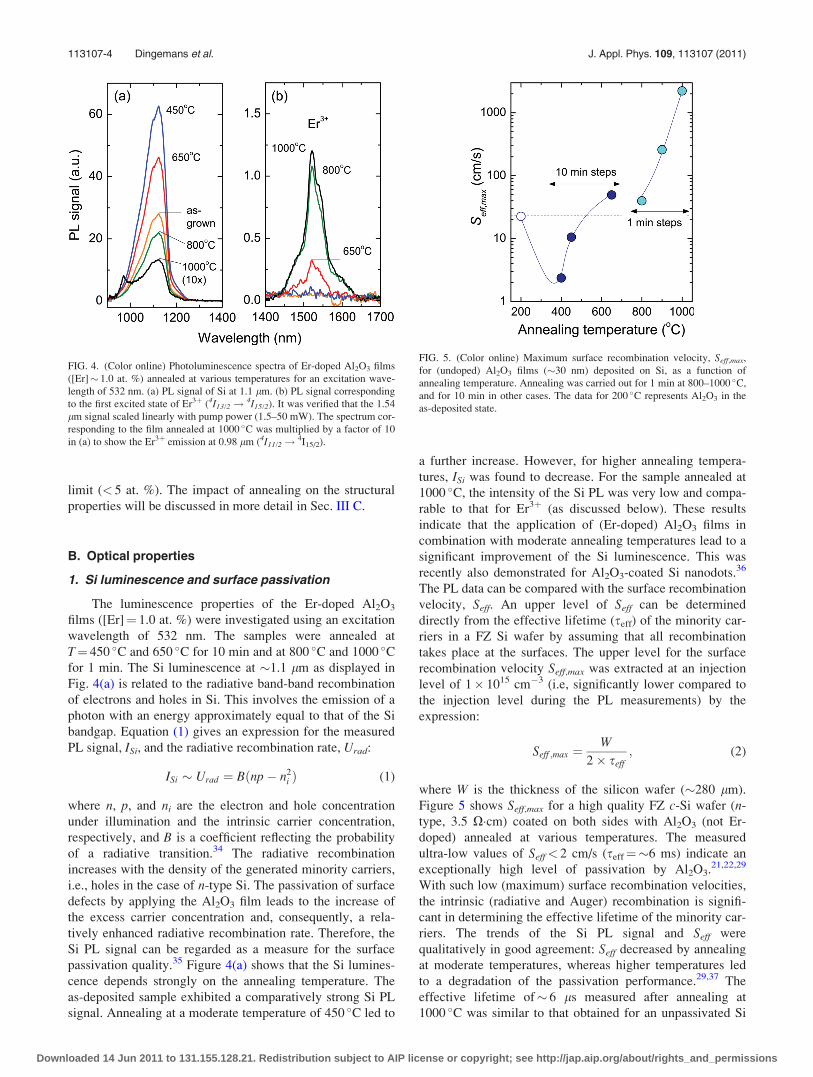
1. Si luminescence and surface passivation
The luminescence properties of the Er-doped Al2O3
films ([Er]¼ 1.0 at. %) were investigated using an excitation
wavelength of 532 nm. The samples were annealed at
T¼ 450 �C and 650 �C for 10 min and at 800 �C and 1000 �Cfor 1 min. The Si luminescence at �1.1 lm as displayed in
Fig. 4(a) is related to the radiative band-band recombination
of electrons and holes in Si. This involves the emission of a
photon with an energy approximately equal to that of the Si
bandgap. Equation (1) gives an expression for the measured
PL signal, ISi, and the radiative recombination rate, Urad:
ISi � Urad ¼ Bðnp� n2i Þ (1)
where n, p, and ni are the electron and hole concentration
under illumination and the intrinsic carrier concentration,
respectively, and B is a coefficient reflecting the probability
of a radiative transition.34 The radiative recombination
increases with the density of the generated minority carriers,
i.e., holes in the case of n-type Si. The passivation of surface
defects by applying the Al2O3 film leads to the increase of
the excess carrier concentration and, consequently, a rela-
tively enhanced radiative recombination rate. Therefore, the
Si PL signal can be regarded as a measure for the surface
passivation quality.35 Figure 4(a) shows that the Si lumines-
cence depends strongly on the annealing temperature. The
as-deposited sample exhibited a comparatively strong Si PL
signal. Annealing at a moderate temperature of 450 �C led to
a further increase. However, for higher annealing tempera-
tures, ISi was found to decrease. For the sample annealed at
1000 �C, the intensity of the Si PL was very low and compa-
rable to that for Er3þ (as discussed below). These results
indicate that the application of (Er-doped) Al2O3 films in
combination with moderate annealing temperatures lead to a
significant improvement of the Si luminescence. This was
recently also demonstrated for Al2O3-coated Si nanodots.36
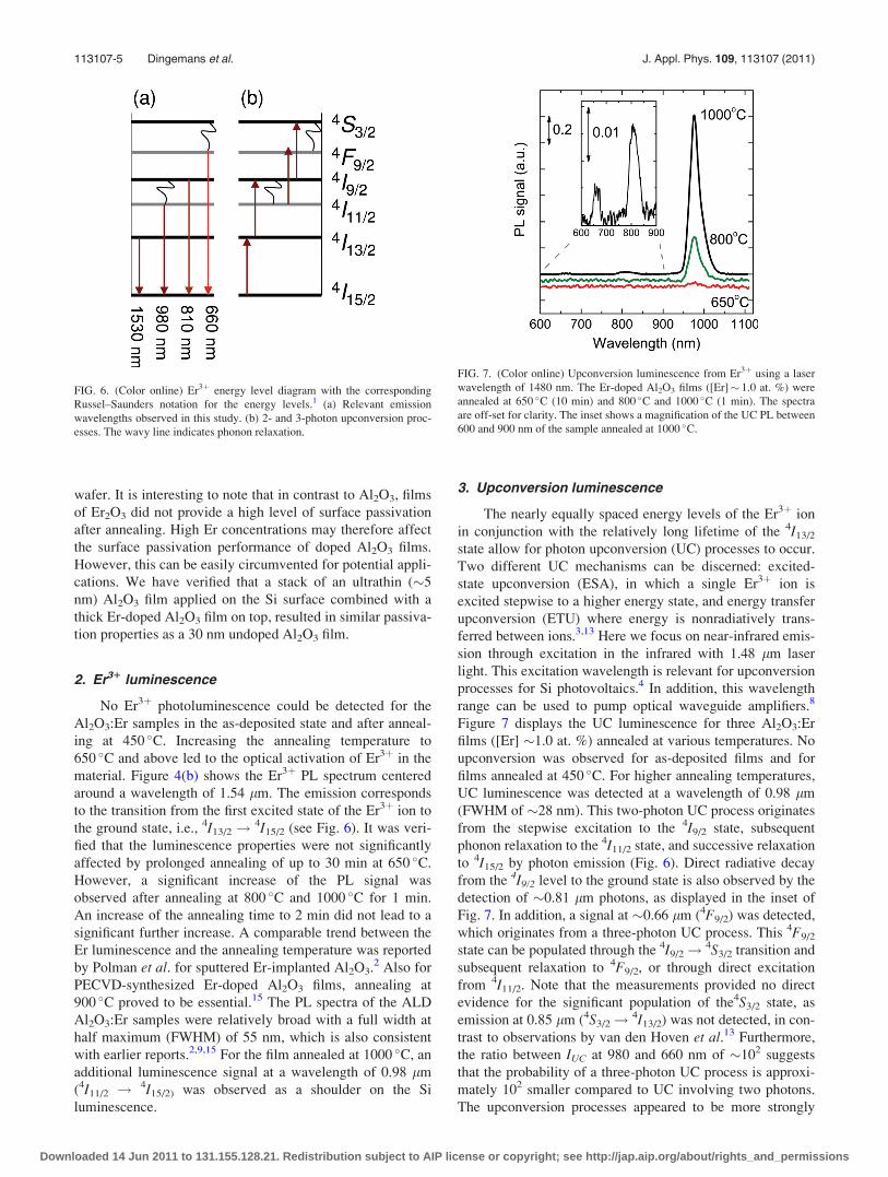
The PL data can be compared with the surface recombination
velocity, Seff. An upper level of Seff can be determined
directly from the effective lifetime (seff) of the minority car-
riers in a FZ Si wafer by assuming that all recombination
takes place at the surfaces. The upper level for the surface
recombination velocity Seff,max was extracted at an injection
level of 1� 1015 cm�3 (i.e, significantly lower compared to
the injection level during the PL measurements) by the
expression:
Seff ;max ¼W
2� seff; (2)
where W is the thickness of the silicon wafer (�280 lm).
Figure 5 shows Seff,max for a high quality FZ c-Si wafer (n-
type, 3.5 X�cm) coated on both sides with Al2O3 (not Er-
doped) annealed at various temperatures. The measured
ultra-low values of Seff< 2 cm/s (seff¼�6 ms) indicate an
exceptionally high level of passivation by Al2O3.21,22,29
With such low (maximum) surface recombination velocities,
the intrinsic (radiative and Auger) recombination is signifi-
cant in determining the effective lifetime of the minority car-
riers. The trends of the Si PL signal and Seff were
qualitatively in good agreement: Seff decreased by annealing
at moderate temperatures, whereas higher temperatures led
to a degradation of the passivation performance.29,37 The
effective lifetime of� 6 ls measured after annealing at
1000 �C was similar to that obtained for an unpassivated Si
FIG. 4. (Color online) Photoluminescence spectra of Er-doped Al2O3 films
([Er]� 1.0 at. %) annealed at various temperatures for an excitation wave-
length of 532 nm. (a) PL signal of Si at 1.1 lm. (b) PL signal corresponding
to the first excited state of Er3þ (4I13/2! 4I15/2). It was verified that the 1.54
lm signal scaled linearly with pump power (1.5–50 mW). The spectrum cor-
responding to the film annealed at 1000 �C was multiplied by a factor of 10
in (a) to show the Er3þ emission at 0.98 lm (4I11/2! 4I15/2).
FIG. 5. (Color online) Maximum surface recombination velocity, Seff,max,
for (undoped) Al2O3 films (�30 nm) deposited on Si, as a function of
annealing temperature. Annealing was carried out for 1 min at 800–1000 �C,
and for 10 min in other cases. The data for 200 �C represents Al2O3 in the
as-deposited state.
113107-4 Dingemans et al. J. Appl. Phys. 109, 113107 (2011)
Downloaded 14 Jun 2011 to 131.155.128.21. Redistribution subject to AIP license or copyright; see http://jap.aip.org/about/rights_and_permissions
wafer. It is interesting to note that in contrast to Al2O3, films
of Er2O3 did not provide a high level of surface passivation
after annealing. High Er concentrations may therefore affect
the surface passivation performance of doped Al2O3 films.
However, this can be easily circumvented for potential appli-
cations. We have verified that a stack of an ultrathin (�5
nm) Al2O3 film applied on the Si surface combined with a
thick Er-doped Al2O3 film on top, resulted in similar passiva-
tion properties as a 30 nm undoped Al2O3 film.
2. Er31 luminescence
No Er3þ photoluminescence could be detected for the
Al2O3:Er samples in the as-deposited state and after anneal-
ing at 450 �C. Increasing the annealing temperature to
650 �C and above led to the optical activation of Er3þ in the
material. Figure 4(b) shows the Er3þ PL spectrum centered
around a wavelength of 1.54 lm. The emission corresponds
to the transition from the first excited state of the Er3þ ion to
the ground state, i.e., 4I13/2 ! 4I15/2 (see Fig. 6). It was veri-
fied that the luminescence properties were not significantly
affected by prolonged annealing of up to 30 min at 650 �C.
However, a significant increase of the PL signal was
observed after annealing at 800 �C and 1000 �C for 1 min.
An increase of the annealing time to 2 min did not lead to a
significant further increase. A comparable trend between the
Er luminescence and the annealing temperature was reported
by Polman et al. for sputtered Er-implanted Al2O3.2 Also for
PECVD-synthesized Er-doped Al2O3 films, annealing at
900 �C proved to be essential.15 The PL spectra of the ALD
Al2O3:Er samples were relatively broad with a full width at
half maximum (FWHM) of 55 nm, which is also consistent
with earlier reports.2,9,15 For the film annealed at 1000 �C, an
additional luminescence signal at a wavelength of 0.98 lm
(4I11/2 ! 4I15/2) was observed as a shoulder on the Si
luminescence.
3. Upconversion luminescence
The nearly equally spaced energy levels of the Er3þ ion
in conjunction with the relatively long lifetime of the 4I13/2
state allow for photon upconversion (UC) processes to occur.
Two different UC mechanisms can be discerned: excited-
state upconversion (ESA), in which a single Er3þ ion is
excited stepwise to a higher energy state, and energy transfer
upconversion (ETU) where energy is nonradiatively trans-
ferred between ions.3,13 Here we focus on near-infrared emis-
sion through excitation in the infrared with 1.48 lm laser
light. This excitation wavelength is relevant for upconversion
processes for Si photovoltaics.4 In addition, this wavelength
range can be used to pump optical waveguide amplifiers.8
Figure 7 displays the UC luminescence for three Al2O3:Er
films ([Er] �1.0 at. %) annealed at various temperatures. No
upconversion was observed for as-deposited films and for
films annealed at 450 �C. For higher annealing temperatures,
UC luminescence was detected at a wavelength of 0.98 lm
(FWHM of �28 nm). This two-photon UC process originates
from the stepwise excitation to the 4I9/2 state, subsequent
phonon relaxation to the 4I11/2 state, and successive relaxation
to 4I15/2 by photon emission (Fig. 6). Direct radiative decay
from the 4I9/2 level to the ground state is also observed by the
detection of �0.81 lm photons, as displayed in the inset of
Fig. 7. In addition, a signal at �0.66 lm (4F9/2) was detected,
which originates from a three-photon UC process. This 4F9/2
state can be populated through the 4I9/2! 4S3/2 transition and
subsequent relaxation to 4F9/2, or through direct excitation
from 4I11/2. Note that the measurements provided no direct
evidence for the significant population of the4S3/2 state, as
emission at 0.85 lm (4S3/2! 4I13/2) was not detected, in con-
trast to observations by van den Hoven et al.13 Furthermore,
the ratio between IUC at 980 and 660 nm of �102 suggests
that the probability of a three-photon UC process is approxi-
mately 102 smaller compared to UC involving two photons.
The upconversion processes appeared to be more strongly
FIG. 6. (Color online) Er3þ energy level diagram with the corresponding
Russel–Saunders notation for the energy levels.1 (a) Relevant emission
wavelengths observed in this study. (b) 2- and 3-photon upconversion proc-
esses. The wavy line indicates phonon relaxation.
FIG. 7. (Color online) Upconversion luminescence from Er3þ using a laser
wavelength of 1480 nm. The Er-doped Al2O3 films ([Er]� 1.0 at. %) were
annealed at 650 �C (10 min) and 800 �C and 1000 �C (1 min). The spectra
are off-set for clarity. The inset shows a magnification of the UC PL between
600 and 900 nm of the sample annealed at 1000 �C.
113107-5 Dingemans et al. J. Appl. Phys. 109, 113107 (2011)
Downloaded 14 Jun 2011 to 131.155.128.21. Redistribution subject to AIP license or copyright; see http://jap.aip.org/about/rights_and_permissions
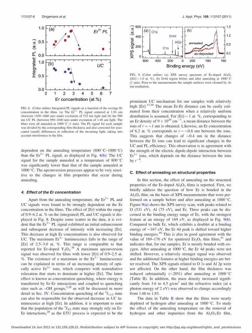
dependent on the annealing temperature (800 �C–1000 �C)
than the Er3þ PL signal, as displayed in Fig. 4(b): The UC
signal for the sample annealed at a temperature of 800 �Cwas significantly lower than that of the sample annealed at
1000 �C. The upconversion processes appear to be very sensi-
tive to the changes in film properties that occur during
annealing.
4. Effect of the Er concentration
Apart from the annealing temperature, the Er3þ PL and
UC signals were found to be strongly dependent on the Er
concentration in the films. The effect of [Er] within the range
of 0.9–6.2 at. % on the (integrated) PL and UC signals is dis-
played in Fig. 8. Despite some scatter in the data, it is evi-
dent that the Er3þ PL signal exhibited an initial enhancement
and subsequent decrease of intensity with increasing [Er].
This decrease at high Er concentrations is also observed for
UC. The maximum Er3þ luminescence falls in the range of
[Er] of 2.5–3.0 at. %. This range is comparable to that
reported for Er-doped Y2O3.38 A maximum upconversion
signal was observed for films with lower [Er] of 0.9–2.5 at.
%. The existence of a maximum in the Er3þ luminescence
can be explained in terms of an increasing density of opti-
cally active Er3þ ions, which competes with nonradiative
relaxation that starts to dominate at higher [Er]. The latter
effect is known as concentration quenching, where energy is
transferred by Er-Er interactions and coupled to quenching
sites such as –OH groups,2,28 as will be discussed in more
detail in Sec. IV. Concentration quenching of the 4I11/2 state
can also be responsible for the observed decrease in UC lu-
minescence at high [Er]. In addition, it is important to note
that the population of the 4I9/2 state may strongly rely on Er-
Er interactions,28 as the ETU process is expected to be the
prominent UC mechanism for our samples with relatively
high [Er].13,39 The mean Er-Er distance can be easily esti-
mated from their concentration when a relatively uniform
distribution is assumed. For [Er]¼ 1 at. %, corresponding to
an Er density of 9� 1020 cm�3, a mean distance between the
ions of r¼�1 nm is obtained. Likewise, an Er concentration
of 6.2 at. % corresponds to r¼�0.6 nm between the ions.
This suggests that changes of �0.4 nm in the distance
between the Er ions can lead to significant changes in the
UC and PL efficiency. This observation is in agreement with
the strength of the electric dipole-dipole interaction between
Er3þ ions, which depends on the distance between the ions
by r�6.
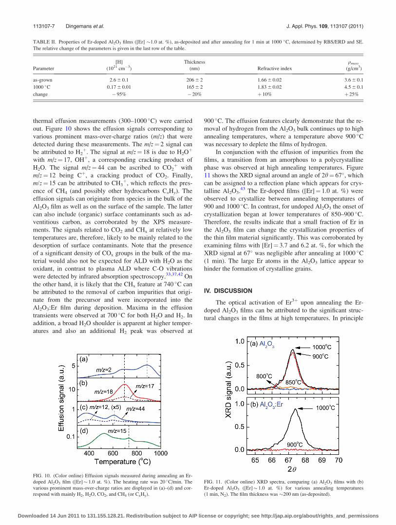
C. Effect of annealing on structural properties
In this section, the effect of annealing on the structural
properties of the Er-doped Al2O3 films is reported. First, we
briefly address the question of how Er is bonded in the
Al2O3 film, on the basis of XPS measurements that were per-
formed on a sample before and after annealing at 1000 �C.
Figure 9(a) shows the XPS survey scan, with peaks related to
O (531 eV), Al (75 eV), and Er. Three peaks can be dis-
cerned in the binding energy range of Er, with the strongest
feature at an energy of 169 eV, as displayed in Fig. 9(b).
Compared to bulk Er, which exhibits a doublet at a binding
energy of �167 eV, the Er 4d peak is shifted toward higher
binding energies.40 This is also in good agreement with the
value of 169–170 eV for sputtered Er2O3 thin films,41 and
indicates that, for our samples, Er is mostly bonded with ox-
ygen. After annealing at 1000 �C, the Er 4d peaks were not
shifted. However, a relatively stronger signal was observed
and the additional features at higher binding energies are bet-
ter resolved. The XPS signals related to O 1s and Al 2p were
not affected. On the other hand, the film thickness was
reduced substantially (�20%) after annealing at 1000 �C(Table II). In addition, the mass density increased signifi-
cantly from 3.6 to 4.5 g/cm3 and the refractive index (at a
photon energy of 2 eV) was observed to change accordingly
from 1.66 to 1.83.
The data in Table II show that the films were nearly
depleted of hydrogen after annealing at 1000 �C. To study
the effect of the annealing temperature on the removal of
hydrogen and other impurities from the Al2O3:Er film,
FIG. 8. (Color online) Integrated PL signals as a function of the average Er
concentration in the films. (a) The Er3þ PL signal centered at 1.54 lm
(between 1430–1660 nm) under excitation of 532 nm light and (b) the 980
nm UC PL (between 950–1040 nm) under excitation of 1.48 lm light. The
films were all annealed at 1000 �C (1 min). The PL signal for each sample
was divided by the corresponding film thickness and also corrected for asso-
ciated (small) differences in reflection of the incoming light, taking into
account interference in the film.
FIG. 9. (Color online) (a) XPS survey spectrum of Er-doped Al2O3
([Er]� 1.0 at. %), (b) Er4d region before and after annealing at 1000 �C(1 min). Prior to the measurements the sample surfaces were cleaned by Ar
ion irradiation.
113107-6 Dingemans et al. J. Appl. Phys. 109, 113107 (2011)
Downloaded 14 Jun 2011 to 131.155.128.21. Redistribution subject to AIP license or copyright; see http://jap.aip.org/about/rights_and_permissions
thermal effusion measurements (300–1000 �C) were carried
out. Figure 10 shows the effusion signals corresponding to
various prominent mass-over-charge ratios (m/z) that were
detected during these measurements. The m/z¼ 2 signal can
be attributed to H2þ. The signal at m/z¼ 18 is due to H2Oþ
with m/z¼ 17, OHþ, a corresponding cracking product of
H2O. The signal m/z¼ 44 can be ascribed to CO2þ with
m/z¼ 12 being Cþ, a cracking product of CO2. Finally,
m/z¼ 15 can be attributed to CH3þ, which reflects the pres-
ence of CH4 (and possibly other hydrocarbons CxHy). The
effusion signals can originate from species in the bulk of the
Al2O3 film as well as on the surface of the sample. The latter
can also include (organic) surface contaminants such as ad-
ventitious carbon, as corroborated by the XPS measure-
ments. The signals related to CO2 and CHx at relatively low
temperatures are, therefore, likely to be mainly related to the
desorption of surface contaminants. Note that the presence
of a significant density of COx groups in the bulk of the ma-
terial would also not be expected for ALD with H2O as the
oxidant, in contrast to plasma ALD where C-O vibrations
were detected by infrared absorption spectroscopy.33,37,42 On
the other hand, it is likely that the CHx feature at 740 �C can
be attributed to the removal of carbon impurities that origi-
nate from the precursor and were incorporated into the
Al2O3:Er film during deposition. Maxima in the effusion
transients were observed at 700 �C for both H2O and H2. In
addition, a broad H2O shoulder is apparent at higher temper-
atures and also an additional H2 peak was observed at
900 �C. The effusion features clearly demonstrate that the re-
moval of hydrogen from the Al2O3 bulk continues up to high
annealing temperatures, where a temperature above 900 �Cwas necessary to deplete the films of hydrogen.
In conjunction with the effusion of impurities from the
films, a transition from an amorphous to a polycrystalline
phase was observed at high annealing temperatures. Figure
11 shows the XRD signal around an angle of 2h¼ 67�, which
can be assigned to a reflection plane which appears for crys-
talline Al2O3.43 The Er-doped films ([Er]¼ 1.0 at. %) were
observed to crystallize between annealing temperatures of
900 and 1000 �C. In contrast, for undoped Al2O3 the onset of
crystallization began at lower temperatures of 850–900 �C.
Therefore, the results indicate that a small fraction of Er in
the Al2O3 film can change the crystallization properties of
the thin film material significantly. This was corroborated by
examining films with [Er]¼ 3.7 and 6.2 at. %, for which the
XRD signal at 67� was negligible after annealing at 1000 �C(1 min). The large Er atoms in the Al2O3 lattice appear to
hinder the formation of crystalline grains.
IV. DISCUSSION
The optical activation of Er3þ upon annealing the Er-
doped Al2O3 films can be attributed to the significant struc-
tural changes in the films at high temperatures. In principle
FIG. 10. (Color online) Effusion signals measured during annealing an Er-
doped Al2O3 film ([Er]� 1.0 at. %). The heating rate was 20 �C/min. The
various prominent mass-over-charge ratios are displayed in (a)–(d) and cor-
respond with mainly H2, H2O, CO2, and CH4 (or CxHy).
FIG. 11. (Color online) XRD spectra, comparing (a) Al2O3 films with (b)
Er-doped Al2O3 ([Er]� 1.0 at. %) for various annealing temperatures
(1 min, N2). The film thickness was �200 nm (as-deposited).
TABLE II. Properties of Er-doped Al2O3 films ([Er] �1.0 at. %), as-deposited and after annealing for 1 min at 1000 �C, determined by RBS/ERD and SE.
The relative change of the parameters is given in the last row of the table.
Parameter
[H]
(1021 cm�3)
Thickness
(nm) Refractive index
qmass
(g/cm3)
as-grown 2.6 6 0.1 206 6 2 1.66 6 0.02 3.6 6 0.1
1000 �C 0.17 6 0.01 165 6 2 1.83 6 0.02 4.5 6 0.1
change � 95% � 20% þ 10% þ 25%
113107-7 Dingemans et al. J. Appl. Phys. 109, 113107 (2011)
Downloaded 14 Jun 2011 to 131.155.128.21. Redistribution subject to AIP license or copyright; see http://jap.aip.org/about/rights_and_permissions
two effects can play a role here. First, it may be speculated
that the fraction of optically active Er3þ ions increases.2,44
Second, the influence of nonradiative processes that compete
with the luminescence yield can be significantly reduced dur-
ing annealing. The importance of the second effect was dem-
onstrated for Er2O3 and Er-implanted Al2O3 films, where a
significant enhancement of the lifetime of the 4I13/2 level was
observed with increasing annealing temperature.2,45 Nonra-
diative relaxation can take place when Er3þ ions transfer
energy by coupling to the phonon modes of Al2O3 (phonon
energy of 870 cm�1),2 or to impurities in the host material.
Al2O3 exhibits a relatively high phonon energy compared to,
e.g., chlorides and other halides,4,5 and, therefore, a rela-
tively high nonradiative recombination rate may be
expected.46 On the other hand, the transition from an amor-
phous to polycrystalline Al2O3 structure (Fig. 11) is expected
to lead to only a slight variation in the phonon energy distri-
bution. As these minor changes only occur for temperatures
> 900 �C, the coupling to phonon modes of Al2O3 cannot
account for the general trend of increasing luminescence
yield upon annealing. As a counter effect, we hypothesize
that grain boundaries in the polycrystalline Al2O3 constitute
additional quenching sites for the Er3þ luminescence. Apart
from the phonon modes of the host lattice, OH impurities
have been identified as prominent quenching sites for Er3þ
luminescence.2,28,47 An important quenching mechanism is
concentration quenching, i.e., the transfer of energy between
Er3þ ions until it is nonradiatively dissipated.13 The energy
migration between Er3þ ions is expected to be effective con-
cerning the relatively high Er concentrations in our films.
The broad energy range of the OH stretching vibration
around �3600 cm�1 (Ref. 33) matches closely with the
energy between 4I11/2! 4I13/2 states (�3670 cm�1). Further-
more, the energy of the second harmonic of the OH vibration
is relatively close to the energy between the 4I13/2 ! 4I15/2
states (�6500 cm�1). Other impurities, such as CHx, can
also be identified as possible quenching centers. The stretch-
ing vibration of CH3 is located in the infrared absorption
spectrum at an energy of �2945 cm�1,27,33 which is in the
same energy range as that of OH.
The removal of hydrogen from the films during anneal-
ing may explain the negative correlation between the Er3þ
and Si photoluminescence. The normalized Er and Si PL sig-
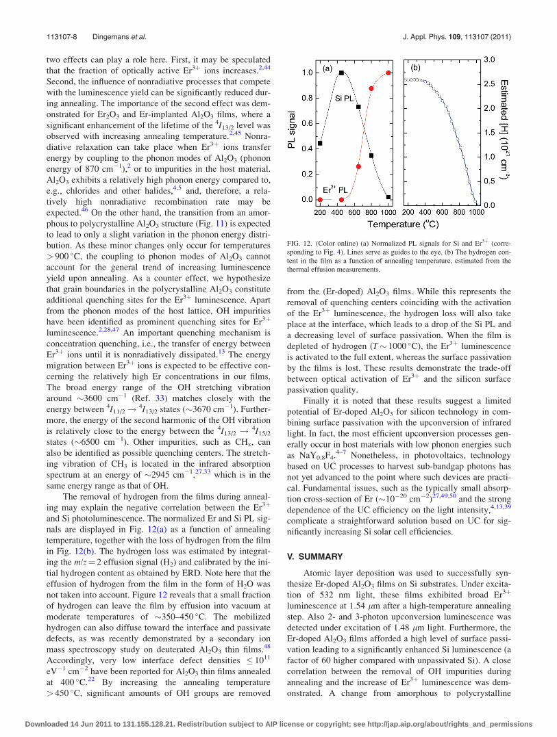
nals are displayed in Fig. 12(a) as a function of annealing
temperature, together with the loss of hydrogen from the film
in Fig. 12(b). The hydrogen loss was estimated by integrat-
ing the m/z¼ 2 effusion signal (H2) and calibrated by the ini-
tial hydrogen content as obtained by ERD. Note here that the
effusion of hydrogen from the film in the form of H2O was
not taken into account. Figure 12 reveals that a small fraction
of hydrogen can leave the film by effusion into vacuum at
moderate temperatures of �350–450 �C. The mobilized
hydrogen can also diffuse toward the interface and passivate
defects, as was recently demonstrated by a secondary ion
mass spectroscopy study on deuterated Al2O3 thin films.48
Accordingly, very low interface defect densities � 1011
eV�1 cm�2 have been reported for Al2O3 thin films annealed
at 400 �C.22 By increasing the annealing temperature
> 450 �C, significant amounts of OH groups are removed
from the (Er-doped) Al2O3 films. While this represents the
removal of quenching centers coinciding with the activation
of the Er3þ luminescence, the hydrogen loss will also take
place at the interface, which leads to a drop of the Si PL and
a decreasing level of surface passivation. When the film is
depleted of hydrogen (T� 1000 �C), the Er3þ luminescence
is activated to the full extent, whereas the surface passivation
by the films is lost. These results demonstrate the trade-off
between optical activation of Er3þ and the silicon surface
passivation quality.
Finally it is noted that these results suggest a limited
potential of Er-doped Al2O3 for silicon technology in com-
bining surface passivation with the upconversion of infrared
light. In fact, the most efficient upconversion processes gen-
erally occur in host materials with low phonon energies such
as NaY0.8F4.4–7 Nonetheless, in photovoltaics, technology
based on UC processes to harvest sub-bandgap photons has
not yet advanced to the point where such devices are practi-
cal. Fundamental issues, such as the typically small absorp-
tion cross-section of Er (�10�20 cm�2)27,49,50 and the strong
dependence of the UC efficiency on the light intensity,4,13,39
complicate a straightforward solution based on UC for sig-
nificantly increasing Si solar cell efficiencies.
V. SUMMARY
Atomic layer deposition was used to successfully syn-
thesize Er-doped Al2O3 films on Si substrates. Under excita-
tion of 532 nm light, these films exhibited broad Er3þ
luminescence at 1.54 lm after a high-temperature annealing
step. Also 2- and 3-photon upconversion luminescence was
detected under excitation of 1.48 lm light. Furthermore, the
Er-doped Al2O3 films afforded a high level of surface passi-
vation leading to a significantly enhanced Si luminescence (a
factor of 60 higher compared with unpassivated Si). A close
correlation between the removal of OH impurities during
annealing and the increase of Er3þ luminescence was dem-
onstrated. A change from amorphous to polycrystalline
FIG. 12. (Color online) (a) Normalized PL signals for Si and Er3þ (corre-
sponding to Fig. 4). Lines serve as guides to the eye. (b) The hydrogen con-
tent in the film as a function of annealing temperature, estimated from the
thermal effusion measurements.
113107-8 Dingemans et al. J. Appl. Phys. 109, 113107 (2011)
Downloaded 14 Jun 2011 to 131.155.128.21. Redistribution subject to AIP license or copyright; see http://jap.aip.org/about/rights_and_permissions
Al2O3 at annealing temperatures > 900 �C did not play a sig-
nificant role in the optical activation. In contrast to Er, the Si
luminescence decreased at high annealing temperatures,
indicating a decreasing level of surface passivation.
ACKNOWLEDGMENTS
Dr. W. Beyer and Dr. F. Einsele (Forschungszentrum
Julich) are kindly acknowledged for the effusion measure-
ments. Dr. S.E. Potts and W. Keuning (Eindhoven Univer-
sity) are thanked for their experimental support and
discussions. This work is carried out within the Thin Film
Nanomanufacturing (TFN) program of the Dutch Technol-
ogy Foundation STW. Financial support was received from
the German Ministry for the Environment, Nature Conserva-
tion, and Nuclear Safety (BMU) under contract number
0325150 (“ALADIN”).
1A. J. Kenyon, Prog. Quantum Electron. 26, 225 (2002)2A. Polman, J. Appl. Phys. 82, 1 (1997).3F. Auzel, Chem. Rev. 104, 139 (2004).4A. Shalav, B. S. Richards, and M. A. Green, Sol. Energy Mater. Sol. Cells
91, 829 (2007)5J. F. Suyver, A. Aebischer, D. Biner, P. Gerner, J. Grimm, S. Heer, K.W.
Kramer, C. Reinhard, and H. U. Gudel, Opt. Mater. 27, 1111 (2005).6C. Strumpel, M. McCann, G. Beaucarne, V. Arkhipov, A. Slaoui,
V. Svrcek, C. del Canizo, and I. Tobias, Sol. Energy Mater. Sol. Cells 91,
238 (2007).7B. M. van der Ende, L. Aarts, and A. Meijerink, Phys. Chem. 11, 11081
(2009).8G. N. van den Hoven, R. J. I. M. Koper, A. Polman, C. van Dam, J. W. M.
van Uffelen, M. K. Smit, Appl. Phys. Lett. 68, 1886 (1996).9L. Agazzi, J. D. B. Bradley, M. Dijkstra, F. Ay, G. Roelkens, R. Baets,
K. Worhoff, and M. Pollnau, Opt. Express 18, 27703 (2010).10R. Serna and C. N. Afonso, Appl. Phys. Lett. 69, 1541 (1996).11P. G. Kik and A. Polman, J. Appl. Phys. 93, 5008 (2003).12K. Worhoff, J. D. B. Bradley, F. Ay, D. Geskus, T. P. Blauwendraat, and
M. Pollnau, IEEE J. Quantum Electron. 45, 454 (2009).13G. N. van den Hoven, E. Snoeks, A. Polman, C. van Damn, J. W. M. Uffe-
len, and M. K. Smit, J. Appl. Phys. 79 1258 (1996).14S. Musa, H. J. van Weerden, T. H. Yau, and P. V. Lambeck, IEEE J. Quan-
tum Electronics 36, 1089 (2000).15C. E. Chryssou and C. W. Pitt, IEEE J. Quantum Electronics 34, 282
(1998).16S. M. George, Chem. Rev. 110, 111 (2010).17T. T. Van, J. Hoang, R. Ostroumov, K. L. Wang, J. R. Bargar, J. Lu, H.-O.
Blom, and J. P. Chang, J. Appl. Phys. 100, 073512 (2006).18R. L. Puurunen, J. Appl. Phys. 97, 121301 (2005).19T. Trupke, J. Zhao, A. Wang, R. Corkish, and M. A. Green, Appl. Phys.
Lett. 82, 2996 (2003).20M. J. Chen, Y. T. Shih, M. K. Wu, and F. Y. Tsai, J. Appl. Phys. 101,
033130 (2007).21B. Hoex, J. J. H. Gielis, M. C. M. van de Sanden, and W. M. M. Kessels,
J. Appl. Phys 104, 113703 (2008).
22G. Dingemans, N. M. Terlinden, D. Pierreux, H. B. Profijt, M. C. M. van
de Sanden, and W. M. M. Kessels, Electrochem. Solid-State Lett. 14, H1
(2011).23P. Poodt, A. Lankhorst, F. Roozeboom, K. Spee, D. Maas, and A. Ver-
meer, Adv. Mater. 22, 3564 (2010).24J. Paivasaari, M. Putkonen, T. Sajavaara, and L. Niinisto, J. Alloys
Compd. 374, 124 (2004).25J. Paivasaari, J. Niinisto, K. Arstila, K. Kukli, M. Putkonen, and L. Nii-
nisto, Chem. Vap. Deposition 11, 415 (2005).26K. Solehmainen, M. Kapulainen, P. Heimala, and K. Polamo, IEEE Pho-
tonics Technol. Lett. 16, 194 (2004).27J. Hoang, T. T. Van, M. Sawkar-Mathur, B. Hoex, M. C. M. van de San-
den, W. M. M. Kessels, R. Ostroumov, K. L. Wang, J. R. Bargar, and J. P.
Chang, J. Appl. Phys. 101, 123116 (2007).28E. Snoeks, P. G. Kik, and A. Polman, Opt. Mater. 5, 159 (1996).29G. Dingemans, R. Seguin, P. Engelhart, M. C. M. van de Sanden, and
W. M. M. Kessels, Phys. Status Solidi (RRL) 4, 10 (2010).30W. Beyer, J. Herion, H. Wagner, and U. Zastrow, Philos. Mag. B 63, 269
(1991).31E. Langereis, S. B. S. Heil, H. C. M. Knoops, W. Keuning, M. C. M. van
de Sanden, and W. M. M. Kessels, J. Phys. D 42, 073001 (2009).32J. Paivasaari, M. Putkonen, and L. Niinisto, Thin Solid Films 472, 275
(2005).33V. Verlaan, L. R. J. G. van den Elzen, G. Dingemans, M. C. M. van de
Sanden, and W. M. M. Kessels, Phys. Status Solidi C 7, 976 (2010).34P. P. Altermatt, F. Geelhaarb, T. Trupke, X. Dai, A. Neisser, and E. Daub,
Appl. Phys. Lett. 88, 261901 (2006).35T. Trupke, R. A. Bardos, and M. D. Abbott, Appl. Phys. Lett. 87, 184102
(2005).36E. Sun, F.-H. Su, C.-H. Chen, and M.-J. Chen, Appl. Surf. Sci. 256, 5021
(2010).37G. Dingemans, R. Seguin, P. Engelhart, F. Einsele, B. Hoex, M. C. M. van
de Sanden, and W. M. M. Kessels, J. Appl. Phys. 106, 114907 (2009).38R. Lo Savio, M. Miritello, P. Cardile, and F. Priolo, J. Appl. Phys. 106,
043512 (2009).39M. Pollnau, D. R. Gamelin, S. R. Luthi, H. U. Gudel, and M. P. Hehlen,
Phys. Rev. B 61, 3337 (2000).40J. K. Moulder, W. F. Stickle, P. E. Sobol, and K. D. Bomben, Handbook of
X-ray Photoelectron Spectroscopy (Physical Electronics, Chanhassen,
MN, 1995).41T.-M. Pan, C.-L. Chen, W. W. Yeh, and S.-J. Hou, Appl. Phys. Lett. 89,
222912 (2006).42E. Langereis, J. Keijmel, M. C. M. van de Sanden, and W. M. M. Kessels,
Appl. Phys. Lett. 92, 231904 (2008).43S. Jakschik, U. Schroeder, T. Hecht, M. Gutsche, H. Seidl, and J. W. Bar-
tha, Thin Solid Films 425, 216 (2003).44D. Navarro-Urrios, Y. Lebour, O. Jambois, B. Garrido, A. Pitanti, N. Dal-
dosso, L. Pavesi, J. Cardin, K. Hijazi, L. Khomenkova, F. Gourbilleau,
and R. Rizk, J. Appl. Phys. 106, 093107 (2009).45M. Miritello, R. Lo Savio, A. M. Piro, G. Franzo, F. Priolo, F. Iacona, and
C. Bongiorno, J. Appl. Phys. 100, 013502 (2006).46N. Maeda, N. Wada, H. Onoda, A. Maegawa, and K. Kojima, Opt. Mater.
27, 1851 (2005).47A. Polman, Physica B 300, 78 (2001).48G. Dingemans, W. Beyer, M. C. M. van de Sanden, and W. M. M. Kessels,
Appl. Phys. Lett. 97, 152106 (2010).49H. Mertens, A. Polman, I. M. P. Aarts, W. M. M. Kessels, and M. C. M.
van de Sanden, Appl. Phys. Lett. 86, 241109 (2005).50C. Strohhofer and A. Polman, Opt. Mater. 21, 705 (2003).
113107-9 Dingemans et al. J. Appl. Phys. 109, 113107 (2011)
Downloaded 14 Jun 2011 to 131.155.128.21. Redistribution subject to AIP license or copyright; see http://jap.aip.org/about/rights_and_permissions