fabrication of carbon nanostructures using photo-nanoimprint lithography and pyrolysis
TRANSCRIPT

This content has been downloaded from IOPscience. Please scroll down to see the full text.
Download details:
IP Address: 128.146.90.34
This content was downloaded on 07/03/2014 at 19:50
Please note that terms and conditions apply.
Fabrication of carbon nanostructures using photo-nanoimprint lithography and pyrolysis
View the table of contents for this issue, or go to the journal homepage for more
2012 J. Micromech. Microeng. 22 045024
(http://iopscience.iop.org/0960-1317/22/4/045024)
Home Search Collections Journals About Contact us My IOPscience
IOP PUBLISHING JOURNAL OF MICROMECHANICS AND MICROENGINEERING
J. Micromech. Microeng. 22 (2012) 045024 (8pp) doi:10.1088/0960-1317/22/4/045024
Fabrication of carbon nanostructuresusing photo-nanoimprint lithography andpyrolysisVarun Penmatsa1, Hiroshi Kawarada2 and Chunlei Wang1
1 Department of Mechanical and Materials Engineering, Florida International University,10555 W. Flagler St., Miami, FL 33174, USA,2 School of Science and Engineering, Waseda University, 3-4-1 Okubo, Tokyo 169-8555, Japan
E-mail: [email protected]
Received 2 February 2012, in final form 15 February 2012Published 23 March 2012Online at stacks.iop.org/JMM/22/045024
AbstractHigh-throughput synthesis of carbon nanostructures with reproducible shape and dimensions,at desired locations, has been a key challenge for further exploring carbon nanostructures asfunctional units in various nanodevices. In this work, carbon structures with dimensions fromthe 50 nano- to micrometer level have been fabricated by carbonizing a photo-nanoimprintlithography patterned resist polymer (AR-UL-01) at high temperature under inert atmosphere.The resulting carbon nanostructures showed significant vertical shrinkage but minimal loss inthe lateral direction. Thermal behavior studies of the resist polymer in the pyrolysis cycleindicated gaseous evolution of various byproducts before the formation of solid carbon.Microstructure, elemental composition and resistivity characterization of the nanostructuresproduced by this process has shown that the carbon derived from a pyrolyzed nanoimprintresist is very similar to the pyrolyzed photoresist carbon from an SU-8 negative-tonephotoresist. This simple approach is valuable as a wafer-level carbon nano-patterningtechnique.
(Some figures may appear in colour only in the online journal)
1. Introduction
Over the last two decades, one-dimensional carbonnanostructures including nanotubes, nanowires and nanobeltshave been extensively studied for their potential as buildingblocks in electronic, optoelectronic and electrochemicalnanodevices due to their high surface to volume ratio,decreased charging currents and faster electrochemicalreactions [1, 2]. In particular, carbon nanotubes (CNTs) haveattracted the majority of the research efforts due to theirunique physiochemical and electrical properties. Prototypedevices integrated with surface-engineered CNTs have beendemonstrated as molecular probes for chemical and biologicalinvestigations, field emitters and nanoprobes in metrology [3].However, in order to incorporate nanostructures in practicalfunctional devices, two major issues still remain, i.e. (i) howto synthesize substantial quantities of nanostructures withcontrollable sizes and shapes at preferred locations; and (ii)
how to integrate nanostructures in devices that are feasible formass production.
The ability to fabricate well-defined carbon microstruc-tures with atomically smooth surfaces is made possible bypyrolyzing organic polymer precursors [4–8]. In this approach,polymers patterned by conventional photolithography or softlithography are carbonized at high temperatures under inertambience, causing the chain scission of organic compounds toform solid carbon. Since lithography techniques are used forthe patterning purpose, the electrodes obtained by this mannerhave better resolution and reproducibility when compared tothe traditional casted carbon ink electrodes [9]. Such carbonstructures have been used in applications such as on-chipsupercapacitors [10], microbatteries [11], DNA detection [12],glucose sensors [13] and dielectrophoretic electrode arrays forthe micromanipulation of micro- and nanoparticles [14]. Inaddition, different research groups have adapted this methodto produce carbon architectures such as suspended nanowires,
0960-1317/12/045024+08$33.00 1 © 2012 IOP Publishing Ltd Printed in the UK & the USA
J. Micromech. Microeng. 22 (2012) 045024 V Penmatsa et al
nanobridges and three-dimensional (3D) carbon micropil-lars [15]. Recently, controlled carbon nanostructures havebeen fabricated by employing tools such as scanning electronbeam lithography (EBL) [16] and ion-beam lithography [17]combined with pyrolysis. Although these procedures are ca-pable of patterning sub-100 nm features, they are not econom-ically feasible for mass production due to their low inherentthroughput, need for ultra-high vacuum systems and high op-erating costs.
The emergence of photo-nanoimprint lithography(P-NIL) has garnered attention as a potential low-cost, high-throughput technique for the fabrication of nano-scale featuresbeyond the resolution of the traditional photolithography.In a typical P-NIL process, the patterned UV transparentmold is stamped onto a photo-sensitive polymer and curedby ultraviolet light to create a thickness contrast [18]. Theanisotropic reactive ion etching (RIE) process is performedto remove the residual resist in the compressed areas andtransfer the thickness contrast pattern onto the underlyingresist and substrate. The versatility of the NIL process allowsdirect patterning of functional materials with desired physicalproperties at the wafer level [19]. In comparison, othernanopatterning techniques such as holographic lithography,extreme ultraviolet interference lithography (EUV-IL) andEBL come with critical drawbacks. The holographiclithography and EUV-IL allow only for the fabrication ofperiodic features without alignment and the long writing timesmake EBL only suited for small-area patterning. Furthermore,in P-NIL, a transparent mold enables optical alignment withhigh accuracy. Also, typically, carbon nanostructures mustbe coupled with microfabricated contact pads for electricaland electrochemical measurements which are made througha second lithographic step to deposit metal pads. In contrast,by combining P-NIL and pyrolysis processes, structures withdimensions from nanometers to millimeters can be seamlesslyintegrated. Due to these characteristic advantages, nanoimprintlithography has been extensively used in photonics[20–24], organic electronics [25], magnetic devices [26–30]and biological applications [31–34]. However, to the bestof our knowledge no research effort has been published toutilize the nanoimprinting technique for fabricating carbonnanostructures.
Here, we report our first effort to fabricate carbonnanostructure arrays based on P-NIL and pyrolysis. Inthis strategy, P-NIL patterning of photoresist over ananoimprint resist, followed by an etch transfer step, providespatterned nanostructures that are then carbonized underinert atmosphere. The resulting carbon nanostructures havecomposition and electrical properties comparable to carbonderived from pyrolysis of SU-8 precursor widely used incarbon-based MEMS fabrication. This versatile approach canaddress the need for high-throughput fabrication of carbonnanostructures at desired locations.
2. Experimental methods
2.1. Fabrication process
A silicon oxide wafer (4 inch size, (1 0 0)-oriented, n-type)was spin cleaned by acetone and methanol followed by adehydration bake at 150 ◦C for 5 min. At the beginning,a 200 nm thin coating of AR-UL-01 (nanoimprint resist)was carried out using Headway researchTM (Garland, TX)photoresist spinner at 4000 rpm for 45 s and baked at 180 ◦Cfor 90 s. For patterning the nanoimprint resist, a thin layerof AR-UV-01 (photoresist) is spin coated on the top of AR-UL-01 layer at 5000 rpm for 7 s. Both resists used in thisexperiment were purchased from NanoLitho Solutions Inc.(San Marcos, CA). The P-NIL process was conducted usingan OAI Model 800 (San Jose, CA) mask aligner equippedwith OAI Nano Imprint Module. The compressed photoresistwas exposed by a 365 nm mercury lamp for 60 s with lightintensity at 900 mJ cm−2 to crosslink the polymer chains. In ourwork, the nanoimprinting was performed using a 5 inch × 5inch mask with the nanoimprinted area being 2 inch diametercircle. The actual pattern area containing arrays of assortednanostructures in the nanoimprinted area was 1 inch × 1inch square. Following the patterning process, initially a 10:1CF4 and O2 mixture at 150 Torr and 75 W etch was preparedfor 30 s to remove the residual photoresist followed by anoxygen plasma treatment at 50 W and 150 mTorr for 100 s toetch the residual nanoimprint resist. The remaining photoresistlayer on the top was then removed by a 10:1 CF4 and O2 RIEfor 60 s at 150 mTorr and 75 W. The samples were carbonizedin an alumina-tube furnace (Lindberg) by a two-step pyrolysisprocess. The samples were initially heated at 5 ◦C min−1 ratefrom room temperature to 350 ◦C, and held at that temperaturefor 40 min followed by ramping to 1000 ◦C and 60 min holdingtime. The samples were eventually cooled down slowly tothe room temperature under constant gas flow. During thepyrolysis process, forming gas (95% N2 + 5% H2) wascontinuously flowed at 500 sccm.
2.2. Characterization
Thermal behavior of AR-UL-01 was investigated by DSC-2910 and TGA-2950 (both from thermal Analysis Instruments,New Castle, DE) under an argon atmosphere. The heatingcycle used for both DSC and TGA tests was the sameas the pyrolysis cycle. The morphology of the carbonnanostructures was characterized by the JEOL JSM-5335scanning electron microscopy (SEM). In the case ofnonconducting nanostructures, a thin gold film was evaporatedon the top to avoid charging. The Raman spectra weremeasured at room temperature using a Dilor Ramanspectrometer equipped with a CCD camera and an opticalmicroscope that provided a laser beam focus diameter ofabout 1 μm. An argon-ion laser (514.5 nm) was used asthe source during measurement. The chemical compositionof the AR-UL-01 surface before and after carbonization wasinvestigated by an Ulvac � 3300 XPS (Ulvac-Phi) with ananode source providing Al Kα radiation. The electron takeoffangle was 45 ± 3◦ relative to the substrate surface and the
2
J. Micromech. Microeng. 22 (2012) 045024 V Penmatsa et al
(a) (b) (c)
(d) (e) (f )
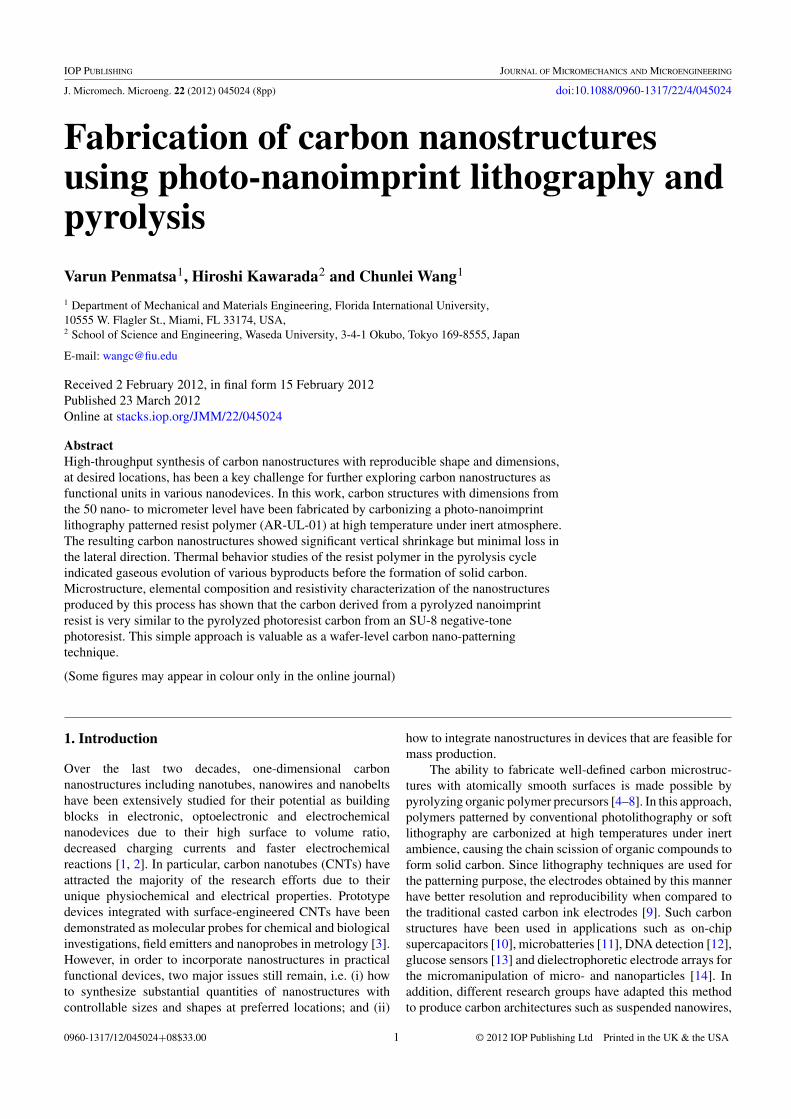
Figure 1. Schematic showing the fabrication process. (a) Spin coat thin layers of nanoimprint resist and the photoresist on the substrate,(b) imprint a predesigned glass mold to transfer the pattern onto the polymers and cure it with UV exposure, (c) retreat the glass mold tonotice the pattern, (d) oxygen plasma treatment to etch residual nanoimprint resist, (e) etch the residual photoresist top layer by theCF4+oxygen reactive ion etch and ( f ) carbonizing the polymer microstructures under forming gas atmosphere at high temperature.
C1s peak was chosen as the reference binding energy (285 eV).The sheet resistance measurements were performed using anAgilent 4156C precision semiconductor parameter analyzer(Santa Clara, CA) connected with a 4-point probe station. Itshould be pointed out that unpatterned pyrolyzed resist films(PPFs) from AR-UL-01 and SU-8 using the same pyrolysisconditions were used for characterization measurements.
3. Results and discussion
3.1. Morphology
A schematic illustration of the experimental process is shownin figure 1. A hard mold with surface-relief features is stampedonto a bilayer resist film of silicon containing UV-curablephotoresist and poly (methyl methacrylate) (PMMA)-basednanoimprint resist. The primary reason to use a bilayer resisttechnique is, if both the pattern definition layer (photoresist)and the pattern transfer layer (nanoimprint resist) are the same,removing residual resist by dry etch may cause damage tothe resist profile. To overcome this problem, in our worka bilayer resist film was used. In addition, the PMMA-based nanoimprint layer in the bilayer resist film providesgood adhesion between the UV-curable photoresist and theunderlying substrate. The critical difference between both theresists used in this work is the high contrast in etch selectivitiesand it is also important to note that the underlying nanoimprintresist is not sensitive to UV light and therefore cannot bepatterned without the presence of photoresist. After the moldis stamped, the bilayer resist film is irradiated with UV lightin order to pattern the photoresist top layer. Subsequently,the pattern is transferred to nanoimprint resist via a two-step reactive ion etching. Initially a CF4+O2 RIE etch isperformed to remove the residual photoresist followed byO2 RIE to etch the residual imprint resist present between thephotoresist pattern. Since the silicon containing UV-curablephotoresist top layer is resistant to O2 RIE, there is negligibleetching of the photoresist. Finally to completely remove the
photoresist top layer before pyrolysis of imprint resist, aCF4+O2 etch is performed. It is critical to completely removethe photoresist top layer because the silicon present in thephotoresist could form silicon carbide during pyrolysis, whichsignificantly affects the electrical conductivity of the carbonnanostructures. In the final step, the nanoimprint resist patternis carbonized by heating the sample at high temperature underinert atmosphere along with a precarbonization bake. Thestructures were subject to precarbonization bake to ensureextensive crosslinking and to improve the adhesion betweenpolymer and the substrate. This helps the nanoimprint resiststructures to maintain their shape during carbonization.
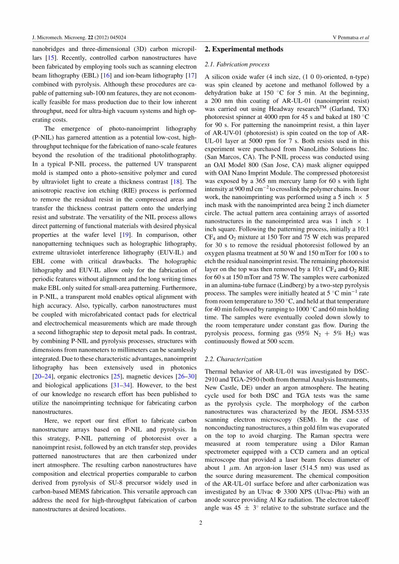
Examples of carbon structures with different criticaldimensions ranging from 50 nm to few microns fabricatedusing this methodology are shown in figure 2(a). The50 nm nanogratings with spacing of 150 nm (figure 2(b))between them appear to be straight without visible defects.These linear nanogratings with nanometer dimensions can befabricated with few millimeters length. Figure 2(c) illustratesthe higher magnification SEM images of comb pattern with afeature width of 500 nm. The distance between each featurein this pattern is 800 nm. The carbon pattern shown infigure 2(d) resembles a mesh structure with line widths of200 nm horizontally and 300 nm vertically. The minutetaperings at the edges could be attributed to the scatteringof UV light during photocuring. A high-magnification SEMimage of the chequered pattern with the smallest featuresize of 70 nm (figure 2(e)) demonstrates that even structureswith curved patterns maintain its lateral fidelity through thepyrolysis cycle. It is important to note that critical dimensionsof the features shown here were limited by the mold available.As evident from these SEM images, the experimental approachgreatly reduces the production time when compared to serialprocessing tools such as e-beam lithography EBL, ion-beamlithography due to the batch processing capability of P-NIL[35] and the nanostructures maintain good conformity throughthe pyrolysis cycle.
Carbonization of the nanostructures during the pyrolysisprocess usually involves a significant loss of material.
3
J. Micromech. Microeng. 22 (2012) 045024 V Penmatsa et al
(a) (d )
(b) (c)
(e)
Figure 2. SEM images of carbon nanostructures. (a) Carbon nanostructures with different design patterns and feature sizes, (b) 50 nm linearnanogratings, (c) comb design with 500 nm pattern critical dimensions, (d) mesh pattern having 180 nm critical dimension features,(e) chequered pattern with smallest feature size of 70 nm maintaining its lateral fidelity after pyrolysis.
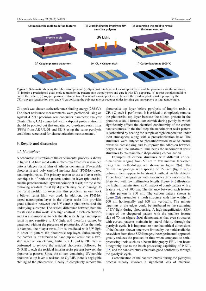
Figure 3. AFM images of the P-NIL patterned AR-UL-01 nanostructures (a) before and (b) after pyrolysis.
Several reports have indicated the aromatization of polymeraccompanied by the elimination of hydrogen and otherheteroatoms during pyrolysis resulting in structure shrinkage.The removal of noncarbon species during carbonizationinduces densification of the polymer nanostructures and thusaccounts for the volume shrinkage [36]. We investigated thevertical shrinkage of the nanoimprint resist by imaging linearstructures of different widths before and after carbonizationusing atomic force microscopy (AFM). Figure 3 shows theAFM images that reveal a significant vertical shrinkage from200 nm to 45 nm. The 77.5% shrinkage we observe here issimilar to those recorded for carbon nanostructures derivedfrom SU-8 2000.1 using EBL and pyrolysis [16]. Additionally,
the lateral shrinkage calculated from SEM images (data notshown) exhibits a decrease of 5% or less. The reason for theminor shrinkage could be due to the strong adhesion betweenthe nanoimprint resist and the Si substrate which forms a SiCinterfacial layer during the pyrolysis process [16]. From theresults, we can point out that the lateral shrinkage of the carbonnanostructures is similar to that of the nanofeatures derivedfrom SU-8 2000.1.
3.2. Thermal analysis
The thermophysical analysis of the nanoimprint resist wasinvestigated using differential scanning calorimetry (DSC)
4
J. Micromech. Microeng. 22 (2012) 045024 V Penmatsa et al
(a) (b)
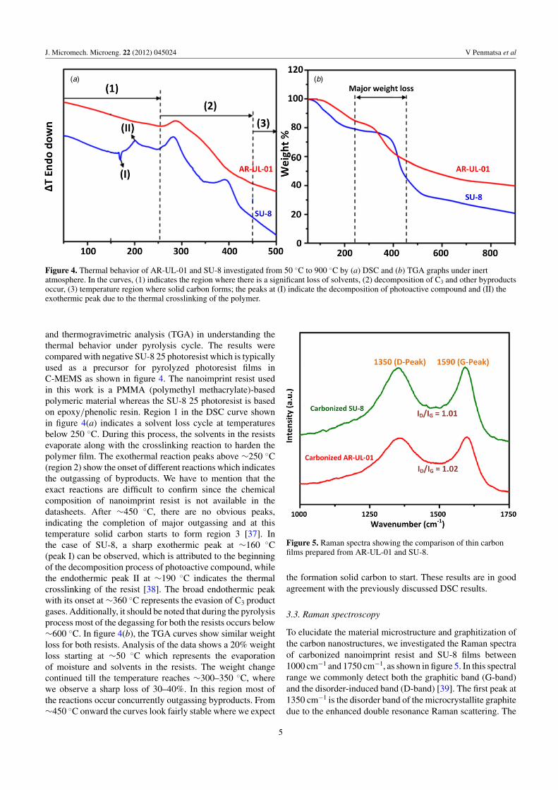
Figure 4. Thermal behavior of AR-UL-01 and SU-8 investigated from 50 ◦C to 900 ◦C by (a) DSC and (b) TGA graphs under inertatmosphere. In the curves, (1) indicates the region where there is a significant loss of solvents, (2) decomposition of C3 and other byproductsoccur, (3) temperature region where solid carbon forms; the peaks at (I) indicate the decomposition of photoactive compound and (II) theexothermic peak due to the thermal crosslinking of the polymer.
and thermogravimetric analysis (TGA) in understanding thethermal behavior under pyrolysis cycle. The results werecompared with negative SU-8 25 photoresist which is typicallyused as a precursor for pyrolyzed photoresist films inC-MEMS as shown in figure 4. The nanoimprint resist usedin this work is a PMMA (polymethyl methacrylate)-basedpolymeric material whereas the SU-8 25 photoresist is basedon epoxy/phenolic resin. Region 1 in the DSC curve shownin figure 4(a) indicates a solvent loss cycle at temperaturesbelow 250 ◦C. During this process, the solvents in the resistsevaporate along with the crosslinking reaction to harden thepolymer film. The exothermal reaction peaks above ∼250 ◦C(region 2) show the onset of different reactions which indicatesthe outgassing of byproducts. We have to mention that theexact reactions are difficult to confirm since the chemicalcomposition of nanoimprint resist is not available in thedatasheets. After ∼450 ◦C, there are no obvious peaks,indicating the completion of major outgassing and at thistemperature solid carbon starts to form region 3 [37]. Inthe case of SU-8, a sharp exothermic peak at ∼160 ◦C(peak I) can be observed, which is attributed to the beginningof the decomposition process of photoactive compound, whilethe endothermic peak II at ∼190 ◦C indicates the thermalcrosslinking of the resist [38]. The broad endothermic peakwith its onset at ∼360 ◦C represents the evasion of C3 productgases. Additionally, it should be noted that during the pyrolysisprocess most of the degassing for both the resists occurs below∼600 ◦C. In figure 4(b), the TGA curves show similar weightloss for both resists. Analysis of the data shows a 20% weightloss starting at ∼50 ◦C which represents the evaporationof moisture and solvents in the resists. The weight changecontinued till the temperature reaches ∼300–350 ◦C, wherewe observe a sharp loss of 30–40%. In this region most ofthe reactions occur concurrently outgassing byproducts. From∼450 ◦C onward the curves look fairly stable where we expect
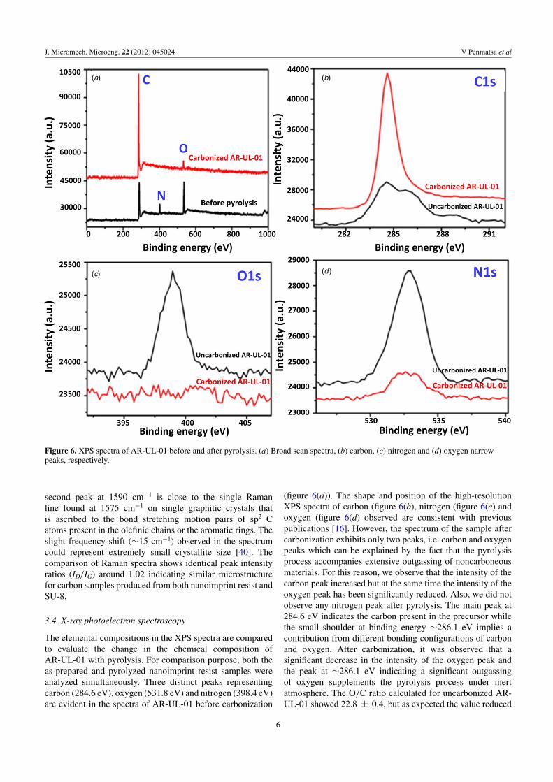
Figure 5. Raman spectra showing the comparison of thin carbonfilms prepared from AR-UL-01 and SU-8.
the formation solid carbon to start. These results are in goodagreement with the previously discussed DSC results.
3.3. Raman spectroscopy
To elucidate the material microstructure and graphitization ofthe carbon nanostructures, we investigated the Raman spectraof carbonized nanoimprint resist and SU-8 films between1000 cm−1 and 1750 cm−1, as shown in figure 5. In this spectralrange we commonly detect both the graphitic band (G-band)and the disorder-induced band (D-band) [39]. The first peak at1350 cm−1 is the disorder band of the microcrystallite graphitedue to the enhanced double resonance Raman scattering. The
5
J. Micromech. Microeng. 22 (2012) 045024 V Penmatsa et al
(a) (b)
(c) (d )
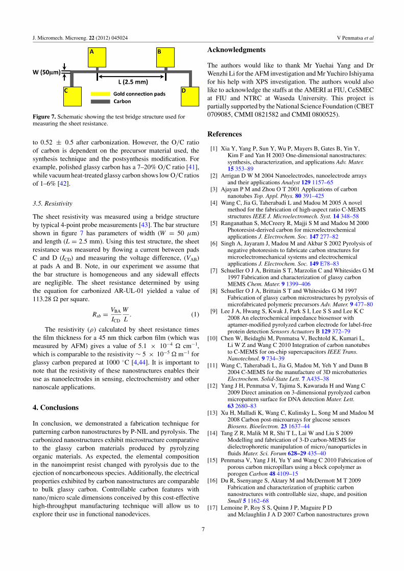
Figure 6. XPS spectra of AR-UL-01 before and after pyrolysis. (a) Broad scan spectra, (b) carbon, (c) nitrogen and (d) oxygen narrowpeaks, respectively.
second peak at 1590 cm−1 is close to the single Ramanline found at 1575 cm−1 on single graphitic crystals thatis ascribed to the bond stretching motion pairs of sp2 Catoms present in the olefinic chains or the aromatic rings. Theslight frequency shift (∼15 cm−1) observed in the spectrumcould represent extremely small crystallite size [40]. Thecomparison of Raman spectra shows identical peak intensityratios (ID/IG) around 1.02 indicating similar microstructurefor carbon samples produced from both nanoimprint resist andSU-8.
3.4. X-ray photoelectron spectroscopy
The elemental compositions in the XPS spectra are comparedto evaluate the change in the chemical composition ofAR-UL-01 with pyrolysis. For comparison purpose, both theas-prepared and pyrolyzed nanoimprint resist samples wereanalyzed simultaneously. Three distinct peaks representingcarbon (284.6 eV), oxygen (531.8 eV) and nitrogen (398.4 eV)are evident in the spectra of AR-UL-01 before carbonization
(figure 6(a)). The shape and position of the high-resolutionXPS spectra of carbon (figure 6(b), nitrogen (figure 6(c) andoxygen (figure 6(d) observed are consistent with previouspublications [16]. However, the spectrum of the sample aftercarbonization exhibits only two peaks, i.e. carbon and oxygenpeaks which can be explained by the fact that the pyrolysisprocess accompanies extensive outgassing of noncarboneousmaterials. For this reason, we observe that the intensity of thecarbon peak increased but at the same time the intensity of theoxygen peak has been significantly reduced. Also, we did notobserve any nitrogen peak after pyrolysis. The main peak at284.6 eV indicates the carbon present in the precursor whilethe small shoulder at binding energy ∼286.1 eV implies acontribution from different bonding configurations of carbonand oxygen. After carbonization, it was observed that asignificant decrease in the intensity of the oxygen peak andthe peak at ∼286.1 eV indicating a significant outgassingof oxygen supplements the pyrolysis process under inertatmosphere. The O/C ratio calculated for uncarbonized AR-UL-01 showed 22.8 ± 0.4, but as expected the value reduced
6
J. Micromech. Microeng. 22 (2012) 045024 V Penmatsa et al
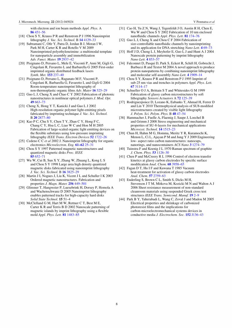
Figure 7. Schematic showing the test bridge structure used formeasuring the sheet resistance.
to 0.52 ± 0.5 after carbonization. However, the O/C ratioof carbon is dependent on the precursor material used, thesynthesis technique and the postsynthesis modification. Forexample, polished glassy carbon has a 7–20% O/C ratio [41],while vacuum heat-treated glassy carbon shows low O/C ratiosof 1–6% [42].
3.5. Resistivity
The sheet resistivity was measured using a bridge structureby typical 4-point probe measurements [43]. The bar structureshown in figure 7 has parameters of width (W = 50 μm)and length (L = 2.5 mm). Using this test structure, the sheetresistance was measured by flowing a current between padsC and D (ICD) and measuring the voltage difference, (VAB)at pads A and B. Note, in our experiment we assume thatthe bar structure is homogeneous and any sidewall effectsare negligible. The sheet resistance determined by usingthe equation for carbonized AR-UL-01 yielded a value of113.28 � per square.
Rsb = VBA
ICD
W
L. (1)
The resistivity (ρ) calculated by sheet resistance timesthe film thickness for a 45 nm thick carbon film (which wasmeasured by AFM) gives a value of 5.1 × 10⁻⁴ � cm−1,which is comparable to the resistivity ∼ 5 × 10⁻⁵ � m−1 forglassy carbon prepared at 1000 ◦C [4,44]. It is important tonote that the resistivity of these nanostructures enables theiruse as nanoelectrodes in sensing, electrochemistry and othernanoscale applications.
4. Conclusions
In conclusion, we demonstrated a fabrication technique forpatterning carbon nanostructures by P-NIL and pyrolysis. Thecarbonized nanostructures exhibit microstructure comparativeto the glassy carbon materials produced by pyrolyzingorganic materials. As expected, the elemental compositionin the nanoimprint resist changed with pyrolysis due to theejection of noncarboneous species. Additionally, the electricalproperties exhibited by carbon nanostructures are comparableto bulk glassy carbon. Controllable carbon features withnano/micro scale dimensions conceived by this cost-effectivehigh-throughput manufacturing technique will allow us toexplore their use in functional nanodevices.
Acknowledgments
The authors would like to thank Mr Yuehai Yang and DrWenzhi Li for the AFM investigation and Mr Yuchiro Ishiyamafor his help with XPS investigation. The authors would alsolike to acknowledge the staffs at the AMERI at FIU, CeSMECat FIU and NTRC at Waseda University. This project ispartially supported by the National Science Foundation (CBET0709085, CMMI 0821582 and CMMI 0800525).
References
[1] Xia Y, Yang P, Sun Y, Wu P, Mayers B, Gates B, Yin Y,Kim F and Yan H 2003 One-dimensional nanostructures:synthesis, characterization, and applications Adv. Mater.15 353–89
[2] Arrigan D W M 2004 Nanoelectrodes, nanoelectrode arraysand their applications Analyst 129 1157–65
[3] Ajayan P M and Zhou O T 2001 Applications of carbonnanotubes Top. Appl. Phys. 80 391–425
[4] Wang C, Jia G, Taherabadi L and Madou M 2005 A novelmethod for the fabrication of high-aspect ratio C-MEMSstructures IEEE J. Microelectromech. Syst. 14 348–58
[5] Ranganathan S, McCreery R, Majji S M and Madou M 2000Photoresist-derived carbon for microelectrochemicalapplications J. Electrochem. Soc. 147 277–82
[6] Singh A, Jayaram J, Madou M and Akbar S 2002 Pyrolysis ofnegative photoresists to fabricate carbon structures formicroelectromechanical systems and electrochemicalapplications J. Electrochem. Soc. 149 E78–83
[7] Schueller O J A, Brittain S T, Marzolin C and Whitesides G M1997 Fabrication and characterization of glassy carbonMEMS Chem. Mater. 9 1399–406
[8] Schueller O J A, Brittain S T and Whitesides G M 1997Fabrication of glassy carbon microstructures by pyrolysis ofmicrofabricated polymeric precursors Adv. Mater. 9 477–80
[9] Lee J A, Hwang S, Kwak J, Park S I, Lee S S and Lee K C2008 An electrochemical impedance biosensor withaptamer-modified pyrolyzed carbon electrode for label-freeprotein detection Sensors Actuators B 129 372–79
[10] Chen W, Beidaghi M, Penmatsa V, Bechtold K, Kumari L,Li W Z and Wang C 2010 Integration of carbon nanotubesto C-MEMS for on-chip supercapacitors IEEE Trans.Nanotechnol. 9 734–39
[11] Wang C, Taherabadi L, Jia G, Madou M, Yeh Y and Dunn B2004 C-MEMS for the manufacture of 3D microbatteriesElectrochem. Solid-State Lett. 7 A435–38
[12] Yang J H, Penmatsa V, Tajima S, Kawarada H and Wang C2009 Direct amination on 3-dimensional pyrolyzed carbonmicropattern surface for DNA detection Mater. Lett.63 2680–83
[13] Xu H, Malladi K, Wang C, Kulinsky L, Song M and Madou M2008 Carbon post-microarrays for glucose sensorsBiosens. Bioelectron. 23 1637–44
[14] Tang Z R, Malik M R, Shi T L, Lai W and Liu S 2009Modelling and fabrication of 3-D carbon-MEMS fordielectrophoretic manipulation of micro/nanoparticles influids Mater. Sci. Forum 628–29 435–40
[15] Penmatsa V, Yang J H, Yu Y and Wang C 2010 Fabrication ofporous carbon micropillars using a block copolymer asporogen Carbon 48 4109–15
[16] Du R, Ssenyange S, Aktary M and McDermott M T 2009Fabrication and characterization of graphitic carbonnanostructures with controllable size, shape, and positionSmall 5 1162–68
[17] Lemoine P, Roy S S, Quinn J P, Maguire P Dand Mclaughlin J A D 2007 Carbon nanostructures grown
7
J. Micromech. Microeng. 22 (2012) 045024 V Penmatsa et al
with electron and ion beam methods Appl. Phys. A86 451–56
[18] Chou S Y, Krauss P R and Renstrom P J 1996 Nanoimprintlithography J. Vac. Sci. Technol. B 14 4129–33
[19] Subramani C, Ofir Y, Patra D, Jordan B J, Moran I W,Park M H, Carter K R and Rotello V M 2009Nanoimprinted polyethyleneimine: a multimodal templatefor nanoparticle assembly and immobilizationAdv. Funct. Mater. 19 2937–42
[20] Pisignano D, Persano L, Mele E, Visconti P, Anni M, Gigli G,Cingolani R, Favaretto L and Barbarella G 2005 First-orderimprinted organic distributed feedback lasersSynth. Met. 153 237–40
[21] Pisignano D, Persano L, Raganato M F, Visconti P,Cingolani R, Barbarella G, Favaretto L and Gigli G 2004Room-temperature nanoimprint lithography ofnon-thermoplastic organic films Adv. Mater 16 525–29
[22] Guo L J, Cheng X and Chao C Y 2002 Fabrication of photonicnanostructures in nonlinear optical polymers J. Mod. Opt.49 663–73
[23] Cheng X, Hong Y T, Kanicki J and Guo L J 2002High-resolution organic polymer light-emitting pixelsfabricated by imprinting technique J. Vac. Sci. Technol.B 20 2877–80
[24] Kao P C, Chu S Y, Chen T Y, Zhan C Y, Hong F C,Chang C Y, Hsu L C, Liao W C and Hon M H 2005Fabrication of large-scaled organic light emitting devices onthe flexible substrates using low-pressure imprintinglithography IEEE Trans. Electron Devices 52 1722–26
[25] Cedeno C C et al 2002 J. Nanoimprint lithography for organicelectronics Microelectron. Eng. 61–62 25–31
[26] Chou S Y 1997 Patterned magnetic nanostructures andquantized magnetic disks Proc. IEEE85 652–71
[27] Wu W, Cui B, Sun X Y, Zhang W, Zhuang L, Kong L Sand Chou S Y 1998 Large area high density quantizedmagnetic disks fabricated using nanoimprint lithographyJ. Vac. Sci. Technol. B 16 3825–29
[28] Martin J I, Nogues J, Liu K, Vicent J L and Schuller I K 2003Ordered magnetic nanostructures. Fabrication andproperties J. Magn. Mater. 256 449–501
[29] Glinsner T, Hangweier P, Luesebrink H, Dorsey P, Homola Aand Wachenschwanz D 2005 Nanoimprint lithographyenables patterned tracks for high-capacity hard disksSolid State Technol. 15 51–4
[30] McClelland G M, Hart M W, Rettner C T, Best M E,Carter K R and Terris B D 2002 Nanoscale patterning ofmagnetic islands by imprint lithography using a flexiblemold Appl. Phys. Lett. 81 1483–85
[31] Cao H, Yu Z N, Wang J, Tegenfeldt J O, Austin R H, Chen E,Wu W and Chou S Y 2002 Fabrication of 10 nm enclosednanofluidic channels Appl. Phys. Lett. 81 174–76
[32] Guo L J, Cheng X and Chou C F 2004 Fabrication ofsize-controllable nanofluidic channels by nanoimprintingand its application for DNA stretching Nano Lett. 4 69–73
[33] Hoff J D, Cheng L J, Meyhofer E, Guo L J and Hunt A J 2004Nanoscale protein patterning by imprint lithographyNano Lett. 4 853–57
[34] Falconnet D, Pasqui D, Park S, Eckert R, Schift H, Gobrecht J,Barbucci R and Textor M 2004 A novel approach to produceprotein nanopatterns by combining nanoimprint lithographyand molecular self-assembly Nano Lett. 4 1909–14
[35] Chou S Y, Krauss P R and Renstrom P J 1995 Imprint ofsub-25 nm vias and trenches in polymers Appl. Phys. Lett.67 3114–17
[36] Schueller O J A, Brittain S T and Whitesides G M 1999Fabrication of glassy carbon microstructures by softlithography Sensors Actuators A 72 125–39
[37] Rodriguezponce D, Lozano K, Eubanks T, Ahmad H, Ferrer Dand Lin Y 2010 Thermophysical analysis of SU8-modifiedmicrostructures created by visible light lithographyJ. Polym. Sci. Polym. Phys. B 48 47–54
[38] Hammacher J, Fuelle A, Flaemig J, Saupe J, Loechel Band Grimm J 2008 Stress engineering and mechanicalproperties of SU-8-layers for mechanical applicationsMicrosyst. Technol. 14 1515–23
[39] Chun H, Hahm M G, Homma, Meritz Y R, Kuramochi K,Menon L, Ci L, Ajayan P M and Jung Y J 2009 Engineeringlow- aspect ratio carbon nanostructures: nanocups,nanorings, and nanocontainers ACS Nano 3 1274–79
[40] Tuinstra F and Koenig J L 1970 Raman spectrum of graphiteJ. Chem. Phys. 53 1126–30
[41] Chen P and McCreery R L 1996 Control of electron transferkinetics at glassy carbon electrodes by specific surfacemodification Anal. Chem. 68 3958–65
[42] Fagan D T, Hu I F and Kuwana T 1985 Vacuumheat-treatment for activation of glassy carbon electrodesAnal. Chem. 57 2759–63
[43] Enderling S, Brown C L, Smith S, Dicks M H,Stevenson J T M, Mitkova M, Kozicki M N and Walton A J2006 Sheet resistance measurement of non-standardcleanroom materials using suspended Greek cross teststructures IEEE Trans. Semicond. Manuf. 19 2–9
[44] Park B Y, Yaherabadi L, Wang C, Zoval J and Madou M 2005Electrical properties and shrinkage of carbonizedphotoresist films and the implications forcarbon-microelectromechanical systems devices inconductive media J. Electrochem. Soc. 152 J136–43
8