colloidal lithography for photovoltaics: an attractive route for
TRANSCRIPT

nanomaterials
Review
Colloidal Lithography for Photovoltaics: An Attractive Routefor Light Management
Rui D. Oliveira † , Ana Mouquinho *,† , Pedro Centeno, Miguel Alexandre, Sirazul Haque ,Rodrigo Martins , Elvira Fortunato, Hugo Águas and Manuel J. Mendes *
Citation: Oliveira, R.D.; Mouquinho,
A.; Centeno, P.; Alexandre, M.; Haque,
S.; Martins, R.; Fortunato, E.; Águas,
H.; Mendes, M.J. Colloidal
Lithography for Photovoltaics: An
Attractive Route for Light
Management. Nanomaterials 2021, 11,
1665. https://doi.org/10.3390/
nano11071665
Academic Editors: Federico Cesano,
Mohammed Jasim Uddin and
Simas Rackauskas
Received: 18 May 2021
Accepted: 18 June 2021
Published: 24 June 2021
Publisher’s Note: MDPI stays neutral
with regard to jurisdictional claims in
published maps and institutional affil-
iations.
Copyright: © 2021 by the authors.
Licensee MDPI, Basel, Switzerland.
This article is an open access article
distributed under the terms and
conditions of the Creative Commons
Attribution (CC BY) license (https://
creativecommons.org/licenses/by/
4.0/).
CENIMAT/I3N, Departamento de Ciência dos Materiais, Faculdade de Ciências e Tecnologia, FCT, UniversidadeNova de Lisboa, and CEMOP/UNINOVA, 2829-516 Caparica, Portugal; [email protected] (R.D.O.);[email protected] (P.C.); [email protected] (M.A.); [email protected] (S.H.);[email protected] (R.M.); [email protected] (E.F.); [email protected] (H.Á.)* Correspondence: [email protected] (A.M.); [email protected] (M.J.M.)† Those authors contributed equally to this work.
Abstract: The pursuit of ever-more efficient, reliable, and affordable solar cells has pushed the devel-opment of nano/micro-technological solutions capable of boosting photovoltaic (PV) performancewithout significantly increasing costs. One of the most relevant solutions is based on light manage-ment via photonic wavelength-sized structures, as these enable pronounced efficiency improvementsby reducing reflection and by trapping the light inside the devices. Furthermore, optimized mi-crostructured coatings allow self-cleaning functionality via effective water repulsion, which reducesthe accumulation of dust and particles that cause shading. Nevertheless, when it comes to marketdeployment, nano/micro-patterning strategies can only find application in the PV industry if theirintegration does not require high additional costs or delays in high-throughput solar cell manu-facturing. As such, colloidal lithography (CL) is considered the preferential structuring methodfor PV, as it is an inexpensive and highly scalable soft-patterning technique allowing nanoscopicprecision over indefinitely large areas. Tuning specific parameters, such as the size of colloids, shape,monodispersity, and final arrangement, CL enables the production of various templates/masks fordifferent purposes and applications. This review intends to compile several recent high-profile workson this subject and how they can influence the future of solar electricity.
Keywords: colloidal lithography; thin-film photovoltaics; photonics; light-trapping; self-cleaning
1. Introduction
Highly efficient renewable energy sources and storage devices are needed to dealwith the increasingly expensive energetic demands of our society. Considering the de-pleting fossil fuel stock and the devastating effects of global warming, technologies likephotovoltaics (PV) have become one of the leading contenders in this field, as PV offers abroad diversity of devices—each with their potential use and functionality [1–4]. Recentreports [5,6] show that, despite its current small output, about half of the growth in theelectric production capacity worldwide is now held by solar energy systems (Figure 1), withthe technology costs decreasing largely. These are indicators of a clear energy transitionwith large investment, highlighting a tremendous growth potential.
Nanomaterials 2021, 11, 1665. https://doi.org/10.3390/nano11071665 https://www.mdpi.com/journal/nanomaterials

Nanomaterials 2021, 11, 1665 2 of 38
Figure 1. Annual growth of the solar energy market in each development area/country. Although Europe is slowlyincreasing its production, China is decreasing its yearly rate—overall, the global market is growing largely throughout theyears. The inset pie plot presents the net power generating capacity (in GW) added in 2019 for several energy-generatingsources, showing that the biggest market growth belongs to solar energy. Adapted with permission from [5]. Copyright2020 SolarPower Europe.
First-generation solar cells based in mono-crystalline silicon wafers convert a largefraction of the incident sunlight energy with an efficiency of up to ~26 %, being still themost commercially used PV technology with a widespread application on rooftops andsolar farms. Second-generation solar cells, based on thin-film technologies, have shownsigns of becoming a competitive PV class due to potential advantages in low cost, large area,lightweight, solution-process fabrication, and mechanical flexibility [7]. In this category,we can additionally include semitransparent organic and hybrid (organic-inorganic) PVdevices, which also tend to be suitable for indoor applications as they work relatively wellwith diffuse visible light [8–10].
Thin-film solar cells enable fast and cheap production methods, such as flexibleroll-to-roll processes [9,11]. Moreover, thin devices benefit from lower material usageand thence further cost reduction, also with the potential of increase in the open-circuitvoltages, VOC (and consequently efficiencies), due to lower bulk recombination. These arecrucial factors at the industrial level for cost-effective production, making the technologyattractive for application in affordable solar-powered consumer products such as mobileelectronics (e.g., wearable PV), intelligent packaging (e.g., smart labels), electronic devicesfor Internet of Things (IoT) applications (e.g., smart buildings), and portable medicaldiagnostic services [12–18].
The efficiency of the solar cells is inherently limited by the absorber material’s bandgap,as it sets the lower energy limit for absorption [19]. Moreover, thin-film PV suffers fromadditional absorption losses from the smaller travel path of light within the thin absorberlayer [20]. One method to circumvent the first problem would be shifting the incidentlower energy photons into higher energy photons [21]. To overcome the second drawback,advanced light management techniques must be used to improve the optical response ofthe devices. From these, light-trapping (LT) schemes that create challenging conditions forlight to escape the device have been the topic of many studies [22–31]. The development ofphotonic structures, implemented via nano-patterning methods [32,33], has been funda-

Nanomaterials 2021, 11, 1665 3 of 38
mental for PV performance enhancements, for instance by extending the absorption onsetto the near-infrared (NIR) region of the solar spectrum [34].
As a production technique, microfabrication has been essential to modern science andtechnology through its role in microelectronics and optoelectronics. Photolithography isthe current state-of-the-art patterning technique, and as such, it is the most well-establishedmicrofabrication method [35,36]. However, it is primarily limited by its low diffraction-limited resolution, high-cost, and low-throughput. The sizes of the features that it canproduce (i.e., patterning resolution) are mostly determined by the wavelength of theradiation used. As such, small features require high-energy radiation and thence complexand expensive facilities and technologies [37,38]. Moreover, photolithography cannot beeasily applied to nonpolar surfaces, as it tolerates little variation in the materials that canbe used, and it provides almost no control over the chemistry of the patterned surfaces.
With these disadvantages in mind, many alternative techniques have been developedto fabricate nanostructures [39]. For instance, electron beam lithography is capable offabricating designs with <10 nm resolution, with a high level of acceptance for applicationin more sophisticated devices where costs are not critical, but is even more limited interms of patterning speed [40]. Focused ion beam (FIB) lithography has similar advan-tages and drawbacks, but permits patterning without the use of a resistor or mask [41].Nevertheless, these techniques do not entirely mitigate the previously mentioned issuesof photolithography, such as the cost, low throughput, and the requirement for highly so-phisticated equipment. Hence, such disadvantages prompted research for unconventionalsoft-lithography fabrication techniques [39] as: nanoimprint lithography (NIL) [42,43],hot embossing [44], thermal injection molding [45], light-initiated polymerization (withultraviolet, UV-NIL, and step-and-flash NIL [43,46]), solvent-based processing [47], andcolloidal lithography (CL) [48]. These cost-effective soft techniques have brought focus tothe patterning world, as they can be used in nonpolar surfaces—increasing the range ofallowed materials, enable large scale patterning, and most importantly, employ industriallyattractive fabrication methods due to their ease of use and low manufacturing cost [49].
Among several soft-lithography techniques developed in the last decade, NIL and CLsparked the highest research interest for micro and nanostructuring in photovoltaics [42].In NIL [50], a pattern is created by pressing a mold into the resist, thus printing the inversedesign of the mold. This technique is severely limited when applied to large areas, due tosticking issues from the large contact area between the mold and the imprinted structure,as well as the low pattern fidelity over large areas since the polymer chains in the stampingmaterials tend to relax elastically. NIL depositions are also strictly reserved for materialsthat can be molded and cured at moderated temperatures, resulting in a limited range ofmaterials that can be effectively NIL patterned. As such, NIL may not provide the bestsolution for photonic applications, which usually require dense dielectric or metal oxidematerials with a high refractive index for stronger interaction with light [26,51].
The main focus of this study, CL, is presently considered the most promising nano/micro-structuring method for photonic and PV applications [52]. It is an especially interestingtechnique since it can pattern almost any material, as it is not affected by the aforementionedlimitations of NIL. It uses low-temperature steps (<100 C), therefore not limiting the usageof temperature-sensitive materials (e.g., polymeric-based flexible substrates) or devices(e.g., perovskite solar cells, PSCs) [52], tolerating a wide range of materials and surfacechemistries. Properties such as processing simplicity, low cost, and substrate agnosticpatterning make CL a highly desirable method [53]. It can also produce well-orderedtwo-dimensional (2D) and three-dimensional (3D) periodic arrays of nanoparticles fromvarious materials on many substrates. Three-dimensional layers are of tremendous interestfor photonic crystal-based applications [49], whereas two-dimensional layers can be usedas etching or lithographic masks that can be used for nanofabrication of several structures,specially photonic-enhanced PV devices [29,31,52].
In terms of the CL resolution, it is solely dependent on the colloidal particle sizes thatcan be deposited, thus allowing nanoscale patterning. However, the smaller the particles

Nanomaterials 2021, 11, 1665 4 of 38
the more they become affected by destabilizing Brownian forces which prevent theirordered arrangement in the self-assembly process. Consequently, thus far the minimumfeasible resolution of CL ranges between 50 to 200 nm [22,54], which is comparable to thatof state-of-the-art hard-lithography (more costly) systems, such as photolithography (setby the diffraction limit of UV light), but not as low as the resolution of E-beam or FIB(order of nanometers). Nevertheless, research means are underway to further improvethe CL resolution, for instance by operating at low temperature to hinder the Browniandiffusion [55].
This article provides an overview of the present panorama of CL, exploring its workingconcept and the patterning materials, with a focus on its last-generationPV-related applications.
2. Colloidal Lithography (CL) Methodologies
The use of colloids in lithography has been studied for about 35 years, with thecontinuous development of nano and microfabrication methods reaching increasing po-tentialities [39]. The methodology (Figure 2) generally comprises two main stages: thepatterning mask preparation (Figure 2a,b), followed by the nano/micro-structure produc-tion (Figure 2c,d). The process starts with a colloidal deposition technique which is furtherdescribed in Section 2.2, where we present a large set of procedures that use self-assembledcolloidal arrays for surface patterning. The variety of methods that can be used for thecolloidal array formation, as well as for the subsequent structure production, shows thehigh versatility of this method for implementation in various applications.
Figure 2. Illustration of the colloidal lithography (CL) main steps, depicting the sequence of(a) the deposition of colloidal particles on a surface, (b) reactive ion etching (RIE) for particle shap-ing, (c) material deposition, and (d) lift-off of the colloids leaving only the patterned material onthe surface.
2.1. Colloidal Self-Assembly
Colloid particles are an important class of materials, sharing properties with bulkand molecularly dispersed systems. Their behavior is mostly governed by the particles’size, shape, surface area, and surface charge density [56]. Several techniques and protocols

Nanomaterials 2021, 11, 1665 5 of 38
have been developed to synthesize highly monodispersed colloidal spheres with diametersranging from a few to thousands of nanometers.
For CL applications, any particle material can potentially be used to create the self-assembled colloidal mask in the first 2 steps of Figure 2. However, the preference lies incolloidal materials that: (1) can be synthesized with precise monodispersed particle sizes;(2) allow highly-selective etching (RIE) in step b) of Figure 2; and (3) can be easily removedby chemical lift-off in step d) [54,57–64]. In view of that, the most synthesized particlematerials for use in CL have been polystyrene (PS), polymethyl methacrylate (PMMA),and silica [65]. Good phase stability, together with a narrow colloidal size distribution (lessthan 5% for the typically employed microspheres), has been achieved by suspension [40],emulsion [66], and dispersion polymerization [64,67] synthesis techniques.
The self-assembly of colloidal particles, crucial for next-generation surface and volumenanostructuring applications, consists of their spontaneous arrangement into orderedsuperstructures (Figure 3) [68].
Figure 3. (a) Illustration of the self-assembly of colloidal particle structures forming a hexagonal close-packed array (alsoknown as honeycomb), which results in the highest in-plane packing density; (b) Top-view and (c) cross-sectional scanningelectron microscopy (SEM) images of honeycomb arrays of 800 nm PS spheres. Adapted with permission from [69].Copyright 2021 Elsevier.

Nanomaterials 2021, 11, 1665 6 of 38
Based on the type of dominant force driving the self-assembly, these methods can beorganized into four classes: physical (process dominated by shear forces, adhesion, andsurface structuring), fluidic (by capillary forces, evaporation, surface tension), externalfields (by electric and magnetic fields) and chemical (by chemical interaction, changing thesurface charge or creating binding sites) [70].
In 1981, a lithographic method using self-assembled PS monolayers as a mask was firstproposed by Fisher and Zingsheim [71]. Afterwards, Deckman and co-workers successfullyincreased the mask area for patterning [72]. Owing to the size, shape, and monodispersity,colloidal particles can self-assemble into 2D or 3D extended periodic arrays, but the 2Dcolloidal crystals are those that captured the most attention for PV application [53,73,74].
The production of self-assembled arrays of colloidal particles is the starting pointof the CL process, which utilizes the close packing of such colloidal crystals to fabricatelong-range ordered nano/micro-structures in/with any material [68,70,73].
Interesting examples are the fabrication of nanoporous templates [75], 3D photonicbandgap structures [76], and thin-film nanocrystal solids for electronic devices [77]. Forinstance, it has been shown that spherical colloidal particles coated with liquid crystals,or other materials having nematic degrees of freedom, can form composite materialsthat exhibit point defects with sp and sp3 valences. For future applications, the mostintriguing aspects of colloidal particles are their potential utility as building blocks, capableof mimicking molecular self-assembly through covalent and non-covalent interactions, tocreated artificially-designed materials [78].
2.2. Deposition of Colloidal Arrays
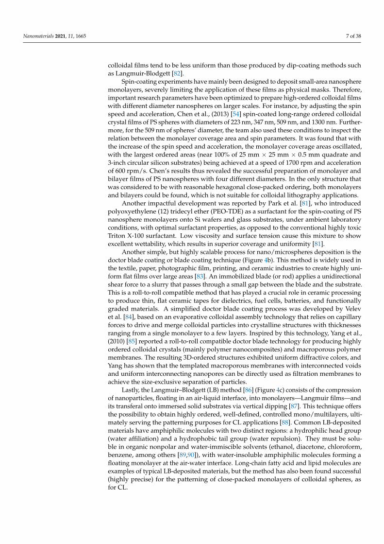
Three techniques should be emphasized when considering the initial step of colloidalmonolayer deposition on the substrate of the CL method (see Figure 2a). These are spin-coating, doctor blade, and Langmuir–Blodgett sketched in Figure 4 and described in thissub-section.
Figure 4. Production of a colloidal monolayer using (a) a spin-coating technique, (b) doctor blade trough, (c), and aLangmuir–Blodgett trough.
The spin-coating technique (Figure 4a) can be considered a simple process for rapidlydepositing thin coatings onto relatively flat substrates [54,79–81]. A spinning fixture holdsthe substrate (often using vacuum to clamp and position the substrate in place), and thecoating solution/dispersion is then dispensed onto the surface. The revolving action causesthe solution to spread out and leave behind a uniform coating of the chosen material onthe surface. Due to its short time of production, combined with its simplicity and low cost,this method is useful in industrial conditions as far as small-area batch coating processesare concerned. However, it is not compatible with large-area deposition, and the resulting
Nanomaterials 2021, 11, 1665 7 of 38
colloidal films tend to be less uniform than those produced by dip-coating methods suchas Langmuir-Blodgett [82].
Spin-coating experiments have mainly been designed to deposit small-area nanospheremonolayers, severely limiting the application of these films as physical masks. Therefore,important research parameters have been optimized to prepare high-ordered colloidal filmswith different diameter nanospheres on larger scales. For instance, by adjusting the spinspeed and acceleration, Chen et al., (2013) [54] spin-coated long-range ordered colloidalcrystal films of PS spheres with diameters of 223 nm, 347 nm, 509 nm, and 1300 nm. Further-more, for the 509 nm of spheres’ diameter, the team also used these conditions to inspect therelation between the monolayer coverage area and spin parameters. It was found that withthe increase of the spin speed and acceleration, the monolayer coverage areas oscillated,with the largest ordered areas (near 100% of 25 mm × 25 mm × 0.5 mm quadrate and3-inch circular silicon substrates) being achieved at a speed of 1700 rpm and accelerationof 600 rpm/s. Chen’s results thus revealed the successful preparation of monolayer andbilayer films of PS nanospheres with four different diameters. In the only structure thatwas considered to be with reasonable hexagonal close-packed ordering, both monolayersand bilayers could be found, which is not suitable for colloidal lithography applications.
Another impactful development was reported by Park et al. [81], who introducedpolyoxyethylene (12) tridecyl ether (PEO-TDE) as a surfactant for the spin-coating of PSnanosphere monolayers onto Si wafers and glass substrates, under ambient laboratoryconditions, with optimal surfactant properties, as opposed to the conventional highly toxicTriton X-100 surfactant. Low viscosity and surface tension cause this mixture to showexcellent wettability, which results in superior coverage and uniformity [81].
Another simple, but highly scalable process for nano/microspheres deposition is thedoctor blade coating or blade coating technique (Figure 4b). This method is widely used inthe textile, paper, photographic film, printing, and ceramic industries to create highly uni-form flat films over large areas [83]. An immobilized blade (or rod) applies a unidirectionalshear force to a slurry that passes through a small gap between the blade and the substrate.This is a roll-to-roll compatible method that has played a crucial role in ceramic processingto produce thin, flat ceramic tapes for dielectrics, fuel cells, batteries, and functionallygraded materials. A simplified doctor blade coating process was developed by Velevet al. [84], based on an evaporative colloidal assembly technology that relies on capillaryforces to drive and merge colloidal particles into crystalline structures with thicknessesranging from a single monolayer to a few layers. Inspired by this technology, Yang et al.,(2010) [85] reported a roll-to-roll compatible doctor blade technology for producing highlyordered colloidal crystals (mainly polymer nanocomposites) and macroporous polymermembranes. The resulting 3D-ordered structures exhibited uniform diffractive colors, andYang has shown that the templated macroporous membranes with interconnected voidsand uniform interconnecting nanopores can be directly used as filtration membranes toachieve the size-exclusive separation of particles.
Lastly, the Langmuir–Blodgett (LB) method [86] (Figure 4c) consists of the compressionof nanoparticles, floating in an air-liquid interface, into monolayers—Langmuir films—andits transferal onto immersed solid substrates via vertical dipping [87]. This technique offersthe possibility to obtain highly ordered, well-defined, controlled mono/multilayers, ulti-mately serving the patterning purposes for CL applications [88]. Common LB-depositedmaterials have amphiphilic molecules with two distinct regions: a hydrophilic head group(water affiliation) and a hydrophobic tail group (water repulsion). They must be solu-ble in organic nonpolar and water-immiscible solvents (ethanol, diacetone, chloroform,benzene, among others [89,90]), with water-insoluble amphiphilic molecules forming afloating monolayer at the air-water interface. Long-chain fatty acid and lipid molecules areexamples of typical LB-deposited materials, but the method has also been found successful(highly precise) for the patterning of close-packed monolayers of colloidal spheres, asfor CL.
Nanomaterials 2021, 11, 1665 8 of 38
The two main steps of the LB technique are the preparation of a floating self-assembledcolloidal monolayer at the air-water interface (Langmuir-film) and its deposition on a solidsubstrate [91]. At first, the colloidal particles are dispersed in a volatile and preferablywater-insoluble solvent to prepare the colloidal dispersion. Then, small amounts of thissolution are carefully deposited and spread onto the air-water interface at the LB trough.Afterward, the volatile solvent evaporates, and the LB barriers are compressed accord-ingly to force the formation of a self-assembled close-packed colloid monolayer at theinterface [88]. Finally, the immersed substrate is withdrawn vertically from the aqueoussubphase, while the lateral barriers continue to close in towards the substrate, at controlledrates, therefore transferring the colloids stabilized at the air/water interface to the upwardsmoving substrate [86], resulting in a successfully deposited monolayer colloidal film. Mul-tilayer films can also be engineered by successively subjecting the previously depositedsubstrate to further cycles of LB deposition. These multilayers have been considered modelmembranes due to their remarkable 3D uniformity; and offer potential application asphotonic waveguides and in breakthrough optoelectronic, nonlinear optical, and sensorydevices [92,93].
Surface and interface chemistry is of paramount importance for defining how the col-loidal particles float and are packed [32,33,81,94]. For instance, relatively small PS colloidswith sizes close to visible wavelengths (under 1 µm) tend to sink into the aqueous subphase,contrasting with larger ones that typically float [94]. The fabrication of monolayers byinterface coating methods as LB has been subject to numerous studies, varying the size ofcolloids, the amount of solution, temperature, deposition angle, and others [22,95–97].
It is also believed that the use of surfactants in the aqueous subphase may enhancethe floating and Langmuir-film production of colloidal particles at the air/water interface,with larger areas and mechanical strength, similarly to the solutions presented by Vogelet al., (2011) [94] for the spin-coating method. Surfactant molecules tend to occupy themedia interfaces and join the incoming colloidal particles together, thus opposing theirdispersion caused by the Brownian motion. The surface assembly forces tend to enlarge thearray area, increasing the monolayer order and coverage [95]. There is also a reduction ofsurface tension at the interface due to the presence of the surfactant, which favors colloidalparticle movement along the interface to find their lowest energy configuration, resultingin an optimally-ordered hexagonal close-packed monolayer [98]. Adding the surfactant,however, may introduce undesired contamination to the interface. Therefore, care must betaken to avoid the transfer of substantial amounts of contaminants to the substrate duringthe LB lift-up process, to avoid imperfections in the deposited colloidal array [79].
From the three methods mentioned above, the Langmuir-Blodgett method combinesquality, versatility, and scalability, being the headmost characteristics for the fabricationof high-quality 2D or 3D crystalline films. Furthermore, the capacity to precisely controlthe deposition of each layer in a layer-by-layer process, the ability to choose differentparticle sizes for each deposited layer, and the possibility for this method to be adaptedto fast industrial production techniques such as roll-to-roll processing [22,99–101] makeit an outstanding candidate for the first step of the CL process. These advantages aredemonstrated in the research of O. Sanchez-Sobrado et al. [29,33,48] that has revealedoutstanding results of thin-film solar cells enhanced with photonic front structures thatwere patterned via CL using highly-uniform LB-deposited colloidal masks.
2.3. Colloidal Masking for Surface Patterning
After achieving a good monolayer of close-packed colloidal particles, as previouslydescribed, it is then necessary to define how one can effectively use such array as amask to achieve the desired microstructures in the targeted material (recall Figure 2).The final structures and properties achieved by the CL process are highly dependenton the prepared mask of material and packing [102,103]. Although attaching functionalmolecules or coating materials to colloids offers various possibilities for additional tuning

Nanomaterials 2021, 11, 1665 9 of 38
of their properties [104], most polymeric or silica colloids end up being straightforwardlyassembled into monolayers without functionalization, for further processing in CL.
The use of the originally deposited close-packed colloids (Figure 2a) as a mask allowsonly a limited exposure area in the interstitial spaces of the hexagonal array. Therefore,increasing the inter-particle distance in non-close-packed arrays (Figure 2b) is an importanttool to optimize the masked area on the surface, at the expense of requiring an extraintermediate step of physical etching of the colloids.
Still, using the simpler CL version with close-packed 2D colloidal crystals as etchingmasks, triangular nanoparticles [105], nanodots [106], and thin-films with nanohole ar-rays [107], nanotips [108], or nanopillars [109] have been fabricated on several substrates(such as polymer-based, silica, and silicon) [65,69,97].
Regarding the formation of non-close-packed monolayers (Figure 2b), dry etchingmethods have been used (such as reactive ion etching, RIE) to reduce the size of thespheres after their deposition, and therefore increase their inter-space distancing in thearray (Figure 5).
Figure 5. Schematic illustration of the reduction of the colloidal spheres dimension (with 0.5 µm initial diameter) andincrease of their spacing in the array, via low-frequency plasma etching, with increasing etching time (left to right). Adaptedwith permission from [60]. Copyright 2021 MDPI.
A recent study from Yun Chen et al., (2019) [60] has shown that low-frequency plasmaetching (40 kHz) can be used to produce PS nanospheres-based arrays with smooth sur-faces, doubling the etching rate when compared to high-frequency systems. This studyrevealed that low-frequency RIE processes are dominated by a thermal evaporation etchingmechanism, different from the atom-scale dissociation mechanism that underlines thehigh-frequency etching. It was found that the PS features size can be precisely controlledby adjusting the etching time and/or power. By introducing oxygen as the assisting gas inthe low-frequency RIE system, one can achieve a coalesced PS particle array and use it, forinstance, as a template for metal-assisted chemical etching which can significantly improvethe aspect ratio of silicon nanowires to over 200 due to their improved flexure rigidity.
RIE has also been used in the CL fabrication of optimized photonic front structuresfor light-trapping in thin-film solar cells, which is crucial for increasing light absorbancein the absorber layer and subsequently the performance of the devices. Recently, twoefficient four-step approaches were described by Mendes et al., (2020) [52] that can producetwo types of geometries based on arrays of semi-spheroidal voids or domes, as shownin Figure 6. Briefly, for both cases, this method starts with the deposition of a monolayerof close-packed colloidal PS microspheres (LB method), followed by RIE producing anon-close-packed array.

Nanomaterials 2021, 11, 1665 10 of 38
Figure 6. Depiction of two different CL methods used to create distinct geometries of photonic microstructures for light-trapping, integrated in the front contact of thin-film solar cells, arranged in non-closed-packed hexagonal (honeycomb)arrays of semi-spheroidal voids (a) or domes (b) Adapted with permission from [52]. Copyright 2021 Elsevier.
The main difference between both approaches occurs in the first two steps. In thefirst method (Figure 6a), the selective RIE only acts on the particles, so the final void-likestructures are defined by the subsequent deposition of material in the inter-spaces betweenparticles (as in Figure 2c,d). Although in the second method (Figure 6b), the less-selectiveRIE process also etches the underlying layer, ultimately defining the final dome/cone-likestructures obtained.
Using etched nanospheres as molds/masks in processes such as metal deposition, in-filtration, or imprint, it has been possible to produce ordered arrays of spherical voids [110]and nanoshells [111,112]. Through dewetting around nanospheres, nanorings of poly-mers [113], carbon nanotubes, or nanoparticles [63] can be obtained. Resorting to site-selective deposition or etching, nanospheres with asymmetric shapes or functional featureshave been produced [114], difficult or impossible to obtain by other synthetic routes.
After the deposition of the intended material onto the RIE-shaped colloidal maskin step c) of Figure 2, a lift-off treatment removes the colloids (step d) leaving only themicrostructured material on the front surface. After this process, undesirable colloidalresidues may be found in the areas previously occupied by the particles, due to incomplete

Nanomaterials 2021, 11, 1665 11 of 38
removal. In such cases, besides the chemical removal (e.g., with toluene), both oxygenplasma [115] and thermal annealing [116] treatments can also be used to remove thepolymeric particle residues which are usually quite volatile at temperatures around 100 C.
3. Photonic Crystals
The previous section showed that there is a wide range of nano/micro-structuredesigns that can be engineered with CL techniques for various technologies, whose di-mensions are chiefly set by the size of the masking particles. The colloidal particles’ sizepropinquity to visible light’s wavelengths will therefore grant the fabricated structuresexcellent interaction properties with this type of radiation (Figure 7) [57,70,117–119].
Figure 7. Schematic optical interaction of (a) an ordered colloidal crystal and (b) an amorphous colloidal array under whitelight. The structural color from the colloidal crystal changes depending on the viewing angle, while that of the amorphousarray remains nearly unchanged.
It is important to note that photonic crystals have structural similarities with commoncrystals but have no direct relationship with crystalline materials. The dimensionalityof the photonic crystal is defined by the length(s) in which the dielectric constant variesperiodically, and they can be represented by basic 1D, 2D, and 3D crystals. However, only3D photonic crystals allow for omnidirectional photonic bandgaps [120] that are an opticalanalog of the energy bandgap of the crystalline network.
In nature, one can find many examples of natural photonic crystals (Figure 8), such asin wings of butterflies and natural opals (Figure 8a,b). These natural crystals are composedof periodic microstructures whose scattering and transmission properties strongly dependon the incident light frequency, thus displaying brilliant colors, which have inspiredartificial designs (Figure 8c,f).

Nanomaterials 2021, 11, 1665 12 of 38
Figure 8. Natural photonic crystals (left): (a) photo showing the blue iridescence and SEM image of the 1D structure of theMorpho butterfly, (b) photo of an opal gemstone, and SEM image of the silica sphere structure within it. Adapted withpermission from [121]. Copyright 2021 The Royal Society of Chemistry. Artificial fabricated photonic crystals deposited onflexible substrates made of semitransparent: (c) photonic crystal films and (d) photonic crystal films with anti-transmissionblack tape as the transferred substrate, which blocks backlight transmission [122], as well as (e) photo and (f) reflectancespectra of stripe-patterned composite photonic crystals with 20 different optical bandgaps. Adapted with permissionfrom [123]. Copyright 2021 John Wiley and Sons.
Due to their unique characteristics, photonic crystals fabricated via colloidal assemblyhave attracted much interest for various prospective applications, ranging from gas sens-ing to optical filters [124,125], photonic papers [126], inkless printing [127], flat reflectivedisplays [128], optical devices, photochemistry, and biological sensors [70]. Recent devel-opments have further enhanced their complexity using non-spherical particles [129,130],binary colloidal dispersions [131], as well as controlled production of 3D defects (actingas optical cavities) within the crystals [132,133]. Several approaches have been developedenabling defect engineering controlled to a great extent, such as surface micromachiningwhich allows for symmetries other than face-centered cubic [117,134].
Self-assembly has a crucial role in the fabrication of photonic crystals with a pho-tonic bandgap in the visible and near-infrared region [135]. For instance, freestandingfilms have been fabricated by the layer-by-layer assembly [136], solution casting [137],surfactant-assisted deposition [138], and filtration of dispersions of materials using mem-brane filters [61]. A facile approach to fabricate such large asymmetric free-standing 2Darray films is by forming 2D colloidal particle arrays at the air−water interface, as in the LBmethod [139]. Nevertheless, besides LB, colloidal photonic crystal growth via self-assemblyof monodispersed colloids can involve, as previously mentioned, various fabrication meth-ods such as controlled evaporation, spin coating, shear growth, among others.
Although the fabrication of 1D or 2D photonic crystals is relatively straightforward,adapting the conventional patterning techniques to fabricate 3D crystals remains a chal-lenge. This originates from the stringent constitutional quality, and functional requirements.Several methods have been proposed in this respect. The most economical and direct ap-proach to fabricating 3D photonic crystals is also by the self-organization of colloidalparticles. The most inexpensive and direct approach to fabricating 3D photonic crystalsis also by the self-organization of colloids that can be used as a template. Inverse opalsmaterials with a high degree of periodicity in three dimensions are important templatesfor the design of photonic crystals. One method used to prepare these photonic crystals

Nanomaterials 2021, 11, 1665 13 of 38
consists in infiltrating the void spaces between spheres in a colloidal crystal template withthe desired material in solution phase (sol-gel), which is subsequently solidified. Thesubsequent removal of the templating spheres leaves a structured photonic crystal [140].The sequential passivation reactive ion etching (SPRIE) method, [117] as the name suggests,relies on sequential passivation and reactive ion etching reactions using C4F8 and SF6plasma chemistries. It allows the addition of the third dimension using a simple and robustprotocol for direct structuring of silicon-based 3D photonic crystals. Through a singleprocessing step, SPRIE transcribes 2D colloidal crystal arrangements into well-ordered3D architectures. The lateral etch extent controls various 3D topologies, useful in thedelamination of 3D photonic crystals slabs or for the insertion of structural defects [117].
Alternatively, direct writing or single-step processing techniques have emerged aspowerful tools for rapid and scalable 3D photonic crystals fabrication. Multiphoton poly-merization lithography seems an attractive scenario, as it allows for unprecedented controlof the crystal geometry and the defect incorporation, although it suffers from low through-put due to the serial writing procedure [117]. By infiltrating the interstices of polymer latexcolloidal crystals with inorganic materials, and subsequently burning out the polymer latex,ordered macroporous films known as ‘inverse opals’ can be prepared. Inverse opals canhave higher reflectivity over wider optical stop gaps (which prohibits light from propagat-ing in only some directions) [121] due to the higher refractive index mismatch between thespheres and the medium. Such structures can also have 3D photonic bandgaps in the veryhigh-frequency regions. Despite their bandgaps being very narrow, these can be reducedeven further with the introduction of small defects, since they exhibit wider stop gapsand broader mechanical stability. For the production of inverse opal structures, colloidaltemplates of inorganic colloids (silica) can be used. Within this process, composites withpolymeric materials are formed and then converted to polymeric inverse opal structuresvia the removal of the inorganic particles using selective etchants such as hydrofluoricacid [141].
Non-crystalline colloidal arrays—photonic glasses (see Figure 8b)—have also muchinterest for certain applications. These structures consist of aggregates of monodispersecolloids with short-range order, over a range of a few particles, that can be detected fromthe structure’s diffraction pattern. Although photonic crystals can be used to manipulateballistic photons, photonic glasses are useful in controlling light diffusion. The randomstructures of designed uniform colloids can interact strongly with light and produceunusual diffusion phenomena, including random lasing, angle-independent color, and lightlocalization. These disordered monodisperse and short-range ordered particle structureshave been produced by destabilizing the colloids with the control of the salt concentration,or by adding particles of different sizes to the colloidal solution [141].
4. Photovoltaics Enhanced with Micro-Structuring
The amazing light-interaction properties of wavelength-sized structures overviewedin the previous section have motivated their development for optical manipulation inPV devices, aiming for maximum sunlight conversion to electrical power. In particular,thin-film solar cells suffer from significant absorption losses, relative to thicker wafer-basedcells, due to their diminished absorber thickness. As such, advanced light managementtechniques are necessary to compensate for such losses and ensure that high efficiencies areachieved [20,33]. As was already introduced, nanophotonic elements in the wave-opticsregime are seen as a promising method to efficiently trap light inside the thin absorbermaterial, thus boosting its broadband absorption, as further discussed in Section 4.1 [142].
The self-assembled templates from colloidal spheres can provide monolayers withlong-range order throughout large device areas, thus providing an inexpensive and easilyscalable mask to engineer materials with the physical parameters appropriate for efficientlight-trapping (LT) in solar cells. This has led to a significant interest in CL methods forphotovoltaic devices, which is the focus of this review. Nevertheless, the CL applications inthe PV field are not limited to the integration of LT structures. In the next sub-sections, we

Nanomaterials 2021, 11, 1665 14 of 38
will highlight two other promising nano/micro-structuring solutions that have also beendemonstrated with CL: namely for transparent electrodes (Section 4.2) and self-cleaningfunctionality (Section 4.3).
A review article by Wang (2018) [73] described that CL can produce several differentpatterns and geometries that could form an anti-reflective LT mechanism. It may includeJanus particles, hexagonal and non-close-packed single layers, double layers, free-standingfilms, and template-induced arrangements. The nanostructures obtained by this processcan already be promptly applied to many different areas. Furthermore, this technique canalso be adapted by tweaking the experimental parameters, such as the dimension of thespheres, the morphology of the surface, and chemical composition, thereby increasing thespectrum of possible applications.
Micro-meshed electrodes (MMEs) obtained by CL have been one of the most promisingapproaches to produce industrial-compatible transparent conducting materials (TCMs),with excellent optical transmittance and electrical conductance, composed of TCO/metal/TCO multilayers (TCO = transparent conductive oxide). In particular, replacing the intra-layer metallic film (usually silver) with a micro-grid of the same material has allowedadditional degrees of freedom to optimize the TCM performance, namely enabling muchhigher transparency in the red-NIR (near-infrared) spectral range while maintaining highlyconductive TCMs [62].
Besides efficiency, the outdoor reliability of PV systems is another crucial factornecessary for their widespread deployment. Solar panels tend to lose efficiency withtime mainly due to unavoidable environmental degradation. Phenomena such as theformation of hot-spots (areas of large heat dissipation) caused by partial shading of solarcells (e.g., due to debris/dirt deposits) can be responsible for pronounced efficiency lossesthat, for instance, have reached 11% in three days and 65% after six months in certainpower plants [74,143]. Therefore, decreasing unwanted processes that block the amountof sunlight reaching the cell, such as dust and other accumulation of particles, meritsparticular attention due to their inevitability and ubiquity [74].
Most current solutions to this include the mechanical cleaning of the devices [31] toexpel dust specks via four types of techniques: the robotic method, air-blowing method,water-blowing method, and ultrasonic vibration method. Nevertheless, such type of activemechanical methods requires a power source for enabling the self-cleaning mechanism.Moreover, manual cleaning can also create cracks on the PV panel surface due to harshbrushing which will further deteriorate PV performance. Moreover, very small particlescannot be removed effectively by a manual cleaning process. On the other hand, the useof a self-cleaning coating, as no PV panel movement is required for its working function,is way simpler and more fitting to PV applications [74]. Another active method—theelectrostatic cleaning method [144]—expels the surface dust through electrostatic standingand traveling waves, due to an existing electric curtain. The electric curtain consists of aseries of parallel electrodes embedded in a dielectric surface, across which are transmittedoscillations in the electrode potentials. During this process, the standing wave oscillatesthe dust particles up and downward while a traveling wave does the same process in ahorizontal direction.
Concerning passive coating methods, they employ either a superhydrophilic or super-hydrophobic film on the outer PV surface. Superhydrophilic coatings reduce the amountof dirt through photocatalytic reactions, while superhydrophobic coatings potentiate theformation of water droplets and their roll-off, carrying away the dirt from the surfaceswith minimum water usage [31,74]. To allow water (or other liquids) droplets to effectivelyroll down a surface, different superhydrophobic-oriented strategies are being investigatedmainly via surface micro-structuring, mimicking natural processes such as the skin ofcertain plant leaves with self-cleaning capability [145], as further detailed in Section 4.3.
The aforementioned applications reveal that CL offers a wide range of promisingpossibilities for the advancement of PV-related technologies, as illustrated in Figure 9 andelaborated in the following sections.

Nanomaterials 2021, 11, 1665 15 of 38
Figure 9. Illustration of the distinct applications of CL for micro-structuring in photovoltaics. Adapted with permissionfrom [62]. Copyright 2021 Elsevier. Adapted with permission from [52]. Copyright 2021 Elsevier. Adapted with permissionfrom [31]. Copyright 2021 John Wiley and Sons.
4.1. Light-Trapping in Photovoltaics
Light-trapping (LT) structures are a critical enabling factor in PV technology, asthey improve the absorption of incident photons, therefore impacting its conversion effi-ciency [23,29,31,51,52,62,146,147].
On one hand, reflection losses are an unavoidable shortcoming in all types of PVtechnologies. Proper index matching in the surface—using materials with an index betweenthat of the absorber material and the light incidence medium—can help mitigate thisproblem. Photonic structures can further diminish these losses in a broad wavelengthrange—by providing geometric index matching.
On the other hand, these structures also bring about LT mechanisms to help with lightmanagement within the device. As previously mentioned, this is particularly important forthin-film solar cells, where the short optical path is not enough to absorb all the incomingsolar radiation, and it can be useful also for other emerging solar technologies [148].This shortcoming has also been severely hindering flexible thin-film PV technology fromachieving its market potential. As a matter of fact, many thin solar cells have so far onlyreached modest efficiencies (~14%) compared to those of conventional cells based on rigidsilicon wafers (22–25%). Therefore, there is much improvement potential in thin-film PVwith the implementation of effective LT techniques, mainly as a means to make the cellsoptically thicker but without increasing their physical thickness (to allow efficient chargescollection) [52].
Here, a detailed analysis is presented of different types of photonic structures inte-grated via CL methods for LT in thin-film solar cells, particularly based in silicon andperovskite PV materials, enabling the development of high-efficiency flexible devices.

Nanomaterials 2021, 11, 1665 16 of 38
4.1.1. Computational Design and Optimization of Photonic Solutions
The resonant nature of wavelength-sized photonic structures substantially limitsthe parameter space in which their optical effects can provide exceptional absorptionimprovements across the relevant sunlight spectrum. Specifically, the wave-optical frontfeatures (as those integrated via the CL methods of Figure 6) need to provide a graduallyvarying effective refractive index, from the air towards the absorber layer to minimizereflection. Simultaneously, their geometry must interact with the incoming light to producestrong scattered fields preferentially directed into the higher index absorber layer. Therefore,before experimental implementation, it is crucial to perform a rigorous screening basedon modeling, to understand the influence that the parameters of the LT structures haveon such effects, and then appropriately search for the best parameter set that allows thehighest photocurrent enhancement in the devices [142,149,150].
Theoretical studies reported by Mendes et al., (2016 and 2018) [142,149] have soughtfor designs of wavelength-sized structures optimized towards maximum broadband lightabsorption, with the double aim of enabling the reduction of the absorbing layer thickness(potentiating flexibility) while improving the efficiency of thin solar cells (Figure 10).Two geometries of front-located photonic structures were pointed out, compatible withthe CL fabrication methods of Figure 6, and computationally optimized to maximizeabsorption without degrading the electrical performance of the devices (by avoidingincreased recombination since the absorber layer remains flat, i.e., it is not corrugated asoccurs with texturing).
Figure 10. Electromagnetic modeling results of two types of LT geometries (sketched in a,d) composed of hexagonal arraysof TiO2 half-spheroids (a–c) or semi-spheroidal voids in a TiO2 or AZO layer (d–f), both integrated into thin-film (300 nm)Si solar cells. The results show the light absorption, Abs, spectra (b,e) and photogeneration rate, G, profiles (c,f) of theoptimized photonic front structures, compared with flat reference cell structures without LT or with a standard AZOantireflection coating (ARC). The G profiles reveal much higher carrier generation in the cells with the photonic elementsdue to the enhanced broadband absorption. Adapted with permission from [142]. Copyright 2021 Elsevier.

Nanomaterials 2021, 11, 1665 17 of 38
These LT structures are composed of honeycomb arrays of semi-spheroidal featureseither made of domes (TiO2 half-spheroids separated by a flat aluminum-doped zincoxide—AZO—layer—Figure 10a) or voids (semi-spheroidal holes in a layer of eitherTiO2 or AZO—Figure 10d). The electromagnetic field distribution simulations in thethin-film solar cell structures were carried out using a 3D Finite Difference Time Domain(FDTD) method.
The modeling results show that the structures patterned on the front of the cellsdrastically reduce reflection losses at short wavelengths—Figure 10b,e (at energies abovethe absorber bandgap)—via geometrical refractive index matching with the cell media.They also boost the absorption of longer wavelengths by increasing their path length vialight bending and coupling with wave-guided modes confined in the absorber layer.
These combined effects (antireflection and light scattering) lead to a substantial broad-band absorption enhancement in the absorber material, which allows reducing its thicknesswithout lowering the output current.
When evaluating the different LT geometries, it was found that the optimized absorp-tion spectra attained with the two types of structures do not differ significantly. Neverthe-less, the highest photocurrent gains were generally provided by the void geometry dueto higher NIR absorption enhancement, as it allows a higher degree of angular spreadingof the scattered light. Simultaneously, the domes tend to act as micro-lenses that insteadfocus the scattered light in localized hot-spots located beneath them, as observed in theoptical generation profiles of Figure 10c,f.
Pronounced photocurrent enhancements, up to 37%, 27%, and 48%, are demonstratedwith honeycomb arrays of semi-spheroidal dome or void-like elements front-patterned onthe cells with ultrathin (100 and 300 nm thick) amorphous, and thin (1.5 µm) crystallinesilicon absorbers, respectively [142].
The geometrical optics limits for photocurrent enhancement via LT are known asthe Lambertian or Green broadband absorption limits. Isabella et al. [147] purposed anadvanced LT scheme applied to thin-film silicon-based solar cells, capable of actuallyovercoming such limits. They showed that optimized 3D optical modeling of thin-film hy-drogenated nanocrystalline silicon (nc-Si:H) solar cells endowed with decoupled front andback textures, result in pronounced photocurrent densities (>36 mA/cm2), thus developinga suitable base for the fabrication of high-efficiency single and multi-junction thin-film solarcells. The simulated enhancements result from a gain in light absorption, especially in theNIR part of the spectrum close to the bandgap of nc-Si:H. Within this wavelength region,the material is weakly absorbing, whereas with the LT design of Isabella et al., significantabsorption peaks are observed that can only be explained by the simultaneous excitationof guided resonances by front and rear textures. Using the same advanced LT employedfor nc-Si:H, one would obtain a very high implied photocurrent density of 41.1 mA/cm2
for a device with a 2-µm thick absorber.A recent breakthrough contribution by Li et al. [151] showed that the Green light
absorption limit can also be approached without the need for complex LT geometries. Withsimple (yet smartly designed) grating structures, composed of checkerboard and/or pentaarrangements, the photocurrent of thin-film silicon cells can be realistically doubled, thusrevealing performance improvements at the level of the most sophisticated LT gratingstructures but here attained with much simpler (hence industrial-friendly) geometries.
4.1.2. Thin-Film Solar Cells Improved with Front-Located Photonic Structures
Guided by the modeling studies, in the past few years, LT mechanisms have beensuccessfully implemented in both rigid and flexible solar cell devices with promisingexperimental results. In this section, we summarize some of these results and the progressthat has been achieved in practice. The LT mechanisms, in addition to allowing remarkableenhancement of the optical density of ultrathin PV films, can be fabricated with low-costmaterials and integrated by industrial-scale procedures via inexpensive and large-area

Nanomaterials 2021, 11, 1665 18 of 38
soft-lithography processes. Accordingly, colloidal lithography has been applied to patternthin-film solar cells on a photonic length scale with low manufacturing costs.
The simplest CL-related LT implementation consists of using the close-packed arrayof colloidal spheres (Figure 2a), self-assembled on the front contact of the solar cells, notas a mask but as the photonic front structure itself. This allows forming the photonicstructures with a single step performed as a post-process on the cells, as it avoids theadditional colloidal masking steps. Such an approach was tested by Grandidier et al. [26],employing a monolayer of silica nanospheres deposited by Langmuir-Blodgett on the frontTCO of hydrogenated amorphous silicon (a-Si:H) solar cells. In this design the dielectriccolloids act as resonant Mie scatterers, coupling light into the absorber via their near-field proximity. At the same time, it acts in the far-field as a graded-index antireflectioncoating to further improve the photocurrent. Overall, even though the simple approach ofGrandidier et al. allowed significant enhancements in the photocurrent (average of 6.3%)and efficiency (1.8%, reaching the absolute value of 11.1%), the attained gains are relativelylow in comparison with those shown in Figure 10, predicted with optimized LT structures.One of the main reasons for this has to do with the low refractive index (n~1.5) of the silicaspheres, while higher n values are desired for stronger antireflection and light scatteringaction, as indicated by the theoretical models [149].
As such, photonic structures composed of high-index dielectric materials, (e.g., TiO2)as suggested in the simulation works reported in Section 4.1.1, should be capable of yieldingmuch more pronounced enhancements. Given that, Sanchez-Sobrado et al. [33] (Figure 11)developed a CL technique aimed at engineering the TiO2 semi-spheroidal void-like arraygeometry of Figure 6b. The TiO2-based wave-optical structures were first integrated byCL on the front surface of a-Si:H thin-film absorbers, to optimize the parameters of thefabrication method while looking at the absorption enhancement caused in the films.
Figure 11. Schematic drawings and SEM pictures of the samples obtained after the different steps ofthe TiO2 nanostructure construction via CL on glass substrates: (a) a hexagonal array of colloidal PSspheres is patterned on the cell front, (b) O2 dry etching, (c) TiO2 is deposited, filling the inter-particlespaces, (d) the spheres are removed leaving an array of semi-spheroidal void-like features. Thefinal TiO2 structure (e) uniformly covers the entire sample area. Adapted with permission from [33].Copyright 2021 The Royal Society of Chemistry.
The method developed by the authors employs the four main steps illustrated inFigure 11: (a) deposition of periodic close-packed arrays of PS colloids (original diameter

Nanomaterials 2021, 11, 1665 19 of 38
of 1.0 µm, 1.5 µm or 2.0 µm) which act as the mask, (b) shaping the particles and increasingtheir spacing via dry etching, (c) infiltration of TiO2 in the inter-particles spacing and (d)removal of the PS particles to leave only the nanostructured TiO2 layer [33].
It was demonstrated that when directly deposited on a-Si:H absorber films, suchLT microstructures provided pronounced broadband absorption enhancement (27.3% onspectral average) in the a-Si:H medium relative to the unpatterned sample.
In subsequent work [48], the authors advanced to integrating this type of photonicstructure in actual solar cell devices by CL. These were implemented as a top coating(see Figure 12), with two different materials tested for the photonic coatings in this work:TiO2, due to its high refraction index, and indium zinc oxide (IZO), for better optical andelectrical coupling with the front contact of the cells composed of a flat IZO layer.
Figure 12. (a) SEM images of the cross-section of an a-Si:H solar cell coated with a TiO2-based LT structure (patterned byCL) over its front flat IZO contact; (b) Measured J-V curves of solar cells incorporating four different photonic coatings madeof either TiO2 or IZO and formed with either 1.3 or 1.6 µm diameter PS spheres, and compared with the curve of the planarreference cell with no LT structure over the IZO contact; (c) measured and theoretically modeled enhancement, relativeto the reference, of the generated current density (dark grey and empty bars, respectively), and the measured conversionefficiency (light grey bars) of the devices in (b). Adapted with permission from [48]. Copyright 2021 The Royal Societyof Chemistry.
It was observed that all the different photonic structures applied on the a:Si:H cellsproduced significant broadband absorption enhancement, leading to systematic increasesin the current (17.6–21.5%, Figure 12c), relative to that of the planar reference cells withoutthe LT features. The TiO2 structures achieved higher optical performance than the IZOones, as expected, mostly due to the higher refractive index and lower optical absorption

Nanomaterials 2021, 11, 1665 20 of 38
of TiO2. Nevertheless, the extra electrical benefits (reduced sheet resistance) on the frontelectrode caused by the IZO structures allowed for the highest efficiency enhancement(Figure 12c) [48].
Given the promising results attained with the photonic-structured IZO front contacts,in a subsequent work Sanchez-Sobrado et al., (2020) [29] further improved the devicearchitecture and CL process parameters to further optimize the geometry of the IZOstructures and, importantly, their location concerning the Si absorber. This was achievedby optimization of the thickness (investigating from 30 to 250 nm) of the flat IZO layerbeneath the LT structures, to allow an electrically effective front contact ideally coupledwith the geometry of the CL-patterned IZO structures (Figure 13).
Figure 13. SEM cross-sections of a-Si:H solar cells with two different thicknesses of the flat IZO layer(30 (a) and 190 nm (b), respectively) located between the a-Si: H absorber and the front LT structures;(c) Polar plot representing the angular response of the solar cells with 30 nm, S30 (blue lines), and with190 nm of IZO thickness, S190 (red lines), in terms of the gains attained in the short-circuit currentdensity, (JSC, solid lines) and power-conversion efficiency (PCE, dashed lines) of the cells; (d) J-Vcurves and (e) external quantum efficiency obtained for S190 (190 nm of IZO thickness). Adaptedwith permission from [29]. Copyright 2021 Elsevier.
Here, the CL fabrication method consisted of first dispersing a colloidal suspension of1.6 µm PS spheres in a water-ethanol mixture (1:3) at a solution concentration of 2.5% wt.Using the Langmuir–Blodgett technique [152], a close-packed monolayer was then de-posited onto the flat IZO-coated surface of the a-Si:H cells.
The final IZO structure is revealed after removing the PS particle mask by a combina-tion of Ar/CF4 reactive ion etching and a toluene bath.
As previously mentioned, the main parameter optimized in this work was the thick-ness of the flat IZO layer deposited on the cell before the CL process of integrating the topmicrostructured IZO. Such thickness defines the separation between the a-Si:H absorberand the photonic features, and the best results were attained with 30 nm and 190 nmthicknesses, shown in Figure 13a. These results reveal that the LT structures lead to aremarkable broadband enhancement of the total light absorbed by the devices, thereforeleading to photocurrent gains (relative to reference planar cells) up to 26.7% with the 30 nmflat IZO space—Figure 13c. However, the best efficiency enhancement (23.1%) was attainedwith the optimized thickness of 190 nm for this layer (Figure 13d,e), as it provides the mostfavorable combination of optical and electrical gains.

Nanomaterials 2021, 11, 1665 21 of 38
Another important finding of this work was the remarkable LT gains attained atoblique light incidence. The angular response of the devices was evaluated by measuringthe JV curve for a range of light incidence angles from 0 to 90. The highest gain reaches53.2% enhancement in photocurrent at 70 incidence angle for the cell with the optimized190 nm thick flat IZO, and 52.2 in efficiency (at 40 incidence) with the ultrathin (30 nm)flat IZO (Figure 13e) [29].
4.1.3. Photonic-Enhanced Perovskite Solar Cells and CL Compatibility
Perovskite-based PV materials, as thin-film absorbers for perovskite solar cells (PSCs)[153], have received unprecedented attention in both academia and industry due to theexceptionally rapid efficiency advancement from ~3.8% to >25.2% over the last decade[30,154]. As usual, for most PV technologies in the early stages of development, theprogress was mainly accomplished by exploring the composition of perovskite-basedmaterials and optimizing the fabrication process of the perovskite layer, as well as thequality of the cells’ interfaces to ensure efficient charge collection and to suppress unwantedrecombination routes [155]. As such, PSCs have reached a stable point in the developmentphase, and optical strategies are now paramount to advance beyond its current recordefficiency, particularly for the thinner perovskite layers which are attractive to enable deviceflexibility [156].
The rapid progress in this PV technology has enabled improved PSC depositionmethods allowing conformal coating of the cell layers onto microstructured substrates,resulting in improved efficiencies. This is a promising path that has only recently startedbeing unraveled for nano/micro-structuring in the PSCs field. Photonic microstructurescan improve the cells’ absorption beyond the standard values achieved with planar devices,facilitating thickness reduction without compromising the output current and withoutdegrading the electrical performance. On the other hand, the operational stability ofthe devices can also be improved by blocking the harmful higher-energy photons of UVradiation. This is particularly advantageous to assist in the stability of this less-matured PVtechnology which quickly degrades with UV exposure [52].
Recently, several LT schemes have been shown to improve the performance of PSCs,such as disordered micro-pyramids [155,156], nanojets, corrugated substrates, self-cleaningnanostructures, and micro-cones [157], as well as other approaches such as plasmonicnanoparticles, surface plasmon resonances, down and/or upconversion, etc. [158–160]. Itis also observed that simple grating structures in the front [161] and back electrodes [162]enable enhancement in the light absorption and PSCs stability.
CL can play an incredible role in thin-film PV process technology due to its compatibil-ity with large-scale (even roll-to-roll) manufacturing. The developed low-cost CL processescommented in the previous sections, for the integration of LT structures in silicon-basedsolar cells [29,31], can be adapted for photonic-structuring in PSCs. Previous theoreticalcontributions presented novel LT designs [27,28], operating in the wave-optics regime thatdemonstrated record photocurrent gains in PSCs via the incorporation of wavelength-sizedfeatures in the front electron transport layer (ETL) of the cells with a substrate configuration,similarly to the integration discussed in detail in Section 4.1.2. Interestingly, it was shownthat the proposed front-patterned TiO2 LT coatings also lead to UV stability improve-ments [27], with even better results being achieved by incorporating another front-locatedluminescent down-shifting layer that can convert the harmful UV photons to non-harmfulvisible photons [28]. These structures can be straightforwardly fabricated using the sameprocedures of CL (Figure 6) as those developed for silicon-based solar cells [29,31], asfurther detailed next.
The initial simulation work by Haque et al., (2019) [27] considered an inverted(substrate-type) PSC architecture, allowing the integration of the LT structures as a post-process on the front contact of the cells, in a similar way as in Figure 12 for thin-filmsilicon cells. The wave-optical structures optimized by the authors (Figure 14) for the

Nanomaterials 2021, 11, 1665 22 of 38
inverted PSCs are also based on high-index dielectric (TiO2) micro-scale features, withsemi-spheroidal geometries.
Figure 14. (a) Photocurrent enhancements attained with the optimized photonic structures presented in Haque’s work.(b) Light absorption spectra of PSCs with (photonic-enhanced) and without (planar) the optimized LT structures integratedinto the ETL of the cell—a low absorption in the UV region indicates the desired blocking effect caused by the photonicstructure. Adapted with permission from [27]. Copyright 2021 Elsevier. (c) Sketch of the luminescent down-shifting materialencapsulating the photonic-structured PSC. (d) Jph values obtained considering the full UV-Visible-NIR wavelength range(300–1000 nm), for two different refractive indexes (n) values of the encapsulating media. (e) UV photocurrent (Jph-UV)values for wavelengths ranging from 300 to 400 nm (the more transparent bars refer to the devices with 250 nm perovskitethickness, while the others refer to those with 500 nm). Adapted with permission from [28]. Copyright 2021 AmericanChemical Society.
The optically lossless TiO2 material allows the structures to be patterned in the finalprocessing steps, integrated into the top n contact of the cell. This, in turn, avoids structur-ing the cell layers, thence avoiding increased roughness and consequent electrical lossesdue to higher recombination. The electromagnetic field distribution simulations in the PSCstructures were also carried out using the same FDTD method of Figure 10, and the mainresults are summarized in Figure 14a. In particular, the optimized array of TiO2 voids,which was shown to be optically favorable when compared with the domes, enables aphotocurrent enhancement of 21% and 27% in PSCs with conventional (500 nm thick) andultrathin (250 nm) perovskite layers, respectively.
The photocurrent enhancements attained with the optimized LT designs are mainlydue to absorption improvements for wavelengths above 600 nm, which the authors attributeto strong antireflection (of visible light) and light scattering effects (of near-infrared), asshown in Figure 14b.
Furthermore, the TiO2 material of the structures advantageously acts as a UV blockinglayer, as also shown in Figure 14b, protecting the perovskite from known degradation

Nanomaterials 2021, 11, 1665 23 of 38
mechanisms caused by UV penetration [163–165]. Here the UV light is absorbed in the frontTiO2 features and does not reach the perovskite, while the light at the longer visible plusNIR wavelengths is coupled and trapped within the cells, generating an overall enhancedphotocurrent. UV blocking mechanisms as this one can enhance the operational stability ofPSCs upon solar exposure, but inevitably they prevent the conversion of the UV energy bythe cell, so they are not the ultimate solution when aiming for maximizing efficiency.
Alexandre et al. [28] presented an interesting approach to exploit such, otherwiselost, UV energy via the combined effects of LT and luminescent down-shifting (LDS).Simply put, this latter effect shifts higher energy light into lower-energy light. Consideringthe extensively studied degradation problems of PSCs with UV radiation [166,167], thismethod can bypass these unwanted mechanisms while also recurring to the energy comingfrom the UV photons.
The use of optimized LDS materials in the front encapsulation of the previous photonic-enhanced PSCs designed by Haque et al. (Figure 14c) led to an increase in photocurrentof at best 2% (~0.6 mA/cm2), which is almost half of the theoretical maximum current(1.4 mA/cm2) that could be gained from all the UV range. The optimum spectral down-shift was found to be from a central 350 nm UV wavelength to around 500 nm visiblewavelength, matching well with the electrical performance peak of PSCs, which couldimply that an increased device’s efficiency surpassed the projected gains. The LT cellsalso revealed a decrease in the harmful TiO2 photogeneration near the perovskite/TiO2interface due to the LT structures’ UV shading effect. By assessing the UV penetrationin the perovskite material (given by the UV generated photocurrent by the PSC) for thedifferent simulated cells, reductions up to 86% (Figure 14d) were obtained when comparingphotocurrent values for the original (pristine) and optimized down-shifted spectrum.Therefore, these analyses show that the use of LDS provides a more effective way toeliminate the unwanted effects of UV radiation in the perovskite, demonstrated by thehefty decrease in UV absorption coupled with the diminished TiO2 photoactivity fromlower photogeneration, while also enabling additional power generation from the UVportion of the sunlight [28].
Although promising and compatible with CL structuring, the aforementioned LTimplementations in Figure 14 require the photonic elements to be patterned on top of theplanar cell layers during the final processing stages, which brings the risk of degrading thehighly sensitive PSC materials located underneath [52]. Specifically, the fast degradation ofPSCs with humidity exposure may render this class of devices incompatible with immersionor coating with aqueous solutions, as required in the first steps of the CL process (seeSection 2.2).
Given this, Haque et al., (2020) [30] investigated a more industrially viable LT strategyconsisting of the development of photonic substrates used for subsequent PSC deposition.The authors have shown that it is possible to achieve pronounced broadband absorptionenhancement provided by the LT-patterned substrates, relative to planar cells, which wasalso observed for a broad range of incidence angles (0–70 degrees), as seen in Figure 15a.Apart from substantial light absorption enhancement, this approach has a significantadvantage for its practical compatibility with PSC technology over the previous ones, asthe PSC layers can be wet coated by traditional methods onto a substrate already patternedwith the designed LT structure.

Nanomaterials 2021, 11, 1665 24 of 38
Figure 15. (a) The polar plot shows the photocurrent density gain as a function of the incidence angle (θ), attained with theoptimized photonic-structured PSCs in a conformal architecture, for both the substrate and superstrate cell configurationsillustrated in the middle and right sketches. The Lambertian limits of LT in PSCs, in the geometrical optics regime, are alsoindicated for normal incidence angle (θ = 0) in the left plot. Adapted with permission from [30]. Copyright 2021 Elsevier.(b) SEM image of a single-junction PSC conformally coated onto a textured glass substrate. Adapted with permissionfrom [168]. Copyright 2021 Elsevier. (c) SEM image of a tandem perovskite/silicon cell with ~25.1% efficiency, in whichthe PSC is conformally coated onto the textured silicon wafer-based bottom cell [169]. (d) SEM image of a triple-junctionperovskite/perovskite/silicon cell in which the top and middle PSCs are also conformally deposited onto textured silicon.Adapted with permission from [170]. Copyright 2021 American Chemical Society.
This makes the full photonic integration independent of the fabrication of the PSCs.Moreover, this is a potentially more cost-effective approach since it requires no extramaterials (coatings) for the LT structuring.
However, the LT designs of Figure 15a are only achievable with highly conformal PSCdeposition methods, capable of coating the cell layers onto the micro-patterned substratesurfaces without defect formation. In that respect, the work of Wang et al. [168] is animportant contribution, as the authors developed a recrystallization treatment that enabledthe conformal coating of high-quality perovskite layers onto textured glass with featuresin the order of the micrometer, resulting in 18.6% PSC efficiency with a ~300 nm thinperovskite absorber, as seen in Figure 15b.
Conformal deposition methods have also shown remarkable potential in monolithictandem PV cells, in which perovskite-based top cells are coated onto fully textured crystallinesilicon bottom cells. That is the case of the perovskite/silicon double-junctions developed byAydin et al. [169] with 25.1% efficiency (Figure 15c) and the perovskite/perovskite/silicontriple-junctions (Figure 15d) of Werner et al. [170] reaching ~2.7 V.

Nanomaterials 2021, 11, 1665 25 of 38
Within this section, we went through some of the latest trends on LT strategies forPSCs, revealing promising modeling results with optimized designs for efficiency andstability improvement. We also discuss the first experimental steps that have been re-cently undertaken to circumvent the challenges associated with the practical realization ofphotonic-structured PSCs, which is a new avenue for CL implementation with enormouspotential in the PV field.
4.2. Micro-Meshed Transparent Electrodes
Another highly promising solution offered by nano/micro-structuring is the devel-opment of high-performing transparent electrodes, with strong interest not only for theilluminated contacts of solar cells but also for many other optoelectronic applications.Nano/microstructured metallic films (termed micro-mesh electrodes, MMEs) offer anexciting alternative to flat TCO (transparent conductive oxide) layers, and CL was shownto be one of the most promising approaches to produce industrial-compatible MMEs withexcellent properties [62].
State-of-the-art indium tin oxide (ITO) based TCOs are ubiquitously spread in opto-electronic technologies as they are in the illuminated contacts of solar cells, in displays,touch screens, and light-emitting diodes, with low sheet resistances between 8 and 12 Ω/(for commercial ITO) [171] and optical transmittance above 80% in the visible range [62,172].However, as with most TCO materials, their free electrons cause strong parasitic absorptionlosses in the NIR range, limiting their performance for solar cell applications. This is furthercompounded by the rising cost of In, a rare material, while alternative TCOs made withEarth-abundant materials (e.g., based in ZnO [173]) offer reduced figures-of-merit in termsof transmittance-over-resistance ratio. Furthermore, ITO is usually deposited by costlyDC-magnetron sputtering involving high temperatures (up to 300 C) [174], making itunsuitable for deposition on thermal-sensitive materials. Moreover, ITO is brittle, makingit also less attractive for flexible electronics as well as resistive touch screens [175].
A solution to mitigate the issues of state-of-the-art TCOs is to use a metallic micro-grid (MMEs) sandwiched between ultrathin layers of TCO, which allows a pronouncedincrease in transparency (especially in the red-NIR region) while maintaining high sheetconductance; thus, offering an exciting alternative to flat TCOs. CL provides a promis-ing approach to produce industrial-compatible MMEs, as demonstrated with the copper(Cu) nanomeshes developed by Gao et al., (2014) [175] exhibiting an excellent diffusetransmission of 80% and sheet resistance of 17 Ω/ (Figure 16a,b).
More recently, Torrisi et al., (2019) [62] have shown the use of CL to create silver (Ag)micro-grids that were sandwiched between TCO layers. First, a PS colloidal microspheremonolayer (deposited using the Langmuir–Blodgett technique) is submitted to plasmaetching to serve as a deposition mask. The subsequent evaporation of Ag throughout thismask, followed by lift-off of the colloids, creates a metallic grid as shown in Figure 16c,d.Compared to conventional transparent electrodes (i.e., ITO), excellent electrical and opticalcharacteristics have been accomplished with such TCO/Ag micro-grid/TCO multilayers,such as sheet resistances below 10 Ω/ and pronouncedly higher near-infrared transmit-tance, using different layer thicknesses and mesh dimensions (Figure 16e).
The structural parameters of the produced mesh (openings, line width, and thickness)play a vital role in the electrical and optical performance of the transparent electrodes.Larger hole structures, attained with large sizes of the PS colloids, result in excellenttransmittance values at the cost of increased sheet resistance. Alternatively, meshes withsmaller holes are less transparent but have a lower resistance, permitting higher cur-rents (Figure 16f). To reduce the sheet resistance values, one can also increase the metalgrid thickness, by evaporating more Ag material, without having a large effect on trans-parency [62]. Finally, the best performing correlation between optical and electrical prop-erties (Figure 16g) is attained with 5 µm spheres and 17 nm Ag thickness, either (120 or240s RIE).

Nanomaterials 2021, 11, 1665 26 of 38
Figure 16. (a) Schematic of the Cu MME fabrication process by CL. (b) Plot of the measured diffusetransmission, specular transmission, reflection, and absorption at λ = 550 nm versus sheet resistancefor a variety of Cu MMEs on quartz. Adapted with permission from [172]. Copyright 2021 AmericanChemical Society. (c,d) Schematic of the CL fabrication of Ag MMEs, showing the initially depositedPS sphere mask (c) and the final structure of the IZO/Ag grid/IZO electrode (d), in which the topand bottom IZO layers are ultrathin (30 nm). (e) Transmittance of samples with 17 nm thick Ag grids(blue and red lines), produced with distinct sphere size and etching time, compared to a continuousAg film (grey line)—high transparency can be noted in the NIR region. (f) Sheet resistance of theelectrodes fabricated with different diameters of PS spheres (1.6 or 5 µm), etching time, and Agthickness. (g) Haacke’s figure-of-merit (expression in inset) for the main MMEs attained in this work,in comparison with a state-of-the-art TCO film made of ITO and with continuous (planar) Ag layers.Adapted with permission from [62]. Copyright 2021 Elsevier.
It is also believed that the use of metallic grids for electrodes when compared tocontinuous layers, can bring several advantages for flexible transparent materials. Inparticular, honeycomb grids as produced via CL allow the highest flexural robustnesswith thinner MME structures [175], due to the fact that the honeycomb lattice enables thehighest packing density in 2D arrays. Overall, the use of metallic micro-grids opens newand promising paths for transparent electronics, offering additional degrees of freedom forfurther electro-optical improvements. Specifically, their much higher transmission if the red-NIR region can be crucial for applications such as smart windows, low-energy photovoltaicdevices, and as intermediate contacts in multi-terminal multi-junction (tandem) solar cellarchitectures [176,177].
4.3. Self-Cleaning with Photonic Structuring
Unavoidable environmental degradation is a major cause of efficiency losses in solarpanels over time. Phenomena such as the formation of hot-spots (areas of large heatdissipation) caused by partial shading of solar cells can be responsible for large efficiencylosses [74,143]. Among different solutions mentioned at the beginning of Section 4, theuse of a self-cleaning coating appears to be the simplest and most fitting approach forlarge-scale PV installations [74], as no mechanical structure is required for its cleaningfunction.
Through superhydrophobic coatings, the concept of self-cleaning glass materialsshowed a maturing research trend between 2009 and 2017, with 1125 research articles

Nanomaterials 2021, 11, 1665 27 of 38
being published (ScienceDirect keywords: “self-cleaning glass, superhydrophobic glass”).These coatings can be fabricated using top-down approaches such as template-based,photolithographic, and surface plasma treatment [178], or top-down methods such aschemical modification [179], colloidal assembly [180], layer-by-layer deposition [181], andsol-gel methods [182] can also be applied [74].
An important application for PV technology was presented by Centeno et al., (2020) [31],showing a simple, low-temperature, low-cost, and scalable CL method (Figure 17a) toengineer parylene-C (poly(chloro-p-xylylene)) coatings with encapsulating properties thatendow effective light-trapping (LT) and water-repelling functionality when applied inthin-film solar cells (Figure 17b–e). Parylene-C was used as the preferred coating material,as it is a polymer with excellent barrier properties for encapsulation [183,184] and lowwater-adhesion surface energy.
Figure 17. (a) Depiction of the patterning of the photonic-structured parylene-C coating on the trans-parent front contact of thin-film silicon solar cells, via chemical vapor deposition (CVD), followedby CL with a patterning approach similar to that of Figure 6b. (b) Artistic image of the photoniccoating on the solar cell, illustrating its superhydrophobic surface where water droplets easily roll-off.The microstructured parylene-C provides LT while also acting as a water-repellent protective layer,which allows an effective self-cleaning functionality. (c) SEM image of the parylene-C surface mi-crostructured via the CL process (O2 + SF6 RIE). (d) 1-Sun JV curves of the solar cells before (uncoatedreference, left curves) and after (right curves) coating with the photonic-structured parylene-C shownin images (c,d), for illumination angles varying from 0 (normal to cell’s surface) to 90 (parallel tothe surface). (e) Polar plot presenting the angular dependence of the gain in efficiency (top) andphotocurrent (bottom) of the LT-enhanced solar cells relative to the planar references. Adapted withpermission from [31]. Copyright 2021 John Wiley and Sons.
It also benefits from optical transparency, adequate refractive index, outstandingflexibility, and mechanical strength. Moreover, parylene is deposited via chemical vapordeposition, which allows for the deposition of more uniform coatings at room temperature,thus making it usable with non-flat temperature-sensitive materials [183,185,186].
In this work, the hydrophobicity of parylene was controlled by simultaneously ad-justing the surface corrugations (i.e., roughness, patterned features) and surface chemicalcomposition with the CL patterning process following Figure 17a. In this way, a parylene-C

Nanomaterials 2021, 11, 1665 28 of 38
film was micro-patterned with a hexagonal array of cones (see SEM in Figure 17c) afterbeing coated on the front TCO of nc-Si:H solar cells [31].
These microstructured parylene coatings also enable outstanding antireflection andlight scattering properties that were shown to enhance the solar cells’ photocurrent byup to 23.6% with normal incident light. Furthermore, the cells’ angular response wasalso improved, similarly to the previous work of Sanchez-Sobrado et al., (2020) [29]shown in Figure 13. Figure 17d displays the JV curves with an illumination angle rang-ing from 0 to 90. The polar plot of Figure 17e shows the influence of the illuminationangle on the efficiency and JSC enhancement relative to the flat reference cell without thefront microstructures.
These enhancement values increase with the angle until ~50, with peak enhancementsup to 52% and 61% in JSC and efficiency, respectively, while both VOC and FF (fill-factor)were only marginally reduced with increasing angle. Such gains for oblique incident lighttranslate to an estimated average daily enhancement of ~35% in the generated energy, ascompared with the daily energy delivered by the uncoated reference cells.
4.4. Overview of Achievements
The following tables list the best results concerning the CL-patterned PV devices (rela-tive to the unpatterned references) commented along this section (see Figure 9 schematic).Table 1 summarizes the optimized computational designs and Table 2 theexperimental outcomes.
Table 1. Overview of simulation results on photonic microstructures for thin-film PV.
Authors Year [Ref.] Simulated Structure Best Results
Mendes et al.2016 [149] Front-located TiO2 domes on planar Si
solar cellsPhotocurrent gain of 50% for thin c-Si cells with 1.5
µm thick absorber
2018 [142] Front-located TiO2/TCO wavelength-sizeddome/void arrays
Photocurrent gains of 37%, 27%, and 48% in 100nm a-Si, 300 nm a-Si, and 1.5 µm c-Si, respectively
Isabella et al. 2018 [148] Thin-film nc-Si:H solar cells withdecoupled front and back textures
Photocurrent densities reaching 41.1 mA/cm2with 2-µm thick nc-Si:H absorber.
Haque et al.
2019 [27] TiO2 LT structures integrated on the frontcontact of flat Perovskite solar cells (PSC)
Photocurrent gains up to 27% with planarultrathin (250 nm) perovskite layers, together with
UV blocking effect granting improved stability.
2020 [30] Microstructured PSCs on transparent andopaque photonic substrates
Photocurrent gains of 22.8% and 24.4%,respectively with transparent and opaque
substrates, with 300 nm perovskite.
Alexandre et al. 2019 [28] Combined luminescent down-shifting andfront-located photonic structures on PSCs
Photocurrent gains similar to Haque et al.,together with up to 86% reduction of UV
penetration in the perovskite layer.
Table 2. Overview of experimental results on CL-fabricated microstructures for thin-film PV.
Authors Year [Ref.] Experimental Structure Best Results
Grandidier et al. 2013 [26]Close-packed monolayer of silica
microspheres on the front of a-Si:Hsolar cells
Spheres acting as resonant Mie scatterersprovide photocurrent and efficiency gains up to
8.9% and 11.1%, respectively.
Sanchez-Sobrado et al.
2017 [33] Front-located TiO2 microstructures ona-Si:H thin-film absorbers
Absorption enhancement of 27.3% on spectralaverage in 300 nm a-Si:H absorbers
2019 [48] TiO2 or IZO structures integrated intofront contact of a-Si:H solar cells
Photocurrent gains up to 21.5% with TiO2(better optically) and efficiency gain up to 14.4%
with IZO (better electrically) LT structures.
2020 [29] Front-located IZO structures on a-Si:Hsolar cells with optimized parameters
Photocurrent and efficiency gains up to 26.7%and 23.1%, respectively, while gains >50% are
attained at an oblique incidence.

Nanomaterials 2021, 11, 1665 29 of 38
Table 2. Cont.
Authors Year [Ref.] Experimental Structure Best Results
Centeno et al. 2020 [31]Micro-patterned parylene-C film withmicro-cone array coated on the front
TCO of nc-Si:H solar cells.
Water repellant (self-cleaning) surface, grantingphotocurrent and efficiency gains up to 23.6%,
and up to ~60% at oblique incidence.
Gao et al. 2014 [172] Cu micro-mesh electrode as atransparent conductive material
Diffuse transmission of 80% in the visible range;sheet resistance of 17 Ω/ on quartz; high
flexural robustness.
Torrisi et al. 2019 [62] Ag micro-grids sandwiched betweenultrathin TCO layers
Sheet resistances below 10 Ω/ andnear-infrared transmittance over 50%.
5. Other Applications of Colloidal Lithography: Biological Cell Studies
Apart from the engineering of photonic solutions for optoelectronic-related technolo-gies, such as photovoltaics, several nano/micro-structuring colloidal lithography (CL)approaches have been used to develop breakthrough advances in most various scientificareas. Among those, the biology community has been gaining increasing interest in CL, asoverviewed next to show the bigger picture of promising applications.
Micro and nanofabrication techniques have revolutionized the pharmaceutical andmedical fields. Complex geometries can be reproduced with technologies such as pho-tolithography and particularly colloidal lithography [187]. The interaction of cells withmaterial surfaces has been widely studied, having relevance for the function of medicaldevices, as well as to gain a better understanding of cellular action in vivo and in vitro [188].In this field, nano-topography has shown that nanoscale features can strongly influence cellmorphology, adhesion, proliferation, and gene regulation, but the mechanisms mediatingthis cellular response remain unclear [189]. Nano-topographies produced by CL may beof great importance when considering how cells respond to their environment, allowingfor the elucidation of nano-feature effects on cell behavior. This appears to significantlyalter the morphology of endothelial cells, epithelial cells, epitenon cells, macrophages,osteoblasts, and fibroblasts [190]. The cell reactions can be controlled by the surface charac-teristics morphology, chemistry, and viscoelastic properties. Investigations on the influenceof nano-topographies in the cell response require surfaces patterned over large areas withhigh reproducibility, high throughput, and fabricated in biocompatible materials [189,191].
For instance, the ability of fibrinogen molecules to specifically bind to receptors inplatelet membranes has been correlated with both nanoscale chemistry (hydrophobic andhydrophilic) and surface topography (nanopits and planar surface) [192]. Thus, CL wasused to create a continuous thin-film of TiO2 with a distribution of nanopits with 40 nmdiameter and 10 nm depth.
Similarly, collagen adsorption in terms of both adsorbed amount and the supramolecu-lar organization was investigated concerning the influence of substrate surface topography(smooth surface versus nano-protrusions) and surface chemistry (CH3 versus OH groups).CL and functionalization with alkanethiol were used to create model substrates withthese controlled topographical and chemical surface properties [193] (Figure 18a). Thesurface chemistry was found to control collagen protein adsorption, while chemistry andtopography control collagen protein conformation.

Nanomaterials 2021, 11, 1665 30 of 38
Figure 18. (a) Schematic illustration of prepared substrates with controlled nanotopography usingCL and surface chemistry by alkanethiol self-assembly: i) smooth substrates were obtained bydepositing titanium and gold layers onto silicon wafers; rough substrates were obtained by adhesionof negatively charged polystyrene colloidal particles to a smooth positively charged surface, followedby coating with a thin layer of gold. Adapted with permission from [193]. Copyright 2021 AmericanChemical Society. (b) Schematic structure of fabrication of ordered tantalum (Ta) nanotopographiesusing a combination of CL and glancing angle deposition techniques; and corresponding SEM images.Adapted with permission from [194]. Copyright 2021 American Chemical Society.
The application of nanotechnology in the field of regenerative medicine has openeda new realm of advancement in this field. The human fibroblasts have a pivotal roleduring the initial phases of implant integration and resultant healing processes. Concern-ing the tissue–implant interface, in vitro investigations indicate that micro-topographycan be used to control cell behavior, including that of fibroblasts, via initial adhesiveinteractions [191,195]. In this respect, CL was used to fabricate irregular nanotopographieswith features of either 20 or 50 nm diameter pillars. These nano-pillar topographies modi-fied fibroblast adhesion, morphology, and behavior relative to those deposited on planarsubstrates. The fibroblast adhesion is observed to be greater on substrates patterned with20 and 50 nm diameter colloidal topographies, which result in increased fibroblast adhesionat 20 min and 60 min. Although the colloidal topographies alter the fibroblast adhesion,morphology, and behavior when compared to control conditions (planar substrates), for180 min the adhesion is similar to planar surfaces [191].
Andersson et al. [188] investigated how pancreatic epithelial cell lines (AR4-2J) re-spond to surface structures (titanium pillars) of systematically increasing size. For thisstudy, a surface with the same surface chemistry and similar surface roughness (but withincreasing size of column diameters from 60 to 170 nm) was produced via CL. The changesin the epithelial cells were studied by evaluating cell area and cell shape. It was observedthat the larger the feature, the more spread the cells became [188].
The behavior of primary human adipose-derived stem cells was studied on highlyordered bowl arrays (Figure 18b). PS colloids (722 nm diameter) were self-assembledinto a hexagonally close-packed crystal array at the water-air interface, transferred ontoa biocompatible Ta surface, and used as a mask to generate an ordered Ta pattern. Theresults showed that ordered Ta nanotopographies inhibited cell spreading, focal adhe-sion formation, and filopodia extension when the surface roughness and feature heightincreased [194]. It was also demonstrated that by changing the feature size, the orderedtopographies could alter stem cell adhesion and differentiation.

Nanomaterials 2021, 11, 1665 31 of 38
These remarkable investigations have been expanding our knowledge in cell-surfaceinteractions, which is of great interest in biomaterials, tissue engineering, and cell ther-apy applications; being CL a preferential industry-compatible technique for the neededsurface structuring.
6. Conclusions
As nano/microstructures fabrication grows in importance in a wide range of areasfrom electronics through optics, microanalysis, combinatorial synthesis, displays, cellbiology, etc., the research on ever-more cost-effective patterning methods will undoubtedlycontinue to increase.
In the past decade, colloidal lithography has grown to become one of the most attrac-tive soft-patterning techniques, and a solid alternative to conventional hard-patterningprocesses. Its main characteristic is that it embodies a simple and inexpensive way ofproducing the lithographic mask, using monodisperse colloidal particles self-assembledon the target surface. This method offers advantages in applications in which photolithog-raphy falters, for instance, manufacturing below the (sub-wavelength) scale of 100 nm,patterning on non-planar surfaces, fabrication of three-dimensional structures, patterningfunctional materials other than photoresists, among other types of surface modifications.Another key advantage is that colloidal lithography allows the formation of nano/micro-scale structures of virtually any material, via scalable process steps that are compatiblewith industrial mass-production requirements. As such, it is highly attractive for craftingphotonic schemes, such as those discussed here for photovoltaic applications, since itenables the precise engineering of long-range ordered wavelength-sized features, with thematerials and geometries appropriate for efficient light-trapping.
This article overviewed some of the most promising nano/micro-structuring solutionsin the growing field of photovoltaics, where colloidal lithography was shown to be apreferential patterning technique for the practical realization of the concepts in industri-ally attractive ways. In particular, photonic-enhanced photovoltaics has been shown tocircumvent many of the conventional shortcomings of current solar cell technologies, suchas the reflection losses and impaired light absorption especially in thin-film devices; aswell as enabling other interesting functionalities such as improved transparent contactsand self-cleaning due to the high aspect ratio of the photonic microstructures.
Author Contributions: Original draft preparation—R.D.O. and A.M.; review and editing—P.C.,M.A., S.H., H.Á. and M.J.M.; project and funding management—R.M., E.F., H.Á. and M.J.M. Allauthors have read and agreed to the published version of the manuscript.
Funding: This work received funding from the European Union’s Horizon 2020 research and innova-tion program under the projects APOLO (H2020-LCE-2017-RES-RIA), grant agreement nº 763989and Synergy (H2020-Widespread-2020-5, CSA), proposal nº 952169. This publication reflects only theauthor’s views, and the European Union is not liable for any use that may be made of the informa-tion contained therein. The work was also funded by FCT (Fundação para a Ciência e Tecnologia,I.P.) under the projects UIDB/50025/2020, SuperSolar (PTDC/NAN-OPT/28430/2017), TACIT(PTDC/NAN-OPT/28837/2017) and LocalEnergy (PTDC/EAM-PEC/29905/2017). M. Alexandre,P. Centeno, and S. Haque acknowledge funding by FCT-MCTES through the grant SFRH/BD/148078/2019, DFA/BD/7882/2020, and the AdvaMTech Ph.D. program scholarship PD/BD/143031/2018,respectively.
Data Availability Statement: Not applicable.
Conflicts of Interest: The authors declare no conflict of interest.
References1. Green, M.A. Commercial progress and challenges for photovoltaics. Nat. Energy 2016, 1, 15015. [CrossRef]2. Tawalbeh, M.; Al-Othman, A.; Kafiah, F.; Abdelsalam, E.; Almomani, F.; Alkasrawi, M. Environmental impacts of solar
photovoltaic systems: A critical review of recent progress and future outlook. Sci. Total Environ. 2021, 759, 143528. [CrossRef]3. Kannan, N.; Vakeesan, D. Solar energy for future world: A review. Renew. Sustain. Energy Rev. 2016, 62, 1092–1105. [CrossRef]

Nanomaterials 2021, 11, 1665 32 of 38
4. Breyer, C.; Bogdanov, D.; Aghahosseini, A.; Gulagi, A.; Child, M.; Oyewo, A.S.; Farfan, J.; Sadovskaia, K.; Vainikka, P. Solarphotovoltaics demand for the global energy transition in the power sector. Prog. Photovolt. Res. Appl. 2018, 26, 505–523. [CrossRef]
5. Schmela, M. Global Market Outlook for Solar Power 2020–2024; Solar Power: Brussels, Belgium, 2020.6. International Renewable Energy Agency. Renewable Power Generation Costs in 2019; IRENA (2020), Renewable Power Generation
Costs in 2019; International Renewable Energy Agency: Abu Dhabi, United Arab Emirates, 2020.7. Liu, J.; Yao, M.; Shen, L. Third generation photovoltaic cells based on photonic crystals. J. Mater. Chem. C 2019, 7, 3121–3145.
[CrossRef]8. Hagfeldt, A.; Boschloo, G.; Sun, L.; Kloo, L.; Pettersson, H. Dye-Sensitized Solar Cells. Chem. Rev. 2010, 110, 6595–6663. [CrossRef]9. Yan, N.; Zhao, C.; You, S.; Zhang, Y.; Li, W. Recent progress of thin-film photovoltaics for indoor application. Chin. Chem. Lett.
2020, 31, 643–653. [CrossRef]10. Li, M.; Igbari, F.; Wang, Z.; Liao, L. Indoor Thin-Film Photovoltaics: Progress and Challenges. Adv. Energy Mater. 2020, 10.
[CrossRef]11. Lee, T.D.; Ebong, A.U. A review of thin film solar cell technologies and challenges. Renew. Sustain. Energy Rev. 2017, 70, 1286–1297.
[CrossRef]12. Edoff, M. Thin Film Solar Cells: Research in an Industrial Perspective. Ambio 2012, 41, 112–118. [CrossRef]13. Lizin, S.; van Passel, S.; de Schepper, E.; Vranken, L. The future of organic photovoltaic solar cells as a direct power source for
consumer electronics. Sol. Energy Mater. Sol. Cells 2012, 103, 1–10. [CrossRef]14. Hoffmann, W. PV solar electricity industry: Market growth and perspective. Sol. Energy Mater. Sol. Cells 2006, 90, 3285–3311.
[CrossRef]15. Schuss, C.; Rahkonen, T. Photovoltaic (PV) energy as recharge source for portable devices such as mobile phones. In Proceedings
of the 2012 12th Conference of Open Innovations Association (FRUCT), Oulu, Finland, 5–9 November 2012; pp. 1–9. [CrossRef]16. Vicente, A.T.; Araújo, A.; Mendes, M.J.; Nunes, D.; Oliveira, M.J.; Sanchez-Sobrado, O.; Ferreira, M.P.; Águas, H.; Fortunato,
E.; Martins, R. Multifunctional cellulose-paper for light harvesting and smart sensing applications. J. Mater. Chem. C 2018, 6,3143–3181. [CrossRef]
17. Vicente, A.; Águas, H.; Mateus, T.; Araújo, A.; Lyubchyk, A.; Siitonen, S.; Fortunato, E.; Martins, R. Solar cells for self-sustainableintelligent packaging. J. Mater. Chem. A 2015, 3, 13226–13236. [CrossRef]
18. Águas, H.; Mateus, T.; Vicente, A.; Gaspar, D.; Mendes, M.J.; Schmidt, W.A.; Pereira, L.; Fortunato, E.; Martins, R. Thin FilmSilicon Photovoltaic Cells on Paper for Flexible Indoor Applications. Adv. Funct. Mater. 2015, 25, 3592–3598. [CrossRef]
19. Shockley, W.; Queisser, H.J. Detailed Balance Limit of Efficiency of p-n Junction Solar Cells. J. Appl. Phys. 1961, 32, 510–519.[CrossRef]
20. Karg, M.; König, T.A.; Retsch, M.; Stelling, C.; Reichstein, P.M.; Honold, T.; Thelakkat, M.; Fery, A. Colloidal self-assemblyconcepts for light management in photovoltaics. Mater. Today 2015, 18, 185–205. [CrossRef]
21. Balling, P.; Christiansen, J.; Christiansen, R.E.; Eriksen, E.; Lakhotiya, H.; Mirsafaei, M.; Møller, S.; Nazir, A.; Vester-Petersen, J.;Jeppesen, B.; et al. Improving the efficiency of solar cells by upconverting sunlight using field enhancement from optimized nanostructures. Opt. Mater. 2018, 83, 279–289. [CrossRef]
22. Parchine, M.; Kohoutek, T.; Bardosova, M.; Pemble, M.E. Large area colloidal photonic crystals for light trapping in flexibleorganic photovoltaic modules applied using a roll-to-roll Langmuir-Blodgett method. Sol. Energy Mater. Sol. Cells 2018, 185,158–165. [CrossRef]
23. Brongersma, M.L.; Cui, Y.; Fan, S. Light management for photovoltaics using high-index nanostructures. Nat. Mater. 2014, 13,451–460. [CrossRef] [PubMed]
24. Battaglia, C.; Hsu, C.-M.; Söderström, K.; Escarré, J.; Haug, F.-J.; Charrière, M.; Boccard, M.; Despeisse, M.; Alexander, D.T.L.;Cantoni, M.; et al. Light Trapping in Solar Cells: Can Periodic Beat Random? ACS Nano 2012, 6, 2790–2797. [CrossRef] [PubMed]
25. Rim, S.-B.; Zhao, S.; Scully, S.R.; McGehee, M.D.; Peumans, P. An effective light trapping configuration for thin-film solar cells.Appl. Phys. Lett. 2007, 91, 243501. [CrossRef]
26. Grandidier, J.; Weitekamp, R.A.; Deceglie, M.G.; Callahan, D.M.; Battaglia, C.; Bukowsky, C.R.; Ballif, C.; Grubbs, R.H.; Atwater,H.A. Solar cell efficiency enhancement via light trapping in printable resonant dielectric nanosphere arrays. Phys. Status SolidiAppl. Mater. Sci. 2012, 210, 255–260. [CrossRef]
27. Haque, S.; Mendes, M.J.; Sanchez-Sobrado, O.; Águas, H.; Fortunato, E.; Martins, R. Photonic-structured TiO2 for high-efficiency,flexible and stable Perovskite solar cells. Nano Energy 2019, 59, 91–101. [CrossRef]
28. Alexandre, M.; Chapa, M.; Haque, S.; Mendes, M.J.; Águas, H.; Fortunato, E.; Martins, R. Optimum Luminescent Down-ShiftingProperties for High Efficiency and Stable Perovskite Solar Cells. ACS Appl. Energy Mater. 2019, 2, 2930–2938. [CrossRef]
29. Sanchez-Sobrado, O.; Mendes, M.J.; Mateus, T.; Costa, J.; Nunes, D.; Águas, H.; Fortunato, E.; Martins, R. Photonic-structuredTCO front contacts yielding optical and electrically enhanced thin-film solar cells. Sol. Energy 2020, 196, 92–98. [CrossRef]
30. Haque, S.; Alexandre, M.; Mendes, M.J.; Águas, H.; Fortunato, E.; Martins, R. Design of wave-optical structured substrates forultra-thin perovskite solar cells. Appl. Mater. Today 2020, 20, 100720. [CrossRef]
31. Centeno, P.; Alexandre, M.; Chapa, M.; Pinto, J.V.; Deuermeier, J.; Mateus, T.; Fortunato, E.; Martins, R.; Águas, H.; Mendes, M.J.Self-Cleaned Photonic-Enhanced Solar Cells with Nanostructured Parylene-C. Adv. Mater. Interfaces 2020, 7. [CrossRef]
32. Ye, X.; Qi, L. Two-dimensionally patterned nanostructures based on monolayer colloidal crystals: Controllable fabrication,assembly, and applications. Nano Today 2011, 6, 608–631. [CrossRef]

Nanomaterials 2021, 11, 1665 33 of 38
33. Sanchez-Sobrado, O.; Mendes, M.J.; Haque, S.; Mateus, T.; Araujo, A.; Aguas, H.; Fortunato, E.; Martins, R. Colloidal-lithographedTiO2 photonic nanostructures for solar cell light trapping. J. Mater. Chem. C 2017, 5, 6852–6861. [CrossRef]
34. Dimitrov, S.D.; Durrant, J.R. Materials design considerations for charge generation in organic solar cells. Chem. Mater. 2014, 26,616–630. [CrossRef]
35. Levenson, M.; Viswanathan, N.; Simpson, R. Improving resolution in photolithography with a phase-shifting mask. IEEE Trans.Electron Devices 1982, 29, 1828–1836. [CrossRef]
36. Xia, Y.; Whitesides, G.M. Soft Lithography. Annu. Rev. Mater. Res. 1998, 28, 153–184. [CrossRef]37. Stepanova, M.; Dew, S. Nanofabrication: Techniques and Principles; Springer: Vienna, Austria, 2011; ISBN 9783709104248.38. Cui, Z. Nanofabrication: Principles, Capabilities and Limits, 2nd ed.; Springer: Gewerbestrasse, Switerzland, 2017; ISBN
9783319393612.39. Ai, B.; Möhwald, H.; Wang, D.; Zhang, G. Advanced Colloidal Lithography Beyond Surface Patterning. Adv. Mater. Interfaces
2016, 4. [CrossRef]40. Vieu, C.; Carcenac, F.; Pépin, A.; Chen, Y.; Mejias, M.; Lebib, A.; Manin-Ferlazzo, L.; Couraud, L.; Launois, H. Electron beam
lithography: Resolution limits and applications. Appl. Surf. Sci. 2000, 164, 111–117. [CrossRef]41. Melngailis, J. Focused ion beam technology and applications. J. Vac. Sci. Technol. B Microelectron. Nanom. Struct. 1987, 5, 469–495.
[CrossRef]42. Liu, H.; Ding, Y.; Jiang, W.; Lian, Q.; Yin, L.; Shi, Y.; Lu, B. Novel imprint lithography process used in fabrication of mi-
cro/nanostructures in organic photovoltaic devices. J. Micro/Nanolithogr. MEMS MOEMS 2009, 8, 021170. [CrossRef]43. Glinsner, T.; Lindner, P.; Mühlberger, M.; Bergmair, I.; Schöftner, R.; Hingerl, K.; Schmidt, H.; Kley, E.-B. Fabrication process of
3D-photonic crystals via UV-nanoimprint lithography. In Proceedings of the 2007 NSTI Nanotechnology Conference and TradeShow, Santa Clara, CA, USA, 20–24 May 2007. [CrossRef]
44. Pourdavoud, N.; Hu, T.; Chen, Y.; Marianovich, A.; Kowalsky, W.; Heiderhoff, R.; Scheer, H.; Riedl, T.; Wang, S.; Mayer, A.Photonic Nanostructures: Photonic Nanostructures Patterned by Thermal Nanoimprint Directly into Organo-Metal HalidePerovskites. Adv. Mater. 2017, 29. [CrossRef]
45. Nazirizadeh, Y.; von Oertzen, F.; Plewa, K.; Barié, N.; Jakobs, P.-J.; Guttmann, M.; Leiste, H.; Gerken, M. Sensitivity optimizationof injection-molded photonic crystal slabs for biosensing applications. Opt. Mater. Express 2013, 3, 556–565. [CrossRef]
46. Miller, M.; Brooks, C.B.; Lentz, D.; Doyle, G.; Resnick, D.; LaBrake, D.L. Step and flash imprint process integration techniques forphotonic crystal patterning: Template replication through wafer patterning irrespective of tone. In Proceedings of the AdvancedFabrication Technologies for Micro/Nano Optics and Photonics, San Jose, CA, USA, 21–23 January 2008. [CrossRef]
47. Hong, L.; Yao, H.; Wu, Z.; Cui, Y.; Zhang, T.; Xu, Y.; Yu, R.; Liao, Q.; Gao, B.; Xian, K.; et al. Eco-Compatible Solvent-ProcessedOrganic Photovoltaic Cells with Over 16% Efficiency. Adv. Mater. 2019, 31, e1903441. [CrossRef]
48. Sanchez-Sobrado, O.; Mendes, M.J.; Haque, S.; Mateus, T.; Águas, H.; Fortunato, E.; Martins, R. Lightwave trapping in thin filmsolar cells with improved photonic-structured front contacts. J. Mater. Chem. C 2019, 7, 6456–6464. [CrossRef]
49. Acikgoz, C.; Hempenius, M.A.; Huskens, J.; Vancso, G.J. Polymers in conventional and alternative lithography for the fabricationof nanostructures. Eur. Polym. J. 2011, 47, 2033–2052. [CrossRef]
50. Chou, S.Y.; Krauss, P.R.; Renstrom, P.J. Imprint Lithography with 25-Nanometer Resolution. Science 1996, 272, 85–87. [CrossRef]51. Grandidier, J.; Atwater, H.A.; Deceglie, M.G.; Callahan, D.M. Simulations of solar cell absorption enhancement using resonant
modes of a nanosphere array. In Proceedings of the Physics, Simulation, and Photonic Engineering of Photovoltaic Devices, SanFrancisco, CA, USA, 23–26 January 2012.
52. Mendes, M.J.; Sanchez-Sobrado, O.; Haque, S.; Mateus, T.; Águas, H.; Fortunato, E.; Martins, R. Wave-optical front structureson silicon and perovskite thin-film solar cells. In Solar Cells and Light Management; Enrichi, F., Righini, G.C., Eds.; Elsevier:Amsterdam, The Netherlands, 2020; pp. 315–354. [CrossRef]
53. Yu, Y.; Zhang, G. Colloidal Lithography. In Updates in Advanced Lithography; Hosaka, S., Ed.; InTechOpen: London, UK, 2013;ISBN 978-953-51-1175-7.
54. Chen, J.; Dong, P.; Di, D.; Wang, C.; Wang, H.; Wang, J.; Wu, X. Controllable fabrication of 2D colloidal-crystal films withpolystyrene nanospheres of various diameters by spin-coating. Appl. Surf. Sci. 2013, 270, 6–15. [CrossRef]
55. You, J.; Wang, J.; Wang, L.; Wang, Z.; Wang, Z.; Li, J.; Lin, X. Dynamic particle packing in freezing colloidal suspensions. ColloidsSurf. A Physicochem. Eng. Asp. 2017, 531, 93–98. [CrossRef]
56. Birdi, K.S. Surface and Colloid Chemistry: Principles and Applications; CRC Press Taylor & Francis Group: Boca Raton, FL, USA, 2010;ISBN 9781420095036.
57. Vlad, A.; Huynen, I.; Melinte, S. Wavelength-scale lens microscopy via thermal reshaping of colloidal particles. Nanotechnology2012, 23, 285708. [CrossRef] [PubMed]
58. Chandramohan, A.; Sibirev, N.V.; Dubrovskii, V.G.; Petty, M.C.; Gallant, A.J.; Zeze, D.A. Model for large-area monolayer coverageof polystyrene nanospheres by spin coating. Sci. Rep. 2017, 7, 40888. [CrossRef] [PubMed]
59. Technique, M.S.L.; Wei-dong, R.; Zhi-cheng, L.; Nan, J.I.; Chun-xu, W.; Bing, Z.; Jun-hu, Z. Facile Fabrication of Large AreaPolystyrene Colloidal Crystal Monolayer via Surfactant-free Langmuir-Blodgett Technique. Chem. Res. Chin. Univ. 2007, 3,712–714.
60. Chen, Y.; Shi, D.; Chen, Y.; Chen, X.; Gao, J.; Zhao, N.; Wong, C.-P. A Facile, Low-Cost Plasma Etching Method for Achieving SizeControlled Non-Close-Packed Monolayer Arrays of Polystyrene Nano-Spheres. Nanomaterials 2019, 9, 605. [CrossRef] [PubMed]

Nanomaterials 2021, 11, 1665 34 of 38
61. Peng, X.; Jin, J.; Ericsson, E.M.; Ichinose, I. General Method for Ultrathin Free-Standing Films of Nanofibrous Composite Materials.J. Am. Chem. Soc. 2007, 129, 8625–8633. [CrossRef]
62. Torrisi, G.; Luis, J.S.; Sanchez-Sobrado, O.; Raciti, R.; Mendes, M.J.; Águas, H.; Fortunato, E.; Martins, R.; Terrasi, A. Colloidal-structured metallic micro-grids: High performance transparent electrodes in the red and infrared range. Sol. Energy Mater. Sol.Cells 2019, 197, 7–12. [CrossRef]
63. Chen, J.; Liao, W.-S.; Chen, X.; Yang, T.; Wark, S.E.; Son, D.H.; Batteas, J.D.; Cremer, P.S. Evaporation-Induced Assembly ofQuantum Dots into Nanorings. ACS Nano 2008, 3, 173–180. [CrossRef] [PubMed]
64. Ober, C.; Lok, K.P.; Hair, M.L. Monodispersed, micron-sized polystyrene particles by dispersion polymerization. J. Polym. Sci.Part C Polym. Lett. 1985, 23, 103–108. [CrossRef]
65. Kallepalli, L.D.; Constantinescu, C.; Delaporte, P.; Utéza, O.; Grojo, D. Ultra-high ordered, centimeter scale preparation ofmicrosphere Langmuir films. J. Colloid Interface Sci. 2015, 446, 237–243. [CrossRef]
66. Zou, D.; Aklonis, J.J.; Salovey, R. Model filled polymers. XI. Synthesis of monodisperse crosslinked polymethacrylonitrile beads.J. Polym. Sci. Part A Polym. Chem. 1992, 30, 2443–2449. [CrossRef]
67. Shen, S.; Sudol, E.D.; El-Aasser, M.S. Dispersion polymerization of methyl methacrylate: Mechanism of particle formation. J.Polym. Sci. Part A Polym. Chem. 1994, 32, 1087–1100. [CrossRef]
68. van Dommelen, R.; Fanzio, P.; Sasso, L. Surface self-assembly of colloidal crystals for micro- and nano-patterning. Adv. ColloidInterface Sci. 2018, 251, 97–114. [CrossRef]
69. Li, W.; Song, X.; Zhao, X.; Zhang, X.; Chen, R.; Zhang, X.; Jiang, C.; He, J.; Xiao, X. Design of wafer-scale uniform Au nanotiparray by ion irradiation for enhanced single conductive filament resistive switching. Nano Energy 2020, 67, 104213. [CrossRef]
70. Zhang, J.; Li, Y.; Zhang, X.; Yang, B. Colloidal Self-Assembly Meets Nanofabrication: From Two-Dimensional Colloidal Crystalsto Nanostructure Arrays. Adv. Mater. 2010, 22, 4249–4269. [CrossRef]
71. Fischer, U.C.; Zingsheim, H.P. Submicroscopic pattern replication with visible light. Proc. J. Vac. Sci. Technol. 1981, 19, 881–885.[CrossRef]
72. Deckman, H.W.; Dunsmuir, J.H. Natural lithography. Appl. Phys. Lett. 1982, 41, 377–379. [CrossRef]73. Wang, Y.; Zhang, M.; Lai, Y.; Chi, L. Advanced colloidal lithography: From patterning to applications. Nano Today 2018, 22, 36–61.
[CrossRef]74. Syafiq, A.; Pandey, A.K.; Adzman, N.N.; Rahim, N.A. Advances in approaches and methods for self-cleaning of solar photovoltaic
panels. Sol. Energy 2018, 162, 597–619. [CrossRef]75. Velev, O.; Jede, T.A.; Lobo, R.F.; Lenhoff, A. Porous silica via colloidal crystallization. Nat. Cell Biol. 1997, 389, 447–448. [CrossRef]76. Maskaly, G.R.; Petruska, M.A.; Nanda, J.; Bezel, I.V.; Schaller, R.D.; Htoon, H.; Pietryga, J.M.; Klimov, V.I. Amplified Sponta-
neous Emission in Semiconductor-Nanocrystal/Synthetic-Opal Composites: Optical-Gain Enhancement via a Photonic CrystalPseudogap. Adv. Mater. 2006, 18, 343–347. [CrossRef]
77. Urban, J.J.; Talapin, D.V.; Shevchenko, E.V.; Murray, C.B. Self-Assembly of PbTe Quantum Dots into Nanocrystal Superlatticesand Glassy Films. J. Am. Chem. Soc. 2006, 128, 3248–3255. [CrossRef]
78. Edwards, E.W.; Wang, D.; Möhwald, H. Hierarchical Organization of Colloidal Particles: From Colloidal Crystallization toSupraparticle Chemistry. Macromol. Chem. Phys. 2007, 208, 439–445. [CrossRef]
79. Zhang, C.; Cvetanovic, S.; Pearce, J.M. Fabricating ordered 2-D nano-structured arrays using nanosphere lithography. MethodsX2017, 4, 229–242. [CrossRef]
80. Fang, Y.; Phillips, B.M.; Askar, K.; Choi, B.; Jiang, P.; Jiang, B. Scalable bottom-up fabrication of colloidal photonic crystals andperiodic plasmonic nanostructures. J. Mater. Chem. C 2013, 1, 6031–6047. [CrossRef]
81. Park, B.; Na, S.Y.; Bae, I.-G. Uniform two-dimensional crystals of polystyrene nanospheres fabricated by a surfactant-assistedspin-coating method with polyoxyethylene tridecyl ether. Sci. Rep. 2019, 9, 1–9. [CrossRef]
82. Birnie, D.P. Spin coating technique. In Sol-Gel Technologies for Glass Producers and Users; Aegerter, M.A., Menning, M., Eds.;Springer: New York, NY, USA, 2004; pp. 49–55.
83. Hsieh, C.-H.; Lu, Y.-C.; Yang, H. Self-Assembled Mechanochromic Shape Memory Photonic Crystals by Doctor Blade Coating.ACS Appl. Mater. Interfaces 2020, 12, 36478–36484. [CrossRef] [PubMed]
84. Prevo, B.G.; Velev, O. Controlled, Rapid Deposition of Structured Coatings from Micro- and Nanoparticle Suspensions. Langmuir2004, 20, 2099–2107. [CrossRef] [PubMed]
85. Yang, H.; Jiang, P. Large-Scale Colloidal Self-Assembly by Doctor Blade Coating. Langmuir 2010, 26, 13173–13182. [CrossRef]86. Corkery, R.W. Langmuir−Blodgett (L−B) Multilayer Films. Langmuir 1997, 13, 3591–3594. [CrossRef]87. Bardosova, M.; Pemble, M.E.; Povey, I.M.; Tredgold, R.H. The langmuir-blodgett approach to making colloidal photonic crystals
from silica spheres. Adv. Mater. 2010, 22, 3104–3124. [CrossRef] [PubMed]88. Hussain, S.A.; Dey, B.; Bhattacharjee, D.; Mehta, N. Unique supramolecular assembly through Langmuir—Blodgett (LB) technique.
Heliyon 2018, 4, e01038. [CrossRef]89. Açıkbas, Y.; Evyapan, M.; Ceyhan, T.; Çapan, R.; Bekaroglu, Ö. Characterisation of Langmuir–Blodgett films of new multinuclear
copper and zinc phthalocyanines and their sensing properties to volatile organic vapours. Sens. Actuators B Chem. 2007, 123,1017–1024. [CrossRef]

Nanomaterials 2021, 11, 1665 35 of 38
90. Huang, S.; Tsutsui, G.; Sakaue, H.; Shingubara, S.; Takahagi, T. Experimental conditions for a highly ordered monolayer of goldnanoparticles fabricated by the Langmuir–Blodgett method. J. Vac. Sci. Technol. B Microelectron. Nanometer Struct. 2001, 19, 2045.[CrossRef]
91. Schwartz, D. Langmuir-Blodgett film structure. Surf. Sci. Rep. 1997, 27, 245–334. [CrossRef]92. Kausar, A. Survey on Langmuir–Blodgett Films of Polymer and Polymeric Composite. Polym. Technol. Eng. 2016, 56, 932–945.
[CrossRef]93. Pechkova, E.; Nicolini, C. Langmuir-Blodgett Protein Multilayer Nanofilms by XFEL. NanoWorld J. 2018, 4. [CrossRef]94. Vogel, N.; Goerres, S.; Landfester, K.; Weiss, C. A Convenient Method to Produce Close- and Non-close-Packed Monolayers using
Direct Assembly at the Air-Water Interface and Subsequent Plasma-Induced Size Reduction. Macromol. Chem. Phys. 2011, 212,1719–1734. [CrossRef]
95. Retsch, M.; Zhou, Z.; Rivera, S.; Kappl, M.; Zhao, X.S.; Jonas, U.; Li, Q. Fabrication of Large-Area, Transferable ColloidalMonolayers Utilizing Self-Assembly at the Air/Water Interface. Macromol. Chem. Phys. 2009, 210, 230–241. [CrossRef]
96. Hur, J.; Won, Y.-Y. Fabrication of high-quality non-close-packed 2D colloid crystals by template-guided Langmuir–Blodgettparticle deposition. Soft Matter 2008, 4, 1261–1269. [CrossRef] [PubMed]
97. Parchine, M.; McGrath, J.; Bardosova, M.; Pemble, M.E. Large Area 2D and 3D Colloidal Photonic Crystals Fabricated by aRoll-to-Roll Langmuir–Blodgett Method. Langmuir 2016, 32, 5862–5869. [CrossRef]
98. Reynaert, S.; Moldenaers, P.; Vermant, J. Control over Colloidal Aggregation in Monolayers of Latex Particles at the Oil-WaterInterface. Langmuir 2006, 22, 4936–4945. [CrossRef]
99. Zhavnerko, G.; Marletta, G. Developing Langmuir–Blodgett strategies towards practical devices. Mater. Sci. Eng. B 2010, 169,43–48. [CrossRef]
100. Chen, I.-T.; Schappell, E.; Zhang, X.; Chang, C.-H. Continuous roll-to-roll patterning of three-dimensional periodic nanostructures.Microsyst. Nanoeng. 2020, 6, 1–11. [CrossRef]
101. Li, X.; Gilchrist, J. Large-Area Nanoparticle Films by Continuous Automated Langmuir–Blodgett Assembly and Deposition.Langmuir 2016, 32, 1220–1226. [CrossRef]
102. Zhang, G.; Wang, D.; Möhwald, H. Decoration of Microspheres with Gold Nanodots—Giving Colloidal Spheres Valences. Angew.Chem. 2005, 117, 7945–7948. [CrossRef]
103. Zheng, J.; Dai, Z.; Mei, F.; Xiao, X.; Liao, L.; Wu, W.; Zhao, X.; Ying, J.; Ren, F.; Jiang, C. Micro–Nanosized NontraditionalEvaporated Structures Based on Closely Packed Monolayer Binary Colloidal Crystals and Their Fine Structure EnhancedProperties. J. Phys. Chem. C 2014, 118, 20521–20528. [CrossRef]
104. Li, Z.-W.; Zhou, J.; Zhang, Z.-J.; Dang, H.-X. Self-assembly of carboxyl functionalized polystyrene nano-spheres into close-packedmonolayers via chemical adsorption. Chin. J. Chem. 2010, 22, 1133–1137. [CrossRef]
105. Dickreuter, S.; Gleixner, J.; Kolloch, A.; Boneberg, J.; Scheer, E.; Leiderer, P. Mapping of plasmonic resonances in nanotriangles.Beilstein J. Nanotechnol. 2013, 4, 588–602. [CrossRef] [PubMed]
106. Haynes, C.L.; Duyne, R.P. Van Nanosphere Lithography: A Versatile Nanofabrication Tool for Studies of Size-DependentNanoparticle Optics. J. Polym. Sci. Part B Polym. Phys. 2001, 105, 5599–5611. [CrossRef]
107. Lee, S.H.; Bantz, K.C.; Lindquist, N.C.; Oh, S.-H.; Haynes, C.L. Self-Assembled Plasmonic Nanohole Arrays. Langmuir 2009, 25,13685–13693. [CrossRef] [PubMed]
108. Ai, B.; Yu, Y.; Möhwald, H.; Wang, L.; Zhang, G. Resonant Optical Transmission through Topologically Continuous Films. ACSNano 2014, 8, 1566–1575. [CrossRef]
109. Naureen, S.; Sanatinia, R.; Shahid, N.; Anand, S. High Optical Quality InP-Based Nanopillars Fabricated by a Top-DownApproach. Nano Lett. 2011, 11, 4805–4811. [CrossRef]
110. Li, Y.; Ye, X.; Ma, Y.; Qi, L. Interfacial Nanosphere Lithography toward Ag2S-Ag Heterostructured Nanobowl Arrays withEffective Resistance Switching and Enhanced Photoresponses. Small 2014, 11, 1183–1188. [CrossRef]
111. Yao, Y.; Yao, J.; Narasimhan, V.K.; Ruan, Z.; Xie, C.; Fan, S.; Cui, Y. Broadband light management using low-Q whispering gallerymodes in spherical nanoshells. Nat. Commun. 2012, 3, 664. [CrossRef]
112. Liu, G.; Li, Y.; Duan, G.; Wang, J.; Changhao, L.; Cai, W. Tunable Surface Plasmon Resonance and Strong SERS Performances ofAu Opening-Nanoshell Ordered Arrays. ACS Appl. Mater. Interfaces 2012, 4, 1–5. [CrossRef] [PubMed]
113. Sun, Z.; Li, Y.; Zhang, J.; Li, Y.; Zhao, Z.; Zhang, K.; Zhang, G.; Guo, J.; Yang, B. A Universal Approach to Fabricate VariousNanoring Arrays Based on a Colloidal-Crystal-Assisted-Lithography Strategy. Adv. Funct. Mater. 2008, 18, 4036–4042. [CrossRef]
114. Zhang, G.; Wang, D.; Möhwald, H. Patterning Microsphere Surfaces by Templating Colloidal Crystals. Nano Lett. 2005, 5, 143–146.[CrossRef] [PubMed]
115. Rizzato, S.; Primiceri, E.; Monteduro, A.G.; Colombelli, A.; Leo, A.; Manera, M.G.; Rella, R.; Maruccio, G. Interaction-tailoredorganization of large-area colloidal assemblies. Beilstein J. Nanotechnol. 2018, 9, 1582–1593. [CrossRef] [PubMed]
116. Kumar, K.; Kim, Y.-S.; Yang, E.-H. The influence of thermal annealing to remove polymeric residue on the electronic doping andmorphological characteristics of graphene. Carbon 2013, 65, 35–45. [CrossRef]
117. Vlad, A.; Frölich, A.; Zebrowski, T.; Dutu, C.A.; Busch, K.; Melinte, S.; Wegener, M.; Huynen, I. Direct Transcription of Two-Dimensional Colloidal Crystal Arrays into Three-Dimensional Photonic Crystals. Adv. Funct. Mater. 2012, 23, 1164–1171.[CrossRef]

Nanomaterials 2021, 11, 1665 36 of 38
118. Marlow, F.; Muldarisnur, M.; Sharifi, P.; Brinkmann, R.; Mendive, C.B. Opals: Status and Prospects. Angew. Chem. Int. Ed. 2009,48, 6212–6233. [CrossRef]
119. Lee, S.Y.; Gradon, L.; Janeczko, S.; Iskandar, F.; Okuyama, K. Formation of Highly Ordered Nanostructures by Drying MicrometerColloidal Droplets. ACS Nano 2010, 4, 4717–4724. [CrossRef] [PubMed]
120. Lourtioz, J.-M.; Benisty, H.; Berge, V.; Gerard, J.-M.; Maystre, D.; Tchelnokov, A. Photonic Crystals: Towards Nanoscale PhotonicDevices; Springer: Berlin/Heidelberg, Germany, 2003; ISBN 9783540244318.
121. Armstrong, E.; O’Dwyer, C. Artificial opal photonic crystals and inverse opal structures—Fundamentals and applications fromoptics to energy storage. J. Mater. Chem. C 2015, 3, 6109–6143. [CrossRef]
122. Kim, H.; Ge, J.; Kim, J.; Choi, S.-E.; Lee, H.; Lee, H.; Park, W.; Yin, Y.; Kwon, S. Structural colour printing using a magneticallytunable and lithographically fixable photonic crystal. Nat. Photon. 2009, 3, 534–540. [CrossRef]
123. Kim, S.-H.; Park, H.S.; Choi, J.H.; Shim, J.W.; Yang, S.-M. Integration of Colloidal Photonic Crystals toward MiniaturizedSpectrometers. Adv. Mater. 2009, 22, 946–950. [CrossRef]
124. Xu, H.; Wu, P.; Zhu, C.; Elbaz, A.; Gu, Z.Z. Photonic crystal for gas sensing. J. Mater. Chem. C 2013, 1, 6087–6098. [CrossRef]125. Noda, S. Photonic crystals. In Comprehensive Microsystems; Elsevier: Amsterdam, The Netherlands, 2007; pp. 101–112. ISBN
9780444521903. [CrossRef]126. Fudouzi, H.; Xia, Y. Colloidal Crystals with Tunable Colors and Their Use as Photonic Papers. Langmuir 2003, 19, 9653–9660.
[CrossRef]127. Liu, Y.; Wang, H.; Ho, J.; Ng, R.C.; Ng, R.J.H.; Hall-Chen, V.H.; Koay, E.H.H.; Dong, Z.; Liu, H.; Qiu, C.-W.; et al. Structural color
three-dimensional printing by shrinking photonic crystals. Nat. Commun. 2019, 10, 1–8. [CrossRef]128. Arsenault, A.C.; Puzzo, D.P.; Manners, I.; Ozin, G.A. Photonic-crystal full-colour displays. Nat. Photon. 2007, 1, 468–472.
[CrossRef]129. Ding, T.; Song, K.; Clays, K.; Tung, C.-H. Controlled Directionality of Ellipsoids in Monolayer and Multilayer Colloidal Crystals.
Langmuir 2010, 26, 11544–11549. [CrossRef] [PubMed]130. Hosein, I.D.; Lee, S.; Liddell, C.M. Dimer-Based Three-Dimensional Photonic Crystals. Adv. Funct. Mater. 2010, 20, 3085–3091.
[CrossRef]131. Hynninen, A.-P.; Thijssen, J.; Vermolen, E.C.M.; Dijkstra, M.; Van Blaaderen, A. Self-assembly route for photonic crystals with a
bandgap in the visible region. Nat. Mater. 2007, 6, 202–205. [CrossRef] [PubMed]132. Rinne, S.A.; García-Santamaría, F.; Braun, P.V. Embedded cavities and waveguides in three-dimensional silicon photonic crystals.
Nat. Photon. 2007, 2, 52–56. [CrossRef]133. Blaszczyk-Lezak, I.; Aparicio, F.J.; Borras, A.; Barranco, A.; Alvarez-Herrero, A.; Fernández-Rodríguez, M.; Gonzalez-Elipe, A.
Optically Active Luminescent Perylene Thin Films Deposited by Plasma Polymerization. J. Phys. Chem. C 2009, 113, 431–438.[CrossRef]
134. Qi, M.; Lidorikis, E.; Rakich, P.T.; Johnson, S.G.; Joannopoulos, J.D.; Ippen, E.P.; Smith, H.I. A three-dimensional optical photoniccrystal with designed point defects. Nat. Cell Biol. 2004, 429, 538–542. [CrossRef]
135. Shao, J.; Liu, G.; Zhou, L. Biomimetic Nanocoatings for Structural Coloration of Textiles; Elsevier: Amsterdam, The Netherlands, 2016;pp. 269–299.
136. Jiang, C.; Markutsya, S.; Pikus, Y.; Tsukruk, V.V. Freely suspended nanocomposite membranes as highly sensitive sensors. Nat.Mater. 2004, 3, 721–728. [CrossRef]
137. Feng, D.; Lv, Y.; Wu, Z.; Dou, Y.; Han, L.; Sun, Z.; Xia, Y.; Zheng, G.; Zhao, D. Free-Standing Mesoporous Carbon Thin Films withHighly Ordered Pore Architectures for Nanodevices. J. Am. Chem. Soc. 2011, 133, 15148–15156. [CrossRef] [PubMed]
138. Jin, J.; Wakayama, Y.; Peng, X.; Ichinose, I. Surfactant-assisted fabrication of free-standing inorganic sheets covering an array ofmicrometre-sized holes. Nat. Mater. 2007, 6, 686–691. [CrossRef] [PubMed]
139. Zhang, J.-T.; Chao, X.; Asher, S.A. Asymmetric Free-Standing 2-D Photonic Crystal Films and Their Janus Particles. J. Am. Chem.Soc. 2013, 135, 11397–11401. [CrossRef] [PubMed]
140. Stein, A.; Li, F.; Denny, N.R. Morphological Control in Colloidal Crystal Templating of Inverse Opals, Hierarchical Structures, andShaped Particles. Chem. Mater. 2008, 20, 649–666. [CrossRef]
141. Kim, S.-H.; Lee, S.Y.; Yang, S.-M.; Yi, G.-R. Self-assembled colloidal structures for photonics. NPG Asia Mater. 2011, 3, 25–33.[CrossRef]
142. Mendes, M.J.; Haque, S.; Sanchez-Sobrado, O.; Araújo, A.; Águas, H.; Fortunato, E.; Martins, R. Optimal-Enhanced Solar CellUltra-thinning with Broadband Nanophotonic Light Capture. iScience 2018, 3, 238–254. [CrossRef]
143. Karmouch, R.; El Hor, H. Solar Cells Performance Reduction under the Effect of Dust in Jazan Region. J. Fundam. Renew. EnergyAppl. 2017, 7. [CrossRef]
144. He, G.; Zhou, C.; Li, Z. Review of Self-Cleaning Method for Solar Cell Array. Procedia Eng. 2011, 16, 640–645. [CrossRef]145. Saravanan, V.; Darvekar, S.K. Solar Photovoltaic Panels Cleaning Methods A Review. Int. J. Pure Appl. Math. 2018, 118, 1–17.146. Deceglie, M.G.; Ferry, V.E.; Alivisatos, A.P.; Atwater, H.A.; Alivisatos, P. Design of Nanostructured Solar Cells Using Coupled
Optical and Electrical Modeling. Nano Lett. 2012, 12, 2894–2900. [CrossRef]147. Isabella, O.; Vismara, R.; Linssen, D.; Wang, K.; Fan, S.; Zeman, M. Advanced light trapping scheme in decoupled front and rear
textured thin-film silicon solar cells. Sol. Energy 2018, 162, 344–356. [CrossRef]

Nanomaterials 2021, 11, 1665 37 of 38
148. Righini, G.C.; Enrichi, F. Solar cells’ evolution and perspectives: A short review. In Solar Cells and Light Management; Elsevier:Amsterdam, The Netherlands, 2020; pp. 1–32. ISBN 978-0-08-102762-2.
149. Mendes, M.J.; Araújo, A.; Vicente, A.; Águas, H.; Ferreira, I.; Fortunato, E.; Martins, R. Design of optimized wave-opticalspheroidal nanostructures for photonic-enhanced solar cells. Nano Energy 2016, 26, 286–296. [CrossRef]
150. Mendes, M.J.; Tobías, I.; Martí, A.; Luque, A. Light concentration in the near-field of dielectric spheroidal particles with mesoscopicsizes. Opt. Express 2011, 19, 16207–16222. [CrossRef]
151. Li, K.; Haque, S.; Martins, A.; Fortunato, E.; Martins, R.; Mendes, M.J.; Schuster, C. Simple, yet mighty, principles to maximisephoton absorption in thin media. Opt. 2020, 7. [CrossRef]
152. Ariga, K.; Yamauchi, Y.; Mori, T.; Hill, J.P. 25th Anniversary Article: What Can Be Done with the Langmuir-Blodgett Method?Recent Developments and its Critical Role in Materials Science. Adv. Mater. 2013, 25, 6477–6512. [CrossRef] [PubMed]
153. Kirchartz, T. Photon Management in Perovskite Solar Cells. J. Phys. Chem. Lett. 2019, 10, 5892–5896. [CrossRef]154. NREL. Best Research-Cell Efficiencies Chart; Rev. 04–06–2020; 2020. Available online: https://www.nrel.gov/pv/cell-efficiency.html
(accessed on 4 June 2021).155. Dudem, B.; Heo, J.H.; Leem, J.W.; Yu, J.S.; Im, S.H. CH3NH3PbI3planar perovskite solar cells with antireflection and self-cleaning
function layers. J. Mater. Chem. A 2016, 4, 7573–7579. [CrossRef]156. Thangavel, N.R.; Adhyaksa, G.W.P.; Dewi, H.A.; Tjahjana, L.; Bruno, A.; Birowosuto, M.D.; Wang, H.; Mathews, N.; Mhaisalkar, S.
Disordered Polymer Antireflective Coating for Improved Perovskite Photovoltaics. ACS Photon. 2020, 7, 1971–1977. [CrossRef]157. Heifetz, A.; Kong, S.-C.; Sahakian, A.V.; Taflove, A.; Backman, V. Photonic Nanojets. J. Comput. Theor. Nanosci. 2009, 6, 1979–1992.
[CrossRef] [PubMed]158. Chen, J.-D.; Jin, T.-Y.; Li, Y.-Q.; Tang, J.-X. Recent progress of light manipulation strategies in organic and perovskite solar cells.
Nanoscale 2019, 11, 18517–18536. [CrossRef]159. Erwin, W.R.; Zarick, H.F.; Talbert, E.M.; Bardhan, R. Light trapping in mesoporous solar cells with plasmonic nanostructures.
Energy Environ. Sci. 2016, 9, 1577–1601. [CrossRef]160. Zhang, H.; Toudert, J. Optical management for efficiency enhancement in hybrid organic-inorganic lead halide perovskite solar
cells. Sci. Technol. Adv. Mater. 2018, 19, 411–424. [CrossRef]161. Wang, Y.; Wang, P.; Zhou, X.; Li, C.; Li, H.; Hu, X.; Li, F.; Liu, X.; Li, M.; Song, Y. Diffraction-Grated Perovskite Induced Highly
Efficient Solar Cells through Nanophotonic Light Trapping. Adv. Energy Mater. 2018, 8. [CrossRef]162. Deng, K.; Liu, Z.; Wang, M.; Li, L. Nanoimprinted Grating-Embedded Perovskite Solar Cells with Improved Light Management.
Adv. Funct. Mater. 2019, 29. [CrossRef]163. Ito, S.; Tanaka, S.; Manabe, K.; Nishino, H. Effects of Surface Blocking Layer of Sb2S3 on Nanocrystalline TiO2 for CH3NH3PbI3
Perovskite Solar Cells. J. Phys. Chem. C 2014, 118, 16995–17000. [CrossRef]164. Leijtens, T.; Eperon, G.E.; Pathak, S.; Abate, A.; Lee, M.M.; Snaith, H.J. Overcoming ultraviolet light instability of sensitized TiO2
with meso-superstructured organometal tri-halide perovskite solar cells. Nat. Commun. 2013, 4, 2885. [CrossRef]165. Quitsch, W.-A.; Dequilettes, D.W.; Pfingsten, O.; Schmitz, A.; Ognjanovic, S.; Jariwala, S.; Koch, S.; Winterer, M.; Ginger, D.S.;
Bacher, G. The Role of Excitation Energy in Photobrightening and Photodegradation of Halide Perovskite Thin Films. J. Phys.Chem. Lett. 2018, 9, 2062–2069. [CrossRef] [PubMed]
166. Lee, S.-W.; Kim, S.; Bae, S.; Cho, K.; Chung, T.; Mundt, L.E.; Lee, S.; Park, S.; Park, H.; Schubert, M.C.; et al. UV Degradation andRecovery of Perovskite Solar Cells. Sci. Rep. 2016, 6, 38150. [CrossRef] [PubMed]
167. Farooq, A.; Hossain, I.M.; Moghadamzadeh, S.; Schwenzer, J.A.; Abzieher, T.; Richards, B.S.; Klampaftis, E.; Paetzold, U.W.Spectral Dependence of Degradation under Ultraviolet Light in Perovskite Solar Cells. ACS Appl. Mater. Interfaces 2018, 10,21985–21990. [CrossRef]
168. Wang, F.; Zhang, Y.; Yang, M.; Fan, L.; Yang, L.; Sui, Y.; Yang, J.; Zhang, X. Toward ultra-thin and omnidirectional perovskite solarcells: Concurrent improvement in conversion efficiency by employing light-trapping and recrystallizing treatment. Nano Energy2019, 60, 198–204. [CrossRef]
169. Aydin, E.; Allen, T.G.; De Bastiani, M.; Xu, L.; Ávila, J.; Salvador, M.; Van Kerschaver, E.; De Wolf, S. Interplay betweentemperature and bandgap energies on the outdoor performance of perovskite/silicon tandem solar cells. Nat. Energy 2020, 5,851–859. [CrossRef]
170. Werner, J.; Sahli, F.; Fu, F.; Leon, J.J.D.; Walter, A.; Kamino, B.A.; Niesen, B.; Nicolay, S.; Jeangros, Q.; Ballif, C. Per-ovskite/Perovskite/Silicon Monolithic Triple-Junction Solar Cells with a Fully Textured Design. ACS Energy Lett. 2018, 3,2052–2058. [CrossRef]
171. SigmaAldrich. Indium Tin Oxide Coated Glass Slide, Square. Available online: https://www.sigmaaldrich.com/catalog/product/aldrich/703192?lang=pt®ion=PT (accessed on 23 June 2021).
172. Gao, T.; Wang, B.; Ding, B.; Lee, J.-K.; Leu, P.W. Correction to Uniform and Ordered Copper Nanomeshes by MicrosphereLithography for Transparent Electrodes. Nano Lett. 2014, 14, 3694. [CrossRef]
173. Lyubchyk, A.; Vicente, A.; Alves, P.U.; Catela, B.; Soule, B.; Mateus, T.; Mendes, M.J.; Águas, H.; Fortunato, E.; Martins, R.Influence of post-deposition annealing on electrical and optical properties of ZnO-based TCOs deposited at room temperature.Phys. Status Solidi Appl. Mater. Sci. 2016, 213, 2317–2328. [CrossRef]
174. Tuna, O.; Selamet, Y.; Aygun, G.; Ozyuzer, L. High quality ITO thin films grown by dc and RF sputtering without oxygen. J. Phys.D Appl. Phys. 2010, 43. [CrossRef]

Nanomaterials 2021, 11, 1665 38 of 38
175. Gao, T.; Wang, B.; Ding, B.; Lee, J.-K.; Leu, P.W. Uniform and Ordered Copper Nanomeshes by Microsphere Lithography forTransparent Electrodes. Nano Lett. 2014, 14, 2105–2110. [CrossRef]
176. Kim, W.-K.; Lee, S.; Lee, D.H.; Park, I.H.; Bae, J.S.; Lee, T.W.; Kim, J.-Y.; Park, J.H.; Cho, Y.C.; Cho, C.R.; et al. Cu mesh for flexibletransparent conductive electrodes. Sci. Rep. 2015. [CrossRef]
177. Chapa, M.; Alexandre, M.F.; Mendes, M.J.; Águas, H.; Fortunato, E.; Martins, R. All-Thin-Film Perovskite/C-Si Four-TerminalTandems: Interlayer and Intermediate Contacts Optimization. ACS Appl. Energy Mater. 2019. [CrossRef]
178. Li, X.-M.; Reinhoudt, D.; Crego-Calama, M. What do we need for a superhydrophobic surface? A review on the recent progressin the preparation of superhydrophobic surfaces. Chem. Soc. Rev. 2007, 36, 1350–1368. [CrossRef] [PubMed]
179. Liu, Q.; Chen, D.; Kang, Z. One-Step Electrodeposition Process to Fabricate Corrosion-Resistant Superhydrophobic Surface onMagnesium Alloy. ACS Appl. Mater. Interfaces 2015, 7, 1859–1867. [CrossRef] [PubMed]
180. Zhang, G.; Wang, D.; Gu, Z.-Z.; Möhwald, H. Fabrication of Superhydrophobic Surfaces from Binary Colloidal Assembly.Langmuir 2005, 21, 9143–9148. [CrossRef]
181. Jindasuwan, S.; Nimittrakoolchai, O.; Sujaridworakun, P.; Jinawath, S.; Supothina, S. Surface characteristics of water-repellentpolyelectrolyte multilayer films containing various silica contents. Thin Solid Films 2009, 517, 5001–5005. [CrossRef]
182. Hikita, M.; Tanaka, K.; Nakamura, T.; Kajiyama, T.; Takahara, A. Super-Liquid-Repellent Surfaces Prepared by Colloidal SilicaNanoparticles Covered with Fluoroalkyl Groups. Langmuir 2005, 21, 7299–7302. [CrossRef] [PubMed]
183. Meng, E.; Li, P.-Y.; Tai, Y.-C. Plasma removal of Parylene C. J. Micromech. Microeng. 2008, 18. [CrossRef]184. Kim, H.; Lee, J.; Kim, B.; Byun, H.R.; Kim, S.H.; Oh, H.M.; Baik, S.; Jeong, M.S. Enhanced Stability of MAPbI3 Perovskite Solar
Cells using Poly(p-chloro-xylylene) Encapsulation. Sci. Rep. 2019, 9, 1–6. [CrossRef] [PubMed]185. Ortigoza-Diaz, J.; Scholten, K.; Meng, E. Characterization and Modification of Adhesion in Dry and Wet Environments in
Thin-Film Parylene Systems. J. Microelectromech. Syst. 2018, 27, 874–885. [CrossRef]186. Gołda, M.; Brzychczy-Włoch, M.; Faryna, M.; Engvall, K.; Kotarba, A. Oxygen plasma functionalization of parylene C coating for
implants surface: Nanotopography and active sites for drug anchoring. Mater. Sci. Eng. C 2013, 33, 4221–4227. [CrossRef]187. Ciurana, J. Designing, prototyping and manufacturing medical devices: An overview. Int. J. Comput. Integr. Manuf. 2014, 27,
901–918. [CrossRef]188. Andersson, A.-S.; Brink, J.; Lidberg, U.; Sutherland, D.S. Influence of systematically varied nanoscale topography on the
morphology of epithelial cells. IEEE Trans. Nanobiosci. 2003, 2, 49–57. [CrossRef]189. Wood, M. Colloidal lithography and current fabrication techniques producing in-plane nanotopography for biological applications.
J. R. Soc. Interface 2006, 4, 1–17. [CrossRef] [PubMed]190. Dalby, M.J.; O Riehle, M.; Sutherland, D.S.; Agheli, H.; Curtis, A.S.G. Morphological and microarray analysis of human fibroblasts
cultured on nanocolumns produced by colloidal lithography. Eur. Cells Mater. 2005, 9, 1–8. [CrossRef]191. Wood, M.A.; Wilkinson, C.D.W.; Curtis, A.S.G. The Effects of Colloidal Nanotopography on Initial Fibroblast Adhesion and
Morphology. IEEE Trans. Nanobiosci. 2006, 5, 20–31. [CrossRef] [PubMed]192. Sutherland, D.S.; Broberg, M.; Nygren, H.; Kasemo, B. Influence of Nanoscale Surface Topography and Chemistry on the
Functional Behaviour of an Adsorbed Model Macromolecule. Macromol. Biosci. 2001. [CrossRef]193. Denis, F.A.; Hanarp, P.; Sutherland, D.S.; Gold, J.; Mustin, C.; Rouxhet, A.P.G.; Dufrêne, Y.F. Protein Adsorption on Model
Surfaces with Controlled Nanotopography and Chemistry. Langmuir 2002, 18, 819–828. [CrossRef]194. Wang, P.-Y.; Bennetsen, D.T.; Foss, M.; Ameringer, T.; Thissen, H.; Kingshott, P. Modulation of Human Mesenchymal Stem Cell
Behavior on Ordered Tantalum Nanotopographies Fabricated Using Colloidal Lithography and Glancing Angle Deposition. ACSAppl. Mater. Interfaces 2015, 7, 4979–4989. [CrossRef] [PubMed]
195. Dalby, M.J.; Riehle, M.O.; Sutherland, D.S.; Agheli, H.; Curtis, A.S. Fibroblast response to a controlled nanoenvironment producedby colloidal lithography. J. Biomed. Mater. Res. 2004, 69, 314–322. [CrossRef] [PubMed]