metal oxide applications in organic-based photovoltaics
TRANSCRIPT

LITERATURE REVIEW
Metal oxide applications in organic-basedphotovoltaics
T. Gershon*
Organic-based photovoltaics (PV) have attracted increasing attention in recent years and
efficiencies exceeding 8% have recently been confirmed. These low cost, lightweight and
mechanically flexible devices offer unique advantages and opportunities currently unavail-
able with crystalline silicon technology. Progress in the field of organic PV has been achieved
in part due to the incorporation of transition metal oxides. These offer a wide range of optical
and electronic properties, making them applicable in organic-based PV in many capacities.
Transparent electrodes can be made from doped metal oxides. The high intrinsic charge
carrier mobility of many undoped metal oxides makes them attractive as active materials and
charge collectors. Metal oxides can increase the charge selectivity of the electrodes due to
the energetic positioning of their valence and conduction bands. Thin films of these materials
can manipulate the light distribution inside of organic devices, allowing for improved light
harvesting. Metal oxides are stable and can be processed at low temperatures.
Consequently, they have been demonstrated as suitable intermediate layer materials in
tandem cells. Finally, oxygen-deficient metal oxides can improve the stability of the oxygen-
sensitive organic semiconductors. The present work reviews the various applications of metal
oxide layers in organic PV devices and summarises the challenges associated with organic/
oxide interfaces.
Keywords: Metal oxide, Organic photovoltaics, Charge blocking layer, Charge collector, Optical spacer, Tandem cell, Stability, Review
This review was the winning review of the 2010 Materials Literature Review Prize of the Institute of Materials, Mineralsand Mining, which is administered by the Editorial Board of Materials Science and Technology
Introduction
Hybrid photovoltaics (PV) motivationThe growing interest in renewable energy of recentdecades has rapidly accelerated research into PVtechnology. Crystalline silicon, one of the most heavilyresearched PV materials and the current market leader,has yielded power conversion efficiencies of over 20%.1
For large scale power production, however, the energyrequired to process crystalline silicon makes thesedevices too costly to compete with inexpensive fossilfuel based electricity,2,3 illustrating the need for low costPV alternatives. Inexpensive PV devices are attractivenot only for large scale power production but also smallscale, portable and remote technological applications.
A promising and rapidly developing low cost PVsystem is based on organic semiconducting polymers.These can be dissolved and coated onto many differentsurfaces via low temperature techniques such as roll-to-roll processing.1 These soft materials give way tolightweight and flexible devices, which are currently
impossible from crystalline silicon. Organic semiconduc-tors are strong light absorbers and can capture mostincident light within 100–200 nm. Their optoelectronicproperties can be manipulated by changing theirmolecular chemistries, allowing for the development ofa highly diverse class of materials. Efficiencies exceeding8% have recently been confirmed and numerouscompanies have emerged with the aim of commercialis-ing this technology.4–6
Transition metal oxides are another attractive class ofsemiconducting materials. These have excellent chargetransport properties and can be tuned in various waysthrough the introduction of dopants, the generation ofnanostructures, or modification of their surfaces. Owingto the wide range of properties that these offer bothoptically and electronically, transition metal oxides canplay many different roles within a ‘hybrid’ organic/inorganic PV device.
Most of the reviews that have been published onhybrid PV to date have focused on the implementationof metal oxides with polymers as part of the active layerof the device (i.e. the layer responsible for the genera-tion of charge carriers).7–9 The present work will brieflydiscuss metal oxides as active layer materials but willfocus mainly on the other key applications of thesematerials in organic-based PV.
Department of Materials Science and Metallurgy, University of Cambridge,Pembroke Street, Cambridge CB2 3QZ, UK
*Corresponding author, email [email protected]
� 2011 Institute of Materials, Minerals and MiningPublished by Maney on behalf of the InstituteReceived 4 May 2010; accepted 9 May 2011DOI 10.1179/026708311X13081465539809 Materials Science and Technology 2011 VOL 27 NO 9 1357

It should be noted that one specific metal oxideapplication has been intentionally excluded from thisreview. ‘Dye-sensitised’ solar cells utilise dye-coatedmetal oxide nanoparticles and oxidation/reduction reac-tions. The breadth of this topic made its inclusion in thepresent work impossible and the reader is thereforereferred to a review by Gratzel.10
Excitonic PVUnlike crystalline inorganic semiconductors, organicsemiconducting polymers do not have continuous bandsof energy levels, and thus no ‘valence’ and ‘conduction’bands. Instead, these molecules contain a series of filledand unfilled electron orbitals. Delocalised p molecu-lar orbitals are formed when atomic p orbitals in apolymer’s backbone overlap. The resulting ‘highestoccupied molecular orbital’, or HOMO, and the ‘lowestunoccupied molecular orbital’, or LUMO, determine theoptical and electronic properties of the macromolecule,as discussed in the review by Kippelen and Bredas.11 Theenergy of transition between these two is often referredto as the polymer’s ‘band gap’ energy (Eg) because of itssimilarity to that of inorganic semiconductors.
Like inorganic solar cells, contemporary organic PVoperate via the implementation of a quasi-p–n junction.Some organic materials naturally conduct positive charges(‘p-type’) and others negative charges (‘n-type’). Unlikethe case in inorganic PV, however, the electron–hole pairs,known as excitons, generated in organic semiconductorsare not as mobile at room temperature.12 These tightlybound excitons must overcome an energy barrier ofapproximately 0?3–0?4 eV before independent chargecarrier motion can take place.1 Therefore, there must bea sufficient mismatch between the energy levels of thedonor (p-type) and acceptor (n-type) materials to induceexciton dissociation, or separation of the electron from thehole.12 This mismatch makes it energetically preferable forthe exciton’s electron to occupy the material with thelower LUMO level while the hole preferentially occupiesthe material with the higher HOMO level. A schematic ofhow independent charges are generated and transportedin organic materials is shown in Fig. 1. A morecomprehensive explanation of organic PV device physicscan be found in other reviews.11,13
Unless otherwise noted, it should be assumed that theorganic polymers are p-type and act as the light
absorbers, as this is true of the majority of hybridPV devices. The most successful and widely implementedp-type polymers include poly(3-hexylthiophene) (P3HT),poly(cyclopenta-dithiophenebenzothiadiazole) (PCPDTBT) and derivatives of poly(phenylene-vinylene)(PPV).14–16 In organic PV devices, the n-type acceptormaterial is traditionally fullerene-based and is common-ly [6,6]-phenyl-C61 butyric acid methyl ester (PCBM) orsimilar molecules with larger cage structures (e.g.PC70BM). In some hybrid devices, the acceptor is ann-type inorganic material. The highest-efficiency solarcells certified in industry contain proprietary polymerswhose structures are not commonly known.4
In the remainder of the present work, the terms ‘oxide’,‘metal oxide’ and ‘transition metal oxide’ will be usedinterchangeably. It should be assumed, unless otherwisenoted, that notations like ZnO and TiO2 represent puremetal oxide materials. In general, these materials containan equilibrium concentration of vacancies and thus arenot stoichiometric. The deviation from stoichiometrydepends on the oxide’s processing history and has asignificant impact on the material’s properties. This fact isoften overlooked and stoichiometries are rarely reported.References in the present work to ‘ZnO’ and ‘TiO2’ aremade without providing additional stoichiometric infor-mation because this information is unavailable. Thereader should remember that metal oxide processinginfluences fundamental material properties includingdefect densities and surface states.
Finally, the reported devices were tested under stand-ard conditions unless otherwise noted. This includesexposure to a standardised solar spectrum, knownas AM 1?5G, with an irradiance intensity of 100mW cm22. Power conversion efficiency (g) is calcu-lated from equation (1), where Voc is the open-circuitvoltage, Jsc is the short-circuit current density and FFis the fill factor, which is a unitless measurement, out of1, that represents the diode quality. An index of thedifferent devices described in the present work, alongwith their performance characteristics, can be found atthe end of the work in Table 2
g~Pout
Pincident
~Voc|Jsc|FF
Pincident
(1)
1 Schematic of charge photogeneration and transport in excitonic PV. The transition between the polymer’s highest
occupied molecular orbital (HOMO) and lowest unoccupied molecular orbital (LUMO) represents the polymer’s ‘band
gap’ energy (Eg). Incident light (1) is absorbed by the polymer and an exciton is generated (2). The exciton diffuses
inside the material (3). If it reaches an interface with an appropriate acceptor, the exciton dissociates (4). Holes are
transported through the p-type material and electrons through the n-type material (5)
Gershon Metal oxide applications in organic-based photovoltaics
1358 Materials Science and Technology 2011 VOL 27 NO 9

Roles of metal oxide materialsMetal oxides can play a number of different roles inorganic-based PV. The ones addressed further in thisreview are introduced here:
Active materials. The active materials are responsiblefor the absorption of light and photogeneration ofcharge carriers as illustrated in Fig. 1. Light is absorbedby the polymer and excitons are dissociated at theinterfaces with the metal oxide. In the absence of anexciton dissociation interface (the oxide), free carriersare not generated. Holes are then transported throughthe polymer, and electrons through the oxide, until theyare collected at the electrodes. Some common hybridactive layer geometries are shown in Fig. 2.
Transparent electrodes. Organic semiconductors haverelatively low conductivities and thus photogeneratedcharge carriers can only diffuse several hundred nano-metres before they recombine. Transparent electrodesare thus needed, which can collect charges over theentire device area while still allowing incident light toreach the active layer. Wide band gap transition metaloxides are suitable materials for this application due totheir excellent optical properties and the ability to tunetheir electrical properties through doping.
Charge blocking layers. One major source of ineffi-ciency in organic PV stems from ‘dark current’, or‘leakage current’. Charges injected at the electrodesrecombine with photogenerated charges, thus reducingdevice performance. Organic PV suffers from thisproblem in particular because of the blended nature ofthe active layer; both p- and n-type materials directlycontact both electrodes. One way to reduce leakagecurrent is to insert metal oxide ‘blocking’ layers on eitherside of the active layer. Owing to the differences inenergy level positioning, one layer favours the transportof holes and the other favours the transport of electrons(Fig. 3). This improves electrode selectivity and reducesthe dark current.
Charge collectors. Some metal oxides have relativelyhigh bulk electron mobilities (hundreds of cm2 V21 s21,3–4 orders of magnitude higher than that of manyorganics). As such, they can act as charge collectors intraditional organic PV devices. Organic or hybrid blendsare intercalated into an array of oxide nanostructures(Fig. 4), where the high-mobility nanowires extend intothe active layer and conduct photogenerated chargecarriers to an electrode.
Optical spacers. As light travels through a device, itpasses through multiple films with different opticalproperties (i.e. glass slide, transparent electrode, elec-tron/hole blocking layer, active layer, etc.) and canexperience reflections at each interface. When the lightreaches the electrode, it is reflected back through all ofthe layers. Based on the thicknesses of these films andtheir refractive indices, the intensity of each wavelengthof light is maximised in different regions of the devicedue to constructive and destructive interference. Opticalspacers can be used to ensure that the wavelengths oflight most efficiently absorbed by the polymer have theirhighest intensities in the active region (Fig. 5).
Intermediate layers in tandem cells. The highest-efficiency inorganic PV devices to date contain multiplelayers, with different band gaps, stacked in a tandemarchitecture (e.g. GaInP/GaInAs/Ge).18 To accomplish
this in an organic-based device, an intermediate layermust be present for several reasons. First, this layerprotects the bottom cell and prevents it from dissolvingupon deposition of subsequent cells. Second, it makesohmic contact between the different cells. Third, itallows unwanted electrons from one layer and unwantedholes from another to recombine; otherwise theserecombine with the charges intended for extraction.This intermediate layer can be comprised of a fewnanometres of a metal oxide (Fig. 6).
Stability enhancers. Semiconducting polymers aregenerally unstable in the presence of light and oxygen.It has been shown, however, that oxygen-deficientoxides like TiOx (x<1?34) can scavenge for oxygenand humidity, improving the stability of the organiclayer.
Oxides as active materialsThree of the main approaches for the generation ofhybrid active layers are: to deposit a polymer film ontoa flat oxide surface, to intercalate an organic materialinto an array of oxide nanostructures and to create acomposite film of polymers intimately mixed withoxides on the nanoscale. The first approach, creatinga bilayer, is the simplest technique and helps answerquestions regarding the basic science of the oxide/polymer interaction.
One such question is the origin of the Voc in hybriddevices. Previously, it was believed that the workfunctions of the electrodes dictated the Voc.
19 It is nowunderstood that the Voc is heavily influenced by theband positions of the active materials, among otherfactors. In a hybrid device, the polymer’s HOMO andthe oxide’s conduction band edge (Ec) fundamentallydetermine the maximum possible Voc; changing theseenergy levels with respect to the vacuum level changesthe upper limit to the Voc (Fig. 7). This concept wasdemonstrated by substituting Mg into ZnO. Thissubstitution provides continuous control over the oxide’sEc, which in turn provides control over the Voc.
20
Whereas unsubstituted bilayer P3HT/ZnO devices havea Voc of 500 mV, those with an oxide composition ofZn0?65Mg0?35O have a Voc of 900 mV. The highest effici-ency bilayer made in that study contained Zn0?75Mg0?25O,giving Jsc, Voc, FF and g of 1?27 mA cm22, 0?70 V, 0?56and 0?49% respectively. Similarly, incorporating Li intoZnO shifts the oxide’s energy levels and increases theEc/HOMO gap; by incorporating up to 15–20 at-%Li,the Voc of bilayer oxide/P3HT devices increases by42%.21
Organic materials have characteristically low excitondiffusion lengths (10 nm or less for P3HT22,23). Whenthe polymer layer is much thicker than the excitondiffusion length in a bilayer, most of the photogeneratedexcitons recombine before they reach a dissociationinterface. It has therefore become practice to nanos-tructure the oxide material in order to increase thepolymer/oxide surface area and thus the likelihood ofdissociation. A promising morphology is an array ofvertically oriented nanorods protruding from a flatsurface, as this provides continuous charge transportpathways through each material to the electrodes. AnSEM image of these types of devices is shown inFig. 8.22 In most cases, the interrod spacing is still toolarge (100 nm) to dissociate all of the photogeneratedexcitons.22–25 As the spacing is decreased, however,
Gershon Metal oxide applications in organic-based photovoltaics
Materials Science and Technology 2011 VOL 27 NO 9 1359

filling the nanorod arrays with polymer becomesincreasingly challenging.1 The main parameter improvedthrough nanostructuring is the Jsc, as demonstratedthrough comparisons between bilayer ZnO/P3HTdevices and nanostructured devices comprised of thesame materials. Nanostructuring improves g from 0?15%for flat films to 0?53% (Ref. 24) due to a large increase inJsc (2?17 mA cm22 compared with 0?52 mA cm22).
Nanostructured ZnO can be produced using variouslow-energy techniques.26 Many of these techniquesresult in nanorod arrays that are reasonably uniformand perpendicular to the device substrates, but they lackprecise control over the dimensions and orientations ofresulting arrays. Therefore, much effort has been putinto templating large-area arrays of perfectly uniform,vertically aligned nanostructures of appropriate oxidematerials.26–28 Despite these accomplishments, however,the lower temperature approaches remain popular dueto their easier accessibility.
A third approach to generating a hybrid active layer isto codissolve oxide nanoparticles and a polymer in anorganic solvent and deposit a blended film. The ad-vantage of this approach is an even larger surface areafor exciton dissociation compared with the intercalated
nanostructures. Like the bulk heterojunction conceptin all-organic solar cells (Fig. 9), the blended morphol-ogy allows for a large amount of charge carrier ge-neration but is limited by charge transport through thefilms. If the morphology is not optimised, islands ofisolated oxide nanoparticles can act as charge traps,limiting the charge collection efficiency. After synthesis,the oxide nanoparticles are often capped with organicmolecules such as oleic acid (OLEA) or trioctylpho-sphine oxide; without the presence of organic moleculeson the surface the particles are often insoluble andprecipitate out of solution, thus making the intimatemixing shown in Fig. 9 impossible. It has been found,however, that both trioctylphosphine oxide and OLEAact as insulating barriers between the polymer and oxideand must be removed or replaced to obtain a goodinterface.29,30
One study employing a blended hybrid active layerimplemented P3HT and small TiO2 nanorods, whichhad undergone ligand exchange to replace the OLEAmolecules on the surface with pyridine.29 To reduce shuntpathways, this active layer was placed between the hole-conducting polymer poly(3,4-ethylenedioxy-thiophene):
4 Illustration of metal oxide nanorods as charge collec-
tors. The organic or hybrid blend absorbs light and
photogenerates charges. This blend is intercalated into
an array of metal oxide nanorods, which have a high
electron mobility and the potential to efficiently con-
duct charges to the electrodes
2 Illustration of hybrid active layer geometries. The
‘organic’ material is the p-type polymer, which absorbs
light and photogenerates excitons. The ‘oxide’ is the n-
type exciton dissociation interface. Electrons are trans-
ported through the oxide and holes through the
organic. Top: flat bilayer. Bottom left: blend. Bottom
right: metal oxide nanorods intercalated with polymer
3 Illustration of solar cell with metal oxide blocking
layers. The organic or hybrid blend is the active layer,
which absorbs light and photogenerates charges. The
charge blocking layers improve the selectivity of the
electrodes by accepting only one charge carrier type
from the active layer
5 Schematic of optical spacing in an organic photovoltaic
device. ITO is the transparent electrode. PEDOT is an
electron blocking polymer. Incident light travels
through multiple films with different optical properties
and can experience reflections at each interface. Upon
reaching the back electrode, it is reflected back
through each layer. Constructive and destructive inter-
ference occur and the intensity of each wavelength of
light is maximised in different regions of the device.
Optical spacers influence where in the device the light
intensity is maximised. Reproduced with permission
from Ref. 17. Copyright 2006 Wiley-VCH Verlag GmbH
& Co. KgaA
Gershon Metal oxide applications in organic-based photovoltaics
1360 Materials Science and Technology 2011 VOL 27 NO 9

poly(styrenesulfonate) (PEDOT:PSS) on one side andan additional layer of TiO2 nanorods on the other. Theresulting device had a Jsc of 2?97 mA cm22, a Voc of0?52 V and an FF of 0?54, giving an efficiency of 0?83%.This relatively high Jsc illustrates that more excitons canbe dissociated in a high-surface-area blend.
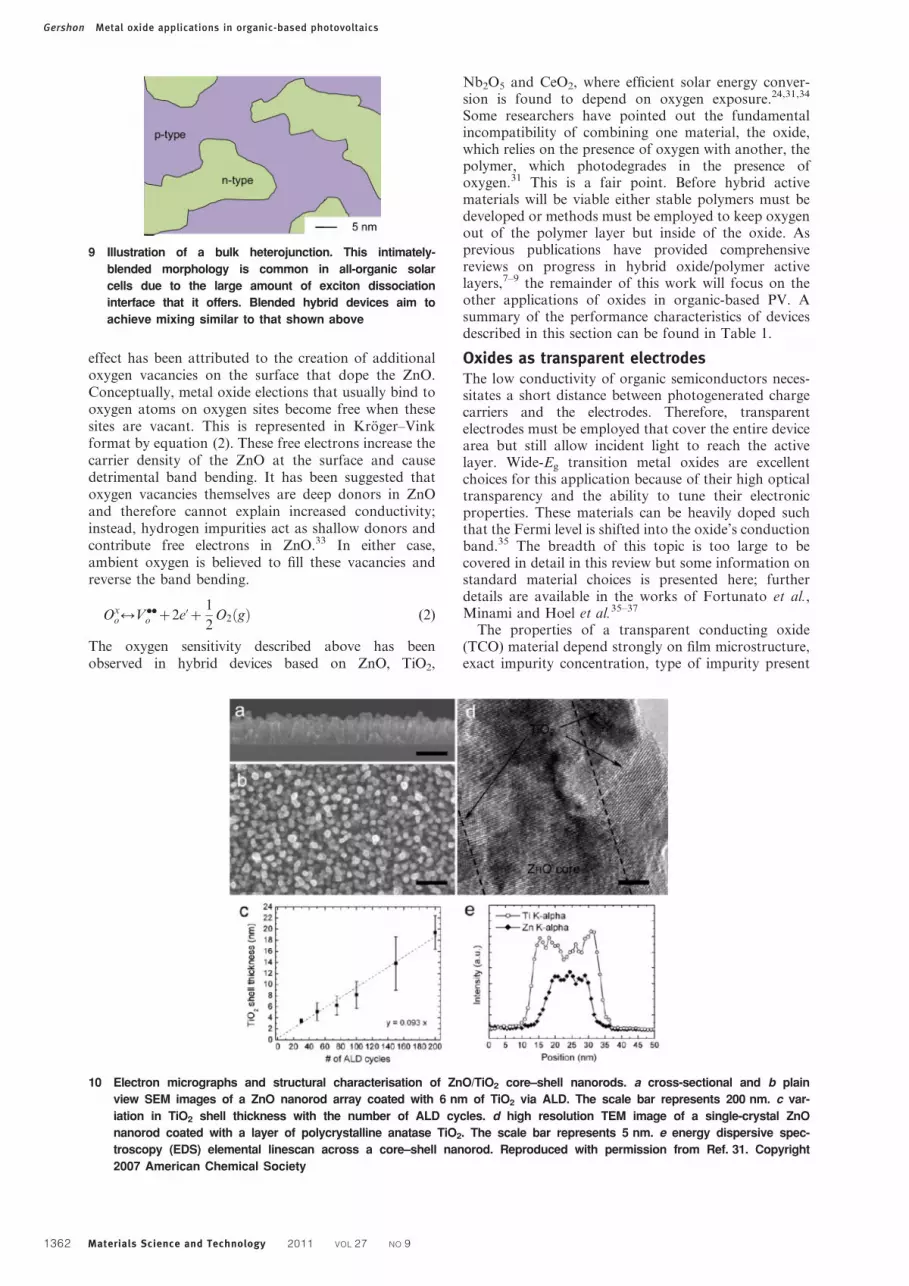
It has been suggested that despite having similar bandgap energies of approximately 3?2–3?4 eV, as well assimilar band edge positions, TiO2 is better than ZnO atdissociating excitons in P3HT. This was supported by astudy comparing nanostructured ZnO/P3HT deviceswith nanostructured ZnO/TiO2/P3HT devices. Electronmicrographs and structural information about these
nanostructures are shown in Fig. 10.31 A thin layer (4–10 nm) of TiO2 at the oxide/polymer interface gave largeincreases in power conversion efficiency. The authorsnoted the differences in surface chemistry, doping andresistivity between ZnO and TiO2 and suggested thatthese could influence charge transfer dynamics at theinterface.
The performance of hybrid devices strongly dependson the oxide’s processing history. One paper publishedin 2007 admitted that the authors could not account forthe difference between their ZnO nanorod/P3HT devicesand those of another group published 1 year prior.22,31
This may be because the ZnO nanorods used in the twostudies were grown using different seed layers, differentannealing steps and growth solutions containing differ-ent chemicals. While both techniques produced arrays of‘ZnO’ nanorods, the material properties were undoubt-edly different. Another study explored surface treat-ments performed on ZnO nanorod arrays beforepolymer deposition. It was found that in the absenceof all treatments, the ZnO/P3HT devices were notreproducible.32 Heat treatment of the nanorod arrays,however, were found to reproducibly give good deviceperformance; the heat treatment is believed to removephysisorbed molecules on the oxide surface leading tobetter contact with the polymer. In contrast, UV ozonetreatments led to poor device performance with low Voc,which was attributed to the creation of interfacialdipoles that shift the band alignment at the interface.
Many studies report reduced hybrid PV deviceperformance in the absence of oxygen. For example, itwas found that ZnO/P3HT devices improve when storedin air, after the contacts are thermally evaporated in avacuum, for up to 5 days as shown in Fig. 11.24 This
6 Illustration of a tandem cell with an oxide intermediate layer. PEDOT:PSS is an electron blocking polymer. The oxide
intermediate layer protects ‘active layer 1’ during the deposition of ‘active layer 2,’ forms ohmic contact between the
two devices and allows for the recombination of the unwanted charge carriers from each layer
7 Schematic of the origin of the open-circuit voltage Voc
limit in organic-based PV. The energetic difference
between the conduction band edge position Ec of the
oxide and the HOMO position of the polymer dictates
the upper limit to the Voc of the device. The LUMO
level is the position of lowest unoccupied molecular
orbital of the polymer. Ev is the valence band edge
position of the oxide
8 Vertically oriented nanorod arrays of ZnO, as shown in a, have a high surface area and therefore provide more exciton
dissociation area than flat ZnO films. To complete nanostructured devices, these arrays are intercalated with a semi-
conducting polymer, as shown in b. Reproduced with permission from Ref. 22. Copyright 2006 Elsevier
Gershon Metal oxide applications in organic-based photovoltaics
Materials Science and Technology 2011 VOL 27 NO 9 1361
effect has been attributed to the creation of additionaloxygen vacancies on the surface that dope the ZnO.Conceptually, metal oxide elections that usually bind tooxygen atoms on oxygen sites become free when thesesites are vacant. This is represented in Kroger–Vinkformat by equation (2). These free electrons increase thecarrier density of the ZnO at the surface and causedetrimental band bending. It has been suggested thatoxygen vacancies themselves are deep donors in ZnOand therefore cannot explain increased conductivity;instead, hydrogen impurities act as shallow donors andcontribute free electrons in ZnO.33 In either case,ambient oxygen is believed to fill these vacancies andreverse the band bending.
Oxo<V..
o z2e’z1
2O2 gð Þ (2)
The oxygen sensitivity described above has beenobserved in hybrid devices based on ZnO, TiO2,
Nb2O5 and CeO2, where efficient solar energy conver-sion is found to depend on oxygen exposure.24,31,34
Some researchers have pointed out the fundamentalincompatibility of combining one material, the oxide,which relies on the presence of oxygen with another, thepolymer, which photodegrades in the presence ofoxygen.31 This is a fair point. Before hybrid activematerials will be viable either stable polymers must bedeveloped or methods must be employed to keep oxygenout of the polymer layer but inside of the oxide. Asprevious publications have provided comprehensivereviews on progress in hybrid oxide/polymer activelayers,7–9 the remainder of this work will focus on theother applications of oxides in organic-based PV. Asummary of the performance characteristics of devicesdescribed in this section can be found in Table 1.
Oxides as transparent electrodesThe low conductivity of organic semiconductors neces-sitates a short distance between photogenerated chargecarriers and the electrodes. Therefore, transparentelectrodes must be employed that cover the entire devicearea but still allow incident light to reach the activelayer. Wide-Eg transition metal oxides are excellentchoices for this application because of their high opticaltransparency and the ability to tune their electronicproperties. These materials can be heavily doped suchthat the Fermi level is shifted into the oxide’s conductionband.35 The breadth of this topic is too large to becovered in detail in this review but some information onstandard material choices is presented here; furtherdetails are available in the works of Fortunato et al.,Minami and Hoel et al.35–37
The properties of a transparent conducting oxide(TCO) material depend strongly on film microstructure,exact impurity concentration, type of impurity present
9 Illustration of a bulk heterojunction. This intimately-
blended morphology is common in all-organic solar
cells due to the large amount of exciton dissociation
interface that it offers. Blended hybrid devices aim to
achieve mixing similar to that shown above
10 Electron micrographs and structural characterisation of ZnO/TiO2 core–shell nanorods. a cross-sectional and b plain
view SEM images of a ZnO nanorod array coated with 6 nm of TiO2 via ALD. The scale bar represents 200 nm. c var-
iation in TiO2 shell thickness with the number of ALD cycles. d high resolution TEM image of a single-crystal ZnO
nanorod coated with a layer of polycrystalline anatase TiO2. The scale bar represents 5 nm. e energy dispersive spec-
troscopy (EDS) elemental linescan across a core–shell nanorod. Reproduced with permission from Ref. 31. Copyright
2007 American Chemical Society
Gershon Metal oxide applications in organic-based photovoltaics
1362 Materials Science and Technology 2011 VOL 27 NO 9

and oxygen partial pressure during fabrication. Thesefactors influence the degree of doping (including thedensity of oxygen vacancies), the ease of dopantincorporation into the host lattice and thus the resultingconductivity and optical properties of the films. For highoptical transparency, a suitable TCO must have an Eg ofat least 3?1 eV and a free carrier plasma resonanceabsorption in the near infrared (1?5 mm) or longerwavelengths. Decreasing the oxide’s resistivity via dop-ing is limited by the visible-shift in the infrared absorp-tion edge, which narrows the range of transmitted lightas the dopant concentration increases.35 The mini-mum performance requirements for a TCO have beendefined as: a transmittance of at least 85% of light inthe visible range, a maximum resistivity of 1023 V cmand a charge carrier concentration on the order of1020 cm23.36,37
To date, the most promising TCO compounds includeIn2O3, SnO2, ZnO and doped variations of these. Thebest performance has come from tin-doped indium oxide(ITO), processed using a zone confinement technique tooptimise local crystallisation and impurity incorpora-tion, with 5?1 at-% Sn. This gave a laboratory thin filmresistivity of 4?461025 V cm.38,39 ITO is currently theTCO of choice for organic PV research; however, indiumis scarce and expensive ($685/kg in 200837) and ITO isenergy-intensive to process, underscoring the need foralternatives. The next best performing TCO is alumi-nium-doped ZnO (AZO), with 2 wt-% Al2O3, whoselaboratory resistivity is 1?4361024 V cm.40 Gallium-doped ZnO is easier to process, as Ga is less reactive
with oxygen than is Al, and has been pro-cessed with a resistivity of 2?661024 V cm for a Ga2O3
concentration of 2 wt-%.41
High-performance TCOs, such as those mentionedabove, are generally processed via sputtering, e-beamreactive evaporation or pulsed laser deposition (PLD),all of which are high-energy vacuum batch processingtechniques. The most economically viable TCO on themarket to date is fluorine-doped SnO2 (FTO). FTO canbe deposited via chemical depositions like spraypyrolysis from chlorides or other organometallic pre-cursors, giving it potential in low cost and continuousprocessing applications. The lowest resistivity demon-strated to date for FTO is y661024 V cm.35 Amor-phous indium zinc oxide (IZO) has also shown promiseand can be processed at room temperature35 or underambient conditions.42
Oxides as charge blocking layersOne major source of inefficiency in organic PV resultsfrom electrical shunting or short circuiting between thetop and bottom electrodes, which allows for the leakageof current. In organic PV, the active layer is a blend ofthe p- and n-type materials; if either material is in directcontact with both electrodes then shunting reducesdevice performance. Charge blocking layers can beinserted on either side of the active layer to address thisproblem. There are several key parameters thatdetermine a material’s utility as a charge blockinglayer. This layer must be transparent, have suitableenergy levels for accepting either electrons or holes (butnot both) from the active layer, make ohmic contactwith adjacent layers and be chemically inert withrespect to those layers.43 In all of these ways, thelarge-Eg transition metal oxides described below areappropriate choices.
TiO2 and ZnO are highly n-type and have been widelyimplemented in organic-based PV devices as holeblocking materials.44–47 Moreover, their energy levelsare conducive to accepting electrons from the activelayer while rejecting holes, as shown in Fig. 12. Therehas been significant research into the interactionsbetween these two and p-type polymers, as these havebeen used in a variety of the applications discussed inthis work. More interesting are the electron blockingoxides, as these are less widespread and are still underdevelopment.
Most wholly-organic PV rely on PEDOT:PSS as anelectron blocker but this layer is unstable and can corrodethe adjacent ITO electrode.67,68 Furthermore, differentPEDOT:PSS depositions yield films with differentmorphologies and inhomogeneous electrical properties,illustrating the need to replace it with a more stable and
11 J–V curve of a ZnO nanorod/P3HT device aged in air
for up to 5 days. Improvements in the Jsc, Voc and FF
are seen as the aging time increases up to 5 days.
Reproduced with permission from Ref. 24. Copyright
2007 American Chemical Society
Table 1 Summary of the performance characteristics of devices discussed in section on ‘Active materials’ of presentwork*
Device structure Voc/V Jsc/mA cm22 FF g Reference
ITO/flat ZnO/P3HT/Ag 0.5 0.52 0.55 0.15 24ITO/flat Zn0?75Mg0?25O/P3HT/Ag 0.7 1.27 0.56 0.49 20ITO/ZnO nanorods/P3HT/Ag 0.44 2.17 0.56 0.53 24ITO/ZnO nanorods/P3HT/Ag … … … Not functional 31ITO/ZnO nanorods/TiO2 shell/P3HT/Ag 0.5 1.14 0.5 0.29 31ITO/PEDOT:PSS/P3HT:TiO2 nanoparticles/TiO2 nanoparticles/Ag 0.52 2.97 0.54 0.83 29
*Voc is the open-circuit voltage, Jsc is the short-circuit current density, FF is the fill factor and g is the power conversion efficiency.
Gershon Metal oxide applications in organic-based photovoltaics
Materials Science and Technology 2011 VOL 27 NO 9 1363
homogeneous material.67,68 This has been attempted witha number of different oxides, all incorporating standardP3HT:PCBM active layers.45,48–51
One study demonstrated that PEDOT:PSS can beeffectively replaced with 5 nm of thermally-evaporatedMoO3 without compromising performance (g of 3?18%with PEDOT:PSS, 3?33% with MoO3).49 Similarly, sig-nificant improvements were seen upon replacing PEDOT:PSS with WO3 (2?5% efficiency with PEDOT:PSS, 3?1%with WO3); the oxide layer was shown to increase shuntresistance, reduce recombination at the ITO electrode,introduce a significant barrier to electrons and induce ahigher degree of ordering in the P3HT.50 Devices withno electron blocking layer at all performed worst (g of1?9%). A third study showed that NiO, deposited viaPLD, is another promising material;43 the success of theNiO layer was attributed to the energetic similaritybetween the Fermi level of the NiO and the HOMO ofP3HT.
If oxide-based electron blocking layers are to be usedcommercially, these films must become processable us-ing low-temperature ambient techniques. A 2009 studyused solution-processed V2O5 nanoparticles, depositedfrom a suspension in isopropanol, as both an electronblocking layer and optical spacer, to increase efficien-cy from 2?5% without the oxide layer to 3?56% withthe oxide layer.45 A more recent study demonstrat-ed the ability to solution-process NiO films at lowtemperatures.51 Samples containing solution processedNiO performed as well as those containing PEDOT:PSS or PLD-deposited NiO. The ability to processthese films at low temperatures will become increasinglyimportant as organic PV technology moves closer tocommercialisation.
As a reminder, many experimental parameters varybetween the studies discussed in this section; theseinclude oxide film thicknesses, active layer thickness,processing conditions and thermal treatments. There-fore, the presentation of efficiencies as above shouldmainly illustrate the importance of charge blockinglayers and improvements made possible by replacingPEDOT:PSS.
Oxides as charge collectorsOne drawback to using vertically-aligned metal oxidenanorod arrays in the active layer is the finite excitondiffusion length in the polymers. While the interna-norod spacing is usually of the order of 100 nm, theexciton diffusion lengths in the polymers are usually anorder of magnitude smaller (10 nm or less in P3HT).
Excitons generated in the polymer region further than10 nm from an interface recombine before dissociation.Therefore, attempts have been made to intercalate ablended active layer, rather than a neat polymer, intothe oxide nanostructure. In this model, excitons aredissociated within the blended region and dissociatedcharges are conducted out of the device via the nanorodstructure.
This idea was demonstrated in a study that used ablend of the small molecules copper phthalocyanine(CuPC) and C60 as the active layer.46 Devices containinga flat ZnO layer (ITO/compact ZnO/CuPc:C60/CuPC/PEDOT:PSS/Au) were compared with those contain-ing a nanostructured ZnO layer (ITO/compact ZnO/ZnO nanorods/CuPC:C60/CuPC/PEDOT:PSS/Au). Itwas shown that the sample containing the nanostruc-tured ZnO demonstrated a significantly higher Jsc
(3?86 mA cm22, compared with 1?76 mA cm22), sug-gesting that the nanorods helped extract charges fromthe active layer.
Another study showed improved device performancewhen blends of P3HT and small TiO2 nanorods (20–30 nm long, 4–5 nm in diameter), rather than neatP3HT, are infiltrated into nanostructured ZnO (180 nmlong, 50 nm in diameter).53 Electron micrographs of thedifferent components of these devices are shown inFig. 13. In the neat P3HT devices, the ZnO nanostruc-ture provides the sole interfaces for exciton dissociation.Introducing the TiO2 nanorods into the active layercreates additional area for exciton dissociation, resultingin the improvement of the Jsc from 0?3 to 1?96mA cm22. A similar study compared nanostructuredZnO/P3HT devices with nanostructured ZnO/P3HT:PCBM devices.22 The incorporation of PCBM increasedthe Jsc from 2?2 to 10?0 mA cm22, illustrating that themajority of the photocurrent was generated in the blendand the ZnO nanorods functioned mainly as chargecollectors.
As previously stated, the processing history of ZnOhas a significant impact on its properties. Despite thefact that two studies in the above paragraph bothreportedly used ‘hydrothermally-grown ZnO nanostruc-tures’, for example, the reported performance of thenanostructured ZnO/P3HT devices was substantiallydifferent (e.g. Jsc values of 0?3 and 2?2 mA cm22). Manyfactors have likely contributed to this: differences innanorod dimensions, polymer processing, seed layerdepositions, solution concentrations and surface treat-ments, among others. The variation in experimental
12 Approximate energy level (Ec, Ev, HOMO and LUMO) positions of oxides and polymers discussed in this work: values
are approximate in that they depend on methods and circumstances of measurement43,45,48–52
Gershon Metal oxide applications in organic-based photovoltaics
1364 Materials Science and Technology 2011 VOL 27 NO 9

parameters therefore prevents the direct comparison oftwo studies such as these. Instead, the individual resultshave been presented to demonstrate how devices withmodified architectures compare with controls made inthe same group.
Also, while the Jsc of a device may improve byincorporating a ZnO charge collector, in the case ofP3HT:PCBM, the Voc and FF both decrease.11,22
Furthermore, recent results have demonstrated thatnearly 100% internal quantum efficiency can alreadybe achieved for some systems (PCPDTBT:PC70BM)without the use of nanostructures, i.e. nearly 100% ofabsorbed photons can be collected as charge carriers.54
These factors must be considered before nanostructuredcharge collectors will become widely-adopted.
Oxides as optical spacersAs light travels through a device, it passes throughseveral thin films with different optical properties (e.g.transparent electrode, charge blocking layers, activelayer, etc.) before reaching the back electrode, where it isreflected in the other direction. The reflections atdifferent interfaces cause optical interference (construc-tive and destructive), resulting in a non-uniformdistribution of the light intensity in the device. Thisdistribution depends on the thicknesses and opticalproperties of the different layers. Ideally, a high intensityof the light most effectively absorbed by the polymerwould spatially correspond to the active region. It hasbeen shown that the thickness of the charge blockinglayer can be modified to adjust the spatial distribution ofthe light intensity (Fig. 5).
The concept of optical engineering in an organic solarcell has been demonstrated with ITO/PEDOT:PSS/P3HT:PCBM/ZnO/LiF/Al devices.55 The Jsc of thedevice oscillates with both active layer thickness andthe ZnO thickness due to interference effects that changethe light intensity reaching the P3HT for absorption.For some active layer thicknesses, adding a 40 nm thickZnO layer significantly improves the Jsc. For otheractive layer thicknesses, introducing the ZnO layer shiftsthe light distribution to a less optimal location in thedevice, thus reducing performance (Fig. 14).
Similar results were obtained using a layer ofamorphous TiOx (x<1?34) grown via low temperaturesol–gel processing.17 This study demonstrated a 40%improvement in external quantum efficiency over theentire spectral response of a cell containing 30 nm of theoxide. This is attributed to improved photocurrentgeneration in the active layer. The optical effect wasfurther supported by comparing reflectance spectra oftwo devices, one with a TiOx layer and one without. Theresults indicated increased active layer absorption owingto a higher light intensity in the active region.
Oxides as intermediate layers in tandem cellsLarge-Eg polymers like P3HT (y2?2 eV) cannot absorblow-energy light and therefore yield devices with limitedJsc values. Devices based only on small-Eg polymers,however, are limited by the relaxation of high-energyelectron–hole pairs to the polymer’s band edges andgenerally exhibit low Voc values. One approach tocircumventing this problem is to stack active layers withcomplementary absorption spectra in a tandem architec-ture. In principle, this type of multijunction device shouldgive a maximum Voc approximately equal to the sum of
the individual Voc values while the maximum Jsc would belimited by the smaller of the two individual Jsc values.15,56
The strategy of stacking cells in tandem is what hasallowed inorganic PV to reach efficiencies .40%.18
In single-cell organic PV, the ITO electrode collectsthe holes and the top metallic electrode collects theelectrons. For double-junction tandem cells to operate,electrons from the bottom cell and holes from the topcell must recombine in the middle to avoid recombiningwith the carriers intended for collection (Fig. 6).Furthermore, it is crucial to prevent the dissolution ofthe bottom cell during the deposition of the top cell. It isalso important that there be ohmic contact between thetwo individual devices. Employing an inorganic inter-mediate layer can help accomplish all of the above; thismaterial acts as a foundation layer, a charge recombina-tion layer and an ohmic contact.
A 2007 study reported the use of ZnO nanoparticlesand modified PEDOT in an intermediate layer of atandem cell. The two active layers were a P3HT:PCBMblend and a PPV derivative:PCBM blend.57 The devicewas solution-processed and high Voc values weredemonstrated up to 1?53 V for a double junction celland 2?19 V for a triple junction cell. The devices,however, still had low conversion efficiencies (1?9% forthe double junction device and 2?1% for the triplejunction) due to low Jsc values. Another 2007 studyreported a solution-processed tandem cell whose effi-ciency (6?5%) surpassed those of the individual cellscomprising it. This device contained a P3HT:PC70BMcell and a PCPDTBT:PCBM cell. The intermediate layerwas TiOx/PEDOT:PSS (x<1?34), where the oxide wasprocessed using sol–gel chemistry.58 A more recent studyexplored the nature of the interlayer and its influence ondevice properties.56 It was found that the PEDOT/TiO2
interface behaved as a metal/semiconductor contact.This junction showed a Schottky-to-ohmic transitionunder UV illumination, which was attributed to achange in the TiO2 carrier density. The Voc of thetandem cell was nearly the sum of the two individualcells, while the net Jsc was lower than either of the
13 a schematic of device structure: a blend of P3HT and
TiO2 nanorods are infiltrated into an array of ZnO charge
collectors. b high-resolution TEM image of TiO2 nanor-
ods to be blended with P3HT. c SEM cross-section
of ZnO nanorod array into which blend is intercalated.
d SEM cross-section of intercalated nanostructure. Re-
produced with permission from Ref. 53. Copyright 2007
The Royal Society of Chemistry
Gershon Metal oxide applications in organic-based photovoltaics
Materials Science and Technology 2011 VOL 27 NO 9 1365

individual cells. This may be due to the partialdissolution of one active layer during the deposition ofthe second.
Oxides as stability enhancersOrganic semiconducting polymers generally degrade inthe presence of UV light, water, oxygen or oxidisedmetal electrodes.59 In order to address this problem,various encapsulation techniques have been developed,some utilising UV epoxy and others rigid protectivelayers.59,60 These work to a limited degree, partiallypreventing the diffusion of water and oxygen into thedevice, but degradation remains a problem.
One way to improve device stability is to incorporatemetal oxides that are slightly oxygen deficient, like TiOx
(x<1?34), which can absorb oxygen and humidity fromthe polymer film. One study examined the effect of thisoxide on the stability of a polyfluorene (PF) polymer.61
Of the different films explored, the order of increasingstability is as follows: glass/PF, glass/TiOx/PF, glass/PF/TiOx and glass/TiOx/PF/TiOx. Depth profiling illu-strated that covering the PF with the oxide drasticallyreduces the oxygen present inside the polymer film.Furthermore, when P3HT:PCBM devices were made,those containing the TiOx layer in between the activematerials and the Al electrode degraded two orders ofmagnitude more slowly than control devices without theoxide layer (Fig. 15).
Another study incorporated TiOx (where ‘x’ was notspecified) on the ITO side of the active layer and similarlyobserved improved device stability.62 This study com-pared two device geometries: ITO/PEDOT:PSS/P3HT:PCBM/Al and ITO/TiOx/P3HT:PCBM/PEDOT:PSS/Au.The starting efficiencies of the two were similar (g offormer was 2?10% and g of latter was 2?20%) but after10 h of illumination, the former device had degraded to50% of its initial efficiency while the latter retained over99?5% of its starting efficiency. This effect is convin-cingly attributed to the oxygen-scavenging and UV-absorbing behaviour of the TiOx. There are, however,two other factors that may also be contributing: the useof a Au electrode instead of Al, which readily oxidisesand reduces performance and the inconsistency in thepresence of a buffer layer between the P3HT:PCBMand the electrode. It has been suggested that hot metalatoms colliding with the active layer during electrodedeposition can damage the polymers. Additionally, the
diffusion of metal atoms from the top electrode into theactive layer can create recombination sites; a bufferlayer would prevent both of these. To isolate the roleof the TiOx in device stability, the number of varia-bles contributing to degradation must be kept to aminimum.
Finally, it should be noted that the more stoichio-metric oxides TiO2, ZnO and SnO2 can all photooxidiseorganic materials. The UV illumination of TiO2 photo-generates electron–hole pairs. When an electron istransferred to a bound oxygen, an oxygen radical anionis formed. When a hole reacts with a surface hydroxylgroup, a radical TiOH cation is formed. Both of theseradical species can oxidise organic compounds resultingin degradation.59 ZnO and SnO2 have similar photo-catalytic properties. For this reason, oxygen deficientoxides that remove oxygen from polymer films arelikelier candidates for stable ambient condition devicesthan their stoichiometric counterparts.
Interface considerationsIn hybrid organic/oxide PV, the interface plays severalcrucial roles in device operation. In bilayer devices, forexample, the hybrid interface is exclusively responsiblefor exciton dissociation. When oxides are used as chargecollectors, electrons must be injected into the oxide fromthe active layer at the interface. To accomplish chargeblocking, there must be charge selectivity where theorganic and the oxide materials meet. Any surface trapsor dipoles that exist at the boundary between thesematerials can influence device efficiency. Studies haveshown that unmodified metal oxide surfaces do indeedhave a high density of electron traps.63 Therefore, muchattention has been paid to these interfaces and how theycan be optimised.
One way to control the interface is to introducesurface modifiers. One study attached organic self-assembled monolayers (SAMs) onto the TiO2 holeblocking surface of a P3HT:PCBM device. It was foundthat device performance improved for three reasons.First, the binding of the SAM to the TiO2 passivatescharge traps on the oxide surface, leading to reducedcontact resistance. Second, the SAM offers improvedelectronic coupling between the oxide and the activelayer, which helps the TiO2 extract electrons. And third,the SAM can influence the morphology of the active
14 a Calculated thickness dependence of the short circuit current density (Jsc or Isc) of devices containing ZnO optical
spacers of different thicknesses: the calculation assumes 100% internal quantum efficiency, i.e. that all absorbed
photons generate collectable photocurrent. b theoretical versus experimental calculations of the dependence of
device Jsc on active layer thickness. The ZnO optical spacer used was 39 nm thick. Reproduced with permission from
Ref. 55. Copyright 2007 American Institute of Physics
Gershon Metal oxide applications in organic-based photovoltaics
1366 Materials Science and Technology 2011 VOL 27 NO 9

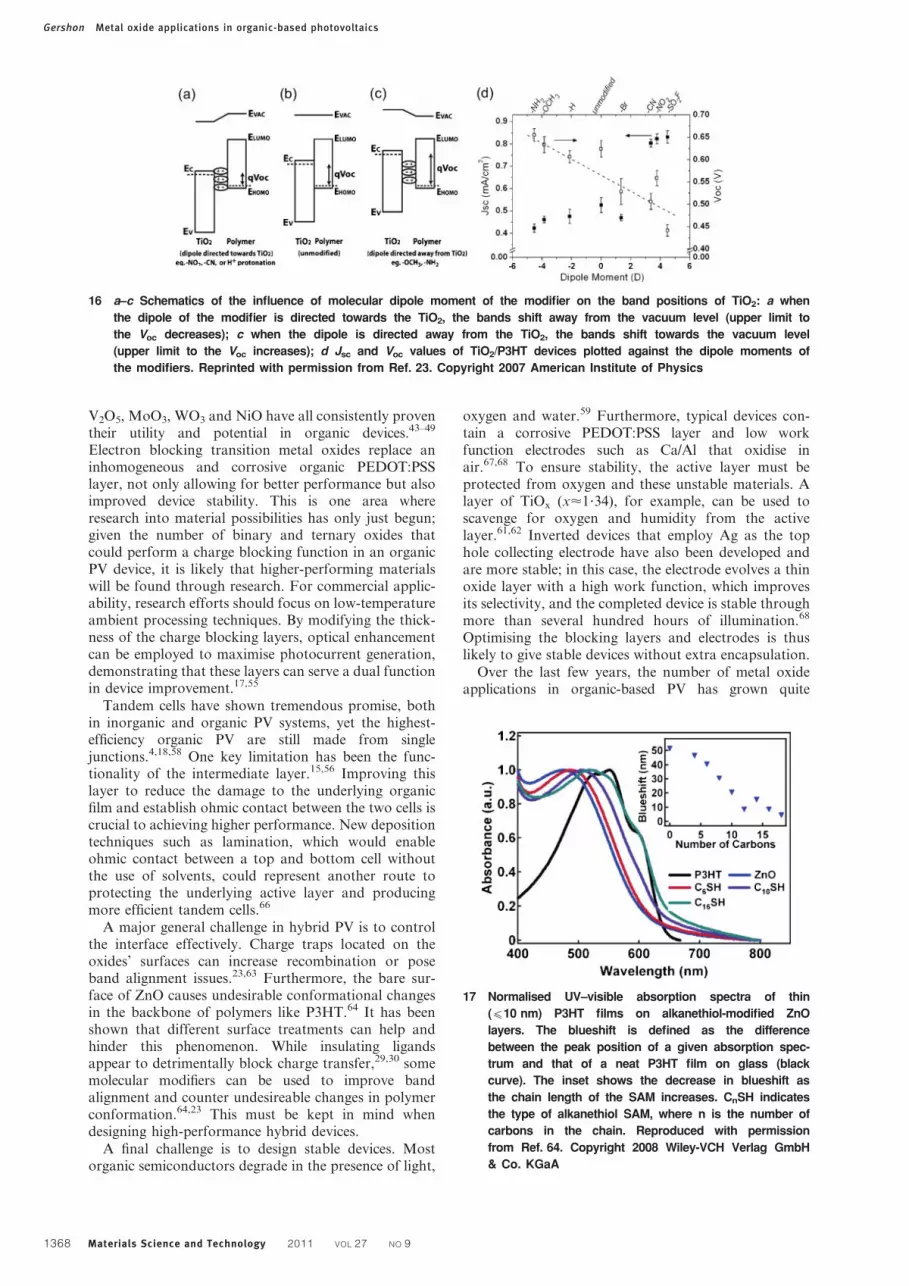
layer and improve the crystallinity of the P3HT.44 Fourkinds of SAMs were explored and each was bound to theTiO2 by a single carboxylic acid group. The largestimprovement in device performance came from the C60-based SAM, which increased device efficiency from 2?80to 3?78%.
A similar study examined the donor/acceptor interfacein flat bilayer TiO2/P3HT devices and the influence ofmolecular modifiers.23 It was found that dipole momentson the modifiers shift the band positions of the TiO2,which consequently influences the Voc of resultingdevices (Fig. 16). It was also found that acid–baseinteractions occur between the carboxylic acid attach-ment groups of the modifier and the oxide surface,which can also shift the band positions of the TiO2 dueto hydrogen protonation. The number of carboxylic acidgroups on the modifier correlates with the degree towhich the device Voc decreases.
The same study then examined interface modificationusing dyes commonly employed in dye-sensitised solarcells.10,23 The same correlation was seen between thenumber of carboxylic acid attachment groups on the dyeand the decrease in device Voc. The Jsc values of nearlyall of the dye-modified devices, however, increaseddramatically compared with the non-modified devices.This effect could not stem solely from absorption in thedye because the EQE follows the absorption spectrum ofthe P3HT and, furthermore, only a monolayer of the dyeis present. Instead, the improved Jsc suggests that dye-modification improves electron injection at the TiO2/P3HT interface.
It has also been shown that the bare surface of ZnO cancause P3HT to become disordered, which hinders excitondiffusion and hole transport.64 This disorder is evidentfrom the blueshift observed in the absorbance of P3HTwhen thin films ((10 nm) come into contact withunmodified ZnO; this blueshift is a sign of reducedelectron delocalisation along the backbone due totwisting of the polymer chains. It was shown that treatingthe ZnO surface with alkanethiol SAMs of different
lengths can reduce this blueshift by 90%.64 The SAMswith longer hydrocarbon backbones reduce this blueshiftmost effectively, as shown in Fig. 17. This improvementin polymer ordering allows for increased device Jsc andimproved EQE over the whole spectrum of P3HT.
Finally, as was described in the section on ‘Activematerials’, when polymers and oxide nanoparticles arecodissolved in solution insulating ligands are oftenintroduced to enhance nanoparticle solubility; thesegenerally hinder charge transfer between the twomaterials. While capping agents are often necessary forsolubility, they must later be removed to promoteinteraction between the two materials. Even withoutthe presence of these molecules on the surface, theproblems described above must be considered whenemploying a polymer/oxide blend.
Future and challenges of oxide use inorganic-based PVMany of the oxide applications discussed in this workhave become integral components of organic-based PV.The field could not exist, for example, without highperformance transparent electrodes due to the lowconductivity and charge transport lengths of the cons-tituent organic materials. While ITO is currently themost common TCO in organic PV research due to itssuperior performance, the scarcity of indium and highenergy processing requirements of ITO in its currentform make it an unlikely choice in low cost flexible solarcell applications. For organic PV to reach its commercialpotential, other promising materials such as AZO, FTO,IZO or completely new conducting oxides must bedeveloped further.35,42 New ambient methods of grow-ing high-quality metal oxide films, particularly atmo-spheric atomic layer deposition, have emerged in recentyears with the potential to revolutionise TCOs for PVapplications.65
Charge blocking layers are another crucial applicationof transition metal oxides in organic PV. TiO2, ZnO,
15 a Impact of TiOx layers on the photoluminescence spectra of polyfluorene (PF) films before and after annealing at
150uC in air. The feature appearing in the glass/PF and glass/TiOx/PF films between 500 and 600 nm is the result of
degradation. b J–V curves of P3HT:PCBM solar cells, with and without TiOx layers, left in air up to 5 h. Devices with-
out TiOx degrade considerably while those with TiOx maintain their initial performance. Reproduced with permission
Ref. 61. Copyright 2007 Wiley-VCH Verlag GmbH & Co. KGaA
Gershon Metal oxide applications in organic-based photovoltaics
Materials Science and Technology 2011 VOL 27 NO 9 1367
V2O5, MoO3, WO3 and NiO have all consistently proventheir utility and potential in organic devices.43–49
Electron blocking transition metal oxides replace aninhomogeneous and corrosive organic PEDOT:PSSlayer, not only allowing for better performance but alsoimproved device stability. This is one area whereresearch into material possibilities has only just begun;given the number of binary and ternary oxides thatcould perform a charge blocking function in an organicPV device, it is likely that higher-performing materialswill be found through research. For commercial applic-ability, research efforts should focus on low-temperatureambient processing techniques. By modifying the thick-ness of the charge blocking layers, optical enhancementcan be employed to maximise photocurrent generation,demonstrating that these layers can serve a dual functionin device improvement.17,55
Tandem cells have shown tremendous promise, bothin inorganic and organic PV systems, yet the highest-efficiency organic PV are still made from singlejunctions.4,18,58 One key limitation has been the func-tionality of the intermediate layer.15,56 Improving thislayer to reduce the damage to the underlying organicfilm and establish ohmic contact between the two cells iscrucial to achieving higher performance. New depositiontechniques such as lamination, which would enableohmic contact between a top and bottom cell withoutthe use of solvents, could represent another route toprotecting the underlying active layer and producingmore efficient tandem cells.66
A major general challenge in hybrid PV is to controlthe interface effectively. Charge traps located on theoxides’ surfaces can increase recombination or poseband alignment issues.23,63 Furthermore, the bare sur-face of ZnO causes undesirable conformational changesin the backbone of polymers like P3HT.64 It has beenshown that different surface treatments can help andhinder this phenomenon. While insulating ligandsappear to detrimentally block charge transfer,29,30 somemolecular modifiers can be used to improve bandalignment and counter undesireable changes in polymerconformation.64,23 This must be kept in mind whendesigning high-performance hybrid devices.
A final challenge is to design stable devices. Mostorganic semiconductors degrade in the presence of light,
oxygen and water.59 Furthermore, typical devices con-tain a corrosive PEDOT:PSS layer and low workfunction electrodes such as Ca/Al that oxidise inair.67,68 To ensure stability, the active layer must beprotected from oxygen and these unstable materials. Alayer of TiOx (x<1?34), for example, can be used toscavenge for oxygen and humidity from the activelayer.61,62 Inverted devices that employ Ag as the tophole collecting electrode have also been developed andare more stable; in this case, the electrode evolves a thinoxide layer with a high work function, which improvesits selectivity, and the completed device is stable throughmore than several hundred hours of illumination.68
Optimising the blocking layers and electrodes is thuslikely to give stable devices without extra encapsulation.
Over the last few years, the number of metal oxideapplications in organic-based PV has grown quite
16 a–c Schematics of the influence of molecular dipole moment of the modifier on the band positions of TiO2: a when
the dipole of the modifier is directed towards the TiO2, the bands shift away from the vacuum level (upper limit to
the Voc decreases); c when the dipole is directed away from the TiO2, the bands shift towards the vacuum level
(upper limit to the Voc increases); d Jsc and Voc values of TiO2/P3HT devices plotted against the dipole moments of
the modifiers. Reprinted with permission from Ref. 23. Copyright 2007 American Institute of Physics
17 Normalised UV–visible absorption spectra of thin
((10 nm) P3HT films on alkanethiol-modified ZnO
layers. The blueshift is defined as the difference
between the peak position of a given absorption spec-
trum and that of a neat P3HT film on glass (black
curve). The inset shows the decrease in blueshift as
the chain length of the SAM increases. CnSH indicates
the type of alkanethiol SAM, where n is the number of
carbons in the chain. Reproduced with permission
from Ref. 64. Copyright 2008 Wiley-VCH Verlag GmbH
& Co. KGaA
Gershon Metal oxide applications in organic-based photovoltaics
1368 Materials Science and Technology 2011 VOL 27 NO 9

remarkably (Table 2). Metal oxides have improveddevice operation in many ways, increasing the photo-current, electrode selectivity, achievable Voc values andlight distribution. Furthermore, they make solution-processed tandem cells possible, offering a promisingroute to higher efficiency. While there are still hurdles toovercome, it is clear that metal oxides will remain crucialcomponents of organic-based PV in the years to come.
References1. S.-S. Sun and N. S. Sariciftci: ‘Organic photovoltaics: mechanisms,
materials, and devices’, 1st edn; 2005, Boca Raton, FL, Taylor &
Francis Group, LLC.
2. C. F. Kutscher: ‘Tackling climate change in the U.S.: potential
carbon emissions reductions from energy efficiency and renewable
energy by 2030’, ASES report, American Solar Energy Society,
Boulder, CO, USA, 2007.
3. D. J. Mackay: ‘Sustainable energy – without the hot air’,
Cambridge Limited, Cambridge, UK, 2009.
4. http://solarmer.com/ (2 May 2011).
5. http://www.konarka.com/ (2 May 2011).
6. http://www.plextronics.com/ (2 May 2011).
7. J. Boucle, P. Ravirajan and J. Nelson: ‘Hybrid polymer-metal
oxide thin films for photovoltaic applications’, J. Mater. Chem.,
2007, 17, 3141–3153.
8. I. Gonzalez-Valls and M. Lira-Cantu: ‘Vertically-aligned nanos-
trutures of ZnO for excitonic solar cells: a review’, Energy Environ.
Sci., 2008, 2, 19–34.
9. J. W. P. Hsu: ‘Development of nanostructured and surface
modified semiconductors for hybrid organic-inorganic solar cells’,
Technical report, Sandia National Laboratories, Albuquerque,
NM, USA, 2008.
10. M. Gratzel: ‘Dye-sensitized solar cells’, J. Photochem. Photobiol. C:
Photochem. Rev., 2003, 4, (2), 145–153.
11. B. Kippelen and J.-L. Bredas: ‘Organic photovoltaics’, Energy
Environ. Sci., 2009, 2, (3), 251–261.
12. S. E. Shaheen, D. S. Ginley and G. E. Jabbour: ‘Organic-based
photovoltaics: toward low-cost power generation’, MRS Bull.,
2005, 30, 10–19.
13. P. Peumans, A. Yakimov and S. R. Forrest: ‘Small molecular
weight organic thin-film photodetectors and solar cells’, J. Appl.
Phys., 2003, 93, (7), 3693–3723.
14. T. Kietzke: ‘Recent advances in organic solar cells’, Adv.
OptoElectron., 2007, 2007, 1–15.
15. T. Ameri, G. Dennler, C. Lungenschmied and C. J. Brabec:
‘Organic tandem solar cells: a review’, Energy Environ. Sci., 2009, 2,
347–363.
16. W. J. Beek, L. H. Slooff, M. M. Wienk, J. M. Kroon and R. A.
Janssen: ‘Hybrid solar cells using a zinc oxide precursor and a
conjugated polymer’, Adv. Funct. Mater., 2005, 15, (10), 1703–
1707.
17. J. Y. Kim, S. H. Kim, H.-H. Lee, K. Lee, W. Ma, X. Gong and
A. J. Heeger: ‘New architecture for high-efficiency polymer
photovoltaic cells using solution-based titanium oxide as an optical
spacer’, Adv. Mater., 2006, 18, (5), 572–576.
18. R. R. King, D. C. Law, K. M. Edmondson, C. M. Fetzer, G. S.
Kinsey, H. Yoon, R. A. Sherif and N. H. Karan: ‘40% efficient
metamorphic GaInP/GaInAs/Ge multijunction solar cells’, Appl.
Phys. Lett., 2007, 90, (18), 183516.
19. G. Chamberlain: ‘Organic solar cells: a review’, Sol. Cells, 1983, 8,
(1), 47–83.
20. D. C. Olson, S. E. Shaheen, M. S. White, W. J. Mitchell, M. F. A. M.
van Hest, R. T. Collins and D. S. Ginley: ‘Band-offset engineering
for enhanced open-circuit voltage in polymer-oxide hybrid solar
cells’, Adv. Funct. Mater., 2007, 17, (2), 264–269.
21. M. T. Lloyd, Y.-J. Lee, R. J. Davis, E. Fang, R. M. Fleming,
J. W. P. Hsu and M. F. Toney: ‘Improved efficiency in poly
Table 2 Summary of performance characteristics of devices discussed in present work*
Index of devices discussed in the present work
Device structure Role of oxide Voc/V Jsc/mA cm22 FF g/% Reference
ITO/flat ZnO/P3HT/Ag AM 0.5 0.52 0.55 0.15 24ITO/flat Zn0?75Mg0?25O/P3HT/Ag AM 0.7 1.27 0.56 0.49 20ITO/ZnO nanorods/P3HT/Ag AM 0.44 2.17 0.56 0.53 24ITO/ZnO nanorods/P3HT/Ag AM … … … Not
functional31
ITO/ZnO nanorods/TiO2 shell/P3HT/Ag AM 0.5 1.14 0.5 0.29 31ITO/ZnO nanorods/P3HT/Au AM 0.34 0.3 0.4 0.04 53ITO/ZnO nanorods/P3HT:TiO2 nanoparticles/Au AM and CC 0.38 1.96 0.39 0.29 53ITO/ZnO nanorods/P3HT:TiO2 nanoparticles/TiO2 nanoparticles/Au
AM and CCand CB
0.4 2.20 0.35 0.31 53
ITO/PEDOT:PSS/P3HT:TiO2
nanoparticles/TiO2 nanoparticles/AgAM and CB 0.52 2.97 0.54 0.83 29
ITO/flat MoO3/P3HT:PCBM/Ca/Al CB 0.6 8.94 0.62 3.33 49ITO/flat TiO2/P3HT:PCBM/WO3/Ag CB 0.6 7.2 0.6 2.58 48ITO/flat NiO/P3HT:PCBM/LiF/Al CB 0.64 11.3 0.70 5.16 43ITO/WO3/P3HT:PCBM/Ca/Al CB y0.63 y7.0 0.7 3.1 50ITO/ZnO nanorods/P3HT:PCBM/Ag CC 0.48 10.0 0.43 2.03 22ITO/ZnO nanorods/P3HT:PCBM/LiF/Al CC 0.50 10.21 0.50 2.52 45ITO/ZnO nanorods/P3HT:PCBM/V2O5/LiF/Al CC and CB 0.55 10.75 0.60 3.56 45ITO/flat ZnO/CuPC:C60/CuPC/PEDOT:PSS/Au CB 0.27 1.76 0.28 0.13 46ITO/ZnO nanorods/CuPC:C60/CuPC/PEDOT:PSS/Au CC and CB 0.46 3.86 0.30 0.53 46ITO/PEDOT:PSS/MDMO-PPV:PCBM/ZnOnanoparticles/PEDOT/P3HT:PCBM/LiF/Al
IL 1.53 3.0 0.42 1.9 57
ITO/PEDOT:PSS/MDMO-PPV:PCBM/ZnOnanoparticles/PEDOT/MDMO-PPV:PCBM/ZnOnanoparticles/PEDOT/P3HT:PCBM/LiF/Al
IL 2.19 2.6 0.37 2.1 57
ITO/PEDOT/PCPDTBT:PCBM/TiOx/PEDOT/P3HT:PC70BM/TiOx/Al
IL 1.24 7.8 0.67 6.5 58
ITO/TiO2/P3HT:PCBM/PEDOT:PSS/Ag CB 0.61 9.80 0.47 2.8 44ITO/TiO2/C60 SAM/P3HT:PCBM/PEDOT:PSS/Ag
IM 0.62 10.6 0.57 3.8 44
ITO/TiOx/P3HT:PCBM/PEDOT:PSS/Au SE 0.56 6.70 0.55 2.1 62
*AM indicates an active material, CC indicates a charge collector, CB indicates a charge blocker, IL indicates an intermediate layer, IMindicates an interface-modified blocking layer and SE indicates a stability enhancer. In some cases, an oxide layer can fill several roles atthe same time. Voc is the open-circuit voltage, Jsc is the short-circuit current, FF is the fill factor and g is the power conversion efficiency.
Gershon Metal oxide applications in organic-based photovoltaics
Materials Science and Technology 2011 VOL 27 NO 9 1369

(3-hexylthiophene)/zinc oxide solar cells via lithium incorporation’,
J. Phys. Chem. C: Lett., 2009, 113, (41), 17608–17612.
22. D. C. Olson, P. Jorge, R. T. Collins, S. E. Shaheen and D. S.
Ginley: ‘Hybrid photovoltaic devices of polymer and ZnO
nanofiber composites’, Thin Solid Films, 2006, 496, 26–29.
23. C. Goh, S. R. Scully and M. D. McGehee: ‘Effects of molecular
interface modification in hybrid organic-inorganic photovoltaic
cells’, J. Appl. Phys., 2007, 101, (114503), 1–12.
24. D. C. Olson, S. E. Shaheen, R. T. Collins and D. S. Ginley: ‘The
effect of atmosphere and ZnO morphology on the performance of
hybrid poly(3-hexylthiophene)/ZnO nanofiber photovoltaic
devices’, J. Phys. Chem. C, 2007, 111C, (44), 16670–16678.
25. P. Ravirajan, A. M. Peiro, M. K. Nazeeruddin, M. Graetzel, D. D. C.
Bradley, J. R. Durrant and J. Nelson: ‘Hybrid polymer/zinc oxide
photovoltaic devices with vertically oriented ZnO nanorods and an
amphiphilic molecular interface layer’, J. Phys. Chem. B, 2006, 110B,
7635–7639.
26. V. V. Kislyuk and O. P. Dimitriev: ‘Nanorods and nanotubes for
solar cells’, J. Nanosci. Nanotechnol., 2008, 8, 131–148.
27. X. Ren, T. Gershon, D. C. Iza, D. Munoz-Rojas, K. Musselman
and J. L. MacManus-Driscoll: ‘The selective fabrication of large-
area highly ordered TiO2 nanorod and nanotube arrays on
conductive transparent substrates via sol-gel electrophoresis’,
Nanotechnology, 2009, 20, 365604.
28. K. P. Musselman, G. J. Mulholland, A. P. Robinson, L. Schmidt-
Mende and J. L. MacManus-Driscoll: ‘Low-temperature synthesis
of large-area, free-standing nanorod arrays on ITO/glass and other
conducting substrates’, Adv. Mater., 2008, 20, 1–6.
29. T.-W. Zeng, H.-H. Lo, C.-H. Chang, Y.-Y. Lin, C.-W. Chen and
W.-F. Su: ‘Hybrid poly(3-hexylthiophene)/titanium dioxide nanor-
ods material for solar cell applications’, Sol. Energy Mater. Sol.
Cells, 2008, 93, 952–957.
30. J. Boucle, S. Chyla, M. S. P. Shaffer, J. R. Durrant, D. D. C.
Bradley and J. Nelson: ‘Hybrid bulk heterojunction solar cells
based on blends of TiO2 nanorods and P3HT’, Comptes Rend.
Phys., 2008, 9, 110–118.
31. L. E. Greene, M. Law, B. D. Yuhas and P. Yang, ‘ZnO-TiO2 core-
shell nanorod/P3HT solar cells’, J. Phys. Chem. C: Lett., 2007, 111,
(50), 18451–18456.
32. D. C. Olson, Y.-J. Lee, M. S. White, N. Kopidakis, S. E. Shaheen,
D. S. Ginley, J. A. Voigt and J. W. P. Hsu: ‘Effect of ZnO
processing on the photovoltage of ZnO/poly(3-hexylthiophene)
solar cells’, J. Phys. Chem. C: Lett., 2008, 112, 9544–9547.
33. A. Janotti and C. G. V. de Walle: ‘Fundamentals of zinc oxide as a
semiconductor’, Rep. Prog. Phys., 2009, 72, 126501.
34. M. Lira-Cantu and F. C. Krebs: ‘Hybrid solar cells based on
MEH-PPV and thin film semiconductor oxides (TiO2, Nb2O5,
ZnO, CeO2 and CeO2-TiO2): performance improvement during
long-time irradiation’, Sol. Energy Mater. Sol. Cells, 2006, 90, (14),
2076–2086.
35. E. Fortunato, D. Ginley, H. Hosono and D. C. Paine: ‘Transparent
conducting oxides for photovoltaics’, MRS Bull., 2007, 32, (3),
242–247.
36. T. Minami: ‘Transparent conducting oxide semiconductors for
transparent electrodes’, Semicond. Sci. Technol., 2005, 20, (4), S25–
S44.
37. C. A. Hoel, T. O. Mason, J.-F. Gaillard and K. R. Poeppelmeier:
‘Transparent conducting oxides in the ZnO-In2O3-SnO2 system’,
Chem. Mater., 2010, 22, 3569–3579.
38. I. A. Rauf: ‘Structure and properties of tin-doped indium oxide
thin films prepared by reactive electron-beam evaporation with a
zone-confining arrangement’, J. Appl. Phys., 1996, 79, (8), 4057–
4065.
39. I. A. Rauf: ‘Low-resistivity and high-mobility tin-doped indium
oxide films’, Mater. Lett., 1993, 18, 123–127.
40. A. Suzuki, T. Matsushita, N. Wada, Y. Sakamoto and M. Okuda:
‘Transparent conducting Al-doped ZnO thin films prepared by
pulsed laser deposition’, Jpn J. Appl. Phys., 1996, 35, (1A), L56–
L59.
41. E. Fortunato, V. Assuncao, A. Goncalves, A. Marques, H. Aguas,
L. Pereira, I. Ferreira and P. V. R. Martins: ‘High quality
conductive gallium-doped zinc oxide films deposited at room
temperature’, Thin Solid Films, 2004, 451, 443–447.
42. R. M. Pasquarelli, C. J. Curtis, A. Miedaner, M. F. A. M. -
van Hest, R. P. O’Hayre and D. S. Ginley: ‘Solution synthesis
and characterization of indium-zinc formate precursors for
transparent conducting oxides’, Inorg. Chem., 2010, 49, 5424–
5431.
43. M. D. Irwin, D. B. Buchholz, A. W. Hains, R. P. H. Chang
and T. J. Marks: ‘p-type semiconducting nickel oxide as
an efficiency-enhancing anode interfacial layer in polymer
bulk-heterojunction solar cells’, Proc. Natl Acad. Sci. USA,
2008, 105, (8), 2783–2787.
44. S. K. Hau, H.-L. Yup, O. Acton, N. S. Baek, H. Ma and K.-Y. Jen:
‘Interfacial modification to improve inverted polymer solar cells’,
J. Mater. Chem., 2008, 18, 5113–5119.
45. J.-S. Huang, C.-Y. Chou, M.-Y. Liu, K.-H. Tsai, W.-H. Lin and
C.-F. Lin: ‘Solution-processed vanadium oxide as an anode
interlayer for inverted polymer solar cells hybridized with ZnO
nanorods’, Org. Electron., 2009, 10, 1060–1065.
46. J. Liu, S. Wang, Z. Bian, M. Shan and C. Huang: ‘Organic/
inorganic hybrid solar cells with vertically oriented ZnO nano-
wires’, Appl. Phys. Lett., 2009, 94, 173107.
47. H. Hansel, H. Zettl, G. Krausch, R. Kisselev, M. Thelakkat and
H.-W. Schmidt: ‘Optical and electronic contributions in double-
heterojunction organic thin-film solar cells’, Adv. Mater., 2003, 15,
(24), 2056–2060.
48. C. Tao, S. Ruan, G. Xie, X. Kong, L. Shen, F. Meng, C. Liu,
X. Zhang, W. Dong and W. Chen: ‘Role of tungsten oxide in
inverted polymer solar cells’, Appl. Phys. Lett., 2009, 94, 043311.
49. V. Shrotriya, G. Li, Y. Yao, C.-W. Chu and Y. Yang: ‘Transition
metal oxides as the buffer layer for polymer photovoltaic cells’,
Appl. Phys. Lett., 2006, 88, (7), 073508.
50. S. Han, W. S. Shin, M. Seo, D. Gupta, S.-J. Moon and S. Yoo:
‘Improving performance of organic solar cells using amorphous
tungsten oxides as an interfacial buffer layer on transparent
anodes’, Org. Electron., 2009, 10, (5), 791–797.
51. K. X. Steirer, J. P. Chesin, N. E. Widjonarko, J. J. Berry,
A. Miedaner, D. S. Ginley and D. C. Olson: ‘Solution deposited
NiO thin-films as hole transport layers in organic photovoltaics’,
Org. Electron., 2010, 11, (8), 1414–1418.
52. Y. Xu and M. A. A. Schoonen: ‘The absolute energy positions of
conduction and valence bands of selected semiconducting miner-
als’, Am. Miner., 2000, 85, 543–556.
53. Y.-Y. Lin, C.-W. Chen, T.-H. Chu, W.-F. Su, C.-C. Lin, C.-H. Ku,
J.-J. Wu and C.-H. Chen: ‘Nanostructured metal oxide/conjugated
polymer hybrid solar cells by low temperature solution processes’,
J. Mater. Chem., 2007, 17, 4571–4576.
54. S. H. Park, A. Roy, S. Beaupre, S. Cho, N. Coates, J. S. Moon,
D. Moses, M. Leclerc, K. Lee and A. J. Heeger: ‘Bulk
heterojunction solar cells with internal quantum efficiency
approaching 100%’, Nat. Photon., 2009, 3, (5), 297–U5.
55. J. Gilot, I. Barbu, M. M. Wienk and R. A. Janssen: ‘The use of
ZnO as optical spacer in polymer solar cells: theoretical and
experimental study’, Appl. Phys. Lett., 2007, 91, 113520.
56. S. Sista, M.-H. Park, Z. Jong, Y. Wu, J. Hou, W. L. Kwan, G. Li
and Y. Yang: ‘Highly efficient tandem polymer photovoltaic cells’,
Adv. Mater., 2010, 22, 380–383.
57. J. Gilot, M. M. Wienk and R. A. Janssen: ‘Double and triple
junction polymer solar cells processed from solution’, Appl. Phys.
Lett., 2007, 90, 143512.
58. J. Y. Kim, K. Lee, N. E. Coates, D. Moses, T.-Q. Nguyen,
M. Dante and A. J. Heeger: ‘Efficient tandem polymer solar cells
fabricated by all-solution processing’, Science, 2007, 317, (5835),
222–225.
59. M. Jorgensen, K. Norrman and F. C. Krebs: ‘Stability-degratation
of polymer solar cells’, Sol. Energy Mater. Sol. Cells, 2008, 92, (7),
686–714.
60. H.-Y. Chen, J. Hou, S. Zhang, Y. Liang, G. Yang, Y. Yang, L. Yu,
Y. Wu and G. Li: ‘Polymer solar cells with enhanced open-circuit
voltage and efficiency’, Nat. Photon., 2009, 3, 649–653.
61. K. Lee, J. Y. Kim, S. H. Park, S. H. Kim, S. Cho and A. J.
Heeger: ‘Air-stable polymer electronic devices’, Adv. Mater., 2007,
19, 2445.
62. T. Kuwabara, T. Nakayama, K. Uozumi, T. Yamaguchi and
K. Takahashi: ‘Highly durable inverted-type organic solar cell
using amorphous titanium oxide as electron collection electrode
inserted between ITO and organic layer’, Sol. Energy Mater. Sol.
Cells, 2008, 92, (11), 1476–1482.
63. N. Kopidakis, N. R. Neale, K. Zhu, J. van de Lagemaat and A. J.
Frank: ‘Spatial location of transport-limiting traps in TiO2
nanoparticle films in dye-sensitized solar cells’, Appl. Phys. Lett.,
2005, 87, 202106.
64. T. C. Monson, M. T. Lloyd, D. C. Olson, Y.-J. Lee and J. W. P.
Hsu: ‘Photocurrent enhancement in polythiophene- and alka-
nethiol-modified ZnO solar cells’, Adv. Mater., 2008, 20,
4755.
65. L. Dunlop, A. Kursomovic and J. L. MacManus-Driscoll:
‘Reproducible growth of p-type ZnO:N using a modified atomic
Gershon Metal oxide applications in organic-based photovoltaics
1370 Materials Science and Technology 2011 VOL 27 NO 9

layer deposition process combined with dark annealing’, Appl.
Phys. Lett., 2008, 93, 172111.
66. B. A. Bailey, M. O. Reese, D. C. Olson, S. E. Shaheen and
N. Kopidakis, ‘Air-processed organic photovoltaic devices fabri-
cated with hot press lamination’, Org. Electron., 2011, 12, 108–112.
67. M. P. de Jong, L. J. van IJzendoorn and M. J. A. de Voigt:
‘Stability of the interface between indium-tin-oxide and poly
(3,4-ethylenedioxythiophene)/poly(styrenesulfonate) in polymer
light-emitting diodes’, Appl. Phys. Lett., 2000, 77, 14.
68. M. T. Lloyd, C. H. Peters, A. Garcia, I. V. Kauvar, J. J. Berry,
M. O. Reese, M. D. McGehee, D. S. Ginley and D. C. Olson:
‘Influence of the hole-transport layer on the initial behavior
and lifetime of inverted organic photovoltaics’, Sol. Energy
Mater. Sol. Cells, 2011, 95, 1382–1388.
Gershon Metal oxide applications in organic-based photovoltaics
Materials Science and Technology 2011 VOL 27 NO 9 1371