znsip$_2$ for monolithic tandem photovoltaics on silicon
TRANSCRIPT
ZnSiP2 for monolithic tandem photovoltaics on silicon†
Aaron D. Martinez,∗a Emily L. Warren,b Prashun Gorai,a,b Kasper A. Borup,b,d
Darius Kuciauskas,b Patricia C. Dippo,b Brenden R. Ortiz,a Robin T. Macaluso,c
Sau D. Nguyen,c Andrew G. Norman,b Vladan Stevanovic,a,b Eric S. Toberer,a,b
and Adele C. Tambolia,b
Received Xth XXXXXXXXXX 20XX, Accepted Xth XXXXXXXXX 20XX
First published on the web Xth XXXXXXXXXX 200X
DOI: 10.1039/b000000x
Implementation of an optically active material on silicon has been a persistent technological challenge. For tandemphotovoltaics using a Si bottom cell, as well as for other optoelectronic applications, there has been a longstanding needfor optically active, wide band gap materials that can be integrated with Si. ZnSiP2 is a stable, wide band gap (2.1 eV)material that is lattice matched with silicon and comprised of inexpensive elements. Here, we examine photovoltaic-relevant properties of ZnSiP2 to evaluate its use as a monolithic top cell on silicon. We show that ZnSiP2 has excellentphotoresponse and high open circuit voltage, as measured in a photoelectrochemical configuration. Photoluminescencedata combined with theoretical defect calculations confirm that the intrinsic defects in ZnSiP2 are shallow and theminority carrier lifetime is high. These favorable results encourage the development of ZnSiP2 and related materialsas photovoltaic absorber materials.
Broader Context
Of all the renewable energy technologies, solar photovoltaic electricity has one of the highest resource potentials;there is enough energy in the sunlight incident on the surface of the earth to meet the worlds energy demandsmany times over (∼10,000:1). However, significant market penetration requires photovoltaics to be cost competitivewith fossil fuels even when unsubsidized. Currently, balance of system costs, rather than module costs, representthe majority of total installed cost. Thus, increasing module efficiency is attractive as high efficiency cells canreduce installation size and therefore cost. Tandem photovoltaic architectures can provide a transformative boostin module efficiency over the single junction alternative due to reduced thermalization losses. Silicon photovoltaicsis a well established (>90% market share), high efficiency, low cost technology that provides a crystalline templateto grow top cells upon. However, the top cell material must satisfy strict requirements, including high efficiency andlong reliability, or its presence will simply reduce the performance of the silicon bottom cell. The primary top cellmaterials considered to date include III-V materials, but the cost of these materials and their sensitivity to defectshave proven challenging. In this work, ZnSiP2 emerges as a wide band gap absorber that has the potential to meetthe requirements needed for a top cell in tandem silicon-based photovoltaics.
† Electronic Supplementary Information (ESI) available: [details ofany supplementary information available should be included here].See DOI: 10.1039/b000000x/∗ E-mail: [email protected] Department of Physics, Colorado School of Mines, 1500 IllinoisStreet, Golden CO 80401, USA.b National Renewable Energy Laboratory, 15013 Denver W PkwyGolden, CO 80401, USA.c Address, Address, Town, Country.d Department of Chemistry, Aarhus University, Langelandsgade140, DK-8000 Aarhus C, Denmark‡ Additional footnotes to the title and authors can be includede.g. ‘Present address:’ or ‘These authors contributed equally tothis work’ as above using the symbols: ‡, §, and ¶. Please place
the appropriate symbol next to the author’s name and include a\footnotetext entry in the the correct place in the list.
1–12 | 1
arX
iv:1
506.
0537
1v1
[co
nd-m
at.m
trl-
sci]
17
Jun
2015

5.4 5.6 5.8 6.0 6.2 6.4Lattice Constant (
◦A)
0.0
0.5
1.0
1.5
2.0
2.5
Band
Gap
(eV
)
±1%
±1%
Si
Ge
GaAs
InAs
InP
GaSb
AlAs
GaPAlP
AlSb
CdGeP2
MgSnP2
ZnSnP2
CdSnP2
ZnGeAs2
CdGeAs2
MgSnAs2
ZnSnAs2
CdSnAs2
MgSiAs2
ZnSiAs2 CdSiAs2
MgGeAs2
MgSiP2
ZnSiP2CdSiP2
MgGeP2
ZnGeP2
IV, Indirect
III-V, Direct
III-V, Indirect
II-IV-V2, Allowed
II-IV-V2, Forbidden
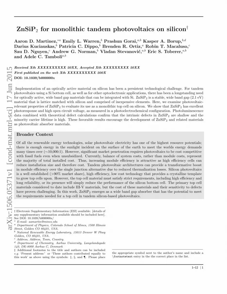
Fig. 1 Theoretically determined band gaps versus latticeconstants for some of the more earth abundant II-IV-V2
chalcopyrites. Also shown are III-V materials along with Siand Ge from group IV. The gray vertical bars overlaying Siand Ge highlight materials with similar lattice constant,within ± 1%.
1 Introduction
Optoelectronic materials are typically tetrahedral, cova-lently bonded semiconductors (i.e. group IV, II-VI andIII-V materials). While the ternary II-VI analogs suchas I-III-VI2 (i.e. CuInSe2) have been extensively inves-tigated,1 it is surprising that III-V analogs such as II-IV-V2 (i.e. ZnSiP2) have received less attention for opto-electronic devices.2–9 Figure 1 shows that II-IV-V2 chal-copyrite compounds span a broad range of band gapsfrom 0.4 eV (CdSnAs2) to 2.5 eV (MgSnP2) and latticeconstants that are compatible with many unary and bi-nary semiconductors. Many of the II-IV-V2 compoundsare formed from comparatively inexpensive and non-toxicelements (e.g. Zn, Mg, Si, Sn, N, P), rendering them
particularly attractive for applications requiring largescale deployment such as photovoltaics.10–12 Several ofthese compounds (e.g. ZnSnP2, ZnGeAs2) have directband gaps suitable for one-sun, thin film applications,and some effort has been directed towards determiningtheir optoelectronic properties and device characteriza-tion.6–9,13 In contrast, the wider band gap materials haveseen virtually no investigation and represent a significantopportunity for tandem photovoltaic (PV), light emittingdiode, photonic circuit, and laser applications.14–16
Within tandem PV, the II-IV-V2 compounds ZnSiP2
and ZnGeP2 are of particular interest as epitaxial topcell materials on a silicon bottom cell. Implementingthese materials as inexpensive, earth-abundant top cellson Si leverages the dominance of Si PV (>90% mar-ket share).17 The fundamental properties of ZnSiP2 havebeen studied since the late 1950’s using crystals that havebeen grown in a flux (typically Zn or Sn) or by halo-gen assisted vapor transport.2,11,12,18–35 Studies of thesecrystals reveal ZnSiP2 has a very small lattice mismatchwith Si of 0.5% (Fig. 1), has a band gap of ∼2.1 eV,forms with minimal atomic disorder, and is structurallystable at temperatures up to 800 ◦C.11,12,32–38 Doping ofZnSiP2 has yielded n-type (Se, Te, In, or Ga) and p-type(Cu) crystals.11,18,19,27,30
Some characterization has been done which is specif-ically relevant to the applications of tandem PV cellswith silicon. Heteroepitaxy has been successfully demon-strated between ZnSiP2 and Si by crystallization of Si onZnSiP2 substrates.24,38 In addition, such a device wouldbe expected to have good light transmission throughthe top cell, and into the bottom cell, because ZnSiP2
has little parasitic below-band-gap absorption, and goodindex of refraction matching with Si (reflection at theSi/ZnSiP2 interface would be less than 1%).36 Consid-ering that it is a stable, bipolar dopable, wide bandgap semiconductor that is lattice and index of refractionmatched with Si, ZnSiP2 is a promising material for im-plementation as a top cell on Si PV.
One of the main challenges that could impede the de-velopment of ZnSiP2 as a PV material is the symmetryforbidden nature of its direct band gap.27,36,39 This arisesbecause the electric dipole transition between the valenceband maximum (VBM) and conduction band minimum(CBM) is forbidden by a selection rule.40 The conceptof forbidden transitions is discussed more thoroughly insection 2.5, but the resulting consequence is weak opticalabsorption onset, similar to an indirect band gap mate-rial. Contrary to indirect materials, there may be ways tostrengthen the weak absorption onset due forbidden tran-sitions; one possible approach is presented in section 2.5.In addition to the forbidden transition challenge, pho-
2 | 1–12

c
a
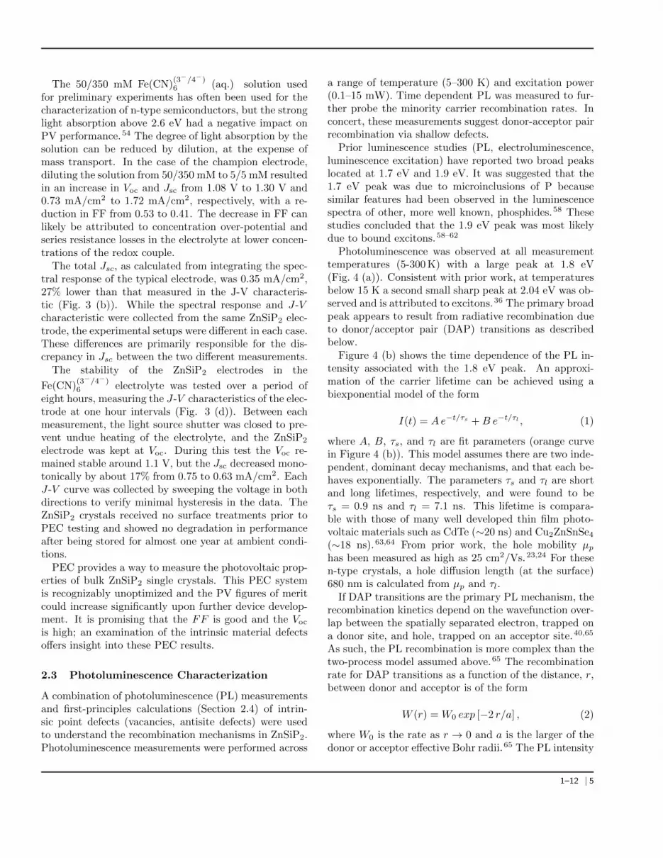
(a) (b)
Fig. 2 (a) Photograph of ZnSiP2 single crystals grown inZn flux. (b) Crystal structure of II-IV-V2 chalcopyrites(I42d) emphasizing two interlaced networks of corner sharingtetrahedra. In one network, the tetrahedra (red) have aGroup IV atom at the center and Group V atoms on thecorners. The second network differs from the first, in thatthe tetrahedra (blue) are slightly distorted and they have aGroup II atom at the center.
tovoltaic energy conversion properties, material defects,electrical contacts, surface passivation, and film growthare unknowns that must be addressed for photovoltaicimplementation of ZnSiP2.
In this work, we have employed a variety of theoreticaland experimental techniques to address some of the chal-lenges and unknowns regarding ZnSiP2 as a top cell mate-rial on Si PV. We show photoelectrochemical (PEC) mea-surements of ZnSiP2 which demonstrate excellent pho-toresponse and high open circuit voltage (Voc). We findthe intrinsic material to contain both donor and accep-tor defects, that the associated energy levels are shal-low (∼0.1 eV from the associated band edge), and thatwithin detection limits of single crystal X-ray diffraction,the material is ordered. Finally, we show theoretically,that it may be possible to significantly strengthen theabsorption onset of a forbidden band gap transition byalloying. These findings establish ZnSiP2 as a potentialmonolithic top cell material on Si.
2 Results and Discussion
2.1 Synthesis and Structure
Flux synthesis yielded ZnSiP2 crystals which are translu-cent, dark red in color, and with dimensions up to 2mm thick, 5 mm wide, and 20 mm long (see Fig. 2 (a)).Single crystal X-ray diffraction (SCXRD) data confirmsthat ZnSiP2 crystallizes in the I42d space group (No.
122) with unit cell dimensions of a = 5.3986(2) andc = 10.4502(6) A (see Fig. 2 (b)). The SCXRD struc-tural analysis results are given in Supplementary Ta-bles ??-?? and agree well with previously reported struc-tural data.37
Some chalcopyrites are known to display atomic dis-order resulting in variation of their optical proper-ties.21,41–43 Refinements of the SCXRD data indicate nosignificant disorder of Zn and Si between the 4a (Zn) and4b (Si) sites. When occupancies and atomic displacementparameters were allowed to refine, the occupancies of allsites remained stable at 1.00(2) (see Supplementary Ta-ble ??), indicating that all sites are fully occupied. Astructural model with Zn and Si occupying both 4a and4b sites was also employed. This model led to less than1.3% occupancy of Si on the 4a site and no mixing ofZn onto the 4b site. Statistics for this model are com-parable to statistics for the model with no site mixing.In addition, all atomic displacement parameters led tonearly spherical thermal ellipsoids. Consistent with pre-vious results, and in contrast to other ternary and quar-ternary PV materials,41,44–46 ZnSiP2 prefers a highly or-dered atomic structure that is very stable.32,36,37
2.2 Photovoltaic Characterization
Regenerative photoelectrochemistry (PEC) allows themeasurement of the current density vs. potential (J-V ) of irregularly shaped, multi-faceted, bulk single crys-tals without the need to create a solid state p-n junc-tion. Briefly, a ZnSiP2 crystal is formed into an elec-trode and submersed in an aqueous solution contain-ing a one- electron, reversible, outer-sphere redox cou-
ple, Fe(CN)(3−/4−)6 (aq.), creating a semiconductor-liquid
junction (Fig 3 (a)). This method has proven to be a suc-cessful initial characterization technique for many semi-conductors.47–53 Within this photoelectrochemical con-figuration, an initial measurement of 0.9% photoconver-sion efficiency was obtained from ZnSiP2 single crystals.
Photoelectrochemical electrodes were constructed fromseveral single crystals, and representative J-V charac-teristic data is shown in Fig. 3 (b), along with datafrom the champion electrode. The representative J-Vdata was collected for electrodes in contact with 50mMK4Fe(CN)6/350mM K3Fe(CN)6 (aq.),54 while the cham-pion J-V data was collected in a solution with 5mMof each redox species. The PEC rectification with the
Fe(CN)(3−/4−)6 (aq.) electrolyte indicates that the ZnSiP2
crystal is n-type. The champion electrode produced aVoc of 1.30 V, a short circuit current density (Jsc) of1.72 mA/cm2, a fill-factor (FF ) of 0.41, and a one-sunefficiency (η) of 0.9%. The crystals exhibit excellent pho-
1–12 | 3

(b)
(c)
(a)
AM1.5 or Monochromatic Light
Electrolyte
Pt Counter
SCE Reference
Calibrated SiPhotodiode
ZnSiP2 Working
Rapid Stirring
0 1 2 3 4 5 6 7 8Time (h)
0.0
0.2
0.4
0.6
0.8
1.0
1.2
VO
C(V
vs.
Soln
)
VOC
0.0
0.2
0.4
0.6
0.8
1.0
J SC
(mA
/cm
2)
JSC
(d)
400 500 600 700 800Wavelength (nm)
0
2
4
6
8
10
EQ
E (
%)
Response
ZnSiP2 Absorb.
Solution Absorb.
0.0
0.2
0.4
0.6
0.8
1.0A
bso
rbance
2.6 2.1 1.6Energy (eV)
1.2 0.8 0.4 0.0Potential (V vs. Soln.)
0.0
0.5
1.0
1.5
2.0
J (m
A/c
m2
)
ChampionTypicalDark
Fig. 3 (a) Schematic of the photoelectrochemical cell with ZnSiP2 working electrode, and Si photodiode for calibrating lightintensity. (b) Photoelectrochemical current - voltage characteristic for ZnSiP2, with the voltage swept in both directions. (c)Spectral response of the typical ZnSiP2 electrode shown in (b). Results of stability test (8 hours in solution in the dark).
toresponse and good PV figures of merit, considering theearly stage in the development of ZnSiP2.
The 1.30 V Voc of ZnSiP2 from these measurements isparticularly high given the material’s 2.1 eV band gap(Eg) and the non-optimized nature of the PEC junction.A homojunction PV device would be expected to have amaximum Voc of ∼1.8 V.55,56 In the PEC cell, however,the Voc is related to the barrier height set by the redoxpotential of the electrolyte. High Voc is indicative of goodmaterial quality, good charge carrier lifetime, and a lackof deep level defects. This is a good sign because increas-ing the Voc can be one of the most significant challengesin the development of a new material.57
There are several potential explanations for the ob-served low current density of the electrodes: diffusion lim-itation due to crystal thickness (0.2 to 1 mm), weak lightabsorption, resistive losses, and parasitic light absorptionby the solution. Figure 3 (c) shows the spectral responseof the same ZnSiP2 electrode from which the J-V char-
acteristic is shown in Fig. 3 (b), along with the solutionabsorbance, and that of ZnSiP2. From the spectral re-sponse, it is apparent that the short wavelength spectralregion is cut off by solution absorption; only a small bandof the AM1.5 spectrum was absorbed by the crystal, re-sulting in very few photogenerated carriers. The longwavelength edge of the spectral response closely resem-bles the ZnSiP2 absorbance spectrum, indicating that PVperformance is limited by light absorption, as expecteddue to the symmetry forbidden nature of transitions atthe band gap. The crystals were thick (0.5-2 mm), there-fore it is probable that many photocarriers recombinedbefore they could be collected. There are also three con-tributions to series resistance: solution, bulk, and backcontact, each of which could be significant. The J-Vcurves shown herein have not been corrected by takingthe solution resistance into account; this resistance is dueto mass transport limitation and results in artificially lowFF .
4 | 1–12
The 50/350 mM Fe(CN)(3−/4−)6 (aq.) solution used
for preliminary experiments has often been used for thecharacterization of n-type semiconductors, but the stronglight absorption above 2.6 eV had a negative impact onPV performance.54 The degree of light absorption by thesolution can be reduced by dilution, at the expense ofmass transport. In the case of the champion electrode,diluting the solution from 50/350 mM to 5/5 mM resultedin an increase in Voc and Jsc from 1.08 V to 1.30 V and0.73 mA/cm2 to 1.72 mA/cm2, respectively, with a re-duction in FF from 0.53 to 0.41. The decrease in FF canlikely be attributed to concentration over-potential andseries resistance losses in the electrolyte at lower concen-trations of the redox couple.
The total Jsc, as calculated from integrating the spec-tral response of the typical electrode, was 0.35 mA/cm2,27% lower than that measured in the J-V characteris-tic (Fig. 3 (b)). While the spectral response and J-Vcharacteristic were collected from the same ZnSiP2 elec-trode, the experimental setups were different in each case.These differences are primarily responsible for the dis-crepancy in Jsc between the two different measurements.
The stability of the ZnSiP2 electrodes in the
Fe(CN)(3−/4−)6 electrolyte was tested over a period of
eight hours, measuring the J-V characteristics of the elec-trode at one hour intervals (Fig. 3 (d)). Between eachmeasurement, the light source shutter was closed to pre-vent undue heating of the electrolyte, and the ZnSiP2
electrode was kept at Voc. During this test the Voc re-mained stable around 1.1 V, but the Jsc decreased mono-tonically by about 17% from 0.75 to 0.63 mA/cm2. EachJ-V curve was collected by sweeping the voltage in bothdirections to verify minimal hysteresis in the data. TheZnSiP2 crystals received no surface treatments prior toPEC testing and showed no degradation in performanceafter being stored for almost one year at ambient condi-tions.
PEC provides a way to measure the photovoltaic prop-erties of bulk ZnSiP2 single crystals. This PEC systemis recognizably unoptimized and the PV figures of meritcould increase significantly upon further device develop-ment. It is promising that the FF is good and the Voc
is high; an examination of the intrinsic material defectsoffers insight into these PEC results.
2.3 Photoluminescence Characterization
A combination of photoluminescence (PL) measurementsand first-principles calculations (Section 2.4) of intrin-sic point defects (vacancies, antisite defects) were usedto understand the recombination mechanisms in ZnSiP2.Photoluminescence measurements were performed across
a range of temperature (5–300 K) and excitation power(0.1–15 mW). Time dependent PL was measured to fur-ther probe the minority carrier recombination rates. Inconcert, these measurements suggest donor-acceptor pairrecombination via shallow defects.
Prior luminescence studies (PL, electroluminescence,luminescence excitation) have reported two broad peakslocated at 1.7 eV and 1.9 eV. It was suggested that the1.7 eV peak was due to microinclusions of P becausesimilar features had been observed in the luminescencespectra of other, more well known, phosphides.58 Thesestudies concluded that the 1.9 eV peak was most likelydue to bound excitons.58–62
Photoluminescence was observed at all measurementtemperatures (5-300 K) with a large peak at 1.8 eV(Fig. 4 (a)). Consistent with prior work, at temperaturesbelow 15 K a second small sharp peak at 2.04 eV was ob-served and is attributed to excitons.36 The primary broadpeak appears to result from radiative recombination dueto donor/acceptor pair (DAP) transitions as describedbelow.
Figure 4 (b) shows the time dependence of the PL in-tensity associated with the 1.8 eV peak. An approxi-mation of the carrier lifetime can be achieved using abiexponential model of the form
I(t) = Ae−t/τs +B e−t/τl , (1)
where A, B, τs, and τl are fit parameters (orange curvein Figure 4 (b)). This model assumes there are two inde-pendent, dominant decay mechanisms, and that each be-haves exponentially. The parameters τs and τl are shortand long lifetimes, respectively, and were found to beτs = 0.9 ns and τl = 7.1 ns. This lifetime is compara-ble with those of many well developed thin film photo-voltaic materials such as CdTe (∼20 ns) and Cu2ZnSnSe4
(∼18 ns).63,64 From prior work, the hole mobility µphas been measured as high as 25 cm2/Vs.23,24 For thesen-type crystals, a hole diffusion length (at the surface)680 nm is calculated from µp and τl.
If DAP transitions are the primary PL mechanism, therecombination kinetics depend on the wavefunction over-lap between the spatially separated electron, trapped ona donor site, and hole, trapped on an acceptor site.40,65
As such, the PL recombination is more complex than thetwo-process model assumed above.65 The recombinationrate for DAP transitions as a function of the distance, r,between donor and acceptor is of the form
W (r) = W0 exp [−2 r/a] , (2)
where W0 is the rate as r → 0 and a is the larger of thedonor or acceptor effective Bohr radii.65 The PL intensity
1–12 | 5

(c)
(a)
CBM
VBM
ED
EA
1.4 1.6 1.8 2.0 2.2 2.4Energy (eV)
Inte
nsi
ty (
arb
.)
(b)
(d) (e)
10-1 100 101
Power (mW)
103
104
105
Inte
nsi
ty (
arb
.)
Power Law Fit
100 K
10-1 100 101
Power (mW)
1.661.681.701.721.74
Peak
(eV
) 100 K
5 K
100 101
Time (ns)
100
101
102
103
Inte
nsi
ty (
arb
.)
DataExponential Fit, Eqn. (1)DAP Fit, Eqn. (3)
300 K
0 50 100 150 2001000/T (K)
10-3
10-2
10-1
100
Inte
nsi
ty (
arb
.)
Fit, Eqn. (5)
Fig. 4 (a) Photoluminescence spectrum of ZnSiP2. The inset energy level diagram illustrates the most likely mechanism forthe observed luminescence: donor/acceptor pair (DAP) transitions. (b) Time dependence of the 1.8 eV peak is evidence ofDAP transitions and shows good carrier lifetime. (c) The temperature dependence of the 1.8 eV peak integrated intensity fitsEqn. (5), giving ED = 58 meV. (d) The power dependence of the 1.8 eV peak position shows a blue shift characteristic ofDAP transitions. (e) The power dependence of the 1.8 eV peak integrated intensity; a fit to the data with I(P ) ∝ P k furthersupports DAP transitions.
as a function of time, t, is proportional to
I(t) ∝ exp[4πN
∫ ∞0
(exp [−W (r) t]− 1) r2 dr
]× 4πN
∫ ∞0
W (r) exp [−W (r) t] r2 dr, (3)
where N is the concentration of the majority defect(donors in this case).65 While W0, a, and N are freeparameters, the parameters a and N are coupled into thenon-dimensional constant ζ ≡ a3N . The black curve inFigure 4 (b) shows the resulting fit is significantly bet-ter than the biexponential fit (orange) despite fewer freeparameters. Because the donor and acceptor concentra-tions are similar (as suggested by our theoretical analysisin section 2.4), the donor and acceptor contributions to ζ(1.856× 10⁻²) cannot be decoupled. W0 was found to be7.2× 109 s−1, slightly higher than GaAs (3× 10⁸ s−1).66
The fit of Eqn. (3) to the time dependent data (Fig. 4 (b))demonstrates that DAP transitions are likely the domi-nant recombination mechanism.
The power dependence of the PL gives additional evi-dence of DAP transitions. With increased injection lev-els, the increased density of excited charge carriers leadsto a stronger Coulomb interaction between ionized DAPs.This interaction leads to an increase in the emitted pho-ton energy following:
hω(r) = Eg − EA − ED +e2
r(cgs), (4)
where Eg is the band gap, EA is the ionization energy ofthe acceptor, ED is the ionization energy of the donor, eis the electron charge, and r is the distance between thedonor and acceptor responsible for the transition. Fig-ure 4 (d) shows the peak position shifting to higher en-ergy as the injection level is increased, characteristic ofDAP transitions.
Finally, the power dependence of the peak intensity(Fig. 4 (e)) can be considered within the DAP hypothesis.An exponential model of the form I(P ) ∝ P k, where P isthe excitation power and k is the exponent, was fit to theexperimental data. For the nine distinct temperatures at
6 | 1–12

which power dependent data was collected, the average kwas 0.72 with a standard deviation of the average of 0.12.With k < 1, the power dependence of the peak intensity ischaracteristic of either free to bound, or DAP transitionsas being the primary source of radiative recombination.67
In addition to recombination mechanisms, PL dataanalysis can provide the donor (because the material isn-type) activation energy. Fig. 4 (c) shows the integratedintensity was found to increase significantly with decreas-ing temperature down to 25 K. Falling below 25 K, thePL intensity decreased and eventually appeared to satu-rate. The temperature region above 25 K was fit with
I(T ) ∝ 1
1 + α e(ED/kBT ), (5)
where α is a process rate parameter, kB is Boltzmann’sconstant, and T is the temperature.68 Six temperature-dependent data sets were collected at different excitationpowers, and the activation energy of the 1.8 eV peak wasfound to be ED = 58± 16 meV; this value is shallow, andin agreement with previous reports.58,59
The time and power dependence of the PL intensityand the power dependence of the peak position are allindicative of DAP recombination. There was no evidencein the PL of deep level defects, and the temperature de-pendence of the PL intensity predicts the donor level tobe shallow, which corresponds to the high Voc found inthe PEC characterization.
2.4 Identification of Potential Intrinsic Defects
To better understand the nature of plausible point de-fects that act as donors and acceptors in ZnSiP2, we em-ployed first-principles density functional theory (DFT)calculations. By calculating the enthalpies of formationof known Zn-Si-P phases, a stability map in chemicalpotential space was constructed.69 The enthalpy of for-mation of intrinsic defects within the ZnSiP2 region ofstability of this chemical potential space were also calcu-lated, along with the associated density of states (DOS)of relevant defects. The formation enthalpies (∆HD,q)of 7 different point defect types (3 vacancies, 4 antisitedefects) were calculated in 7 different charge states (3-through 3+; 4- and 4+ were additionally examined forVSi) as a function of Zn, Si and P chemical potentials,and Fermi level (EF).
The Zn-Si-P phase diagram calculated at standard con-ditions using Fitted Elemental-Phase Reference Energies(FERE) is shown in Fig. 5 (a).69 ZnSiP2 occupies a largeregion of this chemical potential phase space, with com-peting phases that include Zn, Si and P elements, andthe binary compounds SiP, Zn3P2, and ZnP2. Within
the phase space where ZnSiP2 is stable, there are threedistinct regimes (labelled R1, R2, and R3) with differentlowest-energy defect pairs. The dominant DAPs that pinthe Fermi level are Si2+
Zn and Si1−P in Region 1, P1+Si and
Zn2−Si in Region 2, and Si2+
Zn and Zn2−Si in Region 3. The
pinned Fermi levels (EF ) are indicated by dotted verticallines in Figs. 5 (c), (d), and (e).
The ZnSiP2 crystals were grown under Zn-rich, Si-poor, and P-poor conditions. These growth conditionsmost likely lie near the line connecting points 1 and 3,shown in Fig. 5 (a). For this reason, the defect forma-tion energies and their concentrations are examined atpoints 1, 2, and 3, which lie in the corresponding re-gions R1, R2, and R3, in Fig. 5 (a). For the point de-fects considered, ∆HD,q as a function of EF is shown inFig. 5 (c), (d), and (e). A first order approximation ofthe defect concentrations can be found from
[N ] = [S] e∆HD,qkBT , (6)
where [S] is the crystallographic site concentration([Zn] = [Si] = [P] /2 ≈ 1.3× 1022 cm−3), kB is the Boltz-mann constant, and T is the temperature at which thedefects form. The defect concentrations were calculatedat T = 500 ◦C, resulting in a lower limit to what maybe observed experimentally; this is because the crystalgrowth occurs as the temperature of the Zn flux slowlycools (∼2 ◦C/h) from 1000 ◦C to 500 ◦C, after which theflux is rapidly cooled to room temperature. The calcu-lated DAP pairs and associated concentrations are foundin Table 1.
Table 1 Concentrations of dominant defects ZnSiP2. Thelocations of points 1, 2, and 3 are identified in Fig. 2.4 (a).[D] and [A] are the donor and acceptor concentrations incm−3.
Point DAP [D] [A]
1 Si2+Zn /Si1−P 7.5× 10¹⁸ 1.5× 10¹⁹
2 Si2+Zn /Zn2−
Si 6.1× 10¹³ 6.1× 10¹³
3 P1+Si /Zn2−
Si 4.3× 10¹⁵ 4.3× 10¹⁵
1–12 | 7

1.0
Pinn
ed F
erm
i Lev
el (e
V)
1.1
1.2
1.3
1.4
1.5
1.6
1.72.17
Si
0.0
0.2
0.4
0.6
0.8
1.0
1.2
1.4
1.6
Zn0.00.20.40.60.81.01.21.41.6
(eV)
(eV)
ZnSiP2SiP
R1
R2
R3Zn3P2
ZnP2
mid-gap
band gapVZn
0 -1
-2 VSi+1
-2
ZnSi
0 -1
-2
VP0
+3
+1 -1
SiZn
0+1
PSi
+1 0
SiP
0+1-1
+2
-4
HD
,q (e
V)
0
2
4
61
2
3
VZn
0 -1-2
VSi
+1
-2
ZnSi
0 -1
-2
VP
0
+3
+1
SiZn
0+1
PSi+1
0
SiP
0+1 -1
+2
HD
,q (e
V)
0
2
4
6
VZn
0 -1-2
VSi
+1
-2
ZnSi
0 -1
-2
VP 0
+3+1
-1
SiZn
0+1
PSi+1
0SiP
0+1 -1
+2
-4HD
,q (e
V)
0
2
4
6
EF (eV)0 1 2
1
2
3
Bulk VBM CBM
DO
S
20
40
SiP(-1)
DO
S
20
40
0
SiZn(+2)
DO
S
0
20
40
PSi(+1)
DO
S
0
20
40
ZnSi(-2)
DO
S
0
20
40
E (eV)0 1 2 3 4 5 6 7 8
∆µP = 0
(a)
(b)
(c)
(d)
(e)
Fig. 5 (a) Zn-Si-P phase diagram in chemical potential space. The flux growth conditions are Zn rich and are thereforeexpected to lie in the region between point 1 and point 3. Also shown is the pinned Fermi level, which ranges from slightlybelow mid-gap at point 1 to around 1.7 eV above the valence band maximum. (b) The density of states of bulk ZnSiP2 andthe four primary intrinsic defects: Si2+
Zn , Si1−P , P1+Si , and Zn2−
Si . These defect energy levels appear to be shallow; there is noevidence of deep trap states that could detrimentally reduce the Voc. (c) Defect formation energies at point 1 in (a). (d)Defect formation energies at point 2 in (a). (e) Defect formation energies at point 3 in (a).
8 | 1–12
The density of states (DOS) of defect-free ZnSiP2 andZnSiP2 containing one of the four prominent defects areshown in Fig 5 b. The shallow donor and acceptor statesappear as shoulders near the conduction band minima(CBM) and the valence band maxima (VBM), respec-tively. There is no evidence of mid-gap states in eithercase. This lack of deep level mid-gap states is promis-ing for achieving a high Voc photovoltaic device. Previ-ous studies have observed a deep acceptor level, ∼0.7 eVabove the VBM, which appears to have been the resultof extrinsic impurity (Cu) doping.19,22,70
Doping of many wide-band gap semiconductors hasproven to be challenging.71 Figure 5 (a) shows the heatmap of the pinned EF , which is determined by the chargebalance between the predominant donor and acceptorpoint defects. The pinned EF lies above the mid-gap inthe majority of the chemical potential phase space whereZnSiP2 is stable, resulting in intrinsic or moderately n-type behavior. In fact, ZnSiP2 has been synthesized asboth n- or p-type material, likely due to impurities aris-ing from the synthesis techniques. Crystals grown in a Znflux have been reported with both n-type,2,20,23,28,29,31
and p-type conductivity.19,22,23,29 All reports of growthin Sn flux have been n-type.11,20,22,23,27,29,31,34 Halogenassisted vapor transport growth with I has produced n-type crystals,27,34 while use of Cl as the carrier gas, withZnCl2 and PbCl2 as Cl sources, has produced p-type crys-tals.19,22,23,72 There is one report of n-type conductivityresulting from Cl vapor transport using SiCl4 as the Clsource.20 The crystals have intentionally been extrinsi-cally doped n-type by adding Se, Te, In, or Ga, and p-type by adding Cu.11,18,19,27,30 The electronic propertiesthat have been reported in these and other studies aregiven in Table ??. When other elements are involved inthe synthesis (Sn flux or I, or Cl vapor transport) theyhave been found as impurities in the resultant crystals.34
These studies demonstrate that ZnSiP2 can be synthe-sized either n- or p-type, using extrinsic dopants, withcarrier concentrations acceptable for PV devices.
PL experiments and theoretical defect calculations areconsistent with DAP antisite defects as the prevalent re-combination mechanism in ZnSiP2. These DAP defectswork together to pin the Fermi level such that carefullyprepared ZnSiP2 is expected to be intrinsic, or lightlyn-type. The temperature dependence of the PL inten-sity found the donor level to be shallow: ∼58 meV belowthe CBM. Correspondingly, the dominant defects iden-tified in the calculations were found to occupy shallowlevels, based on their associated DOS. These results in-dicate that, over the full chemical potential region of sta-bility, ZnSiP2 PV devices should have high Voc, which isin agreement with the PEC results from Section 2.2.
2.5 Enhancing Optical Absorption in II-IV-V2
Chalcopyrites
Further improvements to photovoltaic performance ofZnSiP2 must address the weak light absorption proper-ties, which reduce the available Jsc. Ideally, a materialwith a 2.1 eV band gap could be capable of producing∼12 mA/cm2 under AM1.5G illumination, significantlyhigher than the 1.7 mA/cm2 observed in this study. Onereason for the low Jsc is weak absorption due to the sym-metry forbidden band gap. The symmetry forbidden na-ture of a band-to-band transition can be understood byexamining the evolution of s and p atomic orbitals intovalence and conduction bands in a semiconductor crys-tal;40 the bands can be thought of as maintaining thes- or p-like symmetry they possessed as atomic orbitals.One selection rule from the electronic dipole approxima-tion requires that the angular momentum of the finalstate be equal to that of the initial state plus or minusone (`f = `i ± 1, due to the absorption or emission ofa photon). Therefore, transitions from bands with s-likesymmetry (` = 0) to those with p-like symmetry (` = 1),and vice versa, are allowed, while s to s and p to p tran-sitions are forbidden. In a material with a direct butsymmetry forbidden band gap, the band ordering is suchthat the valence band maximum (VBM) and the conduc-tion band minimum (CBM) can be treated as having thesame symmetry; thus transitions between these bands issymmetry forbidden. When moving away from the VBMand CBM, the transitions become weakly allowed with anincreasing transition probability, resulting an absorptiononset with a slope similar to that of an indirect gap ma-terial, as shown in Fig. 6 for pure ZnGeP2 and ZnSiP2,both materials of similar lattice constants, with ∼2.1 eVband gaps and symmetry forbidden transitions.
Within the II-IV-V2 phosphide and arsenide materi-als, the position of the s-like conduction band dependson the chemical composition, while the p-like band isroughly fixed in energy (Fig. 7). As the formula mass in-creases, the s-like band drops, reaching below the p-likeband for the heavier members of the II-IV-V2 class.73
This trend suggests that alloying with heavier elementscould break the symmetry constraint on the forbiddenband gap materials, resulting in a steeper absorption on-set. ZnGeP2 is a material with very similar propertiesto ZnSiP2 but a slightly heavier composition (Ge insteadof Si); thus, its s and p bands are closer in energy andthus may be easier to modify. Fig. 6 shows the theoret-ical absorption coefficients of ZnSiP2, ZnGeP2, and twoalloys: Zn(Ge0.5Sn0.5)P2 and (Zn0.5Cd0.5)GeP2. In bothalloys, the addition of a heavier element has significantlyincreased the absorption strength of the material with
1–12 | 9

2 3 4 5E (eV)
100
101
102
103
104
105
106
α(c
m−
1)
ZnSiP2
ZnGeP2
(Zn0.5Cd0.5)GeP2
Zn(Ge0.5Sn0.5)P2
Fig. 6 Theoretical absorption coefficient of ZnSiP2,ZnGeP2, and two ZnGeP2 alloys. Alloying may significantlyincrease the near-edge absorption strength of the material.
little effect on the location of the absorption edge. Thissuggests that adding heavier elements to ZnGeP2 andZnSiP2 has the potential to significantly increase theirlight absorption properties, enhancing Jsc.
3 Methods
The ZnSiP2 crystals used in this study were synthesizedby the flux growth technique described in Ref.36. Inthis technique elemental zinc, silicon, and phosphorous(20:1:2 molar ratio and 5N, 5N, and 6N purity, respec-tively) are sealed in an evacuated quartz ampule, heatedto 1000 ◦C, and then slowly cooled (2◦C/h). The excesszinc acts as a solvent for silicon and phosphorous. Crystalnucleation and growth occurs within the zinc flux whichis removed after growth by washing in HCl:H2O (1:3 byvolume). Surface precipitates of Si can be removed byetching in dilute HF:HNO3:H2O (10:3:87 by volume) so-lution. Si precipitates within the ZnSiP2 crystal interiorhave not been observed.
A fragment (approximately 0.01×0.01×0.03 mm) cutfrom a larger single crystal was used to collect singlecrystal X-ray diffraction (SCXRD) data. This crystalfragment was mounted onto the goniometer of a BrukerKappaCCD diffractometer equipped with Mo Kα (λ =0.71073 A) radiation. Data collection and structure solu-tion were performed with SHELX-97. Structural refine-ments and extinction corrections were performed using
(a)
(b)
MgSiP
2
ZnSiP
2
CdSiP
2
MgGeP2
ZnGeP2
CdGeP2
MgSnP2
ZnSnP2
CdSnP2
0.00.51.01.52.02.53.03.5
E−EVBM(eV)
s-states
p-states
MgSiAs 2
ZnSiAs 2
CdSiAs 2
MgGeAs 2
ZnGeAs 2
CdGeAs 2
MgSnAs 2
ZnSnAs 2
CdSnAs 2
0.00.51.01.52.02.53.03.5
E−EVBM(eV)
s-states
p-states
Fig. 7 (a) A plot of the two lowest conduction band statesfor relevant II-IV-P2 chalcopyrites, highlighting thesymmetry of each state and showing a decreasing trend inthe position of states with s-like symmetry for differentGroup II and IV atoms of increasing atomic mass. (b) Aplot of the two lowest conduction band states for relevantII-IV-As2 chalcopyrites showing a similar trend to thatshown in (b), and that the levels of both the p-like and s-likestates have decreased as the atomic mass of the Group Vatom has increased.
SHELXL suite.The photoelectrochemical (PEC) response of ZnSiP2
was tested using the Fe(CN)(3−,4−)6 redox couple
(350 mM potassium ferrocyanide, 50 mM potassium fer-ricyanide in H2O with no supporting electrolyte).54,74
ZnSiP2 electrodes were constructed by evaporating metalback contacts on one flat side of the crystals. The backcontacts were either 700 nm of In or 150 nm of Au, andthey were capacitively blasted to achieve ohmic behavior.A copper lead wire was affixed to the back contact withsilver paint and the electrode was sealed at the end ofa glass tube with epoxy (Loctite, Hysol 1C). An AM1.5light source (ABET Technologies, model no. 10500) wasused to illuminate the front of the crystal and the light in-tensity was set by placing a calibrated photodiode (ThorLabs part no. FDS100) electrode in the same position asthe crystal electrode, resulting in very repeatable data.
10 | 1–12

Current-voltage data was collected using a BioLogic SP-240 potentiostat with Pt foil as the counter electrodeand a saturated calomel reference electrode. Potentialswere later adjusted to reference the solution potential,E(A/A−), which was measured with a Pt wire in theelectrolyte.
Photoluminescence spectra were collected with a 442nm HeCd laser with a 250 µm spot size. Spectra werecollected at temperatures of 5, 10, 15, 20, 25, 30, 50, 75,100, and 300 K. At each temperature, the laser powerwas varied and spectra were collected at 0.1, 0.5, 1.0, 5.0,10.0, and 15.0 mW (laser power at crystal surface).
A Yb:KGW laser and an optical parametric amplifier(pulse length 0.3 ps, repetition rate 1.1 Mhz, wavelength420 nm) were used for single photon excitation photo-luminescence lifetime measurements. Excitation beamdiameter was 0.2 mm, average laser power 2 mW. PLwas measured with 10 nm bandpass filter at 650 nm, Siavalanche photodiode detector, and time-correlated sin-gle photon counting. Measurements were done at roomtemperature on two different, opposing sides of the samecrystal. The results were slightly different from one sideto the other and measurements of different spots on thesame side yielded very consistent data.
4 Conclusions
A combination of photoeletrochemical (PEC) charac-terization, photoluminescence (PL) measurements, andtheoretical intrinsic defect calculations have shown thatZnSiP2 has the potential to be a high quality photo-voltaic top cell material. PEC characterization revealedhigh open circuit voltage, indicating a lack of deep leveldefects. PL confirmed the presence of shallow donor-acceptor pairs as well as the lack of deep level de-fects. Theoretical defect calculations established that thedominant defects in ZnSiP2 are shallow antisite defectsthroughout the stability window in Zn-Si-P chemical po-tential space. ZnSiP2 is additionally predicted to be in-trinsic, or moderately n-type throughout this entire re-gion in chemical potential space. Thus, this material isintrinsically very stable and defect-tolerant. Calculationsof absorption coefficient indicate that alloying is a promis-ing method for improving Jsc in future devices.
References
1 M. A. Green, Journal of Materials Science: Materials in Elec-tronics, 2007, 18, 15–19.
2 G. Kuhnel, W. Siegel and E. Ziegler, Physica Status Solidi (a),1975, 30, K25–K27.
3 T. Shirakawa, K. Okamura and J. Nakai, Physics Letters A,1979, 73, 442–444.
4 H. Shin and P. Ajmera, Materials Letters, 1987, 5, 211–214.
5 H. Shin and P. Ajmera, Materials Letters, 1989, 8, 464–467.
6 Y.-C. Wen and B. A. Parkinson, The Journal of Physical Chem-istry B, 1997, 101, 2659–2662.
7 T. J. Peshek, L. Zhang, R. K. Singh, Z. Tang, M. Vahidi, B. To,T. J. Coutts, T. A. Gessert, N. Newman and M. van Schilf-gaarde, Progress in Photovoltaics: Research and Applications,2013, 21, 906–917.
8 G. Xing, K. Bachmann, J. Posthill and M. Timmons, Journalof Crystal Growth, 1991, 113, 113–119.
9 S. G. Choi, M. van Schilfgaarde, D. E. Aspnes, A. G. Norman,J. M. Olson, T. J. Peshek and D. H. Levi, Phys. Rev. B, 2011,83, 235210.
10 C. L. Goodman, Nature, 1957, 179, 828–829.
11 A. Spring-Thorpe and B. Pamplin, Journal of Crystal Growth,1968, 3, 313–316.
12 V. D. Prochukhan and V. R. Yu, Soviet Physics: Semiconduc-tors, 1977, 12, 129–132.
13 A. Springthorpe, R. Harvey and B. Pamplin, Journal of CrystalGrowth, 1969, 6, 104–106.
14 H. Morkoc, S. Strite, G. Gao, M. Lin, B. Sverdlov and M. Burns,Journal of Applied Physics, 1994, 76, 1363–1398.
15 M. A. Green, Progress in Photovoltaics: Research and Appli-cations, 2001, 9, 123–135.
16 R. Soref, Selected Topics in Quantum Electronics, IEEE Jour-nal of, 2006, 12, 1678–1687.
17 Fraunhofer ISE, pg. 18, 28 July 2014, Photovoltaics Report,http://www.webcitation.org/6SFRTUaBS, Achived 31 August,2014.
18 A. Springthorpe and R. Monk, physica status solidi (a), 1970,1, K9–K12.
19 E. Ziegler, W. Siegel and G. Kuehnel, physica status solidi (a),1973, 18, 483–487.
20 W. Siegel and E. Ziegler, physica status solidi (a), 1974, 21,639–647.
21 J. Shay and J. Wernick, Ternary chalcopyrite semiconduc-tors: growth, electronic properties, and applications, PergamonPress, 1975.
22 I. Gorban, G. Grishchenko, A. Sakalas and I. Tychina, physicastatus solidi (a), 1976, 35, 571–574.
23 W. Siegel, A. Heinrich and E. Ziegler, physica status solidi (a),1976, 35, 269–279.
24 G. K. Averkieva, I. V. Grekhov, E. S. Kalevich, L. S. Kostina,V. D. Prochukhan and O. K. Semchinova, Izvestiya AkademiiNauk SSSR, Neorganicheskie Materialy, 1983, 19, 1967–1972.
25 G. Yao, H. Shen, R. Kershaw, K. Dwight and A. Wold, Mate-rials Research Bulletin, 1986, 21, 653–660.
26 E. Buehler and J. Wernick, Journal of Crystal Growth, 1971,8, 324–332.
27 J. L. Shay, B. Tell, E. Buehler and J. H. Wernick, Phys. Rev.Lett., 1973, 30, 983–986.
28 R. Humphreys and B. Pamplin, Le Journal de Physique Collo-ques, 1975, 36, C3–159.
29 R. Humphreys, Journal of Physics C: Solid State Physics, 1976,9, 4491.
30 E. Ziegler, W. Siegel, G. Kuhnel and E. Buhrig, physica statussolidi (a), 1978, 48, K63–K65.
31 G. Kuhnel, W. Siegel and E. Ziegler, physica status solidi (a),1978, 49, 705–711.
32 B. R. Pamplin, T. Kiyosawa and K. Masumoto, Progress inCrystal Growth and Characterization, 1979, 1, 331–387.
33 O. G. Folberth and H. Pfister, New Semiconducting Compounds
1–12 | 11

with Chalcopyrite Structure, Vieweg+Teubner Verlag, Braun-schweig, 1958, pp. 474–476.
34 W. Clark and R. Stroud, Journal of Physics C: Solid StatePhysics, 1973, 6, 2184–2190.
35 A. L. Gentile and O. M. Stafsudd, Materials Research Bulletin,1974, 9, 105–116.
36 A. Martinez, B. Ortiz, N. Johnson, L. Baranowski, L. Krishna,S. Choi, P. Dippo, B. To, A. Norman, P. Stradins, V. Ste-vanovic, E. Toberer and A. Tamboli, Photovoltaics, IEEE Jour-nal of, 2015, 5, 17–21.
37 S. C. Abrahams and J. L. Bernstein, The Journal of ChemicalPhysics, 1970, 52, 5607–5613.
38 I. Bertoti, Journal of Materials Science, 1970, 5, 1073–1077.
39 E. Alekperova, Y. A. Valov, N. Goryunova, S. Ryvkin andG. Shpenkov, physica status solidi (b), 1969, 32, 49–54.
40 P. Yu and M. Cardona, Fundamentals of Semiconductors:Physics and Materials Properties, Springer, 4th edn, 2010.
41 D. O. Scanlon and A. Walsh, Applied Physics Letters, 2012,100, 251911–1–251911–3.
42 G. A. Seryogin, S. A. Nikishin, H. Temkin, A. M. Mintairov,J. L. Merz and M. Holtz, Applied Physics Letters, 1999, 74,2128–2130.
43 N. Dietz, I. Tsveybak, W. Ruderman, G. Wood and K. Bach-mann, Applied physics letters, 1994, 65, 2759–2761.
44 P. Zawadzki, A. Zakutayev and S. Lany, Physical Review Ap-plied, 2015, 3, 034007–1–034007–7.
45 G. Rey, A. Redinger, J. Sendler, T. P. Weiss, M. Thevenin,M. Guennou, B. El Adib and S. Siebentritt, Applied PhysicsLetters, 2014, 105, 112106–1–112106–4.
46 P. St-Jean, G. Seryogin and S. Francoeur, Applied Physics Let-ters, 2010, 96, 231913.
47 E. L. Warren, D. B. Turner-Evans, R. L. Grimm, H. A. Atwaterand N. S. Lewis, Photovoltaic Specialists Conference (PVSC),2012 38th IEEE, 2012, pp. 000826–000830.
48 E. A. Santori, J. R. Maiolo III, M. J. Bierman, N. C. Strandwitz,M. D. Kelzenberg, B. S. Brunschwig, H. A. Atwater and N. S.Lewis, Energy & Environmental Science, 2012, 5, 6867–6871.
49 S. W. Boettcher, J. M. Spurgeon, M. C. Putnam, E. L. Warren,D. B. Turner-Evans, M. D. Kelzenberg, J. R. Maiolo, H. A.Atwater and N. S. Lewis, Science, 2010, 327, 185–187.
50 B. J. Tufts, L. G. Casagrande, N. S. Lewis and F. J. Grunthaner,Applied Physics Letters, 1990, 57, 1242–1244.
51 M. L. Rosenbluth and N. S. Lewis, Journal of the AmericanChemical Society, 1986, 108, 4689–4695.
52 A. Heller, B. Miller, H. Lewerenz and K. Bachmann, Journal ofthe American Chemical Society, 1980, 102, 6555–6556.
53 G. Hodes, J. Manassen and D. Cahen, Nature, 1976, 261, 403–404.
54 N. C. Strandwitz, D. J. Comstock, R. L. Grimm, A. C. Nichols-Nielander, J. Elam and N. S. Lewis, The Journal of PhysicalChemistry C, 2013, 117, 4931–4936.
55 P. Baruch, A. De Vos, P. Landsberg and J. Parrott, Solar En-ergy Materials and Solar Cells, 1995, 36, 201–222.
56 M. Y. Levy and C. Honsberg, Solid-state electronics, 2006, 50,1400–1405.
57 S.-H. Wei, S. Zhang and A. Zunger, Applied physics letters,1998, 72, 3199–3201.
58 J. Shay, R. Leheny, E. Buehler and J. Wernick, Journal of Lu-minescence, 1970, 1, 851–861.
59 R. Nahory, J. Shah and R. Leite, Physical Review B, 1970, 1,4677–4686.
60 J. Shah and E. Buehler, Physical Review B, 1971, 4, 2827–2829.
61 J. Shah, Physical Review B, 1972, 6, 4592–4596.
62 H. Nishida, K. Okamura, M. Kinoshita, T. Shirakawa andJ. Nakai, Japanese Journal of Applied Physics, 1981, 20, 1167–1168.
63 J. Ma, D. Kuciauskas, D. Albin, R. Bhattacharya, M. Reese,T. Barnes, J. V. Li, T. Gessert and S.-H. Wei, Physical reviewletters, 2013, 111, 067402–1–067402–5.
64 L. Guo, Y. Zhu, O. Gunawan, T. Gokmen, V. R. Deline,S. Ahmed, L. T. Romankiw and H. Deligianni, Progress in Pho-tovoltaics: Research and Applications, 2014, 22, 58–68.
65 D. Thomas, J. Hopfield and W. Augustyniak, Physical Review,1965, 140, A202–A220.
66 P. Dean, Progress in solid state chemistry, 1973, 8, 1–126.
67 T. Schmidt, K. Lischka and W. Zulehner, Physical Review B,1992, 45, 8989.
68 J. Krustok, H. Collan and K. Hjelt, Journal of applied physics,1997, 81, 1442–1445.
69 V. Stevanovic, S. Lany, X. Zhang and A. Zunger, Physical Re-view B, 2012, 85, 115104.
70 T. Endo, Y. Sato, H. Takizawa and M. Shimada, Journal ofMaterials Science Letters, 1992, 11, 567–569.
71 W. Walukiewicz, Physica B: Condensed Matter, 2001, 302,123–134.
72 E. Ziegler, W. Siegel and A. Heinrich, physica status solidi (a),1974, 24, K79–K83.
73 M. van Schilfgaarde, T. J. Coutts, N. Newman and T. Peshek,Applied Physics Letters, 2010, 96, 143503.
74 A. G. Scheuermann, J. D. Prange, M. Gunji, C. E. Chidseyand P. C. McIntyre, Energy & Environmental Science, 2013, 6,2487–2496.
12 | 1–12